DVM 1815 E3 DVM1815
User Manual: DVM1815
Open the PDF directly: View PDF ![]() .
.
Page Count: 49
- MODEL DVM-1815
- TABLE OF CONTENTS
- SPECIFICATIONS
- LASER BEAM SAFETY PRECAUTIONS
- IMPORTANT SAFETY PRECAUTIONS
- STANDARD NOTES FOR SERVICING
- CABINET DISASSEMBLY INSTRUCTIONS
- TROUBLESHOOTING
- BLOCK DIAGRAMS
- SCHEMATIC DIAGRAMS / CBA’S AND TEST POINTS
- DVD Main 1/3 Schematic Diagram
- DVD Main 2/3 Schematic Diagram
- IC101 VOLTAGE CHART
- DVD Main 3/3 Schematic Diagram
- AV 1/2 Schematic Diagram
- AV 2/2 Schematic Diagram
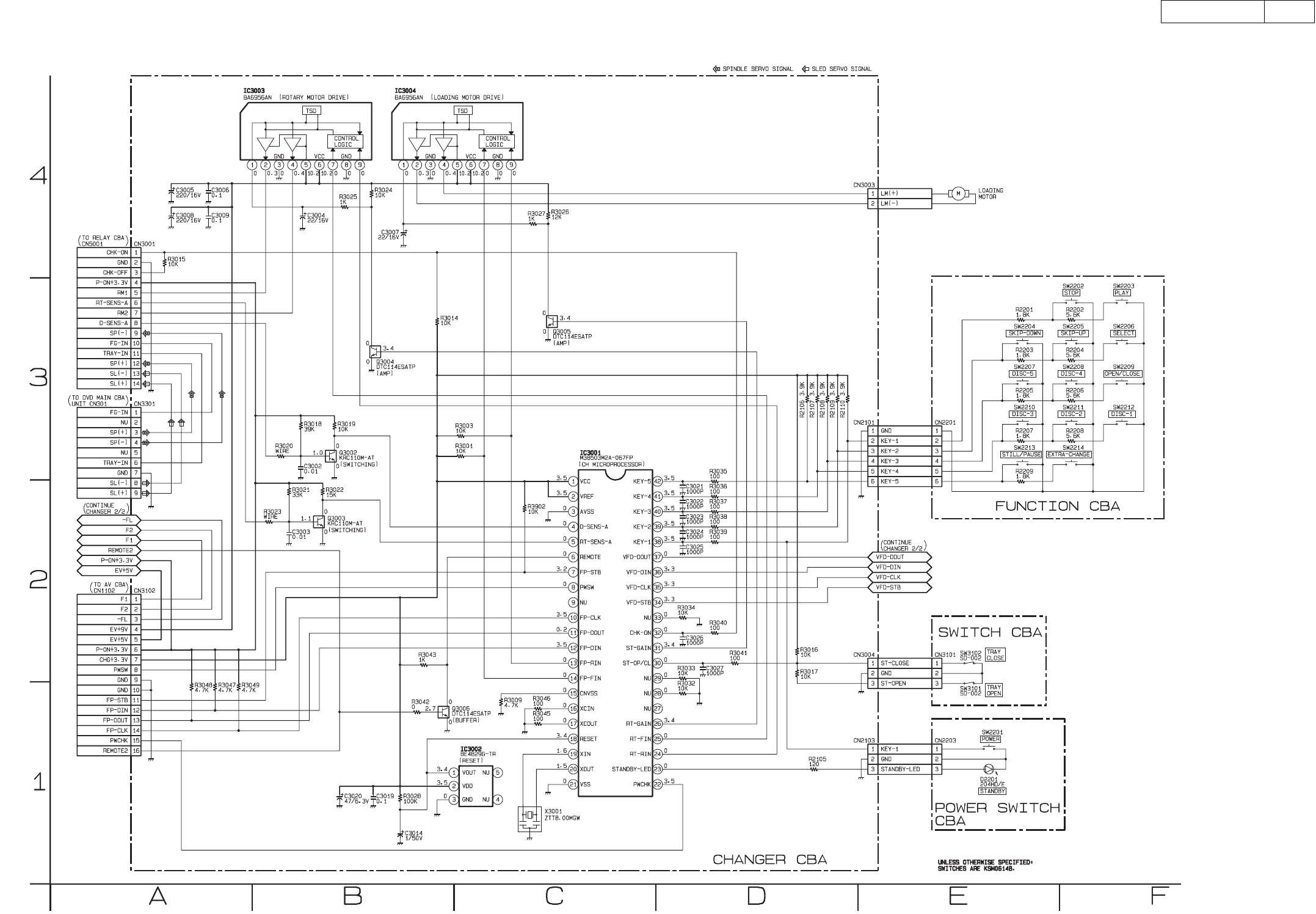
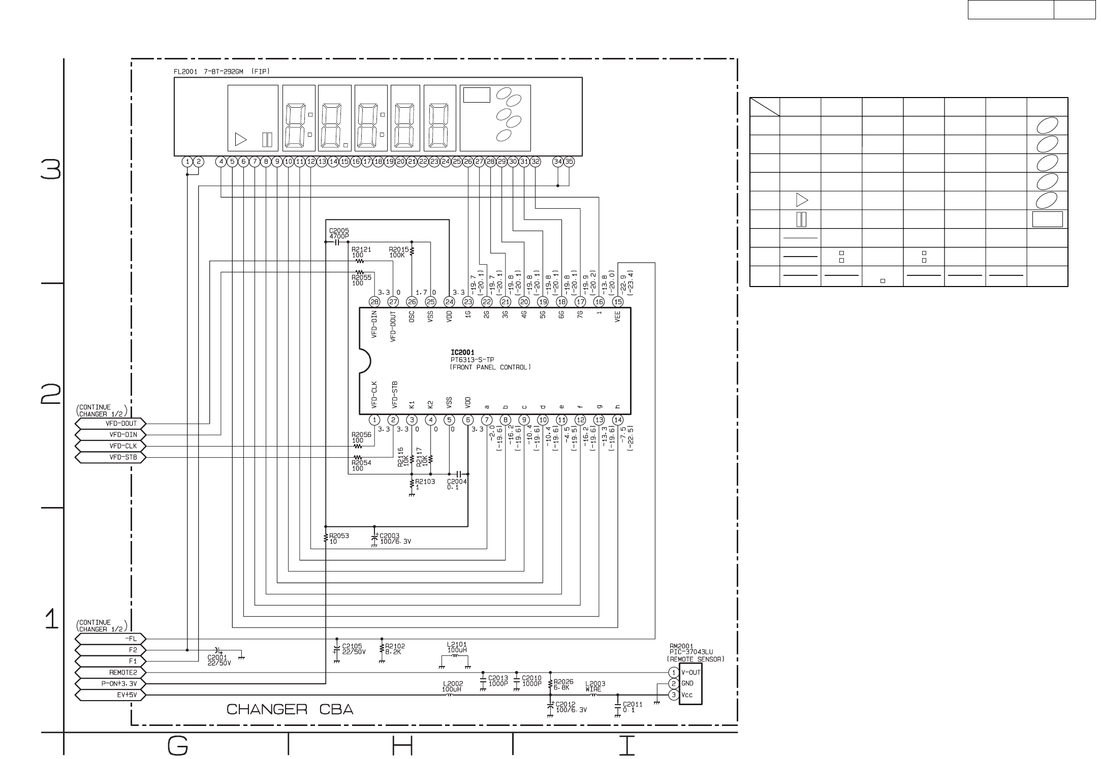
- Changer 1/2, Function, Power Switch & Switch Schematic Diagram
- Changer 2/2 Schematic Diagram
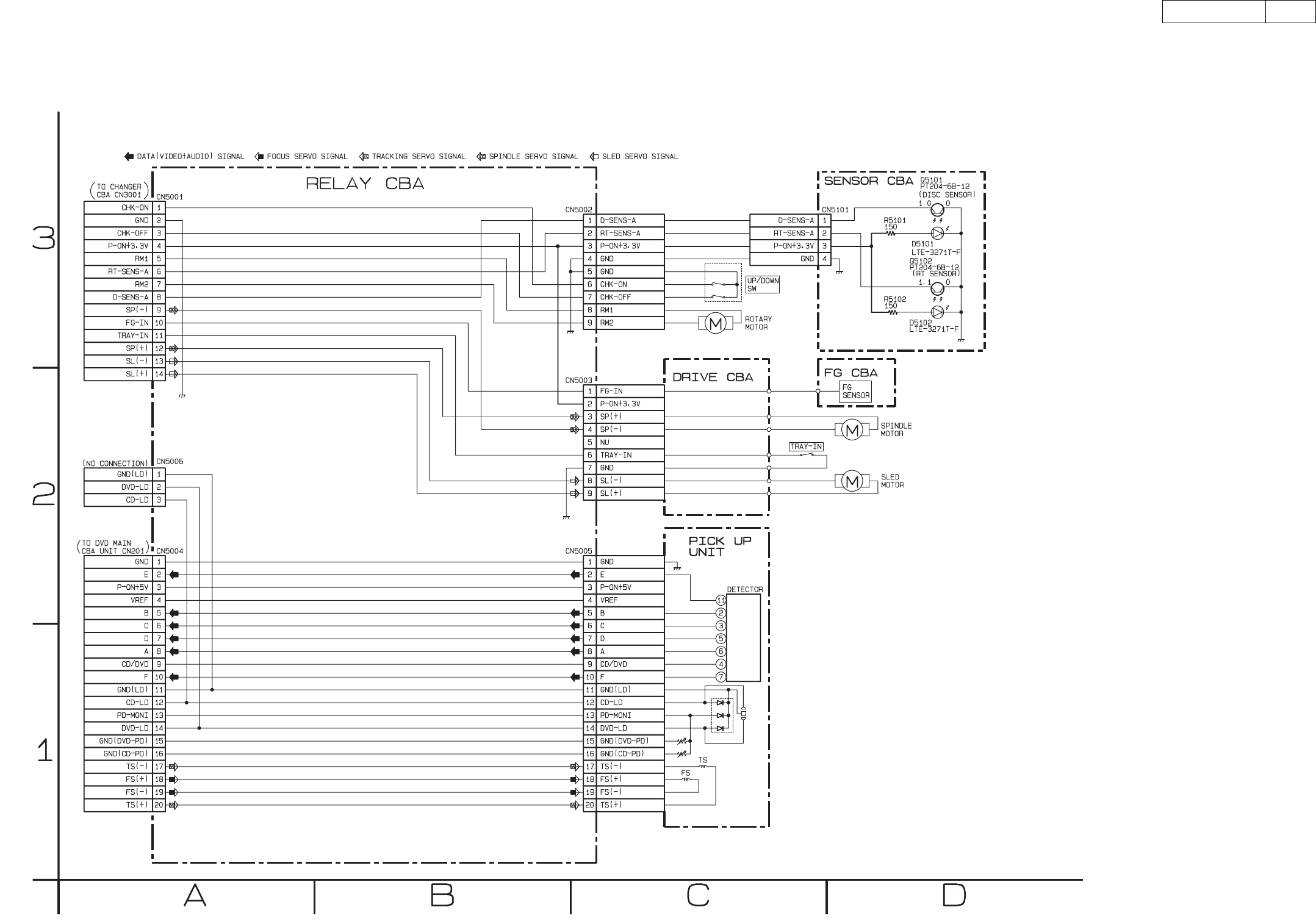
- Relay Schematic Diagram
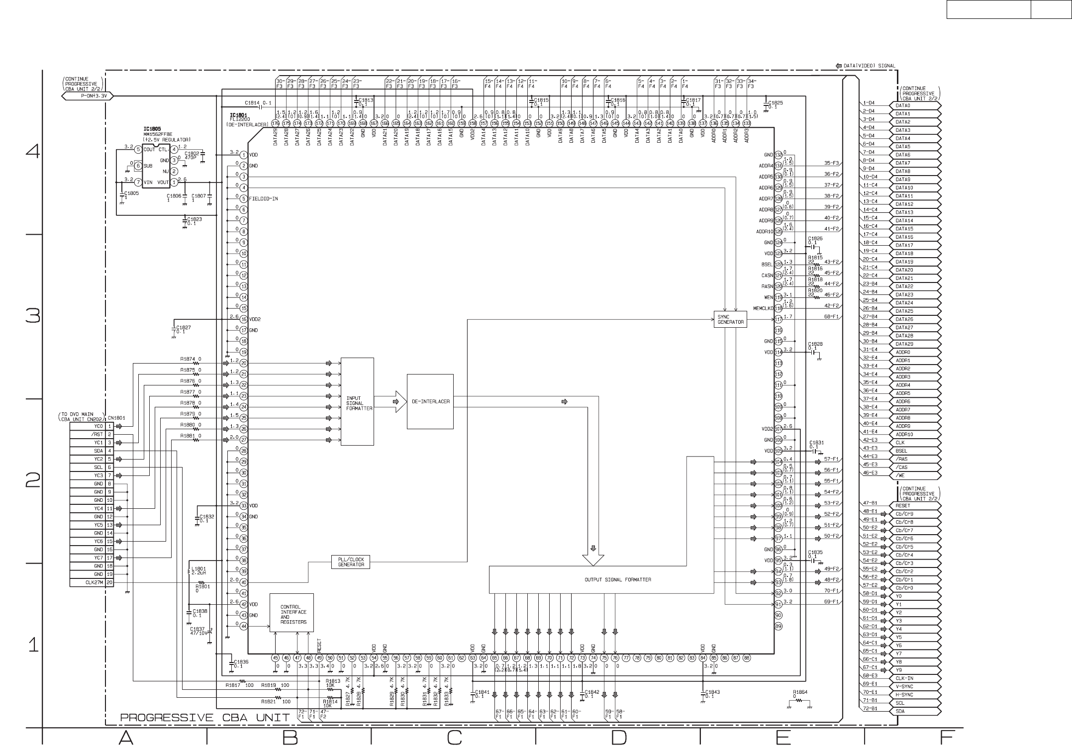
- Progressive 1/2 Schematic Diagram
- Progressive 2/2 Schematic Diagram
- WAVEFORMS
- WIRING DIAGRAM
- FIRMWARE RENEWAL MODE
- LEAD IDENTIFICATIONS
- EXPLODED VIEWS
- PARTS LIST
SERVICE MANUAL
MODEL
DVM-1815
DVD VIDEO AUTO CHANGER
For U.S.A. & Canada model
16-11, YUSHIMA 3-CHOME, BUNKYOU-KU, TOKYO 113-0034 JAPAN
X0183V.02 DE/CDM 0307
注 意
サービスをおこなう前に、このサービスマニュアルを
必ずお読みください。本機は、火災、感電、けがなど
に対する安全性を確保するために、さまざまな配慮を
おこなっており、また法的には「電気用品安全法」に
もとづき、所定の許可を得て製造されております。
従ってサービスをおこなう際は、これらの安全性が維
持されるよう、このサービスマニュアルに記載されて
いる注意事項を必ずお守りください。
● 本機の仕様は性能改良のため、予告なく変更すること
があります。
● 補修用性能部品の保有期間は、製造打切後 8年です。
Some illustrations using in this service manual are
slightly different from the actual set.
●
●
Please use this service manual with referring to
the operating instructions without fail.
●
For purposes of improvement, specifications and
design are subject to change without notice.
●
修理の際は、必ず取扱説明書を参照の上、作業を行って,
ください。
● 本文中に使用しているイラストは、説明の都合上現物
と多少異なる場合があります。
Ver. 2

2
2
DVM-1815
TABLE OF CONTENTS
SPECIFICATIONS . . . . . . . . . . . . . . . . . . . . . . . . . . . . . . . . . . . . . . . . . . . . . . . . . . . . . . . . . . . . . . . . . . . . . . . . . 3
LASER BEAM SAFETY PRECAUTIONS . . . . . . . . . . . . . . . . . . . . . . . . . . . . . . . . . . . . . . . . . . . . . . . . . . . . . . . 4
IMPORTANT SAFETY PRECAUTIONS . . . . . . . . . . . . . . . . . . . . . . . . . . . . . . . . . . . . . . . . . . . . . . . . . . . . . . . . 5
STANDARD NOTES FOR SERVICING. . . . . . . . . . . . . . . . . . . . . . . . . . . . . . . . . . . . . . . . . . . . . . . . . . . . . . . . . 7
CABINET DISASSEMBLY INSTRUCTIONS . . . . . . . . . . . . . . . . . . . . . . . . . . . . . . . . . . . . . . . . . . . . . . . . . . . . 10
TROUBLESHOOTING. . . . . . . . . . . . . . . . . . . . . . . . . . . . . . . . . . . . . . . . . . . . . . . . . . . . . . . . . . . . . . . . . . . . . 14
BLOCK DIAGRAMS. . . . . . . . . . . . . . . . . . . . . . . . . . . . . . . . . . . . . . . . . . . . . . . . . . . . . . . . . . . . . . . . . . . . . . . 22
SCHEMATIC DIAGRAMS / CBA’S AND TEST POINTS . . . . . . . . . . . . . . . . . . . . . . . . . . . . . . . . . . . . . . . . . . . 27
WAVEFORMS . . . . . . . . . . . . . . . . . . . . . . . . . . . . . . . . . . . . . . . . . . . . . . . . . . . . . . . . . . . . . . . . . . . . . . . . . . . 40
WIRING DIAGRAMS . . . . . . . . . . . . . . . . . . . . . . . . . . . . . . . . . . . . . . . . . . . . . . . . . . . . . . . . . . . . . . . . . . . . . . 41
FIRMWARE RENEWAL MODE . . . . . . . . . . . . . . . . . . . . . . . . . . . . . . . . . . . . . . . . . . . . . . . . . . . . . . . . . . . . . . 42
LEAD IDENTIFICATIONS . . . . . . . . . . . . . . . . . . . . . . . . . . . . . . . . . . . . . . . . . . . . . . . . . . . . . . . . . . . . . . . . . . 44
EXPLODED VIEWS. . . . . . . . . . . . . . . . . . . . . . . . . . . . . . . . . . . . . . . . . . . . . . . . . . . . . . . . . . . . . . . . . . . . . . . 45
PARTS LIST . . . . . . . . . . . . . . . . . . . . . . . . . . . . . . . . . . . . . . . . . . . . . . . . . . . . . . . . . . . . . . . . . . . . . . . . . . . . 48
Manufactured under license from Dolby Laboratories. "Dolby"
and the double-D symbol are trademarks of Dolby Laboratories.

3
3
DVM-1815
SPECIFICATIONS
NOTES:
1. All Items are measured without pre-emphasis unless otherwise specified.
2. Power supply : AC120 V 60 Hz
3. Load imp. : 100 K ohm
4. Room ambient : 5 °C ~ 40 °C
ITEM CONDITIONS UNIT NOMINAL LIMIT
1. Video Output 75 ohm load Vpp 1.0 ± 0.1
2. Optical Digital Out dBm -18
3. Audio (PCM)
3-1. Output Level 1kHz 0dB Vrms 2.0
3-2. S/N dB 120
3-3. Freq. Response
DVD fs=48kHz 20~22kHz dB ± 0.5
CD fs=44.1kHz 20~20 kHz dB ± 0.5
3-4. THD+N
DVD 1 kHz 0dB % 0.025
CD 1 kHz 0dB % 0.03
4
4
DVM-1815
D
rive Mecha Assembly
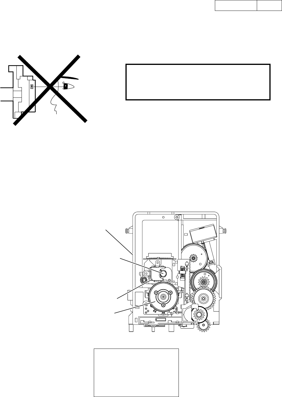
Laser Beam Radiation
Laser Pickup
Turntable
LASER RADIATION
WHEN OPEN. DO NOT
STARE INTO BEAM.
CAUTION
LASER BEAM SAFETY PRECAUTIONS
This DVD player uses a pickup that emits a laser beam.
The laser beam is emitted from the location shown in the figure. When checking the laser diode, be sure to keep
your eyes at least 30cm away from the pickup lens when the diode is turned on. Do not look directly at the laser
beam.
Caution: Use of controls and adjustments, or doing procedures other than those specified herein, may result in
hazardous radiation exposure.
Do not look directly at the laser beam coming
from the pickup or allow it to strike against
your skin.
Location: Inside Top of DVD mechanism.

5
5
DVM-1815
IMPORTANT SAFETY PRE-
CAUTIONS
Product Safety Notice
Some electrical and mechanical parts have special
safety-related characteristics which are often not evi-
dent from visual inspection, nor can the protection
they give necessarily be obtained by replacing them
with components rated for higher voltage, wattage,
etc. Parts that have special safety characteristics are
identified by a ! on schematics and in parts lists. Use
of a substitute replacement that does not have the
same safety characteristics as the recommended
replacement part might create shock, fire, and/or other
hazards. The Product’s Safety is under review contin-
uously and new instructions are issued whenever
appropriate. Prior to shipment from the factory, our
products are carefully inspected to confirm with the
recognized product safety and electrical codes of the
countries in which they are to be sold. However, in
order to maintain such compliance, it is equally impor-
tant to implement the following precautions when a set
is being serviced.
Precautions during Servicing
A. Parts identified by the ! symbol are critical for
safety. Replace only with part number specified.
B. In addition to safety, other parts and assemblies
are specified for conformance with regulations
applying to spurious radiation. These must also be
replaced only with specified replacements.
Examples: RF converters, RF cables, noise block-
ing capacitors, and noise blocking filters, etc.
C. Use specified internal wiring. Note especially:
1)Wires covered with PVC tubing
2)Double insulated wires
3)High voltage leads
D. Use specified insulating materials for hazardous
live parts. Note especially:
1)Insulation tape
2)PVC tubing
3)Spacers
4)Insulators for transistors
E. When replacing AC primary side components
(transformers, power cord, etc.), wrap ends of
wires securely about the terminals before solder-
ing.
F. Observe that the wires do not contact heat produc-
ing parts (heatsinks, oxide metal film resistors, fus-
ible resistors, etc.).
G. Check that replaced wires do not contact sharp
edges or pointed parts.
H. When a power cord has been replaced, check that
5 - 6 kg of force in any direction will not loosen it.
I. Also check areas surrounding repaired locations.
J. Be careful that foreign objects (screws, solder
droplets, etc.) do not remain inside the set.
K. Crimp type wire connector
The power transformer uses crimp type connectors
which connect the power cord and the primary side
of the transformer. When replacing the transformer,
follow these steps carefully and precisely to pre-
vent shock hazards.
Replacement procedure
1)Remove the old connector by cutting the wires at a
point close to the connector.
Important: Do not re-use a connector. (Discard it.)
2)Strip about 15 mm of the insulation from the ends
of the wires. If the wires are stranded, twist the
strands to avoid frayed conductors.
3)Align the lengths of the wires to be connected.
Insert the wires fully into the connector.
4)Use a crimping tool to crimp the metal sleeve at its
center. Be sure to crimp fully to the complete clo-
sure of the tool.
L. When connecting or disconnecting the internal con-
nectors, first, disconnect the AC plug from the AC
outlet.
6
6
DVM-1815
Chassis or Secondary Conducto
r
dd'
Primary Circuit Terminals
AC Voltmeter
(High Impedanc
e)
Exposed Accessible Part
BEarth Ground
Power Cord Plug Prongs
Z
1.5k 0.15 F
Safety Check after Servicing
Examine the area surrounding the repaired location for
damage or deterioration. Observe that screws, parts,
and wires have been returned to their original posi-
tions. Afterwards, do the following tests and confirm
the specified values to verify compliance with safety
standards.
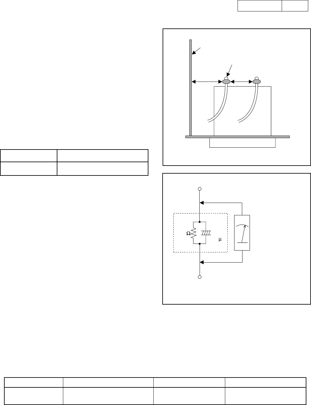
1. Clearance Distance
When replacing primary circuit components, confirm
specified clearance distance (d) and (d’) between sol-
dered terminals, and between terminals and surround-
ing metallic parts. (See Fig. 1)
Table 1: Ratings for selected area
Note: This table is unofficial and for reference only.
Be sure to confirm the precise values.
2. Leakage Current Test
Confirm the specified (or lower) leakage current
between B (earth ground, power cord plug prongs)
and externally exposed accessible parts (RF termi-
nals, antenna terminals, video and audio input and
output terminals, microphone jacks, earphone jacks,
etc.) is lower than or equal to the specified value in the
table below.
Measuring Method (Power ON) :
Insert load Z between B (earth ground, power cord
plug prongs) and exposed accessible parts. Use an
AC voltmeter to measure across the terminals of load
Z. See Fig. 2 and the following table.
AC Line Voltage Clearance Distance (d) (d’)
120 V ≥ 3.2mm (0.126 inches)
Table 2: Leakage current ratings for selected areas
Note: This table is unofficial and for reference only. Be sure to confirm the precise values.
AC Line Voltage Load Z Leakage Current (i) Earth Ground (B) to:
120 V 0.15µF CAP. & 1.5kΩ RES.
Connected in parallel i≤0.5mA Peak Exposed accessible parts
Fig. 1
Fig. 2
7
7
DVM-1815
STANDARD NOTES FOR SERVICING
Circuit Board Indications
1. The output pin of the 3 pin Regulator ICs is indi-
cated as shown.
2. For other ICs, pin 1 and every fifth pin are indicated
as shown.
3. The 1st pin of every male connector is indicated as
shown.
Instructions for Connectors
1. When you connect or disconnect the FFC (Flexible
Foil Connector) cable, be sure to first disconnect
the AC cord.
2. FFC (Flexible Foil Connector) cable should be
inserted parallel into the connector, not at an angle.
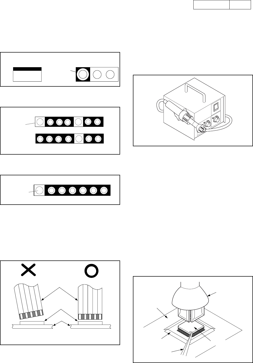
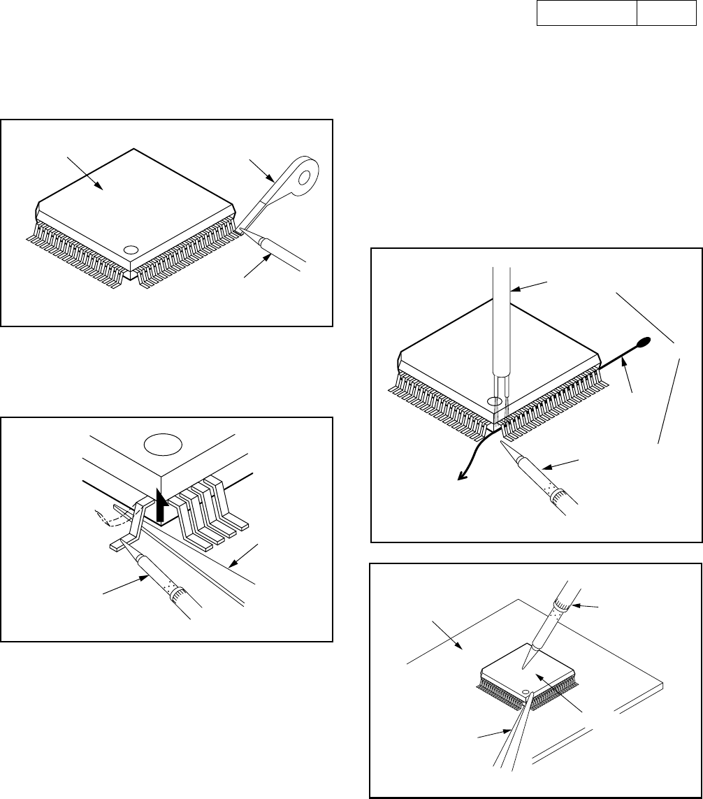
How to Remove / Install Flat Pack-IC
1. Removal
With Hot-Air Flat Pack-IC Desoldering Machine:.
(1) Prepare the hot-air flat pack-IC desoldering
machine, then apply hot air to the Flat Pack-IC
(about 5 to 6 seconds). (Fig. S-1-1)
(2) Remove the flat pack-IC with tweezers while apply-
ing the hot air.
(3) Bottom of the flat pack-IC is fixed with glue to the
CBA; when removing entire flat pack-IC, first apply
soldering iron to center of the flat pack-IC and heat
up. Then remove (glue will be melted). (Fig. S-1-6)
(4) Release the flat pack-IC from the CBA using twee-
zers. (Fig. S-1-6)
Caution:
1. Do not supply hot air to the chip parts around the
flat pack-IC for over 6 seconds because damage to
the chip parts may occur. Put masking tape around
the flat pack-IC to protect other parts from damage.
(Fig. S-1-2)
2. The flat pack-IC on the CBA is affixed with glue, so
be careful not to break or damage the foil of each
pin or the solder lands under the IC when removing
it.
Top View
O
ut In
Bottom View
Input
5
10
P
in 1
P
in 1
FFC Cable
Connector
CBA
* Be careful to avoid a short circuit.
Fig. S-1-1
Hot-air
Flat Pack-IC
Desoldering
Machine
CBA
Flat Pack-IC
Tweezers
Masking
Tape
Fig. S-1-2
8
8
DVM-1815
With Soldering Iron:
(1) Using desoldering braid, remove the solder from all
pins of the flat pack-IC. When you use solder flux
which is applied to all pins of the flat pack-IC, you
can remove it easily. (Fig. S-1-3)
(2) Lift each lead of the flat pack-IC upward one by
one, using a sharp pin or wire to which solder will
not adhere (iron wire). When heating the pins, use
a fine tip soldering iron or a hot air desoldering
machine. (Fig. S-1-4)
(3) Bottom of the flat pack-IC is fixed with glue to the
CBA; when removing entire flat pack-IC, first apply
soldering iron to center of the flat pack-IC and heat
up. Then remove (glue will be melted). (Fig. S-1-6)
(4) Release the flat pack-IC from the CBA using twee-
zers. (Fig. S-1-6)
With Iron Wire:
(1) Using desoldering braid, remove the solder from all
pins of the flat pack-IC. When you use solder flux
which is applied to all pins of the flat pack-IC, you
can remove it easily. (Fig. S-1-3)
(2) Affix the wire to a workbench or solid mounting
point, as shown in Fig. S-1-5.
(3) While heating the pins using a fine tip soldering
iron or hot air blower, pull up the wire as the solder
melts so as to lift the IC leads from the CBA contact
pads as shown in Fig. S-1-5
(4) Bottom of the flat pack-IC is fixed with glue to the
CBA; when removing entire flat pack-IC, first apply
soldering iron to center of the flat pack-IC and heat
up. Then remove (glue will be melted). (Fig. S-1-6)
(5) Release the flat pack-IC from the CBA using twee-
zers. (Fig. S-1-6)
Note:
When using a soldering iron, care must be taken
to ensure that the flat pack-IC is not being held by
glue. When the flat pack-IC is removed from the
CBA, handle it gently because it may be damaged
if force is applied.
F
lat Pack-IC Desoldering Braid
Soldering Iron
Fig. S-1-3
F
ine Tip
S
oldering Iron
Sha
rp
Pin
Fig. S-1-4
To Solid
Mounting Point
Soldering Iron
Iron Wire
or
Hot Air Blower
Fig. S-1-5
Fine Tip
Soldering Iro
n
CBA
Flat Pack-IC
Tweezers
Fig. S-1-6
9
9
DVM-1815
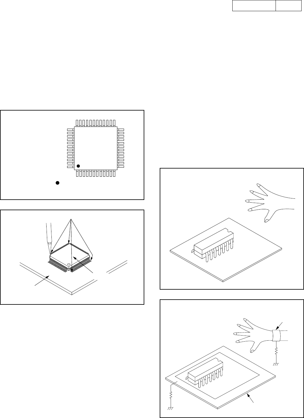
2. Installation
(1) Using desoldering braid, remove the solder from
the foil of each pin of the flat pack-IC on the CBA
so you can install a replacement flat pack-IC more
easily.
(2) The “I” mark on the flat pack-IC indicates pin 1.
(See Fig. S-1-7.) Be sure this mark matches the 1
on the PCB when positioning for installation. Then
presolder the four corners of the flat pack-IC. (See
Fig. S-1-8.)
(3) Solder all pins of the flat pack-IC. Be sure that none
of the pins have solder bridges.
Instructions for Handling
Semi-conductors
Electrostatic breakdown of the semi-conductors may
occur due to a potential difference caused by electro-
static charge during unpacking or repair work.
1. Ground for Human Body
Be sure to wear a grounding band (1MΩ) that is prop-
erly grounded to remove any static electricity that may
be charged on the body.
2. Ground for Workbench
(1) Be sure to place a conductive sheet or copper plate
with proper grounding (1MΩ) on the workbench or
other surface, where the semi-conductors are to be
placed. Because the static electricity charge on
clothing will not escape through the body ground-
ing band, be careful to avoid contacting semi-con-
ductors with your clothing.
Example :
P
in 1 of the Flat Pack-IC
i
s indicated by a " " mark. Fig. S-1-7
Presolder
CBA
Flat Pack-IC
Fig. S-1-8
CBA
< Incorrect >
CBA
Grounding Ban
d
Conductive Sheet or
Copper Plate
1MΩ
1MΩ
< Correct >
10
10
DVM-1815
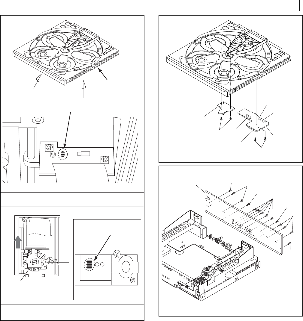
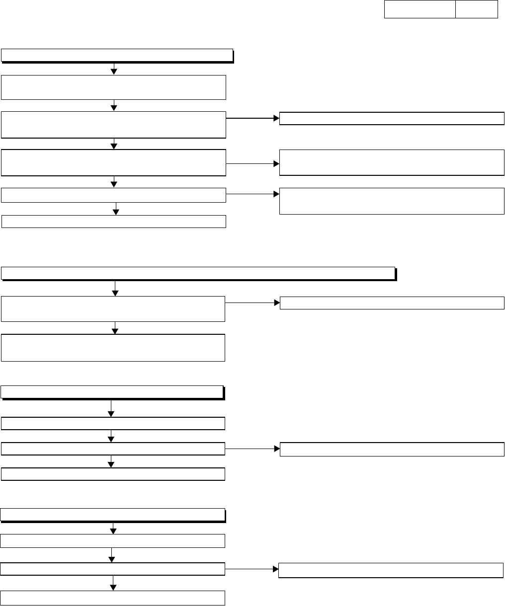
CABINET DISASSEMBLY INSTRUCTIONS
1. Disassembly Flowchart
This flowchart indicates the disassembly steps to gain
access to item(s) to be serviced. When reassembling,
follow the steps in reverse order. Bend, route, and
dress the cables as they were originally.
2. Disassembly Method
ID/
LOC.
No.
PART
REMOVAL
Fig.
No.
REMOVE/*UNHOOK/
UNLOCK/RELEASE/
UNPLUG/DESOLDER
Note
[1] Top Cover D1 6(S-1) -
[2] Front
Assembly D2 2(S-2), *8(L-1) 1-1
[3] Bracket
(Top) D3 *2(L-2) -
[4]
Stopper
Bracket
L, R
D3 4(S-3) -
[5] Drive Mecha
Assembly
D4,
D5 CN201, CN3001
2
2-1
2-2
3
4
[1] Top Cover
[2] Front Assembly
[3] Bracket (Top)
[4] Stopper Bracket L, R
[5] Drive Mecha
Assembly
[12] Tray Guide
(R) Unit
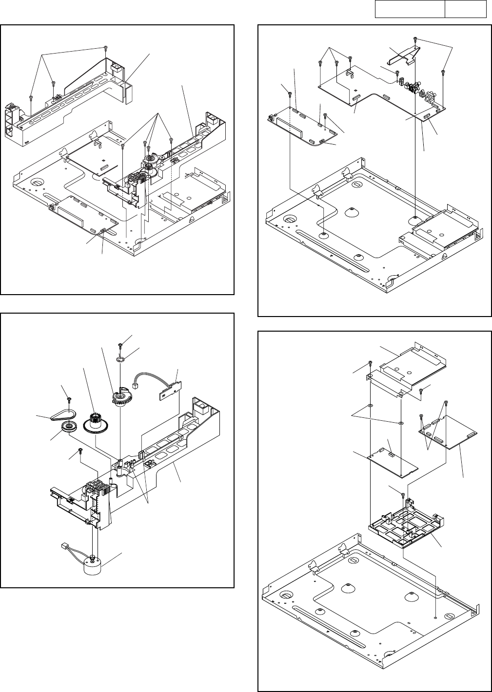
[19] Changer CBA
[23] DVD Main CBA Unit
[20] AV CBA
[24] PCB Holder
[13] Loading
Pulley
[8] Relay CBA
[6] Function CBA
[9] Sensor CBA
[14] Slide Tray
Gear (B)
[15] Slide Tray
Gear (A)
[16] Motor
Assembly
[17] Switch CBA
[18] Tray
Guide (R)
[7] Power SW
CBA
[21] Shield Plate
[22] Progressive CBA Unit
[10] Rear Panel
[11] Tray Guide (L)
[6] Function CBA D4 *2(L-3), CN2201 -
[7] Power SW
CBA D4 CN2103, (S-4) -
[8] Relay CBA D6
2(S-5), CN5001,
CN5002, CN5003,
CN5005
-
[9] Sensor
CBA D6 2(S-6) -
[10] Rear Panel D7 4(S-7), 11(S-8) -
[11] Tray
Guide (L) D8 3(S-9) -
[12]
Tray
Guide (R)
Unit
D8 4(S-10), CN3003,
CN3004 -
[13] Loading
Pulley D9 (S-11), Belt L -
[14] Slide Tray
Gear (B) D9 (S-12), *(P-1) -
[15] Slide Tray
Gear (A) D9 ---------- -
[16] Motor
Assembly D9 (S-13) -
[17] Switch
CBA D9 *2(L-4) -
[18] Tray
Guide (R) D9 ---------- -
[19] Changer CBA D10 CN3102, 2(S-14),
CN3301 -
[20] AV CBA D10
6(S-15), CN1601,
CN1602, CN1001,
FFC Clamper
-
[21] Shield Plate D11 2(S-16), 2(W-1) -
[22] Progressive
CBA Unit D11 CN1801 -
[23] DVD Main
CBA Unit D11 2(S-17) -
[24] PCB Holder D11 (S-18) -
↓
(1)
↓
(2)
↓
(3)
↓
(4)
↓
(5)
ID/
LOC.
No.
PART
REMOVAL
Fig.
No.
REMOVE/*UNHOOK/
UNLOCK/RELEASE/
UNPLUG/DESOLDER
Note
11
11
DVM-1815
(1): Identification (location) No. of parts in the figures
(2): Name of the part
(3): Figure Number for reference
(4): Identification of parts to be removed, unhooked,
unlocked, released, unplugged, unclamped, or
desoldered.
P=Spring, L=Locking Tab, S=Screw,
CN=Connector
*=Unhook, Unlock, Release, Unplug, or Desolder
e.g. 2(S-2) = two Screws (S-2),
2(L-2) = two Locking Tabs (L-2)
(5): Refer to “Reference Notes.”
Reference Notes
CAUTION 1: Locking Tabs (L-1) are fragile. Be careful
not to break them.
1-1. To release eight Locking Tabs (L-1), first release
five Locking Tabs (A), and then three Locking
Tabs (B). (Fig. D2)
CAUTION 2: Electrostatic breakdown of the laser
diode in the optical system block may occur as a
potential difference caused by electrostatic charge
accumulated on cloth, human body etc, during
unpacking or repair work.
To avoid damage of pickup follow next procedures.
2-1. Slide out the pickup unit as shown in Fig. D5.
2-2. Short the three short lands of FPC cable with sol-
der before removing the FFC cable (CN201) from
it. If you disconnect the FFC cable (CN201), the
laser diode of pickup will be destroyed. (Fig. D5)
CAUTION 3: When reassembling, confirm the FFC
cable (CN201) is connected completely. Then remove
the solder from the three short lands of FPC cable.
(Fig. D5)
CAUTION 4: Before reinstalling, turn the Slide Tray
Gear (B) fully clockwise. (Fig. D4)
(S-1)
(S-1)
(S-1)
[1] Top Cover
(S-1)
Fig. D1
[2] Front Assembly (L-1)
(A)
(B)
(B)
(L-1)
(L-1)
(S-2)
(L-1)
(L-1)
(S-2)
Fig. D2
[3] Bracket (Top)
[4] Stopper Bracket R
[4] Stopper Bracket L
(L-2)
(L-2)
(S-3)
(S-3)
(S-3)
Fig. D3
Slide Tray
Gear (B)
CN201
CN3001
CN2201 [6] Function CBA
(L-3)
(L-3)
(S-4)
[7] Power
SW CBA
CN2103
[5] Drive Mecha
Assembly
Turn
Fig. D4
12
12
DVM-1815
View for B
Pickup Unit
C
B
Short the three short
lands by soldering
View for C
Slide
View for A
OR
Short the three short lands by soldering
Drive Mecha
Assembly
A
Fig. D5
[8] Relay
CBA
[9] Sensor CBA
(S-6)
CN5002
CN5005
(S-5)
CN5003
CN5001
Fig. D6
(S-7)
(S-7)
(S-7)
(S-7)
(S-8)
(S-8)
(S-8
)
[10] Rear Panel
Fig. D7
13
13
DVM-1815
(S-9)
[12] Tray Guide
(R) Unit
[11] Tray Guide (L)
CN3004
CN3003
(S-10)
Fig. D8
(S-11)
Belt L
[13] Loading
Pulley
[14] Slide Tray Gear (B)
[16] Motor Assembly
[17] Switch CBA
(S-13)
(L-4)
[15] Slide Tray Gear (A)
[18] Tray
Guide (R)
(P-1)
(S-12)
Fig. D9
CN3102
CN3301
[20] AV CBA
[19] Changer CBA
(S-15)
(S-15)
(S-15) FFC
Clamper
(S-14)
(S-14) CN1601
CN1001 CN1602
Fig. D10
(S-16)
(S-17)
(S-16)
(W-1)
(S-18)
[21] Shield Plate
[24] PCB
Holder
CN1801
[23]
DVD Ma
in
CBA Unit
[22]
Progressive
CBA Unit
Fig. D11
14
14
DVM-1815
FLOW CHART NO.2
The fuse blows out.
After servicing, replace the fuse.
Check the presence that the primary component
is leaking or shorted and service it if defective. Check the presence that the rectifying diode or
circuit is shorted in each rectifying circuit of
secondary side, and service it if defective.
FLOW CHART NO.3
When the output voltage fluctuates.
Yes
No
FLOW CHART NO.4
When buzz sound can be heard in the vicinity of AV circuit.
Check if there is any short-circuit on the rectifying diode and the circuit in each rectifying circuit of the secondary side
,
and service it if defective.
(D1003, D1006, D1008, D1016, D1030, IC1002, Q1002, Q1004, Q1010, Q1011, Q1014)
Does the photo coupler circuit on the secondary
side operate normally?
Check IC1001, D1012, D1024 and their periphery,
and service it if defective.
Check IC1001, IC1006, D1015 and their
periphery, and service it if defective.
FLOW CHART NO.5
-FL is not outputted.
Is -24V voltage supplied to the anode of D1003? Check D1003 and periphery circuit, and service it
if defective.
Check if there is any leak or short-circuit
on the loaded circuit, and service it if defective.
Yes
No
FLOW CHART NO.1
The power cannot be turned on.
Is the fuse normal?
Is normal state restored when once unplugged
power cord is plugged again after several seconds?
Is the EV +9V line voltage normal?
Is each voltage of the secondary side normal?
See FLOW CHART No.2 <The fuse blows out.>
Check if there is any leak or shor-circuiting on the
primary circuit component, and service it if defective
.
(Q1001, Q1003, T1001, D1001, D1002, D1004,
D1005, D1011, C1003, C1005)
Check each rectifying circuit of the secondary circui
t
and service it if defective.
Yes
Yes
Yes
Is the voltage of 3.3V supplied to pin(1) of IC3001?
Is the voltage of 3.3V outputted to pin(19) of CN1001?
Yes
When pressing POWER button (SW2201), is the
voltage of 0V supplied to pin(38) of IC3001?
Yes
Yes
Replace IC3001. Ye s
No
No
No
No
Check POWER button (SW2001) and their
periphery, and service it if defective.
No
Check CHG+5V line
and service it if defective.
See FLOW CHART No.2 <The fuse blows out.>
No
Replace DVD Main CBA unit.
No
TROUBLESHOOTING

15
15
DVM-1815
FLOW CHART NO.7
P-ON+5V is not outputted. (P-ON+9V is outputted normally.)
Is the "H" pulse inputted into the base of Q1004?
Replace Q1004.
Check R1068 and D1046, and service it if defective
.
Yes
No
FLOW CHART NO.8
P-ON+3.3V is not outputted. (P-ON+9V is outputted normally.)
Is 3.3V voltage supplied to the collector of Q1011?
Replace Q1011 and R1067.
Check D1008, D1015, C1007, C1038, L1007 and
the periphery circuit, and service it if defective.
Yes
No
FLOW CHART NO.9
EV+5V is not outputted.
Is EV+9V outputted normally?
Check Q1014, D1047 and the periphery circuit,
and service it if defective.
Refer to "FLOW CHART NO.6"
<P-ON+9V (EV+9V) is not outputted.>
Yes
No
FLOW CHART NO.6
P-ON+9V (EV+9V) is not outputted.
Is 9V voltage supplied to the emitter of Q1002?
Is the voltage of base on Q1002 lower than the
voltage of emitter on Q1002 when turning the power on?
Replace Q1002.
Check D1030, C1035, C1048, L1009 and
the periphery circuit, and service it if defective.
Check Q1016 and service it if defective.
Yes
Yes
No
No
FLOW CHART NO.10
EV+1.5V is not outputted.
Is 2.5V voltage supplied to Pin(1) of IC1002?
Is 1.25V voltage supplied to Pin(4) of IC1002?
Replace IC1002. Replace IC3001
.
Check the circuit between Pin(18)
of IC3001 and Pin(4) of IC1002
,
and service it if defective.
Check D1006, C1014, C1050, L1008 and the
periphery circuit, and service it if defective.
Is the "L" pulse outputted into Pin(18) of IC3001?
Yes
Yes Yes No
No
No
FLOW CHART NO.11
EV+3.3V is not outputted.
Is 3.3V voltage supplied to emitter of Q1010?
Is the "L" pulse inputted to base of Q1012?
Check Q1010, Q1012, R1087 and R1088, and
service it if defective. Replace IC3001
.
Check the circuit between Pin(18)
of IC3001 and base of Q1012
,
and service it if defective.
Check D1008, D1015, C1007, C1038, L1007 and
the periphery circuit, and service it if defective.
Is the "L" pulse outputted into Pin(18) of IC3001?
Yes
Yes Yes No
No
No
16
16
DVM-1815
Yes No
FLOW CHART NO.13
The key operation is not functioning.
Are the contact point and the installation state of the
key switches (SW2201 - 2214) normal?
Is the control voltage normally supplied to pins(38,
39, 40, 41, 42) of IC3001? Check the switches (
SW2201 - 2214
)
and their periphery, and service it if defective.
No Re-install the switches (
SW2201 - 2214
)
correctly or replace the poor switch.
Replace IC3001.
Yes
Yes
Yes
Yes
Yes
No
No
No
No
FLOW CHART NO.12
The fluorescent display tube does not light up.
Is 3.3V voltage supplied to Pin(6) and
Pin(24) of IC2001?
Is the voltage of approximately -24V to -28V
supplied to Pin(15) of IC2001?
Is there 500kHz oscillation at Pin(26) of IC2001?
Are the filament voltage supplied between
Pins(1, 2) and Pins(34, 35) of the fluorescent
display tube? And the negative voltage applied
between these pins and GND?
Replace the fluorescent display tube.
Check the P-ON+3.3V line and service it if defectiv
e.
Check the -FL (-28V) line and service it if defective
.
Check R2015, IC2001 and their periphery, and
service it if defective.
Check the EV+3.3V
line, and service
it if defective.
Is the "H" signal inputted
to base of Q1016?
Check D1016, D1017, T1001, and their periphery,
and service it if defective.
Is -17V voltage supplied to collector of Q1005?
No
Yes
Yes
No
Check Q1015, Q1016, D1055, and
their periphery, and service it if defective.
38pin 39pin 40pin 41pin 42pin
KEY1 KEY2 KEY3 KEY4 KEY5
0.00 - 0.50 SW2201
POWER
SW2204
SKIP DOWN
SW2207
DISC-5
SW2210
DISC-3
SW2213
STILL/PAUSE
0.51 - 1.53 SW2202
STOP
SW2205
SKIP UP
SW2208
DISC-4
SW2211
DISC-2
SW2214
EXTRA
CHANGE
1.54 - 2.57 SW2203
PLAY
SW2206
SELECT
SW2209
OPEN/CLOSE SW2212
DISC-1 -----
2.58 - 3.30 (KEY OFF) (KEY OFF) (KEY OFF) (KEY OFF) (KEY OFF)
IC3001
Terminal Voltage of Pins (38 - 42) on IC3001
17
17
DVM-1815
FLOW CHART NO.17
[No Disc] indicated. (When the focus error occurs.)
Replace the DVD Main CBA.
No improvement can be found. Original DVD Main CBA is poor.
Replace the DVD Mecha.
No
Yes
Yes
FLOW CHART NO.16
The disc tray cannot be opened and closed.
Replace the DVD Main CBA.
Original DVD Main CBA is poor.
Replace the DVD Mecha.
No improvement can be found. No
Yes
FLOW CHART NO.15
The disc tray cannot be opened and closed. (It can be done using the remote control unit.)
Is the normal control voltage inputted to Pin(40) of
IC3001?
Refer to "FLOW CHART NO.16" <The disc tray
cannot be opened and closed.>
Replace the "OPEN/CLOSE" button (SW2209).
No
FLOW CHART NO.14
No operation is possible from the remote control unit.
Operation is possible from the DVD, but no
operation is possible from the remote control unit.
Replace the infrared remote control receiver (RM2001
).
Or replace the remote control unit.
Check the line between Pin(20) of IC2002 and
Pin(22) of CN1001, and service it if defective.
Is the "L" pulse sent out Pin(1) terminal of receiver
(RM2001) when the infrared remote control is activated?
Is the "L" pulse supplied to the Pin(22) of CN1001?
Replace DVD Main CBA.
Yes
Yes
Is 5V voltage supplied to the Pin(3) terminal of
the infrared remote control receiver (RM2001)?
Yes
No
Check P-ON+5V line and service it if defective.
No
No
Yes
18
18
DVM-1815
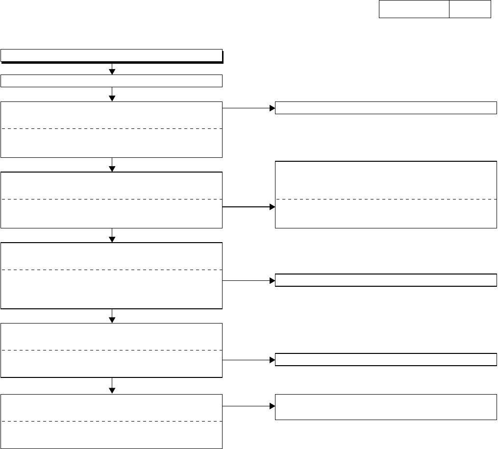
FLOW CHART NO.20
Both functions of picture and sound do not operate normally.
Replace the DVD Main CBA.
Replace the DVD Mecha.
No
Yes
No improvement can be found. Original DVD Main CBA is poor.
FLOW CHART NO.18
[No Disc] indicated. (When the focus servo is not functioning.)
FLOW CHART NO.19
[No Disc] indicated. (When the laser beam does not light up.)
Replace the DVD Main CBA.
Replace the DVD Mecha.
No
Yes
Replace the DVD Main CBA.
Replace the DVD Mecha.
No
Yes
No improvement can be found. Original DVD Main CBA is poor.
No improvement can be found. Original DVD Main CBA is poor.
FLOW CHART NO.21
Picture does not appear normally.
Set the disc on the disc tray, and playback.
Are the video signals outputted to each pin (as shown
below) of CN1601 and CN1602 on the AV CBA?
Replace the DVD Main CBA or DVD Mecha.
No
No No
<Interlace mode>
CN1601 7PIN S-Y
CN1601 9PIN S-C
CN1601 5PIN Cb
CN1601 3PIN Cr
<Progressive mode>
CN1602 2PIN S-Y
CN1602 4PIN Pb
CN1602 6PIN Pr
Replace FFC cable.
Replace the DVD Main
CBA Unit or DVD Mecha
.
Replace Progressive
CBA Unit.
Replace FFC cable.
Is FFC cable (W1802) connecting CN6102 on the
AV CBA and Progressive CBA Unit normally?
Yes
Is FFC cable (W1801) connecting CN1801 on the
Progressive CBA Unit and DVD Main CBA Unit
normally?
Is component video signals outputted in interlace
mode?
Yes
Yes No
No
(continued to "A" on next page)
19
19
DVM-1815
Check the line between each pin of IC6102 and
each pin of IC1402 on the AV CBA, and service it
if defective.
Is 5V voltage applied to the pin(1, 24) of
IC1402?
Replace IC1402. Check P-ON+5V line and
service it if defective.
IC6102 4PIN → IC1402 6PIN S-Y
IC6102 15PIN → IC1402 9PIN Pb/Cb
IC6102 14PIN → IC1402 11PIN Pr/Cr
Are the video signals shown above inputted into
each pin of IC1402?
Are the video signals outputted to each pin
of IC1402?
Yes
Yes No
Yes
Yes
Yes
No
No
Check the line between pin(9) of CN1601 and
pin(2) of IC1402 on the AV CBA, and service it
if defective.
No
No
Are the video signals outputted to each pin of
IC6102?
IC6102 4PIN S-Y
IC6102 15PIN Pb/Cb
IC6102 14PIN Pr/Cr
IC1402 6PIN S-Y
IC1402 9PIN Pb/Cb
IC1402 11PIN Pr/Cr
Are the video signals shown above inputted into
pin(2) of IC1402?
IC1402 21PIN CVBS
IC1402 18PIN S-Y
IC1402 23PIN S-C
IC1402 15PIN Pb/Cb
IC1402 13PIN Pr/Cr
Check the periphery of JK1403 from Pins (13, 15,
18) of IC1402 and service it if defective.
Check the periphery of JK1401 from
Pin (18) of IC1402 and service it if defective.
Check the periphery of JK1401 from
Pin (23) of IC1402 and service it if defective.
Are the video signals outputted to the specific
output terminal?
Are the component video signals outputted to the
VIDEO OUT terminal (JK1403)?
Are the luminance signals outputted to the
S-OUT terminal (JK1401)?
Are the chroma signals outputted to the
S-OUT terminal (JK1401)?
No
No
No
Check P-ON+5V line an
d
service it if defective.
Replace IC6102.
Is 5V voltage supplied to Pin(16) of IC6102?
Yes No
Yes
A
20
20
DVM-1815
FLOW CHART NO.22
Audio is not outputted.
Set the disc on the disc tray, and playback.
Are the analog audio signals outputted to each pin
of CN1601 on AV CBA?
Is the "H" level mute signal outputted to CN1601
on AV CBA ?
CN1601 13PIN AUDIO-L
CN1601 15PIN AUDIO-R
CN1601 12PIN A-MUTE
CN1601 16PIN A-R-MUTE
CN1601 14PIN A-L-MUTE
IC1201 1PIN AUDIO-L
IC1201 7PIN AUDIO-R
IC1201 2PIN AUDIO-L
IC1201 6PIN AUDIO-R
Replace the DVD Main CBA or DVD Mecha.
Replace the DVD Main CBA or DVD Mecha.
Replace IC1201.
Check the periphery between Pins(1,7) of IC1201
and JK1201, and service it if defective.
Check each line between each pin of CN1601
and each pin of IC1201 on AV CBA, and service it
if defective.
CN1601 13PIN → IC1201 2PIN AUDIO-L
CN1601 15PIN → IC1201 6PIN AUDIO-R
Are the analog audio signals inputted to each pin
of IC1201.
Are the analog audio signals inputted to each pin
of IC1201?
Are the audio signals outputted to the specific
output terminal?
Are the audio signals outputted to the audio
terminal (JK1201)?
Yes
Yes
Yes
Yes
No
No
No
No
No
21
21
DVM-1815
FLOW CHART NO.23
Rotary tray does not function.
Is the normal control voltage inputted to pins
(39, 40, 41) of IC3001? For each terminal voltage,
refer to FLOW CHART No.13 <The key operation
is not functioning.>
Is the voltage of 3.3V supplied to pin(1) of IC3001?
Is the normal control voltage outputted to pins(2,4)
of IC3003?
Check the switches (SW2206 - 2208, 2210 - 2212
)
and their periphery, and service it if defective.
Replace IC3001.
Replace Rotary Motor. Check EV+9V line and
service it if detective.
Check CHG 3.3V line and service it if detective.
Is the normal control voltage outputted to pins
(24, 25) of IC3001?
Is the voltage of 9V supplied to pin(6) of IC3003?
Replace IC3003.
Yes
Yes
Yes Yes No
Yes
No
No
No
No
22
22
DVM-1815
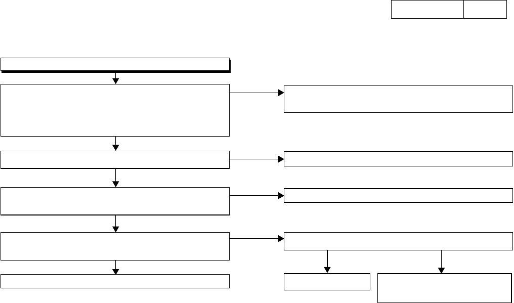
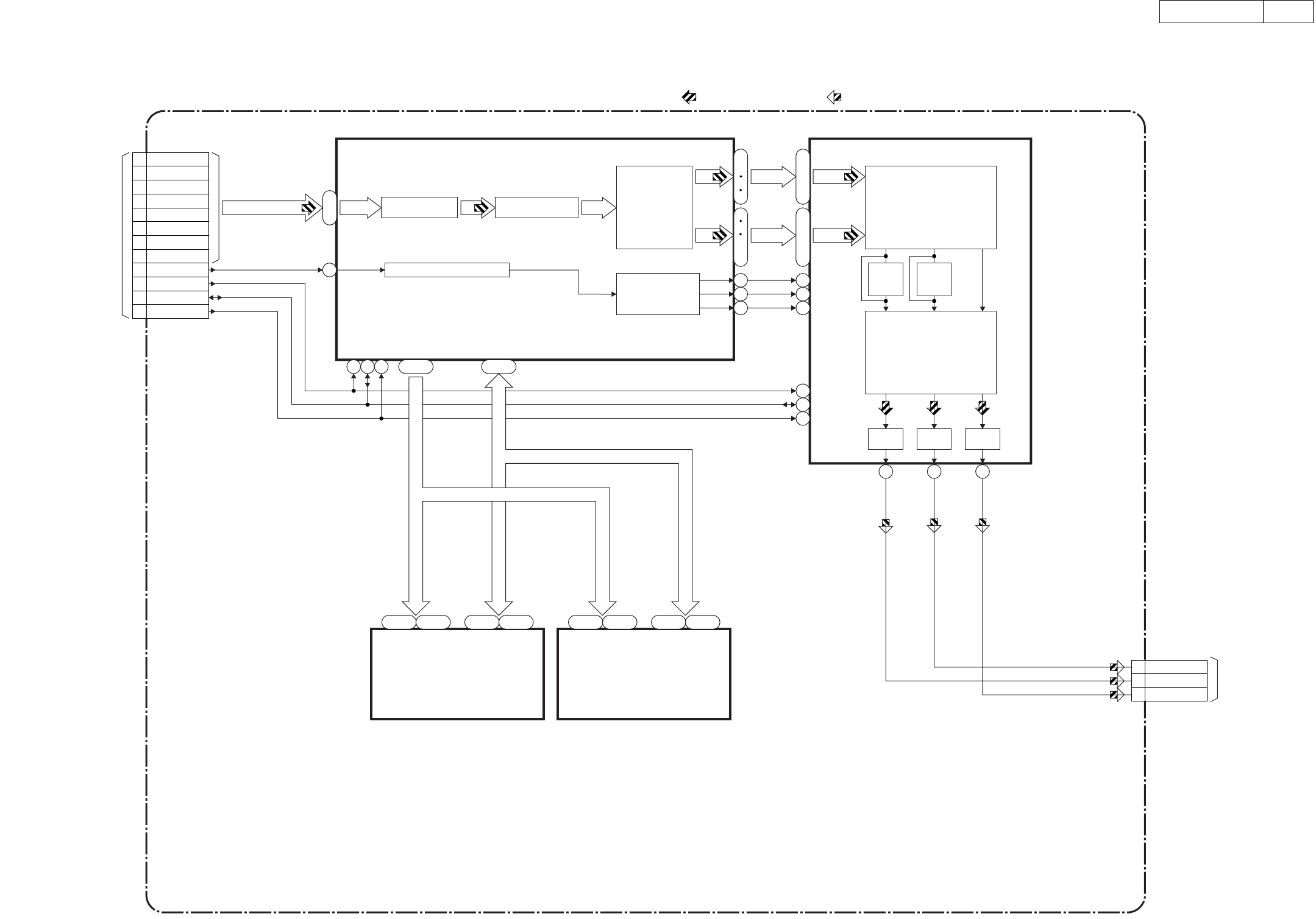
System Control/Servo Block Diagram BLOCK DIAGRAMS
FOCUS SERVO SIGNAL TRACKING SERVO SIGNAL SLED SERVO SIGNAL SPINDLE SERVO SIGNAL
59
27
7
8
4
15
10
14
26
1
2
3
4
6
23
5
17
18
12
11
14
13
15
16 25
24
FP-STB
54FP-DIN
55
FP-DOUT
61
REMOTE1
53
FP-CLK
CN401 CN1001 CN3102
REMOTE
SENSOR
KEY SWITCH
RM2001
DVD MAIN CBA UNIT
RELAY CBA
FG CBA
SWITCH CBA
SENSOR CBA
RELAY CBA
IC301 (SERVO DRIVE)
IC451 (CLOCK GENERATOR)
IC3004 (LOADING MOTOR DRIVE)
Q3002
Q3004
Q3005
Q3003
IC905
(INVERTER)
CHANGER
CBA
AV CBA
FUNCTION CBA
CHANGER CBA
47
PWCHK
IC202
(OP AMP)
12 14
CN301CN5001CN5003
DRIVE
CBA
FG
SENSOR
SLED
MOTOR
SPINDLE
MOTOR
ROTARY
MOTOR
Q5101
Q5102
IC101 (MICRO CONTROLLER)
IC3001
(CH MICROPROCESSOR)
+
-+
-
+
-
+
-
+
-
+
-
+
-
SLED
MOTOR
DRIVE
FOCUS
ACTUATOR
DRIVE
1/8
1/4 PLL2
X451
MULTI
PLL X'TAL
OSC 36.864MHz
OSC
SPINDLE
MOTOR
DRIVE
TRACKING
ACTUATOR
DRIVE
EXT CLOCK
+3.3V
+3.3V
DRIVE CONTROL
LOGIC
CLK33M
BE CLOCK
172
170
150
FG-IN
SLD
70
SPDL
71
TRACKING
DRIVE
152
FOCUS
DRIVE
66
TO DIGITAL SIGNAL
PROCESS BLOCK
DIAGRAM
TO DIGITAL SIGNAL
PROCESS BLOCK
DIAGRAM
FS(+)
FS(-)
TS(+)
TS(-)
TO
VIDEO/ AUDIO
BLOCK DIAGRAM
TO
VIDEO/ AUDIO
BLOCK DIAGRAM
51
50
87
PCM-SCLK
CLK27M
86 ADAC-MD
ADAC-MC
ADAC-ML
A-MUTE
A-MUTE
ADAC-MC
ADAC-ML
ADAC-MD
17
92
FSEL
RESET68
RESET
IC461
5 4
+3.3V
3SP(+)
4SP(-)
8SL(-)
9SL(+)
1
3
4
8
9
1 FG-IN
16 FP-STB 16
18 FP-DIN 18
20 FP-DOUT 20
21 FP-CLK 21
22 REMOTE1 22
19 PWCHK 19
CN1102
11 FP-STB 11
12 FP-DIN 12
13 FP-DOUT 13
14 FP-CLK 14
16 REMOTE2 16
15 PWCHK 15
CN2201CN2101
2 KEY-1 2
3 KEY-2 3
4 KEY-3 4
POWER
SWITCH CBA
CN2203CN2103
1 KEY-1 1
2 GND 2
3
STANDBY-LED
3
5 KEY-4 5
6 KEY-5
KEY-1
KEY-2
KEY-3
KEY-4
KEY-5 6
24
SW2201
D2201
STANDBY
POWER
SW3102 TRAY CLOSE
SW3101 TRAY OPEN
DISC SENSOR
RT SENSOR
3
4
8
9
1
CN3001 CN3301
12
9
13
14
10
12
9
13
14
10
7
12
11
10
6
22
38
39
40
41
42
23
30
13
4
5
32
CN3101 CN3004
1 ST-CLOSE 1
2 GND 2
CN5101 CN5002
1 D-SENS-A 1
2 RT-SENS-A 2
CN5001 CN3001
8 D-SENS-A 8
6 RT-SENS-A 6
CN5001 CN3001
7RM2 7
5RM1 5
CN5001 CN3001
1 CHK-ON 1
3 CHK-OFF 3
3 ST-OPEN 3
M
M
M
LOADING
MOTOR M
CN5002
RM2 9
RM1 8
CN5002
CHK-ON 6
CHK-OFF 7
GND 5
CN3003
LM+ 1
LM- 2
4
2
9
7
1
IC3003 (ROTARY MOTOR DRIVE)
DRIVE
4
2
9
7
1
14
31
24
25
26
Q3006
AMP
AMP
UP/DOWN
SW
CONTROL
LOGIC
ST-OP/CL
FP-RIN
FP-FIN
ST-GAIN
RT-RIN
RT-FIN
RT-GAIN
D-SENS-A
RT-SENS-A
CHK-ON
FP-STB
FP-DIN
FP-DOUT
FP-CLK
REMOTE
PWCHK
STANDBY-LED
34
36
37
35
VFD-STB
VFD-DIN
VFD-DOUT
VFD-CLK
2
28
27
1
VFD-STB
VFD-DIN
VFD-DOUT
VFD-CLK
GRID
SEGMENT
IC2001
FRONT
PANEL
CONTROL
12
7
8
9
10
11
13
14
16
23 17
~
a
b
c
d
e
f
g
h
i
1G 7G
~
FIP
FL2001
TO
VIDEO/ AUDIO
BLOCK DIAGRAM
REMOTE2
REMOTE1
23
23
DVM-1815
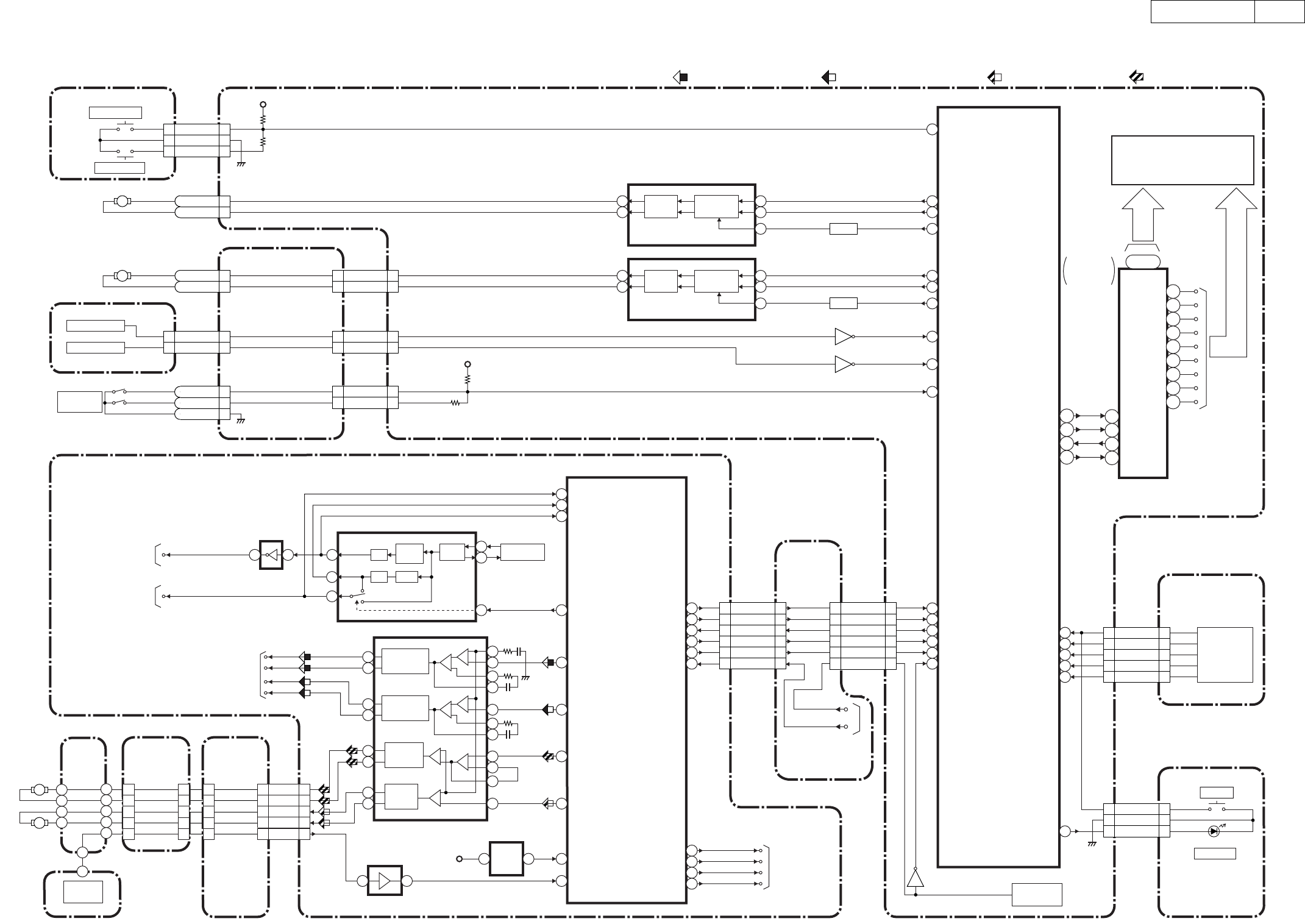
Digital Signal Process Block Diagram
DATA(VIDEO/AUDIO) SIGNAL VIDEO SIGNAL DATA(AUDIO) SIGNALDATA(VIDEO) SIGNAL FOCUS SERVO SIGNAL TRACKING SERVO SIGNAL
C6
D7
A8
B5
F10
E2
DVD-LD 14
CD-LD 12
PD-MONI 13
FS(+) 18
FS(-) 19
TS(+) 20
TS(-) 17
CN201
CN201
CN201
IC201
(SW)
IC105 (LATCH)
IC102 (SDRAM) IC101 (MICRO CONTROLLER)
FS
FS(+)
CD/DVD
FS(-)
TS(+)
TS(-)
TS
PICK-UP
UNIT RELAY
CBA
DETECTOR
CD/DVD 9
Q251,Q252
CD DVD
AMP
Q253,Q254
AMP
4
1 3
6
GND(DVD-PD)
15
GND(CD-PD)
16
GND(LD)
11
6
7
8
5
10
2
14
12
13
18
19
20
17
9
15
16
11
TO SYSTEM
CONTROL/SERVO
BLOCK DIAGRAM
RF
SIGNAL
PROCESS
CIRCUIT
DVD/CD
FORMATTER
AUDIO
I/F
VIDEO
I/F NTSC/PAL
ENCODER
DMA
BCU
INST.
ROM 32BIT
CPU
DATA
ROM
INTERRUPT
CONTROLLER WATCH DOG
TIMER CPU
I/F
TIMER
DECODER
I/F
CPU
I/F
READ
MEMORY
DATA
ROM
DSP
DECODER
PIXEL
OPERATION
I/O
PROCESSOR
INST.
ROM
DATA
ROM
INST.
ROM
DATA
ROM
INST.
ROM
SERIAL
D/A
GENERAL
I/O
INTERRUPT
CONTROLLER
TIMER
WATCH DOG
TIMER
32BIT CPU
STREAM
I/F
EXTERNAL
MEMORY
I/F
SDRAM
ECC
UMAC
124
125
122
123
128
129
126
127
131
130
135
133
132
134
78
DEBUG
BCU
INST
CACHE
DTYPE
LATCH
DATA
CACHE
D/A
D/A
D/A
TO VIDEO
/AUDIO
BLOCK
DIAGRAM
158
164
Y
C
Cr
Cb
VIDEO-Y
VIDEO-C
VIDEO-Cr
VIDEO-Cb
TO VIDEO
/AUDIO
BLOCK
DIAGRAM
TO
PROGRESSIVE
BLOCK
DIAGRAM
CN1801
TO SYSTEM CONTROL
/SERVO BLOCK DIAGRAM
181
SPDIF
CLK27M
/RST
SDA
SCL
175
PCM-BCK
176
PCM-DATA0
174
PCM-LRCLK
161
160
EXADT (0-15), EXADR (16-19)
EXADT (0-15), EXADR (16-19)
EXADT (0-7)
EXADT (8-15)
EXADR (0-7)
EXADR (0-15)
EXADR (8-15)
SDRAM DATA(0-31)
SDRAM DATA(0-31)
SDRAM ADDRESS(0-10)
SDRAM ADDRESS(0-10)
2
9
~
12
19
~
210
235
~
IC104 (LATCH)
DTYPE
LATCH
2
9
~
12
19
~
2
13
184
205
247
256
~~~
2
13
31
56
74
85
~~~
IC103 (FLASH ROM)
FLASH
ROM
29
36
38
45
~
~
DVD MAIN CBA UNIT
24
27
60
66
~~
EXADT (0-15)
EXADR (16-19)
~
1
9
16
25
48
~
103
100
~
~~
94
97
~
65
62
63
YC0
CN202
YC3
YC4
YC7
YC0 1
YC1 3
YC2 5
YC3 7
YC4 11
YC5 13
YC6 15
YC7 17
/RST 2
SDA 4
SCL 6
CLK27M 20
C6
D7
A8
B5
F10
E2
DVD-LD 14
CD-LD 12
PD-MONI 13
FS(+) 18
FS(-) 19
TS(+) 20
TS(-) 17
CN5005
CN5005
CN5005
CN5004
CN5004
CN5004
CD/DVD 9
GND(DVD-PD)
15
GND(CD-PD)
16
GND(LD)
11
24
24
DVM-1815
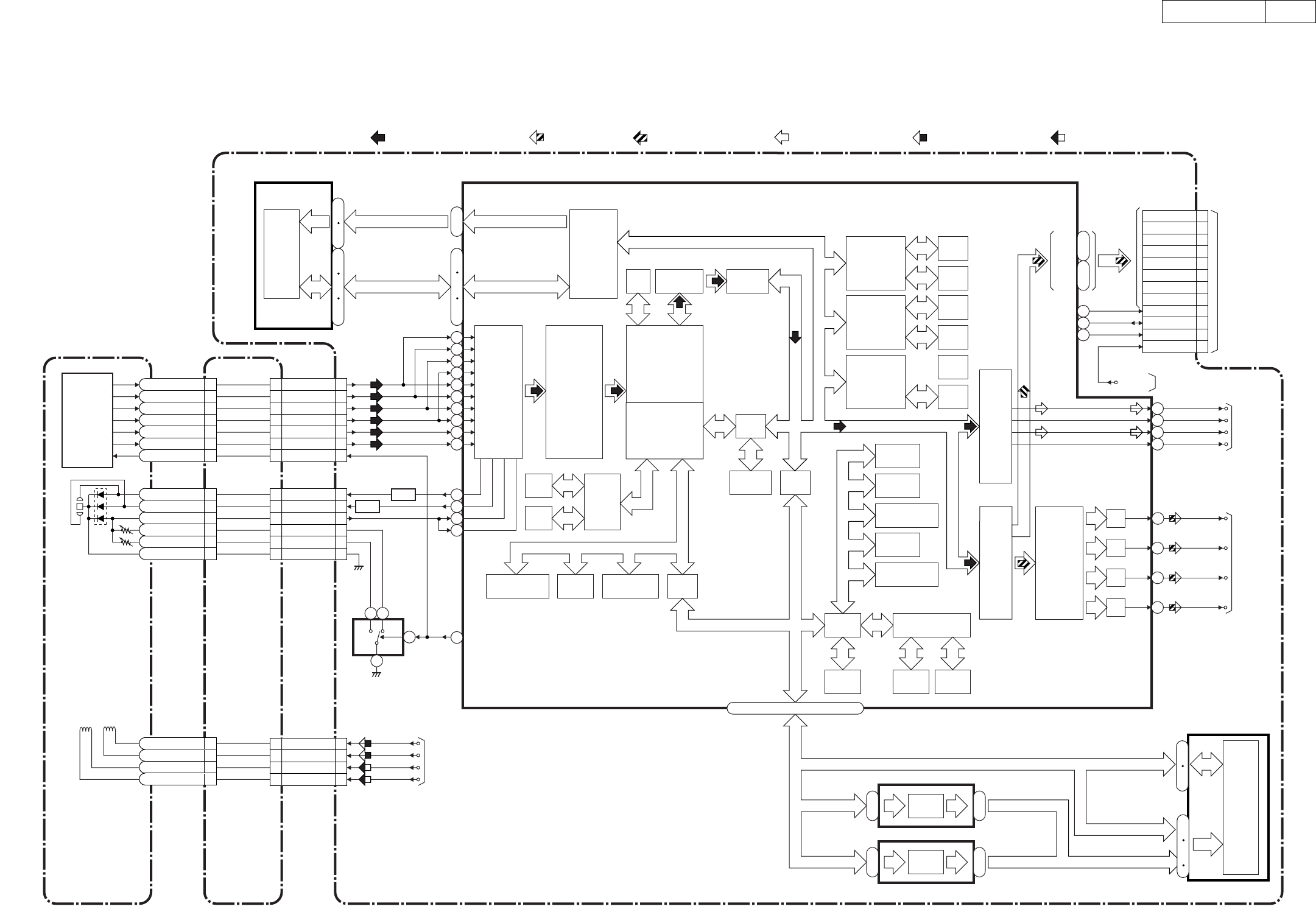
Video / Audio Block Diagram
IC601 (AUDIO DAC)
7
8
12
11
DIGITAL
AUDIO OUT
JK1202
JK1201
AMP
Q1351
IC1201
Q1203
Q1201
Q1202
+3.3V
(AMP)
CN601 CN1601
11 11AUDIO-L
13 13
AUDIO-R
12 12A-L-MUTE
14 14A-R-MUTE
10 10A-MUTE
AUDIO-L
OUT
1
2
3
13
14
15
16
TO
SYSTEM
CONTROL
/SERVO
BLOCK
DIAGRAM
TO
DIGITAL
SIGNAL
PROCESS
BLOCK
DIAGRAM
SERIAL
PORT
SERIAL
CONTROL
4X/8X
OVERSAMPLING
DIGITAL FILTER
/FUNCTION
CONTROLLER
ENHANCED
MULTI-LEVEL
DELTA-SIGMA
MODULATOR
DAC LPF+AMP L-CH
R-CH
LPF+AMP
DAC
ZERO DETECT
SYSTEM CLOCK
1
2
67
5AUDIO-R
OUT
PCM-BCK
SPDIF
PCM-DATA0
PCM-LRCLK
ADAC-MD
ADAC-MC
ADAC-ML
PCM-SCLK
AV CBADVD MAIN CBA UNIT
AUDIO SIGNALDATA(AUDIO) SIGNAL
16 16
SPDIF
A-MUTE +3.3V
Q1204
WF6
3
WF4
WF5
CN601
77VIDEO-C
55VIDEO-Y
33VIDEO-Cb
11VIDEO-Cr
VIDEO-C
VIDEO-Y
VIDEO-Cb
VIDEO-Cr
JK1401
S-VIDEO OUT
CN1601
3 4
2
1
YC
COMPOSITE
VIDEO OUT
VIDEO-Pb/Cb
OUT
VIDEO-Y
OUT
VIDEO-Pr/Cr
OUT
JK1403
TO DIGITAL
SIGNAL PROCESS
BLOCK DIAGRAM
VIDEO SIGNAL
WF1 WF2
VREF
WF3
IC1402 (VIDEO DRIVER)
18
4dB
AMP 2dB
AMP
LPF DRIVER
21
2dB
AMP DRIVER
4dB
AMP 2dB
AMP
LPF DRIVER
15
4dB
AMP 2dB
AMP
LPF DRIVER
9
13
4dB
AMP 2dB
AMP
LPF
MUTE
DRIVER
11
3
6
223
SW1401
+5V
PROGRESSIVE
/INTERLACE
IC6102 (OUTPUT SELECT)
SW CTL
4
14
3
5
13
12
10 11
15
1
2
PROGRESSIVE
INTERLACE
PROGRESSIVE
INTERLACE
PROGRESSIVE
INTERLACE
9
2VIDEO-Y
4VIDEO-Pb
6VIDEO-Pr
CN1602
TO
PROGRESSIVE
BLOCK DIAGRAM
CN1802
FIBER OPTIC
TRANS MODULE
IC1204
JK3501
REMOTE
CONTROL-IN
REMOTE
CONTROL-OUT
IC3510
(AMP)
1
7AMP
BUFFER
Q3503
REMOTE2
REMOTE1
TO SYSTEM
CONTROL/SERVO
BLOCK DIAGRAM
25
25
DVM-1815
CN1801
FORMATTER DE-INTERLACER
DAC DACDAC
PLL/CLOCK GENERATOR
SYNC
GENERATOR
IC1801 IC1803
20
27
~
65
72
75
76
~
40
49 47 48
92
91
117
29
28
25
40
31
30
~
93
94
97
104
11
2
~
~
42
51
FORMATTER TEST PATT.GENE.
/DELAY
/GAMMA CORRECTOR
X2
INTER-
POLATION
RESET
SDA
SCL
V-SYNC
H-SYNC
CLK-IN
RESET
SDA
SCL
136125
~
ADDR0
ADDR10
139 176
~
DATA0
DATA29
~~
IC1808
20 24
~
27 32
~
ADDR0
(SD-RAM) (SD-RAM)
ADDR10
~
212
~
39 49
~
DATA0
DATA15
~
IC1809
20 24
~
27 32
~
ADDR0
ADDR10
~
212
~
39 46
~
DATA16
DATA29
~
CN1802
36
4:2:2
TO
4:4:4
4:2:2
TO
4:4:4
DATA(VIDEO) SIGNAL VIDEO SIGNAL
TO
DIGITAL SIGNAL
PROCESS BLOCK
DIAGRAM CN202
TO VIDEO
/AUDIO
BLOCK
DIAGRAM
CN1602
PROGRESSIVE CBA UNIT
(DE-INTERLACER) (PROGRESSIVE ENCODER)
2 VIDEO-Y
4 VIDEO-Pb
6 VIDEO-Pr
Progressive Block Diagram
YC01
YC13
YC25
YC37
YC411
YC513
YC615
YC717
/RST2
SDA4
SCL6
CLK27M20
32 34
26
26
DVM-1815
NOTE :
The voltage for parts in hot circuit is measured using
hot GND as a common terminal.
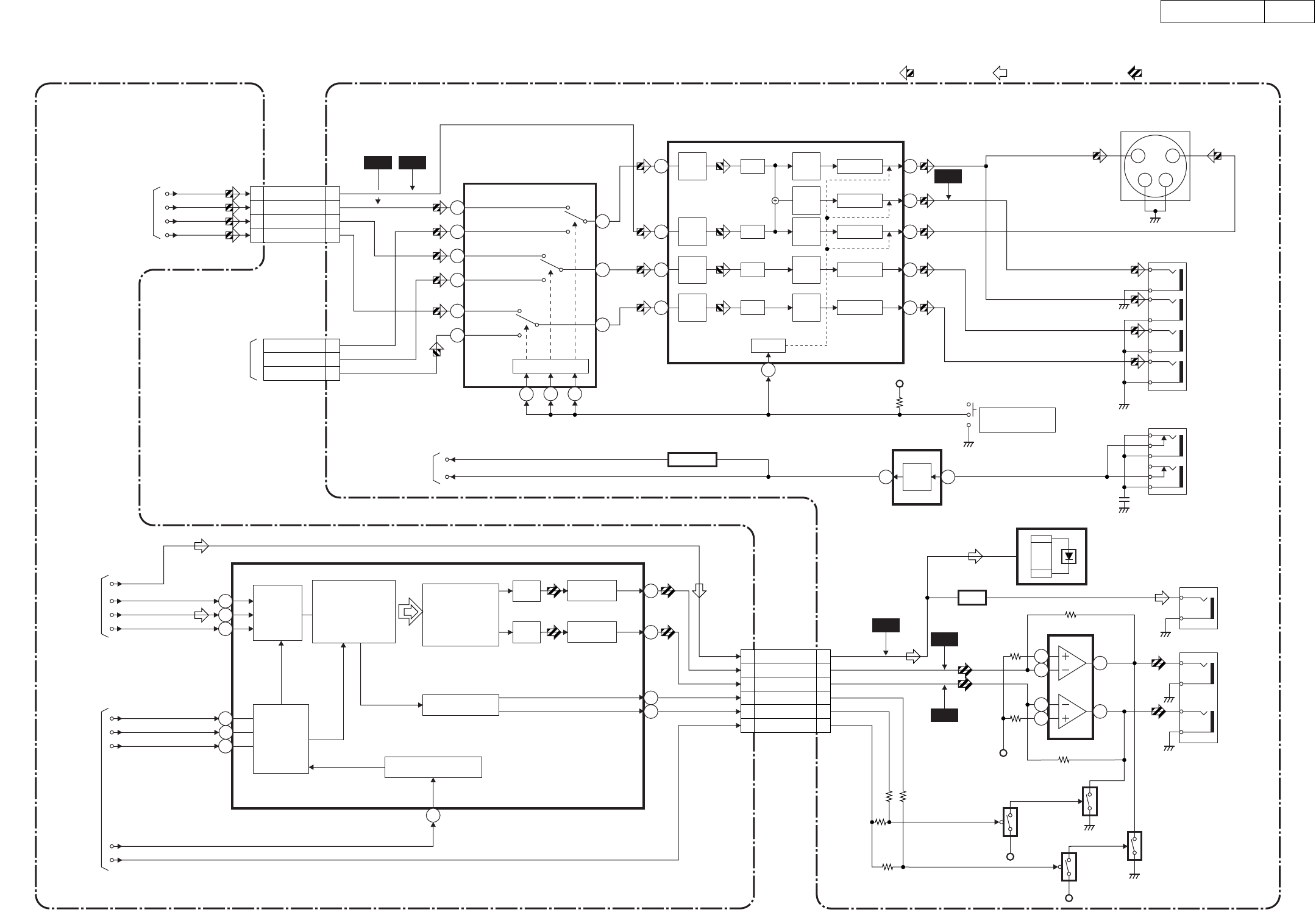
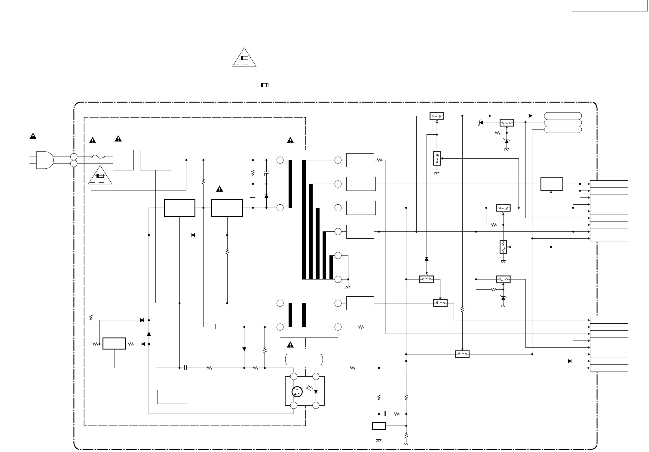
Power Supply Block Diagram
AC1001
AC CORD F1001
1A 250V LINE
FILTER
L1001
D1001, D1002
D1004, D1005
Q1003
Q1008
Q1001
2
4
7
3
4
IC1001
ERROR
VOLTAGE DET
T1001
11
12
13
15
14
16
17
18
IC1006
(SHUNT REGULATOR)
SWITCHING
D1008
D1003
Q1002
Q1016
D1006
RECTIFIER
D1030
RECTIFIER
D1016
RECTIFIER
SWITCHING
CONTROL
LATCH
REG
1
2
6
BRIDGE
RECTIFIER
HOT
AV CBA
-REPLACE FUSE AS MARKED.
"Ce symbole reprèsente un fusible à fusion rapide."
CAUTION
FOR CONTINUED PROTECTION AGAINST FIRE HAZARD,
REPLACE ONLY WITH THE SAME TYPE FUSE.
ATTENTION : POUR UNE PROTECTION CONTINUE LES RISQES
D'INCELE N'UTILISER QUE DES FUSIBLE DE MEMO TYPE.
RISK OF FIRE
"This symbol means fast operating fuse."
AV
F
AV
F
CN1001
CN1102
+1.5V
REG.
IC1002
HOT CIRCUIT. BE CAREFUL.
1 EV+1.5V
P-ON+9V
2 EV+1.5V
3 EV+1.5V
4 EV+3.3V
5 EV+3.3V
13 P-ON+5V
14 EV+9V
15 EV+9V
17 P-ON+3.3V
1F1
2F2
3-FL
4EV+9V
5EV+5V
6P-ON+3.3V
7 CHG+3.3V
8PWSW
P-ON+5V
P-ON+3.3V
Q1005
Q1015
Q1004
Q1010
Q1012
Q1014
Q1011
CAUTION !
Fixed voltage ( or Auto voltage selectable ) power supply circuit is used in this unit.
If Main Fuse (F1001) is blown, check to see that all components in the power supply
circuit are not defective before you connect the AC plug to the AC power supply.
Otherwise it may cause some components in the power supply circuit to fail.
SCHOTTKY
BARRIER
SCHOTTKY
BARRIER
TO DVD MAIN
CBA UNIT
CN401
TO
CHANGER
CBA CN3102

27
27
DVM-1815
SCHEMATIC DIAGRAMS / CBA’S AND TEST POINTS
Standard Notes
WARNING
Many electrical and mechanical parts in this chassis
have special characteristics. These characteristics
often pass unnoticed and the protection afforded by
them cannot necessarily be obtained by using replace-
ment components rated for higher voltage, wattage,
etc. Replacement parts that have these special safety
characteristics are identified in this manual and its
supplements; electrical components having such fea-
tures are identified by the mark " # " in the schematic
diagram and the parts list. Before replacing any of
these components, read the parts list in this manual
carefully. The use of substitute replacement parts that
do not have the same safety characteristics as speci-
fied in the parts list may create shock, fire, or other
hazards.
Notes:
1. Do not use the part number shown on these draw-
ings for ordering. The correct part number is
shown in the parts list, and may be slightly different
or amended since these drawings were prepared.
2. All resistance values are indicated in ohms
(K=103, M=106).
3. Resistor wattages are 1/4W or 1/6W unless other-
wise specified.
4. All capacitance values are indicated in µF
(P=10-6 µF).
5. All voltages are DC voltages unless otherwise
specified.
28
28
DVM-1815
LIST OF CAUTION, NOTES, AND SYMBOLS USED IN THE SCHEMATIC DIAGRAMS ON THE FOLLOWING
PAGES:
1. CAUTION:
FOR CONTINUED PROTECTION AGAINST FIRE HAZARD, REPLACE ONLY WITH THE
SAME TYPE FUSE.
ATTENTION: POUR UNE PROTECTION CONTINUE LES RISQES D'INCELE N'UTILISER
QUE DES FUSIBLE DE MÊME TYPE.
RISK OF FIRE-REPLACE FUSE AS MARKED.
2. CAUTION:
Fixed Voltage (or Auto voltage selectable) power supply circuit is used in this unit.
If Main Fuse (F1001) is blown, first check to see that all components in the power supply circuit are not defec-
tive before you connect the AC plug to the AC power supply. Otherwise it may cause some components in the
power supply circuit to fail.
3. Note:
(1) Do not use the part number shown on the drawings for ordering. The correct part number is shown in the parts
list, and may be slightly different or amended since the drawings were prepared.
(2) To maintain original function and reliability of repaired units, use only original replacement parts which are listed
with their part numbers in the parts list section of the service manual.
4. Wire Connectors
(1) Prefix symbol "CN" means "connector" (can disconnect and reconnect).
(2) Prefix symbol "CL" means "wire-solder holes of the PCB" (wire is soldered directly).
5. Voltage indications for PLAY and STOP mode on the schematics are as shown below:
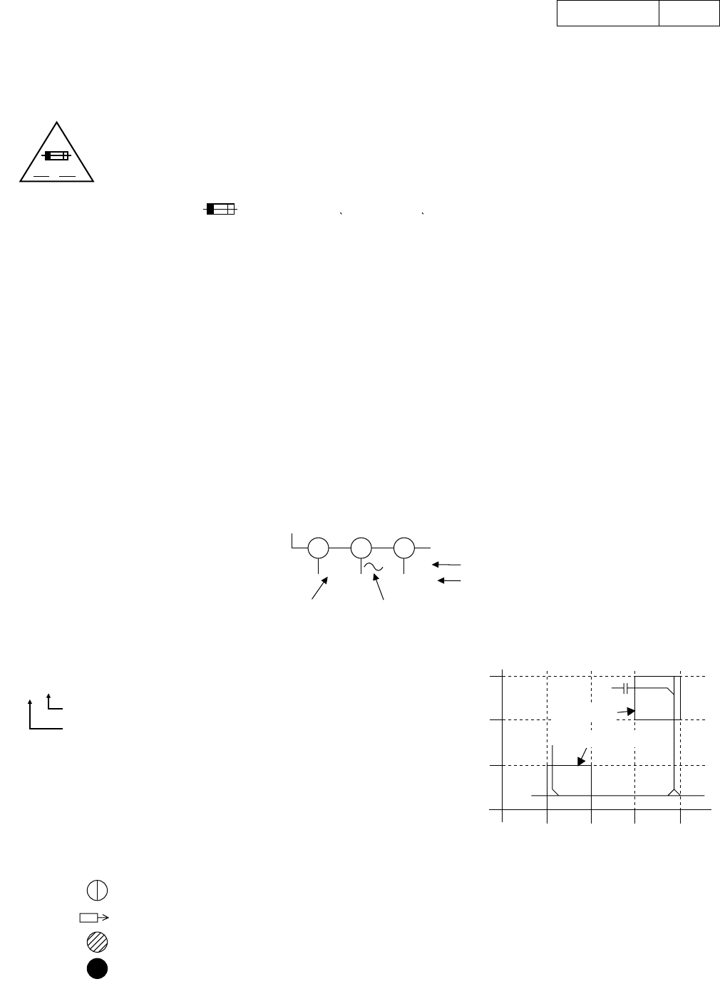
6. How to read converged lines
7. Test Point Information
This symbol means fast operating fuse.
Ce symbole represente un fusible a fusion rapide.
23
1 5.0
(2.5)
5.0
T
he same voltage for
b
oth PLAY & STOP modes Indicates that the voltage
is not consistent here.
PLAY mod
e
STOP mod
e
(Unit: Volt)
1
-D3
Distinction Area
Line Number
(1 to 3 digits)
Examples:
1. "1-D3" means that line number "1" goes to area "D3
".
2. "1-B1" means that line number "1" goes to area "B1
".
3
2
1
ABCD
1-B1
1-D3
AREA D3
AREA B1
: Indicates a test point with a jumper wire across a hole in the PCB.
: Used to indicate a test point with a component lead on foil side.
: Used to indicate a test point with no test pin.
: Used to indicate a test point with a test pin.
A V
F
29
29
DVM-1815
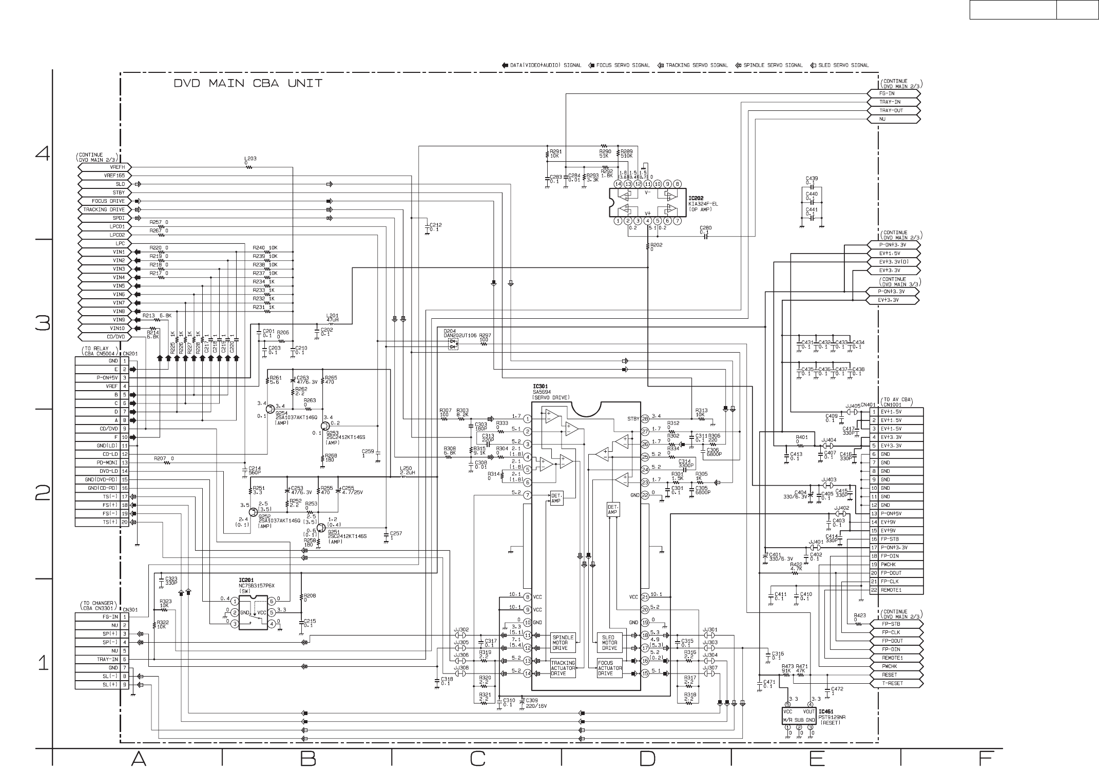
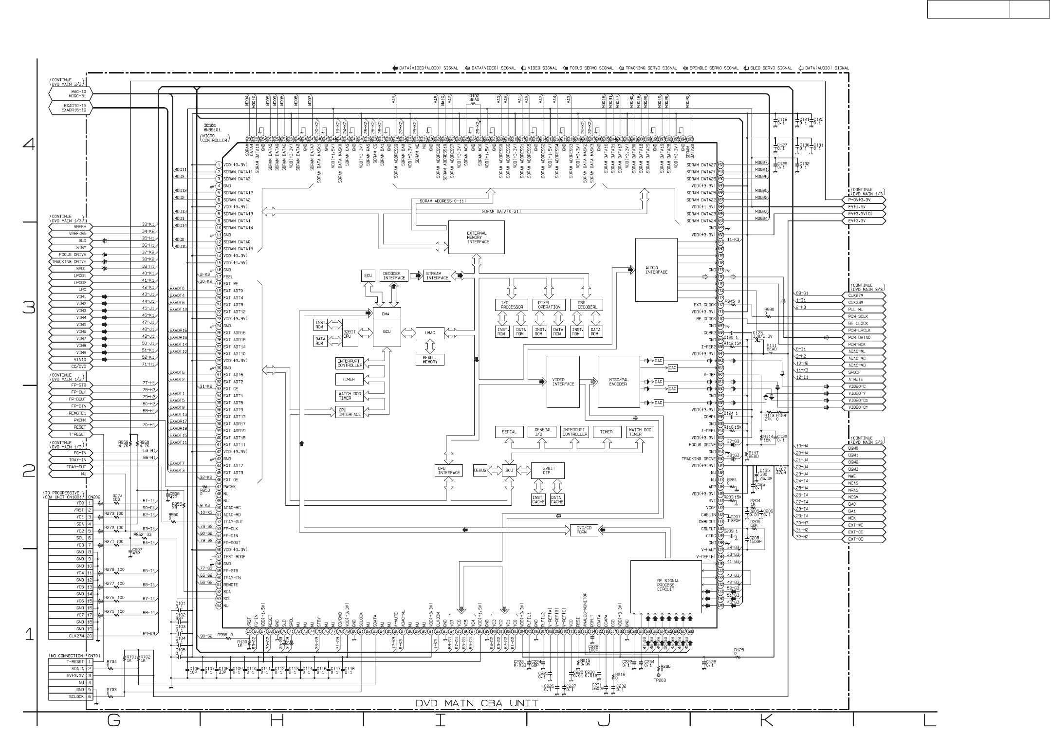
DVD Main 1/3 Schematic Diagram
30
30
DVM-1815
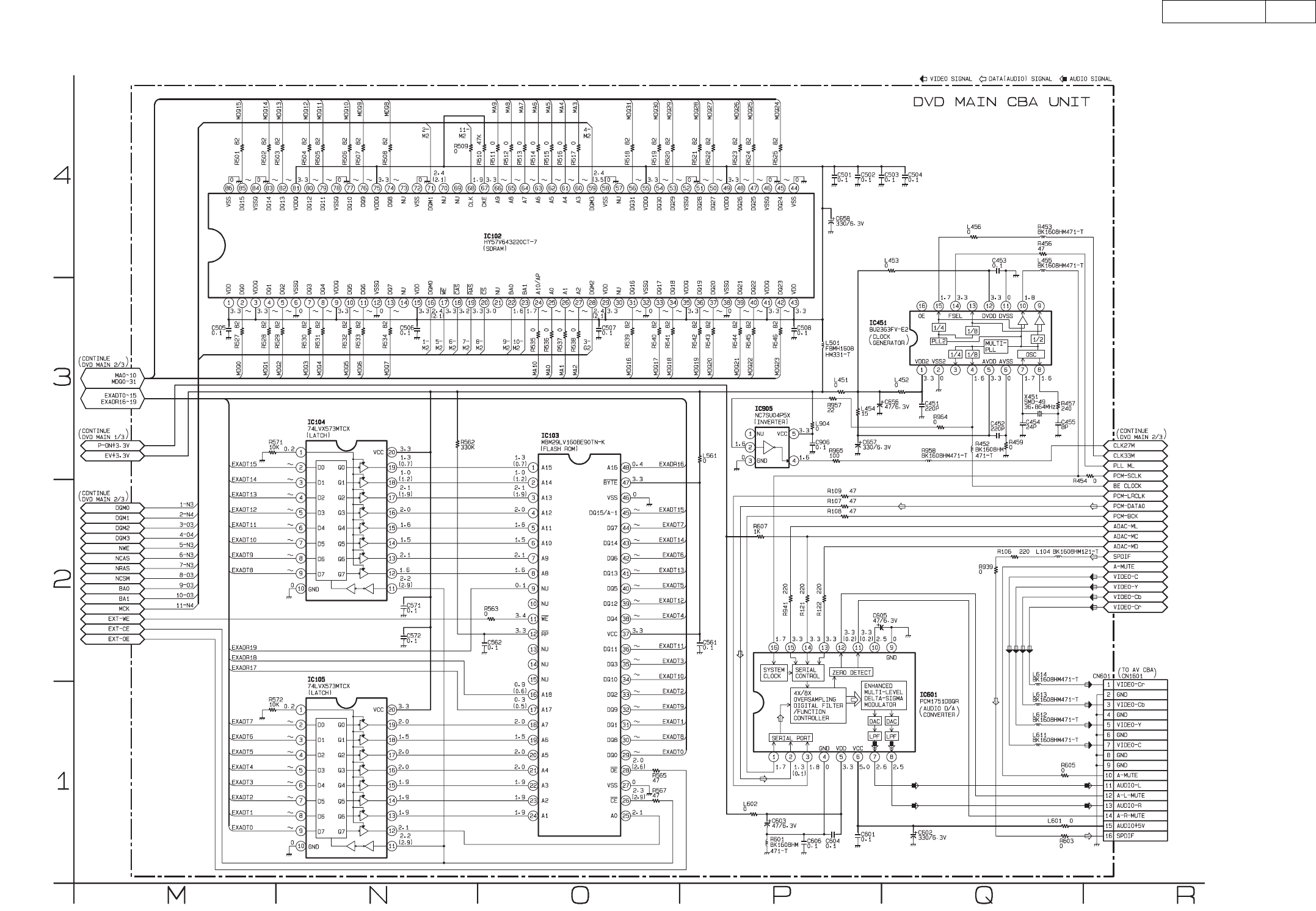
DVD Main 2/3 Schematic Diagram

31
31
DVM-1815
IC101 VOLTAGE CHAR
T
PIN.NO PLAY STOP PIN.NO PLAY STOP PIN.NO PLAY STOP PIN.NO PLAY STOP PIN.NO PLAY STOP PIN.NO PLAY STOP PIN.NO PLAY STOP PIN.NO PLAY STOP
1 3.3 3.3 33 2.2 2.9 65 0.1 0.1 97 1.4 1.4 129 2.0 2.0 161 0.5 0.5 193 ~ ~ 225 1.9 1.9
2 ~ ~ 34 ~ ~ 66 1.2 2.5 98 1.6 1.6 130 2.2 2.2 162 1.4 1.4 194 0 0 226 3.3 3.3
3 ~ ~ 35 ~ ~ 67 1.6 1.6 99 0 0 131 2.3 2.3 163 ----- ----- 195 3.3 3.3 227 ~ ~
4 0 0 36 ~ ~ 68 3.4 3.4 100 1.1 1.1 132 0.4 0.1 164 0.9 0.9 196 ~ ~ 228 ~ ~
5 ~ ~ 37 ~ ~ 69 0 0 101 1.3 1.3 133 1.2 0.4 165 3.3 3.3 197 ~ ~ 229 ~ ~
6 ~ ~ 38 0.3 0.5 70 1.7 1.7 102 1.2 1.2 134 0.4 0.1 166 1.5 1.5 198 0 0 230 0 0
7 3.3 3.3 39 0.1 0.1 71 2.4 1.7 103 1.2 1.2 135 0.2 0.2 167 0 0 199 ~ ~ 231 ----- -----
8 ~ ~ 40 ~ ~ 72 ----- ----- 104 3.3 3.3 136 2.3 2.3 168 2.1 2.1 200 ~ ~ 232 3.3 3.3
9 ~ ~ 41 ~ ~ 73 ----- ----- 105 0.9 0.9 137 1.7 1.7 169 0 0 201 ~ ~ 233 3.3 3.3
10 ~ ~ 42 3.3 3.3 74 ----- ----- 106 0 0 138 0 0 170 0.8 0.8 202 3.3 3.3 234 1.6 1.6
11 0 0 43 0 0 75 3.4 3.4 107 0.8 0.8 139 1.7 1.7 171 3.3 3.3 203 ~ ~ 235 ~ ~
12 ~ ~ 44 ~ ~ 76 ----- ----- 108 1.6 1.6 140 1.7 1.7 172 1.6 1.6 204 ~ ~ 236 0 0
13 ~ ~ 45 ~ ~ 77 ----- ----- 109 2.1 2.1 141 1.7 1.7 173 ----- ----- 205 ~ ~ 237 1.7 1.7
14 3.3 3.3 46 2.0 2.6 78 0.1 0.1 110 2.6 2.6 142 1.7 1.7 174 1.8 1.8 206 0 0 238 3.0 3.0
15 1.5 1.5 47 3.4 3.4 79 3.3 3.3 111 2.0 2.0 143 0.5 0.5 175 1.7 1.7 207 2.4 3.5 239 3.3 3.3
16 0 0 48 ----- ----- 80 0 0 112 0.7 0.9 144 1.6 1.6 176 1.4 0.1 208 2.4 2.1 240 3.3 3.3
17 3.4 3.4 49 ----- ----- 81 3.3 3.3 113 2.1 2.1 145 3.3 3.3 177 0 0 209 3.3 3.3 241 0 0
18 3.4 3.4 50 3.4 3.4 82 ----- ----- 114 1.8 1.8 146 1.8 1.8 178 ----- ----- 210 ~ ~ 242 3.2 3.2
19 ~ ~ 51 3.4 3.4 83 3.4 3.4 115 1.4 1.4 147 ----- ----- 179 ----- ----- 211 0 0 243 2.4 2.1
20 ~ ~ 52 3.4 3.4 84 ----- ----- 116 0.3 0.3 148 ----- ----- 180 ----- ----- 212 ~ ~ 244 1.5 1.5
21 ~ ~ 53 3.4 3.4 85 2.4 2.4 117 1.6 1.6 149 3.3 3.3 181 1.7 1.7 213 1.5 1.5 245 0 0
22 ~ ~ 54 3.4 3.4 86 3.4 0.1 118 3.3 3.3 150 1.7 1.7 182 3.3 3.3 214 ~ ~ 246 2.4 2.1
23 3.3 3.3 55 3.3 3.3 87 3.4 3.4 119 0 0 151 0 0 183 0 0 215 0 0 247 ~ ~
24 0 0 56 3.3 3.3 88 ----- ----- 120 1.9 1.9 152 1.7 1.7 184 ~ ~ 216 ~ ~ 248 0 0
25 0.4 0.4 57 0 0 89 ----- ----- 121 1.9 1.9 153 3.3 3.3 185 ~ ~ 217 ~ ~ 249 ~ ~
26 0.9 0.6 58 0 0 90 ----- ----- 122 2.4 2.4 154 1.4 1.4 186 1.5 1.5 218 3.3 3.3 250 3.3 3.3
27 ~ ~ 59 3.3 3.3 91 3.3 3.3 123 2.4 2.4 155 0 0 187 ~ ~ 219 ~ ~ 251 ~ ~
28 ~ ~ 60 3.4 3.4 92 1.7 1.5 124 2.4 2.4 156 2.2 2.2 188 ~ ~ 220 ~ ~ 252 ~ ~
29 3.3 3.3 61 3.1 3.1 93 0 0 125 2.4 2.4 157 3.3 3.3 189 3.3 3.3 221 0 0 253 ~ ~
30 0 0 62 3.3 3.3 94 2.0 2.0 126 2.0 2.0 158 0.7 0.7 190 ~ ~ 222 1.5 1.5 254 0 0
31 ~ ~ 63 3.3 3.3 95 1.3 1.3 127 2.0 2.0 159 0 0 191 ~ ~ 223 1.9 1.9 255 ~ ~
32 ~ ~ 64 0.8 0.8 96 1.5 1.5 128 2.0 2.0 160 0.5 0.5 192 ~ ~ 224 0 0 256 ~ ~
32
32
DVM-1815
DVD Main 3/3 Schematic Diagram
33
33
DVM-1815
AV 1/2 Schematic Diagram
NOTE :
The voltage for parts in hot circuit is measured
using hot GND as a common terminal.
A V
F
CAUTION
FOR CONTINUED PROTECTION AGAINST FIRE HAZARD,
REPLACE ONLY WITH THE SAME TYPE FUSE.
ATTENTION : POUR UNE PROTECTION CONTINUE LES RISQES
D'INCELE N'UTILISER QUE DES FUSIBLE DE MÊME TYPE.
RISK OF FIRE-REPLACE FUSE AS MARKED.
"This symbol means fast operating fuse."
"Ce symbole reprèsente un fusible à fusion rapide."
CAUTION !
Fixed voltage ( or Auto voltage selectable ) power supply circuit is used in this unit.
If Main Fuse (F1001) is blown, check to see that all components in the power supply
circuit are not defective before you connect the AC plug to the AC power supply.
Otherwise it may cause some components in the power supply circuit to fail.
34
34
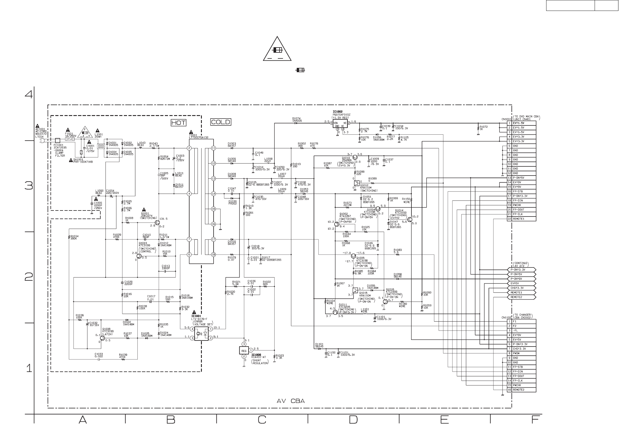
DVM-1815
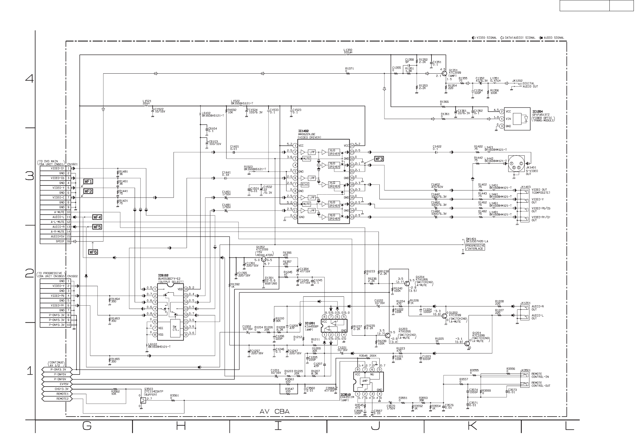
AV 2/2 Schematic Diagram
35
35
DVM-1815
Changer 1/2, Function, Power Switch & Switch Schematic Diagram
36
36
DVM-1815
Changer 2/2 Schematic Diagram
7G 5G 3G 1G4G6G 2G
a
d
g
cb
ef
1
3
2
4
5
DVD
VCD
PBC
STANDBY
A-B
REPEAT
TRK.CHP.TITLE
7G 6G 5G 4G 3G 2G 1G
a
b
c
d
e
f
g
c
d
e
f
g
c
d
e
f
g
c
d
e
f
g
c
d
e
f
g
c
d
e
f
g
h
i
a
b
a
b
a
b
a
b
a
b
FL2001 MATRIX CHART
STANDBY
TITLE CHP. TRK. CD
V
PBC
DVD
REPEAT
A
-B
1
3
2
4
5
37
37
DVM-1815
Relay Schematic Diagram
38
38
DVM-1815
Progressive 1/2 Schematic Diagram
39
39
DVM-1815
Progressive 2/2 Schematic Diagram
40
40
DVM-1815
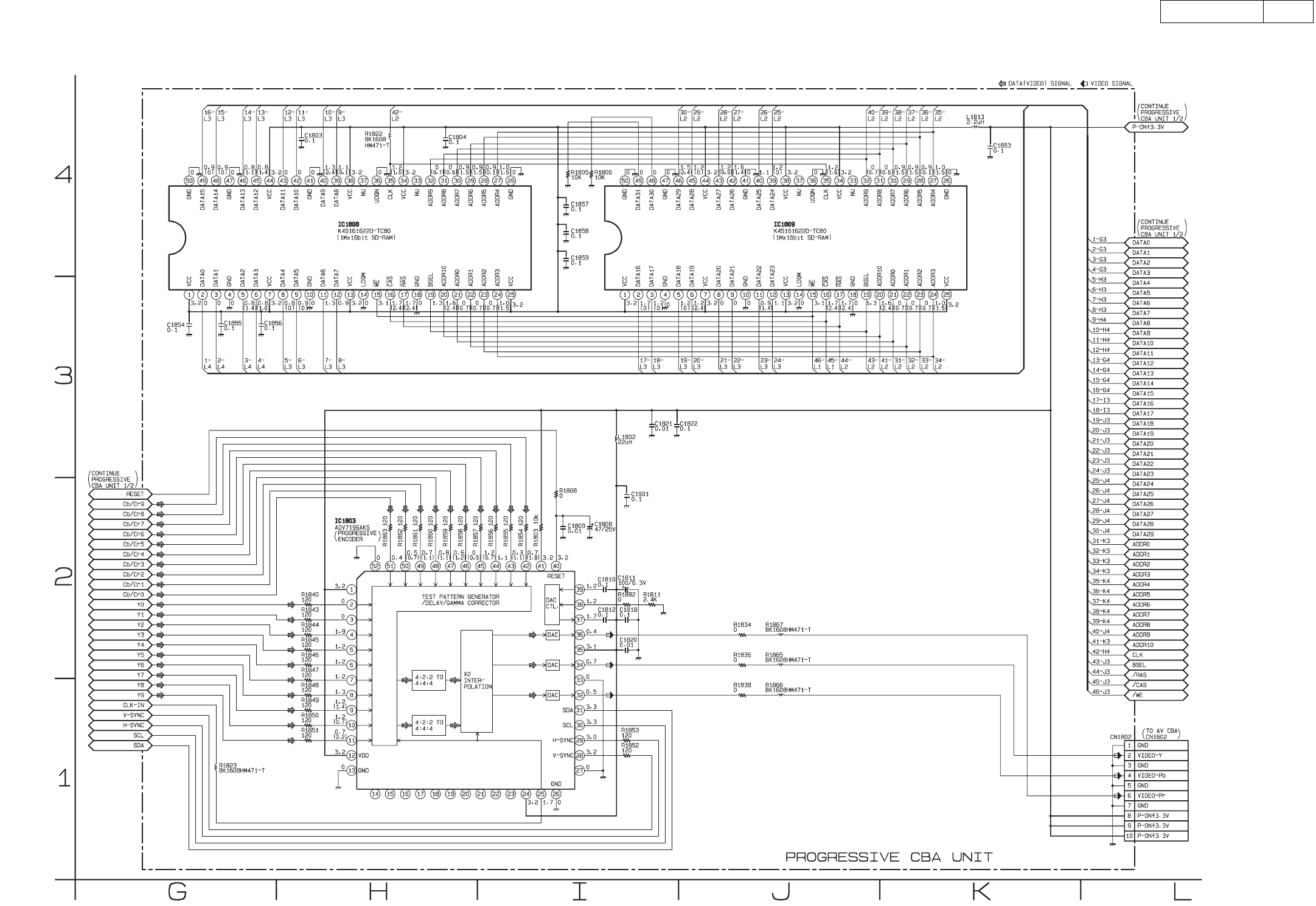
NOTE:
Input
CD: 1kHz PLAY
(WF4~WF6)
DVD: POWER ON (STOP) MODE
(WF1~WF3)
WAVEFORMS
WF6
SPDIF
Pin 16 of CN1601
1V 0.1
µ
sec
WF1
Pin 5 of CN1601
WF3
Pin 21 of IC1402
WF4
AUDIO-L
Pin 11 of CN1601
1V 0.5msec
WF5
AUDIO-R
Pin 13 of CN1601
1V 0.5msec
WF2
Pin 7 of CN1601
VIDEO-Y 0.2V 20
µ
sec
VIDEO-C 0.2V 20
µ
sec
VIDEO-CVBS 0.5V 20
µ
sec
41
41
DVM-1815
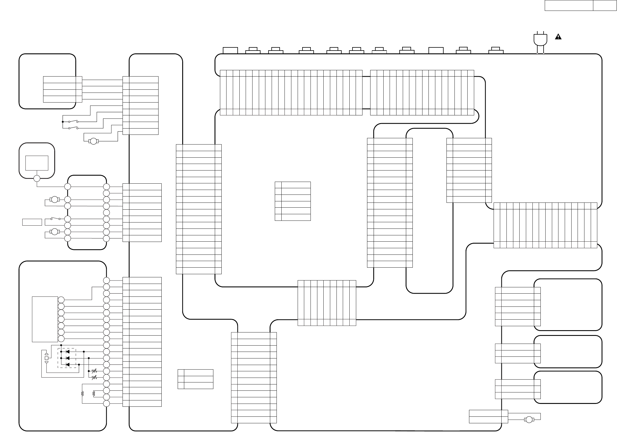
WIRING DIAGRAM
SENSOR CBA
MLOADING
MOTOR
DVD MAIN CBA UNIT
RELAY CBA
PROGRESSIVE
CBA UNIT
CN701
(NO CONNECTION)
(NO CONNECTION)
YC0 11
/RST 22
YC1 33
SDA 44
YC2 55
SCL 66
YC3 77
GND 88
GND 99
GND 1010
YC4 1111
GND 1212
YC5 1313
GND 1414
YC6 1515
GND 1616
GND 1919
CLK27M 2020
CN202 CN1801W1801
GND 11
E22
P-ON+5V 33
VREF 44
B55
C66
D77
A88
CD/DVD 99
F1010
GND(LD) 1111
CD-LD 1212
PD-MONI 1313
DVD-LD 1414
GND(DVD-PD) 1515
GND(CD-PD) 1616
TS(-) 1717
FS(+) 1818
FS(-) 1919
TS(+) 2020
CN5004 CN201W3003
W5001
GND 11
VIDEO-Y 22
GND 33
VIDEO-Pb 44
GND 55
VIDEO-Pr 66
GND 77
P-ON+3.3V 88
P-ON+3.3V 99
P-ON+3.3V 1010
W1811
CN1802 CN1602
AC CORD
AUDIO-L
OUT
AUDIO-R
OUT
VIDEO
OUT
VIDEO-Pr/Cr
OUT
VIDEO-Pb/Cb
OUT
VIDEO-Y
OUT
DIGITAL
AUDIO OUT
S-VIDEO
OUT
VIDEO-Cr 11
GND 22
GND 44
VIDEO-Y 55
GND 66
VIDEO-C 77
GND 88
GND 99
A-MUTE 1010
AUDIO-L 1111
A-L-MUTE 1212
AUDIO-R 1313
AUDIO+5V 1515
A-R-MUTE 1414
SPDIF 1616
CN601
CN1601
W3005
VIDEO-Cb 33
PWCHK 1919
FP-DOUT 2020
FP-CLK 2121
REMOTE1 2222
W3006
CN401
CN1001
EV+1.5V 1
1
EV+1.5V 2
2
EV+1.5V 3
3
EV+3.3V 4
4
EV+3.3V 5
5
GND 6
6
GND 7
7
GND 8
8
GND 9
9
GND 10
10
GND 11
11
GND 12
12
P-ON+5V 13
13
EV+9V 14
14
EV+9V 15
15
FP-STB 16
16
P-ON+3.3V 17
17
FP-DIN 18
18
ROTARY
MOTOR
UP/DOWN
SWITCH
CN5002
CN5101
4
GND
3
P-ON+3.3V
2
RT-SENS-A
1
D-SENS-A
FUNCTION CBA
CN2101 CN2201
GND 1
1
KEY-1 2
2
KEY-2 3
3
KEY-3 4
4
KEY-4 5
5
KEY-5 6
6
W2101
CN2103 CN2203
KEY-1 1
1
GND 2
2
STANDBY-LED 3
3
POWER SWITCH CBA
CN3003
2
1LM(+)
LM(-)
W3001
SWITCH CBA
CN3004 CN3101
ST-CLOSE 1
1
GND 2
2
ST-OPEN 3
3
M
1 T-RESET
2 SDATA
3 EV+3.3V
CN5006
CN5005
1 GND(LD)
2 DVD-LD
3 CD-LD
4NU
5 GND
6 SCLOCK
1 D-SENS-A
2 RT-SENS-A
3 P-ON+3.3V
4 GND
5 GND
6 CHK-ON
7 CHK-OFF
8 RM1
9 RM2
OPTICAL
AUDIO OUT
PICK UP UNIT
1
2
3
4
5
6
7
8
9
10
11
12
13
14
15
16
17
18
19
20
GND
VREF
P-ON+5V
F
E
C
B
D
A
PD-MONI
DVD-LD
GND(LD)
GND(DVD-PD)
TS(+)
FS(-)
FS(+)
TS(-)
GND(CD-PD)
CD-LD
CD/DVD
FSTS
DETECTOR
11
2
3
5
6
4
7
CN5003
1
2
3
4
NU
TRAY-IN
6
SP(-)
7
SP(+)
8 SL(-)
9 SL(+)
FG-IN
P-ON+3.3V
TRAY-IN
DRIVE CBA
FG
SENSOR
SLED
MOTOR
SPINDLE
MOTOR
W3004CN5001 CN3001
D-SENS-A 8
8
RT-SENS-A 6
6
P-ON+3.3V 4
4
GND 2
2
CHK-ON 1
1
CHK-OFF 3
3
RM1 5
5
RM2 7
7
SP(-) 9
9
TRAY-IN 11
11
SL(-) 13
13
FG-IN 10
10
SP(+) 12
12
SL(+) 14
14
W3007
CN3301
CN301
SL(-) 8
8
TRAY-IN 6
6
SP(-) 4
4
NU 2
2
FG-IN 1
1
SP(+) 3
3
NU 5
5
GND 7
7
SL(+) 9
9
W3008
CN3102
CN1102
PWSW 8
8
P-ON+3.3V 6
6
EV+9V 4
4
F2 2
2
F1 1
1
-FL 3
3
EV+5V 5
5
CHG+3.3V 7
7
GND 9
9
FP-STB 11
11
FP-DOUT 13
13
GND 10
10
FP-DIN 12
12
FP-CLK 14
14
PWCHK 15
15
REMOTE2 16
16
AV CBA
CHANGER CBA
M
M
GND
5
W5006
W5002
YC7 1717
GND 1818
REMOTE
CONTROL-IN
REMOTE
CONTROL-OUT
FG CBA
42
42
DVM-1815
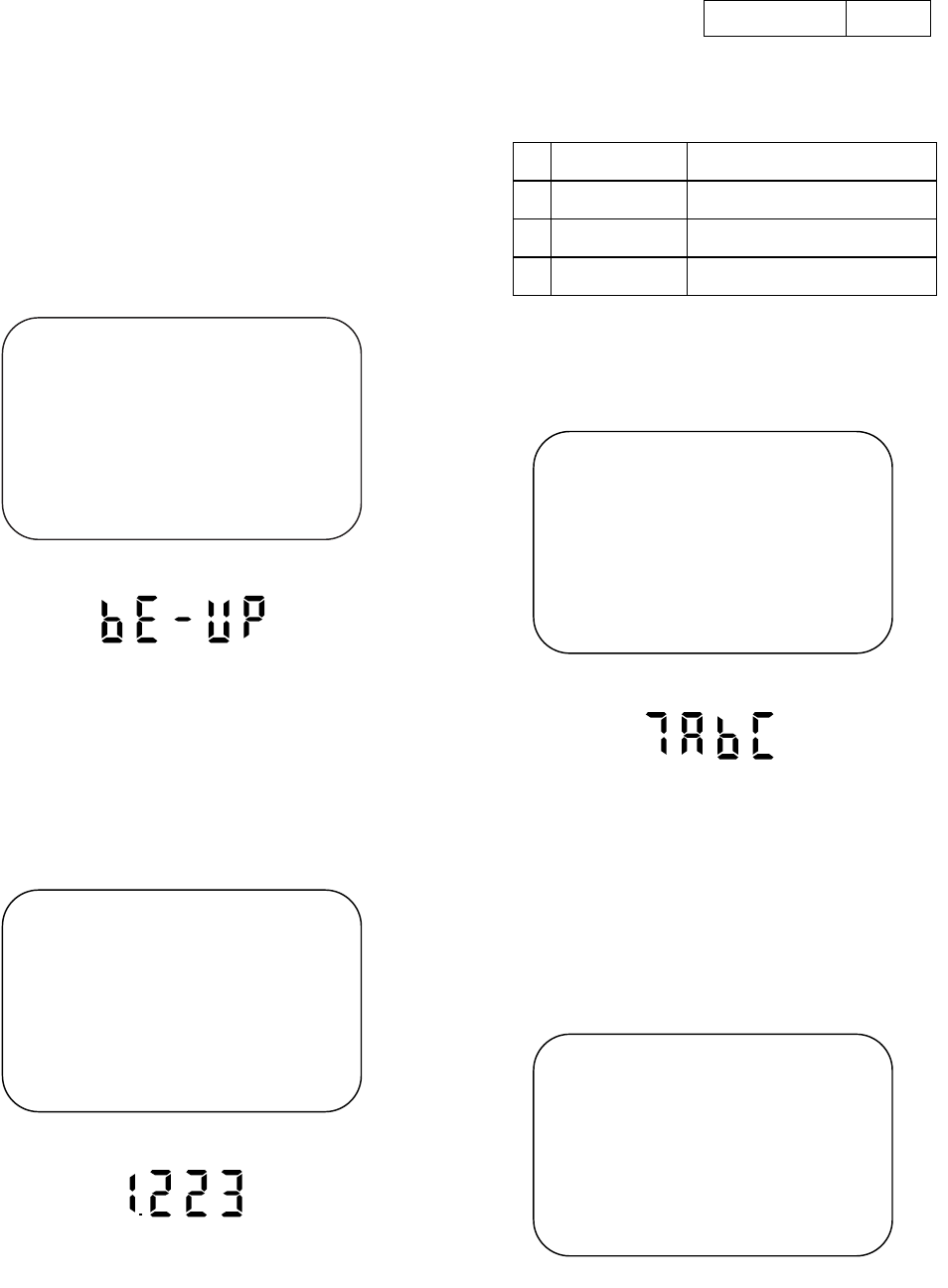
FIRMWARE RENEWAL MODE
1.Turn the power on and remove the disc on the tray.
2.To put the DVD player into version up mode, press
[9], [8], [7], [6], and [SEARCH MODE] buttons on
the remote control unit in that order. The tray will
open automatically.
Fig. a appears on the screen and Fig. b appears on
the VFD.
The DVD player can also enter the version up mode
with the tray open. In this case, Fig. a will be shown
on the screen while the tray is open.
3.Load the disc for version up.
4.The DVD player enters the F/W version up mode
automatically. Fig. c appears on the screen and Fig.
d appears on the VFD.
The appearance shown in (*2) of Fig. c is described
as follows:
5.After programming is finished, the tray opens auto-
matically. Fig. e appears on the screen and the
checksum in (*3) of Fig. e appears on the VFD.
(Fig. f)
At this time, no buttons are available.
6.Unplug the AC cord from the AC outlet. Then plug it
again.
7.Turn the power on by pressing the power button and
the tray will close.
8.Press [1], [2], [3], [4], and [DISPLAY] buttons on the
remote control unit in that order.
Fig. g appears on the screen.
9.Press [3] button on the remote control unit.
Fig. h appears on the screen.
F/W Version Up Mode
Please insert a DISC
for F/W Version Up.
EXIT: POWER
Fig. a Version Up Mode Screen
F
ig. b VFD in Version Up Mod
e
Fig. c Programming Mode Screen
F/W Version Up Mode
VERSION : ********
Reading...(*2)
EXIT: POWER
F
ig. d VFD in Programming Mode (Exampl
e)
AppearanceNo. State
Reading... Sending files into the memory
Erasing... Erasing previous version data
Programming...
1
2
3 Writing new version data
Fig. e Completed Program Mode Screen
F/W Version Up Mode
VERSION : ********
Completed
SUM : 7abc (*3)
F
ig. f VFD upon Finishing the Programming Mode (Exampl
e)
Fig. g
model: ****** Ver: **** Region: **
1: VFD TEST
2: TT REPEAT PLAY
3: EEPROM CLEAR
4: MEASUREMENT SERVO
5: DISC READ CHECK
6: MECHA CHECK
7: DISC INFO
8: ERROR RATE
EXIT: POWERRETURN: -----

43
43
DVM-1815
10.To finish this mode, press [POWER] button.
Fig. h
model: ****** Ver: **** Region: **
TEST 3: EEPROM CLEAR
EEPROM CLEAR: OK
EXIT: POWERRETURN: -----
44
44
DVM-1815
1 4
8 5
NJM4558D
KIA4558P
CXA1511M
28 15
14
PT6313-S-TP
1
E C B
A
K
C
E
LTV-817(B,C)-F
2SK3374
KIA431-AT
K A R
PQ070XF01SZ
1234
1: Vin
2: Vo
3: GND
4: Vc
24 13
12
MM1622XJBE
1
GP1FA513TZ
123
16 9
8
BU4053BCFV-E2
MM74HC4053MTCX
1
S D G
Note:
A: Anode
K: Cathode
E: Emitter
C: Collector
B: Base
R: Referenc
e
1 VCC
2 GND
3 OUT
KTC3198 (Y)
KTC3205 (Y)
2SA966(Y)
E C B
2SC2785 (H)
KTC3199 (GR)
KRA110M
KRC110M-AT
BA1L3Z-T
BN1L3Z (P)
2SA1015-Y (TPE2)
KTA1266 (Y)
KTA1267 (Y)
DTC114ESA TP
PT204-6B-12
E
C
17
BA6956AN
42 22
21
M
38503M2A-067FP
1
123
54
BE4829G-TR
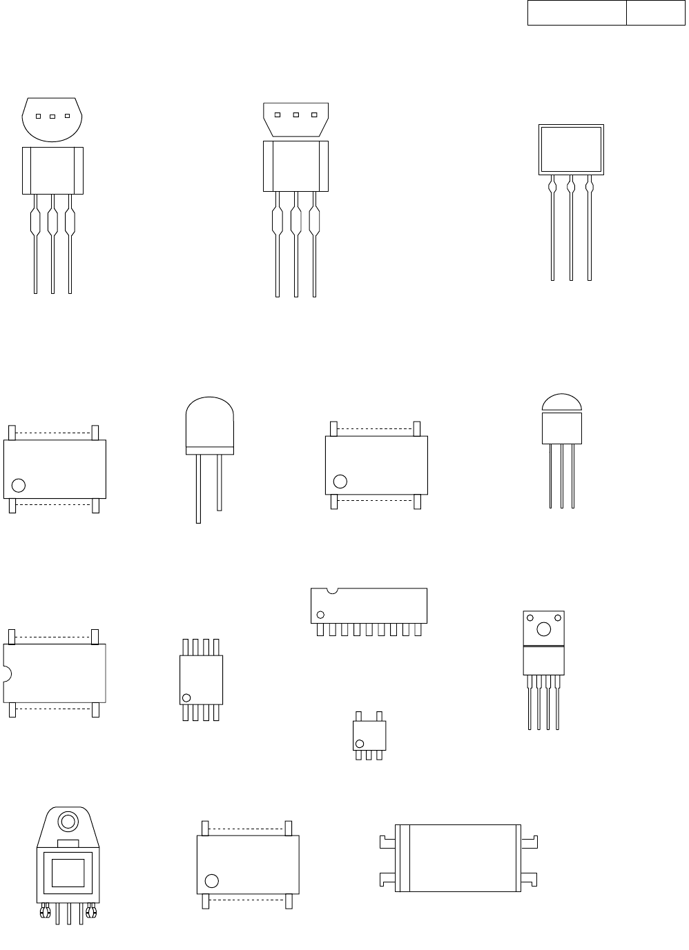
LEAD IDENTIFICATIONS
45
45
DVM-1815
See Electrical Parts List
for parts with this mark.
Some Ref. Numbers are
not in sequence.
2L021
A16
2L021
2L021
2L021
2L021
2L021
Relay CBA
AV CBA
Canger CBA
Power SW
CBA
Function CBA
Switch CBA
A2
2B6
2B1
2B2
2B6
2B3
2L032
2L051
2L032
W3002 D-3
A1X
A15
2L011
2L011
2L011
2L081
2B18
2L051
2L051
1L016
1B12
1B4
1B11
2L051
2L011
2L103
2L011
W3006
A
G'
G
A'
B'
B
C
C'
D'
E'
E
F
F'
D
1B32
1B31
2L032
2L051
JK3501
FC1001
JK1403
JK1202
1B1
1L023
1B33
1L017
W2101
W3001
2L033
2L033
2L033
2L033
2L033
2L012
2L012
2L012
A21
2L012
2L041
2L061
W3003
W3004
W3007
2L041
2L091
2B11
2B12
AC1001
FC1002
W3008
JK1201
JK1401
IC1204
A17
W1811
W3005
2B9
2B24
2B9
2B9
2B22
2B21
2B7
2L031
2L031
2B15
A3
A3
2B10
DVD Main
CBA Unit
Progressive
CBA Unit
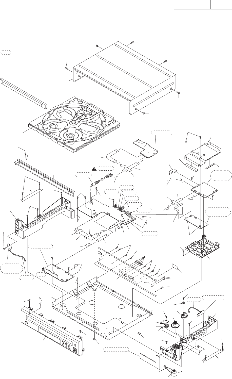
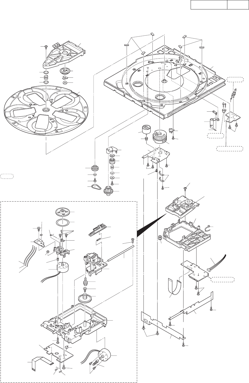
EXPLODED VIEWS
Cabinet View 1
46
46
DVM-1815
Cabinet View 2
B1-12
B1-38
B1-6 B1-5
B1-11
D-3
B1-13
B1-36
B1-14
B1-16
B1-15
B1-52
B1-21
B1-45
B1-4
6
B1-19
B1-20
B1-32
B1-9
B1-7
B1-37
B1-8
L1-26
L1-25
L1-5
B1-4
B1-43
B1-24
B1-24
B1-22
B1-2
B1-30
B1-30
B1-1
SW-403
L1-11
L1-11
L1-11
L1-11
L1-11
L1-11
L1-15
L1-11
L1-23
L1-7
L1-10
Mecha Holder
Assembly
L1-6
B1-26
L1-6
B1-42
B1-41
B1-3
W5002
W5001
B0-7
L0-2
B0-2
B0-3
PA-1
B0-5
B0-8
B0-9
B0-10
M3002
B0-4
B0-1
B0-6
L0-3
M3001
SW3002
L0-8 B0-2
L0-5
R3001 R3002
L0-3
L0-8
FG CBA
PI3001
F-2
L0-4
Drive CBA
W5006
F-3
F-1 L0-4
B0-8
B0-11
Relay CBA
Sensor CBA
See Electrical Parts List
for parts with this mark.
Some Ref.Numbers are
not in sequence.
47
47
DVM-1815
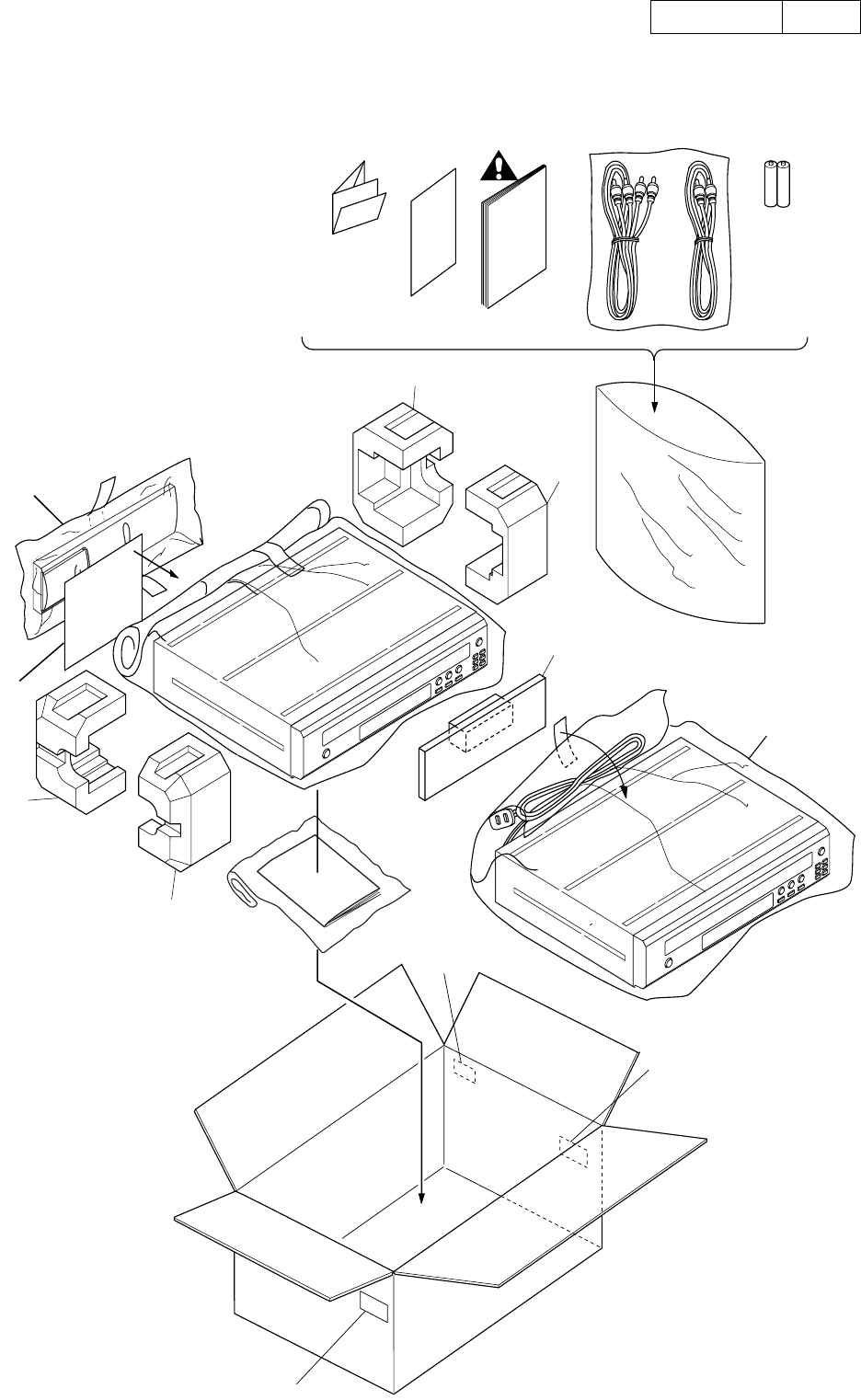
Packing
X10X22X21 X5 X2
X4
S2
S10
S2
S1
A22
A30
A30
S3
S
5
S3
X1
S4
Unit

48
48
DVM-1815
PARTS LIST
PRODUCT SAFETY NOTE: Products marked with a !
have special characteristics important to safety. Before
replacing any of these components, read carefully the
product safety notice in this service manual. Don't
degrade the safety of the product through improper ser-
vicing.
NOTE:
Parts that are not assigned part numbers (---------) are
not available.
Safe Ref. No. Description Funai Parts No. DENON Parts.No Qty New
A1X FRONT ASSEMBLY 0VM204290 9H2 6000 410 1
A2 TRAY PANEL ASSEMBLY 0VM414121 9H2 6000 322 1
A3 FOOT 0VM406940 9H2 6000 411 2
A15 CHASSIS 0VM101293 9H2 6000 412 1
A16 TOP COVER 0VM203048 9H2 6000 325 1
A17 REAR PANEL 0VM204152 9H2 6000 413 1
A21 LABEL, SERIAL NO. ---------- 1
A22 LABEL, BAR CODE ---------- 1
A30 LABEL, CONTROL ---------- 2
1B1 SLIDE TRAY ASSEMBLY N79F0GVC N79F0GVC 9H2 6000 424 1
1B4 LOADING PULLEY 0VM304636 9H2 6000 328 1
1B11 MOTOR PULLEY 21P7048 9H2 6000 329 1
1B12 BELT L 0RM400160 9H2 6000 330 1
1B31 SLIDE TRAY GEAR(B) 0VM304632 9H2 6000 331 1
1B32 SLIDE TRAY GEAR(A) 0VM304631 9H2 6000 332 1
1B33 TRAY GUIDE SPRING 0VM412360 9H2 6000 333 1
1L016 SCREW, P-TIGHT M3X8 WASHER+ GCMP3080 9H2 6000 351 1
1L017 SCREW, P-TIGHT 3X12 WASHER HEAD+ GCMP3120 9H2 6000 352 1
1L023 SCREW, SEMS M2.6X4 PAN HEAD+ CPM39040 9H2 6000 353 1
2B1 TRAY GUIDE(L) 0VM000136H 9H2 6000 414 1
2B2 TRAY GUIDE(RÅj 0VM000137I 9H2 6000 415 1
2B3 BRACKET(TOP) 0VM203160 9H2 6000 336 1
2B6 STOPPER BRACKET 0VM411941 9H2 6000 337 2
2B9 WIRE TAPE K3220UA 0VM404993 - 3
2B10 NON WOVEN FABRICS(35*20) -1
2B11 HOLDER, PCB 0VM204153 9H2 6000 416 1
2B12 SHIELD PLATE 0VM204262 9H2 6000 417 1
2B15 WASHER(D8) 0VM408931 9H2 6000 436 2
2B18 FFC CLAMPER 0VM415656 9H2 6000 418 1
2B21 GASKET 0VM415817 9H2 6000 437 1
2B22 GASKET(B) 0VM415818 9H2 6000 438 1
2B24 DOUBLE SIDE TAPE 0VM415819 9H2 6000 481 1
2L011 SCREW, C-TIGHT M3X6 BIND HEAD GBMC3060 9H2 6000 303 7
2L012 SCREW, C-TIGHT M3X5 BIND HEAD + GBKC3050 9H2 6000 301 4
2L021 SCREW, C-TIGHT M3X5 BIND HEAD + GBKC3050 9H2 6000 301 6
2L031 P-TIGHT SCREW 3X8 BIND + GBMP3080 9H2 6000 240 2
2L032 P-TIGHT SCREW 3X8 BIND + GBMP3080 9H2 6000 240 4
2L033 SCREW, A-TIGHT M3X8 BIND HEAD+ DBK13080 9H2 6000 354 11
2L041 P-TIGHT SCREW 3X8 BIND + GBMP3080 9H2 6000 240 2
2L051 SCREW, S-TIGHT M3X8 BIND + CHROME GBMS3080 9H2 6000 355 7
2L061 P-TIGHT SCREW 3X8 BIND + GBMP3080 9H2 6000 240 2
2L081 SCREW, S-TIGHT M3X8 BIND + CHROME GBMS3080 9H2 6000 355 1
2L091 SCREW, C-TIGHT M3X6 BIND HEAD GBMC3060 9H2 6000 303 1
2L103 P-TIGHT SCREW 3X8 BIND + GBMP3080 9H2 6000 240 1
D-3 MOTOR(LOAD/ROTARY) M31E-1(R-14 7218) MMDZB4EMM002 9H2 6000 419 1
FC1001 CLAMP FILTER XL06035TE001 9H2 6000 439 1
FC1002 FERRITE CORE XL05033TU001 9H2 6000 448 1
W1811 10P FFC AV TO PRS WX1E8620-010 9H2 6000 428 1

49
49
DVM-1815
W3002 MOTOR CABLE MOTOR CABLE WX1E8620-902 9H2 6000 429 1
W3003 20P FFC MAIN TO RELAY WX1E8620-120 9H2 6000 430 1
W3004 14P FFC CONTROL TO RELAY WX1E8620-014 9H2 6000 431 1
W3005 16P FFC AV TO MAIN WX1E8620-016 9H2 6000 432 1
W3006 22P FFC AV TO MAIN WX1E8620-022 9H2 6000 433 1
W3007 9P FFC CONTROL TO MAIN WX1E8620-009 9H2 6000 434 1
W3008 16P FFC AV TO CONTROL WX1E8620-116 9H2 6000 435 1
PACKING & ACCESSORIES
S1 GIFT BOX CARTON 0VM306356 9H2 6000 420 1
S2 FRONT PAD 0VM101008A 9H2 6000 317 2
S3 REAR PAD 0VM101007 9H2 6000 318 2
S4 SET BAG 0DM400731 9H2 6000 316 2
S5 PAD 0VM415718 9H2 6000 421 1
S10 TRAY PAD 0VM415859 9H2 6000 449 1
X1 REMOTE CONTROL UNIT NA801UD 9H2 6000 422 1
X2 DRY BATTERY R6P/2S XB0M451T0001 - 2
X2 or DRY BATTERY ES-GR6M-C XB0M571GLP01 -
X4 I/B BAG 0DM400757 9H2 6000 319 1
X5 AV CORD TSCKA-Y/RW100 WPZ0102TM015 9H2 6000 226 1
X5 AV CORD RCA(M*2)TO RCA(M*2) WPZ0102LTE01 9H2 6000 243 1
! X10 OWNER'S MANUAL 0VMN03732 9H2 6000 423 1
X21 WARRANTY SHEET 0VM305871 - 1
X22 SERVICE CENTER SHEET 0VM413951B - 1
ELECTRICAL PARTS
DVD MAIN CBA UNIT N79DKGUP 9H2 6000 425 1
PROGRESSIVE CBA UNIT 0VSA14428 9H2 6000 426 1
CHG-MAIN CBA ASSEMBLY 0VSA14418 9H2 6000 427 1
Safe Ref. No. Description Funai Parts No. DENON Parts.No Qty New
