R2843_NN DVR 3100 S RRV2843
User Manual: DVR-3100
Open the PDF directly: View PDF ![]() .
.
Page Count: 137 [warning: Documents this large are best viewed by clicking the View PDF Link!]
- DVR-3100-S
- <グラフィック>
- CONTENTS
- CONTENTS
- 1. SPECIFICATIONS
- <グラフィック>
- 2. EXPLODED VIEWS AND PARTS LIST
- 2.1 PACKING
- 2.2 EXTERIOR
- 2.3 FRONT PANEL
- 3. BLOCK DIAGRAM AND SCHEMATIC DIAGRAM
- 3.1 BLOCK DIAGRAM
- 3.1.1 OVERALL BLOCK DIAGRAM
- 3.1.2 TUJB ASSY BLOCK DIAGRAM
- 3.1.3 MAIN ASSY BLOCK DIAGRAM
- 3.1.4 POWER BLOCK DIAGRAM
- 3.2 ATAB ASSY and OVERALL WIRING DIAGRAM
- 3.3 TUJB(1/3) ASSY
- 3.4 TUJB ASSY(2/3)
- 3.5 TUJB ASSY(3/3)
- 3.6 FRJB and DVJB ASSYS
- 3.7 MAIN ASSY(1/5)
- 3.8 MAIN ASSY(2/5)
- 3.9 MAIN ASSY(3/5)
- 3.10 MAIN ASSY(4/5)
- 3.11 MAIN ASSY(5/5)
- 3.12 MHLP ASSY
- 3.13 FLKY ASSY
- 3.14 SCRB ASSY
- 3.15 POWER SUPPLY UNIT
- 3.16 WAVE FORMS
- 4. PCB CONNECTION DIAGRAM
- 4.1 ATAB ASSY
- 4.2 TUMJ ASSY
- 4.3 MAIN and MHLP ASYS
- 4.4 POWER SUPPLY UNIT
- 4.5 FRJB and DVJB ASSYS
- 4.6 FLKY ASSY
- 4.7 SCRB ASSY
- 5. PCB PARTS LIST
- 6. ADJUSTMENT
- 6.1 TUJB ASSY ADJUSTMENT
- 6.2 MAIN ASSY ADJUSTMENT
- 7. GENERAL INFORMATION
- 7.1 DIAGNOSIS
- 7.1.1 CPRM ID NUMBER AND DATA SETTING
- 7.1.2 SERVICE MODE
- 7.1.3 DV DEBUG MODE
- 7.1.4 ERROR RATE MEASUREMENT
- 7.1.5 VIDEO ADJUSTMENT FOR SPECIFIC AREA
- 7.1.6 SETUP SEQUENCE
- 7.1.7 DISASSEMBLY
- 7.2 IC
- 7.3 OUTLINE OF THE PRODUCT
- 7.4 DISC/CONTENT FORMAT
- 7.5 CLEANING
- 8. PANEL FACILITIES
- 8.1 FRONT SECTION
- 8.2 DISPLAY
- 8.3 REAR PART
- 8.4 REMOTE CONTROL

ORDER NO.
PIONEER CORPORATION 4-1, Meguro 1-chome, Meguro-ku, Tokyo 153-8654, Japan
PIONEER ELECTRONICS (USA) INC. P.O. Box 1760, Long Beach, CA 90801-1760, U.S.A.
PIONEER EUROPE NV Haven 1087, Keetberglaan 1, 9120 Melsele, Belgium
PIONEER ELECTRONICS ASIACENTRE PTE. LTD. 253 Alexandra Road, #04-01, Singapore 159936
PIONEER CORPORATION 2003
DVR-3100-S
RRV2843
DVD RECORDER
DVR-3100-S
THIS MANUAL IS APPLICABLE TO THE FOLLOWING MODEL(S) AND TYPE(S).
Model Type Power Requirement Region No. Serial No.
Please confirm 3rd & 4th
alphabetical letters.
DVR-3100-S WY AC220-240V 2 &&TT######$$
DVR-3100-S WYXU AC220-240V 2 &&PG######$$
DVR-3100-S WVXU AC220-240V 2 &&PG######$$
÷ When servicing this model, some service procedures may reset the settings that customer
set (*) to the factory default settings. Make sure to explain this to the customer.
(*) : Initial Setup (Clock Setting, Remote Control Set, Channel settings, Video Out settings,
Audio In settings, Audio Out settings, Language settings)
Refer to the chapter 12 of the Operating Instructions for more details.
For details, refer to "Important symbols for good services" .
T-ZZV OCT. 2003 printed in Japan
DVR-3100-S
2
1234
1234
C
D
F
A
B
E
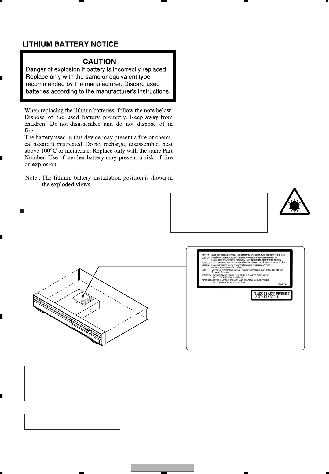
SAFETY INFORMATION
WARNING!
DEVICE INCLUDES LASER DIODE WHICH
EMITS INVISIBLE INFRARED RADIATION
WHICH IS DANGEROUS TO EYES. THERE IS
A WARNING SIGN ACCORDING TO PICTURE
1 INSIDE THE DEVICE CLOSE TO THE LASER
DIODE.
LASER
Picture 1
Warning sign for
laser radiation
LASER DIODE CHARACTERISTICS
MAXIMUM OUTPUT POWER : 50 mw
WAVELENGTH : 658 nm
1. The ON/OFF(ON:low level,OFF:high level) status of the
CLAMP signals for detecting the loading state are detected
by the drive CPUs, and the design prevents laser diode
oscillation when the CLAMP signal turns OFF.
In normal operation, if no disc is clamped, the laser diode
oscillation is disabled.
However, the interlock does not always operate in the test
mode.
2. When the cover is opened, close viewing of the objective
lens with the naked eye will cause exposure to a Class 3A
laser beam.
Additional Laser Caution
IMPORTANT
THIS PIONEER APPARATUS CONTAINS
LASER OF CLASS 1.
SERVICING OPERATION OF THE APPARATUS
SHOULD BE DONE BY A SPECIALLY
INSTRUCTED PERSON.
LABEL CHECK
DRW2179
DVR-3100-S 3
5678
5678
C
D
F
A
B
E
[ Important symbols for good services ]
In this manual, the symbols shown-below indicate that adjustments, settings or cleaning should be made securely.
When you find the procedures bearing any of the symbols, be sure to fulfill them:
2. Adjustments
To keep the original performances of the product, optimum adjustments or specification confirmation is indispensable.
In accordance with the procedures or instructions described in this manual, adjustments should be performed.
3. Cleaning
For optical pickups, tape-deck heads, lenses and mirrors used in projection monitors, and other parts requiring cleaning,
proper cleaning should be performed to restore their performances.
5. Lubricants, glues, and replacement parts
Appropriately applying grease or glue can maintain the product performances. But improper lubrication or applying
glue may lead to failures or troubles in the product. By following the instructions in this manual, be sure to apply the
prescribed grease or glue to proper portions by the appropriate amount.For replacement parts or tools, the prescribed
ones should be used.
4. Shipping mode and shipping screws
To protect the product from damages or failures that may be caused during transit, the shipping mode should be set or
the shipping screws should be installed before shipping out in accordance with this manual, if necessary.
1. Product safety
You should conform to the regulations governing the product (safety, radio and noise, and other regulations), and
should keep the safety during servicing by following the safety instructions described in this manual.

DVR-3100-S
4
1234
1234
C
D
F
A
B
E
CONTENTS
SAFETY INFORMATION..................................................................................................................................... 2
1. SPECIFICATIONS ............................................................................................................................................ 5
2. EXPLODED VIEWS AND PARTS LIST ............................................................................................................ 8
2.1 PACKING ................................................................................................................................................... 8
2.2 EXTERIOR............................................................................................................................................... 10
2.3 FRONT PANEL ........................................................................................................................................ 12
3. BLOCK DIAGRAM AND SCHEMATIC DIAGRAM..........................................................................................14
3.1 BLOCK DIAGRAM ................................................................................................................................... 14
3.1.1 OVERALL BLOCK DIAGRAM............................................................................................................... 14
3.1.2 TUJB ASSY BLOCK DIAGRAM............................................................................................................ 16
3.1.3 MAIN ASSY BLOCK DIAGRAM............................................................................................................ 18
3.1.4 POWER BLOCK DIAGRAM.................................................................................................................. 20
3.2 ATAB ASSY and OVERALL WIRING DIAGRAM...................................................................................... 22
3.3 TUJB(1/3) ASSY ...................................................................................................................................... 24
3.4 TUJB ASSY(2/3) ...................................................................................................................................... 26
3.5 TUJB ASSY(3/3) ...................................................................................................................................... 28
3.6 FRJB and DVJB ASSYS .......................................................................................................................... 29
3.7 MAIN ASSY(1/5) ...................................................................................................................................... 30
3.8 MAIN ASSY(2/5) ...................................................................................................................................... 32
3.9 MAIN ASSY(3/5) ...................................................................................................................................... 34
3.10 MAIN ASSY(4/5) .................................................................................................................................... 36
3.11 MAIN ASSY(5/5) .................................................................................................................................... 38
3.12 MHLP ASSY .......................................................................................................................................... 40
3.13 FLKY ASSY ........................................................................................................................................... 42
3.14 SCRB ASSY .......................................................................................................................................... 44
3.15 POWER SUPPLY UNIT.......................................................................................................................... 46
3.16 WAVE FORMS....................................................................................................................................... 47
4. PCB CONNECTION DIAGRAM ..................................................................................................................... 50
4.1 ATAB ASSY.............................................................................................................................................. 50
4.2 TUMJ ASSY ............................................................................................................................................. 52
4.3 MAIN and MHLP ASYS ........................................................................................................................... 56
4.4 POWER SUPPLY UNIT............................................................................................................................ 60
4.5 FRJB and DVJB ASSYS .......................................................................................................................... 62
4.6 FLKY ASSY ............................................................................................................................................. 63
4.7 SCRB ASSY ............................................................................................................................................ 64
5. PCB PARTS LIST ........................................................................................................................................... 66
6. ADJUSTMENT ............................................................................................................................................... 71
6.1 TUJB ASSY ADJUSTMENT .................................................................................................................... 71
6.2 MAIN ASSY ADJUSTMENT .................................................................................................................... 72
7. GENERAL INFORMATION............................................................................................................................. 73
7.1 DIAGNOSIS ............................................................................................................................................. 73
7.1.1 CPRM ID NUMBER AND DATA SETTING............................................................................................ 73
7.1.2 SERVICE MODE................................................................................................................................... 75
7.1.3 DV DEBUG MODE................................................................................................................................ 83
7.1.4 ERROR RATE MEASUREMENT.......................................................................................................... 86
7.1.5 VIDEO ADJUSTMENT FOR SPECIFIC AREA..................................................................................... 88
7.1.6 SETUP SEQUENCE............................................................................................................................. 92
7.1.7 DISASSEMBLY ..................................................................................................................................... 93
7.2 IC ............................................................................................................................................................. 96
7.3 OUTLINE OF THE PRODUCT............................................................................................................... 127
7.4 DISC/CONTENT FORMAT .................................................................................................................... 130
7.5 CLEANING............................................................................................................................................. 132
8. PANEL FACILITIES ...................................................................................................................................... 133
DVR-3100-S 5
5678
5678
C
D
F
A
B
E
1. SPECIFICATIONS
VHF (low)
VHF (high)
Hyper
UHF
VHF (low)
VHF (high)
Hyper
UHF
STEREO
B/G - A2
I - NICAM
L - NICAM
B/G - NICAM
D/K - NICAM
Channel
E2 - E4
X - Z
E5 - E12
S1 - S20
M1 - M10
U1 - U10
S21 - S41
E21 - E69
Frequency
47 - 89 MHz
104 - 300 MHz
302 - 470 MHz
470 - 862 MHz
Channel
A - C
X - Z
D - J
11, 13
S1 - S20
S21 - S41
E21 - E69
Frequency
44 - 89 MHz
104 - 300 MHz
302 - 470 MHz
470 - 862 MHz
PAL B/G PAL I
Channel
2 - 4
5 - 10
B - Q
S21 - S41
21 - 69
Frequency
49 - 65 MHz
104 - 300 MHz
300 - 470 MHz
470 - 862 MHz
Channel
R1 - R5
R6 - R12
S1 - S20
S21 - S41
E21 - E69
Frequency
49 - 94 MHz
104 - 300 MHz
302 - 470 MHz
470 - 862 MHz
SECAM L SECAM D/K
General
System...........................DVD-Video, DVD-R/RW,Video-CD,
CD, CD-R/RW (WMA, MP3, JPEG. CD-DA)
Power requirements.............................220–240 V, 50/60 Hz
Power consumption.......................................................35 W
Power consumption in standby mode..............0.7 W (FL off)
Weight..........................................................................4.4 kg
Dimensions...........................420 (W) x 69 (H) x 341 (D) mm
Operating temperature....................................+5°C to +35°C
Operating humidity..................5% to 85% (no condensation)
TV system..............PAL/SECAM/NTSC (external input only)
Recording
Recording format................................DVD Video Recording
DVD-VIDEO
Recordable discs
DVD-RW (DVD Re-recordable disc)
DVD-R (DVD Recordable disc)
Video recording format
Sampling frequency.................................................13.5MHz
Compression format....................................................MPEG
Audio recording format
Sampling frequency.....................................................48kHz
Compression format..................Dolby Digital or Linear PCM
(uncompressed)
Recording time
Fine (FINE).....................................................Approx. 1 hour
Standard Play (SP).......................................Approx. 2 hours
Long Play (LP)..............................................Approx. 4 hours
Extended Play (EP).......................................Approx. 6 hours
Manual Mode (MN)...................................Approx. 1–6 hours
Tuner
Receivable channels
Timer
Programs..............................................1 month/32 programs
Clock..............................Quartz lock (24-hour digital display)
Power off memory.........Approx. 5 years (after manufacture)
Input/Output
VHF/UHF antenna input/output terminal...........VHF/UHF set
75 Ω (IEC connector)
Video input......................................Input 1, 3 (rear), 2 (front)
Input level.........................................................1 Vp-p (75 Ω)
Jacks............................................. AV connector 2 (Input 1),
RCA jack (Input 2,3)
Video output..........................................................Output 1,2
Output level .....................................................1 Vp-p (75 Ω)
Jacks...............................................AV connector (Output 1)
RCA jack (Output 2)
S-Video input..................................Input 1, 3 (rear), 2 (front)
Y (luminance) - Input level................................1 Vp-p (75 Ω)
C (colour) - Input level...............................286 mVp-p (75 Ω)
Jacks..............................................AV connector 2 (Input 1),
4 pin mini DIN (Input 2,3)
S-Video output.......................................................Output 1,2
Y (luminance) - Output level.............................1 Vp-p (75 Ω)
C (colour) - Output level............................286 mVp-p (75 Ω)
Jacks...........................................AV connector 1 (Output 1),
4 pin mini DIN (Output 2)
Audio input...............................Input 1, 3 (rear), 2 (front) L/R
Input level
During audio input......................................................2V rms
(Input impedance: more than 22 kΩ)
Jacks..............................................AV connector 2 (Input 1),
RCA jacks (Inputs 2,3)
DVR-3100-S
6
1234
1234
C
D
F
A
B
E
Accessories
• Remote control ×1
(VXX2884 : WYXU/WY types)
(VXX2883 : WVXU type)
• RF antenna cable(PAL) ×1
(VDE1075)
• Power cable ×1
(ADG1154 : WYXU/WY types)
• Audio / Video cable(1.5m) ×1
(red/white/yellow)
(VDE1077)
• Dry cell batteries ×2
(AA/R6P)
Audio output....................................................Output 1,2 L/R
During audio output.....................................................2V rms
(Output impedance: less than 1.5 kΩ)
Jacks............................................AV connector 1 (output 1),
RCA jacks (output 2)
Control input.............................................................Mini jack
DV input/output...............................................................4 pin
(i.LINK/IEEE 1394 standard)
AV Connectors (21-pin connector assignment)
AV connector input/output...........................21-pin connector
This connector provides the video and audio signals for
connection to a compatible colour TV or monitor.
PIN no.
1........................................................................Audio 2/R out
11.................................................................................G∗ out
3........................................................................Audio 1/L out
15.......................................................................R∗ or C∗ out
4.....................................................................................GND
17...................................................................................GND
7...................................................................................B∗ out
19.............................................................Video out or Y∗ out
8...................................................................................Status
21...................................................................................GND
∗ : AV CONNECTOR 1(RGB)-TV is output
Supplied accessories
Remote control.....................................................................1
Dry cell batteries (AA/R6P)..................................................2
Audio / Video cable (red/white/yellow).................................1
RF antenna cable.................................................................1
Power cable..........................................................................1
Operating Instructions..........................................................1
Warranty card.......................................................................1
Note: The specifications and design of this product are
subject to change without notice, due to improvement.
(ADG1156 : WVXU type)

DVR-3100-S 7
5678
5678
C
D
F
A
B
E
DVR-3100-S
8
1234
1234
C
D
F
A
B
E
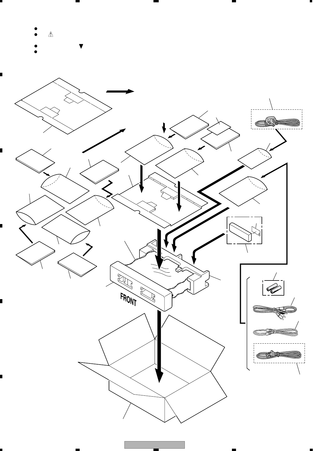
2. EXPLODED VIEWS AND PARTS LIST
2.1 PACKING
Parts marked by "NSP" are generally unavailable because they are not in our Master Spare Parts List.
The mark found on some component parts indicates the importance of the safety factor of the part.
Therefore, when replacing, be sure to use parts of identical designation.
Screws adjacent to mark on product are used for disassembly.
For the applying amount of lubricants or glue, follow the instructions in this manual.
(In the case of no amount instructions, apply as you think it appropriate.)
NOTES:
for WYXU/WY types
for WVXU type
20
18
16
19
5
4
17
17
15
14
7
15
15
15
15
10
15
15
9
12 6
2
13
8
11
3
1
1
DVR-3100-S 9
5678
5678
C
D
F
A
B
E
PACKING parts List
(2) CONTRAST TABLE
DVR-3100-S/WY, WYXU and WVXU are constructed the same except for the following :
Mark No. Description Part No.
>
1Power Cable See Contrast table(2)
2Audio/Video Cable VDE1077
3 RF Antenna Cable VDE1075
4 Remote Control See Contrast table(2)
5 Battery Cover AZA7424
NSP 6 Dry Cell Batteries (R6P,AA) VEM1030
7 Operating Instructions See Contrast table(2)
(English)
8 Operating Instructions See Contrast table(2)
(French)
9 Operating Instructions See Contrast table(2)
(German)
10 Operating Instructions See Contrast table(2)
(Italian)
11 Operating Instructions See Contrast table(2)
(Dutch)
12 Operating Instructions See Contrast table(2)
(Spanish)
NSP 13 Warranty Card ARY7065
NSP 14 Cord Sheet See Contrast table(2)
15 Polyethylene Bag VHL1051
16 Mirror Sheet VHL1006
17 Accessory Case VHC1112
18 Front Pad See Contrast table(2)
19 Rear Pad See Contrast table(2)
20 Packing Case See Contrast table(2)
Mark No. Description Part No.
Mark No. Symbol and Description DVR-3100-S/WY DVR-3100-S/
WYXU DVR-3100-S/
WVXU
>
1Power Cord ADG1154 ADG1154 ADG1156
4 Remote Control VXX2884 VXX2884 VXX2883
7 Operating Instructions VRB1316 VRB1316 VRB1318
(English)
8 Operating Instructions VRE1101 VRE1101 Not used
(French)
9 Operating Instructions VRE1103 VRE1103 Not used
(German)
10 Operating Instructions VRE1105 VRE1105 Not used
(Italian)
11 Operating Instructions VRE1107 VRE1107 Not used
(Dutch)
12 Operating Instructions VRE1109 VRE1109 Not used
(Spanish)
NSP 14 Cord Sheet Not used Not used VEG-012
18 Front Pad VHA1348 VHA1346 VHA1346
19 Rear Pad VHA1349 VHA1347 VHA1347
20 Packing Case VHG2445 VHG2417 VHG2416
DVR-3100-S
10
1234
1234
C
D
F
A
B
E
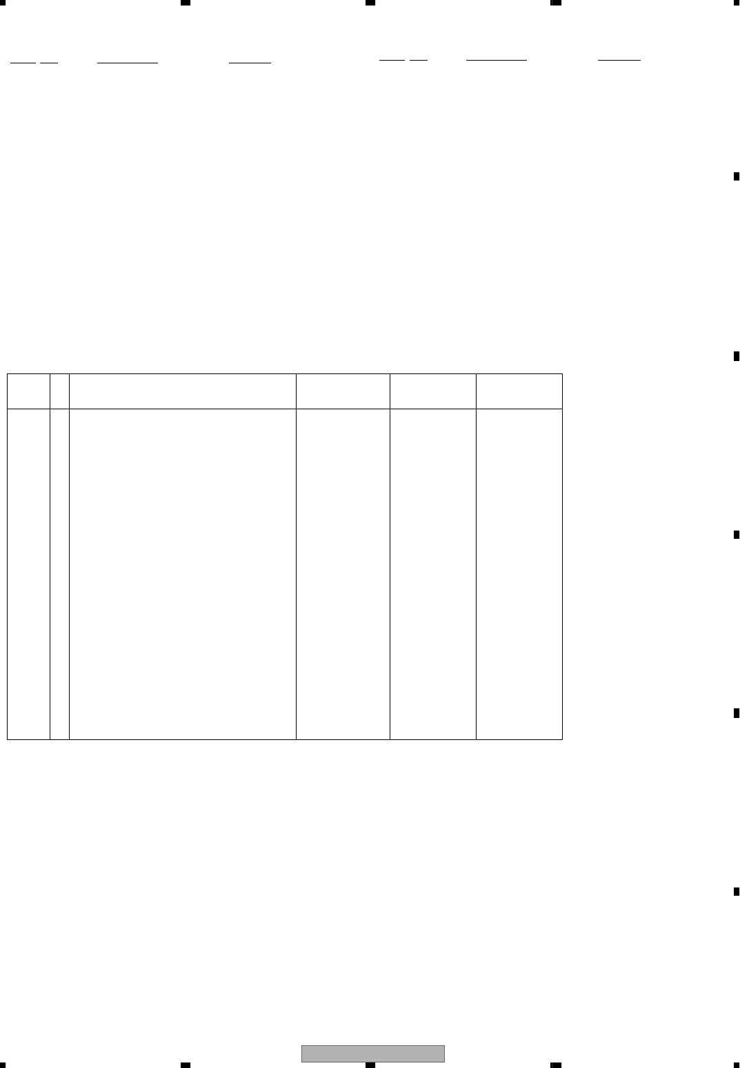
2.2 EXTERIOR
K
C
N
M
G
A
F
N
E
FG
C
H
A
H I J
J
I
K
M
BB
E
E
H
D
B
I
G
A
C
52
1
16
49
49
36
49
49
49 38
49
49
18
31
31
48
48
22
22
15
11 10
8
6
37
52
33 49
55
49
7
31
31
49
41
49
49
49
61
62
59
60
61 58
49
49
13
12
49
4
49
49
49
49
49
49
49
49
42
44
43
57
45
43
49
349
35
49 49
949
53
54
56
23
26
21
27
28 29
39
20
25
30
40 5
19 17
14
34
24
49
49
49
51
50
50
50
32
2
49
50
25 21
47
46
46
CONTACT SIDE
NON-CONTACT
SIDE
Lithium
Battery
Acetate Tape
(Taping for No.14 FFC)
Refer to "2.3 FRONT PANEL".
31
Bond Lock process
(Use GYA1011 or GYL1005)
Paste the bond both to the aluminum
tape and the side chassis of the
DRIVE Assy.( part)
The paste point is only this aluminum tape.

DVR-3100-S 11
5678
5678
C
D
F
A
B
E
EXTERIOR parts List
(2) CONTRAST TABLE
DVR-3100-S/WY, WYXU and WVXU are constructed the same except for the following :
Mark No. Description Part No.
1 ATAB ASSY VWV1968
2 TUJB ASSY VWV1962
3 FRJB ASSY VWV1965
4 MAIN ASSY VWV1971
5 MHLP ASSY VWV1991
>
6POWER SUPPLY UNIT VWR1374
7 DRIVE ASSY R6 VXX2898
8 DC FAN Motor VXM1109
9DVJB ASSY VWV1967
10 Connector Assy PF08EE-D25
11 Connector Assy PF13PP-D25
12 Flexible Cable (32P) VDA1975
13 Flexible Cable (21P) VDA1976
14 Flexible Cable (40P) VDA1977
15 Flexible Cable (15P) VDA1980
16 Housing Assy (4P) VKP2313
17 Housing Assy (8P) VKP2314
18 Housing Assy (2P) VKP2315
19 Leg Assy AEC7113
NSP 20 PCB Holder PNW1706
NSP 21 P. Plate Holder PNY-405
22 Earth Plate VBK1148
23 Radiation Sheet VEB1360
24 Card Spacer VEC1708
NSP 25 Clamp VEC2362
26 Heatsink Cushion VEC2363
27 Gasket A VEC2382
28 Gasket B VEC2393
29 Gasket Sheet VEC2394
30 M Cushion A VEC2398
31 Aluminum tape VEF1056
32 Rear Panel See Contrast table(2)
33 Bonnet Case VXX2897
NSP 34 Base Chassis See Contrast table(2)
35 PCB Base VNE2278
NSP 36 Writer Stay R VNE2318
NSP 37 Writer Stay L VNE2319
NSP 38 HDD Stay VNE2320
NSP 39 Bonnet Angle VNE2321
NSP 40 Heatsink VNH1070
41 Cable Holder VNK5330
42 Pioneer Name Plate VAM1136
43 Tray Sheet A VEC2346
44 Tray Sheet B VEC2358
45 Tray Sheet C VEC2395
46 Tray Sheet D VEC2396
47 Tray Panel Assy VXA2602
48 Screw AMZ30P060FMC
49 Screw BBZ30P060FMC
50 Screw BPZ30P080FZK
51 Screw PPZ30P080FMC
52 Screw BCZ40P060FN
53 Flexible Cable (7P) VDA1979
NSP 54 DV Angle VNE2322
55 Bonnet Label See Contrast table(2)
56 Screw VBA1088
NSP 57 Front Panel Assy See Contrast table(2)
58 SCRB ASSY VWV1958
59 Flexible Cable(35P) VDA1982
60 Flexible Cable(15P) VDA1983
NSP 61 Spacer 40 PNW2488
62 Earth Plate VBK1149
Mark No. Description Part No.
Mark No. Symbol and Description DVR-3100-S/WY DVR-3100-S/
WYXU DVR-3100-S/
WVXU
32 Rear Panel VNA2674 VNA2610 VNA2610
NSP 34 Base Chassis VNB1040 VNB1039 VNB1039
55 Bonnet Label VRW1990 VRW1990 VRW1987
NSP 57 Front Panel Assy VXA2634 Not used Not used
(WYXU and WVXU types are individual parts.)
DVR-3100-S
12
1234
1234
C
D
F
A
B
E
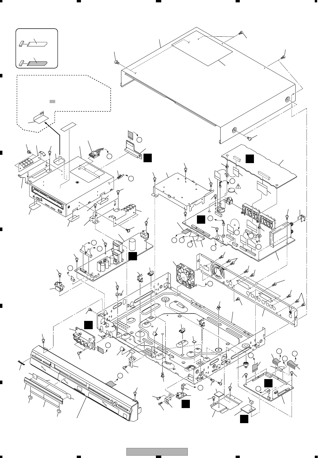
2.3 FRONT PANEL
F
16
15 20
18
11
14
17
8
935
5
25
24 24
24
4
619
2
1
7
10
12
23
13
21
22
CONTACT SIDE
NON-CONTACT
SIDE
11
Daifree
GEM1036
DVR-3100-S 13
5678
5678
C
D
F
A
B
E
FRONT PANEL parts List
(2) CONTRAST TABLE
DVR-3100-S/WY, WYXU and WVXU are constructed the same except for the following :
Mark No. Description Part No.
1 FLKY ASSY VWG2443
2 Flexible Cable (19P) VDA1974
3 Rubber Sheet AEB7054
4 Door Spring VBK1144
5 Rubber Foot VEB1349
6Drive Sheet VEC2345
7 FL Lens VEC2352
8 Door Lens See Contrast table(2)
9Jack Sheet VEC2381
10 FL Filter VEC2354
11 Jack Door VNK5309
12 JOG Dial S VNK5316
13 JOG Base VNK5317
14 Hologram Label VRW1962
15 Flont Panel Assy VXA2616
NSP 16 Front Panel VNK5361
17 Front Cover R VNK5360
18 Front Cover L VNK5358
19 Main Key S VNK5312
20 Power Key S VNK5313
21 Rec Key VNK5314
22 Stop Key S VNK5315
23 Function Cover VNK5318
24 Screw BPZ30P080FZK
25 DV Cover VNK5355
Mark No. Description Part No.
Mark No. Symbol and Description DVR-3100-S/WY DVR-3100-S/
WYXU DVR-3100-S/
WVXU
8 Door Lens VEC2377 VEC2377 VEC2376
DVR-3100-S
14
1234
1234
C
D
F
A
B
E
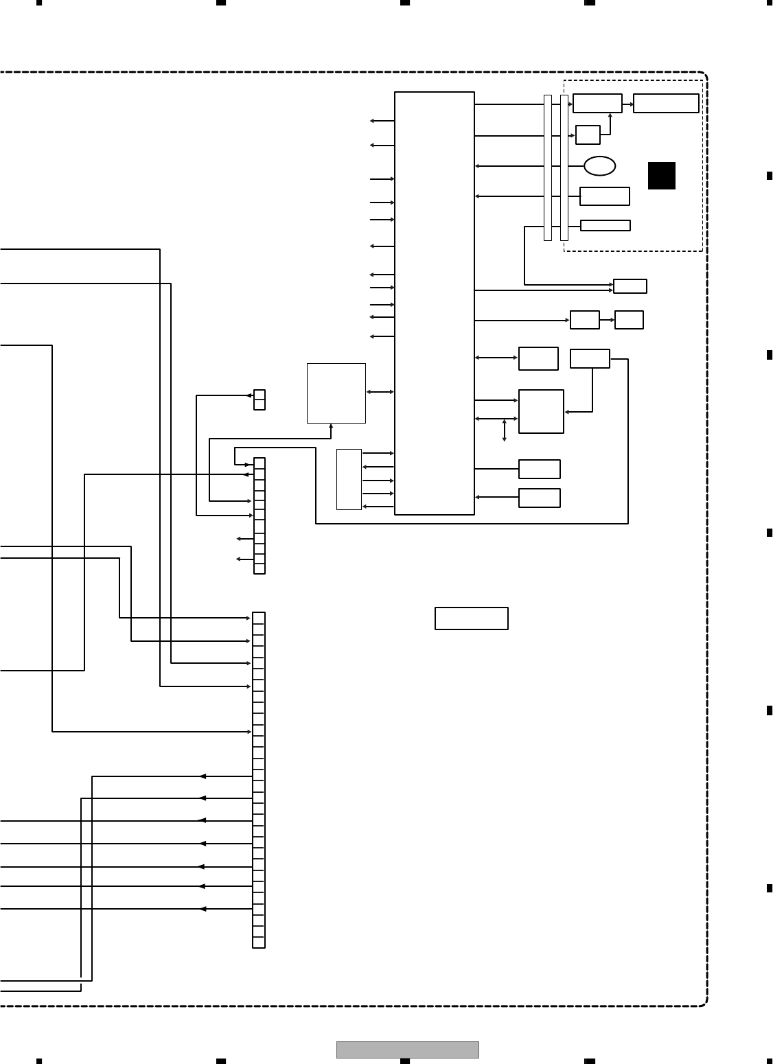
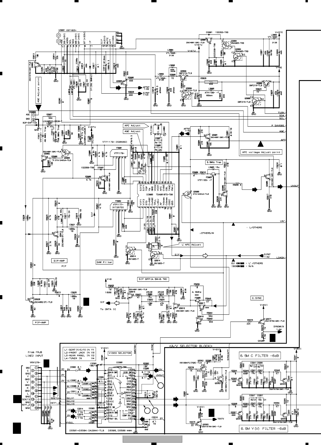
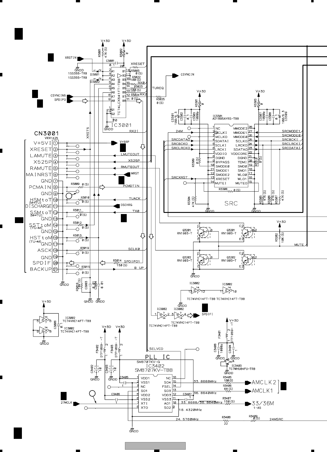
3. BLOCK DIAGRAM AND SCHEMATIC DIAGRAM
3.1 BLOCK DIAGRAM
3.1.1 OVERALL BLOCK DIAGRAM
SPDL
MOTOR
LD
DRIVE
Pickup
LOADING
MOTOR
STEPPIONG
MOTOR
TV TUNER MODULE
U3001 VXF1023
ANT
INPUT3
VIDEO
Y/C
L
R
(15P)
CN1301 (15P)
(35P)
CN3002
CN210(1/2)
(35P)
CN203(1/2)
FRJB
ASSY
SCRB
ASSY(1/2)
TUJB ASSY(1/3)
TUJB ASSY
(2/3)
D
C
I1/2
MAIN ASSY
DRIVE ASSY
M
14 2
4
6
6
12
10
IF
OUT
Y
L
R/C
LL
C
V/Y
V/Y
V/Y
C
UVL
SIF
IN L
OUT
LIN2
LIN1
LIN3
L
V/Y
C
RF IN
RF
OUT
V/Y
UVV
3V
3Y
1Y
2Y
3C
1C
2C
2V
C
Y/Comp
Selector
IC3301
LA73030
IC2801
LC75342M
IC4001 MSP3417G
IC3903 TDA9818TS
IC101(1/2)
LA73026AV
13
5
11
14
12
32
34
24
36
1
3
15
17
19
5
7
9
LPF
1 Chip
Sysytem Codec
Stereo
Decoder
VIF/SIF
IC
Audio Selector with Electirc ATT
227
16
12
JA1302
JA1301
VIN2
YIN2
CIN2
10
LIN2
INPUT3
PICKUP
ASSY
Y
C
JA2832
VIDEO
Y/C
L
R
LIN3
VIN3
YIN3
M
(40P)
[ATAPI]
DVD-VR
DVD-Video
DVD-VR
DVD-Video
CD Digital
CD Digital
CN4401
1
CN201
(2P)
CN2009 (2P)
CN101
(45P)
8
CIN3
CN501
CN502
(12P)
33
39
A
B
C
D
S4
S3
S2
S1
5
4
3
2
1/3
B
2/3
B
PB DVD/CD
IC1001
M65672WG
IC201
UPD63620
IC501
M63028FP
IC101
UPC3320GC
RF IC
IC301
M30700FJLGP
IC202
SDRAM
16Mbit
7-10
13-16
(40P)
CN401
(21P) (21P)
CN2008
(1/2)
DSP
48
37
40
36
38
34
35
LPF
IC1401
IC1421 ATA SDRAM
256Mbit×2
CPU SDRAM
128Mbit
IC1102 IC1101
Flash
64Mbit
IC1103
SRAM
4Mbit
2
8 8
Writer
CPU
26
6CH
Driver
2
IC203
DS90LV027ATM
LVDS
Driver
26
28
LPF
201
76 CN3001
(1/2)
1,2
23,24
PIF
SAW
Trap SIF
SAW
11
AV1(TV) AV2(STB)
31
15
9
5
5
39
21
27
23
28
33
36
JA101
JA102
DVR-3100-S 15
5678
5678
C
D
F
A
B
E
FFLKY
ASSY
SCRB
ASSY
(2/2)
I2/2
H
E
MHLP ASSY
L
Control
Data
IC1301
IC3201
PCM1742KE
IC1001 PT6315
V1001
IC3101
AK5381VT
IC3301
AD1895AYRS
IC5101
UPD72852AGB-8EU
IEEE1394
Physical IC
IC5202
UPD72893AGD-LML
IEEE1394
Link IC
Audio
A/D 2
SEL.L
VOUT
L
L
V/Y
V/Y
V/Y
V/Y
L
L
R/C
R/C
G
G
B
B
IC4001 Pin27
IC3903 Pin16
(19P)
CN2005
(19P)
CN1001
DVJB ASSY
YOUT
COUT
LOUT
(32P)
CN3001(1/2)
24 SEL.V/Y
26 SEL.C
C IN
V/Y IN
CN1302
(7P)
CN5102
(7P)
JA1303
(32P)
(30P) (30P)
(21P) (21P)
CN2001
(2/2) (32P)
CN3001
(2/2)
CN2008(2/2)
38 39 37 36
1,3 2 6 7
XTPA
TPA
TPB
XTPB
XTPB
TPB
XTPA
TPA
1,3 2 6 7
1 2 3 4
Audio
D/A Conv.
PLD
ALTERA
SCART Interface
MIX
FL Driver
FL Key
SW
IC3501
LA73054
Sampling Rate
Converter
7
C
Y
G
R
B
C OUT
Y OUT
G OUT
B OUT
C
Y
G
B
R
L
TU_V
TU_L
R OUT
6
4
8
10
12
CN3001(2/2)
CN2
CN4702
6
4
8
10
12
29 27 25 19 17 13 5 3
L OUT
16 16
SPDIF
20 20
3
21
IC3251-1/2
UPC4570G2
Y
C
V
Tuner U-com
JA3081
OPTICAL
AC-3/PCM
DIGITAL
AUDIO
OUT
LINE
OUT 2
VIDEO
JA3551
JA101
JA102
Y
C
L
R
: Recording system signal route
• R ch is same as L ch.
: Playback system signal route DV TERMINAL
(32P)
CN2001
(1/2)
24
28
26
48KHz 20Bit
TUJB ASSY(3/3)
3/3
B
ENC
SDRAM
128Mbit
IC1201
IC1
PDY081A
DEC
SDRAM
64Mbit
IC5204
DV SDRAM
16Mbit
8
6
28
31
33
I
C2001
PD5947A8
Tuner
U-com
I
C2251
BR24L32F-W
EEPROM
I
C2271
RS5C372A
Real
Time
Clock
28
9
10
12
1-3
F5 D2
AE24
AG25
AD21
AF23
AG24
T26
V27
• MPEG2 PS Encode
• AC-3/Linear PCM
Audio Encode
• 2ch ATA/ATAPI Interface
• MPEG2 PS Decode
• AC-3/MPEG1/Linear
PCM Audio Decode
AV1(TV) AV2(STB)
IC101(2/2)
LA73026AV
25
26
30
42
7
18
23
28
2
16
33
36
IC103
42
6
IC114
42
6
IC102
112
15 14 13
2
IC106
42
6
IC107
42
6
IC113
12 13
14
IC105
42
6
7 9 11 17 19 23 31 33
DVR-3100-S
16
1234
1234
C
D
F
A
B
E
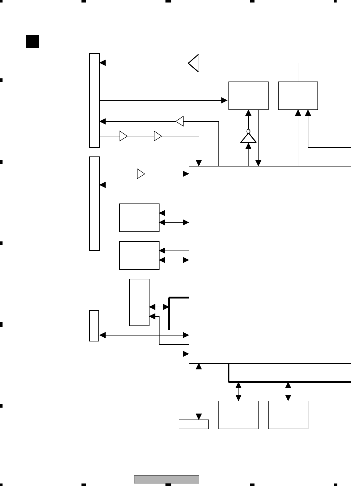
3.1.2 TUJB ASSY BLOCK DIAGRAM
U3001
V/U Tuner Module
VXF 1023-
SCL
SDA
SCL
SDA
AFT
AGC
<u-com>
TUON<u-com>
+32V
Reg. +6V
SW.
+5V
Ripple Filter
IC3301
LA73030
Video
Selector
IC3903
TDA9818TS
VIF/SIF
IC
EVOLCLK
EVOLDATA
EVOLCE
LC75342M
IC2801
Audio Selector
with
Electric A.T.T
Audio Input Circuit
Output Circuit
Video Input Circuit
SDET2 <u-com>
IC3903 Pin16
SDET3 <u-com>
LAMUTE
RAMUTE
<MAIN>
(Discrete)
R
L
Comp
C
Y
V
C
Y
C
Y
G
B
R
L
R
TU_L
TU_CVBS
TU_R
Muting
OUT2
JA1301
JA1302
IN3
(Rear)
IN2
(Front)
JA2832
V
Y
Y
IF
AGC
AGC
<u-com>
C
C
V
Y
C
S
S
L
R
L
R
L
R
JA3551
IC3501
LA73054
Video Driver
with LPF
<u-com>
SELV1
SELV2
SELV3
YVSEL
SWSTBY <u-com>
R
L
V/Y
C
SYNC
LPF
Trap
PIF
SAW
SIF
SAW
LPF
Sync-Sepa
13.5MHz
LPF
13.5MHz
LPF
C
V/Y
24
16
12
11
1,2
23,24
26
28
2
5
28
31
33
6
8
26
TUJB ASSY (VWV1962)
B
FRJB ASSY (VWV1965)
SCRB ASSY
(2/2)
(VWV1958)
C
I2/2
CN1301
CN3002
CN210(2/2)
CN203(2/2)
8
8
610
6
10
2
14
12
4
JA3081
Optical
OUT
12 4
13
11
3
1
17
19
27
29
25
23
25
33
531
35
19
17
9
7
11
SCRB ASSY
(1/2)
(VWV1958)
I1/2
CN203
(1/2) CN210(1/2)
29
21
5
27
7
15
31
9
Stereo
Decoder
MSP3417G
IC4001
<u-com>
SYNCAFT<u-com>
SYNCMAIN
SYNC<u-com>
SIF <IC3903:VIF/SIF IC>
SIF <IC4001:Pin2>
Q3344
Q3342
Q3362
Comparator
Q3371
Q4001-Q4004
AFC
AGC
15kHz LPF
6.5MHz
LPF
13.5MHz
Trap
6.5MHz
LPF
13.5MHz
LPF
DVR-3100-S 17
5678
5678
C
D
F
A
B
E
+6V
SW
FL Driver
PT6315
Front Keys
IR Detector
FAN
Driver FAN
EEPROM Battery
Ceramic
Resonator
EVOLCLK
EVOLDATA
EVOLCE
SPDIF
PCMOUT
PCMOUT
LAMUTE
RAMUTE
FLKY
ASSY
(VWG2443)
FLPON
SELIR
BUP
BUP
JOGA, JOGB
KEY1, KEY2
KEY1_2
FLCLK, FLDATA, FLSTB
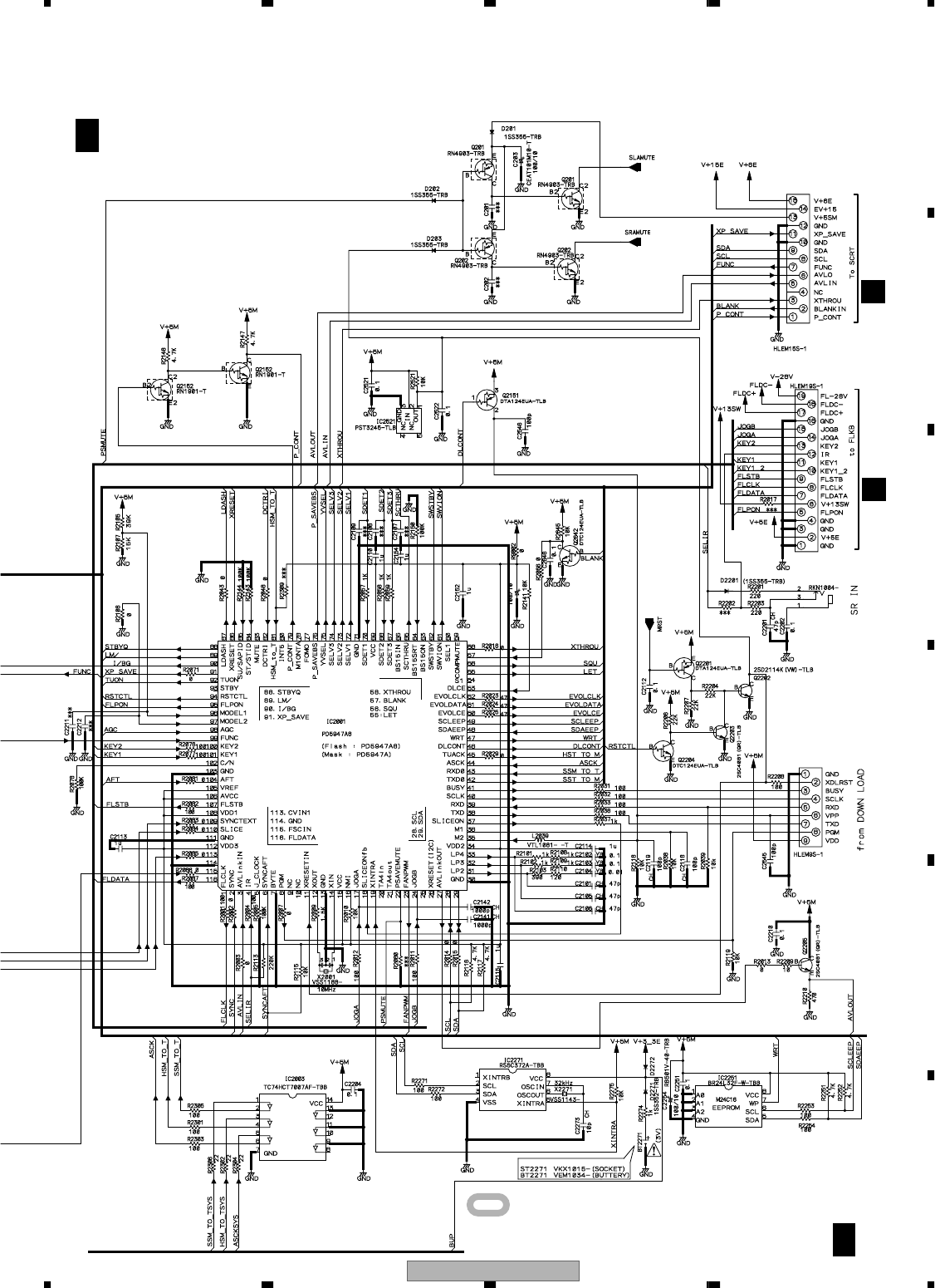
IC2001
CN1001
CN2005
Tuner/FL
Control U-com
PD5947A8
XINTRA
SCL
XIN, XOUT
XRESETIN
SDA
Other Devices
SCLEEP
SDAEEP
BR24L32F-W
IC2271
Real-Time
Clock
RS5C372A
U-com I/F
Y
24
23
22
21
20
19
18
30
29
28
27
26
25
17
16
15
14
13
12
11
10
9
8
7
6
5
4
3
2
1
C
Y/G
Cb/B
Cr/R
R
L
SYNCMAIN
SELC
CN2008
< from/to MAIN >
CN2009
< from DRIVE >
SELV/Y
SELR
SELL
20
21
3
5
8
2
F
SYNCAFT
<Q3362>
PSAVEBS
<Q3907>
IC1001
Q1001
Q2640
IC2251 BT2271
X2001
Reset IC
PST3245
IC2521
IC1002
S1001-S1008
S1003
SR In
JOG
JA2201
FL Display
V1001
SYNC
<IC3301>
LM/LDASH
<IC3903>
TUON
FUNC
AVLO
ASCK
SST to M
SSM to T
HST to M
HSM to TSYS
XRESET
<Q3006,etc>
AVLIN
BLANK
XP_SAVE
AGC
<U3001>
DCTR1
<IC4001>
STBYQ
<IC4001>
<IC2801>
SELV1
SELV2
SELV3
SWSTBY
<IC3301>
SDET1
SDET2
SDET3
<JA1301,
JA2832>
< to/from MAIN >
CN3001
SCART
Control
DVR-3100-S
18
1234
1234
C
D
F
A
B
E
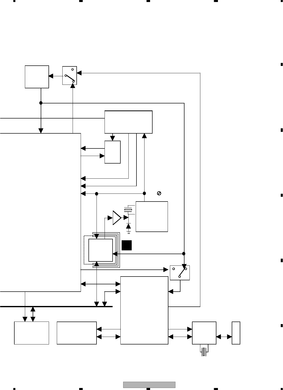
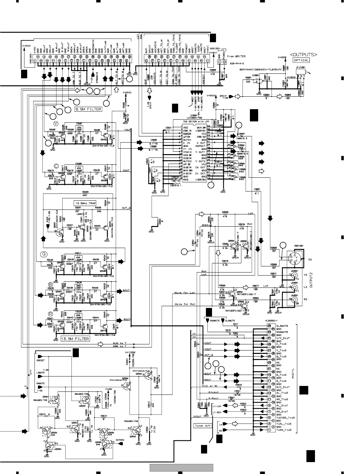
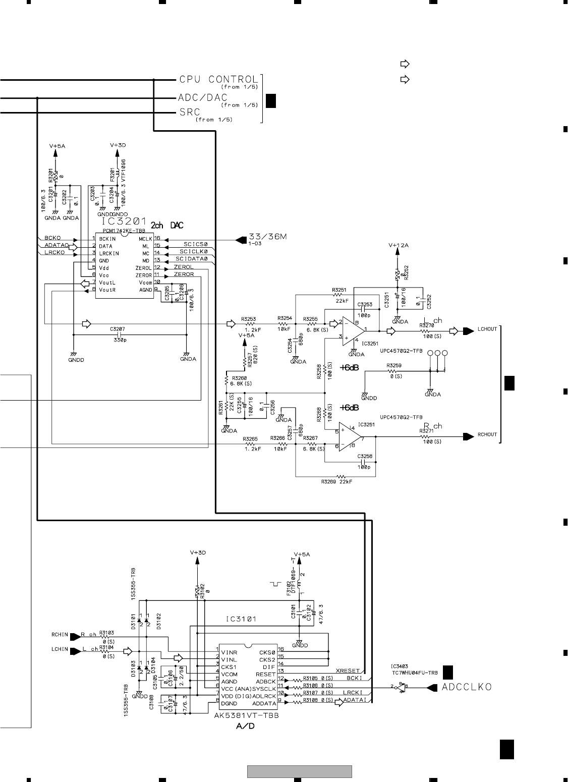
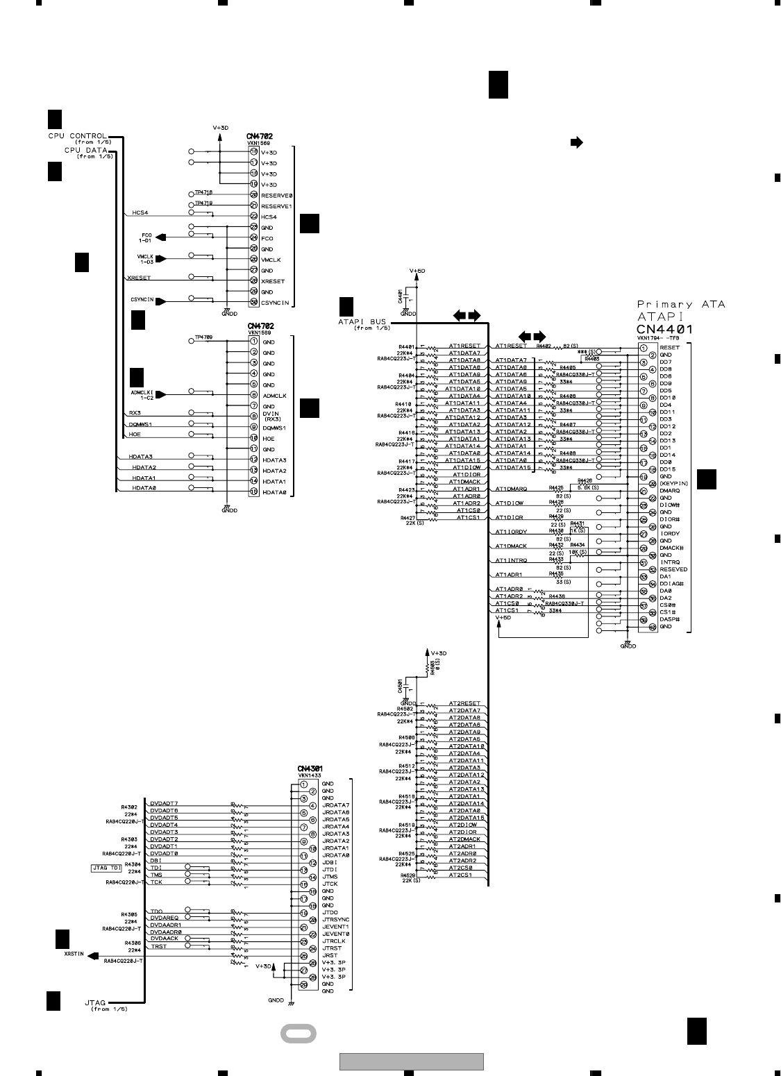
3.1.3 MAIN ASSY BLOCK DIAGRAM
To Writer
IC1401
ATA SDRAM
CN4401
ATA BUS
IC1102
FLASH
IC1103
IC1301
ENC
SDRAM
MT48LC4M32B2TG-6
K4S561632D-TC75
IC1201
DEC
SDRAM
W986416DH-6
VYW2116 CY62148VLL-70ZI
ARCLK0
DCLK0
ECLK0
IC3201
PCM1742KE
DAC
IC3101
A/D
AK5381VT
ADCCLKO
IC3403
AUDIO LR OUT
AUDIO LR IN
IC3251
CN2001CN3001
CN1901
SERIAL
MAIN ASSY
(VWV1971)
D
IC1001
M65672WG
1 Chip System Codec
• MPEG2 PS Encode
• AC-3/Linear PCM Audio Encode
• 2ch ATA/ATAPI Interface
• MPEG2 PS Decode
• AC-3/MPEG1/Linear PCM Audio Decode
Backup
SRAM
IC3001
Q2402,Q2403
Q2101-Q2105
IC2301,IC2331,Q2203
Q2222
VIDEO Y,C,Yp,Cb,Cr OUT
VIDEO Y,C IN
TO TUNER u-COM
DVR-3100-S 19
5678
5678
C
D
F
A
B
E
HOST BUS
DV
IC1101
CPU SDRAM
IC5202
UPD72893AGD-LML UPD72852AGB-8EU
LINK/DV CODEC
IC5101
Phy
CN5102
CN2
CN4702
IC5204
DV SDRAM
K4S281632E-TC75 K4S161622D
MCLK
VCLKI
SCLK
HCLK0
IC3301
SRC
SRC**O
SRC**I
IC4205
TC7WHU04FU
AD1895AYRS
Play Mster clock
IC4206
AMCLK2
IC3402
PLL IC
27M
24
VMCLKI
AMCLK1
33M
36M
33/36M
X4102
VSS1195
VCXO
Input Mster
clock
ADMCLKI
27M
IC4101
DVPLLCK(ADMCLKI)
DVVPWM
IC4009
DVVCLKO
SM8707KV
IC1
PDY081A
ALTERA
MHLP ASSY
(VWV1991)
E
Master Clock
Free Run
DVR-3100-S
20
1234
1234
C
D
F
A
B
E
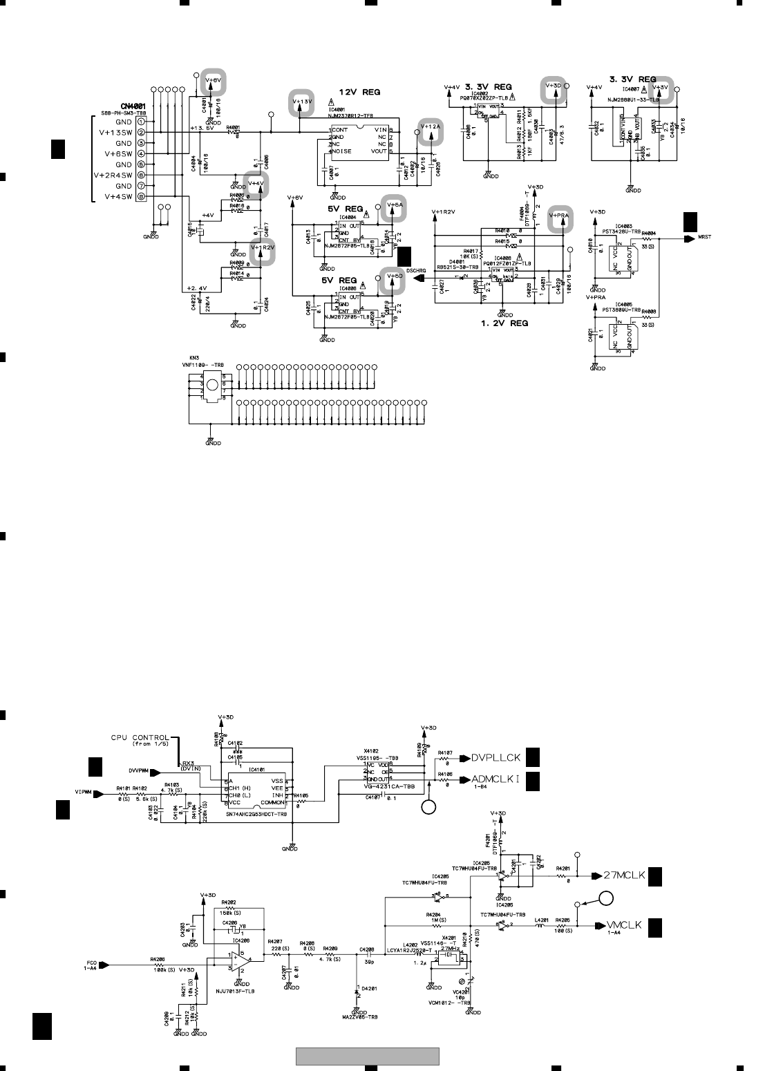
3.1.4 POWER BLOCK DIAGRAM
LIVE
FLDC (–)
AC IN
F1
T4A/250V
NEUTRAL
1
2
3
5
4
7
9
11
13
3
5
4
7
9
11
13
FLDC (+)
FL–28V
EV+37V
V+37E
EV+15V
EV+6V
SW+13
SW+12V
1
4
1
SW+5V
SW+12V
1
4SW+5V
DRIVE ASSY
R6
DC FAN
MOTOR
CN1 CN204
(4P)
CN203
(4P)
CN201
(13P)
SW+4V
V+13FAN
V+4SW
V+4SW
V+2_4SW
V+2_4SW
CN2001
(8P)
CN2006
(2P)
CN2003
(8P)
CN4001
(8P)
2
3
5
7
2 4 6 8
2 4 6 8
2
3
5
7
V+6SW
V+6SW
V+13SW
V+13SW
Q2640
Q2532Q2531
Q2621
SW+4V
SW+2.4V
SW+6V
CN202
(8P)
CN2
(30P)
16
17
18
19
16
17
18
19
CN4702
(30P)
POWER SUPPLY UNIT
G
FLKY ASSY
F
TUJB ASSY
B
MAIN ASSY
DMHLP ASSY
E
CN2004
(13P)
V–28V
V+13SW
V+6SW
V+2_4SW
V+4SW
VEE 1
2
3
14
18
19
18
17
6
2
V+5VO
V+5VI
CN3001
(32P)
CN2001
(32P)
1
1
V+5VO
CN2008
(21P)
CN3001
(21P)
1
1
V+5VI
FLDC –
FLDC +
V+13SW (NC)
V+5E
V+5E
CN1001
(19P) CN2005
(19P)
V+15E V+6E V+13SW
IC2551
5V REG.
V+6E
V+5M
V+5E
IC2541
3.3V REG.
V1001
FL TUBE
IC1001
FL Driver
V+6E
V+6SW
V+6E
V+3_3E
V+5VO
V+13V
V+4V
V+4V
V+6V
V+1R2V
V+5VO
V+12A
V+5VI
V+5RP
IC2581
9V REG.
V+13SW
V+9
1
1
6
3
1 3
30
IC4001
12V REG.
5 8
V+5A IC4004
5V REG.
5 1
V+6V
V+5D IC4006
5V REG.
5 1
V+3D
IC4002
3.3V REG.
1 3
V+3D
V+2R5
IC5002
2.5V REG.
7 1
V+1R2V
V+PRA
V+3D
V+3D
IC4008
1.2V REG.
1 3
V+4V
V+3V
IC4007
3.3V REG.
5 4
V+3D
V+3D
V+3D
V+3D

DVR-3100-S 21
5678
5678
C
D
F
A
B
E
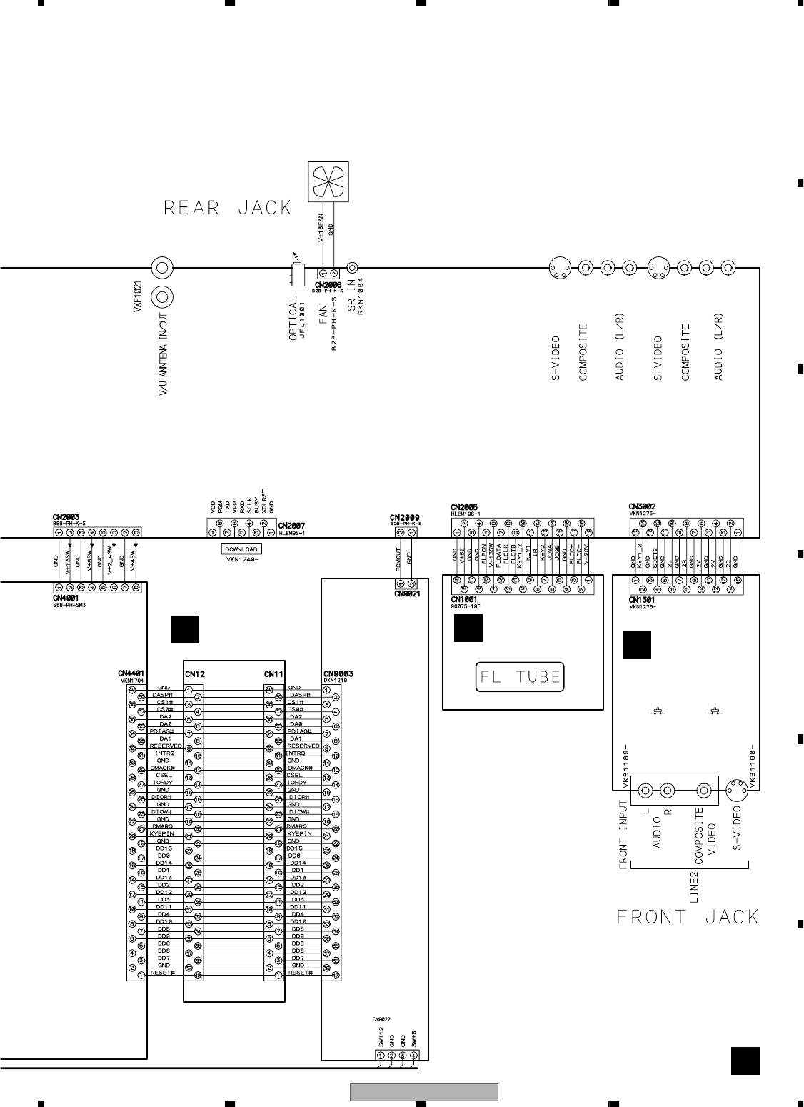
DVR-3100-S 23
5678
5678
C
D
F
A
B
E
A
FRJB ASSY
(VWV1965)
C
FLKY ASSY
(VWG2443)
F
ATAB ASSY
(VWV1968)
A
DRIVE ASSY R6
(VXX2898)
DISC NAVI POWER
CKS4052 VKN1805
JA3551 JA2832
JA3081
U3001
DC FAN MOTOR
: VXM1109
Note : When ordering service parts, be sure to refer to "EXPLODED VIEWS and PARTS LIST" or "PCB PARTS LIST".
OUTPUT X1
VKB1184-
INPUT X1
VKB1192-
DVR-3100-S 27
5678
5678
C
D
F
A
B
E
CN3001
CN2008
CN2009 JA3081
JA3551
CN210
CN203
I
B2/3
TUJB ASSY (VWV1962)
to DRIVE ASSY R6 CN9021
CN2001
D2/5
CN3001
D3/5
: S VIDEO SIGNAL ROUTE
(Y)/(C)
(C)
(Y)
(G)
(G)
(Y)
(C)
(B) (B)
(B)
(R)
(R)
(R)
(Y)
(Y)
(C)
(C)
(D)
(G)
(Y)
(C)
(C)
(G)
(V)/(Y)
(D)
(C)
(B)
(R)
(V)/(Y)
(C)
: COMPONENT VIDEO SIGNAL
ROUTE
(G)/(B)/(R)
: VIDEO SIGNAL ROUTE
(D)
: AUDIO SIGNAL ROUTE (L ch)
B1/3
B1/3
B3/3
B1/3
B1/3
B2/3
79
5
6
8
10
11
19
16
17
20
12
18
15
14
13
DVR-3100-S
28
1234
1234
C
D
F
A
B
E
3.5 TUJB ASSY(3/3)
Stereo Decoder IC
B3/3
B3/3
B3/3
TUJB ASSY (VWV1962)
B2/3
B1/3 B1/3,2/3
DVR-3100-S 29
5678
5678
C
D
F
A
B
E
3.6 FRJB and DVJB ASSYS
DV Terminal
CN1301
JA1301
JA1302
FRJB ASSY (VWV1965)
C
CN3002
B2/3
Switches
S1201 : Standby On
S1202 :
Disc Navigator
C H HC
: S VIDEO SIGNAL ROUTE (Y)
(Y)
(Y)
(Y)
: S VIDEO SIGNAL ROUTE (C)
(C)
(C)
(C)
: VIDEO SIGNAL ROUTE
: AUDIO SIGNAL ROUTE (L ch)
CN5102
D5/5
DVJB ASSY
(VWV1967)
H
DVR-3100-S
36
1234
1234
C
D
F
A
B
E
3.10 MAIN ASSY(4/5)
D4/5
CN2003
B1/2
D3/5
D5/5
D1/5
D1/5
D5/5
D1/5
D3/5
D3/5
1
2
DVR-3100-S 37
5678
5678
C
D
F
A
B
E
D4/5
D4/5
MAIN ASSY (VWV1971)
CN12
A
CN2
E
CN2
E
D1/5
D1/5
D1/5
D1/5
D1/5
D1/5
D1/5
D3/5
: ATA DATA SIGNAL ROUTE
(AT)
(AT)
(AT)
: The power supply is shown with the marked box.
DVR-3100-S
46
1234
1234
C
D
F
A
B
E
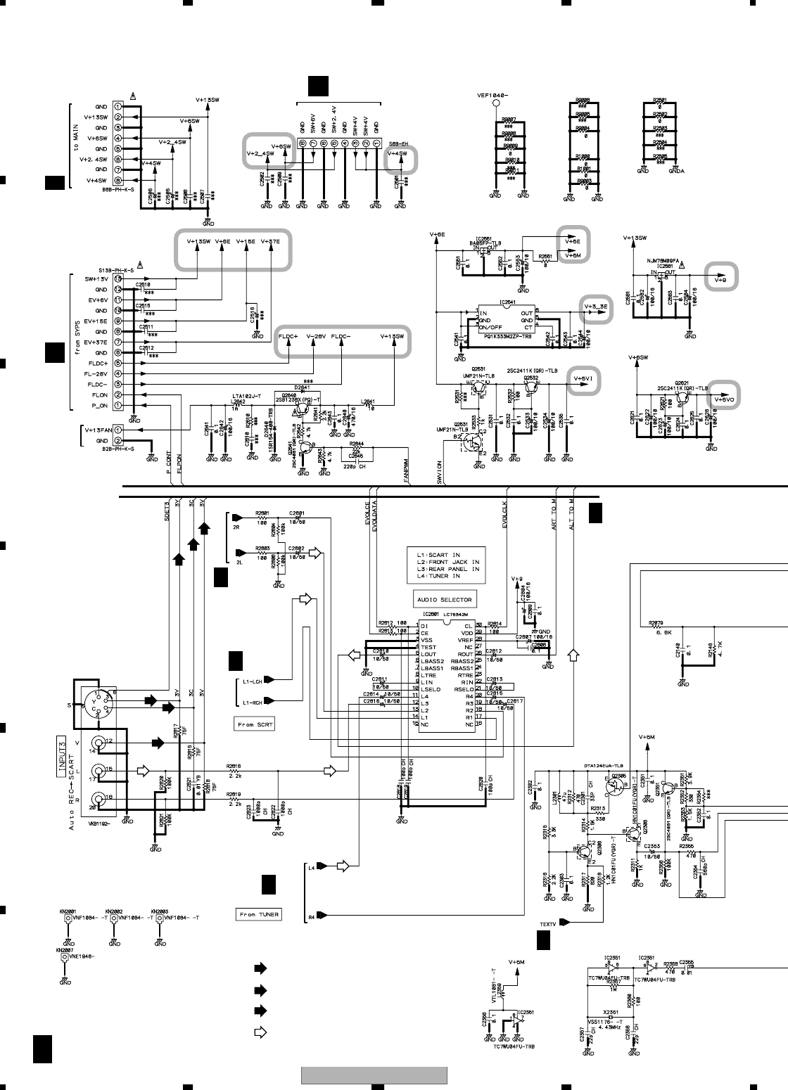
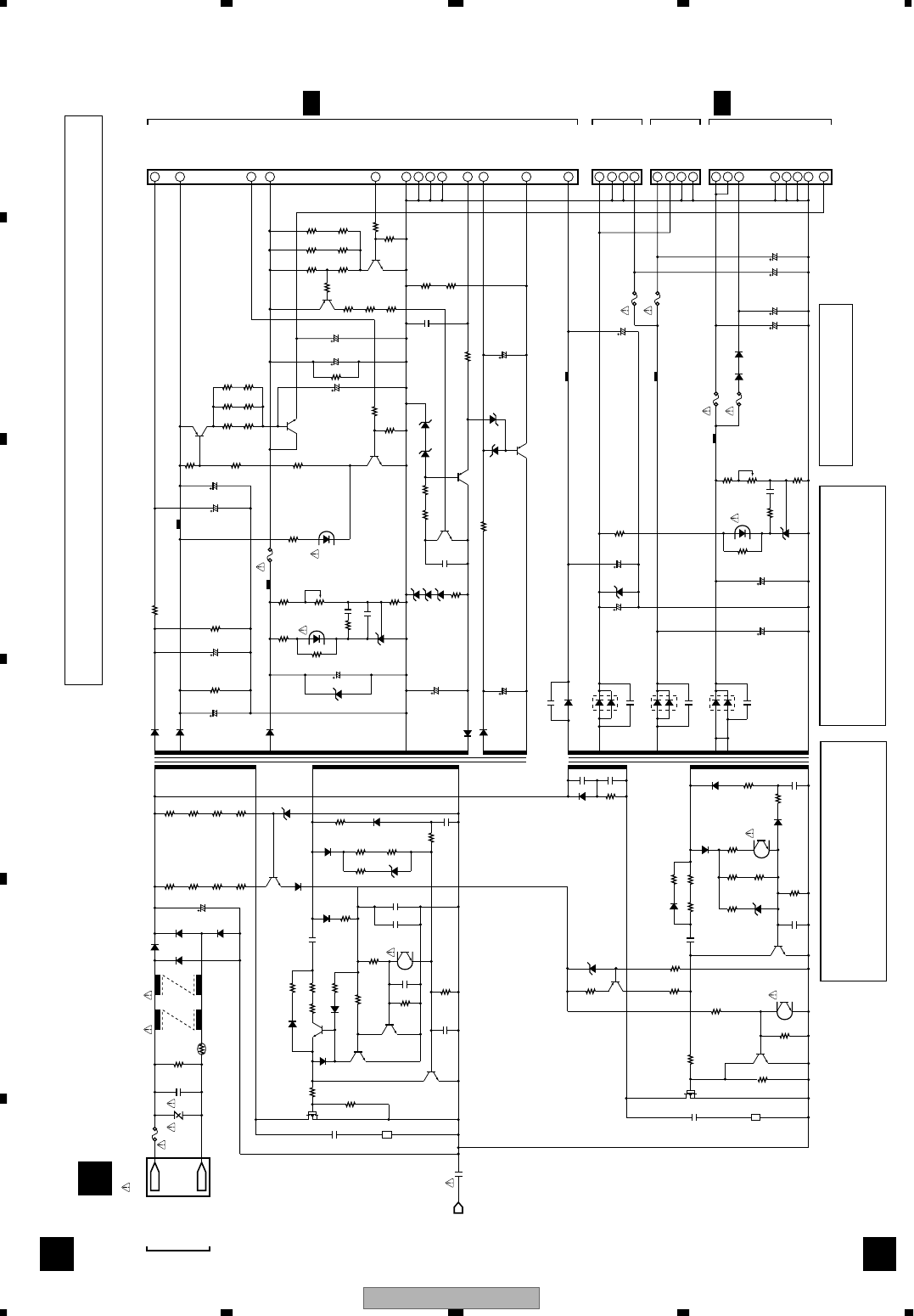
3.15 POWER SUPPLY UNIT
GG
CN1 CN201
CN203
CN202
CN204
LIVE
NEUTRAL
7
9
1
2
8
6
4
5
3
1
2
2
3
3
4
11
12
10
13
EV+37V
EV+18V
PO. ON
EV+6V
FL. ON
GND
GND
GND
GND
FL–28V
FLDC (+)
SW+13
SW+12V
GND
GND
GND
GND
GND
GND
GND
GND
SW+5V
SW+5V
SW+6V
SW+4V
SW+4V
SW+2.4V
SW+12V
FLDC (–)
4
1
3
2
5
1
4
6
8
7
POWER SUPPLY UNIT (VWR1374)
G
AC IN
F1
(T4AH 250V)
C1Z1 R1
L1 L2 D12
D14 D13
D11
C51
Q71
R71 R70
R75
R73
R77
R72
R76
R74
T1
D71
C7
CN901
C6
Q1 R19
R5
D7
D6
D17
Q22
Q23
Q2
Q21
R7
R6
R2
R30
R16 C10
D4
C73 C72
PC1
C15
R33
C9 R8
R31
R12
D5
R11
R13
D9
R17
D8
R10
C11
C52
BEA51
BEA1
Q51 R59
R55 Q91
R85
R24
PC3
R79
D73
R78
Q72
R81 C60
D57
D54
R57
R55 R56
R62
D55
Q52
C59 R58
R61
R63
R59
PC51
D50
R50
C51
R67
D56
D501
D504
D401
R504
C501 R501 C601 R601
L501
C602 C502
NTC1
D72
R9
D30
R90
C90 C91
D101
D470
D301
C102
C471
C302
T51
C353
D351
C470 C101
R101
IC101
PC51
R105 C110 VR101
R102
R103
L101 P101
P201
D201
R106
C351
D302
C301
L470
L351
D801
D701
C801
C701
Q801
D802 D811
Q701
R801
C702 Q703
R704 R703
D703 D704
R404
R705
D707
D706
D708
Q402
R408
R407
IC403 C409
R413
C410
PC1 VR401
D402 C401
R402
R401 R403 L401 P401
R557
PC3
R412
C411
R457
C403
Q451
R560 Q403
R411
R551
R552
R555
R556
R553
R554
C404
Q404
Q401
R434
R451
R452
R453
R454
R455
R456
R433
R432
R810
R811
C703
R710
C802
R435
R437
R436
C352 P403
P404
D202
C103
C406 C405
C201
P101 : AEK7050 (3A)
P201, P401, P403, P404 : AEK7067 (2A)
CN2004
To
DRIVE ASSY
R6 CN9022
B1/2
CN2001
B1/2
• NOTE FOR FUSE REPLACEMENT
FOR CONTINUED PROTECTION AGAINST RISK OF FIRE.
REPLACE WITH SAME TYPE AND RATINGS ONLY.
CAUTION -
CAUTION : FOR CONTINUED PROTECTION
AGAINST RISK OF FIRE.
REPLACE ONLY WITH SAME TYPE
NO. 491003 FOR P101 MFD, BY
LITTELFUSE INC.
CAUTION : FOR CONTINUED PROTECTION
AGAINST RISK OF FIRE.
REPLACE ONLY WITH SAME TYPE
NO. 491002 FOR P201, P401, P403
and P404 MFD, BY LITTELFUSE INC.
DVR-3100-S 47
5678
5678
C
D
F
A
B
E
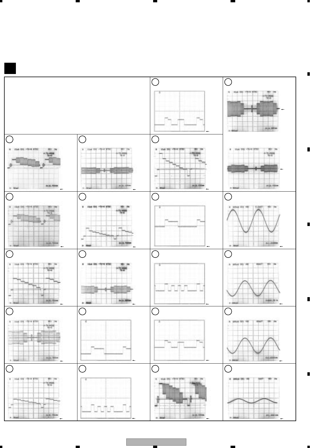
3.16 WAVE FORMS
Measurement condition ;
No.1 to No.6 : 75% Color-bar
No.7 to No.17 : 75% Color-bar, AXP disc 1-24
No.18 : 1kHz, 2Vrms
No.19, No.20 : 1kHz, 2Vrms, AXP disc 1-1
TUJB ASSY
B
1UVIN jumper as same as C3306
(UVIN) (Function : 1 ch)
V: 500mV/div. H: 10µsec/div.
2BSIN jumper as same as C3309
(BSIN) (Function : BS9 ch)
V: 500mV/div. H: 10µsec/div.
3IC3301-pin 24 (Y) (Function : L1)
V: 500mV/div. H: 10µsec/div.
4IC3301-pin 26 (C) (Function : L1)
V: 500mV/div. H: 10µsec/div.
5CN3001-pin 24 (Y) (Function : L1)
V: 500mV/div. H: 10µsec/div.
6CN3001-pin 26 (C) (Function : L1)
V: 500mV/div. H: 10µsec/div.
7CN3001-pin 4 (Y) (Function : PLAY)
V: 500mV/div. H: 10µsec/div.
8CN3001-pin 6 (C) (Function : PLAY)
V: 500mV/div. H: 10µsec/div.
9CN3001-pin 8 (G)
(Function : PLAY)
V: 500mV/div. H: 10µsec/div.
10 CN3001-pin 10 (B)
(Function : PLAY)
V: 500mV/div. H: 10µsec/div.
12 Foot of C3511 + side (Y)
(Function : PLAY)
V: 500mV/div. H: 10µsec/div.
13 CN210-pin25 (G)
(Function : PLAY)
V: 500mV/div. H: 10µsec/div.
14 CN210-pin19 (B)
(Function : PLAY)
V: 500mV/div. H: 10µsec/div.
15 CN210-pin17 (R)
(Function : PLAY)
V: 500mV/div. H: 10µsec/div.
16 Foot of C3507 + side (CVBS)
(Function : PLAY)
V: 500mV/div. H: 10µsec/div.
11 CN3001-pin 12 (R)
(Function : PLAY)
V: 500mV/div. H: 10µsec/div.
17 Rear Jack Cout (C)
(Function : PLAY)
V: 500mV/div. H: 10µsec/div.
18 CN3001-pin 28 (Audio Lch)
(Function : L1)
V: 500mV/div. H: 200µsec/div.
19 CN3001-pin 16 (Audio Lch)
(Function : PLAY)
V: 2V/div. H: 200µsec/div.
20 Foot of C3552 + side (Audio Lch)
(Function : PLAY)
V: 2V/div. H: 200µsec/div.
21 L4 line (Audio Lch)
(Function : 1ch)
V: 1V/div. H: 200µsec/div.
GND
(Not terminated)
(75Ω termi-
nated)
GND
GND
GND
GND
GND GND
GND
GND
GND
GND
GND
GND GND
GND
GND
GND
GND
GND
GND
GND
GND
Note : The encircled numbers denote measuring point in the schematic diagram.
DVR-3100-S
48
1234
1234
C
D
F
A
B
E
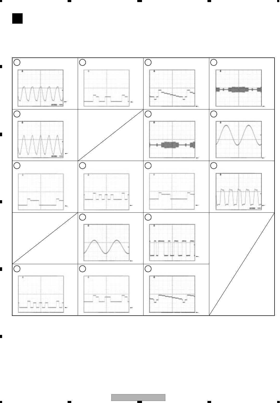
MAIN ASSY
D
1X4102 - pin 4 (ADMCLKI)
V: 1V/div. H: 20nsec/div.
(Function : P.ON)
2R4205 (VMCLK)
V: 1V/div. H: 20nsec/div.
(Function : P. ON)
3Q2103 - B (G)
V: 500mV/div. H: 10µsec/div.
(Function : PLAY)
5Q2104 - B (B)
V: 500mV/div. H: 10µsec/div.
(Function : PLAY)
6Q2105 - B (R)
V: 500mV/div. H: 10µsec/div.
(Function : PLAY)
8CN2001-pin 10 (B Out)
V: 500mV/div. H: 10µsec/div.
(Function : PLAY)
9CN2001-pin 16 (Lch Out)
V: 2V/div. H: 200µsec/div.
(Function : PLAY)
10 CN2001-pin 12 (R Out)
V: 500mV/div. H: 10µsec/div.
(Function : PLAY)
11 CN2001-pin 4 (Y Out)
V: 500mV/div. H: 10µsec/div.
(Function : PLAY)
12 CN2001-pin 6 (C Out)
V: 500mV/div. H: 10µsec/div.
(Function : PLAY)
13 CN2001-pin 8 (G Out)
V: 500mV/div. H: 10µsec/div.
(Function : PLAY)
14 CN3001-pin 8 (PCMAIN)
V: 1V/div. H: 400nsec/div.
(Function : PLAY)
15 CN2001-pin 24 (SEL Y/V)
V: 500mV/div. H: 10µsec/div.
(Function : L1)
16 CN2001-pin 26 (SEL C)
V: 500mV/div. H: 10µsec/div.
(Function : L1)
17 CN2001-pin 28 (SEL L)
V: 500mV/div. H: 200µsec/div.
(Function : L1)
18 IC3402-pin 7 (27MCLK)
V: 1V/div. H: 20nsec/div.
(Function : P.ON)
GND
GND
GND
GND GND
GND
GND
GND
GND GND GND
GND GND
GND
GND GND
Measurement condition ;
No.3 to No.8, No.10 to No.13 : 75% Color-bar, AXP disc 1-24
No.15 ,No.16 : 75% Color-bar
No.9, No.14 : 1kHz, 2Vrms, AXP disc 1-1
No.17 : 1kHz, 2Vrms
DVR-3100-S 49
5678
5678
C
D
F
A
B
E
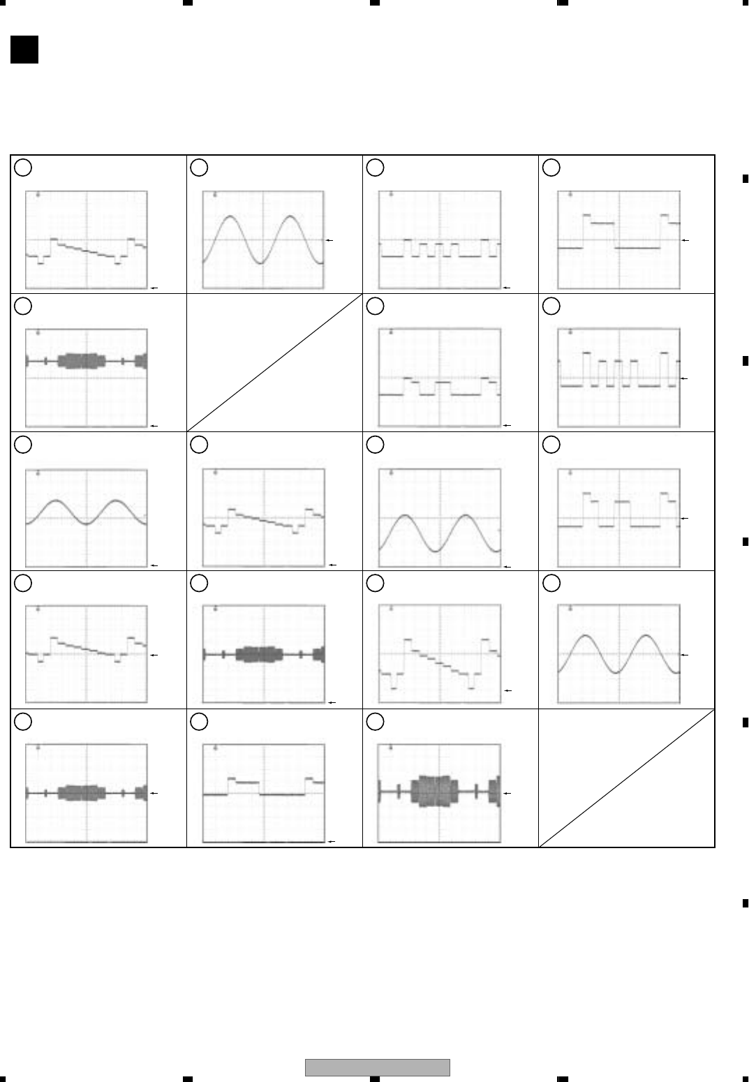
SCRB ASSY
I
1CN203 - pin 5 (Y In)
V: 500mV/div. H: 10µsec/div.
(Function : AV2/L1)
2CN203 - pin 21 (C In)
V: 500mV/div. H: 10µsec/div.
(Function : AV2/L1)
3CN203 - pin 27 (Lch In)
V: 1.0V/div. H: 200µsec/div.
(Function : AV2/L1)
4JA101 - pin 20 (Y In)
V: 500mV/div. H: 10µsec/div.
(Function : AV2/L1)
5JA101 - pin 15 (C In)
V: 500mV/div. H: 10µsec/div.
(Function : AV2/L1)
6JA101 - pin 6 (Lch In)
V: 500mV/div. H: 10µsec/div.
(Function : AV2/L1)
8CN203-pin 9 (Y)
V: 500mV/div. H: 10µsec/div.
(Function : PLAY)
9CN203-pin 7 (C)
V: 500V/div. H: 10µsec/div.
(Function : PLAY)
10 CN203-pin 11 (G)
V: 500mV/div. H: 10µsec/div.
(Function : PLAY)
11 CN203-pin 17 (B)
V: 500mV/div. H: 10µsec/div.
(Function : PLAY)
12 CN203-pin 19 (R)
V: 500mV/div. H: 10µsec/div.
(Function : PLAY)
13 CN203-pin 23 (Lch)
V: 500mV/div. H: 10µsec/div.
(Function : PLAY)
14 JA102-pin 19 (Y Out)
V: 500mV/div. H: 10µsec/div.
(Function : PLAY)
19 JA102-pin 3 (Lch Out)
V: 2.0V/div. H: 200µsec/div.
(Function : PLAY)
15 JA102-pin 15 (C Out)
V: 500mV/div. H: 10µsec/div.
(Function : PLAY)
16 JA102-pin 11 (G Out)
V: 500mV/div. H: 10µsec/div.
(Function : PLAY)
17 JA102-pin 7 (B Out)
V: 500mV/div. H: 200µsec/div.
(Function : PLAY)
18 JA102-pin 15 (R Out)
V: 500mV/div. H: 10µsec/div.
(Function : PLAY)
GND
GND
GND
GND
GND
GND
GND
GND
GND
GND GND
GND
GND
GND
GND
GND
GND
GND
Measurement condition ;
No.8 to No.12, No.14 to No.18 : 75% Color-bar, AXP disc 1-24
No.1, No.2, No.4, No.5 : 75% Color-bar
No.13, No.19 : 1kHz, 2Vrms, AXP disc 1-1
No.3, No.6 : 1kHz, 2Vrms
DVR-3100-S
50
1234
1234
C
D
F
A
B
E
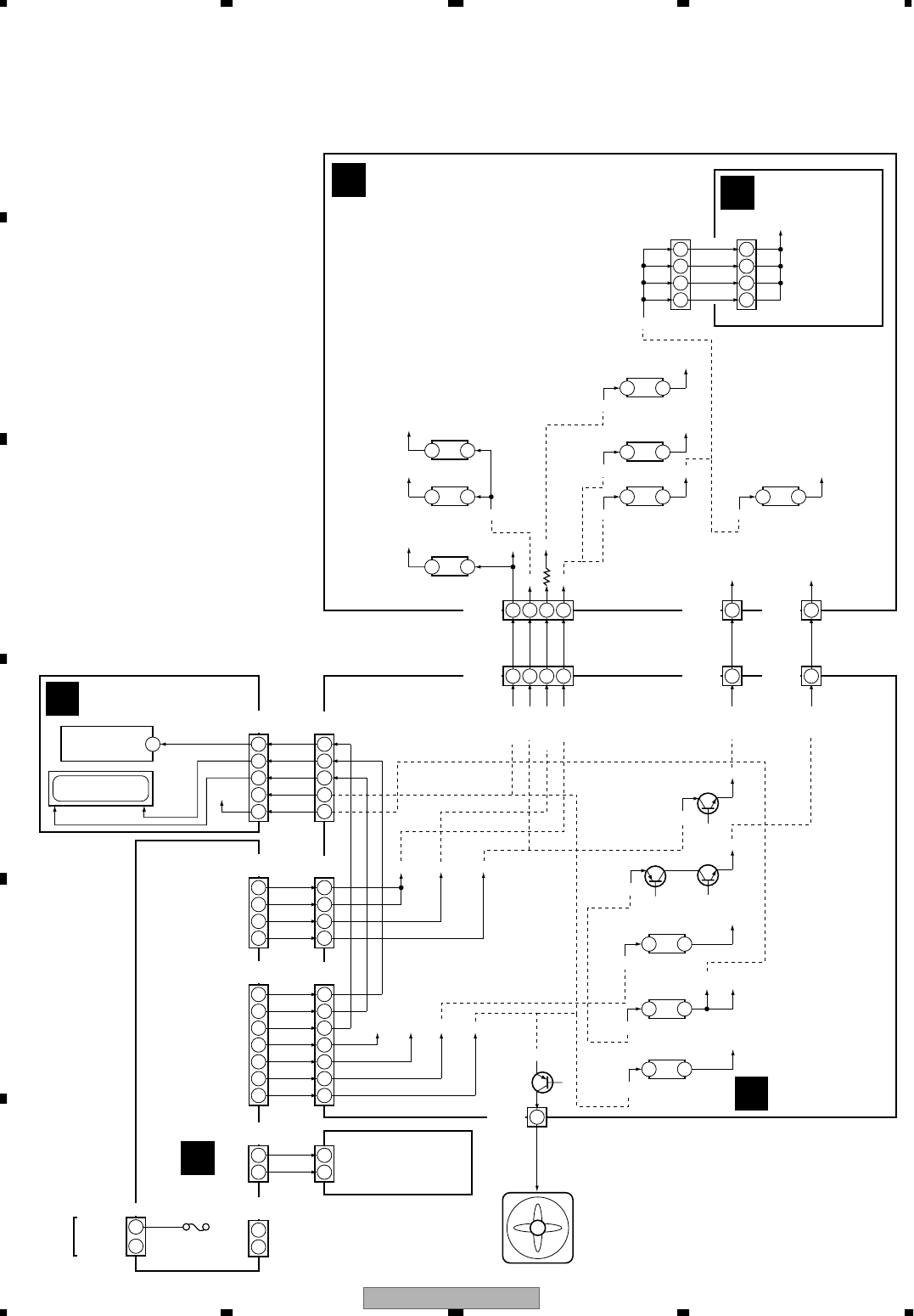
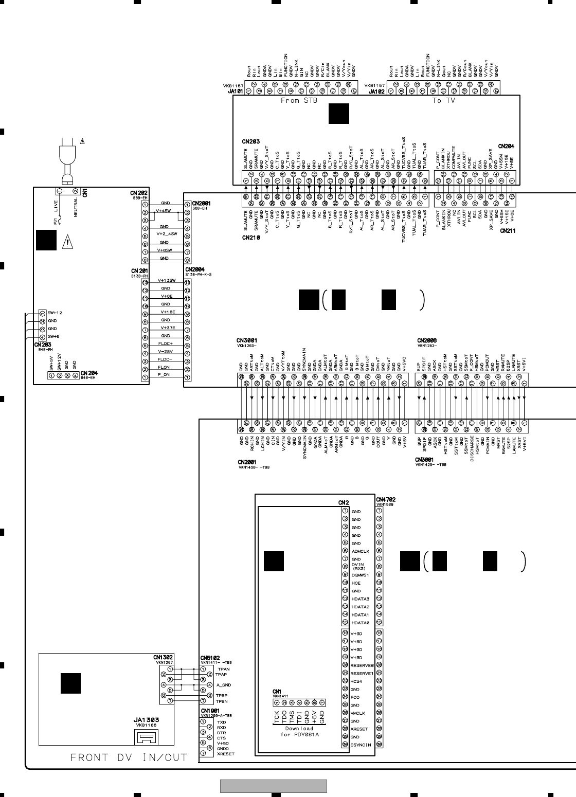
4. PCB CONNECTION DIAGRAM
4.1 ATAB ASSY
140
140
R16
R17
R18
R14
R13
R12
R11
R15
CN12
E119697
VNP1937-A
VWV1968-
ATAB
BOTTOM SIDE
CONTACT
1
2
40
39
1
2
39
40
CN11
20
10
15
5
30
35
25
SIDE A SIDE B
A A
CN4401
To DRIVE ASSY R6
CN9003
D
CN12
CN11
ATAB ASSY
AATAB ASSY
A
(VNP1937-A) (VNP1937-A)
NOTE FOR PCB DIAGRAMS :
1. Part numbers in PCB diagrams match those in the schematic
diagrams.
2. A comparison between the main parts of PCB and schematic
diagrams is shown below.
3. The parts mounted on this PCB include all necessary parts for
several destinations.
For further information for respective destinations, be sure to
check with the schematic diagram.
4. View point of PCB diagrams.
Symbol In PCB
Diagrams Symbol In Schematic
Diagrams Part Name
BCE
D
D
G
G
S
S
BCE
BCE
DGS
BCEBCE
BCE
Transistor
Transistor
with resistor
Field effect
transistor
Resistor array
3-terminal
regulator
Capacitor
Connector
P.C.Board Chip Part
SIDE A
SIDE B

DVR-3100-S 51
5678
5678
C
D
F
A
B
E
DVR-3100-S
52
1234
1234
C
D
F
A
B
E
4.2 TUMJ ASSY
88
116
30 58
129
59
87
41
58
14
5
8
1
1
9
1
1
10
15
1
13
46
12
34
5
78
910
1213
14
15 18
115
12
14
17
8
18
12
13
+-
C2115
R2119
X2001
C2106
C2105
R2007
R2004
C2104
C2103
C2102
R2102
C2101
R2101
R2038
R2118
IC2001
C2111
X2271
IC2251
C2251 C2622
C2623
C2626
IC2351
R2357
C2356
X2351
CN2006
C2642
R2305
R2012
R2011
R2303
KN2003
C2534
C2533
R2361
C2254
C2354
R2355
Q2351
R9004
R9005
R9006
R9007
R9008
CN2007
C2107
C2108
C2109
R2115
JA2201
R2113
C2355
C2357
R2360
C2358
R2359
R2358
C2353
R2354
C2352
R2352
R2353
R2351
C2351
R2103
L2642
C203
R2356
R2251
R2252
C2253
C2252
R2001 R2002
R2003
R2005
R2013
R2081
R2084
R2086
R2087
R2085
R2083
R2079
R2071
C2119
R2043
R2066
R2016
IC2551
C2553
R2551
KN2007
R2048
CN211
CN2009
C2544
IC2541
R2309
R2311
L2301
R2317
R2315
R2316
C2303
R2318C2302 Q2306
C2505
R
3
R33
5
C3316
R3348
L3342
R3346
L3341
R3342
R3345
R3344
Q3341
C3346
C3341
C3343
C3344
C3345 C3301
R
33
4
3
C3518
C3517
C3516
C3511
C3515
C3507
C3504
C3083
JA3081
C3552
C3554
C3555
JA3551
C3364
R3561
Q3554
Q3556
C3354
CN3002
C3356
R3349
JA3582
C3533
R2205
CN3003
R2108
C2204
R3597
C2140
R2301
R2058
C2141
R2145
C2142
R2146
R2059
R2109
ST2271
R2140
R3599
C2118
Q2640
C2640
C2152
C2153
C2154
R2057
L2039
R2078
IC2003
R2110
R2029
R2080
Q3565
Q3564
R3574
R3573
C2082
R2017
R2253
CN2001CN2004
C2210
R2209
Q2205
R2210
R3643
BT2271
R2254
WARNING
AGC2
TUJB ASSY
FC D
C
PC
CONTACT UPPER SIDE
4
1
85
V+5E
V+3.3SW
V+6E
V+13SW
V+6SW
V+13SW
V+5VO
V+5VI
V+6SW
V+5M
V+5VO
V+5E
13
1
15
1
1 9
15
1
CMKD-P3X
8
1
58
129
5987
88
116
30
1
1
1
25249.6 - PROPOSITION 65
HEALTH & SAFETY CODE SECTION
DEFECTS OR OTHER REPRODUCTIVE
H
OF CALIFORNIA TO CAUSE CANCER,BI
R
CHEMICALS WHITCH ARE KNOWN TO T
H
AND CERTAIN ELECTRICAL PARTS CON
THIS PRODUCT CONTAINS LEAD IN SO
L
8
1
5
4
13
46
12
17
814
-+
SIDE A
B
IC2003
IC4001
IC2541
IC2551
IC2351
IC2581
IC2251
IC2001
Q3452
Q2205
Q3451
Q3564
Q3565
Q2640
Q4002
Q4001
Q4003
Q4004
Q3906
Q3004
Q3913
Q3099
Q3916
Q3915
Q3556
Q3554
Q3006
Q3404
Q3407
Q3341
Q3342
Q3343
Q3344
Q2306
Q2351
CN3002
CN1301
C
CN2004
CN201
G
CN2001
CN202
G
CN2007
DOWN LOAD
CN211
CN204
I
C
N
C
F
TUJB ASSY
B
Lithium
Battery
to SIDE B
DVR-3100-S 53
5678
5678
C
D
F
A
B
E
12
8
12
34
5
6
78
910
11
1213
14
15 18
1
10
19
1
119
15 18
12 3
46
1
10 20 30
35
1
32
111
12 22
23 33
34 44
R3949
C2582
C2584
IC2581
C2801
C2803
C2813
C2811
C2807 C2812
C2810
C2804
C2802
C2806
CN2003
KN2002
KN2001
JA2832
C2815
C2814
CN2005
009
C2817
C2816
C2516
CN2008
C2505
C2506
R3354
Q3344
L3344
L3343
R3351
R3357
Q3343
R3352
R3350
C3353
C3349
C3347
C3350
C3351
C3352
R3355
C3316
D3304
D3303 C3315
C3314
C3310
D3302
D3301
C3311
C3308
Q3342
R3348
L3342
L3341
R
3342
R3345
R3344
Q3341
C3307
C3346
C
3343
C
3344
C3345 C3301
R3343
C3029
C3028
C3026
C3022
R3023
C3015
C3013
C3006
C3009
C3001
U3001
R3442
Q3407
R3435
R3436
R3432
R3423
C3419
R3424
R3420
Q3404
L3403
C3415
R3421
R3405
L3401
C3403
C
3552
C3554
A
3551
6
4
R3026
Q3006
L3005
C3427
R3304
C3354
C3355
L3409
L3407
L3405
C3935
C3936
C3931
C3934
C3929
Q3915
R3937
R3941
C3932
C3930
C3933
Q3916
R3933
C3928
VR3902
F3903
R3909
VR3901
F3901
C3904
L4002
Q3099
R3099
R3098
L3098
C3099
C3201
R3908
R3931
Q3913
R3930 F3902
R3925
C3357
F3911
F3912
R3910
F3904
R3922
R3921
CN210
F3906
R3945
R3944
C4033
CN3001
L3099
R3935
R3934
R3942
R3915
R3356
R3349
Q3004
L3909
L3910
L3911
L3912
Q3906
C3010
R202
Q4004
C4028
R4019
C4027
R4018
R4017
C4026
R4016
C4023
Q4003
C4022
R4014
R4013
R4012
X4001
R4015C4024
R4011
C4016
C4015
R4010
C4014
C4013
C4012
C4011
C4019
C4020
C4017
Q4001
R4008
R4006
R4007
Q4002
C4009
C4008
C4006
C4007
C4004
C4003
C4010
R4003
C4001
R4005
IC4001
C4002
R3998
R3005
C4032
R1000
D3306
R3457
D3305
R1001
C3641
R2017
Q3451
R3643
R3642
C3642
Q3452
L3451
R3456
R3452
R3453
R3454
R3455
CVBS2
A
RNING
AFT2
ARM2T
L`AFC
Adjust
AGC
FC DC
1C
1V
3V
Adjust Adjust
AFC
19
1
33
34
12 22
23
44
111
8
1
EBC2
CB2E2
V+5E
V+5VI
V+5E
V+5VO
V+15E
V+5VI
V+15E
V+5VI
V+6E
V+13SW
V+6SW
V+37E
V+5TU
35
1
2
211
34
1
119
- PROPOSITION 65
& SAFETY CODE SECTION
T
S OR OTHER REPRODUCTIVE HARM.
FORNIA TO CAUSE CANCER,BIRTH
A
LS WHITCH ARE KNOWN TO THE STATE
R
TAIN ELECTRICAL PARTS CONTAIN
ODUCT CONTAINS LEAD IN SOLDER
1
32
SIDE A
B
CN2003
CN4001
D
CN210
CN203
I
CN2008
CN3001
D
CN3001
CN2001
D
CN2005
CN1001
F
(VNP1933-C)
DVR-3100-S
54
1234
1234
C
D
F
A
B
E
115
1630
118
1936
112
13
24
R3956
R3955R3954
R3953
R3952
R3951
R3950
R3021
R3020
C2581
C2583
R2810
R2804
C2808
IC2801
C2809
R2808
R2811
C2507 C2508
Q3003
L3920
C3922
C3923
R2505
R2802
R2806
R2805
C2805
R2812
R2813
R2814
R2801
R2803
R2807
R2809
C2820
C2819
C2818
C2821
R2815
R2818
R2817
R2821
R2819
R2820
R2816
C3312
C3313
C3306
C3305
C3303
C3302
R3302
IC3301
C3017
C3014
C3012
D3002
C3005
Q3001
Q3410
R3444
R3443
R3441
R3447
Q3409
C3431
Q3408
R3440
C3430
C3426
R3438
R3445
C3420
C3425
R3433
R3430
Q3406
C3424
R3428
R3426
R3427
Q3405 C3418
C3411
R3417
R3418
Q3403
R3415
R3416
C3414
R3412
C3412
C3408
C3410
R3402
Q3402
R3408
R3406R3403
R3404
Q3401
C3407
C3406
C3405
R3401
C3401
C3404
R3409
R3575
R3341
R
Q3002
R3014
R3013
R3003
C3007
L3003
C3409
C3413
C3421
C3432
R3018
R3019
C3021 C3020
R3303
R3305
C3317
C3428
C3422
C3416
C3429
C3423
C3417
C3924
R3926
R3932
IC3903
R3907
Q3904
R3916
Q3909
L3903
R3901
C3909
R3904
C3908
C3907
R3929
C3905
Q3912
C3921
L3902
R3201
C3202
R3202
D3901
L3906
L3908
D3902
C3917
L3907
R3924
R3918
R3928
C3925
C3918
Q3920
R3923
R3927
C3920
L3957
C3958
Q3901
R3905
C3902
R3920
R3911
L3904
R3912
R3917
C3916
C3906
R3940
Q3914
L3004
Q3911
C3910
R3939
Q3908
Q3905
Q3917
Q3918
R3373
Q3371
D3001
C3023
C3903
R3902
Q3902
R3903
R3906
R3946
R3913
C3912
C3911
R3582
R3936
L3913
R3623
R2822
R2823
R3943
R3948
Q3903
C4030
R4023
R4022
C4029
R4020
R4021
C4021C4018
D4001
R4009
R4004
R4001
C4031
R4024
L4001
R4025
R30
R9001
C3919
R2504
R9009
C3562
R3999
C2825
C2823
C2824
C4034
R3598
R3458
C2822
R3375
R3957
C3901
R3958
Q4005
R3959
R3002
Q3453
L3960
C3960
R3644
R3641
R3451
C3451
TUAR_T_to_S
TUCVBS_T_to_S
AL_T_to_S
1
CSYNC
BT_to_S
AGC1
L1-Y
L3-Rch
L1-Rch
R
L3-Lch
L3-V
L1-Lch
L1-V
L3-C
L3-Y
CT_to_S
18
15
1
36
YT_to_M
ALM_to_T
ARM_to_T
AFT1
AGC2
SIF
CUBS1
SIF2
PIF
AFT2
SIF3
GS_to_T
YT_to_S
V/YS to T
L1-C
CT_to_M
TU_R
TU_L
IN
16
GT_to_S
BS_to_T
RT_to_S
AR_T_to_S
AR_S_to_T
TUAL_T_to_S
19
ALM_to_T
ARM_to_T
Cr/RM_to_T
Cb/B
Y/GM_to_T
CM_to_T
Y/VM_to_T
GND
ALT_to_M
ART_to_M
SPDIF
ASCKSYS
HST_TO_M
SST_TO_M
SSM_TO_TSYS
HSM_TO_SYS
PCMOUT
X525P
MRST
XRESET
RAMUTE
LAMUTE
BUP
V+5VI
SW+4V
SW+2.4V
SW+6V
SW+13V
EV+6V
EV+
EV+37E
30
V
W
13
12
24
1
V+5VO
V+5VI
EV+15E
1
32
V+9
OUT
FL-28V FLDC-
FLDC+ GND
JOGB JOGA
KEY2 IR
KEY1
KEY1 2
2Y
2L
2R
TU_V
TUON
STBYQ
RESETQ
V
W
35
3020
10
1
21 1
1
19
SIDE B
B
CN2003
CN210
CN2008CN3001 CN2005
TUJB ASSY
B
IC3903
IC3081
IC3501
IC3301
IC2521
IC2801
IC2271
Q3453
Q2152
Q2151
Q4005
Q2641
Q202 Q201
Q3903
Q3902
Q3559 Q3562
Q3561
Q3563
Q3551Q3371
Q3918
Q3917
Q3905
Q3908
Q3911
Q3914
Q3901
Q3920
Q3912
Q3909
Q3904
Q3363
Q3362
Q3002
Q3401
Q3402
Q3403
Q3405
Q3406
Q3408
Q3409
Q3410
Q3001
Q2305
Q2531
Q2621
Q2642
Q2532
Q3003
Q2203
Q2201
Q2202
Q2204
(VNP1933-C)
DVR-3100-S 55
5678
5678
C
D
F
A
B
E
4
5
8
1
18
19
118
1936
13
46
R2010
R2009
C2114
C2113
R2037
R2036
R2033
R2032
R2031
R2077
R2076
C202
C2110
R2208
C2271
IC2271
C2273
C2274
R2274
D2271
D2272
R2271 R2272
C2621
C2624
C2625
Q2204
Q2202
Q2201
Q2203
R2204
R2207
C2112
R2206
C2641
C2511 C2512
C2515C2501
C3532
C2535
Q2532
C2532
R2532
C2531
R2533
R2531
R2645
Q2642
C2510C2509
C2545
Q2621
R2104
R2106
R2107
R2105
R2621
R2802
R2203
D2201
C2201
R2201
C2202
R2202
D2640
C201
Q2531
R2501
R2502
R2503
R2116
R2117
R2014
R2015
R2082
R2025
R2024
R2023
IC2521
C2521
R2521
C2522
C2552
C2551
C2502
R201
C2272
R2275
C2543
C2542
C2541
C2821
2
815
R2817
Q2305
R2313
C2301
R2312
R2314
C3312
C3313
C3304
R3302
R3301
R3551
D3506
C3519
D3505
D3504
C3514
C3520
C3512
C3513
D3502
D3503
C3508
C3510
C3506
C3505
R3504
R3503
IC3501
C3503
R3502
R3589
R3591
R3587
R3083
R3082
R3084
C3084
R2039
IC3081
C3081
R3081
R3563
R3560
R3570
R3565
R3559
R3575
D3551
R3562
R3558
C3551
R3555
C3521
R3370
C3365
R3367
R3368
C3362
R3372
Q3362
Q3363
R3369
R3004
R3576
C3556
C3557 C3559
C3558
R3572
R3305
R218 R217
R3373 Q3371
R3374
Q3551
Q3563
Q3561
Q3562
Q3559
R3577
R3582
R3569
R3568
R3571
R3001
R3308
R3550
C3531
C3530
C3560
R9003
D3560
R2150
D201
Q201Q202
R2302
R2144
C2001
C3562
C2610
R2141
R2143
D2641
C2211
C2646
R3596
R3598
R2304
Q2641
L2641
R2641
R2642
R2643
R2644
C2643
C2087
R3375
C3561
C3553
R9002
C2546
R2306
R3085
R2147
Q2151
C2212
R2148
Q2152
R3002
R2610
R3376
C2645
12
SDA
V+6E
EV+15
AVLIN
SRAMUTE
8
15
GND
AL_T_to_S
BT_to_S
L1-Y
CY
Y
C
V
RV
L
L3-Y
L
R
SLAMUTE
CT_to_S
18
1
2Y
Cr
Y
Cb
GS_to_T
YT_to_S
AVLO
V/YS_to_T
2C
L1-C
19
18
1
36
C
EB
E2B2CCB2
C2
EB
BE
C
VWV1963
VWV1962
VWV1978
GT_to_S
BLANK
BS_to_T
RT_to_S
AR_T_to_S
XP_SAVE
V+5SM
FUNC
XTHROU
SCL
NC
P_CONT
19
V
EV+15E
2V
2R
2L
SDET2
KEY1_2
FLON
PON
FLDC-
FLDC+
GND
GND
FL-28V
EV+37E
EV+15E
EV+6V
GND
GND
GND
SW+13V
SW+6V
SW+2.4V
SW+4V
GND
1
10
GND
GND
GND
VWV1977
VWV
LF
FL-28V FLDC-
FLDC+ GND
JOGB JOGA
KEY2 IR
KEY1 KEY1_2
PCMOUT
FLCLK
FLDATA
V+13SW
FLPON
GND
GND
V+5E
GND
FLSTB
GND
V+5M
V+5M
SW+13V
SW+13V
V+5SC
2C
2V
2Y
2L
2R
AGC
GND
1
VWV
15
1
35
1
4
85
5
1
1
19
1
1
13
45
1
13
SIDE B
B
CN3002CN2004CN2001
CN2007CN211
N
2005
from SIDE A
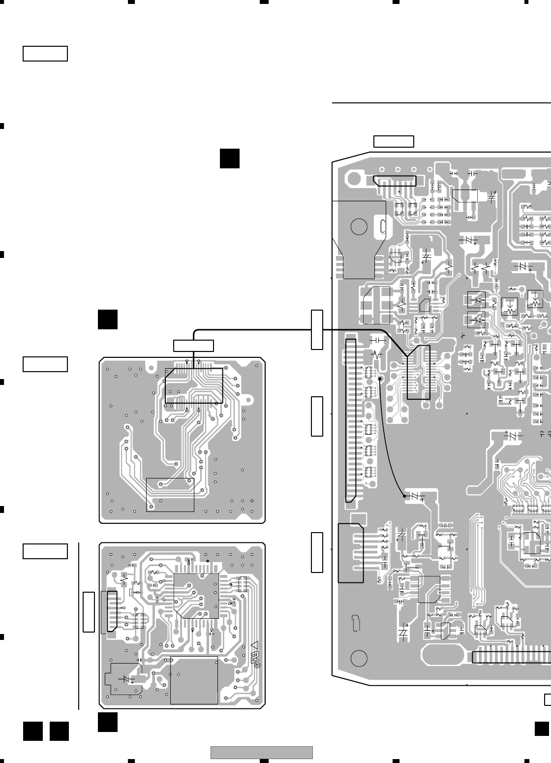
DVR-3100-S
56
1234
1234
C
D
F
A
B
E
4.3 MAIN and MHLP ASYS
30
16
151
CN2
VNP1953-A
MHLPB
VWV1991-
VWV1991- -U
1
2130
15
D1111
R5104
C1061
C5111
5CN5102
C5101
C5131
C5135
C4033 C4032
TP4015
C5102
F5101
L5101
L5102
IC4007
31
4
R5103
R5108
R5107
R5106
R5105
7 1
C5105
C5110
C4035
C5132
C5138
C5137
C5136
C4034
L5103
L5104
L5106
L5105
TP1026 TP4305
C1013
Q2104
Q2105
R1102
C2265
R2109
R1011
C1016
R4110
R4109
VR1001
1
4
R4105
C1011
R1071
R1111
R1052
R1012
C1114
C4107
C4102
C4105
R4108
R1007
R1001
C1054
TP1060
Q1102
C4106
VR2104
X4102
3
2
29
C1104
R4106
R4107
R2112
R2115
R1024
R1023
R1022
R1021 R4104 R4103
R4102R4101
R2113
R2114 R2116
R5265
R2266
C4103
C4104
TP28
TP4708
TP4707
TP4706 TP4702
0
41
TP1050
TP1051
IC4101
14
58
VR2105
VR1002 Q2103
TP4701TP4703 TP4302
R2107
CN4702
R2102
R2103
TP4705
Q2102
Q2101
R2106
R2105
C2246
C2105
C2106
R2252
TP1002
C1017
TP4709
TP4711
TP4710
TP4718
TP4719
R4306
17
28
R2111
C2102
C2103
C2104
C1012
C1018
C1019
TP4304
TP4307
TP4704 TP4712
TP4713
R4305
17
28
CN4301
82
71
R4304
8
2
71
R4303
TP4717
TP4716 TP4715
TP4714
TP4303
TP4301
C2101
C1021
C1022
C1023
C1024
C2225
R1905
R2306
1
82
7
1
R4302
82
71
R1048
2
7
1
R
1045
82
71
R1043
R1080
C2221 TP4306
TP1027
TP1028
T
P1029
TP1032
TP1031TP1033
TP1024
C4206
Q2311
Q2222
R1902
C4203
C2222
R2233
R2235
R4202
R4206R4211 R4212 R2311 R1901
R1903
R1904
C2317
13
C1901
Q2312R2239R4207R4208
2
09 R2313
R2314R2312
R2221
CN1901
C4207
IC4206 45
C2334
85
41
IC2301
13
46
IC2331
32
Q2402
TP50
TP49
TP48
TP47
TP46
TP45
C2405
Q2403
C2333
C2311
C2305
C2332
R2331
R2332 R2333
R2411
R2412
R2406
R2405
R2407
R2409
R2408
R2404
C2407
C2319
C2406
17
44
34
33
23
22
12
11 1
C1
C3
R3
CN1
R2
R5
C2
C4
C6
C8
D1
C5
R4
IC1
C7
R1
VWV1991- -UVWV1991-
GCMK-G3X
17
111
12 22
23 33
34 44
Q2103Q2311
Q2222Q2312 IC4206
IC2301 IC2331 Q2403 Q2402
SIDE A
SIDE A
SIDE B
D E
MAIN ASSY
D
MHLP ASSY
E
MHLP ASSY
E
IC4007Q1102
IC4101
Q2105
Q2101 Q2102
Q2104
VR2104
VR2105 VR1002
VR1001
IC1
B
C
(VNP1953-A)
(VNP1953-A)
CN1
CN1901 CN4301
CN5102
CN4702
CN2
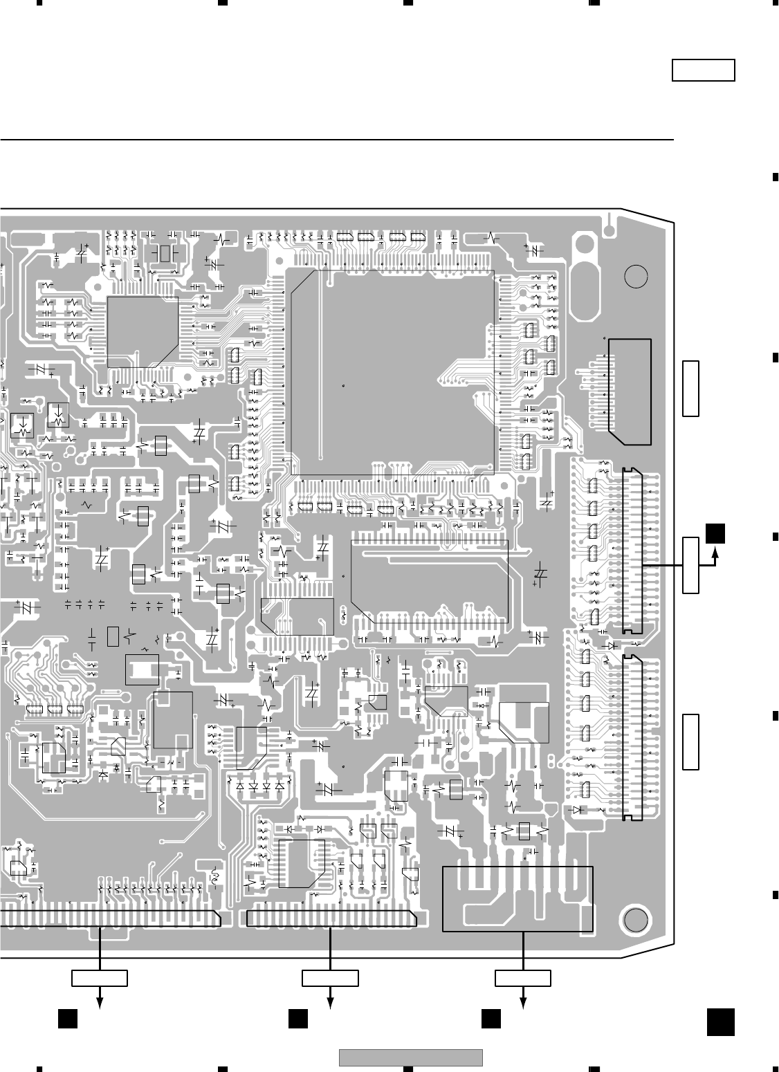
DVR-3100-S 57
5678
5678
C
D
F
A
B
E
R5104
IC5101 C5111
R5236
R5121
R5110
C5101
TP34TP36 82
71
R5247
82
7
1
R5249
82
71
R5263
R5262
R5260
R5120
R5116
R5122
R5114
R5253
R5254
R5256
R5257
C5210
C5121C5122C5124
C5209
C5212
C5204
C5206
C5214
R5102
R5208
TP35
T
P
C5102
F5101
C5207
R5252
17
28
R5251
R5103
R5108
R5107
R5106
R5105
1
208
157
156
X5101
33
3217
16
R5235
R5216
R5217
R5231
R5109
R5125
R5128
R5117
R5115
R5126
R5129
R5232
R5214 R5233
R5215
R5234
C5103
C5105
C5110
C5112
C5127
C5120
C5216
TP31
TP32
TP33TP37
TP38
TP5202
TP5201
C5104
1
2
1TP1026TP3303 TP3301
R5292
R1005
C5231C5224 C5229
C
R5298R5297
R4504
R1074
53
R4405
C5205
Q2104
Q2105
TP5204
F1001
C5218
R5283
R2109
R1011
C1041
C1037
C1034
C1028
C1027
C1025
C1016
R5124
R5123
R5286
C5118
C5119
C5123
C5227
VR1001
20
CN4601
R5272
R5130
IC5202
64 49
48
1
82
7
1
R5275
8
7
R5218
82
7
1
R5219
82
71
R5220
8
2
7
1
R5221
82
71
R5274
82
71
R5273
C1014
R5237
R5238
R5132
R5131
R1071
R5112
R5113
R5127
R5276 C5113
C5125
C5126
C5226
C5217
C5215
C1054
TP1060
TP5106
1
R1024
R1023
R1022
R1021
105
104
52
2
1
2
1
R5290
82
71
R5289
82
71
R5229
2
1
8
2
71
R5230
C1050
C1004
C1003
C1002
C1001
C1508
C1509
R5280
R5281
R5228
R5224
R5288
R5225
R5278
R5279
C1510
R5227
R4403
R4402 R2114 R21
1
R5277
R5287
R5282
R5313
R5314
C5228
F1007
R1003
R1009
C1060
TP1041
TP1050
TP1051
VR1002
R1031
Q2103
C5321
R1004
C1006
R2107
C5225
R2103
Q2102
Q2101
R4407
1
2
R5295
R5296
R5242
R5240
R5241
R5243
R5248
R2106
R210
5
R1034
C5329
C5213
C5211
C5208
C2105
R5284
R5285
R5244
R5245
R5246
R5239
R5261
TP1002
C1042
C1017
F1005
R1006
C1057
7
8
R5259
17
2
8
R5258
17
28
R5250
17
28
R5255
17
28
7
8
R4406
17
28
R2111
8
2
7
C5230C5223 C5222
C3307
C2103
C2104
R3307
R3306R3305
R1066
R5293R5294
C1005
C1051 C1052 C1012
C1044
C1045
C1018
C1019
R3303 C1055
C3309
CN4401
7
8
R4408
1
15 28
IC3301
C1056
C1059
IC5204
8
2
71
R4436
40
39
D4401
C5221 TP1013TP3302
C2101
C1058
R1008
F1006
F1004
C1021
C1048
C1047
R3310
R4435
R4432
R4429
R4428
R3308
R4427
C1022
C1023
C1024
C1026
C1030
C1029
C1035
C1038
C1036
C1049
C1039
C3308
C4401
F1003
F3102
D3102
D3101
D3104
D3103
R4001
C4213
C4212
C4006
C4005
IC4008
R4201
41
X4201
1
F4201
C4201
C4202
R4017
C4028
D4001
14
C4036
C3403
R3411
82
7
1
R4508
82
7
1
R4509
82
71
R4507
2
1
82
71
R1048
82
71
R1045
82
71
R1043
85 IC3403 23
VC4201
C3107
F3401
F3403
916
IC3402
C4211
C3404
C3405 C3407
C3302
C3303
C3108
C3408
C1053
C1040
R3309
R2227
R3405
R3406
R3407
R3403
R3304
R4505
R4440
R4205
R5223
R5222
R1080
R3102
R3301
C3301
TP3401
TP4202
TP1012
TP1027
TP1028
TP1029
TP1030 TP1032
TP1031TP1033
TP1024
D4202
C4206
R4204
C3105
C4208
C4203
F3402
5
C4014
TP3402
TP3403
R3410
R4202
R4206
R4210
R4211 R4212
R3409
R3107
R3106
R3108
R3105R4531
R4530
C3101
C3406
C4209
C3106
F4004
8
IC3101
8
9
4
1
L4201
13
IC4205
14
8
CN4501
R4510
17
28
R3408
L4202
C3402
TP4201 TP4008
R4015
F4001
C4031
C4018
C4027 R4207R4208
R4209
R3103
R3104
R4534
R4537
C4210
C4207
D4201
F4202
C3102
16
1
IC4206 45
IC4004
13
45
R4538
17
28
IC4207
L2101
R4213
40
39
1
CN2001
81
CN4001
IC4003IC4005
21
1
CN3001
D4501
20
11
10
1
IC3001
Q2001
Q3202 Q3201
Q2402
D3001D3002
TP44
TP43
TP42
TP41
TP40
TP39
TP4001
TP4009
TP4003 TP4002
TP4010
C4004
R4014
R4010
R4009
R3002
R2017
C4010
C4021
C4024
C4023
C4013
R2041
R2042
R2043
R2044
R2045
R2046
R3271
R3270
R2019
R3022
R4541
R3010
R3001
R3003
R3012 R2411
R2412
R2406
R2405
R2012
R2011
R2013
R2015
R2014
R3023
R3024
R3202
R4004
R4008
R2404
R3025
F4003
C2407
C3004
C3002
C3001
C2406
Q2103
IC4206
IC3001IC4207
IC4205
VC4201
IC3101
IC3301
IC3403
IC3402
IC4008
IC4004
Q3201
Q3202
IC4003
IC4005
Q2001
IC5204
Q2402
SIDE A
D
(VNP1931-A)
0
5
1
Q2102
Q2104
VR1002
VR1001
IC5101 IC5202
CN2003
B
CN4001
CN2008
B
CN3001
CN3001
B
CN2001
CN12
A
CN4601CN4401CN4501
This PCB is six layer structure.
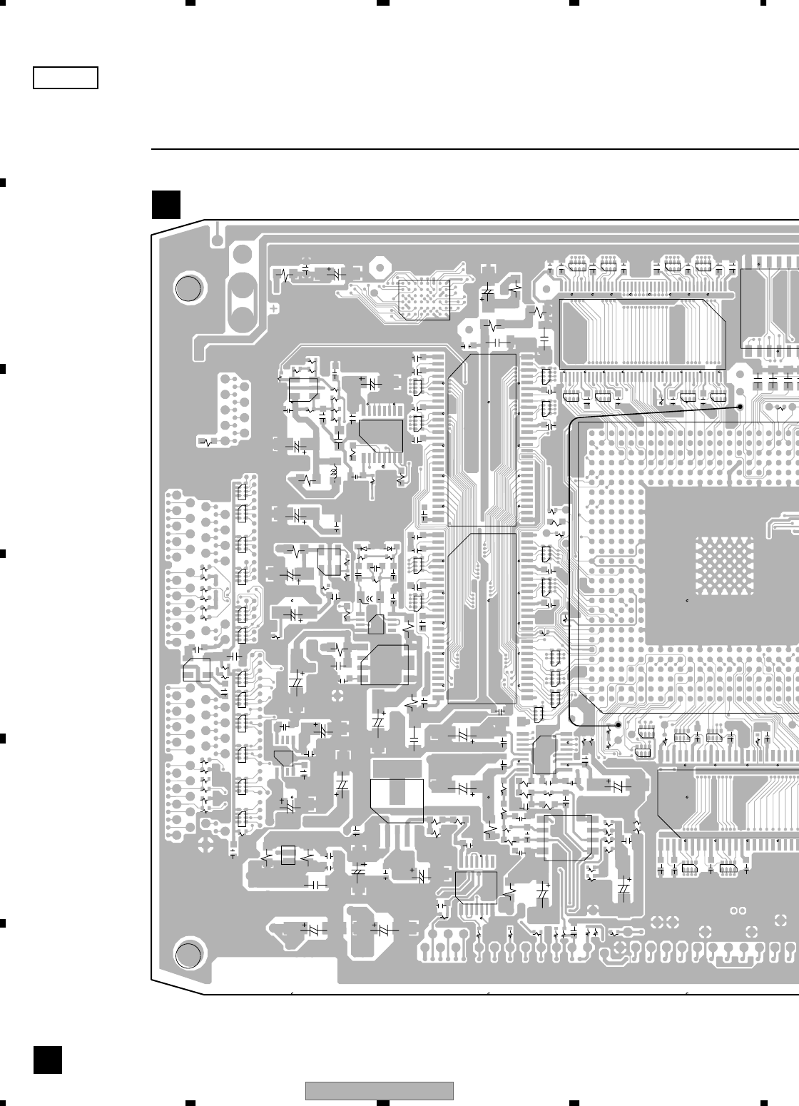
DVR-3100-S
58
1234
1234
C
D
F
A
B
E
C1301
IC5203
16 82
71
R1306
82
71
R1305
82
71
R1304
82
71
R1303
C5219
C5203
TP5203
TP1
TP5
TP2
TP6
TP3 TP7
TP4
TP8
R5207
R5291
R1421
R1301
C5220
IC1301
143
C1302
C1303
C1304
C1305
C1307
C1309
C1310
C1313
IC5002
IC4006C5006
R4404
TP1017 R1065 TP4405
R1425
TP4601
C5310
C5342
R5310
R1079
R5307
17
C1421
C5341
82
7
1
R1426
8
7
82
7
1
R1424
82
71
R1423
82
71
R1310
82
71
TP4606
TP4607
TP4604
TP4605
TP4602
TP4603
C5311
C5308
C1422 C1423
C1424
C1425
C1426
C1306
C1308
C1311
C1312
44
86
154
TP4608
R1302
R5305
R5306
R5311
R5309
R5308
R5312
R5304
8
C1507
C1506
C1505
C1504
TP1049
TP1034
P
1063 TP1064
16
9
IC5301
5
4
3
1
R130717
28
R1308 17
28
R1309
R4603
R5342
R5341
2
1
82
71
R4401
2
1
TP4403
TP4401
R5301
C5343
C1427
C1428
IC1421
TP4609
R5343
C5309
C5301
L5301
IC5341
1
8
R4430
R5330 TP4419
C5325
C1406
R5327
R1407
R4426
R4425
R1032
D5322 D5321
82
71
R4416
82
71
R4410
8
7
TP4402
TP4404
TP4406
TP4407
TP4408
TP4409
TP4411
TP4412
TP4413
TP4414
TP4410
TP4416
TP4417
TP4415
TP4418
R5321
C5306
C5326
C5327
C1429
C1405
C1404
C1403
IC1001
2728
154
R1033
R5323
R5326 R5325
TP1016
TP101
C5322
C5307
IC5321
5
4
31
R1404
17
28
R1405
17
28
7
8
R4433
R4434
R4431
R5328
7
1
82
71
R1408
82
71
R4423
82
71
R4417
TP4421
TP4422
TP4420
TP4424
TP4425
TP4423
TP4427
TP4428
TP4429
TP4430
TP4426
R5322
R5209
C5323
C5328
C4025
C1407
C1408
IC1401
R1402
R4501
R5324
R5329
R5264
C4019
TP5003
IC5322
14
58
C5324
L5321
51
R1406
17
28
1
2
R3259 TP4526
C3258
C4008
21
R4518
2
IC3201
C4026 TP4517 TP4514
R3262
R1053
TP1014
R1075
C1401
F3201
5
4
82
71
R1409
82
71
R1410
82
71
R1411
8
2
7
1
R4512
8
2
7
1
R4506
8
2
7
1
R4502
82
71
R1050
82
82
71
8
7
1
34
C4002
16
1
8
5
C5008
R1401
C5007
C4012
C4020
C1409
C1205
C1207
C1402
C1202
2728
C3203
TP4512
TP4511
TP4513
TP4507 TP4506
TP4510
TP4509
TP4508
TP4502
TP4505
TP4504
TP4503
TP4501
R1202
R1055
R3263
R4503
TP1010
TP1011 TP1015
TP5004
T
P1066 C3204
C5005
GND
R3264
R3255
R4527
R4528
IC4002
R3254
R4011 R4012
R3266 R3265
R3253
R3251
8
2
7
1
R4525
8
2
7
1
R4519
8771
R1049
R1206 R1204
9
8
C4011
41
IC4001
C4007
C3208 C3207
54
IC1201
C3257
C3205
C3202
C3253
C3254
TP4524
TP4525
TP4522
TP4521
TP4523
TP4519
TP4520
TP4516
TP4518
TP4515
TP3251
TP3253
TP4014
R3268
R4535
R4536
R4532
R4533
C3206
C3201
C4029
TP3252 TP4011
17
R3258
R3261
R3267 R4013
R3269
C4015
C4003
TP4529
TP4530
TP4527
TP4528
R4016
R4006
R3252
R3201
C4030
C4501
C4017
C4016
C3006
C3003
C3252
C1208
C1206
C1204
C1203
1
C3256
TP4004
TP4006
TP4013
TP4012
R3257
R3256
R3260
R4529
C3255 C3251
IC3251
C4009
IC3002
814
F4002
R1203
17
28
R1205
17
28
TP3013 TP3007
TP3002
TP3003
TP3005
TP3010 TP3006
TP3001
TP3008
TP3009
TP3011
TP3012 TP3004
TP2017TP2007
T
P2005
TP2006 TP2008
TP2009
TP2010TP2011 TP2013
TP2012 TP2014
TP2015
C3005
TP3014
TP2022
TP2023 TP2024
TP2025TP2021
TP2020
TP2019
TP4005
TP4007
TP9
TP10
TP11 TP12 TP13
TP14
R3017
R3015
R3014
R3011
R3009
R3013
R3016
R3019
R2026
C4022C4001
SIDE B
D
MAIN ASSY
D
IC5301
IC5203
IC5341
IC5321 IC5002
IC4006 IC4001 IC4002 IC3002 IC3251
IC3201IC1401
IC1421
IC1301
IC1001
IC1201
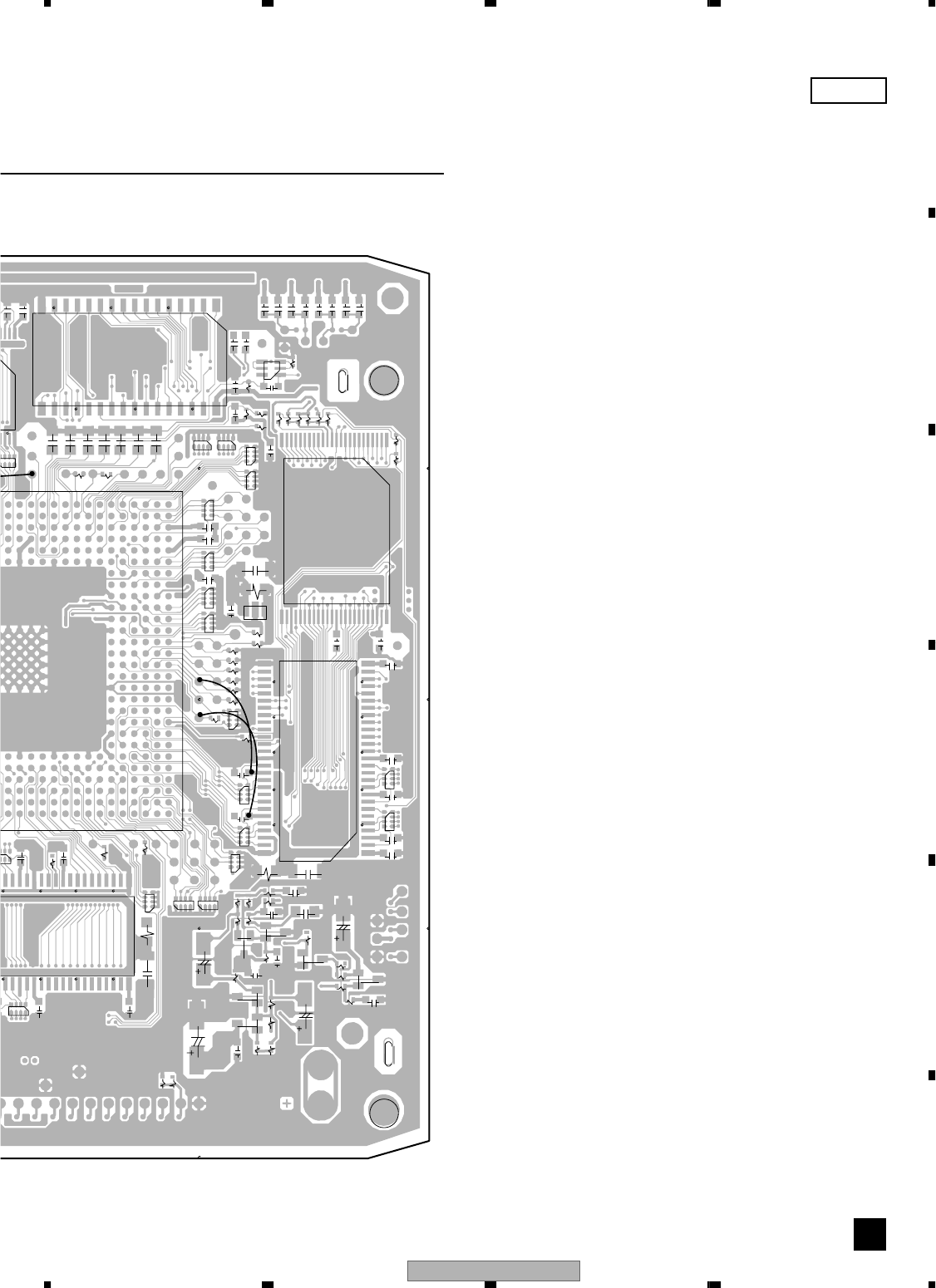
DVR-3100-S 59
5678
5678
C
D
F
A
B
E
R1118
R1113
R1112
R1108
R1110
R1109
TP23 TP21
C1512 R1103
116
IC1103
64
3
1Q1101
TP5105
TP5103
TP5104
TP5102
TP5101
R1104
TP27 TP26
TP25
TP24
C5134
C5133
C1112
C5106
C5107
C5108
C5109
C5117
C5116
C5115
C5114
1
C1108
C1303
C1304
R1116
2
1
R1002
R1079
17
32
82
71
R1026
82
71
R1025
C1511
86
TP22
R1078
R1015
R1016
R1017
R1106R1107
C1501
C1502
C1507
C1503
C1506
C1505
C1504
TP1043
TP1044
TP1045
TP1046 TP1047
TP1048
TP1049
TP1034
TP1063 TP1064
R1072
17
28
R1073
17
28
R130
7
1
7
2
8
IC1102
C1062
82
71
R1077
82
71
R1076
C1009
C1008
C1007
TP1040
TP1037
TP1052
TP1053
TP1054 TP1055
TP1056
TP1057
TP1058
TP1059
R1063 TP1007
R1060
R1059
R1058
TP1003
C1113
C1105
C1111
C1010
IC1001
27
28
R1057
R1056 TP1001
TP1004 TP1005
TP1008
TP1020
F1002
R1069
17
28
R1068
7
8
R1061
R1062
2
1
C1110
C1109
IC1101
R1064
R1105
TP1006
TP1009
TP1042
R1054
17
28
C2208
Q2302
R2204
TP1907
C2205
TP1903
TP1036
TP1022
TP1061
82
71
R1117
82
71
R1115
82
71
R1114
8
7
82
71
R1051
2
1
C1107
C1106
C1103
C1102
C1207
C1202
1
54
R1202
R1070
R1081
TP1035
TP1038
TP1019
TP1062
TP1065
TP1066
C1101
82
71
R1046
82
71
R1044
82
71
R1042
R12
0
C2301
TP1902
TP1901
TP1904
TP1905
R1101
R1201
C2209 28
IC1201
C2202
TP1906
R2301
R2302
R2203 R2202
R2201
R2205R2207
R2206
R2210
C2204
TP1039TP1018 TP1023
Q2201
Q2202
C1201
C1209
C1208
27C2201
C2206
C2306
R2303
R2304
R2305
R2307
R2209
R2208
R2334
Q2301
Q2203
Q2204
C2331
R1205
17
28
C2308
TP2004
TP2003 TP2007
TP2002
TP2001 TP2005
TP2006 TP2008
TP2009TP2016
TP
2
T
TP2021
TP2020
TP2018
TP15
TP16 TP17 TP18
TP19
TP20
R2025
R2040
SIDE B
D
(VNP1931-A)
IC1103 Q1101
IC1001
IC1201
Q2202
Q2203
Q2204
Q2201 IC1101
IC1102
Q2302 Q2301
This PCB is six layer structure.
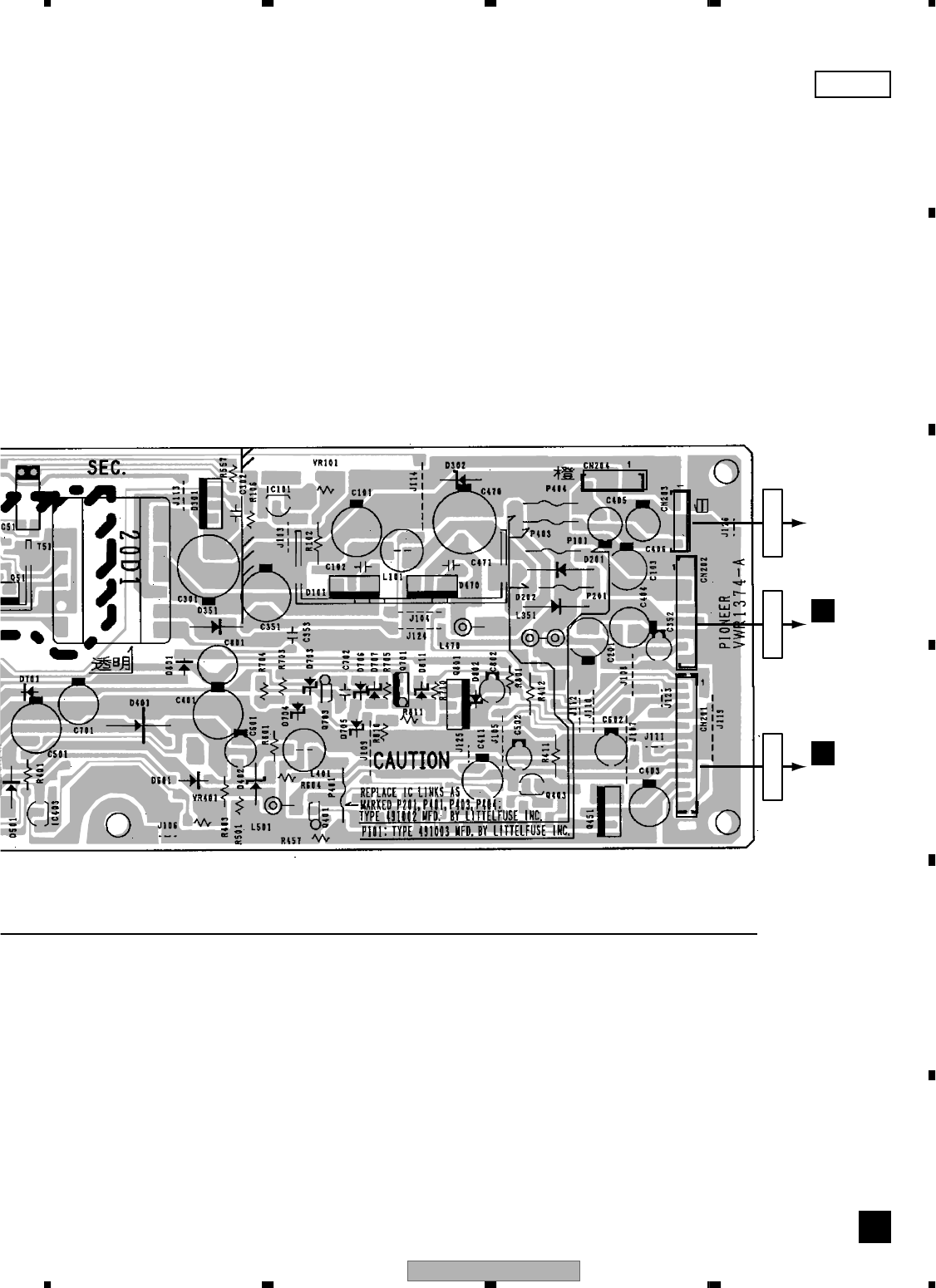
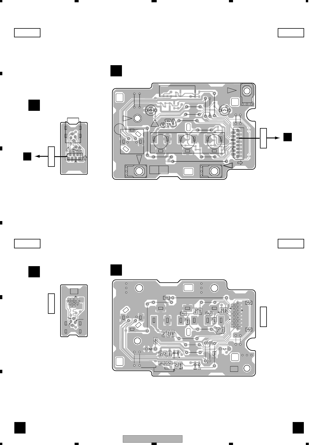
DVR-3100-S
62
1234
1234
C
D
F
A
B
E
4.5 FRJB and DVJB ASSYS
R1304
C1305
C1308
C1303
R1201 C1301
R1306
R1301
C1302
R1355
R1350
R1311
R1302
R1202
C1309
C1307
R1312C1306
R1307
R1308
C1304
R1303
D1304
D1301
R1309
R1305
D1302
D1303
R1310
GND
GND
V
Y
S_DET
KEY1_2
DISC NAVI
C
TPA
R
Y
GND
C
Lch
GND
C
L
S-Video
S_DET
Rch
POWER
Y
S_DET
HDD/DVD
S_DET
V
Video
KEY1_2
GND
TPB
XTPB
XTPA
L
GND
15
1
17
LF
LF
115
17
1
2
3
4
1
2
34
5
6
7
1
23
4
W715
W707
S1202
CN1301
CN1302
W709
W713
JA1303
W706
W712 KN1303
W705
W710
JA1301
S1201
W704
KN1302
W714
JA1302 W703
W711
W708
W701
KN1301 W702
GND
Contact
GND
V
S_DET
Upper Side
L
HDD/DVD
Video C
YKEY1_2
Y
VWV1967
DVJB ASSY
S-Video
KEY1_2
GND
DCFC
RchLch
GND
V
C
S_DET
GND
L
Y
S_DET
POWER
S_DET
C
FRJB ASSY
VWV1965
PC DISC NAVI
R
PYKC F4
PYKC F4
15
1
7
1
SIDE A SIDE A
SIDE B SIDE B
I I
DVJB ASSY
H
DVJB ASSY
H
FRJB ASSY
C
FRJB ASSY
C
CN5102
D
(VNP1936-B)
(VNP1936-B) (VNP1936-B)
(VNP1936-B)
CN1302CN1302
CN3002
B
CN1301CN1301
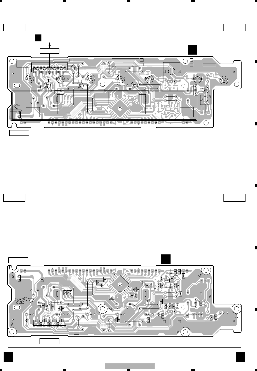
DVR-3100-S 63
5678
5678
C
D
F
A
B
E
4.6 FLKY ASSY
21
LF
19 1
21
49 41
33 27 9 1
C1003
R1502
R1030
R1006
R1501
Q1002
R1503
Q1001
R1029
C1001
Q1009
C1500
R1013
R1012
C1502 R1011
R1101
C1017
R1504
R1010
C1007
C1019
R1009
R1008
C1008
R1016
R1032
R1004
IC1001
R1003
R1500
C1011
R1505
R1015
C1016
C1014
R1033
Q1007
R1001
GND
GND
JOGA
IR
FLSTB
FLCLK
FLDATA
FLPON
KEY1
KEY2
JOGB
FLDC+
FLDC-
FL-28V
GND
KEY1_2
LEDHDD
GND
V+5V
D1102
C1002
C1006
R1005
C1018
R1002
R1014
C1009
Q1008
C1501
C1013
R1031
C1004
R1007
33
V+5FL
V-28V
GND
GND
V+5FL
FLDC-
V+5FL
FLDC+
V+5FL
44
PYKC F4
23
34
V+5FL
12 22
V-28V
GND
GND
PYKC F4
11
LF
GND
1
1
GND
4434
3323
22
12
111
12
1
19
21
4941
933
27
1
S1004
S1001
W1006
S1007
C1012
W1030
W1016
CN1002
W1009
W1019
C1015
W1010
L1002
W1023
W1017
W1011
W1004
S1008
S1003
W1003
C1005
IC1002
W1008
W1022
W1026
W1013
W1007
W1012
W1018
CN1001
CN1101
W1029
W1015 W1014
S1005
D1101
L1001
C1010
V1001
S1006
KN1001
S1002
W1002
W1005
PLAY
FC
REC STOP
V+5FL
GND
PC
GND
REC
FUNCTION
V+5FL
VWG2433
FLDC-
FLDC+
V+5FL
OPEN/CLOSE
PAUSE
VWG2443
V+5FL
GND
Contact upper side
STOP
LED
VWG2434
GND
GND
VWG
VWG2432 VWG2444
GND
LEDB
V-28V
GND
FLKY ASSY
V-28V
21
132
1
19
1
21
9
132 35
SIDE A SIDE A
SIDE B SIDE B
F F
FLKY ASSY
F
FLKY ASSY
F
LEDB ASSY
?
LEDB ASSY
?
(VNP1934-A)
IC1001 Q1009 Q1007
Q1002Q1001 Q1008
(VNP1934-A)
(VNP1934-A)
(VNP1934-A)
CN2005
B
CN1001
CN1001
CN1002
CN1002
CN1101CN1101
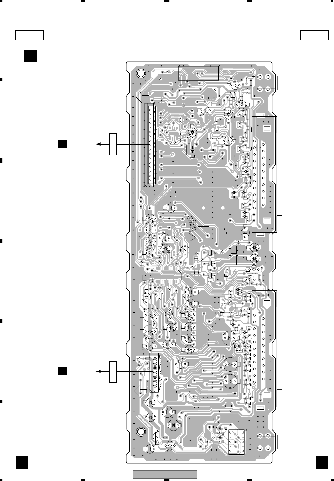
DVR-3100-S
64
1234
1234
C
D
F
A
B
E
4.7 SCRB ASSY
15
610
1
64
3
1
64
3
1
64
3
44 23
221
1
10
15
1
10 20 30
35
1
8
4
5
D142
D144
D132
D130
R1019
R155
R1006
D139
D160
R278
R274
R270
R272
R271
R273
R276
R275
R277
RY101
R121
R151
R147
R225
R224
R207
R203
R202
R201
R200
R115
R107
R106
Q122
Q121
Q120
Q118
Q110
Q109
Q106
Q105
L103
JA101
IC107
IC106
IC103
IC101
D129
D128
D127
D126
D125
D124
D123
D122
D121
D120
D119
D118
D117
D116
D115
D114
D112
D111
D110
D109
D108
D107
D106
D105
D104
D103
D102
D101
CN204
CN203
C228
C227
C221
C220
C219
C218
C214
C212
C209
C208
C207
C204
C183
C182
C170
C169
C168
C167
C166
C165
C161
C160
C159
C158
C156
C155
C152
C151
C149
C146
C141
C140
C139
C138
C137
C136
C135
C134
C133
C132
C131
C128
C127
C126
C125
C124
C123
C121
C120
C119
C118
C117
C116
C115
C112
C111
C110
C107
C106
C105
C104
C103
C102
D134
JA102
D135
R290
R1008
D140
C402
D131
D133
R1055
R1005
R1004
R1003
R1047
D150
R141
C401
D147
R1036
D138
R1024
R1056
R1034
R289
D141
R1041
KN101
KN102
R1018
R1017
R1016
R1009
C303
C188
R1045
R110
R1035
D148
D146
D145
R1058
D149
D136
D143
IC104
C148
C147
D159
R1046 D137
R160
R161
R162
R159
R288
R1043
R1039
R1029R291
Q289
15.P_CONT
14.BLANKIN
13.XTHROU
12.COMPMUTE
to TV
29.AR_StoT
11.SNL_IN
10.SNL_O
9.FUNC
8.SCL
7.SDA
6.GND
5.XP_SAVE
4.GND
3.V+5SM
2.EV+15
1.V+6E
1.SLAMUTE
13.G_StoT
11.G_TtoS
9.Y_TtoS
7.C_TtoS
5.V/Y_StoT
3.SRAMUTE
27.AL_StoT
25.AR_TtoS
23.AL_TtoS
21.R/C_StoT
19.R_TtoS
35.TUAR_TtoS
33.TUAL_TtoS
17.B_TtoS
15.B_StoT
18.GNDV
17.GNDV
20.V-YIN
19.V/Yout
16.BLANK
15.R/Cout
6.LIN
7.Bout
13.GNDV
10.N-LINK
14.GNDV
12.NC
9.GNDV
11.Gout
8.FUNCTION
5.GNDV
3.Lout
4.GNDA
1.Rout
2.RIN
21.GNDV
21.GNDV
20.V-YIN
19.V/Yout
18.GNDV
17.GNDV
16.BLANK
6.LIN
13.GNDV
10.N-LINK
14.GNDV
3.Lout
7.BIN
12.NC
15.R/CIN
9.GNDV
2.RIN
11.GIN
8.FUNCTION
V+5SC
1.Rout
GNDA
GNDV V+12SC
AV1
from STB
4.GNDA
SCRB ASSY
PYKC F4X
31.TUCVBS_TtoS
5.GNDV
AV2
Contact Side
Contact Side
PC
FC DC
V+12SC
V+12SC
V+5SC
1
EBEC2B
CCB2E2
35
44 23
221
31
64
31
64
31
64
15
1
NP NP
NP
NP
5
8
14
NP
SIDE A SIDE A
I I
SCRB ASSY
I
CN210
B
(VNP1935-B)
CN203
CN211
B
CN204
IC104
IC101
IC103
IC106
IC107
Q289
Q105
Q106
Q109
Q110
Q118
Q120
Q121
Q122
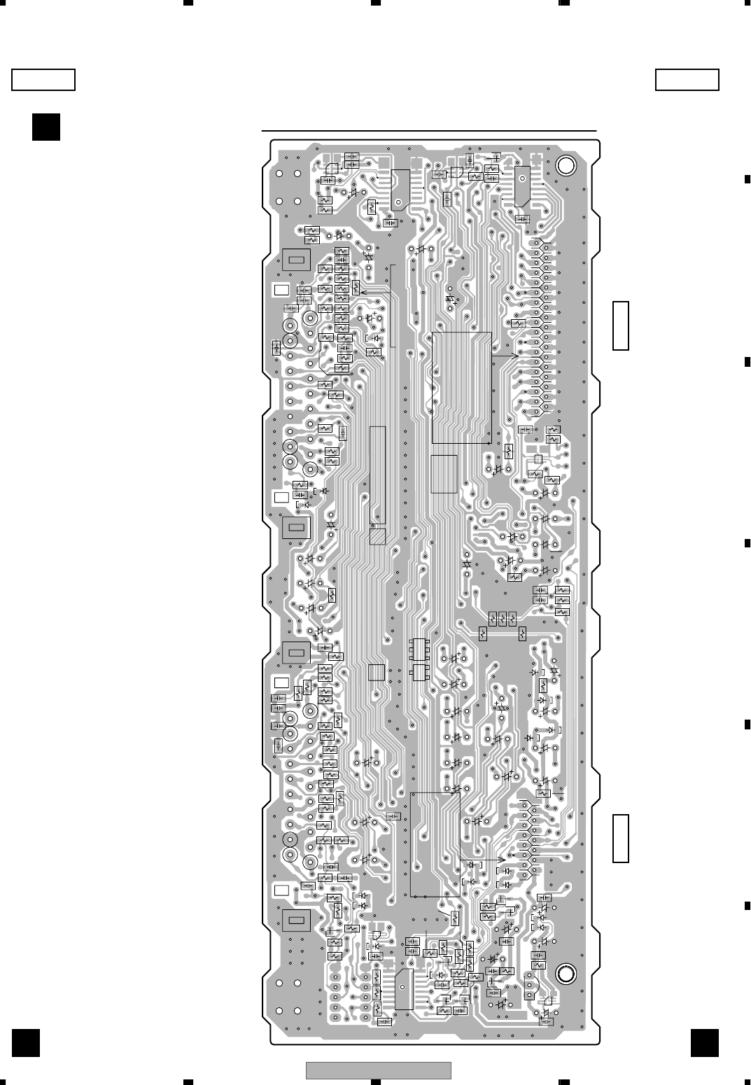
DVR-3100-S 65
5678
5678
C
D
F
A
B
E
3
4
1
6
81
916
3
4
1
6
16 9
8
1
16 9
8
1
R1002
R1001
D151
R117
D157
D184
R279
R280
R1023
R281
R269
R268
R122
R123
R243
R242
R241
R240
R239
R238
R237
R236
R235
R234
R233
R148
R232
R231
R230
R229
R228
R227
R226
R146
R223
R222
R221
R220
R219
R145
R218
R144
R217
R216
R215
R214
R143
R213
R212
R208
R140
R139
R205
R204
R136
R135
R132
R164
R131
R130
R126
R125
R124
R116
R114
R109
R108
R105
R104
R101
Q123
Q119
Q104
Q102
Q101
IC114
IC113
IC105
IC102
D182
D181
D113
C226
C225
C224
C223
C222
C217
C215
C213
C206
C205
C203
C201
C200
C199
C181
C180
C164
C162
C157
C154
C153
C150
C145
C144
C143 C142
C130
C129
C114
C113
C109
R152 R153
D188
R1007
D154
R156
R158
R282
D155
D156
R314
R313
R312
R311
R310
R309
R308
R307
C171
Q309
Q308 Q307
IC301
D307
C309
C308
R157
C307
C301
D158
R315 R1025
Q115
D187
D152
C231
C232
D153
R154
R1031
R1032
C283
D185
D186
R1033
C229
C230
Q124
R119
R112
R283
Q281
GNDV
BLANK
RIN
Lout
GNDV
Rout
LIN
V/Yout
V-YIN
GNDV
Rout
RIN
GNDA
Lout
15.P_CONT
13.XTHROU
11.SNL_IN
9.FUNC
7.SDA
14.BLANKIN
12.COMPMUTE
10.SNL_O
8.SCL
5.XP_SAVE
6.GND
R/CIN
GNDV
GNDV
GNDV
BIN
LIN
GNDV
GNDA
N-LINKGNDV
FUNC
GIN
NC
Bout
4.GND
FUNC
N-LINK
Gout
NC
GNDV
3.V+5SM
2.EV+15
GNDV
V-YIN
GNDV
V/Yout
GNDV BLANK
GNDV
R/Cout
GNDV
AV2
from STB
C
7.C_TtoS
E
9.Y_TtoS
B
GNDA
GNDV
1.SLAMUTE
V+5SC
V+12SC
11.G_TtoS
29.AR_StoT
31.TUCVBS_TtoS
33.TUAL_TtoS
35.TUAR_TtoS
23.AL_TtoS
25.AR_TtoS
27.AL_StoT
13.G_StoT
15.B_StoT
17.B_TtoS
19.R_TtoS
21.R/C_StoT
to TV
3.SRAMUTE
5.V/Y_StoT
1.V+6E
AV1
EBC2
E2B2C
VWV1958-
V+12SC
V+5SC
V+12SC
V+5SC
V+5SC
LF
21
20
2
1
1
6
3
4
9
81
16
1
6
3
4
1
16
8
9
15
10
1
35
3020
10
1
20
21
2
1
1
16
9
8
NP
SIDE B SIDE B
I I
SCRB ASSY
I
(VNP1935-B)
CN203CN204
IC301
IC102
IC105
IC113
IC114
Q281
Q124
Q115
Q307
Q308
Q309
Q101
Q102
Q104
Q119
Q123

DVR-3100-S
66
1234
1234
C
D
F
A
B
E
5. PCB PARTS LIST
Parts marked by "NSP" are generally unavailable because they are not in our Master Spare Parts List.
The mark found on some component parts indicates the importance of the safety factor of the part.
Therefore, when replacing, be sure to use parts of identical designation.
When ordering resistors, first convert resistance values into code form as shown in the following examples.
Ex.1 When there are 2 effective digits (any digit apart from 0), such as 560 ohm and 47k ohm (tolerance is shown by J=5%,
and K=10%).
Ex.2 When there are 3 effective digits (such as in high precision metal film resistors).
561
473
R50
1R0
5621
NOTES:
560 Ω
47k Ω
0.5 Ω
1 Ω
RD1/4PU J
RD1/4PU J
RN2H K
RS1P K
56 x 10
1
47 x 10
3
R50
1R0
561
473
5.62k Ω
RN1/4PC F562 x 10
1
5621
Mark No. Description Part No.
LIST OF ASSEMBLIES
1..ATAB ASSY VWV1968
1..TUJB ASSY VWV1962
NSP 1..FJDB ASSY VWM2206
2..FRJB ASSY VWV1965
2..DVJB ASSY VWV1967
1..MAIN ASSY VWV1971
2..MHLP ASSY VWV1991
1..FLKB ASSY VWM2212
2..FLKY ASSY VWG2443
>1..POWER SUPPLY UNIT VWR1374
1..SCRB ASSY VWV1958
Mark No. Description Part No.
AATAB ASSY
OTHERS
CN12 CONECTOR CKS4052
CN11 40P ATA CONECTOR VKN1805
BTUJB ASSY
SEMICONDUCTORS
IC2551 BA05FP
IC2251 BR24L32F-W
IC3301 LA73030
IC3501 LA73054
IC2801 LC75342M
IC4001 MSP3417G
IC2581 NJM78M09FA
IC2001 PD5947A8
IC2541 PQ1K333M2ZP
IC2521 PST3245
IC2271 RS5C372A
IC2003 TC74HCT7007AF
IC2351 TC7WU04FU
IC3903 TDA9818TS
Q3002, Q3342, Q3344, Q3363, Q3371 2SA1576A
Q3402, Q3404, Q3406, Q3408, Q3410 2SA1576A
Q3452, Q3909, Q4001-Q4004 2SA1576A
Q2640 2SB1238X
Q2532, Q2621 2SC2411K
Q2203, Q2205, Q2351, Q2641, Q3001 2SC4081
Q3453, Q3901, Q3902, Q3904, Q3905 2SC4081
Q3915, Q3916 2SC4081
Q3912, Q3920 2SC4082
Q4005 2SD1664
Q2202 2SD2114K
Q2151, Q2201, Q2305, Q3559, Q3562 DTA124EUA
Q3903, Q3906 DTA124EUA
Q2204, Q2642, Q3451 DTC124EUA
Q3362 HN1B04FU
Q2306 HN1C01FU
Q3554, Q3556 HN1C03FU
Q2152 RN1901
Q3914 RN1903
Q201, Q202, Q3004, Q3561, Q3563 RN4903
Q2531, Q3006, Q3099 UMF21N
D2640 1SR154-400
D2271 1SS352
D201-D203, D2201, D3001, D3551 1SS355
D3560, D4001 1SS355
D3901 1SS356
D3301-D3304 DA204K
D2272 RB501V-40
D3002 UDZS33B
COILS AND FILTERS
L3005 RADIAL INDUCTOR ATH1109
L3341, L3343 LAU180J
L3401, L3403, L3405, LL3407, L3409 LAU220J
L3451 LAU2R2J
L2301 LAU470J
L3957 LCKAWR22J2520
L3960 LCKAWR47J2520
L2641, L3342, L3344 LCYA100J2520
L3903, L3909, L3912 LCYA150J2520
L3911 LCYA4R7J2520
L3910 LCYA8R2J2520
L3907, L3920 LCYAR68J2520
L2642 INDUCTOR LTA102J
F3902 SAW FILTER VTF1177
F3901 SAW FILTER VTF1179
F3912 IF TRAP FILTER VTF1180
F3911 IF TRAP FILTER VTF1181
F3903 TRAP FILTER VTF1183
L2039, L2359, L3018, L3019 VTL1081
Mark No. Description Part No.

DVR-3100-S 67
5678
5678
C
D
F
A
B
E
CHIP BEAD
L3003, L3004, L3099, L3902 VTL1096
CHIP BEAD
L4002 VCO COIL VTL1164
CAPACITORS
C3356, C3357 CCSRCH100D50
C2118, C2119, C2545, C2546 CCSRCH101J50
C2818-C2820, C3362, C3365 CCSRCH101J50
C2141, C2142, C2822, C2823, C4016 CCSRCH102J50
C4022, C4023, C4028 CCSRCH102J50
C3932 CCSRCH121J50
C3917 CCSRCH150J50
C3345, C3352, C3404, C3410, C3416 CCSRCH180J50
C3422, C3428 CCSRCH180J50
C3935 CCSRCH181J50
C2357, C2358, C4029, C4030 CCSRCH220J50
C2645 CCSRCH221J50
C3343, C3350, C3960 CCSRCH270J50
C2301, C3020, C3021 CCSRCH330J50
C3405, C3412, C3417, C3423, C3429 CCSRCH390J50
C2101, C2105, C2106, C2201, C3933 CCSRCH470J50
C3561, C3562 CCSRCH471J50
C4017, C4019 CCSRCH560J50
C2354 CCSRCH561J50
C3905, C4018 CCSRCH5R0C50
C3344, C3351, C3451, C3936 CCSRCH680J50
C3901, C4021 CCSRCH6R0D50
C3341, C3347 CCSRCH8R0D50
C2273 CCSRCH4R0C50
C2353, C2801, C2802, C2810-C2817 CEAT100M50
C3001, C3364, C3641, C3642, C4007 CEAT100M50
C4012 CEAT100M50
C203, C2111, C2254, C2533, C2534 CEAT101M10
C2544, C2553, C2622, C2623, C2626 CEAT101M10
C3083, C3301, C3310, C3349, C3403 CEAT101M10
C3504, C3518, C4011, C4013 CEAT101M10
C4032, C4033 CEAT101M10
C2582, C2584, C2642, C2804, C2807 CEAT101M16
C3555, C3928, C4002, C4004 CEAT101M16
C3013, C3507, C3511 CEAT102M6R3
C3552, C3554 CEAT220M25
C3533 CEAT221M16
C3201 CEAT330M25
C4009 CEAT3R3M50
C2640 CEAT471M16
C3010, C3904 CEAT471M6R3
C3911, C3912 CKSQYB225K10
C3918, C3920, C3921, C3923, C3925 CKSRYB102K50
C2104, C2355, C2821, C3317, C3902 CKSRYB103K50
C3906, C3907, C3930, C4010, C4024 CKSRYB103K50
C2102, C2103, C3302, C3305-C3308 CKSRYB104K16
C3311, C3314-C3316, C3505, C3508 CKSRYB104K16
C3909 CKSRYB104K16
C3012, C3023, C3908, C3916 CKSRYB222K50
C3924 CKSRYB224K10
C4015, C4027 CKSRYB472K50
C2112, C2140, C2202, C2204, C2210 CKSRYF104Z25
C2251, C2302, C2303, C2351, C2352 CKSRYF104Z25
C2356, C2521, C2522, C2531, C2532 CKSRYF104Z25
Mark No. Description Part No.
C2535, C2541-C2543, C2551, C2552 CKSRYF104Z25
C2581, C2583, C2621, C2624, C2625 CKSRYF104Z25
C2641, C2643, C2646, C2808, C2809 CKSRYF104Z25
C3017, C3084, C3304, C3312, C3313 CKSRYF104Z25
C3346, C3353, C3407, C3415, C3419 CKSRYF104Z25
C3425, C3431, C3503, C3506, C3514 CKSRYF104Z25
C3519, C3521, C3530-C3532, C3551 CKSRYF104Z25
C3903, C3910, C3929, C3931, C3934 CKSRYF104Z25
C4001, C4003, C4006, C4008, C4014 CKSRYF104Z25
C4020, C4026, C4031, C4034 CKSRYF104Z25
C3005 CKSRYF104Z50
C2110, C2113-C2115, C2152, C2154 CKSRYF105Z10
RESISTORS
R4001, R4004 RS1/10S0R0J
R4009 RS1/10S100J
R3098 RS1/10S150J
R3346, R3349, R3352, R3356 RS1/16S5600F
R3406, R3418, R3428, R3438, R3443 RS1/16S6800F
R2815, R2817, R2818, R3303-R3305 RS1/16S75R0F
R3451, R3568, R3569, R3571 RS1/16S75R0F
VR3901 (10K) VCP1156
Other Resistors RS1/16S###J
OTHERS
U3001 TV TUNER MODULE VXF1023
X2271 (32kHz) VSS1143
X2351 (4.433619MHz) VSS1176
X2001 (10MHz) VSS1188
X4001 (18.432MHz) VSS1189
CN2006, CN2009 KR CONNECTOR B2B-PH-K
CN3003 2P TOP POST B2P-SHF-1AA
CN2003 KR CONNECTOR B8B-PH-K
CN211 15P FFC CONNECTOR HLEM15S-1
CN2005 19P FFC CONNECTOR HLEM19S-1
CN210 35P FFC CONNECTOR HLEM35S-1
CN2007 9P FFC CONNECTORE HLEM9S-1
JA3081 OPTICAL LINK OUT JFJ1001
JA2201 REMOTE CONTROL JACK RKN1004
CN2004 KR CONNECTOR S13B-PH-K
CN2001 8P SIDE POST S8B-EH
0 PCB BINDER VEF1040
BT2271 LITHIUM BATTERY VEM1034
JA2832 JACK VKB1192
JA3551 JACK VKB1193
CN2008 21P FFC CONNECTOR VKN1252
CN3001 32P FFC CONNECTOR VKN1263
CN3002 15P FFC CONNECTOR VKN1275
ST2271 BATTERY SOCKET VKX1015
2007 SCREW PLATE VNE1948
KN2001-KN2003 VNF1084
WRAPPING TERMINAL
CFRJB ASSY
SEMICONDUCTORS
D1301-D1304 UDZS5.6B
SWITCHES AND RELAYS
S1201, S1202 VSG1009
Mark No. Description Part No.

DVR-3100-S
68
1234
1234
C
D
F
A
B
E
CAPACITORS
C1308, C1309 CCSRCH471J50
RESISTORS
Other Resistors RS1/16S###J
OTHERS
JA1302 3P JACK VKB1189
JA1301 Y/C CONNECTOR VKB1190
CN1301 15P FFC CONNECTOR VKN1275
KN1301-KN1303 VNF1084
WRAPPING TERMINAL
DMAIN ASSY
SEMICONDUCTORS
IC3301 AD1895AYRS
IC3101 AK5381VT
IC2301 BA7655AF
IC1103 CY62148VLL-70ZI
IC5204 K4S161622D-TC80
IC1101 K4S281632E-TC75
IC1401 K4S561632D-TC75
IC1001 M65672WG-C
IC2331 MM1508XN
IC5002 MM1562FF
IC1301 MT48LC4M32B2TG-6
IC4001 NJM2370R12
IC4004, IC4006 NJM2872F05
>IC4007 NJM2880U1-33
IC4206, IC5301, IC5321 NJU7013F
IC3201 PCM1742KE
IC4008 PQ012FZ01ZP
IC4002 PQ070XZ02ZP
IC4003 PST3428U
IC4005 PST3809U
IC3402 SM8707KV
IC4101 SN74AHC2G53HDCT
IC3001 TC74LCX541FT
IC3002 TC74VHC14FT
IC5341 TC74VHC157FT
IC3403, IC4205, IC5322 TC7WHU04FU
IC3251 UPC4570G2
IC5101 UPD72852AGB-8EU
IC5202 UPD72893AGD-LML
IC1102 VYW2116
IC1201 W986416DH-6
Q2101-Q2105, Q2201, Q2203, Q2301 2SA1576A
Q2312 2SA1576A
Q2202, Q2222 2SC4081
Q2302, Q2311 DTC114EUA
Q2402, Q2403 HN1B04FU
Q1101 HN1K03FU
Q3201, Q3202 RN1903
Q1102 RN4982
Q2001 UMF21N
D3001, D3002, D3101-D3104 1SS355
D5321 HVC359
D5322 HVC362
D4201 MA2ZV05
D1111, D4001 RB521S-30
Mark No. Description Part No.
COILS AND FILTERS
F3102, F3401-F3403, F4004, F4201 DTF1069
F5101 CHIP BEAD DTF1069
L5301, L5321 LCYA100J2520
L4202 LCYA1R2J2520
F3201 CHIP SOLID INDUCTOR VTF1096
L5101, L5102 CHOKE COIL VTH1043
L2101 CHIP COIL VTL1067
L4201 CHIP BEAD VTL1079
L5103-L5106 VTL1082
CAPACITORS
C5311, C5329 CCSRCH100D50
C3253, C3258 CCSRCH101J50
C5105 CCSRCH271J50
C5325, C5327 CCSRCH330J50
C3207 CCSRCH331J50
C4208 CCSRCH390J50
C5131-C5138 CCSRCH4R0C50
C5326 CCSRCH5R0C50
C3254, C3257 CCSRCH681J50
C5121, C5122 CCSRCH8R0D50
C2208, C2317, C4002, C4034, C5203 CEVW100M16
C5322 CEVW100M16
C3251, C3255, C4001, C4004, C4029 CEVW101M16
C2101, C2221, C2331, C2405, C2501 CEVW101M6R3
C3201, C3204, C3206, C3301, C3309 CEVW101M6R3
C2301, C5102 CEVW220M6R3
C1054, C1055, C1057, C1058 CEVW221M4
C1060, C1061, C4022 CEVW221M4
C3106 CEVW2R2M50
C5321 CEVW470M16
C2308, C3102, C3107, C4003, C5205 CEVW470M6R3
C5207, C5221, C5341 CEVW470M6R3
C5301 CEVW4R7M35
C2204, C2334, C4206, C5309 CKSQYB105K10
C1901, C4014, C4019, C4033, C4036 CKSQYB225K10
C5006 CKSQYB225K10
C1501-C1507 CKSQYB475K6R3
C1004, C1012, C1014, C1029, C1034 CKSRYB102K50
C1040, C1044, C1049, C1051 CKSRYB102K50
C1110-C1112, C1207, C1208, C1307 CKSRYB102K50
C1311, C1313, C1407, C1408, C3303 CKSRYB102K50
C3307, C3408 CKSRYB102K50
C1003, C1027, C1037, C1052, C1109 CKSRYB103K50
C1206, C1305, C1308, C1310, C1406 CKSRYB103K50
C2305, C3003, C3004, C4018, C4020 CKSRYB103K50
C4207, C5214, C5222, C5224 CKSRYB103K50
C1508-C1510, C2225, C2311, C4104 CKSRYB104K16
C5306 CKSRYB104K16
C4103 CKSRYB223K50
C5328 CKSRYB473K25
C2202 CKSRYB563K16
C1002, C1005, C1007-C1010, C1016 CKSRYF104Z25
C1018, C1019, C1021-C1023 CKSRYF104Z25
C1025, C1026, C1028, C1030, C1035 CKSRYF104Z25
C1038, C1041, C1042, C1047, C1102 CKSRYF104Z25
C1105, C1106, C1108, C1114, C1202 CKSRYF104Z25
C1204, C1302, C1304, C1312, C1402 CKSRYF104Z25
C1404, C2102-C2106, C2201, C2206 CKSRYF104Z25
C2222, C2306, C2319, C2332 CKSRYF104Z25
Mark No. Description Part No.

DVR-3100-S 69
5678
5678
C
D
F
A
B
E
C2406, C2407, C2502-C2506, C3001 CKSRYF104Z25
C3006, C3101, C3105, C3108 CKSRYF104Z25
C3202, C3203, C3205, C3252, C3256 CKSRYF104Z25
C3302, C3308, C4006-C4008, C4010 CKSRYF104Z25
C4012, C4013, C4017, C4021 CKSRYF104Z25
C4024-C4026, C4032, C4035, C4107 CKSRYF104Z25
C4202, C4203, C4209, C5101, C5103 CKSRYF104Z25
C5111-C5113, C5118-C5120 CKSRYF104Z25
C5123-C5127, C5204, C5206 CKSRYF104Z25
C5208-C5213, C5215-C5218 CKSRYF104Z25
C5225-C5230, C5308, C5310, C5323 CKSRYF104Z25
C5342, C5343 CKSRYF104Z25
C1001, C1006, C1011, C1013, C1017 CKSRYF105Z10
C1024, C1036, C1039, C1045, C1048 CKSRYF105Z10
C1050, C1053, C1103, C1107, C1113 CKSRYF105Z10
C1203, C1205, C1209, C1303, C1306 CKSRYF105Z10
C1309, C1403, C1405, C1409, C2507 CKSRYF105Z10
C3404-C3407, C4027, C4028 CKSRYF105Z10
C4030, C4031, C4105, C4201, C4401 CKSRYF105Z10
C4501, C5110, C5231 CKSRYF105Z10
C1056, C1059, C1062, C1101, C1104 CKSYF106Z10
C1201, C1301, C1401, C3402, C3403 CKSYF106Z10
C4015 CKSYF106Z10
VC4201 (10pF) VCM1012
RESISTORS
R1025, R1026, R1042-R1046 RAB4CQ103J
R1048-R1051, R1054, R1068, R1069 RAB4CQ103J
R1072, R1073, R5218-R5221 RAB4CQ103J
R5229, R5230, R5247, R5249-R5252 RAB4CQ103J
R5255, R5258, R5259, R5273-R5275 RAB4CQ103J
R5289, R5290 RAB4CQ103J
R1408-R1411, R4302-R4306 RAB4CQ220J
R4401, R4404, R4410, R4416, R4417 RAB4CQ223J
R4423, R4502, R4506, R4512 RAB4CQ223J
R4518, R4519, R4525 RAB4CQ223J
R1114-R1117, R4405-R4408, R4436 RAB4CQ330J
R1303-R1310, R1404-R1407 RAB4CQ560J
R1203-R1206 RAB4CQ680J
R5103 RN1/16SE5101D
R5108 RN1/16SE9101D
R1001-R1009, R1101, R1102, R1201 RS1/10S0R0J
R1301, R1401, R2017, RS1/10S0R0J
R3002, R3102, R3201, R3252, R3301 RS1/10S0R0J
R3303, R4001, R4006, R4009, R4014 RS1/10S0R0J
R4016, R4108, R4109, R5102 RS1/10S0R0J
R5207-R5209, R5292, R5322 RS1/10S0R0J
R5321 RS1/10S101J
R4013 RS1/16S1001F
R3254, R3266 RS1/16S1002F
R3253, R3265 RS1/16S1201F
R4011 RS1/16S1501F
R4012 RS1/16S1800F
R1021, R1023 RS1/16S2201F
R3251, R3269 RS1/16S2202F
R2105, R2106, R2111, R2112, R2115 RS1/16S3300F
R5104-R5107 RS1/16S56R0D
Other Resistors RS1/16S###J
Mark No. Description Part No.
OTHERS
CN4001 PH CONNECTOR S8B-PH-SM3
CN1901 7P FFC CONNECTOR VKN1299
CN2501, CN5102
7P FFC CONNECTOR
VKN1411
CN3001 21P FFC CONNECTOR VKN1425
CN4301 29P FFC CONNECTOR VKN1433
CN2001 32P FFC CONNECTOR VKN1436
CN4401 40P FFC CONNECTOR VKN1794
KN3 EARTH METAL FITTING VNF1109
X4201 (27.000MHz) VSS1146
X5101 (24.576MHz) VSS1184
X4102 (27MHz) VCXO VSS1195
EMHLP ASSY
SEMICONDUCTORS
IC1 PDY081A
D1 RB521S-30
CAPACITORS
C1 CEVW101M6R3
C2-C6 CKSRYF104Z25
C7 CKSRYF105Z10
RESISTORS
R3 RAB4C0R0J
R2 RAB4C102J
R1 RS1/16S0R0J
Other Resistors RS1/10S###J
OTHERS
CN1 7P FFC CONNECTOR VKN1411
CN2 B TO B CONNECTOR 30P VKN1571
FFLKY ASSY
SEMICONDUCTORS
IC1001 PT6315
COILS AND FILTERS
L1001 LAU220J
SWITCHES AND RELAYS
S1001, S1002, S1004-S1008 VSG1009
S1003 VSX1004
CAPACITORS
C1012 CEJQ101M6R3
C1010 CEJQ220M35
C1015 CEJQ470M16
C1001-C1004, C1006-C1009, C1011 CKSRYB103K50
C1013, C1016 CKSRYB103K50
RESISTORS
Other Resistors RS1/16S###J
OTHERS
CN1001 19P FFC CONNECTOR 9607S-19F
IC1002 REMOTE RECEIVER UNIT RPM7140-H4
V1001 FL TUBE VAW1081
RUBBER SPACER VEB1357
1001 FL HOLDER VNF1120
Mark No. Description Part No.

DVR-3100-S
70
1234
1234
C
D
F
A
B
E
GPOWER SUPPLY UNIT
OTHERS
>P101 PROTECTOR(3A) AEK7050
>P201, P401, P403, P404 AEK7067
PROTECTOR(2A)
HDVJB ASSY
OTHERS
JA1303 DV-TERMINAL VKB1186
CN1302 7P FFC CONNECTOR VKN1238
ISCRB ASSY
SEMICONDUCTORS
IC104 BA4558F-HT
IC113 BU4052BCF
IC101 LA73026AV
IC114 MM1503XN
IC103, IC106, IC107 MM1506XN
IC105 MM1511XN
IC102, IC301 TC74HC4053AF
Q101, Q120-Q122, Q124 2SA1576A
Q118 2SC1740S
Q104, Q307-Q309 2SC4081
Q109, Q110 DTA124EUA
Q115, Q123 DTC124EUA
Q105, Q106 HN1C03FU
Q281, Q289 RN2903
Q102, Q119 RN4903
D113-D117, D130-D133, D181 1SS355
D184, D187, D188, D307 1SS355
D134 RB501V-40
D182 UDZS12B
D101-D112, D118-D121 UDZS5.6B
D123-D127, D129, D135-D150 UDZS5.6B
D185, D186 UDZS5.6B
COILS AND FILTERS
L103 LCYA220J2520
SWITCHES AND RELAYS
RY101 VSR1017
CAPACITORS
C142-C145 CCSRCH102J50
C225, C226 CCSRCH220J50
C307, C308 CCSRCH221J50
C113, C114, C127-C130 CCSRCH471J50
C203-C206 CCSRCH471J50
C115, C116, C227, C228 CEANP100M16
C158, C159, C165, C166 CEAT100M50
C168, C169, C212, C219-C221 CEAT100M50
C156, C161, C182 CEAT101M10
C103-C105, C147, C209, C214 CEAT101M16
C218 CEAT101M16
C151, C152, C160, C167, C170 CEAT102M6R3
C138 CEAT1R0M50
C102, C117, C118, C123-C126 CEAT220M25
C139-C141, C149 CEAT220M25
Mark No. Description Part No.
C207, C208 CKSQYB105K16
C110 CKSQYF105Z16
C121, C146, C150, C153, C162 CKSRYB103K50
C222-C224 CKSRYB105K10
C109, C135-C137, C148 CKSRYF104Z25
C154, C155, C157, C164, C180 CKSRYF104Z25
C200, C201, C213, C217, C301 CKSRYF104Z25
C303, C309, C401, C402 CKSRYF104Z25
C111, C112 CKSRYF105Z10
RESISTORS
R121, R126, R140, R143-R148 RS1/16S75R0F
R151, R207 RS1/16S75R0F
Other Resistors RS1/16S###J
OTHERS
CN204 15P FFC CONNECTOR HLEM15S-1
CN203 35P FFC CONNECTOR HLEM35S-1
JA101, JA102 SCART CONNECTOR VKB1157
101, 102 SCREW PLATE VNE1948
Mark No. Description Part No.
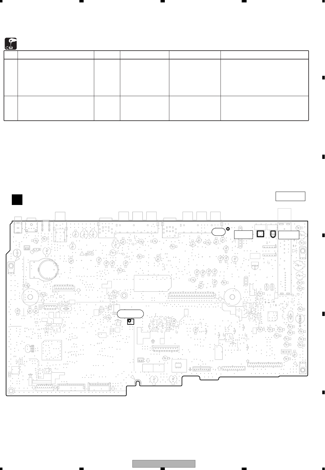
DVR-3100-S 71
5678
5678
C
D
F
A
B
E
6. ADJUSTMENT
6.1 TUJB ASSY ADJUSTMENT
The solder land named
"AFT2" (uppe
r side)
Q3901-Emitter
CN3003 Pin1
(AGC)
1.90V ± 0.20V
Note1
3.80V ± 0.20V
2
T
errestrial tuner input /through output.
Any channel, RF Input
≥ 60dBu
System = B/G, I or D/K
Manual Adjust (in GUI of Manual Ch
Setting) = ON
Note1
T
errestrial tuner input
Ch = E9(203.25MHz),
Video= Blackburst
RF Input = 60.0
±
1.0dBu
System = B/G, I or D/K
Note 1 : The adjustment spec. is defined without the thermal drift after the power on.
Therefore, start the adjustment at least 10 minutes after the power on.
No. Adjustment Name
Adj. Point Measurement Point
Adjustment Value
Adjustment State
1
VCO freerun frequency (AFC voltage)
adjustment
AGC start point adjustment
L4002
VR3901
* It is not necessary to adjust the ASSY normaly when exchanging the ASSY. But the adjustment is
necessary when exchanging the Tuner Module and IC3003 VIF/SIF IC.
88
116
30 58
129
59
87
41
58
14
5
8
1
12
8
12
34
5
6
78
910
11
1213
14
15 18
1
9
1
10
19
1
10
15
1
13
46
119
12
34
5
78
910
1213
14
15 18
115
12 3
46
1
10 20 30
35
1
32
111
12 22
23 33
34 44
12
14
17
8
18
12
13
+-
C2115
R2119
X2001
C2106
C2105
R2007
R2004
C2104
C2103
C2102
R2102
C2101
R2101
R2038
R2118
R3949
IC2001
C2111
X2271
IC2251
C2251
C2582
C2584
C2622
C2623
C2626
IC2581
IC2351
R2357
C2356
X2351
CN2006
C2801
C2803
C2813
C2811
C2807 C2812
C2810
C2804
C2802
C2806
C2642
R2305
R2012
R2011
R2303
CN2003
KN2003
KN2002
KN2001
C2534
C2533
R2361
C2254
JA2832
C2354
R2355
Q2351
R9004
R9005
R9006
R9007
R9008
CN2007
C2107
C2108
C2109
R2115
JA2201
R2113
C2355
C2357
R2360
C2358
R2359
R2358
C2353
R2354
C2352
R2352
R2353
R2351
C2351
R2103
L2642
C203
R2356
C2815
C2814
R2251
R2252
C2253
C2252
R2001 R2002
R2003
R2005
R2013
R2081
R2084
R2086
R2087
R2085
R2083
R2079
R2071
C2119
R2043
R2066
R2016
IC2551
C2553
R2551
KN2007
CN2005
R2048
CN211
CN2009
C2544
IC2541
R2309
C2817
C2816
C2516
R2311
L2301
R2317
R2315
R2316
C2303
R2318C2302 Q2306
CN2008
C2505
C2506
R3354
Q3344
L3344
L3343
R3351
R3357
Q3343
R3352
R3350
C3353
C3349
C3347
C3350
C3351
C3352
R3355
C3316
D3304
D3303 C3315
C3314
C3310
D3302
D3301
C3311
C3308
Q3342
R3348
L3342
R3346
L3341
R3342
R3345
R3344
Q3341
C3307
C3346
C3341
C3343
C3344
C3345 C3301
R3343
C3029
C3028
C3026
C3022
R3023
C3015
C3013
C3006
C3009
C3001
U3001
R3442
Q3407
R3435
R3436
R3432
R3423
C3419
R3424
R3420
Q3404
L3403
C3415
R3421
R3405
L3401
C3403
C3518
C3517
C3516
C3511
C3515
C3507
C3504
C3083
JA3081
C3552
C3554
C3555
JA3551
C3364
R3026
Q3006
L3005
C3427
R3561
Q3554
Q3556
R3304
C3354
C3355
CN3002
L3409
L3407
L3405
C3935
C3936
C3931
C3934
C3929
Q3915
R3937
R3941
C3932
C3930
C3933
Q3916
R3933
C3928
VR3902
F3903
R3909
VR3901
F3901
C3904
L4002
Q3099
R3099
R3098
L3098
C3099
C3201
R3908
R3931
Q3913
R3930 F3902
R3925
C3357
C3356
F3911
F3912
R3910
F3904
R3922
R3921
CN210
F3906
R3945
R3944
C4033
CN3001
L3099
R3935
R3934
R3942
R3915
R3356
R3349
Q3004
L3909
L3910
L3911
L3912
Q3906
C3010
R202
JA3582
Q4004
C4028
R4019
C4027
R4018
R4017
C4026
R4016
C4023
Q4003
C4022
R4014
R4013
R4012
X4001
R4015C4024
R4011
C4016
C4015
R4010
C4014
C4013
C4012
C4011
C4019
C4020
C4017
Q4001
R4008
R4006
R4007
Q4002
C4009
C4008
C4006
C4007
C4004
C4003
C4010
R4003
C4001
R4005
IC4001
C4002
C3533
R3998
R2205
R3005
CN3003
R2108
C2204
R3597
C4032
C2140
R2301
R2058
C2141
R2145
R1000
C2142
R2146
R2059
R2109
ST2271
R2140
D3306
R3599
C2118
Q2640
C2640
R3457
C2152
C2153
C2154
R2057
D3305
R1001
L2039
R2078
C3641
IC2003
R2110
R2029
R2080
Q3565
Q3564
R3574
R3573
C2082
R2017
R2253
CN2001CN2004
Q3451
C2210
R2209
Q2205
R2210
R3643
R3642
C3642
Q3452
L3451
R3456
R3452
R3453
R3454
R3455
BT2271
R2254
CVBS2
WARNING
AGC2
AFT2
ARM2T
TUJB ASSY
L`AFC
Adjust
AGC
FC DC
PC
1C
1V
3V
Adjust
CONTACT UPPER SIDE
Adjust
AFC
19
1
33
34
12 22
23
44
111
8
1
4
1
85
EBC2
CB2E2
V+5E
V+3.3SW
V+6E
V+13SW
V+6SW
V+13SW
V+5VO
V+5VI
V+6SW
V+5M
V+5VO
V+5E
V+5VO
V+15E
V+5VI
V+15E
V+5VI
V+6E
V+13SW
V+6SW
V+37E
V+5TU
13
1
15
1
19
15
1
CMKD-P3X
35
1
2
8
1
211
58
129
5987
88
116
30
34
1
1
119
25249.6 - PROPOSITION 65
HEALTH & SAFETY CODE SECTION
DEFECTS OR OTHER REPRODUCTIVE HARM.
OF CALIFORNIA TO CAUSE CANCER,BIRTH
CHEMICALS WHITCH ARE KNOWN TO THE STATE
AND CERTAIN ELECTRICAL PARTS CONTAIN
THIS PRODUCT CONTAINS LEAD IN SOLDER
8
1
5
4
13
46
1
32
12
17
814
-+
TUJB ASSY
BSIDE A
VR3901
L4002
Fig.1 Adjustment Points (TUJB ASSY)
CN3003 Pin1
AFT2
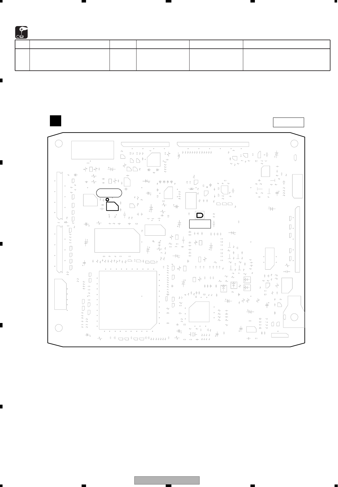
DVR-3100-S
72
1234
1234
C
D
F
A
B
E
6.2 MAIN ASSY ADJUSTMENT
MAIN ASSY
IC3402 Pin8 (XTO)
(SM8707KV)
No. Adjustment Name
Adj. Point Measurement Point
Adjustment Value
Adjustment State
127.000000MHZ
± 130Hz
Master clock free-running adjustment
(Clock system adjustment)
VC4201 No signal input
* It is not necessary to adjust the ASSY normaly when exchanging the ASSY but confirm the data.
D1111
R5104
IC5101
C1061
C5111
R5236
5
CN5102
R5121
R5110
C5101
C5131
C5135
TP34
TP36
C4033
8
2
71
R5247
82
7
1
R5249
82
71
R5263
R5262
R5260
R5120
R5116
R5122
R5114
R5253
R5254
R5256
R5257
C5210
C5121C5122C5124
C5209
C5212
C5204
C5206
C5214
C4032R5102
R5208
TP35
TP4015
C5102
F5101
C5207
R5252
17
28
R5251
L5101
L5102
IC4007
31
4
R5103
R5108
R5107
R5106
R5105
1
208
157
156 X5101
71
33
3217
16
R5235
R5216
R5217
R5231
R5109
R5125
R5128
R5117
R5115
R5126
R5129
R5232
R5214 R5233
R5215
R5234
C5103
C5105
C5110
C5112
C5127
C5120
C5216 C4035
C5132
C5138
C5137
C5136
TP31
TP32
TP33
TP37
TP38
TP5202
TP5201
C5104
C4034
L5103
L5104
L5106
L5105
1
2
1
TP1026 TP4305TP3303 TP3301R5292
R1005
C5231C5224 C5229
C1013
R5298R5297
R4504
R1074
53
R4405
C5205
Q2104
Q2105
TP5204 R1102
F1001
C2265
C5218
R5283
R2109
R1011
C1041
C1037
C1034
C1028
C1027
C1025
C1016
R4110
R5124
R5123
R5286
C5118
C5119
C5123
C5227
R4109
VR1001
1
4
20
CN4601
R4105
R5272
R5130
IC5202
64 49
48
1
8
2
7
1
R5275
8
7
R5218
82
7
1
R5219
82
7
1
R5220
82
7
1
R5221
82
71
R5274
8
2
71
R5273
C1011
C1014
R5237
R5238
R5132
R5131
R1071
R5112
R5113
R5127
R5276
R1111
R1052
R1012
C5113
C5125
C5126
C5226
C5217
C5215
C1114
C4107
C4102
C4105
R4108
R1007
R1001
C1054
TP1060
TP5106
Q1102
C4106
VR2104
X4102
3
229
1
C1104
R4106
R4107
R2112
R2115
R1024
R1023
R1022
R1021
105104
52
2
1
2
1
R5290
8
2
71
R5289
82
71
R5229
2
1
82
7
1
R5230
C1050
C1004
C1003
C1002
C1001
C1508
C1509
R4104 R4103
R4102R4101
R5280
R5281
R5228
R5224
R5288
R5225
R5278
R5279
C1510
R5227
R2113
R4403
R4402 R2114R2116
R5277
R5287
R5282
R5313
R5314
R5265
R2266
C5228
C4103
C4104
F1007
R1003
R1009
C1060
TP28
TP4708
TP4707
TP4706 TP4702
TP1041
TP1050
TP1051
IC4101
14
58
VR2105
VR1002
R1031
Q2103
TP4701TP4703 TP4302C5321
R1004
C1006
R2107
CN4702
C5225
R2102
R2103
TP4705
Q2102
Q2101
R4407
1
2
R5295
R5296
R5242
R5240
R5241
R5243
R5248
R2106
R2105
R1034 C2246
C5329
C5213
C5211
C5208
C2105
C2106
R2252
R5284
R5285
R5244
R5245
R5246
R5239
R5261
TP1002
C1042
C1017
F1005
R1006
C1057
TP4709
TP4711
TP4710
TP4718
TP4719
7
8
R5259
17
28
R5258
17
28
R5250
1
7
28
R5255
17
28
R4306
17
28
7
8
R4406
17
28
R2111
82
7
C5230
C5223 C5222
C3307
C2102
C2103
C2104
R3307
R3306R3305
R1066
R5293R5294
C1005
C1051 C1052 C1012
C1044
C1045
C1018
C1019
R3303 C1055
C3309
TP4304
TP4307
TP4704 TP4712
TP4713
CN4401
R4305
17
28
7
8
R4408
1
CN4301
15 28
IC3301
C1056
C1059
IC5204
82
7
1
R4436
8
2
7
1
R4304
82
71
R4303
40
39
D4401
C5221 TP1013
TP4717
TP4716TP4715
TP4714
TP4303
TP4301
TP3302
C2101
C1058
R1008
F1006
F1004
C1021
C1048
C1047
R3310
R4435
R4432
R4429
R4428
R3308
R4427
C1022
C1023
C1024
C1026
C1030
C1029
C1035
C1038
C1036
C1049
C1039
C3308
C4401
F1003
F3102
D3102
D3101
D3104
D3103
R4001
C2225
C4213
C4212
C4006
C4005
R1905
R2306
IC4008
R4201
41
X4201
1
F4201
C4201
C4202
R4017
C4028
D4001
1
14
C4036
C3403
R3411
82
7
1
R4508
82
71
R4509
82
71
R4507
82
71
R4302
2
1
82
71
R1048
82
71
R1045
82
71
R1043
85
IC3403 23
VC4201
C3107
F3401
F3403
916
IC3402
C4211
C3404
C3405 C3407
C3302
C3303
C3108
C3408
C1053
C1040
R3309
R2227
R3405
R3406
R3407
R3403
R3304
R4505
R4440
R4205
R5223
R5222
R1080
R3102
R3301
C3301
C2221
TP3401
TP4202
TP4306
TP1012
TP1027
TP1028
TP1029
TP1030 TP1032
TP1031TP1033
TP1024
D4202
C4206
Q2311
Q2222
R4204
R1902
C3105
C4208
C4203
F3402
5
C4014
TP3402
TP3403
C2222
R2233
R2235
R3410
R4202
R4206
R4210
R4211
R4212
R3409
R3107
R3106
R3108
R3105
R2311 R1901
R4531
R4530 R1903
R1904
C3101
C3406
C4209
C3106
C2317
F4004
8
IC3101
8
9
4
1
L4201
13
IC4205
14
8
CN4501
R4510
17
28
R3408
L4202
C3402
C1901
Q2312
TP4201 TP4008
R4015
F4001
C4031
C4018
C4027 R2239R4207
R4208R4209
R3103
R3104
R2313
R2314R2312
R4534
R4537
R2221
CN1901
C4210
C4207
D4201
F4202
C3102
16
1
IC4206
45
IC4004
13
45
R4538
17
28
IC4207
C2334
85
41
IC2301
1
3
46
IC2331
L2101
R4213
40
39
132
CN2001
81
CN4001
IC4003IC4005
21
1
CN3001
D4501
20
11
10
1
IC3001
Q2001
Q3202Q3201
Q2402
D3001D3002
TP50
TP49
TP48
TP47
TP46
TP45
TP44
TP43
TP42
TP41
TP40
TP39
TP4001
TP4009
TP4003 TP4002
TP4010
C4004
C2405
R4014
R4010
R4009
R3002
R2017
Q2403
C2333
C2311
C2305
C2332
C4010
C4021
C4024
C4023
C4013
R2041
R2042
R2043
R2044
R2045
R2046
R2331
R2332
R2333
R3271
R3270
R2019
R3022
R4541
R3010
R3001
R3003
R3012 R2411
R2412
R2406
R2405
R2407
R2409
R2408
R2012
R2011
R2013
R2015
R2014
R3023
R3024
R3202
R4004
R4008
R2404
R3025
F4003
C2407
C2319
C3004
C3002
C3001
C2406
MAIN ASSY
DSIDE A
VC4201
IC3402 Pin8
Fig.2 Adjustment Point (MAIN ASSY)
DVR-3100-S 73
5678
5678
C
D
F
A
B
E
7. GENERAL INFORMATION
7.1 DIAGNOSIS
7.1.1 CPRM ID NUMBER AND DATA SETTING
Entering the ID Number and ID Data for DVD Recorder
To enter the input mode, press ESC + STEREO sequentially in
a status with no ID number set, such as after FLASH-ROM
downloading.
• " CPRM ERR" is displayed on the FL display immediately after the power is turned on or in Stop mode.
• When the MAIN ASSY , DRIVE ASSY or the FLASH ROM is exchanged.
Important: If no ID label is found on the rear panel, write down the specified ID number by checking it according to "How to
confirm the ID number" shown below.
Note:
Be sure to enter the ID number in Stop mode.
Use the service remote control (GGF1381) for operations. Only opening/closing of the tray are performed from the player.
The ID data disc is swept out automatically after the recorder has read the data from it.
For the DVD recorder,it is necessary with the recoding/playback of DVD–RW disc to set an individual number (ID number) and ID data to
each recorder. If the number and data are not set correctly with the following procedure, operations in the future may not be guaranteed.
You will find the ID number to be set on the ID label on the rear panel.
Use DVD Recorder DATA DISC [GGV1134] and Service Remote Control Unit [GGF1381]
The Input is Necessary When:
How to Input the ID Number and ID Data
[Recorder's ID Number Setting]
ID Number ?
> - - - - - - - - -
<CLEAR> Exit
Input ID Number !
1
As number input is enabled when the unit enters the input
mode, input the 9-digit ID number.
(The entered number is also displayed on the FL display.)
2
2
[Recorder's ID Data Setting]
<CLEAR> Exit
Insert The ID Data Disc !
When the ID number has been registered, the unit enters the ID
data input mode. (The FL display indicates
"INSERT ID.")
In this condition, place the ID data disc on the tray and close the
tray using the CLOSE key "7/0" on the player.
4
4
[Recorder's ID Data Setting]
Loading The ID Data Disc !
While the data are being read, the message shown in the figure
at left is displayed on the screen.
(The FL display indicates "LOAD ID.")
5
5
[Recorder's ID Number Setting]
ID Number ?
> 0 0 0 0 0 0 0 0 1 OK ?
<PLAY> Compare Mode
<SEARCH> Enter
Input ID Number !
After inputting the number, press SEARCH to register the ID
number.
3
3
DVR-3100-S
74
1234
1234
C
D
F
A
B
E
How to Confirm the ID Number
How to Clear the ID Number
[Recorder's ID Data Setting]
Wait Rom Writing !
When the ID data have been read, the data are written to the
FLASH-ROM.
(The FL display indicates "WRITE ID.")
6
6
[Recorder's ID Data Setting]
Rom Write OK !
<CLEAR> Exit
When the ID data have been written to the FLASH-ROM, the
message "Rom Write OK" is displayed on the screen.
(The FL display indicates "ID DATA OK.")
After confirming this message, press CLEAR to exit the input
mode.
7
8
7
8
[Recorder's ID Number Setting]
ID Number ?
[ 0 0 0 0 0 0 0 0 1]
Compare
> * * * * * * * * *
<CLEAR> Exit
Input ID Number !
Press ESC + STEREO sequentially with an ID number already
set, and the unit enters the ID number confirmation mode.
The set ID number is displayed on the screen (and on the FL
display), permitting you to confirm it.
To exit this mode, press CLEAR .
1
Press ESC + STEREO sequentially with an ID number already
set, and the unit enters the ID number confirmation mode.
Input the same number as the ID number you have set.
1
2
2
3
2
3
[Recorder's ID Number Setting]
ID Number ?
[ 0 0 0 0 0 0 0 0 1]
Compare
> * * * * * * * * *
<CLEAR> Exit
<STEREO> ID Data Setting Mode
<STEREO> ID Data Setting Mode
Input ID Number !
2
After inputting the number, press STOP .
Only when the entered number matches the set ID number, the
ID number is cleared and the unit exits this mode.
If the numbers do not match, you must return to step 2.
( STOP is not accepted until 9 digits are entered.)
3
[Recorder's ID Number Setting]
ID Number ?
[ 0 0 0 0 0 0 0 0 1]
Compare
> 0 0 0 0 0 0 0 0 1 OK ?
<PLAY> Enter
<STOP> Memory Clear
Input ID Number !
3
DVR-3100-S 75
5678
5678
C
D
F
A
B
E
7.1.2 SERVICE MODE
For service operations, use the GGF1381 remote control unit for service.
The Service-mode screens consist of nine mode screens, which are classified into such rough categories as recording system and VR
playback system, and their subscreens.
• How to enter Service mode : Press the ESC then DISP keys in turn while no GUI is displayed. The first screen (version
information, etc.) shown below is displayed.
• How to exit Service mode : Press the ESC key.
• How to advance to the next Service-mode screen
:While the first screen is displayed, press directly one of the keys 1-9. For service, use the
keys 2, 4 or 5, as shown below.
• How to advance to a subscreen within the same Service-mode screen
:Press the DIG/ANA key. Pressing the DIG/ANA key repeatedly will change the subscreens
within the same Service-mode screen cyclically.
The Service-mode screens to be used for service are as follows:
1 = First screen: Version information, etc.
2 = Second screen: ATA/ATAPI debug screen (Writer data)
4 = Fourth screen: Error log for the VR recording system
5 = Fifth screen: Error log for the VR playback system
Note: After entering one of the Service-mode screens, if you wish to shift to another Service-mode screen, exit Service mode first,
then reenter Service mode and select your desired Service-mode screen.
DVR-3100-S/WY
SYSCON : 2.00
ComRev : 1.1140.2.6 $
FirmRev : 1.2834.2.4 $
AppRev : 1.3873.2.8 $
TUFLCON : 2.18 F OK
DRIVE : DVD-RW DVR-106 OK
1.01L
CBT0900720WL OK
H D D : ----
DEVICE : PRISM=ES 2.0C
REGION : 2
C:∗ ∗ ∗ ∗ ∗ ∗ ∗ ∗ ∗
Description of Each Service-mode screen
• Subscreen: Result of error-rate measurement
ERR RATE : x.xe-x/
1
2
4
5
6
7
8
3
OK : OK (proper combination)
OK+ : Version of the tuner microcomputer too advanced
NG– : Version of the tuner microcomputer too old
NG! : "Type"(e.g. J type, WY type) of Syscom's and TUFL
microcomputers are mismatching.
OK : OK (proper combination)
OK+ : Version of the drive too advanced
NG– : Version of the drive too old
OK : Serial No. of the drive already registered
NG : Serial No. of the drive not registered
1Model name/destination
2Version of the recorder software
3Revision No. of the system-control computer software
(Edition administration No. [from top to bottom, common
software, firmware, application software])
4Version No. of the tuner microcomputer, Mask or
flash (M: Mask type, F: FLASH type)
5Information on the built-in drive
(Model name, version No., serial No.)
6Version No. of PRISM
7Region No.
8CPRM data (CPRM key No.)
While the first screen shown above is displayed, press the DIG/ANA key to enter the subscreen shown below.
Note: Each time the DIG/ANA key is pressed, the display changes between the first screen and its subscreen.
Note: Be sure to start playback after displaying this subscreen
to calculate the error rate.
1. First screen (version information, etc.)
During playback in VR mode, the average error rate of the past 10 VOBUs is displayed, and during playback in DVD-Video or
Video mode, the average error rate of the past 256 sectors is displayed. During playback in VR mode, the rotation rate of the
drive (/: normal speed, no display = double speed) is also displayed.
DVR-3100-S
76
1234
1234
C
D
F
A
B
E
• Subscreen 1: Command log (ALL) of ATA/ATAPI DEBUG OSD
Subscreen 1 of the second screen is displayed when the ESC, DISP, then "2" keys are pressed, in that order.
Note: Each time the DIG/ANA key is pressed, the display changes cyclically among subscreens 1 to 4.
The cumulative power-on time and error log that are administered by the writer are displayed. Such information is obtained when the power
is turned on. Thereafter, each time the SEARCH key on the remote control unit for service is pressed while subscreen 3 is displayed, the
updating command is sent, and the data on the subscreen are updated. Care must be taken when updating this subscreen, because an
undesired command is inserted if it is executed while recording, etc.
A T A / A T A P I History - ALL
3 2 0 1 0 0 0 0 0 0 0 0 0 0 A 0 0 0 OK
3 2 2 A 0 0 0 0 0 D E B B 0 0 0 0 6 3 0 0 0 OK
3 2 2 A 0 0 0 0 0 D F 1 E 0 0 0 0 6 3 0 0 0 OK
3 2 2 A 0 0 0 0 0 D F 8 1 0 0 0 0 6 3 0 0 0 OK
3 2 2 A 0 0 0 0 0 D F E 4 0 0 0 0 6 2 0 0 0 OK
3 2 2 A 0 0 0 0 0 E 0 4 6 0 0 0 0 6 3 0 0 0 OK
3 2 2 A 0 0 0 0 0 E 0 A 9 0 0 0 0 6 3 0 0 0 OK
3 2 2 A 0 0 0 0 0 E 1 0 C 0 0 0 0 6 3 0 0 0 OK
>3 2 2 A 0 0 0 0 0 E 1 6 F 0 0 0 0 6 2 0 0 0 2 3 A 0 0
• Subscreen 3: Writer mentenance information of ATA/ATAPI DEBUG OSD
A T A / A T A P I Writer MaintenanceInfo
Power ON 0 0 0 0 0 0 0 0 0 0 0 0 0 0 0 0 0 0
0 1 0 2 : 5 6 0 1 0 0 0 0 0 0 0 0 0 0 0 0 0 0 0 0
D V D 0 2 0 0 0 0 0 0 0 0 0 0 0 0 0 0 0 0
R 0 0 5 3 : 4 8 0 3 0 0 0 0 0 0 0 0 0 0 0 0 0 0 0 0
W 0 0 2 2 : 1 6 0 4 0 0 0 0 0 0 0 0 0 0 0 0 0 0 0 0
C D 0 5 0 0 0 0 0 0 0 0 0 0 0 0 0 0 0 0
R 0 0 3 4 : 0 4 0 6 0 0 0 0 0 0 0 0 0 0 0 0 0 0 0 0
W 0 0 0 0 : 0 0 0 7 0 0 0 0 0 0 0 0 0 0 0 0 0 0 0 0
0 0- 0 0
• Subscreen 2: Command log (ERROR) of ATA/ATAPI DEBUG OSD
Error log for the Writer
1
2
3
4
5
1Power-on time/cumulative power-on time
2Duration of emission of the laser diode (LD) for DVD-R/DVD while reading
3Duration of emission of the LD for DVD-W/DVD while writing
4Duration of emission of the LD for CD-R/CD while reading
5Duration of emission of the LD for CD-W/CD while writing
2. Second screen (ATA/ATAPI debug screen)
DVR-3100-S 77
5678
5678
C
D
F
A
B
E
The degrees of degradation of the LD (laser diode) for the writer (LDs for CD and DVD separately), temperature, and RF level are
displayed. To update the data on the subscreen, press the SEARCH key on the remote control unit for service while subscreen 4 is
displayed. See Table 1 below for a description of each item and the conditions for updating data.
• Subscreen 4: ATA/ATAPI DEBUG OSD_LD degradation judgment
1
2
3
4
5
A T A / A T A P I - LD Degrade
C D : 0 0 7 0 1 0 4 % O K
D V D : 0 0 6 8 9 6 % O K
T M P : 0 0 A 3 4 1 °C
A D J : 0 0 67 2 6 °C
RF : 3 D 7 0
Table 1: Description of each item and conditions for updating data
No. Item Description Conditions for updating by
pressing the SEARCH key Remarks
1CD Degradation judgment of LD for CD. Regarded as NG when the value
is 120% or higher (same standard as for the PC drive) No disc inserted in the disc tray ∗1
2DVD Degradation judgment of LD for DVD. Regarded as NG when the
value is 120% or higher (same standard as for the PC drive) No disc inserted in the disc tray ∗1
3TMP Current temperature inside the Writer No disc inserted in the disc tray ∗1
4ADJ Temperature (approx. 25°C) inside the Writer during adjustment No disc inserted in the disc tray ∗1
5RF RF level (16-bit data, proportional calculation performed using the
actual RF level value with 2.5 V = 0xFFFF as the maximum value,
displayed in 4-digit hexadecimal)
During playback of disc medium
∗1 : For correct judgment, after leaving the unit at a normal temperature for some time, judgment must be performed immediately after the
unit is turned on with no disc loaded.

DVR-3100-S
78
1234
1234
C
D
F
A
B
E
• Subscreen 1:
• Subscreens 2 and 3:
• Subscreens 5 to 11:
• Subscreen 4: Error log for VR recording
Subscreen 1 of the fourth screen is displayed when the ESC, DISP, then "4" keys are pressed, in that order.
Note: Each time the DIG/ANA key is pressed, the display changes cyclically among subscreens 1 to 11.
1Recording-related error log for the last 18 errors, divided
into 2 screens
(generation time [year-month-day, hour:minute:second],
error data in simplified description)
RunFnc : ---- Ecl : **** Rate : **
----------------------
----------------------
----------------------
----------------------
----------------------
----------------------
R e c o r d i n g E r r o r H i s t o r y D i s p l a y
0 1 – 0 6 – 0 1 2 0 : 0 5 : 3 0 N o S y s H d r I N
0 1 – 0 6 – 0 2 0 0 : 2 2 : 1 0 W r i t e E r r o r
1
Notes:
• For details on error messages, see Table 2 "Description of VR-recording-related errors".
• The two error-log screens can be switched by pressing the SPEED+ or SPEED- key.
These subscreens are not for service use.
These subscreens are not for service use.
3. Fourth screen (VR-recording-related error log)
DVR-3100-S 79
5678
5678
C
D
F
A
B
E
• Subscreen 1:
• Subscreens 3 and 4:
• Subscreen 2: Error log for VR playback
Subscreen 1 of the fifth screen is displayed when the ESC, DISP, then "5" keys are pressed, in that order.
Note: Each time the DIG/ANA key is pressed, the display changes cyclically among subscreens 1 to 4.
1Data on location of the display
Original(G)/play list (L), title No., chapter No. (X:XX-XX),
time of the display (min, sec, frame [XXmXXsXX]), busy
mark of the virtual mechanical-control computer (#),
error rate of the transfer data (X.XeXX), playback logical
address (ID [XXXXXXXX])
2Error message log
Original(G)/play list (L), title No., time of generation (min,
sec [XXX:XXXX]), playback-related error log for the last
13 errors (XX:XXXXXXX)
G : 0 1–0 1 0 0 m 0 0 s 0 0 # –. – e – – 0 0 . 0 0 M
Tgt : STOP Now : STOP Spd : 0
Man : STOP Sub : 0 VBF : 000 ABF : 00
TrMd : STOP TrSt : 0 TNo : Ver : 00
RvMd : STOP RvSt : 0 DNo : Aer : 00
CcSt : STOP ld : 00000000
Stc : 00000000 Tpp-Av1 : +-0 V-A : +-0
MPEG2 720x480 A0 AC-3 2ch 0256k
NT ASP : 43 CGMS : 0 APS : 0 Src : 0
END : 00m00s00 Cell : 000
G : 0 1–0 1 0 0 m 0 0 s 0 0 # –. – e – – 0 0 0 0 0 0 0 0
m s M e s s a g e m s E r
G01 : 0 0 0 0 Tr : N u l l b l k
L 02 : 1 2 3 0 Tr : S c h L a t e
L 02 : 4 1 0 3 Tp : V o b D i f +
L 02 : 4 1 0 4 Tp : V o b D o f –
1
2
These subscreens are not for service use.
4. Fifth screen (Error log for VR playback)
Notes:
• For details on error messages, see Table 1 "Description of VR-playback-related errors".
• If a VR-playback-related error is generated, a problem in data reading from the disc may be suspected.
(The possibility of a problem on the drive side is high.)

DVR-3100-S
80
1234
1234
C
D
F
A
B
E
egasseMrorrE noitpircseD
klBlluN:rT kcolbpotehttaLLUN:ksatrefsnarT ).ssecorpnoitcetorpgnitratsdnaseires0001-RVDehttaedammaertsGNgnitceteD(
rrEdaeR:rTrorredaerATA:ksatrefsnarT
etaLhcS:rTetalhcraesATA:ksatrefsnarT
rvOTmeS:rT )yalpsidehthtiwnoitazinorhcnyson(erohpamesgniniagroftuoemiT:ksatrefsnarT
rrEivaN:rT IVANlautcadnaatadtnemeganamfo)rotagivan(IVANneewtebycnetsisnocnI:ksatrefsnarT
rEredrO:rTredrotnetsisnocnI:ksatrefsnarT
gnaH1vA:nM yrevocerstratsdnaredocedVAfopu-gnahstceteD:ksatniaM
!VCR_RRE yrevocerstratsdnaredocedVAfopu-gnahstceteD:ksatPPT
+fiDboV:pT .ruohUBOV1ybsecnavdaCTSredocedehT:ksatPPT
-fiDboV:pT secnavdanoitamrofnitnemeganamehtfoCTSehT:ksatPPT
LLUNdim:pT .LLUNsawdetangisedretniopnoitamrofnitnemeganamehT:ksatPPT
gNnacS:pT .delecnacsawgninnacsnehwyromemPPTehttesoteruliaF:ksatPPT
rEpetSR:pT .detacolsawllecpotehtesuacebdetanimretylbicrofsawnoitarepoeht,deliafdahpetsesreverehthguohtlA:ksatPPT
rrEppt:pT.derruccoycnetsisnocnI:ksatPPT
rvOTts1:vR gnidocedgnitratsretfayletaidemmiUBOVpotehtotnoitpurretnirofgnitiawroftuoemiT:ksatkcabyalpesreveR
rvOTnpO:vR gnidocedgnitratsretfayletaidemmiPOGnepoehtfoerutcip-BrofgnitiawroftuoemiT:ksatkcabyalpesreveR
rvOTlpO:vR gnidocedgnitratsretfayletaidemmiPOGnepoehtfoerutcip-IrofgnitiawroftuoemiT:ksatkcabyalpesreveR
rvOTknL:vR knilrofgnitiawroftuoemiT:ksatkcabyalpesreveR
liaFknL:vR eruliafknilgnitcetedybnoitasnepmocstratS:ksatkcabyalpesreveR
rvOTF2R:vR esuapdrawrofotesuapesrevermorftuoemitgnitcetedretfalairterstratS:ksatkcabyalpesreveR
rEbVpoT:vR
kcabyalplamronesrevergnirudatadpotehtfororreelbissopafoesuacebnoitanimretdecroF:ksatkcabyalpesreveR
rEredrO:vRredrotnetsisnocnI:ksatkcabyalpesreveR
rvOTC/B:vAtuoemitraelc-reffuB:1VA
rvOmrtS:vAydaermaertsrofgnitiawroftuoemiT:1VA
rvOTmpT:vAegnahcedomPTroftuoemiT:1VA
rvOTmpS:vAdnammocpetsaroftuoemiT:1VA
RRE_SO_CCrorreSO:ksatnoitpacdesolC
Table 1: Description of VR-playback-related errors
Abbreviations:
STC = System Time Clock
VOBU = Video Object Unit
GOP = Group Of Picture
B-picture = Bidirectionally predictive-picture
I-picture = Intra-picture
P-picture = Predictive-picture
TP mode change = AV1 term (Trick Play mode change)

DVR-3100-S 81
5678
5678
C
D
F
A
B
E
Table 2: Description of VR-recording-related errors
Error
Message Description Error
Message Description
Non Err ∗Normal Invalid TMVMG Invalid TMP_VMGI content
DRAM NG Abnormality in access to the work DRAM Unmatch Stamp ∗Impossible to modify because of nonmatching
time stamps
SRAM NG Abnormality in access to the backup work SRAM Virgin DISC Blank disc
CPRM IC NG Inappropriate CPRM IC Fail Repair Repair failed
Drive Destroy The drive has crashed. ReadOnly DISC ∗Because some data are invalid, data cannot be
written.
MKB REVOKED Error in gaining data Rzn Rsv NG R-zone reserve failed.
WM Cracked WM cracked Rzn Cls NG R-zone Closure failed.
VBR-SRAM NG Abnormality in VBR SRAM Rzn Rpr NG R-zone repair failed.
BK BATT Down Backup RAM data has been erased. Bdr Opn Opening of border failed.
BK FSYS Dirty Backup RAM data has been written on the file
system. Bdr Cls Closing of border failed.
Stream NG Inappropriate input stream data Format NG Formatting failed.
Stm Start NG Failure to start encoding (reasons not clear) OPC NG OPC failed.
AVEnc Hang Inappropriate MPEG encoder PCA Full PCA has been used up.
No SysHdr IN System packet is not input periodically. RMA Full RMA has been used up.
Strm Start NG Timeout waiting for system packet input at the
beginning SW Vrec mode ∗Switching to video recording routine is required.
IN Encode ∗Changes cannot be made in the process of
encoding SW Vpb mode ∗Switching to video playback routine is required.
EncModul Hang Encoder routine is hung up. NV Pck MK Err Error in creating NAVI pack
Ourob Strm NG Inappropriate stream data to the Ouroboros input NV Pck DMA Err Inappropriate NAVI pack DMA
WaterMark Det Watermark detected Cell Close NG Cell closure failed.
BUF Overflow Overflow of the stream buffer Something ∗Undetermined error
Drive Hang The drive is hung up. Status NG ∗Abnormality in change of statuses
Write Err The drive failed to write and could not be
recovered. Irr Action ∗Incorrect action
Read Err Reading failed, ECC failed, etc. Abort ∗Cancellation
Drv Hard Err Abnormality in the drive hardware or firmware Repair Exec Repairing has been executed.
Mech No Res No response from the mechanical-control
computer Format Exec Formatting has been executed.
Drv TimeOut Timeout waiting for drive operation BUG Some bugs
NWA Exhaust NWA surpassed and impossible to use BusReset Done Bus Reset has been executed.
MKB Invalid MKB reading error Task No Activ Task has not been activated.
Drv Err General error of the drive Mem get NG Video mode memory has not been ensured.
DISC Full No further data can be written because the disc is
full. V Rsv RzoneNG Video mode reserve R-zone failed.
No More Info ∗No more space in the internal work-management
area Tracon Tm NG Video Mode Tracon transfer has not been
completed.
No Perm ∗No permission to write to the disc DRAM CLR Err Video Mode DRAM (Stream Buffer) clear failure
Limit Over ∗Standard maximum limit exceeded VTSI_B Wr Err Video Mode VTSI BUP write error
Rec Pause ∗No operation permitted during recording pause VTSI Wr Err Video Mode write error
No Video ∗No video input (not locked) TMP-VMG WrErr Video Mode TMP VMGI write error
Relocation Do VR-recording data was relocated. CLS Rzon Fail Video Mode Closure R-zone failure
Invalid Param ∗Invalid parameter V Categ ID NG Inappropriate Category ID
Protect Src ∗Source to be recorded is copy-protected. V Cate Inf NG Inappropriate Category information
Now Busy ∗In the process of the emergency processing V Ext TY NG Typing error
Invalid Disc ∗The disc cannot be recognized. V Ext MAX Ovr Count MAX exceeded
Invalid UDF ∗Invalid UDF content V ExtfToo Big The extension file is too large.
Invalid VMG ∗Invalid VMG content HDD Destroy HDD not recognized on the bus.
Notes;
• Any error message marked with ∗ is displayed "RecErr : ---------"
on the Subscreen 1 of the fourth screen.
•:Indicates an error of the MPEG encoder
: Indicates an error of the drive system
•
In a case of an error in the drive system, scratches or dirt on a disc,
or a problem of the drive itself (dirty pickup) may be suspected.
Abbreviations:
ECC = 4 byte Code for Error Correction
UDF = Universal Disc Format
PCA = Power Calibration Area
OPC = Optical Power Control
NWA = Next Writable Address
VMG = Video Manager
RMA = Recording Management Area
MKB = Media Key Block
TMP_VMGI =
Temporary Video Manager
Information
Border = from Lead-in to Lead-out

DVR-3100-S
82
1234
1234
C
D
F
A
B
E
Table 3: List of Key Codes
How to enter each check mode
Test mode remote control unit : [A8**]
Remote control unit supplied with the DVR : [AB**]
No. Check Item Key Input Operation / purpose Remarks
1EE system
(same as preview)
[ESC] → [A.MON] Turns on/off EE mode cyclically Make sure that CGMS = 11 becomes when
CGMS = 10 is input.
EE mode: Simulation mode for recording status
[PLAY] Starts the EE system in EE mode
(main-unit setting rate)
[STOP] Stops the EE system in EE mode
2Error-rate measurement [ESC] → [SIDEB]
V-mode recording:
After recording for 10 seconds, the
unit starts playback while
displaying the error rate.
DVD-Video:
The error rate is automatically
measured, then the result will be
displayed.
For details, see
" 7.1.4 ERROR RATE MEASUREMENT ".
3Settings for specific areas
[ESC] → [CHP/TIM] Enters Adjustment mode for AVIO
settings Settings are made for the selected input
(TUNER, LINE).
For details, see
" 7.1.5 SETTINGS FOR SPECIFIC AREAS ".
[ESC] Determines the settings, then exits
Adjustment mode
How the ESC code is processed
• When the ESC code is received, ESCAPE mode is entered, but in combination with the code(s) that follow(s), a specific meaning is added.
• If ESC codes are received continuously, ESCAPE mode is retained.
DVR-3100-S 83
5678
5678
C
D
F
A
B
E
7.1.3 DV DEBUG MODE
(DV/1394) Init:OK AV:01 DV:01 INT4:02
[Recoder] GUID:00E036000160001 IRM
iPCR:C03F0000 oPCR:0000007A
[DV] GUID:0080880303480E96
VN:VICTOR MN:GR-D50K
TM:C3 TS:75 CT:32 WP:01 PS:FF OS:00
[DVdecoder:Yes]
TC:00h20m35s02f RD:02/02/05 RT:10h34m50s
ASPECT:4:3 CGMS:000000 APSTB:00 DEC:525-60
SF:32kHz QU:12bit AMODE:4) Stereo
[DVencode:No]
TC:--h--m--s--f RD:--/--/--/-- RT:--h--m--s
ASPECT:-------- CGMS:-- APSTB:--
1
2
4
5
6
7
8
9
10
11
12
13
3
Press the ESC, DISP, then "8" keys, in that order.
Boldface alphanumerics : Fixed indications
Nonboldface alphanumerics : Variable indications
No. Item Description Remarks
1
Init Whether the initialization of uPD72893A
(1394LINK & DVcodec IC) has been completed
(OK) or not (NG)
In a case of NG, communication with uPD72893A may have
failed.
AV Number of AV devices on the local bus
DV Number of DV devices on the local bus If the number does not become 01 even if a DV device is
connected, identification of that device fails.
INT4 Number of executing INT4(PIO) interrupt
processing routines until a POWER ON
notification arrives from uPD72893A (normally, 02)
2GUID GUID set in ConfigROM of the unit In a case of ROOT (IRM), IRM is displayed at the rightmost of
the GUID indication
3iPCR iPCR value of the unit
oPCR oPCR value of the unit
4GUID GUID set in ConfigROM of the connected DV
device
Data are displayed only if one DV device is identified. If the
connected DV device is ROOT (IRM), IRM is displayed at the
rightmost of the GUID indication
5
VN Vendor name set in ConfigROM of the connected
DV device
Data are displayed only if one DV device is identified.
(Depending on the device, the vendor name may not be set in
ConfigROM.)
MN Model name set in ConfigROM of the connected
DV device
Data are displayed only if one DV device is identified.
(Depending on the device, the vendor name may not be set in
ConfigROM.)
6
TM Transport Mode data obtained from the DV device
Data are displayed only if one DV device is identified.
TS Transport State data obtained from the DV device
CT Cassette Type data obtained from the DV device
WP Copy-protection data obtained from the DV device
PS Power-state data obtained from the DV device
OS Output signal mode data obtained from the DV
device
7[DVdecode:XXX] Whether Yes (in the process of requesting DV
input) or No is indicated in XXX Normally, Yes is indicated only when CH is set to DV
DVR-3100-S
84
1234
1234
C
D
F
A
B
E
No. Item Description Remarks
8
TC Time-code data of the DVdecode Stream, or
response data of the Time Code command
Stream time-code data are obtained when playback in
the forward direction is performed. Otherwise, time-code
data are obtained through an AV/C command.
RD Rec Date of DVdecode Stream
RT Rec Time of DVdecode Stream
9
ASPECT Aspect Ratio of DVdecode Stream
CGMS CGMS of DVdecode Stream (from left to right,
CGMS data of bits 5-4: Audio ch2, bits 3-2:
Audio ch1, and bits 1-0: Video)
Recording of DV input cannot be performed unless the
value of CGMS is 00.
APSTB APS trigger bit of DVdecode stream
DEC With/without DVdecode stream input
With input: Signal type (525-60, 625-50, 1125-60, 1250-
50, or Invalid) is indicated, Without input: "No" is
indicated.
0
SF Sampling Frequency of DVdecode Stream If SF is 44 kHz, it is considered that 44.1-kHz audio is
input, and sound is muted on the unit.
QU QUANTIZATION of DVdecode Stream
AMODE AUDIO MODE of DVdecode Stream
-[DVencode:XXX] Whether Yes (in the process of requesting DV
output) or No is indicated in XXX
Normally, Yes is indicated only with HDD or DVD
playback
=
TC TIME CODE of DVencode stream
RD REC DATE of DVencode stream
RT REC TIME of DVencode stream
~
ASPECT Aspect Ratio of DVencode stream
CGMS CGMS of DVencode stream (common to
video, audio ch1 and audio ch2) Normally, sources other than CGMS=00 are not output.
APSTB APS trigger bit of DVencode stream

DVR-3100-S 85
5678
5678
C
D
F
A
B
E
Simple Diagnosis
Symptoms Location in the
Debug Screen Items to be Checked, and Conditions Possible causes
No operation for either DV
input or output 1
Check the init indication:
OK: Initialization of DV-related LSIs (IC5101, IC5202) appropriately completed
NG: Communication failure between DV-related LSIs (IC5101, IC5202) and
HOST microcomputer (IC1001). Initialization of DV-related LSIs (IC5101,
IC5202) has not been completed properly.
Defective IC, defective soldering, defective power supply,
etc.
Check the number of DV devices when one DV device is connected to the
recorder:
01: The connected DV device is correctly identified.
Other than 01: The connected DV device is not correctly identified.
Defective DV terminals, improper connection of the
DV-terminal board, defective IC, defective cables, an
IEEE 1394 device other than the DV device connected
No picture nor sound for DV
input
7
Check of DV decoding when the recorder channel is set to DV:
Yes: The recorder is in the process of a DV input operation
No: The recorder is not executing a DV input operation
Defective IC, defective soldering, defective power supply,
etc.
9
Check DEC:
525-60: An NTSC DV signal is input from the DV device.
625-50: A PAL DV signal is input from the DV device.
No: No DV signal is input from the DV device.
Defective DV terminals, improper connection of the
DV-terminal board, defective IC, defective source device
Note: As to a model having the Input Line System
setting, if the setting and the actual input signal
system do not match, no picture appears.
DV input recording impossible 9
Check CGMS:
00: A copy-permitted source is being input.
Other than 00: A copy-protected source is being input.
Recording cannot be performed for a copy-protected
source.
No sound for DV input 0
Check SF:
32 khz: An audio signal with 32-kHz sampling frequency is being input.
48 khz: An audio signal with 48-kHz sampling frequency is being input.
44 khz: An audio signal with 44.1-kHz sampling frequency is being input.
An audio signal with 44.1-kHz sampling frequency is
muted.
No picture nor sound for DV
output -
Check DVencode during DVD/HDD playback:
Yes: The recorder is in the process of a DV output operation
No: The recorder is not executing a DV output operation
(No is also displayed during playback of copy-prohibited sources or
simultaneous-recording/playback.)
Defective IC, defective soldering, defective power supply,
etc.
DVR-3100-S
86
1234
1234
C
D
F
A
B
E
7.1.4 ERROR RATE MEASUREMENT
How to enter Error-Rate Measurement mode
Press the ESC key then the SIDE-B key of the remote control unit for service to enter Error-Rate Measurement mode. During playback of
DVD-VIDEO, Error-Rate Measurement mode can also be entered by pressing the ESC key then the PLAY key.
How to exit Error-Rate Measurement mode
Press the ESC key. The error-rate display disappears, and Error-Rate Measurement mode is exited.
Note: The error rate cannot be measured in VR mode or during CD playback.
Functions
1Video-mode recording (recording medium)
In this mode, DVD recording is automatically performed for 10 seconds, the recorded DVD title is played back while the error rate is
being measured, then as soon as playback of the recorded DVD title is finished, playback stops.*1 After error-rate measurement is
finished, the average error rate will be displayed on the FL display and OSD. Only in a case in which the calculation of the average error
rate fails, the tray will open.
2DVD-VIDEO (playback medium)
Only during playback, when the ESC key then the SIDE-B key (or the ESC key then the PLAY key) are pressed, the error rate is
calculated and displayed on the FL display and OSD.(∗2) Only in a case in which the calculation of the average error rate fails, the tray
will open.
Changes of display
Table 1: Video mode (recording medium)
E R R O R R A T E
E R R O R R A T E
xxxxx
E R x . x E - x
E R x . x E - x
ERR RATE : x.xE-x -
ERR RATE : x.xE-x * OK
Operation Display
FL Display OSD (On Screen Display)
"ERROR RATE" is displayed on the FL display for an instant.
DVD recording starts.
DVD recording is performed for 10 seconds.
The recorded DVD title is played back while the error rate is being measured,
then as soon as playback is finished it stops.
After error-rate measurement is finished (∗1), the average error rate, the
measurement-finish mark (∗), and the OK/NG-judgment result (∗3) will be
displayed on the FL display and OSD.
(If the tray opens as a result of NG judgment, the display on the FL display
and OSD will be retained.)
Table 2: DVD-Video (playback medium)
E R x . x E - x
E R x . x E - x
ERR RATE : x.xE-x -
ERR RATE : x.xE-x - OK
Operation Display
FL Display OSD (On Screen Display)
Only during playback, when the corresponding keys are pressed, the error rate
is calculated and displayed on the FL display and OSD. (∗2)
After error-rate measurement is finished (∗1), the average error rate, the
measurement-finish mark (∗), and the OK/NG-judgment result (∗3) will be
displayed on the FL display and OSD.
(If the tray opens as a result of NG judgment, the display on the FL display and
OSD will be retained.)
DVR-3100-S 87
5678
5678
C
D
F
A
B
E
∗1 : Whether error-rate measurement is finished or not is judged, as shown in Table 3 below.
∗2 : During DVD-VIDEO error-rate measurement, even after error-rate measurement is finished, playback continues, and the display of the
error rate results is retained. In this playback mode, if Error-Rate Measurement mode is exited by pressing the ESC key, then it is
reentered by pressing the ESC and SIDE-B keys (or ESC and PLAY keys), the error rate will not be updated, and the previous value is
displayed. To reset the previous error rate, stop disc playback.
∗3 : OK/NG judgment
In DVD/VIDEO and Video Mode recording, OK/NG judgment is displayed under the following conditions:
Table 3: On judgment whether error-rate measurement is finished or not
Table 4: List of OK/NG threshold values
Recording Mode Judgment whether error-rate
measurement is finished or not Recording/playback duration required
for error-rate measurement
Video mode
After playback of a certain amount (∗) of data
Measurement of the 16 ECC blocks is performed 16 times,
then the grand sum is used for calculation of the error rate.
The capacity is as follows:
16 ECC blocks × 16 sectors × 2048 bytes × 16 times
= 8388608 bytes
= 67108864 bits
The time required for completion of error-rate
measurement varies, depending on the input video
signal to be recorded.
(The more the motion in the input video signal to be
recorded is animated, the shorter the playback time
required for completion of error-rate measurement
becomes.)
Disc Type Recording Mode Finalized or not finalized Reference Value Display
DVD-VIDEO 8.0 × 10 OK / NG
DVD-R Video mode Finalized 1.0 × 10 OK / NG
Not finalized 1.0 × 10 OK / NG
DVD-RW Video mode Finalized 1.0 × 10 OK / NG
Not finalized 1.0 × 10 OK / NG
–4
–3
–3
–3
–3
DVR-3100-S
88
1234
1234
C
D
F
A
B
E
7.1.5 VIDEO ADJUSTMENT FOR SPECIFIC AREA
Purposes: Depending on the area, jitter may appear in a picture received by the tuner, as conditions of signals received by
the tuner are different from area to area. To correct this kind of problem, the function of the System Codec AVIO
control section for adjusting signals received by the tuner can be used.
How to enter setting modes: To enter General Setting mode, press the ESC key then the CHP/TIM key of the remote control
unit for service. To enter Specific Channel Setting mode, press the DIG/ANA key in General
Setting mode.
How to exit setting modes: Press the ESC key. The setting mode is exited, the OSD disappears.
1. General Setting mode
This mode can be entered only during recording/playback stop. In this mode, each item and its current settings are displayed on the OSD.
The currently selected input mode (TUNER or LINE) is displayed. If L1, L2, L3 or DV is selected for input, general settings for the line
input can be made, and if TUNER is selected, general settings for the tuner input can be made.
AVIO Specific Area Mode
Input - [ TUNER ]
Sync AGC : ON ∗
Threshold : Manual Threshold Level
Threshold Level : 0 ∗
[General Setting mode] (∗2)
∗ : setting is the default.
Table 1: Key operations in General Setting mode (effective only during recording/playback stop)
∗R: Refers to keys on the remote control unit supplied with this unit. The keys without "R" refer to the remote control unit for service.
Key Operation Setting (∗: Default) Remarks
INPUT SELECT,
CHANNEL +/–
(∗R) Switches inputs or channels. ––
2 ×3, ×3 3 (∗1) Sets Sync AGC. ON (∗) / OFF –
4 CHAPTER SKIP,
CHAPTER SKIP ¢
(∗1) Sets Threshold.
(∗) Normal
Auto Threshold Level
Manual Threshold Level
Pedestal Level
–
e STILL STEP,
STILL STEP E
(∗1) Sets Threshold level.
According to the setting of Threshold,
the values can be changed within the
range mentioned below. –
• Normal:
The value is fixed, with no display of
the value. –
• Auto Threshold Level:
0-8 (Default: 0)
The value can be changed with the
e or E key.
• Manual Threshold Level:
0-8 (Default: 0)
The value can be changed with the
e or E key.
• Pedestal Level:
0-8 (Default: 0) The value can be changed with the
e or E key.
CLEAR (∗1) Initializes the setting of General
Setting mode. –
Pressing the key resets all settings
of General Setting mode to the
initial values. Settings of Specific
Channel Setting mode are not
affected (they are retained).
ESC Exits AVIO setting for specific areas,
clearing the OSD. ––
DVR-3100-S 89
5678
5678
C
D
F
A
B
E
[Display in General Setting mode when the channel currently displayed has specific settings]
∗1 : When a setting value is changed, that value is immediately displayed and is stored in nonvolatile memory.
• Settings made will not be reset to the default settings even if resetting to the factory-preset values is performed.
∗2 : In General Setting mode, if the channel displayed has specific settings, the following will be displayed.
AVIO Specific Area Mode
Input - [ TUNER ]
Sync AGC : ON *
Threshold : Manual Threshold Level
Threshold Level : 0 *
This channel is set up
individually.
[Display in Specific Channel Setting mode]
This mode is entered when the DIG/ANA key is pressed in General Setting mode. In this mode, specific settings can be made for up to 12
channels. For channels that do not have specific settings, the settings of General Setting mode are applied.
Display in Specific Channel Setting mode (A picture from the tuner can be viewed using the semitransparent OSD display.)
2. Specific Channel Setting mode
AVIO Specific Area Mode
Input - [ TUNER ]
Sync AGC : ON *
Threshold : Manual Threshold Level
Threshold Level : 0 *
Individual setting state
Input Channel - [ 1CH]
Sync AGC : ---
Threshold : ------
Threshold Level : --h
[When specific channel settings have NOT
been made]
[When specific channel settings have
been made]
General Setting data
Specific Channel
Setting data
AVIO Specific Area Mode
Input - [ TUNER ]
Sync AGC : ON *
Threshold : Manual Threshold Level
Threshold Level : 2
Individual setting state
Input Channel - [ 1CH]
Sync AGC : ON
Threshold : Manual Threshhold Level
Threshold Level : 3
∗ : setting is the default.
• If a channel that does not have specific settings is displayed, the setting figures are displayed as hyphens (--).
If the setting figures are not displayed as hyphens, those settings have been specifically set even if they are identical to the default settings
or those of General Setting mode.
• The channels to be displayed in "Input Channel" are as follows:
• In a case of line input: L1-L3,DV
• In a case of tuner input: Received channel (a channel to be set in specific channel settings)

DVR-3100-S
90
1234
1234
C
D
F
A
B
E
Table 2: Key operations in Specific Channel Setting mode
(effective only during recording/playback stop)
Key Operation Setting (∗: Default) Remarks
DIG/ANA Switches cyclically between General
Setting mode and Specific Channel
Setting mode. ––
INPUT SELECT,
CHANNEL +/–
(∗R) Switches inputs or channels. ––
2 ×3, ×3 3 (∗1) Sets Sync AGC. ON (∗) / OFF –
4 CHAPTER SKIP,
CHAPTER SKIP ¢Sets Threshold.
(∗) Normal
Auto Threshold Level
Manual Threshold Level
Pedestal Level
–
e STILL STEP,
STILL STEP ESets Threshold level.
According to the setting of Threshold,
the values can be changed within the
range mentioned below. –
• Normal:
The value is fixed, with no display of
the value. –
• Auto Threshold Level:
0-8 (Default: 0)
The value can be changed with the
e or E key.
• Manual Threshold Level:
0-8 (Default: 0)
The value can be changed with the
e or E key.
• Pedestal Level:
0-8 (Default: 0)
The value can be changed with the
e or E key.
PLAY
All channels assigned to have specific
settings are canceled, and the
specific settings are reset to their
default values.
–Settings of General Setting mode
are not affected.
CLEAR
If the channel currently selected is
assigned to have specific settings,
that assignment is canceled.
(If that channel is canceled, the
number of remaining channels for
which specific channel settings can
be made increases by 1.)
–
Pressing the key resets the settings
of Specific Channel Setting mode for
that channel to the initial values.
Settings of General Setting mode
are not affected.
PAUSE
The specific-setting data for the
currently selected channel are reset
to their default values.
(But the assignment of a channel
having specific settings is not
canceled.)
–
Pressing the key resets the settings
of Specific Channel Setting mode for
that channel to the initial values.
Settings of General Setting mode
are not affected (retained).
ESC Exits AVIO setting for specific areas,
clearing the OSD. ––
∗R: Refers to keys on the remote control unit supplied with this unit. The keys without "R" refer to the remote control unit for service.

DVR-3100-S 91
5678
5678
C
D
F
A
B
E
• Settings made will not be reset to the default settings even if resetting to the factory-preset values is performed.
• Screen display when Specific Channel settings are made on 12 (maximum) channels: In such a case. If a channel which does not have
specific settings is selected, the individual setting state for that channel is not displayed, as shown in the figure below, and the settings
cannot be modified. In such a case, if you wish to make Specific Channel Settings for the currently selected channel, you must clear the
Specific Channel Settings for one or more channels beforehand.
AVIO Specific Area Mode
Input - [ TUNER ]
Sync AGC : ON *
Threshold : Manual Threshold Level
Threshold Level : 3
Individual setting state
Sorry !
You can store only 12 channels
for Specific Area mode.
[With 12 channels having specific settings,
when the currently selected channel does not have specific settings]
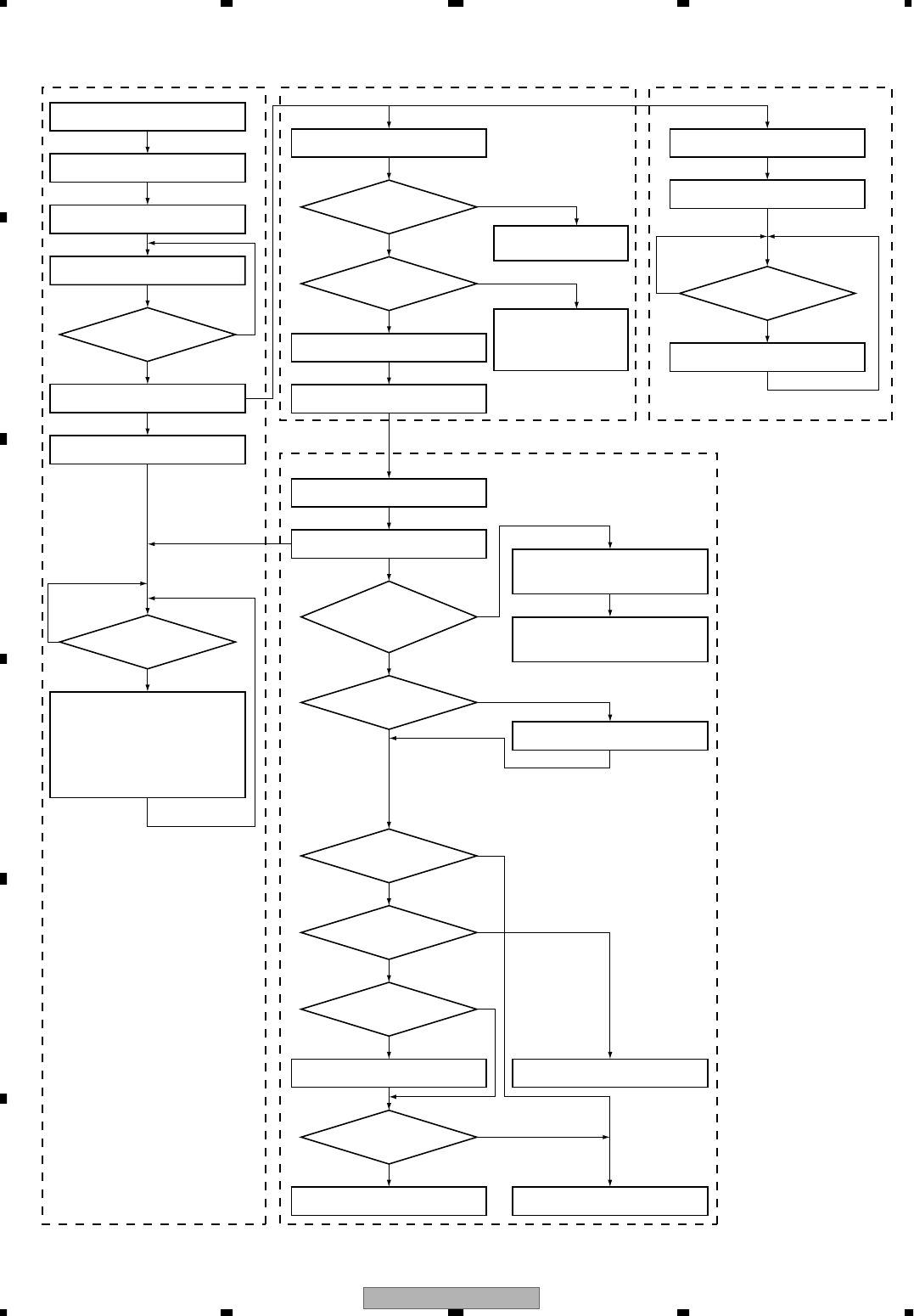
DVR-3100-S
92
1234
1234
C
D
F
A
B
E
7.1.6 SETUP SEQUENCE
DVD-R/RW Drive
Tuner/FL U-com System Codec IC (Inital Program Loader)
System Codec IC
(Firmware)
Connect power cord.
Tuner/FL microcomputer starts up.
System microcomputer starts up.
Initialization of peripheral-circuit
register, RAM, etc.
Initialization of peripheral-circuit
register, RAM, etc.
Starting communication
with Tuner/FL microcomputer Request for power off of
system-control computer made to
Tuner/FL microcomputer
System-control computer is turned off
(entering standby) following request
from Tuner/FL microcomputer
Repair process
Playback
Clock indication on FL display
Power ON ?
Waiting
for communication to be
established
Is ID check of drive OK?
Is disc in?
Obtaining LD
temperature data from drive.
Is temperature below
62°C?
LSI Check
No
No
Yes
Yes
Power ON, cancellation of reset
OK
NG
NG
NG
Has command arrived?
Yes
No
FLASH Check
OK
OK
"POWER ON" displayed
on FL display
Key-input and channel data
transmitted to the system-control
computer, and responding to
instructions from it,
indication displayed on FL
display and channel switching
performed
Firmware stored in Flash memory
is developed in SD-RAM.
Yes
Is disc valid?
Yes
Repair required?
Yes
Yes
No
No
No
No
Playback requested?
Yes
Stop
Tray Open
Jumping to developed firmware
Downloading through
RS232C required.
"MONITOR" displayed
on FL display
LSI NG displayed
on FL display
Drive microcomputer starts up.
ATA/ATAPI command processing
Initialization of peripheral-circuit
register, RAM, etc.
No
"CPRM ERR" displayed on FL display
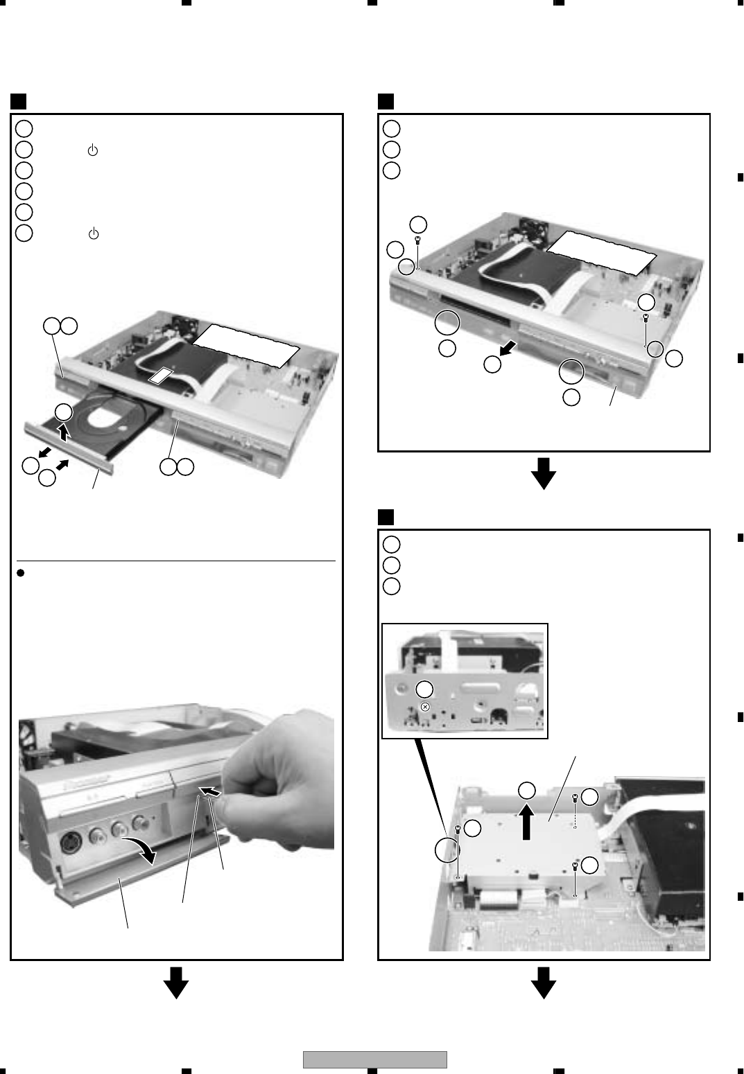
DVR-3100-S 93
5678
5678
C
D
F
A
B
E
7.1.7 DISASSEMBLY
1Remove the bonnet by removing the eight screws.
2Press the STANDBY/ON button to turn on the power.
3Press the 0 button to open the tray.
5Press the 0 button to close the tray.
4Remove the tray panel assy.
Bonnet S, Tray Panel Assy
1
1Remove the two screws.
2Remove the four hooks.
3Remove the front panel section.
Front Panel Section
2
1Remove the one screw.
2Remove the three screws.
3Remove the HDD stay.
HDD Stay
3
3
3
5
1
4
1
2
3
Tray panel assy
Front panel section
long thin pole
HDD stay
Emergency eject hole
Jack door
6Press the STANDBY/ON button to turn off the power.
62
53
How to open the tray when the power cannot be on
When the player cannot eject disc tray due to power failure or
any other reasons, open the jack door, and use a long thin pole
and push the emergency eject hole under the tray panel to eject.
1
2
2
2
2
2
2
Note: This photograph shows other models.
However, the work method is the same.
Note: This photograph shows other models.
However, the work method is the same.
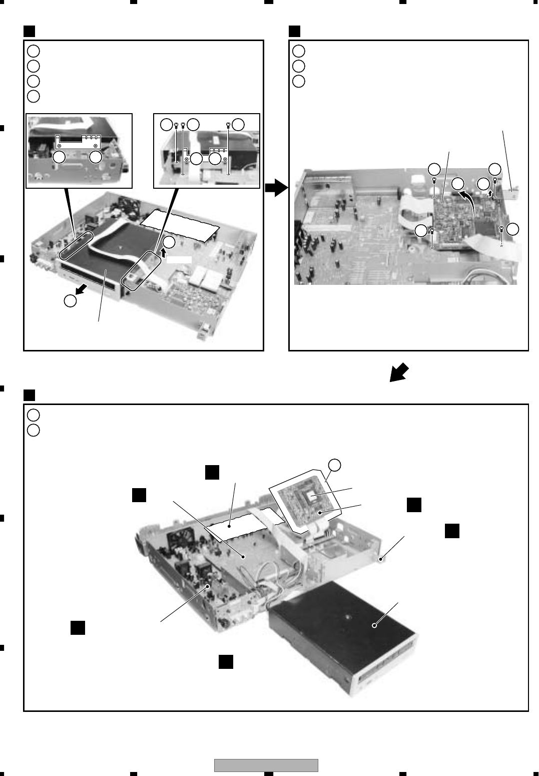
DVR-3100-S
94
1234
1234
C
D
F
A
B
E
1Remove the two screws.
2Remove the five screws.
3Disconnect the connector.
4Remove the DRIVE Assy R6.
DRIVE Assy R6
4
4
1 1 1 1
32
11
2
3
2
222
1Remove the four screws.
2Disconnect the flexible cable from DVJB Assy.
3Stand the MAIN Assy.
DRIVE Assy R6
CN2009
DRIVE Assy R6
POWER SUPPLY Unit
TUJB Assy
FRJB Assy
Insulation sheet
IC1001
MAIN Assy
DVJB Assy
MAIN Assy
MAIN Assy
5
1Insert the insulation sheet between the MAIN Assy and chassis.
2Arrange the unit as shown in the photo below.
Caution: MAIN IC (IC1001) on the MAIN Assy generate heat to around 80 degrees.
Be careful when works.
Diagnosis
6
DVJB Assy
1
D
H
B
SCRB Assy
I
G
C
Note: This photograph shows other models.
However, the work method is the same.
Note: This photograph shows other models.
However, the work method is the same.
Note:
This photograph shows other mod-
els. However, the work method is
the same.
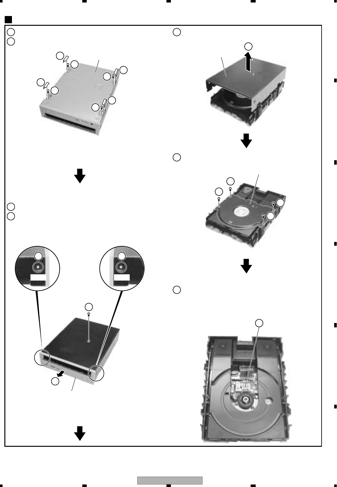
DVR-3100-S 95
5678
5678
C
D
F
A
B
E
1Remove the four aluminium tape.
2Remove the four screws.
5Remove the bonnet.
6Remove the clamper holder by removing the four screws.
7Clean the pickup lens.
3Remove the one screw.
4Remove the front bezel by removing the two hooks.
Hook
Front bezel
Hook
DRIVE Assy R6 (DVD-R/RW WRITER)
7
12
1
1
1
2
2
5
Bonnet
DRIVE Assy R6
Clamper holder
Pickup lens
3
4
4
2
4
6
7
6
6
6

DVR-3100-S
96
1234
1234
C
D
F
A
B
E
7.2 IC
PD5947A8 (TUJB ASSY : IC2001)
• TUFL Microcomputer
PD5947A8, RS5C372A, LC75342M, AK5381VT, PST3428U, PST3809U, NJM2880U1-33, M65672WG-C,
UPD72852AGB-8EU, UPD72893AGD-LML, TDA9818TS, LA73026AV
No. Pin Name Signal Name I/O Function Active
1 P95/ANEX0/CLK4 FLCLK O FL Driver communication line CLK −
2 P94/DA1/TB4in SYNC I C-Sync of input video ↑
3 P93/DA0/TB3in AVLINKIN I Input line of NexTViewLink −
4 P92/TB2in/Sout3 IR I Pulse input of remote control −
5 P91/TB1in/Sin3 J_CLOCK I
6 P90/TB0in/CLK3 SYNCAFT I C-Sync of input video ↑
7 BYTE BYTE I
8 CNVss PGM I Communication line
9 P87/XCin NC (O) −
10 P86/XCout NC (O) −
11 -RESET XRESETIN I u-Con Reset
12 Xout XOUT I
13 Vss GND −
14 Xin XIN I
15 Vcc VCC −
16 P85/-NMI NMI I ↓
17 P84/-INT2 JOGA I Phase VOL input ↑ ↓
18 P83/-INT1 SLICEONFB I Feedback from SLICEON pin ↑ ?
19 P82/-INT0 XINTRA I Alarm/interval interruption ↓
20 P81/TA4in NC (O) −
21 P80/TA4out NC (O) −
22 P77/TA3in NC (O) −
23 P76/TA3out FANPWM O FAN power control H
24 P75/TA2in JOGB I Phase VOL input ↑ ↓
25 P74/TA2out NC (O) −
26 P73/-CTS2/-RTS2/TA1in IICRST O Reset output to I2C microcomputer L
27 P72/CLK2/TA1out AVLINKOUT O Output line of NextViewLink H
28
P71/RxD2/SCL/TA0in/TB5in
SCL I/O I2C communication (clock) −
29 P70/TxD2/SDA/TA0out SDA I/O I2C communication (data) −
30 Vss2 GND −
31 LP2 LP2 O
32 LP3 LP3 O
33 LP4 LP4 O
34 Vdd2 VDD2 −
35 M2 M2 I Mode switch
36 M1 M1 I
37 P11/SLICEON SLICEON O Slicer operating signal H?
38 P67/TxD1 TXD O Communication line for firmware download/monitor −
39 P66/RxD1 RXD I Communication line for firmware download/monitor −
40 P65/CLK1 SCLK (O) Communication line for firmware download/monitor −
Pin Function
• The information shown in the list is basic information and may not correspond exactly to that shown in the schematic diagrams.
List of IC

DVR-3100-S 97
5678
5678
C
D
F
A
B
E
No. Pin Name Signal Name I/O Function Active
41
P64/-CTS1/-RTS1/CLKS1
BUSY O Communication line for firmware download/monitor −
42 P63/TxD0 SSTTOM O SYS controller communication line (Tuner → Main) −
43 P62/RxD0 SSMTOT I SYS controller communication line (Main → Tuner) −
44 P61/CLK0 SCK I SYS controller communication line (clock) ↑
45 P60/-CTS0/-RTS0 HSTTOM O Tuner → SYS handshake L
46 P57/-RDY/CLKout DLCONT O Voltage supply SW of FLASH-ROM writing L
47 P56/ALE WRT O Write signal H
48 P55/-HOLD SDAEEP I/O SDA line for EEPROM −
49 P54/-HLDA SCLEEP O SCL line for EEPROM −
50 P53/BCLK VOLCE O Communication line CE H
51 P52/-RD VOLDATA O Communication line DATA −
52 P51/-WRH/-BHE VOLCLK O Communication line CLK −
53 P50/-WRL/-WR DLCE I Signal for serial I/O mode selection −
54 P47/-CS3 S1 O
55 P46/-CS2 LET O Letterbox signal add H
56 P45/-CS1 SQU O Squeeze signal add −
57 P44/-CS0 BLANK I BLANK signal input −
58 P43/A19 XTHROU O Through control of SCART1/2 L
59 P42/A18 NC (O) −
60 P41/A17 SEL1 O Parallel control (for audio switch) −
61 P40/A16 SWVION O Independent source SW for video I/O output circuit H
62 P37/A15 SWSTBY O Standby mode of video input selector H
63 P36/A14 BS15ON O
64 P35/A13 BS15SRT I
65 P34/A12 SCTHRU O SCART loop through control during power OFF L
66 P33/A11 BS15IN I
67 P32/A10 SDET3 I S terminal detection of Video input 3 L
68 P31/A9 SDET2 I
−
−
S terminal detection of Video input 2 L
69 Vcc VCC
70 P30/A8 SDET1 I S terminal detection of Video input 1 L
71 Vss GND
72 P27/A7 SELV1 O Parallel control −
73 P26/A6 SELV2 O Parallel control −
74 P25/A5 SELV3 O Parallel control −
75 P24/A4 YVSEL O CVBS/YC switch of Video input selector −
76 P23/A3 P_SAVEBS O RF through output switch H
77 P22/A2 FOMO O −
78 P21/A1 M1ONTA O −
79 P20/A0 P_CONT O System Power ON H
80 P17/D15/-INT5 NC (O) −

DVR-3100-S
98
1234
1234
C
D
F
A
B
E
No. Pin Name Signal Name I/O Function Active
81 P16/D14/-INT4 HSMTOT I SYS → Tuner handshake ↓
82 P15/D13/-INT3 DCTRI I Change detection of audio condition ↑
83 P14/D12 MUTE O MUTE control H
84 P13/D11 SU/SAPID I
85 P12/D10 ST/STID I
86 P11/D9 XRESET O System Reset output L
87 P10/D8 LDASH O ColorSystem distinction signal H
88 P07/D7 STBYQ O EU multiplex decoder standby mode L
89 P06/D6 LM/ O ColorSystem distinction signal H
90 P05/D5 I/BG O ColorSystem distinction signal H
91 P04/D4 XP_SAVE O Power save control (SCART) L
92 P03/D3 TUON O Tuner power H
93 P02/D2 YCSW O
94 P01/D1 RSTCTL O Reset signal mask from the system controller L
95 P00/D0 FLPON O FL Driver Power ON H
96 P107/AN7/-KI3 MODEL1 A/D IN Input for destination judgment −
97 P106/AN6/-KI2 MODEL2 A/D IN Input for destination judgment −
98 P105/AN5/-KI1 AGC A/D IN Field intensity detection −
99 P104/AN4/-KI0 FUNC A/D IN Function signal input −
100 P103/AN3 KEY2 A/D IN Main unit key input −
101 P102/AN2 KEY1 A/D IN Main unit key input −
102 P101/AN1 C/N A/D IN −
103 Avss GND
104 P100/AN0 AFT A/D IN AFT voltage input −
105 VREF VREF
106 AVcc AVCC
107 P97/-ADTRG/Sin4 FLSTB O
−
−
−
−
−
−
−
I
Communication line strobe of FL driver L
108 Vdd1 VDD1
109 SYNCIN SYNCTEXT I Video input for sync. sep.
110 SVREF SLICE I Slice level input
111 Vss1 GND
112 Vdd3 VDD3
113 CVIN1 CVIN1 I Video input for teletext
114 Vss3 GND
115 FSCIN FSCIN Fsc input
116 P96/ANEX1/Sout4 FLDATA O Communication line data of FL driver −
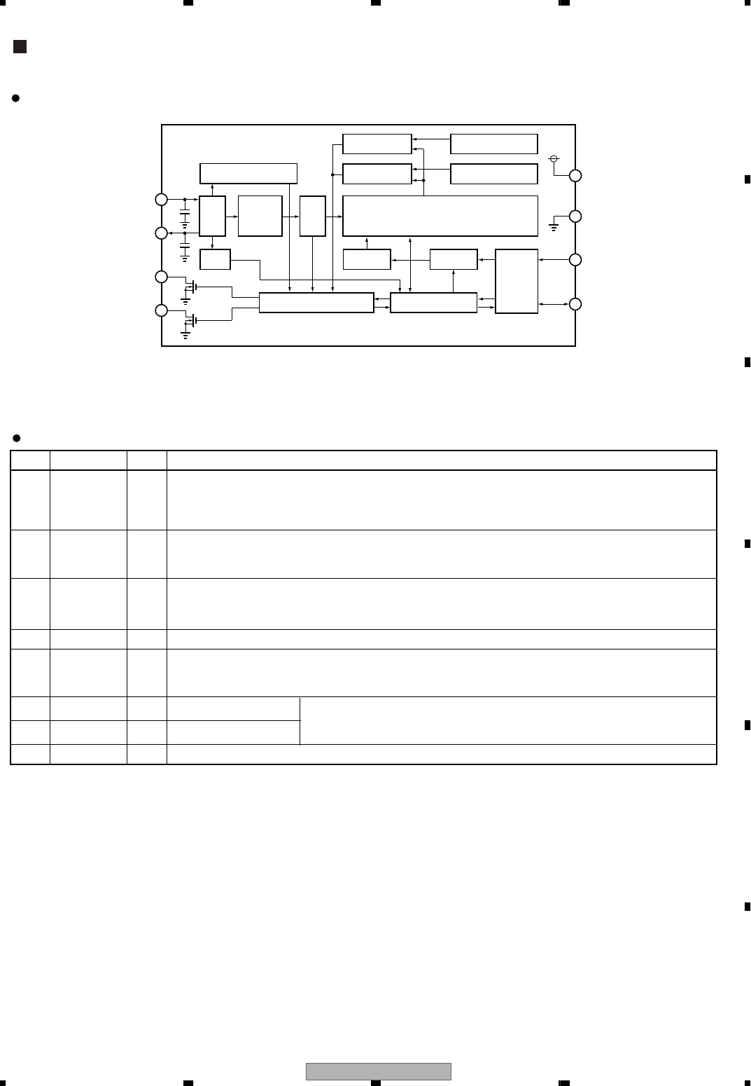
DVR-3100-S 99
5678
5678
C
D
F
A
B
E
• Real Time Clock IC
32kHz Output
Control
Address
Decoder Address
Resister
I/O
Control
OSC
Detect
Driver
Correction Time Counter
(SEC, MIN, HOUR, WEEK, DAY, MONTH, YEAR)
OSC
OSCIN
DIV
Comparator_B
Comparator_A
Shift ResisterInterrupt Control
Alarm_B Register
(WEEK, MIN, HOUR)
Alarm_A Register
(WEEK, MIN, HOUR)
7
OSCOUT 6
/INTRA 5
SCL
2
VSS
4
VDD
8
SDA
3
/INTRB 1
No. Pin Name I/O Function
1 /INTRB O
Interruption output B
The output of 32.768kHz (in 32768Hz crystal use), cycled interrupt for CPU, or output alarm interrupt
(ALARM_B). This pin output 32.768kHz when activated power from 0V.
Nch open drain output.
2 SCL I Shift clock input
Synchronize with this clock, and input and output data from a SDA terminal.
Exceed VDD, and can input to 6V.
3 SDA I/O Serial input and output
Synchronize with SCL, and input and output writing data or readout data.
Exceed VDD, and can input to 6V. Nch open drain output in the output.
4 VSS −Ground pin
5 /INTRA O Interruption output A
Cycled interrupt for CPU, or output alarm interruption (ALARM_A, ALARM_B).
This pin becomes an OFF state when activated power from 0V. N ch open drain output.
6 OSCOUT O Oscillation circuit output Connect a crystal resonator of 32.768kHz or 32.000kHz between OSCIN and
OSCOUT, and constitute oscillation circuit.
(component parts of oscillation circuit except crystal resonator have it built-in.)
7 OSCIN I Oscillation circuit input
8 VDD −Positive supply input
RS5C372A (TUJB ASSY : IC2271)
Pin Function
Block Diagram
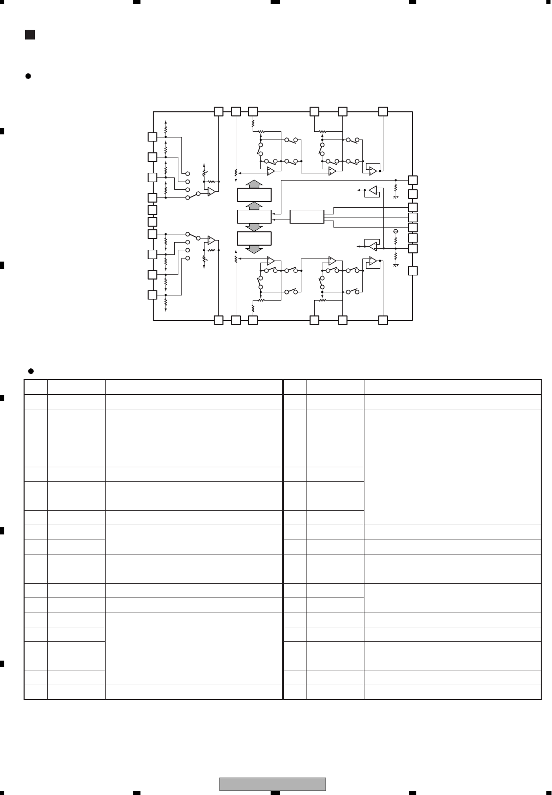
DVR-3100-S
100
1234
1234
C
D
F
A
B
E
• Electric Volume IC
11
10
L4
LSELO
9
LIN
8
LTRE
7
LBASS1
8
LBASS2
5
4
LOUT
TEST
2CE
3VSS
1DI
30 CL
28 Vref
27 NC
29 VDD
12
L3
13
L2
14
L1
15
NC
20
R4
19
R3
18
R2
17
R1
16
NC
21
RSELO
22
RIN
23
RTRE
24
RBASS1
25
RBASS2
26
ROUT
Control
Circuit
Logic
Circuit CCB
Interface
LVref
RVref
Control
Circuit
No. Pin Name Function No. Pin Name Function
1DI Serial data input for control 16 NC Not connected
2CE
Chip enable pin
Data are written in the internal latch by a timing
of "H" → "L", and each analog switch works.
Data transfer is enabled by "H" level. 17 R1
Input signal pin
3 VSS Ground pin 18 R2
4 TEST Pin for electronic volume test
Set to VSS electric potential. 19 R3
5 LOUT Volume and equalizer output pin 20 R4
6 LBASS2 Capacitor and resistor connection pins for bus
bandpass filter
21 RSELO Input selector output pin
7 LBASS1 22 RIN Volume and equalizer input pin
8 LTRE Capacitor connection pin for treble bandpass
filter 23 RTRE Capacitor connection pin for treble bandpass
filter
9 LIN Volume and equalizer input pin 24 RBASS1 Capacitor and resistor connection pins for bus
bandpass filter
10 LSELO Input selector output pin 25 RBASS2
11 L4
Input signal pins
26 ROUT Volume and equalizer output pin
12 L3 27 NC Not connected
13 L2 28 Vref 0.5XVDD voltage generation block
14 L1 29 VDD Power supply pin
15 NC Not connected 30 CL Clock input pin for control
LC75342M (TUJB ASSY : IC2801)
Pin Function
Block Diagram
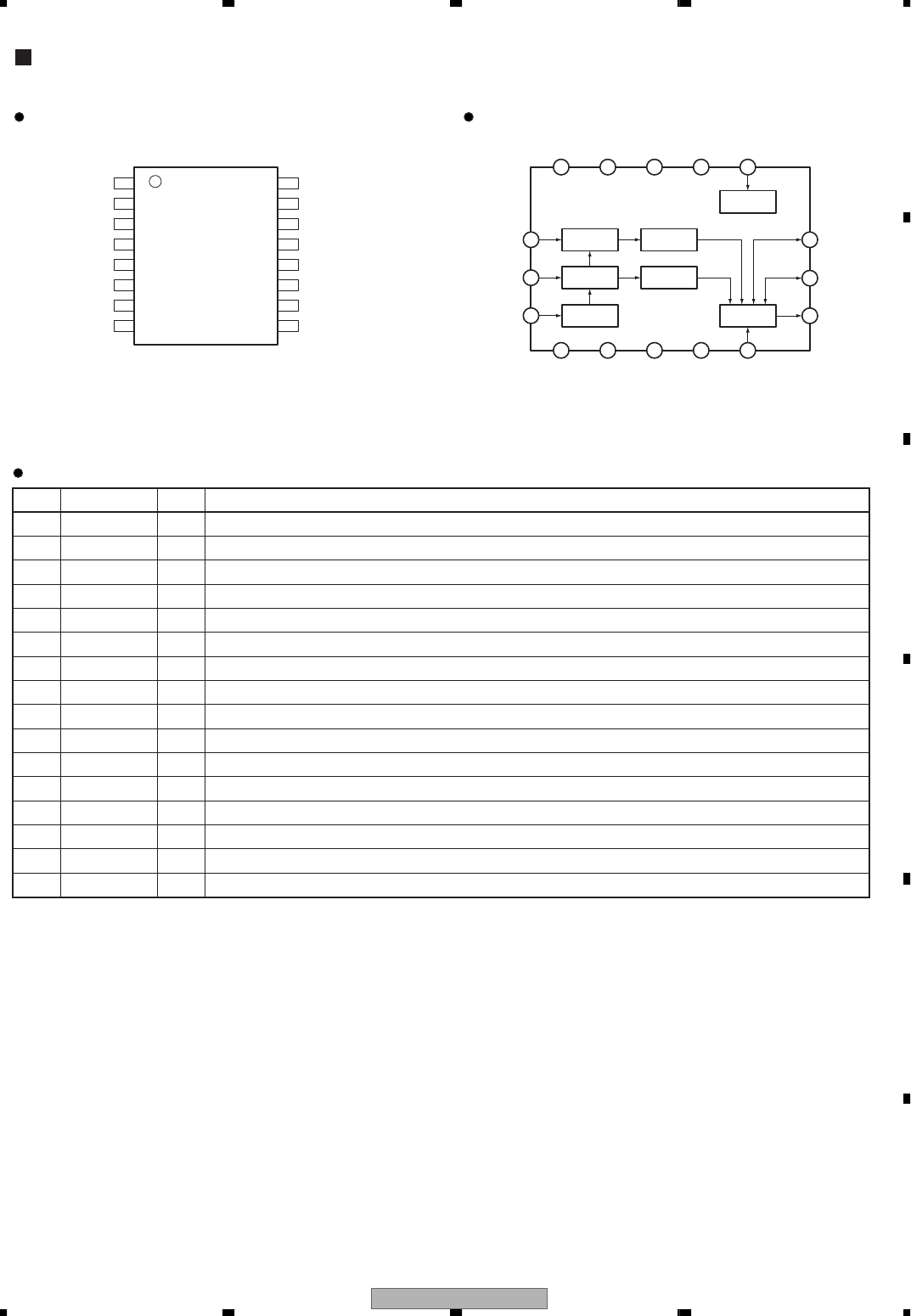
DVR-3100-S 101
5678
5678
C
D
F
A
B
E
• 96kHz 24 bit ∆∑ ADC
AINL
AINR 1
∆∑
Modulator
2
AINR ∆∑
Modulator
1
VCOM
DIF
SCLK
SDTO
LRCK
MCLK
Voltage
Reference
Decimation
Filter
Decimation
Filter
Serial I/O
Interface
Clock
Divider
4
14
10
12
9
11
DGND
8
VD
7
AGND
5
VA
6
PDN
13
CKS0
16
CKS1
3
CKS2
15
AINL 2
CKS1 3
VCOM 4
AGND 5
VA 6
VD 7
DGNS 8
16 CKS0
15 CKS2
14 DIF
13 PDN
12 SCLK
11 MCLK
10 LRCK
9 SDTO
No. Pin Name I/O Function
1 AINR I R ch analog input
2 AINL I L ch analog input
3 CKS1 I Mode select 1
4 VCOM O Common voltage output, bias voltage of VA/2 and ADC input
5 AGND −Analog ground
6VA −Analog power supply, 4.5V to 5.5V
7VD −Digital power supply, 2.7 to 5.5V (fs = 4k to 48kHz), 3.0 to 5.5V (fs = 48k to 96kHz)
8 DGND −Digital ground
9 SDTO O Audio serial data output, outputs "L" in the power down mode.
10 LRCK I/O Channel clock I/O, outputs "L" by master mode in the power down mode.
11 MCLK I Master clock input
12 SCLK I/O Audio serial data clock, outputs "L" by master mode in the power down mode.
13 PDN I Power down mode "H": power up, "L": power down
14 DIF I Audio interface format, "H" : 24 bit I2S compatibility, "L" : 24 bit MSB justify
15 CKS2 I Mode select 2
16 CKS0 I Mode select 0
AK5381VT (MAIN ASSY : IC3101)
Pin Function
Pin Arrangement (Top view) Block Diagram
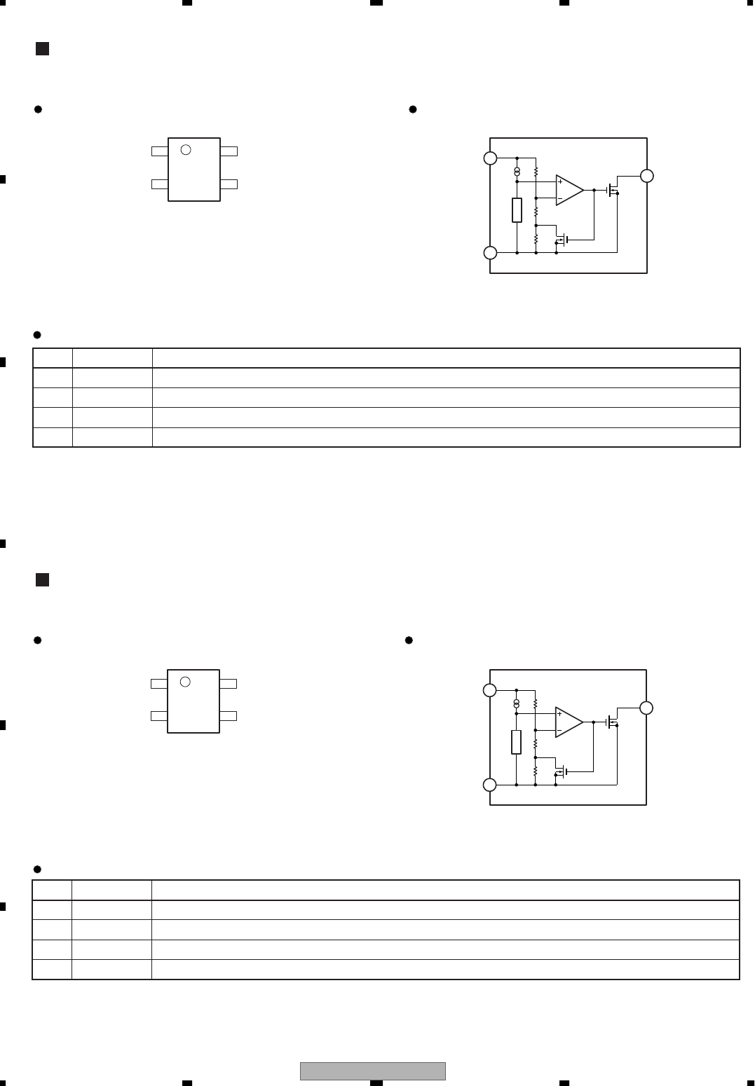
DVR-3100-S
102
1234
1234
C
D
F
A
B
E
• Reset IC
VDD
VOUT
VOUT 1
Vref
2
1
VSS 4
VDD 2
4 VSS
3NC
No. Pin Name Function
1 VOUT Reset signal output
2 VDD Power supply / voltage detection
3NC Not connected
4 VSS VSS
PST3428U (MAIN ASSY : IC4003)
Pin Function
Pin Arrangement (Top view) Block Diagram
VDD
OUT
OUT 1
Vref
2
1
GND 4
VDD 2
4 GND
3NC
No. Pin Name Function
1 OUT Reset signal output
2 VDD Power supply / voltage detection
3NC Not connected
4 GND Ground
• Reset IC
PST3809U (MAIN ASSY : IC4005)
Pin Function
Pin Arrangement (Top view) Block Diagram
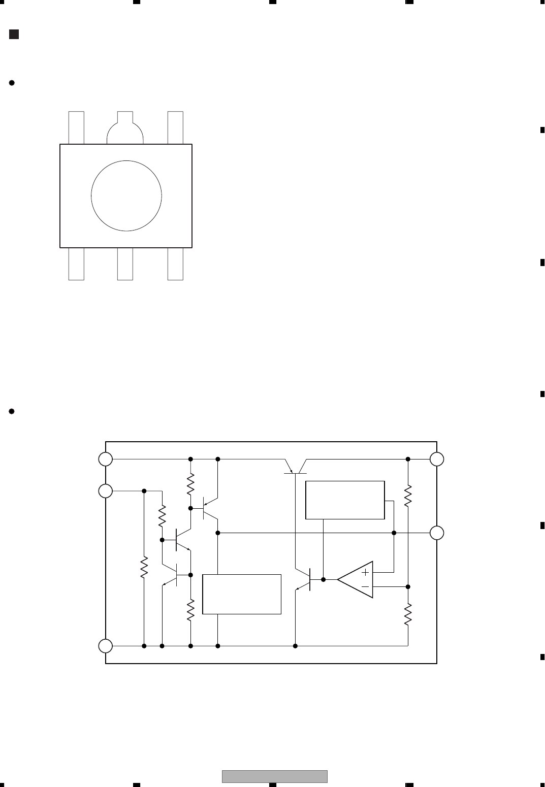
DVR-3100-S 103
5678
5678
C
D
F
A
B
E
VIN
54
13
1 : CONTROL (Active High)
2 : GND
3 : NOISE BYPASS
4 : VOUT
5 : VIN
2
5 4
CONTROL
VOUT
3NOISE BYPASS
Bandgap
Reference
Thermal
Protection
1
GND 2
• Regulator IC
NJM2880U1-33 (MAIN ASSY : IC4007)
Pin Arrangement (Top view)
Block Diagram
DVR-3100-S
104
1234
1234
C
D
F
A
B
E
A
1
2
3
4
5
6
7
8
9
10
11
12
13
14
15
16
17
18
19
20
21
22
23
24
25
26
27
28
BCDEFGHJKLMNPRTUVWYAAABACADAEAFAGAH
Buffer Name Main Function Remarks
PDIDGZ Input buffer (5V tolerant)
PDUDGZ Input buffer (5V tolerant), pull-up
PDDDGZ Input buffer (5V tolerant), pull-down
PDO04CDG Output buffer, 4mA
PDO08CDG Output buffer, 8mA
PDO0204DGZ Output buffer, 2/4mA
PDO0406DSGZ Output buffer, 4/6mA For SDRAM IF
PDO0406DSGZ×2 Output buffer, 8/12mA For SDRAM IF
PDT0204DGZ 3 state output buffer, 2/4mA
PDB04DGZ Bidirectional buffer, 4mA
PDB08DGZ Bidirectional buffer, 8mA
PDB0204DGZ Bidirectional buffer, 2/4mA
PDB0406DSGZ Bidirectional buffer, 4/6mA For SDRAM IF
• Signal Processing IC for DVD Recorder
M65672WG-C (MAIN ASSY : IC1001)
Pin Arrangement (Top view)
I/O buffer list
DVR-3100-S 105
5678
5678
C
D
F
A
B
E
VDD EDATA[23] EDATA[22] EDATA[20] EDATA[18] EDATA[16] EADRS[0] EBS[0] ERAS EDQM EDATA[6] EDATA[3] EDATA[0] AVDDAD8 BG8 VRB8 AVDDAD8 VRM10 AVDDAD10 PACKETEN WM2DTO[2] VDD WMCLKO WM1DTO[4] WM1DTI[1] WM1DTI[3] HKEYPLS VDD
ABCDEFGHJKLMNPRTUVWYAAABAC AD AE AF AG AH
ABCDEFGHJKLMNPRTUVWYAAABAC AD AE AF AG AH
AT1DATA[12] EDATA[24] EDATA[25] EDATA[21] EDATA[19] EDATA[17] EADRS[1] EBS[1] ECS EWE EDATA[7] EDATA[4] EDATA[1] AVSSAD8 GIN VRT8 DVSSAD10 CVBSIN VBGR10 STREAM WM2DTQ[4] WM2DTO[6] WM1DTO[1] WM1DTO[6] WM1DTI[4] PEDCTL REC656O[1] REC656O[3]
AT1DATA[8] AT1DATA[13] AT1DATA[15] EDATA[26] EDATA[29] EDATA[30] EADRS[2] EADRS[10] EADRS[11] ECAS EDATA[8] EDATA[5] EDATA[2] DVSSAD8 CRIN CIN VRBD10 VRT10 NBC10 SYNC WM2DTO[3] WM1DTO[0] WM1DTO[5] WM1DTI[2] WM1DTI[7] ACCCTL REC656O[2] AVDD2DA10
AT1DATA[7] AT1DATA[6] AT1DATA[14] EDATA[27] EDATA28] EDATA[31] EADRS[4] EADRS[6] EADRS[8] ECLKEN EDATA[9] EDATA[11] EDATA[13] DVDDAD8 AVDDAD8 AVSSAD8 VRB10 AVSSAD10 TSRW WM2DTO[0] WM2DTO[7] WM1DTO[2] WM1DTI[0] WM1DTI[6] AGCCTL REC656O[5] YOUT AVSS2DA10
AT1DATA[2] AT1DATA[1] AT1DATA[5] AT1DATA[10] AT1DATA[14] EDATA[3] EADRS[5] EADRS[7] EADRS[9] ECLKO EDATA[10] EDATA[12] EDATA[14] EDATA[15] AVSSAD8 DVDDAD10 VRTD10 TSCLK WM2DTO[1] WM2DTO[4] WM1DTO[3] WM2DTC[1] WM1DTI[5] REC656O[0] COUT IREF[1] ROUT AVDD1DA10
AT1DIOW AT1DMACK AT1DATA[0] AT1DATA[3] AT1DATA[9] GND VDD3 VDD GND VDD3 VDD GND VDD3 VDD GND VDD2 VDD GND VDD2 VDD GND VDD3 VDD REC656O[4] AVDD1DA10 BOUT DVACK DVREQ
AT1ADR[1] AT1INTRQ AT1DIOR AT1RESET AT1DATA4] VDD3 VDD3 IREF[0] AVSS1DA10 REC656O[6] DVVIDEO[0] DVVIDEO[1]
AT1CS[0] AT1CS[1] AT1ADR[0] AT1IORDY AT1DMARQ VDD VDD GOUT REC656O[7] DVVIDEO[3] DVVIDEO[4] PLL2AVSS
AT2DATA[11] AT2DATA[12] AT1DATA[13] AT2DATA[14] AT1ADR[2] GND GND DVVIDEO[2] ADMCLKI PLL2AVDD DVVCLKI DVVIDEO[7]
AT2DATA[6] AT2DATA[7] AT2DATA[8] AT2DATA[10] AT2DATA[15] VDD3 VDD3 R656CLKI DVVIDEO[5] REC656I[0] REC656I[1] REC656I[2]
AT2DATA[1] AT2DATA[2] AT2DATA[4] AT2DATA[5] AT2DATA[9] VDD VDD DVVIDEO[6] REC656I[3] REC656I[4] REC656I[6] REC656I[7]
AT2DIOW AT2DMARQ AT2RESET AT2DATA[0] AT2DATA[3] GND GND GND GND GND GND GND GND REC656I[5] PXCLK DVVCLKO PLLRST TRST
AT2ADR[2] AT2INTRQ AT2IORDY AT2DIOR AT2DMACK VDD3 GND GND GND GND GND GND VDD3 TCK TDI TDO TMS PLLON
AT2MODE AT2CS[0] AT2CS[1] AT2ADR[0] AT2ADR[1] VDD GND GND GND GND GND GND VDD VIPWM CSYNC TESTMOD[0] TESTMOD[1] TESTMOD[2]
RESET VDD DBI TRACE VDD GND GND GND GND GND GND GND VDD TESTMOD[6] VDD TESTMOD[5] TESTMOD[4] TESTMOD[3]
PCO PLL3AVSS PLL3AVDD VMCLK PLL1AVDD VDD3 GND GND GND GND GND GND VDD3 HADRS[28] HADRS[29] HADRS[24] HADRS[25] HADRS[26]
PLL1AVSS ADCCLKO VDD DVAMCLKO DVAMCLKI VDD GND GND GND GND GND GND GND HADRS[27] HADRS[19] HADRS[18] HADRS[23] HADRS[22]
DACCLKO AMCLK1 AMCLK2 ARDATA[1] ARDATA[0] GND VDD HADRS[15] HADRS[16] HADRS[17] HADRS[20] HADRS[21]
ARDATA[14] ARDATA[15] ARDATA[4] ARDATA[3] ARDATA[2] VDD2 VDD3 HDCS[1] HDCS[0] HCAS HRAS HCLKEN
ARDATA[11] ARDATA[12] ARDATA[13] ARDATA[6] ARDATA[5] VDD GND HDATA[7] HDWE DQMWS[0] DQMWS[1] HCLKO
ARDATA[10] ARDATA[9] ARWE ARDQM[0] ARDATA[7] GND VDD HDATA[6] HDATA[5] HDATA[4] HDATA[8] HDATA[9]
ARDATA[8] ARDQM[1] ARCS[0] ARRAS ARCAS VDD3 VDD3 HADRS[9] HDATA[2] HDATA[3] HDATA11] HDATA[10]
ARCLKO ARADRS[12] ARADRS[13] ARADRS[14] ARCS[1] VDD VDD3 GND VDD VDD3 VDD GND VDD3 VDD GND VDD3 VDD GND VDD3 VDD GND VDD3 VDD HADRS[10] HDATA[1] HDATA[0] HDATA[12] HDATA[13]
ARADRS[11] ARADRS[9] ARADRS[1] ARADRS[0] ARADRS[10] SPDIFI ACMOD[0] BCKO DVDADT[4] DVDAADR[0] SCIDATA[0] SPIDATAO DDATA[11] DDATA[8] DCLKO DADRS[9] DADRS[8] INT[7] INT[1] CTS[2] RTS[0] TX[3] HWAIT HCS[5] HADRS[11] HADRS[12] HDATA[15] HDATA[14]
ARADRS[8] ARADRS[3] ARADRS[2] SRCBCKI SRCDATAO ACMOD[1] LRCKO DVDADT[3] DVDAREQ SCIDATA[1] SPICS DDATA[14] DDATA[12] DDATA[9] DDQM[1] DADRS[11] DADRS[7] DADRS[6] INT[6] INT[2] CTS[1] RX[3] TX[2] HDACK[0] VDD HCS[0] HADRS[13] HADRS[14]
ARADRS[7] ARADRS[6] SRCLRCKI SRCLRCKO DVBCK ADATAI DVDADT[5] DVDADT[1] DVDAACK VDD SPIDATAI DDATA[15] DDATA[13] DDATA[10] DWE DCS DADRS[10] DADRS[5] DADRS[4] INT[3] SCLK[0] CTS[0] RX[2] TX[1] HDREQ[0] HCS[3] HCS[2] HADRS[30]
ARADRS[5] ARADRS[4] SRCBCKO SPDIFO BCKI DVDADT[7] DVDADT[6] DVDADT[0] SCICS[1] SCICLK[1] SPICLK DDATA[2] DDATA[3] DDATA[6] DDQM[0] DRAS DBS[1] DADRS[1] DADRS[2] INT[4] SCLK[1] RTS[3] RTS[2] RX[1] HDACK[1] HOE HCS[4] HCS[1]
VDD
28
27
26
25
24
23
22
21
20
19
18
17
16
15
14
13
12
11
10
9
8
7
6
5
4
3
2
1
28
27
26
25
24
23
22
21
20
19
18
17
16
15
14
13
12
11
10
9
8
7
6
5
4
3
2
1
SRCDATAI DVLRCK DVADATA LRCKI ADATAO DVDADT[2] DVDAADR[1] SCICS[0] SCICLK[0] DDATA[0] DDATA[1] DDATA[4] DDATA[5] DDATA[7] DCAS DBS[0] DADRS[0] DADRS[3] INT[5] INT[0] CTS[3] RTS[1] RX[0] TX[0] HDREQ[1] NC NC
VDD
VDD3
GND
: 1.2V Power supply
: 3.3V Power supply
: Ground
Pin Name list

DVR-3100-S
106
1234
1234
C
D
F
A
B
E
No. BALL
Address Pin Name I/O Function No. BALL
Address Pin Name I/O Function
1 VDD3 VDD3 −3.3V I/O power supply 56 V26 VRT10 −
2 GND GND −Ground 57 V28 VRM10 −
3 VDD VDD −1.2V LOGIC power supply 58 U25 VRB10 −
4 AH28 VDD −1.2V LOGIC power supply 59 U26 VRBD10 −
5 AF26 ACCCTL O 60 U27 DVSSAD10 −
6 AF27 PEDCTL O VIDEO-Analog, Output buffer 61 T24 DVDDAD10 −
7 AG28 HKEYPLS O VIDEO-Analog, Output buffer 62 GND GND −Ground
8 GND GND −Ground 63 VDD VDD −1.2V LOGIC power supply
VIDEO-Analog
VIDEO-Analog
VIDEO-Analog
VIDEO-Analog
VIDEO-Analog
VIDEO-Analog
VIDEO-Analog
VIDEO-Analog
VIDEO-Analog
VIDEO-Analog
9 AE26 WM1DTI[7] I/O WM/VWM, Bidirectional buffer 64 U28 AVDDAD8 −
10 AD25 WM1DTI[6] I/O WM/VWM, Bidirectional buffer 65 T25 AVSSAD8 −
11 AC24 WM1DTI[5] I/O WM/VWM, Bidirectional buffer 66 T26 CIN I
12 AE27 WM1DTI[4] I/O WM/VWM, Bidirectional buffer 67 T27 VRT8 −
13 AF28 WM1DTI[3] I/O WM/VWM, Bidirectional buffer 68 T28 VRB8 −
14 AD26 WM1DTI[2] I/O WM/VWM, Bidirectional buffer 69 R25 AVDDAD8 −
15 AE28 WM1DTI[1] I/O WM/VWM, Bidirectional buffer 70 R24 AVSSAD8 −
16 AC25 WM1DTI[0] I/O WM/VWM, Bidirectional buffer 71 R26 CRIN I
17 AB24 WM1DTO[7] I/O WM/VWM, Bidirectional buffer 72 R28 BG8 −
18 VDD VDD −1.2V LOGIC power supply 73 P28 AVDDAD8 −
19 GND GND −Ground 74 P27 AVSSAD8 −
20 AD27 WM1DTO[6] I/O WM/VWM, Bidirectional buffer 75 R27 GIN I
21 AC26 WM1DTO[5] I/O WM/VWM, Bidirectional buffer 76 P26 DVSSAD8 −
22 AD28 WM1DTO[4] I/O WM/VWM, Bidirectional buffer 77 P25 DVDDAD8 −
23 AA24 WM1DTO[3] I/O WM/VWM, Bidirectional buffer 78 GND GND −Ground
24 AB25 WM1DTO[2] I/O WM/VWM, Bidirectional buffer 79 P24 EDATA[15] I/O SDRAM ENC, Bidirectional buffer
25 VDD VDD −1.2V LOGIC power supply 80 VDD3 VDD3 −3.3V I/O power supply
26 AC27 WM1DTO[1] I/O WM/VWM, Bidirectional buffer 81 N28 EDATA[0] I/O SDRAM ENC, Bidirectional buffer
27 GND GND −Ground 82 N27 EDATA[1] I/O SDRAM ENC, Bidirectional buffer
28 AC28 WMCLKO O WM/VWM, Output buffer 83 N26 EDATA[2] I/O SDRAM ENC, Bidirectional buffer
29 VDD3 VDD3 −3.3V I/O power supply 84 VDD VDD −1.2V LOGIC power supply
30 AB26 WM1DTO[0] I/O WM/VWM, Bidirectional buffer 85 N25 EDATA[13] I/O SDRAM ENC, Bidirectional buffer
31 AA25 WM2DTO[7] O WM/VWM, Output buffer 86 GND GND −Ground
32 AB27 WM2DTO[6] O WM/VWM, Output buffer 87 M28 EDATA[3] I/O SDRAM ENC, Bidirectional buffer
33 AB28 VDD −1.2V LOGIC power supply 88 GND GND −Ground
34 Y24 WM2DTO[5] O WM/VWM, Output buffer 89 N24 EDATA[14] I/O SDRAM ENC, Bidirectional buffer
35 AA27 WM2DTO[4] O WM/VWM, Output buffer 90 M27 EDATA[4] I/O SDRAM ENC, Bidirectional buffer
36 AA26 WM2DTO[3] O WM/VWM, Output buffer 91 M26 EDATA[5] I/O SDRAM ENC, Bidirectional buffer
37 AA28 WM2DTO[2] O WM/VWM, Output buffer 92 VDD3 VDD3 −3.3V I/O power supply
38 W24 WM2DTO[1] O WM/VWM, Output buffer 93 M25 EDATA[11] I/O SDRAM ENC, Bidirectional buffer
39 GND GND −Ground 94 L28 EDATA[6] I/O SDRAM ENC, Bidirectional buffer
40 Y25 WM2DTO[0] O WM/VWM, Output buffer 95 L27 EDATA[7] I/O SDRAM ENC, Bidirectional buffer
41 GND GND −Ground 96 VDD VDD −1.2V LOGIC power supply
42 Y26 SYNC I/O TS OUT, Bidirectional buffer 97 M24 EDATA[12] I/O SDRAM ENC, Bidirectional buffer
43 Y27 STREAM I/O TS OUT,Bidirectional buffer 98 GND GND −Ground
44 Y28 PACKETEN I/O TS OUT,Bidirectional buffer 99 L26 EDATA[8] I/O SDRAM ENC, Bidirectional buffer
45 VDD3 VDD3 −3.3V IO power supply 100 GND GND −Ground
46 W25 TSRW O TS OUT,Output buffer 101 L25 EDATA[9] I/O SDRAM ENC, Bidirectional buffer
47 GND GND −Ground 102 K28 EDQM O SDRAM ENC, Output buffer
48 V24 TSCLK O TS OUT,Output buffer
VIDEO-Analog
VIDEO-Analog
VIDEO-Analog
VIDEO-Analog
103 K27 EWE O SDRAM ENC, Output buffer
49 VDD3 VDD3 −3.3V I/O power supply 104 VDD3 VDD3 −3.3V I/O power supply
50 W26 NBC10 −105 K26 ECAS O SDRAM ENC, Output buffer
51 W27 VBGR10 −106 L24 EDATA[10] I/O SDRAM ENC, Bidirectional buffer
52 W28 AVDDAD10 −107 K25 ECLKEN O Output buffer, 4/6mA
53 V25 AVSSAD10 −108 VDD VDD −1.2V LOGIC power supply
54 V27 CVBSIN I 109 J28 ERAS O SDRAM ENC, Output buffer
55 U24 VRTD10 −110 GND GND −Ground
Pin Function

DVR-3100-S 107
5678
5678
C
D
F
A
B
E
No. BALL
Address Pin Name I/O Function No. BALL
Address Pin Name I/O Function
111 J27 ECS O SDRAM ENC, Output buffer 166 VDD3 VDD3 −3.3V I/O power supply
112 GND GND −Ground 167 C25 AT1DATA[11] I/O ATAPI-DVD, Bidirectional buffer
113 J26 EADRS[11] O SDRAM ENC, Output buffer 168 D24 AT1DATA[10] I/O ATAPI-DVD, Bidirectional buffer
114 J25 EADRS[8] O SDRAM ENC, Output buffer 169 E23 AT1DATA[9] I/O ATAPI-DVD, Bidirectional buffer
115 GND GND −Ground 170 GND GND −Ground
116 K24 ECLKO O SDRAM ENC, Output buffer 171 A26 AT1DATA[8] I/O ATAPI-DVD, Bidirectional buffer
117 VDD3 VDD3 −3.3V I/O power supply 172 A25 AT1DATA[7] I/O ATAPI-DVD, Bidirectional buffer
118 H28 EBS[0] O SDRAM ENC, Output buffer 173 B25 AT1DATA[6] I/O ATAPI-DVD, Bidirectional buffer
119 H27 EBS[1] O SDRAM ENC, Output buffer 174 GND GND −Ground
120 H26 EADRS[10] O SDRAM ENC, Output buffer 175 C24 AT1DATA[5] I/O ATAPI-DVD, Bidirectional buffer
121 VDD VDD −1.2V LOGIC power supply 176 VDD3 VDD3 −3.3V I/O power supply
122 G28 EADRS[0] O SDRAM ENC, Output buffer 177 E22 AT1DATA[4] I/O ATAPI-DVD, Bidirectional buffer
123 GND GND −Ground 178 VDD VDD −1.2V LOGIC power supply
124 J24 EADRS[9] O SDRAM ENC, Output buffer 179 D23 AT1DATA[3] I/O ATAPI-DVD, Bidirectional buffer
125 GND GND −Ground 180 A24 AT1DATA[2] I/O ATAPI-DVD, Bidirectional buffer
126 G27 EADRS[1] O SDRAM ENC, Output buffer 181 B24 AT1DATA[1] I/O ATAPI-DVD, Bidirectional buffer
127 H25 EADRS[6] O SDRAM ENC, Output buffer 182 GND GND −Ground
128 G26 EADRS[2] O SDRAM ENC, Output buffer 183 C23 AT1DATA[0] I/O ATAPI-DVD, Bidirectional buffer
129 VDD3 VDD3 −3.3V I/O power supply 184 D22 AT1RESET O Output buffer,8mA
130 F27 EDATA[17] I/O SDRAM ENC, Bidirectional buffer 185 E21 AT1DMARQ I ATAPI-DVD, Input buffer
131 F28 EDATA[16] I/O SDRAM ENC, Bidirectional buffer 186 GND GND −Ground
132 H24 EADRS[7] O SDRAM ENC, Output buffer 187 B23 AT1DMACK O ATAPI-DVD, Output buffer
133 VDD VDD −1.2V LOGIC power supply 188 VDD3 VDD3 −3.3V I/O power supply
134 G25 EADRS[4] O SDRAM ENC, Output buffer 189 A23 AT1DIOW O ATAPI-DVD, Output buffer
135 GND GND −Ground 190 VDD VDD −1.2V LOGIC power supply
136 F26 EDATA[30] I/O SDRAM ENC, Bidirectional buffer 191 C22 AT1DIOR O ATAPI-DVD, Output buffer
137 GND GND −Ground 192 D21 AT1IORDY I ATAPI-DVD, Input buffer
138 E27 EDATA[19] I/O SDRAM ENC, Bidirectional buffer 193 B22 AT1INTRQ I ATAPI-DVD, Input buffer
139 E28 EDATA[18] I/O SDRAM ENC, Bidirectional buffer 194 GND GND −Ground
140 F25 EDATA[31] I/O SDRAM ENC, Bidirectional buffer 195 E20 AT1ADR[2] O ATAPI-DVD, Output buffer
141 VDD3 VDD3 −3.3V I/O power supply 196 A22 AT1ADR[1] O ATAPI-DVD, Output buffer
142 E26 EDATA[29] I/O SDRAM ENC, Bidirectional buffer 197 C21 AT1ADR[0] O ATAPI-DVD, Output buffer
143 G24 EADRS[5] O SDRAM ENC, Output buffer 198 GND GND −Ground
144 D28 EDATA[20] I/O SDRAM ENC, Bidirectional buffer 199 B21 AT1CS[1] O ATAPI-DVD, Output buffer
145 VDD VDD −1.2V LOGIC power supply 200 VDD3 VDD3 −3.3V I/O power supply
146 D27 EDATA[21] I/O SDRAM ENC, Bidirectional buffer 201 A21 AT1CS[0] O ATAPI-DVD, Output buffer
147 GND GND −Ground 202 VDD VDD −1.2V LOGIC power supply
148 C28 EDATA[22] I/O SDRAM ENC, Bidirectional buffer 203 E19 AT2DATA[15] I/O ATAPI-HDD, Bidirectional buffer
149 GND GND −Ground 204 D20 AT2DATA[14] I/O ATAPI-HDD, Bidirectional buffer
150 F24 EADRS[3] O SDRAM ENC, Output buffer 205 C20 AT2DATA[13] I/O ATAPI-HDD, Bidirectional buffer
151 E25 EDATA[28] I/O SDRAM ENC, Bidirectional buffer 206 GND GND −Ground
152 D26 EDATA[26] I/O SDRAM ENC, Bidirectional buffer 207 B20 AT2DATA[12] I/O ATAPI-HDD, Bidirectional buffer
153 VDD3 VDD3 −3.3V I/O power supply 208 A20 AT2DATA[11] I/O ATAPI-HDD, Bidirectional buffer
154 B28 EDATA[23] I/O SDRAM ENC, Bidirectional buffer 209 D19 AT2DATA[10] I/O ATAPI-HDD, Bidirectional buffer
155 C27 EDATA[25] I/O SDRAM ENC, Bidirectional buffer 210 GND GND −Ground
156 B27 EDATA24] I/O SDRAM ENC, Bidirectional buffer 211 E18 AT2DATA[9] I/O ATAPI-HDD, idirectional buffer
157 VDD VDD −1.2V LOGIC power supply 212 VDD3 VDD3 −3.3V I/O power supply
158 D25 EDATA[27] I/O SDRAM ENC, Bidirectional buffer 213 C19 AT2DATA[8] I/O ATAPI-HDD, Bidirectional buffer
159 GND GND −Ground 214 VDD VDD −1.2V LOGIC power supply
160 C26 AT1DATA[15] I/O ATAPI-DVD, Bidirectional buffer 215 B19 AT2DATA[7] I/O ATAPI-HDD, Bidirectional buffer
161 E24 AT1DATA[14] I/O ATAPI-DVD, Bidirectional buffer 216 A19 AT2DATA[6] I/O ATAPI-HDD, Bidirectional buffer
162 GND GND −Ground 217 D18 AT2DATA[5] I/O ATAPI-HDD, Bidirectional buffer
163 A28 VDD −1.2V LOGIC power supply 218 GND GND −Ground
164 B26 AT1DATA[13] I/O ATAPI-DVD, Bidirectional buffer 219 C18 AT2DATA[4] I/O ATAPI-HDD, Bidirectional buffer
165 A27 AT1DATA[12] I/O ATAPI-DVD, Bidirectional buffer 220 E17 AT2DATA[3] I/O ATAPI-HDD, Bidirectional buffer

DVR-3100-S
108
1234
1234
C
D
F
A
B
E
No. BALL
Address Pin Name I/O Function No. BALL
Address Pin Name I/O Function
221 B18 AT2DATA[2] I/O ATAPI-HDD, Bidirectional buffer 276 VDD3 VDD3 −3.3V I/O power supply
222 GND GND −Ground 277 C11 AMCLK2 I CLOCK, Input buffer
223 A18 AT2DATA[1] I/O ATAPI-HDD, Bidirectional buffer 278 GND GND −Ground
224 VDD3 VDD3 −3.3V I/O power supply 279 D11 ARDATA[1] I/O SDRAM-ATAPI, Bidirectional buffer
225 D17 AT2DATA[0] I/O ATAPI-HDD, Bidirectional buffer 280 VDD3 VDD3 −3.3V I/O power supply
226 VDD VDD −1.2V LOGIC power supply 281 A10 ARDATA[14] I/O SDRAM-ATAPI, Bidirectional buffer
227 C17 AT2RESET I/O ATAPI-HDD, Bidirectional buffer 282 VDD VDD −1.2V LOGIC power supply
228 B17 AT2DMARQ I ATAPI-HDD, Input buffer 283 B10 ARDATA[15] I/O SDRAM-ATAPI, Bidirectional buffer
229 E16 AT2DMACK O ATAPI-HDD, Output buffer 284 E11 ARDATA[0] I/O SDRAM-ATAPI, Bidirectional buffer
230 GND GND −Ground 285 C10 ARDATA[4] I/O SDRAM-ATAPI, Bidirectional buffer
231 A17 AT2DIOW O ATAPI-HDD, Output buffer 286 GND GND −Ground
232 D16 AT2DIOR O ATAPI-HDD, Output buffer 287 D10 ARDATA[3] I/O SDRAM-ATAPI, Bidirectional buffer
233 C16 AT2IORDY I ATAPI-HDD, Input buffer 288 A9 ARDATA[11] I/O SDRAM-ATAPI, Bidirectional buffer
234 GND GND −Ground 289 B9 ARDATA[12] I/O SDRAM-ATAPI, Bidirectional buffer
235 B16 AT2INTRQ I ATAPI-HDD, Input buffer 290 GND GND −Ground
236 VDD3 VDD3 −3.3V I/O power supply 291 C9 ARDATA[13] I/O SDRAM-ATAPI, Bidirectional buffer
237 A16 AT2ADR[2] I/O ATAPI-HDD, Bidirectional buffer 292 E10 ARDATA[2] I/O SDRAM-ATAPI, Bidirectional buffer
238 VDD VDD −1.2V LOGIC power supply 293 D9 ARDATA[6] I/O SDRAM-ATAPI, Bidirectional buffer
239 E15 AT2ADR[1] I/O ATAPI-HDD, Bidirectional buffer 294 VDD3 VDD3 −3.3V I/O power supply
240 GND GND −Ground 295 A8 ARDATA[10] I/O SDRAM-ATAPI, Bidirectional buffer
241 D15 AT2ADR[0] I/O ATAPI-HDD, Bidirectional buffer 296 B8 ARDATA[9] I/O SDRAM-ATAPI, Bidirectional buffer
242 VDD VDD −1.2V LOGIC power supply 297 C8 ARWE O SDRAM-ATAPI, Output buffer
243 C15 AT2CS[1] O ATAPI-HDD, Output buffer 298 VDD VDD −1.2V LOGIC power supply
244 GND GND −Ground 299 A7 ARDATA[8] I/O SDRAM-ATAPI, Bidirectional buffer
245 B15 AT2CS[0] O ATAPI-HDD, Output buffer 300 E9 ARDATA[5] I/O SDRAM-ATAPI, Bidirectional buffer
246 VDD VDD −1.2V LOGIC power supply 301 D8 ARDQM[0] O SDRAM-ATAPI, Output buffer
247 A15 AT2MODE I ATAPI-HDD, Input buffer 302 GND GND −Ground
248 GND GND −Ground 303 B7 ARDQM[1] O SDRAM-ATAPI, Output buffer
249 GND GND −Ground 304 C7 ARCS[0] O SDRAM-ATAPI, Output buffer
250 A14 RESET I Input buffer (5V tolerant) 305 VDD3 VDD3 −3.3V I/O power supply
251 VDD3 VDD3 −3.3V I/O power supply 306 A6 ARCLKO O SDRAM-ATAPI, Output buffer
252 B14 VDD −1.2V LOGIC power supply 307 GND GND −Ground
253 C14 DBI I TEST, Input buffer 308 B6 ARADRS[12] O SDRAM-ATAPI, Output buffer
254 GND GND −Ground 309 E8 ARDATA[7] I/O SDRAM-ATAPI, Bidirectional buffer
255 D14 TRACE I TEST, Input buffer 310 D7 ARRAS O SDRAM-ATAPI, Output buffer
256 E14 VDD −1.2V LOGIC power supply 311 VDD3 VDD3 −3.3V I/O power supply
257 A13 PCO O CLOCK, 3 state output buffer 312 A5 ARADRS[11] O SDRAM-ATAPI, Output buffer
258 GND GND −Ground 313 C6 ARADRS[13] O SDRAM-ATAPI, Output buffer
259 B13 PLL3AVSS −314 B5 ARADRS[9] O SDRAM-ATAPI, Output buffer
260 C13 PLL3AVDD −315 VDD VDD −1.2V LOGIC power supply
261 D13 VMCLK I CLOCK, Input buffer 316 E7 ARCAS O SDRAM-ATAPI, Output buffer
262 E13 PLL1AVDD −317 D6 ARADRS[14] O SDRAM-ATAPI, Output buffer
263 A12 PLL1AVSS −318 C5 ARADRS[1] O SDRAM-ATAPI, Output buffer
264 VDD3 VDD3 −3.3V I/O power supply 319 GND GND −Ground
265 B12 ADCCLKO O CLOCK, Output buffer 320 B4 ARADRS[3] O SDRAM-ATAPI, Output buffer
266 GND GND −Ground 321 A4 ARADRS[8] O SDRAM-ATAPI, Output buffer
267 C12 VDD −1.2V LOGIC power supply 322 A3 ARADRS[7] O SDRAM-ATAPI, Output buffer
268 VDD3 VDD3 −3.3V I/O power supply 323 GND GND −Ground
269 D12 DVAMCLKO O CLOCK, Output buffer 324 E6 ARCS[1] O SDRAM-ATAPI, Output buffer
270 GND GND −Ground 325 D5 ARADRS[0] O SDRAM-ATAPI, Output buffer
271 A11 DACCLKO O CLOCK, Output buffer 326 C4 ARADRS[2] O SDRAM-ATAPI, Output buffer
272 VDD3 VDD3 −3.3V I/O power supply 327 VDD3 VDD3 −3.3V I/O power supply
273 E12 DVAMCLKI I AUDIO CLOCK, Input buffer 328 A2 ARADRS[5] O SDRAM-ATAPI, Output buffer
274 GND GND −Ground 329 B3 ARADRS[6] O SDRAM-ATAPI, Output buffer
275 B11 AMCLK1 I CLOCK, Input buffer 330 B2 ARADRS[4] O SDRAM-ATAPI, Output buffer

DVR-3100-S 109
5678
5678
C
D
F
A
B
E
No. BALL
Address Pin Name I/O Function No. BALL
Address Pin Name I/O Function
331 GND GND −Ground 386 VDD VDD −1.2V LOGIC power supply
332 E5 ARADRS[10] O SDRAM-ATAPI, Output buffer 387 GND GND −Ground
333 D4 SRCBCKI I AUDIO, Input buffer 388 L3 SPIDATAI I/O HOST, Bidirectional buffer
334 VDD3 VDD3 −3.3V I/O power supply 389 VDD VDD −1.2V LOGIC power supply
335 C3 SRCLRCKI I AUDIO, Input buffer 390 M5 SPIDATAO I/O HOST, Bidirectional buffer
336 B1 SRCDATAI I AUDIO, Input buffer 391 GND GND −Ground
337 A1 VDD −1.2V LOGIC power supply 392 L2 SPICLK I/O HOST, Bidirectional buffer
338 GND GND −Ground 393 GND GND −Ground
339 C2 SRCBCKO O AUDIO, Output buffer 394 L1 DDATA[0] I/O SDRAM-DEC, Bidirectional buffer
340 VDD VDD −1.2V LOGIC power supply 395 VDD3 VDD3 −3.3V I/O power supply
341 D3 SRCLRCKO O AUDIO, Output buffer 396 M4 DDATA[14] I/O SDRAM-DEC, Bidirectional buffer
342 E4 SRCDATAO O AUDIO, Output buffer 397 M3 DDATA[15] I/O SDRAM-DEC, Bidirectional buffer
343 F5 SPDIFI I AUDIO, Input buffer 398 M2 DDATA[2] I/O SDRAM-DEC, Bidirectional buffer
344 D2 SPDIFO O AUDIO, Output buffer 399 VDD VDD −1.2V LOGIC power supply
345 C1 DVLRCK I/O AUDIO, Bidirectional buffer 400 N5 DDATA[11] I/O SDRAM-DEC, Bidirectional buffer
346 E3 DVBCK I/O AUDIO, Bidirectional buffer 401 GND GND −Ground
347 D1 DVADATA I/O AUDIO, Bidirectional buffer 402 M1 DDATA[1] I/O SDRAM-DEC, Bidirectional buffer
348 F4 ACMOD[1] I AUDIO, Input buffer 403 GND GND −Ground
349 G5 ACMOD[0] I AUDIO, Input buffer 404 N4 DDATA[12] I/O SDRAM-DEC, Bidirectional buffer
350 E1 LRCKI I AUDIO, Input buffer 405 N3 DDATA[13] I/O SDRAM-DEC, Bidirectional buffer
351 E2 BCKI I AUDIO, Input buffer 406 N2 DDATA[3] I/O SDRAM-DEC, Bidirectional buffer
352 GND GND −Ground 407 VDD3 VDD3 −3.3V I/O power supply
353 F3 ADATAI I AUDIO, Input buffer 408 N1 DDATA[4] I/O SDRAM-DEC, Bidirectional buffer
354 GND GND −Ground 409 P5 DDATA[8] I/O SDRAM-DEC, Bidirectional buffer
355 G4 LRCKO O AUDIO, Output buffer 410 P4 DDATA[9] I/O SDRAM-DEC, Bidirectional buffer
356 VDD VDD −1.2V LOGIC power supply 411 VDD VDD −1.2V LOGIC power supply
357 H5 BCKO O AUDIO, Output buffer 412 P3 DDATA[10] I/O SDRAM-DEC, Bidirectional buffer
358 F1 ADATAO O DVD-AUDIO, Output buffer 413 GND GND −Ground
359 F2 DVDADT[7] O DVD-AUDIO, Output buffer 414 P2 DDATA[6] I/O SDRAM-DEC, Bidirectional buffer
360 G2 DVDADT[6] O DVD-AUDIO, Output buffer 415 GND GND −Ground
361 G3 DVDADT[5] O DVD-AUDIO, Output buffer 416 P1 DDATA[5] I/O SDRAM-DEC, Bidirectional buffer
362 J5 DVDADT[4] O DVD-AUDIO, Output buffer 417 R1 DDATA[7] I/O SDRAM-DEC, Bidirectional buffer
363 H4 DVDADT[3] O DVD-AUDIO, Output buffer 418 R2 DDQM[0] O SDRAM-DEC, Output buffer
364 G1 DVDADT[2] O DVD-AUDIO, Output buffer 419 VDD3 VDD3 −3.3V I/O power supply
365 H3 DVDADT[1] O DVD-AUDIO, Output buffer 420 R3 DWE O SDRAM-DEC, Output buffer
366 H2 DVDADT[0] O DVD-AUDIO, Output buffer 421 VDD VDD −1.2V LOGIC power supply
367 H1 DVDAADR[1] O DVD-AUDIO, Output buffer 422 R4 DDQM[1] O SDRAM-DEC, Output buffer
368 K5 DVDAADR[0] O DVD-AUDIO, Output buffer 423 GND GND −Ground
369 J4 DVDAREQ I/O DVD-AUDIO, Bidirectional buffer 424 R5 DCLKO O SDRAM-DEC, Output buffer
370 GND GND −Ground 425 VDD3 VDD3 −3.3V I/O power supply
371 J3 DVDAACK O DVD-AUDIO, Output buffer 426 VDD VDD −1.2V LOGIC power supply
372 VDD VDD −1.2V LOGIC power supply 427 T1 DCAS O SDRAM-DEC, Output buffer
373 J2 SCICS[1] I/O HOST, Bidirectional buffer 428 GND GND −Ground
374 VDD3 VDD3 −3.3V I/O power supply 429 T2 DRAS −SDRAM-DEC, Output buffer
375 J1 SCICS[0] I/O HOST, Bidirectional buffer 430 GND GND −Ground
376 VDD VDD −1.2V LOGIC power supply 431 T3 DCS O SDRAM-DEC, Output buffer
377 K4 SCIDATA[1] I/O HOST, Bidirectional buffer 432 T4 DADRS[11] O SDRAM-DEC, Output buffer
378 GND GND −Ground 433 U1 DBS[0] O SDRAM-DEC, Output buffer
379 L5 SCIDATA[0] I/O HOST, Bidirectional buffer 434 VDD3 VDD3 −3.3V I/O power supply
380 K3 VDD −1.2V LOGIC power supply 435 T5 DADRS[9] O SDRAM-DEC, Output buffer
381 K2 SCICLK[1] I/O HOST, Bidirectional buffer 436 U2 DBS[1] O SDRAM-DEC, Output buffer
382 GND GND −Ground 437 U3 DADRS[10] O SDRAM-DEC, Output buffer
383 K1 SCICLK[0] I/O HOST, Bidirectional buffer 438 VDD VDD −1.2V LOGIC power supply
384 GND GND −Ground 439 U4 DADRS[7] O SDRAM-DEC, Output buffer
385 L4 SPICS I/O HOST, Bidirectional buffer 440 GND GND −Ground

DVR-3100-S
110
1234
1234
C
D
F
A
B
E
No. BALL
Address Pin Name I/O Function No. BALL
Address Pin Name I/O Function
441 V1 DADRS[0] O SDRAM-DEC, Output buffer 496 VDD VDD −1.2V LOGIC power supply
442 GND GND −Ground 497 AD4 HDACK[0] O Output buffer, 4mA
443 V2 DADRS[1] O SDRAM-DEC, Output buffer 498 AF1 HDREQ[1] I HOST, Input buffer
444 VDD VDD −1.2V LOGIC power supply 499 AE3 HDREQ[0] I HOST, Input buffer
445 U5 DADRS[8] O SDRAM-DEC, Output buffer 500 AC5 HWAIT I HOST, Input buffer
446 GND GND −Ground 501 AF2 HOE O HOST, Output buffer
447 V3 DADRS[5] O SDRAM-DEC, Output buffer 502 VDD3 VDD3 −3.3V I/O power supply
448 VDD3 VDD3 −3.3V I/O power supply 503 GND GND −Ground
449 V4 DADRS[6] O SDRAM-DEC, Output buffer 504 AE4 VDD −1.2V LOGIC power supply
450 W1 DADRS[3] O SDRAM-DEC, Output buffer 505 AD5 HCS[5] O HOST, Output buffer
451 W2 DADRS[2] O SDRAM-DEC, Output buffer 506 AG2 HCS[4] O HOST, Output buffer
452 VDD VDD −1.2V LOGIC power supply 507 AF3 HCS[3] O HOST, Output buffer
453 W3 DADRS[4] O SDRAM-DEC, Output buffer 508 AG3 HCS[2] O HOST, Output buffer
454 GND GND −Ground 509 AH2 HCS[1] O HOST, Output buffer
455 GND GND −Ground 510 GND GND −Ground
456 GND GND −Ground 511 AF4 HCS[0] O HOST, Output buffer
457 V5 INT[7] I/O HOST, Bidirectional buffer 512 VDD VDD −1.2V LOGIC power supply
458 VDD VDD −1.2V LOGIC power supply 513 AD6 HADRS[10] I/O HOST, Bidirectional buffer
459 W4 INT[6] I/O HOST, Bidirectional buffer 514 GND GND −Ground
460 Y1 INT[5] I/O HOST, Bidirectional buffer 515 AE5 HADRS[11] I/O HOST, Bidirectional buffer
461 Y2 INT[4] I/O HOST, Bidirectional buffer 516 AG4 HADRS[13] I/O HOST, Bidirectional buffer
462 VDD3 VDD3 −3.3V I/O power supply 517 AH3 HADRS[30] I/O HOST, Bidirectional buffer
463 Y3 INT[3] I/O HOST, Bidirectional buffer 518 VDD3 VDD3 −3.3V I/O power supply
464 GND GND −Ground 519 AF5 HADRS[12] I/O HOST, Bidirectional buffer
465 Y4 INT[2] I/O HOST, Bidirectional buffer 520 GND GND −Ground
466 VDD VDD −1.2V LOGIC power supply 521 AH4 HADRS[14] I/O HOST, Bidirectional buffer
467 W5 INT[1] I/O HOST, Bidirectional buffer 522 AE6 HDATA[1] I/O HOST, Bidirectional buffer
468 AA1 INT[0] I/O HOST, Bidirectional buffer 523 AD7 HADRS[9] I/O HOST, Bidirectional buffer
469 AA2 SCLK[1] I/O HOST, Bidirectional buffer 524 VDD3 VDD3 −3.3V I/O power supply
470 AA3 SCLK[0] I/O HOST, Bidirectional buffer 525 AG5 HDATA[15] I/O HOST, Bidirectional buffer
471 AB1 CTS[3] I/O HOST, Bidirectional buffer 526 GND GND −Ground
472 GND GND −Ground 527 AH5 HDATA[14] I/O HOST, Bidirectional buffer
473 Y5 CTS[2] I/O HOST, Bidirectional buffer 528 GND GND −Ground
474 GND GND −Ground 529 AF6 HDATA[0] I/O HOST, Bidirectional buffer
475 AA4 CTS[1] I/O HOST, Bidirectional buffer 530 AD8 HDATA[6] I/O HOST, Bidirectional buffer
476 VDD VDD −1.2V LOGIC power supply 531 AE7 HDATA[2] I/O HOST, Bidirectional buffer
477 AB3 CTS[0] I/O HOST, Bidirectional buffer 532 VDD3 VDD3 −3.3V I/O power supply
478 AB2 RTS[3] I/O HOST, Bidirectional buffer 533 AG6 HDATA[12] I/O HOST, Bidirectional buffer
479 AC2 RTS[2] I/O HOST, Bidirectional buffer 534 VDD VDD −1.2V LOGIC power supply
480 AC1 RTS[1] I/O HOST, Bidirectional buffer 535 AH6 HDATA[13] I/O HOST, Bidirectional buffer
481 AA5 RTS[0] I/O HOST, Bidirectional buffer 536 AG7 HDATA[11] I/O HOST, Bidirectional buffer
482 VDD3 VDD3 −3.3V I/O power supply 537 AF7 HDATA[3] I/O HOST, Bidirectional buffer
483 AB4 RX[3] I/O HOST, Bidirectional buffer 538 GND GND −Ground
484 GND GND −Ground 539 AE8 HDATA[5] I/O HOST, Bidirectional buffer
485 AC3 RX[2] I/O HOST, Bidirectional buffer 540 GND GND −Ground
486 VDD VDD −1.2V LOGIC power supply 541 AD9 HDATA[7] I/O HOST, Bidirectional buffer
487 AD2 RX[1] I/O HOST, Bidirectional buffer 542 AF8 HDATA[4] I/O HOST, Bidirectional buffer
488 AD1 RX[0] I/O HOST, Bidirectional buffer 543 AH7 HDATA[10] I/O HOST, Bidirectional buffer
489 AB5 TX[3] I/O HOST, Bidirectional buffer 544 VDD3 VDD3 −3.3V I/O power supply
490 AC4 TX[2] I/O HOST, Bidirectional buffer 545 AG8 HDATA[8] I/O HOST, Bidirectional buffer
491 AD3 TX[1] I/O HOST, Bidirectional buffer 546 VDD VDD −1.2V LOGIC power supply
492 GND GND −Ground 547 AH8 HDATA[9] I/O HOST, Bidirectional buffer
493 AE1 TX[0] I/O HOST, Bidirectional buffer 548 AE9 HDWE O HOST, Output buffer
494 GND GND −Ground 549 AF9 DQMWS[0] O HOST, Output buffer
495 AE2 HDACK[1] O HOST, Output buffer 550 GND GND −Ground

DVR-3100-S 111
5678
5678
C
D
F
A
B
E
No. BALL
Address Pin Name I/O Function No. BALL
Address Pin Name I/O Function
551 AD10 HDCS[1] O HOST, Output buffer 606 AG16 TMS I TEST, nput buffer
552 GND GND −Ground 607 GND GND −Ground
553 AG9 DQMWS[1] O HOST, Output buffer 608 AF16 TDO O TEST, Output buffer
554 VDD3 VDD3 −3.3V I/O power supply 609 VDD VDD −1.2V LOGIC power supply
555 AH9 HCLKO O HOST, Output buffer 610 AE16 TDI I TEST, Input buffer
556 GND GND −Ground 611 VDD3 VDD3 −3.3V I/O power supply
557 AE10 HDCS[0] O HOST, Output buffer 612 AH17 TRST I TEST, Input buffer
558 VDD3 VDD3 −3.3V I/O power supply 613 GND GND −Ground
559 AD11 HADRS[15] I/O HOST, Bidirectional buffer 614 AD16 TCK I TEST, Input buffer
560 VDD VDD −1.2V LOGIC power supply 615 VDD3 VDD3 −3.3V I/O power supply
561 AF10 HCAS O HOST, Output buffer 616 AG17 PLLRST I CLOCK, Input buffer
562 AG10 HRAS O HOST, Output buffer 617 GND GND −Ground
563 AH10 HCLKEN O HOST, Output buffer 618 AF17 DVVCLKO O CLOCK, Output buffer
564 GND GND −Groud 619 VDD3 VDD3 −3.3V I/O power supply
565 AE11 HADRS[16] I/O HOST, Bidirectional buffer 620 AE17 PXCLK O CLOCK, Output buffer
566 GND GND −Ground 621 GND GND −Ground
567 AF11 HADRS[17] I/O HOST, Bidirectional buffer 622 AH18 REC656I[7] I VIDEO-Digital, Input buffer
568 AD12 HADRS[27] I/O HOST, Bidirectional buffer 623 VDD VDD −1.2V LOGIC power supply
569 AG11 HADRS[20] I/O HOST, Bidirectional buffer 624 AG18 REC656I[6] I VIDEO-Digital, Input buffer
570 VDD3 VDD3 −3.3V I/O power supply 625 GND GND −Ground
571 AH11 HADRS[21] I/O HOST, Bidirectional buffer 626 AD17 REC656I[5] I VIDEO-Digital, Input buffer
572 VDD VDD −1.2V LOGIC power supply 627 AF18 REC656I[4] I VIDEO-Digital, Input buffer
573 AE12 HADRS[19] I/O HOST, Bidirectional buffer 628 AE18 REC656I[3] I VIDEO-Digital, Input buffer
574 AF12 HADRS[18] I/O HOST, Bidirectional buffer 629 AH19 REC656I[2] I VIDEO-Digital, Input buffer
575 AG12 HADRS[23] I/O HOST, Bidirectional buffer 630 AG19 REC656I[1] I VIDEO-Digital, Input buffer
576 GND GND −Ground 631 AF19 REC656I[0] I VIDEO-Digital, Input buffer
577 AD13 HADRS[28] I/O HOST, Bidirectional buffer 632 AH20 DVVIDEO[7] I/O VIDEO-Digital, Bidirectional buffer
578 VDD VDD −1.2V LOGIC power supply 633 AD18 DVVIDEO[6] I/O VIDEO-Digital, Bidirectional buffer
579 AH12 HADRS[22] I/O HOST, Bidirectional buffer 634 AE19 DVVIDEO[5] I/O VIDEO-Digital, Bidirectional buffer
580 GND GND −Ground 635 VDD3 VDD3 −3.3V I/O power supply
581 AE13 HADRS[29] I/O HOST, Bidirectional buffer 636 AG20 DVVCLKI I CLOCK, Input buffer
582 VDD VDD −1.2V LOGIC power supply 637 AF20 PLL2AVDD −
583 AF13 HADRS[24] I/O HOST, Bidirectional buffer 638 AH21 PLL2AVSS −
584 VDD3 VDD3 −3.3V I/O power supply 639 AD19 R656CLKI I CLOCK, Input buffer
585 AG13 HADRS[25] I/O HOST, Bidirectional buffer 640 GND GND −Ground
586 GND GND −Ground 641 AE20 ADMCLKI I CLOCKl, Input buffer
587 AH13 HADRS[26] I/O HOST, Bidirectional buffer 642 VDD3 VDD3 −3.3V I/O power supply
588 GND GND −Ground 643 AG21 DVVIDEO[4] I/O VIDEO-Digital, Bidirectional buffer
589 GND GND −Ground 644 AF21 DVVIDEO[3] I/O VIDEO-Digital, Bidirectional buffer
590 AD14 TESTMOD[6] I TEST, Input buffer 645 AD20 DVVIDEO[2] I/O VIDEO-Digital, Bidirectional buffer
591 AE14 VDD −1.2V LOGIC power supply 646 AH22 DVVIDEO[1] I/O VIDEO-Digital, Bidirectional buffer
592 AF14 TESTMOD[5] I TEST, Input buffer 647 AG22 DVVIDEO[0] I/O VIDEO-Digital, Bidirectional buffer
593 GND GND −Ground 648 AE21 REC656O[7] O VIDEO-Digital, Output buffer
594 AG14 TESTMOD[4] I TEST, Input buffer 649 AF22 REC656O[6] O VIDEO-Digital, Output buffer
595 VDD VDD −1.2V LOGIC power supply 650 VDD VDD −1.2V LOGIC power supply
596 AH14 TESTMOD[3] I TEST, Input buffer 651 AH23 DVREQ I VIDEO-Digital, Input buffer
597 GND GND −Ground 652 GND GND −Ground
598 AH15 TESTMOD[2] I TEST, Input buffer 653 AG23 DVACK O VIDEO-Digital, Output buffer
VIDEO-Analog
VIDEO-Analog
VIDEO-Analog
599 VDD VDD −1.2V LOGIC power supply 654 GND GND −Ground
600 AG15 TESTMOD[1] I TEST, Input buffer 655 AE22 AVSS1DA10 −
601 GND GND −Ground 656 AD21 GOUT O
602 AF15 TESTMOD[0] I TEST, Input buffer 657 AH24 AVDD1DA10 −
603 AE15 CSYNC I CLOCK, Input buffer 658 AF23 BOUT O
604 AD15 VIPWM O CLOCK, Output buffer 659 AE23 AVDD1DA10 −
605 AH16 PLLON I TEST, Input buffer 660 AG24 ROUT O
DVR-3100-S
112
1234
1234
C
D
F
A
B
E
No. BALL
Address Pin Name I/O Function No. BALL
Address Pin Name I/O Function
661 AD22 IREF[0] −669 AD23 REC656O[4] O VIDEO-Digital, Output buffer
662 AF24 IREF[1] −670 AH27 REC656O[3] O VIDEO-Digital, Output buffer
663 AG25 YOUT O 671 AG26 REC656O[2] O VIDEO-Digital, Output buffer
664 AH25 AVSS2DA10 −672 AG27 REC656O[1] O VIDEO-Digital, Output buffer
665 AE24 COUT O 673 GND GND −Ground
666 AH26 AVDD2DA10 −674 AD24 REC656O[0] O VIDEO-Digital, Output buffer
VIDEO-Analog
667 GND GND −Ground 675 AE25 AGCCTL O
668 AF25 REC656O[5] O VIDEO-Digital, Output buffer
BALL
Address Pin Name BALL
Address Pin Name BALL
Address Pin Name BALL
Address Pin Name
AA23 GND P12 GND AC11 VDD AB23 VDD3
AA6 GND P13 GND AC14 VDD AB6 VDD3
AC12 GND P14 GND AC6 VDD AC10 VDD3
AC17 GND P15 GND AC8 VDD AC13 VDD3
AC20 GND P16 GND L6 VDD AC16 VDD3
AC9 GND P17 GND AC11 VDD AC19 VDD3
F11 GND R12 GND AC14 VDD AC22 VDD3
F14 GND R13 GND AC6 VDD AC7 VDD3
F17 GND R14 GND AC8 VDD F10 VDD3
F20 GND R15 GND L6 VDD F13 VDD3
F23 GND R16 GND P6 VDD F16 VDD3
F8 GND R17 GND U6 VDD F19 VDD3
H6 GND R23 GND Y6 VDD F22 VDD3
J23 GND R6 GND F12 VDD F7 VDD3
M12 GND T12 GND F6 VDD G23 VDD3
M13 GND T13 GND F9 VDD G6 VDD3
M14 GND T14 GND J6 VDD K23 VDD3
M15 GND T15 GND AC15 VDD K6 VDD3
M16 GND T16 GND AC18 VDD N23 VDD3
M17 GND T17 GND AC21 VDD N6 VDD3
M23 GND U12 GND AC23 VDD T23 VDD3
M6 GND U13 GND F15 VDD T6 VDD3
N12 GND U14 GND F18 VDD W23 VDD3
N13 GND U15 GND F21 VDD W6 VDD3
N14 GND U16 GND H23 VDD
N15 GND U17 GND L23 VDD
N16 GND V23 GND P23 VDD
N17 GND V6 GND U23 VDD
Y23 VDD
Others
VIDEO-Analog
VIDEO-Analog
VIDEO-Analog
VIDEO-Analog
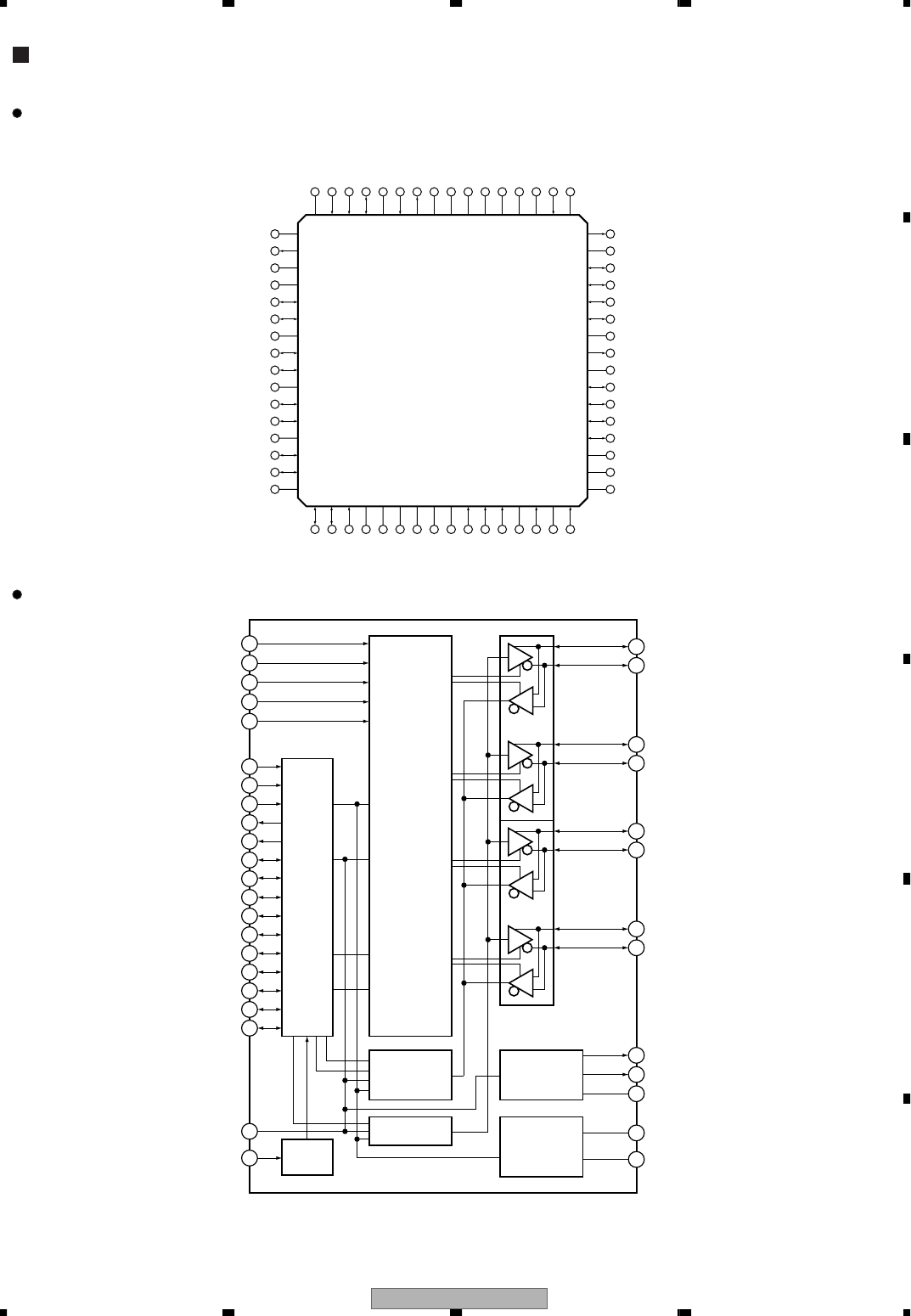
DVR-3100-S 113
5678
5678
C
D
F
A
B
E
UPD72852AGB-8EU (MAIN ASSY : IC5101)
• IEEE1394 Physical IC
Pin Arrangement
DGND 1
SCLK 2
IC (DL) 3
DVDD 4
CTL0 5
CTL1 6
DGND 7
D0 8
D1 9
DVDD 10
D2 11
D3 12
DGND 13
D4 14
D5 15
DGND 16
D6 17
D7 18
SUS/RES 19
DVDD 20
DGND 21
XO 22
XI 23
AGND 24
AVDD 25
PC0 26
PC1 27
PC2 28
IC (AL) 29
CMC 30
AVDD 31
CPS 32
48 TpBias1
47 AVDD
46 TpA1p
45 TpA1n
44 TpB1p
43 TpB1n
42 AGND
41 TpBias0
40 AVDD
39 TpA0p
38 TpA0n
37 TpB0p
36 TpB0n
35 AGND
34 RI1
33 AGND
64 DGND
63 LREQ
62 FNSel
61 SPD/BDB
60 DVDD
59 LPS
58 LKON
57 DGND
56 DVDD
55 RESETB
54 AVDD
53 AGND
52 AGND
51 IC (AL)
50 DIRECT
49 AGND
Block Diagram
30 39
38
CMC TpA0p
TpA0n
26
PC0
27
PC1
28
PC2
19
SUS/RES
63
LREQ
59
LPS
50
DIRECT
2
SCLK
58
32
LKON
Link
Interface
I/O
5
CTL0
6
CTL1
8
D0
9
D1
11
D2
12
D3
14
D4
15
D5
17
D6
18
D7
CPS
55
RESETB
Arbitration
and
Control State
Machine
Logic
Cable
Port 0
Receive Data
Decoder
and
Retimer
Voltage
and
Current
Generator
Crystal Oscillator
PLL System
and
Transmit Clock
Generator
Transmit Data
Encoder
Cable
Power
Status
37
36
TpB0p
TpB0n
46
45
TpA1p
TpA1n
Cable
Port 1 44
43
TpB1p
TpB1n
41 TpBias0
48 TpBias1
34 RI1
23 XI
22 XO
DVR-3100-S
114
1234
1234
C
D
F
A
B
E
Pin Function
• Cable Interface Pins
• Link Interface Pins
No. Pin Name I/O Function
39 TpA0p I/O Port 0 twisted pair cable A positive phase I/O
38 TpA0n I/O Port 0 twisted pair cable A negative phase I/O
37 TpB0p I/O Port 0 twisted pair cable B positive phase I/O
36 TpB0n I/O Port 0 twisted pair cable B negative phase I/O
46 TpA1p I/O Port 1 twisted pair cable A positive phase I/O
45 TpA1n I/O Port 1 twisted pair cable A negative phase I/O
44 TpB1p I/O Port 1 twisted pair cable B positive phase I/O
43 TpB1n I/O Port 1 twisted pair cable B negative phase I/O
19 SUS/RES I Suspend/Resume function select
1 : Suspend/Resume on (IEEE1394a-2000 compliant)
0 : Suspend/Resume off (P1394a draft 1.3 compliant)
32 CPS I
Cable power status
Connect to the cable through a 390 kΩ resistor and to the GND through a 100 kΩ resistor.
0 : Cable power fail
1 : Cable power on
No. Pin Name I/O Function
8D0 I/O Data input/output (bit 0)
9D1 I/O Data input/output (bit 1)
11 D2 I/O Data input/output (bit 2)
12 D3 I/O Data input/output (bit 3)
14 D4 I/O Data input/output (bit 4)
15 D5 I/O Data input/output (bit 5)
17 D6 I/O Data input/output (bit 6)
18 D7 I/O Data input/output (bit 7)
5 CTL0 I/O Link interface control (bit 0)
6 CTL1 I/O Link interface control (bit 1)
63 LREQ I Link request input
2 SCLK O Link control output clock
LPS 1 : 49.152 MHz output
LPS 0 : Clamp to 0 (The clock signal will be output within 25 µsec after change to "0")
59 LPS I Link power status input
0 : Link power off
1 : Link power on (PHY/Link direct connection)
58 LKON O Link-on signal output
Link-on signal is 6.1444 MHz clock output.
50 DIRECT I PHY/Link isolation barrier control input
0 : Isolation barrier
1 : PHY/Link direct connection
DVR-3100-S 115
5678
5678
C
D
F
A
B
E
• Control Pins
• IC
No. Pin Name I/O Function
26 PC0 I Power class set input
This pin status will be loaded to Pwr_class bit which allocated to PHY register 4H.
IEEE1394a-2000 chapter [4.3.4.1]
27 PC1 I
28 PC2 I
30 CMC I
Configuration manager capable setting
This pin status will be loaded to Contender bit which allocated to PHY register 4H.
0 : Non contender
1 : Contender
55 RESETB I
Power on reset input
Connect to GND through a 0.1 µF capacitor.
0 : Reset
1 : Normal
61 SPD/BDB
I
FNSel = 0
Speed select (UPD72852GB)
0 : MAX. S200
1 : MAX. S400
O
FNSel = 1
BIAS Detected output (Logical Inverse)
0 : BIAS is coming from some port.
1 : BIAS is not coming from any port.
No. Pin Name I/O Function
29, 51 IC (AL) −Internally Connected (Low Clamped)
Connected to GND.
3 IC (DL) −Internally Connected (Low Clamped)
Connected to GND.
• Power Supply Pins
No. Pin Name I/O Function
25, 31, 40, 47, 54 AVDD −Analog power
24, 33, 35, 42, 49, 52, 53 AGND −Analog GND
4, 10, 20, 56, 60 DVDD −Digital VDD
1, 7, 13, 16, 21, 57, 64 DGND −Digital GND
• Other Pins
No. Pin Name I/O Function
41 TpBias0 O Port 0 twisted pair output
48 TpBias1 O Port 1 twisted pair output
34 RI1 −Resistor connection pin 1 for reference current generator
Please connect to GND pin through the 9.1 kΩ resistor.
23 XI −Crystal oscillator connection XI
22 XO −Crystal oscillator connection XO
62 FNSel I Function Select
0 : #61 acts as SPD (UPD72852GB compliant)
1 : #61 acts as BDB
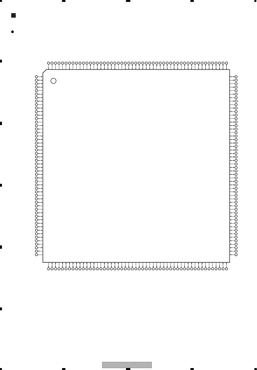
DVR-3100-S
116
1234
1234
C
D
F
A
B
E
UPD72893AGD-LML (MAIN ASSY : IC5202)
• IEEE1394 Link IC
Pin Arrangement
RESETB 1
PHY_D7 2
PHY_D6 3
PHY_D5 4
3.3VDD 5
PHY_D4 6
PHY_D3 7
PHY_D2 8
3.3GND 9
PHY_D1 10
PHY_D0 11
CTL1 12
CTL0 13
2.5VDD 14
SCLK 15
LREQ 16
LPS 17
LINKON 18
STREAM10 19
STREAM11 20
STREAM12 21
STREAM13 22
STREAM14 23
STREAM15 24
STREAM16 25
STREAM17 26
PACKETEN1 27
TSERROR1 28
TSRW1 29
SYNC1 30
3.3VDD 31
TSSUB1 32
PACKETEN2/VSYNC
33
TSERROR2/HSYNC
34
3.3GND 35
TSRW2/FLD 36
SYNC2 37
TSSUB2 38
2.5GND 39
STREAM20/VD0 40
STREAM21/VD1 41
STREAM22/VD2 42
STREAM23/VD3 43
STREAM24/VD4 44
STREAM25/VD5 45
STREAM26/VD6 46
STREAM27/VD7 47
AFS1 48
AFS2 49
VCLKI 50
VCLKO 51
3.3VDD 52
VPWM 53
MD0 54
MD1 55
3.3GND 56
MD2 57
MD3 58
MD4 59
MD5 60
MD6 61
MD7 62
3.3VDD 63
MD8 64
MD9 65
MD10 66
2.5VDD 67
3.3GND 68
MD11 69
MD12 70
MD13 71
MD14 72
MD15 73
MWE 74
MCAS 75
MRAS 76
MCLK 77
3.3VDD 78
MA0 79
MA1 80
MA2 81
3.3GND 82
MA3 83
MA4 84
MA5 85
MA6 86
MA7 87
MA8 88
MA9 89
MA10 90
2.5GND 91
MA11 92
ALRCK 93
ABCK 94
3.3VDD 95
PCM1 96
PCM2 97
AEMP1 98
3.3GND 99
IC (O) 100
AMCLKO 101
APWM 102
AMCLK44 103
AMCLK48 104
A1156 BR_MON155 IC (PL)154 DV_INT153 IC (PL)152 SCS151 RXD150 TXD149 3.3GND148 SCK147 SI146 SO145 2.5GND144 P_D15143 P_D14142 P_D13141 3.3VDD140 P_D12139 P_D11138 P_D10137 P_D9136 P_D8135 P_D7134 P_D6133 P_D5132 3.3GND131 P_D4130 P_D3129 P_D2128 3.3VDD127 P_D1126 P_D0125 INT124 IOCHRDY123 IC (O)122 IC (H)121 IOR120 RWZ119 2.5VDD118 CS117 AD10116 AD9115 AD8114 AD7113 AD6112 AD5111 AD4110 AD3109 AD2108 AD1107 PSSEL1106 PSSEL0105
IFIROME208 IC (L)207 IC (L)206 IC (L)205 IC (PL)204 IC (L)203 HS_CLK202 PLLDGND201 PLLAGND200 PLLAVDD199 PLLDVDD198 IC (L)197 D15196 2.5GND195 D14194 D13193 D12192 D11191 D10190 D9189 3.3GND188 3.3VDD187 D8186 D7185 D6184 D5183 D4182 D3181 D2180 D1179 D0178 WRZ177 RDZ176 A17175 A16174 3.3GND173 A15172 A14171 2.5VDD170 A13169 A12168 A11167 3.3VDD166 A10165 A9164 A8163 A7162 A6161 A5160 A4159 A3158 A2157
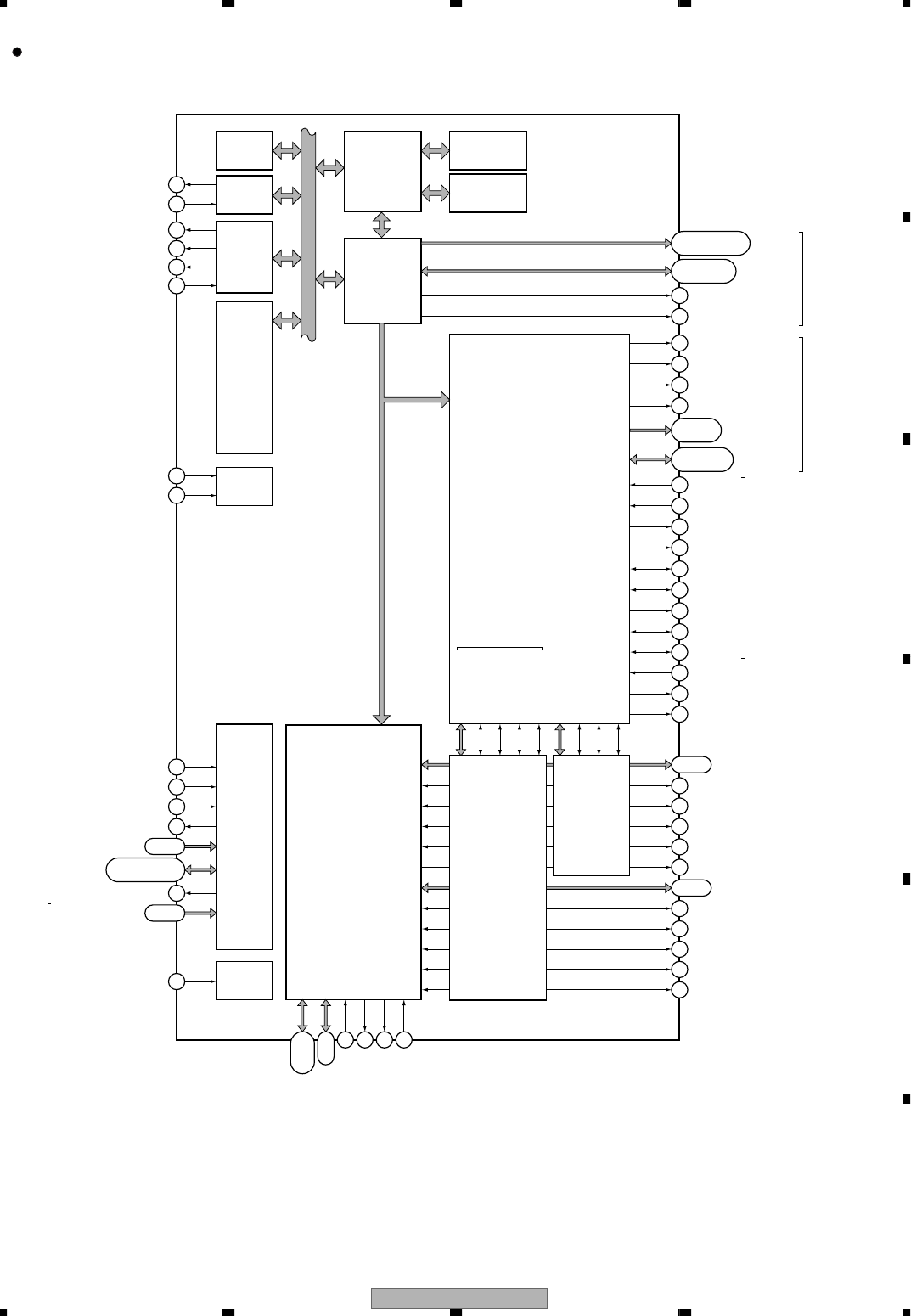
DVR-3100-S 117
5678
5678
C
D
F
A
B
E
Block Diagram
149
1
76
TXD
150
RXD
Host
Interface
<UART>
RESETB
202
HS_CLK
208
IFIROME
PHY_D [7 : 0]
CTL [1 : 0]
15
SCLK
16
LREQ
17
LPS
18
LINKON
STREAM [7 : 0]
TSRW
PACKETEN
SYNC
TSSUB
VD [7 : 0]
VSYNC
HSYNC
FLD
117
CS
119
RWZ
120
IOR
123
IOCHRDY
AD [10 : 1]
116-107
106, 105
47-40
12, 13
143-141, 139-132,
130-128, 126, 125
2-4, 6-8,
10, 11
P_D [15 : 0]
175, 174, 172, 171,
169-167, 165-156
196, 194-189,
186-178
A [17 : 0]
D [15 : 0]
92, 90-83,
81-79
MA [11 : 0]
73-69, 66-64,
62-57, 55, 54
MD [15 : 0]
RDZ
124
INT
PSSEL [1 : 0]
System
Control
Test
Block
Host
Inteface IEEE1394 Link Core
DV Codec Core
External
Flash ROM
Interface
SDRAM
Interface
Audio
Interface
Parallel Interface
Stream
Interface
16-bit Timer
Unit D
<TMD> CPU Core
High-speed
Internal ROM
192 kbytes
151
SCS
147
SCK
145
SO
146 176
WRZ
177
104
103
102
101
SI
MRAS
EEPROM
Interface
<CSI>
High-speed
Internal ROM
60 kbytes
Memory
Controller
INTC
77 MCLK
75 MCAS
74 MWE
AMCLK44
AMCLK48
APWM
AMCLKO
97 PCM2
96 PCM1
98 AEMP1
93 ALRCK
94 ABCK
36 TSRW2 / FLD
33 PACKETEN2 / VSYNC
37 SYNC2
34 TSERROR2 / HSYNC
38 TSSUB2
29 TSRW1
27 PACKETEN1
30 SYNC1
28 TSERROR1
32 TSSUB1
50 VCLKI
51 VCLKO
STREAM2 [7 : 0] / VD [7 : 0]
26-19
STREAM1 [7 : 0]
53 VPWM
Selector
Selector
DVR-3100-S
118
1234
1234
C
D
F
A
B
E
(1) Link relation
No. Pin Name I/O Function Active
18 LINKON I
Link-on signal input
Clock input
When LPS is active, input 0.
−
17 LPS O
Link power status output
Link power OFF : 0
Link power ON : 2.7 MHz pulse output (20 dividing of host clock 54 MHz)
−
16 LREQ O Link request output −
15 SCLK I
Clock input for Link control
LPS is active : 49.152 MHz input
LPS = 0 0 : fixed
−
12, 13 CTL [1 : 0] I/O PHY/Link control signal input/output −
2-4, 6-8, 10,11 PHY_D [7 : 0] I/O Data input/output between PHY-Link −
26-19 STREAM1 [7 : 0] I/O ISO data bus of stream interface 1 −
27 PACKETEN1 I/O Packet enable signal input/output of stream interface 1 H/L
28 TSERROR1 I/O Packet error signal input/output of stream interface 1 H/L
29 TSRW1 I/O Data read/write enable signal input/output of stream interface 1 −
30 SYNC1 I/O Frame synchronous signal input/output of stream interface 1 H/L
32 TSSUB1 I/O Not used Connect to VDD or GND through a resistor. H/L
47-40 STREAM2 [7 : 0] I/O ISO data bus of stream interface 2 −
33 PACKETEN2 I/O Packet enable signal input/output of stream interface 2 H/L
34 TSERROR2 I/O Packet error signal input/output of stream interface 2 H/L
36 TSRW2 I/O Data read/write enable signal input/output of stream interface 2 −
37 SYNC2 I/O Frame synchronous signal input/output of stream interface 2 H/L
38 TSSUB2 O Not used Set to open. −
(2) Video interface pins
No. Pin Name I/O Function Active
50 VCLKI I Video clock input (27 MHz) −
51 VCLKO O Video clock output (27 MHz) −
47-40 VD [7 : 0] I/O Video data signal −
33 VSYNC I/O Video vertical sync. signal L
34 HSYNC I/O Video horizontal sync. signal L
36 FLD I/O Field index signal −
53 VPWM O PWM signal for video PLL −
Pin Function
DVR-3100-S 119
5678
5678
C
D
F
A
B
E
(3) Audio interface pins
No. Pin Name I/O Function Active
104 AMCLK48 I Audio master clock input for sampling frequency 48 kHz −
103 AMCLK44 I Audio master clock input for sampling frequency 44 kHz −
101 AMCLKO O Audio master clock output −
96 PCM1 I/O
Audio PCM serial data
At 2ch : System 1 (data of audio block 1)
At 4ch : System 1
The above is default setting value. Input/output data of PCM 1 and PCM 2 is replaced
by Channel swap setting of an AUDIO_FUNC register.
−
97 PCM2 I/O
Audio PCM serial data
At 2ch : Mute
At 4ch : System 2 (data of audio block 2)
The above is default setting value. Input/output data of PCM 1 and PCM 2 is replaced
by Channel swap setting of an AUDIO_FUNC register.
Note: Cannot use it in DV decode.
−
98 AEMP1 O PCM1 emphasis ON/OFF in PCM 1 output H
93 ALRCK I/O
Audio LR clock
L ch : High
R ch : Low
−
94 ABCK I/O Audio bit clock −
49, 48 AFS [2 : 1] O
Audio sampling frequency
AFS2 AFS1
44.1 kHz 0 1
48 kHz 0 0
32 kHz 1 0
−
102 APWM O PWM signal for audio PLL −
(4) SDRAM interface pins
No. Pin Name I/O Function Active
77 MCLK O CLK pin connection of SDRAM −
76 MRAS O RAS pin connection of SDRAM −
75 MCAS O CAS pin connection of SDRAM −
74 MWE O WE pin connection of SDRAM −
92, 90-83,
81-79 MA [ 11 : 0] O Address pin connection of SDRAM −
73-69, 66-64,
62-57, 55, 54 MD [ 15 : 0] I/O
Data pin connection of SDRAM
Note: Process of pull-up or pull down is necessary.
So connect it to SDRAM directly.
−

DVR-3100-S
120
1234
1234
C
D
F
A
B
E
(a) Parallel interface pins
(5) Host interface pins
No. Pin Name I/O Function Active
117 CS I Chip select input of parallel interface L
119 RWZ I
Read and write control input of parallel interface
ISA type bus, SH-1 bus: Write strobe
68000 bus : Read/write selection signal
L
120 IOR I
IO read control input of parallel interface
ISA type bus, SH-1 bus : Read strobe
68000 bus : Data strobe (DS)
L
123 IOCHRDY O Ready output of parallel interface L
116-107 AD [ 10 : 1] I Address input of parallel interface −
143-141, 139-132,
130-128, 126, 125
P_D [15 : 0] I/O Data input/output of parallel interface −
(b) Serial interface pins
No. Pin Name I/O Function Active
149 TXD I/O Serial transmission data output of unsynchronous serial interface (UART) −
150 RXD I/O Serial transmission data input of unsynchronous serial interface (UART) −
(c) Others
No. Pin Name I/O Function Active
124 INT O Interrupt output to the outside H
106, 105 PSSEL [1 : 0] I
Parallel/serial interface selection
Input signal to select the outside interface which of parallel interface or serial interface.
PSSEL [1 : 0] Select
00 Serial interface (UART)
01 Parallel interface (ISA type bus)
10 Parallel interface (68000 bus)
11 Parallel interface (SH-1 bus)
−
DVR-3100-S 121
5678
5678
C
D
F
A
B
E
(a) Flash ROM interface pins
(6) External ROM connection pins
No. Pin Name I/O Function Active
196, 194-189,
186-178 D [15 : 0] I/O
External ROM data bus
Data bus in the external ROM access.
Process of pull-up or pull down is necessary.
−
175, 174, 172,
171, 169-167,
165-156
A [17 : 1] O
External ROM address bus
Address bus in the external ROM access.
Can addressing the 256k byte space.
−
176 RDZ O
ROM read
Strobe signal which shows a read cycle for external ROM.
It becomes the inactive in the idle state.
L
177 WRZ O ROM write
Strobe signal which shows a write cycle for external ROM. L
(b) EEPROM interface pins
No. Pin Name I/O Function Active
145 SO I/O Serial transmit data output of clock-synchronous system serial interface (CSI) −
146 SI I/O Serial receive data input of clock-synchronous system serial interface (CSI) −
147 SCK I/O Clock output of clock-synchronous system serial interface (CSI) −
151 SCS I/O Chip select output of clock-synchronous system serial interface (CSI) −
(7) Clock and reset pins
No. Pin Name I/O Function Active
1 RESETB I
Reset
RESETB input is asynchronous input. When a signal of fixed low-level width is input
without relation to an operation clock, take precedence of all operation, and reset the
system. Note: RESETB is low-active.
L
202 HS_CLK I
Host clock
Clock input pin which is supplied to CPU core and built-in peripheral I/O.
Please input 27 MHz clock. Perform 2 multiply with internal PLL by 27 MHz clock, 54
MHz clock is supplied to CPU core and internal peripheral I/O.
−
DVR-3100-S
122
1234
1234
C
D
F
A
B
E
(8) Power supply and ground pins
No. Pin Name I/O Function Active
5, 31, 52, 63,
78, 95, 127,
140, 166, 187
3.3VDD −3.3V power supply
3.3V positive power supply pins. Power supply for 3.3V interface I/O. −
14, 67,
118, 170 2.5VDD −2.5V power supply
2.5V positive power supply pins. Power supply for internal each block. −
39, 91,
144, 195 2.5GND
−Ground pins
Connect all GND pins to the common ground.
−
9, 35, 56, 68,
82, 99, 131,
148, 173, 188
3.3GND −
199 PLLAVDD −Analog power supply for multiply circuit
Analog positive power supply pin for PLL. Supply 2.5V. −
200 PLLAGND −Analog ground for multiply circuit
Analog ground for PLL −
198 PLLDVDD −Digital power supply for multiply circuit
Digital positive power supply pin for PLL. Supply 2.5V. −
201 PLLDGND −Digital ground for multiply circuit
Digital ground for PLL −
121 IC (H) −Internally connected pin
Connect to VDD directly. −
197, 203,
205-207 IC (L) −Internally connected pin
Connect to ground directly. −
152, 154, 204 IC (PL) −Internally connected pin
Connect to ground through a resistor. −
100, 122 IC (O) −Internally connected pin
Set to open. −
(9) Others
No. Pin Name I/O Function Active
153 DV_INT I/O Interrupt pin to the outside for the DV status read out. H
155 BR_MON I/O Shows the bus reset occurred. There is some delay after real bus reset occurred
because of set by the built-in firmware. H
208 IFIROME I ROM operation selection input
Set to 1 normally. −
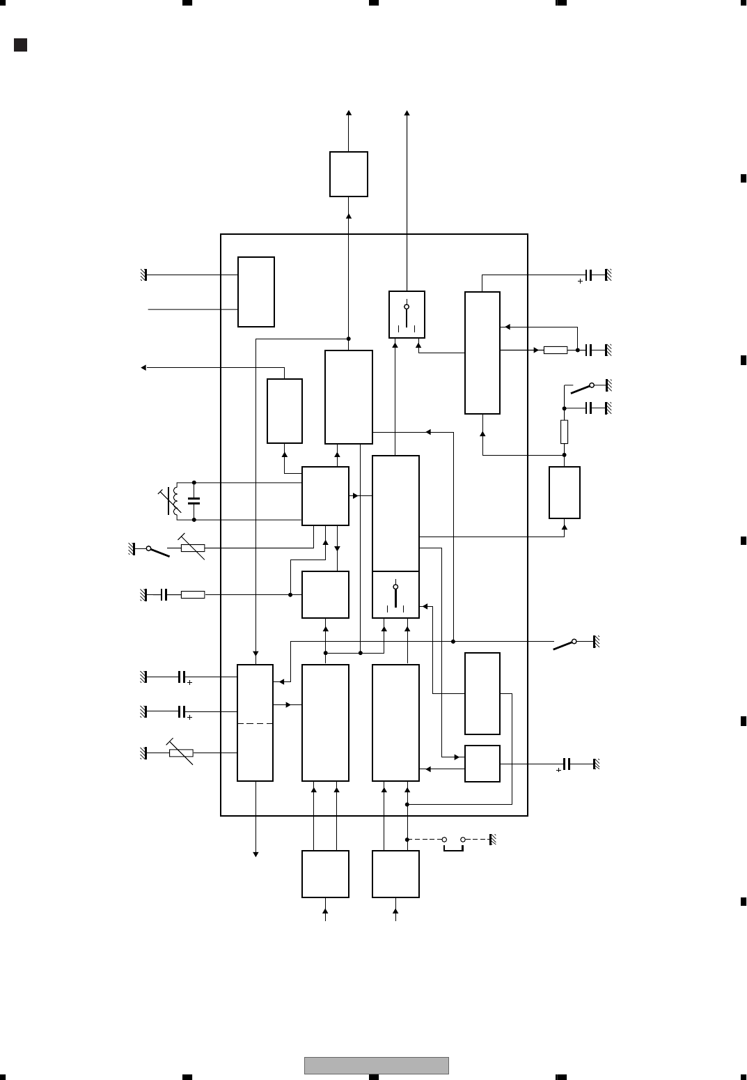
DVR-3100-S 123
5678
5678
C
D
F
A
B
E
QSS MIXER
INTERCARRIER MIXER
AM DEMODULATOR
SIF AMPLIFIER
SIF
AGC
intercarrier
mode
INTERCARRIER
MODE SWITCH
FM-PLL
DEMODULATOR
9
mute
switch
standards
selection
switch
CSAGC Cde-em
Vde-em CDEC
13
FMin
QSSSTD
12
3
(1)
510 11
audio
video
CVBS
1 V (p-p)
1.1 V (p-p)
8
16
2021171819
7
(1)
615
(1)
422
AFC
AF
2 × fpc
L/L accent switch
and adjust
TPLL
CVAGC
CBLTOP LADJ VCO2 VCO1 VPGND
VIF AMPLIFIER FPLL
VIF
SAW
SIF
SAW 24
23
2
1
14
VCO
TWD
5.5 MHz
VIDEO
DEMODULATOR
AND AMPLIFIER
SOUND
TRAP
AFC
DETECTOR
VOLTAGE
REFERENCE
TUNER
AGC
TAGC
VIF1
VIF2
SIF1
SIF2
VIF
AGC
TDA9818
MHA663
• VIF/SIF IC
TDA9818TS (TUJB ASSY : IC3903)
DVR-3100-S
124
1234
1234
C
D
F
A
B
E
PIN FUNCTION
SYMBOL PIN DESCRIPTION
VIF1 1 VIF differential input signal voltage 1
VIF2 2 VIF differential input signal voltage 2
STD 3 standards selection switch; note 1
CVAGC 4 VIF AGC capacitor
CSAGC 5 SIF AGC capacitor
TPLL 6 PLL filter
LADJ 7 L/L accent switch and adjust
AF 8 audio output
Vde-em 9 de-emphasis output
Cde-em 10 de-emphasis input
CDEC 11 decoupling capacitor
QSS 12 single reference QSS/intercarrier
output voltage
FMin 13 sound intercarrier input voltage
TAGC 14 tuner AGC output
CBL 15 black level detector
CVBS 16 composite video output voltage
AFC 17 AFC output
VCO1 18 VCO1 resonance circuit
VCO2 19 VCO2 resonance circuit
GND 20 ground
VP21 supply voltage
TOP22tuner AGC takeover point adjust
SIF1 23 SIF differential input signal voltage 1
SIF2 24 SIF differential input signal voltage 2
TDA9818
1
2
3
4
5
6
7
8
9
10
11
12
VIF1
VIF2
STD
CVAGC
CSAGC
TPLL
LADJ
AF
Vde-em
Cde-em
CDEC
QSS
SIF2
SIF1
TOP
VP
GND
VCO2
VCO1
AFC
CVBS
CBL
TAGC
FMin
24
23
22
21
20
19
18
17
16
15
14
13
PIN LAYOUT

DVR-3100-S 125
5678
5678
C
D
F
A
B
E
No. Pin Name DC Voltage Function
1
2
10
11
15
16
33
34
36
37
AIN1R
AIN1L
AIN2R
AIN2L
AIN3R
AIN3L
AIN4L
AIN4R
AIN5L
AIN5R
5.58V Audio input terminal
3
4
19
35
EXTCTL1
EXTCTL2
EXTCTL3
EXTCTL4
2.5mA, ON
→0.75V
OFF
→OPEN
5 VOUT
6
17
27
32
38
GND
GND
EXT-75ΩDR-GND
DEC-75Ω-GND
GND
0V
7
13
18
23
28
VIN1
VIN2
VIN3
VIN4
VIN5
1.8V
1.10V
Video input terminal
Sync-tip clamp
Input/Hi-impedance
General purpose output
Opencollector
Video output terminal
Push-pull output/Low-impedance
8 PWRSAV 0.2V Power save mode select pin
OPEN : L
9 AUMUTE 0.05V Control terminal for audio mute
OPEN : L
Video driver output terminal
Push-pull output/Low-impedance
Audio output terminal
Push-pull output/Low-impedance
Audio output terminal
Push-pull output/Low-impedance
Output terminal of audio muting
FSS control terminal
Output H, M, L
3 values with serial control
Terminal for Ref_DC ripple removing
Vcc for audio
Confirmed to IIC BUS. Data input terminal
Confirmed to IIC BUS. Clock input terminal
Control Vcc for Video
Always VCC for Video
12 REFFIL 4.94V
14 VCC12
20 FSSOUT H : Vcc-0.5V
M : 6V
L : 0V
21 DATA
22 CLOCK
24 VCC5A
25
26 VOUT75A
VOUT75B 1.10V
29 VCC5B
30
31
42
43
AOUT2L
AOUT2R
AOUT3L
AOUT3R
4.91V
39
40 AOUT1L
AOUT1R 4.91V
41
44 PWRMUTE1
PWRMUTE2 0V
Pin Function
• Dual SCART Interface IC
LA73026AV (SCRB ASSY : IC101)
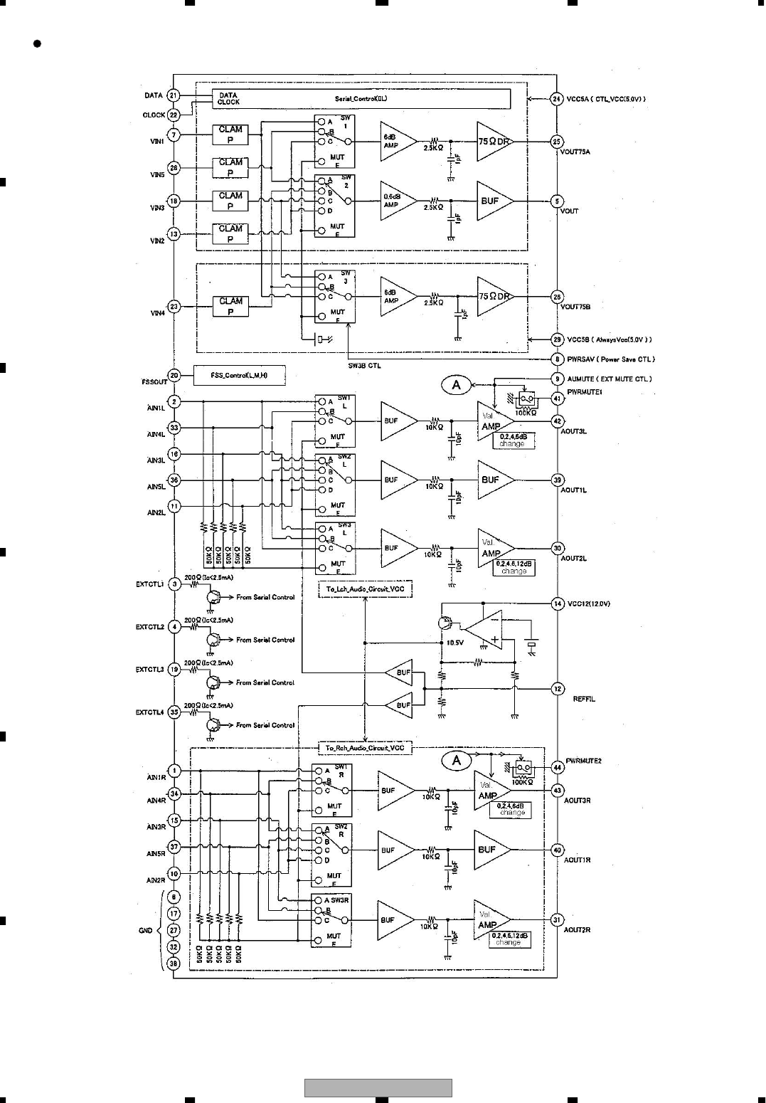
DVR-3100-S
126
1234
1234
C
D
F
A
B
E
Block Diagram
DVR-3100-S 127
5678
5678
C
D
F
A
B
E
7.3 OUTLINE OF THE PRODUCT
Main newly developed technologies
1. Pickup
The pickup supports quadruple-speed recording for the DVD-
R/RW.
A liquid-crystal tilt servo system is adopted for the pickup.
2. Recording-signal-processing LSI
• UPD3320GC (DRIVE Assy: IC101)
The recording-signal-processing module of conventional models
consists of two chips, but this has been integrated into a
single newly developed recording-signal-processing LSI, enabling
stable performance and cost reduction.
3. AV-signal-processing LSI
• M65672WG-B (MAIN Assy: IC1001)
The AV-signal-processing module of conventional models
consists
of eleven chips, but this has been integrated into a single
newly developed AV-signal-processing LSI, enabling large-scale
cost reduction while maintaining the conventional functions. In
the new LSI, all the basic functions necessary for a DVD
recorder have been integrated. Like conventional models, this
model is designed to support multitasking. The main functions
are as follows:
• 3-D Y/C separation
• Video decoding
• Frame TBC
• MPEG video encoding
• Dolby Digital Consumer Encoding
• ATA/ATAPI I/F (2 ch)
• Main CPU (32-bit RISC, 54 MHz)
• Graphics engine (OSD, scaling, mixing)
• MPEG video decoding
• Audio decoding (AC-3, MPEG)
• Video encoding
• Progressive conversion
• Audio I/F
• 3-D DNR for playback
4. DV-signal-processing LSI
The DV-signal-processing LSI consists of the following two
chips:
• UPD72862AGB-SEU (MAIN Assy: IC5101)
A 400-Mbps two-port PHY LSI in compliance with the
IEEE1394a-
2000 standards
• UPD72893AGD-LML (MAIN Assy: IC5202)
An EEE1394 link controller LSI having DV (digital video)
encoding/decoding functions. Encoding/decoding of digital video
signals in compliance with the SD specifications (NTSC/PAL) of
the DV standard is supported. The 32-bit RISC CPU is built in
for controlling the IEEE1394 bus and sending/receiving AV/C
commands.
Fig.1 MAIN Assy
IC1001
(SIDE B)
IC5202
(Side A)
IC5101
(Side A)
SIDE B
MAIN ASSY
D
DVR-3100-S
128
1234
1234
C
D
F
A
B
E
System configuration
In each signal-processing LSI of the main function blocks,
various processes have been integrated into one chip, which
enables simpler system configuration. With the AV-signal-
processing LSI at the center, video inputs/outputs, audio
inputs/outputs, DV inputs/outputs, writer, HDD, and various
memory cells are connected to it.
Fig2. System configuration
1394 (DV)
CVBS/YC/YCbCr
Analog Audio
DIF
Playback
Record
Tuner / Line
Select
IC2001
Tuner / FL
Control
CPU
IC1001
AV Signal
Processing
LSI
Drive Assy
(DVD-R/RW)
IC5101
1394 Phy
IC1102
Flash
IC1103
SRAM
IC1101, IC1201, IC1301
IC1401 SDRAM
IC5202
1394 Link /
DV Codec
FL
Video : IC3301 LA73030
Audio : IC2801 LC75342M
IC3101
Audio A/D
AK5381VT
IC3201
Audio D/A
PCM1742KE
UPD72893AGD-LML UPD72852AGB-8EU

DVR-3100-S 129
5678
5678
C
D
F
A
B
E
New functions and specifications
In this model, the following new functions and specifications
have been included in addition to those of conventional models:
1. Improved multitasking functions
This model supports DVD multitasking (only in VR mode),
which was impossible with conventional models.
a Pursuit playback
Playback of the title being recorded by the DVD drive in VR
mode .
b Simultaneous recording/playback
Playback of a title other than that being recorded by the DVD
drive in VR mode.
2. Advanced disc NAVI
In the conventional disc NAVI function, recorded titles are
displayed with still pictures as a list. In the advanced disc
NAVI function, the title selected with the cursor is displayed
as an animated picture with sound.
3. Improved Still Picture menu in Video mode
The disc NAVI function, which enables displaying a list of
recorded titles with still pictures, is enabled in Video mode
with this model. Selection from among nine title menus is also
supported.
4. Adoption of MPEG2 SIF
In MN1-6 modes, MPEG2 SIF has been adopted, instead of the
MPEG1 SIF of conventional models. This enables higher-quality
recording for longer hours.
5. Improved editing functions
For DVD, the original/play-list editing in DVD-VR mode
available with conventional models is provided.
The automatic-chapter-mark-insertion function in response to a
change in audio type (stereo, monaural, bilingual) makes
commercial-cutting editing easier.
5. Various-format playback
Playback of WMA, MP3, and JPEG formats is supported.
6. Other functions and specifications
The following main functions and specifications adopted with
conventional models are also provided with this model:
• 192-kHz, 24-bit DAC
• 48-kHz, 20-bit ADC
• Digital 3-D Y/C separation circuit
• Digital frame TBC
• 3-D DNR
• DV (iLink) input/output
• Built-in BS tuner
• Playback with commercials skipped
• CD/video-CD playback
• Picture creation
• Recording with 3/4-D1 and 2/3-D1 resolutions
• Recording mode with 32-step MNs
• LPCM recording
• High-resolution GUI
• Progressive output
• SRS TruSurround
DVR-3100-S
130
1234
1234
C
D
F
A
B
E
7.4 DISC/CONTENT FORMAT
Disc / content format playback
compatibility
General disc compatibility
This recorder was designed and engineered to be
compatible with software bearing one or more of the
following logos:
Also compatible with KODAK Picture CD
is a trademark of Fuji Photo Film Co. Ltd.
Other formats, including but not limited to the following,
are not playable in this recorder:
DVD-Audio / SACD / DVD-RAM
DVD-ROM / CD-ROM*
* Except those that contain WMA, MP3 or JPEG. See also
Compressed audio compatibility and JPEG file
compatibility below.
DVD-R/RW and CD-R/RW discs recorded using a DVD
recorder, CD recorder or personal computer may not be
playable in this recorder. This may be caused by a
number of possibilities, including but not limited to: the
type of disc used; the type of recording; damage, dirt or
condensation on either the disc or the pick-up lens. See
below for notes about particular software and formats.
DVD-R/RW compatibility
This recorder will play and record DVD-R/RW discs that
use DVD-Video format (Video mode), and DVD-RW discs
that use the Video Recording (VR) format. It is compatible
with DVD-RW Ver. 1.1 and Ver. 1.1 / 2x, and DVD-R Ver.
2.0 and Ver. 2.0 / 4x.
CD-R/RW compatibility
This recorder will play CD-R and CD-RW discs recorded
in CD Audio or Video CD format, or as a CD-ROM
containing MP3, WMA or JPEG files. However, any other
content may cause the disc not to play, or create noise/
distortion in the output.
This recorder cannot record CD-R or CD-RW discs.
PC-created disc compatibility
If you record a disc using a personal computer, even if it
is recorded in a "compatible format" as listed above, there
will be cases in which the disc may not be playable in this
recorder due to the setting of the application software
used to create the disc. In these particular instances,
check with the software publisher for more detailed
information.
Check the DVD-R/RW or CD-R/RW software disc boxes
for additional compatibility information.
WMA (Windows Media Audio) compatibility
The Windows Media logo printed on the box indicates
that this recorder can playback WMA data.
WMA is short for Windows Media Audio and refers to an
audio compression technology developed by Microsoft
Corporation. WMA data can be encoded by using
Windows Media Player version 9 (or less) or Windows
Media Player for Windows XP.
Windows Media, and the Windows logo are trademarks,
or registered trademarks of Microsoft Corporation in the
United States and/or other countries.
Compressed audio compatibility
This recorder will play CD-ROM, CD-R, and CD-RW discs
containing files saved in the MPEG-1 Audio Layer 3 (MP3)
or Windows Media Audio (WMA) format with a sampling
rate of 44.1 or 48kHz. Incompatible files will not play and
the message Cannot play this file format will be
displayed (CAN’T PLAY in the front panel display).
Fixed bit-rate MP3 files are recommended. Variable bit-
rate (VBR) MP3 files are playable, but playing time may
not be shown correctly.
This recorder is compatible with 44.1 and 48 kHz WMA
files encoded with Windows Media Codec 8. Files
encoded using Windows Media Codec 9 may be playable,
but some parts of the specification are not supported
(specifically, Pro, Lossless, Voice and VBR WMA files).
WMA files encoded with DRM (Digital Rights
Management) copy protection will not play and the
message Cannot play this file format will be displayed
(CAN’T PLAY in the front panel display).
DVD-Video
DVD-R DVD-RW
Vi deo CD
Fujicolor CD
Audio CD CD-R CD-RW

DVR-3100-S 131
5678
5678
C
D
F
A
B
E
The CD-ROM used to compile your WMA/MP3 files must
be ISO 9660 Level 1 or 2 compliant. CD physical format:
Mode1, Mode2 XA Form1. Romeo and Joliet file systems
are both compatible with this recorder.
Use CD-R or CD-RW media for recording your files. The
disc must be finalized (i.e. the session must be closed) in
order to play in this recorder.
This recorder only plays tracks that are named with the
file extension .MP3 or .WMA (upper or lower-case).
When naming MP3 and WMA files, add the
corresponding file name extension (.mp3 or .wma). Files
are played according to the file extension. To prevent
noise and malfunctions, do not use these extensions for
other kinds of files.
This recorder can recognize up to 99 folders and 999 files
(WMA/MP3). If a disc exceeds these limits, only files and
folders up to these limits will be playable. Files and
folders are read/displayed in alphabetical order. Note
that if the file structure is very complex, you may not be
able to read/play all files on the disc.
Folder, track and file names (excluding the file extension)
are displayed.
There are many different recording bit-rates available to
encode MP3 files. This recorder has been designed to be
compatible with all of them. Audio encoded at 128Kbps
should sound close to regular CD Audio quality. This
recorder will play lower bit-rate files, but please note that
the sound quality becomes noticeably worse at lower bit-
rates.
JPEG file compatibility
This recorder is compatible with Fujicolor CD and Kodak
Picture CD formats, as well as CD-R/RW/ROM discs
containing JPEG files.
Baseline JPEG and EXIF 2.2*1 still image files are
supported (horizontal resolution from 160–5120 pixels;
vertical resolution between 120–3840 pixels).
*1
File format used by digital still cameras
The CD-ROM used to compile your JPEG files must be
ISO 9660 Level 1 or 2 compliant. CD physical format:
Mode1, Mode2 XA Form1. Romeo and Joliet file systems
are both compatible with this recorder.
This recorder only displays files that are named with the
file extension .jpg, .jpeg, .jif, or .jfif (upper or lower-case).
The recorder can load up to 99 folders and 999 files at one
time. If there are more files/folders than this on the disc
then more can be reloaded.

DVR-3100-S
132
1234
1234
C
D
F
A
B
E
7.5 CLEANING
Before shipping out the product, be sure to clean the following positions by using the prescribed cleaning tools:
Position to be cleaned Cleaning tools
Pickup lenses Cleaning liquid : GEM1004
Cleaning paper : GED-008
Position to be cleaned Cleaning tools
Fans Cleaning paper : GED-008
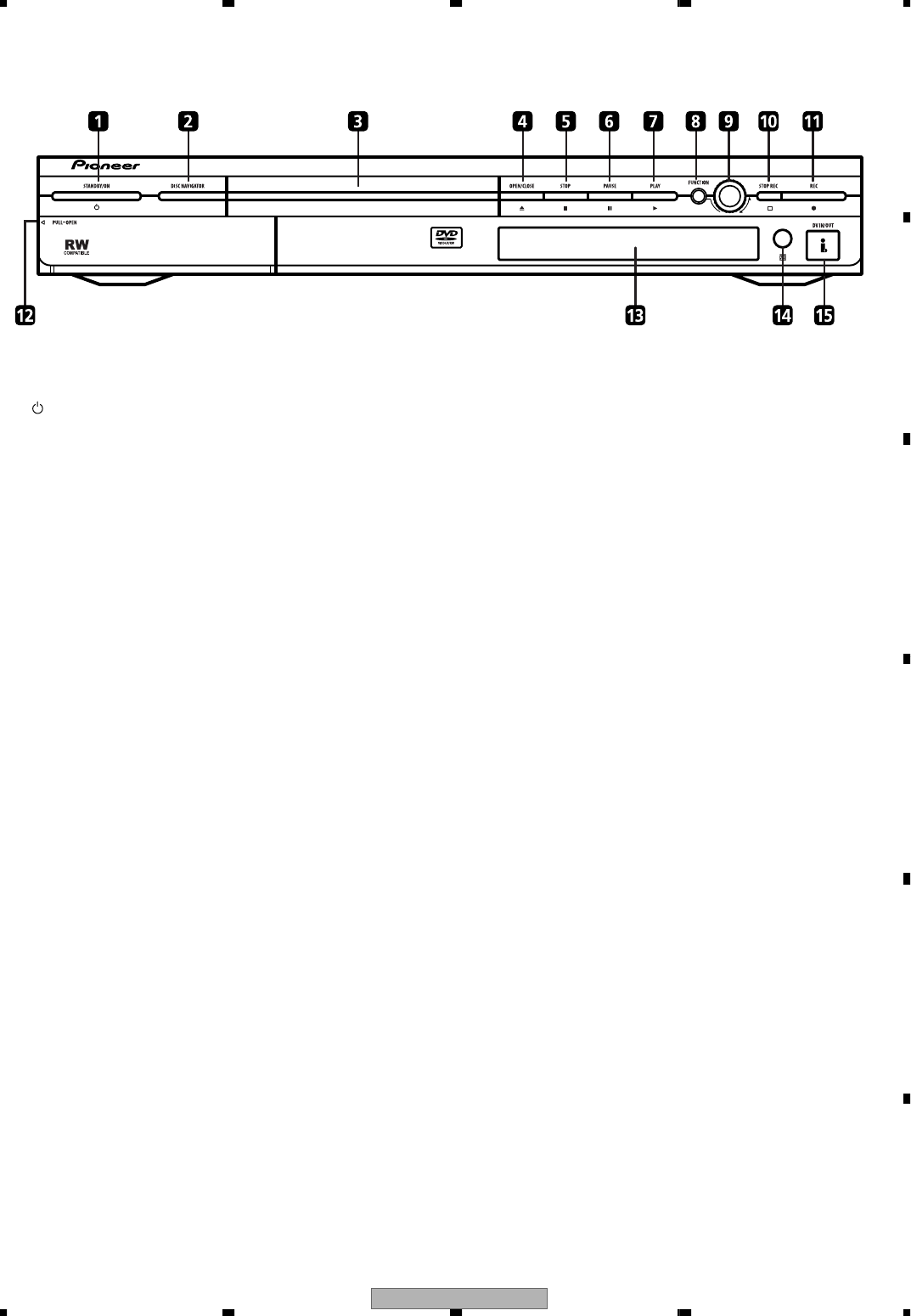
DVR-3100-S 133
5678
5678
C
D
F
A
B
E
8. PANEL FACILITIES
8.1 FRONT SECTION
1 STANDBY/ON
Press to switch the recorder on/into standby.
2 DISC NAVIGATOR
Press to directly access the Disc Navigator screen.
3 DVD disc tray
40 OPEN/CLOSE
Press to open/close the disc tray.
57 STOP
Press to stop playback.
68 PAUSE
Press to pause/restart playback or recording.
73 PLAY
Press to start or restart playback.
8 FUNCTION
Press repeatedly to set the function of the SMART JOG
dial. The function is shown in the display.
9SMART JOG dial
10 & STOP REC
Press to stop recording.
11 ¶ REC
Press to start recording.
12 Front panel inputs
Pull the cover down where indicated to access the front
panel input jacks. Especially convenient for connecting
camcorders and other portable equipment.
13 Front panel display
See Display for details.
14 IR remote sensor
15 DV IN/OUT jack
Digital input/output jack for use with a DV camcorder.
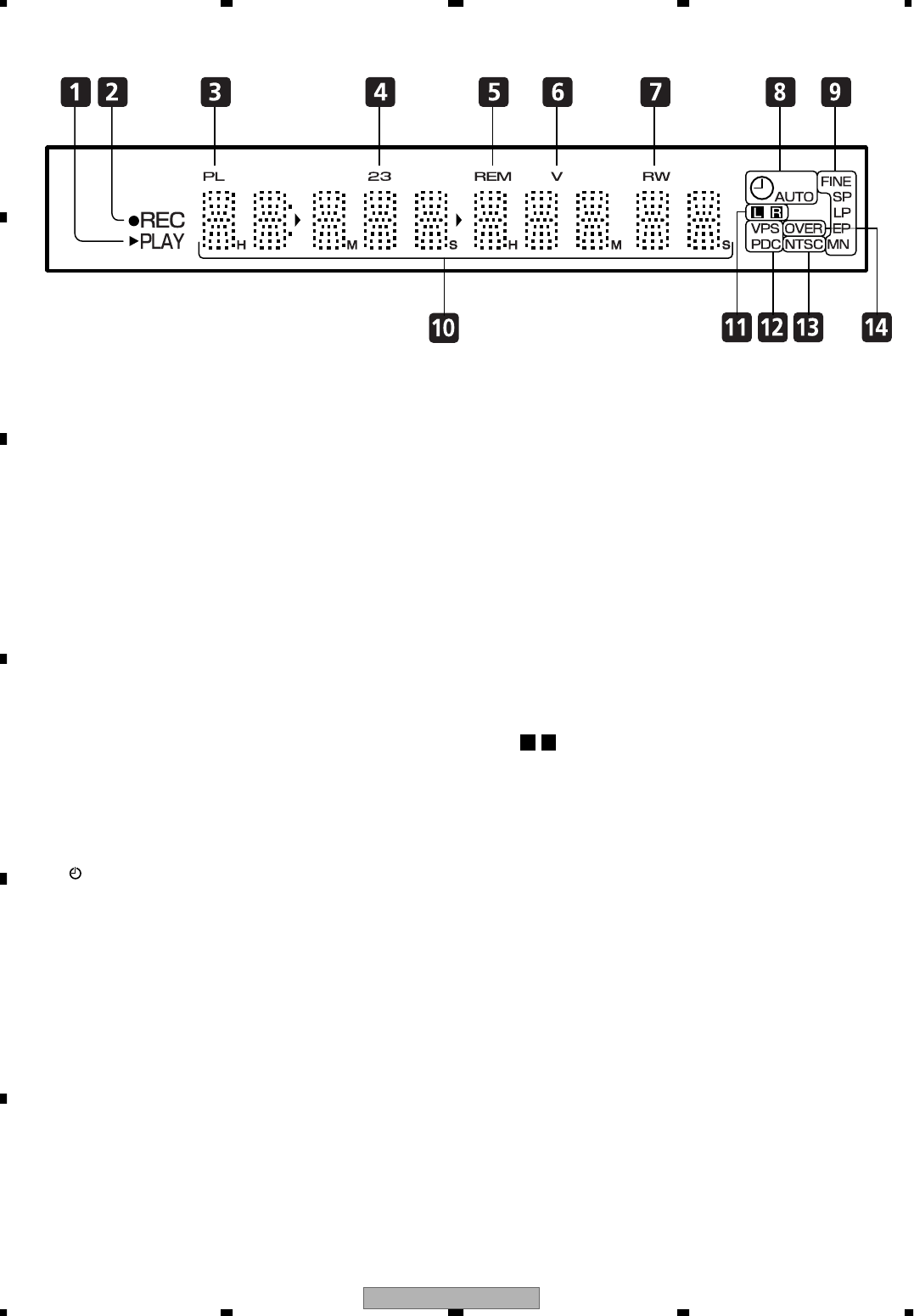
DVR-3100-S
134
1234
1234
C
D
F
A
B
E
8.2 DISPLAY
13 PLAY
Lights during playback; blinks when paused.
2¶ REC
Lights during recording; blinks when recording is paused.
3PL
Lights when a VR mode disc is loaded and the recorder is
in Play List mode.
42 3
Shows the remote control mode (if nothing is displayed,
the remote control mode is 1).
5 REM
Lights when the character display is showing the remaining
available recording time.
6V
Lights when an unfinalized Video mode disc is loaded.
7R / RW
Indicates the type of recordable DVD loaded: DVD-R or
DVD-RW.
8Lights when a timer recording has been set.
(Indicator blinks if the timer has been set but there
isn't a recordable disc loaded.)
AUTO
Lights when Auto Start Recording has been set, and
during Auto Start Recording.
9 Recording quality indicators
FINE
Lights when the recording mode is set to FINE
(best quality).
SP
Lights when the recording mode is set to SP
(standard play).
LP
Lights when the recording mode is set to LP (long play).
EP
Lights when the recording mode is set to EP
(extended play).
MN
Lights when the recording mode is set to MN
(manual recording level) mode.
10 Character display
11
Indicates which channels of a bilingual broadcast are
recorded.
12 VPS / PDC
Lights when receiving a VPS/PDC broadcast during a
VPS/PDC-enabled timer recording.
13 NTSC
Lights when the video output is NTSC format.
14 OVER
Lights when the analog audio input level is too high.
L R
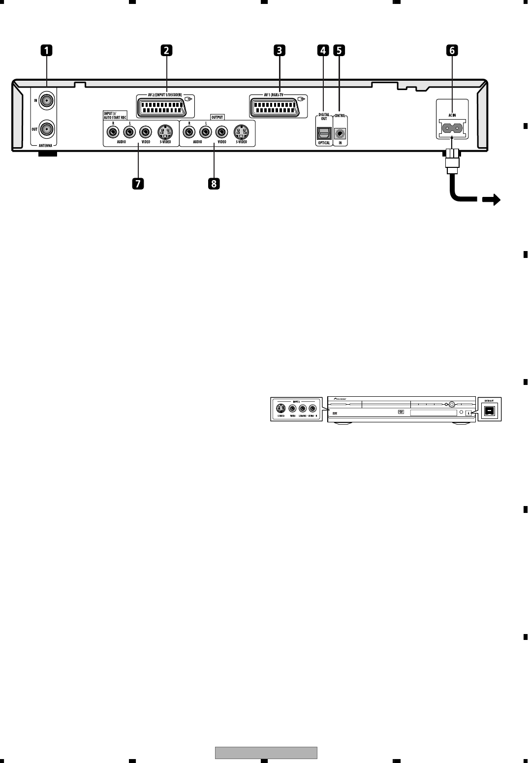
DVR-3100-S 135
5678
5678
C
D
F
A
B
E
8.3 REAR PART
1 ANTENNA IN/OUT
Connect your TV antenna to the ANTENNA IN jack. The
signal is passed through to the ANTENNA OUT jack for
connection to your TV.
2 AV2/(INPUT 1/DECODER) AV connector
Audio/video input SCART-type connector for connecting
to a VCR, or other equipment with a SCART connector.
The input accepts video and S-video.
3 AV1(RGB)-TV AV connector
Audio/video output SCART-type connector for connecting to
a TV or other equipment with a SCART connector. The
video output is switchable between video, S-video and
RGB.
4 DIGITAL OUT OPTICAL
For connecting to an AV receiver, Dolby Digital/DTS/
MPEG decoder or other equipment with optical digital input.
5 CONTROL IN
Use to control this recorder from the remote sensor of
another Pioneer component with a CONTROL OUT
terminal and bearing the Pioneer Î mark. Connect the
CONTROL OUT of the other component to the CONTROL
IN of this recorder using a mini-plug cord.
6 AC IN – Power inlet
7 INPUT 3/AUTO START REC jacks
Audio/video inputs (stereo analog audio; video and S-video)
that you can use to connect to a satellite receiver, TV, VCR
or other source component for recording.
8 OUTPUT jacks
Audio/video outputs (stereo analog audio; video and
S-video) that you can use to connect to a TV, monitor, AV
receiver or other equipment.
Front panel connections
On the left side of the front panel a flip-down cover hides
a second audio/video input, consisting of a video and
S-video jack, and stereo analog audio jacks. (You can also
connect a mono source using just the L(MONO) jack.)
On the right side is the DV input/output i.LINK connector.
This is for connection to a DV camcorder.
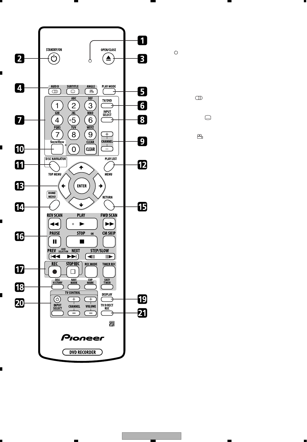
DVR-3100-S
136
1234
1234
C
D
F
A
B
E
8.4 REMOTE CONTROL
1 Remote control indicator
Lights when setting up the remote control for use with a TV
and when setting the remote control mode
2 STANDBY/ON
Press to switch the recorder on/into standby.
30 OPEN/CLOSE
Press to open/close the disc tray.
4 DVD playback functions
AUDIO
Changes the audio language or channel. (When the
recorder is stopped, press to change the tuner audio.)
SUBTITLE
Displays/changes the subtitles included in multilingual
DVD-Video discs.
ANGLE
Switches camera angles on discs with multi-angle
scenes.
5 PLAY MODE
Press to display the Play Mode menu (for features such as
search, repeat and program play).
6 TV/DVD
Press to switch between 'TV mode', in which you get
the picture and sound from the TV's tuner, and 'DVD
mode', in which you get picture and sound from the
recorder's tuner (or an external input).
7 Alphanumeric buttons and CLEAR
Use the number buttons for track/chapter/title selection;
channel selection, and so on. The same buttons can also
be used to enter names for titles, discs and so on.
Use CLEAR to clear an entry and start again.
8 INPUT SELECT
Press to change the input to use for recording.
9 CHANNEL +/–
Press to change the channel of the built-in TV tuner.
10 SHOWVIEW(for WYXU and WY types)
Press, then use the number buttons to enter a ShowView
programming number for timer recording.
VIDEO Plus+(for WVXU type)
Press, then use the number buttons to enter a PlusCode
programming number for timer recording.
11 DISC NAVIGATOR / TOP MENU
Press to display the Disc Navigator screen, or the top menu
if a DVD-Video disc is loaded.
12 PLAY LIST / MENU
Press to switch between Original and Play List content on
VR mode discs, or display the disc menu if a DVD-Video
disc is loaded.

DVR-3100-S 137
5678
5678
C
D
F
A
B
E
13 » / « / | / \ (cursor buttons) and ENTER
Used to navigate all on-screen displays. Press ENTER to
select the currently highlighted option.
14 HOME MENU
Press to go display the Home Menu, from which you can
navigate all the functions of the recoder.
15 RETURN
Press to go back one level in the on-screen menu or
display.
16 Playback controls
1 REV SCAN / FWD SCAN ¡
Press to start reverse or forward scanning. Press again
to change the speed.
3 PLAY
Press to start playback.
8 PAUSE
Press to pause playback or recording.
7 STOP
Press to stop playback.
CM SKIP
Press to skip 30 seconds forward on the disc (about the
length of a typical TV commercial); press repeatedly to
skip up to 4 minutes.
4 PREV / NEXT ¢
Press to skip to the previous or next title / chapter /
track / folder; or to display the previous or next menu
page.
e STEP/SLOW E
During playback, press to start slow-motion playback;
while paused, press to show the previous or next video
frame.
17 Recording controls
¶ REC
Press to start recording. Press repeatedly to set the
recording time in blocks of 30 mins.
& STOP REC
Press to stop recording.
REC MODE
Press repeatedly to change the recording mode (picture
quality).
TIMER REC
Press to set a timer recording from the standard Timer
Recording screen.
EASY TIMER
Press to set a timer recording from the Easy Timer
screen.
18 DISC HISTORY
Press to display summary information (disc name,
recording time left, etc.) from the last 30 recordable
discs loaded.
NAVI MARK
Press to select a thumbnail picture for the current title
for use in the Disc Navigator screen.
CHP MARK
Press to insert a chapter marker when playing/
recording a VR mode DVD-RW disc.
19 DISPLAY
Displays/changes the on-screen information displays.
20 TV CONTROL
After setting up, use these controls to control your TV.
21 TV DIRECT REC
Press to start recording whatever channel your TV is set to.
