RRV3734 001 DVRLX61
User Manual: DVRLX61
Open the PDF directly: View PDF ![]() .
.
Page Count: 192 [warning: Documents this large are best viewed by clicking the View PDF Link!]
- DVR-LX61
- <グラフィック>
- CONTENTS
- CONTENTS
- 1. SERVICE PRECAUTIONS
- 1.1 NOTES ON SOLDERING
- 1.2 NOTES ON HANDLING THE HDD
- 1.3 NOTES ON REPLACEMENT OF THE SDRAM
- 1.4 NOTES ON REPLACEMENT OF THE FL LENS (DVR-LX61 ONLY)
- 2. SPECIFICATIONS
- 2.1 ACCESSORIES
- 2.2 SPECIFICATIONS
- 2.3 DISC/CONTENT FORMAT
- 2.4 PANEL FACILITIES
- 3. BASIC ITEMS FOR SERVICE
- 3.1 CHECK POINTS AFTER SERVICING
- 3.2 QUICK REFERENCE
- 3.3 PCB LOCATIONS
- 3.4 JIGS LIST
- 4. BLOCK DIAGRAM
- 4.1 OVERALL WIRING DIAGRAM
- 4.2 OVERALL BLOCK DIAGRAM
- 4.3 POWER BLOCK DIAGRAM
- 5. DIAGNOSIS
- 5.1 SETUP SEQUENCE
- 5.2 DIAGNOSIS OF THE MAIN ASSY
- 6. SERVICE MODE
- 6.1 VERSION INFORMATION, ETC. (FIRST SCREEN)
- 6.2 ATA/ATAPI DEBUG SCREEN (SECOND SCREEN)
- 6.3 VR-RECORDING-RELATED ERROR LOGS (FOURTH SCREEN)
- 6.4 VR-PLAYBACK-RELATED ERROR LOGS (FIFTH SCREEN)
- 6.5 DV SERVICE MODE
- 6.6 EPG SERVICE MODE
- 6.7 HDMI SERVICE MODE
- 6.8 AGING MODE
- 6.9 USB CHECK MODE
- 6.10 HDD CHECK MODE
- 6.11 DIAGNOSTIC PROCEDURES WHEN AAC DECODING HAS FAILED
- 6.12 DIAGNOSTIC PROCEDURES WHEN CONNECTING THE LAN
- 7. DISASSEMBLY
- 8. EACH SETTING AND ADJUSTMENT
- 8.1 MODEL SETTING
- 8.2 LD POWER ADJUSTMENT
- 8.3 CPRM ID NUMBER AND DATA SETTING
- 8.4 FIRMWARE UPDATE METHOD
- 8.5 GRACENOTE DATABASE UPDATE METHOD
- 8.6 VIDEO ADJUSTMENT FOR SPECIFIC AREA
- 9. EXPLODED VIEWS AND PARTS LIST
- 9.1 PACKING SECTION
- 9.2 EXTERIOR SECTION
- 9.3 FRONT PANEL SECTION (DVR-LX61)
- 9.4 FRONT PANEL SECTION (DVR-560H-S,-K)
- 9.5 SERVICE LOADER MAIN SECTION
- 10. SCHEMATIC DIAGRAM
- 10.1 SERVICE TUSB ASSY (1/4)
- 10.2 SERVICE TUSB ASSY (2/4)
- 10.3 SERVICE TUSB ASSY (3/4)
- 10.4 SERVICE TUSB ASSY (4/4)
- 10.5 SERVICE FLKY ASSY
- 10.6 SERVICE MAIN ASSY (1/5)
- 10.7 SERVICE MAIN ASSY (2/5)
- 10.8 SERVICE MAIN ASSY (3/5)
- 10.9 SERVICE MAIN ASSY (4/5)
- 10.10 SERVICE MAIN ASSY (5/5)
- 10.11 ETAB ASSY (DVR-LX61 ONLY)
- 10.12 SERVICE DVUB ASSY
- 10.13 POWER SUPPLY ASSY
- 10.14 WAVEFORMS
- 11. PCB CONNECTION DIAGRAM
- 11.1 SERVICE FRJB ASSY
- 11.2 SERVICE TUSB ASSY
- 11.3 SERVICE FLKY ASSY
- 11.4 SERVICE MAIN ASSY
- 11.5 ETAB ASSY (DVR-LX61 ONLY)
- 11.6 SERVICE DVUB ASSY
- 11.7 POWER SUPPLY ASSY
- 12. PCB PARTS LIST
- RRV3760

ORDER NO.
PIONEER CORPORATION 4-1, Meguro 1-chome, Meguro-ku, Tokyo 153-8654, Japan
PIONEER ELECTRONICS (USA) INC. P.O. Box 1760, Long Beach, CA 90801-1760, U.S.A.
PIONEER EUROPE NV Haven 1087, Keetberglaan 1, 9120 Melsele, Belgium
PIONEER ELECTRONICS ASIACENTRE PTE. LTD. 253 Alexandra Road, #04-01, Singapore 159936
PIONEER CORPORATION
2008
2008 Printed in Japan
DVR-LX61
RRV3734
HDD/DVD RECORDER
DVR-LX61
DVR-560H-S
DVR-560H-K
THIS MANUAL IS APPLICABLE TO THE FOLLOWING MODEL(S) AND TYPE(S).
Model Type Power Requirement Region No.
Serial No.
Please Confirm 3rd & 4th
alphabetical letters.
DVR-LX61 WYXK5 AC 220 V to 240 V 2 &&UK######$$
DVR-LX61 WYXV5 AC 220 V to 240 V 2 &&DL######$$
DVR-560H-S WYXK5 AC 220 V to 240 V 2 &&UK######$$
DVR-560H-S WYXV5 AC 220 V to 240 V 2 &&DL######$$
DVR-560H-K WYXK5 AC 220 V to 240 V 2 &&UK######$$
DVR-560H-K WYXV5 AC 220 V to 240 V 2 &&DL######$$
For details, refer to "Important Check Points for good servicing".
T-IZA-001 APR.
2DVR-LX61
12 3 4
A
B
C
D
E
F
12 3 4
SAFETY INFORMATION
LABEL CHECK
WARNING!
The laser component is capable of emitting radiation exceeding
the limit for CLASS 1. A specially instructed person should do
servicing operation of the apparatus.
Laser Pickup specifications and
Laser characteristics
For CD
Wave length : 785 nm
Operating output :
Read mode : 1.07 mW (CW), Class1
Maximum output : Class1M
For DVD
Wave length : 660 nm
Operating output :
Read mode : 1.08 mW, Class1
Write mode : 21.89 mW (Pulse), Class1M
Maximum output : Class2M
CLAMP signals for detecting the loading state are detected
by the drive CPUs, and the design prevents laser diode
oscillation when the CLAMP signal turns OFF.
In normal operation, if no disc is clamped, the laser diode
oscillation is disabled.
However, the interlock does not always operate in the
"LD Degration Judgment of ATA/ATAPI DEBUG OSD"
and "LD POWER ADJUSTMENT"*.
2. When the cover is opened, close viewing of the objective
lens with the naked eye will cause exposure to a Class 3A
laser beam.
* Refer to Pages 51 and 86.
Additional Laser Caution
1. The ON/OFF(ON:low level,OFF:high level) status of the
VRW2262
STANDBY/ON
REC
u
1

3
DVR-LX61
56 7 8
56 7 8
A
B
C
D
E
F
[Important Check Points for Good Servicing]
In this manual, procedures that must be performed during repairs are marked with the below symbol.
Please be sure to confirm and follow these procedures.
1. Product safety
Please conform to product regulations (such as safety and radiation regulations), and maintain a safe servicing environment by
following the safety instructions described in this manual.
1 Use specified parts for repair.
Use genuine parts. Be sure to use important parts for safety.
2 Do not perform modifications without proper instructions.
Please follow the specified safety methods when modification(addition/change of parts) is required due to interferences such as
radio/TV interference and foreign noise.
3 Make sure the soldering of repaired locations is properly performed.
When you solder while repairing, please be sure that there are no cold solder and other debris.
Soldering should be finished with the proper quantity. (Refer to the example)
4 Make sure the screws are tightly fastened.
Please be sure that all screws are fastened, and that there are no loose screws.
5 Make sure each connectors are correctly inserted.
Please be sure that all connectors are inserted, and that there are no imperfect insertion.
6 Make sure the wiring cables are set to their original state.
Please replace the wiring and cables to the original state after repairs.
In addition, be sure that there are no pinched wires, etc.
7 Make sure screws and soldering scraps do not remain inside the product.
Please check that neither solder debris nor screws remain inside the product.
8 There should be no semi-broken wires, scratches, melting, etc. on the coating of the power cord.
Damaged power cords may lead to fire accidents, so please be sure that there are no damages.
If you find a damaged power cord, please exchange it with a suitable one.
9 There should be no spark traces or similar marks on the power plug.
When spark traces or similar marks are found on the power supply plug, please check the connection and advise on secure
connections and suitable usage. Please exchange the power cord if necessary.
a Safe environment should be secured during servicing.
When you perform repairs, please pay attention to static electricity, furniture, household articles, etc. in order to prevent injuries.
Please pay attention to your surroundings and repair safely.
2. Adjustments
To keep the original performance of the products, optimum adjustments and confirmation of characteristics within specification.
Adjustments should be performed in accordance with the procedures/instructions described in this manual.
4. Cleaning
For parts that require cleaning, such as optical pickups, tape deck heads, lenses and mirrors used in projection monitors, proper
cleaning should be performed to restore their performances.
3. Lubricants, Glues, and Replacement parts
Use grease and adhesives that are equal to the specified substance.
Make sure the proper amount is applied.
5. Shipping mode and Shipping screws
To protect products from damages or failures during transit, the shipping mode should be set or the shipping screws should be
installed before shipment. Please be sure to follow this method especially if it is specified in this manual.

4DVR-LX61
12 3 4
A
B
C
D
E
F
12 3 4
CONTENTS
SAFETY INFORMATION..........................................................................................................................................................2
1. SERVICE PRECAUTIONS ....................................................................................................................................................6
1.1 NOTES ON SOLDERING ...............................................................................................................................................6
1.2 NOTES ON HANDLING THE HDD.................................................................................................................................7
1.3 NOTES ON REPLACEMENT OF THE SDRAM .............................................................................................................9
1.4 NOTES ON REPLACEMENT OF THE FL LENS (DVR-LX61 ONLY) ...........................................................................10
2. SPECIFICATIONS ...............................................................................................................................................................11
2.1 ACCESSORIES ............................................................................................................................................................11
2.2 SPECIFICATIONS.........................................................................................................................................................12
2.3 DISC/CONTENT FORMAT ...........................................................................................................................................17
2.4 PANEL FACILITIES.......................................................................................................................................................22
3. BASIC ITEMS FOR SERVICE.............................................................................................................................................28
3.1 CHECK POINTS AFTER SERVICING..........................................................................................................................28
3.2 QUICK REFERENCE....................................................................................................................................................30
3.3 PCB LOCATIONS .........................................................................................................................................................31
3.4 JIGS LIST .....................................................................................................................................................................32
4. BLOCK DIAGRAM...............................................................................................................................................................34
4.1 OVERALL WIRING DIAGRAM......................................................................................................................................34
4.2 OVERALL BLOCK DIAGRAM.......................................................................................................................................36
4.3 POWER BLOCK DIAGRAM..........................................................................................................................................38
5. DIAGNOSIS.........................................................................................................................................................................39
5.1 SETUP SEQUENCE .....................................................................................................................................................39
5.2 DIAGNOSIS OF THE MAIN ASSY ...............................................................................................................................40
6. SERVICE MODE .................................................................................................................................................................44
6.1 VERSION INFORMATION, ETC. (FIRST SCREEN) ....................................................................................................45
6.2 ATA/ATAPI DEBUG SCREEN (SECOND SCREEN).....................................................................................................50
6.3 VR-RECORDING-RELATED ERROR LOGS (FOURTH SCREEN) .............................................................................52
6.4 VR-PLAYBACK-RELATED ERROR LOGS (FIFTH SCREEN)......................................................................................57
6.5 DV SERVICE MODE .....................................................................................................................................................60
6.6 EPG SERVICE MODE ..................................................................................................................................................63
6.7 HDMI SERVICE MODE ................................................................................................................................................65
6.8 AGING MODE...............................................................................................................................................................67
6.9 USB CHECK MODE .....................................................................................................................................................69
6.10 HDD CHECK MODE ...................................................................................................................................................70
6.11 DIAGNOSTIC PROCEDURES WHEN AAC DECODING HAS FAILED .....................................................................76
6.12 DIAGNOSTIC PROCEDURES WHEN CONNECTING THE LAN ..............................................................................79
7. DISASSEMBLY....................................................................................................................................................................80
8. EACH SETTING AND ADJUSTMENT ................................................................................................................................85
8.1 MODEL SETTING.........................................................................................................................................................85
8.2 LD POWER ADJUSTMENT..........................................................................................................................................86
8.3 CPRM ID NUMBER AND DATA SETTING....................................................................................................................90
8.4 FIRMWARE UPDATE METHOD ...................................................................................................................................94
8.5 GRACENOTE DATABASE UPDATE METHOD.............................................................................................................97
8.6 VIDEO ADJUSTMENT FOR SPECIFIC AREA.............................................................................................................99
9. EXPLODED VIEWS AND PARTS LIST.............................................................................................................................104
9.1 PACKING SECTION ...................................................................................................................................................104
9.2 EXTERIOR SECTION.................................................................................................................................................106
9.3 FRONT PANEL SECTION (DVR-LX61) ......................................................................................................................110
9.4 FRONT PANEL SECTION (DVR-560H-S,-K)..............................................................................................................112
9.5 SERVICE LOADER MAIN SECTION..........................................................................................................................114

5
DVR-LX61
56 7 8
56 7 8
A
B
C
D
E
F
10. SCHEMATIC DIAGRAM.................................................................................................................................................. 116
10.1 SERVICE TUSB ASSY (1/4)..................................................................................................................................... 116
10.2 SERVICE TUSB ASSY (2/4)..................................................................................................................................... 118
10.3 SERVICE TUSB ASSY (3/4)..................................................................................................................................... 120
10.4 SERVICE TUSB ASSY (4/4)..................................................................................................................................... 122
10.5 SERVICE FLKY ASSY.............................................................................................................................................. 124
10.6 SERVICE MAIN ASSY (1/5) ..................................................................................................................................... 126
10.7 SERVICE MAIN ASSY (2/5) ..................................................................................................................................... 128
10.8 SERVICE MAIN ASSY (3/5) ..................................................................................................................................... 130
10.9 SERVICE MAIN ASSY (4/5) ..................................................................................................................................... 132
10.10 SERVICE MAIN ASSY (5/5) ................................................................................................................................... 134
10.11 ETAB ASSY (DVR-LX61 ONLY).............................................................................................................................. 136
10.12 SERVICE DVUB ASSY........................................................................................................................................... 138
10.13 POWER SUPPLY ASSY ......................................................................................................................................... 140
10.14 WAVEFORMS......................................................................................................................................................... 142
11. PCB CONNECTION DIAGRAM ...................................................................................................................................... 147
11.1 SERVICE FRJB ASSY.............................................................................................................................................. 147
11.2 SERVICE TUSB ASSY ............................................................................................................................................. 148
11.3 SERVICE FLKY ASSY.............................................................................................................................................. 152
11.4 SERVICE MAIN ASSY.............................................................................................................................................. 154
11.5 ETAB ASSY (DVR-LX61 ONLY)................................................................................................................................ 158
11.6 SERVICE DVUB ASSY............................................................................................................................................. 159
11.7 POWER SUPPLY ASSY ........................................................................................................................................... 160
12. PCB PARTS LIST............................................................................................................................................................ 162

6DVR-LX61
12 3 4
A
B
C
D
E
F
12 3 4
1. SERVICE PRECAUTIONS
1.1 NOTES ON SOLDERING
When servicing this model, some service procedures may reset the customer settings
to the factory default settings. Make sure to explain this to the customer.
An HDD (Hard Disc Drive) is mounted in this product.
When an HDD becomes defective and inoperable, restoration of the user's data recorded on the HDD,
or copying of the user's recorded data to other media (such as a new HDD) is totally impossible.
Before servicing, OBTAIN THE USER'S PRIOR CONSENT to that effect.
The user must be made aware that all recorded data are deleted if the HDD is intialized.
• For environmental protection, lead-free solder is used on the printed circuit boards mounted in this unit.
Be sure to use lead-free solder and a soldering iron that can meet specifications for use with lead-free solders for repairs
accompanied by reworking of soldering.
• Compared with conventional eutectic solders, lead-free solders have higher melting points, by approximately 40 °C.
Therefore, for lead-free soldering, the tip temperature of a soldering iron must be set to around 373 °C in general, although
the temperature depends on the heat capacity of the PC board on which reworking is required and the weight of the tip of
the soldering iron.
Do NOT use a soldering iron whose tip temperature cannot be controlled.
Compared with eutectic solders, lead-free solders have higher bond strengths but slower wetting times and higher melting
temperatures (hard to melt/easy to harden).
The following lead-free solders are available as service parts:
• Parts numbers of lead-free solder:
GYP1006 1.0 in dia.
GYP1007 0.6 in dia.
GYP1008 0.3 in dia.

7
DVR-LX61
56 7 8
56 7 8
A
B
C
D
E
F
1.2 NOTES ON HANDLING THE HDD
Reference: Main specifications on damage to the HDD
The HDD is about 10 times as sensitive to shock
during operation than during nonoperation.
During operation During noperation
Shock G
(acceleration) <approx. 20 G <approx. 200 G
Temperature
change < 20ºC/hour
Moisture change < 20%/hour
0.5 inch / 12.7 mm 387 217 200 26
1.0 inch / 25.4 mm 595 457 310 37
2.0 inch / 50.8 mm 1133 600 680 70
4.0 inch / 101.6 mm 1795 1040 1050 267
Reference: Estimate value of falling distance vs. shock (G)
when the HDD is dropped without protection
Landing
surface
Falling
distance
Granite
surface
Concrete
floor
Synthetic-resin-
coated table Antistatic
sponge
[1] Cautions on Handling the HDD
• The HDD is very sensitive to shocks and vibrations. Care must be taken especially during operation (when the power is on).
• The HDD is very sensitive to electrostatic charges.
• Rapid change in temperature or humidity may cause deterioration of the HDD.
Note: After receiving damage caused by any above-mentioned factors, the HDD may operate normally for dozens or some
hundreds of hours but then suddenly crash. If you are certain you have damaged a new repair part (HDD) while making
repairs, do not use the part.
[2] Cautions on handling the product on which the HDD is mounted or the HDD
as a repair part, and examples of dangerous handling
[Cautions on handling the product on which the HDD is mounted]
• While the unit is turned on, the HDD is always in operation. Be sure NOT to impart shock to the unit.
Examples of dangerous handling: while the power is on
• Bumping on the bonnet
• Dropping an object, such as a small screwdriver or remote control unit, onto the bonnet, or bumping an object against the
cabinet
• Moving the unit by dragging
• Stacking another product on the unit
Note: Be sure NOT to impart shock, such as bumping or hitting a screwdriver against the HDD, during diagnosis with the
bonnet open.
Examples of dangerous handling: while the power is off
• Imparting strong shock, although the HDD is more resistant to shock when the power is off
• Dropping the unit from a height of several centimeters, or after lifting one side of the unit up, then letting the unit drop.
• Do NOT move the unit immediately after the power is turned off. Wait at least 30 seconds after the indication on the FL
display changed from POWER OFF to the clock indication before moving the unit. If the AC power cord is accidentally
disconnected before turning the unit off, wait at least for one minute before moving it. In this case, damage to the HDD
caused by sudden shutoff may be small, because the emergency relief mechanism is activated. However, if sudden shutoff
occurrs during recording or playback, recorded data may be damaged. Be sure to check operations.
[Cautions on handling the HDD as a repair part]
1. Handle the HDD in a safe environment:
• Handle the HDD over an antistatic pad that can also absorb shock.
• Wear wrist bands to prevent electrostatic charges generated in your body from affecting the HDD.
2. The following must be observed when handling the HDD:
• Handle one HDD at a time. Do NOT hold several HDDs at the same time.
• Grip the HDD on both sides so that you do not touch its terminals or circuit boards.
• Do NOT stack one HDD onto another HDD (even if the HDDs are protected in antistatic bags).
• Do NOT bump the HDDs against one another.
• Do NOT bump any tool, such as a screwdriver, or other hard object against the HDD.
• When a repair part (HDD) is transported and there is a large temperature difference between outdoors and indoors, to the
indoor, leave it in its package for about a half day to gradually cool or warm the HDD to room temperature before unpacking it.
[Notes on packing for shipment]
• When returning a defective HDD for analysis, handle with care as if it were a good product. Otherwise, the results of analysis
may not be correct.
• When packing, use the antistatic bag and packing materials in which the repair part for service was delivered. Attach a copy
of the slip for service or a memo stating symptoms in as much detail as possible.
8DVR-LX61
12 3 4
A
B
C
D
E
F
12 3 4
ST3250820SCE250GBDVR-LX61 VXF1131
DVR-560H-S
DVR-560H-K ST3160215SCE160GB VXF1152
Capacity
SEAGATE
Model
Name Pioneer's
Part No.
(for service)
Manufacture's
Part No.
Capacity
Manufacturer's
part No.
Date of
Manufacturer
Seagate(160GB) Seagate(250GB)
[3] Outline and part No. of the HDDs *Pioneer's part No. is not stamped.
• When replacing the HDD, carefully check the capacity and manufacturer's part No. on the part label to avoid replacing with
a similar but inappropriate product. You can also check the model No. of the mounted HDD on the Service mode screen.
• Do NOT use repair parts, such as commercially available HDDs, other than those designated above, as their functions,
performance or reliability cannot be guaranteed.

9
DVR-LX61
56 7 8
56 7 8
A
B
C
D
E
F
1.3 NOTES ON REPLACEMENT OF THE SDRAM
Note when replacing the SDRAM
When replacement of the SDRAM (IC1201 or IC1221) on the MAIN Assy is required, identify the manufacturer of the SDRAM.
If the SDRAM that needs replacement was manufactured by ELPIDA, both IC1201 and IC1221 must be replaced at the same
time.
SDRAMs for service are manufactured by SAMSUNG.
How to identify the manufacturer
Confirm the name of the manufacturer stamped on the surface of the part.
Measures to be taken
1. If the SDRAM that needs replacement was manufactured by ELPIDA:
Replace both IC1201 and IC1221 at the same time.
2. If the SDRAM that needs replacement was manufactured by SAMSUNG:
Replacement of only the defective SDRAM (IC1201 or IC1221) is possible.
Possible malfunctions
If SDRAMs made by different manufacturers are mounted on the MAIN Assy, the following malfunctions may occur:
1. The power does not come on.
2. High-speed dubbing disabled
3. Other malfunctions related to the SDRAM
By ELPIDA (replacement of both SDRAMs required) By SAMSUNG (replacement of only the defective SDRAM possible)

10 DVR-LX61
12 3 4
A
B
C
D
E
F
12 3 4
1.4 NOTES ON REPLACEMENT OF THE FL LENS (DVR-LX61 ONLY)
Panel Frame
FL Lens
OPEN/CLOSE Key
The Panel Frame, FL Lens, and FL Filter are attached to the chassis with two-sided (double-back) tape.
If one of these parts has to be replaced, replace all three parts at the same time.
To replace the FL Lens, follow the procedures described below:
Procedures for replacement of the FL Lens
1. Lightly attach the FL Lens so that the two projections on the upper side of the panel touch the Panel Frame and that
the clearances between the OPEN/CLOSE key and the cutout for that key on the FL Lens will be the same on the
left and right sides.
2. After confirming that the FL Lens is properly aligned, strongly push the black part of the FL Lens to firmly attach it.
Be careful not to press the OPEN/CLOSE key while attaching the FL Lens.

11
DVR-LX61
56 7 8
56 7 8
A
B
C
D
E
F
2. SPECIFICATIONS
2.1 ACCESSORIES
• Remote control ×1
(VXX3286 : DVR-LX61)
(VXX3287 : DVR-560H-S)
(VXX3293 : DVR-560H-K)
• RF antenna cable(PAL) ×1
(VDE1075 : WYXK5 type)
(VDE1095 : WYXV5 type)
• Dry cell batteries ×2
(AA/R6P)
• Power cable ×1
(ADG1127 )
• Audio / Video cable(1.5m) ×1
(red/white/yellow)
(VDE1077)
• G-Link™ Cable (3m) ×1
(VDX1010)
• Operating Instructions (French)
(VRC1493 : DVR-LX61/WYXK5)
(VRC1460 : DVR-LX61/WYXV5)
(VRC1484 : DVR-560H-S,-K/WYXK5)
(VRC1459 : DVR-560H-S,-K/WYXV5)
• Operating Instructions (German)
(VRC1486 : DVR-LX61/WYXK5)
(VRC1465 : DVR-LX61/WYXV5)
(VRC1485 : DVR-560H-S,-K/WYXK5)
(VRC1464 : DVR-560H-S,-K/WYXV5)
• Operating Instructions (Italian)
(VRC1488 : DVR-LX61/WYXK5)
(VRC1482 : DVR-LX61/WYXV5)
(VRC1487 : DVR-560H-S,-K/WYXK5)
(VRC1468 : DVR-560H-S,-K/WYXV5)
• Operating Instructions (Dutch)
(VRC1490 : DVR-LX61/WYXK5)
(VRC1472 : DVR-LX61/WYXV5)
(VRC1489 : DVR-560H-S,-K/WYXK5)
(VRC1471 : DVR-560H-S,-K/WYXV5)
• Operating Instructions (Spanish)
(VRC1492 : DVR-LX61/WYXK5)
(VRC1476 : DVR-LX61/WYXV5)
(VRC1491 : DVR-560H-S,-K /WYXK5)
(VRC1475 : DVR-560H-S,-K/WYXV5)
• Warranty Card
12 DVR-LX61
12 3 4
A
B
C
D
E
F
12 3 4
2.2 SPECIFICATIONS
[1] For DVR-LX61

13
DVR-LX61
56 7 8
56 7 8
A
B
C
D
E
F

14 DVR-LX61
12 3 4
A
B
C
D
E
F
12 3 4
[2] For DVR-560H-S,-K
15
DVR-LX61
56 7 8
56 7 8
A
B
C
D
E
F
16 DVR-LX61
12 3 4
A
B
C
D
E
F
12 3 4
17
DVR-LX61
56 7 8
56 7 8
A
B
C
D
E
F
2.3 DISC/CONTENT FORMAT
18 DVR-LX61
12 3 4
A
B
C
D
E
F
12 3 4

19
DVR-LX61
56 7 8
56 7 8
A
B
C
D
E
F

20 DVR-LX61
12 3 4
A
B
C
D
E
F
12 3 4
21
DVR-LX61
56 7 8
56 7 8
A
B
C
D
E
F
22 DVR-LX61
12 3 4
A
B
C
D
E
F
12 3 4
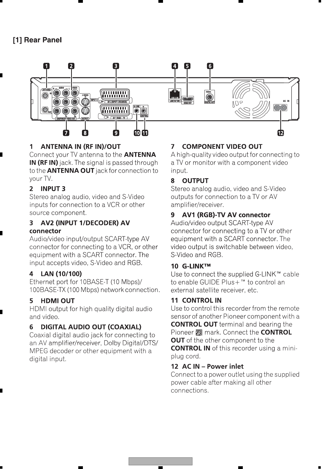
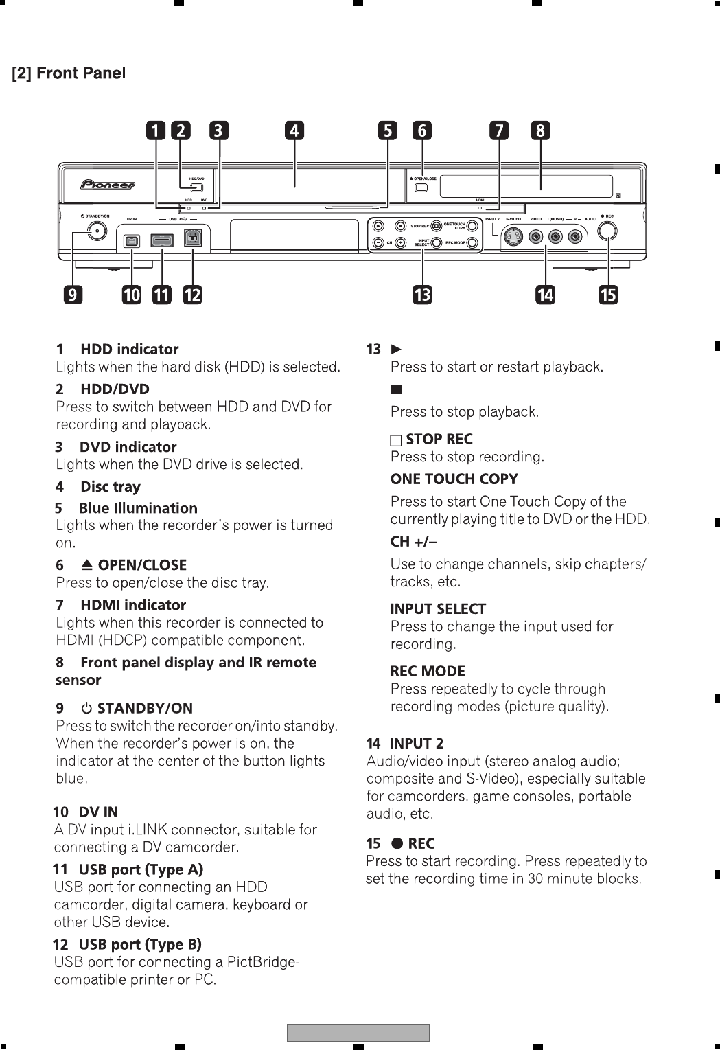
2.4 PANEL FACILITIES
(DVR-LX61 Only)
23
DVR-LX61
56 7 8
56 7 8
A
B
C
D
E
F
(for DVR-LX61)

24 DVR-LX61
12 3 4
A
B
C
D
E
F
12 3 4
[3] Front Panel (for DVR-560H-S,-K)

25
DVR-LX61
56 7 8
56 7 8
A
B
C
D
E
F
[4] Display
26 DVR-LX61
12 3 4
A
B
C
D
E
F
12 3 4
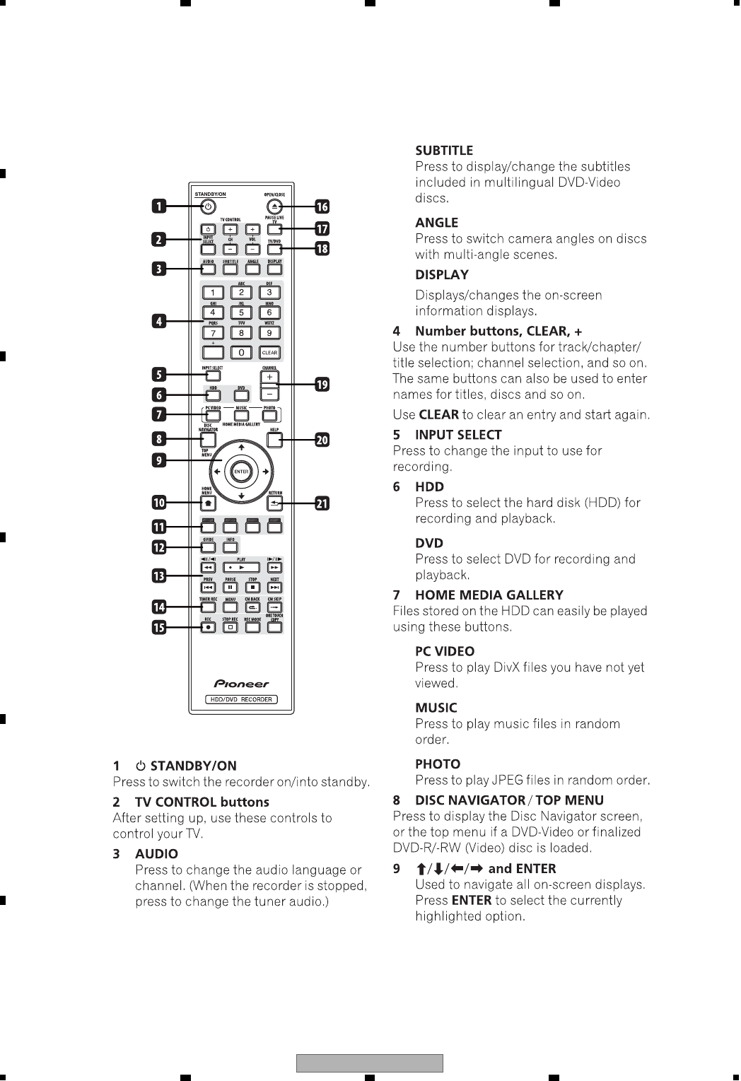
[5] Remote Control Unit

27
DVR-LX61
56 7 8
56 7 8
A
B
C
D
E
F
28 DVR-LX61
12 3 4
A
B
C
D
E
F
12 3 4
3. BASIC ITEMS FOR SERVICE
3.1 CHECK POINTS AFTER SERVICING
Before shipping out the product, be sure to clean the following positions by using the prescribed cleaning tools:
Position to be cleaned Cleaning tools
Pickup lenses Cleaning liquid : GEM1004
Cleaning paper : GED-008
Position to be cleaned Cleaning tools
Fans Cleaning paper : GED-008
29
DVR-LX61
56 7 8
56 7 8
A
B
C
D
E
F
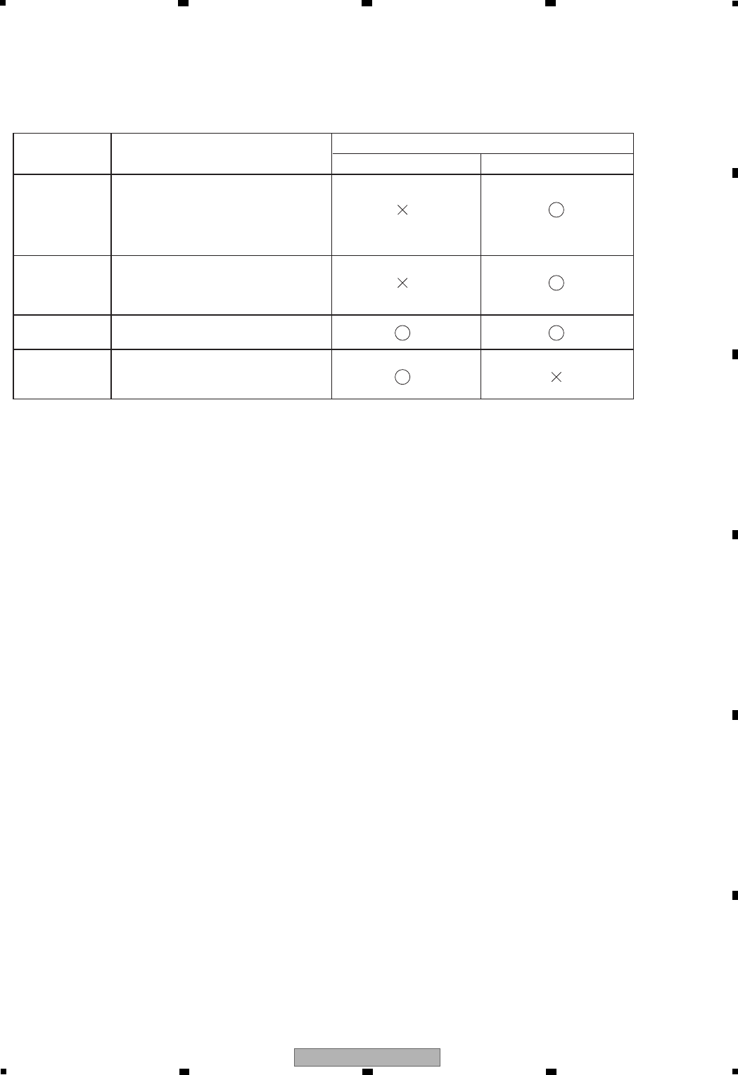
MAIN ASSY
1. Model setting
2. LD power adjustment
3. CPRM setting
4. Firmware update
Replaced ASSY
Necessary settingState after replacing
User settingHDD contents
[2] Necessary Procedure List When Replacing Assys
Following is the surely necessary procedures and the product state after changing, when replacing next ASSYs.
1. Model setting
2. CPRM setting
3. Firmware update
1. LD power adjustment
1. CPRM setting
2.Gracenote Database update
TUSB ASSY
HDD
LOADER ASSY

30 DVR-LX61
12 3 4
A
B
C
D
E
F
12 3 4
3.2 QUICK REFERENCE
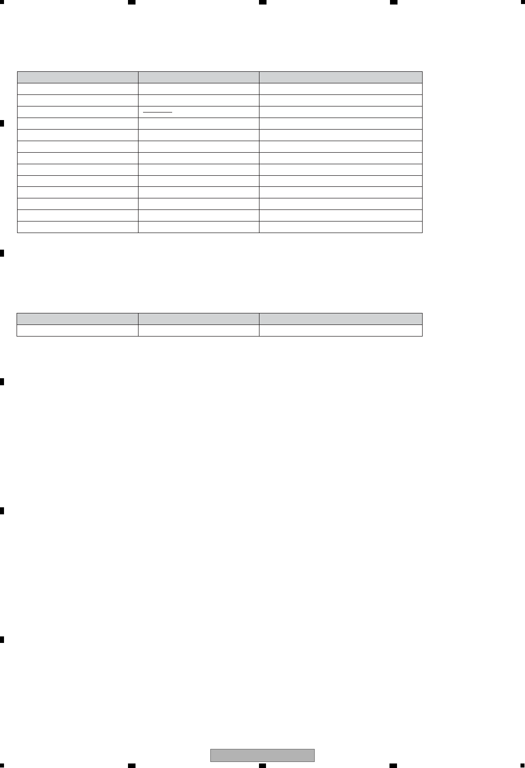
Description of work Procedure Jigs
LD power adjustment [ESC]+[CX]+[1]+[0] GGF1381 : Service Remote Control Unit
GGV1054 : CD-ROM (CDT-313)
GGV1036 : DVD-ROM DL (DVDT-002)
GGV1278 : Blank DVD-R (That's DR-C12WTY5PA)
GGV1282 : Blank DVD-RW (JVC VD-W120XH5)
GGV1284 : Blank DVD-RAM (maxell DRM120C.1P5S)
ID input [ESC]+[STEREO] GGF1381 : Service Remote Control Unit
GGV1321 : ID disc
Firmware update [REC STOP]+[PLAY] Update disc
Version check [ESC]+[DISP] GGF1381 : Service Remote Control Unit
Error Rate Measurement [ESC]+[DISP]+[DIG/ANA] × twice GGF1381 : Service Remote Control Unit
Operation check disc (See remarks)
HDD Check Mode [ESC]+[CX]+[0]+[1] GGF1381 : Service Remote Control Unit
Indication of VR-playback-related
error log [ESC]+[DISP]+[5]+[DIG/ANA] GGF1381 : Service Remote Control Unit
Indication of VR-recording-related
error log [ESC]+[DISP]+[4]+[DIG/ANA] × 3times GGF1381 : Service Remote Control Unit
Remarks
Disc for check of
recording/playback operations
Operation check discs
(manufacturers and model numbers) Error rate threshold
(Note) GGV1278 : Blank DVD-R
(That's DR-C12WTY5PA) 3.3e-3 or below
When judging the drive quality,
make sure to use the operation
check disc.
GGV1279 : Blank DVD-R DL
(MCM VHR21YD1)
L0 : 3.3e-3 or below
L1 : 3.3e-3 or below
GGV1280 : Blank DVD+R
(That's DR+120TY5PA) 3.3e-3 or below
GGV1281 : Blank DVD+R DL
(MCM VTR21N1)
L0 : 3.3e-3 or below
L1 : 3.3e-3 or below
GGV1189 : Blank DVD-RW
(JVC VD-W120N10) 3.3e-3 or below
GGV1282 : Blank DVD-RW [RW2]
(JVC VD-W120XH5) 3.3e-3 or below
GGV1283 : Blank DVD+RW
(RICOH D4RWV-S3CW)3.3e-3 or below
GGV1284 : Blank DVD-RAM
(maxell DRM120C.1P5S) 3.3e-3 or below
GGV1036 : DVD-ROM DL
(DVDT-002) L0/L1 : 8.0e-4 or below
How to read error rate X.Xe-Y
Y: The bigger the better,
X X: The smaller the better
How to exit from Service Mode [ESC]

31
DVR-LX61
56 7 8
56 7 8
A
B
C
D
E
F
3.3 PCB LOCATIONS
• For DVR-LX61 model
1..ETAB ASSY VWV2344
NSP 1..TUJB ASSY YWM1002
2..SERVICE DVUB ASSY YXX1001
2..SERVICE TUSB ASSY YXX1003
NSP 1..FLKB ASSY YWM1006
2..SERVICE FRJB ASSY YXX1027
2..SERVICE FLKY ASSY YXX1008
NSP 1..SERVICE LOADER MAIN VXU1014
2..SERVICE MAIN ASSY VXX3309
> 1..POWER SUPPLY ASSY VWR1406
1..HDD VXF1131
• For DVR-560H model
NSP 1..TUJB ASSY YWM1002
2..SERVICE DVUB ASSY YXX1001
2..SERVICE TUSB ASSY YXX1003
NSP 1..FLKB ASSY YWM1005
2..SERVICE FRJB ASSY YXX1004
2..SERVICE FLKY ASSY YXX1007
NSP 1..SERVICE LOADER MAIN VXU1013
2..SERVICE MAIN ASSY VXX3308
> 1..POWER SUPPLY ASSY VWR1406
1..HDD VXF1152
Mark No. Description Part No. Mark No. Description Part No.
LIST OF ASSEMBLIES
NOTES:
-
Parts marked by “NSP” are generally unavailable because they are not in our Master Spare Parts List.
-
The > mark found on some component parts indicates the importance of the safety factor of the part.
Therefore, when replacing, be sure to use parts of identical designation.
FLKY ASSY KEYB ASSY
BSERVICE FLKY ASSY
EETAB ASSY
DVR-LX61 ONLY
ASERVICE TUSB ASSY
HDD
CSERVICE FRJB ASSYSERVICE LOADER ASSY
F
SERVICE DVUB ASSY
G
POWER SUPPLY
ASSY
D
SERVICE MAIN ASSY
32 DVR-LX61
12 3 4
A
B
C
D
E
F
12 3 4
3.4 JIGS LIST
Service Remote Control Unit GGF1381
DVD Test Disc (DVD-Video)
(*)
Adjustment, diagnosis
Name Jig No. Remarks
Check of DVD-Video
DVD Recorder Data Disc
Typ e 2
GGV1025
Diagnosis (ID data setting)
FFC Cable (40p) GGD1436 Diagnosis of MAIN Assy
CD-ROM GGV1054
DVD-ROM DL GGV1036
LD Power Adjustment
LD Power Adjustment
Blank DVD-R GGV1278LD Power Adjustment
Blank DVD-RAM GGV1284 LD Power Adjustment
[1] Jigs List
Blank DVD-RWGGV1282 LD Power Adjustment
Disc Ejection Rod GGF1529 Emergency Disc Ejection
USB Cable GGD1445 USB Check Mode
RS-232C I/F Jig GGF1348Serial Update
FFC Cable (7P) VDA1681Serial Update
(*) Be sure to use the latest disc (Type 2).
In Apr, 2008, the latest disc is GGV1321.
Hanarl GEM1041
Name Lubricants and Glues No. Remarks
refer to "9.3 FRONT PANEL SECTION"
[2] Lubricants and Glues List

33
DVR-LX61
56 7 8
56 7 8
A
B
C
D
E
F

34 DVR-LX61
12 3 4
A
B
C
D
E
F
12 3 4
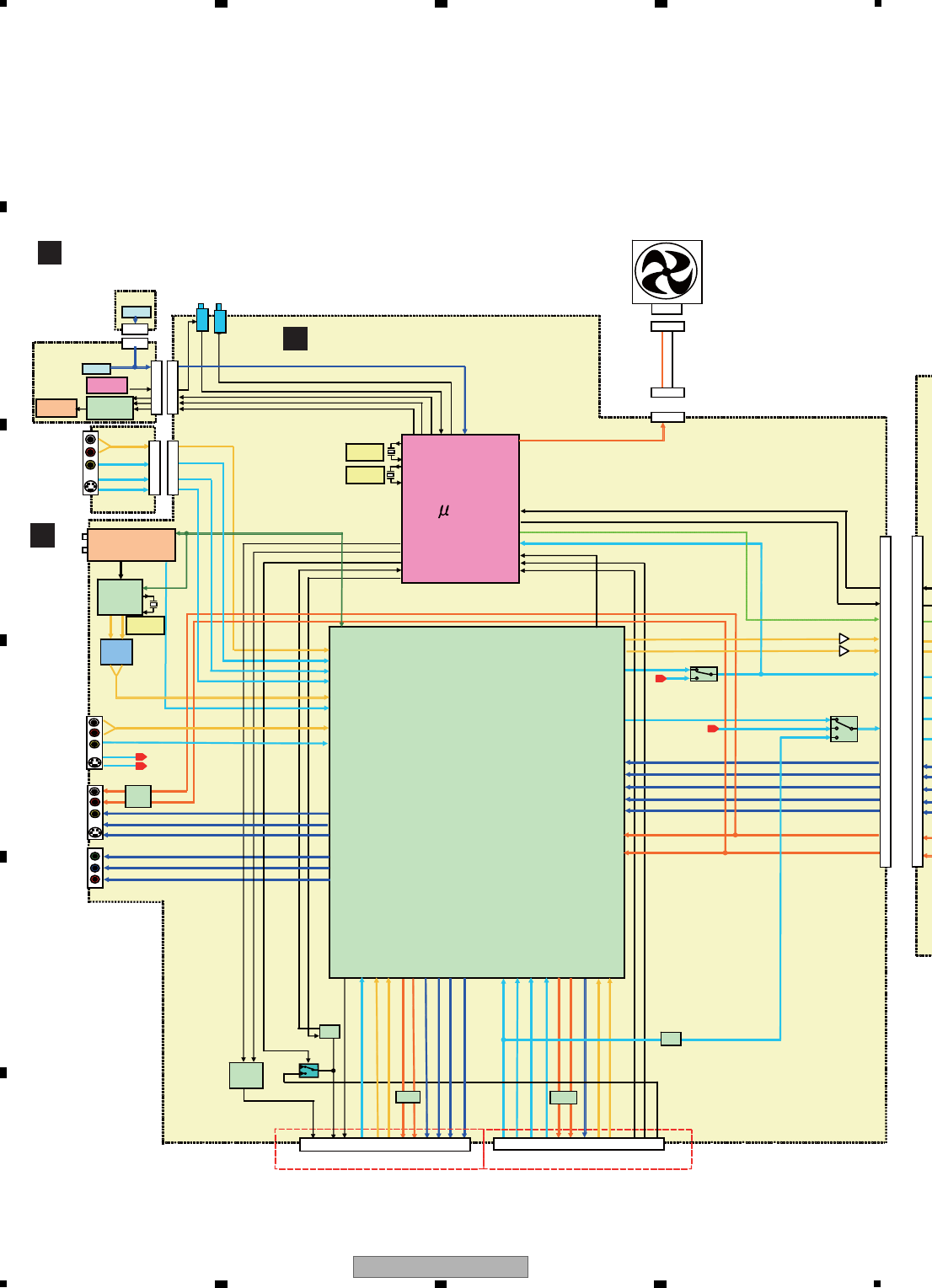
4. BLOCK DIAGRAM
4.1 OVERALL WIRING DIAGRAM
LPS2
GNDD
BLACK
LPS1
RED
ST1+
ST2+
ST2-
ST1-
VA5V
GNDA
SW1
S4
S3
S2
S1
RF-
HU-
VCC
HU+
HV-
HW+
HV+
HW-
HB
U
W
V
GNDD
TPAN
GND
TPAP
GND
TPBP
TPBN
USBDP1
V+5USB
USBDM1
USBVFB
USBDM2
USBDP2
GND
GND
GND
GND
SW2
VA5V
VREFPD
FMO+
M1
RF+
M2
M3
M4
DVD/CD
GNDA
FMO-
GND0
HFGAIN
GND0
V05V
V05V
OSCNT
W2EN-
W3EN+
W2EN+
W1EN-
W1EN+
W3EN-
OSCEN+
LDDEN
OSCEN-
VPP
TEMP
RSET
RESET
VD3V
W2SET
W1SET
W3SET
SEN
SCLK
SDIO
TR
FR
TD
FD
V+12M
GNDD
GNDM
V+12V
GNDD
GND
V+5M
RXN
RXP
GND
GNDD
GND
GND
SW+5V
GND
TXN
TXP
GND
SW+12V
54132
54 123
4
1
4
1
3
2
3
2
8
7
1
2
3
4
5
6
7
4
1
8
2
3
5
6
1210 11897
12 1011 9 78
563421
562341
2
13
64
5
1
2
3
64
5
1
2
3
4
5
6
7
10 8
9
1
2
3
4
5
6
7
108
9
40
39
33
34
37
30
31
38
35
36
32
9
14
12
10
15
11
16
13
17
9
10
14
16
13
15
12
11
17
18
19
20
22
21
23
25
24
26
23
21
26
18
20
25
24
22
19
27
29
28
30
32
31
33
34
35
30
28
32
31
35
27
29
33
34
41
42
44
40
38
39
43
36
37
43
44
41
38
39
40
36
37
42
45
46
50
47
49
48
45
47
46
50
49
48
43
45
46
49
44
47
48
50
45
43
44
49
48
47
46
50
36
39
41
40
42
35
38
37
34 34
35
36
42
38
41
40
37
39
13
27
31
25
26
30
28
29
32
33
32
33
31
28
30
29
25
26
27
3
4
5
6
9
10
8
11
12
7
16
23
24
17
21
18
19
22
20
23
24
22
20
19
21
17
18
16 4
7
5
6
2
1
25
23
24
26
28
29
22
21
27
18
20
19
12
16
15
14
13
17
6
11
8
4
10
9
7
2
3
5
1
12
13 3
4
5
68
11 9
10
731
2
42
12
10
11
9
13
12
14
8
7
10
15
11
14
13
15
10
12
11
8
7
9
3
1
2
1
2
3
5
6
4
1
6
2
4
5
3
1
3
3
42
75
6
412
1
2
8
6
4
1
2
3
7
5
1
9
FRONTSTEPPER
CN601 CN502
SPDL CN901
JA901
CN501
YKP1002-
CN5101
CN902
JA902JA903
VKP2391-
CN5201
P. U .
CN101
V+3D
V+3D
V+3D
ASI1
GND
ASO2
GND
LRCK2
GND
BLCK2
GND
XRESET
AAC_RST
FIFO_SEL
INT_B
IRQ
CS_B
N_CS
GND
A10
RD
WR
NC
A9
A8
A7
GND
GND
D15
A6
A5
A4
A2
A1
A3
To HDD
CN4501
CN2301
PF13PP-S17
SW+1.53V
SW+3.33V
SW+3.33V
EV+5.8V
VKP2389-
SW+1.53V
YDX1001-
CN201
D14
D13
D12
D11
D10
D9
D8
D7
D6
CN5604
CN501
JA301 CN1501
JA5701
D5
D4
D3
D2
D1
D0
JA5801
LAN
COAXIAL
DIGITAL
AUDIO OUT HDMI
AC-INLET
CN203
(NEUTRAL)
HDD
160GB:VXF1152-
250GB:VXF1131-
LIVE
CN101
CN202
AC POWER CORD
GND
EV+5.8V
GND
EV+12.1V
P_CONT
SERVICE
LOADER
MAIN
(DVR-560-H-S,-K)
(DVR-LX61)
POWER
SUPPLY
ASSY
(VWR1406)
G
SERVICE MAIN ASSY
(VXX3309 : DVR-LX61)
(VXX3308 : DVR-560H-S, -K)
D1/5- D5/5
D
S
(Y
F
ETAB ASSY
E(VWV2344 : DVR-LX61 Only)

35
DVR-LX61
56 7 8
56 7 8
A
B
C
D
E
F
USBDM2
YP_OUT
X525P
GND
Y_OUT
GND
GND
CB_OUT
C_OUT
GND
GND
CR_OUT
LED_P_ON
GND
V+12F
KEY3
LED_HDD
LED_DVD
G_IN
B_IN
GND
L_OUT
GND
Y_IN
GND
GND
C/R_IN
R_OUT
MRST
AMUTE1
L_IN
R_IN
GND
GND
P_CONT2
GNDA
ASCK
XRST1
DAM_TO_T
DSCL
CEC
HSM_TO_T
DSDA
DAT_TO_M
HST_TO_M
HPD
DDC_SW1
FLPON
V+12R1E
FLDATA
FLCLK
V+5F
FLSTB
GND
LED_ICEB
GND
LED_P_ON
LED_DVD
KEY2
SDET2
KEY3
KEY1
LED_HDD
IR
GND
2C
GND
GND
2V
2Y
2R
2L
GND
GND
GND
10
10 40
39
33
34
37
30
31
38
35
36
32
39
40 6
5
6
5
37
35
31
30
38
32
36
33
34
2
3
2
3
11
44
25
23
24
26
28
29
22
21
27
18
20
19
12
16
15
14
13
17
6
11
8
4
10
9
7
2
3
5
28
27
29
25
21
22
23
24
26
19
12
16
14
13
17
20
18
15
10
9
8
7
2
3
4
5
6
11
11
814 12
16 10
10
426
8624
17 15 13 11 791
11
35
75913
2
1
4
37
6
5
8
11
10
91
12
1713 15
1614 2
3
4
5
6
7
8
9
10
11
5
3
1
2
4
2
1
2
VKP2391-
VDA2159-
CN102CN201
JA301
INPUT2
JA302
S-VIDEO
COMPOSITE
AUDIO (L/R)
FLKY ASSY
KEYB
ASSY
YDA1002-
CN2301 CN101
FL TUBE
CN101 CN301
VDA2162-
CN105 CN106
PrCOMPONENT
OUT
AUDIO
VIDEO
Y
S OUT
Pb
GND
EV+5.8V
GND
EV+12.1V
P_CONT
YKP1001-
4240
GNDV
V/YIN
V/Yout
JA501
BLANK
GNDV
AV1(to TV)
Gout
Bout
2834
R/Cout
GNDV
GNDV
NC
30
N-LINK
GNDV
32
Lin
GNDV
36 38
FUNCTION
SR IN
FAN+
JA701
FAN-
CN201
VKP2392-
CN301
GNDV
V/Yin
V/Yout
JA751
BLASTER
IR
41
19
20
21
35 37 3931 3327 29
15 1711 1379
GNDV
GNDV
BLANK
R/Cin
14 16 1810 12
NC
GNDV
GNDV
Gin
N-LINK
FUNCTION
68
Bin
GNDV
Lin
FAN MOTOR
VXM1123-
AV2(INPUT1/DECORDER)
JA401
24 26
GNDV
GNDA
Lout
Rout
Rin
22
S ININL
JA402
U601
R
2523
351
42
GNDV
Rin
Lout
GNDA
Rout
S-VIDEO IN/OUT
U/V IN/OUT
SERVICE DVUB ASSY
(YXX1001)
FSERVICE FLKY ASSY
B(YXX1008 : DVR-LX61)
(YXX1007 : DVR-560H-S, -K)
SERVICE
FRJB
ASSY
C
SERVICE TUSB ASSY
(YXX1003)
A1/4- A4/4
A
When ordering service parts, be sure to refer to "EXPLODED VIEWS and PARTS
LIST" or "PCB PARTS LIST".
The > mark found on some component parts indicates the importance of the safety
factor of the part. Therefore, when replacing, be sure to use parts of identical
designation.
: The power supply is shown with the marked box.
(YXX1027:DVR-LX61)
(YXX1004:
DVR-560H-S,-K)
36 DVR-LX61
12 3 4
A
B
C
D
E
F
12 3 4
4.2 OVERALL BLOCK DIAGRAM
RENESAS
HA118326PF
IC101
Tuner Control
CON
PMC026A8
15MHz
CSYNCIN
INPUT 2
FLSTB
FLCLK
FLDATA
32.768kHz
TU_VIN
OUTPUT
LPF 2VIN
C3IN
Y3IN
3VIN
COMPONENT OUT
Y
Cb
Cr
Cb/B_OUT
Cr/R_OUT
Y/G_OUT
Y3IN
1VOUT
AV2
L_OUT
Tuner
R_OUT
TU_L&RIN
L3_L&RIN
Y_IN
C_IN
L_IN
R_IN
BLANK
FUNCTION
N-LINK
C_OUT
Y_OUT
MUTE
MUTE
from STB
18
14
86,87
91,92
84,85
90 8972 71
Y1OUT
C1OUT
32
36
34
20
Y2IN
C2IN7
9
G IN
B IN
R/C IN
49 4850
AV2_V/YIN
12
40
38
39
22
61
59
55
57
51
53
52
77
76
79
80
FUNC_ON
SQU
AVLT H
AVLIN
AVLOUT
FUNC_IN
BLANK
L2_L&RIN
IR Blaster
SEL_IR
SR
AV2_LOUT
AV2_ROUT
AV2_V/YOUT
AV2_LIN
AV2_RIN
TEXTV
XRST1
SYS <-> Tuner Con.
BUF
U601
VHF/UHF Tuner
IC601
Multi sound
Decoder
MSP3417G
IR_B
INPUT3
Lc
Rc
XR
A
C
Y
DA
IR
CN301
CN201
KEYB
KEY SW
IR Receiver
FL DRIVER
PT6315
FL TUBE
FLKY
CN102
KEY SW
CN101
KEY1/KEY2/KEY3
CN105
FANCTL
CN101
JA501 (2/2)
IC403
MM1503XN
IC402
BA4560RF
CN106
JA401 (1/2)
JA401 (2/2)
JA402 (1/3)
JA402 (2/3)
JA402 (3/3)
C3IN
42,43
IC104
TC7MB3257FK
ASCK/DAM_TO_T/HSM_TO_T
DAT_TO_M/HST_TO_M
41
AV1
G OUT
R/C OUT
B OUT
AV1_V/YIN
AV1_LIN
MUTE
BLANK
N-LINK
Voltage
change
FUNCTION
to TV
94 93 74 73 30
AV1_RIN
44 4616
RGBOUT
AV1_ROUT
AV1_LOUT
FUNC_ON
SQU
AVLT H
AVLOUT
AVLIN
AV1_V/YOUT
45
JA501 (1/2)
54
IC406
TC7S66FU
BUF
JA751
JA701
38.432MHz
CN2301
CN201
IC401
SERVICE
FRJB ASSY
C
SERVICE
FLKY ASSY
B
SERVICE TUSB ASSY
A

37
DVR-LX61
56 7 8
56 7 8
A
B
C
D
E
F
IC1102
128M Flash
S29G L128 N90
TFIR2
IC5103
1394 PHY
UPD72852AG8-8EU
Y_OUT
C_OUT
YP_OUT
CR_OUT
CB_OUT
24.576MHz
ADCCLKO
HDMI
SATA HDD
Lch_IN
Rch_IN
Lch_OUT
48MHz
AILRCK0/AIBCK0/AIBD0
IC3101
Audio ADC
AK5359ET
IC3101
Audio ADC
AK5359ET
G_IN
B_IN
Tuner Con.
RS-232C
RXD1/TXD1
XRST1
27MHz
IC3201
Audio DAC
PCM1742KE
DACCLKO
AOLRCK/AOBCK/AOD0
NSCS/SMCKOUT/SMDOUT
Host Bus
PHYSCLK
UART
YI
YOUT
COUT
YP_OUT
CR_OUT
CB_OUT
PHY_D/PHYLINKON
/PHYLPS
PHY_RST
USB_DP0/USB_DN0
USB_CLKI
USB_H_OCI0/USB_H_PPON0
USB_D_DP0/USB_D_DN0
USB_D_VBUS
24.576MHz
ASCK/DAMtoT/HSMtoT
EJTAG
JTRST/EDINT/JTCL/JTDI/JTDO/JTMS
JTSEL/DINTEN/EJSNGENBOOT
EJTAG
LPF
ATT
IC1201
512M DDR SDRAM
EDD5116AFTA-6B-E
IC201
64M SDRAM
K4S641632K-UC60
SL1
SL2
MDRV
LO
FDRV
TDRV
ST1+/-
ST2+/-
CN
501
SPDL
LOAD+/-
LOADER
F+/-
T+/-
RF+/-
A~D
C/R_IN
Y_IN
IC3202
UPC4570G2
DAT_TO_M/HST_TO_M SMDIN/HSTtoM
IC3701
5V->3V
TC7WH34FU
JA5701
COAXIAL
Digital out
IC5801
HDMI PHY
SiI9002CSU
ATA0
ATA1
SATA
IC5602
S ATA bridge
88SA8040-B1
For Debac
CN201
HADRS13
SCLK/SI/SO
SPDIFO
25MHz
CN
502
CN
601
16.93MHz
IC1001
EMMA2 RFEX
MC-10050F1-507LU1A
For Debac
CN
1401
CN
1402
CN5201 CN5101
CN101
HTXCTL/HTX_D/SDA1/SCL1
IC1221
512M DDR SDRAM
EDD5116AFTA-6B-E
CN3801 CN3802 CN5604
Rch_OUT
C/RI
BI
GI
IC3702
5V->3V
TC7SH08FUS1
XRESET
TPAP/APAN/TPBP/TPBN
TXP/TXN/
RXP/RXN
For Debac
USBVFB
IC5203
TC7SH08FUS1
IC5202
R5523N001B
V+5USB
USB
(A-type) DV
CN902 CN901
JA902 JA903 JA901
USB
(B-type)
JA5801
CN101
IC402
BA4560RF
IC501
FTS driver
BD7956FS
CN2301
LPF
ATT
LPF
ATT
LPF
ATT
CN1501
IC5801
TC7MBL3257A
AIBCK_PHYCTL0
/AIBD_PHYCLT1
/
CLT0/CLT1/LREQ
AOBCK_CN
/
AOD1_CN/
to FLASH LAN AAC
to FLASH LAN AAC
CN501
IC101
AAC
UPD99914F1
IC301
LAN
LAN9211
BCLK2/
ASO2/
LRCK2
JA301
LAN
TPI+/TPI-/
TPO+/TPO-
SERVICE MAIN ASSY
D
ETAB ASSY
E
SERVICE
DVUB ASSY
F

38 DVR-LX61
12 3 4
A
B
C
D
E
F
12 3 4
4.3 POWER BLOCK DIAGRAM
6
6
1
9
7
11
13
3
4
1
4
1
9
EMMA2RFEx
IC1001
V+12V V+12A Audio LPF
V+5_VO
V+3D V+3D_IO
V+3V V+3_ADC
V+3_DAC
VREF_V
VREF_D
V+15A
V+1R0
Video OUT buffer
Video INPUT buffer
Audio DAC
IC3201
Audio ADC
IC3101
FLASH
IC1102
DDR×2
IC1201,IC1221 2.5V for DDR_SDRAM
DVREF F6
Video_DAC_Vref B22
3.3V for ADC
3.3V for I/O_buffer
1.0V for Core
TC74VHC125FK IC4703
RS-232C
RESET IC
IC3707
EJTAG
5V−>3V
IC3701
V+12M
V+5M
VO5V
VA5V P. U .
SPDL
VD3V
V+5D
USB
FTS Driver
IC501
V+3A
P201
P204
P501
P401
P402
IC4502
IC4501
IC5204
IC4552
IC4511
IC4521
IC4541
VREFPD
VCC
TC74VHC00FTS1 IC5701
V+2R5
V+1R5_IN
P_CONT
FL DRIVER
IC101
V+32V
V+12R1E
Tuner
U601
FAN
FAN Circuit
V+5R8E
V+5V
V+5F
V+5M
V+5VO
V+5VI
Infared sencer
Button SW
Tuner Con
IC101
FL Tube
V101
FL-28V
FLDC+
FLDC-
RedLED
BlueLED
V+12V
RESET IC
(Tu-con,ACDET)IC102
DCDC Con
DC
DC
Con
IC317
V+5F
Function
N Link
SCART MUTE
Multi Sound
Decoder
MSP3417G
IC601
Audio&Video
select Video
amp(RENESAS)
IC401
V+12R1
V+9V
HDD
ETAB
SW+12V(W)
SW+5V(W)
SW+12V(H)
SW+5V(H)
EV+5.8V(M)
EV+5.8V(T)
SW+3.3V(M)
SW+1.5V(M)
V+5BB
EV+12V
IC150
AmberLED
V+5TU
V+5TUA
Audio
MUTE
+- FAN-
V+5_AO
V+5_AIN
V+5_VI
V+5DO
EV+5.8V
V+5HD
V+3HD
IC4561
IC4562
1394PHY
IC5103
TC74VCX245FK
IC4701
SATA Bridge IC
IC5602
64M SDRAM
IC201
AVD D
DVD D
V+3DS
V+1R8
IC4571
3.3V for DAC
HCL BPF
fsc BPF
V+15D
IC4531
1.0V for DLL
1.0V for DEC
1.0V for PLL
VRPD
P_CONT
CN203
CN201
CN202
V+1R85
VREF16
1.5V for DVDD15
1.5V for AVDD15
3.3V for AVDD33
V+5BB
P-SW IC
HDMI
HDMI PHY
IC5801
Bus switch
IC5802
AAC
IC101
V+1R2
LAN
IC301
V+3D
3V −> 1.85V IC201,202,203
IC411
IC401
SERVICE
FLKY ASSY
B
SERVICE MAIN ASSY
D
ETAB
ASSY
E
SERVICE
TUSB
ASSY
A
POWER
SUPPLY
ASSY
G

39
DVR-LX61
56 7 8
56 7 8
A
B
C
D
E
F
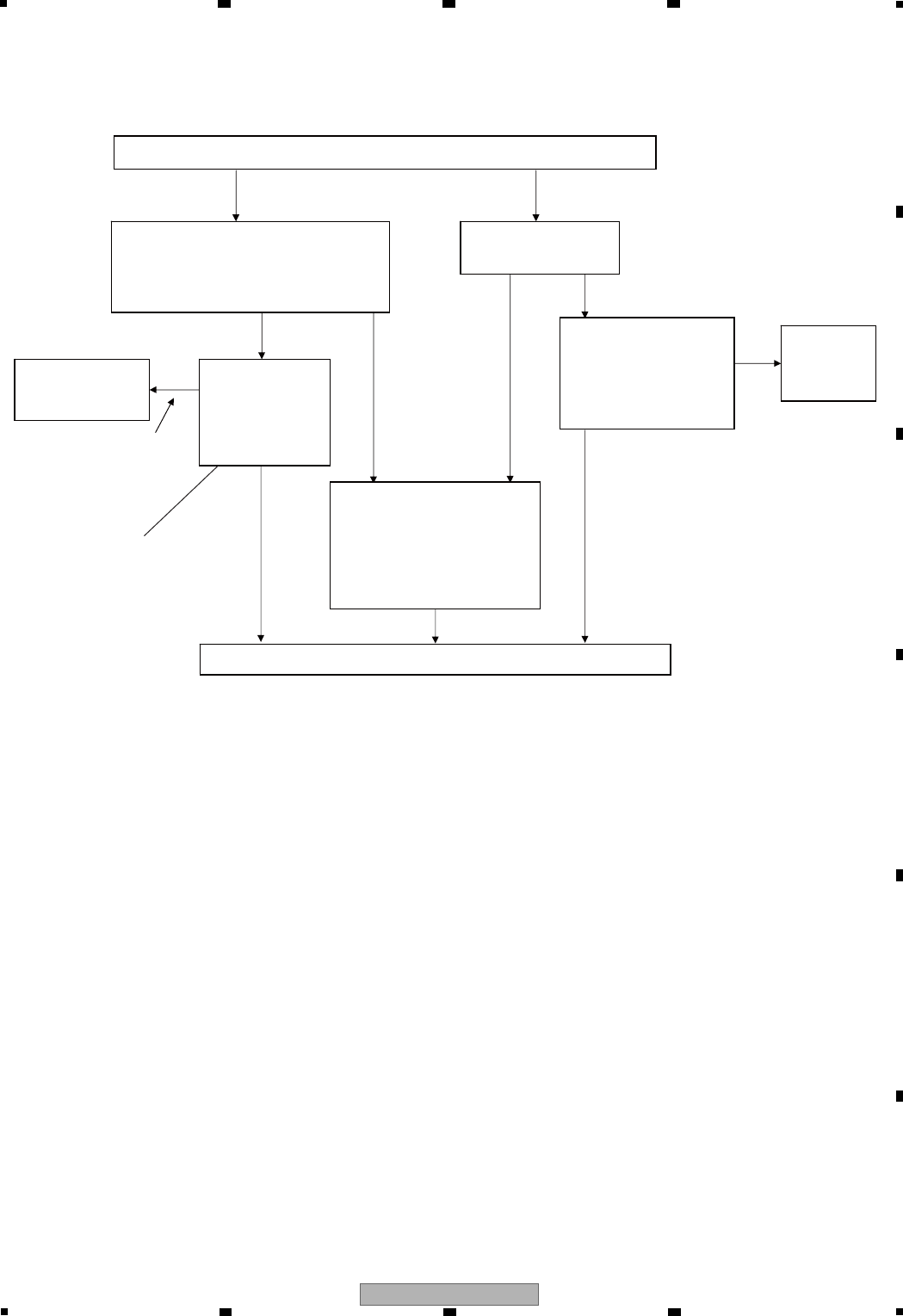
5. DIAGNOSIS
5.1 SETUP SEQUENCE
Tuner/FL microcomputer System Codec IC (Initial Program Loader)
System Codec IC (Firmware)
DVD-R/RW Drive
Is ID check of drive OK?
Ye s
Power ON ? No
Ye s
Has
command
arrived ?
Ye s
OK
FLASH check ? NG
No
Stop
Tray Open
Ye s
No
"CPRM ERR" displayed on FL display
Request for power off of
system-control computer made to
Tuner/FL microcomputer
System-control computer is turned off
(entering standby) following request
from Tuner/FL microcomputer
Obtaining LD
temperature data from drive.
Is temperature below
74°C?
No
Ye s
Repair process
Is disc in?
Is starting/ID check of
HDD OK?
No
Ye s
Is disc valid?
Ye s
Repair required?
Ye s
Ye s
No
No
No
No
Playback
Playback
requested?
Ye s
"E01 or E02" displayed on FL display
∗1: If both the drive ID check and starting/ID
check of HDD failed, "CPRM ERR" is first
displayed on FL display.
Tuner/FL microcomputer starts up.
Connect the power cord.
System microcomputer starts up.
Downloading through
RS232C required.
FLASH check is NG
when
"POWER ON" displayed
for over 1 minutes
on the FL display.
Jumping to developed
firmware.
"POWER ON" displayed
on the FL display.
Key input and channel data
transmitted to the system
controller.
And make displayed data by
instructions from the system
controller, and switch a
channel.
Drive microcomputer
starts up.
ATA/ATAPI
command processing
Firmware stored in Flash memory
is developed in SD-RAM
expanding the compressed data.
Initialization of the peripheral
circuit register and RAM, etc.
Waiting for
communication to be
established.
Ye s
No
Initialization of the
peripheral circuit
register and RAM, etc.
Initialization of the peripheral
circuit register and RAM, etc.
Clock displayed
on the FL display.
Power ON/Release the reset
Communication start with the
Tuner/FL microcomputer.
∗1
∗1

40 DVR-LX61
12 3 4
A
B
C
D
E
F
12 3 4
5.2 DIAGNOSIS OF THE MAIN ASSY
Power ON
Does
a desired screen
appear when selected
a tuner?
Video recording and playback by HDD
1 Failure in the periphery of CN2301
(Poor contact with the TUSB Assy.)
2 Failure in the periphery of CN4501
(Power supply is not supplied from the POWER SUPPLY Assy.)
3 Failure in the periphery of IC4511, IC4521, IC4531, IC4541, IC4552,
IC4561, IC4562 and IC4571 (Power supply is not supplied to each IC.)
Ye s
No No
Does a desired
audio output it?
1 Failure in the periphery of CN2301
(Poor contact with the TUSB Assy.)
2 Failure in the periphery of IC3101
(Failure in the periphery of AUDIO ADC for input audio.)
3 Failure in the periphery of IC3201
(Failure in the periphery of AUDIO DAC for output audio.)
No
No
No
No
No
Ye s
No
Video recording and playback by DVD
DVD recording
End
Can the video recording
and playback of HDD?
1 Failure in the periphery of CN5604
(Poor contact with the HDD.)
2 To the HDD check mode
Ye s
No
Can record desired
video and audio?
Failure in the periphery of CN101
(Poor contact with the Pickup Assy.)
Failure in the periphery of IC1001
(There is possibility of failure of
the EMMA2RFE chip.)
Ye s
No
Does the tray open?
1 Failure in the periphery of CN601
(Poor contact with the FRONT Assy.)
2 Failure in the periphery of IC501
(Failure in the periphery of the Driver IC.)
Ye s
No
Do play back desired
video and audio?
1 Failure in the periphery of CN2301
(Poor contact with the TUSB Assy.)
2 Failure in the periphery of IC3101
(Failure in the periphery of AUDIO ADC for input audio.)
3 Failure in the periphery of IC3201
(Failure in the periphery of AUDIO DAC for output audio.)
Ye s
No
Insert a disc and close the tray, then playback it
Do recognize a disc?
1 Failure in the periphery of CN101 (Poor contact with the Pickup Assy.)
2 Failure in the periphery of CN501 (Poor contact with the SPDL.)
3 Failure in the periphery of CN502 (Poor contact with the STEPPER.)
Ye s
No
41
DVR-LX61
56 7 8
56 7 8
A
B
C
D
E
F
*This flowchart shows how to confirm the output from the HDMI block on the basis that an external input signal to the L1
connector is through-output from the analog output connector properly.
Connect the unit to a DVI monitor
that is provided with the HDCP
function (HDMI-DVI conversion
connector required), or to a monitor
that supports HDMI.
Set the input setting to L1.
Input an external PAL signal to L1.
YES
NO
YES
NO YES
YES
AA
No
Is an image
properly
displayed?
Are the
images output
successively
(does HDMI LED
light up)?
Does it repeat correct output
for a moment followed by black
screen (or sandstorm)?
With the aid of an oscilloscope, check IC1001, IC5801 for the
points listed below. (Only checking with a PAL signal
is enough. Checking with an NTSC signal is not required):
• R5865 (HTX_CLK : 27 MHz/74.25 MHz/148.5 MHz @PAL)
From the following points, a 3.3-V swing signal must be output:
• R5855 (H sync)
• R5855 (V sync)
• R5826 to R5828 (Video lines)
Are all the signals
mentioned above
output?
It is most likely that IC5801 and the
subsequent parts are in failure.
Check the soldering of the parts
listed below:
• IC5801 itself
• L5801 to L5804, JA5801
• R5842 to R5845, C5815 to 5818
Possible defect in EMMA2RFEX.
1. In a case when only the HDMI video is not outputted
[1] Diagnosis of the HDMI Block

42 DVR-LX61
12 3 4
A
B
C
D
E
F
12 3 4
AA
The monitor owned by the user may not be compatible
with this unit.
Is a correct picture displayed when the monitor owned by
the user is connected with this unit using a 5-meter cable
made by JAE?
The cable used by the user is in failure.
Is a momentary correct picture and a fully black or a
snowy screen alternately displayed? Or, another
symptom?
Confirm the manufacturer and model number, and check
symptoms in the following steps, then refer to similar
case examples that happened in the past. In some
cases, upgrading the software/firmware of this unit may
resolve the problem.
1 Does the symptom change when the HDMI cable between the monitor and recorder is disconnected then reconnected?
2 With the HDMI cable between the monitor and this unit connected, if the power to the monitor is turned off then back on
again, does the symptom change?
3 Turn off the power to both the recorder and monitor. Then, turn on the monitor, then after 30 seconds, turn on the
recorder. Does the symptom change?
4 Is the HDMI LED lit, unlit, or flashing?
5 What is the picture on the screen like? A fully black, snowy, combination of the both, or other (a fully green or pink
screen)?
6 Does the symptom change if the length of the cable (made by JAE) is different?
7 Are some spots missing by dots (missing pixels) on the screen? If so, there may be problems in the length or quality of
the cable or the reception capacity of the monitor. Check if the symptom disappears when a 5-meter or less cable made
by JAE is used.
Ye s N o
If there is no measure, ask us for product
quality information.
43
DVR-LX61
56 7 8
56 7 8
A
B
C
D
E
F
2. In a case when only the HDMI audio is not outputted
Is a DVI device connected (with a DVI device, only the video signal is output, and no
sound is output)? Is an HDMI device that does not support the audio signals connected?
Set the Dolby Digital output setting in "Audio
Output" of the home menu to PCM. Play
back the Dolby Digital audio signal of a DVD.
Is the audio signal correctly output from the
HDMI and coaxial output (S/PDIF)?
Play back a CD. Are the
HDMI and analog audio
signals correctly output?
Measure the signal
at R*** (Note 1)
with an oscilloscope,
using a probe, to
check if the signal is
correct.
There may be a
problem with the
coaxial output circuit.
HDMI: No
S/PDIF: Yes
HDMI: No
S/PDIF: No
There may be a problem with the EMMA2RFEX.
No
Yes
(Coaxial output)
No (Checking of the S/PDIF path) No (Checking of the CLK, DATA, LRCK,
and BCK paths)
Measure the signal at
R1030 (CLK), R3201 (BCK),
R3202 (DATA) and R3203
(LRCK) with an oscilloscope,
using a probe, to check if
the signal is correct.
HDMI: No
Analog: Yes
HDMI: No
Analog: No
No
With the aid of an oscilloscope,
check IC1001 and IC5801 for
the points listed below.
• R5865 (HTX_CLK)
From the following points, a 3.3V
swing signal must be output:
• R5826 to R5828
There may be
a problem
since audio
DAC circuit.
Yes
No
Note 1 : R5708: AT model
R5701: DT model
44 DVR-LX61
12 3 4
A
B
C
D
E
F
12 3 4
6. SERVICE MODE
To be used to check the status of the product and to collect the information for failure diagnosis.
The following information to be used for servicing is displayed:
[1] First screen : Version, HDD information, etc.
[2] Second screen : ATA/ATAPI debug screen (Writer information)
[4] Fourth screen : VR-recording-related error logs
[5] Fifth screen : VR-playback-related error logs
Each screen has sublevel screens.
After entering any Service mode screen, to shift to another Service mode screen, first quit that Service
mode screen then enter another Service mode screen.
[Note]
Overview and Purposes
Category Mode Procedure Necessary When
Adjustment Model Setting Automatically start up when necessary After replacing M/B or T/B
Adjustment LD Power Adjustment [ESC] + [CX] + [1] + [0] After replacing M/B or Loader
Adjustment CPRM ID Number/Data Setting [ESC] + [STEREO] After replacing M/B or HDD
Adjustment Firmware Update [REC STOP] + [OPEN/CLOSE] After replacing M/B or T/B
Adjustment Gracenote Database Update [REC STOP] + [OPEN/CLOSE] After replacing HDD
Adjustment Video Adjustment for Specific
Area [ESC] + [CHP/TIM] As needed
Adjustment OSD Filter Setting [ESC] + [DISP] + [DIG/ANA] x4 As needed
Diagnosis Version Info, etc. [ESC] + [DISP]
Diagnosis RF Level [ESC] + [DISP] + [DIG/ANA]
Diagnosis Error Rate [ESC] + [DISP] + [DIG/ANA] x2
Diagnosis HDD Info [ESC] + [DISP] + [DIG/ANA] x3
Diagnosis Writer Maintenance Info [ESC] + [DISP] + [2] + [DIG/ANA] x2 + [SEARCH]
Diagnosis LD Degradation Check [ESC] + [DISP] + [2] + [DIG/ANA] x3 + [SEARCH]
Diagnosis DV Info [ESC] + [DISP] + [3]
Diagnosis VR Recording Error Log [ESC] + [DISP] + [4] + [DIG/ANA] x3
Diagnosis VR Playback Error Log [ESC] + [DISP] + [5] + [DIG/ANA]
Diagnosis EPG Info [ESC] + [DISP] + [7] Europe model only
Diagnosis AAC Info [ESC] + [DISP] + [+10] + [1]
Diagnosis HDMI Info [ESC] + [DISP] + [+10] x2 + [4]
Diagnosis Ethernet Info [ESC] + [DISP] + [+10] x2 + [7]
Diagnosis HDD Check [ESC] + [CX] + [0] + [1]
Diagnosis USB Check [ESC] + <TIMER/REC>
Diagnosis DVD Aging Mode <DVD> + [ESC] + [REP.B] + [PLAY]
Diagnosis HDD Aging Mode <HDD> + [ESC] + [REP.B] + [PLAY]
Service Mode Map

45
DVR-LX61
56 7 8
56 7 8
A
B
C
D
E
F
6.1 VERSION INFORMATION, ETC. (FIRST SCREEN)
To check the versions of the system control
computer, TUNER microcomputer, and
firmware for the drive, simple measurement of
the RF level for the U/V tuner, results of the
simple error rate measurement, HDD
information, and OSD Filter setting
While the GUI screen is not displayed, press the ESC then DISP keys.
How to enter and change subscreens of the first screen: While the first screen is displayed, press the
DIG/ANA key repeatedly until your desired subscreen is displayed. The subscreens change cyclically.
[Purposes] [Tools to be used]
[How to enter]
Press the ESC key.
[How to quit]
Remote control unit for servicing
(GGF1381)
Aluminum-coated test disc
(GGV1025)
Model name/destination
Version of the recorder software
Revision No. of the system-control computer software
Version No. of the tuner microcomputer
Result of the combination ckeck with system u-com
Information on the built-in drive
(Model name, version No., model type)
Physical capacity of the HDD
DEVICE information (EMMA type, ES No.)
FLASH ROM information
Region No.
CPRM information (CPRM key No.)
PICUP SERIAL No.
HDCP information (HDMI authentication key)
Same number as that for CPRM.
Gracenote Database information
Gracenote Database Update information
Operating capacity of the HDD
OK : Appropriate version compared with that of the firmware of
the system control computer.
NG- : The version of the TUNER microcomputer is older.
Measures to be taken:
• Download the firmware.
OK : Appropriate version compared with that of the firmware of
the system control computer.
NG- : The version of the drive microcomputer is older.
Measures to be taken: Download the firmware.
OK : The appropriate drive is mounted.
NG : An inappropriate drive is mounted.
Measures to be taken: Download the firmware.
NG : NOBKUP: No Data
Download the Gracenote Database.
12
4
5
11
15
12
6
3
(1) First screen
[Description]
78
9
10
16 17
DVR-LX61/WY VERSION : 0.14
SYSCON : RELEASE_179
Rev.1.7379
TUNERCON : 2.22 OK
DRIVE : DVD-RW DVR-U13 OK
1.10 OK
PIC SERIAL : 007710217604
HDD INT : ----
HDD USE : ----
GNDB B : NOBKUP GNDB U : NOBKUP
DEVICE : E2R-FEx1.1 FLASH : 128M
REGION : 2 C : 0000000153
HDCP : 0000000153
46 DVR-LX61
12 3 4
A
B
C
D
E
F
12 3 4
If an error indication in the HDD data does not disappear even after the above measures were taken, refer to another sheet of "HDD Service
Mode."
• Details on HDD data are described below:
HDD : WDC10234564 # 160
Name of manufacturer, part No. by manufacturer
HDD identification error indication
Capacity of the HDD (unit: Gbytes)
If any abnormality exists in HDD connection, the indications shown in Table 1 below are displayed.
Table 1: HDD recognition status represented by the HDD data display
HDD identification conditions Example of HDD data
to be displayed Remarks
Failure in physical identification of HDD
(no connection, defective HDD, interface error) Blank space
Physical identification of HDD possible, but not identified
(CPRM ID is not input.) WDC 10234564 # 160 • Input the CPRM ID.
• Check the connection to the SATA connector.
• Replace the SATA flexible cable and connector.
• Replace the HDD.
• Replace the resistor in the SATA communication
line.
Physical identification of HDD possible, HDD identified,
but failure in logical formatting WDC 10234564 ! 160 "!" represents an HDD-recognition error.
• Initialize the HDD or erase all titles.
Physical identification of HDD possible, HDD identified,
and correct logical formatting (HDD correctly identified) WDC 10234564 160
To check the RF signal of the U/V tuner by checking the input frequency difference and AGC voltage
in this debug mode
Press the ESC key.
[
Purposes
]
[
How to enter
]
[
How to quit
]
While the User Setting display is displayed, press the ESC , DISP , then DIG/ANA keys, in that order.
[
Description
]
Input frequency difference
Subscreen 1
AGC voltage
Input channel
[1] Simple Diagnosis of the RF Level (Subscreen 1)
DVR-LX61/WY VERSION : 0.14
SYSCON : RELEASE_179
Rev.1.7379
TUNERCON : 2.22 OK
DRIVE : DVD-RW DVR-U13 OK
1.10 OK
PIC SERIAL : 007710217064
HDD INT : ----
GNDB B : NOBKUP GNDB U : NOBKUP
DEVICE : E2R-FEx1.1 FLASH : 128M
REGION : 2 C : 0000000153
Input CH : ∗∗ ch
Freq Diff : Low 1
AGC Volt : ∗∗∗∗ mV
47
DVR-LX61
56 7 8
56 7 8
A
B
C
D
E
F
ERR RATE : *.*e-*
• While the User Operation screen is displayed, press the ESC then DISP keys, then the DIG/ANA
key twice, in that order.
• While subscreen 1 of the first screen is displayed, press the DIG/ANA key.
[How to enter]
Press the ESC key.
[How to quit]
[Measurement procedures]
Display subscreen 2.
Load the Test disc (GGV1025).
Judge the results of the error rate measurement by
referring to Table 1.
[Tips]
During VR mode playback, the average value of the past 10 VOBUs is displayed. During DVD-Video or Video mode
playback, the average value of the past 256 sectors is displayed.
During VR mode playback, the speed ratio of the drive (/: normal, no indication: double speed) is also displayed.
Subscreen 2
1) Frequency Difference (Freq Diff)
How much tuning is off is monitored, as shown below:
2) AGC voltage (AGC Volt)
The gain controlled by the tuner is monitored to infer the input electric field intensity.
(The accuracy of inference differs depending on the product.)
Field Intensity AGC VOL
Intense field area
(Clear image)
Less intense field area
(Noise may be generated.)
Weak field area
(Much noise. EPG/VPS/PDC sometimes cannot be
obtained.)
Very weak field area
(Image damaged. EPG/VPS/PDC cannot be obtained.)
70 dB or more 3100 mV or less
50 dB or more
70 dB or less 3100 - 4400mV
30 dB or more
50 dB or less
4400 mV or more
(It is unable to discriminate
under the weak field area.)
30 dB or less 4400 mV or more
(It is unable to discriminate.)
High
(within 200kHz)
Input Frequency Display
Low
Just Tune
Faraway
High 1~5
Low 1~5
Low 7
Center
High 7
within
200kHz
over
200kHz
[2] Simple Error Rate Measurement (Subscreen 2)
Tips:
For good reception, the field intensity must be 50 dB or more (AGC Volt 4400 mV or less).
For accurate measurement, use a field intensity meter.
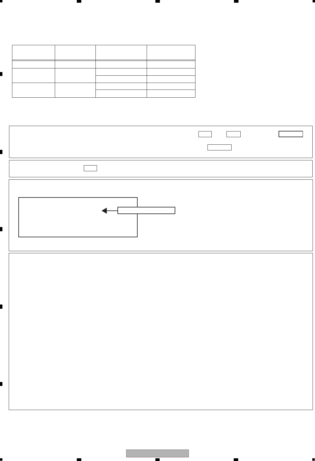
48 DVR-LX61
12 3 4
A
B
C
D
E
F
12 3 4
HDD Info
Life Time: 87599h 09m 05s
[How to enter]
[How to quit]
Cumulative HDD-on time
[Mode description]
[Tips]
• How the data on cumulative HDD-on time are processed in memory
Storage place:
FLASH ROM
Timing of referring to the data on cumulative HDD-on time:
When the power is turned on, fails, the FLASH ROM is referred to.
Timing of updating the data on cumulative HDD-on time:
While the HDD is on, the data on cumulative HDD-on time in the RAM is updated every 3 seconds, and every time
updating is executed the data are stored in the Backup SRAM. When the power is turned off, the data are stored in
the FLASH ROM.
• How to clear the data on cumulative HDD-on time
FLASH ROM:
When the HDD Identification Setting is performed, the data on cumulative HDD-on time are automatically cleared.
The HDD Identification Setting is automatically performed when the CPRM setting is performed on the CPRM
setting screen (to display the CPRM setting screen, press the ESC then the STEREO keys).
Notes: • The data on cumulative HDD-on time are not cleared when resetting to factory-preset values is performed.
• The data on cumulative HDD-on time are not cleared when the system-control computer software is
downloaded.
Subscreen 3
• While the User Operation screen is displayed, press the ESC then DISP keys, then the DIG/ANA
key three times, in that order.
• While subscreen 2 of the first screen is displayed, press the DIG/ANA key.
Press the ESC key.
Table 1: Thresholds when determining OK or Error
- - 8.0×10⁻⁴
Disc type Recording
mode Reference value
Finalized or not
finalized
DVD-VIDEO
Video mode Finalized 3.3×10⁻³
Not finalized 3.3×10⁻³
DVD-R
Video mode Finalized 3.3×10⁻³
Not finalized 3.3×10⁻³
DVD-RW
[3] HDD Information (Subscreen 3)
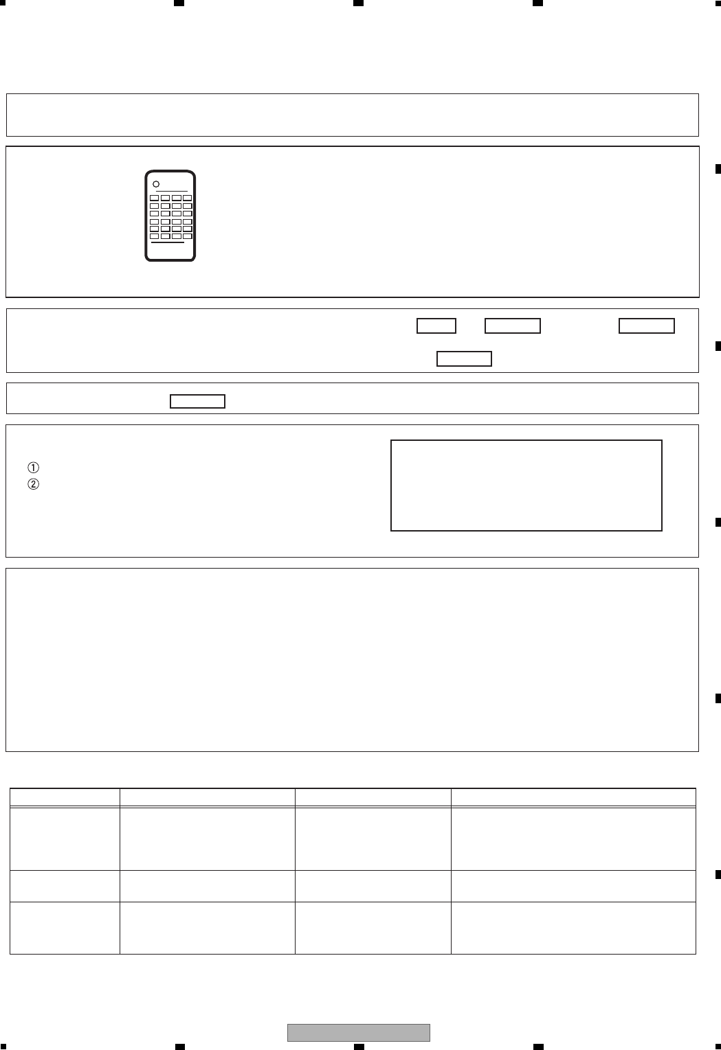
49
DVR-LX61
56 7 8
56 7 8
A
B
C
D
E
F
OSD Filter Setting
OSD FILTER : 4
• While the User Operation screen is displayed, press the then keys, then the
key four times, in that order.
• While subscreen 3 of the first screen is displayed, press the key.
[How to enter]
Press the key.
[How to quit]
ESC DISP
DIG/ANA
ESC
Depending on the monitor used, the character flicker on the OSD may stand out.
If a system, such as character flicker, appears on the monitor, select the filter response.
[Purpose]
DIG/ANA
[Setting procedures]
Display subscreen 4.
Select the setting from the key operation table.
[Tips]
As the setting value becomes greater, jitter is reduced on a CRT display. However, as lines for characters appear thick,
complex characters may become difficult to read. On the contrary, as the setting value becomes smaller, jitter
increases on a CRT display. However, as lines for characters become sharper, complex characters become more
legible.
Note: Use the remote control unit for servicing.
Note: A new setting becomes active as soon as it is made. As a new setting is stored in nonvolatile memory, it will be
retrieved when the unit it turned on the next time.
Note: After the factory-preset values are downloaded, the setting value for the OSD Filter will be the default value (4).
Subscreen 4
[Tools to be used]
Remote control unit for servicing
(GGF1381)
[(Table 2) Key operation of OSD Filter setting]
Key Operation Setting value Remarks
0 - 4 (Default value: 4)
[ Rev x 3 ], [SPEED+]
[ x 3 Fwd], [SPEED-]
[ Rev x 3 ], [SPEED+]
: The setting value increases by 1.
[ x 3 Fwd ], [SPEED-]
: The setting value decreases by 1.
Changing the setting value for the
OSD Filter
The setting value is reset to default.
[ESC]
[CLEAR]
–
–
To exit the OSD Filter Setting and
clear the screen
(Appears the tuner
screen.)
–
[4] OSD Filter Setting (Subscreen 4)

50 DVR-LX61
12 3 4
A
B
C
D
E
F
12 3 4
6.2 ATA/ATAPI DEBUG SCREEN (SECOND SCREEN)
A T A / A T A P I Writer MaintenanceInfo
Power ON 0 0 0 0 0 0 0 0 0 0 0 0 0 0 0 0 0 0
0 1 0 2 : 5 6 0 1 0 0 0 0 0 0 0 0 0 0 0 0 0 0 0 0
D V D 0 2 0 0 0 0 0 0 0 0 0 0 0 0 0 0 0 0
R 0 0 5 3 : 4 8 0 3 0 0 0 0 0 0 0 0 0 0 0 0 0 0 0 0
W 0 0 2 2 : 1 6 0 4 0 0 0 0 0 0 0 0 0 0 0 0 0 0 0 0
C D 0 5 0 0 0 0 0 0 0 0 0 0 0 0 0 0 0 0
R 0 0 3 4 : 0 4 0 6 0 0 0 0 0 0 0 0 0 0 0 0 0 0 0 0
W 0 0 0 0 : 0 0 0 7 0 0 0 0 0 0 0 0 0 0 0 0 0 0 0 0
0 0- 0 0
Error log for the Writer
(Not for Service)
1
2
3
4
5
Power-on time/cumulative power-on time
Duration of emission of the laser diode (LD) for DVD-R/DVD
while reading
Duration of emission of the LD for DVD-W/DVD while writing
Duration of emission of the LD for CD-R/CD while reading
Duration of emission of the LD for CD-W/CD while writing
(This function is not used for this model.)
To be used as a rough guide to judge
whether the pickup unit is all right or not
• Dirt on the pickup lens
• Degradation of the laser diodes for
reading CDs and reading/writing to/from
DVDs
• While the User Operation display is displayed, press the ESC , DISP , then 2 keys, in that order.
• While any subscreen of the second screen is displayed, press the DIG/ANA key repeatedly.
The subscreens change cyclically.
[
Purposes
][Tools to be used]
[
How to enter
]
[
How to quit
]
Remote control unit for servicing
(GGF1381)
[
How to enter
]
[
How to quit
]
Aluminum-coated test disc
(GGV1025)
Update the display by pressing the SEARCH key while subscreen 3 is displayed.
[
Procedures
]
If the total hours of duration of emission of the laser diode (LD) for DVDs while reading and that of
emission of the LD for DVDs while writing exceed 4,700 hours, the LDs may be degraded.
Perform an LD degradation judgment, using subscreen 4.
Press the ESC key.
Press the ESC key.
• While the User Operation screen is displayed, press the ESC , DISP then 2 keys, then the DIG/ANA
key twice, in that order.
MTTF hours for each LD
DVD: 4,700 hours
CD: 11,000 hours
The ATA/ATAPI Writer Maintenance Info is obtained each time the power is turned on. Thereafter, the
data on the subscreen is updated each time the SEARCH key is pressed (the updating command is
sent) while this subscreen is displayed. Care must be taken when updating this subscreen, because an
undesired command is inserted if it is executed while recording, etc.
[Note on lighting time data for each LD]
Since data on lighting time of each laser diode (LD) are stored in the flash ROM on the MAIN Assy, after
the MAIN Assy is replaced, the data will be cleared. However, after the LOADER Assy is replaced, data
on lighting time of each LD will be retained in the MAIN Assy. Therefore, before either the MAIN Assy or
LOADER Assy is to be replaced, it is recommended that you write down the lighting time data.
[
Tips
]
[1] Writer Maintenance Information of ATA/ATAPI DEBUG OSD (Subscreen 3)
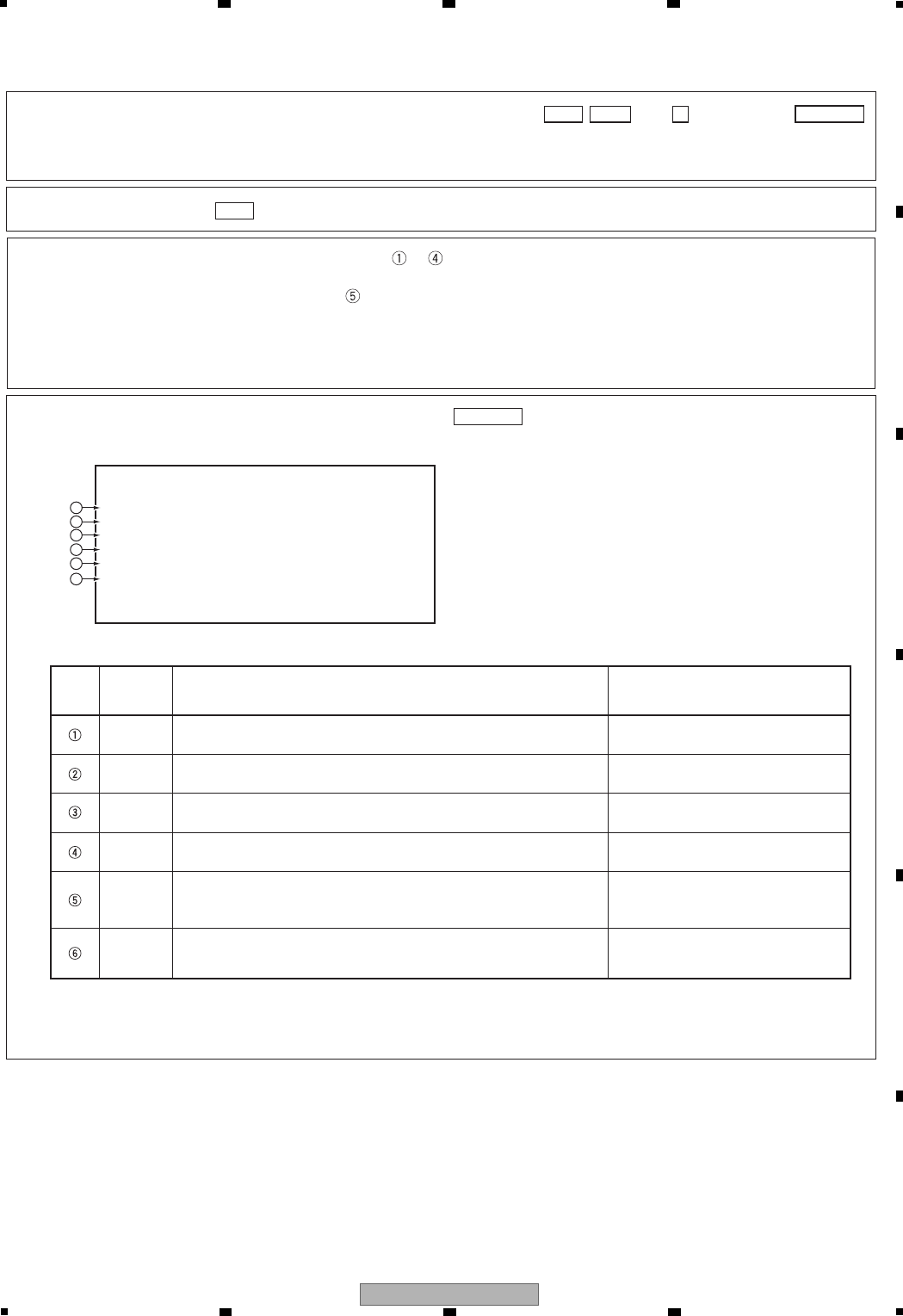
51
DVR-LX61
56 7 8
56 7 8
A
B
C
D
E
F
1
2
3
4
5
6
A T A / A T A P I - LD Degrade
C D : 0 0 7 0 1 0 4 % O K
D V D : 0 0 6 8 9 6 % O K
T M P : 0 0 A 3 4 1 °C
A D J : 0 0 67 2 6 °C
RF : 3 D 7 0
TLT : F F D 5
[
How to enter
]
[
How to quit
]
To update the value for each item, press the SEARCH key while subscreen 4 is displayed.
For details on each item and the conditions of updating the values, see Table 2 below.
[
Procedures
]
If the results of degradation of the LDs for CDs or DVDs are NG, replace the drive.
• For correct measurement of items to indicated in the display below, leave the unit at room
temperature (25˚C) for a while before turning it on, and do not load a disc.
• For RF measurement (item ), it is recommended to use the Test disc (GGV1025).
As the RF level differs depending on the characteristics of the pickup from product to product, it cannot
be used for judging degradation of the LD. Use the RF level as a rough guide to know the difference
between before and after lens cleaning.
[
Notes
]
• While the User Operation screen is displayed, press the ESC , DISP then 2 keys, then the DIG/ANA
key three times, in that order.
Press the ESC key.
Table 2: Description of each item and conditions for updating data
No. Item Description Conditions for updating by
pressing the SEARCH key
CD Degradation judgment of LD for CD. Regarded as NG when the value
is 120% or higher (same standard as for the PC drive) No disc inserted in the disc tray
DVDDegradation judgment of LD for DVD. Regarded as NG when the value
is 120% or higher (same standard as for the PC drive) No disc inserted in the disc tray
TMP Current temperature inside the Writer No disc inserted in the disc tray
ADJ Temperature (approx. 25°C) inside the Writer during adjustment No disc inserted in the disc tray
RF
RF level (16-bit data, proportional calculation performed using the
actual RF level value with 2.5 V = 0xFFFF as the maximum value,
displayed in 4-digit hexadecimal)
During playback of disc medium
(GGV1025)
TLT Writer adjustment data for straight (non-HDD) model
(FFFF is diplayed when the writer is not adjusted.) No condition
[2] LD Degration Judgment of ATA/ATAPI DEBUG OSD (Subscreen 4)

52 DVR-LX61
12 3 4
A
B
C
D
E
F
12 3 4
6.3 VR-RECORDING-RELATED ERROR LOGS (FOURTH SCREEN)
• Errors related to recording are displayed on the lines "Rec Err:," as shown below.
For details on errors, see "Table 1: Description of VR-recording-related errors."
1 There are two error-log screens, on which up to 9 logs per screen are displayed.
(generation time [year-month-day, hour:minute:second], error data in simplified description)
RunFnc : ---- Ecl : **** Rate : **
----------------------
----------------------
----------------------
----------------------
----------------------
----------------------
R e c o r d i n g E r r o r H i s t o r y D i s p l a y
0 1 – 0 6 – 0 1 2 0 : 0 5 : 3 0 N o S y s H d r I N
0 1 – 0 6 – 0 2 0 0 : 2 2 : 1 0 W r i t e E r r o r
1
To roughly determine in which category shown below a symptom
that is difficult to reproduce belongs.
For details on the categories of error logs displayed, see "Table 1:
Description of VR-recording-related errors."
• Errors related to the MPEG Encoder
• Errors related to the drive system
• Errors related to copying
• Errors related to others
• Errors related to the HDD
[
Purposes
][Tool to be used]
[
How to enter
]
[
How to quit
]
(1) VR-Recording-Related Error Logs (Subscreen 1)
(2) Subscreen 2 and 3
(3) VR-Recording-Related Error Logs (Subscreen 4)
(4) Subscreen 5 to 12
[Description of each subscreen]
Remote control unit for servicing
(GGF1381)
• The two error-log screens can be switched by pressing the SPEED+ or SPEED- key.
• For details on error messages, see Table 1 "Description of VR-recording-related errors".
[
Tips
]
Recording-related errors are displayed.
Press the ESC key.
• While the User Operation display is displayed, press the ESC , DISP , then 4 keys, in that order.
• While any subscreen of the fourth screen is displayed, press the DIG/ANA key repeatedly.
The subscreens change cyclically.
(These subscreens are not for service use.)
(These subscreens are not for service use.)

53
DVR-LX61
56 7 8
56 7 8
A
B
C
D
E
F
Error Related to MPEG Encoder
Error Related to Dubbing
Error Related to Drive System
In a case of an error in the drive system, scratches or dirt on a disc, or a problem of the drive itself (dirty pickup) may be suspected.
Any error message marked with * is displayed "RecErr : ---------" on the Subscreen 1 of the fourth screen.
Error Message Description Cause
Cause
Cause
IN Encode * Changes cannot be made in the process of encoding
Failure to start encoding (reasons not clear)
No SysHdr INSystem packet is not input periodically
Stm Start NG
AVEncoder failed
AVEnc Hang
Inappropriate input stream data
Stream NG
Timeout waiting for system packet input at the beginning
Strm Start NG
Error Message Description
Mech No Res No response from the mechanical-control computer
Bdr Opn NGOpen Border failed
Fail Repair Repair failed
OPC NGOPC failed
Read Err Reading failed, ECC failed, etc.
PCA Full PCA has been used up.
Drv TimeOut Timeout waiting for drive operation
Video Mode VTSI Write Error (After Layer Change)
Video Mode Close Rzone failure
Close Rzone failed at dual layer disc
Format failed
May be +VR disc, but no RSAT
Close RZone failed
Video Mode VTSI BUP Write Error
Reserve RZone failed
MKB Invalid MKB reading error
VTSI2 Wr Err
BUF Overflow Overflow of the Stream Buffer
CLS Rzon Fail
NWA surpassed and impossible to use
NWA Exhaust
DLVR trace NG
Format NG
May Be PVR
V Final fail Abnormal process occurred when finalizing Video mode
Write Err The Drive failed to write and could not be recovered.
Rzn Cls NG
Repair RZone failed
Rzn Rpr NG
Video Mode VTSI BUP Write Error (After Layer Change)
VTSI_B2 Wr Err
RMA Full RMA has been used up.
TMP-VMG WrErr Video Mode TMP VMGI Write Error
VTSI_B Wr Err
Rzn Rsv NG
Close Border failed
Bdr Cls NG
The Drive is hung up.
Drive Hang
General error of the drive
Drv Err
Abnormality in the drive hardware or firmware
Drv Hard Err
May Be V mode Although TMP_VMGI is not written, it may be Video Mode disc.
Because some data are invalid, data cannot be written
ReadOnly DISC *
VTSI Wr Err Video Mode VTSI Write Error
RSAT : Reserved Space Allocation Table
Error Message Description
VC Pck Anl NGAnalizing Video Mode Copy Pack failed
Mem get NGVideo Mode Copy Memory has not ensured.
VC HDD Inf NGNo information on Video Mode Copy HDD
VC HDD C Err Obtaining Video Mode Copy HDD Cell information failed
Video Mode Copy Tracon transfer has not been completed.
Format failed
Strm TransfNGVideo Mode Copy Stream Transfer NG
Tracon Trn NG
VC HDD Info NG
Other NG HDD -> DVD copy
H2D CP SomeNG
Maximum number for Video Mode copy Cells exceeded
VC Cell Max
Video Mode Copy Copy Cancel
VC CopyCancel
Video Mode Copy Flush Cache NG
VC FlushC NG
VC Idling NGVideo Mode Copy idling NG
[1] Description of VR-Recording-Related Errors
Defective engine or software-related problem
Defective engine or software-related problem
Defective engine or software-related problem
Defective engine or software-related problem
Defective engine or software-related problem
Defective disc
Defective disc
Defective disc
Defective disc
Defective disc
Defective disc
Defective disc
Defective disc
Defective disc
Defective disc
Defective disc
Defective disc
Defective disc
Defective disc
Defective disc
Defective disc
Defective disc
Defective disc
Defective disc or drive
Defective disc or drive
Defective disc or drive
Defective disc or drive
Defective disc or drive
Software-related problem
Software-related problem

54 DVR-LX61
12 3 4
A
B
C
D
E
F
12 3 4
Other Errors
Error Related to Dubbing (Continued)
Error Message Description
DRAM NGAbnormality in access to the Work DRAM
Already open Extension file is already opened.
Dir Depth Err Tree of Directory is too deep.
F Alrdy Exst Extension file is already exist.
FileNot Exist Extension file is not exist.
File cancel Extension file is canceled.
CPRM IC NGInappropriate CPRM IC
Error in gaining data
Backup RAM data has not been written on the File Sys.
Inappropriate stream data to the Ouroboros input
No video input (not locked)
No further data can be written because the disc is full.
No more space in the internal work-management area
Invalid parameter
In the process of the emergency processing
Invalid VMG content
Invalid TMP_VMGI content
Drive Destroy The drive has crashed.
MKB REVOKED
BK BATT Down Backup RAM data has been erased.
BK FSYS Dirty
Ourob Strm NG
Encoder routine is hung up.
EncModul Hang
No Video
Disc Full
No More Info *
No Permission *No permission to write to the disc
Limit Over *Standard maximum limit exceeded
Invalid Param *
VTSI information of +VR is unusual.
Invalid VTSI
Now Busy *
Invalid Disc *The disc cannot be recognized.
Invalid UDF *Invalid UDF content
Invalid VMG *
Invalid TMVMG
Cancellation
Abort *
Some bugs
BUG
Bus Reset has been executed.
BusReset Done
Cell Close NG
Cell Close NG
DRAM CLR Err Video Mode DRAM (Stream Buffer) Clear failure
Formatting has been executed.
Format Excec
Irr Action *Incorrect action
NV Pck MK Err
NV Pck DMA Er
Error in creating NaviPack
Inappropriate NaviPack DMA
Over Heat Abnormal temperatute
PARAM NO ACCP Recording parameter is not matched.
Source to be recorded is copy-protected.Protect Src *
Process Over Process is overfull.
Rec Pause *No operation permitted during recording pause
Relocation Do VR-recording data was relocated
Error Message Description
V2H V Reso NGVR → HDD Video resolution NG
VC TSO BLK NGVideo Mode Copy TSO Block transfer has not been completed.
V2H SRC Prot VR → HDD copy prohibited material
H2D TO SPRO HDD → DVD (VR) TimeOut at internal processing
H2D TO DVDWRHDD → DVD (VR) TimeOut at HDD recording side
C2H LOG (XXX) HDD CAM → HDD operation log (XXX is a process code.)
C2H ERR (XXX) HDD CAM → HDD NG (XXX is a process code.)
V2H Aud Stm N VR → HDD Audio Stream number NG
Video Mode Copy Reserve Rzone failed
VR → HDD other NG
H2D CP NoSpac HDD → DVD insufficient free space for copy
VC VOBU SizeE Video Mode Copy VOBU Size NG
V Rsv RzoneNG
HDD → DVD (VR) TimeOut at HDD playing side
H2D TO HDDRD
V2H Unknown
Video Mode Copy Transfer Stop
VC Transf Stp
VR → HDD APP FLG is OFF
V2H APP FL NG
VR → HDD Audio Channel NG
V2H Aud Ch NG
VR → HDD Audio Mode NG
V2H Aud Md NG
V2H VOBU TMNGVR → HDD Play back time of each VOBU is different
Cause
Cause
Defective disc
Problem in the logical structure of the disc
Defective engine
Defective engine, drive, or HDD
Defective engine or software-related problem
Problem in the logical structure of the disc
Problem in the logical structure of the disc
Problem in the logical structure of the disc
Problem in the logical structure of the disc
Software-related problem

55
DVR-LX61
56 7 8
56 7 8
A
B
C
D
E
F
Other Errors (continued)
Error Related to HDD
Error Message Description
V Ext MAX Ovr Count Max exceeded
Something *Undetermined error
VBR-SRAM NGAbnormality in VBR SRAM
Virgin DISC Virgin Disc
WaterMark Det Watermark detected
VOBU Info NGInappropriate VOBU information
Unmatch Stamp *Impossible to modify because of nonmatching time stamp
Abnormality in change of statuses
Inappropriate Category ID
Information of +VR is NG. (VRMI)
V ExtToo Big The extension file is too large.
SRAM NGAbnormality in access to the backup work SRAM
Status NG *
Typ e NG
V Ext TY NG
V Categ ID NG
Invalid VRMI
Param Short Editing Error (Clear A-B)
Reattempting to secure the necessary amount of memory
Heap Mem RETY
Heap Mem NGFailure in securing the necessary amount of memory
Repairing has been executed.
Repair Excec
Switch to +VR playback process
SW PVR
Switching to video playback routine is required.
SW Vpb mode *
Switching to video recording routine is required.
SW Vrec mode *
V Cate Inf NGInappropriate Category information
WM Cracked
WM Cracked
Error Message Description
HDDReset Done HDD Reset executed
ESFSYS CORUPT easyfsys error
HDD Initialize HDD initialized
HDD SMART NGInappropriate HDD SMART
HDD unauthor Inconsistent HDD serial No.
HDD Trans Err DMA error in HDD copy transfer
HDD INFO BAD Incorrect HDD Management Data
Delete the title moving on the way inside HDD
Error generated in HDD Test mode
Gracenote Database deleted
Error generated while Gracenote Database was being downloaded
File development of Gracenote Database failed.
File deletion of Gracenote Database failed.
Gracenote Database not downloaded
Problem in Gracenote Database
File operation of Gracenote Database failed.
High-level process executed for the HDD Buffer
Abnormal power off
Title recording time full
Program file installed in HDD is NG.
Invalid HDD target No. is directed.
HDD ROMSUM NGRom-code check sum NG
HDD DEL OC TT
HDD Aging NG
HDD TFD INIT
HDD DWNLD NG
HDD TFD WR NG
HDD TFD CL NG
HDD TFD NON
HDD CDDB NG
GN API NG
ESFSYS INIT easyfsys initializing
HDD Buff High
Inconsistent HDD Management Data Magic
HDD SIG NG
HDD IRRG POFF
TT Rec Over
Delete the title by HDD recovery.
HDD DEL TT
Tas k No Activ Task has not been activated.
extHDD Ignore External HDD is dismounted.
HDD PFile NG
HDD WRONG TGT
Do nothing for demand.
Do nothing
HDD deflag finished
HDD DEF DONE
HDD deflag error
HDD DEF ERR
HDD is not recognized on the bus.
HDD Destroy
HDD MBR NGInconsistent MBR data
MBR was written
HDD Zero WR
HDD DEL PL Delete the dubbing list by HDD recovery.
Cause
Cause
Problem in the logical structure of the disc
Soft-related problem
Defective HDD, engine
Defective HDD or software-related problem
Defective HDD
Defective HDD
Defective HDD
Problem in the logical structure of the disc

56 DVR-LX61
12 3 4
A
B
C
D
E
F
12 3 4
No Error
Error Message Description
Non Err *Normal
Abbreviations:
ECC = 4 byte Code for Error Correction
UDF = Universal Disc Format
PCA = Power Calibration Area
OPC = Optical Power Control
NWA = Next Writable Address
VMG = Video Manager
RMA = Recording Management Area
MKB = Media Key Block
TMP_VMGI =
Temporary Video Manager Information
Border = from Lead-in to Lead-out
RSAT = Reserved Space Allocation Table
57
DVR-LX61
56 7 8
56 7 8
A
B
C
D
E
F
6.4 VR-PLAYBACK-RELATED ERROR LOGS (FIFTH SCREEN)
Information on display position
Original / Play list (G/L), Title No., Chapter No. [X:XXX-XX]
Display time (hour, minute, second & frame) [XXhXXmXXsXX]
Logic address for playback (ID) [XXXXXXXX]
Number of entries to error log [XXXXXXXX]
Error message log
Original / Play list (G/L), Title No., Time of occurrence (min & sec) [XXX:XXXX]
Location of occurrence (this data is used for development), Name: Name of module where the error
occurred, Line: Number of line where error occurred
Playback-system errors that occurred in 13 times of playback in past [XXX:XXXXXXX]
* For details of error information, refer to the Appendix Table 1.
* If information on errors which occurred on days earlier than the current day is contained on the screen,
the information that follows the information which are displayed with "^" between “Time of occurrence”,
“Name”, “Line” and “Message” indicates the errors that occurred on the current day.
G:001-01 00h00m00s00 00000000
Error=[00000000]
h m s f Name Line Message
G001-01:00000001 ChgSta 01676 WaiPau Err
L002-01 :00123002 ComInf 00669 DecHdl(14)
L002-01 :00410303 ComInf 00669 DecHdl(40)
G004-01:00000004 ChgSta 01676 WaiPau Err
1
2
It can be inferred that an operation that
caused an error in the drive was
performed or that a failure occurred in
the drive if any of the error logs shown
in "Table 2: Description of
VR-playback-related errors" is recorded
on this screen.
[Purposes] [Tool to be used]
[How to enter]
[How to quit]
(1) Subscreen 1
[Description of each subscreen]
Remote control unit for servicing
(GGF1381)
• For details on error messages, see Table 2 "Description of VR-playback-related errors".
• If a VR-playback-related error is generated, a problem in data reading from the disc may be suspected.
(The possibility of a problem on the drive side is high.)
(2) VR-Playback Error Logs (Subscreen 2)
• While the User Operation display is displayed, press the ESC , DISP , then 5 keys, in that order.
• While any subscreen of the fifth screen is displayed, press the DIG/ANA key repeatedly.
The subscreens change cyclically.
Press the ESC key.
(This subscreen is not for service use.)

58 DVR-LX61
12 3 4
A
B
C
D
E
F
12 3 4
[1] Description of VR-Playback-Related Errors
Error Message Details of error
AudioPB Err Audio initialization error
WaiPau Err Pause was disabled though tried. (Pause-wait timeout)
CC_OS_ERR CC output processing error
Tr:NullBlk No valid data in the first block
Tr:NaviErr Navigation pack error
Tr:ReadErr Data read error
Dec:PicDisp Not played up to final PTS
Dec:Size horizontal/vertical_size in sequence header is 0 or above 720 × 576.
Dec:PicTyp picture_coding_type in picture header is neither of the I, P, nor B picture type.
Dec:Struct picture_structure in picture coding extension is neither top/bottom_field or frame picture.
Dec:Syntax Header size is insufficient or does not match with markerbit.
Dec:NoHead No picture header exists between picture data.
Dec:SqErr Detected sequence_error_code.
Dec:Refrenc In Field structure, top_field and bottom_field of temporal_reference in picture header does not match.
Dec:Profile profile_and_level_indication in sequence extension header is exceeding MP@ML.
DecHdl(**) Decoder command execution timeout. (**) is replaced by No. of command which was to be executed.
The Nos. and names of commands are as follows.
/* DECODER system command */
0 HANDLER_DECODER_INIT,
1 HANDLER_DECODER_INIT_STARTUP,
2 HANDLER_DECODER_INIT_PLAY,
3 HANDLER_DECODER_INIT_RTR_PLAY,
4 HANDLER_DECODER_INIT_AUDIO,
5 HANDLER_DECODER_EXIT,
6 HANDLER_DECODER_BLACK_BACK,
7 HANDLER_DECODER_SET_DISP_FMT,
8 HANDLER_DECODER_SET_ASPECT_MODE,
9 HANDLER_DECODER_DISP_BITRATE,
/* DVD command */
10 HANDLER_DEC_DVD_VIDEO_PLAY,
11 HANDLER_DEC_DVD_VIDEO_PLAY_LIST,
12 HANDLER_DEC_DVD_AUDIO_PLAY,
13 HANDLER_DEC_DVD_STOP,
14 HANDLER_DEC_DVD_PAUSE,
15 HANDLER_DEC_DVD_PAUSE_STILL_MODE,
16 HANDLER_DEC_DVD_STEP,
17 HANDLER_DEC_DVD_REWSTEP,
18 HANDLER_DEC_DVD_PAUSE_OFF,
19 HANDLER_DEC_DVD_FF,
20 HANDLER_DEC_DVD_REW,
21 HANDLER_DEC_DVD_SLOW,
22 HANDLER_DEC_DVD_REWSLOW,
23 HANDLER_DEC_DVD_SCAN_OFF,
24 HANDLER_DEC_DVD_SLOW_OFF,
25 HANDLER_DEC_DVD_REWSLOW_OFF,
26 HANDLER_DEC_DVD_REWSKIP_TO_REWSLOW,
27 HANDLER_DEC_DVD_REWPAUSE,
28 HANDLER_DEC_DVD_PLAY_LIST_END_CHECK,
29 HANDLER_DEC_DVD_SET_CAPTION_SW_OFF,
30 HANDLER_DEC_DVD_SET_CAPTION_SW_ON,
31 HANDLER_DEC_DVD_REWPAUSE_TO_REWSLOW,

59
DVR-LX61
56 7 8
56 7 8
A
B
C
D
E
F
32 HANDLER_DEC_DVD_REGIST_TRICK_CALLBACK,
33 HANDLER_DEC_DVD_TRICK_DATA_END,
34 HANDLER_DEC_DVD_AUDIO_STOP,
/* management information */
35 HANDLER_DEC_INIT_NV_PCK,
36 HANDLER_DEC_INIT_RDI_PCK,
37 HANDLER_DEC_READ_NV_PCK_POINT,
38 HANDLER_DEC_READ_RDI_PCK_POINT,
39 HANDLER_DEC_READ_STC,
40 HANDLER_DEC_READ_PTS,
41 HANDLER_DEC_HLI_ENABLE,
42 HANDLER_DEC_COMMAND_PLAY,
43 HANDLER_DEC_COMMAND_PAUSE,
44 HANDLER_DEC_COMMAND_RSLOW_VOBU_STOP,
45 HANDLER_DEC_INIT_VIDEO_MODE,
46 HANDLER_DEC_SET_VIDEO_MODE,
47 HANDLER_DEC_CHECK_VIDEO_OUTPUT,
48 HANDLER_DEC_CHECK_VIDEO_ERROR,
49 HANDLER_DEC_DISPLAY_SUBPICTURE,
50 HANDLER_DEC_SET_SUBPICTURE_PALLET,
51 HANDLER_DEC_IPB_REVERSE,
52 HANDLER_DEC_SET_AUDIO_SYNC,
53 HANDLER_DEC_COMPULSION_OUTPUT_SUBPICTURE,
54 HANDLER_DEC_CLEAR_LAST_NV_PCK_POINT,
55 HANDLER_DEC_CLEAR_LAST_RDI_PCK_POINT,
56 HANDLER_DEC_GET_PICTURE_PARAM,
57 HANDLER_DEC_CHECK_BUFFER_EMPTY,
58 HANDLER_DEC_CHECK_TRICK_END,
59 HANDLER_DEC_READ_VCD_PTS,
/* still picture */
60 HANDLER_DEC_DVD_STILL_NOTIFY,
61 HANDLER_DEC_DVD_STILL_PLAY,
62 HANDLER_DEC_DVD_STILL_FF,
63 HANDLER_DEC_DVD_STILL_FF_OFF,
64 HANDLER_DEC_DVD_STILL_SLOW,
65 HANDLER_DEC_DVD_STILL_SLOW_OFF,
66 HANDLER_DEC_DVD_STILL_PAUSE,
67 HANDLER_DEC_DVD_STILL_PAUSE_OFF,
68 HANDLER_DEC_DVD_STILL_DATA,
69 HANDLER_DEC_DVD_STILL_GET_COUNT,
70 HANDLER_DEC_DVD_RDI_NOTIFY,
/* closed caption */
71 HANDLER_DEC_CAPTION_NOTIFY,
72 HANDLER_DEC_CAPTION_BUFFER_RESET,
73 HANDLER_DEC_CAPTION_SET_INPUT_USER_DATA,
74 HANDLER_DEC_CAPTION_SET_INPUT_FRAME_DATA,
75 HANDLER_DEC_CAPTION_SEND_FRAME_DATA,
76 HANDLER_DEC_FRAME_CHANGE_NOTIFY
Error Message Details of error
60 DVR-LX61
12 3 4
A
B
C
D
E
F
12 3 4
6.5 DV SERVICE MODE
To check whether communication
between a DV device and the unit is
normal when a DV device is connected
[Purpose] [Tools to be used]
[How to enter]
[How to quit]
[Mode description]
Remote control unit for servicing
(GGF1381)
• DV device
• DV cable
Press the ESC key.
Press the ESC , DISP then 3 keys, in that order.
No. Item Description Remarks
Init
Whether the initialization of 1394 LINK and DV
decoder inside EMMA2RFEX has been completed
(OK) or not (NG)
AV Number of AV devices recognizing connection
DV Number of DV devices recognizing connection If the number does not become 01 even if a DV device is
connected, identification of that device fails.
GUID : Global Unique ID (Specific ID for DV devices)
If the unit is ROOT (IRM), IRM is displayed at the side position
of GUID display.
Identification number of AV devices including D-VHS, Digital
Tuner, etc other than DV devices.
GUID GUID set in ConfigROM of the unit
Boldface alphanumerics : Fixed indications
Nonboldface alphanumerics : Variable indications
(DV/1394) Init:OK AV:02 DV:01
[Recorder] GUID:00E0360006100001 IRM
iPCR:C03F0000
[DV] GUID:0080880303480E96
VN:VICTOR MN:GR-D50K
TM:C3 TS:75 CT:32 WP:01 PS:FF OS:00
CA:A000002020 MD:VTR
[DVdecode:Yes] LineSys:525-60
TC:00h20m35s RD:02/02/05 RT:10h34m50s
ASPECT:4:3 CGMS:000000 APSTB:00 DEC:525-60
SF:32KHz QU:12bit AMODE:4) Stereo
1
3
4
5
6
7
8
9
10
11
2
[1] DV Debug
61
DVR-LX61
56 7 8
56 7 8
A
B
C
D
E
F
No. Item Description Remarks
TC Time-code data of the DVdecode Stream, or
response data of the Time Code command
Stream time-code data are obtained when the tape is
played in forward direction. Otherwise, time-code data
are obtained through an AV/C command.
CGMS
CGMS of DVdecode Stream (from left to right,
CGMS data of bits 5-4: Audio ch 2, bits 3-2:
Audio ch 1, and bits 1-0: Video)
*CGMS (Copy Generation Management System): The
two-digit codes added to broadcast programs represent
the following:
00: Copy freely, 10: Once copy, 11: Never copy
VN Vendor name set in ConfigROM of the connected
DV device
TM Transport Mode data obtained from the DV device
TS Transport State data obtained from the DV device
CT Cassette Type data obtained from the DV device
WP Write-protection data obtained from the DV device
PS Power-state data obtained from the DV device
OS Output signal mode data obtained from the DV
device
[DVdecode:XXX] Whether Yes (in the process of requesting DV
input) or No is indicated in XXX Normally, Yes is indicated only when CH is set to DV.
Data are displayed only if one DV device is identified.
CA Connect AV data obtained from the DV device
LineSys Input Line System setting
RD Rec Date of DVdecode Stream
APSTB APS trigger bit of DVdecode stream
QU QUANTIZATION of DVdecode Stream
AMODE AUDIO MODE of DVdecode Stream
ASPECT Aspect Ratio of DVdecode Stream
RT Rec Time of DVdecode Stream
MD DV device mode
Data are displayed only if one DV device is identified.
(Depending on the device, the vendor name may not be set in
ConfigROM.)
MN Model name set in ConfigROM of the connected
DV device
Data are displayed only if one DV device is identified.
(Depending on the device, the model name may not be set in
ConfigROM.)
Camera or VTR is displayed only if one DV device is identified.
Data are displayed only if one DV device is identified.
DEC With/without DVdecode stream input
With input: Signal type (525-60, 625-50, 1125-60,
1250-50, or Invalid) is indicated, Without input: "No" is
indicated.
SF Sampling Frequency of DVdecode Stream If SF is 44 kHz, it is considered that 44.1-kHz audio is
input, and sound is muted on the unit.
iPCR iPCR value of the unit
Data are displayed only if one DV device is identified.
If the connected DV device is ROOT (IRM), IRM is displayed
at the side position of GUID display.
GUID
GUID set in ConfigROM of the connected DV device
62 DVR-LX61
12 3 4
A
B
C
D
E
F
12 3 4
Symptoms Location in the
Debug Screen Items to be Checked, and Conditions Possible causes
DV
DV
2
1
1
2
1
Check the Init indication:
OK: Initialization of 1394 LINK and DV decoder inside EMMA2RFEX
appropriately completed.
NG: Initialization of 1394 LINK and DV decoder inside EMMA2RFEX has not
been completed properly.
Defective IC1001(
EMMA2RFEX
)/ IC5103(1394PHY),
improper connection between IC1001 / IC5103, defective
soldering, defective power supply, etc.
Check the number of DV devices when one DV device is connected to the
recorder:
01 : The connected DV device is correctly identified.
Other than 01 : The connected DV device is not correctly identified.
Defective DV terminals, improper connection of the
DV-terminal board, defective IC5103(1394PHY), defective
cables, an IEEE 1394 device other than the DV device
connected.
No picture nor sound for
DV input
No operation for DV input
DV
Check of DV decoding when the recorder channel is set to DV:
Yes: The recorder is in the process of a DV input operation
No: The recorder is not executing a DV input operation
Defective IC1001(
EMMA2RFEX
), defective soldering,
defective power supply, etc.
DV
Check DEC:
525-60: An NTSC DV signal is input from the DV device.
625-50: A PAL DV signal is input from the DV device.
No: No DV signal is input from the DV device.
Defective DV terminals, improper connection of the
DV-terminal board, defective source device
defective IC1001(
EMMA2RFEX
), IC5103(1394PHY)
Note: As to a model having the Input Line System
setting, if the setting and the actual input signal
system do not match, no picture appears.
DV input recording
impossible DV Check CGMS: Recording cannot be performed for a copy-protected
source.
1
No sound for DV input DV
Check SF:
32 khz: An audio signal with 32-kHz sampling frequency is being input.
48 khz: An audio signal with 48-kHz sampling frequency is being input.
44 khz: An audio signal with 44.1-kHz sampling frequency is being input.
An audio signal with 44.1-kHz sampling frequency is
muted.
[2] Simple Diagnosis of DV

63
DVR-LX61
56 7 8
56 7 8
A
B
C
D
E
F
6.6 EPG SERVICE MODE
1. Summary screen
Reasons for the following malfunctions can be
inferred by checking the conditions for obtaining
the past EPG data:
EPG data cannot be obtained.
Some EPG data obtained are missing.
[Purposes] [Tool to be used]
[How to enter]
[How to quit]
[Description of the mode]
[Tips]
Remote control unit for servicing
(GGF1381)
In a case where only "HS" is displayed in the MD column of the logs, the host channel has not been found.
It is necessary to check the country and postal-code settings in the user settings.
Press the ESC key.
• Press the ESC , DISP , 7 keys, in that order.
Lines 01-02
The next download starting time for the EPG data is displayed.
Next Data Download Time: Starting time
Duration: Duration required for acquiring the EPG data
Lines 03
The Gemster EPG data cannot be found.
Number times of Host Scan and Schedule Download, DT models only
(Always 00 except DT model)
Lines 09-14 The 6 latest error logs when EPG data were received are displayed, with the latest one at the top.
Date
Start
End
MD
CH
RcvPkt
Total Err
: Month/day when reception started
: Time when reception started
: Time when reception ended
: Method for acquiring the EPG data (HS: Host scanning process, DL: Downloading pro-
cess of the EPG data)
: Data-receiving channel
: Total number of received packages.
A number 999,999 or greater is displayed as "999999."
: Total errors during reception.
The sum of Hamming Err, Trans Err and InvLine Err numbers indicated on the Detail
screen. A number 999,999 or greater is displayed as "999999."
(EPG EURO)
Next Data Download Time : 14:00
Duration : 01h30m
Gemster Data Fail Count : 00
EPG Data Receive Err Summary
Date Start End MD CH RcvPkt TotalErr
03/31 13:00 13:30 DL 03 001853 000000
03/31 09:00 11:00 DL 03 001192 000000
03/31 08:00 08:05 HS -- 000645 000000
03/31 00:00 00:00 000000 000000
03/31 00:00 00:00 000000 000000
03/31 00:00 00:00 000000 000000
012345678901234567890123456789012345678901234567
0 1 2 3 4
00
01
02
03
04
05
06
07
08
09
10
11
12
13
14

64 DVR-LX61
12 3 4
A
B
C
D
E
F
12 3 4
Press the ESC key.
[How to quit]
[Description of the Detail screens]
Press the DIG/ANA key while the Summary screen is displayed. Up to 6 detail screens (1 to 6) are
displayed, one each time the DIG/ANA key is pressed. Each detail screen 1 to 6 corresponds with the
EPG reception error logs from the top on the Summary screen.
[How to enter]
Line Display item Description Remarks
2. Detail screen
Note: The data on lines 12-14 are for software development, not for service use.
Line 01
Lines 03-05,
Reception conditions
Lines 07-10,
details on errors during
reception
EPG Data Receive
Err Details-X
Date
Start Time
END Time
Host CH
P-ON Kind
Total Err
Pkt Rcv Num
Pkt Snd Num
InvLine Err
The rightmost figure represents the
number of the current detail screen.
This number corresponds to the order
of the EPG reception error log from the
top.
: Month/day when reception started
: Time when reception started
: Time when reception ended
: Data-receiving channel
: Methods for acquiring the EPG data
(host scanning and downloading)
: Total numbers of errors during reception.
The total number of Hamming Err, Trans
Err and InvLine Err indicated on the
Detail screen. A number 999,999 or
greater is displayed as "999999."
: Total number of received packages. A number
999,999 or greater is displayed as "999999."
: Total number of packages that were sent to
the application program among all the
received packages. A number 999,999 or
greater is displayed as "999999."
Only during initialization, host scanning
is automatically executed to find the
host broadcast.
Total Errors: If the total number of errors
reaches two digits or greater, it is likely that
EPG data acquisition failed. Display
subscreen 1 of the first screen and check the
electric field intensity from the AGC level.
If the total number of received
packages is 0, it is likely that the
country and postal-code settings are
wrong.
: Total number of errors that were gene-
rated by receiving data from invalid lines.
A number 999,999 or greater is display-
ed as "999999."
Slice Cont
: Slice level control
Auto-Tu Con, Manual - Syscon.
EQ
: Equalizer setting (ON, OFF)
LV
: Slice level (10~30 hex)
(Only when the slice Count is Manual.)
(EPG EURO)
EPG Data Receive Err Details - 1
Date : 03/31
Start Time : 13:00 END Time : 13:30
Host CH : 03 P-ON Kind : Download
Data Receive Info Total Err : 000000
Pkt Rcv Num : 001853 Pkt Snd Num : 001853
Inv Line Err : 000000
Slice Cont : Auto EQ : OFF LV : -h
Temporary Buffer Information
Pool Num : 000000 Max Store : 000000
Discard Pkt : 000000
012345678901234567890123456789012345678901234567
0 1 2 3 4
00
01
02
03
04
05
06
07
08
09
10
11
12
13
14

65
DVR-LX61
56 7 8
56 7 8
A
B
C
D
E
F
6.7 HDMI SERVICE MODE
• Press the ESC , DISP then +10 , +10 , 4 keys, in that order.
Table 1: Description of the items on the HDMI main information screen
Line Item Description Remark
1 Connect Connection status of the HDMI device See Table 2.
Reso Output resolution See Table 3.
Audio HDMI audio output status See Table 4.
2 DevType Type of connected device See Table 5.
Color Output color See Table 6.
3 TMDS TMDS (video stream) signal output status See Table 7.
HDCP HDCP Authentication status See Table 8.
Fs Output audio Fs See Table 9.
Table 2: Connection status of the HDMI device
Indication Description
ON Connected
HtPlg Not connected but Hot plug is ON.
Table 3: Output resolution
Indication Description
480i NTSC 720x480i NTSC
480p NTSC 720x480p NTSC
720p NTSC 1280x720p NTSC
1080i NTSC 1920x1080i NTSC
1080p NTSC 1920x1080p NTSC
576i PAL 720x576i PAL
576p PAL 720x576p PAL
720p PAL 1280x720p PAL
1080i PAL 1920x1080i PAL
1080p PAL 1920x1080p PAL
---------- TMDS Off
OFF Not connected
[HDMI] 1/6
Connect:*** Reso :********* Audio:***
DevType:**** Color:********** APath:*****
TMDS :*** HDCP :** : ** Fs :***
SType:
[Video Check]
Pic_Asp :
Active_Asp :
[Copyright Control Check]
ACP_Type: (Actual send: )
ChSts0: ChSts1: (C: , L: )
[Digital Tuner]
HDMI Out: AC3 32kHz
LL SPDIF: AC3 32kHz DAC: 32kHz
1. HDMI MAIN information screen (First screen)
To check the statuses of the connected
HDMI devices.
[
Purposes
] [Tool to be used]
[
How to enter
]
[
How to quit
]
[Description of the mode]
Remote control unit for servicing
(GGF1381)
Press the ESC key.
• HDMI device
• HDMI cable
00
01
02
03
(*1) [Tips]
Because all the data on connection and authenti-
-cation are canceled once the function of the
connected HDMI device is set to a position other
than HDMI, all the debugging data in Table 1 are
deleted.
Note: Do not press any key on the remote control unit supplied with the unit or for servicing
while the HDMI debug screen is displayed.

66 DVR-LX61
12 3 4
A
B
C
D
E
F
12 3 4
Table 6: Output color
Indication Description
YCbCr4:2:2 Component 12 bits (YCbCr4:2:2)
YCbCr4:4:4 Component (YCbCr4:4:4)
RGB(0-255) RGB full range (0-255)
RGB(16-235) RGB (16-235)
----------- TMDS Off
Table 7: TMDS signal output status
Indication Description
OFF Output: Off
ON Output: On
Table 8: HDCP
Left side : HDCP Authentication Status
Refer to this item only when HDMI or DVI is displayed for the item for the type of the connected device (Table 5).
If OK is not displayed although HDMI or DVI is displayed, it means that the HDCP authentication failed.
Right side : Check Revocation list
Refer to this item only when HDMI or DVI is displayed for the item for the type of the connected device (Table 5).
When there is also no valid SRM (include Revocation list), "--" is displayed here.
Table 9: Fs
Indication Description
32k 32kHz
44k 44.1kHz
48k 48kHz
48kHz (original data of 96kHz is down-sampled.)
96k 96kHz
96k/2
--- Audio Off
Indication Description
OK
--
OK
--
Indication
If an device supporting HDCP is connected, HDCP authentication is in progress.
HDCP authentication succeeded.
Description
Checking that the connected device (all downstream devices) is not registered to the
Revocation list, or so.
The connected device (all downstream devices) is not registered to the Revocation list.
[Description of the Main screen] (Continued)
Table 4: HDMI audio output status
Indication Description
OFF Output: Off
ON Output: On
Table 5: Type of the connected device
Indication Description
------ Not connected
HDMI It has been confirmed that an HDMI device supporting HDCP is connected.
DVI It has been confirmed that a DVI device supporting HDCP is connected.
When the unit is connected to DVI device (refer to Table 5), the Audio is not outputted.
When the unit is connected to device with no HDCP support, this display is "HDMI-" or "DVI-".

67
DVR-LX61
56 7 8
56 7 8
A
B
C
D
E
F
6.8 AGING MODE
Aging for the DVD-RW/+RW/-RAM Aging for the DVD-R/+R
During Aging mode, the following operations are
repeated in the order shown below.
The tray opens.
The tray closes.
Initialization
Recording for 60 minutes
Playback for 45 minutes
<DVD-RW>
The initialization process in step 3 follows the setting
specified in "Disc setting--Basic--Auto initialization of
a DVD-RW."
<DVD+RW>
The initialization process in step 3 is the same as
that described in "Disc
setting--Initialization--Initialization of a DVD+RW."
<DVD-RAM>
In the initialization process in step 3, physical
formatting is performed, if required.
During Aging, the number of loops is indicated on
the FL display, as shown below.
[AGING 0001]
If an error is generated, the aging operation stops.
Note: Indications on the FL display are retained, and
this information is also retained as an OSD.
During Aging mode, the following operations are repeated in the order
shown below.
The tray opens.
The tray closes.
Recording for 1 minute
Recording pause for 6 minutes
Recording stops.
Playback for 1 minute
Playback pause for 6 minutes
Playback stops.
Note: A continuous test of the above operations is possible for
approximately 23 hours.
After the tray closes, disc detection is performed,
<DVD-R>
In step 2, if the disc is judged to have recorded up to 99 titles, the
operation stops at that point.
<DVD+R>
If the disc is judged to have recorded up to 49 titles, the operation
stops at that point. On the FL display, the number of loops is retained.
On the OSD display, the error indication is retained.
During Aging, the number of loops is indicated on the FL display, as
shown below.
[AGING 0001]
If an error is generated, the aging operation stops.
Note: Indications on the FL display are retained, and this information
is also retained as an OSD.
Note: Recording time depends on the recording rate set. For example,
if the recording rate is MN32, only up to 60 titles can be registered.
Check the setting for recording rate before performing aging.
Remote control unit
for servicing
(GGF1381)
Commercially available,
recordable DVD-R/+R
and DVD-RW/+RW/
-RAM discs
If symptoms regarding recording/
playback of discs and/or the HDD that
your customer claimed are difficult to
reproduce, they can be reproduced with
a long-time test in Aging mode.
• When aging for the
DVD-RW/+RW/-RAM
and HDD is executed, all recorded data on them will be erased.
• Commands from the remote control unit are accepted during Aging mode.
• If Aging mode is quit using the ESC key, indications on the FL display will return to normal display.
• Cancel timer settings before entering Aging mode.
• Set the recording rate beforehand. It cannot be changed during Aging mode.
[
Purposes
][Tools to be used]
[
Notes
]
Press the ESC key on the remote control unit for servicing to quit Aging mode and return to Normal
mode.
Notes:
• If during recording: Recording is stopped.
• If during playback: Playback is paused. (aging for ±RW/-RAM only)
• If during initialization: The unit stops after initialization is finished.
• If the tray is being opened/closed: The unit stops after the tray is opened/closed.
[
How to quit
]
Press the DVD key to switch to DVD.
Load a recordable disc.
Select the input function of a recordable source.
After disc detection is performed, press the ESC then REP.B , and then PLAY keys on the
remote control unit for servicing to enter Aging mode.
[
How to enter
]
[
Description of operation
]Aging for the DVD-RW/DVD-R
Remote control unit
supplied with the unit

68 DVR-LX61
12 3 4
A
B
C
D
E
F
12 3 4
Press the ESC key on the remote control unit for servicing to quit Aging mode and return to Normal
mode.
Notes:
• If during recording: Recording is stopped.
• If during playback: Playback is paused.
• If during erasure of all memory data from the HDD, the unit stops after all memory data have been
erased.
[
How to quit
]
Press the HDD key to switch to HDD.
Press the ESC key then the REP.B , and then the PLAY keys on the remote control unit for
servicing to enter Aging mode.
[
How to enter
]
During Aging mode, the following operations are repeated in the order shown below.
Erasure of all the memory data from the HDD
Recording for 60 minutes
Playback for 60 minutes
[
Description of operation
]
During Aging, the number of loops is indicated on the FL display, as shown below.
[AGING 0001]
If an error is generated, the aging operation stops.
Note:
Indications on the FL display are retained, and this information is also retained as an OSD.
[
Tips
]
[Aging for the HDD]
* Take caution as all recorded data of the HDD is deleted.
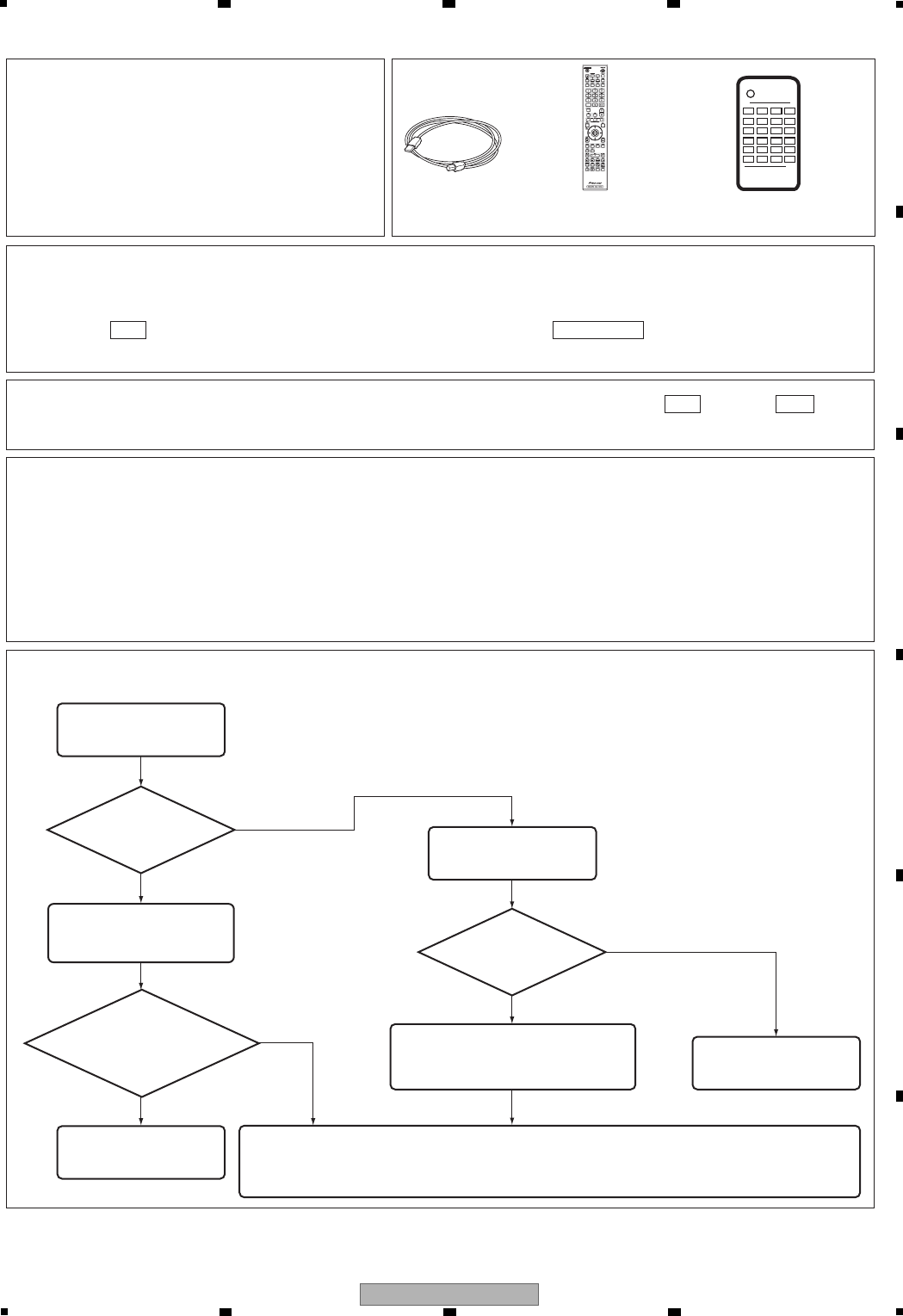
69
DVR-LX61
56 7 8
56 7 8
A
B
C
D
E
F
6.9 USB CHECK MODE
Remote control unit
supplied with the unit
[Purposes] [Tools to be used]
[How to quit]
[How to enter this mode]
[Procedures]
Remote control unit for servicing
(GGF1381)
As this unit is provided with two USB
ports, operation checks of these ports
are possible by connecting them (loop
connection).
1. Connect Connector A (at the front panel) and Connector B (at the front panel), using a USB cable.
2. Enter USB Check mode.
Press the ESC key on the remote control unit for servicing then press the TIMER REC key on the remote control unit
supplied with this unit.
To quit while the ports are operating properly ("USB CHK OK" is lit.): Press the ESC key or the clear key.
To quit while port operation is abnormal: Turn the power off then back on.
1. Check the indication on the FL display.
When the two ports are operating properly: "USB CHK OK" is lit.
When port operation is abnormal: "USB CHK NG" is lit.
2. When "USB CHK OK" is lit in Step 1, disconnect the USB cable in order to perform the
detachment/attachment test.
The indication on the FL display will change, as follows:
If the result is OK: "USB CHK OK" will flash.
If the result is not OK: "USB CHK OK" will remain lit.
[Troubleshooting]
Possibility of contact between USB connectors A (at the front panel) and B (at the front panel).
Possibility of breakage of the internal flexible cables that connect USB connector A (at the front
panel) and B (at the front panel) with the control circuitry on the MAIN Assy.
EMMA2RFEX on the MAIN Assy is in failure.
"USB CHK OK"
is lit on the FL
display.
Is the USB cable OK?
(Perform USB checking, using
another USB cable.)
Enter USB Check mode.
"USB CHK OK" flashes.
Disconnect the USB cable.
USB-port test: OK
"USB CHK OK" remains lit,
indicating that the result of the
detachment/attachment test is not OK.
The USB cable is
defective.
"USB CHK NG" is lit on the
FL display, indicating port
operation is abnormal.
Ye s
Ye s
Ye s
No
No
No
USB cable
(GGD1445)

70 DVR-LX61
12 3 4
A
B
C
D
E
F
12 3 4
6.10 HDD CHECK MODE
(1) Flowchart of HDD diagnosis
Purpose:
With use of the HDD-diagnostic program contained in the product itself, physical errors on the HDD can be diagnosed. Use
this program to diagnose whether or not the HDD is in failure when one of the symptoms indicated below is recognized, or
when a failure in the HDD is suspected.
Symptoms of failure in HDD:
(1) HDD Error
(2) Failure in HDD recording or playback
(3) HDD not recognized
Tool to be used:
Remote control unit for servicing (GGF1381)
Check the HDD Information.
Is something wrong?
No
Ye s
Execute Self-Test.
Has an error occurred?
No
Ye s
Execute Extended Self-Test.
Has an error occurred?
No
Ye s
Execute HDD Read/Write Check.
Has an error occurred?
Execute writing test, if required.
Result of the diagnosis: No abnormality
No
Ye s
Result of the diagnosis: Failure in HDD
Measures to be taken: Replacement of HDD
[2] Flow of HDD Diagnosis
[1] How to Diagnose Failure of the Hard Disc Drive (HDD)

71
DVR-LX61
56 7 8
56 7 8
A
B
C
D
E
F
(2) Overview of the diagnosis items
How to start/terminate the diagnostic program
HDD Information
SELF TEST
EXTENDED SELF TEST
HDD Read / Write Check
Use the remote control unit for servicing.
How to start: Press the "ESC", "CX", "0", and "1" keys simultaneously.
How to terminate: Press the "ESC" key.
Do NOT perform other operations on the unit while the HDD diagnosis is in progress. Although the diagnostic program is
designed to function independently from the unit's functions, an operation on the unit during a diagnosis may cause a
malfunction.
The status of the unit recommended during diagnosis is as follows: All stop, no timer recording (including auto-recording), and
Input selection to L1-L3.
This is a display for checking the HDD information, such as the model name of the
HDD, continuous power-on time, authentication status, and results of the diagnosis on
the end of service life.
This is a simplified diagnosis for the HDD.
A serious failure in the HDD can be detected with this test.
Time required for testing: Approx. 60 sec.
This is a reading test across all sectors of the HDD.
Data recorded on the HDD will not be erased, because no writing operation is
performed.
Time required for testing: Approx. 2.5 hours/500 GB
1.3 hours/250 GB
This is a writing, reading, and comparing test across all sectors of the HDD.
All data recorded on the HDD will be erased, because all the data are to be
overwritten. Be sure to obtain your client's consent beforehand.
Time required for testing: Approx. 15 hours/500 GB
8 hours/250 GB
[3] How to Start or Terminate the Diagnostic Program
You must redownload Gracenote DB data, because Gracenote DB data are to be over
written too.
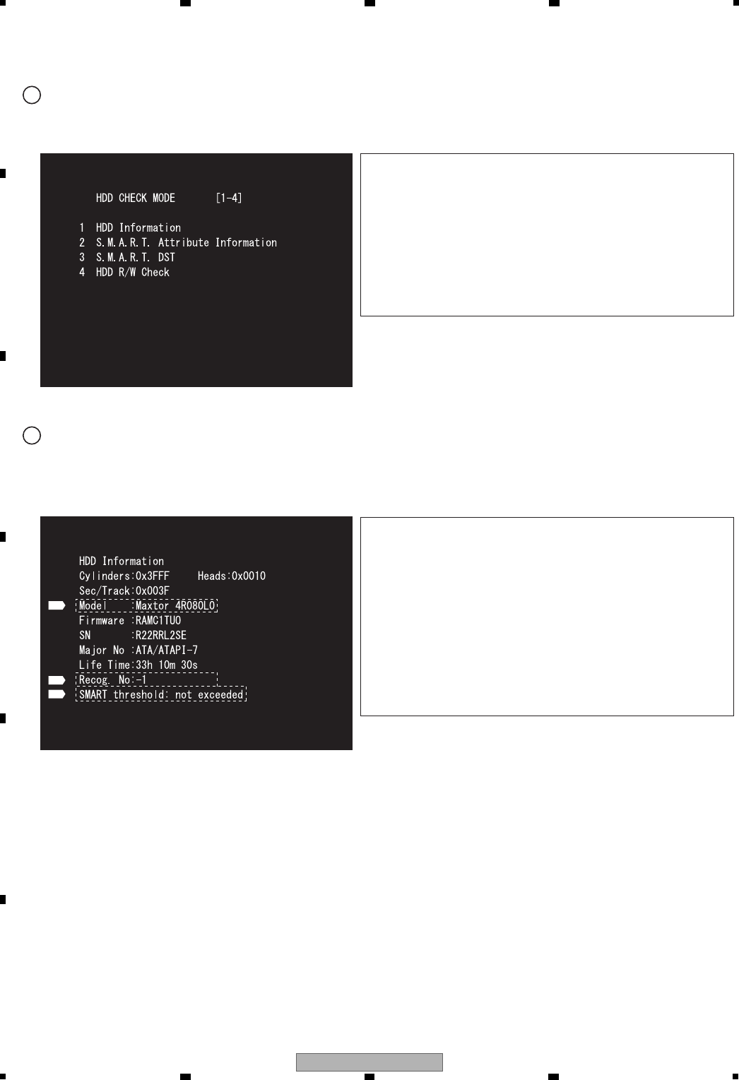
72 DVR-LX61
12 3 4
A
B
C
D
E
F
12 3 4
1Display the menu on the screen.
The menu indicated below is displayed when the diagnostic program is started. To enter each mode, press the
corresponding key "1"-"4" on the remote control unit for servicing.
Tests to be executed
1 HDD Information:
Check of the HDD information
2 S.M.A.R.T. DST:
Executing a simplified test or a reading test of all data
3 HDD R/W Check:
Executing a writing/reading test of all data. All data on the
HDD will be erased if this test is executed.
Note: "2. S.M.A.R.T. Attribute . . ." is not to be used.
2Check the HDD information.
Press the "1" key on the remote control unit for servicing. Check the following data:
Model: Is the correct model name of the HDD displayed?
Recog. No: Is a positive value displayed?
SMART threshold: Is "not exceeded" displayed?
To return to the menu screen, press the "Clear" key.
Detailed description
1 Model:
For the correct model name, refer to the display of the unit.
2 Recog. No:
Positive value: The HDD has been authenticated.
Negative value: The HDD has not been authenticated.
3 SMART threshold:
exceeded: The HDD has come to the end or near the end of
its service life.
not exceeded: The HDD has not reached the end of its
service life.
[4] Diagnosis Procedures
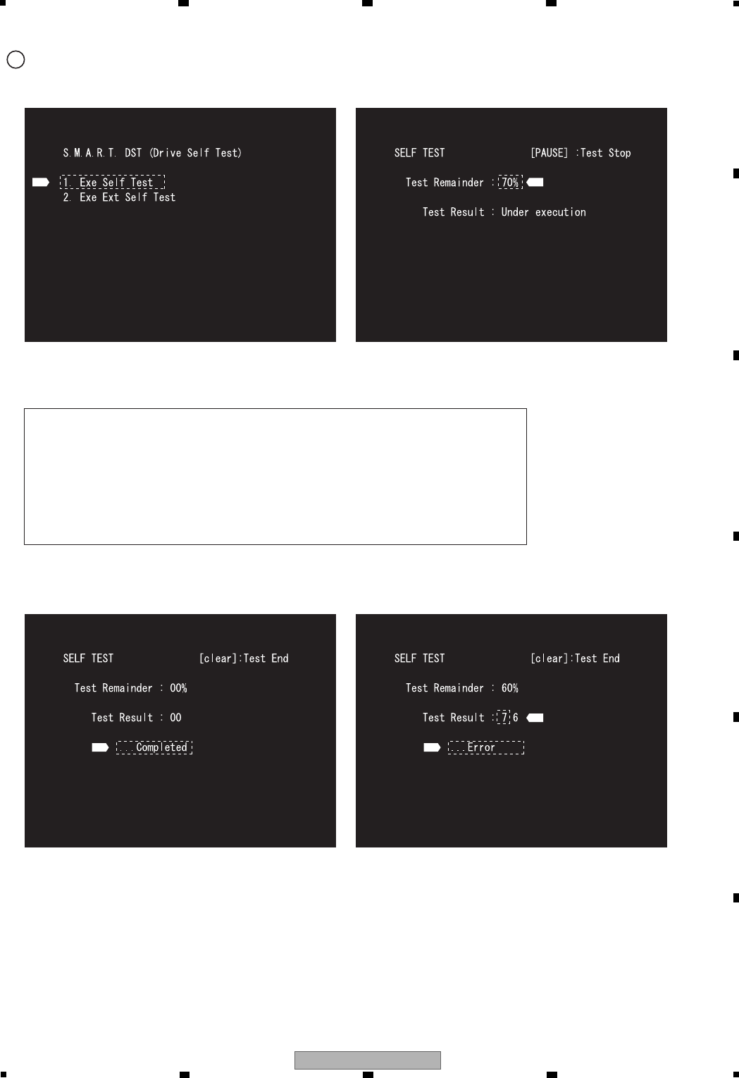
73
DVR-LX61
56 7 8
56 7 8
A
B
C
D
E
F
3Execute Self-Test.
Press the "3" key on the remote control unit for servicing while the menu screen is displayed.
When the following screen is displayed, press the "1" key to start the Self-Test.
The progress of the test is displayed on the screen. The percentage remaining of the test is displayed on the screen,
and the test is terminated when the percentage reaches 00%.
Check whether or not an error has occurred after the test is finished.
To return to the menu screen, press the "Clear" key.
Example: No error Example: With an error
Diagnosis results
• Without an error: ". . . Completed" is displayed.
Then, proceed to the Extended Self-Test.
• With an error: ". . . Error" is displayed. Look at the number in Test Result.
If the place value for tens is 1 or 2, execute the Self-Test again.
If it is from 3 to 7, the HDD must be replaced.
Note: If the result of the second test is the same, replacement of the HDD is required.
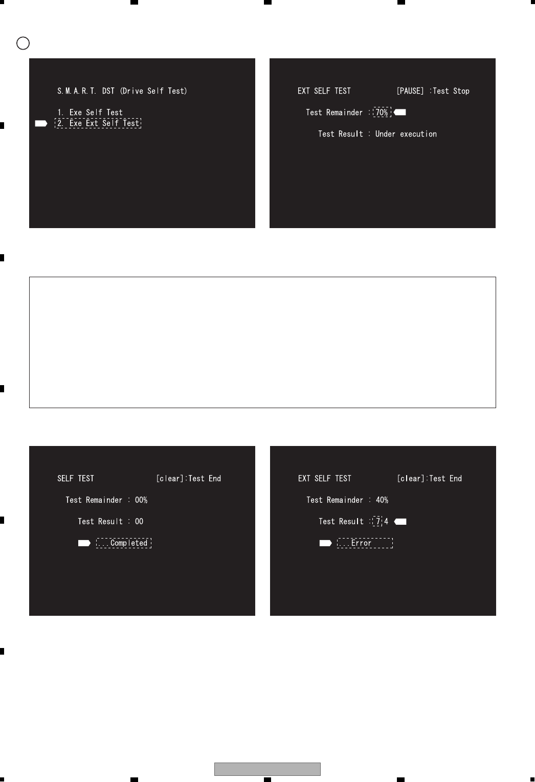
74 DVR-LX61
12 3 4
A
B
C
D
E
F
12 3 4
4Execute the Ext (Extended) Self-Test.
Press the "3" key while the menu screen is displayed, then the "2" key on the remote control unit for servicing.
The Extended Self-Test starts. The percentage remaining of the test is displayed on the screen, and the test is
terminated when the percentage reaches 00%. Check whether or not an error has occurred after the test is finished.
To return to the menu screen, press the "Clear" key.
Example: No error Example: With an error
Diagnosis results
• Without an error: ". . . Completed" is displayed.
If no error occurs up until this stage, HDD operations are normal except for writing operations.
If the unit has a failure in HDD playback, a block other than the HDD may be in failure.
If the unit's failure is in HDD recording, however, the next HDD Read/Write Check must be executed to test
writing operations.
• With an error: ". . . Error" is displayed.
Look at the number in Test Result.
If the place value for tens is 1 or 2, execute the Ext Self-Test again.
If it is from 3 to 7, the HDD must be replaced.
Note: If the result of the second test is the same, replacement of the HDD is required.
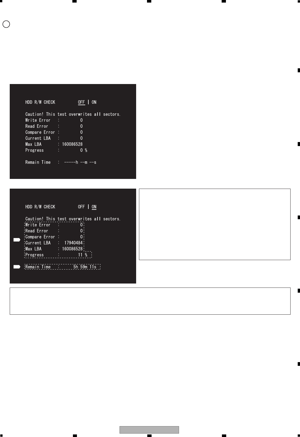
75
DVR-LX61
56 7 8
56 7 8
A
B
C
D
E
F
5
The display on the left indicates the progress of the test.
The percentage of the test progress is displayed on the screen,
and the test is finished when the percentage reaches 100%.
Diagnosis results
• If no error occurs in any of the Write/Read/Compare items, the HDD is in normal condition and is not required to
be replaced. A block other than the HDD is in failure.
• If any error occurs, the HDD must be replaced.
When the status is OFF
To terminate the diagnostic program, press the "ESC" key.
When the status is ON
The status becomes OFF when the test is interrupted by pressing the "SKIP o" key or when "Progress" reaches 100%.
Detailed description on each item on the screen
• Write Error: Number of write errors
• Read Error: Number of read errors
• Compare Error: Number of comparison errors
• Current LBA: The address during testing
• Max LBA: Highest address number of the HDD
• Progress: Percentage of test progress (%)
• Remain Time: Estimated time required for finishing the test
across all sectors.
Estimated time: 15 hours/500 GB
8 hours/250 GB
Execute the HDD R/W Check.
Before executing this test, be sure to obtain your client's consent for erasure of HDD data.
Press the "4" key while the menu screen is displayed then the "SKIP p" key to start the HDD R/W Check.
NOTE
Be sure to press the "SKIP o" key to complete this test after the progress reaches 100% or cancel this test (OFF) while
it's in progress.
Do not press "ESC" key without pressing "SKIP o" key, otherwise this test is not completed and it causes unexpected
errors on the HDD.

76 DVR-LX61
12 3 4
A
B
C
D
E
F
12 3 4
6.11 DIAGNOSTIC PROCEDURES WHEN AAC DECODING HAS FAILED
[1] AAC information
[Purpose]
AAC Error Information
[How to Enter]
Press [ESC], [DISP], [+10], then [1], in that order. The first screen is displayed.
To switch screens, press [DIG/ANA].
First screen
Note 1: Startup status (OK/NG) of the external decoder
If the external decoder starts up normally, OK is displayed. If it fails to start up, NG is displayed. With NG, playback of any AAC
file will fail.
Possible causes for failure of startup and how to diagnose
Possible cause 1: No reset signal is input to IC101.
How to diagnose: Check whether a high signal is input to Pin AAC_RESET_B of IC101.
Possible cause 2: Communication failure between IC101 and IC1001 on the MAIN ASSY.
How to diagnose: Check whether high and low signals are alternately input to Pins AAC_D0 to AAC_D15, AAC_A0 to
AAC_A10, AAC_RD_B, AAC_WR_B, and AAC_CS_B for communication.
Possible cause 3: Failure in IC101
How to diagnose: Check whether a low signal is output from Pin AAC_INT_B in response to the reply from IC101
Possible cause 4: Failure in IC101 that cannot be diagnosed
The flow of startup processes is as follows:
(1) A high signal is input to Pin AAC_RESET_B.
(2) Communication starts, using Pins AAC_D0 to AAC_D15, AAC_A0 to AAC_A10, AAC_RD_B, AAC_WR_B, and
AAC_CS_B.
(3) In response to the process in step (2) above, a low signal is output from Pin AAC_INT_B.
(4) Steps (2) and (3) are repeated until the startup process is completed.
(Note 1)
(Note 2)
Second screen: Information on playback of MUSIC files
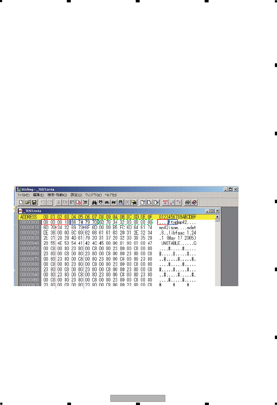
77
DVR-LX61
56 7 8
56 7 8
A
B
C
D
E
F
Note 2:
ERROR information
If any error code is indicated in parentheses, a playback error has been generated. Each error code is displayed in its fixed
position. (The duration of error-code indication is short, because when an error is generated, playback of the next file is
automatically attempted.)
Description of error codes
FMT : The file cannot be recognized as having an MP4 file format.
DEC : Although the file is recognized as playable, the decoder could not decode the data of the file correctly.
CH : The number of channels is not supported.
QNT : The quantization bit rate is not supported.
BPS : The bit rate is not supported.
FS : The sampling frequency is not supported.
BOX : The file format is judged to be not supported upon analysis of the MP4 file.
PRF : The Advanced Audio Codec (AAC) is judged to be not playable.
MEM : The system failed to secure the amount of memory required for playback.
Possible causes for errors and how to diagnose
Possible causes for an FMT error
Possible cause 1: Impossible box size for the first box of an MP4 format file
How to diagnose: Check the binary data of the file with which an FMT error was generated. Consider the first 4 bytes at the
beginning of the file as the box size and check if the size is 0 or a value that exceeds the file size.
If the box size is 1, consider the 8 bytes from the 8th byte from the beginning as the box size. Check if the
size is 0 or a value that exceeds the file size.
How to check the box size:
For checking the binary data of the file, use the Binary Editor of the PC tools.
The figure below shows the binary data of an MPEG4 file:
Possible cause 2: Failure in data reading during file analysis
How to diagnose: Check the ATA error log on the Debug screen.
How to check the ATA error log:
Display the ATA error log page by pressing [ESC], [DISP], [2], then [DIG/ANA], in that order.
The first 4 digits denote date, and the next 6 digits denote time. Check if the date and time match those when an error was
generated during AAC playback.
You can switch between Writer and HDD data, using [FRM/TIM]. Switch according to the type of medium being played back.
For USB, there is no log for reading errors.
BOX size BOX name
With this file, the first box is an "ftyp" box, and its size is 0x18 bytes (the figure in the frame in red).
In a case of an FMT error, the first box size is 0 or a value that exceeds the file size (impossible value for the MPEG4 file format).
If the box size is 1, the data that are framed in dotted green lines in the above figure are treated as the box size.

78 DVR-LX61
12 3 4
A
B
C
D
E
F
12 3 4
Possible causes for a DEC error
Possible cause 1: An error notification was issued by the decoder, because there was an error in the stream.
How to diagnose: Play back the file on the PC to check if an error is generated.
Possible cause 2: Data reading failed while the data were being transmitted to the decoder.
How to diagnose: Check the ATA error log on the Debug screen.
* See "How to check the ATA error log," above.
A "CH" error does not occur during AAC playback.
Possible causes for a QNT error
Possible cause 1: The encoding method is not 16-bit quantization.
How to diagnose: Check the number of quantization bits, using a PC analysis tool.
Possible cause 2: After data reading failed, an erroneous number of quantization bits was obtained.
How to diagnose: Check the ATA error log on the Debug screen.
* See "How to check the ATA error log," above.
Possible causes for a BPS error
Possible cause 1: The average bit rate exceeded 480 Kbps.
How to diagnose: Check the average bit rate, using a PC analysis tool.
Possible cause 2: After data reading failed, an erroneous average bit rate was obtained.
How to diagnose: Check the ATA error log on the Debug screen.
* See "How to check the ATA error log," above.
Possible causes for an FS error
Possible cause 1: The sampling frequency was less than 8 KHz or greater than 96 KHz.
How to diagnose: Check the sampling frequency, using a PC analysis tool.
Possible cause 2: After data reading failed, an erroneous sampling frequency was obtained.
How to diagnose: Check the ATA error log on the Debug screen.
* See "How to check the ATA error log," above.
Possible causes for a BOX error
Possible cause 1: An impossible box size was obtained during box analysis.
How to diagnose: Check the box size, using a PC analysis tool.
Possible cause 2: Data necessary for playback could not be obtained.
How to diagnose: Analyze the file, using a PC analysis tool, and check that SAMPLE DESCRIPTION BOX, TIME TO SAMPLE
BOX, SAMPLE SIZE BOX (SAMPLE SIZE 2 BOX), SAMPLE TO CHUNK BOX, CHUNK OFFSET BOX
(64BIT CHUNK OFFSET BOX) exist.
Possible cause 3: SAMPLE DESCRIPTION BOX, which signifies that audio streams are contained, did not exist.
How to diagnose: Check the binary data of the file with which this error was generated and confirm that the 20th byte does not
indicate "mp4a." (A DRM file may also have this error.)
Possible cause 4: "AudioSpecificConfig" was not described in "SAMPLE DESCRIPTION BOX," which should show that an
audio stream is contained.
How to diagnose: Check AudioSpecificConfig, using a PC analysis tool.
Possible cause 5: Data reading failed during file analysis.
How to diagnose: Check the ATA error log on the Debug screen.
* See "How to check the ATA error log," above.
Possible causes for a PRF error
Possible cause 1: Audio streams were not contained in "AAC LC" and "High Efficiency AAC Profile."
How to diagnose: Check the type of audio stream in AudioObjectType of AudioSpecificConfig, using a PC analysis tool.
Possible cause 2: After data reading failed, erroneous AudioObjectType data were obtained.
How to diagnose: Check the ATA error log on the Debug screen.
* See "How to check the ATA error log," above.
Possible causes for an MEM error
Possible cause 1: The shared memory region for the system was fragmented, and the memory region of 4,096 bytes that was
necessary for file analysis could not be ensured.
How to diagnose: After setting the unit to Standby mode, turn the unit back on and check if an MEM error is generated.
If it is, the system memory may be defective.
79
DVR-LX61
56 7 8
56 7 8
A
B
C
D
E
F
6.12 DIAGNOSTIC PROCEDURES WHEN CONNECTING THE LAN
In bold print: Fixed indications
[1] Specifications of the Ether Debug Screen
[Purpose]
Diagnose based on Ethernet connection information.
[How to Enter]
Press [ESC], [DISP], [+10], [+10], then [7], in that order.
[2] Simple diagnostic procedures
In regular print: Variable indications
Sympton: Neither CDDBonline search nor ConnectPC (Ethernet) function.
1
2
3
4
5
6
7
DescriptionsNameNo. Remarks
Init Whether initialization of LAN9211 (Ethernet Controller)
has been completed successfully (OK) or not (NG)
In a case of NG, communication between the LAN9211
and EMMA2RFEx may have failed.
Link
Whether the unit is connected to equipment that can
communicate through Ethernet and has established
links (UP) or not (DOWN)
MAC MAC address that is set for the unit
DHCP Setting for automatic acquisition of an IP address
DNS Setting for automatic acquisition of a DNS server
PRX Proxy setting
With the Proxy setting ON, when the server assignment
method is server name or IP address, NAME or IP is
indicated, respectively.
IP IP address that is set for the unit
SM Subnet mask that is set for the unit
4DG Default gateway that is set for the unit
7SPEED Display the communication speed and Duplex mode.
DP DNS server primary address
DS
PR
DNS server secondary address
With the Proxy setting ON, the server name or IP
address is displayed.
With the Proxy setting OFF, - - - is displayed.
PT With the Proxy setting ON, the port number is displayed. With the Proxy setting OFF, - - - is displayed.
1
3
5
6
2
Check Items and Unit Status
Screen
Position
No. Possible Cause
Ether 1
Init indication:
OK: Initialization of the Ethernet-associated LSI (IC301) has
been successfully completed.
NG: Poor communication between the Ethernet-associated
LSI (IC301) and HOST microcomputer (IC1001).
Initialization of the Ethernet-associated LSI (IC301) has
failed.
With NG:
Failure in IC301 (the Ethernet Controller).
Failure in communication between IC301 and IC1001,
defective solder, or failure in power supply.
With an IP address that is out of the range described
on the left:
If automatic acquisition of an IP address is set to ON,
check the setting of the router.
Ether 1
Link indication:
UP: The unit is connected to equipment that can communicate
through Ethernet and has established links.
DOWN: The links are not established.
With DOWN:
Defective LAN terminal, poor connection of the ETAB
board, defective LAN cable, the router's power is OFF,
or the connected equipment cannot communicate
through Ethernet.
Ether 2
IP indication:
Is the IP address set within the ranges shown below?
CLASS A: 10.0.0.1 to 10.255.255.254
CLASS B: 172.16.0.1 to 172.31.255.254
CLASS C: 192.168.0.1 to 192.168.255.254
1
3
2
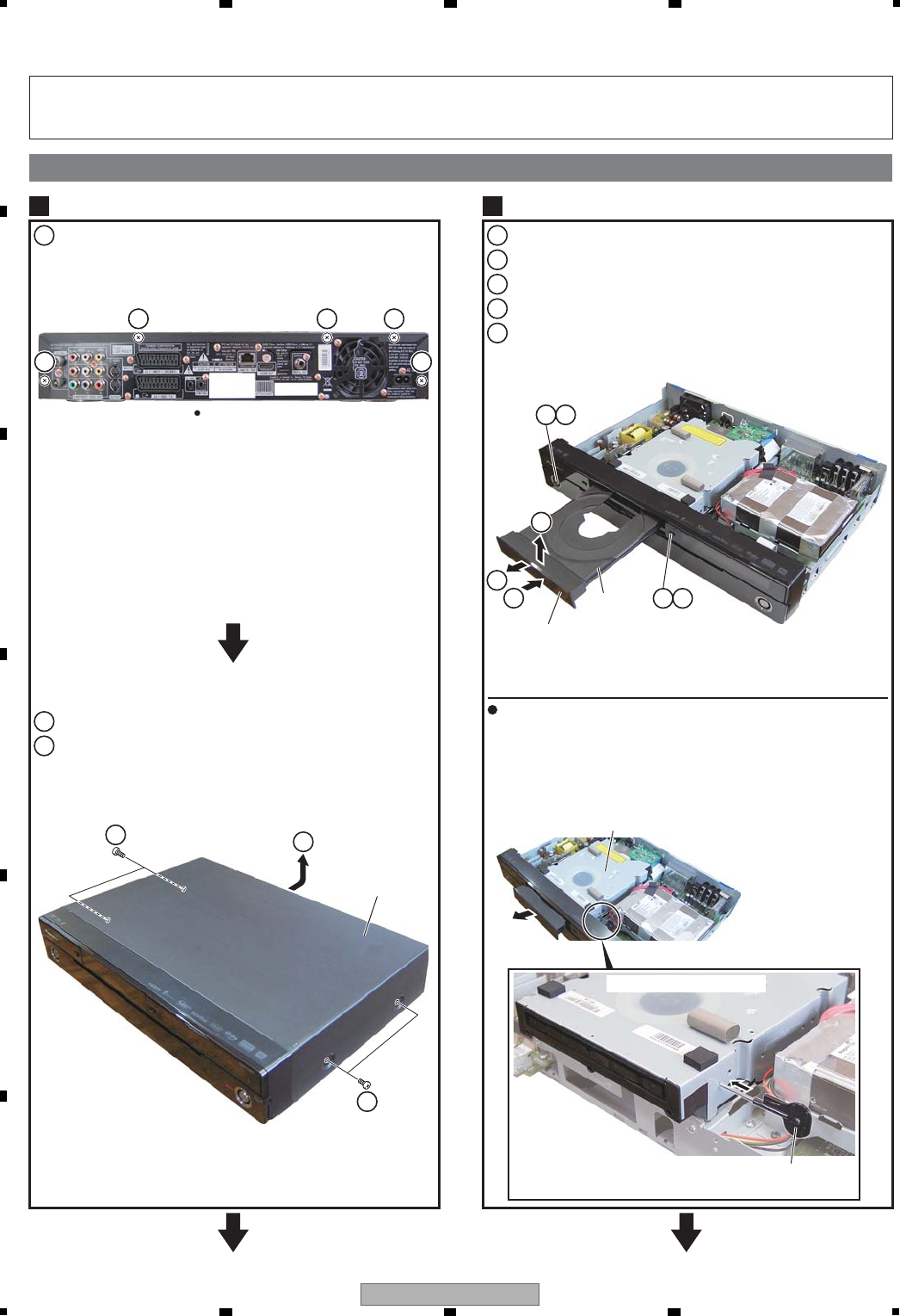
80 DVR-LX61
12 3 4
A
B
C
D
E
F
12 3 4
7. DISASSEMBLY
Bonnet
1
Remove the five screws.
Diagnosis
1
Remove the four screws.
2
Remove the bonnet.
3
1
1 1
2
1
1
Tray Panel
2
Press the u STANDBY/ON button to turn on the power.
1
Press the h OPEN/CLOSE button to open the tray.
2
Remove the tray panel.
3
Press the h OPEN/CLOSE button to close the tray.
4
Press the u STANDBY/ON button to turn off the power.
5
Note 1: Do NOT look directly into the pickup lens. The laser beam may cause eye injury.
Note 2: Even if the unit shown in the photos and illustrations in this manual may differ from your product, the procedures
described here are common.
Emergency disc ejection rod
(GGF1529)
When the tray cannot be opened because the power cannot be
turned on, it can be opened using the emergency disc ejection
rod (GGF1529). (A long, thin rod about 1 mm in diameter can be
used in place of the rod.)
How to open the tray when the power cannot be turned on
Rear view
Bonnet
×2
23
3
×2
Tray panel
Tray
51
42
24
SERVICE LOADER Assy
SERVICE LOADER Assy

81
DVR-LX61
56 7 8
56 7 8
A
B
C
D
E
F
Front Panel Section
3
Unhook the four hooks.
1
Disconnect the one flexible cable.
2
Remove the front panel section.
3
HDD
4
Remove the two screws.
1
Remove the two screws.
2
Remove the HDD with the HDD stay.
3
3
2
1
CN105
SERVICE TUSB
Assy
Front panel section
3
HDD
Bottom view
1 1
1
1
2 2
1

82 DVR-LX61
12 3 4
A
B
C
D
E
F
12 3 4
Disconnect the three connectors.
1
Remove the two screws.
DVR-LX61 Only
2
Remove the ETAB Assy while disconnecting the B to B
connector.
3
Remove the one screw.
4
Disconnect the one flexible cable.
6
Remove the six screws.
7
Remove the SERVICE LOADER MAIN.
8
Remove the one screw.
5
SERVICE LOADER MAIN
5
1
CN201 CN902
CN901
CN2301
CN501
SERVICE DVUB
Assy
1
1
POWER SUPPLY
Assy
SERVICE LOADER MAIN
SERVICE LOADER MAIN
3
ETAB Assy
2 2
Bottom view
4
7 7
7
7
7
7
5
Bottom view
8
6
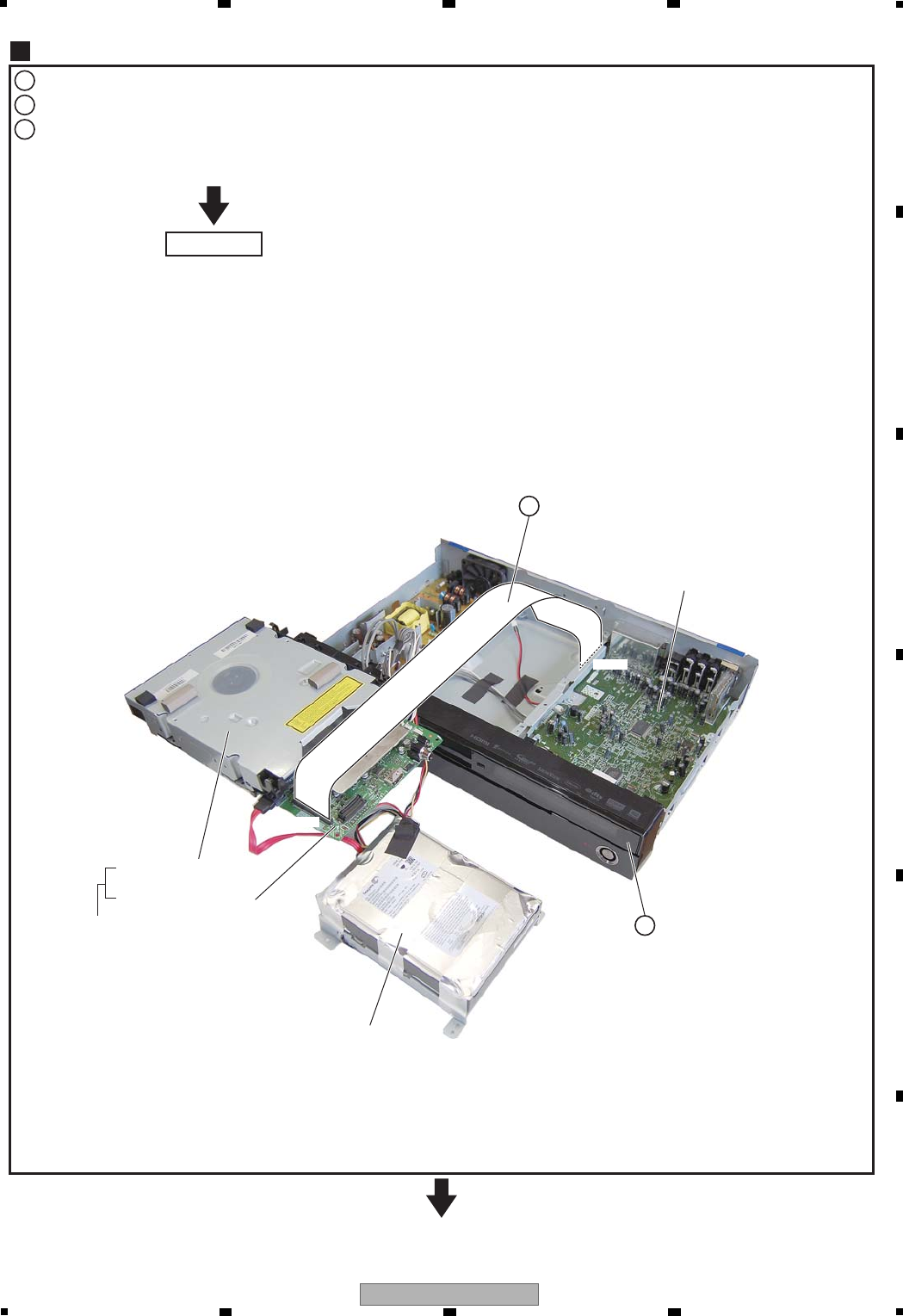
83
DVR-LX61
56 7 8
56 7 8
A
B
C
D
E
F
Diagnosis
6
Reassembling the front panel section.
1
Connect the flexible cable for service.
2
Arrange the unit as shown in the photo below.
3
Diagnosis
SERVICE LOADER Assy
SERVICE MAIN Assy
SERVICE LOADER MAIN
HDD
Front panel section
SERVICE TUSB Assy
1
Flexible cable for service
(40P)
2
CN101
CN2301

84 DVR-LX61
12 3 4
A
B
C
D
E
F
12 3 4
Access to the SERVICE MAIN Assy, Cleaning the Pickup Lens
Remove the Upper case.
4
Remove the two screws.
1
Remove the cord holder.
2
Cord Holder
Remove the four screws.
1
Remove the two tapes.
2
Remove the low case U11.
3
Low Case U11, Upper Case
Before shipment, be sure to clean the pickup lens,
using the following cleaning materials:
Cleaning liquid : GEM1004
Cleaning paper : GED-008
Cord holder
SERVICE LOADER Assy
Low case U11
Upper case
SERVICE MAIN AssySERVICE LOADER Assy
Pickup lens
11
2
11
2
11
2Bottom view
Bottom view
3
4
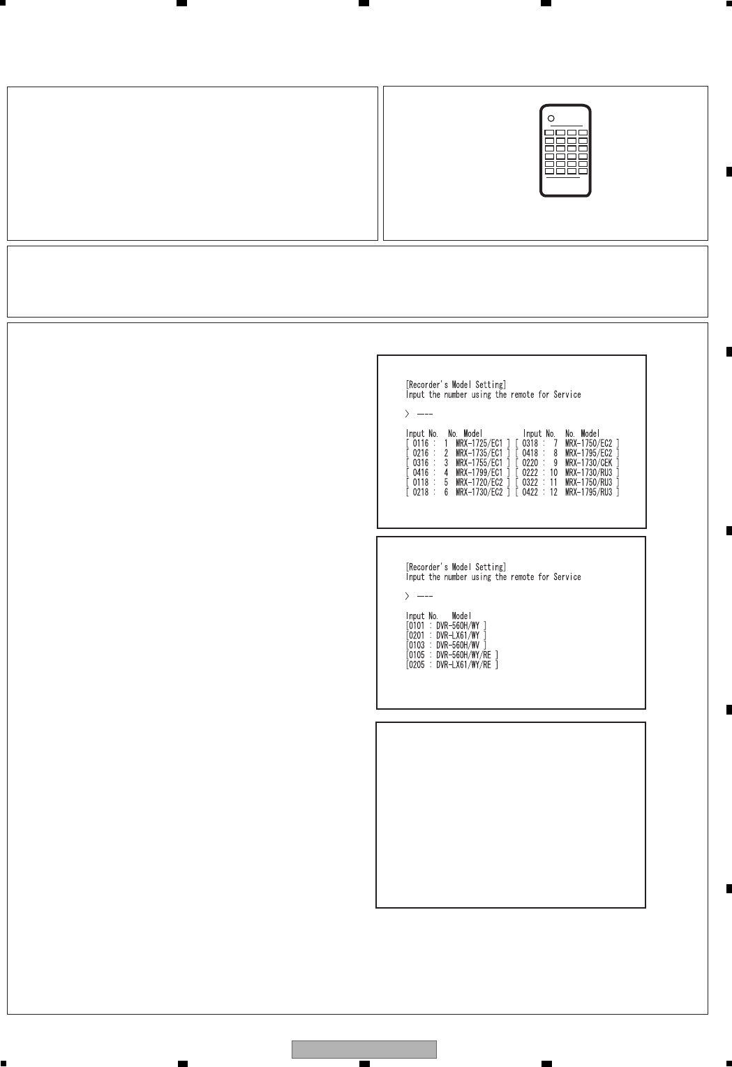
85
DVR-LX61
56 7 8
56 7 8
A
B
C
D
E
F
8. EACH SETTING AND ADJUSTMENT
8.1 MODEL SETTING
When the MAIN Assy and/or TUJB Assy that are(is)
commonly used with another model are(is) replaced,
they(it) must recognize the model of this unit.
Items to be set: The model number, destination, and
region No. must be set.
• Once the setting has been made, it can never be changed. Be sure to make the setting correctly.
• As this setting resets the Assy(s) in question to the factory-preset status, it is recommended that you obtain
the customer's consent beforehand.
1 After the unit is turned on, the model name for the
original equipment manufacturer is displayed on the
TV monitor screen. Input "9696" on the remote control
unit for service to change it to the model name for
Pioneer.
2 The following screen is displayed on TV monitor.
Press four digits properly by using the remote control
unit for service,
according to the screen information.
3 Disconnect then reconnect the AC power cord of the
unit. Be careful not to impart vibration to the unit
immediately after the AC power cord is disconnected.
[Procedures]
[Purposes] [Tool to be used]
[Notes]
5 Press [ESC] then [DISP] keys by using the remote
control unit for servicing, and then confirm each
Model Name.
6
End
Remote control unit for servicing
(GGF1381)
4 Reset the recorder to all its factory settings.
(Make sure that the recorder is on. Press and hold
g (STOP) key and press u (STANDBY/ON) key on
the front panel.)
The recorder turns off with all settings reset.
DVR-LX61/WY VERSION : 0.14
SYSCON : RELEASE_179
Rev.1.7379
TUNERCON : 2.22 OK
DRIVE : DVD-RW DVR-U13 OK
1.10 OK
PIC SERIAL : 007710217604
HDD INT : ----
HDD USE : ----
GNDB B : NOBKUP GNDB U : NOBKUP
DEVICE : E2R-FEx1.1 FLASH : 128M
REGION : 2 C : 0000000153
HDCP : 0000000153
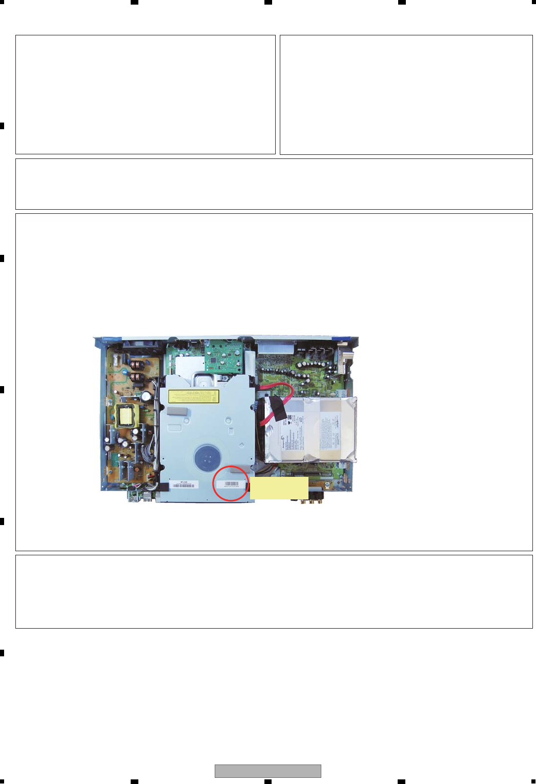
86 DVR-LX61
12 3 4
A
B
C
D
E
F
12 3 4
8.2 LD POWER ADJUSTMENT
[Purposes]
If a combination of a main board and PU is
changed, the LD power adjustment and
adjustment for disc judgment needs to be made
for a new combination of the main board and PU
since the adjusted LD-power value becomes
inappropriate for the new combination and stable
playback and recording to disc becomes
impossible.
[Tools to be used]
[Notes] Never turn the power off while any of the following operations is in progress:
• While laser diode (LD) power adjustment is being performed normally by the unit
• While adjustment for disc judgment is being performed
[Explanation on each adjustment mode]
• Drive Adjustment Mode
This mode is used to select each mode for LD power adjustment.
In this mode, you can confirm an 11-digit number provided for the LD power adjustment.
The 11-digit number is stored in FLASH (IC1102) of the main board.
• PU Data Setting Mode
This mode is used to enter an 11-digit number provided for the LD power adjustment.
If you have changed a combination of the main board and PU, enter an 11-digit number marked
on the case of a loader which is provided in pairs with PU.
The LD power adjustment is made by using this 11-digit number.
• Power Adjustment Mode
This mode is used to execute the LD power adjustment and to check the progress of the adjustment.
In case an error occurs during the adjustment, you can also check the error details in this mode.
11-digit
numeric data
[How to enter Drive Adjustment Mode]
To enter the Drive Adjustment Mode, press [ESC]+[CX]+[1]+[0] on the remote control unit for service.
Though the LD power adjustment can be executed irrespective of the product functions, do not operate
the product during the LD power adjustment to prevent misadjustment.
GGF1381 : Service Remote Control Unit
GGV1054 : CD-ROM (CDT-313)
GGV1036 : DVD-ROM DL (DVDT-002)
GGV1278 : Blank DVD-R (That's DR-C12WTY5PA)
GGV1282 : Blank DVD-RW (JVC VD-W120XH5)
GGV1284 : Blank DVD-RAM (maxell DRM120C.1P5S)

87
DVR-LX61
56 7 8
56 7 8
A
B
C
D
E
F
[Operation procedure]
1. When you enter the Drive Adjustment Mode, the following screen is displayed. On this screen, you can check
11-digit numeric data stored in FLASH of MAIN Assy, and can also switch over between each mode.
[Drive Adjustment Mode]
PU DATA
[12345678910]
<CLEAR> Exit
<STEREO> PU Data Setting
<SEARCH> Power Adjustment
2. To enter the PU Data Setting Mode, press [STEREO] on the remote control unit for service.
Entering the PU Data Setting Mode displays the following screen.
[PU Data Setting Mode]
OLD PU DATA
[12345678910]
NEW PU DATA?
>***********
<CLEAR> Exit
<SEARCH> PU DATA CLEAR
11-digit number
for adjustment
3. By pressing [0] to [9] keys on the remote control unit for service, enter an 11-digit number marked on
the case of a loader provided in pairs with PU.
Entering the 11-digit number displays the following screen.
[PU Data Setting Mode]
OLD PU DATA
[12345678910]
NEW PU DATA?
>01987654321 OK
<CLEAR> Exit
<SEARCH> PU DATA CLEAR
<PLAY> Enter
4. To enter the 11-digit number, press [PLAY] on the remote control unit for service.
The 11-digit number contains 2-digit checksum data to prevent input errors.
The screens displayed for the correct/incorrect check sum are as follows.
When the checksum is correct
[Drive Adjustment Mode]
PU DATA
[01987654321]
<CLEAR> Exit
<STEREO> PU Data Setting
<SEARCH> Power Adjustment
When the checksum is correct
Enter the Power Adjustment Mode and
execute the LD power adjustment, as
described in 5.
When the checksum is incorrect
[Drive Adjustment Mode]
PU DATA
[12345678910]
CHECK SUM NG!
[01987654321]
<CLEAR> Exit
<STEREO> PU Data Setting
<SEARCH> Power Adjustment
When the checksum is incorrect
The input data may be incorrect.
Return to 2 and enter the PU Data Setting
Mode to re-enter the 11-digit number.
88 DVR-LX61
12 3 4
A
B
C
D
E
F
12 3 4
5. When the checksum is correct, enter the Power Adjustment Mode and execute the LD power adjustment.
To enter the Power Adjustment Mode, press [SEARCH] on the remote control unit for service.
Entering the Power Adjustment Mode displays the following screen and opens the tray automatically.
[Power Adjustment Mode]
Close The Tray!
<CLEAR> Exit
6. Close the tray manually to execute the LD power adjustment mode.
You can check the progress of adjustment in the following screen.
[Power Adjustment Mode]
Step Mode : DVD Read Power
<CLEAR> Exit
7. When DVD Disc Judgment is displayed in the Step Mode, the tray opens automatically.
Place DVDT-002 in the tray. The tray closes after 15 seconds from the time it opened.
If the adjustment for DVD disc judgment is completed successfully, CD Disc Judgment is displayed in the Step Mode.
When the tray does not open
• Check if flexible cables and wire rods are connected properly.
• Errors in the loader, main board, or power source board are
suspected.
Explanation on Step Mode (time needed)
• DVD Read Power (approx. 10 sec.)
Adjustment of DVD playback power
• RAM Read Power (approx. 20 sec.)
Adjustment of RAM playback power
• DVD Write Power (approx. 40 sec.)
Adjustment of DVD recording power
• CD Read Power (approx. 10 sec.)
Adjustment of CD playback power
• DVD Disc Judgment (approx. 30 sec.)
Adjustment for DVD disc judgment
• CD Disc Judgment (approx. 30 sec.)
Adjustment for CD disc judgment
If the adjustment for DVD disc judgment is not completed successfully
• A disc other than DVDT-002 may have been placed.
Place DVDT-002 in the tray.
8. When CD Disc judgment is displayed in the Step Mode, the tray opens automatically.
Place CDT-313 in the tray. The tray closes after 15 seconds from the time it opened.
If the adjustment for CD disc judgment is completed successfully, the following screen is displayed.
Since the judgment is completed successfully, press [CLEAR] on the remote control unit for service and exit
from the adjustment mode.
[Power Adjustment Mode]
Step Mode : -
Result : OK
<CLEAR> Exit
9. Turn off the power.
If the adjustment for CD disc judgment is not completed successfully
• A disc other than CDT-313 may have been placed.
Place CDT-313 in the tray.

89
DVR-LX61
56 7 8
56 7 8
A
B
C
D
E
F
[Error information]
In case of errors in the Power Adjustment Mode, the following screen is displayed.
[Power Adjustment Mode]
Step Mode : -
Result : 4 - 1
Error!
<CLEAR> Exit
[Contents to check]
1. Record the data to a designated disc (DVD-R / DVD-RW / DVD-RAM) in real time.
2. Measure an error rate at a place where recording is executed.
Measurement method: Refer to the simplified error rate measurement method in the Service Mode.
3. Check that the error rate is 3.3e-3 or below.
About error indication
[Left number]
The left number indicates the Step Mode in
which the error has occurred.
2: Adjustment of DVD playback power
3: Adjustment of RAM playback power
4: Adjustment of DVD recording power
5: Adjustment of CD playback power
6: Adjustment for DVD disc judgment
7: Adjustment for CD disc judgment
[Right number]
The right number indicates the error information.
1 or 2: Error in the adjustment process
(Details of error)
• The PU flexible cables may not have been connected.
• TM or main board error is suspected.
3: Forced termination
This number is displayed when you pressed [CLEAR]
on the remote control unit for service and executed
forced termination.
Error is displayed
If the error rate is out of specification
• Check if there is any defect or fingerprint on the disc. If you find any problem with the disc,
change the disc and try the check again.
• The power adjustment may have been unsuccessful.
Try the power adjustment again.
If the above two do not solve the problem, a defect with MAIN Assy or PU is suspected.
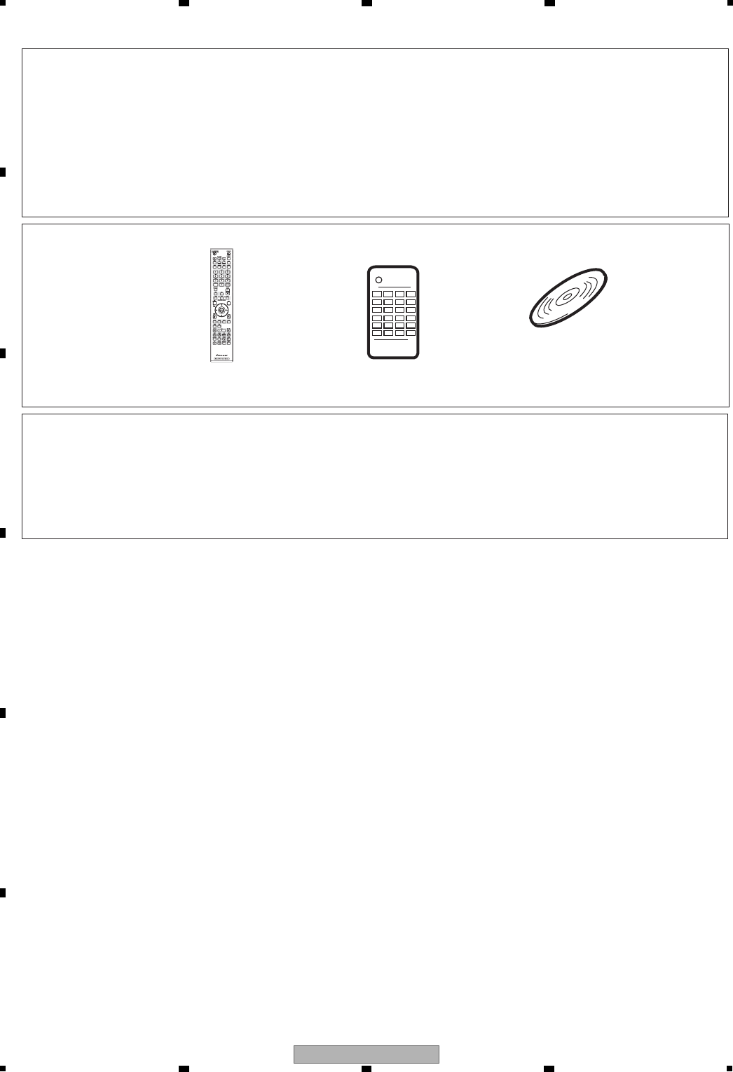
90 DVR-LX61
12 3 4
A
B
C
D
E
F
12 3 4
8.3 CPRM ID NUMBER AND DATA SETTING
For the DVD recorder,it is necessary with the recoding/playback of DVD-RW disc to set an individual
number (ID number) and ID data to each recorder. If the number and data are not set correctly with the
following procedure, cannot work with residual quantity 0:00 or operations in the future may not be
guaranteed with RW disc. You will find the ID number to be set on the ID label on the rear panel.
The Input is Necessary When:
• " CPRM ERR" is displayed on the FL display immediately after the power is turned on or in Stop mode.
• When the MAIN ASSY or the HDD is exchanged.
Important: If no ID label is found on the rear panel, write down the specified ID number by checking it
according to "How to confirm the ID number" shown below.
• Input the ID number while the unit is in Stop mode.
• After the data are read from the data disc (Type 2), the disc will automatically be unloaded.
[Purposes]
[Tools to be used]
[Notes]
Remote control unit supplied
with the unit
Remote control unit for servicing
(GGF1381)
DVD Recorder Data Disc (Type 2)
Be sure to use the latest disc (Type 2).
In Apr. 2008, the latest disc is GGV1321.

91
DVR-LX61
56 7 8
56 7 8
A
B
C
D
E
F
An error occured. Please consult
the service center. Note that
contents on the HDD may be
erased when servicing this unit.
HDD information is not correct.
Execute HDD Initialize from
the Disc Setup menu.
CPRM information is not correct.
When displayed following message at
Power on
FL Tube : [E01]
CRT display :
When displayed following message at
Power on
FL Tube : [E02]
CRT display :
When displayed following message at
Power on
FL Tube : [CPRM ERR]
CRT display :
Power ON
When displayed "CPRM ERR"
• When exchanging HDD or MAIN
Assy, or both exchanged
Initialize HDD Start
Basic
Initialize
Finalize
Initialize HDD
Disc Setup
Confirmation of the CPRM ID No.
Normal operation mode
All recorded data are deleted if the HDD is intialized.
Take care that restoration of the user's data recorded on the HDD is totally
impossible.
Before servicing, OBTAIN THE USER'S PRIOR CONSENT to that effect.
*Use Remote Control of
the unit
*Goes to normal operation
with no caution
New HDD/when
there is error
on recorded contents
Exchanging to the original HDD(when
there is no error on
the recorded
contents.)
[CAUTION]
End
End
Deletion of the CPRM ID No.(when ID No. is registered.)
Input of the CPRM ID No. and ID data
Power OFF ON
Execute
HOME MENU Disc Setup Intialize
HDD Initialize HDD Start
After OSD displaying "Finished" after initilaization, reboot.
[1] Input Flow of the ID No. and ID Data When Exchanging HDD or MAIN Assy
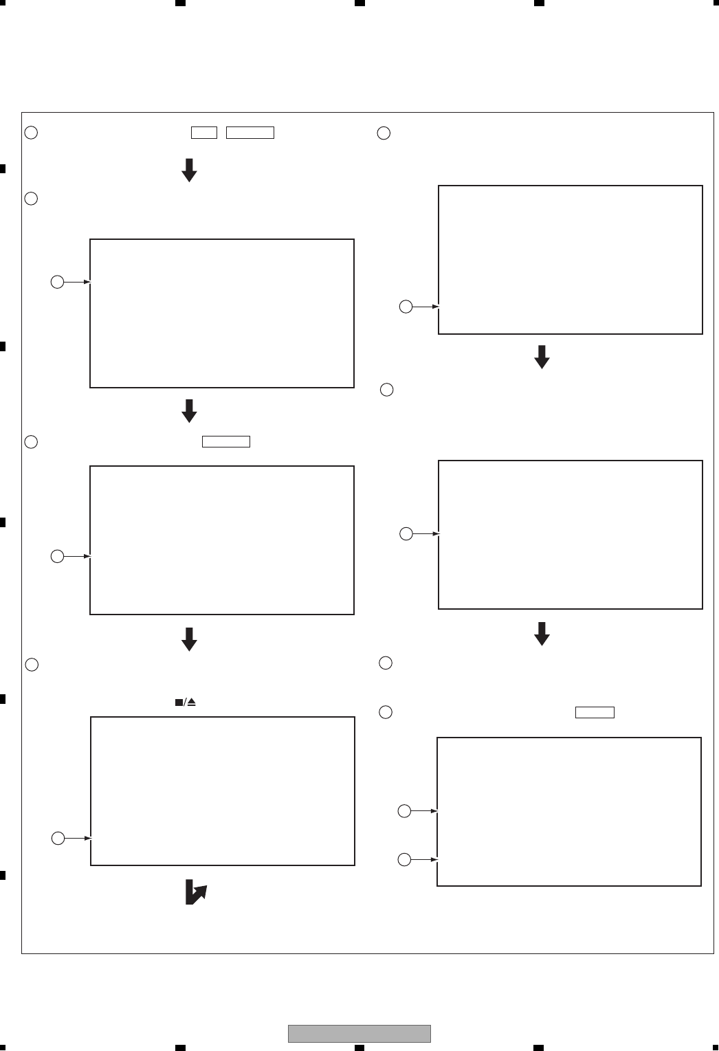
92 DVR-LX61
12 3 4
A
B
C
D
E
F
12 3 4
To enter the input mode, press ESC + STEREO keys
sequentially in a status with no ID number set, such as after
FLASH-ROM downloading.
[Recorder's ID Number Setting]
ID Number ?
> - - - - - - - - -
<CLEAR> Exit
Input ID Number !
1
As number input is enabled when the unit enters the input
mode, input the 9-digit ID number.
(The entered number is also displayed on the FL display.)
2
2
[Recorder's ID Data Setting]
<CLEAR> Exit
Insert The ID Data Disc !
4
4
[Recorder's ID Data Setting]
Loading The ID Data Disc !
While the data are being read, the message shown in the figure
at left is displayed on the screen.
(The FL display indicates "LOAD ID.")
5
5
[Recorder's ID Number Setting]
ID Number ?
> 0 0 0 0 0 0 0 0 1 OK ?
<PLAY> Compare Mode
<SEARCH> Enter
Input ID Number !
After inputting the number, press SEARCH keys to register the
ID number.
3
3
[Recorder's ID Data Setting]
Wait Rom Writing !
When the ID data have been read, the data are written to the
FLASH-ROM.
(The FL display indicates "WRITE ID.")
6
6
[Recorder's ID Data Setting]
Rom Write OK !
<CLEAR> Exit
When the ID data have been written to the FLASH-ROM, the
message "Rom Write OK" is displayed on the screen.
(The FL display indicates "ID OK.")
After confirming this message, press CLEAR key to exit the
input mode.
7
8
7
8
When the ID number has been registered, the unit enters the ID
data input mode. (The FL display indicates
"INSERT ID.")
In this condition, place the ID data disc on the tray and close the
tray using the CLOSE key
"
"
on the player.
[2] How to Input the ID Number and ID Data

93
DVR-LX61
56 7 8
56 7 8
A
B
C
D
E
F
[How to Confirm the ID Number]
[How to Clear the ID Number]
[Recorder's ID Number Setting]
ID Number ?
[ 0 0 0 0 0 0 0 0 1]
Compare
> * * * * * * * * *
<CLEAR> Exit
Input ID Number !
Press ESC + STEREO keys sequentially with an ID number
already set, and the unit enters the ID number confirmation
mode.
The set ID number is displayed on the screen (and on the FL
display), permitting you to confirm it.
To exit this mode, press CLEAR key.
1
2
3
2
3
Press ESC + STEREO keys sequentially with an ID number
already set, and the unit enters the ID number confirmation
mode.
Input the same number as the ID number you have set.
1
2
[Recorder's ID Number Setting]
ID Number ?
[ 0 0 0 0 0 0 0 0 1]
Compare
> * * * * * * * * *
<CLEAR> Exit
<STEREO> ID Data Setting Mode
<STEREO> ID Data Setting Mode
Input ID Number !
2
<STEREO> ID Data Setting Mode
After inputting the number, press STOP key.
Only when the entered number matches the set ID number, the
ID number is cleared and the unit exits this mode.
If the numbers do not match, you must return to step .
( STOP key is not accepted until 9 digits are entered.)
3
[Recorder's ID Number Setting]
ID Number ?
[ 0 0 0 0 0 0 0 0 1]
Compare
> 0 0 0 0 0 0 0 0 1 OK ?
<PLAY> Enter
<STOP> Memory Clear
Input ID Number !
3
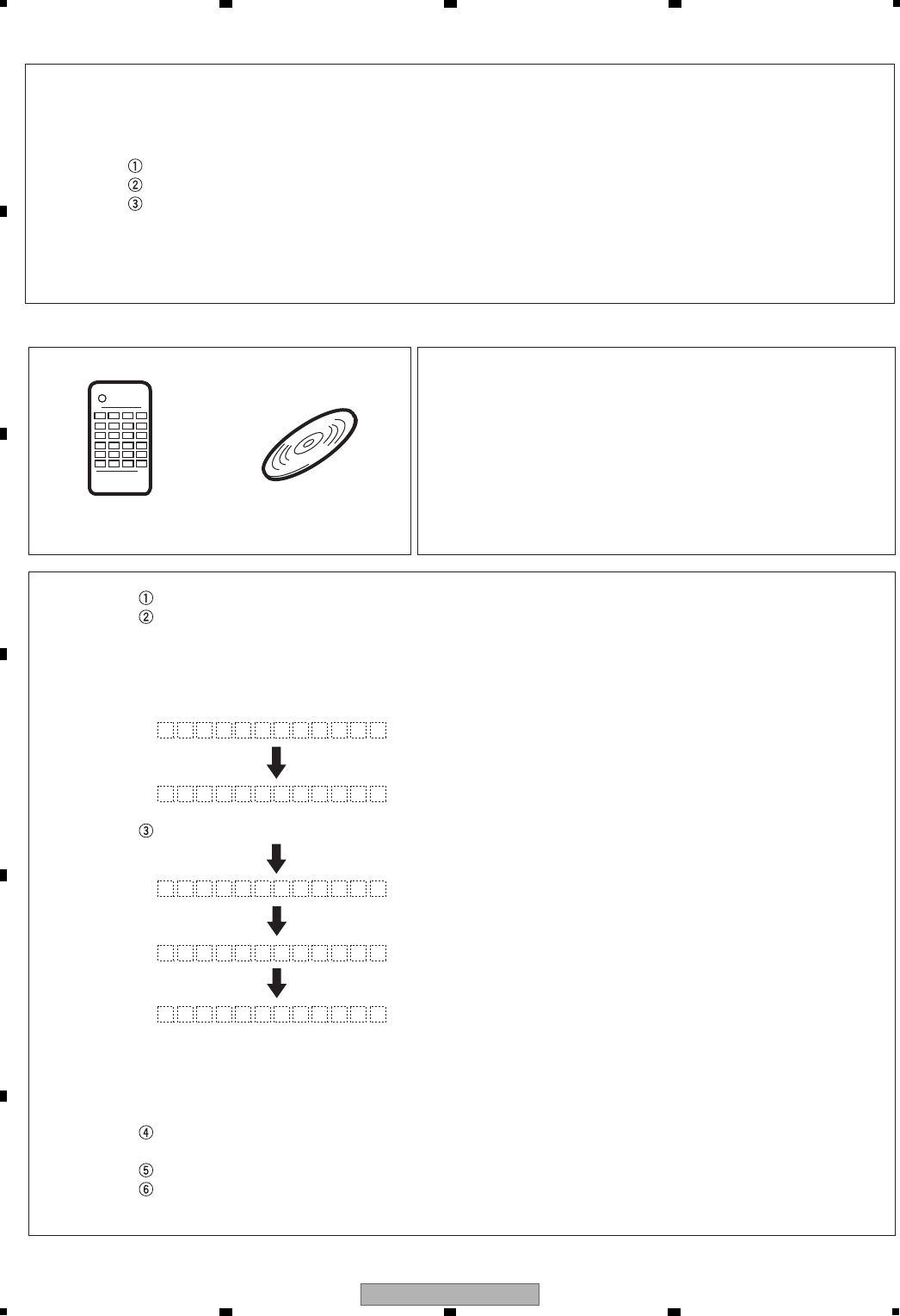
94 DVR-LX61
12 3 4
A
B
C
D
E
F
12 3 4
8.4 FIRMWARE UPDATE METHOD
Open a disc tray by pressing the "OPEN/CLOSE" button.
Put the update disc on the tray. Press a " OPEN/CLOSE " button while pressing a "Record Stop"
button on the frontpanel.
* The disc tray closes automatically and the disc is loaded.
* The disc tray opens automatically after loading.
Take out the Download Disc.
FL display
SYSCON download
FrontEnd
download
[Procedure]
Remote control unit
for servicing
(GGF1381)
Firmware Update Disc
(Refer to Page 96.)
[Notes]
Be sure NOT to turn off the unit during update.
If the unit is turned off during update, the SYSCON,
TUNERCON, DRIVE programs may not be properly rewritten, in
which case the unit may not be able to initialize itself normally
when turned on again.
1. When the main board is replaced, the firmware versions for the system control computer, drive, and the TUFL
microcomputer do not match, and operations of the unit may be destabilized.
To match the versions for the above three, firmware downloading is necessary in the following cases:
After the model setting
When NG is displayed on the first screen (version information, etc.) of Service mode
After changing MAIN Assy or TUSB Assy
2. Rewriting the firmware to the latest version may ameliorate the symptoms claimed by the customer.
There are the following two methods for update: disc update and serial update
[Purposes]
[Tools to be used]
* After update is completed, the power turns off, and a disc tray
closes automatically.
* It takes for about 7-8 minutes until update is completed.
S CD I D W L D
W N LD O O A D - 2
L O A D
W N LD O O A D - 3
W N LD O O A D - 4 TunerCon
download
[1] Disc Update
The power turns on and press a " ESC " button, then press " DISP " button on the remote control unit for
servicing.
Confirm a firmware release version.
Press " ESC " button on the remote control unit for servicing in order to exit the test mode.

95
DVR-LX61
56 7 8
56 7 8
A
B
C
D
E
F
[Tips]
If the power is not correctly turned on or when the power is shut off during update, proceed as follows before
performing update again:
• In a case where update was incorrectly terminated while "DOWNLOAD-2" was displayed on the FL display:
The SYSCON program will not function correctly.
If the program cannot be update from the disc or through serial communication, replace the MAIN Assy.
• In a case where update was incorrectly terminated while "DOWNLOAD-3" was displayed on the FL display:
The DRIVE program will not function correctly.
If the program cannot be update from the disc, replace the MAIN Assy.
• In a case where update was incorrectly terminated while "DOWNLOAD-4" was displayed on the FL display
The program for the tuner microcomputer will not function correctly.
If the program cannot be update from the disc, replace the TUNERCON microcomputer (IC101 : TUSB Assy).
(1)
Connect the 232C I/F jigs above way.
Turn on the PC and start the " UFU.exe ".
Select the Firmware file. ("sz0" file)
Turn the DVD recorder on and start the update
program.
" Target Device is connected " is appeared on the
screen.
Select the Communication Speed (Baud Rate)
a) Base Speed 115,200
b) Data Send Speed 115,200
START
• Even if you click "START" button, sometimes
"Communication Error" may come out one to
twice, and update may fail.
In this case, please click "START" again.
• Other factors can be considerd if update fails 3
times or more.
• And it takes about 40 minutes for updating the
firmware.
[Procedures]
[Connection]
Connect as follows: * PC with serial port
* RS-232C straight cable
* RS-232C I/F jig (GGF1348)
* 7P FFC (VDA1681)
* Update program (UFU.exe)
* Firmware
[Tools to be used]
[Purposes]
1. This method is used when disc update fails.
PC This unit
CN1402
(MAIN Assy)
RS-232C I/F
RS-232C cable 7P FFC
[2] Serial Update
5
4
6

96 DVR-LX61
12 3 4
A
B
C
D
E
F
12 3 4
HOW TO PRODUCE A DISC FOR UPDATING
Items necessary for producing a disc (CD-R or CD-RW) for updating
• CD-R/RW drive
• CD-R/RW writing software
• Blank CD-R or CD-RW disc
• Supported OS: Windows 98/98SE/ME/2000/XP *
* Other OS's, such as Linux and MacOS, cannot be used.
1. Right-click on the icon of the file for updating that you
downloaded to any folder and select "Send To" in order
to send the file to the drive to be used for writing to the disc.
* Do NOT change the filename.
How to produce a disc for updating
2. An icon appears at the right of the taskbar on the bottom
of the screen. Click on it.
* If the icon does not appear, select the drive to be used
for writing to the disc from My Computer.
When the PC is ready for writing, the window shown will
be displayed.
3. Load a CD-R/RW disc in the drive. Select File then
"Write these files to CD" * Be sure to use a blank disc.
* Scratches or dirt on the disc may result in a failure in
writing.
4. The Writing to CD Wizard will be displayed. Click on
Next to start writing.
5. When writing is finished, the disc will be ejected.
Production of the disc for updating is completed.

97
DVR-LX61
56 7 8
56 7 8
A
B
C
D
E
F
8.5 GRACENOTE DATABASE UPDATE METHOD
Open a disc tray by pressing the "OPEN/CLOSE" button.
Put the update disc on the tray. Press a " OPEN/CLOSE " button while pressing a "Record Stop"
button on the frontpanel.
* The disc tray closes automatically and the disc is loaded.
FL display
GNDB download
[Procedure]
Remote control unit
for servicing
(GGF1381)
Gracenote DB
Update Disc
(Refer to Page 96.)
[Notes]
Be sure NOT to turn off the unit during update.
If the unit is turned off during update, the GNDB programs may
not be properly rewritten, in which case the unit may not be able
to initialize itself normally when turned on again.
1. Gracenote DB should be stored in build-in HDD to search for audio CD titles.
After replacing the HDD, it is necessary to download the Gracenote DB.
2. While the GUI screen is not displayed, press the ESC then DISP keys.
When “NOBKUP” was displayed on the first screen (version information, etc.), update the latest Gracenote
Database (GNDB) information.
3. Rewriting the database to the latest version may ameliorate the symptoms claimed by the customer.
(Confirm that the GNDB B and GNDB U are latest version.)
[Purposes]
[Tools to be used]
L O A D
S CD I D W L D
W N LD O O A D - 1
[1] Disc Update
*After update is completed, the disc tray opens automatically.
At this time, "DOWNLOAD-1" or "CLOCK" is displayed on the FL display.
*It takes for about 15 minutes until update is completed.
Take out the Update Disc.
The power turns on and press a " ESC " button, then press " DISP " button on the remote control unit for
servicing.
Confirm a GNDB B and GNDB U version.
Press " ESC " button on the remote control unit for servicing in order to exit the test mode.
The power turns off. (An effective key is "STANDBY/ON" key.)
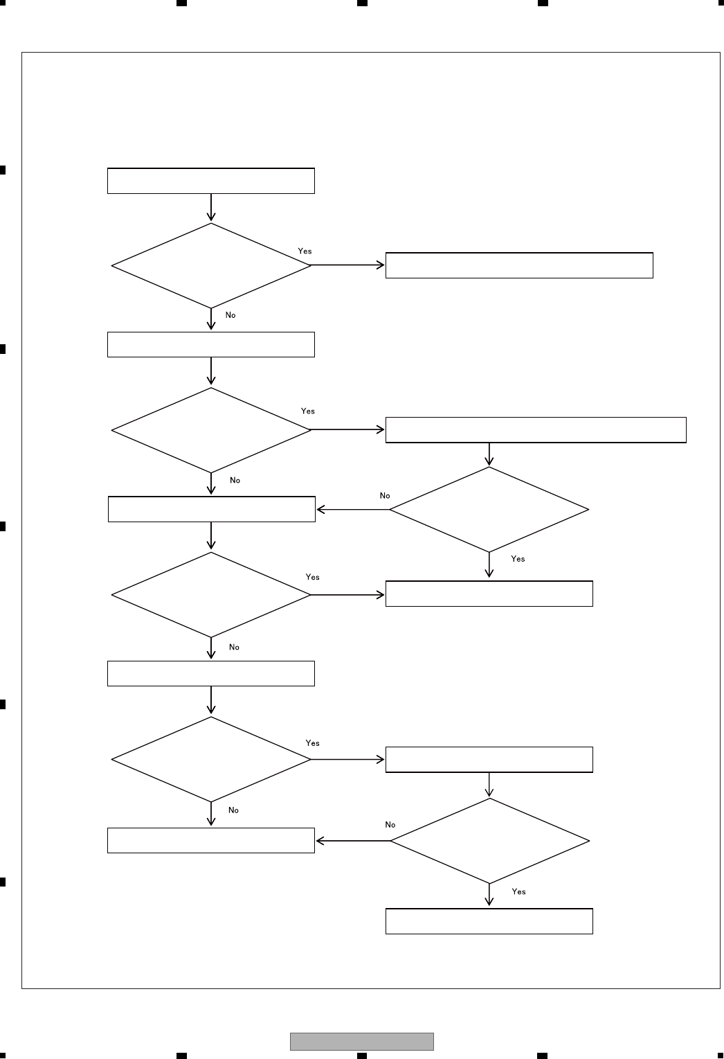
98 DVR-LX61
12 3 4
A
B
C
D
E
F
12 3 4
[Tips]
[Diagnosis Flowchart]
Note: If the AC power fails during updating, the HDD may be damaged.
CD titles cannot be searched.
Is "Initial Setup--Gracenote
Database--Version Information"
(the version display) normal?
GNDB error (damage or loss)
Is "GNDB B, GNDB U"
(the version display) on the version
information screen normal?
The database (DB) is normal. Download the firmware again.
Restore the database from the backup data then restart the system.
After restarting, does the
system operate normally?
Abnormality in the GNDB backup file.
Redownload GNDB.
After redownloading of
GNDB, is the version displayed in
"Version Information"?
Abnormality in the HDD, or file-system error.
Perform an HDD check.
Is the HDD normal as a
result of the check? File-system error. Initialize the HDD.
After initialization, does the
system operate normally?
Completed
Failure in the HDD. After replacement
of the HDD, redownload the DB.
Completed
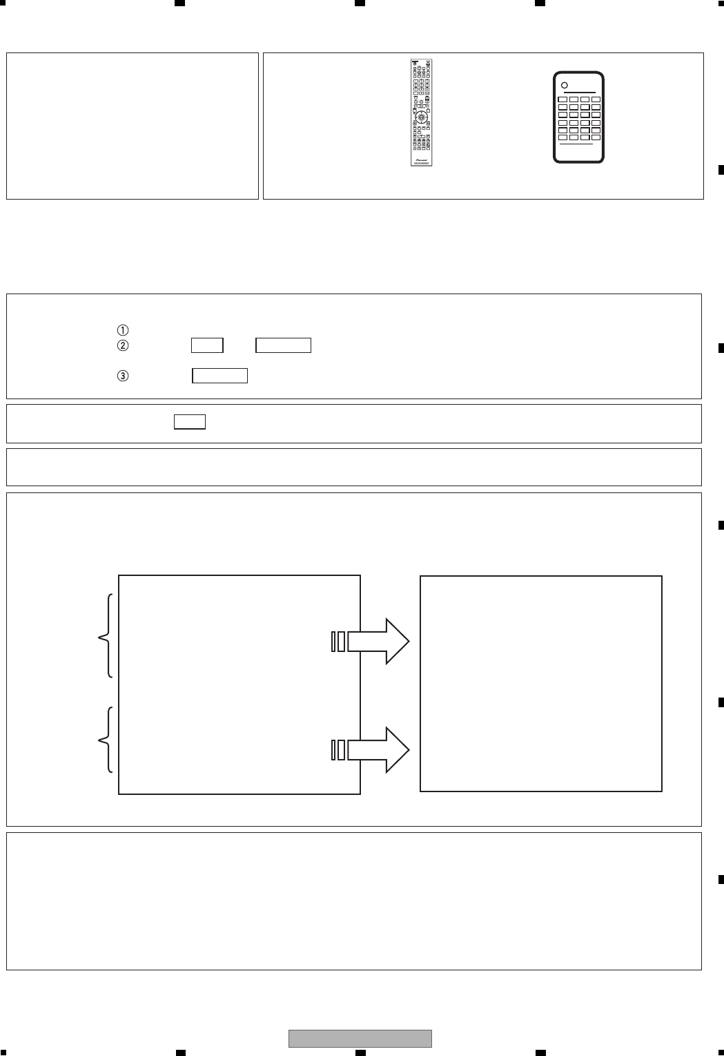
99
DVR-LX61
56 7 8
56 7 8
A
B
C
D
E
F
8.6 VIDEO ADJUSTMENT FOR SPECIFIC AREA
[When specific channel setting have NOT been made] [When specific channel setting have been made]
Depending on the area, if a flicker
may appear in a picture received by
the tuner, it can be corrected or
reduced with this setting.
Select a channel or line input (L1-L3) on which a specific setting is to be made.
Press the ESC then CHP/TIM keys on the remote control unit for servicing. "General Setting mode"
is displayed.
Press the DIG/ANA key in General Setting mode. Specific-Channel Setting mode is entered.
[Purposes] [Tools to be used]
[How to enter this mode]
Press the ESC key on the remote control unit for servicing to return the Normal mode.
[How to exit]
Setting is in effect only during recording/playback stop.
[Note]
The setting examples in Specific-Channel Setting mode are shown below.
For details on each setting item, see "Table 1: Key operations in Specific-Area Setting mode."
[Setting examples]
• If a channel that does not have specific settings is displayed, the setting figures are displayed as hyphens (- -).
• If the setting figures are not displayed as hyphens, those settings have been specifically set even if they are
identical to the default settings or those of General Setting mode.
• The setting indicated with an asterisk (*) is the default.
• The channels to be indicated for "Input Channel" are as shown below:
Line inputs: L1-L3, DV (DV is not valid for specific-area settings.)
Tuner channels: Channels received by the tuner (channels to be set in Specific-Channel Setting mode, etc.)
[Tips]
Remote control unit supplied
with the unit
Remote control unit for servicing
(GGF1381)
In this mode, specific settings can be made for up to 12 channels.
For channels that do not have specific settings, the settings of General Setting mode are applied.
General setting
data
Specific channel
setting data
VDEC Specific Area Mode Ver2.00
Input - [ TUNER ]
Sync AGC : ON *
H Threshold Level : 12 *
V Threshold Level : 10
EPG EQ : OFF *
Individual setting state
Input Channel - [ 1CH ]
Sync AGC : ---
H Threshold Level : ---
V Threshold Level : ---
VDEC Specific Area Mode Ver2.00
Input - [ TUNER ]
Sync AGC : ON *
H Threshold Level : 12 *
V Threshold Level : 10 *
EPG EQ : OFF *
Individual setting state
Input Channel - [ 1CH ]
Sync AGC : ON *
H Threshold Level : 14
V Threshold Level : 7
[1] Specific-Channel Setting Mode

100 DVR-LX61
12 3 4
A
B
C
D
E
F
12 3 4
[General Setting mode screen]
*: Setting is the default.
[Display in General Setting mode when the channel
currently displayed has specific settings]
• Indication when the maximum number (12) of channels have individual settings
If a channel that does not have specific settings is currently selected, the indication will be as shown below,
and individual data items cannot be set for that channel. To set individual data items for the currently selected
channel, you must clear any specific-channel settings for one or more channels.
[H Threshold Level]
The slice level setting for the horizontal(H)-sync separation circuit can
be changed. By your changing the slice level, horizontal sync
disturbance may be ameliorated. Set the slice level to a value with
which the least sync disturbance is seen.
[V Threshold Level]
The slice level setting for the vertical(V)-sync separation circuit can be
changed. By your changing the slice level, vertical sync disturbance
may be ameliorated. Set the slice level to a value with which the least
sync disturbance is seen.
[Receiver sensitivity setting for an electronic program guide (EPG)]
The sensitivity when receiving an electronic program guide can be
selected. Set the sensitivity to "High" only if reception is unstable.
[Tips]
• To shift from Specific-Channel Setting mode:
Each time the DIG/ANA key is pressed, Specific-Channel Setting mode and General Setting mode
are alternately selected.
• To shift from Normal mode (recording/playback stop):
Press the ESC then CHP/TIM keys.
[How to enter this mode]
Press the ESC key to return the normal mode.
[How to exit]
Show setting example on the General Setting mode screen to the following.
Regarding setting of actual each item, refer to table 1 (key operations in specific-area setting mode).
[Setting examples]
• General Setting mode can be entered only during recording/playback stop.
• The currently selected input mode (TUNER or LINE) is displayed for "Input."
• If L1, L2, L3, or DV is selected for input, general settings for the line input can be made (DV is not valid for
specific-area settings), and if TUNER is selected, general settings for the tuner input can be made.
[Tips]
Specific Area Mode
Input - [ TUNER ]
Sync AGC : ON *
H Threshold Level : 12 *
V Threshold Level : 10 *
EPG EQ : OFF *
Individual setting state
Sorry !
You can store only 12 channels
for Specific Area mode.
Specific Area Mode
Input - [ TUNER ]
Sync AGC : ON *
H ThresholdLevel : 12 *
V Threshold Level : 10 *
EPG EQ : OFF *
Specific Area Mode
Input - [ TUNER ]
Sync AGC : ON *
H ThresholdLevel : 12 *
V Threshold Level : 10 *
EPG EQ : OFF *
This channel is set up
individually.
[2] General Setting Mode
101
DVR-LX61
56 7 8
56 7 8
A
B
C
D
E
F
Key Operation Switching (*: Default) Used in Specific-
Channel Setting mode
Used in General
Setting mode
Remarks
[INPUT SELECT],
[CHANNEL +/-]
(Remote control unit
supplied with this unit)
–
Switches inputs or channels.
[ SIDE A ] , [ SIDE B ] ON(*) / OFF
Sets SyncAGC.
[ DIG/ANA ] –
––
Switches General setting mode
and Specific setting mode.
[ Rev ×3 ], [ ×3 Fwd ] [ Rev ×3 ] :
Decreasing 1 by 1 in the range 0 to 15.
(Cyclic operation)
[
Rev CHAPTER SKIP
]
:
Decreasing 1 by 1 in the range 0 to 15.
(Cyclic operation)
[
CHAPTER SKIP Fwd
]
:
Increasing 1 by 1 in the range 0 to 15.
(Cyclic operation)
[ ×3 Fwd ] :
Increasing 1 by 1 in the range 0 to 15.
(Cyclic operation)
0 – 15 (Default : 12)
Sets H Threshold.
[ Rev CHAPTER SKIP ]
[ CHAPTER SKIP Fwd ]
0 – 15 (Default : 10)
Sets V Threshold Level.
ON : The sync level is set to an appropriate value.
OFF : Cancel the Sync AGC.
Table 1: key operations in specific-Area setting mode (1/2)
Key operations in Specific Area Setting mode of the remote control units are shown in the table below
(the keys are of the remote control unit for servicing unless otherwise stated):
102 DVR-LX61
12 3 4
A
B
C
D
E
F
12 3 4
[ CLEAR ]
–
[ PAUSE ]
–
[ ESC ]
––
[ PLAY ] –
All channels that have specific
setting data will be canceled, and
the specific data will be initialized.
The General Setting data will not be changed.
Key Operation Switching (*: Default) Used in Specific-
Channel Setting mode
Used in General
Setting mode
Remarks
Table 1: key operations in specific-Area setting mode (2/2)
Notes:
• Each key listed in Table 1 above is active only while the tuner is completely stopped.
• The setting values will not be reset to default even if resetting to the state at the time of shipment is performed.
Specific-Channel Setting mode:
If the currently selected channel
has its specific setting, that
setting will be canceled. (By
canceling the specific setting for
that channel, the number of
remaining channels that can
have specific settings will be
increased by one.)
General Setting mode:
Settings of General Setting
mode are initialized.
Specific-Channel Setting mode:
All specific data are initialized.
The General Setting data will not be changed.
General Setting mode:
All general setting data are reset to default.
The specific setting data will not be changed
(will be retained).
The specific-channel-setting
data for the currently selected
channel are reset to default.
To quit Setting mode for a
specific area and clear the
on-screen display.
The General Setting data will not be changed
(will be retained).

103
DVR-LX61
56 7 8
56 7 8
A
B
C
D
E
F
104 DVR-LX61
12 3 4
A
B
C
D
E
F
12 3 4
9. EXPLODED VIEWS AND PARTS LIST
9.1 PACKING SECTION
NOTES:
-
Parts marked by “NSP” are generally unavailable because they are not in our Master Spare Parts List.
-
The > mark found on some component parts indicates the importance of the safety factor of the part.
Therefore, when replacing, be sure to use parts of identical designation.
-
Screws adjacent to b mark on product are used for disassembly.
-
For the applying amount of lubricants or glue, follow the instructions in this manual.
(In the case of no amount instructions, apply as you think it appropriate.)
DVR-560H
ONLY
DVR-LX61
ONLY
105
DVR-LX61
56 7 8
56 7 8
A
B
C
D
E
F
(1) PACKING SECTION PARTS LIST
(2) CONTRAST TABLE
DVR-LX61/WYXK5, WYXV5, DVR-560H-S/WYXK5, WYXV5, DVR-560H-K/WYXK5 and WYXV5 are constructed
the same except for the following:
Mark No. Description Part No.
>1Power Cable ADG1127
2Audio / Video Cable (1.5 m) VDE1077
(red/white/yellow)
3 RF Antenna Cable (PAL) See Contrast table (2)
4 G-Link™ Cable (3 m) VDX1010
5 Remote Control See Contrast table (2)
6 Battery Cover VZN1025
NSP 7 Dry Cell Batteries (AA/R6P) VEM1010
8 Operating Instructions (French) See Contrast table (2)
9 Operating Instructions (German)See Contrast table (2)
10 Operating Instructions (Dutch) See Contrast table (2)
11 Operating Instructions (Spanish)See Contrast table (2)
12 Operating Instructions (Italian) See Contrast table (2)
13 HDD Caution 8L See Contrast table (2)
14 HDD Caution 8L B See Contrast table (2)
NSP 15 Caution Card See Contrast table (2)
NSP 16 Warranty Card See Contrast table (2)
NSP 17 Serial Label S See Contrast table (2)
18 WEEE Label VRW2231
19 Polyethylene Bag B5 VHL1088
20 Polyethylene Bag B5 See Contrast table (2)
21 Front Pad See Contrast table (2)
22 Rear Pad See Contrast table (2)
23 Mirror Mat VHL1095
24 Nonwoven Cloth Cover See Contrast table (2)
25 Packing Case See Contrast table (2)
26 Mirror Sheet See Contrast table (2)
Mark No. Description Part No.
Mark No. Symbol and Description DVR-LX61
/WYXK5
DVR-LX61
/WYXV5
DVR-560H-S
/WYXK5
DVR-560H-S
/WYXV5
DVR-560H-K
/WYXK5
DVR-560H-K
/WYXV5
3 RF Antenna Cable (PAL) VDE1075 VDE1095 VDE1075 VDE1095 VDE1075 VDE1095
5 Remote Control VXX3286 VXX3286 VXX3287 VXX3287 VXX3293 VXX3293
8 Operating Instructions (French) VRC1493 VRC1460 VRC1484 VRC1459 VRC1484 VRC1459
9 Operating Instructions (German) VRC1486 VRC1465 VRC1485 VRC1464 VRC1485 VRC1464
10 Operating Instructions (Dutch) VRC1490 VRC1472 VRC1489 VRC1471 VRC1489 VRC1471
11 Operating Instructions (Spanish) VRC1492 VRC1476 VRC1491 VRC1475 VRC1491 VRC1475
12 Operating Instructions (Italian) VRC1488 VRC1482 VRC1487 VRC1468 VRC1487 VRC1468
13 HDD Caution 8L VRR1072 VRR1071 VRR1072 VRR1071 VRR1072 VRR1071
14 HDD Caution 8L B VRR1077 VRR1076 VRR1077 VRR1076 VRR1077 VRR1076
NSP 15 Caution Card VRR1095 VRR1094 VRR1095 VRR1094 VRR1095 VRR1094
NSP 16 Warranty Card ARY7112 ARY7113 ARY7112 ARY7113 ARY7112 ARY7113
NSP 17 Serial Label S VRW2017 VRW2188 VRW2017 VRW2188 VRW2017 VRW2188
20 Polyethylene Bag B5 VHL1051 VHL1088 VHL1051 VHL1088 VHL1051 VHL1088
21 Front Pad VHA1425 VHA1427 VHA1425 VHA1427 VHA1425 VHA1427
22 Rear Pad VHA1426 VHA1428 VHA1426 VHA1428 VHA1426 VHA1428
24 Nonwoven Cloth Cover VHL1116 VHL1116 Not used Not used Not used Not used
25 Packing Case YHG1006 YHG1003 YHG1008 YHG1004 YHG1010 YHG1005
26 Mirror Sheet Not used Not used VHL1117 VHL1117 VHL1117 VHL1117

106 DVR-LX61
12 3 4
A
B
C
D
E
F
12 3 4
9.2 EXTERIOR SECTION
A
A
B
B
CD
C
D
E
E
F
F
G
H
H
I
I
G
CONTACT SIDE
NON-CONTACT
SIDE
Cleaning paper :
GED-008
A
G
F
C
E
Refer to
“9.3 FRONT PANEL SECTION (DVR-LX61)”,
“9.4 FRONT PANEL SECTION (DVR-560H)”.
Refer to
“9.5 SERVICE LOADER
MAIN SECTION”.
DVR-LX61
ONLY
DVR-LX61
ONLY
DVR-LX61
ONLY
DVR-LX61
ONLY
DVR-LX61
ONLY
DVR-LX61
ONLY
DVR-LX61
ONLY
DVR-560H
ONLY

107
DVR-LX61
56 7 8
56 7 8
A
B
C
D
E
F
(1) EXTERIOR SECTION PARTS LIST
Mark No. Description Part No.
1 ETAB Assy See Contrast table (2)
2 SERVICE DVUB Assy YXX1001
3 SERVICE TUSB Assy YXX1003
4 SERVICE FRJB Assy See Contrast table (2)
NSP 5 SERVICE LOADER MAIN See Contrast table (2)
>6 POWER SUPPLY Assy VWR1406
7 HDD See Contrast table (2)
8 Connector Assy PF13PP-S17
9 Flexible Cable (40P) VDA2159
10 Flexible Cable (11P) VDA2162
11 Housing Assy (4P) VKP2389
12 Housing Assy (10P) VKP2391
13 Housing Assy (2P) VKP2392
14 SATA Cable YDX1001
15 Housing Assy (TUJB) YKP1001
16 Housing Assy (6P) YKP1002
17 DC Fan Motor 60 VXM1123
18 Spacer Cushion VEB1400
19 Cushion VEB1401
NSP 20 HDD Stay VNE2450
21 Cord Holder VNL1971
NSP 22 Binder (BK-1) ZCA-BK1
23 Rubber Spacer VEB1378
24 Rubber Spacer VEB1408
25 Gasket 30 x 10T VEC2522
26 Aluminum Tape 13 x 25 VEF1068
27 Aluminum Tape 70 x 19 YEF1001
28 Bonnet S See Contrast table (2)
29 PCB Support AEC1215
30 Rubber Foot VEB1349
31 Screw Guard VEB1399
32 Barrier See Contrast table (2)
NSP 33 Base Chassis VNB1057
NSP 34 Writer Stay L VNE2448
NSP 35 Writer Stay R VNE2449
36 DV Angle See Contrast table (2)
37 Insulator H.S. See Contrast table (2)
38 Rear Panel See Contrast table (2)
39 LAN Angle See Contrast table (2)
40 Earth Plate TU VBK1173
41 Tray Sheet VEC2551
42 Tray Panel YNK1038
NSP 43 ID Label Assy See Contrast table (2)
44 Laser Caution Label VRW2262
NSP 45 Serial Label S See Contrast table (2)
NSP 46 Tape ZTA-156A-19
47 • • • • •
48 • • • • •
49 #6-32 ScrewDBA1125
50 ScrewSee Contrast table (2)
51 Screw M3 x 8 See Contrast table (2)
52 Screw M3 x 8 VBA1088
53 ScrewAMZ30P060FTC
54 ScrewSee Contrast table (2)
55 ScrewBPZ30P080FTC
56 ScrewBSR30P060FTC
57 ScrewBSR30P080FTB
58 ScrewSee Contrast table (2)
59 ScrewBSZ30P040FTC
60 ScrewSee Contrast table (2)
61 ScrewSee Contrast table (2)
Mark No. Description Part No.

108 DVR-LX61
12 3 4
A
B
C
D
E
F
12 3 4
(2) CONTRAST TABLE
DVR-LX61/WYXK5, WYXV5, DVR-560H-S/WYXK5, WYXV5, DVR-560H-K/WYXK5 and WYXV5 are constructed
the same except for the following:
Mark No. Symbol and Description DVR-LX61
/WYXK5
DVR-LX61
/WYXV5
DVR-560H-S
/WYXK5
DVR-560H-S
/WYXV5
DVR-560H-K
/WYXK5
DVR-560H-K
/WYXV5
1 ETAB Assy VWV2344 VWV2344 Not used Not used Not used Not used
4 SERVICE FRJB Assy YXX1027 YXX1027 YXX1004 YXX1004 YXX1004 YXX1004
NSP 5 SERVICE LOADER MAIN VXU1014 VXU1014 VXU1013 VXU1013 VXU1013 VXU1013
7 HDD VXF1131 VXF1131 VXF1152 VXF1152 VXF1152 VXF1152
28 Bonnet S YXX1009 YXX1009 YXX1010 YXX1010 YXX1009 YXX1009
32 Barrier VEC2548 VEC2548 Not used Not used Not used Not used
36 DV Angle VNE2474 VNE2474 VNE2453 VNE2453 VNE2474 VNE2474
37 Insulator H.S. VNK6329 VNK6329 Not used Not used Not used Not used
38 Rear Panel YNA1009 YNA1007 YNA1010 YNA1008 YNA1012 YNA1011
39 LAN Angle YNE1001 YNE1001 Not used Not used Not used Not used
NSP 43 ID Label Assy VXW1019 VXW1019 VXW1015 VXW1015 VXW1015 VXW1015
NSP 45 Serial Label S VRW2017 VRW2188 VRW2017 VRW2188 VRW2017 VRW2188
50 ScrewVBA1112 VBA1112 BSZ30P060FTC BSZ30P060FTC BSZ30P060FBN BSZ30P060FBN
51 ScrewYBA1001 YBA1001 VBA1088 VBA1088 VBA1088 VBA1088
54 ScrewBPZ30P080FCC BPZ30P080FCC BPZ30P080FTC BPZ30P080FTC BPZ30P080FTC BPZ30P080FTC
58 ScrewBSZ30P040FCC BSZ30P040FCC BSZ30P040FTC BSZ30P040FTC BSZ30P040FTC BSZ30P040FTC
60 ScrewBSZ30P060FCC BSZ30P060FCC BSZ30P060FTC BSZ30P060FTC BSZ30P060FBN BSZ30P060FBN
60 ScrewPPZ30P080FCC PPZ30P080FCC PBZ30P080FTC PBZ30P080FTC PBZ30P080FTC PBZ30P080FTC

109
DVR-LX61
56 7 8
56 7 8
A
B
C
D
E
F
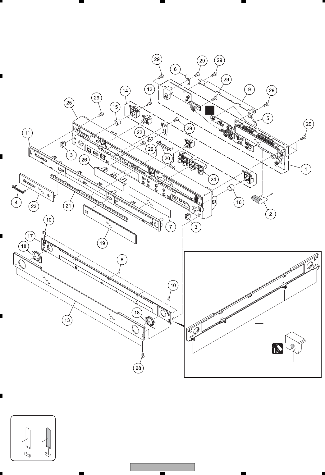
110 DVR-LX61
12 3 4
A
B
C
D
E
F
12 3 4
9.3 FRONT PANEL SECTION (DVR-LX61)
CONTACT SIDE
NON-CONTACT
SIDE
Paste lubricant hanarl (GEM1041) to
salient points of both sides of the door.
SERVICE TUSB
CN105
to Door Shaft
Lubricant Hanarl
GEM1041
B

111
DVR-LX61
56 7 8
56 7 8
A
B
C
D
E
F
FRONT PANEL SECTION (DVR-LX61) PARTS LIST
Mark No. Description Part No.
1 SERVICE FLKY Assy YXX1008
2 Flexible Cable (17P) YDA1002
3 Magnet Holder Assy AEC1077
4 Pioneer Name Plate VAM1158
5 Earth Plate FLKY VBK1176
6 Earth Plate VBK1179
7 FL Filter VEC2544
8 Door Pad VEC2562
9 FP Bridge VNE2464
10 Magnet Catcher B VNE2482
11 Panel Frame VNK6149
12 LED Lens VNK6290
13 Door Panel YAH1001
14 Main Key YNK1004
15 Key Top PW YNK1005
16 Key Top REC YNK1006
17 Door Base YNK1011
18 Door Ring YNK1013
19 FL Lens YNK1020
20 Optical Lens YNK1035
21 Center Lens YNK1036
22 Damper Assy YXA1001
23 Sub Panel PTD YXA1010
24 Function Key PTD YXA1054
25 Front Panel Assy PTD YXA1055
26 CI Cover YNK1026
27 • • • • •
28 Flat Head ScrewVBA1113
29 ScrewBPZ30P080FTC

112 DVR-LX61
12 3 4
A
B
C
D
E
F
12 3 4
9.4 FRONT PANEL SECTION (DVR-560H-S,-K)
CONTACT SIDE
NON-CONTACT
SIDE
Paste lubricant hanarl (GEM1041) to
salient points of both sides of the door.
SERVICE TUSB
CN105
to Door Shaft
Lubricant Hanarl
GEM1041
Lubricant Hanarl
GEM1041
Lubricant Hanarl
GEM1041 B

113
DVR-LX61
56 7 8
56 7 8
A
B
C
D
E
F
(1) FRONT PANEL SECTION (DVR-560H) PARTS LIST
(2) CONTRAST TABLE
DVR-560H-S/WYXK5, WYXV5, DVR-560H-K/WYXK5 and WYXV5 are constructed the same except for the
following:
Mark No. Description Part No.
1 SERVICE FLKY Assy YXX1007
2 Flexible Cable (17P) YDA1002
3 Pioneer Name Plate See Contrast table (2)
4 Earth Plate FLKY VBK1176
5 Earth Plate VBK1179
6Rubber Foot VEB1349
7Rubber Sheet VEB1396
8 Door Cushion VEC2561
9 FP Bridge VNE2464
10 Panel Frame VNK6149
11 CI Cover See Contrast table (2)
12 Key Top PW See Contrast table (2)
13 Key Top REC See Contrast table (2)
14 Door Spring YBK1001
15 Main Key YNK1004
NSP 16 Lens L YNK1007
NSP 17 Key Lens YNK1009
NSP 18 Key Base YNK1010
NSP 19 Lens R YNK1024
20 FLKB Holder 2 YNK1043
21 FL Lens PTD YXA1011
22 Door PTD See Contrast table (2)
NSP 23 Front Panel PTD See Contrast table (2)
24 Sub Panel PTD YXA1027
25 Function Key PTD See Contrast table (2)
NSP 26 Tray ScrewDBA1327
27 Front Panel Assy S See Contrast table (2)
28 Flat Head ScrewVBA1113
29 ScrewBPZ30P080FTC
30 ScrewBPZ30P120FTB
Mark No. Symbol and Description DVR-560H-S
/WYXK5
DVR-560H-S
/WYXV5
DVR-560H-K
/WYXK5
DVR-560H-K
/WYXV5
3 Pioneer Name Plate VAM1148 VAM1148 VAM1153 VAM1153
11 CI Cover VNK6188 VNK6188 VNK6229 VNK6229
12 Key Top PW VNK6359 VNK6359 VNK6239 VNK6239
13 Key Top REC VNK6361 VNK6361 VNK6240 VNK6240
22 Door PTD YXA1013 YXA1013 YXA1034 YXA1034
NSP 23 Front Panel PTD YXA1056 YXA1056 YXA1057 YXA1057
25 Function Key PTD YXA1053 YXA1053 YXA1054 YXA1054
27 Front Panel Assy S YXA1065 YXA1065 YXA1073 YXA1066
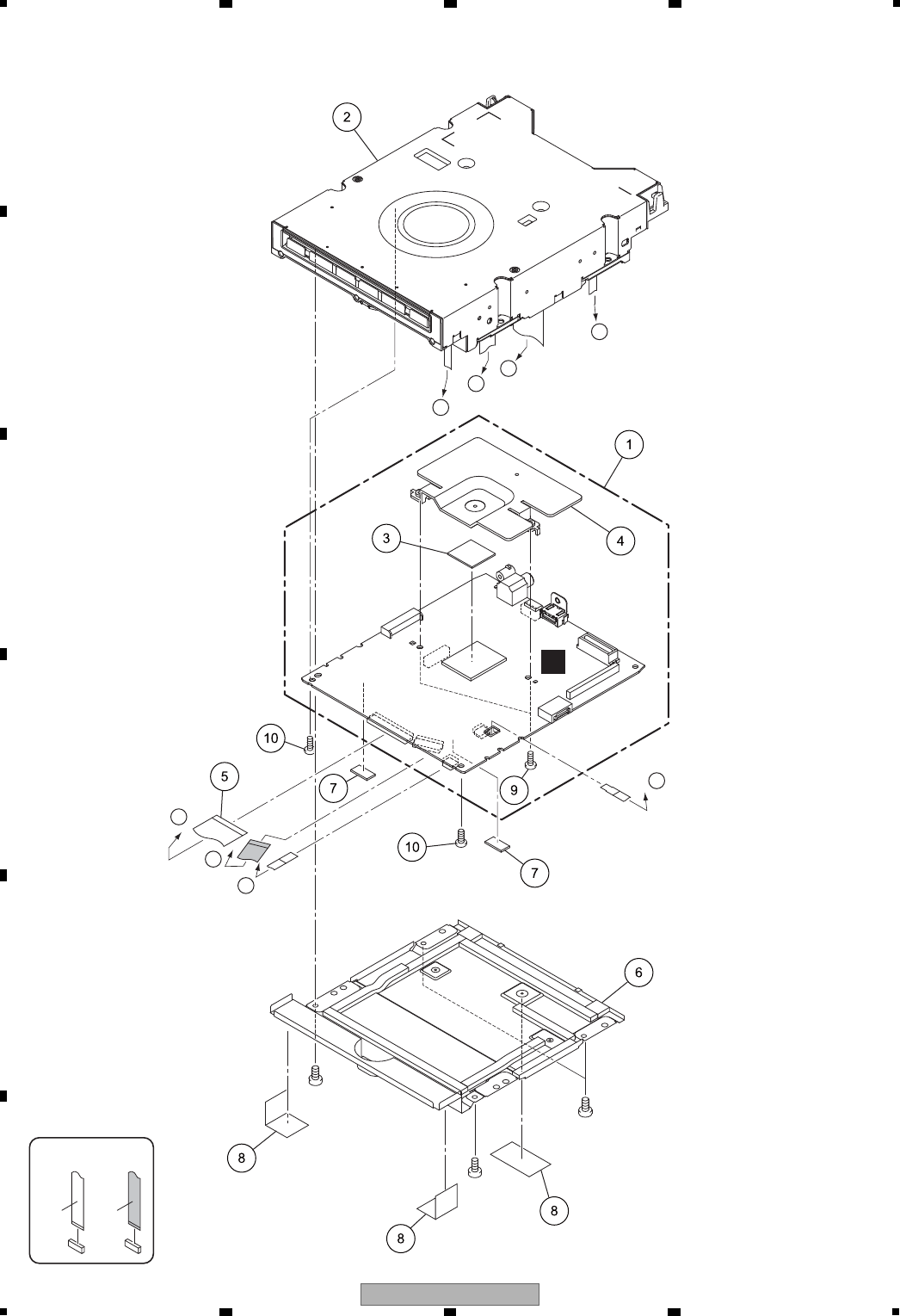
114 DVR-LX61
12 3 4
A
B
C
D
E
F
12 3 4
9.5 SERVICE LOADER MAIN SECTION
CONTACT SIDE
NON-CONTACT
SIDE
(
∗
)
(
∗
)
(
∗
)
D
D
C
B
A
D
C
B
A
Reuse (∗) marked parts when
exachanging SERVICE LOADER Assy.
• Case Screw S
(DBA1250) x2
115
DVR-LX61
56 7 8
56 7 8
A
B
C
D
E
F
(1) SERVICE LOADER MAIN SECTION PARTS LIST
(2) CONTRAST TABLE
DVR-LX61/WYXK5, WYXV5, DVR-560H-S/WYXK5, WYXV5, DVR-560H-K/WYXK5 and WYXV5 are constructed
the same except for the following:
Mark No. Description Part No.
1 SERVICE MAIN Assy See Contrast table (2)
2 SERVICE LOADER Assy VXX3306
3 Radiation Sheet (Silicon) VEB1360
4 Heatsink VNH1079
5 FFC U11 DDX1208
6Low Case U11 DNC1761
7 Silicon Sheet R9B DEB1726
NSP 8 Tape • • • • •
9 ScrewBBZ30P060FTC
10 ScrewDBA1220
Mark No. Symbol and Description DVR-LX61
/WYXK5
DVR-LX61
/WYXV5
DVR-560H-S
/WYXK5
DVR-560H-S
/WYXV5
DVR-560H-K
/WYXK5
DVR-560H-K
/WYXV5
1 SERVICE MAIN Assy VXX3309 VXX3309 VXX3308 VXX3308 VXX3308 VXX3308
116 DVR-LX61
12 3 4
A
B
C
D
E
F
12 3 4
10. SCHEMATIC DIAGRAM
10.1 SERVICE TUSB ASSY (1/4)
A
A
1/4
A1/4
SERVICE TUSB ASSY (1/4)
(YXX1003)
CN121
G
TUON
RFTHRU
TXD1
RXD1
RESET
DBGP2
DBGP0
DBGP1
HSM_TO_T
DAM_TO_T
DAT_TO_M
LED_HDD
LED_DVD
LED_P_ON
ASCK
FANCTL
P_CONT
ANT5V_SW
DET_ANT
DBGP1
DTBON
DBGP2
DBGP0
HST_TO_M
MRST
TU_DCCON
SWVION9V
SWVION5V
B
R312
Q310
C324
C325
R283
R282
R270
R269 R324
R325
R298
R299
R281
R280 R267
R268
R279
R278
R266
R265
R276
R277 R264
R263
R323
R322
R297
R296
R321
R320 R294
R295
R293
R292
R316
R275
R274 R261
R262
R272
R273 R260
R271
R291
R290
R198
KN103
KN102
KN101
C120
D1
D1
R311
C322
C321
R310
Q309
IC317
L304
D303
C323
Q311 Q311
R314
R313
Q303
C311
C310
C312
C329
R305
R318
Q303
C309
Q304
Q301
C307
C306
C308
R304
L303
C305
Q301
Q302
Q201
C208
L201
C203
R251
D201
C205
CN201
C326
C328
R315
L305
Q307
C318
D302
C319
C320
C147
C317
R309
Q307
D304
Q308
Q305
C314
C315
C316
C313
R306
Q305
Q306
R308
R307
R196
CN103
R193
R194
R195
C106
R220
C201
C206
R219
C202
C204
R218
C16
C139
C301
C302
CN301
C304 R302
D301
C303
R301
R303
E
BC
B
E
C
1
C
E
B
E2
B2
C2
2
E
B
C
B2
E2
C2
BC
E
E
B
C
B2
E2
C2
B
E
C
1
2
E
B
C
E
B
C
B2
2
3
4
1
C2
E2
E
BC
C
B2
B
E
E2
C2
BC
E
5
7
6
9
8
3
4
1
2
5
2SC4081(QR)-TLB
GND
10k 2SC5876(QR)-TLB
GND
GND
0.1
GNDGNDGND
***
***
***
***
GNDGNDGNDGND
***
*** ***
***
***
*** ***
***
***
***
***
***
***
*** ***
***
***
*** ***
***
***
***
***
***
***
***
***
GNDGND
22K(F)
***
*** ***
***
***
*** ***
***
***
***
GNDGNDGNDA
***
***
***
***
VNF1084- -T
VNF1084- -T
GND
***
0.1
1SR15
1SS355
820
CEK1278- -T
GND
100p
0.1
4.7k
LFCA331J-T
1SS355-TRB
1/50
22k
180K
HN1A01FU(YGR)-T
HN1A01FU(YGR)-T
V+12R1E
V+5R8E
UMD2N-TLB
GND
220/16
100/16
0
0.1
UMD2N-TLB
33
0.1
2SD2153(VW)-TRB
0.1
UMD2N-TLB
GND
100/16
0.1
100/16
V+5TU
CTF1399- -T
V+5R8E
UMD2N-TLB
100
0.1
2SC4081(QR)-TLB
V+5BB
GND
2SD2114K(VW)-TLB
GND
0(2125)
YB0.1
ATH1109- -T
***
22/25
S2B-PH-K-S
GND
100K(F)
10/50
0.1/50
CTF1399- -T
V+32VV+32E
UMD2N-TLB
UDZS9R1(B)-TRB
GND
1SS355-TRB
100/16
0.1
100/16
V+5R8E
GND
0.1
GND
GND
0.1
GND
UMD2N-TLB
1.5k
2SC2411K(QR)-TLB VKN2015-
GND
V+12R1E
UMD2N-TLB
GND
0.1
100/16
100/16
V+9V
1u
UMD2N-TLB
33
V+5R8E
2SC2411K(QR)-TLB
0(2125)
0(2125)
V+5VOV+5VI
100
100k
100k
100k
0.1
V+5VV+5V
GNDGND
3.3k
2.2k
***
470p
1SS355-TRB
GND
0.1
GND
100/16
0(2125)
V+12R1E
1000
0.1
0.1
0.1
S5B-PH-K-S
GND
470/16
GND
UDZS15(B)-TRB
GND
0(2125)
100/16
V+5R8E
0(2125)
0(2125)
V+12R1E V+12R1
(1/2) (2/2)
to FAN
FAN-
FAN+
RXD1
TXD1
GND
V+5V
DBGP2
DBGP1
DBGP0
RESET
GND
GND
EV+5.8V
GND
EV+12.1V
P_CONT
YWV1001-
YWM1002-
YNP1005-
560H/WY
LX61/WY
***
15k
NOTE1
PCB
R120
R119
AI ASSY
MI ASSY
MODEL
CAUTION - FOR CONTINUED PROTECTION AGAINST RISK OF FIRE,
REPLACE ONLY WITH SAME TYPE NO. 494.500 (CEK1278) MFD. BY
LITTELFUSE FOR IC317.
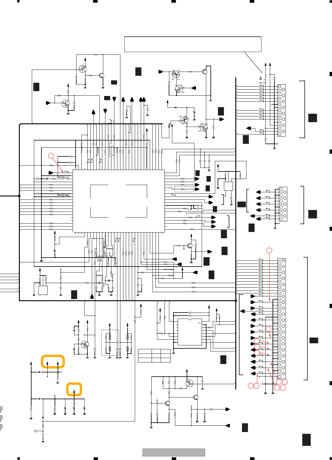
117
DVR-LX61
56 7 8
56 7 8
A
B
C
D
E
F
CN101
B
CN301
C
CN2301
D4/5
A2/4,3/4
A2/4
A3/4
A4/4
A2/4
A2/4
A2/4
A4/4
A2/4
A2/4
A3/4
A2/4
A3/4
A3/4
A2/4
A3/4
A2/4
A4/4
A3/4
A1/4
(1/4)
EPGEQ
D1
RESET
KEY2
KEY1
KEY3
AGC
CEC0
DDC_SW2
CEC
D1
ET
P2
GP0
P1
HSM_TO_T
DAM_TO_T
DAT_TO_M
LED_HDD
LED_DVD
LED_P_ON
ASCK
ANT5V_SW
DET_ANT
DBGP1
DTBON
DBGP2
DBGP0
HST_TO_M
HOTPLUG
MSPSTAT
RXD1
TXD1
CEC0
FLPON
P_CONT
TUON
EPGEQ
LED_ICEB
FANCTL
RFTHRU
RESET
SDA
SCL
SCL0
SDA0
DDC_SCL
DDC_SDA
SDA0 MRST
XRST1
XRST1
SCL0 DAM_TO_T
HSM_TO_T
DAT_TO_M
ASCK
HST_TO_M
DDC_SDA
DDC_SW1
CEC
DDC_SCL
HOTPLUG
AFT
DDC_SW2
DDC_SW1
FLDATA
FLSTB
FLCLK
FLPON
MRST
FLDATA
LED_ICEB
FLCLK
FLSTB
LED_P_ON
LED_DVD
LED_HDD
KEY1
KEY2
KEY3
TU_CON
TEXTV
TEXTVIN
YP_OUT
SEL_IR
SDET3
SDET2
TEXTV
CR_OUT
Y_OUT
CB_OUT
C_OUT
Y_IN
C/R_IN
BTOMAIN
GTOMAIN
L_OUT
AMUTE1
R_IN
R_OUT
L_IN
P_CONT2
FUNC_IN
AVLOUT
XAMUTE2
RCSEL1
RCSEL2
C2IN
SDET2
Y2IN
FUNC_ON
SQU
IR_B
P_SAVE
2VIN
L2_LIN
L2_RIN
AVLTH
IR
BLANK
TU_DCCON
AVLIN
P_CONT2
SWVION9V
CSYNCIN
MUTECTL
SWVION5V
AMUTE1
SAMUTE
MUTECTL
+
VSS1197-
R211
BT101
103
102
101
C120
D110
C122
C123
D104
D103 R130
C121
C119
C118
R215
R216
C150
R214
Q111
R209
R210 C149
L102
R207
R208
R217
R212
C151
C152
Q112
C207
Q110
R197
IC102
C105
R114
D102
C109
R226
C116
R120
C117
R122
R228
IC104
R113
Q101
R225
D101
C110
R112
R119
R227
R121
R213
R229
R230
R221
C111
C112
C114
R127
C115
C106
R107
R106
C104 R104
R189
R200
R188
R184
R185
R183
R108
R116
X102
R115
R111
C166
X101
R131
C124
R118
R132
C113
R139
R141
R136
R135
R109
R110
C108
R105
C107
R129
R124
R123
R134
R126
R117
R133
R137
R203
R144
R204
R205
R180
R182
R181
C169
C140
R179
R177
R178
C139 R176
C138
C137
R175
IC101
R201
R146
R152
C168
C136
R173
R172
R171
R164
R165
R158
R157
R155
R156
R153
R148
R102
R101
R150
R128
R103
R149
R174
R168
R167
R199
R160
R154
R125
C131
R159
R151
D108
R223
R224
R232
R231
C141
C142
R140
R142
R143
R138
C125
Q102
CN101
R222
R202
C167
C126
C157
IC103 CN106
C101
C102
C103
C156
R145
C128
C129
C154
Q108
R170
R169
C135
C133
C132
Q103
D106
R163
C134
R162
C130
R161
Q106 Q107
Q104
Q103
C127
Q105
Q104
IC150
C155
CN105
R147
E
B
C
E
B
C
C
B
E
1
2
3
5
4
E
BC8
6
7
5
3
4
1
2
3
1
2
21
100
99
65743109811
96
97
98
95
93
94
141312 15 16 20191817 21 22 23 24 27 282625
32
31
29 30
35
34
33
37
36
38
91
90
92
88
89
87
86
85
84
40
41
39
43
44
42
46
47
45
83
82
81
8079 7677787475 71 7073 72 66676869 636465 6162 5860 5759
48
49
50
535456 55 52 51
21
4
5
6
9
8
7
12
10
11
9
11
10
13
12
14
16
15
15
14
13
16
17
18
19
21
20
22
23
24
26
27
25
28
30
29
32
31
33
34
35
36
37
38
39
C
E
B
40
1
2
3
4
5
4
51
2
3
7
8
6
11
9
10
C2
E
B4
3
2
1
C
E
B
3B2
C
E
B
C
E
C
B2
B
E2 C2
B
E
E2
C
7
6
5
8
9
10
13
11
12
BC
14
15
16
1
17
2
E
3-B5
3-B5
***
***
***
GND
VNF1084- -T
VNF1084- -T
GND
***
GNDGND
0.1
470/6.3
1u
1SR154-400-TRB
GND
1SS355-TRB
0
1u
GND
GNDGND
1000/6.3
***
750(F)
3.3k
1u
680
2SC4081(QR)-TLB
V+5M
3.3k
820(F)
LAU470J-TA
0
10p
470
GND
***
GND
1k
***
1u
2SC4081(QR)-TLB
GND
0.1
DTA143EUA-TLB
GNDA GND
0
V+5R8EV+5FV+5V
BD4846G-TRB
GNDGND
0.1
1SS355-TRB
GNDGND
***
DTC124EUA-TLB
***
0.1
GNDGNDGNDGND
***
***
0
***
***
TC7MB3257FK-TBB
V+5VI
GND
0
***
1SS355-TRB
YB1u
10k
V+5R8EV+5M
V+5V
15K
***
***
V+5V
***
***
100
***
12p
GND
12p
10k
V+5V
GNDGND
V+5V
0.1
10k
0
V+5V
GND
22/25 47k
470
V+5V
100
330
100
100
100
***
12p
***
0
100
CSS1653- -T12p
0.1
4.7k
0
6.8K
1000p
1u
6.8k
6.8k
100k
1k
V+5V
330
100
***
100
330p
1k
1M
100
100
100
100
***
100
2SC4081(QR)-TLB
100
100
100
100
100
1000p 0.1
100
0.1 1k
2.2/50
100
100
***
330
PMC026A8-K
1u
1000p
100k
100
100
100k
100
100
100
100
100k
***
100
0
180
100
100k
100
100
100
100
0
100
0
V+5M
0
3.9k
0.1
0
DAP202U-TLB
UMD2N-TLB
0
0
***
***
1u
1000p
V+5V
V+5V
47
47
100
GND
470
0.1
VKN2007-
0
V+5V
0
0
0
GND1000p
GND
0.1
GND
0
100
0
GND
0.1 YB
BU4220G-TRB HLEM11S-1
100
GND
V+5M
***
***
***
0.1
10k
GNDGNDGND
***
UMD2N-TLB
***
GND
0.1
DTC124EUA-TLB
GND
***
V+5V
0.1
GND
GND
0.1
0.1
V+5R8E
1SS355-TRB
10k
GNDGND
***
0.1
***
***
***
V+5V
0
***
UMD2N-TLB
GND
100/16
GND
1k
UMD2N-TLB
2SD2114K(VW)-TLB
CEK1278- -T
HLEM17S-1
1000p
V+12R1E V+5F
X525P
YP_OUT
GND
OUT
IN
NC
NC
H
L
DDCSW2
TC7MB3257FK
Func
A=B1
A=B2 TUJB
MAIN
NOTE1
2B2
2A
GND
1B2
1A
2B1
1B1
S
G
NC
NC
ACDET
HSM_TO_T
NC
WDT
IR
XT1
RESET
GND
XT2
NC
NC
LED_DVD
LED_HDD
LED_P_ON
98. DAT_TO_M
99. DAM_TO_T
100.ASCK
CF2
CF1
VDD1
MODEL1
AGC
MODEL2
KEY2
KEY3
KEY1
SDET2
BATTDET
FUNC
SDET3
32. NC
31. AFT
33. XAMUTE2
SDA
SDET1
SCL
AVLOUT
NC
XRST1
RCSEL2
RCSEL1
DDCSW1
DDCSW2
NC
DBGP2
DBGP0
DBGP1
GND
VDD3
DET_ANT82. GND
84. VDDVCO
83. FILTSLC
DTBON
ANT5V_SW
HST_TO_M
VDDODA
81. CVBSIN
TU_DCCON
HOTPLUG
MSPSTAT
47. XSCMUTE
SWVION5V
48. AVLTH
SWVION9V
49. FLDATA
50. FLSTB
MUTECTL
P_CONT2
CSYNCIN
XCHECKER
VDD4
FUNC_ON
GND
CAPACITOR
SQUEEZE
NC
LED_ICEB
P_SAVE
BLAIR
RXD2
TXD1
TXD2
RXD1
AVLIN
BLANK
NC(IN)
CEC
MRST
P_CONT
FLON
EPGEQ
TUON
GND
FANCTL
VDD2
FLCLK
RFTHRU
GND
CB_OUT
CR_OUT
GND
Y_OUT
GND
C_OUT
GND
Y_IN
3B1
3B2
3A
4B2
4B1
4A
OE
VCC
GND
GND
C/R_IN
GND
B_IN
G_IN
L_OUT
GNDA
GND
R_OUT
AMUTE1
R_IN
GND
GND
L_IN
P_CONT2
MRST
XRST1
HSM_TO_T
DAT_TO_M
DAM_TO_T
ASCK
DSDA
HST_TO_M
CEC
DSCL
DDC_SW1
HPD
SDET2
2C
2Y
GND
GND
WY ONLY
CT
NC
IN
OUT
G
2L
2V
GND
2R
GND
GND
FLPON
IR
V+12R1E
V+5F
(2/2)
(2/2)
(1/2) GND
FLDATA
FLCLK
FLSTB
LED_ICEB
GND
LED_DVD
LED_P_ON
GND
(1/2)
LED_HDD
KEY2
KEY1
KEY3
CAUTION- FOR CONTINUED PROTECTION AGAINST RISK OF FIRE,
REPLACE ONLY WITH SAME TYPE NO. 494.500 (CEK1278) MFD. BY
LITTELFUSE INC. FOR IC150.
24
23
20
19
9
8
10 13 11 14
12 15
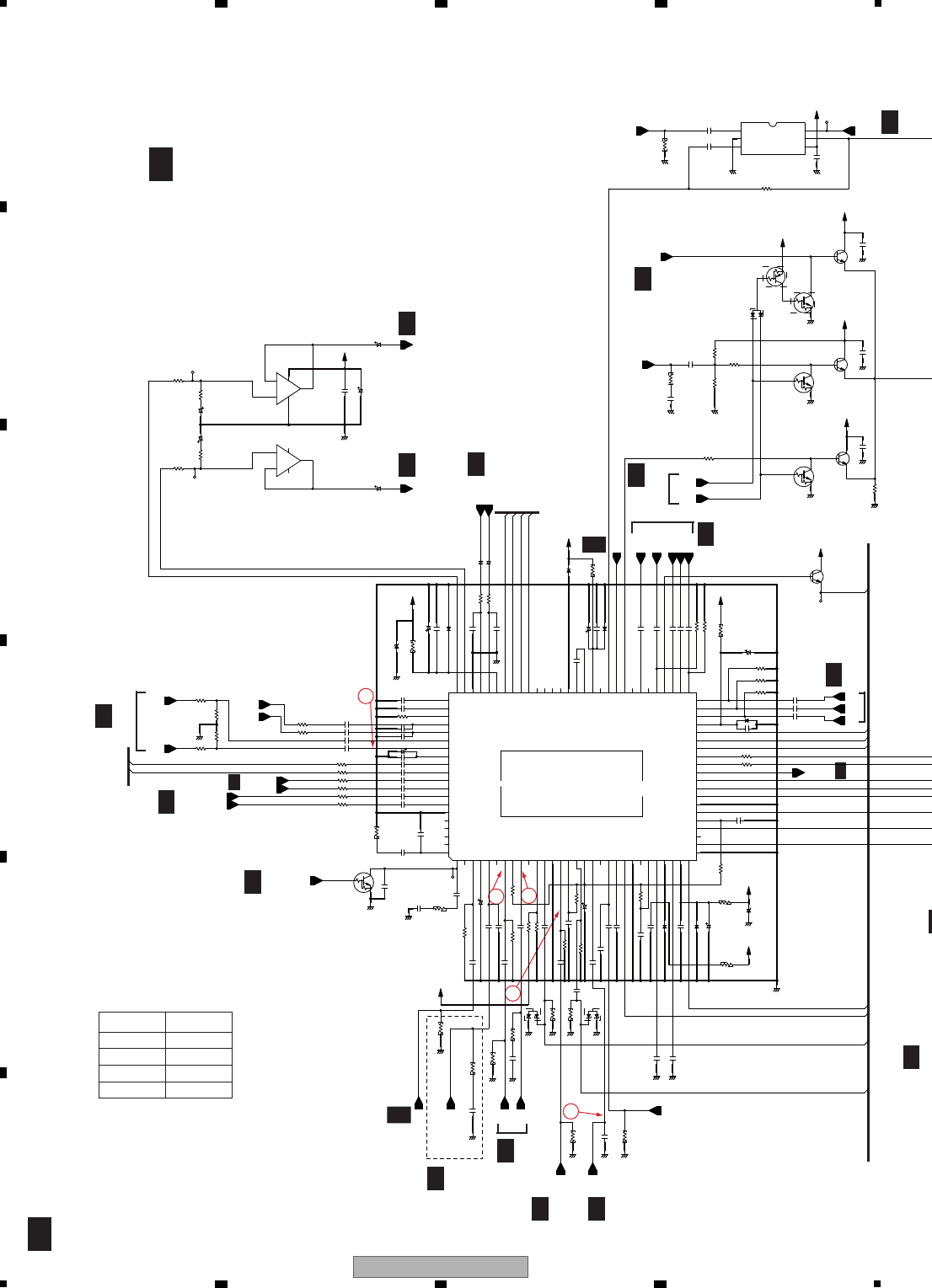
118 DVR-LX61
12 3 4
A
B
C
D
E
F
12 3 4
10.2 SERVICE TUSB ASSY (2/4)
A2/4
A1/4
A1/4 A1/4 A1/4
A3/4
A1/4
A1/4
A
A1/
A3/4
A4/4
A1/4
A1/4
A1/4
A1/4
A1/4
A4/4
A3/4
A1/4,3/4
A1/4
A1/4
A2/4 SERVICE TUSB ASSY (2/4)
(YXX1003)
21
16
1
18
17
-
+
+
-
AV_BUS
AV1_V/YIN
AV2_V/YIN
AV2_V/YOUT
AV1_V/YOUT
AV_BUS
AV2_LIN
AV2_RIN
AV1_LOUT
AV1_ROUT
AV2_ROUT
AV2_LOUT
BOUT
GOUT
R/COUT
RGBOUT
AV_BUS
12
3
12
3
E
C
B
100
99
96
97
98
93
94
95
91
90
92
89
88
87
84
86
85
83
82
81
6
4
7
8
5
4
1
8
3
2
2315764121191081413 15 16 20191817 23 2421 22 25 282926 27 30
32
31
34
33
35
37
36
38
41
39
40
43
44
42
45
46
47
49
50
48
788079 7577 7476 6971 7073 72 66676865 61626364 5658575960 53 525455 51
BC
E
E
BCE
BC
BC
E
E
BC
2
B2
5
4
6
1
3
E
B
C2 C
E2 E
BC
3
2
1
R443
R447
C449
R449
C448
R446
R445
C447
C494
C495
R444
D421
R441
R442 C446
D422
Q401
C498
C427 R426
IC401
C425
C497
R418
R419
R416
R417
R415
R423
C423
C422
C424
C421
C420
C419
R413
R411 R409
R408
C412
R414
R412
R410 C416
C417
C411
C418
C455
C468
C469
C414
R422
C415
D401
R404
C401
C452
C475
R462
R463 C474 R453C471
IC402
IC402
R454
C464
C473
C472
C429
C443
R429
C500
R430
C430
R428
C431
C432
R427
C456
C444
R432
C445
C496
R431
C434
C433
C441
C440
C428
C457
R448
C442
D407
D408
C458
D402
C426
R425
R421
R420
R438
R439
C439
R436
R437
D406
C438
R435
C402
D404
C403
C413
D405
C404
C406
C453
R433
R434
C409
C408
C410
C407
R450
R406
C454
R407
R402
R403
C450
C451
D403
R401
C437
C435
C436
Q402
C405
R465
R466
R499
C470
R498
R440
Q413
R461
C467
Q410
Q412
Q409
C466
D420
Q411
R459
C460
C461
Q411
Q408
R460
C465
C462
IC403
V+5VI
GND
***
GND
GNDGNDGND
75F(2125)
***
75F(2125)
***
GNDGND
75F(2125)
***
0.01
GND
***
***
GND
75F(2125)
GND
YB
***
GNDGNDGND
***(2125)
***(2125)
1u YB
***
GND
GND
GND
***(2125)
DTC124EUA-TLB
0.1
***
HA118326APFR-K
***
***(2125)
0.1
470
470
1u
1u
1u
YB
YB
YB
470
470
470 1u
1u
1u
YB
YB
YB
GND
470
*** ***
470
470
470
YB1u
470 1u
4.7/50
YB1u
1u YB
YB1u
***
***
0.1
10k
0.1
GND
UDZS11(B)-TRB
0(2125)
1u
100/10
V+9V
10k(F)
10/50
8.2k(F) 10/50 8.2k(F)
10/50
GND
100/16
10k(F)
V+9V
0.1
10/50
YB1u
YB1u
1M
1M
***
0.1
0
***
YB1u
0.1
1uYB
1M
YB1u
***
0.1
1M
YB
0.1
YB1u
1u
YB0.1
0(2125)
V+5VO
0.1
***
100/10
***
GND
1/50
***
YB
YB 100k
3.3M
YB
10/50
3.3M
0(2125)
V+5VO
1.8M
0.1
UDZS6R8(B)-TRB
YB
100
100
100p
GND
100p
***
0.1 YB
***
1u
100/10
0.1
100/10
1u
1u
1u
1u
***
***
0(2125)
560
560
CEANP4R7M50-T
CEANP4R7M50-T
4.7/50
NP
4.7/50
NP
YB
***
0(2125)
YB
YB
YB
YB
V+5VO
1u
***
1M
1u
YB1u
1u YB
YB
1M
***
V+5VI
2SD2114K(VW)-TLB
V+5VI
GND
***
GND
470
***
22k
YB
22k
0.1 470
DAP202U-TLB
GND
DTC124EUA-TLB GND
680
GND
2SC4081(QR)-TLB
DTC124EUA-TLB
GND
V+5VI
1u
GND
2SC4081(QR)-TLB
GND
1000p
UMD2N-TLB
GND
75F(2125)
GND
YB 1u
YB 1u
MM1503XN-TRB
UMD2N-TLB V+5VI
GND
2SC4081(QR)-TLB
V+5VI
V+5VI
***
0.1
GND
1u
V+5VI
DT_Y
2VIN
TU_VIN
DT_C
Y2IN
C2IN
V3IN
P_SAVE
AV1_RIN
AV1_LIN
L2_RIN
L2_LIN
TU_LIN
TU_RINL3_RIN
L3_LIN
R_IN
L_IN
CSYNCIN
BLANK
C_OUT
CR_OUT
Y_OUT
CB_OUT
YP_OUT
GIN
R/CIN
BIN
L_OUT
R_OUT
RCSEL2
RCSEL1
C3IN
RTOMAIN
Y3INRCSEL1
C448
R446
R443
MODEL
AI ASSY
75F(2125)
75F(2125)
0.01u(YB)
YWV1001-
LX61/WY
560H/WY
BA4560RF-TBB
BA4560RF-TBB
V C&S C3 IN
DL3 DRIVE
SEP Y1 IN
SYNC DET
SEP Y2 IN
SYNC DET OUT
SYNC DET
SEP C1 IN
VIDEO L3 IN
59/61PIN
S1/S2 B OUT
SEP C2 IN
VIDEO L1 IN
FBC
GND
VIDEO L2 IN
FBCD
TUNER IN
RS IN D OUT
BS IN
BG
FBCD
VTR OUT
GND
AV2 OUT
VCC
C1 OUT
VCC
V1 OUT
Y1 OUT
A L5 IN(L)
A L5 IN(R)
GND 100:VTR VorY&S Y3 IN
99:A AGC D
98:RF-C A OUT
97:A AV1 R OUT(L)
A L2 IN(L)
A L2 IN(R)
A L3 IN(L)
85:A L4 IN(L)
84:A L4 IN(R)
83:V DVD M C
96:A AV1 R OUT(R)
S1/S2 B OUT:33
V2 OUT:32
GND:31
SCART G IN:48
VCC:47
PY(Y)/G OUT:46
FBCD
C2 OUT
Pb(Cb)/ OUT
GND
Y2 OUT
PY(Y) OUT
Pr(Cr)/ OUT
SYNC
VREF(9V/2)
A TUNER IN(L)
A TUNER IN(R)
A L3 IN(R) 82:A HIFI IN(L)
81:A HIFI IN(R)
A HorHDD/OUT(R)
A HorHDD/OUT(L)
To DVD(L)
To DVD(R)
A DVD M C
F A DVD(L)
F A DVD(R)
A AV1/OUT(L)
A AV1/OUT(R)
A AV2/OUT(L)
A AV2/OUT(R)
VCC
A AV1/OUT2(L)
A AV1/OUT2(R)
VIDEO AGC
MAIN C D
MAIN C IN
VCC
SLICER OUT
DVD VorY OUT
PAL SCART IN
DVD C OUT
PAL SCART D2
F DVD C
PAL SCART D1
SCART B IN:50
SCART RorC IN:49
Pr(Cr)/ RorC OUT
Pb(Cb)/B OUT
SDA
SCL
F DVD Y
RGB M OUT
F DVD Pb(B)
F DVD Pr(R)
F DVD PY(G)
IN 1
GND
IN 2
OUT
Vcc
SW
NOTE2
NOTE2
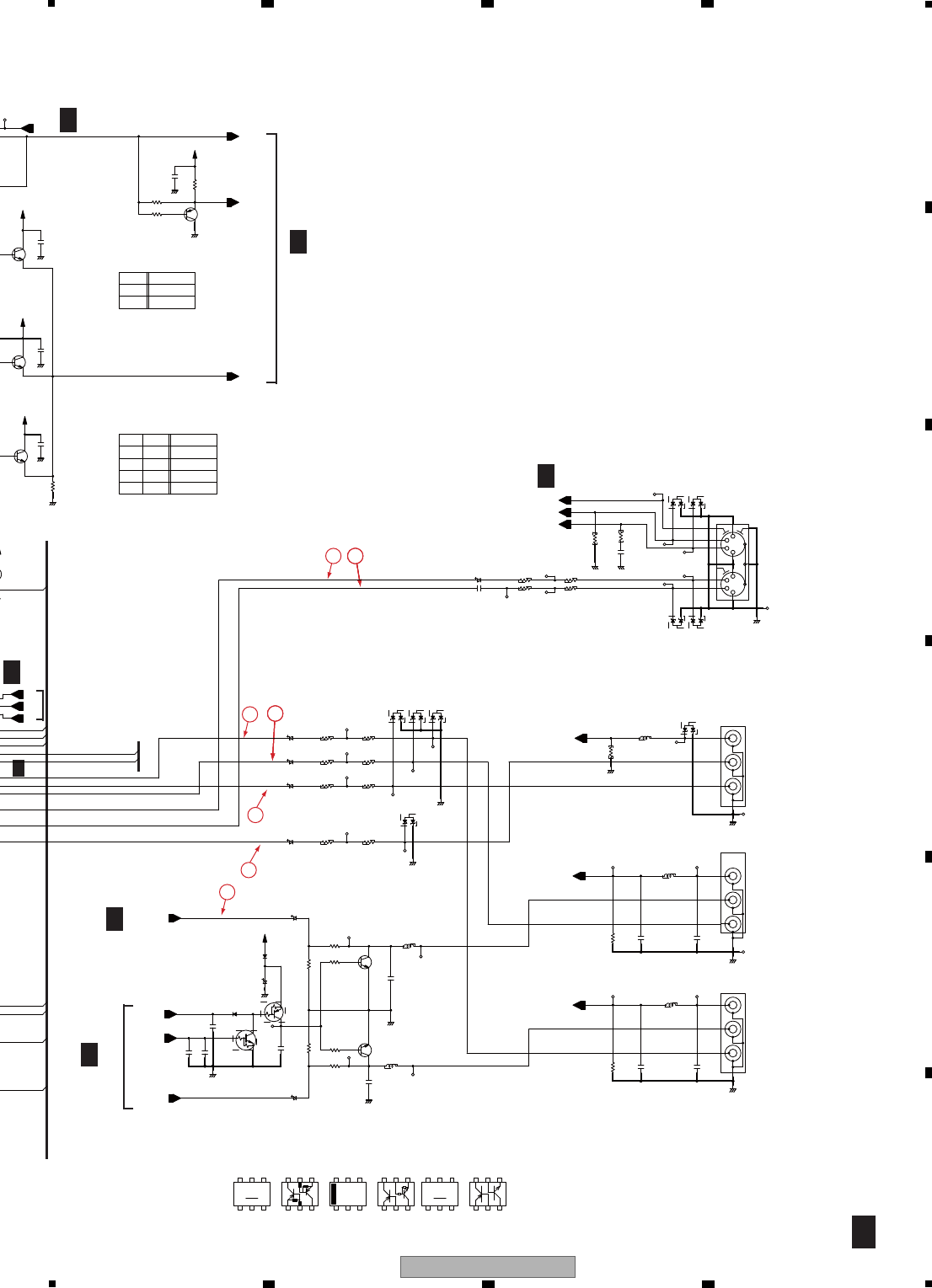
119
DVR-LX61
56 7 8
56 7 8
A
B
C
D
E
F
A2/4
A1/4
A1/4
A1/4
A1/4
A1/4
A3/4
A1/4
11132
1116
22
5
7
4
AV_BUS
AV1_V/YIN
AV2_V/YIN
V2_V/YOUT
V1_V/YOUT
BOUT
GOUT
R/COUT
SCL
TU_CON
SDA
RGBOUT
B
C
E
C
B2
C2
E2
E
B1
4
2
E
BC
12
3
C
E
122112
333
E
BC
E
BC
3
8
7
6
5
12
9
10
2
3
1
11
3
2121
3
4
2
3
1
10
6
85
9
11 12
7
3
1212
3
E
BC
E
BC
C463
C481
C479
Q404
D419
C493
R488
C484
L405
C480
R487
R486
Q404
C492
Q407
C482
C483
R489
C485
D418
R485
R484
R479
C491
Q406
L404
R478
C490 R480
C489R476
D416
R477
C488 R474
C487R472
R475
R473
D414
D413
D415
C476 R470
C486R468
R461
C467
Q410
Q409
C466
R481
C477
L403
JA402
C478
L402
JA402
R424
L401
D417
JA402
D410
D409
R471
R469
R405
C533 R467
JA401
D412
D411
Q408
C465
Q403
R455
C459
R456
R458
C462
GND
***
***
UMD2N-TLB
1SS355-TRB
***
47/16
470
GND
470p
CTF1388- -T
22k
***
1k
UMD2N-TLB
GND
220/6.3
470p
2SD2114K(VW)-TLB
GND
2SD2114K(VW)-TLB
GND
100k
1500p
***
1SS355-TRB
22k
1k
470
V+5V
47/16
CTF1388- -T
68F(2125)
1000/6.3 3.9(2125)
GND
68F(2125)
470/6.3
470/6.3 68F(2125)
***
3.9(2125)
GND
3.9(2125)
VI
1000/6.3 68F(2125) 3.9(2125)
***
***
***
YB0.01 68F(2125)
1000/6.3 68F(2125)
GND
680
GND
2SC4081(QR)-TLB
V+5VI
1u
GND
2SC4081(QR)-TLB
1000p
CTF1388- -T
100k
1500p
VKB1250-
GND
***
CTF1388- -T
VKB1250-
GND
GND
***
CTF1388- -T
***
VKB1250-
***
GND
***
3.9(2125)
GND
3.9(2125) GND
75F(2125)
YB0.01
***
AKP1234-
***
***
V+5VI
GND
2SC4081(QR)-TLB
V+5VI
2SA1576A(QR)-TLB
0.1
GND
47
GND
***
1u
470
D
V+5VI
1-C6
R_OUT
XAMUTE2
AMUTE1
L_OUT
CIN
L3_RIN
L3_LIN
GIN
R/CIN
BIN
C/R_IN
C3IN
Y3IN
SDET3
V3IN
TEXTVIN
RCSEL1
Y_IN
EC2BEEBBC2 C2BEC2 E B C2 E B C2
C
VC
UMB1N(R1=R2=22k)
B2 E2 E2B2C CB2
VC
E2
UMF21N
CB2 E2 E2B2C
RN4903
CB2 E2
ROUT
COMPONENT Y OUT
H
LH
RTOMAINH
C3IN
H
C/R_IN
L
RCSEL1
L
L
RCSEL2
IC401 59pin
RIN
COMPONENT CB OUT
LIN
LOUT
VOUT
COMPONENT CR OUT
VIN
(T-VKB083)
S OUT
C
Y
C
YS IN
MM1507
RCSEL1
L
H
Y3IN
IC401 61pin
Set Prohibition
OUT PUT
OUT PUT
120 DVR-LX61
12 3 4
A
B
C
D
E
F
12 3 4
10.3 SERVICE TUSB ASSY (3/4)
A1/4
A2/4
A2/4
A2/4
A3/4
A3/4 SERVICE TUSB ASSY (3/4)
(YXX1003)
35
B
E
C
BC
E
E
B
C
B
E
C
E
B
C
E2
B2
C2
E
B
C
B2
E2
C2
Q508
C545
D528
C543
C544
R568
Q511
C549
R569
R566
C551
Q510
R565
R564
C548
R562
C550
C546
R561
R560
Q509
C547
R558
R557
R556 Q507
Q507
R554
R555
C553
C540
R550
R552 L510
L509
R572
R571
C542
C541
R546
R548
R547
C536
R549
R540
R541
C534
C535
C537
C538
L508
C539
L507
L505
L506
R536
R538
R534
Q506
L504
L503
R535
Q506
DTA124EUA-TLB GND
100/16
1SS355-TRB
V+12R1
4.7/50
4.7/50
GND
12k
2SA1576A(QR)-TLB
GND
1u
1k
22k
22/25
GND
V+5VI
680
15k
2SC4081(QR)-TLB
1000p
V+5VI
GND
10k
22/25
GND
0.1
GND
680
2SC4081(QR)-TLB
15k
22/25
10k
V+5VI
3.9k
3.9k
GND
HN1C03FU(AB)-T
GNDGNDGND
GND
HN1C03FU(AB)-T
100k
100k
470p
470
470
GND
470p
GND
GND
75F(2125)
GND
***
4.7/50
4.7/50
100k
100k
100k
100k
GND
GND
100k
GND
100k
470p
1500p
1500p
1500p
1500p
470p
470
470
GND
HN1C03FU(AB)-T
3.9k
GND
3.9k
HN1C03FU(AB)-T
SAMUTE
RTOMAIN
GTOMAIN
BTOMAIN
AV1_LIN
AV1_RINGIN
R/CIN
BIN
R/COUT
AV_BUS
GOUT
AV1_V/YIN
BOUT
AV1_V/YOUT
RGBOUT
AV2_LOUT
AV2_ROUT
AV2_V/YIN
AV2_V/YOUT
R/CIN
GIN
BIN
AV2_RIN
AV1_RIN
AV2_LIN
AV1_LIN
AV1_ROUT
AV1_LOUT
(2/2)
(1/2)
C539
C538
C537
C536
1500p
1500p
1500p
1500p
C525
C512
MODEL
AI ASSY
100p
100p
YWV1001-
560H/WY
LX61/WY
(1/2) (2/2)
NOTE3
NOTE3
L503-L510 : CTF1389--T
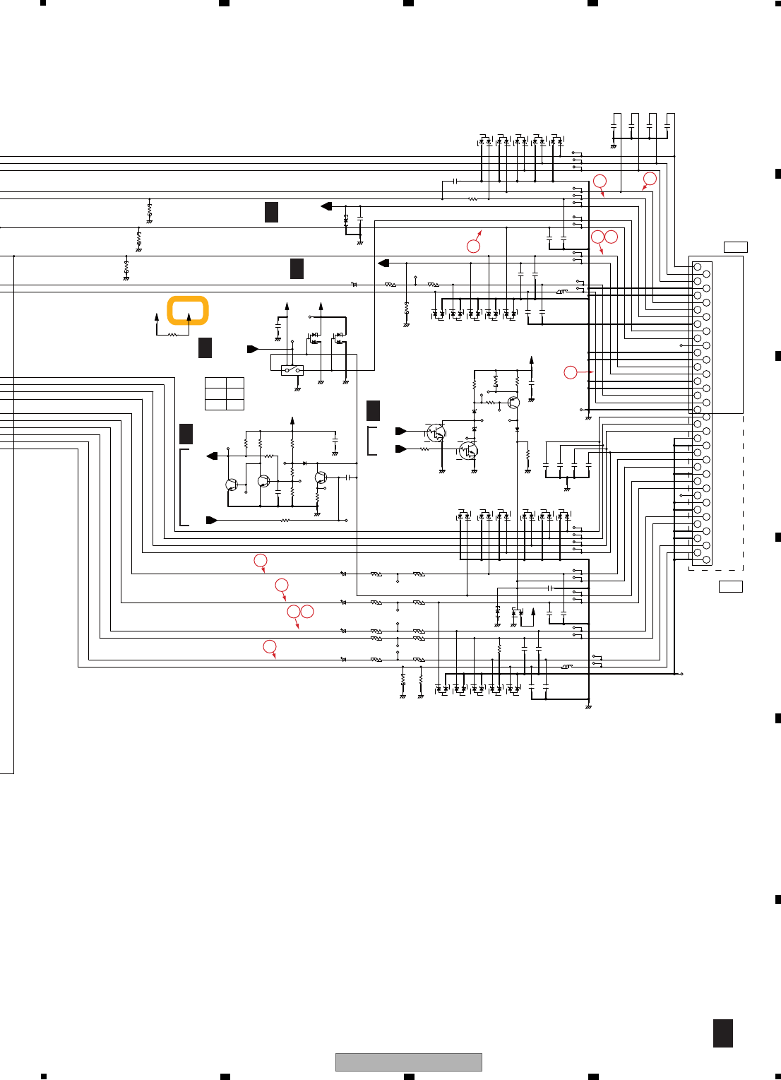
121
DVR-LX61
56 7 8
56 7 8
A
B
C
D
E
F
A1/4
A1/4
A1/4
A1/4
A1/4,2/4
A3/4
26
33
34
30
25 29
31 32
27
28
36
2112
33
E
E
BC
C
B
E
C
B
12
3
B
E2
B2
C2
5
1
3
2
4
12
3
12
3
2
3
12 1
3
2
3
112
3
2
3
1
12
3
38
41
40
42
39
112
33
12
3
21212
33
37
35
36
34
33
32
29
31
30
E
C
B
C
26
28
27
25
23
24
20
22
21
E
18
19
17
16
15
14
12
11
13
1212
33
12
3
10
9
8
4
5
6
7
3
1
2
12 12 12 1 122
33 333
R532
D518
R533
D520D519
C532
R527
R530
C531 R525
C530 R523
R528
R531
R526
R524
C529 R521 R522
R513
Q504
C511
Q503
R512
R520
Q505
R511
C517
D531
Q501
R503
R506
R507
R508
R510 D527
R509
C515
R574
Q501
D501
IC406
R517
C510
D523 D524
C528
R514
D508D509 D510
R504 R505
D521 D522
C525
C526
L501
C523
C524
R529 D525
C527
C522
D530
C521
D513 D515D514 D516
C518
C516
D517
C520
C519
R519
D502
D526
R518
Q502
R515
R516
C514
D511 D512
C512
C513
C504
C503
L502
R502
R501
D529
C501
C552
R573
C502
C509
JA501
D503 D504 D505 D507D506
C505
C506
C507
C508
75F(2125)
GNDGND
***
1000/6.3
0(2125)
68F(2125)
470/6.3 68F(2125)
470/6.3 68F(2125)
75F(2125)
3.9(2125)
3.9(2125)
3.9(2125)
470/6.3 68F(2125) 3.9(2125)
100k
2SC4081(QR)-TLB
2SC4081(QR)-TLB
220p
GND
2SC4081(QR)-TLB
100k
220
220k
220p
UMH1N-T
GNDGND
***
0
GND
V+5VR
75F(2125)
V+5V
4.7k
2.2M
47k
V+5V
1SS355-TRB
27k
0.1
GND0
UMH1N-T
UDZS5R1(B)-TRB
GND
TC7S66FU-TLB
GND
GNDGND
DAN217U-TLB
DAN217U-TLB
0.1
V+5VV+5VR
1000/6.3
68F(2125)
GND
75F(2125)
3.9(2125)
***
220p
LCYA5R6J2520-T
GND
***
100k
***
GNDGND
***
***
***
V+12R1
***
***
GND
UDZS5R1(B)-TRB
GND
***
***
***
***
1SS355-TRB
56k
10 GND
2SA1576A(QR)-TLB
GND
560
1.5k
1.2k
0.1
V+12R1
220p
***
LCYA5R6J2520-T
***
***
75F(2125)
GND
75F(2125)
GND
GND
***
***
***
***
0
***
VKB1249-
GND
***
***
***
***
AVLOUT
AVLIN
FUNC_ON
SQU
AVLTH
BLANK
FUNC_IN
D518~D522:UMZ6R8N-TLB
D513~D517:UMZ6R8N-TLB
(1/2)
HON
(2/2)
OFF
TC7S66FU
SW
L
4
D508~D512:UMZ6R8N-TLB
AV1
to TV
GNDV
V/YIN
V/Yout
GNDV
GNDV
BLANK
R/Cout
GNDV
NC
Gout
GNDV
FUNCTION
GNDV
N-LINK
GNDV
Bout
Lin
Rin
Lout
GNDA
GNDV
V/Yin
Rout
(2125)
GNDV
GNDV
V/Yout
BLANK
R/Cin
GNDV
NC
GNDV
Gin
N-LINK
Bin
GNDV
FUNCTION
Lin
GNDV
GNDA
Rin
Lout
Rout
from STB
AV2
(T-VKB082)
D503~D507:UMZ6R8N-TLB
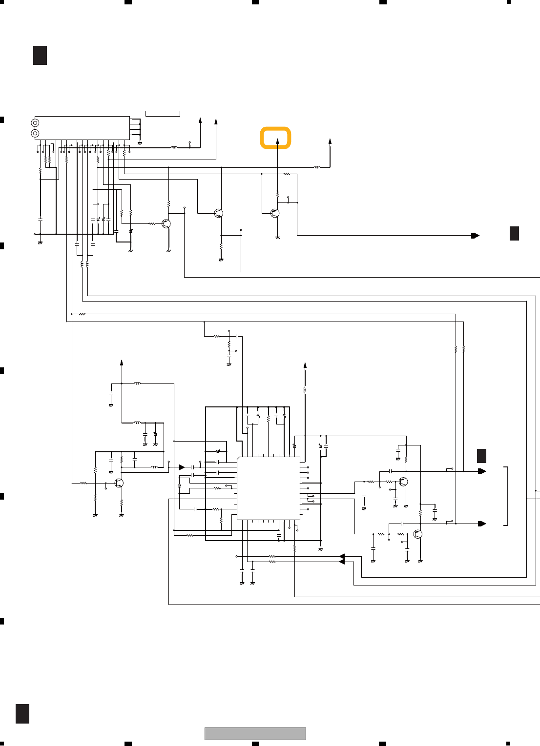
122 DVR-LX61
12 3 4
A
B
C
D
E
F
12 3 4
10.4 SERVICE TUSB ASSY (4/4)
A2/4
A2/4
A4/4
A4/4 SERVICE TUSB ASSY (4/4)
(YXX1003)
TU_RIN
TU_LIN
TU_VIN
B
E
C
E
BC
1412 13 15 181716
10
11
21 222019
24
23
B
7
9
8
4
5
6
1
3
2
25
26
27
29
28
30
32
33
31
BC
E
C
E
44 43 42 41 383940 3437 3536
EB
BCE
C
123 65479810 11 14 1512 13 16 17
18
19
20
21
R619
R634
R633
R632 Q606
R631
C616
R630
C615
C624
X601
L609
C623
C621
C614
L607
C640
C613
L606
L604
L605
R640
C602
C605
C606
C608
C611
C609
C603
C607
C604
Q603
R607
R635
R603
R604
Q602
R605
C636
C635
R622
R621
C625
R618
R617
R620
C632
C633
R627 R628
C631
R616
C622
C620
C629
C630
Q604
R624 R625
C628
R623
Q605 R626
C627
C643
R615
C617
C638
C618
C641
C642
C619
C639
C626
IC601
L608
C634 R612
R629
C612
R613
R614
Q601
R606
R602
R601
R609
R608
R639
R636
R637
R638
L601
U601
L602
GNDGND
5p
10k
2.2k
100
22
GND
2SC4081(QR)-TLB
0.01
4.7k
100p
330
LCYA100J2520-T
VSS1189- -T
18.43MHz
5p
56p
YB
LCYA101J2520-T
GNDGND
100/10
0.1
1u
CTF1399- -T
GND
***
V+5TU
CTF1306- -T
CTF1306- -T
GND
GND
10p
10p
10/50
***
1k ***
2SA1576A(QR)-TLB
GND
YB2200p
100/10
YB2200p
1/50
100p
0
***
10k
GNDGND
22p
22p
100
3900p
GNDGND
100
***
***
0
GND
1u
YB
560p
3.3k
YB0.01
3.3k
GNDGNDGND
0
56p
1u
YB3900p
560p
2SA1576A(QR)-TLB
3.3k
0.01
3.3k
YB
1k
GND
GND
2SA1576A(QR)-TLB
GND
1k
1000p
100/10
0.1
***
10/50
10/50
100/10
0.1
0.1
3.3/50
0.1
GND
MSP3417G-TBB
CTF1399- -T
***
***
***
***
V+5TU
***
***
GND
GND
10k
2SA1576A(QR)-TLB
1k
***
CTF1399- -T
0
0
0
***
0
0
0
GND
CTF1399- -T
VXF1146- V+5BB
V+5TUA V+5TU
V+32V
SIF BPF(4.5M~6.7M)
ADSEL
TP
STBYQ
TP
TP
TP
13:SDA
12:SCL
22:RESETQ
TP
DVSUP
DVSS
TP
TP
TP
DCO0
DCO1
TP
TESTEN
XIN
XOUT
40:NC/ASG
41:SCIR
38:NC
39:NC
AVSUP
AIN1-
AIN1+
VREF2
DACMR
DACML
37:NC
SCOR
VREF1
TP
AHVSUP
SCOL
NC
VREFTOP
AVSS
MONOIN
AHVSS
AGNDC
CAPLM
MULTI SOUND DECODER
AUDOUT(L)
SIFOUT(R)
NC
BB(5V)
NC
NC
NC
SCL
GND
SDA
AGCOUT
IF-AGC
GND
TU(31V)
MB(5V)
AFT
VIDEO
U/V TUNER
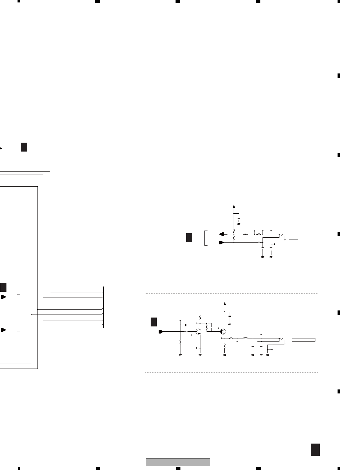
123
DVR-LX61
56 7 8
56 7 8
A
B
C
D
E
F
A2/4
A2/4
A1/4
A1/4
A4/4
MSPSTAT
XRST1
SDA
AGC
AFT
SCL
TU_CON
TU_RIN
TU_LIN
IR_B
IR
SEL_IR
TU_VIN
E
BC
BC
E
1
3
2
1
3
2
R755
R753
Q752
R752
C753
C752
R751
C754
C755
R756
R754
Q751
L751 JA751
C751
C702
R703
R704
R701
D701 R702
C703
JA701
C701
GNDGND
2SC4081(QR)-TLB
4.7k
4.7k
100p
4.7k
100p
1k
100p
GNDGNDGNDGND
1k
150
2SA1576A(QR)-TLB
CTF1306- -T
GND
***
RKN1004-
0.1
V+5V
GNDGND
***
220
220k
1SS355-TRB 220
0.1
680p
RKN1004-
V+5V
GND
1u
IR BLASTER
SR_IN
WY Only
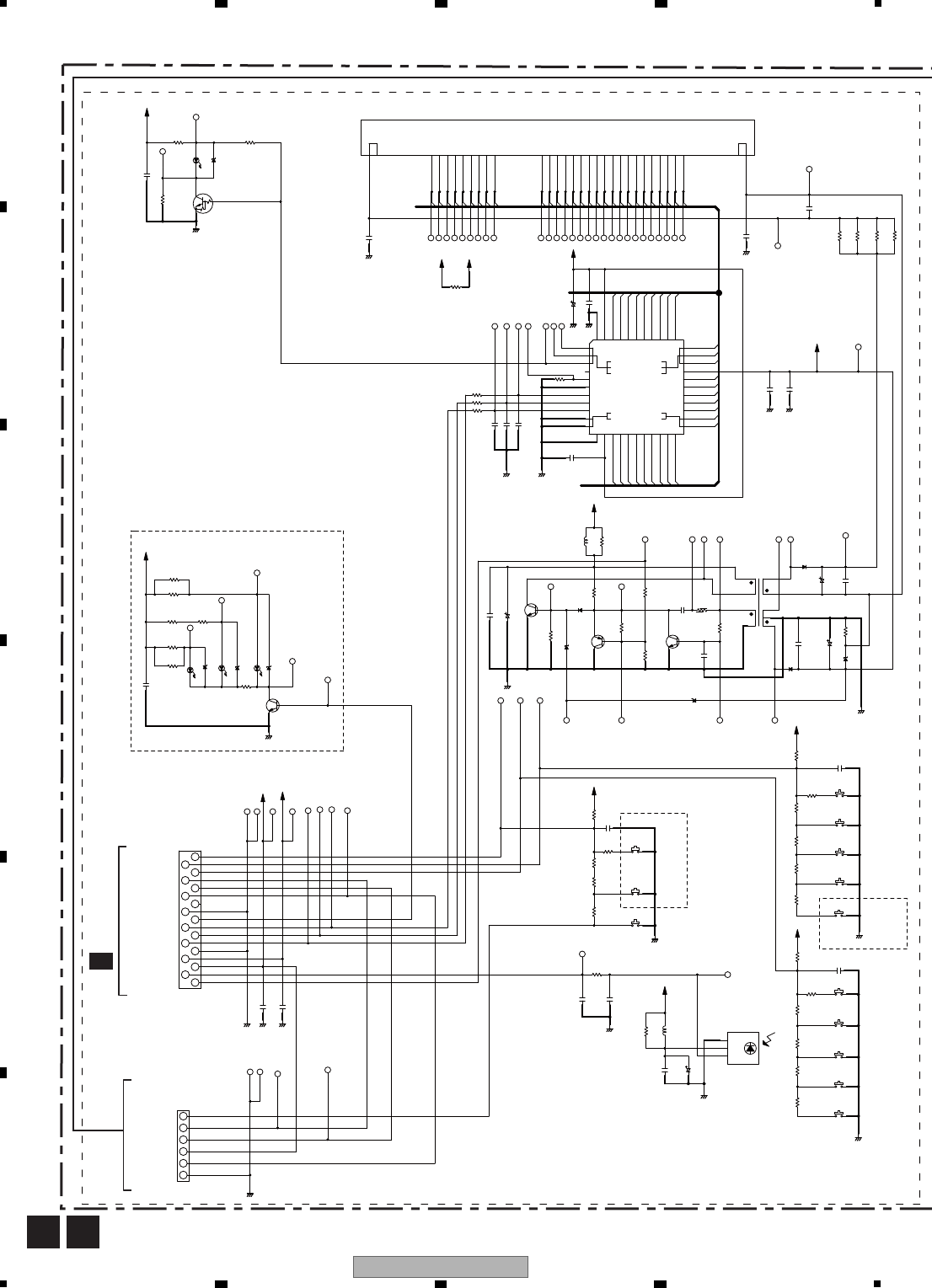
124 DVR-LX61
12 3 4
A
B
C
D
E
F
12 3 4
10.5 SERVICE FLKY ASSY
B C
CN105
A
1/4
FLKY ASSY
DVR-LX61 Only
DVR-560H-S,-K Only
DVR-560H-S,-K Only
LED_P_ON
to KEYB
V+12F
KEY3
LED_DVD
LED_HDD
GND
V+12R1E
FLPON
IR
2.85V
REC MODE (AT only)
1.53V
2.18V
0.90V
0V
to TUJB
LED_P_ON
LED_ICE BLUE
FLSTB
GND
LED_REC
FLCLK
GND
FLDATA
V+5F
LED_HDD
LED_DVD
KEY3
KEY1
KEY2
ICE BLUE
1.53V
0.90V
0V
regular model
2.85V
0.90V
1.53V
2.18V
0V
(2125)
FL-28V
FLDC+
FLDC-
DC-DC Convertor
SEG1
KEY1
KEY2
VDD
VSS
STB
SEG2
SEG3
SEG6
SEG5
SEG4
SEG11
SEG10
DOUT
DIN
CLK
SEG12
SEG7
SEG8
SEG9
SEG15
SEG14
SEG13
LED4 LED2
OSC
LED3 GRID12
GRID11
GRID1
VDD
VSS
LED1
GRID2
GRID3
GRID6
GRID5
GRID4
GRID10
SEG16
VEE
GRID7
GRID8
GRID9
HDMI LED (RED)
VAW1091-
FL Holder: VNF1134-
FL_F
P1
P2
P4
P5
P3
P6
P8
P9
P7
P11
P10
P12
P14
P13
P16
P15
12G
11G
10G
P1
P2
P3
2G
1G
4G
3G
6G
5G
7G
8G
9G
P4
P6
P7
P5
P9
P8
P10
P11
P12
P14
P13
P15
11G
P16
12G
9G
10G
8G
7G
6G
5G
1G
4G
3G
2G
Vout
GND
Vcc
CN102
C120
C119
R138
C127
C128
L102
C125
C126
R137
IC103
R135
S110
R132
S108
R130
S106
R128
S104
R149
R126
S103
C124
CN101
C134
R162
Q112
R166
D116
D122
D120
D117
R157
R156 R165
D118
D121
R164
R155
R161
S112
R163 R160
S114
R159
R158
C135
S115
R150
S113
R131
S109
R129
S111
R127
S107
R148S105
R125
C123
D112
R119
C115
C116
D108
R124
R120
Q105
D109
C121
Q106
R122
Q104
R117
R118
L101
R116
C117 R121
T101
D110
C122
D111
C118
R123
C113
C114
D107
C111
C110
C109
R110
R112
R111
C112
IC101
R113
C105
C108
C107
C132
C103
R136
Q103
D113
D105
R133 R134
V101
R144
C106
C104
R104
R105
C101
R107
R106
2
3
1
6
4
5
3
2
1
1
3
2
11
12
6
8
7
5
4
9
10
13
17
15
16
14
E
BC
E
BC
E
C
B
E
C
B
7
6
8
9
4
3
5
2
1
13 1412 15 181716
10
11
7
9
8
19 2120 22
24
23
26
27
25
4
5
6
1
3
2
43 4244 41 383940
29
28
30
31
33
32
3637 3435
C
E
B
1109 151617 231211 1413 26 27 2824 25 3229 30 31 36353433 3837 39 4140 49
GND
YKP1007-
GND
0.1
GNDGND
***
GND
0.1
100/10
LAU***J-TA
GND
0
***
***
0
GP1UM28XK0VF
***
V+5F
REC
GND
5.6K
ONE TOUCH COPY
3.3K
ATV/DTV(DT only)
2.2K 2.2K
INPUT SELECT
47 STOP REC
0.1
9604S-17C
V+12VV+5F
V+12V
SLR343BC4T(JKLM)-TS
0.1
SLR343WBCT(MNPQ)
0
GND
2SD2153(VW)-TRB
SLR343BC4T(JKLM)-TS
1.5k
1.5k
***
3.9k 0
***
***
1.5k
1.5k
GND
2.2K
OPEN/CLOSE
MUSIC
0 2.2K
47 PC VIDEO
0.1
10K
V+5F
10K
GND
V+5F PHOTO
5.6k 3.3K
PLAY
2.2K
STOP
CH-
2.2K
47 CH+
0.1
10K
GND
UDZS13(B)-TRB
100/16
0.1
2SC5712-TLB
UDZS15(B)-TRB
2SA1576A(QR)-TLB
1.0k
27k
10k
1SS355-TRB
0.01YB
2SC4081(QR)-TLB
1.2k
0.022YB 220
100k
1k
LAU220J-TA
***
22
VTT1171-A
RF101L2S-TRB
UDZS2R4(B)-TRB
GND
V+5F
10/50
***
10k
100/10
***
RF101L2S-TRB
GNDGND
V+12V
0.1
47
***
***
***
47
47
PT6315
82k
GNDGND
GNDGND
***
0.1/50
FL-28V
GND
0.01/50YB
V+5F
GND
DTC124EUA-TLB
***
0.1
SLR-343VC(NPQ)-TS
270
***
V+5F
***
0
V+5F
***
0.1
V+5F
GND
0.01/50YB
0
***
***
***
***
2 48
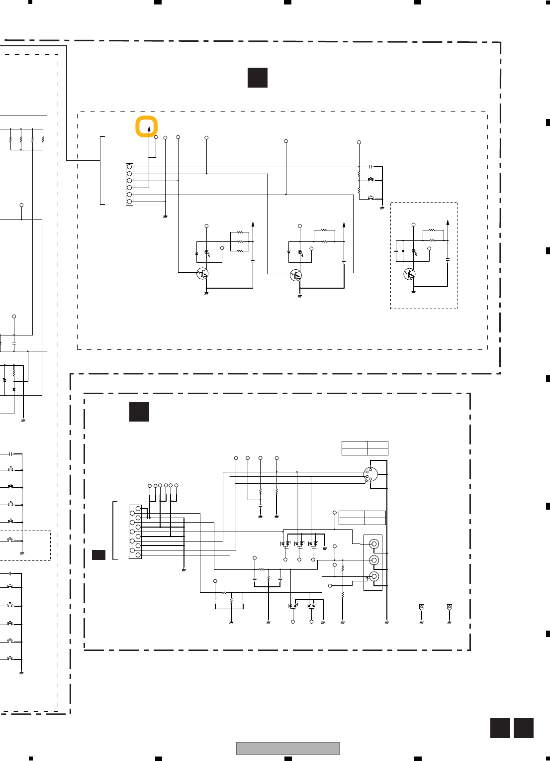
125
DVR-LX61
56 7 8
56 7 8
A
B
C
D
E
F
CB
B
SERVICE FLKY ASSY
(YXX1008 : DVR-LX61)
(YXX1007 : DVR-560H-S, -K)
C
SERVICE FRJB ASSY
(YXX1027:DVR-LX61)
(YXX1004:DVR-560H-S, -K)
CN106
A
1/4
KEYB ASSY
Y ASSY
DVR-LX61 Only
DVR-560H-S,-K Only
2.85V
REC MODE (AT only)
1.53V
2.18V
0.90V
0V
Rch
regular model
2.85V
GND
2V
GND
GND
2Y
2C
SDET2
0.90V
1.53V
2.18V
GND
GND
2R
2L
0V
FL-28V
FLDC+
FLDC-
V+12F
LED_P_ON
GND
DVD LED (AMBLE)
HDD LED (BLUE)
VIDEO
/MONO
Lch
FRONT INPUT JACK
S
2.85V
P_ON LED (BLUE)
KEY3
LED_HDD
from FLKY
LED_DVD2.18V
DVR-LX61
DVR-560H-S,-K
DVR-LX61
DVR-560H-S,-K
YKB1001-
S110
S108
S106
S104
S103
C124
D305D304
C304
R307
C305
R306
C302
R304
C303
R308R305
KN302 KN301
S113
S109
S111 CN301
S107
S105
C123
R303
D301 D302 D303
R301
C301
R302
D111
C118
R123 C114
Q206 Q204
D211
C202
D212
R225
R224
R221
D205
D206
R222
R223
JA302
JA301
Q203
C204
C271
D270
D271
R270
C270
S201
R204
R272
CN201
R104
R105
R107
R106
R205
S202
C201
33
1212
4
7
1
7
8
5
6
11
9
10
1
2
3
4
11
3
2
3
212
3
6
5
4
B
EE
B
CC
5
2
6
3
6
5
1
3
2
4
E
BC
2
3
1
REC
GND
ONE TOUCH COPY
ATV/DTV(DT only)
PUT SELECT
STOP REC
0.1
GND
***
GND
***
GND
GND
***
***
470p
0
***
0
***
470p
GNDGNDGNDGND
***
VNF1084- -T VNF1084- -T
GND
PHOTO
PLAY
STOP
CH-
HLEM11S-1
CH+
0.1
*** *** ***
GNDGND
***
***
***
UDZS2R4(B)-TRB
GND
10/50
10k
100/10
***
TRB
DTC124EUA-TLB
GND
DTC124EUA-TLB
GND
***
SLR-343DC(NPQ)-TS
0.1
***
1.8k
1.8k
SLR343BC4T(JKLM)-TS
***
***
GNDV+12F
0
GND
VKB1208-A
AKP1238-B
AKP1239-B
DTC124EUA-TLB
GND
0.1
1.8k
***
SLR343BC4T(JKLM)-TS
***
1.8k
1.8k
0.1
P_ON
GND
V+12F
5.6K
V+12F
YKP1007-
0
***
***
***
V+12F
3.3K
HDD/DVD
0.1
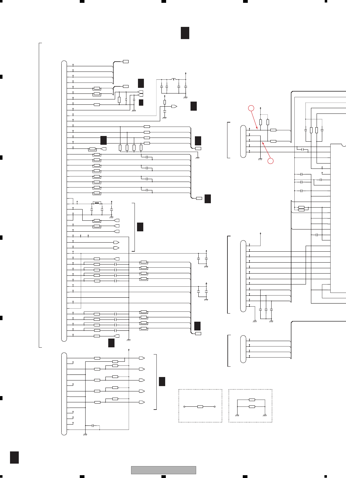
126 DVR-LX61
12 3 4
A
B
C
D
E
F
12 3 4
10.6 SERVICE MAIN ASSY (1/5)
F+
F-
T+
T-
APCV
W1SET
W2SET
W3SET
OSCEN-
W1EN+
W3EN-
W3EN+
W2EN-
W2EN+
A
RF+
S3
S2
RF-
OSCEN+
W1EN-
D
C
B
S1
S4
SI
U
U
OPEN
W
V
ST2+
CLOSE
ST1+
W
ST1-
ST2-
V
SCLK
CN502
DKN1288-A
1ST1+
2ST1-
3ST2-
4ST2+
CN601
DKN1402-A
1
RED
2
BLACK
3
LPS1
4
GNDD
5
LPS2
DKN1312-A
CN501
1
GNDD
2
W
3
V
4
U
5
HB
6
HW-
7
HW+
8
HV-
9
HV+
10
HU-
11
HU+
12
VCC
NM
CN103
1
2
3
4
5
6
7
8
9
10
11
12
13
14
DKN1404-A
CN101
1SW1
2S4
3S1
4S2
5S3
6VA5V
7RF-
8GNDA
9RF+
10VREFPD
11M4
12M1
13M2
14M3
15SW2
16VA5V
17FMO+
18FMO-
19GNDA
20DVD/CD
21HFGAIN
22GNDO
23GNDO
24OSCNT
25VO5V
26VO5V
27W2EN+
28W2EN-
29W3EN+
30W3EN-
31W1EN+
32W1EN-
33OSCEN+
34OSCEN-
35LDDEN
36W3SET
37W2SET
38W1SET
39RSET
40TEMP
41VD3V
42RESET
43VPP
44SEN
45SDIO
46SCLK
47TD
48TR
49FD
50FR
C180
10u
C302
NM
C181
C194
C193
C503
470p/50
C199
NM
C534
NM
C511
1u/16
C510 68p/50
C192
C535
NM
C189
C188
C186
NM
C533
NM
C171
0.1u/10
C197
0.1u/10
C187
C174 47p/50
C172 47p/50
C173 47p/50
C170 47p/50
C182
C509
33p/50
C304 NM
C305 NM
C306 NMC502 DCH1263-A
10u
(Size2125)
C185
NM
C177 22p/50
C165 22p/50
C176 22p/50
C166 22p/50
C303
NM
C508
1000p/50
C515
0.1u/25
C501 0.1u/16
F105
NM
GNDS
GNDS
GNDS
GNDS
GNDS
GNDD
GNDS
GNDD
GNDD
GNDS
GNDS
GNDD
GNDM
GNDS
IC501
BD7956F
LDO-
1
LDO+
2
VCC
3
ACTIN1
4
5
ACTIN2
6
TJMON
7
BTHC
8
SPVM_S
9
PGND1
10
PGND2
11
U
12
SPVM1
13
V
14
fin1
15
PGND3
16
W
17
SPVM2
18
SPRNF
19
HB
20
HU+
21
HU-
22
HV+
23
HV-
24
HW+
25
HW-
26
SPIN
27
DGND
L105
BTH1103-A
R602
10k
R603
1k
R604
1k
R1680
R123 NM
R102 NM
R122 NM
R101 NM
R172
3.3k
R171
3.3k
R170
3.3k
R245 NM
R243 NM
R241 NM
R239 NM
R237 NM
R236 NM
R238NM
R240 NM
R242 NM
R244 NM
R135 220
R163 NM
R162 NM
R159 NM
R158NM
R161 NM
R160 NM
R156 NM
R601
10k
R120 NM
R113 NM
R103 NM
R121 NM
R516 12k
R304 NM
R307 2.2k
R515 33k
R306 2.2k
R133 220
R303 NM
R132 220
R136 220
R137 220
R302 NM
R313
47k
R118NM
R323
NM
R322
NM
R6001
NM
R501
DCN1171-A
0.47
R502
DCN1172-A
0.33
R131 220
R130 220
R139 220
R157 NM
R174
4.7k
(F)
R305 NM
R169
NM
R167 820
R166 820
R165 820
R115 0
TP171
TP505
TP518
TP512
TP515
TP136
TP6110
TP163
TP6109
TP173
TP175
TP177
TP102
TP187
TP183
TP184
TP607
TP612
TP199
TP198
TP503
TP196
TP191
TP200
TP501
TP197
TP182
TP181
TP179
TP103
TP143
TP146
TP504
TP508
TP513
TP190
TP507
TP516
TP194
TP506
TP142
TP141
TP100
TP605
TP6002TP6001
TP519
TP610
TP140
TP162
TP510
TP517
TP150
TP144TP145
TP511
TP611
TP101
TP193
TP509
TP105
TP148
TP192
TP195
TP514
TP161
TP170
TP165
V+5M
V+3D
V+3D
V+3A
V+5L
V+3A
V+5L
VRPD
SW1
2:11K
LDDEN
2:11K
DVD/CD
2:11K
LCDS
2:11K
XRESET
2:14C;2:5C;3:12H;4:B9
HFGAIN
2:11K
SW2
2:11K
OSCNT
2:11K
14K;2:11K
2:11K
12B
PUTEMP
2:10E
FMO-
2:11K
FMO+
2:11K
DDO
2:11K
DMS
2:11K
DRST
2:11K
DDI
2:11K
DCK
2:11K
DRST
DDI
GNDD
DDO
DMS
GNDD
GNDD
DCK
V+3D
NC
NC
NC
NC
NC
STBY STBY
DCH1201-A
4.7u/6.3
4.7u/6.3
NM
NM
1000p/50
0.01u/16
0.01u/16
DCH1201-A
21
20
SERVICE MAIN ASSY (1/5)
(VXX3309 : DVR-LX61)
(VXX3308 : DVR-560H-S, -K)
D1/5
D1/5
To Pick-Up
To STEPPER To SPDL To FRONT
2/5D
2/5
D
2/5
D
2/5
D
2/5
D
2/5
D
2/5D
2/5
D
2/5
D
D
2/5,3/5,
4/5
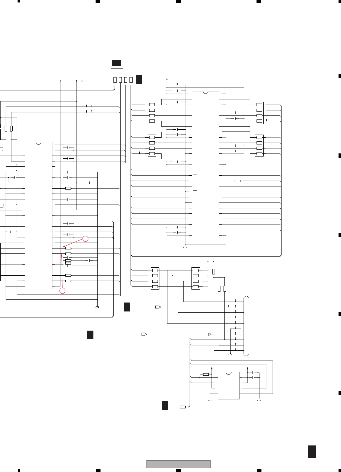
127
DVR-LX61
56 7 8
56 7 8
A
B
C
D
E
F
ST1+
TDRV
XDMUTE1
CASZ
MA1
MA9
SL2
FDRV
RASZ
ST2-
T-
REMI
UDQM
T+
SI
F-
LO
MA5
MA0
MD0
MDRV
MA6
MA2
MD5
FG
MA8
MCKE
MBA
SO
MD2
REMO
ST2+
WEZ
MA10
MA11
ST1-
MD1
LDQM
SCLK
MA4
MA7
F+
XDMUTE2
SL1
MA3
MD1
MD2
MD0
MD3
MD5
MD6
MD4
MD7
MD14
MD13
MD15
MD12
MD10
MD9
MD11
MD8
MCLK
CSOZ
VKN2029-A
CN201
1
2
3
4
5
6
7
8
9
10
C537
NM
C503
470p/50
C506
NM
C513 0.1u/16
C505 0.1u/25
C516
0.1u/10
C504 0.1u/10
C2811u
C2821u
C285
1u
C2871u
C2801u
C511
1u/16
C510 p
C514
0.1u/25
C536
NM
C512 0.1u/16
C284
1u
C202
NM
C2831u
C509
33p/50
A
C288
0.1u/16
C289
C291
1000p/50
C290
0.1u/16
C507
NM
C201
NM
C532 0.1u/10
C286
DCH1201-A
10u
C203
NM
GNDM
GNDD
GNDD
GNDD GNDD
IC200
SST25V016BCS-TBB
CE
1
SO
2
WP
3
VSS
45
SI
6
SCK
7
HOLD
8
VDD
IC201
K4S641632K-UC60
VDD1
1
DQ0
2
VDDQ1
3
DQ1
4
5
DQ2
6
VSSQ1
7
DQ3
8
DQ4
9
VDDQ2
10
DQ5
11
DQ6
12
VSSQ2
13
DQ7
14
VDD2
15
LDQM
16
WE
17
CAS
18
RAS
19
CS
20
BA0
21
BA1
22
A10/AP
23
A0
24
A1
25
A2
26
A3
27
VDD3 28
VSS1
29
A4
30
A5
31
A6
32
A7
33
A8
34
A9
35
A11
36
N.C
37
CKE
38
CLK
39
UDQM
40
N.C/RFU
41
VSS2
42
DQ8
43
VDDQ3
44
DQ9
45
DQ10
46
VSSQ3
47
DQ11
48
DQ12
49
VDDQ4
50
DQ13
51
DQ14
52
VSSQ4
53
DQ15
54
VSS3
IC501
BD7956FS
LDO-
1
LDO+
2
VCC
3
ACTIN1
4
5
ACTIN2
6
TJMON
7
BTHC
8
SPVM_S
9
PGND1
10
PGND2
11
U
12
SPVM1
13
V
14
fin1
15
PGND3
16
W
17
SPVM2
18
SPRNF
19
HB
20
HU+
21
HU-
22
HV+
23
HV-
24
HW+
25
HW-
26
SPIN
27
DGND28
DVCC
29
SLIN1
30
SLIN2
31
SLVDD
32
SLRNF1
33
SLRNF2
34
CTL1
35
CTL2
36
SLGND
37
SLO2-
38
SLO2+
39
SLO1-
40
SLO1+
41
fin2
42
VC
43
FG
44
SPCNF
45
AGND
46
LDIN
47
ACTIN3
48
AVM
49
ACO3-
50
ACO3+
51
ACO2-
52
ACO2+
53
ACO1-
54
ACO1+
R320
33
2
1
4
36
5
8
7
R317
33
2
1
4
36
5
8
7
R319
33
2
1
4
36
5
8
7
R318
33
2
1
4
36
5
8
7
R220
4.7k
2
1
4
36
5
8
7
R219
4.7k
2
1
4
36
5
8
7
R222 47k
R221 47k
R505
12k
R503 1k
R510 1.8
R516 12k
R223
22
R511 1.8
R515 33k
R281
0
R507 1k
R506 1k
R201
10k
R504 1k
TP203
TP204
TP202
TP205
TP501
TP209
TP206
TP208
TP6121
TP207
TP212
TP211
TP523
TP519
TP520
TP201
TP522
TP210
TP521
V+3D
VREF16
V+3D
V+5M
V+3D
V+3D
V+3D
V+12M
HADRS13
XRESET
3A
2:11K
3B;2:11K
2:11K
2:10K
XRESET
TX_FE
D0(MA)
A13(ATA)
D2(PW)
D5(AG)
RX_FE
GND
D1(SL)
V+3D
1000p/50
19
18
D1/5
2/5D
2/5D
2/5
D
2/5, 3/5, 4/5,
D
2/5
D
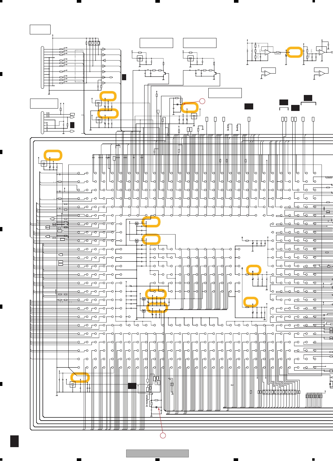
128 DVR-LX61
12 3 4
A
B
C
D
E
F
12 3 4
10.7 SERVICE MAIN ASSY (2/5)
JTDI
JTDO
JTMS
JTCL
HADRS5
HADRS7
HADRS6
BI
JTDI
JTMS
C/RI
JTDO
JTMRST
EDINT
JTCL
SDA0
HADRS17
HDATA9
HADRS18
HDATA13
HDATA14
HDATA7
HSTtoM
HDATA12
HADRS22
HADRS10
HADRS12
HSMtoT
HDATA15
HADRS16
HADRS20
HDATA8
HDATA11
HDATA5
HDATA10
HCS2
HADRS19
HADRS13
HDATA6
HADRS11
HADRS14
HDATA3
HADRS7
HDATA4
HCS1
HADRS5
HDATA0
TP6042
HADRS21
HADRS4
HDATA1
HADRS2
HADRS9
HADRS1
HADRS6
HDATA2
HADRS3
AIOBCK
HADRS8
HADRS15
VIOD6
VIOD7
DDATA 1
DDATA 1 9
DDM0
DDATA 0
DDQS0
DDATA 1 6
DDATA 1 7
DDATA 2
DDATA 1 8
DDATA 3
DDATA 6
DDATA 7
DDATA 2 2
DDATA 2 1
DDATA 2 0
DDATA 4
DDATA 5
DDM2
DDQS2
DDATA 2 3
AT1 DATA 0
AT1 I NTRQ
USB_H_OCI0
AT1 DATA 13
AT1 DATA 4
USB_CLKI
USB_H_PPON0
USB_D_VBUS
AT1 DATA 6
AT1 DATA 9
USB_D_DN0
USB_D_DP0
USB_D_CONNECT
AT1 DATA 2
AT1 DATA 11
AT1 DATA 1
AT1 DATA 3
AT1 DATA 5
AT1 C S 0
AT1 A D R 2
AT1 DATA 7
AT1 DATA 8
AT1 DATA 10
AT1 I O R DY
AT1 D I O W
AT1 DATA 12
AT1 DATA 14
AT1 A D R 0
AT1RESET
AT1DMARQ
AT1DIOR
AT1DMACK
AT1CS1
MD6
MD8
AT1 DATA 15
AT1ADR1
MD9
MD15
MD0
MD7
MD11
MD10
MD14
MD5
MD1
LDQM
MD3
MD2
MD4
UDQM
MD13
MCKE
MD12
DADRS5
DADRS12
DADRS9
DADRS4
DADRS7
DADRS11
DADRS6
DADRS8
DWE
DCLKO
DCS0B
DCAS
DCLKNO
DRAS
DBA1
DBA0
YI
GI
DADRS1
DADRS0
DADRS10
AOD0
DDM1
DADRS3
DADRS2
DCKE
DDATA13
DDATA12
DDATA30
DDQS1
DDATA31
DDATA14
DDATA28
DDATA11
DDATA29
DDATA15
DDATA10
DDATA26
DDATA8
DDATA27
DDATA9
DDQS3
DDATA24
DDATA25
DDM3
PHY_D7
HTX_PDB
PHY_D6
HTX_RSEN
HTX_CTL2
PHY_D5
HTX_D10
PHY_D4
HTX_D11
HTX_D9
PHY_D3
HTX_D7
PHY_D2
HTX_D8
HTX_D6
PHY_D1
HTX_CLK
PHY_D0
HTX_D5
HTX_D4
HTX_D3
HTX_D2
HTX_D1
PHYSCLK
HTX_D0
HTX_DE
HTX_HSYNC
PHYLPS
PHYLINKON
HTX_CTL3
AIBCK0
AOBCK
AILRCK0
AOLRCK
AIBD0
COUT
Y/GOUT
Pb/BOUT
VIOD0
SCL0
Pr/ROUT
DACCLKO
ADCCLKO
YOU T
RASZ
MA2
MA11
CASZ
MA0
MA9
MBA
MA8
MA1
MA5
MA6
MA3
MA4
MA7
MA10
MCLK
AT0CS1
AT0CS0
AT0 DATA 14
AT0ADR0
AT0 DATA 3
AT0 DATA 9
AT0 DATA 4
AT0 I NTRQ
AT0RESET
AT0 DATA 0
AT0 D M A C K
AT0 A D R 1
AT0 DATA 1
AT0 DATA 2
AT0 DATA 11
AT0 A D R 2
AT0 DATA 13
AT0 DATA 5
AT0 I O R DY
AT0 DATA 15
AT0 D M A R Q
AT0 D I O R
AT0 DATA 8
AT0 DATA 12
AT0 DATA 7
AT0 DATA 6
AT0 D I O W
AT0 DATA 10
HTX_VSYNC
HTX_DSDA
HTX_DSCL
HTX_HPD
MD7
MD8
MD9
MD10
MD11
MD12
MD13
MD14
MD15
USB_DN0
USB_DP0
VIOCLK
AIOBD
VIOD5
VIOD3
AIOLRCK
VIOD2
VIOD1
NMI
VIOD4
MD6
MD4
MD3
EDINT
JTMRST
SI SCLK
SO
WEZ
HCS0
HDOE
HWS0
SDA_GP
SCL_GP
HTX_DSDA_GP
HTX_DSCL_GP
AT/XDT
AAC_INT_B
LAN_FIFO_SEL
LAN_IRQ
AAC_RESET
HADRS23
RKN1048-A
CN1402 1
2
3
4
5
6
7
VKN2030-A
CN1401
1
2
3
4
5
6
7
8
9
10
11
12
13
14
47u/6.3
C1304
10u/16
C1020
100u/4
C1039
100u/4
C1036
220u/4
C163 10u/16
C153
100u/4
C1050
220u/4
C1007
100u/4
C1024
VCH1234-A
C1009
150u
VCH1234-A
C103
150u
VCH1268-A
C1012
75u
100u/4
C1003
101/4
C1314
NM
C1049
1000p
C1048
1u
C1421
1u
C1013
1u
C1056 1u
VCG1057
C1057 0.1u
C127
C144
C125
C135
0.01u/16
C129
C100
C101
C136
C131
C137
C130
C147
C121
C122
C113
C114
C148
C115
C156
C145
C107
C155
C157
C158
C140
C141
C175 NM
C146
C142
C169
C143
C1031 0.1u/10
C1004
1u
C1315
2.2u/10
C1025
1u
C1033 0.1u/10
C10180.1u/10
C1301
2.2u/10
C1801
1u
C1814
150p/50
C1017 0.1u/10
C1019 0.1u/10
C1015 0.1u/10
C1811
1u
C1002
0.1u/10
C1302
0.1u/16
C1041
1000p/50
C1812
2.2u/10
C1804
330p/50
C1803
220p/50
C1047 0.1u/10
C1026
1000p/50
C1008
1u
C1805
0.047u/10
C1032 0.1u/10
C1001
0.1u/10
C1016 0.1u/10
C1813
100p/50
C1029 0.1u/10
C10280.1u/10
C1037
1u
C1038
1000p/50
C1303
0.1u
C1802
2.2u/10
C1030 0.1u/10
C1010
1u
C1022
1u
VCG1057
C1023
1000p/50
C1035 0.1u/10
C1040
1u
C1815
0.047u/10
C1034 0.1u/10
C134
C1027 0.1u/10
C1021
DCH1201-A
10u
C1005
1000p/50
C1052
1u
C1051
10u
C1053
1000p
C1011
1000p
C1014
1000p
C1061
1000p
C1059
1u
C1060
0.1u
C1062
1u
C1063
0.1u
C1064
1000p
C1065
1000p
C1066
1u
C1067
0.1u
C1068
1000p
C152
1000p
C164
1000p
C162
VCG1057-A
1u
C1313
0.1u
C1058
0.01u/16
IC1001
C167
0.1u
C104
VCG1057-A
1u
C106
0.1u
C159
0.1u
C1006
1u
C1401
0.01u/16
C128
C133
C154
VCG1057-A
1u
C1312
0.1u
C1044
5p/50
C1045
5p/50
C105
1000p
L1021
DTL1106-A-T
3
2
1
L1023
DTL1106-A-T
3
2
1
L1004
DTL1106-A
3
2
1
L1024
DTL1106-A-T
3
2
1
L1001
DTL1106-A
3
2
1
L1821
DTL1106-A-T
3
2
1
L1022
DTL1106-A-T
3
2
1
L1025
DTL1106-A-T
3
2
1
L1002
DTL1106-A
3
2
1
L1831
DTL1106-A-T
3
2
1
L1003
DTL1106-A
3
2
1
GNDD
GNDD
GNDD
GNDD
GNDD
GNDD
GNDD
GNDD
GN
GNDD
GNDS
GNDD
GNDD
GNDDGNDD GNDD
GNDS
GNDD
GNDD
GNDD
GNDD
GNDD
GNDD
GNDD GNDDGNDD
GNDD
A1
GND(Digital)1
A2
DRASB
A3
DBA1
A4
DADD01
A5
DDQM1
A6
DQ13
A7
DQ11
A8
DQ08
A9
DIHM
A10
HTX_PDB
A11
HTX_D10
A12
HTX_D7
A13
HTX_CLK
A14
HTX_D3
A15
HTX_D0
A16
HTX_VSYNC
A17
HTX_DSDA
A18
SS0DOUT/GPIO46
A19
DA2_GND
A20
VAY(Video_DAC_CVBS/Y_out)
A21
RSET1(Video_DAC_RSET)
A22
VAR(Video_DAC_Pr/R_out)
A23
RSET0(Video_DAC_RSET)
A24
VAB(Video_DAC_Pb/B_out)
B1
DCLKB
B2
DCASB
B3
DBA0
B4
DADD00
B5
DADD03
B6
DQ12
B7
DQ15
B8
DQ09
B9
DDQM3
B10
HTX_RSEN
B11
HTX_D11
B12
HTX_D8
B13
HTX_D5
B14
HTX_D2
B15
HTX_DE
B16
HTX_CTL3
B17
HTX_DSCL
B18
SS0CKIN/GPIO44
B19
DA2_VDD3
B20
COMP1(Video_DAC_COMP)
B21
VAC(Video_DAC_C_out)
B22
VREF(Video_DAC_VREF)
B23
VAG(Video_DAC_Y_/G_out)
B24
COMP0(Video_DAC_COMP)
C1
DCLK
C2
DWEB
C3
DCS0B
C4
DADD10
C5
DADD02
C6
DDQS1
C7
DQ14
C8
DQ10
C9
DDQS3
C10
DILM
C11
HTX_CTL2
C12
HTX_D9
C13
HTX_D6
C14
HTX_D4
C15
HTX_D1
C16
HTX_HSYNC
C17
HTX_HPD
C18
SDA1/GPIO34
C19
AOBCK
C20
AIOMCLK0
C21
DA1_VDD3
C22
DA1_GND
C23
VCOMB(ADC(B)VCOM)
C24
VRTB(ADC(B)VRT)
D1
DADD06
D2
DADD07
D3
DADD08
D4
DADD11
D5
DCKE
D6
DQ30
D7
DQ28
D8
DQ26
D9
DQ24
D10
PHY_D7
D11
PHY_D5
D12
PHY_D3
D13
PHY_D1
D14
CTL1
D15
SCLK
D16
LPS
D17
SCL1/GPIO35
D18
SS0SB/GPIO47
D19
ATX
D20
AOLRCK
D21
VCOMY(ADC(Y)VCOM)
D22
VRTY(ADC(Y)VRT)
D23
ABI(ADC_B/G/Cb_in)
D24
VRBB(ADC(B)VRB)
E1
DADD04
E2
DADD05
E3
DCS1B
E4
DADD09
E5
DADD12
E6
DQ31
E7
DQ29
E8
DQ27
E9
DQ25
E10
PHY_D6
E11
PHY_D4
E12
PHY_D2
E13
PHY_D0
E14
CTL0
E15
LREQ
E16
LINKON
E17
SS0DIN/GPIO45
E18
AOD0
E19
AIBCK0
E20
AIBD0
E21
AIOMCLK1
E22
VRBY(ADC(Y)VRB)
E23
VCLY(ADC_PWM_VCL)
E24
AYI(ADC_CVBS/Y_in)
F1
DQ19
F2
DDQS0
F3
DDQM0
F4
DQ01
F5
DQ00
F6
DVREF
F7
DVDD25_1
F8
DVDD25_2
F9
DVDD25_3
F10
DVDD25_4
F11
DVDD25_5
F12
GND(Digital)2
F13
GND(Digital)3
F14
GND(Digital)4
F15
GND(Digital)5
F16
GND(Digital)6
F17
CSYNC/GPIO54
F18
IR_OUT/GPIO53
F19
AILRCK0
F20
IR_IN/GPIO52
F21
JTDI
F22
VRTR(ADC(R )VRT)
F23
ARI(ADC_R/B/Cr_in)
F24
VRBR(ADC(R)VRB)
G1
DQ16
G2
DQ17
G3
DQ18
G4
DQ03
G5
DQ02
G6
DVDD25_6
G7
DVDD25_7
G19
JTDO
G20
JTMS
G21
VCOMR(ADC(R)VCOM)
G22
VRTC(ADC(C)VRT)
G23
VRBC(ADC(C)VRB)
G24
ACI(ADC_C/G/R_in)
H1
DQ22
H2
DQ21
H3
DQ20
H4
DQ06
H5
DQ07
H6
DVDD25_8
H19
EDINT
H20
JTRST
H21
HLCI
H22
VCOMC(ADC(C)VCOM)
H23
AD2_VDD3(3.3V)
H24
AD2_GND
J1
DDQM2
J2
DDQS2
J3
DQ23
J4
DQ04
J5
DQ05
J6
DVDD25_9
J19
JTCL
J20
PH_VDD1(1.0V)
J21
HCBP
J22
FCBP
J23
PF_GND
J24
FSCI
K1
PLL_VDD(1.0V)
K2
CLK27AOUT
K3
CLKPWM0/GPIO60
K4
CLKPWM1/GPIO61
K5
SMCKOUT/SSCKIN
K6
DVDD25_10
K10
GND(Digital)7
K11
GND(Digital)8
K12
DVDD33_1
K13
DVDD33_2
K14
DVDD33_3
K15
DVDD33_4
K19
DGNDR
K20
HLCO
K21
HC_VDD3(3.3V)
K22
FC_VDD3(3.3V)
K23
FSCO
K24
PF_VDD1(1.0V)
L1
CLK27AIN
L2
PLL_GND
L3
CLK27BIN/GPIO62
L4
SMDOUT/SSDOUT
L5
SMDIN/SSDIN
L6
DLL_VDD
L10
GND(Digital)9
L11
DVDD33_5
L12
DVDD33_6
L13
DVDD33_7
L14
DVDD33_8
L15
DVDD33_9
L19
SDA0
L20
NMI
L21
RSTSWB
L22
PH_GND
L23
AD1_VDD3(3.3V)
L24
CLK24OUT
M1
USB_DN0
M2
USB_DP0
M3
USB_H_OCI0/GPIO56
M4
AT1D00
M5
AT1 I NTRQ
M6
DLL_GND
M10
TEST_MODE
M11
FPIND
M12
LVSPOWD
M13
DVDD33_10
M14
DVDD33_11
M15
DVDD33_12
M19
SCL0
M20
RADD23/GPIO02
M21
RADD17
M22
RDATA09
M23
AD1_GND
M24
CLK24IN
N1
USB_CLKI/GPIO55
N2
USB_H_PPON0/GPIO57
N3
USB_D_VBUS/GPIO58
N4
AT1D13
N5
AT1D04
N6
GND(Digital)11
N10
DVDD10_1
N11
DVDD10_2
N12
DVDD10_3
N13
DVDD10_4
N14
DVDD33_13
N15
DVDD33R
N19
RADD24/GPIO03
N20
RDATA14
N21
RADD18
N22
RDATA13
N23
RDATA07
N24
GND(Digital)10
P1
USB_D_DN0
P2
USB_D_DP0
P3
USB_D_CONNECT/GPIO59
P4
AT1D06
P5
AT1D09
P6
GND(Digital)12
P10
DVDD10_5
P11
DVDD10_6
P12
DVDD10_7
P13
AT0D06
P14
AT0 D I O WB
P15
AT0D10
P19
RADD25/GPIO04
P20
RADD00/GPIO01
P21
RDATA12
P22
RADD10
P23
RADD12
P24
RADD22
R1
AT1D01
R2
AT1D03
R3
AT1D05
R4
AT1D02
R5
AT1D11
R6
GND(Digital)13
R10
DVDD10_8
R11
DVDD10_9
R12
AT0DIORB
R13
AT0 D 0 8
R14
AT0D12
R15
AT0D07
R19
GCSB2/GPIO05
R20
GRDYB/GPIO07
R21
RDATA15
R22
RADD20
R23
RDATA08
R24
RADD16
T1
AT1D07
T2
AT1D08
T3
AT1D10
T4
AT1CS0B
T5
AT1 DA 2
T6
GND(Digital)14
T10
DVDD10_10
T11
DVDD10_11
T12
AT0D05
T13
AT0 I O R DY
T14
AT0D15
T15
AT0DMARQ
T19
GCSB3/GPIO06
T20
GCSB1
T21
RDATA11
T22
RDATA10
T23
RADD19
T24
RDATA05
U1
AT1D12
U2
AT1D14
U3
AT1 DA 0
U4
AT1 I O R DY
U5
AT1 D I O WB
U6
GND(Digital)15
U10
AT0 DA 1
U11
AT0D01
U12
AT0D02
U13
AT0D11
U14
AT0 DA 2
U15
AT0D13
U19
CTS0B/GPIO37
U20
RADD14
U21
RADD13
U22
RADD11
U23
RDATA03
U24
RDATA06
V1
AT1DIORB
V2
AT1 D M A C K B
V3
AT1CS1B
V4
AT1RESETB
V5
AT1DMARQ
V6
GND(Digital)16
V10
AT0D09
V11
AT0D04
V12
AT0 INTRQ
V13
AT0RESETB
V14
AT0D00
V15
AT0 D M A C K B
V19
RTS0B/GPIO36
V20
GCSB0
V21
RADD07
V22
RDATA04
V23
RADD05
V24
FCSB0
W1
AT1 D 1 5
W2
AT1 DA 1
W3
MD9
W4
MD6
W5
MD8
W6
DVDD15_1
W10
GND(Digital)17
W11
AT0CS1B
W12
AT0CS0B
W13
AT0 D 1 4
W14
AT0 DA 0
W15
AT0 D 0 3
W19
SP1REQB/GPIO11
W20
RADD21
W21
RDATA00
W22
FOEB/GOEB
W23
RADD04
W24
FCSB1
Y1
MD15
Y2
MD11
Y3
MD0
Y4
MD7
Y5
MD10
Y6
DVDD15_2
Y10
GND(Digital)18
Y11
GND(Digital)19
Y12
AGND1
Y13
AGND2
Y14
AGND3
Y15
AGND4
Y19
SP0REQB/GPIO33
Y20
RADD01
Y21
RDATA01
Y22
RADD09
Y23
RADD06
Y24
RADD02
AA1
MD14
AA2
LDQM
AA3
MD5
AA4
MD1
AA5
MD3
AA6
DVDD15_3
AA19
RTS1B/GPIO40
AA20
SP0CLK/GPIO31
AA21
RDATA02
AA22
RADD03
AA23
RADD08
AA24
FWEB/GWEB
AB1
MD2
AB2
UDQM
AB3
MD4
AB4
MCLKOUT
AB5
MD13
AB6
DVDD15_4
AB19
CTS1B/GPIO41
AB20
SP0EN/GPIO21
AB21
SP1CLK/GPIO08
AB22
SP0STRT/GPIO32
AB23
SP1STRT/GPIO10
AB24
RADD15
AC1
MA9
AC2
MD12
AC3
MA10
AC4
MCKE
AC5
MA7
AC6
PDIAGB
AC19
MONI3/SWRF4/RFPM3
AC20
SP1EN/GPIO09
AC21
SP1DAT2/GPIO14
AC22
SP0DAT7/GPIO29
AC23
SP1DAT7/GPIO19
AC24
SP0DAT6/GPIO28
AD1
MA6
AD2
MA5
AD3
MA1
AD4
MA8
AD5
MBA
AD6
DASPB
AD7
HIOCS16B
AD8
SFSO
AD9
SFSCK
AD10
SFSI
AD11
SFCS0B
AD12
AVDD15
AD13
AVDD33_1
AD14
AVDD33_2
AD15
AVDD33_3
AD16
AVDD33_4
AD17
TEST1
AD18
MONI1/RFPM1
AD19
MONI2/RFPM2
AD20
SP1ERRB/GPIO20
AD21
SP1DAT6/GPIO18
AD22
SP1DAT5/GPIO17
AD23
SP0DAT5/GPIO27
AD24
SP0DAT3/GPIO25
AE1
XA1
AE2
CASB
AE3
MA0
AE4
MA4
AE5
MA3
AE6
PB4
AE7
PB1
AE8
RLDM
AE9
WLD
AE10
WLDM
AE11
PLED
AE12
CWAGC
AE13
CWHP
AE14
CAD
AE15
CBC
AE16
CTEC
AE17
CRC
AE18
CBHLPP/CRAPC
AE19
ADIN/LE/RFP4
AE20
SP0ERRB/GPIO30
AE21
SP0DAT2/GPIO24
AE22
SP1DAT3/GPIO15
AE23
SP1DAT4/GPIO16
AE24
SP0DAT1/GPIO23
AF1
XA2
AF2
WEB
AF3
MA2
AF4
RASB
AF5
PB2
AF6
PB5
AF7
PB7
AF8
RLD
AF9
REF16
AF10
VREFIO
AF11
P2LD
AF12
CADO
AF13
CBHWBL/CID
AF14
CAMIRR
AF15
CBPD
AF16
CAGC
AF17
CAGC2
AF18
CEQDC
AF19
FEO/LE/SWRF2/SWRF4/RFP5
AF20
TEO/LE/SWRF1/SWRF3/RFP6
AF21
TxD0B
AF22
RxD0B
AF23
SP0DAT4/GPIO26
AF24
SP0DAT0/GPIO22
AG1
PB3
AG2
PA0
AG3
PA4
AG4
PB0
AG5
PB6
AG6
PA3
AG7
PA5
AG8
PDIN
AG9
FPDVI
AG10
FPDVO
AG11
CREG
AG12
CBCO
AG13
WALPF
AG14
CMIRR
AG15
CBBD
AG16
RFEQOM
AG17
RFEQOP
AG18
RFO
AG19
CDEF
AG20
FG
AG21
RFT1/SWRF1/RFP1
AG22
RxD1B/GPIO38
AG23
TxD1B/GPIO39
AG24
SP1DAT1/GPIO13
AH1
PKPULSE1M
AH2
PKPULSE1P
AH3
WRPULSEM
AH4
WRPULSEP
AH5
HFONP
AH6
PA7
AH7
PA2
AH8
H1/FOM
AH9
G1/FOP
AH10
F1
AH11
E1
AH12
RFP
AH13
ASY
AH14
FCEFM2
AH15
PCEFM2
AH16
RFI_M
AH17
RFI_P
AH18
AGCIN
AH19
CDEF2
AH20
TDRV
AH21
FDRV
AH22
RFT2/SWRF2/RFP2
AH23
RXD2B/GPIO42
AH24
SP1DAT0/GPIO12
AJ1
OFPULSE/WRCKP
AJ2
OFPULSE/WRCKM
AJ3
PKPULSE2/NRZIM
AJ4
PKPULSE2/NRZIP
AJ5
HFONM
AJ6
PA1
AJ7
PA6
AJ8
D1
AJ9
C1
AJ10
B1
AJ11
A1
AJ12
RFN
AJ13
EFM
AJ14
FCEFM1
AJ15
PCEFM1
AJ16
EXTR
AJ17
CEQ
AJ18
REQ
AJ19
DAOUT
AJ20
SDRV2
AJ21
SDRV1
AJ22
MDRV
AJ23
WRFM/SWRF3/RFP3
AJ24
TXD2B/GPIO43
IC1301
NJM12904V
34
2
1
8
IC1302
NJM129
34
2
1
8
IC1301
NJM12904V
5
6
7
IC1302
NJM129
5
6
7
L1005
15u
L1811
15u
L1801
39u 2SA1576A(QR)
Q1801
2SA1576A(QR)
Q1811
R204
33 2
1
4
36
5
8
7
R206
33 2
1
4
36
5
8
7
R205
33 2
1
4
36
5
8
7
R1411
10k
2
1
4
3
6
5
8
7
R5856
10k
R230 0
R192
NM
R1303
1k
R1012
NM
R1013
10k
R129 0
R127
R134 4
R235
R234 0
R1312
1k
R104
R1313
1k
R1404
22
R1422
10k
R1421
10k
R210 33
R202 33
R251 NM
R203 33
R1412
10k
R1414
22
R1415
22
R109
R1416
22
R1011
NM
R1003
680F
R1814
33
R1801 NM
R1405
22
R1406
22
R116 3.3k
R1407
22
R1401
22
R1001
10k
R1811 NM
R1803
330
R1040
100 (F)
R1006 15k
R1005 15k
R10600
R1402
22
R145
R247 NM
R1802
220
R119 0
R146
R1068
47k
R1069
47k
R1067
47k
R1066
NM
R1063
0
R1061 0
R1062
0
R1004
470 F
R311 1k
R149 NM
R1086.8k
R1039
43 (D)
R1403
22
R274
0
R1010
NM
R1008
NM
R273
0
R1009
NM
R
R256 10k
R257 10k
R271
0
R1812
220
R117 68
R310
R
R11
33k
R258NM
R255 NM
R254 NM
R253 10k
R1037
100 F
R1199
10k
R252 10k
R250 NM
R231
R1813
330
R1036
43 D
R249 NM
R1031
150
R1030
47
IC1001
R24810k
R232
R233 0
R1304
NM
R105 0
R1413
47k
R131
0
R1070
NM
R1071 10k
R1111
100k
R
R1029
82
R125
R
R1182
10k
R1181
10k
R
R1301
4700
R1302
1k
R1804
33
R211 0
R1019
0
R1018
0
R1017
0
R124 0
TP160
TP1004
TP1003
TP1426
TP1414
TP1201
TP1409
TP128
TP6119
TP123
TP1408
TP1406
TP1430
TP1413
TP1407
TP1412
TP122
TP127
TP1405
TP1410
TP1404
TP119
TP1411
TP139
TP121
TP120
TP1429
TP1006
TP1007TP1008
TP1001
TP1002
TP1403
TP1009
TP1010
TP1011
TP1012
TP1013
TP1014
TP1015
TP1402
TP1401
TP1427
TP1428
TP1425
TP1005
V+1R0_CORE
V+3D_IO
V+3D_RF
V+1R0_DLL
V+3D
V+3_ADC
V+3D
V+3_DEC
V+3D
V+5D
V+1R0
V+3V
V+3V
V+3D
VREF_V
VREF16
V+2R5
VREF_D
V+1R0_DEC
VRPD
V+2R5
V+3V
V+3HD
V+2R5
VREF_V
V+3V
V+3D
V+3D
V+1R0_PLLV+1R0
V+3D_IO
V+3
V+1R0
V+3_DAC
V+3V
V+3D
V+3D
V+3V
V+15D
V+3A
X101
DSS1157-A
X1001
VSS1220-A
24.576MHz
X1002
VSS1172-A
XRESET
1:13H;1:4B;14C;3:12H;4:B9
SMDIN4:B11
RXD2_BRIDGE
5:13B
RXD0_LL
3:12H
1080P
AMUTE
NSCS
ADPOW
4:A2
TXD2_BRIDGE
5:13B
SPDIFSEL
LLRST
TXD0_LL
3:12H
HDMI/XDVI
TXD1
9D
X525P
4:O2
AIBD_PHYCTL1
TXD1
2C
RXD1
4:B11
AIBCK_PHYCTL0
SEL_ADATA
SCL_GP
PHY_XRST
SDA_GP
SCL1
SDA1
BECS
AILRCK_PHYLREQ
SMDOUT 4:F2;4:N5
RXD
4:E10
JTRST
4:E10
SMCKOUT
4:F2;4:N6
SPDIFO 5:9H
232RST
4:E10
C1042
3p/50
C1043
3p/50
TXD
RXD
DTR
CTS
V+5D
GNDD
XRESET
TRST
EJSNGEN
TDI
GND
TDO
DINTEN
TMS
GND
TCK
GND
RST
JTSEL
DINT
V+3
MAIN CHIP
RS-232C
EJTAG
fsc BPF
to AUDIO
to VID
to DV
HCL BPF
to HD
to US
27MHz
to DD
16.93MHz
to HD
to Au
from
to HDMI
to VIDEO OUT
to Audio
from DV
to DDR SDRAM
IC1001
MC-10050F1-507LU1A-K
V+1R5_IN
V+15A
24
23
D2/5
4/5D
4/5
D
4/5D
4/5
D
5/5
D
5/5D
4/5D
129
DVR-LX61
56 7 8
56 7 8
A
B
C
D
E
F
DADRS9
DADRS0
DADRS1
DADRS10
DADRS4
DADRS6
DADRS3
DADRS7
DADRS11
DADRS2
DADRS8
DRAS
DWE
DCS0B
DCAS
DCLKNO
DCLKO
DADRS12
DBA0
DBA1
TAD R S5
TAD R S0
TAD R S4
TAD R S6
TAD R S1 0
TAD R S1 1
TAD R S2
TAD R S7
TAD R S1 2
TBA0
TBA1
TWE
TCS
TRAS
DDQS3
TAD R S9
HDATA5
HDATA13
HDATA14
HDATA6
HDATA15
HDATA7
HADRS10
HADRS8
HADRS4
HADRS3
HADRS2
DADRS5
HSMtoT
HSTtoM
LLRST
TAD R S8
TAD R S1
HADRS20
SPDIFSEL
TP6042
HDATA3
HDATA11
HDATA10
HDATA2
HDATA9
HDATA1
HDATA8
HDATA0
HDATA4
HDATA12
HADRS22
DDM1
TWE
TCAS
TRAS
TCS
TBA0
TBA1
TAD R S1 0
TAD R S0
TAD R S1
TAD R S2
TAD R S3
DDQS1
DDATA 1 5
DDATA 1 4
DDATA 1 3
DDATA 1 2
DDATA 1 1
DDATA 1 0
DDATA 9
DDATA 8
TAD R S3
TAD R S2
TAD R S1
TAD R S0
TAD R S1 0
TBA1
TBA0
TCS
TRAS
TCAS
TWE
DDM0
DDQS0
DDATA7
DDATA6
DDATA5
DDATA4
DDATA3
DDATA2
DDATA1
DDATA0
DDM3
TAD R S1 2
TAD R S1 1
TAD R S9
TAD R S8
TAD R S7
TAD R S6
TAD R S5
TAD R S4
DDATA24
DDATA25
DDATA26
DDATA27
DDATA28
DDATA29
DDATA30
DDATA31
TAD R S4
TAD R S5
TAD R S6
TAD R S7
TAD R S8
TAD R S9
TAD R S1 1
TAD R S1 2
DDM2
DDQS2
DDATA16
DDATA17
DDATA18
DDATA19
DDATA20
DDATA21
DDATA22
DDATA23
SW2
CLOSE
S2
D
S1
C
S3
W2SET
S4
A
CSOZ
W3SET
LO
SL2
TDRV
FDRV
SL1
XDMUTE2
W2EN-
W2EN+
W1EN-
W3EN+
W1EN+
SW1
OSCEN-
OSCEN+
RASZ
MA2
HFGAIN
DRST
DCK
REMI
DDI
OSCNT
LDDEN
DDO
REMO
DMS
FMO+
OPEN
SCLK
SO
RF-
RF+
XDMUTE1
MDRV
W3EN-
FMO-
APCV
SI
MD7
MD8
MD9
MD10
MD11
MD12
MD13
MD14
MD15
HADRS20
HADRS19
HADRS18
HADRS12
DCKE
DVD/CD
MD6
MD4
MD3
LCDS
W1SET
B
FG
TCLKNO
TCLKO
TCLKNO
TCLKO
WEZ
TCLKO
TCLKNO
TAD R S3
TCAS
LAN_FIFO_SEL
LAN_IRQ
HWS0
AAC_RESET
HDATA7
HDATA5
HDATA1
HDATA9
HDATA3
HDOE
HADRS16
HADRS15
HADRS14
HADRS13
HADRS12
HADRS11
HADRS10
HADRS9
HADRS21
HWS0
HADRS19
HADRS18
HADRS8
HADRS7
HADRS6
HADRS5
HADRS4
HADRS3
HADRS2
HADRS17
HDATA15
HDATA7
HDATA14
HDATA6
HDATA13
HDATA5
HDATA12
HDATA4
HDATA11
HDATA3
HDATA10
HDATA2
HDATA9
HDATA1
HDATA8
HDATA0
HCS0
HADRS1
HADRS23
HDATA0
HDATA2
HDATA6
HDATA4
HDATA10
HDATA11
HDATA8
HDATA15
HDATA14
HDATA12
HDATA13
HADRS2
HADRS1
HADRS3
HADRS4
HADRS6
HADRS5
HADRS7
HADRS9
HADRS10
HADRS8
HADRS11
HCS2
HCS1
HDOE
AAC_RESET
AAC_INT_B
AAC_RESET
LAN_FIFO_SEL
AAC_INT_B
LAN_IRQ
HCS2
HCS1
HDOE
HWS0
HADRS11
*CN1501
VKN2079-A
1
2
3
4
5
6
7
8
9
10
11
12
14
15
16
17
18
19
20
21
22
23
24
25
13
26
27
28
29
30
31
32
33
34
35
36
37
38
39
40
41
42
43
44
45
46
47
48
49
50
VCH1268-A
C1236
75u
VCH1268-A
C1215
75u
C1201
NM
C1202
1u
C1204
1u
C1208
1u
C1217
1u
C1218
1u
C1221
1u
C1223
1u
C1227
1u
C1219
1u
C1220
1u
C1314
NM
C1216
1u
C1225
0.01u/16
C1224
0.01u/16
C1228
1000p/50
C1207
1000p/50
C1292 NM
C1293 NM
C109 NM
C127 0.047u/10
C144 0.01u/16
C125 VCG1058-A
1u
C135
0.01u/16
C129 1u
C100 1000p/50
C101 1000p/50
C136 0.1u/10
C131 0.068u/10
C137 6800p/25
C130 4.7u/6.3
C147 DCH1198-A0.33u
C121 2200p/50
C122 2200p/50
C113 4700p/25
C114 4700p/25
C148DCH1198-A0.33u
C1206
0.01u/16
C115 0.01u/16
C156 1800p/50
C145 0.01u/16
C107 680p/50
C155 DCH1199-A
0.47u
C157 0.01u/16
C1580.01u/16
C140 DCH1199-A0.47u
C141 DCH1199-A0.47u
C120 0.1u/10
C175 NM
C146 DCH1201-A
10u
C142 DCH1201-A
10u
C169 0.1u/10
C151 NM
C1281NM
C143
DCH1201-A
10u
C149 0.01u/16
C1214
0.1u/16
C1282NM
C116
0.1u/10
C117
1000p/50
C1283NM
C1315
2.2u/10
C1205
0.01u/16
C1291 0.1u/16
C1203
0.1u/16
C1211
0.1u/16
C1212
0.1u/16
C1213
0.1u/16
C134 0.1u/10
C124 0.1u/10
C1113
1u
C1313
0.1u
C1209
1000p/50
C1210
1000p/50
C1226
1000p/50
C1101
1000p/50
C1229
1000p/50
C178NM
C1316
DCH1201-A
10u
C1280.1u/10
C133 0.1u/10
C1312
0.1u
C1102
1u
C1103
1000p/50
C1222
0.1u/16
C1230
0.1u/16
C1105
0.1u/16
C1235
DCH1201-A
C1231
DCH1201-A
C1104
1u
NM
D101
GNDD
GNDD
GNDD
GNDD
GNDD
GNDD
GNDD
GNDD
GNDD
GNDD
GNDD
GNDS
GNDD
GNDD
RFP5
RFP6
6
2
AG1
PB3
AG2
PA0
AG3
PA4
AG4
PB0
AG5
PB6
AG6
PA3
AG7
PA5
AG8
PDIN
AG9
FPDVI
AG10
FPDVO
AG11
CREG
AG12
CBCO
AG13
WALPF
AG14
CMIRR
AG15
CBBD
AG16
RFEQOM
AG17
RFEQOP
AG18
RFO
AG19
CDEF
AG20
FG
AG21
/SWRF1/RFP1
AG22
D1B/GPIO38
AG23
D1B/GPIO39
AG24
DAT1/GPIO13
AH1
PKPULSE1M
AH2
PKPULSE1P
AH3
WRPULSEM
AH4
WRPULSEP
AH5
HFONP
AH6
PA7
AH7
PA2
AH8
H1/FOM
AH9
G1/FOP
AH10
F1
AH11
E1
AH12
RFP
AH13
ASY
AH14
FCEFM2
AH15
PCEFM2
AH16
RFI_M
AH17
RFI_P
AH18
AGCIN
AH19
CDEF2
AH20
TDRV
AH21
FDRV
AH22
RFT2/SWRF2/RFP2
AH23
RXD2B/GPIO42
AH24
SP1DAT0/GPIO12
AJ1
OFPULSE/WRCKP
AJ2
OFPULSE/WRCKM
AJ3
PKPULSE2/NRZIM
AJ4
PKPULSE2/NRZIP
AJ5
HFONM
AJ6
PA1
AJ7
PA6
AJ8
D1
AJ9
C1
AJ10
B1
AJ11
A1
AJ12
RFN
AJ13
EFM
AJ14
FCEFM1
AJ15
PCEFM1
AJ16
EXTR
AJ17
CEQ
AJ18
REQ
AJ19
DAOUT
AJ20
SDRV2
AJ21
SDRV1
AJ22
MDRV
AJ23
WRFM/SWRF3/RFP3
AJ24
TXD2B/GPIO43
IC1102
S29GL128N90TFIR2-K
A23
1
A22
2
A15
3
A14
4
5
A13
6
A12
7
A11
8
A10
9
A9
10
A8
11
A19
12
A20
13
WE#
14
RESET#
15
A21
16
WP#/ACC
17
RY/B Y#
18
A18
19
A17
20
A7
21
A6
22
A5
23
A4
24
A3
25
A2
26
A1
27
NC1
28
NC2
29
VIO
30
NC3
31
A0
32
CE#
33
VSS1
34
OE#
35
DQ0
36
DQ8
37
DQ1
38
DQ9
39
DQ2
40
DQ10
41
DQ3
42
DQ11
43
VCC
44
DQ4
45
DQ12
46
DQ5
47
DQ13
48
DQ6
49
DQ14
50
DQ7
51
DQ15/A-1
52
VSS2
53
BYTE#
54
A16
55
NC4
56
NC5
IC1302
NJM12904V
34
2
1
8
IC1302
NJM12904V
5
6
7
RT1N141U
Q102
R1283
47
2
1
4
3
6
5
8
7
R1281
47
2
1
4
3
6
5
8
7
R1282
47
2
1
4
3
6
5
8
7
R1241
0
2
1
4
36
5
8
7
R1293
NM
2
1
4
3
6
5
8
7
R1274
22
2
1
4
36
5
8
7
R1273
22
2
1
4
36
5
8
7
R1256
22
2
1
4
36
5
8
7
R1255
22
2
1
4
36
5
8
7
R1245
22
2
1
4
36
5
8
7
R1246
22
2
1
4
36
5
8
7
R1265
22
2
1
4
36
5
8
7
R1292
NM
2
1
4
3
6
5
8
7
R1033
10k
2
1
4
36
5
8
7
R1034
10k
2
1
4
36
5
8
7
R1035
10k
2
1
4
36
5
8
7
45
R1262
0
2
1
4
36
5
8
7
R1261
0
2
1
4
36
5
8
7
R1269
0
2
1
4
36
5
8
7
R1268
0
2
1
4
36
5
8
7
R1249
0
2
1
4
36
5
8
7
R1248
0
2
1
4
36
5
8
7
R1242
0
2
1
4
36
5
8
7
R1266
22
2
1
4
36
5
8
7
R1227
NM
2
1
4
3
6
5
8
7
R1291
NM
2
1
4
3
6
5
8
7
R1297
NM
2
1
4
3
6
5
8
7
*R1505
02
1
4
3
6
5
8
7
*R1506
02
1
4
3
6
5
8
7
*R1507
02
1
4
3
6
5
8
7
*R1508
02
1
4
3
6
5
8
7
*R1509
02
1
4
3
6
5
8
7
*R1510
02
1
4
3
6
5
8
7
*R1511
0
2
1
4
3
6
5
8
7
*R1512
0
2
1
4
3
6
5
8
7
*R1513
0
2
1
4
3
6
5
8
7
R1221
NM
2
1
4
3
6
5
8
7
R1223
NM
2
1
4
3
6
5
8
7
R1204
NM
2
1
4
3
6
5
8
7
R1203
NM
2
1
4
3
6
5
8
7
R1224
NM
2
1
4
3
6
5
8
7
R1201
NM
2
1
4
3
6
5
8
7
R1207
NM
2
1
4
3
6
5
8
7
R1032
10k
2
1
4
36
5
8
7
R1287
47
2
1
4
3
6
5
8
7
R230 0
R192
NM
R129 0
R127 NM
R134 47k
R1110
0
R235 NM
R234 0
R1312
1k
R104 12k
R1313
1k
R210 33
R251 NM
R1028
10k
R1016
10k
R1132
47
R109 6.2k
R110 1k
R1250
0
R1270
0
R1263
0
R1243
0
R116 3.3k
R177 NM
R178NM
R301
47k
R145 NM
R1294
NM
R247 NM
R119 0
R146 NM
R1109
NM
R1106
NM
R311 1k
R149 NM
R1086.8k
R312 1k
R256 10k
R257 10k
R1153 4.7k
R1154 NM
R1175 NM
R1161 4.7k
R1163 4.7k
R1164 NM
R1191 4.7k
R1194 NM
R1195 4.7k
R1197 4.7k
R310 1k
R314 1k
R193
0
R114
33k
R258NM
R1295
NM
R255 NM
R254 NM
R253 10k
R191 10k
R252 10k
R1165 4.7k
R1027
10k
R1523
47k
R1522
47k
R1521
47k
R1520
47k
R1519
47k
R1518
47k
R1517
47k
R1516
47k
R1515
NM
*R1514
0
R1230
NM
R1298
NM
R1211
NM
R1210
NM
R1212
NM
R250 NM
R231 NM
R249 NM
R24810k
R232 NM
*R1504
0
R233 0
R1202
NM
R1205
10k
*R1502
0
*R1501
0
R1214
NM
*R1503
22
R1215
NM
R1231
NM
R1299
NM
R1296
NM
R105 0
R1314
0
R1219
0
R107 47k
R1252
33
R112 470kR125 NM
R1103
0
R1272
33
R111 470k
R199 NM
R1107
0
R106 NM
R1275
22
R1276
22
R1258
22
R1257
22
R1247
22
R1240
22
R1267
22
R1260
22
R1280
R126
NM
R1264
33
R1244
33
R1251
33
R1271
33
R13847k
R1284
47
R1285
47
R1286
47
R1289
22
R1288
22
R1279
390
R1021
10k
R211 0
R1278
0
R1277
0
R124 0
TP614
TP1202
TP128
TP131
TP123
TP117
TP118
TP122
TP127
TP119
TP139
TP121
TP120
TP1005
VREF_D
V+3D
V+3D
VREF_D
V+3D
EF_V
VREF16
V+3D
V+2R5
VTT
V+3D
VRPD
VTT
V+3D
V+3D
V+3D
V+2R5
V+3D
VTT
VREF_D
X101
DSS1157-A
XRESET
1:13H;1:4B;14C;3:12H;4:B9
AOD0_CN
PUTEMP
AOLRCK_CN
AOBCK_CN
XRESET
BECS
RXD2_BRIDGE
5:13B
12B;3:7G
4:O6;5:4A;5:7D;5:7E
5:1E
4:J2;4:J3;4:J4;4:J5
DCLKEN
16E;16G
DCLKEN
16E;16J
TXD2_BRIDGE
5:13B
3:14B;5:11B
5:3I
DCLKEN
16G;16J
4:G7;4:G8;4:G10;4:G11
1:3D;1:3F;1:3G;1:3I;1:4B;1:5D;1:5E;1:5I
1:12B
1:12B
11K;2F;6D;3:12H;3:7G;4:B11;4:N5;5:8H
1:4J;1:4K
1:12B
4:A2
1:14K;1:3B;12B;4:B11;4:N5
TXD1
2C
4:B11
HADRS13
AOD1_CN
*C1501
DCH1201-A
*C1503 0.1u/16
*C1504 1000p/50
*C1502 VCG1057-A
IC1201
EDD5116AFTA-6B-E-K
VDD1
1
DQ0
2
VDDQ1
3
DQ1
4
5
DQ2
6
VSSQ1
7
DQ3
8
DQ4
9
VDDQ2
10
DQ5
11
DQ6
12
VSSQ2
13
DQ7
14
NC1
15
VDDQ3
16
LDQS
17
NC2
18
VDD2
19
NC3
20
LDM
21
/WE
22
/CAS
23
/RAS
24
/CS
25
NC4
26
BA0
27
BA1
28
A10/AP
29
A0
30
A1
31
A2
32
A3
33
VDD3
34
VSS1
35
A4
36
A5
37
A6
38
A7
39
A8
40
A9
41
A11
42
A12
43
NC5
44
CKE
45
CK
46
/CK
47
UDM
48
VSS2
49
VREF
50
NC6
51
UDQS
52
VSSQ3
53
NC7
54
DQ8
55
VDDQ4
56
DQ9
57
DQ10
58
VSSQ4
59
DQ11
60
DQ12
61
VDDQ5
62
DQ13
63
DQ14
64
VSSQ5
65
DQ15
66
VSS3
IC1221
EDD5116AFTA-6B-E-K
VDD1
1
DQ0
2
VDDQ1
3
DQ1
4
5
DQ2
6
VSSQ1
7
DQ3
8
DQ4
9
VDDQ2
10
DQ5
11
DQ6
12
VSSQ2
13
DQ7
14
NC1
15
VDDQ3
16
LDQS
17
NC2
18
VDD2
19
NC3
20
LDM
21
/WE
22
/CAS
23
/RAS
24
/CS
25
NC4
26
BA0
27
BA1
28
A10/AP
29
A0
30
A1
31
A2
32
A3
33
VDD3
34
VSS1
35
A4
36
A5
37
A6
38
A7
39
A8
40
A9
41
A11
42
A12
43
NC5
44
CKE
45
CK
46
/CK
47
UDM
48
VSS2
49
VREF
50
NC6
51
UDQS
52
VSSQ3
53
NC7
54
DQ8
55
VDDQ4
56
DQ9
57
DQ10
58
VSSQ4
59
DQ11
60
DQ12
61
VDDQ5
62
DQ13
63
DQ14
64
VSSQ5
65
DQ15
66
VSS3
Clock:166MHz
Flash ROM
DDR
to VIDEO OUT
to HDD
to USB
to FLASH LAN AAC
to DDR SDRAM
16.93MHz
to HDMI
to FRONT
to Audio
from DV
from LL
from LL
K4H511638D-UCB3-K
K4H511638D-UCB3-K
DVR-LX61 Only
VWV2341 VWV2343
C1501 NM 10u
C1502 NM 1u
C1503 NM 0.1u
C1504 NM 1000p
R1501 NM 0
R1502 NM 0
R1503 NM 22
R1504 NM 0
R1505 NM 0
R1506 NM 0
R1507 NM 0
R1508 NM 0
R1509 NM 0
R1510 NM 0
R1511 NM 0
R1512 NM 0
R1513 NM 0
R1514 NM 0
CN1501 NM VKN2079-A
SERVICE MAIN ASSY (2/5)
(VXX3309 : DVR-LX61)
(VXX3308 : DVR-560H-S,-K)
D2/5
D2/5
1/5D
2/5
D
CN501
1/5, 3/5,
4/5
D
4/5D
5/5
D
4/5, 5/5D
1/5
D
5/5
D3/5, 5/5
D
1/5D
4/5
D3/5
D1/5, 4/5
D
4/5D
1/5D
E
130 DVR-LX61
12 3 4
A
B
C
D
E
F
12 3 4
10.8 SERVICE MAIN ASSY (3/5)
V+1R5_IN
10u/16
C4516
220u/4
C4572
100u/16
C4559
100u/16
C4558
100u/16
C4507
100u/16
C4581
47u/6.3
C4515
220u/4
C4508
220u/4
C4509
C4513
4.7u/6.3
C4571
4.7u/6.3
C4555
4.7u/6.3
C4557
0.01u/16
C4556
4.7u/6.3
C4514
NM
C4544
NM
C4574
NM
C4504
0.1u/16
C4506
0.1u/16
C4525
4.7u/6.3
C4502
1u
C4511
4.7u/6.3
C4534
10u
C4501
1u
C4505
1u
C4532
0.01u/16
C4524
4.7u/6.3
C4543
1000p/50
C4542
2.2u/10
C4535
1000p/50
C4536
1000p/50
C4537
1000p/50
C4538
NM
C4539
1000p/50
C4540
1000p/50
C4541
1u
C4533
1u
C4531
1u
C4522
1u
C4503
1u
C4553
NM
D4531
NM
D4521
RB501V-40
D4511
NM
D4552
RB501V-40
D4541 NM
D4571
RB501V-40
GNDD
GNDM
GNDD
GNDD
GNDD
GNDD
GNDD
GNDD
GNDA
GNDD
GNDD
GNDD
GNDD
GNDD
GNDD
GNDD
GNDD
GNDM
IC4511
S-1170B33UC-OTS
ON/OFF
1
VSS
2
NC
3
VIN
4
5
VOUT
IC4521
S-1170B25UC-OTK
ON/OFF
1
VSS
2
NC
3
VIN
4
5
VOUT
IC4571
S-1132B18-U5
VOUT
1
VSS
2
NC
3
ON/OFF
4
5
VIN
IC4552
S-1170B50UC-OUJ
ON/OFF
1
VSS
2
NC
3
VIN
4
5
VOUT
MM1563DF
IC4541
VO
1
NC
2
GND
3
CN
4
5
CONT
6
SUB
7
VIN
MM1701WH
IC4531
VOUT
1
NC1
2
GND
3
CN
45
CONT
6
NC2
7
NC3
8
VIN
L
L4571
NM
L4551 NM
IC4501
CEK1285
IC4551(Polaris)
12
IC4502
CEK1285
IC4552(Polaris)
12
R4551
0
R4556
0
R4553
0
R4502 NM
R4552
0
R4559
0
R4503
NM
R4558
22k
R4521
6.8k
R5445
0
R4504
2.7k
R4505
2.7k
R4507
2.7k
R4531
0
R
R4574
0
R4573
0
R4557
NM
R4506
NM
R4501 0
R4526
15k
R4554
0
R4572
NM
R4541
0
R4511
0
TP4504
TP4606
TP4610
TP4604
TP4506
TP4605
TP4607
TP4507
TP4509
TP4518
TP4517
TP4516
TP4515
TP4505
TP4568
TP4510
TP4501
TP4567
TP4503
TP4602
TP4603
TP4502
TP4572 TP4609
TP4511
TP4608
TP4508
TP4600
TP4514
TP4601
TP4571
TP4513
TP4512
EV+5.8
V+3D
V+1R5_IN
V+5D
V+5M
V+3D
V+1R5_IN
V+1R0
V+1R5_IN
V+12V
EV+5.8V
V+3D
V+5_AIN
V+12M
V+5L
V+5_AO
V+3V
EV+5.8V
V+3D
V+3A
V+3D
EV+5.8
V+5_VI
V+5_VO
V+
EV+5.8V
V+3D
V+2R5
V+12V
P_CONT2
P_CONT2
P_CONT2
P_CONT2
P_CONT2
P_CONT2
KM200NA13L
CN4501
1
2
3
4
5
6
7
8
9
10
11
12
13
SW+1.53V
SW+3.33V
GND
GNDD
V+12V
SW+3.33V
GNDD
EV+5.8V
V+12M
SW+1.53V
GNDD
GNDM
V+5M
EMMA2RFEX
K21,K22 3.3V for VDEC
1.0V for Core
N10,N11,N12,N13
1.0V for VDECK24,J20
Regulator
1.0V for 27M PLL
K1
H23,L23 3.3V for V ADC
3.3V for V DAC
B19,C21
K12,K13,K14,K15
L11,L12,L13,L14,L15
M13,M14,M15,N14
3.3V for I/O buffers
2.5V for DDR SDRAM
F7,F8,F9,F10,F11
G6,G7,H6,J6,K6
Audio ADC
Audio DAC
V_In
Buffer
V_Out
Buffer
S-Combo4(Digital)
P. U .
S-Combo4,P.U.
W6,Y6,AA6,AB6
AD12 S-Combo4(Analog)
S-Combo4(Analog)AD13,AD14,AD15,AD16
P10,P11,P12
R10,R11,T10,T11
1.0V for DLL
L6
N15 3.3V for RF
D3/5
4/5D4/5
D
CN201
G
CAUTION- FOR CONTINUED PROTECTION AGAINST RISK OF FIRE,
REPLACE ONLY WITH SAME TYPE
NO. 49402.5 (CEK1285) MFD.
BY LITTELFUSE INC. FOR IC4501 and IC4502.
131
DVR-LX61
56 7 8
56 7 8
A
B
C
D
E
F
AT0 D ATA 7
AT0RESET
AT0 D ATA 8
AT0 D ATA 9
AT0 D ATA 1 0
AT0 D ATA 1 1
AT0 D ATA 1 2
AT0 D ATA 1 3
AT0 D ATA 1 4
AT0 D ATA 0
AT0 D ATA 1
AT0 D ATA 2
AT0 D ATA 3
AT0 D ATA 4
AT0 D ATA 5
AT0 D ATA 6
AT0 D ATA 1 5
AT0ADR0
AT0ADR2
AT0CS0
AT0CS1
AT0DMARQ
AT0IORDY
AT0 I NTRQ
AT0DIOW
AT0DIOR
AT0DMACK
AT0ADR1
AT1RESET
AT1 D ATA 7
AT1 D ATA 8
AT1 D ATA 6
AT1 D ATA 9
AT1 D ATA 5
AT1 D ATA 1 0
AT1 D ATA 4
AT1 D ATA 1 1
AT1 D ATA 3
AT1 D ATA 1 2
AT1 D ATA 2
AT1 D ATA 1 3
AT1 D ATA 1
AT1 D ATA 1 4
AT1 D ATA 0
AT1 D ATA 1 5
AT1RESET
AT1 D ATA 7
AT1 D ATA 8
AT1 D ATA 6
AT1 D ATA 9
AT1 D ATA 5
AT1 D ATA 1 0
AT1 D ATA 4
AT1 D ATA 1 1
AT1 D ATA 3
AT1 D ATA 1 2
AT1 D ATA 2
AT1 D ATA 1 3
AT1 D ATA 1
AT1 D ATA 1 4
AT1 D ATA 0
AT1 D ATA 1 5
AT1 C S 1
B_AT1DATA1
B_AT1DATA11
B_AT1DATA7
B_AT1DATA15
B_AT1DATA9
B_AT1DATA0
B_AT1DATA4
B_AT1DATA2
B_AT1DATA14
B_AT1DATA10
B_AT1DATA13
B_AT1DATA6
B_AT1DATA12
B_AT1DATA3
B_AT1DATA5
AT1DIOW
AT1DIOR
AT1 D M A C K
AT1ADR1
AT1ADR0
AT1ADR2
AT1 C S 0
B_AT1DATA8
B_AT1RESET
AT1IORDY
AT1 D M A R Q
B_AT1DMARQ
AT1 D I O W
B_AT1DIOW
AT1 D I O R
B_AT1DIOR
B_AT1IORDY
AT1 I O R DY
B_AT1DMACK
AT1 D M A C K
AT1 I NTRQ
B_AT1INTRQ
AT1 A D R 1
B_AT1ADR1
AT1 C S 1
AT1 C S 0
AT1 A D R 2
AT1 A D R 0
B_AT1ADR0
B_AT1ADR2
B_AT1CS0
B_AT1CS1
PDIAG
DASP
CN3801
CKS5321-A
1
GND
2
XDASP
3
XCS3FX
4
XCS1FX
5
HA2
6
HA0
7
XPDIAG
8
HA1
9
XIOCS16
10
INTRQ
11
GND
12
XDMACK
14
IORDY
15
GND
16
XDIOR
17
GND
18
XDIOW
19
GND
20
DMARQ
21
GND
22
GND
23
HDB15
24
HDB0
25
HDB14
26
HDB1
27
HDB13
28
HDB2
29
HDB12
30
HDB3
31
HDB11
32
HDB4
33
HDB10
34
HDB5
35
HDB9
36
HDB6
37
HDB8
38
HDB7
39
GND
40
HRESET
13
HCSEL
CN3802
NM
1
2
3
4
5
6
7
8
9
10
11
12
14
15
16
17
18
19
20 21
22
23
24
25
26
27
28
29
30
31
32
33
34
35
36
37
38
39
40
13
100u/16
C4586
220u/4
C4572
100u/16
C4581
4.7u/6.3
C4573
4.7u/6.3
C4585
0.1u/16
C3803
1u
C3804
1u
C3805
NM
C4582
NM
C4594
NMC4591
NMC4564
NMC4565
NM
C4566
NM
C4569
NM
C4568
NM
C4567
1u
C4563
1u
C4562
1u
C4561
NM
C4570
1u
D4562
NM
D4561
NM
D3802
NM
D4571
RB501V-40
GNDD
GNDD
GNDD
GNDD
GNDD
GNDD
GNDA
GNDD
IC4571
S-1132B18-U5
VOUT
1
VSS
2
NC
3
ON/OFF
4
5
VIN
IC4562
S-1112B33MC-L6S
VIN
1
VSS
2
ON/OFF
3
NC
4
5
VOUT
IC4561
S-1112B50MC-L7J
VIN
1
VSS
2
ON/OFF
3
NC
4
5
VOUT
NM
IC4591
NC
1
GND
2
V_SENSE
3
V_REF
45
V_DDQ
6
AV_IN
7
PV_IN
8
V_TT
L4572
NM
Q4581
2SC4081(QR)
R3828
22k
RAB4CQ223J-T
2
1
4
3
6
5
8
7
R3811
33
RAB4CQ330J-T
2
1
4
3
6
5
8
7
R3813
33
RAB4CQ330J-T
2
1
4
3
6
5
8
7
R3810
33
RAB4CQ330J-T
2
1
4
3
6
5
8
7
R3812
33
RAB4CQ330J-T
2
1
4
3
6
5
8
7
R3840
33
RAB4CQ330J-T
2
1
4
3
6
5
8
7
R3837
33
RAB4CQ330J-T
2
1
4
3
6
5
8
7
R3839
33
RAB4CQ330J-T
2
1
4
3
6
5
8
7
R3832
22k
RAB4CQ223J-T
2
1
4
36
5
8
7
R3829
22k
RAB4CQ223J-T
2
1
4
3
6
5
8
7
R3833
22k
RAB4CQ223J-T
2
1
4
36
5
8
7
R3831
22k
RAB4CQ223J-T
2
1
4
3
6
5
8
7
R3838
33
RAB4CQ330J-T
2
1
4
3
6
5
8
7
R3851
33
RAB4CQ330J-T
2
1
4
3
6
5
8
7
R3830
22k
RAB4CQ223J-T
2
1
4
3
6
5
8
7
R3824
82
RAB4CQ820J-T
2
1
4
3
6
5
8
7
R3862
0
R3809 NM
R3870 NM
R3816
82
R3859
NM
R3835 33
R3817
82
R3869
NM
R4591
NM
R3820
82
R3823
82
R3815
NM
R3846
1k
R4582
NM
R3852 NM
R3842
5.6k
R3857
0
R3854
NM
R3850
33
R3845
82
R3844
22
R3856
NM
R3848
82
R3853 NM
R4575
0
R3843
22
R3855 NM
R3847
22
R3849
10k
R3841
82
R3871 22k
R4581
100
R3822 NM
R4592
NM
R3821
22
R3836 NM
R3808
100
R3814
22
R3818
22
TP3810
TP3809
TP3812
TP3815
TP3814
TP3811
TP3813
TP3807
TP3806
TP3816
TP3817
TP3808
TP3803
TP3805
TP3804
TP3802
TP3801
TP3818
TP3819
TP4566
TP3820
TP3821
TP3822
TP4565
TP3823
TP3824
TP3825
TP3826
TP3827
TP3829
TP3830
TP3831
TP3832
TP4573
TP4569
TP4570
TP3828
V+3HD
EV+5.8V
VREF_D
V+3D
V+12V
V+12A
V+3D
V+1R8
EV+5.8V
V+5HD
V+2R5
VTT
V+3D
V+3D
C4584
NM
to ATA0
DASP#
DA1
DA2DD6
DD0
DD14
DD13
DD5
DD3
GND
CSEL
GND
CS0#
DMARQ
DD9
RESERVED
DD11
DD2
PDIAG#
DD4
DD8
DIOW#
to ATA1
DD12
DA0
RESET#
GND
GND
GND
GND
DMACK#
GND
KEYPIN
DD1
CS1#
INTRQ
DD7
DD10
IORDY
DD15
DIOR#
Audio LPF
IDE I/F
SATA
HDMI
DDR
HDMI
SERVICE MAIN ASSY (3/5)
(VXX3309 : DVR-LX61)
(VXX3308 : DVR-560H-S, -K)
D3/5
D3/5
2/5, 5/5D
5/5
D
132 DVR-LX61
12 3 4
A
B
C
D
E
F
12 3 4
10.9 SERVICE MAIN ASSY (4/5)
AOBCK
AOD0
AOLRCK
AIBCK0
AILRCK0
AIBD0
ADPOW
ADCCLKO
DACCLKO
100u/16
C3103
220u/4
C3219
220u/4
C3108
47u/6.3
C3207
100u/16
C3218
100u/16
C3211
C3320
7p/50
C3203
1000p/50
C3104
1u
C3105
0.1u/16
C3202
0.1u/16
C3204 330p/50
C3206
0.1u/16
C3212
0.1u/16
C3217
0.1u/16
C3701
0.01u/16
C3101
NM
C3102
NM
C3209 NM
C3210 NM
C3208 NM
C3205 NM
C3106
1000p/50
C3107
1u
C3314
7p/50
C3312
7p/50
C3334
1u
C3335
1u
C3703 1u
C3704 10u
C3702
NM
C3302
7p/50
C3220 VCG1057-A
1u
C3705 1000p
C3325
1u/10
1u
C3319
1u/10
1u
C3313
1u/10
1u
C3221
NM
C3109
NM
C3222
NM
C3110
NM
C3323
68p/50
C3317
68p/50
C3330
68p/50
C3304
68 /50
C3706
1000p/50
C3707
VCG1057-A
1u
C3332
1u
C3213
560p/50
C3214
560p/50
C3215
82p/50
C3216
82p/50
C3333
1u
C3307
1u/10
1u
D3102
NM
D3104
NM
D3101
NM
D3202
NM
D3103
NM
D3201
DAN202U
GNDD
GNDA
GNDA
GNDD
GNDA
GNDA
GNDD
GNDD
GNDD
GNDD
GNDD
GNDD
GNDD
GNDD
GNDD
GNDD
GNDD
GNDD
GNDA
GNDD
GNDD
GNDD
GNDD
GNDD
GNDD
GNDD
GNDD
GNDD
GNDD
GNDD
GNDD
GNDD
GNDD
GNDD
GNDD
GNDD
IC3203
NM
INB
1
INA
2
GND
3
OUTY
4
5
VCC
IC3702
TC7SH08FUS1
INB
1
INA
2
GND
3
OUTY
4
5
VCC
IC3102
NM
INB
1
INA
2
GND
3
OUTY
4
5
VCC
TC7WH34FU
IC3701
1A 1
3Y 2
2A 3
GND 4
52Y
63A
71Y
8VCC
AK5359ET
IC3101
AINR
1
AINL
2
CKS1
3
VCOM
4
5
AGND
6
VA
7
VD
8
DGND
9
SDTO
10
LRCK
11
MCLK
12
SCLK
13
PDN
14
DIF
15
CKS2
16
CKS0
PCM1742KE
IC3201
BCKIN
1
DATA
2
LRCKIN
3
GND
4
5
Vdd
6
Vcc
7
Vou t L
8
Vou t R
9
AGND
10
Vcom
11
ZEROR
12
ZEROL
13
MD
14
MC
15
ML
16
MCLK
IC3202
UPC4570G2-A
34
2
1
8
IC3202
UPC4570G2-A
5
6
7
L3301
18u
L3307
18u
L3305
18u
L3303
18u
Q3304
2SC4081(QR)
Q3308
2SC4081(QR)
Q3302
2SC4081(QR)
Q3306
2SC4081(QR)
2
R3101
0
R3314
10
R3227
100
R3309
680
R3319
10
R3703
100
R3704 100
R3230
0
R3705 100
R3206 47
R3214
6.8k
R3315
680
R3220
100
R3708
10k
R3213
680
R3106
10k
R3222
6.8k
R3219
6.8k
R3223
22k
R3218
22k
R3217
10k
R3211
10k
R3216
1.2k
R3210
1.2k
R3320
680
R3221
100
R3736
NM
R3212
NM
R3326
10
R3327
680
R3204
0
R3228
10k
R3208 47
R3205
NM
R3229
10k
R3102
0
R3225 NM
R3240
NM
R3239
NM
R3215
22k
R3711
NM
R3325
5.6k (F)
R3324
5.6k (F)
R3313
5.6k (F)
R3307
5.6k (F)
R3238
0
R3237
0
R3113
10k
R3112
NM
R3236
NM
R3738
10k
R3737
10k
R3103
0
R3104
0
R3209
100k
R3202 47
R3201 47
R3109
47
R3108
47
R3107
47
R3203 47
R3233 0
R3224
100
R3105
1M R3111
0R3234
0
R3207 47
R3110
NM
R3235
NM
R3735
0
R3308
10
TP3102
TP3202
TP3201
TP3103
TP3101
V+3D
V+3D
V+3D
V+12A
V+3D
V+3D
V+5_AO
V+3D
V+5_AO
V+3D
V+5_AIN
V+3D
V+12A
V+5_VI
V+3D
Pr/ROUT
2:10L
SMDOUT
2:5J;N5
SMCKOUT
2:4K;N6
DAT_TO_M
N6
RCHIN
O5
Pb/BOUT
2:10L
XRST1
N5
HST_TO_M
N6
Y/GOUT
2:10L
NSCS
2:5K
YOUT
2:10L
COUT
2:10L
JTRST
2:3B
RXD
2:2C
232RST
2:2D
LCHIN
O5
AMUTE
2:2G
2:10L;2:6D
AOD0_CN
AOBCK_CN
AOLRCK_CN
YI
2:11K
C/RI
2:11K
GI
2:11K
RCHOUT O4
LCHOUT O4
XRESET
1:13H;1:4B;2:14C;2:5C;3:12H
SMDIN
2:5K
RXD1
2:9D
HSTtoM
2:11K;2:12B
AMUTE1
O4
BI
2:11K
C3303
5p/50
C3329
5p/50
C3316
5p/50
C3322
5p/50
1000u/6.3
C3201
5V 3V
Y_OUT
C_OUT
Yp_OUT
L ch
R ch
Cb_OUT
Cr_OUT
Audio DAC
Audio LPF
Audio ADC
C1 B2
B1
E
C2
C
B2
E1
UMF21N-TLB
B1 C2
E2 E2
B
C1
E1
to EMMA
Video
from 232C
1
2
3
7
6
8
D4/5
2/5D
2/5D
2/5
D
2/5
D
2/5D
2/5
D
2/5
D
2/5D
1/5, 2/5, 3/5
D
2/5D
2/5
D
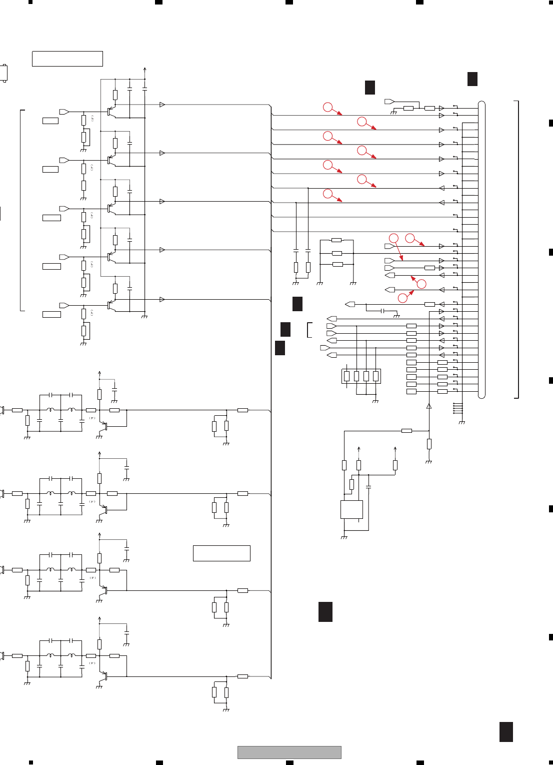
133
DVR-LX61
56 7 8
56 7 8
A
B
C
D
E
F
CR_OUT
YP_OUT
CB_OUT
C_OUT
Y_OUT
G_IN
B_IN
Y_IN
C_OUT
CB_OUT
C/R_IN
Y_IN
CR_OUT
YP_OUT
C/R_IN
G_IN
B_IN
Y_OUT
CN2301
VKN2065-A-TBB
1
2
3
4
5
6
7
8
9
10
11
12
13
14
15
16
17
18
19
20
21
22
23
24
25
26
27
28
29
30
31
32
33
34
35
36
37
38
39
40
C3320
7p/50
C2301
NM
C2504
1u
C2503
1u
C2502
1u
C2501
1u
C3339
1u
C3340
1u
C3341
1u
C3314
7p/50
C3312
7p/50
C3738
1u
C2302
NM
C3342
1u
C2505
1u
C3302
7p/50
C2506
10u
C3323
68p/50
C3317
68p/50
C3330
68p/50
C3304
68p/50
C2305
VCG1058-A
1u
C3321
7p/50
C3315
7p/50
C3311
7p/50
C3301
7p/50
GNDD
GNDD
GNDD
GNDD
GNDD
D
GNDD
GNDD
GNDA
GNDD
GNDD
D
GNDD
GNDD
GNDD
GNDD
GNDD
GNDD
GNDD
GNDD
GNDD
D
GNDD
GNDD
GNDD
GNDD
GNDD
GNDD
GNDD
GNDD
GNDD
D
GNDD
GNDD
GNDD
IC3707
PST3813U
OUT
1
VDD
2
NC
3
GND
4
L3308
10u
L3301
18u
L3307
18u
L3305
18u
L3306
10u
L3303
18u
L3302
10u
L3304
10u
3304
SC4081(QR)
3308
SC4081(QR)
3302
SC4081(QR)
3306
SC4081(QR)
2SA1576A(QR)
Q3305
C
B
E
2SA1576A(QR)
Q2503
C
B
E
2SA1576A(QR)
Q2505
C
B
E
2SA1576A(QR)
Q3303
C
B
E
2SA1576A(QR)
Q3307
C
B
E
2SA1576A(QR)
Q2501
C
B
E
2SA1576A(QR)
Q2504
C
B
E
2SA1576A(QR)
Q2502
C
B
E
Q3301
2SA1576A(QR)-TLB
C
B
E
R3005
10k
2143
6587
R2511
150
R3314
10
R2507
680
R2302
0
R3720
0
R3003 0
R2501
680
R3348
NM
R3347
NM
R3346
NM
R3345
NM
R3002 0
R2504
680
R2508
150
R3303
NM
R2514
150
R3319
10
R3304
NM
R3232
0
R3009 0
R3716
33
R3717
NM
R2314
NM
R3721
NM
R3004 0
R3326
10
R3715
0
R2316
10k
R3323
470
R3312
470
R2512
NM
R2515
NM
R2503
NM
R2509
NM
R3311
NM
R3316
NM
R2510
680
R3325
5.6k (F)
R3324
5.6k (F)
R3313
5.6k (F)
R3307
5.6k (F)
R3341
47
R3336
47
R3302
47
R2505
150
R2502
150
R3714
NM
R3342
NM
R3337
NM
R3310
NM
R3226
NM
R3231
NM
R3321
NM
R2304
0
R2506
0
R3318
470
R3306
470
R3012 0
R3006 0
R2301
3.3k
R3322
330
R3317
330
R3344
330
R3305
330
R3007 0
R3008 0
R3010 0
R3011 0
R2315
NM
R2513
680
R3308
10
R3301
47
TP2315
TP2321
TP2326
TP2325
TP2302
TP2307
TP2324
TP2308
TP2328
TP2322
TP2319
TP2309
TP6100
TP2312
TP2331
TP2320
TP2305
TP2311
TP2303
TP6105
TP6108
TP6106
TP2301
TP2313
TP2327
TP2306
TP2323
TP6107
TP2329
TP2330
TP2310
TP2317
TP2314
TP2304
V+5_VI
V+5_VI
V+5_VI
V+5_VO
V+3D
V+5_VI
Pr/ROUT
2:10L
SMDOUT
2:5J;F2
SMCKOUT
2:4K;F2
RCHOUT
F6
AMUTE1
E1
Pb/BOUT
2:10L
X525P
2:7D
Y/GOUT
2:10L
YOUT
2:10L
COUT
2:10L
HSMtoT
2:11K;2:12B
LCHOUT
F5
TU_HPD
TU_CEC
DDC_SW1
TU_DSCL
TU_DSDA
LCHIN
B8
DAT_TO_M
E11
HST_TO_M
E11
P_CONT2
3:1G;3:1I;3:2E;3:2F;3:8C
RCHIN
B7
XRST1
F9
C3324
15p/50
C3318
15p/50
C3331
15p/50
C3305
15p/50
C3303
5p/50
C3329
5p/50
C3316
5p/50
C3322
5p/50
HSM_TO_T
MRST
1.002Vpp,SYNC DC???V
1.00Vpp,SYNC DC???V
GND
YP_OUT
from TUJB
0.268Vpp,CENTER DC???V
GND
Y_OUT
C_OUT GND
Yp_OUT
GND
Y_OUT
C_OUT
GND
DAT_TO_M
Y_IN
GNDA
R_IN
GND
GND
R_OUT
XRST1
HST_TO_M
0.7104Vpp,CENTER DC???V
1.002Vpp,SYNC DC???V
GND
CB_OUT
CR_OUT
GND
AMUTE1
L_OUT
L_IN
X525P
Cb_OUT
Cr_OUT
P_CONT2
C/R_IN
DAM_TO_T
ASCK
0.2873Vpp,CENTER DC???V
0.7104Vpp,CENTER DC???V
C2
E2 Video OUT
Video IN
G_IN
B_IN
GND
GND
DSDA
CEC
DSCL
DDC_SW1
HPD
V+1R5_IN
13
11
14
12
16
15
17
4
10
9
5
SERVICE MAIN ASSY (4/5)
(VXX3309 : DVR-LX61)
(VXX3308 : DVR-560H-S,-K)
D4/5
D4/5
CN101
A1/4
2/5D
2/5
2/5D
3/5
D
2/5
D
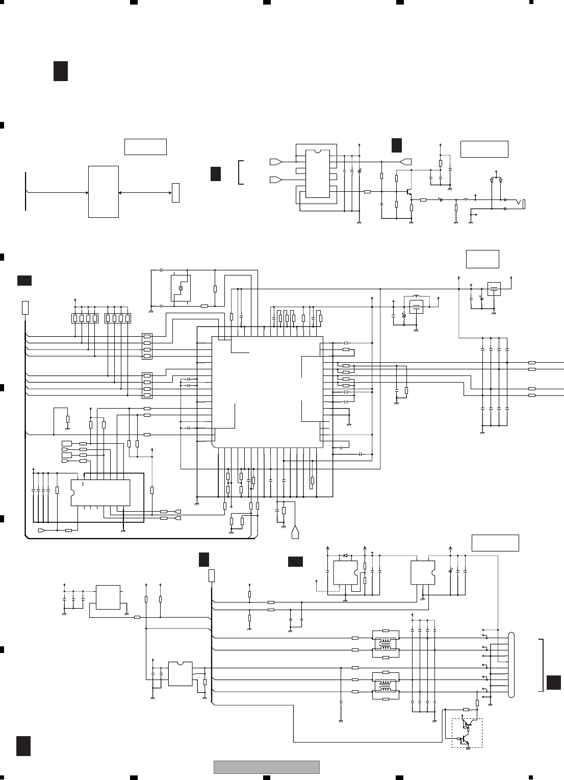
134 DVR-LX61
12 3 4
A
B
C
D
E
F
12 3 4
10.10 SERVICE MAIN ASSY (5/5)
PHY_D7
PHY_D3
PHY_D2
PHY_D1
PHY_D0
USB_DP0
USB_DN0
TPB0N
TPB0P
TPA0P
USB_D_VBUS
PHY_D6
PHY_D5
PHY_D4
USB_D_DP0
USB_D_DN0
TPA0N
USB_CLKI
USB_H_OCI0
USB_H_PPON0
USB_D_CONNECT
PHYLINKON
PHYLPS
PHYSCLK
CN5201
VKN1936-A
1
2
3
4
5
6
7
8
9
10
1u/50
C5704
220u/4
*C5708
100u/4
C5121
100u/16
C5210
100u/4
C5122
C5701
NM
C5703
NM
C5216
1000p/50
*C5707
VCG1057-A
C5702
1u
C5213
1u
C5205
1u
C5123
1u
C5120
1u
C5115
1u
C5116 1u
C5133
1u
C5112 1u
C5111
1u C5132
1u
C5110 1u
C51081u
C5107 1u
C5106
1u
C5105 1u
C5219
1000p/50
C5114
0.1u/16
C5113
0.1u/16
C5129
NM
C5221
NM
C5125
NM
C5220
NM
C5131
NM
C5124
NM
C5128
NM
C5127
NM
C5204
NM
C5207
NM
C5208
NM
C5201
NM
C5202
NM
C5203
NM
C5214
NM
C5215
NM
C5212
2.2u/10
C5209
0.1u/16
C5109
0.1u/16
C5104
0.1u/16
C5117
12p/50
C5118
12p/50
C5218
1000p/50
*C5705
1000p/50
C5223
1000p
C5222
0.1u
C5211
1000p
C5706
1000p/50
C5119
270p/50
C5154 1000p
C5152 1u
C5151 10u
C5153 0.1u
C5126
NM
C5130
NM
C5217
1u
D5209
NM
D5701
NM
L5121
NM
3
2
1
L5122
DTL1106-A
3
2
1
GNDD
GNDD
GNDD
GNDD
GNDD
GNDD GNDD
GNDD
GNDD
GNDD
GNDD
GNDD
GNDD
GNDD
GNDD
GNDD
GNDD
GNDD
GNDD
GNDD
GNDD
GNDD
GNDD
GNDD
GNDD
GNDD
GNDD
GNDD
IC5204
R1173H001B
ADJ
1
GND
2
CE
3
VDD
4
5
VOUT
IC5202
R5523N001B
EN
1
GND
2
FLG
3
VIN
4
5
VOUT
IC5203
TC7SH08FUS1
INB
1
INA
2
GND
3
OUTY
4
5
VCC
*IC5701
TC74VHC00FTS1
1A
1
1B
2
1Y
3
2A
4
52B
62Y
7GND8
3Y
9
3A
10
3B
11
4Y
12
4A
13
4B
14
Vcc
IC5103
UPD72852AGB-8EU-A
1
2
3
4
5
6
7
8
9
10
11
12
13
14
15
16
21
22
23
24
25
26
27
28
29
30
31
32
33
34
35
36
37
38
39
40
41
42
43
44
45
46
47
48
52
53
54
55
56
57
58
59
60
61
62
63
64
20
19
18
17
51
50
49
JA5701
VKB1159-A
2
1
L5202
ATH7015-A
1
122
33
4
4
L5201
ATH7015-A
1
122
33
4
4
L5701
CTF1382-A
L5101
CTF1305-A
NM
Q5201
Q5701
2SC4081(QR)
R5106
68
RAB4CQ680J-T
2
1
4
36
5
8
7
R5101
100k
2
1
4
36
5
8
7
R5102
100k
2
1
4
36
5
8
7
R5105
68
RAB4CQ680J-T
2
1
4
36
5
8
7
R5103
100k
R5125
1k
R5707
100k
R5134 0
R5135 0
R5133 0
R5132 0
R5207
0
R5141
0
R5706
75 (F)
R5702
470
R5122
56
R5205
68
R5110
10k
R5703
680
R5215
47k
R5214
47k
R5705
0
R5220
1.5k
R5115
10k
R5116
10k
R5204
820 (F)
R5104
100k
R5117
100k
R5112
NM
R5704
150
R5120
56
R5113
10k
R5114
10k
R5119
56
R5221
47k
R5213 0
R5208
NM
R5222
10
R5111
1k
R5212 0
R5126
NM
R5124 NM
R5123 10k
R5127
10k
R5121
56
R5118
9.1k
R5164
0
R5163
0
R5162 0
R5161 0
R5160 0
R5159 0
R5158
0
R5157
100k
R5155
10k
R5156
10k
R5154
100k
R5153
100k
R5152
100k
R5151
10k
R5217
0
R5216
0
R5202
0
R5201
0
*R5701
470
*R5708
NM
R5130
0
R5140
10k
R5203
3.3k (F)
R5128
NM
R5129
82
R5109 47
R510868
R5107 68
R5224
NM
R5223
NM
R5225
NM
R5226
NM
R5206
NM
R5131
5.1k
TP5202
TP5207
TP5107
TP5106
TP5204
TP5205
TP6122
TP5208
TP5209
TP5203
TP5206
TP5201
TP5101
TP5103
TP6094
TP6095
TP5102
TP5104
V+3D
EV+5.8V
V+3D
V+3D
V+3D
V+3D
V+3D V+3D
V+5USB
V+3D
V+3D
V+5DO
V+3D
V+3DV_A
V+3DV_D
V+3D
V+3D
V+3D
V+3D
V+3D
V+3D
X5101
VSS1211-A
1
1
2
2
4
4
3
3
X5201
VSS1218-A
(48MHz)
STANDBY
1
GND
2
VDD
4
OUTPUT
3
AOBCK_CN
AOLRCK_CN
AOD1_CN
SEL_ADATA
AILRCK_PHYLREQ
SPDIFO
SPDIFO_LL
PHY_XRST
2:3D
SPDIFSEL
AIBCK_PHYCTL0
2:10L
2:10L
AIBD_PHYCTL1
TC7MBL3257AFK
IC5151
S
1
1B1
2
1B2
3
1A
4
5
2B1
6
2B2
7
2A
8
GND
9
3A
10
3B2
11
3B1
12
4A
13
4B2
14
4B1
15
OE
16
Vcc
TpA1p
AVDDDIRECT
D2
TpA1n
24.576MHz
CPS
TpB0n
FNSEL
D3
TpA0p
AGND
D5
DGND
SPD/BDB
D
DGND
TpBias0
SCLK
PC0
YB
AVDD
CTL1
DGND
AGND
DVDD
DGND
TpB0p
DGND
RI1
D
LREQ
TpA0n
D4
AGND
IC(DL)
DVDD
LPS
D
SUS/RES
PC1
CH
AGND
X0
DGND
LKON
TpB1n
D_3.3V
D7
PC2
D
AGND
X1
D0
DGND
TpB1p
D6
D
AGND
DVDD
DVDD
D
AVDD
AVDD
D_3.3V
RESETB
CTL0
IC(AL)
IC(AL)
D1
TpBias1
CMC
CH
AGND
DVDD
YB
YB
USB
GND
USBDM2
USBVFB
USBDP2
V+5USB
GND
USBDM1
USBDP1
GND
GND
SPDIF
F
DV
from/to RFEX
AKP1278-A
JA5801
HDMI OUT
HDMI
IC9001
Sil9002CSU
SERVICE MAIN ASSY (5/5)
(VXX3309 : DVR-LX61)
(VXX3308 : DVR-560H-S,-K)
D5/5
D5/5
CN902
F
2/5D
2/5D
2/5D
2/5
D
2/5
D
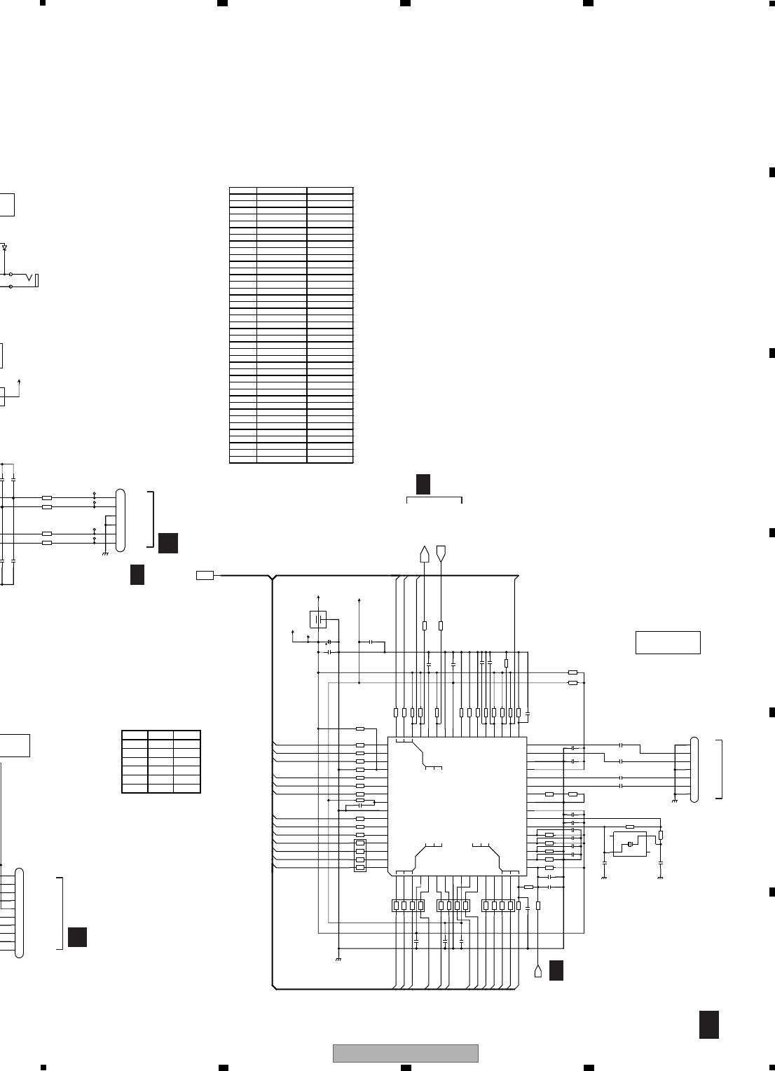
135
DVR-LX61
56 7 8
56 7 8
A
B
C
D
E
F
B_AT1DATA12
B_AT1DATA2
B_AT1DATA4
B_AT1DMARQ
B_AT1DIOW
B_AT1DATA13
B_AT1DIOR
B_AT1RESET
B_AT1DATA6
B_AT1DATA1
B_AT1DATA9
B_AT1DATA10
B_AT1DATA14
B_AT1DATA7
B_AT1DATA0
B_AT1DATA15
B_AT1CS0
B_AT1ADR1
B_AT1ADR0
B_AT1IORDY
B_AT1ADR2
B_AT1DATA11
B_AT1DMACK
B_AT1INTRQ
B_AT1CS1
PDIAG
B_AT1DATA3
B_AT1DATA5
B_AT1DATA8
DASP
VKN1932-A
CN5101
1TPAP
2TPAN
3A_GND
4A_GND
5TPBP
6TPBN
VKN2077-A
CN5604
1GND
2TXP
3TXN
4GND
5RXN
6RXP
7GND
CN5201
VKN1936-A
1
2
3
4
5
6
7
8
9
10
100u/4
C5613
C5612
0.1u
C5617 0.01u
C5602
1u
C5640
12p
C5623
0.01u/16
C5622
0.01u/16
C5625 0.01u/16
C5610
0.01u
C5611
0.01u
C5604
0.01u
C5605
0.01u
C5624 0.01u/16
C5607 0.01u
C56080.01u
C5616 0.1u
C5609 0.01u
C5615
0.1u
C5131
NM
C5127
NM
C5632
0.01u
C5631
0.01u
C5630
0.01u
C5603
0.1u
C5606 0.01u
C5614
0.01u
C5626
0.01u
C5627
0.01u
C5628
0.01u
C5629
0.01u
C5641
12p
NM
C5130
NM
D5701
NM
L5601
DTL1106-A
3
2
1
A
3
D
GNDD
GNDDGNDD
GNDD
GNDD
IC5602
88SA8040-B1-TBC1
H_DD13
1
H_DD2
2
H_DD12
3
VDDIO1
4
H_DD3
5
H_DD11
6
H_DD4
7
GND1
8
VDD1
9
H_DD10
10
H_DD5
11
H_DD9
12
H_DD6
13
H_DD8
14
H_DD7
15
H_RESET_N
16
ATAI O S E L
21
XTLIN/OSC
22
XTLOUT
23
VAA1
24
VSS1
25
ISET
26
RX_P
27
RX_M
28
VAA2
29
VSS2
30
TX_M 31
TX_P
32
T0
33
T1 34
T2
35
T3
36
T4
37
T5
38
T6
39
T7
40
VDD2
41
GND2
42
UAI
43
VDDIO2
44
UAO
45
H_PDIAG_N
46
H_CS_N1
47
H_CS_N0
48
H_IOCS16_N
52
H_INTRQ
53
H_DMACK_N
54
H_IORDY
55
VDD3
56
GND3
57
H_DIOR_N
58
H_DIOW_N
59
H_DMARQ
60
H_DD15
61
H_DD0
62 H_DD14
63
H_DD1
64
CNFG2
20
CNFG1
19
CNFG0
18
RST_N
17
H_DA1
51
H_DA0
50
H_DA2
49
JA5701
VKB1159-A
2
1
R5638
33
2
1
4
36
5
8
7
R5632
33
2
1
4
36
5
8
7
R5642
33
2
1
4
36
5
8
7
R5646
33
2
1
4
36
5
8
7
R56581k
R5661 1k
R5637 NM
R5660 NM
R5619
1k
R5624 82
R5134 0
R5135 0
R5133 0
R5132 0
R5615
1k
R5614
1k
R5613
1k
R5607
82
R5610
1k
R5671
NM
R5672
0
R5606
82
R5631 22
R5691
NM
R5664 0
R5693
0
R5692
0
R5652
100
R5636 NM
R5617
NM
R5623 82
R5651
12k (F)
R5608
10k
R5688 1MEG
R5622 82
R5629 82
R5627 82
R5657 1k
R5612
10k
R5690
0
R5609
10k
R5611
NM
R562822
R5659 1k
R5616
10k
R5618
10k
R5626 22
R5630 82
R5650
82
R5689
1.5k
TP5601
5208
TP5101
TP5103
TP5102
TP5104
V+3D
V+3DS
V+3D
V+1R8
X5502
VSS1214-A
1
1
2
2
4
433
TXD2_BRIDGE
XRESET
1:13H;1:4B;14C;3:12H;4:B9
2:10L;3:14B
RXD2_BRIDGE
SB
GND
USBDM2
USBVFB
USBDP2
V+5USB
GND
USBDM1
USBDP1
GND
GND
SATA
F
VWV2341 VWV2343
C5705 NM NM
C5707 NM NM
C5708 NM NM
R5701 NM NM
R5708 390 390
IC5701 NM NM
VWV2341 VWV2343
C4701 NMNM
C4702 NMNM
C4703 NMNM
C4704 NMNM
C4705 NMNM
C4706 NMNM
R4701 NMNM
R4702 NMNM
R4703 NMNM
R4704 NMNM
R4705 NMNM
R4706 NMNM
R4707 NMNM
R4708NMNM
R4709 NMNM
R4710 NMNM
R4711 NMNM
R4712 NMNM
R4713 NMNM
R4714 NMNM
R4715 10k 10k
R4716 10k 10k
R4717 10k 10k
R471800
R4719 0 0
R4720 0 0
R4721 100 100
R4722 100 100
R4723 47 47
R4724 22 22
R4725 22 22
R4726 22 22
R4727 NMNM
R472810k 10k
R4729 NMNM
R4730 NMNM
IC4701 NMNM
IC4702 NMNM
IC4703 NMNM
CN4701 NMNM
D5/5
CN901
F
CN902
F
To HDD
2/5D
2/5, 3/5
D
1/5,3/5,4/5
D
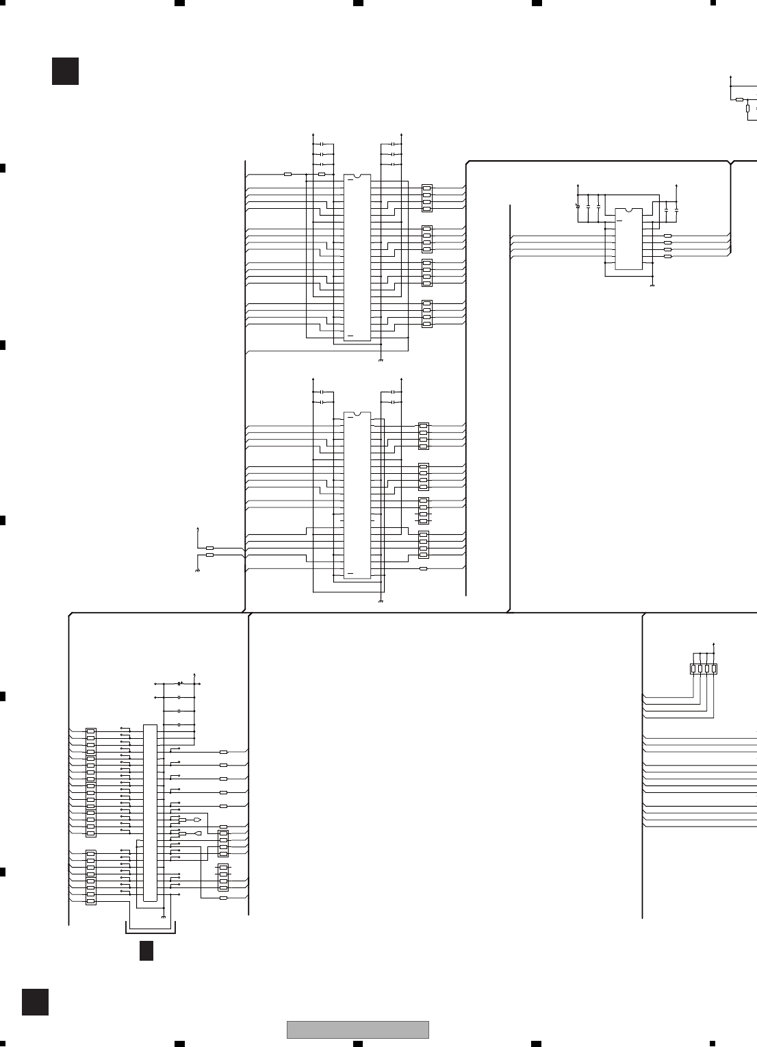
136 DVR-LX61
12 3 4
A
B
C
D
E
F
12 3 4
10.11 ETAB ASSY (DVR-LX61 ONLY)
E
D1
D0
D2
D4
D6
D12
D9
AAC_D0
AAC_D1
AAC_D2
AAC_D3
AAC_D6
AAC_D4
AAC_D7
AAC_D5
AAC_D14
AAC_D15
AAC_D13
AAC_D12
AAC_RESET_B
A9
WR
AAC_A9
AAC_CS_B
AAC_RD_B
AAC_A10
AAC_RESET
AAC_WR_B
A10
D8
D10
D13
D15
A2
AAC_A1
AAC_A2
A6
AAC_A8
A3
AAC_A5A5
AAC_A6
AAC_A7
A4
A1
AAC_A4
AAC_A3
AAC_BCLK2
AAC_INT_B
AAC_LRCK2
D15
D14
D13
D12
D11
D10
D9
D8
D7
RD
WR
N_CS
XRESET
RD
WR
N_CS
AAC_D10
AAC_D11
AAC_D8
AAC_D9
D3
D5
D7
D11
D14
A8
A7
ASI1
CS_B
CS_B
RD
AAC_ASO2
BCLK2
INT_B
LRCK2
ASO2
AAC_ASI1
RD
AAC_RESET
CS_B
D0
D1
D2
D3
D4
D5
D6
D7
D8
D9
D10
D11
D12
D13
D14
D15
A1
A2
A3
A4
A7
A6
A5
A8
A10
A9
CS_B
WR
RD
AAC_RESET
ASI1
BCLK2
LRCK2
ASO2
INT_B
XRESET
N_CS
C205
VCG1057-A
1u
C206
1000p/50
V+1R85
C203
1000p/50
V+3D
C202
VCG1057-A
1u
GNDD
C213
VCG1057-A
1u
GNDD
C214
1000p/50
C222
1000p/50
V+3D
C221
VCG1057-A
1u
GNDD
V+3D
GNDD
C211
VCG1057-A
1u
V+3D
C212
1000p/50
V+3D
C405
R401
NM
C418
1u
VCG1057-A-T
C417
0.1u/16
C416
1000p/50
R402
10k
TP401TP421
TP422
TP501
TP524
TP502
TP503
TP504
TP505
TP506
TP507
TP508
TP509
TP510
TP511
TP512
TP513
TP514
TP515
TP516
TP517
TP518
TP519
TP520
TP521
V+1R85
TP522
TP523
V+3D
IRQ
FIFO_SEL
TP525
TP526
TP527
TP528
TP529
TP530
TP531
TP532
TP533
TP534
TP535
TP536
TP537
TP538
TP539
TP548
R201
22
R202
NM
R214
10
2
1
4
36
5
8
7
R216
10
2
1
4
3
6
5
8
7
R219
10
2
1
4
3
6
5
8
7
R215
10
2
1
4
3
6
5
8
7
R213
10
2
1
4
36
5
8
7
R217
10
2
1
4
3
6
5
8
7
R220
10
2
1
4
3
6
5
8
7
R218
10
2
1
4
3
6
5
8
7
R204
22
2
1
4
36
5
8
7
R209
22
2
1
4
3
6
5
8
7
R208
22
2
1
4
3
6
5
8
7
R210
22
2
1
4
3
6
5
8
7
R203
22
2
1
4
36
5
8
7
R205
22
2
1
4
36
5
8
7
R206
22
2
1
4
36
5
8
7
R207
22
2
1
4
3
6
5
8
7
V+
IC203
TC7MP3125FK
S
1
1B1
2
1B2
3
1A
4
5
2B1
6
2B2
7
2A
8
GND
9
3A
10
3B2
11
3B1
12
4A
13
4B2
14
4B1
15
OE
16
Vcc
V+1R85
R221
22
R222
22
R223 22
R224
22
R226 22
R225 22
C224
1000p/50
C223
VCG1057-A
1u
R211
22
R212
22
R22810
R227 10
R501
47k
R502
47k
V+3D
GNDD
R312
NM
2
1
4
36
5
8
7
C201
DCH1201-A 10u
C204
DCH1201-A
10u
TP40
R229
22
R230
22
R231
22
R232
22
IC201
TC74VCX163245FT
1DIR
1
1B1
2
1B2
3
GND1
4
5
1B3
6
1B4
7
VCCB1
8
1B5
9
1B6
10
GND2
11
1B7
12
1B8
13
2B1
14
2B2
15
GND3
16
2B3
17
2B4
18
VCCB2
19
2B5
20
2B6
21
GND4
22
2B7
23
2B8
24
2DIR
25
2OE
26
2A8
27
2A7
28
GND5
29
2A6
30
2A5
31
VCCA1
32
2A4
33
2A3
34
GND6
35
2A2
36
2A1
37
1A8
38
1A7
39
GND7
40
1A6
41
1A5
42
VCCA2
43
1A4
44
1A3
45
GND8
46
1A2
47
1A1
48
1OE
IC202
TC74VCX163245FT
1DIR
1
1B1
2
1B2
3
GND1
4
5
1B3
6
1B4
7
VCCB1
8
1B5
9
1B6
10
GND2
11
1B7
12
1B8
13
2B1
14
2B2
15
GND3
16
2B3
17
2B4
18
VCCB2
19
2B5
20
2B6
21
GND4
22
2B7
23
2B8
24
2DIR
25
2OE
26
2A8
27
2A7
28
GND5
29
2A6
30
2A5
31
VCCA1
32
2A4
33
2A3
34
GND6
35
2A2
36
2A1
37
1A8
38
1A7
39
GND7
40
1A6
41
1A5
42
VCCA2
43
1A4
44
1A3
45
GND8
46
1A2
47
1A1
48
1OE
CN501
VKN2080-A
1
2
3
4
5
6
7
8
9
10
11
12
14
15
16
17
18
19
20
21
22
23
24
25
13
26
27
28
29
30
31
32
33
34
35
36
37
38
39
40
41
42
43
44
45
46
47
48
49
50
VCH1234-A
C419
150u
VCH1268-A
C220
75u
ETAB ASSY
(VWV2344 : DVR-LX61 Only)
2/5
D
E
CN1501
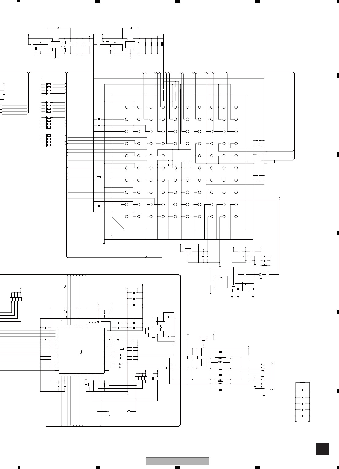
137
DVR-LX61
56 7 8
56 7 8
A
B
C
D
E
F
E
AAC_D0
AAC_D5
AAC_D8
AAC_D10
AAC_D9
AAC_D11
AAC_D12
AAC_D13
AAC_D14
AAC_D15
AAC_A10
AAC_A9
AAC_A7
AAC_A6
AAC_A8
AAC_A4
AAC_A5
AAC_A1
AAC_A3
AAC_A2
AAC_LRCK2
AAC_WR_B
AAC_RD_B
AAC_BCLK2
TMPW2
AAC_BCLK2
AAC_INT_B
AAC_LRCK2
AAC_ASO2
D6
D5
D4
D3
D2
D1
D0
A7
A6
A5
A4
A3
A2
A1
AAC_ASI1
AAC_D2
AAC_D4
AAC_D6
AAC_D3
AAC_D1
AAC_CS_B
AAC_D7
AAC_D8
AAC_D11
AAC_D10
AAC_D12
AAC_D13
AAC_D15
AAC_D14
AAC_D5
AAC_D7
AAC_D4
AAC_D6
AAC_D3
AAC_D2
AAC_D1
AAC_D0
AAC_D9
AAC_ASO2
AAC_INT_B
AAC_RESET_B
AAC_CLKIN
XRESET
GNDD
V+1R85
V+1R2_AAC_PLL
GNDD
C188
0.1u/16
V+1R2
V+1R2
C172
VCG1057-A
1u
C173
1000p/50
F171
DTL1106-A
3
2
1
C146
1u
C147
1000p/50
C144
VCG1057-A
1u
C145
1000p/50
C148
1u
C149
1000p/50
GNDD
V+3D
C317
1000p/50
GNDS
C308
VCG1057-A
1u
C304
VCG1057-A
1u
C309
1000p/50
C315
1000p/50
C336
(R336 0)
C305
1000p/50
C318
VCG1057-A
1u
GNDD
TP301
C337
(R337 0)
C319
1000p/50
TP303
R311
12k (F)
C302
VCG1057-A
1u
C306
0.1u/16
R301
10k
C313
1000p/50
R306 49.9
(F)
GNDD
C307
1000p/50
R307 49.9
(F)
C338
(R338 0)
R302
10k
C320 0.1u/16
R30849.9
(F)
C339
(R339 0)
C321
1000p/50
R309 49.9
(F)
R303
10k
V+3D
C312
0.1u/16
C303
1000p/50
GNDS
V+3D V+3D
TP302
TP308
TP309
TP310
TP311
TP312
IC401
S-1133B00
VOUT
1
VSS
2
NC
3ON/OFF 4
5
VIN
V+3D
GNDD
C404
1000p/50
C403
0.1u/16
C405
NM
R401
NM
GNDD
IC411
S-1133B12
VOUT
1
VSS
2
NC
3ON/OFF 4
5
VIN
C413
0.1u/16
V+3D
C414
1000p/50
R411
NM
FIFO_SEL
R402
10k
R412
10k
TP402TP403
TP304
TP305
TP171
TP306
TP101
C182
VCG1057-A
1u
V+1R85
C183
1000p/50
GNDD
C340
0.022u/50
X301
VSS1214-A
25MHz
1
1
2
2
4
4
3
3
R314
1M
C328
12p/50
C327
12p/50
R315
1k
IRQ
C325
VCG1057-A
1u
C326
1000p/50
TP547
V+1R85
R111
10k
2
1
4
3
6
5
8
7
R114
10k
2
1
4
3
6
5
8
7
R113
10k
2
1
4
3
6
5
8
7
R112
10k
2
1
4
3
6
5
8
7
R101
22
C108
VCG1057-A
1u
C109
1000p/50
C110
VCG1057-A
1u
C111
1000p/50
C104
VCG1057-A
1u
C105
1000p/50
C107
1000p/50
C106
VCG1057-A
1u
V+1R85
22
22
1000p/50
C223
VCG1057-A
1u
10
10
R181
10
R102
22
R103
10k
C181
DCH1201-A
10u
R304
47k
2
1
4
36
5
8
7
R312
NM
2
1
4
36
5
8
7
C341
0.1u/16
C342
1000p/50
C314
VCG1057-A
1u
GNDD GNDD
R183
10M
GNDD
R184
NM
R185
0
C185
1000p/50
C184
VCG1057-A
1u
V+3D V+CLK
GNDD
TP181
R305
47k
R310 10
(D)
F301
DTL1106-A
3
2
1
V+3D
GNDD
X101
ASS1172-A
32.768KHz
1
2
4
3
C316 VCG1057-A
1u
C343
1000p/50
C189
1000p/50
V+3A_LAN
V+1R8C
R404
2k (D)
R403
56 (D)
GNDD
TP102
C311
VCG1057-A
1u
C310
DCH1201-A
10u
GNDD
TP406
TP404
TP405
TP313
TP314
TP315
TP316
D401
NM
D411
NM
R410
NM
R413
1k
IC101
UPD99914F1-BAC
C5
D1
C6
D3
C7
D6
C8
TM5
C9
D8
C10
D7
D1
DGND1
D2
ASI1
D3
LRCLK1
D4
EGND3
D5
DGND2
D6
DVDD1
D7
D12
D8
D11
D9
D9
D10
D10
E1
EGND4
E2
N.C.3
E3
EGND5
E4
EGND6
E5
DVDD2
E7
D15
E8
D14
E9
D13
E10
DGND3
F1
EGND7
F2
EGND8
F3
EGND9
F4
EGND10
F7
TMPW2
F8
A9
F9
A10
F10
DVDD3
G1
EGND11
G2
EGND12
G3
EGND13
G4
DVDD4
G5
DVDD5
G6
DGND4
G7
A0
G8
A8
G9
A6
G10
A7
H1
PLLVDD
H2
EGND14
H3
CLKIN
H4
EVDD3
H5
PO4
H6
PO7
H7
EGND15
H8
A1
H9
A5
H10
A4
J1
PLLGND
J2
TM4
J3
PO0
J4
PO2
J5
PO5
B7
D4
A6
BCLK2
K3
PO1
K6
INT_B
B6
D2
A5
D0
A2
TM10
K2
TM3
C4
CS_B
B5
ASI2
K1
N.C.4
C3
ASO1
B4
ASO2
A3
WR_B
J10
TM0
C2
LRCLK2
B3
TM6
A4
RD_B
J9
TM2
C1
BCLK1
B2
EGND1
K10
N.C.5
J8
A3
B10
TM9
B1
EVDD2
A1
N.C.1
K9
TM1
J7
RESET_B
B9
TM8
A8
EVDD1
A10
N.C.2
K5
PO6
K8
A2
J6
EGND16
B8
EGND2
A7
D5
A9
TM7
K4
PO3
K7
EVDD4
IC301
LAN9211-ABZJ
1
VDD_IO1
2
VDD_CORE1 3
GPIO0/nLED1 4
GPIO1/nLED2
5
GPIO2/nLED3
6
A7
7
A6
8
A5
9
A4
10
A3
11
A2
12
A1
13
FIFO_SEL
14
NC
15
nRD
16 nWR
17 nCS
18
VDD_IO2
19
D15
20
D14
21
D13
22
D12
23 D11
24
VDD_IO3
25
D10
26
D9
27
D8
28
D7
29
D6
30 VDD_IO4
31 D5
32 D4
33
D3
34 D2
35
D1
36 D0
37
VDD_CORE2
38
EEDIO/GPO3
39 EECS
40
EECLK/GPO4
41
PME
42
nRESET
43
IRQ
44
TPO- 45
TPO+ 46
VDD_A331 47
TPI-
48
TPI+ 49
VDD_A332 50
EXRES1 51
VDD_A333 52
AMDIX_EN
53
VDD_A18
54
XTAL2
55
XTAL1/CLKIN
56
VDD_IO5
57
VSS
F321
VTH1056-A
1
1
2
233
44
F331
VTH1056-A
1
1
2
233
44
R321
NM
R322
NM
R331
NM
R332
NM
C344
NM
C345
NM
R186
NM
GNDD
GNDD
R182
470k
C402
VCG1058-A
1u
C412
VCG1058-A
1u
IC182
TC7SZU04FU
IC181
TC4SU69F
NC
1
IN_A
2
VSS
3
OUT_X
4
5
VDD
C186
27p/50
C187
22p/50
C415
VCG1058-A
1u
100u/4
C171
100u/4
C301
VCH1268-A
C411
75u
VCH1268-A
C401
75u
VCH1268-A
C324
75u
VKN2078-A
JA301
1TX+
2TX-
3RX+
4TCT
5RCT
6RX-
7NC
8GND
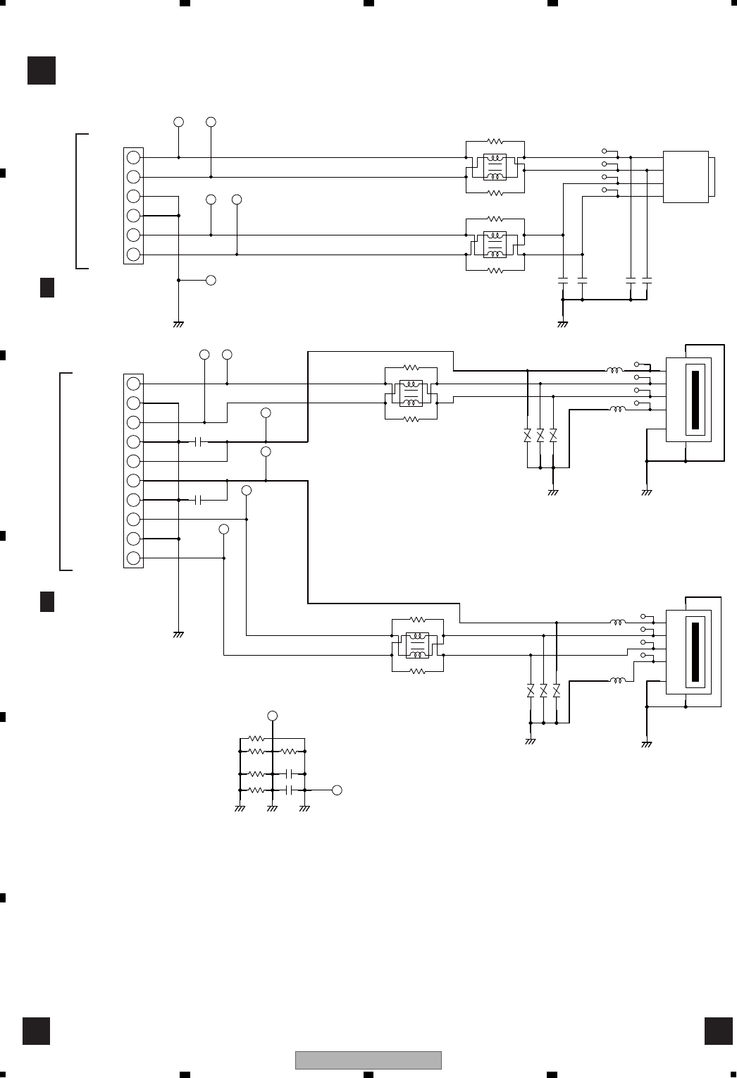
138 DVR-LX61
12 3 4
A
B
C
D
E
F
12 3 4
10.12 SERVICE DVUB ASSY
2
1
2
43
12
6
5
4
3
2
1
7
3
4
5
8
6
7
9
10
21
43
5
6
4
3
2
1
7
2
1
3
4
5
43
1
43 2
1
612 4
3
VA906
VA905
VA904
CN902
L906
R909
L908
R907 L907
VA903
VA902
R908
R912
R913
R910
JA903
C906
C905
L903
VA901
R906
L905
R905 L904
L902
R904
C901
C903
C902
R903
R902
JA902
C904
C908
C907
R911
CN901
L901
R901
JA901
AVR-M1608C120MT2AB-T
AVR-M1608C120MT2AB-T
AVR-M1608C120MT2AB-T
GND GND
VKN1936- -TFB
GND
***
33
***
***
VTL1169- -T
***
33
VTL1169- -T
AVR-M1608C120MT2AB-T
AVR-M1608C120MT2AB-T
GND GNDIA
0
0
VKB1227-A
***
***
1
1
***
AVR-M1608C120MT2AB-T
GND
33
***
***
***
VTL1169- -T
33
VTL1169- -T
GND
GND GNDIS
***
0
***
***
***
***
0
0
VKB1226-A
***
GNDIS
0.1
0.1
***
VKN1932- -TFB 0VKN2028-A
GND
GND
TPBP
TPAP
TPAN
GND
USBDP2
V+5USB
USBVFB
GND
USBDM1
GND
GND
USBDP1
USBDM2
GND
D+
D-
+5V
GND
D+
D-
+5V
TPAP
TPAN
TPBN
TPBP
TPBN
SERVICE DVUB ASSY
(YXX1001)
5/5
D
F
CN5201
5/5D
CN5101
F F

139
DVR-LX61
56 7 8
56 7 8
A
B
C
D
E
F
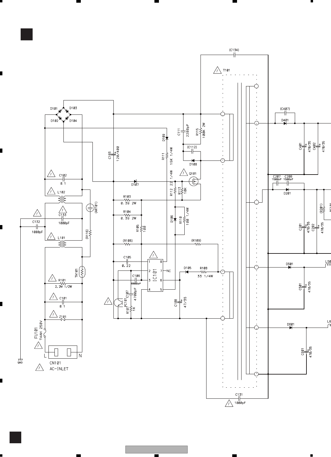
140 DVR-LX61
12 3 4
A
B
C
D
E
F
12 3 4
10.13 POWER SUPPLY ASSY
G
G
POWER SUPPLY ASSY
(VWR1406)
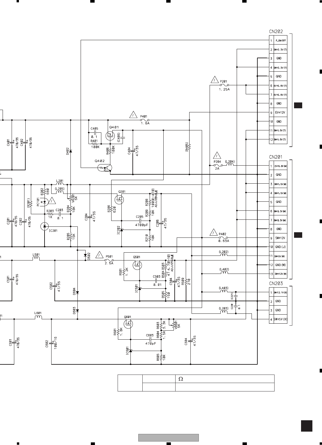
141
DVR-LX61
56 7 8
56 7 8
A
B
C
D
E
F
Unit Resistor
Capacitor
/W (under 1/4W for no direction W)
μF/V (under 50V for no direction V)
G
CN4501
D
3/5
CN301TO HDD
A1/4
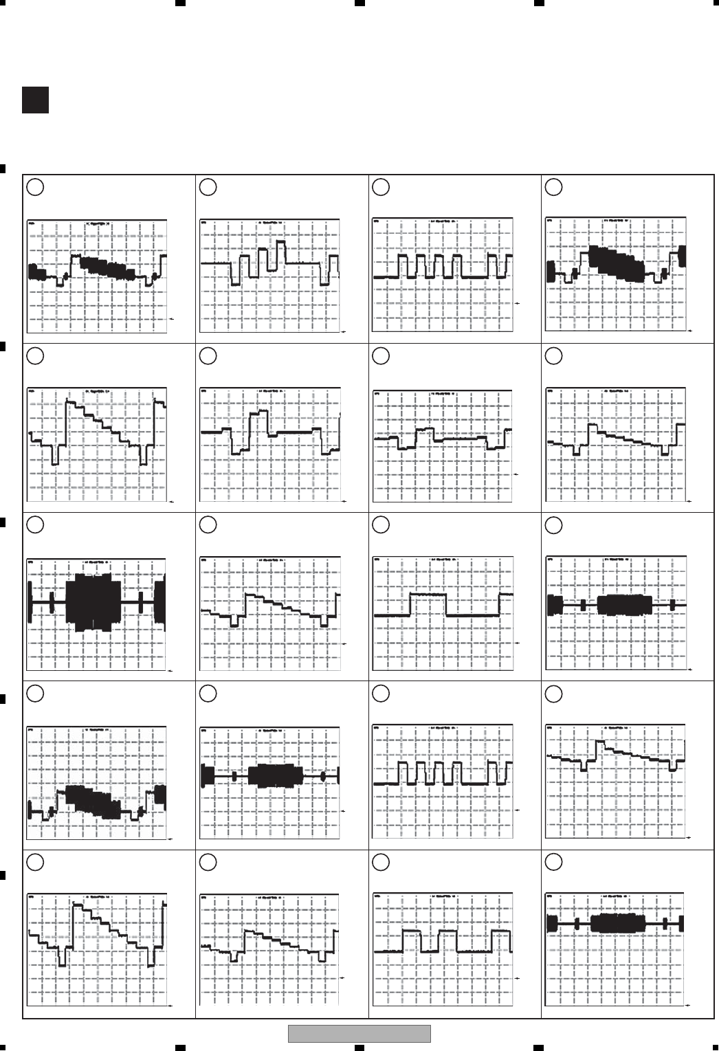
142 DVR-LX61
12 3 4
A
B
C
D
E
F
12 3 4
10.14 WAVEFORMS
1IC401-pin18 (TU-VIN)
(Function : Tuner 9ch)
V:500mV/div. H:10μsec/div.
2C486+side (Y2OUT)
(Function : DVD play)
V:500mV/div. H:10μsec/div.
3IC401-pin34 (C2OUT)
(Function : DVD play)
V:500mV/div. H:10μsec/div.
4C490+side (V1OUT)
(Function : DVD play)
V:1V/div. H:10μsec/div.
5C487+side (YOUT)
(Function : DVD play)
V:500mV/div. H:10μsec/div.
6C488+side (CbOUT)
(Function : DVD play)
V:500mV/div. H:10μsec/div.
7C489+side (CrOUT)
(Function : DVD play)
V:500mV/div. H:10μsec/div.
8CN101-pin8 (Y_OUT MtoT)
(Function : Tuner 9ch)
V:500mV/div. H:10μsec/div.
9CN101-pin10 (C_OUT MtoT)
(Function : DVD play)
V:500mV/div. H:10μsec/div.
10 CN101-pin2 (Yp_OUT MtoT)
(Function : DVD play)
V:500mV/div. H:10μsec/div.
11 CN101-pin6 (Cb_OUT MtoT)
(Function : DVD play)
V:500mV/div. H:10μsec/div.
12 CN101-pin4 (Cr_OUT MtoT)
(Function : DVD play)
V:500mV/div. H:10μsec/div.
13 CN101-pin2 (Y/G_OUT MtoT)
(Function : DVD play)
V:500mV/div. H:10μsec/div.
14 CN101-pin6 (Cb/B_OUT MtoT)
(Function : DVD play)
V:500mV/div. H:10μsec/div.
15 CN101-pin4 (Cr/R_OUT MtoT)
(Function : DVD play)
V:500mV/div. H:10μsec/div.
16 IC401-pin14 (2VIN)
(Function : LINE2 IN)
V:500mV/div. H:10μsec/div.
17 IC401-pin7 (Y2IN)
(Function : LINE2 IN)
V:500mV/div. H:10μsec/div.
18 IC401-pin9 (C2IN)
(Function : LINE2 IN)
V:500mV/div. H:10μsec/div.
19 CN101-pin12 (Y_IN TtoM)
(Function : LINE2 IN)
V:500mV/div. H:10μsec/div.
20 CN101-pin14 (C_IN TtoM)
(Function : LINE2 IN)
V:500mV/div. H:10μsec/div.
SERVICE TUSB ASSY
A
GND
GND
GND
GND
GND
GND
GND
GND
GND
GND
GND
GND
GND
GND
GND
GND
GND
GND
GND
GND
Note : The encircled numbers denote measuring point in the schematic diagram.
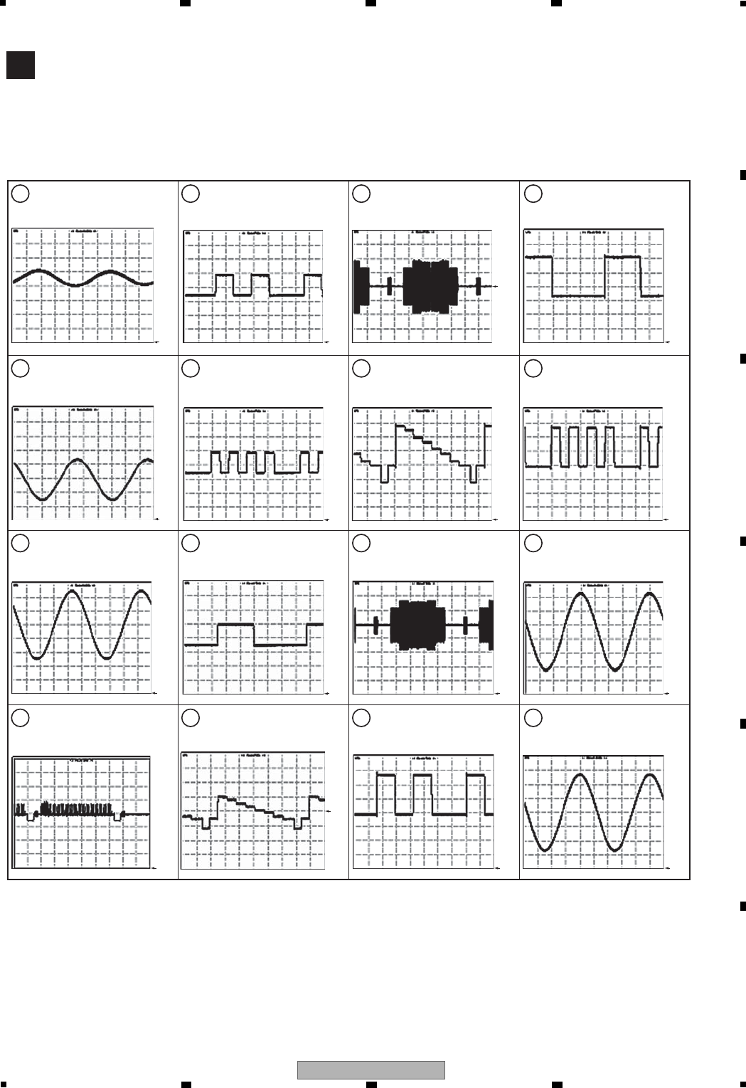
143
DVR-LX61
56 7 8
56 7 8
A
B
C
D
E
F
21 IC401-pin87 (TU-LIN)
(Function : Tuner 9ch)
V:500mV/div. H:10μsec/div.
22 C491+side (L_OUT)
Function : DVD play)
V:500mV/div. H:10μsec/div.
23 CN101-pin26 (L_IN)
(Function : LINE2 IN)
V:500mV/div. H:10μsec/div.
24 IC101-pin81 (TEXTV)
(Function : RF IN)
V:1V/div. H:10μsec/div.
Measurement Condition :
SERVICE TUSB ASSY
A
GND
GND
GND
GND
25 JA501-pin15 (R/C IN)
(Function : LINE1 IN)
V:500mV/div. H:10μsec/div.
29 JA501-pin15 (R/C IN)
(Function : LINE1 IN)
V:500mV/div. H:10μsec/div.
33 C530+side (AV1_G_OUT)
(Function : DVD play)
V:500mV/div. H:10μsec/div.
26 JA501-pin7 (BIN)
(Function : LINE1 IN)
V:500mV/div. H:10μsec/div.
30 C532+side (AV1_V/Y_OUT)
(Function : DVD play)
V:500mV/div. H:10μsec/div.
34 C529+side (AV1_B_OUT)
(Function : DVD play)
V:500mV/div. H:10μsec/div.
27 JA501-pin11 (G IN)
(Function : LINE1 IN)
V:500mV/div. H:10μsec/div.
31 C531+side (AV1_R/C_OUT)
(Function : DVD play)
V:500mV/div. H:10μsec/div.
35 C542+side (AV1_L_OUT)
(Function : DVD play)
V:500mV/div. H:10μsec/div.
28 JA501-pin20 (AV2_V/Y IN))
(Function : LINE1 IN)
V:1V/div. H:10μsec/div.
32 C531+side (AV1_R/C_OUT)
(Function : DVD play)
V:500mV/div. H:10μsec/div.
36 JA501-pin6 (AV2_L_IN)
(Function : LINE1 IN)
V:1V/div. H:10μsec/div.
GND
GND
GND
GND GND
GND
GND GND GND
GND
GND GND
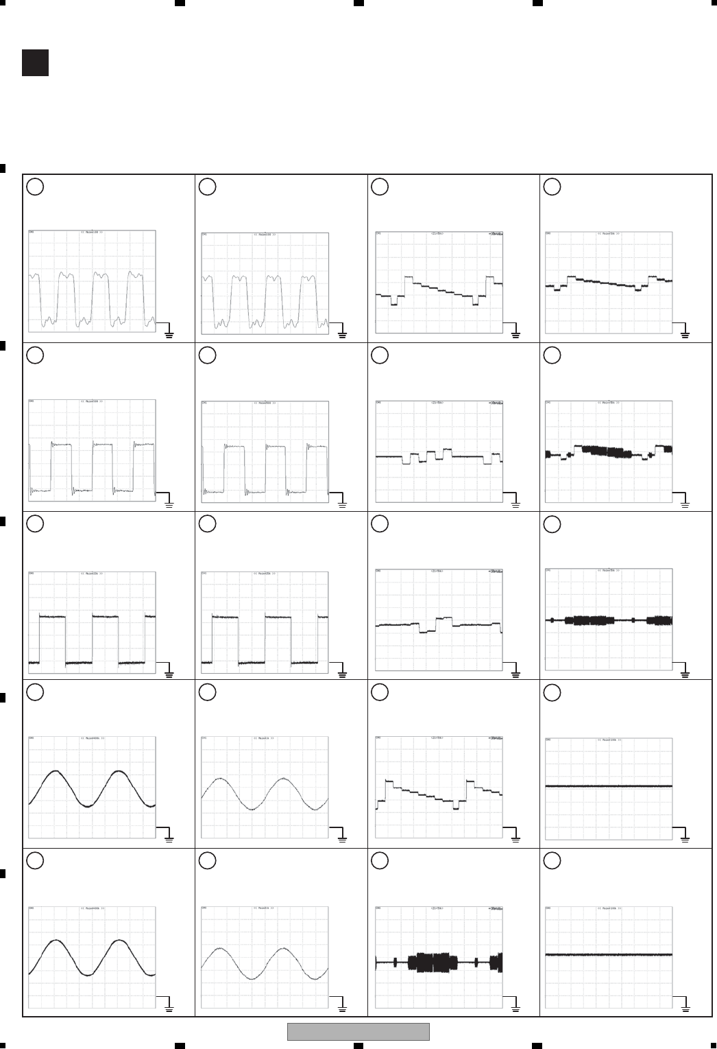
144 DVR-LX61
12 3 4
A
B
C
D
E
F
12 3 4
1IC3201 Pin16 (DACMCK)
V: 1V/div. H: 20ns/div.
2IC3201 Pin1 (DACBCK)
V: 1V/div. H: 100ns/div.
3IC3201 Pin3 (DACLRCK)
V: 1V/div. H: 5us/div.
4CN2301 Pin21 (LCHOUT)
V: 2V/div. H: 200us/div.
5CN2301 Pin19 (RCHOUT)
V: 2V/div. H: 200us/div.
6IC3101 Pin11 (ADCCLK0)
V: 1V/div. H: 20ns/div.
7IC3101 Pin12 (AD_BCK)
V: 1V/div. H: 100ns/div.
8IC3101 Pin10 (AD_LRCK)
V: 1V/div. H: 5us/div.
9CN2301 Pin15 (LCHIN)
V: 1V/div. H: 200us/div.
10 CN2301 Pin17 (RCHIN)
V: 1V/div. H: 200us/div.
11 CN2301 Pin39 (YP)
V: 0.5V/div. H: 10us/div.
12 CN2301 Pin35 (CB)
V: 0.5V/div. H: 10us/div.
13 CN2301 Pin37 (CR)
V: 0.5V/div. H: 10us/div.
14 CN2301 Pin33 (Y)
V: 0.5V/div. H: 10us/div.
15 CN2301 Pin31 (C)
V: 0.5V/div. H: 10us/div.
16 CN2301 Pin29 (S_Y)
V: 1V/div. H: 10us/div.
16 CN2301 Pin29 (CVBS)
V: 1V/div. H: 10us/div.
17 CN2301 Pin27 (S_C)
V: 1V/div. H: 10us/div.
18 IC501 Pin34 (XDMUTE1)
V: 1V/div. H: 20us/div.
19 IC501 Pin35 (XDMUTE2)
V: 1V/div. H: 20us/div.
Measurement Condition :
No.1 - 8 : EBU Color Bar (100 / 0 / 75 / 0)
SERVICE MAIN ASSY
D
GND GND GND GND
GND GND GND GND
GND GND GND GND
GND GND GND
GND GND GND
GND
GND
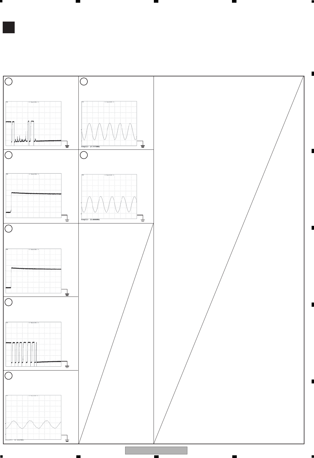
145
DVR-LX61
56 7 8
56 7 8
A
B
C
D
E
F
20 CN601 Pin3 (CLOSE)
open → close
V: 1V/div. H: 20us/div.
20 CN601 Pin3 (CLOSE)
close → open
V: 1V/div. H: 20us/div.
21 CN601 Pin5 (OPEN)
open → close
V: 1V/div. H: 20us/div.
21 CN601 Pin5 (OPEN)
close → open
V: 1V/div. H: 20us/div.
22 X101 (16.66667 MHz)
V: 1V/div. H: 20ns/div.
23 X1002 (27.77778 MHz)
V: 1V/div. H: 20ns/div.
24 X1001 (25 MHz)
V: 1V/div. H: 20ns/div.
SERVICE MAIN ASSY
D
GND GND
GND GND
GND
GND
GND

146 DVR-LX61
12 3 4
A
B
C
D
E
F
12 3 4
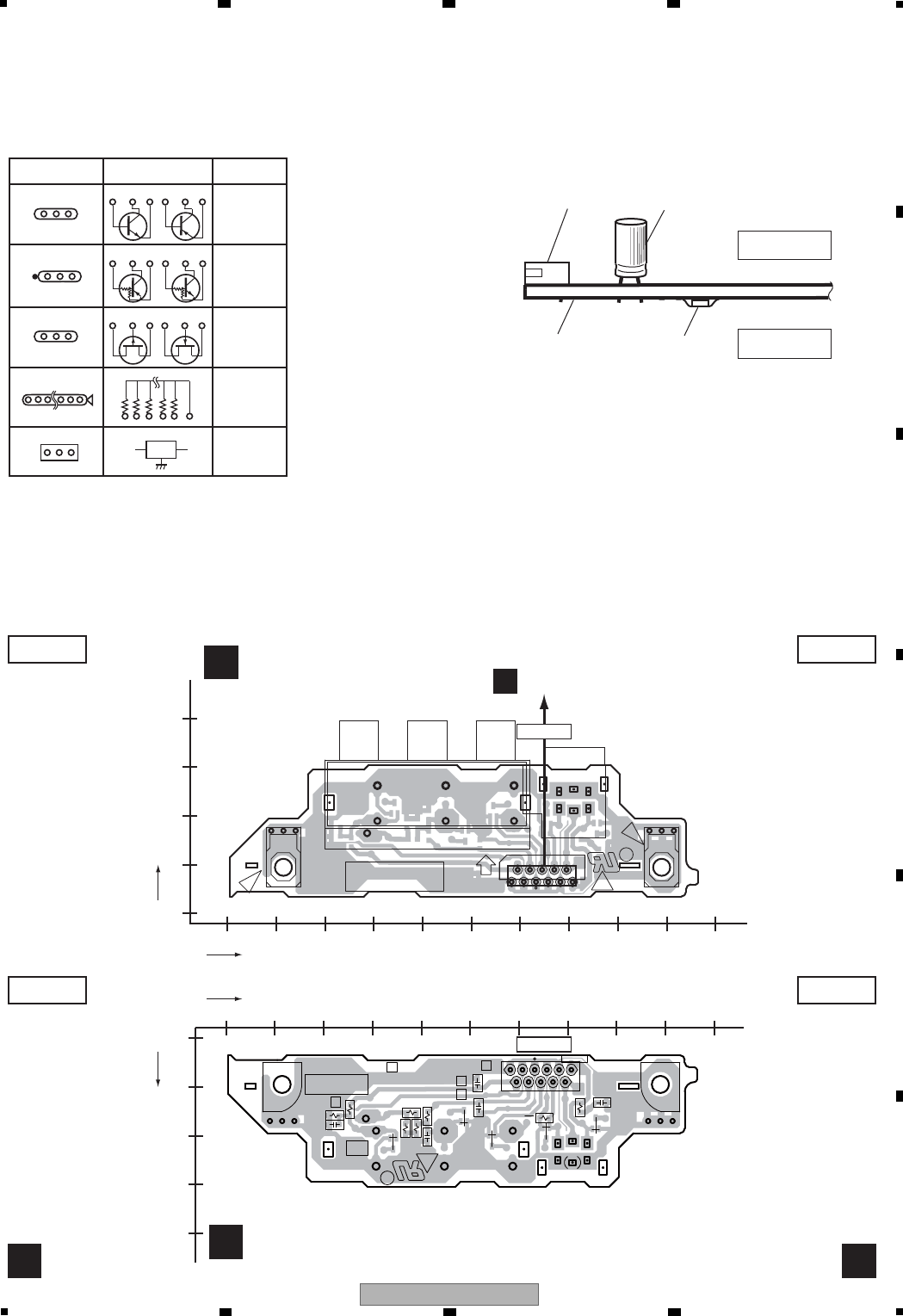
147
DVR-LX61
56 7 8
56 7 8
A
B
C
D
E
F
11. PCB CONNECTION DIAGRAM
11.1 SERVICE FRJB ASSY
NOTE FOR PCB DIAGRAMS :
1. Part numbers in PCB diagrams match those in the schematic
diagrams.
2. A comparison between the main parts of PCB and schematic
diagrams is shown below.
3. The parts mounted on this PCB include all necessary parts for
several destinations.
For further information for respective destinations, be sure to
check with the schematic diagram.
4. View point of PCB diagrams.
Symbol In PCB
Diagrams
Symbol In Schematic
Diagrams Part Name
BCE
D
D
G
G
S
S
BCE
BCE
DGS
BCEBCE
BCE
Transistor
Transistor
with resistor
Field effect
transistor
Resistor array
3-terminal
regulator
Capacitor
Connector
P.C.Board Chip Part
SIDE A
SIDE B
140 150 160 170 180 190 200 210 220 230 240
0
10
20
30
40
X
X
Y
Y
111
R
C7
[[ G ]]
JA301
KN301
JA302
KN302
CN301
FRJB
PC
140 150 160 170 180 190 200 210 220 230 240
0
10
20
30
40
SIDE A
SIDE B SIDE B
C
SIDE A
C
CN106
A
CN301
CN301
SERVICE FRJB ASSY
C
SERVICE FRJB ASSY
C
(YNP1006-B)
(YNP1006-B)
10
11 1
R
LF
C305
R307
C304
C302
R306
R305
C303
R304
R303
R308
D303
D302
D301
C301
R301
R302
D304
D305
YWM1003- /V
YWM
YWM1005- /V
YWM1006- /V
YWM1004- /V
FRJB
10.SDET2
11.2C
1.GND
2.2R
3.GND
4.2L
5.GND
6.2V
7.GND
8.2Y
9.GND
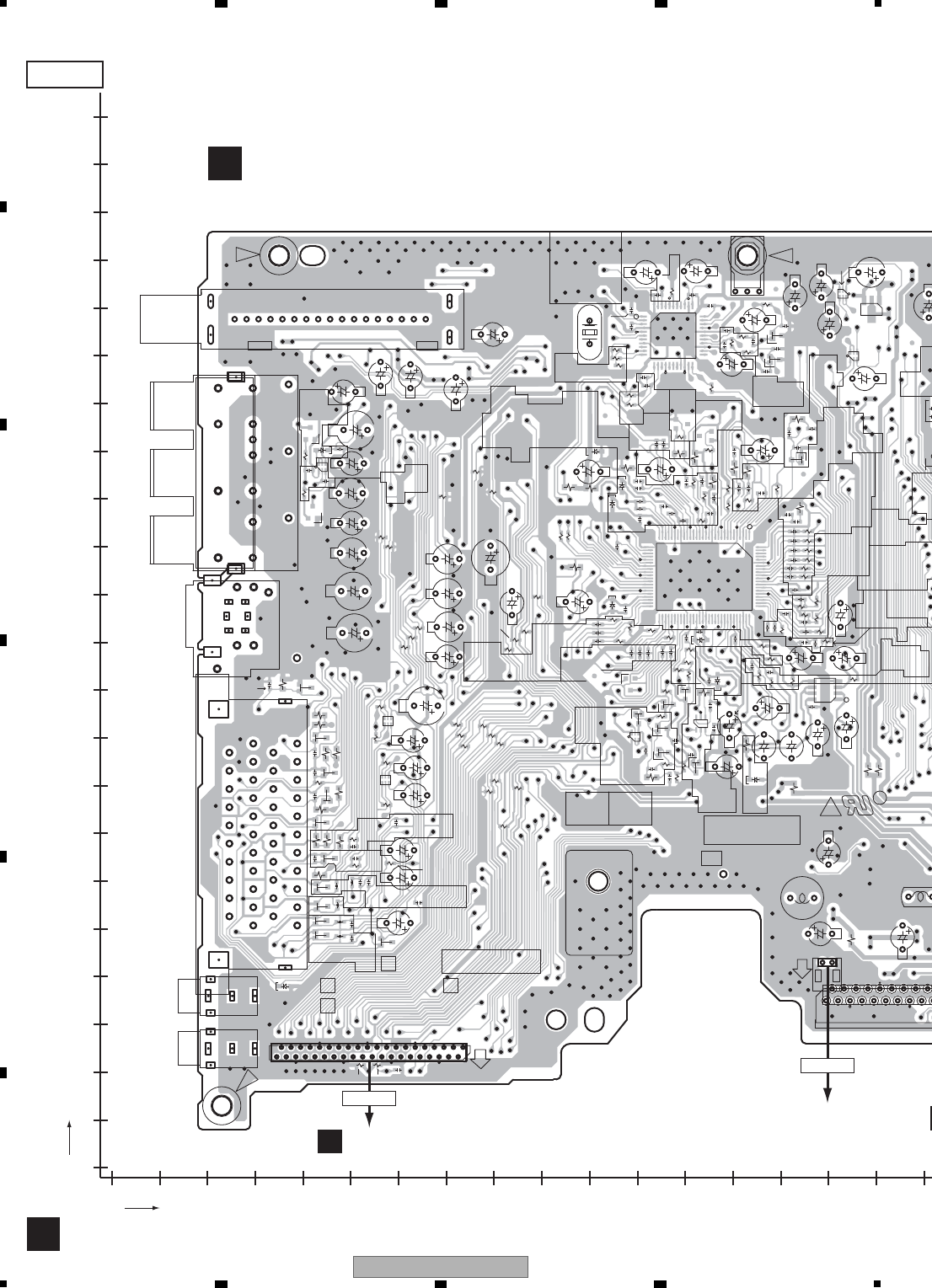
148 DVR-LX61
12 3 4
A
B
C
D
E
F
12 3 4
11.2 SERVICE TUSB ASSY
0 10 20 30 40 50 60 70 80 90 100 110 120 130 140 150 160 170
0
10
20
30
40
50
60
70
80
90
100
110
120
130
140
150
160
170
180
190
200
210
220
X
Y
NPNP
A30C5/C7
[[ G ]]
100
81
80
51
50
31
30
1
85
4
1
64
3
1
12
FCICT
LF
R
1
40
NP
CONTACT UPPER SID
1
NP
34
33
23
22
12
11
1
44
1
1
C463
C401
C402
C403
C404
C405
C406
C407
C408
C409
C410
C411
C412
C414
C415
C416
C417
C418
C419
C420
C421
C422
C423
C424
C425
C426
C427
C428
C431
C432
C433
C434
C435
C436
C437
C438
C439
C440
C441
C442
C443
C444
C445
C446
C447
C449
C450
C451
C452
C453
C454
C455
C456
C457
C458
C459
C460
C461
C462
C464
C465
C466
C467
R498
C470
R465
C472
C475
C479
C480 C481
C486
C487
C488
C489
C490
C491
C492
C493
C494
C495
C496
R296
R461
Q413
Q411
D401
D402
D403
D405
D406
D407
D408
D419
IC401
IC402
IC403
Q410
Q409
C497
JA401
JA402
Q303
Q401
Q402
Q403
Q404
Q406
Q407 C498
C307
R402
R403
R404
R406
R407
R408
R409
R410
R411
R412
R413
R414
R415
R416
R417
R418
R419
R422
R423
R426
R427R428
R430
R431
R432
R433
R434
R435
R436
R437
R438
R441
R442
R444
R445
R447
R448
R453
R454
R456
R458
R459
R460
R462
R463
C471
R466
R484
R486
C308
R499
C500
R440
Q412
R297
C123
Q408
C474
C311
R449
C303
R203
C528
C326
D531
C607
C473
C469
C468
R299
R293
C312
R223
R260
R261
R262
R263
R264
R265
R266
R267
R268
R269
R270
CN201
R301
C204
C205
R290
R218
R298
Q301
R294
C532
C531
C551
C550
Q304
C547
R557
R556
C534
L201
C535
C527
CN101
C525
R549
C536
JA701 JA751
C537
C538
C524
R197
C540
C553
L503
C523
C521
C530
C545
C529
Q507
D517
D515
D516
C543
C526
R521
CN302
R525
R529
R533
D514
D521
JA501
R320
R524
R523
R530
R527
R526
R528
D513
R531
D518
R532
D519
R534
L504
R547
R546
C541
D520
R535
D522
C542
C544
R522
Q506
R572
L304
R307
KN101
R615
R617
R618
R619
R621
R622
R625
R627
Q604
Q605
C609
L505
C642
C628
C629
C630
C632
C633
C618
C636
C638 C639
C640
C641
C620
C622
C617
R620
C611
R628
R624
C631
C635
C619
IC601
X601
C643
U601
L506
R308
R450
R201
C157
C156
R13
R291
IC104
R204
C141
R101
R222
R145
R146
Q103
Q102
IC103
C125
D108
R148
R152
C129
R142
R141
C128
C126
C101
C103
L510
R198
R292
R429
R295
R421
D422
R455
D421 C142
R221
R229
D530
PC
TUSB
YWM1001- YWM1011-
YWM1002-
YWM
SIDE A
A
TO FAN MOTOR
CN201
CN2301
D
CN101
SERVICE TUSB ASSY
A
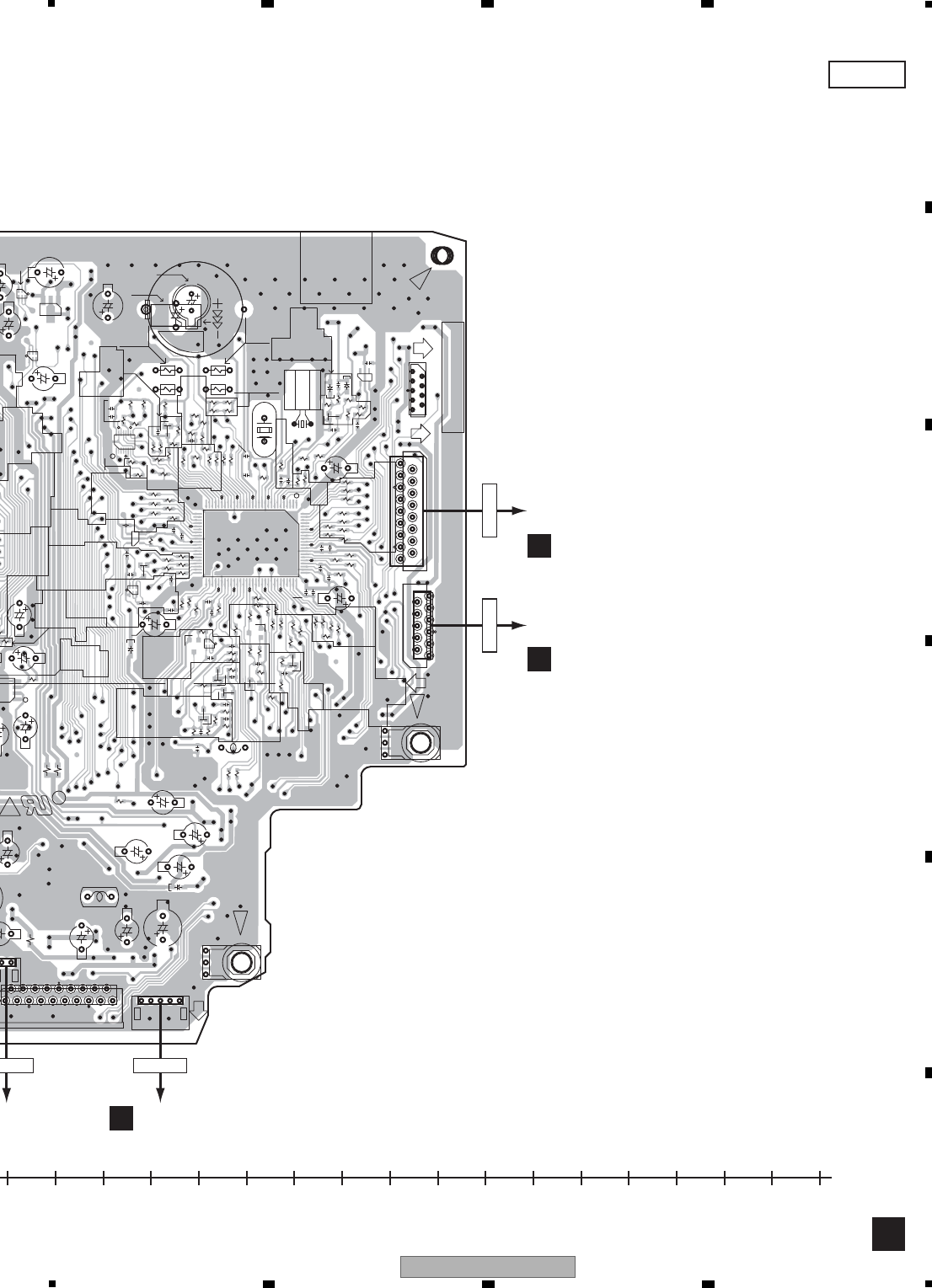
149
DVR-LX61
56 7 8
56 7 8
A
B
C
D
E
F
150 160 170 180 190 200 210 220 230 240 250 260 270 280 290 300 310 320
+-
4
1
117
12
5
1
R
CONTACT UPPER SIDE
19
11
1
19
16 9
8
1
1
5
5
1
100
81
80 51
50
31
30
1
C166
C167
C168
C169
C402
C403
C411
C412
C414
C415
C416
C417
C418
C419
C420
C421
C422
C423
C424
C425
C427
C431
C443
C455
C472
R227
C304
R226
BT101
IC402
C497
Q303
01
R314
98
C307
R402
R403
R408
R409
R410
R411
R412
R413
R414
R415
R416
R417
R418
R419
R422
R423
R426
430
R445
R453
R463
C471
C308
C500
C315
C123
4
C108
C311
R228
C303
R215
R203
C119
C326
CN105
C319
C469
C468
312
R199
R136
R223
CN301
C204
R205
C316
R185
C320
D103
R218
R207
R208
R209
Q301
Q304
CN302
L304
R307
R200
R308
R212
X101
R184
R217
R202
R201
R183
R182
CN106
C104
R117
C106
R129
C207
R216
R115
CN103
C107
R213
R124
C157
C156
R114
R113
X102
R135
R176
R175
R174
R173
R172
R171
R170
R169
R168
R167
IC104
R165
R133
R134
C131
R178
R179
R180
R181
R188
C109
R112
R123
R204
C141
R210
R111
R110
R109
R107
R106
R105
R214
R104
R122
R121 R120
R103
R101
R119
R224
Q112
Q111
Q110
R143
R144R222
R145
R146
Q108 Q107
C124
Q106
R177
Q105
Q103
Q104
C105
Q102
Q101
L102
IC103
C110
IC102
C113
C152
IC101
C125
D108
C151
R147
R189
R148
R149
C150
R150
C149
C140
C139
C138
C137
C136
C135
C134
D106
C133
R132
R151
R152
R153
R155
R156
R157
R131
R158
R159
C132
C130
R160
R161
R162
R163
C129
R142
R127
R141
C128
D102
R140
C127
C126
C101
R139
D101
C103
R138
R137
R126
KN102
KN103
R225
R429
C118
R230
R232
R164
R231
C142
R221
R229
R125
SIDE A
A
CN202
G
N MOTOR
N201 CN301
CN301
C
CN106
CN101
B
CN105
(YNP1005-B)
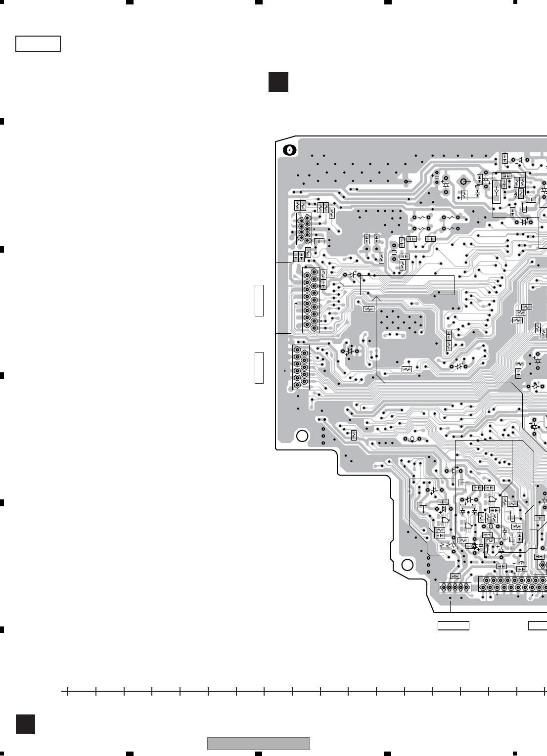
150 DVR-LX61
12 3 4
A
B
C
D
E
F
12 3 4
15160170180190200210220230240250260270280290300310320
SIDE B
A
CN2CN301
CN106 CN105
SERVICE TUSB ASSY
A
17
1
15
CN302
19
11
10
1
1
9
C448
C318
R325
R322
Q309
C314
C203
R313
R309
R310
Q307
R446
C
C328
C313
C302
C317
R195
R323
C122
C301
Q311
R211
R312
R315
C323
C322
C324
C325
R316
C202
C310
D303
R233
D301
D104
R303
C321
C115
R302
R128
Q306
Q305
Q308
R321
R324
Q310
R306
L305
D110
D302
R311
R194
R196
C155
R116
R130
C121
C112
R108
R102
C154
R118
C116
C114
C147
C117
R193
R154
C111
C102
D304
IC150
IC317
16.GND
19.DT_Y
18.GND
17.DT_C
CN105
CN301
CN201
CN103
CN106
IC150 TYPE NO.494.500NR
MFD. BY LITTELFUSE INC.
3.D
1.F
2.G
4.EV+5.8V 4.ANT5V_SW
6.P_CONT2
5.DET_ANT
7.GND
8.V+32V
9.GND
10.EV+5.8V
11.GND
12.EV+5.8V
13.GND
14.EV+12.1V
15.P_CONT
3.GND
2.EV+12.1V
1.P_CONT
5.GND
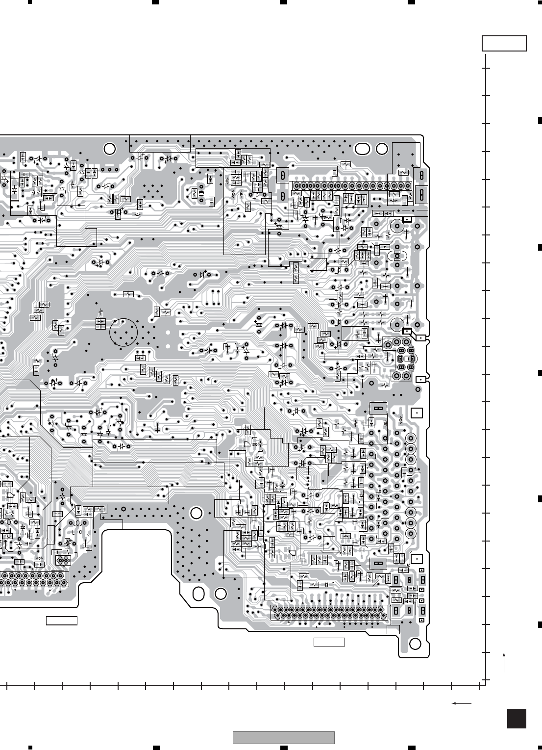
151
DVR-LX61
56 7 8
56 7 8
A
B
C
D
E
F
0102030405060708090100110120130140150160170
0
10
20
30
40
50
60
70
80
90
100
110
120
130
140
150
160
170
180
190
200
210
220
X
Y
SIDE B
A
CN201
CN101
(YNP1005-B)
40
1
5
1
3
4
NP
N302
1
42
41
23
22
21
20 2
1
15 10 5 1
C608
C413
C429
C430
C448
C476
C477
C478
C482
C483
C484
C485
C318
R325
R322
Q309
R318
C552
C208
C203
D409
D410
D411
D412
D413 D414
D415
D416
D417
D418
R313
D201
R310
D420
R401
R425
R439
R443
R446
R468
R469
R470
R471
R472
R473
R474
R475
R476 R477
R478
R479
R480
R481
R485
R487
R488
R489
C306
C309
C328
C305
R323
C301
Q311
R219
R305
Q302
R312
R315
C323
C322
C324
C325
C201
R316
C202
C310
D303
R574
C613
C120
D301
D104
C321
R271
R272
R273
R274
R275
R276
R277
R278
R279
R280
R281
R282 R283
R573
C329
Q201
R220
Q508
D528
D525
C510
C509
C548
C702
C703
C754
C755
C546
C504
R555
R554
C502
R552
R550
R548
C512
R701
L751
C539
R538
R536
C501
C517
C514
C520
R702
R704
R754
R756
C513
Q751
Q752
R502
IC406
C516
R503
R508
L303
C511
C503
C519
D509
D701
C522
R501
C549
Q501
Q505
C515
R569
R517
R755
R753
R752
R751
R703
R505
R541
R509
R558
R564
R513
Q510
D502
D510
R519
R321
C505
R560
C751
C701
R324
R520
R506
D511D512
D503
D508
Q511
Q509
D501
R562
R561
R514
Q310
R511
R512
C753
R510
R540
C752
R504
R507
C507
C508
C518
C506
R518
D523
R565
D524
D526
D527
R566
Q502
Q503
Q504
R568
R571
R515
R516
D504
D505
D506
D507
R304
R638
R639
L305
R640
C603
C605
R614
R623
R626
R629
R630
R631
L601
L606
L608
L609
C606
R612
C634
C612
C621
C624
C625
C626
C614
C616
C604
R616
R613
L607
Q606
R633
L604
L602
Q601
L605
Q603
Q602
R601
R602
R603
R605
R604
R606
C623
C627
C615
C602
R634
R632
R311
L507
R635
L508
C533
L509
D404
R405
L401
L402
L403
L404
L405
L501
L502
R467 R424
R420
R608
R607
R251
IC317
C206
D529
R609
R636
R637
CN201
CN101
JA501 JA402
JA751JA701
U601
REPLACE IC LINKS AS MARKED.
REMPLACER LE IC LINK COMME INDIQUE.
CAUTION -
ATTENTION -
IC317 TYPE NO.494.500NR
MFD. BY LITTELFUSE INC.
3.DT_TUON
1.FAN-
2.GND
4.ANT5V_SW
6.P_CONT2
5.DET_ANT
7.GND
8.V+32V
9.GND
10.EV+5.8V
11.GND
12.EV+5.8V
13.GND
V
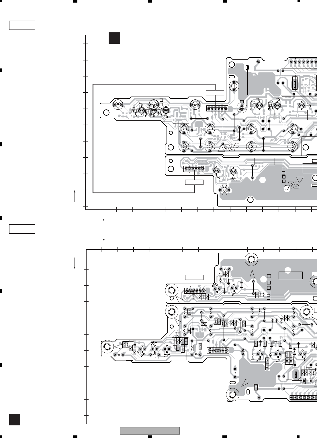
152 DVR-LX61
12 3 4
A
B
C
D
E
F
12 3 4
11.3 SERVICE FLKY ASSY
0 10 20 30 40 50 60 70 80 90 100 110 120 130
0
10
20
30
40
50
60
70
80
90
100
X
X
Y
Y
0 10 20 30 40 50 60 70 80 90 100 110 120 130
0
10
20
30
40
50
60
70
80
90
100
9
1
C
R
R
C7
[[ G ]]
1
6
1
6
S112
S104
S103
S106
C105
W133
V101
S108
S202
D106
S111
S107
S109
S105
D205
W144
W147
W139
D113
D212
W138
W142
W141
W154
W146
W153
W143
W140
W137
W134
CN102
W165
CN201
D119
D120
D121
D122
S113
S114
S115
W164
W161
W162
YWM1003- /V
GND
YWM
FLKY
KEY1
KEY3
V+5F
GND
LED-HDMI
LED-ICE BLUE
V+5F
FLDC
KEYB
V+5F
YWM1005- /V
YWM1006- /V
YWM1004- /V
YWM1003- /V
PC
AT V
HDD
DVD
DTV
PLAY
CH-
STOP
CH+ ATV/DTV
INPUT
STOP REC ONE TOUCH COPY
OPEN/CLOSE
HDD/DVD
V+12F
KEY2
GND
GND
GND
HDMI
GND
GND
VEDIO
MUSIC
PHOTO
SELECT
LED-ATV
YWM1004- /V
YWM1005- /V
YWM1006- /V
YWM
1
9
F
16
16
R128
R130
R164
R162
R165
C119
R163
C112
C110
C111
R112
R111
C109
R132
R113
R110
R166
C103
Q103
R126
C124
C201
R223
R140
D105
R152
R125
C123
R127
R129
R131
R205
Q107
C129R139
Q204
D206
R221
C132
R141
D114
R222
Q206
D211
R134
R136
C204
C202
R133
R224
R225
C133
C134
C135
D115
R148
R149
R150
D116
D117
D118
Q111
Q112
R153
R154
R155
R156
R157
R158
R159
R160
R161
REC
SELECT
5.LED-P-ON
YWM1005- /V
YWM1006- /V
KEY
HDMI
FLKY
ONE
STOP
INPUT ATV/DTV
CH+
STOP
CH-
PLAY
1.KEY3
DTV
AT V
OPEN/CLOSE
HDD/DVD
TOUCH COPY
YWM1003- /V
HDD
DVD
3.LED-DVD
4.V+12F
6.GND
2.LED-HDD
1.KEY3
2.LED-HDD
3.LED-DVD
4.V+12F
5.LED-P-ON
6.GND
VIDEO
MUSIC PHOTO
YWM1004- /V
YWM
SIDE A
B
SIDE B
SERVICE FLKY ASSY
B
CN102
CN102
CN201
CN201
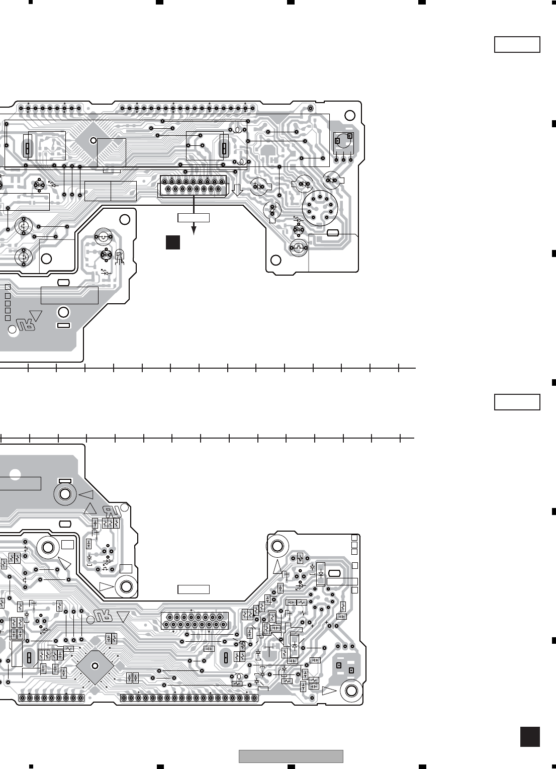
153
DVR-LX61
56 7 8
56 7 8
A
B
C
D
E
F
10 120 130 140 150 160 170 180 190 200 210 220 230 240 250
10 120 130 140 150 160 170 180 190 200 210 220 230 240 250
4941
23
179
C7
[[ G ]]
R
FCICT
1
17
L102
C128
C118
C116
C113
T101
L101
S110
S106
S108
S201
D106
W158
W144
W147
W149
W148
IC103
D113
W160
W156
W150
W159
W142 W154
W157
W146
W155
W143
W152
W151
D271
CN101
D124
W163
M
Y
LED-DTV
KEY1
LED-ATV
FLDC+
GND
GND
V+5F
LED-HDMI
IR VCC
FL-28V
IR
V+5F
B
PC
V+5F
V
V
ATV/DTV
ONE TOUCH COPY
REC
P-ON
GND
GND
HDMI
P-ON
DCP
GND
/V
/V
LED REC
33
34 44
111
12 22
23
9
17
23
41
49
R
R
LF
LF
1
17
R128
R130
R137
D110
D112
R123
D111
C122
C121
Q106
R124
Q105
R119
D108
C117
R121
R122
R118
R120
R117
D109
Q104
R272
C115
C114
D107
R116
C112
C271
C110
C111
R112
R111
C109
R132
C108
C107
R113
R110
IC101
C106
R106
R107
R105
R104
C101
C104
Q103
C127
C125
R135
R204
C120
D105
C129R139
C136
C132
R138
C126
R134
R136
D123
R133
D270
R270
C270
R144
Q203
Q108
R142
005- /V
1006- /V
KEYB
YWM1006- /V
YWM1003- /V
YWM1004- /V
HDMI
Y
ONE
ATV/DTV
REC
V
15.KEY1
P_ON
TOUCH COPY
003- /V
6.FLDATA
5.GND
4.V+5F
3.V+12R1E
2.IR
1.FLPON
7.FLCLK
8.FLSTB
9.LED-ICE BLUE
10.GND
11.LED-REC
14.LED-HDD
12.LED-P-ON
13.LED-DVD
16.KEY2
17.KEY3
P_ON
1004- /V
YWM
YWM1005- /V
SIDE A
SIDE B
B
CN105
A
CN101
CN101
(YNP1006-B)
(YNP1006-B)
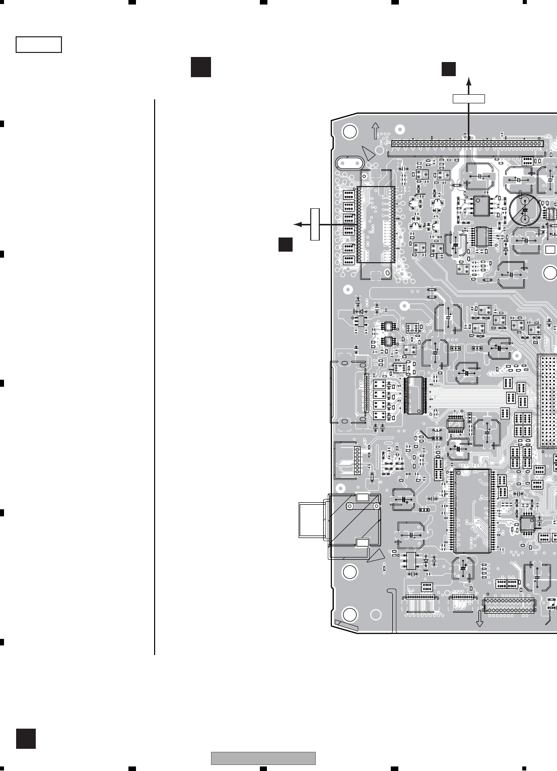
154 DVR-LX61
12 3 4
A
B
C
D
E
F
12 3 4
11.4 SERVICE MAIN ASSY
VNP2097-A
MAIN
C1501
L3301
L3302
L3303
L3304
CN201
IC1302
CN2301
L1022
L1024
Q2501
Q2502
Q2503
Q2504
Q2505
CN
Q5805
C5809
Q5809
Q5810
Q3301
L5101
Q3302
Q3303
Q3304
IC5801
IC5803
IC5804
JA5801 L5121
L5122
C1003
CN1401
CN1402
IC370
C1036
CN4501
C1236
CN4701
C4507
IC1221
D4521
IC4521
C4558
C4559
D101
C5121
C4569
C5122
C5708
C4586
D4562
C3207
IC4562
C3211
C3218
C3219
JA5701
D3201
D3202
IC3201
IC3202
L5801
L5802
L5803
L5804
L5805
CN1501
IC5151
UPPER BOTTOM
1
14
5
14
5
81
8
916
1
2
13
45
114
1
33
34
66
1
4
58
110
1
2
23
24
A
124
HADRS13
40
1
19
25
1
4
5
1
4
3
6
24
UPPER
7
1
50 26
25
1
3
C3201
48
1
15 10
1
5
1
1
1
1
1
1
15
10
1520
25
3035
40
1
1
E
E
E
E
E
E
1
1
EE
E
E
1 5 10 15 20
25303540
45 1
5
1
5
511015
1
1
1
1
1
1
15 10
15
1
A
1
1
1
15 15
10 20
1
11
1 5 10 15 20 25 30
35404550556065
1
1
11
1
1
1
11
1
1
1
1
1
1
1
1
1
1
1
115 10
51
1
5
1
1
1
1
1
1 5 10 15 20 25
15
10
15
IC Q
IC1302
Q2501
Q2502
Q2503
Q2504
Q2505
Q5805
Q5809
IC5202
IC5203
IC5204
Q5810
Q3301
Q3302
Q3303
Q3304
IC5602
IC5801
IC5803
IC5804
IC3701
IC3707
IC1001
Q1811
IC1221
IC4502
IC4511
IC4521
IC4552
IC4562
IC3201
IC3202
IC5151
SIDE A
D
CN101
A
CN2301
CN501
E
CN1501
SERVICE MAIN ASSY
D
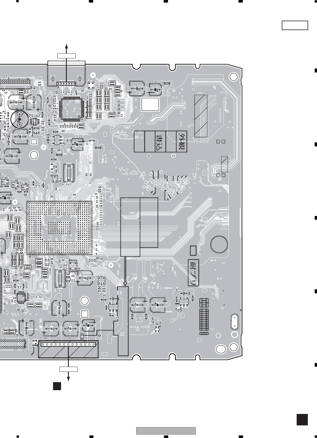
155
DVR-LX61
56 7 8
56 7 8
A
B
C
D
E
F
1/2
IC1302
L1003
L1005
Q2503
Q2504
Q2505
L1811
CN5604
C5210
L1831
X5502
C5613
D5209
C5809
IC5202
IC5203
IC5204
IC5602
L4551
C1003
C1007
IC3701
IC3707
IC1001
CN4501
Q1811
CN4701
C4507
C103
C4508C4509
C1050
C4515
IC1221
9
87654
32
10
A
B
C
3210
01
01
IC4502
A30C5
[[ G ]]
D4511
LF
IC4511
X5201
D101
C163
C4572
D4552
C4581
IC4552
C4586
C3211
C3219
D3202
L5601
1
IC3202
X1001
X1002
FC
ICT
HEAT PROOF PRE FLUX
PC
SIDE A (SECOND)
TYPE 49402.5NR
REPLACE IC
ATTENTION-
REMPLACER LE
1
1
2
34
14
5
8
5
81
834
66
1
4
58
23
24
113
A
124
AJ
5
4
3
1
13
4
5
MFD.BY LITTELFUSE INC.
MD7
MD12
AT0DATA5
AT0DATA9
AT0DATA6
AT0DATA10
AT0DATA11
AT0DATA4 AT0DATA3
AT0DATA12 AT0DATA2
AT0DATA13 AT0DATA1
AT0DATA0
AT0DATA14
AT0DATA15
HCSEL
AT0DMARQ
AT0DIOR
CAUTION-
AT0IORDY
AT0INTRQ
AT0CS0
AT0CS1
AT0MACK
AT0ADR1
XIOCS16
XPDIAG
XDASPZ
AT0DIOW
AT0ADR0
AT0ADR2
AT0RESET
AT0DATA7
AT0DATA8
A
LINK COMME INDIQUE.
LINKS AS MARKED.
1
16
17
32
33
48
49
7
13
54
MAIN
64
1
VWV2341
VWV VWV2342
VWV2343
VWV2362
C3201
1
5
11
1
1
1
1
1
111
1
15
10
1
E
E
E
E
1
5
1
1
1
1
5
1
15 1015
20 25 30
35 40 45
50 55 60
1
1
1
1
1
1 1 1
1
5
1
A
1
1
1
1 01
5
1
E
515
10 20
11
35404550556065
1
11
1
1
11
1
11
1
11
11
1
1
1
1
1
1
1
51 5
1
1
SIDE A
D
1TO HDD
CN5604
CN201
G
CN4501 (VNP2097-A)
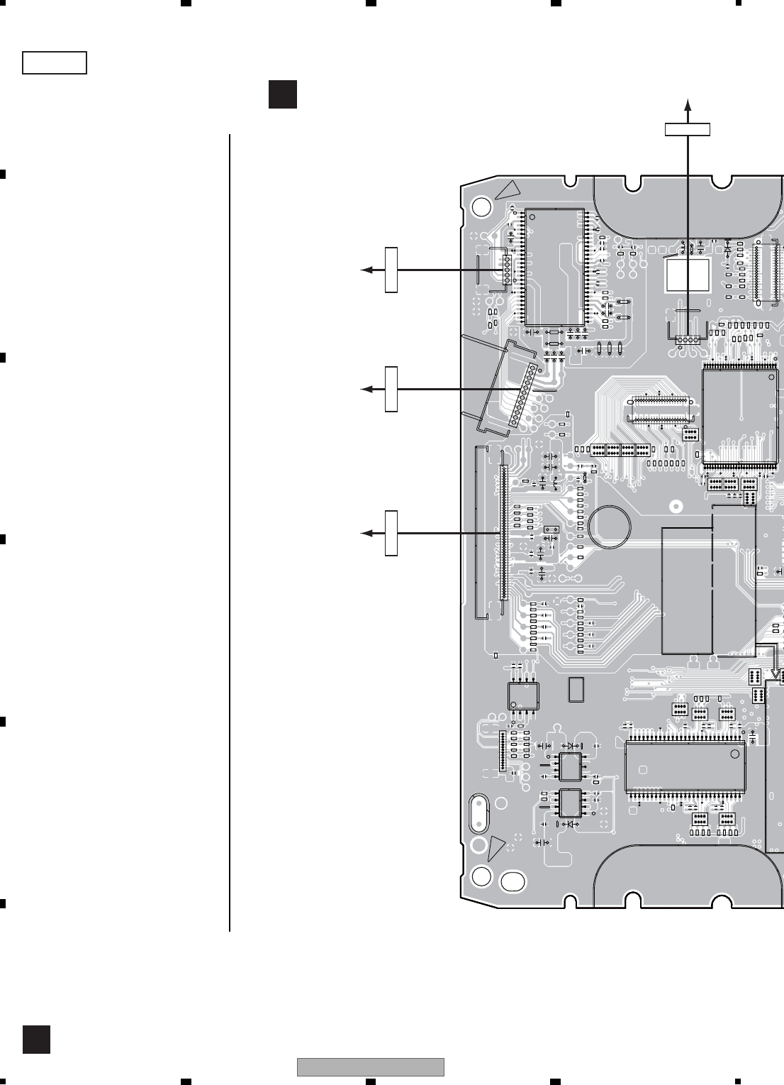
156 DVR-LX61
12 3 4
A
B
C
D
E
F
12 3 4
IC1102
CN601
F105
L105
IC200
IC201
L4572
CN101
CN103
CN501
CN502
LF
D4531
IC4531
D4541
IC4541
IC501
CN3801
D3802
BOTTOM
UPPER
UPPER
BOTTOM
SIDE B (FIRST)
MFD BY LITTELFUSE INC
TYPE 49402.5NR
LINKS AS MARKED.
ATTENTION-
REMPLACER LE
LINK COMME INDIQUE.
REPLACE IC
15
1
27
28
54
1
12
14
150
14
58
1
1
14
1
4
57
14
58
1
27
4582
1
28
29
56
UPPER
B
CAUTION-
1
20
21
40
20
21 40
1
11
1
1
1 5 10 15 20 25
30 35 40 45 50 55
1
1
5
1
5
1510 15 20 25
3035
40
45
50
15101520253035404550 15 10
1
1
1 1
1510
1
1 1 1
1
1
5
1
5
1 5 10 15 20 25
3035
40
4550
15 101520
2530
3540
15 101520
25
303540
1
1
1
IC1102 IC1301
Q5201
Q102
Q5801
Q5802
Q5804
Q5808
IC200
IC201
Q3305
Q3306
Q3307
Q3308
IC3101
IC3102
IC3702
Q1801
IC1201
IC4501
IC4701
IC4702
IC4703
IC4531
IC4541
Q5701
IC5103
Q4581
IC4561
IC501
IC5701
IC4571
IC3203
IC4591
IC Q
SIDE B
D
SERVICE MAIN ASSY
D
CN101
To PICKUP
CN601
To FRONT
CN502
To STEPPER
CN501
To SPDL
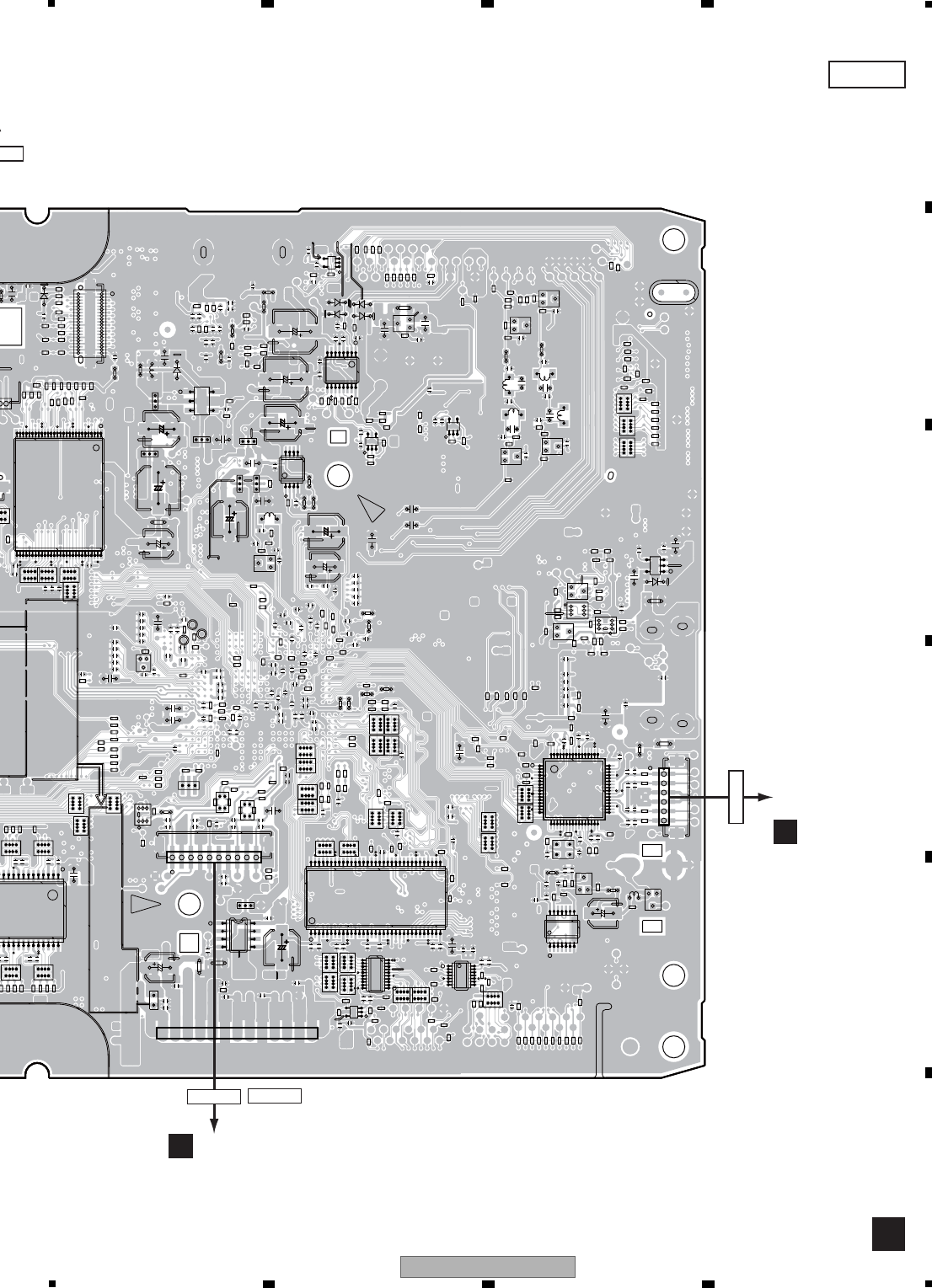
157
DVR-LX61
56 7 8
56 7 8
A
B
C
D
E
F
L3305
L3306
L3307
L3308
IC1102
IC1301
L1001
L1002
L1004
L1021
L1023
L1025
L1801
CN5201
X5101
Q5201
L1821
Q102
Q5801
Q5802
Q5804
Q5808
C3103
C3108
Q3305
Q3306
Q3307
Q3308
D3101 D3102
D3103 D3104
IC3101
IC3102
L5701
C1009 C1012
C1020
C1215
IC3702
C1024
Q1801
C1039
IC1201
X101
C4516
IC4501
IC4701
CN5101
IC4702
IC4703
C153
C5704
Q5701
IC5103
D4561
Q4581
D5701
IC4561
D4571
C5151
IC5701
IC4571
CN3802
IC3203
IC4591
C1304
D3802
MFD.BY LITTELFUSE INC.
TYPE 49402.5NR
LINKS AS MARKED.
ATTENTION-
REMPLACER LE
LINK COMME INDIQUE.
REPLACE IC
4
1
1
45
110
13
4
6
14
58
1
33
3466
110
11
20
17
814
1
43
13
4
6
13
4
5
1
28
29
56
1
8
916
1
5
10
13
EV+5.8V
GNDD
GNDD
GNDD
GND
GNDM
V+12M
V+5M
V+12V
SW+3.33V
SW+3.33V
SW+1.53V
SW+1.53V
RFO
FE
TE
17
8
14
17
32
33 48
49
1
6
16 1 64
1
3
46
1
20
21
40
5
4
1
3
5
0
1
1 5 10 15 20 25
30 35 40 45 50 55
1
1
5
1
1
1
1 1 1
1
1
1
5101
1
1
1
1
1
1
E
1
1510
45
50
EE
E
E
15
10
15
1
5
1
5
1
1
1
1
E
1
1
1 5 10 15 20 25 30
35
40
45
50
55
60
65
1
1
1
1
1 1
1
1
1
1
1
1
15 10
1520
51
1
5
15
10
11
11
1
11
1
11
E
1
1
1
15
10 15
20
25
30
354045
50
55
60
1
E
1
1
1
1
15
10
1
15 101520
25
303540
1
5
5
1
1
1
1
SIDE B
D
CN4501 (VNP2097-A)
CN901
F
CN5101
CN902
F
CN5201
502
PPER
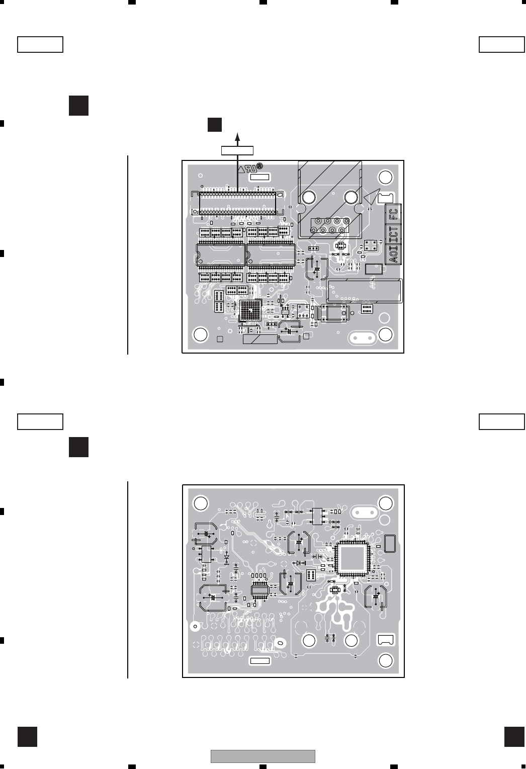
158 DVR-LX61
12 3 4
A
B
C
D
E
F
12 3 4
11.5 ETAB ASSY (DVR-LX61 ONLY)
1/4
IC182
LF
F301
IC201
IC202
F171
JA301
CN501
C301
X101
X301
C171
HEAT PROOF PRE FLUX SIDE A (SECOND)
AK
1
10
1
50 26
25
7
8
VWV2344
VWV
A30C5/C7
[[ G ]]
1
2
VNP2100-A
IC101
IC181
F321
PC
1
11 1 1
1 1 1 1
1
5
1
1 5 10 15 20
2530354045
1 5 10 15 20
253035
40
45
1
1 1
11
1
15
1510 15 20 25
30
35
40
45
50
1
1
1 1 1 1
1 1 1
1
A1
1
C401
C411
C220
C419
IC203
IC401
IC411
LF
C324
IC301
SIDE B (FIRST)
D401
D411
F331
15
10 15
1
1
1
15
15 20
30 35 40
45 50 55
25
10
1
IC Q
IC Q
IC182
IC201 IC202
IC101
IC181
IC401
IC411
IC301
SIDE A
E E
SIDE A
SIDE B SIDE B
CN1501
D
CN501
(VNP2100-A)
(VNP2100-A)
ETAB ASSY
E
ETAB ASSY
E
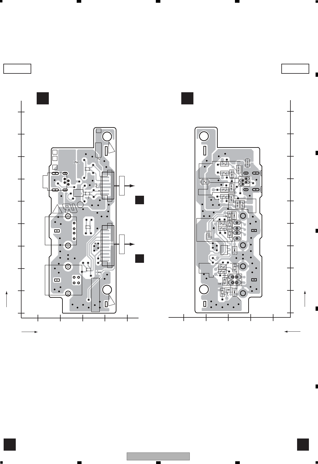
159
DVR-LX61
56 7 8
56 7 8
A
B
C
D
E
F
11.6 SERVICE DVUB ASSY
200 210 220 230 240
X
0
10
20
30
40
50
60
70
80
90
Y
200210220230240
0
10
20
30
40
50
60
70
80
90
X
Y
R
16
A30C5/C7
[[ G ]]
LF
110
CN901 R908
L906
JA902
L903
JA903
L901
L902
C906
CN902
R911 R912
JA901
YWM1001-
YWM1002-
PC
YWM1011-
YWM
DVUB
LF
L908
R901
C905
C907
R907
L905
L907
R906
R913
R909
L904
C903
R910
C904 C901
R902
C902
VA903
R905
R903
R904
C908
VA904
VA905
VA906 VA901
VA902
SERVICE DVUB ASSY
F
SERVICE DVUB ASSY
F
SIDE A
F
SIDE B
F
CN5101
D
CN901
CN5201
D
CN902
(YNP1005-B) (YNP1005-B)
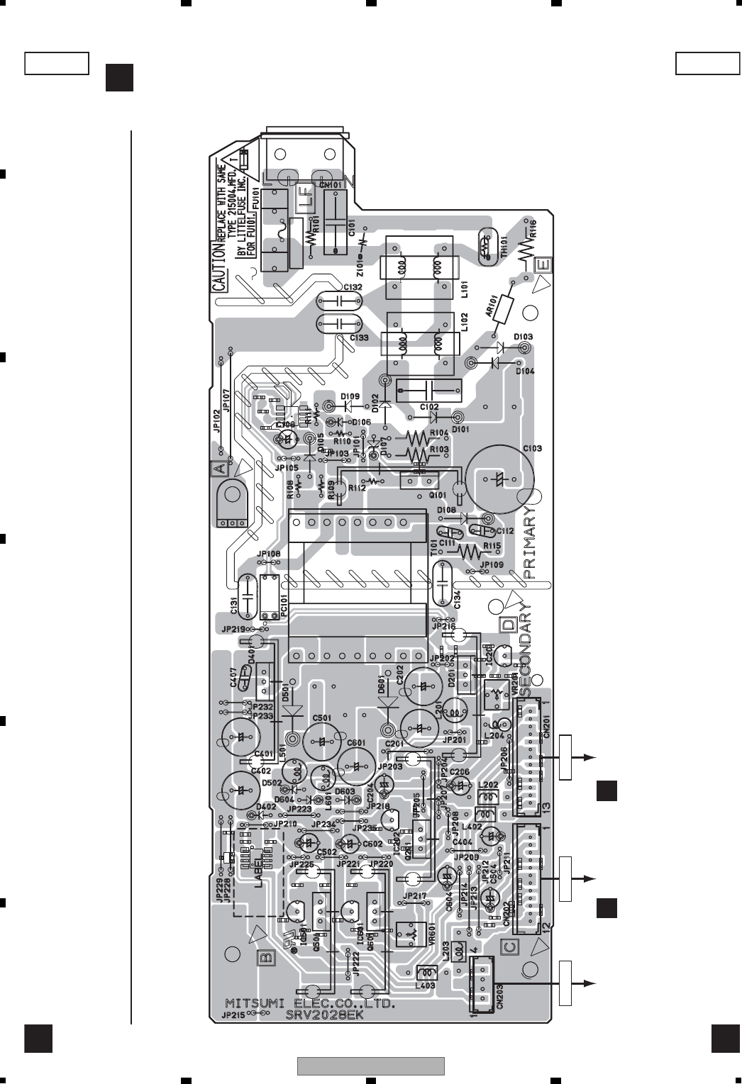
160 DVR-LX61
12 3 4
A
B
C
D
E
F
12 3 4
11.7 POWER SUPPLY ASSY
G G
SIDE A SIDE A
POWER SUPPLY ASSY
G
LIVENEUTRAL
IC
IC201
Q
Q101
IC202
IC501 IC601
Q201
Q501 Q601
CN4501
D
CN201
CN301
A
CN202
TO HDD
CN203
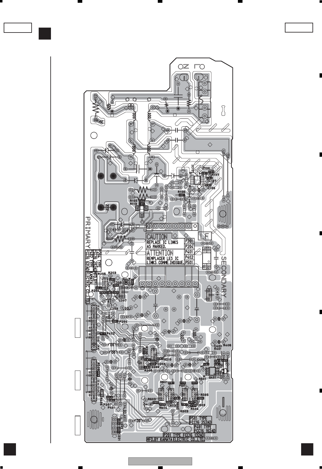
161
DVR-LX61
56 7 8
56 7 8
A
B
C
D
E
F
POWER SUPPLY ASSY
G
G G
SIDE B SIDE B
CN201CN202CN203
IC
IC101
Q
Q401
Q402

162 DVR-LX61
12 3 4
A
B
C
D
E
F
12 3 4
12. PCB PARTS LIST
Parts marked by "NSP" are generally unavailable because they are not in our Master Spare Parts List.
The mark found on some component parts indicates the importance of the safety factor of the part.
Therefore, when replacing, be sure to use parts of identical designation.
When ordering resistors, first convert resistance values into code form as shown in the following examples.
Ex.1 When there are 2 effective digits (any digit apart from 0), such as 560 ohm and 47k ohm (tolerance is shown by J=5%,
and K=10%).
Ex.2 When there are 3 effective digits (such as in high precision metal film resistors).
561
473
R50
1R0
5621
NOTES:
560
Ω
47k
Ω
0.5
Ω
1
Ω
RD1/4PU J
RD1/4PU J
RN2H K
RS1P K
56 x 10
1
47 x 10 3
R50
1R0
561
473
5.62k ΩRN1/4PC F562 x 10 15621
Meaning of the figures and others in the parentheses in the parts list.
Example) IC 301 is on the point (face A, 91 of x-axis, and 111 of y-axis) of the corresponding
PC board.
IC 301 (A, 91, 111) IC NJM2068V
Mark No. Description Part No.
LIST OF ASSEMBLIES
1..ETAB ASSY (DVR-LX61 ONLY) VWV2344
NSP 1..TUJB ASSY YWM1002
2..SERVICE DVUB ASSY YXX1001
2..SERVICE TUSB ASSY YXX1003
NSP 1..FLKB ASSY (DVR-LX61) YWM1006
NSP 1..FLKB ASSY (DVR-560H) YWM1005
2..SERVICE FRJB ASSY YXX1027
(DVR-LX61)
2..SERVICE FRJB ASSY YXX1004
(DVR-560H)
2..SERVICE FLKY ASSY YXX1008
(DVR-LX61)
2..SERVICE FLKY ASSY YXX1007
(DVR-560H)
NSP 1..SERVICE LOADER MAIN VXU1014
(DVR-LX61)
NSP 1..SERVICE LOADER MAIN VXU1013
(DVR-560H)
2..SERVICE MAIN ASSY VXX3309
(DVR-LX61)
2..SERVICE MAIN ASSY VXX3308
(DVR-560H)
2..SERVICE LOADER ASSY VXX3306
>1..POWER SUPPLY ASSY VWR1406
Mark No. Description Part No.
ASERVICE TUSB ASSY
MISCELLANEOUS
IC 101 (A,201,131) MICROCOMPUTER IC PMC026A8
IC 102 (A,225,166) RESET IC BD4846G
IC 103 (A,177,132) RESET IC BU4220G
IC 104 (A,175,152) IC TC7MB3257FK
>IC 150 (B,229,147) FUSE CEK1278
>IC 317 (B,170,52) FUSE CEK1278
IC 401 (A,124,124) IC FOR DVD REC HA118326APFR
IC 402 (A,149,100) OP-AMP IC BA4560RF
IC 403 (A,123,93) VIDEO SW IC MM1503XN
IC 406 (B,67,46) IC TC7S66FU
IC 601 (A,118,174) MULTI SOUND DECODER MSP3417G
Q 101 (A,218,157) DIGITAL TRANSISTOR DTC124EUA
Q 102 (A,184,154) TRANSISTOR 2SC4081
Q 103 (A,176,121) TRANSISTOR UMD2N
Q 104 (A,192,110) TRANSISTOR UMD2N
Q 105 (A,189,109) TRANSISTOR 2SD2114K
Q 108 (A,210,106) DIGITAL TRANSISTOR DTC124EUA
Q 110 (A,194,103) DIGITAL TRANSISTOR DTA143EUA
Q 111 (A,191,95) TRANSISTOR 2SC4081
Q 112 (A,196,100) TRANSISTOR 2SC4081
Q 201 (B,142,49) TRANSISTOR 2SD2114K
Q 301 (A,155,170) TRANSISTOR UMD2N
Q 302 (B,158,171) TRANSISTOR 2SC4081
Q 303 (A,153,183) TRANSISTOR UMD2N
Q 304 (A,159,180) TRANSISTOR 2SD2153
Q 305 (B,186,59) TRANSISTOR UMD2N
Q 306 (B,193,63) TRANSISTOR 2SC2411K
Q 307 (B,177,57) TRANSISTOR UMD2N
Q 308 (B,179,71) TRANSISTOR 2SC2411K
Q 309 (B,162,53) TRANSISTOR 2SC5876
Q 310 (B,162,61) TRANSISTOR 2SC4081
Q 311 (B,169,67) CHIP TRANSISTOR HN1A01FU
Q 401 (A,143,148) DIGITAL TRANSISTOR DTC124EUA
Q 402 (A,109,101) TRANSISTOR 2SD2114K
Q 403 (A,120,99) TRANSISTOR 2SA1576A
Q 404 (A,44,147) TRANSISTOR UMD2N
Q 406 (A,42,137) TRANSISTOR 2SD2114K
Q 407 (A,42,154) TRANSISTOR 2SD2114K
Q 408 (A,110,94) TRANSISTOR 2SC4081
Q 409 (A,116,87) TRANSISTOR 2SC4081
Q 410 (A,115,92) TRANSISTOR 2SC4081
Q 411 (A,110,90) TRANSISTOR UMD2N
Q 412 (A,122,84) DIGITAL TRANSISTOR DTC124EUA
Q 413 (A,117,97) DIGITAL TRANSISTOR DTC124EUA
Q 501 (B,84,85) TRANSISTOR UMH1N
Q 502 (B,75,75) TRANSISTOR 2SA1576A
Q 503 (B,87,62) TRANSISTOR 2SC4081
Q 504 (B,84,62) TRANSISTOR 2SC4081
Q 505 (B,81,56) TRANSISTOR 2SC4081
Q 506 (A,57,81) DUAL CHIP TRANSISTOR HN1C03FU
Mark No. Description Part No.

163
DVR-LX61
56 7 8
56 7 8
A
B
C
D
E
F
Q 507 (A,58,94) DUAL CHIP TRANSISTOR HN1C03FU
Q 508 (B,91,119) CHIP DIGITAL TRANS. DTA124EUA
Q 509 (B,65,55) TRANSISTOR 2SC4081
Q 510 (B,67,60) TRANSISTOR 2SC4081
Q 511 (B,67,67) TRANSISTOR 2SA1576A
Q 601 (B,67,172) TRANSISTOR 2SA1576A
Q 602 (B,59,165) TRANSISTOR 2SA1576A
Q 604 (A,139,174) TRANSISTOR 2SA1576A
Q 605 (A,139,169) TRANSISTOR 2SA1576A
Q 606 (B,84,181) TRANSISTOR 2SC4081
Q 751 (B,43,37) TRANSISTOR 2SA1576A
Q 752 (B,51,41) TRANSISTOR 2SC4081
D 101 (A,221,164) DIODE 1SS355
D 102 (A,218,163) DIODE 1SS355
D 103 (A,186,59) DIODE 1SS355
D 104 (B,167,176) DIODE 1SR154-400
D 106 (A,176,109) DIODE 1SS355
D 108 (A,179,125) DIODE DAP202U
D 201 (B,144,53) DIODE 1SS355
D 301 (B,173,50) DIODE UDZS15(B)
D 302 (B,175,62) DIODE UDZS9R1(B)
D 303 (B,164,55) DIODE 1SS355
D 304 (B,179,62) DIODE 1SS355
D 401 (A,135,81) DIODE UDZS11(B)
D 402 (A,101,150) DIODE UDZS6R8(B)
D 418 (B,48,165) DIODE 1SS355
D 419 (A,44,150) DIODE 1SS355
D 420 (B,116,91) DIODE DAP202U
D 501 (B,79,85) DIODE UDZS5R1(B)
D 502 (B,81,85) DIODE UDZS5R1(B)
D 503 (B,45,65) DIODE UMZ6R8N
D 504 (B,46,61) DIODE UMZ6R8N
D 505 (B,45,56) DIODE UMZ6R8N
D 506 (B,42,46) DIODE UMZ6R8N
D 507 (B,45,51) DIODE UMZ6R8N
D 508 (B,42,92) DIODE UMZ6R8N
D 509 (B,46,87) DIODE UMZ6R8N
D 510 (B,45,82) DIODE UMZ6R8N
D 511 (B,45,76) DIODE UMZ6R8N
D 512 (B,45,71) DIODE UMZ6R8N
D 513 (A,46,65) DIODE UMZ6R8N
D 514 (A,44,59) DIODE UMZ6R8N
D 515 (A,44,49) DIODE UMZ6R8N
D 516 (A,44,55) DIODE UMZ6R8N
D 517 (A,44,52) DIODE UMZ6R8N
D 518 (A,44,72) DIODE UMZ6R8N
D 519 (A,45,78) DIODE UMZ6R8N
D 520 (A,46,83) DIODE UMZ6R8N
D 521 (A,44,90) DIODE UMZ6R8N
D 522 (A,41,101) DIODE UMZ6R8N
D 523 (B,72,45) DIODE DAN217U
D 524 (B,63,44) DIODE DAN217U
D 526 (B,71,70) DIODE 1SS355
D 527 (B,80,48) DIODE 1SS355
D 528 (B,87,119) DIODE 1SS355
D 701 (B,55,34) DIODE 1SS355
L 102 (A,200,88) AXIAL INDUCTOR LAU470J
L 201 (A,147,57) RADIAL INDUCTOR ATH1109
L 303 (B,161,175) INDUCTOR CTF1399
Mark No. Description Part No.
L 304 (A,167,57) RADIAL INDUCTOR LFCA331J
L 305 (B,158,44) INDUCTOR CTF1399
L 401 (B,42,135) INDUCTOR CTF1388
L 402 (B,42,150) INDUCTOR CTF1388
L 403 (B,37,168) INDUCTOR CTF1388
L 404 (B,34,142) INDUCTOR CTF1388
L 405 (B,34,156) INDUCTOR CTF1388
L 501 (B,28,94) CHIP COIL LCYA5R6J2520
L 502 (B,34,92) CHIP COIL LCYA5R6J2520
L 503 (A,48,52) INDUCTOR CTF1389
L 504 (A,48,49) INDUCTOR CTF1389
L 505 (A,47,55) INDUCTOR CTF1389
L 506 (A,47,59) INDUCTOR CTF1389
L 507 (B,47,47) INDUCTOR CTF1389
L 508 (B,48,60) INDUCTOR CTF1389
L 509 (B,48,52) INDUCTOR CTF1389
L 510 (A,50,60) INDUCTOR CTF1389
L 601 (B,31,173) INDUCTOR CTF1399
L 602 (B,86,175) INDUCTOR CTF1399
L 604 (B,42,173) INDUCTOR CTF1306
L 605 (B,46,173) INDUCTOR CTF1306
L 606 (B,123,168) INDUCTOR CTF1399
L 607 (B,89,175) COIL LCYA101J2520
L 608 (B,146,178) INDUCTOR CTF1399
L 609 (B,91,180) INDUCTOR LCYA100J2520
L 751 (B,33,37) INDUCTOR CTF1306
JA 402 (A,17,146) 9P PIN JACK VKB1250
JA 501 (A,18,70) RGB CONNECTOR VKB1249
JA 701 (A,18,25) JACK RKN1004
JA 751 (A,18,36) JACK RKN1004
KN 101 (A,131,184) WRAPPING TERMINAL VNF1084
KN 102 (A,192,46) WRAPPING TERMINAL VNF1084
X 101 (A,204,157) CRYSTAL OSCILLATOR CSS1653
(15 MHZ)
X 102 (A,210,156) CRYSTAL RESONATOR VSS1197
(32 KHz)
X 601 (A,100,173) CERAMIC RESONATOR VSS1189
(18.432 MHZ)
CN 101 (A,35,23) 40P CONNECTOR VKN2007
CN 103 (A,235,159) 9P CONNECTOR VKN2015
CN 105 (A,232,148) CONNECTOR HLEM17S-1
CN 106 (A,238,107) CONNECTOR HLEM11S-1
CN 201 (A,149,43) CONNECTOR S2B-PH-K-S
CN 301 (A,178,35) CONNECTOR S5B-PH-K-S
401 2P 4PIN MINIDIN(S) AKP1234
U 601 (A,26,178) TV TUNER PACK VXF1146
RESISTORS
R 101 (A,187,125) RS1/16S101J
R 102 (B,184,121) RS1/16S101J
R 103 (A,187,118) RS1/16S101J
R 104 (A,224,158) RS1/16S473J
R 105 (A,215,149) RS1/16S101J
R 106 (A,221,158) RS1/16S0R0J
R 107 (A,224,159) RS1/16S103J
R 109 (A,212,144) RS1/16S331J
R 110 (A,211,144) RS1/16S101J
R 111 (A,212,149) RS1/16S101J
Mark No. Description Part No.

164 DVR-LX61
12 3 4
A
B
C
D
E
F
12 3 4
R 112 (A,222,161) RS1/16S103J
R 113 (A,219,161) RS1/16S0R0J
R 116 (B,208,153) RS1/16S0R0J
R 117 (A,204,145) RS1/16S105J
R 118 (B,201,150) RS1/16S0R0J
R 120 (A,197,163) CARBON FILM RESISTOR RD1/4PU153J
R 123 (A,197,148) RS1/16S101J
R 124 (A,195,148) RS1/16S101J
R 125 (A,196,83) RS1/16S101J
R 126 (A,192,148) RS1/16S101J
R 127 (A,192,151) RS1/16S103J
R 128 (B,213,134) RS1/16S392J
R 129 (A,194,148) RS1/16S101J
R 130 (B,235,155) RS1/16S0R0J
R 131 (A,189,154) RS1/16S472J
R 132 (A,190,149) RS1/16S682J
R 134 (A,187,148) RS1/16S102J
R 135 (A,185,152) RS1/16S104J
R 136 (A,189,158) RS1/16S102J
R 137 (A,186,155) RS1/16S101J
R 138 (A,183,160) RS1/16S471J
R 139 (A,184,149) RS1/16S682J
R 140 (A,182,148) RS1/16S470J
R 141 (A,182,151) RS1/16S682J
R 142 (A,181,151) RS1/16S470J
R 143 (A,183,145) RS1/16S101J
R 144 (A,184,140) RS1/16S0R0J
R 145 (A,180,131) RS1/16S103J
R 146 (A,187,126) RS1/16S101J
R 147 (A,191,112) RS1/16S102J
R 148 (A,184,126) RS1/16S101J
R 149 (A,188,119) RS1/16S0R0J
R 150 (A,190,117) RS1/16S0R0J
R 151 (A,194,117) RS1/16S0R0J
R 152 (A,184,127) RS1/16S0R0J
R 153 (A,198,113) RS1/16S101J
R 154 (B,199,113) RS1/16S101J
R 155 (A,198,83) RS1/16S101J
R 156 (A,201,116) RS1/16S101J
R 157 (A,202,118) RS1/16S104J
R 158 (A,202,119) RS1/16S104J
R 159 (A,205,117) RS1/16S0R0J
R 160 (A,206,114) RS1/16S101J
R 161 (A,201,108) RS1/16S0R0J
R 165 (A,206,117) RS1/16S0R0J
R 167 (A,207,114) RS1/16S101J
R 168 (A,211,112) RS1/16S181J
R 169 (A,207,101) RS1/16S103J
R 171 (A,215,114) RS1/16S101J
R 172 (A,216,114) RS1/16S101J
R 173 (A,218,113) RS1/16S104J
R 174 (A,217,111) RS1/16S104J
R 175 (A,219,113) RS1/16S331J
R 176 (A,220,124) RS1/16S102J
R 177 (A,222,126) RS1/16S101J
R 178 (A,219,127) RS1/16S101J
R 179 (A,222,128) RS1/16S101J
R 180 (A,221,132) RS1/16S101J
R 181 (A,217,133) RS1/16S101J
Mark No. Description Part No.
R 182 (A,220,134) RS1/16S101J
R 183 (A,217,134) RS1/16S101J
R 184 (A,220,135) RS1/16S101J
R 185 (A,220,137) RS1/16S101J
R 188 (A,221,140) RS1/16S331J
R 189 (A,221,142) RS1/16S471J
R 193 (B,230,171) RS1/16S104J
R 194 (B,236,171) RS1/16S104J
R 195 (B,228,171) RS1/16S104J
R 196 (B,238,171) RS1/16S101J
R 197 (A,52,22) RS1/16S0R0J
R 199 (A,209,110) RS1/16S101J
R 200 (A,221,144) RS1/16S101J
R 201 (A,187,128) RS1/16S0R0J
R 202 (A,184,138) RS1/16S0R0J
R 203 (A,181,139) RS1/16S0R0J
R 204 (A,181,137) RS1/16S101J
R 205 (A,185,136) RS1/16S101J
R 207 (A,197,104) RS1/16S471J
R 208 (A,197,106) RS1/16S0R0J
R 209 (A,191,101) RS1/16S332J
R 210 (A,197,108) RS1/16S8200F
R 214 (A,189,91) RS1/16S332J
R 215 (A,192,91) RS1/16S681J
R 216 (A,194,94) CHIP RESISTOR RS1/16S7500F
R 217 (A,196,93) RS1/16S102J
R 218 (A,155,48) RS1/10S0R0J
R 219 (B,141,62) RS1/16S332J
R 220 (B,137,62) RS1/16S222J
R 221 (A,178,145) RS1/16S101J
R 222 (A,181,141) RS1/16S0R0J
R 223 (A,174,157) RS1/16S0R0J
R 224 (A,177,156) RS1/16S0R0J
R 228 (A,196,160) RS1/16S0R0J
R 233 (B,218,89) RS1/16S104J
R 251 (B,148,46) RS1/10S0R0J
R 301 (A,143,80) RS1/10S0R0J
R 302 (B,187,50) RS1/10S0R0J
R 303 (B,185,50) RS1/10S0R0J
R 304 (B,159,176) RS1/16S101J
R 305 (B,158,180) RS1/16S330J
R 306 (B,188,56) RS1/16S330J
R 307 (A,158,83) RS1/10S0R0J
R 308 (A,161,83) RS1/10S0R0J
R 309 (B,179,52) RS1/16S152J
R 310 (B,160,57) RS1/16S472J
R 311 (B,164,66) RS1/16S821J
R 312 (B,162,65) RS1/16S103J
R 313 (B,170,60) RS1/16S184J
R 314 (A,174,77) RS1/16S223J
R 315 (B,168,60) RS1/16S1003F
R 316 (B,173,60) RS1/16S2202F
R 318 (B,160,180) RS1/16S0R0J
R 401 (B,137,96) RS1/10S0R0J
R 402 (A,138,102) RS1/16S561J
R 403 (A,136,103) RS1/16S561J
R 404 (A,133,89) RS1/10S0R0J
R 407 (A,97,126) RS1/10S0R0J
R 408 (A,148,115) RS1/16S471J
R 410 (A,150,110) RS1/16S471J
Mark No. Description Part No.

165
DVR-LX61
56 7 8
56 7 8
A
B
C
D
E
F
R 412 (A,148,112) RS1/16S471J
R 413 (A,148,119) RS1/16S471J
R 414 (A,145,124) RS1/16S471J
R 415 (A,145,126) RS1/16S471J
R 416 (A,146,127) RS1/16S471J
R 417 (A,146,129) RS1/16S471J
R 418 (A,146,131) RS1/16S471J
R 419 (A,146,133) RS1/16S471J
R 420 (B,116,133) CHIP RESISTOR RS1/16S335J
R 421 (A,124,136) CHIP RESISTOR RS1/16S335J
R 422 (A,140,113) RS1/16S103J
R 425 (B,126,139) RS1/16S104J
R 428 (A,129,139) RS1/16S0R0J
R 429 (A,139,142) RS1/16S105J
R 430 (A,133,140) RS1/16S105J
R 431 (A,124,141) RS1/16S105J
R 432 (A,122,144) RS1/16S105J
R 433 (A,106,110) RS1/16S105J
R 435 (A,105,115) RS1/16S105J
R 436 (A,94,132) RS1/16S101J
R 437 (A,96,132) RS1/16S101J
R 438 (A,96,143) RS1/10S0R0J
R 439 (B,113,132) RS1/16S185J
R 440 (A,116,85) RS1/16S471J
R 443 (B,136,133) RS1/10S75R0F
R 444 (A,130,147) RS1/10S75R0F
R 445 (A,133,146) RS1/10S75R0F
R 446 (B,159,115) RS1/10S75R0F
R 447 (A,122,149) RS1/10S75R0F
R 448 (A,100,142) RS1/10S0R0J
R 449 (A,108,147) RS1/10S75R0F
R 453 (A,155,102) RS1/16S8201F
R 454 (A,136,109) RS1/16S1002F
R 455 (A,121,103) RS1/16S470J
R 458 (A,121,109) RS1/16S471J
R 459 (A,124,100) RS1/10S75R0F
R 461 (A,115,95) RS1/16S681J
R 462 (A,138,107) RS1/16S1002F
R 463 (A,143,102) RS1/16S8201F
R 465 (A,116,100) RS1/16S471J
R 467 (B,44,124) RS1/10S75R0F
R 468 (B,43,113) CHIP TYPE RESISTOR RS1/10S68R0F
R 469 (B,40,113) RS1/10S3R9J
R 470 (B,38,117) CHIP TYPE RESISTOR RS1/10S68R0F
R 471 (B,37,119) RS1/10S3R9J
R 472 (B,36,160) CHIP TYPE RESISTOR RS1/10S68R0F
R 473 (B,33,160) RS1/10S3R9J
R 474 (B,42,147) CHIP TYPE RESISTOR RS1/10S68R0F
R 475 (B,34,146) RS1/10S3R9J
R 476 (B,42,132) CHIP TYPE RESISTOR RS1/10S68R0F
R 477 (B,35,132) RS1/10S3R9J
R 478 (B,42,129) CHIP TYPE RESISTOR RS1/10S68R0F
R 479 (B,43,139) RS1/16S471J
R 480 (B,35,129) RS1/10S3R9J
R 481 (B,44,153) RS1/16S104J
R 484 (A,40,141) RS1/16S102J
R 485 (B,50,138) RS1/16S223J
R 486 (A,41,149) RS1/16S102J
R 487 (B,49,151) RS1/16S223J
R 488 (B,42,156) RS1/16S471J
Mark No. Description Part No.
R 489 (B,42,161) RS1/16S104J
R 498 (A,120,84) RS1/16S223J
R 499 (A,118,82) RS1/16S223J
R 501 (B,61,57) RS1/10S75R0F
R 502 (B,48,71) RS1/10S75R0F
R 503 (B,48,76) RS1/10S75R0F
R 504 (B,51,92) CHIP TYPE RESISTOR RS1/10S68R0F
R 505 (B,49,90) RS1/10S3R9J
R 506 (B,75,46) RS1/16S0R0J
R 507 (B,89,57) RS1/16S472J
R 508 (B,86,55) RS1/16S473J
R 509 (B,88,49) RS1/16S273J
R 510 (B,87,52) RS1/16S225J
R 511 (B,84,49) RS1/16S224J
R 512 (B,84,51) RS1/16S104J
R 513 (B,81,61) RS1/16S104J
R 514 (B,48,82) RS1/10S75R0F
R 515 (B,80,78) RS1/10S561J
R 516 (B,79,75) RS1/16S122J
R 517 (B,83,79) RS1/16S152J
R 518 (B,79,80) RS1/16S100J
R 519 (B,73,70) RS1/16S563J
R 520 (B,81,52) RS1/16S221J
R 521 (A,48,68) CHIP TYPE RESISTOR RS1/10S68R0F
R 522 (A,44,61) RS1/10S3R9J
R 523 (A,45,69) CHIP TYPE RESISTOR RS1/10S68R0F
R 524 (A,43,69) RS1/10S3R9J
R 525 (A,48,79) CHIP TYPE RESISTOR RS1/10S68R0F
R 526 (A,44,75) RS1/10S3R9J
R 527 (A,47,87) RS1/10S0R0J
R 528 (A,45,87) RS1/10S75R0F
R 529 (A,43,81) RS1/16S104J
R 530 (A,44,95) CHIP TYPE RESISTOR RS1/10S68R0F
R 531 (A,44,93) RS1/10S3R9J
R 532 (A,36,101) RS1/10S75R0F
R 534 (A,58,76) RS1/16S392J
R 535 (A,58,85) RS1/16S392J
R 536 (B,54,80) RS1/16S471J
R 538 (B,56,83) RS1/16S471J
R 540 (B,52,80) RS1/16S104J
R 541 (B,53,83) RS1/16S104J
R 546 (A,51,63) RS1/16S104J
R 547 (A,51,69) RS1/16S104J
R 548 (B,49,47) RS1/16S104J
R 549 (A,58,64) RS1/16S104J
R 550 (B,55,89) RS1/16S471J
R 552 (B,70,109) RS1/16S471J
R 554 (B,58,92) RS1/16S104J
R 555 (B,74,110) RS1/16S104J
R 556 (A,56,97) RS1/16S392J
R 557 (A,55,90) RS1/16S392J
R 558 (B,67,55) RS1/16S103J
R 560 (B,70,55) RS1/16S153J
R 561 (B,69,53) RS1/16S681J
R 562 (B,70,59) RS1/16S103J
R 564 (B,70,61) RS1/16S153J
R 565 (B,67,63) RS1/16S681J
R 566 (B,74,65) RS1/16S223J
R 568 (B,70,64) RS1/16S123J
R 569 (B,76,65) RS1/16S102J
Mark No. Description Part No.

166 DVR-LX61
12 3 4
A
B
C
D
E
F
12 3 4
R 571 (B,45,92) RS1/10S75R0F
R 573 (B,52,63) RS1/16S0R0J
R 574 (B,83,90) RS1/16S0R0J
R 602 (B,62,172) RS1/16S102J
R 603 (B,51,169) RS1/16S0R0J
R 605 (B,83,170) RS1/16S103J
R 606 (B,77,172) RS1/16S103J
R 607 (B,55,166) RS1/16S102J
R 608 (B,31,175) RS1/16S0R0J
R 609 (B,27,183) RS1/16S0R0J
R 616 (B,103,175) RS1/16S0R0J
R 619 (A,106,170) RS1/16S103J
R 620 (A,126,163) RS1/16S0R0J
R 621 (A,109,162) RS1/16S101J
R 622 (A,109,160) RS1/16S101J
R 623 (B,133,173) RS1/16S102J
R 624 (A,132,174) RS1/16S332J
R 625 (A,137,181) RS1/16S332J
R 626 (B,144,176) RS1/16S102J
R 627 (A,130,173) RS1/16S332J
R 628 (A,133,171) RS1/16S332J
R 630 (B,88,181) RS1/16S331J
R 631 (B,81,181) RS1/16S472J
R 632 (B,77,183) RS1/16S220J
R 633 (B,79,181) RS1/16S101J
R 634 (B,77,179) RS1/16S222J
R 635 (B,25,174) RS1/16S0R0J
R 636 (B,54,174) RS1/16S0R0J
R 637 (B,58,174) RS1/16S0R0J
R 638 (B,66,175) RS1/16S0R0J
R 701 (B,60,34) RS1/16S224J
R 702 (B,30,29) RS1/16S221J
R 704 (B,30,32) RS1/16S221J
R 751 (B,46,37) RS1/16S102J
R 752 (B,48,41) RS1/16S472J
R 753 (B,58,43) RS1/16S472J
R 754 (B,36,37) RS1/16S151J
R 755 (B,60,43) RS1/16S472J
R 756 (B,40,37) RS1/16S102J
CAPACITORS
C 104 (A,216,147) CEAT220M25
C 105 (A,223,156) CKSRYF104Z25
C 106 (A,226,169) CKSRYF104Z25
C 107 (A,209,144) CCSRCH331J50
C 109 (A,218,155) CKSRYF104Z25
C 110 (A,219,164) CKSRYB105K10
C 111 (B,214,159) CCSRCH120J50
C 112 (B,210,159) CCSRCH120J50
C 113 (A,200,149) CKSRYF105Z10
C 114 (B,201,158) CCSRCH120J50
C 115 (B,200,153) CCSRCH120J50
C 119 (A,189,183) ELECT. CAPACITOR CEAT102M6R3
C 120 (B,165,179) CKSRYF104Z25
C 121 (B,237,153) CKSRYF105Z10
C 122 (B,173,181) CKSRYF105Z10
C 123 (A,171,178) ELECT. CAPACITOR CEAT471M6R3
C 124 (A,189,152) CKSRYF104Z25
C 125 (A,182,154) CKSRYF104Z25
C 126 (A,185,134) CKSRYF104Z25
C 127 (A,178,114) CEAT101M16
Mark No. Description Part No.
C 131 (A,192,119) CKSRYF104Z25
C 132 (A,193,116) CKSRYF104Z25
C 133 (A,197,109) CKSRYF104Z25
C 134 (A,203,106) CKSRYF104Z25
C 135 (A,208,104) CKSRYF104Z25
C 136 (A,214,121) CKSRYF105Z10
C 138 (A,222,119) CEAT2R2M50
C 139 (A,216,126) CKSRYF104Z25
C 140 (A,218,130) CKSRYF104Z25
C 141 (A,172,157) CKSRYF105Z10
C 142 (A,172,159) CCSRCH102J50
C 147 (B,231,159) CKSRYF104Z25
C 149 (A,197,103) CCSRCH100D50
C 150 (A,191,91) CKSRYF105Z10
C 152 (A,196,97) CKSRYF105Z10
C 154 (B,229,143) CKSRYF104Z25
C 155 (B,239,153) CCSRCH102J50
C 156 (A,175,135) CKSRYF104Z25
C 157 (A,175,129) CKSRYB104K16
C 166 (A,200,145) CCSRCH102J50
C 167 (A,187,132) CCSRCH102J50
C 168 (A,213,121) CCSRCH102J50
C 169 (A,216,130) CCSRCH102J50
C 202 (B,152,60) CKSRYF104Z25
C 204 (A,150,64) CEAT101M16
C 205 (A,146,49) CEAT220M25
C 206 (B,141,60) CCSRCH471J50
C 207 (A,190,88) CKSRYF104Z25
C 208 (B,152,46) CKSRYB104K16
C 301 (B,166,43) CKSRYF104Z25
C 302 (B,182,39) CKSRYF104Z25
C 303 (A,175,47) CEAT101M16
C 304 (A,183,48) CEAT471M16
C 305 (B,155,173) CKSRYF104Z25
C 306 (B,162,169) CKSRYF104Z25
C 307 (A,155,165) CEAT101M16
C 308 (A,150,174) CEAT101M16
C 309 (B,164,182) CKSRYF104Z25
C 310 (B,164,188) CKSRYF104Z25
C 311 (A,161,188) CEAT221M16
C 312 (A,149,182) CEAT101M16
C 313 (B,188,54) CKSRYF105Z10
C 314 (B,186,66) CKSRYF104Z25
C 315 (A,189,63) CEAT101M16
C 316 (A,192,70) CEAT101M16
C 317 (B,177,50) CKSRYF104Z25
C 318 (B,174,71) CKSRYF104Z25
C 319 (A,180,66) CEAT101M16
C 320 (A,180,77) CEAT101M16
C 321 (B,171,54) CKSRYF104Z25
C 322 (B,159,53) CCSRCH101J50
C 323 (B,162,49) CERAMIC CAPACITOR CKSQYF105Z50
C 324 (B,170,71) CKSRYF104Z25
C 326 (A,166,51) CEAT100M50
C 328 (B,158,42) CKSRYF104Z50
C 329 (B,146,185) CKSRYF104Z25
C 401 (A,131,111) CKSRYF105Z10
C 402 (A,138,104) CCSRCH101J50
C 403 (A,134,105) CCSRCH101J50
Mark No. Description Part No.

167
DVR-LX61
56 7 8
56 7 8
A
B
C
D
E
F
C 404 (A,123,112) CKSRYF105Z10
C 406 (A,117,108) CKSRYB104K16
C 407 (A,115,108) CKSRYB105K10
C 408 (A,112,108) CKSRYB105K10
C 409 (A,111,108) CKSRYB105K10
C 410 (A,109,108) CKSRYB105K10
C 411 (A,145,114) CKSRYB105K10
C 412 (A,144,119) CKSRYB105K10
C 413 (B,122,116) CKSRYB104K16
C 414 (A,137,113) CKSRYF104Z25
C 415 (A,139,113) CKSRYF104Z25
C 416 (A,147,110) CKSRYB105K10
C 417 (A,145,112) CKSRYB105K10
C 418 (A,143,121) CKSRYF105Z10
C 419 (A,142,124) CKSRYB105K10
C 420 (A,142,126) CKSRYB105K10
C 421 (A,143,127) CKSRYB105K10
C 422 (A,143,129) CKSRYB105K10
C 423 (A,143,131) CKSRYB105K10
C 424 (A,143,133) CKSRYB105K10
C 428 (A,125,137) CKSRYB104K16
C 429 (B,136,129) CKSRYB105K10
C 430 (B,136,127) CKSRYB104K16
C 431 (A,131,142) CKSRYB104K16
C 432 (A,126,140) CKSRYB105K10
C 433 (A,110,144) CKSRYB105K10
C 434 (A,120,136) CKSRYB104K16
C 435 (A,102,110) CKSRYB105K10
C 436 (A,102,112) CKSRYB105K10
C 437 (A,102,114) CKSRYB105K10
C 438 (A,108,117) CKSRYF105Z10
C 439 (A,106,130) CKSRYB104K16
C 440 (A,117,137) CKSRYB104K16
C 441 (A,111,140) CKSRYF105Z10
C 442 (A,111,136) CKSRYF104Z25
C 443 (A,133,142) CKSRYB105K10
C 444 (A,124,144) CKSRYB105K10
C 445 (A,114,152) CKSRYB105K10
C 446 (A,120,144) CKSRYB105K10
C 447 (A,130,150) CKSRYB103K50
C 448 (B,160,111) CKSRYB103K50
C 450 (A,142,91) CEANP4R7M50
C 451 (A,137,91) CEANP4R7M50
C 452 (A,129,95) CEAT101M10
C 453 (A,135,96) CEAT101M10
C 454 (A,100,119) CEAT101M10
C 455 (A,153,118) CEAT4R7M50
C 456 (A,139,150) CEAT1R0M50
C 457 (A,117,146) CEAT100M50
C 458 (A,97,146) CEAT101M10
C 459 (A,125,102) CKSRYF105Z10
C 460 (A,120,111) CKSRYB105K10
C 461 (A,125,97) CKSRYB105K10
C 462 (A,126,92) CKSRYF105Z10
C 464 (A,147,97) CKSRYF104Z25
C 465 (A,112,87) CKSRYF104Z25
C 466 (A,118,90) CCSRCH102J50
C 467 (A,121,87) CKSRYF105Z10
C 470 (A,113,84) CKSRYB104K16
C 471 (A,151,107) CEAT100M50
Mark No. Description Part No.
C 472 (A,154,95) CEAT100M50
C 473 (A,131,84) CEAT101M16
C 474 (A,142,107) CEAT100M50
C 475 (A,148,93) CEAT100M50
C 476 (B,43,116) CKSRYB103K50
C 477 (B,42,153) CCSRCH152J50
C 482 (B,38,143) CCSRCH471J50
C 483 (B,40,161) CCSRCH152J50
C 484 (B,37,155) CCSRCH471J50
C 486 (A,53,112) ELECT. CAPACITOR CEAT102M6R3
C 487 (A,54,155) ELECT. CAPACITOR CEAT102M6R3
C 488 (A,53,141) ELECT. CAPACITOR CEAT471M6R3
C 489 (A,53,129) ELECT. CAPACITOR CEAT471M6R3
C 490 (A,53,121) ELECT. CAPACITOR CEAT102M6R3
C 491 (A,53,135) CEAT470M16
C 492 (A,46,163) CEAT221M6R3
C 493 (A,53,148) CEAT470M16
C 497 (A,142,137) CKSRYF104Z25
C 498 (A,144,151) CKSRYF104Z25
C 510 (B,75,50) CKSRYF104Z25
C 511 (B,84,53) CCSRCH221J50
C 512 (B,39,93) CCSRCH221J50
C 514 (B,78,71) CKSRYF104Z25
C 515 (B,88,47) CKSRYF104Z25
C 517 (B,79,54) CCSRCH221J50
C 525 (A,33,101) CCSRCH221J50
C 528 (A,68,97) ELECT. CAPACITOR CEAT102M6R3
C 529 (A,73,128) ELECT. CAPACITOR CEAT471M6R3
C 530 (A,73,113) ELECT. CAPACITOR CEAT471M6R3
C 531 (A,73,120) ELECT. CAPACITOR CEAT471M6R3
C 532 (A,79,130) ELECT. CAPACITOR CEAT102M6R3
C 533 (B,41,125) CKSRYB103K50
C 534 (A,50,51) CCSRCH471J50
C 535 (A,50,48) CCSRCH471J50
C 536 (A,51,65) CCSRCH152J50
C 537 (A,51,67) CCSRCH152J50
C 538 (A,60,72) CCSRCH152J50
C 539 (B,50,60) CCSRCH152J50
C 540 (A,54,60) CCSRCH471J50
C 541 (A,66,78) CEAT4R7M50
C 542 (A,66,84) CEAT4R7M50
C 543 (A,66,90) CEAT4R7M50
C 544 (A,73,107) CEAT4R7M50
C 545 (A,84,121) CEAT101M16
C 546 (B,72,55) CKSRYF104Z25
C 547 (A,63,51) CEAT220M25
C 548 (B,73,60) CCSRCH102J50
C 549 (B,72,63) CKSRYF105Z10
C 550 (A,63,61) CEAT220M25
C 551 (A,63,67) CEAT220M25
C 553 (A,52,60) CCSRCH471J50
C 602 (B,27,173) CKSRYB222K50
C 603 (B,51,173) CKSRYB222K50
C 604 (B,60,174) CCSRCH101J50
C 605 (B,44,173) CCSRCH100D50
C 606 (B,48,173) CCSRCH100D50
C 607 (A,72,166) CEAT1R0M50
C 609 (A,63,168) CEAT101M10
C 611 (A,56,169) CEAT470M16
C 613 (B,130,168) CKSRYF105Z10
Mark No. Description Part No.

168 DVR-LX61
12 3 4
A
B
C
D
E
F
12 3 4
C 614 (B,80,176) CKSRYF104Z25
C 615 (B,88,179) CCSRCH101J50
C 616 (B,80,178) CKSRYB103K50
C 617 (A,114,183) CKSRYF104Z25
C 618 (A,122,183) CKSRYF104Z25
C 619 (A,125,181) CKSRYF104Z25
C 620 (A,109,180) CKSRYF105Z10
C 621 (B,88,183) CCSRCH560J50
C 622 (A,109,176) CCSRCH560J50
C 623 (B,97,180) CCSRCH5R0C50
C 624 (B,96,172) CCSRCH5R0C50
C 625 (B,122,171) CKSRYF105Z10
C 626 (B,139,182) CKSRYF104Z25
C 627 (B,141,182) CCSRCH102J50
C 628 (A,134,173) CKSRYB103K50
C 629 (A,129,175) CKSRYB392K50
C 630 (A,141,176) CCSRCH561J50
C 631 (A,137,167) CKSRYB103K50
C 632 (A,128,172) CKSRYB392K50
C 633 (A,139,172) CCSRCH561J50
C 635 (A,111,166) CCSRCH220J50
C 636 (A,112,164) CCSRCH220J50
C 638 (A,114,188) CEAT100M50
C 639 (A,120,188) CEAT3R3M50
C 640 (A,82,175) CEAT101M10
C 641 (A,132,178) CEAT100M50
C 642 (A,143,180) CEAT101M10
C 643 (A,127,168) CEAT101M10
C 701 (B,65,34) CKSRYF105Z10
C 702 (B,26,28) CCSRCH681J50
C 703 (B,24,30) CKSRYF104Z25
C 751 (B,48,37) CKSRYF104Z25
C 752 (B,56,43) CCSRCH101J50
C 753 (B,46,41) CCSRCH101J50
C 754 (B,27,40) CCSRCH101J50
BSERVICE FLKY ASSY (DVR-LX61)
MISCELLANEOUS
IC 101 (B,143,78) FL DRIVER IC PT6315
Q 103 (B,122,57) DIGITAL TRANSISTOR DTC124EUA
Q 104 (B,204,73) TRANSISTOR 2SC5712
Q 105 (B,201,66) TRANSISTOR 2SA1576A
Q 106 (B,211,61) TRANSISTOR 2SC4081
Q 107 (B,108,56) DIGITAL TRANSISTOR DTC124EUA
Q 111 (B,98,56) DIGITAL TRANSISTOR DTC124EUA
Q 112 (B,61,49) TRANSISTOR 2SD2153
Q 203 (B,144,32) DIGITAL TRANSISTOR DTC124EUA
Q 204 (B,79,18) DIGITAL TRANSISTOR DTC124EUA
Q 206 (B,76,23) DIGITAL TRANSISTOR DTC124EUA
D 107 (B,222,46) DIODE RF101L2S
D 108 (B,202,81) DIODE UDZS15(B)
D 109 (B,200,73) DIODE 1SS355
D 110 (B,213,71) DIODE RF101L2S
D 111 (B,209,79) DIODE UDZS2R4(B)
D 112 (B,200,83) DIODE UDZS13(B)
D 113 (A,123,62) LED(RED) SLR-343VC(NPQ)
D 120 (A,32,59) LED(WHITE) SLR343WBCT(MNPQ)
D 121 (A,39,59) LED(BLUE) SLR343BC4T(JKLM)
Mark No. Description Part No.
D 122 (A,24,59) LED(BLUE) SLR343BC4T(JKLM)
D 205 (A,83,21) LED(BLUE) SLR343BC4T(JKLM)
D 212 (A,73,22) LED(ORANGE) SLR-343DC(NPQ)
D 271 (A,146,38) LED(BLUE) SLR343BC4T(JKLM)
L 101 (A,198,70) AXIAL INDUCTOR LAU220J
V 101 (A,97,89) FLUORESCENT TUBE VAW1091
S 103 (A,93,45) SWITCH VSG1024
S 104 (A,93,39) SWITCH VSG1024
S 105 (A,68,39) SWITCH VSG1024
S 106 (A,119,39) SWITCH VSG1024
S 107 (A,52,39) SWITCH VSG1024
S 108 (A,119,45) SWITCH VSG1024
S 109 (A,52,45) SWITCH VSG1024
S 110 (A,213,40) SWITCH VSG1024
S 111 (A,68,45) SWITCH VSG1024
S 112 (A,83,72) SWITCH VSG1024
S 201 (A,149,44) SWITCH VSG1024
S 202 (A,79,10) SWITCH VSG1024
T 101 (A,223,54) TRANSFORMER VTT1171
CN 101 (A,188,63) CONNECTOR 9604S-17C
103 REMOTE RECEIVER UNIT GP1UM28XK0VF
102 HOUSING ASS'Y(6P) YKP1007
RESISTORS
R 104 (B,196,60) RS1/16S0R0J
R 110 (B,126,74) RS1/16S470J
R 111 (B,129,74) RS1/16S470J
R 112 (B,124,74) RS1/16S470J
R 113 (B,134,72) RS1/16S823J
R 117 (B,195,75) RS1/16S104J
R 118 (B,193,75) RS1/16S102J
R 119 (B,210,73) RS1/16S273J
R 120 (B,203,65) RS1/16S103J
R 121 (B,216,59) RS1/10S221J
R 122 (B,216,56) RS1/16S122J
R 123 (B,210,83) RS1/16S103J
R 124 (B,205,61) RS1/16S102J
R 125 (B,81,43) RS1/16S103J
R 126 (B,83,43) RS1/16S103J
R 127 (B,75,44) RS1/16S222J
R 128 (B,111,42) RS1/16S222J
R 129 (B,73,42) RS1/16S222J
R 130 (B,114,40) RS1/16S222J
R 131 (B,71,42) RS1/16S332J
R 132 (B,116,40) RS1/16S332J
R 133 (B,117,63) RS1/16S271J
R 135 (B,215,40) RS1/16S562J
R 137 (B,220,83) RS1/16S0R0J
R 138 (B,193,84) RS1/16S0R0J
R 139 (B,115,63) RS1/16S271J
R 144 (B,150,68) RS1/16S0R0J
R 148 (B,77,44) RS1/16S470J
R 149 (B,88,44) RS1/16S470J
R 150 (B,61,58) RS1/16S562J
R 152 (B,102,66) RS1/16S271J
R 155 (B,49,54) RS1/16S152J
R 156 (B,47,54) RS1/16S392J
R 157 (B,47,51) RS1/16S152J
R 158 (B,63,44) RS1/16S103J
Mark No. Description Part No.

169
DVR-LX61
56 7 8
56 7 8
A
B
C
D
E
F
R 159 (B,14,56) RS1/16S470J
R 160 (B,16,56) RS1/16S222J
R 161 (B,56,59) RS1/16S222J
R 162 (B,21,61) RS1/16S0R0J
R 163 (B,19,59) RS1/16S0R0J
R 164 (B,52,55) RS1/16S152J
R 165 (B,47,58) RS1/16S0R0J
R 166 (B,47,49) RS1/16S152J
R 204 (B,151,28) RS1/16S562J
R 205 (B,78,13) RS1/16S332J
R 221 (B,61,27) RS1/16S182J
R 222 (B,98,26) RS1/16S182J
R 224 (B,65,27) RS1/16S182J
R 270 (B,149,28) RS1/16S182J
R 272 (B,147,28) RS1/16S182J
CAPACITORS
C 103 (B,95,83) CKSRYB103K50
C 104 (B,216,85) CKSRYB103K50
C 106 (B,148,68) CKSRYF104Z25
C 107 (B,155,82) CKSRYF104Z50
C 112 (B,132,80) CKSRYF104Z25
C 113 (A,206,55) CEAL101M10
C 115 (B,197,66) CKSRYF104Z25
C 116 (A,200,62) CEJQ101M16
C 117 (B,206,65) CKSRYB223K50
C 118 (A,218,63) ELECTR. CAPACITOR CEAL100M50
C 119 (B,98,35) CKSRYF104Z25
C 121 (B,212,56) CKSRYB103K50
C 123 (B,108,42) CKSRYF104Z25
C 124 (B,106,42) CKSRYF104Z25
C 127 (B,220,76) CKSRYF104Z25
C 128 (A,225,64) CEAL101M10
C 129 (B,115,67) CKSRYF104Z25
C 132 (B,117,67) CKSRYF104Z25
C 133 (B,102,70) CKSRYF104Z25
C 134 (B,54,36) CKSRYF104Z25
C 135 (B,54,48) CKSRYF104Z25
C 201 (B,76,13) CKSRYF104Z25
C 202 (B,57,27) CKSRYF104Z25
C 204 (B,96,26) CKSRYF104Z25
C 270 (B,143,28) CKSRYF104Z25
BSERVICE FLKY ASSY (DVR-560H)
MISCELLANEOUS
IC 101 (B,143,78) FL DRIVER IC PT6315
Q 103 (B,122,57) DIGITAL TRANSISTOR DTC124EUA
Q 104 (B,204,73) TRANSISTOR 2SC5712
Q 105 (B,201,66) TRANSISTOR 2SA1576A
Q 106 (B,211,61) TRANSISTOR 2SC4081
Q 107 (B,108,56) DIGITAL TRANSISTOR DTC124EUA
Q 111 (B,98,56) DIGITAL TRANSISTOR DTC124EUA
Q 112 (B,61,49) TRANSISTOR 2SD2153
Q 203 (B,144,32) DIGITAL TRANSISTOR DTC124EUA
Q 204 (B,79,18) DIGITAL TRANSISTOR DTC124EUA
Q 206 (B,76,23) DIGITAL TRANSISTOR DTC124EUA
D 107 (B,222,46) DIODE RF101L2S
D 108 (B,202,81) DIODE UDZS15(B)
D 109 (B,200,73) DIODE 1SS355
Mark No. Description Part No.
D 110 (B,213,71) DIODE RF101L2S
D 111 (B,209,79) DIODE UDZS2R4(B)
D 112 (B,200,83) DIODE UDZS13(B)
D 113 (A,123,62) LED(RED) SLR-343VC(NPQ)
D 205 (A,83,21) LED(BLUE) SLR343BC4T(JKLM)
D 212 (A,73,22) LED(ORANGE) SLR-343DC(NPQ)
L 101 (A,198,70) AXIAL INDUCTOR LAU220J
V 101 (A,97,89) FLUORESCENT TUBE VAW1091
S 103 (A,93,45) SWITCH VSG1024
S 104 (A,93,39) SWITCH VSG1024
S 105 (A,68,39) SWITCH VSG1024
S 106 (A,119,39) SWITCH VSG1024
S 107 (A,52,39) SWITCH VSG1024
S 108 (A,119,45) SWITCH VSG1024
S 109 (A,52,45) SWITCH VSG1024
S 110 (A,213,40) SWITCH VSG1024
S 111 (A,68,45) SWITCH VSG1024
S 112 (A,83,72) SWITCH VSG1024
S 113 (A,61,63) SWITCH VSG1024
S 114 (A,36,63) SWITCH VSG1024
S 115 (A,9,63) SWITCH VSG1024
S 201 (A,149,44) SWITCH VSG1024
S 202 (A,79,10) SWITCH VSG1024
T 101 (A,223,54) TRANSFORMER VTT1171
CN 101 (A,188,63) CONNECTOR 9604S-17C
102 HOUSING ASS'Y(6P) YKP1007
103 REMOTE RECEIVER UNIT GP1UM28XK0VF
RESISTORS
R 104 (B,196,60) RS1/16S0R0J
R 110 (B,126,74) RS1/16S470J
R 111 (B,129,74) RS1/16S470J
R 112 (B,124,74) RS1/16S470J
R 113 (B,134,72) RS1/16S823J
R 117 (B,195,75) RS1/16S104J
R 118 (B,193,75) RS1/16S102J
R 119 (B,210,73) RS1/16S273J
R 120 (B,203,65) RS1/16S103J
R 121 (B,216,59) RS1/10S221J
R 122 (B,216,56) RS1/16S122J
R 123 (B,210,83) RS1/16S103J
R 124 (B,205,61) RS1/16S102J
R 125 (B,81,43) RS1/16S103J
R 126 (B,83,43) RS1/16S103J
R 127 (B,75,44) RS1/16S222J
R 128 (B,111,42) RS1/16S222J
R 129 (B,73,42) RS1/16S222J
R 130 (B,114,40) RS1/16S222J
R 131 (B,71,42) RS1/16S332J
R 132 (B,116,40) RS1/16S332J
R 133 (B,117,63) RS1/16S271J
R 135 (B,215,40) RS1/16S562J
R 137 (B,220,83) RS1/16S0R0J
R 138 (B,193,84) RS1/16S0R0J
R 139 (B,115,63) RS1/16S271J
R 144 (B,150,68) RS1/16S0R0J
R 148 (B,77,44) RS1/16S470J
R 149 (B,88,44) RS1/16S470J
R 150 (B,61,58) RS1/16S562J
Mark No. Description Part No.

170 DVR-LX61
12 3 4
A
B
C
D
E
F
12 3 4
R 152 (B,102,66) RS1/16S271J
R 155 (B,49,54) RS1/16S152J
R 156 (B,47,54) RS1/16S392J
R 157 (B,47,51) RS1/16S152J
R 158 (B,63,44) RS1/16S103J
R 159 (B,14,56) RS1/16S470J
R 160 (B,16,56) RS1/16S222J
R 161 (B,56,59) RS1/16S222J
R 162 (B,21,61) RS1/16S0R0J
R 163 (B,19,59) RS1/16S0R0J
R 164 (B,52,55) RS1/16S152J
R 165 (B,47,58) RS1/16S0R0J
R 166 (B,47,49) RS1/16S152J
R 204 (B,151,28) RS1/16S562J
R 205 (B,78,13) RS1/16S332J
R 221 (B,61,27) RS1/16S182J
R 222 (B,98,26) RS1/16S182J
R 224 (B,65,27) RS1/16S182J
R 270 (B,149,28) RS1/16S182J
R 272 (B,147,28) RS1/16S182J
CAPACITORS
C 103 (B,95,83) CKSRYB103K50
C 104 (B,216,85) CKSRYB103K50
C 106 (B,148,68) CKSRYF104Z25
C 107 (B,155,82) CKSRYF104Z50
C 112 (B,132,80) CKSRYF104Z25
C 113 (A,206,55) CEAL101M10
C 115 (B,197,66) CKSRYF104Z25
C 116 (A,200,62) CEJQ101M16
C 117 (B,206,65) CKSRYB223K50
C 118 (A,218,63) ELECTR. CAPACITOR CEAL100M50
C 119 (B,98,35) CKSRYF104Z25
C 121 (B,212,56) CKSRYB103K50
C 123 (B,108,42) CKSRYF104Z25
C 124 (B,106,42) CKSRYF104Z25
C 127 (B,220,76) CKSRYF104Z25
C 128 (A,225,64) CEAL101M10
C 129 (B,115,67) CKSRYF104Z25
C 132 (B,117,67) CKSRYF104Z25
C 133 (B,102,70) CKSRYF104Z25
C 134 (B,54,36) CKSRYF104Z25
C 135 (B,54,48) CKSRYF104Z25
C 201 (B,76,13) CKSRYF104Z25
C 202 (B,57,27) CKSRYF104Z25
C 204 (B,96,26) CKSRYF104Z25
C 270 (B,143,28) CKSRYF104Z25
CSERVICE FRJB ASSY (DVR-LX61)
MISCELLANEOUS
JA 301 (A,211,31) 4P MINIDIN SOCKET(S) AKP1239
JA 302 (A,181,32) JACK YKB1001
KN 301 (A,232,17) WRAPPING TERMINAL VNF1084
KN 302 (A,154,17) WRAPPING TERMINAL VNF1084
CN 301 (A,198,7) CONNECTOR HLEM11S-1
Mark No. Description Part No.
RESISTORS
R 303 (B,181,16) RS1/16S0R0J
R 305 (B,178,15) RS1/16S0R0J
R 306 (B,165,15) RS1/16S0R0J
CAPACITORS
C 303 (B,181,20) CCSRCH471J50
C 305 (B,162,18) CCSRCH471J50
CSERVICE FRJB ASSY (DVR-560H)
MISCELLANEOUS
JA 301 (A,211,31) 4P MINIDIN SOCKET(S) AKP1238
JA 302 (A,181,32) JACK VKB1208
KN 301 (A,232,17) WRAPPING TERMINAL VNF1084
KN 302 (A,154,17) WRAPPING TERMINAL VNF1084
CN 301 (A,198,7) CONNECTOR HLEM11S-1
RESISTORS
R 303 (B,181,16) RS1/16S0R0J
R 305 (B,178,15) RS1/16S0R0J
R 306 (B,165,15) RS1/16S0R0J
CAPACITORS
C 303 (B,181,20) CCSRCH471J50
C 305 (B,162,18) CCSRCH471J50
DSERVICE MAIN ASSY (DVR-LX61)
SEMICONDUCTORS
IC 201 K4S641632K-UC60
IC 501 BD7956FS
IC 1001 MC-10050F1-507LU1A
IC 1102 VYW2410
IC 1201,1221 EDD5116AFTA-6B-E
IC 1301,1302 NJM12904V
IC 3101 AK5359ET
IC 3201 PCM1742KE
IC 3202 UPC4570G2-A
IC 3701 TC7WH34FU
IC 3702,5203 TC7SH08FUS1
IC 3707 PST3813U
>IC 4501,4502 CEK1285
IC 4511 S-1170B33UC-OTS
IC 4521 S-1170B25UC-OTK
IC 4531 MM1701WH
IC 4541 MM1563DF
IC 4552 S-1170B50UC-OUJ
IC 4561 S-1112B50MC-L7J
IC 4562 S-1112B33MC-L6S
IC 4571 S-1132B18-U5
IC 5103 UPD72852AGB-8EU-A
IC 5151 TC7MBL3257AFK
IC 5202 R5523N001B
IC 5204 R1173H001B
IC 5602 88SA8040B1-TBC1
IC 5801 SII9002CSU
IC 5803 TC7WPB306FK
IC 5804 TC7WB125FK
Mark No. Description Part No.

171
DVR-LX61
56 7 8
56 7 8
A
B
C
D
E
F
Q 102 RT1N141U
Q 1801,1811,2501-2505 2SA1576A
Q 3301,3303,3305,3307 2SA1576A
Q 3302,3304,3306,3308 2SC4081
Q 4581,5701 2SC4081
Q 5801 HN1C01FU
Q 5802 UMB1N
Q 5804 DTC124EUA
Q 5805 2SA1576A
Q 5808 2SK2034
Q 5810 UMF21N
D 3201 DAN202U
D 4521,4552,4571 RB501V-40
MISCELLANEOUS
L 105 CHIP COIL BTH1103
L 1001-1004,1021-1025 EMI FILTER DTL1106
L 1005 INDUCTOR LCTC150K2125
L 1801 CHIP COIL LCYA390J2520
L 1811 INDUCTOR LCYA150J2520
L 1821,1831,5122,5601 EMI FILTER DTL1106
L 3301,3303,3305,3307 CHIP COIL LCYA180J2520
L 3302,3304,3306,3308 INDUCTOR LCYA100J2520
L 5101 INDUCTOR CTF1305
L 5201,5202 COIL ATH7015
L 5701 INDUCTOR CTF1382
L 5801-5804 EMI FILTER ATF1209
L 5805 EMI FILTER DTL1106
JA 5701 JACK VKB1159
JA 5801 HDMI CONNECTOR AKP1318
X 101 CERAMIC RESONATOR (16.934MHZ) DSS1157
X 1001 CRYSTAL RESONATOR (24.576MHZ) VSS1220
X 1002 CRYSTAL RESONATOR (27MHZ) VSS1172
X 5101 CRYSTAL (24.576MHZ) VSS1211
X 5201 CRYSTAL (48MHZ) VSS1218
X 5502 CRYSTAL (25MHZ) VSS1214
CN 101 CONNECTOR DKN1404
CN 201 CONNECTOR VKN2029
CN 501 CONNECTOR DKN1312
CN 502 4P CONNECTOR DKN1288
CN 601 5P CONNECTOR DKN1402
CN 1401 CONNECTOR VKN2030
CN 1402 07P CONNECTOR RKN1048
CN 1501 50P B TO B CONNECTOR VKN2079
CN 2301 40P CONNECTOR VKN2065
CN 3801 CONNECTOR CKS5321
CN 4501 KR CONNECTOR S13B-PH-K-S
CN 5101 CONNECTOR VKN1932
CN 5201 CONNECTOR VKN1936
CN 5604 SATA PLUG HEADER VKN2077
HEATSINK(AL) VNH1079
SCREW BBZ30P060FTC
RADIATION SHEET VEB1360
RESISTORS
R 174 RS1/16S4701F
R 204-206,317-320 RAB4CQ330J
R 219,220 RAB4CQ472J
R 271,273,274,3230 RS1/10S0R0J
R 501 DCN1171
Mark No. Description Part No.
R 502 DCN1172
R 510,511 RS1/10S1R8J
R 1003 RS1/16S6800F
R 1004,1301,3306,3312 RS1/16S4700F
R 1032-1035,1411,3005 RAB4CQ103J
R 1036,1039 RS1/16S43R0D
R 1037,1040 RS1/16S1000F
R 1241,1242,1248,1249 RAB4CQ0R0J
R 1245,1246,1255,1256 RAB4CQ220J
R 1261,1262,1268,1269 RAB4CQ0R0J
R 1265,1266,1273,1274 RAB4CQ220J
R 1281-1283,1287 RAB4CQ470J
R 1302,1303,1312,1313 RS1/16S1001F
R 1314,2506,4574,4575 RS1/16S0R0J
R 1505-1513 RAB4CQ0R0J
R 2502,2505,2508,2511 RS1/16S1500F
R 2514 RS1/16S1500F
R 3210,3216 RN1/16SE1201D
R 3211,3217 RN1/16SE1002D
R 3218,3223 RN1/16SE2202D
R 3307,3313,3324,3325 RS1/16SS5601F
R 3318,3323 RS1/16S4700F
R 3810-3813,3837-3840 RAB4CQ330J
R 3824 RAB4CQ820J
R 3828-3833 RAB4CQ223J
R 3851,5632,5638,5642 RAB4CQ330J
R 4501,4551-4554,4556 RS1/10S0R0J
R 4504,4505,4507 RS1/10S272J
R 4716,4717 RAB4CQ103J
R 4721,4722 RAB4CQ101J
R 5101,5102 RAB4CQ104J
R 5105,5106 RAB4CQ680J
R 5118 RN1/16SE9101D
R 5119-5122 RS1/16S56R0D
R 5131 RN1/16SE5101D
R 5203 RS1/16S3301F
R 5204 RS1/16S8200F
R 5220 RS1/16S1501F
R 5445,5819,5820 RS1/10S0R0J
R 5646 RAB4CQ330J
R 5651 RS1/16S1202F
R 5664,5672,5705,5830 RS1/16S0R0J
R 5706 RS1/16S75R0F
R 5825-5828 RAB4CQ220J
R 5855 RAB4CQ100J
Other Resistors RS1/16SS###J
CAPACITORS
C 100,101,105,117 CKSSYB102K50
C 103,1009 VCH1234
C 104,154,162,1004 VCG1057
C 106,159,167,288 CKSSYF104Z16
C 107 CKSSYB681K50
C 113,114 CKSSYB472K25
C 115,135,144,145 CKSSYB103K16
C 116,120,124,128 CKSSYB104K10
C 121,122 CKSSYB222K50
C 125,129,280-285 VCG1058
Mark No. Description Part No.

172 DVR-LX61
12 3 4
A
B
C
D
E
F
12 3 4
C 127,1805,1815 CKSSYB473K10
C 130,181,194,4511 CKSQYB475K6R3
C 131 CKSSYB683K10
C 133,134,136,169 CKSSYB104K10
C 137 CKSSYB682K25
C 140,141,155 DCH1199
C 142,143,146,180 DCH1201
C 147,148 DCH1198
C 149,157,158,187 CKSSYB103K16
C 152,164,189,289 CKSSYB102K50
C 153,1020,4516 CEVW100M16
C 156 CKSSYB182K50
C 163,1007,3108,3219 CEVW221M4
C 165,166,176,177 CCSSCH220J50
C 170,172-174 CCSSCH470J50
C 171,197,504,516 CKSSYB104K10
C 182,286,1021,1051 DCH1201
C 188,1058,1205,1206 CKSSYB103K16
C 287,2305,4522,4531 VCG1058
C 290,501,1057,1060 CKSSYF104Z16
C 291,508,1005,1011 CKSSYB102K50
C 502 DCH1263
C 503 CKSRYB471K50
C 505,514,515 CKSRYB104K25
C 509 CCSSCH330J50
C 510,3304,3317,3323 CCSSCH680J50
C 511 CKSQYB105K16
C 512,513,803,832 CKSRYF104Z16
C 532,1001,1002 CKSSYB104K10
C 824 CKSQYF104Z25
C 1003,1024,1036,1039 CEVW101M4
C 1006,1008,1010,1013 VCG1057
C 1012,1215,1236 VCH1268
C 1014,1023,1026,1038 CKSSYB102K50
C 1015-1019,1027-1035 CKSSYB104K10
C 1022,1025,1037,1040 VCG1057
C 1041,1049,1053,1061 CKSSYB102K50
C 1042,1043 CCSSCJ3R0C50
C 1044,1045,3303,3316 CCSSCH5R0C50
C 1047 CKSSYB104K10
C 1048,1052,1056,1059 VCG1057
C 1050,5121,5122,5613 CEVW101M4
C 1062,1066,1102,1104 VCG1057
C 1063,1067,1105,1203 CKSSYF104Z16
C 1064,1065,1068,1101 CKSSYB102K50
C 1103,1207,1209,1210 CKSSYB102K50
C 1113,1202,1204,1208 VCG1057
C 1211-1214,1222,1230 CKSSYF104Z16
C 1216-1221,1223,1227 VCG1057
C 1224,1225,1401,3701 CKSSYB103K16
C 1226,1228,1229,1504 CKSSYB102K50
C 1231,1235,1316,1501 DCH1201
C 1291,1302,1303,1312 CKSSYF104Z16
C 1301,1315,1802,1812 CKSQYB225K10
C 1304,3207,4515 CEVW470M6R3
C 1313,1503,3105,3202 CKSSYF104Z16
C 1421,1502,1801,1811 VCG1057
C 1803 CCSSCH221J50
C 1804,3204 CKSSYB331K50
Mark No. Description Part No.
C 1813 CCSSCH101J50
C 1814 CCSSCH151J50
C 2501-2505,3104,3107 VCG1057
C 2506,3704,4534,5151 DCH1201
C 3103,3211,3218,4507 CEVW101M16
C 3106,3203,3705,3706 CKSSYB102K50
C 3201 CEAT102M6R3
C 3206,3212,3217,4504 CKSSYF104Z16
C 3213,3214 CKSSYB561K50
C 3215,3216 CCSSCH820J50
C 3220,3332-3335 VCG1057
C 3301,3302,3311,3312 CCSRCH7R0D50
C 3305,3318,3324,3331 CCSSCH150J50
C 3307,3313,3319,3325 CKSRYB105K10
C 3314,3315,3320,3321 CCSRCH7R0D50
C 3322,3329 CCSSCH5R0C50
C 3330 CCSSCH680J50
C 3339-3342,3703,3707 VCG1057
C 3738,3803,3804 VCG1057
C 4501-4503,4505 VCG1057
C 4506,4585,5104,5109 CKSSYF104Z16
C 4508,4509,4572,5809 CEVW221M4
C 4513,4524,4525,4555 CKSQYB475K6R3
C 4532,4557,5604-5611 CKSSYB103K16
C 4533,4541,4562,4563 VCG1058
C 4535-4537,4539,4540 CKSSYB102K50
C 4542,5212 CKSQYB225K10
C 4543,5154,5211,5216 CKSSYB102K50
C 4556,4571,4573 CKSQYB475K6R3
C 4558,4559,4581,4586 CEVW101M16
C 4567,4570,5217 VCG1058
C 5105-5108,5110-5112 VCG1057
C 5113,5114,5153,5209 CKSSYF104Z16
C 5115,5116,5120,5123 VCG1057
C 5117,5118,5640,5641 CCSSCH120J50
C 5119 CKSSYB271K50
C 5132,5133,5152,5205 VCG1057
C 5210 CEVW101M16
C 5213,5601,5602,5702 VCG1057
C 5218,5219,5223,5706 CKSSYB102K50
C 5222,5603,5612,5615 CKSSYF104Z16
C 5614,5617,5622-5632 CKSSYB103K16
C 5616,5812,5813 CKSSYF104Z16
C 5704 CEVW1R0M50
C 5801,5803,5805-5808 VCG1057
C 5802,5804,5819 CKSSYB102K50
C 5814 CKSRYF104Z16
C 5815-5818 CKSRYB104K25
C 5820,5824,5826 VCG1057
C 5821-5823,5825 CKSSYB102K50
DSERVICE MAIN ASSY (DVR-560H)
SEMICONDUCTORS
IC 201 K4S641632K-UC60
IC 501 BD7956FS
IC 1001 MC-10050F1-507LU1A
IC 1102 VYW2410
IC 1201,1221 EDD5116AFTA-6B-E
Mark No. Description Part No.

173
DVR-LX61
56 7 8
56 7 8
A
B
C
D
E
F
IC 1301,1302 NJM12904V
IC 3101 AK5359ET
IC 3201 PCM1742KE
IC 3202 UPC4570G2-A
IC 3701 TC7WH34FU
IC 3702,5203 TC7SH08FUS1
IC 3707 PST3813U
IC 4501,4502 CEK1285
IC 4511 S-1170B33UC-OTS
IC 4521 S-1170B25UC-OTK
IC 4531 MM1701WH
IC 4541 MM1563DF
IC 4552 S-1170B50UC-OUJ
IC 4561 S-1112B50MC-L7J
IC 4562 S-1112B33MC-L6S
IC 4571 S-1132B18-U5
IC 5103 UPD72852AGB-8EU-A
IC 5151 TC7MBL3257AFK
IC 5202 R5523N001B
IC 5204 R1173H001B
IC 5602 88SA8040B1-TBC1
IC 5801 SII9002CSU
IC 5803 TC7WPB306FK
IC 5804 TC7WB125FK
Q 102 RT1N141U
Q 1801,1811,2501-2505 2SA1576A
Q 3301,3303,3305,3307 2SA1576A
Q 3302,3304,3306,3308 2SC4081
Q 4581,5701 2SC4081
Q 5801 HN1C01FU
Q 5802 UMB1N
Q 5804 DTC124EUA
Q 5805 2SA1576A
Q 5808 2SK2034
Q 5810 UMF21N
D 3201 DAN202U
D 4521,4552,4571 RB501V-40
MISCELLANEOUS
L 105 CHIP COIL BTH1103
L 1001-1004,1021-1025 EMI FILTER DTL1106
L 1005 INDUCTOR LCTC150K2125
L 1801 CHIP COIL LCYA390J2520
L 1811 INDUCTOR LCYA150J2520
L 1821,1831,5122,5601 EMI FILTER DTL1106
L 3301,3303,3305,3307 CHIP COIL LCYA180J2520
L 3302,3304,3306,3308 INDUCTOR LCYA100J2520
L 5101 INDUCTOR CTF1305
L 5201,5202 COIL ATH7015
L 5701 INDUCTOR CTF1382
L 5801-5804 EMI FILTER ATF1209
L 5805 EMI FILTER DTL1106
JA 5701 JACK VKB1159
JA 5801 HDMI CONNECTOR AKP1318
X 101 CERAMIC RESONATOR (16.934MHZ) DSS1157
X 1001 CRYSTAL RESONATOR (24.576MHZ) VSS1220
X 1002 CRYSTAL RESONATOR (27MHZ) VSS1172
X 5101 CRYSTAL (24.576MHZ) VSS1211
X 5201 CRYSTAL (48MHZ) VSS1218
Mark No. Description Part No.
X 5502 CRYSTAL (25 MHZ) VSS1214
CN 101 CONNECTOR DKN1404
CN 201 CONNECTOR VKN2029
CN 501 CONNECTOR DKN1312
CN 502 4P CONNECTOR DKN1288
CN 601 5P CONNECTOR DKN1402
CN 1401 CONNECTOR VKN2030
CN 1402 07P CONNECTOR RKN1048
CN 2301 40P CONNECTOR VKN2065
CN 3801 CONNECTOR CKS5321
CN 4501 KR CONNECTOR S13B-PH-K-S
CN 5101 CONNECTOR VKN1932
CN 5201 CONNECTOR VKN1936
CN 5604 SATA PLUG HEADER VKN2077
HEATSINK(AL) VNH1079
SCREW BBZ30P060FTC
RADIATION SHEET VEB1360
RESISTORS
R 174 RS1/16S4701F
R 204-206,317-320 RAB4CQ330J
R 219,220 RAB4CQ472J
R 271,273,274,3230 RS1/10S0R0J
R 501 DCN1171
R 502 DCN1172
R 510,511 RS1/10S1R8J
R 1003 RS1/16S6800F
R 1004,1301,3306,3312 RS1/16S4700F
R 1032-1035,1411,3005 RAB4CQ103J
R 1036,1039 RS1/16S43R0D
R 1037,1040 RS1/16S1000F
R 1241,1242,1248,1249 RAB4CQ0R0J
R 1245,1246,1255,1256 RAB4CQ220J
R 1261,1262,1268,1269 RAB4CQ0R0J
R 1265,1266,1273,1274 RAB4CQ220J
R 1281-1283,1287 RAB4CQ470J
R 1302,1303,1312,1313 RS1/16S1001F
R 1314,2506,4574,4575 RS1/16S0R0J
R 2502,2505,2508,2511 RS1/16S1500F
R 2514 RS1/16S1500F
R 3210,3216 RN1/16SE1201D
R 3211,3217 RN1/16SE1002D
R 3218,3223 RN1/16SE2202D
R 3307,3313,3324,3325 RS1/16SS5601F
R 3318,3323 RS1/16S4700F
R 3810-3813,3837-3840 RAB4CQ330J
R 3824 RAB4CQ820J
R 3828-3833 RAB4CQ223J
R 3851,5632,5638,5642 RAB4CQ330J
R 4501,4551-4554,4556 RS1/10S0R0J
R 4504,4505,4507 RS1/10S272J
R 4716,4717 RAB4CQ103J
R 4721,4722 RAB4CQ101J
R 5101,5102 RAB4CQ104J
R 5105,5106 RAB4CQ680J
R 5118 RN1/16SE9101D
R 5119-5122 RS1/16S56R0D
R 5131 RN1/16SE5101D
R 5203 RS1/16S3301F
Mark No. Description Part No.

174 DVR-LX61
12 3 4
A
B
C
D
E
F
12 3 4
R 5204 RS1/16S8200F
R 5220 RS1/16S1501F
R 5445,5819,5820 RS1/10S0R0J
R 5646 RAB4CQ330J
R 5651 RS1/16S1202F
R 5664,5672,5705,5830 RS1/16S0R0J
R 5706 RS1/16S75R0F
R 5825-5828 RAB4CQ220J
R 5855 RAB4CQ100J
Other Resistors RS1/16SS###J
CAPACITORS
C 100,101,105,117 CKSSYB102K50
C 103,1009 VCH1234
C 104,154,162,1004 VCG1057
C 106,159,167,288 CKSSYF104Z16
C 107 CKSSYB681K50
C 113,114 CKSSYB472K25
C 115,135,144,145 CKSSYB103K16
C 116,120,124,128 CKSSYB104K10
C 121,122 CKSSYB222K50
C 125,129,280-285 VCG1058
C 127,1805,1815 CKSSYB473K10
C 130,181,194,4511 CKSQYB475K6R3
C 131 CKSSYB683K10
C 133,134,136,169 CKSSYB104K10
C 137 CKSSYB682K25
C 140,141,155 DCH1199
C 142,143,146,180 DCH1201
C 147,148 DCH1198
C 149,157,158,187 CKSSYB103K16
C 152,164,189,289 CKSSYB102K50
C 153,1020,4516 CEVW100M16
C 156 CKSSYB182K50
C 163,1007,3108,3219 CEVW221M4
C 165,166,176,177 CCSSCH220J50
C 170,172-174 CCSSCH470J50
C 171,197,504,516 CKSSYB104K10
C 182,286,1021,1051 DCH1201
C 188,1058,1205,1206 CKSSYB103K16
C 287,2305,4522,4531 VCG1058
C 290,501,1057,1060 CKSSYF104Z16
C 291,508,1005,1011 CKSSYB102K50
C 502 DCH1263
C 503 CKSRYB471K50
C 505,514,515 CKSRYB104K25
C 509 CCSSCH330J50
C 510,3304,3317,3323 CCSSCH680J50
C 511 CKSQYB105K16
C 512,513,803,832 CKSRYF104Z16
C 532,1001,1002 CKSSYB104K10
C 824 CKSQYF104Z25
C 1003,1024,1036,1039 CEVW101M4
C 1006,1008,1010,1013 VCG1057
C 1012,1215,1236 VCH1268
C 1014,1023,1026,1038 CKSSYB102K50
C 1015-1019,1027-1035 CKSSYB104K10
C 1022,1025,1037,1040 VCG1057
C 1041,1049,1053,1061 CKSSYB102K50
C 1042,1043 CCSSCJ3R0C50
C 1044,1045,3303,3316 CCSSCH5R0C50
Mark No. Description Part No.
C 1047 CKSSYB104K10
C 1048,1052,1056,1059 VCG1057
C 1050,5121,5122,5613 CEVW101M4
C 1062,1066,1102,1104 VCG1057
C 1063,1067,1105,1203 CKSSYF104Z16
C 1064,1065,1068,1101 CKSSYB102K50
C 1103,1207,1209,1210 CKSSYB102K50
C 1113,1202,1204,1208 VCG1057
C 1211-1214,1222,1230 CKSSYF104Z16
C 1216-1221,1223,1227 VCG1057
C 1224,1225,1401,3701 CKSSYB103K16
C 1226,1228,1229,3106 CKSSYB102K50
C 1231,1235,1316,2506 DCH1201
C 1291,1302,1303,1312 CKSSYF104Z16
C 1301,1315,1802,1812 CKSQYB225K10
C 1304,3207,4515 CEVW470M6R3
C 1313,3105,3202,3206 CKSSYF104Z16
C 1421,1801,1811 VCG1057
C 1803 CCSSCH221J50
C 1804,3204 CKSSYB331K50
C 1813 CCSSCH101J50
C 1814 CCSSCH151J50
C 2501-2505,3104,3107 VCG1057
C 3103,3211,3218,4507 CEVW101M16
C 3201 CEAT102M6R3
C 3203,3705,3706 CKSSYB102K50
C 3212,3217,4504,4506 CKSSYF104Z16
C 3213,3214 CKSSYB561K50
C 3215,3216 CCSSCH820J50
C 3220,3332-3335 VCG1057
C 3301,3302,3311,3312 CCSRCH7R0D50
C 3305,3318,3324,3331 CCSSCH150J50
C 3307,3313,3319,3325 CKSRYB105K10
C 3314,3315,3320,3321 CCSRCH7R0D50
C 3322,3329 CCSSCH5R0C50
C 3330 CCSSCH680J50
C 3339-3342,3703,3707 VCG1057
C 3704,4534,5151 DCH1201
C 3738,3803,3804 VCG1057
C 4501-4503,4505 VCG1057
C 4508,4509,4572,5809 CEVW221M4
C 4513,4524,4525,4555 CKSQYB475K6R3
C 4532,4557,5604-5611 CKSSYB103K16
C 4533,4541,4562,4563 VCG1058
C 4535-4537,4539,4540 CKSSYB102K50
C 4542,5212 CKSQYB225K10
C 4543,5154,5211,5216 CKSSYB102K50
C 4556,4571,4573 CKSQYB475K6R3
C 4558,4559,4581,4586 CEVW101M16
C 4567,4570,5217 VCG1058
C 4585,5104,5109,5113 CKSSYF104Z16
C 5105-5108,5110-5112 VCG1057
C 5114,5153,5209,5222 CKSSYF104Z16
C 5115,5116,5120,5123 VCG1057
C 5117,5118,5640,5641 CCSSCH120J50
C 5119 CKSSYB271K50
C 5132,5133,5152,5205 VCG1057
C 5210 CEVW101M16
C 5213,5601,5602,5702 VCG1057
C 5218,5219,5223,5706 CKSSYB102K50
Mark No. Description Part No.

175
DVR-LX61
56 7 8
56 7 8
A
B
C
D
E
F
C 5603,5612,5615,5616 CKSSYF104Z16
C 5614,5617,5622-5632 CKSSYB103K16
C 5704 CEVW1R0M50
C 5801,5803,5805-5808 VCG1057
C 5802,5804,5819 CKSSYB102K50
C 5812,5813 CKSSYF104Z16
C 5814 CKSRYF104Z16
C 5815-5818 CKSRYB104K25
C 5820,5824,5826 VCG1057
C 5821-5823,5825 CKSSYB102K50
EETAB ASSY (DVR-LX61 ONLY)
SEMICONDUCTORS
IC 101 UPD99914F1-BAC
IC 181 TC4SU69F
IC 182 TC7SZU04FU
IC 201,202 TC74VCX163245FT
IC 203 TC7MP3125FK
IC 301 LAN9211-ABZJ
IC 401 S-1133B00-U5
IC 411 S-1133B12-U5
MISCELLANEOUS
L 321,331 COIL VTH1056
F 171,301 EMI FILTER DTL1106
JA 301 RJ45 CONNECTOR TRNS VKN2078
X 101 CRYSTAL OSCILLATOR (32.768MHZ) ASS1172
X 301 CRYSTAL (25MHZ) VSS1214
CN 501 50P B TO B CONNECTOR VKN2080
RESISTORS
R 111-114 RAB4CQ103J
R 185 RS1/16S0R0J
R 203-210 RAB4CQ220J
R 213-220 RAB4CQ100J
R 304 RAB4CQ473J
R 306-309 RS1/10SR49R9F
R 310 RS1/10SR10R0F
R 311 RS1/16SS1202F
R 403 RS1/16S56R0D
R 404 RS1/16S2001D
Other Resistors RS1/16SS###J
CAPACITORS
C 104,106,108,110 VCG1057
C 105,107,109,111 CKSSYB102K50
C 144,146,148,172 VCG1057
C 145,147,149,173 CKSSYB102K50
C 171,301 CEVW101M4
C 181,201,204,310 DCH1201
C 182,184,202,205 VCG1057
C 183,185,189,203 CKSSYB102K50
C 186 CCSSCH270J50
C 187 CCSSCH220J50
C 188 CKSSYB104K16
C 206,212,214,222 CKSSYB102K50
C 211,213,221,223 VCG1057
C 220,324,401,411 VCH1268
C 224,303,305,307 CKSSYB102K50
Mark No. Description Part No.
C 302,304,308,311 VCG1057
C 306,312,320,341 CKSSYF104Z16
C 309,313,315,317 CKSSYB102K50
C 314,316,318,325 VCG1057
C 319,321,326,342 CKSSYB102K50
C 327,328 CCSSCH120J50
C 340 CKSRYB223K50
C 343,404,414,416 CKSSYB102K50
C 402,412,415 VCG1058
C 403,413,417 CKSSYF104Z16
C 418 VCG1057
C 419 VCH1234
FSERVICE DVUB ASSY
MISCELLANEOUS
L 904 (B,218,44) CHIP FERRITE BEADS VTL1169
L 905 (B,217,28) CHIP FERRITE BEADS VTL1169
L 907 (B,220,10) CHIP FERRITE BEADS VTL1169
L 908 (B,217,9) CHIP FERRITE BEADS VTL1169
JA 901 (A,204,59) 1394-TERMINAL VKN2028
JA 902 (A,203,37) USB CONNECTOR VKB1226
JA 903 (A,220,15) USB CONNECTOR VKB1227
CN 901 (A,231,57) CONNECTOR VKN1932
CN 902 (A,231,30) CONNECTOR VKN1936
RESISTORS
R 901 (B,222,52) RS1/16S0R0J
R 902 (B,222,55) RS1/16S0R0J
R 903 (B,222,63) RS1/16S0R0J
R 904 (B,222,67) RS1/16S0R0J
R 905 (B,223,40) RS1/16S330J
R 906 (B,223,38) RS1/16S330J
R 907 (B,223,19) RS1/16S330J
R 908 (A,226,57) RS1/16S0R0J
R 909 (B,223,21) RS1/16S330J
R 912 (A,227,69) RS1/16S0R0J
CAPACITORS
C 905 (B,229,35) CKSRYF105Z10
C 906 (A,228,18) CKSRYF105Z10
C 907 (B,216,49) CKSRYF104Z25
C 908 (B,212,67) CKSRYF104Z25
GPOWER SUPPLY ASSY
POWER SUPPLY ASSY has no service part.
Mark No. Description Part No.
ORDER NO.
PIONEER CORPORATION 4-1, Meguro 1-chome, Meguro-ku, Tokyo 153-8654, Japan
PIONEER ELECTRONICS (USA) INC. P.O. Box 1760, Long Beach, CA 90801-1760, U.S.A.
PIONEER EUROPE NV Haven 1087, Keetberglaan 1, 9120 Melsele, Belgium
PIONEER ELECTRONICS ASIACENTRE PTE. LTD. 253 Alexandra Road, #04-01, Singapore 159936
PIONEER CORPORATION
2008
2008 Printed in Japan
DVR-660H-K
RRV3760
HDD/DVD RECORDER
DVR-660H-K
DVR-560H-K
THIS MANUAL IS APPLICABLE TO THE FOLLOWING MODEL(S) AND TYPE(S).
This service manual should be used together with the following manual(s):
Model Type Power Requirement Region No.
Serial No.
Please Confirm 3rd & 4th
alphabetical letters.
DVR-660H-K WPWXV AC 220 V to 240 V 4 &&DL######$$
DVR-560H-K WPWXV AC 220 V to 240 V 4 &&DL######$$
Model Order No. Remarks
DVR-660H-K/KCXV RRV3751
T-ZZA-001 MAY

2DVR-660H-K
12 3 4
A
B
C
D
E
F
12 3 4
1. CONTRAST OF MISCELLANEOUS PARTS
1.1 FOR DVR-660H-K/WPWXV
DVR-660H-K/KCXV and DVR-660H-K/WPWXV are constructed the same except for the following:
*1: Refer to SERVICE TUJB Assy for DVR-660H-K/KCXV.
*2: Refer to SERVICE MAIN Assy for DVR-660H-K/KCXV.
*3: POWER SUPPLY Assy has no service part.
Parts marked by "NSP" are generally unavailable because they are not in our Master Spare Parts List.
The mark found on some component parts indicates the importance of the safety factor of the part.
Therefore, when replacing, be sure to use parts of identical designation.
Screws adjacent to mark on product are used for disassembly.
For the applying amount of lubricants or glue, follow the instructions in this manual.
(In the case of no amount instructions, apply as you think it appropriate.)
Nos. indicate the pages and Nos. in the service manual for the base model.
NOTES:
Mark No. Symbol and Description DVR-660H-K/
KCXV
DVR-660H-K/
WPWXV Remarks
PCB ASSEMBLIES
P101-1 ETAB Assy VWV2344 Not used
NSP 1..TUJB Assy YWM1007 YWM1009
P101-3 2..SERVICE TUJB Assy YXX1011 YXX1012 *1
P105-1 SERVICE MAIN Assy VXX3309 VXX3308 *2
>P101-6 POWER SUPPLY Assy VWR1408 VWR1406 *3
PACKING SECTION
>P99-1 Power Cable ADG7021 ADG7102
P99-3 RF Antenna Cable VDE1088 VDE1095
P99-5 Remote Control VXX3288 VXX3330
P99-8 Operating Instructions (English) VRB1490 VRB1491
P99-9 Operating Instructions (French) VRC1461 Not used
P99-10 Quick Start Guide (English) VRG1025 Not used
P99-11 Quick Start Guide (French) VRG1026 Not used
NSP P99-16 Warranty Card ARY7045 Not used
P99-25 Packing Case YHG1012 YHG1036
EXTERIOR SECTION
NSP P101-5 SERVICE LOADER MAIN VXU1014 VXU1013
P101-38 Rear Panel YNA1034 YNA1048
P101-39 LAN Angle YNE1001 Not used
P101-42 Tray Panel YNK1038 YXA1051
NSP P101-43 ID Label Assy VXW1019 VXW1015
FRONT PANEL SECTION
P103-22 Door PTD YXA1037 YXA1080
NSP P103-23 Front Panel PTD YXA1058 YXA1079
P103-27 Front Panel Assy S YXA1067 YXA1082

3
DVR-660H-K
56 7 8
56 7 8
A
B
C
D
E
F
1.2 FOR DVR-560H-K/WPWXV
DVR-560H-K/KCXV and DVR-560H-K/WPWXV are constructed the same except for the following:
*1: Refer to SERVICE TUJB Assy for DVR-660H-K/KCXV.
*2: POWER SUPPLY Assy has no service part.
Mark No. Symbol and Description DVR-560H-K/
KCXV
DVR-560H-K/
WPWXV Remarks
PCB ASSEMBLIES
NSP 1..TUJB Assy YWM1007 YWM1009
P101-3 2..SERVICE TUJB Assy YXX1011 YXX1012 *1
>P101-6 POWER SUPPLY Assy VWR1408 VWR1406 *2
PACKING SECTION
>P99-1 Power Cable ADG7021 ADG7102
P99-3 RF Antenna Cable VDE1088 VDE1095
P99-5 Remote Control VXX3288 VXX3330
P99-8 Operating Instructions (English) VRB1490 VRB1491
P99-9 Operating Instructions (French) VRC1461 Not used
P99-10 Quick Start Guide (English) VRG1025 Not used
P99-11 Quick Start Guide (French) VRG1026 Not used
NSP P99-16 Warranty Card ARY7045 Not used
P99-25 Packing Case YHG1013 YHG1037
EXTERIOR SECTION
P101-38 Rear Panel YNA1035 YNA1049
P101-42 Tray Panel YNK1038 YXA1051
FRONT PANEL SECTION
P103-22 Door PTD YXA1037 YXA1080
NSP P103-23 Front Panel PTD YXA1058 YXA1079
P103-27 Front Panel Assy S YXA1067 YXA1082

4DVR-660H-K
12 3 4
A
B
C
D
E
F
12 3 4
2. PCB PARTS LIST
Parts marked by "NSP" are generally unavailable because they are not in our Master Spare Parts List.
The mark found on some component parts indicates the importance of the safety factor of the part.
Therefore, when replacing, be sure to use parts of identical designation.
When ordering resistors, first convert resistance values into code form as shown in the following examples.
Ex.1 When there are 2 effective digits (any digit apart from 0), such as 560 ohm and 47k ohm (tolerance is shown by J=5%,
and K=10%).
Ex.2 When there are 3 effective digits (such as in high precision metal film resistors).
561
473
R50
1R0
5621
NOTES:
560
Ω
47k
Ω
0.5
Ω
1
Ω
RD1/4PU J
RD1/4PU J
RN2H K
RS1P K
56 x 10
1
47 x 10 3
R50
1R0
561
473
5.62k ΩRN1/4PC F562 x 10 15621
Meaning of the figures and others in the parentheses in the parts list.
Example) IC 301 is on the point (face A, 91 of x-axis, and 111 of y-axis) of the corresponding
PC board.
IC 301 (A, 91, 111) IC NJM2068V
Mark No. Description Part No.
A
F
SERVICE TUJB ASSY
MISCELLANEOUS
IC 101 (A,201,131) MICROCOMPUTER IC PMC026A8
IC 102 (A,225,166) RESET IC BD4846G
IC 104 (A,175,152) IC TC7MB3257FK
>IC 150 (B,229,147) FUSE CEK1278
>IC 317 (B,167,59) FUSE CEK1278
IC 401 (A,94,122) IC FOR DVD REC HA118326APFR
IC 402 (A,119,99) OP-AMP IC BA4560RF
IC 601 (A,118,174) MULTI SOUND DECODER MSP3417G
Q 101 (A,218,157) DIGITAL TRANSISTOR DTC124EUA
Q 201 (B,196,68) TRANSISTOR 2SD2114K
Q 301 (A,155,170) TRANSISTOR UMD2N
Q 302 (B,158,171) TRANSISTOR 2SC4081
Q 303 (A,153,183) TRANSISTOR UMD2N
Q 304 (A,160,180) TRANSISTOR 2SD2153
Q 305 (B,179,66) TRANSISTOR UMD2N
Q 306 (B,185,66) TRANSISTOR 2SC2411K
Q 307 (B,170,59) TRANSISTOR UMD2N
Q 308 (B,170,67) TRANSISTOR 2SC2411K
Q 309 (B,163,56) TRANSISTOR 2SC5876
Q 310 (B,159,69) TRANSISTOR 2SC4081
Q 311 (B,156,60) CHIP TRANSISTOR HN1A01FU
Q 403 (A,94,99) TRANSISTOR 2SA1576A
Q 404 (A,93,83) TRANSISTOR UMD2N
Q 405 (A,90,99) TRANSISTOR 2SC4081
Q 406 (A,42,78) TRANSISTOR 2SD2114K
Q 407 (A,42,97) TRANSISTOR 2SD2114K
Q 408 (A,42,84) TRANSISTOR 2SD2114K
Q 409 (A,48,100) TRANSISTOR 2SD2114K
Q 410 (A,87,96) TRANSISTOR 2SC4081
Q 601 (B,66,172) TRANSISTOR 2SA1576A
Q 602 (B,59,163) TRANSISTOR 2SA1576A
Q 604 (A,139,174) TRANSISTOR 2SA1576A
Q 605 (A,139,169) TRANSISTOR 2SA1576A
Q 606 (B,84,181) TRANSISTOR 2SC4081
D 101 (A,221,164) DIODE 1SS355
D 102 (A,218,163) DIODE 1SS355
D 103 (A,150,63) DIODE 1SS355
D 104 (B,167,176) DIODE 1SR154-400
D 110 (B,174,176) DIODE 1SS352
D 201 (B,189,62) DIODE 1SS355
D 301 (B,172,48) DIODE UDZS15(B)
D 302 (B,176,72) DIODE UDZS9R1(B)
D 303 (B,160,54) DIODE 1SS355
D 304 (B,174,69) DIODE 1SS355
D 401 (A,107,96) DIODE UDZS11(B)
D 402 (A,74,150) DIODE UDZS6R8(B)
D 418 (B,93,79) DIODE 1SS355
D 419 (A,97,84) DIODE 1SS355
D 701 (B,29,33) DIODE 1SS355
L 201 (A,192,60) RADIAL INDUCTOR ATH1109
L 303 (B,161,175) INDUCTOR CTF1399
L 304 (A,160,65) RADIAL INDUCTOR LFCA331J
L 305 (B,159,46) INDUCTOR CTF1399
L 601 (B,31,173) INDUCTOR CTF1399
L 602 (B,86,172) INDUCTOR CTF1399
L 604 (B,43,172) INDUCTOR CTF1306
L 605 (B,47,172) INDUCTOR CTF1306
L 606 (B,124,167) INDUCTOR CTF1399
L 607 (B,88,174) COIL LCYA101J2520
L 608 (B,146,178) INDUCTOR CTF1399
L 609 (B,91,178) INDUCTOR LCYA100J2520
JA 402 (A,17,78) 9P PIN JACK VKB1250
JA 403 (A,17,132) JACK VKB1183
JA 701 (A,18,25) JACK RKN1004
KN 101 (A,131,184) WRAPPING TERMINAL VNF1084
KN 102 (A,192,46) WRAPPING TERMINAL VNF1084
X 101 (A,204,157)
CRYSTAL OSCILLATOR(15.0MHZ)
CSS1653
X 102 (A,210,156)
CRYSTAL RESONATOR (32 KHZ)
VSS1197
X 601 (A,100,173)
CERAMIC RESONATOR (18.432 MHZ)
VSS1189
CN 101 (A,35,23) 40P CONNECTOR VKN2007
CN 103 (A,235,159) 9P CONNECTOR VKN2015
CN 105 (A,232,148) CONNECTOR HLEM17S-1
CN 106 (A,238,107) CONNECTOR HLEM11S-1
CN 201 (A,149,43) CONNECTOR S2B-PH-K-S
CN 301 (A,178,35) CONNECTOR S5B-PH-K-S
U 601 (A,26,178) TV TUNER PACK VXF1146
401 2P 4PIN MINIDIN(S) AKP1234
>BT 101 (A,179,180) LITHIUM BATTERY VEM1037
RESISTORS
Mark No. Description Part No.

5
DVR-660H-K
56 7 8
56 7 8
A
B
C
D
E
F
R 101 (A,187,125) RS1/16S101J
R 102 (A,182,123) RS1/16S101J
R 103 (A,187,118) RS1/16S101J
R 104 (A,224,158) RS1/16S473J
R 105 (A,215,149) RS1/16S101J
R 106 (A,221,158) RS1/16S0R0J
R 107 (A,224,159) RS1/16S103J
R 109 (A,212,144) RS1/16S331J
R 110 (A,211,144) RS1/16S101J
R 111 (A,212,149) RS1/16S101J
R 112 (A,222,161) RS1/16S103J
R 113 (A,219,161) RS1/16S0R0J
R 116 (B,208,153) RS1/16S224J
R 117 (A,204,145) RS1/16S105J
R 118 (B,201,150) RS1/16S0R0J
R 119 (A,192,167) CARBON FILM RESISTOR RD1/4PU393J
R 120 (A,197,163) CARBON FILM RESISTOR RD1/4PU153J
R 123 (A,197,149) RS1/16S101J
R 124 (A,197,146) RS1/16S101J
R 126 (A,194,147) RS1/16S101J
R 129 (A,195,149) RS1/16S101J
R 130 (B,235,155) RS1/16S0R0J
R 131 (A,190,153) RS1/16S104J
R 134 (A,187,148) RS1/16S102J
R 135 (A,185,152) RS1/16S102J
R 136 (A,189,148) RS1/16S102J
R 139 (A,184,149) RS1/16S682J
R 140 (A,182,148) RS1/16S470J
R 141 (A,182,151) RS1/16S682J
R 142 (A,181,151) RS1/16S470J
R 143 (A,183,145) RS1/16S101J
R 144 (A,185,139) RS1/16S0R0J
R 145 (A,183,130) RS1/16S104J
R 149 (A,188,119) RS1/16S0R0J
R 150 (A,190,117) RS1/16S0R0J
R 151 (A,195,118) RS1/16S0R0J
R 152 (A,200,83) RS1/16S101J
R 153 (A,198,116) RS1/16S101J
R 154 (B,202,113) RS1/16S101J
R 155 (A,201,84) RS1/16S101J
R 156 (A,201,116) RS1/16S101J
R 157 (A,203,117) RS1/16S104J
R 158 (A,202,119) RS1/16S104J
R 159 (A,205,117) RS1/16S0R0J
R 160 (A,206,114) RS1/16S101J
R 161 (A,201,108) RS1/16S0R0J
R 165 (A,206,117) RS1/16S104J
R 167 (A,208,114) RS1/16S101J
R 168 (A,211,112) RS1/16S181J
R 170 (B,205,123) RS1/16S104J
R 171 (A,215,114) RS1/16S101J
R 172 (A,216,114) RS1/16S101J
R 173 (A,218,113) RS1/16S104J
R 174 (A,217,111) RS1/16S104J
R 175 (A,219,113) RS1/16S331J
R 176 (A,220,124) RS1/16S102J
R 180 (A,221,132) RS1/16S101J
R 181 (A,218,133) RS1/16S101J
R 182 (A,221,134) RS1/16S101J
Mark No. Description Part No.
R 183 (A,218,135) RS1/16S101J
R 184 (A,221,136) RS1/16S101J
R 188 (A,221,140) RS1/16S331J
R 189 (A,221,142) RS1/16S471J
R 193 (B,230,171) RS1/16S104J
R 194 (B,236,171) RS1/16S104J
R 195 (B,228,171) RS1/16S104J
R 196 (B,238,171) RS1/16S101J
R 197 (A,52,22) RS1/16S0R0J
R 199 (A,209,110) RS1/16S101J
R 200 (A,221,143) RS1/16S101J
R 204 (A,182,136) RS1/16S101J
R 205 (A,185,134) RS1/16S101J
R 211 (B,179,175) RS1/16S102J
R 212 (A,196,96) RS1/16S0R0J
R 213 (A,192,156) RS1/16S103J
R 218 (A,184,60) RS1/10S0R0J
R 219 (B,195,74) RS1/16S332J
R 220 (B,196,71) RS1/16S222J
R 221 (A,177,145) RS1/16S101J
R 222 (A,184,140) RS1/16S0R0J
R 223 (A,174,157) RS1/16S101J
R 224 (A,177,156) RS1/16S101J
R 228 (A,196,160) RS1/16S0R0J
R 251 (B,147,48) RS1/10S0R0J
R 302 (B,176,55) RS1/10S0R0J
R 303 (B,179,55) RS1/10S0R0J
R 304 (B,159,176) RS1/16S101J
R 305 (B,158,180) RS1/16S330J
R 306 (B,180,62) RS1/16S330J
R 307 (A,161,103) RS1/10S0R0J
R 308 (A,161,101) RS1/10S0R0J
R 309 (B,170,56) RS1/16S152J
R 310 (B,162,61) RS1/16S472J
R 311 (B,162,71) RS1/16S821J
R 312 (B,153,58) RS1/16S103J
R 313 (B,158,54) RS1/16S184J
R 314 (B,154,67) RS1/16S223J
R 315 (B,156,54) RS1/16S1003F
R 316 (B,154,54) RS1/16S2202F
R 318 (B,160,180) RS1/16S0R0J
R 401 (A,98,100) RS1/10S0R0J
R 404 (A,104,99) RS1/10S0R0J
R 407 (A,58,116) RS1/10S0R0J
R 408 (A,117,114) RS1/16S471J
R 410 (A,89,106) RS1/16S103J
R 412 (B,90,126) RS1/16S185J
R 413 (A,117,117) RS1/16S471J
R 414 (A,115,122) RS1/16S471J
R 415 (A,115,124) RS1/16S471J
R 416 (A,116,126) RS1/16S471J
R 417 (A,116,128) RS1/16S471J
R 418 (A,116,130) RS1/16S471J
R 419 (A,116,132) RS1/16S471J
R 420 (B,91,130) RS1/16S185J
R 421 (A,112,135) RS1/16S105J
R 422 (A,111,113) RS1/16S103J
R 423 (A,117,135) RS1/10S75R0F
R 424 (A,104,134) RS1/16S105J
Mark No. Description Part No.

6DVR-660H-K
12 3 4
A
B
C
D
E
F
12 3 4
R 425 (B,98,126) RS1/16S104J
R 426 (A,107,140) RS1/10S75R0F
R 428 (B,97,131) RS1/16S0R0J
R 430 (A,100,143) RS1/16S105J
R 431 (A,95,136) RS1/16S105J
R 432 (A,93,145) RS1/16S105J
R 433 (B,48,68) CHIP TYPE RESISTOR RS1/10S68R0F
R 434 (B,46,68) RS1/10S3R9J
R 436 (A,78,119) RS1/16S101J
R 437 (A,78,121) RS1/16S101J
R 438 (A,73,147) RS1/10S0R0J
R 439 (B,90,125) RS1/16S185J
R 441 (A,97,153) RS1/10S75R0F
R 442 (A,91,150) RS1/10S75R0F
R 443 (A,105,143) RS1/10S75R0F
R 444 (A,99,149) RS1/10S75R0F
R 445 (A,101,151) RS1/10S75R0F
R 446 (A,103,144) RS1/10S75R0F
R 447 (A,94,151) RS1/10S75R0F
R 448 (A,75,147) RS1/10S0R0J
R 450 (B,39,142) RS1/16S101J
R 451 (B,41,142) RS1/16S104J
R 452 (B,43,156) RS1/16S104J
R 453 (A,124,103) RS1/16S8201F
R 454 (A,106,108) RS1/16S1002F
R 455 (A,94,103) RS1/16S470J
R 458 (A,96,98) RS1/16S471J
R 459 (A,89,103) RS1/16S471J
R 460 (A,91,103) RS1/16S470J
R 461 (A,84,97) RS1/16S681J
R 462 (A,108,105) RS1/16S1002F
R 463 (A,112,100) RS1/16S8201F
R 464 (B,40,39) CHIP TYPE RESISTOR RS1/10S68R0F
R 465 (A,88,100) RS1/16S471J
R 466 (B,37,39) RS1/10S3R9J
R 467 (B,41,56) CHIP TYPE RESISTOR RS1/10S68R0F
R 468 (B,40,45) CHIP TYPE RESISTOR RS1/10S68R0F
R 469 (B,37,45) RS1/10S3R9J
R 470 (B,43,50) CHIP TYPE RESISTOR RS1/10S68R0F
R 471 (B,41,50) RS1/10S3R9J
R 472 (B,41,89) CHIP TYPE RESISTOR RS1/10S68R0F
R 473 (B,39,89) RS1/10S3R9J
R 474 (B,48,80) CHIP TYPE RESISTOR RS1/10S68R0F
R 475 (B,46,80) RS1/10S3R9J
R 476 (B,46,74) CHIP TYPE RESISTOR RS1/10S68R0F
R 477 (B,41,74) RS1/10S3R9J
R 478 (B,39,61) CHIP TYPE RESISTOR RS1/10S68R0F
R 479 (A,45,79) RS1/16S471J
R 480 (B,37,61) RS1/10S3R9J
R 481 (B,38,56) RS1/10S3R9J
R 482 (B,35,75) RS1/16S101J
R 483 (A,47,84) RS1/16S471J
R 484 (A,42,81) RS1/16S102J
R 485 (B,49,83) RS1/16S223J
R 486 (A,44,100) RS1/16S102J
R 487 (A,41,87) RS1/16S102J
R 488 (A,42,94) RS1/16S471J
R 489 (B,48,94) RS1/16S223J
R 490 (B,34,89) RS1/16S101J
Mark No. Description Part No.
R 491 (A,50,100) RS1/16S102J
R 492 (A,48,97) RS1/16S471J
R 493 (B,43,83) RS1/16S101J
R 494 (B,43,96) RS1/16S101J
R 495 (B,39,156) RS1/16S101J
R 496 (B,43,150) RS1/16S104J
R 497 (B,39,150) RS1/16S101J
R 498 (B,39,164) RS1/16S101J
R 499 (B,43,162) RS1/16S104J
R 602 (B,63,170) RS1/16S102J
R 603 (B,51,171) RS1/16S0R0J
R 605 (B,83,170) RS1/16S103J
R 606 (B,77,172) RS1/16S103J
R 607 (B,56,166) RS1/16S102J
R 608 (B,29,183) RS1/16S0R0J
R 609 (B,26,174) RS1/16S0R0J
R 610 (B,54,174) RS1/16S0R0J
R 611 (B,59,174) RS1/16S0R0J
R 616 (B,103,172) RS1/16S0R0J
R 619 (A,108,168) RS1/16S103J
R 620 (A,126,163) RS1/16S0R0J
R 621 (A,109,162) RS1/16S101J
R 622 (A,110,160) RS1/16S101J
R 623 (B,134,175) RS1/16S102J
R 624 (A,129,174) RS1/16S332J
R 625 (A,131,175) RS1/16S332J
R 626 (B,144,176) RS1/16S102J
R 627 (A,131,172) RS1/16S332J
R 628 (A,134,171) RS1/16S332J
R 630 (B,88,181) RS1/16S331J
R 631 (B,81,181) RS1/16S472J
R 632 (B,77,182) RS1/16S220J
R 633 (B,79,181) RS1/16S101J
R 634 (B,77,179) RS1/16S222J
R 635 (B,65,175) RS1/16S0R0J
R 636 (B,55,187) RS1/16S0R0J
R 637 (B,77,185) RS1/16S0R0J
R 701 (B,36,34) RS1/16S224J
R 702 (B,27,32) RS1/16S221J
R 704 (B,31,32) RS1/16S221J
CAPACITORS
C 104 (A,216,147) CEAT220M25
C 105 (A,223,156) CKSRYF104Z25
C 106 (A,226,169) CKSRYF104Z25
C 107 (A,209,144) CCSRCH331J50
C 109 (A,218,155) CKSRYF104Z25
C 110 (A,219,164) CKSRYB105K10
C 111 (B,214,159) CCSRCH120J50
C 112 (B,210,159) CCSRCH120J50
C 113 (A,201,145) CKSRYF105Z10
C 114 (B,201,158) CCSRCH150J50
C 115 (B,200,153) CCSRCH150J50
C 120 (B,165,179) CKSRYF104Z25
C 121 (B,237,153) CKSRYF105Z10
C 122 (B,173,181) CKSRYF105Z10
C 123 (A,171,178) CEAT221M6R3
C 126 (A,187,132) CKSRYF104Z25
C 131 (A,192,119) CKSRYF104Z25
C 132 (A,193,116) CKSRYF104Z25
Mark No. Description Part No.

7
DVR-660H-K
56 7 8
56 7 8
A
B
C
D
E
F
C 133 (A,197,110) CKSRYF104Z25
C 134 (A,203,106) CKSRYF104Z25
C 136 (A,213,121) CKSRYF105Z10
C 138 (A,221,119) CEAT2R2M50
C 139 (A,216,126) CKSRYF104Z25
C 140 (A,216,130) CKSRYF104Z25
C 141 (A,172,157) CKSRYF105Z10
C 142 (A,172,159) CCSRCH102J50
C 147 (B,231,159) CKSRYF104Z25
C 152 (A,196,97) CKSRYF105Z10
C 154 (B,229,143) CKSRYF104Z25
C 155 (B,239,153) CCSRCH102J50
C 202 (B,186,59) CKSRYF104Z25
C 204 (A,187,55) CEAT101M16
C 205 (A,184,50) CEAT220M25
C 206 (B,193,72) CCSRCH471J50
C 208 (B,149,46) CKSRYB104K16
C 211 (A,191,150) CKSRYF104Z25
C 301 (B,168,43) CKSRYF104Z25
C 302 (B,176,40) CKSRYF104Z25
C 303 (A,169,46) CEAT101M16
C 304 (A,176,45) CEAT101M16
C 305 (B,155,173) CKSRYF104Z25
C 306 (B,162,169) CKSRYF104Z25
C 307 (A,155,165) CEAT101M16
C 308 (A,150,174) CEAT101M16
C 309 (B,164,182) CKSRYF104Z25
C 310 (B,165,189) CKSRYF104Z25
C 311 (A,162,188) CEAT221M16
C 312 (A,149,182) CEAT101M16
C 313 (B,179,60) CKSRYF105Z10
C 314 (B,179,70) CKSRYF104Z25
C 315 (A,181,73) CEAT101M16
C 316 (A,188,71) CEAT101M16
C 317 (B,170,54) CKSRYF104Z25
C 318 (B,170,64) CKSRYF104Z25
C 319 (A,175,65) CEAT101M16
C 320 (A,167,71) CEAT101M16
C 321 (B,166,61) CKSRYF104Z25
C 322 (B,164,59) CCSRCH101J50
C 323 (B,163,53) CERAMIC CAPACITOR CKSQYF105Z50
C 324 (B,156,64) CKSRYF104Z25
C 326 (A,159,50) CEAT100M50
C 328 (B,157,44) CKSRYF104Z50
C 329 (B,146,184) CKSRYF104Z25
C 401 (A,100,109) CKSRYF105Z10
C 402 (A,108,102) CKSRYF104Z25
C 403 (A,104,104) CKSRYF104Z25
C 404 (A,93,111) CKSRYF105Z10
C 406 (A,86,106) CKSRYB104K16
C 407 (A,84,106) CKSRYB105K10
C 408 (A,82,106) CKSRYB105K10
C 409 (A,80,106) CKSRYB105K10
C 410 (A,79,106) CKSRYB105K10
C 411 (A,115,113) CKSRYB105K10
C 412 (A,114,118) CKSRYB105K10
C 413 (B,92,115) CKSRYB104K16
C 414 (A,107,112) CKSRYF104Z25
C 415 (A,109,112) CKSRYF104Z25
Mark No. Description Part No.
C 418 (A,112,120) CKSRYF105Z10
C 419 (A,112,122) CKSRYB105K10
C 420 (A,112,124) CKSRYB105K10
C 421 (A,113,126) CKSRYB105K10
C 422 (A,113,128) CKSRYB105K10
C 423 (A,113,130) CKSRYB105K10
C 424 (A,113,132) CKSRYB105K10
C 425 (A,114,134) CKSRYB105K10
C 426 (A,105,137) CKSRYB104K16
C 427 (A,108,143) CKSRYB103K50
C 428 (A,95,134) CKSRYB104K16
C 429 (A,103,138) CKSRYB105K10
C 430 (A,101,136) CKSRYB104K16
C 431 (A,98,135) CKSRYB104K16
C 432 (A,97,140) CKSRYB105K10
C 434 (A,89,134) CKSRYB104K16
C 435 (A,80,114) CKSRYF104Z25
C 436 (A,79,114) CKSRYF104Z25
C 437 (A,77,112) CKSRYF104Z25
C 438 (A,78,118) CKSRYF105Z10
C 439 (B,87,125) CKSRYB104K16
C 440 (A,88,137) CKSRYB104K16
C 441 (A,81,139) CKSRYF105Z10
C 442 (A,81,135) CKSRYF104Z25
C 443 (A,100,145) CKSRYB105K10
C 444 (A,94,139) CKSRYB105K10
C 445 (A,86,146) CKSRYB105K10
C 446 (A,92,143) CKSRYB105K10
C 447 (A,99,153) CKSRYB103K50
C 448 (A,104,147) CKSRYB103K50
C 452 (A,104,93) CEAT101M10
C 453 (A,92,107) CEAT101M10
C 454 (A,73,113) CEAT101M10
C 455 (A,121,121) CEAT4R7M50
C 456 (A,112,144) CEAT1R0M50
C 457 (A,89,141) CEAT100M50
C 458 (A,73,138) CEAT101M10
C 459 (A,94,96) CKSRYF105Z10
C 460 (A,91,96) CKSRYF105Z10
C 461 (B,43,142) CCSRCH471J50
C 462 (B,41,156) CCSRCH471J50
C 463 (B,41,150) CCSRCH471J50
C 464 (A,117,95) CKSRYF104Z25
C 465 (B,41,162) CCSRCH471J50
C 467 (A,87,93) CKSRYF105Z10
C 468 (A,111,114) CKSRYF104Z25
C 469 (A,110,116) CKSRYF104Z25
C 470 (B,34,143) CCSRCH102J50
C 471 (A,122,107) CEAT100M50
C 472 (A,127,96) CEAL100M16
C 473 (A,117,86) CEAT101M16
C 474 (A,112,107) CEAT100M50
C 475 (A,113,95) CEAL100M16
C 476 (B,48,52) CKSRYB103K50
C 477 (B,34,157) CCSRCH102J50
C 478 (A,58,68) ELECT. CAPACITOR CEAT102M6R3
C 482 (B,33,75) CCSRCH471J50
C 483 (A,60,48) ELECT. CAPACITOR CEAT102M6R3
C 484 (B,34,85) CCSRCH471J50
Mark No. Description Part No.

8DVR-660H-K
12 3 4
A
B
C
D
E
F
12 3 4
C 485 (B,46,57) CKSRYB103K50
C 486 (A,60,57) ELECT. CAPACITOR CEAT102M6R3
C 487 (A,49,91) ELECT. CAPACITOR CEAT102M6R3
C 488 (A,56,78) ELECT. CAPACITOR CEAT471M6R3
C 489 (A,49,73) ELECT. CAPACITOR CEAT471M6R3
C 490 (A,48,62) ELECT. CAPACITOR CEAT102M6R3
C 491 (A,57,85) CEAT470M16
C 492 (A,99,81) CEAT221M6R3
C 493 (B,41,83) CCSRCH471J50
C 495 (A,57,96) CEAT470M16
C 496 (A,89,135) CKSRYF104Z25
C 497 (B,41,96) CCSRCH471J50
C 498 (B,34,148) CCSRCH102J50
C 499 (B,34,162) CCSRCH102J50
C 602 (B,28,172) CKSRYB222K50
C 603 (B,51,174) CKSRYB222K50
C 604 (B,61,174) CCSRCH101J50
C 605 (B,43,174) CCSRCH100D50
C 606 (B,47,174) CCSRCH100D50
C 607 (A,74,165) CEAT1R0M50
C 609 (A,62,167) CEAT101M10
C 611 (A,55,169) CEAT470M16
C 613 (B,136,167) CKSRYF105Z10
C 614 (B,80,176) CKSRYF104Z25
C 615 (B,88,179) CCSRCH101J50
C 616 (B,80,178) CKSRYB103K50
C 617 (A,114,183) CKSRYF104Z25
C 618 (A,122,183) CKSRYF104Z25
C 619 (A,127,179) CKSRYF104Z25
C 620 (A,109,180) CKSRYF105Z10
C 621 (B,88,183) CCSRCH560J50
C 622 (A,109,177) CCSRCH560J50
C 623 (B,97,178) CCSRCH5R0C50
C 624 (B,97,172) CCSRCH5R0C50
C 625 (B,121,171) CKSRYF105Z10
C 626 (B,139,182) CKSRYF104Z25
C 627 (B,141,182) CCSRCH102J50
C 628 (A,134,174) CKSRYB103K50
C 629 (A,127,175) CKSRYB392K50
C 630 (A,141,176) CCSRCH561J50
C 631 (A,137,167) CKSRYB103K50
C 632 (A,127,171) CKSRYB392K50
C 633 (A,139,171) CCSRCH561J50
C 635 (A,112,162) CCSRCH220J50
C 636 (A,114,164) CCSRCH220J50
C 638 (A,114,188) CEAT100M50
C 639 (A,120,188) CEAT3R3M50
C 640 (A,82,175) CEAT101M10
C 641 (A,132,178) CEAT100M50
C 642 (A,143,180) CEAT101M10
C 643 (A,127,168) CEAT101M10
C 701 (B,39,35) CKSRYF105Z10
C 702 (B,29,29) CCSRCH681J50
C 703 (B,24,31) CKSRYF104Z25
Mark No. Description Part No.
D
F
SERVICE MAIN ASSY
SEMICONDUCTORS
IC 201 K4S641632K-UC60
IC 501 BD7956FS
IC 1001
MC-10050F1-507LU1A
IC 1102 VYW2410
IC 1201,1221 EDD5116AFTA-6B-E
IC 1301,1302 NJM12904V
IC 3101 AK5359ET
IC 3201 PCM1742KE
IC 3202 UPC4570G2-A
IC 3701 TC7WH34FU
IC 3702,5203 TC7SH08FUS1
IC 3707 PST3813U
IC 4501,4502 CEK1285
IC 4511 S-1170B33UC-OTS
IC 4521 S-1170B25UC-OTK
IC 4531 MM1701WH
IC 4541 MM1563DF
IC 4552 S-1170B50UC-OUJ
IC 4561 S-1112B50MC-L7J
IC 4562 S-1112B33MC-L6S
IC 4571 S-1132B18-U5
IC 5103 UPD72852AGB-8EU-A
IC 5151 TC7MBL3257AFK
IC 5202 R5523N001B
IC 5204 R1173H001B
IC 5602 88SA8040B1-TBC1
IC 5801 SII9002CSU
IC 5803 TC7WPB306FK
IC 5804 TC7WB125FK
Q 102 RT1N141U
Q 1801,1811,2501-2505 2SA1576A
Q 3301,3303,3305,3307 2SA1576A
Q 3302,3304,3306,3308 2SC4081
Q 4581,5701 2SC4081
Q 5801 HN1C01FU
Q5802 UMB1N
Q 5804 DTC124EUA
Q 5805 2SA1576A
Q 5808 2SK2034
Q 5810 UMF21N
D 3201 DAN202U
D 4521,4552,4571 RB501V-40
MISCELLANEOUS
L 105 CHIP COIL BTH1103
L 1001-1004,1021-1025 EMI FILTER DTL1106
L 1005 INDUCTOR LCTC150K2125
L 1801 CHIP COIL LCYA390J2520
L 1811 INDUCTOR LCYA150J2520
L 1821,1831,5122,5601 EMI FILTER DTL1106
L 3301,3303,3305,3307 CHIP COIL LCYA180J2520
L 3302,3304,3306,3308 INDUCTOR LCYA100J2520
L 5101 INDUCTOR CTF1305
L 5201,5202 COIL ATH7015
L 5701 INDUCTOR CTF1382
L 5801-5804 EMI FILTER ATF1209
L 5805 EMI FILTER DTL1106
Mark No. Description Part No.

9
DVR-660H-K
56 7 8
56 7 8
A
B
C
D
E
F
JA 5701 JACK VKB1159
JA 5801 HDMI CONNECTOR AKP1318
X 101 CERAMIC RESONATOR (16.934MHZ) DSS1157
X 1001 CRYSTAL RESONATOR (24.576MHZ) VSS1220
X 1002 CRYSTAL RESONATOR (27MHZ) VSS1172
X 5101 CRYSTAL (24.576MHZ) VSS1211
X 5201 CRYSTAL (48MHZ) VSS1218
X 5502 CRYSTAL (25MHZ) VSS1214
CN 101 CONNECTOR DKN1404
CN 201 CONNECTOR VKN2029
CN 501 CONNECTOR DKN1312
CN 502 4P CONNECTOR DKN1288
CN 601 5P CONNECTOR DKN1402
CN 1401 CONNECTOR VKN2030
CN 1402 07P CONNECTOR RKN1048
CN 2301 40P CONNECTOR VKN2065
CN 3801 CONNECTOR CKS5321
CN 4501 KR CONNECTOR S13B-PH-K-S
CN 5101 CONNECTOR VKN1932
CN 5201 CONNECTOR VKN1936
CN 5604 SATA PLUG HEADER VKN2077
HEATSINK(AL) VNH1079
SCREW BBZ30P060FTC
RADIATION SHEET VEB1360
RESISTORS
R 174 RS1/16S4701F
R 204-206,317-320 RAB4CQ330J
R 219,220 RAB4CQ472J
R 271,273,274,3230 RS1/10S0R0J
R 501 DCN1171
R 502 DCN1172
R 510,511 RS1/10S1R8J
R 1003 RS1/16S6800F
R 1004,1301,3306,3312 RS1/16S4700F
R 1032-1035,1411,3005 RAB4CQ103J
R 1036,1039 RS1/16S43R0D
R 1037,1040 RS1/16S1000F
R 1241,1242,1248,1249 RAB4CQ0R0J
R 1245,1246,1255,1256 RAB4CQ220J
R 1261,1262,1268,1269 RAB4CQ0R0J
R 1265,1266,1273,1274 RAB4CQ220J
R 1281-1283,1287 RAB4CQ470J
R 1302,1303,1312,1313 RS1/16S1001F
R 1314,2506,4574,4575 RS1/16S0R0J
R 2502,2505,2508,2511 RS1/16S1500F
R 2514 RS1/16S1500F
R 3210,3216 RN1/16SE1201D
R 3211,3217 RN1/16SE1002D
R 3218,3223 RN1/16SE2202D
R 3307,3313,3324,3325 RS1/16SS5601F
R 3318,3323 RS1/16S4700F
R 3810-3813,3837-3840 RAB4CQ330J
R 3824 RAB4CQ820J
R 3828-3833 RAB4CQ223J
R 3851,5632,5638,5642 RAB4CQ330J
R 4501,4551-4554,4556 RS1/10S0R0J
R 4504,4505,4507 RS1/10S272J
R 4716,4717 RAB4CQ103J
Mark No. Description Part No.
R 4721,4722 RAB4CQ101J
R 5101,5102 RAB4CQ104J
R 5105,5106 RAB4CQ680J
R 5118 RN1/16SE9101D
R 5119-5122 RS1/16S56R0D
R 5131 RN1/16SE5101D
R 5203 RS1/16S3301F
R 5204 RS1/16S8200F
R 5220 RS1/16S1501F
R 5445,5819,5820 RS1/10S0R0J
R 5646 RAB4CQ330J
R 5651 RS1/16S1202F
R 5664,5672,5705,5830 RS1/16S0R0J
R 5706 RS1/16S75R0F
R 5825-5828 RAB4CQ220J
R 5855 RAB4CQ100J
Other Resistors RS1/16SS###J
CAPACITORS
C 100,101,105,117 CKSSYB102K50
C 103,1009 VCH1234
C 104,154,162,1004 VCG1057
C 106,159,167,288 CKSSYF104Z16
C 107 CKSSYB681K50
C 113,114 CKSSYB472K25
C 115,135,144,145 CKSSYB103K16
C 116,120,124,128 CKSSYB104K10
C 121,122 CKSSYB222K50
C 125,129,280-285 VCG1058
C 127,1805,1815 CKSSYB473K10
C 130,181,194,4511 CKSQYB475K6R3
C 131 CKSSYB683K10
C 133,134,136,169 CKSSYB104K10
C 137 CKSSYB682K25
C 140,141,155 DCH1199
C 142,143,146,180 DCH1201
C 147,148 DCH1198
C 149,157,158,187 CKSSYB103K16
C 152,164,189,289 CKSSYB102K50
C 153,1020,4516 CEVW100M16
C 156 CKSSYB182K50
C 163,1007,3108,3219 CEVW221M4
C 165,166,176,177 CCSSCH220J50
C 170,172-174 CCSSCH470J50
C 171,197,504,516 CKSSYB104K10
C 182,286,1021,1051 DCH1201
C 188,1058,1205,1206 CKSSYB103K16
C 287,2305,4522,4531 VCG1058
C 290,501,1057,1060 CKSSYF104Z16
C 291,508,1005,1011 CKSSYB102K50
C 502 DCH1263
C 503 CKSRYB471K50
C 505,514,515 CKSRYB104K25
C 509 CCSSCH330J50
C 510,3304,3317,3323 CCSSCH680J50
C 511 CKSQYB105K16
C 512,513,803,832 CKSRYF104Z16
C 532,1001,1002 CKSSYB104K10
C 824 CKSQYF104Z25
C 1003,1024,1036,1039 CEVW101M4
Mark No. Description Part No.

10 DVR-660H-K
12 3 4
A
B
C
D
E
F
12 3 4
C 1006,1008,1010,1013 VCG1057
C 1012,1215,1236 VCH1268
C 1014,1023,1026,1038 CKSSYB102K50
C 1015-1019,1027-1035 CKSSYB104K10
C 1022,1025,1037,1040 VCG1057
C 1041,1049,1053,1061 CKSSYB102K50
C 1042,1043 CCSSCJ3R0C50
C 1044,1045,3303,3316 CCSSCH5R0C50
C 1047 CKSSYB104K10
C 1048,1052,1056,1059 VCG1057
C 1050,5121,5122,5613 CEVW101M4
C 1062,1066,1102,1104 VCG1057
C 1063,1067,1105,1203 CKSSYF104Z16
C 1064,1065,1068,1101 CKSSYB102K50
C 1103,1207,1209,1210 CKSSYB102K50
C 1113,1202,1204,1208 VCG1057
C 1211-1214,1222,1230 CKSSYF104Z16
C 1216-1221,1223,1227 VCG1057
C 1224,1225,1401,3701 CKSSYB103K16
C 1226,1228,1229,3106 CKSSYB102K50
C 1231,1235,1316,2506 DCH1201
C 1291,1302,1303,1312 CKSSYF104Z16
C 1301,1315,1802,1812 CKSQYB225K10
C 1304,3207,4515 CEVW470M6R3
C 1313,3105,3202,3206 CKSSYF104Z16
C 1421,1801,1811 VCG1057
C 1803 CCSSCH221J50
C 1804,3204 CKSSYB331K50
C 1813 CCSSCH101J50
C 1814 CCSSCH151J50
C 2501-2505,3104,3107 VCG1057
C 3103,3211,3218,4507 CEVW101M16
C 3201 CEAT102M6R3
C 3203,3705,3706 CKSSYB102K50
C 3212,3217,4504,4506 CKSSYF104Z16
C 3213,3214 CKSSYB561K50
C 3215,3216 CCSSCH820J50
C 3220,3332-3335 VCG1057
C 3301,3302,3311,3312 CCSRCH7R0D50
C 3305,3318,3324,3331 CCSSCH150J50
C 3307,3313,3319,3325 CKSRYB105K10
C 3314,3315,3320,3321 CCSRCH7R0D50
C 3322,3329 CCSSCH5R0C50
C 3330 CCSSCH680J50
C 3339-3342,3703,3707 VCG1057
C 3704,4534,5151 DCH1201
C 3738,3803,3804 VCG1057
C 4501-4503,4505 VCG1057
C 4508,4509,4572,5809 CEVW221M4
C 4513,4524,4525,4555 CKSQYB475K6R3
C 4532,4557,5604-5611 CKSSYB103K16
C 4533,4541,4562,4563 VCG1058
C 4535-4537,4539,4540 CKSSYB102K50
C 4542,5212 CKSQYB225K10
C 4543,5154,5211,5216 CKSSYB102K50
C 4556,4571,4573 CKSQYB475K6R3
C 4558,4559,4581,4586 CEVW101M16
C 4567,4570,5217 VCG1058
C 4585,5104,5109,5113 CKSSYF104Z16
Mark No. Description Part No.
C 5105-5108,5110-5112 VCG1057
C 5114,5153,5209,5222 CKSSYF104Z16
C 5115,5116,5120,5123 VCG1057
C 5117,5118,5640,5641 CCSSCH120J50
C 5119 CKSSYB271K50
C 5132,5133,5152,5205 VCG1057
C 5210 CEVW101M16
C 5213,5601,5602,5702 VCG1057
C 5218,5219,5223,5706 CKSSYB102K50
C 5603,5612,5615,5616 CKSSYF104Z16
C 5614,5617,5622-5632 CKSSYB103K16
C 5704 CEVW1R0M50
C 5801,5803,5805-5808 VCG1057
C 5802,5804,5819 CKSSYB102K50
C 5812,5813 CKSSYF104Z16
C 5814 CKSRYF104Z16
C 5815-5818 CKSRYB104K25
C 5820,5824,5826 VCG1057
C 5821-5823,5825 CKSSYB102K50
Mark No. Description Part No.
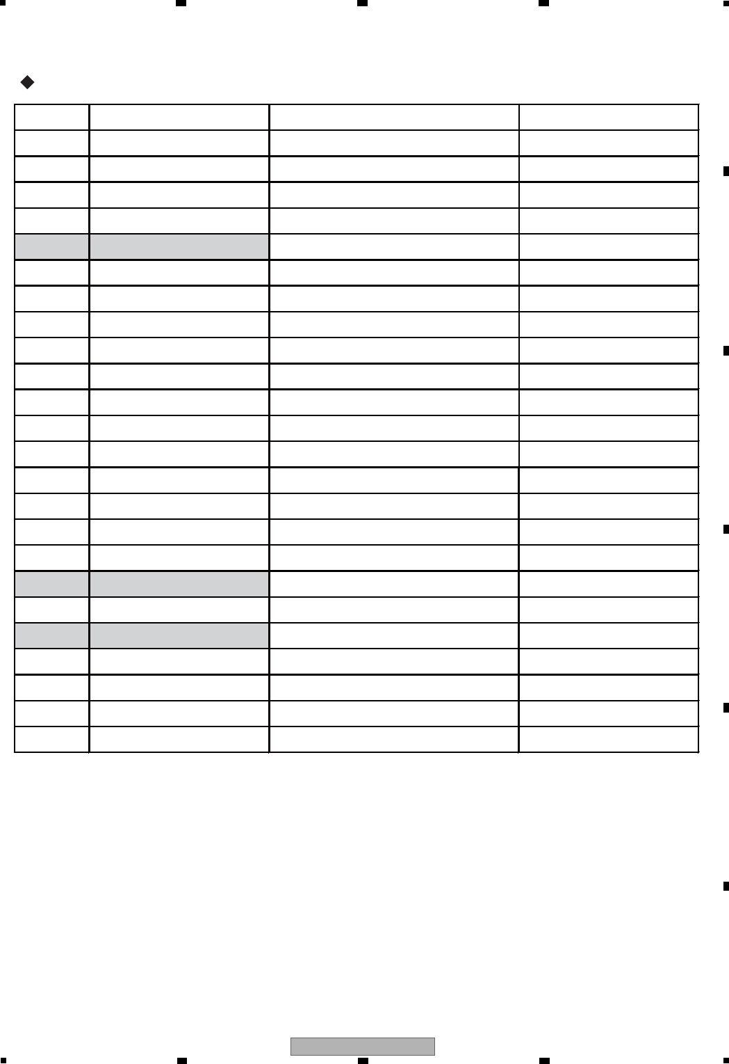
11
DVR-660H-K
56 7 8
56 7 8
A
B
C
D
E
F
3. SERVICE MODE
SERVICE MODE for WPWXV type is the same as KCXV type except for the following:
Category Mode Procedure Necessary When
Adjustment Model Setting Automatically start up when necessary After replacing M/B or T/B
Adjustment LD Power Adjustment [ESC] + [CX] + [1] + [0] After replacing M/B or Loader
Adjustment CPRM ID Number/Data Setting [ESC] + [STEREO] After replacing M/B or HDD
Adjustment Firmware Update [REC STOP] + [OPEN/CLOSE] After replacing M/B or T/B
Adjustment Gracenote Database Update This mode does not correspond.
Adjustment Video Adjustment for Specific
Area [ESC] + [CHP/TIM] As needed
Adjustment OSD Filter Setting [ESC] + [DISP] + [DIG/ANA] x4 As needed
Diagnosis Version Info, etc. [ESC] + [DISP]
Diagnosis RF Level [ESC] + [DISP] + [DIG/ANA]
Diagnosis Error Rate [ESC] + [DISP] + [DIG/ANA] x2
Diagnosis HDD Info [ESC] + [DISP] + [DIG/ANA] x3
Diagnosis Writer Maintenance Info [ESC] + [DISP] + [2] + [DIG/ANA] x2 + [SEARCH]
Diagnosis LD Degradation Check [ESC] + [DISP] + [2] + [DIG/ANA] x3 + [SEARCH]
Diagnosis DV Info [ESC] + [DISP] + [3]
Diagnosis VR Recording Error Log [ESC] + [DISP] + [4] + [DIG/ANA] x3
Diagnosis VR Playback Error Log [ESC] + [DISP] + [5] + [DIG/ANA]
Diagnosis EPG Info [ESC] + [DISP] + [7] Europe model only
Diagnosis AAC Info This mode does not correspond.
Diagnosis HDMI Info [ESC] + [DISP] + [+10] x2 + [4]
Diagnosis Ethernet Info This mode does not correspond.
Diagnosis HDD Check [ESC] + [CX] + [0] + [1]
Diagnosis USB Check [ESC] + <TIMER/REC>
Diagnosis DVD Aging Mode <DVD> + [ESC] + [REP.B] + [PLAY]
Diagnosis HDD Aging Mode <HDD> + [ESC] + [REP.B] + [PLAY]
Service Mode Map
12 DVR-660H-K
12 3 4
A
B
C
D
E
F
12 3 4
3.1 VERSION INFORMATION, ETC. (FIRST SCREEN)
To check the RF signal of the U/V tuner by checking the input frequency difference and AGC voltage
in this debug mode
Press the ESC key.
[
Purposes
]
[
How to enter
]
[
How to quit
]
While the User Setting display is displayed, press the ESC , DISP , then DIG/ANA keys, in that order.
[
Description
]
Input frequency difference
Subscreen 1
AGC voltage
Input channel
[1] Simple Diagnosis of the RF Level (Subscreen 1)
DVR-660H/WPW VERSION : 0.14
SYSCON : RELEASE_179
Rev.1.7379
TUNERCON : 2.22 OK
DRIVE : DVD-RW DVR-U13 OK
1.10 OK
PIC SERIAL : 007710217064
HDD INT : ----
GNDB B : NOBKUP GNDB U : NOBKUP
DEVICE : E2R-FEx1.1 FLASH : 128M
REGION : 2 C : 0000000153
Input CH : ∗∗ ch
Freq Diff : Low 1
AGC Volt : ∗∗∗∗ mV
1) Frequency Difference (Freq Diff)
How much tuning is off is monitored, as shown below:
2) AGC voltage (AGC Volt)
The gain controlled by the tuner is monitored to infer the input electric field intensity.
(The accuracy of inference differs depending on the product.)
Field Intensity AGC VOL
Intense field area
(Clear image)
Less intense field area
(Noise may be generated.)
Weak field area
(Much noise. EPG/VPS/PDC sometimes cannot be
obtained.)
Very weak field area
(Image damaged. EPG/VPS/PDC cannot be obtained.)
70 dB or more 3100 mV or less
50 dB or more
70 dB or less 3100 - 4400mV
30 dB or more
50 dB or less
4400 mV or more
(It is unable to discriminate
under the weak field area.)
30 dB or less 4400 mV or more
(It is unable to discriminate.)
High
(within 200kHz)
Input Frequency Display
Low
Just Tune
Faraway
High 1~5
Low 1~5
Low 7
Center
High 7
within
200kHz
over
200kHz
Tips:For good reception, the field intensity must be 50 dB or more (AGC Volt 4400 mV or less).
For accurate measurement, use a field intensity meter.

13
DVR-660H-K
56 7 8
56 7 8
A
B
C
D
E
F
14 DVR-660H-K
12 3 4
A
B
C
D
E
F
12 3 4
4. SCHEMATIC DIAGRAM
4.1 POWER SUPPLY ASSY
POWER SUPPLY ASSY
(VWR1406)
G
F
G
F
15
DVR-660H-K
56 7 8
56 7 8
A
B
C
D
E
F
Unit Resistor
Capacitor
/W (under 1/4W for no direction W)
F/V (under 50V for no direction V)
CN4501
D
3/5
CN301TO HDD
A1/3
G
F
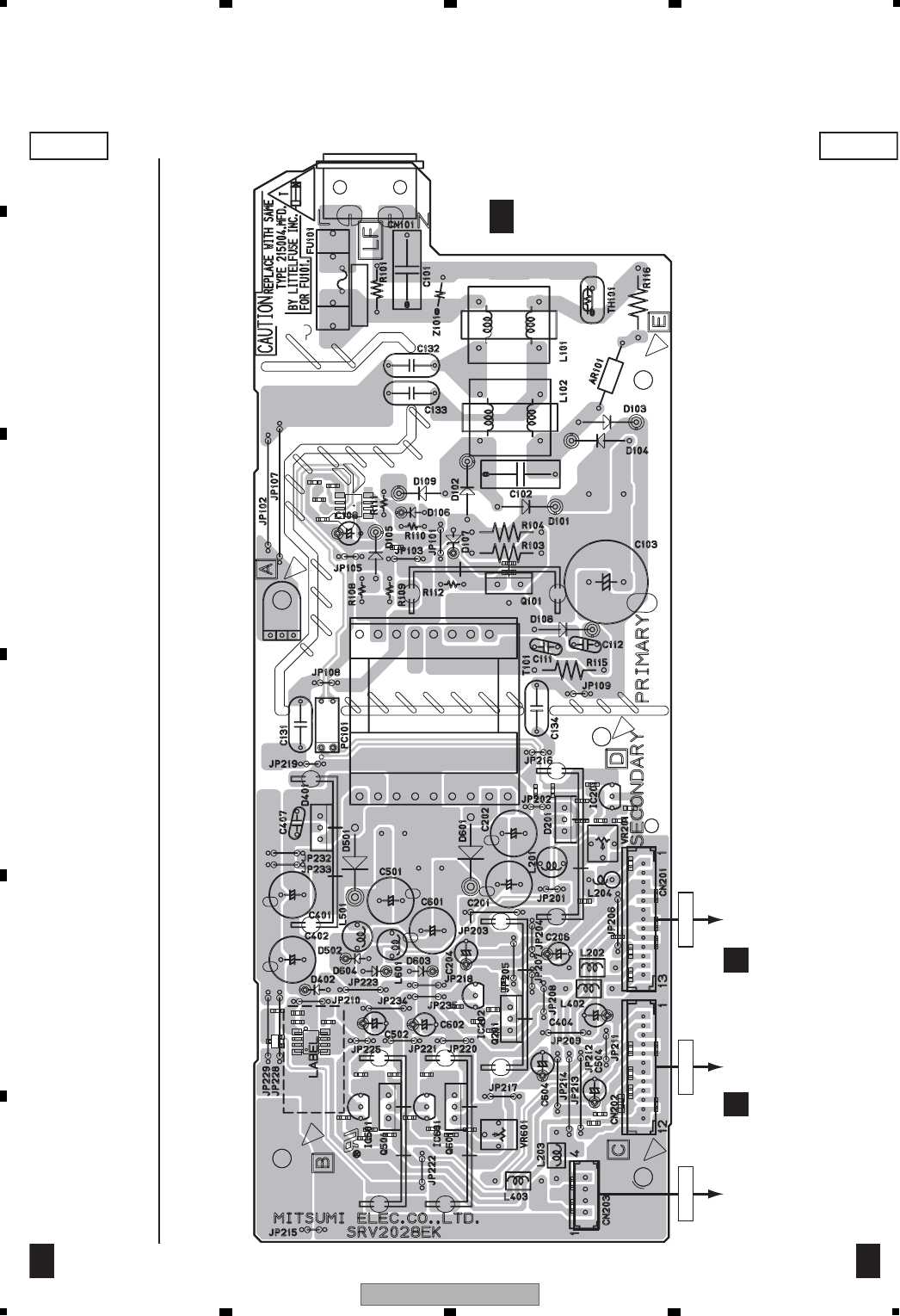
16 DVR-660H-K
12 3 4
A
B
C
D
E
F
12 3 4
5. PCB CONNECTION DIAGRAM
5.1 POWER SUPPLY ASSY
SIDE A SIDE A
POWER SUPPLY ASSY
LIVENEUTRAL
IC
IC201
Q
Q101
IC202
IC501 IC601
Q201
Q501 Q601
G
F
G
F
G
F
CN301 CN4501
DA
CN201CN202
TO HDD
CN203
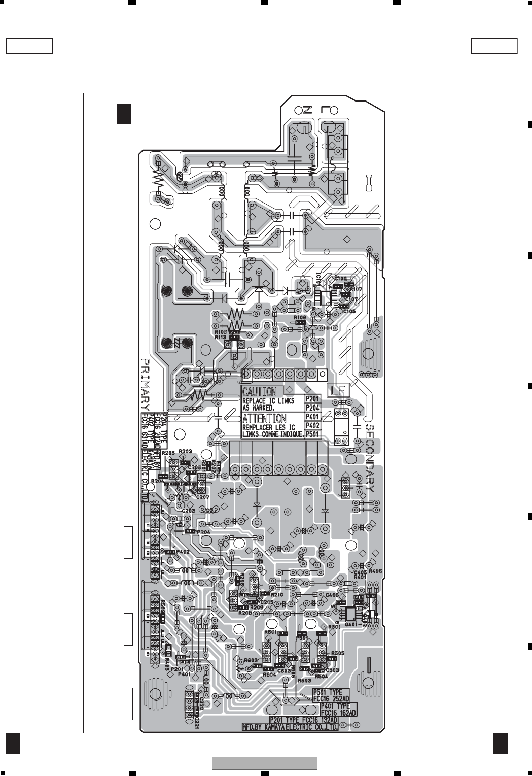
17
DVR-660H-K
56 7 8
56 7 8
A
B
C
D
E
F
POWER SUPPLY ASSY
SIDE B SIDE B
CN201CN202CN203
IC
IC101
Q
Q401
Q402
G
F
G
F
G
F
