Digital Design Solution Manual
Digital_Design_Solution_Manual
User Manual:
Open the PDF directly: View PDF ![]() .
.
Page Count: 228 [warning: Documents this large are best viewed by clicking the View PDF Link!]

1
CHAPTER 1
INTRODUCTION
1.1 EXERCISES
Section 1.2: The World of Digital Systems
1.1. What is a digital signal and how does it differ from an analog signal? Give two
everyday examples of digital phenomena (e.g., a window can be open or closed) and
two everyday examples of analog phenomena.
A digital signal at any time takes on one of a finite number of possible values,
whereas an analog signal can take on one of infinite possible values. Examples of
digital phenomena include a traffic light that is either be red, yellow, or green; a tele-
vision that is on channel 1, 2, 3, ..., or 99; a book that is open to page 1, 2, ..., or 200;
or a clothes hangar that either has something hanging from it or doesn’t. Examples
of analog phenomena include the temperature of a room, the speed of a car, the dis-
tance separating two objects, or the volume of a television set (of course, each ana-
log phenomena could be digitized into a finite number of possible values, with some
accompanying loss of information).
1.2 Suppose an analog audio signal comes in over a wire, and the voltage on the wire can
range from 0 Volts (V) to 3 V. You want to convert the analog signal to a digital sig-
nal. You decide to encode each sample using two bits, such that 0 V would be
encoded as 00, 1 V as 01, 2 V as 10, and 3 V as 11. You sample the signal every 1
millisecond and detect the following sequence of voltages: 0V 0V 1V 2V 3V 2V 1V.
Show the signal converted to digital as a stream of 0s and 1s.
00 00 01 10 11 10 01
1.3 Assume that 0 V is encoded as 00, 1 V as 01, 2 V as 10, and 3 V as 11. You are
given a digital encoding of an audio signal as follows: 1111101001010000. Plot
2c1 Introduction
the re-created signal with time on the x-axis and voltage on the y-axis. Assume that
each encoding’s corresponding voltage should be output for 1 millisecond.
1.4 Assume that a signal is encoded using 12 bits. Assume that many of the encodings
turn out to be either 000000000000, 000000000001, or 111111111111. We
thus decide to create compressed encodings by representing 000000000000 as
00, 000000000001 as 01, and 111111111111 as 10. 11 means that an
uncompressed encoding follows. Using this encoding scheme, decompress the fol-
lowing encoded stream:
00 00 01 10 11 010101010101 00 00 10 10
000000000000 000000000000 000000000001 111111111111 010101010101
000000000000 000000000000 111111111111 111111111111
1.5 Using the same encoding scheme as in Exercise 1.4, compress the following unen-
coded stream:
000000000000 000000000001 100000000000 111111111111
00 01 11 100000000000 10
1.6 Encode the following words into bits using the ASCII encoding table in Figure 1.9.
a. LET
b. RESET!
c. HELLO $1
a) 1001100 1000101 1010100
b) 1010010 1000101 1010011 1000101 1010100 0100001
c) 1001000 1000101 1001100 1001100 1001111 0100000 0100100 0110001 (don’t
forget the encoding 0100000 for the space between the O and the $).
1.7 Suppose your are building a keybad that has the buttons A through G. A three-bit
output should indicate which button is currently being pressed. 000 represents no
button being pressed. Decide on a 3-bit encoding to represent each button being
pressed.
One possible set of encodings is: A=001, B=010, C=011, D=100, E=101, F=110,
and G=111. Another possible set is: A=001, B=010, C=100, D=101, E=110, F=111,
G=011. Many other sets of encodings are possible; any set of encodings is fine as
long as each encoding is unique.
1.8 Convert the following binary numbers to decimal numbers:
a. 100
21 3 4 65 7 8
0
1
2
3
ms
V
1.1 Exercises b3
b. 1011
c. 0000000000001
d. 111111
e. 101010
a) 4
b) 11
c) 1
d) 63
e) 42
1.9 Convert the following binary numbers to decimal numbers:
a. 1010
b. 1000000
c. 11001100
d. 11111
e. 10111011001
a) 10
b) 64
c) 204
d) 31
e) 1497
1.10 Convert the following binary numbers to decimal numbers:
a. 000011
b. 1111
c. 11110
d. 111100
e. 0011010
a) 3
b) 15
c) 30
d) 60
e) 26
1.11 Convert the following decimal numbers to binary numbers using the addition
method:
a. 9
b. 15
c. 32
d. 140
a) 1001
b) 1111
c) 100000
d) 10001100
4c1 Introduction
1.12 Convert the following decimal numbers to binary numbers using the addition
method:
a. 19
b. 30
c. 64
d. 128
a) 10011
b) 11110
c) 1000000
d) 10000000
1.13 Convert the following decimal numbers to binary numbers using the addition
method:
a. 3
b. 65
c. 90
d. 100
a) 11
b) 1000001
c) 1011010
d) 1100100
1.14 Convert the following decimal numbers to binary numbers using the divide-by-2
method:
a. 9
b. 15
c. 32
d. 140
a) 1001
b) 1111
c) 100000
d) 10001100
1.15 Convert the following decimal numbers to binary numbers using the divide-by-2
method:
a. 19
b. 30
c. 64
d. 128
a) 10011
b) 11110
c) 1000000
d) 10000000
1.1 Exercises b5
1.16 Convert the following decimal numbers to binary numbers using the divide-by-2
method:
a. 3
b. 65
c. 90
d. 100
a) 11
b) 1000001
c) 1011010
d) 1100100
1.17 Convert the following decimal numbers to binary numbers using the divide-by-2
method:
a. 23
b. 87
c. 123
d. 101
a) 10111
b) 1010111
c) 1111011
d) 1100101
1.18 Convert the following binary numbers to hexadecimal:
a. 11110000
b. 11111111
c. 01011010
d. 1001101101101
a) F0
b) FF
c) 5A
d) 136D
1.19 Convert the following binary numbers to hexadecimal:
a. 11001101
b. 10100101
c. 11110001
d. 1101101111100
a) CD
b) A5
c) F1
d) 1B7C
1.20 Convert the following binary numbers to hexadecimal:
a. 11100111
b. 11001000
6c1 Introduction
c. 10100100
d. 011001101101101
a) E7
b) C8
c) A4
d) 336D
1.21 Convert the following hexadecimal numbers to binary:
a. FF
b. F0A2
c. 0F100
d. 100
a) 1111 1111
b) 1111 0000 1010 0010
c) 0000 1111 0001 0000 0000
d) 0001 0000 0000
1.22 Convert the following hexadecimal numbers to binary:
a. 4F5E
b. 3FAD
c. 3E2A
d. DEED
a) 0100 1111 0101 1110
b) 0011 1111 1010 1101
c) 0011 1110 0010 1010
d) 1101 1110 1110 1101
1.23 Convert the following hexadecimal numbers to binary:
a. B0C4
b. 1EF03
c. F002
d. BEEF
a) 1011 0000 1100 0100
b) 0001 1110 1111 0000 0011
c) 1111 0000 0000 0010
d) 1011 1110 1110 1111
1.24 Convert the following hexadecimal numbers to decimal:
a. FF
b. F0A2
c. 0F100
d. 100
a) 255
b) 61602
c) 61696
1.1 Exercises b7
d) 256
1.25 Convert the following hexadecimal numbers to decimal:
a. 10
b. 4E3
c. FF0
d. 200
a) 16
b) 1251
c) 4080
d) 512
1.26 Convert the decimal number 128 to the following number systems:
a. binary
b. hexadecimal
c. base three
d. base five
e. base fifteen
a) 10000000
b) 80
c) 11202
d) 1003
e) 88
1.27 Compare the number of digits necessary to represent the following decimal numbers
in binary, octal, decimal, and hexadecimal representations. You need not determine
the actual representations -- just the number of required digits. For example, repre-
senting the decimal number 12 requires four digits in binary (1100 is the actual rep-
resentation), two digits in octal (14), two digits in decimal (12), and one digit in
hexadecimal (C).
a. 8
b. 60
c. 300
d. 1000
e. 999,999
a) 4 digits in binary, 2 digits in octal, 1 digit in decimal, 1 digit in hexadecimal
b) 6 digits in binary, 2 digits in octal, 2 digits in decimal, 2 digits in hexadecimal
c) 9 digits in binary, 3 digits in octal, 3 digits in decimal, 3 digits in hexadecimal
d) 10 digits in binary, 4 digits in octal, 4 digits in decimal, 3 digits in hexadecimal
e) 20 digits in binary, 7 digits in octal, 6 digits in decimal, 5 digits in hexadecimal
1.28 Determine the decimal number ranges that can be represented in binary, octal, deci-
mal, and hexadecimal using the following numbers of digits. For example, 2 digits
can represent decimal number range 0 through 3 in binary (00 through 11), 0
through 63 in octal (00 through 77), 0 through 99 in decimal (00 through 99), and 0
through 255 in hexadecimal (00 through FF).

8c1 Introduction
a. 1
b. 3
c. 6
d. 8
a) 0-1 in binary, 0-7 in octal, 0-9 in decimal, 0-15 in hexadecimal
b) 0-7 in binary, 0-511 in octal, 0-999 in decimal, 0-4,095 in hexadecimal
c) 0-63 in binary, 0-262,143 in octal, 0-999,999 in decimal, 0-16,777,215 in hexa-
decimal
d) 0-255 in binary, 0-16,777,215, 0-99,999,999 in decimal, 0-4,294,967,295 in
hexadecimal
1.29 Rewrite the following bit quantities as byte quantities, using the most appropriate
metric prefix, e.g., 16,000 bits (2,000 bytes) would be rewritten as 2 Kbytes.
a. 8,000,000
b. 32,000,000,000
c. 1,000,000,000
a) 8,000,000 bits * (1 byte/ 8 bits) = 1,000,000 bytes = 1 Mbyte
b) 32,000,000,000 bits / 8 = 4,000,000,000 = 4 Gbytes
c) 1,000,000,000 bits / 8 = 125,000,000 bytes = 125 Mbytes
Section 1.3: Implementing Digital Systems: Programming Microprocessors versus
Designing Digital Circuits
1.30 Use a microprocessor like that in Figure 1.23 to implement a system that sounds an
alarm whenever there is motion detected at the same time in three different rooms.
Each room’s motion sensor output comes to us on a wire as a bit, 1 meaning motion,
0 meaning no motion. We sound the alarm by setting an output wire “alarm” to 1.
Show the connections to and from the microprocessor, and the C code to execute on
the microprocessor.
void main() {
while (1) {
P0 = I0 && I1 && I2;
}
}
1.31 A security camera company wishes to add a face recognition feature to their cameras
such that the camera only broadcasts video when a human face is detected in the
video. The camera records 30 video frames per second. For each frame, the camera
would execute a face recognition application. The application implemented on a
P0
I0
Microprocessor
P1
P2
P3
P4
P5
P6
P7
I1
I2
I3
I4
I5
I6
I7
alarm
motion sensor 1
motion sensor 2
motion sensor 3
1.1 Exercises b9
microprocessor requires 50 ms. The application implemented as a custom digital cir-
cuit requires 1 ms. Compute the maximum number of frames per second that each
implementation supports, and indicate which implementation is sufficient for 30
frames per second.
50 ms/frame means 1 frame / 50 ms = 1 frame / 0.05 s = 20 frames / s.
1 ms/frame means 1 frame / 1 ms = 1 frame / 0.001 s = 1000 frames / s.
Thus, the digital circuit implementation would suffice, but the microprocessor
implementation is too slow.
1.32 Suppose a particular banking system supports encrypted transactions, and that
decrypting each transaction consists of three sub-tasks A, B, and C. The execution
times of each task on a microprocessor versus a custom digital circuit are 50 ms ver-
sus 1 ms for A, 20 ms versus 2 ms for B, and 20 ms versus 1 ms for C. Partition the
tasks among the microprocessor and custom digital circuitry, such that you mini-
mize the amount of custom digital circuitry, while meeting the constraint of decrypt-
ing at least 40 transactions per second. Assume each task requires the same amount
of digital circuitry.
40 transactions / second means that decryption should occur at a rate of 1 second /
40 transactions = 0.025 seconds / transaction, or 25ms/transaction. Implementing all
three tasks on the microprocessor would result in 50+20+20 = 90 ms/transaction,
which is too slow. Implementing any one task as a digital circuit is still too slow.
Implementing A as a digital circuit would reduce the time to 1+20+20 = 41 ms.
Implementing A and B as a digital circuit would reduce the time to 1+2+20 = 23 ms.
Implementing A and C as a digital circuit would reduce the time to 1+20+1 = 22 ms.
Thus, either solution suffices. Implementing B and C as a digital circuit would not
suffice, as the time would be 50+2+1 = 53 ms. Implementing all three as a digital
circuit would result in 1+2+1 = 4 ms/transaction, which is plenty fast but uses extra
digital circuitry. Thus, one solution is A and B as digital circuits, C on the micropro-
cessor. Another solution is A and C as digital circuits, B on the microprocessor.
1.33 How many possible partitionings are there of a set of N tasks where each task can be
implemented either on the microprocessor or as a custom digital circuit? How many
possible partitionings are there of a set of 20 tasks (expressed as a number without
any exponents)?
2n
For 20 tasks, there are 220 or 1,048,576 (over 1 million) possible partitionings.
10 c1 Introduction

13
CHAPTER 2
COMBINATIONAL LOGIC
DESIGN
2.1 EXERCISES
Any problem noted with an asterisk (*) represents an especially challenging problem.
Section 2.2: Switches
2.1. A microprocessor in 1980 used about 10,000 transistors. How many of those micro-
processors would fit in a modern chip having 3 billion transistors?
3,000,000,000 / 10,000 = 300,000 microprocessors
2.2 The first Pentium microprocessor had about 3 million transistors. How many of
those microprocessors would fit in a modern chip having 3 billion transistors?
3,000,000,000 / 3,000,000 = 1,000 microprocessors
2.3 Describe the concept known as Moore’s Law.
Integrated circuit density doubles approximately every 18 months.
2.4 Assume for a particular year that a particular size chip using state-of-the-art technol-
ogy can contain 1 billion transistors. Assuming Moore’s Law holds, how many tran-
sistors will the same size chip be able to contain in ten years?
Approximately 100 billion transistors (10 years * 12 months/year / 18 months/dou-
bling = 6.667 doublings. 1 billion * 26.667 = 101.617 billion).
2.5 Assume a cell phone contains 50 million transistors. How big would such a cell
phone be if the phone used vacuum tubes instead of transistors, assuming a vacuum
tube has an volume of 1 cubic inch?
50,000,000 transistors * 1 in3/transistor = 50,000,000 in3 (nearly 30,000 cubic feet -
as large as a house)

14 c2 Combinational Logic Design
2.6 A modern desktop processor may contain 1 billion transistors in a chip area of 100
mm2. If Moore’s Law continues to apply, what would be chip area for those 1 billion
transistors after 9 years? What percentage is that area of the original area? Name a
product into which the smaller chip might fit whereas the original chip would have
been too big.
Doubling chip capacity every 18 months also suggests halving of size every 18
months of the same number of transistors. 9 years / 18 months is 108 months / 18
months = 6 halvings. 100 mm2 * (1/2)6 = 100 mm2 / 64 = 1.56 mm2 . 1.56 mm2 /
100 mm2 = 1.56% of the original area. A product into which such a small chip might
now fit is a hearing aid, for example.
Section 2.3: The CMOS Transistor
2.7 Describe the behavior of the CMOS transistor
circuit shown in Figure 2.77, clearly indicating
when the transistor circuit conducts.
When x is a logical 0, the top transistor will con-
duct, otherwise the top transistor will not con-
duct. Likewise, when y is a logical 0, the bottom
transistor will conduct and not conduct other-
wise. Thus, the circuit conducts only when x is 0
and y is 0.
2.8 If we apply a voltage to the gate of a CMOS transistor, why doesn’t the current flow
to the transistor’s source or drain?
An insulator exists between the gate and the source-drain channel, prohibiting cur-
rent from flowing to the transistor’s source or drain.
2.9 Why does applying a positive voltage to the gate of a CMOS transistor cause the
transistor to conduct between source and drain?
The positive voltage at the gate attracts electrons into the channel between source
and drain. Those electrons are enough to change the channel from non-conducting to
conducting.
Section 2.4: Boolean Logic Gates—Building Blocks for Digital Circuits
2.10 Which Boolean operation, AND, OR or NOT, is appropriate for each of the follow-
ing:
a. Detecting motion in any motion sensor surrounding a house (each motion sen-
sor outputs 1 when motion is detected).
b. Detecting that three buttons are being pressed simultaneously (each button out-
puts 1 when a button is being pressed).
c. Detecting the absence of light from a light sensor (the light sensor outputs 1
when light is sensed).
a) OR
b) AND
c) NOT
Figure 2.77
x
y
2.1 Exercises b15
2.11 Convert the following English problem statements to Boolean equations. Introduce
Boolean variables as needed.
a. A flood detector should turn on a pump if water is detected and the system is set
to enabled
b. A house energy monitor should sound an alarm it is night and light is detected
inside a room but motion is not detected.
c. An irrigation system should open the sprinkler’s water valve if the system is
enabled and niether rain nor freezing temperatures are detected.
a) Pump = WaterDetected AND SystemEnabled
b) Alarm = Night AND LightInsideDetected AND NOT MotionDetected
c) WaterValveOpen = SystemEnabled AND NOT (RainDetected OR FreezingTem-
peraturesDetected)
2.12 Evaluate the Boolean equation F = (a AND b) OR c OR d for the given values of
variables a, b, c, and d:
a. a=1, b=1, c=1, d=0
b. a=0, b=1, c=1, d=0
c. a=1, b=1, c=0, d=0
d. a=1, b=0, c=1, d=1
a) F = (1 AND 1) OR 1 OR 0 = 1 OR 1 OR 0 = 1
b) F = (0 AND 1) OR 1 OR 0 = 0 OR 1 OR 0 = 1
c) F = (1 AND 1) OR 0 OR 0 = 1 OR 0 OR 0 = 1
d) F = (1 AND 0) OR 0 OR 0 = 0 OR 0 OR 0 = 0
2.13 Evaluate the Boolean equation F = a AND (b OR c)AND d for the given values of
variables a, b, c, and d:
a. a=1, b=1, c=0, d=1
b. a=0, b=0, c=0, d=1
c. a=1, b=0, c=0, d=0
d. a=1, b=0, c=1, d=1
a) F = 1 AND (1 OR 0) AND 1 = 1 AND 1 AND 1 = 1
b) F = 0 AND (0 OR 0) AND 1 = 0 AND 0 AND 1 = 0
c) F = 1 AND (0 OR 0) AND 0 = 1 AND 0 AND 0 = 0
d) F = 1 AND (0 OR 1) AND 1 = 1 AND 1 AND 1 = 1
2.14 Evaluate the Boolean equation F = a AND (b OR (c AND d)) for the given values
of variables a, b, c, and d:
a. a=1, b=1, c=0, d=1
b. a=0, b=0, c=0, d=1
c. a=1, b=0, c=0, d=0
d. a=1, b=0, c=1, d=1
a) F = 1 AND (1 OR (0 AND 1)) = 1 AND (1 OR 0) = 1 AND 1 = 1
b) F = 0 AND (0 OR (0 AND 1)) = 0 AND (0 OR 0) = 0 AND 0 = 0
c) F = 1 AND (0 OR (0 AND 0)) = 1 AND (0 OR 0) = 1 AND 0 = 0
d) F = 1 AND (0 OR (1 AND 1)) = 1 AND (0 OR 1) = 1 AND 1 = 1
16 c2 Combinational Logic Design
2.15 Show the conduction paths and output value of the OR gate transistor circuit in Fig-
ure 2.12 when: (a) x = 1 and y = 0, (b) x = 1 and y = 1.
2.16 Show the conduction paths and output value of the AND gate transistor circuit in
Figure 2.14 when: (a) x = 1 and y = 0, (b) x = 1 and y = 1.
2.17 Convert each of the following equations directly to gate-level circuits:
a.F = ab’ + bc + c’
b.F = ab + b’c’d’
c.F = ((a + b’) * (c’ + d)) + (c + d + e’)
2.18 Convert each of the following equations directly to gate-level circuits:
a.F = a’b’ + b’c
(b)
x
F
1
0
y
y
x
1
1
11
1
(a)
x
F
1
0
y
y
x
0
1
10
1
(b)
(a)
x
F
1
0
y
y
x
x
F
1
0
y
y
x
01
(b)
(a)
a
F
b
c
a
F
b
c
d
a
F
b
c
d
e
(c)
2.1 Exercises b17
b.F = ab + bc + cd + de
c.F = ((ab)’ + (c)) + (d + ef)’
2.19 Convert each of the following equations directly to gate-level circuits:
a.F = abc + a’bc
b.F = a + bcd’ + ae + f’
c.F = (a + b) + (c’ * (d + e + fg))
2.20 Design a system that sounds a buzzer inside a home whenever motion outside is
detected at night. Assume a motion sensor has an output M that indicates whether
motion is detected (M=1 means motion detected) and a light sensor with output L
that indicates if light is detected (L=1 means light is detected). The buzzer inside the
home has a single input B that when 1 sounds the buzzer. Capture the desired system
behavior using an equation, and then convert the equation to a circuit using AND,
OR, and NOT gates.
B = M * L’
(b)
(a)
a
F
b
c
a
b
c
d
e
F
a
b
c
d
f
e
F
(c)
(b)
(a)
a
F
b
c
a
b
c
d
f
F
a
b
c
d
f
e
F
(c)
e
g
M
LB

18 c2 Combinational Logic Design
2.21 A DJ (“disc jockey,” meaning someone who plays music at a party) would like a sys-
tem to automatically control a strobe light and disco ball in a dance hall depending
on whether music is playing and people are dancing. Asound sensor has output S
that when 1 indicates that music is playing, and a motion sensor has output M that
when 1 indicates that people are dancing. The strobe light has an input L that when 1
turns the light on, and the disco ball has an input B that when 1 turns the ball on. The
DJ wants the disco ball to turn on only when music is playing and nobody is danc-
ing, and wants the strobe light to turn on only when music is playing and people are
dancing. Create equations describing the desired behavior for B and for L, and then
convert each to a circuit using AND, OR, and NOT gates.
B = S * M’ L = S * M
2.22 We want to concisely describe the following situation using a Boolean equation. We
want to fire a football coach (by setting F=1) if he is mean (represented by M=1). If
he is not mean, but has a losing season (represented by the Boolean variable L=1),
we want to fire him anyways. Write an equation that translates the situation directly
to a Boolean equation for F, without any simplification.
F = M + (M’ * L)
Section 2.5: Boolean Algebra
2.23 For the function F = a + a’b + acd + c’:
a. List all the variables.
b. List all the literals.
c. List all the product terms.
a) a, b, c, d
b) a, a’, b, a, c, d, c’
c) a, a’b, acd, c’
2.24 For the function F = a’d’ + a’c + b’cd’ + cd:
a. List all the variables.
b. List all the literals.
c. List all the product terms.
a) a, b, c, d
b) a’, d’, a’, c, b’, c, d’, c, d
c) a’d’, a’c, b’cd’, cd
2.25 Let variables T represent being tall, H being heavy, and F being fast. Let’s consider
anyone who is not tall as short, not heavy as light, and not fast as slow. Write a Bool-
ean equation to represent the following:
a. You may ride a particular amusement park ride only if you are either tall and
light, or short and heavy.
S
MBS
ML
2.1 Exercises b19
b. You may NOT ride an amusement park ride if you are either tall and light, or
short and heavy. Use algebra to simplify the equation to sum of products.
c. You are eligible to play on a particular basketball team if you are tall and fast, or
tall and slow. Simplify this equation.
d. You are NOT eligible to play on a particular football team if you are short and
slow, or if you are light. Simplify to sum of products form.
e. You are eligible to play on both the basketball and football teams above, based
on the above criteria. Hint: combine the two equations into one equation by
ANDing them.
a) Ride = TH’ + T’H
b) Ride = (TH’ + T’H)’ = (TH’)’(T’H)’ = (T’ + H)(T + H’) = T’H’ + TH
c) Basketball = TF + TF’ = T(F+F’) = T(1) = T
d) Football = (T’F’ + H’)’ = (T’F’)’H = (T + F)H = TH + FH
e) BasketballAndFootball = T(TH + FH) = TTH + TFH = TH + TFH = TH(1+F) =
TH. In other words, only people who are both tall and heavy can play on both teams.
2.26 Let variables S represent a package being small, H being heavy, and E being expen-
sive. Let’s consider a package that is not small as big, not heavy as light, and not
expensive as inexpensive. Write a Boolean equation to represent the following:
a. Your company specializes in delivering packages that are both small and inex-
pensive (a package must be small AND inexpensive for us to deliver it); you’ll
also deliver packages that are big but only if they are expensive.
b. A particular truck can be loaded with packages only if the packages are small
and light, small and heavy, or big and light. Simplify the equation.
c. Your above-mentioned company buys the above-mentioned truck. Write an
equation that describes the packages your company can deliver. Hint: Appropri-
ately combine the equations from the above two parts.
a) Deliver = SE’ + S’E
b) Load = SH’ + SH + S’H’ = SH’ + SH + SH’ + S’H’ = S + H’
c) Packages = Deliver*Load = (SE’ + S’E)*(S+H’) = SSE’ + SS’E + H’SE’ + H’S’E
= SE’ + 0 + H’SE’ + H’S’E = (1+H’)SE’ + H’S’E = SE’ + S’EH’. In other words,
you can deliver small inexpensive packages, or large expensive light packages.
2.27 Use algebraic manipulation to convert the following equation to sum-of-products
form: F = a(b + c)(d’) + ac’(b + d)
F = (ab + ac)d’ + ac’b + ac’d
F = abd’ + acd’ + ac’b + ac’d
2.28 Use algebraic manipulation to convert the following equation to sum-of-products
form: F = a’b(c + d’) + a(b’ + c) + a(b + d)c
F = a’bc + a’bd’ + ab’ + ac + (ab + ad)c
F = a’bc + a’bd’ + ab’ + ac + abc + acd
F = a’bc + a’bd’ + ab’ + ac
2.29 Use DeMorgan’s Law to find the inverse of the following equation: F = abc +
a’b. Reduce to sum-of-products form. Hint: Start with F’ = (abc + a’b)’.
F’ = (abc + a’b)’
20 c2 Combinational Logic Design
F’ = (abc)’(a’b)’
F’ = (a’ + b’ + c’)(a’’ + b’)
F’ = (a’ + b’ + c’)(a + b’)
F’ = a(a’ + b’ + c’) + b’(a’ + b’ + c’)
F’ = 0 + ab’ + ac’ + a’b’ + b’ + b’c’
F’ = (a + a’)b’ + b’ + ac’ + b’c’ (The b’ term makes all other terms with b’ redun-
dant)
F’ = b’ + ac’
2.30 Use DeMorgan’s Law to find the inverse of the following equation: F = ac’ +
abd’ + acd. Reduce to sum-of-products form.
F’ = (ac’ + abd’ + acd)’
F’ = (ac’)’(abd’)’(acd)’
F’ = (a’ + c’’)(a’ + b’ + d’’)(a’ + c’ + d’)
F’ = (a’ + c)(a’ + b’ + d)(a’ + c’ + d’)
F’ = (a’ + a’b’ + a’d + a’c + b’c + cd)(a’ + c’ + d’)
F’ = a’ + a’c’ + a’d’ + a’b’ + a’b’c’ + a’b’d’ + a’d + a’cc’ + a’cd’ + a’b’c + b’cc’ +
b’cd’ + a’cd + cc’d + cdd’ (The a’ term makes all other terms with a’ redundant)
F’ = a’ + b’cd’
Section 2.6: Representations of Boolean Functions
2.31 Convert the following Boolean equations to a digital circuit:
a. F(a,b,c) = a’bc + ab
b. F(a,b,c) = a’b
c. F(a,b,c) = abc + ab + a + b + c
d. F(a,b,c) = c’
2.32 Create a Boolean equation representation of the
digital circuit in Figure 2.78.
F = (ab’ + b)’
(b)
(a)
a
F
b
c
F
(c)
aF
b
a
b
cF
c
(d)
Figure 2.78
a
b
F
2.1 Exercises b21
2.33 Create a Boolean equation representation for the
digital circuit in Figure 2.79.
F = (ab’ + b) + a’c
2.34 Convert each of the Boolean equations in Exer-
cise 2.31 to a truth table.
2.35 Convert each of the following Boolean equations to a truth table:
a. F(a,b,c) = a’ + bc’
b. F(a,b,c) = (ab)’ + ac’ + bc
c. F(a,b,c) = ab + ac + ab’c’ + c’
d.F(a,b,c,d) = a’bc + d’
Figure 2.79
a
b
G
c
Inputs Outputs
abcF
0000
0010
0100
0111
1000
1010
1101
1111
Inputs Outputs
abcF
0000
0010
0101
0111
1000
1010
1100
1110
Inputs Outputs
abcF
0000
0011
0101
0111
1001
1011
1101
1111
Inputs Outputs
abcF
0001
0010
0101
0110
1001
1010
1101
1110
(a) (b)
(c) (d)

22 c2 Combinational Logic Design
2.36 Fill in Table 2.8’s columns for the
equation: F= ab + b’
Inputs Outputs
abcF
0001
0011
0101
0111
1000
1010
1101
1110
Inputs Outputs
abcF
0001
0011
0101
0111
1001
1011
1100
1111
Inputs Outputs
abcF
0001
0010
0101
0110
1001
1011
1101
1111
Inputs Outputs
abcdF
00001
00010
00101
00110
01001
01010
01101
01111
10001
10010
10101
10110
11001
11010
11101
11110
(a) (b)
(c)
(d)
Table 2.8
Inputs Output
a b ab b’ ab+b’ F
000 1 1 1
010 0 0 0
100 1 1 1
111 0 1 1

2.1 Exercises b23
2.37 Convert the function F shown in the truth table in
Table 2.9 to an equation. Don’t minimize the equa-
tion.
F = a’b’c + a’bc’ + a’bc + ab’c + abc’ + abc
2.38 Use algebraic manipulation to minimize the equa-
tion obtained in Exercise 2.37
F = a’b’c + a’bc’ + a’bc + ab’c + abc’ + abc
F = a’(b’c + bc’ + bc) + a(b’c + bc’ + bc)
F = a’(b’c + b(c’ + c)) + a(b’c + b(c’ + c))
F = a’(b’c + b) + a(b’c + b)
F = (a’ + a)(b’c + b)
F = b’c + b
2.39 Convert the function F shown in the truth table in
Table 2.10 to an equation. Don’t minimize the
equation.
F = a’b’c’ + a’bc’ + ab’c’ + ab’c + abc’
2.40 Use algebraic manipulation to minimize the equa-
tion obtained in Exercise 2.39
F = a’b’c’ + a’bc’ + ab’c’ + ab’c + abc’
F = a’(b’c’ + bc’) + a(b’c’ + b’c + bc’)
F = a’((b’ + b)c’) + a(b’(c’ + c) + bc’)
F = a’c’ + a(b’ + bc’)
2.41 Convert the function F shown in the truth table in
Table 2.11 to an equation. Don’t minimize the
equation.
F = a’b’c + abc’ + abc
2.42 Use algebraic manipulation to minimize the equa-
tion obtained in Exercise 2.41.
F = a’b’c + abc’ + abc
F = a’b’c + ab(c’ + c)
F = a’b’c + ab
2.43 Create a truth table for the circuit of Figure 2.78
Table 2.9
abcF
0000
0011
0101
0111
1000
1011
1101
1111
Table 2.10
abcF
0001
0010
0101
0110
1001
1011
1101
1110
Table 2.11
abcF
0000
0011
0100
0110
1000
1010
1101
1111

24 c2 Combinational Logic Design
.
2.44 Create a truth table for the circuit of Figure 2.79.
2.45 Convert the function F shown in the truth table in Table 2.9 to a digital circuit.
2.46 Convert the function F shown in the truth table in Table 2.10 to a digital circuit.
2.47 Convert the function F shown in the truth table in Table 2.11 to a digital circuit.
2.48 Convert the following Boolean equations to canonical sum-of-minterms form:
Inputs Outputs
abF
001
010
100
110
Inputs Outputs
a b c ab’ + b a’c F
0000 0 0
0010 1 1
0101 0 1
0111 1 1
1001 0 1
1011 0 1
1101 0 1
1111 0 1
F
b
c
F
a
c
b
F
a
c
b
2.1 Exercises b25
a. F(a,b,c) = a’bc + ab
b. F(a,b,c) = a’b
c. F(a,b,c) = abc + ab + a + b + c
d. F(a,b,c) = c’
a) F(a,b,c) = a’bc + abc’ + abc
b) F(a,b,c) = a’bc’ + a’bc
c) F(a,b,c) = a’b’c + a’bc’ + a’bc + ab’c’ + ab’c + abc’ + abc
d) F(a,b,c) = a’b’c’ + a’bc’ + ab’c’ + abc’
2.49 Determine whether the Boolean functions F = (a + b)’*a and G = a + b’
are equivalent, using: (a) algebraic manipulation, and (b) truth tables.
a) Convert the two functions to canonical sum-of-minterms form:
F = (a + b)’ * a
F = a’b’a
F = 0
G = a + b’
G = ab’ + ab + a’b’
F and G are not equivalent.
2.50 Determine whether the Boolean functions F = ab’ and G = (a’ + ab)’ are
equivalent, using: (a) algebraic manipulation, and (b) truth tables.
a) Convert the two functions to canonical sum-of-minterms form:
F = ab’
G = (a’ + ab)’
G = (a)(ab)’
G = a(a’ + b’)
G = 0 + ab’
G = ab’
F and G are equivalent.
Inputs Outputs
abF
000
010
100
110
Inputs Outputs
abG
001
010
101
111
(b)
Inputs Outputs
abF
000
010
101
110
Inputs Outputs
abG
000
010
101
110
(b)

26 c2 Combinational Logic Design
2.51 Determine whether the Boolean function G =
a’b’c + ab’c + abc’ + abc is equiva-
lent to the function represented by the circuit in
Figure 2.80.
The circuit can be converted to the equation H =
ab + b’c. That equation can be algebraically
expanded to canonical sum-of-minterms form as
H = ab(c’+c) + (a’+a)b’c = abc’ + abc + a’b’c +
ab’c, which is equivalent to G.
2.52 Determine whether the two cir-
cuits in Figure 2.81 are equiva-
lent circuits using: (a) algebraic
manipulation, and (b) truth
tables.
a) F = ab + cd and G = (1*((ab)’
* (cd)’)’)’
In canonical sum-of-minterms
form, F = a’b’cd + a’bcd + ab’cd + abc’d’ + abc’d + abcd’ + abcd and G = a’b’c’d’
+ a’b’c’d + a’b’cd’+ a’bc’d’ + a’bc’d + a’bcd’ + ab’c’d’ + ab’c’d + ab’cd’. F and G
are not equivalent (F = G’)
b)
Figure 2.80
a
b
H
c
Figure 2.81
a
bF
c
d
bG
c
d
a1
Inputs Outputs
abcdF
00000
00010
00100
00111
01000
01010
01100
01111
10000
10010
10100
10111
11001
11011
11101
11111
(a)
Inputs Outputs
abcdF
00001
00011
00101
00110
01001
01011
01101
01110
10001
10011
10101
10110
11000
11010
11100
11110
(b)
2.1 Exercises b27
2.53 *Figure 2.82 shows two cir-
cuits whose inputs are unla-
beled.
a. Determine whether the
two circuits are equiva-
lent. Hint: Try all possible
labellings of the inputs
for both circuits.
(No solution provided for challenge problem)
b. How many circuit comparisons would need to be performed to determine if two
circuits with 10 unlabeled inputs are equivalent?
(No solution provided for challenge problem)
Section 2.7: Combinational Logic Design Process
2.54 A museum has three rooms, each with a motion sensor (m0, m1, and m2) that outputs
1 when motion is detected. At night, the only person in the museum is one security
guard who walks from room to room. Create a circuit that sounds an alarm (by set-
ting an output A to 1) if motion is ever detected in more than one room at a time
(i.e., in two or three rooms), meaning there must be one or more intruders in the
museum. Start with a truth table.
Step 1 - Capture the function
Step 2A - Create equations
A = m2’m1m0 + m2m1’m0 + m2m1m0’ + m2m1m0
Step 2B- Implement as a gate-based circuit
Figure 2.82
G
F
Inputs Outputs
m2 m1 m0 A
0000
0010
0100
0111
1000
1011
1101
1111
m1 m0m2
A
28 c2 Combinational Logic Design
2.55 Create a circuit for the museum of Exercise 2.54 that detects whether the guard is
properly patrolling the museum, detected by exactly one motion sensor being 1. (If
no motion sensor is 1, the guard may be sitting, sleeping, or absent).
Step 1 - Capture the function
Step 2A - Create equations
A = m2’m1’m0 + m2’m1m0’ + m2m1’m0’
Step 2B- Implement as a gate-based circuit
Inputs Outputs
m2 m1 m0 A
0000
0011
0101
0110
1001
1010
1100
1110
m1 m0m2
A
2.1 Exercises b29
2.56 Consider the museum security alarm function of Exercise 2.54, but for a museum
with 10 rooms. A truth table is not a good starting point (too many rows), nor is an
equation describing when the alarm should sound (too many terms). However, the
inverse of the alarm function can be straightforwardly captured as an equation.
Design the circuit for the 10 room security system, by designing the inverse of the
function, and then just adding an inverter before the circuit’s output.
Step 1 - Capture the function
The inverse function detects that motion is detected by exactly one motion sensor, or
no motion sensor detecting motion; all the other possibilities are for two or more
sensors detecting motion. Thus, the inverse function can be written as:
A’ =
m9m8’m7’m6’m5’m4’m3’m2’m1’m0’ + m9’m8m7’m6’m5’m4’m3’m2’m1’m0’ +
m9’m8’m7m6’m5’m4’m3’m2’m1’m0’ + m9’m8’m7’m6m5’m4’m3’m2’m1’m0’ +
m9’m8’m7’m6’m5m4’m3’m2’m1’m0’ + m9’m8’m7’m6’m5’m4m3’m2’m1’m0’ +
m9’m8’m7’m6’m5’m4’m3m2’m1’m0’ + m9’m8’m7’m6’m5’m4’m3’m2m1’m0’ +
m9’m8’m7’m6’m5’m4’m3’m2’m1m0’ + m9’m8’m7’m6’m5’m4’m3’m2’m1’m0 +
m9’m8’m7’m6’m5’m4’m3’m2’m1’m0’
The first term is for motion sensor m9 detecting motion and all others detecting no
motion, the second term is for m8, and so on. That last term is for no sensor detect-
ing motion.
Step 2A - Create equations
Already done.
Step 2B- Implement as a gate-based circuit
m9
m8
m7
m6
m5
m4
m3
m2
m1
m0
A
30 c2 Combinational Logic Design
2.57 A network router connects multiple computers together and allows them to send
messages to each other. If two or more computers send messages simultaneously,
the messages “collide” and the messages must be resent. Using the combinational
design process of Table 2.5, create a collision detection circuit for a router that con-
nects 4 computers. The circuit has 4 inputs labeled M0 through M3 that are 1 when
the corresponding computer is sending a message and 0 otherwise. The circuit has
one output labeled C that is 1 when a collision is detected and 0 otherwise.
Step 1 - Capture the function
A truth table is convenient for this problem.
Step 2A - Create equation
We note that there are more 1s in the output column than there are 0s. Thus, we
choose to create an equation for the inverse of the function, and we’ll then add an
inverter at the output. The problem could also be solved by creating a (longer) equa-
tion for the function itself rather than the inverse.
C’ = M3’M2’M1’M0’ + M3’M2’M1’M0 + M3’M2’M1M0’ + M3’M2M1’M0’ +
M3M2’M1’M0’
Inputs Outputs
M3 M2 M1 M0 C
00000
00010
00100
00111
01000
01011
01101
01111
10000
10011
10101
10111
11001
11011
11101
11111
2.1 Exercises b31
Step 2B- Implement as a gate-based circuit
2.58 Using the combinational design process of Table 2.5, create a 4-bit prime number
detector. The circuit has four inputs, N3, N2, N1, and N0 that correspond to a 4-bit
number (N3 is the most significant bit) and one output P that is 1 when the input is a
prime number and that is 0 otherwise.
Step 1 - Capture the function
The prime numbers in the range 0-15 are 2, 3, 5, 7, 11, and 13. Rows whose input
binary number correspond to those numbers have P set to a 1; the other rows get 0.
Step 2A - Create equations
P = N3’N2’N1N0’ + N3’N2’N1N0 + N3’N2N1’N0 + N3’N2N1N0 + N3N2’N1N0
+ N3N2N1’N0
M3
M2
M1
M0
C
Inputs Outputs
N3 N2 N1 N0 P
00000
00010
00101
00111
01000
01011
01100
01111
10000
10010
10100
10111
11000
11011
11100
11110
32 c2 Combinational Logic Design
Step 2B - Implement as a gate-based circuit
2.59 A car has a fuel-level detector that outputs the current fuel-level as a 3-bit binary
number, with 000 meaning empty and 111 meaning full. Create a circuit that illu-
minates a “low fuel” indicator light (by setting an output L to 1) when the fuel level
drops below level 3.
Step 1 - Capture the function
Step 2A -Create equations
L = F2’F1’F0’ + F2’F1’F0 + F2’F1F0’
Step 2B- Implement as a gate-based circuit
2.60 A car has a low-tire-pressure sensor that outputs the current tire pressure as a 5-bit
binary number. Create a circuit that illuminates a “low tire pressure” indicator light
(by setting an output T to 1) when the tire pressure drops below 16. Hint: you might
find it easier to create a circuit that detects the inverse function. You can then just
append an inverter to the output of that circuit.
Step 1 - Capture the function
N3
N2
N1
N0
P
Inputs Outputs
F2 F1 F0 L
0001
0011
0101
0110
1000
1010
1100
1110
F2
F1
F0
L
2.1 Exercises b33
The inverse function outputs 1 if the input is 16 or greater. For a 5-bit number, we
know that any number 16 or greater has a 1 in the leftmost bit, which we’ll name P4.
Any number less than 16 will have a 0 in P4. Thus, an equation that detects 16 or
greater is just:
T’ = P4
Step 2A - Create equations
Already done
3 - Implement as a gate-based circuit
Section 2.8: More Gates
2.61 Show the conduction paths and output value of the NAND gate transistor circuit in
Figure 2.54 when: (a) x = 1 and y = 0, (b) x = 1 and y = 1.
2.62 Show the conduction paths and output value of the NOR gate transistor circuit in
Figure 2.54 when: (a) x = 1 and y = 0, (b) x = 0 and y = 0.
2.63 Show the conduction paths and output value of the AND gate transistor circuit in
Figure 2.55 when: (a) x = 1 and y = 1, (b) x = 0 and y = 1.
P4 T
x
F
1
0
y
y
x
x
F
1
0
y
y
x
(a) (b)
10
(a) (b)
0
x
F
1
0
y
y
x
1
x
F
1
0
y
y
x
(a) (b)
0
1
F
1
0
x
1
0
y
y
x
F
1
0
x
1
0
y
y
x
34 c2 Combinational Logic Design
2.64 Two people, denoted using variables A and B, want to ride with you on your motor-
cycle. Write a Boolean equation that indicates that exactly one of the two people can
come (A=1 means A can come, A=0 means A can’t come). Then use XOR to sim-
plify your equation.
F = A’B + AB’
F = A XOR B
2.65 Simplify the following equation by using XOR wherever possible: F = a’b +
ab’ + cd’ + c’d + ac.
F = (a XOR b) + (c XOR d) + ac
2.66 Use 2-input XOR gates to create a circuit that outputs a 1 when the number of 1s on
inputs a, b, c, d is odd.
2.67 Use 2-input XOR or XNOR gates to create a circuit that detects if an even number of
the inputs a, b, c, d are 1s.
Section 2.9: Decoders and Muxes
2.68 Design a 3x8 decoder using AND, OR and NOT gates.
2.69 Design a 4x16 decoder using AND, OR and NOT gates.
F
a
b
c
d
F
a
b
c
d
i2
i1
i0
d7 d6 d5 d4 d3 d2 d1 d0
i2
i1
i0
d9 d8 d7 d6 d5 d4 d3 d2 d1 d0d15 d14 d13 d12 d11 d10
i3

2.1 Exercises b35
2.70 Design a 3x8 decoder with enable using AND, OR and NOT gates.
2.71 Design an 8x1 multiplexer using AND, OR and NOT gates.
2.72 Design a 16x1 multiplexer using AND, OR and NOT gates.
i2
i1
i0
d7 d6 d5 d4 d3 d2 d1 d0
e
s2
s1
s0
d
i7 i6 i5 i4 i3 i2 i1 i0
i2
i1
i0
i9 i8 i7 i6 i5 i4 i3 i2 i1 i0
i15 i14 i13 i12 i11 i10
i3
d
36 c2 Combinational Logic Design
2.73 Design a 4-bit 4x1 multiplexer using four 4x1 multiplexors.
2.74 A house has four external doors each with a sensor that outputs 1 if its door is open.
Inside the house is a single LED that a homeowner wishes to use to indicate whether
a door is open or closed. Because the LED can only show the status of one sensor,
the homeowner buys a switch that can be set to 0, 1, 2, or 3 and that has a 2-bit out-
put representing the switch position in binary. Create a circuit to connect the four
sensors, the switch, and the LED. Use at least one mux (a single mux or an N-bit
mux) or decoder. Use block symbols with a clearly defined function, such as “2x1
mux,” “8-bit 2x1 mux,” or “3x8 decoder”; do not show the internal design of a mux
or decoder..
i3 i2 i1 i0
s1
s0
d
s1
s0
d
s1
s0
d
s1
s0
d
s1
s0
i3[3]
i2[3]
i1[3]
i0[3]
i3 i2 i1 i0
i3[2]
i2[2]
i1[2]
i0[2]
i3 i2 i1 i0
i3[1]
i2[1]
i1[1]
i0[1]
i3 i2 i1 i0
i3[0]
i2[0]
i1[0]
i0[0]
d3 d2 d1 d0
LED
d3 d2
i3 i2
d
s1
4x1 Mux
Switch
s0
d1 d0
i1 i0
(0, 1,
2, or 3
2.1 Exercises b37
2.75 A video system can accept video from one of two video sources, but can only display
one source at a given time. Each source outputs a stream of digitized video on its
own 8-bit output. A switch with a single bit output chooses which of the two 8-bit
streams will be passed on a display’s single 8-bit input. Create a circuit to connect
the two video sources, the switch, and the display. Use at least one mux (a single
mux or an N-bit mux) or decoder. Use block symbols with a clearly defined func-
tion, such as “2x1 mux,” “8-bit 2x1 mux,” or “3x8 decoder”; do not show the inter-
nal design of a mux or decoder.
2.76 A store owner wishes to be able to indicate to customers that the items in one of the
store’s eight aisles are temporarily discounted (“on sale”). The store owner thus
mounts a light above each aisle, and each light has a single bit input that turns on the
light when 1. The store owner has a switch that can be set to 0, 1, 2, 3, 4, 5, 6, or 7,
and that has a 3-bit output representing the switch position in binary. A second
switch can be set up or down and has a single bit output that is 1 when the switch is
up; the store owner can set this switch down if no aisles are currently discounted.
Use at least one mux (a single mux or an N-bit mux) or decoder. Use block symbols
each with a clearly defined function, such as “2x1 mux,” “8-bit 2x1 mux,” or “3x8
decoder”; do not show the internal design of a mux or decoder.
to display
Source B Source A
i1 i0
d
8-bit
2x1 Mux
s0
Switch
8
8 8
e
i2
Switch
(0 to 7)
Switch
(up or
down)
i1
i0
d7
d6
d5
d4
d3
d2
d1
d0
3x8 decoder
(with enable)
to aisle7
to aisle0
38 c2 Combinational Logic Design
Section 2.10: Additional Considerations
2.77 Determine the critical path of the specified circuit. Assume that each AND and OR
gate has a delay of 1 ns, each NOT gate has a delay of 0.75 ns, and each wire has a
delay of 0.5 ns.
a. The circuit of Figure 2.37.
The path from input c to output F has a delay of 0.5 + 0.75 + 0.5 + 1 + 0.5 = 3.25 ns.
The path from input h to output F has a delay of 0.5 + 1 + 0.5 + 1 + 0.5 = 3.5 ns
The path from input p to output F has a delay of 0.5 + 1 + 0.5 + 1 + 0.5 = 3.5 ns.
The longest path is 3.5 ns. Thus, the circuit’s critical path is 3.5 ns.
b. The circuit of Figure 2.41.
The path from input a to output F has a delay of 0.5 + 1 + 0.5 + 0.75 + 0.5 + 1 + 0.5
= 4.75 ns.
The path from input b to output F is identical to that from input a: 4.75 ns.
The path from input c to output F has a delay of 0.5 + 0.75 + 0.5 + 1 + 0.5 = 3.25 ns.
The longest path is 4.75 ns. Thus, the circuit’s critical path is 4.75 ns.
2.78 Design a 1x4 demultiplexer using AND, OR and NOT gates.
s1
s0
d3
i
d2 d1 d0
2.1 Exercises b39
2.79 Design an 8x3 encoder using AND, OR and NOT gates. Assume that only one input
will be asserted at any given time.
e2 = I7 + I6 + I5 + I4
e1 = I7 + I6 + I3 + I2
e0 = I7 + I5 + I3 + I1
Inputs Outputs
i7 i6 i5 i4 i3 i2 i1 i0 e2 e1 e0
000000010 0 0
000000100 0 1
000001000 1 0
000010000 1 1
000100001 0 0
001000001 0 1
010000001 1 0
100000001 1 1
i7
i6
i5
i4
i3
i2
i1
e2 e1 e0

40 c2 Combinational Logic Design
2.80 Design a 4x2 priority encoder using AND, OR and NOT gates. If every input is 0,
the output should be “00”.
e1 = i3 + i2
e0 = i3 + i2’i1
Inputs Outputs
i3 i2 i1 i0 e1 e0
00000 0
00010 0
00100 1
00110 1
01001 0
01011 0
01101 0
01111 0
10001 1
10011 1
10101 1
10111 1
11001 1
11011 1
11101 1
11111 1
i3
i2
i1
e1
e0

41
CHAPTER 3
SEQUENTIAL LOGIC
DESIGN -- CONTROLLERS
3.1 EXERCISES
Any problem noted with an asterisk (*) represents an especially challenging problem.
Section 3.2: Storing One Bit—Flip-Flops
3.1. Compute the clock period for the following clock frequencies.
a. 50 kHz (early computers)
b. 300 MHz (Sony Playstation 2 processor)
c. 3.4 GHz (Intel Pentium 4 processor)
d. 10 GHz (PCs of the early 2010s)
e. 1 THz (1 terahertz) (PCs of the future?)
a) 1/50,000 = 0.00002 s = 20 us
b) 1/300,000,000 = 3.33 ns
c) 1/3,400,000,000 = 294 ps = 0.294 ns
d) 1/10,000,000,000 = 100 ps = 0.1 ns
e) 1/1,000,000,000,000 = 1 ps
3.2 Compute the clock period for the following clock frequencies.
a. 32.768 kHz
b. 100 MHz
c. 1.5 GHz
d. 2.4 GHz
a) 1/32768 = 30.5 us
b) 1/100,000,000 = 10 ns
c) 1/1,500,000,000 = 0.66 ns = 667 ps
d) 1/ 2,400,000,000 = 0.416 ns = 416 ps
42 c3 Sequential Logic Design -- Controllers
3.3 Compute the clock frequency for the following clock periods.
a. 1 s
b. 1 ms
c. 20 ns
d. 1 ns
e. 1.5 ps
a) 1/1s = 1 Hz
b) 1/.001 = 1000 Hz = 1 kHz
c) 1/20ns = 50,000,000 Hz = 50 MHz
d) 1 /1ns = 1,000,000,000 = 1 GHz
e) 1/1.5ps = 666 GHz
3.4 Compute the clock frequency for the following clock periods.
a. 500 ms
b. 400 ns
c. 4 ns
d. 20 ps
a) 1/500ms = 2 Hz
b) 1/400 ns = 2,500,000 Hz = 2.5 MHz
c) 1/4ns = 250,000,000 Hz = 250 MHz
d) 1/20ps = 50,000,000,000 Hz = 50 GHz
3.5 Trace the behavior of an SR latch for the following situation: Q, S, and R have been
0 for a long time, then S changes to 1 and stays 1 for a long time, then S changes
back to 0. Using a timing diagram, show the values that appear on wires S, R, t, and
Q. Assume logic gates have a tiny nonzero delay..
S
R
1
0
1
0
t1
0
Q1
0

3.1 Exercises b43
3.6 Repeat Exercise 3.5, but assume that S was changed to 1 just long enough for the sig-
nal to propagate through one logic gate, after which S was changed back to 0 -- in
other words, S did not satisfy the hold time of the latch.
3.7 Trace the behavior of a level-sensitive SR latch (see Figure 3.16) for the input pat-
tern in Figure 3.92. Assume S1, R1, and Q are initially 0. Complete the timing dia-
gram, assuming logic gates have a tiny but non-zero delay.
3.8 Trace the behavior of a level-sensitive SR latch (see Figure 3.16) for the input pat-
tern in Figure 3.93. Assume S1, R1, and Q are initially 0. Complete the timing dia-
gram, assuming logic gates have a tiny but non-zero delay.
S
R
1
0
1
0
t1
0
Q1
0
Figure 3.92
S
C
R
S1
R1
Q
Figure 3.93
S
C
R
S1
R1
Q
44 c3 Sequential Logic Design -- Controllers
3.9 Trace the behavior of a level-sensitive SR latch (see Figure 3.16) for the input pat-
tern in Figure 3.94. Assume S1, R1, and Q are initially 0. Complete the timing dia-
gram, assuming logic gates have a tiny but non-zero delay..
3.10 Trace the behavior of a D latch (see Figure 3.19) for the input pattern in Figure 3.95.
Assume Q is initially 0. Complete the timing diagram, assuming logic gates have a
tiny but non-zero delay.
3.11 Trace the behavior of a D latch (see Figure 3.19) for the input pattern in Figure 3.96.
Assume Q is initially 0. Complete the timing diagram, assuming logic gates have a
tiny but non-zero delay.
Figure 3.94
S
C
R
S1
R1
Qmetastable
Figure 3.95
D
C
S
R
Q
Figure 3.96
D
C
S
R
Q
3.1 Exercises b45
3.12 Trace the behavior of an edge-triggered D flip-flop using a master-servant design
(see Figure 3.25) for the input pattern in Figure 3.97. Assume each internal latch ini-
tially stores a 0. Complete the timing diagram, assuming logic gates have a tiny but
non-zero delay.
3.13 Trace the behavior of an edge-triggered D flip-flop using the master-servant design
(see Figure 3.25) for the input pattern in Figure 3.98. Assume each internal latch ini-
tially stores a 0. Complete the timing diagram, assuming logic gates have a tiny but
non-zero delay.
3.14 Compare the behavior of D latch and D flip-flop devices by completing the timing
diagram in Figure 3.99. Provide a brief explanation of the behavior of each device.
Assume each device initially stores a 0.
As long as the C (clock) input is 1, the D latch will store the value of D (after a short
gate delay). The D flip-flop will only store the value of D on the rising edge of C
(after a short gate delay).
Figure 3.97
D/Dm
C
Cm
Qm/Ds
Cs
Qs
Figure 3.98
D/Dm
C
Cm
Qm/Ds
Cs
Qs
Figure 3.99
Q(latch)
Q(FF)
D
C
46 c3 Sequential Logic Design -- Controllers
3.15 Compare the behavior of D latch and D flip-flop devices by completing the timing
diagram in Figure 3.100. Assume each device initially stores a 0. Provide a brief
explanation of the behavior of each device.
As long as the C (clock) input is 1, the D latch will store the value of D (after a short
gate delay). The D flip-flop will only store the value of D on the rising edge of C
(after a short gate delay).
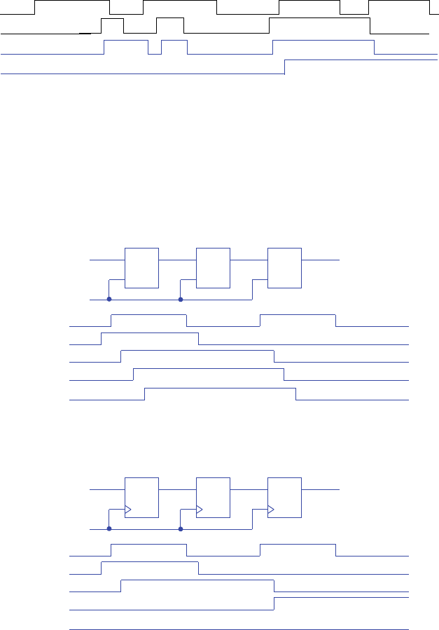
3.16 Create a circuit of three level-sensitive D latches connected in series (the output of
one is connected to the input of the next). Use a timing diagram to show how a clock
with a long high-time can cause the value at the input of the first D latch to trickle
through more than one latch during the same clock cycle.
3.17 Repeat Exercise 3.16 using edge-triggered D flip-flops, and use a timing diagram to
show how the input of the first D flip-flop does not trickle through to the next flip-
flop no matter how long the clock signal is high.
Figure 3.100
D
C
Q(latch)
Q(FF)
Clk
D1
D2/Q1
D3/Q2
Q3
DQ
Q1 D2
D1 DQ
Q2 D3 DQ Q3
Clk
CCC
Clk
D1
D2/Q1
D3/Q2
Q3
DQ
Q1 D2
D1 DQ
Q2 D3 DQ Q3
Clk
3.1 Exercises b47
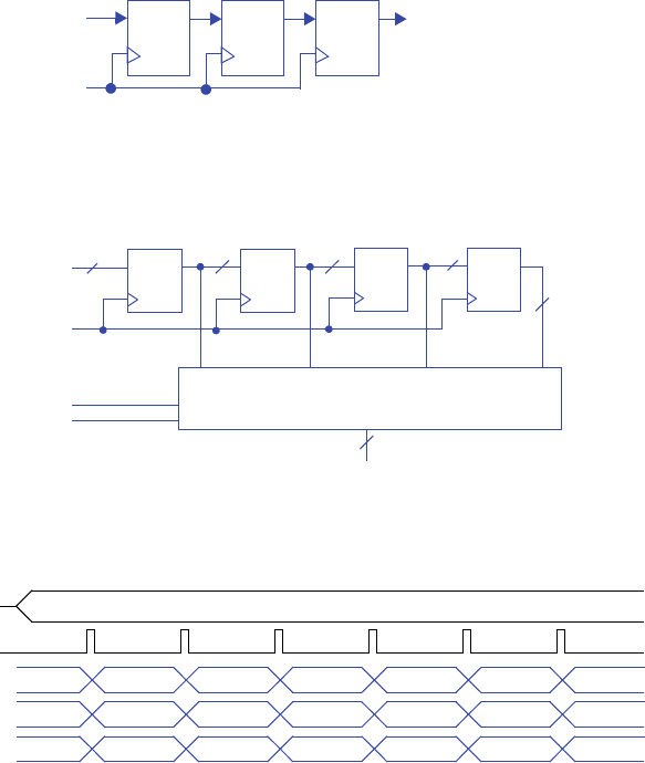
3.18 A circuit has an input X that is connected to the input of a D flip-flop. Using addi-
tional D flip-flops, complete the circuit so that an output Y equals the output of X’s
flip-flop but delayed by two clock cycles.
3.19 Using four registers, design a circuit that stores the four values present at an 8-bit
input D during the previous four clock cycles. The circuit should have a single 8-bit
output that can be configured using two inputs s1 and s0 to output any one of the
four registers. (Hint: use an 8-bit 4x1 mux.)
3.20 Consider three 4-bit registers connected as in Figure 3.101. Assume the initial values
in the registers are unknown. Trace the behavior of the registers by completing the
timing diagram of Figure 3.102.
X
Clock
Q
DY
Q
DQ
D
DQ
DDQ
Clk
DQ DQ
s0
s1
0123
8 8 8 8
8
8
out
s0
s1
8-bit 4x1 mux
Figure 3.102
a3..a0
b3..b0
c3..c0
d3..d0
C
11148159 1533914000727
14 5 15 9 0 2
5
5
15
15 9
9
0
0
???
???
???
???
???
14
14
48 c3 Sequential Logic Design -- Controllers
3.21 Consider three 4-bit registers connected as in Figure 3.103. Assume the initial values
in the registers are unknown. Trace the behavior of the registers by completing the
timing diagram of Figure 3.104.
Section 3.3: Finite-State Machines (FSMs)
3.22 Draw a timing diagram (showing inputs, state, and outputs) for the flight-attendant
call-button FSM of Figure 3.53 for the following scenario. Both inputs Call and
Cncl are initially 0. Call becomes 1 for 2 cycles. Both inputs are 0 for 2 more cycles,
then Cncl becomes 1 for 1 cycle. Both inputs are 0 for 2 more cycles, then both
inputs Call and Cncl become 1 for 2 cycles. Both inputs become 0 for 1 last cycle.
Assume any input changes occur halfway between two clock edges.
3.23 Draw a timing diagram (showing inputs, state, and outputs) for the code-detector
FSM of Figure 3.58 for the following scenario. (Recall that when a button (or but-
tons) is pressed, a becomes 1 for exactly 1 clock cycle, no matter how long the but-
ton (or buttons) is pressed). Initially no button is pressed. The user then presses
buttons in the following order: red, green, blue, red. Noticing the final state of the
system, can you suggest an improvement to the system to better handle such incor-
rect code sequences?
Do not assign this exercise. The exercise refers to an earlier version of the figure,
which was changed when creating the second edition, and thus the exercise
description is not consistent with the figure.
Figure 3.104
a3..a0
b3..b0
c3..c0
d3..d0
C
11148159151533914000727
14
14
14
5
5
5
15
15
15
9
9
9
0
0
2
???
???
??? ???
???
???
Clk
Call
Cncl
State
L
LightOff LightOn LightOff LightOn
3.1 Exercises b49
3.24 Draw a state diagram for an FSM that has an input X and an output Y. Whenever X
changes from 0 to 1, Y should become 1 for two clock cycles and then return to 0 --
even if X is still 1. (Assume for this problem and all other FSM problems that an
implicit rising clock is ANDed with every FSM transition condition.)
3.25 Draw a state diagram for an FSM with no inputs and three outputs x, y, and z. xyz
should always exhibit the following sequence: 000, 001, 010, 100, repeat. The out-
put should change only on a rising clock edge. Make 000 the initial state.
3.26 Do Exercise 3.25, but add an input I that can stop the sequence when set to 0. When
input I returns to 1, the sequence resumes from where it left off.
Inputs: X, Outputs: Y
A
Y=0
B
Y=1
C
Y=1
X’
X
D
Y=0
X’
X
X
X’
Inputs: None, Outputs: x,y,z
xyz = 001
xyz = 010
xyz = 100
xyz = 000
A
B
C
D
Inputs: I, Outputs: x,y,z
xyz = 001 xyz = 010
xyz = 100
xyz = 000
A
B
C
D
II
I
I
I’
I’
I’
I’
50 c3 Sequential Logic Design -- Controllers
3.27 Do Exercise 3.25, but add an input I that can stop the sequence when set to 0. When
I returns to 1, the sequence starts from 000 again..
3.28 A wristwatch display can show one of four items: the time, the alarm, the stopwatch,
or the date, controlled by two signals s1 and s0 (00 displays the time, 01 the alarm,
10 the stopwatch, and 11 the date—assume s1s0 control an N-bit mux that passes
through the appropriate register). Pressing a button B (which sets B = 1) sequences
the display to the next item. For example, if the presently displayed item is the date,
the next item is the current time. Create a state diagram for an FSM describing this
sequencing behavior, having an input bit B, and two output bits s1 and s0. Be sure to
only sequence forward by one item each time the button is pressed, regardless of
how long the button is pressed—in other words, be sure to wait for the button to be
released after sequencing forward one item. Use short but descriptive names for
each state. Make displaying the time be the initial state.
Inputs: I, Outputs: x,y,z
xyz = 001 xyz = 010
xyz = 100
xyz = 000
A
B
C
D
I
I
I
I’
I
I’
xyz = 001
B2
I’
I
xyz = 010
C2
I’
xyz = 100
D2
I’
I’
I
I’
I
Inputs: B, Outputs: s1,s0
Time
Alarm
s1s0=00
s1s0=01
Stopwatch
s1s0=10
Date
s1s0=11
Alarm2
s1s0=01
Stopwatch2
s1s0=10
Date2
s1s0=11
Time2
s1s0=00
B’
B
B’
B
B’ B’
BB
B’
B’
B
B
B’
B’
B
B
3.1 Exercises b51
3.29 Extend the state diagram created in Exercise 3.28 by adding an input R. R=1 forces
the FSM to return to the state that displays the time.
3.30 Draw a state diagram for an FSM with an input gcnt and three outputs, x, y and z.
The xyz outputs generate a sequence called a Gray code in which exactly one of the
three outputs changes from 0 to 1 or from 1 to 0. The Gray code sequence that the
FSM should output is 000, 010, 011, 001, 101, 111, 110, 100, repeat. The output
should change only on a rising clock edge when the input gcnt = 1. Make the ini-
tial state 000.
3.31 Trace through the execution of the FSM created in Exercise 3.30 by completing the
timing diagram in Figure 3.107, where C is the clock input. Assume the initial state
is the state that sets xyz to 000.
Inputs: B,R, Outputs: s1,s0
Time
Alarm
s1s0=00
s1s0=01
Stopwatch
s1s0=10
Date
s1s0=11
Alarm2
s1s0=01
Stopwatch2
s1s0=10
Date2
s1s0=11
Time2
s1s0=00
R+B’
R’B
R+B’
R’B R’B’ R’B’
R’B R’B
R’B’
R’B’
R’B
R’B
R’B’
R’B’
R’B
R’B
R
R
RR
R
R
Inputs: gcnt
Outputs: x, y, z
A
B C
D
E
F
G
H
gcnt’
gcnt
gcnt gcnt
gcnt
gcnt
gcnt
gcnt
gcnt
xyz=000 xyz=010 xyz=011
xyz=001
xyz=101
xyz=111
xyz=110
xyz=100
gcnt’
gcnt’
gcnt’
gcnt’
gcnt’
gcnt’
gcnt’
Figure 3.105
gcnt
x
y
z
C
52 c3 Sequential Logic Design -- Controllers
3.32 Draw a timing diagram for the FSM in Figure 3.108with the FSM starting in state
Wait. Choose input values such that the FSM reaches state EN, and returns to Wai t.
3.33 For FSMs with the following numbers of states, indicate the smallest possible num-
ber of bits for a state register representing those states:
a. 4
b. 8
c. 9
d. 23
e. 900
a) 2 bits
b) 3 bits
c) 4 bits
d) 5 bits
e) 10 bits
3.34 How many possible states can be represented by a 16-bit register?
216 = 65,536 possible states
3.35 If an FSM has N states, what is the maximum number of possible transitions that
could exist in the FSM? Assume that no pair of states has more than one transition in
the same direction, and that no state has a transition point back to itself. Assuming
there are a large number of inputs, meaning the number of transitions is not limited
by the number of inputs? Hint: try for small N, and then generalize.
For two states A and B, there are only 2 possible transitions: A->B and B->A. For
three states A, B, and C, possible transitions are A->B, A->C, B->A, B->C, C->A,
and C->B, for 6 possible transitions. For each of N states, there can be up to N-1
transitions pointing to other states. Thus, the maximum possible is N*(N-1).
3.36 *Assuming one input and one output, how many possible four-state FSMs exist?
The complete solution to this challenge problem is not provided.The solution
involves determining a way to enumerate all possible transitions from each state,
and all possible actions in a state.
C
State Wai t
s
r
a
en
Start C1 C2 C3 C4 EN Wait
3.1 Exercises b53
3.37 *Suppose you are given two FSMs that execute concurrently. Describe an approach
for merging those two FSMs into a single FSM with identical functionality as the
two separate FSMs, and provide an example. If the first FSM has N states and the
second has M states, how many states will the merged FSM have?
The complete solution to this challenge problem is not provided. The solution
involves creating the “cross product” of the two FSMs. If the first FSM has states n0
and n1, and the second has states m0, m1, and m2, then the cross product is an FSM
having 2*3=6 states, which we might call n0m0, n0m1, n0m2, n1m0, n1m1, and
n1m2. In each state, the actions of the two states from which that state is composed
must all be included. Transitions must be combined also so that the transitions of the
original FSMs are obeyed in the new FSM.
3.38 *Sometimes dividing a large FSM into two smaller FSMs results in simpler circuitry.
Divide the FSM shown in Figure 3.111 into two FSMs, one containing G0-G3, the
other containing G4-G7. You may add additional states, transitions, and inputs or
outputs between the two FSMs, as required. Hint: you will need to introduce signals
between the FSMs for one FSM to tell the other FSM to go to some state.
The solution idea involves the first FSM going to some new “idle” state rather than
going to G4. Upon going to that idle state, the first FSM should tell the second FSM
to go to G4. Meanwhile, the second FSM should be waiting in some new state until
instructed to go to G4. Likewise, the second FSM should tell the first FSM when to
go from its idle state to G0.
Section 3.4: Controller Design
3.39 Using the process for designing a controller, convert the FSM of Figure 3.109 to a
controller, implementing the controller using a state register and logic gates.
Step 1 - Capture the FSM
The appropriate FSM is given above.
Figure 3.107
Inputs: a
Outputs: y
A
BC
D
a
a’
a’
a
y=0
y=1 y=1
y=0
54 c3 Sequential Logic Design -- Controllers
Step 2A - Set up the architecture
Step 2B - Encode the states
A straightforward encoding is A=00, B=01, C=10, D=11.
Step 2C - Fill in the truth table
Step 2D - Implement the combinational logic
n1 = s1’s0a + s1s0’a’ + s1s0’a = s1’s0a + s1s0’
n0 = s1’s0’a’ + s1’s0a’ + s1s0’a’ + s1s0’a = s1’a’ + s1s0’
y = s1’s0a’ + s1’s0a + s1s0’a’ + s1s0’a = s1’s0 + s1s0’ = s1 xor s0
Combinational
Logic
ay
State Register
s1 s0
n1
n0
Inputs Outputs
s1 s0 a n1 n0 y
000010
001000
010011
011101
100111
101111
110000
111000
a
y
State Register
s1 s0
n1
n0
3.1 Exercises b55
3.40 Using the process for designing a controller, convert the FSM of Figure 3.110 to a
controller, implementing the controller using a state register and logic gates.
Step 1 - Capture the FSM
The appropriate FSM is given above.
Step 2A - Set up the architecture
Step 2B - Encode the states
A straightforward encoding is A=00, B=01, C=10, D=11.
Figure 3.108
Inputs: a,b
Outputs: y
A
BC
D
a
a’b
a’
a
y=0
y=1 y=1
y=0
a’b’
b’
b
Combinational
Logic
ay
State Register
s1 s0
n1
n0
b
56 c3 Sequential Logic Design -- Controllers
Step 2C - Fill in the truth table
Step 2D - Implement the combinational logic
n1 = s1’s0’a’b’ + s1’s0a + s1s0’
n0 = s1’s0’a’b + s1’s0a’ + s1s0’b
y = s1’s0 + s1s0’
Note: The above equations can be minimized further.
3.41 Using the process for designing a controller, convert the FSM you created for Exer-
cise 3.24 to a controller, implementing the controller using a state register and logic
gates.
Step 1 - Capture the FSM
The FSM was created during Exercise 3.25.
Inputs Outputs
s1 s0 a b n1 n0 y
0000100
0001010
0010000
0011000
0100011
0101011
0110101
0111101
1000101
1001111
1010101
1011111
1100000
1101000
1110000
1111000
Inputs: None, Outputs: x,y,z
xyz = 001
xyz = 010
xyz = 100
xyz = 000
A
B
C
D
3.1 Exercises b57
Step 2A - Set up the architecture
Step 2B - Encode the states
A straightforward encoding is A=00, B=01, C=10, D=11.
Step 2C - Fill in the truth table
Step 2D - Implement the combinational logic
n1 = s1’s0 + s1s0’ = s1 XOR s0
n0 = s1’s0’ + s1s0’ = s0’
x = s1s0
y = s1s0’
z = s1’s0
Combinational
Logic
z
State Register
s1 s0
n1
n0
s2
y
x
Inputs Outputs
s1 s0 n1 n0 x y z
0001000
0110001
1011010
1100100

58 c3 Sequential Logic Design -- Controllers
3.42 Using the process for designing a controller, convert the FSM you created for Exer-
cise 3.28 to a controller, implementing the controller using a state register and logic
gates.
Step 1 - Capture the FSM
The FSM was created during Exercise 3.28.
Step 2A - Set up the architecture
Step 2B - Encode the states
A straightforward encoding is Time2=000, Alarm=001, Alarm2=010, Stop-
watch=011, Stopwatch2=100, Date=101, Date2=110, Time=111.
Inputs: B, Outputs: s1,s0
Time
Alarm
s1s0=00
s1s0=01
Stopwatch
s1s0=10
Date
s1s0=11
Alarm2
s1s0=01
Stopwatch2
s1s0=10
Date2
s1s0=11
Time2
s1s0=00
B’
B
B’
B
B’ B’
BB
B’
B’
B
B
B’
B’
B
B
Combinational
Logic
B
State Register
s1 s0
n1
n0
s2
n2
s0
s1

3.1 Exercises b59
Step 2C - Fill in the truth table
Step 2D - Implement the combinational logic
n2 = s2’s1s0B’ + s2s1’ + s2s0’ + s2B
n1 = s1s0’ + s1B + s2s0B + s2’s1’s0B’
n0 = s0’B + s2’B + s1B + s2s1’s0B’
s1 = s2s0’ + s2s1’ + s2’s1s0
s0 = s1 XOR s0
3.43 Using the process for designing a controller, convert the FSM you created for Exer-
cise 3.30 to a controller, implementing the controller using a state register and logic
gates.
Step 1 - Capture the FSM
The FSM was created during Exercise 3.30.
Inputs Outputs
s2s1s0Bn2n1n0s1s0
000000000
000100100
001001001
001100101
010001001
010101101
011010010
011101110
100010010
100110110
101010111
101111011
110011011
110111111
111000000
111111100
Inputs: gcnt
Outputs: x, y, z
A
B C
D
E
F
G
H
gcnt’
gcnt
gcnt gcnt
gcnt
gcnt
gcnt
gcnt
gcnt
xyz=000 xyz=010 xyz=011
xyz=001
xyz=101
xyz=111
xyz=110
xyz=100
gcnt’
gcnt’
gcnt’
gcnt’
gcnt’
gcnt’
gcnt’
60 c3 Sequential Logic Design -- Controllers
Step 2A - Set up the architecture
Step 2B - Encode the states
A straightforward encoding is A=000, B=001, C=010, D=011, E=100, F=101,
G=110, H=111.
Step 2C - Fill in the truth table
Step 2D - Implement the combinational logic
n2 = s2’s1s0gcnt + s2s1’ + s2s1s0’ + s2s1s0gcnt’
n1 = s2’s1’s0gcnt + s2’s1s0’ + s2’s1s0gcnt’ + s2s1’s0gcnt + s2s1s0’ + s2s1s0gcnt’
n0 = s2’s1’s0’gcnt + s2’s1’s0gcnt’ + s2’s1s0’gcnt + s2’s1s0gcnt’ + s2s1’s0’gcnt +
s2s1’s0gcnt’ + s2s1s0’gcnt + s2s1s0gcnt’
x = s2
y = s2’s1’s0 + s2’s1s0’ + s2s1’s0 + s2s1s0’
z = s2’s1 + s2s1’
Note: The above equations can be minimized further.
Combinational
Logic
gcnt
z
State Register
s1 s0
n1
n0
s2
n2
y
x
Inputs Outputs
s2 s1 s0 gcnt n2 n1 n0 x y z
A0000 000000
0001 001000
B0010 001010
0011 010010
C0100 010011
0101 011011
D0110 011001
0111 100001
E1000 100101
1001 101101
F1010 101111
1011 110111
G1100 110110
1101 111110
H1110 111100
1111 000100
3.1 Exercises b61
3.44 Using the process for designing a controller, convert the FSM in Figure 3.111 to a
controller, stopping once you have created the truth table. Note: your truth table will
be quite large, having 32 rows -- you might therefore want to use a computer tool,
like a word processor or spreadsheet, to draw the table.
Step 1 - Capture the FSM
The FSM is given in Figure 3.111.
Step 2A - Set up the architecture
Step 2B - Encode the states
A straightforward encoding is G0=000, G1=001, G2=010, G3=011, G4=100,
G5=101, G6=110, G7=111.
Figure 3.111
G0
G1
G2 G3 G4
G5
Inputs: g,r
Outputs: x,y,z
G6
xyz=110
G7
xyz=000
xyz=100
xyz=010 xyz=011 xyz=111 xyz=101 xyz=001
gr’
gr’
gr’ gr’ gr’ gr’ gr’
r
rrrr rg
g’+r
g’r’ g’r’ g’r’ g’r’ g’r’ g’
g’r’
Combinational
Logic
g
z
State Register
s1 s0
n1
n0
s2
n2
y
x
r

62 c3 Sequential Logic Design -- Controllers
Step 2C - Fill in the truth table
Inputs Outputs
s3s2s1grn2 n1 n0 x y z
G0
00000000000
00001000000
00010001000
00011000000
G1
00100001100
00101000100
00110010100
00111000100
G2
01000010110
01001000110
01010011110
01011000110
G3
01100011010
01101000010
01110100010
01111000010
G4
10000100011
10001000011
10010101011
10011000011
G5
10100101111
10101000111
10110110111
10111000111
G6
11000110101
11001000101
11010111101
11011000101
G7
11100111001
11101111001
11110000001
11111000001
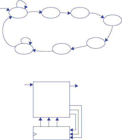
3.1 Exercises b63
3.45 Create an FSM that has an input X and an output Y. Whenever X changes from 0 to 1,
Y should become 1 for five clock cycles and then return to 0 -- even if X is still 1.
Using the process for designing a controller, convert the FSM to a controller, stop-
ping once you have created the truth table.
Step 1 - Capture the FSM
Step 2A - Set up the architecture
Step 2B - Encode the states
A straightforward encoding is Wait=000, Y1=001, Y2=010, Y3=011, Y4=100,
Y5=101, Wait2=110.
Inputs: X
Outputs: Y
Wait
x’
y=0
Y1
xY2
Y3
Y4
Y5
Wait2
x
x’
y=0 y=1
y=1 y=1
y=1
y=1
Combinational
Logic
X
State Register
s1 s0
n1
n0
s2
n2
Y

64 c3 Sequential Logic Design -- Controllers
Step 2C - Create the state table
Step 2D - Implement the combinational logic
n2 = s2s1’ + s2’s1s0 + s2s0’X’
n1 = s1’s0 + s2’s1s0’ + s1s0’X’
n0 = s2s1’s0’ + s2’s1s0’ + s2’s0’X
Y = (s2 xor s1) + s2’s0
Inputs Outputs
s2s1s0Xn2n1n0Y
Wait 00000000
00010010
Y1 00100101
00110101
Y2 01000111
01010111
Y3 01101001
01111001
Y4 10001011
10011011
Y5 10101101
10111101
Wait2 11001100
11010000
11100000
11110000
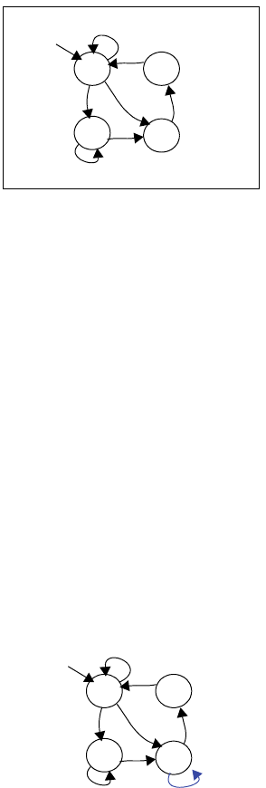
3.1 Exercises b65
3.46 The FSM in Figure 3.112 has two problems: one state has non-exclusive transitions,
and another state has incomplete transitions. By ORing and ANDing the conditions
for each state’s transitions, prove that these problems exist. Then, fix these problems
by refining the FSM, taking your best guess as to what was the FSM creator’s intent.
If we AND each pair of transitions with each other in state A, we get:
a * a’b = 0*b = 0
a’b * b’ = a’*0 = 0
a*b’ = ab’, which is not equal to 0.
State A’s transitions are thus not exclusive, i.e., both a and b’ could be simultane-
ously true.
ORing state B’s transitions yields:
a+a’ = 1
ORing state C’s transitions yields:
b
Clearly, state C’s transitions are not completely specified, because their ORing
doesn’t result in 1. If b is 0, the FSM doesn’t indicate what to do from state C.
We can address both of these problems with the following changes. The designer
likely wanted to stay in state A when a is true, and go to B on a’b and go to C on
a’b’. The designer likely wanted to stay in state C when b is 0.
Figure 3.112
Inputs: a,b
Outputs: y
A
BC
D
a
a’b
a’
a
y=0
y=1 y=1
y=0
b’ b
Inputs: a,b
Outputs: y
A
BC
D
a
a’b
a’
a
y=0
y=1 y=1
y=0
a’b’ b
b’

66 c3 Sequential Logic Design -- Controllers
3.47 Reverse engineer the poorly-designed three-cycles high circuit in Figure 3.41 to an
FSM. Explain why the behavior of the circuit, as described by the FSM, is undesir-
able.
Step 2D was already completed, so we’ll begin with Step 2C:
Step 2C - Fill in the truth table
Note that this circuit does not have the standard structure of a controller. However,
we could say that the three flip-flops represent a 3-bit state register (so the leftmost
flip-flop’s value is the s2 signal, the middle flip-flop’s value is the s1 signal, and the
rightmost flip-flop’s value is the s0 signal. Similarly, the input to the leftmost flip-
flop, b, is n2, the signal from the output of the leftmost flip-flop to the input of the
middle flip-flop is n1, and the signal from the output of the middle flip-flop is n0).
n2 = b; n1 = s2; n0 = s1; x = s2 + s1 + s0
Step 2B - Encode the states
A straightforward encoding is A=000, B=001, C=010, D=011, E=100, F=101,
G=110, H=111
Step 2A - Set up the architecture
Inputs Outputs
s2 s1 s0 b n2 n1 n0 x
00000000
00011000
00100001
00111001
01000011
01011011
01100011
01111011
10000101
10011101
10100101
10111101
11000111
11011111
11100111
11111111
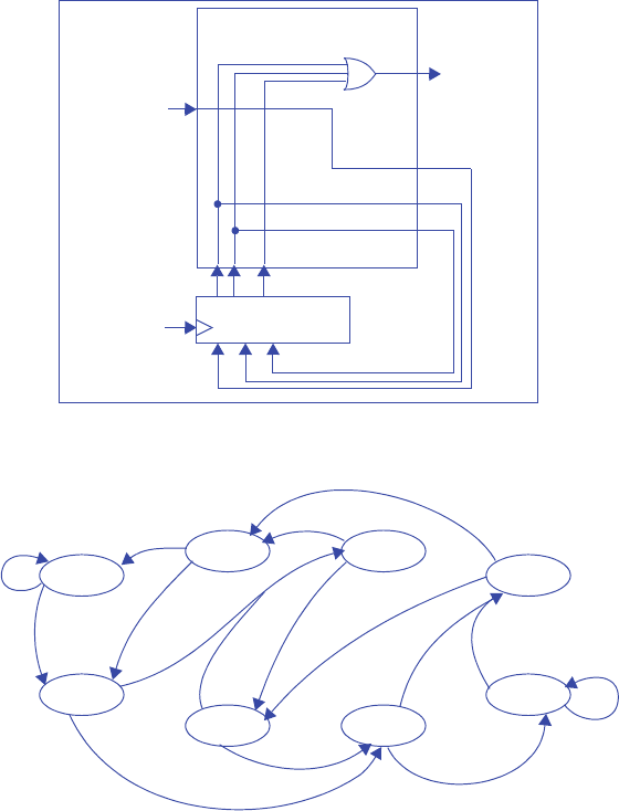
3.1 Exercises b67
Step 1: Capture the FSM
The behavior of this circuit is undesirable because if, after transitioning from A and
before transitioning back to A, the user presses the button again, the output will stay
on for more than three cycles.
State register
Combinational logic
s1s2
n0
n1
FSM
outputs
inputs
b
x
FSM
clk
s0
n2
Inputs: b, Outputs: x
A
x=0 B
x=1
C
x=1
D
x=1
H
x=1
G
x=1
F
x=1
E
x=1
b’
b
b’
b
b’
b’
b
b
b’
b
b
b’
b
b’
b’
b

68 c3 Sequential Logic Design -- Controllers
3.48 Reverse engineer the behavior of the sequential circuit shown in Figure 3.113.
For this problem, we carry out the controller design process in reverse. We already
have step 2D completed above, so we will begin with step 2C.
Step 2C - Fill in the truth table
Step 2B - Encode the states
We will name the encodings as states as follows: 00=A, 01=B, 10=C, and 11=D.
Step 2A- Set up the architecture
The architecture has already been defined
Figure 3.113
State register
Combinational logic
s0s1
n0
n1
FSM
outputs
inputs
a
y
FSM
clk
Inputs Outputs
s1 s0 a n1 n0 y
00 0 0 0 0
00 1 0 1 0
01 0 0 0 0
01 1 1 0 0
10 0 0 0 1
10 1 1 0 1
11 0 0 0 0
11 1 0 0 0
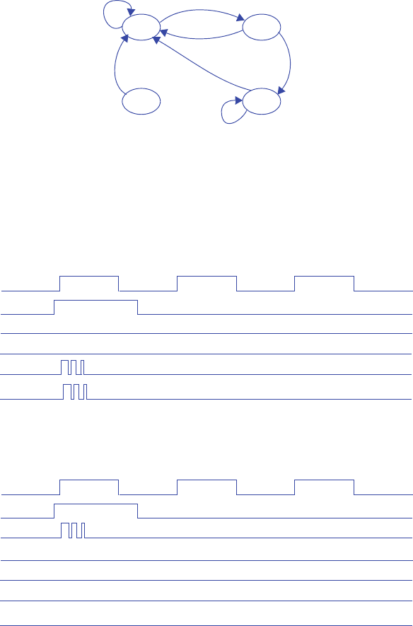
3.1 Exercises b69
Step 1 - Capture the FSM
Section 3.5: More on Flip-Flops and Controllers
3.49 Use a timing diagram to illustrate how metastability can yield incorrect output for
the secure car key controller of Figure 3.69. Use a second timing diagram to show
how the synchronizer flip-flop introduced in Figure 3.84 may reduce the likelihood
of such incorrect output.
Without Synchronizer:
With Synchronizer:
Note that in this case, even though metastability caused the Synchronizer flip-flop to
end in zero (which caused us to miss the pulse on “a”), at least our state register did
not go metastable, and as a result we did not experience incorrect output.
Inputs: a
Outputs: y
A B
D C
y=0 y=0
y=1y=0
a’ a
a’
a
a
a’
Clk
s2
r
s1
s0
a
Clk
s2
r
s1
s0
a
Synchronizer

70 c3 Sequential Logic Design -- Controllers
3.50 Design a controller with a 4-bit state register that gets synchronously initialized to
state 1010 when an input reset is set to 1.
3.51 Redraw the laser-timer controller timing diagram of Figure 3.63 for the case of the
output being registered as in Figure 3.88.
One more clock pulse has been added to show that the change of x is delayed by 1 pulse.
D Q
S
State
D Q
R
DQ
S
DQ
R
s3 s2 s1 s0
Register
reset
Controller
combinational logic
n0
n1
n2
n3
Clk
b
x
State Off Off On1 On2
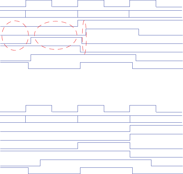
3.1 Exercises b71
3.52 Draw a timing diagram for three clock cycles of the sequence generator controller of
Figure 3.68 assuming that AND gates have a delay of 2 ns and inverters (including
inversion bubbles) have a delay of 1 ns. The timing diagram should show the incor-
rect outputs that appear temporarily due to glitching. Then, introduce registered out-
puts to the controller using flip-flops at the outputs, and show a new timing diagram,
which should no longer have glitches (but the output may be shifted in time).
Let’s assume the delay of an XOR gate is the same as for an AND gate.
Unregistered Output:
Registered Output:
Note that we do not register the n1 or n0 outputs -- they are inputs to the state regis-
ter.
Also note that the glitch here is not a temporary spurious ouput value on one control
line, but a temporary spurious value on (wxyz) due to the varying delays for each of
w, x, y, and z.
Clk
x
s1s0 00 01 10 11
w
y
z
n1
n0
Clk
x
s1s0 00 01 10 11
w
y
z
n1
n0
72 c3 Sequential Logic Design -- Controllers
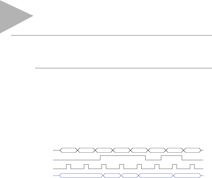
67
CHAPTER
4
DATAPATH COMPONENTS
4.1 EXCERCISES
Exercises marked with an asterisk (*) represent especially challenging problems.
For exercises relating to datapath components, each problem indicates whether the
problem emphasizes the component’s internal design or the component’s use.
Section 4.2: Registers
4.1. Trace the behavior of an 8-bit parallel load register with 8-bit input I, 8-bit output Q,
and load control input ld by completing the timing diagram in Figure 4.95.
I
ld
clk
5 124 92 0165021
Q??? 124 65 92 0
Figure 4.95
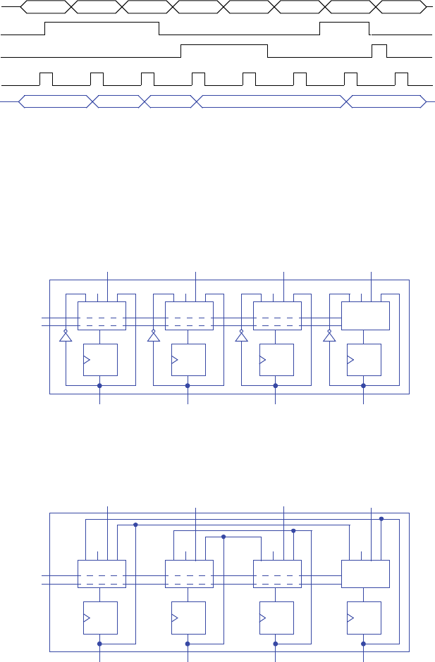
68 c4 Datapath Components
4.2 Trace the behavior of an 8-bit parallel load register with 8-bit input I, 8-bit output Q,
load control input ld, and synchronous clear input clr by completing the timing dia-
gram in Figure 4.96.
4.3 Design a 4-bit register with 2 control inputs s1 and s0, 4 data inputs I3, I2, I1 and I0,
and 4 data outputs Q3, Q2, Q1 and Q0. When s1s0=00, the register maintains its
value. When s1s0=01, the register loads I3..I0. When s1s0=10, the register clears
itself to 0000. When s1s0=11, the register complements itself, so for example 0000
would become 1111, and 1010 would become 0101. (Component design problem).
4.4 Repeat the previous problem, but when s1s0=11, the register reverses its bits, so
1110 would become 0111, and 1010 would become 0101. (Component design prob-
lem).
I
ld
clk
5 124 92 0165021
Q
clr
??? 124 0 01
Figure 4.96
Q
D
s1
s0
3210
0
Q
D
s1
s0
3 210
0
Q
D
s1
s0
3 210
0
Q
D
s1
s0
3210
0
I3 I2 I1 I0
Q3 Q2 Q1 Q0
s1
s0
Q
D
s1
s0
3210
0
Q
D
s1
s0
3 210
0
Q
D
s1
s0
3 210
0
Q
D
s1
s0
3210
0
I3 I2 I1 I0
Q3 Q2 Q1 Q0
s1
s0
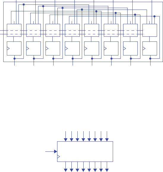
4.1 Excercises b69
4.5 Design an 8-bit register with 2 control inputs s1 and s0, 8 data inputs I7..I0, and 8
data outputs Q7..Q0. s1s0=00 means maintain the present value, s1s0=01 means
load, and s1s0=10 means clear. s1s0=11 means to swap the high nibble with the low
nibble (a nibble is 4 bits), so 11110000 would become 00001111, and 11000101
would become 01011100. (Component design problem).
4.6 The radar gun used by a police officer outputs a radar signal and measures the speed
of the cars as they pass. However, when the officer wants to ticket an individual for
speeding, he must save the measured speed of the car on the radar unit. Build a sys-
tem to implement a speed save feature for the radar gun. The system has an 8-bit
speed input S, an input B from the save button on the radar gun, and an 8-bit output
D that will be sent to the radar gun’s speed display. (Component use problem).
s1
s0
Q
D
s1
s0
3210
Q
D
s1
s0
3210
Q
D
s1
s0
3210
Q
D
s1
s0
3210
Q
D
s1
s0
3210
Q
D
s1
s0
3210
Q
D
s1
s0
3210
Q
D
s1
s0
3210
00000000
Q7 Q6 Q5 Q4 Q3 Q2 Q1 Q0
I6 I5 I4 I3 I2 I1I7 I0
ld
Q7 Q6 Q5 Q2 Q1 Q0Q4 Q3
I7 I6 I5 I2 I1 I0I4 I3
S7 S6 S4 S3 S2 S1 S0S5
D7 D6 D4 D3 D2 D1 D0D5
B

70 c4 Datapath Components
4.7 Design a system with an 8-bit input I that can be stored in 8-bit registers A, B, and/or
C when input La, Lb, and/or Lc is 1, respectively. So if inputs La and Lb are 1, then
registers A and B will be loaded with input I, but register C will keep its current
value. Furthermore, if input R is 1, then the register values swap such that A=B,
B=C, and C=A. Input R has priority over the L inputs. The system has one clock
input also. (Component use problem.)
Section 4.3: Adders
4.8 Trace the values appearing at the outputs of a 3-bit carry-ripple adder for every one-
full-adder-delay time period when adding 111 with 011. Assume all inputs were pre-
viously 0 for a long time.
ld
Q
I
A (8 bits)
i0 i1
s
d
ld
Q
I
B (8 bits)
ld
Q
I
C (8 bits)
I
8-bit mux
i0 i1
s
d
8-bit mux
i0 i1
s
d
8-bit mux
R
La
Lb
Lc
abci
sco
abci
sco
ab
sco
11101 1
0010
abci
sco
abci
sco
ab
sco
11101 1
0101
abci
sco
abci
sco
ab
sco
11101 1
0101
Second Delay
First Delay
Third Delay
1111
11
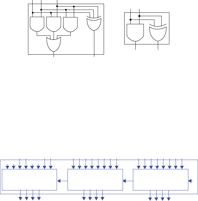
4.1 Excercises b71
4.9 Assuming all gates have a delay of 1 ns, compute the longest time required to add
two numbers using an 8-bit carry-ripple adder.
An 8-bit carry-ripple adder contains 7 full adders and 1 half adder. Each full adder
has 2 gate delays and the half adder has 1 gate delay. Therefore a minimum of (7 FA
* 2 gate delay/FA * + 1 HA * 1 gate delay/HA) * 1ns/gate delay = 15 ns is required
to ensure that the carry-ripple adder’s sum is correct.
4.10 Assuming AND gates have a delay of 2 ns, OR gates have a delay of 1 ns, and XOR
gates have a delay of 3 ns, compute the longest time required to add two numbers
using an 8-bit carry-ripple adder.
From the illustration above, we see that both the FA and HA have a maximum gate
delay of 3 ns. Therefore, 8 adders * 3 ns/adder = 24 ns is required for an 8-bit carry-
ripple adder to ensure a correct sum is on the adder’s output.
An answer of 23 ns is also acceptable since the carry out of a half-adder will be cor-
rect after 2 ns, not 3 ns, and a half-adder may be used for adding the first pair of bits
(least significant bits) if the 8-bit adder has no carry-in.
4.11 Design a 10-bit carry-ripple adder using 4-bit carry-ripple adders. (Component use
problem).
ab ci
co s
ab
co s
23
3
1
222
Full Adder Half Adder
co
s2 s1s3
a3 a2 a1 b2 b1 b0a0 b3
a3 a2 a0 b3 b2 b1 b0a1
s3 s2 s1 s0
ci
s0
co
s2 s1s3
a3 a2 a1 b2 b1 b0a0 b3
a7 a6 a4 b7 b6 b5 b4a5
s7 s6 s5 s4
ci
s0
co
s2 s1s3
a3 a2 a1 b2 b1 b0a0 b3
00
a8
00
b9 b8a9
co s9 s8
ci
s0
0
4-bit adder 4-bit adder 4-bit adder
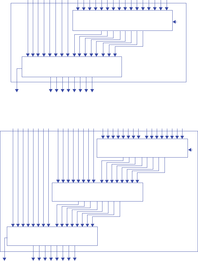
72 c4 Datapath Components
4.12 Design a system that computes the sum of three 8-bit numbers using 8-bit carry-rip-
ple adders. (Component use problem).
4.13 Design an adder that computes the sum of four 8-bit numbers, using 8-bit carry-rip-
ple adders. (Component use problem).
Another correct solution would add C+D, and then add the results to the result of
A+B. That solution also uses just three adders, but actually has less delay.
co
s2 s1s3
b7 b6 b5 b2 b1 b0b4 b3
b7 b6 b4 b3 b2 b1 b0b5
ci
s0
0
a7 a6 a5 a2 a1 a0a4 a3
a7 a6 a4 a3 a2 a1 a0a5
s6 s5s7 s4
c7 c6 c4 c3 c2 c1 c0c5
co
s2 s1s3
b7 b6 b5 b2 b1 b0b4 b3
ci
s0
a7 a6 a5 a2 a1 a0a4 a3
s6 s5s7 s4
co s7 s6 s5 s1s3 s2 s0s4
8-bit adder
8-bit adder
co
s2 s1s3
ci
s0
0
a6 a5 a2 a1 a0a4
a7 a6 a4 a3 a2 a1 a0a5
s6 s5s7 s4
8-bit adder
a3a7 b6 b5 b2 b1 b0b4
b7 b6 b4 b3 b2 b1 b0b5
b3b7
co
s2 s1s3
ci
s0
a6 a5 a2 a1 a0a4
s6 s5s7 s4
8-bit adder
a3a7 b6 b5 b2 b1 b0b4 b3b7
c7 c6 c4 c3 c2 c1 c0c5d7 d6 d4 d3 d2 d1 d0d5
co
s2 s1s3
ci
s0
a6 a5 a2 a1 a0a4
s6 s5s7 s4
8-bit adder
a3a7 b6 b5 b2 b1 b0b4 b3b7
co s7 s6 s5 s1s3 s2 s0s4
4.1 Excercises b73
4.14 Design a digital thermometer system that can compensate for errors in the tempera-
ture sensing device’s output T, which is an 8-bit input to the system. The compensa-
tion amount can be positive only and comes to the system as a 3-bit binary number
c, b, and a (a is the least significant bit), which come from a 3-pin DIP switch. The
system should output the compensated temperature on an 8-bit output U. (Compo-
nent use problem).
co
s2 s1s3
b7 b6 b5 b2 b1 b0b4 b3
00 00
a
0
ci
s0
0
a7 a6 a5 a2 a1 a0a4 a3
T7 T6 T4 T3 T2 T1 T0T5
s6 s5s7 s4
U7 U6 U5 U1U3 U2 U0U4
DIP Switches
bc
from Temperature Sensor
8-bit adder
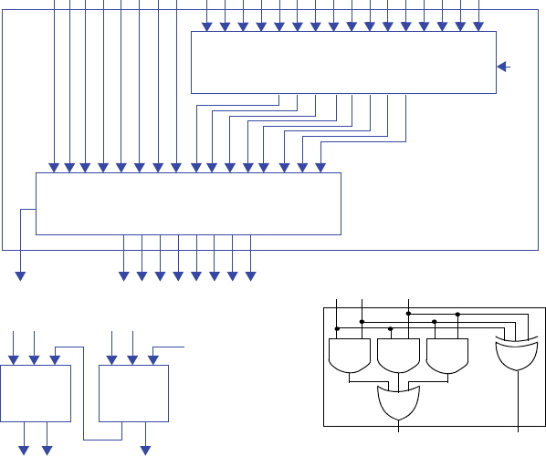
74 c4 Datapath Components
4.15 We can add three 8-bit numbers by chaining one 8-bit carry-ripple adder to the out-
put of another 8-bit carry-ripple adder. Assuming every gate has a delay of 1 time-
unit, compute the longest delay of this three 8-bit number adder. Hint: you may have
to look carefully inside the carry-ripple adders, even inside the full-adders, to cor-
rectly compute the longest delay (Component use problem).
The above shows two 8-bit adders chained together to form a three 8-bit number
adder. Each adder is made from eight full adders, whose configuration is shown at
the bottom left. The bottom right shows the internal design of a full adder. Thus, the
carry out of each stage requires 2 time units (following the problem’s assumption of
1 time unit per gate), and the sum output requires 1 time unit.
The longest delay in a full adder is 2 time units, from carry-in to carry-out. Since
only 1 of the 8 full-adders in the top 8-bit adder has its carry-out unconnected (for a
delay of 1 time unit), the delay from the top adder is 7*2 + 1 = 15 time units. The
lower adder has its carry-out connected, however, giving the lower adder a delay of
8*2 = 16 time units. Thus, our adder has a total delay of 15 + 16 = 31 time units.
co
s2 s1s3
b7 b6 b5 b2 b1 b0b4 b3
b7 b6 b4 b3 b2 b1 b0b5
ci
s0
0
a7 a6 a5 a2 a1 a0a4 a3
a7 a6 a4 a3 a2 a1 a0a5
s6 s5s7 s4
c7 c6 c4 c3 c2 c1 c0c5
co
s2 s1s3
b7 b6 b5 b2 b1 b0b4 b3
ci
s0
a7 a6 a5 a2 a1 a0a4 a3
s6 s5s7 s4
co s7 s6 s5 s1s3 s2 s0s4
8-bit adder
8-bit adder
abci
sco
abci
sco
ab
co s
Full Adder
ci
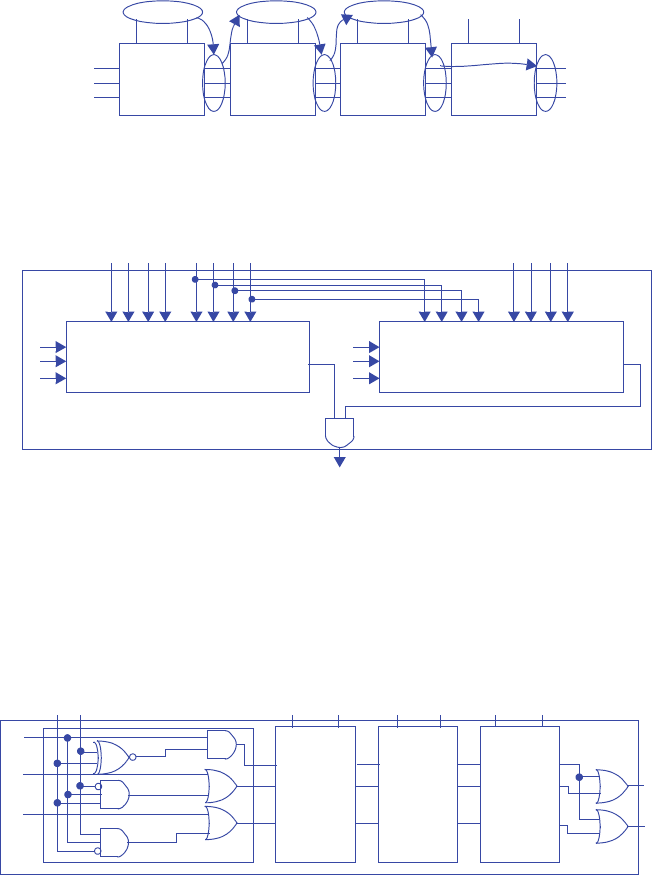
4.1 Excercises b75
Section 4.4: Comparators
4.16 Trace through the execution of the 4-bit magnitude comparator shown in Figure 4.45
when a=15 and b=12. Be sure to show how the comparisons propagate thought the
individual comparators.
4.17 Design a system that determines if three 4-bit numbers are equal, by connecting 4-bit
magnitude comparators together and using additional components if necessary.
(Component use problem).
4.18 Design a 4-bit carry-ripple style magnitude comparator that has two outputs, a
greater-than or equal-to output gte, and a less-than or equal-to output lte. Be sure to
clearly show the equations used in developing the individual 1-bit comparators and
how they are connected to form the 4-bit circuit. (Component design problem).
For each 1-bit comparator, assuming gte means “a >= b” and lte means “a <= b”, gt
= igt+((a XNOR b)*a*b’), lt = ilt+((a XNOR b)*a’*b), e = ie*(a XNOR b). Recall
that XNOR detects equality. a*b’ detects a>b. a’*b detects a<b.
1 1
ab
Stage3
in_gt
in_eq
in_lt
out_gt
out_eq
out_lt
0
1
0
1
ab
Stage2
in_gt
in_eq
in_lt
out_gt
out_eq
out_lt
1
ab
Stage1
in_gt
in_eq
in_lt
out_gt
out_eq
out_lt
1 0
ab
Stage0
in_gt
in_eq
in_lt
out_gt
out_eq
out_lt
AgtB
AeqB
AltB
01
0
1
0
0
1
0
1
0
0
1
0
0
AeqB
4-bit magnitude comparator
AgtB
AltB
Igt
Ieq
Ilt
0
1
0
b3 b2 b1 b0
a3 a2 a1 a0
b3 b2 b1 b0a3 a2 a1 a0
AeqB
4-bit magnitude comparator
AgtB
AltB
Igt
Ieq
Ilt
0
1
0
b3 b2 b1 b0a3 a2 a1 a0
c3 c2 c1 c0
AeqBeqC
a3 b3
0
0
a
igt
ilt
gt
lt
b a
igt
ilt
gt
lt
b a
igt
ilt
gt
lt
b
a2 b2 a1 b1 b0
a0
gte
lte
1
ie e ie e ie e
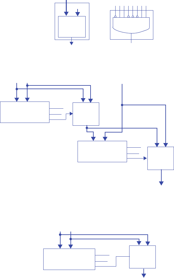
76 c4 Datapath Components
4.19 Design a circuit that outputs 1 if the circuit’s 8-bit input equals 99: (a) using an
equality comparator, (b) using gates only. Hint: In the case of (b), you need only 1
AND gate and some inverters. (Component use problem).
4.20 Use magnitude comparators and logic to design a circuit that computes the minimum
of three 8-bit numbers. (Component use problem).
4.21 Use magnitude comparators and logic to design a circuit that computes the maxi-
mum of two 16-bit numbers. (Component use problem).
8-bit equality
eq
eq
a
I
99
b
comparator
i7 i6 i5 i4 i3 i2 i1 i0
eq
(a) (b)
AltB
AgtB
AeqB
8-bit magnitude
a
a
b
comparator
AeqB
AgtB
AltB
Igt
Ieq
Ilt
b
0
0
1
1x2
s
16-bit mux
i1 i0
d
AltB
AgtB
AeqB
8-bit magnitude
ab
comparator
AeqB
AgtB
AltB
Igt
Ieq
Ilt
0
0
1
1x2
s
16-bit mux
i1 i0
d
min
c
AltB
AgtB
AeqB
16-bit magnitude
a
a
b
comparator
AeqB
AgtB
AltB
Igt
Ieq
Ilt
b
0
0
1
1x2
s
16-bit mux
i1 i0
d
o
4.1 Excercises b77
4.22 Use magnitude comparators and logic to design a circuit that outputs 1 when an 8-bit
input a is between 75 and 100, inclusive. (Component use problem).
4.23 Design a human body temperature indicator system for a hospital bed. Your system
takes an 8-bit input representing the temperature, which can range from 0 to 255. If
the measured temperature is 95 or less, set output A to 1. If the temperature is 96 to
104, set output B to 1. If the temperature is 105 or above, set output C to 1. Use 8-bit
magnitude comparators and additional logic as required. (Component use problem).
A being 95 or less is the same as being less than 96. B should be 1 if the input is
equal or greater than 96, AND if the input is less than 105. C is 1 if the input is equal
to 105 OR if the output is greater than 105.
a
0
0
1
8-bit magnitude
ab
comparator
AeqB
AgtB
AltB
Igt
Ieq
Ilt
0
0
1
8-bit magnitude
ab
comparator
AeqB
AgtB
AltB
Igt
Ieq
Ilt
75 100
o
temp
0
0
1
8-bit magnitude
ab
comparator
AeqB
AgtB
AltB
Igt
Ieq
Ilt
0
0
1
8-bit magnitude
ab
comparator
AeqB
AgtB
AltB
Igt
Ieq
Ilt
96 105
ABC
78 c4 Datapath Components
4.24 You are working as a weight guesser in an amusement park. Your job is to try to
guess the weight of an individual before they step on a scale. If your guess is not
within ten pounds of the individual’s actual weight (higher or lower), the individual
wins a prize. So if you guess 85 and the actual weight is 95, the person does not win;
if you’d guessed 84, the person wins. Build a weight guess analyzer system that out-
puts whether the guess was within ten pounds. The weight guess analyzer has an 8-
bit guess input G, an 8-bit input from the scale W with the correct weight, and a bit
output C that is 1 if the guessed weight was within the defined limits of the game.
Use 8-bit magnitude comparators and additional logic and components as required.
(Component use problem.)
The solution checks if the guess plus 10 is greater than or equal to the actual weight,
AND if guess is less than or equal to the actual weight plus 10. An alternative solu-
tion would would use a subtractor instead of the adder on the left, comparing G with
W-10 rather than comparing G+10 with W.
Section 4.5: Multiplier—Array Style
4.25 Assuming all gates have a delay of 1 time-unit, which of the following designs will
compute the 8-bit multiplication A*9 faster: (a) a circuit as designed in Exercise
4.45 or (b) an 8-bit array style multiplier with one of its inputs connected to a con-
stant value of nine.
(a) The circuit designed in Exercise 4.45 requires 16 time-units (all for the adder’s
computation)
(b) An 8-bit array style multplier requires 1 time-unit to compute the partial prod-
ucts (9 + 10 + 11 + 12 + 13 + 14 + 15) * 2 = 168 time-units to add the partial prod-
ucts, for a total of 169 time-units. Clearly, the circuit designed in Exercise 4.45 will
compute the multiplication faster.
0
0
1
8-bit magnitude
ab
comparator
AeqB
AgtB
AltB
Igt
Ieq
Ilt
0
0
1
8-bit magnitude
ab
comparator
AeqB
AgtB
AltB
Igt
Ieq
Ilt
C
8-bit adder
ab
s
10
G
8-bit adder
ab
s
W10

4.1 Excercises b79
4.26 Design an 8-bit array-style multiplier. (Component design problem).
a7 a6 a5 a4 a3 a2 a1 a0
9-bit adder
10-bit adder
0
0
00
000
11-bit adder
000
12-bit adder
0
13-bit adder
00000
14-bit adder
000000
15-bit adder
0000000
b0
b1
b2
b3
b4
b5
b6
b7
p7...p0
pp1
pp2
pp3
pp4
pp5
pp6
pp7
80 c4 Datapath Components
4.27 Design a circuit to compute F = (A * B * C) + 3*D + 12. A, B, C, and D are 16-bit
inputs, and F is a 16-bit output. Use 16-bit multiplier and adder components, and
ignore overflow issues.
Section 4.6: Subtractors
4.28 Convert the following two’s complement binary numbers to decimal numbers:
a. 00001111
b. 10000000
c. 10000001
d. 11111111
e. 10010101
a) 15
b) -128
c) -127
d) -1
e) -107
4.29 Convert the following two’s complement binary numbers to decimal numbers:
a. 01001101
b. 00011010
c. 11101001
d. 10101010
e. 11111100
a) 77
b) 26
c) -23
d) -86
e) -4
*
*
*
ABC 3D
+
+
12
F
16 16 16 16 16
16
4.1 Excercises b81
4.30 Convert the following two’s complement binary numbers to decimal numbers:
a. 11100000
b. 01111111
c. 11110000
d. 11000000
e. 11100000
a) -32
b) 127
c) -16
d) -64
e) -32
4.31 Convert the following 9-bit two’s complement binary numbers to decimal numbers:
a. 011111111
b. 111111111
c. 100000000
d. 110000000
e. 111111110
a) 255
b) -1
c) -256
d) -128
e) -2
4.32 Convert the following decimal numbers to 8-bit two’s complement binary form:
a. 2
b. -1
c. -23
d. -128
e. 126
f. 127
g. 0
a) 00000010
b) 1111111
c) 11101001
d) 10000000
e) 01111110
f) 01111111
g) 00000000
82 c4 Datapath Components
4.33 Convert the following decimal numbers to 8-bit two’s complement binary form:
a. 29
b. 100
c. 125
d. -29
e. -100
f. -125
g. -2
a) 00011101
b) 01100100
c) 01111101
d) 11100011
e) 10011100
f) 10000011
g) 11111110
4.34 Convert the following decimal numbers to 8-bit two’s complement binary form:
a. 6
b. 26
c. -8
d. -30
e. -60
f. -90
a) 00000110
b) 00011010
c) 11111000
d) 11100010
e) 11000100
f) 10100110
4.35 Convert the following decimal numbers to 9-bit two’s complement binary form:
a. 1
b. -1
c. -256
d. -255
e. 255
f. -8
g. -128
a) 000000001
b) 111111111
c) 100000000
d) 100000001
e) 011111111
f) 111111000
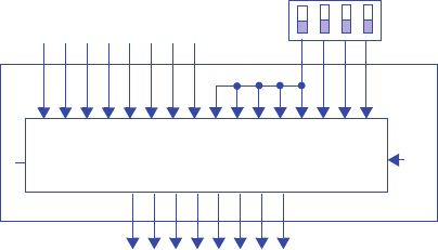
4.1 Excercises b83
4.36 Repeat Exercise 4.14, except that the compensation amount can be positive or nega-
tive, coming to the system via four inputs d, c, b, and a from a 4-pin DIP switch (d is
the most significant bit). The compensation amount is in two’s complement form (so
the person setting the DIP switch must know that). Design the circuit. What is the
range by which the input temperature can be compensated? (Component use prob-
lem).
The 4-bit input must be extended to the 8-bit input of the adder. If the high-order bit
d of the 4-bit input is 0, then b7-b3 should all be 0. If the high-order bit d is 1, then
b7-b3 should all be 1. The temperature can be compensated from -8 to +7 degrees.
co
s2 s1s3
b7 b6 b5 b2 b1 b0b4 b3
a
ci
s0
0
a7 a6 a5 a2 a1 a0a4 a3
T7 T6 T4 T3 T2 T1 T0T5
s6 s5s7 s4
U7 U6 U5 U1U3 U2 U0U4
DIP Switches
bc
from Temperature Sensor
8-bit adder
d
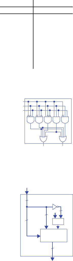
84 c4 Datapath Components
4.37 Create the internal design of a full-subtractor. (Component design problem).
d = a’b’wi + a’bwi’ + ab’wi’ + abwi
wo = a’b’wi + a’bwi’ + a’bwi + abwi
4.38 Create an absolute value component abs with an 8-bit input A that is a signed binary
number, and an 8-bit output Q that is unsigned and that is the absolute value of A. So
if the input is 00001111 (+15) then the output is also 00001111 (+15), but if the input
is 11111111 (-1) then the output is 00000001 (+1).
Inputs Outputs
abwid wo
000 0 0
001 1 1
010 1 1
011 0 1
100 1 0
101 0 0
110 0 0
111 1 1
a
b
wi
dwo
s
i0 i1
d
1x2 8-bit mux
+
1
A
Q
8
1 (MSB)
8
8
8
abs
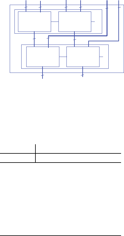
4.1 Excercises b85
4.39 Using 4-bit subtractors, build a circuit that has three 8-bit inputs, A, B, and C, and a
single 8-bit output F, where F=(A-B)-C. (Component use problem.)
First compose the 4-bit subtractors into an 8-bit subtractor, then use 8-bit subtractors
in the design.
Section 4.7: Arithmetic-Logic Units—ALUs
4.40 Design an ALU with two 8-bit inputs A and B, and control inputs x, y, and z. The
ALU should support the operations described in Table 4.3. Use an 8-bit adder and an
arithmetic/logic extender. (Component design problem).
Table 4.3
Inputs Operation
xyz
000S = A - B
001S = A + B
010S = A * 8
011S = A / 8
100S = A NAND B (bitwise NAND)
101S = A XOR B (bitwise XOR)
110S = Reverse A (bit reversal)
111S = NOT A (bitwise complement)
ab
4-bit
subtractor
d
wo wi
ab
4-bit
subtractor
d
wo wi 0
a7...a4 b7.b4 a3...a0 b3...b0
ab
4-bit
subtractor
d
wo wi
ab
4-bit
subtractor
d
wo wi 0
c7...c4 c3..c0
s7...s4 s3...s0
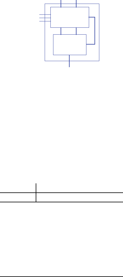
86 c4 Datapath Components
Operation of the AL-extender:
When xyz=000, ao=a, bo=b’, co=1
When xyz=001, ao=a, bo=b, co=0
When xyz=010, ao=a<<3, bo=0, co=0
When xyz=011, ao=a>>3, bo=0, co=0
When xyz=100, ao=a NAND b, bo=0, co=0
When xyz=101, ao=a XOR b, bo=0, co=0
When xyz=111, ao=a reversed, bo=0, co=0
When xyz=111, ao=NOT a, bo=0, co=0
4.41 Design an ALU with two 8-bit inputs A and B, and control signals x, y, and z. The
ALU should support the operations described in Table 4.4. Use an 8-bit adder and an
arithmetic/logic extender. (Component design problem).
Table 4.4
Inputs Operation
xyz
000S = A + B
001S = A AND B (bitwise AND)
010S = A NAND B (bitwise NAND)
011S = A OR B (bitwise OR)
100S = A NOR B (bitwise NOR)
101S = A XOR B (bitwise XOR)
110S = A XNOR B (bitwise XNOR)
111S = NOT A (bitwise complement)
A
S
x
ab
8-bit
adder
s
co ci
ab
8-bit
AL-extender
s2 co
B
y
zs0
s1
ao bo
4.1 Excercises b87
Operation of the AL-extender:
When xyz=000, ao=a, bo=b’, co=1
When xyz=001, ao=a AND b, bo=0, co=0
When xyz=010, ao=a NAND b, bo=0, co=0
When xyz=011, ao=a OR b, bo=0, co=0
When xyz=100, ao=a NOR b, bo=0, co=0
When xyz=101, ao=a XOR b, bo=0, co=0
When xyz=110, ao=a XNOR b, bo=0, co=0
When xyz=111, ao=NOT a, bo=0, co=0
4.42 An instructor teaching Boolean algebra wants to help her students learn and under-
stand basic Boolean operators by providing the students with a calculator capable of
performing bitwise AND, NAND, OR, NOR, XOR, XNOR, and NOT operations.
Using the ALU specified in Exercise 4.41, build a simple logic calculator using
DIP-switches for input and LEDs for output. The logic calculator should have three
DIP-switch inputs to select which logic operation to perform. (Component use prob-
lem).
A
S
x
ab
8-bit
adder
s
co ci
ab
8-bit
AL-extender
s2 co
B
y
zs0
s1
ao bo
ALU
z
x
y
BA
S
DIP Switches DIP Switches
DIP Switches
LEDs
88 c4 Datapath Components
Section 4.8: Shifters
4.43 Design an 8-bit shifter that shifts its inputs two bits to the right (shifting in 0s) when
the shifter's shift control input is 1 (Component design problem).
4.44 Design a circuit that outputs the average of four 8-bit inputs representing unsigned
binary numbers:
a. Ignoring overflow issues.
b. Using wider internal components or wires to avoid losing information due to
overflow.
(Component use problem.).
a.)
b.)We can use the same circuit from a), but now we prefix the output bus of each
adder with the carry-out bit of that adder, thus adding one bit of precision at each
level of additions..
i2 i1 i0i3
01 01 01 01
00
q3 q2 q1 q0
sh
i6 i5 i4i7
01 01 01 01
q7 q6 q5 q4
+ +
+
>> 2
8 8 8 8
8
I1 I2 I3 I4
O
4.1 Excercises b89
+ +
+
>> 2
8 8 8 8
8
(8 least-
I1 I2 I3 I4
significant bits)
10
99
O

90 c4 Datapath Components
4.45 Design a circuit whose 16-bit output is nine times its 16-bit input D representing an
unsigned binary number. Ignore overflow issues. (Component use problem.)
Use a left shift by 3 to obtain 8D, then add D to the result to obtain 8D+D=9D.
4.46 Design a special multiplier circuit that can multiply its 16-bit input by 1, 2, 4, 8, or
16, or 32, specified by three inputs a, b, c (abc=000 means no multiply, abc=001
means multiply by 2, abc=010 means by 4, abc=011 means by 8, abc=100 means by
16, abc=101 means by 32). Hint: A simple solution consists entirely of just one copy
of a component from this chapter. (Component use problem).
The solution just uses a single barrell shifter component. The internals of such a
component are shown below for convenience.
D2 D1 D0D3
00
D6 D5 D4D7
0
a6 a5 a4 a3 a2 a1 a0a7 b6 b5 b4 b3 b2 b1 b0b7
cico
s6 s5 s4 s3 s2 s1 s0s7
0
0
s7s6 s5 s4 s3 s2 s1 s0
8-bit adder
I
sh in
<< 4
sh in
<< 2
sh in
<< 1
0
0
0
a
b
c
O
Barrel shifter component
4.1 Excercises b91
4.47 Use strength reduction to create a circuit that computes P = 27*Q using only shifts
and adds. P is a 12-bit output and Q is a 12-bit input. Estimate the transistors in the
circuit and compare to the estimated transistors in a circuit using a multiplier.
We can implement 27*Q as (16 + 8 + 2 + 1)*Q = (Q*16 + Q*8 + Q*2 + Q), which
could be accomplished using only shifts and adds as (Q<<4 + Q<<3 + Q<<1 + Q):
Since each shifter can be implemented with only wires, each shifter uses 0 transis-
tors. We have 3 12-bit adders, which means 3*12 = 36 full-adders. If each full-adder
requires approximately 12 transistors, this means 12*36 = 432 transistors in the
shift-and-add implementation.
Since the smallest power of two which is greater than or equal to 27 is 32, the small-
est multiplier we could use is a 12x5 multiplier. Assuming the multiplier is an array-
style multiplier, this means 12*5 = 60 AND gates, a 13-bit adder, a 14-bit adder, a
15-bit adder, and a 16-bit adder. Each AND gate is ~6 transistors, so we have 360
transistors from the AND gates alone. The 13-bit adder has (13 * 12) = 156 transis-
tors, the 14-bit adder (14 * 12) = 168 transistors, the 15-bit adder (15 * 12) = 180
transistors, and the 16-bit adder (16 * 12) = 192 transistors. In total, the multiplier
would consist of (360 + 156 + 168 + 180 + 192) = 1052 transistors.
It’s easy to see how the use of strength reduction can drastically reduce the number
of transistors required.
<<1 <<3 <<4
+ +
+
P
Q
12
12
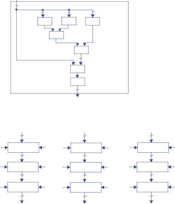
92 c4 Datapath Components
4.48 Use strength reduction to create a circuit that approximately computes P = (1/3)*Q
using only shifters and adders. Strive for accuracy to the hundredths place (0.33). P
is a 12-bit output and Q is a 12-bit input. Use wider internal components and wires
as necessary to prevent internal overflow.
Our goal here is essentially to find a fraction whose denominator is a power of two
and whose value approximates 1/3 to the hundredths place. For instance, we might
choose the approximation 85/256, whose value is ~0.332.
The multiplication could thus be approximated by Q*(64 + 16 + 4 + 1) / 256 =
(Q*64 + Q*16 + Q*4 + Q) / 256, which could be accomplished using only shifters
and adders as (Q<<6 + Q<<4 + Q<<2 + Q)>>8:
4.49 Show the internal values of the barrel shifter of Figure 4.64, when I=01100101, x =
1, y = 0, and z = 1. Be sure to show how the input I is shifted after each internal
shifter stage. (Component design problem).
Q
<< 6 << 4 << 2
+
+
+
>> 8
19
(padded with 0’s)
12
(12 least-significant bits)
19 19 19
19
P
<<4
1sh in 0
<<2
0sh in 0
<<1
1sh in 0
01100101
Q
8
8
8
8
01010000
<<4
1sh in 0
<<2
0sh in 0
<<1
1sh in 0
01100101
Q
8
8
8
8
01010000
<<4
1sh in 0
<<2
0sh in 0
<<1
1sh in 0
01100101
Q
8
8
8
8
01010000
01010000 01010000
10100000
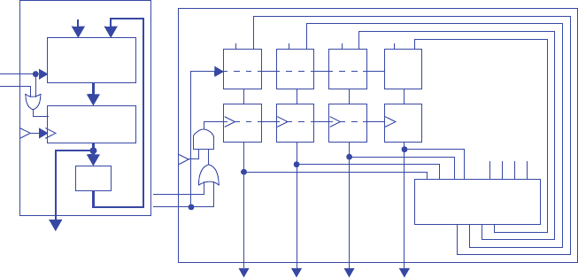
4.1 Excercises b93
4.50 Using the barrel shifter shown in Figure 4.42, what settings of the inputs x, y, and z
are required to shift the input I left by six positions.
x = 1, y = 1, z = 0
Section 4.9: Counters
4.51 Design a 4-bit up-counter that has two control inputs: cnt enables counting up, while
clear synchronously resets the counter to all 0s, (a) using a parallel load register as a
building block, (b) using flip-flops and muxes directly by following the register
design process of Section 4.2. (Component design problem).
0
cnt
ld 4-bit register
1x2 4-bit mux
sd
i0i1
+1
clear
D
Q
a3a2 a1a0 b3b2b1b0
s3 s2 s1s0
4-bit adder
d
s
i1 i0
D
Q
d
s
i1 i0
D
Q
d
s
i1 i0
D
Q
d
s
i1 i0
out
0000
0100
clear
cnt
out3 out2 out1 out0
(a) (b)
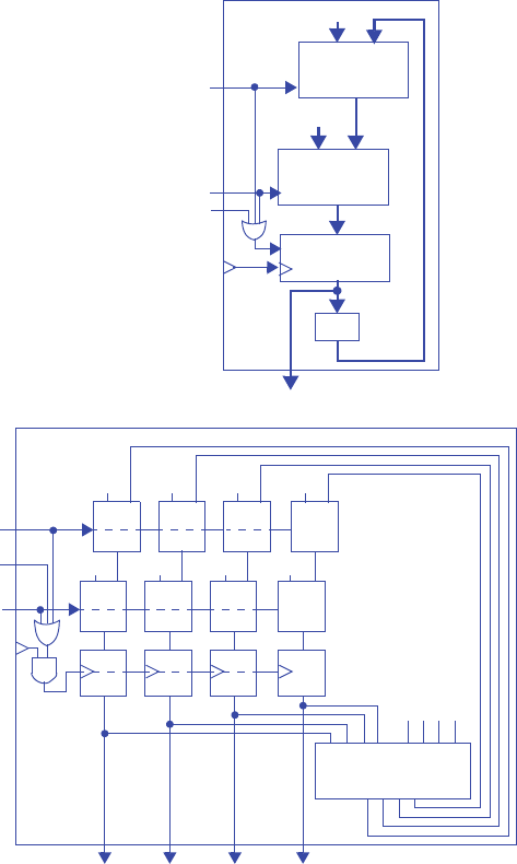
94 c4 Datapath Components
4.52 Design a 4-bit down-counter that has three control inputs: cnt enables counting up,
clear synchronously resets the counter to all 0s, and set synchronously sets the coun-
ter to all 1s, (a) using a parallel load register as a building block, (b) using flip-flops
and muxes directly by following the register design process of Section 4.2. (Compo-
nent design problem).
0
cnt
ld 4-bit register
1x2 4-bit mux
sd
i0i1
-1
clear
out
(a)
1x2 4-bit mux
sd
i0i1
set
15
D
Q
a3a2 a1a0 b3b2 b1b0
s3s2 s1 s0
4-bit adder
d
s
i1 i0
D
Q
d
s
i1 i0
D
Q
d
s
i1 i0
D
Q
d
s
i1 i0
0000
0100
clear
cnt
out3 out2 out1 out0
(b)
we’ll give clear
precedence over set
d
s
i1 i0
d
s
i1 i0
d
s
i1 i0
d
s
i1 i0
set
1 1 1 1
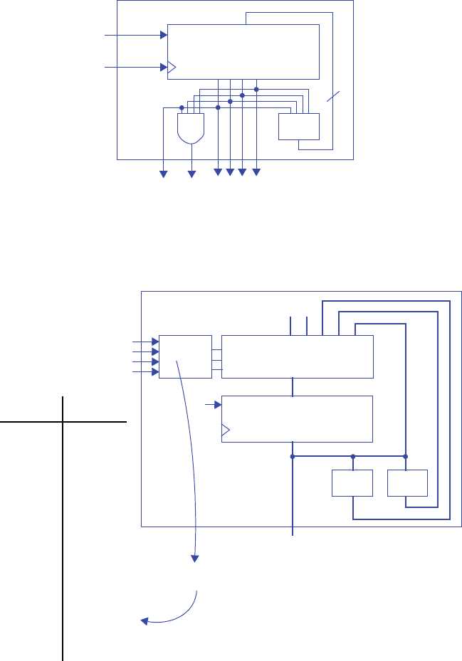
4.1 Excercises b95
4.53 Design a 4-bit up-counter with an additional output upper. upper outputs a 1 when-
ever the counter is within the upper half of the counter’s range, 8 to 15. Use a basic
4-bit up-counter as a building block. (Component design problem)
Upper is obtained simply from the 4th bit of the counter, which will be 1 for values
8 to 15. The internals of the up-counter are shown below for convenience.
4.54 Design a 4-bit up/down-counter that has four control inputs: cnt_up enables counting
up, cnt_down enables counting down, clear synchronously resets the counter to all
0s, and set synchronously sets the counter to all 1s. If two or more control inputs are
1, the counter retains its current count value. Use a parallel load register as a build-
ing block. (Component design problem.)
4-bit register
ld
+1
tc
4
cnt
o3 o2 o1 o0
upper
4-bit register
ld
-1
cnt_up
cnt_down
clear
set
+1
01234567
00001111
s2
s1
s0
u
d
c
s
o2
o1
o0
1
4-bit 3x8 mux
C
Inputs Outputs
u d c s o2 o1 o0
00000 0 0
00011 0 0
00100 1 1
00110 0 0
01000 1 0
01010 0 0
01100 0 0
01110 0 0
10000 0 1
10010 0 0
10100 0 0
10110 0 0
11000 0 0
11010 0 0
11100 0 0
11110 0 0
combinational logic
implementing this truth table
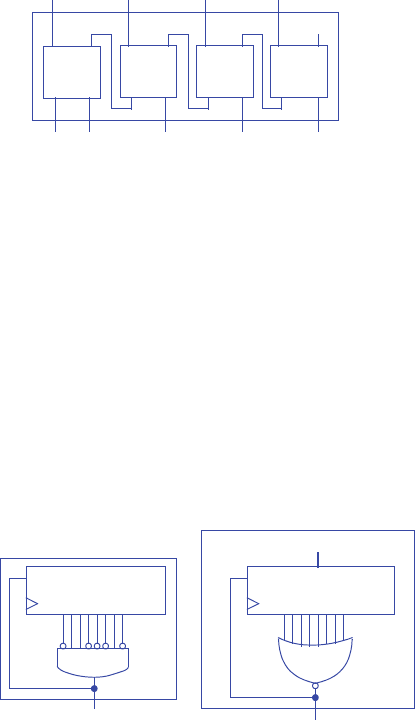
96 c4 Datapath Components
4.55 Design a circuit for a 4-bit decrementer. (Component design problem).
4.56 Assume an electronic turnstile internally uses a 64-bit counter that counts up once
for each person that passes through the turnstile. Knowing that California’s Disney-
land park attracts about 15,000 visitors per day, and assuming they all pass that one
turnstile, how many days would pass before the counter would roll over? (Compo-
nent use problem.)
264/15000 = 1,229,782,938,247,303 days. That’s a long time.
4.57 Design a circuit that outputs a 1 every 99 clock cycles:
a. Using an up-counter with a synchronous clear control input, and using extra
logic,
b. Using a down-counter with parallel load, and using extra logic.
c. What are the tradeoffs between the two designs from parts (a) and (b)?
(Component use problem.)
(c) The circuit implemented in (a) is smaller, while the circuit implemented in (b) is
easier to modify to pulse at a different rate.
HS
1
ab
wo s
HS
ab
wo s
HS
ab
wo s
HS
ab
wo s
s3 s2 s1 s0
wo
i0i1
i2
i3
8-bit up-counter
clr
o
(a)
8-bit down-counter
ld
o
(b)
98

4.1 Excercises b97
4.58 Give the count range for the following sized up-counters:
a. 8-bits, 12-bits, 16-bits, 20-bits, 32-bits, 40-bits, 64-bits, and 128-bits.
b. For each size of counter in part (a), assuming a 1 Hz clock, indicate how much
time would pass before the counter wraps around; use the most appropriate
units for each answer (seconds, minutes, hours, days, weeks, months, or years).
(Component use problem.)
8 bits: 0-255 (4 mins, 16 secs)
12 bits: 0-4,095 (1 hour, 8 mins, 16 secs)
16 bits: 0-65,535 (18 hours, 12 mins, 16 secs)
20 bits: 0-1,048,575 (12 days, 3 hours, 16 mins, 16 secs)
32 bits: 0-4,294,967,295 (136 years, 70 days, 6 hours, 28 mins, 16 secs)
40 bits: 0-1,099,511,627,775 (34,865 years, 104 days, 36 mins, 16 secs)
64 bits: 0-1.845E19 (5.849E11 years)
128 bits: 0-3.403E38 (1.079E31 years)
(For comparison, the universe is approximately 14 billion or 14E9 years old)
4.59 Create a clock divider that converts a 14 MHz clock into a 1 MHz clock. Use a
down-counter with parallel load. Clearly indicate the width of the down counter and
the counter’s load value. (Component use problem.)
Note that this is technically a pulse generator, but it still divides the clock by 14. If a
50% duty cycle is required, we can change the down-counter load value to 6, add a
register whose ld signal is Clk_out and whose input is a 1x2 mux, where i0 is 1, i1 is
0, and the select line is the output of the register. The output of the register would
then also be the divided clock signal.
4-bit down-counter
ld
13
Clk
Clk_out
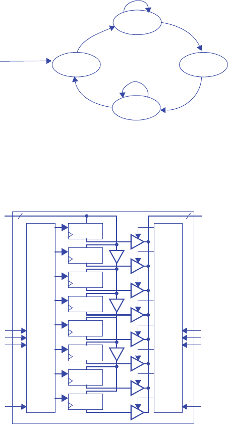
98 c4 Datapath Components
4.60 Assuming a 32-bit microsecond timer is available to a controller and a controller
clock frequency of 100 MHz, create a controller FSM that blinks an LED by setting
an output L to 1 for 5 ms and then to 0 for 13 ms, and then repeats. Use the timer to
achieve the desired timing (i.e., do not use a clock divider). For this example, the
blinking rate can vary by a few clock cycles. (Component use problem.)
Assuming the timer’s input is connected to a 1x2 32-bit mux whose i0 is 5000 and
whose i1 is 13000, the mux’s select line is called ‘s’, one possible FSM would be:
Section 4.10: Register Files
4.61 Design an 8x32 two port (1 read, 1 write) register file. (Component design problem).
Inputs: Q
Outputs: s, load, enable, L
s = 0
load = 1
enable = 1
On
Off
L = 1
OnToOffOffToOn
s = 0
load = 0
enable = 1
L = 1
s = 1
load = 1
enable = 1
L = 0
s = 1
load = 0
enable = 1
L = 0
Q’
Q’
Q
Q
ld reg0
ld reg1
ld reg2
ld reg3
ld reg4
ld reg5
ld reg6
ld reg7
d0
d1
d2
d3
d4
d5
d6
d7
i0
i1
i2
e
d0
d1
d2
d3
d4
d5
d6
d7
i0
i1
i2
e
W_en
W_addr
W_data
32
R_addr
R_data
R_en
8x32 Register File
32
4.1 Excercises b99
4.62 Design a 4x4 three port (2 read, 1 write) register file. (Component design problem).
ld reg0
ld reg1
ld reg2
ld reg3
d0
d1
d2
d3
i0
i1
e
d0
d1
d2
d3
i0
i1
e
W_en
W_addr
W_data 4
R1_addr
R1_data
R1_en
d0
d1
d2
d3
i0
i1
e
R2_addr
R2_en
R2_data
4x4 Register File
4
4
100 c4 Datapath Components
4.63 Design a 10x14 register file (one read port, one write port). (Component design
problem).
4.64 A 4x4 register file’s four registers initially each contain 0101.
a. Show the input values necessary to read register 3 and to simultaneously write
register 3 with the value 1110.
b. With these values, show the register file’s register values and output values
before the next rising clock edge, and after the next rising clock edge.
a.)W_data = 1110, W_addr = 11, W_en = 1, R_addr = 11, R_en = 1.
b.) Before rising edge:
R0 = 0101
R1 = 0101
R2 = 0101
R3 = 0101
R_data = 0101
After rising edge:
R0 = 0101
R1 = 0101
R2 = 0101
R3 = 1110
R_data = 1110
ld reg0
ld reg1
ld reg2
ld reg3
ld reg4
ld reg5
ld reg6
ld reg7
d0
d1
d2
d3
d4
d5
d6
d7
i0
i1
i2
e
d0
d1
d2
d3
d4
d5
d6
d7
i0
i1
i2
e
W_en
W_addr
W_data
14
R_addr
R_data
R_en
10x14 Register File
14
i3 i3
ld reg8
ld reg9
d8
d9
d10
d11
d12
d13
d14
d15
d8
d9
d10
d11
d12
d13
d14
d15
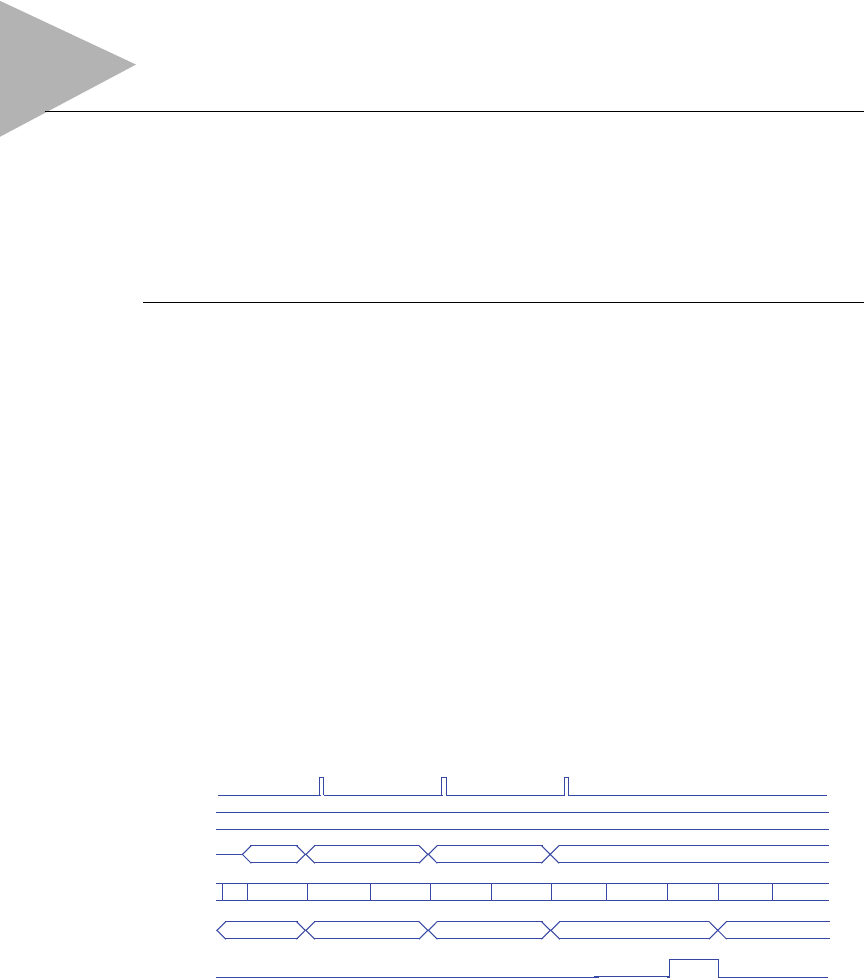
95
CHAPTER 5
REGISTER-TRANSFER
LEVEL (RTL) DESIGN
5.1 EXERCISES
For each exercise, unless otherwise indicated, assume that the clock frequency is much
faster than any input events of interest, and that any button inputs have been debounced.
Problems noted with an asterisk (*) represent especially challenging problems.
Section 5.2: High-Level State Machines
5.1. Draw a timing diagram to trace the behavior of the soda dispenser HLSM of Figure
5.3 for the case of a soda costing 50 cents and for the following coins being depos-
ited: a dime (10 cents), then a quarter (25 cents), and then another quarter. The tim-
ing diagram should show values for all system inputs, outputs, and local storage
items, and for the systems’ current state.
Note: figure not drawn to scale
s
c
State Init Wait Add
a
tot
d
50
Wai t A dd Wait A dd Wa it Disp Init Wait
???
10 25 25
0
10 35 60
0
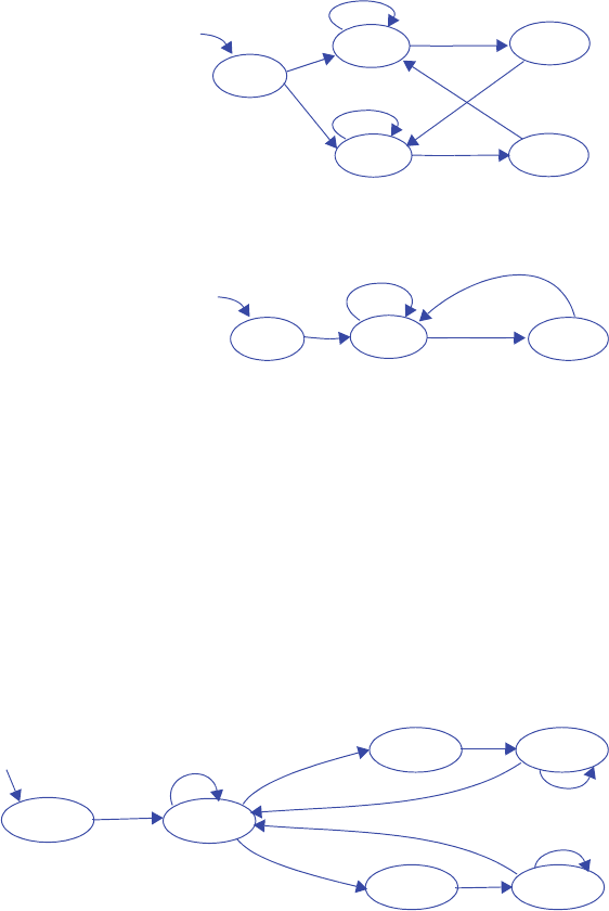
96 5 Register-Transfer Level (RTL) Design
5.2 Capture the following system behavior as an HLSM. The system counts the number
of events on a single-bit input B and always outputs that number unsigned on a 16-
bit output C, which is initially 0. An event is a change from 0 to 1 or from 1 to 0.
Assume the system count rolls over when the maximum value of C is reached.
5.3 Capture the following system behavior as an HLSM. The system has two single-bit
inputs U and D each coming from a button, and a 16-bit output C, which is initially
0. For each press of U, the system increments C. For each press of D, the system dec-
rements C. If both buttons are pressed, the system does not change C. The system
does not roll over; it goes no higher than than the largest C and no lower than C=0.
A press is detected as a change from 0 to 1; the duration of that 1 does not matter.
Inputs: B(bit)
Outputs: C (16 bits)
Local registers: Creg (16 bits)
Init
Wait1
Creg := 0
Inc1 Creg := Creg + 1
B
B’
Inputs: B(bit)
Outputs: C (16 bits)
Local registers: Creg (16 bits), prev (bit)
Init Wait
Creg := 0
Change
Creg := Creg + 1
(B == prev)’
B == prev
prev := B prev := B
Alternative solution:
B’
Wait0
BB
B’ Inc0 Creg := Creg + 1
Init Wait
PressU WaitR elU
PressD WaitRelD
Inputs: U (bit), D (bit)
Outputs: C (16 bits)
Local registers: Creg (16 bits)
Creg := 0
UD’*(Creg < 65535)
U’D*(Creg > 0)
( UD’*(Creg < 65535) + U’D*(Creg > 0) )’
Creg := Creg + 1
Creg := Creg - 1
U
D
U’
D’

5.1 Exercises 97
5.4 Capture the following system behavior as an HLSM. A soda machine dispenser sys-
tem has a 2-bit control input C1 C0 indicating the value of a deposited coin. C1C0 =
00 means no coin, 01 means nickel (5 cents), 10 means dime (10 cents), and 11
means quarter (25 cents); when a coin is deposited, the input changes to indicate the
value of the coin (for possibly more than one clock cycle) and then changes back to
00. A soda costs 80 cents. The system displays the deposited amount on a 12-bit
output D. The system has a single-bit input S coming from a button. If the deposited
amount is less than the cost of a soda, S is ignored. Otherwise, if the button is
pressed, the system releases a single soda by setting a single-bit output R to 1 for
exactly one clock cycle, and the system deducts the soda cost from the deposited
amount.
Inputs: C1C0 (2 bits), S (bit)
Outputs: D (12 bits), R (bit)
Local registers: Dreg (12 bits)
Init
Dreg := 0
Wait
Nickel Wait5
Dime Wait10
Quarter Wait25
Dispense WaitS
C1’C0
C1C0’
C1C0
C1’C0’ *
(S*(Dreg>=80))’
C1’C0’ * S * (Dreg >= 80)
S
S’
C1’C0
(C1’C0 )’
C1C0’
C1C0
(C1C0 )’
(C1C0’)’
R := ‘1’
Dreg := Dreg - 80
R := ‘0’
R := ‘0’
Dreg := Dreg + 5
Dreg := Dreg +10
Dreg := Dreg + 25
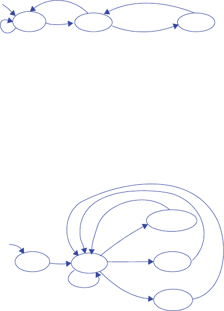
98 5 Register-Transfer Level (RTL) Design
5.5 Create a high-level state machine that initializes a 16x32 register file’s contents to
0s, beginning the initialization when an input rst becomes 1. The register file does
not have a clear input; each register must be individually written with a 0. Do not
define 16 states; instead, declare a local storage item so that only a few states need
to be defined.
5.6 Create a high-level state machine for a simple data encryption/decryption device. If a
single-bit input b is 1, the device stores the data from a 32-bit signed input I, refer-
ring to this as an offset value. If b is 0 and another single-bit input e is 1, then the
device “encrypts” its input I by adding the stored offset value to I, and outputs this
encrypted value over a 32-bit signed output J. If instead another single-bit input d is
1, the device “decrypts” the data on I by subtracting the offset value before output-
ting the decrypted value over J. Be sure to explicitly handle all possible combina-
tions of the three input bits.
Inputs: rst (bit)
Outputs: rfAddr (4 bits), rfLoad (bit), rfData (32 bits)
Local registers: index, rfAddrreg(4 bits), rfDatareg (32 bits)
Init
index := 0
ClearReg
rst
rfAddrreg := index
rfLoad := ‘1’
rfDatareg := 0
Next
index := index + 1
index < 15
(index < 15)’
rfLoad := ‘0’
rst’
Inputs: I (32 bits), b (bit), e (bit), d (bit)
Outputs: J (32 bits)
Local registers: offset (32 bits), Jreg (32 bits)
Init Wait
offset := 0
LoadOffset
Encrypt
Decrypt
offset := I
Jreg := I + offset
Jreg := I - offset
b’e
b’e’d
b
(b + b’e + b’e’d)’
Jreg := 0
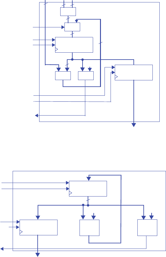
5.1 Exercises 99
Section 5.3: RTL Design Process
5.7 Create a datapath for the HLSM in Figure 5.98.
(Note that “P” is not involved in the datapath; it will be a controller output.)
5.8 Create a datapath for the HLSM in Figure 5.63.
<
sum
ld
clr
+
5099
16
16
sum_lt_5099
sum_ld
sum_clr
+
16
16
16 16
01
sum_s0
AB
C
16
Sreg
ld
clr
Sreg_ld
Sreg_clr
S
a
ld
clr
Rareg
ld
clr +
1
<
4095
a_ld
a_clr
Rareg_ld
Ra
a_lt_4095
12
0
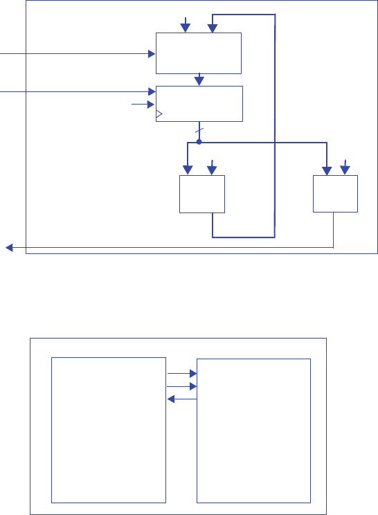
100 5 Register-Transfer Level (RTL) Design
5.9 For the HLSM in Figure 5.14, complete the RTL design process:
a. Create a datapath.
b. Connect the datapath to a controller.
c. Derive the controller’s FSM.
a) Create a datapath.
b) Connect the datapath to a controller.
Jreg
ld
clr
+
1
<
2
Jreg_ld
Jreg_lt_2
8
i0 i1
2x1 8-bit mux
s0
d
1
Jreg_mux_s0
0
Jreg_mux_s0
DatapathController
Jreg_ld
Jreg_lt_2
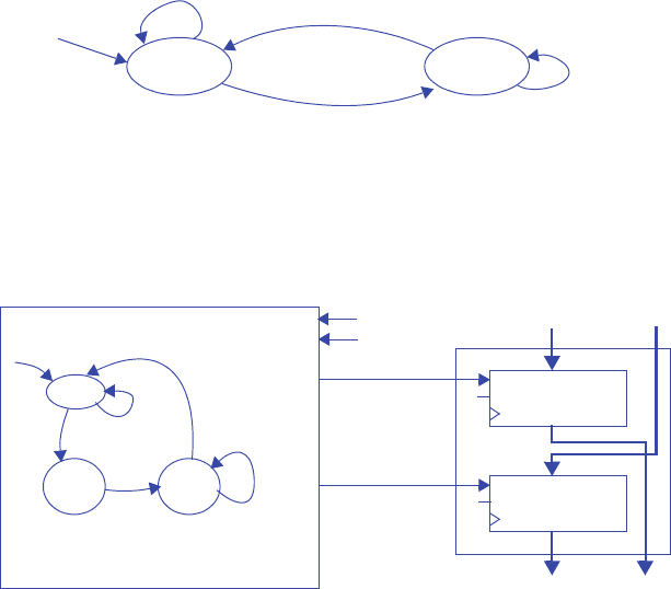
5.1 Exercises 101
c) Derive the controller’s FSM.
5.10 Given the HLSM in Figure 5.99, complete the RTL design process to achieve a con-
troller (FSM) connected with a datapath.
Inputs: B, Jreg_lt_2
Outputs: P, Jreg_mux_s0, Jreg_ld
S0 S1
B’
Jreg_lt_2’
B
Jreg_lt_2
P = 0
Jreg_mux_s0 = 0
Jreg_ld = 1
P = 1
Jreg_mux_s0 = 1
Jreg_ld = 1
Wait
Inputs: start, w_wait (bit)
Outputs: w_wr, w_addr_ld, w_data_ld (bit)
w_addrreg
ld
start’
Send
Addr
start
Send
Data
w_wr=1
w_addr_ld=1
w_wait’
w_wait
w_data_ld=1
w_datareg
ld
addr data
w_data w_addr
Controller FSM
Datapath
w_data_ld
w_addr_ld
(a)
clr0
clr0
start
w_wait
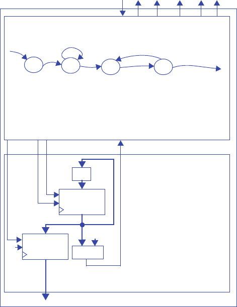
102 5 Register-Transfer Level (RTL) Design
5.11 Given the partial HLSM in Figure 5.75 for the system of Figure 5.74, proceed with
the RTL design process to achieve a controller (partial FSM) connected with a data-
path.
S
Inputs: bu, a_lt_4096
Outputs: a_rst, er, a_ld, ad_buf, Rareg_ld, Rrw, Ren, a_ld
a_rst = 1
er = 1
T
er = 0
bu
U
bu’
ad_ld = 1
ad_buf = 1
Rareg_ld = 1
Rrw = 1
Ren = 1
a_ld = 1
V
a_lt_4096
a_lt_4096’
a
ld
clr
+1
<
4096
a_lt_4096
a_ld
a_rst
erbu ad_buf a_ld Rrw Ren
Rareg
ld
clr
Rareg_ld
Ra
0
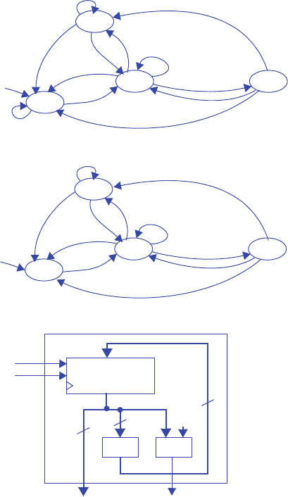
5.1 Exercises 103
5.12 Use the RTL design process to create a 4-bit up-counter with input cnt (1 means
count up), clear input clr, a terminal count output tc, and a 4-bit output Q indicat-
ing the present count. Only use datapath components from Figure 5.21. After deriv-
ing the controller’s FSM, implement the controller as a state register and
combinational logic.
Inputs: cnt (bit), clr (bit)
Outputs: tc (bit)
Local registers: Qreg (4 bits)
Init
Qreg := 0
tc := ‘0’
Count
cnt
clr
Qreg := Qreg + 1
TC
clr’*cnt*
clr’*cnt*(Qreg < 14)
Qreg := 0
tc := ‘1’
Idle
cnt’clr’
clr
cnt’*clr’
clr High-Level State Machine
clr’*cnt
Init
Qreg_clr = 1
tc = 0
Count
cnt
clr
Qreg_ld = 1
TC
cnt*clr’*Qreg_lt_14’
cnt*clr’*Qreg_lt_14
Qreg_clr = 1
tc = 1
Idle
cnt’clr’
cnt*clr’
clr
cnt’clr’
clr Controller FSM
Inputs: cnt, clr, Q_lt_14
Outputs: tc, Qreg_ld, Qreg_clr
<
Qreg
ld
clr
+1
14
4
4
Qreg_lt_14
Datapath
Qreg_ld
Qreg_clr
cnt’
(Qreg < 14)’
clr’*cnt
cnt’clr’
cnt’*clr’
cnt*clr’
Q
4

104 5 Register-Transfer Level (RTL) Design
n1 = (s1 + s0)cnt’clr’ + s1’s0*cnt*clr’Qreg_lt_14’
n0 = s1’s0’cnt + (s1 + s0)cnt*clr’
tc = s1s0
Qreg_ld = s1’s0
Inputs Outputs
s1 s0 cnt clr Qreg_lt_14 n1 n0 tc Qreg_ld Qreg_clr
Init
000 0 0 0000 1
000 0 1 0000 1
000 1 0 0000 1
000 1 1 0000 1
001 0 0 0100 1
001 0 1 0100 1
001 1 0 0100 1
001 1 1 0100 1
Count
010 0 0 1001 0
01001 1001 0
010 1 0 0001 0
01011 0001 0
011 0 0 1101 0
01101 0101 0
011 1 0 0001 0
01111 0001 0
Idle
100 0 0 10000
10001 1000 0
100 1 0 00000
10011 0000 0
101 0 0 0100 0
10101 0100 0
101 1 0 0000 0
10111 0000 0
TC
110 0 0 1010 1
11001 1010 1
110 1 0 0010 1
11011 0010 1
111 0 0 0110 1
11101 0110 1
111 1 0 0010 1
11111 0010 1
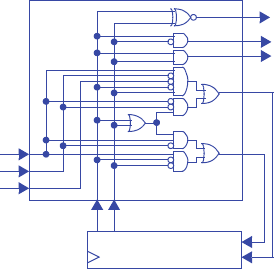
5.1 Exercises 105
Qreg_clr = s1’s0’ + s1s0
cnt
tc
State Register
s1
n1
n0
s0
clr
Qreg_lt_14
Qreg_ld
Qreg_clr
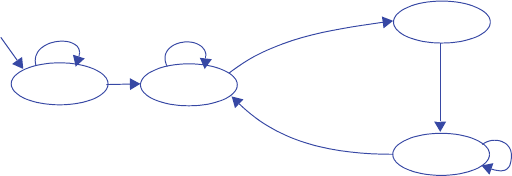
106 5 Register-Transfer Level (RTL) Design
5.13 Use the RTL design process to design a system that outputs the average of the most
recent two data input samples. The system has an 8-bit unsigned data input I, and an
8-bit unsigned output avg. The data input is sampled when a single-bit input S
changes from 0 to 1. Choose internal bitwidths that prevent overflow.
Step 1 - Capture a high-level state machine
Inputs: I (8 bits), S (bit)
Outputs: avg (8 bits)
Local Registers: Prevreg (8 bits), Ireg (8 bits),
Init Wait
Sample
WaitLow
Prevreg := 0
S
S’
S’
S
S’
S
avgreg := 0
Prevreg := Ireg
avgreg (8 bits)
Ireg := 0
Ireg := I
avgreg :=
(Prevreg + Ireg)/ 2
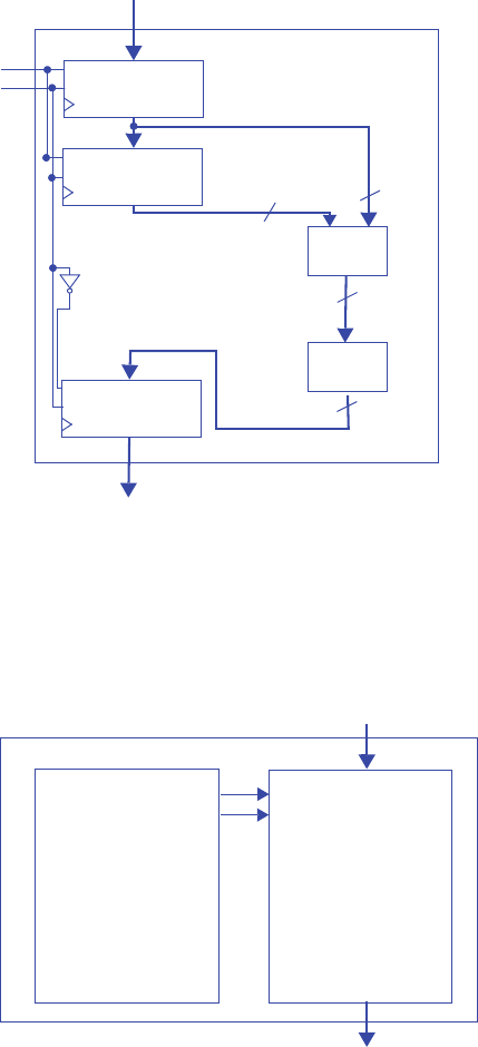
5.1 Exercises 107
Step 2 - Create a datapath
Note: A solution more consistent with the chapter’s methdology would use a sepa-
rate clear and ld signal for each register. In this particular example, a single clr and a
single load line happens to work.
Step 3 - Connect the datapath to a controller
Prevreg
ld
clr
avgreg
ld
clr
+
>> 1
I
avg
ld
clr
8
9
8
8
Ireg
ld
clr
ld
DatapathController
clr
avg
I
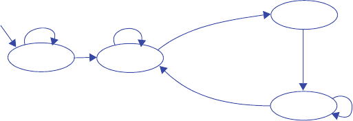
108 5 Register-Transfer Level (RTL) Design
Step 4 - Derive the controller’s FSM
Inputs: S
Outputs: ld, clr
Init Wait
Sample
WaitLow
S
S’
S’
S
S’
S
clr = 1
ld = 1
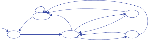
5.1 Exercises 109
5.14 Use the RTL design process to create an alarm system that sets a single-bit output
alarm to 1 when the average temperature of four consecutive samples meets or
exceeds a user-defined threshold value. A 32-bit unsigned input CT indicates the
current temperature, and a 32-bit unsigned input WT indicates the warning thresh-
hold. Samples should be taken every few clock cycles. A single-bit input clr when
1 disables the alarm and the sampling process. Start by capturing the desired system
behavior as an HLSM, and then convert to a controller/datapath.
Step 1 - Capture a high-level state machine
Init
Inputs: CT, WT (32 bits); clr (bit)
Outputs: alarm (bit)
Local Registers: tmp0, tmp1, tmp2, tmp3, avg (32 bits)
alarm := ‘0’
tmp0 := 0
tmp1 := 0
tmp2 := 0
tmp3 := 0
Sample
tmp0 := CT
tmp1 := tmp0
tmp2 := tmp1
tmp3 := tmp2
avg := (tmp0 + tmp1
+ tmp2 + tmp3) / 4
Clr
alarm := ‘0’
clr
clr’
avg := 0
clr AlrmOn
AlrmOff
clr
clr
clr’*(avg>=WT)
clr’
clr’
clr’*(avg>=WT)’
alarm := ‘1’
alarm := ‘0’
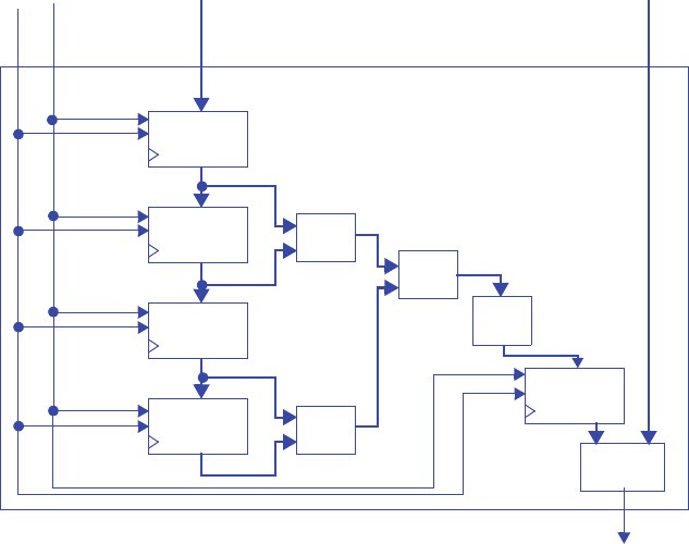
110 5 Register-Transfer Level (RTL) Design
Step 2A - Create a datapath
Note: A solution more consistent with the chapter’s methdology would use a separate
clear and ld signal for each register. In this particular example, a single clr and a single
load line happens to work.
tmp0
ld
CT
tmp1
ld
tmp2
ld
tmp3
ld
tmp_ld
+
+
+
>> 2
>=
WT
avg_ge_WT
avg
ld
clr
clr
clr
clr
clr
clr_all
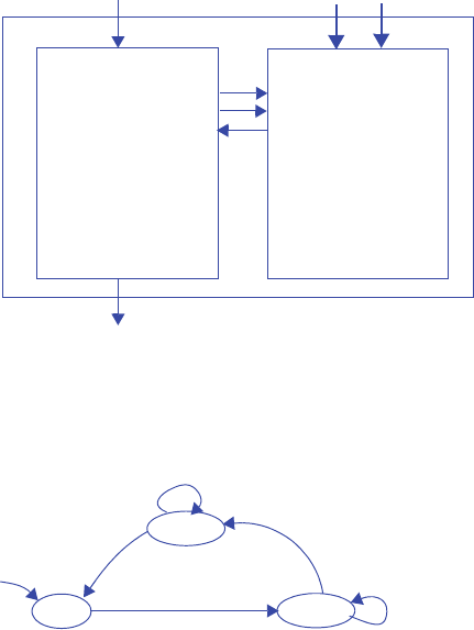
5.1 Exercises 111
Step 2B- Connect the datapath to a controller
Step 2C - Derive the controller’s FSM
CT
DatapathController
clr
ld
avg_ge_WT
alarm
WT
clr_all
Inputs: clr, avg_lt_WT
Outputs: alarm, clr_all, ld
Init
alarm = 0
clr_all = 1
Sample
Clr
alarm = 0
clr
clr’
clr
clr’
ld = 1
alarm = avg_ge_WT
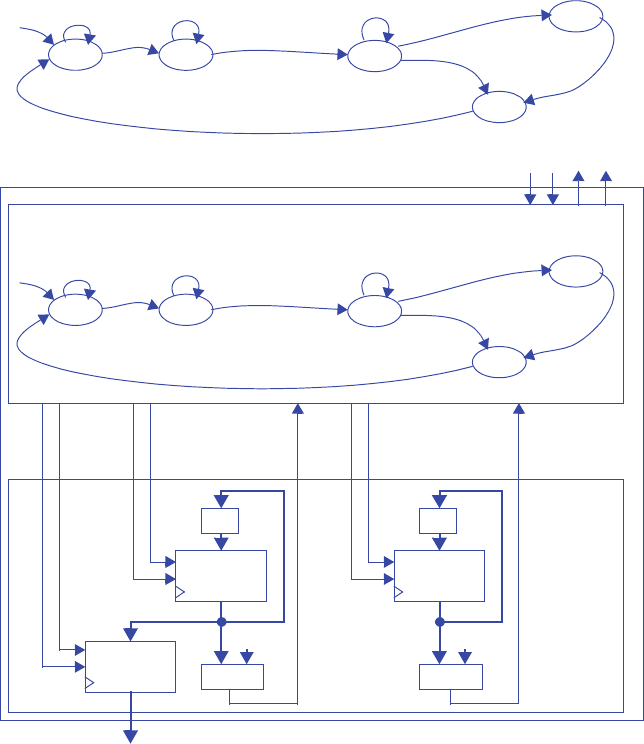
112 5 Register-Transfer Level (RTL) Design
5.15 Use the RTL design process to design a reaction timer system that measures the time
elapsed between the illumination of a light and the pressing of a button by a user.
The reaction timer has three inputs, a clock input clk, a reset input rst, and a button
input B. It has three outputs, a light enable output len, a 10-bit reaction time output
rtime, and a slow output indicating that the user was not fast enough. The reaction
timer works as follows. On reset, the reaction timer waits for 10 seconds before illu-
minating the light by setting len to 1. The reaction timer then measures the length of
time in milliseconds before the user presses the button B, outputting the time as a
12-bit binary number on rtime. If the user did not press the button within 2 seconds
(2000 milliseconds), the reaction timer will set the output slow to 1 and output 2000
on rtime. Assume that the clock input has a frequency of 1 kHz. Do not use a timer
component in the datapath.
Init
Inputs: rst, B (bit)
Outputs: len, slow (bit); rtime (11 bits)
wCount := 0
Wait
rtime := 0
rst’
rst
Local Registers: wCount (14 bits); rCount (11 bits)
rCount := 0 wCount := wCount + 1
wCount < 9999
len := ‘1’
slow := ‘0’
(wCount < 9999)’
Count
rCount := rCount + 1
Slow
Done
B’*(rCount < 1999)
B’*(rCount < 1999)’
B
slow := ‘1’
rtime := rCount
High-Level State Machine
Init
Inputs: rst, B, rCount_lt_1999, wCount_lt_9999
Outputs: len, slow, wCount_clr, rCount_clr, rTime_clr, wCount_ld, rCount_ld, rtime_ld
wCount_clr = 1
Wait
rtime_clr = 1
rst’
rst
rCount_clr = 1 wCount_ld = 1
wCount_lt_9999
len = 1
slow = 0
wCount_lt_9999’
Count
rcount_ld = 1
Slow
Done
B’*rCount_lt_1999
B’*rCount_lt_1999’
B
slow = 1
rtime_ld = 1
wCount
ld
clr
rtime
ld
clr
+1
<
9999
rCount
ld
clr
+1
<
1999
wCount_clr
wCount_ld
wCount_lt_9999
rCount_clr
rCount_ld
rtime_clr
rtime_ld
rCount_lt_1999
rtime
rst B slow len
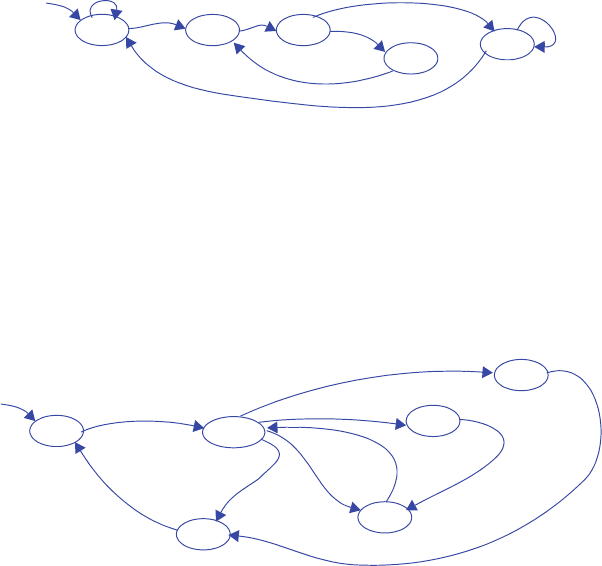
5.1 Exercises 113
Section 5.4: More RTL Design
5.16 Create an FSM that interfaces with the datapath in Figure 5.100. The FSM should
use the datapath to compute the average value of the 16 32-bit elements of any array
A. Array A is stored in a memory, with the first element at address 25, the second at
address 26, and so on. Assume that putting a new value onto the address lines
M_addr causes the memory to almost immediately output the read data on the
M_data lines. Ignore overflow issues.
5.17 Design a system that repeatedly computes and outputs the sum of all positive num-
bers within a 512-word register file A consisting of 32-bit signed numbers.
Step 1 - Capture a high-level state machine
Init
Inputs: go, i_lt_16 (bit)
Outputs: s_clr, i_clr, avg_clr, s_ld, i_ld, a_ld (bit)
s_clr=1
i_clr=1
avg_clr=1
Read
a_ld=1
Add
s_ld=1
i_lt_16
Next
i_ld=1
i_lt_16’
Divide
avg_ld = 1
go
go’
go’
go
Init
Inputs: A_data (32 bits)
Outputs: A_addr (9 bits), sum_out (32 bits)
A_addr := 0
Local Registers: sum (32 bits), index (9 bits)
sum := 0
Add
index := 0
(A_data>0)*(index<511)
Next
sum := sum+A_data
Done
(A_data>0)’*
index<511
(A_data>0)’*
(index<511)’
sum_out := sum
A_addr := index
Compare
index := index+1
AddLast
sum := sum+A_data
(A_data>0)*(index<511)’
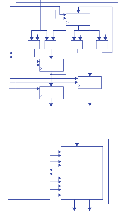
114 5 Register-Transfer Level (RTL) Design
Step 2A - Create a datapath
Step 2B - Connect the datapath to a controller
sum
ld
index
clr
ld
clr
sum_ld
sum_clr
index_ld
index_clr
>
A_data_gt_0
0
<
511
index_lt_511
+
1
A_addr
A_data
sum_out
+
sum_out
ld
sum_out_ld
A_addrreg
ld
clr
Addr_ld
Addr_clr
sum_ld
sum_clr
index_ld
index_clr
data_ld
data_clr
data_gt_0
index_lt_511
A_addr
A_data
sum_out
Datapath
Controller sum_out_ld
Addr_ld
Addr_clr
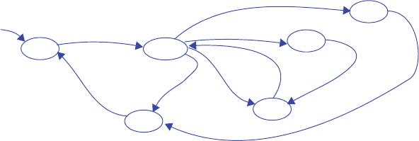
5.1 Exercises 115
Step 2C - Derive the controller’s FSM
Init
Inputs: data_gt_0, index_lt_511
Outputs: sum_clr, sum_ld, index_clr, index_ld, data_ld, sum_out_ld
sum_clr=1
Add
index_clr=1
data_gt_0*index_lt_511
Next
sum_ld=1
Done
data_gt_0’*
index_lt_511
data_gt_0’*
index_lt_511’
sum_out_ld=1
Addr_ld=1
Compare
AddLast
sum_ld=1
data_gt_0*index_lt_511
index_ld=1
Addr_clr=1

116 5 Register-Transfer Level (RTL) Design
5.18 Design a system that repeatedly computes and outputs the maximum value found
within a register file A consisting of 64 32-bit unsigned numbers.
Step 1 - Capture a high-level state machine
Step 2A - Create a datapath
Reset
Inputs: A_data (32 bits)
Outputs: A_addr (6 bits), max (32 bits)
Local Registers: tmp (32 bits), index (6 bits)
index := 0
tmp := 0
Compare
Next
index := index + 1
NewMax
A_data > tmp
(A_data > tmp)’
(index=0)’
Done
(index=0)
max := tmp
tmp := A_data
tmp := 0
max := 0
Init
A_addr := 0
A_addr := index
index
=
0
+1
ld
clr max_tmp
ld
clr
ld
A_addr
A_data
tmp_ld
tmp_clr
index_ld
index_clr
A_addr_ld
index_eq_0
>
maxreg
ld
maxreg_ld
data_gt_max
max
clr
clr
A_addr_clr
0
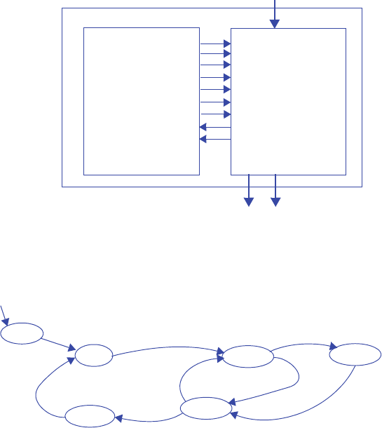
5.1 Exercises 117
Step 2B - Connect the datapath to a controller
Step 2C - Derive the controller’s FSM
A_addr_ld
max
A_data
DatapathController
index_clr
index_ld
tmp_clr
tmp_ld
maxreg_ld
index_lt_64
data_gt_max
A_addr
A_addr_clr
Inputs: index_eq_0, data_gt_max
Outputs: A_addr_ld, A_addr_clr, index_clr, index_ld, tmp_clr, tmp_ld, maxreg_ld
Reset
tmp_clr=1
index_clr=1
Compare
Next
index_ld=1
NewMax
data_gt_max
data_gt_max’
index_eq_0’
Done
index_eq_0
maxreg_ld=1
tmp_ld=1
tmp_clr=1
Init
A_addr_clr=1
A_addr_ld=1

118 5 Register-Transfer Level (RTL) Design
5.19 Using a timer, design a system with single-bit inputs U and D corresponding to two
buttons, and a 16-bit output Q which is initially 0. Pressing the button for U causes Q
to increment, while D causes a decrement; pressing both buttons causes Q to stay the
same. If a single button is held down, Q should then continue to increment or decre-
ment at a rate of once per second as long as the button is held. Assume the buttons
are already debounced. Assume Q simply rolls over if its upper or lower value is
reached.
Step 1 - Capture a high-level state machine
Step 2A - Create a datapath
Inputs: U, D, tm_pulse (bit)
Outputs: Q (16 bits), Tmr_ld, Tmr_en (bit)
Init Wait
PressU HoldU
PressD HoldD
(U’*D’) +(U*D)
U*D’
U’*D
cnt := cnt + 1
cnt := cnt - 1
Tmr_en := ‘1’
Tmr_ld := ‘1’
Tmr_ld := ‘1’
Tmr_en := ‘1’
U*tm_pulse’
D*tm_pulse’
U*tm_pulse
D*tm_pulse
U’
D’
cnt := 0
Local Registers: cnt (16 bits)
Q := 0
Q := cnt
Q := cnt
Q := cnt
Q := cnt
Q := cnt
1000000
microsecond
timer
ld
en
Qreg
ld
clr
-1 +1
i0 i1
s1x2 16-bit
Qtm_pulse
Qreg_clr
Qreg_ld
Qreg_sel Tmr_en Tmr_ld
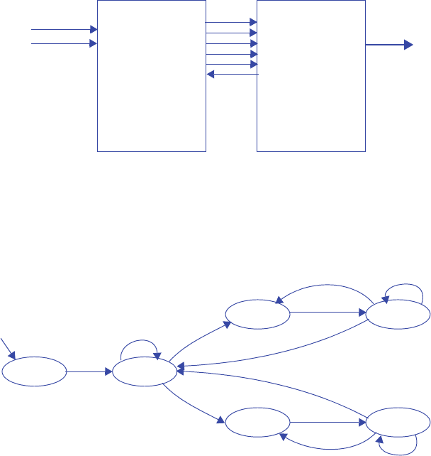
5.1 Exercises 119
Step 2B - Connect the datapath to a controller
Step 2C - Derive the controller’s FSM
5.20 Using a timer, design a display system that reads the ASCII characters from a 64-
word 8-bit register file RF and writes each word to a 2-row LED-based display hav-
ing 32 characters per row, doing so 100 times per second. The display has an 8-bit
input A for the ASCII character to be displayed, a single-bit input row where 0 or 1
denotes the top or bottom row respectively, a 5-bit input col that indicates a column
in the row, and an enable input en whose change from 0 to 1 causes the character to
be displayed in the given row and column. The system should write RF[0] through
RF[15] to row 0’s columns 0 to 15 respectively, and RF[16] to RF[31] to row 1.
Do not assign this exercise; it contains an error.
Controller Datapath
U
D
Qreg_clr
Qreg_ld
Qreg_sel
Tmr_ld
Tmr_en
tm_pulse
Q
Inputs: U, D, tm_pulse
Outputs: Qreg_clr, Qreg_ld, Qregsel, Tmr_ld, Tmr_en
Init Wait
PressU HoldU
PressD HoldD
U’D’ + UD
UD’
U’D
Qreg_sel = 1
Qreg_ld = 1
Qreg_sel = 0
Qreg_ld = 1
Tmr_en = 1
Tmr_ld = 1
Tmr_ld = 1
Tmr_en = 1
U * tm_pulse’
D * tm_pulse’
U * tm_pulse
D * tm_pulse
U’
D’
Qreg_clr = 1
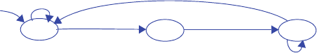
120 5 Register-Transfer Level (RTL) Design
5.21 Design a data-dominated system that computes and outputs the sum of the absolute
values of 16 separate 32-bit registers (not in a register file) storing signed numbers
(do not consider how those numbers get stored). The computation of the sum should
be done using a single equation in one state. The computation should be performed
once when a single-bit input go changes from 0 to 1, and the computed result
should be held at the output until the next time go changes from 0 to 1.
Step 1 - Capture a high-level state machine
Since this problem is a data-dominated design, the problem’s high-level state
machine is fairly simple:
Init
Inputs: go (bit), R0...R15 (32 bits)
Outputs: sum (32 bits)
go’
Comp
go
sum := abs(R0)+abs(R1)+...abs(R15)
Wait
go
go’
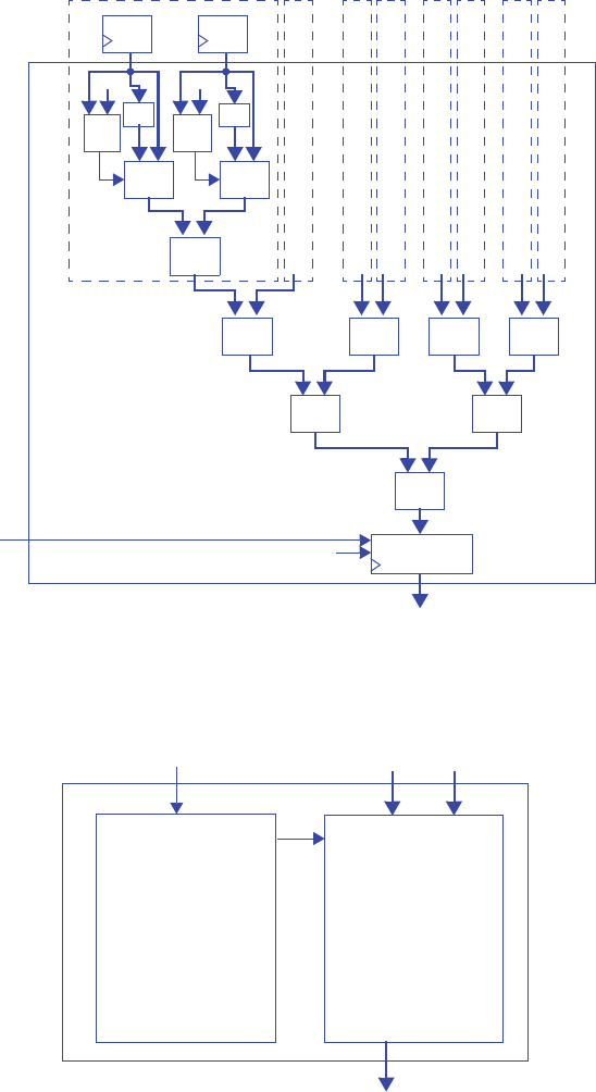
5.1 Exercises 121
Step 2A - Create a datapath
Note: the abs component may be found in Exercise 4.38
Step 2B - Connect the datapath to a controller
R0
>
0
sum
01
+
R1
>
0
01
Same structure for R2, R3
Same structure for R4, R5
Same structure for R6, R7
Same structure for R8, R9
Same structure for R10, R11
Same structure for R12, R13
Same structure for R14, R15
+ + + +
+ +
+
sum
ld
sum_ld
abs abs
clr
0
sum_ld
sum
R0
DatapathController
go R15
...
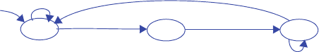
122 5 Register-Transfer Level (RTL) Design
Step 2C - Derive the controller’s FSM
Section 5.5: Determining Clock Frequency
5.22 ) Assuming an inverter has a delay of 1 ns, all other gates have a delay of 2 ns, and
wires have a delay of 1 ns, determine the critical path for the full-adder circuit in
Figure 4.30.
The critical path of the full adder lies along the path from any of the inputs to the co
output. The critical path features two gates with a total delay of 4ns and three seg-
ments of wire with a total delay of 4ns, for a total critical path delay of 7ns.
5.23 Assuming an inverter has a delay of 1 ns, all other gates have a delay of 2 ns, and
wires have a delay of 1 ns, determine the critical path for the 3x8 decoder of Figure
2.62.
The critical path of the decoder lies along one of the decoder’s inverted inputs to one
of its outputs: 1ns (wire) + 1ns (inverter) + 1ns (wire) + 2ns (AND gate) + 1ns
(wire) = 6ns.
5.24 Assuming an inverter has a delay of 1 ns, all other gates have a delay of 2 ns, and
wires have a delay of 1 ns, determine the critical path for the 4x1 multiplexer of Fig-
ure 2.67.
The critical path of a 4x1 multiplexer involves an inverter (1ns), an AND gate (2ns),
and an OR gate (2ns), resulting in a total critical path delay of 5ns.
5.25 Assuming an inverter has a delay of 1 ns, and all other gates have a delay of 2 ns,
determine the critical path for the 8-bit carry-ripple adder, assuming a design fol-
lowing Figure 4.31 and Figure 4.30, and: (a) assuming wires have no delay, (b)
assuming wires have a delay of 1 ns.
(a) Assume the 8-bit carry-ripple adder consists of 8 full-adders chained together.
Each full-adder features a critical path delay of 4ns (an AND gate and a XOR gate).
Thus, the total critical path delay for the 8-bit carry-ripple adder is 8*4ns = 32ns.
(b) Each full-adder’s critical path features one internal wire between an AND and
XOR gate and two wires that connect the full-adder’s inputs and outputs. For the
entire 8-bit carry-ripple adder, the 8 internal wires contribute 8ns to the critical path
delay. Wires connecting full-adders together contribute 7ns to the critical path delay.
Inputs: go (bit)
Outputs: sum_ld (bit)
Init
go’
Comp
go
sum_ld = 1
Wait
go
go’

5.1 Exercises 123
The initial ci and final co contribute 2ns to the critical path delay. Thus, the total
critical path delay is 32ns (for gates) + 8ns + 7ns + 2ns = 49ns.
5.26 (a) Convert the laser-based distance measurer’s FSM, shown in Figure 5.21, to a
state register and logic. (b) Assuming all gates have a delay of 2 ns and the 16-bit
up-counter has a delay of 5 ns, and wires have no delay, determine the critical path
for the laser-based distance measurer. (c) Calculate the corresponding maximum
clock frequency for the circuit.
(a)
Inputs Outputs
s2 s1 s0 B S n2 n1 n0 L Dreg_clr Dreg_ld Dctr_clr Dctr_cnt
0000000101 0 0 0
0000100101 0 0 0
0001000101 0 0 0
0001100101 0 0 0
0010000100 0 1 0
0010100100 0 1 0
0011001000 0 1 0
0011101000 0 1 0
0100001110 0 0 0
0100101110 0 0 0
0101001110 0 0 0
0101101110 0 0 0
0110001100 0 0 1
0110110000 0 0 1
0111001100 0 0 1
0111110000 0 0 1
1000000100100
1000100100 1 0 0
1001000100100
1001100100 1 0 0
1010000000 0 0 0
1010100000 0 0 0
1011000000 0 0 0
1011100000 0 0 0
1100000000 0 0 0
1100100000 0 0 0
1101000000 0 0 0
1101100000 0 0 0
1110000000 0 0 0
1110100000 0 0 0
1111000000 0 0 0
1111100000 0 0 0
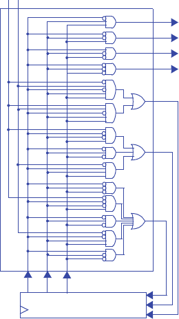
124 5 Register-Transfer Level (RTL) Design
n2 = s1’s1s0B’S + s2’s1s0BS
n1 = s2’s1’s0B + s2’s1s0’ + s2’s1s0S’
n0 = s2’s1’s0’ + s2’s1’s0B’ + s2’s1s0’ + s2’s1s0S’ + s2s1’s0’
Dreg_clr = s2’s1’s0’
Dreg_ld = s2s1’s0’
Dctr_clr = s2’s1’s0
Dctr_ctr = s2’s1s0
(b) The controller features two levels of gates, resulting in a delay of 4ns. Therefore
the critical path is within the up-counter, or 5ns.
(c) With a critical path of 5ns, the maximum clock frequency is 1,000,000,000/5 =
200MHz.
Dreg_clr
State Register
s1 s0
n1
n0
s2
BS
n2
Dreg_ld
Dctr_clr
Dctr_cnt
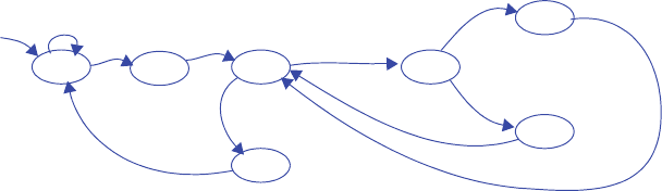
5.1 Exercises 125
Section 5.5: Behavioral-Level Design: C to Gates (Optional)
5.27 Convert the following C-like code, which calculates the greatest common divisor
(GCD) of the two 8-bit numbers a and b, into a high-level state machine.
Inputs: byte a, byte b, bit go
Outputs: byte gcd, bit done
GCD:
while(1) {
while(!go);
done = 0;
while ( a != b ) {
if( a > b ) {
a = a - b;
}
else {
b = b - a;
}
}
gcd = a;
done = 1;
}
A
Inputs: go (bit), a, b (8 bits)
Outputs: done (bit), gcd (8 bits)
go’
go
Local Registers: a_reg (8 bits), b_reg (8 bits)
C
done := ‘0’
a_reg := a
b_reg := b
D
(a_reg==b_reg)’
E
a > b
F
(a > b)’
a_reg := a_reg - b_reg
b_reg := b_reg - a_reg
gcd := a_reg
G
done := ‘1’
a_reg==b_reg
B
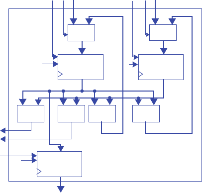
126 5 Register-Transfer Level (RTL) Design
5.28 Use the RTL design process to convert the high-level state machine you created in
Exercise 5.27 to a controller and a datapath. Design the datapath to structure, but
design the controller to the point of an FSM only.
Step 1 - Capture a high-level state machine
The high-level state machine was developed in Exercise 5.27.
Step 2 - Create a datapath
a_reg
ld
b_reg
ld
=
gcd
ld
a
gcd
gcd_ld
01 01
b
- -
a_ld b_selb_ld
a_sel
a_gt_b
>
a_eq_b
clr
0clr
0
clr
0
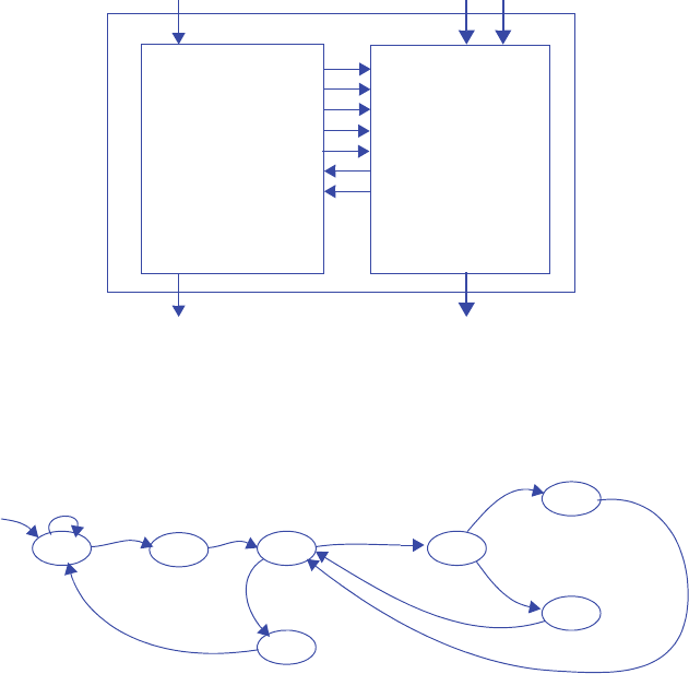
5.1 Exercises 127
Step 3 - Connect the datapath to a controller
Step 4 - Derive the controller’s FSM
a_ld
DatapathController
a_sel
b_ld
gcd
a
done
go b
b_sel
gcd_ld
a_eq_b
a_gt_b
A
Inputs: go, done, a_gt_b, a_eq_b (bit)
Outputs: done, a_ld, a_sel, b_ld, b_sel, gcd_ld (bit)
go’
go
C
done=0
a_ld=1
a_sel=0
D
a_eq_b’
E
a_gt_b
F
a_gt_b’
gcd_ld=1
G
done=1
a_eq_b
b_ld=1
b_sel=0
b_ld=1
b_sel=1
a_ld=1
a_sel=1
B
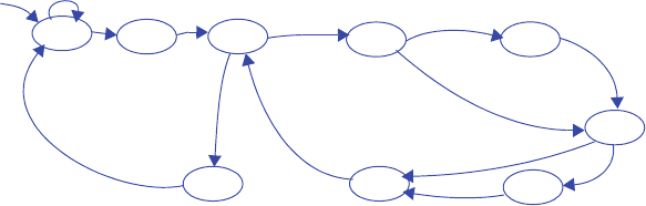
128 5 Register-Transfer Level (RTL) Design
5.29 Convert the following C code, which calculates the maximum difference between
any two numbers within an array A consisting of 256 8-bit values, into a high-level
state machine.
Inputs: byte a[256], bit go
Outputs: byte max_diff, bit done
MAX_DIFF:
while(1) {
while(!go);
done = 0;
i = 0;
max = 0;
min = 255; // largest 8-bit value
while( i < 256 ) {
if( a[i] < min ) {
min = a[i];
}
if( a[1] > max ) {
max = a[i];
}
i = i + 1;
}
max_diff = max - min;
done = 1;
}
A
Inputs: go (bit), a, b (256-byte memory)
Outputs: done (bit), max_diff (8 bits)
go’
go
Local Registers: min, max, i (8 bits)
B
done := ‘0’
i := 0
max := 0
min := 255
D
i<256
E
a[i]<min
min := a[i]
F
H
i := i+1
I
max_diff := max-min
done := ‘1’
C
(i<256)’
max := a[i]
(a[i]<min)’
Ga[i]>max
(a[i]>max)’
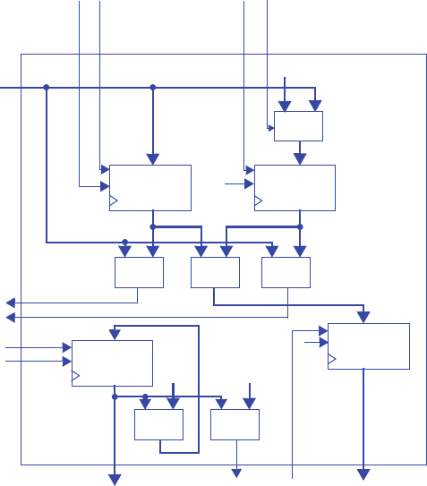
5.1 Exercises 129
5.30 Use the RTL design process to convert the high-level state machine you created in
Exercise 5.29 to a controller and a datapath. Design the datapath to structure, but
design the controller to the point of an FSM only.
Step 1 - Capture a high-level state machine
The high-level state machine was developed in Exercise 5.29.
Step 2 - Create a datapath
max
ld
min
ld
i
ld
01
<
max_ld
a_gt_max
>
a_lt_min
max_clr
min_ld
min_sel
a[i]
-
max_diff
ld
i_ld
i_clr clr
+
1
<
256
ii_lt_256 max_diff_ld max_diff
255
clr clr
0
clr
0
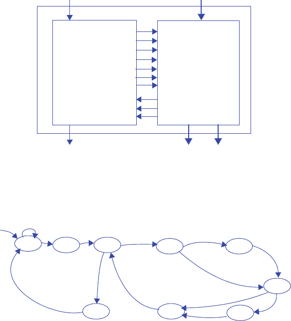
130 5 Register-Transfer Level (RTL) Design
Step 3 - Connect the datapath to a controller
Step 4 - Derive the controller’s FSM
max_clr
DatapathController
max_ld
min_sel
max_diff
a[i]
done
go
min_ld
max_diff_ld
a_lt_min
i_lt_256
a_gt_max
i_ld
i_clr
i
A
Inputs: go, i_lt_256, a_gt_max, a_lt_min (bit)
Outputs: done, max_clr, max_ld, min_sel, min_ld, max_diff_ld, i_ld, i_clr (bit)
go’
go
B
done=0
i_clr=1
max_clr=1
min_sel=0
D
i_lt_256
E
a_lt_min
min_sel=1
F
H
i_ld=1
I
max_diff_ld=1
done=1
C
i_lt_256’
max_ld=1
a_lt_min’
Ga_gt_max
a_gt_max’
min_ld=1
min_ld=1
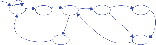
5.1 Exercises 131
5.31 Convert the following C code, which calculates the number of times the value b is
found within an array A consisting of 256 8-bit values, into a high-level state
machine.
Inputs: byte a[256], byte b, bit go
Outputs: byte freq, bit done
FREQUENCY:
while(1) {
while(!go);
done = 0;
i = 0;
freq = 0;
while( i < 256 ) {
if( a[i] == b ) {
freq = freq + 1;
}
i = i + 1;
}
done = 1;
}
A
Inputs: go (bit), a (256-byte memory), b (8 bits)
Outputs: done (bit), freq (8 bits)
go’
go
B
done := ‘0’
i := 0
freq := 0
D
i<256
E
a[i]==b
freq := freq+1
F
i := i+1
(a[i]==b)’
G
done := ‘1’
C
(i<256)’
132 5 Register-Transfer Level (RTL) Design
5.32 Use the RTL design process to convert the high-level state machine you created in
Exercise 5.31 to a controller and a datapath. Design the datapath to structure, but
design the controller to the point of an FSM only.
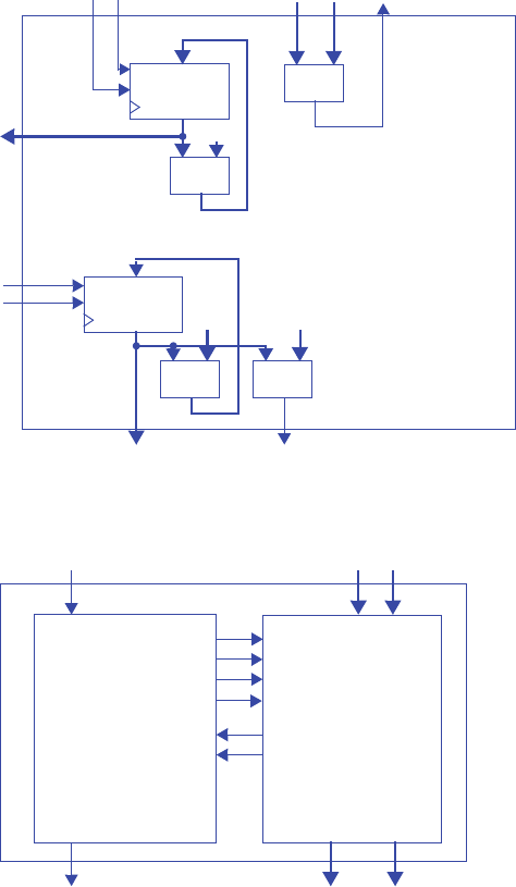
5.1 Exercises 133
Step 1 - Capture a high-level state machine
The high-level state machine was developed in Exercise 5.31.
Step 2 - Create a datapath
Step 3 - Connect the datapath to a controller
freq
ld
i
ld
a[i]
i_ld
i_clr clr
+
1
<
256
ii_lt_256
clr
=
bfreq_ld
freq_clr
+
1
a_eq_b
freq
freq_clr
DatapathController
freq_ld
i_clr
freq
a[i]
done
go
i_ld
i_lt_256
a_eq_b
i
b
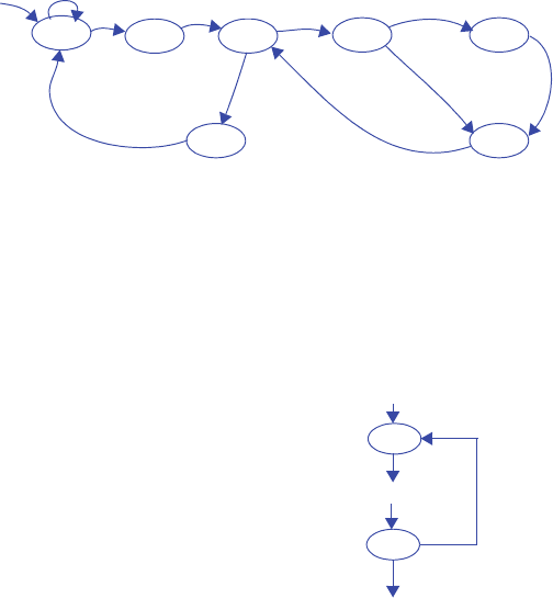
134 5 Register-Transfer Level (RTL) Design
Step 4 - Derive the controller’s FSM
5.33 Develop a template for converting a do{ }while loop of the following form to a
high-level state machine.
do {
// do while statements
} while (cond);
A
Inputs: go, i_lt_256, a_eq_b (bit)
Outputs: done, i_clr, i_ld, freq_clr, freq_ld (bit)
go’
go
B
done=0
i_clr=1
freq_clr=1
D
i_lt_256
E
a_eq_b
freq_ld=1
F
i_ld=1
a_eq_b’
G
done=1
C
i_lt_256’
do {
// do while statements
} while (cond);
(do while statements) cond
!cond
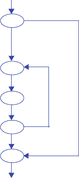
5.1 Exercises 135
5.34 Develop a template for converting a for() loop of the following form to a high-
level state machine.
for(i=start; i<cond; i++)
{
// for statements
}
5.35 Compare the time required to execute the following computation using a custom cir-
cuit versus using a microprocessor. Assume a gate has a delay of 1 ns. Assume a
microprocessor executes one instruction every 5 ns. Assume that n=10 and m=5.
Estimates are acceptable; you need not design the circuit, or determine exactly how
many software instructions will execute.
for (i = 0; i<n; i++) {
s = 0;
for (j = 0; j < m; j++) {
s = s + c[i]*x[i + j];
}
y[i] = s;
}
Based on our answer for Exercise 5.34, we naively assume that each “for” construct
requires 4 states, not including any statements. We’ll also assume that “s=0”
requires one state, “s = s + c[i] * x[i + j]” requires one state, and “y[i] = s” requires
one state.
The inner loop statement is executed 5 times per outer loop iteration, which means
we go through ((2 states + 1 state/inner statement) * 5 iterations) + 2 states = 17
states for the entire inner loop at each outer loop iteration. That means the outer
for (i = start; i < cond; i++) {
// for statements
}
(for statements)
i<cond
i=start
i<cond
i++
(i<cond)’
(i<cond)’
136 5 Register-Transfer Level (RTL) Design
loop’s inner statement is comprised of 19 states. We execute the outer loop 10 times,
for a total of ((2 states + 19 states/inner statement) * 10 iterations) + 2 states = 212
states.
We’ll assume that one state takes at most the same amount of time as one micropro-
cessor instruction. This gives us 212 * 5ns = 1060 ns for the hardware implementa-
tion.
On the microprocessor, if we assume we are allowed base + offset addressing, we
must first compute i+j for the inner loop’s inner statement, then fetch x[i + j], then
fetch c[i], then multiply, and then add. This equates to 5 instructions per inner loop
statement. The for loop itself requires two extra instructions, for incrementing j and
branching. For 5 iterations, this gives us (5 instr./inner statement * 5 iterations + 1
increment * 5 iterations + 1 branch * 5 iterations) = 35 instructions / inner loop.
Thus, each outer loop iteration requires 35 + 2 = 37 instructions. We then have a
total of (37 instr./inner statement * 10 iterations + 1 increment * 10 iterations + 1
branch * 10 iterations) = 390 instructions. This gives us 390 instructions * 5ns/
instruction = 1950 ns for the software implementation.
We can see that even with very rough estimates, hardware is clearly much faster
than software.
Section 5.6: Memory Components
5.36 Calculate the approximate number of DRAM bit storage cells that will fit on an IC
with a capacity of 10 million transistors.
10 million transistors / 1 transistor/DRAM bit storage cell = 10 million DRAM bit
storage cells.
5.37 Calculate the approximate number of SRAM bit storage cells that will fit on an IC
with a capacity of 10 million transistors.
10 million transistors / 6 transistors/SRAM bit storage cell = 1,666,666 SRAM bit
storage cells, or about 1.67 million SRAM bit storage cells.
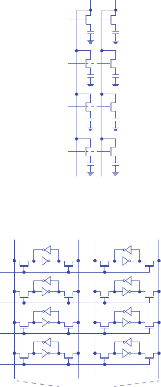
5.1 Exercises 137
5.38 Summarize the main differences between DRAM and SRAM memories.
DRAM memories use a single transistor and capacitor per bit, while SRAM memo-
ries require six transistors per bit. SRAM is thus less compact and more expensive
than a DRAM that can store the same number of bits. However, SRAMs typically
feature faster access times than DRAMs as DRAMs require a periodic refresh of its
contents, a process which blocks DRAM accesses.
5.39 Draw a circuit of transistors showing the internal structure for all the storage cells for
a 4x2 DRAM (four words, two bits each), clearly labelling all internal components
and connections.
5.40 Draw a circuit of transistors showing the internal structure for all the storage cells for
a 4x2 SRAM (four words, two bits each), clearly labelling all internal components
and connections.
w0
enable
w1
enable
w2
enable
w3
enable
d0
d1
d1 d1’ d0 d0’
w0
enable
w1
enable
w2
enable
w3
enable
to sense amplifiers
138 5 Register-Transfer Level (RTL) Design
5.41 Summarize the main differences between EPROM and EEPROM memories.
An EPROM is erased en masse by shining ultraviolet light on the memory (typically
through a window in the memory’s packaging). An EEPROM is erased through a
high-voltage signal, and specific words can be erased.
5.42 Summarize the main differences between EEPROM and flash memories.
Whereas an EEPROM may permit erasing one word at a time, a flash memory is a
type of EEPROM which permits erasing larger blocks of memory at a time (or per-
haps the entire memory).
5.1 Exercises 139
5.43 Use an HLSM to capture the design of a system that can save data samples and then
play them back. The system has an 8-bit input D where data appears. A single-bit
input S changing from 0 to 1 requests that the current value on D (i.e., a sample) be
saved in a nonvolatile memory. Sample requests will not arrive faster than once per
10 clock cycles. Up to 10,000 samples can be saved, after which sampling requests
are ignored. A single-bit input P changing from 0 to 1 causes all recorded samples to
be played back—i.e., to be written to an output Q one sample at a time in the order
they were saved at a rate of one sample per clock cycle. A single-bit input R resets
the system, clearing all recorded samples. During playback, any sample or reset
request is ignored. At other times, reset has priority over a sample request. Choose
an appropriate size and type of memory, and declare and use that memory in your
HLSM.
Inputs: S, P, R (bit); D, Mem_D (8 bits)
Outputs: Q (8 bits); Mem_D (8 bits) [both an input and an output]; Mem_addr (14 bits); Mem_wr, Mem_rd (bit)
Local Registers: index (14 bits), pb_index (14 bits)
Init Wait
Sample WaitSLow
PlayBack WaitPLow
index := 0
pb_index := 0
Q := 0
Q := 0
Mem_D := D
Q := Mem_D
pb_index := pb_index + 1
pb_index := 0
pb_index < index
(pb_index < index)’
P*R’
S*R’
R
R
R
R’*P’*S’
R’*P’*S
R’*P
Q := 0
S’*R’
P’*R’
Mem_rd := ‘1’
Mem_addr := pb_index
index := index + 1
Mem_addr := index
Sample Mem_wr := ‘1’
Mem_wr := ‘0’
Mem_D := 0
Mem_addr := 0
Mem_wr := ‘0’
Mem_rd := ‘0’
Mem_D := 0
Mem_rd := ‘0’
140 5 Register-Transfer Level (RTL) Design
Section 5.7: Queues (FIFOs)
5.44 For an 8-word queue, show the queue’s internal state and provide the value of
popped data for the following sequences of pushes and pops: (1) push A, B, C, D, E,
(2) pop, (3) pop, (4) push U, V, W, X, Y, (5) pop, (6) push Z, (7) pop, (8) pop, (9)
pop.
A
76543210
Step 1 BCDE
rf
A
Step 2 BCDE
rf
A
Step 3 BCDE
rf
popped A
popped B
X
Step 4 YCDE
rf
popped C
U
VW
X
Step 5 YCDE
rf
U
VW
popped D
X
Step 6 YZDE
rf
U
VW
X
Step 7 YZDE
rf
U
VW
popped E
X
Step 8 YZDE
rf
U
VW
popped U
X
Step 9 YZDE
rf
U
VW
5.1 Exercises 141
5.45 Create an FSM describing the queue controller of Figure 5.79. Pay careful attention
to correctly setting the full and empty outputs.
Init
rear_clr=1
front_clr=1
empty=1
full=0
rf_wr=0
rf_rd=0
WaitE
full=0
ReadE
front_inc=1
rf_rd=1
reset’wr’rd
Read2E
reset’wr’rd’
WriteE
reset’wr
rear_inc=1
rf_wr=1
Write2E
empty=1
Inputs: wr, rd, reset, eq Outputs: rear_clr, rear_inc, front_clr, front_inc, rf_wr, rf_rd, full, empty
reset
full=1
empty=0
full=0
empty=0
full=0
empty=1
full=0
empty=1
Wait
full=0
Read
front_inc=1
rf_rd=1
reset’wr’rd
Read2 eq’
reset’wr’rd’
Write
reset’wr
rear_inc=1
rf_wr=1
Write2
empty=0
eq’
eq
reset
full=0
empty=0
full=0
empty=0
full=0
empty=0
full=0
empty=0
eq
WaitF
full=1
ReadF
front_inc=1
rf_rd=1
reset’wr’rd
Read2F
reset’wr’rd’
WriteF
reset’wr
rear_inc=1
rf_wr=1
Write2F
empty=0
full=1
empty=0
full=1
empty=0
full=1
empty=0
full=0
empty=0
reset
142 5 Register-Transfer Level (RTL) Design
5.46 Create an FSM describing the queue controller of Figure 5.79, but with error-pre-
venting behavior that ignores any pushes when the queue is full, and ignores pops of
an empty queue (outputting 0).
Init
rear_clr=1
front_clr=1
empty=1
WaitMT
reset’wr’
full=0
rf_wr=0
rf_rd=0
reset
WriteMT
reset’wr
rear_inc=1
rf_wr=1
empty=1
full=0
Wait
full=0
Read
front_inc=1
rf_rd=1
reset’wr’rd
Read2
eq
eq’
reset’wr’rd’
reset
Write
reset’wr
rear_inc=1
rf_wr=1
Write2
empty=0
eq’
WaitFull
eq
ReadFull
reset’rd
front_inc=1
rf_rd=1
empty=0
full=1
reset’rd’
reset
Inputs: wr, rd, reset, eq Outputs: rear_clr, rear_inc, front_clr, front_inc, rf_wr, rf_rd, full, empty
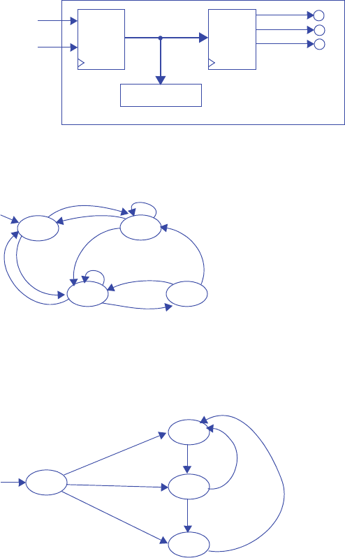
5.1 Exercises 143
Section 5.9: Multiple Processors
5.47 A system S counts people that enter a store, incrementing the count value when a
single-bit input P changes from 1 to 0. The value is reset when R is 1. The value is
output on a 16-bit output C, which connects to a display. Furthermore, the system
has a lighting system to indicate the approximate count value to the store manager,
turning on a red LED (LR=1) for 0 to 99, else a blue LED (LB=1) for 100 to 199,
else a green LED (LG=1) for 200 and above. Draw a block diagram of the system
and its peripheral components, using two processors for the system S. Show the
HLSM for each processor.
]
P
R
Counter
Processor
Display
C
LED
Processor
LR
LG
LB
System Diagram:
Counter HLSM:
Inputs: P, R (b it)
Outputs: C (16 bits)
Local Registers: Cnt (16 bits)
Init Wait0
Wait1 Incr
P == 0
P == 1
(R==0)*(P==0)
R == 1
(R==0)*(P==1)
R == 1
(R==0)*(P==1)
(R==0)*(P==0)
P == 1
P == 0
Cnt := 0
C := Cnt
C := Cnt
C := Cnt
Cnt := Cnt + 1
C := Cnt
LED HLSM:
Inputs: Cnt (16 bits)
Outputs: LR, LG, LB (bit)
Init
Red
Blu
Grn
(Cnt>=0)*(Cnt<=99)
(Cnt>=100)*(Cnt<=199)
Cnt>=200
Cnt>99
Note: RGB will be a name for LR, LG, LB concatenated
RGB:=”100”
RGB:=”001”
RGB:= “010”
Cnt>199
Cnt<100
Cnt<200
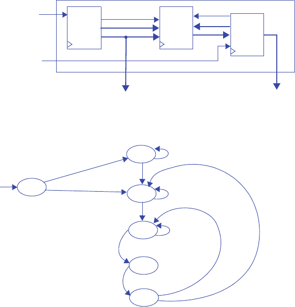
144 5 Register-Transfer Level (RTL) Design
5.48 A system S counts the cycles high of the most recent pulse on a single-bit input P
and displays the value on a 16-bit output D, holding the value there until the next
pulse completes. The system also keeps track of the previous 8 values, and com-
putes and outputs the average of those values on a 16-bit output A whenever an
input C changes from 0 to 1. The system holds that output value until the next
change of C from 0 to 1. Draw a block diagram of the system and its peripheral
components, using two processors and a global register file for the system. Show the
HLSM for each processor.
P
C
Pulse
Processor
D
8-word
16-bit RF
System Diagram:
RF_wr
RF_w_addr Average
Processor
RF_rd
RF_r_addr
RF_r_data
A
Pulse HLSM:
Inputs: P (bit)
Outputs: RF_waddr (3 bits), RF_we (bit), RF_wd (16 bits)
Init
Local Registers: i (3 bits), Cnt (16 bits)
i := 0
WaitH
WaitL
Pulse
Write
Cnt := Cnt + 1
Cnt := 0
RF_wd := Cnt
Cnt := 0
i := (i + 1) % 8
P
P’
P
P’
P’
P
P
P’
P’
P
SetAddr
RF_we := ‘1’
RF_waddr := i
5.1 Exercises 145
Average HLSM:
Inputs: C (bit), RF_rd (16 bits)
Outputs: A (16 bits), RF_re (bit), RF_raddr (3 bits)
Local Registers: i (3 bits), tmp (16 bits)
Init
i := 0
tmp := 0 WaitL
i := 0
tmp:= 0
WaitH
Go
Choose
i := i + 1
tmp := tmp + RF_rd
i < 7
C
C’
C
C
C’
C’
C’
C
i >= 7
SetAddr
RF_raddr := i
i := i + 1
RF_re := ‘1’
RF_raddr := i
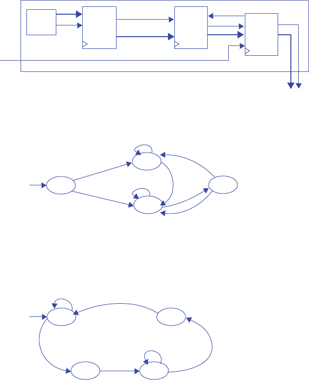
146 5 Register-Transfer Level (RTL) Design
5.49 A system S counts people that enter a store, incrementing the count value when a
single-bit input P changes from 1 to 0. The value is reset when R is 1. The value is
output on a 16-bit output C, which connects to a display. Furthermore, the system
has a lighting system to indicate the approximate count value to the store manager,
turning on a red LED (LR=1) for 0 to 99, else a blue LED (LB=1) for 100 to 199,
else a green LED (LG=1) for 200 and above. Draw a block diagram of the system
and its peripheral components, using two processors for the system S. Show the
HLSM for each processor.
Crec
Keypress
Processor
data_in
Queue from
System Diagram:
wr Interface
Processor
rd
empty
data_out
CK
Keypad
K
EEx. 5.46
[32](4)
CE
Keypress HLSM:
Inputs: K (4 bits), E (bit)
Outputs: data_in (4 bits), wr (bit)
Init
WaitH
WaitL
Go
E
E’
E’
E
E’
E
E
E’
data_in := 0
wr := ‘0’
data_in := 0
wr := ‘0’
data_in := 0
wr := ‘0’
data_in := K
wr := ‘1’
Interface HLSM:
Inputs: empty (bit), Crec (bit), data_out (4 bits)
Outputs: rd (bit), CE (bit), CK (4 bits)
WaitD
Try
Recvd
empty
Local Registers: tmp (4 bits)
Read
empty’
Crec’
Crec
CE := ‘0’
CK := 0
CE := ‘0’
CK := 0
rd := ‘1’
rd := ‘0’
tmp := data_out
CE := ‘1’
CK := tmp
rd := ‘0’
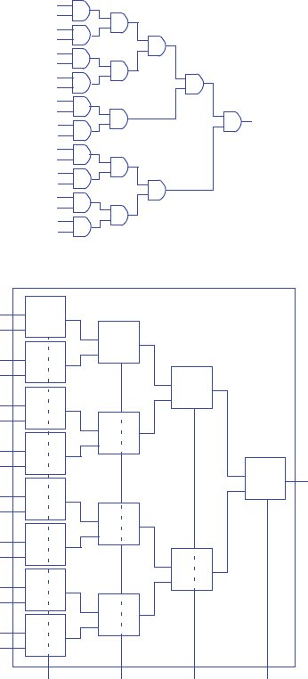
5.1 Exercises 147
Section 5.10: Hierarchy—A Key Design Concept
5.50 Compose a 20-input AND gate from 2-input AND gates.
5.51 Compose a 16x1 mux from 2x1 muxes.
i19
i18
F
i17
i16
i15
i14
i13
i12
i11
i10
i9
i8
i7
i6
i5
i4
i3
i2
i1
i0
i0 d
s
2x1
i1
i0 d
s
2x1
i1
i0 d
s
2x1
i1
i0 d
s
2x1
i1
i0 d
s
2x1
i1
i0 d
s
2x1
i1
i0 d
s
2x1
i1
i0 d
s
2x1
i1
i0 d
s
2x1
i1
i0 d
s
2x1
i1
i0 d
s
2x1
i1
i0 d
s
2x1
i1
i0 d
s
2x1
i1
i0 d
s
2x1
i1
i15
i14
i13
i12
i11
i10
i9
i8
i7
i6
i5
i4
i3
i2
i1
i0
i0 d
s
2x1
i1
d
s0 s1 s2 s3
16x1
148 5 Register-Transfer Level (RTL) Design
5.52 Compose a 4x16 decoder with enable from 2x4 decoders with enable.
5.53 Compose a 1024x8 RAM using only 512x8 RAMs.
5.54 Compose a 512x8 RAM using only 512x4 RAMs.
i0
d3
e
2x4
i1
i3
i2
d2
d1
d0
i0
d3
e
2x4
i1 d2
d1
d0
i0
d3
e
2x4
i1 d2
d1
d0
i0
d3
e
2x4
i1 d2
d1
d0
i0
d3
e
2x4
i1 d2
d1
d0
i1
i0
d15
d14
d13
d12
d11
d10
d9
d8
d7
d6
d5
d4
d3
d2
d1
d0
4x16
e(or “1”)
addr
rw
i0
e
1x2 dcd
d1
d0
1024x8 RAM
512x8
RAM
addr
en data
a8..a0
a9
8
rw
512x8
RAM
addr
en data
rw
en
data
10 9
addr
rw
512x4
RAM
addr
en data
rw
en
9
512x4
RAM
addr
en data
rw
4
44
8
data
512x8 RAM
5.1 Exercises 149
5.55 Compose a 1024x8 ROM using only 512x4 ROMs.
5.56 Compose a 2048x8 ROM using only 256x8 ROMs.
addr
512x4
ROM
addr
en data
en
9
512x4
ROM
addr
en data
4
44
8
data
1024x8 ROM
512x4
ROM
addr
en data
512x4
ROM
addr
en data
i0
e
1x2 dcd
d1
d0
a8..a0
a9
addr
en
8
2048x8 ROM
e
3x8 dcd
d1
d0
a7..a0
a10
256x8
ROM
en
addr
data
i2
i1
i0 d3
d2
d5
d4
d7
d6
a9
a8
256x8
ROM
en
addr
data
256x8
ROM
en
addr
data
256x8
ROM
en
addr
data
256x8
ROM
en
addr
data
256x8
ROM
en
addr
data
256x8
ROM
en
addr
data
256x8
ROM
en
addr
data
data
150 5 Register-Transfer Level (RTL) Design
5.57 Compose a 1024x16 RAM using only 512x8 RAMs.
5.58 Compose a 1024x12 RAM using 512x8 and 512x4 RAMs.
addr
512x8
RAM
addr
en data
en
9
512x8
RAM
addr
en data
8
8
16
data
1024x16 RAM
512x8
RAM
addr
en data
512x8
RAM
addr
en data
i0
e
1x2 dcd
d1
d0
a8..a0
a9
rw
rw
rw rw
rw
addr
512x8
RAM
addr
en data
en
9
512x4
RAM
addr
en data
8
4
12
data
1024x12 RAM
512x8
RAM
addr
en data
512x4
RAM
addr
en data
i0
e
1x2 dcd
d1
d0
a8..a0
a9
rw
rw
rw rw
rw

5.1 Exercises 151
5.59 Compose a 640x12 RAM using only 128x4 RAMs.
5.60 *Write a program that takes a parameter N, and automatically builds an N-input
AND gate from 2-input AND gates. Your program merely need indicate how many
2-input AND gates exist in each level, from which we could easily determine the
connections.
Solution not shown for challenge problems. The general solution involves a while
loop that continues until an iteration involves just 1 AND gate. Each iteration should
place X/2 gates, where X is initially N and where X is set to X/2 in each iteration.
Care must be taken when a level has an odd number of inputs.
addr
128x4
RAM
addr
en data
en
7
128x4
RAM
addr
en data
44
12
data
640x12 RAM
i2
e
3x8 dcd
d4
d3
a6..a0
a7
rw
rw rw
128x4
RAM
addr
en data
rw
4
128x4
RAM
addr
en data
128x4
RAM
addr
en data
rw rw
128x4
RAM
addr
en data
rw
d2
d1
d0
d5
i1
i0
a8
a9 d6
d7
128x4
RAM
addr
en data
128x4
RAM
addr
en data
rw rw
128x4
RAM
addr
en data
rw
128x4
RAM
addr
en data
128x4
RAM
addr
en data
rw rw
128x4
RAM
addr
en data
rw
128x4
RAM
addr
en data
128x4
RAM
addr
en data
rw rw
128x4
RAM
addr
en data
rw
152 5 Register-Transfer Level (RTL) Design

139
CHAPTER 6
OPTIMIZATIONS AND
TRADEOFFS
6.1 EXERCISES
SECTION 6.1: INTRODUCTION
6.1) Define the terms “optimization” and “tradeof.f”
An optimization improves all criteria of interest to us, whereas a tradeoff improves
certain criteria at the expense of other criteria.
6.2) A homeowner wishes to increase the amount of light inside the house during the day,
with the only criteria of interest being the amount of light and the cost of electricity.
Describe how to increase the light via: (a) an optimization, (b) a tradeoff.
(a) An optimization would be to add a window or sunroof (note: the initial cost of
installing those items was not listed as a criteria of interest and thus can be
neglected). The window or sunroof adds light without changing the cost of electric-
ity.
(b) A tradeoff would be to turn on a lamp during the day. The light would increase,
but at the expense of higher electric cost.
140 6 Optimizations and Tradeoffs
SECTION 6.2: COMBINATIONAL LOGIC OPTIMIZATIONS AND
TRADEOFFS
6.3) Perform two-level logic size optimization for F(a,b,c) =ab'c +abc +a'bc +
abc' using (a) algebraic methods, (b) a K-map. Express the answers in sum-of-products
form.
(a) F = ab’c + abc + a’bc + abc’
F = ab’c + abc + abc + a’bc + abc + abc’
F = ac(b’ + b) + bc(a + a’) + ab(c + c’)
F = ac + bc + ab
6.4) Perform two-level logic size optimization for F(a,b,c) = a + a'b'c + a'c using
a K-map..
6.5) Perform two-level logic size optimization for F(a,b,c,d) = a'bc' + abc'd' +
abd using a K-map.
0
01
01 0
11
a
bc
0
1
00 01 11 10
F
ab
bc
ac
F(a,b,c) = ab + ac + bc
(b)
0
11
11 0
11
a
bc
0
1
00 01 11 10
F
a
c
F(a,b,c) = a + c
F(a,b,c,d) = bc’ + abd
0
11
00 0
00
ab
cd
00
01
00 01 11 10
F
1
00
11 0
00
11
10
abd
bc’
6.1 Exercises 141
6.6) Perform two-level logic size optimization F(a,b,c,d) = ab + a'b'd' using a K-
map.
6.7) Perform two-level logic size optimization for F(a,b,c) = a'b'c + abc, assuming
input combinations a'bc and ab'c can never occur (those two minterms represent don’t
cares).
6.8) Perform two-level logic size optimization for F(a,b,c,d) = a'bc'd + ab'cd',
assuming that a and b can never both be 1 at the same time, and that c and d can never
both be 1 at the same time (i.e., there are don’t cares).
6.9) Consider the function F(a,b,c) = a'c + ac + a'b. Using a K-map: (a) Determine
which of the following terms are implicants (but not necessarily prime implicants) of the
equation: a'b'c', a'b', a'bc, a'c, c, bc, a'bc', a'b. (b) Determine
which of those terms are prime implicants of the function.
(b) Prime implicants: a’b, c
F(a,b,c,d) = ab + a’b’d’
1
00
00 1
00
ab
cd
00
01
00 01 11 10
F
1
00
11 1
00
11
10 ab
a’b’d’
0
0x
1x 0
10
a
bc
0
1
00 01 11 10
Fc
F(a,b,c) = c
F(a,b,c,d) = ac + bd
0
01
0x 0
x0
ab
cd
00
01
00 01 11 10
F
x
00
xx x
x1
11
10
ac
bd
Implicants listed in the question:
0
11
01 1
11
ab
cd
00
01
00 01 11 10
F
0
00
01 1
11
11
10
a’b’c’, a’b’, a’bc, a’c, c, bc, a’bc’, a’b
142 6 Optimizations and Tradeoffs
6.10) For the function F(a,b,c) = a'c + ac + a'b, determine all prime implicants and
all essential prime implicants: (a) using a K-map, (b) using the tabular method.
(a)
(b)
6.11) For the equation F(a,b,c,d) = ab'c' + abc'd + abcd + a'bcd + a'bcd',
determine all prime implicants and all essential prime implicants: (a) using a K-map, (b)
using the tabular method.
(a)
0
01
11 1
10
a
bc
0
1
00 01 11 10
Fc
a’b and c are both prime implicants and
a’b
also essential prime implicants; each is the
only cover of some particular 1.
1
2
a’b
a’c
ac
c
2-literal impl. 1-literal impl.
Prime implicants
Minterm a’b c
a’b
a’c
c
XX
X
All prime implicants are essential; stop
Step 1:
Step 2:
0
00
00 0
11
ab
cd
00
01
00 01 11 10
F
0
11
11 0
00
11
10
a’bc
bcd
abd
ac’d
ab’c’
Prime implicants: ab’c’, ac’d, a’bc, bcd, abd
Essential prime implicants: ab’c’, a’bc
6.1 Exercises 143
6.12) Use repeated application of the expand operation to heuristically minimize the equa-
tion F(a,b,c) = a'b'c + a'bc + abc. (a) Try expanding each term for each
variable. (b) Instead, determine a way to randomly choose an expand operation, and then
apply 5 random expands.
(a) A possible sequence of expand attempts:
F = b’c + a’bc + abc - invalid (ab’c is not in on-set)
F = a’c + a’bc + abc - valid
F = a’ + a’bc + abc - invalid (a’c’ is not in on-set)
F = a’c + bc + abc - valid
F = a’c + c + abc - invalid (b’c is not in on-set)
F = a’c + b + abc - invalid (bc’ is not in on-set)
F = a’c + bc + bc - valid
F = a’c + bc + c - invalid (b’c is not in on-set)
F = a’c + bc + b - invalid (bc’ is not in on-set)
Final equation:
F = a’c + bc + bc
(F = a’c + bc if a simple search for redundant terms is included)
(b) We may choose a heuristic which chooses a minterm to expand at random and a
variable in that minterm to expand at random. One possible sequence of random
2
3
a’bcd’
abc’d
4-literal impl.
Minterm ab’c’
ab’c’
Step 1:
Step 2:
a’bcd
4abcd
1
2
ab’c’
a’bc
3-literal impl.
bcd
3abd
1ab’c’d’
ab’c’d ac’d Cannot be expanded further; stop
Prime implicants are circled.
a’bc ac’d abd bcd
abc’d
abcd
a’bcd
a’bcd’
X
X
X
X
XX
X
XEssential prime implicants:
ab’c’, a’bc
Step 3:
With ab’c’ and a’bc, we only have abc’d and abcd left to cover. Choosing abd
will cover both with only one prime implicant, so the final cover is:
F(a, b, c, d) = ab’c’ + a’bc + abd
144 6 Optimizations and Tradeoffs
expand attempts:
F = a’b’c + a’bc + ab - invalid (abc’ is not in on-set)
F = a’b’c + bc + abc - valid
F = b’c + bc + abc - invalid (ab’c is not in on-set)
F = a’c + bc + abc - valid
F = a’c + bc + ac - invalid (ab’c is not in on-set)
6.13) Use repeated application of the expand operation to heuristically minimize the equa-
tion F(a,b,c,d,e) = abcde + abcde' + abcd'e'. (a) Try expanding each
term for each variable. (b) Instead, determine a way to randomly choose an expand opera-
tion, and then apply 5 random expands.
(a)
One possible sequence of expand attempts:
F = bcde + abcde’ + abcd’e’ - invalid (a’bcde is not in on-set)
F = acde + abcde’ + abcd’e’ - invalid (ab’cde is not in on-set)
F = abde + abcde’ + abcd’e’ - invalid (abc’de is not in on-set)
F = abcd + abcde’ + abcd’e’ - valid
F = abcd + bcde’ + abcd’e’ - invalid (a’bcde’ is not in on-set)
F = abcd + acde’ + abcd’e’ - invalid (ab’cde’ is not in on-set)
F = abcd + abde’ + abcd’e’ - invalid (abc’de’ is not in on-set)
F = abcd + abce’ + abcd’e’ - valid
F = abcd + abc + abcd’e’ - invalid (abcd’e is not in on-set)
F = abcd + abce’ + bcd’e’ - invalid (a’bcd’e’ is not in on-set)
F = abcd + abce’ + acd’e’ - invalid (ab’cd’e’ is not in on-set)
F = abcd + abce’ + abd’e’ - invalid (abc’d’e’ is not in on-set)
F = abcd + abce’ + abce’ - valid
F = abcd + abce’ + abc - invalid (abcd’e is not in on-set)
Final equation:
F = abcd + abce’ + abce’
(F = abcd + abce’ if a simple search for redundant terms is included)
(b) We may choose a heuristic which chooses a minterm to expand at random and a
variable in that minterm to expand at random. One possible sequence of random
expand attempts:
F = abde + abcde’ + abcd’e’ - invalid (abc’de is not in on-set)
F = abcde + abcde’ + bcd’e’ - invalid (a’bcd’e’ is not in on-set)
F = abcde + acde’ + abcd’e’ - invalid (ab’cde’ is not in on-set)
F = abcde + abcd + abcd’e’ - valid
F = abcde + abcd + abd’e’ - invalid (abc’d’e’ is not in on-set)
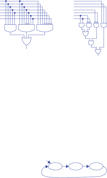
6.1 Exercises 145
6.14) Using algebraic methods, reduce the number of gate inputs for the following equa-
tion by creating a multilevel circuit: F(a,b,c,d,e,f,g) = abcde + abcd'e'fg +
abcd'e'f'g'. Assume only AND, OR, and NOT gates will be used. Draw the circuit
for the original equation and for the multilevel circuit, and clearly list the delay and num-
ber of gate inputs for each circuit.
F = abcde + abcd’e’fg + abcd’e’f’g’
F = abc(de + d’e’fg + d’e’f’g’)
F = abc(de + d’e’(fg + f’g’))
SECTION 6.3: SEQUENTIAL LOGIC OPTIMIZATIONS AND TRADEOFFS
6.15) Reduce the number of states for the FSM in Figure 6.88 using the partitioning
method.
Initial groups: G1:{S0,S3}, G2:{S1,S4}, G3:{S2,S5}
G1: S0 goes to S1 (G2), S3 goes to S4 {G2} --> Next states in same group
G2: S1 goes to S2 (G3), S4 goes to S5 (G3) --> Next states in same group
G3: S2 goes to S3 (G1), S5 goes to S0 (G1) --> Next states in same group
Thus, no groups need to be partitioned further, and hence states within a group are
equivalent. Replace S3 by S0, S4 by S1, and S5 by S2 to yield:
a
b
c
d
e
f
g
F
a
b
c
d
e
f
g
F
19 Gate Inputs
5 Levels of Gate Delay
28 Gate Inputs
3 Levels of Gate Delay
Note: each “bubble” is a NOT gate
S0,S3
xy=00 xy=01 xy=10
Inputs: none; Outputs: x,y
S1,S4 S2,S5
146 6 Optimizations and Tradeoffs
6.16) Reduce the number of states for the FSM in Figure 6.89 using the partitioning
method.
Initial groups: G1:{S0, S1, S2, S3, S6}, G2:{S4, S5}
x=0: G1: S0 -> S1 (G1), S1 -> S3 (G1), S2 -> S5 (G2), S3 -> S0 (G1), S6 -> S0 (G1)
--> Next states NOT all in same group
New groups: G1: {S0, S1, S3, S6}, G2:{S4, S5}, G3:{S2}
x=0: G1: S0 -> S1 (G1), S1 -> S3 (G1), S3 -> S0 (G1), S6 -> S0 (G1)
x=0: G2: S4 -> S0 (G1), S5 -> S0 (G1)
x=0: G3 (One state group; nothing to check)
x=1: G1: S0 -> S2 (G3), S1 -> S4 (G2), S3 -> S0 (G1), S6 -> S0 (G1)
--> Next states NOT all in same group
New groups: G1:{S0}, G2:{S4, S5}, G3:{S2}, G4:{S1}, G5:{S3, S6}
x=0: G1: (One state group; nothing to check)
x=0: G2: S4 -> S0 (G1), S5 -> S0 (G1)
x=0: G3: (One state group; nothing to check)
x=0: G4: (One state group; nothing to check)
x=0: G5: S3 -> S0 (G1), S6 -> S0 (G1)
x=1: G1: (One state group; nothing to check)
x=1: G2: S4 -> S0 (G1), S5 -> S0 (G1)
x=1: G3: (One state group; nothing to check)
x=1: G4: (One state group; nothing to check)
x=1: G5: S3 -> S0 (G1), S6 -> S0 (G1)
Thus, no groups need to be partitioned further, and hence states within a group are
equivalent. Replace S6 by S3 and S5 by S4 to yield:
S0
y=0
S1 S2
S3,S6 S4,S5
x
x
xx’
x’
x’ y=0
y=1
y=0
y=0
Inputs: x; Outputs: y
6.1 Exercises 147
6.17) Reduce the number of states for the FSM in Figure 6.90 using the partitioning
method.
Initial groups: G1:{A, D, E, F, G}, G2:{B, C}
i=0: G1: A -> F (G1), D -> F (G1), E -> G (G1), F -> F (G1), G -> C (G2)
-->Next states NOT all in same group
New groups: G1:{A, D, E, F}, G2:{B, C}, G3:{G}
i=0: G1: A -> F (G1), D -> F (G1), E -> G (G3), F -> F (G1)
-->Next states NOT all in same group
New groups: G1:{A, D, F}, G2: {B, C}, G3:{G}, G4:{E}
i=0: G1: A -> F (G1), D -> F (G1), F -> F (G1)
i=0: G2: B -> E (G4), C -> E (G4)
i=0: G3: (One state group; nothing to check)
i=0: G4: (One state group; nothing to check)
i=1: G1: A -> F (G1), D -> F (G1), F -> E (G4)
-->Next states NOT all in same group
New groups: G1:{A, D}, G2: {B, C}, G3:{G}, G4:{E}, G5:{F}
i=0: G1: A -> F (G5), D -> F (G5)
i=0: G2: B -> E (G4), C -> E (G4)
i=0: G3: (One state group; nothing to check)
i=0: G4: (One state group; nothing to check)
i=0: G5: (One state group; nothing to check)
i=1: G1: A -> F (G5), D -> F (G5)
i=1: G2: B -> A (G1), C-> D (G1)
i=1: G3: (One state group, nothing to check)
i=1: G4: (One state group, nothing to check)
i=1: G5: (One state group, nothing to check)
Thus, no groups need to be partitioned further, and hence states within a group are-
equivalent. Replace C by B and D by A to yield:
Inputs: i; Outputs: h
A,D
h=0
B,C E
F
G
i
i’
h=0
h=1 h=0
h=0
i
i’
i
i’
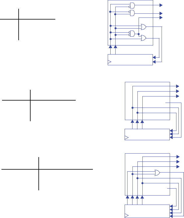
148 6 Optimizations and Tradeoffs
6.18) Compare the logic size (number of gate inputs) and the delay (number of gate-
delays) of a straightforward 2-bit binary encoding of the FSM in Figure 6.91 using a 3-bit
output encoding versus using a one-hot encoding.
Inputs Outputs
s2 s1 s0 n2 n1 n0 w x y
100010100
010001010
001000001
000000000
Inputs Outputs
s1 s0 n1 n0 w x y
0 0 01100
0 1 10010
1 0 11001
1 1 11000
State encodings: S0: 00, S1: 01, S2: 10, S3: 11
y
State Register
s1
n1
n0
s0
x
w
n1=s1+s0
n0=s1’s0’ + s1
w = s1’s0’
x = s1’s0
y=s1s0’
State encodings: S0: 100, S1: 010, S2: 001, S3: 000
n2 = 0
y
State Register
n1
n0
s2
x
w
s1 s0
n2
Logic size: 10 gate inputs
Delay: 2 gate delays
Logic size: 0 gate inputs
Delay: 0 gate delays
2-bit binary encoding:
3-bit output encoding:
State encodings: S0: 0001, S1: 0010, S2: 0100, S3: 1000
Inputs Outputs
s3 s2 s1 s0 n3 n2 n1 n0 w x y
0 0 0 1 0010100
0 0 1 0 0100010
0 1 0 0 1000001
1 0 0 0 1000000
n3 = s3 + s2
n2 = s1
n1 = s0
n0 = 0
w = s0
x = s1
y = s2
y
State Register
s3
n1
n0
s2
x
w
0
s1 s0
n2
n3
Logic size: 2 gate inputs
Delay: 1 gate delays
One-hot encoding:
n1 = s2
n0 = s1
w = s2
x = s1
y = s0
0

6.1 Exercises 149
6.19) Compare the logic size (number of gate inputs) and the delay (number of gate-
delays) of a minimal bitwidth state encoding versus an output encoding for the laser-based
distance measurer FSM shown in Figure 5.26..
Inputs Outputs
s2 s1 s0 B S n2 n1 n0 L Dreg_clr Dreg_ld Dcnt_clr Dcnt_cnt
000xx00101 0 0 0
0010x00100 0 1 0
0011x01000 0 1 0
010xx01110 0 0 0
011x001100 0 0 1
011x110000 0 0 1
100xx00100 1 0 0
State encodings: S0: 000, S1: 001, S2: 010, S3: 011, S4: 100
Minimal bit width encoding:
n2 = s1s0S
n1 = s1’s0B + s1s0’ + s1s0S’
n0 = s1’s0’ + s1’s0B’ + s1s0’ + s1s0S’
L = s1s0’
Dreg_clr = s2’s1’s0’
Dreg_ld = s2
Dcnt_clr = s1’s0
Dcnt_cnt = s1s0
Logic size: 37 gate inputs
Delay: 2 gate delays
Inputs Outputs
s4 s3 s2 s1 s0 B S n4n3n2n1n0L
Dreg_clr
Dreg_ld
Dcnt_clr
Dcnt_cnt
0 1 0 0 0 x x 0001001000
0 0 0 1 0 0 x 0001000010
0 0 0 1 0 1 x 1000000010
1 0 0 0 0 x x 0000110000
0 0 0 0 1 x 0 0000100001
0 0 0 0 1 x 1 0010000001
0 0 1 0 0 x x 0001000100
State encodings: S0: 01000, S1: 00010, S2: 10000, S3: 00001, S4: 00100
Output encoding:
n4 = s1’B
n3 = 0
n2 = s0S
n1 = s3 + s1x’ + s2
n0 = s4 + s0S’
L = s4
Dreg_clr = s3
Dreg_ld = s2
Dcnt_clr = s1
Dcnt_cnt = s0
Logic size: 13 gate inputs
Delay: 2 gate delays
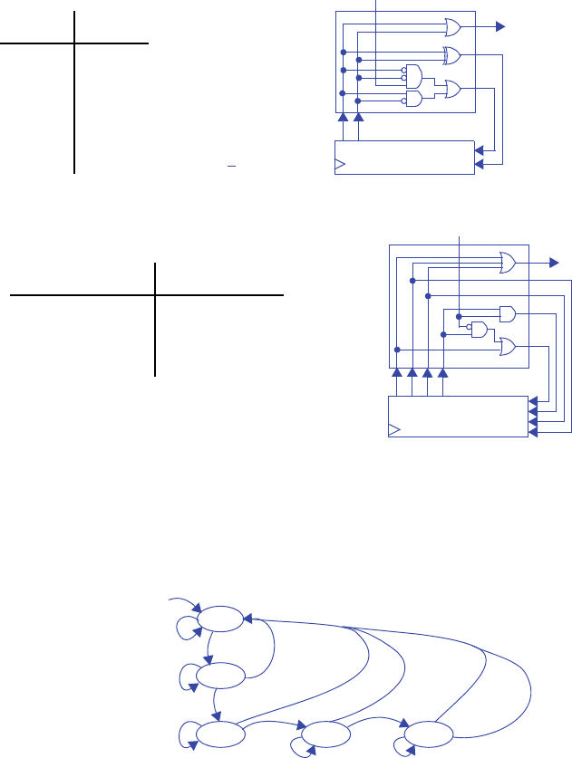
150 6 Optimizations and Tradeoffs
6.20) Compare the logic size (number of gate inputs) and the delay (number of gate-
delays) of a minimum binary encoding, an output encoding (if it is possible; if not, indi-
cate why not), and a one-hot encoding of the laser timer FSM in Figure 3.47..
6.21) Convert the Moore FSM for the code detector circuit shown in Figure 3.58 to the
nearest Mealy FSM equivalent.
.
Inputs Outputs
s1 s0 b n1 n0 x
000000
001010
010101
011101
100111
101111
110001
111001
State encodings: S0: Off, On1: 01, On2: 10, On3: 11
State Register
s1
n1
n0
s0
x
State encodings: S0: 0001, S1: 0010, S2: 0100, S3: 1000
Inputs Outputs
s3 s2 s1 s0 b n3n2n1n0x
0 0 0 1 0 00010
0 0 0 1 1 00100
0 0 1 0 x 01001
0 1 0 0 x 10001
1 0 0 0 x 00011
n3 = s2
State Register
s3
n0
s2
x
s1 s0
n1
n2
Logic size: 11 gate inputs
Delay: 2 gate delays
Logic size: 9 gate inputs
Delay: 2 gate delays
n1 = s1 xor s0
n0 = s1’s0’b + s1s0’
x = s1 + s0
b
n2 = s1
n1 = s0b
n0 = s0b’ + s3
x = s3 + s2 + s1
n3
b
An output encoding is not possible since each state’s external outputs are not unique.
One-hot encoding:
Minimum binary encoding:
Inputs: s, r, g, b, a
Outputs: u
Wait
Start
s/u=0
s’/u=0
Red1
a’/u=0
a(r’+b+g)/u=0
arb’g’/u=0
a’/u=0 Blue
abr’g’/u=0
a(b’+r+g)/u=0
a’/u=0
Green
agr’b’/u=0
a’/u=0
a(g’+r+b)/u=0
a(r’+b+g)/u=0
arb’g’/u=1
6.1 Exercises 151
6.22) Convert the Moore FSM in Figure 6.92 to the nearest Mealy FSM equivalent.
6.23) Convert the Mealy FSM in Figure 6.93 to the nearest Moore equivalent.
6.24) Convert the Mealy FSM in Figure 6.94 to the nearest Moore equivalent.
.
Inputs: s, r
Outputs: u, y
Wait
Start
s/a=1, en=0
s’/a=0, en=0
C1
r’/a=0, en=0
r/a=0, en=0
r/a=0, en=0 C2 r/a=0, en=0 C3 r/a=0, en=0 C3
C4
r/a=0, en=0
/a=0, en=1
r’/a=0, en=0
r’/a=0, en=0
r’/a=0, en=0
Inputs: s, r
Outputs: u, y Start
uy=00
S2 S0 S1
uy=10 uy=01
s’
s
uy=10
r
r’
Inputs: g, r
Outputs: x, y, z
G0
G1
xyz=000
gr’
G2
r+g’
g’r’ xyz=110
r
gr’
xyz=100
g’r’
G3
xyz=010
gr’
g’r’
G4
xyz=111
g
gr’
g’
152 6 Optimizations and Tradeoffs
SECTION 6.4: DATAPATH COMPONENT TRADEOFFS
6.25) Trace the execution of the 4-bit carry-lookahead adder shown in Figure 6.57 when a
= 11 (eleven) and b = 7. Show all the input and output values of the SPG blocks and of the
carry-lookahead block initially and after each relevant number of gate delays..
b3
ab cin
SPG Block
PG S
P3 G3
cout
cout S3
ab cin
SPG Block
PG S
c3 P2 G2 c2
S2
ab cin
SPG Block
PG S
c1P1 G1
ab cin
SPG Block
PG S
P0 G0
b0
b2 b1 c0
S1 S0
4-bit carry-lookahead logic
a3 a2 a1 a0
01111110 0
Initial values
XX XX XXXX
XX XXX
XXX
b3
ab cin
SPG Block
PG S
P3 G3
cout
cout S3
ab cin
SPG Block
PG S
c3 P2 G2 c2
S2
ab cin
SPG Block
PG S
c1P1 G1
ab cin
SPG Block
PG S
P0 G0
b0
b2 b1 c0
S1 S0
4-bit carry-lookahead logic
a3 a2 a1 a0
01111110 0
01 10 1001
XX XXX
XXX
Generate/Propagate
bits computed
b3
ab cin
SPG Block
PG S
P3 G3
cout
cout S3
ab cin
SPG Block
PG S
c3 P2 G2 c2
S2
ab cin
SPG Block
PG S
c1P1 G1
ab cin
SPG Block
PG S
P0 G0
b0
b2 b1 c0
S1 S0
4-bit carry-lookahead logic
a3 a2 a1 a0
01111110 0
01 10 1001
1XXX0
111
Carry-lookahead
after 1 gate delay (S0
logic outputs
computed after
2 more gate delays
b3
ab cin
SPG Block
PG S
P3 G3
cout
cout S3
ab cin
SPG Block
PG S
c3 P2 G2 c2
S2
ab cin
SPG Block
PG S
c1P1 G1
ab cin
SPG Block
PG S
P0 G0
b0
b2 b1 c0
S1 S0
4-bit carry-lookahead logic
a3 a2 a1 a0
01111110 0
01 10 1001
10 010
111
Sums computed
after 1 more gate
delay
will be computed
after one more gate
delay; we won’t show
another diagram/step
just for this one bit)
6.1 Exercises 153
6.26) Trace the execution of the 4-bit carry-lookahead adder shown in Figure 6.57 when a
= 5 and b = 4. Show all the input and output values of the SPG blocks and of the carry-
lookahead block initially and after each relevant number of gate delays.
b3
ab cin
SPG Block
PG S
P3 G3
cout
cout S3
ab cin
SPG Block
PG S
c3 P2 G2 c2
S2
ab cin
SPG Block
PG S
c1P1 G1
ab cin
SPG Block
PG S
P0 G0
b0
b2 b1 c0
S1 S0
4-bit carry-lookahead logic
a3 a2 a1 a0
1
0010010 0
Initial values
XX XX XXXX
XX XXX
XXX
b3
ab cin
SPG Block
PG S
P3 G3
cout
cout S3
ab cin
SPG Block
PG S
c3 P2 G2 c2
S2
ab cin
SPG Block
PG S
c1P1 G1
ab cin
SPG Block
PG S
P0 G0
b0
b2 b1 c0
S1 S0
4-bit carry-lookahead logic
a3 a2 a1 a0
1
0010010 0
10 00 0100
XX XXX
XXX
Generate/Propagate
bits computed
b3
ab cin
SPG Block
PG S
P3 G3
cout
cout S3
ab cin
SPG Block
PG S
c3 P2 G2 c2
S2
ab cin
SPG Block
PG S
c1P1 G1
ab cin
SPG Block
PG S
P0 G0
b0
b2 b1 c0
S1 S0
4-bit carry-lookahead logic
a3 a2 a1 a0
1
0010010 0
10 00 0100
0XXX1
100
Carry-lookahead
after 1 gate delay (S0
logic outputs
computed after
2 more gate delays
b3
ab cin
SPG Block
PG S
P3 G3
cout
cout S3
ab cin
SPG Block
PG S
c3 P2 G2 c2
S2
ab cin
SPG Block
PG S
c1P1 G1
ab cin
SPG Block
PG S
P0 G0
b0
b2 b1 c0
S1 S0
4-bit carry-lookahead logic
a3 a2 a1 a0
1
0010010 0
10 00 0100
01001
100
Sums computed
after 1 more gate
will be computed
after one more gate
delay; we won’t show
another diagram/step
just for this one bit)
delay
154 6 Optimizations and Tradeoffs
6.27) Trace the execution of the 16-bit carry-lookahead adder built from 4-bit adders as
shown in Figure 6.60 when a = 43690 and b = 21845. Do not trace internal behavior of
the individual 4-bit carry-lookahead adders..
a3
4-bit adder
PG
P3 G3
cout 4-bit carry-lookahead logic
a2 a1 a0 b3 b2 b1 b0
cout
cin
s3 s2 s1 s0
P G
a3
4-bit adder
PG
a2 a1 a0 b3 b2 b1 b0
cout
cin
s3 s2 s1 s0
P2 G2c3
a3
4-bit adder
PG
a2 a1 a0 b3 b2 b1 b0
cout
cin
s3 s2 s1 s0
P1 G1c2
a3
4-bit adder
PG
a2 a1 a0 b3 b2 b1 b0
cout
cin
s3 s2 s1 s0
P0 G0c1
0011001100110011 001 1001 1001 1001 1
x
xx
xxxxxxxxxxxxxxxxxx x
xx
x
xx
x
xx
a3
4-bit adder
PG
P3 G3
cout 4-bit carry-lookahead logic
a2 a1 a0 b3 b2 b1 b0
cout
cin
s3 s2 s1 s0
P G
a3
4-bit adder
PG
a2 a1 a0 b3 b2 b1 b0
cout
cin
s3 s2 s1 s0
P2 G2c3
a3
4-bit adder
PG
a2 a1 a0 b3 b2 b1 b0
cout
cin
s3 s2 s1 s0
P1 G1c2
a3
4-bit adder
PG
a2 a1 a0 b3 b2 b1 b0
cout
cin
s3 s2 s1 s0
P0 G0c1
0011001100110011 001 1001 1001 1001 1
0
00
1111xxxxxxxxxxxxxx x
xx
x
xx
x
xx
a3
4-bit adder
PG
P3 G3
cout 4-bit carry-lookahead logic
a2 a1 a0 b3 b2 b1 b0
cout
cin
s3 s2 s1 s0
P G
a3
4-bit adder
PG
a2 a1 a0 b3 b2 b1 b0
cout
cin
s3 s2 s1 s0
P2 G2c3
a3
4-bit adder
PG
a2 a1 a0 b3 b2 b1 b0
cout
cin
s3 s2 s1 s0
P1 G1c2
a3
4-bit adder
PG
a2 a1 a0 b3 b2 b1 b0
cout
cin
s3 s2 s1 s0
P0 G0c1
0011001100110011 001 1001 1001 1001 1
0
00
11111 111xxxxxxxxxx x
00
0
xx
x
xx
a3
4-bit adder
PG
P3 G3
cout 4-bit carry-lookahead logic
a2 a1 a0 b3 b2 b1 b0
cout
cin
s3 s2 s1 s0
P G
a3
4-bit adder
PG
a2 a1 a0 b3 b2 b1 b0
cout
cin
s3 s2 s1 s0
P2 G2c3
a3
4-bit adder
PG
a2 a1 a0 b3 b2 b1 b0
cout
cin
s3 s2 s1 s0
P1 G1c2
a3
4-bit adder
PG
a2 a1 a0 b3 b2 b1 b0
cout
cin
s3 s2 s1 s0
P0 G0c1
0011001100110011 001 1001 1001 1001 1
0
00
111111111111xxxxxx x
00
0
00
0
xx
6.1 Exercises 155
6.28) (a) Design a 64-bit hierarchical carry-lookahead adder using 4-bit carry-lookahead
adders. (b) What is the total delay through the 64-bit adder? (c) What is the speedup of the
carry-lookahead adder compared to a 64-bit carry-ripple adder; compute speedup as
(slower time)/(faster time).
(a)
a3
4-bit adder
PG
P3 G3
cout 4-bit carry-lookahead logic
a2 a1 a0 b3 b2 b1 b0
cout
cin
s3 s2 s1 s0
P G
a3
4-bit adder
PG
a2 a1 a0 b3 b2 b1 b0
cout
cin
s3 s2 s1 s0
P2 G2c3
a3
4-bit adder
PG
a2 a1 a0 b3 b2 b1 b0
cout
cin
s3 s2 s1 s0
P1 G1c2
a3
4-bit adder
PG
a2 a1 a0 b3 b2 b1 b0
cout
cin
s3 s2 s1 s0
P0 G0c1
0011001100110011 001 1001 1001 1001 1
0
00
1111111111111111xx x
00
0
00
0
00
a3
4-bit adder
PG
P3 G3
cout 4-bit carry-lookahead logic
a2 a1 a0 b3 b2 b1 b0
cout
cin
s3 s2 s1 s0
P G
a3
4-bit adder
PG
a2 a1 a0 b3 b2 b1 b0
cout
cin
s3 s2 s1 s0
P2 G2c3
a3
4-bit adder
PG
a2 a1 a0 b3 b2 b1 b0
cout
cin
s3 s2 s1 s0
P1 G1c2
a3
4-bit adder
PG
a2 a1 a0 b3 b2 b1 b0
cout
cin
s3 s2 s1 s0
P0 G0c1
0011001100110011 001 1001 1001 1001 1
0
00
111111111111111100
0
00
0
00
0
00
4-bit
CLA
logic
4-bit
CLA
logic
4-bit
CLA
logic
4-bit
CLA
logic
4-bit
CLA
logic
4-bit
CLA
logic
4-bit
CLA
logic
4-bit
CLA
logic
4-bit
CLA
logic
4-bit
CLA
logic
4-bit
CLA
logic
4-bit
CLA
logic
4-bit
CLA
logic
4-bit
CLA
logic
4-bit
CLA
logic
4-bit
CLA
logic
4-bit
CLA
logic
4-bit
CLA
logic
4-bit
CLA
logic
4-bit
CLA
logic
4-bit
CLA
logic
SPG blocks
for bits 63..32
SPG blocks
for bits 31..0
cout
156 6 Optimizations and Tradeoffs
(b) The hierarchical carry-lookahead adder depicted above requires 8 gate delays (2
for the SPG blocks, and 6 for the three levels of CLA logic).
(c) Compared to a carry-ripple adder (composed of a chain of full-adders), the hier-
archical carry-lookahead adder speedup is 128 gate delays/8 gate delays = 16 times
faster.
6.29) Design a 24-bit hierarchical carry-lookahead adder using 4-bit carry-lookahead
adders.
6.30) Design a 16-bit carry-select adder using 4-bit ripple carry adders.
4-bit
CLA
logic
4-bit
CLA
logic
2-bit
CLA
logic
4-bit
CLA
logic
4-bit
CLA
logic
4-bit
CLA
logic
4-bit
CLA
logic
4-bit
CLA
logic
cout
2-bit
CLA
logic
a3..a0
4-bit adder
b3..b0
cout
cin
s3..s0
a3..a0
4-bit adder
b3..b0
cout
cin
s3..s0
0
5-bit 2x1 mux
S
a3..a0
4-bit adder
b3..b0
cout
cin
s3..s0
1
I1 I0
Q
A
4-bit
B
co
ci
S
adder
0
A
4-bit
B
co
ci
S
adder
1
5-bit 2x1 mux
S
I1 I0
Qco
ci
similar structure for upper 4 bits
b3..b0b7..b4a7..a4 a3..a0
b7..b4a7..a4
b11..b8
a11..a8
b11..b8
a11..a8
s11..s8 s7..s4
6.1 Exercises 157
Section 6.5: RTL Design Optimizations and Tradeoffs
6.31) The adder tree shown in Figure 6.2 is used to compute the sum of eight inputs on
every clock cycle, where the sum is: S = R + T + U + V + W + X + Y + Z. (a)
Design a pipelined version of the adder tree to maximize the speed at which we can oper-
ate our clock input clk. (b) Create a timing diagram of the pipelined tree circuit showing
the values of pipeline registers and the output register for the following input valuesL
R=1, T=2, U=3, V=4, W=5, X=6, Y=7, and Z=8. (c) If the delay of an adder is 3 ns, com-
pare the fastest clock frequency of the original circuit versus the pipelined circuit. (d)
Again assuming 3 ns adders, compare the fastest latency and throughput values for the
original circuit versus the pipelined circuit.
(a)
(b)
RTUV
S
++
+
WXYZ
++
+
+
clk
R1 R2 R3 R4
R5 R6
Clk
R1
R=1, T=2, U=3, V=4, W=5, X=6, Y=7, Z=8
3
?33
R2 7
?77
R3 11
?1111
R4 15
?1515
R5 ?
?1010
R6 ?
?2626
S?
??36
158 6 Optimizations and Tradeoffs
(c) The non-pipelined adder tree can be operated with a clock period of 9 ns while
the pipelined adder tree can be operated with a clock period of 3 ns. The frequencies
are 1/9ns = 1.11E8 or 111 MHz, versus 1/3ns = 3.33E8 or 333 MHz.
(d) Assuming the delay of an adder is 3 ns, the latency and throughput of the origi-
nal circuit are 9 ns and 9 ns, and of the pipelined circuit are 9 ns and 3 ns.
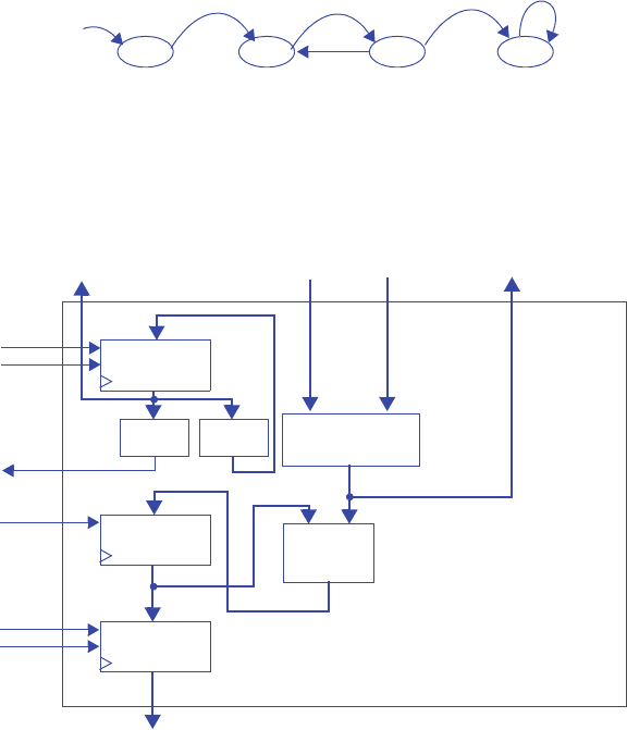
6.1 Exercises 159
6.32) (a) Convert the following C-like code to a high-level state machine. Ignore overflow.
(b) Use the RTL design process shown in Table 5.1 to convert the HLSM for the C code to
a controller and a datapath. Design the datapath to structure, but design the controller to
the point of an FSM only. (c) Redesign the datapath to allow for concurrency in which
four multiplications and two additions can be performed concurrently. Assume memory
ports can can be introduced as needed. (d) Assuming a multiplier delay is 4 ns and an
adder delay is 2 ns, list the fastest clock period, latency, and throughput for the original
design and for the more concurrent design, assuming the critical path is in the datapath. (e)
Introduce more multipliers or adders and pipeline registers as needed to further improve
the speed of the design, and compare the clock period, throughput, and latency with the
previous two designs.
(a)
(b)
Step 1 - Capture a high-level state machine - (completed above)
Step 2 - Create a datapath
Inputs: byte a[256], byte b[256]
Outputs: byte sum, byte c[256]
Init MAC Iterate Idle
Local Storage: byte temp, byte i
i := 0
sum := 0
c[i] := a[i] * b[i]
temp := temp + (a[i] * b[i])
sum := temp
i != 255
i = 255
i := i + 1
ld
clr i
ld
clr sumreg
ld
clr temp
ABC_addr A_data B_data
*
C_data
sum
+
=255 +1
i_ld
i_clr
i_ne_255
temp_ld
sumreg_ld
sumreg_clr
160 6 Optimizations and Tradeoffs
Step 3 - Connect the datapath to a controller
Step 4 - Derive the controller’s FSM
Controller Datapath
i_ld
i_clr
i_ne_255
temp_ld
sumreg_ld
sumreg_clr
sum
AB_rd
C_wr
ABC_addr
A_data
B_data
C_data
Inputs: i_ne_255
Outputs: i_ld, i_clr, temp_ld, sumreg_ld, sumreg_clr, AB_rd, C_wr
Init MAC Iterate Idle
i_clr = 1
sumreg_clr = 1
temp_ld = 1
sumreg_ld = 1
i_ne_255
i_ne_255’
temp_ld = 0
i_ld = 1
AB_rd = 1
C_wr = 1
C_wr = 0
AB_rd = 0

6.1 Exercises 161
(c)
ld
clr i
ld
clr sumreg
ld
clr temp
ABC_addr_1
sum
=255 +1
i_ld
i_clr
i_ne_255
temp_ld
sumreg_ld
sumreg_clr
+2 +3
* * * *
A_data_1
B_data_1
. . .
A_data_4
B_data_4
C_data_4
C_data_3
C_data_2
C_data_1
+4
ABC_addr_2
ABC_addr_3
ABC_addr_4
+ +
+
+
162 6 Optimizations and Tradeoffs
(d)
Original Design: 4ns + 2ns = 6ns critical path, so 6ns clock period. Latency is 6 ns,
and throughput is 1 multiply-accumulates per 6ns -- 166.6 million multiply-accumu-
lates per second.
Concurrent Design: 4ns + 2ns + 2ns + 2ns = 10ns critical path, so 10ns clock period.
Latency is also 10ns, and throughput is 4 multiply-accumulates per 10ns -- 400 mil-
lion multiply-accumulates per second.
(e) We have a range of area-performance tradeoffs available to us. For instance, we
could theoretically include 128 multipliers and a full adder tree (assuming we can
either reorganize the memory or create a 256 port memory). With pipeline register-
ing, we could have a 4ns clock period. Our latency would be 5 clock cycles, or 20ns.
We would, however, complete the entire operation in ‘one go’, for a throughput of
256 MACs in 20ns = 12.80 billion MACs / second.
A more likely scenario, though, would be to pipeline the datapath in (c):
6.1 Exercises 163
With the circuit above, we would see a clock period of 4ns, a latency of (4ns + 4ns +
4ns) = 12ns, and a throughput of 4 MACs per cycle, or 1 billion MACs / second.
ld
clr i
ld
clr sum
ld
clr temp
ABC_addr_1
sum
=255 +1
i_ld
i_clr
i_ne_255
temp_ld
sum_ld
sum_clr
+2 +3
* * * *
A_data_1
B_data_1
. . .
A_data_4
B_data_4
C_data_4
C_data_3
C_data_2
C_data_1
+4
ABC_addr_2
ABC_addr_3
ABC_addr_4
+ +
+
+
164 6 Optimizations and Tradeoffs
6.33) (a) Convert the following C-like code to a high-level state machine. Ignore overflow.
(b) Use the RTL design process shown in Table 5.1 to convert the high-level state machine
for the C code to a controller and a datapath. Design the datapath to structure, but design
the controller to the point of an FSM only. (c) Redesign your datapath to allow for concur-
rency in which three comparisons, three additions, and three multiplications can be per-
formed concurrently.
(a)
(b)
Step 1 - Capture a high-level state machine - (completed above)
Inputs: byte a[256], byte b[256], byte cy
Outputs: byte sumx, byte sumy, byte c[256]
Init
Local Storage: byte i
i := 0
sumx := 0
sumy := 0
Choose
GT128 Else
Iter
c[i] := a[i] * b[i]
sumx := sumx + (a[i] * b[i])
c[i] := a[i] * (b[i] + cy)
sumy := sumy + (a[i] * (b[i] + cy))
Idle
a[i] > 128
a[i] <= 128
(i == 0)’
i == 0
i := i + 1 i := i + 1
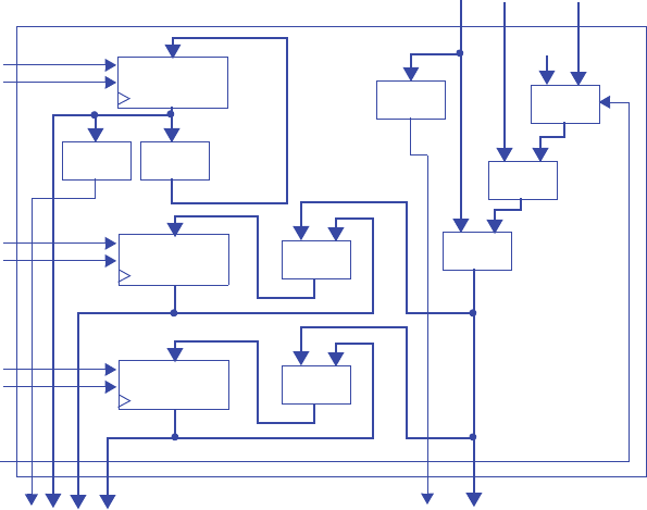
6.1 Exercises 165
Step 2 - Create a datapath
Step 3 - Connect the datapath to a controller
Omitted. Datapath and controller are connected in the same manner as 6.32. The
controller’s signals to the datapath are i_ld, i_clr, sumx_ld, sumx_clr, sumy_ld,
sumy_clr, and B_mux_sel. The datapath’s signals to the controller are i_eq_0 and
A_gt_128.
ld
clr i
+1
*
+
2x1 8bit
01
0
ld
clr sumx +
ld
clr sumy +
cyB_dataA_data
C_data
sumy
sumx
ABC_addr
i_ld
i_clr
sumx_ld
sumx_clr
sumy_ld
sumy_clr
B_mux_sel
> 128
A_gt_128
= 0
i_eq_0
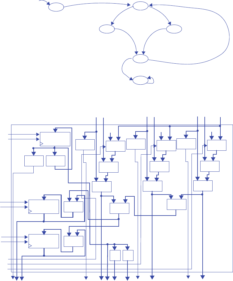
166 6 Optimizations and Tradeoffs
Step 4 - Derive the controller’s FSM
(c)
Inputs: i_eq_0, A_gt_128
Outputs: i_ld, i_clr, sumx_ld, sumx_clr, sumy_ld, sumy_clr, B_mux_sel
Init
i_clr = 1
sumx_clr = 1
sumy_clr = 1
Choose
GT128 Else
Iter
B_mux_sel = 0
sumx_ld = 1
B_mux_sel = 1
sumy_ld = 1
Idle
A_gt_128
A_gt_128’
i_eq_0’
i_eq_0
i_ld = 1 i_ld = 1
ld
clr i
+3
*
+
2x1 8bit
01
0
ld
clr sumx +
ld
clr sumy +
cy
B_data1A_data1
C_data1
sumy
sumx
i_ld
i_clr
sumx_ld
sumx_clr
sumy_ld
sumy_clr
B_mux_sel1
> 128
A1_gt_128
= 0
i_eq_0
*
+
2x1 8bit
01
0
B_data2A_data2
C_data2
> 128
A2_gt_128
*
+
2x1 8bit
01
0
B_data3A_data3
C_data3
> 128
A3_gt_128
B_mux_sel2
B_mux_sel3
ABC_addr1
+1 +2
ABC_addr2
ABC_addr3
+
+
6.1 Exercises 167
6.34) Redesign the datapath and controller designed in Exercise 6.33 by allowing up to
nine concurrent additions and inserting pipeline registers, updating the controller as neces-
sary. Assuming a comparator has a delay of 4 ns, an adder has a delay of 3 ns, and a multi-
plier has a delay of 20 ns, how long will the circuit take to finish its computation?
Note that if we choose the maximum number of operations (9), then we will have a
few units at the end adding erroneous data, and so the results must be gated off on
the last cycle. If we choose 8 operations, we have a similar problem -- we end up
adding an element from address 0. While entirely possible, these are likely not the
best design choices. Thus, we will use the maximum number of concurrent additions
which allow an easy design (i.e. the remainder of 255 divided by this number is
zero). Thus, we will use 5 concurrent additions in this solution.
The solution is very similar to 6.33(c), but with 5 separate (mux, comparator, adder,
multiplier) units instead of 3. The most obvious pipeline register insertion would be
before and after each multiplier, to give us a clock period of 20 ns.
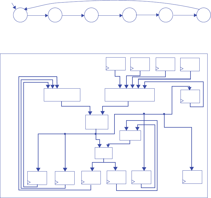
168 6 Optimizations and Tradeoffs
6.35) Given the HLSM in Figure 6.98, create two different designs: one optimized for
minimum circuit speed and the other optimized for minimum circuit size. Be sure to
clearly indicate the component allocation, operator binding, and operator scheduling used
to design the two circuits.
Design 1: Optimize For Size
New Schedule: (an extra register is definitely smaller than an extra multiplier)
AB1 B2 C D1 D2
s0 := s0 * c0 s1 := s1 + s0*c1 s2 := s0*x2 s3 := s2 + s0*c1
s4 := s0 * c1
tmp := s4*c2 F := s3 * tmp
Component Allocation: We’ll only need the registers, one adder, one multiplier, and
three muxes (one with two inputs, one with at least three inputs and one with at least
s0 s1 s2
s3
s4
tmp
F
x2
c2
c1
c0
5 inputs)
+
*
2x1 mux
8x1 mux
4x1 mux
Note: control signals are omitted for simplicity
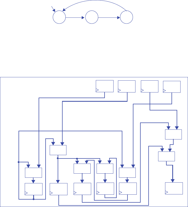
6.1 Exercises 169
Design 2: Optimize For Speed
New Schedule:
ABD
s0 := s0 * c0 s1 := s1 + s0*c1 F := s3 * s4 * c2
Component Allocation: We can use two multipliers if we are OK with using muxes.
s0 s1 s2
s3
s4 F
x2
c2c1
c0
Note: control signals are omitted for simplicity
s2 := s0 * x2 s3 := s2 + s0*c1
s4 := s0*c1
However, for the best performance possible, we will use dedicated multipliers (albeit
at a huge cost in area). We will also use dedicated adders.
*
*
*++
*
*
170 6 Optimizations and Tradeoffs
SECTION 6.6: MORE ON OPTIMIZATIONS AND TRADEOFFS
6.36) Trace through the execution of the binary search algorithm when searching for the
number 86 in the following sorted list of 15 numbers: 1, 10, 25, 62, 74, 75, 80, 84, 85, 86,
87, 100, 106, 111, 121. How many comparisons were required to find the number using
the binary search and how many comparisons would have been required using a linear
search?
Assume that the 15 numbers are indexed from 0 to 14.
1. We compare the middle number (number[7]: 84) with 86 and determine that 86
might be between number[8] and number[14], inclusive
2. We compare the middle number (number[11]: 100) to 86 and determine that 86
might be between number[8] and number[10], inclusive
3. We compare the middle number (number[9]: 86) to 86 and conclude the search
A binary search requires 3 comparisons to find number 86, while a linear search
(assuming we start from number[0]) requires 9 comparisons to find number 86.
6.37) Trace through the execution of the binary search algorithm when searching for the
number 99 in the following list of 15 numbers: 1, 10, 25, 62, 74, 75, 80, 84, 85, 87, 99,
100, 106, 111, 121. How many comparisons were required to look for the number using
the binary search and how many comparisons are required using a linear search?
Assume that the 15 numbers are indexed from 0 to 14.
1. We compare the middle number (number[7]: 84) with 99 and determine that 99
might be between number[8] and number[14], inclusive
2. We compare the middle number (number[11]: 100) to 99 and determine that 99
might be between number[8] and number[10], inclusive
3. We compare the middle number (number[9]: 86 to 99) and determine that 99
might be number[10].
4. We compare number[10] (87) and conclude the search (99 was not found).
Using a binary search required 4 comparisons, while a linear search would require
12 comparisons.
6.1 Exercises 171
6.38) Trace through the execution of the binary search algorithm when searching for the
number 121 in the list of numbers from the previous example. How many comparisons
were required to find the number using the binary search and how many comparisons are
required using a linear search?
A binary search requires 4 or 5 comparisons (depending on how the middle number
is chosen for even-sized ranges) to find 121, while a linear search takes 14 compari-
sons to find 121.
6.39) Using the list of 15 numbers from Exercise 6.37, how many numbers can be found
faster using a linear search algorithm compared with the binary search algorithm?
Depending on how the middle number is chosen for even-sized ranges, we can find
the first 2 or first 3 numbers in the list faster using linear search instead of binary
search.
Section : Power Optimization
6.40) Given the logic gate library in Figure 6.99, optimize the circuit in Figure 6.100 by
reducing power consumption without increasing the circuit’s delay..
.6.41) Given the logic gates shown in Figure 6.99, optimize the circuit in Figure 6.101 by
reducing power consumption without increasing the circuit’s delay.
6.42) Given the logic gates shown in Figure 6.99, optimize the circuit in Figure 6.102 by
reducing power consumption without increasing the circuit’s delay..
a
b
c
d
e
f
g
h
1/1
1/1
1/1
1/1
2/1
1.5/1.5
a
b
c
d
e
f
g
h
1/1
1/1
1/1
2/1
b
c
d
f
g
h
2/0.5
1/1 1/1
1/1
1.5/1.5
e
a
172 6 Optimizations and Tradeoffs
6.43) Given the logic gates shown in Figure 6.99, optimize the circuit in Figure 6.103by
reducing power consumption without increasing the circuit’s delay.
a
b
c
d
e
f
h
1/1
1/1
1/1
1.5/1.5
1.5/1.5
2/0.5
Z
g
i

165
CHAPTER 7
PHYSICAL IMPLEMENTA-
TION
7.1 EXERCISES
Section 7.2: Manufactured IC Technologies
7.1. Explain why gate array IC technology has a shorter production time than full-custom
IC technology.
Full-custom IC technology requires that every layer of the chip be manufactured,
and each layer takes time to produce. Gate array IC technology only requires the
wiring layers to be manufactured, so the lower transistor layers can be pre-manufac-
tured. Furthermore, gate array technology will have fewer errors due to eliminating-
errors in the pre-designed transistor layers.
7.2 Explain why the use of NAND or NOR gates in a CMOS gate-array circuit imple-
mentations is typically preferred over an AND/OR/NOT implementation of a cir-
cuit.
NAND and NOR gates have more efficient CMOS implementations, due to pMOS
transistors being efficient at passing 1s and nMOS transistors being efficient at pass-
ing 0s. As such, a 2-input NAND gate can be built using two pMOS transistors con-
nected to 1 (power) and two nMOS transistors connected to 0 (ground); an AND
gate would then be built be adding an inverter (two more transistors) to the NAND
output, yielding more transistors and larger delay.
7.3 Draw a gate array IC having three rows, the first row having four 2-input AND gates,
the second row having four 2-input OR gates, and the third having row four NOT
166 7 Physical Implementation
gates. Show how to instantiate wires to the gate array to implement the function
F(a,b,c) = abc + a’b’c’.
7.4 Assume a standard cell library has a 2-input AND gate, a 2-input OR gate, and a
NOT gate. Use a drawing to show how to instantiate and place standard cells on an
IC and wire them together to implement the function in Exercise 7.3. Draw your
cells the same size as the gates in Exercise 7.3, and be sure your rows are of equal
size.
Note that wires are shorter. There are also fewer gates.
7.5 Draw a gate array IC having three rows, the first row having four 2-input AND gates,
the second row having four 2-input OR gates, and the third having row four NOT
gates. Show how to instantiate wires to the gate array to implement the function
F(a,b,c,d) = a’b + cd + c’.
7.6 Assume a standard cell library has a 2-input AND gate, a 2-input OR gate, and a
NOT gate. Use a drawing to show how to instantiate and place standard cells on an
IC and wire them together to implement the function in Exercise 7.5. Be sure to
a
b
c
F
a
b
c
F
b
a
F
c
d
7.1 Exercises 167
draw your cells the same size as the gates in Exercise 7.5, and be sure your rows are
of equal size.
Note that wires are shorter. There are also fewer gates.
7.7 Consider the implementations of a half adder with a gate array in Figure 7.5 and with
standard cells in Figure 7.7. Assume each gate or cell (including inverters) has a
delay of 1 ns. Also assume that every inch of wire (for each inch in your drawing,
not on an actual IC) in the drawing has a delay of 3 ns (wires are relatively slow in
the era of tiny fast transistors). Estimate the delay of the gate array and the standard
cell circuits.
The gate array-based half adder requires 3 levels of gates, contributing 3ns to its
delay, and approximately 4.25” of wire, contributing 12.75ns to its delay for a total
of 15.75ns. The standard cell-based half adder requires 3 levels of gates (3ns) and
approximately 3” of wire (9ns) for a total delay of 12ns.
7.8 For your solutions to Exercises 7.3 and 7.4, assume that each gate and cell has a
delay of 1 ns, and that every inch of wire (for each inch in your drawing, not on an
actual IC) your drawing corresponds to a delay of 3 ns. Estimate the delays of the
gate-array and standard cell circuits.
Our solution to Exercise 7.3 required 4 levels of gates (4ns) and approximately 4.5”
of wire (13.5ns) for a total delay of 17.5ns. Our solution to Exercise 7.4 required 4
levels of gates (4ns) and approximately 3” of wire (9ns) for a total delay of 13ns.
7.9 Draw a circuit using AND, OR and NOT gates for the following function:
F(a,b,c) = a’bc + abc’. Place inversion bubbles on that circuit to convert
that circuit to: (a) NAND gates only, (b) NOR gates only.
a
d
F
b
c
(b)
(a)
a
b
cF
a
b
cF
a
b
cF

168 7 Physical Implementation
7.10 Draw a circuit using AND, OR and NOT gates for the following function:
F(a,b,c) = abc + a’ + b’ + c’. Place inversion bubbles on that circuit
to convert that circuit to: (a) NAND gates only, (b) NOR gates only.
7.11 Draw a circuit using AND, OR, and NOT gates for the following function:
F(a,b,c) = (ab + c)(a’ + d) + c’. Convert the circuit to a circuit
using: (a) NAND gates only, (b) NOR gates only.
7.12 Draw a circuit using AND, OR, and NOT gates for the following function:
F(w,x,y,z) = (w + x)(y + z) + wy + xz. Convert the circuit to a cir-
cuit using: (a) NAND gates only, (b) NOR gates only..
a
b
c
F
b
c
F
a
a
b
cF
(b)
(a)
a
b
c
F
d
a
b
c
F
d
(a)
F
a
b
c
d
(b)
w
x
F
y
z
w
x
F
y
z
w
x
F
y
z
(b)
(a)
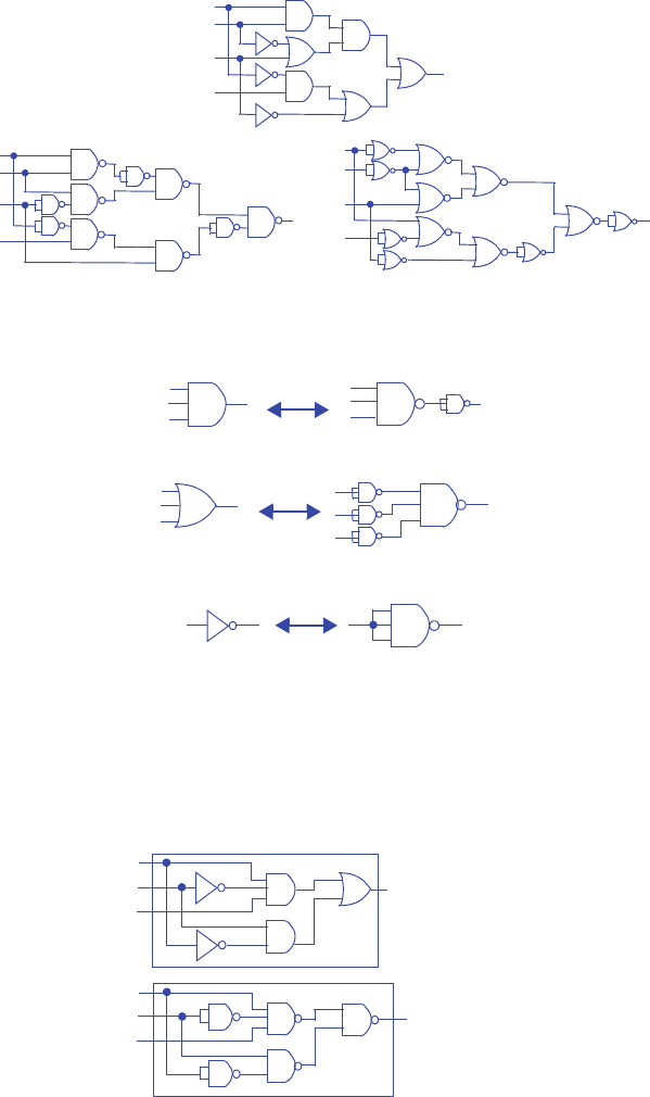
7.1 Exercises 169
7.13 Draw a circuit using AND, OR, and NOT gates for the following function:
F(a,b,c,d) = (ab)(b’ + c) + (a’d + c’). Convert the circuit to a cir-
cuit using: (a) NAND gates only, (b) NOR gates only.
7.14 Show how to convert the following gates into circuits having only 3-input NAND gates:
a. a 3-input AND gate
b. a 3-input OR gate.
c. a NOT gate.
7.15 Assume a standard cell library consisting of 2-input and 3-input NAND gates with a
delay of 1 ns each, 2-input and 3-input AND and OR gates with a delay of 1.8 ns
each, and a NOT gate with a delay of 1 ns. Compare the number of transistors and
the delay of an implementation using only AND/OR/NOT gates with an implemen-
tation using only NAND gates for the function: F(a,b,c)=ab’c + a’b. For
calculating the size of an implementation, assume each gate requires two transistors.
a
b
F
c
d
(b)
a
b
F
c
d
(a)
a
b
F
c
d
bF
a
c
Delay: 4.6ns
bF
a
c
Delay: 3ns
Size: 10 transistors
Size: 10 transistors
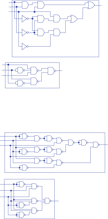
170 7 Physical Implementation
7.16 Assume a standard cell library consisting of 2-input AND and OR gates with a delay
of 1 ns each, 3-input AND and OR gates with a delay of 1.5 ns each, and a NOT gate
with a delay of 1 ns. Compare the number of transistors and the delay of an imple-
mentation using only 2-input AND/OR gates and NOT gates with an implementa-
tion using only 3-input AND/OR gates and NOT gates for the function:
F(a,b,c)= abc + a’b’c + a’b’c’. For calculating the size of an imple-
mentation, assume each gate requires two transistors.
7.17 Assume a standard cell library consisting of 2-input NAND and NOR gates with a
delay of 1 ns each, and 3-input NAND and NOR gates with a delay of 1.5 ns each.
Compare the number of transistors and the delay of an implementation using only 2-
input NAND/NOR gates with an implementation using only 3-input NAND/NOR
gates for the function: F(a,b,c)= a’bc + ab’c + abc’. For calculating the
size of an implementation, assume each gate requires two transistors.
bF
a
c
Delay: 5ns
bF
a
c
Delay: 3ns
Size: 11 transistors
Size: 10 transistors
b
a
c
Delay: 7ns
Size: 30 transistors
F
a
b
cF
Delay: 4.5ns
Size: 14 transistors
7.1 Exercises 171
Section 7.3: Programmable IC Technology -- FPGA
7.18 Show how to implement on a 3-input 2-output lookup table the function F(a,b,c)
= a + bc.
7.19 Show how to implement on two 3-input 2-output lookup tables the function
F(a,b,c,d) = ab + cd. Assume you can connect the lookup tables in a cus-
tom manner (i.e., do not use a switch matrix, just directly connect your wires).
7.20 Show how to implement on two 3-
input 2-output lookup tables the
following function:
F(a,b,c,d) = a’bd +
b’cd’. Assume the two lookup
tables are connected in the manner
shown in Figure 7.47. You may
not need to use every lookup table
output.
a1
a0
8x2 Mem.
d0
a2
000
100
200
301
401
501
601
701
d1
a
b
c
F
Inputs Outputs
abcF
0000
0010
0100
0111
1001
1011
1101
1111
a1
a0
8x2 Mem.
d0
a2
000
101
200
301
400
501
610
711
d1
a1
a0
8x2 Mem.
d0
a2
000
100
201
301
400
501
601
701
d1
a
b
c
d
F
c
ab
c
ab
Figure 7.47: Two 3-input 2-output lookup tables
implemented using 8x2 memory.
a1
a0
8x2 Mem.
d0
a2
0
1
2
3
4
5
6
7
d1
a1
a0
8x2 Mem.
d0
a2
0
1
2
3
4
5
6
7
d1
172 7 Physical Implementation
Inputs Outputs
xyc- F
0000 0
0010 0
0100 0
0110 1
1000 1
1010 1
1100 1
1110 1
a1
a0
8x2 Mem.
d0
a2
010
100
200
301
410
500
600
700
d1
a1
a0
8x2 Mem.
d0
a2
000
100
200
301
401
501
601
701
d1
a
b
d
c
F
a
F
b
d
c
a
F
b
d
c
x
y
y
x
Inputs Outputs
abdy x
0001 0
0010 0
0100 0
0110 1
1001 0
1010 0
1100 0
1110 0
7.1 Exercises 173
7.21 Show how to implement on two 3-input 2-output lookup tables the following func-
tions: F(x,y,z) = x’y + xyz’ and G(w,x,y,z) = w’x’y + w’xyz’.
Assume the two lookup tables are connected in the manner shown in Figure 7.47.
7.22 Show how to implement on two 3-input 2-output lookup tables the following func-
tions: F(a,b,c,d) = abc + d and G = a’. You must implement both F and
G with only two lookup tables connected in the manner shown in Figure 7.47.
a1
a0
8x2 Mem.
d0
a2
000
100
201
301
400
500
610
700
d1
a1
a0
8x2 Mem.
d0
a2
000
100
211
310
411
510
611
710
d1
x
F
y
z
w
G
F = x’y + xyz’
G = w’x’y + w’xyz’
x
y
z
w
F
G
Inputs Outputs
abwF G
0000 0
0010 0
0101 1
0111 0
1001 1
1011 0
1101 1
1111 0
Inputs Outputs
xyzb a
0000 0
0010 0
0100 1
0110 1
1000 0
1010 0
1101 0
1110 0
a
b
x
y
z
wba
GF
a1
a0
8x2 Mem.
d0
a2
000
100
200
300
410
510
610
711
d1
a1
a0
8x2 Mem.
d0
a2
001
100
211
310
411
510
611
710
d1
a
F
b
G
Inputs Outputs
ydxF G
0000 1
0010 0
0101 1
0111 0
1001 1
1011 0
1101 1
1111 0
Inputs Outputs
abcx y
0000 0
0010 0
0100 0
0110 0
1001 0
1011 0
1101 0
1111 1
a
b
c
dxy
GF
c
dx
y

174 7 Physical Implementation
7.23 Implement a 2-bit comparator that compares two 2-bit numbers and has three outputs
indicating greater-than, less-than, and equal-to, using any number of 3-input 2-out-
put lookup tables and custom connections among the lookup tables.
Only the left component need be completed for this exercise. The right component
with the ilt, ieq, igt components goes beyond the exercise’s problem statement.
a1
a0
8x2 Mem.
d0
a2
010
100
200
310
410
500
600
710
d1
Inputs Outputs
-- a1 b1 gt lt
00 0 0 0
00 1 0 1
01 0 1 0
01 1 0 0
10 0 0 0
10 1 0 1
11 0 1 0
11 1 0 0
a1
a0
8x2 Mem.
d0
a2
000
101
210
300
400
501
610
700
d1
a1
a0
8x2 Mem.
d0
a2
000
101
201
301
400
500
600
700
d1
a1
a0
8x2 Mem.
d0
a2
000
100
200
300
400
501
610
700
d1
gt
lt
eq
ab
a1 b1 a0 b0
gt
lt
eq
ab
ingt
inlt
ineq
Inputs Outputs
-- a1 b1 eq --
00 01 0
00 10 0
01 00 0
01 11 0
10 01 0
10 10 0
11 00 0
11 11 0
gt = ingt + (ineq*a*b’)
lt = inlt + (ineq*a’b)
eq = ineq*(a xnor b)
T1
T2
a1
a0
8x2 Mem.
d0
a2
000
110
210
310
400
510
610
710
d1
a1
a0
8x2 Mem.
d0
a2
000
110
210
310
400
510
610
710
d1
gt lt eq
a1
b1
0
0
ineq
a0
b0
T1 T2
inlt
ingt
00
An alternative solution creates a single 16-row truth table for a1 a0 b1 b0, and 3 output
functions gt, lt, eq; creates minimized equations; and maps equations to LUTs. The above
ripple-carry-based approach may be simpler.
7.1 Exercises 175
7.24 Show how to implement a 4-bit carry-ripple adder using any number of 3-input 2-
output lookup tables and custom connections among the lookup tables. Hint: map
one full-adder to each lookup table.
7.25 Show how to implement a 4-bit carry-ripple adder using any number of 4-input 1-
output lookup tables and custom connections among the lookup tables.
a1
a0
8x2 Mem.
d0
a2
000
101
201
310
401
510
610
711
d1
s0
a0
b0
ci
a1
a0
8x2 Mem.
d0
a2
000
101
201
310
401
510
610
711
d1
s1
c0
a1
a0
8x2 Mem.
d0
a2
000
101
201
310
401
510
610
711
d1
s2
a1
a0
8x2 Mem.
d0
a2
000
101
201
310
401
510
610
711
d1
s3
a1
b1
a2
b2
c1
co
a3
b3
176 7 Physical Implementation
Similarly to Exercise 7.24, we can simply use one LUT for each output of a full-
adder. We can just “ignore” the extra input by repeating the first 8 entries of the table
to fill the last 8 entries of the table.
a1
a0
16x1 Mem.
a2
00
11
21
30
41
50
60
71
80
91
10 1
11 0
12 1
13 0
14 0
15 1
a3
d
a1
a0
16x1 Mem.
a2
00
10
20
31
40
51
61
71
80
90
10 0
11 1
12 0
13 1
14 1
15 1
a3
d
X
ci
a0
b0
s0
X
ci
a0
b0
a1
a0
16x1 Mem.
a2
00
11
21
30
41
50
60
71
80
91
10 1
11 0
12 1
13 0
14 0
15 1
a3
d
a1
a0
16x1 Mem.
a2
00
10
20
31
40
51
61
71
80
90
10 0
11 1
12 0
13 1
14 1
15 1
a3
d
X
a1
b1
s1
X
a1
b1
a1
a0
16x1 Mem.
a2
00
11
21
30
41
50
60
71
80
91
10 1
11 0
12 1
13 0
14 0
15 1
a3
d
a1
a0
16x1 Mem.
a2
00
10
20
31
40
51
61
71
80
90
10 0
11 1
12 0
13 1
14 1
15 1
a3
d
X
a2
b2
s2
X
a3
b3
a1
a0
16x1 Mem.
a2
00
11
21
30
41
50
60
71
80
91
10 1
11 0
12 1
13 0
14 0
15 1
a3
d
a1
a0
16x1 Mem.
a2
00
10
20
31
40
51
61
71
80
90
10 0
11 1
12 0
13 1
14 1
15 1
a3
d
X
a3
b3
s3
X
a3
b3
co Note: ‘X’ means “Don’t Care”
7.1 Exercises 177
7.26 Show how to implement a comparator that compares two 8-bit numbers and has a
single equal-to output, using any number of 4-input 1-output lookup tables and cus-
tom connections among the lookup tables.
7.27 Show the bitfile necessary to program the FPGA fabric in Figure 7.31 to implement
the function F(a,b,c,d) = ab + cd, where a, b, c and d are external inputs.
The corresponding bitfile is: 00000000 00010000 0 0 11 00 10 00000000 00110111
0 0
a1
a0
16x1 Mem.
d0
a2
01
10
20
31
40
50
60
70
80
90
10 0
11 0
12 1
13 0
14 0
15 1
a0
b0
a3
a1
b1
a1
a0
16x1 Mem.
d0
a2
01
10
20
31
40
50
60
70
80
90
10 0
11 0
12 1
13 0
14 0
15 1
a2
b2
a3
a3
b3
a1
a0
16x1 Mem.
d0
a2
01
10
20
31
40
50
60
70
80
90
10 0
11 0
12 1
13 0
14 0
15 1
a4
b4
a3
a5
b5
a1
a0
16x1 Mem.
d0
a2
01
10
20
31
40
50
60
70
80
90
10 0
11 0
12 1
13 0
14 0
15 1
a6
b6
a3
a7
b7
a1
a0
16x1 Mem.
d0
a2
00
10
20
30
40
50
60
70
80
90
10 0
11 0
12 0
13 0
14 0
15 1
a3
equal-to
a1
a0
8x2 Mem.
d0
a2
000
100
200
301
400
500
600
700
d1
m0
m1
m2
m3 o0
o1
11
00
Switch
matrix
0000
CLB
a1
a0
8x2 Mem.
d0
a2
000
100
201
301
400
501
601
701
d1
0000
CLB
0
a
b
d
0
10
10
10
1
F
o1
10
c
178 7 Physical Implementation
7.28 Show the bitfile necessary to program the FPGA fabric in Figure 7.31 to implement
the function F(a,b,c,d) = abcd, where a, b, c and d are external inputs.
The corresponding bitfile is: 00000000 00000001 0 0 11 00 10 00000000 00000010
0 0
7.29 Show the bitfile necessary to program the FPGA fabric in Figure 7.31 to implement
the function F(a,b,c,d) = a’b’ + c’d, where a, b, c and d are external
inputs.
The corresponding bitfile is: 00000000 10000000 0 0 11 00 10 00000000 00111011
0 0
a1
a0
8x2 Mem.
d0
a2
000
100
200
300
400
500
600
701
d1
0000
CLB
a1
a0
8x2 Mem.
d0
a2
000
100
200
300
400
500
601
700
d1
0000
CLB
d
a
b
c
0
0
10
10
10
1
F
m0
m1
m2
m3 o0
o1
11
00
Switch
matrix
o1
10
a1
a0
8x2 Mem.
d0
a2
001
100
200
300
400
500
600
700
d1
0000
CLB
a1
a0
8x2 Mem.
d0
a2
000
100
201
301
401
500
601
701
d1
0000
CLB
d
0
a
b
c
0
10
10
10
1
F
m0
m1
m2
m3 o0
o1
11
00
Switch
matrix
o1
10
7.1 Exercises 179
Section 7.4: Other Technologies
7.30 Use any combination of 7400 ICs listed in Table 7.1 to implement the function
F(a,b,c,d) = ab + cd.
7.31 Use any combination of 7400 ICs listed in Table 7.1 to implement the function
F(a,b,c,d) = abc + ab’c’ + a’bd + a’b’d’.
7.32 By drawing Xs on the circuit, program the PLD of Figure 7.38(a) to implement a
full-adder.
74LS08 74LS32
ab cd F
74LS32
abcd
74LS04
74LS11 74LS11
F
O1
PLD IC
I1 I2 I3
O2
Inputs Outputs
a b cin cout s
000 0 0
001 0 1
010 0 1
011 1 0
100 0 1
101 1 0
110 1 0
111 1 1
ab
s
cout
cin
180 7 Physical Implementation
7.33 By drawing Xs on the circuit, program the PLD of Figure 7.38(a) to implement a 2-
bit equality comparator. Assume the PLD has an additional I4 input.
7.34 *(a) Design a PLD device capable of supporting a 2-bit carry-ripple adder. By draw-
ing Xs on your PLD circuit, program the PLD to implement the 2-bit carry-ripple
adder. (b) Using a CPLD device consisting of several PLDs from Figure 7.38 and
assuming you can connect the PLDs in a custom manner, implement the 2-bit carry-
ripple adder by drawing X’s on the PLDs . (c) Compare the size of your PLD and the
CPLD by determining the gates required for both designs (make sure you compare
the number of gates within the PLD and CPLD and not the number of gates used for
your implementation).
Solution not shown for challenge problems.
Section 7.5: IC Technology Comparisons
7.35 For each of the system constraints below, choose the most appropriate technology
from among FPGA, standard cell, and full-custom IC technologies for implement-
ing a given circuit. Justify your answers.
a. The system must exist as a physical prototype by next week.
b. The system should be as small and low-power as possible. Short design time
and low cost are not priorities.
c. The system should be reprogrammable even after the final product has been
produced.
d. The system should be as fast as possible and should consume as little power as
possible, subject to being completely implemented in just a few months.
e. Only five copies of the system will be produced and we have no more than
$1,000 to spend on all the ICs.
a) FPGA
b) Full-custom IC
c) FPGA
d) Standard cell
e) FPGA
O1
PLD IC
I1 I2 I3
b1 a0
eq
I4
a1 b0
O2
7.1 Exercises 181
7.36 Which of the following implementations are not possible? (1) A custom processor on
an FPGA. (2) A custom processor on an ASIC. (3) A custom processor on a full-
custom IC. (4) A programmable processor on an FPGA. (5) A programmable pro-
cessor on an ASIC. (6) A programmable processor on a full-custom IC. Explain
your answer.
None of the above - both a custom processor and a progammable processor can be
implemented on either an FPGA, an ASIC, or a full-custom IC. Each implementa-
tion has its own strengths and weaknesses, but each implementation is possible.
182 7 Physical Implementation

181
CHAPTER 8
PROGRAMMABLE PROCES-
SORS
8.1 EXERCISES
Section 8.2: Basic Architecture
8.1. If a processor’s program counter is 20-bits wide, up to how many words can the pro-
cessor’s instruction memory hold (ignoring any special tricks to expand the instruc-
tion memory size)?
220 = 1,048,576
8.2 Which of the following are legal single-cycle datapath operations for the datapath in
Figure 8.2? Explain your answer.
a. Copy data from a memory location into another memory location.
b. Copy two register locations into two memory locations.
c. Add data from a register file location and a memory location, storing the result
in a memory location.
a) Invalid. Data must first be loaded into the register file then stored into the destina-
tion memory location.
b) Invalid. Only one register file to memory location copy is permitted during a sin-
gle cycle.
c) Invalid. Data must first be loaded into a register file, then the addition must be
performed, then the sum must be stored into a memory location. The entire sequence
of operations would take three cycles.
182 8 Programmable Processors
8.3 Which of the following are legal single-cycle datapath operations for the datapath in
Figure 8.2? Explain your answer.
a. Copy data from a register file location into a memory location.
b. Subtract data from two memory locations and store the result in another mem-
ory location.
c. Add data from a register file location and a memory location, storing the result
in the same memory location.
a) Valid operation.
b) Invalid. Two cycles are required to load the two operands. One cycle is required
to perform the subtraction. One cycle is required to store the difference. Four cycles
total are needed to perform this sequence of operations.
c) Invalid. Three cycles are required (Load, Add, Store).
8.4 Assume we are using a dual-port memory from which we can read two locations
simultaneously. Modify the datapath of the programmable processor of Figure 8.2 to
support an instruction that performs an ALU operation on any two memory loca-
tions and stores the result in a register file location. Trace through the execution of
this operation, as illustrated in Figure 8.3.
8.5 Determine the operations required to instruct the datapath of Figure 8.2 to perform
the operation: D[8] = (D[4] + D[5]) - D[7], where D represents the data memory.
1) Load D[4] into the register file (R[0])
2) Load D[5] into the register file (R[1])
3) Add R[0] and R[1] and store the result in the register file (R[2])
4) Load D[7] into the register file (R[0])
5) Subtract R[0] from R[2] and store the result in the register file (R[1])
6) Store R[1] in the data memory location D[8]
Data memory D
Register file RF
n-bit
2x1
ALU
to the outside world
n-bit
2x1 n-bit
2x1
somehow connected Data memory D
Register file RF
n-bit
2x1
ALU
n-bit
2x1 n-bit
2x1
Two memory locations
are read from data memory
D and, via the ALU’s input
multiplexers, are fed into the
ALU. The result of the ALU
operation is then fed into
the register file’s input mux
and stored in the appropriate
location.
8.1 Exercises 183
Section 8.3: A Three-Instruction Programmable Processor
8.6 If a processor’s instruction has 4 bits for the opcode, how many possible instructions
can the processor support?
24 = 16
8.7 What does the following assembly program, which uses the three-instruction instruc-
tion set of this chapter, compute? MOV R5, 19; ADD R5, R5, R5; MOV 20, R5.
D[20] = D[19] + D[19]
8.8 What does the following assembly program, which uses the three-instruction instruc-
tion set of this chapter, compute? MOV R4, 20; MOV R9, 18; ADD R4, R4, R9;
MOV R5, 30; ADD R9, R4, R5; MOV 20, R9.
D[20] = D[20] + D[18] + D[30]
8.9 Using the three-instruction instruction set of this chapter, write an assembly program
that updates the data memory D as follows: D[0]=D[0]+D[1].
MOV R0, 0
MOV R1, 1
ADD R0, R0, R1
MOV 0, R0
8.10 Using the three-instruction instruction set of this chapter, write an assembly program
that updates the data memory D as follows: D[4]=D[1]*2+D[2].
MOV R0, 1
ADD R0, R0, R0
MOV R1, 2
ADD R0, R0, R1
MOV 4, R0
8.11 Convert the following assembly program to machine code based on the three-
instruction instruction set of this chapter: MOV R5, 19; ADD R5, R5, R5; MOV 20,
R5.
0000 1001 00010011
0010 1001 1001 1001
0001 1001 00010100
184 8 Programmable Processors
8.12 List the basic register/memory transfers and operations that occur during each clock
cycle for the following program, based on the three-instruction instruction set of this
chapter: MOV R0, 1; MOV R1, 9; ADD R0, R0, R1;
1) Fetch Instruction #1
2) Decode Instruction #1
3) The FSM sets the control lines on the memory and register file to load D[1] into
RF[0]
4) Fetch Instruction #2
5) Decode Instruction #2
6) The FSM sets the control lines on the memory and register file to load D[9] into
RF[1]
7) Fetch Instruction #3
8) Decode Instruction #3
9) The FSM sets the control lines on the ALU and register file to effect RF[0] :=
RF[0] + RF[1]
Section 8.4: A Six-Instruction Programmable Processor
8.13 List the basic register/memory transfers and operations that occur during each clock
cycle for the following program, based on the six-instruction instruction set of this
chapter, assuming that the content of D[9] is 0: MOV R6, #1; MOV R5, 9; JMPZ
R5, label1; ADD R5, R5, R6; label1: ADD R5, R5, R6. What is the value in R5 after
the program completes?
1) Fetch Instruction #1
2) Decode Instruction #1
3) The FSM sets the control lines on the register file and RF write mux to load the
constant value ‘1’ to RF[6]
4) Fetch Instruction #2
5) Decode Instruction #2
6) The FSM sets the conrol lines on the register file, RF write mux, and memory to
load the contents of D[9] (which contains ‘0’) to RF[5]
7) Fetch Instruction #3
8) Decode Instruction #3
9) The FSM sets the control lines on the register file to test whether RF[5] is ‘0’
10) RF[5] was ‘0’, so the PC gets loaded with PC + 2 - 1 (the offset of label1)
11) Fetch Instruction #5
12) Decode Instruction #5
13) The FSM sets the control lines on the register file, the RF write mux, and the
ALU to effect RF[5] := RF[5] + RF[6]
After the program completes, RF[5] is 1.
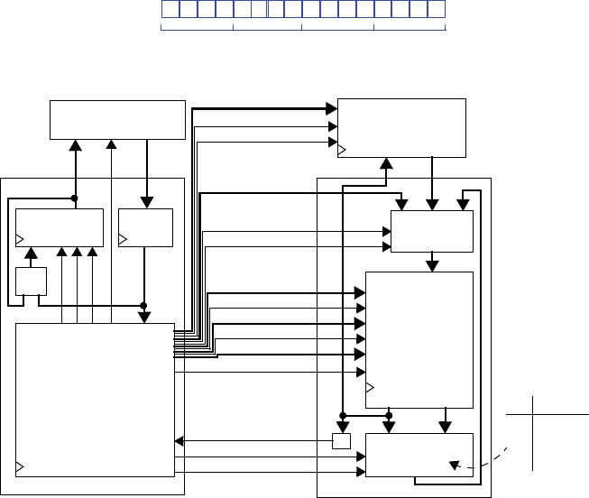
8.1 Exercises 185
8.14 Add a new instruction to the six-instruction instruction set of this chapter that per-
forms a bitwise AND of two registers and stores the result in a third register. Extend
the datapath, control unit, and the controller’s FSM as needed.
We’ll use the opcode 0110 for the AND operation. We’ll modify the ALU to per-
form the AND operation when the ALU’s s1s0=11
opcode
15 14 13 12 11 10 9 8 7 6 5 4 3 2 1 0
(0110)
ra
dest register
rb
src register 1
rc
src register 2
AND ra, rb, rc
addr D
rd
wr W_data R_data
256x16
16-bit
3x1
21 0
s1
s0
W_data
W_addr
W_wr
Rp_addr
Rp_rd
Rq_addr
Rp_data Rq_data
16x16
RF
ALU
AB
s1
s0
=0
Datapath
IR
ld
PC
ld clr up
Controller
(a+b-1)
+
addr rd data
I
I_rd
PC_ld
PC_clr
PC_inc
D_addr
D_rd
D_wr
RF_W_data
RF_s1
RF_s0
RF_W_addr
RF_W_wr
RF_Rp_addr
RF_Rp_rd
RF_Rq_addr
RF_Rq_rd Rq_rd
RF_Rp_zero
alu_s1
alu_s0
Control unit
s1
0
0
1
1
s0
0
1
0
1
ALU op
pass A
A+B
A-B
A AND B
IR[7:0]
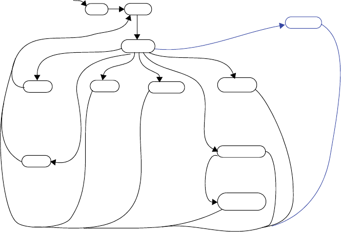
186 8 Programmable Processors
.
Init Fetch
Decode
Load
Store
D_addr=d
D_rd=1
RF_s1=0
RF_s0=1
RF_W_addr=ra
RF_W_wr=1
D_addr=d
D_wr=1
RF_s1=X
RF_s0=X
RF_Rp_addr=ra
RF_Rp_rd=1
Add
RF_Rp_addr=rb
RF_Rp_rd=1
RF_s1=0
RF_s0=0
RF_Rq_add=rc
RF_Rq_rd=1
RF_W_addr=ra
RF_W_wr=1
alu_s1=0
alu_s0=1
Load-
constant
RF_s1=1
RF_s0=0
RF_W_addr=ra
RF_W_wr=1
Subtract
RF_Rp_addr=rb
RF_Rp_rd=1
RF_s1=0
RF_s0=0
RF_Rq_addr=rc
RF_Rq_rd=1
RF_W_addr=ra
RF_W_wr=1
alu_s1=1
alu_s0=0
Jump-if-zero
RF_Rp_addr=ra
RF_Rp_rd=1
Jump-if-
zero-jmp
PC_ld=1
op=0100
op=0101
op=0011
I_rd=1
PC_inc=1
IR_ld=1
PC_clr=1
op=0010
op=0001
op=0000
RF_Rp_zero
RF_Rp_zero’
AND
RF_Rp_addr=rb
RF_Rp_rd=1
RF_s1=0
RF_s0=0
RF_Rq_addr=rc
RF_Rq_rd=1
RF_W_addr=ra
RF_W_wr=1
alu_s1=1
alu_s0=1
op=0110
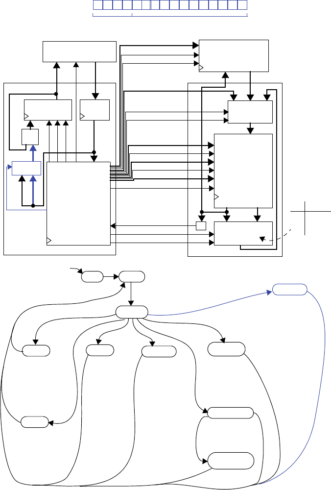
8.1 Exercises 187
8.15 Add a new instruction to the six-instruction instruction set of this chapter that per-
forms an unconditional jump (jumps always) to a location specified by a 12-bit off-
set. Extend the datapath, control unit, and the controller’s FSM as needed.
We’ll use opcode 0110.
opcode
15 14 13 12 11 10 9 8 7 6 5 4 3 2 1 0
(0110)
offset
JMP offset
addr D
rd
wr W_data R_data
256x16
16-bit
3x1
21 0
s1
s0
W_data
W_addr
W_wr
Rp_addr
Rp_rd
Rq_addr
Rp_data Rq_data
16x16
RF
ALU
AB
s1
s0
=0
Datapath
IR
ld
PC
ld clr up
Controller
(a+b-1)
+
addr rd data
I
I_rd
PC_ld
PC_clr
PC_inc
D_addr
D_rd
D_wr
RF_W_data
RF_s1
RF_s0
RF_W_addr
RF_W_wr
RF_Rp_addr
RF_Rp_rd
RF_Rq_addr
RF_Rq_rd Rq_rd
RF_Rp_zero
alu_s1
alu_s0
Control unit
s1
0
0
1
s0
0
1
0
ALU op
pass A
A+B
A-B
IR[7:0]
01
IR[11:0]
s
PCmux_s
Init Fetch
Decode
Load
Store
D_addr=d
D_rd=1
RF_s1=0
RF_s0=1
RF_W_addr=ra
RF_W_wr=1
D_addr=d
D_wr=1
RF_s1=X
RF_s0=X
RF_Rp_addr=ra
RF_Rp_rd=1
Add
RF_Rp_addr=rb
RF_Rp_rd=1
RF_s1=0
RF_s0=0
RF_Rq_add=rc
RF_Rq_rd=1
RF_W_addr=ra
RF_W_wr=1
alu_s1=0
alu_s0=1
Load-
constant
RF_s1=1
RF_s0=0
RF_W_addr=ra
RF_W_wr=1
Subtract
RF_Rp_addr=rb
RF_Rp_rd=1
RF_s1=0
RF_s0=0
RF_Rq_addr=rc
RF_Rq_rd=1
RF_W_addr=ra
RF_W_wr=1
alu_s1=1
alu_s0=0
Jump-if-zero
RF_Rp_addr=ra
RF_Rp_rd=1
Jump-if-
zero-jmp
PC_ld=1
op=0100
op=0101
op=0011
I_rd=1
PC_inc=1
IR_ld=1
PC_clr=1
op=0010
op=0001
op=0000
RF_Rp_zero
RF_Rp_zero’
Jump
PC_ld=1
op=0110
PCmux_s=0
PCmux_s=1
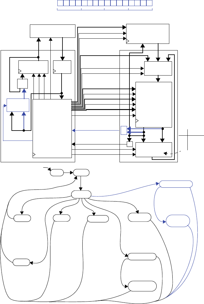
188 8 Programmable Processors
8.16 Add a new instruction to the six-instruction instruction set of this chapter that per-
forms a jump if two registers are equal, to a location specified by a 4-bit offset.
Extend the datapath, control unit, and the controller’s FSM as needed.
We’ll use opcode 0110.
opcode
15 14 13 12 11 10 9 8 7 6 5 4 3 2 1 0
(0110)
ra
register 1 rb
register 2
offset
JMPEQ ra, rb, offset
addr D
rd
wr W_data R_data
256x16
16-bit
3x1
21 0
s1
s0
W_data
W_addr
W_wr
Rp_addr
Rp_rd
Rq_addr
Rp_data Rq_data
16x16
RF
ALU
AB
s1
s0
=0
Datapath
IR
ld
PC
ld clr up
Controller
addr rd data
I
I_rd
PC_clr
PC_inc
D_addr
D_rd
D_wr
RF_W_data
RF_s1
RF_s0
RF_W_addr
RF_W_wr
RF_Rp_addr
RF_Rp_rd
RF_Rq_addr
RF_Rq_rd Rq_rd
RF_Rp_zero
alu_s1
alu_s0
Control unit
s1
0
0
1
s0
0
1
0
ALU op
pass A
A+B
A-B
=
Rp_eq_Rq
(a+b-1)
+
PC_ld
IR[7:0]
01
IR[3:0]
PCmux_s
s
Init Fetch
Decode
Load
Store
D_addr=d
D_rd=1
RF_s1=0
RF_s0=1
RF_W_addr=ra
RF_W_wr=1
D_addr=d
D_wr=1
RF_s1=X
RF_s0=X
RF_Rp_addr=ra
RF_Rp_rd=1
Add
RF_Rp_addr=rb
RF_Rp_rd=1
RF_s1=0
RF_s0=0
RF_Rq_add=rc
RF_Rq_rd=1
RF_W_addr=ra
RF_W_wr=1
alu_s1=0
alu_s0=1
Load-
constant
RF_s1=1
RF_s0=0
RF_W_addr=ra
RF_W_wr=1
Subtract
RF_Rp_addr=rb
RF_Rp_rd=1
RF_s1=0
RF_s0=0
RF_Rq_addr=rc
RF_Rq_rd=1
RF_W_addr=ra
RF_W_wr=1
alu_s1=1
alu_s0=0
Jump-if-zero
RF_Rp_addr=ra
RF_Rp_rd=1
Jump-if-
zero-jmp
PC_ld=1
op=0100
op=0101
op=0011
I_rd=1
PC_inc=1
IR_ld=1
PC_clr=1
op=0010
op=0001
op=0000
RF_Rp_zero
RF_Rp_zero’
Jump-if-equal
RF_Rp_addr=ra
op=0110
PCmux_s=0
Jump-if-
equal-jmp
RF_Rp_rd=1
RF_Rq_addr=rb
RF_Rq_rd=1
Rp_eq_Rq
PC_ld=1
PCmux_s=1
Rp_eq_Rq’
8.1 Exercises 189
8.17 Using the six-instruction instruction set of this chapter, write an assembly program
for the following C code, which computes the sum of the first N numbers, where N
is another name for D[9]. Hint: use a register to first store N..
i=0;
sum=0;
while ( i!=N ) {
sum = sum + i;
i = i + 1;
}
MOV R0, #0 // R0 is “i”
MOV R1, #0 // R1 is “sum”
MOV R2, #1 // R2 is the constant “1”
MOV R3, 9 // R3 is “N” or “D[9]”
MOV R4, #0 // R4 is the constant “0” (for looping)
loop: SUB R5, R3, R0 // R4 = N - i
JMPZ R5, done // if i==N, end while loop
ADD R1, R1, R0 // sum = sum + i
ADD R0, R0, R2 // i = i + 1
JMPZ R4, loop // continue through while loop
done:
8.18 Using the extended instruction set you designed in Exercise 8.16, write an assembly
program for the C code in Exercise 8.17.
MOV R0, #0 // R0 is “i”
MOV R1, #0 // R1 is “sum”
MOV R2, #1 // R2 is the constant “1”
MOV R3, 9 // R3 is “N” or “D[9]”
MOV R4, #0 // R4 is the constant “0” (for looping)
loop: JMPEQ R0, R3, done // end while loop if i==N
ADD R1, R1, R0 // sum = sum + i
ADD R0, R0, R2 // i = i + 1
JMPZ R4, loop // continue through while loop
done:

190 8 Programmable Processors
Section 8.5: Example Assembly and Machine Programs
8.19 Define two new data movement instructions for the six-instruction instruction set of
this chapter. Extend the datapath, control unit, and the controller’s FSM as needed.
We’ll define LUI and MOVR, with opcodes 0110 and 0111.
LUI will act just as “MOV Ra, #C” but will load #C into the upper 8 bits of Ra.
MOVR will allow us to duplicate the contents of one register into another, eliminat-
ing the need to use memory or initialize another register to zero. Its syntax is
“MOVR Ra, Rb”, where Ra is assigned Rb’s value.
opcode
15 14 13 12 11 10 9 8 7 6 5 4 3 2 1 0
(0110)
ra
dest register
LUI ra, #C
C
constant value
opcode
15 14 13 12 11 10 9 8 7 6 5 4 3 2 1 0
(0111)
ra
dest register rb
src register
xxxx
extraneous
MOVR ra, rb
addr D
rd
wr W_data R_data
256x16
16-bit
3x1
21 0
s1
s0
W_data
W_addr
W_wr
Rp_addr
Rp_rd
Rq_addr
Rp_data Rq_data
16x16
RF
ALU
AB
s1
s0
=0
Datapath
IR
ld
PC
ld clr up
Controller
addr rd data
I
I_rd
PC_clr
PC_inc
D_addr
D_rd
D_wr
RF_W_data
RF_s1
RF_s0
RF_W_addr
RF_W_wr
RF_Rp_addr
RF_Rp_rd
RF_Rq_addr
RF_Rq_rd Rq_rd
RF_Rp_zero
alu_s1
alu_s0
Control unit
s1
0
0
1
s0
0
1
0
ALU op
pass A
A+B
A-B
(a+b-1)
+
PC_ld
IR[7:0]
<< 8 3

8.1 Exercises 191
8.20 Define two new arithmetic/logic instructions for the six-instruction instruction set of
this chapter. Extend the datapath, control unit, and the controller’s FSM as needed.
We’ll define AND and NOT, with opcodes 0110 and 0111. The syntax for AND will
be “AND Ra, Rb, Rc”, where Ra gets the bitwise AND of the contents of of Rb and
Rc. The syntax for NOT will be “NOT Ra, Rb”, where Ra gets the logical comple-
ment of the contents of Rb.
Init Fetch
Decode
Load
Store
D_addr=d
D_rd=1
RF_s1=0
RF_s0=1
RF_W_addr=ra
RF_W_wr=1
D_addr=d
D_wr=1
RF_s1=X
RF_s0=X
RF_Rp_addr=ra
RF_Rp_rd=1
Add
RF_Rp_addr=rb
RF_Rp_rd=1
RF_s1=0
RF_s0=0
RF_Rq_add=rc
RF_Rq_rd=1
RF_W_addr=ra
RF_W_wr=1
alu_s1=0
alu_s0=1
Load-
constant
RF_s1=1
RF_s0=0
RF_W_addr=ra
RF_W_wr=1
Subtract
RF_Rp_addr=rb
RF_Rp_rd=1
RF_s1=0
RF_s0=0
RF_Rq_addr=rc
RF_Rq_rd=1
RF_W_addr=ra
RF_W_wr=1
alu_s1=1
alu_s0=0
Jump-if-zero
RF_Rp_addr=ra
RF_Rp_rd=1
Jump-if-
zero-jmp
PC_ld=1
op=0100
op=0101
op=0011
I_rd=1
PC_inc=1
IR_ld=1
PC_clr=1
op=0010
op=0001
op=0000
RF_Rp_zero
RF_Rp_zero’
LUI
RF_s1=1
RF_s0=1
RF_W_addr=ra
RF_W_wr=1
op=0110
MOVR
RF_Rp_addr=rb
RF_Rp_rd=1
RF_s1=0
RF_s0=0
RF_W_addr=ra
RF_W_wr=1
alu_s1=0
alu_s0=0
op=0111
opcode
15 14 13 12 11 10 9 8 7 6 5 4 3 2 1 0
(0110)
ra
dest register
rb
src register 1
rc
src register 2
AND ra, rb, rc
opcode
15 14 13 12 11 10 9 8 7 6 5 4 3 2 1 0
(0111)
ra
dest register rb
src register
xxxx
extraneous
NOT ra, rb

192 8 Programmable Processors
addr D
rd
wr W_data R_data
256x16
16-bit
3x1
21 0
s1
s0
W_data
W_addr
W_wr
Rp_addr
Rp_rd
Rq_addr
Rp_data Rq_data
16x16
RF
ALU
AB
s2
s1
=0
Datapath
IR
ld
PC
ld clr up
Controller
addr rd data
I
I_rd
PC_clr
PC_inc
D_addr
D_rd
D_wr
RF_W_data
RF_s1
RF_s0
RF_W_addr
RF_W_wr
RF_Rp_addr
RF_Rp_rd
RF_Rq_addr
RF_Rq_rd Rq_rd
RF_Rp_zero
alu_s2
alu_s1
Control unit
s2
0
0
1
s1
0
1
0
op
pass A
A+B
A-B
(a+b-1)
+
PC_ld
IR[7:0]
alu_s0 s0
s0
0
0
0
0
0
1
0
A&B
A|B
1
1
Init Fetch
Decode
Load
Store
D_addr=d
D_rd=1
RF_s1=0
RF_s0=1
RF_W_addr=ra
RF_W_wr=1
D_addr=d
D_wr=1
RF_s1=X
RF_s0=X
RF_Rp_addr=ra
RF_Rp_rd=1
Add
RF_Rp_addr=rb
RF_Rp_rd=1
RF_s1=0
RF_s0=0
RF_Rq_add=rc
RF_Rq_rd=1
RF_W_addr=ra
RF_W_wr=1
Load-
constant
RF_s1=1
RF_s0=0
RF_W_addr=ra
RF_W_wr=1
Subtract
RF_Rp_addr=rb
RF_Rp_rd=1
RF_s1=0
RF_s0=0
RF_Rq_addr=rc
RF_Rq_rd=1
RF_W_addr=ra
RF_W_wr=1 Jump-if-zero
RF_Rp_addr=ra
RF_Rp_rd=1
Jump-if-
zero-jmp
PC_ld=1
op=0100
op=0101
op=0011
I_rd=1
PC_inc=1
IR_ld=1
PC_clr=1
op=0010
op=0001
op=0000
RF_Rp_zero
RF_Rp_zero’
AND
op=0110
NOT
RF_Rp_addr=rb
RF_Rp_rd=1
RF_s1=0
RF_s0=0
RF_W_addr=ra
RF_W_wr=1
RF_Rp_addr=rb
RF_Rp_rd=1
RF_s1=0
RF_s0=0
RF_W_addr=ra
RF_W_wr=1
alu_s2=0
alu_s1=1
alu_s0=1
op=0111
RF_Rq_addr=rc
RF_Rp_rd=1
alu_s2=1
alu_s1=0
alu_s0=0
alu_s2=0
alu_s1=1
alu_s0=0
alu_s2=0
alu_s1=0
alu_s0=1
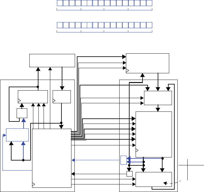
8.1 Exercises 193
8.21 Define two new flow-of-control instructions for the six-instruction instruction set of
this chapter. Extend the datapath, control unit, and the controller’s FSM as needed.
We’ll define JMPLT and JMPGE, with opcodes 0110 and 0111. The syntax for
JMPLT will be “JMPLT Ra, Rb, offset”, where we jump to the offset if the contents
of Ra are less than the contents of Rb. The syntax for JMPGE will be “JMPGE Ra,
Rb, offset”, where we jump to the offset if the contents of Ra are greater than or
equal to the contents of Rb.
opcode
15 14 13 12 11 10 9 8 7 6 5 4 3 2 1 0
(0110)
ra
register 1 rb
register 2
offset
JMPLT ra, rb, offset
opcode
15 14 13 12 11 10 9 8 7 6 5 4 3 2 1 0
(0111)
ra
register 1 rb
register 2
offset
JMPGE ra, rb, offset
addr D
rd
wr W_data R_data
256x16
16-bit
3x1
21 0
s1
s0
W_data
W_addr
W_wr
Rp_addr
Rp_rd
Rq_addr
Rp_data Rq_data
16x16
RF
ALU
AB
s1
s0
=0
Datapath
IR
ld
PC
ld clr up
Controller
addr rd data
I
I_rd
PC_clr
PC_inc
D_addr
D_rd
D_wr
RF_W_data
RF_s1
RF_s0
RF_W_addr
RF_W_wr
RF_Rp_addr
RF_Rp_rd
RF_Rq_addr
RF_Rq_rd Rq_rd
RF_Rp_zero
alu_s1
alu_s0
Control unit
s1
0
0
1
s0
0
1
0
ALU op
pass A
A+B
A-B
<
Rp_lt_Rq
(a+b-1)
+
PC_ld
IR[7:0]
01
IR[3:0]
PCmux_s
s
194 8 Programmable Processors
8.22 Assuming that the microprocessor’s external pins I0..I7 and P0..P7 are mapped to
data memory locations as in Figure 8.15 and an AND instruction has been added to
the six-instruction instruction set of this chapter, create an assembly program that
will output 0 on P4 if all eight inputs I0..I7 are 1s.
MOV R0, #1 // R0 is the constant “1”
MOV R1, 240 // R1 gets the value of I0
MOV R2, 241 // R2 gets the value of I1
AND R2, R1, R2 // R2 = I0 ANDI1
MOV R1, 242 // R1 = I2
AND R2, R1, R2 // R2 = R2 AND I2
MOV R1, 243 // R1 = I3
AND R2, R1, R2 // R2 = R2 AND I3
MOV R1, 244 // R1 = I4
AND R2, R1, R2 // R2 = R2 AND I4
MOV R1, 245 // R1 = I5
AND R2, R1, R2 // R2 = R2 AND I5
MOV R1, 246 // R1 = I6
AND R2, R1, R2 // R2 = R2 AND I6
MOV R1, 247 // R1 = I6
AND R2, R1, R2 // R2 = R2 AND I7
SUB R2, R2, R0 // R2 = R2 - 1
MOV R0, #0 // R0 is the constant “0”
JMPZ R2, output // If R2-1==0, then I7..I0 were all 1s
JMPZ R0, done // exit program
output: MOV 252, R0 // P4 = 0
done:
Init Fetch
Decode
Load
Store
D_addr=d
D_rd=1
RF_s1=0
RF_s0=1
RF_W_addr=ra
RF_W_wr=1
D_addr=d
D_wr=1
RF_s1=X
RF_s0=X
RF_Rp_addr=ra
RF_Rp_rd=1
Add
RF_Rp_addr=rb
RF_Rp_rd=1
RF_s1=0
RF_s0=0
RF_Rq_add=rc
RF_Rq_rd=1
RF_W_addr=ra
RF_W_wr=1
alu_s1=0
alu_s0=1
Load-
constant
RF_s1=1
RF_s0=0
RF_W_addr=ra
RF_W_wr=1
Subtract
RF_Rp_addr=rb
RF_Rp_rd=1
RF_s1=0
RF_s0=0
RF_Rq_addr=rc
RF_Rq_rd=1
RF_W_addr=ra
RF_W_wr=1
alu_s1=1
alu_s0=0
Jump-if-zero
RF_Rp_addr=ra
RF_Rp_rd=1
Jump-if-
zero-jmp
PC_ld=1
op=0100
op=0101
op=0011
I_rd=1
PC_inc=1
IR_ld=1
PC_clr=1
op=0010
op=0001
op=0000
RF_Rp_zero
RF_Rp_zero’
Jump-if-GE
RF_Rp_addr=ra
Jump-if-
GE-jmp
RF_Rp_rd=1
RF_Rq_addr=rb
RF_Rq_rd=1
Rp_lt_Rq’
PC_ld=1
PCmux_s=1
Jump-if-LT
RF_Rp_addr=ra
Jump-if-
LT-jm p
RF_Rp_rd=1
RF_Rq_addr=rb
RF_Rq_rd=1
Rp_lt_Rq
PC_ld=1
PCmux_s=1
PCmux_s=0
Rp_lt_Rq
Rp_lt_Rq’
op=0110
op=0111
