Dual3360VCABuild Guide
User Manual:
Open the PDF directly: View PDF ![]() .
.
Page Count: 11
Dual AS3360 VCA
Eurorack Module
Build Guide
(c) 2019 Nicholas M. Tuckett

Components
Suggested Suppliers
•uk.farnell.com
•www.mouser.com
•www.bitsbox.co.uk – for toggle switches
•www.thonk.co.uk – for AS3360 and jack sockets
•www.ericasynths.lv/shop/diy/diy-accessories – for AS3360
Component Notes
Except where noted in the BOMs below, the following apply:
•Resistors are 1% thick film 1206 surface mount.
•Capacitors are ceramic 1206 surface mount, at least 16V.
•Electrolytic capacitors are 25V, 4mm diameter radial can, e.g. Panasonic EEEFP1E100AR.
•Trimmers are multiturn Bourns series 3296W style package. Many alternatives are available
for these.
Other variants of the given op-amps and voltage regulators will likely work.
Googling the supplied part numbers should produce results with more information and links to
suppliers.
•There are many alternatives available for the suggested pin headers, sockets and power
header items.
Note that J3, R1 or R2 are not present on the board, BOM or schematic.
Main PCB Bill of Materials
Parts Description Quantity Package Recommended
Part
C1-6 100nF Capacitor 6 1206
C7, C8 10uF Electrolytic Capacitor,
25V
2 Radial
can, 4mm
diameter
C9 4.7nF Capacitor 1 1206
D1, D2 Schottky rectifier diode 2 SMB STPS1L30U
D3, D4 10V reference 2 SOT-23 LM4040BIM3
D5-10 Schottky diode 6 SOD-123 BAT48ZFILM
J1 2.54mm socket, 4 x 1 row 1 309AE-04-SGN-1-
040A3
J2 2.54mm socket, 6 x 1 row 1 309AE-06-SGN-1-
040A3
J4 2.54mm socket, 3 x 1 row 1 309AE-03-SGN-1-
040A3
J5 Shrouded power header 1 302-S-10-D1R1
L1, L2 Ferrite bead 2 BL01RN1A1F1J
R19, R36 270R resistor, 1% 2 1206
R21, R38 1K resistor, 1% 2 1206
R17, R34 2K43 resistor, 1% 2 1206
R3, R4 4K7 resistor, 1% 2 1206
R13, R18, R30,
R35
10K resistor, 1% 4 1206
R10, R27 15K resistor, 1% 2 1206
R8, R25 27K resistor, 1% 2 1206
R9, R11, R26,
R28
56K resistor, 1% 4 1206
R5, R14, R15,
R22, R31, R32
100K resistor, 1% 6 1206
R20, R37 110K resistor, 1% 2 1206
R6, R7, R12,
R16, R23, R24,
R29, R33
402K resistor, 1% 8 1206
RV1-4 100K multiturn trimmer 4 3296W
U1 TL084 op-amp 1 SOIC TL084BCD
U2 AS3360 VCA 1 SOIC AS3360D
U3 TL072 op-amp 1 SOIC TL072BCD
Panel PCB Bill of Materials
Parts Description Quantity Package Recommended
Part
J1 2.54mm pin header, 4 x 1 row 1 VMHS-1x16-120-
065-030
J2 2.54mm pin header, 6 x 1 row 1 VMHS-1x16-120-
065-030
J3 2.54mm pin header, 3 x 1 row 1 VMHS-1x16-120-
065-030
J4-9 3.5mm mono switched jack socket 6 PJ398SM or
PJ301M-12
SW1-2 SPDT miniature ON/ON toggle switch 1 Bitsbox
Assembly
This module requires both surface mount and through-hole soldering. You can use various methods
for the surface mount soldering, such as hand soldering, heat gun or the hotplate method. If you
haven't attempted these before, it is highly recommended to study them and practice first.
•Hotplate method by Hobbytronics – this shows the basics
•Surface Mount Soldering – this shows the heat gun method, both with and without a stencil.
The steps to follow for this module using the hotplate method are as below. Start with the main PCB
first, then the panel PCB.
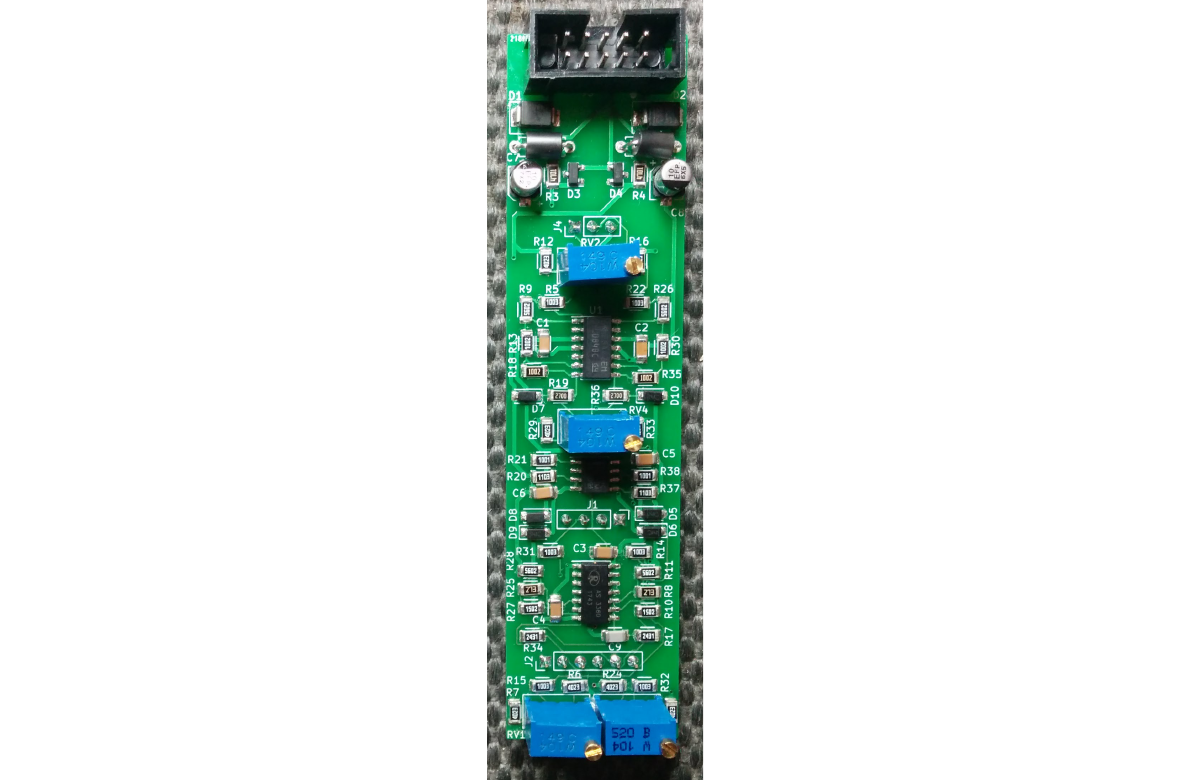
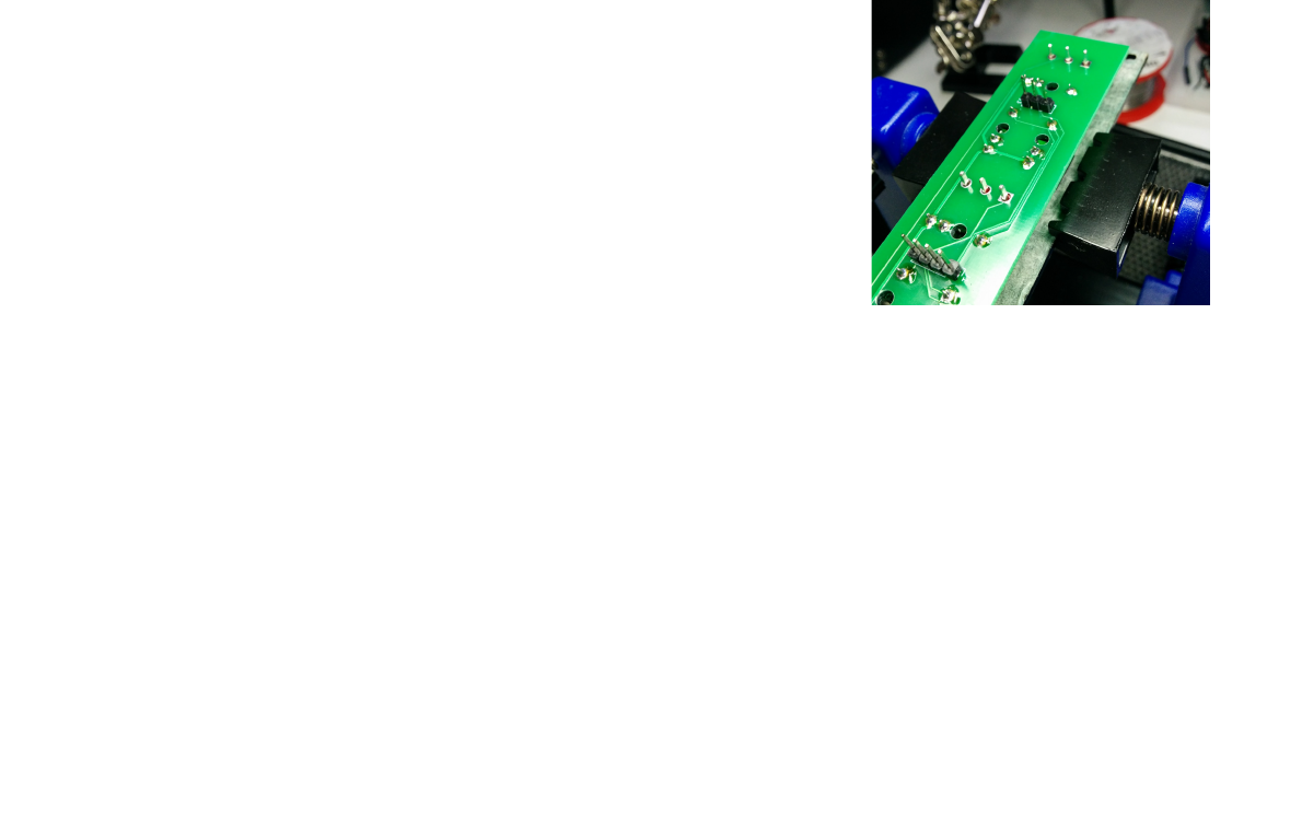
Main PCB
Add solder paste to all the SMD mounting pads on the main PCB, working from top to bottom, then
consistently in one horizontal direction (depending left or right handed).
•For reference, the Eurorack power connector is at the top of the board.
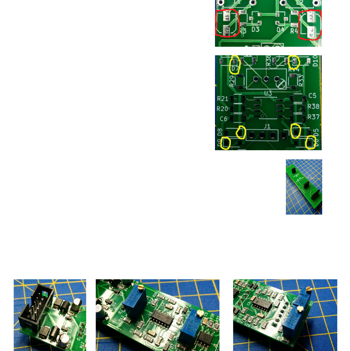
Place the SMD components onto the board using tweezers, seating them into the solder paste. It is
recommended to work from top to bottom, then middle out.
•Orient the electrolytic cap bases with the outline on the
PCB (highlighted in red, right).
•Orient all diodes correctly; the cathode is the closed end
of any diode outline on the PCB, and should line up
with the cathode marking on the diode itself, usually a
line) (outlined in yellow on the right).
•Orient all the ICs properly; pin 1 on all ICs will be top
left pad on the PCB. Any line marking pin 1 on an IC
should be at the top when placed, and any sloped edge
on the IC should be on the left.
Start heating your hotplate and place the PCB on it. Watch
carefully to see that all the solder joints go nice and shiny after
a few minutes, then remove the PCB with great care from the
hotplate, so as not to disturb the components. Allow to cool.
Solder the through-hole single row sockets onto the back of the board; it is suggested to
use a dab of glue, sticky tape or other common adhesive to hold them in place and
accurately aligned before soldering.
Solder the power connector, ferrite beads and trimmers onto the front of the board.
Again, some sort of adhesive or tape is helpful to hold the components in place before
soldering them.
•Place the slot in the shrouded power header at the top.
•Before soldering, adjust each trimmer so the resistance between the middle and outer pins is
the same (i.e. roughly 50K ohms) , using a multimeter.
•Align the trimmers so their screws match the outlines on the PCBs.
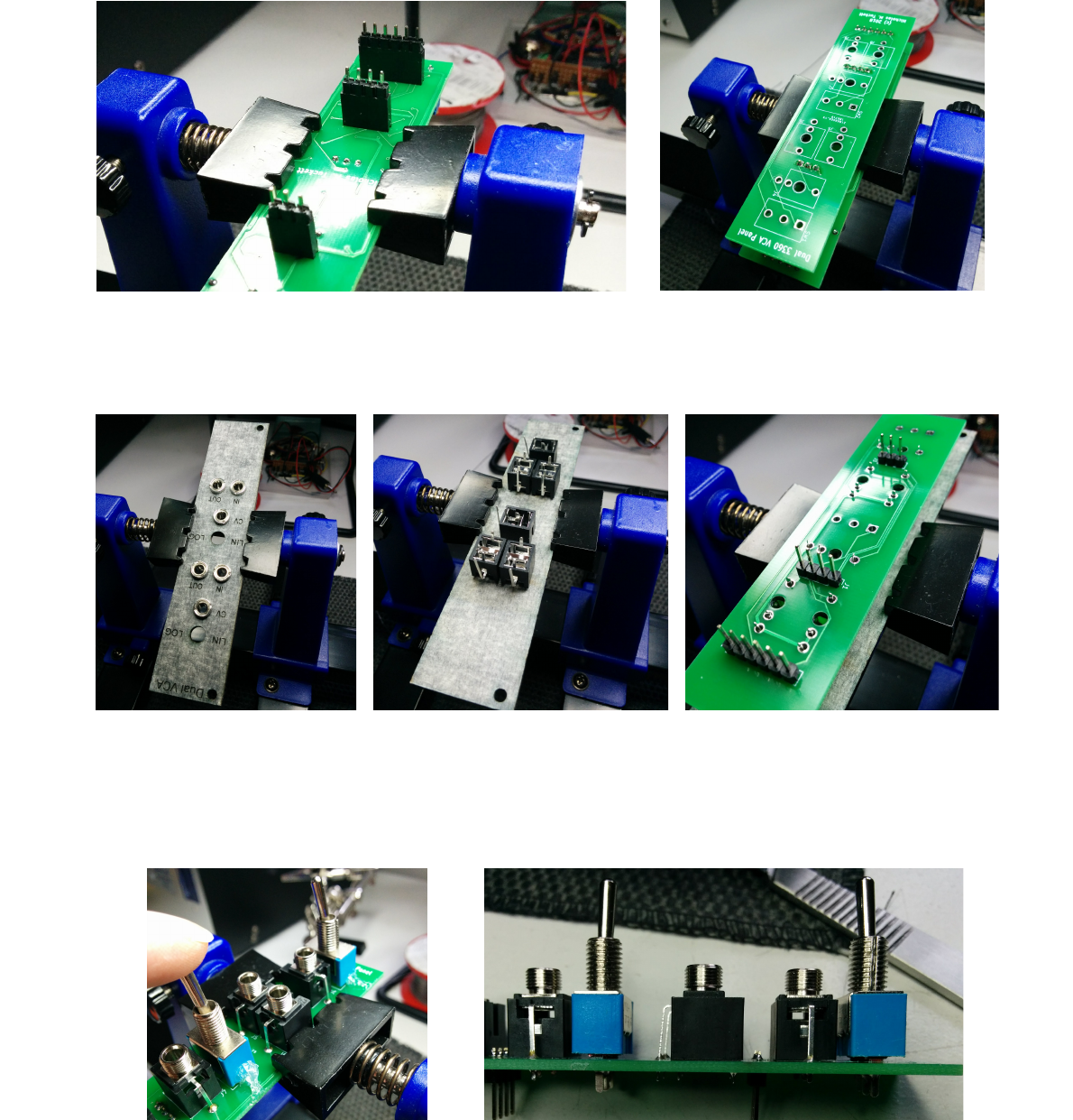
Panel PCB
Place the main PCB upside down in a holding device, insert the three pin headers into the sockets
and then place the panel PCB on top so the headers go through the relevant holes, and solder.
Screw in the jack sockets into the panel to be finger tight and aligned to match the PCB holes, and
place it into a holding device upside down. Align the panel PCB with the jack sockets, fit it over
and solder the sockets to the PCB.
Place each toggle switch and secure with a dab of hot glue; the pins widen close to the switch body
with some insulating material, so don't go all the way into the PCB. They should align with the top
surfaces of the jack sockets; it is best to hold them in place completely straight and vertical while
the glue sets.
Place the panel upside down into a holding device and mount the
panel PCB on top so the switch pins come through, and solder them.
Then remove any glue – e.g. for hot glue, warm it to soften first, then
cut or scrape it away.
Final Assembly
1. Screw the panel onto the panel PCB components firmly.
2. Connect the main board to the back of the panel PCB.
3. It's ready to calibrate!
Calibration
The CV inputs should control the VCA from fully closed at 0V to fully open at 5V.
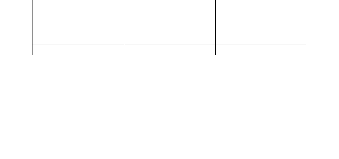
The following trimmer controls are available for calibration:
Channel Trimmer Control
1 RV1 Input signal offset
1 RV2 CV offset
2 RV3 Input signal offset
2 RV4 CV offset
When a trimmer is in the centre of the range, it has no effect. Turning the trimmer away from the
centre of its range will have a positive or negative offset affect on the corresponding voltage.
The easiest way to calibrate the VCA requires an oscilloscope, an oscillator and an LFO.
1. Power up all the modules
1. Set the oscillator to around 200Hz and ensure it outputs a 10V peak-to-peak square wave
that is evenly centered around 0V.
2. Set the LFO to around 20Hz and ensure it outputs a 10V peak-to-peak triangle or trapezoid
wave.
3. Set the VCA channel switch to linear response (LIN).
4. Connect the oscillator to the input of the VCA channel.
5. Connect the LFO to the CV input of that VCA channel.
6. Connect the output of the VCA channel to one oscilloscope channel. You can do this via a
jack cable, or touch a probe to the top leg of the output jack socket
7. It is suggested to connect the LFO output as well to another oscilloscope channel, and use
that channel to synchronise the scope for a more stable display.
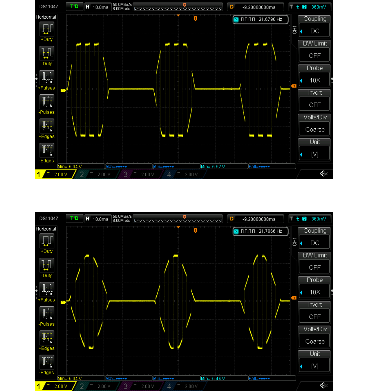
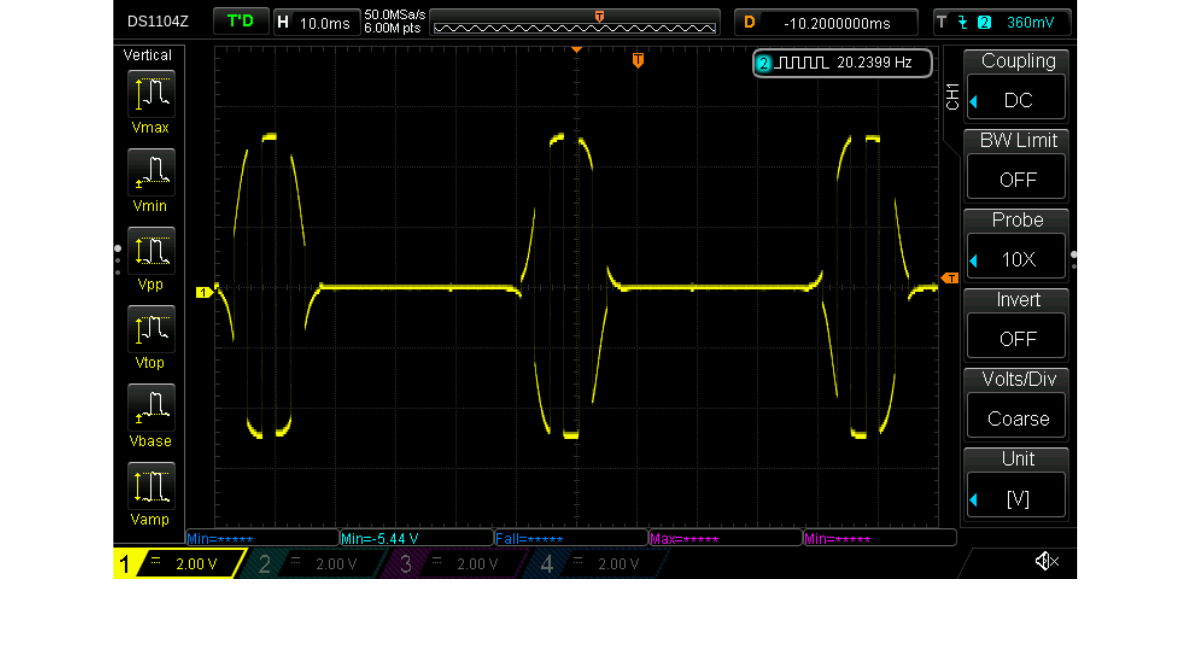
You should see something like this as the output of the VCA for a trapezoid LFO CV waveform:
A triangle LFO wave would look like this:
In both cases, you're seeing the VCO output being amplitude modulated by the LFO output. When
the LFO signal goes negative, the VCA cuts off completely, giving rise to this 'stripey pulse'
appearance.
The waveform should be symmetrical around the 0V line; if it is not, adjust the input offset
trimmer for this to ensure it is. This also depends on whether your VCO output is symmetrical; if
you're not sure about that, best to check it also with your oscilloscope. You could overlay the VCO
output on the VCA output via another oscilloscope channel, and adjust the input offset trimmer so
the VCO and VCA peaks and troughs align.
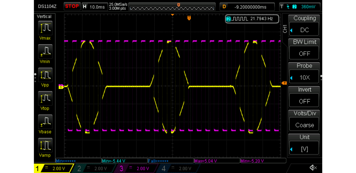
Here's a shot of an oscilloscope showing the VCO signal in magenta and the VCA signal in yellow.
Some slight adjustment needed to the offset here when comparing the peaks and troughs of the two:
Next, switch the channel to logarithmic response (the switch position labelled LOG). You should
see the edges of the pulses change shape to follow a logarithmic curve, like this:
Toggle the switch between the linear and logarithmic response, and check that the VCA output
amplitude of both modes is the same. If not, adjust the CV offset trimmer for the channel until they
do match. This trimmer will affect the amplitude of both linear and logarithmic responses, so you
will need to switch back and forth between the two to get a nice match. You may also find you need
to tweak the input offset adjustment afterwards in case the signal has become not quite symmetrical.
Repeat this calibration for the other channel, and your dual AS3360 VCA is now set up!
