EK DZ110 UG 002 DZ11 User's Guide
EK-DZ110-UG-002 DZ11 User's Guide EK-DZ110-UG-002 DZ11 User's Guide
User Manual: EK-DZ110-UG-002 DZ11 User's Guide
Open the PDF directly: View PDF ![]() .
.
Page Count: 60

DZ11
user's
guide

EK-DZ110-UG-002
DZ11
user's
guide
digital
equipment
corporation
•
maynard,
massachusetts
Preliminary Edition, March 1977
Preliminary Edition (Rev), June 1977
1
st
Edition, September 1977
2nd Edition, February 1979
The drawings
and
specifications herein are the property
of
Digital Equipment
Corporation and shall
not
be reproduced
or
copied
or
used
in
whole
or
in
part
as the basis for the manufacture
or
sale
of
equipment described herein without
written permission.
Copyright © 1977, 1979 by Digital Equipment Corporation
The material
in
this manual
is
for informational
purposes and
is
subject to change without notice.
Digital Equipment Corporation assumes no re-
sponsibility for any errors which may appear in
this manual.
Printed
in
U.S.A.
This document was
set
on DIGITAL's DECset-8000
computerized typesetting system.
The following are trademarks
of
Digital Equipment Corporation,
Maynard, Massachusetts:
DIGITAL
DEC
PDP
DECUS
UNIBUS
DECsystem-lO
DECSYSTEM-20
DIBOL
EDUSYSTEM
VAX
VMS
MASSBUS
OMNIBUS
OS/8
RSTS
RSX
lAS
CHAPTER 1
1.1
1.2
1.2.1
1.3
1.3.1
1.3.1.1
1.3.1.2
1.3.2
1.3.3
1.3.4
1.3.5
1.3.6
1.3.7
1.3.8
1.3.9
1.3.10
1.4
1.4.1
1.4.2
1.4.3
CHAPTER 2
2.1
2.2
2.3
2.4
2.4.1
2.4.1.1
2.4.1.2
2.4.2
2.4.3
CHAPTER 3
3.1
3.1.1
3.2
3.2.1
3.2.2
3.2.3
3.2.4
CONTENTS
Page
GENERAL DESCRIPTION
INTRODUCTION
..............................................................................................
1-1
PHYSICAL
DESCRIPTION
..............................................................................
1-2
Configurations .............................................................................................
1-3
GENERAL
SPECIFICATIONS
.........................................................................
1-8
Outputs
........................................................................................................
1-9
DZII-A,
-B,
and
-E
..............................................................................
1-9
DZII-C,-E,and-F
..............................................................................
1-9
Inputs
...........................................................................................................
1-9
Power Requirements, DZ11-A, -B,
and
-E ....................................................
1-9
Power Requirements,
DZII-C,
-D,
and
-F
....................................................
1-9
Environmental Requirements -All
DZl1s
..................................................
1-1O
Distortion
-
DZII-A,
-B,
and
-E
.................................................................
I-I0
Interrupts
................................................................................................... 1-10
Line Speed .................................................................................................. 1-10
Distance
(DZ
II-A,
-
B,
and
-E) ....................................................................
1-11
Distance
(DZI1-C,
-D,
and
-F)
...................................................................
1-11
FUNCTIONAL
DESCRIPTION
......................................................................
1-11
PDP-II
Unibus
Interface ............................................................................
1-
12
Control
Logic ............................................................................................. 1-12
Line Interface ............................................................................................. 1-13
INST ALLA TION
SCOPE
................................................................................................................
2-1
CONFIGURATION
DIFFERENCES
...............................................................
2-1
UNPACKING
AND
INSPECTION
.......................................
~
...........................
2-1
INSTALLATION
PROCEDURE
.......................................................................
2-1
H317
Distribution
Panel
and
Static Filter Installation ...................................
2-1
EIA
Option
..........................................................................................
2-1
20 rnA
Option
....................................................................................... 2-2
M7819
Module
Installation .......................................................................... 2-2
M7814
Module
Installation .......................................................................... 2-6
PROGRAMMING
INTRODUCTION
..............................................................................................
3-1
Device
and
Vector Address Assignments ......................................................
3-1
REGISTER
BIT
ASSIGNMENTS
...................................................................... 3-2
Control
and
Status
Register
(CSR)
............................................................... 3-2
Receiver Buffer
(RBUF)
............................................................................... 3-6
Line
Parameter
Register
(LPR)
..................................................................... 3-7
Transmit
Control
Register
(TCR)
................................................................. 3-8
iii
3.2.S
3.2.6
3.3
3.3.1
3.3.2
3.3.3
3.3.4
3.3.S
3.3.6
3.3.7
3.3.8
3.4
CONTENTS (CONT)
Page
Modem Status Register (MSR) ..................................................................... 3-9
Transmit
Data
Register
(TDR)
..................................................................... 3-9
PROGRAMMING
FEATURES
........................................................................
3-9
Baud Rate ....................................................................................................
3-9
Character Length ........................................................................................
3-1
0
Stop Bits ..................................................................................................... 3-10
Parity .........................................................................................................
3-1
0
Interrupts ...................................................................................................
3-1
0
Emptying the Silo .......................................................................................
3-11
Transmitting a Character ............................................................................ 3-12
Data
Set Control ........................................................................................ 3-13
PROGRAMMING
EXAMPLES
...................................................................... 3-13
APPENDIX A
DZll
(M7814) TO
AN
ACTIVE DEVICE INSTALLATION
Figure No.
1-1
1-2
1-3
1-4
I-S
1-6
1-7
1-8
2-1
2-2
2-3
2-4
2-S
3-1
A-I
A-2
FIGURES
Title Page
DZ
11
System Applications ...................................................................................
1-1
DZll
EIA Module (M7819), Distribution Panel (H317-E), Static Filter
(H7004C), and Cables (BC06L-OJ and BCOSW -IS) ..............................................
1-2
DZII
20
rnA Module (M7814), Distribution Panel (H317-F), Static
Filter (H7004B), and Cables (BC06K-OJ and BC08S-1S) ......................................
1-3
DZ
11
Hardware Interconnections ........................................................................
1-4
H3271
or
H327
Turnaround
.................................................................................
1-S
Test Connectors H327, H3190, H3271, and H32S .................................................
1-6
H3190 Staggered Line
Turnaround
.......................................................................
1-7
General Functional Block Diagram .................................................................... 1-12
M7819 Address Selection .....................................................................................
2-3
M7819 Vector Selection ........................................................................................
2-3
BCOSW -IS and BC08S-1S Interconnection ...........................................................
2-S
M7814 Address Selection ..................................................................................... 2-6
M7814 Vector Selection ........................................................................................ 2-7
Register Bit Assignments ......................................................................................
3-3
DZll
(M7814)
to
Active Device Connection .......................................................
A-l
H319 Current Loop Receiver Schematic Diagram ............................................... A-2
IV
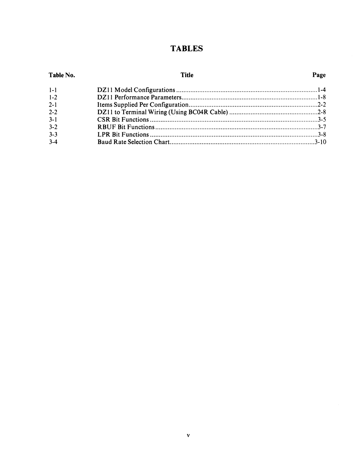
Table No.
1-1
1-2
2-1
2-2
3-1
3-2
3-3
3-4
TABLES
Title Page
DZII
Model Configurations ................................................................................
1-4
DZ
11
Performance Parameters .............................................................................
1-8
Items Supplied Per Configuration .........................................................................
2-2
DZII
to
Terminal Wiring (Using BC04R Cable) ..................................................
2-8
CSR
Bit Functions ...............................................................................................
3-5
RBUF
Bit Functions ............................................................................................
3-7
LPR
Bit Functions ............................................................................................... 3-8
Baud Rate Selection CharL ................................................................................. 3-10
v

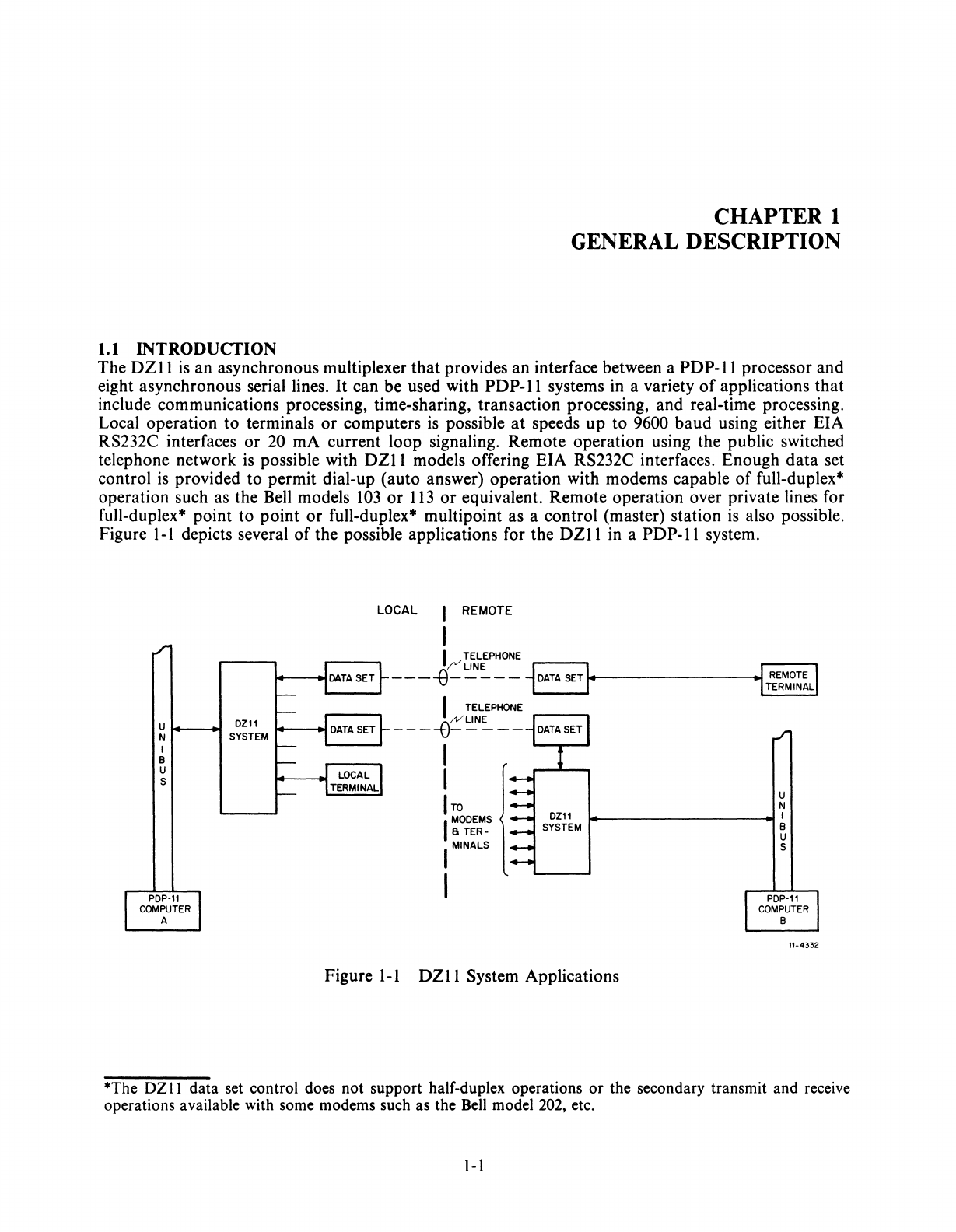
1.1
INTRODUCfION
CHAPTER 1
GENERAL DESCRIPTION
The
DZII
is
an asynchronous multiplexer that provides an interface between a
PDP-II
processor and
eight asynchronous serial lines.
It
can be used with
PDP-II
systems in a variety
of
applications that
include communications processing, time-sharing, transaction processing, and real-time processing.
Local operation to terminals
or
computers
is
possible
at
speeds
up
to 9600 baud using either EIA
RS232C interfaces
or
20 rnA current loop signaling. Remote operation using the public switched
telephone network
is
possible with
DZII
models offering EIA RS232C interfaces. Enough
data
set
control
is
provided to permit dial-up (auto answer) operation with modems capable
of
full-duplex*
operation such as the Bell models
103
or
113
or
equivalent. Remote operation over private lines for
full-duplex* point to point
or
full-duplex* multipoint as a control (master) station
is
also possible.
Figure I-I depicts several
of
the possible applications for the
DZII
in a
PDP-II
system.
u
t---~
DZII
N SYSTEM
I
B
U
S
LOCAL
REMOTE
I TELEPHONE
--
-
~
~=-
--J
DATA
SETI
....
..----------..tJ
REMOTE I
1.
-I
TERMINAL
I TELEPHONE
----e~~~--
ITO
I
MODEMS
Ii
TER-
I MINALS
I
U
N
~---
_____
~I
B
U
S
Figure I-I
DZll
System Applications
11-4332
*The
DZII
data set control does not support half-duplex operations
or
the secondary transmit and receive
operations available with some modems such as the Bell model 202, etc.
I-I
The
DZ
II
has several features
that
provide
flexible
control
of
parameters
such as
baud
rate,
character
length,
number
of
stop
bits for
each
line,
odd
or
even
parity
for each line,
and
transmitter-receiver
interrupts.
Additional
features include limited
data
set
control,
zero receiver
baud
rate,
break
gener-
ation
and
detection, silo buffering
of
received
data,
module
plug-in
to
hex
SPC
slots,
and
line
turn-
around.
Each
DZII
module
provides for
operation
of
eight
asynchronous
serial lines. Since
the
module
inter-
faces
to
these
channels
with a 16-line
distribution
panel, 2
DZll
modules
can
be used with 1 panel.
Also note
that
the
two
versions
of
the
DZII
(EIA
or
20 rnA
output)
consist
of
different
module
and
panel types.
This
fact allows a system
to
mix
EIA
and
20 rnA by using multiple
DZlls.
1.2 PHYSICAL DESCRIPTION
The
DZII
(8-line
configuration)
comprises a single hex
SPC
module
and
a 13.34 cm (5.25 in),
unpo-
wered
distribution
panel,
connected
by a 4.6 m (15 ft)
ribbon
cable. Several types
of
interconnecting
cables
are
used between
the
distribution
panel
and
the
modem
or
terminal,
depending
on
the
device. A
16-line
configuration
uses two
modules
and
a single
distribution
panel
connected
by
two
ribbon
cables.
The
DZII
modules, cables, static filters, *
and
distribution
panel
are
shown
in Figures
1-2
and
1-3.
The
subsequent
paragraphs
present
a detailed description
of
the
physical
and
electrical specifications
of
the
various
DZII
options
and
configurations.
eZl1
(M7819-EIA)
CABLE
(BCOSW-15)
==:::0-
__
STATIC
FILTER
(H7004C)
CABLE
---------
(BC06L-OJ)
DISTRIBUTION
PANEL
(H317-E)
8884-1
Figure
1-2
DZII
EIA
Module
(M7819),
Distribution
Panel
(H317-E),
Static
Filter
(H7004C),
and
Cables (BC06L-OJ
and
BC05W
-IS)
·Static
filters are
not
supplied with earlier modules.
1-2
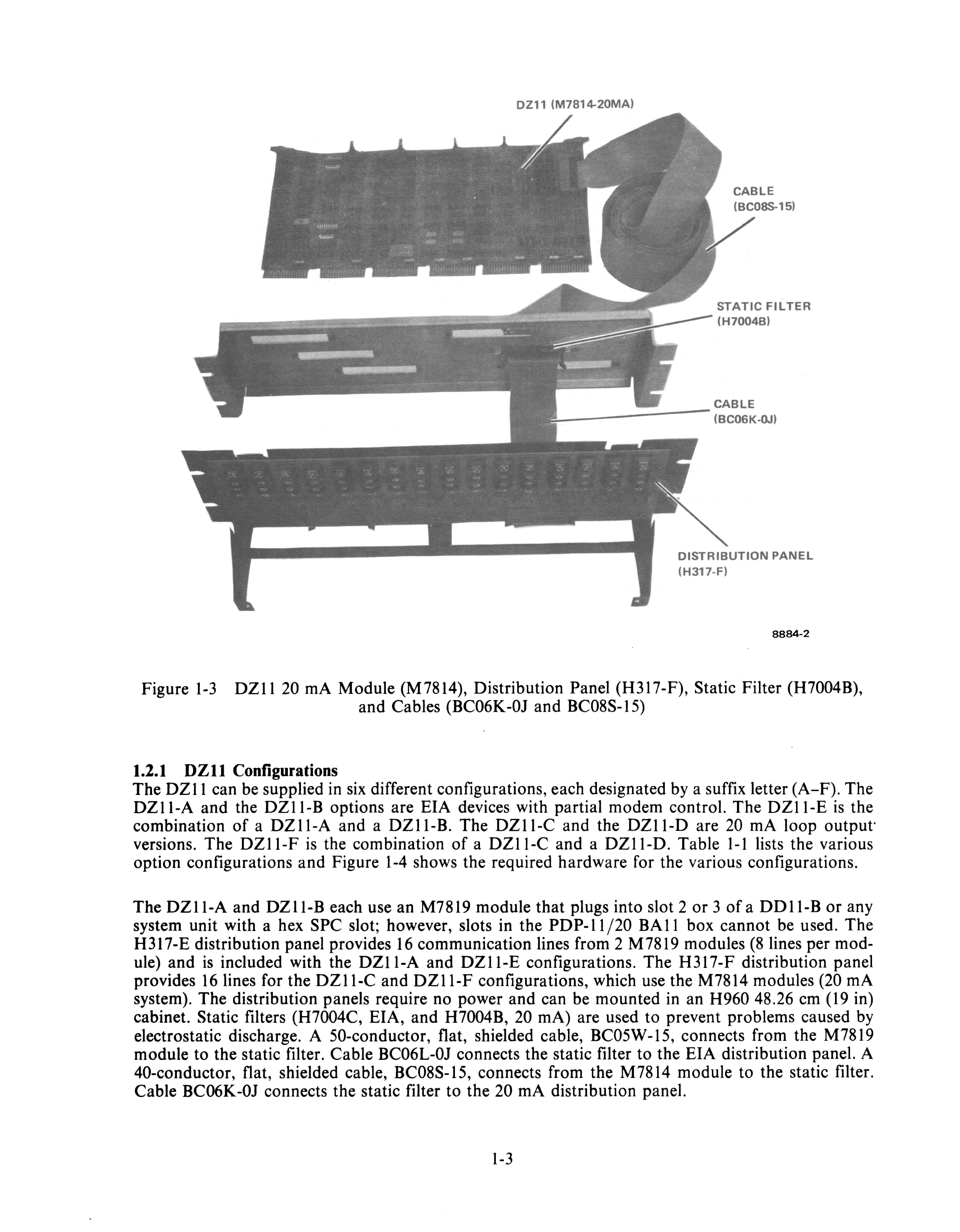
DZ11
(M7814-20MA)
CABLE
(BC08S-15)
STATIC
FILTER
(H7004B)
CABLE
L-------
(BC06K-OJ)
DISTRIBUTION
PANEL
(H317-F)
8884-2
Figure
1-3
DZ
11
20
rnA Module (M7814), Distribution Panel (H317-F), Static Filter (H7004B),
and Cables (BC06K-OJ and BC08S-15)
1.2.1
DZll
Configurations
The
DZll
can be supplied
in
six
different configurations, each designated
by
a suffix letter (A-F). The
DZI1-A and the DZI1-B options are EIA devices with partial modem control. The
DZI1-E
is
the
combination
of
a DZI1-A and a
DZII-B.
The DZI1-C and the DZI1-D are
20
rnA loop output·
versions. The
DZI1-F
is
the combination
of
a DZI1-C and a
DZII-D.
Table
1-1
lists the various
option configurations and Figure
1-4
shows the required hardware for the various configurations.
The
DZII-A
and
DZII-B
each use an M7819 module that plugs into slot 2 or 3
ofa
DDll-B
or
any
system unit with a hex SPC slot; however, slots in the
PDP-II/20
BAll
box cannot be used. The
H317-E distribution panel provides
16
communication lines from 2 M7819 modules
(8
lines per mod-
ule) and
is
included with the DZI1-A and
DZII-E
configurations. The H317-F distribution panel
provides
16
lines for the
DZII-C
and
DZII-F
configurations, which use the M7814 modules (20
rnA
system). The distribution panels require no power and can be mounted in an H960 48.26
cm
(19
in)
cabinet. Static filters (H7004C, EIA, and H7004B,
20
rnA) are used to prevent problems caused
by
electrostatic discharge. A 50-conductor, flat, shielded cable, BC05W -15, connects from the M7819
module to the static filter. Cable BC06L-OJ connects the static filter to the EIA distribution panel. A
40-conductor, flat, shielded cable, BC08S-15, connects from the M7814 module to the static filter.
Cable BC06K-OJ connects the static filter to the
20
rnA
distribution panel.
1-3
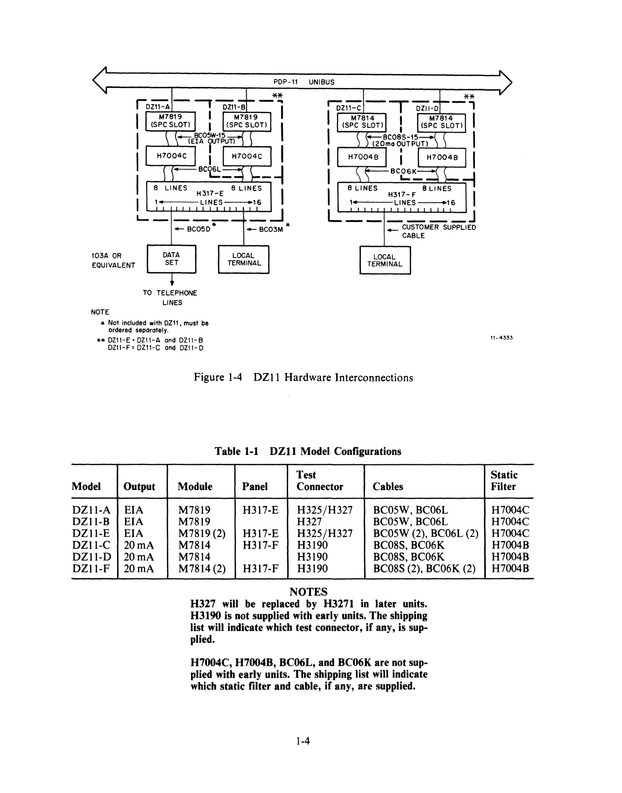
103A
OR
EQUIVALENT
LOCAL
TERMINAL
PDP-ll
UNIBUS
_
CUSTOMER
SUPPLIED
CABLE
TO
TELEPHONE
LINES
NOTE
* Not included with
DZll
, must
be
ordered separately.
**
DZII-E=DZll-A
and DZ11-B
DZII-F=
DZ11-C
and
DZ11-D
Model Output
DZI1-A
EIA
DZII-B
EIA
DZI1-E
EIA
DZ11-C
20
rnA
DZII-D
20 rnA
DZII-F
20 rnA
Figure
1-4
DZ11 Hardware Interconnections
Table
1-1
DZll
Model Configurations
Test
Module Panel Connector Cables
M7819 H317-E H325/H327 BC05W, BC06L
M7819 H327 BC05W, BC06L
M7819 (2) H317-E H325/H327 BC05W (2), BC06L (2)
M7814 H317-F H3190 BC08S, BC06K
M7814 H3190 BC08S, BC06K
M7814 (2) H317-F H3190 BC08S (2), BC06K (2)
NOTES
H327 will be replaced by H3271 in later units.
H3190 is not supplied with early units. The shipping
list
will
indicate which test connector,
if
any, is sup-
plied.
H7004C, H7004B, BC06L, and BC06K are not sup-
plied with early units. The shipping list
will
indicate
which static filter and cable,
if
any, are supplied.
1-4
11-4333
Static
Filter
H7004C
H7004C
H7004C
H7004B
H7004B
H7004B
Modems
or
terminals are connected to the H317-E
EIA
panel by cables
that
attach to
16
DB25P cinch
connectors. These cables are
not
provided with the
DZII.
The BC05D-25 cable is recommended for
data
set interconnections,
and
the BC03M cable is recommended for local terminal interconnections.
The BC05W
-15
cable carries the
data
and
control signals for all eight lines. Connections between
terminals and the H317-F 20 rnA panel are by customer-supplied cables to
16
(4-screw) terminal strips.
The
data
signals for all eight lines are carried to the distribution panel by the BC08S-15 cable.
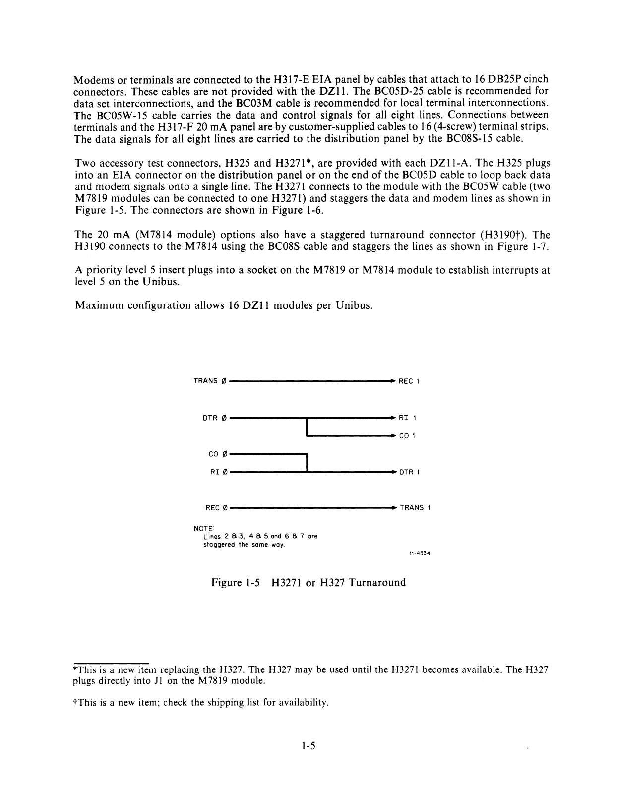
Two accessory test connectors, H325 and H3271*, are provided with each
DZII-A.
The H325 plugs
into an EIA connector on the distribution panel
or
on
the end
of
the BC05D cable to loop back
data
and modem signals
onto
a single line. The H3271 connects to the module with the BC05W cable (two
M7819 modules can be connected to one H3271) and staggers the
data
and
modem lines as shown in
Figure 1-5. The connectors are shown in Figure 1-6.
The 20 rnA (M7814 module) options also have a staggered
turnaround
connector (H3190t). The
H 3190 connects to the M7814 using the BC08S cable and staggers the lines as shown in Figure 1-7.
A priority level 5 insert plugs into a socket
on
the M7819
or
M7814 module to establish interrupts
at
level 5 on the Unibus.
Maximum configuration allows
16
DZII
modules per Unibus.
TRANS
0-------------
••
REC
I
DTR
0------~------~RI
I
~--------.-
COl
CO
0---------__.
RI!1l------~------
••
DTRI
REC!1l--------------
••
TRANS
1
NOTE:
Lines 2 S 3, 4 S 5
and
6 S 7 are
staggered the same
way.
Figure
1-5
H3271 or H327
Turnaround
11-4334
*This
is
a new item replacing the H327.
The
H327 may be used until the H327l becomes available.
The
H327
plugs directly into
Jl
on the
M78l9
module.
tThis
is
a new item; check the shipping list for availability.
1-5
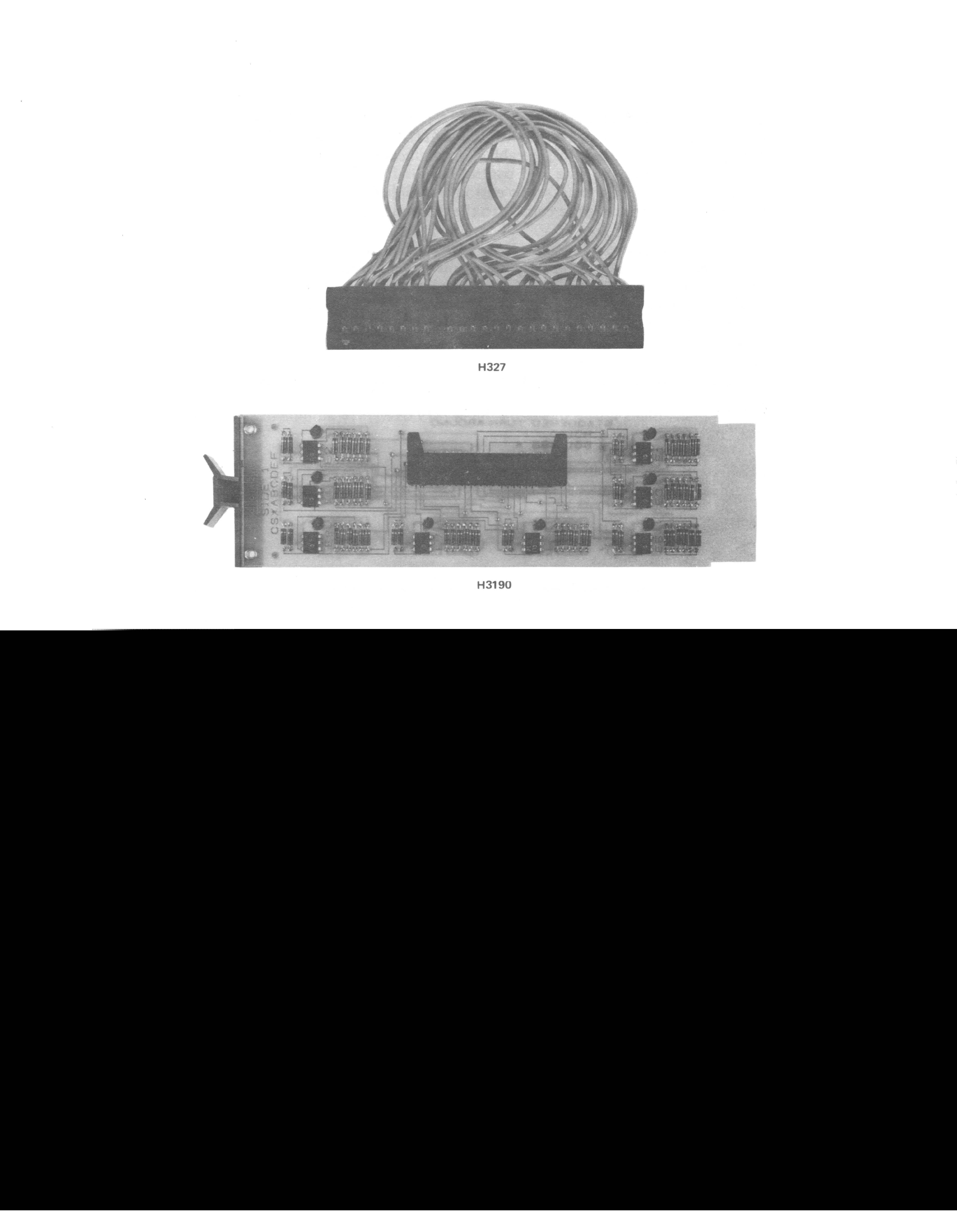
H327
H3190
+
LINE 0
TRANSMITTER
LINE 1
TRANSMITTER
20MA
LOOP
20MA
LOOP
LINES 2
III
3,
4111
6,
AND
8
III
7 ARE STAGGERED THE
SAME
WAY
Figure
1-7
H3190 Staggered Line Turnaround
1-7
LINE 1
RECEIVER
LINE 0
RECEIVER
11-5141
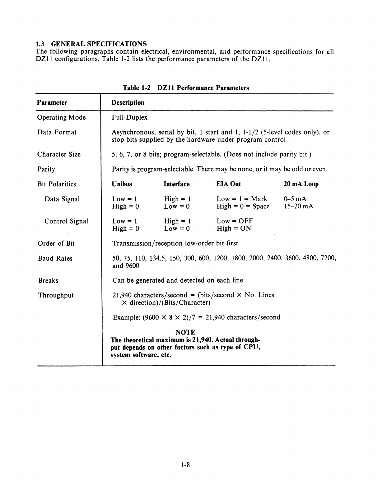
1.3 GENERAL SPECIFICATIONS
The following paragraphs contain electrical, environmental, and performance specifications for all
DZII
configurations. Table
1-2
lists the performance parameters
of
the
DZII.
Parameter
Operating Mode
Data
Format
Character Size
Parity
Bit Polarities
Data
Signal
Control Signal
Order
of
Bit
Baud Rates
Breaks
Throughput
Table 1-2
DZll
Performance Parameters
Description
Full-Duplex
Asynchronous, serial
by
bit, I start and I, 1-1/2 (5-level codes only),
or
stop bits supplied
by
the hardware under program control
5,
6,
7,
or
8 bits; program-selectable. (Does not include parity bit.)
Parity
is
program-selectable. There may be none, or it may be odd or even.
Unibus Interface EIA Out 20mALoop
Low = 1 High = I Low = I = Mark 0-5
rnA
High = 0 Low
=0
High = 0 = Space 15-20
rnA
Low = I High = I Low =
OFF
High = 0
Low=O
High =
ON
Transmission/reception low-order bit first
50,
75,
110,
134.5,
150,
300, 600,
1200, 1800,
2000, 2400, 3600, 4800, 7200,
and 9600
Can be generated and detected on each line
21,940 characters/second = (bits/second X No. Lines
X direction)/(Bits/Character)
Example: (9600 X 8 X 2)/7 = 21,940 characters/second
NOTE
The theoretical maximum
is
21,940. Actual through-
put depends on other factors such as type of CPU,
system software, etc.
1-8
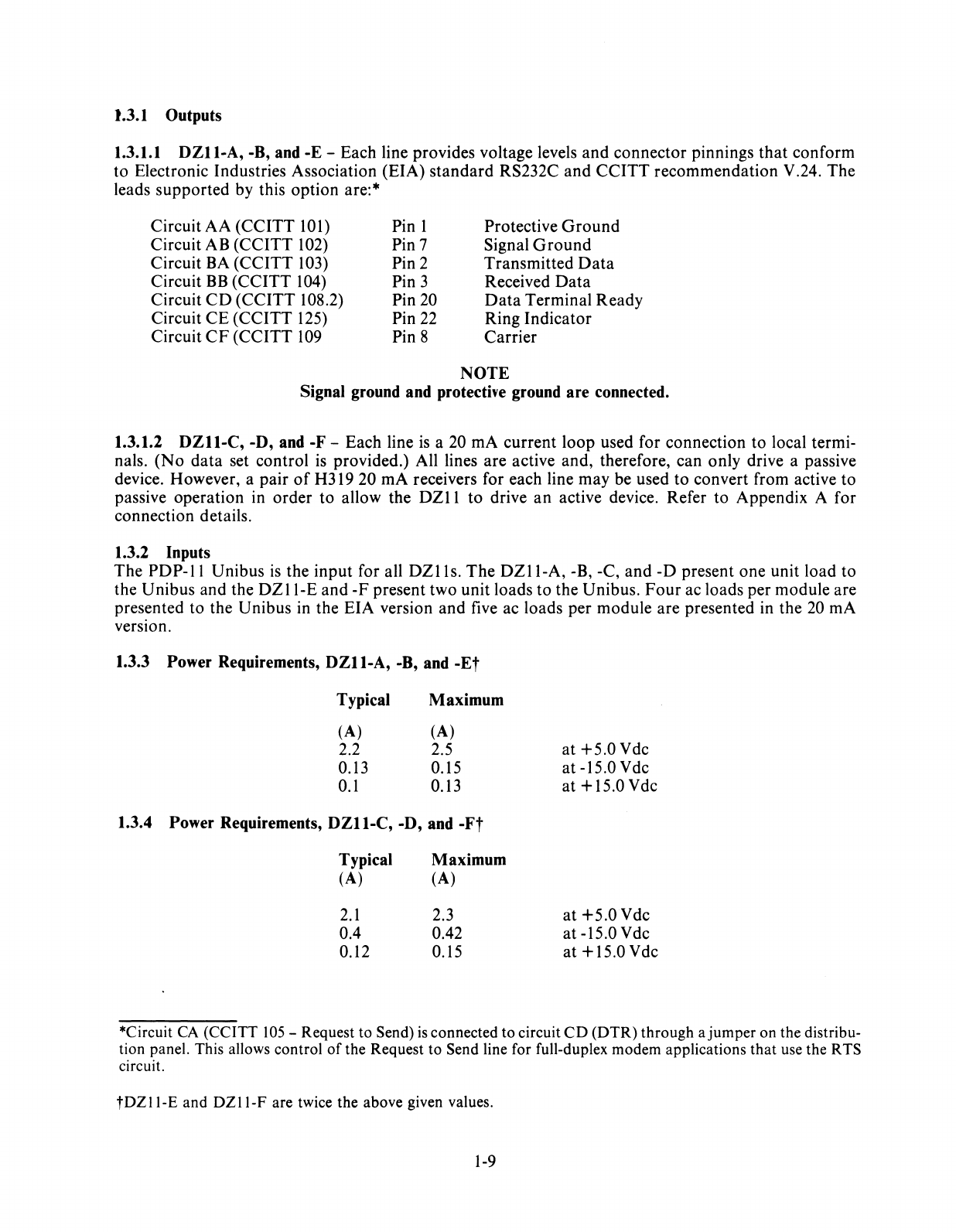
1.3.1 Outputs
1.3.1.1
DZII-A,
-B, and -E -Each line provides voltage levels and connector pinnings that conform
to Electronic Industries Association (EIA) standard RS232C and CCITT recommendation V.24. The
leads supported by this option are:*
Circuit AA (CCITT
101)
Circuit AB (CCITT
102)
Circuit
BA
(CCITT
103)
Circuit
BB
(CCITT
104)
Circuit
CD
(CCITT 108.2)
Circuit CE (CCITT
125)
Circuit
CF
(CCITT
109
Pin 1
Pin 7
Pin 2
Pin 3
Pin
20
Pin
22
Pin 8
Protective
Ground
Signal
Ground
Transmitted
Data
Received Data
Data
Terminal Ready
Ring Indicator
Carrier
NOTE
Signal ground and protective ground are connected.
1.3.1.2
DZll-C,
-D, and -F -Each line
is
a 20 rnA current loop used for connection to local termi-
nals.
(No
data set control
is
provided.) All lines are active and, therefore, can only drive a passive
device. However, a pair
of
H319 20 rnA receivers for each line may be used to convert from active to
passive operation in order to allow the
DZII
to drive
an
active device. Refer to Appendix A for
connection details.
1.3.2 Inputs
The
PDP-II
Unibus
is
the input for all
DZlls.
The
DZII-A,
-B, -C, and
-D
present one unit load to
the Unibus and the
DZII-E
and
-F
present two unit loads to the Unibus.
Four
ac loads per module are
presented to the Unibus in the EIA version and
five
ac loads per module are presented in the
20
rnA
version.
1.3.3 Power Requirements,
DZll-A,
-B,
and -Et
Typical Maximum
(A) (A)
2.2 2.5
0.13 0.15
0.1
0.13
1.3.4 Power Requirements,
DZII-C,
-D, and
-Ft
Typical Maximum
(A) (A)
2.1
2.3
0.4 0.42
0.12 0.15
at
+5.0Vdc
at
-15.0 Vdc
at
+15.0Vdc
at
+5.0Vdc
at -15.0 Vdc
at
+15.0Vdc
*Circuit
CA
(CCITT
105
-Request to Send)
is
connected to circuit
CD
(DTR) through ajumper on the distribu-
tion panel. This allows control
of
the Request to Send line for full-duplex modem applications that use the R
TS
circuit.
tDZll-E
and
DZll-F
are twice the above given values.
1-9
1.3.5 Environmental Requirements -
All
DZlls
Class C Environment Operating
Temperature
Relative Humidity
Cooling
DZII-A,
-B, -C,
and
-0
DZII-E
and
-F
Heat
Dissipation
DZII-A
and-B
DZII-E
DZII-C
and-D
DZII-F
5° to 50°
C·
(41
° to 122° F)
10
to 95%, with a maximum wet bulb
of
32° C (90° F)
and
a
minimum dewpoint
of
2° C (36° F)
Air flow 1.416
l/second
(3
cu.
ft/min)
Air flow 2.832 I/second
(6
cu.
ft/min)
3.99
g·cal/second
(57
Btu/hr)
7.98
g·cal/second
(114
Btu/hr)
3.85
g·cal/second
(55
Btu/hr)
7.7
g·cal/second
(110
Btu/hr)
1.3.6 Distortion -
DZll-A,
-B, and -E
The
maximum
"space
to
mark"
and
"mark
to space" distortion allowed in a received character
is
40
percent.
The
maximum speed distortion allowed in a received
character
for 2000
baud
is
3.8 percent. All
other
baud
rates allow 4 percent.
The
maximum speed distortion from the transmitter for 2000
baud
is
2.2
percent. All other
baud
rates have less
than
2 percent.
1.3.7 Interrupts
RDONE
SA
TROY
Occurs each time a character appears
at
the silo
output.
Silo Alarm. Occurs after
16
characters enter the silo.
Rearmed
by reading the
silo. This
interrupt
disables the
RDONE
interrupt.
Occurs when the scanner finds a line ready to transmit on.
NOTE
There are
no
modem interrupts.
Normally, a level 5 priority plug
is
supplied.
The
interface level can be modified to level 4,
6,
or
7 by
using the
proper
priority plug.
1.3.8 Line Speed
The
baud
rate for a line (both transmitter
and
receiver)
is
program-selectable. Also, the receiver for
each line can be individually turned on
or
off
under
program
control. (See Table
1-2
for a list
of
available
baud
rates.)
*Maximum operating temperature
is
reduced
1.8
0 C per 1000 meters (1.00 F per 1000 feet) for operation at
altitudes above sea level.
1-10
1.3.9 Distance
(DZII-A,
-B, and -E)
The recommended distance from computer
to
DZII
is
15
m (50 ft)
at
up to 9600
baud
with a BC05D
cable
or
equivalent. Operation beyond
15
m (50 ft) does not conform to the RS232C
or
CCITT
V.24
specifications. However, operation will often be possible
at
greater distance depending on the terminal
equipment, type
of
cable, speed
of
operation, and electrical environment. Reliable communication
over long cables depends on the absence
of
excessive electrical noise.
For
these reasons,
DIGITAL
cannot guarantee error-free communication beyond
15
m (50 ft). However, the EIA versions
of
the
DZII
may be connected to local
DIGITAL
terminals and most other terminals
at
distances beyond
15
m (50 ft) with satisfactory results if the terminal and computer are located in the same building, in a
modern office environment. Shielded twisted pair wire (Belden 8777
or
equivalent)
is
recommended
and
is
used in the BC03M null modem cable.
With cables made with shielded twisted pair wire, such as the Belden 8777, the following rate/distance
table may be used
as
a guide. This
chart
is
for informational purposes only and
is
not
to be construed
as
a warranty by Digital Equipment Corporation
of
error-free
DZll
operation at these speeds and
distances under all circumstances.
90 m (300 ft)
at
9600 baud
300 m (1000 ft)
at
4800 baud
300 m (1000 ft)
at
2400 baud
900 m (3000 ft)
at
1200 baud
1500 m (5000 ft) at 300 baud
NOTE
The ground potential difference between the
DZll
and terminal must not exceed 2
V.
This requirement
will
generally limit operation to within a single build-
ing served
by
one ac power service. In other cases, or
in
noisy electrical environments,
20
mA
operation
should
be
used.
1.3.10 Distance
(DZll-C,
-D, and -F)
The length
of
cable
that
may be used reliably
is
a function
of
electrical noise, loop resistance, cable
type,
and
speed
of
operation. The following
chart
is
given as a guide; however, there
is
no guarantee
of
error-free operation under all circumstances.
Speed (Baud)
9600
4800
2400
1200 and below
Belden 8777,
22
AWG,
shielded, twisted pairs
(shields floating)
(D EC P
/N
9107723)
150
m (500 ft)
300 m (1000 ft)
600 m (2000 ft)
1200 m (4000 ft)
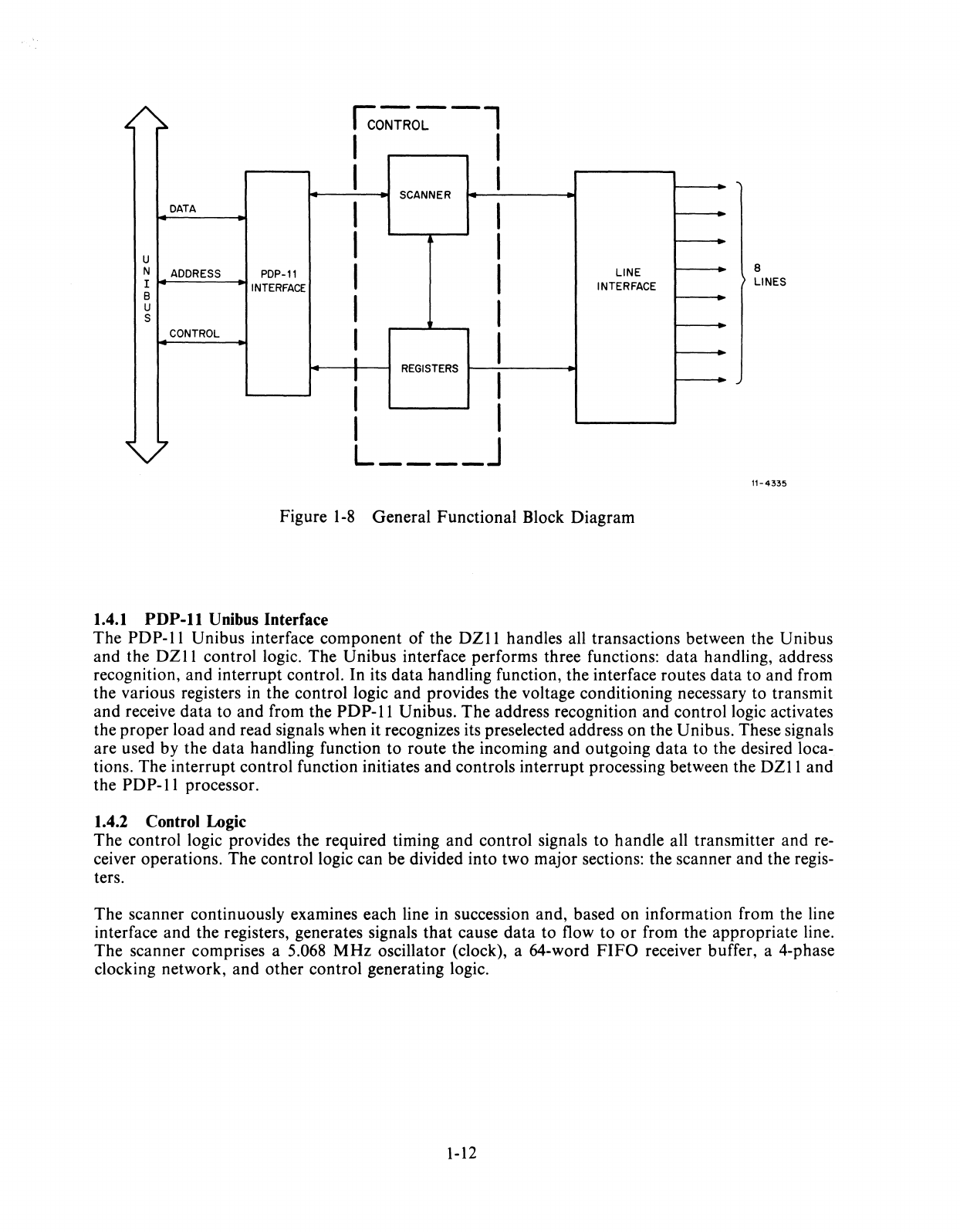
1.4 FUNCTIONAL
DESCRIPTION
22
AWG, 4 conductor
inside station wire
(DEC
PIN
9105856-4)
300 m (1000 ft)
540 m (1800 ft)
900 m (3000 ft)
1500 m (5000 ft)
The following paragraphs present a general description
of
DZII
operation. Figure
1-8
is
a general
functional block diagram
that
divides the
DZII
into three basic components: Unibus interface, control
logic, and line interface.
1-11
Ico~o~-l
I I
I I
SCANNER
DATA
I I
u I I
N
ADDRESS
PDP-11
I I LINE
I
INTERFACE
INTERFACE
B I
u I
S
CONTROL
I I
I
I
REGISTERS
I
I I
I
" L
____
J
Figure
1-8
General Functional Block Diagram
1.4.1
PDP-ll
Unibus Interface
8
LINES
11-4335
The
PDP-II
Unibus interface component
of
the
DZII
handles all transactions between the Unibus
and the
DZII
control logic. The Unibus interface performs three functions:
data
handling, address
recognition, and interrupt control. In its
data
handling function, the interface routes
data
to and from
the various registers
in
the control logic and provides the voltage conditioning necessary to transmit
and receive
data
to and from the
PDP-II
Unibus. The address recognition and control logic activates
the proper load and read signals when it recognizes its preselected address on the Unibus. These signals
are used by the
data
handling function to route the incoming and outgoing
data
to the desired loca-
tions. The interrupt control function initiates
and
controls interrupt processing between the
DZII
and
the
PDP-II
processor.
1.4.2 Control Logic
The control logic provides the required timing and control signals to handle all transmitter and re-
ceiver operations. The control logic can be divided into two major sections: the scanner and the regis-
ters.
The scanner continuously examines each line in succession and, based on information from the line
interface and the registers, generates signals
that
cause data to flow to
or
from the appropriate line.
The scanner comprises a 5.068
MHz
oscillator (clock), a 64-word
FIFO
receiver buffer, a 4-phase
clocking network, and other control generating logic.
1-12
The
DZII
uses four device registers in a manner
that
yields six unique and accessible registers, each
having a 16-bit word capacity. The six discrete registers temporarily store input
and
output
data,
monitor control signal conditioning, and establish
DZll
operating status. Depending on their func-
tions, some
of
the registers are accessible in bytes
or
words; others are restricted to word-only oper-
ation. Registers can be read
or
loaded (written), depending on the operation.
The
ability to read
or
write a register allows the use
of
two
of
the device registers as four independent registers.
1.4.3 Line Interface
Two
of
the most important operations in the
DZII
are the conversions from serial-to-parallel and
parallel-to-serial data formats. These conversions are required since the
DZII
is
located between the
PDP-II
Unibus (a parallel data path) and either local terminals
or
telephone lines (serial data paths).
Conversions for each line in the
DZII
are performed by independent universal asynchronous receiver-
transmitter (U AR T) integrated circuits. Another component
of
the line interface, the line receiver
or
driver, converts the
TTL
voltage levels in the
DZII
so that they correspond to those in the external
device input lines (modem
or
terminal).

2.1
SCOPE
CHAPTER
2
INST ALLATION
This chapter contains the procedures for the unpacking, installation,
and
initial checkout
of
the
DZII
Asynchronous Multiplexer.
2.2 CONFIGURATION DIFFERENCES
The
DZII
can be supplied with
or
without a distribution panel. The
DZll-B
and -D do
not
have
distribution panels. The following list describes the variations.
DZII-A
DZII-B
DZII-C
DZII-D
DZII-E
DZII-F
EIA level conversion with distribution panel
(8
lines)
EIA level conversion without distribution panel
(8
lines)
20
rnA
loop conversion with distribution panel
(8
lines)
20
rnA loop conversion without distribution panel
(8
lines)
DZII-A
and
DZII-B
(16 lines)
DZII-C
and
DZII-D
(16 lines)
2.3 UNPACKING AND INSPECTION
The
DZ
11
is
packaged in accordance with commercial packaging practices. First, remove all packing
material
and
check the equipment against the shipping list. (Table
2-1
contains a list
of
supplied items
per configuration.) Report damage
or
shortages to the shipper immediately and notify the
DIGITAL
representative. Inspect all parts
and
carefully inspect the module for cracks, loose components, and
separations in the etched paths.
2.4 INSTALLATION PROCEDURE
The following paragraphs should be followed
to
install the
DZII
option in a
PDP-II
system.
2.4.1 H317 Distribution Panel and Static Filter Installation
Install the H317 distribution panel and static filters according to unit assembly drawing
D-UA-DZll-
0-0.
2.4.1.1 EIA Option -
For
the
DZI1-A
or
DZI1-E
option, check to ensure
that
all
of
the machine-
insertable jumpers on the distribution panel
are
in place. (See Drawing E-UA-5411928-0-0 for
jumper
locations.) These jumpers are
in
anticipation
of
future use
of
the
DZII
with modems other than the
103;
however, two
of
the jumpers are now functional. The
jumper
labeled
DTR
(refer to D-CS-
5911928-0-1) connects
DTR
to
pin 4
or
Request to Send. This allows the
DZll
to assert
both
DTR
and RTS ifusing a modem which requires control
of
RTS.
Thejumper
labeled BUSY
is
also connected
to the
DTR
lead for use in modems
that
implement the Force Busy function. This
jumper
should
normally be cut
out
unless the modem has the Force Busy feature and the system software
is
imple-
mented
to
control it.
2-1
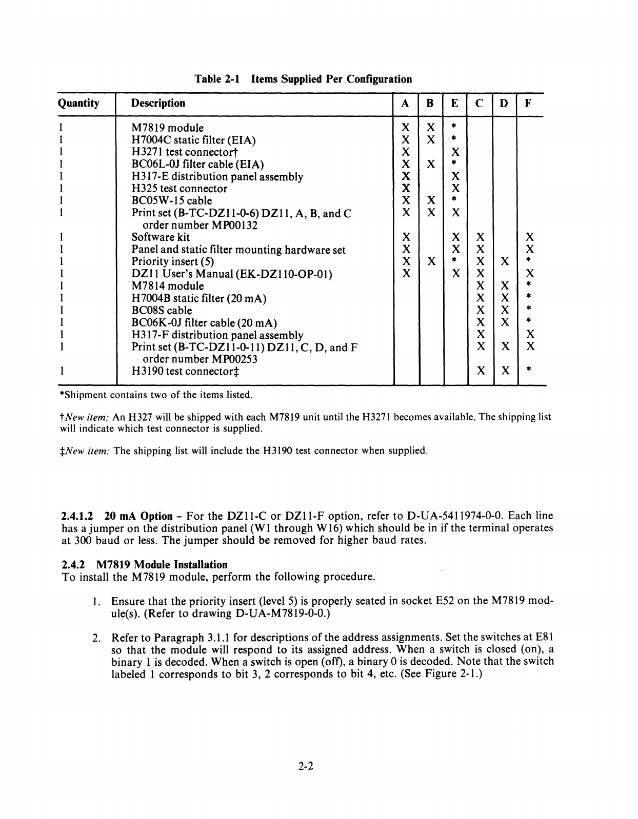
Table
2-1
Items Supplied
Per
Configuration
Quantity Description A B E C D F
I M7819 module X X *
I H7004C static filter (EIA) X X *
I H3271 test connectort X X
I BC06L-OJ filter cable (EIA) X X *
I H317-E distribution panel assembly X X
I H325 test connector X X
I BC05W -15 cable X X *
I Print set (B-TC-DZII-0-6)
DZll,
A,
B,
and C X X X
order number
MPOO132
I Software kit X X X X
I Panel
and
static filter mounting hardware set X X X X
I Priority insert (5) X X * X X *
I
DZII
User's Manual (EK-DZllD-OP-Ol) X X X X
I M7814 module X X *
1 H7004B static filter (20 rnA) X X *
I BC08S cable X X *
I BC06K-OJ filter cable (20 rnA) X X *
I H317-F distribution panel assembly X X
I Print set
(B-TC-DZII-0-ll)
DZll,
C, D, and F X X X
order number MP00253
I H3190 test connectort X X *
*Shipment contains two
of
the items listed.
t
New
item: An H327 will be shipped with each M7819 unit until the
H3271
becomes available. The shipping list
will indicate which test connector
is
supplied.
:j:New
item: The shipping list will include the H3190 test connector when supplied.
2.4.1.2 20
mA
Option -
For
the
DZII-C
or
DZII-F
option, refer
to
D-UA-5411974-0-0. Each line
has a jumper on the distribution panel (WI through W16) which should be in if the terminal operates
at 300 baud
or
less. The jumper should be removed for higher baud rates.
2.4.2 M7819 Module Installation
To install the M7819 module, perform the following procedure.
I. Ensure
that
the priority insert (level
5)
is
properly seated in socket E52 on the M7819 mod-
ul~(s).
(Refer to drawing D-UA-M7819-0-0.)
2.
Refer to Paragraph
3.1.1
for descriptions
of
the address assignments. Set the switches at
E81
so that the module will respond to its assigned address. When a switch
is
closed (on), a
binary 1
is
decoded. When a switch
is
open (off), a binary 0 is decoded. Note
that
the switch
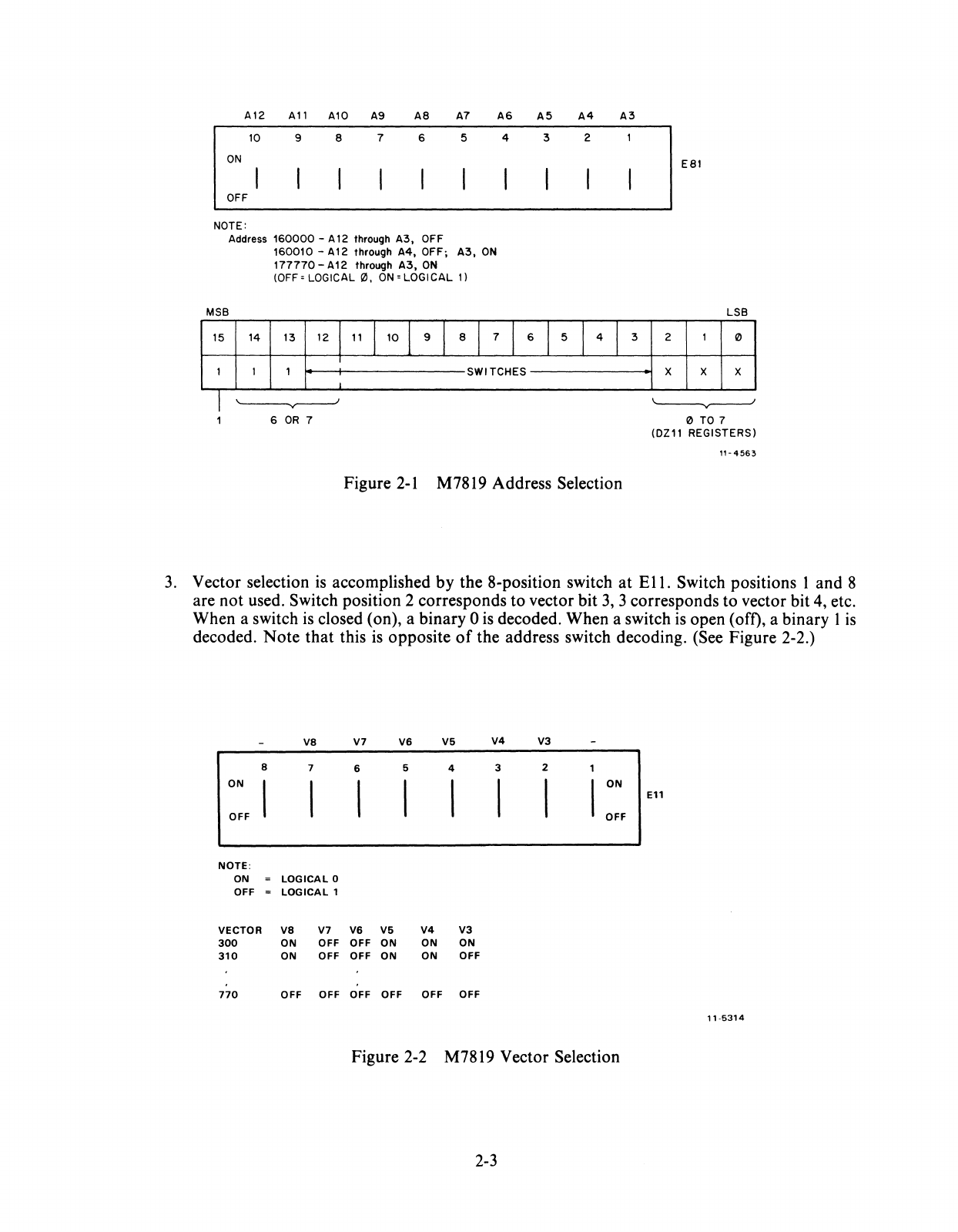
labeled I corresponds to bit 3, 2 corresponds to bit 4, etc. (See Figure 2-1.)
2-2
A12
All
Al0
A9
A8
A7
10
9 8 7 6 5
ON
OFF
NOTE:
Address
160000
- A
12
through
A3,
OFF
MSB
160010
-A12 through
A4,
OFF;
A3,
ON
177770-A12
through
A3,
ON
(OFF
~
LOGICAL 0,
ON
= LOGICAL
1)
A6
A5 A4
A3
4 3 2
15
14
13
12
111
110
I 9 I 8 I 7 I 6 I 5 I 4 I 3
I
1 I 1 SWITCHES
I
'-------y------
6
OR
7
Figure
2-1
M78l9 Address Selection
E81
LSB
2 1 0
X X X
~
o TO 7
(Ol11
REGISTERS)
"-4563
3.
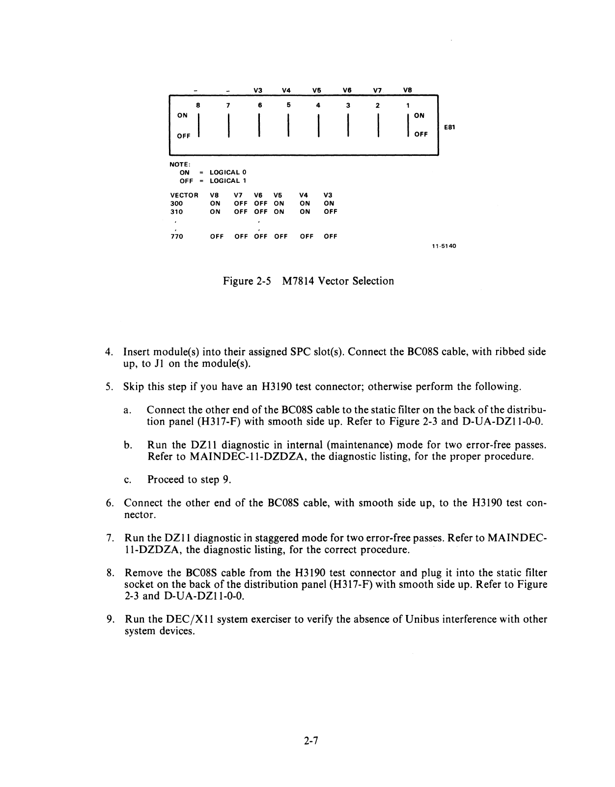
Vector selection
is
accomplished by the 8-position switch at
Ell.
Switch positions 1 and 8
are not used. Switch position 2 corresponds to vector bit
3,
3 corresponds to vector bit
4,
etc.
When a switch
is
closed (on), a binary 0
is
decoded. When a switch
is
open (off), a binary 1
is
decoded.
Note
that this
is
opposite
of
the address switch decoding. (See Figure 2-2.)
va
V7 V6
V5 V4
V3
a 7 6 5 4 3 2
ON
ON
Ell
OFF OFF
NOTE:
ON
LOGICAL
0
OFF
LOGICAL
1
VECTOR
va
V7 V6 V5
V4 V3
300
ON OFF OFF
ON ON ON
310
ON OFF OFF
ON ON
OFF
770
OFF OFF OFF OFF OFF OFF
"
-5314
Figure 2-2 M7819 Vector Selection
2-3
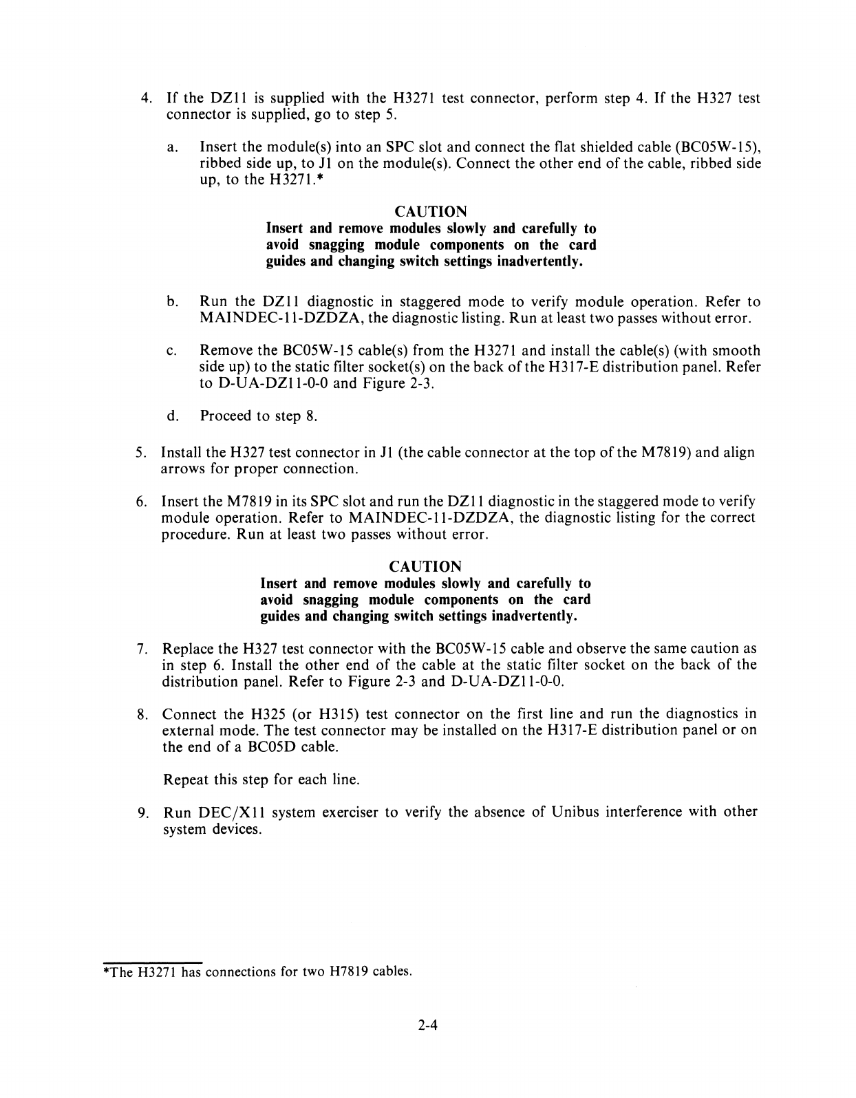
4.
If
the DZ11
is
supplied with the H3271 test connector, perform step
4.
If
the H327 test
connector
is
supplied, go
to
step
5.
a. Insert the module(s) into an SPC slot and connect the flat shielded cable (BC05W-15),
ribbed side up,
to
11
on the module(s). Connect the other end
of
the cable, ribbed side
up, to the H3271.*
CAUTION
Insert and remove modules slowly and carefully to
avoid snagging module components on the card
guides and changing switch settings inadvertently.
b.
Run
the
DZII
diagnostic in staggered mode to verify module operation. Refer
to
MAINDEC-I1-DZDZA,
the diagnostic listing.
Run
at least two passes without error.
c.
Remove the BC05W-15 cable(s) from the H3271 and install the cable(s) (with smooth
side up)
to
the static filter socket(s) on the back
of
the H317-E distribution panel. Refer
to
D-UA-DZll-0-0
and Figure 2-3.
d. Proceed
to
step
8.
5.
Install the H327 test connector in
11
(the cable connector
at
the top
of
the M7819) and align
arrows for
proper
connection.
6.
Insert the M7819 in its SPC slot and run the
DZll
diagnostic in the staggered mode to verify
module operation. Refer to
MAINDEC-II-DZDZA,
the diagnostic listing for the correct
procedure.
Run
at
least two passes without error.
CAUTION
Insert and remove modules slowly and carefully to
avoid snagging module components on the card
guides and changing switch settings inadvertently.
7.
Replace the H327 test connector with the BC05W-15 cable and observe the same caution as
in step
6.
Install the other end
of
the cable
at
the static filter socket
on
the back
of
the
distribution panel. Refer
to
Figure
2-3
and
D-UA-DZII-0-0.
8.
Connect the H325 (or H315) test connector on the first line and run the diagnostics in
external mode. The test connector may be installed on the H317-E distribution panel
or
on
the end
of
a BC05D cable.
Repeat this step for each line.
9.
Run
DEC/X
11
system exerciser to verify the absence
of
Unibus interference with other
system devices.
*The
H3271
has connections for two H7819 cables.
2-4
STATIC
FILTER
SOCKET
r:=:1
..
0
U6\J
SMOOTH
SIDE
BC05W-15
CABLE
OR
BC08S-15
CABLE
r\on
~
OUTPUT
BOARD
11-4327
Figure
2-3
BC05W
-15
and BC08S-15 Interconnection
10.
The DZ11
is
now ready for connection
to
external equipment.
Ifthe
connection
is
to a local
terminal, a null modem cable must be used. Use the BC03M
or
BC03P null modem cables
for connection between the distribution panel
and
the terminal.
The
H312-A null modem
unit may also be used with two BC05D EIA cables (one on each side
of
the null modem
unit).
If
connection
is
to a BellI
03
or
equivalent modem, a BC05D cable
is
required between
the distribution panel and
the
modem. All
of
the cables mentioned must be ordered sepa-
rately as they are not components
of
a standard
DZII
shipment. When possible, run the
diagnostic in echo test mode to verify the cable connections
and
the terminal equipment.
2-5
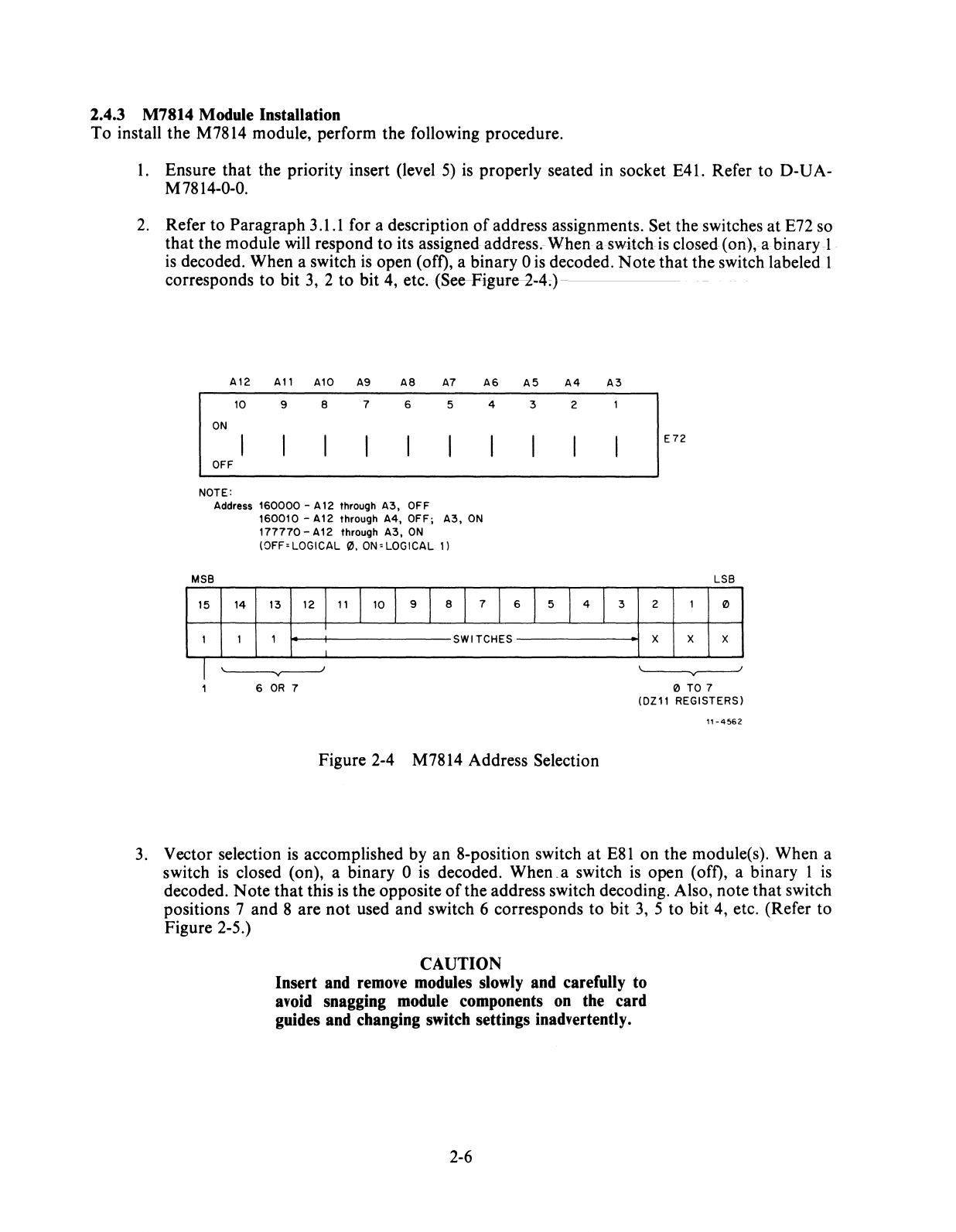
2.4.3 M7814 Module Installation
To install the M7814 module, perform the following procedure.
1.
Ensure
that
the priority insert (level
5)
is
properly seated in socket E41. Refer to D-UA-
M7814-0-0.
2.
Refer to Paragraph 3.1.1 for a description
of
address assignments. Set the switches at E72 so
that the module
will
respond to its assigned address.-When a switch
is
closed (on), a binary
-1
.
is
decoded. When a switch
is
open (off), a binary 0
is
decoded.
Note
that the switch labeled 1
corresponds to bit
3,
2 to bit 4, etc.
(See-Figure~-4;)
-
--
A12
All
A10 A9
A8
A7
A6
A5 A4 A3
10
9 8 7 6 5 4 3 2
ON
OFF
NOTE:
Address
160000
- A
12
through
A3,
OFF
MSB
15
14
1 1
160010
-A12 through
A4,
OFF;
A3,
ON
177770
-A12 through
A3,
ON
(OFF'LOGICAL
0.
ON'
LOGICAL
1)
13 12
111
110
I 9 I 8 I 7 I 6 I 5 I 4 I 3
I
1 SWITCHES
2
X
E72
LSB
1 0
X X
I
'-----...r---'
~
6
OR
7 o
TO
7
(OZ11 REGISTERS)
11-4562
Figure 2-4 M7814 Address Selection
3.
Vector selection
is
accomplished by an 8-position switch
at
E81
on the module(s). When a
switch
is
closed (on), a binary 0
is
decoded.
When.a
switch
is
open (off), a binary 1
is
decoded. Note that this is the opposite
of
the address switch decoding. Also, note that switch
positions 7 and 8 are not used and switch 6 corresponds to bit
3,
5 to bit 4, etc. (Refer to
Figure 2-5.)
CAUTION
Insert
and
remove modules slowly
and
carefully to
avoid snagging module components
on
the
card
guides
and
changing switch settings inadvertently.
2-6
V3 V4
V5 V6
V7
VB
B 7 6 5 4 3 2
ON
ION
EB1
OFF OFF
NOTE:
ON
LOGICAL
0
OFF
LOGICAL
1
VECTOR
VB
V7 V6 V5
V4
V3
300
ON OFF OFF ON ON ON
310
ON OFF OFF ON ON OFF
770
OFF OFF OFF OFF OFF OFF
11-5140
Figure
2-5 M7814 Vector Selection
4. Insert module(s)
into
their assigned
SPC
slot(s).
Connect
the
BC08S cable, with ribbed side
up,
to
11
on
the
module(s).
5.
Skip this step
if
you have an H3190 test connector; otherwise
perform
the
following.
a.
Connect
the
other
end
of
the
BC08S cable
to
the
static filter
on
the
back
of
the distribu-
tion
panel
(H317-F) with
smooth
side up. Refer
to
Figure
2-3
and
D-UA-DZII-O-O.
b.
Run
the
DZll
diagnostic in internal (maintenance)
mode
for two error-free passes.
Refer
to
MAINDEC-II-DZDZA,
the diagnostic listing, for the
proper
procedure.
c.
Proceed
to
step 9.
6.
Connect
the
other
end
of
the BC08S cable, with
smooth
side
up,
to
the
H3190 test con-
nector.
7.
Run
the
DZll
diagnostic in staggered
mode
for two error-free passes. Refer
to
MAINDEC-
Il-DZDZA,
the diagnostic listing, for
the
correct
procedure.
8.
Remove
the BC08S cable from the H3190 test
connector
and
plug it
into
the static filter
socket
on
the
back
of
the
distribution
panel
(H317-F) with
smooth
side up. Refer
to
Figure
2-3
and
D-UA-DZII-O-O.
9.
Run
the
DEC/XII
system exerciser
to
verify
the
absence
of
Unibus
interference with
other
system devices.
2-7
10.
The
DZII
is
now ready for
~onnection
to passive external equipment. This
is
accomplished
with a customer-supplied cable. Most
DIGITAL
terminals use a BC04R cable as shown in
Figure
2-6.
Table
2-2
shows terminal connections for connecting VT05, LA30, or LA36 to
DZII.
Run an echo test to verify terminal connections.
NOTE
For customer terminals that can only transmit or re-
ceive
in
a single direction, the echo test cannot
be
run.
If
the
DZ
11
is
to be connected to an active device, a pair
of
H319s are required. Refer to
Appendix A for details on this connection.
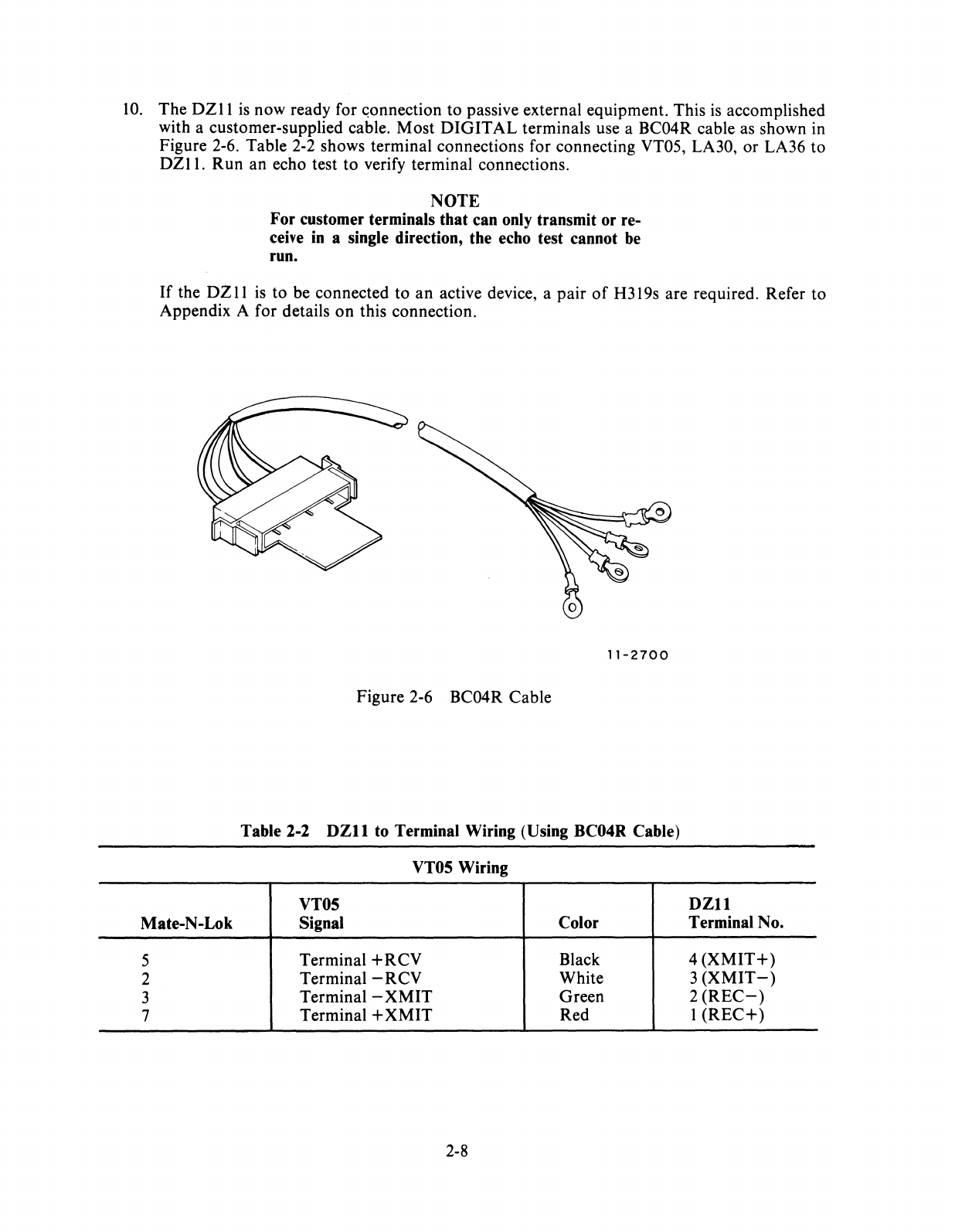
11-2700
Figure
2-6
BC04R Cable
Table 2-2
DZll
to Terminal Wiring (Using BC04R Cable)
VT05 Wiring
VT05
DZll
Mate-N-Lok Signal Color Terminal No.
5 Terminal
+RCV
Black 4
(XMIT+)
2 Terminal -RCV White 3
(XMIT-)
3 Terminal -
XMIT
Green 2
(REC-)
7 Terminal +
XMIT
Red 1
(REC+)
2-8
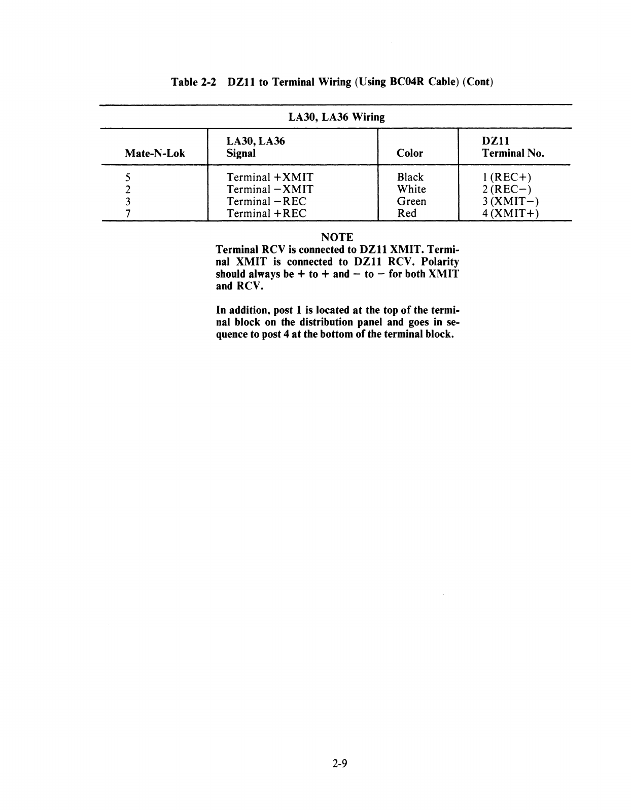
Table 2-2
DZll
to Terminal Wiring (Using BC04R Cable) (Cont)
Mate-N-Lok
5
2
3
7
LA30, LA36 Wiring
LA30,LA36
Signal Color
Terminal +
XMIT
Black
Terminal -
XMIT
White
Terminal -REC Green
Terminal + REC Red
NOTE
Terminal RCV
is
connected to
DZll
XMIT. Termi-
nal
XMIT
is connected to
DZll
RCV. Polarity
should always be + to + and -to -for both XMIT
and RCV.
In addition, post 1
is
located
at
the top
of
the termi-
nal block
on
the distribution panel and goes
in
se-
quence to post 4
at
the bottom of the terminal block.
2-9
DZll
Terminal No.
1
(REC+)
2
(REC-)
3
(XMIT-)
4
(XMIT+)

3.1
INTRODUCTION
CHAPTER 3
PROGRAMMING
This
chapter
provides basic information for
programming
the
DZII.
A description
of
each DZ11
register, its format,
programming
constraints,
and
bit functions are presented to aid programming
and
maintenance efforts. Special
programming
features
are
also presented in this chapter.
3.1.1. Device and Vector Address Assignments
The
DZ11
's
device
and
vector addresses are selected from the floating vector
and
device address space.
NOTE
The device floating address space is 1600108 to
1637768, The vector floating address space is 3008 to
7768,
Its floating address space follows the DJ11,
DHll,
DQl1,
DUll,
DUP11,
LK11,
and
DMCll.
Its floating vector space follows the
DCll;
KL11jDL11-A,
-B; DP11, DM11-A; DN11; DM11-BB
and
other
modem
control
vectors; DR11-A; DR11-C; PA611 reader, PA611 punch; DT11;
DXll;
DLll-C,
-D, -E; DJ11;
DHll;
GT40;
LPSll;
DQ11;
KWll-W;
DUll;
DUP11; DV11; LK11-A;
DWUN;
and
DMCII.
If
a
DZll
is installed in a system with any
of
the above listed options, then its
assigned vector and device address should follow the vector
and
device address
of
the other options.
Two examples follow. First, the simplest case where there
is
only one
DZII.
Option Address
GAP
160010
GAP
160020
GAP
160030
GAP
160040
GAP
160050
GAP
160060
GAP
160070
DZ11 160100
GAP
160110
Vector
300
3-1
Comment
No
DJ11s
No
DH11s
No
DQlls
No
DUlls
No
DUP11s
No
LKlls
NoDMC11s
No
more
DZ11s
Next, a system with one
DJll,
one
DHll,
one GT40, one
KWll-W,
and two
DZlls.
Option Address Vector Comment
DJll
160010 300
GAP
160020
No
more
DJlls
GAP
160030
DH
II must start on an address bound-
ary that
is
a mUltiple
of
20.
DHll
160040 310
160050
GAP
160060
No
more
DHlls
GT40 320 GT40 address
is
not in the floating ad-
dress space.
KWII-W
330
KWII-W
address
is
not in the floating
address space.
GAP
160070
No
DQlls
GAP
160100
No
DUlls
GAP
160110
No
DUPlls
GAP
160120
No
LKlls
GAP
160130
NoDMClls
DZII
160140 340
DZII
160150 350
GAP
160160
No
more
DZlls
3.2 REGISTER BIT ASSIGNMENTS
A comprehensive pictorial
of
all register bit assignments
is
shown in Figure 3-1. The four device
registers (DRO, DR2, DR4, and
DR6)
are subdivided to form six unique registers. This subdivision
is
accomplished
in
DR2
and
DR6 by assigning read-only (RO)
or
write-only (WO) status to each regis-
ter. Since the reading and writing
of
DR2
and
DR6
accesses two registers,
PDP-II
processor instruc-
tions that perform a read-modify-write
(DA
TIP) bus cycle cannot be used with D R2 or D R6. Also,
DR2
permits only word instructions,
but
either byte
or
word instructions may be used with DR6. DRO
and
DR4
have no programming constraints. In all register operations, the following applies: read-only
bits are not affected by an attempt to write, and write-only and
"not-used"
bits appear as a binary 0 if
a read operation
is
performed. Specific programming constraints for each register are discussed in the
following paragraphs. A description
of
each bit function
is
presented in Tables
3-1
through 3-3.
3.2.1 Control and Status Register (CSR)
The control
and
status register (CSR) contains the states
of
flags and enable bits for scanning, proces-
sor interrupts, clearing, and maintenance. The 16-bit
CSR
has no programming constraints. The for-
mat
is
depicted in Figure 3-1, and bit functions are described in Table 3-1. Write-only and
"not-used"
bits are read as zeros
by
the Unibus, and read-only bits are
not
affected by write attempts.
3-2
ORO
DR2
DR4
DR6
MSB
15
14 13
12
11
RO
RW
RO
RW
1---
1---
r----
----
~
CONTROL
&
STATUS
TROY
TIE
SA
SAE
~
(CSR)
~
RO RO
RO
RO
1----
1---
.
r----.
~----
t?i
RECEIVER
DATA
FRAM
PAR
BUFFER
VALID
OVRN
ERR ERR
(RBUF)
.$'
WO
WO
~
~
~
----
---
LINE
RX
PARAMETER
~
Q
ON
FREO
~
9
(LPR)
~
~':j
0
RW RW RW
RW
~~W
__
~---
--
1----
----
TRANSMIT
*
CONTROL
DTR DTR DTR DTR DTR
(TCR)
7 6 5 4 3
RO
RO
RO
RO RO
~---
r----
r-----
---
---
MODEM
*
STATUS
CO
CO CO
CO CO
(MSR)
7 6 5 4 3
WO
WO
WO WO WO
TRANSMIT
r----
---
t----
...
---
~---
DATA
BRK BRK
BRK BRK
BRK
(TOR)
7 6 5 4 3
10
09
~O_
_RO_
TLiNE TLiNE
C B
RO RO
--_.
RX RX
LINE
LINE
C B
WO
WO
FREO FREO
C B
RW
RW
--
DTR
DTR
2 1
RO
RO
---
--
CO CO
2 1
WO WO
~--
~--
BRK BRK
2 1
BYTES
HIGH
LOW
08
07
RO
RO_
--
TLiNE
~DONE
A
RO RO
r----
---
RX
LINE
RBUF
A 07
WO WO
---
---
ODD
FREO
PAR
A
RW
j1W
__
DTR
LINE
0
ENAB
7
RO RO
--
--
CO
RI7
0
WO WO
----
--
BRK
TBUF
0 7
06
RW
---
RIE
RO
---
RBUF
06
WO
---
PAR
ENAB
RW
LINE'
ENAB
6
RO
~--
RI6
WO
1----
TBUF
6
*The
high
byte
of
the
TCR
(Data
Terminal
Ready)
and
the
MSR
are
not
used
with
the
20
mA
options.
LSB
05 04
03
02
01
00
RW RW
RW
1,1
---
---
~---
trf
~
~ Q
~Q
~
Q
MSE
CLR
MAINT
~ ~ ~
~ ~ ~
RO RO RO
RO
RO
RO
---
----
----
---
---
~----
RBUF
RBUF RBUF RBUF RBUF
RBUF
05 04
03 02
01
DO
WO
WO
WO WO WO WO
---
----
----
----
~---
---
STOP
CHAR
CHAR
CODE
LGTH
LGTH
LINE LINE
LINE
B A C B A
RW RW
~'---
I-~--
_ R1f_ I-Rl! _
~R1f
__
LINE
LINE LINE
LINE
LINE
LINE
ENAB
ENAB
ENAB
ENAB
ENAB ENAB
5 4 3 2 1 0
RO
RO
RO RO
RO
RO
~--
---
t-----
t----
t--_.
t----
RI5 RI4 RI3 RI2
RI1
RIO
WO
WO WO
WO
WO
WO
---
----
r-
-
---
1----
~--
...
---
TBUF TBUF
TBUF TBUF TBUF TBUF
5 4 3 2 1 0
11-5313
Figure
3-1
Register Bit Assignments
3-3

Bit
00-02
03
04
05
06
07
08-10
11
12
Table 3-1 CSR Bit Functions
Title
Not
used
Maintenance
(MAINT)
Clear (CLR)
Master Scan Enable
Receiver
Interrupt
Enable
Receiver
Done
(RDONE)
Transmit Line
A-C
(TUNE)
Not
used
Silo Alarm Enable (SAE)
Function
A
read/write
bit that, when set, causes the serial
output
data
from the transmitter to be fed back as
serial input
data
to
the receiver. All lines are turned
around. Cleared by BUS
INIT
and
CLR.
A read/write bit
that
fires a one-shot to generate a
15
JlS
reset which clears the receiver silo, all
UARTs, and the CSR. After a
CLR
is
issued, the
CSR
and line parameters must be set again.
CLR
in progress
is
indicated by
CLR
=
1.
Modem con-
trol registers are
not
affected,
nor
are bits 00
through
14
of
RBUF.
A read/write
bit
that activates the scanner to en-
able the receiver transmitter and silo. Cleared by
CLR
and
BUS
INIT.
A
read/write
bit
that
enables the receiver interrupt.
Cleared by
CLR
and BUS
INIT.
A read-only bit (hardware set)
that
generates RCV
INT
if
bit 06 = 1
and
bit
12
=
O.
The bit clears
when the
RBUF
is
read
and
resets when another
word reaches the
output
of
the silo (RBUF).
If
bit
06 = 0,
RDONE
can be used as a flag to indicate
that
the silo contains a character.
If
bit
12
=
1,
RDONE
does
not
cause interrupts
but
otherwise
acts the same.
When bit
15
=
1,
these three read-only bits indicate
the line
that
is
ready
to
transmit a character. Bit
15
clears when the character
is
loaded into the trans-
mit buffer,
but
sets again if another line
is
ready. A
new line number could appear within a minimum
of
1.9
JlS.
Bits 08-10 return
to
line 0 after a
CLR
or
BUS
INIT.
These bits are meaningful only when
bit
15
(TRDY)
is
true.
A
read/write
bit
that
enables the silo alarm and
prevents
RDONE
from causing interrupts.
If
bit 06
=
1,
the SAE allows the SA (bit
13)
to
cause an
interrupt after
16
entries in the silo.
If
bit 06 = 0,
the SA can be used as a flag. The bit
is
cleared by
CLR
and
BUS
INIT.
3-5
Bit
13
14
15
Table 3-1 CSR Bit Functions (Cont)
Title
Silo Alarm (SA)
Transmitter Interrupt Enable
(TIE)
Transmitter Ready (TROY)
Function
A read-only bit set by the hardware after
16
char-
acters enter the silo.
It
causes an interrupt if bit
06
= 1 and
is
cleared by CLR, BUS INIT, and read-
ing the RBUF. When the silo flag occurs (SA = I),
the silo must be emptied because the flag will not
be set again until
16
additional characters enter the
silo.
A read/write bit that allows an interrupt if bit
15
(TROY) =
1.
A read-only bit that
is
set by hardware when a line
number
is
found
that
has its transmit buffer empty
and its
LINE
ENAB bit set.
It
is
cleared by CLR,
BUS INIT, and by loading the
TBUF
register.
3.2.2 Receiver Buffer (RBUF)
The receiver buffer (RBUF) register contains the received character bits, with line identification, error
status, and data validity flag. As one
of
two registers in
OR2
(RBUF
and LPR),
RBUF
is
accessed
when a read operation
is
performed (write operation accesses the LPR). The programming constraints
for the
RBUF
register are as follows.
I. Byte instructions cannot be used.
2.
It
is
a read-only register.
3.
TST or BIT instructions cannot be used because they cause the loss
of
a character.
4.
The register requires master scan enable (CSR, bit 05) to be set in order to be functional.
When this bit
is
off, bits 00 to
14
of
the
RBUF
become invalid regardless
of
the state
of
bit
15
(data valid) and the silo is held empty. The register format
of
RBUF
is
depicted
in
Figure
3-1
and bit functions are described in Table 3-2. Each reading
of
the
RBUF
register ad-
vances the silo and presents the next character to the program. Bits
00
through
14
do not go
to zero after a
CLR
or
BUS INIT; however, they become invalid and the silo
is
emptied. Bit
15
(data valid) does clear
to
zero. (See Table 3-2.)
3-6
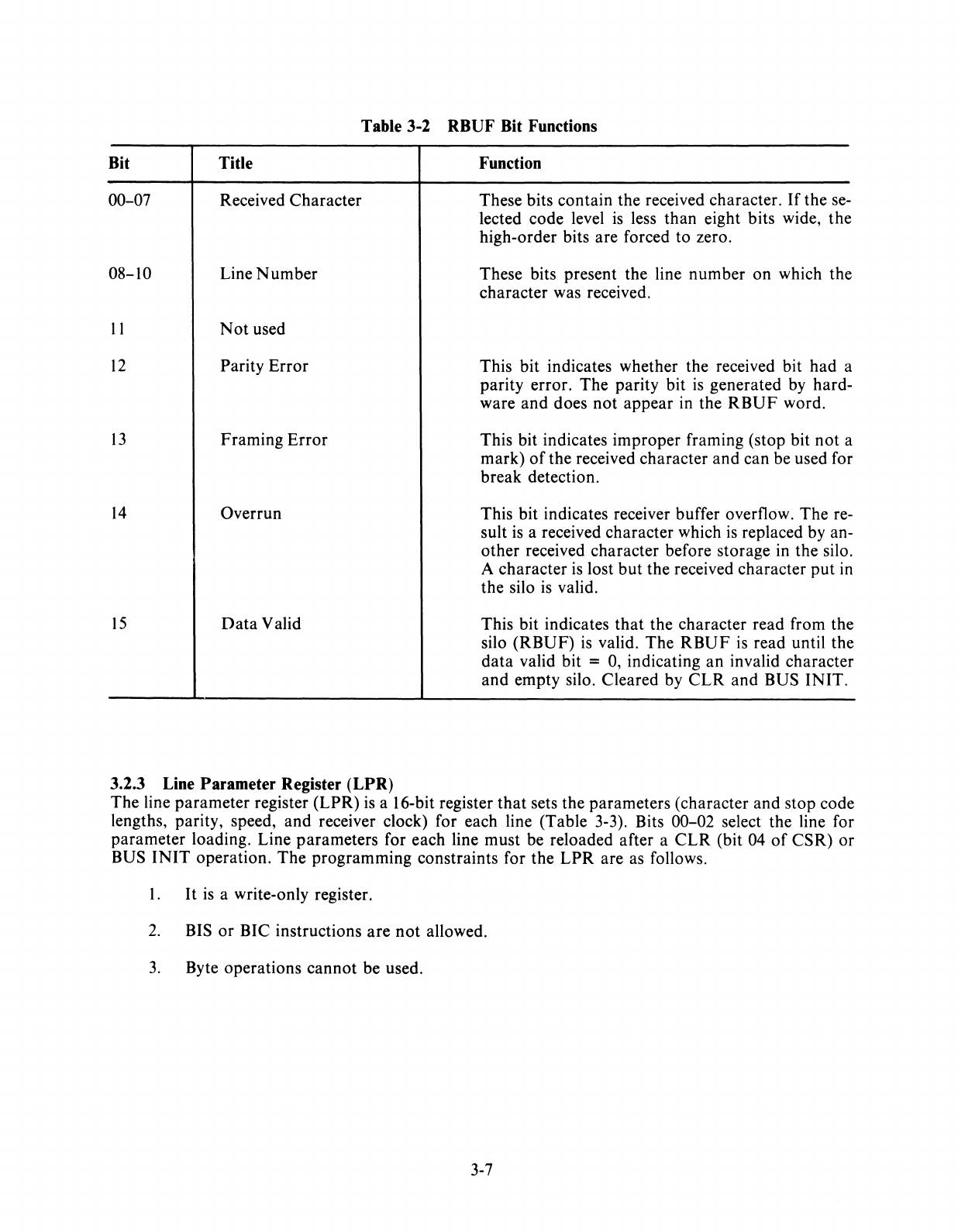
Table 3-2 RBUF Bit Functions
Bit Title
00-07 Received Character
08-10 Line
Number
11
Not
used
12
Parity
Error
13
Framing
Error
14
Overrun
15
Data
Valid
3.2.3 Line Parameter Register
(LPR)
Function
These bits contain the received character.
If
the se-
lected code level
is
less than eight bits wide,
the
high-order bits are forced to zero.
These bits present the line number on which the
character was received.
This bit indicates whether the received bit
had
a
parity error.
The
parity bit
is
generated
by
hard-
ware
and
does
not
appear in the
RBUF
word.
This bit indicates improper framing (stop bit
not
a
mark)
of
the received character
and
can be used for
break detection.
This bit indicates receiver buffer overflow. The re-
sult
is
a received character which
is
replaced by an-
other received character before storage in the silo.
A character
is
lost
but
the received character
put
in
the silo is valid.
This bit indicates
that
the character read from the
silo
(RBUF)
is
valid. The
RBUF
is
read until the
data
valid bit = 0, indicating
an
invalid character
and
empty silo. Cleared by
CLR
and BUS
INIT.
The line parameter register (LPR)
is
a 16-bit register
that
sets the parameters (character and stop code
lengths, parity, speed, and receiver clock) for each line (Table 3-3). Bits 00-02 select the line for
parameter loading. Line parameters for each line must be reloaded after a
CLR
(bit 04
of
CSR)
or
BUS
INIT
operation.
The
programming constraints for the
LPR
are as follows.
1.
It
is
a write-only register.
2.
BIS
or
BIC instructions
are
not
allowed.
3.
Byte operations
cannot
be used.
3-7
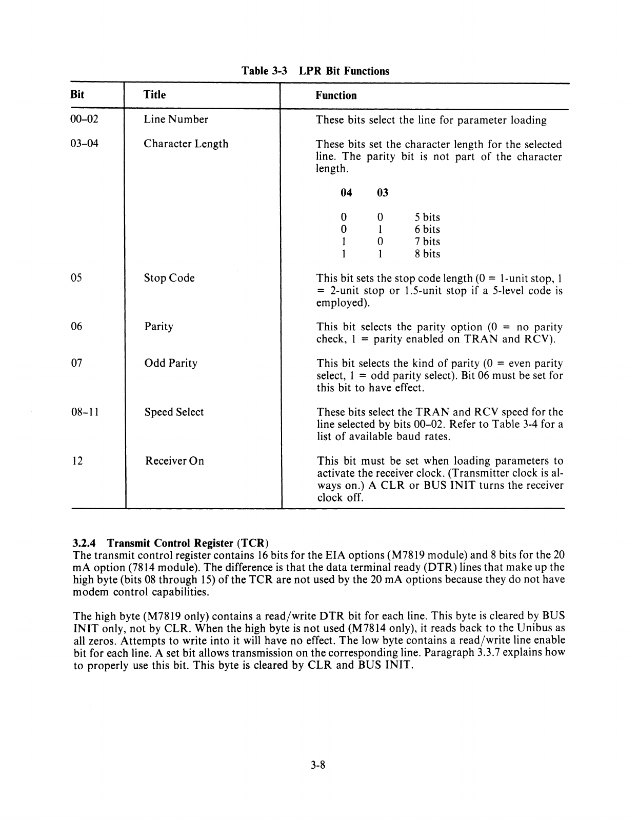
Table 3-3
LPR
Bit Functions
Bit Title
00-02 Line
Number
03-04 Character Length
05
Stop
Code
06 Parity
07
Odd
Parity
08-11 Speed Select
12
Receiver
On
3.2.4 Transmit Control Register (TCR)
Function
These bits select the line for parameter loading
These bits set the character length for
the
selected
line.
The
parity bit
is
not
part
of
the character
length.
04 03
0 0 5 bits
0 1 6 bits
1 0 7 bits
1 1 8 bits
This bit sets the stop code length (0 = I-unit stop, 1
= 2-unit stop
or
1.5-unit stop if a 5-level code
is
employed).
This bit selects the parity option
(0
= no parity
check, 1 = parity enabled on
TRAN
and RCV).
This bit selects the kind
of
parity (0 = even parity
select, 1 =
odd
parity select). Bit 06 must be set for
this bit to have effect.
These bits select the
TRAN
and
RCV speed for the
line selected by bits 00-02. Refer to Table 3-4 for a
list
of
available baud rates.
This bit must be set when loading parameters to
activate the receiver clock. (Transmitter clock
is
al-
ways on.) A
CLR
or
BUS
INIT
turns the receiver
clock off.
The transmit control register contains
16
bits for the
EIA
options (M7819 module) and 8 bits for the
20
rnA option (7814 module).
The
difference is
that
the
data
terminal ready
(DTR)
lines
that
make up the
high byte (bits
08
through
15)
of
the
TCR
are
not
used by the 20 rnA options because they do not have
modem control capabilities.
The
high byte (M7819 only) contains a
read/write
DTR
bit for each line. This byte
is
cleared by BUS
INIT
only,
not
by
CLR.
When the high byte
is
not
used (M7814 only), it reads back to the Unibus as
all zeros. Attempts to write into it will have no effect.
The
low byte contains a
read/write
line enable
bit for each line. A set bit allows transmission
on
the corresponding line.
Paragraph
3.3.7 explains how
to properly use this bit. This byte
is
cleared by
CLR
and
BUS
INIT.
3-8
3.2.5 Modem Status Register (MSR)
This
is
a 16-bit register used only with the EIA options (M7819 module).
The
20 rnA options (M7814
module) do
not
have modem control capabilities. When
not
used, this register reads all zeros to the
Unibus.
The
MSR
consists
of
two bytes: the low byte (bits 00-07) and the high byte (bits 08-15).
The
low byte
monitors the state
of
each line's ring indicator (RI) lead; the high byte monitors the state
of
each line's
carrier (CO) lead.
The
MSR
is the read-only portion
of
DR6
and
has the following programming
characteristics.
l.
It
is
a read-only register.
2.
CLR
and BUS
INIT
have
no
effect.
3.
Bit format
is
shown in Figure 3-1.
3.2.6 Transmit Data Register (TDR)
The
TDR
consists
of
two 8-bit bytes. The low byte
is
the transmit buffer
(TBUF)
and holds the
character
that
is
to be transmitted.
The
high byte
is
the break register with each line controlled by an
individual bit. When a break bit
is
set, the line associated with
that
bit starts sending zeros immediately
and continuously. The
TDR
is the write-only portion
of
DR6
and
has the following programming
characteristics.
l.
It
is
a write-only register.
2.
BIS
or
BIC instructions
cannot
be used.
3.
For
character lengths less
than
8 bits,
the
character loaded into the
TBUF
must be right
justified because the hardware forces the most significant bits to zero.
4.
The break register has no effect when running in the maintenance mode (i.e.,
CSR
bit
03
=
1
).
5.
It
is
cleared by
CLR
and BUS
INIT.
6.
Bit format is shown in Figure 3-1.
3.3 PROGRAMMING FEATURES
The
DZII
has several programming features
that
allow control
of
baud
rate, character length, stop
bits, parity, and interrupts. This section discusses the application
of
these controls to achieve the
desired operating parameters.
3.3.1 Baud Rate
The
selection
of
the desired transmission
and
reception speed is controlled by the conditions
of
bits
08
through
11
of
the LPR. Table 3-4 depicts the required bit configuration for each operating speed. The
baud rate for each line
is
the same for both the transmitter
and
receiver. The receiver clock is turned
on
and
off by setting and clearing bit
12
in the
LPR
for
the
selected line.
3-9
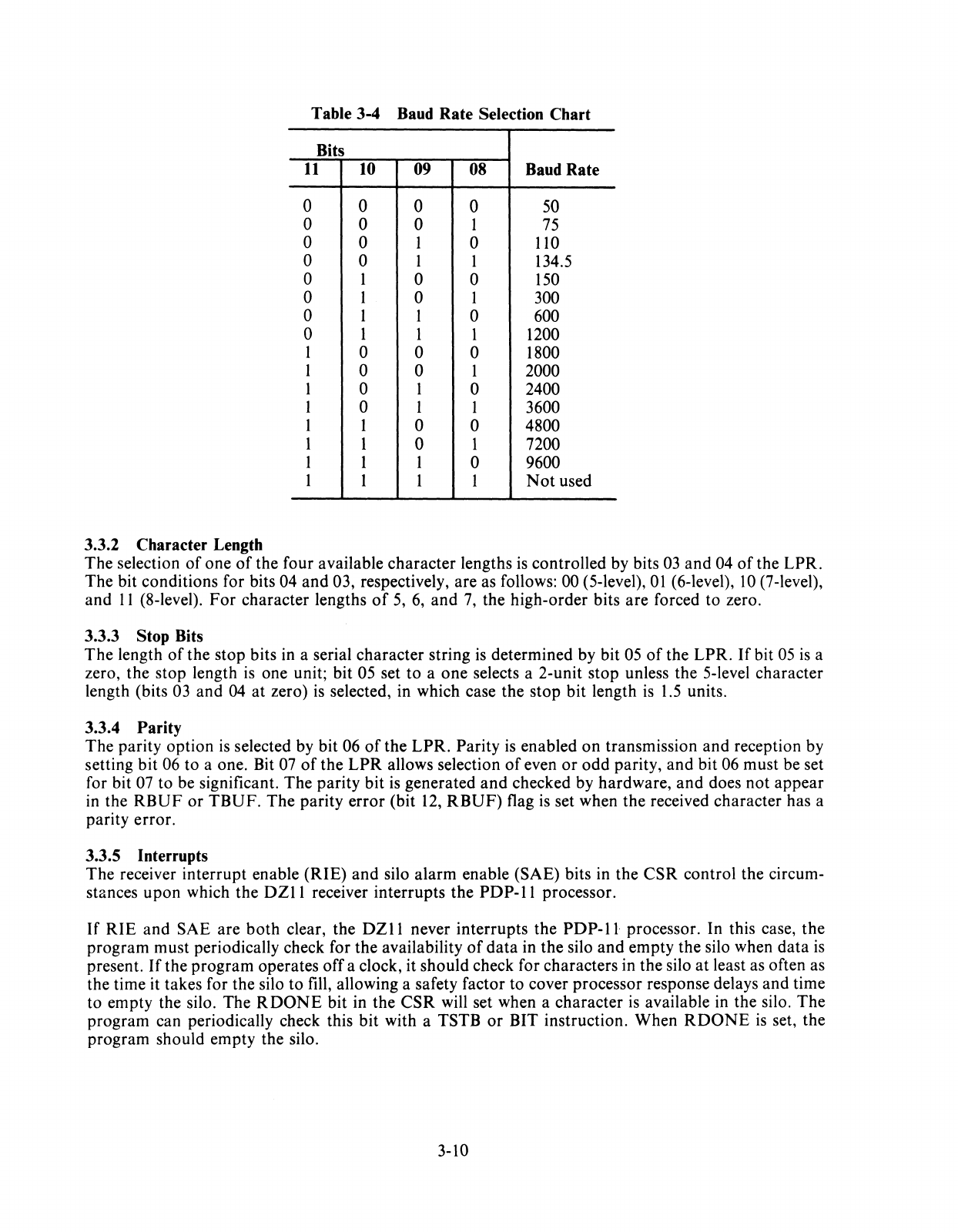
Table 3-4 Baud Rate Selection Chart
Bits
11
10 09 08 Baud Rate
0 0 0 0 50
0 0 0 1
75
0 0 1 0
110
0 0 1 1 134.5
0 1 0 0
150
0 1 0 1 300
0 1 1 0 600
0 1 1 1 1200
1 0 0 0 1800
1 0 0 1 2000
1 0 1 0 2400
1 0 1 1 3600
1 1 0 0 4800
1 1 0 1 7200
1 1 1 0 9600
1 1 1 1
Not
used
3.3.2 Character Length
The selection
of
one
of
the four available character lengths
is
controlled by bits
03
and 04
of
the LPR.
The bit conditions for bits 04 and 03, respectively, are as follows: 00 (5-level),
01
(6-level),
10
(7-level),
and
11
(8-level).
For
character lengths
of
5,
6,
and
7,
the high-order bits are forced
to
zero.
3.3.3 Stop Bits
The
length
of
the stop bits in a serial character string
is
determined by bit
05
of
the LPR.
If
bit
05
is
a
zero, the stop length
is
one unit; bit 05 set
to
a one selects a 2-unit stop unless the 5-level character
length (bits
03
and 04
at
zero)
is
selected, in which case the stop bit length
is
1.5
units.
3.3.4 Parity
The parity option
is
selected by bit 06
of
the
LPR.
Parity
is
enabled
on
transmission and reception by
setting
bit
06
to
a one. Bit
07
of
the
LPR
allows selection
of
even
or
odd
parity,
and
bit 06 must be set
for bit
07
to be significant. The parity bit
is
generated
and
checked by hardware,
and
does
not
appear
in the
RBUF
or
TBUF.
The parity error (bit
12,
RBUF)
flag
is
set when the received character has a
parity error.
3.3.5 Interrupts
The receiver interrupt enable (RIE)
and
silo alarm enable (SAE) bits in the
CSR
control the circum-
stances
upon
which the
DZII
receiver interrupts the
PDP-II
processor.
If
RIE
and SAE are
both
clear, the
DZll
never interrupts the
PDP-ll
processor. In this case,
the
program must periodically check for the availability
of
data
in the silo
and
empty the silo when
data
is
present.
If
the program operates off a clock, it should check for characters in the silo
at
least as often as
the time it takes for the silo
to
fill, allowing a safety factor to cover processor response delays and time
to
empty the silo. The
RDONE
bit in the
CSR
will set when a character
is
available in the silo. The
program can periodically check this bit with a TSTB
or
BIT instruction. When
RDONE
is
set, the
program should empty the silo.
3-10
If
RIE
is set
and
SAE
is
clear,
the
DZII
will
interrupt
the
PDP-II
processor
to
the
DZII
receiver
vector address when
RDONE
is
set, indicating the presence
of
a
character
at
the
bottom
of
the
silo.
The
interrupt
service routine can
obtain
the
character
by performing a
MOV
instruction from the
RBUF.
If
the
program
then dismisses
the
interrupt,
the
DZII
will
interrupt
when
another
character
is
available (which may be immediately
if
additional
characters were placed in the silo while the
interrupt
was being serviced). Alternatively,
the
interrupt
service
routine
may
respond
to
the
interrupt
by empty-
ing the silo before dismissing
the
interrupt.
If
RIE
and
SAE
are
both
set, the
DZII
will
interrupt
the
PDP-II
processor
to the
DZII
receiver
vector when
the
silo
alarm
(SA) bit in
the
CSR
is
set.
The
SA
bit
will be set when
16
characters
have
been placed
in
the
silo since
the
last
time
the
program
has accessed
the
RBUF.
Accessing
the
RBUF
will clear the SA bit
and
the associated
counter.
The
program
should
follow
the
procedure
described in
Paragraph
3.3.6
to
empty
the silo completely in response
to
a silo
alarm
interrupt.
This will ensure
that
any characters placed in
the
silo while it
is
being
emptied
are
processed by
the
program.
NOTE
If
the program processes only 16 entries in response
to each silo
alarm
interrupt, characters coming
in
while interrupts
are
being processed will build up
without being counted by the silo alarm circuit and
the silo may eventually overflow without the
alarm
being issued.
If
the
silo
alarm
interrupt
is used,
the
program
will
not
be
interrupted
if
fewer
than
16
characters are
received. In
order
to
respond
to
short
messages
during
periods
of
moderate
activity, the
PDP-II
program
should
periodically
empty
the
silo.
The
scanning period will
depend
on
the
required respon-
siveness
to
received characters. While
the
program
is emptying
the
silo, it
should
ensure
that
DZII
receiver
interrupts
are
inhibited. This
should
be
done
by raising the
PDP-II
processor priority.
The
silo
alarm
interrupt
feature can significantly reduce the
PDP-II
processor
overhead
required by
the
DZII
receiver by eliminating the need
to
enter
and
exit
an
interrupt
service
routine
each time a charac-
ter
is
received.
The
transmitter
interrupt
enable bit
(TIE)
controls
transmitter
interrupts
to
the
PDP-II
processor.
If
enabled, the
DZ
II
will
interrupt
the
PD
P-II
processor
to
the
DZ
II
transmitter
interrupt
vector when
the
transmitter
ready
(TRDY)
bit in
the
CSR
is set, indicating
that
the
DZII
is
ready
to
accept a
character
to
be
transmitted.
3.3.6 Emptying the Silo
The
program
can
empty
the
silo by repeatedly
performing
MOV
instructions from the
RBUF
to
temporary
storage. Each
MOV
instruction
will
copy
the
bottom
character
in the silo so it will
not
be
lost
and
will clear
out
the
bottom
of
the
silo, allowing
the
next
character
to
move down for access by a
subsequent
MOV
instruction.
The
program
can
determine
when it
has
emptied
the
silo by testing
the
data
valid bit in each
word
moved
out
of
the
RBUF.
A zero value indicates
that
the silo
has
been
emptied.
The
test
can
be
performed
conveniently by
branching
on
the
condition
code following each
MOV
instruction. A
TST
or
BIT instruction
must
not
access
the
RBUF
because these instructions will
cause
the
next entry in the silo
to
move
down
without
saving
the
current
bottom
character.
Further-
more, following a
MOV
from
the
RBUF,
the next
character
in
the
silo will
not
be available for
at
least
1 JlS. Therefore,
on
fast
CPUs,
the
program
must
use sufficient instructions
or
NOPs
to
ensure
that
successive
MOVs
from the
RBUF
are
separated
by
a
minimum
of
I JlS. This will prevent a false
indication
of
an
empty
silo.
3-11
3.3.7 Transmitting a Character
The program controls the
DZII
transmitter through five registers
on
the Unibus: the control
and
status register (CSR), the line parameter register (LPR), the line enable register, the transmitter buffer
(TBUF),
and
the break register (BRK).
Following
DZll
initialization, the
program
must use the
LPR
to
specify the speed
and
character
format for each line
to
be used and must set the master scan enable (MSE) bit in the CSR.
The
program should set the transmitter interrupt enable (TIE) bit in the
CSR
if
it wants the
DZII
trans-
mitter to operate
on
a program interrupt basis.
The
line enable register
is
used
to
enable
and
disable transmission
on
each line. One
bit
in this 8-bit
register
is
associated with each line.
The
program
can set
and
clear bits by using MOV, MOVB, BIS,
BISB, BIC,
and
BICB instructions. (If
word
instructions are used,
the
line enable register
and
the
DTR
registers
on
M7819 modules
are
simultaneously accessed.)
The
DZII
transmitter
is
controlled by a scanner which
is
constantly looking for an enabled line (line
enable bit set) which has
an
empty
UART
transmitter buffer. When the scanner finds such a line, it
loads the number
of
the line into the 3-bit transmit line
number
(TUNE)
field
of
the
CSR
and sets the
TRDY
bit, interrupting the
PDP-II
processor if the
TIE
bit is set.
The
program
can clear the
TRDY
bit by moving a character for the indicated line into the
TBUF
or
by clearing the line enable bit.
Clearing the
TRDY
bit frees the scanner to resume its search for lines needing service.
To
initiate transmission on an idle line, the
program
should set the
TCR
bit for
that
line
and
wait for
the scanner to request service
on
the line, as indicated by the scanner loading the number
of
the line
into
TUNE
and
setting
TRDY.
The program should then load the character to be transmitted into the
TBUF
by using a MOVB instruction. If interrupts are to be used, a convenient way
of
starting up a line
is
to
set the
TCR
bit in the main program
and
let the
normal
transmitter interrupt routine load the
character into the
TBUF.
NOTE
The scanner may find a different line needing service
before it finds the line being started up. This will oc-
cur
if
other lines request service before the scanner
can find the line being started. The program must
always check the
TLINE
field
of
the
CSR
when re-
sponding to
TRDY
to ensure it loads characters for
the correct line. Assuming the program services lines
as requested by the scanner, the scanner will eventu-
ally find the line being started.
If
several lines require
service, the scanner will request service in priority
order as determined by line number. Line 7 has the
highest priority and line 0 the lowest.
To
continue transmission
on
a line, the
program
should load the next character
to
be transmitted into
the
TBUF
each time
the
scanner requests service for the line as indicated by
TUNE
and
TRDY.
To
terminate transmission
on
a line, the program loads the last character normally
and
waits for the
scanner
to
request an additional character for the line.
The
program
clears the line enable bit
at
this
time instead
of
loading the
TBUF.
3-12
The normal rest condition
of
the transmitted
data
lead for any line
is
the 1 state. The break register
(BRK)
is
used to apply a continuous zero signal
to
the line. One bit in this 8-bit register
is
associated
with each line.
The
line will remain in this condition as long
as
the bit remains set. The program should
use a MOVB instruction to access the
BRK
register.
If
the program continues to load characters for a
line after setting the break bit, transmitter operation will appear normal to the program despite the fact
that no characters can be transmitted while the line
is
in the continuous zero sending state. The pro-
gram may use this facility for sending precisely timed zero signals by setting the break bit and using
transmit ready interrupts as a timer.
It
should be remembered
that
each line in the
DZII
is
double buffered. The program must
not
set the
BRK
bit
too
soon
or
the two data characters preceding the break may not be transmitted. The pro-
gram must also ensure
that
the line returns to the 1 state at the end
of
the zero sending period before
transmitting any additional
data
characters. The following procedure will accomplish this. When the
scanner requests service the first time after the program has loaded the last
data
character, the program
should load an all-zero character. When the scanner requests service the second time, the program
should set the
BRK
bit for the line.
At
the end
of
the zero sending period, the program should load an
all-zero character to be transmitted. When the scanner requests service, indicating this character has
begun transmission, the program should clear the
BRK
bit and load the next
data
character.
3.3.8 Data Set Control
DZ
11
models with EIA interfaces include
data
set control as a standard feature. The program may
sense the state
of
the carrier and ring indicator signals from each
data
set and may control the state
of
the
data
terminal ready signal to each data set. The program uses three 8-bit registers to access the
DZ
11
data
set control logic. One bit in each register
is
associated with each
of
the eight lines. There are
no hardware interlocks between the
data
set control logic and the receiver and transmitter logic. Any
required coordination should be done under program control.
The
data
terminal ready
(DTR)
register
is
a read/write register. Setting
or
clearing a bit in this register
will turn the appropriate
DTR
signal on
or
off. The program may access this register with word
or
byte
instructions.
(If
word instructions are used, the
DTR
and line enable registers will be simultaneously
accessed.) The
DTR
register
is
cleared by the
INIT
signal on the Unibus
but
is
not cleared if the
program clears the
DZII
by setting the
CLR
bit
of
the CSR.
The carrier register (CAR) and ring register
(RING)
are read-only registers. The program can deter-
mine the current state
of
the carrier signal for a line by examining the appropriate bit
of
the
CAR
register. It can determine the current state
of
the ring signal by examining the appropriate bit
of
the
ring register. The program can examine these registers separately by using MOVB or BITB instruc-
tions
or
can examine them as a single 16-bit register by using MOV
or
BIT instructions. The
DZl1
data
set control logic does
not
interrupt the
PDP-II
processor when a carrier
or
ring signal changes
state.
The
program should periodically sample these registers to determine the current status. Sam-
pling at a high rate
is
not
necessary.
3.4 PROGRAMMING EXAMPLES
The
following
six
examples are sample programs for the
DZl1
option. These examples are presented
only to indicate how the
DZII
can be used.
3-13
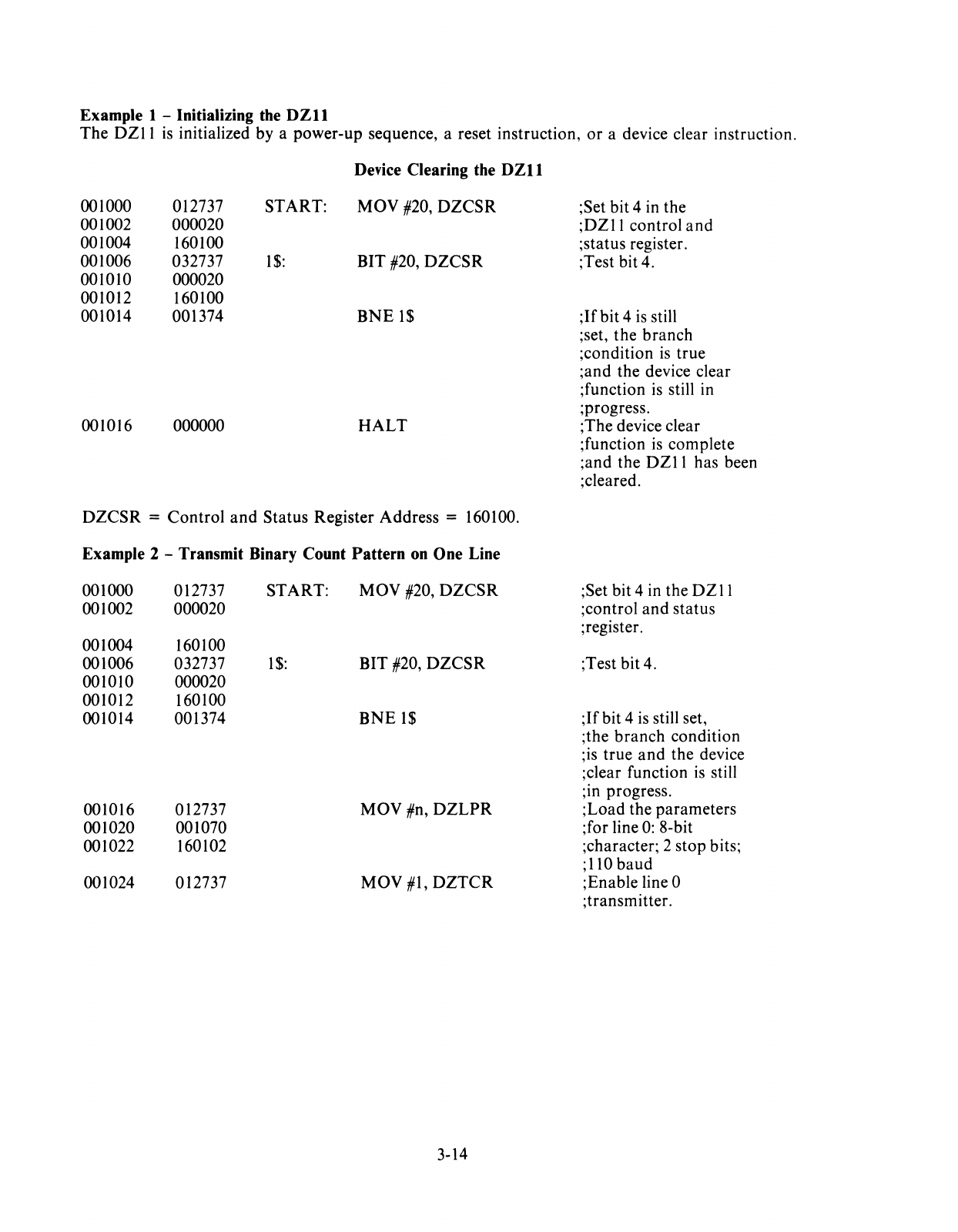
Example 1 - Initializing the
DZll
The DZ11
is
initialized by a power-up sequence, a reset instruction,
or
a device clear instruction.
Device Clearing the
DZll
001000 012737 START:
May
#20,
DZCSR
001002 000020
001004 160100
001006 032737
1$:
BIT #20,
DZCSR
001010 000020
001012 160100
001014 001374
BNE
1$
001016 000000
HALT
DZCSR
=
Control
and
Status Register Address = 160100.
Example 2 - Transmit Binary Count Pattern
on
One Line
001000
001002
001004
001006
001010
001012
001014
001016
001020
001022
001024
012737
000020
160100
032737
000020
160100
001374
012737
001070
160102
012737
START:
May
#20,
DZCSR
1$:
BIT #20,
DZCSR
BNE
1$
May
#n,
DZLPR
May
#1,
DZTCR
3-14
;Set bit 4 in the
;DZ11 control
and
;status register.
;Test bit 4.
;If
bit 4
is
still
;set, the branch
;condition
is
true
;and the device clear
;function
is
still in
;progress.
;The device clear
;function
is
complete
;and the DZ11 has been
;cleared.
;Set bit 4 in the
DZII
;control and status
;register.
;Test bit 4.
;If
bit 4
is
still set,
;the
branch
condition
;is true
and
the device
;clear function
is
still
;10
progress.
;Load the parameters
;for line
0:
8-bit
;character; 2 stop bits;
;110
baud
;Enable line 0
;transmitter.
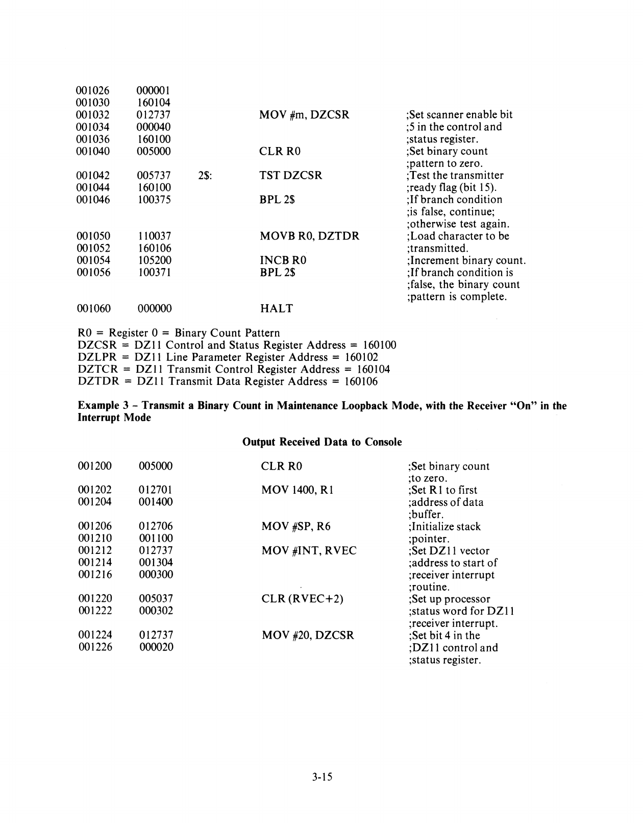
001026 000001
001030 160104
001032 012737 MOV #m,
DZCSR
001034 000040
001036 160100
001040 005000
CLRRO
001042 005737
2$:
TSTDZCSR
001044 160100
001046 100375
BPL2$
001050 110037 MOVB
RO,
DZTDR
001052 160106
001054 105200
INCBRO
001056
100371
BPL2$
001060 000000
HALT
RO
= Register 0 = Binary
Count
Pattern
DZCSR
=
DZll
Control
and
Status Register Address = 160100
DZLPR
=
DZII
Line Parameter Register Address = 160102
DZTCR
=
DZ
11
Transmit Control Register Address =
160
I 04
DZTDR
=
DZII
Transmit
Data
Register Address = 160106
;Set scanner enable bit
;5
in the control
and
;status register.
;Set binary count
;pattern to zero.
;Test the transmitter
;ready flag (bit
15).
;If
branch condition
;is false, continue;
;otherwise test again.
;Load character to be
;transmitted.
;Increment binary count.
;If
branch condition
is
;false, the binary
count
;pattern
is
complete.
Example 3 - Transmit a Binary Count
in
Maintenance Loopback Mode, with the Receiver
"On"
in
the
Interrupt Mode
Output Received
Data
to
Console
001200 005000
CLRRO
;Set binary count
;to zero.
001202 012701 MOV 1400,
Rl
;Set R 1 to first
001204 001400 ;address
of
data
;buffer.
001206 012706
MOV#SP,R6
;Initialize stack
001210 001100 ;pointer.
001212 012737 MOV #INT, RVEC ;Set
DZII
vector
001214 001304 ;address to start
of
001216 000300 ;receiver interrupt
;routine.
001220 005037
CLR
(RVEC+2)
;Set up processor
001222 000302 ;status word for
DZll
;receiver interrupt.
001224 012737 MOV #20,
DZCSR
;Set bit 4 in the
001226 000020
;DZll
control
and
;status register.
3-15
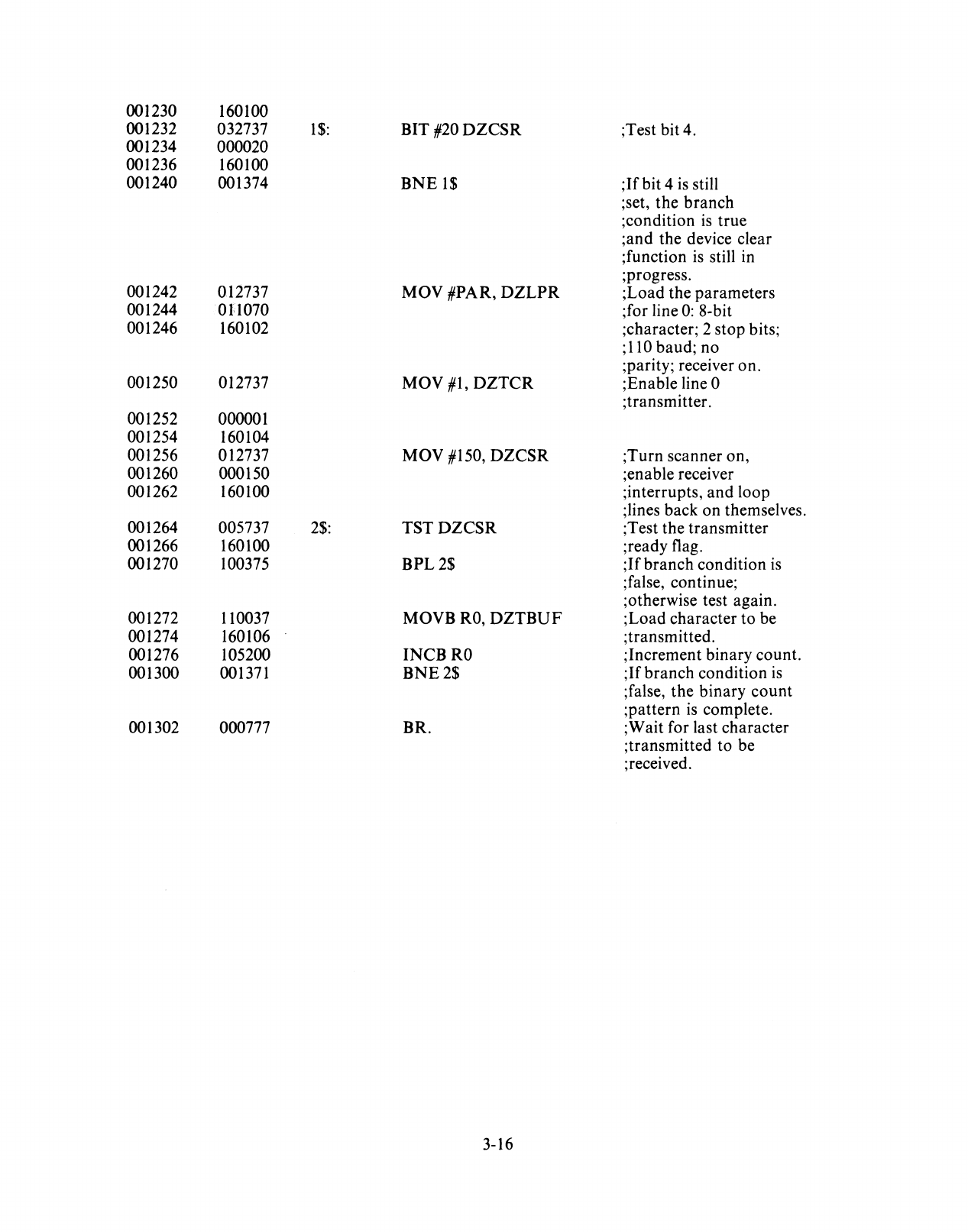
001230 160100
001232 032737
1$:
BIT #20
DZCSR
;Test
bit4.
001234 000020
001236 160100
001240 001374
BNE
1$
;If
bit 4
is
still
;set, the branch
;condition
is
true
;and the device clear
;function
is
still in
;progress.
001242 012737 MOV #PAR,
DZLPR
;Load the parameters
001244
On070
;for line
0:
8-bit
001246 160102 ;character; 2 stop bits;
;110 baud; no
;parity; receiver on.
001250 012737 MOV
#1,
DZTCR
;Enable line 0
;transmitter.
001252 000001
001254 160104
001256 012737 MOV #150,
DZCSR
;Turn scanner on,
001260 000150 ;enable receiver
001262 160100 ;interrupts, and loop
;lines back on themselves.
001264 005737
2$:
TSTDZCSR
;Test the transmitter
001266 160100 ;ready flag.
001270 100375
BPL2$
;If
branch condition
is
;false, continue;
;otherwise test again.
001272 110037 MOVB
RO,
DZTBUF
;Load character to be
001274 160106 ;transmitted.
001276 105200
INCBRO
;Increment binary count.
001300 001371
BNE2$
;If
branch condition
is
;false,
the
binary
count
;pattern
is
complete.
001302 000777 BR. ;Wait for last character
;transmitted to be
;received.
3-16
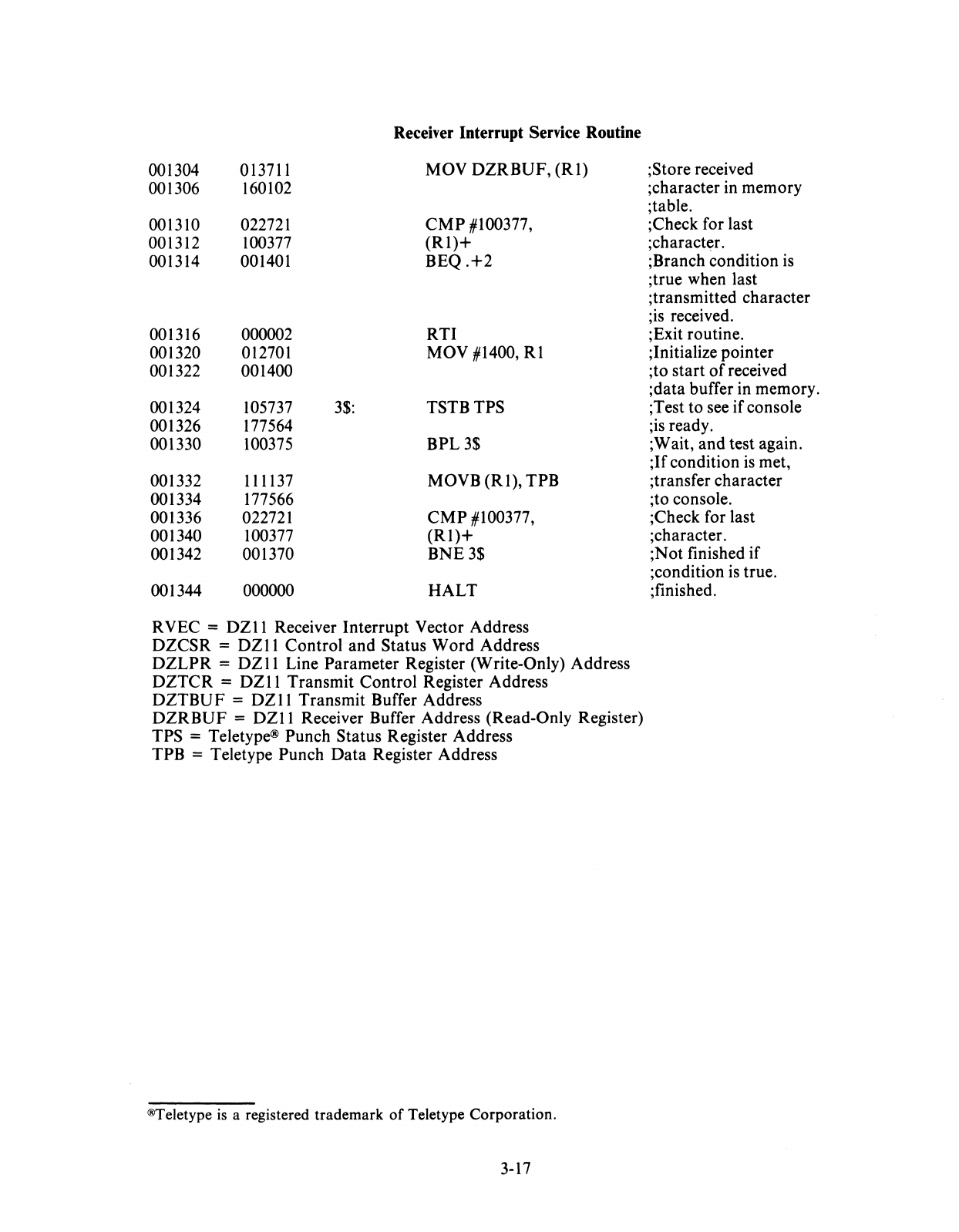
Receiver Interrupt Service Routine
001304 013711 MOV
DZRBUF,
(RI)
001306 160102
001310 022721
CMP
#100377,
001312 100377
(Rl)+
001314 001401
BEQ.+2
001316 000002
RTI
001320 012701 MOV #1400,
Rl
001322 001400
001324 105737
3$:
TSTBTPS
001326 177564
001330 100375
BPL3$
001332 111137 MOVB
(RI),
TPB
001334 177566
001336 022721
CMP
#100377,
001340 100377
(RI)+
001342 001370
BNE3$
001344 000000
HALT
RVEC =
DZII
Receiver Interrupt Vector Address
DZCSR
=
DZII
Control and Status
Word
Address
DZLPR
=
DZII
Line Parameter Register (Write-Only) Address
DZTCR
=
DZII
Transmit Control Register Address
DZTBUF
=
DZ
II Transmit Buffer Address
DZRBUF
=
DZII
Receiver Buffer Address (Read-Only Register)
TPS = Teletype® Punch Status Register Address
TPB = Teletype Punch
Data
Register Address
®Teletype
is
a registered
trademark
of
Teletype
Corporation.
3-17
;Store received
;character in memory
;table.
;Check for last
;character.
;Branch condition
is
;true when last
;transmitted character
;is received.
;Exit routine.
;Initialize pointer
;to start
of
received
;data buffer in memory.
;Test to see
if
console
;is ready.
;Wait, and test again.
;If
condition
is
met,
;transfer character
;to console.
;Check for last
;character.
;Not finished if
;condition
is
true.
;finished.
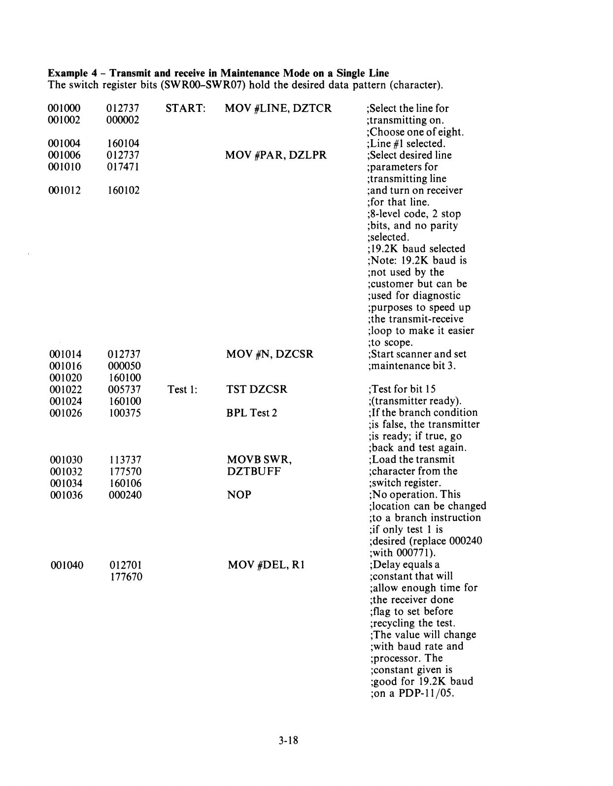
Example 4 - Transmit and receive in Maintenance Mode on a Single Line
The
switch register bits (SWROO-SWR07)
hold
the desired
data
pattern
(character).
001000 012737 START:
Mav
#LINE,
DZTCR
;Select the line for
001002 000002 ;transmitting on.
;Choose
one
of
eight.
001004 160104 ;Line
#1
selected.
001006 012737
MOV
#PAR,
DZLPR
;Select desired line
001010 017471 ;parameters for
;transmitting line
001012 160102 ;and
turn
on
receiver
;for
that
line.
;8-level code, 2 stop
;bits,
and
no parity
;selected.
;
19
.2K
baud
selected
;Note: 19.2K
baud
is
;not
used by the
;customer
but
can be
;used for diagnostic
;purposes to speed
up
;the transmit-receive
;loop to
make
it easier
;to scope.
001014 012737
MaV
#N,
DZCSR
;Start scanner
and
set
001016 000050 ;maintenance bit 3.
001020 160100
001022 005737 Test
1:
TSTDZCSR
;Test for bit
15
001024 160100 ;(transmitter ready).
001026 100375
BPL
Test 2
;If
the
branch
condition
;is false, the transmitter
;is ready;
if
true, go
;back
and
test again.
001030 113737
MOVBSWR,
;Load
the
transmit
001032 177570
DZTBUFF
;character from the
001034 160106 ;switch register.
001036 000240
Nap
;No
operation. This
;location can be changed
;to a
branch
instruction
;if only test 1 is
;desired (replace 000240
;with 000771).
001040 012701
MOV
#DEL,
Rl
;Delay equals a
177670 ;constant
that
will
;allow
enough
time for
;the receiver
done
;flag to set before
;recyc1ing the test.
;The value will change
;with
baud
rate
and
;processor.
The
;constant given
is
;good for 19.2K
baud
;on a
PDP-ll/05.
3-18
001042 105737 Test
2:
TSTBDZCSR
;Test bit 2 (receiver
001044 160100 ;done flag).
001046 100402
BMI1$
; When the branch
;condition
is
true,
;the receiver
done
;flag
is
set.
001050 005201
INCRI
;Increment delay.
001052 001373
BNETEST2
;If
the branch
;condition
is
true,
the
;delay
is
not
finished.
001054 013700
1$:
MOY
DZRBUF,
RO
;Read the
DZll
001056 160102 ;receiver buffer to
001060 000760 ;register
O.
BR
TEST
1
;Loop
back
and
;test again.
Example 5 - Transmit and Receive on a Single Line Using Silo Alarm in Maintenance Mode
001200 012706
MOY
#1100, R6 ;Initialize stack
001202 001100 ;pointer.
001204 012737 MOY #3$,
TYEC
;Initialize transmitter
001206 001274 ;vector address.
001210 000304
001212 005037
CLR
TYEC+2
;Initialize transmitter
001214 000306 ;vector processor status
;word.
001216 012700 MOY
#DBUF,
RO
;Set first address
of
001220 001304 ;input
data
table
;into
RO.
001222 012737
MOY
#1,
DZTCR
;Enable line 0
;transmi tier.
001224 000001
001226 160104
001230 012737 MOY #17470, ;Set up line parameters
001232 017470
DZLPR
;and
turn
on
the receiver
001234 160102 ;clock for line
O.
001236 012737
MOY
#50050, ;Enable transmitter
001240 050050
DZCSR
;interrupt
and
silo
001242 160100 ;alarm.
Turn
on
;scanner
and
maintenance
;mode.
001244 032737
1$:
BIT #20000, ;Test for silo alarm
001246 020000
DZCSR
001250 160100
001252 001774 BEQ
1$
;Loop until silo alarm
001254 013720
2$:
;flag sets.
MOYDZRBUF,
;Read
DZ
11
silo
001256 160102 (RO)+ ;receiver buffer
output.
001260 000240
NOP
;Delay to allow next
001262 000240
NOP
;word in silo to filter
;down
to
the silo
;output.
3-19
001264
001266
001270
001272
001274
001276
001300
001302
100773
012700
001304
000764
112737
000252
160106
000002
3$
BMI2$
;Data
valid set says
;that word
is
good,
;go back for more.
MOV #DBUF,
RO
;Silo has been emptied.
;Reinitialize data
;table address pointer.
BR
1$
;Do it again.
Transmitter Interrupt Service Routine
MOVB DAT,
DZTBUF
RTI
Data
Table
1304
100252;
Word
1
1306
100252
1340 100252 ;Word
16
1342 000252
;Data
valid
NOTE
;not set
;character
is
;invalid
;Transmit
;character
252
It
is possible to get more than 16 words because they
are being put into the silo simultaneously with the
reading
of
the silo.
3-20
Example 6 - Echo Test
on
a Single Line (Transmit Received Data)
001000 012737
START
MOV #PAR,
DZLPR
;Load line parameters
;for line being used.
001002 011073 ;Line 3, 8-bit
001004 160102 ;character, 2 stop
;bits, no parity,
;110 baud, and receiver
;c1ock on.
001006 012737 MOV #LINE,
DZTCR
;Turn line 3
001010 000010 ;transmi-tter on.
001012 160104
001014 012737 MOV #n,
DZCSR
;Turn scanner
on
001016 000040 ;(set CSR-5)
001020 160100
001022 105737
1$:
TSTBDZCSR
;Test (bit 7) for
001024 160100
;RDONE
001026 100375
BPLI$
;Ifbit
7
is
not
set,
;go back and test again.
001030 005737
2$:
TSTDZCSR
;Test (bit 15) for
001032 160100
;TRDY
001034 100375
BPL2$
;Ifbit
15
is
not
set
;go back and test again.
001036 013700
MOVRBUF,RO
;Read received
data
001040 160102 ;word into
RO
001042 110037 MOVB
RO,
DZTDR
;Load character
001044 160106 ;into
DZ
II
TBUF
;register for
;transmitting.
001046 000765
BR
1$
; Repeat.
3-21

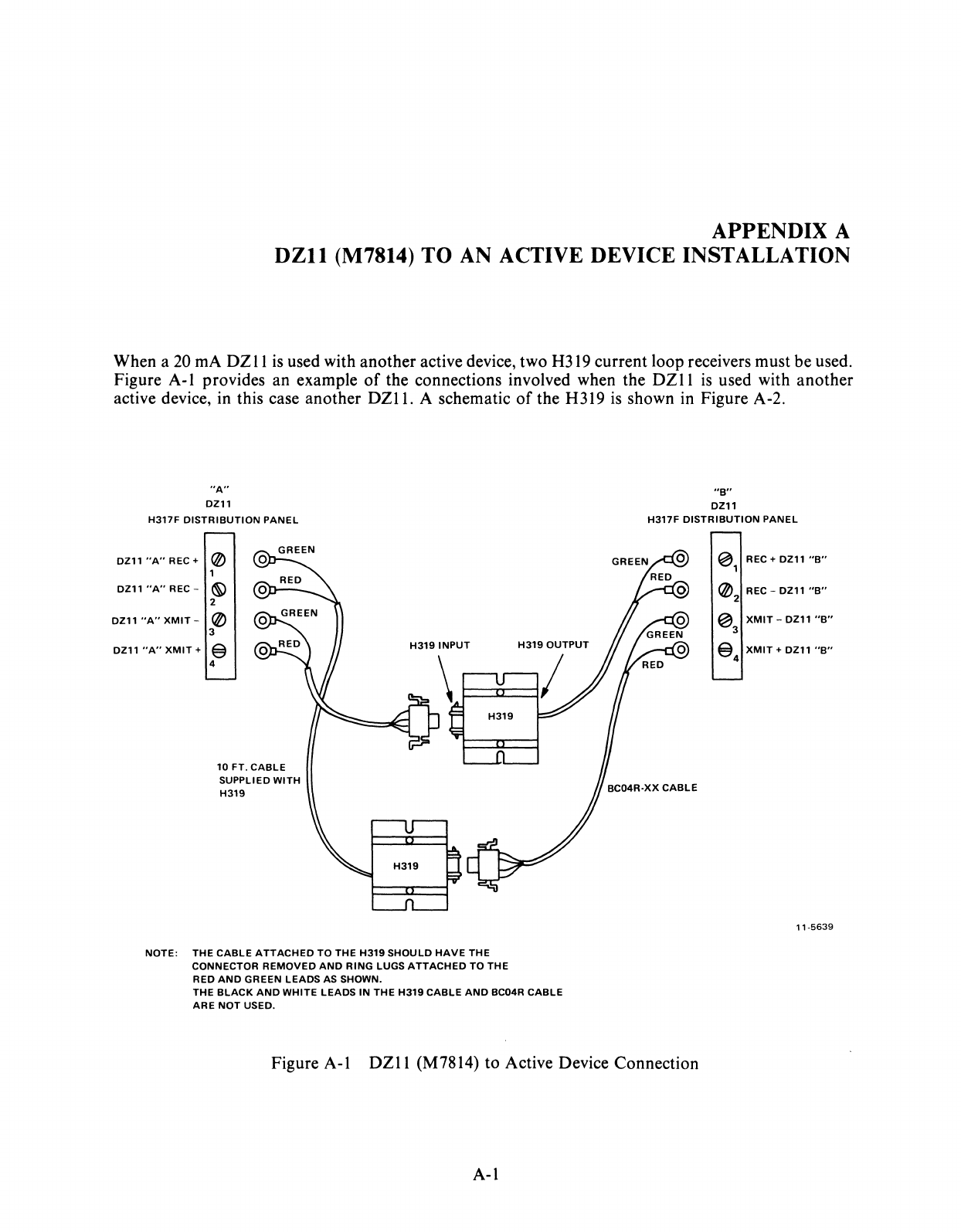
APPENDIX A
DZll
(M7814)
TO
AN ACTIVE DEVICE INSTALLATION
When a 20 rnA
DZ
II
is
used with another active device, two
H3I9
current loop receivers must be used.
Figure A-I provides an example
of
the connections involved when the
DZII
is
used with another
active device, in this case another
DZl1.
A schematic
of
the H319
is
shown in Figure A-2.
"A"
DZ11
H317F
DISTRIBUTION
PANEL
DZ11"A"REC+
@
DZ11
"A"
REC -
~
2
DZ11
"A"
XMIT
-@
3
DZ11
"A"
XMIT
+ @
4
10
FT.
CABLE
SUPPLIED
WITH
H319
H319
INPUT
NOTE:
THE
CABLE
ATTACHED
TO
THE
H319
SHOULD
HAVE
THE
CONNECTOR
REMOVED
AND
RING
LUGS
ATTACHED
TO
THE
RED
AND
GREEN
LEADS
AS SHOWN.
H319
OUTPUT
THE
BLACK
AND
WHITE
LEADS
IN
THE
H319
CABLE
AND
BC04R
CABLE
ARE
NOT
USED.
"B"
DZ11
H317F
DISTRIBUTION
PANEL
~
REC + DZ11
"B"
1
@ REC -DZ11
"B"
2
~
XMIT
-DZ11
"B"
3
@
XMIT
+ DZ11
"B"
4
11-5639
Figure A-I
DZII
(M7814) to Active Device Connection
A-I
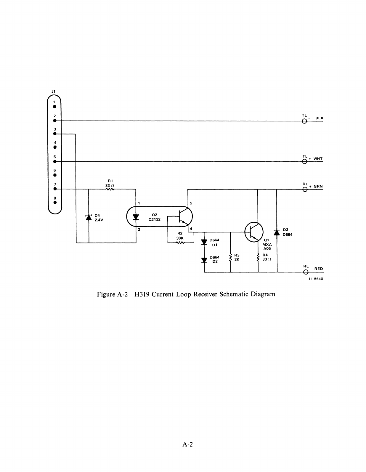
J1
1
•
2
3
4
•
5
6
•
7
8
•
R1
33
f!
04
02
2.4V
02132
2
03
0664
01
0664
02
R3
3K
Q1
MXA
A05
R4
33
f!
Figure A-2 H319 Current Loop Receiver Schematic Diagram
A-2
0664
Tl
-
BlK
Tl+
WHT
Rl
+ GRN
Rl_
RED
11-5640

OZ11 USER'S GUIDE
EK-OZ110-UG-002
Reader's
Comments
Your comments and suggestions will help us in
our
continuous effort
to
improve the quality and usefulness
of
our
publications.
What
is
your
general reaction
to
this manual? In
your
judgment
is
it
complete, accurate, well organized, well
written, etc.?
Is
it easy
to
use?
What features are most useful? -------------------------------------------------------------
What faults
do
you find with the manual?
Does this manual satisfy the need you think it was intended
to
satisfy?
Does
it
satisfy
your
needs?
________________
_ Why?
________________________________
__
Would you please indicate any factual errors you have found.
Please describe
your
position.
Name
--
____________________
Organization
Street
__________________________________
Deputment
City
__________
_ State
___________
_ Zip
or
Country
- - - - - - - - - - -
FoldHere
- - - - - - - - - - -
- - - - -
--
- -
DoNotTear-FoldHereandStaple
- - - - - - - -
BUSINESS REPLY MAIL
NO
POSTAGE STAMP NECESSARY IF MAILED IN THE UNITED STATES
Postage
wiD
be paid by:
Digital Equipment Corporation
Technical Documentation Department
Maynard, Massachusetts
01754
FIRST CLASS
PERMIT NO. 33
MAYNARD, MASS.


digital
equipment corporation
Printed
in
U.S.A.
