ERA310
User Manual: ERA310
Open the PDF directly: View PDF ![]() .
.
Page Count: 39
SERVICE MANUAL
CODE: 00ZERA310USME
ELECTRONIC
CASH REGISTER
MODEL ER-A310
MODEL ER-A330
SRV Key : LKGIM7113RCZZ
PRINTER: ER-A310 : CR-510
: ER-A330 : UCR-812A
(For "U" & "A" version)
CHAPTER 1. SPECIFICATIONS . . . . . . . . . . . . . . . . . . . . . . . . . . . . . . . . . . . . . 1
CHAPTER 2. OPTIONS . . . . . . . . . . . . . . . . . . . . . . . . . . . . . . . . . . . . . . . . . . .6
CHAPTER 3. SRV. RESET AND MASTER RESET . . . . . . . . . . . . . . . . . . . . . . 6
CHAPTER 4. HARDWARE DESCRIPTION . . . . . . . . . . . . . . . . . . . . . . . . . . . . 7
CHAPTER 5. TEST FUNCTION . . . . . . . . . . . . . . . . . . . . . . . . . . . . . . . . . . . . 16
CHAPTER 6. CIRCUIT DIAGRAM & PWB LAYOUT . . . . . . . . . . . . . . . . . . . .20
PARTS GUIDE
CONTENTS
SHARP CORPORATION This document has been published to be used
for after sales service only.
The contents are subject to change without notice.
Parts marked with "!" is important for maintaining the safety of the set. Be sure to replace these parts with specified ones for
maintaining the safety and performance of the set.
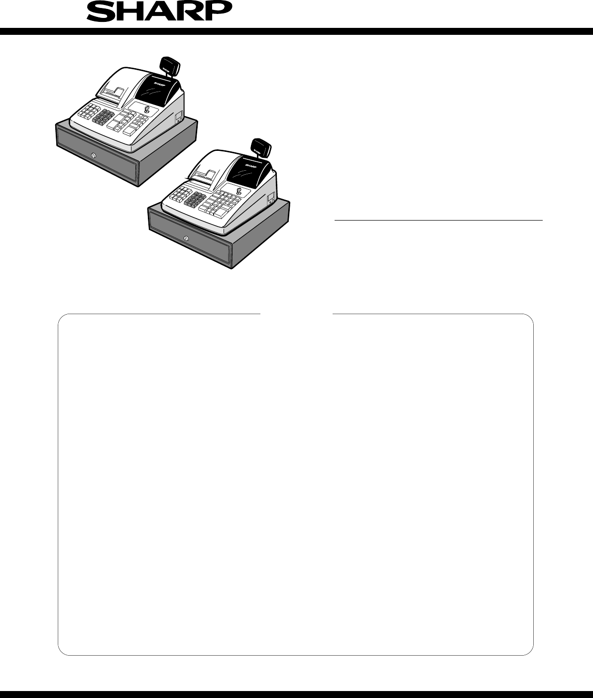
ER-A310
ER-A330
CHAPTER 1. SPECIFICATIONS
1. Appearance/Rating
1) Appearance
1ER-A310
2ER-A330
2) Rating
ER-A310 ER-A330
Power source 120V AC ± 10%, 50/60 Hz
Power
consumption
Stand-by: 10W
Operating: 31W (Max.)
Stand-by: 10W
Operating: 38W (Max.)
Operating
temperature 32˚F to 104˚F (0˚C to 40˚C)
Operating
humidity 10% to 90% (RH)
Physical
dimensions,
including the
drawer
420 (W) × 423 (D) ×
304 (H) mm
(16.5 (W) × 16.7 (D) ×
12.0 (H) in.)
420 (W) × 423 (D) ×
314 (H) mm
(16.5 (W) × 16.7 (D) ×
12.4 (H) in.)
Weight 12.5 kg (27.6 lbs.) 13.5 kg (30.0 lbs.)
Journal paper
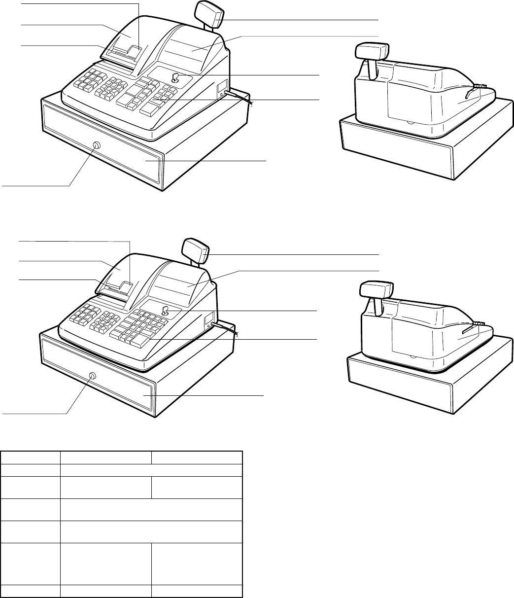
Printer cover
Receipt paper
Drawer lock
Customer display (Pop-up type)
Operator display
Mode switch
Keyboard
Drawer
Journal paper
Printer cover
Receipt paper
Drawer lock
Customer display (Pop-up type)
Operator display
Mode switch
Keyboard
Drawer
– 1 –
2. Keyboard
1) Standard keyboard layout
1ER-A310
2ER-A330
2) Key top name
1Standard key top
KEY TOP DESCRIPTION ER-A310 ER-A330
↑ RECEIPT Receipt paper feed key èè
↑ JOURNAL Journal paper feed key èè
0∼9,00 Numeric keys èè
⋅Decimal point key èè
@/FOR Multiplication key èè
CL/C Clear key èè
PRINT Validation print key èè
Dept.1/+ Department 1/Plus key èè
Dept.2/– Department 2/Minus key èè
Dept.3/×Department 3/
Multiplication key èè
Dept.4/÷Department 4/Division key èè
Dept.5∼8 Department 5∼8 keys èÉ
Dept.5∼10 Department 5∼10 keys Éè
PLU/SUB PLU/Subdepartment key èè
ESC Error escape key èè
CASH# Cashier number entry key Éè
RCPT Receipt print key èè
dDiscount key èÉ
d1, 2 Discount 1 and 2 keys Éè
AUTO Automatic sequencing key èÉ
AUTO1, 2 Automatic sequencing 1
and 2 keys Éè
% Percent key èÉ
KEY TOP DESCRIPTION ER-A310 ER-A330
%1, 2 Percent 1 and 2 keys Éè
NS No-sale key èè
RA/RM Received on account/
Recall memory key èè
PO/CAL Paid out/
Calculation mode key èè
RFND Refund key èè
VOID Void key èè
CH Charge key èÉ
CH1, 2 Charge 1 and 2 keys Éè
CHK Check key èè
CONV Conversion key èè
MDSE SBTL Merchandise subtotal key èè
#/TM/SBTL Non-add code/Time display/
Subtotal key èè
CA/AT /= Cash/Amount tendered/
Equals key èè
FS SHIFT Food stamp shift key Éè
FS TEND Food stamp tender key Éè
2Optional key top
KEY TOP DESCRIPTION ER-A310 ER-A330
Dept. 9∼30 Department 9∼30 keys èÉ
Dept. 11∼50 Department 11∼50 keys Éè
DEPT# Department number
entry key èè
TAX1
SHIFT∼TAX4
SHIFT
Tax1 ∼ Tax4 shift keys
èè
TAX Manual tax key èè
AUTO2 Automatic sequencing 2
key èÉ
AUTO3, 4 Automatic sequencing 3
and 4 keys Éè
CONV2∼4 Conversion 2∼4 keys èè
CA2 Cash total 2 key èè
CH2 Charge 2 key èÉ
d2 Discount 2 key èÉ
%2 Percent 2 key èÉ
RCPT PRINT
PO %
CL
@
FOR
RFND
VOID
987
654
321
0
00
C
RECEIPT
JOURNAL
+
-
X
1
2
3
8
7
6
5
4
PLU/SUB NS ESC AUTO
CH CONV
MDSE
SBTL CHK
#/TM/SBTL
CA/AT
=
Dummy key Dummy key Dummy key
RA
CAL
RM
RCPT PRINT
1 2
%1 %2
CL
@
FOR
RFND
VOID
987
654
321
0
00
C
RECEIPT
JOURNAL
+
1
3
5
10
9
8
7
6
NS ESC
AUTO
1
CH1
CONV
MDSE
SBTL CHK
#/TM/SBTL
CA/AT
=
Dummy key Dummy key
PLU
SUB
CASH
#
4
2
-
RM
X
CAL
AUTO
2
CH2
FS
SHIFT
FS
TEND
RA
PO
– 2 –
4. Display
1) Operator display
DISPLAY DEVICE LED
NUMBER OF LINE 1 line
NUMBER OF POSITIONS 10 positions
COLOR OF DISPLAY Green
CHARACTER SIZE 14.2mm (H) × 8.0mm (H)
2) Customer display (Pop-up type)
DISPLAY DEVICE LED
NUMBER OF LINE 1 line
NUMBER OF POSITIONS 7 positions
COLOR OF DISPLAY Green
CHARACTER SIZE 14.2mm (H) × 8.0mm (H)
3) Lamps
DISPLAY
POSITION DESCRIPTION
AMOUNT 1 ∼ 8
MINUS SIGN 4 ∼ 10 : Floating
ERROR 10
PGM MODE 10
CA/AT
NS
CH
CHK
10 : Lights up when a
registration is finalized by
depressing CA/AT, NS,
CH or CHK key
SUBTOTAL/
SHORT TENDER
10
CHANGE 10 : Lights up whenever the
change due amount
appears in the display.
DEPARTMENT 9 ∼ 10 No zero-suppressed.
PLU 8 ∼ 10 No zero-suppressed.
REPEAT 8 Endless count, starting from 2.
DECIMAL POINT 3 ∼ 1 TAB
LOW BATTERY 10 : Light up when the voltage
of the battery for memory
retention is lower than the
regulated voltage.
(The voltage is checked
when "POWER ON" or
"Batteries are
exchanged".)
RECEIPT OFF 8 —
CASHIER No. 2 ∼ 3– || – : 01 ∼ 06 code entry
VALIDATION 10 : Light up when the
validation printing is
compulsory.
CONVERSION or
CALC. MODE
10
DEPT REPEAT
PLU/SUB
RCPT
OFF
: This appears when a transaction is finalized.
: This appears when the cash register computes the subtotal.
: This appears when the chage due amount is displayed.
: This appears when the batteries are iow.
– 3 –
5. Printer
1) Printer specifications
ITEMS ER-A310 ER-A330
Model name CR-510 UCR-812A
No. of station 2 (Receipt/Journal) 2 (Receipt/Journal)
Printing system Inner hammer, rubber character selection type Print wheel selective type
Printing capacity Receipt : Max. 12 chr. Receipt : Max. 10 chr.
Journal : Max. 12 chr. Journal : Max. 10 chr.
Validation : Max. 24 chr./1 line Validation : Max. 20 chr./1 line
Character size 1.8mm (W) × 2.7mm (H) Figure : 1.7mm (W) × 3.2mm (H)
Symbol : 2.4mm (W) × 3.2mm (H)
Print pitch Column distance : 2.8mm Column distance : 3.35mm for between 1st and 2nd
column 3.0mm for after 3rd column
Row distance : 4.3mm Row distance : 5.1mm
Print speed Approx. 3.0 lines/sec. Approx. 2.6 lines/sec.
Paper feed speed Approx. 29 lines/sec. at receipt issued. Approx. 18 lines/sec. at receipt issued.
Reliability MCBF 2.5 million lines MCBF 2 million lines
Validation form sensor No No
Near end sensor Journal side: No Journal side: No
Receipt side: No Receipt side: No
Cutter Manual Manual
Print wheel layout Parts code: 00BM755001010 Parts code: 00BM712002300
2) Roll paper
121110987654321
PL GT –––CA
000000000CD CH 1⁄2
111111111PCK 1
222222222XCR 2
333333333ZEX 3
444444444#TX 4
555555555RF FS 5
666666666VD %6
777777777TR d7
888888888QRA CG
999999999@PO TD
★★★★★★★★★ +NS TL
– – – – . . . . No – *ST
10987654321
PL ZTX . . . . GT CA @
–––––––#CK Q
★★★★★★★%CH CG
00000000RA TD
11111111PO 1
22222222VD 2
33333333NS 3
44444444TX 4
55555555FS 5
66666666d6
77777777X
1
⁄
2
88888888EX ST
99999999RF TL
Parts code DPAPR1006CSZZ
Dimension 44.5±0.5mm in width
Max. 83mm in diameter
Paper quality Journal/Receipt
Fine quality paper
Paper thickness : 0.06 to 0.09 mm
Paper weight : 52.3 to 64g/m2
Validation form
Normal paper only
Thickness : 0.09 to 0.14 mm
Size : 110mm or more, 210mm or
under (W) × 70mm or more (H)
– 4 –
3) Validation paper
ER-A310 ER-A330
Paper quality Normal paper only Normal paper and pressure sensitive paper only
Thickness : 0.09 to 0.14 mm Thickness : 0.07 to 0.14 mm
Size : 110 mm or more, 210 mm or under (W) × 70 mm or more (H) Size : 115 mm or more (W) × 70 mm or more (H)
Printing area
76.2
14.2
32.6
(11)
9.3
32.6
19.1
16.6
29.4 29.4
10Dig.
10Dig.
Wide over 115mm
16
4) Inking
ER-A310 ER-A330
Parts code NROLR6652RCZZ NROLR6638RCZZ
Ink supply system Ink roller Ink roller
Form Roller Roller
Specification Material-rubber Material-rubber
Roller life Approx. 0.4 million lines Approx. 0.6 million lines
Print color Purple Purple
5) Logo stamp
ER-A310 ER-A330
Material Porous rubber Porous rubber
Size 30mm (W) × 20mm (H) 30mm (W) × 20mm (H)
Color Purple Purple
Parts code for ink UINK1001CCZZ UINK1001CCZZ
6. Drawer
1) Drawer box and drawer
Model name SK423
Size 420(W) × 423(D) × 112(H) mm
Color Light olive gray
Material Metal
Bell —
Release lever Standard equipment; Situated at the bottom
Drawer open sensor Standard equipment
2) Money case
For "U" version For "A" version
Separation from the drawer Allowed Allowed
Separation of the coin
compartments from the
money case
Disallowed Disallowed
Bill separator — Yes
Number of compartments 5B/5C 4B/8C
3) Lock
Location of the lock Front
Method of locking
and unlocking
Locking : Insert the drawer lock key
into the lock and turn it 90
degrees counterclockwise.
Unlocking : Insert the drawer lock key
into the lock and turn it 90
degrees clockwise.
Key No. SK1-1
7. Memory back up
For memory back up, the dry battery ULM-3 (3 pieces) is needed.
1. Memory holding time: Approximate 1 year after NEW dry batter-
ies are inserted.
2. Battery exchange method: When the low battery symbol "L"
lights up, batteries (3 pieces) ex-
change by the following method,
within 2 days.
1) Power on the ECR.
2) Turn the MODE SW to "OP X/Z" mode.
3) Release the OLD dry batteries (3 pieces).
4) Insert the NEW dry batteries (3 pieces).
5) Confirm the low battery symbol "L" lights off.
5B/5C
Bill compartments
Bill separator
Coin compartments
4B/8C
– 5 –
CHAPTER 2. OPTIONS
1. Sales options
No. NAME MODEL DESCRIPTIONS
1 REMOTE DRAWER ER-04DW 5B/5C
2 COIN CASE ER-55C2 5B/5C
3 KEY TOP KIT ER-11KT7 1 × 1 key top
ER-12KT7 1 × 2 key top
ER-22KT7 2 × 2 key top
ER-11DK7 1 × 1 dummy key
ER-51DK7 5 × 1 dummy key
2. Service options
No. NAME PARTS CODE PRICE RANK DESCRIPTIONS
1 SRV KEY LKGIM7113RCZZ AK
2 MODE KEYGRIP COVER LKGIM7126RCZZ AL OP key only
3 DRIP-PROOF KEYBOARD COVER GCÇVH7126BHZZ BE
4 SHIELD PLATE KIT DKIT-8666BHZZ BL Only for ER-A330
3. Supplies
No. NAME PARTS CODE PRICE RANK DESCRIPTIONS
1 ROLL PAPER DPAPR1006CSZZ AR
2 INK ROLLER (ER-A310) NRÇLR6652RCZZ AZ
3 INK ROLLER (ER-A330) NRÇLR6638RCZZ AY
4 INK FOR STAMP UINK-1001CCZZ AK
CHAPTER 3. SRV RESET AND MASTER RESET
The SRV key is used for operating in the SRV mode.
1. SRV. reset (Program Loop Reset)
Used to return the machine back to its operational state after a lock-
up has occurred.
Procedure
•Method 1
1) Turn off the AC switch.
2) Set the mode switch to (SRV′) position.
3) Turn on the AC switch.
4) Turn to (SRV) position from (SRV′) position.
2. Master reset (All memory clear)
There are two possible methods to perform a master reset.
•MRS-1
Used to clear all memory contents and return machine back to its
initial settings. return keyboard back to default. for default keyboard
layout.
Procedure-1 (with SRV key)
1) Unplug the AC cord from the wall outlet.
2) Set the MODE switch to the (SRV′) position.
3) Plug in the AC cord to the wall outlet.
4) While holding down JOURNAL FEED key, turn to (SRV) position
from (SRV′) position.
Procedure-2 (without SRV key)
1) Turn the mode switch to the (REG) position.
2) Ensure the batteries are not installed in the battery compartment
and insert the plug into the outlet.
3) The right most decimal point will blink for a few seconds.
4) The register will sound three beeps.
5) The register will display " ."
– 6 –
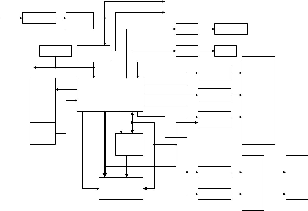
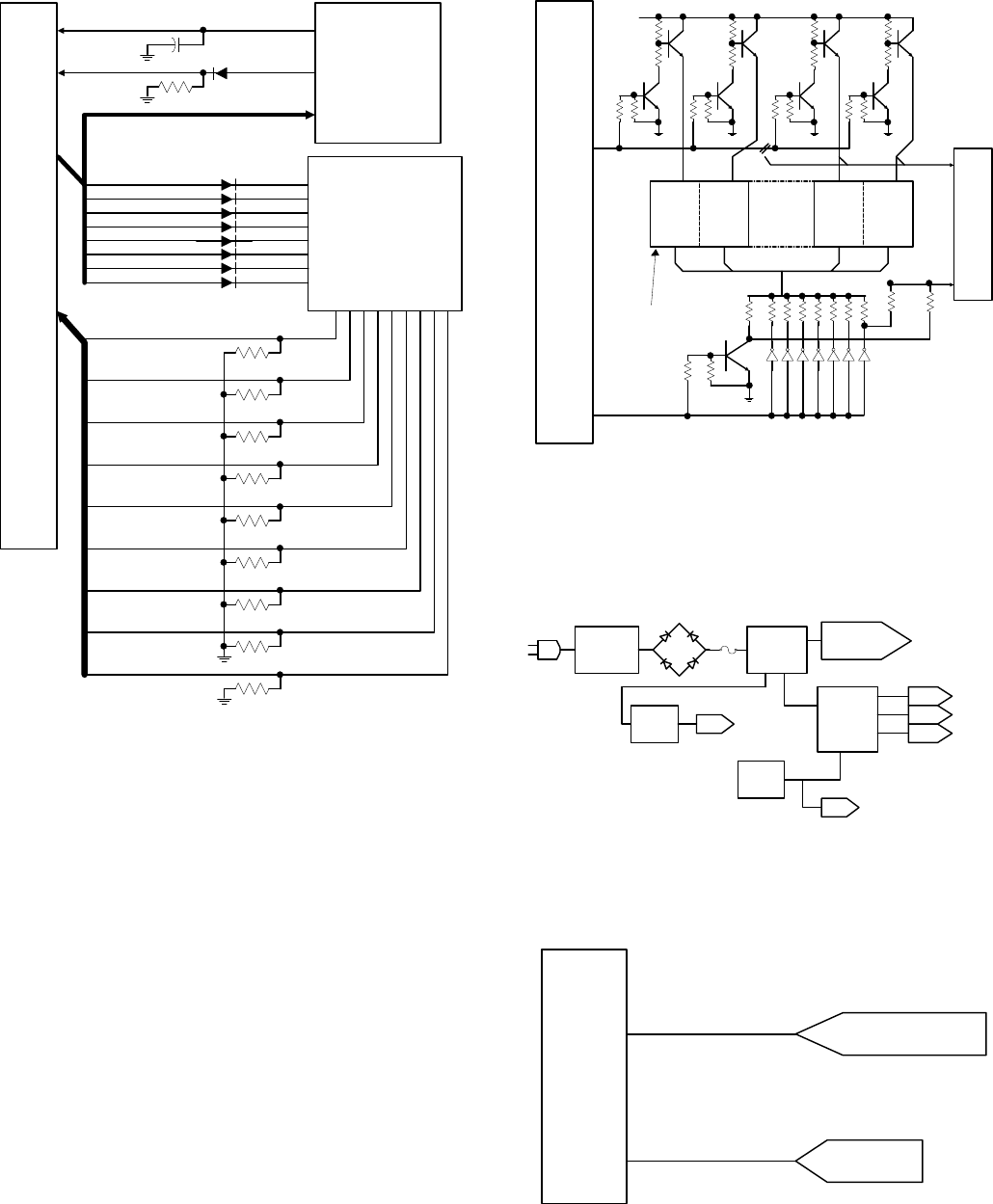
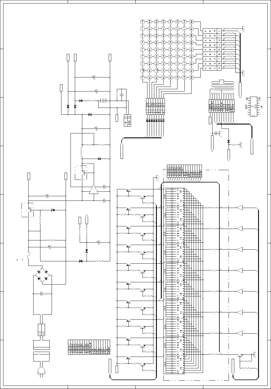
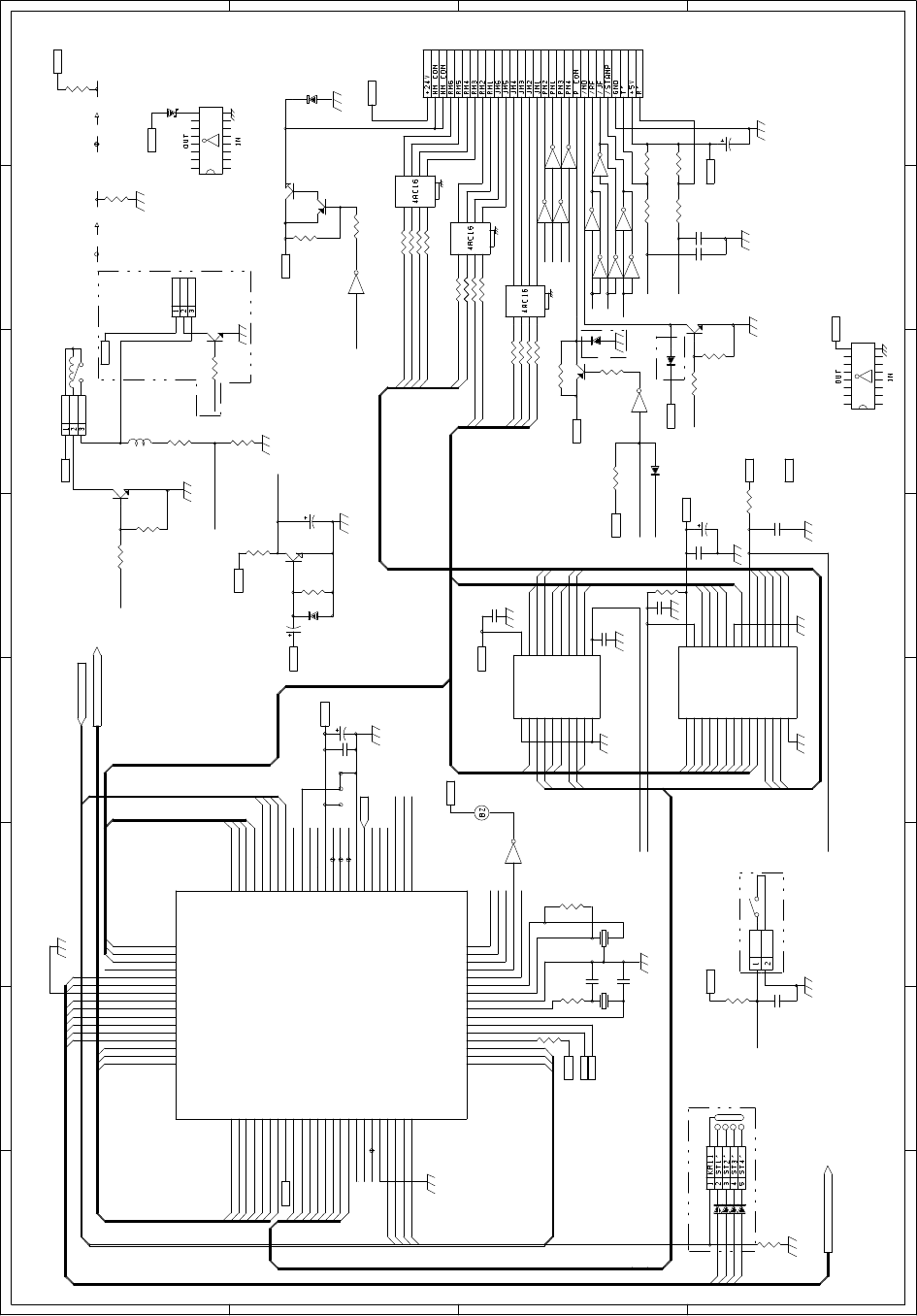
CHAPTER 4. HARDWARE DESCRIPTION
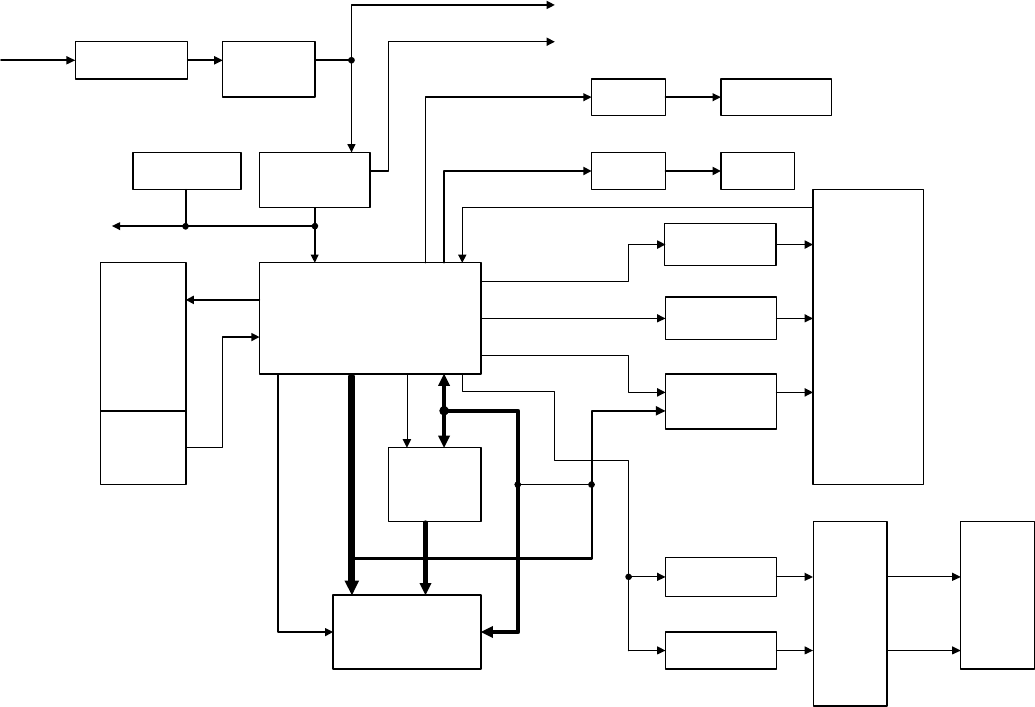
1. Block diagram
1) ER-A310
CPU
µPD78045
S-RAM
256 kbit
ADDRESS
LATCH
HAMMER MG
DRIVER
STAMP, PAPER
FEED DRIVER
STEP MOTOR
DRIVER
PRINTER
CR-510
SEGMENT
DRIVER
DIGIT DRIVER
OP.
DISPLAY
7SEG LED
10DIG
POP-UP
DISPLAY
7SEG LED
7DIG
DRIVER
DRIVER DRAWER
BUZZER
KEYBOARD
8X9 72KEY
MODE
SWITCH
8SIGNAL
DC-DC
CONVERTER
DRY BATTERY
VOLTAGE
REGULATOR
TRANSFORMER
PRINTER POWER SOURCE : +24V
DISPLAY POWER SOURCE : +5.5V
ADDRESS
BUS
HAMMER COMMON SIGNAL
LATCH
SIGNAL
DIGIT SIGNAL
STROBE
SIGNAL
RETURN
SIGNAL
ADDRESS
BUS DATA BUS
DRIVE SIGNAL
DRIVE SIGNAL
DRIVE SIGNAL
TIMING SIGNAL
DRIVE SIGNAL
DRIVE SIGNAL
CHIP SELECTSIGNAL
– 7 –
2) ER-A330
CPU
µPD78045
S-RAM
256 kbit
ADDRESS
LATCH
PRINT WHEEL
MG DRIVER
STAMP, PAPER
FEED DRIVER
STEP MOTOR
DRIVER
PRINTER
UCR-812A
SEGMENT
DRIVER
DIGIT DRIVER
OP.
DISPLAY
7SEG LED
10DIG
POP-UP
DISPLAY
7SEG LED
7DIG
DRIVER
DRIVER DRAWER
BUZZER
KEYBOARD
8X9 72KEY
MODE
SWITCH
8SIGNAL
DC-DC
CONVERTER
DRY BATTERY
VOLTAGE
REGULATOR
TRANSFORMER
PRINTER POWER SOURCE : +18V
DISPLAY POWER SOURCE : +5.5V
ADDRESS
BUS
HAMMER COMMON SIGNAL
LATCH
SIGNAL
DIGIT SIGNAL
STROBE
SIGNAL
RETURN
SIGNAL
ADDRESS
BUS DATA BUS
DRIVE SIGNAL
DRIVE SIGNAL
DRIVE SIGNAL
TIMING SIGNAL
DRIVE SIGNAL
DRIVE SIGNAL
CHIP SELECTSIGNAL
– 8 –

2. CPU (UPD78045F) pin configuration
No. PIN NAME ER-A310 ER-A330 I/O ACTIVE
SIGNAL NAME DESCRIPTION SIGNAL NAME DESCRIPTION
1 P94 DIG7 Display digit 7 DIG7 Display digit 7 O H
2 P93 DIG6 Display digit 6 DIG6 Display digit 6 O H
3 P92 DIG5 Display digit 5 DIG5 Display digit 5 O H
4 P91 DIG4 Display digit 4 DIG4 Display digit 4 O H
5 P90 DIG3 Display digit 3 DIG3 Display digit 3 O H
6 P81 DIG2 Display digit 2 DIG2 Display digit 2 O H
7 P80 DIG1 Display digit 1 DIG1 Display digit 1 O H
8 VDD VDD +5V VDD +5V
9 P27 AD7 RAM Address & Data bus 7 AD7 RAM Address & Data bus 7 I/O H
Printer magnet 8
10 P26 AD6 RAM Address & Data bus 6 AD6 RAM Address & Data bus 6 I/O H
Printer magnet 7
11 P25 AD5 RAM Address & Data bus 5 AD5 RAM Address & Data bus 5 I/O H
Journal print magnet 6 Printer magnet 6
Receipt print magnet 6
12 P24 AD4 RAM Address & Data bus 4 AD4 RAM Address & Data bus 4 I/O H
Journal print magnet 5 Printer magnet 5
Receipt print magnet 5
13 P23 AD3 RAM Address & Data bus 3 AD3 RAM Address & Data bus 3 I/O H
Journal print magnet 4 Printer magnet 4
Receipt print magnet 4
14 P22 AD2 RAM Address & Data bus 2 AD2 RAM Address & Data bus 2 I/O H
Journal print magnet 3 Printer magnet 3
Receipt print magnet 3
15 P21 AD1 RAM Address & Data bus 1 AD1 RAM Address & Data bus 1 I/O H
Journal print magnet 2 Printer magnet 2
Receipt print magnet 2
16 P20 AD0 RAM Address & Data bus 0 AD0 RAM Address & Data bus 0 I/O H
Journal print magnet 1 Printer magnet 1
Receipt print magnet 1
17 /RESET /RESET Reset signal /RESET Reset signal I L
18 P74 SCOM Printer step motor common signal NU NU O H
19 P73 SM4 Printer step motor drive signal 4 NU NU O H
20 AVSS AVSS GND AVSS GND
21 P17 KR11 Key return signal 11 KR11 Key return signal 11 I H
22 P16 KR10 Key return signal 10 KR10 Key return signal 10 I H
23 P15 KR9 Key return signal 9 KR9 Key return signal 9 I H
24 P14 KR8 Key return signal 8 KR8 Key return signal 8 I H
25 P13 KR7 Key return signal 7 KR7 Key return signal 7 I H
26 P12 KR6 Key return signal 6 KR6 Key return signal 6 I H
27 P11 KR5 Key return signal 5 KR5 Key return signal 5 I H
28 P10 P10 Dry battery voltage P10 Dry battery voltage I
29 AVDD AVDD +5V AVDD +5V
30 AVREF AVREF +5V (VCC) AVREF +5V (VCC)
31 XT1 XT1 Sub clock: 32.768 kHz P04 Sub clock: 32.768 kHz I
32 XT2 XT2 XT2 O
33 VSS VSS GND VSS GND
34 X1 X1 Main clock: 4.19 MHz X1 Main clock: 4.19 MHz I
35 X2 X2 X2 O
36 P37 MD Printer motor ON signal MD Printer motor ON signal O H
37 P36 BUZ Buzzer ON signal BUZ Buzzer ON signal O H/L
38 P35 RF Receipt paper feed signal RF Receipt paper feed signal O H
39 P34 JF Journal paper feed signal JF Journal paper feed signal O H
40 P33 STAMP Stamp ON signal STAMP Stamp ON signal O H
– 9 –

No. PIN NAME ER-A310 ER-A330 I/O ACTIVE
SIGNAL NAME DESCRIPTION SIGNAL NAME DESCRIPTION
41 P32 /ALE Address latch signal /ALE Address latch signal O ↓
42 P31 /CE Chip select signal /CE Chip select signal O L
43 P30 /WE Write signal /WE Write signal O L
44 P03 RMS NU RMS NU I
45 P02 R Printer reset signal DRS Drawer open sensor I
46 P01 T Printer timing signal αPrinter timing signal I ↑ H
47 P00 PE Power enable signal PE Power enable signal I H
48 IC IC VSS IC VSS
49 P72 SM3 Printer step motor drive signal 3 P72 NU O H
50 P71 SM2 Printer step motor drive signal 2 MG10 Printer magnet 10 O H
51 P70 SM1 Printer step motor drive signal 1 MG9 Printer magnet 9 O H
52 VDD VDD +5V VDD +5V
53 P127 DRS Drawer open sensor (input) R-COM Printer receipt common signal O H
54 P126 HCOM Printer hammer common signal J-COM Printer journal common signal O H
55 P125 J1 Mode signal (ER-A310: GND) J1 Mode signal (ER-A330: VDD) I H
56 P124 DR1 Standard drawer drive signal DR1 Standard drawer drive signal O H
57 P123 KR4 Key return signal 4 KR4 Key return signal 4 I H
58 P122 KR3 Key return signal 3 KR3 Key return signal 3 I H
59 P121 KR2 Key return signal 2 KR2 Key return signal 2 I H
60 P120 KR1 Key return signal 1 KR1 Key return signal 1 I H
61 P117 A14 RAM Address 14 A14 RAM Address 14 O
62 P116 A13 RAM Address 13 A13 RAM Address 13 O
63 P115 A12 RAM Address 12 A12 RAM Address 12 O
64 P114 A11 RAM Address 11 A11 RAM Address 11 O
65 P113 A10 RAM Address 10 A10 RAM Address 10 O
66 P112 A9 RAM Address 9 A9 RAM Address 9 O
67 P111 A8 RAM Address 8 A8 RAM Address 8 O
68 P110 DR2 Option drawer drive signal DR2 Option drawer drive signal O H
69 P107 DP/ST8 Display segment signal DP DP/ST8 Display segment signal DP OH
Key strobe signal 8 Key strobe signal 8
70 P106 G/ST7 Display segment signal G G/ST7 Display segment signal G OH
Key strobe signal 7 Key strobe signal 7
71 VLOAD VLOAD VSS VLOAD VSS
72 P105 F/ST6 Display segment signal F F/ST6 Display segment signal F OH
Key strobe signal 6 Key strobe signal 6
73 P104 E/ST5 Display segment signal E E/ST5 Display segment signal E OH
Key strobe signal 5 Key strobe signal 5
74 P103 D/ST4 Display segment signal D D/ST4 Display segment signal D OH
Key strobe signal 4 Key strobe signal 4
75 P102 C/ST3 Display segment signal C C/ST3 Display segment signal C OH
Key strobe signal 3 Key strobe signal 3
76 P101 B/ST2 Display segment signal B B/ST2 Display segment signal B OH
Key strobe signal 2 Key strobe signal 2
77 P100 A/ST1 Display segment signal A A/ST1 Display segment signal A OH
Key strobe signal 1 Key strobe signal 1
78 P97 DIG10 Display digit signal 10 DIG10 Display digit signal 10 O H
79 P96 DIG9 Display digit signal 9 DIG9 Display digit signal 9 O H
80 P95 DIG8 Display digit signal 8 DIG8 Display digit signal 8 O H
– 10 –
3. RAM control
/WE: Write signal
When the signal is low, writing is performed. When the
signal is high, reading is performed.
/CE: Chip select signal
A8-A14: Address bus
AD0-7: Address/Data bus
A0-1: Address bus signal
/ALE: Address latch signal
Address signals A0-A7 are used commonly with the data bus. When
the address latch signal /ALE is input to IC3, the address/data bus
signal AD0-AD7 access the RAM as address signals A0-A7.
(READ)
As shown in the attached time chart, address signals are outputted
from P20-P27, P111-P117, and the lower address is latched with
P32. The modes at P20-P27 are changed to the input mode. The chip
enable signal (P31) is output for the RAM. Then the output data from
the RAM are read from P20-P27.
(WRITE)
As shown in the attached time chart, address signals are outputted
from P20-P27, P111-P117, and the lower address is latched with
P32. The write enable signal (P30) is output. The write data to the
RAM are output from P20-P27. Then the chip enable signal (P31) is
output to write the data.
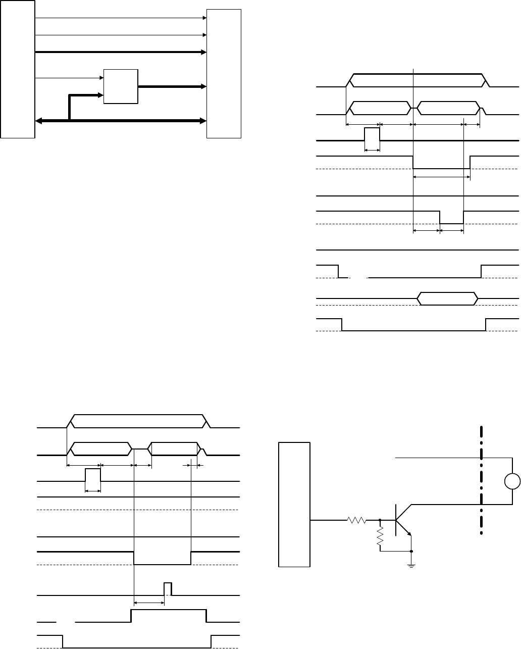
4. Printer control circuit (ER-A310)
1) Printer motor drive circuit
The motor drive signal MD from the CPU is used to operate the
printer motor with switching operation of transistor Q17.
IC2
CPU
IC3
74HC373
IC14
S-RAM
A8~A14
/ALE
A0~A7
AD0~AD7
AD0~AD7
/WE
/CE
P111~P117
P20~P27
P32
P30
RAM /OE
P31
P20~P27
(READ cycle)
Upper address
Lower address RAM data output
15ns or above
15ns or
above 70ns or above
0ns or above
Lower address
latch signal
30ns or above
Fixed to HIGH.
Fixed to LOW
READ timing
Select Input
Output
70ns or above
Hammer common
RAM control
RAM /WE
RAM /CS
P20~P27
P111~P117
P20~P27
P32
P30
RAM /OE
P20~P27
P20~P27
RAM Data IN
RAM control
(WRITE cycle)
Upper address
Lower address Input data to RAM
15ns or above
15ns or
above
30ns or above
0ns or above
Lower address
latch signal
30ns or above
50ns or above
Fixed to LOW.
0ns or
above
60ns or
aboveREAD timing
Select
Input
Output
Hammer common
RAM /WE
RAM /CS
P20~P27
M
VP : +24V
M
R60
R61
Q17
C3784
IC2
CPU
MD
– 11 –
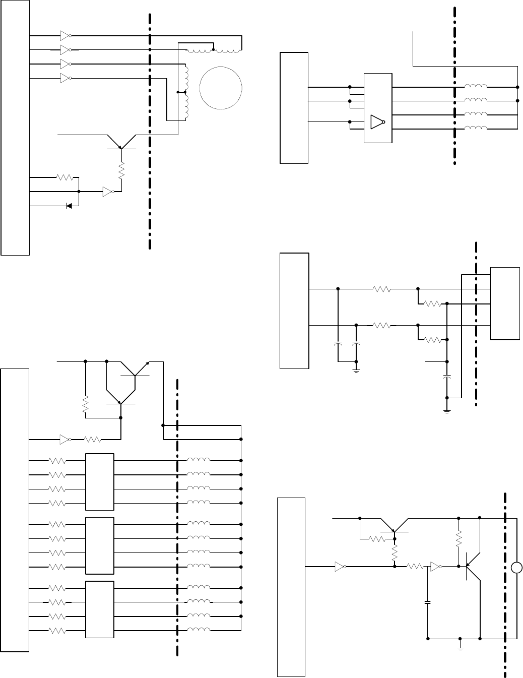
2) Print wheel drive circuit
The stepping motor is used to drive the printer wheel.
The common signal SCOM from the CPU is used to supply voltage
VP to the stepping motor with the switching operation of transistor
Q19, and the stepping motor solenoid drive signal is used to operate
the stepping motor.
3) Print solenoid drive circuit
Since the address bus is used to drive the print solenoid, an access
to the RAM cannot be performed during printing. The common volt-
age of the print solenoid is supplied by switching operations of tran-
sistors Q23 and Q19 with the HCOM signal.
4) Paper feed solenoid and stamp solenoid drive
circuit
PF: Paper feed solenoid drive signal (Receipt side)
JF: Paper feed solenoid drive signal (Journal side)
STAMP: Stamp solenoid drive signal (Receipt side)
5) Timing signal circuit
5. Printer motor drive circuit (ER-A330)
1) Printer motor drive and brake circuit
The printer motor is operated by switching operation of transistor Q17
with the motor drive signal MD from the CPU.
VP : +24V
IC2
CPU
R74
1K
Q19
B888
M
AB
C
D
PM2
PM1
PM3
PM4
STEPPING MOTOR
SM1
SM2
SM3
SM4
IC7B
KID65003P
IC7A
KID65003P
IC7C
KID65003P
IC7D
KID65003P
D29
1SS133
IC7F
KID65003P
R63
4.3K
PCOM
VCC
SCOM
/R ESET
IC2
CPU
VP : +24V
IC7G
KID65003P
Q19
KTD2060
HCOM
IC9
MAC16
IC10
MAC16
IC11
MAC16
Q23
A1266
R70
3.3K
R69
18K
R85
4.7K
R86
4.7K
R87
4.7K
R88
4.7K
R89
4.7K
R90
4.7K
R91
4.7K
R92
4.7K
R93
4.7K
R94
4.7K
R95
4.7K
R96
4.7K
AD5
AD4
AD3
AD2
AD1
AD0
A5
A4
A3
A2
A1
A0
RM6
RM4
RM3
RM5
RM2
RM1
JM6
JM5
JM1
JM2
JM4
JM3
HM COM
HM COM
IC2
CPU
IC6
KID65003P
RM6
RM4
RM3
RM5
VP: +24V
HM COM
JF
RF
STAMP
IC2
CPU
T
STAMP
R
C20
100P
C21
100P R66
1K
R64
1K
R65
4.7K
R67
4.7K
VCC:+5V
C22
10U/50V
+
Timing
generating
circuit
IC2
CPU
VP : +24V
Q17
B601
R78
470
IC6B
KID65003P
MD
R79
2.7K
R80
22K
C20
0.20P
Q18
B926
R81
2.7K
VM
M
– 12 –
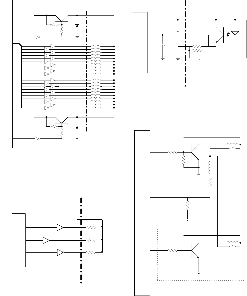
2) Print solenoid drive circuit
Since the address bus is used to drive the print solenoid, an access
to the RAM cannot be performed during printing. The common volt-
age of the print solenoid is supplied by switching operations of tran-
sistors Q23 and Q19 with the J-COM signal and the R-COM signal.
3) Paper feed solenoid and stamp solenoid drive
circuit
PF: Paper feed solenoid drive signal (Receipt side)
JF: Paper feed solenoid drive signal (Journal side)
STAMP: Stamp solenoid drive signal (Receipt side)
4) Timing signal circuit
The timing signal α is delivered to the CPU by the photo transistor
attached to the printer.
6. Drawer drive circuit
The solenoid is driven by switching operation of transistor Q14 with
the drive signal DR1 from the CPU.
When an option drawer is used, the parts enclosed with the dotted
line must be attached to the PWB.
IC2
CPU
AD0
AD2
AD4
AD6
AD7
VP : +18V
Q19
B926
R82
2.7K
IC6C
KID65003P
J-COM
R83
220/2W
VJ
D28
1N4002
AD1
AD3
AD5
MG10
MG9
IC7B
IC7C
IC7G
IC8B
IC8D
IC7E
IC7D
IC7F
IC8C
IC8A
JM2
JM1
JM3
JM4
JM5
JM6
JM7
JM8
JM9
JM10
VP : +24V
Q20
B926
R84
2.7K
IC6E
KID65003P
R-COM
R85
220/2W
VR
D29
1N4002
AD0
AD2
AD4
AD6
AD7
AD1
AD3
AD5
MG10
MG9
IC8E
IC8F
IC9C
IC9E
IC9G
IC9A
IC8G
IC9B
IC9F
IC9D
RM2
RM1
RM3
RM4
RM5
RM6
RM7
RM8
RM9
RM10
IC2
CPU
RF
JF
STAMP
6
1
7
1
6
6
7
VM
IC2
CPU
STAMP
C30
100P
VCC:+5V
C29
10U/16V
α
IC2
CPU
VP : +18V
R53
1K
R54
15K
Q14
C3784
DR1
VP : +18V
R80
1K
Q17
C3784
DR2
DRS
R57
ER-A310:3.3K
ER-A330:4.7K
ER-A310:3.3K
ER-A330:4.7K
R55
15K
L2
STANDARD DRAWER
OPTION DRAWER
– 13 –
7. Keyboard circuit
The keyboard performs key scanning with the eight strobe signals
ST1-ST8, and returns the nine return signal KR1-KR9 to the CPU.
The mode switch performs scanning with the eight strobe signals
ST1-ST8, and returns the return signal KR10 to the CPU. When the
mode switch is at SRV position, the reset signal /RESET is outputted.
8. Display circuit
The 7-segment LED is used in the display. The operator display uses
10 digit signals, and the pop-up display uses 7 digit signals.
9. Power supply circuit
10. Battery voltage monitor circuit
The battery voltage signal is inputted to the CPU P10 and the com-
parison reference voltage VCC (+5V) is inputted to the CPU VREF to
monitor the battery voltage. When the input to P10 falls below
7/10VCC=+3.5V, the low battery display is made.
IC2
CPU
ST8
ST6
ST4
ST2
ST1
ST7
ST5
ST3
KEY MATRIX
KR1
KR2
KR3
KR4
KR6
KR7
KR8
KR5
KR9
RA2
56K X 8
R102
56K
D9
D11
D13
D15
D16
D10
D12
D14
MODE SWITCH
ST1~ST8
/R ESET
KR10 C11
M104
R40
56K
D17
1SS133
DIG1'DIG9'DIG10' DIG2'
A,B,C,D,E,F,G,DP
DP' G' F'E'D'C'B'A'
A',B',C',D',E',F',G',DP' A',B',C',D',E',F',G',DP'
DIG1-DIG10
FND5
FND1FND4,3,2
IC2
CPU
+6V
POP UP
DISPLAY
DIG1'-7'
Operator Display
DP~A
REGURATOR
CIRCUIT
POWER
TRNSFORMER
F1
T1AL/250V
P-OFF
CIRCUIT
REGURATOR
CIRCUIT
BATTERY
CITCUIT
VP:+24V(ER-A310)
+18V(ER-A330)
+6v
VCC:+5V
PE VDD:+5V
: PRINTER, DRAWER
: DISPLAY
: CPU,RAM
VB
IC2
CPU
AVREF
P10
VB:+1.5V X 3=+4.5V
VCC:+5V
– 14 –
11. Clock generator circuit
X2: 4.19MHz is inputted as the CPU main clock.
X1: 32.768KHz is inputted as the time renewal clock.
12. Buzzer circuit
This circuit sounds buzzer with the BUS signal from the CPU.
13. Reset circuit
The reset signal is formed with VOC and VDD. The /RESET signal is
also outputted when the mode switch is at SRV position.
IC2
CPU
X1
32.768KHz
C14
33P
C16
22P
R51
330K
R93
1M
X2
4.19MHz
X2
X1
XT2
P04
IC2
CPU
BUZ BZ
IC6A
KID65003P
BZ1
VCC
+
IC2
CPU
/RESET
VDD
VCC
D24
1SS133
C18
22U/16V
+
+
C19
10U/50V
Q16
C3198
R59
1K
MODE SWITCH
/RESET
C11
M104
R58
1K
– 15 –
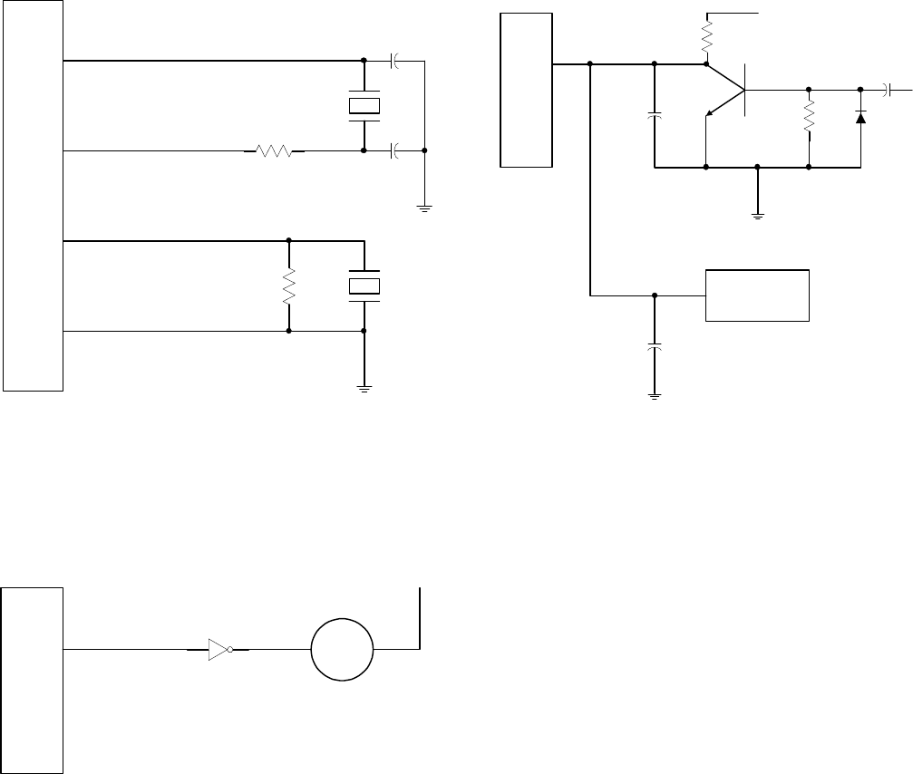
CHAPTER 5 TEST FUNCTION
1. Start of test function
The following key operation is required in the SRV mode to start the
test.
Master reset is required when the system is to be started for the first
time.
2. List of test commands
No. Test contents Key operations
1 Mode switch test 1 → ST
2 Keyboard test XXXX02 → ST
3 Display and Buzzer test 3 → ST
4 Standard Drawer test 4 → ST
5 Option Drawer test 14 → ST
6 Printer test 5 → ST
7 RAM test 6 → ST
8 Battery voltage test 7 → ST
NOTE-1: Test message is printed on the journal
NOTE-2: The contents of the totalizer and the preset values are not
erased by the test.
3. Test function
1) Test No. 1: Mode switch test
1Key operation
Then, turn the mode switches in the following order.
*In the mode switch test, turn the switch rhythmically.
2Description
As the mode switch position number is displayed, check the num-
ber.
3Termination
The test can be terminated when the mode switch is turned to the
SRV side from other position.
Termination print at normal end ****** 0 1
Termination print and error ******* 1
2) Test No. 2: Keyboard test
1Key operation
(1) Enter the test command in succession to the sum check data
of the model.
Model name Sum check data
(Standard keyboard data)
ER-A310 2428
ER-A330 2946
∗NOTE: Sum check data
The check sum is a decimal number obtained by
converting the hard code hexadecimal total of all
keys.
The CA/AT key are the exception.
(2) Next, push every key on the keyboard except for the receipt
and journal keys.
When the CA/AT key is pressed, the termination printout is
immediately produced assuming that all keys have been
pressed.
There is no order in which the keys have to be depressed.
Display: 02 XX ← XX = position code.
[Keyboard position code of model vs. key to be pressed]
[All key position code]
[ER-A310 standard keyboard layout]
[ER-A330 standard keyboard layout]
XXXX
Test command
ST
1
ST
MODE: SRV PGM VOID OFF OP X/Z REG MGR X1/Z1 X2/Z2 SRV
DISPLAYE: (0) (1) (2) OFF (3) (4) (5) (6) (7) (0)
02
Test command
X
X
XX
Sum check data
ST
65 68 67 58 77 78
38
37
27
18
08
48
47
28
17
07
57
46
36
16
06
56
35
75
05
25
55
45
76
15
26
66
42
32
72
0212
62
52
22
R
70
10
00
J
41
21
11
61
31
20
01 14 04 03
24
44
64 63
34
74
53
33
73
8
70
13
54
43
23
70
10
00
67
56
35
75
05
25
68
55
76
26
77
48
47
78
38
37
27
08
03
53
33
73
13
54
43
23
04
63
34
74
31
20
01
41
21
11
61
R
J
67
56
35
75
05
25
70
10
00
41
21
11
31
20
01 04
63
34
74
13
54
43
23
03
53
33
73
68
55
45
76
15
26
65 78
38
37
27
08
77
48
47
61
58
57
46
36
16
06
R
J
– 16 –
2Description
Until the depression of the ST key, the sum of key position
codes is compared with the sum check data, except for the
CA/AT key.
3Termination
The test terminates with the depression of the CA/AT key and
the termination printout is produced.
Termination print at normal end ****** 0 2
Termination print at error ******* 2
3) Test No. 3: Display and buzzer test
1Key operation
2Description
Continuous beeps and the display are tested.
1. 2. 3. 4. 5. 6. 7. 8. 9. 0.
State of display
The decimal point is shifted digit by digit from the lowest digit
(every 200 msec).
Then all segments are lighted (for about 1 sec).
8. 8. 8. 8. 8. 8. 8. 8. 8. 8.
State of display
Pressing any key will terminate the test.
3Check items
Check that each position display is correct.
Check that the display is even and uniform.
Check that the buzzer sound is normal. (No interruption and vibra-
tions of sounds.)
4Test end
End print 3
4) Test No. 4: Drawer open test
1Key operation
2Description
With this test, the drawer opens and its state is displayed in the
following manner:
Drawer open → XX 0
Drawer closed → XX C XX = 04 or 14
*When the model that has no drawer sensor switch, displayed is
"C".
3Termination
With depression of any key
Termination print 04 (For standard drawer)
14 (For Option drawer)
5) Test No. 5: Continuous print test
1Key operation
2Description
The continuous printing as shown below is performed.
3Termination
After pressing any key, one-cycle of printing is performed before
completing the operation.
Print format
ER-A310
000000000CD CH 1⁄2
111111111PCK 1
222222222XCR 2
333333333ZEX 3
444444444#TX 4
555555555RF FS 5
666666666VD %6
777777777TR d7
888888888QRA CG
999999999@PO TD
★★★★★★★★★ +NS TL
––––. . . . No–*ST
PL GT –––CA
1
2
3
4
5
6
7
8
9
NS
ST
ER-A330
PL ZTX . . . . GT CA @
–––––––#CK Q
★★★★★★★%CH CG
00000000RA TD
11111111PO 1
22222222VD 2
33333333NS 3
44444444TX 4
55555555FS 5
66666666d6
77777777X
1
⁄
2
88888888EX ST
99999999RF TL
0
1
2
3
4
5
6
7
EX
TL
3
ST
4
14
: For stardard drawer
: For option drawer
ST
ST
5
ST
– 17 –
6) Test No. 6: RAM test
1Key operation
2Test content
The RAM of 256KByte (standard provision) is checked.
Read and write of each data are made to the addresses shown in the
table below to compare the data. If there is no error, the machine
returns to the key wait state. If an error occurs, intermittent buzzer
sounds are made and the error print is made. Press any key to cancel
the error.
X AD
Upper AD 0123456789ABCDEF
000X 0F 1E 2D 3C 4B 5A 69 78 87 96 A5 B4 C3 D2 E1 F0
001X F0 0F 1E 2D 3C 4B 5A 69 78 87 96 A5 B4 C3 D2 E1
002X E1 F0 0F 1E 2D 3C 4B 5A 69 78 87 96 A5 B4 C3 D2
004X D2 E1 F0 0F 1E 2D 3C 4B 5A 69 78 87 96 A5 B4 C3
008X C3 D2 E1 F0 0F 1E 2D 3C 4B 5A 69 78 87 96 A5 B4
010X B4 C3 D2 E1 F0 0F 1E 2D 3C 4B 5A 69 78 87 96 A5
020X A5 B4 C3 D2 E1 F0 0F 1E 2D 3C 4B 5A 69 78 87 96
040X 96 A5 B4 C3 D2 E1 F0 0F 1E 2D 3C 4B 5A 69 78 87
080X 87 96 A5 B4 C3 D2 E1 F0 0F 1E 2D 3C 4B 5A 69 78
100X 78 87 96 A5 B4 C3 D2 E1 F0 0F 1E 2D 3C 4B 5A 69
200X 69 78 87 96 A5 B4 C3 D2 E1 F0 0F 1E 2D 3C 4B 5A
400X 5A 69 78 87 96 A5 B4 C3 D2 E1 F0 0F 1E 2D 3C 4B
800X 4B 5A 69 78 87 96 A5 B4 C3 D2 E1 F0 0F 1E 2D 3C
3Check item
Check the end print.
4Test end
Normal end print ******* 0 6
Error print ******** 6
7) Test No. 7: Battery voltage test
1Key operation
2Details of test
By the above key operations, the battery voltage is checked with
the A/D conversion circuit of CPU and the following display is
made.
***
Voltage conversion value when the reference voltage Vref (+5V) is
supposed to 256.
3Check item
Display check item
(Example) If the battery voltage is +3 V, 256 × 3/5 = 153 is
displayed.
4Test end
Pressing any key will make the following print and terminate the
test.
End print 07
(Note) Specified value: 3.0 V
6
ST
7
ST
– 18 –
– 19 – – 20 –
123
4
5678
D
C
B
A
D
C
B
A
123
4
5678
VP
HEAT SINK
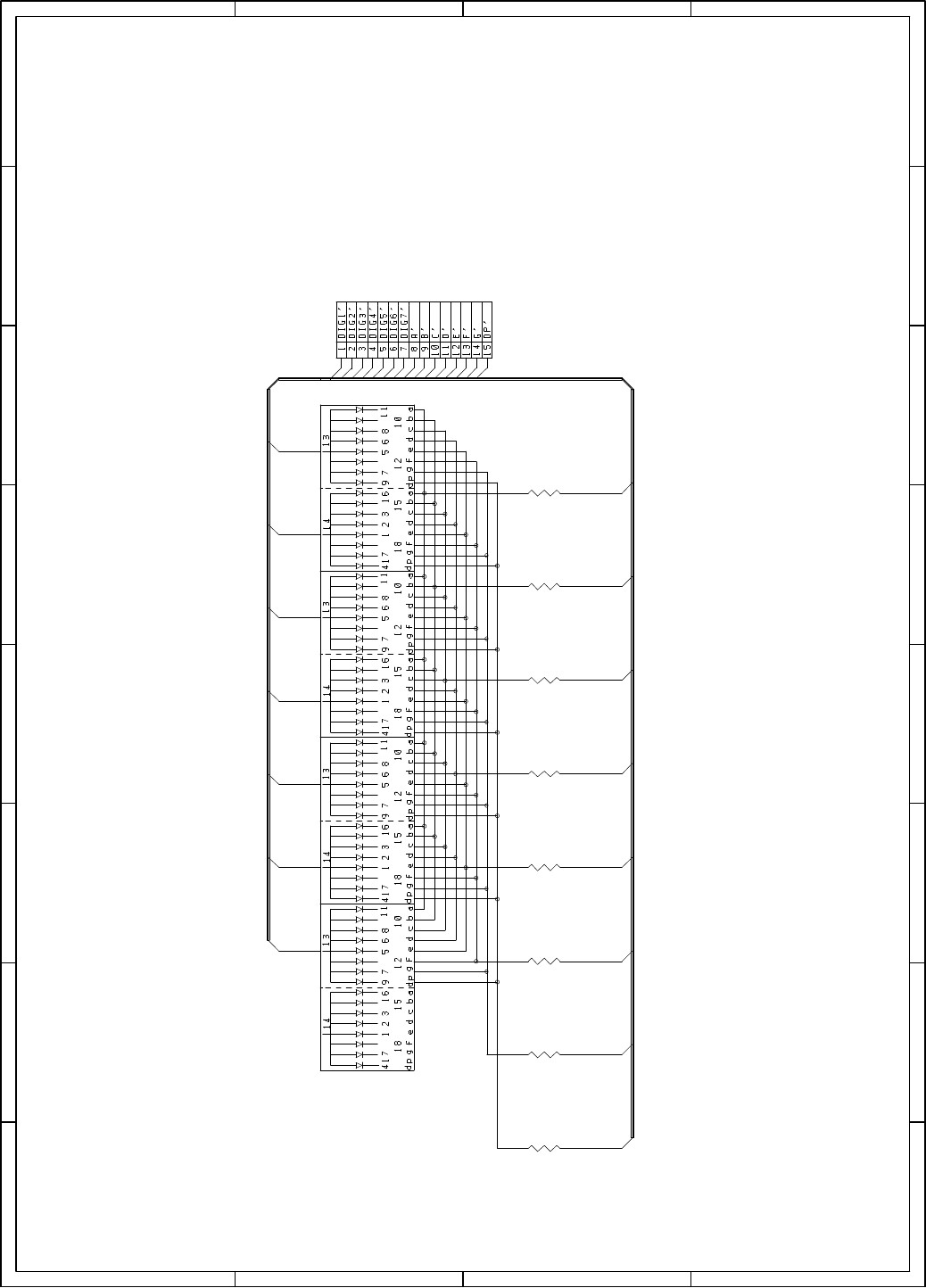
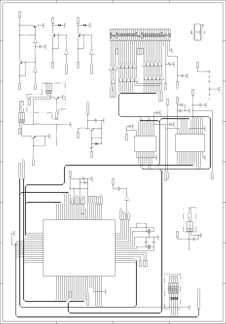
CHAPTER 6. CIRCUIT DIAGRAM & PWB LAYOUT
1. Circuit diagram
CIRCUIT(ERA310/A330)
Q1
KTD1415
F1
S T1.6AL/250V
UL CSA 2.0A/125V
C1
M 0.033u
CN1
PS CN
4
1
2
3
BD1
DI102
C2
4700u
50V
R1
12K
R2
3.9K
ZD1
A330:H:MTZ20D
A3 10: L: MTZJ 27A
C4
330u
50v
GND D6 1N4002
+6V
VCC
VDD
C9
330u
16V
C10
330u
16V
C8
1000u
16V
ZD5
MTZ6.2B
D7 1SS133
D8
1SS133
R9
220
BT
R7
3.6KF
R8
1KF
HEAT SINK
56
12
34
IC1
KA34063A
Q2
KTD1414
R6
10
L1
220uH
D4
PS102R
VCC
PE
R5
100K
R3
56K
R4
2.7K
D3
1SS133
C5
3.3u
50V
ZD2
A3 30: H: MTZ15A
A310:L:MTZ18B
CN14/CN14-1
FM CN
DIG 1~10
Q31
A1271
R122
Q32
R112
R121
12K
+6V
R111
220
R123 R124 R125
Q33
Q34
R113 R114
R115
R126 R127
Q35 Q36 Q37
R116 R117
C6
0.1u
50V
R128 R129 R130
Q38 Q39
R118
R119 R120
ST1~ST8
C7
220P
Q40
Q31~ Q33: A 1271
R121~R130: 12K
VB
CN2
BT CN
GND
A310:LC31
A330:HC34
R101 1M
KEY72
ST8
ST1
ST2
ST3
ST4
ST5
ST6
ST7
D9
D10
D11
D12
D13
D14
D16
CN5
CN8P
D15
1SS133*8
R11,13,15,17, 19 , 21,
23,25,27,29 : 2.2K
CN15
PM CN
POP UP LED CN * 1
R111~R120: 220
Q3~Q12:C3198
Q34~Q40: B926
FND1
DIG3' DIG2' DIG1'
Q10 Q11 Q12
R27 R29
FND2
DIG5' DIG4'
Q8
Q9
R21 R23 R25
FND3
DIG8' DIG7' DIG6'
Q5
Q6 Q7
R15 R17 R19
FND5 FND4
DIG10' DIG9'
Q3
C3198
Q4
R13R11
2.2K
CN7
R102
56K
CN8
CN9P
RA2
56KX8
GND
D17
1SS133
R40
56K
C11M104
/RESET
KR10
1
5
2
B
5
1
6
1
A
5
A'B'
R30
30
1
3
4
D
5
1
4
3
C
5
C'D'
1
1
6
F
5
1
0
7
G
5
1
2
5
E
5
E'F'G'
SEGA ~DP
MAIN LED PWB
DP'
R38
2.2k
DP
R39
12k
Q13
C3198
ST1~ST8
IC5
KID65003P
KR1~KR9
1/4
(3-6C)(4-6C)
7.8
(3-8A)(4-8A )
(3-5D)(4-5D)
R31
30
R32
30
R33
30
R34
30
R35
30
R36
30
R37
30
(3-8A)(4-8A )
(3 -4 B ) (3 -8 C )( 4 -8 C )
(3-5D)
(4-5D)
(3-8A)(4-8A )
(3-5D)(4-5D)
8 7 6 5 4 3 2 1
A
B
C
D
12345678
D
C
B
A
CIRCUIT(ERA310/A330 POP)
DIG7' DIG5'DIG6' DIG2'DIG3'DIG4' DIG1'
CN1
PM CN
POP UP LED CN * 1
FND1FND3 FND2FND4
DP'
R10
27
F'G'
R12
27
R14
27
D'E'
R16
27
R18
27
B'C'
R20
27
R22
27
R24
27
A'
2/4
– 21 –
– 22 – – 23 –
123
4
5678
D
C
B
A
D
C
B
A
123
4
5678
VCC
NOTE
VP
CN11
VP
R53
1K
Q14
C3784
KR1~KR11
DIG1~DIG10
CIRCUIT(ERA310)
D
P
/
S
T
8
D
R
2
D
I
G
1
0
D
I
G
8
D
I
G
9
A
/
S
T
1
B
/
S
T
2
C
/
S
T
3
D
/
S
T
4
E
/
S
T
5
F
/
S
T
6
G
/
S
T
7
P
3
3
4
0
P94
1
P93
2
P92
3
P91
4
P90
5
P81
6
P80
7
VDD
8
P27
9
P26
10
P25
11
P24
12
P23
13
P22
14
P21
15
P20
16
/RESET
17
P74
18
P73
19
AVSS
20
P17
21
P16
22
P15
23
P14
24
P
1
3
2
5
P
1
2
2
6
P
1
1
2
7
P
1
0
2
8
A
V
D
D
2
9
A
V
R
E
F
3
0
P
0
4
3
1
X
T
2
3
2
V
S
S
3
3
X
1
3
4
X
2
3
5
P
3
7
3
6
P
3
6
3
7
P
3
5
3
8
P
3
4
3
9
P114
64
P115
63
P116
62
P117
61
P120
60
P121
59
P122
58
P123
57
P124
56
P125
55
P126
54
P127
53
VDD
52
P70
51
P71
50
P72
49
IC
48
P00
47
P01
46
P02
45
P03
44
P30
43
P31
42
P32
41
P
9
5
8
0
P
9
6
7
9
P
9
7
7
8
P
1
0
0
7
7
P
1
0
1
7
6
P
1
0
2
7
5
P
1
0
3
7
4
P
1
0
4
7
3
P
1
0
5
7
2
V
L
O
A
D
7
1
P
1
0
6
7
0
P
1
0
7
6
9
P
1
1
0
6
8
P
1
1
1
6
7
P
1
1
2
6
6
P
1
1
3
6
5
IC2
UPD78045F
A
8
A
9
A
1
0
R54
15K
DRS
DR1
L2
B CORE
R55
15K
DR2
R80
1K
Q20
C3784
CN16
VP
IC7
KID65003P
ZD29
MTZJ24B*1
D27
1N 4002
VP
Q19
KTD2060
R69
18K
Q23
A1266
R57
4.7K(H)
3. 3K (L)
U:X
V:O
VDD
C18
22u
16V
D24
1SS133
R59
1K
Q22
C3198
R58
1K
/RESET
C19
10u
50V
VDD
1
J1
23
C12
0.1u
12V
VCC
C13
10u
16V
A11
A12
A13
A14
KR1
KR2
KR3
KR4
SM1
SM2
HCOM
DR1
DRS
R77
R76
VDD
DIG 7
DIG 6
DIG 5
DIG 4
DIG 3
DIG 2
DIG 1
AD7
AD6
AD5
AD4
AD3
AD2
AD1
AD0
KR11
KR10
KR9
KR8
/RESET
SCOM
R73
1K
SM4
PE
SM3
T
R
/WE
/CE
/ALE
R75
1K *3
NE
VCC
HCOM
AD5
AD4
AD3
AD2
2
4
6
8
1
10
R70
3.3K
R85~R88
4.7K*4
R89~R92
4. 7K * 4
10 7 7G
IC9
IC10
1
2
3
4
5
6
7
8
9
10
11
12
13
14
15
16
17
18
19
20
21
22
23
24
25
26
27
28
CN12
PRCN28P
3
5
7
9
VP
15
2 7B
13
4
7D
2
4
6
8
3
5
7
9
1
10
SM2
SM1
SM3
SM4
16 1 7A
14 3
7C
2
4
6
8
3
5
7
9
110
IC11
R62
300/2W
R93~R96
4. 7K * 4
AD1
AD0
A5
A4
A3
A2
A1
A0
A7
AD7
AD6
A6
A5
AD5
C23
0.1u
12V
A0
AD0
AD1
A1
A2
AD2
VCC
20
Q7
19
D7
18
D6
17
Q6
16
Q5
15
D5
14
D4
13
Q4
12
/LE
11
IC3
74HC373
VCC
STAMP
JF
RF
MD
BUZ
16 1 6A
BZ1
+
R100
1M
VB
K
R
7
K
R
6
K
R
5
R50
330K R5 1
330K
VDD
VCC
X1
32. 76 8K Hz
C14
33P
C16
22P
/ALE
/WE
X2
4.19MHz
AD3
A3
A14
1
A12
2
A7
3
A6
4
A5
5
A4
6
A3
7
A2
8
A1
9
A0
10
D0
11
D1
12
D2
13
GND
14
IC4
S-RAM256K
AD4
A4
/ALE
C24
330P
R71
22K
C25
330P
VCC
/RESET
SCOM
VP
D25
1N 4002
R63
4.7K
11 6 7F
D26
1N4002
VP
D29
1SS133
R74
1K
Q18
B601
13
4 6D
10 7
6G
11 6
6F
12 5
6E
15
2 6B
RF
JF
STAMP
R64
1K
R66
1K
T
R
14 3
6C
R65
4.7K
R67
4.7K
C22
10u
50V
C21
1000P
C20
1000P
VCC
VDD
MD
R60
1K
Q17
C3784
R61
15K
VCC
VDD
A13
A8
A9
A11
A10
AD7
AD6
AD5
AD4
AD3
/CE
C26
0.1u
12V
R68
22K
C28
330P
C27
10u
16V
A14
A12
A6
A5
A4
A3
A2
A1
A0
AD0
AD1
AD2
A7
CN10
NE CN
U:X
C29
1000P
R83
4.7K
NE
VCC
ST1
ST2
ST3
ST4
R52
56K
D19
D20
D21
CN9
1H K EY
U:X
V:O
D18
1SS133*4
KR11
A/ST1~DP/ST8 /CE
V:X
IC6
KID65003P
VP
3/4
(1-4A)(1-2A )
(1-8C)
(3-4D)
(3-3C)
(3-4D)
(3-2B)
(3-2B)
(3-2B)
(1-5C)
(3-2B)
(3-2B)
(3-7A)
(3-6B)
(3-6A)
(3-6B)
(3-2B)
(3-2B)
(3-2B)
(3-2B)
(1 -3 A )(3 -3 C)
(3-4B)
(3-2B)
(3-5C)
(3-5C)
(3-5C)
(3-6C)
(1-4A)(1-4C)(1-8A)
28
27
26
25
24
23
22
21
20
19
18
17
16
15
VDD
/WE
A13
A8
A9
A11
/OE
A10
/CE
D7
D6
D5
D4
D3
/OE
Q0
D0
D1
Q1
Q2
D2
D3
Q3
GND
1
2
3
4
5
6
7
8
9
10
(1-3A)
(3-3C)
(3-8C)
(3-6B)
(3-6C)
(3-6C)
(3-6B)
(3-6B)
(3-6B)
(3-6C)
(3-6C)
(3-6C)
(3-8C)
(3-6C)
(3-6C)
(3-4B)(3-8C)
(3-6C)
– 24 – – 25 –
123
4
5678
D
C
B
A
D
C
B
A
123
4
5678
VM
R81
2.7K
Q17
B601
R78
470
R79
2.7K
VP
CN11
VPKR1~ KR11
DIG1~DIG10
CIRCUIT(ERA330)
D
R
2
D
P
/
S
T
8
D
I
G
8
D
I
G
9
D
I
G
1
0
A
/
S
T
1
B
/
S
T
2
C
/
S
T
3
D
/
S
T
4
E
/
S
T
5
F
/
S
T
6
G
/
S
T
7
P
3
3
4
0
P94
P93
P92
P91
P90
P81
P80
VDD
P27
P26
P25
P24
P23
P22
P21
P20
/RESET
P74
P73
AVSS
P17
P16
P15
P14
P
1
3
2
5
P
1
2
2
6
P
1
1
2
7
P
1
0
2
8
A
V
D
D
2
9
A
V
R
E
F
3
0
P
0
4
3
1
X
T
2
3
2
V
S
S
3
3
X
1
3
4
X
2
3
5
P
3
7
3
6
P
3
6
3
7
P
3
5
3
8
P
3
4
3
9
P114 64
P115 63
P116 62
P117 61
P120 60
P121 59
P122 58
P123 57
P124 56
P125 55
P126 54
P127 53
VDD 52
P70 51
P71 50
P72 49
IC 48
P00 47
P01 46
P02 45
P03 44
P30 43
P31 42
P32 41
P
9
5
8
0
P
9
6
7
9
P
9
7
7
8
P
1
0
0
7
7
P
1
0
1
7
6
P
1
0
2
7
5
P
1
0
3
7
4
P
1
0
4
7
3
P
1
0
5
7
2
V
L
O
A
D
7
1
P
1
0
6
7
0
P
1
0
7
6
9
P
1
1
0
6
8
P
1
1
1
6
7
P
1
1
2
6
6
P
1
1
3
6
5IC2
UPD78045
A
8A
9A
1
0DR1
R53
1K
R54
15K
L2
B CORE
R55
15K
R56
56K
Q21
C3784 MD
CN16
R89
1K
VP
Q14
C3784
VP
15
2
6B
R80
22K
C32
220P
VJ
12 5 6E
Q19
B926
Q18
B9 26
VR
D28
1N4002
Q20
B926
D29
1N4002
VP
J-COM
R82
2.7K
R83
220/ 2W
14
3
6C
R84
2.7K
DR2
U:X
V:O
VDD
DRS
R57
4.7K(H)
3.3K(L)
R58
1K
VDD
3
C13
10u
16V
C12
0.1u
12V
B
1
A
2
A:KA,KB
B:TQ,TR,TS
MG 10
MG 9
R-COM
J-COM
A11
A12
A13
A14
KR1
KR2
KR3
KR4
DR1
R76
R77
VDD
DIG 7
DIG 6
DIG 5
DIG 4
DIG 3
DIG 2
DIG 1
AD7
AD6
AD5
AD4
AD3
AD2
AD1
/RESET NU
NU
AD0
KR11
KR10
KR9
KR8
a
PE
NE
DRS
NU
/WE
/CE
/ALE
VCC
C18
22u
16V D24
1SS133
R59
1K
Q16
C3198
STAMP
/RESET
10 7 6G
C19
10u
50V
R-COM
R85
220/2W
12 5 6E
11 6 6F 1
2
3
4
5
6
7
8
9
10
11
12
13
14
15
16
17
18
19
20
21
22
23
24
25
26
27
28
29
30
31
PR CN12
PRCN31P
VJ
VM
GND
16 1 7A
15 2 7B
14 3 7C 13
4 7D
12 5 7E 11
6 7F
10 7 7G 16 1 8A
15 2 8B 14 3 8C
13 4 8D
JF
RF
AD0
AD1
AD2
AD3
AD4
AD5
AD6
AD7
VCC C23
0.1u
12V
/OE
1
Q0
2
D0
3
D1
4
Q1
5
Q2
6
D2
7
D3
8
Q3
9
GND
10
VCC
Q7
D7
D6
Q6
Q5
D5
D4
Q4
/LE
IC3
74HC373
VCC
16 1 6A
BZ1
+
STAMP
JF
RF
MD
B
U
Z
R93
1M
VB
K
R
7
K
R
6
K
R
5
R50
330K R51
330K
CN9
1HKEY
VDD
VCC
X1
32.768KHz
C16
22P
C14
33P
X2
4.19MHz
/WE
/ALE
VCC
MG 9
MG 10
VDD
AD0
AD1
AD2
AD3
AD4
AD5
AD6
AD7
C24
330P
R71
22K
VR
C29
10u
16V
12
5
8E
11 6 8F 10
7
8G
16
1 9A 15
2
9B
14 3 9C 13
4
9D
12
5 9E 11
6
9F
10
7 9G
VP
IC6,7, 8,9
KID65003P
C30
0.1uF
aVDD
VDD
C26
0.1u
12V
R68
22K
C27
10u
16V
C25
330P
A14
1
A12
2
A7
3
A6
4
A5
5
A4
6
A3
7
A2
8
A1
9
A0
10
D0
11
D1
12
D2
13
GND
14
IC4
S-RAM28P
A14
A12
A7
A6
A5
A4
A3
A2
A1
A0
AD0
CN10
NE CN
VCC
C31
1000P
R92
4.7K
NE
U:X
V:O
ST1
ST2
ST3
ST4
R52
56K
D19
D20
D21
D18
1SS133*4
KR11
A/ST1 ~DP /ST8 U: X
V:X
/CE
AD1
AD2 C28
330P
VCC
4/4
1
2
3
4
5
6
7
8
9
10
11
12
13
14
15
16
17
18
19
20
21
22
23
24
(1-3A )(4 -3C)
(4-3C)
(4-3C)
(4-3C)
(4-3D)
(4-3A)
(1-5C)
(4-7A)
(4-4C)
(4-5B)
(4-5A)
(4-5B)
(4-3B)
(4-3B)
(4-2C)
(4-2C)
(4-5D)
(1-4A)(1-4C)(1-8A)
(4-5C)
(4-5C)
VDD
/WE
A13
A8
A9
A11
/OE
A10
/CE
D7
D6
D5
D4
D3
28
27
26
25
24
23
22
21
20
19
18
17
16
15
A13
A8
A9
A11
A10
AD7
AD6
/CE
AD5
AD4
AD3
A0
AD0
AD1
A1
A2
AD2
AD3
A3
20
19
18
17
16
15
14
13
12
11
A7
AD7
AD6
A6
A5
AD5
AD4
A4
/ALE
(4-6B)
(4-6B)
(4-6B)
(4-5C)
(4-5C)
(4-5C)
(4-5C)
(4-5C )
(4-5C)
(4-5C )
(4-6B)
(4-5C)
(4-5C)
(1-4A)(1-2A)
(1-8C)
(4-8C)
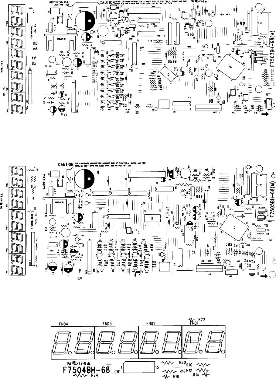
2. PWB layout
1ER-A310 Main PWB layout
2ER-A330 Main PWB layout
3ER-A310/A330 Pop-up display PWB layout
– 26 –

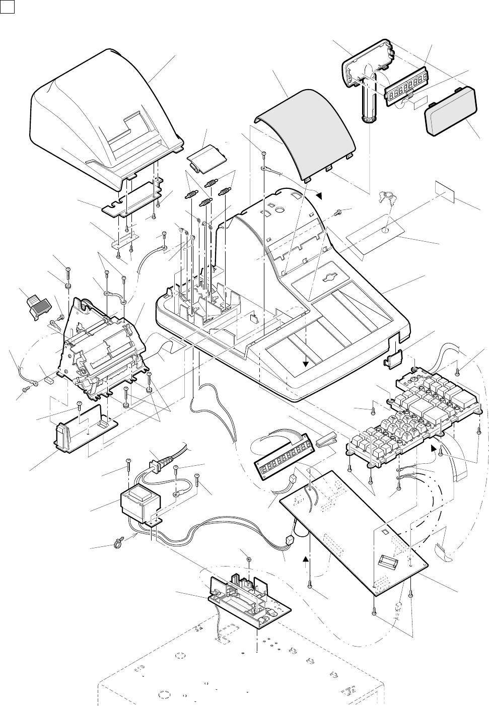
qPARTS GUIDE
ER-A310
MODEL ER-A330
SRV Key : LKGIM7113RCZZ
PRINTER : ER-A310 : CR-510
ER-A330 : UCR-812A
(For “U” & “A” version)
1Exteriors [ER-A310]
2Exteriors [ER-A330]
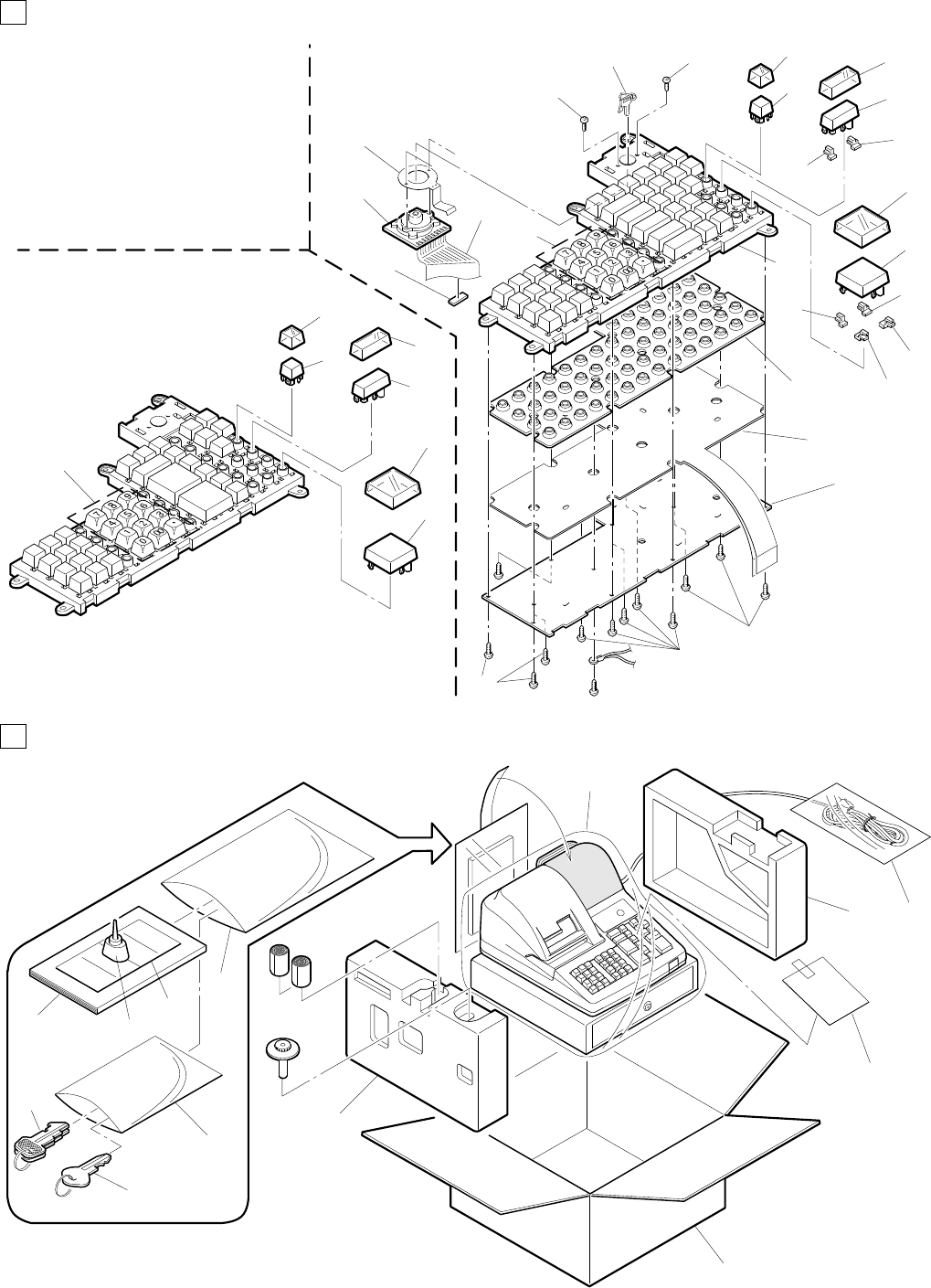
3Keyboard unit
4Packing material&Accessories
5Drawer box unit (SK423type)
6Main PWB unit [ER-A310]
7Main PWB unit [ER-A330]
8Pop-up PWB unit
9Articles for consumption
FService route options
■Index
CONTENTS
Because parts marked with !
is indispensable for the machine safety maintenance and operation, it must be
replaced with the parts specific to the product specification.

1Exteriors[ER-A310]
NO. PARTS CODE PRICE
RANK NEW
MARK PART
RANK DESCRIPTION
1GCOVA7123BHZZ AY N D Printer cover L
2LPLTP6713BHZZ AL N C Printer guide plate
3LX-BZ6788BHZZ AD N C Screw
4PCUT-6654BHZZ AE N C Paper cutter
5GCOVH7124BHZZ AF N D Battery cover
6NROLP6651BHZZ AD C Paper plate roller
7PFILW6962BHZZ AU N D Display filter
8GCAB-7237BHZZ AM N D Pop up cabinet
9CPWBF7504BH01 BC N E Pop up PWB unit
10 QCNW-7815BHZZ AR N C P-flat cable (15p)
11 PFILW6961BHZZ AP N D Pop up filter
12 XHPSD30P06K00 AA C Screw (3 ✕ 6K)
13 XBBSC30P08000 AA C Screw (3 ✕ 8) (for top cover-trans cover)
14 HDECP6847BHZZ AM N D Deco panel
15 TCAUZ6684BHZZ AD D Caution lanel [U.S.A]
TCAUZ6685BHZA AA D Caution label [Canada]
16 GCABB7236BHZZ BC N D Top cabinet
17 GFTAF6921BHZZ AG N D Clerk cover A
18 XEBSD30P08000 AA C Screw (M3 ✕ 8)
19 QCNW-7810BHZZ AG N C GND wire
20 CPWBF7503BH01 BV N E Main PWB unit
21 GCOVH7125BHZZ AP N D Trans cover
22 XNESD30-24000 AA C Nut (M3)
23 LX-BZ6781BHZZ AB C Screw (for transformer)
24 XBPBZ40P08K00 AA C Screw (4 ✕ 8K)
25
! QACCD8411QCZZ AN B AC cord (6A bush 2.5M)
26 XJPSD30P16X00 AB C Screw (3 ✕ 16X) (for transformer)
27! RTRNP6889BHZZ BC N B Power transformer (120V)
28 LHLDZ1017ACZZ AC C Clamp
29 XHBSD40P06000 AA C Screw (4 ✕ 6)
30 QCNW-7823BHZZ AE N C Earth wire
31 LHLDZ6840BHZZ AL N C Printer holder
32 PCUSG7024BHZZ AE N C Printer cushion
33 XJPSD30P12X00 AB C Screw (3 ✕ 12X) (for printer)
34 KI-OB6780RCZZ BW N E Printer unit (CR-510)
35 PGUMM6726BHZZ AE N C Printer gum
36 QCNW-7808BHZZ AF N C P-GND wire
37 PSTM-6805RCZZ AT N C Stamp(YOUR RECEIPT THANK YOU)
38 XBPSD30P10KS0 AB C Screw (M3 ✕ 10KS) (for printer)
39 LX-HZ0056BHZZ AA C Screw (for trans)
40 QTANZ6657BHZZ AD N C Battery terminal d
41 QTANZ1363CCZZ AA C Battery terminal (+/-)B
42 QTANZ1362CCZZ AA C Battery terminal (+/-)A
43 QTANZ6641BHZZ AC C Battery terminal c
44 QCNW-7806BHZZ AN N C PR flat cable (28p)
45 QCNW-7816BHZZ AR N C B/T cable (2p)
46 QCNW-7451BHZZ AG C PS cable (2pin)
47 LBNDJ2003SCZZ AA C Cable band (80mm)
48 XEBSD20P06000 AA C Screw (2 ✕ 6)
ER-A310U
– 1 –
1Exteriors[ER-A310]
RCPS0127
1
2
3
4
5
6
7
8
9
11
10
12
13
14
15
16
17
19
20
21
22
23
24
25
27
32
34
38
6
42
3
41
43
39
40
37
44
33
32
35
18
26
18
18
18
18
18
18
45
46
47
12
31
36
28
12
30
29
48
ER-A310U
– 2 –

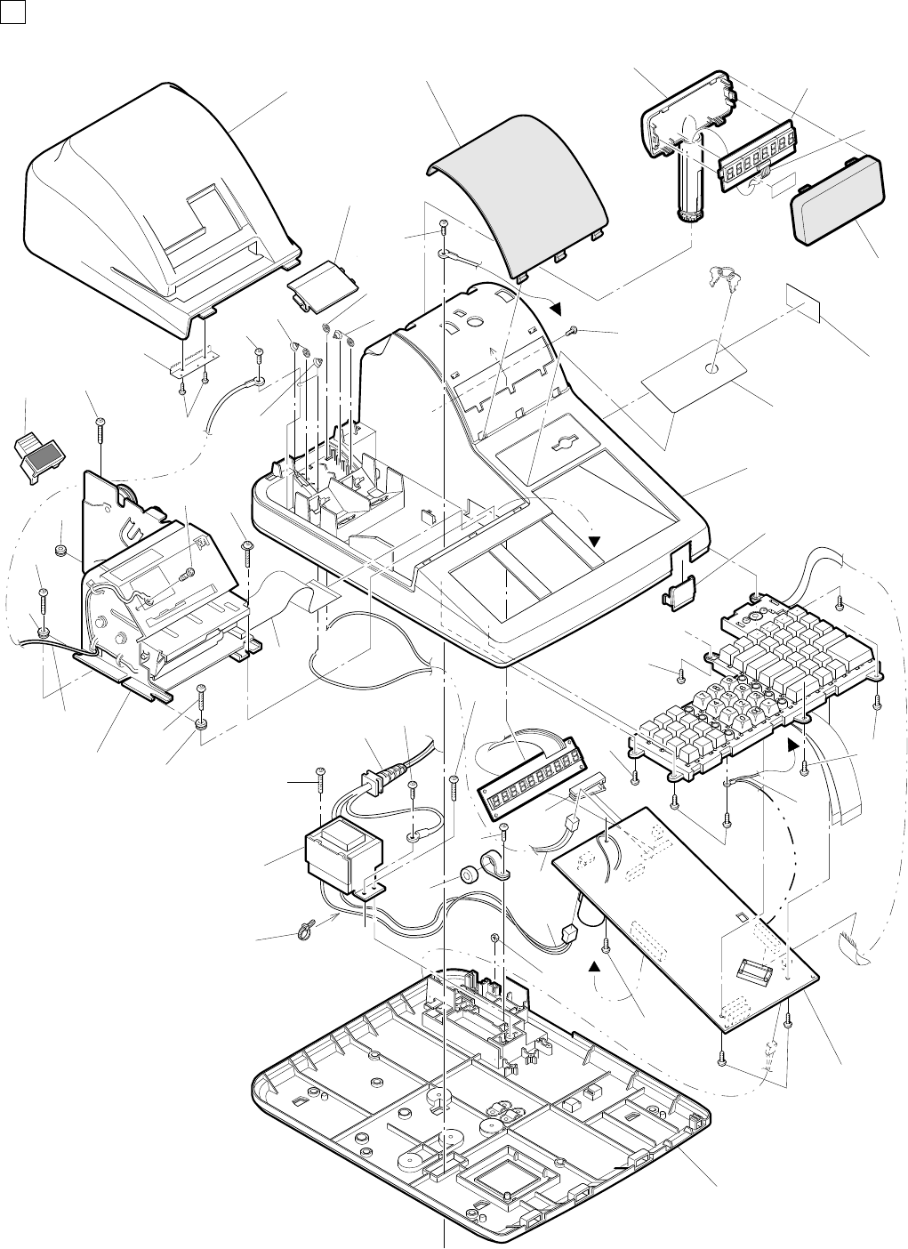
2Exteriors[ER-A330]
NO. PARTS CODE PRICE
RANK NEW
MARK PART
RANK DESCRIPTION
1GCOVA7128BHZZ AY N D Printer cover H
2PCUT-6654BHZZ AE N C Paper cutter
3LX-BZ6788BHZZ AD N C Screw
4GCOVH7124BHZZ AF N D Battery cover
5PFILW6962BHZZ AU N D Display filter
6GCAB-7237BHZZ AM N D Pop up cabinet
7CPWBF7504BH01 BC N E Pop up PWB unit
8QCNW-7815BHZZ AR N C P-flat cable (15p)
9PFILW6961BHZZ AP N D Pop up filter
10 XHPSD30P06K00 AA C Screw (3 ✕ 6K)
11 XBBSC30P08000 AA C Screw (3 ✕ 8) (for top cover-trans cover)
12 HDECP6847BHSA AM N D Deco panel
13 TCAUZ6684BHZZ AD D Caution lanel [U.S.A]
TCAUZ6685BHZA AA D Caution label [Canada]
14 GCABB7236BHZA BC N D Top cabinet
15 GFTAF6921BHZZ AG N D Clerk cover A
16 XEBSD30P08000 AA C Screw (M3 ✕ 8)
17 QCNW-7805BHZZ AF N C Earth wire (mode s/w)
18 CPWBF7505BH01 BU N E Main PWB unit (include No.17)
19 GCABA7239BHZZ BB N D Bottom cabinet
20 XNESD30-24000 AA C Nut (M3)
21 XHBSD30P08000 AA C Screw (3 ✕ 8)
22 XBPBZ40P08K00 AA C Screw (4 ✕ 8K)
23
! QACCD8411QCZZ AN B AC cord (6A bush 2.5M)
24 XJPSD30P16X00 AB C Screw (3 ✕ 16X) (for transformer)
25
! RTRNP9516BHZZ BD N B Power transformer (120V)
27 RCORF6698BHZZ AR C Core
28 LHLDZ1017ACZZ AC C Clamp
29 PCUSG1220BHZZ AE C Printer cushion
30 XBPSD30P10KS0 AB C Screw (M3 ✕ 10KS) (for printer)
31 KI-OB6783RCZZ BZ N E Printer unit (CR-812A)
32 LBNDJ2003SCZZ AA C Cable band (80mm)
33 QCNW-7809BHZZ AH C Earth wire
34 PSTM-6658RC01 AR C Stamp(YOUR RECEIPT THANK YOU)
35 LX-BZ6755BHZZ AB C Screw (for transformer)
36 LX-BZ6781BHZZ AB C Screw
37 QTANZ1363CCZZ AA C Battery terminal (+/-)B
38 QTANZ6657BHZZ AD N C Battery terminal d
39 QTANZ1362CCZZ AA C Battery terminal (+/-)A
40 QTANZ6641BHZZ AC C Battery terminal c
41 QCNW-7807BHZZ AN N C PR flat cable (31p)
42 QCNW-7817BHZZ AF N C B/T cable (2p)
43 QCNW-7451BHZZ AG C Trans cable (2pin)
44 XUBSD30P10000 AC C Screw (3 ✕ 10)
45 00B1009882/// AC C C.C.S.Screw (M3 ✕ 5.5)
ER-A310U
– 3 –
2Exteriors[ER-A330]
RCPS0128
1
2
3
4
5
67
8
9
11
10
12
13
14
15
16
18
19
20
21
22
23
24
25
29
30
31
33
34
36
37 40
39
38
32
16
16
17
42
16
16
16
16
41
29
45
30
35
30
29
43
28
44
27
ER-A310U
– 4 –
3Keyboard unit
NO. PARTS CODE PRICE
RANK NEW
MARK PART
RANK DESCRIPTION
1LANGQ7604BHZZ AG N C Mode sw earth angle
2LKGIW0001BHZZ AS B Mode key (Body)
3QCNW-7804BHZZ AL N C Mode cable
4PHOG-1060CCZZ AA C Cushion
5XBPSD30P08000 AA C Screw (3 ✕ 8)
6LKGIM7110BHZZ AE B Master key (MA)
LKGIM7111BHZZ AE B Operator key (OP)
7JKNBZ6897BHZZ AG C Key cap (1 ✕ 1)
8JKNBZ6896BHZZ AG C Key top (1 ✕ 1)
9JKNBZ6899BHZZ AH C Key cap (1 ✕ 2)
10 JKNBZ6898BHZZ AH C Key top (1 ✕ 2)
11
JKNBZ6905BHZZ AF C Key top (0)
JKNBZ6908BHZZ AK C Key top (.)
JKNBZ6911BHZZ AK C Key top (1)
JKNBZ6912BHZZ AK C Key top (2)
JKNBZ6913BHZZ AK C Key top (3)
JKNBZ6914BHZZ AK C Key top (4)
JKNBZ6915BHZZ AK C Key top (5)
JKNBZ6916BHZZ AK C Key top (6)
JKNBZ6917BHZZ AK C Key top (7)
JKNBZ6918BHZZ AK C Key top (8)
JKNBZ6919BHZZ AK C Key top (9)
JKNBZ6920BHZZ AK C Key top (00)
12 JKNBZ6901BHZZ AQ C Key cap (2 ✕ 2)
13 JKNBZ6900BHZZ AQ C Key top (2 ✕ 2)
14 LFRM-6700BHZZ BB N D Key frame
15 PGUMM6725BHZZ AZ N C Key rubber
16 PSHEP6844BHZZ BC N C Key sheet unit
17 LPLTM6706BHZZ AW N C Key plate
18 XEBSD30P06000 AA C Screw (3 ✕ 6)
19 LHLDZ6836BHZZ AE C Holder R
20 LHLDZ6837BHZZ AE C Holder L
101 CLABH7044BH01 AX N D Key label unit [ER-A310]
CLABH7044BH02 AW N D Key label unit [ER-A330]
501 DUNTK5817BHZZ BN N E Keyboard unit [ER-A310]
DUNTK5817BHSA BN N E Keyboard unit [ER-A330]
4Packing material&Accessories
NO. PARTS CODE PRICE
RANK NEW
MARK PART
RANK DESCRIPTION ER-
A310 ER-
A330
1SPAKA8367BHZZ AT N D Packing add L ||
2
PSHEP6681BHZZ AF D Packing sheet ||
3
SPAKA8366BHZZ AT N D Packing add R ||
4
SPAKC8368BHZZ BA N D Packing case [U.S.A] |
SPAKC8368BHSA BA N D Packing case [U.S.A] |
SPAKC8376BHZZ BA N D Packing case [Canada] |
SPAKC8376BHSA BA N D Packing case [Canada] |
5SSAKH4231CCZZ AA D Vinyl bag (140 ✕ 500mm) ||
6SSAKH3015CCZZ AA D Vinyl bag (200 ✕ 300mm) ||
7
TINSE7360BHZZ AT N D Instruction book [U.S.A] ||
TINSE7372BHZZ AU N D Instruction book [U.S.A] |
TINSK7363BHZZ AT N D Instruction book [Canada] |
TINSK7373BHZZ AU N D Instruction book [Canada] |
8UINK-1001CCZZ AK S Ink (5cc) ||
9TCAUZ6697BHZZ AC N D Battery caution label ||
10 SSAKH3012CCZZ AA D Vinyl bag (80 ✕ 120mm) ||
11 LKGIM7331BHZZ AE B Lock key (1pc) ||
12 LKGIM7110BHZZ AE B Master key (MA) ||
LKGIM7111BHZZ AE B Operator key (OP) ||
13 TCADH6795BHZZ AC D Caution card [U.S.A] ||
TCADH6788BHZZ AC D Caution card [Canada] ||
101 UBNDA6629BHZZ AA C AC cord band (4mm ✕ 200mm)(Green) ||
ER-A310U
– 5 –
3Keyboard unit
4Packing material&Accessories
ER-A310
ER-A330
RCPS0129
1
23
4
5
6
7
8
9
11
10
12
13
14
15
16
17
18
18 18
5
11
7
8
9
10
12
13
20
19
20
19
20
19
RCPS0130
1
2
3
4
5
6
9
8
7
11
10
12
13
ER-A310U
– 6 –
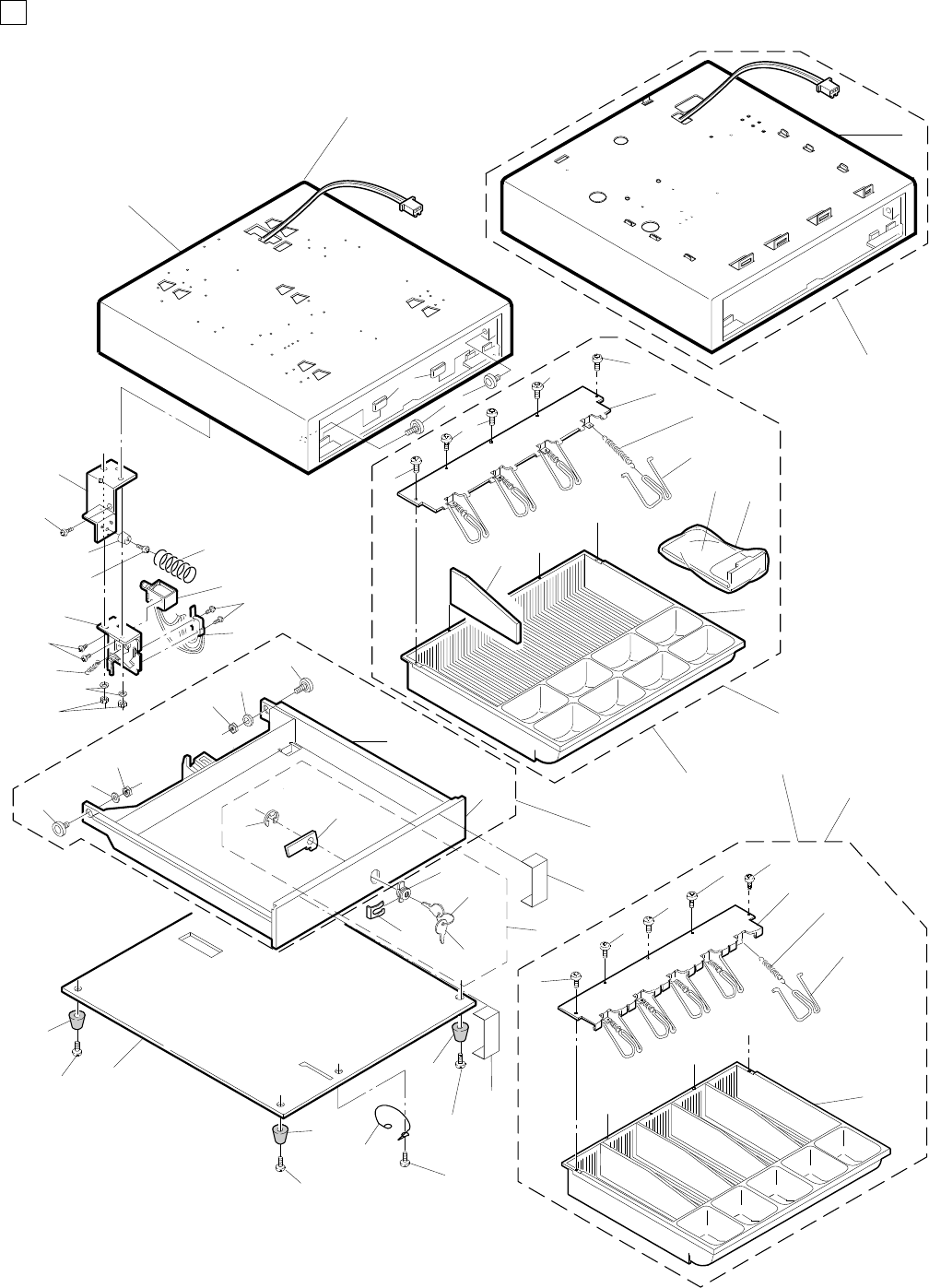
5Drawer box unit(SK423type)
RCPS0131
2
34
30 28
29
31
32
3334
35
25
39
25
39
25
39
40 41
28
29
30
21
20
37
36 42
502
38
38
24
25
26
27
22
13
14
15
16
17
18 23
47
910
57
8
5
505
5
5558 7
11
501
55
56
12
5
7
8
5
1
for CANADA
for U.S.A.
ER-A310
ER-A330
ER-A310U
– 7 –

5Drawer box unit(SK423type)
NO. PARTS CODE PRICE
RANK NEW
MARK PART
RANK DESCRIPTION ER-
A310 ER-
A330
1CCABM7245BH01 BK N D Cabinet frame unit [U.S.A] |
CCABM7251BH02 BK N D Cabinet frame unit [Canada] |
2CCABM7247BH01 BK N D Cabinet frame unit [U.S.A] |
CCABM7252BH02 BK N D Cabinet frame unit [Canada] |
3PGUMM6695BHZZ AE C Stopper gum ||
4NROLP6650BHZZ AP C Roller ||
5
XUBSD30P08000 AA C Screw (3 ✕ 8) ||
6
LBRC-6666BHZZ AQ C Bracket [U.S.A] ||
7MSPRT6714BHZZ AE C Bill spring ||
8
MLEVF6695BHZZ AK C Bill lever ||
9
PSKR-6629BHZZ AL C Bill separator [Canada] ||
10 SSAKA5004BHZZ AA D Vinyl bag ||
11 PSKR-6628BHZZ AG C Separator [Canada] ||
12 GCAS-6682BHZZ AZ D Money case (5B/5C) [U.S.A] ||
13 LX-BZ6776BHZZ AA C Screw (for micro sw) ||
14 QSW-M6872BHZZ AR B Micro switch ||
15 CPLU-6647BH01 AY N B Solenoid ||
16 CFRM-6683BH01 AW D Lock frame unit ||
17 LX-BZ6775BHZZ AA C Screw (for solenoid) ||
18 MSPRT6713BHZZ AD C Open lever spring ||
20 XRESJ50-06000 AA C E type ring (5mm) ||
21 MCAMM6633BHZA AE C Lock cam ||
22 LFRM-6682BHZZ AN D Bell frame ||
23 XWSSD40-10000 AA C Washer (4mm) ||
24 XNESD40-32000 AA C Nut (M4) ||
25 PGUMM6696BHZZ AE C Gum leg ||
26 XHBSD30P12000 AA C Screw (3 ✕ 12) ||
27 MSPRC6712BHZZ AF C Push out spring ||
28 NROLP6650BHZZ AP C Roller ||
29 XNESD60-50000 AA C Nut (M6) ||
30 XWSSD60-15000 AA C Washer (6mm) ||
31 GDRW-6680BHZZ BE D Drawer case frame unit [U.S.A] ||
GDRW-6678BHZZ BF D Drawer case frame unit [Canada] ||
32 GCOVA7036BHZZ AS D Front cover ||
33 LKGIW7330BHZZ AY B Lock key (body) ||
34 PRNGT6637BHZZ AA C Key ring ||
35 LKGIM7331BHZZ AE B Lock key (1pc) ||
36 MSPRK6718BHZZ AF C Lock key spring ||
37 LPLTM6674BH01 AX D Bottom plate [U.S.A] ||
LPLTM6674BHZC AY D Bottom plate [Canada] ||
38 SPAKA8255BHZZ AC D Paper pad ||
39 XHBSD40P12000 AA C Screw (M4 ✕ 12) ||
40 MSPRB6711BHZZ AD C Earth spring ||
41 XHPSC30P08000 AA C Screw (3 ✕ 8) ||
42 DUNT-1306BHZZ AX E Lock key unit ||
57 GCAS-6678BHZZ BC D Money case (4B/8C) [Canada] ||
58 LBRC-6663BHZZ AQ C Bill bracket [Canada] ||
501 CCAS-6682BH01 BF E Money case unit (5B/5C) [U.S.A] ||
502 GDRW-6680BHZA BE E Drawer case unit [U.S.A] ||
GDRW-6678BHZA BG E Drawer case unit [Canada] ||
503 CLOK-6676BH01 BH N E Lock unit ||
504 CFRM-6682BH02 AQ E Bell frame unit (include No.22,26,27) ||
505 CCAS-6678BH01 BF E Money case unit (4B/8C) [Canada] ||
901
GBOXD7139BHZZ BW N E Drawer box unit [U.S.A] |
GBOXD7140BHZZ BW N E Drawer box unit [U.S.A] |
GBOXD7144BHZZ BV N E Drawer box unit [Canada] |
GBOXD7145BHZZ BV N E Drawer box unit [Canada] |
6Main PWB unit[ER-A310]
NO. PARTS CODE PRICE
RANK NEW
MARK PART
RANK DESCRIPTION
1VHDDSS133HV-1 AA B Diode (DSS133HV) [D3,7∼17,24,29]
2VHD1N4002G/-1 AA B Diode (1N4002G) [D6,27]
3VHDPS102R//-1 AD B Diode (PS102R) [D4]
4VRD-RC2EY100J AA C Resistor (1/4W 10Ω ±5%) [R6]
5VRD-RC2EY102G AA C Resistor (1/4W 1.0KΩ ±2%) [R8]
6VRD-RC2EY102J AA C Resistor (1/4W 1.0KΩ ±5%) [R53,58,59,60,64,66,73∼]
7VRD-RC2EY104J AA C Resistor (1/4W 100KΩ ±5%) [R5]
8VRD-RC2EY105J AA C Resistor (1/4W 1.0MΩ ±5%) [R100,101]
9VRD-RC2EY300J AA C Resistor (1/4W 47Ω ±5%) [R30∼37]
10 VRD-RC2EY123J AA C Resistor (1/4W 12KΩ ±5%) [R1,39,121,∼130,78,79,131,132,133]
11 VRD-RC2EY153J AA C Resistor (1/4W 15KΩ ±5%) [R54,55,61]
12 VRD-RC2EY183J AA C Resistor (1/4W 18KΩ ±5%) [R69]
13 VRD-RC2EY221J AA C Resistor (1/4W 220Ω ±5%) [R9,111∼120]
14 VRD-RC2EY222J AA C Resistor (1/4W 2.2KΩ ±5%) [R11,13,15,17,19,21,23,25,27,29,38]
15 VRD-RC2EY223J AA C Resistor (1/4W 22KΩ ±5%) [R68,71]
ER-A310U
– 8 –

6Main PWB unit[ER-A310]
NO. PARTS CODE PRICE
RANK NEW
MARK PART
RANK DESCRIPTION
16 VRD-RC2EY272J AA C Resistor (1/4W 2.7KΩ ±5%) [R4]
17 VRD-RC2EY332J AA C Resistor (1/4W 3.3KΩ ±5%) [R57,70]
18 VRD-RC2EY334J AA C Resistor (1/4W 330KΩ ±5%) [R50,51]
19 VRD-RC2EY362G AA C Resistor (1/4W 3.6KΩ ±2%) [R7]
20 VRD-RC2EY392J AA C Resistor (1/4W 3.9KΩ ±5%) [R2]
21 VRD-RC2EY472J AA C Resistor (1/4W 4.7KKΩ ±5%) [R63,65,67,85∼96]
22 VRD-RC2EY563J AA C Resistor (1/4W 56KΩ ±5%) [R3,40,52,102]
23 VHEMTZ18B//-1 AB B Zener diode (MTZ18B) [ZD2]
24 VHEMTZJ27A/-1 AB B Zener diode (MTZJ27A) [ZD1]
25 VHERD6.2EB2-1 AB B Zener diode (RD6.2EB2)(VHEMTZ6.2B/-1) [ZD5]
26 VHERD24EB2/-1 AB B Zener diode (RD24EB2)(VHEMTZJ24B/-1) [ZD29]
27 QFSHD2109AFZZ AC C Fuse holder [F1]
28 VCQYNA1HM333K AA C Capacitor (50WV 0.033µF) [C1]
29 VCEAGA1HW106M AA C Capacitor (50WV 10µF) [C22]
30 VCEAGA1HW335M AB C Capacitor (50WV 3.3µF) [C5]
31 VCEAGA1CW337M AB C Capacitor (16WV 330µF) [C9,10]
32 VCKYPU1HB221K AB C Capacitor (50WV 220pF) [C7]
33 VCEAGA1CW106M AA C Capacitor (16WV 10µF) [C13,27]
34 VCCCPU1HH330J AB C Capacitor (50WV 33pF) [C14]
35 VCCCPU1HH220J AA C Capacitor (50WV 22PF) [C16]
36 VCEAGA1CW226M AB C Capacitor (16WV 22µF) [C18]
37 VCKYPU1HB102K AA C Capacitor (50WV 0.001µF) [C20,21,29,24]
38 VCKYPU1HB331K AA C Capacitor (50WV 330pF) [C25,28]
39 VSDSC001-//-1 AA B Transistor (2SC945)(VS2SC3198-/-1) [Q3∼13,22]
40 VSDSA001-//-1 AA B Transistor (2SA1266)(VS2SA1266-/-1) [Q23]
41 VS2SB926-S/TC AD B Transistor (KTA1271)(VS2SA1271-/-1) [Q31,32,33]
42 VS2SB926-S/TC AD B Transistor (2SB926-S9TC) [Q34∼40]
43 RC-KZ1054CCZZ AB C Capacitor (50WV 0.1µF) [C6,11,12,23,26,31,34]
44 RC-EZ106ARC1A AD C Capacitor (10WV 10µF) [C19,13]
45 VCKYPU1HB332K AA C Capacitor (50WV 3300pF) [C36]
46 VCKYPU1HB222K AA C Capacitor (50WV 2200pF) [Vb]
47 VCKYPU1HB103K AA C Capacitor (50WV 1.0µF) [C32]
48 VHD1D4B42//-1 AD B Diode (1D4B42)(VHDDI102/BH-1) [BD1]
49 VCEAGU1HW478M AL C Capacitor (50WV 4700µF) [C2]
50 VCEAGA1HW337M AE C Capacitor (50WV 330PF) [C4]
51 VCEAGU1CW108M AD C Capacitor (16WV 1000µF) [C8]
52 VHPHDSP5621-1 AM N B LED (7SEG 2dig) [FND1∼5]
53 VS2SC3784-/-1 AD B Transistor (2SC3784) [Q14,17]
54 QCNCM1101CCZZ AB C Connector (2pin)(QCNCM1101BHZZ) [CN1]
55 QCNCW7081BHZZ AB C Connector (2P)(5267-02A)(Blue) [CN2]
56 QCNCW6882RC1A AD C Connector (11pin)(QCNCW6882BH1A) [CN7]
57 QCNCW7118BH0H AG N C Connector (8pin)(5229-08CPB) [CN5]
58 QCNCW7118BH0I BH C Connector (9pin)(5229-09CPB) [CN8]
59 QCNCW7201BH1E AK N C Connector (52806-1510) [CN15]
60 QCNW-7811BHZZ AM N C F-LED cable (18pin) [CN14]
61 VHIKID65003AP AE B IC (KD65003AP) [IC5∼7]
62 VHIMC34063AM1 AG B IC (MC34063AM1)(VHIKA34063A-1) [IC1]
63 VSKTD20601/-1 AK N B Transistor (KTD2060) [Q19]
64 VSKTD14151/-1 AN N B Transistor (KTD1415) [Q1]
65 VSKTD1414//-1 AL B Transistor (KTD1414) [Q2]
66
! QFS-B0323QCZZ AC A Fuse (2.0A 125V) [F1]
67 RALMB6646BHZZ AQ B Buzzer [BZ1]
68 PRDAF6666BHZZ AN N C Heat sink [Heat sink]
69 LX-BZ6644RCZZ AA C Screw (3.5 ✕ 8S) [Heat sink]
70 XBBSD30P06000 AA C Screw (3 ✕ 6) [Q1]
71 VRS-RE3DA301J AB C Resistor (2W 300Ω ±5%) [R62]
72 RMPTC8563QCJB AC B Resistor array (56KΩ ✕ 8) [RA2]
73 VSKSB601-//-1 AN B Transistor (KSB601) [Q18]
74 QCNCM7057RCZZ AB C Connector (3pin)(QCNCM7057BHZZ) [CN11]
75 VHI4AC16///-1 AK B IC (4AC16) [IC9,10,11]
76 RCRSP6676RCZZ AG B Crystal (32.768KHz) [X1]
77 RCRM-7001BHZZ AH N B Crystal (4.19MHz) [X2]
78 VHIMC74HC373N AK B IC (MC74HC373)(VHIG74HC373-1) [IC3]
79 VHILH52B256N9 AW B IC (LH52B256N9)(VHIG76C256F70) [IC4]
80 RCILC6647RCZZ AE C Coil (RCH-110)(RCILC6647BHZZ) [L1]
81 VHID78045F023 AZ N B IC (D78045F023) [IC2]
82 QCNCW7200BH2H AL N C Connector (52025-2810) [CN12]
83 RMPTC8123QCJB AB B Resistor array (12KΩ ✕ 8) [RA1]
84 QCNW-7812BHZZ AE N C GND wire
85 QCNW-7813BHZZ AF N C GND wire
86 QCNW-7814BHZZ AE N C GND wire
87 VCKYPU1HB222K AA C Capacitor (50WV 2200pF) [R50]
901 CPWBF7503BH01 BV N E Main PWB unit
ER-A310U
– 9 –

7Main PWB unit[ER-A330]
NO. PARTS CODE PRICE
RANK NEW
MARK PART
RANK DESCRIPTION
1VHDDSS133HV-1 AA B Diode (DSS133HV) [D3,7∼17,24]
2VHD1N4002G/-1 AA B Diode (1N4002G) [D6,28,29]
3VHDPS102R//-1 AD B Diode (PS102R) [D4]
4VRD-RC2EY100J AA C Resistor (1/4W 10Ω ±5%) [R6]
5VRD-RC2EY102G AA C Resistor (1/4W 1.0KΩ ±2%) [R8]
6VRD-RC2EY102J AA C Resistor (1/4W 1.0KΩ ±5%) [R53,58,59,76,77,133]
7VRD-RC2EY104J AA C Resistor (1/4W 100KΩ ±5%) [R5]
8VRD-RC2EY105J AA C Resistor (1/4W 1.0MΩ ±5%) [R93,101]
9VRD-RC2EY300J AA C Resistor (1/4W 30Ω ±5%) [R30∼37]
10 VRD-RC2EY123J AA C Resistor (1/4W 12KΩ ±5%) [R1,39,121∼130,87,88,131,132,134]
11 VRD-RC2EY153J AA C Resistor (1/4W 15KΩ ±5%) [R54,55]
12 VRD-RC2EY221J AA C Resistor (1/4W 220Ω ±5%) [R9,111∼120]
13 VRD-RC2EY222J AA C Resistor (1/4W 2.2KΩ ±5%) [R11,13,15,17,19,21,23,25,27,29,38]
14 VRD-RC2EY223J AA C Resistor (1/4W 22KΩ ±5%) [R68,71,80]
15 VRD-RC2EY272J AA C Resistor (1/4W 2.7KΩ ±5%) [R4,79,81,82,84]
16 VRD-RC2EY334J AA C Resistor (1/4W 330KΩ ±5%) [R50,51]
17 VRD-RC2EY362G AA C Resistor (1/4W 3.6KΩ ±2%) [R7]
18 VRD-RC2EY392J AA C Resistor (1/4W 3.9KΩ ±5%) [R2]
19 VRD-RC2EY471J AA C Resistor (1/4W 470Ω ±5%) [R78]
20 VRD-RC2EY472J AA C Resistor (1/4W 4.7KΩ ±5%) [R57,92]
21 VRD-RC2EY563J AA C Resistor (1/4W 56KΩ ±5%) [R3,40,52,102]
22 VHEMTZ15A//-1 AB B Zener diode (MTZ15A) [ZD2]
23 VHEMTZ20D//-1 AA B Zener diode (MTZ20D) [ZD1]
24 VHERD6.2EB2-1 AB B Zener diode (RD6.2EB2)(VHEMTZ6.2B/-1) [ZD5]
25 QFSHD2109AFZZ AC C Fuse holder [F1]
26 VCQYNA1HM333K AA C Capacitor (50WV 0.033µF) [C1]
27 VCEAGA1HW335M AB C Capacitor (50WV 3.3µF) [C5]
28 VCEAGA1CW337M AB C Capacitor (16WV 330µF) [C9,10]
29 VCKYPU1HB221K AB C Capacitor (50WV 220pF) [C7,32]
30 RC-Z1N104RCZZ AA C Capacitor (12WV 0.1µF)(RC-Z1N104BHZZ) [C12,23,26]
31 VCEAGA1CW106M AA C Capacitor (16WV 10µF) [C27,29,13]
32 VCCCPU1HH330J AB C Capacitor (50WV 33pF) [C14]
33 VCCCPU1HH220J AA C Capacitor (50WV 22pF) [C16]
34 VCEAGA1CW226M AB C Capacitor (16WV 22µF) [C18]
35 VCKYPU1HB102K AA C Capacitor (50WV 0.001µF) [C31,24]
36 VCKYPU1HB331K AA C Capacitor (50WV 330pF) [C25,28]
37 VSDSC001-//-1 AA B Transistor (2SC001)(KTC3198GR)(VS2SC3198-/-1) [Q3∼13,16]
38 VS2SB926-S/TC AD B Transistor (2SB926-S) [Q18,19,20,34∼40]
39 VS2SB926-S/TC AD B Transistor (KTA1271)(VS2SA1271-/-1) [Q31,32,33]
40 RC-KZ1054CCZZ AB C Capacitor (50WV 0.1µF) [C6,11,34,35,37]
41 RC-EZ106ARC1A AD C Capacitor (10WV 10µF) [C19]
42 VCEAGU1HW105M AA C Capacitor (50WV 1.0µF) [C30]
43 VCKYPU1HB332K AA C Capacitor (50WV 3300pF) [C36]
44 VHD1D4B42//-1 AD B Diode (1D4B42)(VHDD1102/BH-1) [BD1]
45 VCEAGU1HW478M AL C Capacitor (50WV 4700µF) [C2]
46 VCEAGA1HW337M AE C Capacitor (50WV 33pF) [C4]
47 VCEAGU1CW108M AD C Capacitor (16WV 1000µF) [C8]
48 VHPHDSP5621-1 AM N B LED (7SEG 2dig) [FND1∼5]
49 VS2SC3784-/-1 AD B Transistor (2SC3784) [Q21]
50 QCNCM1101CCZZ AB C Connector (2pin)(QCNCM1101CCZZ) [CN1]
51 QCNCW7081BHZZ AB C Connector (2P)(5267-02A)(Blue) [CN2]
52 QCNCW6882RC1A AD C Connector (11pin)(QCNCW6882BH1A) [CN7]
53 QCNCW7118BH0H AG N C Connector (8pin)(5229-08CPB) [CN5]
54 QCNCW7118BH0I BH C Connector (9pin)(5229-09CPB) [CN8]
55 QCNCW7201BH1E AK N C Connector (52806-1510) [CN15]
56 QCNW-7811BHZZ AM N C F-LED cable (18pin) [CN14]
57 VHIKID65003AP AE B IC (KD65003AP) [IC5∼9]
58 VHIMC34063AM1 AG B IC (MC34063AM1)(VHIKA34063A-1) [IC1]
59 VSKTD14151/-1 AN N B Transistor (KTD1415) [Q1]
60 VSKTD1414//-1 AL B Transistor (KTD1414) [Q2]
61 VHID78045F028 AZ N B IC (D78045F028) [IC2]
62! QFS-B0323QCZZ AC A Fuse (UL125V 2A) [F1]
63 RALMB6646BHZZ AQ B Buzzer [BZ1]
64 PRDAF6666BHZZ AN N C Heat sink
65 LX-BZ6644RCZZ AA C Screw (3.5 ✕ 8S)(LX-BZ6644BHZZ) [Heat sink]
66 XBBSD30P06000 AA C Screw (3 ✕ 6) [Q1]
67 VRS-RE3DA221J AB C Resistor (2W 220Ω ±5%) [R83,85]
68 RMPTC8563QCJB AC B Resistor array (56KΩ ✕ 8) [RA2]
69 QCNCM7057RCZZ AB C Connector (3pin)(QCNCM7057BHZZ) [CN11]
70 VS2SB601-//-1 AM B Transistor (2SB601)(VSKSB601-//-1) [Q17]
71 RCRSP6676RCZZ AG B Crystal (32.768KHz) [X1]
72 RCRM-7001BHZZ AH N B Crystal (4.19MHz) [X2]
73 VHIMC74HC373N AK B IC (MC74HC373)(VHIG74HC373-1) [IC3]
74 VHILH52B256N9 AW B S-RAM (LH52B256N9)(VHIG76C256F70) [IC4]
75 QCNCW7200BH3A AA N C Connector (52045-3110) [CN12]
76 RCILC6647RCZZ AE C Coil (RCH-110)(RCILC6647BHZZ) [L1]
77 RMPTC8123QCJB AB B Resistor array (12KΩ ✕ 8) [RA1]
78 VRD-RC2EY000J AA C Resistor (1/4W 0Ω ±5%) [S-RAM]
79 QCNW-7805BHZZ AF C GND wire (Main-K/B-Dr)
80 QCNW-7824BHZZ AE N C GND wire
ER-A310U
– 10 –
7Main PWB unit[ER-A330]
NO. PARTS CODE PRICE
RANK NEW
MARK PART
RANK DESCRIPTION
81 VCEAGU1CW106M AA C Capacitor (16WV 10µF) [C26]
901 CPWBF7505BH01 BU N E Main PWB unit
8Pop-up PWB unit
NO. PARTS CODE PRICE
RANK NEW
MARK PART
RANK DESCRIPTION
1VRD-RC2EY270J AA C (1/4W 27Ω ±5%) [R10,12,14,16,18,20,22,24]
2QCNCW7202BH1E AK N C Connector (52807-1510) [CN1]
3VHPHDSP5621-1 AM N B LED (7SEG 2dig) [FND6∼9]
901 CPWBF7504BH01 BC N E Pop up PWB unit
9Articles for consumption
NO. PARTS CODE PRICE
RANK NEW
MARK PART
RANK DESCRIPTION ER-
A310 ER-
A330
1DPAPR1006CSZZ AR S Roll paper (5rolls) ||
2
NROLR6652RCZZ AZ S Ink roller |
3NROLR6638RCZZ AY S Ink roller (Purple) |
4UINK-1001CCZZ AK S Ink (5cc) ||
10 Service route options
NO. PARTS CODE PRICE
RANK NEW
MARK PART
RANK DESCRIPTION ER-
A310 ER-
A330
1LKGIM7113RCZZ AK S Service key ||
2
LKGIM7126RCZZ AL S Grip cover (OP key) ||
3
GCOVH7126BHZZ BE N D Drip-proof key cover ||
4DKIT-8666BHZZ BL N S Shield plate kit (include No.101∼103) |
5GCOVH7127BHZZ BA N D Mode switch cover ||
101 LCHSM6705BHZZ BG N C Main chassis |
102 TLABH7054BHZZ AD N D Caution card |
103 LBSHC0004BHZZ AC C Clamp |
ER-A310U
– 11 –

■Index
PARTS CODE NO. PRICE
RANK NEW
MARK PART
RANK
[C ]
CCABM7245BH01 5- 1 BK ND
CCABM7247BH01 5- 2 BK ND
CCABM7251BH02 5- 1 BK ND
CCABM7252BH02 5- 2 BK ND
CCAS-6678BH01 5- 505 BF E
CCAS-6682BH01 5- 501 BF E
CFRM-6682BH02 5- 504 AQ E
CFRM-6683BH01 5- 16 AW D
CLABH7044BH01 3- 101 AX ND
CLABH7044BH02 3- 101 AW ND
CLOK-6676BH01 5- 503 BH NE
CPLU-6647BH01 5- 15 AY NB
CPWBF7503BH01 1- 20 BV NE
" 6- 901 BV NE
CPWBF7504BH01 1- 9 BC NE
" 2- 7 BC NE
" 8- 901 BC NE
CPWBF7505BH01 2- 18 BU NE
" 7- 901 BU NE
[D ]
DKIT-8666BHZZ 10- 4 BL NS
DPAPR1006CSZZ 9- 1 AR S
DUNT-1306BHZZ 5- 42 AX E
DUNTK5817BHSA 3- 501 BN NE
DUNTK5817BHZZ 3- 501 BN NE
[G ]
GBOXD7139BHZZ 5- 901 BW NE
GBOXD7140BHZZ 5- 901 BW NE
GBOXD7144BHZZ 5- 901 BV NE
GBOXD7145BHZZ 5- 901 BV NE
GCAB-7237BHZZ 1- 8 AM ND
" 2- 6 AM ND
GCABA7239BHZZ 2- 19 BB ND
GCABB7236BHZA 2- 14 BC ND
GCABB7236BHZZ 1- 16 BC ND
GCAS-6678BHZZ 5- 57 BC D
GCAS-6682BHZZ 5- 12 AZ D
GCOVA7036BHZZ 5- 32 AS D
GCOVA7123BHZZ 1- 1 AY ND
GCOVA7128BHZZ 2- 1 AY ND
GCOVH7124BHZZ 1- 5 AF ND
" 2- 4 AF ND
GCOVH7125BHZZ 1- 21 AP ND
GCOVH7126BHZZ 10- 3 BE ND
GCOVH7127BHZZ 10- 5 BA ND
GDRW-6678BHZA 5- 502 BG E
GDRW-6678BHZZ 5- 31 BF D
GDRW-6680BHZA 5- 502 BE E
GDRW-6680BHZZ 5- 31 BE D
GFTAF6921BHZZ 1- 17 AG ND
" 2- 15 AG ND
[H ]
HDECP6847BHSA 2- 12 AM ND
HDECP6847BHZZ 1- 14 AM ND
[J]
JKNBZ6896BHZZ 3- 8 AG C
JKNBZ6897BHZZ 3- 7 AG C
JKNBZ6898BHZZ 3- 10 AH C
JKNBZ6899BHZZ 3- 9 AH C
JKNBZ6900BHZZ 3- 13 AQ C
JKNBZ6901BHZZ 3- 12 AQ C
JKNBZ6905BHZZ 3- 11 AF C
JKNBZ6908BHZZ 3- 11 AK C
JKNBZ6911BHZZ 3- 11 AK C
JKNBZ6912BHZZ 3- 11 AK C
JKNBZ6913BHZZ 3- 11 AK C
JKNBZ6914BHZZ 3- 11 AK C
JKNBZ6915BHZZ 3- 11 AK C
JKNBZ6916BHZZ 3- 11 AK C
JKNBZ6917BHZZ 3- 11 AK C
JKNBZ6918BHZZ 3- 11 AK C
JKNBZ6919BHZZ 3- 11 AK C
JKNBZ6920BHZZ 3- 11 AK C
[K ]
KI-OB6780RCZZ 1- 34 BW NE
KI-OB6783RCZZ 2- 31 BZ NE
[L ]
LANGQ7604BHZZ 3- 1 AG NC
LBNDJ2003SCZZ 1- 47 AA C
PARTS CODE NO. PRICE
RANK NEW
MARK PART
RANK
LBNDJ2003SCZZ 2- 32 AA C
LBRC-6663BHZZ 5- 58 AQ C
LBRC-6666BHZZ 5- 6 AQ C
LBSHC0004BHZZ 10- 103 AC C
LCHSM6705BHZZ 10- 101 BG NC
LFRM-6682BHZZ 5- 22 AN D
LFRM-6700BHZZ 3- 14 BB ND
LHLDZ1017ACZZ 1- 28 AC C
" 2- 28 AC C
LHLDZ6836BHZZ 3- 19 AE C
LHLDZ6837BHZZ 3- 20 AE C
LHLDZ6840BHZZ 1- 31 AL NC
LKGIM7110BHZZ 3- 6 AE B
" 4- 12 AE B
LKGIM7111BHZZ 3- 6 AE B
" 4- 12 AE B
LKGIM7113RCZZ 10- 1 AK S
LKGIM7126RCZZ 10- 2 AL S
LKGIM7331BHZZ 4- 11 AE B
" 5- 35 AE B
LKGIW0001BHZZ 3- 2 AS B
LKGIW7330BHZZ 5- 33 AY B
LPLTM6674BHZC 5- 37 AY D
LPLTM6674BH01 5- 37 AX D
LPLTM6706BHZZ 3- 17 AW NC
LPLTP6713BHZZ 1- 2 AL NC
LX-BZ6644RCZZ 6- 69 AA C
" 7- 65 AA C
LX-BZ6755BHZZ 2- 35 AB C
LX-BZ6775BHZZ 5- 17 AA C
LX-BZ6776BHZZ 5- 13 AA C
LX-BZ6781BHZZ 1- 23 AB C
" 2- 36 AB C
LX-BZ6788BHZZ 1- 3 AD NC
" 2- 3 AD NC
LX-HZ0056BHZZ 1- 39 AA C
[M ]
MCAMM6633BHZA 5- 21 AE C
MLEVF6695BHZZ 5- 8 AK C
MSPRB6711BHZZ 5- 40 AD C
MSPRC6712BHZZ 5- 27 AF C
MSPRK6718BHZZ 5- 36 AF C
MSPRT6713BHZZ 5- 18 AD C
MSPRT6714BHZZ 5- 7 AE C
[N ]
NROLP6650BHZZ 5- 4 AP C
" 5- 28 AP C
NROLP6651BHZZ 1- 6 AD C
NROLR6638RCZZ 9- 3 AY S
NROLR6652RCZZ 9- 2 AZ S
[P ]
PCUSG1220BHZZ 2- 29 AE C
PCUSG7024BHZZ 1- 32 AE NC
PCUT-6654BHZZ 1- 4 AE NC
" 2- 2 AE NC
PFILW6961BHZZ 1- 11 AP ND
" 2- 9 AP ND
PFILW6962BHZZ 1- 7 AU ND
" 2- 5 AU ND
PGUMM6695BHZZ 5- 3 AE C
PGUMM6696BHZZ 5- 25 AE C
PGUMM6725BHZZ 3- 15 AZ NC
PGUMM6726BHZZ 1- 35 AE NC
PHOG-1060CCZZ 3- 4 AA C
PRDAF6666BHZZ 6- 68 AN NC
" 7- 64 AN NC
PRNGT6637BHZZ 5- 34 AA C
PSHEP6681BHZZ 4- 2 AF D
PSHEP6844BHZZ 3- 16 BC NC
PSKR-6628BHZZ 5- 11 AG C
PSKR-6629BHZZ 5- 9 AL C
PSTM-6658RC01 2- 34 AR C
PSTM-6805RCZZ 1- 37 AT NC
[Q ]
QACCD8411QCZZ 1- 25 AN B
" 2- 23 AN B
QCNCM1101CCZZ 6- 54 AB C
" 7- 50 AB C
QCNCM7057RCZZ 6- 74 AB C
" 7- 69 AB C
ER-A310U
– 12 –

PARTS CODE NO. PRICE
RANK NEW
MARK PART
RANK
QCNCW6882RC1A 6- 56 AD C
" 7- 52 AD C
QCNCW7081BHZZ 6- 55 AB C
" 7- 51 AB C
QCNCW7118BH0H 6- 57 AG NC
" 7- 53 AG NC
QCNCW7118BH0I 6- 58 BH C
" 7- 54 BH C
QCNCW7200BH2H 6- 82 AL NC
QCNCW7200BH3A 7- 75 AA NC
QCNCW7201BH1E 6- 59 AK NC
" 7- 55 AK NC
QCNCW7202BH1E 8- 2 AK NC
QCNW-7451BHZZ 1- 46 AG C
" 2- 43 AG C
QCNW-7804BHZZ 3- 3 AL NC
QCNW-7805BHZZ 2- 17 AF NC
" 7- 79 AF C
QCNW-7806BHZZ 1- 44 AN NC
QCNW-7807BHZZ 2- 41 AN NC
QCNW-7808BHZZ 1- 36 AF NC
QCNW-7809BHZZ 2- 33 AH C
QCNW-7810BHZZ 1- 19 AG NC
QCNW-7811BHZZ 6- 60 AM NC
" 7- 56 AM NC
QCNW-7812BHZZ 6- 84 AE NC
QCNW-7813BHZZ 6- 85 AF NC
QCNW-7814BHZZ 6- 86 AE NC
QCNW-7815BHZZ 1- 10 AR NC
" 2- 8 AR NC
QCNW-7816BHZZ 1- 45 AR NC
QCNW-7817BHZZ 2- 42 AF NC
QCNW-7823BHZZ 1- 30 AE NC
QCNW-7824BHZZ 7- 80 AE NC
QFS-B0323QCZZ 6- 66 AC A
" 7- 62 AC A
QFSHD2109AFZZ 6- 27 AC C
" 7- 25 AC C
QSW-M6872BHZZ 5- 14 AR B
QTANZ1362CCZZ 1- 42 AA C
" 2- 39 AA C
QTANZ1363CCZZ 1- 41 AA C
" 2- 37 AA C
QTANZ6641BHZZ 1- 43 AC C
" 2- 40 AC C
QTANZ6657BHZZ 1- 40 AD NC
" 2- 38 AD NC
[R ]
RALMB6646BHZZ 6- 67 AQ B
" 7- 63 AQ B
RC-EZ106ARC1A 6- 44 AD C
" 7- 41 AD C
RC-KZ1054CCZZ 6- 43 AB C
" 7- 40 AB C
RC-Z1N104RCZZ 7- 30 AA C
RCILC6647RCZZ 6- 80 AE C
" 7- 76 AE C
RCORF6698BHZZ 2- 27 AR C
RCRM-7001BHZZ 6- 77 AH NB
" 7- 72 AH NB
RCRSP6676RCZZ 6- 76 AG B
" 7- 71 AG B
RMPTC8123QCJB 6- 83 AB B
" 7- 77 AB B
RMPTC8563QCJB 6- 72 AC B
" 7- 68 AC B
RTRNP6889BHZZ 1- 27 BC NB
RTRNP9516BHZZ 2- 25 BD NB
[S ]
SPAKA8255BHZZ 5- 38 AC D
SPAKA8366BHZZ 4- 3 AT ND
SPAKA8367BHZZ 4- 1 AT ND
SPAKC8368BHSA 4- 4 BA ND
SPAKC8368BHZZ 4- 4 BA ND
SPAKC8376BHSA 4- 4 BA ND
SPAKC8376BHZZ 4- 4 BA ND
SSAKA5004BHZZ 5- 10 AA D
SSAKH3012CCZZ 4- 10 AA D
SSAKH3015CCZZ 4- 6 AA D
SSAKH4231CCZZ 4- 5 AA D
PARTS CODE NO. PRICE
RANK NEW
MARK PART
RANK
[T ]
TCADH6788BHZZ 4- 13 AC D
TCADH6795BHZZ 4- 13 AC D
TCAUZ6684BHZZ 1- 15 AD D
" 2- 13 AD D
TCAUZ6685BHZA 1- 15 AA D
" 2- 13 AA D
TCAUZ6697BHZZ 4- 9 AC ND
TINSE7360BHZZ 4- 7 AT ND
TINSE7372BHZZ 4- 7 AU ND
TINSK7363BHZZ 4- 7 AT ND
TINSK7373BHZZ 4- 7 AU ND
TLABH7054BHZZ 10- 102 AD ND
[U ]
UBNDA6629BHZZ 4- 101 AA C
UINK-1001CCZZ 4- 8 AK S
" 9- 4 AK S
[V ]
VCCCPU1HH220J 6- 35 AA C
" 7- 33 AA C
VCCCPU1HH330J 6- 34 AB C
" 7- 32 AB C
VCEAGA1CW106M 6- 33 AA C
" 7- 31 AA C
VCEAGA1CW226M 6- 36 AB C
" 7- 34 AB C
VCEAGA1CW337M 6- 31 AB C
" 7- 28 AB C
VCEAGA1HW106M 6- 29 AA C
VCEAGA1HW335M 6- 30 AB C
" 7- 27 AB C
VCEAGA1HW337M 6- 50 AE C
" 7- 46 AE C
VCEAGU1CW106M 7- 81 AA C
VCEAGU1CW108M 6- 51 AD C
" 7- 47 AD C
VCEAGU1HW105M 7- 42 AA C
VCEAGU1HW478M 6- 49 AL C
" 7- 45 AL C
VCKYPU1HB102K 6- 37 AA C
" 7- 35 AA C
VCKYPU1HB103K 6- 47 AA C
VCKYPU1HB221K 6- 32 AB C
" 7- 29 AB C
VCKYPU1HB222K 6- 46 AA C
" 6- 87 AA C
VCKYPU1HB331K 6- 38 AA C
" 7- 36 AA C
VCKYPU1HB332K 6- 45 AA C
" 7- 43 AA C
VCQYNA1HM333K 6- 28 AA C
" 7- 26 AA C
VHDDSS133HV-1 6- 1 AA B
" 7- 1 AA B
VHDPS102R//-1 6- 3 AD B
" 7- 3 AD B
VHD1D4B42//-1 6- 48 AD B
" 7- 44 AD B
VHD1N4002G/-1 6- 2 AA B
" 7- 2 AA B
VHEMTZJ27A/-1 6- 24 AB B
VHEMTZ15A//-1 7- 22 AB B
VHEMTZ18B//-1 6- 23 AB B
VHEMTZ20D//-1 7- 23 AA B
VHERD24EB2/-1 6- 26 AB B
VHERD6.2EB2-1 6- 25 AB B
" 7- 24 AB B
VHID78045F028 7- 61 AZ NB
VHID78045F023 6- 81 AZ NB
VHIKID65003AP 6- 61 AE B
" 7- 57 AE B
VHILH52B256N9 6- 79 AW B
" 7- 74 AW B
VHIMC34063AM1 6- 62 AG B
" 7- 58 AG B
VHIMC74HC373N 6- 78 AK B
" 7- 73 AK B
VHI4AC16///-1 6- 75 AK B
VHPHDSP5621-1 6- 52 AM NB
" 7- 48 AM NB
ER-A310U
– 13 –

PARTS CODE NO. PRICE
RANK NEW
MARK PART
RANK
VHPHDSP5621-1 8- 3 AM NB
VRD-RC2EY000J 7- 78 AA C
VRD-RC2EY100J 6- 4 AA C
" 7- 4 AA C
VRD-RC2EY102G 6- 5 AA C
" 7- 5 AA C
VRD-RC2EY102J 6- 6 AA C
" 7- 6 AA C
VRD-RC2EY104J 6- 7 AA C
" 7- 7 AA C
VRD-RC2EY105J 6- 8 AA C
" 7- 8 AA C
VRD-RC2EY123J 6- 10 AA C
" 7- 10 AA C
VRD-RC2EY153J 6- 11 AA C
" 7- 11 AA C
VRD-RC2EY183J 6- 12 AA C
VRD-RC2EY221J 6- 13 AA C
" 7- 12 AA C
VRD-RC2EY222J 6- 14 AA C
" 7- 13 AA C
VRD-RC2EY223J 6- 15 AA C
" 7- 14 AA C
VRD-RC2EY270J 8- 1 AA C
VRD-RC2EY272J 6- 16 AA C
" 7- 15 AA C
VRD-RC2EY300J 6- 9 AA C
" 7- 9 AA C
VRD-RC2EY332J 6- 17 AA C
VRD-RC2EY334J 6- 18 AA C
" 7- 16 AA C
VRD-RC2EY362G 6- 19 AA C
" 7- 17 AA C
VRD-RC2EY392J 6- 20 AA C
" 7- 18 AA C
VRD-RC2EY471J 7- 19 AA C
VRD-RC2EY472J 6- 21 AA C
" 7- 20 AA C
VRD-RC2EY563J 6- 22 AA C
" 7- 21 AA C
VRS-RE3DA221J 7- 67 AB C
VRS-RE3DA301J 6- 71 AB C
VSDSA001-//-1 6- 40 AA B
VSDSC001-//-1 6- 39 AA B
" 7- 37 AA B
VSKSB601-//-1 6- 73 AN B
VSKTD1414//-1 6- 65 AL B
" 7- 60 AL B
VSKTD14151/-1 6- 64 AN NB
" 7- 59 AN NB
VSKTD20601/-1 6- 63 AK NB
VS2SB601-//-1 7- 70 AM B
VS2SB926-S/TC 6- 41 AD B
" 6- 42 AD B
" 7- 38 AD B
" 7- 39 AD B
VS2SC3784-/-1 6- 53 AD B
" 7- 49 AD B
[X ]
XBBSC30P08000 1- 13 AA C
" 2- 11 AA C
XBBSD30P06000 6- 70 AA C
" 7- 66 AA C
XBPBZ40P08K00 1- 24 AA C
" 2- 22 AA C
XBPSD30P08000 3- 5 AA C
XBPSD30P10KS0 1- 38 AB C
" 2- 30 AB C
XEBSD20P06000 1- 48 AA C
XEBSD30P06000 3- 18 AA C
XEBSD30P08000 1- 18 AA C
" 2- 16 AA C
XHBSD30P08000 2- 21 AA C
XHBSD30P12000 5- 26 AA C
XHBSD40P06000 1- 29 AA C
XHBSD40P12000 5- 39 AA C
XHPSC30P08000 5- 41 AA C
XHPSD30P06K00 1- 12 AA C
" 2- 10 AA C
XJPSD30P12X00 1- 33 AB C
PARTS CODE NO. PRICE
RANK NEW
MARK PART
RANK
XJPSD30P16X00 1- 26 AB C
" 2- 24 AB C
XNESD30-24000 1- 22 AA C
" 2- 20 AA C
XNESD40-32000 5- 24 AA C
XNESD60-50000 5- 29 AA C
XRESJ50-06000 5- 20 AA C
XUBSD30P08000 5- 5 AA C
XUBSD30P10000 2- 44 AC C
XWSSD40-10000 5- 23 AA C
XWSSD60-15000 5- 30 AA C
[0]
00B1009882/// 2- 45 AC C
ER-A310U
– 14 –
