F2837xD Firmware Development Package User's Guide F2837x D DEV USER
User Manual:
Open the PDF directly: View PDF ![]() .
.
Page Count: 156 [warning: Documents this large are best viewed by clicking the View PDF Link!]
- Copyright
- Revision Information
- 1 Introduction
- 2 Getting Started and Troubleshooting
- 3 Interrupt Service Routine Priorities
- 4 CLA C Compiler
- 5 CPU 1 Bit-field Example Applications
- 5.1 ADC PPB Delay Capture (adc_ppb_delay)
- 5.2 ADC PPB Limits (adc_ppb_limits)
- 5.3 ADC PPB Offset (adc_ppb_offset)
- 5.4 ADC Continuous Triggering (adc_soc_continuous)
- 5.5 ADC Continuous Conversions Read by DMA (adc_soc_continuous_dma)
- 5.6 ADC ePWM Triggering (adc_soc_epwm)
- 5.7 ADC temperature sensor conversion (adc_soc_epwm_tempsensor)
- 5.8 ADC SOC Software Force (adc_soc_software)
- 5.9 ADC Synchronous SOC Software Force (adc_soc_software_sync)
- 5.10 Blinky
- 5.11 Blinky with DCSM
- 5.12 FSK Transmitter using DAC mode on the AFE031
- 5.13 FSK Transmitter using PWM mode on the AFE031
- 5.14 Buffered DAC Enable (buffdac_enable)
- 5.15 Buffered DAC Ramp (buffdac_ramp)
- 5.16 Buffered DAC Random (buffdac_random)
- 5.17 Buffered DAC Sine (buffdac_sine)
- 5.18 Buffered DAC Sine DMA (buffdac_sine_dma)
- 5.19 Buffered DAC Square (buffdac_square)
- 5.20 CAN-A to CAN-B External Transmit (can_external_transmit)
- 5.21 CAN External Loopback Using Driverlib (can_loopback)
- 5.22 CAN External Loopback Using Bitfields (can_loopback_bitfields)
- 5.23 CAN External Loopback with Interrupts (can_loopback_interrupts)
- 5.24 CLA 5 Tap Finite Impulse Response Filter (cla_adc_fir32_cpu01)
- 5.25 CLA arcsine(x) using a lookup table (cla_asin_cpu01)
- 5.26 CLA arctangent(x) using a lookup table (cla_atan_cpu01)
- 5.27 CLA CRC8 Table-Lookup Algorithm (cla_crc8_cpu01)
- 5.28 CLA CRC8 Table-generation Algorithm (cla_crc8table1_cpu01)
- 5.29 CLA Determinant of 3X3 Matrix (cla_det_3by3_cpu01)
- 5.30 CLA Division: Newton Raphson Approximation (cla_divide_cpu01)
- 5.31 CLA 10X using a lookup table (cla_exp2_cpu01)
- 5.32 CLA eAB using a lookup table (cla_exp2_cpu01)
- 5.33 CLA 5 Tap Finite Impulse Response Filter (cla_fir32_cpu01)
- 5.34 CLA 2 Pole 2 Zero Infinite Impulse Response Filter (cla_iir2p2z_cpu01)
- 5.35 CLA Logic Test (cla_logic_cpu01)
- 5.36 CLA Matrix Multiplication (cla_matrix_mpy_cpu01)
- 5.37 CLA Matrix Transpose (cla_matrix_transpose_cpu01)
- 5.38 CLA Mixed C and Assembly Code (cla_mixed_c_asm_cpu01)
- 5.39 CLA Primes (cla_prime_cpu01)
- 5.40 CLA Shell Sort (cla_shellsort_cpu01)
- 5.41 CLA Square Root (cla_sqrt_cpu01)
- 5.42 CLA Vector Inverse (cla_inverse_cpu01)
- 5.43 CLA Vector Maximum (cla_vmaxfloat_cpu01)
- 5.44 CLA Vector Minimum (cla_vminfloat_cpu01)
- 5.45 CMPSS Asynchronous Trip
- 5.46 CMPSS Digital Filter
- 5.47 CPU Timers
- 5.48 SafeCopyCode Reset (dcsm_scc_reset_cpu01)
- 5.49 DMA GSRAM Transfer (dma_gsram_transfer)
- 5.50 ECAP APWM Example
- 5.51 ECAP Capture PWM Example
- 5.52 ECAP Capture PWM XBAR Example
- 5.53 EMIF ASYNC module (emif1_16bit_asram)
- 5.54 EMIF1 SDRAM Module (emif1_16bit_sdram_dma)
- 5.55 EMIF1 SDRAM Module (emif1_16bit_sdram_far)
- 5.56 EMIF1 SDRAM Module (emif1_32bit_sdram)
- 5.57 EMIF Daughtercard CLA Transfer (emif_dc_cla)
- 5.58 EMIF Daughtercard CPU Transfer (emif_dc_cpu)
- 5.59 EMIF Daughtercard DMA Transfer (emif_dc_dma)
- 5.60 EMIF Daughtercard CS2 Flash Memory Access (emif_dc_flash)
- 5.61 EMIF Daughtercard CS2 Virtual Pages (emif_dc_pages)
- 5.62 Empty Project
- 5.63 EPWM dead band control (epwm_deadband)
- 5.64 EPWM Trip Zone Module (epwm_trip_zone)
- 5.65 EPWM Action Qualifier (epwm_up_aq)
- 5.66 EPWM Action Qualifier (epwm_updown_aq)
- 5.67 Frequency measurement using EQEP peripheral (Eqep_freqcal)
- 5.68 EQEP Speed and Position Measurement (Eqep_pos_speed)
- 5.69 External Interrupts (ExternalInterrupt)
- 5.70 External Interrupts Latency (ExternalInterruptLatency)
- 5.71 Device GPIO Setup (GpioSetup)
- 5.72 GPIO toggle test program (GpioToggle)
- 5.73 HRPWM Dead-Band Example (hrpwm_deadband_sfo_v8)
- 5.74 HRPWM SFO Test (hrpwm_duty_sfo_v8)
- 5.75 HRPWM SFO Test (hrpwm_prdupdown_sfo_v8)
- 5.76 HRPWM Slider Test (hrpwm_slider)
- 5.77 I2C EEPROM Example (i2c_eeprom)
- 5.78 Out of Box Demo (LaunchPadDemo)
- 5.79 Low Power Modes: Halt Mode and Wakeup (lpm_haltwake)
- 5.80 Low Power Modes: HIB Mode and Wakeup (lpm_hibwake)
- 5.81 Low Power Modes: Device Idle Mode and Wakeup(lpm_idlewake)
- 5.82 Low Power Modes: Device Standby Mode and Wakeup(lpm_standbywake)
- 5.83 McBSP Loopback (mcbsp_loopback)
- 5.84 McBSP Loopback with DMA (mcbsp_loopback_dma)
- 5.85 McBSP Loopback with Interrupts (mcbsp_loopback_interrupts)
- 5.86 McBSP Loopback using SPI mode (mcbsp_spi_loopback)
- 5.87 SCI Echoback (sci_echoback)
- 5.88 SCI FIFO Digital Loop Back Test (sci_looback)
- 5.89 SCI Digital Loop Back with Interrupts (sci_loopback_interrupts)
- 5.90 SD card using FAT file system (sd_card)
- 5.91 SDFM Filter Sync CLA
- 5.92 SDFM Filter Sync CPU
- 5.93 SDFM Filter Sync DMA
- 5.94 SDFM PWM Sync
- 5.95 Setup CPU01
- 5.96 SPI Digital Loop Back (spi_loopback)
- 5.97 SPI Digital Loop Back with DMA (spi_loopback_dma)
- 5.98 SPI Digital Loop Back with Interrupts (spi_loopback_interrupts)
- 5.99 Software Prioritized Interrupts(sw_prioritized_interrupts)
- 5.100 LED Blink Getting Started Program (timed_led_blink)
- 5.101 Profiling sine(x) using the TMU (tmu_sinegen)
- 5.102 UPP Single Data Rate Receive (upp_sdr_rx)
- 5.103 UPP Single Data Rate Transmit (upp_sdr_tx)
- 5.104 USB Generic Bulk Device (usb_dev_bulk)
- 5.105 USB HID Keyboard Device (usb_dev_keyboard)
- 5.106 USB HID Mouse Device (usb_dev_mouse)
- 5.107 USB Serial Device (usb_dev_serial)
- 5.108 USB Dual Detect (usb_dual_detect)
- 5.109 USB HID Keyboard Host (usb_host_keyboard)
- 5.110 USB HID Mouse Host (usb_host_mouse)
- 5.111 USB Mass Storage Class Host (usb_host_msc)
- 5.112 Watchdog
- 6 CPU 1 Driver Library Example Applications
- 6.1 ADC Software Triggering
- 6.2 ADC ePWM Triggering
- 6.3 ADC Temperature Sensor Conversion
- 6.4 CAN External Loopback
- 6.5 CAN External Loopback with Interrupts
- 6.6 CAN-A to CAN-B External Transmit
- 6.7 CLA arcsine(x) using a lookup table (cla_asin_cpu01)
- 6.8 CLA arctangent(x) using a lookup table (cla_atan_cpu01)
- 6.9 CMPSS Asynchronous Trip
- 6.10 CMPSS Digital Filter Configuration
- 6.11 Buffered DAC Enable
- 6.12 Buffered DAC Random
- 6.13 DMA GSRAM Transfer (dma_ex1_gsram_transfer)
- 6.14 eCAP APWM Example
- 6.15 eCAP Capture PWM Example
- 6.16 EMIF1 ASYNC module accessing 16bit ASRAM.
- 6.17 EMIF1 module accessing 16bit ASRAM as code memory.
- 6.18 EMIF1 module accessing 16bit SDRAM using memcpy_fast_far().
- 6.19 EMIF1 module accessing 16bit SDRAM then puts into Self Refresh mode before entering Low Power Mode.
- 6.20 EMIF1 module accessing 32bit SDRAM using DMA.
- 6.21 ePWM Trip Zone
- 6.22 ePWM Up Down Count Action Qualifier
- 6.23 Frequency Measurement Using eQEP
- 6.24 Position and Speed Measurement Using eQEP
- 6.25 Device GPIO Setup
- 6.26 I2C Digital Loopback with FIFO Interrupts
- 6.27 I2C EEPROM
- 6.28 External Interrupts (ExternalInterrupt)
- 6.29 Setup CPU02 for Control
- 6.30 LED Blinky Example
- 6.31 Low Power Modes: Halt Mode and Wakeup
- 6.32 Low Power Modes: Device Idle Mode and Wakeup
- 6.33 Low Power Modes: Device Standby Mode and Wakeup
- 6.34 McBSP loopback example
- 6.35 McBSP loopback with DMA example.
- 6.36 McBSP loopback with interrupts example
- 6.37 McBSP loopback example using SPI mode
- 6.38 McBSP external loopback example
- 6.39 SCI FIFO Digital Loop Back
- 6.40 SCI Digital Loop Back with Interrupts
- 6.41 SCI Echoback
- 6.42 SDFM Filter Sync CPU
- 6.43 SPI Digital Loopback
- 6.44 SPI Digital Loopback with FIFO Interrupts
- 6.45 SPI Digital External Loopback with FIFO Interrupts
- 6.46 CPU Timers
- 6.47 uPP single data rate transmit example
- 6.48 uPP single data rate receive example
- 6.49 Watchdog
- 7 Dual Core Bit-field Example Applications
- 7.1 ADC & EPWM on CPU2
- 7.2 Blinky
- 7.3 CLA arcsine(x) using a lookup table (cla_asin_cpu01)
- 7.4 CLA 2 Pole 2 Zero Infinite Impulse Response Filter (cla_iir2p2z_cpu01)
- 7.5 CPU01 to CPU02 IPC Driver
- 7.6 CPU01 to CPU02 IPC Lite Drivers (cpu01_to_cpu2_ipcdrivers_lite)
- 7.7 CPU01 to CPU02 IPC Write Protect Driver
- 7.8 CPU02 to CPU01 IPC Driver
- 7.9 CPU02 to CPU01 IPC Lite Drivers (cpu02_to_cpu1_ipcdrivers_lite)
- 7.10 CPU02 to CPU01 IPC Write Protect Driver
- 7.11 DMA Transfer Shared Peripheral
- 7.12 Flash Programming Solution SCI for Single or Dual Core
- 7.13 Firmware Upgrade Kernels using USB for Single or Dual Upgrade
- 7.14 Flash Programming
- 7.15 IPC GPIO toggle
- 7.16 Shared RAM management (RAM_management)
- 7.17 SDFM Filter Sync CLA
- 7.18 CLA arcsine(x) using a lookup table (cla_asin_cpu01)
- 7.19 CLA 2 Pole 2 Zero Infinite Impulse Response Filter (cla_iir2p2z_cpu01)
- 7.20 IPC GPIO toggle
- 8 Dual Core Driver Library Example Applications
- IMPORTANT NOTICE

Copyright © 2018
Texas Instruments Incorporated
USER’S GUIDE
F2837xD Firmware Development Package

Copyright
Copyright © 2018 Texas Instruments Incorporated. All rights reserved. Other names and brands may be claimed as the property of others.
Please be aware that an important notice concerning availability, standard warranty, and use in critical applications of Texas Instruments semicon-
ductor products and disclaimers thereto appears at the end of this document.
Texas Instruments
13905 University Boulevard
Sugar Land, TX 77479
http://www.ti.com/c2000
Revision Information
This is version 3.04.00.00 of this document, last updated on Sun Mar 25 13:25:49 CDT 2018.
2 Sun Mar 25 13:25:49 CDT 2018

Table of Contents
Table of Contents
Copyright ..................................................... 2
Revision Information ............................................... 2
1 Introduction ................................................. 9
1.1 Detailed Revision History .......................................... 9
2 Getting Started and Troubleshooting .................................. 19
2.1 Introduction .................................................. 19
2.2 Project Creation ............................................... 19
2.3 Debugging Dual Core Applications ..................................... 37
2.4 Project: Adding Bit-field or DriverLib Support ............................... 41
2.5 Troubleshooting ............................................... 42
3 Interrupt Service Routine Priorities ................................... 45
3.1 Interrupt Hardware Priority Overview ................................... 45
3.2 PIE Interrupt Priorities ............................................ 46
3.3 Software Prioritization of Interrupts ..................................... 47
4 CLA C Compiler .............................................. 51
4.1 Introduction .................................................. 51
4.2 Overview ................................................... 51
4.3 Framework .................................................. 59
4.4 Getting Started with the CLA Compiler .................................. 60
4.5 Debugging .................................................. 64
4.6 Known Debugging Issues .......................................... 65
4.7 Tips and Tricks ................................................ 65
5 CPU 1 Bit-field Example Applications .................................. 69
5.1 ADC PPB Delay Capture (adc_ppb_delay) ................................ 69
5.2 ADC PPB Limits (adc_ppb_limits) ..................................... 69
5.3 ADC PPB Offset (adc_ppb_offset) ..................................... 70
5.4 ADC Continuous Triggering (adc_soc_continuous) ............................ 70
5.5 ADC Continuous Conversions Read by DMA (adc_soc_continuous_dma) ............... 70
5.6 ADC ePWM Triggering (adc_soc_epwm) ................................. 70
5.7 ADC temperature sensor conversion (adc_soc_epwm_tempsensor) .................. 71
5.8 ADC SOC Software Force (adc_soc_software) .............................. 71
5.9 ADC Synchronous SOC Software Force (adc_soc_software_sync) ................... 71
5.10 Blinky ..................................................... 71
5.11 Blinky with DCSM .............................................. 72
5.12 FSK Transmitter using DAC mode on the AFE031 ............................ 72
5.13 FSK Transmitter using PWM mode on the AFE031 ........................... 72
5.14 Buffered DAC Enable (buffdac_enable) .................................. 73
5.15 Buffered DAC Ramp (buffdac_ramp) ................................... 73
5.16 Buffered DAC Random (buffdac_random) ................................ 74
5.17 Buffered DAC Sine (buffdac_sine) ..................................... 74
5.18 Buffered DAC Sine DMA (buffdac_sine_dma) .............................. 75
5.19 Buffered DAC Square (buffdac_square) .................................. 76
5.20 CAN-A to CAN-B External Transmit (can_external_transmit) ...................... 77
5.21 CAN External Loopback Using Driverlib (can_loopback) ......................... 77
5.22 CAN External Loopback Using Bitfields (can_loopback_bitfields) .................... 78
5.23 CAN External Loopback with Interrupts (can_loopback_interrupts) ................... 78
5.24 CLA 5 Tap Finite Impulse Response Filter (cla_adc_fir32_cpu01) .................... 78
Sun Mar 25 13:25:49 CDT 2018 3

Table of Contents
5.25 CLA arcsine(x)using a lookup table (cla_asin_cpu01) .......................... 79
5.26 CLA arctangent(x)using a lookup table (cla_atan_cpu01) ....................... 79
5.27 CLA CRC8 Table-Lookup Algorithm (cla_crc8_cpu01) .......................... 80
5.28 CLA CRC8 Table-generation Algorithm (cla_crc8table1_cpu01) ..................... 80
5.29 CLA Determinant of 3X3 Matrix (cla_det_3by3_cpu01) ......................... 81
5.30 CLA Division: Newton Raphson Approximation (cla_divide_cpu01) ................... 81
5.31 CLA 10Xusing a lookup table (cla_exp2_cpu01) ............................. 81
5.32 CLA eA
Busing a lookup table (cla_exp2_cpu01) ............................. 82
5.33 CLA 5 Tap Finite Impulse Response Filter (cla_fir32_cpu01) ...................... 82
5.34 CLA 2 Pole 2 Zero Infinite Impulse Response Filter (cla_iir2p2z_cpu01) ................ 83
5.35 CLA Logic Test (cla_logic_cpu01) ..................................... 83
5.36 CLA Matrix Multiplication (cla_matrix_mpy_cpu01) ............................ 84
5.37 CLA Matrix Transpose (cla_matrix_transpose_cpu01) .......................... 84
5.38 CLA Mixed C and Assembly Code (cla_mixed_c_asm_cpu01) ..................... 84
5.39 CLA Primes (cla_prime_cpu01) ...................................... 85
5.40 CLA Shell Sort (cla_shellsort_cpu01) ................................... 85
5.41 CLA Square Root (cla_sqrt_cpu01) .................................... 86
5.42 CLA Vector Inverse (cla_inverse_cpu01) ................................. 86
5.43 CLA Vector Maximum (cla_vmaxfloat_cpu01) ............................... 87
5.44 CLA Vector Minimum (cla_vminfloat_cpu01) ............................... 88
5.45 CMPSS Asynchronous Trip ........................................ 88
5.46 CMPSS Digital Filter ............................................ 89
5.47 CPU Timers ................................................. 89
5.48 SafeCopyCode Reset (dcsm_scc_reset_cpu01) ............................. 89
5.49 DMA GSRAM Transfer (dma_gsram_transfer) .............................. 89
5.50 ECAP APWM Example ........................................... 90
5.51 ECAP Capture PWM Example ....................................... 90
5.52 ECAP Capture PWM XBAR Example ................................... 90
5.53 EMIF ASYNC module (emif1_16bit_asram) ................................ 91
5.54 EMIF1 SDRAM Module (emif1_16bit_sdram_dma) ............................ 91
5.55 EMIF1 SDRAM Module (emif1_16bit_sdram_far) ............................. 91
5.56 EMIF1 SDRAM Module (emif1_32bit_sdram) ............................... 92
5.57 EMIF Daughtercard CLA Transfer (emif_dc_cla) ............................. 92
5.58 EMIF Daughtercard CPU Transfer (emif_dc_cpu) ............................. 92
5.59 EMIF Daughtercard DMA Transfer (emif_dc_dma) ............................ 93
5.60 EMIF Daughtercard CS2 Flash Memory Access (emif_dc_flash) .................... 93
5.61 EMIF Daughtercard CS2 Virtual Pages (emif_dc_pages) ........................ 93
5.62 Empty Project ................................................ 94
5.63 EPWM dead band control (epwm_deadband) ............................... 94
5.64 EPWM Trip Zone Module (epwm_trip_zone) ............................... 95
5.65 EPWM Action Qualifier (epwm_up_aq) .................................. 95
5.66 EPWM Action Qualifier (epwm_updown_aq) ............................... 95
5.67 Frequency measurement using EQEP peripheral (Eqep_freqcal) .................... 96
5.68 EQEP Speed and Position Measurement (Eqep_pos_speed) ...................... 96
5.69 External Interrupts (ExternalInterrupt) ................................... 98
5.70 External Interrupts Latency (ExternalInterruptLatency) .......................... 98
5.71 Device GPIO Setup (GpioSetup) ...................................... 99
5.72 GPIO toggle test program (GpioToggle) .................................. 99
5.73 HRPWM Dead-Band Example (hrpwm_deadband_sfo_v8) ....................... 99
5.74 HRPWM SFO Test (hrpwm_duty_sfo_v8) ................................. 100
5.75 HRPWM SFO Test (hrpwm_prdupdown_sfo_v8) ............................. 101
5.76 HRPWM Slider Test (hrpwm_slider) .................................... 102
4 Sun Mar 25 13:25:49 CDT 2018

Table of Contents
5.77 I2C EEPROM Example (i2c_eeprom) ................................... 103
5.78 Out of Box Demo (LaunchPadDemo) ................................... 103
5.79 Low Power Modes: Halt Mode and Wakeup (lpm_haltwake) ....................... 103
5.80 Low Power Modes: HIB Mode and Wakeup (lpm_hibwake) ....................... 104
5.81 Low Power Modes: Device Idle Mode and Wakeup(lpm_idlewake) ................... 104
5.82 Low Power Modes: Device Standby Mode and Wakeup(lpm_standbywake) .............. 105
5.83 McBSP Loopback (mcbsp_loopback) ................................... 105
5.84 McBSP Loopback with DMA (mcbsp_loopback_dma) .......................... 106
5.85 McBSP Loopback with Interrupts (mcbsp_loopback_interrupts) ..................... 106
5.86 McBSP Loopback using SPI mode (mcbsp_spi_loopback) ....................... 107
5.87 SCI Echoback (sci_echoback) ....................................... 107
5.88 SCI FIFO Digital Loop Back Test (sci_looback) .............................. 108
5.89 SCI Digital Loop Back with Interrupts (sci_loopback_interrupts) ..................... 109
5.90 SD card using FAT file system (sd_card) ................................. 109
5.91 SDFM Filter Sync CLA ........................................... 109
5.92 SDFM Filter Sync CPU ........................................... 110
5.93 SDFM Filter Sync DMA ........................................... 111
5.94 SDFM PWM Sync .............................................. 111
5.95 Setup CPU01 ................................................ 112
5.96 SPI Digital Loop Back (spi_loopback) ................................... 112
5.97 SPI Digital Loop Back with DMA (spi_loopback_dma) .......................... 113
5.98 SPI Digital Loop Back with Interrupts (spi_loopback_interrupts) ..................... 113
5.99 Software Prioritized Interrupts(sw_prioritized_interrupts) ......................... 114
5.100LED Blink Getting Started Program (timed_led_blink) .......................... 114
5.101Profiling sine(x)using the TMU (tmu_sinegen) .............................. 115
5.102UPP Single Data Rate Receive (upp_sdr_rx) ............................... 115
5.103UPP Single Data Rate Transmit (upp_sdr_tx) .............................. 115
5.104USB Generic Bulk Device (usb_dev_bulk) ................................. 116
5.105USB HID Keyboard Device (usb_dev_keyboard) ............................. 116
5.106USB HID Mouse Device (usb_dev_mouse) ................................ 116
5.107USB Serial Device (usb_dev_serial) .................................... 117
5.108USB Dual Detect (usb_dual_detect) .................................... 117
5.109USB HID Keyboard Host (usb_host_keyboard) .............................. 117
5.110USB HID Mouse Host (usb_host_mouse) ................................. 117
5.111USB Mass Storage Class Host (usb_host_msc) ............................. 118
5.112Watchdog .................................................. 118
6 CPU 1 Driver Library Example Applications .............................. 119
6.1 ADC Software Triggering .......................................... 119
6.2 ADC ePWM Triggering ........................................... 119
6.3 ADC Temperature Sensor Conversion ................................... 120
6.4 CAN External Loopback .......................................... 120
6.5 CAN External Loopback with Interrupts .................................. 120
6.6 CAN-A to CAN-B External Transmit .................................... 121
6.7 CLA arcsine(x)using a lookup table (cla_asin_cpu01) .......................... 122
6.8 CLA arctangent(x)using a lookup table (cla_atan_cpu01) ....................... 122
6.9 CMPSS Asynchronous Trip ........................................ 122
6.10 CMPSS Digital Filter Configuration .................................... 123
6.11 Buffered DAC Enable ............................................ 123
6.12 Buffered DAC Random ........................................... 123
6.13 DMA GSRAM Transfer (dma_ex1_gsram_transfer) ............................ 124
6.14 eCAP APWM Example ........................................... 124
6.15 eCAP Capture PWM Example ....................................... 124
Sun Mar 25 13:25:49 CDT 2018 5

Table of Contents
6.16 EMIF1 ASYNC module accessing 16bit ASRAM. ............................ 124
6.17 EMIF1 module accessing 16bit ASRAM as code memory. ....................... 125
6.18 EMIF1 module accessing 16bit SDRAM using memcpy_fast_far(). ................... 125
6.19 EMIF1 module accessing 16bit SDRAM then puts into Self Refresh mode before entering Low Power
Mode. ........................................................ 126
6.20 EMIF1 module accessing 32bit SDRAM using DMA. .......................... 126
6.21 ePWM Trip Zone ............................................... 127
6.22 ePWM Up Down Count Action Qualifier .................................. 127
6.23 Frequency Measurement Using eQEP ................................... 127
6.24 Position and Speed Measurement Using eQEP .............................. 128
6.25 Device GPIO Setup ............................................. 129
6.26 I2C Digital Loopback with FIFO Interrupts ................................. 129
6.27 I2C EEPROM ................................................ 130
6.28 External Interrupts (ExternalInterrupt) ................................... 130
6.29 Setup CPU02 for Control .......................................... 131
6.30 LED Blinky Example ............................................ 131
6.31 Low Power Modes: Halt Mode and Wakeup ................................ 131
6.32 Low Power Modes: Device Idle Mode and Wakeup ............................ 132
6.33 Low Power Modes: Device Standby Mode and Wakeup ......................... 132
6.34 McBSP loopback example ......................................... 133
6.35 McBSP loopback with DMA example. ................................... 133
6.36 McBSP loopback with interrupts example ................................. 134
6.37 McBSP loopback example using SPI mode ................................ 134
6.38 McBSP external loopback example .................................... 135
6.39 SCI FIFO Digital Loop Back ......................................... 136
6.40 SCI Digital Loop Back with Interrupts ................................... 136
6.41 SCI Echoback ................................................ 137
6.42 SDFM Filter Sync CPU ........................................... 137
6.43 SPI Digital Loopback ............................................ 138
6.44 SPI Digital Loopback with FIFO Interrupts ................................. 138
6.45 SPI Digital External Loopback with FIFO Interrupts ............................ 139
6.46 CPU Timers ................................................. 139
6.47 uPP single data rate transmit example .................................. 140
6.48 uPP single data rate receive example ................................... 140
6.49 Watchdog .................................................. 141
7 Dual Core Bit-field Example Applications ............................... 143
7.1 ADC & EPWM on CPU2 .......................................... 143
7.2 Blinky ..................................................... 143
7.3 CLA arcsine(x)using a lookup table (cla_asin_cpu01) .......................... 143
7.4 CLA 2 Pole 2 Zero Infinite Impulse Response Filter (cla_iir2p2z_cpu01) ................ 144
7.5 CPU01 to CPU02 IPC Driver ........................................ 145
7.6 CPU01 to CPU02 IPC Lite Drivers (cpu01_to_cpu2_ipcdrivers_lite) .................. 145
7.7 CPU01 to CPU02 IPC Write Protect Driver ................................ 145
7.8 CPU02 to CPU01 IPC Driver ........................................ 146
7.9 CPU02 to CPU01 IPC Lite Drivers (cpu02_to_cpu1_ipcdrivers_lite) .................. 146
7.10 CPU02 to CPU01 IPC Write Protect Driver ................................ 147
7.11 DMA Transfer Shared Peripheral ..................................... 147
7.12 Flash Programming Solution SCI for Single or Dual Core ........................ 148
7.13 Firmware Upgrade Kernels using USB for Single or Dual Upgrade ................... 148
7.14 Flash Programming ............................................. 148
7.15 IPC GPIO toggle .............................................. 148
7.16 Shared RAM management (RAM_management) ............................ 149
6 Sun Mar 25 13:25:49 CDT 2018

Table of Contents
7.17 SDFM Filter Sync CLA ........................................... 149
7.18 CLA arcsine(x)using a lookup table (cla_asin_cpu01) .......................... 150
7.19 CLA 2 Pole 2 Zero Infinite Impulse Response Filter (cla_iir2p2z_cpu01) ................ 151
7.20 IPC GPIO toggle .............................................. 151
8 Dual Core Driver Library Example Applications ............................ 153
8.1 DMA Transfer Shared Peripheral ..................................... 153
8.2 LED Blinky Example ............................................. 154
8.3 Shared RAM Management ......................................... 154
IMPORTANT NOTICE ............................................... 156
Sun Mar 25 13:25:49 CDT 2018 7

Table of Contents
8 Sun Mar 25 13:25:49 CDT 2018

Introduction
1 Introduction
The Texas Instruments® F2837xD Firmware development library is a group of example applications
and helper libraries that demonstrate the basics of getting started with a F2837xD device.
The following chapter (chapter 2) provides a step by step guide for from scratch project
creation for each core as well as debug. It is highly recommended that users new to the
F2837xD family of devices start by reading this section first.
Because the F2837xD devices have two cores the example applications have been broken up to
distinguish which examples run on each core.
The bit-field example applications which run exclusively on the CPU 1 core can be found in
the ∼/device_support/f2837xD/examples/cpu1 directory.
The driver library example applications which run exclusively on the CPU 1 core can be found
in the ∼/driverlib/f2837xD/examples/cpu1 directory.
The bit-field example applications which require both cores to run can be found in the
∼/device_support/f2837xD/examples/dual directory.
The driver library example applications which require both cores to run can be found in the
∼/driverlib/f2837xD/examples/dual directory.
The examples provided are built for controlCARD compatibility. For LaunchPad use, some
minor modifications may be required.
As users move past evaluation, and get started developing their own application, TI recommends
they maintain a similar project directory structure to that used in the example projects. Example
projects have a heirarchy as follows:
Main project directory
•CPU 1 project folder (cpu01)
*CPU 1 project sources (∗.c, ∗.h)
*CCS folder (ccs)
· CCS project specific files
•CPU 2 project folder (cpu02)
*CPU 2 project sources (∗.c, ∗.h)
*CCS folder (ccs)
· CCS project specific files
TI also recommends that users append either _cpu01 or _cpu02 to project names to help develop-
ers differentiate between projects with similar names.
1.1 Detailed Revision History
V3.04.00.00
New buffdac_sine_dma bit-field example
New empty_project bit-field example
adc_ex2_soc_epwm.c (driverlib example) - Corrected issue where enumerations were rede-
fined as macros
Sun Mar 25 13:25:49 CDT 2018 9

Introduction
gpio_setup (bit-field example) - Switched input Xbar (INPUT8SELECT) to use ECAP2 on
GPIO24
adc_soc_continuous (bit-field example) - Corrected missing write to ADCSOC8CTL
hrpwm_duty_sfo_v8 (bit-field example) - Corrected commented code regarding when auto-
conversion is enabled
F2837xD_Adc.c - Added comment for AdcSetMode() that EALLOW/EDIS must be performed
before calling the function
F2837xD_Adc.c - Updated to support when using with combined bit-field and driverlib support
(_DUAL_HEADERS predefine)
i2c_eeprom (bit-field example) - Corrected I2C module clock prescaler to get between 7-
12MHz
Corrected details, formatting, and instructions in the firmware development document
F2837xD_Ipc_Driver_Util.c - Corrected IPCBootCPU2() to properly check when CPU2 is al-
ready booted
V3.03.00.00
IMPORTANT: Removed DCSM Z1/Z2 OTP structs (f2837xd_dcsm.h) and memory sections in
header linker command files
Updated Driver Library to v1.03.00.00
CAN Loopback Interrupts, External Transmit - Updated for interrupt numbering changes (1 and
2 to 0 and 1)
f2837xd_adc.h - Various comment clarifications
f2837xd_epwm.h - Marked self clear translator as reserved, added structs for valley and edge
modes
f2837xd_flash.h - Marked illegal address detected as reserved in struct
f2837xd_output_xbar.h - Comment numbering correction
f2837xd_xbar.h - Corrected INPUT7 naming to INPUT6
f2837xd_sysctrl.c - Corrected InitSysPll timer overflow check to use CPU timer 1
f2837xd_sysctrl.c, device.c - Added memcpy namespace for when building for C++
f2837xd_GlobalPrototypes.h - Added missing prototypes for GPIO_SetupXINT4Gpio() and
GPIO_SetupXINT5Gpio()
AFE031 DACMODE and PWMMODE Examples - Updates to PWM ISR
New bitfield example - AFE031 FSK Receiver
V3.02.00.00
IMPORTANT: F2837xD_SysCtrl.c - InitSysPll() and InitAuxPll() enhanced with slip bit monitor
and SYSCLK frequency check
IMPORTANT: When combining bitfield and driverlib support files, add a pre-defined symbol
within the project properties called "_DUAL_HEADERS"
Updated Driver Library to v1.02.00.00
All driverlib examples now include F2837xD_CodeStartBranch.asm to properly run from flash
Removed RAM build configurations from LPM hibernate wake bitfield examples
Driverlib cmpss_ex1_asynch and bitfield cmpss_asynch example comments corrected
10 Sun Mar 25 13:25:49 CDT 2018

Introduction
Driverlib timer_ex1_cputimer example - Fixed configuration of LED GPIO
New driverlib example - SPI and FSI Full Duplex Communication (spi_ex4_spifsi_full_duplex)
New driverlib example - ADC temperature sensor conversion (adc_ex3_temp_sensor)
New bitfield example - Empty combined bitfield and driverlib usage example
(empty_bitfield_driverlib)
New Bitfield example - FSK transmitter using DAC or PWM mode on AFE031 boosterpack
New bitfield examples - EMIF daughtercard CLA, CPU, DMA, Flash, and Pages examples
can_ex3_external_transmit.c - Updated description that example requires custom board with
two CAN transceivers
Driverlib usb.c/h removed. Use USB library under the libraries directory
Bitfield CAN loopback example - Fixed configuration of standard message ID
Bitfield CLA ADC FIR32 example - Fixed CLA Task 7
F2837xD_Gpio.c - Renamed various function parameters
Product page links now included in documentation directory
F2837xD_SysCtrl.c - InitFlash() VREADST configuration comments enhanced
F2837xD_memconfig.h - Corrected EMIF2ACCPROT0 bit names from EMIF1 to EMIF2
F2837xD_Ipc.c - Fixed RecvIpcData() to copy to correct location
V3.01.00.00
IMPORTANT: F2837xD_sdfm.h - Renamed bit field "FILRESEN" to "SDSYNCEN" and re-
named registers "SDIPARMx" to "SDDPARMx"
IMPORTANT: Global boot variables EmuKey and EmuBMode corrected and replaced with
EmuBmode and EmuBootPins variables
Updated Driver Library to v1.01.00.00
EPWM Trip Zone Example - Corrected with necessary EALLOW and EDIS
F2837xD_sdfm_drivers.h - Corrected SDFM macros to be volatile
F2837xD_usDelay.asm - Added ramfunc check logic to handle older compilers
ADC Software and ADC Software Sync Examples - Updated examples to use different ADC
channels
Flash API error check and messages updated
device.h - Corrected LSPCLK comments
F2837xD_sysctrl.h - Added DC6 register to header
F2837xD_can.h - Removed PDR and WUBA fields. Removed CAN_REL register. Updated
comments.
GPIO Setup Example - Corrected GPIO33 to GPIO32 for SDAA async input
ECAP Capture PWM Example - Corrected comment
Updated SW Prioritized Interrupts example with dedicated Pie Vect source file
(F2837xD_SWPrioritizedPieVect.c)
Added driverlib SPI external loopback with FIFO interrupts example
Added ADC SOC continuous example with DMA usage
Added ECAP Capture PWM XBAR example
CPU1 to CPU2 IPC Drivers Lite Example - Comments corrected
Sun Mar 25 13:25:49 CDT 2018 11

Introduction
LAUNCHXL F28379D Example - ASCII array text corrected
device.h - Added _LAUNCHXL_F28379D define for driverlib examples to configure for launch-
pad
V3.00.00.00
F2837xD Package updated and enhanced for C2000Ware. New driverlib and examples added.
IMPORTANT: SysCtrl functions switching to INTOSC1 or INTOSC2 now turn off XTAL
Deprecated F2837xD_common/driverlib. Use the new driverlib within the C2000Ware /driver-
lib root folder.
Firmware User Guide - Added section on adding bit field and driverlib support to a project
F2837xD_can.h - Switched byte peripheral arrays to regular uint32_t arrays to fix build issues
FATFS mmc_F2837x.c - Fixed xmit_datablock()
Updated all examples and removed deprecated compiler options
F2837xD_GlobalPrototypes.h - Externed EmuKey and EmuBMode
Fixed ADC SOC Continuous example and added missing EALLOWs
F2837xD_device.h - Updated to avoid CLA and byte peripheral attribute conflicts
CAN Examples - Corrected to handle data incrementation and rollover
SD Card Example - Updated for better Launchpad compatibility
Added bit field HRPWM Deadband SFO v8 example
F2837xD_Ipc_Driver_Util.c - Corrected IPCBootCPU2() status check mask
Various correction of dashes replaced with underscores
Added LAUNCHXL example
Refined development user guide description of examples included
New CCS example importing and building quickstart guide
V2.10
IMPORTANT: For compiler versions 15.9.0 and newer, linker command files use section
.TI.ramfunc instead of ramfuncs
IMPORTANT: F2837xD_CodeStartBranch.asm - Watchdog is now enabled by default
Header files updates: F2837xD_flash.h, F2837xD_epwm.h, F2837xD_dcsm.h
sysctl.c - Fixed SysCtlClockGet function use of IMULT to FMULT
Updated firmware development document with details on Launchpad pre-defined symbols
Updated Bitfield Blinky example with build configuration for Launchpad
Updated Bitfield SCI flash kernel example with Checksum
All Bitfield examples updated to use compiler v15.12.1.LTS
Removed BIST linker files
F2837xD_device.h - Changed BIT0-BIT31 defines to C28X_BIT0-C28X_BIT31
SetDBGIER extern prototype added to F2837xD_GlobalPrototype.h
SPI examples updated to use common InitSpi()
Added CAN bitfield header support
Added CAN loopback example using bitfields
12 Sun Mar 25 13:25:49 CDT 2018

Introduction
Corrected logical OR to AND in F2837xD_Emif.c
Corrected oscillator XTAL and OSC1 define values in sysctl.h
Added CPU1 and CPU2 specific guards to F2837xD_PieVect.c and F2837xD_pievect.h
V2.00
IMPORTANT: InitSysPll and InitAuxPll functions updated for errata fix in F2837xD_SysCtrl.c
Added _LAUNCHXL_F28379D define to F2837xD_SysCtrl.c to support correct launchpad
system PLL selection
Header files updates: F2837xD_cla.h, F2837xD_piectrl.h, F2837xD_sysctrl.h
Added External Interrupt Latency Example
Comment clarifications in DMA GSRAM Transfer example
Comment clarifications in CMPSS Asynch example
Link path correction in SDFM Filters Sync CLA dual example
Cleaned up formatting and whitespace in linker command files
Source, Header, and Example file whitespace cleanup and update to new comment structure
Fixed comment in Blinky with DCSM example Z1 and Z2 Zone Select Block files
F2837xD_TempSensorConv.c - Updated global variables to be float32 types to handle nega-
tive values
CPU1 and Dual Flash Programming examples updated - ECC no longer disabled before ini-
tialization
Flash API User Defined Functions for all flash examples updated to be placed in ramfuncs
memory section
Device part support clarification comments added to linker command files for RAMGS12 to
RAMGS15
Added build guards in F2837xD_SysCtrl.c for C++ support
Fixed Compiler Version guard in linker command files for ramfunc section
F2837xD_EPwm_defines.h - Fixed incorrect defines
V1.90
F2837xD_Gpio.c - Comment correction
can.c - Fixed case statement
Updated IPC CPU2 examples to work for additional GSx memories
Assigned buffer to RAM section in flash programming examples
Fixed ePWM setup in eQEP examples
F2837xD_CpuTimer.c - Fixed period in ConfigCpuTimer function
Updated missing fields in DCCAPCTL register in ePWM header file
Updated DCSM SCC Reset example to allow CPU Timer selection
Updates to blinky DCSM example
General fixes to USB library
USB Dev Mouse example fixes
Updated SCI Flash Kernel Example
Added UPP transmit and receive examples
Sun Mar 25 13:25:49 CDT 2018 13

Introduction
V1.80
SDFM Header - MS bit marked as reserved
EPWM Header - DBRED and DBFED bit fields updated as union and struct. Must be accessed
now using .bit or .all
Flash Header - FBAC.BAGP marked as reserved and FPAC2 register is removed.
I2C Header - Added I2CISRC.WRITE_ZEROS bit field
XBAR Header - Renamed ADCSOCA to ADCSOCAO and ADCSOCB to ADCSOCBO
Added new example - DMA GSRAM Transfer
Corrected issue with Blinky DCSM example
Corrected LPM examples regarding watchdog and flash power down
sysctl.c - Corrected SysCtlAuxClockSet driver function race condition for 120MHz SysClk
V1.70
Fixed flash_programming example to assign Example_CallFlashAPI() to RAM section
Memory Configuration header - Renamed ROM Prefetch register bit field PFDISABLE to
PFENABLE
DMA header - Removed bit fields SYNCE and SYNCSEL from DMA channel Mode register
DMA header - Removed bit fields SYNCFRC and SYNCCLR from DMA channel Control reg-
ister
SCI header - Corrected spelling of SCI FIFO transmit register bit field from TXFIFOXRESET
to TXFIFORESET
SPI header - Removed PRIORITY bit field from SPI priority control register (SPIPRI)
F2837xD_defaultisr.h is no longer included in F2837xD_device.h
Corrected PLLCLK_BY_80 value in F2837xD_Examples.h
DCSM header - Changed GRAB_BANK2 to GRAB_BANK1, EXEONLY_BANK2 to EX-
EONLY_BANK1, and STATUS_BANK2 to STATUS_BANK1
Added CAN Message RAM section to linker command files
Flash header - Added PUMPREQUEST register
Flash header - Removed FSPRD register
Updated linker command files to support ramfunc attribute
Updated CAN (CANA, CANB) interrupt line and ISR references from 1 and 2 to 0 and 1
Added new BUFFDAC examples: buffdac_ramp, buffdac_random, buffdac_sine, and buff-
dac_square
Added new ADC SOC EPWM temperature sensor example (adc_soc_epwm_tempsensor)
Updated example description for adc_soc_software
Added new ADC synchronous software triggering example (adc_soc_software_sync)
X-Bar header - Renamed TrigRegs to SyncSocRegs and moved to the SysCtrl header
X-Bar header - EXTADCSOCSELECT register renamed to ADCSOCOUTSELECT and SYNC-
SOCLOCK.EXTADCSOCSELECT field renamed to SYNCSOCLOCK.ADCSOCOUTSELECT
SysCtrl header - Added SyncSocRegs and removed incorrect DCx and SOFTPRESx registers
Added SafeCopyCode Reset example (dcsm_scc_reset)
IPC header - Removed PUMPREQUEST register
14 Sun Mar 25 13:25:49 CDT 2018

Introduction
SDFM header - Removed SDSTATUS register and removed SDCTLPARM1.MS bit field
F2837xD_Examples.h - Changed FMULT_1 to FMULT_0
V1.60
Aligned sysctl.c SysCtlClockSet() with correct clock initialization flow
Calling InitSysCtrl() from CPU2 will now call InitPeripheralClocks() and enable the clocks
Removed F2837xD_hwbistcontext.asm
Updated F2837xD_epwm.h with HRPCTL PWMSYNCSEL bit
Changed HWBIST bits to reserved in f28x7_nmiintrupt.h and F2837xD_sysctrl.h
Updated InitAuxPll() in F2837xD_SysCtrl.c with correct initialization flow
Updated InitSysPll() in F2837xD_SysCtrl.c to set multipliers in a single 32-bit write
Fixed GPIO setup options in all SCI examples
Fixed CAN drivers to avoid issues with 32-bit reads/writes while using optimization
Fixed adc_soc_epwm example and added volatile to bufferFull variable
Added power consumption note regarding InitPeripheralClocks() in F2837xD_SysCtrl.c
Fixed uart.c driver issue regarding non-volatile loop conditions
Added target configuration file to all examples
usb.c - Updated USBIntStatus to work around USB stalling due to edge triggering issue
Updated USBIntHandlerInternals to accept USBTXIS/USBRXIS status argument to ensure
the status is handled correctly.
Fixed offsets in USBHSCSIWrite10() of usbhscsi.c to prevent writing of incorrect commands
Removed OTG mode section from the USB Library User Guide
Fixed UARTprintf function in uartstdio.c to support long format
V1.50
Added EMIF 16bit SDRAM DMA example
Added EMIF 16bit SDRAM Far memcpy example
Added Single and Dual core hibernate wake-up examples
Added F2837xD Peripheral Driver Library User Guide
F2837xD_cla.h - Reserved space added between MAR1 and MSTF
F2837xD_cla.h - Added a union called MR_REG made up of an Uint32 and a float
F2837xD_epwm.h - Added HRCNFG2 register
F2837xD_epwm.h - Changed TZOSTFLG.DCxEVT2 bits to TZOSTFLG.DCxEVT1
F2837xD_epwm.h - Changed TZOSTCLR.DCxEVT2 bits to TZOSTCLR.DCxEVT1
F2837xD_spi.h - Added HS_MODE bit
Updated hrpwm_prdupdown_sfo_v8 example so that PHSEN is disabled
Fixed issue in IPCBootCPU2 function in F2837xD_Ipc_Driver_Util.c
Cleaned up example source and header code comments
Cleaned up example CCS warnings
Fixed error in mmc-F2837x.c for FATFS
Corrected CAN Loopback interrupts example source name
Sun Mar 25 13:25:49 CDT 2018 15

Introduction
Updated CLA C compiler section in F2837xD User Guide
Updates to F2837xD SCI Flash Kernel examples
Renamed DCAN references to CAN
Updated IPC ISR comments to reflect correct interrupt numbers
V1.40
sci_echoback example description updated
Updated F2837xD_Cla_typedefs.h to include additional typedef guards
Updated F2837xD_device.h typedefs guards
Updated CLA linker command files for C2000 compiler 6.4.x support
Fixed case mismatches in various example include files
Removed PBIST and HWBIST header files
Updated CLA examples and removed 3 NOPs before writing to the MCTL register
Removed CAN sections from linker header files
Updated Flash linker command files to align on 64-bit boundary
Cleaned up F2837xD CPU1 and Dual Examples CCS warnings
F2837xD_PieVect.c - Fixed comment for IPC interrupt
Updated mcbsp_loopback_dma example to initialize PIE correctly
Changed .Mux to .MUX in F2837xD_epwm_xbar.h and F2837xD_output_xbar.h
Fixed build error in SDFM Filter Sync CLA example
Updated EPwm.h - TRIPINPUT13 in DC submodule reserved
Added lpm_haltwake example
Updated EPWM X-Bar TRIPINV misnamed fields
Updated DCSM reserved fields in header structs to correct word size
Added Cla1SoftIntRegs to CLA Header file
Cleaned up code and comments in F2837xD_device.h
Added EMIF1 examples and associated source/header files
F2837xD_Dcan_defines.h renamed to F2837xD_Can_defines.h
V1.30
Removed SPI_REG D
Removed SDFM_REGS 3 and 4
Removed EQEP_REG 4
Removed EPWM_REGS 13 through 16
Removed ECAP_REGS 7 and 8
Removed CMPSS_REGS 9 through 12
Renamed OUTPUT X-XBAR OUT0-7 Registers to OUTPUT1-8
Renamed Register _MSTF bitfield RPC to _RPC
Added DmaClaSrcSelRegs for CPU2
Fixed cla_adc_fir32_cpu01 example undefined symbol
Fixed sdfm_filters_sync_cla build issue
16 Sun Mar 25 13:25:49 CDT 2018

Introduction
SysCtrl.c fixes in HALT() and HIB(). Also add DisablePeripheralClocks() function
F28x7x_SysCtrl.C - InitSysPll() Errata Fix
Removed incorrect comments in Examples
Deleted Can.h and Usb.h bit structured headers from /include
Removed incomplete drivers from F2837xD_common/driverlib
Fixed SysCtrl header comment
Fixed F2837xS Sysctrl.c references InitFlash
Added lpm_idlewake example
Added lpm_standbywake example
Cleaned up Dual Example - Flash_Programming
Corrected data buffer size in Flash API example
Added additional OTP prevention for examples
Fixed redefined TRUE/FALSE defines from stdbool.h
Added Example to show DMA being triggered from other CPU
F2837xD_sci_io.c - Updated SCI Regs
F2837xD_SysCtrl.c - Removed incorrect FlashCtrlRegs reference
Rewrote IPC driver to meet "One entry, one exit" standard
Fixed 2837x_RAM_IQMATH_lnk_cpu1.cmd Page Issue
SPI Module XML - Fixed missing SPICCR
In Device .h - Extended bit definition to 32-bits
Blinky DCSM example corrections
Removed unused variable warning in flash programming example
Fixed Capitalization issues preventing examples from building on Linux
V1.20
Updated eqep examples to use rts2800 for fpu32
Corrected DCSM_OPT_Z1 and DCSM_OPT_Z2 origin addresses
F2837xD_SysCtrl.c - Updated ADC Trim Code
Updated usb_dev_serial_cpu01 to fix CCS linking errors
Fixed some USB examples with missing StackModeSet call
Updated eqep examples with IQmath lib for FPU32
Added cla_support option to cla_atan example
Fixed McBSP Loopback CPU1 Example Issues for 32-bit transfers
Updated F2837xD_Dma_defines.h with missing SPI and USB trigger defines
Corrected USB guide text and formatting issues
Removed Redundant code found in dual core examples
Cleaned up CPU1 Example File Titles/Descriptions
Added DMA SPI example
Fixed McBSP_DLB_DMA example so both DMA CH1 and CH2 Interrupts occur
Corrected EPWMsetup.c in eqep_freq_cal_cpu01 example to output correct waveform
Sun Mar 25 13:25:49 CDT 2018 17

Introduction
Re-added the tmu_support command line option from the tmu example
Re-added the cla_support command line option from the cla examples
V1.10
IPC interrupts renumbered from 1-4 to 0-3 to match flag numbers
BIOS linker files were missing declarations for EmuBModeVar, EmuKeyVar, and PieVectTable-
File. These were added with a DSECT type to prevent warnings.
Added missing F2837xD_common/tools folder
PieVect Table made to be volatile
Removed extra copys of GlobalVariableDefs.c
Added USB Dual Mode Example
USB Examples - moved memcopy before PLL initialization to fix examples
Updated example build options to use built in VCU, CLA, and TMU options
F2837x_Device.h - put guard macros around assert and stdarg.h to prevent the CLA from
using these includes
Added SW Prioritized Interrupt example
GPIO Setup example now properly configures IOs for trip zones
V1.00
This version is the first release (packaged with development tools and customer trainings) of
the F2837xD header files and examples.
18 Sun Mar 25 13:25:49 CDT 2018

Getting Started and Troubleshooting
2 Getting Started and Troubleshooting
ProjectCreation ..........................................................................................19
Project: Adding Bit-fieldorDriverLibSupport .............................................................41
DebuggingDualCore Applications .......................................................................37
Troubleshooting ..........................................................................................42
2.1 Introduction
Because of the sheer complexity of the F2837xD devices, it is not uncommon for new users to
have trouble bringing up the device their first time. This guide aims to give you, the user, a step by
step guide for how to create and debug projects from scratch. This guide will focus on the user of a
F2837xD controlCARD, but these same ideas should apply to other boards with minimal translation.
2.2 Project Creation
A typical F2837xD application consists of two separate CCS projects: one for CPU 1 and one for
CPU2. The two projects are completely independent and have no real linking between them as far
as CCS is concerned.
Sun Mar 25 13:25:49 CDT 2018 19
Getting Started and Troubleshooting
CPU 1 Subsystem Project Creation
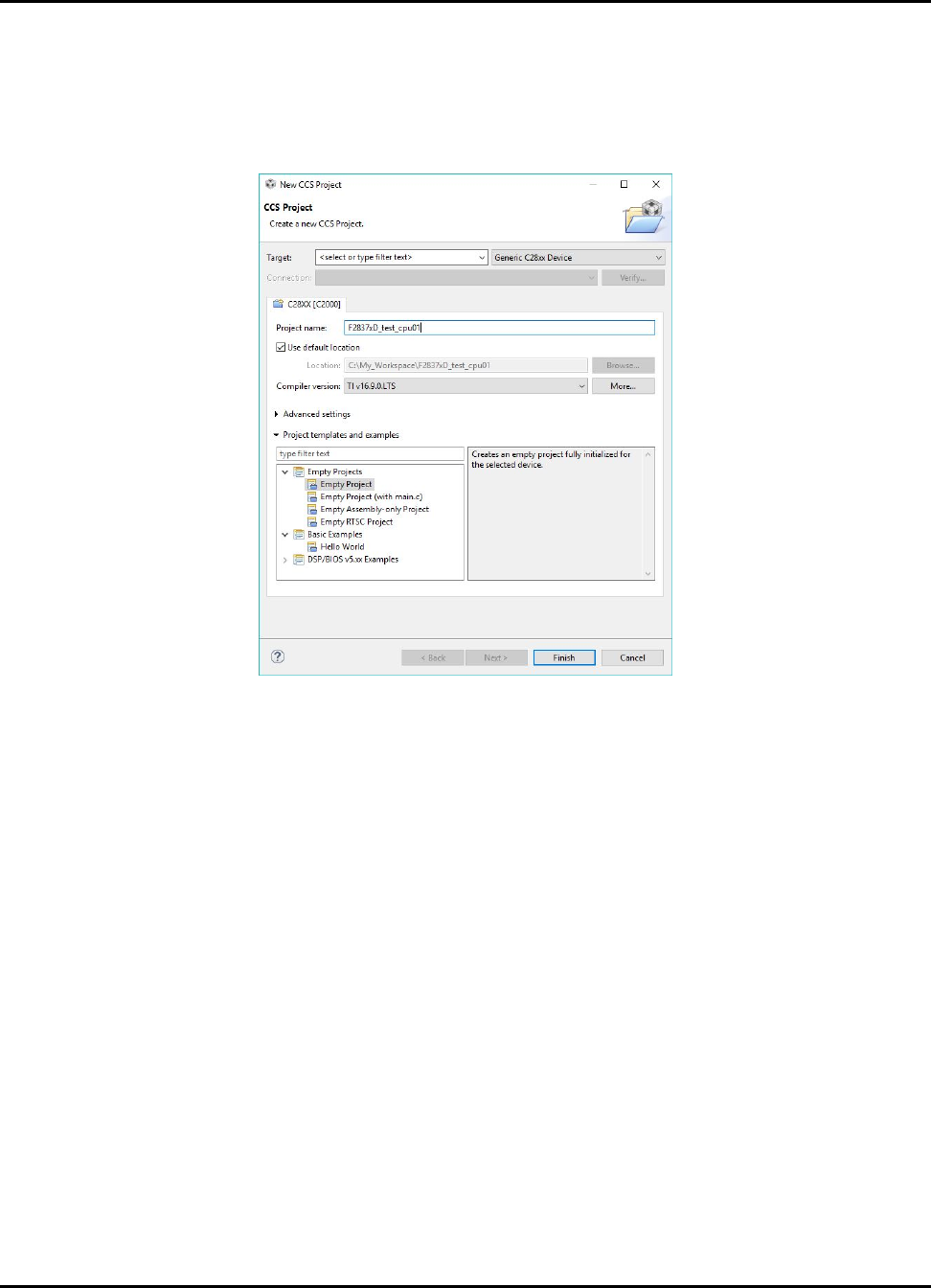
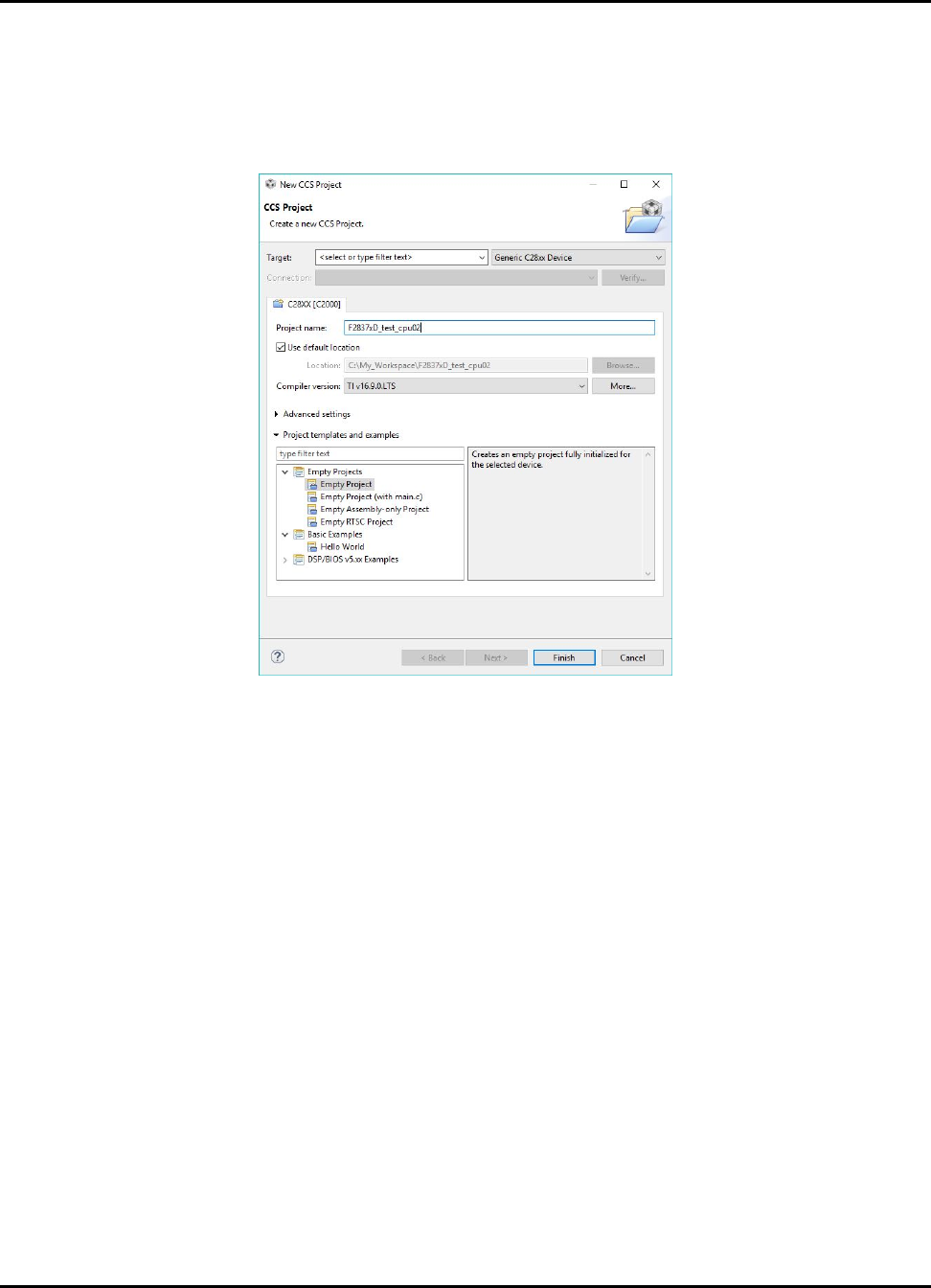
1. From the main CCS window select File ->New ->CCS Project. Select your Target as "Generic
C28xx Device". Name your project and choose a location for it to reside. Click Finish and your
project will be created.
Figure 2.1: Creating a new C28 project
20 Sun Mar 25 13:25:49 CDT 2018
Getting Started and Troubleshooting
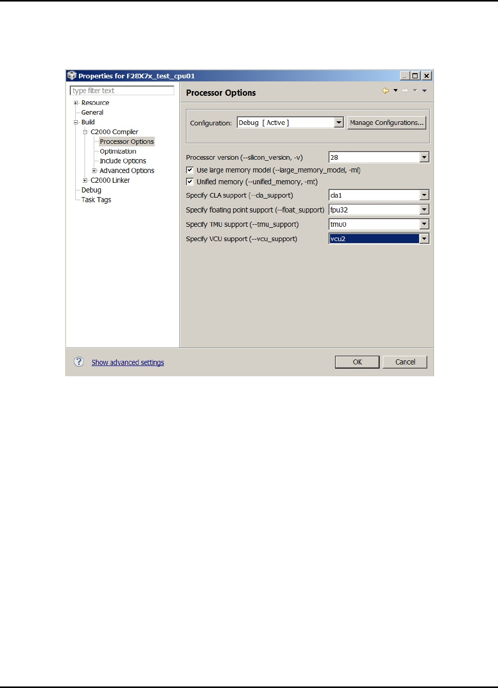
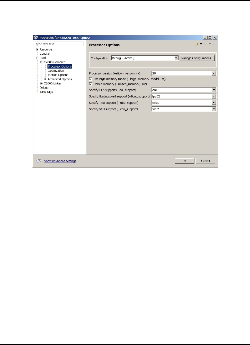
2. Before we can successfully build a project we need to setup some build specific settings. Right
click on your project and select Properties. Look at the Processor Options and ensure they
match the below image:
Figure 2.2: Project configuration dialog box
Sun Mar 25 13:25:49 CDT 2018 21
Getting Started and Troubleshooting
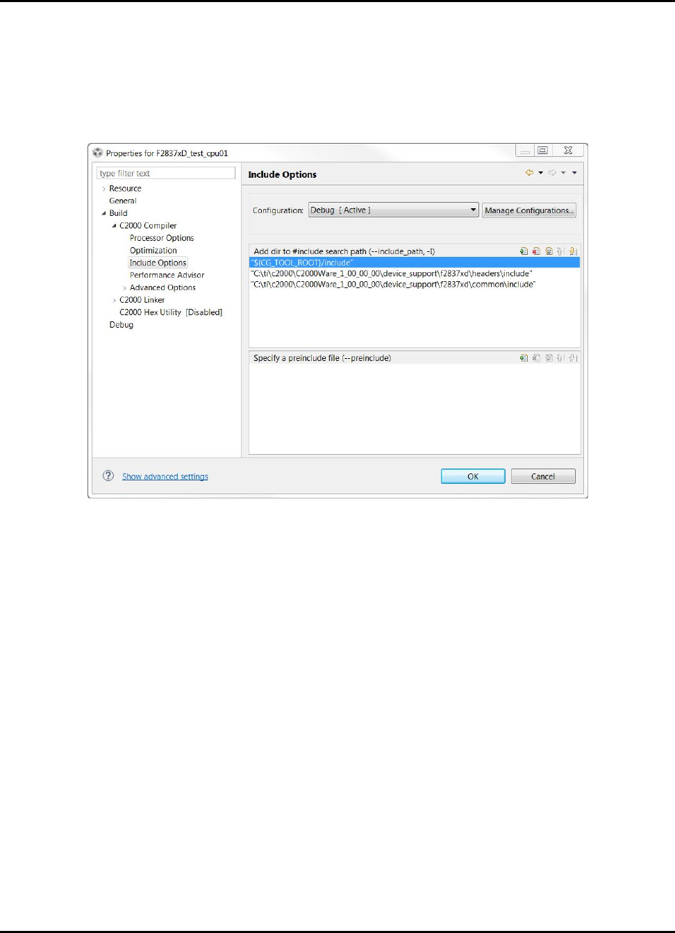
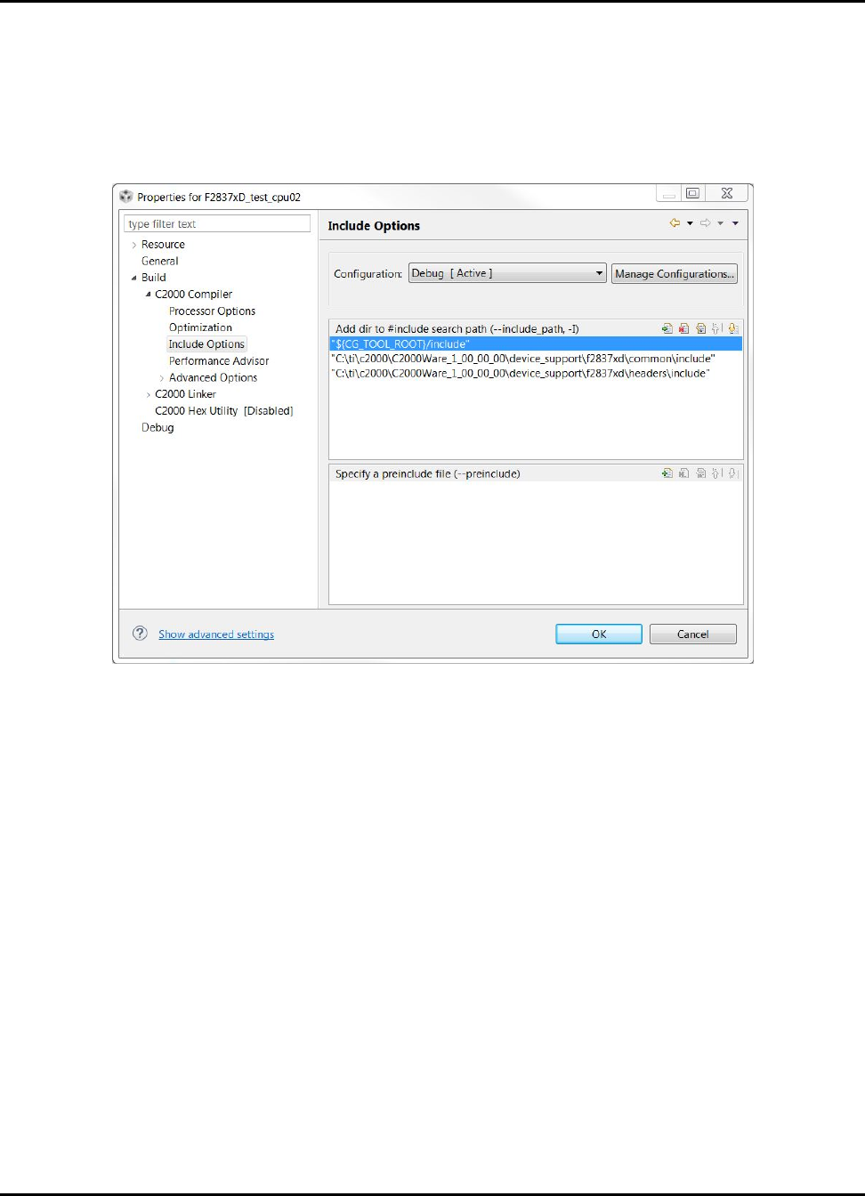
3. In the C2000 Compiler entry look for and select the Include Options. Click on the
add directory icon to add a directory to the search path. Click the File System but-
ton to browse to the common\include folder of your C2000Ware installation (typically
C:\ti\c2000\C2000Ware_X_XX_XX_XX\device_support\f2837xd\common\include).
Replace the ’X’s with your current C2000Ware version installation. Click ok to add this path,
and repeat this same process to add the headers\include directory.
Figure 2.3: Project configuration dialog box
22 Sun Mar 25 13:25:49 CDT 2018
Getting Started and Troubleshooting
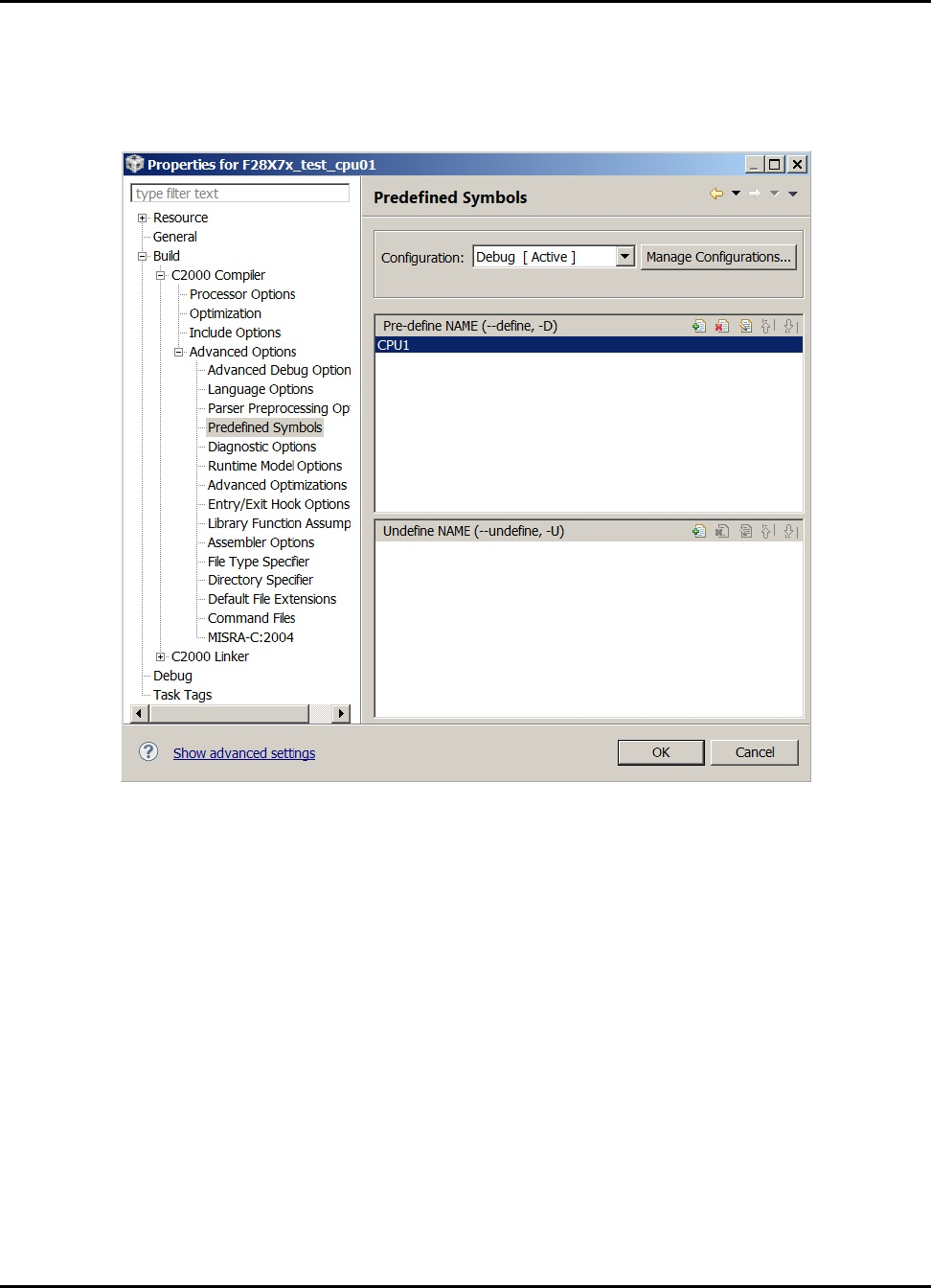
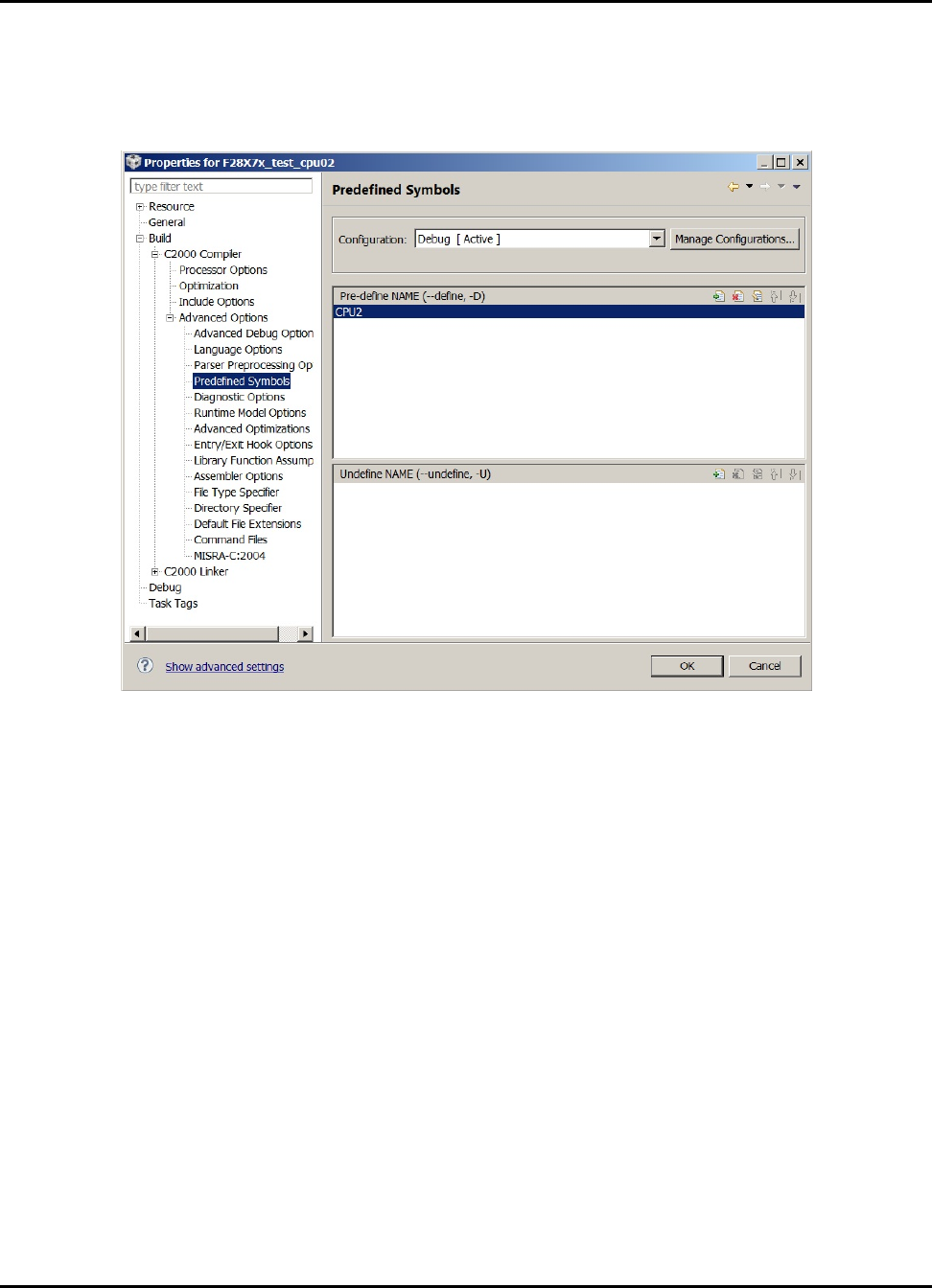
4. Expand the Advanced Options and look for the Predefined Symbol entry. Add a Pre-define
NAME called "CPU1". This ensures that the header files build correct for this CPU. If using a
Launchpad, also add a pre-define NAME called "_LAUNCHXL_F28379D". This is required to
setup the proper device clocking.
Figure 2.4: Project configuration dialog box
Sun Mar 25 13:25:49 CDT 2018 23
Getting Started and Troubleshooting
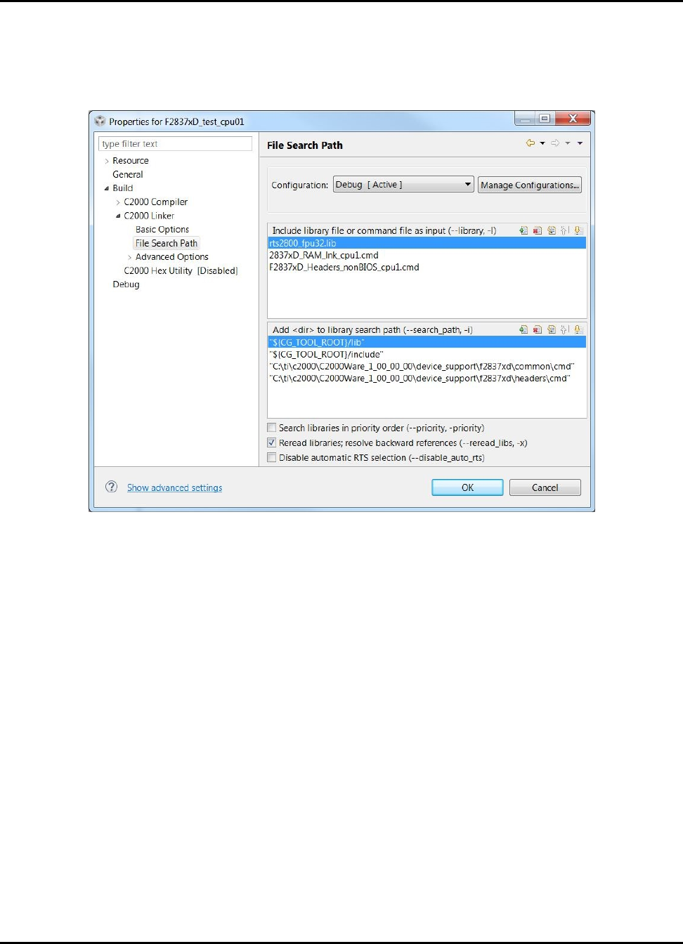
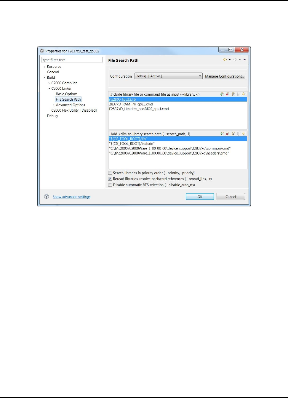
5. Click on the Linker File Search Path. Add these directories to the search path: common\cmd
and headers\cmd. Then you’ll also want to add the following files: rts2800_fpu32.lib,
2837xD_RAM_lnk_cpu1.cmd, and F2837xD_Headers_nonBIOS_cpu1.cmd. Finally,
delete libc.a, we will use rts2800_fpu32.lib as our run time support library instead.
Figure 2.5: Project configuration dialog box
24 Sun Mar 25 13:25:49 CDT 2018
Getting Started and Troubleshooting
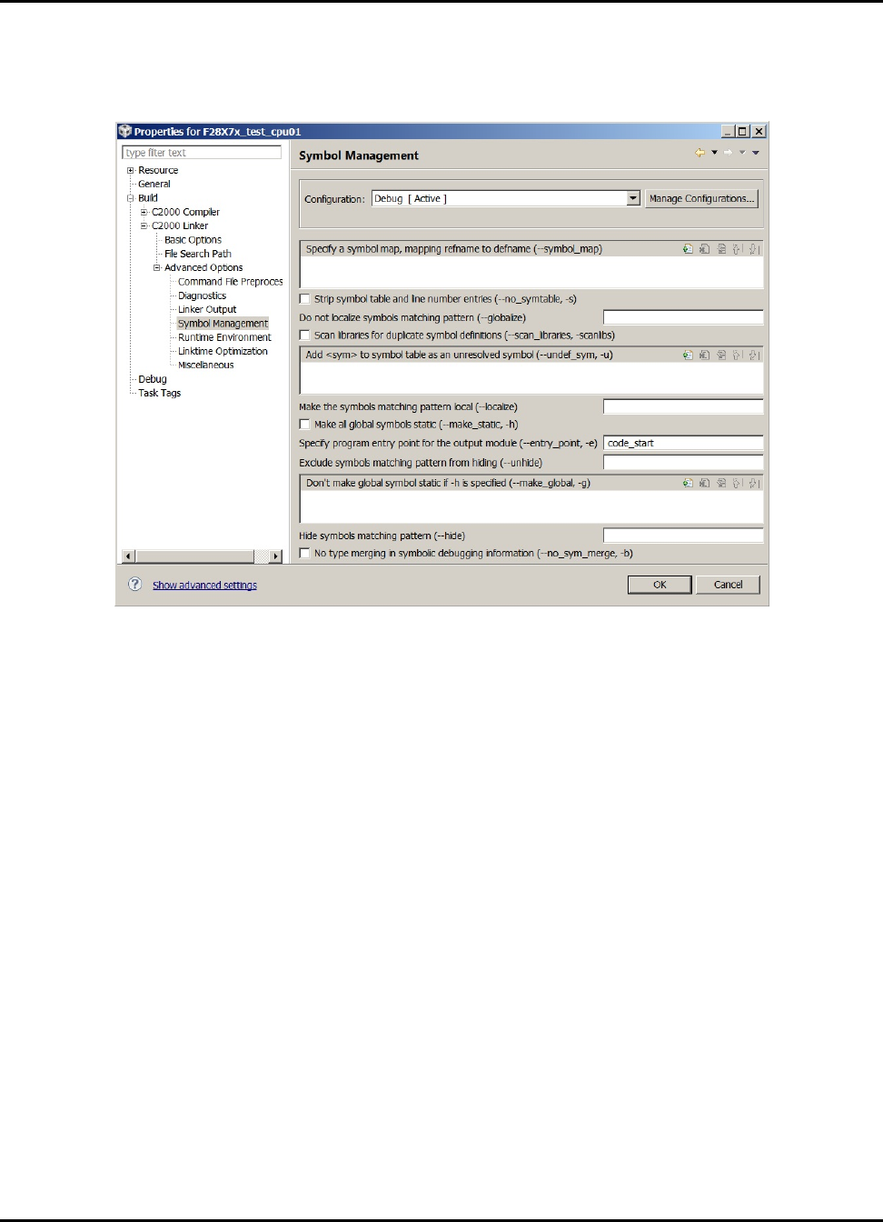
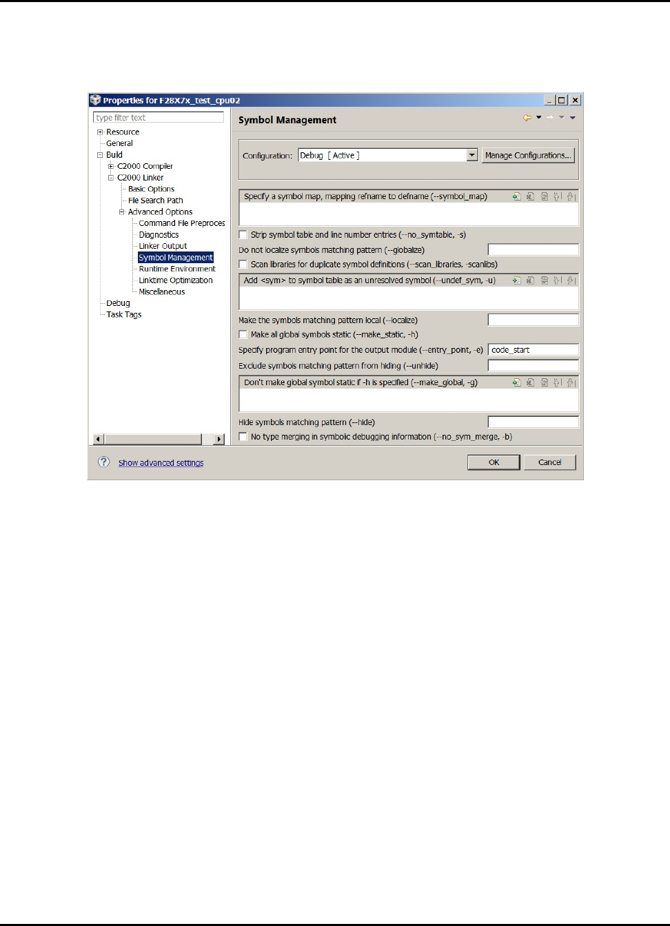
6. While you have this window open select the Symbol Management options under C2000 Linker
Advanced Options. Specify the program entry point to be code_start. Select ok to close
out of the Build Properties.
Figure 2.6: Include path setup
Sun Mar 25 13:25:49 CDT 2018 25
Getting Started and Troubleshooting
7. In the project explorer, check that no linker command file got added during project setup. If so,
remove the linker command file that got added. Additionally, check in the project properties
under the General tab and verify that the linker command text box is blank.
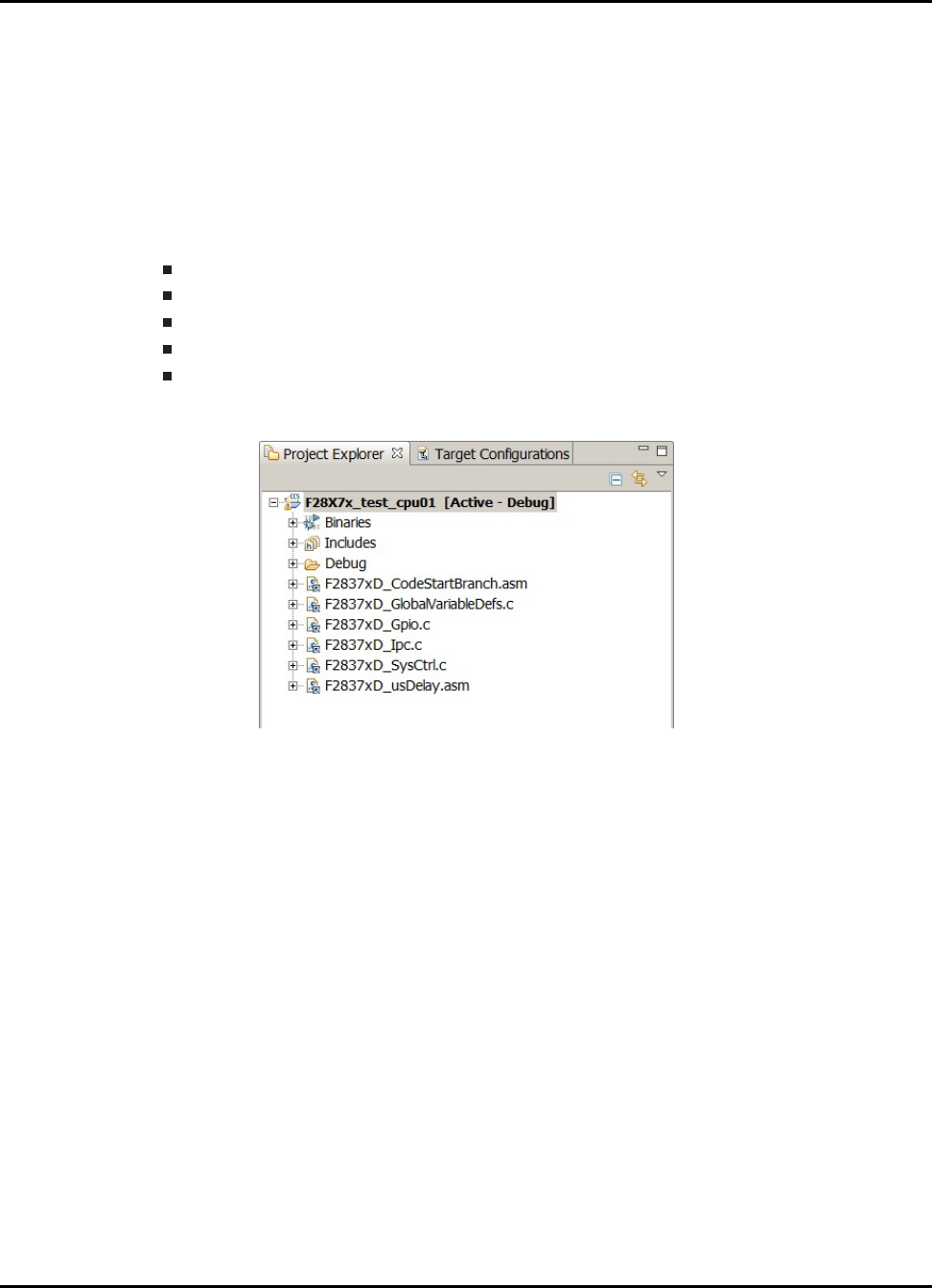
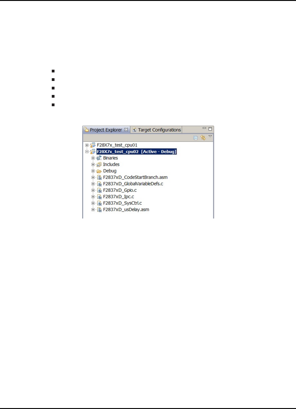
8. Next we need to link in a few files which are used by the header files. To do this right click
on your project in the workspace and select Add Files... Navigate to the headers\source
directory, and select F2837xD_GlobalVariableDefs.c . After you select the file you’ll
have the option to copy the file into the project or link it. We recommend you link files like this
to the project as you will probably not modify these files. In addition, link in the following files
as well:
common\source\F2837xD_CodeStartBranch.asm
common\source\F2837xD_usDelay.asm
common\source\F2837xD_SysCtrl.c
common\source\F2837xD_Gpio.c
common\source\F2837xD_Ipc.c
At this point your project workspace should look like the following:
Figure 2.7: Linking files to project
26 Sun Mar 25 13:25:49 CDT 2018

Getting Started and Troubleshooting
9. Create a new file by right clicking on the project and selecting New ->File. Name this file
main.c and copy the following code into it:
//
// Included Files
//
#include "F28x_Project.h"
//
// Defines
//
#define BLINKY_LED_GPIO 31
void main(void)
{
//
// Step 1. Initialize System Control:
// PLL, WatchDog, enable Peripheral Clocks
// This example function is found in the F2837xD_SysCtrl.c file.
//
InitSysCtrl();
//
// Step 2. Initialize GPIO:
// This example function is found in the F2837xD_Gpio.c file and
// illustrates how to set the GPIO to it’s default state.
//
InitGpio();
GPIO_SetupPinMux(BLINKY_LED_GPIO, GPIO_MUX_CPU1, 0);
GPIO_SetupPinOptions(BLINKY_LED_GPIO, GPIO_OUTPUT, GPIO_PUSHPULL);
//
// Step 3. Loop to blink LED
//
for(;;)
{
//
// Turn on LED
//
GPIO_WritePin(BLINKY_LED_GPIO, 0);
//
// Delay for a bit.
//
DELAY_US(1000*500);
//
// Turn off LED
//
GPIO_WritePin(BLINKY_LED_GPIO, 1);
//
// Delay for a bit.
Sun Mar 25 13:25:49 CDT 2018 27

Getting Started and Troubleshooting
//
DELAY_US(1000*500);
}
}
10. Save main.c and then attempt to build the project by right click on it and selecting Build Project.
Assuming the project builds try debugging this project on a F2837xD device. When the code
runs you should see GPIO 10 toggle.
28 Sun Mar 25 13:25:49 CDT 2018
Getting Started and Troubleshooting
CPU 2 Subsystem Project Creation
1. From the main CCS window select File ->New ->CCS Project. Select your Target as "Generic
C28xx Device". Name your project and choose a location for it to reside. Click Finish and your
project will be created.
Figure 2.8: Creating a new C28 project
Sun Mar 25 13:25:49 CDT 2018 29
Getting Started and Troubleshooting
2. Before we can successfully build a project we need to setup some build specific settings. Right
click on your project and select Properties. Look at the Processor Options and ensure they
match the below image:
Figure 2.9: Project configuration dialog box
30 Sun Mar 25 13:25:49 CDT 2018
Getting Started and Troubleshooting
3. In the C2000 Compiler entry look for and select the Include Options. Click on the
add directory icon to add a directory to the search path. Click the File System but-
ton to browse to the common\include folder of your C2000Ware installation (typically
C:\ti\c2000\C2000Ware_X_XX_XX_XX\device_support\f2837xd\common\include).
Replace the ’X’s with your current C2000Ware version installation. Click ok to add this path,
and repeat this same process to add the headers\include directory.
Figure 2.10: Project configuration dialog box
Sun Mar 25 13:25:49 CDT 2018 31
Getting Started and Troubleshooting
4. Expand the Advanced Options and look for the Predefined Symbol entry. Add a Pre-define
NAME called "CPU2". This ensures that the header files build correct for this CPU. If using a
Launchpad, also add a pre-define NAME called "_LAUNCHXL_F28379D". This is required to
setup the proper device clocking.
Figure 2.11: Project configuration dialog box
32 Sun Mar 25 13:25:49 CDT 2018
Getting Started and Troubleshooting
5. Click on the Linker File Search Path. Add these directories to the search path: common\cmd
and headers\cmd. Then you’ll also want to add the following files: rts2800_fpu.lib,
2837xD_RAM_lnk_cpu2.cmd, and F2837x_Headers_nonBIOS_cpu2.cmd. Finally,
delete libc.a, we will use rts2800_fpu.lib as our run time support library instead.
Figure 2.12: Project configuration dialog box
Sun Mar 25 13:25:49 CDT 2018 33
Getting Started and Troubleshooting
6. While you have this window open select the Symbol Management options under C2000 Linker
Advanced Options. Specify the program entry point to be code_start. Select ok to close
out of the Build Properties.
Figure 2.13: Include path setup
34 Sun Mar 25 13:25:49 CDT 2018
Getting Started and Troubleshooting
7. In the project explorer, check that no linker command file got added during project setup. If so,
remove the linker command file that got added.
8. Next we need to link in a few files which are used by the header files. To do this right click
on your project in the workspace and select Add Files... Navigate to the headers\source
directory, and select F2837xD_GlobalVariableDefs.c. After you select the file you’ll have the
option to copy the file into the project or link it. We recommend you link files like this to the
project as you will probably not modify these files. In addition, link in the following files as well:
common\source\F2837xD_CodeStartBranch.asm
common\source\F2837xD_usDelay.asm
common\source\F2837xD_SysCtrl.c
common\source\F2837xD_Gpio.c
common\source\F2837xD_Ipc.c
At this point your project workspace should look like the following:
Figure 2.14: Linking files to project
Sun Mar 25 13:25:49 CDT 2018 35

Getting Started and Troubleshooting
9. Create a new file by right clicking on the project and selecting New ->File. Name this file
main.c and copy the following code into it:
//
// Included Files
//
#include "F28x_Project.h"
//
// Defines
//
#define BLINKY_LED_GPIO 34
void main(void)
{
//
// Step 1. Initialize System Control:
// PLL, WatchDog, enable Peripheral Clocks
// This example function is found in the F2837xD_SysCtrl.c file.
//
InitSysCtrl();
//
// Step 2. Loop to blink LED
//
for(;;)
{
//
// Turn on LED
//
GPIO_WritePin(BLINKY_LED_GPIO, 0);
//
// Delay for a bit.
//
DELAY_US(1000*500);
//
// Turn off LED
//
GPIO_WritePin(BLINKY_LED_GPIO, 1);
//
// Delay for a bit.
//
DELAY_US(1000*500);
}
}
10. Save main.c and then attempt to build the project by right click on it and selecting Build Project.
Assuming the project builds try debugging both these projects simultaneously on a F2837xD
device, otherwise carefully examine the error and the above steps to determine what could
have gone wrong.
36 Sun Mar 25 13:25:49 CDT 2018

Getting Started and Troubleshooting
2.3 Debugging Dual Core Applications
1. Ensure CCS version 6 or newer is installed and up to date. You should have C2000 Code
Generation Tools version 16.9.1.LTS or later.
2. Connect a USB Mini cable from the computer to the USB port on the left hand side of the
controlCARD. Windows will enumerate and try to install drivers. As long as CCS is installed,
Windows should automatically find and install drivers for the emulator.
3. Apply power either via USB or the 5V DC in jack on the docking station. While the emulator
on the board is powered from the host computer’s USB port, the rest of the board is not.
The reason for this is that the JTAG connection on the F2837xD controlCARDs is completely
electrically isolated. Because of the typical applications these devices will be used in, it is
neccessary to isolate the JTAG connection. However, for bench debug and evaluation (with
low voltages), both halves of the board can be powered from the same supply (i.e. USB). Each
power domain has an associated power LED which can be used to ensure that each domain
has power.
4. Launch CCS and pick the workspace you would like to debug in.
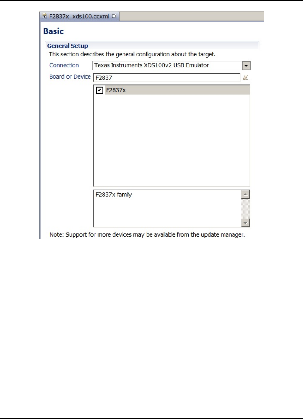
5. Create a new target configuration. Click File ->New ->Target Configuration File and name
the file appropriately (i.e. F2837xD_xds100.ccxml). Select the emulator you intend to use
(XDS100v2) from the drop down list, and then select the device variant present on your board
(F2837xD controlCARDs have a F2837xD). Save the target configuration and close the win-
dow.
Sun Mar 25 13:25:49 CDT 2018 37
Getting Started and Troubleshooting
Figure 2.15: F2837xD Card Target Configuration Setup
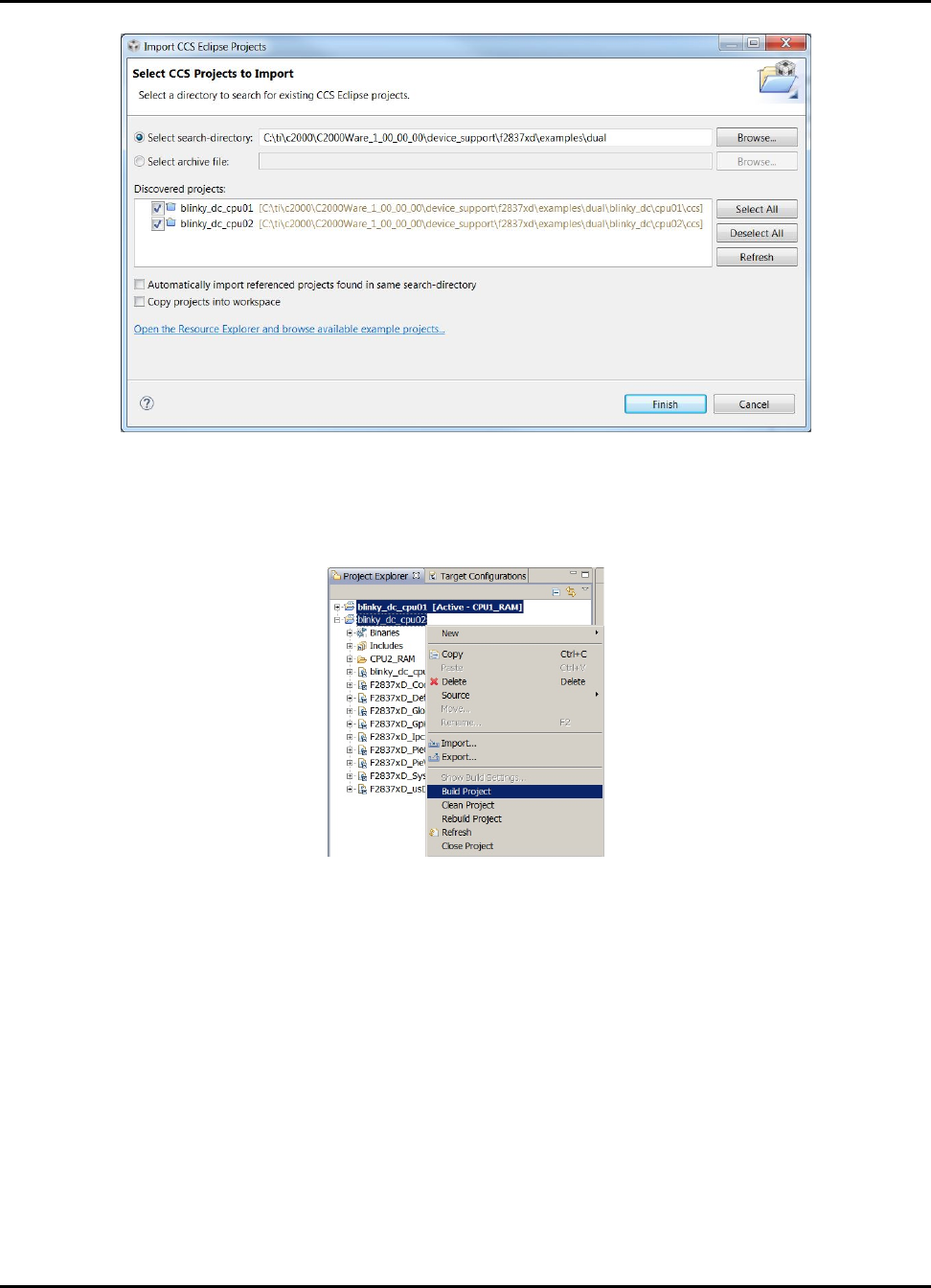
6. Import the desired example projects (or skip this step if you are using projects you created
in the Project Creation section). Click File ->Import, and in the CCS folder select Existing
CCS/CCE Eclipse Projects before clicking Next. With the "Select search-directory" radio but-
ton checked, browse to the root of your C2000Ware installation. Device specific software as
well as examples are stored in the device_support/device_variant folders. Navigate
to the F2837xD directory, and then to the examples/dual directory. Click OK and CCS
will parse all of the projects in this directory. Import any projects you wish to run into the
workspace. Do not select "Copy projects into workspace". These projects link to external
resources relatively, so taking them out of C2000Ware will break the project.
38 Sun Mar 25 13:25:49 CDT 2018
Getting Started and Troubleshooting
Figure 2.16: Importing F2837xD Projects
7. Build each of the example projects. Right click on each project title and select build project.
Figure 2.17: Building F2837xD Projects
8. Launch the previously created target configuration. Click View ->Target Configurations. In
the window that opens, find the target configuration you created previously, right click on it and
select "Launch Target Configuration".
Sun Mar 25 13:25:49 CDT 2018 39
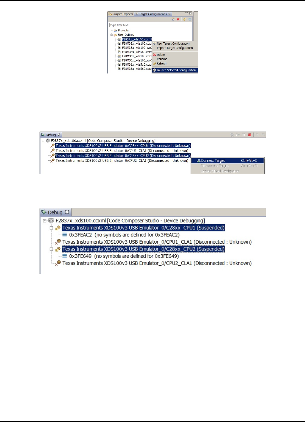
Getting Started and Troubleshooting
Figure 2.18: Launching a CCS Target Configuration
9. Connect to the device. Right click on each core in the debug window and select "Connect
Target. This will connect CCS to the device and will allow you to load code and debug appli-
cations.
Figure 2.19: Connecting to a Target
Figure 2.20: After connection to both cores
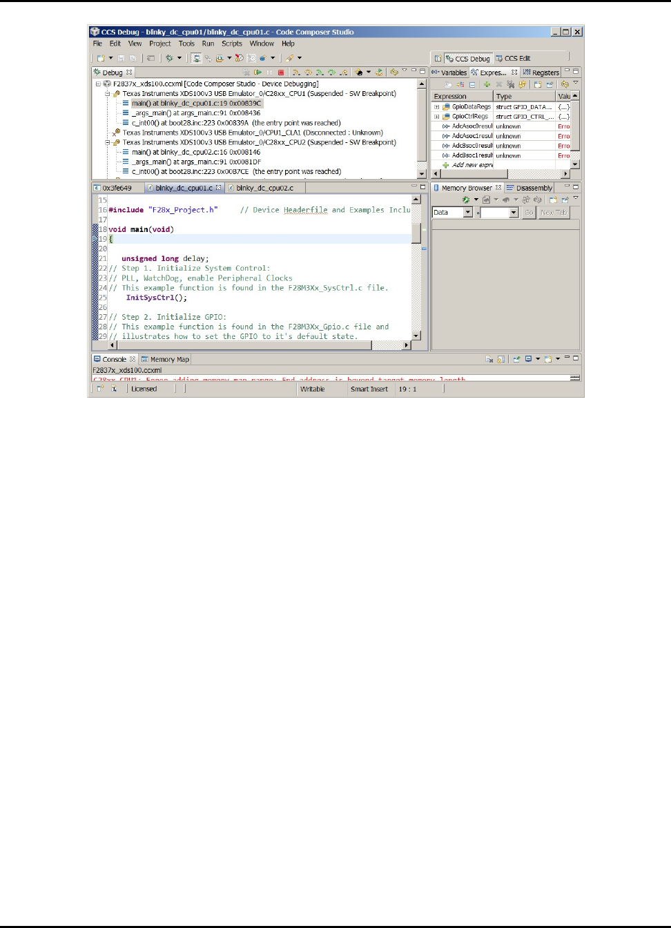
10. Load code on each of the cores. Select one of the cores in the debug window and then click
Target ->Load Program. A dialog box is display which will allow you to select a program
to load. Be careful to ensure that you load the appropriate out file on the appropriate core.
Repeat this process for the other core by selecting it and following these same steps.
11. At this point both cores should have code loaded and be halted at main. From this point, users
should be able to debug code just as they are used to with CCS. Please keep in mind that any
action you take in CCS only has an effect on the core you currently have selected in the debug
window. For instance if CPU 1 is selected, the memory window will display the memory map
of of the system as seen by CPU 1. The opposite would be true if CPU 2 were selected.
40 Sun Mar 25 13:25:49 CDT 2018
Getting Started and Troubleshooting
Figure 2.21: Projects loaded on each core
2.4 Project: Adding Bit-field or DriverLib Support
F2837xD devices support two types of development software, driver library APIs and bit-field struc-
tures. Each have their advantages and are implemented to be compatible together within the same
user application. This section details how to add driverlib support to a bit-field project as well as
how to add bit-field support to a driverlib project.
When combining bit-field and driverlib support, add a pre-defined symbol within the project prop-
erties called "_DUAL_HEADERS". This is required to avoid having conflicting definitions that may
exist in both bit-field and driverlib support.
Adding DriverLib Support
1. Add the following include directory path to the project:
driverlib\f2837xd\driverlib
2. Include the following header file in the project main source file:
device_support\f2837xd\common\include\driverlib.h
3. Add or link the driverlib.lib library to the project. Location of file:
driverlib\f2837xd\driverlib\ccs\Debug
Adding Bit-field Support
1. Add the following include directory path to the project:
device_support\f2837xd\headers\include
Sun Mar 25 13:25:49 CDT 2018 41

Getting Started and Troubleshooting
2. Include the following header file in the project main source file:
device_support\f2837xd\headers\include\f2837xd_device.h
3. Add or link the F2837xD_GlobalVariableDefs.c file to the project. Location of file:
device_support\f2837xd\headers\source
4. Add or link the F2837xD_Headers_nonBIOS.cmd file to the project. Location of file:
device_support\f2837xd\headers\cmd
2.5 Troubleshooting
There are a number of things that can cause the user trouble while bringing up a debug session
the first time. This section will try to provide solutions to the most common problems encountered
with the Delfino devices.
"I get a managed make error when I import the example projects"
This occurs when one imports a project for which he or she doesn’t have the code generation tools
for. Please ensure that you have at least version 16.9.1.LTS of the C2000 Code Generation Tools.
"I cannot build the example projects"
This is caused by linked resources not being where the project expects them to be. For instance, if
you imported the projects and selected "Copy projects to workspace", the projects would no longer
build because the files they reference aren’t a part of your workspace. Always build and run the
examples directly in the C2000Ware directory tree.
"My F2837xD device isn’t in the target configuration selection list"
The list of available device for debug is determined based on a number of factors, including drivers
and tools chains available on the host system. If you system has previously been used only for
development on previous C2000 devices, you may not have the required CCS device files. In CCS
click on "Help, Check for updates" and follow the dialog boxes to update your CCS installation.
"I cannot connect to the target"
This is most often times caused by either a bad target configuration, or simply the emulator being
physically disconnected. If you are unable to connect to a target check the following things:
1. Ensure the target configuration is correct for the device you have.
2. Ensure the emulator is plugged in to both the computer and the device to be debugged.
3. Ensure that the target device is powered.
"I cannot load code"
This is typically caused by an error in the GEL script or improperly linked code. If you are having
trouble loading code, check the linker command files and maps to ensure that they match the device
memory map. If these appear correct, there is a chance there is something wrong in one of your
GEL scripts.
"When a core gets an interrupt, it faults"
Ensure that the interrupt vector table is where the interrupt controller thinks it is. On both cores the
interrupt vector table may be mapped to either RAM or flash. Please ensure that your vector table
is where the interrupt controller thinks it is.
"When the CPU1 comes up, it is not fresh out of reset"
42 Sun Mar 25 13:25:49 CDT 2018

Getting Started and Troubleshooting
F2837xD devices support several boot modes, several of which allow program code to be loaded
into and executed out of RAM via one of the device many serial peripherals. If the boot mode pins
are in the wrong state at power up, one of these peripheral boot modes may be entered accidentally
before the debugger is connected. This leaves the chip in an unclean state with potentially several
of the peripherals configured as well as the interrupt vector table setup. If you are seeing strange
behavior check to ensure that the "Boot to Flash" or "Boot to RAM" boot mode is selected.
"I’m using a Launchpad and my device clocking is incorrect"
The Launchpad has a different oscillator speed compared to the controlCARDs. In your project, add
the pre-define NAME "_LAUNCHXL_F28379D" within the project’s properties->Advanced Options-
>Predefined Symbols.
Sun Mar 25 13:25:49 CDT 2018 43

Getting Started and Troubleshooting
44 Sun Mar 25 13:25:49 CDT 2018

Interrupt Service Routine Priorities
3 Interrupt Service Routine Priorities
InterruptHardwarePriorityOverview .....................................................................45
F2837xDPIEInterruptPriorities ..........................................................................46
SoftwarePrioritization ofInterrupts -The Example ........................................................47
3.1 Interrupt Hardware Priority Overview
With the PIE block enabled, the interrupts are prioritized in hardware by default as follows:
Global Priority (CPU Interrupt level):
CPU Interrupt Hardware Priority
Reset 1(Highest)
INT1 5
INT2 6
INT3 7
INT4 8
INT5 9
INT6 10
INT7 11
... ...
INT12 16
INT13 17
INT14 18
DLOGINT 19(Lowest)
RTOSINT 20
reserved 2
NMI 3
ILLEGAL -
USER1 -(Software Interrupts)
USER2 -
... ...
CPU Interrupts INT1 - INT14, DLOGINT and RTOSINT are maskable interrupts. These interrupts
can be enabled or disabled by the CPU Interrupt enable register (IER).
Group Priority (PIE Level):
If the Peripheral Interrupt Expansion (PIE) block is enabled, then CPU interrupts INT1 to INT12 are
connected to the PIE. This peripheral expands each of these 12 CPU interrupt into 8 interrupts.
Thus the total possible number of available interrupts in the PIE is 96. Note, not all of the 96 are
used on a 2803x device.
Each of the PIE groups has its own interrupt enable register (PIEIERx) to control which of the 8
interrupts (INTx.1 - INTx.8) are enabled and permitted to issue an interrupt.
Sun Mar 25 13:25:49 CDT 2018 45

Interrupt Service Routine Priorities
CPU PIE
Interrupt Group PIE Interrupts
Highest————–Hardware Priority Within the Group—————-Lowest
INT1 1 INT1.1 INT1.2 INT1.3 INT1.4 INT1.5 INT1.6 INT1.7 INT1.8
INT2 2 INT2.1 INT2.2 INT2.3 INT2.4 INT2.5 INT2.6 INT2.7 INT2.8
INT3 3 INT3.1 INT3.2 INT3.3 INT3.4 INT3.5 INT3.6 INT3.7 INT3.8
... etc ...
... etc ...
INT12 12 INT12.1 INT12.2 INT12.3 INT12.4 INT12.5 INT12.6 INT12.7 INT4.8
Table 3.1: PIE Group Hardware Priority
3.2 PIE Interrupt Priorities
The PIE block is organized such that the interrupts are in a logical order. Interrupts that typically
require higher priority, are organized higher up in the table and will thus be serviced with a higher
priority by default.
The interrupts in a control subsystem can be categorized as follows (ordered highest to lowest
priority):
1. Non-Periodic, Fast Response
These are interrupts that can happen at any time and when they occur, they must be serviced
as quickly as possible. Typically these interrupts monitor an external event.
On the F2837xD devices, such interrupts are allocated to the first few interrupts within PIE
Group 1 and PIE Group 2. This position gives them the highest priority within the PIE group.
In addition, Group 1 is multiplexed into the CPU interrupt INT1. CPU INT1 has the highest
hardware priority. PIE Group 2 is multiplexed into the CPU INT2 which is the 2nd highest
hardware priority.
2. Periodic, Fast Response
These interrupts occur at a known period, and when they do occur, they must be serviced as
quickly as possible to minimize latency. The A/D converter is one good example of this. The
A/D sample must be processed with minimum latency.
On the F2837xD devices, such interrupts are allocated to the group 1 in the PIE table. Group
1 is multiplexed into the CPU INT1. CPU INT1 has the highest hardware priority
3. Periodic
These interrupts occur at a known period and must be serviced before the next interrupt.
Some of the PWM interrupts are an example of this. Many of the registers are shadowed, so
the user has the full period to update the register values.
In the F2837xD device’s PIE modules, such interrupts are mapped to group 2 - group 5.
These groups are multiplexed into CPU INT3 to INT5 (the ePWM and eCAP), which are the
next lowest hardware priority.
4. Periodic, Buffered
These interrupts occur at periodic events, but are buffered and hence the processor need
46 Sun Mar 25 13:25:49 CDT 2018

Interrupt Service Routine Priorities
only service such interrupts when the buffers are ready to filled/emptied. All of the serial ports
(SCI / SPI / I2C / CAN) either have FIFOs or multiple mailboxes such that the CPU has plenty
of time to respond to the events without fear of losing data.
In the F2837xD device, such interrupts are mapped to INT6, INT8, and INT9, which are the
next lowest hardware priority.
3.3 Software Prioritization of Interrupts
The user will probably find that the PIE interrupts are organized where they should be for most
applications. However, some software prioritization may still be required for some applications.
Recall that the basic software priority scheme on the C28x works as follows:
Global Priority
This priority can be managed by manipulating the CPU IER register. This register controls the
16 maskable CPU interrupts (INT1 - INT16).
Group Priority
This can be managed by manipulating the PIE block interrupt enable registers (PIEIERx).
There is one PIEIERx per group and each control the 8-interrupts multiplexed within that group.
The F28 software prioritization of interrupt example demonstrates how to configure the Global pri-
ority (via IER) and group priority (via PIEIERx) within an ISR in order to change the interrupt service
priority based on user assigned levels. The steps required to do this are:
1. Set the global priority
Modify the IER register to allow CPU interrupts with a higher user priority to be serviced.
2. Set the Group priority
Modify the appropriate PIEIERx register to allow group interrupts with a higher user set priority
to be serviced.
3. Enable interrupts
The software prioritized interrupts example provides a method using mask values that are config-
ured during compile time to allow you to manage this easily.
To setup software prioritization for the example, the user must first assign the desired global priority
levels and group priority levels.
This is done in the F2837xD_common/include/F2837xD_SWPrioritizedIsrLevels.h file as follows:
1. User assigns global priority levels
INT1PL - INT16PL
These values are used to assign a priority level to each of the 16 interrupts controlled by the
CPU IER register. A value of 1 is the highest priority while a value of 16 is the lowest. More
then one interrupt can be assigned the same priority level. In this case the default hardware
priority would determine which would be serviced first. A priority of 0 is used to indicate that
the interrupt is not used.
Sun Mar 25 13:25:49 CDT 2018 47

Interrupt Service Routine Priorities
2. User assigns PIE group priority levels
GxyPL (where x = PIE group number 1 - 12 and y = interrupt number 1 - 8)
These values are used to assign a priority level to each of the 8 interrupts within a PIE group.
A value of 1 is the highest priority while a value of 8 is the lowest. More then one interrupt can
be assigned the same priority level. In this case the default hardware priority would determine
which would be serviced first. A priority of 0 is used to indicate that the interrupt is not used.
Once the user has defined the global and group priority levels, the compiler will generate mask
values that can be used to change the IER and PIEIERx registers within each ISR. In this manner
the interrupt software prioritization will be changed. The masks that are generated at compile time
are:
IER mask values
MINT1 - MINT16
The user assigned INT1PL - INT16PL values are used at compile time to calculate an IER
mask for each CPU interrupt. This mask value will be used within an ISR to allow CPU inter-
rupts with a higher priority to interrupt the current ISR and thus be serviced at a higher priority
level.
PIEIERxy mask values
MGxy (where x = PIE group number 1 - 12 and y = interrupt number 1 - 8)
The assigned group priority levels (GxyPL) are used at compile time to calculate PIEIERx
masks for each PIE group. This mask value will be used within an ISR to allow interrupts
within the same group that have a higher assigned priority to interrupt the current ISR and
thus be serviced at a higher priority level.
3.3.1 Using the IER/PIEIER Mask Values
Within an interrupt service routine, the global and group priority can be changed by software to
allow other interrupts to be serviced. The procedure for setting an interrupt priority using the mask
values created in the F28_SWPrioritizedIsrLevels.h is the following:
1. Set the global priority
Modify IER to allow CPU interrupts from the same PIE group as the current ISR.
Modify IER to allow CPU interrupts with a higher user defined priority to be serviced.
2. Set the group priority
Save the current PIEIERx value to a temporary register.
The PIEIER register is then set to allow interrupts with a higher priority within a PIE group
to be serviced.
3. Enable interrupts
Enable all PIE interrupt groups by writing all 1’s to the PIEACK register
Enable global interrupts by clearing INTM
4. Execute ISR. Interrupts that were enabled in steps 1-3 (those with a higher software priority)
will be allowed to interrupt the current ISR and thus be serviced first.
5. Restore the PIEIERx register
6. Exit
48 Sun Mar 25 13:25:49 CDT 2018

Interrupt Service Routine Priorities
3.3.2 Example Code
The sample C code below shows an EV-A Comparator 1 Interrupt service routine software
prioritization written in C. This interrupt is connected to PIE group 2 interrupt 1.
// Connected to PIEIER2_1 (use MINT2 and MG21 masks):
#if (G21PL != 0)
interrupt void EPWM1_TZINT_ISR(void) // EPWM1 Trip Zone
{
// Set interrupt priority:
volatile Uint16 TempPIEIER = PieCtrlRegs.PIEIER2.all;
IER |= M_INT2;
IER &= MINT2; // Set "global" priority
PieCtrlRegs.PIEIER2.all &= MG21; // Set "group" priority
PieCtrlRegs.PIEACK.all = 0xFFFF; // Enable PIE interrupts
asm(" NOP");
EINT;
// Insert ISR Code here.......
// for now just insert a delay
for(i = 1; i <= 10; i++) {}
// Restore registers saved:
DINT;
PieCtrlRegs.PIEIER2.all = TempPIEIER;
// Add ISR to Trace
ISRTrace[ISRTraceIndex] = 0x0021;
ISRTraceIndex++;
}
#endif
CMP1INT_ISR:
ASP
ADDB SP,#1
CLRC OVM,PAGE0
MOVW DP,#0x0033
MOV AL,@36
MOV *-SP[1],AL
OR IER,#0x0002
AND IER,#0x0002
AND @36,#0x000E
MOV @33,#0xFFFF
CLRC INTM
User code goes here...
SETC INTM
MOV AL,*-SP[1]
MOV @36,AL
SUBB SP,#1
Sun Mar 25 13:25:49 CDT 2018 49

Interrupt Service Routine Priorities
NASP
IRET
The interrupt latency is approx 22 cycles.
/∗!
50 Sun Mar 25 13:25:49 CDT 2018

CLA C Compiler
4 CLA C Compiler
Introduction ..............................................................................................51
Overview ................................................................................................51
Framework ...............................................................................................59
GettingStarted with theCLA Compiler ...................................................................60
Debugging ...............................................................................................64
Known Debugging Issues ................................................................................65
Tips andTricks ...........................................................................................65
4.1 Introduction
The goal of the CLA compiler is to implement enough of the C programming environment to make
it easier to access the capabilities of the CLA architecture and integrate CLA task code and data
into a C28x application.
The compiler is available as part of the codegen tools (v6.0.1 and later). All bugs, performance
issues should be reported to Compiler Support at the forum Compiler Forum.
4.2 Overview
The README.txt file included in the compiler download package contains the latest details on the
CLA compiler’s C language implementation and it is highly recommended that you go over this
document before you begin coding.
4.2.1 How to Invoke the CLA Compiler
The CLA compiler is invoked using the same command used for compiling C28x code
(cl2000[.exe]).
Files that have a .cla extension will be recognized by the compiler as CLA C files. The shell will
invoke separate CLA versions of the compiler passes to generate CLA-specific code. The object
files generated by the compiler can then be linked with C28x objects files to create a C28x/CLA
program.
Usage:
cl2000 -v28 –cla_support=cla0 [other options] file.cla
or
cl2000 -v28 –cla_support=cla1 [other options] file.cla
NOTE: THE COMPILER DOES NOT SUPPORT COMPILING BOTH CLA AND C28XCFILES IN ONE
INVOCATION.
Sun Mar 25 13:25:49 CDT 2018 51

CLA C Compiler
4.2.2 C Language Implementation
4.2.2.1 Characteristics
Language
Supports C only. No C++ or GCC extension support.
Data Types
(NOTE THE DIFFERENCES FROM C28X DATA TYPES!!)
char,short - 16 bits
int,long - 32 bits (’long long’ data type is not supported)
float, double, long double - 32 bits
pointers - 16 bits
IMPORTANT NOTES:
The CLA and C28x CPU have different type sizes.
•When declaring data that will be shared by both C28x and CLA use
type declarations that will result in objects of the same size
•To avoid ambiguity use typedefs for basic types that include size
information (eg. int32, uint16, etc)
The CLA architecture is oriented for 32-bit data types.
•16-bit data types incur sign extension overhead and should primarily be used
for load/store operations such as reading/writing 16-bit peripherals.
Pointers are INTERPRETED differently
•Pointers on the C28 are 22-bits wide and require at minimum 2 contiguous 16-bit
locations for storage. As such they are treated as 32-bit data types(since we cannot
allocate 22 bit memory locations)
•The CLA treats pointers as 16-bit data types. Any pointer shared between the C28
and CLA will be interpreted as a 16-bit location by the CLA compiler and this could cause
undesired or bad data accesses by the CLA.
NOTE: THE CLA COMPILER DOES NOT PROVIDE 64-BIT DATA TYPE SUPPORT. THE CLA_TYPEDEFS
HEADER FILE DOES HOWEVER DEFINE A 64 BIT INTEGER AS THE UNION OF TWO 32-BIT INTEGERS;
THIS WAS DONE IN ORDER TO PREVENT ERRORS IN THE COMPILATION PROCESS OF OTHER PERIPHERAL
HEADERS THAT USE 64-BIT TYPES,E.G. USB
Pragmas
The compiler accepts C28x pragmas except for the FAST_FUNC_CALL
52 Sun Mar 25 13:25:49 CDT 2018

CLA C Compiler
C Standard Library
In general, the C standard library is not supported. abs() and fabs() are supported as intrinsics. An
inline fast floating-point divide is supported.
Keywords
The keywords ’__cregister’,’far’, and ’ioport’ are not recognized
Intrinsics
The following intrinsics are supported:
float __meisqrtf32(float)
float __meinvf32(float)
float __mminf32(float, float)
float __mmaxf32(float, float)
void __mswapf(float, float)
short __mf32toi16r(float)
unsigned short __mf32toui16r(float)
float __mfracf32(float)
__mdebugstop()
__meallow()
__medis()
__msetflg(unsigned short, unsigned short)
__mnop()
Sun Mar 25 13:25:49 CDT 2018 53

CLA C Compiler
4.2.3 Language Restrictions
Global Initialization
Defining and initializing global data is not supported.
Since the CLA code is executed in an interrupt driven environment there is no C system boot
sequence. As a result, definitions of the form ’int global_var = 5;’ are not allowed for variables that
are defined globally (outside the scope of a function). Initialization of global data must either be
done by the C28x driver code or within a function.
Variables defined as ’const’ can be initialized globally. The compiler will create initialized data sec-
tions named .const_cla to hold these variables. The same restriction applies to variables declared
as ’static’. Even if the variable is defined within a function.
Stack
Local variables and compiler temps are placed into a scratchpad memory area. On older CGT
(before 6.4.0) these variables were accessed directly using the symbols ’__cla_scratchpad_start’
and ’__cla_scratchpad_end’ and it was expected that the user would manage this area and define
these symbols using a linker command file. In CGT 6.4.0 (and above) these variables are placed in
a “.scratchpad” memory section, which the compiler will then partition into local frames, one for the
all eight tasks, and one for each leaf function. These local frames will have unique symbols that the
compiler will use to access variables.
IMPORTANT NOTES:
Local variables and compiler temps are expected to be placed into a scratchpad
memory area and accessed directly using the symbols ’__cla_scratchpad_start’
and ’__cla_scratchpad_end’(for CGT 6.2.x and older), while they are placed in
“.scratchpad” for CGT 6.4.0 (and above) and the compiler access them relative to
the local frame symbol
•For the legacy memory convention (CGT 6.2.x and older) the user
is expected to manage the size of the area and define
startend symbols using a linker command file. For the
newer convention (CGT 6.4.0+), this is handled by the compiler
•This scratchpad serves as a CLA stack.
To allow debug of local variables, the linker .cmd file has been updated
from that originally distributed
•Please ensure the changes to the .cmd file shown below are made
before proceeding.
•The linker file should look like the code shown below.
•This also required a compiler released after July 21, 2011.
54 Sun Mar 25 13:25:49 CDT 2018

CLA C Compiler
Linker Command File (CGT 6.2.x and older)
The following is an example of what needs to be added to a linker command file to define the CLA
compiler scratchpad memory (legacy convention):
Define the scratchpad size - CLA_SCRATCHPAD_SIZE is a linker defined symbol that can
added to the application’s linker command file to designate the size of the scratchpad memory.
A SECTION’s directive can reference this symbol to allocate the scratchpad area. This direc-
tive reserves a 0x100 word memory hole to be used as the compiler scratchpad area.
The scratchpad area is named CLAscratch and is allotted to CLA Data RAM 1 (CLARAM1)
The value of CLA_SCRATCHPAD_SIZE can be changed based on the application.
// Define a size for the CLA scratchpad area that will be used
// by the CLA compiler for local symbols and temps
// Also force references to the special symbols that mark the
// scratchpad area.
// If using --define CLA_SCRATCHPAD_SIZE=0x100, remove next line
CLA_SCRATCHPAD_SIZE = 0x100;
--undef_sym=__cla_scratchpad_end
--undef_sym=__cla_scratchpad_start
.....
MEMORY
{
.....
}
SECTIONS
{
//
// Must be allocated to memory the CLA has write access to
//
CLAscratch :
{*.obj(CLAscratch)
. += CLA_SCRATCHPAD_SIZE;
*.obj(CLAscratch_end) } > CLARAM1, PAGE = 1
}
The scratchpad size can alternatively be defined and altered in the linker options of a project as
shown below
Sun Mar 25 13:25:49 CDT 2018 55

CLA C Compiler
Figure 4.1: Adjusting scratchpad size through the linker options
Linker Command File (CGT 6.4.0 and newer)
The following is an example of the linker command file with the new memory convention (CGT
6.4.0+):
The old convention for CLAScratch will still be supported by the new compiler, albeit, ineffi-
ciently from a memory allocation standpoint.
The new compiler creates a common local frame for the 8 tasks, i.e. each task’s local frame
is overlayed on top of each other - they use the same memory locations; this is possible since
there is no nesting of tasks, so one task cannot corrupt the scratch area of another.
By having the CLAScratch memory section, the compiler cannot take advantage of the over-
laying strategy and is, instead, forced to allocate each task’s locals in separate locations within
the scratchpad.
.....
MEMORY
{
.....
}
SECTIONS
{
//
// Must be allocated to memory the CLA has write access to
//
.scratchpad : > CLARAM1, PAGE = 1
}
Function Nesting
Only 2 levels of call stack depth is supported. See Section 4.2.5 for details on the calling conven-
tions.
56 Sun Mar 25 13:25:49 CDT 2018

CLA C Compiler
Recursion
Recursive function calls are not supported.
Function Pointers
Function pointers are not supported.
Other Operations
The following operations are currently not supported due to lack of instruction set support mak-
ing them expensive to implement. It is not clear that these operations are critical for typical CLA
algorithms.
Integer divide, modulus
Integer unsigned compares
4.2.4 Memory Model - Sections
CLA Program
The CLA compiler will place CLA code into section “Cla1Prog” as per the current convention used
for CLA assembly.
Global Data
Uninitialized global data will be placed in the section “.bss_cla”
Constants
Initialized constant data will be placed in section “.const_cla”
Heap
There is no support for operations such as malloc(). Therefore there is no C system heap for CLA.
4.2.5 Function Structure and Calling Conventions (CGT 6.2.x and older)
Function Nesting
The compiler supports 2 level of function calls. Functions declared as interrupts may call leaf
functions only. Leaf function may not call other functions. Functions not declared as interrupt
Sun Mar 25 13:25:49 CDT 2018 57

CLA C Compiler
will be considered leaf functions. NOTE: THE CLA TASKS ARE PREFIXED WITH THE KEYWORD
’__interrupt’ TO SET THEM APART FROM LEAF FUNCTIONS. THEY ARE NOT TO BE CONFUSED WITH
C28X INTERRUPT SERVICE ROUTINES
Register Calling Convention
The CLA compiler supports calling functions with up to 2 arguments.
Pointer arguments are passed in MAR0/MAR1.
Integer/float arguments are passed in MR0,MR1.
Integer and float return values from functions are passed in MR0.
Pointer or return by reference value from functions are passed in MAR0.
Register Save/Restore
All registers except for MR3 are saved on call. MR3 is saved on entry. NOTE: IF YOU ARE WRITING
AN ASM ROUTINE TO BE CALLED IN THE CCONTEXT IT IS YOUR RESPONSIBILITY TO SAVE/RESTORE
MR3 UPON ENTRY AND EXIT RESPECTIVELY
Local Variables
A static scratchpad area is used as a stack for locals and compiler temporary variables. NOTE:THE
USER IS RESPONSIBLE FOR ENSURING THE SCRATCHPAD AREA IS ALLOCATED INTO THE MEMORY
MAP AND IS LARGE ENOUGH. THIS IS DONE USING THE EITHER THE LINKER COMMAND FILE OR
THROUGH THE PROJECT’S LINKER OPTIONS (SEE ABOVE).
Mixing CLA C and Assembly
When interfacing with CLA assembly language modules use the calling conventions defined above
to interface with compiled CLA code.
4.2.6 Function Structure and Calling Conventions (CGT 6.4.0 and newer)
Function Nesting
The compiler supports an infinite call depth subject to memory constraints. NOTE: THE CLA TASKS
ARE PREFIXED WITH THE KEYWORD ’__interrupt’ TO SET THEM APART FROM LEAF FUNCTIONS.
THEY ARE NOT TO BE CONFUSED WITH C28X INTERRUPT SERVICE ROUTINES
Register Calling Convention
The CLA compiler supports calling functions with up to 2 arguments.
Pointer arguments are passed in MAR0/MAR1.
58 Sun Mar 25 13:25:49 CDT 2018

CLA C Compiler
Integer/float arguments are passed in MR0,MR1, MR2.
Additional arguments are passed on the scratchpad
Integer and float return values from functions are passed in MR0.
Pointer or return by reference value from functions are passed in MAR0.
Register Save/Restore
All registers except for MR3 are saved on call. MR3 is saved on entry. NOTE: IF YOU ARE WRITING
AN ASM ROUTINE TO BE CALLED IN THE CCONTEXT IT IS YOUR RESPONSIBILITY TO SAVE/RESTORE
MR3 UPON ENTRY AND EXIT RESPECTIVELY
Local Variables
A scratchpad area is used as a stack for locals, compiler temporary variables and passed argu-
ments. A call graph is computed in the linker to determine which function frames can be overlayed
in placement to save memory - these are usually the tasks since they can’t be nested. All generated
function frames are part of the .scratchpad section and are named in the form “.scratchpad:[function
section name]”. For example:
.scratchpad:Cla1Prog:_Cla1Task2
.scratchpad:Cla1Prog:_Cla1Func1
Therefore, the only section that needs to be placed in the linker command file is the .scratchpad
section. All function frames that are part of that section will be placed automatically within the
.scratchpad placement. It is not necessary to specify a size for the .scratchpad section. Additionally,
CLA object files compiled with previous tool versions will be fully compatible with newly generated
object files as long as the user supports both scratchpad naming conventions in the linker command
file. However, the scratchpad section used for old object files cannot be overlayed with the new
.scratchpad section and the user must ensure enough memory is available for both.
Mixing CLA C and Assembly
When interfacing with CLA assembly language modules use the calling conventions defined above
to interface with compiled CLA code.
4.3 Framework
The CLA examples are in the folder “F2837xD_examples_Cpu1”. Each CLA example within this
folder share a similar structure as shown in the figure below (Fig. 4.2)
Sun Mar 25 13:25:49 CDT 2018 59
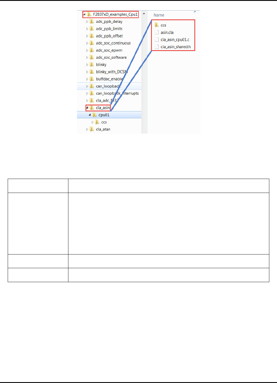
CLA C Compiler
Figure 4.2: Structure of a CLA example
For any given example there are 3 specific files associated with it as described in Table. 4.1.
Source File Description
<example>_cpu01.c implements the main() routine which runs the tests; this often involves trig-
gering a CLA task once or several times, running an algorithm within that
task, returning and storing the result of that algorithm and then finally checking
against a reference output. The main() also performs the system, peripheral,
and CLA intialization. Variables declared in <example>_shared.h are defined
here and allocated to memory (using #pragma DATA_SECTION). NOTE: CLA
VARIABLES MUST BE ALLOCATED TO A MEMORY SPACE THAT THE CLA HAS
ACCESS TO,NAMELY THE CLA<->CPU MESSAGE RAMS OR THE CLA DATA
RAMS.
<example>.cla The C implementation of all the CLA tasks. File level data global to the CLA
only(not shared with the C28x) should also be defined in this file.
<example>_shared.h External declarations for the global data defined in the C28x code and refer-
enced by the CLA task code.
Table 4.1: Example specific files
4.4 Getting Started with the CLA Compiler
The C code for the CLA is saved to a file with the .cla extension. If running an older version of
CCSv5 (v5.2 or older) that does not recognize the extension, you can follow these steps:
NOTE: FOR EACH NEW WORKSPACE THE USER MUST CONFIGURE CCS IN THE MANNER DE-
SCRIBED BELOW
60 Sun Mar 25 13:25:49 CDT 2018
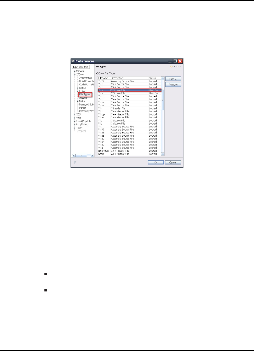
CLA C Compiler
1. Go to Windows->Preferences->C/C++->File Types.
2. Select “New”
3. Type in *.cla in the top text box
4. In the drop down menu select C source file(see Fig. 4.3).
5. Select “ok”
Figure 4.3: Configuring CCS5 to recognize the .cla extension
The IDE will now recognize the .cla extension as code to be compiled.
4.4.1 Creating Your Own Project
The simplest way to start writing code is to copy over an existing project (from the examples folder)
and to edit it. Lets take an example: I would like to create a new project, exp2, from an existing
project, atan.
1. Copy a Project:
Make a copy of the atan folder in the example directory and rename it to exp2
2. Rename Files:
Rename all files atan*.* to exp2*.*. (Notice the naming convention. All files have the test
folder name as a prefix, see Fig. 4.4 below)
Sun Mar 25 13:25:49 CDT 2018 61
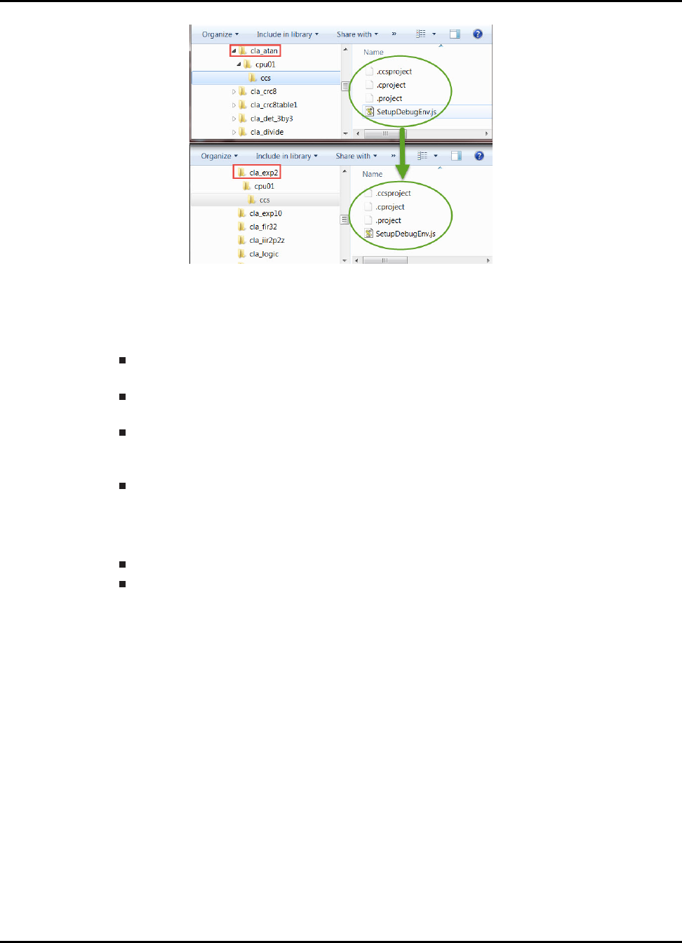
CLA C Compiler
Figure 4.4: Creating a new project from existing examples
3. Edit the Project Files:
Open the .cproject and .project files in any text editor and replace all instances of the word
atan with exp2.
This will ensure all the object files come out with the correct name and any directory
dependencies are taken care of.
If the project uses a predefined symbol, TEST_NAME=<test_name>. For e.g. the atan
project might have a predefined symbol, TEST_NAME=atan. By altering the .cproject files
in the manner described you wont have to change the build settings for each new project .
If the project does not use predefined symbols, go into the .c file and include the
correct shared header file. For e.g. in our example, change cla_atan_shared.h to
cla_exp2_shared.h
4. Import the Project:
Import the exp2 project into your workspace (see Fig. 4.5).
The files highlighted in the red box are common to all the CLA examples and are linked in
by the .project file. The rest of the source files are specific to each test case
62 Sun Mar 25 13:25:49 CDT 2018
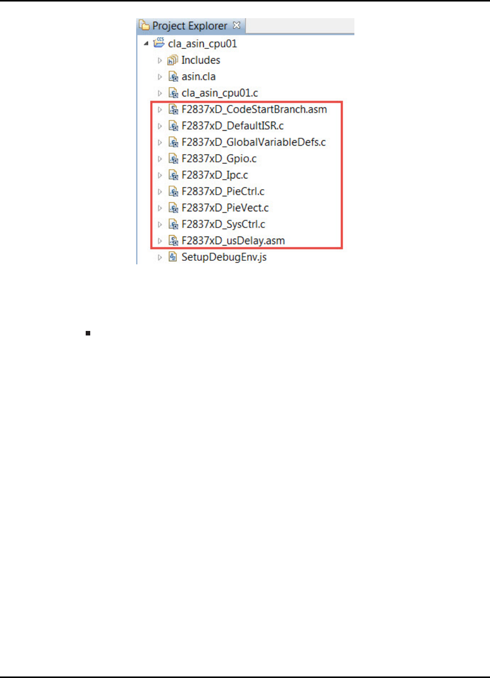
CLA C Compiler
Figure 4.5: Common source files for each CLA example
5. Modify the Source:
Edit the test specific source files.
4.4.2 Suggested Build Options
The following table lists build options that are useful for CLA C code. You can setup build properties
that apply only to *.cla file by right clicking the file and selecting Properties->C/C++ Build.
Sun Mar 25 13:25:49 CDT 2018 63

CLA C Compiler
Option Notes
Debugging Model->Full Symoblic debug (-g) If you would like to access
watch variables etc while debug-
ging(default setting).
Debugging Model->Suppress symbolic debug information View compiler generated as-
sembly code without all the de-
bug information.
Optimization->Optimization Level = none - O2 DUE TO THE SMALL NUMBER
OF REGISTERS AVAILABLE LESS
AGGRESSIVE OPTIMIZATION MAY
YIELD BETTER RESULTS (EG. -
O1 VS -O2).
Assembler Options -> Keep generated assembly files (-k) Useful if you want to compare
compiler generated code with
hand coded assembly.
Table 4.2: Suggested Build Options
4.5 Debugging
The user can follow these steps to start debugging their code on the CLA (The project exp2 is used
as an example here)
1. Add __mdebugstop()
Place an __mdebugstop() at the beginning of the CLA task you wish to debug. For exam-
ple, task 1 of exp2.cla.
2. Set build options:
You can setup individual build properties for the *.cla file seperately from the rest of the
application.
Right click the .cla file and select Properties->C/C++ Build.
3. Connect to the CLA:
Once you have built your project and launched the debug session CCS, by default, will
connect to only the C28 core.
To be able to debug CLA code you will need to connect to the CLA core. The action of
connecting to the CLA core enables all software breakpoints and single-stepping abilities.
IF YOU WISH TO STEP THROUGH CCODE BUILD THE PROJECT WITH -G(FULL SYMBOLIC
DEBUG)TO GENERATE THE SYMBOLS THAT WILL BE LOADED TO THE DEBUGGER.
(a) Click on the CLA debug session (highlighted in Fig. 4.6)
(b) Select Target->Connect to Target or hit Alt-C.
(c) Once the CLA core is connected proceed to load the project symbols by clicking on
Target->Load Symbols-><example>.out (e.g. exp2.out).
64 Sun Mar 25 13:25:49 CDT 2018

CLA C Compiler
Figure 4.6: CLA Debug Session
4. Run the C28x:
In the exp2 example we have enabled task 1 of the CLA and we trigger it in software
on the C28 side. When we run the code on the C28 debug session it seems to stall at
the Cla1ForceTask1andWait() routine. It is waiting for the CLA task 1 to run to comple-
tion. When we switch over to the CLA session we see that execution has stopped at the
__mdebustop() intrinsic
5. Debug the Code:
At this point we can proceed to single step through the code or continue till completion.
There are some restrictions to debugging the CLA and they are discussed next.
4.6 Known Debugging Issues
1. The CLA pipeline is not flushed on a single step and so results may not be visible until a few
instructions later. Please refer to the CLA user guide or the device Technical Reference Man-
ual for more details about the pipeline.
UNLIKE THE C28, SINGLE-STEPPING ON THE CLA DOES NOT FLUSH THE PIPELINE AND EXE-
CUTE AN INSTRUCTION ,IT MERELY MOVES THE PIPELINE FORWARD BY ONE STAGE)
2. If you plan to debug (single step) code on the CLA it is necessary that MNOPs are placed prior
to any MSTOP to ensure the instructions prior to the MSTOP proceed through the pipeline
before the MSTOP executes. The compiler will insert these MNOPs if compiling with debug
(-g). The MNOPs are unnecessary if you are not debugging the CLA code.
3. YOU WILL NOT BE ABLE TO EXECUTE THE “RUN TO LINE”OR “STEP OVER”COMMANDS ON
THE CLA. BE SURE TO PLACE __MDEBUGSTOP() INTRINSICS AROUND FUNCTIONS YOU WISH
TO STEP OVER AND HAVE THE CORE RUN TO THESE BREAKPOINTS DIRECTLY
4.7 Tips and Tricks
4.7.1 Dealing with Pointers
Pointers are interpreted differently on the C28x and the CLA. The C28 treats them as 32-bit data
types(address size is 22-bits) while the CLA can only use an address size of 16 bits. Assume the
following structure is declared in a shared header file(i.e. common to the C28 and CLA) and defined
and allocated to a memory section in a .c file
/********************************************************************
Sun Mar 25 13:25:49 CDT 2018 65

CLA C Compiler
Shared Header File
********************************************************************/
typedef struct{
float a;
float *b;
float *c;
}foo;
/********************************************************************
main.c
********************************************************************/
#pragma(X,"CpuToCla1MsgRam") //Assign X to section CpuToCla1MsgRam
foo X;
/********************************************************************
test.cla
********************************************************************/
__interrupt void Cla1Task1 ( void )
{
float f1,f2;
f1 = *(X.b);
f2 = *(X.c); //Pointer incorrectly dereferenced
//Tries to access location 0x1503 instead
//of 0x1504
}
Assume that the C28 compiler will allocate space for X at the top of the section CpuToCla1MsgRam
as follows:
Element Address
X.a 0x1500
X.b 0x1502
X.c 0x1504
The CLA compiler will interpret this structure differently
Element Address
X.a 0x1500
X.b 0x1502
X.c 0x1503
The CLA compiler treats pointers band cas 16-bits wide and therefore incorrectly dereferences
pointer c.
The solution to this is to declare a new pointer as follows:
/********************************************************************
Shared Header File
********************************************************************/
typedef union{
float *ptr; //Aligned to lower 16-bits
Uint32 pad; //32-bits
66 Sun Mar 25 13:25:49 CDT 2018

CLA C Compiler
}CLA_FPTR;
typedef struct{
float a;
CLA_FPTR b;
CLA_FPTR c;
}foo;
/********************************************************************
main.c
********************************************************************/
#pragma(X,"CpuToCla1MsgRam") //Assign X to section CpuToCla1MsgRam
foo X;
/********************************************************************
test.cla
********************************************************************/
__interrupt void Cla1Task1 ( void )
{
float f1,f2;
f1 = *(X.b.ptr);
f2 = *(X.c.ptr); //Correct Access
}
The new pointer CLA_FPTR is a union of a 32-bit integer and a pointer to a float. The CLA compiler
recognizes the size of the larger of the two elements(the 32 bit integer) and therefore aligns the
pointer to the lower 16-bits. Now both the pointers band cwill occupy 32-bit memory spaces and
any instruction that tries to dereference pointer cwill access the correct address 0x1504.
4.7.2 Benchmarking
The CLA does not support the clock function and therefore it is not possible to get a direct cycle
count of a particular task. The user can configure the time base module on an ePWM to keep track
of the execution time of a task
Setup the time base of ePWM1(or any ePWM) to run at SYSCLKOUT in the up-count mode as
shown below:
void InitEPwm(void)
{
// Setup TBCLK
EPwm1Regs.TBCTL.bit.CTRMODE = TB_COUNT_UP; // Count up
EPwm1Regs.TBPRD = 0xFFFF; // Set timer period
EPwm1Regs.TBCTL.bit.PHSEN = TB_DISABLE; // Disable phase loading
EPwm1Regs.TBPHS.half.TBPHS = 0x0000; // Phase is 0
EPwm1Regs.TBCTR = 0x0000; // Clear counter
EPwm1Regs.TBCTL.bit.HSPCLKDIV = TB_DIV1; // Clock ratio to SYSCLKOUT
EPwm1Regs.TBCTL.bit.CLKDIV = TB_DIV1;
}
Proceed to define two macros READ_CLOCK and RESTART_CLOCK, the former to freeze the
ePWM timer and copy the elapsed time to a variable, and the latter to restart the ePWM timer.
Sun Mar 25 13:25:49 CDT 2018 67

CLA C Compiler
#define READ_CLOCK(X) __meallow();\
EPwm1Regs.TBCTL.bit.CTRMODE = TB_FREEZE;\
X = EPwm1Regs.TBCTR;\
__medis();
#define RESTART_CLOCK __meallow();\
EPwm1Regs.TBCTL.bit.CTRMODE = TB_FREEZE;\
EPwm1Regs.TBCTR = 0;\
EPwm1Regs.TBCTL.bit.CTRMODE = TB_COUNT_UP;\
__medis();
Define a variable e.g. ulCycleCount to hold the cycle count
#pragma DATA_SECTION(ulCycleCount,"Cla1ToCpuMsgRAM");
unsigned long ulCycleCount;
Place the macro RESTART_CLOCK at the beginning of a task to restart the ePWM timer and place
READ_CLOCK at the end of the task to read the value of the timer. The elapsed time will be give
you the cycle count plus a minimal overhead from the two macros
__interrupt void Cla1Task1 ( void )
{
//Local Variables
float a;
__mdebugstop();
RESTART_CLOCK;
a = 10;
...
...
...
READ_CLOCK(ulCycleCount);
}
68 Sun Mar 25 13:25:49 CDT 2018

CPU 1 Bit-field Example Applications
5 CPU 1 Bit-field Example Applications
These example applications show how to make use of various peripherals of a F2837xD device.
These applications are intended for demonstration and as a starting point for new applications.
All these examples contain two build configurations which allow you to build each project to run
from either RAM or Flash. To change how the project is built simply right click on the project and
select "Build Configurations". Then, move over to set the active build configuration, either RAM or
Flash.
The examples provided are built for controlCARD compatibility. For LaunchPad use, some
minor modifications may be required.
If using a Launchpad, add a pre-defined symbol within the project properties called
"_LAUNCHXL_F28379D". This is required to setup the proper device clocking.
Because CPU 1 is ultimately in control of the entire F2837xD device and these applications contain
no CPU 2 dependencies, these examples may be run completely on their own without any associ-
ated CPU2 program. The only exception to this in the CPU1 examples is the setup_cpu1 example.
This example sets up all of the peripherals and GPIOs to be owned by CPU2. In addition, this
example also has a special standalone flash build configuration which will send an IPC command
to boot the second CPU and run the application in its flash memory.
All of these examples reside in the device_support/F2837xD/examples/cpu1 subdirectory
of the C2000Ware package.
5.1 ADC PPB Delay Capture (adc_ppb_delay)
This example demonstrates delay capture using the post-processing block.
Two asynchronous ADC triggers are setup:
ePWM1, with period 2048, triggering SOC0 to convert on pin A0
ePWM1, with period 9999, triggering SOC1 to convert on pin A1
Each conversion generates an ISR at the end of the conversion. In the ISR for SOC0, a conversion
counter is incremented and the PPB is checked to determine if the sample was delayed.
After the program runs, the memory will contain:
conversion : the sequence of conversions using SOC0 that were delayed
delay : the corresponding delay of each of the delayed conversions
5.2 ADC PPB Limits (adc_ppb_limits)
This example sets up the ePWM to periodically trigger the ADC. If the results are outside of the
defined range, the post-processing block will generate an interrupt.
The default limits are 1000LSBs and 3000LSBs. With VREFHI set to 3.3V, the PPB will generate
an interrupt if the input voltage goes above about 2.4V or below about 0.8V.
Sun Mar 25 13:25:49 CDT 2018 69

CPU 1 Bit-field Example Applications
5.3 ADC PPB Offset (adc_ppb_offset)
This example software triggers the ADC. Some SOCs have automatic offset adjustment applied by
the post-processing block.
After the program runs, the memory will contain:
AdcaResult : a digital representation of the voltage on pin A0
AdcaResult_offsetAdjusted : a digital representation of the voltage on pin A0, plus 100 LSBs
of automatically added offset
AdcbResult : a digital representation of the voltage on pin B0
AdcbResult_offsetAdjusted : a digital representation of the voltage on pin B0 minus 100
LSBs of automatically added offset
5.4 ADC Continuous Triggering (adc_soc_continuous)
This example sets up the ADC to convert continuously, achieving maximum sampling rate.
After the program runs, the memory will contain:
AdcaResults : A sequence of analog-to-digital conversion samples from pin A0. The time
between samples is the minimum possible based on the ADC speed.
5.5 ADC Continuous Conversions Read by DMA
(adc_soc_continuous_dma)
This example sets up two ADC channels to convert simultaneously. The results will be transferred
by the DMA into a buffer in RAM.
After the program runs, the memory will contain:
adcData0 : a digital representation of the voltage on pin A3
adcData1 : a digital representation of the voltage on pin B3
5.6 ADC ePWM Triggering (adc_soc_epwm)
This example sets up the ePWM to periodically trigger the ADC.
After the program runs, the memory will contain:
AdcaResults : A sequence of analog-to-digital conversion samples from pin A0. The time
between samples is determined based on the period of the ePWM timer.
70 Sun Mar 25 13:25:49 CDT 2018

CPU 1 Bit-field Example Applications
5.7 ADC temperature sensor conversion
(adc_soc_epwm_tempsensor)
This example sets up the ePWM to periodically trigger the ADC. The ADC converts the internal
connection to the temperature sensor, which is then interpreted as a temperature by calling the
GetTemperatureC function.
After the program runs, the memory will contain:
sensorSample : The raw reading from the temperature sensor.
sensorTemp : The interpretation of the sensor sample as a temperature in degrees Celsius.
5.8 ADC SOC Software Force (adc_soc_software)
This example converts some voltages on ADCA and ADCB based on a software trigger.
After the program runs, the memory will contain:
AdcaResult0 : a digital representation of the voltage on pin A2
AdcaResult1 : a digital representation of the voltage on pin A3
AdcbResult0 : a digital representation of the voltage on pin B2
AdcbResult1 : a digital representation of the voltage on pin B3
Note: The software triggers for the two ADCs happen sequentially, so the two ADCs will run asyn-
chronously.
5.9 ADC Synchronous SOC Software Force
(adc_soc_software_sync)
This example converts some voltages on ADCA and ADCB using input 5 of the input X-BAR as a
software force. Input 5 is triggered by toggling GPIO0, but any spare GPIO could be used. This
method will ensure that both ADCs start converting at exactly the same time.
After the program runs, the memory will contain:
AdcaResult0 : a digital representation of the voltage on pin A2
AdcaResult1 : a digital representation of the voltage on pin A3
AdcbResult0 : a digital representation of the voltage on pin B2
AdcbResult1 : a digital representation of the voltage on pin B3
5.10 Blinky
This example blinks LED X
Sun Mar 25 13:25:49 CDT 2018 71

CPU 1 Bit-field Example Applications
Note:
If using a Launchpad, use the Launchpad build configurations.
5.11 Blinky with DCSM
This example blinks LED X
5.12 FSK Transmitter using DAC mode on the AFE031
This example sets up the TMDS28379D Launchpad with the BOOSTXL-AFE031 boosterpack to
transmit 131.25 and 143.75 KHz FSK signals in a desired sequence, configured using the AFE031’s
DAC
External Connections
Remove JP1, JP2, and JP3 headers on TMDS28379D Launchpad
Connect the BOOSTXL-AFE031 boosterpack to the upper TMDS28379D Launchpad pins
Supply 15V power via upper right most jumpers
Watch Variables
txDataEnable
currentChar
cycleCount
5.13 FSK Transmitter using PWM mode on the AFE031
This example sets up the TMDS28379D Launchpad with the BOOSTXL-AFE031 boosterpack to
transmit 131.25 and 143.75 KHz FSK signals in a desired sequence, configured using EPWMs
External Connections
Remove JP1, JP2, and JP3 headers on TMDS28379D Launchpad
Connect the BOOSTXL-AFE031 boosterpack to the upper TMDS28379D Launchpad pins
Supply 15V power via upper right most jumpers
Watch Variables
txDataEnable
currentChar
cycleCount
72 Sun Mar 25 13:25:49 CDT 2018

CPU 1 Bit-field Example Applications
5.14 Buffered DAC Enable (buffdac_enable)
This example generates a voltage on the buffered DAC output, DACOUTA/ADCINA0 (HSEC Pin 9)
and uses the default DAC reference setting of VDAC.
When the DAC reference is set to VDAC, an external reference voltage must be applied to the
VDAC pin. This can accomplished by connecting a jumper wire from 3.3V to ADCINB0 (HSEC pin
12).
5.15 Buffered DAC Ramp (buffdac_ramp)
This example generates a ramp wave on the buffered DAC output, DACOUTA/ADCINA0 (HSEC
Pin 9) and uses the default DAC reference setting of VDAC.
When the DAC reference is set to VDAC, an external reference voltage must be applied to the
VDAC pin. This can accomplished by connecting a jumper wire from 3.3V to ADCINB0 (HSEC pin
12).
Run the included .js file to add the watch variables. This example uses the SGEN module. Docu-
mentation for the SGEN module can be found in the SGEN library directory.
The generated waveform can be adjusted with the following variables while running:
waveformGain : Adjust the magnitude of the waveform. Range is from 0.0 to 1.0. The default
value of 0.8003 centers the waveform within the linear range of the DAC
waveformOffset : Adjust the offset of the waveform. Range is from -1.0 to 1.0. The default
value of 0 centers the waveform
outputFreq_hz : Adjust the output frequency of the waveform. Range is from -
maxOutputFreq_hz to maxOutputFreq_hz
maxOutputFreq_hz : Adjust the max output frequency of the waveform. Range - See SGEN
module documentation for how this affects other parameters
The generated waveform can be adjusted with the following variables/macros but require recompile:
samplingFreq_hz : Adjust the rate at which the DAC is updated. Range - See SGEN module
documentation for how this affects other parameters
REFERENCE : The reference for the DAC. Range - REFERENCE_VDAC, REFER-
ENCE_VREF
CPUFREQ_MHZ : The cpu frequency. This does not set the cpu frequency. Range - See
device data manual
DAC_NUM : The DAC to use. Range - DACA, DACB, DACC
The following variables give additional information about the generated waveform: See SGEN mod-
ule documentation for details
freqResolution_hz
maxOutput_lsb : Maximum value written to the DAC.
minOutput_lsb : Minimum value written to the DAC.
pk_to_pk_lsb : Magnitude of generated waveform.
Sun Mar 25 13:25:49 CDT 2018 73

CPU 1 Bit-field Example Applications
cpuPeriod_us : Period of cpu.
samplingPeriod_us : The rate at which the DAC is updated. Note that samplingPeriod_us
has to be greater than the DAC settling time.
interruptCycles : Interrupt duration in cycles.
interruptDuration_us : Interrupt duration in uS.
sgen : The SGEN module instance.
DataLog : Circular log of writes to the DAC.
5.16 Buffered DAC Random (buffdac_random)
This example generates random voltages on the buffered DAC output, DACOUTA/ADCINA0 (HSEC
Pin 9) and uses the default DAC reference setting of VDAC.
When the DAC reference is set to VDAC, an external reference voltage must be applied to the
VDAC pin. This can accomplished by connecting a jumper wire from 3.3V to ADCINB0 (HSEC pin
12).
5.17 Buffered DAC Sine (buffdac_sine)
This example generates a sine wave on the buffered DAC output, DACOUTA/ADCINA0 (HSEC Pin
9) and uses the default DAC reference setting of VDAC.
When the DAC reference is set to VDAC, an external reference voltage must be applied to the
VDAC pin. This can accomplished by connecting a jumper wire from 3.3V to ADCINB0 (HSEC pin
12).
Run the included .js file to add the watch variables. This example uses the SGEN module. Docu-
mentation for the SGEN module can be found in the SGEN library directory.
The generated waveform can be adjusted with the following variables while running:
waveformGain : Adjust the magnitude of the waveform. Range is from 0.0 to 1.0. The default
value of 0.8003 centers the waveform within the linear range of the DAC
waveformOffset : Adjust the offset of the waveform. Range is from -1.0 to 1.0. The default
value of 0 centers the waveform
outputFreq_hz : Adjust the output frequency of the waveform. Range is from 0 to maxOut-
putFreq_hz
maxOutputFreq_hz : Adjust the max output frequency of the waveform. Range - See SGEN
module documentation for how this affects other parameters
The generated waveform can be adjusted with the following variables/macros but require recompile:
samplingFreq_hz : Adjust the rate at which the DAC is updated. Range - See SGEN module
documentation for how this affects other parameters
SINEWAVE_TYPE : The type of sine generated. Range - LOW_THD_SINE,
HIGH_PRECISION_SINE
REFERENCE : The reference for the DAC. Range - REFERENCE_VDAC, REFER-
ENCE_VREF
74 Sun Mar 25 13:25:49 CDT 2018

CPU 1 Bit-field Example Applications
CPUFREQ_MHZ : The cpu frequency. This does not set the cpu frequency. Range - See
device data manual
DAC_NUM : The DAC to use. Range - DACA, DACB, DACC
The following variables give additional information about the generated waveform: See SGEN mod-
ule documentation for details
freqResolution_hz
maxOutput_lsb : Maximum value written to the DAC.
minOutput_lsb : Minimum value written to the DAC.
pk_to_pk_lsb : Magnitude of generated waveform.
cpuPeriod_us : Period of cpu.
samplingPeriod_us : The rate at which the DAC is updated. Note that samplingPeriod_us
has to be greater than the DAC settling time.
interruptCycles : Interrupt duration in cycles.
interruptDuration_us : Interrupt duration in uS.
sgen : The SGEN module instance.
DataLog : Circular log of writes to the DAC.
5.18 Buffered DAC Sine DMA (buffdac_sine_dma)
This example generates a sine wave on the buffered DAC output using the DMA to transfer sine
values stored in a sine table in GSRAM to DACVALS, DACOUTA/ADCINA0 (HSEC Pin 9) and uses
the default DAC reference setting of VDAC.
When the DAC reference is set to VDAC, an external reference voltage must be applied to the
VDAC pin. This can accomplished by connecting a jumper wire from 3.3V to ADCINB0 (HSEC pin
12).
Run the included .js file to add the watch variables.
outputFreq_hz = (samplingFreq_hz/SINE_TBL_SIZE)∗tableStep
The generated waveform can be adjusted with the following variables/macros but require recompile:
waveformGain : Adjust the magnitude of the waveform. Range is from 0.0 to 1.0. The default
value of 0.8003 centers the waveform within the linear range of the DAC.
waveformOffset : Adjust the offset of the waveform. Range is from -1.0 to 1.0. The default
value of 0 centers the waveform.
samplingFreq_hz : Adjust the rate at which the DAC is updated. Range - Bounded by cpu
timer maximum interrupt rate.
tableStep : The sine table step size. Range - Bounded by sine table size, should be much
less than sine table size to have good resolution.
REFERENCE : The reference for the DAC. Range - REFERENCE_VDAC, REFER-
ENCE_VREF
CPUFREQ_MHZ : The cpu frequency. This does not set the cpu frequency. Range - See
device data manual
DAC_NUM : The DAC to use. Range - DACA, DACB, DACC
Sun Mar 25 13:25:49 CDT 2018 75

CPU 1 Bit-field Example Applications
5.19 Buffered DAC Square (buffdac_square)
This example generates a square wave on the buffered DAC output, DACOUTA/ADCINA0 (HSEC
Pin 9) and uses the default DAC reference setting of VDAC.
When the DAC reference is set to VDAC, an external reference voltage must be applied to the
VDAC pin. This can accomplished by connecting a jumper wire from 3.3V to ADCINB0 (HSEC pin
12).
Run the included .js file to add the watch variables. This example uses the SGEN module. Docu-
mentation for the SGEN module can be found in the SGEN library directory.
The generated waveform can be adjusted with the following variables while running:
waveformGain : Adjust the magnitude of the waveform. Range is from 0.0 to 1.0. The default
value of 0.8003 centers the waveform within the linear range of the DAC
waveformOffset : Adjust the offset of the waveform. Range is from -1.0 to 1.0. The default
value of 0 centers the waveform
outputFreq_hz : Adjust the output frequency of the waveform. Range is from 0 to maxOut-
putFreq_hz
maxOutputFreq_hz : Adjust the max output frequency of the waveform. Range - See SGEN
module documentation for how this affects other parameters
The generated waveform can be adjusted with the following variables/macros but require recompile:
samplingFreq_hz : Adjust the rate at which the DAC is updated. Range - See SGEN module
documentation for how this affects other parameters
REFERENCE : The reference for the DAC. Range - REFERENCE_VDAC, REFER-
ENCE_VREF
CPUFREQ_MHZ : The cpu frequency. This does not set the cpu frequency. Range - See
device data manual
DAC_NUM : The DAC to use. Range - DACA, DACB, DACC
The following variables give additional information about the generated waveform: See SGEN mod-
ule documentation for details
freqResolution_hz
maxOutput_lsb : Maximum value written to the DAC.
minOutput_lsb : Minimum value written to the DAC.
pk_to_pk_lsb : Magnitude of generated waveform.
cpuPeriod_us : Period of cpu.
samplingPeriod_us : The rate at which the DAC is updated. Note that samplingPeriod_us
has to be greater than the DAC settling time.
interruptCycles : Interrupt duration in cycles.
interruptDuration_us : Interrupt duration in uS.
sgen : The SGEN module instance.
DataLog : Circular log of writes to the DAC.
76 Sun Mar 25 13:25:49 CDT 2018

CPU 1 Bit-field Example Applications
5.20 CAN-A to CAN-B External Transmit
(can_external_transmit)
This example initializes CAN module A and CAN module B for external communication. CAN-A
module is setup to transmit incrementing data for "n" number of times to the CAN-B module, where
"n" is the value of TXCOUNT. CAN-B module is setup to trigger an interrupt service routine (ISR)
when data is received. An error flag will be set if the transmitted data doesn’t match the received
data.
Note:
Both CAN modules on the device need to be connected to each other via CAN transceivers.
GPIOs will be different on Launchpad.
Hardware Required
A C2000 board with two CAN transceivers
External Connections
ControlCARD CANA is on GPIO31 (CANTXA) and GPIO30 (CANRXA)
ControlCARD CANB is on GPIO8 (CANTXB) and GPIO10 (CANRXB)
Watch Variables
TXCOUNT - Adjust to set the number of messages to be transmitted
txMsgCount - A counter for the number of messages sent
rxMsgCount - A counter for the number of messages received
txMsgData - An array with the data being sent
rxMsgData - An array with the data that was received
errorFlag - A flag that indicates an error has occurred
5.21 CAN External Loopback Using Driverlib
(can_loopback)
This example, using driverlib, shows the basic setup of CAN in order to transmit and receive mes-
sages on the CAN bus. The CAN peripheral is configured to transmit messages with a specific
CAN ID. A message is then transmitted once per second, using a simple delay loop for timing. The
message that is sent is a 4 byte message that contains an incrementing pattern.
This example sets up the CAN controller in External Loopback test mode. Data transmitted is visible
on the CAN0TX pin and can be received with an appropriate mailbox configuration.
Watch Variables
g_ulMsgCount - A counter for the number of successful messages received
g_bErrFlag - Indicates the data received didn’t match the transmitted data
Sun Mar 25 13:25:49 CDT 2018 77

CPU 1 Bit-field Example Applications
5.22 CAN External Loopback Using Bitfields
(can_loopback_bitfields)
IMPORTANT: CAN Bitfield headers require compiler v16.6.0.STS and newer!
This example, using bitfield headers, shows the basic setup of CAN in order to transmit and receive
messages on the CAN bus. The CAN peripheral is configured to transmit messages with a specific
CAN ID. A message is then transmitted once per second, using a simple delay loop for timing. The
message that is sent is a 4 byte message that contains an incrementing pattern.
This example sets up the CAN controller in External Loopback test mode. Data transmitted is visible
on the CAN0TX pin and can be received with an appropriate mailbox configuration.
5.23 CAN External Loopback with Interrupts
(can_loopback_interrupts)
This example, using driverlib, shows the basic setup of CAN in order to transmit and receive mes-
sages on the CAN bus. The CAN peripheral is configured to transmit messages with a specific
CAN ID. A message is then transmitted once per second, using a simple delay loop for timing. The
message that is sent is a 4 byte message that contains an incrementing pattern. A CAN interrupt
handler is used to confirm message transmission and count the number of messages that have
been sent.
This example sets up the CAN controller in External Loopback test mode. Data transmitted is visible
on the CAN0TX pin and can be received with an appropriate mailbox configuration.
This example uses the following interrupt handlers:
INT_CANA0 - CANIntHandler
5.24 CLA 5 Tap Finite Impulse Response Filter
(cla_adc_fir32_cpu01)
This example implements a 5 Tap FIR filter. It will setup EPWM1 to trigger ADCA at a frequency of
50KHz. Once the ADC completes sampling, it will trigger task 7 of the CLA which runs the filter on
the ADC sample.
EPWM2 is setup to switch at 10KHz. Connect pin EPWM2A to ADCA0 on the board to see the
filtering effect.
Memory Allocation
CPU to CLA1 Message RAM
•A - Filter Coefficients
CLA1 to CPU Message RAM
•voltFilt - Filtered sample
•X - filter sample delay line
78 Sun Mar 25 13:25:49 CDT 2018

CPU 1 Bit-field Example Applications
Watch Variables
voltFilt - Filtered sample
X - filter sample delay line
External Connections
EPWM2A (GPIO2) to ADCA0
5.25 CLA arcsine(x)using a lookup table (cla_asin_cpu01)
In this example, Task 1 of the CLA will calculate the arcsine of an input argument in the range (-1.0
to 1.0) using a lookup table.
Memory Allocation
CLA1 Math Tables (RAMLS0)
•CLAasinTable - Lookup table
CLA1 to CPU Message RAM
•fResult - Result of the lookup algorithm
CPU to CLA1 Message RAM
•fVal - Sample input to the lookup algorithm
Watch Variables
fVal - Argument to task 1
fResult - Result of arcsin(fV al)
5.26 CLA arctangent(x)using a lookup table
(cla_atan_cpu01)
In this example, Task 1 of the CLA will calculate the arctangent of an input argument using a lookup
table.
Memory Allocation
CLA1 Math Tables (RAMLS0)
•CLAatan2Table - Lookup table
CLA1 to CPU Message RAM
•fResult - Result of the lookup algorithm
CPU to CLA1 Message RAM
•fNum - Numerator of sample input
•fDen - Denominator of sample input
Watch Variables
Sun Mar 25 13:25:49 CDT 2018 79

CPU 1 Bit-field Example Applications
fVal - Argument to task 1
fResult - Result of arctan(fV al)
5.27 CLA CRC8 Table-Lookup Algorithm (cla_crc8_cpu01)
This example implements a table lookup method of determining the 8-bit CRC of a message se-
quence. The polynomial used is 0x07.
Memory Allocation
CLA1 Data RAM 0(RAMLS0)
•table - CRC Lookup table
CLA1 to CPU Message RAM
•crc8_msg1 - CRC of message 1
•crc8_msg2 - CRC of message 2
•crc8_msg3 - CRC of message 3
•crc8_msg4 - CRC of message 4
CPU to CLA1 Message RAM
•msg1 - Test message 1
•msg2 - Test message 2
•msg3 - Test message 3
•msg4 - Test message 4
Watch Variables
crc8_msg1 - CRC of message 1
crc8_msg2 - CRC of message 2
crc8_msg3 - CRC of message 3
crc8_msg4 - CRC of message 4
5.28 CLA CRC8 Table-generation Algorithm
(cla_crc8table1_cpu01)
This example will generate the lookup table for an 8bit CRC checker with the polynomial 0x07.
Memory Allocation
CLA1 Data RAM 0(RAMLS0)
•table - CRC Lookup table
Watch Variables
table - Lookup table
80 Sun Mar 25 13:25:49 CDT 2018

CPU 1 Bit-field Example Applications
5.29 CLA Determinant of 3X3 Matrix (cla_det_3by3_cpu01)
In this example, Task 1 of the CLA will calculate the determinant of a 3x3 matrix.
Memory Allocation
CLA1 to CPU Message RAM
•fDet - Determinant of the 3x3 matrix
CPU to CLA1 Message RAM
•x - 3x3 input matrix
Watch Variables
fDet - Determinant of the 3x3 matrix
5.30 CLA Division: Newton Raphson Approximation
(cla_divide_cpu01)
In this example, Task 1 of the CLA will divide two input numbers using multiple approximations in
the Newton Raphson method.
Memory Allocation
CLA1 to CPU Message RAM
•Res - Result of the division operation
CPU to CLA1 Message RAM
•Num - Numerator of input
•Den - Denominator of input
Watch Variables
Num - Numerator of input
Den - Denominator of input
Res - Result of the division operation
5.31 CLA 10Xusing a lookup table (cla_exp2_cpu01)
In this example, Task 1 of the CLA will calculate the Xth power of 10 using a table lookup method.
Memory Allocation
CLA1 Math Tables (RAMLS0)
•CLAexpTable - Lookup table
CLA1 to CPU Message RAM
Sun Mar 25 13:25:49 CDT 2018 81

CPU 1 Bit-field Example Applications
•ExpRes - Result of the exponentiation operation
CPU to CLA1 Message RAM
•Val - The exponent
Watch Variables
Val - Input
ExpRes - Result of 10V al
5.32 CLA eA
Busing a lookup table (cla_exp2_cpu01)
In this example, Task 1 of the CLA will divide two input numbers using multiple approximations in
the Newton Raphson method and then calculate the exponent of the result using a lookup table.
Memory Allocation
CLA1 Math Tables (RAMLS0)
•CLAexpTable - Lookup table
CLA1 to CPU Message RAM
•ExpRes - Result of the exponentiation operation
CPU to CLA1 Message RAM
•Num - Numerator of input
•Den - Denominator of input
Watch Variables
Num - Numerator of input
Den - Denominator of input
ExpRes - Result of eN um
Den
5.33 CLA 5 Tap Finite Impulse Response Filter
(cla_fir32_cpu01)
This example implements a 5 Tap FIR filter. The input vector, stored in a lookup table, is filtered
and then stored in an output buffer for storage.
Memory Allocation
CLA1 Data RAM 0 (RAMLS0)
•fCoeffs - Filter Coefficients
•fDelayLine - Delay line memory elements
CLA1 to CPU Message RAM
•xResult - Result of the FIR operation
82 Sun Mar 25 13:25:49 CDT 2018

CPU 1 Bit-field Example Applications
CPU to CLA1 Message RAM
•xAdcInput - Simulated ADC input
Watch Variables
xResult - Result of the FIR operation
xAdcInput - Simulated ADC input
pass
fail
5.34 CLA 2 Pole 2 Zero Infinite Impulse Response Filter
(cla_iir2p2z_cpu01)
This example implements a Transposed Direct Form II IIR filter, commonly known as a Biquad. The
input vector is a software simulated noisy signal that is fed to the biquad one sample at a time,
filtered and then stored in an output buffer for storage.
Memory Allocation
CLA1 Data RAM 1 (RAML2)
•S1_A - Feedback coefficients
•S1_B - Feedforward coefficients
CLA1 to CPU Message RAM
•yn - Output of the Biquad
CPU to CLA1 Message RAM
•xn - Sample input to the filter
Watch Variables
fBiquadOutput
pass
fail
5.35 CLA Logic Test (cla_logic_cpu01)
In this example, Task 1 of the CLA implements a set of logic tests. More information about these
logic statements can be found at:
http://graphics.stanford.edu/∼seander/bithacks.html#OperationCounting
Memory Allocation
CLA1 to CPU Message RAM
•cla_pass_count - Logic test pass count
•cla_fail_count - Logic test fail count
Sun Mar 25 13:25:49 CDT 2018 83

CPU 1 Bit-field Example Applications
Watch Variables
cla_pass_count - Logic test pass count
cla_fail_count - Logic test fail count
5.36 CLA Matrix Multiplication (cla_matrix_mpy_cpu01)
In this example, Task 1 of the CLA multiplies two 3x3 matrices.
Memory Allocation
CLA1 to CPU Message RAM
•z - Result of the matrix multiplication
CPU to CLA1 Message RAM
•x - 3X3 Input Matrix
•y - 3X3 Input Matrix
Watch Variables
x - 3X3 Input Matrix
y - 3X3 Input Matrix
z - Result of the matrix multiplication
5.37 CLA Matrix Transpose (cla_matrix_transpose_cpu01)
In this example, Task 1 of the CLA calculates the transpose of a 3x3 matrix.
Memory Allocation
CLA1 to CPU Message RAM
•z - Transposed Matrix
CPU to CLA1 Message RAM
•x - 3X3 Input Matrix
Watch Variables
x - 3X3 Input Matrix
z - Transposed Matrix
5.38 CLA Mixed C and Assembly Code
(cla_mixed_c_asm_cpu01)
This example shows the use of both C and assembly code on the CLA. The arc-cosine function
uses a table lookup method and polynomial interpolation to determine the angle corresponding to
the argument. The tables are stored in the CLA data ROM.
84 Sun Mar 25 13:25:49 CDT 2018

CPU 1 Bit-field Example Applications
The tables needed by the acos routine are located in the CLA data ROM. A symbol table library is
included with this example:
c1bootROM_CLADataROMSymbols(_fpu32).lib
The user must add this to the inclusion list in the upper window of the "File Search Path" options
which can be found under "properties →c2000 linker →File Search Path"
Since this library is present in the source directory, the user must also add the search path to the
bottom window "${PROJECT_ROOT}/../"
Watch Variables
y1 - Accumulated results (angles in radians) from C routine
y2 - Accumulated results (angles in radians) from asm routine
5.39 CLA Primes (cla_prime_cpu01)
In this example, Task 1 of the CLA calculates the set of prime numbers up to a length defined by
the user.
Memory Allocation
CLA1 Data RAM 0 (RAMLS0)
•out - Set of primes
Watch Variables
out - Set of primes
5.40 CLA Shell Sort (cla_shellsort_cpu01)
In this example, Task 1 will perform the shell sort iteratively. Task 2 will do the same with mswapf
intrinsic and Task 3 will also implement an in-place sort on an integer vector
Memory Allocation
CLA1 Data RAM 1 (RAML2)
•vector3 - Input/Output to task 3(in-place sorting)
CLA1 to CPU Message RAM
•vector1_sorted - Sorted output Task 1
•vector2_sorted - Sorted output Task 2
CPU to CLA1 Message RAM
•vector1 - Input vector to task 1
•vector2 - Input vector to task 2
Watch Variables
vector3 - Input/Output to task 3(in-place sorting)
Sun Mar 25 13:25:49 CDT 2018 85

CPU 1 Bit-field Example Applications
vector1_sorted - Sorted output Task 1
vector2_sorted - Sorted output Task 2
vector1 - Input vector to task 1
vector2 - Input vector to task 2
5.41 CLA Square Root (cla_sqrt_cpu01)
In this example, Task 1 calculates the square root of a number using multiple iterations of the
Newton-Raphson approximation
Memory Allocation
CLA1 to CPU Message RAM
•fResult - √fV al
CPU to CLA1 Message RAM
•fVal - Input value
Watch Variables
fVal - Input value
fResult - √fV al
5.42 CLA Vector Inverse (cla_inverse_cpu01)
In this example, Task 1 calculates the element-wise inverse of a vector while Task 2 calculates the
element-wise inverse of a vector and saves the result in the same vector
Memory Allocation
CLA1 Data RAM 1 (RAML2)
•vector2 - Input/Output vector for task 2
CLA1 to CPU Message RAM
•vector1_inverse - Inverse of input vector1
CPU to CLA1 Message RAM
•vector1 - Input vector to task 1
Watch Variables
vector1 - Input vector to task 1
vector1_inverse - Inverse of input vector1
vector2 - Input/Output vector for task 2
86 Sun Mar 25 13:25:49 CDT 2018

CPU 1 Bit-field Example Applications
5.43 CLA Vector Maximum (cla_vmaxfloat_cpu01)
Task 1 calculates the vector max moving backward through the array.
Task 2 calculates the vector max moving forward through the array.
Task 3 calculates the vector max using the ternary operator.
Task 4 calculates the vector max using min/max intrinsics.
Memory Allocation
CLA1 to CPU Message RAM
•max1 - Maximum value in vector 1
•index1 - Index of the maximum value in vector 1
•max2 - Maximum value in vector 2
•index2 - Index of the maximum value in vector 2
•max3 - Maximum value in vector 3
•index3 - Index of the maximum value in vector 3
•max4 - Maximum value in vector 4
•min4 - Minimum value in vector 4
CPU to CLA1 Message RAM
•vector1 - Input vector to task 1
•vector2 - Input vector to task 2
•vector3 - Input vector to task 3
•vector4 - Input vector to task 4
•length1 - Length of vector 1
•length2 - Length of vector 2
Watch Variables
vector1 - Input vector to task 1
vector2 - Input vector to task 2
vector3 - Input vector to task 3
vector4 - Input vector to task 4
max1 - Maximum value in vector 1
index1 - Index of the maximum value in vector 1
max2 - Maximum value in vector 2
index2 - Index of the maximum value in vector 2
max3 - Maximum value in vector 3
index3 - Index of the maximum value in vector 3
max4 - Maximum value in vector 4
min4 - Minimum value in vector 4
Sun Mar 25 13:25:49 CDT 2018 87

CPU 1 Bit-field Example Applications
5.44 CLA Vector Minimum (cla_vminfloat_cpu01)
Task 1 calculates the vector min moving backward through the array.
Task 2 calculates the vector min moving forward through the array.
Task 3 calculates the vector min using the ternary operator.
Memory Allocation
CLA1 to CPU Message RAM
•min1 - Minimum value in vector 1
•index1 - Index of the minimum value in vector 1
•min2 - Minimum value in vector 2
•index2 - Index of the minimum value in vector 2
•min3 - Minimum value in vector 3
•index3 - Index of the minimum value in vector 3
CPU to CLA1 Message RAM
•vector1 - Input vector to task 1
•vector2 - Input vector to task 2
•vector3 - Input vector to task 3
•length1 - Length of vector 1
•length2 - Length of vector 2
•length3 - Length of vector 3
Watch Variables
vector1 - Input vector to task 1
vector2 - Input vector to task 2
vector3 - Input vector to task 3
min - Minimum value in vector 1
index1 - Index of the minimum value in vector 1
min2 - Minimum value in vector 2
index2 - Index of the minimum value in vector 2
min3 - Minimum value in vector 3
index3 - Index of the minimum value in vector 3
5.45 CMPSS Asynchronous Trip
This example enables the CMPSS1 COMPH comparator and feeds the asynch CTRIPOUTH to
GPIO14/OUTPUTXBAR3 pin and CTRIPH to GPIO15/EPWM8B
The COMPH inputs are:
POS signal from CMPIN1P pin
NEG signal from internal DACH
88 Sun Mar 25 13:25:49 CDT 2018

CPU 1 Bit-field Example Applications
5.46 CMPSS Digital Filter
This example enables the CMPSS1 COMPH comparator and feeds the output through the digital
filter to the GPIO14/OUTPUTXBAR3 pin.
The COMPH inputs are:
POS signal from CMPIN1P pin
NEG signal from internal DACH
5.47 CPU Timers
This example configures CPU Timer0, 1, and 2 and increments a counter each time the timer
asserts an interrupt.
Watch Variables
CpuTimer0.InterruptCount
CpuTimer1.InterruptCount
CpuTimer2.InterruptCount
5.48 SafeCopyCode Reset (dcsm_scc_reset_cpu01)
This example shows how to issue a reset using the SafeCopyCode (SCC) function. In the case of
a vector fetch while the PC points to the SCC function, an SCCRESETn gets generated. In this
example, a CPU Timer interrupt is enabled to cause this vector fetch.
Note:
The CPU Timer used can be switched based on the value passed to IssueSCCReset(). Valid
values include CPUTIMER0,CPUTIMER1, and CPUTIMER2.
5.49 DMA GSRAM Transfer (dma_gsram_transfer)
This example uses one DMA channel to transfer data from a buffer in RAMGS0 to a buffer in
RAMGS1. The example sets the DMA channel PERINTFRC bit repeatedly until the transfer of
16 bursts (where each burst is 8 16-bit words) has been completed. When the whole transfer is
complete, it will trigger the DMA interrupt.
Watch Variables
sdata - Data to send
rdata - Received data
Sun Mar 25 13:25:49 CDT 2018 89

CPU 1 Bit-field Example Applications
5.50 ECAP APWM Example
This program sets up the eCAP pins in the APWM mode. This program runs at 200 MHz SYSCLK
assuming a 20 MHz OSCCLK.
eCAP1 will come out on the GPIO5 pin This pin is configured to vary between frequencies using
the shadow registers to load the next period/compare values
5.51 ECAP Capture PWM Example
This example configures ePWM3A for:
Up count
Period starts at 2 and goes up to 1000
Toggle output on PRD
eCAP1 is configured to capture the time between rising and falling edge of the ePWM3A output.
External Connections
eCAP1 is on GPIO19
ePWM3A is on GPIO4
Connect GPIO4 to GPIO19.
Watch Variables
ECap1PassCount - Successful captures
ECap1IntCount - Interrupt counts
5.52 ECAP Capture PWM XBAR Example
This example configures ePWM3A for:
Up count
Set on CMPA, Clear on CMPB
CMP and PRD values are cycled throughout the example
eCAP1 is configured to monitor the pulse width and effective period of ePWM3A through internal
routing via the Input X-Bar
External Connections
No external connections are required
Watch Variables
ECap1PassCount - Successful captures
ECap1IntCount - Interrupt counts
90 Sun Mar 25 13:25:49 CDT 2018

CPU 1 Bit-field Example Applications
5.53 EMIF ASYNC module (emif1_16bit_asram)
This example configures EMIF1 in 16bit ASYNC mode This example uses CS2 as chip enable.
Watch Variables:
TEST_STATUS - Equivalent to TEST_PASS if test finished correctly, else the value is set to
TEST_FAIL
ErrCount - Error counter
5.54 EMIF1 SDRAM Module (emif1_16bit_sdram_dma)
This example configures EMIF1 in 16bit SDRAM mode and uses CS0 (SDRAM) as chip enable. It
will first write to an array in the SDRAM and then read it back using the DMA for both operations.
The buffer in SDRAM will be placed in the .farbss memory on account of the fact that its assigned
the attribute "far" indicating it lies beyond the 22-bit program address space. The compiler will take
care to avoid using instructions such as PREAD, which uses the Program Read Bus, or addressing
modes restricted to the lower 22-bit space when accessing data with the attribute "far"
Note:
The memory space beyond 22-bits must be treated as data space for load/store operations
only. The user is cautioned against using this space for either instructions or working memory.
Example has been tested using Micron 48LC32M16A2 "P -75 C" part.
Watch Variables:
TEST_STATUS - Equivalent to TEST_PASS if test finished correctly, else the value is set to
TEST_FAIL
ErrCount - Error counter
5.55 EMIF1 SDRAM Module (emif1_16bit_sdram_far)
This example configures EMIF1 in 16bit SDRAM mode and uses CS0 (SDRAM) as chip enable.
It will first write to an array in the SDRAM and then read it back using the FPU function, mem-
cpy_fast_far(), for both operations. The buffer in SDRAM will be placed in the .farbss memory on
account of the fact that its assigned the attribute "far" indicating it lies beyond the 22-bit program
address space. The compiler will take care to avoid using instructions such as PREAD, which uses
the Program Read Bus, or addressing modes restricted to the lower 22-bit space when accessing
data with the attribute "far"
Note:
The memory space beyond 22-bits must be treated as data space for load/store operations
only. The user is cautioned against using this space for either instructions or working memory.
Watch Variables:
TEST_STATUS - Equivalent to TEST_PASS if test finished correctly, else the value is set to
TEST_FAIL
ErrCount - Error counter
Sun Mar 25 13:25:49 CDT 2018 91

CPU 1 Bit-field Example Applications
5.56 EMIF1 SDRAM Module (emif1_32bit_sdram)
This example configures EMIF1 in 32bit SDRAM mode. This example uses CS0 (SDRAM) as chip
enable.
Watch Variables:
TEST_STATUS - Equivalent to TEST_PASS if test finished correctly, else the value is set to
TEST_FAIL
ErrCount - Error counter
5.57 EMIF Daughtercard CLA Transfer (emif_dc_cla)
This example runs on an EMIF Daughtercard that connects through the high density connector on
F2837X evaluation boards with EMIF2 access:
TMDSCNCD28379D
Block data is transferred from internal memory to EMIF2 CS2 ASRAM using the CLA and verified
after transfer. CLA can only access EMIF2 CS2.
The source and destination locations can be changed using the DATA_SECTION pragmas.
The following values must match the target evaluation board:
EMIF_NUM (emif_dc_cla.c)
EMIF_DC_F2837X_LAUNCHPAD_V1 (emif_dc.h)
_LAUNCHXL_F28377S or _LAUNCHXL_F28379D (Predefined Symbols)
5.58 EMIF Daughtercard CPU Transfer (emif_dc_cpu)
This example runs on an EMIF Daughtercard that connects through the high density connector on
F2837X evaluation boards:
TMDSCNCD28379D
LAUNCHXL-F28379D
LAUNCHXL-F28377S
Block data is transferred from CS0 SDRAM to CS2 ASRAM using the CPU and verified after trans-
fer.
The source and destination locations can be changed using the DATA_SECTION pragmas. Vari-
ables in far memory (CS0 SDRAM) require special declaration attributes.
The following values must match the target evaluation board:
EMIF_NUM (emif_dc_cpu.c)
EMIF_DC_F2837X_LAUNCHPAD_V1 (emif_dc.h)
_LAUNCHXL_F28377S or _LAUNCHXL_F28379D (Predefined Symbols)
92 Sun Mar 25 13:25:49 CDT 2018

CPU 1 Bit-field Example Applications
5.59 EMIF Daughtercard DMA Transfer (emif_dc_dma)
This example runs on an EMIF Daughtercard that connects through the high density connector on
F2837X evaluation boards:
TMDSCNCD28379D
LAUNCHXL-F28379D
LAUNCHXL-F28377S
Block data is transferred from CS0 SDRAM to CS2 ASRAM using the DMA and verified after trans-
fer.
The source and destination locations can be changed using the DATA_SECTION pragmas. Vari-
ables in far memory (CS0 SDRAM) require special declaration attributes.
The following values must match the target evaluation board:
EMIF_NUM (emif_dc_dma.c)
EMIF_DC_F2837X_LAUNCHPAD_V1 (emif_dc.h)
_LAUNCHXL_F28377S or _LAUNCHXL_F28379D (Predefined Symbols)
5.60 EMIF Daughtercard CS2 Flash Memory Access
(emif_dc_flash)
This example runs on an EMIF Daughtercard that connects through the high density connector on
F2837X evaluation boards:
TMDSCNCD28379D
LAUNCHXL-F28379D
LAUNCHXL-F28377S
Access to external flash memory is demonstrated.
The following values must match the target evaluation board:
EMIF_NUM (emif_dc_cpu.c)
EMIF_DC_F2837X_LAUNCHPAD_V1 (emif_dc.h)
_LAUNCHXL_F28377S or _LAUNCHXL_F28379D (Predefined Symbols)
5.61 EMIF Daughtercard CS2 Virtual Pages
(emif_dc_pages)
This example runs on an EMIF Daughtercard that connects through the high density connector on
F2837X evaluation boards:
TMDSCNCD28379D
Sun Mar 25 13:25:49 CDT 2018 93

CPU 1 Bit-field Example Applications
LAUNCHXL-F28379D
LAUNCHXL-F28377S
GPIO-controlled virtual page selection is demonstrated for CS2.
The following values must match the target evaluation board:
EMIF_NUM (emif_dc_cpu.c)
EMIF_DC_F2837X_LAUNCHPAD_V1 (emif_dc.h)
_LAUNCHXL_F28377S or _LAUNCHXL_F28379D (Predefined Symbols)
5.62 Empty Project
This is an empty project for bit field development
Note:
If using a Launchpad, use the Launchpad build configurations.
5.63 EPWM dead band control (epwm_deadband)
During the test, monitor ePWM1, ePWM2, and/or ePWM3 outputs on a scope.
ePWM1A is on GPIO0
ePWM1B is on GPIO1
ePWM2A is on GPIO2
ePWM2B is on GPIO3
ePWM3A is on GPIO4
ePWM3B is on GPIO5
This example configures ePWM1, ePWM2 and ePWM3 for:
Count up/down
Deadband
3 Examples are included:
ePWM1: Active low PWMs
ePWM2: Active low complementary PWMs
ePWM3: Active high complementary PWMs
Each ePWM is configured to interrupt on the 3rd zero event. When this happens the deadband is
modified such that 0 <= DB <= DB_MAX. That is, the deadband will move up and down between
0 and the maximum value.
View the EPWM1A/B, EPWM2A/B and EPWM3A/B waveforms via an oscilloscope
94 Sun Mar 25 13:25:49 CDT 2018

CPU 1 Bit-field Example Applications
5.64 EPWM Trip Zone Module (epwm_trip_zone)
This example configures ePWM1 and ePWM2 as follows
ePWM1 has TZ1 as one shot trip source
ePWM2 has TZ1 as cycle by cycle trip source
Initially tie TZ1 high. During the test, monitor ePWM1 or ePWM2 outputs on a scope. Pull TZ1 low
to see the effect.
External Connections
EPWM1A is on GPIO0
EPWM2A is on GPIO2
TZ1 is on GPIO12
This example also makes use of the Input X-BAR. GPIO12 (the external trigger) is routed to the
input X_BAR, from which it is routed to TZ1.
The TZ-Event is defined such that EPWM1A will undergo a One-Shot Trip and EPWM2A will un-
dergo a Cycle-By-Cycle Trip.
5.65 EPWM Action Qualifier (epwm_up_aq)
This example configures ePWM1, ePWM2, ePWM3 to produce an waveform with independent
modulation on EPWMxA and EPWMxB.
The compare values CMPA and CMPB are modified within the ePWM’s ISR.
The TB counter is in up count mode for this example.
View the EPWM1A/B(PA0_GPIO0 & PA1_GPIO1), EPWM2A/B(PA2_GPIO2 & PA3_GPIO3) and
EPWM3A/B(PA4_GPIO4 & PA5_GPIO5) waveforms via an oscilloscope.
5.66 EPWM Action Qualifier (epwm_updown_aq)
This example configures ePWM1, ePWM2, ePWM3 to produce an waveform with independent
modulation on EPWMxA and EPWMxB.
The compare values CMPA and CMPB are modified within the ePWM’s ISR.
The TB counter is in up/down count mode for this example.
View the EPWM1A/B(PA0_GPIO0 & PA1_GPIO1), EPWM2A/B(PA2_GPIO2 & PA3_GPIO3) and
EPWM3A/B(PA4_GPIO4 & PA5_GPIO5) waveforms via an oscilloscope.
Sun Mar 25 13:25:49 CDT 2018 95

CPU 1 Bit-field Example Applications
5.67 Frequency measurement using EQEP peripheral
(Eqep_freqcal)
This test will calculate the frequency and period of an input signal using eQEP module.
EPWM1A is configured to generate a frequency of 5 kHz.
See also:
Section on Frequency Calculation for more details on the frequency calculation performed in
this example.
In addition to the main example file, the following files must be included in this project:
Example_freqcal.c - includes all eQEP functions
Example_EPwmSetup.c - sets up EPWM1A for use with this example
Example_freqcal.h - includes initialization values for frequency structure.
The configuration for this example is as follows
Maximum frequency is configured to 10KHz (BaseFreq)
Minimum frequency is assumed at 50Hz for capture pre-scalar selection
SPEED_FR: High Frequency Measurement is obtained by counting the external input pulses for
10ms (unit timer set to 100Hz).
SP EED_F R =Count Delta
10ms
SPEED_PR: Low Frequency Measurement is obtained by measuring time period of input edges.
Time measurement is averaged over 64 edges for better results and capture unit performs the time
measurement using pre-scaled SYSCLK.
Note that pre-scaler for capture unit clock is selected such that capture timer does not overflow at
the required minimum frequency. This example runs forever until the user stops it.
External Connections
Connect GPIO20/EQEP1A to GPIO0/EPWM1A
Watch Variables
freq.freqhz_fr - Frequency measurement using position counter/unit time out
freq.freqhz_pr - Frequency measurement using capture unit
5.68 EQEP Speed and Position Measurement
(Eqep_pos_speed)
This example provides position measurement,speed measurement using the capture unit, and
speed measurement using unit time out. This example uses the IQMath library. It is used merely
to simplify high-precision calculations. The example requires the following hardware connections
from EPWM1 and GPIO pins (simulating QEP sensor) to QEP peripheral.
96 Sun Mar 25 13:25:49 CDT 2018

CPU 1 Bit-field Example Applications
GPIO20/eQEP1A <- GPIO0/ePWM1A (simulates eQEP Phase A signal)
GPIO21/eQEP1B <- GPIO1/ePWM1B (simulates eQEP Phase B signal)
GPIO23/eQEP1I <- GPIO4 (simulates eQEP Index Signal)
See DESCRIPTION in Example_posspeed.c for more details on the calculations performed in this
example. In addition to this file, the following files must be included in this project:
Example_posspeed.c - includes all eQEP functions
Example_EPwmSetup.c - sets up ePWM1A and ePWM1B as simulated QA and QB encoder
signals
Example_posspeed.h - includes initialization values for pos and speed structure
Note:
Maximum speed is configured to 6000rpm(BaseRpm)
Minimum speed is assumed at 10rpm for capture pre-scalar selection
Pole pair is configured to 2 (pole_pairs)
QEP Encoder resolution is configured to 4000counts/revolution (mech_scaler)
Which means: 4000/4 = 1000 line/revolution quadrature encoder (simulated by EPWM1)
EPWM1 (simulating QEP encoder signals) is configured for 5kHz frequency or 300 rpm
(=4∗5000 cnts/sec ∗60 sec/min)/4000 cnts/rev)
SPEEDRPM_FR: High Speed Measurement is obtained by counting the QEP input pulses for
10ms (unit timer set to 100Hz).
SPEEDRPM_FR = (Position Delta/10ms) ∗60 rpm
SPEEDRPM_PR: Low Speed Measurement is obtained by measuring time period of QEP
edges. Time measurement is averaged over 64edges for better results and capture unit per-
forms the time measurement using pre-scaled SYSCLK
Pre-scaler for capture unit clock is selected such that capture timer does not overflow at the
required minimum RPM speed.
External Connections
Connect eQEP1A(GPIO20) to ePWM1A(GPIO0)(simulates eQEP Phase A signal)
Connect eQEP1B(GPIO21) to ePWM1B(GPIO1)(simulates eQEP Phase B signal)
Connect eQEP1I(GPIO23) to GPIO4 (simulates eQEP Index Signal)
Watch Variables
qep_posspeed.SpeedRpm_fr - Speed meas. in rpm using QEP position counter
qep_posspeed.SpeedRpm_pr - Speed meas. in rpm using capture unit
qep_posspeed.theta_mech - Motor mechanical angle (Q15)
qep_posspeed.theta_elec - Motor electrical angle (Q15)
Sun Mar 25 13:25:49 CDT 2018 97

CPU 1 Bit-field Example Applications
5.69 External Interrupts (ExternalInterrupt)
This program sets up GPIO0 as XINT1 and GPIO1 as XINT2. Two other GPIO signals are used to
trigger the interrupt (GPIO30 triggers XINT1 and GPIO31 triggers XINT2). The user is required to
externally connect these signals for the program to work properly.
XINT1 input is synced to SYSCLKOUT.
XINT2 has a long qualification - 6 samples at 510∗SYSCLKOUT each.
GPIO34 will go high outside of the interrupts and low within the interrupts. This signal can be
monitored on a scope.
Each interrupt is fired in sequence - XINT1 first and then XINT2
External Connections
Connect GPIO30 to GPIO0. GPIO0 will be assigned to XINT1
Connect GPIO31 to GPIO1. GPIO1 will be assigned to XINT2
Monitor GPIO34 with an oscilloscope. GPIO34 will be high outside of the ISRs and low within each
ISR.
Watch Variables
Xint1Count for the number of times through XINT1 interrupt
Xint2Count for the number of times through XINT2 interrupt
LoopCount for the number of times through the idle loop
5.70 External Interrupts Latency (ExternalInterruptLa-
tency)
This program triggers external interrupts when GPIO16 is pulled low. GPIO10 can be used to do
this, or an external signal generator can be connected. GPIO19 will toggle when the interrupt is
entered. A global variable (isrType) can be modified at run time to switch between C and assembly
ISRs running out of RAM (0-wait state) or flash (3-wait states).
Measured delays from GPIO16 falling to GPIO19 rising at SYSCLK=200 MHz:
ISR Delay Cycles
—————————
ASM/RAM 125ns 25
ASM/Flash 135ns 27
C/RAM 145ns 29
C/Flash 155ns 31
Some of the delay is due to the rise and fall times of the IOs. To see this, reduce SYSCLK to
less than 75 MHz. Under that condition, the ASM/RAM delay is 23 cycles, which is close to the
theoretical minimum latency of 16 cycles.
98 Sun Mar 25 13:25:49 CDT 2018

CPU 1 Bit-field Example Applications
The extra delay in the flash ISRs is due to the wait states. The extra delay in the C ISRs is due to
two CLRC instructions that are generated to make sure the address and overflow modes match the
normal C environment. With optimization enabled (-O1 and above), these instructions are removed.
5.71 Device GPIO Setup (GpioSetup)
Configures the F2837xD GPIO into two different configurations This code is verbose to illustrate
how the GPIO could be setup. In a real application, lines of code can be combined for improved
code size and efficiency.
This example only sets-up the GPIO. Nothing is actually done with the pins after setup.
In general:
All pullup resistors are enabled. For ePWMs this may not be desired.
Input qual for communication ports (eCAN, SPI, SCI, I2C) is asynchronous
Input qual for Trip pins (TZ) is asynchronous
Input qual for eCAP and eQEP signals is synch to SYSCLKOUT
Input qual for some I/O’s and __interrupts may have a sampling window
5.72 GPIO toggle test program (GpioToggle)
Three different examples are included. Select the example (data, set/clear or toggle) to execute
before compiling using the define statements found at the top of the code.
Toggle all of the GPIO PORT pins
The pins can be observed using Oscilloscope.
5.73 HRPWM Dead-Band Example (hrpwm_deadband_sfo_v8)
This program requires the F2837xD header files, including the following files required for this ex-
ample: SFO_V8.h and SFO_v8_fpu_lib_build_c28.lib
Monitor ePWM1 & ePWM2 A/B pins on an oscilloscope
DESCRIPTION:
This example sweeps the ePWM frequency while maintaining a duty cycle of ∼50% in ePWM
up-down count mode. In addition, this example demonstrates ePWM high-resolution dead-band
(HRDB) capabilities utilizing the HRPWM extension of the respective ePWM module.
This example calls the following TI’s micro-edge positioner (MEP) Scale Factor Optimizer (SFO)
software library V8 functions:
int SFO();
updates MEP_ScaleFactor dynamically when HRPWM is in use updates HRMSTEP register (exists
only in EPwm1Regs register space) which updates MEP_ScaleFactor value
Sun Mar 25 13:25:49 CDT 2018 99

CPU 1 Bit-field Example Applications
returns 0 if not complete for the specified channel
returns 1 when complete for the specified channel
returns 2 if error: MEP_ScaleFactor is greater than maximum value of 255 (Auto-conversion
may not function properly under this condition)
This example is intended to demonstrate the HRPWM capability to control the dead-band falling
edge delay (FED) and rising edge delay (RED).
ePWM1 and ePWM2 A/B channels will have fine edge movement due to HRPWM control.
=======================================================================
NOTE: For more information on using the SFO software library, see the F2837xD High-
Resolution Pulse Width Modulator (HRPWM) Chapter in the Technical Reference Manual.
=======================================================================
To load and run this example:
1. ∗∗!!IMPORTANT!!∗∗ - in SFO_V8.h, set PWM_CH to the max number of HRPWM channels
plus one. For example, for the F2837xD, the maximum number of HRPWM channels is 8.
8+1=9, so set define PWM_CH 9 in SFO_V8.h. (Default is 8)
2. Run this example at maximum SYSCLKOUT
3. Activate Real time mode
4. Run the "AddWatchWindowVars_HRPWM.js" script from the scripting console (View -
>Scripting Console) to populate watch window by using the command: loadJSFile
<path_to_JS_file>/AddWatchWindowVars_HRPWM.js
5. Run the code
6. Watch ePWM A / B channel waveforms on an oscilloscope
7. In the watch window: Change the variable InputPeriodInc to increase or decrease the fre-
quency sweep rate. Setting InputPeriodInc = 0 will stop the sweep while allowing other vari-
ables to be manipulated and updated in real time.
8. In the watch window: Change values for registers EPwm1Regs.DBRED/EPwm2Regs.DBRED
to see changes in rising edge dead-bands for ePWM1 and ePWM2 respectively. Alternatively,
changing values for registers EPwm1Regs.DBFED/EPwm2Regs.DBFED will change falling
edge dead-bands for ePWM1 and ePWM2. Changing these values will alter the duty cycle
percentage for their respective ePWM modules. !!NOTE!!∗∗ - DBRED/DBFED values should
never be set below 4. Do not set these values to 0, 1, 2 or 3.
9. In the watch window: Change values for registers EPwm1Regs.DBREDHR.bit.DBREDHR/EPwm2Regs.DBREDHR.bit.DBREDHR
to increase or decrease number of resolvable high-resolution steps
at the dead-band rising edge. Alternatively, change values for
EPwm1Regs.DBFEDHR.bit.DBFEDHR/EPwm2Regs.DBFEDHR.bit.DBFEDHR to change
the number of resolvable steps at the dead-band falling edge for ePWM1 and ePWM2
respectively.
5.74 HRPWM SFO Test (hrpwm_duty_sfo_v8)
This program requires the F2837xD header files, which include the following files required for this
example: SFO_V8.h and SFO_TI_Build_V8_FPU.lib
Monitor ePWM1-ePWM8 A/B pins on an oscilloscope. DESCRIPTION:
100 Sun Mar 25 13:25:49 CDT 2018

CPU 1 Bit-field Example Applications
This example modifies the MEP control registers to show edge displacement for high-resolution
period with ePWM in Up-Down count mode due to the HRPWM control extension of the respective
ePWM module.
This example calls the following TI’s MEP Scale Factor Optimizer (SFO) software library V8 func-
tions:
int SFO();
updates MEP_ScaleFactor dynamically when HRPWM is in use updates HRMSTEP register (exists
only in EPwm1Regs register space) with MEP_ScaleFactor value
returns 2 if error: MEP_ScaleFactor is greater than maximum value of 255 (Auto-conversion
may not function properly under this condition)
returns 1 when complete for the specified channel
returns 0 if not complete for the specified channel
This example is intended to explain the HRPWM capabilities. The code can be optimized for code
efficiency. Refer to TI’s Digital power application examples and TI Digital Power Supply software
libraries for details.
All ePWM1 -7 all channels will have fine edge movement due to the HRPWM logic
=======================================================================
NOTE: For more information on using the SFO software library, see the
F2837xD High-Resolution Pulse Width Modulator (HRPWM) Reference Guide
=======================================================================
To load and run this example:
1. ∗∗!!IMPORTANT!!∗∗ - in SFO_V8.h, set PWM_CH to the max number of HRPWM channels
plus one. For example, for the F2837xD, the maximum number of HRPWM channels is 8.
8+1=9, so set define PWM_CH 9 in SFO_V8.h. (Default is 8)
2. Run this example at maximum SYSCLKOUT
3. Activate Real time mode
4. Run the code
5. Watch ePWM A / B channel waveforms on a Oscilloscope
6. In the watch window: Set the variable UpdateFine = 1 to observe the ePWMxA & ePWMxB out-
put with HRPWM capabilities (default) Observe the period/frequency of the waveform changes
in fine MEP steps
7. In the watch window: Change the variable UpdateFine to 0, to observe the ePWMxA & eP-
WMxB output without HRPWM capabilities Observe the period/frequency of the waveform
changes in coarse SYSCLKOUT cycle steps.
5.75 HRPWM SFO Test (hrpwm_prdupdown_sfo_v8)
This program requires the F2837xD header files, which include the following files required for this
example: SFO_V8.h and SFO_TI_Build_V8_FPU.lib
Monitor ePWM1-ePWM8 A/B pins on an oscilloscope. DESCRIPTION:
Sun Mar 25 13:25:49 CDT 2018 101

CPU 1 Bit-field Example Applications
This example modifies the MEP control registers to show edge displacement for high-resolution
period with ePWM in Up-Down count mode due to the HRPWM control extension of the respective
ePWM module.
This example calls the following TI’s MEP Scale Factor Optimizer (SFO) software library V8 func-
tions:
int SFO();
updates MEP_ScaleFactor dynamically when HRPWM is in use updates HRMSTEP register (exists
only in EPwm1Regs register space) with MEP_ScaleFactor value
returns 2 if error: MEP_ScaleFactor is greater than maximum value of 255 (Auto-conversion
may not function properly under this condition)
returns 1 when complete for the specified channel
returns 0 if not complete for the specified channel
This example is intended to explain the HRPWM capabilities. The code can be optimized for code
efficiency. Refer to TI’s Digital power application examples and TI Digital Power Supply software
libraries for details.
All ePWM1-8 A/B channels will have fine edge movement due to the HRPWM logic
=======================================================================
NOTE: For more information on using the SFO software library, see the
F2837xD High-Resolution Pulse Width Modulator (HRPWM) Reference Guide
=======================================================================
To load and run this example:
1. ∗∗!!IMPORTANT!!∗∗ - in SFO_V8.h, set PWM_CH to the max number of HRPWM channels
plus one. For example, for the F2837xD, the maximum number of HRPWM channels is 8.
8+1=9, so set define PWM_CH 9 in SFO_V8.h. (Default is 8)
2. Run this example at maximum SYSCLKOUT
3. Activate Real time mode
4. Run the code
5. Watch ePWM A / B channel waveforms on an Oscilloscope
6. In the watch window: Set the variable UpdateFine = 1 to observe the ePWMxA & ePWMxB out-
put with HRPWM capabilities (default) Observe the period/frequency of the waveform changes
in fine MEP steps
7. In the watch window: Change the variable UpdateFine to 0, to observe the ePWMxA & eP-
WMxB output without HRPWM capabilities Observe the period/frequency of the waveform
changes in coarse SYSCLKOUT cycle steps.
5.76 HRPWM Slider Test (hrpwm_slider)
This example modifies the MEP control registers to show edge displacement due to HRPWM con-
trol blocks of the respective EPwm module channel A and B will have fine edge movement due to
HRPWM logic. Load the F2837xD_HRPWM_slider.gel file. Select the HRPWM_eval from the GEL
menu. A FineDuty slider graphics will show up in CCS. Load the program and run. Use the Slider
to and observe the EPwm edge displacement for each slider step change. This explains the MEP
control on the EPwmxA channels.
102 Sun Mar 25 13:25:49 CDT 2018

CPU 1 Bit-field Example Applications
Monitor ePWM1-ePWM8 A/B pins on an oscilloscope.
5.77 I2C EEPROM Example (i2c_eeprom)
This program will write 1-14 words to EEPROM and read them back. The data written and the
EEPROM address written to are contained in the message structure, I2cMsgOut1. The data read
back will be contained in the message structure I2cMsgIn1.
External Connections
This program requires an external I2C EEPROM connected to the I2C bus at address 0x50.
5.78 Out of Box Demo (LaunchPadDemo)
This program is the demo program that comes pre-loaded on the F28379D LaunchPad development
kit. The program starts by flashing the two user LEDs. After a few seconds the LEDs stop flashing
and the device starts sampling ADCIN14 once a second. If the sample is greater than midscale
the red LED on the board is lit, while if it is lower a blue LED is lit. Sample data is also display in
a serial terminal via the boards back channel UART. You may view this data by configuring a serial
terminal to the correct COM port at 115200 Baud 8-N-1.
5.79 Low Power Modes: Halt Mode and Wakeup
(lpm_haltwake)
This example puts the device into HALT mode. If the lowest possible current consumption in HALT
mode is desired, the JTAG connector must be removed from the device board while the device is in
HALT mode.
The example then wakes up the device from HALT using GPIO10. GPIO10 wakes the device from
HALT mode when a high-to-low signal is detected on the pin. This pin must be pulsed by an external
agent for wakeup.
The wakeup process begins as soon as GPIO10 is held low for the time indicated in the device
datasheet. After the device wakes up, GPIO11 can be observed to go low.
GPIO10 is configured as the LPM wakeup pin to trigger a WAKEINT interrupt upon detection of a
low pulse. Initially, pull GPIO10 high externally.
To observe when device wakes from HALT mode, monitor GPIO11 with an oscilloscope (Cleared
to 0 in WAKEINT ISR)
Sun Mar 25 13:25:49 CDT 2018 103

CPU 1 Bit-field Example Applications
5.80 Low Power Modes: HIB Mode and Wakeup
(lpm_hibwake)
This example puts the device into HIB mode. This is the lowest possible power configuration of
the device. To realize the lowest possible current consumption in HIB mode, The JTAG connector
should be removed from the device board while the device is in HIB mode.
This example will configure the IoRestore Address, Memory Retention, and then enter HIB mode.
After wake-up, the example will reconfigure the GPIOs, disable IO isolation and then re-enter main.
GPIOHIBWAKEn(GPIO41) wakes the device from HIB mode when a high->low->high signal is
detected on the pin. This pin must be pulsed by an external agent for wakeup.
GPIO10 and GPIO11 are configured as outputs for status indicators to the outside world. Connect
GPIO10 to an external agent to notify that the device has entered HIB mode. View both GPIO10
and GPIO11 on an oscilloscope to view the device status.
GPIO10 = 1, GPIO11 = 1: Device is in HIB mode
GPIO10 = 1, GPIO11 = 0: Code execution is in IoRestore, IO isolation has been disabled
GPIO10 = 0, GPIO11 = 0: Code execution is in main.
The wakeup process begins after GPIOHIBWAKEn is held low for the time indicated in the device
datasheet and then brought high again After the device wakes up, GPIO11 can be observed to go
low in IoRestore and GPIO10 will go low when the program has re-entered main.
If M0M1 memory retention is not desired, set RETAINM0M1 to 0.
5.81 Low Power Modes: Device Idle Mode and
Wakeup(lpm_idlewake)
This example puts the device into IDLE mode then wakes up the device from IDLE using XINT1
which triggers on a falling edge from GPIO0.
This pin must be pulled from high to low by an external agent for wakeup. GPIO0 is configured as
an XINT1 pin to trigger an XINT1 interrupt upon detection of a falling edge.
Initially, pull GPIO0 high externally. To wake device from idle mode by triggering an XINT1 interrupt,
pull GPIO0 low (falling edge)
External Connections
To observe the device wakeup from IDLE mode, monitor GPIO1 with an oscilloscope, which
goes high in the XINT_1_ISR.
104 Sun Mar 25 13:25:49 CDT 2018

CPU 1 Bit-field Example Applications
5.82 Low Power Modes: Device Standby Mode and
Wakeup(lpm_standbywake)
This example puts the device into STANDBY mode. If the lowest possible current consumption in
STANDBY mode is desired, the JTAG connector must be removed from the device board while the
device is in STANDBY mode.
GPIO0 is configured as the LPM wakeup pin to trigger a WAKEINT interrupt upon detection of a
low pulse. Initially, pull GPIO0 high externally. To wake device from standby mode, pull GPIO0 low
for at least (2+QUALSTDBY) OSCLKS, then pull it high again.
The example then wakes up the device from STANDBY using GPIO0. GPIO0 wakes the device
from STANDBY mode when a low pulse (signal goes high->low->high)is detected on the pin. This
pin must be pulsed by an external agent for wakeup.
As soon as GPIO0 goes high again after the pulse, the device should wake up, and GPIO1 can be
observed to toggle.
External Connections
To observe when device wakes from STANDBY mode, monitor GPIO1 with an oscilloscope
(set to 1 in WAKEINT ISR)
5.83 McBSP Loopback (mcbsp_loopback)
Three different serial word sizes can be tested. Before compiling this project, select the serial word
size of 8, 16 or 32 by using the #define statements at the beginning of the code.
This example does not use interrupts. Instead, a polling method is used to check the receive data.
The incoming data is checked for accuracy. If an error is found the error() function is called and
execution stops.
This program will execute until terminated by the user.
8-bit word example:
The sent data looks like this:
00 01 02 03 04 05 06 07 .... FE FF
16-bit word example:
The sent data looks like this:
0000 0001 0002 0003 0004 0005 0006 0007 .... FFFE FFFF
32-bit word example:
The sent data looks like this:
FFFF0000 FFFE0001 FFFD0002 .... 0000FFFF
Watch Variables:
sdata1 - Sent data word: 8 or 16-bit or low half of 32-bit
sdata2 - Sent data word: upper half of 32-bit
Sun Mar 25 13:25:49 CDT 2018 105

CPU 1 Bit-field Example Applications
rdata1 - Received data word: 8 or 16-bit or low half of 32-bit
rdata2 - Received data word: upper half of 32-bit
rdata1_point - Tracks last position in receive stream 1 for error checking
rdata2_point - Tracks last position in receive stream 2 for error checking
Note:
sdata2 and rdata2 are not used for 8-bit or 16-bit word size
5.84 McBSP Loopback with DMA (mcbsp_loopback_dma)
This program is a McBSP example that uses the internal loopback of the peripheral and utilizes the
DMA to transfer data from one buffer to the McBSP, and then from the McBSP to another buffer.
Initially, sdata[] is filled with values from 0x0000- 0x007F. The DMA moves the values in sdata[]
one by one to the DXRx registers of the McBSP. These values are transmitted and subsequently
received by the McBSP. Then, the DMA moves each data value to rdata[] as it is received by the
McBSP.
The sent data buffer will alternate between:
0000 0001 0002 0003 0004 0005 .... 007F
and
FFFF FFFE FFFD FFFC FFFB FFFA ....
Three different McBSP serial word sizes can be tested. Before compiling this project, select the
serial word size of 8, 16 or 32 by using the #define statements at the beginning of the code.
This example uses DMA channel 1 and 2 interrupts. The incoming data is checked for accuracy. If
an error is found the error() function is called and execution stops.
By default for the McBSP examples, the McBSP sample rate generator (SRG) input clock frequency
is LSPCLK (80E6/4) assuming SYSCLKOUT = 80 MHz.
This example will execute until terminated by the user.
Watch Variables:
sdata - Sent data buffer
rdata - Received data buffer
5.85 McBSP Loopback with Interrupts
(mcbsp_loopback_interrupts)
This program is a McBSP example that uses the internal loopback of the peripheral. Both Rx and
Tx interrupts are enabled.
Incrementing values from 0x0000 to 0x00FF are being sent and received.
This pattern is repeated forever.
106 Sun Mar 25 13:25:49 CDT 2018

CPU 1 Bit-field Example Applications
By default for the McBSP examples, the McBSP sample rate generator (SRG) input clock frequency
is LSPCLK 80E6/4.
Watch Variables:
sdata - Sent data word
rdata - Received data word
rdata_point - Tracks last position in receive stream for error checking
5.86 McBSP Loopback using SPI mode
(mcbsp_spi_loopback)
This program will execute and transmit words until terminated by the user. SPI master mode transfer
of 32-bit word size with digital loopback enabled.
McBSP Signals -SPI equivalent
MCLKX - SPICLK (master)
MFSX - SPISTE (master)
MDX - SPISIMO
MCLKR - SPICLK (slave - not used for this example)
MFSR - SPISTE (slave - not used for this example)
MDR - SPISOMI (not used for this example)
By default for the McBSP examples, the McBSP sample rate generator (SRG) input clock frequency
is LSPCLK 80E6/4.
Watch Variables:
sdata1 - Sent data word(1)
sdata2 - Sent data word(2)
rdata1 - Received data word(1)
rdata2 - Received data word(2)
5.87 SCI Echoback (sci_echoback)
This test receives and echo-backs data through the SCI-A port.
The PC application ’hyperterminal’ or another terminal such as ’putty’ can be used to view the data
from the SCI and to send information to the SCI. Characters received by the SCI port are sent back
to the host.
Running the Application
1. Configure hyperterminal or another terminal such as putty:
For hyperterminal you can use the included hyperterminal configuration file SCI_96.ht. To load this
configuration in hyperterminal
Sun Mar 25 13:25:49 CDT 2018 107

CPU 1 Bit-field Example Applications
1. Open hyperterminal
2. Go to file->open
3. Browse to the location of the project and select the SCI_96.ht file.
Check the COM port. The configuration file is currently setup for COM1. If this is not correct,
disconnect (Call->Disconnect) Open the File-Properties dialogue and select the correct COM port.
1. Connect hyperterminal Call->Call and then start the 2837xD SCI echoback program execu-
tion.
2. The program will print out a greeting and then ask you to enter a character which it will echo
back to hyperterminal.
Note:
If you are unable to open the .ht file, or you are using a different terminal, you can open a COM
port with the following settings
Find correct COM port
Bits per second = 9600
Date Bits = 8
Parity = None
Stop Bits = 1
Hardware Control = None
Watch Variables
LoopCount - the number of characters sent
External Connections
Connect the SCI-A port to a PC via a transceiver and cable.
GPIO28 is SCI_A-RXD (Connect to Pin3, PC-TX, of serial DB9 cable)
GPIO29 is SCI_A-TXD (Connect to Pin2, PC-RX, of serial DB9 cable)
5.88 SCI FIFO Digital Loop Back Test (sci_looback)
This program uses the internal loop back test mode of the peripheral. Other then boot mode pin
configuration, no other hardware configuration is required.
This test uses the loopback test mode of the SCI module to send characters starting with 0x00
through 0xFF. The test will send a character and then check the receive buffer for a correct match.
Watch Variables
LoopCount - Number of characters sent
ErrorCount - Number of errors detected
SendChar - Character sent
ReceivedChar - Character received
108 Sun Mar 25 13:25:49 CDT 2018

CPU 1 Bit-field Example Applications
5.89 SCI Digital Loop Back with Interrupts
(sci_loopback_interrupts)
This program uses the internal loop back test mode of the peripheral. Other then boot mode pin
configuration, no other hardware configuration is required. Both interrupts and the SCI FIFOs are
used.
A stream of data is sent and then compared to the received stream. The SCI-A sent data looks like
this:
00 01
01 02
02 03
....
FE FF
FF 00
etc..
The pattern is repeated forever.
Watch Variables
sdataA - Data being sent
rdataA - Data received
rdata_pointA - Keep track of where we are in the data stream. This is used to check the
incoming data
5.90 SD card using FAT file system (sd_card)
This example application demonstrates reading a file system from an SD card. It makes use of
FatFs, a FAT file system driver.
For additional details about FatFs, see the following site: http://elm-chan.org/fsw/ff/00index_e.html
The application may be operated via a serial terminal attached to UART0. The RS232 communica-
tion parameters should be set to 115,200 bits per second, and 8-n-1 mode. When the program is
started a message will be printed to the terminal. Type “help” for command help.
5.91 SDFM Filter Sync CLA
In this example, SDFM filter data is read by CLA in Cla1Task1. The SDFM configuration is shown
below:
SDFM1 used in this example
MODE0 Input control mode selected
Sun Mar 25 13:25:49 CDT 2018 109

CPU 1 Bit-field Example Applications
Comparator settings
•Sinc3 filter selected
•OSR = 32
•HLT = 0x7FFF (Higher threshold setting)
•LLT = 0x0000(Lower threshold setting)
Data filter settings
•All the 4 filter modules enabled
•Sinc3 filter selected
•OSR = 256
•All the 4 filters are synchronized by using MFE (Master Filter enable bit)
•Filter output represented in 16 bit format
•In order to convert 25 bit Data filter into 16 bit format user needs to right shift by 9 bits for
Sinc3 filter with OSR = 256
Interrupt module settings for SDFM filter
•All the 4 higher threshold comparator interrupts disabled
•All the 4 lower threshold comparator interrupts disabled
•All the 4 modulator failure interrupts disabled
•All the 4 filter will generate interrupt when a new filter data is available
External Connections
SDFM_PIN_MUX_OPTION1 Connect Sigma-Delta streams to (SD-D1, SD-C1 to SD-D8,SD-
C8) on GPIO16-GPIO31
SDFM_PIN_MUX_OPTION2 Connect Sigma-Delta streams to (SD-D1, SD-C1 to SD-D8,SD-
C8) on GPIO48-GPIO63
SDFM_PIN_MUX_OPTION3 Connect Sigma-Delta streams to (SD-D1, SD-C1 to SD-D8,SD-
C8) on GPIO122-GPIO137
5.92 SDFM Filter Sync CPU
In this example, SDFM filter data is read by CPU in SDFM ISR routine. The SDFM configuration is
shown below:
SDFM used in this example - SDFM1
Input control mode selected - MODE0
Comparator settings
•Sinc3 filter selected
•OSR = 32
•HLT = 0x7FFF (Higher threshold setting)
•LLT = 0x0000(Lower threshold setting)
Data filter settings
•All the 4 filter modules enabled
•Sinc3 filter selected
•OSR = 256
110 Sun Mar 25 13:25:49 CDT 2018

CPU 1 Bit-field Example Applications
•All the 4 filters are synchronized by using MFE (Master Filter enable bit)
•Filter output represented in 16 bit format
•In order to convert 25 bit Data filter into 16 bit format user needs to right shift by 9 bits for
Sinc3 filter with OSR = 256
Interrupt module settings for SDFM filter
•All the 4 higher threshold comparator interrupts disabled
•All the 4 lower threshold comparator interrupts disabled
•All the 4 modulator failure interrupts disabled
•All the 4 filter will generate interrupt when a new filter data is available.
5.93 SDFM Filter Sync DMA
In this example, SDFM filter data is read by DMA. The SDFM configuration is shown below:
SDFM1 used in this example
MODE0 Input control mode selected
Comparator settings
•Sinc3 filter selected
•OSR = 32
•HLT = 0x7FFF (Higher threshold setting)
•LLT = 0x0000(Lower threshold setting)
Data filter settings
•All the 4 filter modules enabled
•Sinc3 filter selected
•OSR = 256
•All the 4 filters are synchronized by using MFE (Master Filter enable bit)
•Filter output represented in 16 bit format
•In order to convert 25 bit Data filter into 16 bit format user needs to right shift by 9 bits for
Sinc3 filter with OSR = 256
Interrupt module settings for SDFM filter
•All the 4 higher threshold comparator interrupts disabled
•All the 4 lower threshold comparator interrupts disabled
•All the 4 modulator failure interrupts disabled
•All the 4 filter will generate interrupt when a new filter data is available
5.94 SDFM PWM Sync
In this example, SDFM filter data is read by CPU in SDFM ISR routine. The SDFM configuration is
shown below:
SDFM1 is used in this example
MODE0 Input control mode selected
Sun Mar 25 13:25:49 CDT 2018 111

CPU 1 Bit-field Example Applications
Comparator settings
•Sinc3 filter selected
•OSR = 32
•HLT = 0x7FFF (Higher threshold setting)
•LLT = 0x0000(Lower threshold setting)
Data filter settings
All the 4 filter modules enabled
Sinc3 filter selected
OSR = 256
All the 4 filters are synchronized by using PWM (Master Filter enable bit)
Filter output represented in 16 bit format
In order to convert 25 bit Data filter into 16 bit format user needs to right shift by 9 bits for Sinc3
filter with OSR = 256
Interrupt module settings for SDFM filter
All the 4 higher threshold comparator interrupts disabled
All the 4 lower threshold comparator interrupts disabled
All the 4 modulator failure interrupts disabled
All the 4 filter will generate interrupt when a new filter data is available
5.95 Setup CPU01
This example gives control of all shared GPIOs and peripherals to CPU02
5.96 SPI Digital Loop Back (spi_loopback)
This program uses the internal loop back test mode of the peripheral. Other then boot mode pin
configuration, no other hardware configuration is required. Interrupts are not used.
A stream of data is sent and then compared to the received stream. The sent data looks like this:
0000 0001 0002 0003 0004 0005 0006 0007 .... FFFE FFFF
This pattern is repeated forever.
Watch Variables
sdata - sent data
rdata - received data
112 Sun Mar 25 13:25:49 CDT 2018

CPU 1 Bit-field Example Applications
5.97 SPI Digital Loop Back with DMA (spi_loopback_dma)
This program uses the internal loop back test mode of the peripheral. Other then boot mode pin
configuration, no other hardware configuration is required. Both DMA Interrupts and the SPI FIFOs
are used.
A stream of data is sent and then compared to the received stream. The sent data looks like this:
0000 0001
0001 0002
0002 0003
....
007E 007F
Watch Variables
sdata - Data to send
rdata - Received data
rdata_point - Used to keep track of the last position in the receive stream for error checking
5.98 SPI Digital Loop Back with Interrupts
(spi_loopback_interrupts)
This program uses the internal loop back test mode of the peripheral. Other then boot mode pin
configuration, no other hardware configuration is required. Both interrupts and the SPI FIFOs are
used.
A stream of data is sent and then compared to the received stream. The sent data looks like this:
0000 0001
0001 0002
0002 0003
....
FFFE FFFF
FFFF 0000
etc..
This pattern is repeated forever.
Watch Variables
sdata - Data to send
rdata - Received data
rdata_point - Used to keep track of the last position in the receive stream for error checking
Sun Mar 25 13:25:49 CDT 2018 113

CPU 1 Bit-field Example Applications
5.99 Software Prioritized Interrupts(sw_prioritized_interrupts)
For most applications, the hardware prioritizing of the the PIE module is sufficient. For applications
that need custom prioritizing, this example illustrates how this can be done through software.
For more information on F2837xD interrupt priorities, refer to the "Example ISR Priorities" Appendix
in the Firmware Development Users guide
This program simulates interrupt conflicts by writing to the PIEIFR registers. This will cause multiple
interrupt requests to come into the PIE block at the same time.
The interrupt service routines are software prioritized as per the table found in the
F2837xD_SWPrioritizedIsrLevels.h file.
Running the Application
1. Before compiling you must set the Global and Group interrupt priorities in the
F2837xD_SWPrioritizedIsrLevels.h file.
2. Select which test case you’d like to run with the #define CASE directive (1-9, default 1).
3. Compile the code, load, and run
4. At the end of each test there is a hard coded breakpoint (ESTOP0). When code stops at the
breakpoint, examine the ISRTrace buffer to see the order in which the ISR’s completed. All
PIE interrupts will be added to the ISRTrace. The ISRTrace will consist of a list of hex values
as shown:
0x00wx <- PIE Group w interrupt x finished first
0x00yz <- PIE Group y interrupt z finished next
5. If desired, set a new set of Global and Group interrupt priorities and repeat the test to see the
change.
Watch Variables
ISRTrace - Trace of ISR’s in the order they complete. After each test, examine this buffer to
determine if the ISR’s completed in the order desired.
5.100 LED Blink Getting Started Program (timed_led_blink)
This example configures CPU Timer0 for a 500 msec period, and toggles the GPIO34 LED once
per interrupt. For testing purposes, this example also increments a counter each time the timer
asserts an interrupt.
Watch Variables
CpuTimer0.InterruptCount
Monitor the GPIO34 LED blink on (for 500 msec) and off (for 500 msec) on the F2837xD control
card.
114 Sun Mar 25 13:25:49 CDT 2018

CPU 1 Bit-field Example Applications
5.101 Profiling sine(x)using the TMU (tmu_sinegen)
In this example, we will use TMU intrinsics to calculate the sine for a series of per-unit arguments
(the argument is not represented in radians, it is normalized to the range -1.0 to 1.0). We will profile
the execution time of the TMU versus the conventional implementation in the run-time support
library
∀x∈[−2π, 2π], xpu =x
2πy=sin(xpu ∗2π)
Instead of using intrinsics, the compiler can implement most of the RTS trigonometric functions
through TMU instructions if the option fp_mode is set to relaxed. In this example, this option is left
untouched; it defaults to the strict mode.
Watch Variables
timeRTS - time to run RTS routine
timeTMU - time to run TMU routine
5.102 UPP Single Data Rate Receive (upp_sdr_rx)
This example sets up the F2837xD board’s UPP with the single-data-rate(SDR) interface as a
receiver.
Important: In order to run this example, two F2837xD boards are required. All the UPP pins from
one board to the other must be connected with common ground. One board must be loaded with
this example code and the other board must be loaded with the "upp_sdr_tx" example.
Instructions: # Load the "upp_sdr_tx" on board 1 # Load the "upp_sdr_rx" on board 2 # Run the
"upp_sdr_rx" code on board 2 (Needs to be run before the tx code) # Run the "upp_sdr_tx" code
on board 1
Watch Variables:
TEST_STATUS - Equivalent to TEST_PASS if test finished correctly, else the value is set to
TEST_FAIL
ErrCount - Error counter
5.103 UPP Single Data Rate Transmit (upp_sdr_tx)
This example sets up the F2837xD board’s UPP with the single-data-rate(SDR) interface as a
transmitter.
Important: In order to run this example, two F2837xD boards are required. All the UPP pins from
one board to the other must be connected with common ground. One board must be loaded with
this example code and the other board must be loaded with the "upp_sdr_rx" example.
Instructions: # Load the "upp_sdr_tx" on board 1 # Load the "upp_sdr_rx" on board 2 # Run the
"upp_sdr_rx" code on board 2 (Needs to be run before the tx code) # Run the "upp_sdr_tx" code
on board 1
Watch Variables:
Sun Mar 25 13:25:49 CDT 2018 115

CPU 1 Bit-field Example Applications
TEST_STATUS - Equivalent to TEST_PASS if test finished correctly, else the value is set to
TEST_FAIL
ErrCount - Error counter
5.104 USB Generic Bulk Device (usb_dev_bulk)
This example provides a generic USB device offering simple bulk data transfer to and from the host.
The device uses a vendor-specific class ID and supports a single bulk IN endpoint and a single bulk
OUT endpoint. Data received from the host is assumed to be ASCII text and it is echoed back with
the case of all alphabetic characters swapped.
UART0, connected to the FTDI virtual COM port and running at 115,200, 8-N-1, is used to display
messages from this application.
A Windows INF file for the device is provided under the windows drivers directory. This INF contains
information required to install the WinUSB subsystem on WindowsXP and Windows 7. WinUSB is
a Windows subsystem allowing user mode applications to access the USB device without the need
for a vendor-specific kernel mode driver.
A sample Windows command-line application, usb_bulk_example, illustrating how to connect to
and communicate with the bulk device is also provided. Project files are included to allow the
examples to be built using Microsoft VisualStudio. Source code for this application can be found in
directory ∼/tools/usb_bulk_example/Release.
5.105 USB HID Keyboard Device (usb_dev_keyboard)
This example application turns the evaluation board into a USB keyboard supporting the Human
Interface Device class. When GPIO0 is pulled high, a sequence of key presses is simulated to type
a string. Care should be taken to ensure that the active window can safely receive the text; enter is
not pressed at any point so no actions are attempted by the host if a terminal window is used (for
example). The LED2 is used to indicate the current Caps Lock state and is updated in response to
any other keyboard attached to the same USB host system.
The device implemented by this application also supports USB remote wakeup allowing it to request
the host to reactivate a suspended bus. If the bus is suspended (as indicated on the application dis-
play), toggling GPIO0 will request a remote wakeup assuming the host has not specifically disabled
such requests.
To run the example compile the project, load to the target, and run the example. After the example is
running, connect a USB cable from the PC to the microUSB port on the controlCARD. Then toggle
GPIO0 while the PC’s window focus is in a window that can receive keyboard input (i.e. NotePad).
5.106 USB HID Mouse Device (usb_dev_mouse)
This example application turns the evaluation board into a USB mouse supporting the Human
Interface Device class. After loading and running the example simply connect the PC to the con-
trolCARDs microUSB port using a USB cable, and the mouse pointer will move in a square pattern
for the duration of the time it is plugged in.
116 Sun Mar 25 13:25:49 CDT 2018

CPU 1 Bit-field Example Applications
UART0, connected to the FTDI virtual COM port and running at 115,200, 8-N-1, is used to display
messages from this application.
5.107 USB Serial Device (usb_dev_serial)
This example application turns the evaluation kit into a virtual serial port when connected to the USB
host system. The application supports the USB Communication Device Class, Abstract Control
Model to redirect UART0 traffic to and from the USB host system.
Connect USB cables from your PC to both the mini and microUSB connectors on the control-
CARD.Figure out what COM ports your controlCARD is enumerating (typically done using Device
Manager in Windows) and open a serial terminal to each of with the settings 115200 Baud 8-N-1.
Characters typed in one terminal should be echoed in the other and vice versa.
A driver information (INF) file for use with Windows XP and Windows 7 can be found in the win-
dows_drivers directory.
5.108 USB Dual Detect (usb_dual_detect)
This program uses a GPIO to do ID detection. If a host is connected to the device’s USB port, the
stack will switch to device mode and enumerate as mouse. If a mouse device is connected to the
device’s USB port, the stack will switch to host mode and display the mouses movement and button
press information in a serial terminal.
5.109 USB HID Keyboard Host (usb_host_keyboard)
This example application demonstrates how to support a USB keyboard attached to the evaluation
kit board. The display will show if a keyboard is currently connected and the current state of the
Caps Lock key on the keyboard that is connected on the bottom status area of the screen. Pressing
any keys on the keyboard will cause them to be sent out the UART at 115200 baud with no parity,
8 bits and 1 stop bit. Any keyboard that supports the USB HID BIOS protocol should work with this
demo application.
To run the example you should connect a HID compliant keyboard to the microUSB port on the top
of the controlCARD and open up a serial terminal with the above settings to view the characters
typed on the keyboard.
5.110 USB HID Mouse Host (usb_host_mouse)
This application demonstrates the handling of a USB mouse attached to the evaluation kit. Once
attached, the position of the mouse pointer and the state of the mouse buttons are output to the
display.
The first UART, which is connected to the FTDI virtual serial port on the controlCARD board, is
configured for 115,200 bits per second, and 8-N-1 mode. When a HID compliant mouse is con-
Sun Mar 25 13:25:49 CDT 2018 117

CPU 1 Bit-field Example Applications
nected to the microUSB port on the top of the controlCARD, position and button information will be
displayed to the console.
5.111 USB Mass Storage Class Host (usb_host_msc)
This example application demonstrates reading a file system from a USB mass storage class de-
vice. It makes use of FatFs, a FAT file system driver. It provides a simple command console via the
UART for issuing commands to view and navigate the file system on the mass storage device.
The first UART, which is connected to the FTDI virtual serial port on the controlCARD board, is
configured for 115,200 bits per second, and 8-N-1 mode. When the program is started a message
will be printed to the terminal. Type “help” for command help.
After loading and running the example, open a serial terminal with the above settings to open
the command prompt. Then connect a USB MSC device to the microUSB port on the top of the
controlCARD.
For additional details about FatFs, see the following site: http://elm-chan.org/fsw/ff/00index_e.html
5.112 Watchdog
This example shows how to service the watchdog or generate a wakeup interrupt using the watch-
dog. By default the example will generate a Wake interrupt. To service the watchdog and not
generate the interrupt uncomment the ServiceDog() line the the main for loop.
118 Sun Mar 25 13:25:49 CDT 2018

CPU 1 Driver Library Example Applications
6 CPU 1 Driver Library Example Applications
These example applications show how to make use of various peripherals of a F2837xD device.
These applications are intended for demonstration and as a starting point for new applications.
All these examples are setup using the Code Composer Studio (CCS) "projectspec" format. Upon
importing the "projectspec", the example project will be generated in the CCS workspace with
copies of the source and header files included.
All these examples contain two build configurations which allow you to build each project to run
from either RAM or Flash. To change how the project is built simply right click on the project and
select "Build Configurations". Then, move over to set the active build configuration, either RAM or
Flash.
The examples provided are built for controlCARD compatibility. For LaunchPad use, some
minor modifications may be required.
If using a Launchpad, add a pre-defined symbol within the project properties called
"_LAUNCHXL_F28379D". This is required to setup the proper device clocking.
Because CPU 1 is ultimately in control of the entire F2837xD device and these applications contain
no CPU 2 dependencies, these examples may be run completely on their own without any associ-
ated CPU2 program. The only exception to this in the CPU1 examples is the setup_cpu1 example.
This example sets up all of the peripherals and GPIOs to be owned by CPU2. In addition, this
example also has a special standalone flash build configuration which will send an IPC command
to boot the second CPU and run the application in its flash memory.
All of these examples reside in the driverlib/f2837xD/examples/cpu1 subdirectory of the
C2000Ware package.
6.1 ADC Software Triggering
This example converts some voltages on ADCA and ADCB based on a software trigger.
The software triggers for the two ADCs happen sequentially, so the two ADCs will run asyn-
chronously.
External Connections
A0, A1, B0, and B1 should be connected to signals to convert
Watch Variables
adcAResult0 - Digital representation of the voltage on pin A0
adcAResult1 - Digital representation of the voltage on pin A1
adcBResult0 - Digital representation of the voltage on pin B0
adcBResult1 - Digital representation of the voltage on pin B1
6.2 ADC ePWM Triggering
This example sets up ePWM1 to periodically trigger a conversion on ADCA.
Sun Mar 25 13:25:49 CDT 2018 119

CPU 1 Driver Library Example Applications
External Connections
A0 should be connected to a signal to convert
Watch Variables
adcAResults - A sequence of analog-to-digital conversion samples from pin A0. The time
between samples is determined based on the period of the ePWM timer.
6.3 ADC Temperature Sensor Conversion
This example sets up the ePWM to periodically trigger the ADC. The ADC converts the internal
connection to the temperature sensor, which is then interpreted as a temperature by calling the
ADC_getTemperatureC() function.
Watch Variables
sensorSample - The raw reading from the temperature sensor
sensorTemp - The interpretation of the sensor sample as a temperature in degrees Celsius.
6.4 CAN External Loopback
This example shows the basic setup of CAN in order to transmit and receive messages on the CAN
bus. The CAN peripheral is configured to transmit messages with a specific CAN ID. A message is
then transmitted once per second, using a simple delay loop for timing. The message that is sent
is a 2 byte message that contains an incrementing pattern.
This example sets up the CAN controller in External Loopback test mode. Data transmitted is visible
on the CANTXA pin and is received internally back to the CAN Core.
External Connections
None.
Watch Variables
msgCount - A counter for the number of successful messages received
txMsgData - An array with the data being sent
rxMsgData - An array with the data that was received
6.5 CAN External Loopback with Interrupts
This example shows the basic setup of CAN in order to transmit and receive messages on the CAN
bus. The CAN peripheral is configured to transmit messages with a specific CAN ID. A message
is then transmitted once per second, using a simple delay loop for timing. The message that is
120 Sun Mar 25 13:25:49 CDT 2018

CPU 1 Driver Library Example Applications
sent is a 4 byte message that contains an incrementing pattern. A CAN interrupt handler is used to
confirm message transmission and count the number of messages that have been sent.
This example sets up the CAN controller in External Loopback test mode. Data transmitted is visible
on the CANTXA pin and is received internally back to the CAN Core.
External Connections
None.
Watch Variables
txMsgCount - A counter for the number of messages sent
rxMsgCount - A counter for the number of messages received
txMsgData - An array with the data being sent
rxMsgData - An array with the data that was received
errorFlag - A flag that indicates an error has occurred
6.6 CAN-A to CAN-B External Transmit
This example initializes CAN module A and CAN module B for external communication. CAN-A
module is setup to transmit incrementing data for "n" number of times to the CAN-B module, where
"n" is the value of TXCOUNT. CAN-B module is setup to trigger an interrupt service routine (ISR)
when data is received. An error flag will be set if the transmitted data doesn’t match the received
data.
Note:
Both CAN modules on the device need to be connected to each other via CAN transceivers.
GPIOs will be different on Launchpad.
Hardware Required
A C2000 board with two CAN transceivers
External Connections
ControlCARD CANA is on GPIO31 (CANTXA) and GPIO30 (CANRXA)
ControlCARD CANB is on GPIO8 (CANTXB) and GPIO10 (CANRXB)
Watch Variables
TXCOUNT - Adjust to set the number of messages to be transmitted
txMsgCount - A counter for the number of messages sent
rxMsgCount - A counter for the number of messages received
txMsgData - An array with the data being sent
rxMsgData - An array with the data that was received
errorFlag - A flag that indicates an error has occurred
Sun Mar 25 13:25:49 CDT 2018 121

CPU 1 Driver Library Example Applications
6.7 CLA arcsine(x)using a lookup table (cla_asin_cpu01)
In this example, Task 1 of the CLA will calculate the arcsine of an input argument in the range (-1.0
to 1.0) using a lookup table.
Memory Allocation
CLA1 Math Tables (RAMLS0)
•CLAasinTable - Lookup table
CLA1 to CPU Message RAM
•fResult - Result of the lookup algorithm
CPU to CLA1 Message RAM
•fVal - Sample input to the lookup algorithm
Watch Variables
fVal - Argument to task 1
fResult - Result of arcsin(fV al)
6.8 CLA arctangent(x)using a lookup table
(cla_atan_cpu01)
In this example, Task 1 of the CLA will calculate the arctangent of an input argument using a lookup
table.
Memory Allocation
CLA1 Math Tables (RAMLS0)
•CLAatan2Table - Lookup table
CLA1 to CPU Message RAM
•fResult - Result of the lookup algorithm
CPU to CLA1 Message RAM
•fNum - Numerator of sample input
•fDen - Denominator of sample input
Watch Variables
fVal - Argument to task 1
fResult - Result of arctan(fV al)
6.9 CMPSS Asynchronous Trip
This example enables the CMPSS1 COMPH comparator and feeds the asynchronous CTRIPOUTH
signal to the GPIO14/OUTPUTXBAR3 pin and CTRIPH to GPIO15/EPWM8B.
External Connections
122 Sun Mar 25 13:25:49 CDT 2018

CPU 1 Driver Library Example Applications
Outputs can be observed on GPIO14 and GPIO15
Comparator input pin is on ADCINA2
Watch Variables
None
6.10 CMPSS Digital Filter Configuration
This example enables the CMPSS1 COMPH comparator and feeds the output through the digital
filter to the GPIO14/OUTPUTXBAR3 pin.
External Connections
Output can be observed on GPIO14
Comparator input pin is on ADCINA2
Watch Variables
None
6.11 Buffered DAC Enable
This example generates a voltage on the buffered DAC output, DACOUTA/ADCINA0 and uses the
default DAC reference setting of VDAC.
External Connections
When the DAC reference is set to VDAC, an external reference voltage must be applied to the
VDAC pin. This can be accomplished by connecting a jumper wire from 3.3V to ADCINB0.
Watch Variables
None.
6.12 Buffered DAC Random
This example generates random voltages on the buffered DAC output, DACOUTA/ADCINA0 and
uses the default DAC reference setting of VDAC.
External Connections
When the DAC reference is set to VDAC, an external reference voltage must be applied to the
VDAC pin. This can accomplished by connecting a jumper wire from 3.3V to ADCINB0.
Watch Variables
None.
Sun Mar 25 13:25:49 CDT 2018 123

CPU 1 Driver Library Example Applications
6.13 DMA GSRAM Transfer (dma_ex1_gsram_transfer)
This example uses one DMA channel to transfer data from a buffer in RAMGS0 to a buffer in
RAMGS1. The example sets the DMA channel PERINTFRC bit repeatedly until the transfer of
16 bursts (where each burst is 8 16-bit words) has been completed. When the whole transfer is
complete, it will trigger the DMA interrupt.
Watch Variables
sData - Data to send
rData - Received data
6.14 eCAP APWM Example
This program sets up the eCAP module in APWM mode. The PWM waveform will come out on
GPIO5. The frequency of PWM is configured to vary between 5Hz and 10Hz using the shadow
registers to load the next period/compare values.
6.15 eCAP Capture PWM Example
This example configures ePWM3A for:
Up count mode
Period starts at 500 and goes up to 8000
Toggle output on PRD
eCAP1 is configured to capture the time between rising and falling edge of the ePWM3A output.
External Connections
eCAP1 is on GPIO16
ePWM3A is on GPIO4
Connect GPIO4 to GPIO16.
Watch Variables
ecap1PassCount - Successful captures.
ecap1IntCount - Interrupt counts.
6.16 EMIF1 ASYNC module accessing 16bit ASRAM.
This example configures EMIF1 in 16bit ASYNC mode and uses CS2 as chip enable.
External Connections
124 Sun Mar 25 13:25:49 CDT 2018

CPU 1 Driver Library Example Applications
External ASRAM memory (CY7C1041CV33 -10ZSXA) daughter card
Watch Variables
testStatusGlobal - Equivalent to TEST_PASS if test finished correctly, else the value is set to
TEST_FAIL
errCountGlobal - Error counter
6.17 EMIF1 module accessing 16bit ASRAM as code mem-
ory.
This example configures EMIF1 in 16bit ASYNC mode and uses CS2 as chip enable. This example
enables use of ASRAM as code memory.
External Connections
External ASRAM memory (CY7C1041CV33 -10ZSXA) daughter card
Watch Variables
testStatusGlobal - Equivalent to TEST_PASS if test finished correctly, else the value is set to
TEST_FAIL
errCountGlobal - Error counter
6.18 EMIF1 module accessing 16bit SDRAM using mem-
cpy_fast_far().
This example configures EMIF1 in 16bit SYNC mode and uses CS0 as chip enable.It will first write
to an array in the SDRAM and then read it back using the FPU function, memcpy_fast_far(), for
both operations.
The buffer in SDRAM will be placed in the .farbss memory on account of the fact that its assigned
the attribute "far" indicating it lies beyond the 22-bit program address space. The compiler will take
care to avoid using instructions such as PREAD, which uses the Program Read Bus, or addressing
modes restricted to the lower 22-bit space when accessing data with the attribute "far".
Note:
The memory space beyond 22-bits must be treated as data space for load/store operations
only. The user is cautioned against using this space for either instructions or working memory.
External Connections
External SDR-SDRAM memory (MT48LC32M16A2 -75) daughter card
Watch Variables
testStatusGlobal - Equivalent to TEST_PASS if test finished correctly, else the value is set to
TEST_FAIL
Sun Mar 25 13:25:49 CDT 2018 125

CPU 1 Driver Library Example Applications
errCountGlobal - Error counter
6.19 EMIF1 module accessing 16bit SDRAM then puts into
Self Refresh mode before entering Low Power Mode.
This example configures EMIF1 in 16bit SYNC mode and uses CS0 as chip enable. This example
puts SDRAM into self refresh before entering standby mode. Watchdog timer is configured to trigger
WAKEINT interrupt.
As soon as the watchdog timer expires, the device should wake up, SDRAM should come out of
self refresh mode and GPIO11 can be observed to toggle.
External Connections
External SDR-SDRAM memory (MT48LC32M16A2 -75) daughter card
Watch Variables
testStatusGlobal - Equivalent to TEST_PASS if test finished correctly, else the value is set to
TEST_FAIL
errCountGlobal - Error counter
6.20 EMIF1 module accessing 32bit SDRAM using DMA.
This example configures EMIF1 in 16bit SYNC(SDRAM) mode and uses CS0 as chip enable. It will
first write to an array in the SDRAM and then read it back, using the DMA for both operations.
The buffer in SDRAM will be placed in the .farbss memory on account of the fact that its assigned
the attribute "far" indicating it lies beyond the 22-bit program address space. The compiler will take
care to avoid using instructions such as PREAD, which uses the Program Read Bus, or addressing
modes restricted to the lower 22-bit space when accessing data with the attribute "far".
Note:
The memory space beyond 22-bits must be treated as data space for load/store operations
only. The user is cautioned against using this space for either instructions or working memory.
External Connections
External SDR-SDRAM (Micron MT48LC32M16A2 "P -75 C") daughter card.
Watch Variables
testStatusGlobal - Equivalent to TEST_PASS if test finished correctly, else the value is set to
TEST_FAIL
errCountGlobal - Error counter
126 Sun Mar 25 13:25:49 CDT 2018

CPU 1 Driver Library Example Applications
6.21 ePWM Trip Zone
This example configures ePWM1 and ePWM2 as follows
ePWM1 has TZ1 as one shot trip source
ePWM2 has TZ1 as cycle by cycle trip source
Initially tie TZ1 high. During the test, monitor ePWM1 or ePWM2 outputs on a scope. Pull TZ1 low
to see the effect.
External Connections
ePWM1A is on GPIO0
ePWM2A is on GPIO2
TZ1 is on GPIO12
This example also makes use of the Input X-BAR. GPIO12 (the external trigger) is routed to the
input X-BAR, from which it is routed to TZ1.
The TZ-Event is defined such that ePWM1A will undergo a One-Shot Trip and ePWM2A will un-
dergo a Cycle-By-Cycle Trip.
6.22 ePWM Up Down Count Action Qualifier
This example configures ePWM1, ePWM2, ePWM3 to produce a waveform with independent mod-
ulation on ePWMxA and ePWMxB.
The compare values CMPA and CMPB are modified within the ePWM’s ISR.
The TB counter is in up/down count mode for this example.
View the ePWM1A/B(GPIO0 & GPIO1), ePWM2A/B(GPIO2 &GPIO3) and ePWM3A/B(GPIO4 &
GPIO5) waveforms on oscilloscope.
6.23 Frequency Measurement Using eQEP
This example will calculate the frequency of an input signal using the eQEP module. ePWM1A
is configured to generate this input signal with a frequency of 5 kHz. It will interrupt once every
period and call the frequency calculation function. This example uses the IQMath library to simplify
high-precision calculations.
In addition to the main example file, the following files must be included in this project:
eqep_ex1_calculation.c - contains frequency calculation function
eqep_ex1_calculation.h - includes initialization values for frequency structure
The configuration for this example is as follows
Maximum frequency is configured to 10KHz (baseFreq)
Minimum frequency is assumed at 50Hz for capture pre-scalar selection
Sun Mar 25 13:25:49 CDT 2018 127

CPU 1 Driver Library Example Applications
SPEED_FR: High Frequency Measurement is obtained by counting the external input pulses for
10ms (unit timer set to 100Hz).
SP EED_F R =Count Delta
10ms
SPEED_PR: Low Frequency Measurement is obtained by measuring time period of input edges.
Time measurement is averaged over 64 edges for better results and the capture unit performs the
time measurement using pre-scaled SYSCLK.
Note that the pre-scaler for capture unit clock is selected such that the capture timer does not
overflow at the required minimum frequency. This example runs indefinitely until the user stops it.
For more information about the frequency calculation see the comments at the beginning of
eqep_ex1_calculation.c and the XLS file provided with the project, eqep_ex1_calculation.xls.
External Connections
Connect GPIO20/eQEP1A to GPIO0/ePWM1A
Watch Variables
freq.freqHzFR - Frequency measurement using position counter/unit time out
freq.freqHzPR - Frequency measurement using capture unit
6.24 Position and Speed Measurement Using eQEP
This example provides position and speed measurement using the capture unit and speed mea-
surement using unit time out of the eQEP module. ePWM1 and a GPIO are configured to generate
simulated eQEP signals. The ePWM module will interrupt once every period and call the posi-
tion/speed calculation function. This example uses the IQMath library to simplify high-precision
calculations.
In addition to the main example file, the following files must be included in this project:
eqep_ex2_calculation.c - contains position/speed calculation function
eqep_ex2_calculation.h - includes initialization values for position/speed structure
The configuration for this example is as follows
Maximum speed is configured to 6000rpm (baseRPM)
Minimum speed is assumed at 10rpm for capture pre-scalar selection
Pole pair is configured to 2 (polePairs)
Encoder resolution is configured to 4000 counts/revolution (mechScaler)
Which means: 4000 / 4 = 1000 line/revolution quadrature encoder (simulated by ePWM1)
ePWM1 (simulating QEP encoder signals) is configured for a 5kHz frequency or 300 rpm (= 4
∗5000 cnts/sec ∗60 sec/min) / 4000 cnts/rev)
SPEEDRPM_FR: High Speed Measurement is obtained by counting the QEP input pulses for 10ms
(unit timer set to 100Hz).
SPEEDRPM_FR = (Position Delta / 10ms) ∗60 rpm
128 Sun Mar 25 13:25:49 CDT 2018

CPU 1 Driver Library Example Applications
SPEEDRPM_PR: Low Speed Measurement is obtained by measuring time period of QEP edges.
Time measurement is averaged over 64 edges for better results and the capture unit performs the
time measurement using pre-scaled SYSCLK.
Note that the pre-scaler for capture unit clock is selected such that the capture timer does not
overflow at the required minimum frequency. This example runs indefinitely until the user stops it.
For more information about the position/speed calculation see the comments at the beginning of
eqep_ex2_calculation.c and the XLS file provided with the project, eqep_ex2_calculation.xls.
External Connections
Connect GPIO20/eQEP1A to GPIO0/ePWM1A (simulates eQEP Phase A signal)
Connect GPIO21/eQEP1B to GPIO1/ePWM1B (simulates eQEP Phase B signal)
Connect GPIO23/eQEP1I to GPIO2 (simulates eQEP Index Signal)
Watch Variables
posSpeed.speedRPMFR - Speed meas. in rpm using QEP position counter
posSpeed.speedRPMPR - Speed meas. in rpm using capture unit
posSpeed.thetaMech - Motor mechanical angle (Q15)
posSpeed.thetaElec - Motor electrical angle (Q15)
6.25 Device GPIO Setup
Configures the device GPIO into two different configurations This code is verbose to illustrate how
the GPIO could be setup. In a real application, lines of code can be combined for improved code
size and efficiency.
This example only sets-up the GPIO. Nothing is actually done with the pins after setup.
In general:
All pullup resistors are enabled. For ePWMs this may not be desired.
Input qual for communication ports (CAN, SPI, SCI, I2C) is asynchronous
Input qual for Trip pins (TZ) is asynchronous
Input qual for eCAP and eQEP signals is synch to SYSCLKOUT
Input qual for some I/O’s and __interrupts may have a sampling window
6.26 I2C Digital Loopback with FIFO Interrupts
This program uses the internal loopback test mode of the I2C module. Both the I2C FIFOs and
their interrupts are used.
A stream of data is sent and then compared to the received stream. The sent data looks like this:
0000 0001
0001 0002
Sun Mar 25 13:25:49 CDT 2018 129

CPU 1 Driver Library Example Applications
0002 0003
....
00FE 00FF
00FF 0000
etc..
This pattern is repeated forever.
External Connections
None
Watch Variables
sData - Data to send
rData - Received data
rDataPoint - Used to keep track of the last position in the receive stream for error checking
6.27 I2C EEPROM
This program will write 1-14 words to EEPROM and read them back. The data written and the
EEPROM address written to are contained in the message structure, i2cMsgOut. The data read
back will be contained in the message structure i2cMsgIn.
External Connections
Connect external I2C EEPROM at address 0x50
Connect GPIO32/SDAA to external EEPROM SDA (serial data) pin
Connect GPIO33/SCLA to external EEPROM SCL (serial clock) pin
Watch Variables
i2cMsgOut - Message containing data to write to EEPROM
i2cMsgIn - Message containing data read from EEPROM
6.28 External Interrupts (ExternalInterrupt)
This program sets up GPIO0 as XINT1 and GPIO1 as XINT2. Two other GPIO signals are used to
trigger the interrupt (GPIO30 triggers XINT1 and GPIO31 triggers XINT2). The user is required to
externally connect these signals for the program to work properly.
XINT1 input is synced to SYSCLKOUT.
XINT2 has a long qualification - 6 samples at 510∗SYSCLKOUT each.
GPIO34 will go high outside of the interrupts and low within the interrupts. This signal can be
monitored on a scope.
130 Sun Mar 25 13:25:49 CDT 2018

CPU 1 Driver Library Example Applications
Each interrupt is fired in sequence - XINT1 first and then XINT2
External Connections
Connect GPIO30 to GPIO0. GPIO0 will be assigned to XINT1
Connect GPIO31 to GPIO1. GPIO1 will be assigned to XINT2
Monitor GPIO34 with an oscilloscope. GPIO34 will be high outside of the ISRs and low within each
ISR.
Watch Variables
Xint1Count for the number of times through XINT1 interrupt
Xint2Count for the number of times through XINT2 interrupt
loopCount for the number of times through the idle loop
6.29 Setup CPU02 for Control
This example gives control of all shared GPIOs and peripherals to CPU02
6.30 LED Blinky Example
This example demonstrates how to blink a LED.
External Connections
None.
Watch Variables
None.
6.31 Low Power Modes: Halt Mode and Wakeup
This example puts the device into HALT mode. If the lowest possible current consumption in HALT
mode is desired, the JTAG connector must be removed from the device board while the device is in
HALT mode.
The example then wakes up the device from HALT using GPIO0. GPIO0 wakes the device from
HALT mode when a high-to-low signal is detected on the pin. This pin must be pulsed by an external
agent for wakeup.
The wakeup process begins as soon as GPIO0 is held low for the time indicated in the device
datasheet. After the device wakes up, GPIO1 can be observed to go low.
GPIO0 is configured as the LPM wakeup pin to trigger a WAKEINT interrupt upon detection of a
low pulse. Initially, pull GPIO0 high externally.
Sun Mar 25 13:25:49 CDT 2018 131

CPU 1 Driver Library Example Applications
To observe when device wakes from HALT mode, monitor GPIO1 with an oscilloscope (Cleared to
0 in WAKEINT ISR)
External Connections
GPIO0, GPIO1
6.32 Low Power Modes: Device Idle Mode and Wakeup
This example puts the device into IDLE mode then wakes up the device from IDLE using XINT1
which triggers on a falling edge from GPIO0.
This pin must be pulled from high to low by an external agent for wakeup. GPIO0 is configured as
an XINT1 pin to trigger an XINT1 interrupt upon detection of a falling edge.
Initially, pull GPIO0 high externally. To wake device from idle mode by triggering an XINT1 interrupt,
pull GPIO0 low (falling edge). The wakeup process begins as soon as GPIO0 is held low for the
time indicated in the device datasheet. After the device wakes up, GPIO1 can be observed to go
low.
External Connections
To observe the device wakeup from IDLE mode, monitor GPIO1 with an oscilloscope, which
goes high in the XINT_1_ISR.
6.33 Low Power Modes: Device Standby Mode and
Wakeup
This example puts the device into STANDBY mode. If the lowest possible current consumption in
STANDBY mode is desired, the JTAG connector must be removed from the device board while the
device is in STANDBY mode.
GPIO0 is configured as the LPM wakeup pin to trigger a WAKEINT interrupt upon detection of a
low pulse. Initially, pull GPIO0 high externally. To wake device from standby mode, pull GPIO0 low
for at least (2+QUALSTDBY) OSCLKS, then pull it high again.
The example then wakes up the device from STANDBY using GPIO0. GPIO0 wakes the device
from STANDBY mode when a low pulse (signal goes high->low->high)is detected on the pin. This
pin must be pulsed by an external agent for wakeup.
As soon as GPIO0 goes high again after the pulse, the device should wake up, and GPIO1 can be
observed to toggle low.
External Connections
To observe when device wakes from STANDBY mode, monitor GPIO1 with an oscilloscope
(set to 0 in WAKEINT ISR)
132 Sun Mar 25 13:25:49 CDT 2018

CPU 1 Driver Library Example Applications
6.34 McBSP loopback example
This example demonstrates the McBSP operation using internal loopback. This example does not
use interrupts. Instead, a polling method is used to check the receive data. The incoming data is
checked for accuracy.
Three different serial word sizes can be tested. Before compiling this project, select the serial word
size of 8, 16 or 32 by using the #define statements at the beginning of the code.
This program will execute until terminated by the user.
8-bit word example:
The sent data looks like this:
00 01 02 03 04 05 06 07 .... FE FF
16-bit word example:
The sent data looks like this:
0000 0001 0002 0003 0004 0005 0006 0007 .... FFFE FFFF
32-bit word example:
The sent data looks like this:
FFFF0000 FFFE0001 FFFD0002 .... 0000FFFF
External Connections
None
Watch Variables:
txData1 - Sent data word: 8 or 16-bit or low half of 32-bit
txData2 - Sent data word: upper half of 32-bit
rxData1 - Received data word: 8 or 16-bit or low half of 32-bit
rxData2 - Received data word: upper half of 32-bit
errCountGlobal - Error counter
Note:
txData2 and rxData2 are not used for 8-bit or 16-bit word size.
6.35 McBSP loopback with DMA example.
This example demonstrates the McBSP operation using internal loopback and utilizes the DMA to
transfer data from one buffer to the McBSP and then from McBSP to another buffer.
Initially, txData[] is filled with values from 0x0000- 0x007F. The DMA moves the values in txData[]
one by one to the DXRx registers of the McBSP. These values are transmitted and subsequently
received by the McBSP. Then, the the DMA moves each data value to rxData[] as it is received by
the McBSP.
The sent data buffer looks like this:
Sun Mar 25 13:25:49 CDT 2018 133

CPU 1 Driver Library Example Applications
0000 0001 0002 0003 0004 0005 .... 007F
Three different serial word sizes can be tested. Before compiling this project, select the serial word
size of 8, 16 or 32 by using the #define statements at the beginning of the code.
This example uses DMA channel 1 and 2 interrupts. The incoming data is checked for accuracy.
External Connections
None
Watch Variables:
txData - Sent data buffer
rxData - Received data buffer
errCountGlobal - Error counter
6.36 McBSP loopback with interrupts example
This example demonstrates the McBSP operation using internal loopback. This example uses
interrupts. Both Rx and Tx interrupts are enabled.
External Connections
None
Watch Variables:
txData - Sent data word
rxData - Received data word
errCountGlobal - Error counter
6.37 McBSP loopback example using SPI mode
This example demonstrates the McBSP operation in SPI mode using internal loopback. This ex-
ample demonstrates SPI master mode transfer of 32-bit word size with digital loopback enabled.
McBSP Signals -SPI equivalent
MCLKX - SPICLK (master)
MFSX - SPISTE (master)
MDX - SPISIMO
MCLKR - SPICLK (slave - not used for this example)
MFSR - SPISTE (slave - not used for this example)
MDR - SPISOMI (not used for this example)
External Connections
134 Sun Mar 25 13:25:49 CDT 2018

CPU 1 Driver Library Example Applications
None
Watch Variables:
txData1 - Sent data word: 8 or 16-bit or low half of 32-bit
txData2 - Sent data word: upper half of 32-bit
rxData1 - Received data word: 8 or 16-bit or low half of 32-bit
rxData2 - Received data word: upper half of 32-bit
errCountGlobal - Error counter
6.38 McBSP external loopback example
This example demonstrates the McBSP operation using external loopback. This example does not
use interrupts. Instead, a polling method is used to check the receive data. The incoming data is
checked for accuracy.
Three different serial word sizes can be tested. Before compiling this project, select the serial word
size of 8, 16 or 32 by using the #define statements at the beginning of the code.
This program will execute until terminated by the user.
8-bit word example:
The sent data looks like this:
00 01 02 03 04 05 06 07 .... FE FF
16-bit word example:
The sent data looks like this:
0000 0001 0002 0003 0004 0005 0006 0007 .... FFFE FFFF
32-bit word example:
The sent data looks like this:
FFFF0000 FFFE0001 FFFD0002 .... 0000FFFF
External Connections
McBSPA Signals -McBSPB signals
MCLKXA - MCLKRB
MFSXA - MFSRB
MDXA - MDRB
MCLKRA - MCLKXB
MFSRA - MFSXB
MDRA - MDXB
Watch Variables:
txData1A - Sent data word by McBSPA Transmitter:8 or 16-bit or low half of 32-bit
txData2A - Sent data word by McBSPA Transmitter:upper half of 32-bit
Sun Mar 25 13:25:49 CDT 2018 135

CPU 1 Driver Library Example Applications
rxData1A - Received data word by MCBSPA Receiver:8 or 16-bit or lower half of 32-bit
rxData2A - Received data word by McBSPA Receiver:upper half of 32-bit
txData1B - Sent data word by McBSPB Transmitter:8 or 16-bit or low half of 32-bit
txData2B - Sent data word by McBSPB Transmitter:upper half of 32-bit
rxData1B - Received data word by McBSPB Receiver:8 or 16-bit or lower half of 32-bit
rxData2B - Received data word by McBSPB Receiver:upper half of 32-bit
errCountGlobal - Error counter
Note:
txData2A, rxData2A, txData2B and rxData2B are not used for 8-bit or 16-bit word size.
6.39 SCI FIFO Digital Loop Back
This program uses the internal loop back test mode of the peripheral. Other then boot mode pin
configuration, no other hardware configuration is required.
This test uses the loopback test mode of the SCI module to send characters starting with 0x00
through 0xFF. The test will send a character and then check the receive buffer for a correct match.
Watch Variables
loopCount - Number of characters sent
errorCount - Number of errors detected
sendChar - Character sent
receivedChar - Character received
6.40 SCI Digital Loop Back with Interrupts
This test uses the internal loop back test mode of the peripheral. Other then boot mode pin config-
uration, no other hardware configuration is required. Both interrupts and the SCI FIFOs are used.
A stream of data is sent and then compared to the received stream. The SCI-A sent data looks like
this:
00 01
01 02
02 03
....
FE FF
FF 00
etc..
The pattern is repeated forever.
Watch Variables
136 Sun Mar 25 13:25:49 CDT 2018

CPU 1 Driver Library Example Applications
sDataA - Data being sent
rDataA - Data received
rDataPointA - Keep track of where we are in the data stream. This is used to check the
incoming data
6.41 SCI Echoback
This test receives and echo-backs data through the SCI-A port.
A terminal such as ’putty’ can be used to view the data from the SCI and to send information to the
SCI. Characters received by the SCI port are sent back to the host.
Running the Application Open a COM port with the following settings using a terminal:
Find correct COM port
Bits per second = 9600
Data Bits = 8
Parity = None
Stop Bits = 1
Hardware Control = None
The program will print out a greeting and then ask you to enter a character which it will echo back
to the terminal.
Watch Variables
loopCounter - the number of characters sent
External Connections
Connect the SCI-A port to a PC via a transceiver and cable.
GPIO28 is SCI_A-RXD (Connect to Pin3, PC-TX, of serial DB9 cable)
GPIO29 is SCI_A-TXD (Connect to Pin2, PC-RX, of serial DB9 cable)
6.42 SDFM Filter Sync CPU
In this example, SDFM filter data is read by CPU in SDFM ISR routine. The SDFM configuration is
shown below:
SDFM used in this example - SDFM1
Input control mode selected - MODE0
Comparator settings
•Sinc3 filter selected
•OSR = 32
•HLT = 0x7FFF (Higher threshold setting)
•LLT = 0x0000(Lower threshold setting)
Sun Mar 25 13:25:49 CDT 2018 137

CPU 1 Driver Library Example Applications
Data filter settings
•All the 4 filter modules enabled
•Sinc3 filter selected
•OSR = 128
•All the 4 filters are synchronized by using MFE (Master Filter enable bit)
•Filter output represented in 16 bit format
•In order to convert 25 bit Data filter into 16 bit format user needs to right shift by 8 bits for
Sinc3 filter with OSR = 128
Interrupt module settings for SDFM filter
•All the 4 higher threshold comparator interrupts disabled
•All the 4 lower threshold comparator interrupts disabled
•All the 4 modulator failure interrupts disabled
•All the 4 filter will generate interrupt when a new filter data is available.
6.43 SPI Digital Loopback
This program uses the internal loopback test mode of the SPI module. This is a very basic loopback
that does not use the FIFOs or interrupts. A stream of data is sent and then compared to the
received stream.
The sent data looks like this:
0000 0001 0002 0003 0004 0005 0006 0007 .... FFFE FFFF 0000
This pattern is repeated forever.
External Connections
None
Watch Variables
sData - Data to send
rData - Received data
6.44 SPI Digital Loopback with FIFO Interrupts
This program uses the internal loopback test mode of the SPI module. Both the SPI FIFOs and
their interrupts are used.
A stream of data is sent and then compared to the received stream. The sent data looks like this:
0000 0001
0001 0002
0002 0003
....
FFFE FFFF
138 Sun Mar 25 13:25:49 CDT 2018

CPU 1 Driver Library Example Applications
FFFF 0000
etc..
This pattern is repeated forever.
External Connections
None
Watch Variables
sData - Data to send
rData - Received data
rDataPoint - Used to keep track of the last position in the receive stream for error checking
6.45 SPI Digital External Loopback with FIFO Interrupts
This program uses the external loopback between two SPI modules. Both the SPI FIFOs and their
interrupts are used. SPIA is configured as a slave and receives data from SPI B which is configured
as a master.
A stream of data is sent and then compared to the received stream. The sent data looks like this:
0000 0001
0001 0002
0002 0003
....
FFFE FFFF
FFFF 0000
etc..
This pattern is repeated forever.
External Connections
-GPIO25 and GPIO17 - SPISOMI -GPIO24 and GPIO16 - SPISIMO -GPIO23 and GPIO19 -
SPISTE -GPIO22 and GPIO18 - SPICLK
Watch Variables
sData - Data to send
rData - Received data
rDataPoint - Used to keep track of the last position in the receive stream for error checking
6.46 CPU Timers
This example configures CPU Timer0, 1, and 2 and increments a counter each time the timer
asserts an interrupt.
Sun Mar 25 13:25:49 CDT 2018 139

CPU 1 Driver Library Example Applications
External Connections
None
Watch Variables
cpuTimer0IntCount
cpuTimer1IntCount
cpuTimer2IntCount
6.47 uPP single data rate transmit example
This example sets up the board’s uPP with single-data-rate(SDR) interface as a transmitter.
Important: In order to run this example, two boards with uPP interface are required. All the uPP
pins from one board to the other must be connected with common ground. One board must be
loaded with this example code and the other board must be loaded with the "upp_sdr_rx" example.
Instructions: # Load the "upp_sdr_tx" on board 1 # Load the "upp_sdr_rx" on board 2 # Run the
"upp_sdr_rx" code on board 2 (Needs to be run before the tx code) # Run the "upp_sdr_tx" code
on board 1
External Connections
All Tx pins except wait pin should be connected to respective Rx pins.
Watch Variables:
None
6.48 uPP single data rate receive example
This example sets up the board’s uPP with the single-data-rate(SDR) interface as a receiver.
Important: In order to run this example, two boards with uPP interface are required. All the uPP
pins from one board to the other must be connected with common ground. One board must be
loaded with this example code and the other board must be loaded with the "upp_sdr_tx" example.
Instructions: # Load the "upp_sdr_tx" on board 1 # Load the "upp_sdr_rx" on board 2 # Run the
"upp_sdr_rx" code on board 2 (Needs to be run before the tx code) # Run the "upp_sdr_tx" code
on board 1
External Connections
All Rx pins except wait pin should be connected to respective Tx pins.
Watch Variables
testStatusGlobal - Equivalent to TEST_PASS if test finished correctly, else the value is set to
TEST_FAIL
errCountGlobal - Error counter
140 Sun Mar 25 13:25:49 CDT 2018

CPU 1 Driver Library Example Applications
6.49 Watchdog
This example shows how to service the watchdog or generate a wakeup interrupt using the watch-
dog. By default the example will generate a Wake interrupt. To service the watchdog and not
generate the interrupt, uncomment the SysCtl_serviceWatchdog() line in the main for loop.
External Connections
None.
Watch Variables
wakeCount - The number of times entered into the watchdog ISR
loopCount - The number of loops performed while not in ISR
Sun Mar 25 13:25:49 CDT 2018 141

CPU 1 Driver Library Example Applications
142 Sun Mar 25 13:25:49 CDT 2018

Dual Core Bit-field Example Applications
7 Dual Core Bit-field Example Applications
These example applications show how to make use of F2837xD device functions which span both
the CPU 1 and CPU 2. All of these examples contain two example projects: one for CPU 1 and one
for CPU 2.
Like the CPU1 only projects, these projects also contain different build configurations for RAM and
Flash builds. All of the CPU1 projects contain RAM and Flash build configurations with debugger
support, as well as a standalone flash build configuration which sends an IPC command to boot the
second core and begin executing the application in its flash. The CPU2 projects all only contain a
flash and RAM build configuration as there are no dependencies in the code regarding whether the
application is running with or without a debugger.
The examples provided are built for controlCARD compatibility. For LaunchPad use, some
minor modifications may be required.
If using a Launchpad, add a pre-defined symbol within the project properties called
"_LAUNCHXL_F28379D". This is required to setup the proper device clocking.
To run one of these examples after compiling it, load the appropriate programs on each of the two
cores. Then, for more example specific instructions please refer to the documentation regarding
the example you wish to run on the following pages or in the comments of the example sources.
All of these examples can be found in the
device_support/F2837xD/examples/dual subdirectory of the C2000Ware package.
7.1 ADC & EPWM on CPU2
This example demonstrates how to make use of the ADC and EPWM peripherals from CPU2.
Device clocking (PLL) and GPIO setup are done using CPU1, while all other configuration of the
peripherals is done using CPU2.
CPU2 configures EPWM1 in up count mode in a similar fashion to what is done in the epwm_up_aq
example. The ADC is configured in continuous conversion mode similar to the adc_soc_continuous
example. GPIO0 can be connected to ADCINA0 and the results buffer AdcaResults graphed in CCS
to view the duty cycle of the generated waveform.
7.2 Blinky
Dual Core Blinky Example. This example demonstrates how to implement and run a standalone
application on both cores.
7.3 CLA arcsine(x)using a lookup table (cla_asin_cpu01)
In this example, cpu1 will be used to initialize the clocks for cpu2.cla1. Task 1 of the CLA on cpu2
will calculate the arcsine of an input argument in the range (-1.0 to 1.0) using a lookup table.
Memory Allocation
Sun Mar 25 13:25:49 CDT 2018 143

Dual Core Bit-field Example Applications
CLA1 Math Tables (RAMLS0)
•CLAasinTable - Lookup table
CLA1 to CPU Message RAM
•fResult - Result of the lookup algorithm
CPU to CLA1 Message RAM
•fVal - Sample input to the lookup algorithm
Watch Variables
fVal - Argument to task 1
fResult - Result of arcsin(fV al)
Note:
CPU2 must turn on the CLA clock by writing a 1 to CpuSysRegs.PCLKCR0.bit.CLA1.
7.4 CLA 2 Pole 2 Zero Infinite Impulse Response Filter
(cla_iir2p2z_cpu01)
This example implements a Transposed Direct Form II IIR filter, commonly known as a Biquad. The
input vector is a software simulated noisy signal that is fed to the biquad one sample at a time,
filtered and then stored in an output buffer for storage.
Memory Allocation
CLA1 Data RAM 1 (RAML2)
•S1_A - Feedback coefficients
•S1_B - Feedforward coefficients
CLA1 to CPU Message RAM
•yn - Output of the Biquad
CPU to CLA1 Message RAM
•xn - Sample input to the filter
Watch Variables
fBiquadOutput
pass
fail
Note:
CPU2 must turn on the CLA clock by writing a 1 to CpuSysRegs.PCLKCR0.bit.CLA1.
144 Sun Mar 25 13:25:49 CDT 2018

Dual Core Bit-field Example Applications
7.5 CPU01 to CPU02 IPC Driver
This example tests all of the basic read/write CPU01 to CPU02 IPC Driver functions available in
F2837xD_Ipc_Driver.c. The CPU01 project sends commands to the CPU02 project, which then
processes the commands. The CPU02 project responds to the commands sent from the CPU01
project. Note that IPC INT0 and IPC INT1 are used for this example to process IPC commands.
Watch Variables for CPU01 :
ErrorCount - Counts # of errors
pusCPU01BufferPt - Stores 256 16-bit words block to write to CPU02
pusCPU02BufferPt - Points to beginning of 256 word block received back from CPU02
usWWord16 - 16-bit word to write to CPU02
ulWWord32 - 32-bit word to write to CPU02
usRWord16 - 16-bit word to read from CPU02
ulRWord32 - 32-bit word to read from CPU02
Watch Variables for CPU02 :
ErrorFlag - Indicates an unrecognized command was sent from CPU01 to CPU02.
7.6 CPU01 to CPU02 IPC Lite Drivers
(cpu01_to_cpu2_ipcdrivers_lite)
This example application demonstrates the use of the CPU01 to CPU02 IPC Lite Driver Functions
which allow the CPU01 to read/write to addresses on the CPU02. CPU02 to CPU01 MSG RAM is
used to pass the addresses of local variables between the processors.
Watch Variables on CPU01:
ErrorCount - Counts # of errors
usWWord16 - 16-bit word to write to CPU02
ulWWord32 - 32-bit word to write to CPU02
usRWord16 - 16-bit word to read from CPU02
ulRWord32 - 32-bit word to read from CPU02
Watch Variables on CPU02:
ErrorFlag - Indicates an unrecognized command was sent from CPU01 to CPU02.
7.7 CPU01 to CPU02 IPC Write Protect Driver
This example tests all of the basic read/write CPU01 to CPU02 IPC Write Protect Driver functions
available in F2837xD_Ipc_Driver.c. The CPU01 project sends commands to the CPU02 project,
Sun Mar 25 13:25:49 CDT 2018 145

Dual Core Bit-field Example Applications
which then processes the commands. The CPU02 project responds to the commands sent from
the CPU01 project. Note that IPC INT0 and IPC INT1 are used for this example to process IPC
commands.
Watch Variables for CPU01 :
ErrorCount - Counts # of errors
ulCPU01Buffer - Stores 4 32-bit words block to write to CPU02
pulCPU01BufferPt - Points to beginning of 256 word block received back from CPU02
usWWord16 - 16-bit word to write to CPU02
ulWWord32 - 32-bit word to write to CPU02
usRWord16 - 16-bit word to read from CPU02
ulRWord32 - 32-bit word to read from CPU02
Watch Variables for CPU02 :
ErrorFlag - Indicates an unrecognized command was sent from CPU01 to CPU02.
7.8 CPU02 to CPU01 IPC Driver
This example tests all of the basic read/write CPU02 to CPU01 IPC Driver functions available in
F2837xD_Ipc_Driver.c. The CPU02 project sends commands to the CPU01 project, which then
processes the commands. The CPU01 project responds to the commands sent from the CPU02
project. Note that IPC INT0 and IPC INT1 are used for this example to process IPC commands.
Watch Variables for CPU02 :
ErrorCount - Counts # of errors
usCPU02Buffer - Stores 256 16-bit words block to write to CPU01
pusCPU01BufferPt - Points to beginning of 256 word block received back from CPU01
usWWord16 - 16-bit word to write to CPU01
ulWWord32 - 32-bit word to write to CPU01
usRWord16 - 16-bit word to read from CPU01
ulRWord32 - 32-bit word to read from CPU01
Watch Variables for CPU01 :
ErrorFlag - Indicates an unrecognized command was sent from CPU02 to CPU01.
7.9 CPU02 to CPU01 IPC Lite Drivers
(cpu02_to_cpu1_ipcdrivers_lite)
This example application demonstrates the use of CPU02 to CPU01 IPC Lite Driver Functions
which allow the CPU02 to read/write to addresses on the CPU01. CPU01toCPU02 MSG RAM is
used to pass the addresses of local variables between the processors.
Watch Variables for CPU02:
146 Sun Mar 25 13:25:49 CDT 2018

Dual Core Bit-field Example Applications
ErrorCount - Counts # of errors
usWWord16 - 16-bit word to write to CPU01
ulWWord32 - 32-bit word to write to CPU01
usRWord16 - 16-bit word to read from CPU01
ulRWord32 - 32-bit word to read from CPU01
Watch Variables for CPU01 :
ErrorFlag - Indicates an unrecognized command was sent from CPU02 to CPU01.
7.10 CPU02 to CPU01 IPC Write Protect Driver
This example tests all of the basic read/write CPU02 to CPU01 IPC Write Protect Driver functions
available in F2837xD_Ipc_Driver.c. The CPU02 project sends commands to the CPU01 project,
which then processes the commands.
The CPU01 project responds to the commands sent from the CPU02 project. Note that IPC INT0
and IPC INT1 are used for this example to process IPC commands.
Watch Variables for CPU02:
ErrorCount - Counts # of errors
ulCPU02Buffer - Stores 4 32-bit words block to write to CPU01
pulCPU01BufferPt - Points to beginning of 256 word block received back from CPU01
usWWord16 - 16-bit word to write to CPU01
ulWWord32 - 32-bit word to write to CPU01
usRWord16 - 16-bit word to read from CPU01
ulRWord32 - 32-bit word to read from CPU01
Watch Variables for CPU01:
ErrorFlag - Indicates an unrecognized command was sent from CPU01 to CPU02.
7.11 DMA Transfer Shared Peripheral
This example shows how to initiate a DMA transfer on CPU1 from a shared peripheral which is
owned by CPU2. In this specific example, a timer ISR is used on CPU2 to initiate a SPI transfer
which will trigger the CPU1 DMA. CPU1’s DMA will then in turn update the EPWM1 CMPA value
for the PWM which it owns. The PWM output can be observed on the GPIO pins configured in the
InitEPwm1Gpio() function.
Watch Pins
GPIO0 and GPIO1 - ePWM output can be viewed with oscilloscope
Sun Mar 25 13:25:49 CDT 2018 147

Dual Core Bit-field Example Applications
7.12 Flash Programming Solution SCI for Single or Dual
Core
In this example, we set up a UART connection with a host using SCI, receive commands for CPU1
to perform which then sends ACK, NAK, and status packets back to the host after receiving and
completing the tasks. This kernel has the ability to program, verify, unlock, reset, run, and boot
CPU2 to SCI boot loader. Each command either expects no data from the command packet or
specific data relative to the command.
In this example, we set up a UART connection with a host using SCI, receive an application for
CPU01 in -sci8 ascii format to run on the device and program it into Flash.
7.13 Firmware Upgrade Kernels using USB for Single or
Dual Upgrade
Build Configuration: DUAL
In this example, we set up a USB connection with a host, receive a binary application for CPU01 in
sci8 format to run on the device and program it into Flash. Then CPU01 receiver a CPU02 kernel
and loads that into Shared RAM. This kernel should be linked to run from RAMGS2 and RAMGS3.
CPU01 then boots CPU02 with an IPC message and tells it to branch to address $0x0000E000$.
CPU01 continues to receive another binary application to be run in CPU02 Flash and it transmits
the binary application to CPU02 through IPC. CPU02 reads the application from IPC and programs
it into Flash. After CPU01 and CPU02 complete, they both branch to their respective applications
programmed in their respective Flash Banks.
Build Configuration: CPU01_RAM
In this example, we set up a USB connection with a host, receive a binary application for CPU01 in
hex boot format to run on the device and program it into Flash.
7.14 Flash Programming
This example demonstrates F021 Flash API usage.
7.15 IPC GPIO toggle
This example shows GPIO input on the local CPU triggering an output on the remote CPU. A GPIO
input change on CPU01 causes an output change on CPU02 and vice versa.
CPU1 has control of GPIO31 , GPIO15 and GPIO14.
CPU2 has control of GPIO34 , GPIO12 and GPIO11.
Hardware Connections
connect GPIO15 to GPIO11
148 Sun Mar 25 13:25:49 CDT 2018

Dual Core Bit-field Example Applications
connect GPIO14 to GPIO12
Watch Pins
GPIO31 - output on CPU2 (LED blinking if using control card)
GPIO11 - input on CPU2
GPIO34 - output on CPU1 (LED blinking if using control card)
GPIO14 - input on CPU1
GPIO12 - square wave output on CPU02
GPIO15 - square wave output on CPU01
7.16 Shared RAM management (RAM_management)
This example shows how to assign shared RAM for use by both the CPU02 and CPU01 core.
Shared RAM regions are defined in both the CPU02 and CPU01 linker files. In this example GS0
and GS14 are assigned to/owned by CPU02. The remaining shared RAM regions are owned by
CPU01. In this example:
A pattern is written to c1_r_w_array and then IPC flag is sent to notify CPU02 that data is ready to
be read. CPU02 then reads the data from c2_r_array and writes a modified pattern to c2_r_w_array.
Once CPU02 acknowledges the IPC flag to , CPU01 reads the data from c1_r_array and compares
with expected result.
A Timed ISR is also serviced in both CPUs. The ISRs are copied into the shared RAM region owned
by the respective CPUs. Each ISR toggles a GPIO. Watch GPIO31 and GPIO34 on oscilloscope.
If using the control card watch LED1 and LED2 blink at different rates.
c1_r_w_array[] is mapped to shared RAM GS1
c1_r_array[] is mapped to shared RAM GS0
c2_r_array[] is mapped to shared RAM GS1
c2_r_w_array[] is mapped to shared RAM GS0
cpu_timer0_isr in CPU02 is copied to shared RAM GS14 , toggles GPIO31
cpu_timer0_isr in CPU01 is copied to shared RAM GS15 , toggles GPIO34
Watch Variables
error Indicates that the data written is not correctly received by the other CPU.
7.17 SDFM Filter Sync CLA
In this example, SDFM filter data is read by CPU-1 CLA in Cla1Task1. The CPU-2 CLA is also
initialized for demonstration purposes and can be setup to interface with SDFM.
The SDFM configuration is shown below:
SDFM1 used in this example
MODE0 Input control mode selected
Sun Mar 25 13:25:49 CDT 2018 149

Dual Core Bit-field Example Applications
Comparator settings
•Sinc3 filter selected
•OSR = 32
•HLT = 0x7FFF (Higher threshold setting)
•LLT = 0x0000(Lower threshold setting)
Data filter settings
•All the 4 filter modules enabled
•Sinc3 filter selected
•OSR = 256
•All the 4 filters are synchronized by using MFE (Master Filter enable bit)
•Filter output represented in 16 bit format
•In order to convert 25 bit Data filter into 16 bit format user needs to right shift by 9 bits for
Sinc3 filter with OSR = 256
Interrupt module settings for SDFM filter
•All the 4 higher threshold comparator interrupts disabled
•All the 4 lower threshold comparator interrupts disabled
•All the 4 modulator failure interrupts disabled
•All the 4 filter will generate interrupt when a new filter data is available
External Connections
SDFM_PIN_MUX_OPTION1 Connect Sigma-Delta streams to (SD-D1, SD-C1 to SD-D8,SD-
C8) on GPIO16-GPIO31
SDFM_PIN_MUX_OPTION2 Connect Sigma-Delta streams to (SD-D1, SD-C1 to SD-D8,SD-
C8) on GPIO48-GPIO63
SDFM_PIN_MUX_OPTION3 Connect Sigma-Delta streams to (SD-D1, SD-C1 to SD-D8,SD-
C8) on GPIO122-GPIO137
7.18 CLA arcsine(x)using a lookup table (cla_asin_cpu01)
In this example, cpu1 will be used to initialize the clocks for cpu2.cla1. Task 1 of the CLA on cpu2
will calculate the arcsine of an input argument in the range (-1.0 to 1.0) using a lookup table.
Memory Allocation
CLA1 Math Tables (RAMLS0)
•CLAasinTable - Lookup table
CLA1 to CPU Message RAM
•fResult - Result of the lookup algorithm
CPU to CLA1 Message RAM
•fVal - Sample input to the lookup algorithm
Watch Variables
fVal - Argument to task 1
fResult - Result of arcsin(fV al)
Note:
CPU2 must turn on the CLA clock by writing a 1 to CpuSysRegs.PCLKCR0.bit.CLA1.
150 Sun Mar 25 13:25:49 CDT 2018

Dual Core Bit-field Example Applications
7.19 CLA 2 Pole 2 Zero Infinite Impulse Response Filter
(cla_iir2p2z_cpu01)
This example implements a Transposed Direct Form II IIR filter, commonly known as a Biquad. The
input vector is a software simulated noisy signal that is fed to the biquad one sample at a time,
filtered and then stored in an output buffer for storage.
Memory Allocation
CLA1 Data RAM 1 (RAML2)
•S1_A - Feedback coefficients
•S1_B - Feedforward coefficients
CLA1 to CPU Message RAM
•yn - Output of the Biquad
CPU to CLA1 Message RAM
•xn - Sample input to the filter
Watch Variables
fBiquadOutput
pass
fail
Note:
CPU2 must turn on the CLA clock by writing a 1 to CpuSysRegs.PCLKCR0.bit.CLA1.
7.20 IPC GPIO toggle
This example shows GPIO input on the local CPU triggering an output on the remote CPU. A GPIO
input change on CPU01 causes an output change on CPU02 and vice versa.
CPU1 has control of GPIO31 , GPIO15 and GPIO14.
CPU2 has control of GPIO34 , GPIO12 and GPIO11.
The IPC is used to signal a change on the CPU’s input pin.
Hardware Connections
connect GPIO15 to GPIO11
connect GPIO14 to GPIO12
Watch Pins
GPIO34 - output on CPU2 (LED2 blinking if using control card)
GPIO11 - input on CPU2
GPIO31 - output on CPU1 (LED1 blinking if using control card)
GPIO14 - input on CPU1
GPIO12 - square wave output on CPU02
GPIO15 - square wave output on CPU01
Sun Mar 25 13:25:49 CDT 2018 151

Dual Core Bit-field Example Applications
152 Sun Mar 25 13:25:49 CDT 2018

Dual Core Driver Library Example Applications
8 Dual Core Driver Library Example
Applications
These example applications show how to make use of F2837xD device functions which span both
the CPU 1 and CPU 2. All of these examples contain two example projects: one for CPU 1 and one
for CPU 2.
Like the CPU1 only projects, these projects also contain different build configurations for RAM and
Flash builds. All of the CPU1 projects contain RAM and Flash build configurations with debugger
support, as well as a standalone flash build configuration which sends an IPC command to boot the
second core and begin executing the application in its flash. The CPU2 projects all only contain a
flash and RAM build configuration as there are no dependencies in the code regarding whether the
application is running with or without a debugger.
All these examples are setup using the Code Composer Studio (CCS) "projectspec" format. For
these dual core example applications, the "projectspec" allows for two projects to be defined in
one file. Upon importing the "projectspec", the two example projects will be generated in the CCS
workspace with copies of the source and header files included for each project. All these examples
contain two build configurations which allow you to build each project to run from either RAM or
Flash. To change how the project is built simply right click on the project and select "Build Configu-
rations". Then, move over to set the active build configuration, either RAM or Flash.
The examples provided are built for controlCARD compatibility. For LaunchPad use, some
minor modifications may be required.
If using a Launchpad, add a pre-defined symbol within the project properties called
"_LAUNCHXL_F28379D". This is required to setup the proper device clocking.
To run one of these examples after compiling it, load the appropriate programs on each of the two
cores. Then, for more example specific instructions please refer to the documentation regarding
the example you wish to run on the following pages or in the comments of the example sources.
All of these examples can be found in the
driverlib/f2837xD/examples/dual subdirectory of the C2000Ware package.
8.1 DMA Transfer Shared Peripheral
This example shows how to initiate a DMA transfer on CPU1 from a shared peripheral which is
owned by CPU2. In this specific example, a timer ISR is used on CPU2 to initiate a SPI transfer
which will trigger the CPU1 DMA. CPU1’s DMA will then in turn update the ePWM1 CMPA value for
the PWM which it owns. The PWM output can be observed on the GPIO pins.
Watch Pins
GPIO0 and GPIO1 - ePWM output can be viewed with oscilloscope
Sun Mar 25 13:25:49 CDT 2018 153

Dual Core Driver Library Example Applications
8.2 LED Blinky Example
This example demonstrates how to blink a LED using CPU1 and blink another LED using CPU2
(led_ex1_blinky_cpu2.c).
External Connections
None.
Watch Variables
None.
8.3 Shared RAM Management
This example shows how to assign shared RAM for use by both the CPU2 and CPU1 core. Shared
RAM regions are defined in both the CPU2 and CPU1 linker files. In this example GS0 and GS14
are assigned to/owned by CPU2. The remaining shared RAM regions are owned by CPU1.
In this example, a pattern is written to cpu1RWArray and then an IPC flag is sent to notify CPU2 that
data is ready to be read. CPU2 then reads the data from cpu2RArray and writes a modified pattern
to cpu2RWArray. Once CPU2 acknowledges the IPC flag, CPU1 reads the data from cpu1RArray
and compares with expected result.
A timer ISR is also serviced in both CPUs. The ISRs are copied into the shared RAM region owned
by the respective CPUs. Each ISR toggles a GPIO. Watch the GPIOs on an oscilloscope, or if using
the controlCARD, watch LED1 and LED2 blink at different rates.
cpu1RWArray[] is mapped to shared RAM GS1
cpu1RArray[] is mapped to shared RAM GS0
cpu2RArray[] is mapped to shared RAM GS1
cpu2RWArray[] is mapped to shared RAM GS0
cpuTimer0ISR in CPU2 is copied to shared RAM GS14, toggles LED1
cpuTimer0ISR in CPU1 is copied to shared RAM GS15, toggles LED2
Watch Variables
error Indicates that the data written is not correctly received by the other CPU.
154 Sun Mar 25 13:25:49 CDT 2018

Sun Mar 25 13:25:49 CDT 2018 155

IMPORTANT NOTICE
Texas Instruments Incorporated and its subsidiaries (TI) reserve the right to make corrections, modifications, enhancements, improvements,
and other changes to its products and services at any time and to discontinue any product or service without notice. Customers should
obtain the latest relevant information before placing orders and should verify that such information is current and complete. All products are
sold subject to TI’s terms and conditions of sale supplied at the time of order acknowledgment.
TI warrants performance of its hardware products to the specifications applicable at the time of sale in accordance with TI’s standard
warranty. Testing and other quality control techniques are used to the extent TI deems necessary to support this warranty. Except where
mandated by government requirements, testing of all parameters of each product is not necessarily performed.
TI assumes no liability for applications assistance or customer product design. Customers are responsible for their products and applications
using TI components. To minimize the risks associated with customer products and applications, customers should provide adequate design
and operating safeguards.
TI does not warrant or represent that any license, either express or implied, is granted under any TI patent right, copyright, mask work
right, or other TI intellectual property right relating to any combination, machine, or process in which TI products or services are used.
Information published by TI regarding third-party products or services does not constitute a license from TI to use such products or services
or a warranty or endorsement thereof. Use of such information may require a license from a third party under the patents or other intellectual
property of the third party, or a license from TI under the patents or other intellectual property of TI.
Reproduction of TI information in TI data books or data sheets is permissible only if reproduction is without alteration and is accompanied
by all associated warranties, conditions, limitations, and notices. Reproduction of this information with alteration is an unfair and deceptive
business practice. TI is not responsible or liable for such altered documentation. Information of third parties may be subject to additional
restrictions.
Resale of TI products or services with statements different from or beyond the parameters stated by TI for that product or service voids
all express and any implied warranties for the associated TI product or service and is an unfair and deceptive business practice. TI is not
responsible or liable for any such statements.
TI products are not authorized for use in safety-critical applications (such as life support) where a failure of the TI product would reasonably
be expected to cause severe personal injury or death, unless officers of the parties have executed an agreement specifically governing
such use. Buyers represent that they have all necessary expertise in the safety and regulatory ramifications of their applications, and
acknowledge and agree that they are solely responsible for all legal, regulatory and safety-related requirements concerning their products
and any use of TI products in such safety-critical applications, notwithstanding any applications-related information or support that may be
provided by TI. Further, Buyers must fully indemnify TI and its representatives against any damages arising out of the use of TI products in
such safety-critical applications.
TI products are neither designed nor intended for use in military/aerospace applications or environments unless the TI products are specifi-
cally designated by TI as military-grade or “enhanced plastic.” Only products designated by TI as military-grade meet military specifications.
Buyers acknowledge and agree that any such use of TI products which TI has not designated as military-grade is solely at the Buyer’s risk,
and that they are solely responsible for compliance with all legal and regulatory requirements in connection with such use.
TI products are neither designed nor intended for use in automotive applications or environments unless the specific TI products are
designated by TI as compliant with ISO/TS 16949 requirements. Buyers acknowledge and agree that, if they use any non-designated
products in automotive applications, TI will not be responsible for any failure to meet such requirements.
Following are URLs where you can obtain information on other Texas Instruments products and application solutions:
Products
Amplifiers
Data Converters
DLP® Products
DSP
Clocks and Timers
Interface
Logic
Power Mgmt
Microcontrollers
RFID
RF/IF and ZigBee® Solutions
amplifier.ti.com
dataconverter.ti.com
www.dlp.com
dsp.ti.com
www.ti.com/clocks
interface.ti.com
logic.ti.com
power.ti.com
microcontroller.ti.com
www.ti-rfid.com
www.ti.com/lprf
Applications
Audio
Automotive
Broadband
Digital Control
Medical
Military
Optical Networking
Security
Telephony
Video & Imaging
Wireless
www.ti.com/audio
www.ti.com/automotive
www.ti.com/broadband
www.ti.com/digitalcontrol
www.ti.com/medical
www.ti.com/military
www.ti.com/opticalnetwork
www.ti.com/security
www.ti.com/telephony
www.ti.com/video
www.ti.com/wireless
Mailing Address: Texas Instruments, Post Office Box 655303, Dallas, Texas 75265
Copyright © 2018, Texas Instruments Incorporated
156 Sun Mar 25 13:25:49 CDT 2018
