1.0 FO155
User Manual: FO155
Open the PDF directly: View PDF ![]() .
.
Page Count: 94
FO-155A
FO-355A
SHARP SERVICEMANUAL
No. OOZFO155A/SME
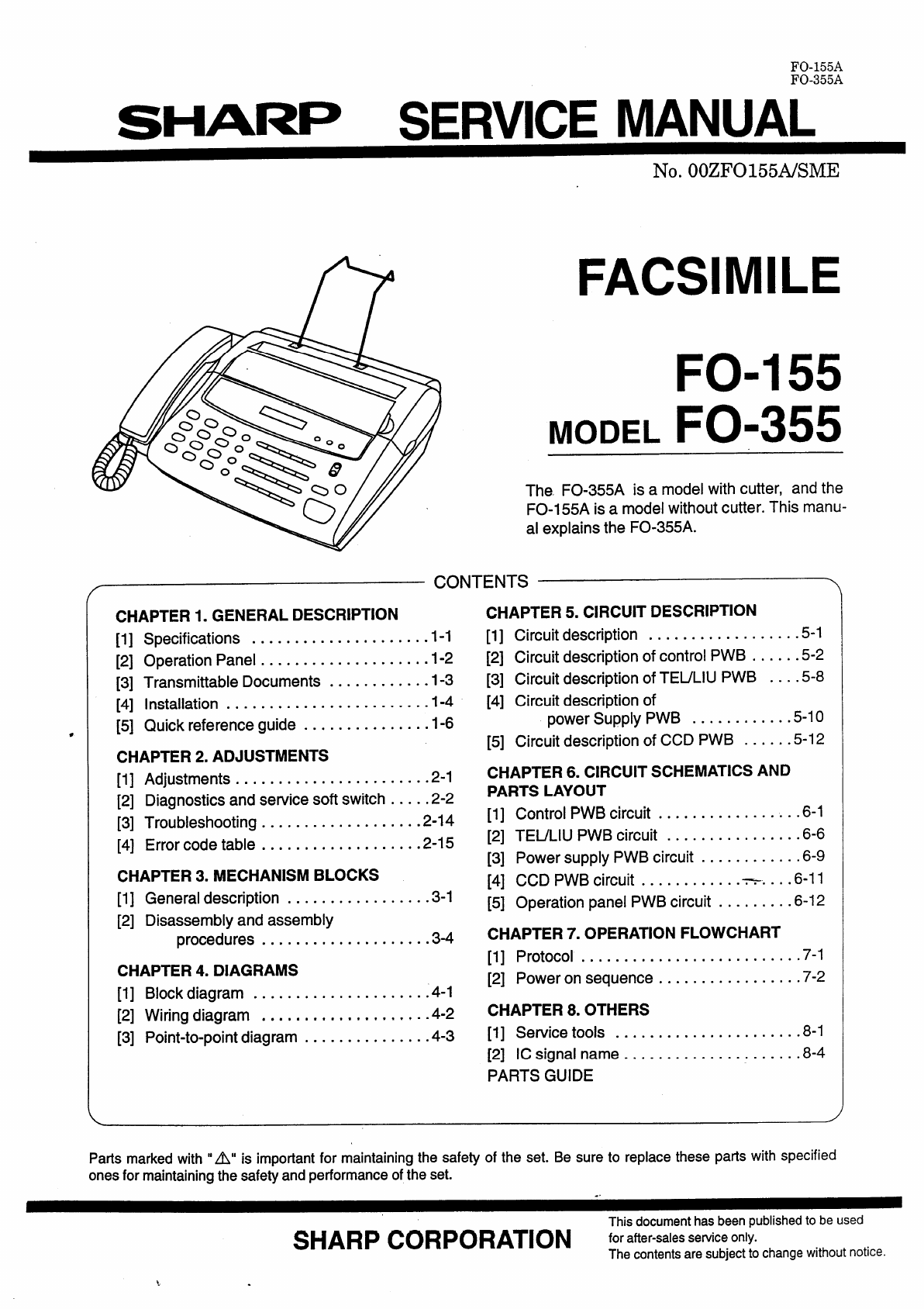
FACSIMILE
CHAPTER 1. GENERAL DESCRIPTION
[1]Specifications . . . . . . . . . . . . . . . . . . . . .
FO-155
MODEL FO-355
The. FO-355A is amodelwithcutter, andthe
FO-I55A is amodelwithoutcutter.This manu-
al explainsthe FO-355A.
CONTENTS
1-1
[2] OperationPanel....................1-2
[3] TransmittableDocuments ... .........1-3
[4] Installation. . . . . . . . . . . . . . . . . . . . . . . .1-4
[5] Quickreferenceguide .. .............1-6
CHAPTER 2. ADJUSTMENTS
[1]Adjustments.......................2-1
[2] Diagnosticsand servicesoftswitch.....2-2
[3] Troubleshooting...................2-14
[4] Errorcodetable . .. . . .. . . .. .. .. ....2-15
CHAPTER 3. MECHANISM BLOCKS
[1]Generaldescription .................3-1
[2] Disassemblyandassembly
procedures....................3-4
CHAPTER 4. DIAGRAMS
[1]Blockdiagram .....................4-1
[2] Wiringdiagram . . . . . . . . . . . . . . . . *, --4-2
[3] Point-to-pointdiagram ... ............4-3
CHAPTER 5. CIRCUIT DESCRIPTION
[1]Circuitdescription ..................5-1
[2] Circuitdescriptionof controlPWB ......5-2
[3] CircuitdescriptionofTEULIU PWB ... .5-8
[4] Circuitdescriptionof
powerSupplyPWB ............5-10
[5] Circuitdescriptionof CCD PWB ......5-12
CHAPTER 6. CIRCUIT SCHEMATICS AND
PARTSLAYOUT
[1] ControlPWBcircuit .................6-1
[2] TEULIU PWBcircuit ................6-6
[3] PowersupplyPWBcircuit ............6-9
[4] CCD PWBcircuit .......... .......6-11
[5] OperationpanelPWBcircuit .........6-12
CHAPTER7. OPERATIONFLOWCHART
[1] Protocol .........
[2] Poweron sequence
CHAPTER8. OTHERS
[1] Servicetools . . . . .
[2] ICsignalname.. . .
PARTSGUIDE
.................7-1
.................7-2
.................8-1
..................8-4
Partsmarkedwith “A” is importantfor maintainingthe safetyof the set. Be sureto replacethesepartswith specified
onesfor maintainingthesafetyandperformanceofthe set.
Thisdocumenthasbeenpublishedto beused
SHARPCORPORATION fOra”er-SaIeSSeNiCeOnIY.
Thecontentsaresubjectto changewithoutnotice.
FO-155A
FO-355A
CAUTIONFORBATTERYREPLACEMENT—
(Danish) ADVARSEL!
Lithiumbatteri-Eksplosionsfarevedfejlagtigh~ndtering,
Udskiftningmakunskemedbatteriaf sammefabrikatogtype.
Leverdetbrugtebatteritilbagetil Ieverandoren.
(English) Caution!
Dangerofexplosionif batteryis incorrectlyreplaced.
Replaceonlywiththesameor equivalenttype
recommendedbytheequipmentmanufacturer.
Discardusedbatteriesaccordingto manufacturer’s
instructions.
(Finnish) “VAROITUS
Paristovoi r~j~ht~~,josseonvirheeliisestiasennettu.
Vaihdaparistoainoastaanlaitevalmistajansuosittelemaan
WpPiin.H~vit~k~ytettyparistovalmistajanohjeiden
mukaisesti.
(French) AITENTION
IIyadangerd’explosions’il yareplacement incorrect
dela batterie.Remplaceruniquementavecunebatteriedu
m~metypeoud’untyperecommand6parIeconstructeur.
Mettreaur6butIesbatteriesusageesconformementaux
instructionsdufabricant.
(Swedish) VARNING
Explosionsfarevidfelaktigtbatteribyte.
Anv~ndsammabatteritypellerenekvivaient
typsomrekommenderasavapparattiilverkaren.
Kasseraanv~ntbatterienligtfabrikantens
instruction.
(German) Achtung
ExplosionsgefahrbeiVerwendunginkorrekterBatterien.
AlsErsatzbatteriendOrfennurBatterienvomgleichenTypodervom
HerstellerempfohleneBattenenverwendetwerden.
EntsorgungdergebrauchtenBatteriennurnachdenvomHersteller
angegebenenAnweisungen.
FO-155A
FO-355A
— —— —
CHAPTER1. GENERALDESCRIPTION
[1]SPECIFICATIONS
Applicable telephoneline:
Compatibility:
Configuration:
Compression scheme:
Scanning method:
Resolution:
Recording system:
Display:
Automatic cutter:
Reception modes:
Modem speed:
Transmission time*:
Effective recording width:
Input document size:
Publicswitchedtelephonenetwork
IPBX
ITU-T(CCITT)G3mode
Half-duplex,desktoptransceiver
ModifiedHuffmanand Sharpspecial
mode
Flat-bed,solid-stateCCD
Horizontal:
8dot/mm
Vertical:
Standard+.85lines/mm
Fine/Halftone-7.7iines/mm
Superfine-15.4lines/mm
Thermalrecording
7x5dots,1lineby 16-digitdisplay
Standard(tolengthof original)
Auto/Manual
9600 bps with automaticfallbackto
7200,4800,or 2400bps
Approx.15seconds
(Sharpspecialmode)
210mm,max.
Automaticfeeding:
Width—216mm
Length—128to 297mm
Manualfeeding:
Width— 216mm
Length—128to 1000mm
Effective scanning width:, 210 mm
Automatic document feeder: 20 sheets max.
Halftone (gray scale): 64 levels
Contrast control: Automatic/Darkselectable
Copy function: Standard
Telephone function: Standard
(cannotbe usedif powerfails)
Noise emission: Lessthan70 dBA
(Measuredaccordingto DIN45635.)
Power requirements: 230-240 VAC,50/60 Hz
Operating temperature: 5to 35°C
Power consumption: Stand-by:6W
Maximum:120W
Dimensions: Width:352mm
Depth:294mm
Height:130mm
Weight: Approx.3.5kg
~Basedon ITU-T(CCITT)Test Chart#l at standardresolutionin
Sharp special mode, excludingtime for protocol signals (i.e.,
ITU-TphaseCtimeonly).
As apart of our policy of continuousimprovement,SHARPreservesthe right to make designand specificationchangesfor procduct
improvementwithoutpriornotice.Theperformancespecificationsfiguresindicatedarenominalvaluesof productionunits.Theremaybe some
deviationfromthesevaluesin individualunits.
1-1
FO-155A
FO-355A
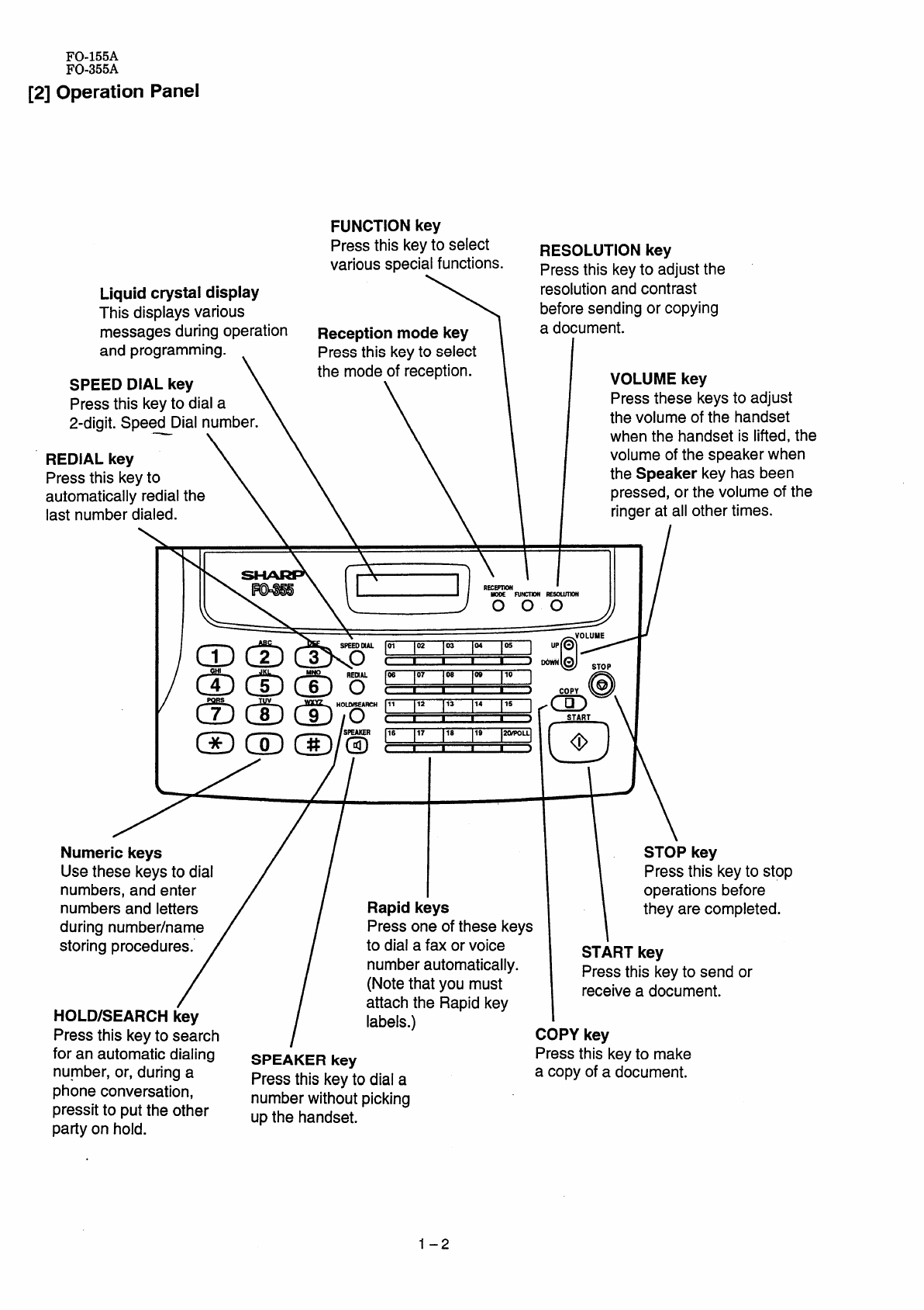
[2] Operation Panel
FUNCTION key
Pressthis keyto select
variousspecialfunctions.
Liquid crystal display
This displaysvarious \
messagesduringoperation Reception mode key
and programming. Pressthis keyto select
SPEED DIAL key the modeof reception.
Pressthis keyto dial a
2-digit.SpeedDial number.
REDIAL key
Pressthis keyto
automaticallyredialthe
lastnumberdialed.
-\\\
\
RESOLUTION key
Pressthis keyto adjustthe
resolutionandcontrast
beforesendingor copying
adocument.
VOLUME key
Pressthesekeysto adjust
thevolumeof the handset
whenthe handsetis lifted,the
volumeof the speakerwhen
the Speaker keyhas been
pressed, or the volume of the
ringerat all othertimes.
Numeric keys
Usethesekeysto dial
numbers, and enter
numbers and letters
duringnumber/name
/ / ,,,,,j::fthesekey,l \:;::ij:;:
/
storingprocedures.”
HOLD/SEARCH key
Pressthis keyto search
for an automaticdialing
number,or, duringa
phoneconversation,
pressitto putthe other
patty on hold.
/
to dial afax or voice
numberautomatically.
(Notethatyou must
attachthe Rapidkey
labels.)
SPEAKER key
Pressthis keyto dial a
numberwithoutpicking
upthe handset.
ISTART key
Pressthis keyto sendor
receiveadocument.
COPYkey
Pressthis keyto make
acopyof adocument.
1 –2
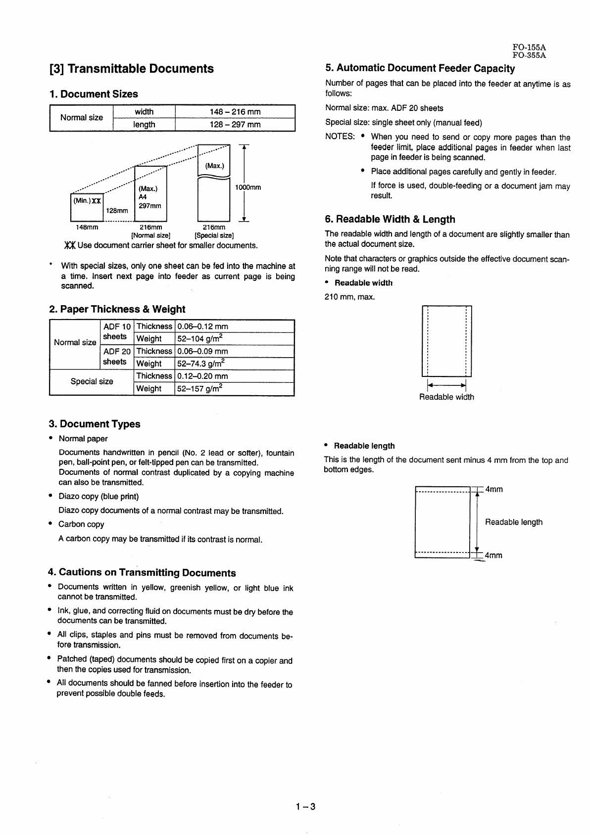
[3] Transmittable Documents
1.Document Sizes
Normalsize width 148-216 mm
length 128-297 mm
n~
..
-----
---”
-.
6:g-’’’--”-’’’hIrm
148mm 216mm 216mm
[Normalsize] [Specialsize]
HUsedocumentcarriersheetforsmallerdocuments.
●With specialsizes,onlyonesheetcanbefed into the machineat
atime. Insert next page into feeder as current page is being
scanned.
2. Paper Thickness& Weight
IADF 10 Thickness0.06-0.12mm
Normalsize sheets Weight 52–104g/m2
IADF20 Thickness10.06-0.09mm I
sheets Weight 52-74.3g/m2
Specialsize Thickness0.12-0.20mm
Weight 52-157glm2
3. Document Types
●
●
●
Normalpaper
Documentshandwrittenin pencil(No. 2lead or softer), fountain
pen,ball-pointpen,or felt-tippedpencanbetransmitted.
Documentsof normalcontrastduplicatedby acopyingmachine
canalsobetransmitted.
Diazocopy(blueprint)
Diazocopydocumentsofanormalcontrastmaybetransmitted.
Carboncopy
Acarboncopymaybetransmittedif its contrastis normal.
4. Cautions on Transmitting Documents
●
●
●
●
●
Documentswritten in yellow, greenishyellow, or light blue ink
cannotbetransmitted.
Ink,glue,andcorrectingfluidondocumentsmustbedrybeforethe
documentscanbetransmitted.
All clips, staplesand pins mustbe removedfrom documentsbe-
foretransmission.
Patched(taped)documentsshouldbecopiedfirst on a copierand
thenthecopiesusedfortransmission.
All documentsshouldbefannedbeforeinsertionintothe feederto
preventpossibledoublefeeds.
FO-155A
FO-355A
5. Automatic Document Feeder Capacity
Numberof pagesthatcan be placedintothe feederat anytime
follows:
Normalsize:max.ADF20sheets
Specialsize:singlesheetonly(manualfeed)
is as
NOTES: ●Whenyou needto sendor copy morepagesthan the
feederlimit, placeadditionalpagesin feederwhenlast
pageinfeederis beingscanned.
●Placeadditionalpagescarefullyandgentlyinfeeder.
If forceis used,double-feedingor adocumentjam may
result.
6. Readable Width& Length
Thereadablewidthandlengthof adocumentareslightlysmallerthan
theactualdocumentsize.
Notethatcharactersor graphicsoutsidetheeffectivedocumentscan-
ningrangewillnotbe
●Readable width
210 mm,max.
read.
,
,
t
Readablewidth
●Readable length
Thisis thelengthof thedocumentsentminus4mmfromthetopand
bottomedges.
Readablelength
t-----------------
{* 4mm
1-3
FO-155A
FO-355A
7. Use of Document Carrier Sheet
Adocumentcarriersheetmustbeusedfor thefollowingdocuments.
●Thosewithtears.
●Thosesmallerthansize148mm(W)x128mm(L).
●Carbon-backeddocuments
Makeprintstraight
acrosspaper
E.G.
Placethedocument
carrierinthedocument
feeder
withthe clearfilm
sidedown
Direction
of insertion -
NOTE: To transmitacarbon-backeddocument,insertawhitesheet
of paperbetweenthe carbonbackof the documentandthe
documentcarrier.
●Thosecontainingan easilyseparablewritingsubstance(e.g.,trac-
ingpaperwrittenonwithasoft,heavyleadpencil).
NOTES: ●
●
●
Whenusingthe documentcarrier,carefullyreadthe in-
structionswrittenonthe back.
If the documentcarrieris dirty,cleanit withasoft,moist
cloth,andthendryit beforeusingfortransmission.
Donot placemorethanonedocumentin thecarrierat a
time.
[4] Installation
1. Site selection
Takethe followingpointsinto considerationwhenselectingasitefor
thismodel.
ENVIRONMENT
●
●
●
●
●
Themachinemustbeinstalledona levelsurface.
Keepthe machineawayfrom air conditioners,heaters,directsun-
light,anddust.
Provideeasyaccessto the front,back,andsidesofthe machine.
In particular,keep the area in front of the machineclear,or the
originaldocumentmayjam as it comesoutafterscanning.
Thetemperatureshouldbebetween5°and35°C.
The humidityshouldbe between30%and 85% (withoutconden-
sation).
ELECTRICITY
230-240V,50/60Hz,grounded(3-prong)AC outletis required.
Caution!
●Connectionto apowersourceotherthanthatspecifiedwill cause
damageto theequipmentandis notcoveredunderthewarranty,
●If your area experiencesahigh incidenceof lightningor power
surges,we recommendthat you installasurgeprotectorfor the
powerandtelephonelines.Surgeprotectorscan be purchasedat
mosttelephonespecialtystores.
If the machineis movedfromacoldto awarmplace...
If the machineis movedfrom acold to awarmplace,it is possible
that the readingglass may fog up, preventingproper scanningof
documentsfor transmission.To removethe fog, turn on the power
andwaitapproximately2hoursbeforeusingthe machine.
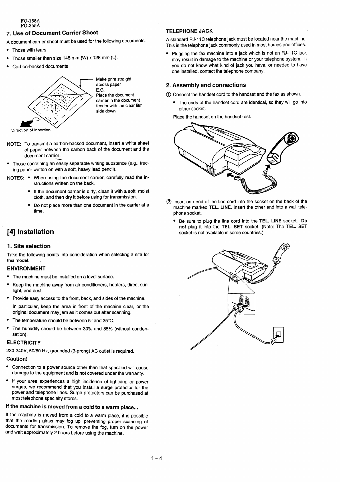
TELEPHONE JACK
AstandardRJ-11Ctelephonejackmustbelocatednearthemachine.
Thisisthetelephonejackcommonlyusedin mosthomesandoffices.
●Pluggingthe fax machineintoajack whichis not an RJ-11Cjack
mayresultin damageto the machineor yourtelephonesystem. If
you do not knowwhat kindof jack you have,or neededto have
oneinstalled,contactthetelephonecompany.
2. Assembly and connections
@Connectthehandsetcordto the handsetandthefaxas shown.
●Theendsof the handsetcordare identical,so theywill go into
eithersocket.
Placethe handsetonthehandsetrest.
@Insertoneendof the line cordinto the socketonthe backof the
machinemarkedTEL. LINE. Insertthe otherendinto awall tele-
phonesocket.
●Be sureto plug the line cord into the TEL. LINE socket. Do
not plug it into the TEL. SET socket.(Note:The TEL. SET
socketis notavailablein somecountries.)
1 –4
FO-155A
FO-355A
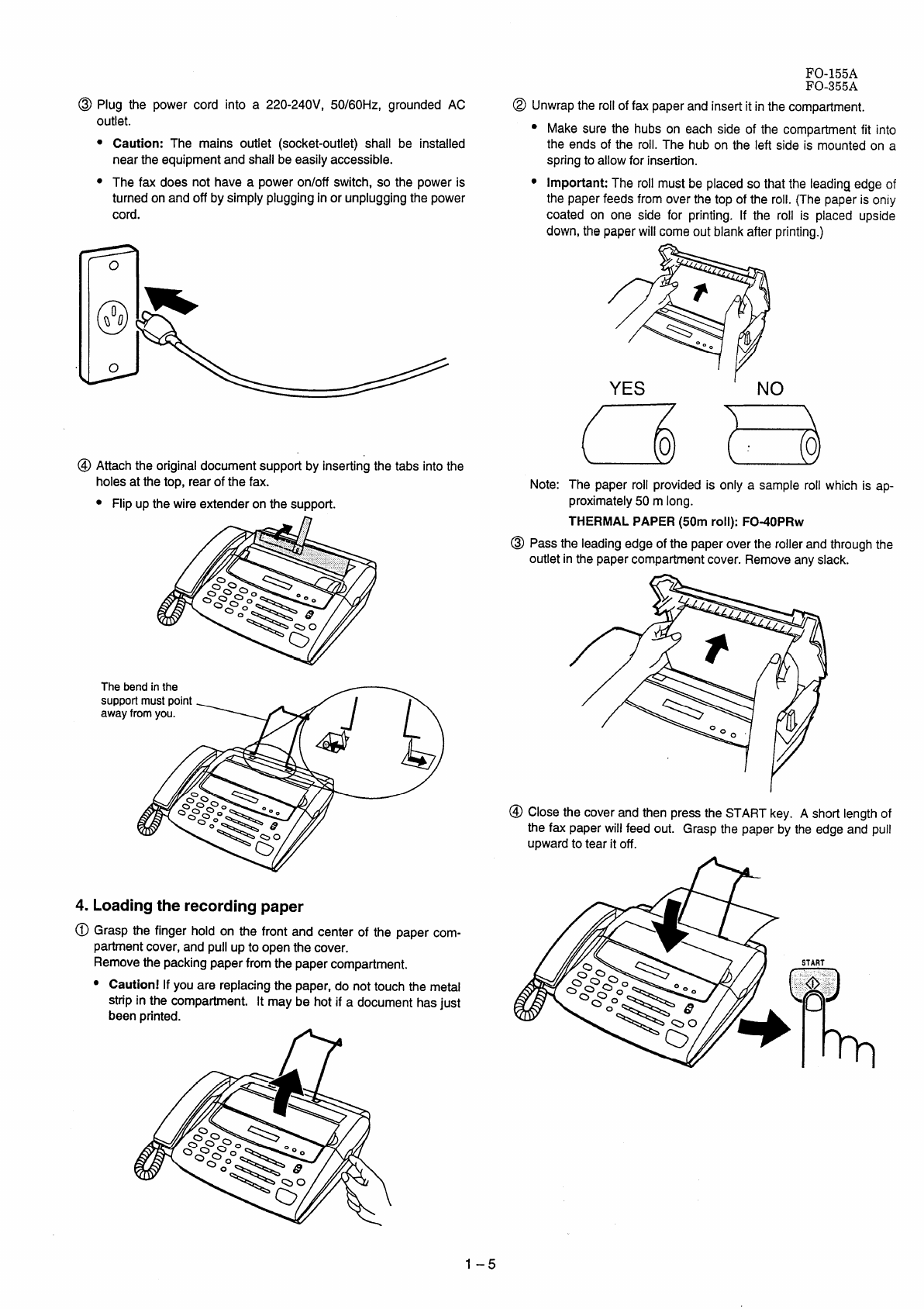
@Plug the power cord into a220-240V,50/60Hz,groundedAC
outlet.
●Caution: The mains outlet (socket-outlet)shall be installed
neartheequipmentandshallbeeasilyaccessible.
●Thefax doesnot haveapoweron/off switch,so the poweris
turnedonandoff bysimplypluggingin or unpluggingthepower
cord.
@Attachtheoriginaldocumentsupportbyinsertingthe tabs intothe
holesatthetop,rearof thefax.
●Flipupthewireextenderonthesupport.
@
@
@Unwraptherollof fax paperandinsertit in thecompartment.
●Makesurethe hubson eachside of the compartmentfit into
the endsof the roll. The hubon the left sideis mountedon a
springtoallowfor insertion.
4. Loading the recording paper
@Graspthe fingerhold on the front and centerof the papercom-
partmentcover,andpull upto openthecover.
Removethepackingpaperfromthepapercompartment.
cCaution! If you are replacingthe paper, do not touchthe metal
stripin the compartment.It maybe hot if adocumenthasjust
beenprinted.
●Important: Theroll mustbe placedso thatthe leadingedgeof
the paperfeedsfromoverthetopof the roll. (Thepaperis oniy
coated on one side for printing. If the roll is placed upside
down,thepaperwillcomeoutblankafterprinting.)
YES ‘NO
Note: The paperroll providedis onlyasampleroll whichis ap-
proximately50mlong.
THERMAL PAPER (50m roll): FO-40PRW
Passtheleadingedgeofthe paperovertherollerandthroughthe
outletinthepapercompartmentcover.Removeanyslack.
I
Closethe coverandthenpresstheSTARTkey. Ashortlengthof
thefax paperwillfeedout. Graspthe paperby theedgeandpull
upwardto tearit off.
1-5
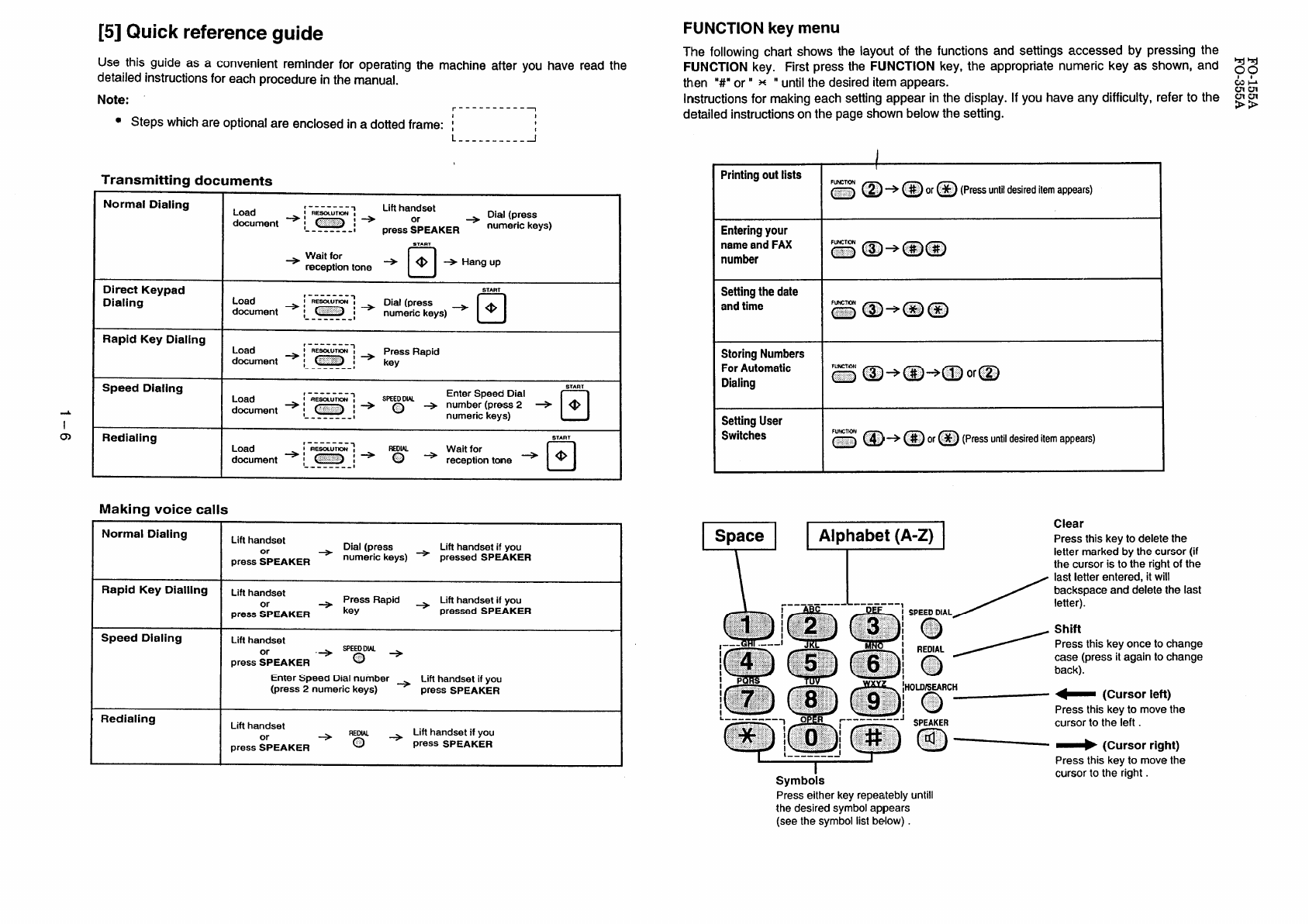
[5] Quick reference guide
Use this guideas aconvenientreminderfor operatinqthe machineafter vou have readthe
detailedinstructionsfor eachprocedureinthemanual.-.
Note: ~.-- ...----=
1
●Stepswhichareoptionalare enclosedin adottedframe: II
t
L.------ .---i
Transmitting documents
Normal Dialing
Direct Keypad
Dialing
Rapid Key Dialing
Speed Dialing
Rediaiing
START
~Waitfor
receptiontone II
+Q+Hangup
.--------
Load iREWUTW~PressRapid
dwument +! - I+kev
.--------1
START
Load ,------- EnterSpeedDial
dmument + ~“~~: +“6’” +number(press2+D
o
----_---l numerickeys)
START
,-------
Load
document‘~ “=W; +‘b” Waitfor
+receptiontone c1
++
---- _---l
Making voice calls
Normai Dialing
Rapid Key Dialling
Speed Dialing
Redialing
Lifthandset Dial(press Lifthandsetif you
press~\ EAKER +numerickeys) +pressedSPEAKER
Lifthandset ~PressRapid ~Lifthandsetifyou
press~\ EAKER key pressedSPEAKER
Lifthandset +WEEDDM
pres ~~EAKER 0+
EnterSpeed Dialnumber ~Lift handset ifYOU
(press2numerickeys) ptessSPEAKER
Lifthandset ~Lifthandsetifyou
press~~EAKER “$ PressSPEAKER
FUNCTION key menu
The followingchart showsthe layoutof the functionsand settingsaccessedby pressingthe
FUNCTION key. Firstpressthe FUNCTIONkey,the appropriatenumerickey as shown,and ~~
then “#” or” x“untilthedesireditemappears. &b
Instructionsfor makingeachsettingappearin the display.If youhaveany difficulty,referto the ~~
detailedinstructionsonthe pageshownbelowthe setting.
J
I
Printingoutiists
H@+@or@ (pre~untildesireditemapp=rs)
Entering
your
nameandFAX
number B@+@@
Settingthedate
andtime a@+@@
StoringNumbers
ForAutomatic
Diaiing H~+@+@ or@
SettingUser
Switches =~+@or@ (Pressuntildesireditemappears)
F[rl Ciear
Pressthiskeyto deletethe
iettermarkedby thecursor(if
Symbo!s
thecursoris to the rightof the
lastietterentered,it will
backspaceand deletethe last
letter).
Shift
Pressthiskeyonceto change
case(pressitagaintochange
back).
Z(Cursor ieft)
Pressthiskeyto movethe
cursorto the left.
~(Cursor right)
Pressthiskeyto movethe
cursorto the}ight.
Presseitherkeyrepeatedlyuntill
thedesiredsymbolappears
(seethesymboliistbelow).
FO-155A
FO-355A
CHAPTER2. ADJUSTMENTS
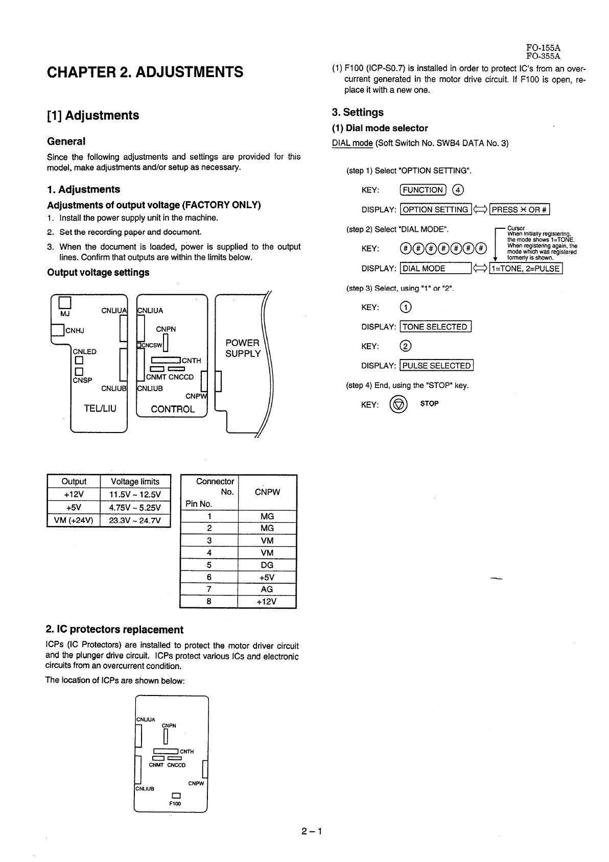
[1] Adjustments
General
Since the followingadjustmentsand settingsare providedfor this
model,makeadjustmentsand/orsetupasnecessary.
I. Adjustments
Adjustmentsofoutputvoltage(FACTORYONLY)
1. Installthepowersupplyunitin themachine.
2. Setthe recordingpaperanddocument.
3. When the documentis loaded,power is supplied to the output
lines. Confirm that outputsare withinthe limits below.
Outputvoltagesettings
bCNHJ I
L
CNLED r
❑
CNSP [
CNLIU[
TEL/LIU II
NLIUA
CNPN
CNCSW
D
~cNTH
00
CNMTCNCCD
NLIUB CNP
CONTROL
Output IVoltaqelimits I
+12V I11.5V-12.5V I
+5V 4.75V-5.25V
VM(+24V) 23.3V-24.7V
(
POWER
SUPPLY
d
\
L
Connector
No. CNPW
PinNo.
1IMG
1
2MG
3IVM
4VM
5DG
6+5V
7AG
8+12V
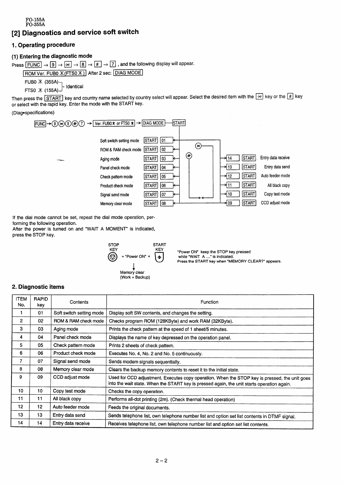
2. IC protectors replacement
ICPS(IC Protectors)are installedto protectthe motordriver circuit
andthe plungerdrivecircuit, ICPSprotectvariousICSandelectronic
circuitsfromanovercurrentcondition.
Thelocationof ICPSareshownbelow:
I
CNUUAcNPti
o
~cm
0=
CNMT
CNCCD
[
CNPW
CNLIUB n
F1OO
(1) F1OO(ICP-SO.7)is installedin orderto protectIC’Sfroman over-
currentgeneratedin the motordrive circuit. If F1OOis open,re-
placeit withanewone.
3. Settings
(1) Dialmodeselector
DIALmode(SoftSwitchNo.SWB4DATANo.3)
(step 1) Select “OPTIONSEITING”,
DISPIAY: OPTIONSE~lNG]~l PRESSXOR#I
(step2)Select“DIALMODE”. rCursor
Wheninitially
registering,
‘Ey: o@@@o@@ !E3:i!%}:si;5:
formerlyisshown.
DISPLAY:DIALMODE I=[l=TONE, 2.PULSE1
(step3)Select,using”1”or“2”.
KEY: o1
DISPLAY:TONESELECTED
KEY: o2
DISPLAY:\PULSESELECTEDJ
(step4) End, usingthe “STOP”key.
KEY: @STOP
2–1
FO-155A
FO-355A
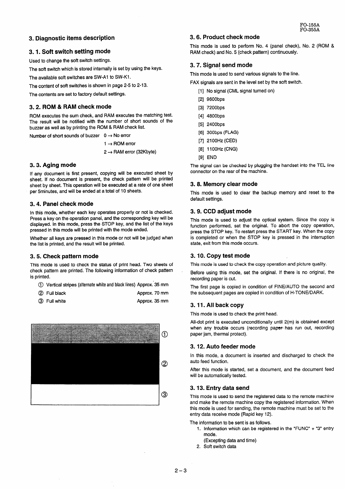
[2] Diagnostics and service soft switch
1.Operating procedure
(1) Enteringthediagnosticmode
PressWI +❑+❑+❑+❑+❑,andthefollowingdisplaywillappear.
IROMVer.FUBOx(FTSOX) ~After2see:IDIAGMODEI
FUBO
X(355A)
1Identical
FTSO~(155A)
.
Thenpressthe ml keyandcountrynameselectedbycountryselectwillappear.Selectthedesireditemwiththe ❑keyor the ❑key
or selectwiththerapidkey.Enterthemodewiththe STARTkey.
(Diagospecifications)
m]+@@@@@ +1 Ver.FUBO*orRSOxl+ DIAGMODE
v
SoftswitchsettingmodeISTART~
ROM&RAMcheckmodeISTARTI
Agingmode m
Panelcheckmode m
Checkpatternmode m
p’odu~~’ckmode m
Signalsendmode m
Memoryclearmode m
101F*
02
03
II [:
#
04
05
06
07
08
Entrydatareceive
Entqdatasend
Autofeedermode
Allblackcopy
Copytestmode
CCDadjustmode
If the dial mode cannot be set, repeat the dial mode operation, per-
forming thefollowingoperation.
After the power is turnedon and “WAITAMOMENT”is indicated,
presstheSTOPkey.
STOP START
KEY KEY
@u
“PowerON’ keeptheSTOPkeypressed
+“PowerON”+ ~ while“WAITA..... isindicated.
PresstheSTARTkeywhen“MEMORYCLEAR?”appears.
1
Memoryclear
(Work+Backup)
2. Diagnostic items
ITEM RAPID
No. key Contents Function
101 Softswitchsettingmode DisplaysoftSWcontents,andchangesthesetting.
2 02 ROM&RAMcheckmode ChecksprogramROM(128KByte)andworkRAM(32KByte).
3 03 Agingmode Printsthecheckpatternat thespeedof 1sheet/5minutes.
404 Panelcheckmode Displaysthenameof keydepressedontheoperationpanel.
5 05 Checkpatternmode Prints2sheetsof checkpattern.
6 06 Productcheckmode ExecutesNo.4, No.2 andNo.5continuously.
7 07 Signalsendmode Sendsmodemsignalssequentially.
808 Memoryclearmode Clearsthebackupmemorycontentsto resetit totheinitialstate.
9 09 CCDadjustmode UsedforCCDadjustment.Executescopyoperation.WhentheSTOPkeyis pressed, the unit goes
into the wait state. WhentheSTARTkeyis pressedagain,theunitstartsoperationagain.
10 10 Copytestmode Checksthecopyoperation.
11 11 All blackcopy Performsall-dotprinting(2m).(Checkthermalheadoperation)
12 12 Autofeedermode Feedstheoriginaldocuments.
13 13 Entrydatasend Sendstelephonelist,owntelephonenumberlistandoptionsetlistcontentsin DTMFsignal.
14 14 Entrydatareceive Receivestelephonelist,owntelephonenumberlistandoptionset list contents.
2-2
3. Diagnostic items description
3.1. Soft switch settingmode
Usedto changethesoftswitchsettings.
Thesoftswitchwhichis storedinternallyissetbyusingthekeys.
TheavailablesoftswitchesareSW-Al to SW-K1.
Thecontentof softswitchesis shownin page2-5to 2-13.
Thecontentsaresetto factorydefaultsettings.
3.2. ROM &RAM check mode
ROMexecutesthe sumcheck,andRAMexecutesthe matchingtest.
The result will be notifiedwith the numberof short soundsof the
buzzeraswellasby printingthe ROM&RAMchecklist.
Numberof shortsoundsof buzzer O+Noerror
1+ROMerror
2+RAMerror(32Kbyte)
3.3. Aging mode
If any documentis first present,copyingwill be executedsheetby
sheet. If no documentis present,the check patternwill be printed
sheetby sheet.Thisoperationwill beexecutedat arateof onesheet
per5minutes,andwill beendedat atotalof 10sheets.
3.4. Panel check mode
In this mode,whethereachkeyoperatesproperlyor not is checked.
Pressakeyontheoperationpanel,andthecorrespondingkeywillbe
displayed.In this mode,pressthe STOPkey,andthe list of the keys
pressedin thismodewill beprintedwiththe modeended.
Whetherall keysare pressedin thismodeor notwill bejudgedwhen
thelist is printed,andtheresultwillbeprinted.
3.5. Check pattern mode
This modeis usedto checkthe statusof print head.Two sheetsof
checkpatternare printed.The followinginformationof check pattern
is printed.
@Verticalstripes(altematewhiteandblacklines)Approx.35mm
@Fullblack Approx.70mm
@Fullwhite Approx.35mm
FO-155A
FO-355A
3.6. Product check mode
This modeis usedto performNo. 4(panelcheck),No. 2(ROM&
RAMcheck)andNo.5(checkpattern)continuously.
3.7. Signal send mode
Thismodeis usedto sendvatioussignalsto the line.
FAXsignalsaresentinthelevelsetbythesoftswitch.
[1] Nosignal(CMLsignalturnedon)
[2] 9600bps
[3] 7200bps
[4] 4800bps
[5] 2400bps
[6] 300bps(FLAG)
[7] 21OOHZ(CED)
[8] 11OOHZ(CNG)
[9] END
Thesignalcanbe checkedbypluggingthe handsetintothe TEL line
connectorontherearof themachine.
3.8. Memory clear mode
This mode is used to clear the backupmemoryand reset to the
defaultsettings.
3.9. CCD adjust mode
This modeis usedto adjustthe optical system. Sincethe copy is
functionperformed,set the original.To abort the copy operation,
presstheSTOPkey.To restartpresstheSTARTkey.Whenthecopy
is completedor when the STOP key is pressedin the interruption
state,exitfromthismodeoccurs.
3.10. Copy test mode
Thismodeis usedtocheckthecopyoperationandpicturequality.
Beforeusingthis mode,set the original.If there is no original,the
recordingpaperiscut.
The first pageis copiedin conditionof FINE/AUTOthe secondand
thesubsequentpagesarecopiedin conditionof H-TONE/DARK.
3.11. All back copy
Thismodeis usedto checktheprinthead.
All-dotprintis executedunconditionallyuntil 2(m) is obtainedexcept
when any trouble occurs (recordingpaper-has run out, recording
paperjam,thermalprotect).
3.12. Auto feeder mode
In this mode, adocumentis insertedand dischargedto checkthe
autofeedfunction.
After this mode is started, set adocument, and the document feed
willbeautomaticallytested.
3.13. Entry data send
Thismodeis usedto sendthe registereddatato the remotemachine
andmakethe remotemachinecopythe registeredinformation.When
this modeis usedforsending,the remotemachinemustbesetto the
entrydatareceivemode(Rapidkey12).
Theinformationto besentis asfollows.
1.
2.
Informationwhichcanbe registeredin the “FUNC”+“3’ entry
mode.
(Exceptingdataandtime)
Softswitchdata
2–3
FO-155A
FO-355A
3.14. Entry data receive
This modeis usedto receivethe registereddatawhichis sentfrom
the remotemachineandto registerthe receiveddatain the machine.
Whenthis mode is usedto receivethe information,the remotema-
chinemustbesetto theentrydatasendmode(Rapidkey11).
After completionof reception,the telephonenumberlist, own tele-
phonenumberlist,optionset list,andsoftswitchlistareprinted.
Caution
Unless the time mode is set, the list print is not performed,“NO
DATA”appearson thedisplay.
4. How to make soft switch setting
To enter the soft switch mode,makethefollowingkeyentriesin
sequence.
IPress IFUNCTION] ❑❑❑❑❑-1
mTA No. 12 345 678
SF T SW-Al =“o o 0 0 0 0 0 0I 1
SFT SW-Al =1:o0 00 ()()()I 4
1
IS FT SW-Al= 1 0:0 o 0 0 0 ()[ 4
1
PresslFUNCTIONlkev.
Press❑key.
Press❑key.
Bitl -8 areset.
ISF T SW-Al =10 0 0 0 0 0 01 -
1
Press1~1 key duringsetting.
SFTSW-A2 =‘o o 0 0 0 0 0 0[ 4
~SoftSW-A2-SW-K1areset.
ISFT SW-K1 =ooooooo#
‘1
●Tofinishthesettingshalfwaybetween
SW-Al andSW-KI, pressthe STOP
key.Inthiscase,the settingbeingdone
to the SWNo.ondisplaywillbe nullified
whilesettingsdoneto thepreceding
SWNos.remainin effect.
.When the COPYkeyis pressed,the
contentsof softswitchesareprinted.
t
IThesoftswitchmodeisterminated.
2-4
FO-155A
FO-355A
5.Soft switch description
●Softswitch
Sw DATA
NO. NO. ITEM SwitchSettingandFunction Initial Remarks
10setting
1Digitallineequalizationsetting Yes .No 1
2Forced4800bpsreception Yes No o
3Reserved o
4Modemspeed 9600BPS 7200BPS 4800BPS 2400BPS
Sw
I
Al 5No.41 1 0 0 1
No.50110 0
6Lengthlimitationofcopy/send/receive Nolimit Copy/Send:1mo
Receive:1.5m
7CSItransmission Notransmitted Transmitted o
8DISreceiveacknowledgementduringG3 Twice NSF:Once o
transmission DIS:Twice
1NonmodulatedcarrierforV29 Yes No o
transmissionmode
2EOLdetecttimer 25sec 13sec o
Sw 3Protocolmonitor Yes No o
I4Linemonitor Yes No o
A2 5Si~naltransmissionlevel Binaryinput 8421 1
6No.=1234 0
71 0 1 1(-lldBm) 1
81
1Sender’sinformationtransmit No Yes o
2H2mode No Yes o
3Communicationerrortreatmentin RTN Nocommunicationerror Communi~tionerror o
Sw sendingmode(reception)
I4CNGtransmission No Yes o
A3 5Autogaincontrol(MODEM) Enable Disable 1
6Equalizerfreezecontrol(MODEM) On off o
7Equalizerfreezecontrol7200bpsonly No Yes o
8Errorcriterion 10-2070 5-1070 0
1DisconnectthelinewhenDISis received No Yes 1
in RXmode.
2FooterPrint Yes No o
3EndBuzzer Yes No 1
Sw “4 Antijunkfaxcheck Yes
INo o
5
OPTION
A4 CEDtonesignalinterval 75ms 500ms 750ms 1000ms
1
6No.50 0 1 1 0
No.6010 1 0
7Resewed o
8Resewed o
1Recallinterval Binaryinput 8421 1
No.=1234
1010
0
1
I4(10x30sec=5rein) o
B1 5Recalltimes Binaryinput 8421 0
6No.=1234 0
70 0 1 0 (Twice) 1
80
1Dialpausing(sec/pause) 4sec 2sec o
2Resewed o
Sw 3Resewed o
I4Resewed o
B2 5Reserved o
6Resewed o
7Reserved o
8Reserved o
2-5
FO-155A
-A . . . &
1?U-6DDA
Sw DATA ITEM SwitchSettingandFunction Initial Remarks
NO. NO. 10setting
1Reserved o
2Reserved o
Sw 3Reserved o
I4Reserved o
B3 5Reserved o
6Reserved o
7Reserved o
8Resewed o
1Autodialmodedelaytimerofbeforeline 3sec Osec 1
connect
2Autodialmodedelaytimerofafterline 3.6sec 3.0sec o
Sw connect
I3Dialmode Tone Pulse 1OPTION
B4 4Pulse+Tonechangefunctionby~key Enable Disable 1
.5 Dialpulsemake/breakratio(%) 40/60 33167 0
6Reserved o
7Reserved o
*. Reserved o
1DTM~vel (low) Binatyinput 8421 1
2No.=1234 0
Sw 31 0 0 1(-9dBm) o
I41
B5 5DTMFlevel(High) Binatyinput 8421 1
6No.=1234 0
71 0 0 0 (-8dBm) o
80
1Readingslice(Binary) Factory Light Dark
Setting Da*er inDark
2No.101 0 10
No.2001 1 0
Sw 3Readingslice(Halftone) Factory Light Dati
ISetting Dati(erin Dark
cl 4No.3 0 1 0 1 0
No.4 0 0 11 0
5Linedensityselection Fine Standard oOPTION
6Reserved o
7Reserved o
8Reserved o
1Numberof ringsforautoreceive Binaryinput 8421 0
2No.=1234 0
3
Sw dO0 1 0(2 times) 1
IoOPTION
D1 5Automaticswitchingmanualtoauto Receptionafter Noreception o
receivemode 4rings
6Reserved o
7Reserved o
8Reserved o
1Cloffdetectiontimer 350ms 700ms o
2Reserved o
Sw 3Reserved
io
4Reserved
D2 o
5Distinctiveringingdetection Yes No oOPTION
6Reserved o
7Reserved
80
Reserved o
2–6
FO-155A
WA-9KK
A
LW-uuun
Sw DATA ITEM SwitchSettingandFunction Initial Remaks
NO. NO. 1 0 setting
1Automaticswitchingmode Tel/Faxautoswitch Switchtofax oOPTION
2Pseudoringingtimeatthephone/fax
automaticswitchingmode 15s 30s 60s 120s
3No.2 0 1 0 1 0
Sw No.3 0 0 1 1 0 OPTlON
I4NumberofCNGsignaldetectionatthe Twice Once 1
El phone/faxautomaticswitchingmode
5CNGdetecttimeatTEUFAXmode 3s 5s o
6Reserved o
7Postanswertonetransmitin TEUFAX No Yes o
mode
8Reserved o
1Pseudoringersoundoutputleveltothe -lOdBm -15dBm -20dBm -25dBm
line
2No.1 0 1 0 1 0
Sw No.2001 1 0
{3Reserved o
E2 4Reserved o
5Resewed o
6Reserved o
7Resewed o
8Reserved o
1DTMFdetectiontime 50ms 80ms IOOms 120ms
2No.1 0 0 1 10
No.201
Sw o10
I3Protectionof remotereception(5XX) Yes No oOPTION
F1 detect
4RemotereceptionwithGEtelephone Compatible Notcompatible 1
5Remoteoperationcodefiguresby Binaryinput 8421 0
6externaltel (O-9) No.=1234 1
7 0 1 0 1 (5XX) o
8 1
1
OPTION
CNGdetectionin STAND-BYmode Yes No o
2Numberof CNGdetect lpulse 2pulses 3pulses 4pulses
(AMmode)
Sw 3No.20 0 1 1 0
INo.3010 1 1
F2 4Numberof CNGdetect(STAND-BY No.4 0 0110
5mode) No.5 0 1 0 1 1
6Reserved o
7Reserved o
8Reserved —o
1Quietdetecttime Binaryinput 8421 0
2No.=1234 1
Sw 30 1 0 0 (4sec) o
I40
G1 OPTION
5Quietdetectstarttiming Binaryinput 8421 0
6No.=1234 1
7010l(5sec) o
81
1Reserved o
2Reserved o
Sw 3Reserved o
I4Reserved o
G2 5Resewed o
6Reserved o
7Reserved o
8Reserved o
2–7
FO-155A
li’fi-35!iA
.- ---.-
Sw DATA SwitchSettingandFunction Initial
ITEM Rematis
NO. NO. 10setting
1Reserved o
2Reserved o
3Reserved o
Sw 4TADconnect Yes No oOPTION
I5Sectiontimeofquietdetection 30sec 40sec 50sec 60sec
G3
6No.5 0 011 0
No.601011
7Reserved o
8Reserved o
1BusytonedetectionON/OFFtime 350ms 150ms o
(Lowerlimit)
2BusytonedetectionON/OFFtime 650ms 900ms o
(Upperlimit)
Sw 3Reserved o
I4Busytonecontinuoussounddetecttime 5sec 10sec 1
H1 5Reserved o
6Busytonedetectcontinuationsound No Yes o
deter
7Reserved o
8Busytonedetectintermittentsound No Yes o
detect
1Busytonedetectionpulsenumber 2pulses 4pulses 6pulses lOpulses
2No.10 0 11 0
Sw No.20101 1
I3FaxswitchingwhenA.M.full Yes No o
H2 OPTION
4Reserved o
5Reserved o
6Reserved o
7Reserved o
8Resewed o
1Reserved o
2Reserved o
Sw 3Reserved o
I4Reserved o
11 5Reserved o
6Resewed o
7Reserved o
8Reserved o
1Reserved o
2Reserved o
Sw 3Reserved o
I4Reserved o
12 5Reserved o
6Reserved o
7Reserved o
8Reserved o
1Reserved o
2Reserved o
Sw 3Resewed o
I4Reserved o
13 5Resetved o
6Reserved o
7Reserved o
8Resewed o
2-8
FO-155A
nn-a~~ A
LU-uuun
Sw DATA ITEM SwitchSettingandFunction Initial Remarks
NO. NO. 10setting
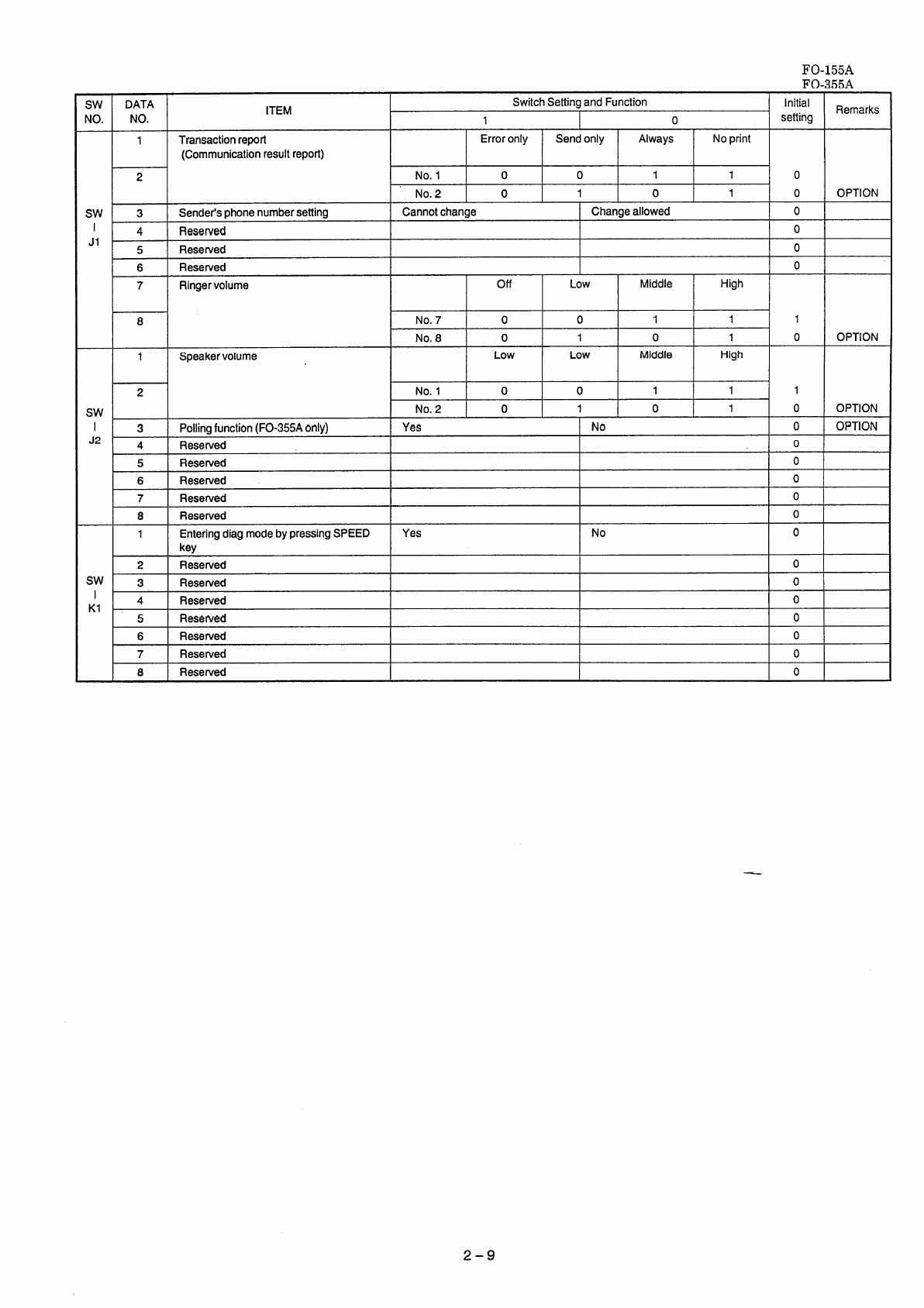
1Transactionrepod Erroronly Sendonly Always Noprint
(Communicationresultreport)
2No.100 1 1 0
No.2 0 1 0 10OPTION
Sw 3Sender’sphonenumbersetting Cannotchange Changeallowed o
I4Reserved o
JI 51Reserved o
6Reserved o
7Ringervolume off Low Middle High
8No.7001 1 1
No.801 0 1 0 OPTION
1Speakervolume Low Low Middle High
2No.10 0 1 1 1
Sw No.201 0 1 0 OPTION
I3Pollingfunction(FO-355Aonly) Yes No oOPTION
J2 4Reserved o
5Reserved o
6Reserved o
7Reserved o
8Reserved o
1EnteringdiagmodebypressingSPEED Yes No o
key
2Reserved o
Sw 3Resewed o
I
K1 4Reserved o
5Reserved o
6Resewed o
7Reserved o
8Reserved o
.
2–9
FO-155A
FO-355A
●Soft switchfunctiondescription
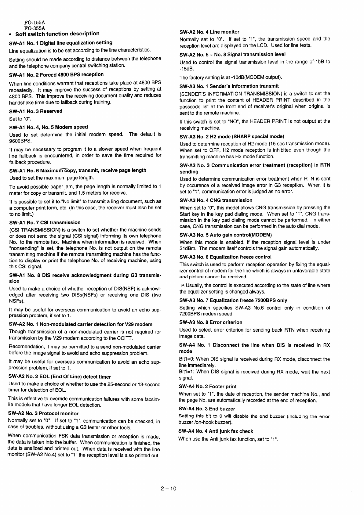
SW-Al No. 1Digital line equalization setting
Lineequalizationis to besetaccordingto the linecharacteristics.
Settingshouldbemadeaccordingto distancebetweenthetelephone
andthetelephonecompanycentralswitchingstation.
SW-Al No. 2Forced 4800 BPS reception
Whenlineconditionswarrantthat receptionstakeplaceat 4800BPS
repeatedly. It may improvethe successof receptionsby settingat
4800BPS. Thisimprovethe receiving document quality and reduces
handshake time due to fallback duringtraining.
SW-Al No. 3Reserved
Setto ‘O”.
SW-Al No. 4, No. 5Modem speed
Used to set determine the initial modem speed. The default is
9600BPS.
It may be necessaryto programit to aslowerspeedwhenfrequent
line fallbackis encountered,in order to save the time requiredfor
fallbackprocedure.
SW-Al No. 6Maximum70py, transmit, receive page length
Usedto setthe maximumpagelength.
To avoid possiblepaperjam, the pagelengthis normallylimitedto 1
meterfor copyortransmit,and1.5metersfor receive.
It is possibleto set it to “Nolimit”to transmitaIingdocument,suchas
acomputerprintform, etc. (Inthiscase,the receivermustalsobeset
to nolimit.)
SW-Al No. 7CSI transmission
(CSI TRANSMISSION)is aswitchto set whetherthe machinesends
or doesnot sendthe signal(CSIsignal)informingits owntelephone
No. to the remotefax. Machinewheninformationis received.When
“nonsending”is set, the telephoneNo. is not outputon the remote
transmittingmachineif the remotetransmittingmachinehasthefunc-
tion to displayor printthe telephoneNo.of receiving machine, using
thisCSIsignal.
SW-Al No. 8DIS receive acknowledgment during G3 transmis-
sion
Used to make achoiceof whetherreceptionof DIS(NSF)is acknowl-
edged after receivingtwo DISS(NSFS)or receivingone DIS (two
NSFS).
It may be usefulfor overseascommunicationto avoidan echosup-
pressionproblem,if setto 1.
SW-A2 No. 1Non-modulated carrier detection for V29modem
Thoughtransmissionof anon-modulatedcarrier is not requiredfor
transmissionbytheV29modemaccordingto theCCllT.
Recommendation,it maybe permittedto asendnon-modulatedcarrier
beforethe imagesignalto avoidandechosuppressionproblem.
It maybe usefulfor overseascommunicationto avoidan echo sup-
pression problem, if setto 1.
SW-A2No.2EOL(End Of Line) detect timer
Usedto makeachoiceof whetherto usethe25-secondor 13-second
timerfor detectionof EOL.
This is effective to override communication failures with some facsim-
ile modelsthathavelongerEOLdetection.
SW-A2 No. 3Protocol monitor
Normallyset to “O”. If set to “1”, communicationcan-bechecked,in
caseof troubles,withoutusing aG3testeror othertools.
When communication
FSK data transmission or reception is made,
the data is taken into the buffer. When communication is finished, the
data is analized and printed out. When data is received with the line
monitor (SW-A2 No.4) set to”1” the reception level is also printed out.
SW-A2 No. 4Line monitor
Normallyset to “O”. If set to “l”, the transmissionspeedand the
receptionlevelaredisplayedontheLCD. Usedfor linetests.
SW-A2No.5- No.8Signaltransmission level
Usedto controlthe signaltransmissionlevelin the rangeof-lbB to
-15dB.
Thefactorysettingisat-l OdB(MODEMoutput).
SW-A3No.1Sender’sinformationtransmit
(SENDER’SINFORMATIONTRANSMISSION)is aswitchto set the
functionto print the contentof HEADERPRINTdescribedin the
passcodelist at the front end of receiver’soriginalwhen originalis
sentto theremotemachine.
If thisswitchis set to “NO”,the HEADERPRINTis not outputat the
receivingmachine.
SW-A3 No. 2H2 mode (SHARP specialmode)
Usedto determinereceptionof H2mode(15sectransmissionmode).
Whenset to OFF, H2 modereceptionis inhibitedeventhoughthe
transmittingmachinehasH2modefunction.
SW-A3No. 3Communicationerror treatment (reception) in RTN
sending
Usedto determinecommunicationerrortreatmentwhenRTNis sent
by occurenceof areceivedimageerror in G3 reception. Whenit is
setto”1”, communicationerrorisjudgedasnoerror.
SW-A3 No. 4CNG transmission
Whensetto “O”,thismodelallowsCNGtransmissionby pressingthe
Startkeyin the key paddialingmode. Whenset to “1”, CNGtrans-
missionin the keypaddialingmodecannotbe performed. In either
case,CNGtransmissioncanbeperformedin theautodialmode.
SW-A3 No. 5Auto gain control(MODEM)
When this mode is enabled,if the receptionsignal level is under
31dBm.Themodemitselfcontrolsthesignalgainautomatically.
SW-A3 No. 6Equalization freezecontrol
Thisswitchis usedto performreceptionoperationbyfixingtheequal-
izercontrolof modemfor thelinewhichis alwaysin unfavorablestate
andpicturecannotbereceived.
MUsually, the control is executed according to the state of linewhere
theequalizersettingischangedalways.
SW-A3No.7Equalizationfreeze7200BPSonly
Setting which specifiesSW-A3 No.6 control only in condition of
7200BPSmodemspeed.
SW-A3 No. 8Error criterion
Usedto selecterror criterionfor sendingback RTNwhen receiving
imagedata.
SW-A4 No. 1Disconnect the line when DIS is received in RX
mode
Bitl=O:WhenDISsignalis receivedduringRXmode,disconnectthe
lineimmediately.
Bitl=l: WhenDISsignalis receivedduringRX mode,wait the next
signal.
SW-A4 No. 2Footer print
Whenset to “1”, the dateof reception,the sendermachineNo.,and
thepageNo,areautomaticallyrecordedattheendof reception.
SW-A4No.3Endbuzzer
Settingthis bit to Owill disablethe end buzzer(includingthe error
buzzer/on-hookbuzzer).
SW-A4 No. 4Anti junk fax check
WhenusetheAntijunkfaxfunction,setto”1”.
2 –10
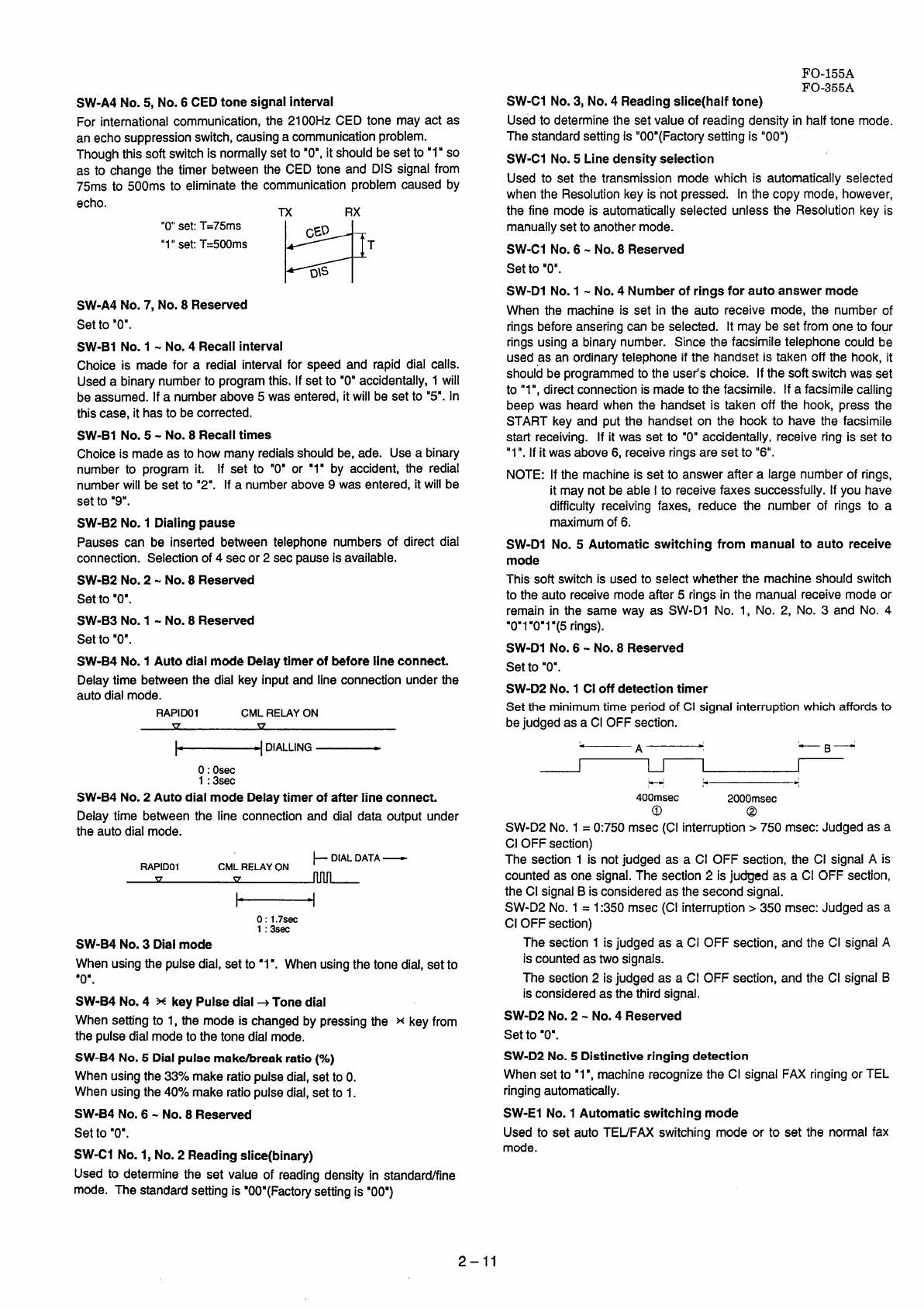
SW-A4 No. 5, No. 6CED tone signal interval
For internationalcommunication,the 21OOHZCEDtone may act as
anechosuppressionswitch,causingacommunicationproblem.
Thoughthissoftswitchis normallysetto “O’,it shouldbesetto”1” so
as to changethe timer betweenthe CEDtoneand DIS signalfrom
75msto 500msto eliminatethe communicationproblemcausedby
echo. TX RX
“O”set:T=75ms
H
CED
“1”set:T=500ms T
~\s
SW-A4 No. 7, No. 8Reserved
Setto ‘O”.
SW-B1 No. 1- No. 4Recall interval
Choiceis madefor aredial intervalfor speedand rapid dial calls.
Usedabinarynumberto programthis. [f setto “O”accidentally,1will
beassumed.If anumberabove5wasentered,it will be setto “5”. In
thiscase,it hasto becorrected.
SW-B1 No. 5- No. 8Recall times
Choiceis madeasto howmanyredialsshouldbe,ade. Useabinary
numberto programit. If set to “O”or “1’ by accident,the redial
numberwill besetto ‘2”. If anumberabove9wasentered,it will be
setto “9”.
SW-B2 No. 1Dialing pause
Pausescan be insertedbetweentelephonenumbersof direct dial
connection.Selectionof 4secor 2secpauseis available.
SW-B2 No. 2- No. 8Reserved
Set to “O”.
SW-B3 No. 1- No. 8Reserved
Setto “O”.
SW-B4No.1Auto dial mode Delay timer of before line connect.
Delaytime betweenthe dial keyinputandlineconnectionunderthe
autodialmode.
RAPIDO1 CMLRELAYON
v v
I-----i ’’A’””’—
O:Osec
1:3sec
SW-B4No.2Auto dial mode Delay timer of after line connect.
Delaytime betweenthe line connectionand dial data outputunder
theautodialmode.
~DIALDATA—
RAPIDO1 CML RELAY QN . . .
1- -1
0:1.7sec
1:3sec
SW-B4No.3Dial mode
Whenusingthepulsedial,setto “1”. Whenusingthetonedial,setto
●*
o.
SW-B4 No. 4 x key Pulse dial+ Tone dial
Whensettingto 1,the modeis changedby pressingthe xkeyfrom
thepulsedialmodetothetonedialmode.
SW-B4 No. 5Dial pulse make/break ratio (%)
Whenusingthe33%makeratiopulsedial,setto O.
Whenusingthe40%makeratiopulsedial,setto 1.
SW-B4 No. 6- No. 8Reserved
Setto “O”,
SW-Cl No. 1, No. 2Reading slice(binary)
Used to determine the set value of reading density in standard/fine
mode. The standard settingis ‘OO”(Factorysettingis “00”)
FO-155A
FO-355A
SW-Cl No. 3, No. 4Reading slice(half tone)
Usedto determinethe setvalueof readingdensityin halftonemode.
Thestandardsettingis “OO”(Factorysettingis “00”)
SW-Cl No. 5Line density selection
Usedto set the transmissionmodewhich is automaticallyselected
whenthe Resolutionkeyisnot pressed. In the copymode,however,
the fine modeis automaticallyselectedunlessthe Resolutionkey is
manuallysetto anothermode.
SW-Cl No. 6- No. 8Reserved
Setto “O”.
SW-D1No.1- No.4Number of rings for auto answer mode
Whenthe machineis set in the auto receivemode,the numberof
ringsbeforeanseringcatI be selected. It maybe setfromoneto four
ringsusingabinarynumber. Sincethe facsimiletelephonecouldbe
usedas an ordina~telephoneif the handsetis takenoff the hook,it
shouldbeprogrammedto the user’schoice. If the softswitchwasset
to “l”, directconnectionis madeto thefacsimile. If afacsimilecalling
beepwas heardwhenthe handsetis takenoff the hook,pressthe
STARTkey and put the handseton the hookto havethe facsimile
start receiving. If it wasset to “O”accidentally,receivering is set to
“1”. If it wasabove6, receiveringsareset to “6”.
NOTE:If the machineis set to answerafteralargenumberof rings,
it maynot be ableIto receivefaxessuccessfully.If youhave
difficulty receivingfaxes, reducethe numberof rings to a
maximumof 6.
SW-DI No. 5Automatic switching from manual to auto receive
mode
Thissoftswitchis usedto selectwhetherthe machineshouldswitch
to theautoreceivemodeafter5ringsin the manualreceivemodeor
remainin the sameway as SW-D1No. 1, No. 2, No. 3 and No. 4
“0’1“0”1“(5rings).
SW-D1 No. 6- No. 8Reserved
Setto “O’.
SW-D2 No. 1Cl off detection timer
Settheminimumtimeperiodof Cl signalinterruptionwhichaffordsto
bejudgedasaCl OFFsection.
~*.D ‘* 7
400msec 2000msec
o@
SW-D2No.1=0:750msec(Cl interruption>750 msec:Judgedasa
Cl OFFsection)
The section1is notjudgedas aCl OFFsection,the Cl signalAis
countedas onesignal.Thesection2is ju~d as aCl OFFsection,
theCl signalBisconsideredasthesecondsignal.
SW-D2No.1=1:350msec(Cl interruption>350 msec:Judgedas a
Cl OFFsection)
Thesection1is judgedas aCl
iscountedastwosignals.
Thesection2isjudgedas aCl
is consideredasthethirdsignal.
SW-D2No.2- No.4Reserved
Setto “O’.
OFFsection,andthe Cl signalA
OFFsection,andthe Cl signalB
SW-D2 No. 5Distinctive ringing detection
When set to “1”,machine recognizethe Cl signal FAXringingor TEL
ringingautomatically.
SW-El No. 1Automatic switching mode
Usedto set autoTEUFAXswitchingmodeor to set the nomal fax
mode.
2–11
FO-155A
FO-355A
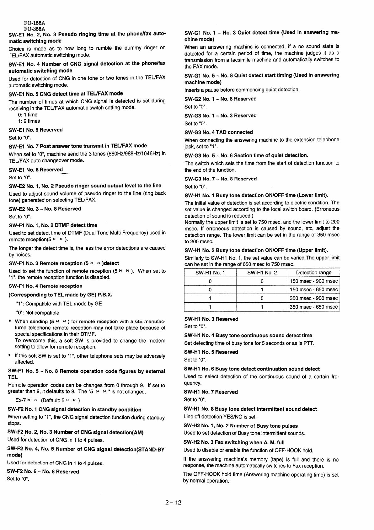
SW-El No. 2, No. 3Pseudo ringing time at the phone/fax auto-
matic switching mode
Choice is made as to how long to rumble the dummy ringer on
TEL/FAXautomaticswitchingmode.
SW-El No. 4Number of CNG signal detection at the phone/fax
automatic switching mode
Usedfor detectionof CNG in one tone or two tones in the TEL/FAX
automaticswitchingmode.
SW-El No.5CNGdetect time at TEMAX mode
The number of times at which CNGsignal is detectedis set during
receivingintheTEUFAXautomaticswitchsettingmode.
O:1time
1:2times
SW-El No. 6Reserved
Setto “O’.
SW-El No. 7Post answer tone transmit in TElfFAX mode
Whensetto “O”,machinesendthe3tones(880Hz/988Hti1046Hz)in
TEUFAXautochangeovermode.
SW-El No. 8Reserved
Setto “O”.
SW-E2 No. 1, No. 2Pseudo ringer sound output level to the line
Usedto adjustsoundvolumeof pseudoringerto the line (ringback
tone)generatedonselectingTEUFAX.
SW-E2No.3- No. 8Reserved
Setto ‘O”.
SW-F1No.1, No.2DTMFdetect time
Usedto setdetecttimeof DTMF(DualToneMultiFrequency)usedin
remotereception(5~ ~ ).
The longer the detect time is, the less the error detections are caused
by noises.
SW-F1 No. 3Remote reception (5 Kx)detect
Usedto set the functionof remotereception(5 x x ). Whensetto
“1”,the remotereceptionfunctionis disabled.
SW-F1 No. 4Remote reception
(Corresponding to TEL made by GE) P.B.X.
“1”:CompatiblewithTEL modebyGE
“O”:Notcompatible
●When sending (5 KM)for remotereceptionwith aGE manufac-
turedtelephoneremotereceptionmay not take placebecauseof
specialspecificationsin theirDTMF.
To overcomethis, asoft SW is providedto changethe modem
settingto allowfor remotereception.
●If thissoft SW is set to “1”, othertelephonesets maybe adversely
affected.
SW-F1 No. 5- No. 8Remote operation code figures by external
TEL
Remoteoperationcodescan be changesfrom Othrough9. If set to
greaterthan9, it defaultsto 9. The“5 x x “is notchanged.
Ex-7KH(Default:5HK)
SW-F2No. 1CNGsignal detection in standby condition
When settingto”1”, theCNGsignaldetectionfunctionduringstandby
stops.
SW-F2No.2, No.3Number of CNG signal detection
Usedfor detectionof CNGin 1to 4pulses.
SW-F2 No. 4, No. 5Number of CNG signal detection(STAND-BY
mode)
Usedfor detectionof CNGin 1to4pulses.
SW-F2 No. 6- No. 8Reserved
Setto “O”.
SW-G1 No. 1-No. 3Quiet detect time (Used in answering ma-
chine mode)
When an answeringmachineis connected,if a no soundstate is
detectedfor acertain periodof time, the machinejudges it as a
transmissionfrom afacsimilemachineandautomaticallyswitchesto
the FAXmode.
SW-G1 No. 5- No. 8Quiet detect start timing (Usedin answering
machine mode)
Insertsapausebeforecommencingquietdetection.
SW-G2No. 1- No.8Reserved
Set to “O”.
SW-G3 No. 1- No. 3Reserved
Set to “O”.
SW-G3 No. 4TAD connected
Whenconnectingthe answeringmachineto the extensiontelephone
jack,setto”1”.
SW-G3No.5- No.6Sectiontime of quiet detection.
Theswitchwhichsetsthe timefromthe startof detectionfunctionto
theendof thefunction.
SVV-G3No.7- No.8Reserved
Set to “O”.
SW-HI No. 1Busy tone detection ON/OFFtime (Lowerlimit).
Theinitialvalueof detectionissetaccordingto electriccondition.The
set valueis changedaccordingto the localswitchboard.(Erroneous
detectionof soundis reduced.)
Normallythe upperlimitis setto 750msec,andthelowerlimitto 200
msec. If erroneousdetectionis causedby sound,etc, adjust the
detectionrange.Thelowerlimitcanbeset in the rangeof 350msec
to 200msec.
SW-Hi No. 2Busy tone detection ON/OFF time (Upper limit).
Similarlyto SW-Hi No. 1,thesetvaluecanbevaried.Theupperlimit
canbesetintheranaeof 650 msecto 750msec.
ISW-Hi No.1ISW-Hi No.2 \Detectionrange \
IoIoI150msec-900 msecI
o1150 msec-650 msec
10350 msec-900 msec
I1I1[350 msec-650 msec \
SW-Hi No. 3Reserved
Set to’”0”.
SW-Hi No. 4Busy tone continuous sound detecttime
Setdetectingtimeof busytonefor 5secondsor as is PIT.
SW-HI No. 5Reserved
Set to ‘O”.
SW-Hi No. 6Busy tone detect continuation sound detect
Usedto select detectionof the continuoussoundof acertainfre-
quency.
SW-Hi No. 7Reserved
Set to “O”.
SW-HI No. 8Busy tone detect intermittent sound detect
Lineoff detectionYES/NOis set.
SW-H2No. 1, No.2Number of Busytone pulses
Usedto setdetectionof Busytoneintermittentsounds.
SW-H2No. 3Fax switching when A. M. full
Usedto disableor enablethefunctionof OFF-HOOKhold.
If the answeringmachine’smemory(tape) is full and there is no
response,themachineautomaticallyswitchesto Faxreception.
TheOFF-HOOKholdtime(Answeringmachineoperatingtime)is set
bynormaloperation.
FO-155A
FO-355A
SW-H2 No. 4- No. 8Reserved
Set to “O”.
SW-II No. 1- No. 8Reserved
Setto “O”.
SW-12No. 1- No. 8Reserved
Setto “O”.
SW-13No. 1- No. 8Reserved
Setto “O”.
SW-J1 No. 1, No. 2Transaction report
printout)
(Communication result
It is possibleto obtaintransactionresultsaftereachcommunication.
Normally,the switchis set (No. 1:0, No.2:0) so that the transaction
repotiis producedonlywhenacommunicationerroris encountered.
If No. 1was set to 1 and No. 2to O,the transactionreportwill be
producedeverytime acommunicationis done, evenif the communi-
cationwassuccessful.
Setting No. 1to 1 and No. 2to 1will disablethis function. No
transactionreportprinted.
SW-J1 No. 3Sender’s phone number registration
Used to make achoiceof whetherthe registeredsender’s phone
number can be changed or not. If the switch is set to “1”, new
registration of thesender’sphonenumberis disabledto preventacci-
dentalwronginput.
SW-J1No.4- No.6Reserved
Setto “O”.
SW-J1 No. 7, No. 8Ringer Volume
Usedto adjustringingvolume.
SW-J2 No. 1, No. 2Seaker Volume
Usedto adjustsoundvolumefromaspeaker.
SW-J2No.3Polling function (FO-355Aonly)
PollingfunctionYES/NOis set.
SW-J2No.4- No.8Reserved
Setto ‘O”.
SW-K1 No. 1Entering DIAG mode by pressing SPEEDkey
Abit whichis usedinthe productionprocessonly. WhentheSPEED
keyis pressed,the switchis changedfromthe stand-bystateto the
DIAGmode.
SW-K1No.2- No.8Reserved
Set to “O”.
Caution
When the valuewhichthe useris not allowedto set usingthe soft SW is set, outputto the indicationor list is notperformed.However,the actual
operationis performedat thesetvalue.
(Example)Numberof ringsfor autoreceive SWD1 No. l-No. 4
0100 +1111
(4times) (15times)
‘r
Display”ENTER(l-5)(4) List 4RINGS
‘r ‘r
Set value Valuewhenshipping Valuewhen shipping
Theoperationis performed15times.
2-13
FO-155A
FO-355A
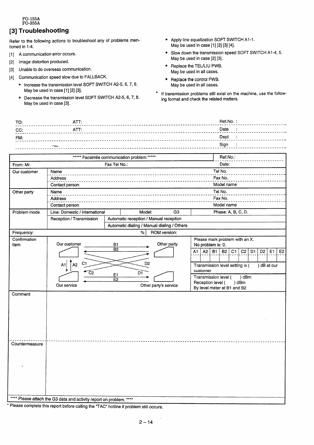
[3] Troubleshooting
Refer to the following actions to troubleshoot any of problems men-
tioned in 1-4.
[1] Acommunicationerroroccurs.
[2] Imagedistortionproduced.
[3] Unableto dooverseascommunication.
[4] Communicationspeedslowdueto FALLBACK.
●Increasethetransmissionlevel SOH SWITCHA2-5,6,7,8.
Maybeused in case [1] [2] [3].
●Decrease the transmission level SO~ SWITCHA2-5,6, 7, 8.
Maybe usedincase[3].
●ApplylineequalizationSO~ SWITCHAl-1.
Maybeusedin case[1] [2] [3] [4].
●Slowdownthetransmissionspeed SO~ SWITCHAl-4, 5.
Maybeused in case[2] [3].
●ReplacetheTEL/LIUPWB.
Maybeusedin all cases.
●ReplacethecontrolPWB.
Maybeusedinall cases.
*If transmissionproblemsstill existon the machine,usethe follow-
ingformatandcheckthe relatedmatters.
TO: ATT: Ref.No. :
----------------------------------------------------------------------------------------------------------------------
cc: A~: Date :
---------------------------------------------------------- ------------------------------------------------------------
FM: Dept :
----------------------------------------------------------------------------------------------------------------- ----—
~Sign :
----------------------------------------------------------------------------------------------------------------------
●**** Facsimilecommunicationproblem●**** IRef.No.:
From: Mr.
------------------------------
Fax Tel No.: Date:
Ourcustomer Name TelNo.
------------------------------------------------------------------------------------------------------,
Address FaxNo.
------------------------------------------------------------------------------------------------------,
Contactperson Modelname
Otherparty Name TelNo.
--------------------------------------------------------------------------------------------------
Address ----.
FaxNo.
-------------------------------------------------------------------------------------------------------
Contactperson Modelname
Problemmode Line:Domestic/international Model: G3 Phase:A, B, C, D.
Reception/Transmission Automaticreception/Manualreception
Automaticdialing/Manualdialing/Others
Frequency: 70 ROMversion:
Confirmation PleasemarkproblemwithanX.
item Ourcustomer ➤Otherpatty Noproblemis: O.
4Al A2 B1 B2 cl C2 DI D2 El E2
---- ---- ---- ----- ----- ----- ---
ZCA2 :::s :me :;-
Transmtsston level setting is ( ) dB at our
El
4E2 Transmissionlevel()dBm
Our service Other party’sservice Reception level ( ) dBm
By level meter at B1andB2
Comment
---------------- ------------------------------------------------------------------------------------------------------
Countermeasure
‘*** PleaseattachtheG3dataandactivityreportonproblem.
●***
●m,–. . . .. . . .
riease compiele tnts reportbeforecallingthe “TAC” hotline if problem still occurs.
2 –14
FO-155A
FO-355A
[4] Error code table
G3Transmission
ICode Finalreceivedsignal ErrorCondition(Receiverside)
IoIncompletesignalframe Cannotrecognizebitstreamafterflag I
I1NSF,DIS CannotrecognizeDCSsignal
CannotrecognizeNSSsignal I
I2ICFR IDisconnectslineduringrece~tion I
3Disconnectslinebyfallback
4MCF Disconnectslineduringreceptionof multi-page
CannotrecognizeNSS,DCSsignalinthecaseof mode change
5PIPor PIN No responsein receiverside to picture signal after no response in transmittersideto receive
TALK modereauest
6RTN or RTP Cannot recognize NSS, DCSsignalaftertransmittingRTN or RTP signal.
7No signal or DCN No response in receiversideor DCNsignalreceived*
G3 Reception
ICode Finalreceivedsignal [ErrorCondition(Transmitterside) I
IoIImcompietesignaiframe ICannotrecognizebitstreamafterflag I
I1NSS,DCS CannotrecognizeCFRor ~signal
Disconnectslinedurinatransmission I
2NSC, DTC Cannot recognize NSS signal
3EOP CannotrecognizeMCF,PIP, PIN, RTN,RTPsignal
4EOM CannotrecognizeMCF,PIP,PIN,RTN, RTP signal in the case of mode change
5MPS CannotrecognizeMCF,PIP,PIN,RTN,RTPsignalinthecaseof multi-page
6PR1-Q CannotrecognizePIP,PINsignalinthecaseof TALKrequest
7Nosignalor DCN Noresponseintransmitter(cannotrecognizeDISsignal)or DCNsignal received*
‘
2-15
FO-155A
FO-355A
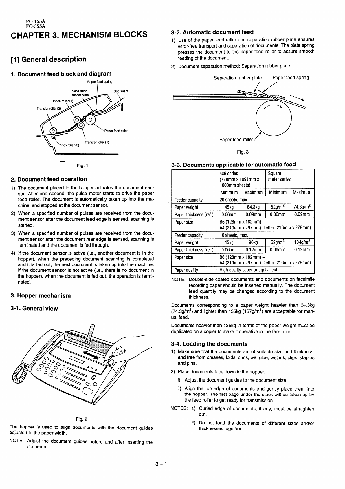
CHAPTER3. MECHANISMBLOCKS
[1] General description
1.
2.
1)
2)
3)
4)
3.
Document feed block and diagram
Paparfeedspring
I
Separation Document
rubberplate
Pi@ roller(1)
Transferroller(2)
\\ Transferroller(l)
in* roller(2)
Fig.1
Document feed operation
The documentplacedin the hopperactuatesthe documentsen-
sor. After one second,the pulsemotorstartsto drivethe paper
feed roller.The documentis automaticallytakenup into the ma-
chine,andstoppedatthedocumentsensor.
Whenaspecifiednumberof pulsesare receivedfrom the docu-
mentsensorafterthe documentleadedgeis sensed,scanningis
started.
Whenaspecifiednumberof pulsesare receivedfrom the docu-
mentsensorafterthe documentrearedgeis sensed,scanningis
terminatedandthe documentisfedthrough.
If the document sensoris active(i.e.,anotherdocumentis in the
hopper),when the precedingdocumentscanningis completed
and it is fed out,the nextdocumentis takenup intothe machine.
If thedocumentsensoris notactive(i.e.,thereis no documentin
the hopper),whenthe documentisfed out,theoperationis termi-
nated.
Hopper mechanism
3-1. General view
Fig.2
The hopperis used to align documentswith the documentguides
adjustedto the paperwidth.
NOTE: Adjust the document guides before and after inserting the
document.
3-2.Automatic document feed
1)Useof the paper feed rollerandseparationrubberplateensures
error-freetransportandseparationof documents.ThepIatespring
presses the document to the paper feed rollerto assuresmooth
feedingof thedocument.
2) Documentseparationmethod:Separationrubberplate
Separationrubberplate Paperfeedspring
//
‘-b ;-
+
.—.—
Paper feedroller/“
Fig.3
3-3.Documents applicable for automatic feed
4x6series Square
(788mmx1091mmxmeterseries
1000mmsheets)
Minimum\Maximum MinimumIMaximum
IFeedercaPaciN I20sheets,max. I
. . 1
Paperweight 45kg 64,3kg 52g/m2 74.3glm2
Paperthickness(ref.) 0.06mm 0.09mm 0.06mm 0.09mm
Papersize B6(128mmx182mm)-
A4(210mmx297mm),Letter(216mmx279mm)
Feedercapacity 10sheets,max.
Paperweight 45kg 90kg 52g/m2 104g/m2
Paperthickness(ref.) 0.06mm 0.12mm 0.06mm 0.12mm
IPapersize B6(128mmx182mm)-
A4(210mmx297mm),Letter(216mmx279mm)
Paperquality IHighqualitypaperorequivalent I
NOTE: Double-sidecoateddocumentsand documentson facsimile
recordingpapershouldbe insertedmanually.
The document
feed quantity may be changed according to the document
thickness.
Documentscorrespondingto apaper weight heavierthan 64.3kg
(74.3g/m2)andlighterthan 135kg(157g/m2)areacceptablefor man-
ualfeed.
Documentsheavierthan 135kgin termsof the paperweightmustbe
duplicatedona copierto makeit operativeinthe facsimile.
3-4.Loading the documents
1)Make surethatthe documentsareof suitablesizeandthickness,
andfreefromcreases,folds,curls,wetglue,wetink,clips,staples
andpins.
2) Placedocumentsfacedowninthe hopper.
i) Adjustthedocumentguidesto thedocumentsize.
ii) Align the top edgeof documentsand gently placethem into
the hopper.Thefirst pageunderthe stackwill be takenup by
thefeedrollerto getreadyfortransmission.
NOTES: 1) Curlededgeof documents,if any, must be straighten
out.
2) Do not load the documentsof different sizes and/or
thicknessestogether.
3-1
FO-155A
FO-355A
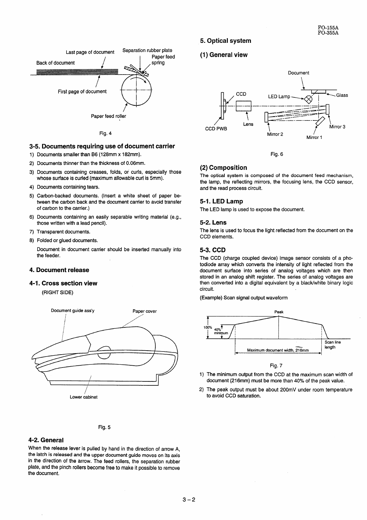
5.Optical system
Lastpageofdocument Separationrubberplate
/
(1)General view
Backofdocument
/
Firstpageofdocument
/
Paperfeedroller
Fig.4
3-5.Documents requiring use of document carrier
1)
2)
3)
4)
5)
6)
7)
8)
4.
DocumentssmallerthanB6(128mmx182mm).
Documentsthinnerthanthethicknessof 0.06mm.
Documentscontainingcreases,folds, or curls, especially those
whose surface is curled (maximum allowable curlis 5mm).
Documentscontainingtears.
Carbon-backeddocuments.(Insertawhite sheet of paper be-
tweenthe carbonbackandthedocumentcarrierto avoidtransfer
of carbonto thecarrier.)
Documentscontainingan easilyseparablewritingmaterial(e.g.,
thosewrittenwithaleadpencil).
Transparentdocuments.
Foldedor glueddocuments.
Documentin documentcarriershouldbe insertedmanuallyinto
thefeeder.
Document release
4-1. Cross section view
(RIGHTSIDE)
Documentguideass’y
/
/
Papercover
/“”
\I
\JI
I
I
I
Lowercabinet
Fig.5
Document
rCCD
n
L’””mp~~-G’ass
–--l
P
—. -— —- —- —- —. —. —-—-—
/-
_=---—-. -—---e-i—
\
F-
._-----—->F>-
--
----- -#\
-—-—-—-—- ‘
Lens
CCDPWB fMirror3
Mirror2Mir/or 1
Fig.6
(2) Composition
The optical system is composed of the document
the lamp, the reflecting mirrors, the focusing lens,
and the read process circuit.
5-1. LED Lamp
TheLEDlampis usedto exposethedocument.
5-2.Lens
feed mechanism,
the CCDsensor,
Thelensis usedto focusthe lightreflectedfromthedocumentonthe
CCDelements.
5-3.CCD
The CCD (chargecoupleddevice)imagesensorconsistsof apho-
todiodearraywhichconvertsthe intensityof light reflectedfrom the
documentsurface into series of analog voltageswhich are then
storedin an analogshift register.The seriesof analogvoltagesare
then convertedinto adigitalequivalentby ablack/whitebinarylogic
circuit.
(Example)Scansignaloutputwaveform
Peak
1)
2)
t
1Scan
line
—
Maximumtiument width,216mm length
4e
Fig. 7
Theminimumoutputfromthe CCD at the maximumscanwidthof
document(216mm)mustbemorethan40%ofthe peakvalue.
The peakoutputmust be about200mVunderroomtemperature
to avoidCCDsaturation.
4-2.General
Whenthe releaseleveris pulledby handin the directionof arrowA,
thelatchis releasedandtheupperdocumentguidemovesonits axis
in the directionof the arrow.Thefeed rollers,the separationrubber
plate,andthepinchrollersbecomefreeto makeit possibleto remove
thedocument.
3-2
FO-155A
FO-355A
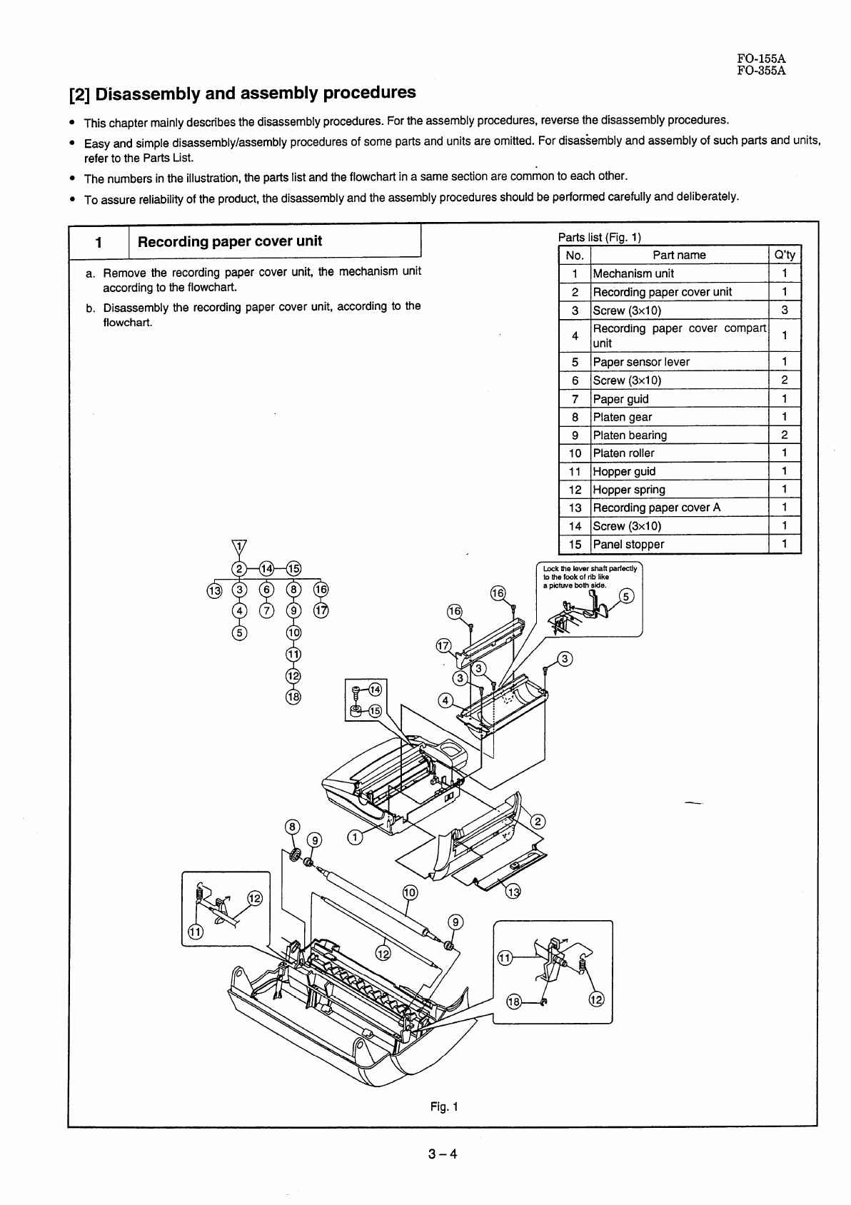
6. Recording block
(1) General view
/
Recordingpaper
Fig. 8
6-1. Driving
Via the pulse motor gear shaft, the reduction gear, and the recording
paper feed gear, rotation of the pulsemotor is conveyedto the re-
cordingpaperfeedrollertofeedthe recordingpaper.
6-2. Recording
Useof athermalheadpermitseasiermaintenanceandlowoperating
costs.
1)Thermalhead
The thermalheadconsistsof 1728-dotheatelementsarrangedin a
singlerow and has the resolutionof 8dots/mm.The maximumre-
cordingspeed is 10ms/line.The thermal head also incorporates a
1728-dot shift registerlatchand an output control driver circuit. Low
powerconsumptionis achievedby dividingthe headinto nineseg-
ments.
2) Structureofthe recordingmechanism
Recording is accomplished by pressing the thermal head on the re-
cording paper against the platen roller.
The main scan (horizontal) is electronically achieved, whilethe sub-
scan (vertical)is achievedby movingthe recordingpaper by the
recordingplatenroller.
Usually,thecausefor unevenprinttoneis causedbymisalignmentof
thethermalheador unevencontactwiththeroller.
It canbecheckedin thefollowingmanner.
1)
2)
3)
4)
5)
Checkif the thermalhead powerand signalcablesare properly
routed.
Checkthatthethermalheadpivotmovessmoothlyupanddown.
Checkthat the thermalheadsupportbracketis securedwithout
anyplay.
Checkto seethat the recordingplatenroller has properconcen-
trici~, in the caseof aprinttone variationevenlyrepeateddown
thepage.
Replace the thermal head with anew one and checkto seeif the
sametroubleoccurs.
3–3
[2] Disassembly and assembly procedures
FO-155A
FO-355A
●Thischaptermainlydescribesthedisassemblyprocedures.Fortheassemblyprocedures,reversethedisassemblyprocedures.
●Easyandsimpledisassemblylassemblyproceduresof somepartsandunitsareomifled.Fordisassemblyandassemblyof suchpartsand units,
referto the PartsList.
●Thenumbersinthe illustration,thepartslistandtheflowchartin asamesectionarecommonto eachother.
●Toassure reliabilityof the product,the disassembly and the assembly procedures shouldbe performed carefully and deliberately.
1Recording paper cover unit
a.
b.
Remove the recording paper cover unit, the
according to the flowchart.
Disassembly the recording paper cover unit,
flowchart.
A
1
2
mechanismunit
accordingto the
1..\\ @
‘artslist (Fig. 1)
No. Part name Q’ty
1Mechanism unit 1
2Recording paper cover unit 1
3Screw (3x1O) 3
~Recording paper cover compart ,
unit
5Paper sensorlever 1
6Screw(3x1O) 2
7Paperguid 1
8Platengear 1
9Platenbearing 2
10 Platenroller 1
11 Hopper guid 1
12 Hopper spring 1
13 Recording paper cover A1
14 Screw (3x1O) 1
15 Panel stopper 1
&w ‘.
Fig.1
.
3-4
FO-355A I f
2Head frame unit
II
a.
b.
c,
Removethe recordingpapercover unit, the mechanismunit
accordingto procedurel-a.
Removethe headframeunit fromthe mechanismunitaccord-
ingto theflowchart.
Disassembletheheadframeunitaccordingtotheflowchart.
.
(Headcable) ~
%
Headcablepasstothecore 4
2times.
Headcable
ThermalHead
Partslist(Fig.2)
No. Partname Q’ty
1Mechanismunit 1
2Screw(3x12) 2
3Connector 1
4Screw(3x6) 1
I5IHeadframeunit
I6IACcord
I7]Screw
[8IConnector 11
@
26
37
48
0
5
Headearthcable
Fig. 2
$
--o
3
3–5
FO-155A
FO-355A
1
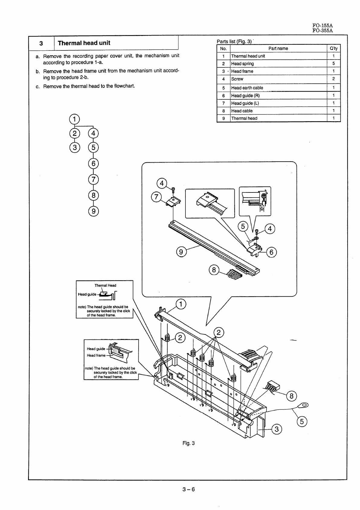
3Thermal head unit
a.
b.
c.
Removethe recordingpapercover unit, the mechanismunit
accordingto procedurel-a.
Remove the head frame unit from the mechanism unit accord-
ing to procedure 2-b.
Removethethermalheadto theflowchart.
@
1
24
35
8
8
9
ThemalHead
Heedguide
*
‘artslist(Fig. 3)”
No. Partname Q’ty
1Thermalheadunit 1
2Headspring 5
3“ Headframe 1
4Screw 2
5Headeatthcable 1
6Headguide(R) 1
7Headguide(L) 1
8Headcable 1
9Themal head 1
(4)
note)Theheadguideshouldbe \lftA D //
securelvlockedbvtheclickkA
ofthehiadframe:
‘\
‘w
Headguide \llT
Headframe
*(> -
note)Theheadguideshouldbe
securelyIcckedbytheclick—Al Ikk
Fig.3
3-6
FO-155A
FO-355A
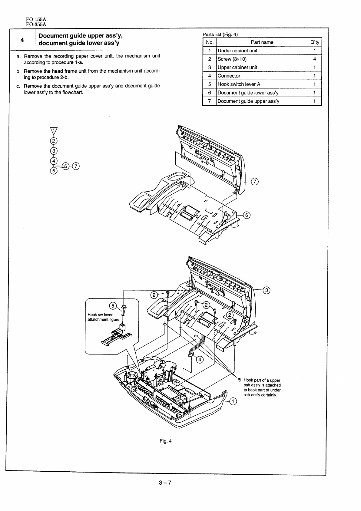
Document guide upper ass’y,
4document guide lower ass’y
a.
b.
c.
Removethe recordingpapercover unit, the mechanismunit
accordingto procedurel-a.
Removethe headframeunitfromthe mechanismunitaccord-
ingto procedure2-b.
Removethe documentguideupperass’yanddocumentguide
lowerass’yto theflowchart.
‘adslist(Fig.4)
No. Partname Q’ty
1Undercabinetunit 1
2Screw[3x10) 4
3Uppercabinetunit 1
4Connector 1
5HookswitchleverA1
6Documentguidelowerass’y 1
7Documentguideupperass’y 1
Hookpartofaupper
cabass’yisattached
tohookpartofunder
cabass’ycertainly.
Fig.4
3-7
FO-155A
FO-355A
I I
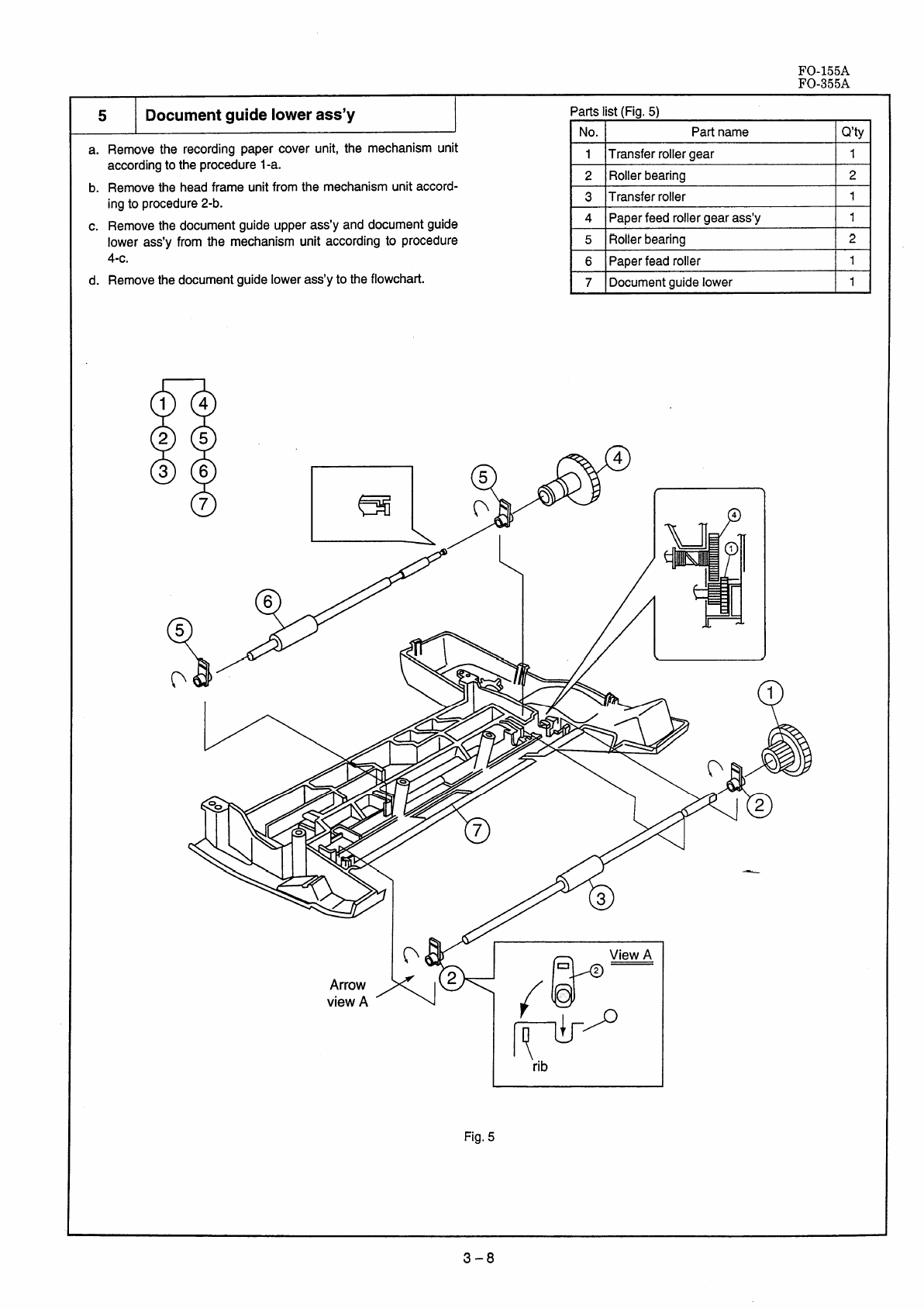
5Document guide lower ass’y I
a.
b.
c.
d.
Removethe recordingpapercover unit, the mechanismunit
accordingto theprocedurel-a.
Removethe headframeunitfrom the mechanismunit accord-
ingto procedure2-b.
Remove the document guide upper ass’y and document guide
lower ass’y from the mechanism unit according to procedure
4-c.
Remove the document guide lower ass’y to the flowchart.
@
14
25
36 0
7
Partslist(Fia. 5)
.“,
No. Padname Q’ty
1Transfer roller gear 1
2Rollerbearing 2
3Transferroller 1
4Paperfeedrollergearass’y 1
5Rollerbearing 2
6IPaDerfeadroller Ill
7Documentguidelower 1
Arrow
viewA
I‘rib
Fig.5
3-8
FO-155A
FO-355A
,I
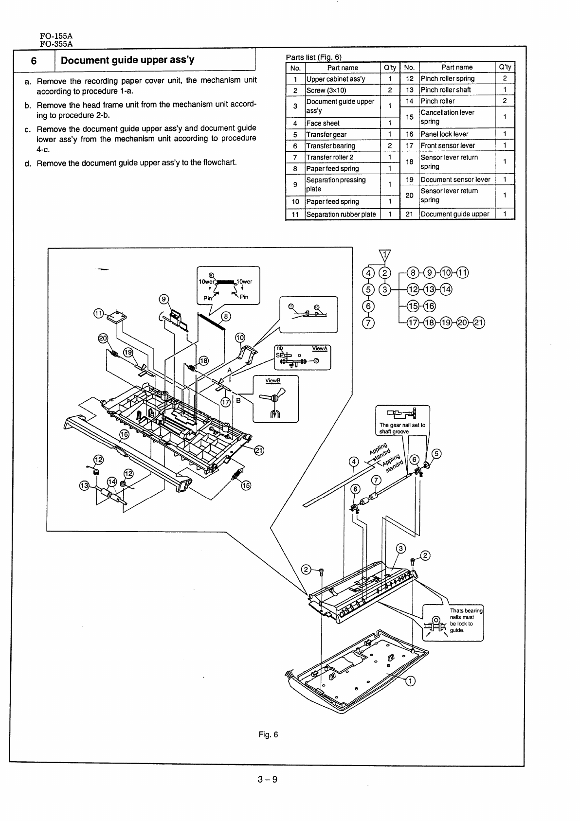
6Document guide upper ass’y
a.
b.
c.
d.
Remove the recording paper cover unit, the mechanism unit
according to procedure l-a.
Remove the head frame unit from the mechanism unit accord-
ingto procedure2-b.
Removethe documentguideupperass’yanddocumentguide
lower ass’yfrom the mechanismunit accordingto procedure
4-c.
Removethe documentguideupperass’yto theflowchart.
Partslist(Fig.6) 1
No. IPartname IQ’ty INo. IPartname IQ’ty
1Uppercabinetass’y 1 12 Pinchrollerspring 2
2Screw(3x1O) 2 13 Pinchrollershaft 1
3Documentguideupper ,14 Pinchroller 2
ass’y ,5 Cancellationlever 1
4Facesheet 1spring
5Transferaear 1 16 Panellocklever 1
6lTransferbearina I2I17 IFrontsensOrlever Ill
7Transferroller21,8 Sensorleverreturn 1
8Paperfeedspring 1spring
~Separationpressing 119 Documentsensorlever 1
plate Z. Sensorleverreturn 1
10 Paperfeedspring 1spring
11 Separationrubberplate 1I21 Documentguideupper I11
n
%+
Thegearnailsetto
shaftgroove
~~
/
Fig. 6
3–9
FO-155A
FO-355A
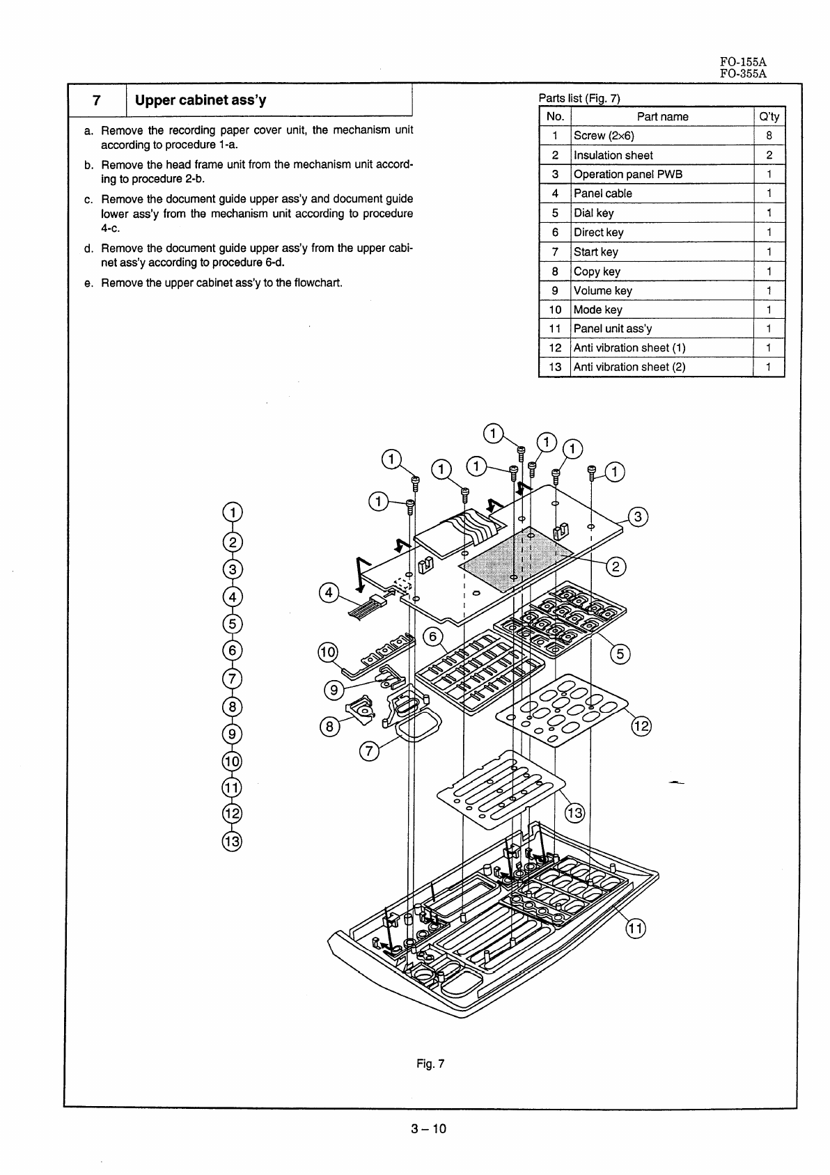
7Upper cabinet ass’y I
a.
b.
c.
d.
e,
Removethe recordingpapercover unit, the mechanismunit
accordingto procedurel-a.
Remove the head frame unit from the mechanism unit accord-
ing to procedure 2-b.
Remove the document guide upper ass’y and document guide
lower ass’yfrom the mechanismunit accordingto procedure
4-c.
Remove the document guide upper ass’y from the upper cabi-
net ass’y according to procedure 6-d.
Remove the upper cabinet ass’y to the flowchart.
Parts list (Fia.7)
.“,
No. Partname Q’ty
1Screw (2x6) 8
2Insulationsheet 2
3OperationpanelPWB 1
4Panelcable 1
5Dialkey 1
6IDirectkey Ill
7Startkey 1
8Copykey 1
9IVolumekey
10 Mode key 1
11 Panel unit ass’y 1
12 Antivibrationsheet(1) 1
13 Antivibrationsheet(2) 1
P
1
-o
2
Fig. 7
3-10
FO-155A
FO-355A
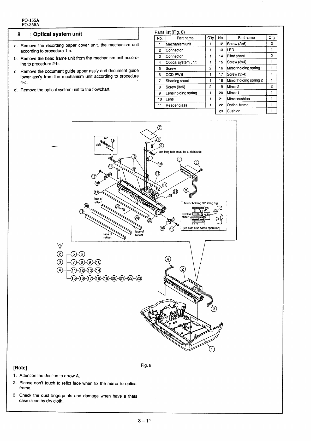
8Optical system unit Partslist(Fig.8)
No.IPartname IQ’tyINo. IPartname IQ’ty
a.
b.
c.
d.
Removethe recordingpapercover unit, the mechanismunit
accordingto procedurel-a.
Removethe headframeunitfromthe mechanismunitaccord-
ingto procedure2-b.
Removethe documentguideupperass’yanddocumentguide
iowerass’y from the mechanismunit accordingto procedure
4-c.
Removethe opticaisystemunitto theflowchart.
v
1
I1Mechanismunit 1I12 lScrew(2x6) 3I
I2Connector 1I13 ILED 1I
3Connector 114 Blindsheet 2
4Opticalsystemunit 115 Screw(3x4) 1
5Screw 216 Mirrorholdingspring11
6CCDPWB 1 17 Screw(3x4) 1
I7Shadingsheet 1I18 IMirrorholdingspring2I1I
8Screw(3x6) 2 19 Mirror2 2
9Lensholdingspring 1 20 Mirror11
10 Lens 121 Mirrorcushion 1
11 Readerglass 1 22 Opticalframe 1
23 Cushion 1
r
““N
,,8The longholemustbeat rightSide.
5
-..
14 -.
*
. .
~Pk’
. . .
1
2
\
18
/
\@
11
faceof
MirrorholdingSP fittingFig.
R&
od
16
SCREW
Mirror—
(Ieffsidealsosameoperation)
>\
4Q
2
Fig.8
1. Attention the dection to arrow A.
2. Piease don’t touch to reflct face whenfix the mirror to opticai
frame.
3. Checkthe dust fingerprintsand damagewhen haveathats
casecleanbydrycioth.
3–11
FO-155A
FO-355A
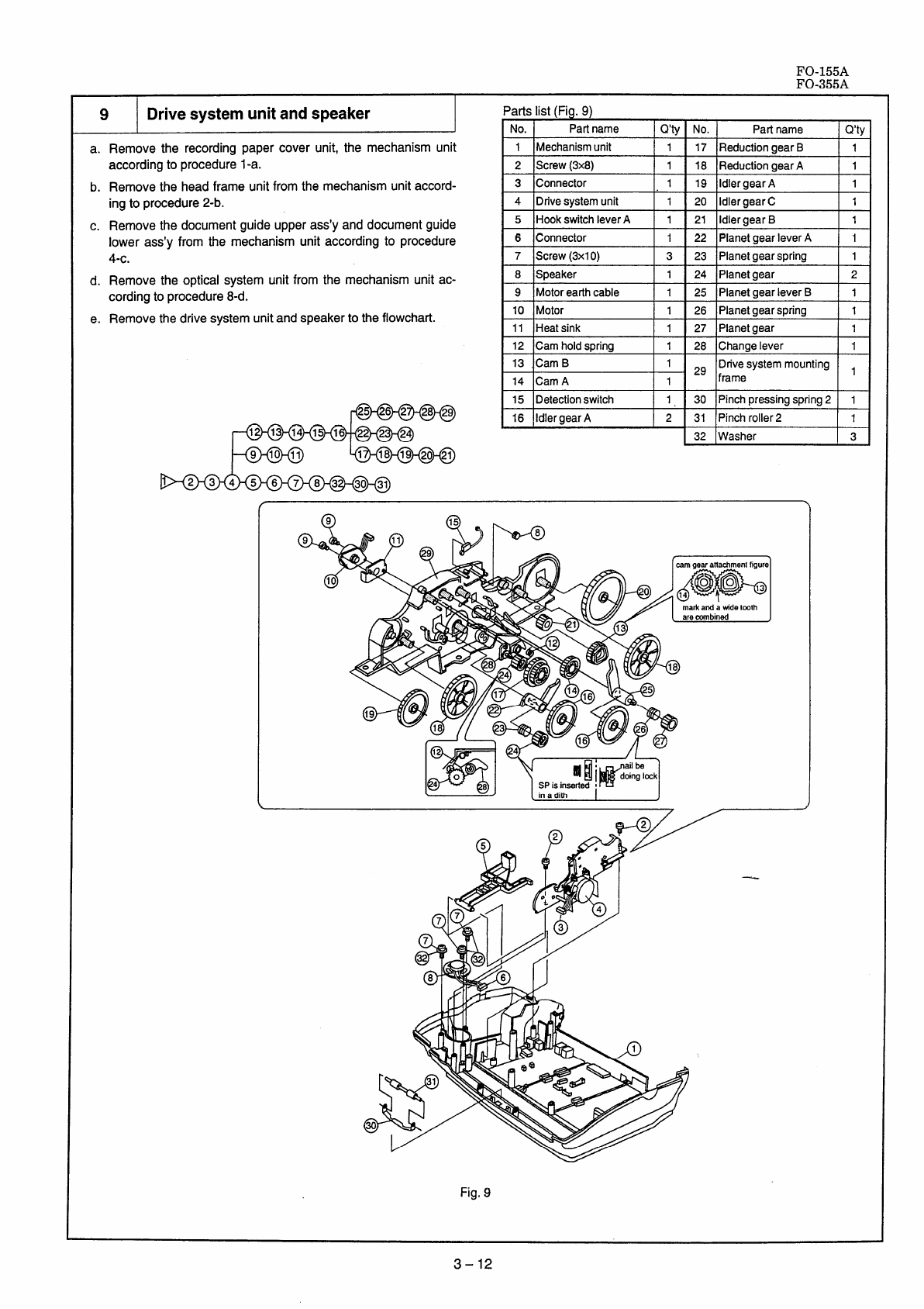
9Drive system unit and speaker Partslist(Fig. 9)
INo. /Partname IQ’tv INo. /Partname /Q’tv [
a.
b,
c.
d.
e.
Remove the recording paper cover unit, the mechanism unit
according to procedure l-a.
Removethe headframeunitfromthe mechanismunitaccord-
ingto procedure2-b.
Removethe document
guide upper ass’y and document guide
lower ass’y from the mechanism unit according to procedure
4-c.
Removethe opticalsystemunitfrom the mechanismunit ac-
cordingto procedure8-d.
Removethedrivesystemunitandspeakerto theflowchart.
1Mechanismunit 1 17 ReductiongearB1
2Screw(3x8) 118 ReductiongearA1
3Connector 1 19 IdlergearA1
4Drivesystemunit 120 ldlergearC1
5HookswitchleverA1 21 IdlergearB1
6Connector 1 22 PlanetgearleverA1
7Screw(3x1O) 323 Planetgearspring 1
8Speaker 1 24 Planetgear 2
I9\Motoreaflhcable/1I25 IPlanet~earleverB/I
I10 IMotor /1I26 IPlanet~earsPfina /1
I11 \Heatsink I1I27 ]Planetgear 11
12 lCamholdspring I1I28 ICt’tangelever /1
13 CamB129 Drivesystemmounting ,
14 CamA1frame
15 Detectionswitch 1, 30 Pinchpressingspring2 1
16 idlergearA2 31 Pinchroller2 1
32 Washer 3
@
. .
LJIin adith 1I
Fig.9
3-12
FO-155A
FO-355A I
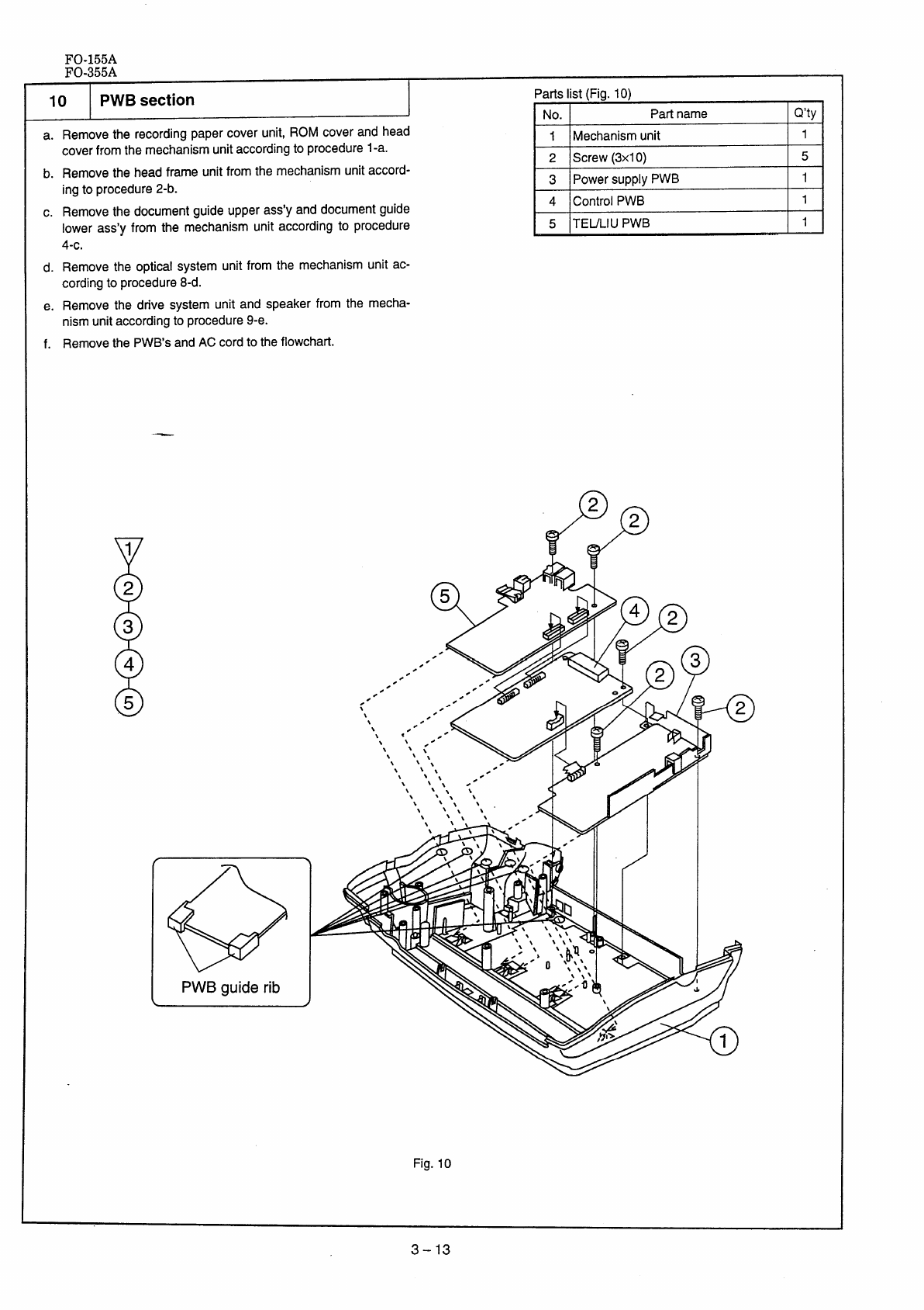
10 PWB section Partslist (Fig.10)
iNo. IPartname IQ’ty
a.
b.
c.
d.
e.
f.
Remove the recording paper cover unit, ROMcoverandhead
coverfromthemechanismunitaccordingto procedurel-a.
Removethe headframeunitfromthe mechanismunitaccord-
ingto procedure2-b.
Removethe documentguideupperass’yanddocumentguide
lowerass’yfrom the mechanismunit accordingto procedure
4-C,
Removethe opticalsystemunit from the mechanismunit ac-
cordingto procedure8-d.
Remove the drive system unit and speaker from the mecha-
nism unit according to procedure 9-e.
Removethe PWB’SandACcordto theflowchart.
!
1
2
3
4
5
1Mechanismunit 1
2Screw(3x1O) 5
3IPowersupplyPWB 1
II
4ControlPWB 1
5TEL/LIUPWB 1
PWB guide rib
Fig.10
3-13
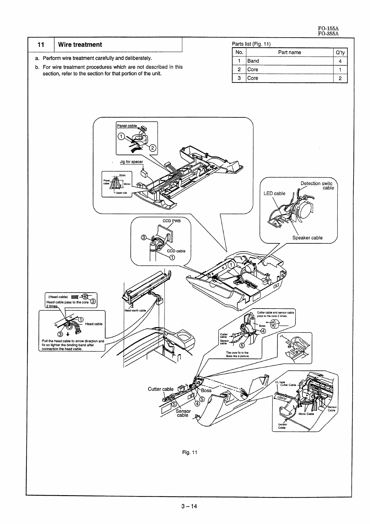
FO-155A
FO-355A
11 Wire treatment Partslist(Fig.11)
No. Partname Q’ty
a. Performwiretreatmentcarefullyanddeliberately. 1Band 4
b. For wire treatmentprocedureswhichare notdescribedin this 2Core 1
section,referto thesectionfor thatportion of the unit. 3Core 2
(Headcable) ~
%)
Headcablepaastothecore 3
, \ \
Headcable
Pulltheheadcabletoarrowdir~tion
fixsotghterthebindingbandafter
connectionIhahaadcable.
CCD PWB \\ \
Detectionswitc
cable
L
Speakercable
\// /
3-14
FO-155A
FO-355A
CHAPTER4. DIAGRAMS
—- —. —-—-—-—-— ,
—-—-—-—-—- —-— I1–-
1t
I-
IEl I I
II
I
I
I
t
I
I
I
tI
I1
II‘i I
I
1
I
II !I
I
tI
I
1
ItI I ‘-’ ,
IIII I
II------ ,-----L.r-----.
t1
TI
t
tI
II
I I
I●
I
1
I
I
I
I
1
I
I
1
I
I
I
I
—-—-—-—-—-—-—,
1t
I
–1
1
-- -t -—
w
zd
i1-
4–1
FO-155A
I?O-355A
n1
*, \
.
r
L
If
1-
3
c.)
z
0b
C9
Ium
1HI
III In- n
ItI
J
1
m/–\
4-2
FO-155A
FO-355A
—
T
mol —
0
—
+
%
—
.
.
,
%
—
N
[
4–3
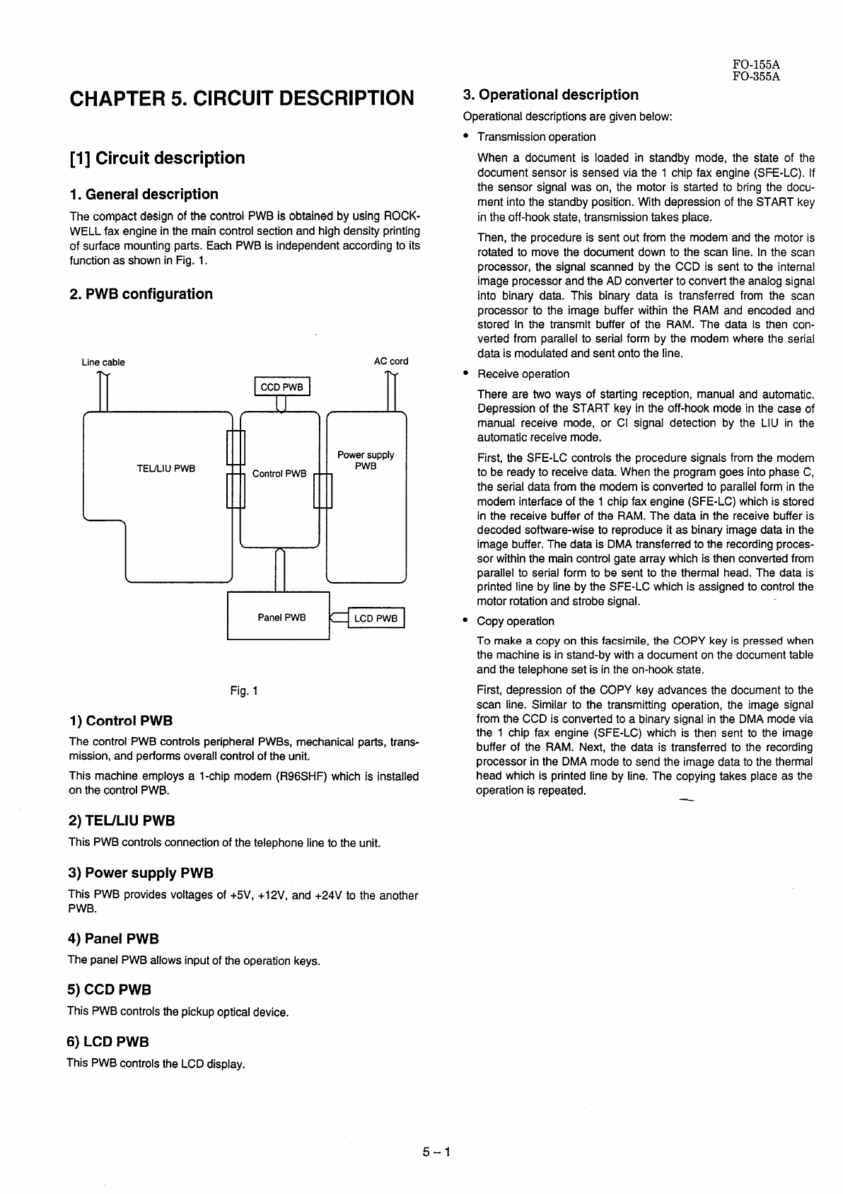
FO-155A
FO-355A
CHAPTER5. CIRCUITDESCRIPTION
[1] Circuit description
1. General description
Thecompactdesignof the controlPWBis obtainedby using ROCK-
WELL fax enginein the maincontrolsectionandhighdensityprinting
of surfacemountingpatts. EachPWBis independentaccordingto its
function asshownin Fig.1.
2.PWB configuration
Linecable
-CCDPWB
[J
f\f
TEULIUPWB ControlPWB
d
(\
Ln
LJ
ACcord
Powersupply
PWB
l—
‘ane’pwB-
Fig.1
1) Control PWB
ThecontrolPWBcontrolsperipheralPWBS,mechanicalparts,trans-
mission,andperformsoverallcontrolof theunit.
This machineemploysal-chip modem(R96SHF)whichis installed
onthecontrolPW13,
2)TEULIU PWB
This PWB controls connection of the telephone line to the unit.
3)Power supply PWB
This PWB provides voltages of +5V, +12V, and +24V to the another
PWB.
4) Panel PWB
The panel PWB allows input of the operation keys.
3. Operational description
Operationaldescriptionsaregivenbelow:
●
●
●
Transmission operation
When adocument is loaded in standbymode,the state of the
documentsensoris sensedvia the 1chipfax engine(SFE-LC).If
the sensorsignalwas on, the motoris startedto bringthe docu-
mentintothe standbyposition.Withdepressionof theSTARTkey
intheoff-hookstate,transmissiontakesplace.
Then,the procedureis sentout fromthe modemandthe motoris
rotatedto movethe documentdownto the scanline. In the scan
processor,the signalscannedby the CCD is sentto the internal
imageprocessorandtheADconverterto converttheanalogsignal
into binary data. This binary data is transferredfrom the scan
processorto the imagebufferwithin the RAM and encodedand
storedin the transmitbuffer of the RAM. The data is then con-
vertedfrom parallelto serialform by the modemwherethe serial
datais modulatedandsentontothe line.
Receiveoperation
Thereare two waysof startingreception,manualand automatic.
Depressionof the STARTkeyin the off-hookmodein the caseof
manualreceivemode, or Cl signal detectionby the LIU in the
automaticreceivemode.
First,the SFE-LCcontrolsthe proceduresignalsfromthe modem
to bereadyto receivedata.Whenthe programgoesintophaseC,
the serialdatafromthe modemis convertedto parallelforminthe
modeminterfaceof the 1chipfaxengine(SFE-LC)whichis stored
in the receivebufferof the RAM.The datain the receivebufferis
decodedsoftware-wiseto reproduceit as binaryimagedatain the
imagebuffer.Thedatais DMAtransferredto the recordingproces-
sorwithinthe maincontrolgatearraywhichisthenconvertedfrom
parallelto serialformto be sentto the thermalhead.Thedatais
printedlineby lineby the SFE-LCwhichis assignedto controlthe
motorrotationandstrobesignal.
Copyoperation
To makeacopyon this facsimile,the COPYkeyis pressedwhen
the machineis in stand-bywithadocumentonthe documenttable
andthetelephonesetis in theon-hookstate.
First,depressionof the COPYkeyadvancesthe documentto the
scan line. Similarto the transmittingoperation,the imagesignal
fromthe CCDis convertedto abinarysignalin the DMAmodevia
the 1chip fax engine(SFE-LC)which is then sent to the image
bufferof the RAM. Next,the data is transferredto the recording
processorin the DMAmodeto sendthe imagedatato thethermal
headwhichis printedline by line.The copying takes place as the
operation is repeated,
5) CCD PWB
ThisPWBcontrolsthepickupopticaldevice.
6) LCD PWB
ThisPWBcontrolstheLCDdisplay.
5-1
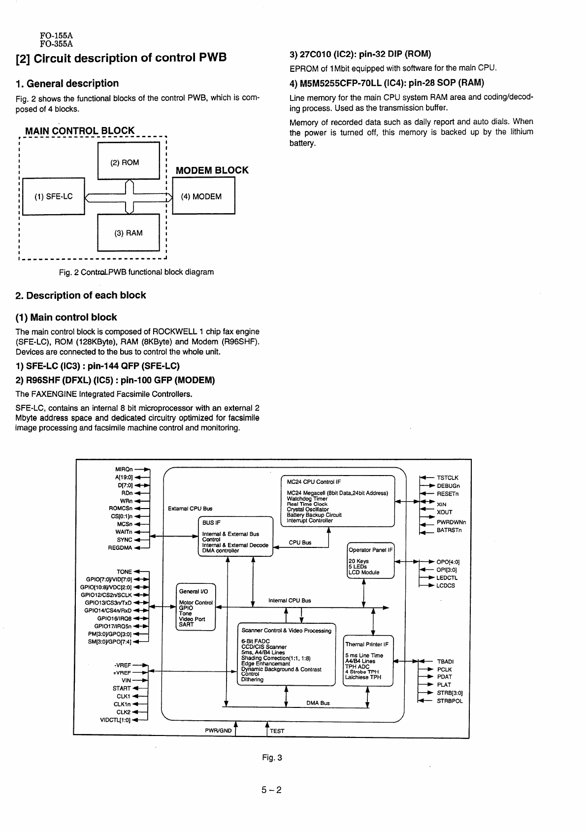
FO-155A
FO-355A
[2] Circuit description of control PWB 3) 27CO1O(IC2):pin-32DIP(ROM)
EPROMof 1Mbitequippedwithsoftwarefor themainCPU.
1.General description 4) M5M5255CFP-TOl-l..(IC4):pin-28SOP(RAM)
Fig. 2shows the functional blocks of the control PWB, whichis com- Line memoryfor the mainCPUsystemRAMarea and coding/decod-
posedof 4blocks. ingprocess.Used as the transmission buffer.
MAIN CONTROLBLOCK
,--------------------------
I
I
I
I
1(2) ROM :
I ; MODEM BLOCK
I
I(’1 t
I
I
I(1)SFE-LC $(4) MODEM
(
I(J I
1,I
1I I I
II
I
I
I
I
I
1---- .. -.----- .-.. ------- ..--1
Fig. 2Cont*WB functional block diagram
2. Description of each block
(1) Main control block
Themaincontrolblockiscomposedof ROCKWELL1chip fax engine
(SFE-LC),ROM (128KByte), RAM (8KByte)and Modem(R96SHF).
Devicesareconnectedto the bus to control the wholeunit.
1)SFE-LC(IC3): pin-144QFP(SFE-LC)
2) R96SHF(DFXL)(IC5): pin-100GFP(MODEM)
TheFAXENGINEIntegratedFacsimileControllers.
SFE-LC,containsan internal8bit microprocessorwithan external2
Mbyte address space and dedicated circuitry optimized for facsimile
image processing and facsimile machine control and monitoring.
Memoryof recordeddata such as daily reportand autodials.When
the power is turned off, this memoryis backedup by the lithium
battery.
MIRQn
A[19:O]
D~:O]
RDn
WRn
ROMCSn
CSIO:l]n
MCSn
WAITn
SYNC
REGDMAi
TONE
GPIO~:O~lD~:O]
GP10[10:8~DC[2:O]
GPlo12/cs2tiscLK
GPlo13/cs3mxD
GP1014fCS4nlRxD
GPI01WIR08
GP1017/lR05n
PM[3:oyGPo[3:o]
sM[3:oyGPop:4] i
-VREF
+VREF
VIN
START
CLK1
CLKln
CLK2
VID~l:O] 3
IMC24CPlJControllF 1
IMC24 Meaacellf8bitData.24bitAddress) I
Walchdog”Time~
RealTime Clock
ExtamalCPU Bus CrystalOscillator
BatteryBackupCircuit
BUS IF 1InterruptController t
.Tv
MaterControl +InternalCPU Bus
+GPIO t
Tone
VideoPort
SART t!
JScannerControl&VI*O Processing
~Bit FADC
CCD/CIS Scanner
*
+u
ThemalPrinterIF
5ms,A4/B4 Lines
ShadingCorrectional:1, 1:8) 5ms Linelime
EdgeEnhancement A4/B4 Lines
DynamicBackground&Contrast TPH ADC
Control 4StrobeTPH
Dithering Qichiese TPH
PWRIGND TEST
f
TSTCLK
DEBUGn
RES=n
XIN
XOUT
PWRDWNn
BATRSTn
EoPq4:o]
OPI[3:O]
LEDCTL
LCDCS
FTBADI
PCLK
PDAT
PLAT
STRB[3:O]
STRBPOL
Fig.3
5-2
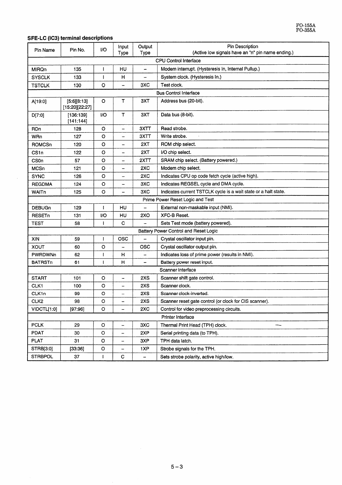
FO-155A
FO-355A
SFE-LC(IC3)terminaldescriptions
Input output Pin Description
Pin Name Pin No. 1/0 Type Type (Activelowsignalshavean “n” pinnameending.)
CPUControlInterface
MIRQn 135 IHU -Modeminterrupt.(HysteresisIn,InternalPullup.)
SYSCLK 133 IH-System clock. (Hysteresis in.)
TSTCLK 130 0-3XC Testclock.
BusControlInterface I
oT3XT
A[19:O] Address bus(20-bit).
Databus(8-bit). I
1/0 T3XT
Readstrobe. I
o-3XTT
o-3xl-r
RDn I128
WRn I127 Write strobe.
ROM chip select.
o-2XT
o-2XT
ROMCSn I120
1/0chipselect.
SRAMchip select. (Battery powered.)
Modem chip select.
CSln 122
CSOn 57 0I-I2XTT
o-2XC
o-2XC
MCSn I121
SYNC I126 Indicates
CPU op code fetch cycle (active high).
Indicates REGSEL cycle and DMA cycle.
o – 3XC
o-3XC
REGDMA I124
WAITn I125 IndicatescurrentTSTCLK cycle is await state or ahalt state.
PrimePowerResetLogicandTest I
DEBUGn 129 IHU -Externalnon-maskableinput(NMI).
RESETn 131 1/0 HU 2X0 XFC-BReset.
TEST 58 Icl- ISetsTestmode(batterypowered).
Battery Power Control and Reset Logic
XIN 59 IOsc -Crystaloscillatorinputpin.
XOUT 60 0 -Osc Crystaloscillatoroutputpin.
PWRDWNn 62 IH-indicates loss of prime power (results in NMI).
BATRSTn 61 IH-Battery power reset input.
ScannerInterface
START 101 0 -2XS Scannershiftgatecontrol.
CLK1 I100 101 -I2XS 1Scannerclock, I
CLK1n 99 0 -2XS Scannerclock-inverted.
CLK2 98 0 -2XS Scannerresetgatecontrol(or clock for CIS scanner).
VIDCTLII:0] [97:96] o-2XC Controlfor videopreprocessingcircuits.
PrinterInterface
PCLK I29 10] -I3XC IThermalPrintHead(TPH)clock. —I
PDAT 30 0 -2XP Serialprintingdata(toTPH).
PLAT 31 0 -3XP TPHdatalatch.
STRB[3:O] [33:36] o-IXP Strobesignalsfor the TPH.
STRBPOL 37 Ic-Sets strobe polarity, active high/low.
5-3
FO-155A
FO-355A
Pin Name Pin No. 1/0 Input output
Type Type Pin Description
OperatorPanelInterface
OPO[4:O] 1[42:44][46:47]1 OI-2XL Keyboard/LEDstrobe[4:0].
OPI[3:O] [49:52] IHU I-Keyboardreturn[3:OJ.(Puilup.Hysteresisin.)
LEDCTL 55 ol- 4XC lndicatesoutputsOPO[4:0]areforLEDs.
LCDCS 54 ol- Ixc LCDchipselect.
GeneralPurposel/O
GP1012/ 80
CS2n/SCLK
GPIO161 76
lRQ8
GP1017/ 75
lRQ5n
+
1/0 H
1/0 H
+
1/0 H
1/0 H
1/0 H
+
1/0 H
1/0 H
2XC
2XC
2XC
2XC
2XC
Ixc
1xc
Programmable:GPIO(8lines)orvideodatabus.
Programmable:GPIO(3lines)orvideo data control signals.
Programmable:GPIOline,1/0chipselectorSCLK(SART).
Programmable: GPIO line, 1/0 chip selector TXD(SART).
Programmable:GPIOline,1/0chipselector RXD(SART).
Programmable: GPIQ line or active high interrupt.
Programmable: GPIO lineor activelowinterrupt.
Miscellaneous
SM[3:O]I [103:106] .0 -1xc Programmable:scanmotorcontrolpinsor GPOpins.
GPO[7:4]
PM[3:O]/ [115:118] o-IXC Programmable:printmotorcontrolpinsor GPOpins.
GPO[3:O]
TONE 119 0-Ixc Toneoutputsignal.
Power,ReferenceVoltages,Ground
-Vref 66 I-VR -Negative
Reference Voltage for Video A/D.
+Vref 68 I+VR -Positive Reference Voltage for VideoA/D.
ADGA 69 VADG A/DAnalogGround.
ADVA 70 VADV A/DAnalogPower.
ADGD 72 VADG A/DDigitalGround.
ADVD 71 VADV WDDigitalPower.
VIN 67 IVA -Analog Video A/D input.
THADI 65 ITA -AnalogThermalA/Dinput.
VSS(8) 134,132,95, DigitalGround.
88, 53, 45, 28,
21
VDD(7) 140, 123, 102, DigitalPower.
81,48,41, 14
VBAT 63 Batte~ Power.
NoConnection
NC 1,2,3,4, 7,32, Noconnection.
38, 39, 40, 56,
64, 73, 74, 77,
82, 107,108,
109,110-114
5–4
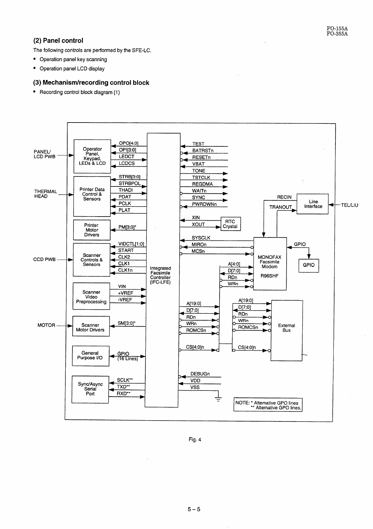
FO-155A
I?O-355A
(2) Panel control
ThefollowingcontrolsareperformedbytheSFE-LC.
●Operationpanelkeyscanning
●OperationpanelLCDdisplay
(3) Mechanism/recording control block
●Recordingcontrolblockdiagram(1)
PANEU
LCDPWB
THERMAl
HEAD
CCD PWB
MOTOR
I
i
Oggpeg~or
Keypa~,
LEDs&LCD H
OPO[4:0
OPI[3:O]
LEDCT
LCDCS
II
—STRB[3:O]
STRBPOL
PrinterData THADI
bControl&*
Sensors PDAT
4PCLK
PLAT
1I
IfI
II
Scanner
EControls&
Sensors
ACLK1nIntegrated
Facsimile
~“ IController
(IFC-LFE)
VIN
Scanner >
Video +VREF >
Preprocessing -VREF >
LII
IiI
III
IJI
k
ITSTCLK ~
REGDMA ~
v
4SYSCLK
MMIROn oGPIO
3MCSn MONOFAX
A[4:O] Facsimile
*Modem GPK)
D~:O] E
3RDn R96SHF
PWRn
H
A[19:O]
D~:O]
RDn
WRn
ROMCSn
A[19:O]
RDn
WRn
ROMCSn External
Bus
CS[4:O]n CS[4:O]n
I I i--
I1I
nDEBUGn
SCLK**
Sy;;;;~nc 4VDD
TXD*’ Vss
Port RXD** >—
.NOTE:*AlternativeGPOlines
** AlternativeGPOlines.
–TEL/LIU
Fig. 4
5-5
FO-155A
FO-355A
(4) Modem (R96DFXL) block
INTRODUCTION
The Rockwell R96DFXL MONOFAX modem is asynchronous 9600
bits per second(bps) half-duplexmodemwith error detectionand
DTMFreception.It has low power consumption and requires only a
single+5V DCpowersupply.The modem is housed in asingleVLSI
devicepackage.
The modemcanoperateoverthe publicswitchedtelephonenetwork
(PSTN) through line terminations provided by adata access arrange-
ment (DAA).
The R96SHFis designedfor usein Group3facsimilemachines.The
modemsatisfiesthe requirementsspecifiedin CCITTrecommenda-
tions V.29,V.27ter, V.21 Channel2 andT.4, and meetsthe binary
signalingrequirementsofT.30.
Themodemcanoperateat 9600,7200,4800,2400,or 300bps,and
alsoincludestheV.27ter shorttrainingsequenceoption.
The modemcan also performHDLCframingaccordingto T.30 at
9600,7200,4800,2400,or 300bps.
The modem features aprogrammable DTMF receiver and three pro-
grammabletone detectorswhichoperateconcurrentlywith the V.21
channel2receiver.
The voicemodeallows*hostcomputerto efficientlytransmitand
receiveaudiosignalsandmessages.
The modemis availablein either a100-pinplasticquad flat pack
(PQFP)or a64-pinquadin-linepackage(QUIP).
Generalpurposeinputioutput(GPIO)pinsare availablefor hostas-
signmentin the 100-pinPQFP.
The modem’ssmallsize,singlevoltagesupply,and low powercon-
sumptionallowthe designof compactsystemenclosuresfor use in
bothofficeandhomeenvironments.
MONOFAX is aregistered trademark of Rockwell International.
FEATURES
●
●
●
●
b
●
●
●
●
●
●
●
●
●
●
●
●
●
●
●
Group3facsimiletransmission/reception
–CCITTV.29,V.27ter,T.30,V.21Channel2,T.4
–HDLCFramingat allspeeds
V.27ter shorttrain
ConcurrentDTMF,FSK,andtonereception
Voicemodetransmission/reception
Half-duplex(2-wire)
Programmablemaximumtransmitlevel:
OdBmto-15 dBm
Programmabletransmitanalogattenuation:
OdBto 14dBin 2dBsteps
Receivedynamicrange:OdBmto -43 dBm
Programmabledualtonegeneration
Programmabletonedetection
Programmableturn-onandturn-offthresholds
Programmableinterfacememoryinterrupt
Diagnosticcapability
–Allows telephone line quality monitoring
Equalization
–Automatic adaptive equalizer
–Fixed digital compromise equalizer
DTE interface: two alternate ports
–Selectable microprocessor bus (6500 or 8085)
–CCITT V.24 (EIA-232-D compatible) interface
~L and CMOS compatible
Low power consumption: 275 mW(typical)
SinglePackage
-100-pinPQFP
–64-pinQUIP
Single+5VDCpowersupply
Software compatible with R96MFX, R96EFX, R96SHF, and
R96VFXmodems
5–6
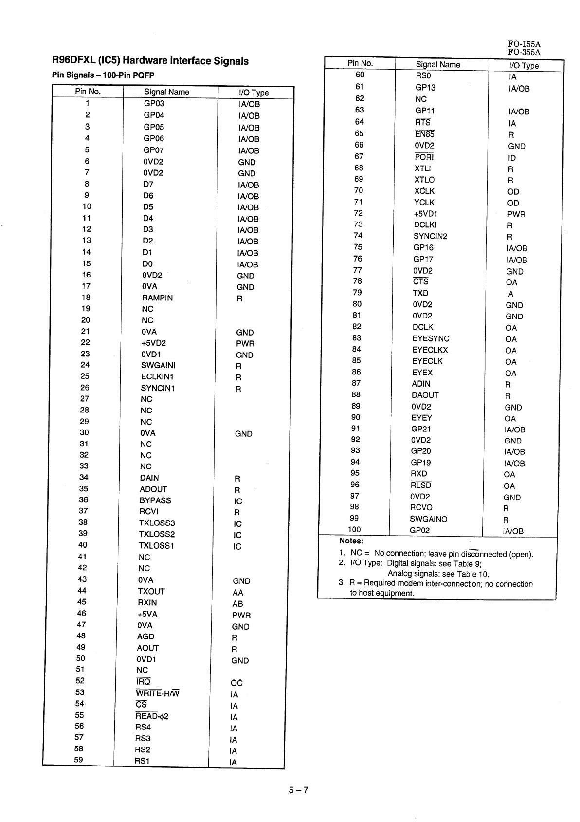
FO-155A
FO-355A
R96DFXL (IC5) Hardware Interface Signals
Pin Signals -100-Pin PQFP
Pin No. Signal Name 1/0Type
1GP03 IA/OB
2GP04 IAIOB
3GP05 IWOB
4GP06 IA/OB
5GP07 IA/OB
6OVD2 GND
7OVD2 GND
8D7 IA/OB
9D6 IA/OB
10 D5 IAIOB
11 D4 IA/OB
12 D3 IAfOB
13 D2 IA/OB
14 D1 IA/OB
15 DO IA/OB
16 OVD2 GND
17 OVA GND
18 RAMPIN R
19 NC
20 NC
21 OVA GND
22 +5VD2 PWR
23 OVD1 GND
24 SWGAINI R
25 ECLKIN1 R
26 SYNCIN1 R
27 NC
28 NC
29 NC
30 OVA GND
31 NC
32 NC
33 NC
34 DAIN R
35 ADOUT R
36 BYPASS Ic
37 RCVi R
38 TXLOSS3 Ic
39 TXLOSS2 Ic
40 TXLOSSI Ic
41 NC
42 NC
43 OVA GND
44 TXOUT AA
45 RXIN AB
46 +5VA PWR
47 OVA GND
48 AGD R
49 AOUT R
50 OVD1 GND
51 NC
52 mOc
53 WRITE-W– 1A
54 m1A
55 READ-$2 1A
56 RS4 IA
57 RS3 1A
58 RS2 1A
59 RSI 1A
PinNo.
60
61
62
63
64
65
66
67
68
69
70
71
72
73
74
75
76
77
78
79
80
81
82
83
84
85
86
87
88
89
90
91
92
93
94
95
96
97
98
99
100
SignalName
RSO
GP13
NC
GP1l
RTS
EN85
OVD2
PORI
XTLI
XTLO
XCLK
YCLK
+5VD1
DCLKI
SYNCIN2
GP16
GP17
OVD2
CTS
TXD
OVD2
OVD2
DCLK
EYESYNC
EYECLKX
EYECLK
EYEX
ADIN
DAOUT
OVD2
EYEY
GP21
OVD2
GP20
GP19
RXD
RLSD
OVD2
RCVO
SWGAINO
GP02
Notes:
1/0Type
1A
IAIOB
IA/OB
1A
R
GND
ID
R
R
OD
OD
PWR
R
R
IA/OB
IA/OB
GND
OA
1A
GND
GND
OA
OA
OA
OA
OA
R
R
GND
OA
IAIOB
GND
IAIOB
IA/OB
OA
OA
GND
R
R
INOB
1. NC =No connection; leave pin dis~onnected (open).
2. 1/0 Type: Digital signals: see Table 9;
Analog signals: see Table 10.
3. R=Required modem inter-connection; no connection
to host eauioment.
5–7
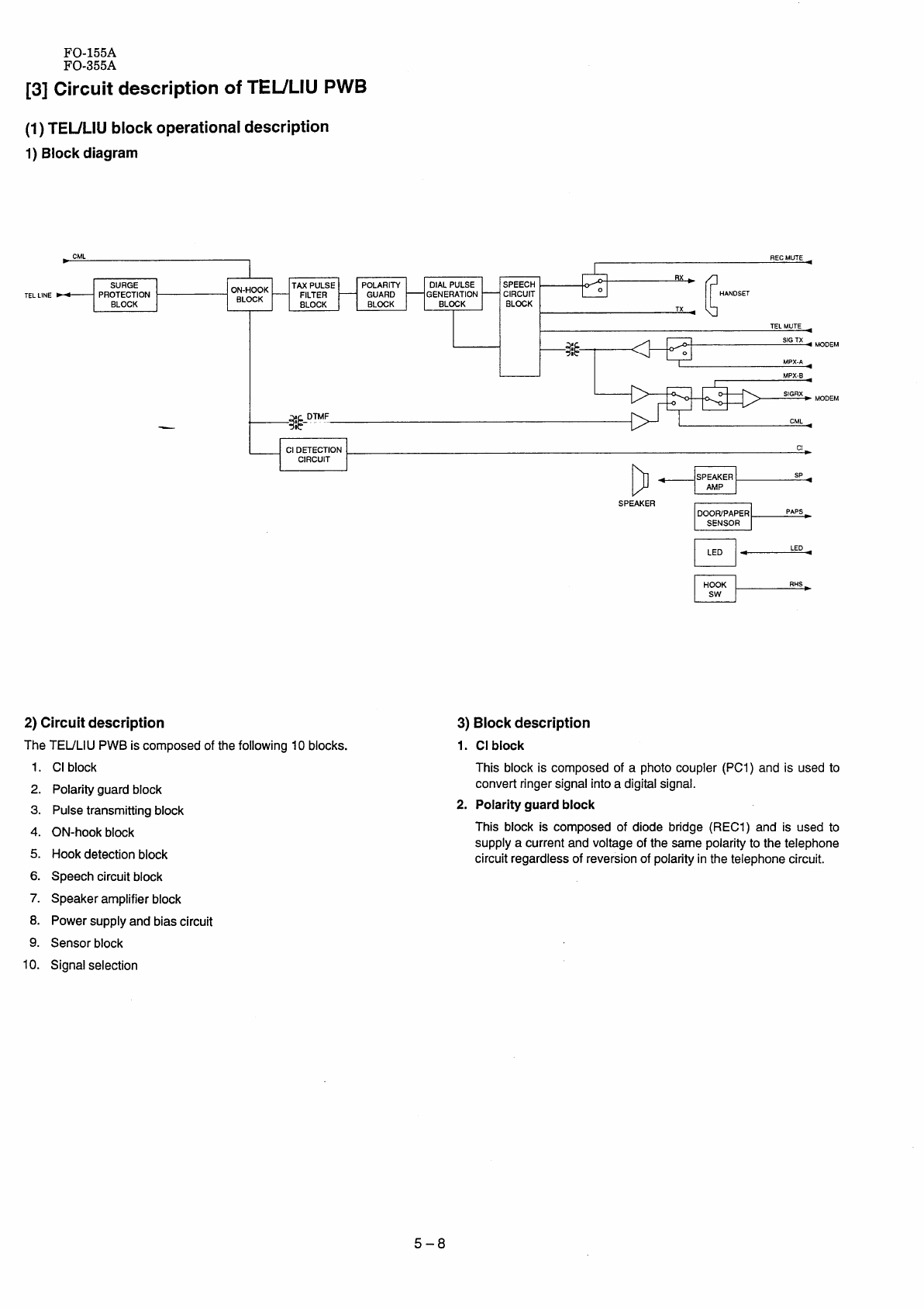
FO-155A
FO-355A
[3] Circuit description of TEULIU PWB
(1) TEVLIU block operational description
1)Blockdiagram
CML RECMUTE
r
,1
SURGE
TELLINE ON-HOOK—TA%PULSE POLARITY DIALPULSE SPEECHf
~PROTECTION FILTER GUARD — GENERATION
—CIRCUIT
BLOCK BLOCK
I“:[
HANDSET
BLOCK BLOCK BLOCK BLOCK TX
LTELMUTE
;i:
SIGTX4MODEM
MPX.B
Y#-DmF
ClDETECTION c1
CIRCUIT
LJ
D“ I
SPEAKER SP
AMP
2) Circuitdescription
TheTEULIUPWBis composedofthefollowing10blocks,
1. Cl block
2. Polarityguardblock
3. Pulse transmitting block
4. ON-hookblock
5. Hookdetectionblock
6. Speechcircuitblock
7. Speakeramplifierblock
8. Power supply and bias circuit
9. Sensorblock
10. Signalselection
SPEAKER DOOFVPAPER PAPS
SENSOR
1 1
II
3) Blockdescription
1. Cl block
This blockis composedof aphotocoupler(PC1)and is usedto
convertringersignalintoadigitalsignal.
2. Polarity guard block
This blockis composedof diode bridge (REC1) and is used to
supply acurrent and voltage of the same polarity to the telephone
circuit regardless of reversion of polarity in the telephone circuit.
5-8
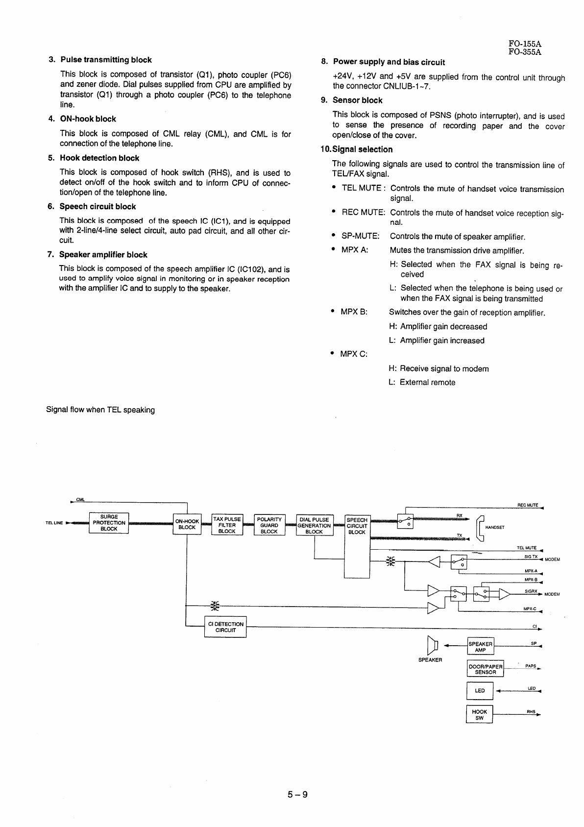
3. Pulse transmitting block
This block is composedof transistor(Ql), photocoupler(PC6)
andzener diode. Dial pulsessuppliedfrom CPUare amplifiedby
transistor(Ql) throughaphotocoupler(PC6)to the telephone
line.
4. ON-hook block
This block is composedof CML relay (CML), and CML is for
connectionof thetelephone
line.
5. Hook detection block
This block is composed of hookswitch (RHS), and is used to
detect on/off of the hook switch and to informCPU of connec-
tion/openof thetelephoneline.
6. Speech circuit block
This blockis composedof the speechIC (ICI), and is equipped
with 2-line/4-lineselectcircuit,autopad circuit,and all othercir-
cuit.
7. Speaker amplifier block
This blockis composedof the speechamplifierIC (IC102),andis
usedto amplifyvoicesignalin monitoringor in speakerreception
withtheamplifierICandto supplytothe speaker.
8.
9.
FO-155A
FO-355A
Power supply and bias circuit
+24V, +12V and +5V are suppliedfrom the controlunit through
theconnectorCNLIUB-1-7.
Sensor block
This block is composed of PSNS(photointerrupter),and is used
to sense the presence of recording paper and the cover
open/closeof thecover.
1O.Signal selection
The following signals are used to control the transmission line of
TEUFAX signal.
●TEL MUTE :Controls the mute of handset voice transmission
signal.
●RECMUTE: Controls the mute of handset voice reception sig-
nal.
●SP-MUTE: Controls the mute of speaker amplifier.
●MPX A: Mutes the transmission drive amplifier.
H: Selectedwhen the FAX signal is being re-
ceived
L: Selectedwhenthe telephoneis beingusedor
whenthe FAXsignalis beingtransmitted
.MPXB: Switchesoverthegainof receptionamplifier.
H:
L:
●MPX C:
H:
L:
Amplifier gain decreased
Amplifier gain increased
Receivesignalto modem
Externalremote
SignalflowwhenTEL speaking
CML
IRECMLITE
I
I
SURGE TAXPULSE Rx
TELLINE PROTECmON
m~ON-HOOK_POIARITY DIALPULSE SPEECH$,.,., ,.
BLOCK BLOCK FILTER GUARD -GENERATION-CIRCUIT o
BLOCK BLOCK
=[
~NDSET
BLOCK BLOCK ~
TELMUTE●
$k
SIGTX ●MODEM
3:
I I
P“
SPEAKER SP
AMP
SPEAKER OOOR/PAPER PAPs&
SENSOR
r1
ILED 1+ Lso
rI
[HOOK RHS
Sw
5-9
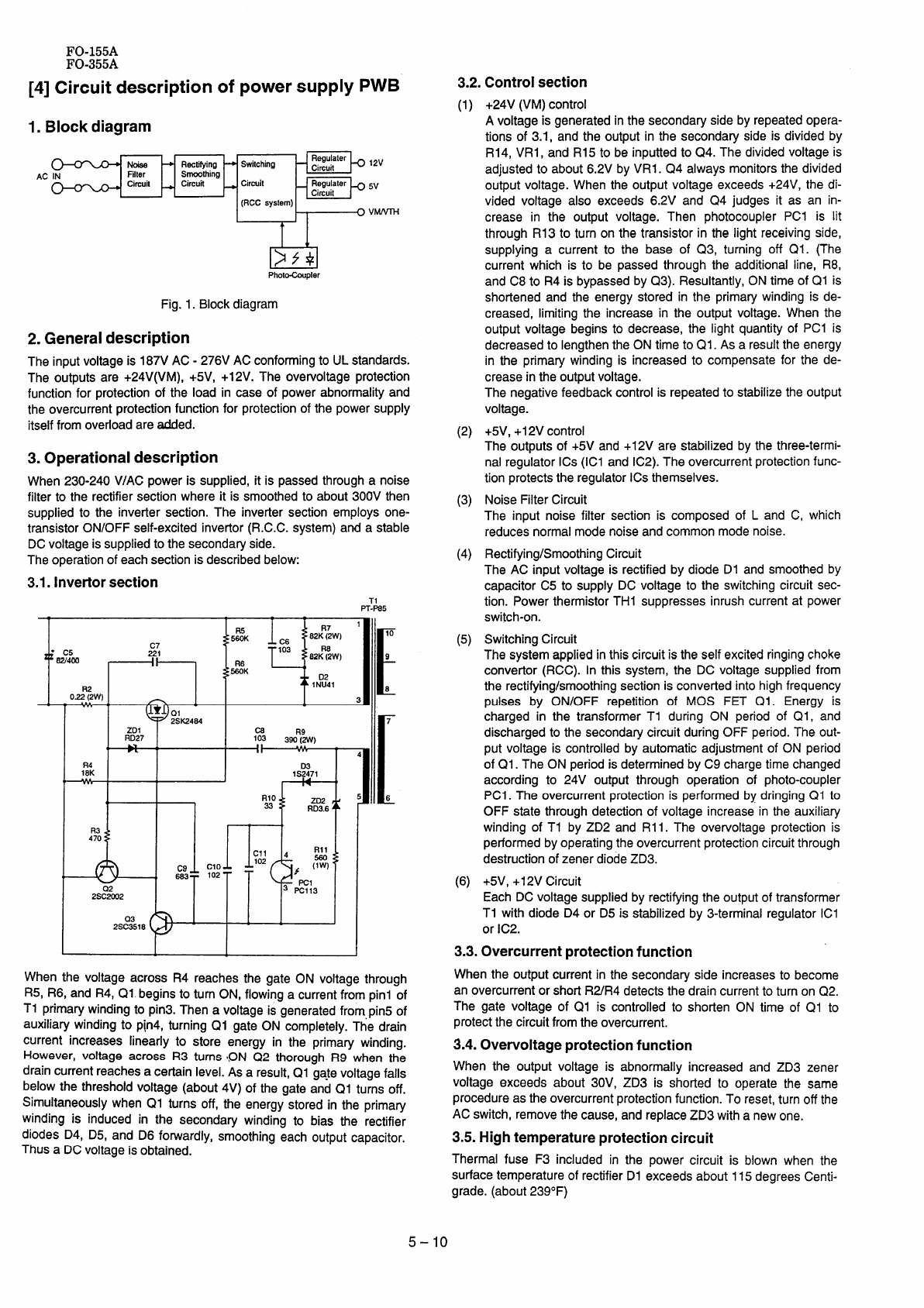
FO-155A
FO-355A
[4] Circuit description of power supply PWB
1. Block diagram
Noiea +Rectifying~Switching Regulater
Circuk *12V
AC IN Filter Smoothing
Cimuit dCircuit -Circuit —Regulater*5V
Circuit
(RCC avstem)
I
. . .
II () vMrvni
t
&l
$+
Phot*pler
Fig. 1. Block diagram
2.General description
Theinputvoltageis 187VAC-276VACconformingto ULstandards.
The outputsare+24V(VM),+5V,+12V.The overvoltageprotection
functionfor protectionof the load in caseof powerabnormalityand
the overcurrentprotectionfunctionfor protectionof the powersupply
itselffromoverloadareadded.
3.Operational description
When230-240V/ACpoweris supplied,it is passedthroughanoise
filterto the rectifiersectionwhereit is smoothedto about300Vthen
suppliedto the invertersection.The invertersectionemploysone-
transistorON/OFFself-excitedinvertor(R.C.C.system)anda stable
DCvoltageissuppliedto thesecondaryside.
Theoperationofeachsectionis describedbelow:
3.1.Invertorsection
ZDI
RD27
R4
18K
,,
R3
470
2S::W2
2S%18 ‘
+
aR9
103
~
1S2471
+
—
7
I[
6
Whenthe voltageacrossR4 reachesthe gate ON voltagethrough
R5,R6,and R4,QI beginsto turnON,flowingacurrentfr;m pinl ;f
T1 primarywindingto pin3.Thenavoltageis generatedfrompin5 of
auxiliarywindingto p~n4,turningQ1 gateON completely.The drain
current increaseslinearlyto store energyin the primarywinding.
However, voltage across R3 turns ION Q2 thorough R9 when the
drain current reaches acertain level. As aresult, Q1 ga~evoltage falls
below the threshold voltage (about 4V) of the gate and Q1 turns off.
Simultaneously when QI turns off, the energystoredin the primary
winding is inducedin the secondarywindingto bias the rectifier
diodesD4, D5, and D6 forwardly,smoothingeachoutputcapacitor.
ThusaDCvoltageisobtained.
3.2.
(1)
(2)
(3)
(4)
(5)
Controlsection
+24V (VM) control
Avoltageis generatedin thesecondarysideby repeatedopera-
tions of 3.1, and the outputin the secondary sideis dividedby
R14,VR1,and R15to be inputtedto Q4.Thedividedvoltageis
adjustedto about6.2VbyVR1.Q4 alwaysmonitorsthe divided
outputvoltage.Whenthe outputvoltageexceeds+24V,the di-
vided voltage also exceeds6.2V and Q4 judges it as an in-
crease in the output voltage. Then photocouplerPC1 is lit
throughR13to turn on the transistorin the light receivingside,
supplyingacurrent to the base of Q3, turning off Q1. (The
currentwhich is to be passedthroughthe additionalline, R8,
andC8to R4is bypassedby Q3). Resultantly,ONtimeof Q1 is
shortenedand the energystoredin the primarywindingis de-
creased,limitingthe increasein the outputvoltage.Whenthe
outputvoltagebeginsto decrease,the light quantityof PCI is
decreasedto lengthenthe ONtimeto Q1.As aresulttheenergy
in the primarywindingis increasedto compensatefor the de-
creaseinthe outputvoltage.
Thenegativefeedbackcontrolis repeatedto stabilizetheoutput
voltage.
+5V,+12Vcontrol
Theoutputsof +5Vand +12Vare stabilizedby the three-termi-
nalregulatorICS(IC1andIC2).Theovercurrentprotectionfunc-
tionprotectsthe regulatorICSthemselves.
NoiseFilterCircuit
The input noisefilter sectionis composedof L and C, which
reducesnormalmodenoiseandcommonmodenoise.
Rectifying/SmoothingCircuit
TheAC inputvoltageis rectifiedby diodeD1 and smoothed by
capacitor C5 to supply DC voltage to the switching circuit sec-
tion. Power thermistor TH1 suppresses inrush current at power
switch-on.
SwitchingCircuit
(6)
Thesystemappliedinthiscircuitis the self excited ringingchoke
convertor(RCC).In this system,the DC voltagesuppliedfrom
the rectifying/smoothingsectionis convertedintohighfrequency
pulses by ON/OFF repetition of MOS FET QI. Energy is
chargedin the transformerTI during ON periodof Q1, and
dischargedto the secondarycircuitduringOFFperiod.Theout-
put voltageis controlledby automaticadjustmentof ON period
of QI. TheON periodis determinedbyC9chargetimechanged
accordingto 24V output through operationof photo-coupler
PC1.Theovercurrentprotectionis performedbydringingQ1 to
OFFstatethroughdetectionof voltageincreasein the auxiliaty
windingof T1 by ZD2 and R11.The overvoltageprotectionis
performedbyoperatingtheovercurrentprotectioncircuitthrough
destructionofzenerdiodeZD3.
+5V,+12VCircuit
EachDCvoltagesuppliedby rectifyingtheoutputof transformer
T1 with diodeD4or D5is stabilizedby 3-terminalregulatorICI
or IC2.
3.3.Overcurrentprotectionfunction
Whenthe outputcurrentin the secondaryside increasesto become
anovercurrentor shortR2/R4detectsthe draincurrentto turnon Q2.
The gate voltageof Q1 is controlledto shortenON time of QI to
protectthecircuitfromtheovercurrent.
3.4.Overvoltageprotectionfunction
When the output voltage is abnormallyincreasedand ZD3 zener
voltageexceedsabout 30V, ZD3 is shortedto operatethe same
procedureastheovercurrentprotectionfunction.To reset,turnoffthe
ACswitch,removethecause,andreplaceZD3withanewone.
3.5.Hightemperatureprotectioncircuit
Thermalfuse F3 includedin the power circuit is blown when the
surfacetemperature of rectifier D1 exceeds about 115 degreesCenti-
grade.(about239°F)
5-10
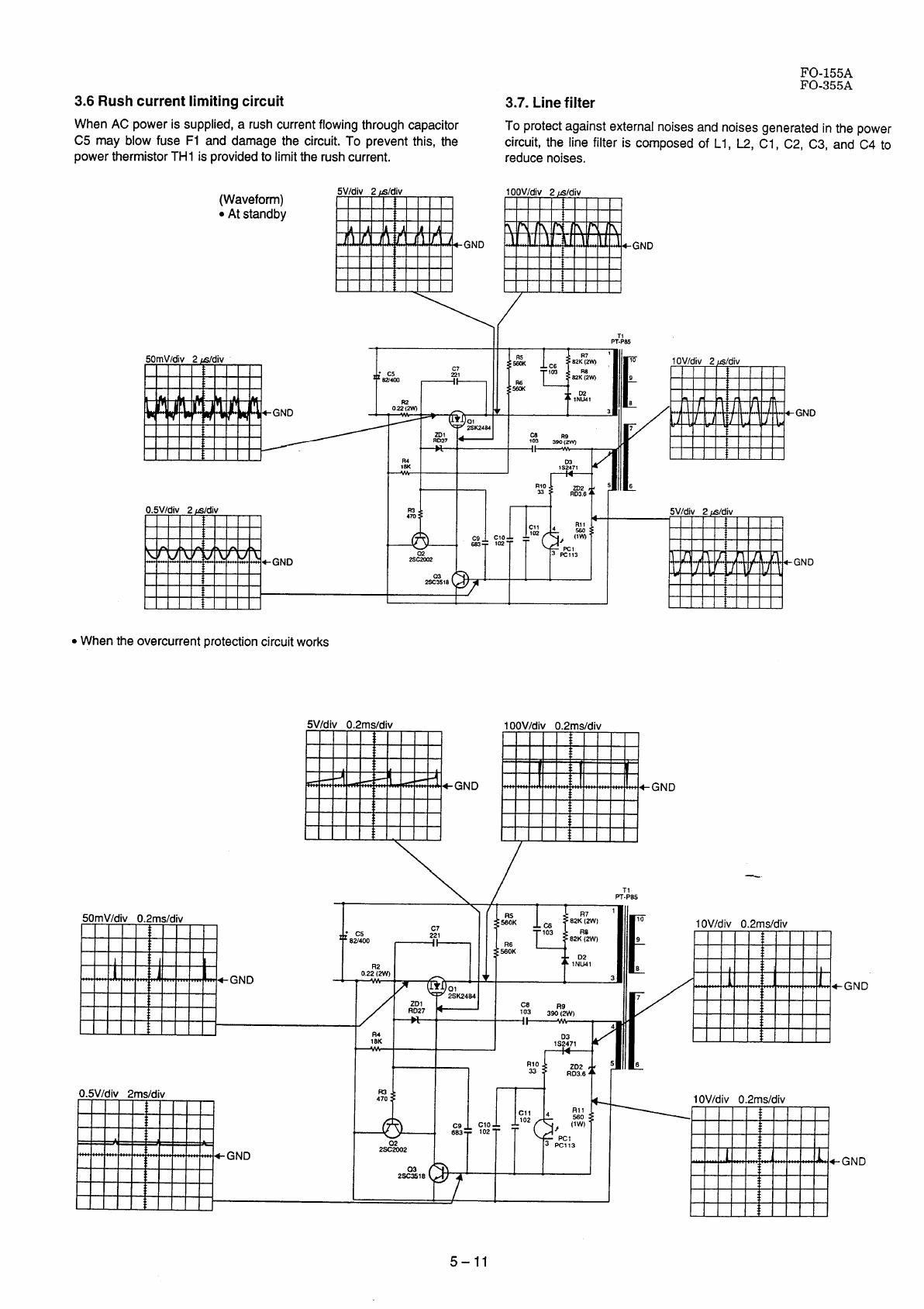
3.6Rushcurrentlimitingcircuit
When AC power is supplied, arush current flowingthroughcapacitor
C5 may blow fuse F1 and damage the circuit. To prevent this, the
powerthermistorTH1 is provided to limit the rush current.
FO-155A
FO-355A
3.7.Linefilter
To protect against external noises and noises generated in the power
circuit,the line filter is cmposed of LI, L2, Cl, C2, C3, and C4 to
reducenoises.
(Waveform)
.At standby
GND GND
+!
\
.When the overcurrent protection circuit works
GND
4%
1m
5Vldiv 2@ldiv
RII
C1l 4~
.. 11r1+r,r1
GND
!+1I [ 1
I(I11!
111
5V/div 0.2ms/div
“GND
IOOVldiv 0.2ms/div
GND
5-11
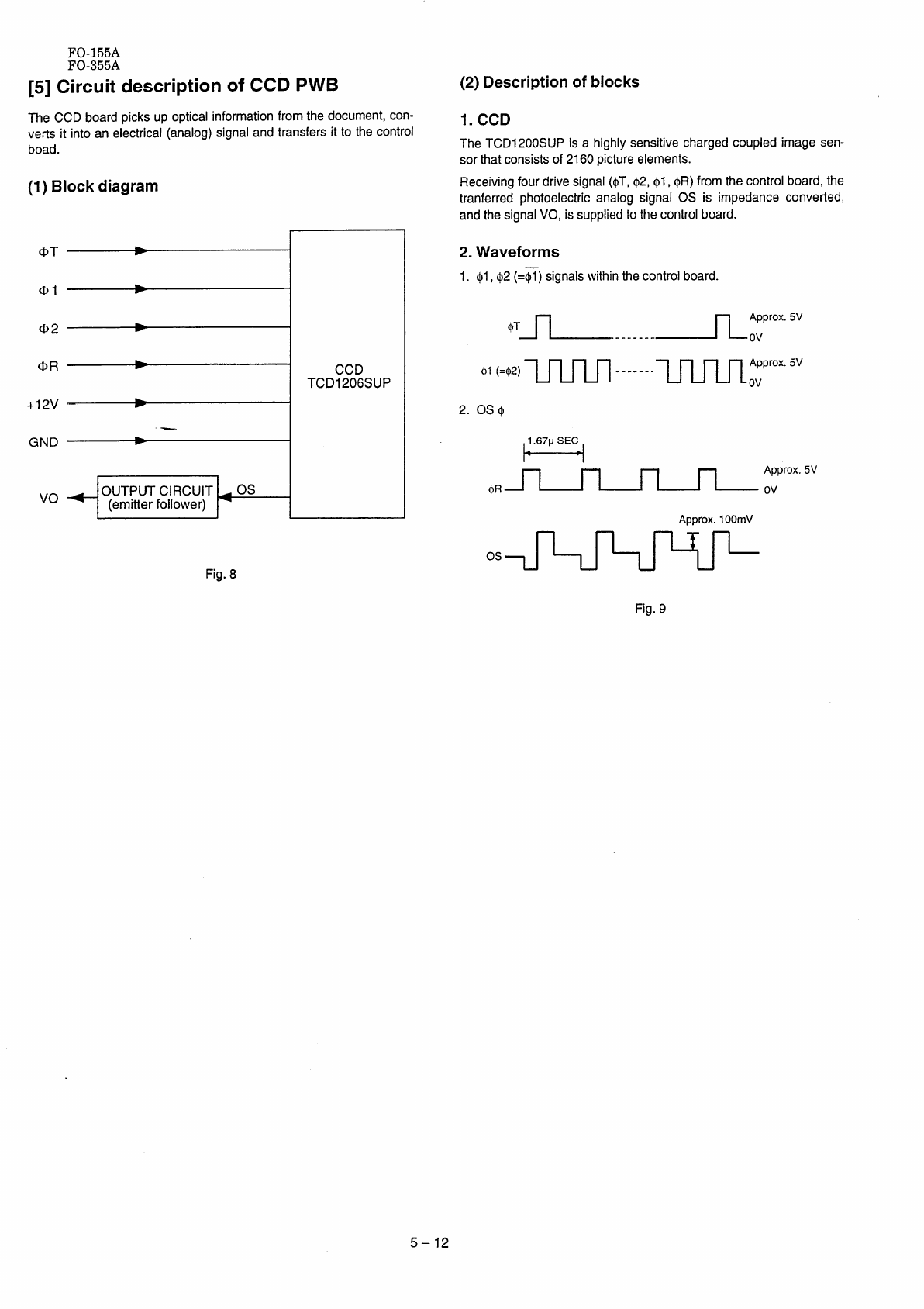
FO-155A
FO-355A
[5] Circuit description of CCD PWB
The CCD board picks up opticalinformationfromthe document,con-
verts it intoan electrical(analog)signalandtransfersit to thecontrol
bead.
(1) Block diagram
Vo +OUTPUTCIRCUIT
(emitterfollower) H
1 J 1
Fig.8
(2) Description of blocks
1. CCD
The TCD1200SUP is ahighly sensitive charged coupled image sen-
sor that consists of 2160 picture elements.
Receivingfourdrivesignal(@T,@2,@l,oR)fromthecontrolboard,the
transferredphotoelectricanalogsignal OS is impedanceconverted,
andthesignalVO,is suppliedto thecontrolboard.
2. Waveforms
—
1. $1,$2 (=$1)signalswithinthecontrolboard.
$T~ ...... J:;prOx”’v
““=’’’uuu”uuln;;prox”;vprox
Approx.IOOmV
Approx.5V
0“
Fig.9
5 – 12
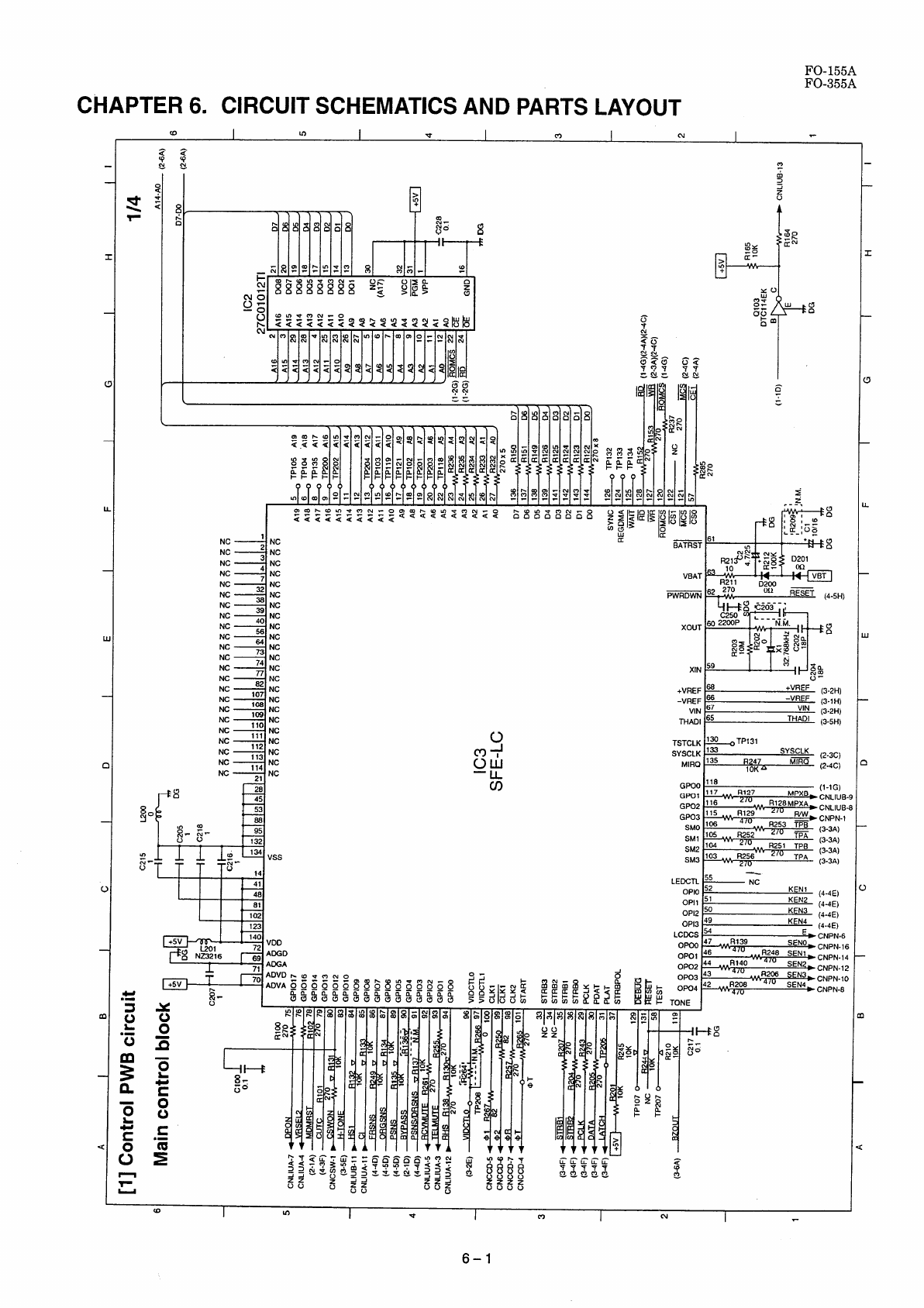
FO-155A
FO-355A
CHAPTER6. CIRCUITSCHEMATICSAND PARTSLAYOUT
(
u
u
c
—
u
(
m
3
n
n
NC 3;
NC
NC ~NC
Nc NC
Nc :NC
t
Nc ‘Nc
Nc :. NC
Nc NC
NC :NC
NC ~NC
NC ~NC
NC 73NC
NC ,4NC
NC ~NC
Nc
NC
NC 1:;::
NC 106
NC
NC ;:; ::
NC ;;; NC
NC
NC 113 ‘c
NC 1;: ;:
28
45
,.
I41
48
81
102
123
‘;; VDD
69 ADGD
rcADGA
s
.-
S
+VREF
E
w‘VREF (3-2H)
-VREF w-vREF (3.IH)
VIN 67 ‘IN (3-2H)
THADI=THADI ~~5H)
TSTCLKIW T~~
SY;:;:: “j~ (2-3C)
10: (2-4C)
E
GPD01’8
GPD1
117 R127 ~pXB (1-lG)
GPD2 ’16 CNLIUB-
GP03 ‘5 R129 “2*MP; CNLIUB-
SMO‘m —CNPN-1
SM1 ‘m R252 ’253 ;% (3-3A)
SM2 lW (3-3A)
SM3 103 R2S6 ’25’ ;~~ (3-3A)
(3-3A)
(4-4E)
(4-4E)
(4-4E)
(4-4E)
CNPN.6
CNPN-16
CNPN-14
CNPN.12
CNPN-10
CNPN-8
-----
ULLLLLL
ZJZA3
-----
6-1
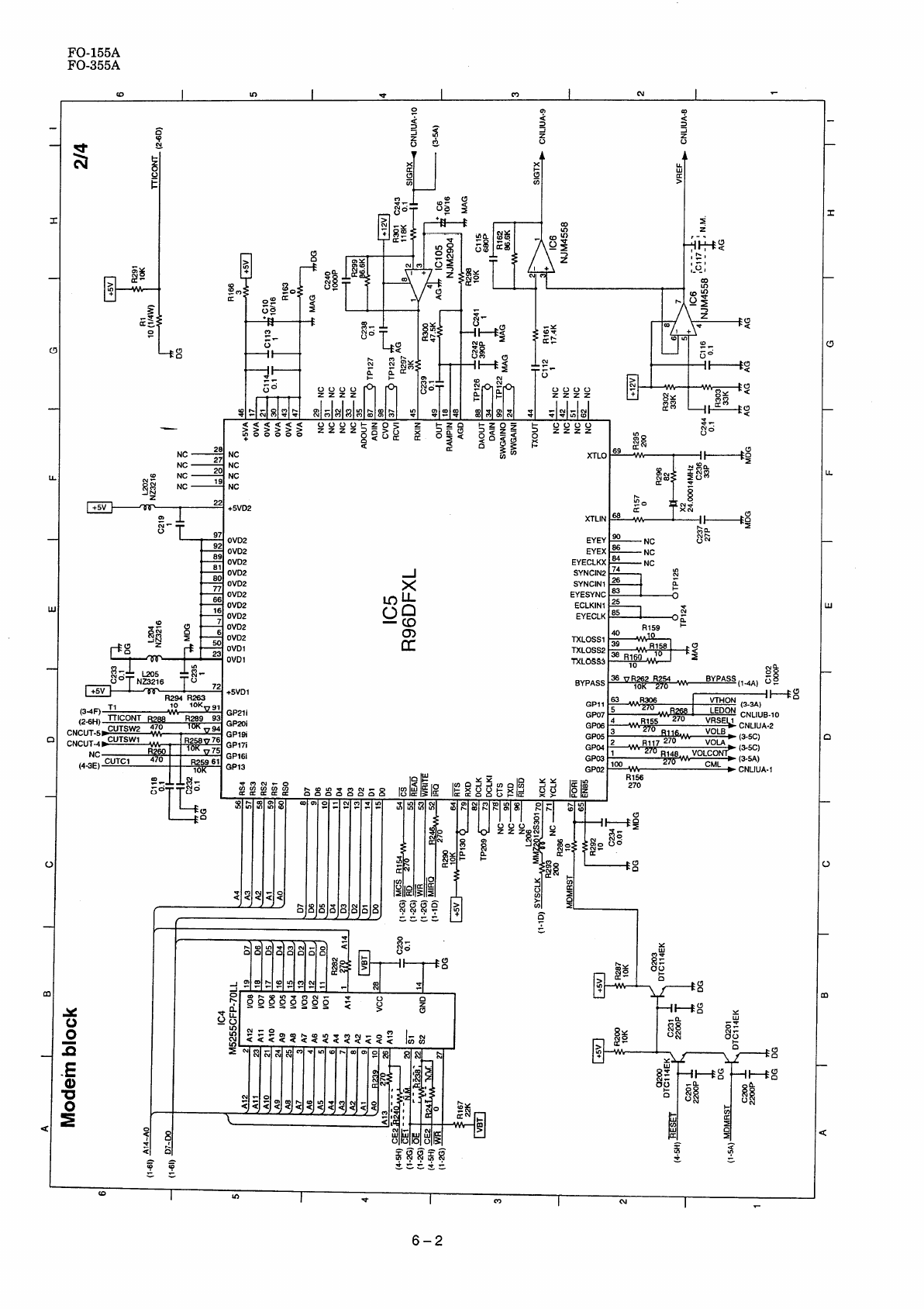
FO-155A
FO-355A
amIwImIN
v197
92 OVD2
R2s4 R2s3
(3-4F)},CONT .;;R~;V;; GP21i
CN;2U;;; CUTSW2 ~?~ 10K ~GPmi
CNCUT-4bcuTsw’ MR25SV76 GP19i
R260 [75 GP17i
NC CUTC1 470 GP16i
(4-3E) yo;g6’ GP13
I
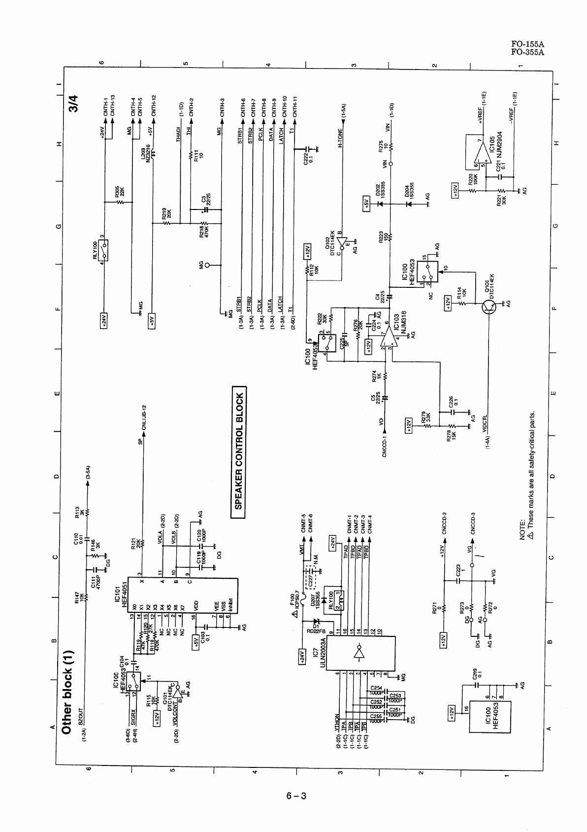
FO-155A
FO-355A
-E
I-.
0
u
,.
I
(
<
6–3
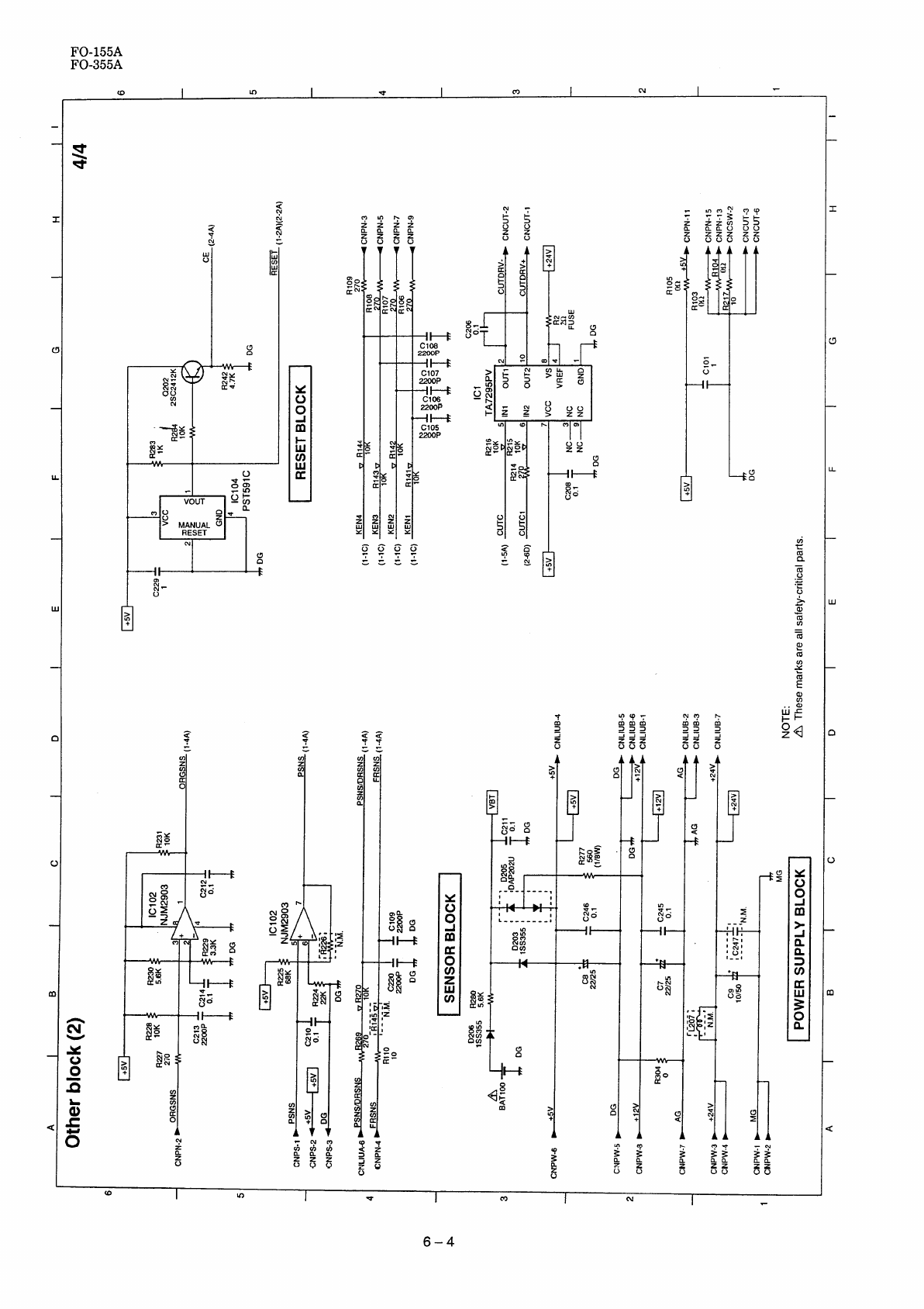
1
.
FO-155A
FO-355A
aIIn 91mINI
-E:
1
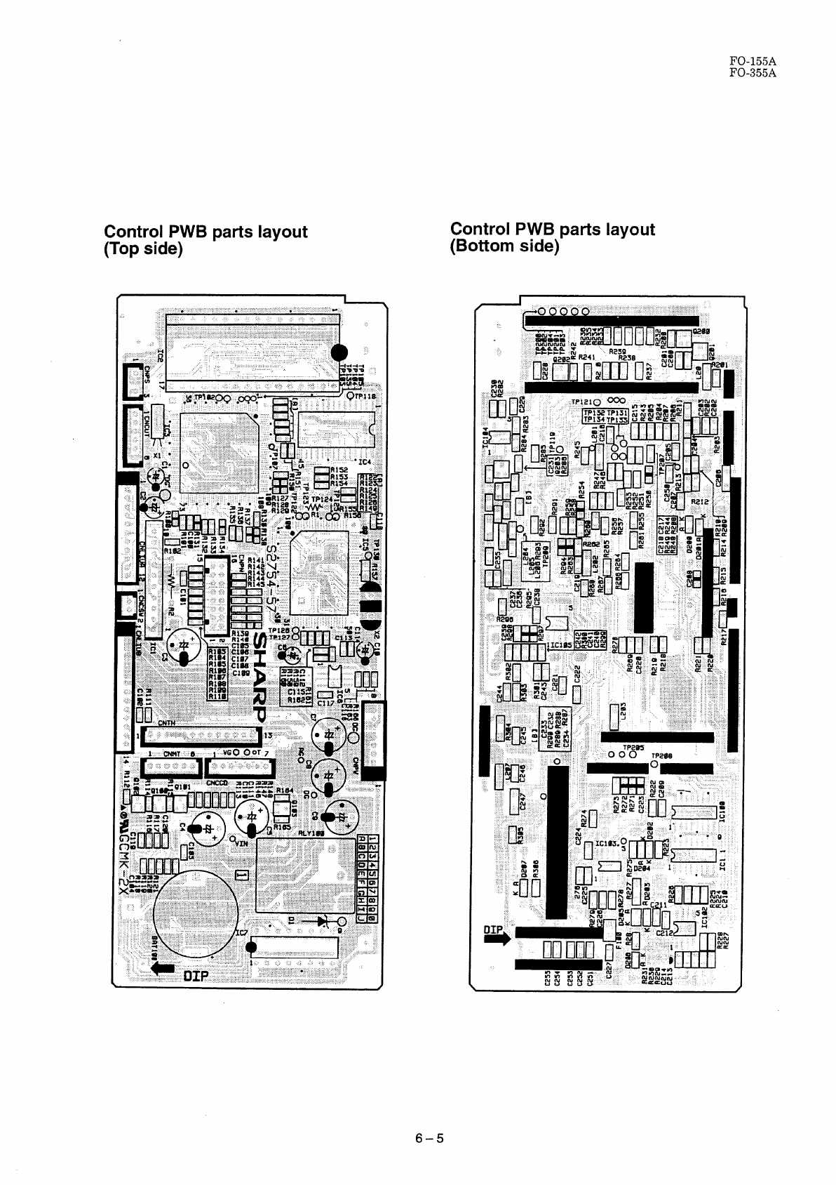
FO-155A
FO-355A
Control PWB parts layout
(Top side) Control PWB parts layout
(Bottom side)
6–5
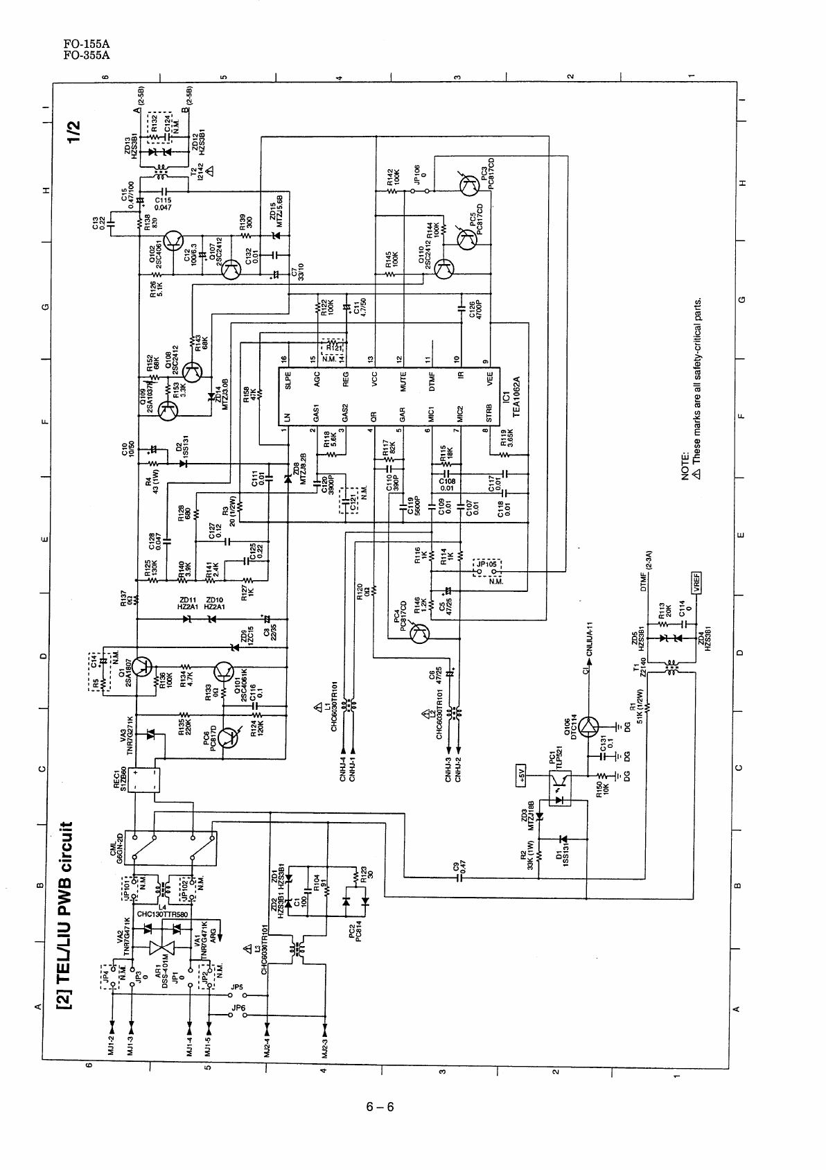
FO-155A
FO-355A
fD Im*mIN
I
N
.
—
L-
u
L
u
K
>
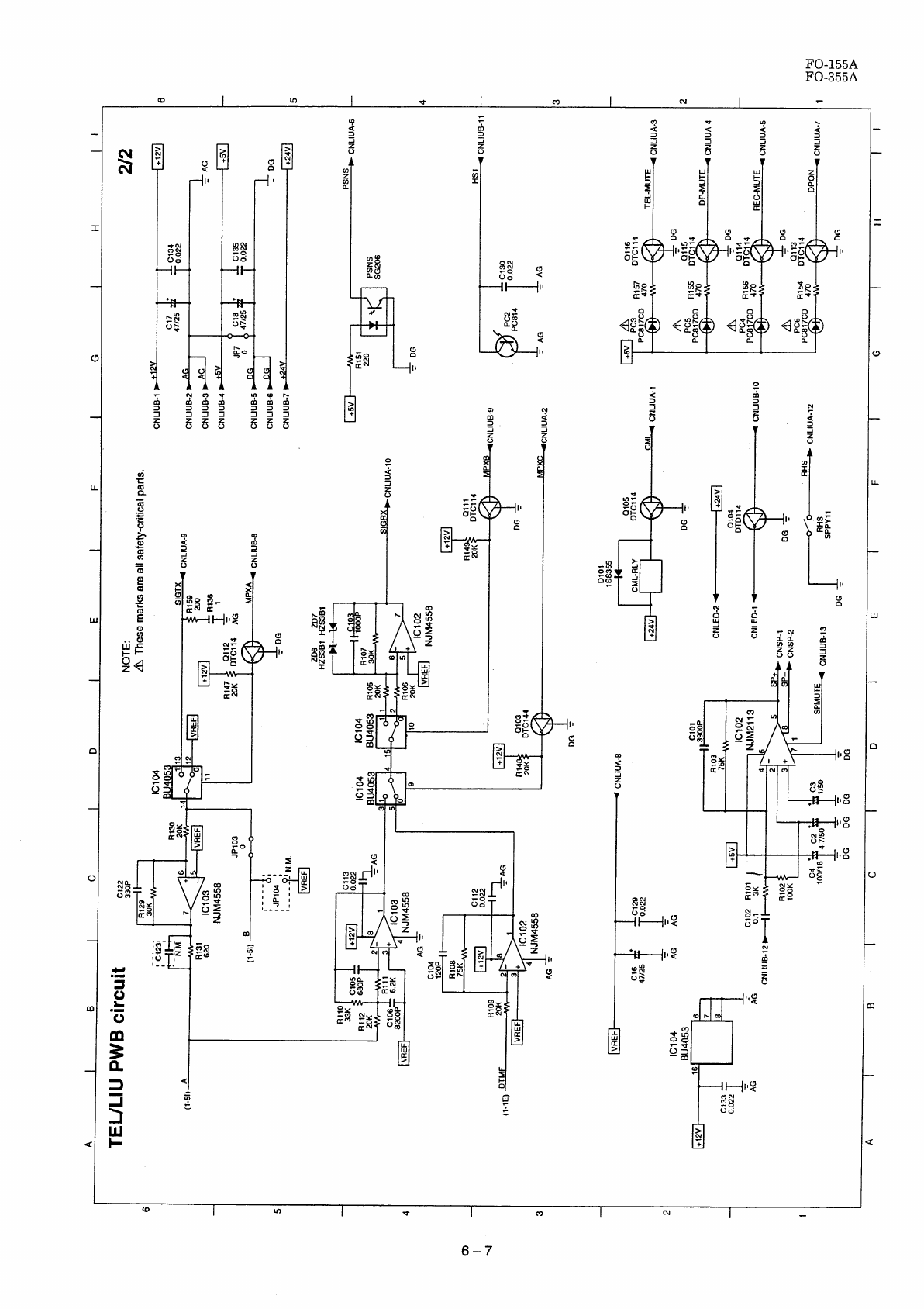
FO-155A
FO-355A
wIIn I.+ I . I mI
c
I
I I
‘Iml I~I . ir.
I
II
—11 fll I1
l--=’ IAi, II
.
I“> I*IFY ImI
6-7
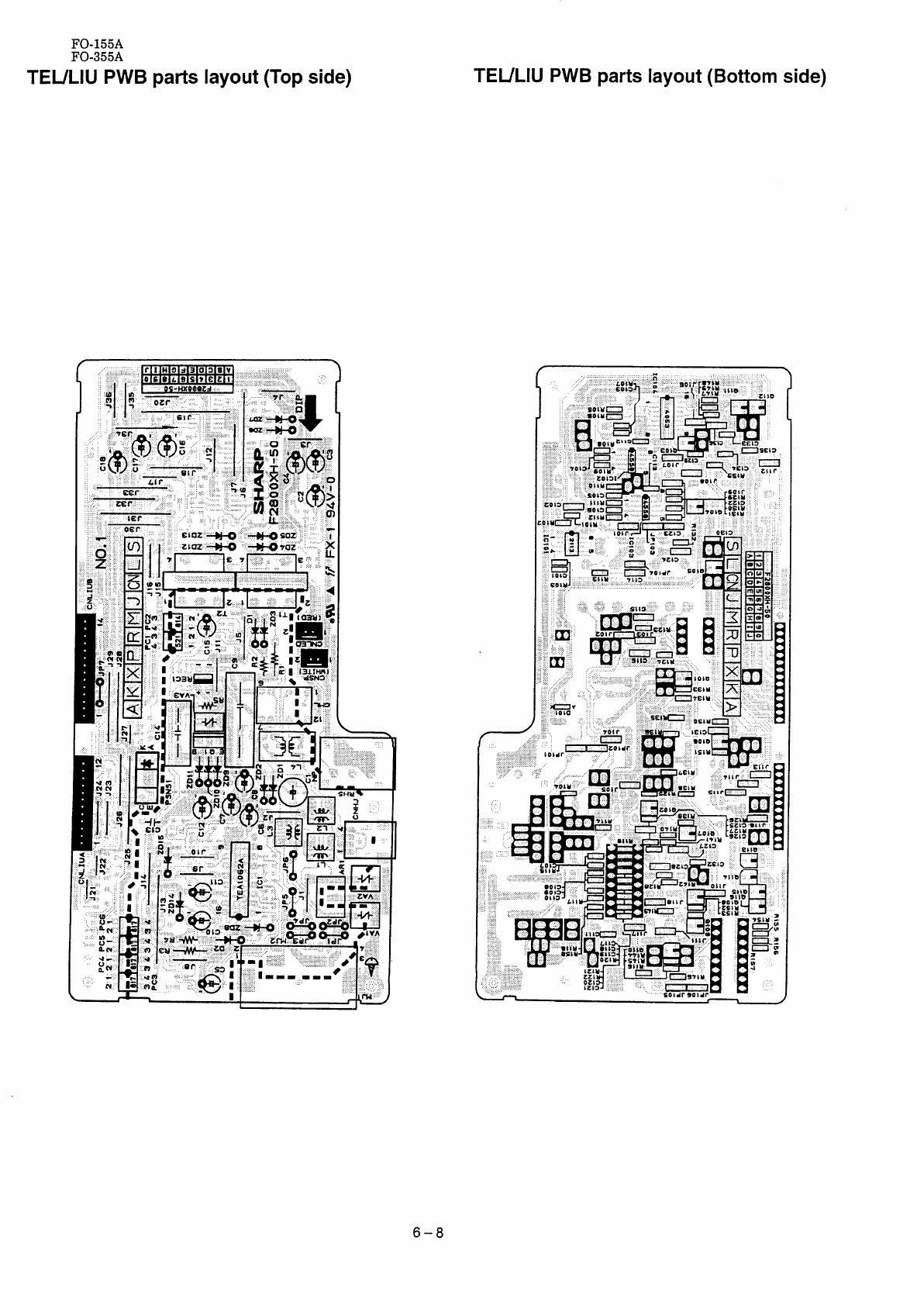
FO-155A
FO-355A
TEL/LIU PWB parts layout (Top side) TEULIU PWB parts layout (Bottom side)
1
6–8
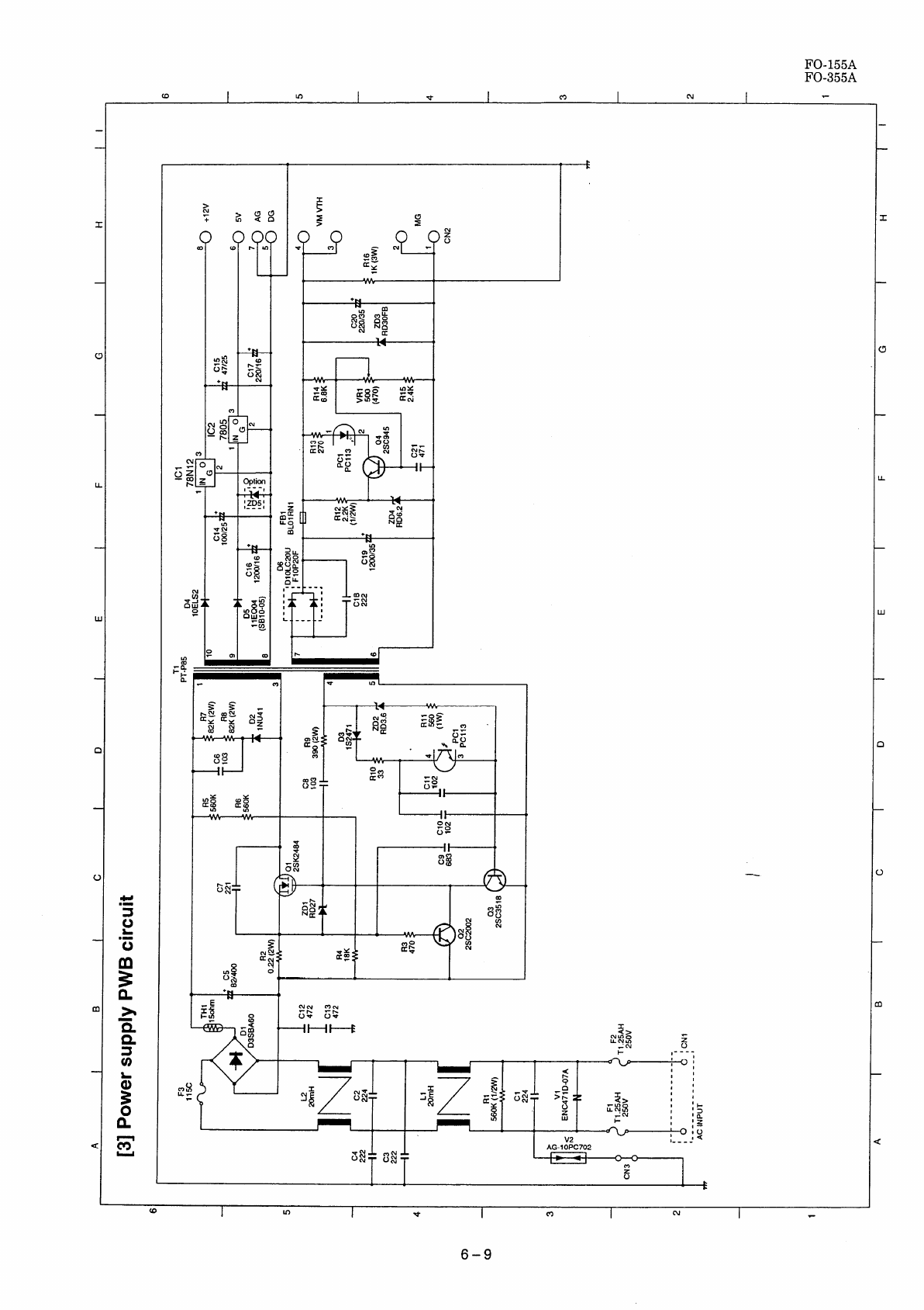
FO-155A
FO-355A
(9 ImI*ImNI
II
A
rIn
1- ‘1
L
,
I
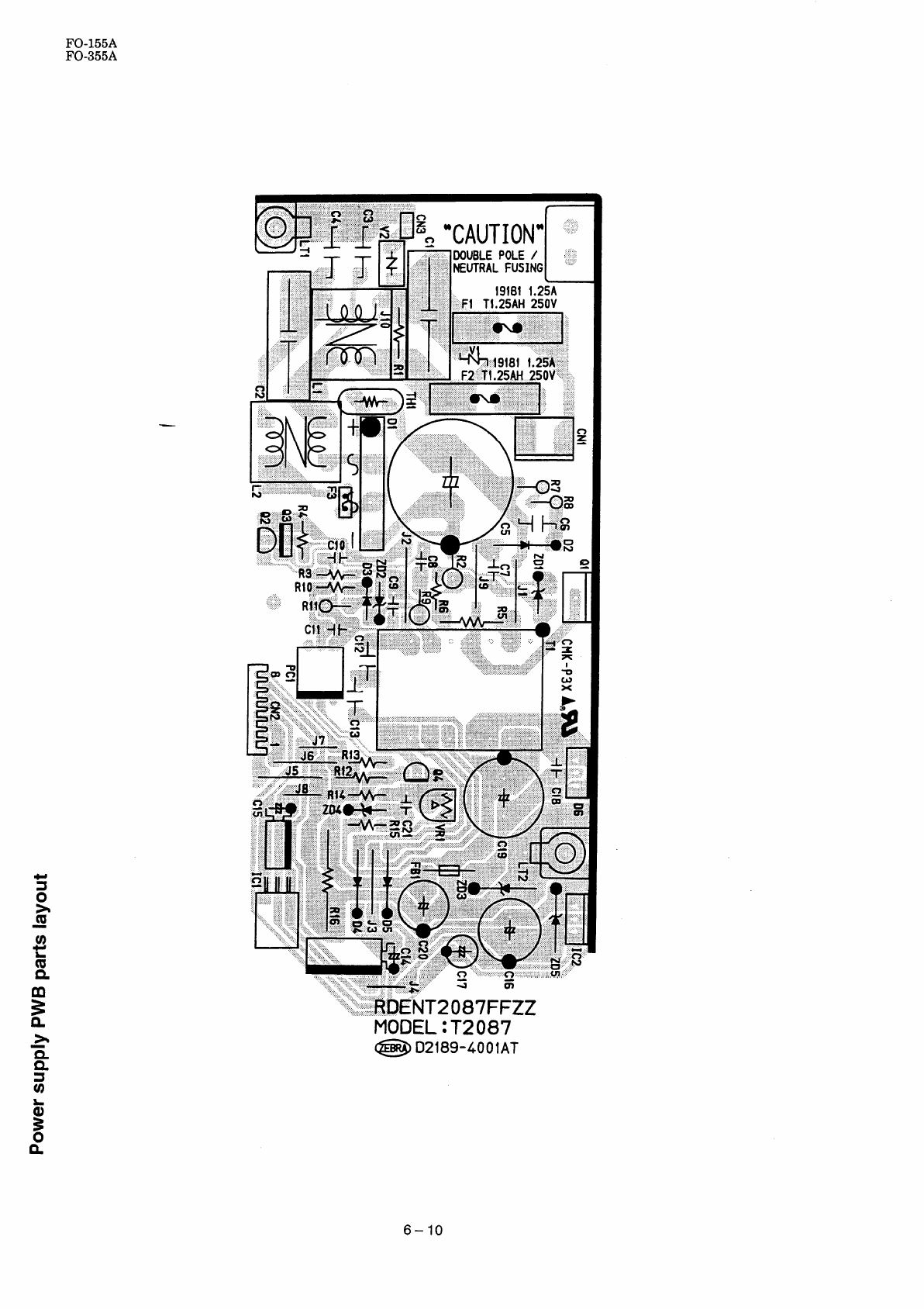
FO-155A
FO-355A
—
m
3
n~~•“RDENT2087FFZZ
MODEL:T2087
~D2189-4001AT
6-10
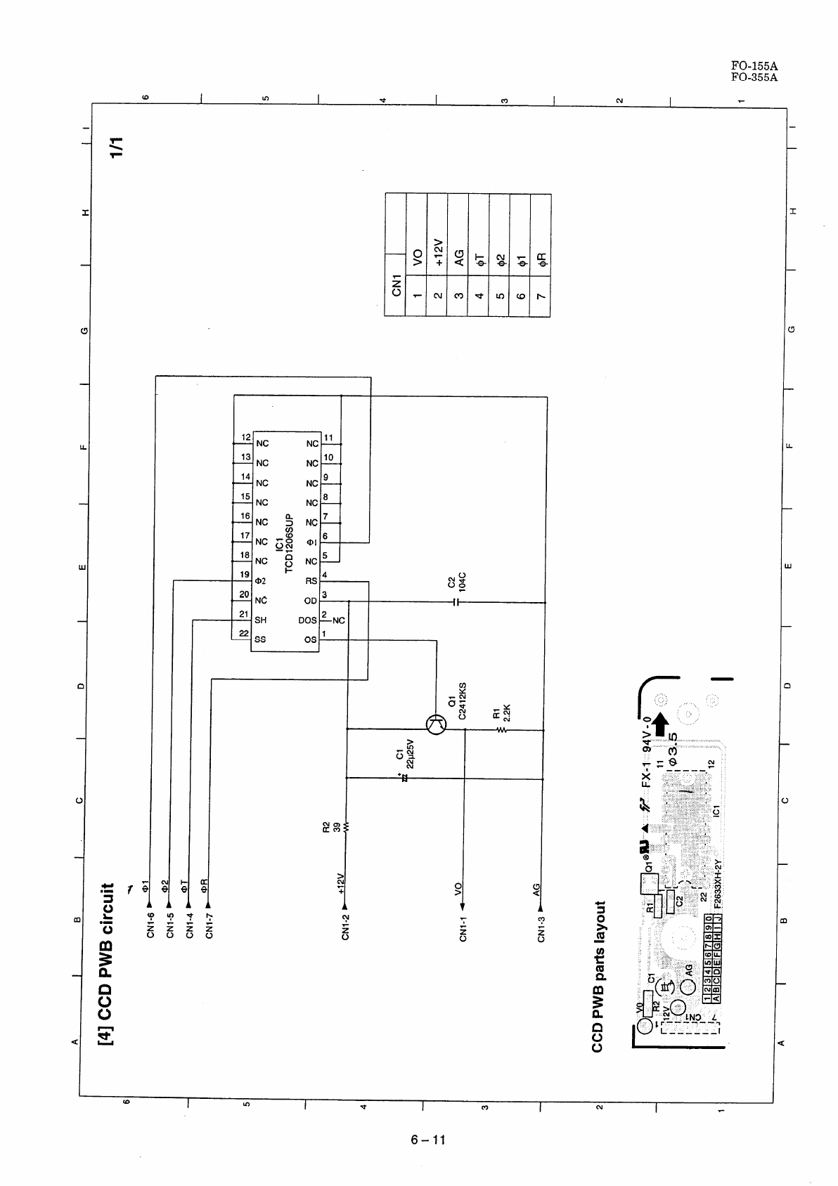
FO-155A
FO-355A
OD
E
3
2
DOS NC
0s ‘
‘,
r—
6-11
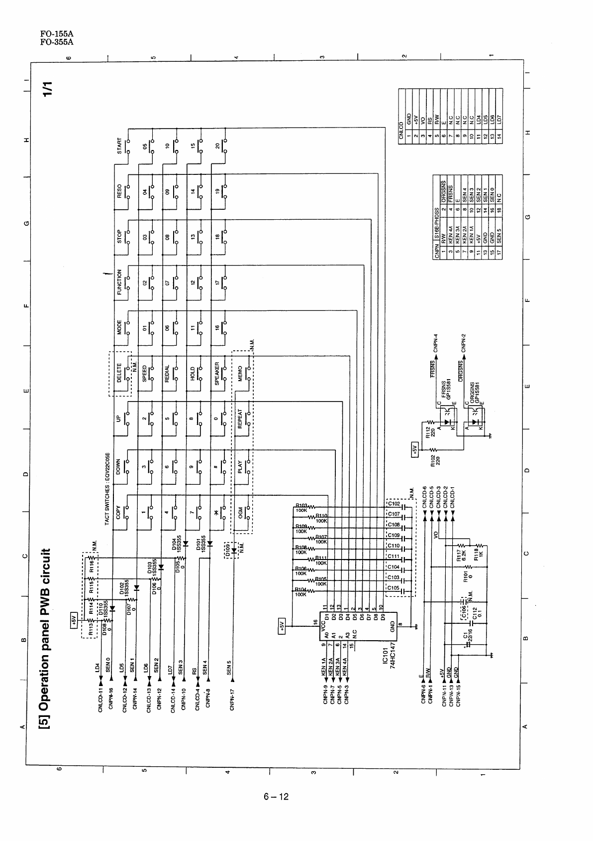
FO-155A
FO-355A
(D IIn *ICY Im
(
L
L
c
c
[
Q
y
z
v
.. ----
x
Ob
NI?
J
I
—
u
;
I
,T
n
6
zI
-Y
T
0I
-Y
T
n
I
Y
T
.I
J
,
1
,
1
I
I
,
L-----
.
:
t
m
—
<
m
K
6 –12
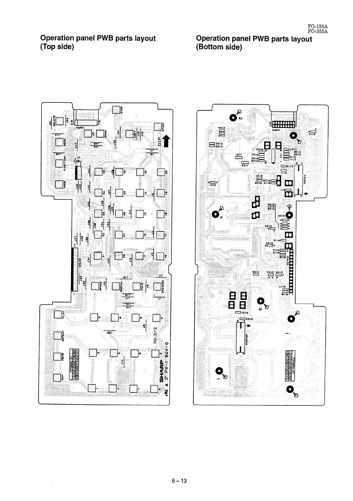
Operation panel PWB parts layout
(Top side)
.
FO-155A
FO-355A
Operation panel PWB parts layout
(Bottom side)
J
6–13
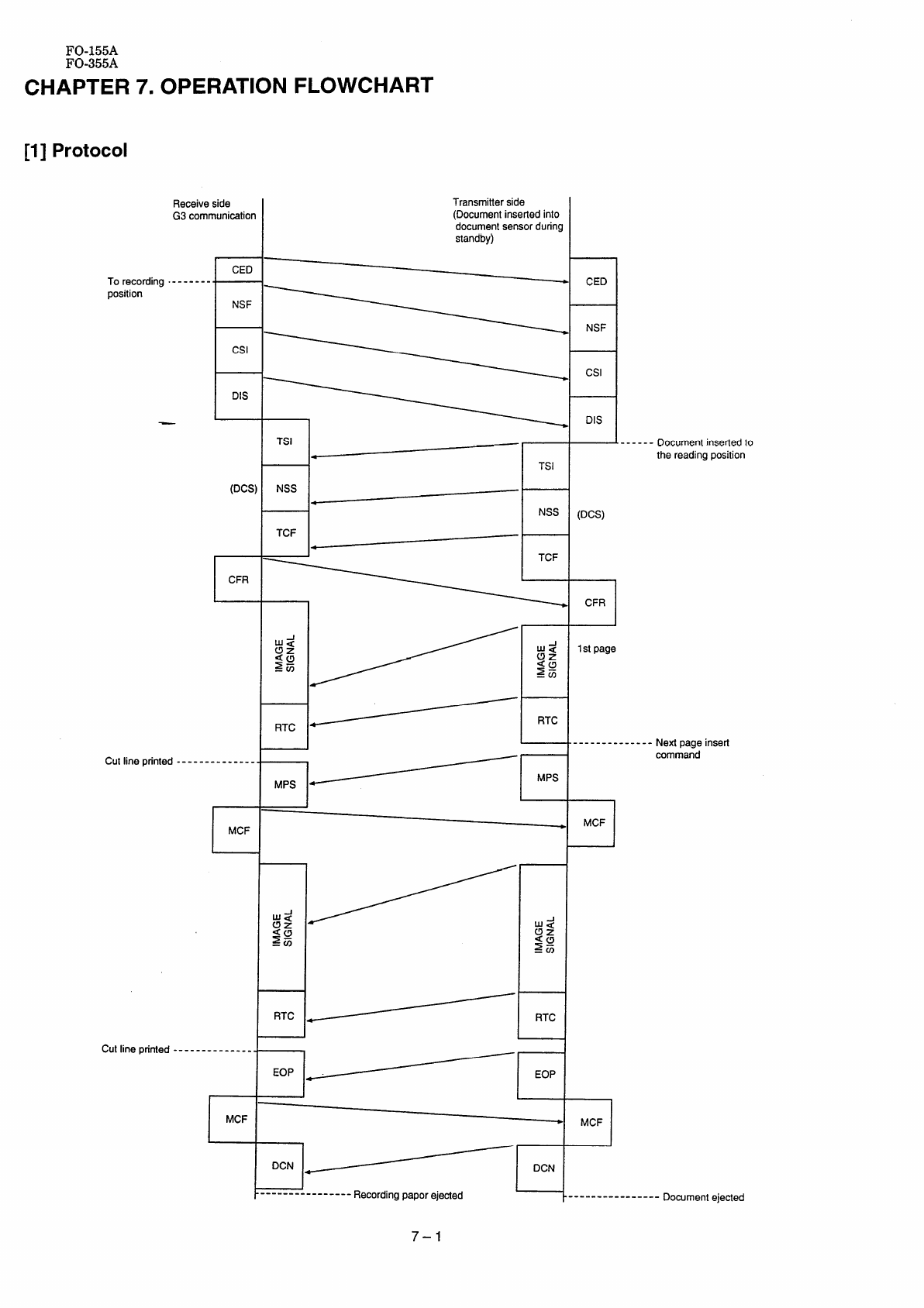
FO-155A
FO-355A
CHAPTER7. OPERATIONFLOWCHART
[1] Protocol
Receiveside
G3communication
F
CED
Torecording--------
position NSF
Csl
DIS
(DCS
r
CFR
Cutlineprinted--------------
1-
MCF
Cutlineprinted---------------
r
MCF
Transmitter
side
(Document inserted into
document sensordurin
standby)
I
i
‘s’~
F
‘S1
‘ss ~NSS
RTC
II
1t
RTc ~FITC
I
EOP
~E
EOP
3
‘c” ~DcN
-------------- Recordingpaporejected c
CED
NSF
Csl
DIS
------
(DCS)
CFR
Documentinsededto
thereadingposition
------------- Nextpageinseri
command
MCF
-------.-----_--Documentejected
7-1
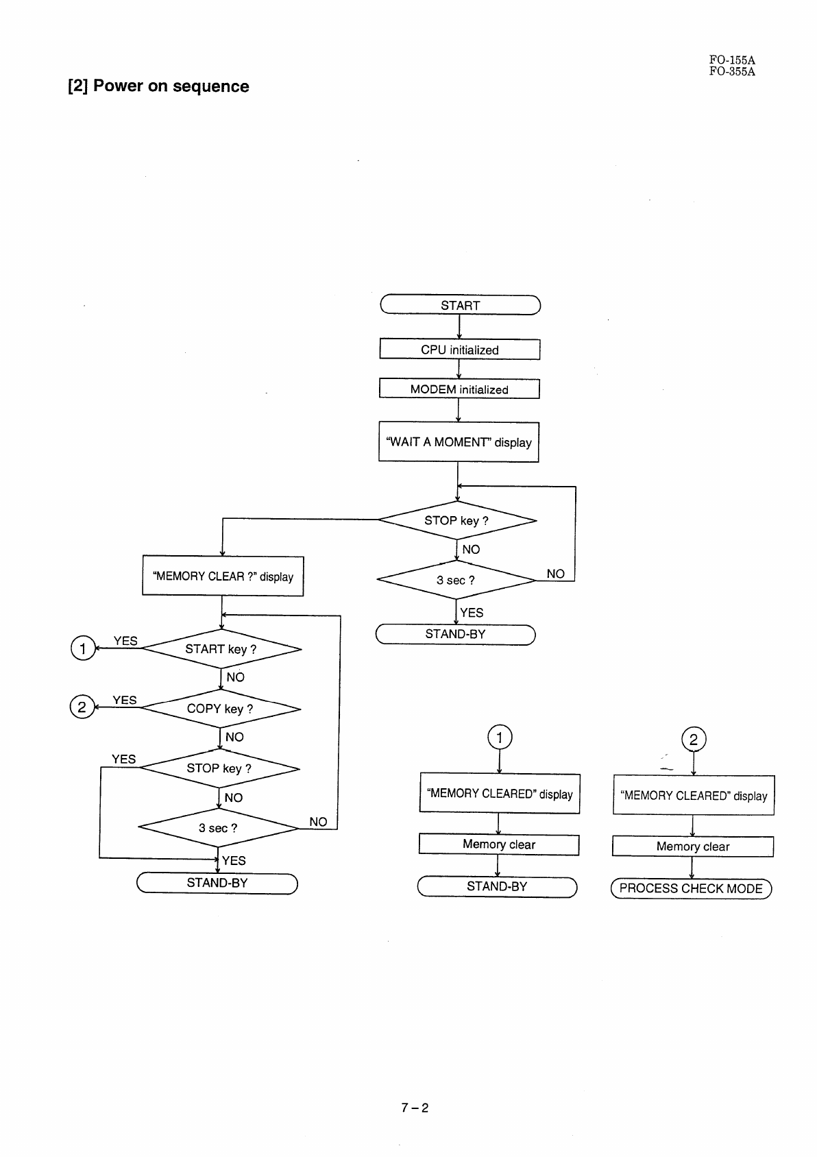
FO-155A
FO-355A
[2] Power on sequence
START
ICPUinitialized I
MODEM initialized
‘WAIT AMOMENT”display
I“MEMORY CLEAR ?“ display I
1’
YES
]NO
YES
INO
YES
NO
4
STAND-BY
NO
I
“MEMORY CLEARED” display
&
[Memoryclear
I
STAND-BY
o
2
I
—
I1(
“MEMORYCLEARED”display
Memory clear
I
fPROCESSCHECK MODE>
7–2
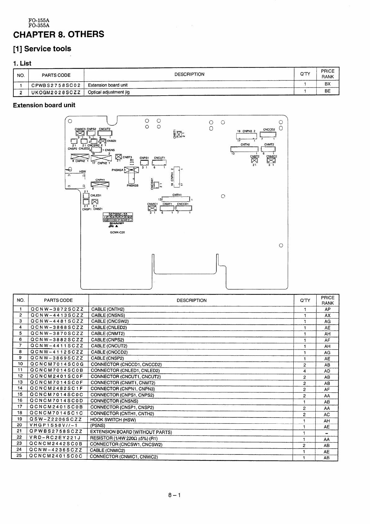
FO-155A
FO-355A
CHAPTER8. OTHERS
[1]Service tools
1. List
INO. PARTSCODE DESCRIPTION Q’TY PRICE
RANK
Extension board unit
“o u
CNMIC3 CNPS2 CNCUT2
qqp
~~2~lmciBn
21 CNCSW2 2 1
cNED24~l CNSNS
00
*r-,
vu
CNPSI CNCLJT1
mm
4P31 6 1
HSW PNSNSA 0
n
21
~cNLEDl
pp
;NSP1 CNBZ1
CNTH1
13r-- -i 1
CNMIC1 CNM71 CNCCD1
~Q=
00
0
0
GCMK-C2X
L-
0
C~H2 CNMT2
~D
13 CNB;2
IF ‘c@2
o
NO. IPARTSCODE IDESCRIPTION IQ’TY IPRICE
RANK I
1QC NW-3872 SCZZ
........
CABLE(CNTH2) 1AP
2QC NW–44 13 SCZZ CABLE(CNSNS) 1AX
3QC N W-448 1SCZZ CABLE(CNCSW2) 1AG
4QC NW-3868S CZZ CABLE(CNLED2) 1AE
5QC N W-3870S CZZ CABLE(CNMT2) 1AH
6QC NW–3882 SCZZ CABLE(CNPS2) 1AF
7QC NW–44 11 SCZZ CABLE(CNCUT2) 1AH
8QC NW-4 112 SCZZ CABLE(CNCCD2) 1AG
9QC NW–3869 SCZZ CABLE(CNSP2) 1AE
10 QC NCM701 4SCOG CONNECTOR(CNCCD1,CNCCD2) 2AB
11 QCNC M70 14SCOB CONNECTOR(CNLED1,CNLED2) 4AD
12 QC NC M2401 SCO FCONNECTOR(CNCUT1,CNCUT2) 2AB
13 QCNC M70 14SC0 FCONNECTOR(CNMT1,CNMT2) 2AB
14 QCNCM2482SC 1FCONNECTOR(CNPN1,CNPN3) 2AF
15 QCNCM701 4SCOC CONNECTOR(CNPS1,CNPS2) 2AA
16 QCNCM70 14SCOD CONNECTOR(CNSNS) 1AB
17 QCNCM2401 SCOB CONNECTOR(CNSP1,CNSP2) 2AA
18 QCNCM70 14SC 1cCONNECTOR(CNTH1,CNTH2) 2AC
19 QSW-Z2 206 SCZZ HOOKSWITCH(HSW) 1AH
20 VH GP1S58 V1l -1(PSNS) 1AE
21 QPWBS2758SCZZ EXTENSIQNBC)ARtI{WITHOUTPARTS) 1
22 VR D- RC2EY22 1JRESISTOR(1/4W220S2*5%) (Rl)
23 1AA
QC N C M2442 SCOB CONNECTOR(CNCSW1,CNCSW2)
24 2AB
QC N W-4236 SCZZ CABLE(CNMIC2)
25 1AE
QCNCM2401 SCOC CONNECTOR(CNMIC1,CNMIC2) 1AB
8–1
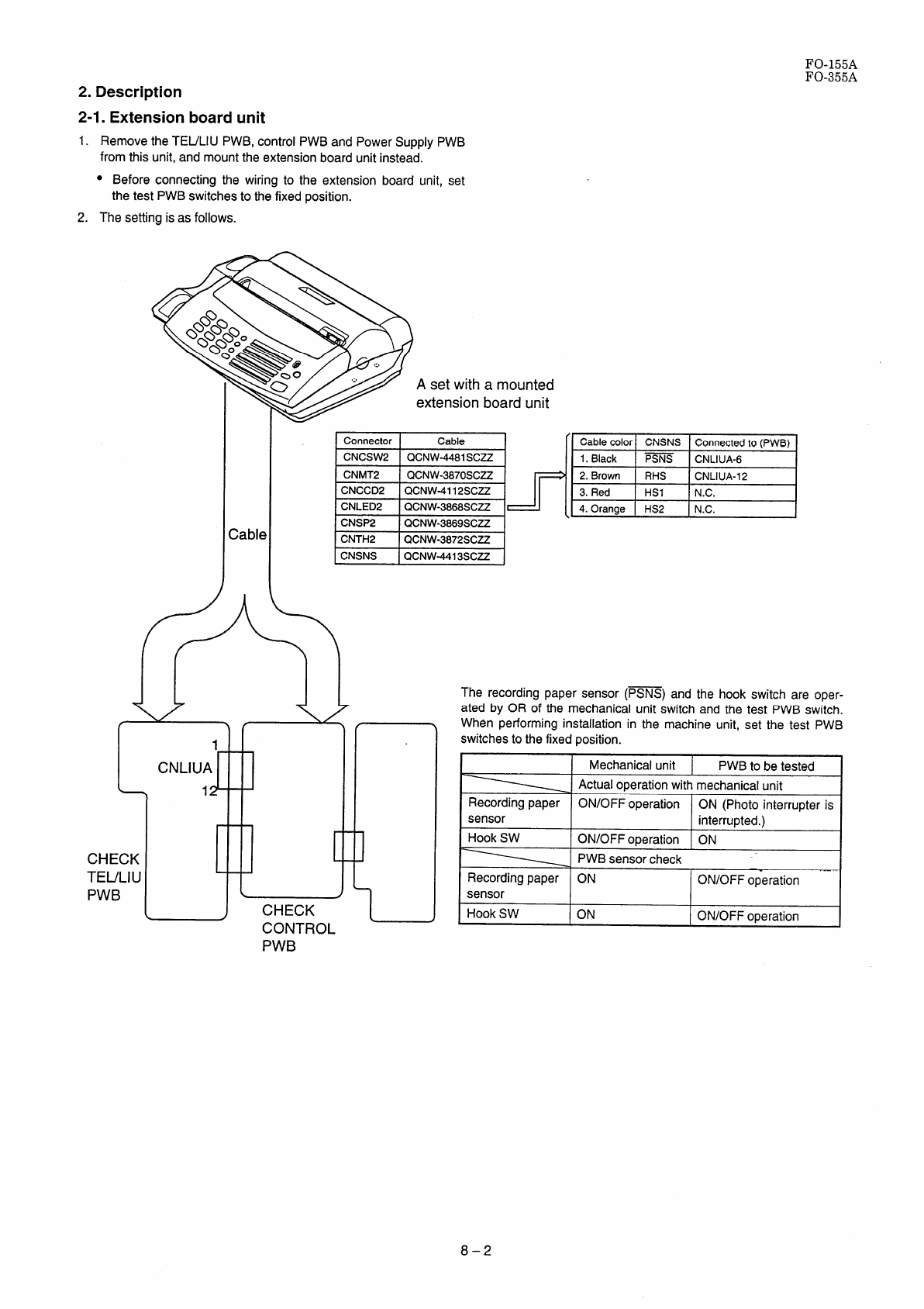
FO-155A
FO-355A
2.Description
2-1. Extension board unit
1. Remove the TEULIU PWB, control PWB and PowerSupplyPWB
fromthisunit,andmounttheextensionboardunitinstead.
●Beforeconnectingthe wiring to the extension board unit, set
the test PWB switches to the fixed position.
2. The setting is as follows.
Connector Cable
[ :
Cablecolor CNSNS Connectedto (PWB)
CNCSW2 QCNW-4481SCZZ 1.Black PSNS CNLIUA-6
ICNMT2 IQCNW-3870SCZZ i=I2.Brown IRHS ICNLIUA-12 I
—1
CNCCD2 IQCNW-4112SCZZ
J3.Red HS1 N.C.
i8SCZZ 4.Orange HS2 N.C.
I
CNSNS IQCNW-4413SCZZ
1
Aset with amounted
extensionboard unit
CONTROL
1
1-
The recordingpapersensor (PSNS)and the hookswitchare oper-
ated by OR of the mechanicalunit switchandthe test PWB switch.
When performing installation in the machineunit, set the test PWB
switchesto thefixedposition.
Mechanicalunit PWBto betested
Actualoperationwithmechanicalunit
Recordingpaper ON/OFFoperation ON (Photointerrupteris
sensor interrupted.)
HookSW ON/OFF operation ON
PWB sensor check
Recordingpaper ON ON/OFF
operation
sensor
HookSW ON ON/OFF operation
PWB
8–2
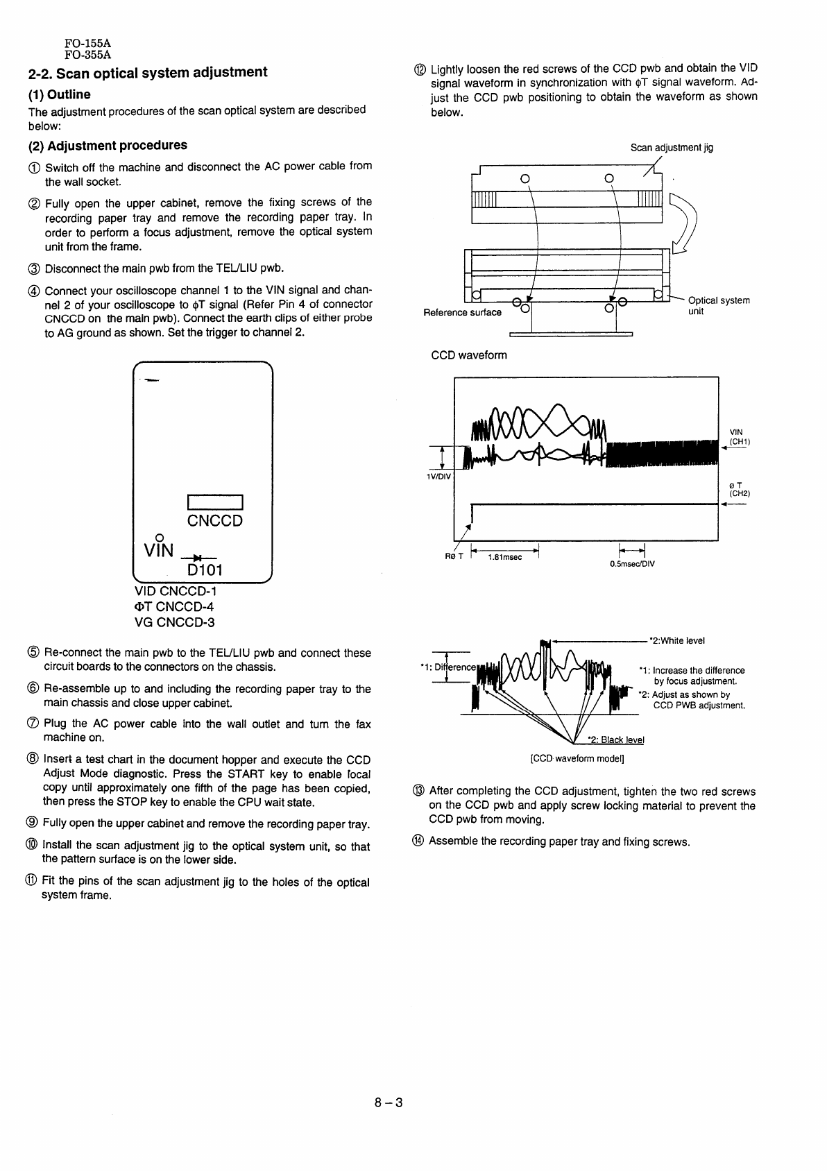
FO-155A
FO-355A
2-2. Scan optical system adjustment
(1)Outline
Theadjustmentproceduresofthescanopticalsystemaredescribed
below:
(2) Adjustmentprocedures
Switchoff the machine and disconnect the AC power cable from
the wall socket.
Fully open the uppercabinet,removethe fixing screwsof the
recordingpaper tray and removethe recordingpaper tray. In
order to performafocusadjustment,removethe opticalsystem
unitfromtheframe.
DisconnectthemainpwbfromtheTEL/LIU pwb.
Connectyouroscilloscopechannel1to the VIN signalandchan-
nel 2of youroscilloscopeto $T signal(ReferPin 4of connector
CNCCDon themainpwb).Connectthe earthclipsof eitherprobe
to AGgroundas shown.Setthetriggerto channel2.
II
CNCCD
n
DIOI A
VID CNCCD-I
@TCNCCD-4
VG CNCCD-3
Re-connect the main pwb to the TEULIU pwbandconnectthese
circuitboardsto theconnectorsonthechassis.
Re-assembleup to and includingthe recordingpapertray to the
mainchassisandcloseuppercabinet.
Plug the AC power cable into the wall outlet and turn the fax
machineon.
Insedatest chart in the document hopper and execute the CCD
Adjust Mode diagnostic. Pressthe STARTkey to enablelocal
@Lightly loosen the redscrewsof the CCDpwbandobtaintheVID
signal waveform in synchronization with $T signal waveform. Ad-
just the CCD pwb positioningto obtainthe waveformas shown
below.
Scanadjustmentjig
/
-1 00‘L
\“
“’’”[)
I
I
I
I/
n4d~
“o oOpticalsystem
Referencesurface unit
)1
CCDwaveform
I
VIN
(CH1)
OT
(CH2)
~
/
ROTF1.81msec +H
0.5msedDlV
w“ ●2:White level
*1: :Increasethedifference
byfocusadjustment.
:Adjustasshownby
CCDPWBadjustment.
[CCDwaveformmodel]
copy until approximatelyone fifth of the page has beencopied, @Afier completingthe CCDadjustment,tightenthe two redscrews
thenpress the STOPkeyto enablethe CPU wait state.
Fully opentheuppercabinetandremovethe recordingpapertray.
Installthe scanadjustmentjig to the opticalsystemunit, so that @
thepatternsurfaceis onthe lowerside.
on the CCDpwbandapplyscrewIockin-gmaterialto
CCDpwbfrommoving.
Assemble the recording paper tray and fixing screws.
prevent the
Fit the pins of the scan adjustment jig to the holes of the optical
system frame.
8–3
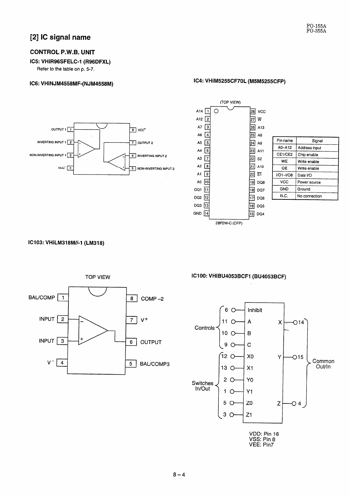
FO-155A
FO-355A
[2] IC signal name
CONTROL P.W.B. UNIT
IC5:VHiR96SFELC-1(R96DFXL)
Refer to the table on p. 5-7.
IC6:VHiNJM4558MF-(NJM4558M)
P
8VCC+
pa
OUTPUT1 1
INVERTINGINPUT1 2 -7OUTPUT2
NON-INVERTINGINPUT1 3 +6INVERTINGINPUT2
Vcc” 4+5NON-INVERTINGINPUT2
IC4:VHiM5255CF70L(M5M5255CFP)
(TOPVIEW)
8
A6 4
A5 5
d
A4 6b
23
a
A3 7
A28o
Al 9
AO ~
d
DQ2 12
a
GND 14
28P2W-C(CFP)
IC103:VHiLM318M//-l(LM318)
TOP VIEW
INPUT 2—-7v+
—+
5BAUCOMP3
E
22
21
Vcc
w
A13
A8
A9
Al 1
S2
AlO
m
OQ8
DQ7
DQ6
DQ5
DQ4
IPinname Signal I
IOE IWriteenable I
I1/01-1/08 IData1/0 I
IVCC IPowerSource I
IGND IGround I
IN.C. Noconnection I
ICIOO:VHiBU4053BCFl (BU4053BCF)
Switches
In/Out
32 +Xo Y+~ 15 Common
Out/In
13
?}
xl
2Yo
1YI
5Zo z4
3ZI
.
VDD: Pin 16
VSS: Pin8
VEE: Pin7
8–4
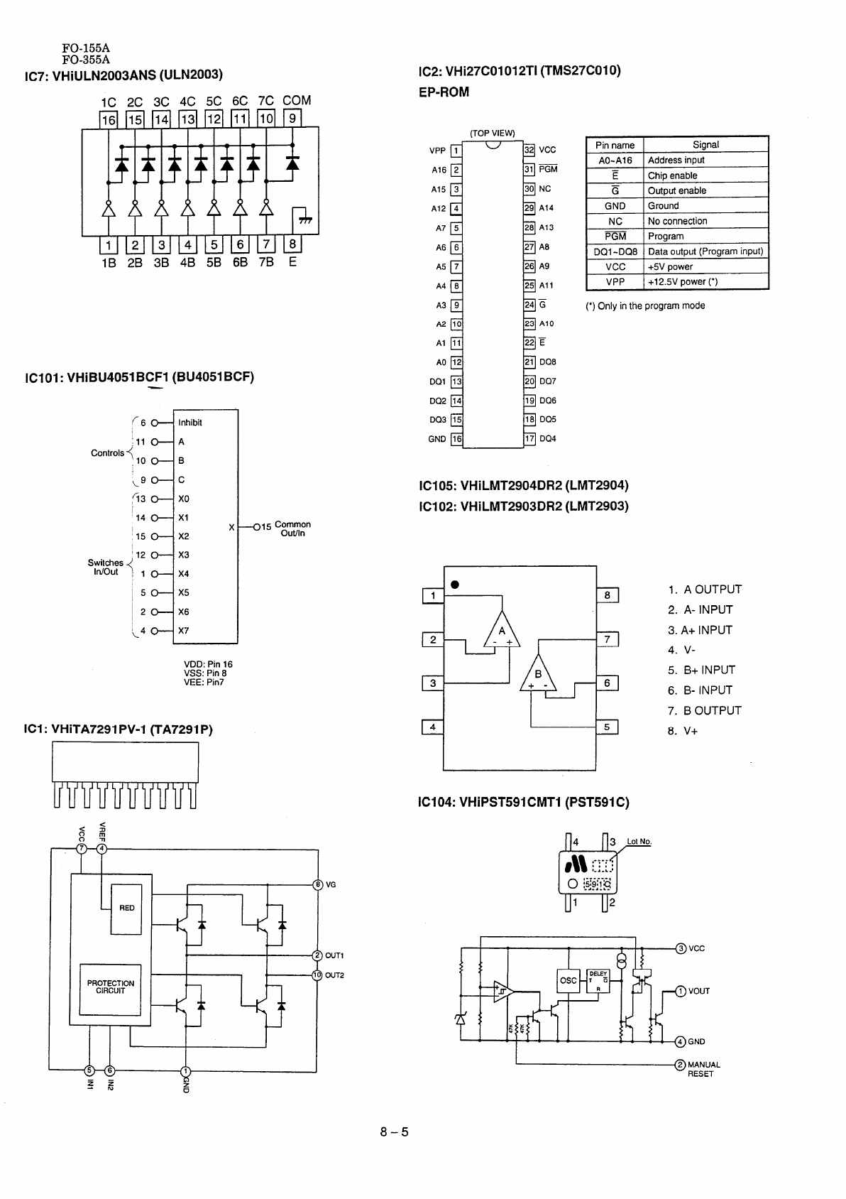
FO-155A
FO-355A
IC7:VHiULN2003ANS(ULN2003)
lC 2C 3C 4C 5C 6C 7C COM
19 29 39 4B 59 69 79 E
IC1OI:VHiBU4051BCFl(BU4051BCF)
—
;11
:2
A
Controls<10 B
~9 c
fi3 Xo
‘12
fa
x3
Switches
In/out 1x4
‘5
a
x5
12 X6
VDD:Pin16
VSS:Pin8
VEE:Pin7
ICI: VHiTA7291PV-1(TA7291P)
<5
m
Rm
VG
OUT1
OUT2
IC2:VHi27CO1012T!(TMS27CO1O)
EP-ROM
VPP
Al’
A15
A12
A7
A’
A5
A4
A3
M
Al
AO
DQ1
DQ2
D03
GND
(TOPVIEW)
J1w
2~PGM
27 A8
26 A9
25 Al1
d
9
a
10
11
IC105:
Pinname Signal
AO-A16 Addressinput
EChipenable
GOutputenable
GND Ground
NC Noconnection
PGM Program
DQ1-DQ8 Dataoutput(Programinput)
Vcc +5V power
VPP +12.5V power(*)
I
24 ~(’) Onlyintheprogrammode
23 AlO
22F
21 DQ8
20 DQ7
19 Do’
18 DQ5
VHiLMT2904DR2(LMT2904)
VHiLMT2903DR2(LMT2903)
●8
7
6
5
lC104: VHiPST591CMTl(PST591C)
w“
1. AOUTPUT
2. A- INPUT
3. A+ INPUT
4. v-
5. B+ INPUT
6. B- INPUT
7. BOUTPUT
8. V+
Vcc
VOUT
GND
I@MANUAL
RESET
8–5
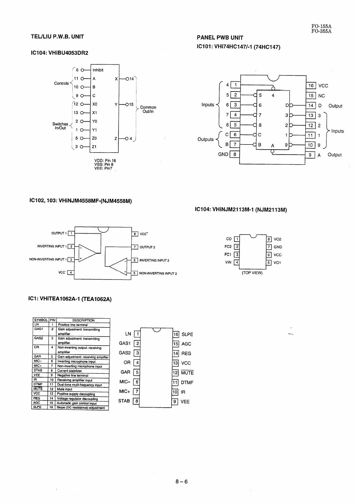
TEULIU P.W.B.UNIT
IC104:VHiBU4053DR2
PANELPWBUNIT
ICIOI: VHi74HC147/-l(74HC147)
FO-155A
FO-355A
11
,ti
A
Controls{,10 B
\9
‘-l c
52
i
Xo
‘13 xl
Switches 2
In/Out {,:
Common
Out/In
Inputs
outputs
VDD: Pin16
VSS: Pin8
VEE: Pin7
{
4
5
6
7
8
{
c
B
GND
h16
c54 15
c6D3 14
c73 3 13
c82 3 12
cc1311
cB~9 310
v9
IC102,103:VHiNJM4558MF-(NJM4558M)
IC104:VHiNJM2113M-1(NJM2113M)
‘“’”1+” b
8 VCC+
P@
INVERTING INPUT 12-7OUTPLJT2
NON-INVERTINGINPUT1 3 +6INVERTINGINPUT2
Vcc- 4+5NON-INVERTINGINPUT2
ICI: VHiTEA1062A-1(TEA1062A)
SYMBOL PIN DESCRIPTION
LN 1Posilrvelinetermmal
GAS1 2Gainadjustment:tranarniting
amplifier
GAS2 3Gamadjustment:transmitting
amplifier
OR 4Non-mvertmgoutput:receivinu
-“. - . . . . . .“ .,,...,”,
I
1
.“
, . .wceivi~amplifierinput
DTMF I11 IDual-lonemulti-fraquencyinput
MUTE I12 IMuteinput
Vcc 13 Positivesupplydecoupling
REG 14 Voltageregulatordecoupling
AGC 15 Automatkgamconfrolinput
SLPE 16 Slope(DC resistance)adjustment
LN
GAS1
GAS2
OR
GAR
MIC-
MIC+
STAB
m
116 SLPE
215 AGC
314 REG
a
4b
13 Vcc
il
512 MUTE
611 DTMF
710 IR
89VEE
m
CD 18V02
FC2 2 7GND
FCI 36VCC
VIN 45Vol
(TOPVIEW)
Vcc
NC
DOutput
3
2
}
Inputs
1
9J
Aoutput
8–6

SHARP PARTS GUIDE
❑Cabinet, etc.
❑Upper cabinet
❑Documentguide
❑Drive unit
❑Optical unit
upper
FO-155
MODEL FO-355
❑Packing material &Accessories
CONTENTS Y
❑Control PWB unit
❑TEL-Liu PWB unit
❑Power supply PWB unit
❑CCD PWB unit
❑Hardware parts
■Index
Becausepartsmarkedwith “~” is indispensablefor the machinesafetymaintenanceandoperation,it mustbe
replacedwiththepartsspecificto the productspecification.
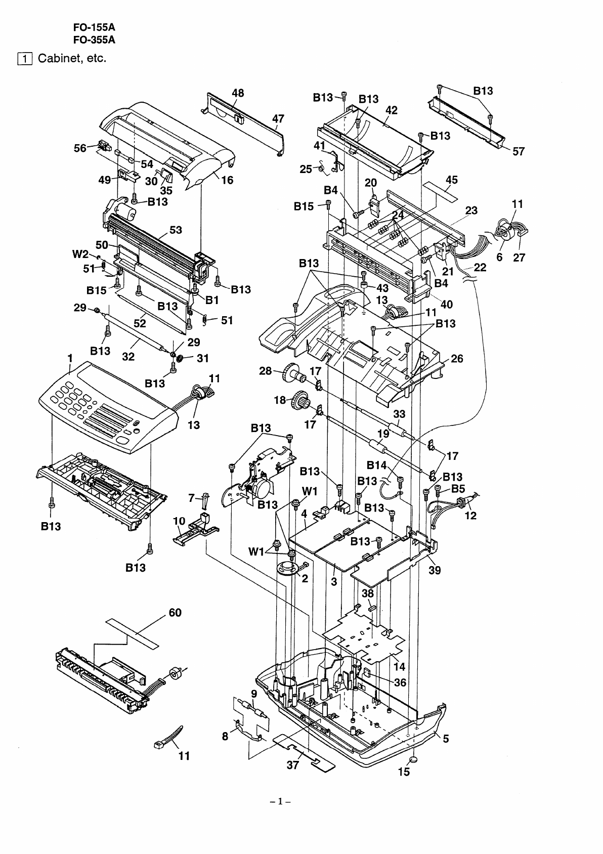
FO-155A
FO-355A
❑Cabinet, etc.
B13+ B13
56
la I
W2
i
I
B13
P
41 \>
)
613
.60
w\ 11 w
8,
,
h
:
>
\
39
113
57
;1
–1-
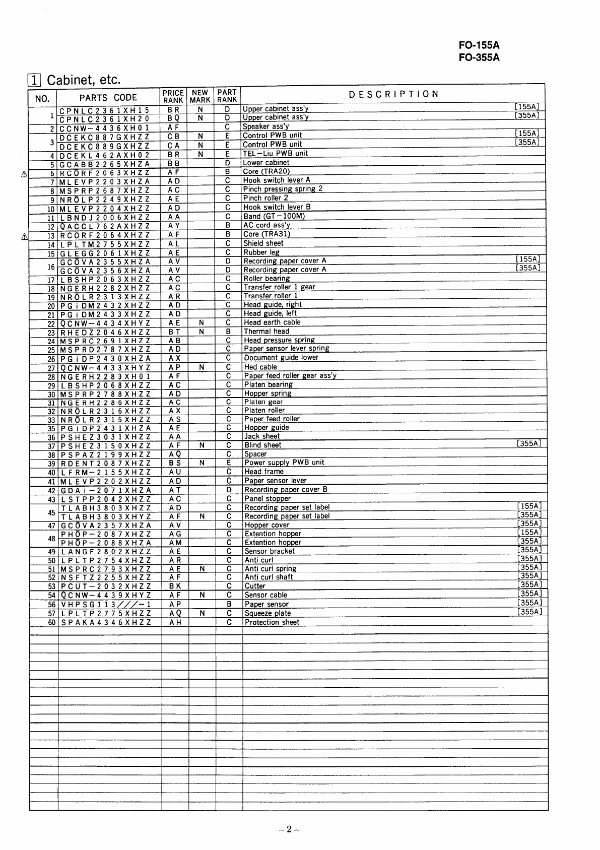
FO-155A
FO-355A
❑Cabinet, etc. 1
NO. PARTS CODE PRICE NEW PART
RANK MARK RANK DESCRIPTION
]per cabinet ass’y [155A]
er cabinet ass’y [355A]
.
dSpeaker ass’y
:Control PWB unit [155A]
:Control PWB unit [355A]
.
:TEL– Liu PWB unit
?t
3ICore (TRA20)
Itch lever A
c\Pinch pressing spring 2
.
J]Pinch roller 2
Ik switch lever B
lnd(GT–100M)
3AC cord ass’y
BCore (TRA31)
IcShield sheet
rding paper cover A[155A]
)IRecording paper cover A[355A]
~CPNLC 236 1XH15 BR N D IUP
CPNLC 236 1XH20 BQ N D !UPp~
2C C NW–4 436 XHO1AF c
sDC EKC8 87G X HZ Z CB N E
DC EKC8 89GXHZ ZCA N E
4DC EKL 46 2AXH0 2BR N E
5GCABB2265XHz ABB DILower cabine
A6RCORF 206 3XH 22 AF E
7ML EVP2203XHz AAD cIHook swi
8MS PRP2687XHzz AC
9NR~LP2249XHzz AE c
10 MLEVP2204XHzz AD cIHOO
11 LBNDJ2006XHzz AA c\Bal
12 QACCL762AXHzz AY E
A13 RCORF2064XHzz AF
14 LPLTM2755XHzz AL
15 GLEGG2061xHzz AE cIRubber leg
16 GC0VA2355xHzA AV DIRecor
GC0VA2356XHzA AV [
17 LBSHP2063xHzz AC cIRollerbearinq
18 NGERH2282xHzz AC (
19 NR0LR2313xHzz AR (
20 PGi DM2432xHzz AD cHead guide
21 PGi DM2433xHzz AD cHeadgl
22 QCNW–4434xHyz AE NcHead ear
23 RHEDZ2046XHzz BT NE
24 MSPRC2691XHZz AB c\Head
25 MSPRD2787xHzz AD cIPapel
26 PGiDP2430XHzA AX
27 QCNW-4433XHYZ AP N(
28 NGERH2283XH01 AF cIPap
29 LBSHP2068XHZZ AC (
30 MSPRP2788XHZz AD cIHoP1
31 NGERH2286XHzz AC (
32 NR0LR2316XHZZ AX (
33 NR0LR2315XHZZ AS (
35 PGiDP2431XHZA AE (
36 PSHEZ3031XHZZ AA c]Ja{
37 PSHEZ3150XHZZ AF
38 PSPAZ2199XHZz AQ
39 RDENT2087XHzz BS NEPower sup]
40 LFRM–2155XHZZ AU cHead
41 MLEVP2202XHZZ AD cPape
42 GDAi –2071XHZA AT r‘-
43 LSTPP2042XHZZ AC (
45 TLABH3803XHZZ AD c
TLABH3803XHYZ AF N(
47 GC~VA2357XHZA AV (
Jg PH~P–2087XHZZ AG (
PHOP–2088XHZA AM cIExtension hop
49 LANGF280-2XHZZ AE
50 LPLTP2754XHZZ AR
51 MSPRC2793XHZZ AE N(
52 NSFTZ2255XHZZ AF
53 PCUT–2032XHZZ BK
54 QcNw–4439xHY2 AF
56 VHPSG1 13///–1 AP I
57 LPLTP2775XHZZ AQ N](
.
.ITransfer roller 1gear
.
uITransfer roller 1
:, right
uide, left
thcable
BIThermal head
1pressure spring
rsensor lever spring
clDocument guide lower
cIHed cable
~erfeed roller gear ass’y
cIPlaten bearing
per spring
cPlaten gear
cPlaten roller
cPaper feed roller
cHopper guide
cksheet
NcIBlind sheet [355A] ~
Ic]Spacer ply PWBunit
!r sensor lever
DIRecording paper cover B
cIPanel stopper
paper set label [155A]
cRecording paper set label [355A]
cHopper cover [355A]
cExtention hopper [155A]
per [355A]
IcSensor bracket [355A]
cAnti curl [355A]
cAnti curl spring [355A]
cAnti curl shaft [355A]
cCutter [355A]
NcSensor cable [355A] _
BPaper sensor [355A]
cSqueeze plate [355A]
I601SPAKA4346XHZZ IAH I I cProtection sheet
I
-2–
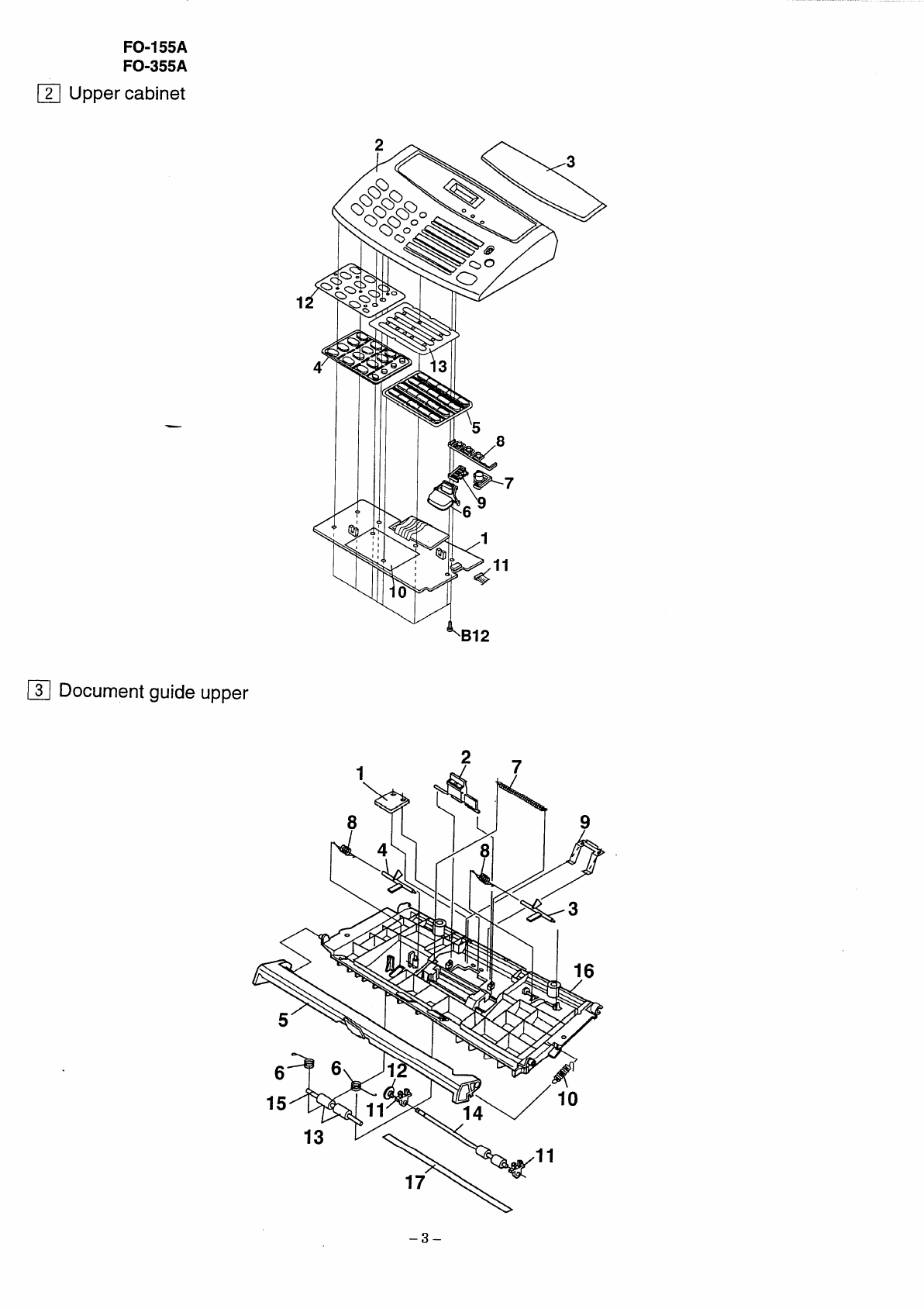
FO-155A
FO-355A
❑Upper cabinet
1
~Document guide upper
–3–
FO-155A
FO-355A
~ Upper cabinet
NO. PARTS CODE PRICE NEW PART
RANK MARK RANK DESCRIPTION
1DC EKP4 43 AX HO 1BL EOperationpanel PWB unit
2GCABA2 264 XH Z F AS NDUppercabinet
3HP NLC 236 IXHZA AH DDecorationpanel [155A]
HPNLC2361XHZD AS DDecorationpanel [355A]
4JBTN–2157XHZA AK cDiai key
5JBTN–2158XHZA AG c-Direct key
6JBTN–2159XHZA ‘AF cStart key
7JBTN–2160XHZA AD cStop key
8JBTN–2161XHXA AE NcMode key
9JBTN–2162XHZA AC cVolumekey
10 PSHEZ3124XHZA AF NcProtect sheet
11 CCNW–4431XH01 AT NcPanelcable
12 PSHEZ3158XHZZ AB NcAnti vibration sheet 1
13 PSHEZ3159XHZA AF NcAnti vibration sheet2
(Unit)
~ol CPNLC2361XH15 8R NDUppercabinet ass’y [155A]
CPNLC2361XH20 NDUppercabinet ass’y [355A]
❑Document guide upper
-4-
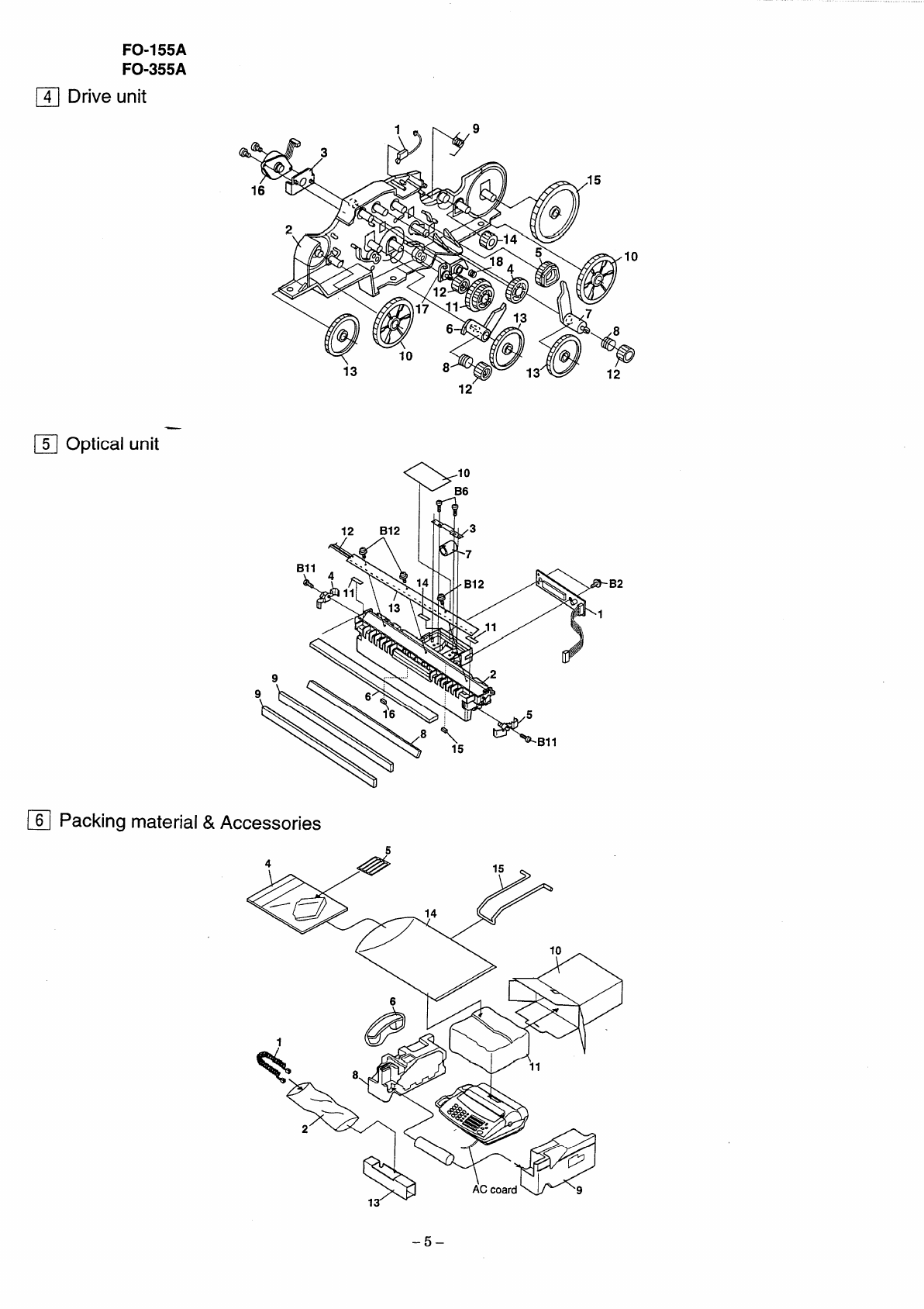
FO-155A
FO”355A
❑Driveunit
❑Optical unit –
B2
❑Packing material& Accessories
–5–
~Drive unit
FO-155A
FO-355A
INO. IPARTS CODE PRICE NEW PART
RANK MARK RANK DESCRIPTION
\2LFRM– 2153 Xl-l Z Z AU cDrive system mounting frame
3LPLTM2 74 1 XHZ ZAE cHeat sink
4MCAMP2019XHZZ AC cCamA
5MCAMP2020XHZZ AC cCamB
6MLEVP2190XHZZ AC cPlanet gear leverA
7MLEVP2191XHZZ AC Planet gear leverB
8MSPRC2735XHZZ AC :Planet gear spring
9MSPRD2736XHZZ AC cCam hold spring
10 NGERH2276XHZZ AC cReductiongearA
11 NGERH2277XHZZ AC cReductiongearB
12 NGERH2278XHZZ AC cPianet gear
13 NGERH2279XHZZ AC cidler gearA
14 NGERH2280XHZZ AC cldlergear B
15 NGERH2281XHZZ AD cldlergear C
16 RMOTZ2121SCZZ AZ NBMotor
17 MLEVP2194XHZZ AC cChangelever
18 MSPRD2744XHZZ AB cchanEeleversDrinE
HODtical unit
DESCRIPTION I
.1,,.s,, ”. ,,”,”,,,~ ~p,,,,~ -I
NO. PARTS CODE PRICE NEW PART
RANK MARK RANK
1DCEKD464AXH11 BF NECCDPWB unit
2LFRM–2147XHYA AV cOpticalframe
3MSPRP2512XHZZ AK cLensholding spring
4MSPRP2618XHZZ AD cMirrnr hnlriinu cnrinu I
5MSPRP2619XHZZ AD cIMirror holding
6PGLSP2043XHZZ AK
7PLNS–2043XHZZ AU
8PMi R-2061XHZZ AH
9PMi R–2062XHZZ AM
10 PSHEZ2879XHZZ AK
11 PSHEZ2915XHZZ AY
12 QCNW–4441XHYZ AE NcLEDcable
13 VHPSNK08A24–1 AZ BLED(SNK08A24)
14 PFLT–2006XHZZ AA r! Himalnn ~haat
15 PCUSS2075XHZZ AA
1,-lnntlee rln-fr”,,77 AR
;spring 2
cIReaderglass
BLens
cMirror 1
cMirror2
cShieldsheet
cBlind sheet
......... .. -....”.
;Cushion 1
Lolruuaazu 1OAtl~L IAfi IcCushion2
I
6[ PackinE material &Accessories
INO. IPARTS CODE PRICE NEW
RANK MAR
1—— —— 1--t PART
1,.......K RANK DESCRIPTION
.......
-,.-.,..,,,x- .- ““and set cord
nyl bag (140X36011urr)
I“llnoNw-jy ,bKH
AKA3001
I4\TiNSE3553
II.-,.-,
-,..,..-,
Al c
cc;; AA c
XHZZ AQ Nc
I5TLABH3733XHZA AD D
TIARH3733)(HYA AD
IUUNIK424AXHOG AY
6nllklTKd92CjxHE2 AR
t1A4656XHZZ AF
;lzD’A”uq465tjxH zz
1. arnfiC4766XHZ Z
SPAKC4772XHZZ \AN I
11 SPAKP?-” ..--,-. ..-.
I-- . . ..... .
I
IH
u
13 sPAKA4tJ31AHLL I
14 SSAKA2003XHZZ IAA IILJ
●rm,,, .n-n. . ., ,, -. -.-
J
[155A] ]
—. [355A] ]
[155A] .
NEHandset [355A] .
-1 Sidepad, left
ISidepad, right
IPackingcase [155A]
NuPackingcase [355A] .
3363>LLL Ah IDVinyl cover
..---.>.,-, -IAC DAddV
-. 1Vinyl bag( 240X360mrri)
1131rw IK‘LU16AH~L Inr IDRecordingpapertray
I[355A]
1
–6–
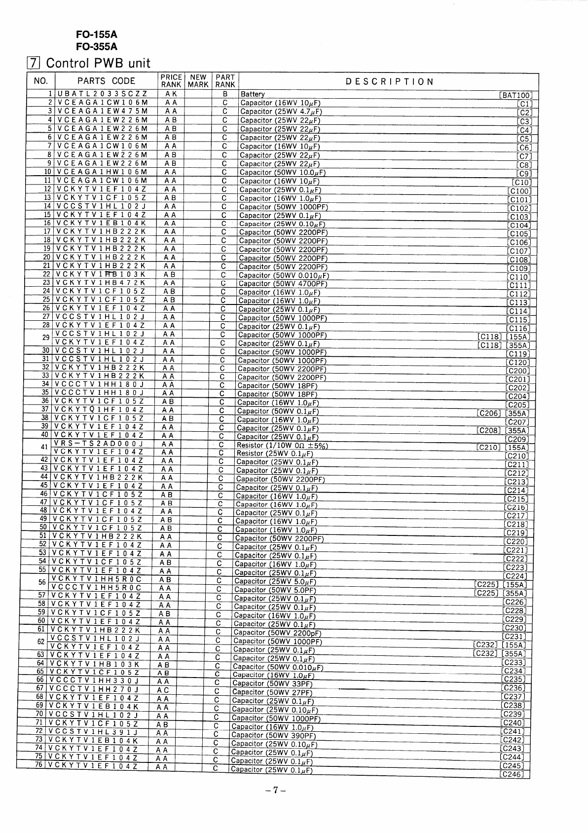
FO-155A
FO-355A
❑Control PWB unit
NO. PARTS CODE PRICE NEW PART
RANK MARK RANK DESCRIPTION
1UBATL2033SCZZ AK BBattery IBATIoo]
2VCEA GA 1CW1 n~M AA cC.nacitnr (1 KWV 10AF) [cl]
3VCEAGA1FWL75M IAA IPICan.eitnr (7RWV L.7EF) [C21
4VCEAGA1EW2 26 MAB cCapacitor(25WV 224F) [C3] .
5VCEAG A1EW2 26 MAB cCapacitor(25WV 22fl F) [C41
6VCEA GA1EW 226 MAB cCapacitor (25WV 22AF) [C51
7VCEAGA1CW 106 MAA cCapacitor(16WV IOgF) [C6]
rny~
-.. - - .. . , .,... I. . . . I I IWWp ”e, .”, ,-” ., , 7
I8jVCEAGA1EW2 26 MIABcICapacitor(25WV 22UF)
9VCEAGA1EW 226 MAB cLb/ J
Capacitor(25WV 22,uF) [C81
10 VCE A GA1HW 1 06 MAA cCapacitor(50WV 1O.OUF) [C91
11 VCEAGA1CW 106 MAA cCapacitor (16WV 1OPF) IClol
12 VCKYTV IEF 104Z AA cCapacitor (25WVO.l~F) [Clool
13 VCKYTV lCF 105Z AB cCapacitor (16WV l.O~F) ICloll
14 VCCSTv ~HI 1n7 1 AA cC.n..i+nr (RflWV1~OOpF) [C102I
15 VCKYTv 1FF 1047 IAA I I cIC~pa~itOr(25wv oolflF) [C103I
16 VCKYTV 1FR1 04K IAA I I PIC=na@itnr (9kW\l n1OKF) [C104I -
17 VCKYTv IH~77 7K IAA I I Pie.n.,-i+nr (tinW\/ 9zOOpF) [C105I
18 VCKYTV 1HB222K IAA cICapacitor(50WV 2200PF)
19 vct(’t Tv1HB77 7K /AA I I [C1061
cI~an..itnr {KnW\/ 9zoOpF) [C107I
20 VCKYTV Jr-iml j/n 1AA II[: If.anae, tnr (h(}W\/ ‘}200PF)”
21 VCKYTv 1HB77 7K [C1081
IAA I I cIPanaeitnr {RnW\/ 9~OopF) [C109I
22 VCKYT n In..c) rn, .ml
.-..- - - - “1,.. . 11t
—““p””,.”, ,“”.. .*,
—
.--- -- .- 1.., . 11“,.
—
.-. . . . - - —- - . .. 1.., . I1I“uy ”u, L”, \G 4,, .“.
— —
-.. —- - - .. I. . . . 1iI“wyu ”L. v, f“ ”.. .G,
-,, , , tm.-la a ,/ . . -I- .. ... .. -
-.- - - - .. 1. . . . !I1“Up ”e, c”, ,“ ”,, ,e,
—1 1 II““~””..”c \“”.? .AZ
.- viKi i i KIABE
tICapacitor (50WV O.L. UP, ,
-- - .—.— — -Lbl IUJ I
Z3 VGKYTV 1HB472K AA cCapacitor(50WV 4700PF) ICllll
24 VCKYTVICF 105Z AB cCapacitor(16WV l.OgF)
25 VCKYTVI f!F 1 n 57 AR [C1121
rCapacitor(16wv l.og F) [cl 131
26 VCKYTVIEF104Z AA cCapacitor (25WV O.lflF) [C1141
27 VCCSTV IHL 10 2J AA cCapacitor (50WV 1000PF)
28 VCKYTV 1FF 1IlA7 AA [C1151
r-’ ~nn=,-i+nr/9K\A/\/n 1 F)
29 VU CSTV IHL 1 0 7 1 [Cl 161
IAA I1P I~n~acitor (50wv 1000PF)”
VCKYTV IEF 1fld7 IAA I I [C1181 [155A]
PIPnnnei+nr f9KW\f n1F)
30 VLUS IVIHL 1 07 1 IAA IIr [C1181 [355A]
IPn~aCitOr(50wv 1000PF)
31 VG G SIV1HL 1 0 2 .J [cl 191
IAA I I r. IPann,-i+nr fknwv 1f)~flpF~ rn I9A7
--- ---- 1..- 11v,>
— —
.--- -- .- 1,., . III“Up”b,.”,\L..J,.“ “.
..- - - —.. ------ 1. . . . 1II““
— —
—--.— 1.... rI[““puQ,L”,
..- - - —.. . . . \G<r.wu.
—
---- I. . . . 11I“.
. . ---—.. .- - —---- ,
\_w.. ._200PF) LU LLUJ
33 VCKYTV 1HB222K -.. p””,.”,
ii [C2001
iCapacitor (50WV 2200PF) [C2011
34 VCCCTV lHH 180 J AA cCapacitor (50WV 18PF)
7K T-- [C2021
VCCCTV lHH1 8OJ \AA IcICapacitor (50WV 18PF~ [C204]
105Z AB cCapacitor (16WV l.OYF) [C205]
104Z AA cCapacitor(50WV
O.lflF) [C206] [355A]
105Z AB cCapacitor(16WV l.OAF) [C207]
104Z AA c
,,, p(
Ca acitor 25WV O1,UF) [C208] [355A]
Oorll IAA I1P ~
IDeSiStor (1/lfjw OQf5%) [C2101 [155A]
[C21OI
1047 IAA IIr [C2111
1capacitor(25wv o.l~F)
.“!. , , . . 1i[C2121
GVCKYTV 1HB222K AA cCapacitor (50WV 2200PF) [C213]
45 VCKYTVIEF 104Z AA cCapacitor (25WV O.lPF) [C214]
46 VCKYTVlc F105Z AB cCapacitor (16WV l.OAF) [C215]
47 VCKYTVlc F105Z AB cCapacitor (16WV l. OflF) [C216]
48 VCKYTV 1EF 104Z AA cCapacitor (25WV O.l,KF) [C2171
49 VCKYTVlc F105Z AB cCapacitor (16WV l.OgF)
50 VCKYTV lCF 105Z AR P[C218]
~apacitor(16WV l.O~F)
51 hLn YIV11-i~z Z.2K IAA IIr [C219]
1‘Sn=-i+n’‘KA’A’”OOOOPF) [C2201
-.
V1EF 1 0 4Z \AA cICapacitor (25WV O.lflFj
l\r
iii:; i ii AA EResistor (25WV O.lflF)
V1EF104Z AA cCapacitor (25WV O.lAF)
.. . ——
-—. .- .- !.., . II“,“
. . .— —- -
—..- !I
,a,, ., - . , . . . - - - - .. I“(
&drrvU.i flh) [C2211
IP5Rafii+A+ r25wv O.lKF) [C2221
16WV 1.OPF) [C2231
25WVO.lflF) [C224]
ip~~,,u,{25WV5.04F) [C225] [155A]
1‘=n=-;+n”‘En’’’” r‘PF) [C225] [355A]
F[C226]
IC.nae;+ar/25wv o.lgF~ [C228]
16WV l.OkF)
9K\~I\I
n~pF) [C2291
)ODF) [C230] ,
rfin-. 7
IAA IIr
541VCKYTV1CF1i5iii ;““ aL:Lu’
P\
Capacitor(
55IVCKYTV1EF104 ZAA cCapacitor (
ICKYTV 1HH5ROC AB
30 IcCa?-.=-;+-”/
,, a a n---., . .. .. - - - - IAA I I r
57IVCKYTV1EF104 ZIi i rf
iI“a au:’”’ ‘“” v‘“”
iP(
Capacitor (25WV 0..1
,n,/ ., -\, . - - .-.-IAA IIrP\
‘C KY TVICF 105Z ii E“a aL:L”’ (;
Capacitor
‘C KYTV lEF 104Z Af.i cCapacitor (2UVVvU. I
‘C KY TV1HB222K AA cCapacitor(50WV 22(
,n n m-., . ,, , . - -
62 Vuba IvlHL 1UZJ IAA I[r t‘=mafi;+n”‘En’’’”‘‘90PF) LL<31~
Vbnl IvlLI- 1U4Z IAA IIr IP-n-,.;+-.f9K\Al\/ n1[C232] [155A]
63 vuF) [C2321 [355A]
64 vC.JVVv“.1 gF) [C233] -
65 v‘n’’’” A“lOKF) [C234]
66 vcCCTV LuvvV J.UUF[C235]
67 vCCCTV jOWV33PF) [C2361
68 Vbnr IvlEF 1U4L aP.~IcuI ~~OWV27PF)
IAA I[r [C237]
69 v1‘“-””;+-- ‘?5WV O.lAF)
‘E’’’” n‘9~F) [C2381
70 v[C239]
71 VCKYTV OPF) [C240]
72 viF) [C2411
73 VCKYTVIEB1 04K iAA IIuI~aPa~lLur (OUVV vs~uPF)
P1‘----;’-” ‘0=’’’” n‘7)F) [C242]
74 v[C2431
75 VCKYTV 1EF 1C14Z /AA 1I I UaPdLI LU~ {ZOVV VU. igF)
:1Pa--a:--. ,Or, a,, ,n., [C244]
76 V~n I I vltp 1U4L IAA I(F
Ir IP--..-:._..,O~,A,.,- .”-? [C245]
m,/ ,, T, , . - - . . . :
. . !IIuupabituu \Juvvvlui
CKYTV lEF 104Z ii i““ aL:L”’ ‘Jvvv ‘“’4
P(
CKYTV1HB103K AB Capacitor (2E’A”JnI
cCapacitor (5UVVvU.U
CKYTVICF 105Z AB cCapacitor (lc~”” ~a
/l HH330J AA cCapacitor (5
/l HH270J AC cc? --,.:+n. /c
nv\/1-,, , F F .A.-rJ (
CKYTVIEB1 04K ii ;Capacitor (;Jvv vU.J1
“a aL:L”r
~S TV1HL 102 JAA cCapacitor (50WV 100
‘1 CF105Z AB cCapacitor (16WV 1.OJ
CCSTV 1HL39 IJ AA P0.... --;4-- ICnlfit, ,---
,
CKYTV 1EF 1 04z ]AA 1IuiudpdLlluI (Lavv vu. lL
PP----: &-. /or,. r\ ,*.
–7–
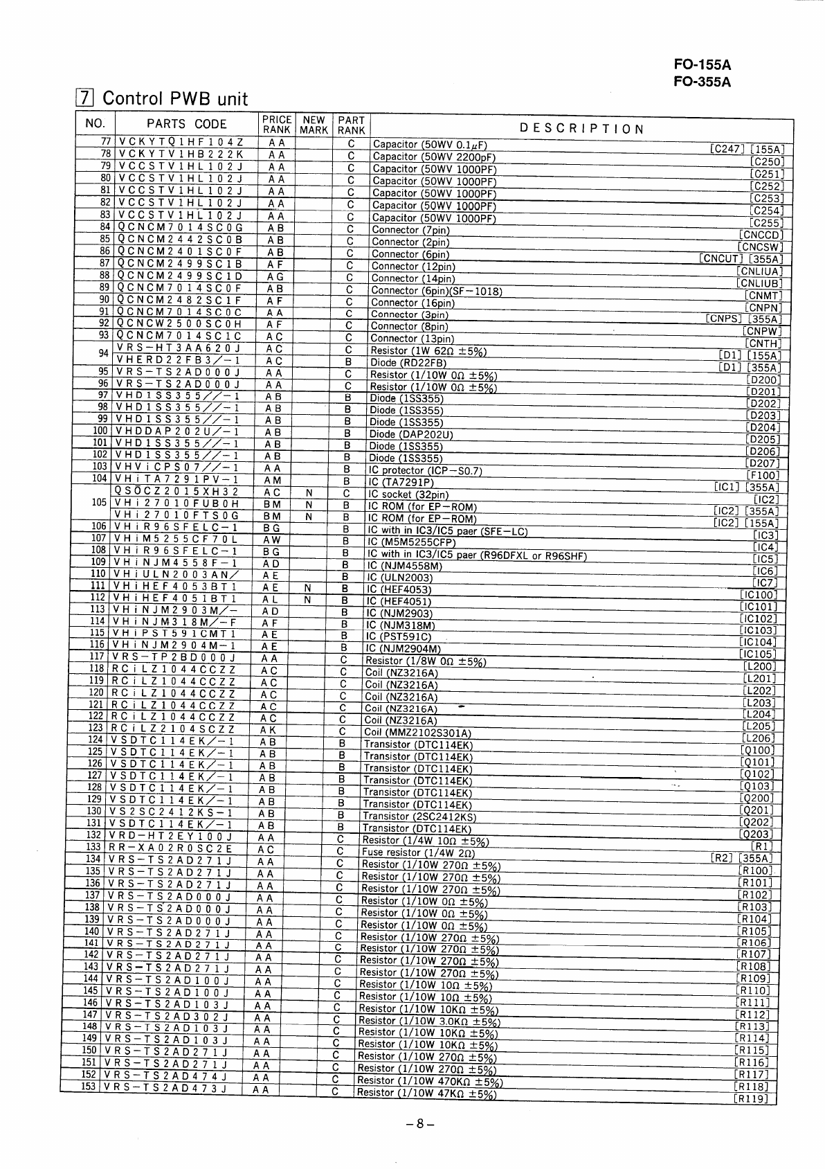
FO-155A
❑Control PWB unit FO-355A
INO. PARTS CODE PRICE NEW PART 7
RANK MARK RANK DESCRIPTION
pacitor (50WV O.lgF) [C2471 [155A]
oacitor(50WV 2200pF) [C250]
~acitor(50WV1000PF) [C251]
=.~acitor(50WV1000PF)
81 VCCST VII-IL loii AA E[C252]
Capacitor(50WV1000PF)
82 VCCSTV IHL 1fI ?IAA P[C2531
~=macitor(5C)WV1000PF)
83 VCCSTV IHL 10 2J AA c[C254]
Capacitor(50WV 1000PF)
84 QC NCM 70 14 SCO GAB c[C255]
Connector(7pin)
85 QCNCM2 442 SCOB AB c[cNccD] -
Connector(2pin)
86 QC NCM 240 1 SCOFAB rr hlPC\AI 1
87 QCNCn ,
88 QCNCM 2499 SC1DAG IUull
89 QCNCM7 o 14 sco FAB :ICon
90 QcNcM2482sclF AF PIn .-
91 QCNCM7014SCOC AA
92
77 VCKYTQ1HF104Z AA cCal
78 VCKYTV1HB222K AA cCal
79 VCCSTV1HL102J AA cCal
80 VCCSTV1HL102J AA cr%,
—
..- -1..,.
—... . . . 1IIUap
cConnector(6pin) LVIXUd~WJ
ICNCUTI [355A]
M2499SC1B IAF cConnector(12pin)
P[CNLIUAl
‘i-nnector (14pin) ICNLIUB]
lnector (6pin)(SF– 1018) ICNMTI
buu[lnector (16pin) ICNPNI
1 1 cConnector(3pin)
6CNCW2500SCOH ICNPSI [355A]
ii cConnector (8pin)
n~hichfi7n1 fl~fiqm I,- 1I[CNPW]
-lnector(13pin) ICNTHI
Imesistor(lW 62Q ~5%)
‘4 VHERD22FB3>~~ ii bIDll [155A] -
BDiode(RD22FB) IDll [355A]
95 VRS–TS2ADOOOJ AA cResistor(l/10WO~ k5%) [D200]
96 vRs–Ts2ADoor3J AA cResistor(l/10w OQY5%)
97 vHDls.s355//-l AB BDiode(lSS355) [D2011
98 vHDlss355//–l AB BDiode(lSS355) [D2021
99 vHDlss355//–l AB BDiode(lSS355) [D203]
100 vHDDAP202u/–l AB BDiode(DAP202U) [D204]
[D205]
101 vHDls.s355//-l AB BDiode(lSS355)
vHDlss355//–l AB R[D206]
‘ifide(lSS355)
--.–-.– /,An -a-. [D2071
93/yulwulvl/u14ab lb IAb IuIuor
a. IVRS–HT3AA620J IAC Ir. n-.
102
103 VHV iCPS07”/-/–l ,1Iw,””
Ai R
104 “r mfi-’=-’~r (iLr—bU./j
1P) [F1OOI
HCII [355A]
105 (32pin) DC21.
~rEP–ROM) ~c21 [355A]
~rEP–ROM)
106 ~c21 [155A]
lc3/iC5Daer (SFE–LCl rlfi-1
107 VHiM5
108
109 VHiNJ
110 VHi ULN2003AN/ IA~ 1
111 vHiHE- --- II
112 VHiHE
113 VHi NJM2903M/– 1AD
114 VHiNJM318MZ–F IAK II
I I
‘n ‘K’’hA290+IVI
117 VRS–Tt-JZBDOIIm IAAI 10 [Di-
1lQ DP:17
VH iTA729 1“P’v–1 AM P
i;:(+;7;;
QSOCZ 2015 XH 32 Ac NcIC socket(
VHi27010FUBOH BM NBICROM(fC
VHi27010FTS0G BM N
VHi R96SFELC–1 ~——BlCROM(fc
BlCwith in I
1255CF70L AW R1P{MKMK?KEcEo
VHi R96SFELC–1 BG
M4558F–1 AD
\I.t.JI.t.JLd4uI r’
i‘“
ICwith in ICs/lCspaer(R9Gf)FxL OrR9GSHF) LIC4]
BIC(NJM4558M) DC51
B~C61
IC(ULN2003)
.F4053BT1 IAEI NBIC(HEF4053) DC7]
F4051BT1 jALl NBrlcloo]
IC(HEF4051)
. . --- - .BIC(NJM2903) Dclol]
DC102I
--..., .1,., IIBIC(NJM318M)
l-c.-, ,,----- .DC103I
.- ra 1Pfnc-rcn~c)
,Ak
1) DC104I
DC105]
nb, LLlo4iccij ii r~caialur (LlOV~On *5°~)
;[L2001
Coil (NZ321fjA)
‘n’’ 71044cczz Ac c[L201]
Coil (NZ3216A)
1044CCZZ AC cCOil(NZ3216A) [L202]
1044CCZZ Ac cCOii(NZ3216A) -[L203]
1nAAnn7 7.- .‘“”’M7=216A) [L204]
[L205]
,IVIIVIL2102S3O1A) [L2061
jistor (DTC114EK) [Q1OOI
jistor (DTC114EK)
.;-A...tn~n+,~v,, [Q101]
L
~. [Q102I
.. -{,.- II“IIv (IVJI1
--- --_—
m
ILL KL ILL iU44LLLL AL L
123 RC iLZ2 104 SCZZ AK Uull (IXLOL
ccoil (ifih#7
124 VSDTC1 14 EK/– 1AB BTrans
125 V S DTC1 14 EK/– 1AB BTrans
126 V S DTC1 14 EK/– 1AB BTransr~,Ur{u IU1i+cn
127 V S DTC1 14 EK/– 1AB BTransistor(DTC114EKJ
128 V S DTC1 14 EK/– 1AB BTrans
129 V S DTC1 14 EK/– 1A13 BTrans
130 VS2 SC2 4 1 2KS–1 At3 BTrans
131 V S DTC1 14 EK/– 1AB BTrans,alur (U IL
132 VRD–H T2E Y 100 JAA cResistor(1/4W LUL~Xayoj
133 RR–X AO 2ROSC2EAC cIRl] I
Fuseresistor (1/4W 2Q) [R2]
134 VR S–T S2AD 27 1 JAA cResistor(1/10W 270n f5%)
135 VRS–TS2AD2 7 1 .1 AA P
--- ‘esistor (1/10W770G ~50~j
--
;istor (DTC114EK) ;v;;;~
;istor (DTC114EK) [Q2011
iistor (2SC2412KS) [Q2021
‘;-+-- ‘nT?l 14EK)
?nn Al-n.. [Q203]
,nr. -fi...---:- 1.., . IIuInl
tljb v K 3 – I3 L A U Z I 1.1 IAA I
137 VK>–I>ZA D U O 0iIAA I
VRS– TSz ADuo rI IIAA I
In --. -. LK IU IJ
‘Desistor l)~OW270Q k50
In [R102I
In-.:---- !* )~ow OQ*5% ‘)
10 [R1031
in..:---- /. /~owOa ~5;)
c[R1041
Resistor(1/10W0~ 25%)
cr~ InKl
Resistor l/10W ~,u,~ A~-
PD[R1061
--:-4 .- !* /~Ow270~ f5$~
10W270Q 35%) [R1071
IcIn--:-L--/,/ 10W 270Q k5%) [R1081
IP–i [R1091
cl.-:----- /1 /~ow IOQ *50
Io-i [R110]
n..-:----- ,* /~ow ~oQ ~5j)
Ic- IRl 11]
im--:---- ,* /~ow~oK~ ~5~;)
1P [R112]
ID--:-*-- ‘T‘low 3.OK~~5y
10 [R113]
ID--:-A-- Z*/~Ow~oK~ &5y;)
In [R1141
[‘--:-* -- ‘“ ‘low loK~ ~5y)
1PID--:-L--,*,* .OW270a A5%) IRl 15]
rD 11 Cl
,-” ------- :- 1.., . IIujml
138
139 VRS– TSZADU 00 J IAA
140 VRS
141 VRS– TS2AD 271 I \ AA
142 VRS– TZ
—--- r,., , IIuImeal>tur (li
------- —--- [,,, , IIu1ne>l>lur(I1
a------ l–
i–TS2AD271J IAA
I
=
l~J VK3- I3ZAU27 1 1 IAA I
144 vRS–TSzAuIo0IIAA I
145 vRS–TSzAuIo0IIAA I
146 VRS–TSzAu1 0 3 IIAA I
147 vRS–TSzAu d O7IIAA I
148 VRS–TSzAu1 0 3 IIAA I
149 vRS–TSzAuIO3IIAA I
150 VRS–TSLAuz7 1 IIAA I
L151 vn- - “
—-- t.., . I1u
.A .-.-— Inesl>lur (l/
—--- !,,, , IIuIme>l>lur [1/
------- —
—--- rr,, ,IIu
.,. .--—— Ine>l>cur[l/
—___ r,,, , IIu
------- Ine>islur(11J
--- 1,,, , IIu
.- .--—. Inc>l>lur(1/ J
KS–I S2ADj7 ~j I ~~
1II I neslslur II/ 1
De —l-e 9Am“.., !/:! (
Resistor lilnl~’ ~TA~ ~5%) L,, LiUJ
[. . IRl 171
JI \./Luvv+/Ur(a t504) IRl 181
1,,.=.,.t~r (1/10W47Kn &5%) [R1191
–8–
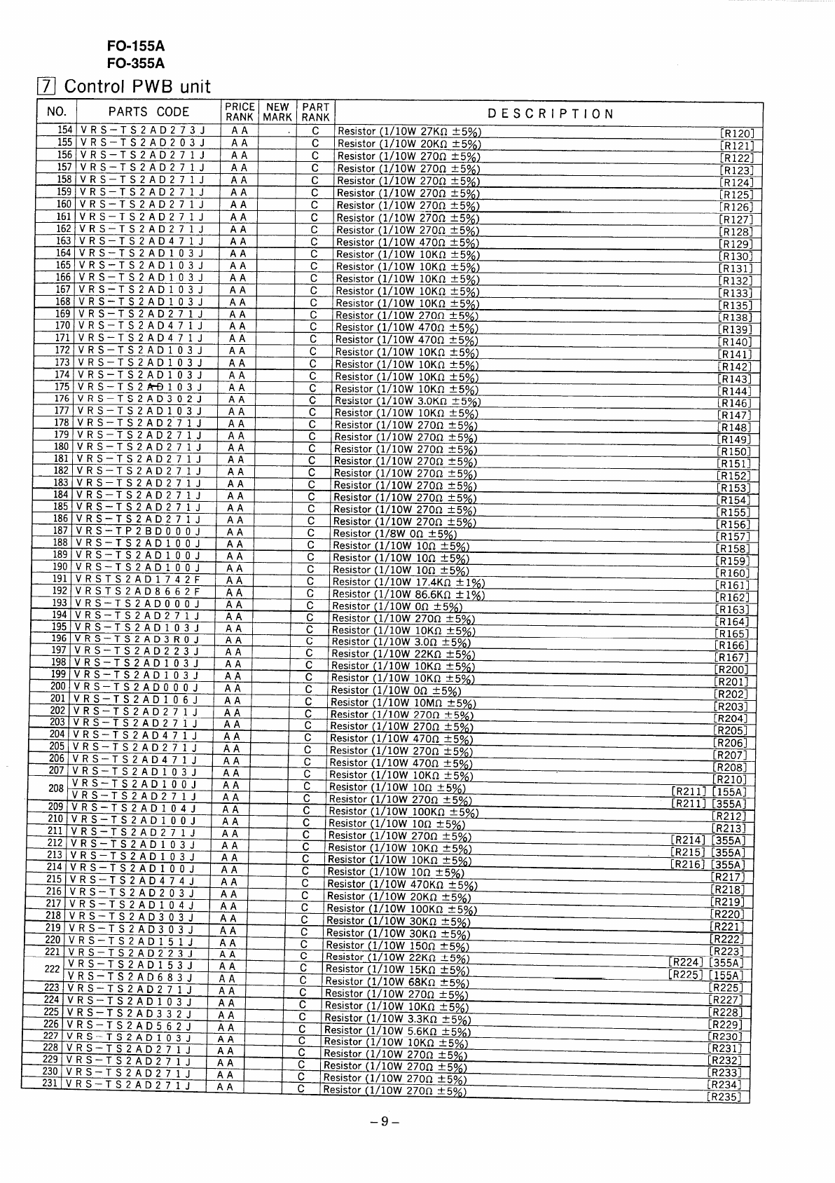
FO-155A
FO-355A
❑Control PWB unit
PRICE NEW PART
RANK MARK RANK DESCRIPTION
NO. PARTS CODE ........ ,.,,..,,. ,.,,..,.
154 VRS– TS2AD 273 JAA .cResistor(1/10W 27Kn t5%) [R1201
155 VRS– TS2AD2 O3JAA cResistor(1/10W 20K~ *5%) [R1211
156 VRS– TS 7AD7 7 1 1 AA cR..i.tnr (1 /1 flW 970~ -I-5%) [R1221
157 VRS– Ts PAD7 7 1 IIAA I I rIRacictnr (1 /1 nw 970Q ~GO~) rR I927
-—..- -.- - 1. . . . 1I1,.”e,e.”, \A, A“. .G,
— —
- - ..- -.-
“
1,., . !1I,. ”4, .J. U, t-, A“. .G, L.- L,i A*OJ
. - - ..- - , . “I,., . ,,.~~istor(1/10W 270~ k5%)
1t[R124] .
.- - ,.- -,-“I,,, . ,t,~.istor (1/10W 270Q t5%)
1I[R125] ,
.- .. . -——
158 vRs– Ts7An7 7 1 IIAA IIr II?ac(
159 VRS– T~ 7A~7 7 1 IIAA IIr IDaci
160 VRS– TS 2AD2 71 JAA cResistor(1/10W270Q t5%) [R126]
161 VRS– TS2AD2 7 1 JAA cResistor(1/10W 270~ *5%) [R127]
162 VRS– TS 2AD 27 1 JAA cResistor(1/10W 270~ Y5%) [R128]
163 VRS– TS2AD 47 1 JAA cResistor(1/10W470~ t5%) [R129]
164 VRS– TS2AD1 03J AA cResistor(1/10W IOK~ f5%) [R1301
165 VRS– TS 2AD 1 03 JAA cResistor(1/10W IOK~ 35%) [R1311
166 VRS– TS2 AD 103 JAA cResistor(1/10W 10KQ t5%) [R132]
167 VRS– TS 2AD 1 03 JAA cResistor(1/10W 10Ko t5%) [R1331
168 VRS– TS2AD1 03 JAA cResistor(1/10W 10KQ A5%) [R1351
169 VRS– TS2AD2 7 1 JAA cResistor(1/10W 270Q A5%) [R138]
170 VRS– TS2AD4 7 1 JAA cResistor(1/10W 470Q A5%) rpI2QI
171 VRS– TS2AD4 7 1 JAA .-.
LjKesistor(1/10W 470Q t;%) L,. A“J.I
[R1401
‘-istor (1/10W IOK~ Y5%) [R1411
,,.”.lstor (1/10W IOK~ ~5~o)
I174IVRS–TS2AD1Q;~IAA 1 1 [R142]
PIRn.istor (l/low loK~ -t5%) [R1431
lstor (1/10W 10KQ f5%o) [R1441
.. ,. . ... --.. —.
I172IVRS–TS2AD1 03 JAA 1IL]Kesl
173IVRS–TS2AD1 03 JIA A If! IRacl
II1,.“+,
175IVRi–TS2%10~ ~ \A A ;IResi
176 IVRS–TS2A D 302 J IA A If! IRacictnr I I I I rlw
L1,,ed,ti.w, \*, *“. ,u.”
177 VRS– TS2AD 10 i j AA :Resistor(1/10W 10I
178 VRS– TS2AD2 7 1 JAA cResistor(1/10W 27(
.-A .. - - - - - .- - —.
11 ‘) 71 I AA cResistor
AA cResistor
AA cResi:
AA cResi:
AA cResi:
AA cResi:
D271J AA cResif
D271J AA cResi:
DOOOJ AA r -“
“J Ll\ LUUJ
stor (1;1OW 270Q t5%) [R1511
stor (1/10W 270~ f5%) [R152]
stor (1/10W 270n f5%) [R1531 ,
stor (1/10W 270Q t5%) [R1541
stor (1/10W 270Q *5%) [R1551
stor (1/10W 270n *5~o) [R156]
LKeslstor(1/8WOQf50~) [R1571
‘S2AD1 OOJ IAA cResistor(1/10W 10~ f5%) [R1581
LKeslstor(1/10W 10~ t5%) [R1591
cResistor(1/10W 10Q t5%) [R1601
. . “stor (1/10W 17.4K~ ~1%) [R1611
stor (1/10W86.6KQ tl~o) [R162]
‘S2ADOOOJ IAA cIResistor(1/10WOn *5%) [R1631 .
Stor(l/10W 2700 &50/o) [R1641
..- ---“f,., . I I u,,,~=,stor(1/10W 10KO f5%)
.--.——— [R1651 .
—- - .. -“1.., . II“,,,==lstor (1/10W 3.OQY5%)
,--. —-—- [R166]
jtor (1/10W 22K~ f50/o) [R1671
—-- [.. .. 11,,.~=,stor(1/10W IOKa k5%)
,, m- - - - .- - - - [R2001
. . ,. . .. !1,,.=.,stor (1/10W 10KQ ~5%)
i, l..m- - - .- - - - [R2011
.- ,... . II,,.==lstor
(1/10W 00 t5%)
,, r. n- - - .- - - - [R2021
-- ,. . .. I!,,,=.,stor (1/10W IOMa Y5%)
., l-..- - - .- - - .[R203]
,II,t,..,;tor (1/10W 270~ A5%)
VRS– TS2AD2 71 ~IAA 6[R204]
IResis+n”‘1 11‘W 270Q f5%)
,, mn- - a.-.- - [R205]
,., .- A- ,-.. ..
I-.
189 VRS–TS2AD 100 J AA rrx:
190 VRS– TS2AC)1 O0 J AA (
191 VRSTS2AD1 742F AA LIKesl!
192 VRSTS2AD8662F AA c/Resi:
193 VRS– T“
&194 vi S–TS2AD2 7 1 JIAA cIResi:
195 VRS– TS2AD 1 0 ? I I AA I I rDnei.
196 VRS– TSZAD3 RfI IIAA IIr ID~e;,
197 VRS– TSZ ADZ 23 JIAA c]Resi:
198 VRS– TS2AD 1 03 1 IAA I I f’ IDaci<
I199~’vK>–IS Z AU1 U 3 J IA A I I PIRacit
Irim”
I4UU IVR~—I>ZADUUUJIAA IIr IDaci.
-t
-t
1
~~ K3 – I5ZAD4/1 J IA A I I P““’ ‘L{ Awl
‘‘a=i=+nr “ “ ““’ “ “ ‘ii Zayo)
ILU3 IVKS—I5ZA D ZI1 J IAA I1P [R206]
IDa.ie+Aw/1/low 270Q f5%)
~uoIv Kb—I3ZA D 4f1JAA c[R207]
IResistor(1/10W 470n t5%)
207 VRS– TS2AD 1 03 JIAA r[R2081
1-
IRac;~+-F(1 flnlA~Inun f5%)
208 VK3— I~~AU 1U(J JAA c[R21OI
IResistor(1/10W 10~ Y5%)
vRS–TS2AD2 7 1 J I A A I[R2111 [155A]
PIDasistor(l/low 270Q *5°/0)
L4UY IVK3—Ib Z A U 1 (J4.] IAA I1P [R2111 [355A]
I~~~~~+fi~tl flnlA/ ~AAK~ ~5%) [R2121
1
211 VRS– T.S2AI)2 7i j 1AA IIIl\ G~la LU1 (L{ IUVV LULL ?50/o
;[R2131
IResistor(1/10W 2700 *5%)
212 VRS– TS2AD1 03J 1AA I I [R214] [355A]
P
213 VK3– I3LAV1 U3J IRa~i~+fi~ ~1 /ln~A1 1nv~ *5%)
IAA I1P [R215] [355A]
IDaei.t,-.w(l /low loK~ f5~)
214 v[R216] [355A1
low IOQ f5%)
215 VR>– I3LAV4 /4 J IAA I1P [R217]
IRacietnr fl 11OW 470K~ ~5%)
216 v[R2181
!III(L, 10W 20KQ *5%)
—217 VRS–TS2AD1 04 :IA A ,\Ga,aL”,
f-’ [R219]
i~ac;.+mw/1/low looK~ ~5%) ro~onl
1
210IVRS–TS2AD1 00 ] I A A 1I I u,~aza~ua (L/ Juvv 1Uul
rIDacie+fir f1/1 nlAf 1 nn
tr1,,G=JQ.”, \L,
/Rs– Ts2AD 100 JIAA ;IResistor(1/
II-i- -1-n----- .
/R S–TS2AD3 O3JIii 1t I (
II-l- 7-,..--... i j i:;;:;:; (;j;ow 30KQ ~5%) I.1
\LCUJ
[R2211
:or(1/10W 30Ka k5%) [R2221
.-” “I’n’” ‘‘a- <5%) [R2231
v~~n~~ x50/. )[R224] [355A]
UI (1/ JUVV 15KQ k5°/o) [R2251 :;;;~;
or (1/10W 68Ka t5%)
RS– TS2AD 103 Jii !lc=lalor (1/1 n“f 270Q t50/)
i[R2271
Resistor(1/1 J10KQ *5%)
RS– TS2AD 332 JAA cResistor(1/1 J-i a,,= Jrn ,. [R2281
RS– TS2AD5 62 J AA PDn.-:-+-. /*1~
--.,.,
-
.Ovva.anii z>y~) [R229] “
227 VRS– T,S2AD1 03 jAA mC31>lU[ (1/ IOW 5.6K0 t5°~)
:[R2301
Resistor(1/10W 10KQ f5%)
228 VRS– TS2AD2 7 1 JAA c[R2311
Resistor(1/10w 270Q t5%)
229 VRS– TS2AD 27 1 JAA c[R232]
Resistor(111OW270Q t5%)
230 VRS– TS 2AD2 7 1 JAA c[R233]
Resistor(1/10W 270Q f5%)
231 VRS– TS2AD2 7 1 JAA c[R234]
Resistor(1/10w 270Q *5%) [R235]
I-—-
–9–
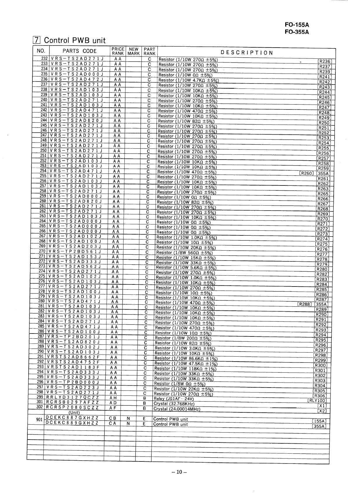
FO-155A
FO-355A
❑Control PWB unit
NO. PARTS CODE PRICE NEW PART
RANK MARK RANK DESCRIPTION
232 VRS– TS2AD2 7 1 JAA cResistor(1/10W 270~ t5%)
--- .. - - —- - .——— [R2361
- ----- .-“.
1.., . ,,,=~lstor~ij JOW270Q t5°/0)
II
—[R237]
... . ,. /. A..,A-- -,-- ..
t—--- I.... tII,, W4,4 L”,
--- . . - - —- - .—- - \&,.L ”,, AL
I——---- I,., . 1t[,,uo, a.”,
. . . . . - - —- - .—-—\L, L“, ,AL
233 VKS– TS2AD77 1IIAA I1P [Qac:-*- . / , /.
234 VRS– Ts 7An7 7 1 IIAA I1P IDae,~rmr , ., , c..,., ‘‘ULJz5yo) [R239]
235 VRS– TS 2AD0 O0JAA cResistor(1/10W On k5%) [R241]
236 VRS–T S2AD 472 JAA cResistor(1/10W 4.7KQ f5%) [R242]
237 VRS– TS 2AD2 71JAA cResistor(1/10W 270Q k5%)
238 VRS–TS2AD103.1 AA c[R243]
I?acic+nr (1 /1 n\A/ 1~K~ i-5%)
Z3Y IVRS–FS.2 A D 1 0 3 I I AA I1P [R2441
IDacictnw (1 /1 n\A/ 1~K~ ~5~]
k
Z4U VKS–IS2A D 7 7 1 I I AA I1P [R245]
IRacic+n” /1 /1 n\A/ 970Q ~5y)
241 vKs – Fs 2 A D 1fI 3I I AA Ilr’ [R2461 -
IRac;stor(1/10W 10KQt5%)
242 VRS–Ts7An47 1 I I AA I1(-’ rR9~ 71
IDacietfir /1 /1 (
243 vRs – TS7An1n7IIAA I1P IDaei-J-7* )-,
244 VRS–Ts7AnR7nIIAA I1P IDacir~m~ , , , ,,
245 VRS–TS7An77 1 IIAA I Ir I Rae; e+fiv f1II f
?Ac \/ wc—Tc 7 nn 9 7 1 1 IA A I1- Im.–. .L. ,. 1.,
I—-. -- 1.., . 1II,,~a, a.u, (L, t“, ,G,
. . - - —- - —
-—..- - - - - I,., . 1I[,,ua,
- ---- .- - I,.. , !I I (., low 470Q t5%) L,,GYJ J
,,go, aL”,
. . —-—-—[R248] “
- ---- - “- - I,., . ,,,~=ls[or~1/ JOW10KQf5°/o)
I I “[R249]
..*.
- ---- - - “ “ I,., . tI“I,\ Ga, aLv, (;/’;OW 82Q Y5%) [R250]
--,, - - , . “I.., , I I “I,\ Ga, ak”, ~~, ~OW270Q t5%) [R251]
A-r”, , ,, u1 dLnu L IL.J II I bInesls~ortli LOW270Q *5%)
247IVRS–TS2AD27 1 Jx: c[R252]
IResistor(1/10W 270~ Y5%)
9AQ IVWC_TC9An97I I ] A A I I nIm-. . [R253]
‘“ ‘“ OW270Q ~5%) [R254] -
ls~or~lt IOW 270Q t50~) [R255] .
istor (1/10W 270~ k5%) [R2561
istor (1/10W270Q Y5%) [R2571 ,
istor (1/10W 10KQ *5%)
,. ,- -.. . . . .. —-- [R2581
%Uw,uh,,+,y
[R259]
Ow470Q :5%) [R2601 [355A1
OW270a f5%) [R261]
-.. . . . . I[R2621
UW 10KQ t5~o)
I[R2631
‘-istor (1;1OW 270Q *5%) [R2651
istor (1/10WOQk5%) [R2661
istor (1/10W82~ k5%) [R2671
. . ‘- ‘- OW270~ &5%) [R2681
-.. .--- ——-
=
265 VRS–Ts7An n nnICal
IAA IIr !D~
266 VRS–Ts7An n n n I I AA I1P IDe=
—
- ---- - “ -“ 1,., , I I uI*\l
—..- -“ “- t,.,. IIuI,,!
LnL/ UJ
stor (1/10WOa 25%3’ [R271]
stor (1/10W0~ f5%) [R2721
stor (1/10W Oa t5~o)
aii iii i;i AA :;jsistor (1/10W l.oKo k5%) [R273]
t&“,I. ,, “
76RIvRc—TC9An1nnIAA n[R274]
RC‘“stor (1/10W 10~ t5~o)
SiAb; iij AA ;[R275]
Resistor(1/10W 20KQ t5%)
— —
-—..—- - - - I,., . rIuIl\t
--.—
-“w . ,. “,d L n u !., (, Jr- - !!, ~“:s1.
269 VR S–T 4
[R2761
270 VRS–T P2 B D5 6 1 JIAA cIResistor(1/8W 560Q Y5%)
271 VRS– TS 7An 1 5 ? I I A A I I P[R2771
1B?SiStor
(1/10w 15K~‘50A)
272 VRS–TS2A D 3 3 3 I I AA I1P [R2781
‘‘a”;”’A”“ “““ ‘=\n t5%)
273 \’-- - [R279]
274 ~KS–1 S.2AD77 1IIAA I1P [R280]
i‘aoietor (1/10W 270Q t50A)
275 kK>– ISZAD1 02J AA rnOOOl
cIResis
276 VRS–TS2 A D 1 03 J I A A I I PJ~esis
I—-- ,,.. .
--,-. Ii , - - - - - . - - —.11Ir,<
Lfl IVKb—ib Z A D Z7 1 J IAA I1P -IDac, c
L/U IVK>—ISZA D 1UOJIAA IIf’ IDaci.
Z/Y IVK>—Ib Z A D 1U3 J IAA I1P IDacic
zuu IvK3—I>Z~U4/1 J IAA I I cIRacic
w
I283I \
——-. -- 1,., . II“I,, G213L
,. - - —--.—-.LRLO<J
jtor (l/10W l.OK~ t-50~) [R2831
;tor (1/10W IOKa k5!?/o) [R2841
I—— -- ,.., .
n-,nI., - - - - - .-.-_,,,~.,stor (l/10W 270a t5°/o)
fI[R2851
I.- 1. . .. 1I,,.=.lstor (1/10W 10~ A5%)
.-1-1-I., -A-,. -.-.-.[R2861
11,,.=.tstor (1/10W 10KQ *5%)
I.-lrln
I,, l-. - --- - - - - . : : “. . . . [R2871
,...,itor (1/10W470~ t5%)
I281IVRS–TS2AD103 jAA [R288] [355A]
;Resistor(1/10W 10KQk5%) [R2891
iRS– TS 2AD 103 JAA cResistor(1/10W 10K~ t5%) [R290]
,iRS– TS2AD 103 JAA cResistor(1/10W 10KQ f5%) [R291]
284 VRS– TS2AD2 7 1 JAA cResistor(1/10W 270Q k5%) [R292]
285 VRS– T$ 2AD 47 1 JAA cResistor(1/10W470Q i5%) [R293]
286 VRS– TS 2AD 100 JAA cResistor(1/10W 10Q f5%) [R294] -
287 VRS– TP 2BD2 O1JAA cResistor(1/8W 200Q k5%) [R295]
288 VRS– TS 2AD8 20 JAA cResistor(1/10W 82Q A5%) [R2961
289 VRS– TS 2AD3 O2JAA cResistor(1/10W3.OK~ f5%) [R297]
290 VRS– TS2AD 103 JAA cResistor(1/10W IOK~ *5%) [R2981
291 VRSTS2AD8662F AA cResistor(1/10W 86.6Kn 31%) [R299]
292 VRSTS2AD 475 2F AA cResistor(1/10W 47.5K~ *1%)
293 VRSTS2AD1 183F AA c[R3001
Resistor(1/10W 118KQ f1%) [R3011
294 VRS– TS2AD3 33 JAA cResistor(1/10W 33KQ t5%) [R302]
295 VRS– TS2AD3 33 JAA cResistor(1/10W33KQ *5%) [R3031
296 VRS– TP2BDIJ O0JAA cResistor(1/8W OQt5%) [R3041
297 VRS– TS 2A D2 23 JAA cResistor (1/10W 22KQ *5%) [R3051
298 VRS– TS 2A D2 7 1 JAA cResistor(1/10W 270Q ~5%) [R3061
299 RR LYD3 12 7QCZZ AH BRclay (JSIAF–24V) [RLY1OOI
301 RCRSB0297AFZZ AD Bcrystal (32.768KHz) [xl]
302 RCRSP2080SCZZ AF Bcrystal (24.00014MHz)
(Unit) [X21
~ol DCEKC88 7GXHZZ cB NEcontrol PWBunit [155A]
DCEKC88 9GXHZZ cA NEcontrol PWBunit [355A]
–10–
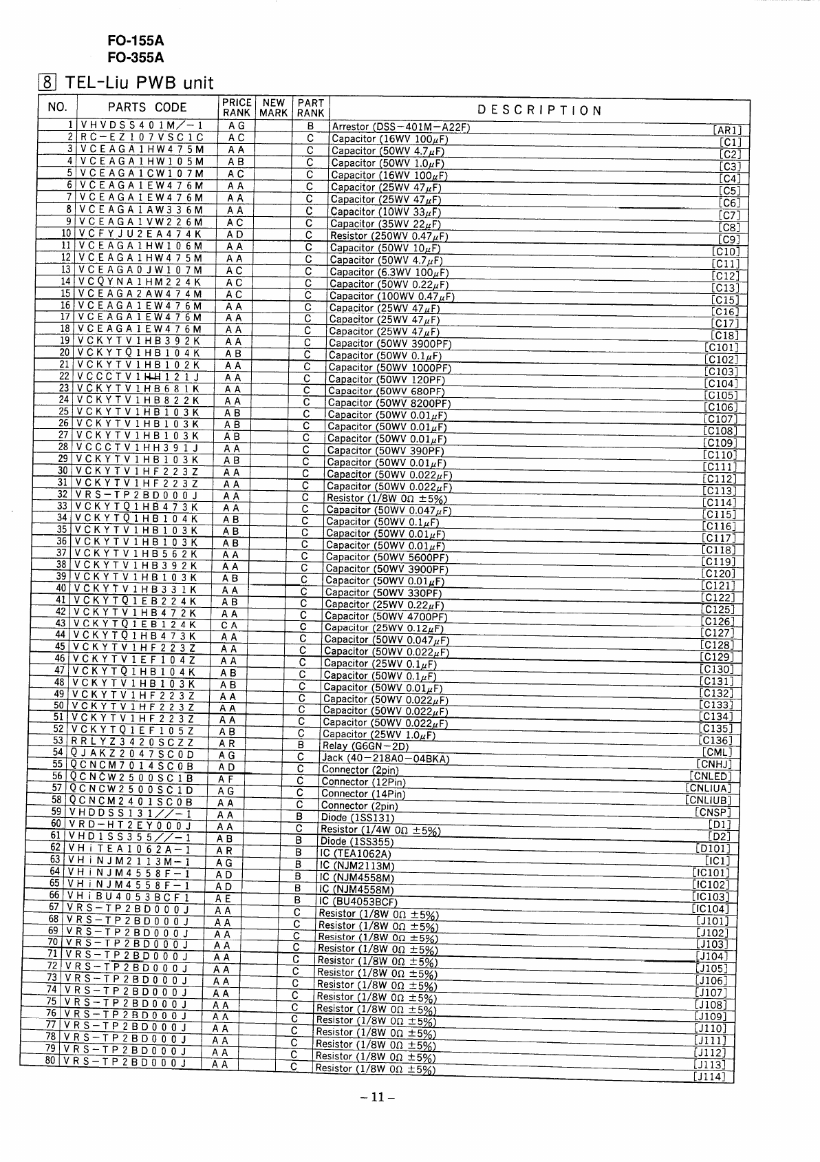
FO-155A
FO-355A
❑TEL-Liu PWB unit
cCapacitor(25WV 47~F) LQ’+J
c[C5]
Capacitor (25WV 47fl F)
.a., .. . ,. . . -[C61
cCapacitor(25WV47g F) Lb1/J
c[C181
Capacitor(50WV3900PF)
n[Cloll
n)acitor (50WV O.lflF) [C102I
~apacitor (50WV 1000PF)
:[C103I
Capacitor (50WV 120PF)
c[C104I
Capacitor [50WV 680PF)
c[C105I
Capacitor (50WV 8200PF) [C1061
nIacitor(50WV O.OlgF) [C107I
lacitor (50WVO.OlgF) [C1081
~apacitor (50WV 0.0 lUF)
:[C109I
Capacitor (50WV 390PF)
c[cl 101
Capacitor (50WV O.Ol~F)
.[cl 111
nacitor (50WV 0.022~F) [C1121
acitor (50WV 0.022XF) [C1131
bIKeslstor (1/8W OQ k5%)
.[C1141
‘nacitor (50WV 0.047fl F) [C1151
acitor (50WV O.l,UF) [C1161
acitor (50WVO.OIPF)
- ,. ,1-Ai.,.,,.-. -. [cl171
NO. PARTS CODE PRICE NEW PART
RANK MARK RANK DESCRIPTION
1VHVDS S 40 1M/– 1 AG BArrestor (DSS–401M–A22F) IARI]
2RC– EZ 10 i’V SC IC AC cCapacitor (16WV 1OOMF) [cl]
3VCEAGA1HW4 75 MAA cCapacitor (50WV 4.7YF) [C2]
4VCE A GA1HW 105 MAB cCapacitor (50WV l.OgF) [C31
5VCEAGA1CW 107 MAC cCac)acitor (16WV 1001,F) rPA 1
6VCE AG A1EW4 76 MAA
7VCEA GA1EW4 76 MAA
8VCEA GA1AW3 36 MAA Gapacltor(1OWV334F)
9VCE A GA1VW 22 6 MAC :[C7]
Capacitor(35WV 22fl F) [C81
10 VCFYJU2EA474K AD cResistor(250WV 0.47MF) [C91
11 VCE A GA1HW 1 06 MAA cCapacitor (50WV 1OMF) IClo]
12 VCEAGA1HW4 75 MAA cCapacitor(50WV 4.7KF) ICll]
13 VCEAGAOJW1 O7M AC cCapacitor(6.3WV IOOgF) [C12] ~
14 VCQYNA 1HM2 24K Ac cCapacitor(50WVO.22,UF) [C131
15 VCEA GA2AW 474 MAc cCapacitor(1OOWV0.47UF)
16 VCE A GA1EW4 76 MAA c[C151
Capacitor(25WV47MF) [C161
17 VCEA GA1EW4 76 MAA cCaDacitor(25WV4711F)
18 VCE AG A1EW4 76 MAA rmI71
19 vCKYTVIHB392K AA
20 vCKYTQIHB1 04K AB bILap
21 vCKYTV1HB102K AA nIn
22 vCC CT VIW1 2lJ AA
23 VCKYTV1HB68 lK AA
24 VCKYTV1HB82 2K AA
25 VCKYTVIHB1 03K AB IP’
26 VCKYTV lHB1 03K AB : I::p(
27 VCKYTVIHB1 03K AB n 1.-.
28 VCCCTV 1HH3 9 1 JAA
29 VCKYTV1HB103K AB
30 v CKYTV1HF223Z AA \Lapi
31 vCKYTV1HF223Z AA :ICap:
32 VRS– TP 2B DO00 JAA =In .
33 vcKYTQl HB473t( AA bapi
34 vCKYTQ1HB104K AB :Cap:
35 vCKy TVl HB103K ABcCap:
36 VCKYTV1HB103K ABcCapacl~or~ouwv u.ul~~j
37 vCKYTV1HB562K AAc[Cl 181
Capacitor(50WV 5600PF)
38 VcKYTVl HB3 92K AAc[C1191
Capacitor(50WV3900PF)
39 vCKYTV1HB103K ABc, [C1201
Capacitor(50WVO.OIZF)
40 v cKYTVl HB33 lK AAc[C1211
Capacitor(50WV330PF)
41 vCKYTQ1EB224K ABc[C1221
Capacitor(25WV 0.22~F) [C125]
42 VCKY TV1HB472K AAcCapacitor(50WV4700PF) [C126]
43 vcKY TQ1EB124K cAcCapacitor(25WV0.12YF)
44 vcKY TQ1HB473K AAc[C1271
Capacitor(50WV0.047gF)
45 vcKY TV1HF223Z AAc[C128]
Capacitor(50WV0.022flF)
46 VCKY TV1EF104Z AAc[C129]
Capacitor(25WVO.lPF)
47 v c KY TQ1HB104K ABc[C1301
Capacitor(50WV0.14F)
48 VCKY TV1HB103K ABc[C1311 ,
Capacitor(50WV O.OIAF)
49 v c KY TV1HF223Z AAc[C1321
capacitor (50WV0.022,uF)
50 v c KY TV1HF223Z AAc[C1331 -
capacitor (50WV0.022,uF)
51 v c KY TVl HF223z AAc[C1341
capacitor (50WV0.022,uF)
52 VCKY TQ1EF1c15z ABc[C1351
capacitor (25WV 1.O,UF)
53 RR LYZ3420SCZZ ARBRclay (G6GN–2D) [;:::; -
54 QJAK Z2047Sc0D AGcJack (40–218AO–04BKA)
55 QCNCM7 O14S COB ADc cQnoectgr(Zpin) [CNHJI
56 QCNCW2 500 SC1B A Fcconnector(12Pin) [cNLEDl
57 QCNCWZ 500 Sc1DAG cconnector(14Pin) [CNLIUAI
58 QCNCM 240 1SCOB AA cconnector (2pin) [CNLIUBl
59 VHDD S S 13 1//– 1A A BDiode (1SS131) [cy:~;
60, VRD–H T2 E Y O00 JA A cResistor (1/4W 00 +qoz) -,
61 VHD1S S 355 //– 1AB.— .
62 VHI“TE A 106 2A–1 ARB
B
63 VHiNJM21 13 M– 1 A G
64 VHiNJM4ss8F–1 AD B
65 VHiNJM45 58F–1 AD B(
B;; (;; E433U
66 VHiBU4053Bc Fl AE BIc (Bl,.n~-,fi
67 VRS–T P2BD0 O0 J AA cResist
68 VRS–T P2B DO O0JAA cResist,
69 VRS–T P2B DO O0JAA cResist!
70 VRS–T P2BD0 O0JAA cResistor~1/uw
71 VRS–TP2BDI)() OJ AA cResistr- ‘“ ‘n’”
72 VRS–TP2BDr) O0JAA cResistf
73 VRS–TP2BDCI O0JAA cResist(
74 VRS–TP2BD O00 JAA cResist(
75 VRS–T P2BD O00 JAA cResistorLl/u
76 VRS–TP2BD000J AA cResist~r/1 IQ1
77 VRS–TP2BD()()0J AA cResistc
78 VRS–TP2BD000J AA cResistc
79 VRS–TP2BDoo OJ AA cResistc
80 VRS–TP2BDooo JAA cDac;e+n
--- —-
1Diode(1SS355) /u] LD2J
1IC (TEA1062A) [D:~;;
1IC (NJM2113M)
k‘n ‘““14558M) [Icloll
[IC102I .
‘“ ”=3M) [IC103I
J4uasdCF)
:or (1/8W on ~5%) [IC104]
or (1/8W 00 *5%) [J101I
or l/8W on 35% [J102I
-- !, ,mt.iOQ~50 )[J103I
ur (AIUV{On t5%) [J104I
or (1/8W OQ~5%) [J105I
or (1/8W OQ&5%) [J106I
or (1/8W on t5Y [J107I
-- “ ‘-lw on 35;; [J108I .
(*, “w on t5%) [J109I
U,
or (1/8W OQt5%) [Jl 101
or (1/8W On &5%) [Jl 111
lr (1/8W OQf5%) [J1121
i‘. G.laLdr (1/8W Oo t5%) [J1131 .
[J1141
–11–
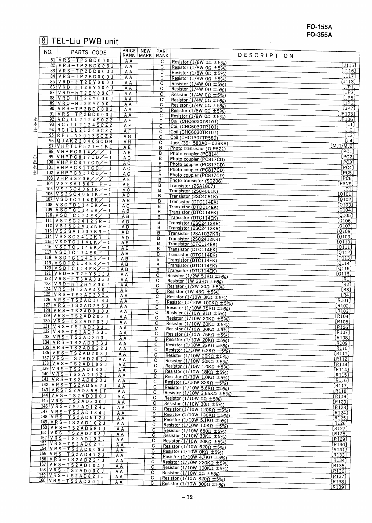
ILCYUUUJ IAA
-r mF., m,-, ,-, ,
rnn J
RANK DESCRIPTION
tor (1/8W On *5%) [J1151
tor (1/8W OQt5%) [J116]
tor (1/8W OQ*5%) [J1171
tor (1/8W OQ*5%)
c[;:;;;
IResistor(1/4W 00 ~5%)
tor (1/4W 00 f5%)
+*w{1/A thl An Acn/, rJP31
lLLIUIJUJ IAA cIResistor (1/4W OQ—*5%)
T9EVnnn t,-
FO-155A
~TEL-1-~u PWB unit FO-355A
Aud vnr au L UOYYY— JIAE BIPhoto
104 VS2 SA 1 80 7–P–1 IAE RITranci
lf15 L
VS 2 S C 406 1 K /– 1 I An I ,
It
IAC BITransi:
.
IHB IBITransi:
.
HB BTransistfir (r
AB BTransisi
AA cResistot
AA cResistoi
AA cResistor,., -.. -w
VRS– HT3A A~;~ ~ AP Pn-- :-. ‘“w 43Q
E
129
130
131
132
133
134
135
.Reslstol
iii i; :Resistol
i3J
IAA cResistor
128IVRS–TS2A D 910 J AA cResister
VRS– TS2 AI) 203 J AP on--:-.–
VRS– TS ,-“. .
VR S–T Sm
VRS– TS2AD 753 JiA; IIvIneslstor f1J1 ~W -
0In-–,–.
VRS– TC
—.—..,
14EK) IQl 131
IQl 141
.“. \“ ,“. 14EK)
tor (DTC114EK) IQl 151
[Q~;y;
r(1/2W 51KQ A5~o)
r(1W 33K~ &5%)
r(117W 7no +Go/\ [R21
—
2A D203J A; Resisror[
-.. -,“:Resistor(., .“.. -
VRS–TS2AD3 33 JAA cResistor(1/10W 3
VRS– TS2AD6 22 JAA r. m--.–*
136 vRS– TS2AD 203 JA~ nesls[or (1/10W 6
;Resistor(1/1nw 9
137 VRS– TS2AD2 O3JAA cResistor(
138 VRS– TS2AD 1 02 JAA cResistor(
139 VRS– TS2AD 1 83 JAA cResistor(
140 VRS– TS2AD 1 02 JAA cResistor(
141 vRS–TS2A D 82 .?I AA .-.
mi
142 VRS– TS2AD~ i5;A;
143 VRSTS2AD 365 1 FAA IIbImeslszor
Pn–-.–*-
144 VRS– TS ~
145 VRS– TS2
146 VRS–T S2
147 VR S–T S2A D134 JIAiII1~esls~or
:IResistor
148 VRS–T S2AD5 12 JIAA IImIi-. ,
149 VRS–TS2
150 VR!j-TS2
151 VR S–TS2
152 VRS–TS2
153 VRS– TS2
154 vRS– TS2 AD I) OOJ IAk IIIKeslsror (
;IResistor(
155 vRS– TS2AD4 72 JIAA IInm––... ,
156 VRs–T s2
157 vRS– TS2
158 VRS–T S2
159 vRS– TS2
160 VRS–T S2 I
\-, -“. .“
‘“ ‘1r-lw a
neslsror ~
Resistor(
Resistor(.,
. . , ,. /
Ibl
-“. .
m
[I1=
– 12–
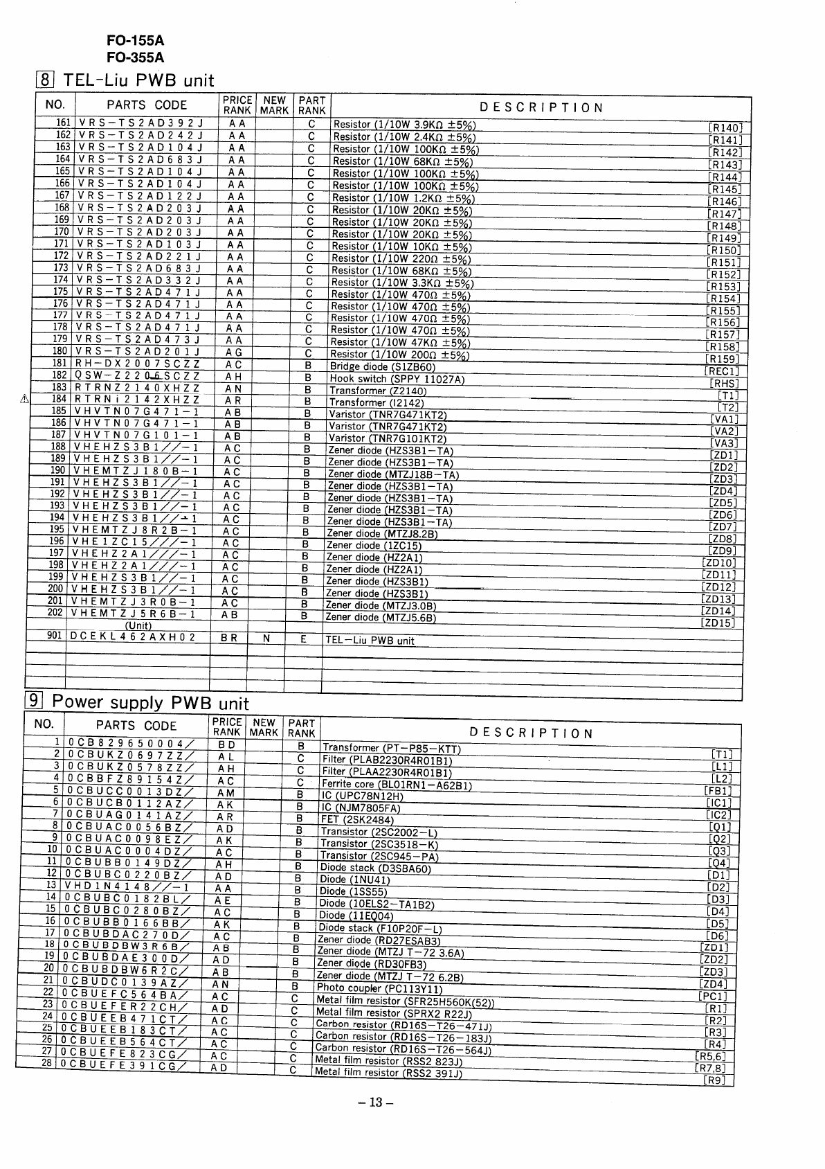
FO-155A
FO-355A
❑TEL-Liu PWB unit
NO. PARTS CODE PRICE NEW PART
RANK MARK RANK DESCRIPTION
.-. . .. ,--...--.. —--
I~un;t) - - - , .
,1
901jD C EKL46 2-AX HO2IB R IN1
I
+a,. , . A.. ,. -‘-~!) LI I LTd J
[R144]
!sls~or\1/ IUW IUUKL1T9~/o [R1451 .
!sistor(1/10W 1.2K~ ~5%) [R146]
. , ,. ,. . ... --, .—-- ..
low 470n t5%) L,, LUVJ
[R1571
10W47Kn *5% [R158]
‘““ ?OOQt5y~ [R1591
(31z1360) IREcll
UK swltcn (SPPY11027A) [~;:;
‘--x--–-r (Z2140)
r(I2142)
dR7G471KT2) [T21
IVA1]
rstor (iINR7G471KT2) [VA21
‘istor (TNR7G101KT2) [VA31
Ier diode(HZS3B1–TA) IZD1] “
ler diode (HZS3B1–TA) [ZD21
‘- -’:-”” ““-7J18B-TA) [ZD31
Ier uluae \rrLa3BI —TA) [ZD4]
Ier diode (HZS3B1–TA) [ZD51
lerdiode (HZS3B1–TA)
-- -“--’- “‘7e3B1–TA) [ZD61
[ZD71
ei uIuue IIVI IiJ8.2B) [zD8]
er diode (1ZC15)
‘“ “:-4- ‘U72A1) [ZD91
‘“ 1) [ZD1OI
r--- . . .
.- 1I
LLUljJ
zJs.ud) [ZD14]
LG1Icl UIUUG (Ivl I-ZJ5.6B) [ZD151
ETEL–Liu PWBunit
1I
I
I I IIt
r
A. .,-” -. .-— i. . ni~tn .,
r- 1rmK I3buut . .... . ..k& PART
IRANKIMARK RANK DESCRIPTION
.--,.-- -— -lsformer(PT–P85–KTT) ITl]
r(PLAB2230R4R01B1) ILl]
‘/D’ A‘~?30R4RolBl) [L2]
sv,,,LC~UIG
(DL() 1RN1—A62B1)
;IC(UPC78N12H) [FBI]
BIC(NJM7805FA) IIcll
R‘ET [2SK2484) [/c;;
sister (2SC2002– L)
L-ie+fi”t?efi-c 40 -K) [Q21
PA) [Q31
~) [Q41
1‘bLb5 z Y65000 4/ BD BTran
2 0 C B U K ZO697 ZZ/ AL cFilter
3 0 C B U K ZO578 ZZ/ At-1 cFilter ~,~mm~~
4 0 CB B F Z 89 154 Z/ AC rrc.v”;+m,.,..- /D1
5 0 CBU CC O0 13 DZ/ AM [
6 0 CBUC BO1 12 AZ/ AK E
7 0 CBUAG O 14 1 AZ/ AR E,
8 0 CBUACO056 BZ/ AD ,L,
BTran~
9 0 CBUACO098 EZ/ AK BTrans,=,u,~z~Uaule-
10 0CBUACO004 DZ/ AC BTransistor (2SC945– F
11 0CBUB B O149 DZ/ AH BDiodestack (D3SBA6L)
12 0 CBUBCO220 BZ/ AD BDiode(1NU41) IDll
13 VH D 1N4 148 //– 1AA BDiode(1SS55) [D21
14 0CBUBCO182 BL/ AE B[D31
Diode(1OELS2–TA1B2)
15 0CBUBCO280 BZ/ Ac BDiode(11EQ04) [D41
16 0 C B UB B O166 BB/ AK BDiode rncl
17 0CBUBDAC270 D/ AC Bzener-.-=- ,,. =
18 0 CBUBDBW 3R6B/ AB Bzenerdiode (Ml-.
19 0CBUBDA E 300 D/ AD Bzenerdiode(RDanc
20 0 CBUBDBW 6R2C/ AB Bzener~in~afm~
21 0CBUDCO139 AZ/ AN BPhoto wwuw,e,\,
22 0CBUEFC564 BA/ AC cMetal film resist
23 0 CBUEFER22 CH/ AD cMetal film resist
24 0 CB U EEB47 1 CT/ AC ccarbon resistor
25 0 CBUE E B 183 CT/ Acccarbon resistor~.._-VW ,LV
26 0 CBUE E B 564 CT/ Acc
27 0 CB U EFE823 CG/ Accarbon resistor (R~l GC–T?K
cMetal
28 0 CBUEFE39 1 CG/ ADcMetal
,..
,”.=,
!stack (F1OP2OF—L) LUJJ
riinri. fR~zTESABs) [D61
ry IT–72 3.6A) IZD1]
._v,’B3) [ZD2]
rzJ T–72 6.2B) [ZD31
-,”-” ,., [ZD4]
iPnltnkr fpcl 13Y1 1)
[~’;;
tor (SFR25H560K(52))
~Or(spRx2 R22J) [R21
(RD16S–T26–471J)
(RnlG~–T9~–183J) [R31
,-ti-564J) [R41
—----- \. .- -“w [R5,61
film resistor(RSS2823J
film resistor(RSS2391J~ [R7,81
[R91
–13 –
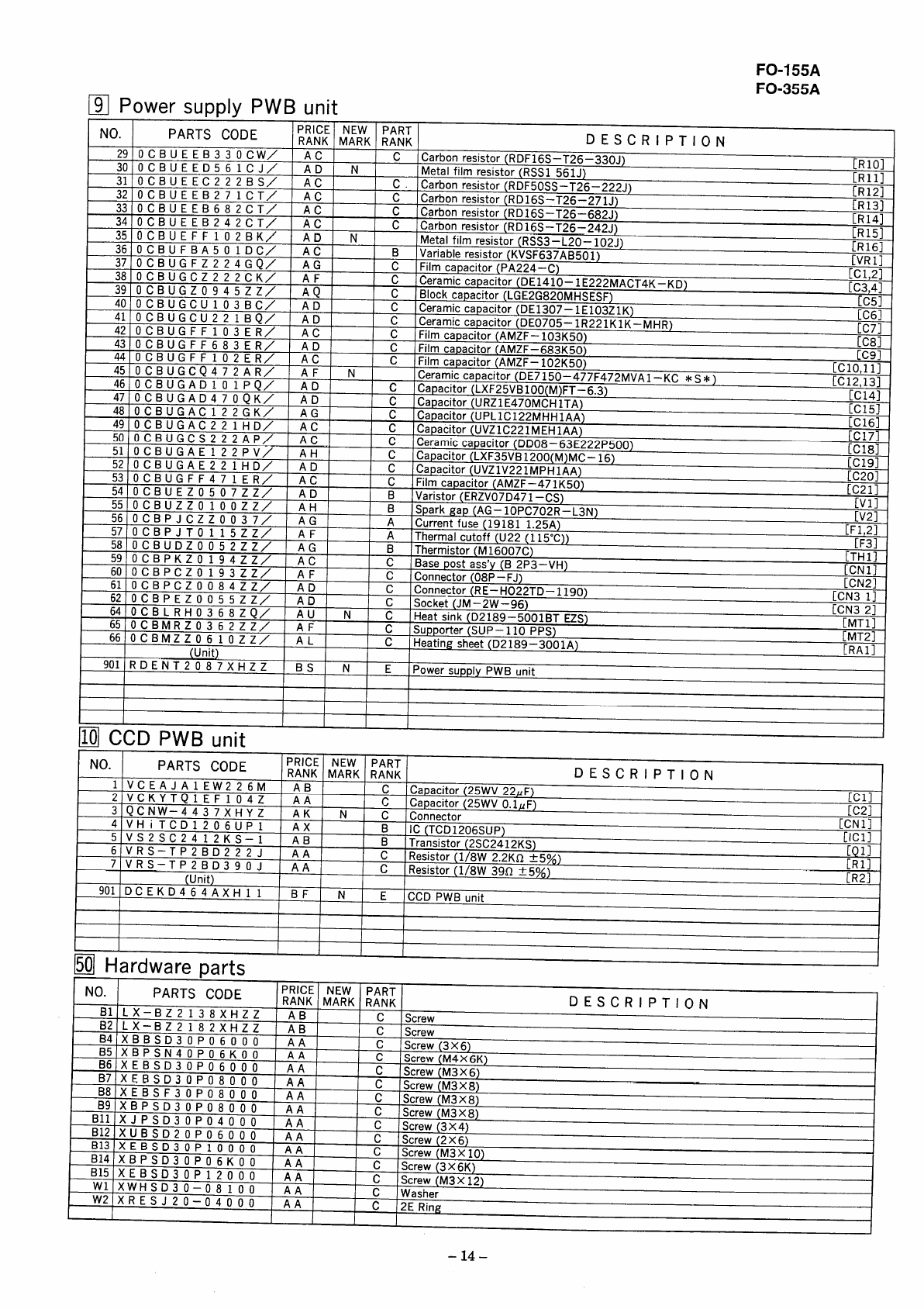
FO-155A
FO-355A
❑Power supply PWB unit
.-
NO. PARTS CODE PRICE NEW PART
RANK MARK RANK DESCRIPTION
29 0 CBUE E B330 CW/ Ac cCarbon resistor (RDF16S–T26–330J)
30 OCBUEED56 ICJ/ AD N[R1OI
Metalfilm resistor (RSS1561J)
31 0 CBUE EC222 BS/ AC c. Carbonresistor(RDF50SS–T26–222J) IRlll
32 0 CBUE E B 27 1 CT/ AC c[R121
Carbonresistor(RD16S–T26–271J)
33 0 CBUE EB 682 CT/ AC c[R131
Carbonresistor(RD16S–T26–682J)
34 0 CBUE E B 242 CT/ AC c[R14]
Carbonresistor(RD16S–T26–242J)
35 0 CBUEF F 102 BK/ AD N[R151
Metal film resistor(RSS3–L20–102J) [R161
36 0 CBUFB A 50 1 DC/ AC BVariableresistor(KVSF637AB501)
37 0 CBUGF Z 224 GQ/ AG c[VR1]
Film capacitor(PA224–C)
38 0 CBUGCZ222 CK/ AF c[C1,21
Ceramiccapacitor (DE141O–1E222MACT4K–KD)
39 0 CBUGZO945 ZZ/ AQ c[C3,41
Block capacitor (LGE2G820MHsEsF)
40 0C BUGC U 103 BC/ AD c[C51
Ceramiccapacitor (DE1307–1E103Z1K)
41 0 CBUGC U 22 1 BQ/ AD c[C61
Ceramiccapacitor(DE0705–1R221K1K–MHR)
42 0 CBUGF F 103 ER/ Ac c[C71
Film capacitor(AMZF–103K5o
43 0 CBUGFF683 ER/ AD cFilmCapacitor(AMzF–683K50] [C81
44 0 CBUGF F 102 ER/ Ac c[C91
Film capacitor(AMZF–102K5O) IClo,l 1]
45 0 CBUGCQ472 AR/ AF Nceramiccapacitor (DE7150–4.77F472MvAl-Kc *S*) [C12,13]
46 0 CBUGAD10 1 PQ/ AD ccapacitor (LXF25VB100(M)FT–6 .3)
47 0 C B U GAD470 QK/ AD c[C141
capacitor (URZ1E470MCH1TA)
48 0 CBUGA C 1 22 GK/ AG c[C151
capacitor (UPL1C122MHH1AA)
49 0 CBUGA C 22 1 HD/ AC ccapacitor (UVZ1C221MEH IAA) [C161
r-. -,.
/
50 0 C BUGCS222 AP/ Ac- —.-. ...
cceramiCcapacitor(DD08–63E~2~p500) Lb1IJ
51 0 CBUGA E 122 PV/ AH c[C181
Capacitor(LXF35VB1200(M)MC– 16)
52 0 CBUGA E 22 1 HD/ AD c[C191
Capacitor(UVZ1V221MPH1AA)
53 0 CBUGF F 47 1 ER/ Ac c[C201
Film capacitor(AMZF–471K50)
54 0 CBUEZO507 ZZ/ AD BVari: r~~ q7
55 0 CBUZ Z O100 ZZ/ AH BSpark gap (AC -_. _. ---- -“,.,
56 0 CB P JCZ Z O03 7/ AG ALVZJ
Current fuse (19181 1.25A)
57 0 C B PJTO1 15 ZZ/ AF A[F1,2]
Thermal cutoff (U22 (115”C))
58 0 C B U D ZO052 ZZ/ AG Br~~?~
Thermistor (M16007c)
co nDnnu7n *n.77 /.-
IIIII
II
\cL (Jlvl —Lvv —30) [CN3 21
“‘;-” ‘m’’189-5001BT EZS)
D—‘13nI- In-. [MT1]
%=llG~L(uz LoY–3001A) LIVI 1CJ
,111 IRA1]
. . wu,,, .
I
II
.- — — ),*n;+
U CCD PWB uii[~
NO. PARTS CODE PRICE NEW PART
RANK MARK RANK Df
1VCEA JA1EW2 26 MAB cCapacitor(25WV 22~F)
2VCKYTQ1 EF 104Z AA cCapacitor (25WV O.lUF)
3QCNW–4 437 XHY Z AK NcPnnn,
4VH iTCD1 206u P1AX E
5VS 2SC2 4 1 2K S–1 AB B
6VRS– TP2BD2 22 JAA ,,U,r=,a.”, \&duLwLGna)
cIQll
Resistor(1/8W 2.2KQ f5x)
7VRS–TP2BD3 90 JAA cResistor(1/8V FR11
(Unit)
901 DC EKD4 64 AXH 1 1 BF NE--- -.. —
ASCRIPTION
[cl]
,-v,,,
,ector [C21
iIIC (TCD1206SUP) ICN1]
?ITrancictnr /9CP9A IOK e\ IIcll
v 39a f5%) L..-J
[R21 I
EW1
W2
‘DL L 1 6LAHLL AB cScrew
IP 06000 AA cScrew
)P06KO(I AA cScrew(N
IP 06000 AA cScrew(M3
000 AA cScrew
IP 08000 AA cScrew(M3~Q~
IP 08000 AA cScrew(M3 -,
‘P 04000 AA cScrew(~~~~
P06000 AA c
m. . . . . Screw~
Id Uuu LRANKIMARK RANK DESCRIPTION
Z138 XHZZ AB
~
3.n n ., ,, - - Screw
.—
(3X6)
f14X6K)
)X6)
~x8)
,,. ”
IX8)
,“. .7
(2X6)
Screw(M3X 10)
Screw(3X6K)
Screw(M3x 12)
cWasher
c2E Ring
AA c
AA I I P
B15 ALHSDSOPIZOO Oii I
;
XWH SD30 – O8 100 AA
XRESJ 20–04000 AA
I
11II
–14 -
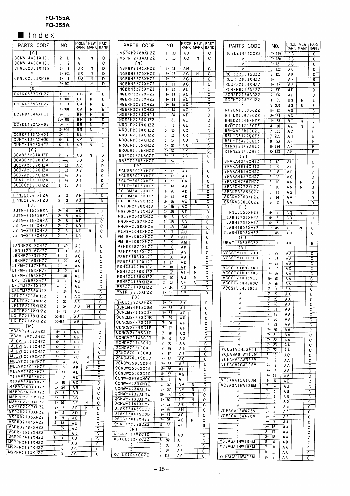
FO-155A
FO-355A
■Index
IPARTS CODE NO. PRICE NEW PART
RANK MARK RANK
ILJ
CCNW–44 31 XHO1 2- 11 AT Nc
CCNW–4436XH01 1- 2AF c
LUA
DCEKC887GXHZZ 1- 3CB N E
// 7-901 CB N E
DCEKC889GXHZZ 1- 3CA N E
It 7-901 CA N E
DCEKD464AXH11 5- 1BF NE
It 10-901 BF NE
DCEKL462AXH02 1- 4BR N E
U8-901 BR N E
DCEKP443AXH01 2- 1BL E
DUNTK424AXHOG 6- 6AY NE
DUNTK4925XHE2 6- 6AR N E
[G]
GCABA2264XHZF 2- 2AS N D
GCABB2265XHZA 1-4 BB D
GCOVA2355XHZA 1- 16 AV D
GCOVA2356XHZA 1- 16 AV D
GCOVA2357XHZA 1- 47 AV c
GDAi–2071XHZA 1- 42 AT D
GLEGG2061XHZZ 1- 15 AE c
[H]
HPNLC2361XHZA 2- 3AH D
HPNLC2361XHZD 2- 3AS D
[J]
JBTN–2157XHZA 2- 4AK c
JBTN–2158XHZA 2- 5AG c
JBTN–2159XHZA 2- 6AF c
JBTN–2160XHZA 2- 7AD c
JBTN–2161XHXA 2- 8AE Nc
JBTN–2162XHZA 2- 9AC c
[L]
LANGF2802XHZZ 1- 49 AE c
LBNDJ2006XHZZ 1- 11 AA c
LBSHP2063XHZZ 1- 17 AC c
LBSHP2068XHZZ 1- 29 AC c
LFRM–2147xHYA 5- 2AV c
LFRM–2153xHzz 4- 2AU c
LFRM–2155xHzz 1- 40 AU c
LPLTG2593XHZZ 3- 1AGc
LPLTM2741xHzz 4- 3AEc
LPLTM2755xHzz 1- 14 ALc
LPLTP2703xHzz 3- 2Acc
LPLTP2754xHzz 1- 50 AR c
LPLTP2775xHzz 1- 57 AQ Nc
LSTPP2042XHZZ 1- 43 Acc
LX–BZ2138xHzZ 50-BI A B c
LX–BZ2182xHzZ 50-B2 AB c
[Ml
MCAMP2019XHZZ 4- 4Acc
MCAMP2020xHzz 4- 5Acc
MLEVP2190XHZZ 4- 6Acc
MLEVP2191XHZZ 4- 7Acc
MLEVP2194XHZZ 4- 17 Acc
ML EVP2199XHZZ 3- 3AcN c
MLEVP2200XHZZ 3- 4Ac Nc
MLEVP2201XHZZ 3- 5AK Nc
MLEVP2202XHZZ 1- 41 AD c
ML EVP2203XHZA 1- 7AD c
MLE VP2204XHZZ 1- 10 AD c
MSP RC2691XHZZ 1- 24 AB c
MSP RC2692XHZZ 3- 6AB c
MSP RC2735XHZZ 4- 8Ac c
MSP RC2793XHZZ 1- 51 AE Nc
MSP RC2797XHZZ 3- 7AE Nc
h’lsPRD2733XHZZ 3- 8AD N c
MSP RD2736xHzz 4- 9Ac c
MSP RD2744xHzz 4- 18 AB c
MSP RD2787xHzz 1- 25 AD c
MSP RP2512xHzz 5- 3AK c
MSP RP2618xHzz 5- 4AD c
MSP RP2619xHzz 5- 5AD c
~sp RP2687xHzz 1- 8Ac c
MSPR P2688xHzz 3- 9Ac c
PARTS CODE NO. PRICE NEW PART
RANK MARK RANK
MSPRP2788XHZZ 1- 30 AD c
MSPRT2734XHZZ 3- 10 AC N c
[N]
NBRGP2”14;XHZZ 3- 11 AH c
NGERH2275XHZZ 3- 12 AC N c
NGERH2276XHZZ 4- 10 AC c
NGERH2277XHZZ 4- 11 AC c
NGERH2278XHZZ 4- 12 AC c
NGERH2279XHZZ 4- 13 AC c
NGERH2280XHZZ 4- 14 AC c
NGERH2281XHZZ 4- 15 AD c
NGERH2282XHZZ 1- 18 AC c
NGERH2283XH01 1- 2a AF c
NGERH2286XHZZ 1- 31 AC c
NROLP2249XHZZ 1- 9AE c
NROLP2300XHZZ 3- 13 AC c
NROLR2313XHZZ 1- 19 AR c
NROLR2314XHZZ 3- 14 AQ Nc
NROLR2315XHZZ 1- 33 AS c
NROLR2316XHZZ 1- 32 AX c
NSFTZ2228SCZZ 3- 15 AC c
NSFTZ2255XHZZ 1- 52 AF c
rPl
~~USS2-07iXHZZ 5- 15 AA c
PCUSS2076XHZZ 5- 16 AA c
PCUT–2032XHZZ 1- 53 BK c
PFLT–2006xHzz 5- 14 AA c
PGiDM2432XHZZ 1- 20 AD c
PGiDM2433XHZZ 1- 21 AD c
PGiDP2429XHZZ 3- 16 AW Nc
PGiDP2430XHZA 1- 26 AX c
PGiDP2431XHZA 1- 35 AE c
PGLSP2043XHZZ 5- 6AK c
PHOP–2087XHZZ 1- 48 AG c
PHOP–2088XHZA 1- 48 AM c
PLNS–2043XHZZ 5- 7AU B
PMi R–2061XHZZ 5- 8AH c
PMIR–2062xHZZ 5- 9AM c
PSHEZ2879XHZZ 5- 10 AK c
PSHEZ2915XHZZ 5- 11 AY c
PSHEZ3031XHZZ 1- 36 AA c
PSHEZ3112XHZZ 3- 17 AD c
PSHEZ3124XHZA 2- 10 AF Nc
PSHEZ3150XHZZ 1-37 AF- Nc
PSHEZ3158XHZZ 2- 12 AB N c
PSHEZ3159XHZA 2- 13 AF Nc
PSPAZ2199XHZZ 1- 38 AQ c
PWiR–2018XHZZ 6- 15 AP D
rnl
L’iA
QACCL762AXHZZ 1- 12 AY B
QCNCM2401SCOB 8- 58 AA c
QCNCM2401SCOF 7- 86 AB c
QCNCM2442SCOB 7- 85 AB c
QCNCM2482SCIF 7- 90 AF c
QCNCM2499SCIB 7- 87 AF c
QCNCM2499SC1D 7- 88 AG c
QCNCM7014SCOB 8- 55 AD c
QcNcM7014scoc 7- 91 AA c
QCNCM7014SCOF 7- 89 AB c
QCNCM7014SCOG 7- 84 AB c
QCNCM7014SCIC 7- 93 Ac c
QCNCW2500SCOH 7- 92 AF c
,QCNCW2500SC1B 8- 56 AF c
QCNCW2500SC1D 8- 57 AG c
QCNW–3976XHOG 6- 1AT c
QCNW–4433XHYZ 1- 27 Ap Nc
QCNW–4434XHYZ 1- 22 AE Nc
QCNW-4437XHYZ 10- 3AK N c
QCNW–4439XHYZ 1- 54 AF Nc
QCNW-4441XHYZ 5- 12 AE Nc
QJ~KZ2046SCDB 8- 96 AH c
QJAKZ2047SCOD 8- 54 AGc
QS0CZ2015XH32 7-105 AcNc
QSW-Z2206SCZZ 8-182 AH B
rml
Lnl
RC–EZ107VSC1C 8- 2Ac c
RCiLL2124SCzz 8- 92 AF c
M8- 93 AF c
H8- 94 AF c
RCiLZ1044CCzz 7-118 Ac c
IPARTS CODE NO. PRICE NEW PART
RANK MARK RANK
RCi LZ1044CCZZ 7-119 AC c
u7-120 AC c
It 7-121 AC c
n7-122 AC c
RCiLZ2104SCZZ 7-123 AK c
RCORF2063XHZZ 1- 6AF B
RCORF2064XHZZ 1- 13 AF B
RCRSB0297AFZZ 7-301 AD B
RCRSP2080SCZZ 7-302 AF B
RDENT2087xHzz 1- 39 BS NE
II 9-901 BS NE
RFi LN2013SCZZ 8- 95 AG c
RH–DX2007SCZZ 8-181 AC i
RHEDZ2046XHZZ 1- 23 BT N B
RMOTZ2121SCZZ 4- 16 AZ N B
RR–XA02ROSC2E 7-133 AC c
RRLYD3127QCZZ 7-299 AH B
RRLYZ3420SCZZ 8- 53 AR B
RTRNi2142XHZZ 8-184 AR B
RTRNZ2140XHZZ 8-183 AN B
[s1
SPAKA4346XHZZ 1- 60 AH c
SPAKA4655XHZZ 6- 9AF D
SPAKA4656XHZZ 6- 8AF D
SPAKA4657XHZZ 6- 13 AC D
SPAKC4766XHZZ 6- 10 AN N D
SPAKC4772XHZZ 6- 10 AN N D
SPAKP3385SCZZ 6- 11 AG D
SSAKA2003XHZZ 6- 14 AA D
SSAKA3001CCZZ 6- 2AA D
rrl
Lfi
TiNSE3553XHZZ 6- 4AQ N D
TLABH3733XHYA 6- 5AD D
TLABH3733XHZA 6- 5AD D
TLABH3803xHYz 1- 45 AF Nc
TLABH3803XHZZ 1- 45 AD c
[u]
UBATL2033SCZZ 7- 1AK B
[v]
VCCCTV1HH121J 8- 22 AA c
VCCCTVIHH180J 7- 34 AA c
u7- 35 AA c
VCCCTV1HH270J 7- 67 AC c
VCCCTVIHH330J 7- 66 AA c
VCCCTV1HH391J 8- 28 AA c
VCCCTVIHH5ROC 7- 56 AA c
VCCSTV1HLI02J 7- 14 AA c
II 7- 27 AA c
// 7- 29 AA c
tl 7- 30 AA c
#7- 31 AA c
It 7- 62 AA c
I/ 7- 70 AA c
II 7- 79 AA c
u7- 80 AA c
IJ 7- 81 AA c
II 7- 82 AA c
fl 7- 83 AA c
vCCSTVIHL391J 7- 72 AA c
vC,EAGAOJW1O7M 8- 13 Acc
vCEAGAIAW336M 8- 8AA c
vCEAGAICW106M 7- 2AA c
u7- 7AA c
JJ 7- 11 AA c
vCEAGA1CW107M 8- 5Acc
Vc EAGA1Ew226M 7- 4AB c
tt 7- 5ABc
U7- 6ABc
#7- 8ABc
#7- 9ABc
Vc EAGA1EW475M 7- 3AAc
Vc EAGA1EW476M 8- 6AA c
II 8- 7AA c
// 8- 16 AAc
il 8- 17 AA c
48- 18 AA c
Vc EAGA1Hw105M 8- 4AB c
Vc EAGAIHW106M 7- 10 AA c
// 8- 11 AA c
Vc EAGA1HW475M 8- 3AA c
–15-
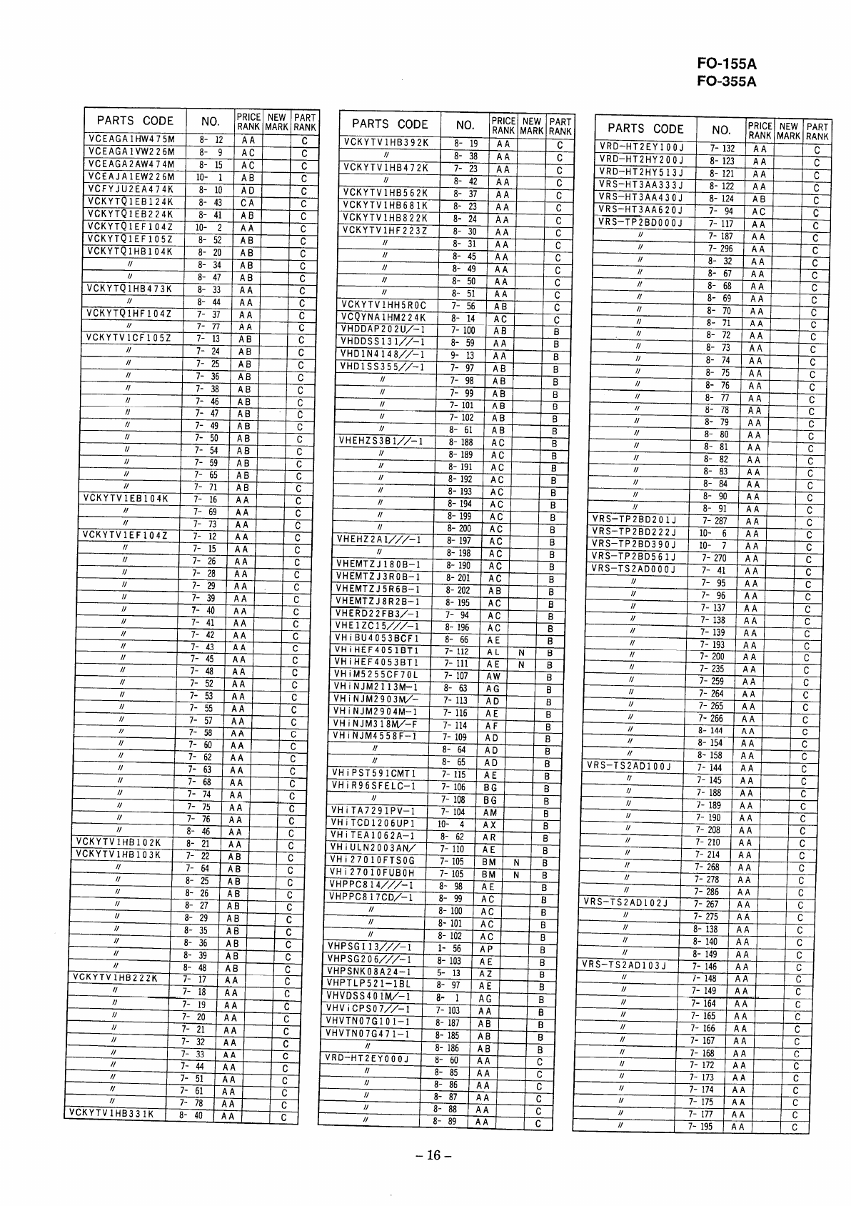
PU-155A
FO-355A
i: ‘!‘::’‘NG
PARTS CODE NO.
VCKYTV1HB392K
u
VCKYTV1HB472K
PARTS CODE NO. PRICE NEW PART
RANK MARK RANK
VCEAGAIHW475M 8- 12 AA c
VCEAGA1VW226M 8- 9AC c
VCEAGA2AW474M 8- 15 AC c
VCEAJA1EW226M 10- 1AB c
VCFYJU2EA474K 8- 10 AD c
VCKYTQ1EB124K 8- 43 CA c
VCKYTQ1EB224K 8- 41 ‘n
VCKYTQIEF104Z 10- 0
VCKYTQ1EFI05Z 8- d.. n. II
VCKYTQIHBI04K 8- 20 AB :I
u8- 34
II “.7
l\u. RANK MARK RANK
:Vlrlnl I7-132 AA c
-177 aA P
Iu8- 42 IAA I.-. I.6. ,.”
cb
VRQ—UT2AA2?1 I0-122 AA c
-124 AB c
-QA AP n
VCKYTvlHB562K 8- 37 AA i
VCKYTvlHB681K 8- 23 AA c
VCKYTvlHB822K 8- 24 AA c
VCKYTV1HF223Z 8- 30 AA c
U8- 31 AA c
// 8- 45 AA c
H8- 49 AA c
If 8- 50 AA c
II 8- 51 AA c
VCKYTV1HH5ROC 7- 56 AB c
,,an.,., ..,,..,.- . .. -.
.,.” ,1, ”nndd.1 J
VRS–HT3AA430J ;:
VRS–HT3AA620J 7-47,””, ,~,
VRS–TP2BDOOOJ 7-
fl 7-187 IAA c
n7-296 IAA cI
I/ “
#8- ;; ;; :
// 8- 68 AA c
#IuIIIL
n8- ;; ;; cI
no L
LAA c
R7 AR o
-117 IAA IcI
1
IQ-27 IAA I I
AB c
I0- ql AB c
AA r.
VCKYTQ1HB473K 8- 33 Imn IIb
#8- 44 IAA cI
VCKYTQIHF1( 04Z 7- 37 AA c
7- 77 AA c
15Z 7- 13 AB c
AB c
25 AB c
36 AB c
38 AB c
7- 46 AB
&c
u7- 47 AB c
#7- 49 AB c
O7- 50 AB c
It 7- 54 AB c
I/ 7- 59 AB c
// 7- 65 AB c
71 AB c
16 AA c
co flh m
vbvYlvAlHMz14K 8- 14 Ac c
vHDDAP202u/–l 7-1oo AB B
vHDDss131//–l 8- 59 AA B
vHDlN4148//–I 9- 13 AA B
vHDlss355//–l 7- 97 AB B
u7- 98 AB B
ff 7- 99 AB B
o7-101 AB B
II 7--102 AB B
n8- 61 AB B
vHEHzs3B1//–l 8-188 Ac B
// 8- 71 AA 6
// 8- 72 AA c
n8- 73 AA c
// 8- 74 AA c
v8- 75 AA c
#8- 76 AA c
U8- 77 AA c
IJ 8- 78 AA c
// 8- 79 AA c
J/ 8- 80 AA c
JJ 8- 81 AA c
8- 82 AA r.
24 1
1/ 7-
VCKYTVIEB1(J4K 7-
Ii 7- v,
u7-
VCKYTV1EF104Z 7- .L
U7- 15
Innl Ibl 1/ 8-199 Ac B
8-200 Ac
vHEHz2;l///–l B
8-197 Ac B
#8-198 AC B
VHEMTZJ180B–I 8-190 Ac B
VHEMTZJ3R0B–1 8-201 Ac B
VRS–TP2BD201J I
7-287 AA i
VRS–TP2BD222J 10- 6AA c
VRS–TP2BD390J 10- 7AA c
VRS-TP2BD561J 7-270 AA c
VRS–TS2ADOOOJ 7- 41 AA c
u7- Q5 AA P
73 IAA c
1’)I AA I I o
t’
.,-1 Ibl
1AA c
// I 7- 26 IAA c
7no IAA P
// 1- <0 I. . I
f/ 7- 29 Ibl
IAA c
I// 7- 39 IAA c
)) I7AA I&a P
VHEMTZJ5R6B–I 8-202 AB B
VHEMTZJ8R2B–1 8-195 AC B
VHERD22FB3/–I 7- 94 Ac B
‘HElzc15///–l 8-196 AC B
HiBU4053BCFl 8- 66 AF R
-“ r,,.
// 7- ‘c ‘“t
// 7-1
u7-1
u7- IJ, IHM I
u7-193 IAA
//
t-- “‘‘- ““ ‘“- ‘‘‘“‘v
v
VHiHEF4051BTl 1II
~7-112 ]ii I N[ ;
tf,,:,,l-r .--”’---- I
I., I,-
,, ---1
L
c
1{ 1- 4J H14 L
I/ 7- 45 AA c
I/ 7- 48 AA c
// 7- 52 AA c
fl 7- 53 AA c
7-200 AA
Ivrlllltr4u35tjll i
I/-111jAEj N I B
il,,:,,rarl-a--”, I I // 7-235 AA
___ C
7- ?59 AA c
ICA AA .
1- lu7
8- 63
7-113
7-116
7-114
VHiNJM4558F–1 7-109 r
II i~- AA a
AW B
AG B
AD B
AE B
AF B
AD B
An D
// 7-55 AA i
I/ 7-57 AA c
f) 7-58 AA c
// 7-60 AA c
II 7-C* AA c
AA
VHiNJM2904M”–1 I
VHiNJM318M/–F IUu IMM IIL
AAiAA .I
,1
8-154 IAA c
IQ-IKO I Aa I I .
I. . ““ I
IJ 8- 65 IAD
l~,,:mf.-r n.,...-. r..- i~I*‘“‘“O ‘“” ‘ ‘ ‘ ‘
If ;- ;;
It 7- 68 :: :
1/ 7- 74 AA c
II
II 7- 76 AA i
It 8- 46 AA c
VCK YTV 1HE 102 K8- 21 AA c
VCKYTV 1HB 103 K7- 22 AB c
If 7- 64 AB c
II 8- 25 AB c
// 8- 26 AB c
If 8- 27 AB c
II 8- 29 AB c
II 8- 35 AB c
1/ 8- 36 AB c
II
,1t
IUOJ I7-lM IAA I I P1
vn Ira IoyI~MI I1
1-115 AE . . ,,,1
BII
VHiR96SFELC–I 7-145 AA ;
7-106 BG BIf 7-188 AA
u7-108 BG Bc
II
,,,,.1-. -,”,..-,. -7-189 AA c
I
7- 75 IAA 1cI
VHPPC817CD/–l I8-
J/ I8-1
., !– Loo
VR S–TS 2AD 102 J7-267 ;: :
1/ 7-275 AA c
I..“” ,. “IIu
1/ 0 ,“,-,I hA I
!t1
II IR-17Q }AA P i
o- 14U IHH IIL
o,“n IA. I
11
8- 39 IAB cI
1
l} IQ-AO[A“1I
VCKYTV1HE22 2KwL
;- 17 ;: c
// 7- 18 AA c
II 7- 19 A)
II 7- 20 Al 1AA c
IAA c
1/ 7-166 AA c
II 7-167 AA c
)) 7-168 AA c
II 7-172 AA c
l) 7-173 AA c
II 7-174 AA c
II 7-175 AA c
1/ 7-177 AA c
II 7-195 AA c
,
I7– ~1 I , AI I I
7- 32 AA c
7- 33 AA c
7- 44 AA r
If
VCKYTVIHB331K ,II
–16–
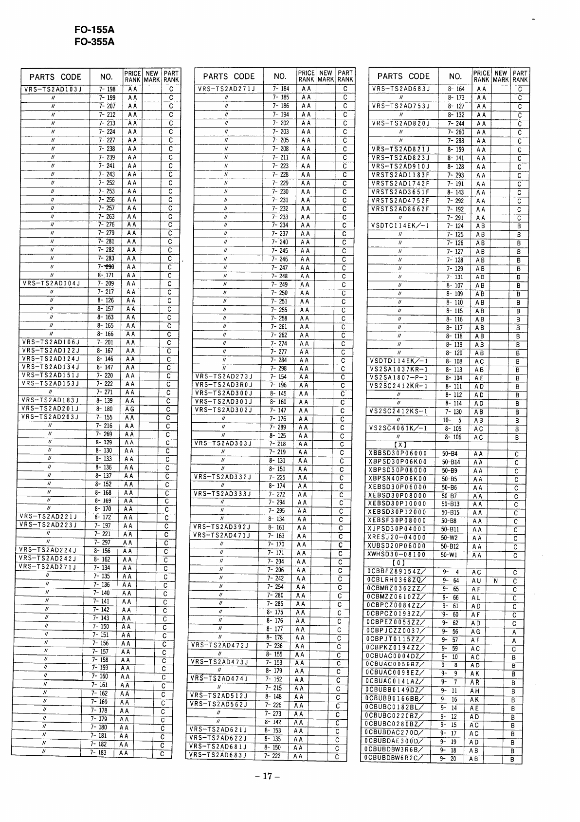
FO-155A
FO-355A
PARTS CODE NO. PRICE NEW PART
RANK MARK RANK
VRS-TS2AD103J 7-198 AA c
I/ 7-199 AA c
rI/ I7-207 IAA IIcl
,
11 7-239 AA c
1/ 7-241 AA c
1/ 7-243 AA c
Ii 7-252 AA c
11 7-253 AA c
1/ 7-256 AA c
II 7-257 AA c
II 7-263 AA c
II 7-276 AA c
1) 7-279 AA c
II 7-281 AA c
IJ 7-282 AA c
1/ 7-283 AA c
II 7-i!90 AA c
II 8-171 AA c
VRS–TS2ADI04J 7-209 AA c
U7-217 AA c
u8-126 AA c
// 8-157 AA c
It 8-163 AA c
// 8-165 AA c
// 8-166 AA c
VRS–TS2AD106J 7-201 AA c
VRS–TS2AD122J 8-167 AA c
VRS–TS2AD124J 8-146 AA c
VRS–TS2AD134J 8-147 AA c
VRS–TS2AD151J 7-220 AA c
VRS–TS2AD153J 7-222 AA c
U7-271 AA c
VRS–TS2AD183J 8-139 AA c
VRS–TS2AD201J 8-180 AG c
VRS–TS2AD203J 7-155 AA c
u7-216 AA c
f/ 7-269 AA c
I/ 8-129 AA c
II 8-130 AA c
I/ 8-133 AA c
// 8-136 AA c
I/ 8-137 AA c
// 8-152 AA c
// 8-168 AA c
// 8-169 AA c
// 8-170 AA c
VR S–TS2AD221J 8-172 AA c
VRS–TS2AD223J 7-197 AA c
// 7-221 AAc
07-297 AA c
vR S–TS2AD224J 8-156 AA c
VRS–TS2AD242J 8-162 A A c
VRS–TS2AD271J 7-134 AAc
// 7-135 AAc
u7-136 AAc
// 7-140 AA c
n7-141 AA c
u7-142 AA c
u7-143 AA c
IJ 7-150 AA c
v7-151 AA c
Y7-156 AA c
I/ 7-157 AA c
I/ 7-158 AA c
fl 7-159 AA c
// 7-160 AA c
u7-161 AA c
If 7-162 AA c
M7-169 AA c
u7-178 AA c
I/ 7-179 AA c
// 7-180 AA c
// 7-181 AA c
// 7-182 AA c
// 7-183 AA c
IPARTS CODE NO. PRICE NEW PART
RANK MARK RANK
VRS–TS2AD271J 7-184 AA c
IJ 7-185 AA c
Y7-186 AA c
I , !
IIt 7-194 IAA cI
u
II /-zu3 IHn I I L
II 7-?k! IAA c
I7-202 IAA c
-“n. I . . i I.I
It 7-211 AA c
II 7-223 AA c
IJ 7-228 AA c
v7-229 AA c
// 7-230 AA c
II 7-231 AA c
, , , 1
I// 7-232 IAA IcI
1[ I-L.
If 7->
II 7->
II 7->
u7-2i
u7-ZI
JI T.
It
U7-233 AA c
// 7-234 AA c
,, 7“37 AA c
$0 AA c
45 AA c
$6 AA c
t7 AA c
!8 jAA c
I-L49 AA c
7-250 AA c
It 7-251 AA c
IJ 7-255 AA c
// 7-258 AA c
II 7-261 AA c
#7-262 AA c
II 7-274 AA c
// 7-277 AA c
It 7-284 AA c
v7-298 AA c
VRS–TS2AD273J 7-154 AA c
VRS–TS2AD3ROJ 7-196 AA c
VRS–TS2AD300J 8-145 AA c
VRS–TS2AD301J 8-160 AA c
VRS–TS2AD302J 7-147 AA c
u7-176 AA c
O7-289 AA c
fl 8-125 AA c
VRS–TS2AD303J 7-218 AA c
// 7-219 AA c
fl 8-131 AA c
If 8-151 AA c
VRS–TS2AD332J 7-225 AA c
// 8-174 AA c
VRS–TS2AD333J 7-272 AA c
II 7-294 AA c
O7-295 AA c
II 8-134 AA c
VRS–TS2AD3
VRS–TS2AD4 I
It 17-170 IAA i
I/ 7-171 IAA c
,, II–LU
J7-20
I
92J 8-161 IAA c
71J 7-163 IAA Ic
,
// I7-’04 AA c
16 AA c
Ii 7-242 AA c
IJ 7-254 AA c
II 7-”30 AA c
>C ,,
,, I-LO
#7-28> HH
If 8-175 AA :
u8-176 AA c
I/ 8-177 AA c
// ~-779 .,
. .,,
VRS–TS2AD47ZJ 7-23L r.n
n8-155 AA ;
JRS-TS2AD473J 7-153 AA c
#8-179 AA c
IRS–TS2AD474J 7-152 AA c
U7-215 AA c
IRS–TS2AD512J 8-148 AA c
IRS–TS2AD562J 7-226 AA c
// 7-273 AA c
// 8-142 AA c
‘RS–TS2AD621J 8-153 AA c
‘RS–TS2AD622J 8-135 AA c
‘RS–TS2AD681J 8-150 AA c
RS–TS2AD683J 7-222 AA c
PARTS CODE NO. PRICE NEW PART
RANK MARK RANK
,
VRS–TS2AD683J 8-164 AA c
u8-173 AA c
VRS–TS2AD753J 8-127 AA c
u8-132 AA c
VRS–TS2AD820J 7-244 AA c
U7-260 AA c
II 7-288 AA c
VRS–TS2AD821J 8-159 AA c
VRS–TS2AD823J 8-141 AA c
VRS–TS2AD91OJ 8-128 AA c
VRSTS2AD1183F 7-293 AA c
VRSTS2AD1742F 7-191 AA c
VRSTS2AD3651F 8-143 AA c
VRSTS2AD4752F 7-292 AA c
VRSTS2AD8662F 7-192 AA c
11 7-291 AA c
vsDTc114EK/–l 7-124 AB B
If 7-125 AB B
u7-126 AB B
M7-127 AB B
I/ 7-128 AB B
v7-129 AB B
IJ 7-131 AB B
M8-107 AB B
I
u8-109 AB B
u8-110 AB B
II 8-115 AB B
u8-116 AB B
n8-117 AB B
I/ 8-118 AB B
IJ 8-119 AB B
II 8-120 AB B
vsDTDl14EK/–l 8-108 AC B
VS2SA1037KR–1 8-113 AB B
VS2SA1807–P–I 8-104 AE B
VS2SC2412KR–1 8-111 AD B
u8-112 AD B
I/ 8-114 AD B
VS2SC2412KS–1 7-130 AB B
u10- 5AB B
JS2SC4061K/–l 8-105 AC B
8-106 AC B
:x]
XBBSD30P06000 50-B4 AA c
XBPSD30P06KO0 50-914 AA c
XBPSD30P08000 50-B9 AA c
XBPSN40P06KO0 50-B5 AA c
XEBSD30P06000 50-B6 AA c
XEBSD30P08000 50-97 AA c
XEBSD30PIOOO0 50-B13 AA c
XEBSD30P12000 50-B15 AA c
XEBSF30P08000 50-B8 AA c
XJPSD30P04000 50-911 AA c
XRESJ20–04000 50-W2 AA c
XUBSD20P06000 50-B12 AA c
XWHSD30–08100 50-W1 AA c
[01
OCBBFZ-89;54Z/ #9- 4AC c
OCBLRH0368ZQ/ 9- 64 AU N c
OCBMRZ0362ZZ/ 9- 65 AF c
ocBMzzo610zz/ 9- 66 AL c
0CBPCZO084ZZ/ 9- 61 AD c
OCBPCZO193ZZ/ 9- 60 AF c
ocBPEzoo55zz/ 9- 62 AD c
ocBPJczzoo37/ 9- 56 AG A
ocBPJTol15zz/ 9- 57 AF A
ocBPKzo194zz/ 9- 59 AC c
OCBUACOO04DZ/ 9- 10 AC B
OCBUACO056BZ/ 9- 8AD B
OCBUACO098EZ/ 9- 9AK B
ocBuAGo141Az/ 9- 7AR B
OCBUBBO149DZ/ 9- 11 AH B
OCBUBBO166BB/ 9- 16 AK B
OCBUBCO182BL/ 9- 14 AE B
OCBUBC0220BZ/ 9- 12 AD B
OCBUBC0280BZ/ 9- 15 AC B
OCBUBDAC270D/ 9- 17 AC B
OCBUBDAE300D/ 9- 19 AD B
OCBUBDBW3R6B/ 9- 18 AB B
OCBUBDBW6R2C/ 9- 20 AB B
–17–
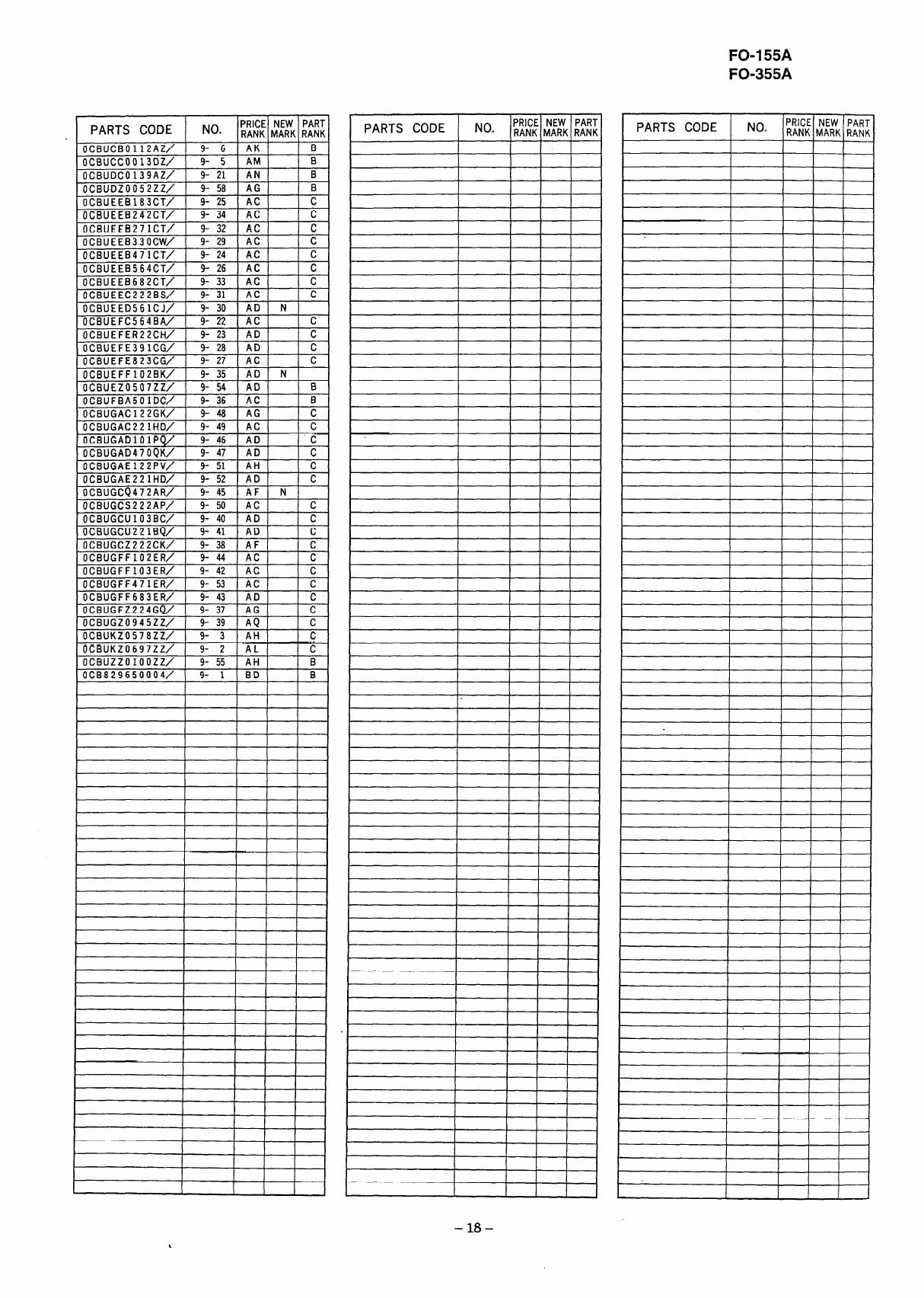
FO-155A
FO-355A
PARTS CODE NO. PRICE NEW PART IPARTS CODE NO. PRICE NEW PART
RANK MARK RANK RANK MARK RANK
ocBucBol12Az/ 9- 6AK B
OCBUCCOO13DZ/ 9- 5AM B
ocBuDco139Az/ 9- 21 AN B
OCBUDZO052ZZ/ 9- 58 AG B
c
c
ocBuEEB183cT/ I9- 25 IAC
OCBUEEB242CT/ I9- 34 IAC I
ocBuGFF471ER/ 9- 53 AC c
OCBUGFF683ER/ 9- 43 AD c
OCBUGFZ224GQ/ 9- 37 AG c
ocBuGzo945zz/ 9- 39 AQ c
OCBUKZ0578ZZ/ 9- 3AH c
I)CBUKZ0697ZZ/ 9- 2AL c
OCBUZZOIOOZZ/ 9- 55 AH B
OCB829650004/ 9- 1BD B
PARTS CODE NO. PRICE NEW PART
RANK MARK RANK
I
III I
,I1
I
,I11
I
t
–l8-
k

FO-155A
FO-355A
—
SHARP
COPYRIGHT @1996 BY SHARP CORPORATION
All rightsreserved.
PrintedinfiJapan.
Nopartofthispublicationmaybe reproduced,
storedinaretrievalsystem,ortransmitted,
inanyformorbyanymeans,
electronic,mechanical,photocopying,recording,orotherwise,
withoutpriorwrittenpermissionof the-publisher.
\
‘\
SHARPCORPORATION
>.
,
Communication&AudioSystemsGroup
Quality&ReliabilityControlCenter
Higashihiroshima,Hiroshima739-o1,Japan
Printedin Japan
9603-542NSOIS*T
