Unknown FO3700
User Manual: FO3700
Open the PDF directly: View PDF ![]() .
.
Page Count: 118 [warning: Documents this large are best viewed by clicking the View PDF Link!]
%
-m
FO-3700A
1---+'
SHARP
SERVICE
MANUAL
CODE:OOZF03700ASME
FACSIMILE
MODEL
FO-3700
CONTENTS
CHAPTER 1. GENERAL DESCRIPTION
[l]
Specifications ......................... l-l
[2]
A look at the machine ...................
1-2
[3]
Operation Panel .......................
1-3
[4]
Transmittable Documents ............... l-4
[5]
Installation ............................ l-5
[6]
Quick reference guide .................. l-9
CHAPTER 2. ADJUSTMENTS
[I]
Adjustments .......................... 2-l
[2]
Diagnostics and service soft switches ...... 2-2
[3]
Trouble shooting ...................... 2-13
[4]
Error code table ...................... 2-14
CHAPTER 3. MECHANISM BLOCKS
[l]
General description .................... 3-l
[2]
Disassembly/assembly procedures ........ 3-4
CHAPTER 4. DIAGRAMS
[l]
Blockdiagram .........................
4-l
[2]
Wiring diagram ........................ 4-2
[3]
Point to point diagram ................... 4-3
[4]
Connector signal name .................. 4-4
CHAPTER 5. CIRCUIT DESCRIPTION
[l]
Circuit description ...................... 5-l
[2]
Control PWB description ................
5-2
[3]
Description of CCD board ..............
5-11
[4]
TEULIU (with Speech PWB unit) board
circuit description .....................
5-l 1
[5]
Description of power supply ............. 5-l 4
CHAPTER 6. CIRCUIT SCHEMATICS AND PARTS
LAYOUT
[l]
Control circuit/PWB .................... 6-l
[2]
TEULIU circuit/PWB and sensor
circuit/PWB ...........................
6-7
[3]
Speech circuiff PWB ................... 6-l 3
[4]
Power supply circuit/PWB ..............
6-15
[5]
CCD circuit/PWB ..................... 6-l 7
[6]
Operation panel circuit/PWB ............ 6-l 8
[7]
LCD unit circuit/PWB ..................
6-20
(81
Print unit circuit/PWB ..................
6-22
CHAPTER 7. OPERATION FLOWCHART
[l]
Flowchart ............................ 7-l
[2]
Power on sequence ....................
7-7
CHAPTER 8. OHTERS
[l]
Service Tools .........................
8-1
[2]
IC signal name ........................
8-3
PARTS GUIDE
Parts marked with
“8”
is important for maintaining the safety of the set. Be sure to replace these parts with specified
ones for maintaining the safety and performance of the set.
This document has been published to be used
SHARP
CORPORATION
foraftersalesserviceonly.
The contents are subject to change without notice.
FO-3700A
Caution:
Please
use
the
per
guage
Part
No.
OJZC214460003
when
repairing
printes
section.
The
inkjet
cartridge
consumeable
cannot
be
exposed
to
the
atmosphese
for
prolong
periods.
CHAPTER
I.
GENERAL
DESCRIPTION
[I]
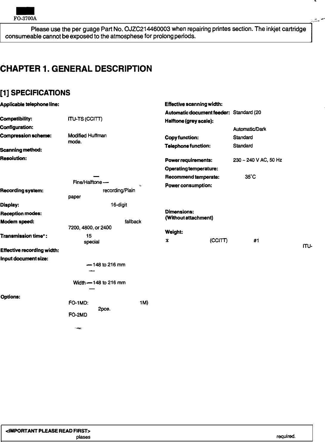
SPECIFICATIONS
Applicable
telephone
line:
Compatibility:
conflguratlon:
Compression
scheme:
Scanning
method:
Reeollltlon:
Recording
system:
Display:
Reception
modes:
Modemspeed:
Transmission
time’
:
Effective
recording
width:
Input
document
size:
Options:
Public switched telephone network/
PBX
IN-TS
(CCITT)
G3 mode
Hatfduplex, desktop transceiver
ModlIed
Huffman and Sharp special
mode.
Flat-bed, solid-state CCD
Effective
scanning
width:
210 mm max.
Automatic
document
feeder: Standard
(20
sheets max.)
Halftone
(grey
scale):
Standard (64 levels)
contrast control: AutornatkYDark selectable
StandardCopy
function:
Telephone
function:
Standard
(cannot be used if power fails)
Horizontal:
8 lines/mm
Vertical:
Standard
-
3.85 lines/mm
Fine/Hatftone
-
7.7 lines/mm
i
Thermal ink jet recordin@Plain bond
paper
7 x 5 dots, 1 line by
16digit
display
Auto/Manual/Answering machine
9600 bps with automatic fallback to
7200,4600,
or
2400
bps
Approx.
15
seconds
(Sharp spsclal mode)
203 mm (average)
Automatic feeding:
Width
-
148to216mm
Length
-
128 to 279 mm
Manual feeding:
width
-
148to216mm
Length
-
128 to 1000 mm
Option memory upgrade PWB
FO-1MD: 4Mbit DRAM (4bit x
1M)
--
Ppoe.
FO-PMD
(Not recommended)
T
Power
requirements:
Operating
temperature:
Recommend
temperate:
Power
consumption:
Dimensions:
(Wiiout
attachment)
230-240VAC,5OHz
5 to 35°C
15 to
35%
Stand-by: 13 W
Transmission: 20 W
Reception: 23 W
copy: 34 w
Width: 393 mm
Depth: 285 mm
Height 212 mm
Approx. (without attachments) 6.9 kg
Weight:
X
Based on ITU-TS
(CCITT)
Test Chart
#i
at standard resolution in
Sharp special mode, excluding time for protocol signals (i.e.,
ITU-
TS phase C time only).
<IMPORTANT
PLEASE
READ
FIRST>
TO avoid problems with supplies, plases don’t use supplies from other units. Please use new supplies, when supply changes are
reC@ed.
l-l
FO-3700A
L-Z---'*'
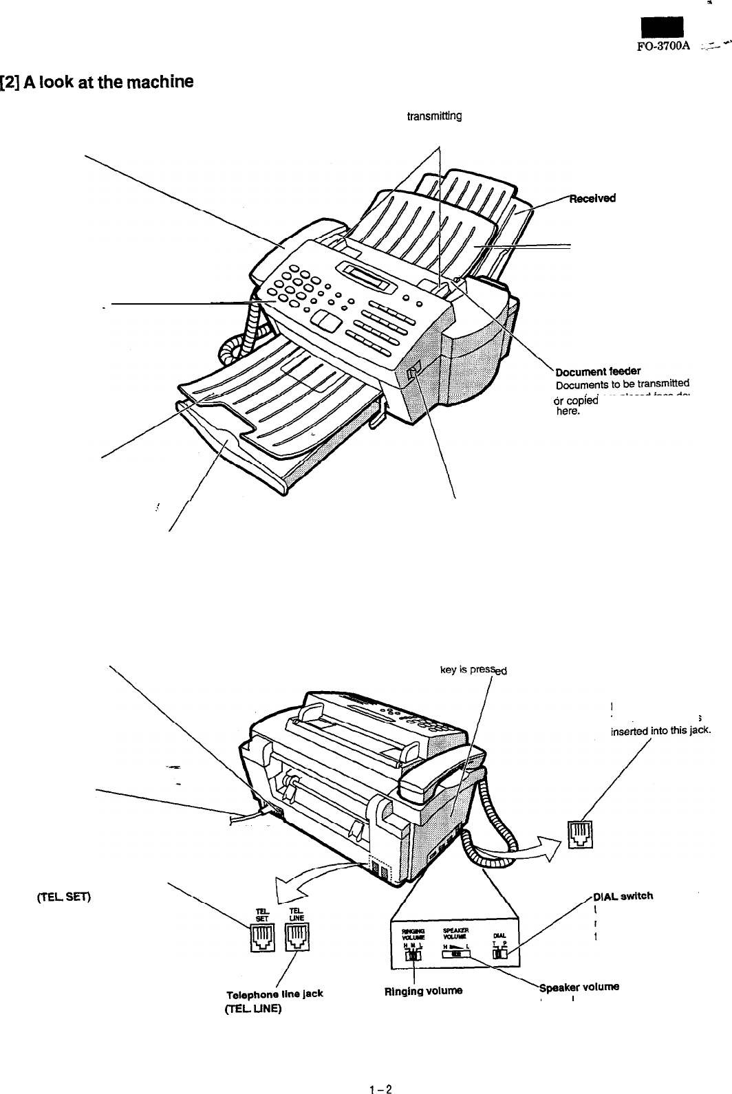
[2]
A
look
at
the
machine
Handset
Use the handset for ordinary
telephone conversations or to
listen for fax connection tones.
Operation panel
Original document out tray
Adjustable document guide
When transmittfng or copying
a document, set these guides
to the width of the document.
fwceived
document tray
Original document In tray
01
copied are placed face down
:
’
/
Paper tray
\
Operation panel knob
Pull this knob to open
the operation panel.
POWER switch
Speaker
The dial tone is heard from
here when the SPEAKER
ed before dialing.
Handset jack
The handset cord is
Power cord
Extension telephone jack
P-
SET)
An extension telephone or
answering machine line can
be inserted into this jack.
Use this to set the
fax
machine to the type of
telephone line you are On.
(TEL.
UNE)
The telephone line is
inserted into this jack.
selector control
l-2
FO-3700A
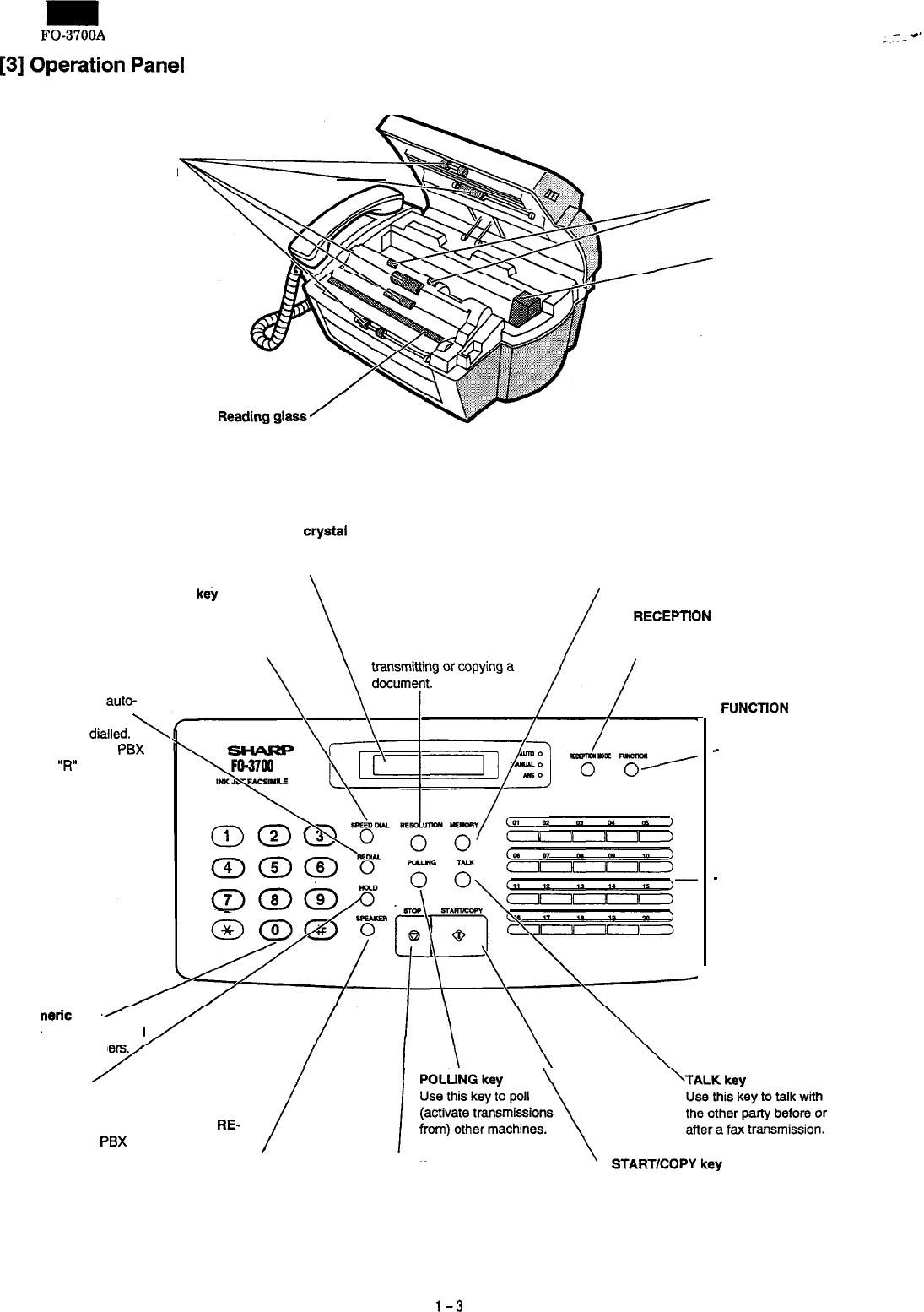
[3]
Operation
Panel
Document rollers
These move the document
through the machine during
scanning.
Document rollers
Ink cartridge
This scans the document for
transmission and copying.
Liquid
crystal
display MEMORY key
Displays various messages during
Use this key to store a
operation and programming. scanned document in
memory before transmitting it.
SPEED DIAL
kei
Press this key to dial a
Speed Dial number.
\
\
RESOLUTION key
/
RECEPTlON
MODE key
Use this key to adjust the
Use this key to select the
resolution and contrast for mode of reception.
REDIAL key
Use this key to auto-
maticallv redial the
\
last number
dialled.
\
Also used as the
PBX
Recall
“R”
key after
pressing HOLD key.
Nur
Use
and
neric
keys
!
these keys to dial
store numbers.
FUNCllON key
Use this key to select
various special functions.
*
Prompts indicating
selections will appear
on the display.
-
Rapid Keys
Use these keys to dial
fax and voice numbers
automatically.
(Note that you must
attach the Rapid Key
labels.)
Press thii key to put the other party on
hold during a telephone conversation.
Also used in conjunction with the
RE-
DIAL key for
PBX
Recall.
/
SPEAKER key
1
iiiJfzL~;\
sTART,c~is%t!;y
STOP key
Press this key to dial a
Press this key to stop
Use this key to start
number without picking operations before they
transmission, reception,
up the handset.
are completed. or copying.
HOLD key
/
l-3
FO-3700A
--e.
[4]
Transmittable
Documents
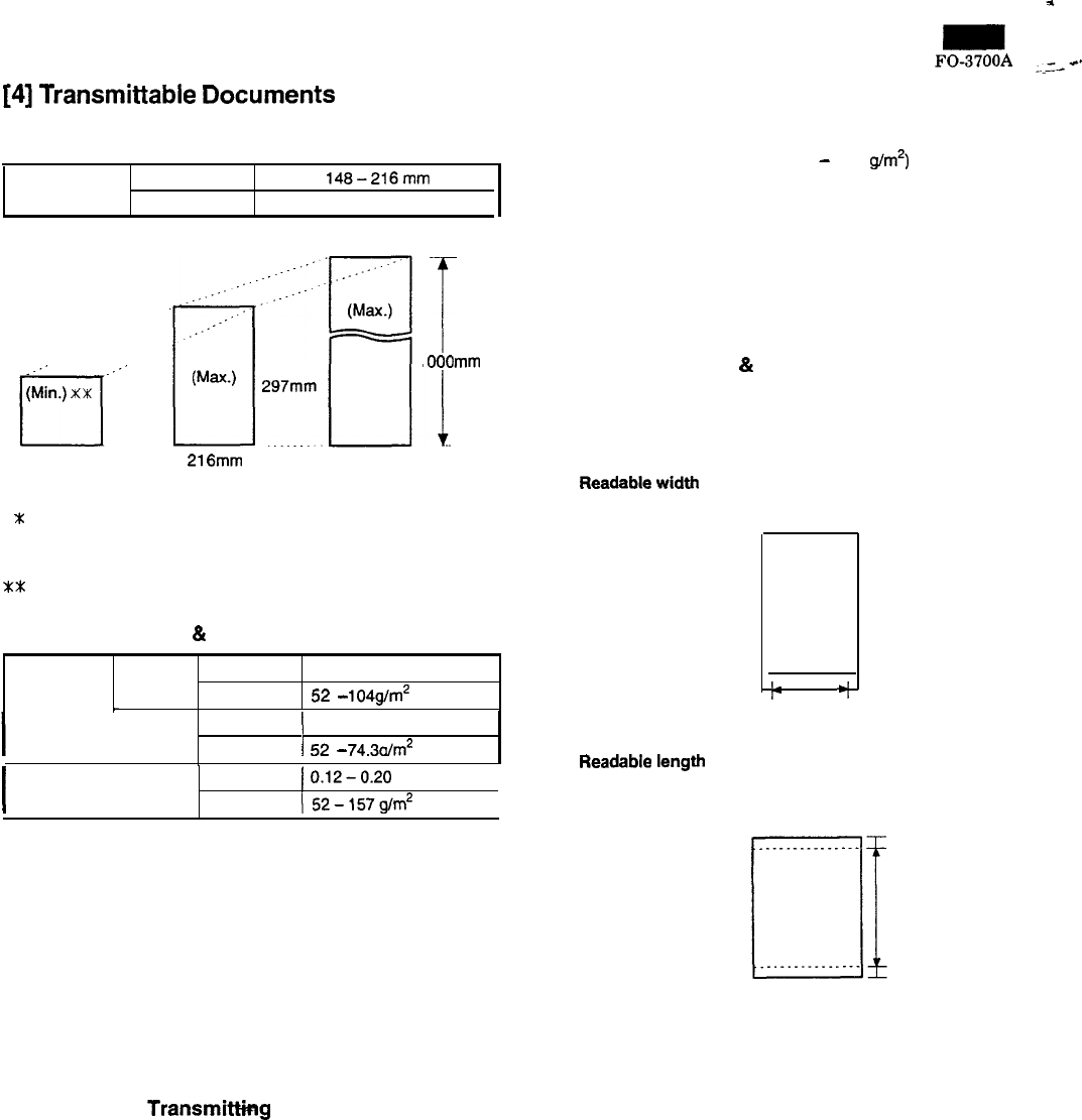
1. Document Sizes
Normal size width
148-216mm
length 128-279mm
_:’
._.-
128mm
:
1
OOOmm
148mm 216mm 216mm
[Normal size] [Special size]
X
With special sizes, only one sheet can be fed into the machine
at a time. Insert next page into feeder as current page is being
scanned.
XX Use Document carrier sheet for smaller documents.
2. Paper Thickness
&
Weight
ADF 15 Thickness 0.12 mm
sheets
Normal size
_
Weight
52
-
1049/m’
ADF 20 Thickness
(
0.06-0.09 mm
sheets Weiaht
I
52
-
74.30/m2
I
Special size Thickness
/
0.12-0.20
mm
Weight
(52-157g/m*
I
3. Document Types
l Normal paper
Documents handwritten in pencil (No. 2 lead or softer), fountain
pen, ball point pen, or felt-tipped pen can be transmitted.
Documents of normal contrast duplicated by a copying machine
can also be transmitted.
. Diazo copy (blueprint)
Diazo copy documents of a normal contrast may be transmitted.
l Carbon copy
A carbon copy may be transmitted if its contrast is normal.
4. Cautions on
TransmitMg
Documents
l Documents written in yellow, greenish yellow, or light blue ink
cannot be transmitted.
l Ink. glue, and correcting fluid on documents must be dry before
the documents can be transmitted.
l All clips, staples and pins must be removed from documents
before transmission.
l
Patched (taped) documents should be copied first on a copier and
then the copies used for transmission.
l
All documents should be fanned before insertion into the feeder to
prevent possible double feeds.
5. Automatic Document Feeder Capacity
Number of pages that can be placed into the feeder at anytime is as
follows:
Normal size: max. 20 sheets (52
-
74.3
g/m2)
Special size: single sheet only (manual feed)
NOTES: l When you need to send or copy more pages than the
feeder limit, place additional pages in feeder when last
page in feeder is being scanned.
l
Place additional pages carefully and gently in feeder.
If force is used, double-feeding or a document jam may
result.
6. Readable Width
&
Length
The readable width and length of a document are slightly smaller than
the actual document size.
Note that characters or graphics outside the effective document scan-
ning range will not be read.
l
Readable
width
210 mm max.
b
+I
Readable width
l
Readable
length
This is the length of the document sent minus 4 mm from the top and
bottom edges.
4mm
Readable length
4mm
l-4
FO-3700A
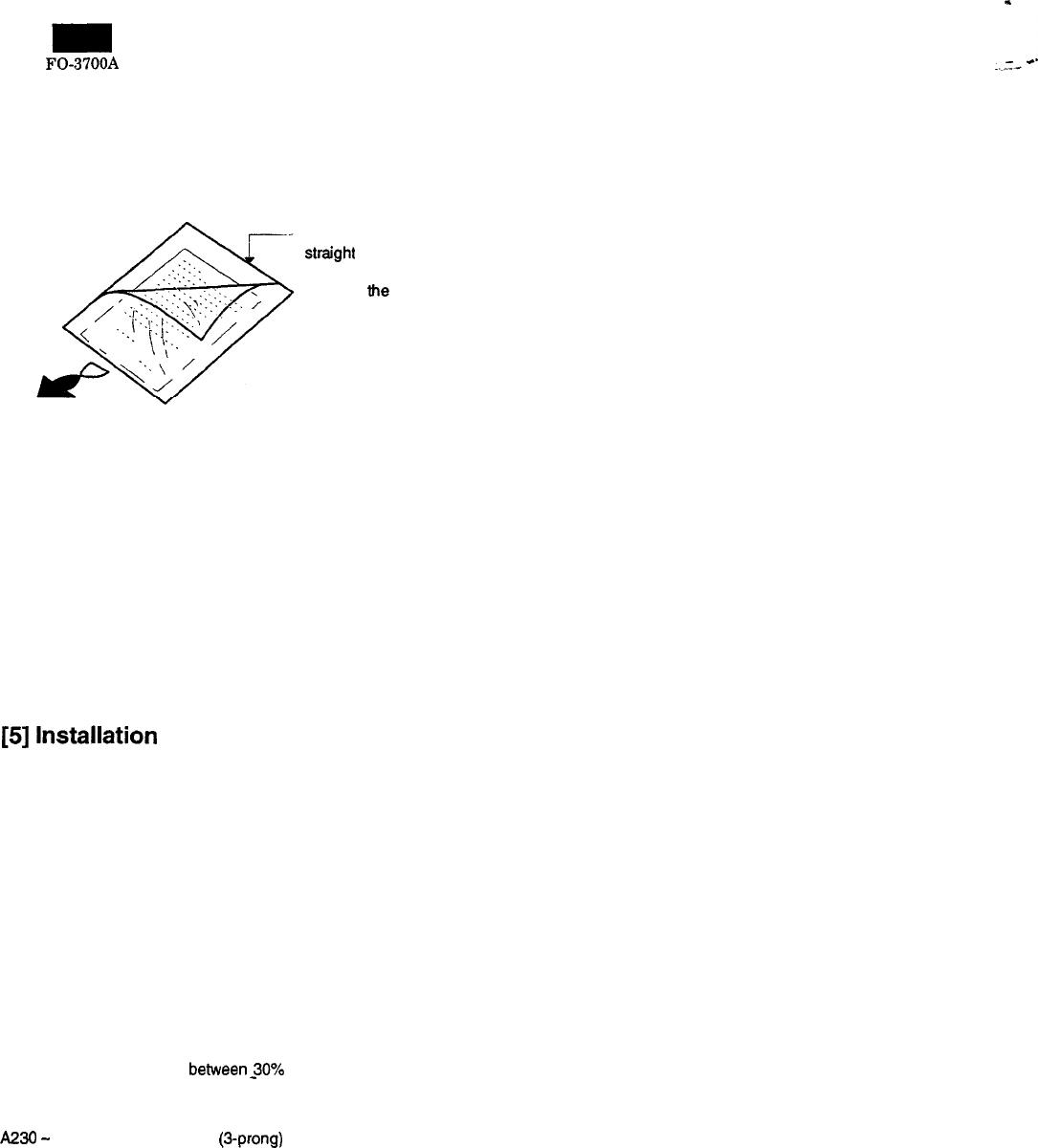
7. Use of Document Carrier Sheet
A document carder sheet must be used for the following documents.
l Those with tears.
l
Those smaller than size 148 mm (W) x 128 mm (L).
l Carbon-backed documents
Ensure document is
straight
in the carrier.
Place the document
carrier in the document
feeder with the clear film
side down
Direction of insertion
NOTE: To transmit a carbon-backed document, insert a white
sheet of paper between the carbon back of the document
and the document carrier.
l
Those containing an easily separable writing substance (e.g., trac-
ing paper written on with a soft, heavy lead pencil).
NOTES: l When using the document carrier, carefully read the in-
structions written on the back.
l
If the document carrier is dirty, clean it with a soft, moist
cloth, and then dry it before using for transmission.
l
Do not place more than one document in the carrier at a
time.
[5]
Installation
1. Site selection
Take the following points into consideration when selecting a site for
this model.
ENVIRONMENT
l
The machine must be installed on a level surface.
l
Keep the machine away from air conditioners, heaters, direct sun-
light, and dust.
l
Provide easy access to the front, back, and sides of the machine.
In particular, keep the area in front of the machine clear, or the
original document may jam as it comes out after scanning.
l
The ambient temperature should be between 5’ and 35’C (Recom-
mend temperate 15 to 35’C). __
l The humidity should be
betweenJO%
and 85% (without conden-
sation).
ELECTRICITY
A230
-
240 V, 50 Hz, grounded (3-prong) AC outlet is required.
Caution!
l
Connection to a power source other than that specified will cause
damage to the equipment and is not covered under the warranty.
l If your area experiences a high incidence of lightning or power
surges, we recommend that you install a surge protector for the
power and telephone lines. Surge protectors can be purchased at
most telephone specialty stores.
1-5
FO-3700A
--+c'
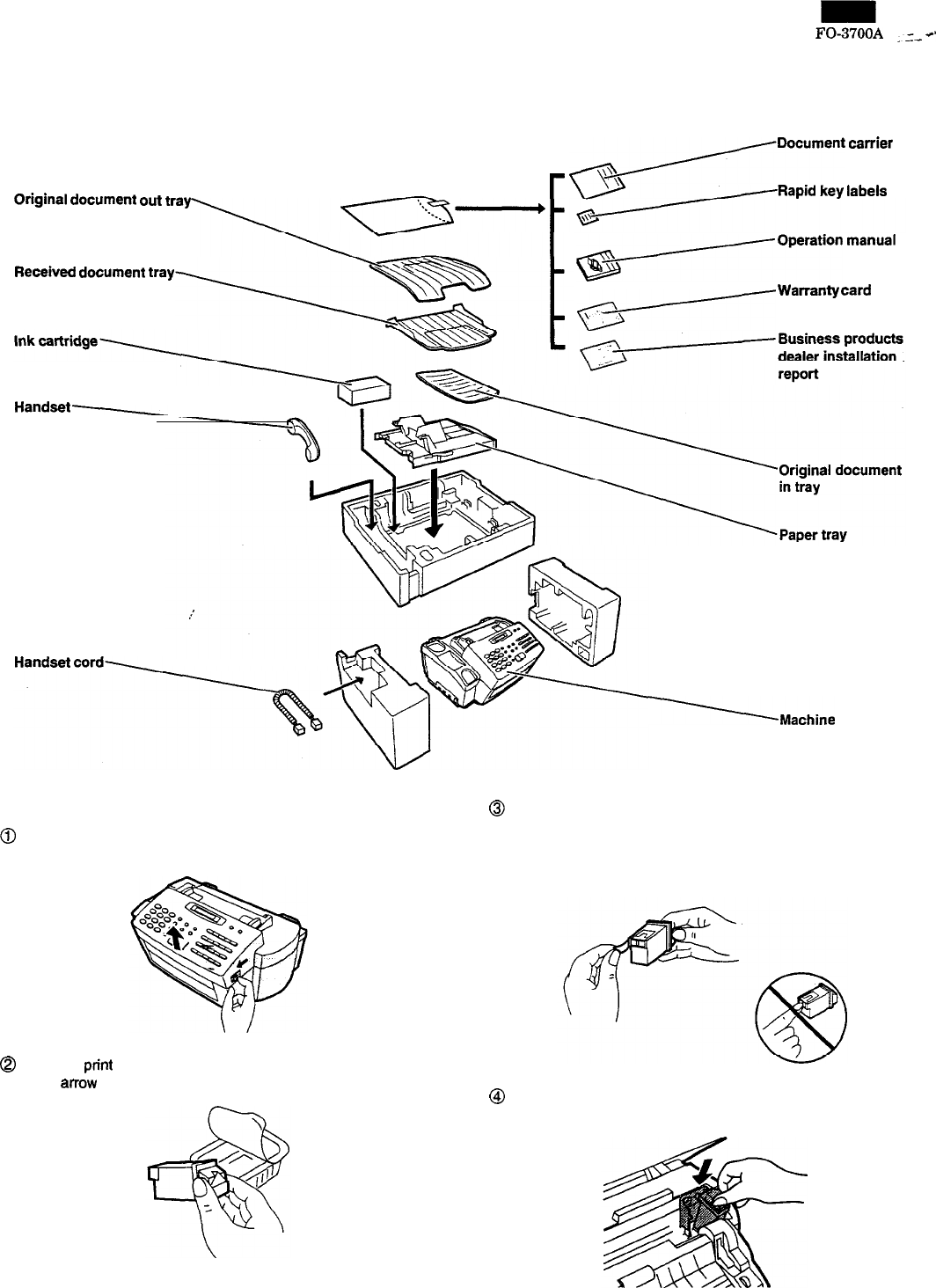
2. Unpacking
Take the machine out of the box carefully, remove all packing
material. Make sure you have all the items listed below.
Received
document
tray
Handset
-
r
a/Document
carrier
-Rapid
key
labels
Original
document
out
tray
Handset
cord.
SyOperation
manual
Gy
Warranty
card
3. Installing the print cartridge
@ Pull the operation panel knob on the
forward, and open the operation panel.
\Machine
@I
Gently remove the tape covering the nozzles on the print
right side of the machine cartridge.
l Be careful not to touch the copper ribbon or the ink nozzles,
0
Open the print cartridge container. Grasp the print cartridge by the
green
arrow
and remove it from the container.
and do not allow them to touch any surface or object. (Skin oil
and dust can cause poor print quality.)
@ Insert the print cartridge into the cradle with the green arrow on
the cartridge top pointing to the green dot on the top of the cradle.
l-6
FO-3700A
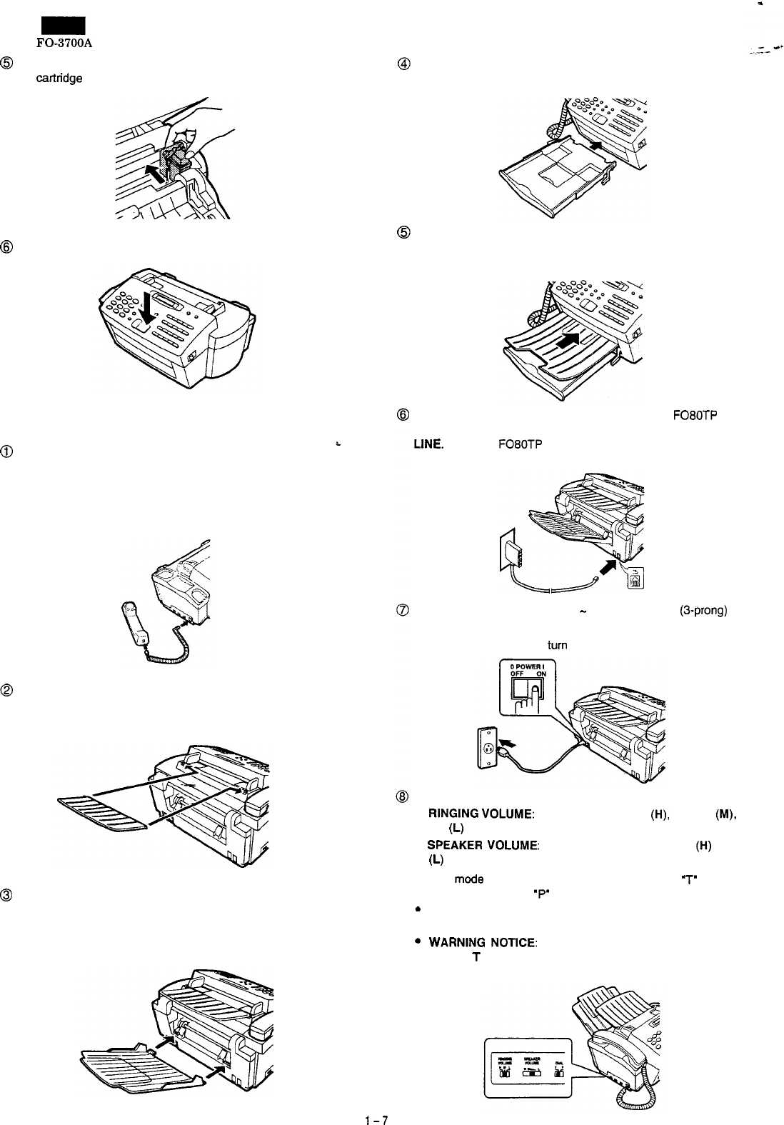
@ Push the green arrow forward toward the green dot, ‘snapping’
the cartddge into place.
@ Close the operation panel.
4. Assembly and connections
i
@ Connect the handset cord to the handset and the machine as
shown.
l The ends of the handset cord are identical, so they will go into
either jack.
Place the handset on the handset rest.
@ Mount the original document tray.
lHold the tray vertically, bend it slightly at the center, and insert
the tabs into the holes on the top of the machine as shown.
0
Mount the received document tray.
l Insert the tabs on the tray into the holes on the back of the
machine.
lIf desired, flip the tray extender out.
@ Mount the paper tray.
lSlide the tray in as shown until it clicks into place.
@ Mount the original document out tray.
lPlace the original document out tray on the paper tray. Slide it
in or out to fit the length of the original.
Insert the small modular plug which terminates the
FOBOTP
adap-
tor line cord into the jack on the back of the machine marked TEL.
LINE.
Plug the F080TP adaptor into the telephone jack on the
wall.
Plug the power cord into a 230
-
240 V, grounded
(9prong)
AC
outlet.
Press the power switch to turn on the power.
Adjust the volume switches on the left side of the machine:
l
RINGING
VOLUME:
Set the switch at high
(H),
medium
(M),
or
low
(L)
as desired.
l
SPEAKER
VOLUME:
Adjust the setting from high
(H)
to low
(L)
as desired.
Set the mode of dialing with the DIAL switch. Select
7”
if you are
on a touch-tone line, or
“P”
if you are on a pulse dial (rotary) line.
.
.
Be sure to make the correct setting, or you will not be able to
make a call.
WARNING
NOTICE:
For all units installed in New Zealand,
only the
T
setting for tone dialing is permitted. The P setting for
pulse dialing does not operate properly and must not be used.
1-7
5. Loading printing paper
Selecting paper
The inkjet printer in your FO-3700 is designed to work well with most
types of plain paper. Bond paper generally produces the best results,
and plain paper manufactured for high-quality photocopying is also
good. However, variation in paper composition may significantly af-
fect print quality, and you should therefore test paper (printing on both
sides) before purchasing large quantities to be assured of the quality
you desire.
Size
and
weight
A4 size paper from 60 to 90
g/m*
can be used.
Printing
side
Plain paper has a ‘print’ side which should be used to obtain the best
print quality. The print side is not visible to the naked eye, so check
the label on the end of the package before removing the paper. The
print side will be indicated by an arrow, symbol, or wording. Remove
the number of sheets you wish to use from the package, and load
them in the paper tray print side up as described below.
Note:
Do not use paper which is folded, curled, or tom, as it may jam in the
prfnter.
Loading paper
A maximum of 100 sheets of paper can be loaded in the paper tray.
Note: Do not remove the paper tray from the machine to load paper
(if the tray is not correctly in the machine when paper is
loaded, the paper sensor will not be able to detect the paper).
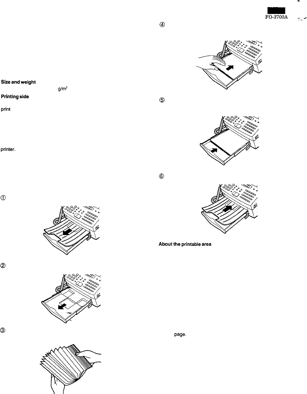
@
Remove the original document out tray.
@ Pull the tray extender out slightly.
@ Fan the paper, and then tap the edge against a flat surface to
even the stack.
P
FO-3700A
--+s
@ Insert the paper into the tray, print side up.
l
Make sure it fits squarely against the inside of the machine.
@ Push the tray extender back in.
l
Make sure it fits snugly against the paper.
@ Replace the original document out tray.
About
the
printable
area
The area of the page on which the FO-3700 can print is slightly
smaller than the page itself. The following dimensions are averages,
and there may be slight deviation from these dimensions depending
on how the paper is loaded in the tray.
Printing width: 203 mm
Printing length: The length of the page minus 1.5 mm from the top,
and 12 mm from the bottom.
The FO-3700 has been set at the factory to automatically reduce the
size of received documents to 92%. This can be configured for 100%
reception by user switch. This ensures that data at the extreme edges
of A4 size documents is not lost.
Note: If you receive a document which is too long to be printed on
one sheet of paper, the remainder will be printed on a second
paw.
l-8
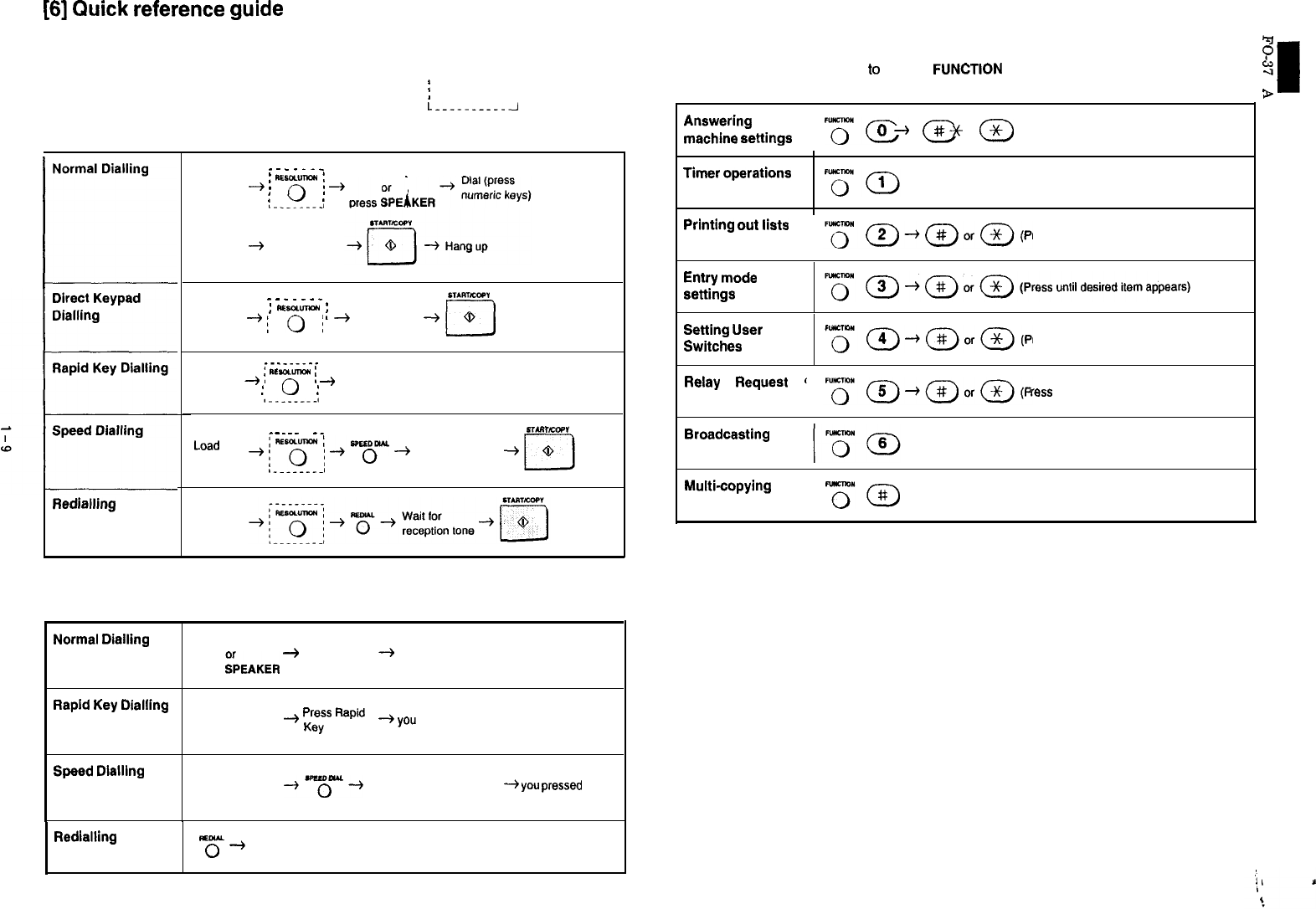
[6]
Quick
reference
guide
Use this guide as a convenient reminder for operating the machine after you have read the
detailed instructions for each procedure in the manual. r-----------Y
Note: Steps which are optional are enclosed in a dotted frame:
i
L----.------l
Transmitting documents
Normal
Dialling
I
Redialling
_
-
_
_
-
-
_
Load
+
j
=‘a”-
j
+
Lift handset
document
:
0
:
,-_._---_I
3
Wait for
reception tone
s,ARTlcw”
-
-
-
_
_
-
_
Load
+
i
RE80LuTyxI
i
+
Dial (press
+
document
:o:
numeric keys)
,__--____I
____---__
Load
+
i
“wwm~
j
+
Press Rapid
document
:
0
:
Key
srIRrzw”
_
-
_
_
_
. .
-
_
LOad
j)-REMlmjjSPEEDDLU
Enter Speed Dial
document
10:
0
+
number (press 2
+
1_-_____-1 numeric keys)
Load
document
Making voice calls
Normal
Diailing
Lift handset Lift handset if
press
&AKER
+
Dial (press
numeric keys)
-3
you pressed
SPEAKER
Rapid
Key
Dialling
Lift handset
+
press
Rap’d Lift handset
if
or Key
+
you pressed
press SPEAKER SPEAKER
Speed
Dlalllng
Lift handset
-3-o”+
Lift handset if
or
Enter Speed Dial number
+
you
pressed
press SPEAKER (press 2 numeric keys) SPEAKER
Redialling
77
-b
Lift handset
Operations using the FUNCTION key
3
The following chart shows how
to
access
FUNCTION
key operations. Once you have accessed
$
the desired operation, follow the instructions which appear in the display. 8
*
Answering
machine
settings
‘To
0
0
0
+
# or
YC
(Press until desired itemappears)
Timer
operations
Printing
out
lists
ress
until desired item appears)
Entry
mode
settings
Setting
User
Switches
ress until desired item appears)
Relay
Request
(
ress until desired item appears)
Broadcasting
Multi-copying
YfxD
FO-3700A
.I-
-*
CHAPTER
2.
ADJUSTMENTS
[l]
Adjustments
General
The following adjustments and settings are provided for this model,
make adjustments and/or settings as necessary.
1;.
Adjustments
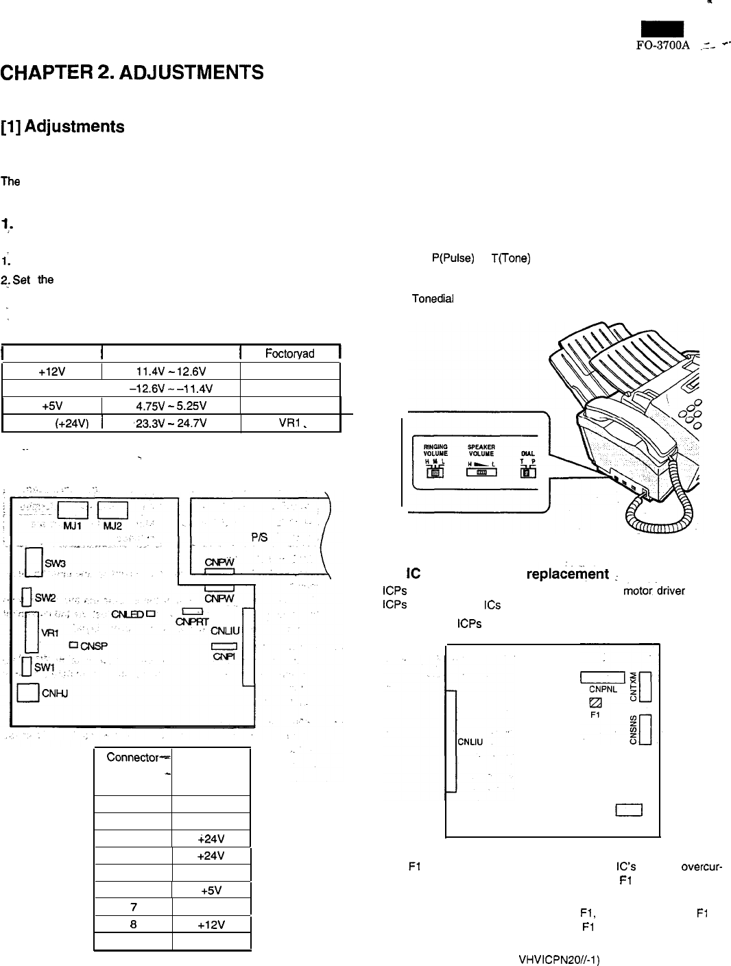
Adjustments of output voltage (FACTORY ONLY)
1:
Install the power supply unit in the machine.
2:
Set
the
recording paper and document.
3. When the document is loaded, power is supplied to the output
1
lines. Confirm that outputs are within the limits below.
Output voltage settings
I
Output
I
Voltage limits
1
Foctoryad
1
+12v
11.4V
-
12.6V
None
-12v
I
-12.6V
-
-11.4V
None
+5v
VM
(+24V)
1
4.75V
-
5.25V
-23.3V
-
24.7V
None
VRI
_
.~
’ (Top view)
‘1..
.-
‘:
Connector-
No.
_
CNPW
Pin No.
1
MG
2
MG
3
i24V
4+24V
5DG
6
+5v
7
AG
6
+12v
9
-12v
Fig. 1
2-
2. Settings
(1) Telephone/Fax setting
Perform the following adjustments and settings for the telephone and
facsimile functions.
a) Ringing volume
The desired telephone ring volume can be selected from among
three levels: high, middle, and low.
b) Speaker volume
When the SPEAKER key is pressed, the speaker volume is ad-
justed with this control.
c) Dial mode selector
(tine selector)
Select
P(Pulse)
or T(Tone) according to the type of the telephone
line.
P: Pulse dial telephone mode (10 PPS)
T: Tonedial tone telephone mode (Tone)
3.
IC
protectors
replacement
:
ICPs
(IC Protectors) are installed to protect the
motor.driver
circuit.
ICPs
protect various
ICs
and electronic circuits from an overcurrent.
The location of
ICPs
is shown below: :
CNCCD
I
1
(1)
Fl
(ICP-20) is installed in order to protect
IC’s
from an overcur-
rent generated in the motor drive circuit. If
Fl
is open, replace it
with a new one.
In addition to the replacement of
Fl,
the factor causing
Fl
to
open must also be repaired. If not,
Fl
will open again.
Replacement parts
ICP-N20 (Sharp code: VHVICPNZOI1)
FO-3700A
[2]
Diagnostics
and
service
soft
switches
1. Diagnostics description
(1) Entering the diagnostic mode
Press the keys in the following sequence
)m]+a-+a+@
+@+m,
and the following display will appear.
ROM1
:m
(This code is ROM version name.)
Then press the ‘START/COPY’ key. Select the desired item by
pressing
mar
q
key or rapid key. Press the
LSTARTIC~PY
1
key
to go into the selected diagnostic mode.
(2) Diagnostic items
06
1
PANEL CHECK MODE
07
1
CHECK
PAlTERN
08
1
PROOlJCTtiHECK
09
(
SIGNALSEND MODE
(3) Description of diagnostic items
01
SOFT SWITCH MODE
Used to change the soft switch settings.
After setting soft switch 22, the following display will appear.
[PRINT SFTSW LIST] and
11:
YES OTHER: NO]
Then ‘SOFT SWITCH TABLE’ list is printed by
pressinga
key.
..****t~*.*...*.........*.**.*******~~.*.*.*.*~**.***.**.~~***.~****
l l
.
6oPT6wIfcpTABm
l
.
wo1-00000010 sn1-00000110
.
l
mlO2-00001000
6wl240000000
l
l
wo340000000
5*1340010000
l
.
mo4-00000000 sm4-00000001
l
l
sm5-00000100
811540000010
t
l
8*0640000101
wl6-10001000
l
.
slm7-00001100
sll7-00000000
l
l
8*06-01010010
wlsl10010010
l
l
810940001000
wl9-00010000
l
.
sm0-00000000 w20-10000000
.
t
.
.*.**.*..t***..***.~*.*.**.*...~*.*.*********..***~.***.***.*****.**
02 AU
BLACK
PRINT
Used to check the printer head. All black pattern printable area
of page is printed.
03 ROM
&
RAM CHECK
Used to check the program ROM and the work RAM area of the
machine and the printer, and check the status of the printer. The
ROM check is used for ROM, and a read/write matching test is
used for the
RAM.
-‘-
**
The result of the machine check is given by a number of beeps,
and the total result is given by printing the ‘ROM & RAM
CHECK TABLE’ list.
number of beeps
1
0 beep
1
NO ERROR
r6
beeps
1~
DRAM
ERROR
(opti
I
*tt~.*~~tt*t**ttt.tt*~*****..***.***~*****.**””******..**~.**..*..~*
.
l
l
Ral4lwlc5cx~
l
l
-MUI-
l
.
PLW
-0x
VW..
PCMB
.
l
WAN-ox
l
l
Drwl-w
*
l
OPRWDW(=POSElDP
l
.
l
l
-PP.nmrR-
l
l
Rml
-OK
vru.
AoO.58
l
.
RAN
-011
l
l
OK
OUT OF INK
normal
1
The ink is missing.
04
AUTO FEEDER MODE
Used to check auto feed function by inserting and ejecting docu-
ments.
Place documents in the hopper before entering this mode. then
press the
1sTART/copy[
key to start the test. As the document
sensor is actuated, the document size is displayed.
05
AGING MODE
If a document is placed in the hopper, a copy is taken first. If no
document is present, a sheet of test patterns is printed out every
60 minutes.
(Total 10 sheets)
06
PANEL CHECK MODE
Used to check proper key operation, Each key entry is displayed
on the LCD.
The test results will be also printed.
*****tt**t.*t.t**.**..***~**.***..***.*..*.******.*~...****.**..*.*.
l
l
l
PAlULCEEClSLI6T
l
91
23
4
5
l
l 6
76 9
*
.
l o
:
SO-D-
RXDIAL SOLD
l
l 6PxaKrx
PXSO~IW
POLLIn
ItDmlx PNJl
l
l
6TArwcoPY
P.xcsP’p1044
PwcTIw
01
02
l
l 03 04 05 06 07
.
l
06
09
10
11
12
t
l 13
14
15 16 17
.
l
16
19 20
6mP
l
l
ADTO’
l
PNmLaucxox
l
l
.
.*.**.***..~.*..*.t.~...****.~*.****~.**.~..~~*.*.*..*~*****..****..
2-2
.
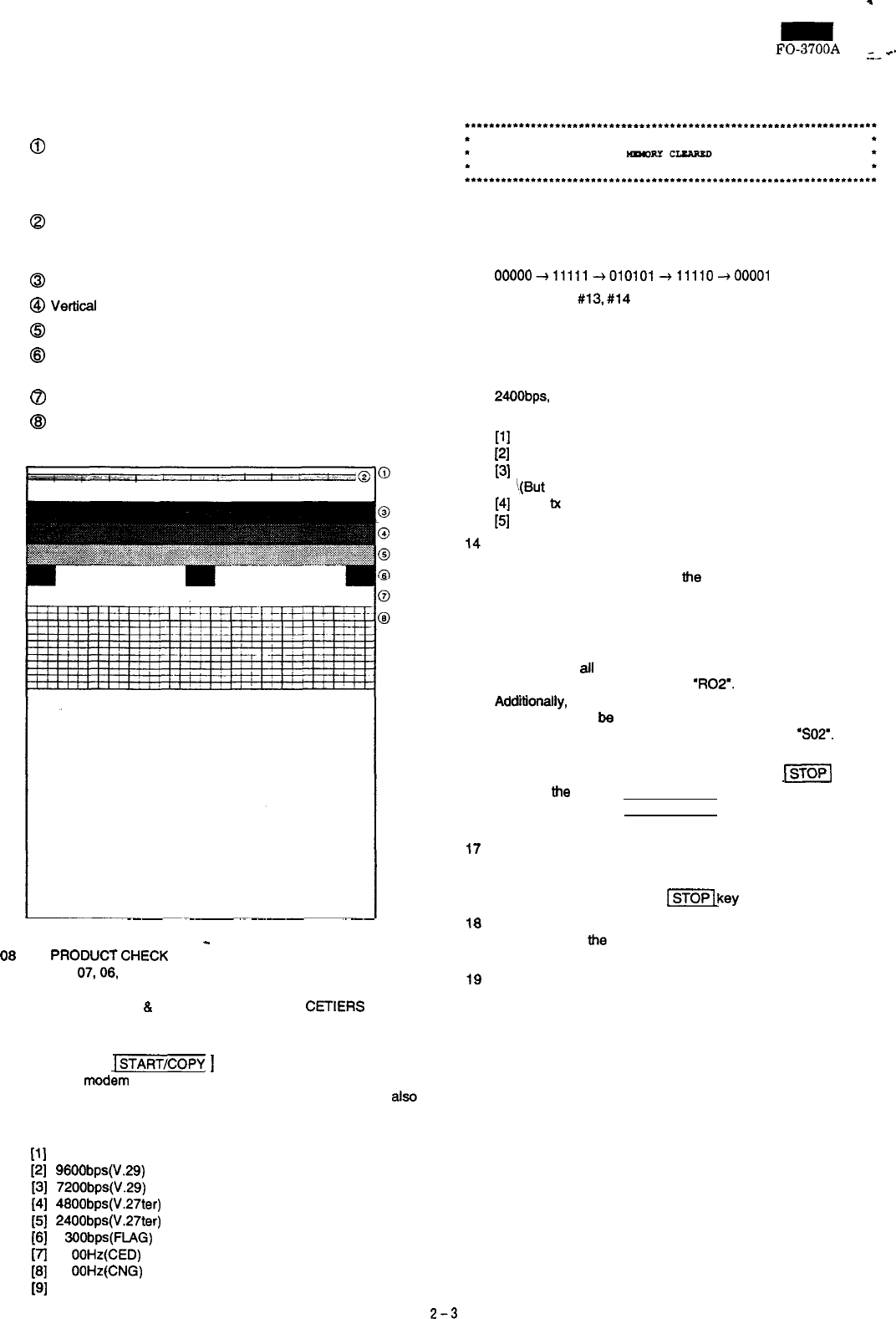
07 CHECK PATTERN
Used to check the nozzles of the print head. The following pat-
tern is printed out on the sheet, A total of two sheets will be
produced.
@ Frame line:
The frame line shows the print area of a page.
The horizontal ruled line at the lower end is specified with
soft SW 18 bit 3. 4, and 5.
Q
Nozzle test:
The pattern is used to check for a clog in the 46 nozzles of
the print head.
@I
Vertical stripes 1
@ Vertical stripes 2
@ Light grey
@ All-black block:
Three all-black blocks for checking print density
8
All white
@Paper feed accuracy check pattern:
Used to check eccentricity of the paper feed motor.
08
PfloDucTcHEc~
-
(Diags,
07,06,
and 03 take place in succession)
Used to carry out the CHECK PATTERN, PANEL CHECK
MODE, and ROM
&
RAM CHECK CAPITAL CETIERS succes-
sively.
09 SIGNAL SEND MODE
Pressing the [START/COPY
1
key after entering this mode will
transmit modem signals out of the TEL Line, in the following
order. Used to check the modem. (Monitor from (This is also
audible from the speaker of the machine) the TEL line socket to
check signals.)
[l]
No signal (CML signal turn on)
[2] 9600bps(V.29)
[3] 7200bps(V.29)
(41
4600bps(V.27ter)
(51
24OObps(V.27ter)
(61
3OObps(FlAG)
(7
21
OOHz(CED)
[a] 11
OOHz(CNG)
[9]
PSEVDC RINGER
FO-3700A
___a
._
10 MEMORY CLEAR
Used to clear the memory. The soft switches and the user
switches will be set to initial states. The following will be printed.
11
12
FACTORY USE ONLY
FSK SEND MODE
Delivers various signals of 300bps in the following data pattern
at the level set by the soft switch.
ooooo+
11111~010101+11110+00001
13.14. Diag
#13,
#14 are used together.
1. Press the Start key on the receive data unit first then the
send unit.
13 ENTRY DATA SEND
Used to send the data registered in memory by signals of
2400bps, and copy the registering contents.
Registering contents
[l]
rapid number
[2]
speed number
[3]
the contents registered in the entry mode
!(But
date & time is excluded.)
14
[4]
relay
tx
data
[5]
soft switch settings
ENTRY DATA RCV.
This mode is the reception mode of ENTRY DATA SEND. The
received data is registered in the memory, and ‘TELEPHONE
LIST’, ‘PASSCODE LIST’. ‘USER SWITCH LIST’. ‘SOFT
SWITCH LIST’ are printed.
15
TEL. NUMBER SET
The TEL number and name registered in rapid number 01 can
be copied to all rapid numbers. The first 3 characters of the
copied name is changed such as
‘R02’.
Additionafly, the TEL number and name registered in speed
number 01 can be copied to all speed numbers. The first 3
characters of the copied name is changed such as ‘SO2’.
16 CCD ADJUST MODE
Used to execute copy operation. When the
[m)
key is
pressed, the unit goes into the waft state to adjust the CCD line
alignment. When the START/COPY key is pressed again, the
copy operation is resumed.
17
PAPER EXIT MODE
Used to check the recording paper feed function by inserting
and ejecting recording paper. This mode will continue until
recording paper is out, or the
lm
key
is pressed.
18
PRINTER SELF TEST
19
Used to check the state of the printer. This the check prints the
check pattern provided by the printer driver.
INK TEST MODE
Used to check the state of the printer. A check pattern as
with diagnostic 07 is produced when this mode is entered.
2-3
FO-3700A
I-
.0*
2. Soft switch description
Soft switch list
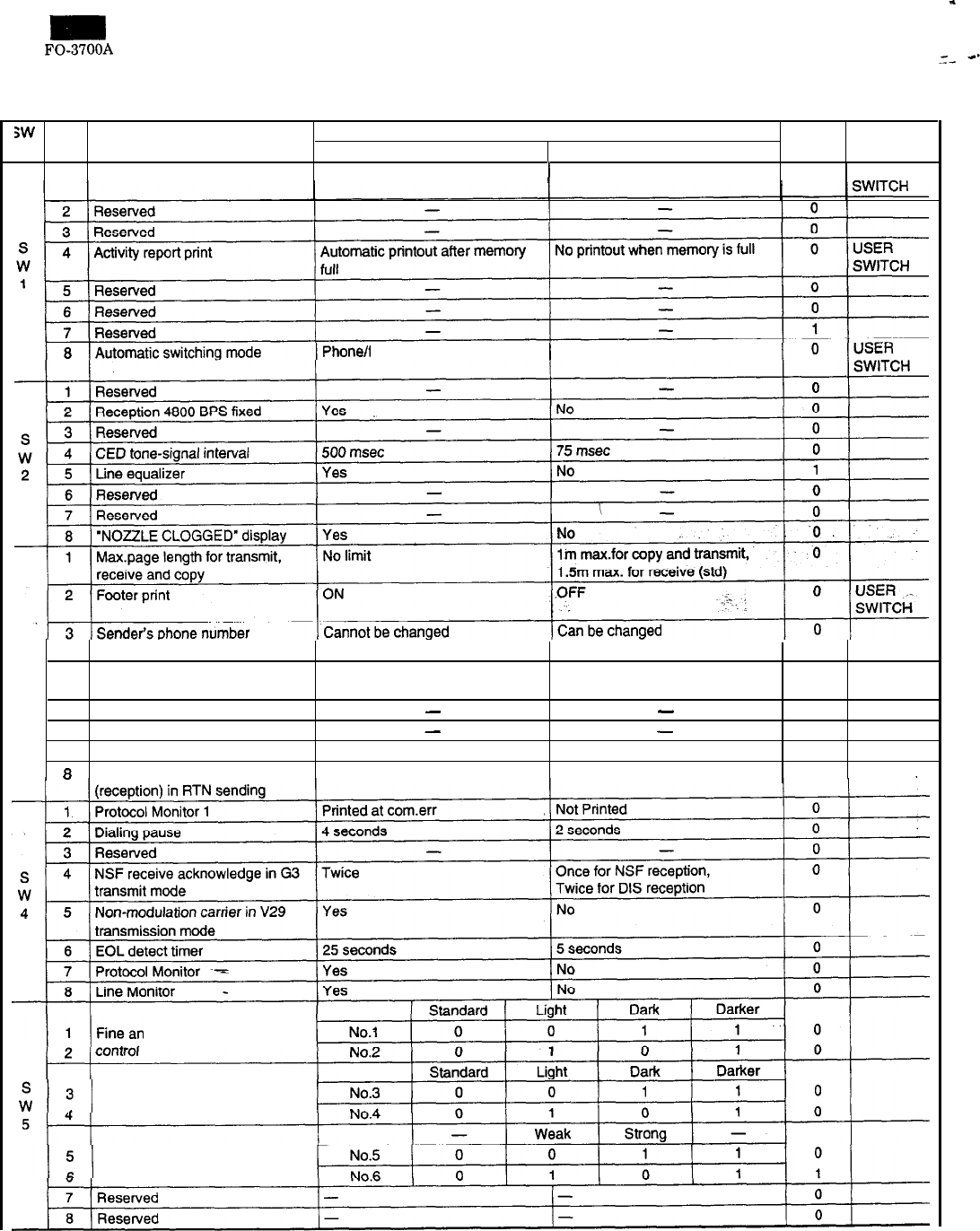
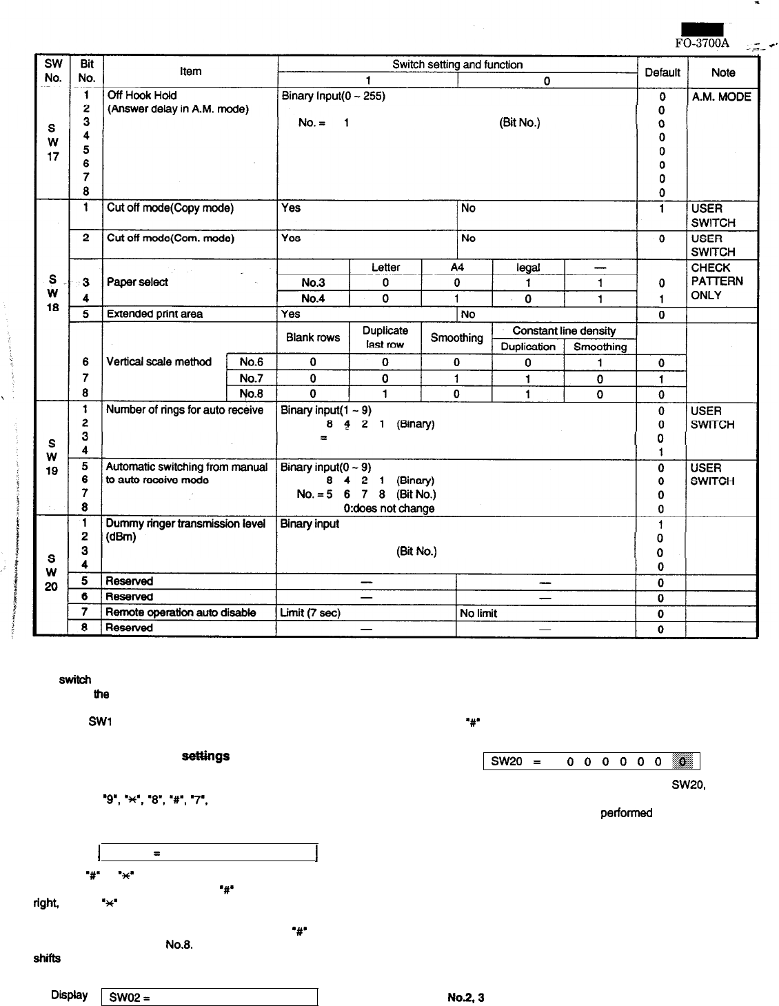
;W Bit Item Switch setting and function Default Note
JO.
No.
1
0
1
Line density choice
FINE
)
STANDARD
0
USER
fax automatic switching switching to fax only
S
W
3
registration
4 Total communication hours and
N
O
Yes 0
pages print
5
Reserved
-
-
0
6Reserved
-
-
0
7CSI transmission Not transmitted transmitted
0
a
Communication error treatment Not transmission error Transmission error
0
d standard contrast
Halftone contrast control
Halftone MTF correction
2-4
FO-3700A
.,---+
8 4
2
1
(Binary)
No.
=5
6
7
a
(Bit No.)
Mode signal transmission level
ON (OVER
-16dBm)
r of Busy tone detection
5
Reduce of copy and manual No.5
00
0
SWITCH
6
receive
No.6 0
1
0
footer off 92 %100%
USER
footer on 91 % 100%
SWITCH
7
Reduce of auto receive
No.7
000
a
No.8
0
1
0
2-5
FO-3700A
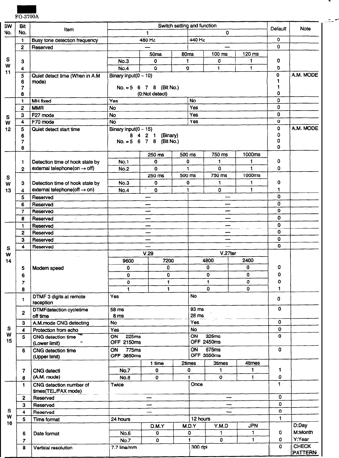
DTMF detection time
8 4 2 1 (Binary)
on number of times
PAlTERN
2-6
FO-3700A
--
128
64 32 16 8 4 2
1
(Binary)
23 4 5
6 7 8
(BitNo.)
No.
=
1 2
3
4 (Bit No.)
8 4
2
1 (Binary)
No.=5 8 78 (BitNo.)
Soft switch setup
Soft
swftch
settings stored in memory can be changed by entering
data from the keyboard. SW1 through SW20 constitutes soft
switches. See the soft switch listing on page 2-4 and 2-7 for the
function of
SW1
through SW20 settings.
How to make soft switch
set&ings
To enter the softswitch mode, make the following key entries in se-
quence.
‘FUNCTION’,
V,
‘*‘,
‘8’,
‘#‘,
‘7’.
‘START/COPY’, ‘START/COPY’
SW1 bii No.1 through No.8 will be displayed.
Bit No. 12345678
Make settings in the same way as for SW2. Proceed to the settings of
SW3 to SW20 in the same manner
When the cursor is on SW20 data No.8 position as shown below,
press the
9’
key to finalize all settings.
Bit No.
12345678
Display
SW20
=
,
0
0
0
0
0
0
.$#g
To finish the settings halfway between SW1 and
SW20,
press the
STOP key. in this case, the setting being performed to the SW No. on
display will be nullified while settings perfomted to the preceding SW
Nos. remain in effect.
Display
1
SW01
=
0 0 0 0 0 0 1 0
1
Press the
‘#.
or
•3~’
key and bring the cursor (blinking pointer) to the
bii No. which is to be changed. (The
‘#’
key moves the cursor to the
right, and the
‘*’
key to the left.)
Press the FUNCTION key to change the setting between 1 and 0.
When the cursor is on data No.8 position, press the
V’
key to display
SW2 data No.1 through No.8. pressing the START/COPY button
shifts cursor to the next soft switch
Bit No. 12345678
DiplaY
swo2=
0 0 0 0 1 0 0 0
Soft switch functional description
SW1 No.1 Line density choice
Used to set the transmission mode which is automatically selected
when the MODE key is not pressed. In copy mode, however, the fine
mode is automatically selected unless the MODE key is manually set
to another mode.
0: Standard
1: Fine
default: 0
SW1
No.2.3
Resewed
Set to ‘0’.
2-7
FO-3700A
SW1
No.4 Activity
report
print
This soft switch is used to select; whether or not to print out the
activity report when the memory is full. An activity report can be
printed when the foilowing key entry command is made.
‘FUNCTION’,
‘2’.
‘#‘,
‘START/COPY
After producing the activity report, all the data in the memory will be
cleared.
When the switch function is set to
‘0’
(NO), the data in the memory
will be deleted from the oldest as it reaches the maximum memory
capadty.
0:
NO (first data lost when memory is full)
1: YES (when memory is full)
default
0
SW1
No.5
-
5
Reserved
Set
to
‘0’.
SW1
No.7
Raserved
Set
to ‘I’.
SW1
No.8
Automatic
switching
mode
This soft switch is used to set the auto tek%x select mode or to set
the normal fax mode.
0: Switching to fax only
1: TEL/FAX automatic switching
Default: 0
i
SW2
No.1
Resewed
Set
to
‘0’.
i
SW2 No.2
Reception
4888
BPS
fixed
When line conditions warrant that the reception take place at 4900
BPS repeatedly. It may improve the success of reception to start at
4900 BPS. This improves the receiving document quality and reduces
handshake time due to fallback during training.
0: NO
1: YES
Default: 0
SW2 No.3
Reserved
Set to
‘0’.
SW2 No.4
CED
tone-signal
interval
For international communication, the
219OHz
CED tone may act as
an echo suppresser switch, causing a communication problem.
Though this soft switch is normally set to
‘o’,
it should be set to ‘1’ so
as to change the timer between CED tone and DIS signal from 75ms
to 500ms to eliminate the communication problem caused by echo.
0: 75
ms
1: 5ooms
Default: 0
SW2
No.5
Line
equaber
Used to set the Line equalizer function.
On --f
7.2kn-1
--a
Off-tOh
0:
Off-tOkm
1:
On47.2km
Default: 1
SW2 No.8
-
7
Reserved
Set
to ‘0’.
SW2
No.8
‘NOZZLE
CLOGGED’
display
select
You can select whether the prompt ‘NOZZLE CLOGGED’ is dis-
played or not when nozzie on the printer cartridge dogged.
0: Not display
1: Display
Default: 0
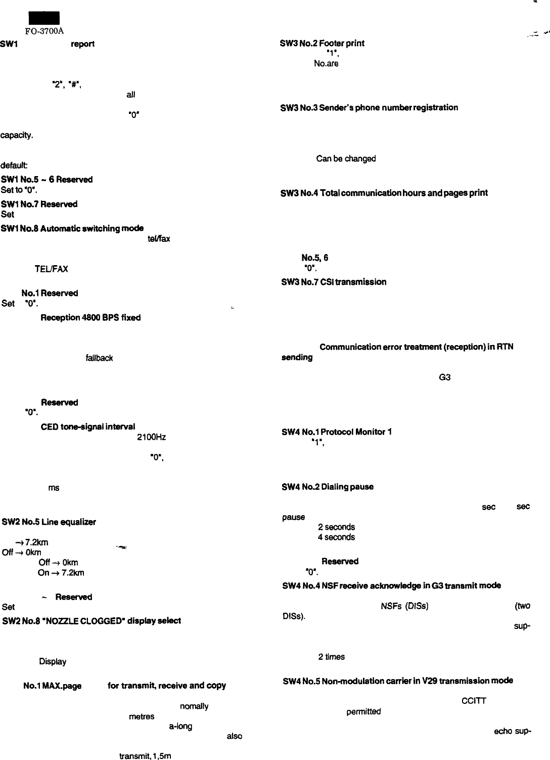
SW3
No.1
MAXpage
length
for
transmit,
receive
and
copy
Used to set the maximum page length.
To avoid possible paper jam, the page length is
non-rally
limited to 1
meter for copy or transmit, and 1.5 metres for receive.
It is possible to set it to ‘No limir to transmit
a-long
document, such
as a computer print from, etc. (In this case, the receiver must also be
set to no limit.)
0:
1 m max. for copy and trensmit,
1,5m
max. for receive (std)
1: No limit
Default: 0
-
4,
._-
SW3
No.2
Footer
print
When set to
‘l’,
the date of reception, the sender’s machine No., and
the page
Noare
automatically recorded at the end of reception.
0: off
1: On
Default: 1
SW3
No.3
Sender’s
phone
number
registration
Used to make a choice of whether the registered sender’s phone
number can be changed or not. If the switch is set to ‘l’, new
registration of the senders phone number is disabled to prevent ac-
cidental wrong input.
0:
canbechanged
1: cannot be changed
Default: 0
SW3
No.4
Total
communication
hours
and
pages
print
Used to make a choice of whether the total communication time and
pages are recorded in the activity report.
0: Yes
1: No
Default: 0
SW3
No.5,8
Resewed
Set to
‘0’.
SW3
No.7
CSI
transmission
CSI signal contains the sender’s phone number registered in the
machine.
0: Transmitted
1: Not transmitted
Default: 0
SW3 No.8
Communication
error
treatment
(reception)
in
RTN
sending
Used to determine communication error treatment when RTN is sent
by occurrence of a received image error in
63
reception. When it is
set to ‘l’, communication error is judged as no error.
0: Transmission error
1: Not transmission error
Default: 0
SW4
No.1
Protocol
Monitor
1
If set to
‘1’.
protocol is printed at communication error.
0: off
1: On
Default: 0
SW4
No.2
Dialing
pause
The length of the pause inserted between telephone numbers of
direct dial contraction. can be adjusted. Selection of 4
set
or 2
set
pause is available.
0:
2smds
1:
4seconds
Default: 0
SW4 No.3
Reserved
Set to
‘0’.
SW4
No.4
NSF
receive
acknowladge
in
G3
transmit
mode
Used to make a choice of whether reception of NSF (DIS) is acknow-
ledged after receiving two
NSFs
(DISs)
or receiving one NSF (two
DISs).
It may be useful for overseas communication to avoid an echo sup-
presser problem, if set to 1
0:
1 for NSF reception, 2 for DIS reception
1:
2times
Default: 0
SW4
No.5
Non-modulation
carrier
in
V29
transmission
moda
Though transmission of non-modulated carrier is not required for
transmission by the V29 modem according to the
CCITT
Recommen-
dation, it may be pemritted to send non-modulation carder before the
image signal to avoid an echo suppresser problem.
It may be useful for overseas communication to avoid an echo sup-
presser problem, if set to 1.
0: No
1: Yes
Default: 0
2-8
I
.
8
Modem
speed
m
mtine the initial modem speed. The default is 9600bps.
i
&essary
to program it to a slower speed when frequent
’
is encountered, in order to save the time required for
!
Ad
‘J29
GBPS
72OOBPS
. V27ter
489OBPS
::
249OBPS
-it. owl
j
No.1
DTMF
3
digits
at
remote
reception
J
to make
a
choice of whether to use the 3 digits code or 2 digits
e for remote receive.
0: No
On+CO+
1: Yes
l*+lOn
,efault
0 5+++503c
:
1
sx49on
W15
No.2
DTMF
datection
cycle/off
time
-,\,’
Used to choose the cycle time and off time.
-’
Normally set to
‘0’.
When the DTMF signal not detected, You
c;an
set
to ‘1’. The DTMF detection is shortened.
0: Cycle time 93ms
Off
time
28ms
1:
Cycletime58ms
Off time 8rns
1
Default: 0
SW15
No.3
A.M
mode
CNG
detecting
Choke is made whether the CNG signal is not detected in
A.M
(Answering machine) mode.
0: Yes
1: No
Default: 0
SW15
No.4
Protection
from
echo
Used to protect from echo in reception.
0: No
1: Yes
Default: 0
SW15
No.5
CNG
detection
time
(Lower
limit)
Used to determine the lower limit of CNG detect time.
0:
ON
325rns
OFF 2450ms
1:
ON225ms
OFF
215Orns
--
Default: 0
SW15
No.8
CNG
detection
time
(Upper
limit)
Used to determine the upper limit of CNG detect time.
0:
ON
675ms
OFF
3559rns
1:
ON775ms
OFF 3859rns
Default: 0
SW15
No.7,8
Number
of
CNG
signal
detection
In
AA
mode
Used for detection of CNG in 1
-
4 pulses in answering machine
mode.
00: 1 time
01: 2 times
10: 3times
11:
4tklles
Default: 10
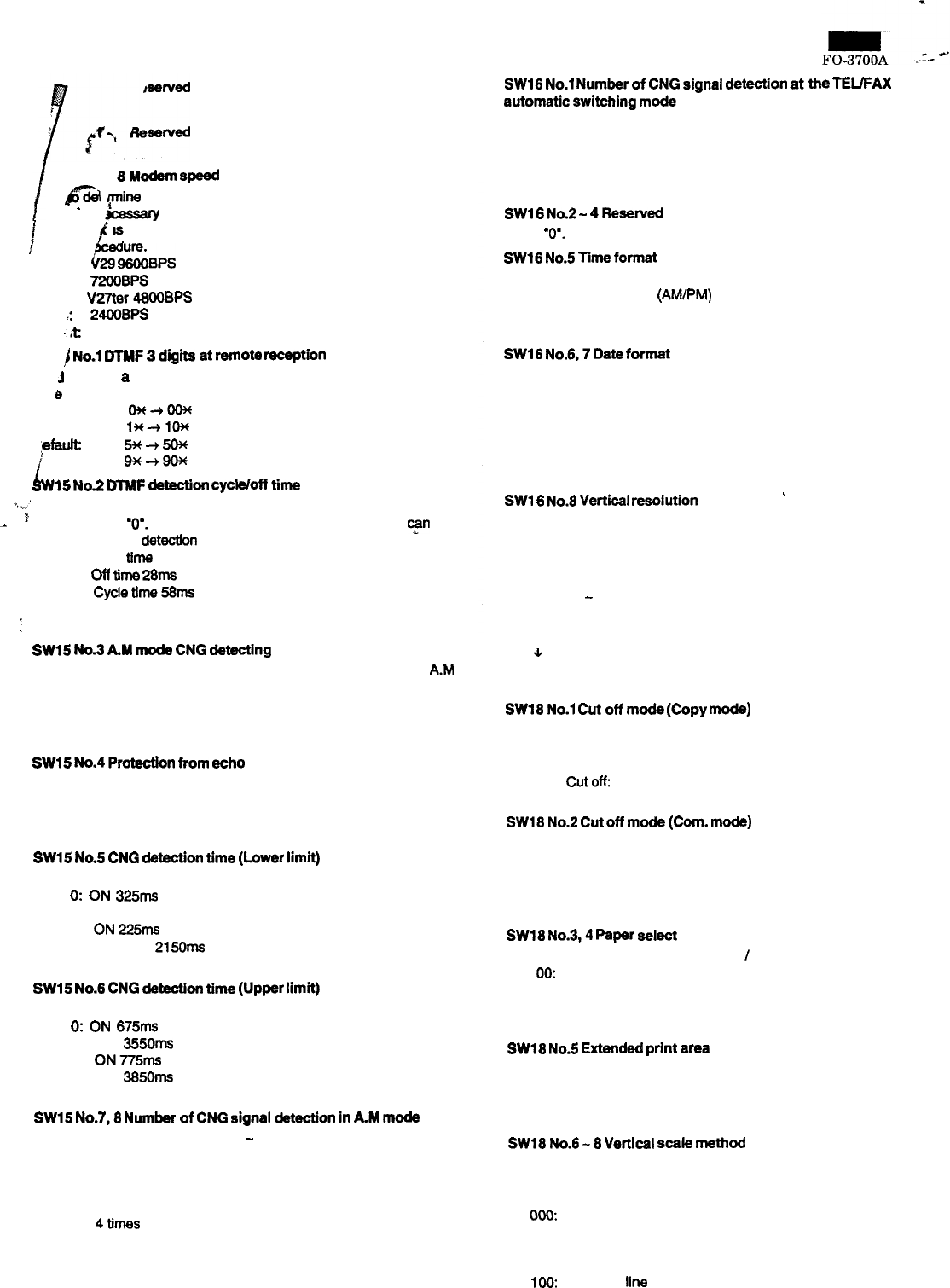
SW16
No.1
Number
of
CNG
signal
detection
at
the
TEUFAX
automatic
switching
mode
Used for detection of CNG in one or two pulses in the TEL/FAX
automatic switching mode
0: Once
1: Twice
Default: 1
SW1
6
No.2
-
4
Reserved
Set to
‘0’.
SW16
No.5
Time
format
Choice is made for the format of time display
0: 12 hours mode (AM/PM)
1: 24hoursmode
Default: 1
SWIG
No.8,7
Date
format
Used to set entry of date into activity report and LED format accord-
ing to specifications of country.
00: day/month/year
01: month/day/year
10: year/month/day
11:
year/month/day (Japan mode: month is not English)
Default: 00
SW1
6
No.8
Vertical
resolution
Used to set the Vertical resolution.
0: 300 dpi
1: 7.7 line/mm
Default: 0
/
SW1 7 No.1
-
8 Off hook hold
Used to set ‘Off hook hold’ time by binary input.
00000000: 0 second
11111111: 255seconds
Default: 00000000
SW18
No.1
Cut
off
mode
(Copy
mode)
When in copy, if the scanned data is out of the range of recording, the
operator has one of the choices below using the switch.
0:
Continue: Data is printed onto the next page.
1:
Cutoff:
Data scanned out of the limit is cut off.
Default: 1
SW18
No.2
Cut
off
mode
(Corn.
mode)
When receiving, if the data is out of the range of recording, the
operator has one of the choices below using the switch.
0: Continue
1: cutoff
Default: 0
SW18
No.3,4
Paper
select
Used to set the media size. (Letter /A4
/
Legal) check pattern only
00:
Letter size
01: A4
10: Legal
Default: 01
SW18
No.5
Extended
print
area
Used to choose of extended print area enable or disable.
0: Disable
1: Enable
Default: 0
SW18
No.6
-
8
Vertical
scale
method
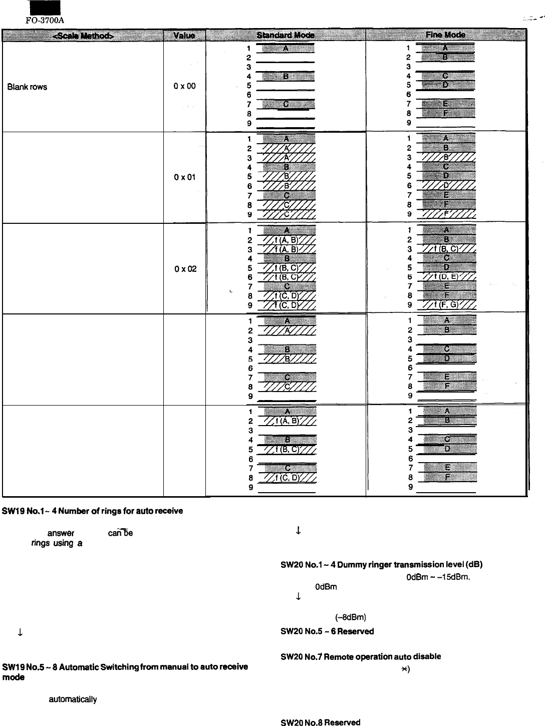
Used to choose of Vertical scale method.
Method used to create the additional rows needed to provide the
proper vertical size.
099: Blank rows
001: Duplicate last row
010: Smoothing
011: Constant line density (Duplication)
196:
Constant line density (Smoothing)
Default: 010
2-11
FO-3700A
Blank
rows
Duplicate last row
Smoothing
Constant line density using duplication
Constant line density using smoothing
0x03
0 x 04
SW19
No.1
-
4
Number
of
rings
for
auto
receive
When the machine is set in the auto receive mode, the number of
rings before
answer
is made
can-e
selected. It may be set from one
to nine
rings
using
a
binary number. Since the facsimile telephone
could be used as an ordinary telephone if the handset is taken off the
hook before connection is made to the facsimile while ringing, it
should be programmed to the user’s choice. If a facsimile calling beep
is heard when the handset is taken off the hook, press the
START/COPY key and put the handset on the hook to have the
facsimile start receiving. If it is set to above 9, receive rings are
automatically set to 1.
0001: 1 time
I
1001: 9 times
Default: 0001
SW19
No.5
-
8
Automatic
Switching
from
manual
to
auto
receive
mode
Choice is made to after how many rings in the manual receive mode
it should be automaticaily changed to the facsimile answer mode or
remain in the manual receive mode. Entering a binary number 0 will
force the machine to remain in the manual answer mode. If a number
between 1 and 9 is entered, the machine will go into the answer
mode after the given number of rings. However, it can be used as an
ordinary telephone if the handset is taken off the hook before this
programmed number has elapsed. Entry of a number above 9 will set
the machine to 0.
0000: Does not change
0001: 1 times
3.
1001: 9 times
Default: 0000
SW20
No.1
-
4
Dummy
ringer
transmission
level
(dB)
Pseude-ringer sending level setting
OdBm
-
-15dBm.
0000:
OdBm
L
1111: -15dB
Default: 1000 (-8dBm)
SW20
No.5
-
8
Reserved
Set to ‘0’.
SW20
No.7
Remote
operation
auto
disable
Selection of remote operation (5,
*)
inhibition after passing a certain
time from reception of Remote operation auto disable.
0: Not inhibited.
1:
Inhibited automatically after 7 sec.
Default: 0
SW20
No.8
Reserved
Set to ‘0’.
2-12
[3]
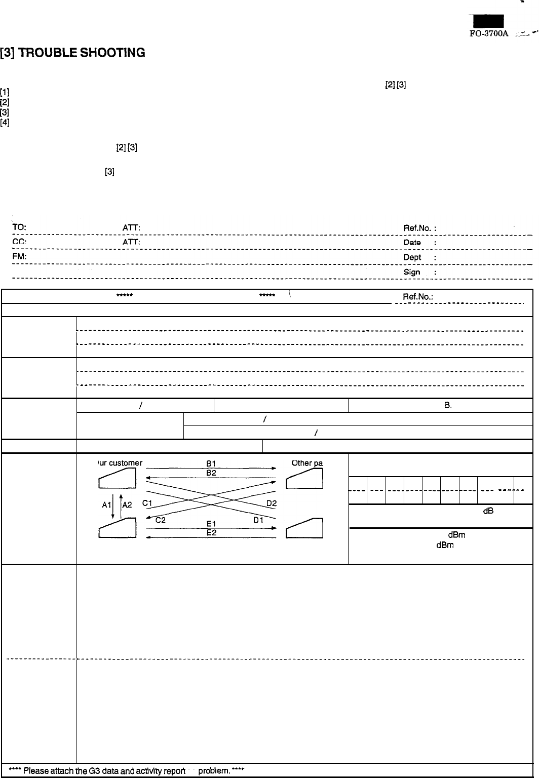
TROUBLE
SHOOTING
Refer to the following actions to troubleshoot any of problems men-
tioned in l-6.
111
A communication error evoked.
[2]
Image distortion produced.
[3]
Unable to do overseas communication
[4]
Communication speed slow liable to failback.
l
Increase the transmission level SOFT SWITCH 7-5 6 7 8
Can be used in case [1]
[2]
[3]
l
Decrease the transmission level SOFT SWITCH 7-5 6 7 8
Can be used in case
[3]
l
Apply line equalization SOFT SWITCH 2-5
Can be used in all cases.
l
Slow down the transmission speed SOFT SWITCH 14-5 6 7 8
Can be used in case
[2]
[3]
l Replace the LIU PWB.
Can be used in all cases.
l Replace the control PWB.
Can be used in all cases.
*If transmission problems still exist on the machine, use the follow-
ing format and check the related matters.
rrease
arracn
me
tin
aara ana acnvny repon on proorem. ----
-**
Facsimile communication problem
-
\
Ref.No.:
___-----___-------__---------.
From: Mr. Fax Tel No.: Date:
Our customer Name Tel No.
________________--______________________--------------------------------------------------------------
Address Fax No.
_________________-______________________--------------------------------------------------------------
Contact person Model name
Other party Name Tel No.
___--___________________________________--------------------------------------------------------------
Address Fax No.
________________________________________--------------------------------------------------------------
Contact person Model name
Problem mode Line: Domestic
/
international Mode:
G3
Phase: A. 8. C. D.
Reception /Transmission Automatic reception
/
Manual reception
Automatic dialling /Manual dialling
/
Others
Frequency:
%
ROM version:
Confirmation Our customer
item Other party Please mark problem with an X
No problem is: 0
e
tFji+f+z
Al A2 Bl B2 Cl C2 Dl D2 El E
-
_
_
_
.
-
-
-
.
-
-
-
_
-
-
-
-
-
-
-
-
_
-
-
-
-
-
-
-
.
_
_
-
-
-
-
-
-
-
Transmission level setting is ( )
dB
at our
El customer
E2
*
.Transmission level ( ) dBm
Our service Other party’s service Reception level ( ) dBm
By level meter at Bl and B2
Comment
_-_______-_____-________________________------------------------------------------------------------------------------
Counter-measure
2-13
Fe!!!
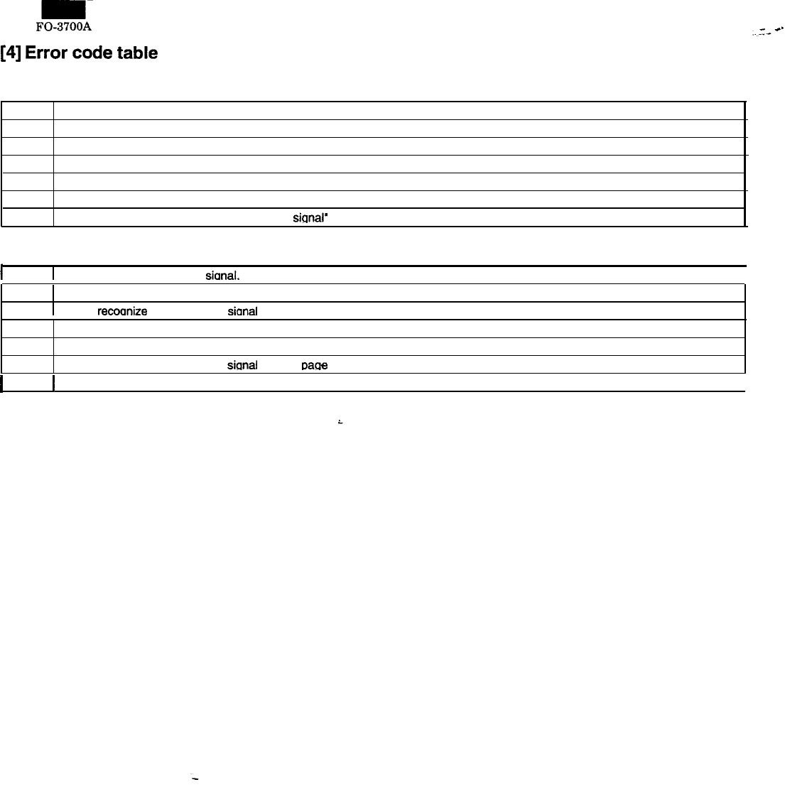
[4]
Error
code
table
Transmission errors
E-O
Able to recognize handshake signal, but it has errors.
E-i Cannot recognize the handshake signal from the receiver side.
E-2
Line disconnected during transmission.
E-3
Line disconnected after modem speed fall-back.
E-4
tine disconnected during multi-page transmission.
E-6
Cannot recognize the handshake signal for next page at receiver side.
E-7
No response from receiver side or ‘disconnect
sional’
is received at transmitter side.
Reception errors
1
E-O
1
Able to recoonize handshake sianal. but it has errors.
I
E-l
1
Line disconnected during reception.
E-2
1
Cannot recoanize the handshake sianal from the transmitter side.
E-3
Cannot recognize the last handshake signal from the transmitter side.
E-4
Cannot recognize the handshake signal for next page from the transmitter side in the case of mode change.
E-5
Cannot recoonize the handshake sianal for next oaoe from the transmitter side.
1
E-7
1
No response from transmitter or ‘disconnect signal’ is received at receiver side.
I
i
2-14
FO-3700A
d-4.
.-
The hopper is used to align documents with the document guides
adjusted to the paper width.
NOTE: Adjust the document guides before and after inserting the
document.
CHAPTER
3.
MECHANISM
BLOCKS
[I]
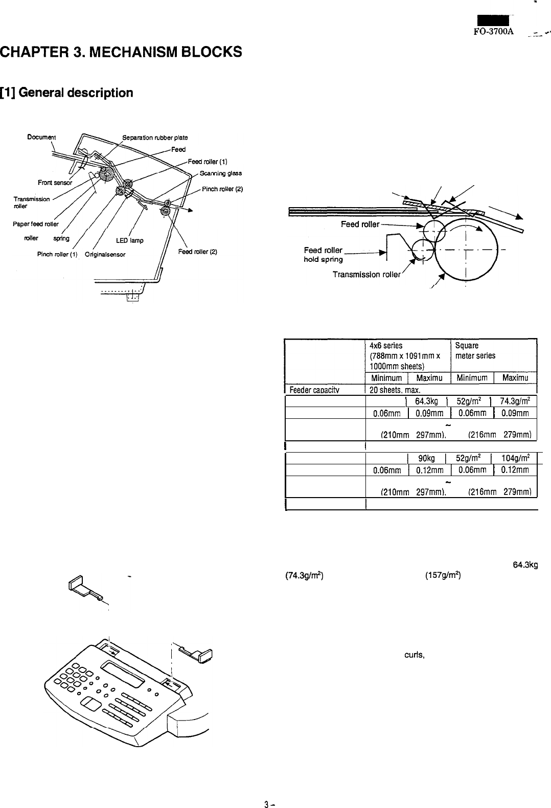
General
description
1. Document feed block and diagram
Oocume
/Feed
roller
.
-Feed
roller(l)
Feed
roller
hold
.y
Fig. 1
2. Document feed operation
1) The document placed in the hopper actuates the front sensor.
After one second, the pulse motor starts to drive the paper feed
roller. The document is automatically taken up into the machine,
and stopped at the original sensor.
2) After a specified number of pulses are received from the docu-
ment lead edge being sensed, scanning is started.
3) When a specified number of pulses are received from the docu-
ment rear edge being sensed, scanning is terminated and the
document is fed through.
4) If the front sensor is active (i.e., another document is in the hop-
per), when the preceding document scanning is completed and
and it is fed out, the next document is taken up into the machine.
If the front sensor is not active (i.e., there is no document in the
hopper), when the document is fed out, the operation is ter-
minated.
3. Hopper mechanism
3-1. General view
Fig. 2
?I-
3-2. Automatic document feed
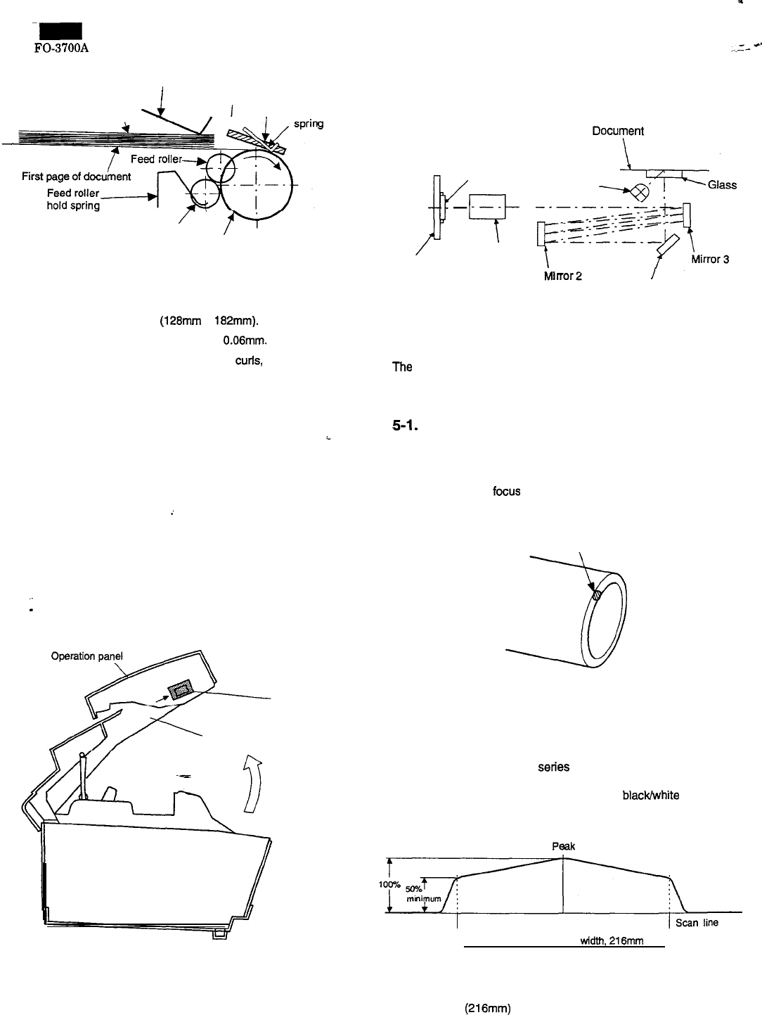
1) Use of the paper feed roller and separation rubber plate ensures
error-free transport and separation of documents. The plate spring
presses the document to the paper feed roller to assure smooth
feeding of the document.
2) Document separation method: Separation rubber plate
Separation rubber plate Paper feed spring
Paper feed spring
Paper feed roller
Fig. 3
3-3. Documents applicable for automatic feed
~1
Paper weight
45kg
)
64.3kg
1
52glm’
1
74.3glm’
Paper thickness (ref.) 0.06mm
1
0.09mm
1
0.06mm
1
0.09mm
Paper size
B6 (128mm x 182mm)
-
A4
(210mm
x
297mm).
Letter
(216mm
x
279mm)
1
Feeder caoacitv
1
15 sheets. max.
I
Paper weight
45kg
1
90kg
1
529/m’
1
104g/m2
Paper thickness (ref.) 0.06mm
1
0.12mm
1
0.06mm
1
0.12mm
Paper size
B6 (128mm x 182mm)
-
A4
(210mm
x
297mm).
Letter
(216mm
x
279mm)
1
Paper quality
1
High quality paper or equivalent
I
NOTE: Double-side coated documents and documents on facsimile
recording paper should be inserted manually. The document
feed quantity may be changed according to the document
thickness.
Documents corresponding to a paper weight heavier than 64.3kg
(74.3g/&)
and lighter than 135kg
(1579/m*)
are acceptable for
manual feed.
Documents heavier than 135kg in terms of the paper weight must be
duplicated on a copier to make it operative in the facsimile.
3-4. Loading the documents
1) Make sure that the documents are of suitable size and thickness,
and free from creases, folds,
curis,
wet glue, wet ink, clips, staples
and pins.
2) Place documents face down in the hopper.
i)
Adjust the document guides to the document size.
ii) Align the top edge of documents and gently place them into
the hopper. The first page under the stack will be taken up by
the feed roller to get ready for transmission.
NOTES:
1) Curled edge of documents, if any, must be straightened
out.
2) Do not load the documents of different sizes and/or
thicknesses together.
-m
FO-3700A
Paper feed spring
Last page of document
I
Separation rubber plate
Back of document
\
\j
,
1
Paper feed
Transmission roller
/.’
ihi/
Paper feed roller
Fig. 4
3-5. Documents requiring use of document carrier
1) Documents smaller than B6 (128mm x
182mm).
2) Documents thinner than the thickness of 0.06mm.
3) Documents containing creases, folds, or
curls,
especially those
whose surface is curled (maximum allowable curl is 5mm).
4) Documents containing tears.
5) Carbon-backed documents. (Insert a white sheet of paper be-
tween the carbon back and the document carrier to avoid transfer
of carbon to the carder.)
i
6) Documents containing an easily separable writing material (e.g.,
those written with a lead pencil).
7) Transparent documents.
8) Folded or glued documents.
;
Document in document carrier should be inserted manually into
the feeder.
4. Document release
4-1
i
Cross section view
(RIGHT SIDE)
Release
Upper document guide
lever
Fig. 5
4-2. General
When the Release Lever is pulled by hand in the direction of arrow A,
the latch is released and the upper document guide moves on its axis
in the direction of the arrow. The feed rollers, the separation rubber
plate, and the pinch rollers become free to make it possible to remove
the document.
5. Optical system
(1) General view
r
CCD
_---_
‘-?
Lens
CCD PWB
LED Lamp
G-&Glass
/
Mirror 1
Fig. 6
(2) Composition
The optical system is composed of the document feed mechanism,
the lamp, the reflecting mirrors, the focusing lens, the CCD sensor,
and the read process circuit.
5-l.
Lamp
The lamp is used to expose the document.
5-2. Lens
The lens is used to focus the light reflected from the document on the
CCD elements.
Mark
\
27
Fig. 7
5-3. CCD
The CCD (charge coupled device) image sensor consists of a
photodiode array which converts the intensity of light reflected from
the document surface into a sertes of analog voltages which are then
stored in an analog shift register. The series of analog voltages are
then converted into a digital equivalent by a
blackhhrhite
binary logic
circuit.
(Example) Scan signal output waveform
Peak
Maximum document
width,
216mm
length
Fig. 8
1) The minimum output from the CCD at the maximum scan width of
document (216mm) must be more than 50% of the peak value.
2) The peak output must be about 150mV under room temperature
to avoid CCD saturation.
3-2
4
FO-3700A
A.2
-'
[2]
Disassembly
and
assembly
procedures
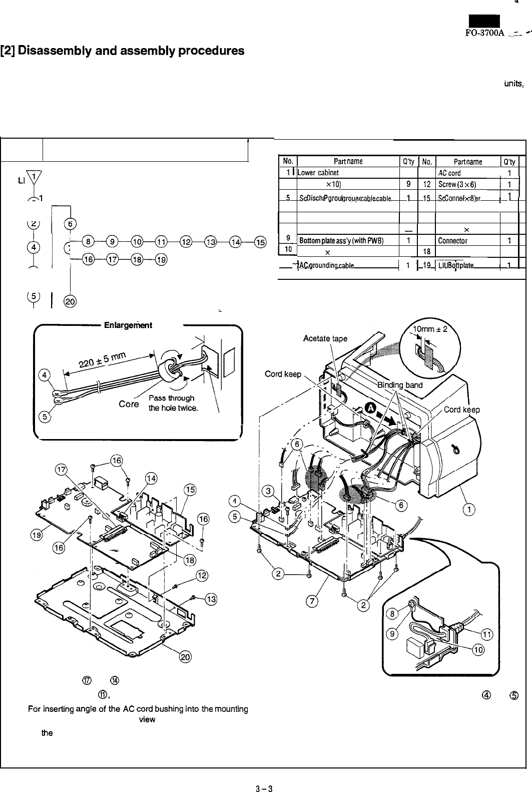
lThis chapter mainly describes the disassembly procedures. For the assembly procedures, reverse the disassembly procedures.
l
Easy and simple disassembly/assembly procedures of some parts and units are omitted. For disassembly and assembly of such parts and tinits,
refer to the Parts List.
lThe numbers in the illustration, the parts list and the flowchart in a same section are common to each other.
lTo assure reliability of the product, the disassembly and the assembly procedures should be performed carefully and deliberately.
I
I
Parts list (Fig. 1)
1
Control PWB, Power unit
a. Remove the AC cord, the power unit, the control PWB, and the
LIU
PWB according to the flow chart.
Y
1
No.
1
Part
name
1
1
Lower
cabinet
1
Q’ly
1
No.
1
Part
name
I 1 I 11
IA1:rnrd
I
Q’tv
I
1
.._“_.I
2
Screw (3
x
10)
9
12 Screw
(3
x
6)
4
3
5Screw
Discharge
Printer
(3
grounding
x
brush
5)
grounding
cable cable
1
1
1
15
13 14
Screw
Connector
Power
(3
unit
x
8)
I
1
I
1
1
t-l
1
1
6Connector
-
16
Screw
x
(3 5)
4
7
Bottom
plate
ass’y (with PWB)
1
17
Connector
1
8
Screw (4
x
6)
1
18 Control
PWB
1
1
Ql
4
0”
16
8
17
9
18
10
11
19
12
13
14
15
10
9
1
AC
AC
connector
grounding
cable
1
111
1
1
20
19
ILIUPWB
1
Bottom
plate
(
I
1
?
I
63
i
f-~
Enlargekent
view A
,-h
Lower cabinet
square hole
[Note for assembly]
1.
Insert connectors
@J
and @ securely.
Fig. 1
3. When wiring, note the following points:
2. When setting AC cord
@I,
note the following points:
l
For
inserting
angle
of
the
AC
cord bushing into
the
mounting
angle, refer to the enlargement view of Fig. 1.
l Fix the AC cable above the AC cord with a screw. (Refer to
the enlargement view.)
l
Before binding each cable, wind grounding cables @ and
0
around the core and insert the core into the square hole in
the lower cabinet until the core is not seen from the outside
as shown in the enlargement view.
l Use two bands and two cord keeps for wiring, and fix with
acetate tape to eliminate slack in the speaker cable. (Refer to
the enlargement view.)
3-3
FO-3700A
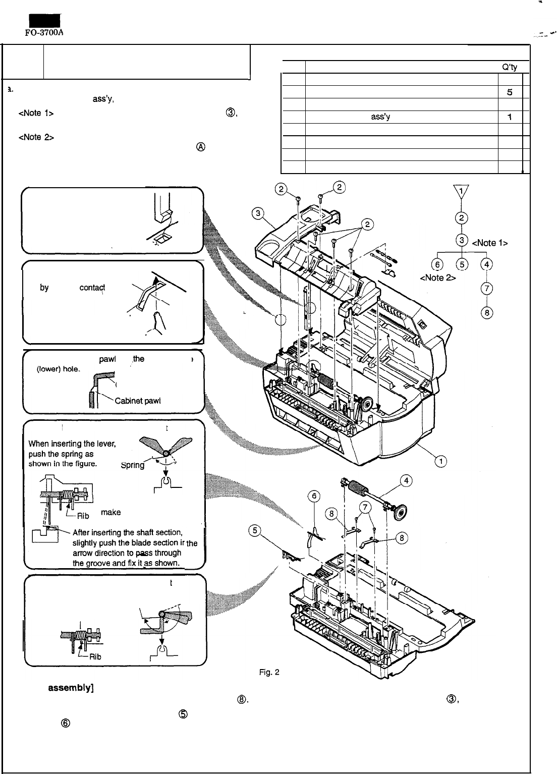
Original guide lower, paper feed roller, Parts list (Fig. 2)
2
sensor lever ass’y, etc.
No.
Part name I Q’ty
I
1
1.
Remove the original guide lower, the paper feed roller, the
original sensor lever
a&y,
and the front sensor lever ass’y.
<Note
I>
When removing original guide lower ass’y
0,
be
careful not to damage the front sensor lever.
<Note
%
When removing the front sensor lever ass’y, refer to
the enlarged view. Press lever section @ in the arrow
direction to put the lever in the dotted line place.
Then turn the lever shaft and remove it upwards.
1
Medium cabinet
1
2
Screw (3 x 8)
5
3
Original guide lower ass’y
1
4
Paper feed roller
a&y
1
5
Original sensor lever ass’y
1
8
Front sensor lever ass’y
1
7
Screw (3 x 8) 2
8
Pinch pressure spring 2
Lock the pawl in the
square hole. (2 positions)
1
a
1
B
2
/
(Note) When attaching the original guide unit,
\
be careful not to break
it
by
making
contaq
with
the front sensor lever.
Original guide (lower) hole
\
Front sensor lever
Insert the cabinet
paw1
into
the
original guide
Original guide (lower)
Front sensor lever attachment
Original sensor lever attachment
When inserting the lever,
push the spring as
Spring
shown in the figure.
the
J
(Note) Be careful not to
make
contact between the
sensor cable and the spring.
<Note
l>
[Note for
assembly]
1.
Be careful to the installing direction of pinch pressure spring @.
2. When attaching original sensor lever ass’y @ and front sensor
lever ass’y @ to the sensor holder, refer to the enlarged view for
the spring position and the attachment procedure.
3. When attaching original guide lower ass’y
0,
note the following
points:
l
Check that the scanning glass is free from dust, finger prints,
etc.
l
Be careful not to damage the front sensor lever.
l
Lock the four pawls and fit them with screws.
3-4
Parts list (Fig. 3)
3
I
Optical unit
I. Remove the original guide lower ass’y, and the paper feed roller
ass’y according to procedure 2-a.
).
Remove the optical unit.
:.
Remove the scanning glass, the LED, and the mirror from the
optical unit.
\1/
9
)
Mirrorholdingspring
1
2
1
<Note> Never disassemble the CCD PWB
and
the lens except
when replacing. If they are disassembled, the optical unit
adjustment must be performed.
Scanning glass disassembly
f
Wind tape around
I
Scanning glass
1
\\
.
(Left side) Disengage both edges of the
q+q
glass from the rib as shown in
the figure, and slide it to
remove. (if only one edge is
disengaged, the other edge
may be broken.)
(Right side) To disengage the right edge,
slide the glass in the left side.
bend the holding arm, and
disengage from the rib.
a
Sensor cable
1
m the square hole.)
[Note for assembly]
1.
When attaching mirrors @ and
0,
note the following points:
l Be careful of the mirror surface direction as shown in the
figure.
9
Be careful that the mirror surface is free from finger prints and
dust.
l
After fixing mirror holding spring
@I
with a screw, apply screw
lock to mirror
0
@ (2 positions). (Refer to the enlarged
view.)
2. Arrange the LED and the CCD cable under the rib. (Refer to the
enlarged view.)
3. For attachment reference of dust-proof sheet @ and reflection
sheet
@,
refer to the enlarged view.
No attachment
Fig. 3
A
APPLY
rptical
frame
--JJ
/
screw
in the left side.
3-5
_m
FO-3700A
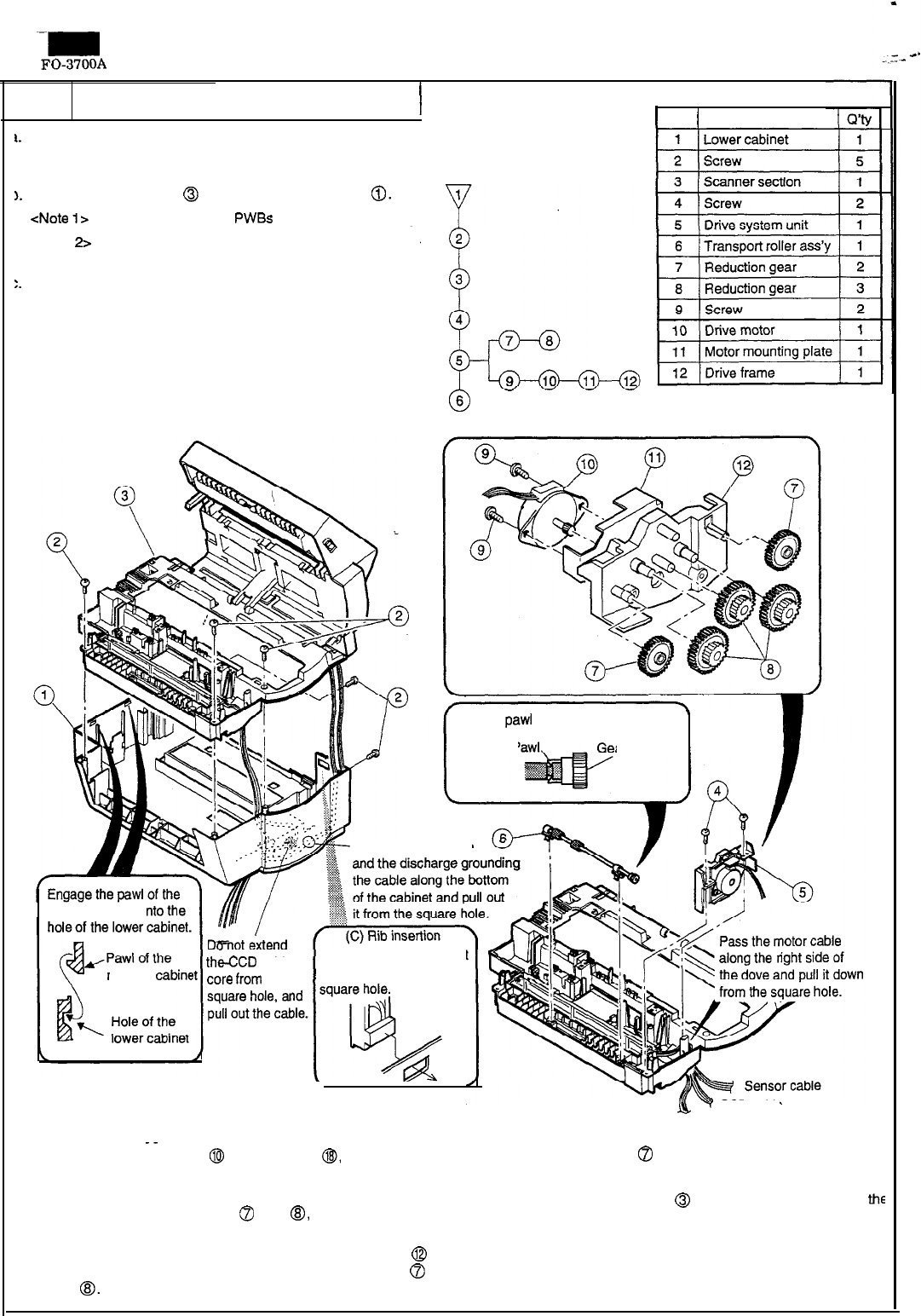
4Drive system unit
I
1.
Remove the PWB section (the control PWB, the LIU PWB, the
power unit) according to procedure l-a, and remove the cable
from the cord keep.
1.
Remove scanner section @ in Fig. 4 from lower cabinet
0.
<Note 1s Be careful not to hang
PWBs
by the cable.
<Note 2> Remove two pawls and one rib. (Refer to the en-
larged view.)
:.
Remove the drive system unit and the transport roller.
0
6
Parts list (Fig. 4)
1
No.
1
Part name
Lock the
paw1
in the groove in the shaft.
’
P
ar
,,,--
Pass the panel cable
medium cabinet i
theCCD cable
Insert the medium cabinet
medium
cabins
cOre
from
the rib into the lower cabinet
[Note for assembly]
__
Fig. 4
-7
CCD cable
Motor cable (Pull out from the square hole.)
1. When attaching drive motor @ to drive frame
6,
be careful of
the attaching direction. The connector PWB must be in the
upper side. (Refer to Fig. 4.)
2. When attaching reduction gears
8
and
@,,
note the following
points:
l Apply Molykote to the mounting shaft of drive frame @
reduction gear, and the teeth surfaces of reduction gears
0
and
@I.
lLock reduction gear
a
to the pawl of the mounting shaft.
3. For wiring, observe the notes in Fig. 4.
4. When fixing scanner section
0
to the lower cabinet, attach
two pawls and one rib to the lower cabinet securely.
3-6
FO-3700A
dz-+'
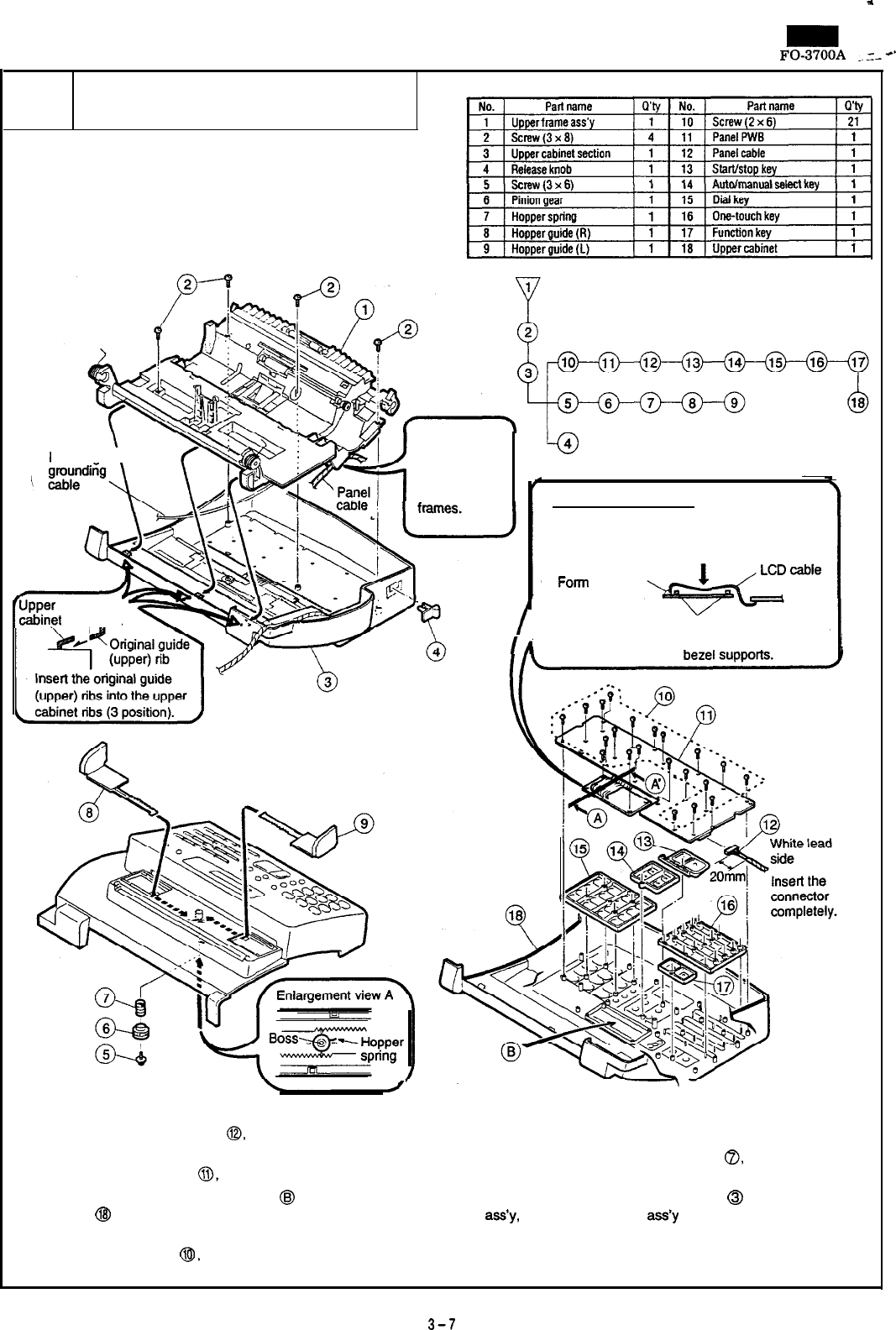
Upper cabinet section (Panel, hopper,
Parts list (Fig. 5)
5etc.)
a.
Remove the scanner section from the lower cabinet according to
procedures 4-a, b.
b.
Remove the upper cabinet section from the upper frame section,
and remove the panel PWB, keys, and hoppers.
Dischame \
f
Upper
cabin,et
rib&-
Pass the panel
cable between
the ribs and
connect the
Cross section (A)-(A’)
(b) Slightly press down the center
portion of the LCD cable so
that it bends down.
(a)
Form
the LCD
cable so that it
is in the right
angle with the (c) Check that the CCD cable
/A
LCD PWB.
is not in contact with the
I
’
Fig. 5
[Note for assembly]
1. When connecting panel cable
0,
insert the white cable as
shown in Fig. 5.
2.
When attaching panel PWB
0,
note the following points:
l Check that the LCD installing section
@I
in Fig. 5) of upper
cabinet
@I
and the glass surface of the LCD are free from
dirt.
l
When tightening screws
@!I,
be sure to tighten
q
and
q
first.
lFor wiring of the LCD cable, refer to the enlarged view.
3.
For attaching direction of hopper spring
a,
refer to the enlarged
view.
4. When attaching upper cabinet section @ to the upper frame
a&y,
put the upper frame ass’y rib under the upper cabinet rib.
(Refer lo the enlarged view.)
5.
For wiring of the panel cable, refer to the note in Fig. 5.
3-7
FO-3700A
Upper frame section (original guide Parts list (Fig. 6)
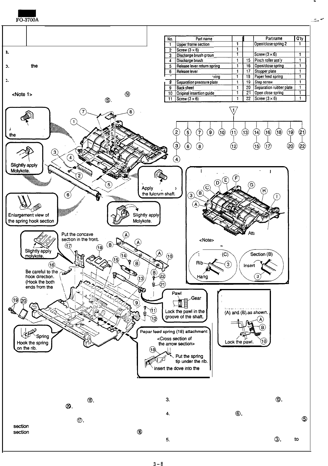
6
upper section)
1.
Remove the scanner section from the lower cabinet according to
procedures 4-a, b.
J.
Remove
me
upper cabinet section from the upper frame section
according to procedure 5-b.
:. Remove the release lever, the original insertion guide, the pinch
7
1
Separation pressure sp
Q
I
ca,..m+inn
nrsce,,ra
nk
roller, and the transport roller from me upper frame section.
<Note
1s
Use a small screwdriver to remove screw @ and be
careful not to scratch pinch roller
0.
1
Q’ty
1
No.
1
Part
name
1
Q’ty
1
1
12
Open/close
spring
2
1
1
13
Transport roller ass’y
1
ding cable
1
14
Screw
(3
x
6)
1
1
1
21
IOpenclosespring
Apply Molykote to
me
fulcrum shaft.
Discharge grouding cable (3) wiring
I
SWW
apply
ADDIV
Molvkote to
SWW
ap$y
“\
t
lower side.)
ach acetate tape
<Note> Insert the rib to eliminate slacks
in cable A
-
I in this sequence.
Section (A)
7\
fizfi
(C)
<
spring positioning hole.
Original insertion guide
(10) attachment
Insert ribs in sections
‘,
W”
-..v
w-h
Fig. 6
[Note for assembly]
1. When attaching paper feed spring
@I,
be careful not to scratch
separation rubber plate
@,
and insert securely. (Refer to the
enlarged view.)
2. When attaching stopper plate
@I,
apply Molykote to the stopper
SectiOn
(referring to the enlarged view), and place the concave
SectiOn
in the front surface, and attach open/close spring @ as
shown in Fig. 6. Be careful not to reverse me spring hook.
For attaching direction of original insertion guide @, refer to the
enlarged view.
When attaching release lever
8,
apply Molykote to the enlarged
view section of Fig. 6, and attach release lever return spring @
as shown in the enlarged view. Be careful to the spring hook
direction.
For wiring of discharge brush grounding cable
0,
refer
to
the
enlarged view.
3-a
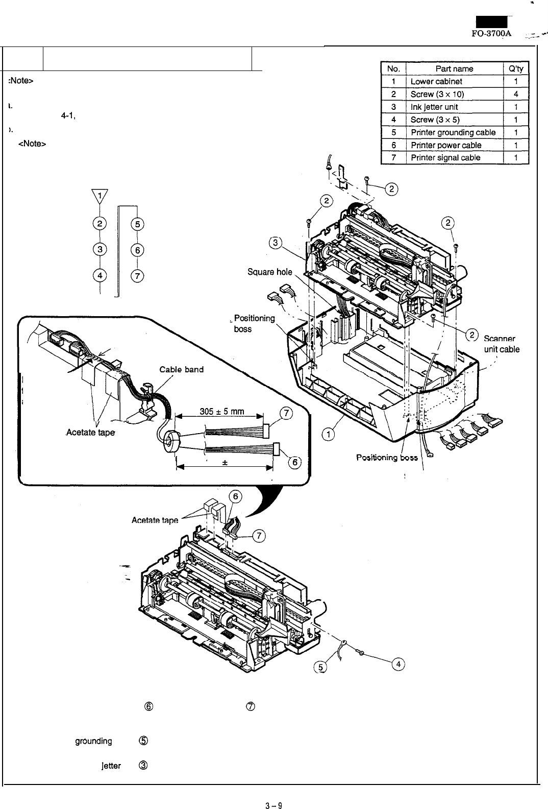
7Ink jetter unit
:Note> This section describes the procedures to remove the ink
jetter section from the body.
1.
Remove the scanner section from the lower cabinet according to
procedures
4-1,
b.
1.
Remove the ink jetter unit,
<Note> When removing the ink jetter unit from the lower
cabinet, be careful not to hang the cables and connec-
tors.
1
2
i
3
4
Put the cable
to the PWB side
and Fix with tape.
Parts list (Pig.
7)
Acetate’tpe
-
h
325
f
5 mm
Wind the cable around the core two turns. Square hole
-
Fig. 7
[Note for assembly]
1. For wiring of printer power cable @ and printer signal cable
8
and the core attaching position, refer to the enlarged view of Fig.
7.
2. Attach printer gr6unding cable
a
at the angle of 45 degrees.
(Refer to Fig. 7.)
3.
Note for attaching ink
letter
unit @
l
Before attaching the ink jetter unit, pass the cables connected
to the PWB section through the square hole and put them
out.
l Be careful not to pinch the cables, and install the ink jetter
unit to the positioning boss of the lower cabinet and fix it with
a screw.
3-9
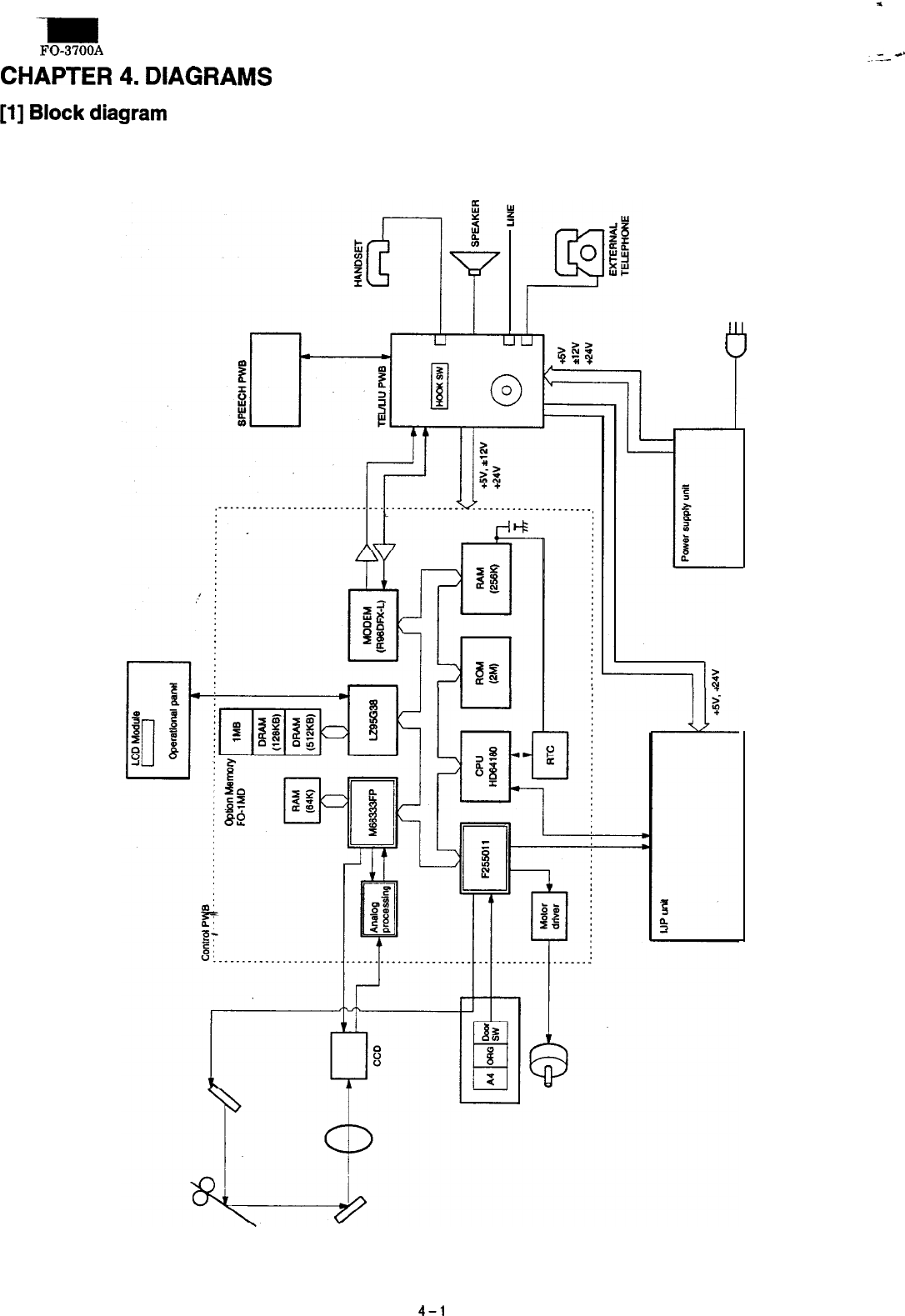
FO-3700A
CHAPTER
4.
DIAGRAMS
[I]
Block
diagram
P
4-l
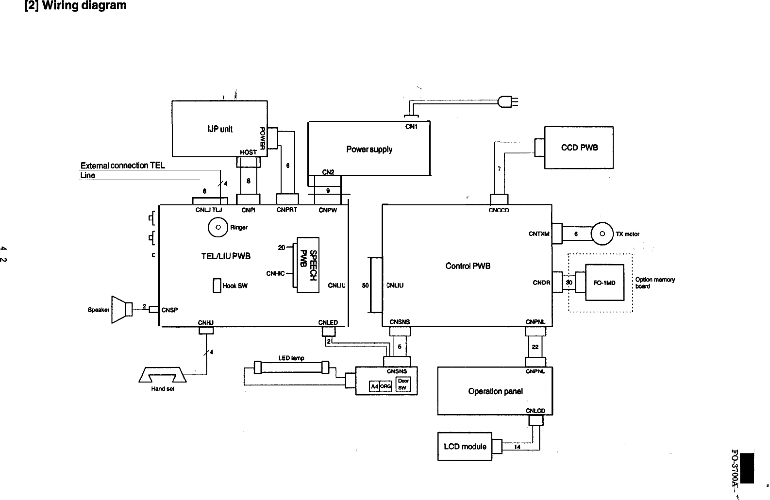
[2]
Wiring
diagram
P
I
N
Speaker
l-i
0
0
WnQ.ar
TEL/LlU
PWB
II
Hooksw
20.
cl
z
!I
8
CNUU
CNHIC
.
1
IJP
unit
CNl
HOST
Power
supply
External
connection
TEL
Me
cN2
,‘4
6
60
I
1
I
w-7
CNLJ
lLJ
CNPI
CNPRT CNPW
CNtU
w
1
M
Control
PWB
XLIU
CCD
PWB
i==
.__._____________..
1:
4

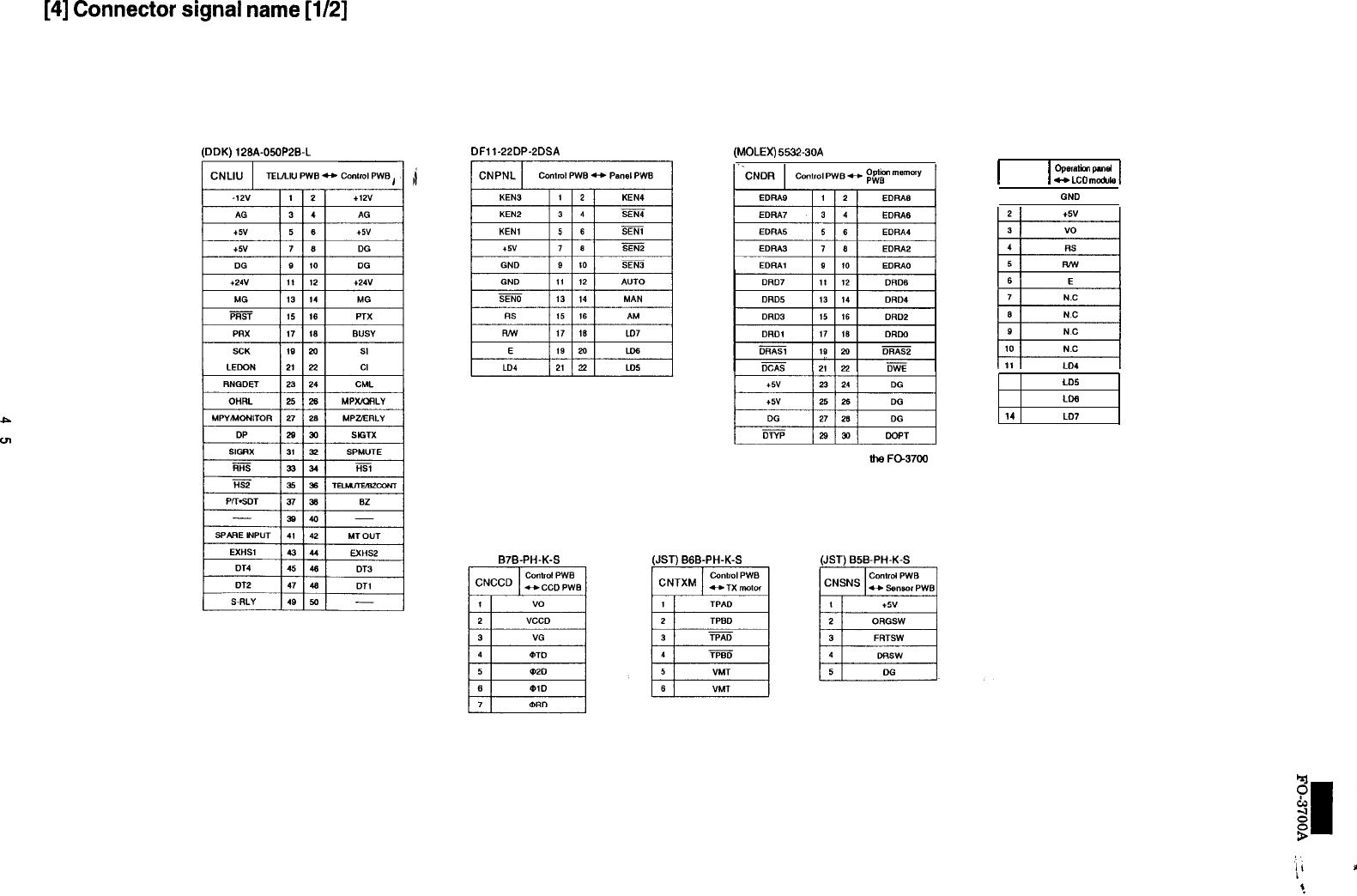
P
I
VI
[4]
Connector
signal
name
[l/2]
Control PWB/Operation panel
(DDK) 126A-05OP2B-L(DDK) 126A-05OP2B-L
DFll-22DP-2DSA
(MOLEX)
5532-30A
ppi$q
CNDR is mounted only in the
FCM700
(JST) B7B-PI-I-K-S (JST) BGB-PH-K-S
’
CNLCD
1
operstim
pmd
-LCD
module
1
I 1 I
GND
I
I 12 I
LD5
I
13
LLM
14 LO7
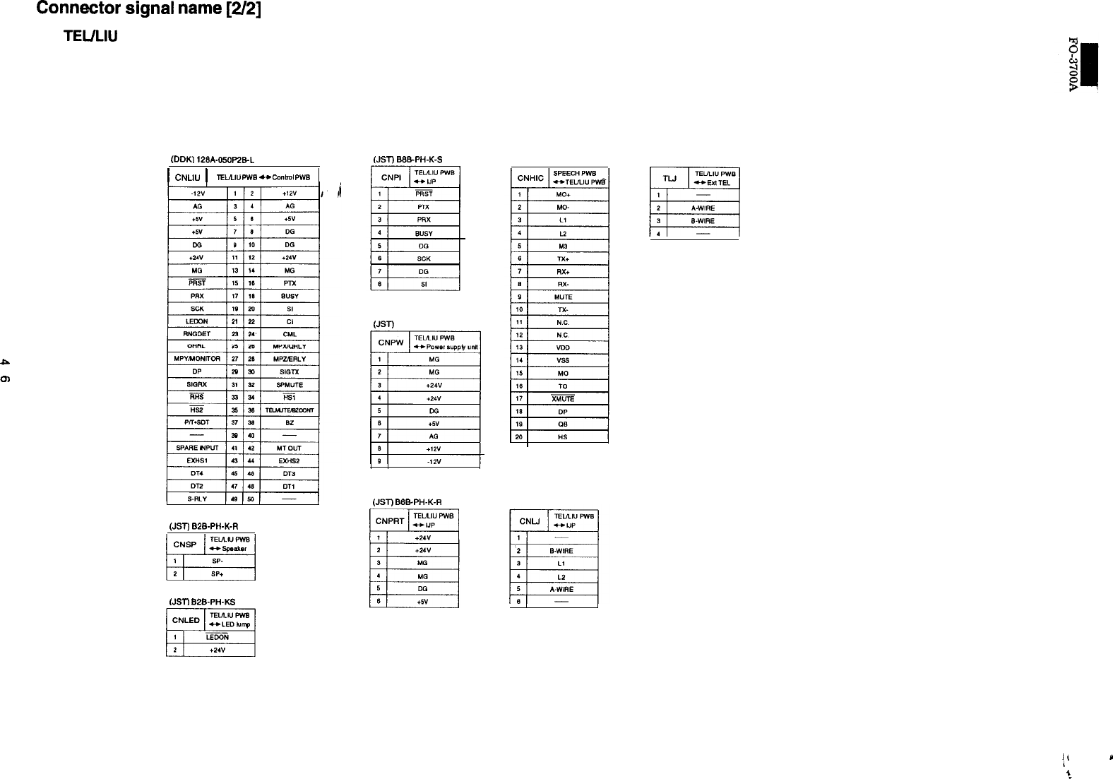
P
I
0)
Connector
signal
name
[2/2]
TEULIU
PWB
(DDK)
128A-OSOP25L
1
CNLIU
1
lEl,u”
Fw8
-
Cc.“bol
PWB
(JST)
628.P&K-R
(JSTI
BPS-PH.KS
(JSTl
SSEPH-K-S
(JST) SP-FJ
(JST)
BBB-PH-K-R
/
i’
Y
?
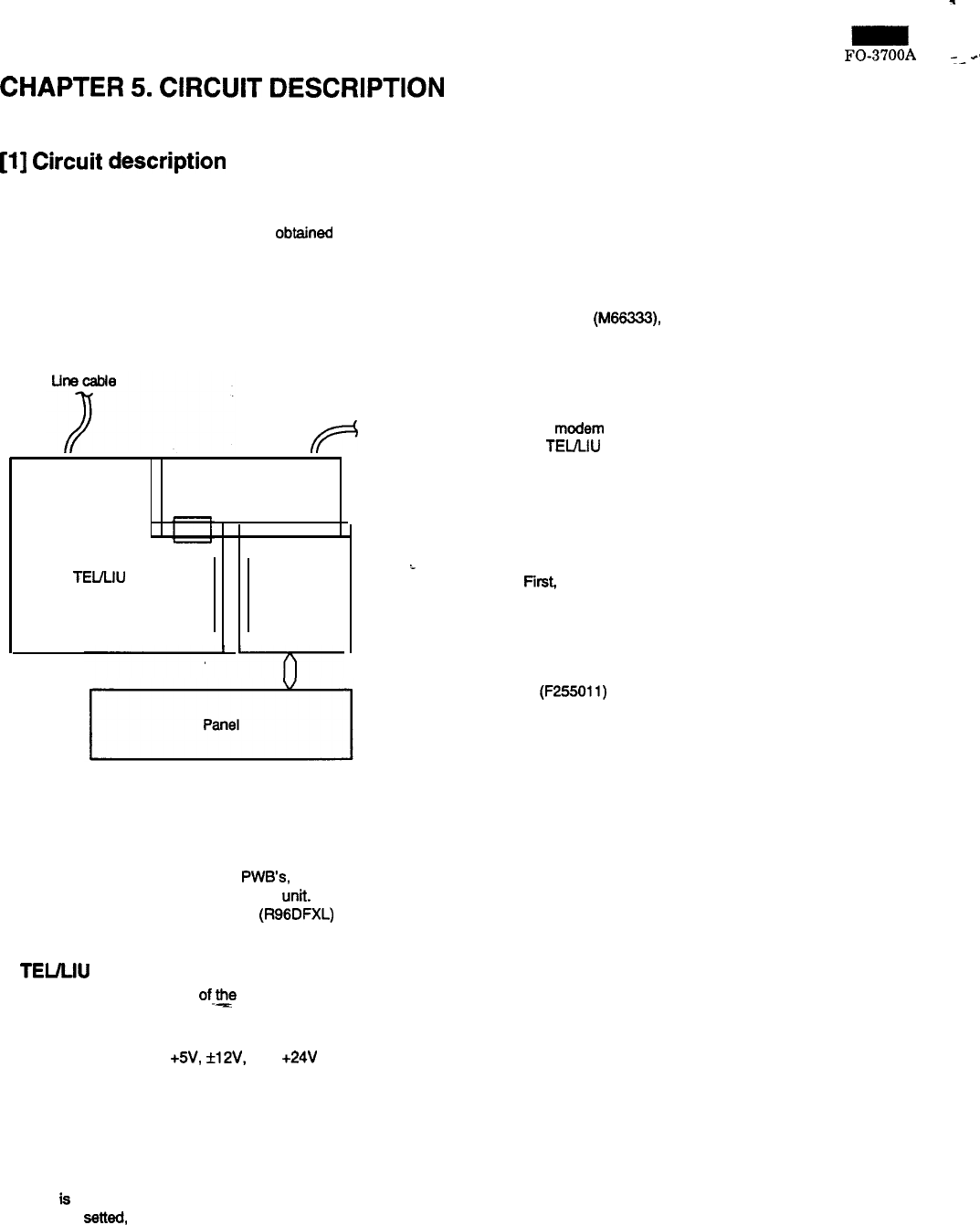
CHAPTER
5.
CIRCUIT
DESCRIPTION
[l]
Circuit
description
1. General description
The compact design of the control PWB is obtained by using two gate
arrays and high density printing of surface mounting parts. Each PWB
is independent according to its function as shown in Fig. 1.
2. PWB configuration
P
To AC outlet
Power supply
TEULIU PWB
Control PWB
1
L
Fig. 1 PWB configuration
1) Control PWB
The control PWB controls peripheral
PWB’s,
mechanical parts, trans-
mission, and performs overall control of the unit.
This machine employs a l-chip modem (R96DFXL) which is installed
on the control PWB.
2)
TELMU
This PWB controls connection
of.5
telephone line to the unit.
3) Power supply
This provides voltages of
+5V,
f12V,
and +24V to the control PWB
and the Inkjet Printer.
4) Panel
me panel allows input of the operation panel and LCD display.
FO-3700A
-_-I
3. Operational description
Operational descriptions are given below:
l Transmission
When a document in loaded in the standby mode, the state of the
document sensor is sensed via the gate array A. If the sensor
signal was on, the motor is started to bring the document into the
standby position. With depression of the START/copy key in the
off-hook state, transmission takes place.
Upon depression of the START/copy key, the CML relay is set
active which switches the line from the telephone to the modem.
Then, the procedure is sent out from the modem and the motor is
rotated to move the document down to the scan line. In the Image
processor
(M66SSS),
the signal scanned by CCD is sent to the
internal AD converter to convert the analog signal into binary data.
This binary data is transferred from the Image processor to the
image buffer and encoded and stored in the transmit buffer of the
DRAM. The data is then written to the modem according to inter-
ruption by the data transmission request signal from the modem.
The modem madulates the code data and sends signals through
the TEULIU PWB.
l Receive operation
There are two ways of starting reception, manual and automatic.
Depression of the START/copy key in the off-hook mode in the
case of the manual receive mode, or Cl signal detection by the LIU
in the automatic receive mode, causes the CML relay to activate to
initiate the receive operation.
First
the CPU controls the procedure signals from the modem to
be ready to receive data. When the program goes into phase C,
the serial data from the modem is stored in the receive buffer of
the RAM. The data in the receive buffer is decoded software-wise
to reproduce it as binary image data in the image buffer. The data
is DMA transferred to the recording processor within the gate array
A (F255011) which is then converted from parallel to serial form to
be sent to the printer unit. The data is printed by the printer unit.
l Copy operation
To make a copy on this facsimile, the START/copy key is pressed
when the machine is ready with a document on the document
table and the telephone set is in the on-hook state.
First, depression of the START/copy key advances the document
to the first scan line. Similar to the transmitting operation, the
image signal from the CCD is converted to a binary signal in the
DMA mode via the Image Processor which is then sent to the
image buffer of the RAM. Next, the data is transferred to the
recording processor in the DMA mode to send the image data to
the printer unit which is printed. The copying takes place as the
operation is repeated.
5) Option memory board (FO-1 MD)
This unit
ls
the use of an extend memory.
If this unit is setted, the memory function is increased.
5-1
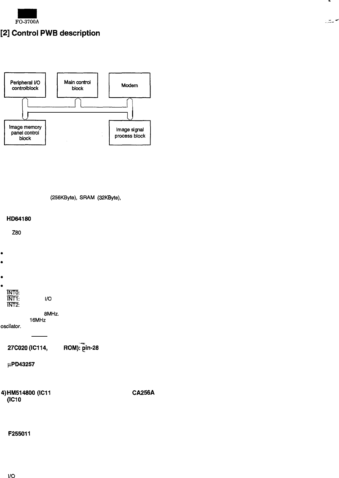
FO-3700A
[2]
Control
PWB
description
1. General description
Fig. 2 shows the functional blocks of the control PWB, which is com-
posed of 6 blocks.
I
I
1
I
Fig. 2 Control PWB functional block diagram
2. Description of each block
(1) Main control block
The main control block is composed of an 8-bit microprocessor
HD64180, ROM (256KByte), SRAM (32KByte), and DRAM
(640KByte). Devices are connected to the bus to control the whole
unit.
1) HD64180
(IC4, main
CPU) . . . pin-80 QFP
This is a CMOS 8-bit microprocessor. A high-speed CPU (compatible
with 280 upper class models) and peripheral functions are incor-
porated in one chip.
This system allows the following functions.
Memory Management Unit (MMU)
DMA controller (2 channel); channel 0: For read data transfer
channel 1: For print data transfer
Timer
Interruption; As external interrupt.
m:
Modem interrupt.
m:
Peripheral
I/O
control section interrupt.
m
RTC detection interrupt.
Operating speed is 8MHz.
In addition, 16MHz clock is internally generated with the ceramic
oscilator.
For reset when power is turned on, a LOW signal of about 200msec
is supplied to RESET terminal.
2)
27CO20
(IC114, main
ROM)$in-28
DIP
EPROM of 2MKbit equipped with software for the main CPU.
3)
pPD43257
(IC5): pin-28, SOP
Line memory for the main CPU system RAM area.
Memory of recorded data such as daily report and auto dials. When
power is turned off, backup is made with a lithium battery.
4)HM514800
(IC11 DRAM): pin-28, SOJ and GM71
CA256A
(ICI0
DRAM): Pin-26, SOJ
Image memory for cording/recording process.
l
Memory for recording pixel data at no paper.
l Memory for ECM
5)
F255011
(IC7, gate array A)
The following functions are incorporated to support the main CPU.
l Printer interface
l Read system control
l Mechanism control
l
I/O
port
5-2
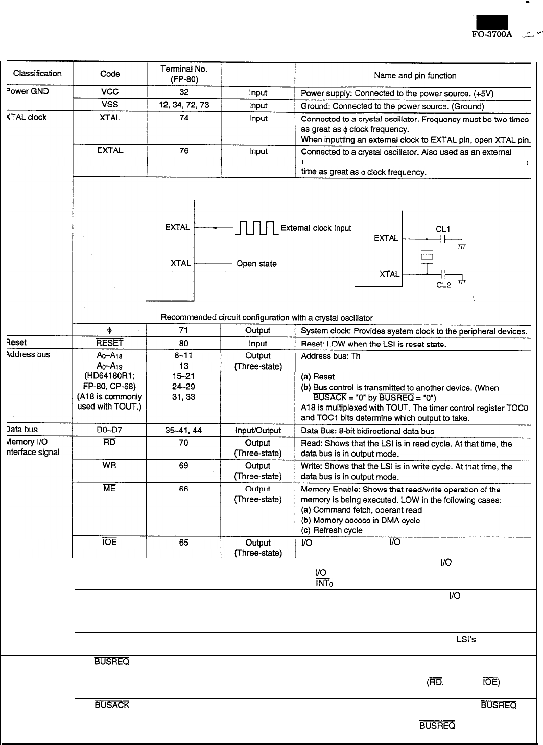
-m
FO-3700A
.mz-+'
HD64180 (IC4) terminal descriptions
clock input pin. The external clock input frequency must be two
e address to make access to the memory
space. HIGH only in the following cases:
Enable: Shows that l/O read/write operation
is
being
executed. LOW in the following cases:
System control
signal
WAIT
77
E
67
BUSREQ 79
BUSACK
78
Input
output
Input
output
(a) Read/write of data in executing an
I10
command
(b)
I/O
access in DMA cycle
(c)
mc
acknowledge cycle
Wait: Used to extend read/write cycle of
I/O
or the memory.
When this input is LOW at the falling edge of T2, TW state is
inserted next to T2. When it is LOW at the falling edge of TW,
another TW is inserted again next to the preceding one.
Enable: Synchronizing clock for peripheral LSl’s of the 6800
system.
Bus Request: Used for other devices to request bus free to
this LSI. When driven LOW, the CPU stops execution of
--
commands and drives some parts
(m,
WR, ME,
m)
of the
address bus, data bus, and memory interface signals HIGH.
Bus acknowledge: Shows that the CPU received BUSREQ
signal and freed the bus.
When a device which outputted BUSREQ signal receives
BUSACK signal, it acknowledges that it has gained bus control
5-3
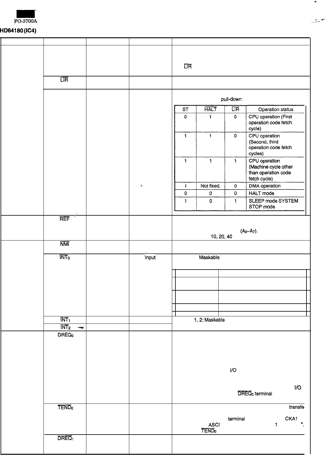
HD64180 (IC4)
Clasaificatlon
System control
signal
Code Terminal No.
HALT
61
iii7
68
ST 7
output
output
output
Name and pin function
HALT: LOW when the CPU executes HALT or SLP command,
and shows to the outside that the CPU is in HALT mode,
SLEEP mode, or SYSTEM STOP mode. Used with ST signal
and
m
signal to show the operation status such as the
internal DMA operation and the CPU operation mode.
Load Instruction Register: Shows that the cycle which is under
operation is the operation code fetch cycle.
Status: Shows the operation status.
Do not connect with a
pulldown
resistor.
System control
signal
Interrupt signal
REF
I’
64
imi
1
lNT0
4
output
Input
Input
Refresh: When LOW, shows that the CPU is in DRAM refresh
cycle. When LOW, refresh addresses are outputted to the
lower 8 bits of the address bus
&--AT).
Refresh interval is
programmable in
10,20,40
or 80 state.
Non-Ma&able interrupt: This is the non-maskable intterrupt
request terminal.
Interrupt 0: Maskable interrupt level 0 request terminal. In leve
0, there are three operation mode:
Operation mode Content
0
Command on the data bus is execu-
ted.
1
Command is executed from address
0038H.
2
Vector system
DMA signal
im=,
in2
--
DREQo
--
(Commonly used
with CKAO.)
5
Input
6
Input
50 Input
=EBi30
DREOl
55
59
output
Input
Interrupt
1,2:
Maskable interrupt level 1 and 2 request
terminals. Vector system
DMA Request for Channel 0: Internal DMAC transfer (to
channel 0) request terminal. With this signal, the internal
DMAC can operate in synchronization with the external I/O
devices. The internal DMAC channel 0 supports the following
transfer types:
(a) Between memories
(b) Between memory and
I/O
(c) Between memory and memory map I/O
This terminal is multiplexed with CKAO terminal. When DMA
channel 0 transfer mode is set to ‘Between memory and
I/O
(including memory map I/O)“,
-lo
temrinal serves as an
input terminal.
Transfer End for Channel 0: Internal DMAC channel 0
transfe,
sent signal. Driven LOW in synchronization with the last data
transfer write cycle. This
teninal
is multiplexed with
CKAl
terminal. When
ASCI
control register A channel
1
is set to ‘1
‘,
it serves as
TENDo
terminal.
DMA Request for Channel 1: Internal DMAC transfer (to
channel 1) request terminal. Channel 1 supports only transfer
between memory and I/O.
5-4
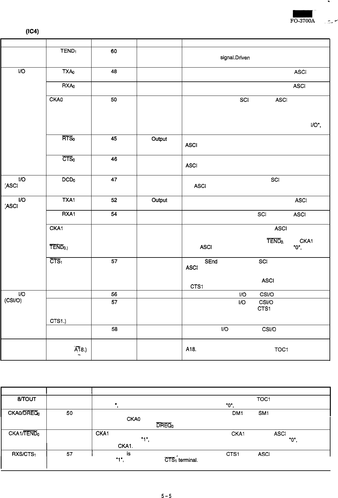
HD64180 (IC4)
Classification Code Terminal No. Name and pin function
DMA signal
TEND1
60
output Transfer End for channel 1: Internal DMAC trasnfer (to
channel 1) end signal.Ddven LOW in synchronization with the
last data transfer write cycle.
Serial
I/O
signal
TXAO
48
(ASCI channel 0) output Transfer Data for Asynchronous SCI Channel 0: ASCI channel
0 transfer data terminal.
RXAo
49 Input Receive Data for Asynchronous SCI Channel 0: ASCI channel
0 receive data terminal.
CKAO
50
Input/Output Clock for Asynchronous
SCI
Channel 0:
ASCI
channel 0 clock
(Commonly input/output terminal.
used with This terminal is multiplexed with transfer request signal
DREQO)
DREQO for internal DMAC channel 0. When DMA channel 0 is
oeprated in the transfer mode of ‘Between memory and
I/o’,
it
cannot be used as a clock output terminal.
RTso
45
output
Request to Send for Asynchronous SCI Channel 0: One of the
ASCI
channel 0 modem control signals. The output can be
controlled to LOW and HIGH by the program.
CTso
46
Input Clear To Send for Asynchronous SCI Channel 0: One of the
ASCI
channel 0 modem control signals. With this input,
transmission can be controlled.
Serial
I/O
signal
DCDc
47
[ASCI
channel 0) Input , Data Carder Detect for Asynchronous
SCI
Channel 0: One of
the
ASCI
channel 0 modem control signals. With this input, the
operation of the receiver section can be reset.
Serial
I/O
signal
TXAl
52
output
:ASCI
channel 1)
Transfer Data for Asynchronous SCI Channel 1:
ASCI
channel 1 transfer data terminal.
RXAl
54
Input Receive Data for Asynchronous
SCI
Channel 1: ASCI channel
1 receive data terminal.
CKAl
55 Input/Output Clock for Asynchronous SCI channel 1:
ASCI
channel 1 clock
(Commonly input/output terminal. This terminal is multiplexed with internal
used with
TENDO.)
DMAC channel 0 transfer end signal
mc.
When
CKAl
D bit
of the
ASCI
control register A channel 1 is set to ‘O‘, it can be
used as a clock input/output terminal.
CTS,
57
Input Clear to
SEnd
for Asynchronous
SCI
Channel 1:
(Commonly
ASCI
channel 1 modem control signal. With this input,
used with transmission can be controlled. This terminal is multiplexed
RXS.)
with RXS signal described below.
ASCI
status register channel
1
CT.91
E bit is used to select this terminal.
Serial
I/O
signal TXS
56
output
(CSVO)
Transfer Data for Serial
I10
Port:
CSVO
serial output terminal.
RXS
57
Input Receive Data for Serial
I/O
Port: CSllO serial input terminal.
(Commonly This terminal is multiplexed with
CTSl
, and selection is made
used with by the program.
CTSl.)
CKS
58
Input/Output Clock for Serial
I/O
Port: Used as
CSVO
clock input/output
terminal.
Timer TOUT (Commonly
31
used with
-A78.)
output Timer Out: Timer output terminal of timer 1. Multiplexed with
A18.
Selection is made with TOCO and TOCl bits of the timer
control register.
Common terminal descriptions HD64180 (IC4)
I
Code
1
Terminal No.
1
Selection method
I
Al 8/TOUT
31
cKAo/Dim&
50
CKAl/TENDo 55
RXSA2T.S
1
57
Al8 is selected immediately after resetting. When either one or both of TOCl bit and TOCO bit is/are
set to ‘1 ‘, TOUT is selected. When the both bits are set to
‘O’,
Al 8 is selected again.
CKAO is selected immediately after resetting. Either one of
DMl
bit or
SMl
bit of DMAC DMA mode
register is ‘I’, CIAO is compulsorily changed to an input terminal though it is set as an output terminal,
and CKAO can be used as
-0
terminal.
CKAl
terminal is selected immediately after resetting. When CKAl D bit of the
ASCI
control register A
channel 1 is Set to
‘l’,
it can be used as TEND0 terminal. When the bit is reset to
“O’,
the terminal
returns to
CKAl.
/
RXS terminal
iS
selected immediatelv after resettina. When
CTSl
E bit of
ASCI
status register channel 1
is set to
‘I’,
it can be used as
mr-terminal.
In this case, however, the function of RXS input terminal
is not prohibited.
I
5-5
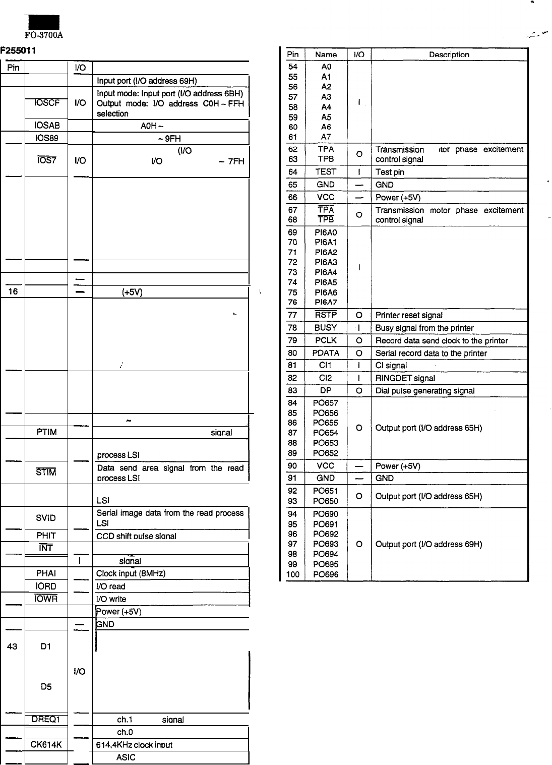
-m
FO-3700A
F255011 PJ pin descriptions
Pin
Name
PI697
I/o
-
I
Description
I
1
ci
Input mode Input port (I/O address 6BH)
2
3
IOSCF
I/O
CPU address bus
ransmrssron
mo
Input port (I/O address 6AH)
IOSAB
IOS89
Ios7
PO660
PO661
PO662
PO663
PO664
PO665
PO666
PO667
PO670
0I/O address
AOH
-
BFH selection
I/O address 80H
-
9FH
selection
Input mode: Input port
(I/O
address 6BH)
Output mode:
I/O
address 70H
-
7Fl-l
selection
4
-
5
-
6
7
8
9
10
11
12
13
-
14
0
I/O
-
0
-
0
Output port (l/O address 66H)
Output port (I/O address 67H)
GND
15 GND
16
vcc
-
-
-
Power
(+5V)
17
18
19
20
21
22
23
-
24
25
26
27
-
28
PO671
PO672
PO673
PO674
PO675
PO676
PO677
GAIN0
GAIN1
GAIN2
GAIN3
AGC
PTIM
i
Output port (l/O address 67H)
8.’
0
0Read image signal gain control signal
I
-
I
GAIN 3
-
0 control signal
Transmission motor start timing sional
29
-
30
-
31
0
-
I
Data send start ready signal to the read
RRDY
STlM
32 SCLK
I
Data send clock from the read process
LSI
I
Serial image data from the read process
T
33
-
34
I
-
I
SVID
PHIT
iiw
RESET
PHAI
IORD
itwn
vcc
GND
DO
Dl
D2
D3
D4
D5
D6
D7
DREQl
DREQO
CK614K
35
-
36
0
-
I
Interruption request signal
Reset sianal
37
38
39
-
40
I
-
I
-
I
E
(+SV)
l
41
-
42
4.3
44
45
46
47
48
49
-
50
51
-
52
-
53
-
-
-
I/O
-
0
-
0
-
I
0
-
CPU data bus
DMA
ch.1
reauest sianal to CPU
I
DMA
ch.0
request signal to CPU
614.4KHz clock inout
CPU
ASIC
clock output
1
CKA
5-6
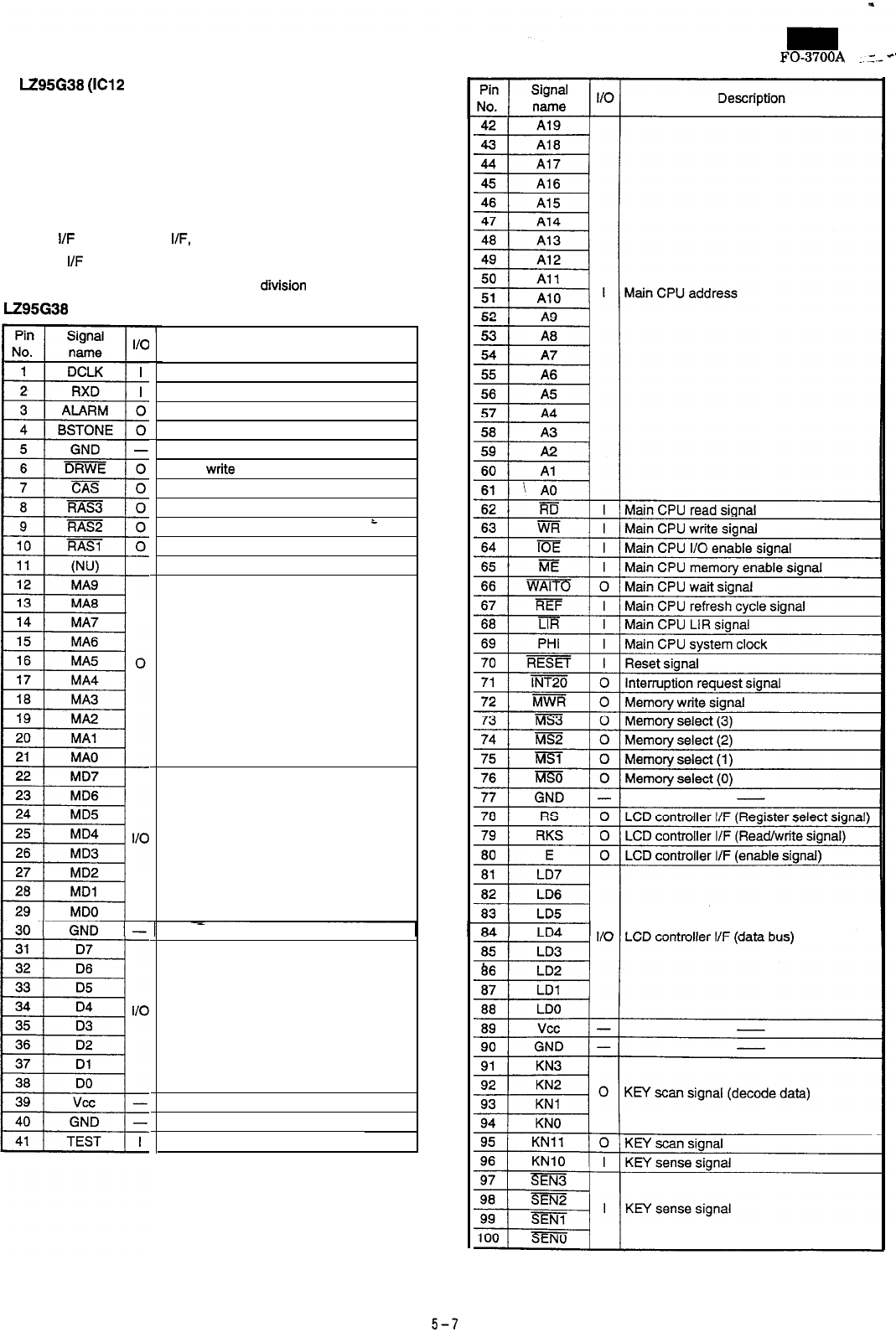
FO-3700A
8)
E95G38
(El2
gate array B) . . . 100 pin QFP
The following functions are provided as the main CPU peripheral
functions.
l Memory mapper
l WAIT control
l
Main CPU timers (3 units)
l DRAM controller
l
Panel
I/F
(LCD controller
I/F,
key scan)
l Modem
I/F
(RTC detection)
l
Alarm buzzer/busy tone clock frequency division
LZ95G38 pin description
Description
MODEM DCLK
MODEM serial reception data
Alarm buzzer clock
Busy tone signal
DRAM write enable signal
DRAM CAS signal
DRAM RAS signal (3)
DRAM RAS signal (2)
i
DRAM RAS signal (1)
Not used.
DRAM address
DRAM data
Main CPU data bus
Test pin
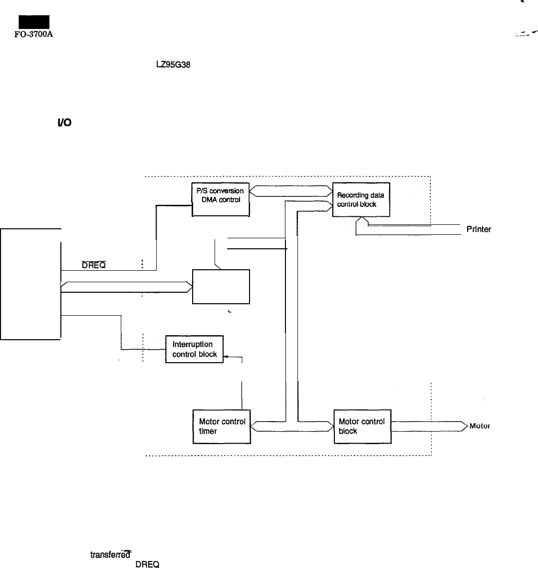
FO-3700A
(2) Panel control block
The following controls are performed through LZ95G38 according to
commands from the main CPU.
l Operation panel key scanning
l Operation panel LCD display
(3) Peripheral l/O control block
l Recording control block diagram
CPU
(84180)
I
block
I
II
bRsh
i
\
/
\,
Register
N
control block
TNT
i
>
Prfnter
unit
Fig. 3
The recording control block is composed as shown above. The
descriptions are given below:
l P/S conversion block, DMA control block, recording data control
block
The recording data is
transferred
to the printer unit by these
blocks. First, the gate array A sends
DREQ
to the CPU. The CPU
transfers the recording data to the P/S conversion block by means
of DMA. The transferred data is converted into serial data and sent
through the recording data control block to the printer unit together
with a clock.
l Motor control block
This block supplies phase output for control of the TX motors. With
register setting, it controls phase switching timing of the motor.
5-8
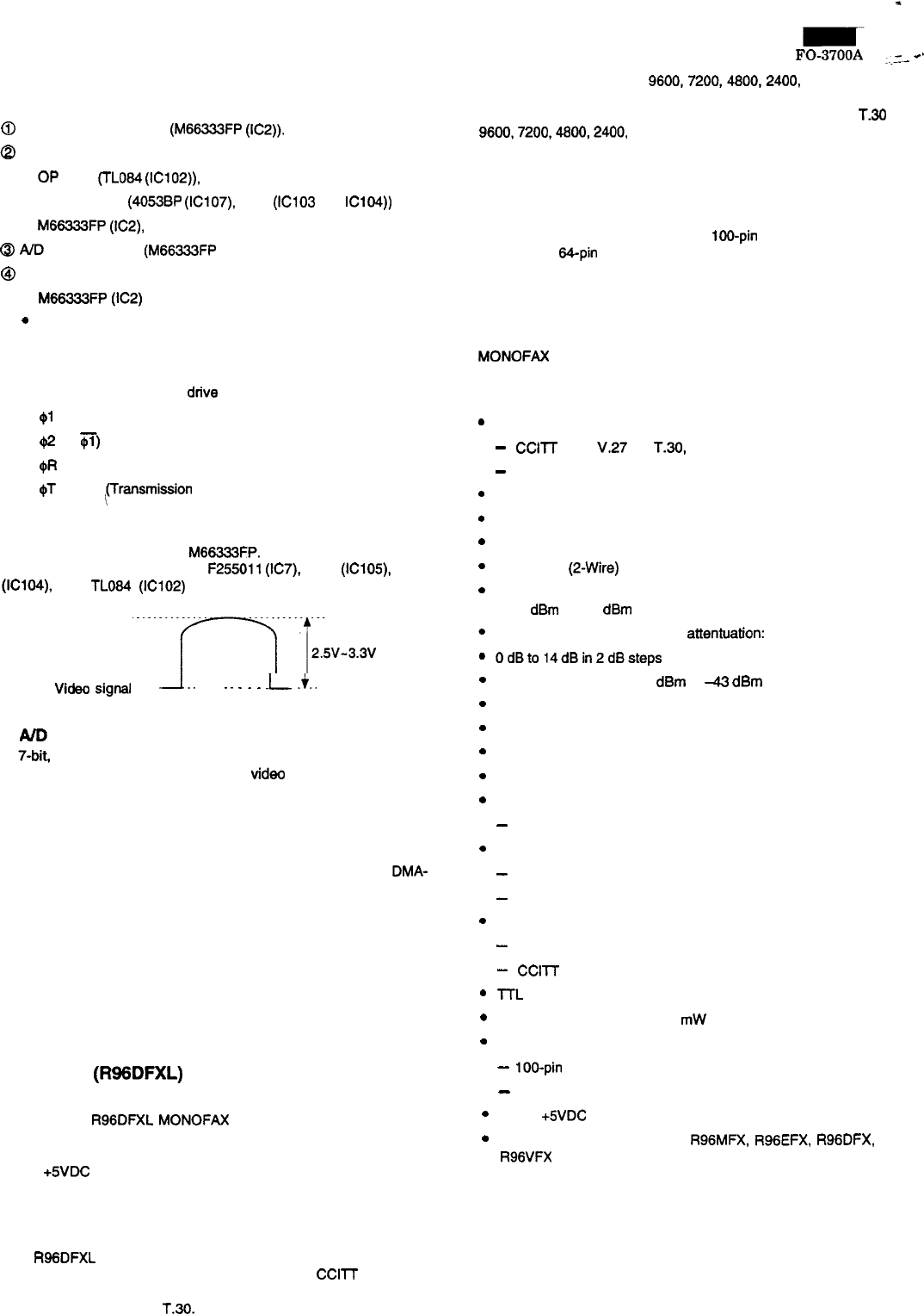
(4) Image signal processing block
The image signal processing block is composed of the following:
@
CCD sensor drive block (M66333FP
(ICZ)).
@ Analog processing block
l OP amp.
(TLO84
(IC102)).
lAnalog switch (4053BP
(IC107).
4066 (lC103 and lC104))
l M66333FP
(IC2),
transistor, etc.
@
A/D converter block (M66333FP (IC2) inside).
@
Binary coding processing block
l M66333FP
(IC2)
*
LH5266 (IC3)
Descriptions on each block are given below:
1) CCD drive block
The Clock necessary for CCD drive is generated in M66333.
l
91
(Synchronization clock)
l
@2
(=
$T)
(Synchronization clock)
l
OR
(Output buffer reset clock)
l
$T
~~ransmission
clock)
2) Analog processing block
Video signals supplied from the CCD PWB are sample-hold, gain
control and clamped to supply M66333FP.
The gain control is performed by
F255011
(IC7),
7406 (IC105), 4066
(IC104), and TL084 (IC102) to control the max. voltage of video
signal to about 3V.
Vi&o
signal
. .
A..
. .
_.
_
_
_
.L
.i..
(IC2, 33pin)
3)
ND
Converter
A 7-b& high-speed A/D converter M66333 in (IC2 80 pin QFP) is
used to supply A/D converted digital
video
signals to the binary
coding processing block.
4) Binary coding processing block
Digital video signals incorporates various algorithms required for bi-
nary coding, and RAM (IC3) which stores data necessary for process-
ing are converted into binary data, and P/S converted, and
DMA-
transmitted to the line memory of the main CPU.
The algorithms for binary coding in the processing block are as fol-
lows:
l Shading correction
l Focus correction
--
l Auto contrast process
l Intermediate Half-tone expression process
(error dispersion process/image area separation)
(5) Modem (R95DFXL) block
INTRODUCTION
The Rockwell
ROBDFXL
MONOFAX modem is a synchronous 9600
bits per second (bps) half-duplex modem with error detection and
DTMF reception. It has low power consumption and requires only a
single
+SVDC
power supply. The modem is housed in a single VLSI
device package.
The modem can operate over the public switched telephone network
(PSTN) through line terminations provided by a data access arrange-
ment (DAA).
The R96DFXL is designed for use in Group 3 facsimile machines.
The modem satisfies the requirements specified in
CCllT
recommen-
dations V.29. V.27 ter. V.21 Channel 2 and T.4, and meets the binary
signaling requirements of
T.30.
FO-3700A
--‘c.
The modem can operate at
9600,7200,4800,2400,
or 300 bps, and
also includes the V.27 ter short training sequence option.
The modem can also perform HDLC framing according to T.30 at
9600.7200,4800,2400,
or300 bps.
The modem features a programmable DTMF receiver and three
programmable tone detectors which operate concurrently with the
V.21 channel 2 receiver.
The voice mode allows the host computer to efficiently transmit and
receive audio signals and messages.
The modem is available in either a
lOO-pin
plastic quad flat pack
(PQFP) or a
64-pin
quad in-line package (QUIP).
General purpose input/output (GPIO) pins are available for host as-
signment in the 1 00-pin PQFP.
The modem’s small size, single voltage supply, and low power con-
sumption allow the design of compact system enclosures for use in
both office and home environments.
MONOFAX is a registered trademark of Rockwell International.
FEATURES
.
.
.
.
.
.
.
.
.
.
.
.
.
.
.
.
.
.
.
.
.
Group 3 facsimile transmission/reception
-
CCllT
V.29, V.27 ter,
T.30,
V.21 Channel 2, T.4
-
HDLC Framing at all speeds
V.27 ter short train
Concurrent DTMF, FSK, and tone reception
Voice mode transmission/reception
Halfduplex (a-Wire)
Programmable maximum transmit level:
0
dBm
to -15 dBm
Programmable transmit analog attentuation:
OdBto14dBin2dBsteps
Receive dynamic range: 0 dBm to
4
dBm
Programmable dual tone generation
Programmable tone detection
Programmable turn-on and turn-off thresholds
Programmable interface memory interrupt
Diagnostic capability
-
Allows telephone line quality monitoring
Equalization
-
Automatic adaptive equalizer
-
Fixed digital compromise equalizer
DTE interface: two alternate ports
-
Selectable microprocessor bus (6500 or 8085)
-
CCllT
V.24 (EIA-232-D compatible) interface
lTL
and CMOS compatible
Low power consumption: 275
mW
(typical)
Single Package
-
loo-pin
PQFP
-
64-pin QUIP
Single
+5VDC
power supply
Software compatible with R96MFX,
R96EFX,
R96DFX, and
R96VFX
modems
5-9
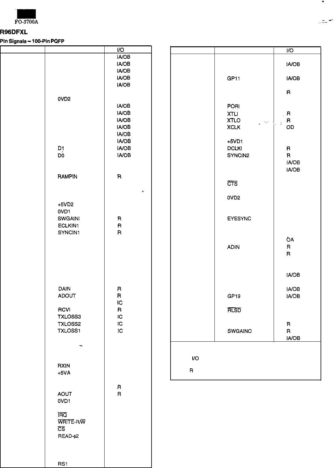
-m
FO-3700A
R96DFXL Hardware Interface Signals
Pin
Signals
-
lOO-Pin
PQFP
Pin No. Signal Name
1
GPO3
2
GPO4
3
GPO5
4
GPO6
5
GPO7
6OVD2
7
OVD2
8
D7
9D6
10
D5
11
D4
12 D3
13
D2
14
Dl
15 Db
16 OVD2
17
OVA
18 RAMPIN
19
NC
20 NC
21
OVA
22 +5VD2
23
OVDl
24 SWGAlNi
25 ECLKINl
26
SYNClNl
27 NC
28
NC
29
NC
30
OVA
31
NC
32
NC
33
NC
34
DAIN
35 ADOUT
36 BYPASS
37
RCVI
38 TXLOSSB
39
TXLOSS2
40
TXLOSSl
41
NC --
42 NC
-
43
OVA
44 TXOUT
45
RXIN
46 +5VA
47
OVA
48 AGD
49
AOUT
50 OVDl
51
NC
52
ma
53
WRITE-W
54
cs
55
READ-Q2
56 RS4
57
RS3
58
RS2
59
RS1
l/O Type
IA/OB
IA/OB
IA/OB
IAIOB
lA!OB
GND
GND
IA/OB
IAIOB
IA/OB
IAIOB
IAJOB
IAIOB
IA/OB
lA/OB
GND
GND
R
i
GND
PWR
GND
R
R
R
GND
R
R
IC
R
IC
IC
IC
GND
AA
AB
PWR
GND
R
R
GND
oc
IA
IA
IA
IA
IA
IA
IA
Pin No.
Signal Name
I/O
Type
60
RSO
IA
61
GP13
IA/OB
62
NC
63
GPll
lA/OB
64
RTS IA
65
EN85
R
66
OVD2
GND
67
PORI
ID
68
X-rLl
.R
69
XTLO
R
70 XCLK
_
.‘-
‘.
;
OD
71
YCLK
OD
72
+5VDl
PWR
73
DCLKI
R
74
SYNCINP
R
75
GP16 IAlOB
76 GP17
IAJOB
77
OVD2
GND
78 CTS OA
79
TXD
IA
80
OVD2
GND
81
OVD2
GND
82 DCLK
OA
83 EYESYNC OA
84 EYECLKX
OA
85
EYECLK OA
86 EYEX OA
87
ADIN
R
88 DAOUT
R
89
OVD2
GND
90 EYEY
OA
91
GP21
IAlOB
92
OVD2
GND
93
GP20
IA/OB
94 GP19
IA/OB
95
RXD
OA
96
RLSD OA
97
OVD2
GND
98
RCVO
R
99 SWGAINO
R
100
GPO2
IA/OB
Notes:
1. NC = No connection; leave pin disconnected (open).
2.
I/O
Type: Digital signals: see Table 9;
Analog signals: see Table 10.
3.
R
= Required modem inter-connection; no connection
to host equipment.
5-10
-m
FO-3700A
-G--"
[3]
Description
of
CCD
board
(2) Description of blocks
The CCD board picks up optical information from the document, con-
1. CCD
Verb
it into an electrical (analog) signal and transfers it to the control
board. The
TCD1206D
is a highly sensitive charged coupled image sensor
that consists of 2160 picture elements.
Receiving four drive signals
($T,
412,
$11,
#R)
from the control board,
the transferred photoelectric analog signal OS is impedance con-
verted, and the signal VO, is supplied to the control board.
(1) Block diagram
@T
L
@l
a2
.
@R
.
+12v
.
vo
4
Output
circuit
I-
03
\
(6mitti?rfdlower)
Fig. 4
2. Waveforms
1.
$1,
g2 (=
v)
. . . signals within the control board.
Approx.lOOmV
CCD
TCDl206D
Fig. 5
[4]
TEULIU
(with
Speech
PWB
unit)
board
circuit
description
1
.General
Telephone interface circuitry for this facsimile is all mounted on one
circuit board unit and is interfaced with the telephone line and fac-
simile circuits via connectors.
Connection to the switched telecommunication network is canted out
by means as of the magnetic relay. Power required for the control of
the unit is supplied from the power supply unit of the facsimile
+24V.
+12v,
-12v,
+5v.
2. Circuit general description
This board is composed of the following blocks.
(1) Surge protection block
(2) Hook detection block(Polarity inversion detection block)
(3) Reception control block --
(4) Transmission control block
-
(5) Cl signal detection block
(6) Speaker output voice select block
(7) Speaker amplifier block
(8) Polarity guard block
(9) Tone ringer block
(10) Hook control block
(11) Dialer control block
(12) Dial control block
(13) 4-bit control block
(14) External TEL hook detection block
Speech PWB unit (IC3)
(15) Dial pulse transmission block
(16) Communication circuit block
3. Each block description
(1) Surge protection block
This is composed of arrester
(ARl).
Used to prevent the LIU block
from damage caused by a surge voltage occurring across lines, the
3-pole type is used.
(2)Hook detection block(Polarity inversion detection
block)
This is composed of
ICll
and its peripheral circuits and detects
inversion of porarity. When the DC circuit is formed, either HS1 or
HS2 turns LOW.
(3) Reception control block
This is composed of
IC5,
IC6,
IC8 and its peripheral circuits and
controls reception signals.
(4) Transmission control block
This is composed of IC5 its peripheral circuits and controls transmis-
sion signals.
(5) Cl signal detection block
The Cl signal detection block consists of
R2,
D6, ZD14. PC5 and its
peripheral circuits. The CI(Calling Indicate) signal is detected by the
half wave rectifier circuit consisting of
D6
and ZD14. The
photocoupler PC5 is driven during the half cycle rectified by D6. The
photocoupler delives current to
ICl
when it is turned on during these
half cycles.
ICl
inverts the signal present at its input to create Cl
signal.
(6) Speaker output voice select block
This is composed of IC7 and its peripheral circuits. The speaker
amplifier input signal is selected as shown in the table below.
MONITOR BZCONT
Speaker output voice
0
1
Buzzer, key sound
0
0
Line signal
1
0
Modem send signal
5-11
FE!!!i
(7) Speaker amplifier block
This is composed of lC9 and its peripheral circuits.
The signal is inputted to amplifier
IC
through volume and amplified
and sent to the speaker. The speaker volume is adjustable by the
volume.
(8)
Polarity
guard block
This is bridge rectifier RECl and has a function to protect the
telephone set against inversion in the line.
(9) Tone ringer block
This is composed of IClO and its peripheral circuits. When a call
signal is inputted. the toner ringer block makes the piezo-electric
buzzer ring.
The
speake
sound volume is varied in by the slide switch.
(10) Hook control block
This is composed of the hook SW, the on-hook relay (OHRLY relay),
and its driver.
When OHRLY is high, H relay is on to close the line regardless of the
hook SW state.
(11) Dialer control block
This is composed of
IClOl
and its peripheral circuits, and supplies
current to the dialer circuit.
(12) Dial control block
This is composed of IC3 and its peripheral circuits. Signal from the
selection signal according to
Chit
signal from the CPU is outputted to
the pulse transmission block DP and the telephone line block (PB)
according to slide SW1 setting (Tone or Pulse)
(13) Cbit control block
This block is composed of phto couplers
(PCI)
is used to supply 4 bit
data from the CPU through the photo coupler to the dial IC.
(14) External TEL hook detection block
This is composed of IC7 and its peripheral
circuits.
When the telephone connected to the external TEL terminal is picked
up to form the DC circuit, either
U(RS1or
)%Fi!Z
turns LOW.
(In Speech PWB unit)
(15) Dial pulse transmission block
This is composed of
IC3
and its peripheral circuits, and has the
switching function for pulse dial transmission and the switching func-
tion of on-hook/off-hook.
(16) Communication circuit block
This is composed of lC3 and its peripheral circuits. It has functions of
reception amplifier, transmission amplifier, AGC circuit, and other
function necessary for communication.
Block diagram
Speaker
Fig.
6
5-12
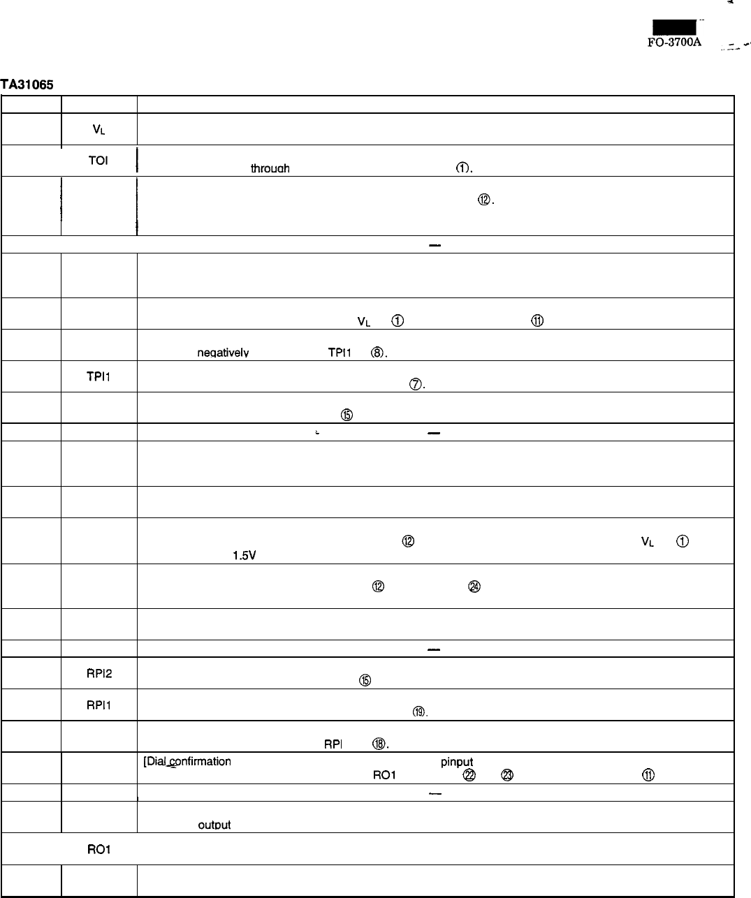
I~~
=
FO-3700A
..--c'
Speech Network IC
TA31065
Pin No. Pin Name
Pin function
1
VL [Line current input pin]
This pin is connected to the positive output of the diode bridge circuit.
2
I
TOI
I
[Send output current flowing pin]
This oin is connected throuoh the 56 Ohm resistor to the VI oin
(;i).
I
I
[Send output current output pin]
3
TOO
This pin is connected through the 15 Ohm resistor to the GND pin
0.
Since most of line currents are outputted from
this pin, the allowable power of the 15 Ohm resistor which is connected between this pin and the GND pin must be
f
determined by taking the expected max. line current into consideration.
4 I NC I
-
[AC signal reference voltage pin]
5AC BIAS When an AC signal is inputted to this pin through the capacitor (for preventing against DC), the signal is transmitted to
the line.
6
MFI
[DTMF or external input signal input pin]
A signal inputted this pin is outputted to the
VL
pin @ only when the MUTE pin @ is LOW,
7TPO [Send input amp output pin]
This pin is
neoativelv
fed back to the
TPll
oin @.
8
TPll
[Send input amp reverse input pin]
This pin receives negative feedback from the TPO pin
0.
9
10
TP12
[Send input amp reverse input pin]
This pin is DC-biased from the REF pin @ through the resistor.
NC
i
-
11
MUTE
[NUTE pin]
Pin for selection between send signals and MFI input signals in the transmitter system.
Pin for selection between send signals and BTI input signals in the receiver system.
12 GND
13 UP
14
PADC
[Ground pin]
This pin is connected to the negative output of the diode bridge.
[AC impedance control pin]
When this pin is connected directly to the GND pin @ or through a resistor, the DC potential of the
VL
pin @ can be
increased to max.
1.5V
(TYP) with the same line current.
[Pad control pin]
When this pin is connected to the GND pin @ or the Vcc pin @ through a resistor, the operating current of gain
control (auto pad) by the line current can be controlled.
15 REF
16 NC
17
RPl2
[Internal reference output pin]
This pin voltage serves as the reference voltage of the internal pre-amp.
-
[Reception input amp non-reverse input pin]
This pin is directly biased from the REF pin @ through the resistor.
18
RPIl [Reception input amp reverse input pin]
This oin receives neoative feedback from the PRO oin
8.
19
RPO
[Reception input amp output pin]
This pin is negatively fed back to the
RPI
1 pin
0.
20
BTI
21
NC
[Dialgnfirmation
sound (Beep tone, DTMF), monitor sound pinput pin]
A signal inputted to this pin is outputted to the ROl and R02 pin
@
and @ only when the MUTE pin @ is LOW.
-
I
I
22 R02 [Reception output pin, reverse side]
This is the outout oin to the receiver.
23
ROl
[Reception output pin, non-reverse side]
This is the output pin to the receiver.
24 vcc [Internal power voltage pin]
Power for the internal pre-amp.
5-13
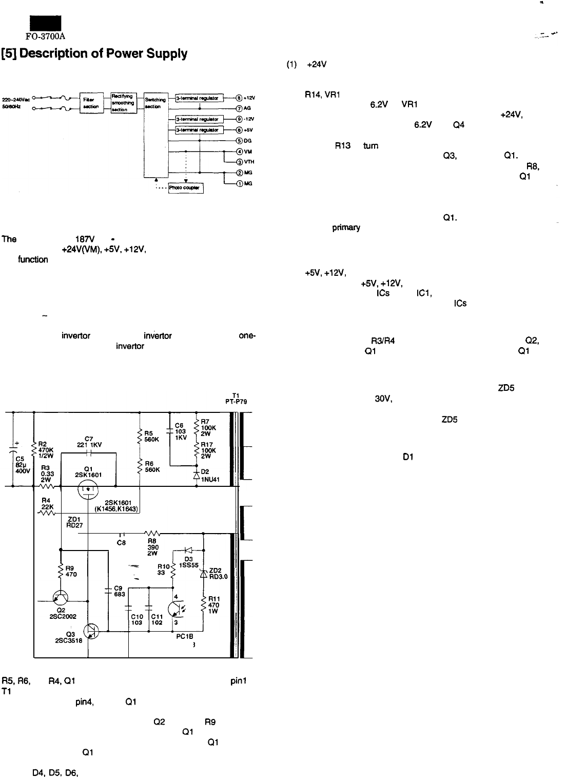
FO-3700A
3.2. Control section
[5]
Description
of
Power
Supply
1. Block diagram
Fig. 1. Block diagram
2. General description
The input voltage is
187V
AC
-
276V AC conforming to UL standards.
The outputs are +24V(VM),
+5V.
+12V, -12V. The overvoltage protec-
tion function for protection of the load in case of power abnormality
and the overcurrent protection function for protection of the power
supply itself from overload are added,
3. Operational description
When 230
-
246 V/AC power is supplied, it is passed through a noise
filter to the rectifier section where it is smoothed to about 300V then
supplied to the
invertor
section. The invertor section employs one-
transistor ON/OFF self-excited invertor (R.C.C. system) and a stable
DC voltage is supplied to the secondary side.
The operation of each section is described below:
3.1.
lnvertor
section
2R24(
w
01 2SK1601
-vvv
__
(K1456.Kl643)
ZDl
RD27
,
I
I
,
vvv
C8
0
103
2ScQ&
PClB
PC113
1
When the voltage across R4 reaches the gate ON voltage through
R5,
R6,
and
R4,
Ql
begins to turn ON, flowing a current from
pin1
of
Tl
primary winding to pin3. Then a voltage is generated from pin5 of
auxiliary winding to
pin4,
turning
Ql
gate ON completely. The drain
current increases linearly to store energy in the primary winding.
However, voltage across R3 turns ON
02
thorough
R9
when the
drain current reaches a certain level. As a result,
01
gate voltage falls
below the threshold voltage (about 4V) of the gate and
Ql
turns off.
Simultaneously when
Ql
turns off, the energy stored in the primary
winding is induced in the secondary winding to bias the rectifier
diodes
D4,
D5,
D6,
and D7 forwardly, smoothing each output
capacitor. Thus a DC voltage is obtained.
+24V
(VM) control
A voltage is generated in the secondary side by repeated opera-
tions of 3.1, and the output in the secondary side is divided by
R14,
VRl
, and R15 to be inputted to Q4. The divided voltage is
adjusted to about 6.2V by
VRl
. Q4 always monitors the divided
output voltage. When the output voltage exceeds +24V, the
divided voltage also exceeds 6.2V and Q4 judges it as an in-
crease in the output voltage. Then photocoupler PC1 is lit
through
R13
to turn on the transistor in the light receiving side,
supplying a current to the base of
Q3,
turning off
Ql.
(The
current which is to be passed through the additional line,
R8,
and C8 to R4 is bypassed by Q3). Resultantly, ON time of
Ql
is
shortened and the energy stored in the primary winding is
decreased, limiting the increase in the output voltage. When the
output voltage begins to decrease, the light quantity of PC1 is
decreased to lengthen the ON time to
Ql.
As a result the energy
in the primary winding is increased to compensate for the
decrease in the output voltage.
The negative feedback control is repeated to stabilize the output
voltage.
(2) +5V,
+12V, -12V control
The outputs of
+5V,
+12V, and -12V are stabilized by the three-
terminal regulator
ICs
(IC3,
ICl,
and IC2). The overcurrent
protection function protects the regulator
ICs
themselves.
3.3. Overcurrent protection function
When the output current in the secondary side increases to become
an overcurrent or short
R3IR4
detects the drain current to turn on
Q2,
The gate voltage of
Ql
is controlled to shorten ON time of
Ql
to
protect the circuit from the overcurrent.
3.4. Overvoltage protection function
When the output voltage is abnormally increased and ZD5 zener
voltage exceeds about
3OV,
ZD5 is shorted to operate the same
procedure as the overcurrent protection function. To reset, turn off the
AC switch, remove the cause, and replace ZD5 with a new one.
3.5. High temperature protection circuit
Thermal fuse F3 included in the power circuit is blown when the
surface temperature of rectifier
Dl
exceeds about 115 degrees Cen-
tigrade. (about 239-F)
5-14
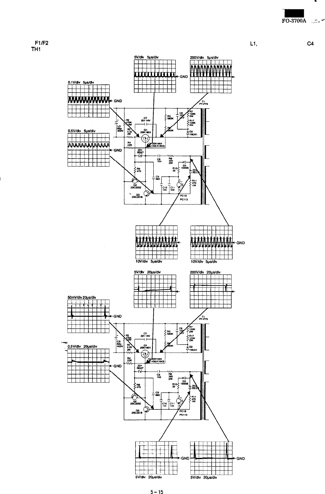
3.6 Rush current limiting circuit
When AC power is supplied, a rush current flowing through capacitor
C5 may blow fuse
Fl/F2
and damage the circuit. To prevent this, the
power thermistor
THl
is provided to limit the rush current.
(Waveform)
l At standby
-m
FO-3700A
m..x-"
3.7. Line filter
To protect against external noises and noises generated in the power
circuit, the line filter is composed of
Ll,
L2, Cl, C2, C3, and C4 to
reduce noises.
GND
lWhen the overcurrent protection circuit works
GND
1OVMii
5@d,div
2QOVMii
ZO&div
GND
MmVldii
PCpJdiv
l~liiIIIl/
1/
/
I
*
I
I
I
L
-GND
-GND
GND
-GND
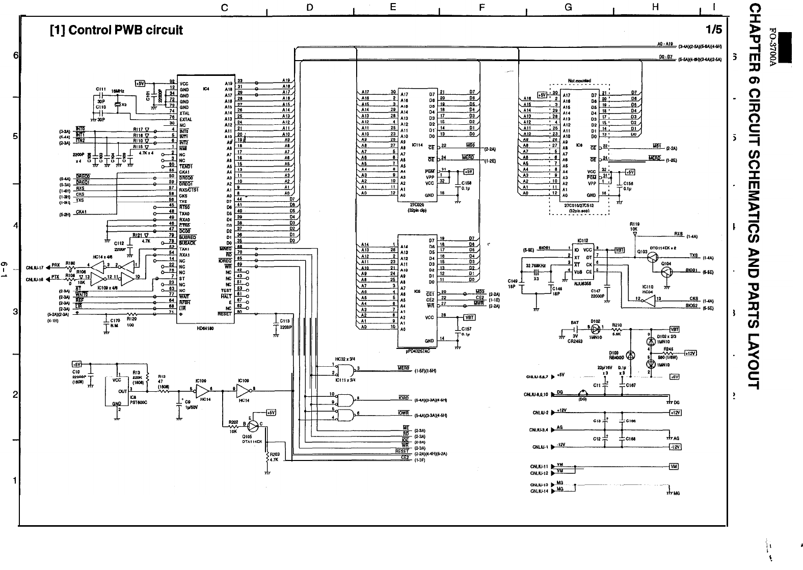
A
I
B
I
[I]
Control
PWB
circuit
Main control block
(2-W
,1.2Ej
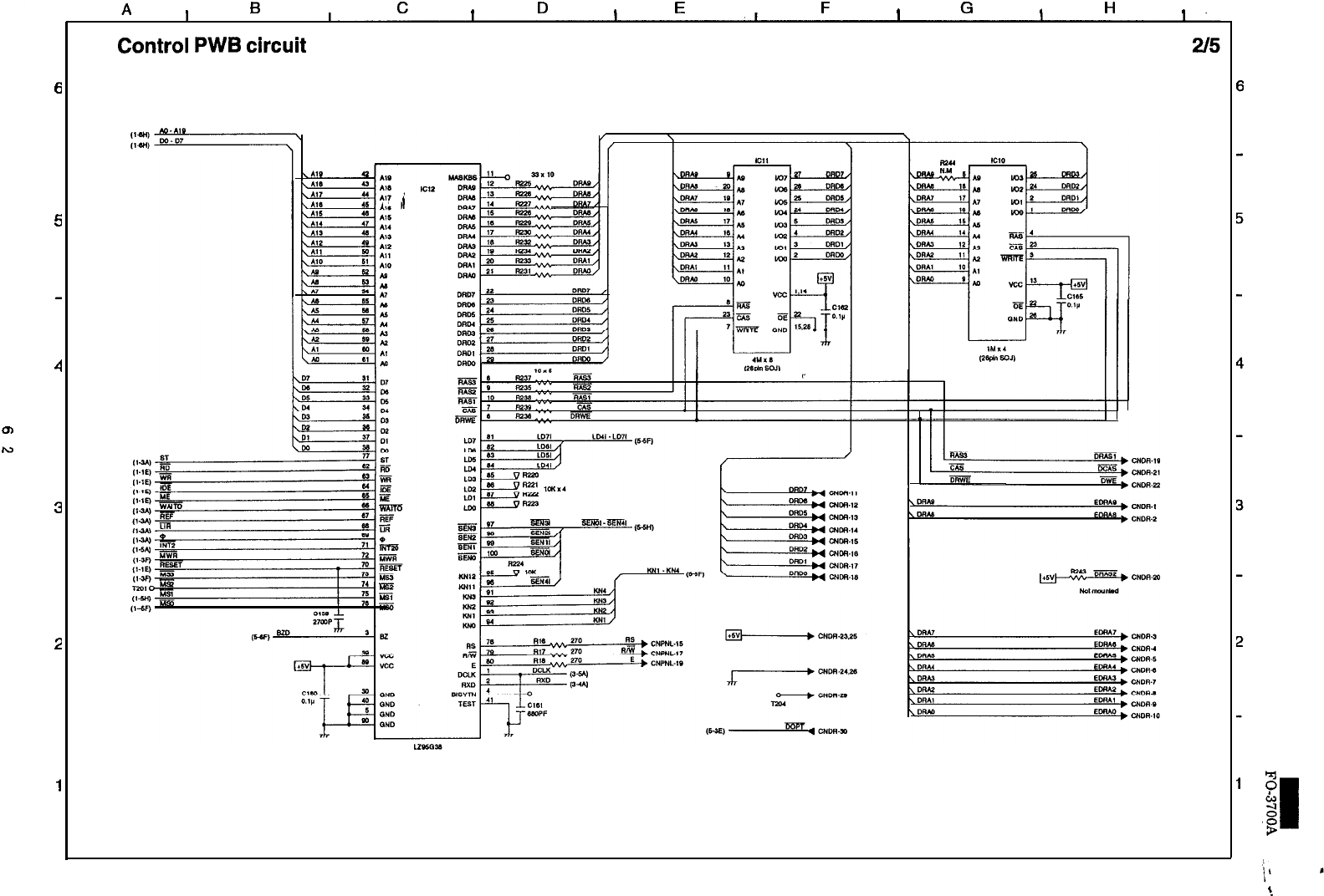
A
.
B
c
I
D
a
E
F
a
G
a
H
I
I
6
5
4
0)
I
N
3
2
1
Control
PWB
circuit
Image memory control
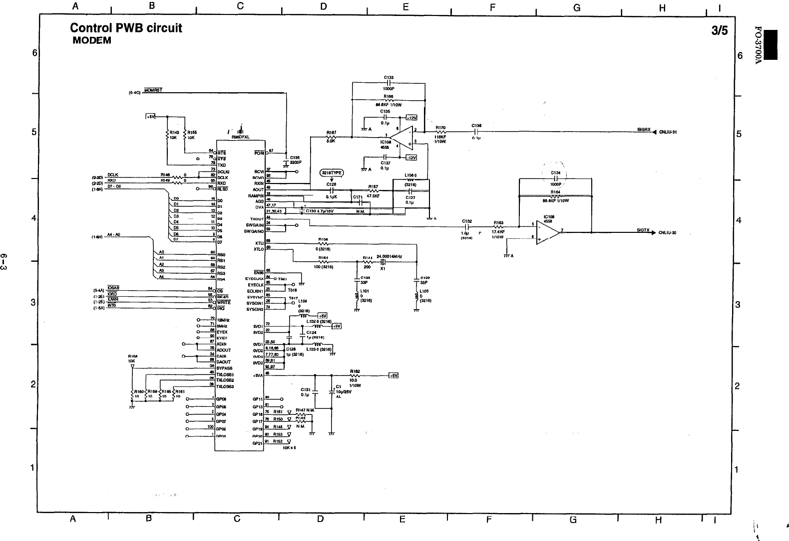
m
I
w
i’
e
?
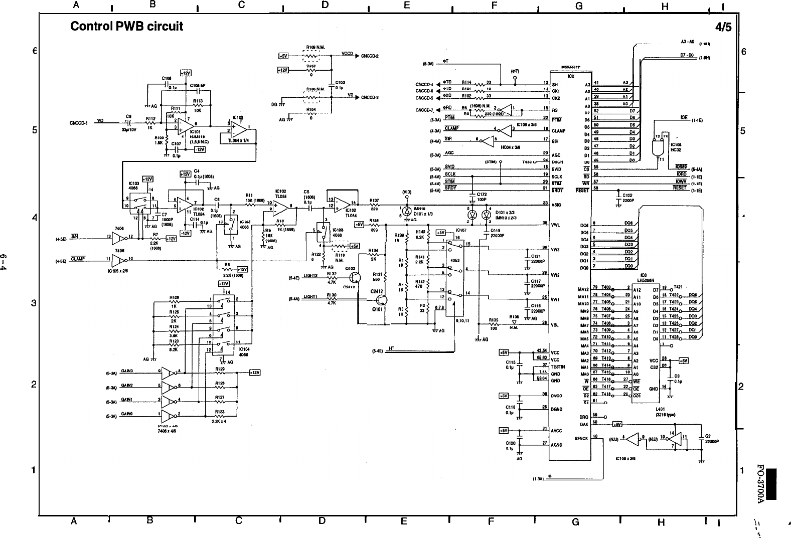
A
I
B
I
C
I
D
I
E
I
F
I
G
I
H
1
I
Control
PWB
circuit
Scanning section
6
5
4
0-l
I
P
3
2
1
CNXDI
“0
Fit34
2K
R131
680
1
C2412
O,OI
I
7tr
l(i
I
2
‘I
,
L
I
i
A
I
B
I
C
I
D
I
E
I
F
I
G
I
H
1
I
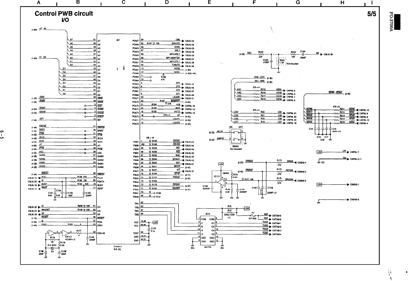
A
I
B
I
C
I
D
I
E
I
F
I
G
I
H
,
1
Control
PWB
circuit
5/5
Peripheral
l/O
control section
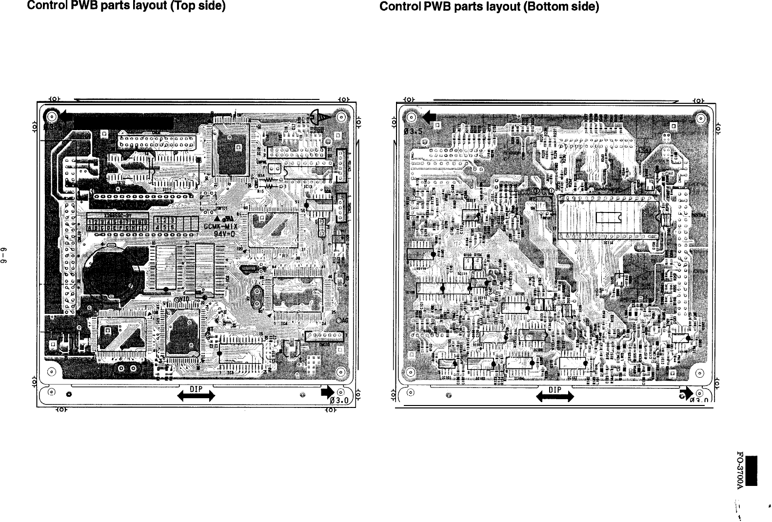
Control
PWB
parts
layout
(Top
side) Control
PWB
parts
layout
(Bottom
side)
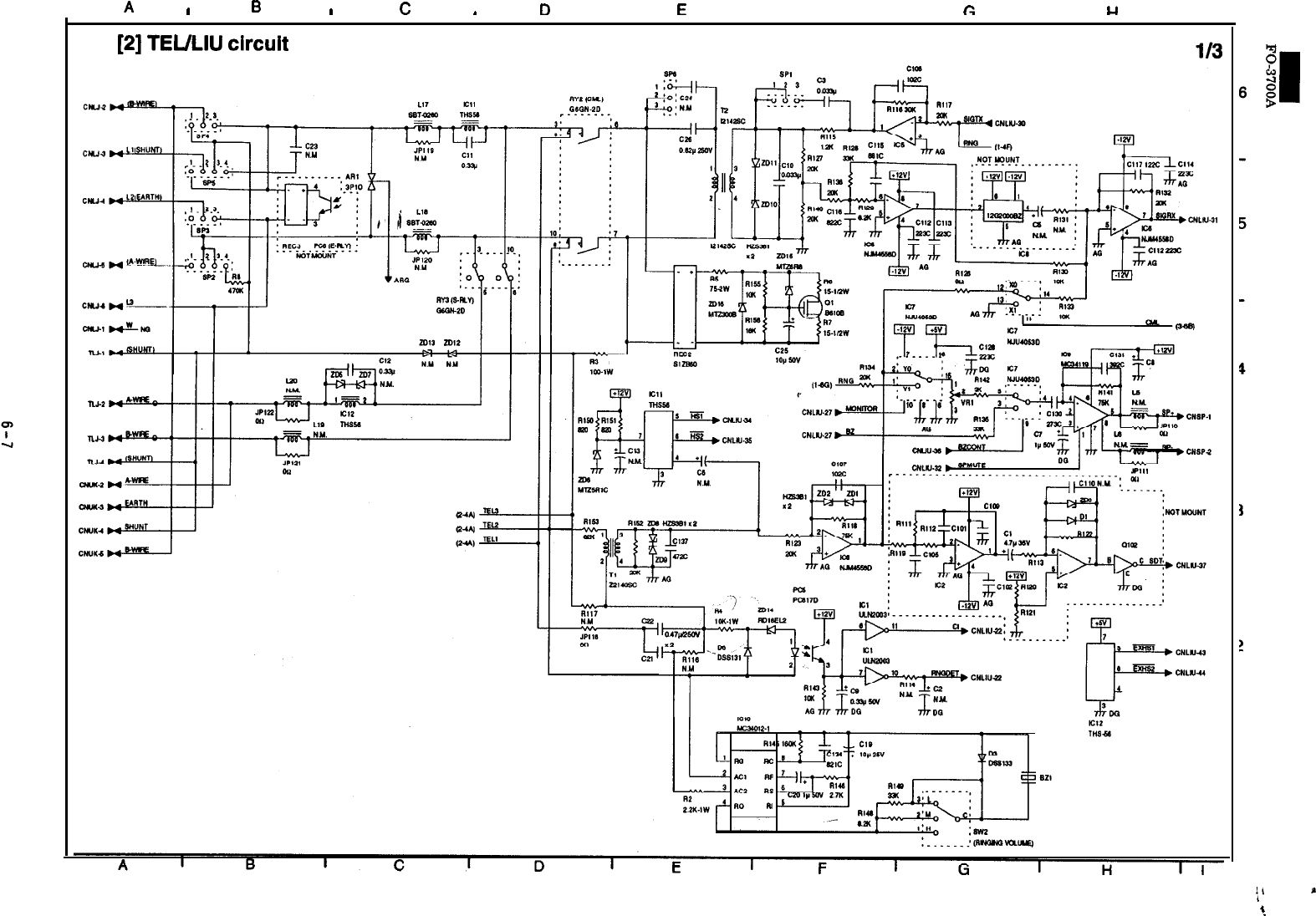
A
I
B
,
c
.
D
E
F
r,
l-l
I
[2]
TEULIU
circuit
i’
e
?
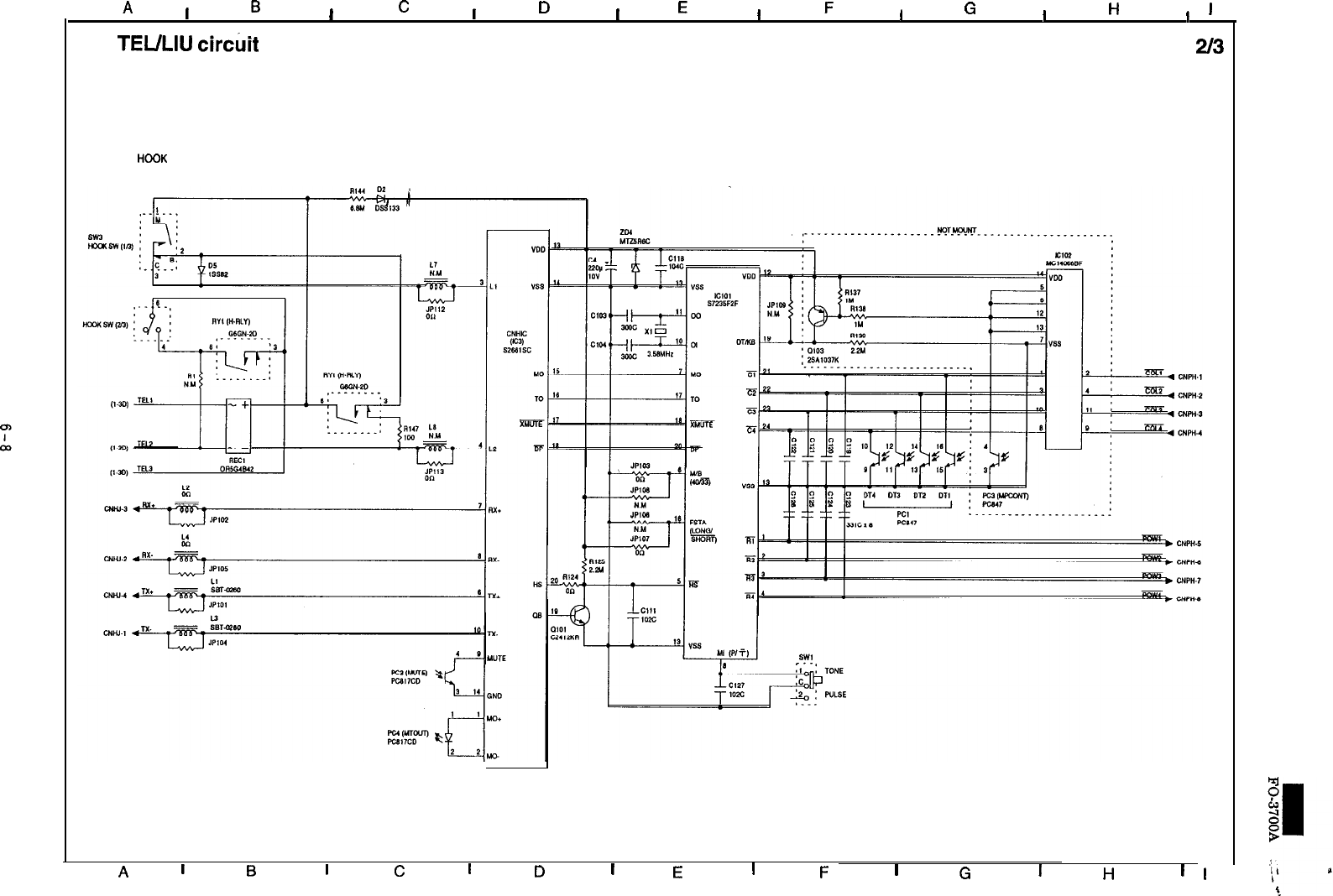
A
I
BI
C
I
D
I
E
I
F
I
G
I
H
,
I
TEULIU
circht
2l3
<ON HOOK STATE>
A
I
B
I
C
I
D
I
E
I
F
I
G
I
H
1
I
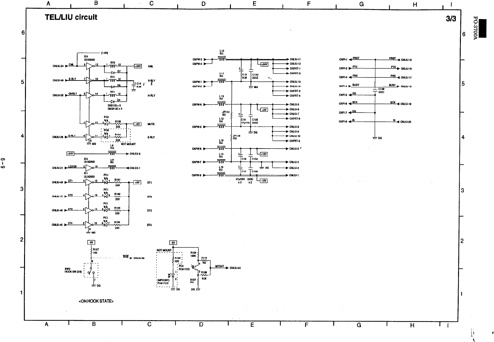
<ON
HOOK
STATE>
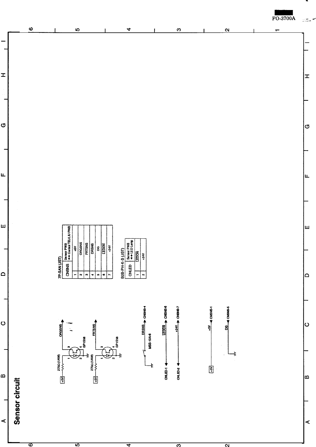
FO-3700A
-.--c.
(0
I
UY
I
*
I
m
I
cu
I
6-10
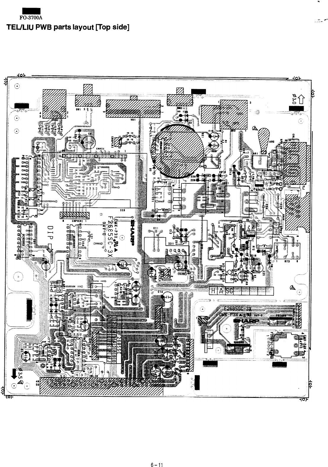
FO-3700A
TEULIU
PWB
parts
layout
[Top
side]
-----
-..
6-11
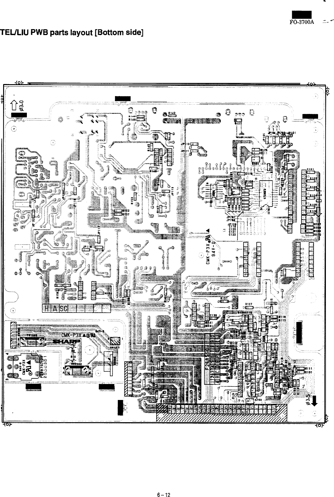
FO-3700A
-Lo"
TEULIU
PWB
parts
layout
[Bottom
side]
6-12
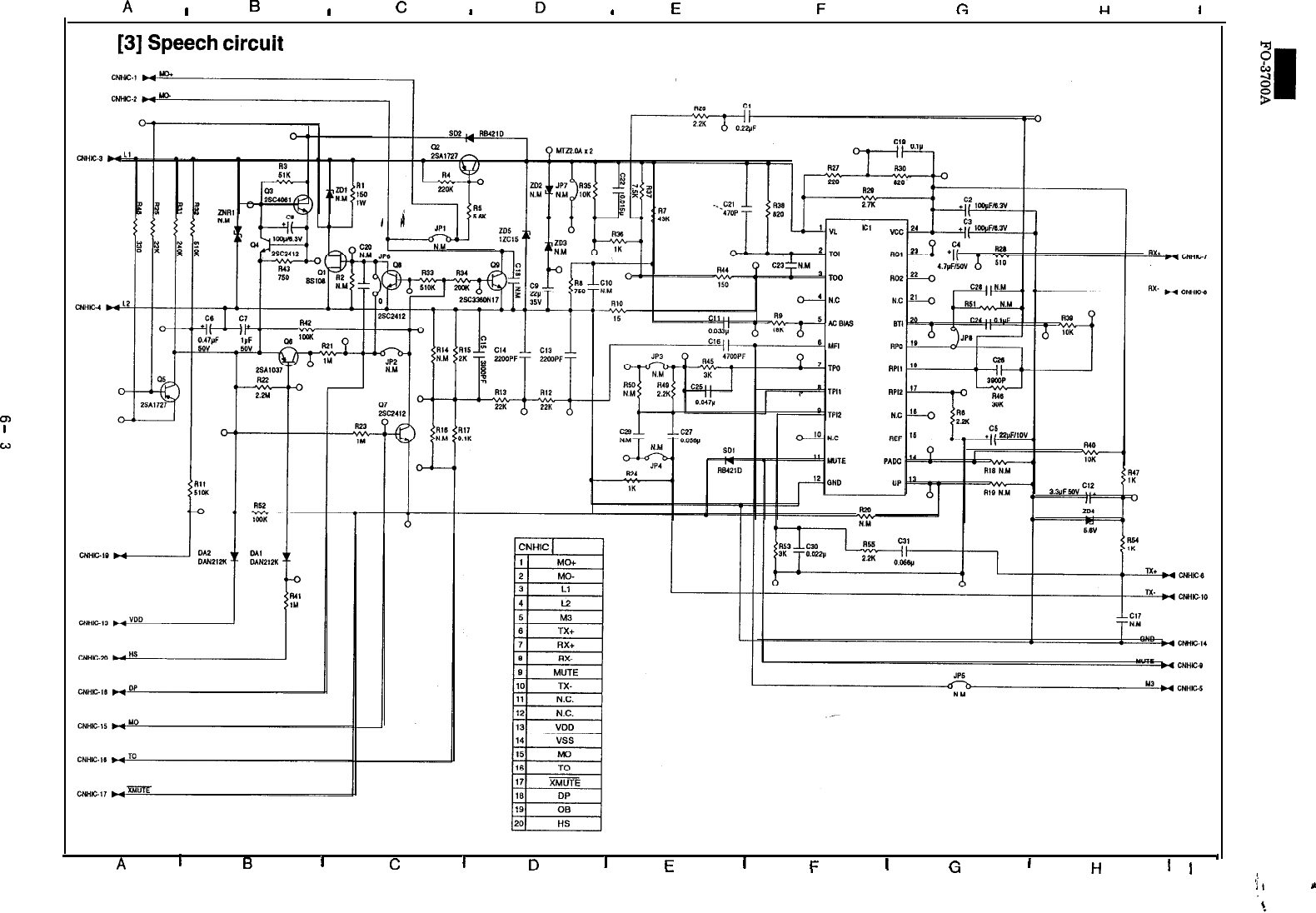
A
I
B
I
c
I
D
,
E
F
Gi
l-4
I
[3]
Speech
circuit
a-2
I
w
A
I
B
I
C
I
D
I
F
I
F
I
I
r-
I
H
I
,
u
’
I
,!
II
L
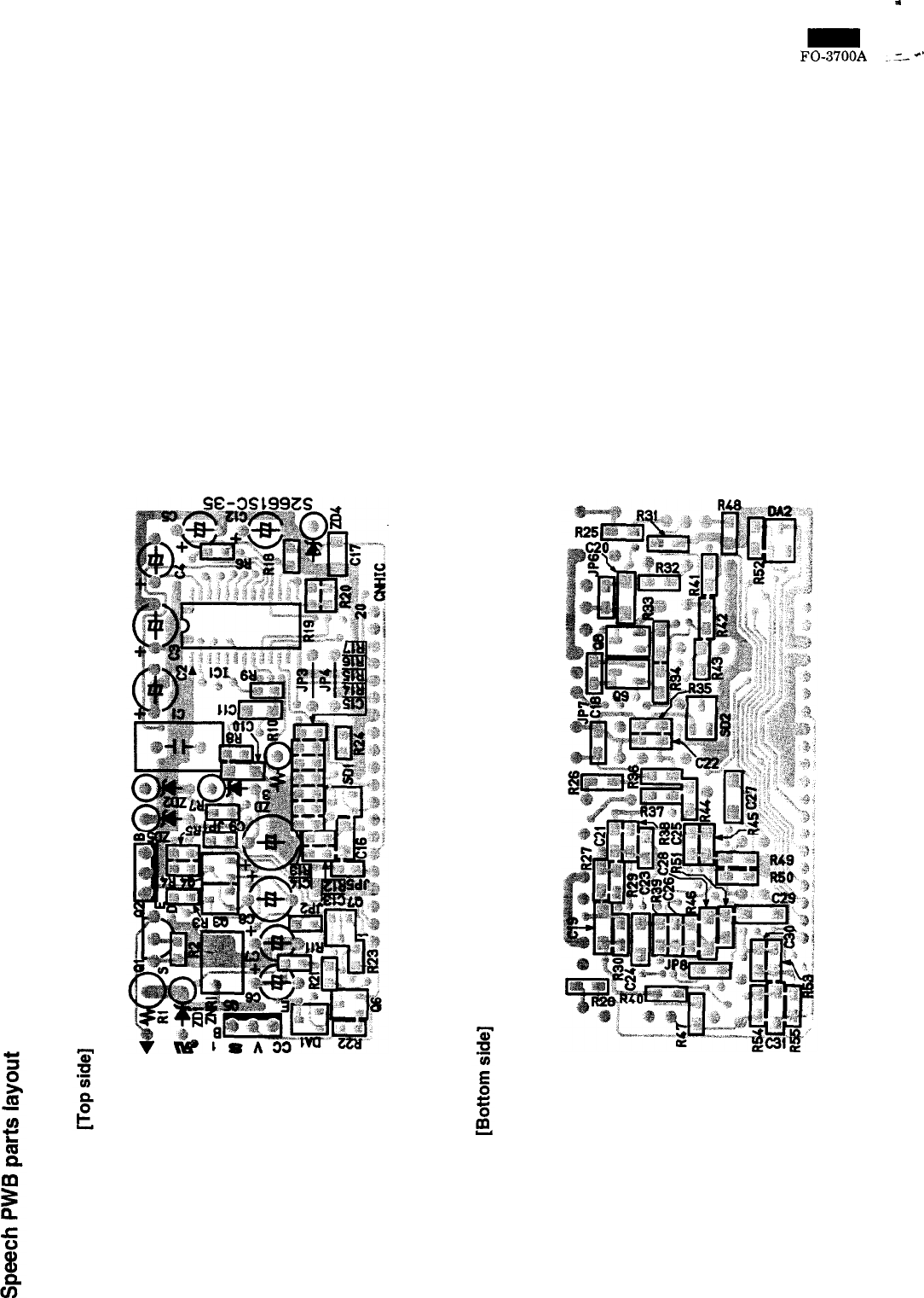
FO-3700A
.I-*'
6-14
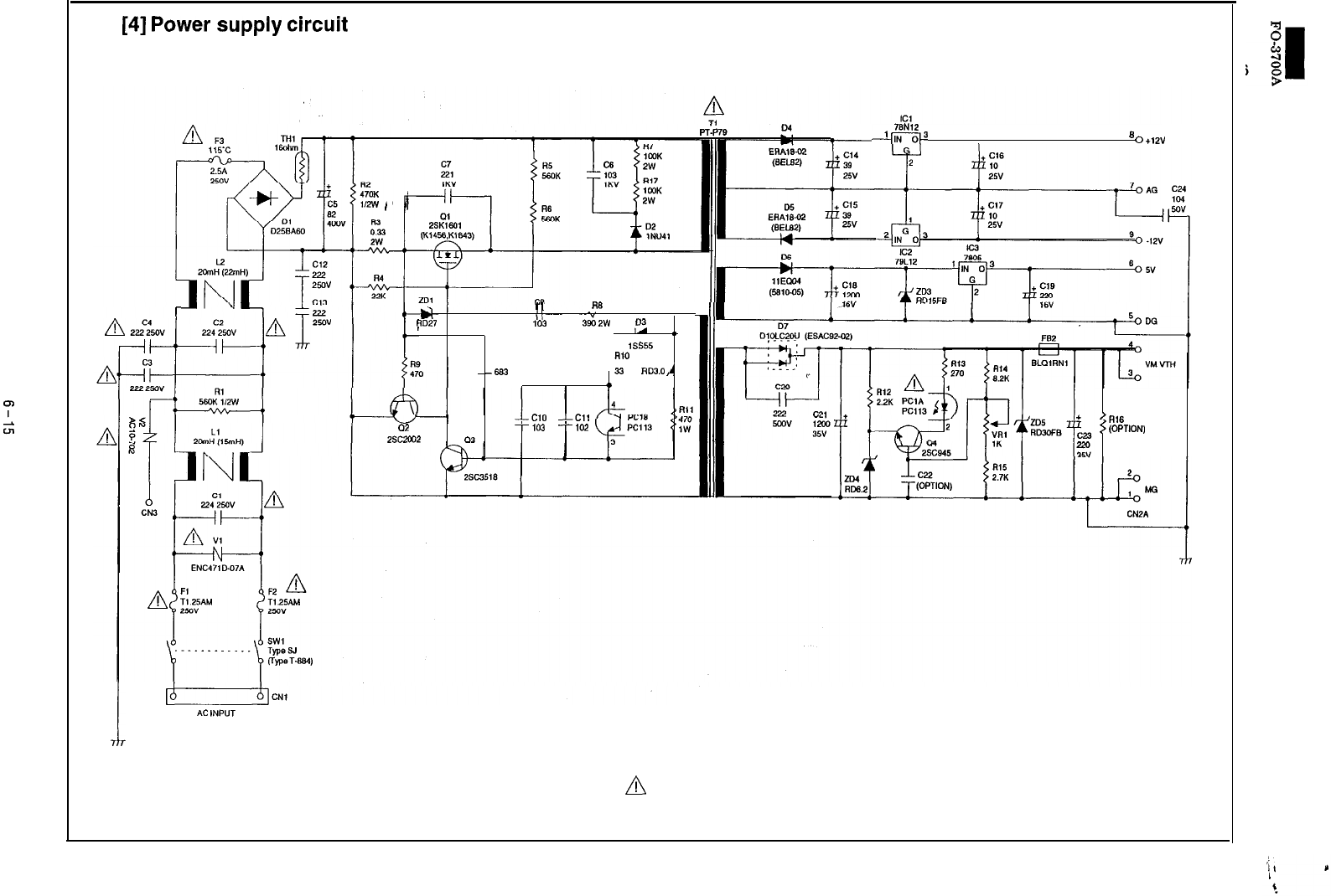
A
I
B
I
C
I
D
I
E
I
F
I
G
I
H
, I
[4]
Power
supply
circuit
76N12
-qiir-$3
6
0
+12v
r
I
,
rw
RD27 103
3902w 03
u
#,
15555
Fe0
--
co
33
ZD2
683 RD3.0
r
A
45
---cl0
---cl,
cl2
--103
--KG
2w.2002
.‘R16
::
(OPTION,
!
AC INPUT
NOTE:
A
These marks are all safety-ciritial parts.
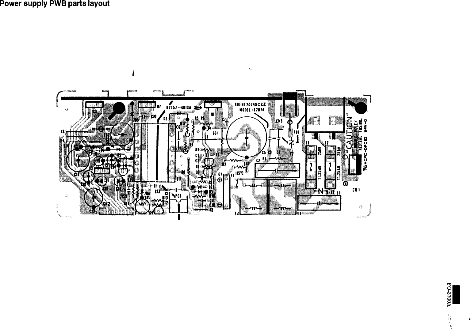
Power
supply
PWB
parts
layout
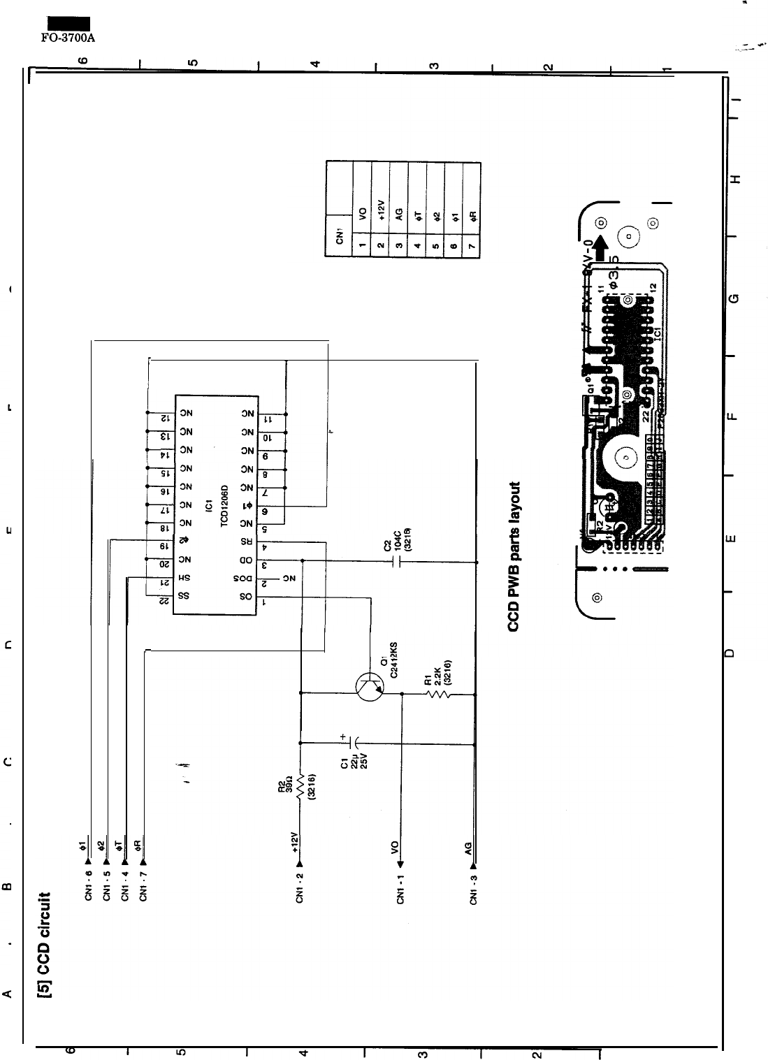
r
FO-3700A
i
I
21
3N
H--
El
3N
VIZN
c
3N
11
3N
01
w
i
3N
6
3N
9
3N
L
10
9
3N
6
6-17
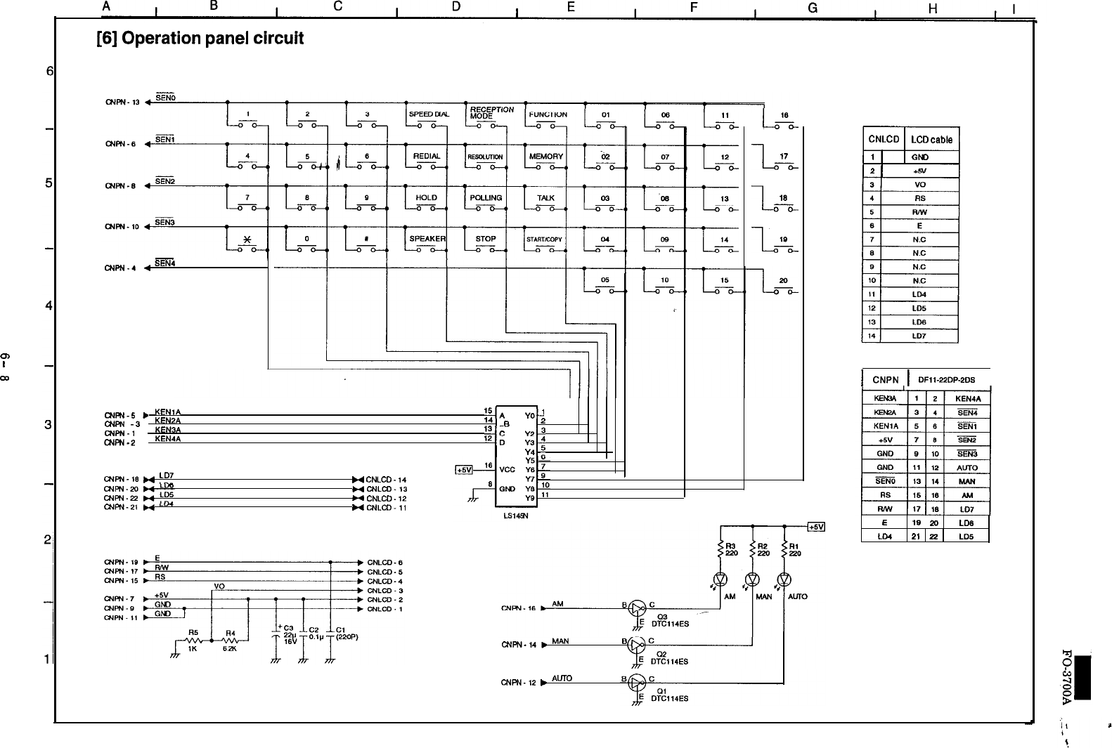
[6]
Operation
panel
circuit
16
Ltz
-L5?5
17
L
16
---5-
CNLCD
LCD
cable
1
GNJ
2
I
-
CNW-4
4
SEN4
0)
I
co
1
CNPN
1
DFII-ZZDP-20s
ICI
chltw-5 b
KENIA
aJpN
M3
,
KENS+
15A
YO’
MPN.,
, KENS.
l4
B
Yl
2
13c
YZ3
c?dFN-P
.
KEN4A
‘*D
YS4
Y4
_”
CNFN-16
H
LD7
H
CNLCD-
14
H
CNLCD-13
H
CNLCD-
12
CNPN-21
H
H
CNLCC-11
E19 20 LD6
LM
21 22
LD.5
CtwN-14.
MAN
B
CNFN-12
t
ALIT0
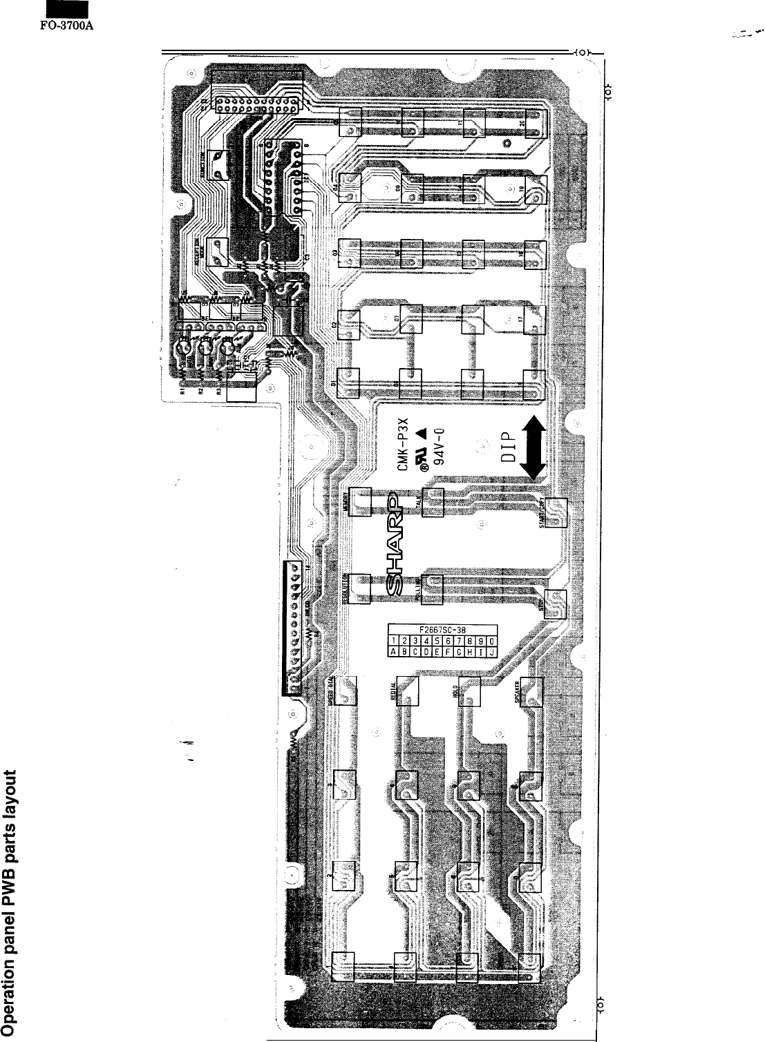
FO-3700A
/---
--~-
-IOk
~-.-_.-
_
6-19
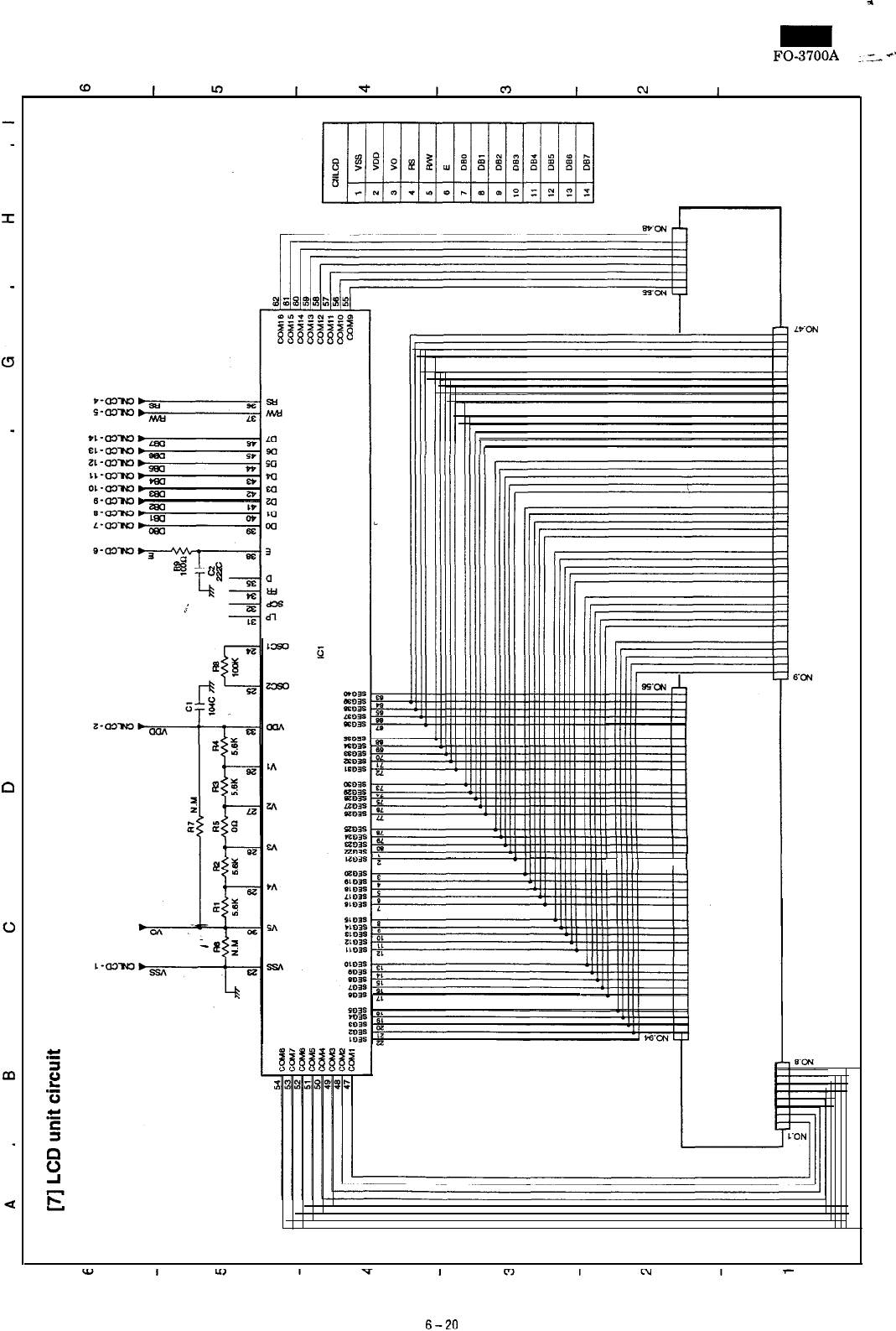
FO-3700A
e,"
LL
W
n
0
E-MM
IIll
Illll
III1
I
I
lllll
I I
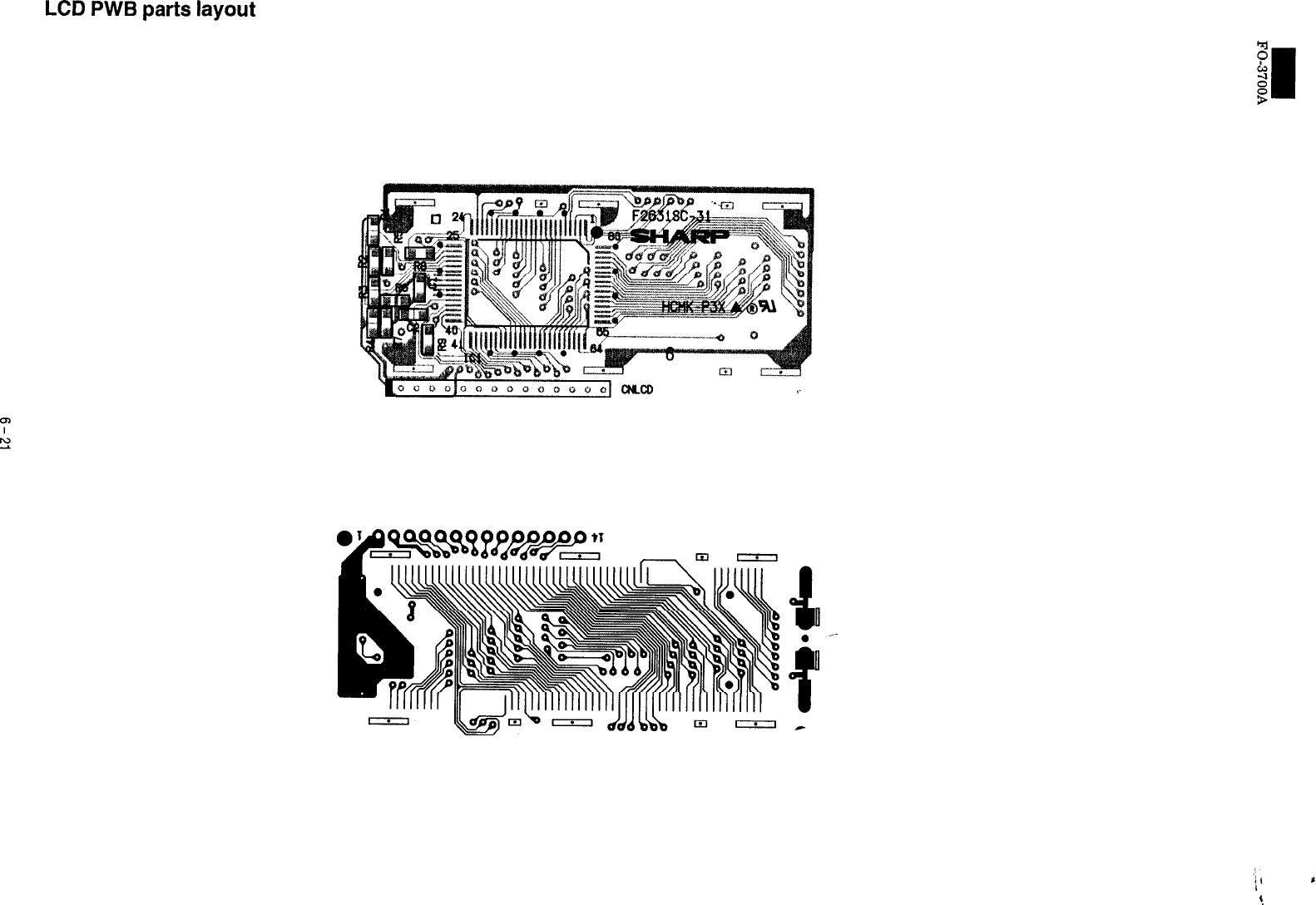
LCD
PWB
parts
layout
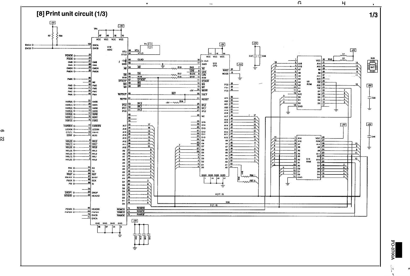
A ,
B
c
I
D .
EF
G
l-l
I
0
I
M
IIII
-
III.
I
I ’
[8]
Print
unit
circuit
(l/3)
I/3
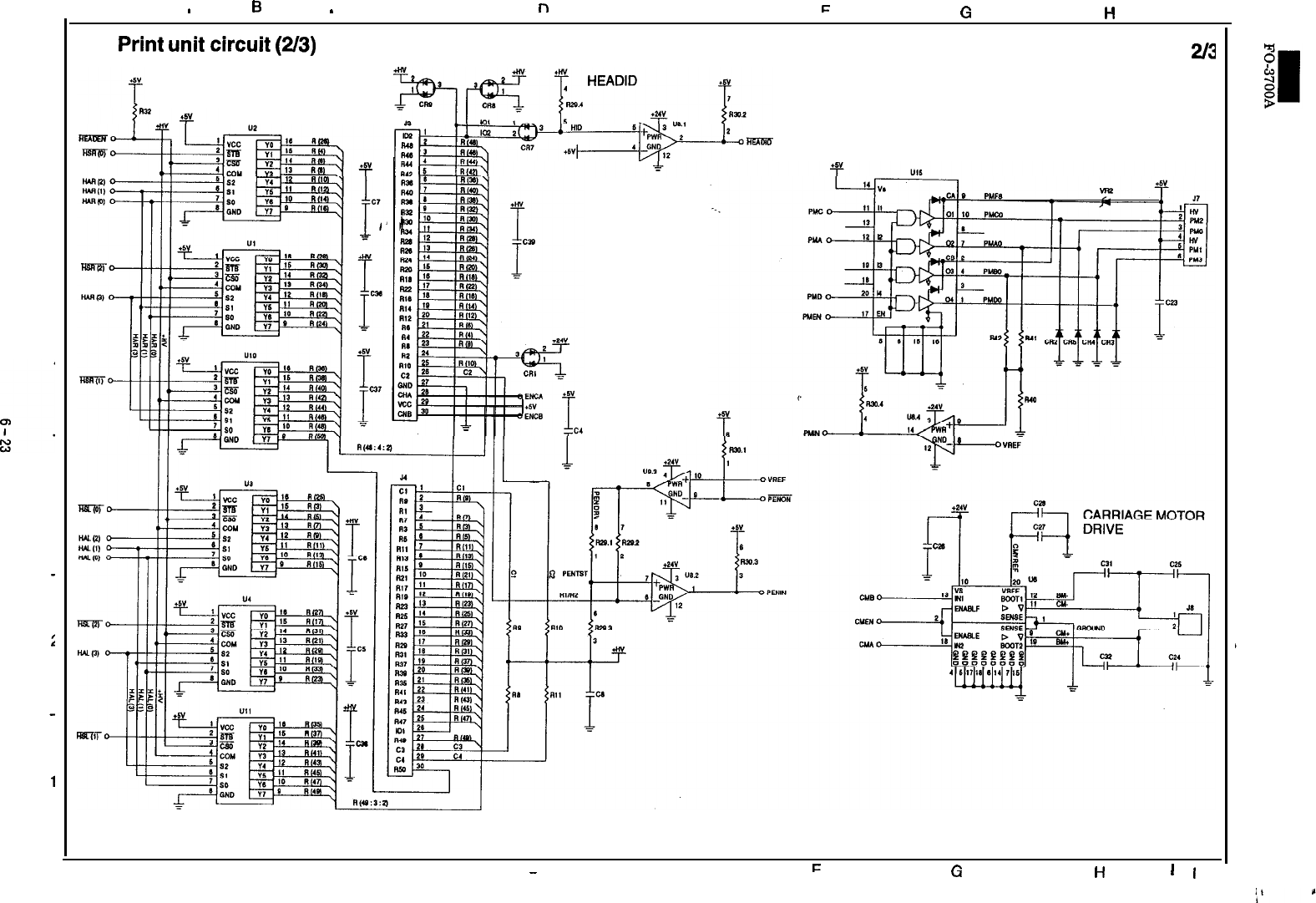
A
a
B
.
C
n
F
F
c
I I
III I II
u
I
l-l
, I
Print
unit
circuit
(2/3)
2l3
PRINT HEAD DRIVE
PEN IN
DETECT
-
PAPER MOTOR DRIVE
A
I
B
I
C
I
D
I
FI
I=
I
c
I
u
I
I
-
u
n
’
I
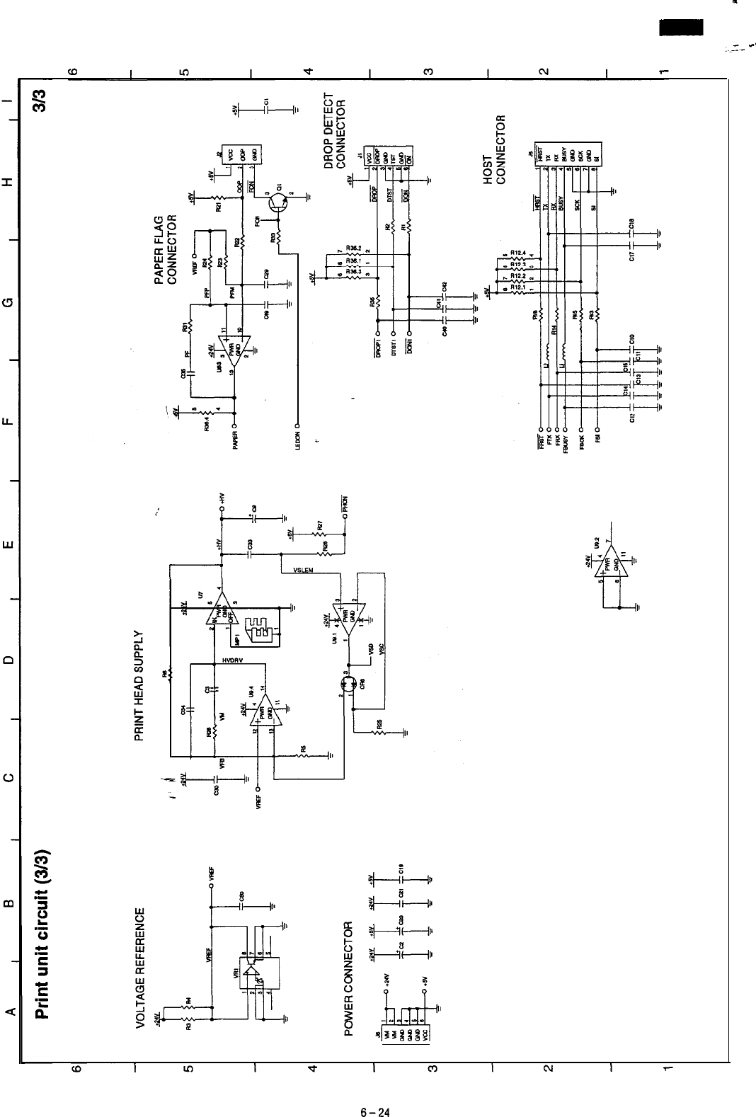
FO-3700A
--c'
r
6-24
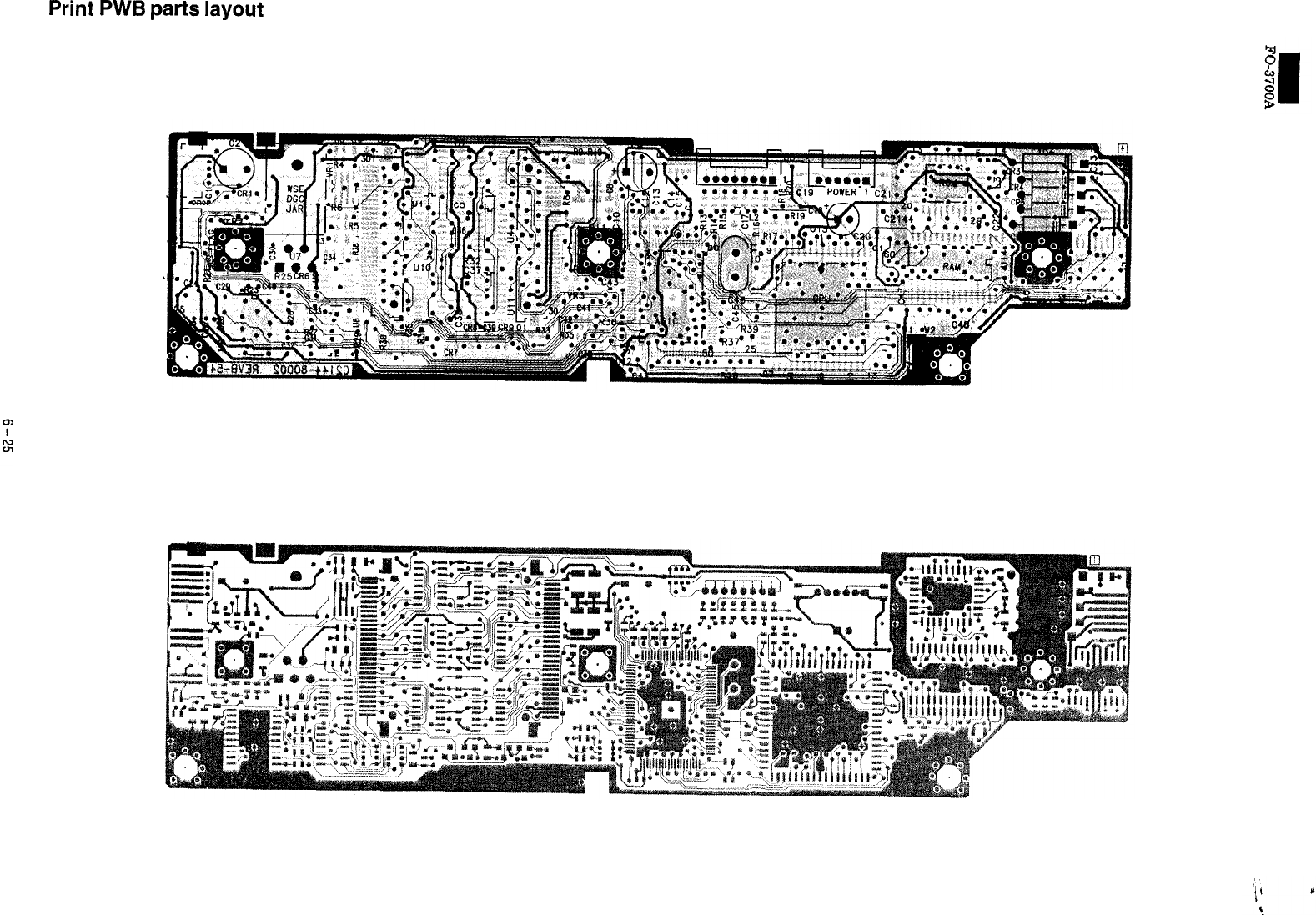
Print
PWB
parts
layout
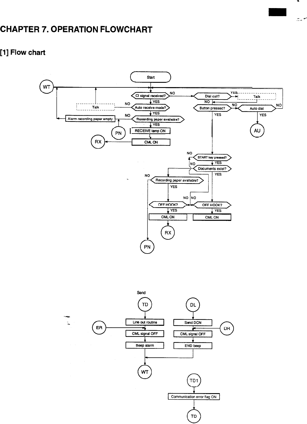
FO-3700A
CY-~'
CHAPTER
7.
OPERATION
FLOWCHART
[I]
Flow
chart
FLOW-VE-1
-
cpN)
1
RECElV;hmpON
1
I
0
-
Send
DCN
7-l
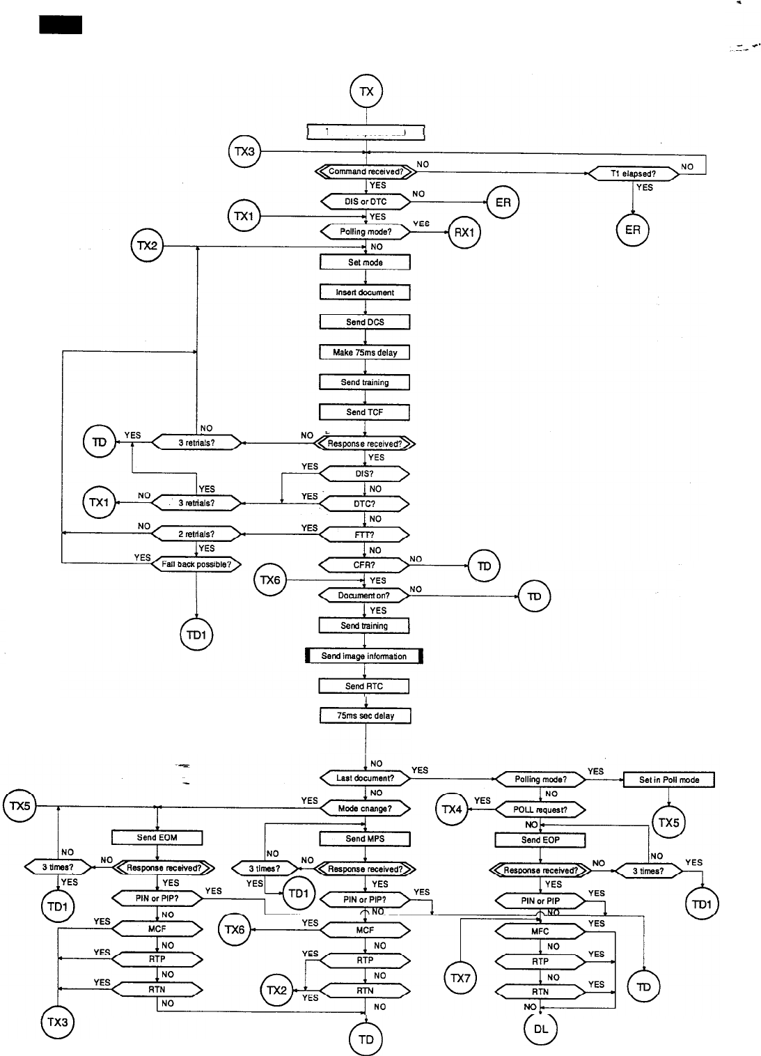
FO-3700A
FLOW-VE-2
Turn on exposure
LED
75ms
set
delay
Y
0
TD
0
DL
7-2
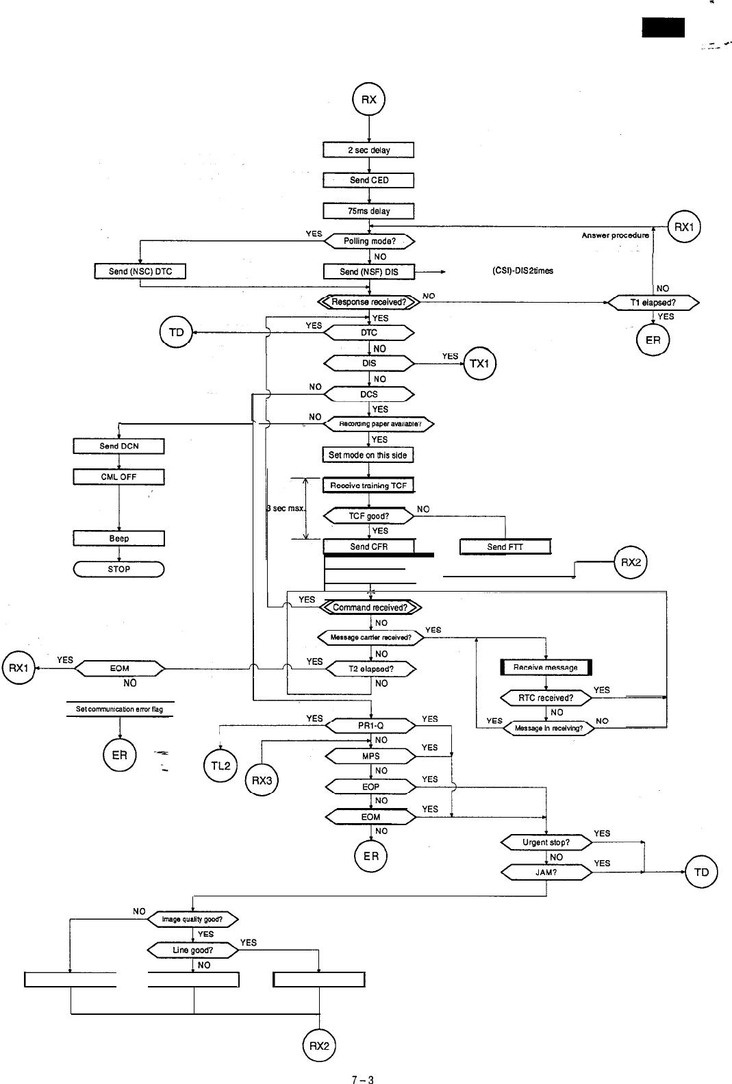
FLOW-VE3
Send (NSF) (CSl)-OS
2times
r
w
NO
0
TL2
ma
FO-3700A
.:a*
Set T2 1I
I_
I
Send TRN
1I
Send RTP
1
I
Send MCF
I
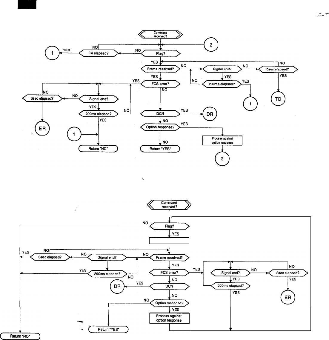
FO-3700A
FLOW-VE-4
YES
Reset T2
I
I
c4
Return
‘NO
f
7-4
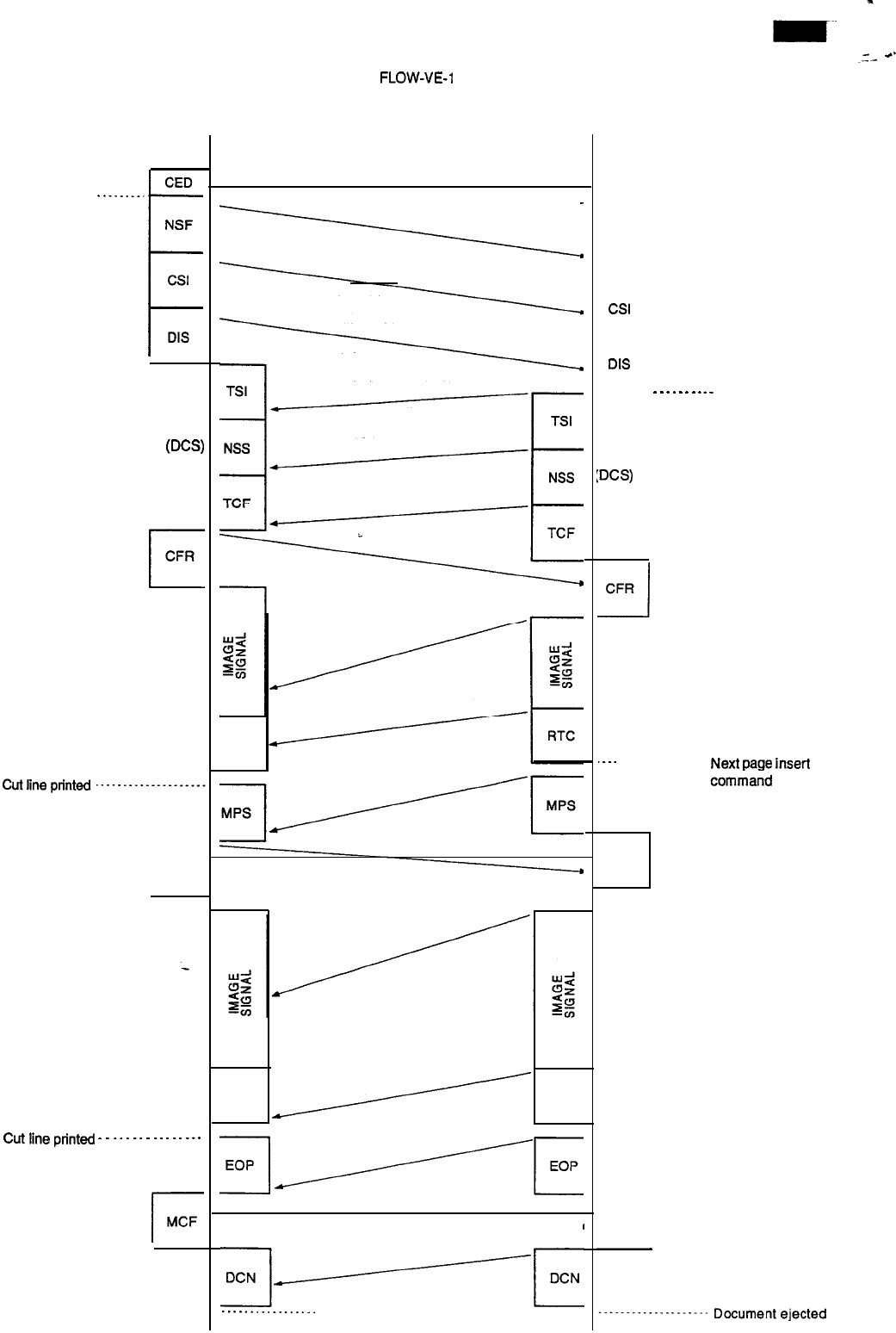
FO-3700A N
ME-
FLOW-‘/E-l
1
Receiver side
G3 communication
Transmitter side
(Document inserted into document sensor during stand by)
TX RX
TX
RX
To recording
..--..-..
position
(DCS)
c
CFR
rMCF
Cut
line
punted
_
_
__
_
__
_
___
__
__.
r
MCF
d
RTC
RTC
RTC
7
EOP
1
EOP
c
I
*-----------
-.--..--.----.--.
Recording paperejected
7-5
CED
NSF
I
CSI
DIS
-
-
-
-
-
-
-
.-
-
Document inserted to
the reading position
:DCS)
i
CFR
1 st page
._..
. . . . . . ___ ____ __
Next
page
insert
MCF
1
MCF
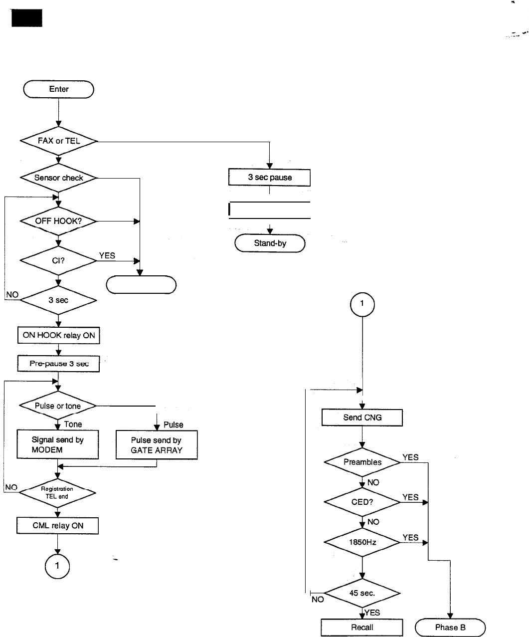
FO-3700A
Auto dial sending
TEL mode
NG
YES
b
b
v
Stand-by
CML relay ON
ir’
0
1
I
Dial send
I
1
:I
--Bj
YES
7-6
FO-3700A
m-z--
[2]
Power
on
sequence
I
Power SW ON
1
1
UOpodinitialize
1
Backup RAM clear
Backup RAM clear
ROMeumEST
i
Printer initialize
I
Standby
7-7
FO-3700A
CHAPTER
8.
OTHERS
[I]
Service
tools
1. List
NO.
PARTS CODE DESCRIPTION
Q’TY PRICE
RANK
1
CPWBS2683SCO3
Extension board unit
1
BX
2. Description
2-l.
Extension board unit
FO-3700
series
extension
PWB
unit
connection
1) Remove the bottom ass’y from the body.
2) Connect the cables from the body with the extension PWB unit
connectors (CNCCDl, CNSNSl,
CNTXMl,
CNPNLl,
CNPI
1,
CNPRTl,
CNLEDl,
CNSPl,
CNPHI) similarly with the control
PWB and the TEULIU PWB unit. Fix the grounding cable to the
bottom PWB with a screw.
(Note) When connecting the cables, check the color of the cables
and the color of the connectors.
3) Pass the five cables which are provided for the extension PWB
through “TEL LINE’ and ‘TEL SET’ holes in the lower cabinet.
Pass the four cables which are in the opposite side to the hook
switch through the AC cord hole and the power switch hole, and
fix the extension PWB.
4) Connect the extension cables which are in the rear of the body
where the extension PWB has been installed with the bottom
ass’y (the control PWB, the TEULIU PWB) as follows:
Extention PWB connection diagram
Extentii cable
when
cmnecting the
exlmslul
ho&
switch (RHS)
d
the TEULtU PWB
Extention
cable
Extension board unit
8-l
NO.
1
PARTS CODE
I
DESCRIPTION
List
of
jigs
used
for
disassembly
and
assembly
of
the
ink
jet
printer
\
NO.
PARTS CODE DESCRIPTION
an
PRICE
RANK
. . . .
1
OJZC214460003
Pen
garage
1
BK
2
UKOGD2031SCZZ
Torx screwdriver (M2.5 x 5)
1
BQ
3
UKOGD2032SCZZ
Torx screwdriver (M3 x 8)
1
BQ
4
UKOGM2026SCZZ
Optical adjustment plate
1
BP
2-2. Scan optical system adjustment
(1) Outline
The adjustment procedures of the scan optical system are described
below:
(2) Adjustment
procedures
@
Fully open the upper cabinet, remove fixing screws of the record-
ing paper tray, and remove the recording paper tray.
In order to perform focus adjustment, remove the optical system
unit from the frame.
@
Install the scan adjustment jig to the optical system unit so that the
pattern surface is in the lower side.
@
Fit the pin of the optical system adjustment jig with the hole in the
optical system frame.
Scan adjustment jig
@ Use an oscilloscope to connect the control PWB VID (1 channel
side), oT (2 channel side), and AG (GND).
I
I
CNCCO
0
0
VID
a
Supply power to the main body to light the LED in the LED array
lighting mode Loosen the two red screws of the CCD to obtain
VID signal waveform in synchronization with eT signal and adjust
the CCD position so that the following waveform is obtained.
CCD waveform
‘1: lnaeasethediffemnw
by
foamy
adjustment
‘2:
Adjust
as
show
by
CCD
FWB
adjustment
[CCD waveform model]
@I
By adjusting the CCD PWB as shown above, focus is adjusted
and scan line is aligned.
After completion of the CCD adjustment, tighten the two red
screws and apply screw lock.
VID
VI0
e-r
CNCCD-4
iUi
CNCCD-3 a-2
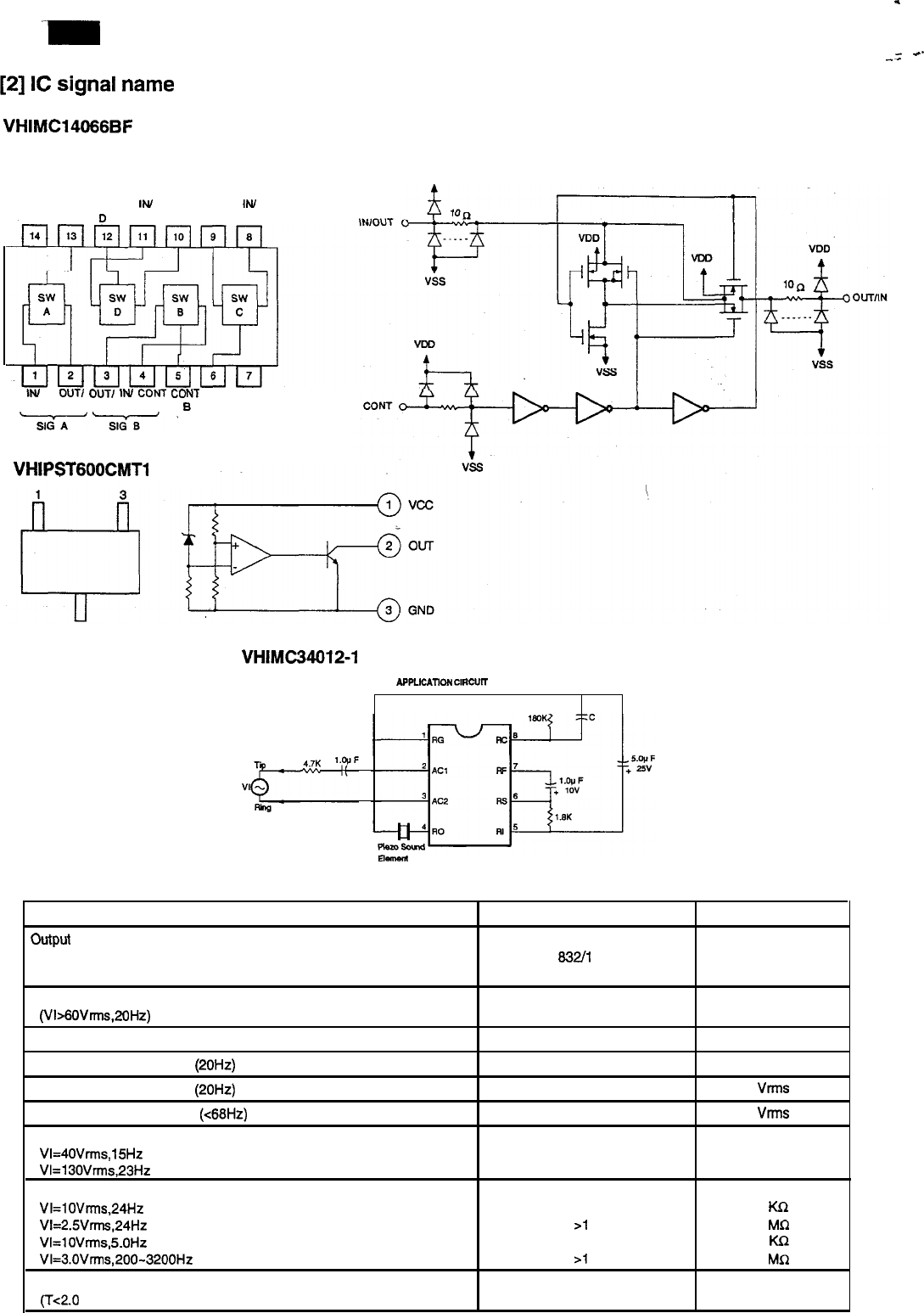
FO-3700A
[2]
IC
signal
name
a
-
.s.-
--
VHIMC14066BF
Pin Arrangement
SIG D SIG C
--
CONT CONT IW OUT/ OUT/ IN/
VCC A
D
OUT IN
IN
OUT
IN/ OUT/
OUT1
INI
CON-f
CON1 VSS
OUT IN IN OUT B C
Qz-i-
-z--r,
Equivalent circuit (One of the four blocks)
VDD
VHIPST600CMTl
2
VHIMC34012-1
P
APFuc*-
ClRcurr
APPLICATION CIRCUIT PERFORMANCE
Characteristic
Output
Tone Frequencies --
MC3401 2-l
Warble Frequency
Output Voltage
(Vl>60Vrms,2OHz)
Output Duty Cycle
Ringing Start Input Voltage
(20Hz)
Ringing Stop Input Voltage
(20Hz)
Maximum AC Input Voltage
(<68Hz)
Impedance When Ringing
VI=4OVrms, 15Hz
VI=130Vrms,23Hz
Impedance When Not Ringing
VI=lOVnns,24Hz
VI=2SVrms,24Hz
VI=lOVm1s,50Hz
VI=3.OVrms,200-3200Hz
Maximum Transient Input Voltage
(Tc2.0
ms)
Typical Value
832/l
040
13
20
50
36
28
150
20
10
28
>l
.o
55
21
.o
1500
Units
HZ
VP-P
%
Vns
vmls
vrrt-s
K
Ko
Ml2
KQ
MR
V
a-3
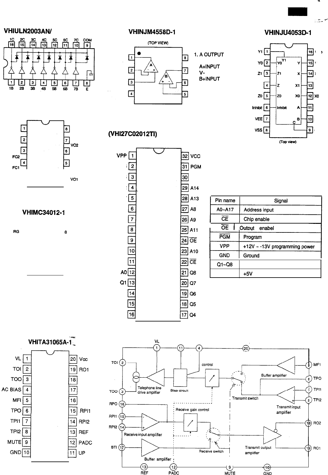
VHIULN2003AN/
VHINJM4558D-1
VHIMC34119/-1
CD 1 a
vo2
FC2 2 7
FCl
VIN
f-7
3 6
GND
vcc
45
VOl
VHIMC34012-1
P
RG
1
6
RC
AC1
2 7
RF
AC2 f-2 3
6RS
RO 4
5
RI
tl
18 R02
17 BTI
E
16 RPO
15 RPIl
(TOP VIEW)
(TOP VIEW)
l.AOUTPUT
2.
A-INPUT
3.
A+INPUT
4.
v-
5.
&INPUT
6.
B-INPUT
7.
B OUTPUT
8.
V+
2M EP-ROM
(VHl27C02012Tl)
(TOP VIEW)
VPP
Al6
Al5
Al2
A7
A6
A5
A4
A3
A2
Al
A0
Ql
Q2
Q3
GND
FO-3700A
~=-.+'
VHINJU4053D-1
Yl VDD
YO
Y
Zl
X
ZXl
m
x0
hhibil
A
ME
B
VBS
C
OE
I
Outtxit enabel
Ql
-Q8
vcc
Data output
+5V
power
UP AC BIAS
VCC
Transmit gain
Transmit
swtch
Transmit
input
amplifier
Receive
input
amplifier
Butler
amplifier
:
@ @
FIEF PADC
&
MUTE GND
3
MFl
>
TPO
>
TPll
>
TPIZ
a-4
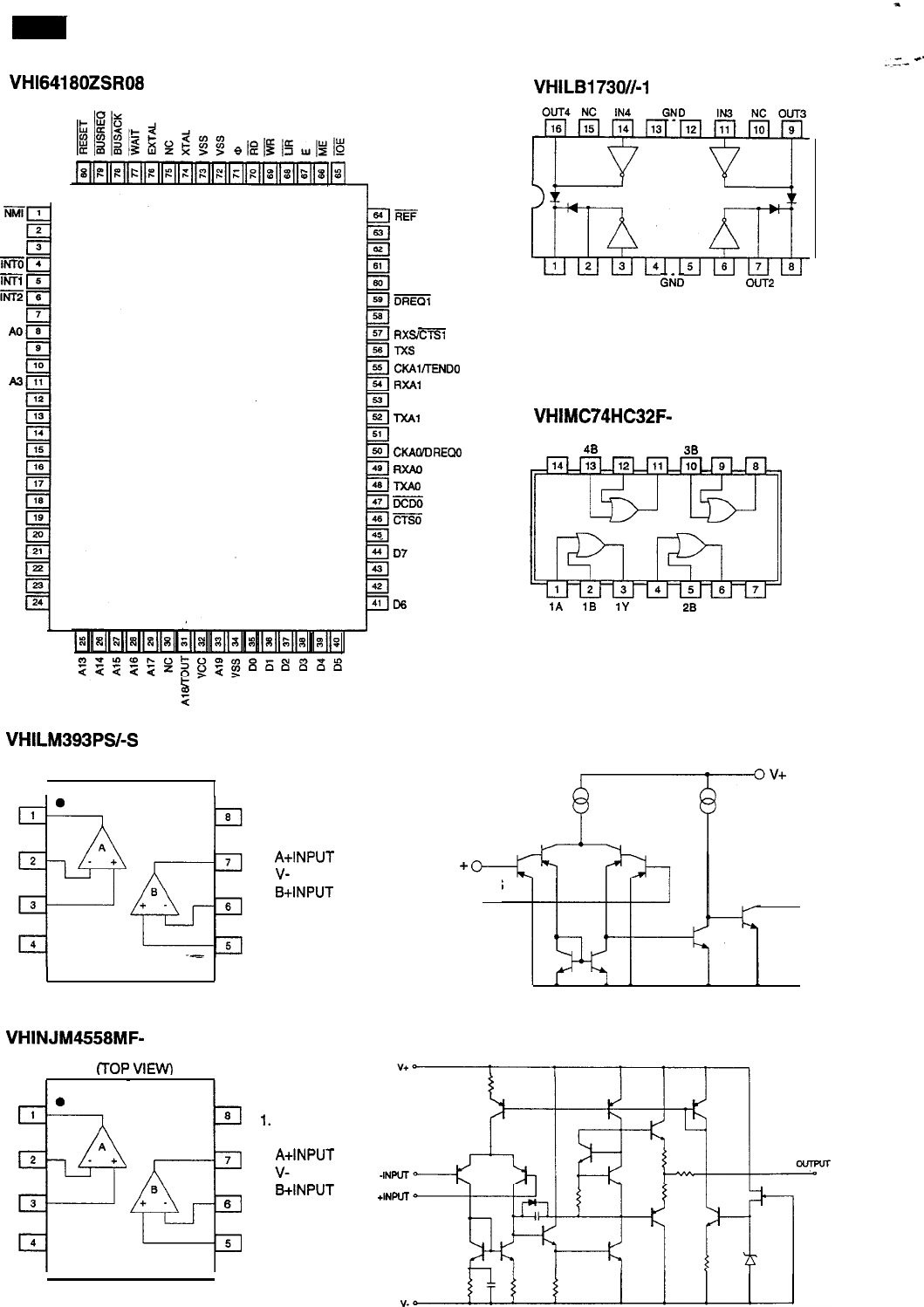
FO-3700A
VHl64180ZSR08
VHILB1730//-1
NMI
NC
NC
im
m
iii5
ST
A0
Al
A2
A3
vss
A4
NC
A5
A6
A7
A8
A9
A10
All
NC
NC
A12
VHILM393PSbS
(TOP VIEW)
I
0
1
A
2
_
+
_;’
3
4
VHINJM4658MF-
crop
VIEW)
1.
A OUTPUT
2.
A-INPUT
3.
A+INPUT
4.
v-
5.
B+INPUT
6.
B-INPUT
7.
B OUTPUT
8.
v+
0
1
A
2
-
+
~
3
4
a
7
4
B
+ .
6
5
1.
A OUTPUT
2.
A-INPUT
3.
A+INPUT
4.
v-
5.
&INPUT
6.
B-INPUT
7.
B OUTPUT
8.
V+
iw
NC
NC
HALT
TEND1
DREQ1
CKS
-
RXS/CTSl
-IX
CKAl/lENDO
RXAI
NC
TXAl
NC
CKAO/DREQO
RXAO
TXAO
5566
CTSO
RTSO
D7
NC
NC
lx
rt’.:b(
VCC OUT1 IN1 GND IN2
our2
vcc
VHlMC74HC32F-
VCC
48
4A 4Y
38
3A 3Y
1A 18 1Y 2A
28
2Y GND
+
INPUTS
00
OUTPUT
GND
0
-INPUT
+INPUT
6-5
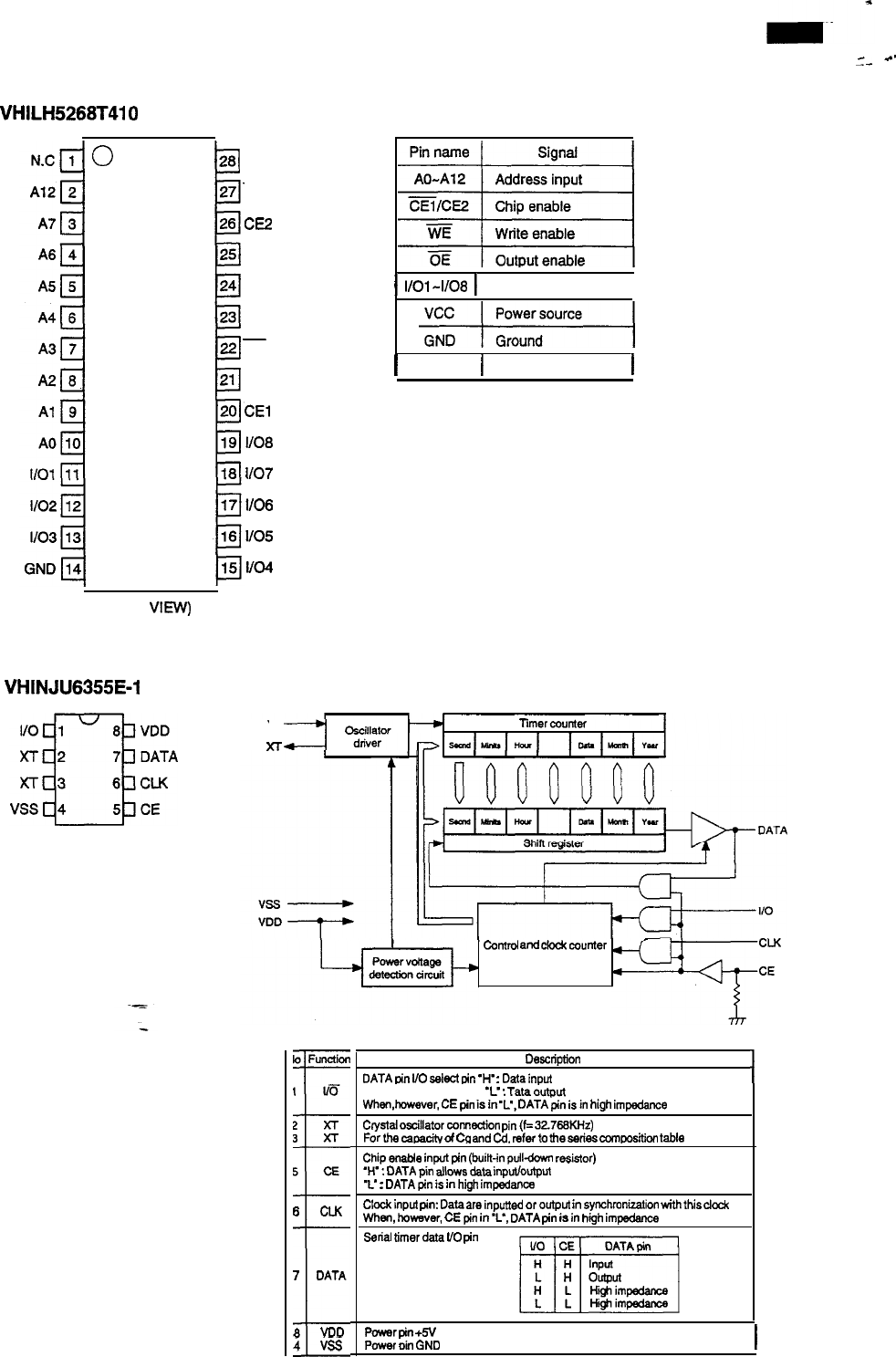
FO-3700A
_.
_'-
VHILH5268T410
0
b
28 VCC
WE
GE2
A8
A9
All
-
OE
A10
CEl
l/O8
Ii07
l/O6
l/O5
l/o4
(TOP
VIRN)
VHINJU6355E-1
(TOP VIEW)
1
l/01-1108
1
Data I/O
I
I
I
N.C.
Non connection
I
XT
Timercounter
XT
Contml
and
clodc
counter
CLK
CE
lo
Function
t
Iii
2
XT
3
XT
5
CE
ti
6
CLK
7
DATA
aVDD
4VSS
DsSX@tfOl-l
I
DATA
tin
i/O
select
tin
‘H’
:
Data
in~ti
I
‘C
:
Tata
&put
When,hcwever,
CE
pin
is
in
‘C,
DATA
pin
is
in
high
impedance
Crystal
oscillator
connection
pin
(f=
32768Kf-k)
For
the
caDacitv
d
Cca
and
Cd.
refer
to
the
series
wmwaition
table
Chip
enable
input
pin
(b&t-in
pulldmw
resistor)
‘H’
:
DATA
pin
allows
data
inputbutput
‘C
:
DATA
pin
is
in
high
impsdanat
Clwk
input
pin:
Data
are
inputted
or
output
in
synchmnization
with
this
ckdc
When,
however,
CE
pin
in
‘L’,
DATA
pin
is
in
high
imp&awe
Serial
timer
data
110
pin
Power
pin
+5V
Power
oin
GND
8-6
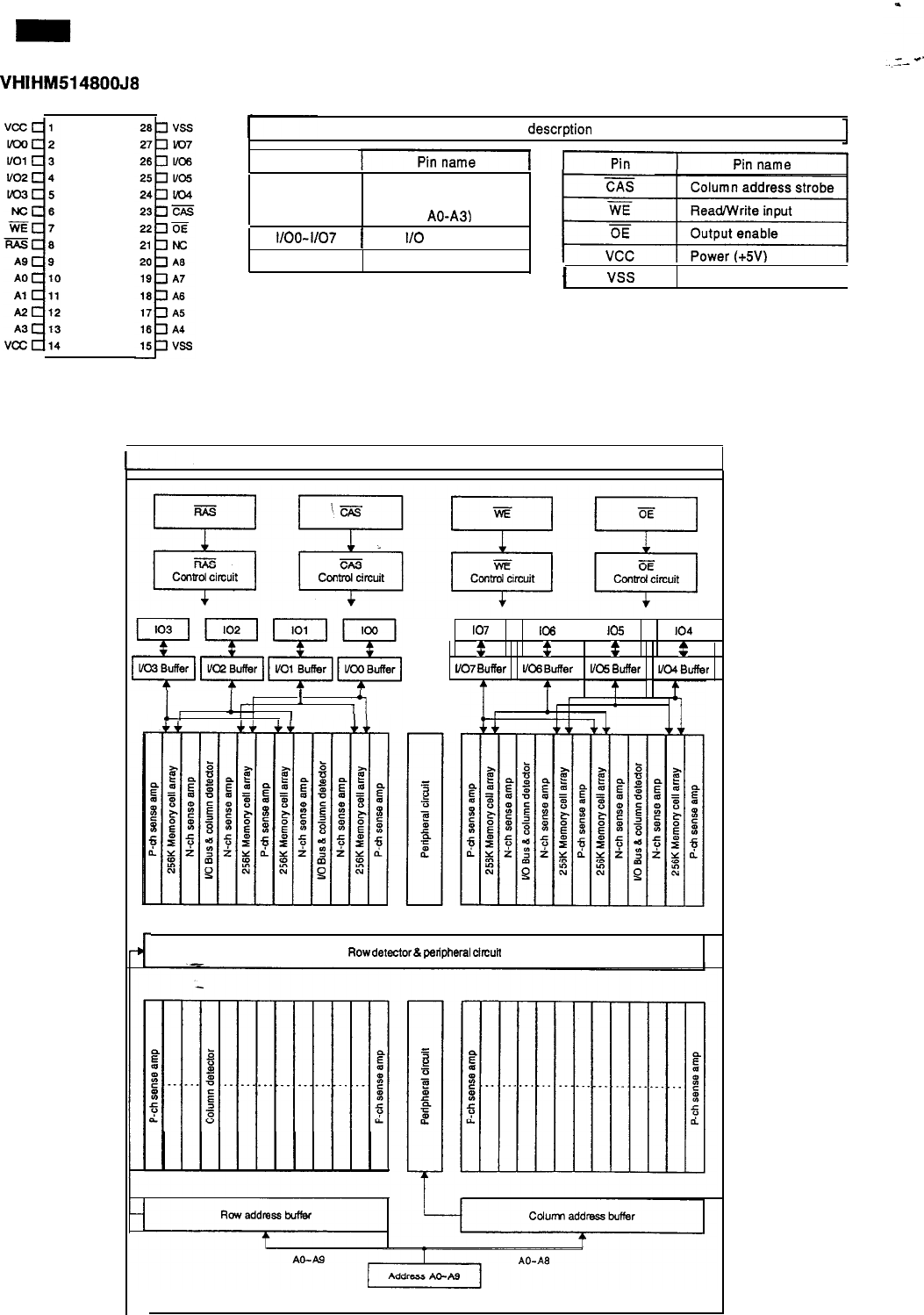
FO-3700A
VHIHM51480WS
AO-A9 Address input
(Low/Refresh AO-A3
Column AO-A31
Pin descrption
Pin
l/00-l/O7
j
Data
I/O
RAS Low address strobe
I
vss
Connection
I
Block diagram
I!
I
I
I
107
106
IO5 104
t
t
:
t
l/O7
Buffer
II06
Buffer
Ilo5
Buffer
VO4BUfb
Row
detector
8
pedpheral
circuit
8-7
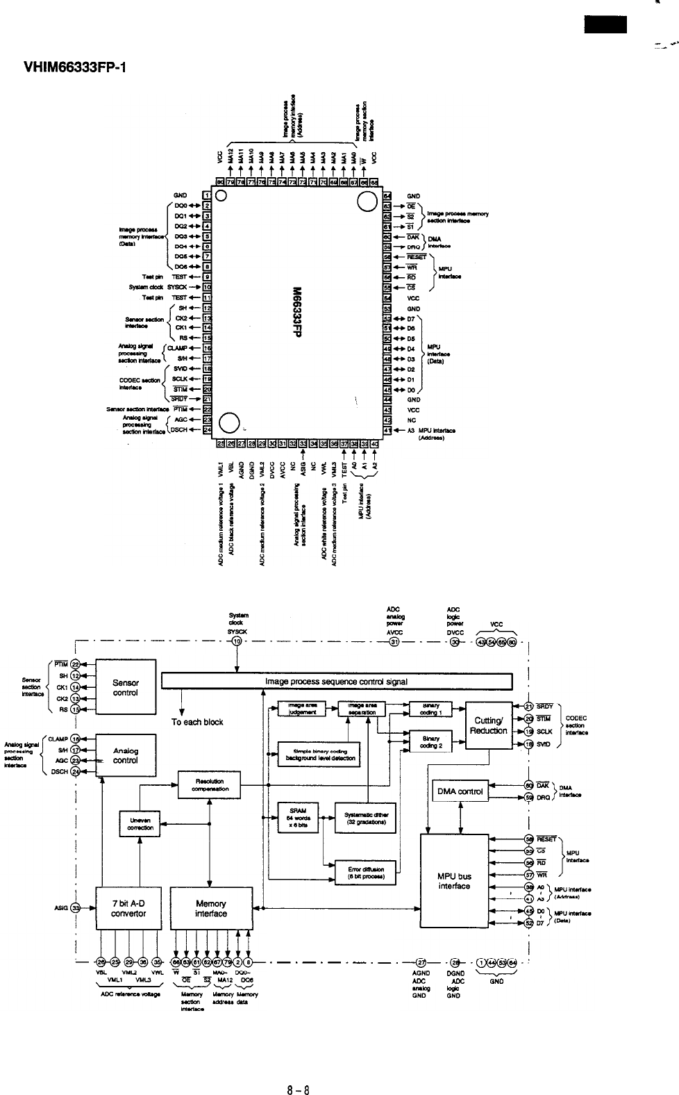
FO-3700A
__...
VHIM66333FP-1
NC: Not connected
z
E
r---------
.$fL-.-.
--.lgL.-.~.*.,
___-.-.-.-.
Am40
DON0
w
Aoc
Aoc
GNO
8-8

SHARI=
PARTS GUIDE
MODEL
FO-3700
6ONTENTS
\
Scanner
mechanism
Upper
cabinet,
document
guide
upper
Print
mechanism
Optical
unit
Packing
material
&
Accessories
Controt-PWB
unit
Power
supply
PWB
unit
TEL-Liu
PWB
unit
Panel
PWB
unit
Sensor
PWB
unit
CCD
PWB
unit
Hardware
parts
n
Index
Because parts marked with
“A”
is indispensable for the machine safety maintenance and operation, it must
be replaced with the parts specific to the product specification.
FO-3700A
111
Scanner
mechanism
23’
I
;’
.@--l
,
1.’
‘23
B14-d
-
FAPS0076
-l-
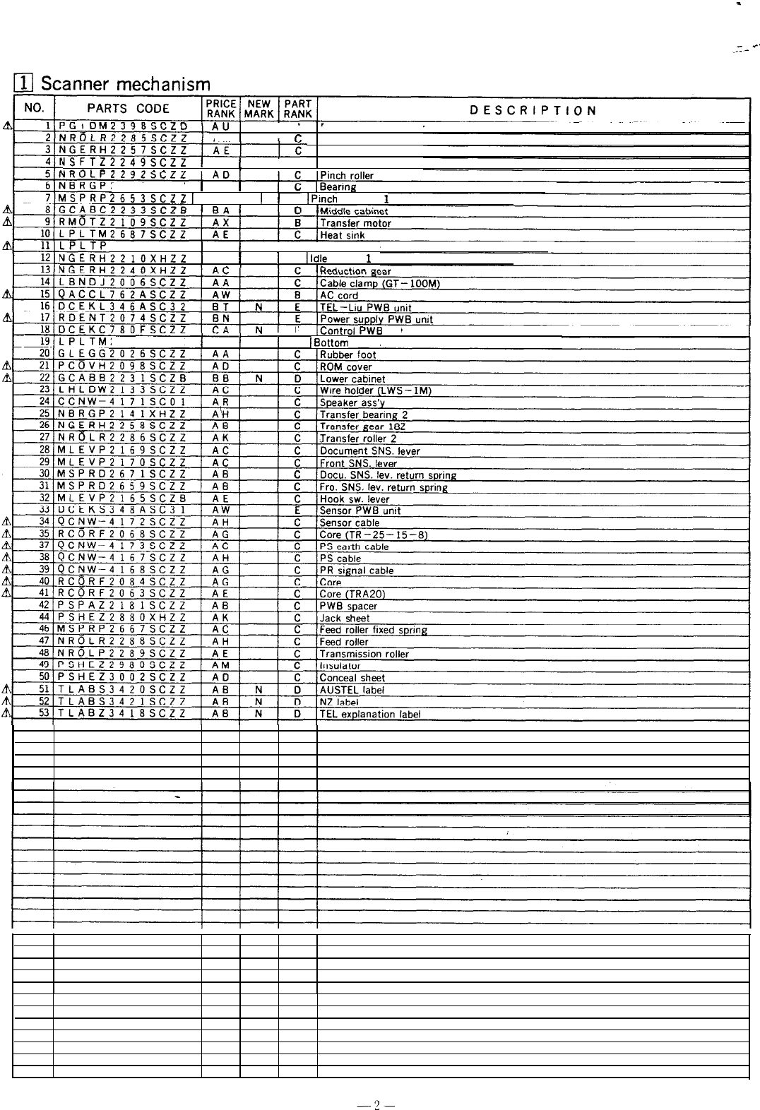
FO-3700A
AU1
N I C Document guide lower
AM
1
c
Paper feed roller
Paper feed gear 542
JSFTZ2249SCZZ
I
AS
1
I c Pinch roller shaft
.^^
.^^^_^^---
I
.-
2138XHZZ
I
AD
I
IBearing
2653SCZZ
1
AC
1
1
C IPinch spring
1
i
RA
i
I
l-l
I
111
Scanner
mechanism
2677SCZZ
1
AH
1
I
C
[Driving plate
NGERH221OXHZZ
1
AC
[
1
C
IIdle
gear
1
NGFRH37AnXU77
I
I
E
/Control
PWB
unit
I
2684SCZZ
1
AR
1
I
C
IBottom
plate
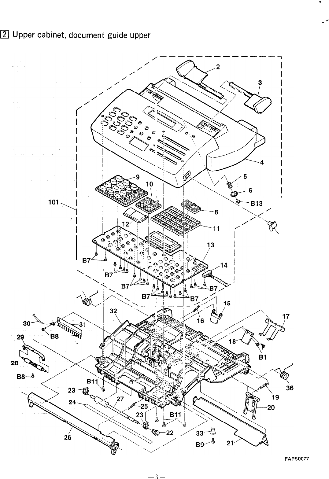
El
FO-3700A
Upper
cabinet, document
guide
upper
h’
I
I
I
y-B13
,
I
\A’
/
‘.
/
39
\
\
\
B7’
’
_I
--/k2!A
!
1%
35,
#
‘7
!ti
FAPS0077
-3-
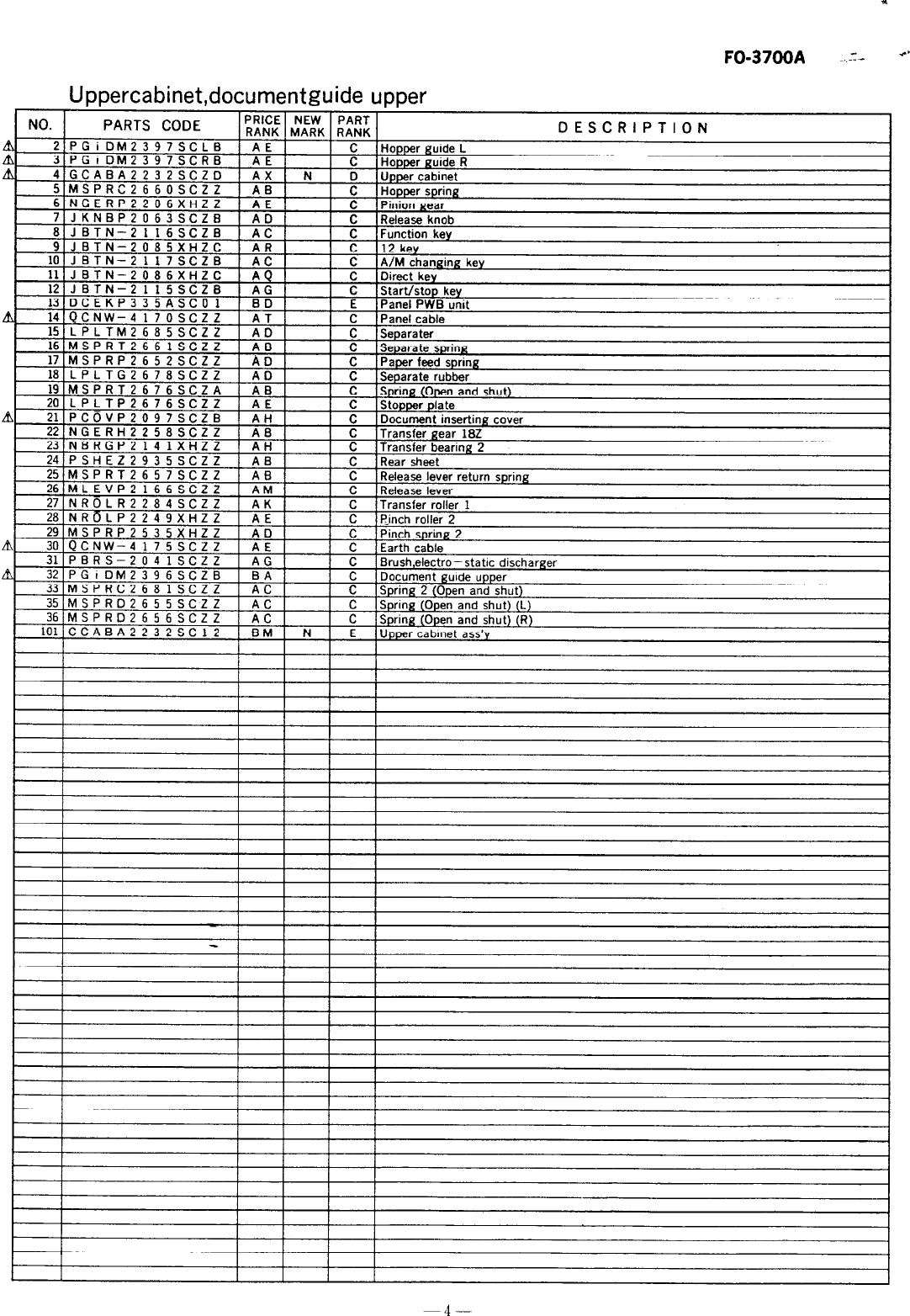
FO-37o()A
-..z-
.-’
q
Upper cabinet,
document
guide upper
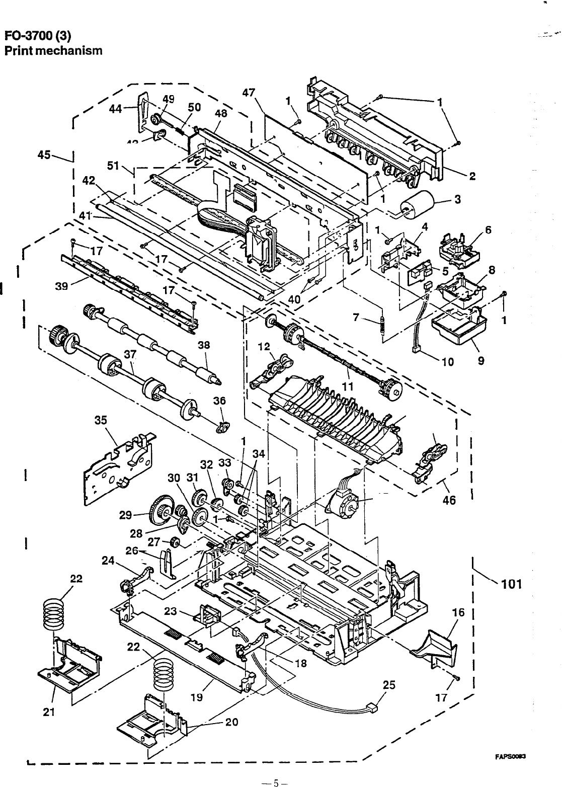
FO-3700
(3)
Print
mechanism
r
I
I
I
I
I
I
I
I
I
I
I
I
I
I
I
I
I
I
I
I
I
I
I
I
I
I
I
I
I
L
/‘44
I
f
I
-!LR
\
@k
43
-----*
----
-
13
’
-/
14
1
I
-15
L
I
I
I
-5-
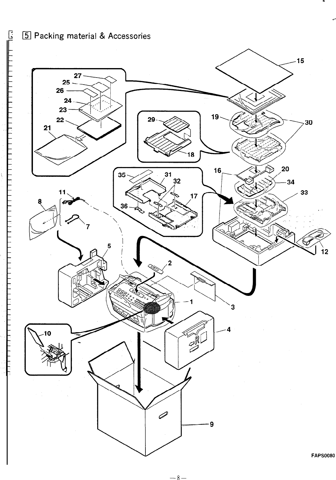
151
Packing material
&
Accessories
FO-3700A -- *’
FAPSOO80
-8-
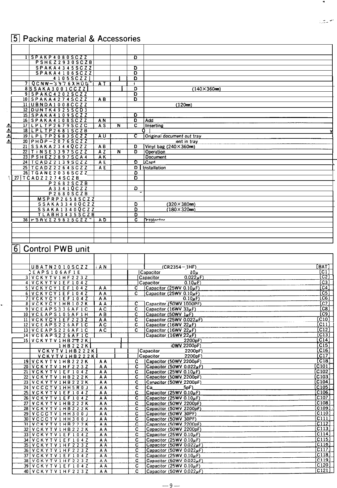
FO-3700A
m
Packing material
&
Accessories
NO.
PARTS CODE
PRICE NEW PART
RANK MARK RANK DESCRIPTION
lSPAKP4080SCZZ
AM
D
Vinyl cover
A2
PSHEZ2930SCZB
AE
C
Face sheet
3
SPAKA4345SCZZ
AC
D
Protector
4
SPAKA4106SCZZ
AM
D
Side pat R
5 SPAKA
7
QCNW-3YlbXHLIti
I
AT
1
I
’
8
SSAKA3001CCZZ
1
AA
1I
I
9(SPAK’
4105SCZZ
I
AM
I
1
D
Side pat L
__-
_....^_
.-
’
c Hand set cord
0Vinyl bag for AC cord
(140x3601~~1)
C4202SCZZ
AP
I3
Packing case
lOjSPAKA4274SCZZ
AB
I3
Protector
1008CCZZ
AA
C
AC code band (12Om)
4925SCD3
AX
E
Hand set
4109SCZZ
AE
D
Pat
tray
2681SCZB
AI
QI
ICI
y
Exit tra
1
All
1
I
ll%oinal
rinr~~nmnt
nttt
trziv
126
ITGANE2036SCZZ
AC
\I
27jTCADZ2274SCZB
AD
P2682SCZB
AH
A3341QCZZ
A0
P268OSCZB
AN
A29 LPLT
30 SSAK
A, 31 LPLT
32
MSPRP2658SCZZ
AC
C
Extend plate spring
33
SSAKA3340QCZZ
AB
D
Vinyl bag (32OX38Omn)
34
SSAKA1340QCZZ
AB
D
Vinyl bag
(180X3201m1)
35
TLABH3435SCZB
AD
D
Paper setting label
s.-
e,..*C-.I^^^^A--
*-
I
-
-
‘SW-+nr
2076SCZZ
I
AQ
I
C
[Original docum
Z2897SCA4
ation
manual
C
IDocument
carrier (A4)
I
n
Ichi
0
1
~%lation
card
cl
Warranty card
D
Rapid key label
C
Extend paper plate
D
Vinyl bag
C - Extend paper tray
J
161
Con
trol
PWB
unit
NO.
PARTS CODE
PRICE NEW PART
RANK MARK RANK DESCRIPTION
1
UBATN2010SCZZ
JAN
B
1
Battery
(CR2354-
1HF)
[BAT]
2
V(
IF)
[Cl1
I
:EAPS106AFlE
AC
I
C
ICapacitor
(25WV
10a
3jVCKYTVlHF223Z
AA
I
C
ICapacitor
(5OWV
0.022rF)
41VCKYTVlEF104Z
AA
1
C
ICapacitor
(25WV
O.lOuF)
:KYCYlEF104Z
C
(Capacitor (25WV
0.11
~KVCVlHR107K
I
AA
I
I
ICannritnr
15nWV
1flC
I
14IVCEAPS
226AFlC
I
AC
1
C
ICapacitor
(16WV
22~
I
15lVCKYTVlHE2-f2K
I
AA
I
1
C /Capacitor (50WV
22OOpF)
lHEl222K
1
AA
1
I
C (Capacitor (5
[Cl41
16 VCKYTV
iOWV
22OOpF)
EC151
17
VCKYTVlHB222K
/
AA
1
1
C
ICapacitor
(50WV
22OOpF)
18
VCKYTVlHB222K
1
AA
1
I
C
ICapacitor
(5OWV
22OOpF)
::::1
19
V(
iOWV
22OOpF)
[Cl81
EE:;
iOWV
22OOpF)
[Cl031
__.__.
.;OWV
22OOpF)
pacitor (5OWV 5pF)
.
-
C.
.-
FO-3700A
161
Control
PWB
unit
ICF1052
1
AE
1
C
ICapacitor (16WV l.OpF)
1HLlOPJ
I
-
..
55
VCCCTV
I
LC137J
58 VCCCTV
59 VCKYTV
60 VCKYTV IV
22OOpF)
I\/
79)An..c
61 VCKYTV
62 VCKYTV )
63
VCKYTVlHF2232
)
AA
1
,-w,zv.a.Lu,
\uu..
.
v.vLLPF
64 VCKYTV
lHB222K
1
AA
1
1
E
ICapacitor
[SOWV
0.022pF)
I C
ICapacItor
(50H
[Cl441
65
VCKYTVIH~ZZ~Z
)
AA
1
IV
22OOpF)
I c
I
cc1451
66 VCKYTV
lHF2232
I AA
1
Capacitor (5OWV
0.022pF)
. .
^
_
IEF1042
AA
C
lHH221J
AA (Capacitor (25WV
O.lOpF;
C
lHH22lJ
AA Capacitor (50WV 22OPF)
C
Capacitor (5OWV 220PF)
lHB222K
AA
C
Capacitor (50H
lHB222K
AA
C
Ca acitor
50M.
rruupr
lHB222K
AA
C
Capacitor (5OWV
22OOpF
lHF223Z
AA r. I
r?.n.ritn.
r+nwv
A
n9)7..,
67
VCCCTVIHHI~UJ
1
AA
1
I C
ICapacitor
(5OWV
0.022~1
F)
68 VCCCTV I C
ICapacitor
(5OWV 18PF)
lHH180J
I
AA
1
69 v
CKYTVlHF223Z
1
AA
1
I C
ICapaditor
(5OWV
18PF)
I C
ICapacitor
(5O\n
70
v-
.-.
-..-
--_.I
,
,.,,
,
,
I
v
\
p)
CKYTVIHR777K
1
AA
1
I
P
I
IV
0.022pF)
Pone.ri,*r
,CcI\A
[Cl501
[
I E
vca
~~LELYI
JV.JV 2200 F
71
VCKYTVlEF104Z
)
AA
1
I
Cl521
72
VCCCTVlHHlOlJ
1
AA
1
I c
1
Capacitor (25WV O.lOpF)
73 VCKYTV
lEFlO4Z
I
AA
I
Capacitor (50WV
1OOPF)
74 VCKYTV
lEF104Z
I AA I I C ICapacitor (25WV O.lOpF)
75
VCKYTVlFFlild;
I
f?
I
f!;lnaritnr
13KW” rl
Irl..E\
i
db
I
I
-
,v..y”-‘.U*
\kdV.
1
“““p1,
IP-..eri+..r
,?C\.,1,
n
In
c\
lHB472K
1
AA
I
i
C
ICapacitor
(50WV 47OOpF)
1
.
^
-
lEFlO4Z
. . ^.
C
ICapacItor
(25WV
O.lOrF)
9iIvii;iii,dd,
I
I
,
LILIJ
I
99IVHtLH5268T410
1
;:
1
I
,
Ib
pnoox.xr)
LlC21
innIvk4
i
fi
A
7
I
FJ
I
IC
(LH5268T410)
“\ E!C31
.-
---
_
.
-
-
.
101
VHi432 I
Y)
LlLJ4J
102 VI
CIC51
103
VI
104
vt
Tl)
[I:;;
105
VI
17)
[ICSI
106
V t
[IClOl
107
v
t
18)
[IClll
108
v
t
109
V H
_
__.
_
_
_
._.,
K:;
I
110
VHtTL084CN,‘-;
1
;;A
1
I
-
I
I”
~..*lnJlol.l,
111
VHlMC14066BMF
1
AD
11
B
IIC
(TL084CN)
[lc1011
1
B
IIC
(MC14066BMF)
[IC1021
_
112
VHnMC14
113 VH I SN74
1F)
K::;
r,n.nc,
80ZRS08
mm57AGlOL
iiF255011/-1
i1PST600CMTl
i174HCU04F-1
idGM4256BSJ7
i1HM514800J8
iiLZ95G38/-1
+iLB1730//-I
I
I
N
IF.47
1
RM/-F
t---a%
1066BMF
AD 8IC (MC 14066Bh
106NS-1
AF
B
114IVHtiSN74HC04NS
AC IC (SN7406NS)
B
IC (SN74HC04NS)
lMC14053BMF
AE
B
IC
(MC14053Bk
..u
.,niNJM4558F-1
AD
B
117
VHiMC74HC14MF
AE IC
(NJM4558MF)
[IClOEl
B
118
VHI
SN74HC04NS
AC IC (MC74HC14MF)
rtc1091
B
119
VHiMC74
IC (SN74HC04NS)
HC32MF
(
AC
I
1
B
IIC
fMC7+lC32h
rIc1101
dF)
120
VHiNJU6355E-1
1
AM
/
I
B
IIC
(NJU6355E)
[IClllI
[ICI
121
FO-3700A
161
Control
PWB
I-
c*
unit
NO.
PARTS CODE
PRtCE
NEW PART
RANK MARK RANK
121
VHiLM393PS/-S
AC
B
122
QSaCZ2051SC32
AC
IC
(Lhl39
CtC
socket
123
VHi’27020FCBOB
BM N
B
174
VRS-TF
IC
(27021
-.-
.
..-
.-
149
VRS-TS
150
VRS-TS
151
VRS-TS
,
..--.
L._.
152
VRS-TS2AD271J
1
AA
j
I
153
VRS-TS2AD271J
1
AA
)
I
IResistor (
I
C IResistor (
I-
.~I~
I
L-
.
I
165
VRS--SS;ADjS;;
I
IResistor
166
VRS-TS2AD330J
1
AA
1 1
(
167 VRS-TS- C IResistor (
168
VRS-TS2AD472J
(
AA
1
C
/Resistor (
I
m
I,.
185
1
V
,
nn,
I
196V
_
197
VRS-+i;A;i;;;
c
198
VRS-TSZADlO3J
AA Reslstor (
C
199
VRS-TSZADIO3J
AA Resistor (
C
RS-TSZAD103J
1
AA
1
Reslstor
CA,
‘,,I.
1
C
TReslstor
(l/lOW
1OKn
L..-l->
200 v
-+
5%)
CR1521
1
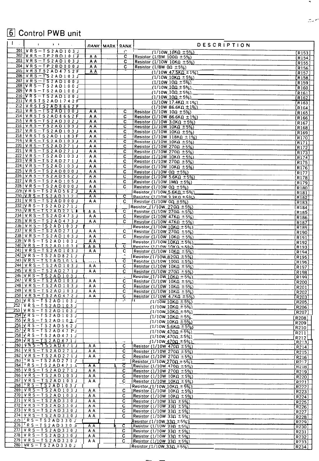
[61
Control
PWB
unit
FO-3700A
-.
~.
NO.
1
PARTS CODE
1
PRICE
nlh,w
1
.alnw
NEW
1
PARTn..,w
1
VRS-TSZAD103J
/
AA
j
I
C
[Resistor
(l/lOW
l(
VRS-TP3Rnltll
I
1
AA
1
I
2AD4752F
C
S2AD103J
AA Reslstor
(l/lOW
47.5KD
‘1%)
C
S2ADlOOJ
AA Resistor
(l/lOW
IOKD
*50/d
C
VRS-TS2ADlOOJ
AA Resistor
(l/lOW
1On
25%)
C
VRS-TS2ADlOOJ
AA Resistor
(l/lOW
1On
*5x)
C
VRS-TS2ADlOOJ
AA Resistor
(l/lOW
1On
25%)
C
VRSTS2AD1742F
AA Resistor
(l/low
IOn
25%)
C
Resistor
(l/lOW
17.4Kn
rtl?”
2AD8662F
AA
C
Resistor
(l/10Wm86.6Kn
VRS-TS2AD562J
VRS-TSZAD332.1
C
I
IResistor
(l/lOW
5.6Kn
+5x)
IRncictnr
IlllmN
77un
+r;o/\
VRS-TS2AD271J
1
AA
(
C IResIstor
(l/lOW
27
VRS-TS7Ai3771
I
t
AA
i
I
S2AD103J
I
AA
I
I
C
IReststor
(l/LOW
1OKn
55%)
VRS-TSZAD103J
C
VRS-TS2AOlO3I
i
AA
i
I
IResIstor
(l/lOti
1OKn
‘5%)
Il?c.cictnr
Il/lnw
1nun
+!Go,!,
VRS-TS2AD821J
1
AA
1
C
IResistor
(l/lOW
82
VRS-TS3Anlnl
I
i
AA
1
I
VRS-TSZADlO3J
I
AA)
C
IResistor
(l[lOW
1OKn
%5x)
VRS-TSZAD103J
AA
C
~~z.,VRS-TSZAD103J
AA Reslstor
(l/lOW
1OKn
25%)
C
253IVRS-TS2AD103J
AA Resistor
(l/lOW
1OKn
25%)
C
VRS-TSZAD103J
AA Resistor
(l/lOW
1OKn
25%)
C
VRS-TS2ADlOAJ
AA Reslstor
(l/lOW
1OKn
25%
C
VRS-TSZAD562J
AA Reslstor
(l/lOW
1OKn
+5Q
C
VRS-TSZAD47pJ
AA Resistor
(l/lOW
5.6Kn
?5%;
C
VRS-TS2AD471J
AA Resistor
(l/lOW
470n
f5%)
C
JRS-TS2AD471J
AA Resistor
(l/low
47OD
25%)
C
,^^
---.-
Resistor
(l/lOW
470n
25%)
[R2081
[R209]
I
EEZ;
[R2121
‘RS-TSZAD271J
I
AA
1
I
C
‘RS-TSZAD471J
I
IResistor
(l/lOW
270n
k5%)
‘RS-TSZAD103J
1
AA
I
C
IResistor
(l/lOW
1OKn
25%)
‘RS-TS2AD330J
I
AA
I
I
c
I
‘RS-TSZAD330J
Resistor
(l/lOW
33n
Z5°/a)
I
RS-TS2AD330J
I
AA
1
C
IResIstor
(l/low
33n
fs%)
-
12
-
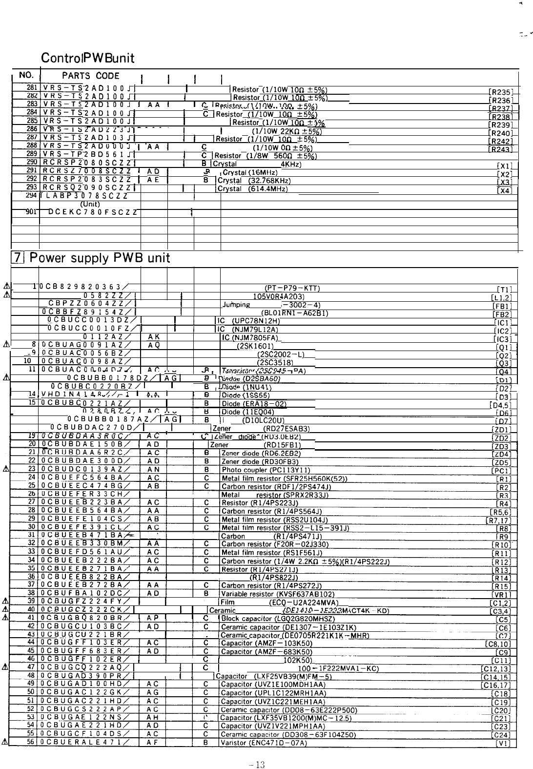
FO-3700A
q
Control
PWB
unit
MA
0Aln-rc.
rrnrrr
I PRICE I NEW I PART I
I
,
I.“.
)
rnnla
b”lJC
/
RANK
1
MARK
1
RANK
1
DESCRIPTION
2ADloo~
I
AA
I
I C IResistor
(l/low
ion
?5%)
;2ADlOOJ
1
AA
(
I C IResistor
(l/low
ion
+5%)
[R235]
i2ADlOOJ
1
AA
I
1
C
lRneic+nr
rl/lnW
,nn
+FOL\
ER2361
2ADlOOJ
1
AA
1
,....“.<..,,
,-,
.“..
*“.*
-d,o,
RS-TS2ADlOOJ
1
AA
1
I
c
IResistor
(I/IOW
ion
25%)
^^
-
^^.----.
I C IResistor
(MOW
ion
*50/e
)
ZAUZZjJ
I
AA
I
I c
1
Resistor
(l/lOW
22Kn
?5yd
[R2391
12AD103J
I
AA
Ii
C IResistor
(l/low
106
+5x)
[R240]
^_-
_^_.
I
.
I
ZAUUUUJ
I
AA
1
I
2BD561J
1
AA
1
I Resistor
(l/low
On
k5%)
I E IResistor (1/8W-
56OD
+5%)
CR2451
4KHz)
[X11
OBOSCZZ
1
AF
)
I
B
ICrystal
(24.000.1
nnRSc77
1
An
1
I
Ia
I
Pmrr+-l
II
CLILI-\
I
0s;scz;
1
Ii;
1
I
,“l,alcIl
\l”I.IIIL,
I ;\
ICrystal
(32.768KHz)
P.21
09OSCZZ
1
AD
1
I
C
ICrystal
(614.4MHz)
294
rLABP3078SCZZ
AA
1
D Shading label (for EP-ROM)
(Umt)
I
901
DCEKC780FSCZZ
CA N
1
E Control PWB unit
I
171
Power
supply
PWB
unit
NO.
PARTS CODE
PRICE NEW PART
RANK MARK RANK DESCRIPTION
2.
1
OCB829820363/
BC
B
2 OCBUKZ Transformer
(PT-P79-KTT)
t-T11
0582ZZ/
1
AH
1
C
Filter (FU
105VORl
3 0
CBPZZO604ZZ/
1
AC
1
tA203)
[L1,21
C
Juinping wire (IPS
^----
4
OCijBFZ
89154Z/
1
AC
I
~-3002-4)
C
Ferrite core
(BLOlRNl-A62 !Bl)
5
OCBUCCO013DZ/
I
AM
1
1
B
IIC
(UPC78N12H)
;z;
6
OCBUCCOOlOFZ,’
1
AC
1
1
B
IIC
(NJM79L12A)
[Cl1
7 OCBUCB
[IC21
_
&
n
n-m.*.-
cc31
m
6lVLi3”Ab
9~i-lCRIIAC
0112AZ/
009lAZ/
0056BZ/
AD
0098AZ/
AG
OflllAl-l7/
AC
B
IC
(NJM7805FA)
B
FET
(2SK1601)
B
Transistor
(2SC2002-L)
B
Transistor (2SC3518)
R
T.Lancic+nr
,?4POAC--D&X
[Qll
1
rP.c.7
,
--..-
.
16
ocBUAC
LVLJ
11
OCBUAC-
_
_
.-_,
,
m
I
12
OCBUBB0178DZ,’
1
AG
1
,
-
I
II”.I.,I.a,“I
,L’“J-.d
I
“,
m
In:,.&.
,~ICDACT\\
r-.7
13
OCBUBCOZZOBZ/
I
An
I
I
I
lAIVHDlNAlAR//-1
I
AA
1
-
,-.-“.,
,A..v-.,
I
FI
I
L”LJ
ninrln
II
cccc, r--.7
,
-
-
.
-
.
-,
,
.
ii
ocsuec
,.
I>
0221AZ/
1
AC
1
_
16 OCBUBC
______I
,
n7RnR7/
1
AC
1
I
17
OCBUBB0187AZ/
1
A:
1
18
OCBUBDAC2700/
1
AC
1
Diode
(DlOLC20U)
rn
“rro,,nr.rrlnnnJ
I
.-
I
I B
1Zener
diode (RD27ESAB3)
I
-
,-
._^^
-----
~ZDll
LU3J
[D4,51
I
L,,“bP”O”AAJK”L,
1
I
CBUBDAEl5OB/
1
::
1
I
G
ILener
aboae
(iiuj.uttu)
1
B IZener diode
(RD15FBl)
12021 I
CRlIRi2AAfiR7f?/
I
AC
l
I
R
[ZD3]
1
-~
_
ER33CH/
I
AC
1
I
C
IMetal
film reslstor
B471BAkI
AC
I
C
ICarbon resistor
(R1/4PS47jJ)
B822BA/
I
AA
1
I
C
I Resistor
(R
1/4PSl
Z224FY/
)
AG
I
I
C
Z222CK/
1
AF
1
IFilm capacitor
(ECQ-U2A224MVA)
;il-,:inR7”RR/
I
C ICeramic capacitor
/nFldln--IC3qvuI
1
AD
1
I
P
I
UZZlBR/
I AC
I
C
ICeramic capacitor
(DE0705R221KlK-
FlOPER/
I
AC
1
I
1
Capacitor (AMZF- 102K50)
Q222AQ,’
1
AE
(
I
E
D390PR,’
1
AE
I
]
Ceramic capacitor (DE7 100
-
1
C lCapac!tor (LXF25VB39(M)FL
E122NS/
C
ICapacitor (LXF35VB1200(M:
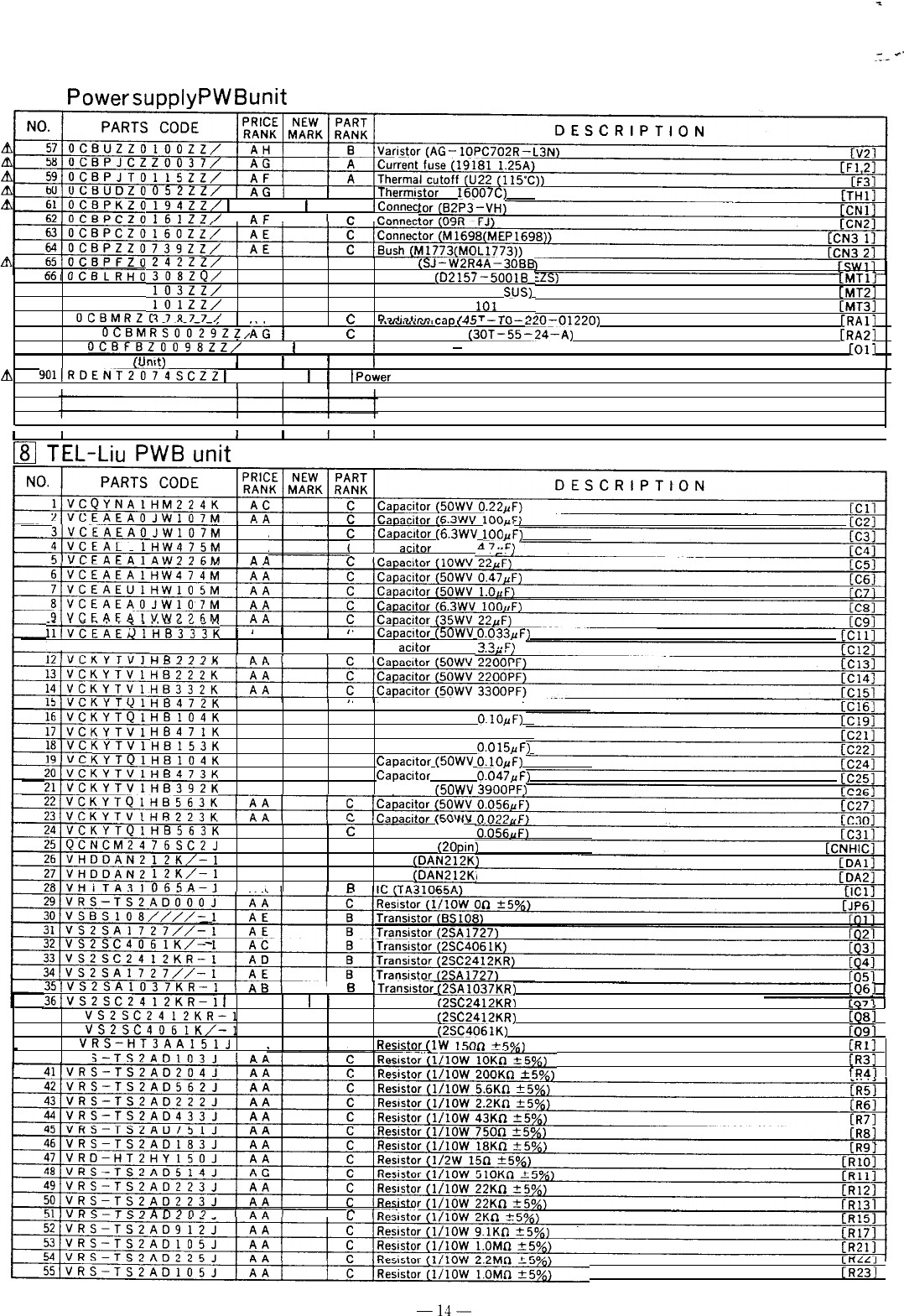
FO-3700A
IeC’
q
Power
supply
PWB
unit
‘05222/
B
119422,’
1
AC
11
Thermrstor (M 16007C)
I c lConnec
Ilfi177/
I
‘IE
I
I
LZS)
67 OCBLRSO
CMTll
68 OCBLRSO
CMT.21
69
OCBMRZO-.
___,
[MT31
I I
70
OCBMRSOO29ZZ/
ih
1
I
E
, ..““I”L1U.I
cap
\-?a
I
I”
1
LLO-01220)
ERA11
242ZZ/
AL
B
Switch
(SJ-W2R4A-3088
308ZQ,’
AM
C
Heat sink
(D2157-50018
I
103ZZ/
AC
C
Supporter (SUP- 103
SUS)
lOlZZ/
AC
C
Supporter (SUP- 101 SUS)
17R77/
AF
I-
Dm4~t;nn
-3,.
IAET-7-n-9,
71
OCBFBZOO98ZZ/
AC
1
I c Radiation sheet
(30T-55-24-A)
I
Terminal (TM
-
12)
CRA21
II
In,+,
I I I
[Oil
\.-.‘..,
I
I
9011RDENT2074SCZZ
1
BN
1
I
1
A
III
1
E IPower supply PWB unit
II
I
I
I
I
I
I
181
TEL-Liu
PWB
unit
I
?t”CFAF“nJW107M
AA
~~
-HW475M
AA
FAFAlAW77KM
AA
“.d..
.
A”“JA,
,
ICapacitor (6.3WV 100pF)
c
1
p
Ca
acitor 50WV d
7..n
P
I
;;iVCEAEAlHW335M
,.HB333K
1
AA AA
1
C
ICapacrtor
(5OWV
1
0.033uF)
1
I c
1
p
Ca
a&or
50WV
2
q,,F\
HR777K
I
HB472K
AA
C
Capacitor (50WV 4700PF)
HB104K
AB
C
Capacitor (5OWV O.lOAF)
HB471K
AA
C
Capacitor (50WV 47OPF)
(YTVlHB153K
AA
C
(YTDlHB104K
AB Capacitor (50WV
0.015pF)
C
Capacrtor
(SOWV
O.lOuF)
HB473K
AA
+:K;T;iHB392K
AA
C
Capacttor (50WV
0.047pF)
C
Capacitor
(5OWV 39OOPF)
\--..
.
HB563K
AA
c
Capacitor (50WV
76SC2J
AK
C
Connector
(20pin)
12K/-1
AC
B
12K,‘-1
AC Diode
(DAN212K:
B
065A-1
AK Diode (DAN212K;
R
slvs2SA1037KR-1
I
B
361VS2SC2412KR-1
1
AD
I
ITranststnr
(2SA1037KR)
1
B
I
LQ61
Transistor 12SC2412KRI
37
VS2SC2412KR-1
AD
38
VS2SC4061K,‘-1
AC
_
39
VRS-HT3AA151J
AA
40 VR!
B
Transistor (2SC2412KR)
B
Transistor
(2SC4061K)
#
Q
C
Resistor
(1W
rn.
7
LI(1J
[R3]
fRA1
Al-l7,,7
I I
P
LMLLJ
CR231
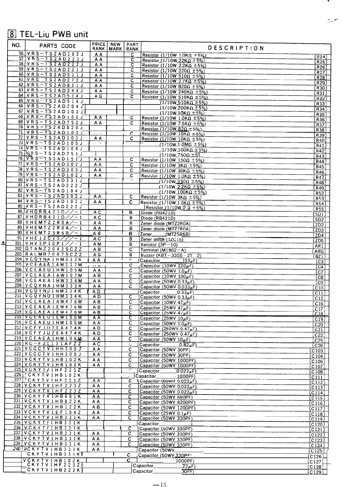
FO-3700A
-:-
[sl TEL-Liu
PWB
unit
SZAUZ23J
IResistor
(l/lOW
22Kn
?5%)
SZAO514J
1
AG
1
C
SZAO204J
1
AA
1
C
Resistor
(l/lOW
510Kn
25%
S2AO103J
1
AA
1
C
Resistor
(l/lOW
200Kn
+5k
Cn.-.^^.
I
.
.
I
Resistor
(l/lOW
1OKn
25%)
S2AO820J
1
AA
1
C
S2AO1031
1
AA
t
I
r?
IResistor
(l/low
82n
25%)
I
+cn/\
VRS-TS2AOlOSJ
1
AA
C
VRS-TSZAOlO4J
1
AA Resistor
(l/lOW
1.C
C
VRS-TSZAO751J
1
AA C Resistor
l/lOW
lO~n&r
~37~
&
\,,,C
-.....-.-.
I
.-
2
Resistor
(l/lOW
750R
t50
VRS-TS2AO331J
1
AA
C
VRS-TS2AO222J
1
AA Resistor
(l/lOW
33
C
S2AO104J
1
AA Resistor
(l/lOW
C
,.”
.^^^
^.
Resistor
(l/lOW
1OOKn
-t5%
SZAOlOZJ
1
AA
1
C
VRS-TS2AO222J
/
AA
1
IResistor
(l/lOW
1.6Kn
25%)
I C IResistor
(l/lOW
2.2
‘dHORB421D//-1
I
R
I
,
At],
I
B
IZener diode
(MTZ5R
I
..--.-
HlliM35jK
(
AA
1
I
C
ICapacitor
(5OWV OS
AlAW777M
I AR I
I
UlHM334K
1
AD
1
I
C
ICapacitor
(50WV
0.33uF)
1131AFZZ
C
ICapacitgy (250WV
0.82#F)
IlHF223Z
1
AA
1
C
‘CKYTVlHElOZK
1
AA
1
I
ICapacitor
(5OWV
O.O22#F)
C
ICapacitor
(5OWV
10
‘CKYTVlHF7777
I
,cnw\,
llHB331K
1
AA
I
I
C
ICapacitor
(5OWV 330PF)
llHB331K
i
AA
1
I
CKYTVlHB331K
I
C
CKYTVlHB331K
1
AA
i
I
r
ICapacitor(5OWV
330PF)
I
r?lnm-it””
Ic.nLu\I
22,nocr
-.-
.
241
V
242
VCKYTVlHBlOZK
1
,“Yy”‘.L”,
AA
1
I
c
1
\d”...
cI4”I I,
[Cl261
Capacitor
243
(50WV
V
CKYTVlHF223Z
)
AA
1
IOOOPF)
244 v
CKYTVlHB222K
1
AA
1
I C ICapacitor (50WV 0.0
[Cl271
I C ICapacitor (50WV 221
22aF)
[Cl281
3OPF)
[Cl291
-
15
Z-
-’
FO-3700A
181
TEL-Liu
PWB
unit
, I.“. ,
rnn13
cI”UC
lHB273K
hln
DAOTF
onnr
I
PRICE
1
NEW
I
PART
1
ARK DESCRIPTION
I
-
RAti
r?
0.027uF)
3900PF)
0.022jzF)
0.022pF)
4700PF)
cc1301
cc1311
CC1321
cc1331
[Cl341
E3
cc1371
[CNHJI
Kfl?uD;
TCNPIl
CKYTVltiF223Z
1
AA
1
^,,__
-...
.-..
~-
I
1
C
ICapacitor
lHFZ23Z
1
AA
1
-
1
c
CKYTVlHF223Z
AA
1
C
CKYTVlHF223Z
AA
1
Capacitor
(5OWV
0.022rF)
C
lHf3821K
AA
1
Capacitor (50WV
0.022pF)
C
Capacitor (50WV 820PF)
.
..^
.-^..
I
*.4
I
,
-..y”-..“.
029SCO0
A0
c
Connector
,vpssa,
014SCOB
AD 0Connector (2pin)
436SC5J
AB
C
Connector (50pin)
014SCOH
AB
C
Connector (8pin)
OSFAF02
AB
258ldCNCM886JAFZZ
A0
C
Connector
(B6B-PH-K-R)
C
LL...
II
I,
Connector (9pin)
4OlSCOB
AA rCNPWi
B
Connector (2pin)
fl47sCFn
AC I- I
aL///-I
I
Atl
I I B
IOiode(lS
HUUSS131//-1
1
AA
[
I
B
IDiode
(DSSl31)
.--40530-i
AF
IC (NJU40530)
“‘Mr14119,‘-1
AF
B
IC
(MC34’
‘_’
AF
HiTHi::>>;:!
AN
B
IC
(MC34L,,,
B
HI
THS56///-1
IC
(THS56)
AN
R
RS-TS2AOOOOJ AA cResistor
(l/low
On
RS-TS2AOOOOJ
AA
C
Resistor
(l/lOW
On
2AOOOOJ AA
C
2AOOOO.l
AA Resistor (l/lOW On
?5y&
nn
RS-TS
RS-TS
RS-TS
RS-TS
--.
.
208
v
I
289
VRS-T;
fm
290 RFiLN2
K:;:;
h-11
m
291
VRO-RCZEYOOOJ
I
AA
I
I c
292
RFiLNZOllSCZZ
I
AC
I
I c Resistor
(1/4W
on
k5%)
EL21
293 VRO-RC2EYOOOJ
1
AA
11
c Coil
(SET-0260)
LL31
394
v
r
-
Resistor
(1/4W
On
25%)
t-L41
r,
07
-_
74r.
I
”
’
?D-RCZEYOOOJ
1
AA
1
RO-RC2EYOOOl
1
AA
/
I C IResistor
(lf4W
on
~5%)
I
c
I
Ff,a<,ctnr
II
IAW
ml
+c,w\
-2”
/
1
296 VRO-RC2EYOOOJ
1
AA
1
,
..v.,.<.-*
\‘I-..
V.,
-.,,o,
LLIU,
297
v
RO-RCZEYOOOJ
AA I
c
1
Resistor
(1/4wmmon
~5%)
C
Resistor
(1/4W
on
EL111
298 v
*50/o)
RD-RC2EYOOOJ
AA
CL121
299
VRD-RC
C
Resistor
(1/4W
On
--.,,,,
-cccl/\
2EYOUBJ
AA [L131
C
300 VRO-RC Resistor
(1/4W
On
f5%)
2EYOOaJ
AA
EL141
C
Resistor
(1/4W
On
+Co”
301
VRO-RC--.
v-w.,
, __ ,
/OJ
7Fvnnn
I
bh
k151
P
Dnrir+nr
,1
I”LA1
nA
302
RFiLN2
, u
,I>.zJIDLYI
(Army,.
“,I
+50/o
h-161
303
RFILN?
7rlLl
”
5:::3
r,
,317
At
--.
.
7°F.
I
\I
OllSCZZ
AC
..-OllSCZZ
AC
RO-RC2EYOOOJ AA
HPPC847///-I
AM
C
Coil (SBT-0260)
C
Coil (SET-0260)
C
Resistor
(1/4W
On
25%)
R
Phn,.-.
Pnllnh~
IDPP”-/\
I
x,
I”_1
.
306
;HPPC8
17’C’O;-i
1
AC
1
1
i
,a
l,VI”
UY”&,‘C’
\
II
“U-v,,
Li-Lli
m
307
VHPPC817CO/-1
1
AC
1
Photo coupler (PC817CO)
A.
308
v
-
-
-
-
-
-
I
B
/Photo
coupler
(~~817~0)
EE;
‘Y!
HPt’C817D//-1
AD
1
B
309[VSBS108///,‘-1
AE Photo coupler
(PC8170)
B
310fVSZSC2412KR-1
AD Transistor (BS108)
B
Transistor
(2SC241;,,,,,
3AA222J
AA
C
Resistor
(1W
2.2Kn
25%)
3AA103J
AA
C
Resistor (1W
1OKn
?55”0)
30A750J
AL
C
Resistor
(2W
750
25%)
RO-HTZHY15OJ
AA
C
Reslstor
(1/2W
15n
_^
..--
LVI,
>YD\
[QlOll
[R21
IR41
TDEI
ZAD221J
AA
C
RS-TS2AD221J
AA Reslstor
(l/low
220n
+5x)
C
Resistor
(l/lOW
221
RS-TS2AOOOOJ AA
C
RS-TS2AD104J
AA Resistor
(l/lOW
On
LJrO’oI
C
RS-TS2ADOOOJ
AA Resistor
(l/lOW
1OOKn
25%)
C
Reslstor
(l/lOW
On
25%)
Lnxvz,
[RllO]
-16-
FO-3700A
-.-
C.
VRS-TSZAD203J
VRS-TS2ADOOOl
IC
IResistor
(l/IO
I
VRS-TS2AD333J
1
AA
1
1
VRS-TS2AD677
I
I
AA
l
C IResistor
(l/10
I
P
I
“iTa--ISLH”L”JJ
I
C
IResistor
(l/low
20Kn 3
VRS-TS7AD7??I
i
AA
l
I
P
I
D...c.i.-ln.
II
,,n\*t
Vnb-ISZAD103J
I
C
IResistor
(l/low
lOKn
~5%)
VKS-ISi!ALlBZZJ
1
AA
1
C
/Resistor
(l/lOW
8.2KR
~5%)
.
I
AA
I
[sl TEL-Liu
PWB
unit
hln
PARTS CODE
PRICE NEW PART
RANK MARK RANK
DE?--
-
‘CKYTQIEF1042
AA
C
‘CKYTQlHB222K
AA Capacitor (25WV
O.lrF)
C
Capacitor (5OWv22OOPF)
I.“.
SGRIPTION
1
‘J
Z
Zt-11~~0066~00,
I
AR
I
EC11
1
[C21
0
1
4
IC
(KS0066FOO)
VRS-TP2BD562J
1
[ICI1
AA
1
I c
1
5 V~
‘RS-TP2BD562J
I
AA
1
I
Resistor (1/8W
5.6Kn
t50/&
[Rll
6V
‘RS-TP2BD562J
1
AA
1
I
:
Resistor (1/8W
5.6Kn
&5%)
CR21
7
V
‘RS-TP2BD562J
1
AA
1
I
c Reststor (1/8W
5.6Kn
*+5x)
fR31
ResIstor (1/8W
5.6Kn
*5%)
[R41
-1i
-
FO-3700A
-‘.-
..*
191
Panel
PWB
unit
NO.
PARTS CODE
PRICE NEW PART
RANK MARK RANK DESCRIPTION
8
VRS-TP2BDOOOJ
AA
1
C
Resistor
(1/8W
On
25%)
9
VRS-TPL
CR51
BD104J
1
AA
I
10
1
1
I
C IReslstor
(1/8W
loohn
k.59
VRS-TP2BDlOlJ
AA
I
/o)
c
I
Resister
(1/8W
1000
25%)
11
LANGHZ
7
k3
12
PGUMM2
1
13
VVLLF71
I
51
VH
1
EG43)
52
[AM]
V
H
EG43)
CAUTOI
n
1
..c\
n
JO
VS
I.__.
_c_,
.
,
r,-
I
,
Y
71
VR
D-RC2EY221J
AA
C
Resistor
(1/4W
220n
25%)
72 VR
D-RC2EY221J
AA
C
73 VR
D-RC2EY221J
AA Resistor
(1/4W
22On
+-50/e\
[Rll
I
[R21
C
Resistor
(1/4W
22On +50/d
)
74 VR-
..__
D-RC7EY622J
AA
C
75
VRD-RC2
Resistor
(1/4W
6.2Kn
25%
3
EZ3
EYlO2J
AA
CCR51
76
QSW-K2194SCZZ
AB
Resist=
(1/4W
l.OKn
25%
I)
B
Tact switch (SOR
-
123HS)
CSWI
LCD PWB unit
(Nal-13)
Panel PWB unit
(Na51--76)
II
I-.&I
I
(“llll,
I
I
9011DCEKP335ASCOl
1
BD
II
I
I
1
E IPanel PWB unit
1
I I
I
I
I
I
I I
I
I I I
q
Sensor
PWB
unit
t
I
-
I I I
I
I
I I
I
I
,
1
I
I I
I
1111
CCD
PWB
unit
NO.
PARTS CODE
PRICE NEW PART
RANK MARK RANK DESCRIPTION
901
DCEKD333ASCOl
BE
E
CCD
PWB
unit
II
I I I
I
-
I
1501
Hardware parts
NO.
PARTS CODE
PRICE NEW PART
RANK MARK RANK DESCRIPTION
Bl
LX-BZ2178SCZZ
AB
C
Screw
-
18-
FO-3700A
•I
Hardware
parts
I
-19-
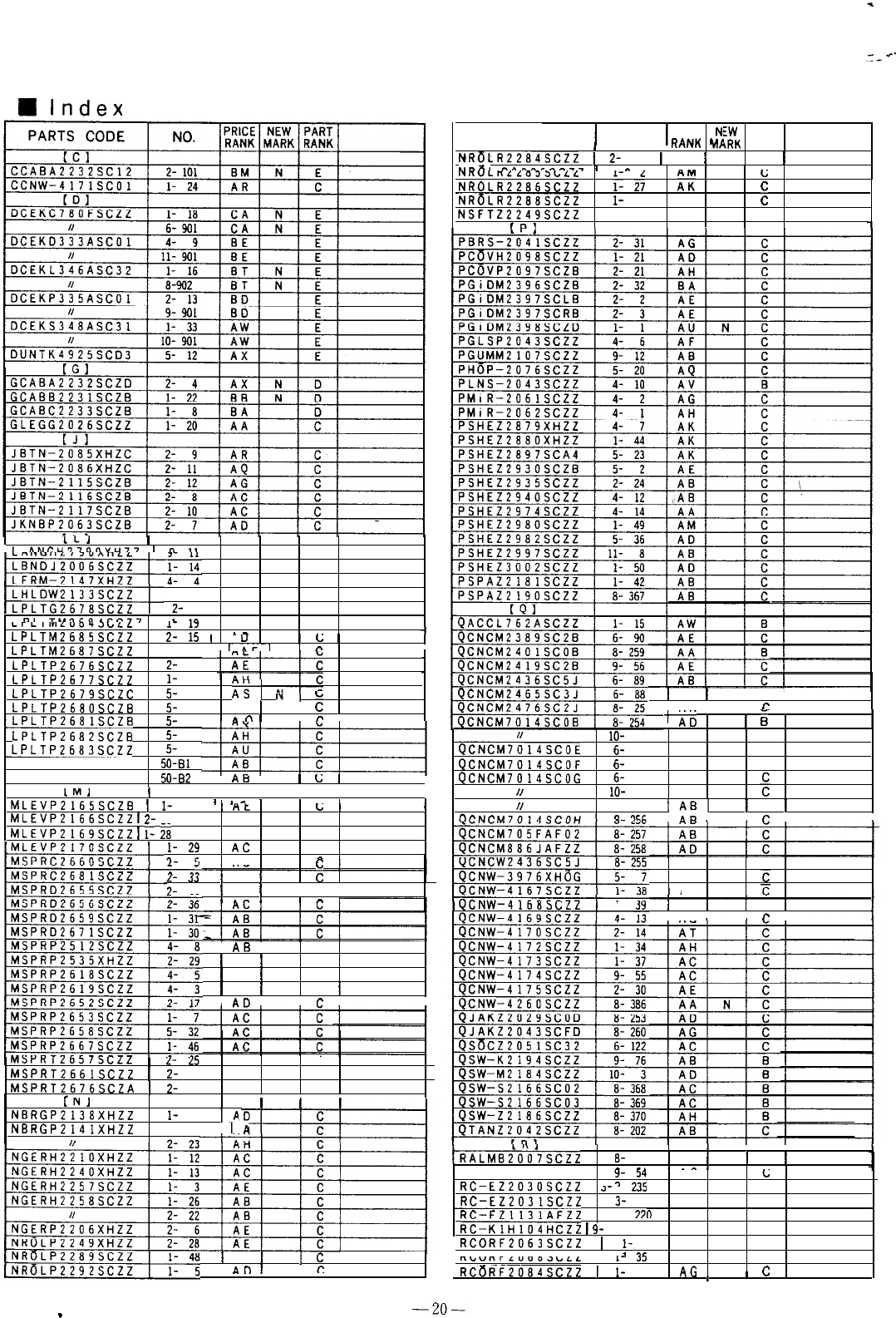
FO-3700A
I
Index
PARTS CODE
1
NO.
1
PRICE NI
EW
PART
I
,
,>r.,,,.
, .
..ARK
D*NY
Ud RANK
NRdLR2284SCZZ
1
2-
27
1
AK
1
.,nx,
n*nnrrn-,7
I
.
I
I . . . , c
1
Rn”Lll‘Lo3~LL‘
L
NROLR2286SCZZ r:
2;
iit
NRoLR2288SCZZ
I-
47 AH
:
NSFTZ2249SCZZ
1-4 AS C
,O,
LLJ
I
I
d~tcu97o”“u77
I
n
,,
AD
C
AA C
AY
i-23 AC
C
C
,
2-
18 AD
II
0,
TLl?COlEO77
I
1
,n
C
AR C
.^
1
CrLIRIL”O*JL.LL
I-
1,
LPLTM2685SCZZ
2-
15
I
A
U
I
I
I;
I
LPLTM2687SCZZ
l-10
‘Ar’
I ,. I
I
LPLTP2676SCZZ
2-
20
LPLTP2677SCZZ
l-
11
LPLTP2679SCZC
5-
17
ii,
I”,
i
I
LPLTP2680SCZB
S- 31 AN
1
I
1
.LPLTP2681SCZE
5-
18
L
n
’
I r. I
LPLTP2682SCZB
s-
29
-LPLTP2683SCZZ
5-
19
LX-BZ2178SCZZ
50-Bl
LX-BZ2182SCZZ
50-82
,
AtJ
,I
L
I
, . . . I
1
AF
1
I c I
I AU I I
r
I
[a
,
“0
1
ii
I
I
QCNCM7:14SCOE
lo- 1 AD
B
6-
91
A B
C
QCNCM7014SCOF
6-
92
A B
C
QCNCM7014SCOG
6-
87
AB
II
lo- 2 AB
LMJ
II I
II
MLEVP2165SCZB
1
l-
32
’
*-
’
,
At
, ,
I,
,
I
MLEVP2166SCZZ
1
Z- 26 I
AM
MLEVP2169SCZZ
1
i-
28
AC
C
C
1-
2q
AC
C
AR
(1
I,
Iii- 3
IABI
I
c
I
I
n
*rr
,
*$J
, I
r
I I
AB C
AT
AH
L-
.I.I
1
AC
/I
I
2-
35
1
AC
1
I
:
I
8
.n
8
I
?.
I
VLNW--4lbUhLLL
I- JY
1
AG
1
I c I
I AC I I
r
I
I
I
AB
I C
1
AD
1
C
[
AD
1
C
1
AD
1
I c
1
I
An
I I
r
I I
,
AB
C
MSPRT2661SCZZ
1
2-
16
AB
C
MSPRT2676SCZA
1
2-
19
AB
C
*
. .
LNl
II
I
I
NBRGP2138XHZZ
l-
6
]A
NBRGP214IXHZZ
l-25
IA
I,
L
I\
1
‘RALMB2007SCZZ
I
1
I
I
8-
203
1
A G
1 1
B
1
RC-EZ2017SCZZ
-
-’
Y-
34
’
.-
AL
’
c;
RC-EZ203OSCZZ
J-
LJJ
7
I,C
AE C
-RC-EZ2031SCZZ
3-
238
AE C
RC-FZ1131AFZZ
R-
77l-l
AC
R&KlH104HCZt
1
9-
53 AC C
C
RCORF2063SCZZ
1
I-
41 AE C
q r-nac,ncor,-77 I
1
,c
nb”“F‘“OOJLLL
,
I-
53 AG C
RCoRF2084SCZZ
1
l-
40
,
&I?
mu
1I
r
”
,
I
1
AE
I
I
c
I
I
An
I
I
f!
I
.
-2o-
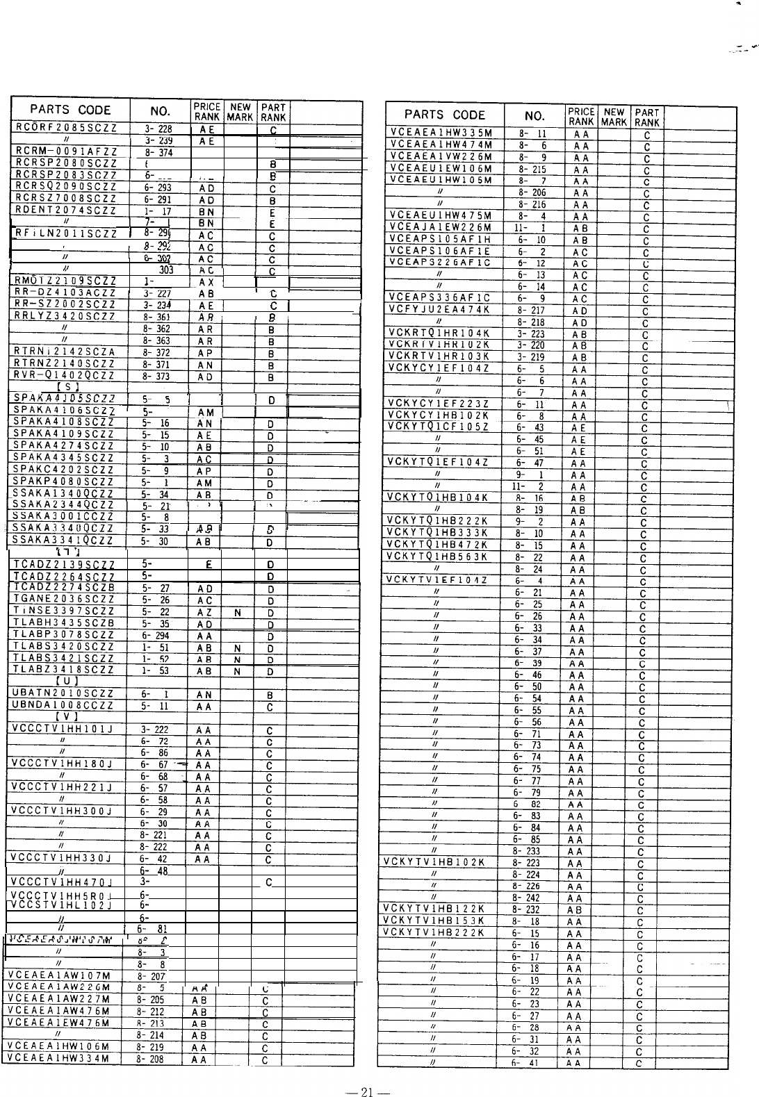
FO-3700A
C
AE
B
6-290 AF
a
6-
292 AF R
1
7-
90:
RFtLNZklSCZZ
1
8-29(
If
I
R-
XI!
t
”
.I”‘
u
a-
30;
,I
ssczz
l-
9
Iix”I
,
I
LO
I
1
B
1
I
,.
1
,
AD
,
’
‘4EI
II
I
k
I
I
LR
I I
R
I
:A41
flG$P77
I
(
A,,,
(I
1
D
1
L
I
5-
4
IAM/
1
D
1
5-
21’
1
A B
I
1
D
1
AA
)
1
D
i
1
AR
i
I
n
I
1
’
1
TCADZ2139SCZZ
5-
24 AED
TCADZ2264SCZZ
5-
25
AED
N
6-
48
AA
C
VCCCTVlHH470J
3-
221
A A
,C
.VCCCTVlHHSROJ
6-
24
A A
C
VCCSTVlHLlOZJ
6-
52
A A C
N
6-
53
AA
C
N
/
6-
ai
AA C
,,P~Acrn,Irr,n,..
I
n
^
AA C
AA C
AA C
AB C
.
1
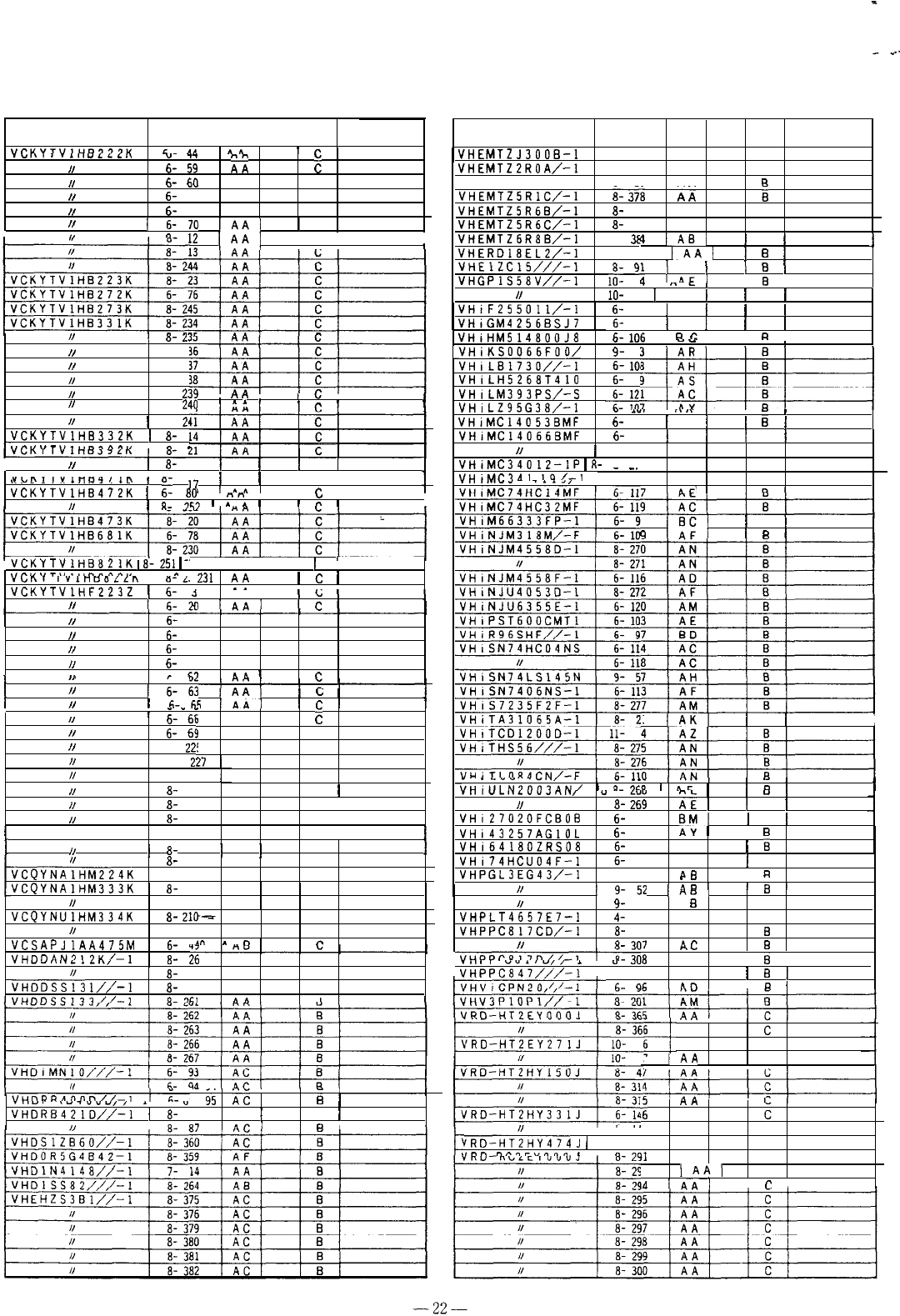
FO-3700A
PARTS CODE
NO.
PRICE NEW PART
RANK MARK RANK
VPY”T”lU~997Y
I
c-
1”
I
AA
I
I
P I
PARTS CODE
NO.
PRICE NEW PART
RANK MARK RANK
VHEMTZJ300B-1
a- 385 AA
B
VHEMTZZROA/-1
a- 88 A A
B
II a- 89 AA
R
.“ISI
I.
AIIULLLI,
u-
?_I
If
6-
59
11
i
I,
6-
60 A A C
I/ 6-
61
AA C
II
6-
64
A A C
VHEMTZSRlC,‘-1
i-
3%
i
i
e
VHEMTZSR6B,‘-1
8-
90 A B
B
VHEMTZ5R6Cbl
8-
377 A A
B
VHEMTZ6RXB,‘-1
a-
38,
4
[ABI
1
B
1
VHERD18ELZ/-1
a-333
IAA]
1
I3
1
I
VHElZClS,‘/,‘-1
R-
a,
1
AC
j
VHGPlS58V//-1
l;;-
JLI
,
”
L
/
1
B
1
d
IACI
I
P
I
,
8.2
,
I,
lo-
5
1
A E
1
[
B
1
VHiF255011,‘-1
I
6-
102
I
A U
I
1
B
1
6-
105
1
AX
1 1
B
1
h-
in6
I
R
c
I I
R
I
VHiGM4256BSJ7
VHiHM514800J8
”
.“”
,
I
-
,
I
I
,VHiKS0066FOO/
9-
VHlLBl730/,‘-1
6-
10’
VHiLH5268T410
6-
9
VHILM393PS,‘-S
VHi
LZ95G38/-1
I
.“.
,
,.,.
I
II
VHiMC14053BMF
6-
115
1
A E
1
1
i
1
VH1h4C14066BMF
6-
111
1
AD
1
1
B
1
I
N
16-70
IAAI
1
c I
I,
I
n
12
IAA]
I c I
.^
I..,
I
II
If
II
1,
If
N
]
a-
L.
a-
2:
a-
2:
a-
2:
a-
2;,
,
m
n
,
,
a-
2~”
1
*
1
1 1
,.
I
I
I,
1
a-
2t
VCKYTVlHB332K
]
8-
,>nl,\,,.,,.IIn*.+nl,
I
”
*
II
1
6-11
VHiMC34012-1P
I
R-
77
“UiMr7.41
lQ/-1
I
2
AD
B
-
-.
4
AF
B
..,......eu
_..A,
. , 8-273 AF
B
AC’
f,
1
8-
246
1
A A
1 1
c
I
I,P.w”Tl,.*lnA,rv
1
0 17
1
AA
1
I
c
I
an
ILAI
I
P
I
I
“LRII”‘“04/1R
1
VCKYTVlHB472K
1
t:
L,
,
nn
, ,
b
,
/I
1
R-
,F+
1
A
*
1
I
,T
I
I
a
IBCI
1
B
9
IAFI
I
R
I
VLKYIVIHUBZIK
1
H-Z51
1
AA
1
I c I
I,~t/“-r~,,IInnn”V
I
0
“jl
AA
I
c
I
.
.
Yl,l\l
IYl”OoLLn
,
O-L.
VCKYTVlHF223Z
(
6-
.j
, AA ,
1
c;
(
N
I6-m
IAAI
I
I,
6-
35
AA
C
I/ 6-
36
AA
C
If 6-
38
AA
C
/I
6-
40
A A
C
,,
r
57
A&
I
I-
1
I,
, a-
1
I,
I6-bJ
IAA[
I
G
1
1,
I
fi-h5
IAAI
I
r!
I
1
I
-
-
-,
.
I
.-
‘i
AA
c
1
AA
C
5
AA
C
’
AA
C
AA
C
I,
I,
I,
II
If
b-
a,
6-
6!
a-
22t
a-
221
I
a- 228
I
a
IAKI
B
I
I
.
.
---
._..,
,
”
..-
I
-
I
vu;tllN7n”?Ahl/
I
*-3co
I
AC
I I
D
I
I
N
8-
229 A
Ac
I
I, 8-
243
A A
c
I
,,
8-
247 A
A
c
I
.III”L#.G”“l)nl.,
”
LY”
If
8-
269
;;
1
,
u
]
1
1
B
1
VHi27020FCBOB
6-
123
BMI
N
I
B
1
VHi43257AGlOL
6-
101
AV
1
I
El
I
VHi64180ZRS08
6-
100
ix
1
i
VHi74HCU04F-1
6-
104
AC
1
B
VHPGL3EG43,‘-1
9-51
AR
I
R
I
If
19-52
I_“,
,
Y
,
I
.
I
d!a
I
I
cl
I
I
II
,,
1
1
8-
8-
248 249
1
1
A A A A
[
1
I
I
c
c
I
I
I
VCQYNAyHM224K
8-
250 A A
C
8-1 AC
C
VCQYNAlHM333K
8-
204 A A
C
I,
a- 209 AA
C
VCQYNUlHM334K
8-
210~
AD
C
N
8-211 AD
C
VCSAPJlAA475M
6-
*n
’
n
n
“UrlrlAN7
IVY
/-1
II-
.“L,ur.l.Lr~a~,
I
“26
AC
B
VHDDSS/13
l/,-l
8-
27 AC
B
8-
265 A A
B
\,“nncc,22,,-,
o-1c1
LI
q
if
9-
67
A
6
B
VHPLT4657E7-1
4-
11
AY
B
VHPPC817CD,‘-1
8-
306
AC
B
If
R-
7n7
AC
R
.
.
v
,111,
vurru,,
I
,
Y
dJ8
AD I
i
I
vidppca47///-i
I a-305 AM
1
E
1
h-
Qh
I
R
I
.I
,.
AA
c
AA
C
I
1AA
C
. .
.llYl
>Y7”““,,
I
,
”
9;
ii
i
1
VHDRB421D,‘/‘-1
1
8-
86
AC
1
B
1
,,
I
!L
!a7
R
I
AA
.i
AA
,
a- 147 AA
IRD-HTiHY474J
(
E-316 AA
C
C
,nn
nn*rvnnn
II
n
“1,
AA
C
13
IAAI
I c I
14
11~1
I
c
I
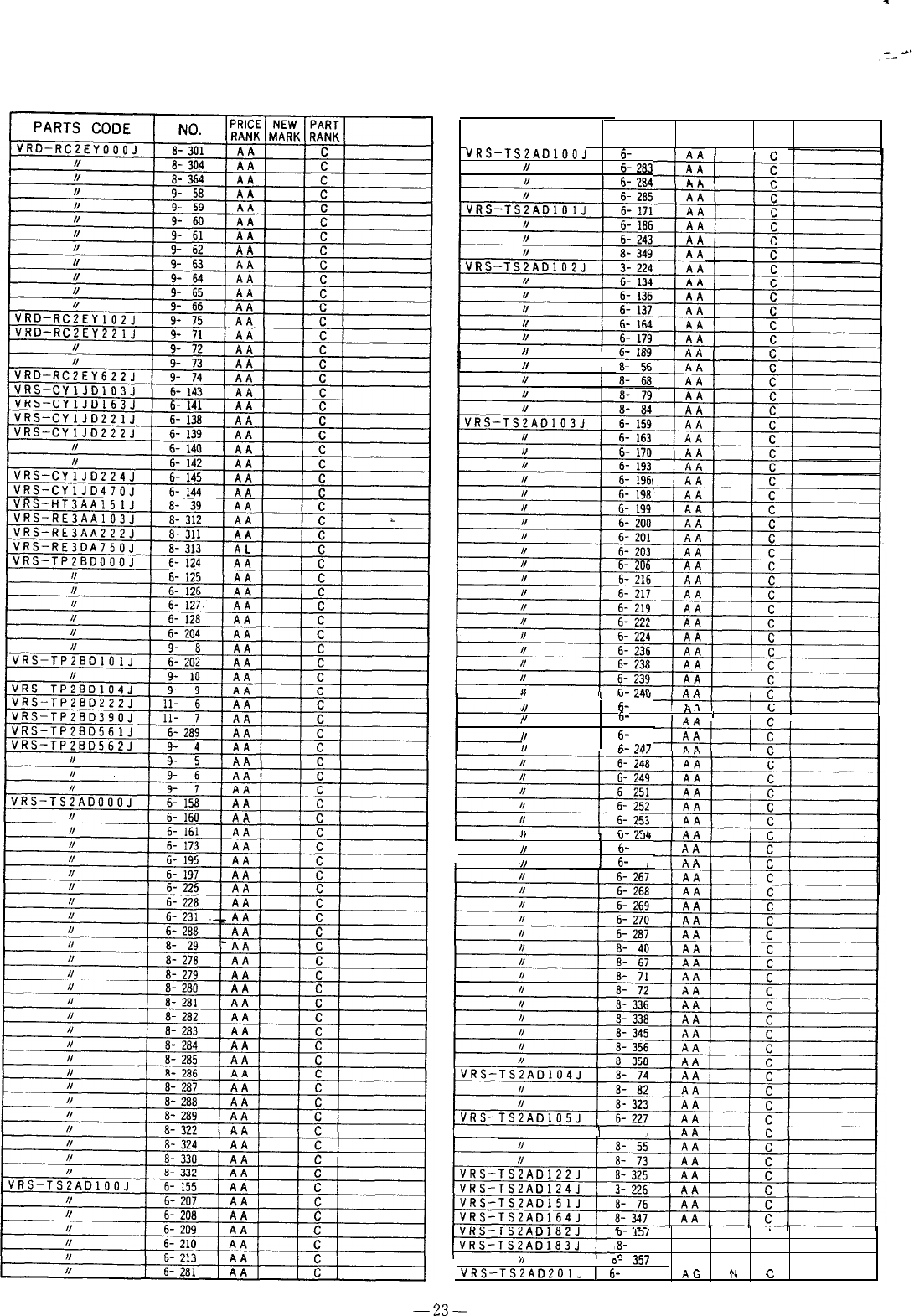
FO-3700A
PARTS CODE
VRS-TSZADlOOJ
I/
NO.
PRICE NEW PART
RANK MARK RANK
6-
282
’
I
n
6-
283
fi-
7Rd
I
N
I
I,
I,
,
u-
“I”
if
6-
241
,
n
A
,
I
L
N
6-
244
’
I
I
If
6-
246
,I
c-
747
I,
,
u-
‘.w
II
1
6-
255
II
1
6-
266
I
II
I
a- 53
o-
13,
AA C
a-
46 A A
C
0
,c_I
AA
C
bf
hl
,-
I,
,
o-
53,
VRS-TSZADZOlJ
1
6-
194 ,
mu
,
8.
, b ,
I
-23-
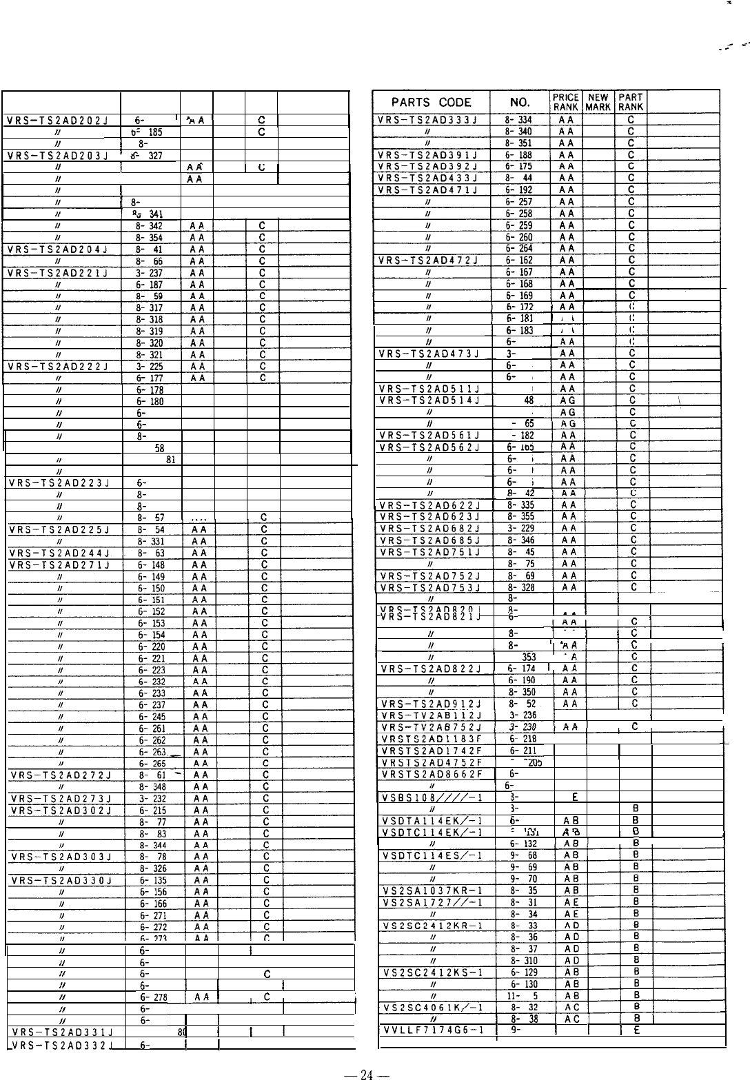
FO-3700A
-
4,
.-
PARTS CODE
NO.
PRICE NEW PART
RANK MARK RANK
VRS-TSZADZOZJ
6-
176
’
*
A
’
AH
I
m
I
II
?
.“-
,
b-
,113
AA
i
N
)
a-
51 AA
C
I
n
mn_l
VRS-TSZADZO~J
,
a-
XI
AA
C
t/
I
a- 329 I.
_
I
1
L
I
I/
I a- 333 I
ii
II c
I
1
a-337 AA I c I
1
a-
339 A A I c I
I
P..
?A,
AA I c I
A/+
C
AA
C
AA
C
C
VRS-TSiAD622J
1
IIII
NN
VRS-TSZAD473JVRS-TSZAD473J
IIII
NN
VRS-TSZAD51lJVRS-TSZAD51lJ
VRS-TSZAD514JVRS-TSZAD514J
NN
I/I/
VRS-TSZADS6
IJ
VRS-TSZADS6
IJ
VRS-TSZAD562JVRS-TSZAD562J
NN
NN
IIII
NN
^
---
6-
183
6-
183
6-
250
6-
250
3-
231
3-
231
6-
234
6-
234
6-
235
6-
235
a- 60a- 60
a-
48
a-
48
a- 64a- 64
aa
rrrr
66
6-
IO,
6-
IO,
6-
226
6-
226
6-
229
6-
229
6-
256
6-
256
RR
.-.-
I/
6-
178
A A C
If 6-
la0 A
A
C
If
6-
la4 A A C
N
6-
191
A A
C
I/ a-
43 A A
C
a-
58
A A
C
N
a-
81
AA
C
N
a- a5 A A
C
VRS-TSZAD223J
6-
286 A A
C
If a-
49’ A A C
N
a-
50 AA C
N
L-
67
AA
N
a-
343
1
A A
1 1
c
I
VRS-TSZADaZOJ
a-
70
1
AA
1 1
c
I
VRS-TS2ADa21J
6-
242
’
-
*
’
I
”
I
//
a-
62
1
A A
1 1
I;
I
I/ a-
352
’
*
’
’
I
,- I I
II
1
a-
353
I A
P
VRS-TSZADa22J
1
A-174
1
Afi
N
1
AA
1
I c
I
I r. I I
1
AA
1
c
1
AA
1 1
c
I
1
b-
LU3
AA C
1
6-
212 A
AC
’
i-
214 AA
C
i-
30 A
E
El
3- 309
A
E
B
j-
133
Al3
B
L
33,
A
D
Ia
I
VSDTA1:4EK,-1
I
VSDTC114EK/-1
b-
,.I,
,
n
0
,
I
I
I, I ;; I
I
If
6-
274 A A
I
c I
I,
6-
275
AA
I
c
I
N
6-
276 A A I
c
I
,,
6-
277
1
A A
1
I c
I
N
r
e-n
o-
LIO
i
I
r
I
I
I/
6-
279
1
AA
1
1
c
M
6-
280
1
AA
1
I
c
I
VRS-TSZAD331J
a-
a0
1
AA
1
I
c
I
I
VRS-TSZAD332J
6-
230
1
A A
II
c
I
I
,I
1
a-38
IACI
+VLLF7174G6-1
1
9-
13
I
AP
I
1
E
I
1
I
I
I I
-24-
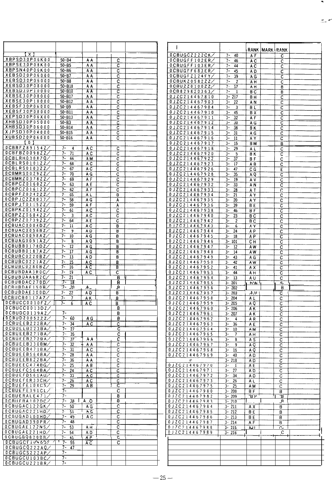
FO-3700A
PARTS CODE
NO.
PRICE NEW PART
RANK MARK RANK
I
PARTS CODE
NO.
PRICE NEW PART
RANK
MARK RANK
1
I
AC
(
I
B
I
7-
ia
1
AC
I
1
B
1
l-
711
I A n I
I
RI
,
“,.I
,
II
1
AG
1
1
ii
1
I
*IA
I
I
OCBUCCOOlOFi;
OCBUCC0013DZ/
7-5 AM
B
OCBUDC0139AZ,’
7-
23 A N
B
7-
cn
A
c
0
I AC
III
1
AA
)
I
c”
1
t
AA
1
I
r
I
I
c
I
7- 30
1
AC
1
I
c
I
7- 56
1
A F
)
7-
1R
1
A
i-l
IJ
B
[
I
R
I ,
tll-
,
I
ti
1
AV
1
I R I
/
I
I‘
43
1
;;
7-48
IAE
/
-
1
AT
/
I
c
I
1
“b”““L,r
I
U‘t”3,
OCBUGCQ222AQ,’
:
OCBUGCS222AP,’
7-
52
OCBUGCU103BC,’
7-
42
OCBUGCU221BR,’
7-
43
IlrOllrPCI
n
Ar,P
/
f
7-
55
2:
7-
47
AE
C
AC
C
AD
C
AC
C
-25-
FO-3700A
-
CAUTION FOR BAlTERY REPLACEMENT
-
(Danish)
ADVARSEL !
Liiiumbatten
-
Eksplosionsfare ved fejlagtig handtering.
Udskiftning
mB
kun ske med batten
af samme fabrikat og type.
\
Lever det brugte batten tilbage til ieverandoren.
(English)
L
Caution !
Danger of explosion if battery is incorrectly replaced.
Replace only with the same or equivalent type
recommended by the equipment manufacturer.
Discard used batteries according to manufacturer’s instructions.
(Finnish)
VAROITUS
Pa&to
voi rajahtaa, jos se on virheellisesti asennettu.
Vaihda paristo ainoastaan laitevalmistajan suosittelemaan
tyyppiin.
H&vi%
kaytetty patisto valmistajan ohjeiden
mukaisesti.
(French)
ATTENTION
II y a danger d’explosion s’
il
y a remplacement incorrect
de la batterfe. Remplacer uniquement avec une batterie du
meme type ou d’un type recommande par le constructeur.
Mettre au rebut les batteries usagees conformement aux
instructions du fabricant.
(Swedish)
VARNING
Explosionsfare vid felaktigt battenbyte.
Anvand samma batterityp eller en ekvivalent
typ som rekommenderas av apparattfllverkaren.
Kassera anvant batten enligt fabrikantens
instruktion.
FO-3700A
SHARP
COPYRIGHT
0
1994 BY SHARP CORPORATION
All rights reserved.
Printed in Japan.
No part of this publication may be reproduced,
stored in a retrieval system, or transmitted,
in any form or by any means,
electronic, mechanical, photocopying, recording, or otherwise,
without prior written permission of the publisher.
SHARP CORPORATION
Communication
&
Audio Systems Group
Quality
&
Reliability Control Center
Higashihiroshima, Hiroshima 739-01, Japan
1994 Printed in Jaoan
[
A9403-378SW&T
1
