FOCC500
User Manual: FOCC500
Open the PDF directly: View PDF ![]() .
.
Page Count: 162 [warning: Documents this large are best viewed by clicking the View PDF Link!]
FO-CC500A
FO-K01A
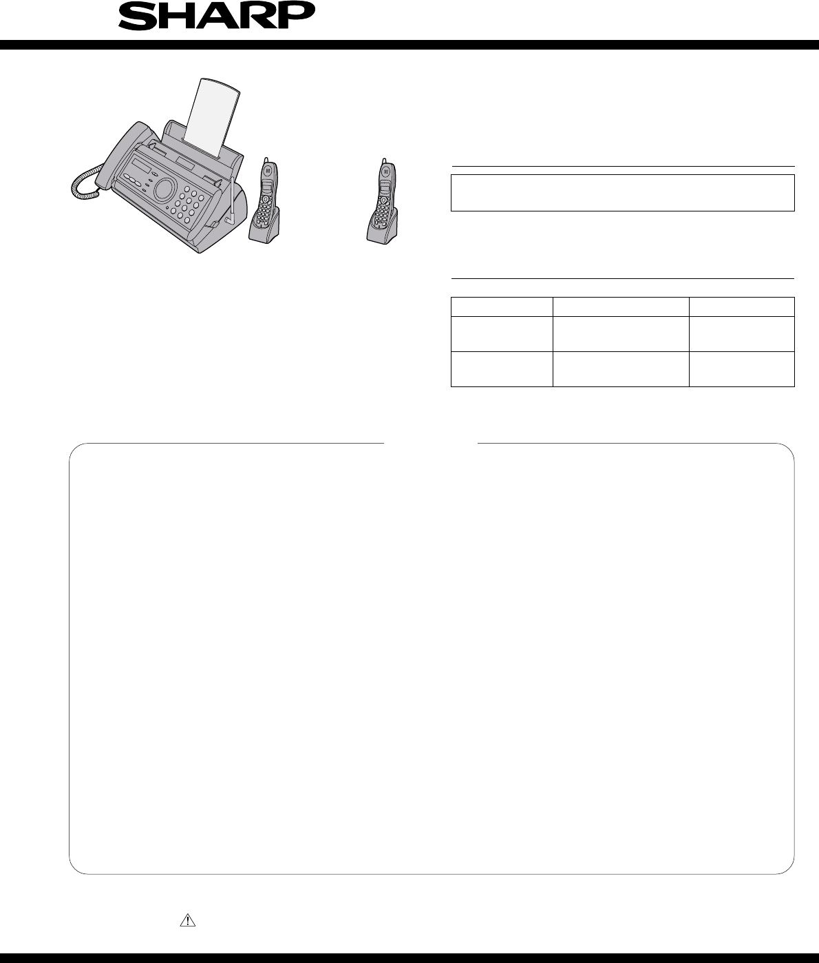
FACSIMILE
FO-CC500
ACCESSORY CORDLESS HANDSET
FO-K01
No. 00ZFCC500ASME
Parts marked with " " are important for maintaining the safety of the set. Be sure to replace these parts with specified ones for
maintaining the safety and performance of the set.
This document has been published to be used
for after sales service only.
The contents are subject to change without notice.
SHARP CORPORATION
SERVICE MANUAL
MODEL
MODEL
Illustration: FO-CC500A
CHAPTER 1. GENERAL DESCRIPTION
[1] Specifications ................................................................ 1-1
[2] Operation panel ............................................................ 1-2
[3] Transmittable documents .............................................. 1-4
[4] Installation ..................................................................... 1-5
[5] Quick reference guide ................................................. 1-10
[6] Option imaging film specifications
(FO-6CR) ............................................................. 1-11
CHAPTER 2. ADJUSTMENTS
[1] Adjustments .................................................................. 2-1
[2] Diagnostics and service soft switch .............................. 2-2
[3] Troubleshooting .......................................................... 2-24
[4] Error code table .......................................................... 2-25
CHAPTER 3. MECHANISM BLOCKS
[1] General description ...................................................... 3-1
[2] Disassembly and assembly
procedures ............................................................. 3-3
CHAPTER 4. DIAGRAMS
[1] Block diagram ............................................................... 4-1
[2] Wiring diagram .............................................................. 4-3
[3] Point-to-point diagram ................................................... 4-4
CHAPTER 5. CIRCUIT DESCRIPTION
[1] Circuit description ......................................................... 5-1
[2] Circuit description of control PWB ................................ 5-2
[3] Circuit description of LIU PWB .................................... 5-10
[4] Circuit description of cordless PWB ............................ 5-13
[5] Circuit description of cordless handset PWB
................
5-22
[6] Circuit description of power supply PWB
.....................
5-24
[7] Circuit description of CIS unit ...................................... 5-25
CHAPTER 6. CIRCUIT SCHEMATICS AND
PARTS LAYOUT
[1] Control PWB circuit ....................................................... 6-1
[2] LIU PWB circuit ............................................................. 6-9
[3] Cordless PWB circuit .................................................. 6-14
[4] Power supply PWB circuit .......................................... 6-19
[5] Operation panel PWB circuit ....................................... 6-21
[6] Cordless handset PWB circuit .................................... 6-23
CHAPTER 7. OPERATION FLOWCHART
[1] Protocol ......................................................................... 7-1
[2] Power on sequence ...................................................... 7-2
CHAPTER 8. OTHERS
[1] Service tools ................................................................. 8-1
[2] IC signal name .............................................................. 8-4
[3] Rewriting version up to the FLASH ROM ..................... 8-6
PARTS GUIDE
CONTENTS
Illustration: FO-K01A
FO-CC500 Facsimile System cosisting of FO-CC500 (Facsimile Unit)
and FO-CC500K (Cordless Handset).
MODEL SELECTION CODE DESTINATION
FO-CC500 A Australia/
New Zealand
FO-K01 A Australia/
New Zealand

FO-CC500A
FO-K01A
(Danish) ADVARSEL !
Lithiumbatteri-Eksplosionsfare ved fejlagtig håndtering.
Udskiftning må kun ske med batteri af samme fabrikat og type.
Levér det brugte batteri tilbage til leverandoren.
(English) Caution !
Danger of explosion if battery is incorrectly replaced.
Replace only with the same or equivalent type
recommended by the equipment manufacturer.
Discard used batteries according to manufacturer’s
instructions.
(Finnish) VAROITUS
Paristo voi räjähtää, jos se on virheellisesti asennettu.
Vaihda paristo ainoastaan laitevalmistajan suosittelemaan
tyyppiin. Hävitä käytetty paristo valmistajan ohjeiden
mukaisesti.
(French) ATTENTION
Il y a danger d’explosion s’ il y a remplacement incorrect
de la batterie. Remplacer uniquement avec une batterie du
même type ou d’un type recommandé par le constructeur.
Mettre au rébut les batteries usagées conformément aux
instructions du fabricant.
(Swedish) VARNING
Explosionsfare vid felaktigt batteribyte.
Använd samma batterityp eller en ekvivalent
typ som rekommenderas av apparattillverkaren.
Kassera använt batteri enligt fabrikantens
instruktion.
(German) Achtung
Explosionsgefahr bei Verwendung inkorrekter Batterien.
Als Ersatzbatterien dürfen nur Batterien vom gleichen Typ oder
vom Hersteller empfohlene Batterien verwendet werden.
Entsorgung der gebrauchten Batterien nur nach den vom
Hersteller angegebenen Anweisungen.
CAUTION FOR BATTERY REPLACEMENT

1 – 1
FO-CC500A
FO-K01A
As a part of our policy of continuous improvement, SHARP reserves the right to make design and specification changes for product
improvement without prior notice. The performance specifications figures indicated are nominal values of production units. There may be some
deviations from these values in individual units.
CHAPTER 1. GENERAL DESCRIPTION
[1] Specifications
Fax machine and general specifications
Automatic dialing: Common book: 40 numbers
Private book: 5 numbers (each
cordless handset has 1 private book)
Imaging film: Initial starter roll: (included with
machine): 10 m (approx. 30 A4 pages)
Replacement roll (not included):
FO-6CR 164 ft. (50 m) (one roll yields
approx. 150 A4 pages)
Memory size* : 448 KB (approx. 24 average pages
with no voice messages recorded, or
20 minutes of voice messages
(including OGMs) with no faxes in
memory)
Modem speed: 14,400 bps with auto fallback to lower
speed
Transmission time* : Approx. 6 seconds
(only when ECM is on)
Resolution: Horizontal:
8 dots/mm
Vertical:
Standard: 3.85 lines/mm
Fine/Halftone: 7.7 lines/mm
Super fine: 15.4 lines/mm
Automatic document feeder: 10 pages max. (A4, 80 g/m2 paper)
Recording system: Thermal transfer recording
Display: 16-digit LCD display
Halftone (grayscale): 64 levels
Compression scheme: MR, MH, MMR
Applicable telephone line: Public switched telephone network
Paper tray capacity: Letter: Approx. 50 A4 sheets
(at room temperature; maximum stack
height should not be higher than the
line on the tray)
Compatibility: ITU-T (CCITT) G3 mode
Input document size: Automatic feeding:
Width: 148 to 216 mm
Length: 140 to 297 mm
Manual feeding:
Width: 148 to 216 mm
Length: 140 to 600 mm
Effective scanning width: 210 mm max.
Effective printing width: 210 mm max.
Contrast control: Automatic/Dark selectable
Reception modes: TEL/FAX, TEL, FAX, A.M.
Copy function: Single/Multi (99 copies/page)
Telephone function: Yes
(cannot be used if power fails)
Power requirements: 230 - 240 V AC, 50 Hz
Operating temperature: 5 - 35°C
Humidity: 25 - 85 % RH
Power consumption: Stand-by: 3.5 W
Maximum: 110 W
Dimensions (without Width: 353 mm
attachments): Depth: 193 mm
Height: 174 mm
Weight (without Approx. 2.8 kg
attachments):
Cordless handset specifications
Frequency: 2.4 GHz (2.405 to 2.475 GHz)
Dimensions: Width: 46 mm
Depth: 42 mm
Height: 180 mm (not including
antenna)
Weight: Approx. 115 g
(without battery)
Battery: 3.6 V Ni-MH battery;
capacity: 850 mAh
Power consumption: Approx. 1.6 W (in stand-by mode)
Initial charging Approx. 10 hours for initial charge
Battery life Approx. 4 hours (240 minutes) (at
room temperature)
Battery life in stand-by Approx. 2 days with one full charge (at
mode room temperature)
Battery life (both normal and in stand-
by mode) may vary depending on
usage, range from base machine, and
environmental conditions such as
temperature.
Accessory cordless FO-K01 (up to 3 handsets can be
handset: added)
* Based on Sharp Standard No. 1 Chart at standard resolution in Sharp
special mode, excluding time for protocol signals (i.e., ITU-T phase
C time only).
1 – 2
FO-CC500A
FO-K01A
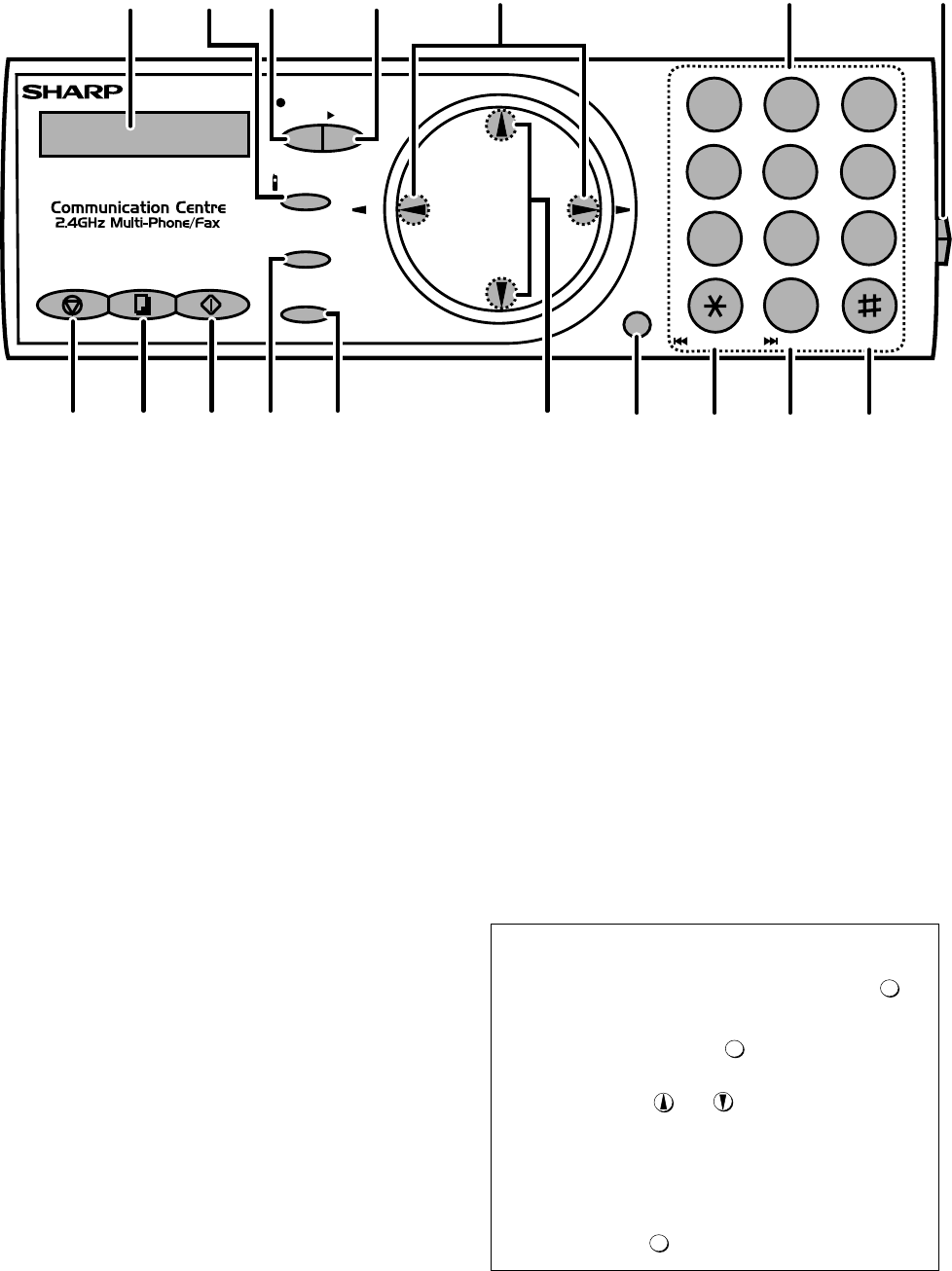
[2] Operation panel
Fax Machine
13
12
11 14
146
23
10
89
1. Display
This displays messages and prompts to help you operate the
machine.
2. INTERCOM key
Press this key to page or locate the cordless handset.
3. REC/MEMO key
Press this key to record an outgoing message, phone
conversation, or memo.
4. PLAY key
Press this key to play recorded messages.
5. Left and right arrow keys
Auto-dial numbers: When sending a fax or making a phone
call, press these keys to scroll through your auto-dial
numbers, the "REVIEW CALLS" list (only available if you
have Caller ID), and the last number dialed (redial).
FUNCTION key settings: Press the right arrow key after
scrolling with the up and down arrow keys to select a
FUNCTION key setting.
6. Number keys
Use these keys to dial numbers, and enter numbers and
letters when storing auto-dial numbers.
7. Panel release
Press this release to open the operation panel.
8. STOP key
Press this key to cancel operations before they are completed.
9. COPY/HELP key
When a document is in the feeder, press this key to make a
copy of a document. At any other time, press this key to print
out the Help List, a quick reference guide to the operation of
your fax machine.
10. START/MEMORY key
Press this key after dialing to begin fax transmission. Press
this key before dialing to send a fax through memory. The
key can also be pressed in the date and time display to show
the percentage of memory currently used.
11. RESOLUTION / RECEPTION MODE key
When a document is in the feeder, press this key to adjust
the resolution for faxing or copying. At any other time, press
this key to select the reception mode (an arrow in the display
will point to the currently selected reception mode).
12. FUNCTION key
Press this key to followed by the arrow keys to select special
functions and settings.
13. UP and DOWN arrow keys
Enlarge/Reduce setting: When marking a copy of a
document, press these keys to select an enlarge/reduce
setting.
Volume setting: When a document is not in the feeder,
press these keys to change the speaker volume when the
SPEAKER key has been pressed, or the ringer volume at
any other time.
FUNCTION key settings: Press these keys after pressing
the FUNCTION key to scroll through the FUNCTION MODE
settings.
14. SPEAKER key
Press this key to listen to the line and fax tones through the
speaker when faxing a document.
Note: This is not a speakerphone. You must pick up the
handset to talk with the other party.
15. REPEAT key
Press this key while listening to a message to play it again.
16. SKIP key
Press this key while listening to a message to skip to the next
message.
17. DELETE key
Press this key to erase recorded messages.
7
15 16 17
5
REC/
MEMO
PLAY
JKL
DELETE
REPEAT
ABC
1
DEF
WXYZ
9
GHI
45
MNO
6
PQRS
TEL
A.M.
FAX
STOP
COPY/HELP
START/MEMORY
RESOLUTION/
RECEPTION MODE
INTERCOM
FUNCTION
REDIAL
Z A
SPEAKER
7
TUV
8
SKIP
0
2 3
D
O
W
N
U
P
TEL/FAX
Monitoring phone conversations
When speaking through the handset, you can press to
allow a third person to listen to the conversation through the
speaker.
(To turn off the speaker, press again.)
To adjust the volume of the speaker when monitoring a
conversation, press or (the volume reverts to the
lowest setting each time the handset is replaced).
Note that the speaker cannot be used for speaking; it is
only for listening.
To avoid feedback (a loud howling sound), be sure to turn off
the speaker (press once again) before you replace the
handset.
SPEAKER
SPEAKER
SPEAKER
1 – 3
FO-CC500A
FO-K01A
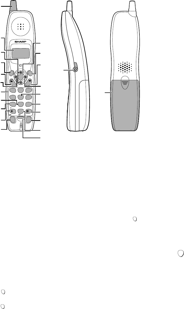
Cordless Handset
1. Antenna
2. Display
This displays messages and prompts to help you use the cordless
handset.
3. UP and DOWN arrow keys
Receiver volume: When talking on the cordless handset, press
these keys to adjust the receiver volume. This also adjusts the
volume when using a headset (purchased separately) connected
to the cordless handset.
Ringer volume: When not talking on the cordless handset, press
these keys to adjust the cordless handset ringer volume.
Scroll through numbers: Press these keys to scroll when
searching for an auto-dial number or reviewing received calls (only
available when you have Caller ID).
4. FUNCTION/PAUSE key
Use this key to store a new auto dial number (press the SEARCH
(right) arrow key, select the book with the UP or DOWN arrow key,
and then press the FUNCTION/PAUSE key). When entering an
auto-dial number, press this key to insert a pause between digits.
5. TALK key
Press this key to make or answer a call.
6. REVIEW (left) arrow key
Press the REVIEW arrow key and then the UP or DOWN arrow
key to scroll through your 30 most recent calls (only available if
you have Caller ID). This key can also be used to move the cursor
left when entering or editing an auto-dial number or name.
7. Number keys
Use these keys to dial numbers, and enter numbers and letters
when storing auto-dial numbers.
8. PLAY NEW key
Press this key after pressing to listen to new messages recorded
in the personal box of the cordless handset.
9. PLAY key
Press this key after pressing to listen to all messages recorded in
the personal box of the cordless handset.
10. REPEAT key
Press this key while listening to a message to play it again.
11. INTERCOM key
Press this key to page the fax machine or another cordless
handset.
12. START key
Press this key to start fax reception from the cordless handset, or
to complete entries when storing, editing, or deleting auto-dial
numbers.
13. REMOTE/RECALL key
Press this key to perform remote operations on the fax machine.
The key is also used to access special services from your
phone company that require subscription (contact your phone
company for details).
14. OFF key
Press this key to end a call.
15. SEARCH (right) arrow key
Use this key to search for an auto dial number (press the
SEARCH key, press the UP or DOWN arrow key to select the
book, and then press the UP or DOWN arrow key to scroll
through your auto-dial numbers). This key can also be used to
move the cursor right when entering or editing an auto-dial
number or name.
16. RECEPTION key
Press this key after pressing to change the reception mode
on the fax machine.
17. STOP key
Press this key to stop playback of messages.
18. DELETE
Press this key while listening to a message to delete it. To
delete all your messages, press this key after playback ends
(while the display shows REMOTE MODE), followed by .
19. HOLD/ERASE key
Hold: Press this key during a call to put the other party on hold.
Erase: Press this key to delete a phone number when
searching through your recently received calls (only when you
have Call ID), or when searching through your auto-dial
numbers. Press the key to delete a digit or character when
storing or editing an auto-dial number.
20. SKIP key
Press this key while listening to your messages to skip to the
next message.
21. REDIAL key
Press this key to redial the last number dialed using the
cordless handset.
22. Headset socket
This socket lets you connect a headset (purchased separately)
to the cordless handset.
23. Battery cover
Remote this cover to install or replace the handset battery.
1
2
3
4
5
6
7
8
9
10
11
12
13
14
15
16
17
18
19
20
21
22
23
START
FUNCTION
/PAUSE
TALK
OFF
REMOTE
/RECALL
START
UP
DOWN
PLAY NEW
PLAY
REPEAT SKIP DELETE
ERASE
STOP
RECEPTION
REVIEW
INTER
COM HOLD
REDIAL
SEARCH
1
ABC DEF
JKLGHI MNO
TUVPQRS WXYZ
23
456
789
0
REMOTE
/RECALL
REMOTE
/RECALL
REMOTE
/RECALL
1 – 4
FO-CC500A
FO-K01A
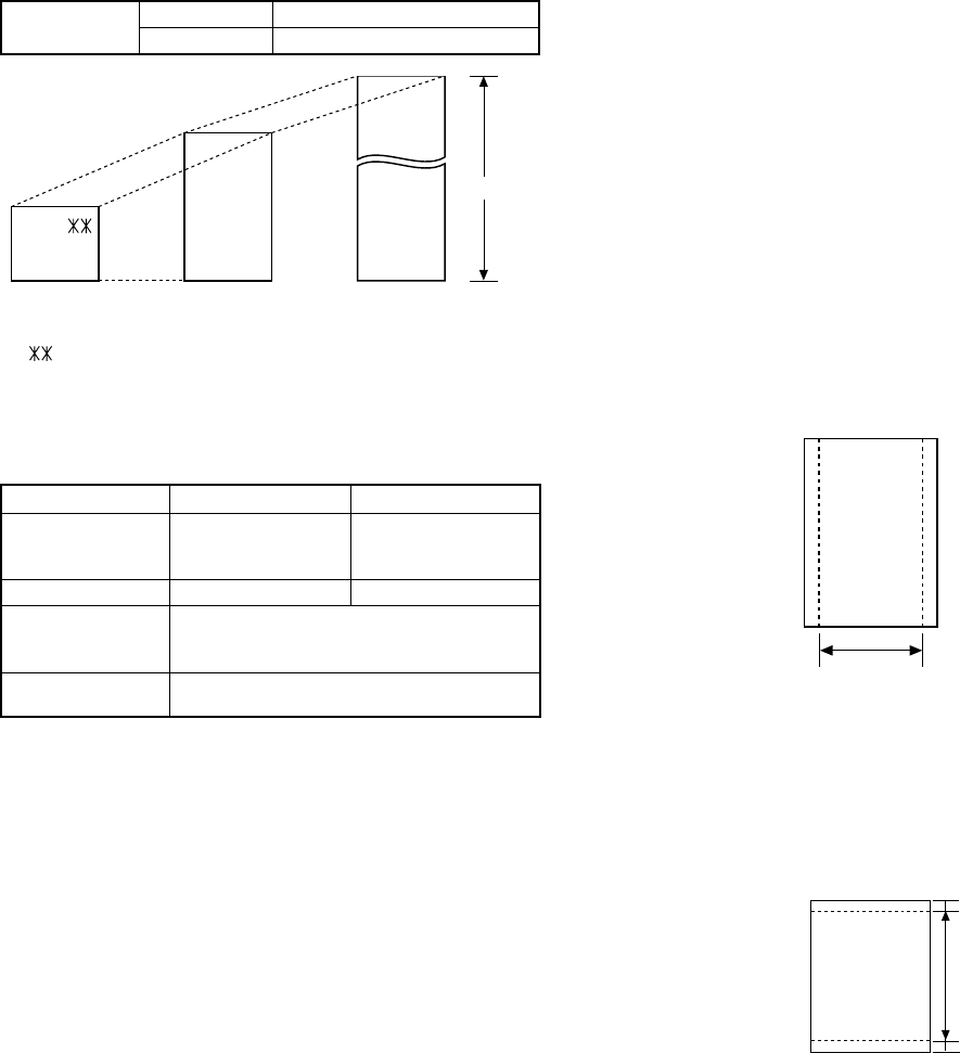
[3] Transmittable documents
1. Document Sizes
* With special sizes, only one sheet can be fed into the machine at a
time. Insert next page into feeder as current page is being scanned.
2. Paper Thickness & Weight
Normal size width 148 – 216 mm
length 140 – 297 mm
5. Automatic Document Feeder Capacity
Number of pages that can be placed into the feeder at anytime is as
follows:
Normal size: max. ADF 10 pages
Special size: single sheet only (manual feed)
NOTES: •When you need to send or copy more pages than the feeder
limit, place additional pages in feeder when last page in
feeder is being scanned.
•Place additional pages carefully and gently in feeder.
If force is used, double-feeding or a document jam may
result.
6. Readable Width & Length
The readable width and length of a document are slightly smaller than
the actual document size.
Note that characters or graphics outside the effective document scan-
ning range will not be read.
•Readable width
210mm, max.
•Readable length
This is the length of the document sent minus 5mm from the top and
bottom edges.
Use document carrier sheet for smaller documents.
Readable width
(Min.)
(Max.)
A4 size
(Max.)
140mm
297mm
600mm
148mm 216mm
[
Normal size
]
216mm
[
S
p
ecial size
]
3. Document Types
•Normal paper
Documents handwritten in pencil (No. 2 lead or softer), fountain pen,
ball-point pen, or felt-tipped pen can be transmitted.
Documents of normal contrast duplicated by a copying machine can
also be transmitted.
•Diazo copy (blue print)
Diazo copy documents of a normal contrast may be transmitted.
•Carbon copy
A carbon copy may be transmitted if its contrast is normal.
4. Cautions on Transmitting Documents
•Documents written in yellow, greenish yellow, or light blue ink cannot
be transmitted.
•Ink, glue, and correcting fluid on documents must be dry before the
documents can be transmitted.
•All clips, staples and pins must be removed from documents before
transmission.
•Patched (taped) documents should be copied first on a copier and
then the copies used for transmission.
•All documents should be fanned before insertion into the feeder to
prevent possible double feeds.
5mm
5mm
Readable length
10 sheets 1sheet(Manual)
Paper weight 70 kg 70 kg ~ 135 kg
21.5 lbs. 14 lbs. ~ 42 lbs.
(80 g/m2) (52 g/m2
~ 157g/
m2)
Paper thickness (ref.)
0.1 mm 0.1 mm ~ 0.18mm
Paper size LGL 8.5” x 14”(216 mm x 355.6 mm)
A4 8.27” x 11.7”(210 mm x 297 mm)
LTR 8.5” x 11”(216 mm x 279 mm)
Feeder capacity A4/LTR: 10 sheets
LGL : 1 sheet
1 – 5
FO-CC500A
FO-K01A
[4] Installation
1. Site selection
Take the following points into consideration when selecting a site for this
model.
ENVIRONMENT
•The machine must be installed on a level surface.
•Keep the machine away from air conditioners, heaters, direct sun-
light, and dust.
•Provide easy access to the front, back, and sides of the machine. In
particular, keep the area in front of the machine clear, or the original
document may jam as it comes out after scanning.
•The temperature should be between 5 - 35°C.
•The humidity should be between 25% and 85% (without conden-
sation).
ELECTRICITY
AC 230 - 240V, 50Hz, grounded(3-prong) AC outlet is required.
Caution!
•Connection to a power source other than that specified will cause
damage to the equipment and is not covered under the warranty.
•If your area experiences a high incidence of lightning or power surges,
we recommend that you install a surge protector for the power and
telephone lines. Surge protectors can be purchased at most telephone
specialty stores.
If the machine is moved from a cold to a warm place...
Condensation may form on the reading glass if machine is moved from
a cold to a warm place, this will prevent proper scanning of documents
for transmission. Turn on the power and wait approximately 2 hours be-
fore using machine.
TELEPHONE JACK
A standard line cord must be located near the machine. This is the tel-
ephone jack commonly used in most homes and offices.
•Plugging the fax machine into a jack which is not line cord may result
in damage to the machine or your telephone system. If you do not
know what kind of jack you have, or need to have one installed, con-
tact the telephone company.
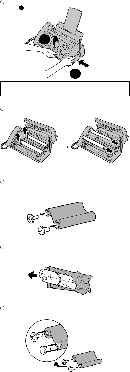
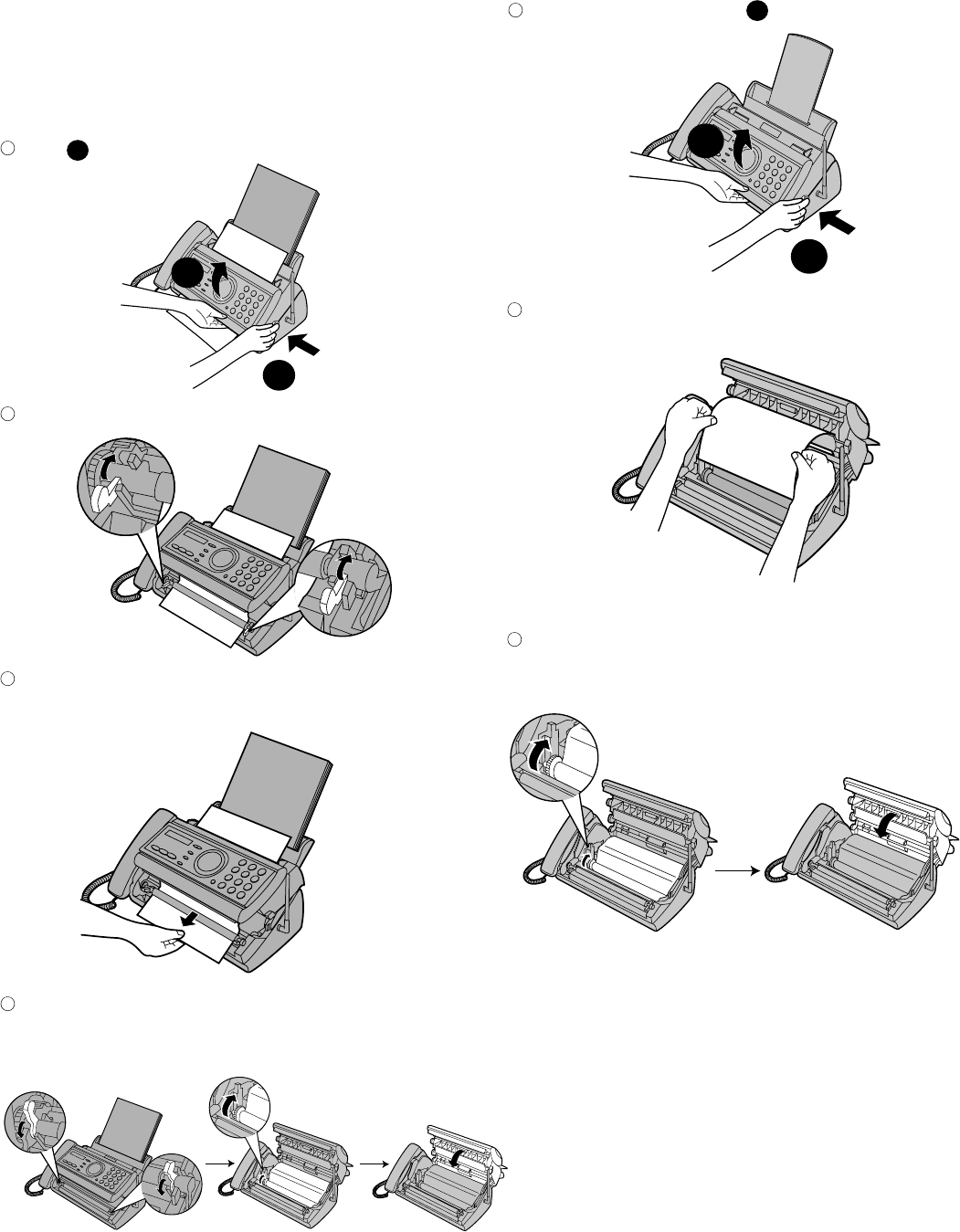
2. Loading the imaging film (FO-6CR)
Your fax uses a roll of imaging film to create printed text and images.
The print head in the fax applies heat to the imaging film to transfer ink
to the paper. Follow the steps below to load or replace the film.
•The initial starter roll of imaging film included with your fax can print
about 30 A4-size pages.
•When replacing the film, use a roll of Sharp FO-6CR imaging film.
One roll can print about 150 A4-size pages.
If you are loading the imaging film for the first time,
go to Step 4.
1
2
1
Remove the used film and empty spool.
Remove the two green gears from the spools.
DO NOT DISCARD THE TWO GREEN GEARS!
Remove the paper from the paper tray and open the operation panel
(press ).
1 slot
2 slots
Remove the new roll of imaging film from its packaging.
• Cut the band that holds rolls together.
Insert the green gears.
Make sure the gears fit into the slots in the ends of the rolls.
1 – 6
FO-CC500A
FO-K01A
Insert the film into the print compartment.
Rotate the front gear as shown until the film is taut.
Fit ends of rolls
onto hubs
Thick roll
to rear
Close the operation panel (press down on both sides to make sure it
cliks into place).
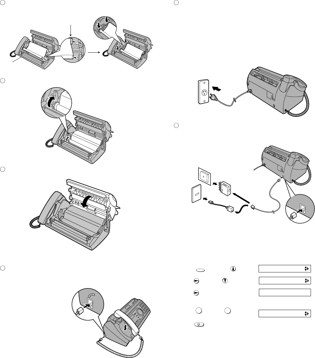
3. Assembly and connections
Connect the handset as shown and place it on the handset rest.
♦ The ends of the handset cord are identical, so they will go into
either jack.
Plug the power cord into a 230 - 240 V, 50 Hz, grounded AC (3-
prong) outlet.
•When disconnecting the fax, unplug the telephone line cord be-
fore unplugging the power cord.
•Caution:
The power outlet must be installed near the equipment and must
be easily accessible.
•The machine does not have a power on/off switch, so the power
is turned on and off by simply plugging in or unplugging the power
cord.
• Make sure the handset cord
goes into the socket
marked with a handset
symbol on the side of the
machine!
• Use the handset to make
ordinary phone calls, or to
transmit and receive faxes
manually.
Insert one end of the telephone line cord into the adaptor. Insert the
other end of the line cord into the socket on the back of the machine
marked TEL. LINE. Plug the adaptor into the telephone socket on
the wall.
Setting the dial mode:
The fax machine is set for tone dialing. If you are on a pulse dial line, you
must set the fax machine for pulse dialing. Press the panel keys as
follows:
TEL.LINE
For Australia
For New Zealand
FUNCTION
1. Press once and once.
2. Press once and twice.
3. Press once.
4. Select the dial mode:
TONE: PULSE:
5. Press to exit.
12
STOP
OPTION SETTING
Display:
DIAL MODE
1=TONE, 2=PULSE
PSEUDO RING
The display briefly shows
your selection, then:
Note: For all units installed in New Zealand, select “1” for tone dialing.
The pulse setting “2” will not operate correctly and must not be used.
Note: If your area experiences a high incidence of lightning or power
surges, we recommend that you install surge protectors for the power
and telephone lines. Surge protectors can be purchased at most tel-
ephone specialty stores.
Moving your fax and reconnecting
Should be necessary to move your fax to a new location, first disconnect
the telephone line cord before disconnecting the power lead. When re-
connecting, it is necessary to connect the power lead before connecting
the telephone line cord.
About condensation
If the machine is moved from a cold to a warm place, it is possible that
condensation may from on the scanning glass, preventing proper scan-
ning of documents for transmission. To remove the condensation, turn
on the power and wait approximately two hours before using the ma-
chine.
1 – 7
FO-CC500A
FO-K01A
Attach the paper tray and paper tray extension.
Note: The paper tray extension has a top side and a bottom side. If the
tabs do not go into the holes, turn the support over.
Click!
Insert
horizontally
and rotate up.
Attach the paper tray. Attach the paper tray extension.
Raising the base antenna.
Raise the base antenna to ensure clear communication with the cord-
less handset.
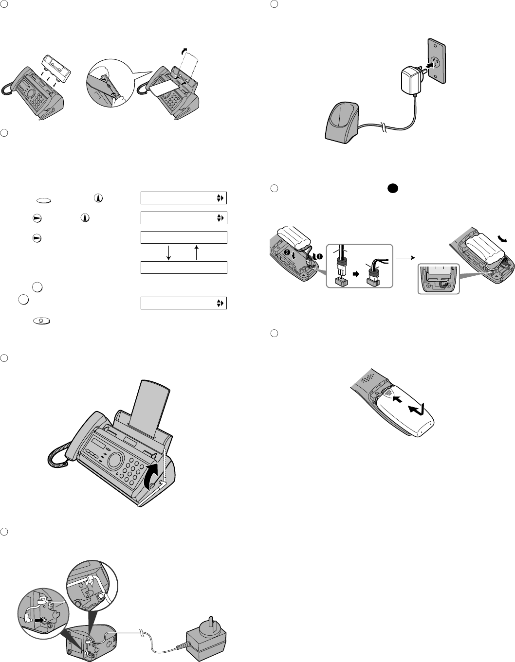
4. Connecting the cordless handset charger
Connect the AC adaptor to the cordless handset charger.
Plug the AC adaptor into a standard 230 - 240 V AC outlet.
Important: Never cover the charger and AC adaptor with a blanket,
cloth, or other material. Excessive heating may result and cause fire.
5. Installing the battery and charging the cordless
handset
Connect the battery connector , and then place the battery pack
in the cordless handset.
• Place the wires as shown.
Place the battery cover on the cordless handset, making sure it snaps
firmly into place.
• Make sure the wires are not caught or pinched by the cover.
Fit the cord into
the holders.
Black
Red
Black
Red
1
Country select setting.
Follow the steps below to set the fax machine for operation in Australia
or in New Zealand.
♦ The initial setting is AUSTRALIA.
FUNCTION
1. Press once and once.
2. Press once and once.
3. Press once.
4. Press if you are in Australia,
or if you are in New Zealand.
5. Press to return to the date and time display.
1
2
STOP
OPTION SETTING
Display:
COUNTRY SELECT
1=AUSTRALIA
NUMBER OF RING
The display briefly shows
your selection, then:
1=NEW ZEALAND
1 – 8
FO-CC500A
FO-K01A
6. Loading printing paper
You can load up to 50 sheets of A4-size, 60 - 80 g/m2 paper in the paper
tray (at room temperature; maximum stack height should not be higher
than the line on the tray).
Fan the paper, and then tap the edge against a flat surface to even
the stack. Make sure the stack edges are even.
Insert the stack of paper into the tray, PRINT SIDE DOWN.
• If paper remains in the tray, take it out and combine it into a single
stack with the new paper.
• Be sure to load the paper so that printing takes place on the print
side of the paper. Printing on the reverse side may result in poor
print quality.
• GENTLY LOAD PAPER INTO THE PAPER TRAY.
• DO NOT FORCE IT DOWN INTO THE FEED SLOT.
Correct Incorrect
The stack
should not
be higher
than this line.
Note: Do not use paper that has already been printed on, or paper that
is curled.
Note: If at any time the display shows
the alternating messages at right, check
the printing paper. If the tray is empty,
add paper. If these is paper in the tray,
take it out and then reinsert it.
When you are finished, press .
START/MEMORY
ADD PAPER &
PRESS START KEY
↑
↑
Print contrast setting.
You fax has been set at the factory to print at normal contrast. If
desired, you can change the print contrast setting to LIGHT.
FUNCTION
1. Press once and once.
2. Press once and 3 times.
3. Press once.
4. Select the print contrast:
NORMAL: LIGHT:
5. Press to return to the date and time display.
12
STOP
OPTION SETTING
Display:
PRINT CONTRAST
1: NORMAL
COPY CUT-OFF
The display briefly shows
your selection, then:
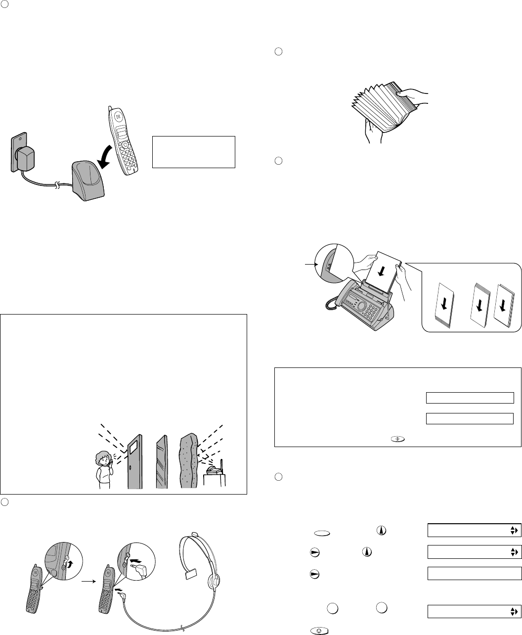
Connecting a headset.
You can connect a headset (purchased separately) to the headset
socket. Remove the cap and insert the connector as shown.
Accessory cordless handsets (FO-K01)
♦ ♦
♦ ♦
♦ You can use up to 3 additional FO-K01 cordless handsets with the
fax machine.
♦ ♦
♦ ♦
♦ Please purchase accessory FO-K01 handsets at your dealer or re-
tailer.
For information on setting up an accessory cordless handset for use
with the fax machine, see the manual that aaompanies the accessory
handset.
Place the cordless handset in the charger with the dial pad facing
forward.
• Important! The dial pad must face forward, or the battery will not
charge.
• The battery charges automatically while the cordless handset is in
the charger. While charging, the display shows CHARGING. When
charging is completed, the display shows IN CHARGER.
• The cordless handset and charger may feel warm while charging.
This is normal.
The battery cannot be overcharged. When not using the cordless hand-
set, keep it in the charger to ensure that it is always charged.
♦ When the battery needs charging, LOW BATTERY will appear in the
display and you will hear beeps during a phone conversation. If you
need to continue the conversation, transfer the call to the fax ma-
chine or another cordless handset. Place the cordless handset in the
charger and let it charge.
♦ To ensure that the battery charges properly, wipe the charger con-
tacts once a month with a cotton swab.
Note: If the battery is extremely low, nothing may appear in the display
during the first several minutes that the cordless handset is in the charger.
The battery will begin to charge normally after several minures.
Charge the battery
at least 10 hours the
first time!
Talking range
The talking range of the cordless handset is approximately 400 m
(line of sight; talking range may decrease depending on transmission
conditions). If you hear noise or interference while talking on the cord-
less handset, move closer to the fax machine.
♦ When outside the talking range, OUT OF RANGE appears in the
display. If you move out of the talking range while talking on the
cordless handset, the handset will beep and you may hear interfer-
ence.
Large metal objects,
metal structures, and
thick walls reduce the
talking range.
Reinforced concreteMetalAluminum sash
1 – 9
FO-CC500A
FO-K01A
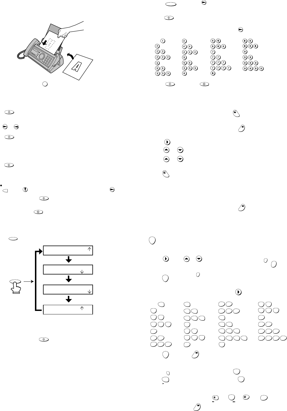
7. Clearing a jammed document
If the original document doesn’t feed properly during transmission or
copying, or DOCUMENT JAMMED appears in the display, first try press-
ing the START/MEMORY key. If the document doesn’t feed out, remove
it as explained below.
Important:
Do not try to remove a jammed document without releasing it as ex-
plained below. This may damage the feeder mechanism.
Press and slowly open the operation panel until it is half open.
1
1
2
Flip up the green levers on each side of the white roller.
Gently and remove the document.
• Be careful not to tear the document.
Flip down the green levers on each side of the white roller. Rotate the
front gear until the film is taut, and then close the operation panel
(press down on both sides to make sure it clicks into place).
8. Clearing jammed printing paper
Open the operation panel (press ).
1
1
2
Gently pull the jammed paper out of the machine, making sure no
torn pieces of paper remain in the print compartment or rollers.
Rotate the front gear until the film is taut, and then close the
operation panel (press down on both sides to make sure it clicks into
place).
1 – 10
FO-CC500A
FO-K01A
Listening to messages
1. Press . (For the general box, press .)
2. Press to listen to all your messages, or to listen to only your
new messages.
3. While listening, you can press , , , or .
4. When finished, press .
USING THE CORDLESS PHONE
Making a phone call
1. Pick up the cordless handset and press .
2. When you hear the dial tone, dial the number.
3. When you are ready to end the call, press .
Making a phone call using automatic dialing
1. Press once.
2. Press or to select the book.
3. Press or until the number you wish to dial appears in the
display.
4. Press .
Receiving a phone call
1. When the cordless handset rings, pick it up and press any key to
answer.
2. When you are ready to end the call, press .
Receiving a fax using the cordless handset
If you hear a fax tone after answering a call on the cordless handset,
or if the other party speaks to you and then wants to send a fax, press
.
Storing auto dial numbers
1. Press , or to select the book, and then .
2. Enter the full fax/phone number. To clear a mistake, press . To
insert a pause, press .
3. Press .
4. Enter a name by pressing number keys. (To enter two letters in suc-
cession that require the same key, press after entering the first
letter.)
5. Press and then .
RECEIVING FAXES
Press the until the arrow in the display points to the desired
reception mode.
FAX mode: The fax machine automatically answers and receives faxes.
TEL mode: Answer all calls (even faxes) by picking up the handset. To
begin fax reception, press .
A.M. mode: Select this mode when you go out to receive both voice
messages and faxes.
[5] Quick reference guide
SENDING FAXES
Place your document (up to 10 pages) face down in the document feeder.
Normal Dialing
1. Lift the handset or press .
2. Dial the fax number.
3. Wait for the reception tone (if a person answers, ask them to press
their Start key).
4. Press .
Automatic Dialing
1. Press or until the desired destination appears in the display.
2. Press .
Direct Keypad Dialing
1. Dial the fax number.
2. Press .
SPEAKER
START/MEMORY
START/MEMORY
START/MEMORY
RESOLUTION/
RECEPTION MODE
RESOLUTION/
RECEPTION MODE
FAX
TEL
A.M.
TEL/FAX
01-JAN 10:30
FAX
TEL
A.M.
TEL/FAX
01-JAN 10:30
A.M.
TEL/FAX
FAX
TEL
01-JAN 10:30
A.M.
TEL/FAX
FAX
TEL
01-JAN 10:30
RECORDING AN OGM
1. Press , press until desired OGM is displayed, and then once.
2. Lift the handset, press , and
speak into the handset.
3. When finished, press .
REC/
MEMO
START/MEMORY
STOP
TALK
OFF
SEARCH
TALK
OFF
START
SEARCH
FUNCTION
/PAUSE
ERASE
HOLD
FUNCTION
/PAUSE
START
A =
B =
C =
D =
E =
F =
G =
H =
I =
J =
K =
L =
M =
N =
O =
P =
Q =
R =
S =
T =
U =
V =
W =
X =
Y =
Z =
SPACE =
WXYZ
9
WXYZ
9
WXYZ
9
WXYZ
9
WXYZ
9
WXYZ
9
WXYZ
9
WXYZ
9
WXYZ
9
WXYZ
9
TUV
8
TUV
8
TUV
8
TUV
8
TUV
8
TUV
8
PQRS
7
PQRS
7
PQRS
7
PQRS
7
PQRS
7
PQRS
7
PQRS
7
PQRS
7
PQRS
7
PQRS
7
MNO
6
MNO
6
MNO
6
MNO
6
MNO
6
JKL
5
JKL
5
JKL
5
MNO
6
JKL
5
JKL
5
JKL
5
GHI
4
GHI
4
GHI
4
GHI
4
GHI
4
GHI
4
DEF
3
DEF
3
DEF
3
DEF
3
DEF
3
DEF
3
ABC
2
ABC
2
ABC
2
ABC
2
ABC
2
ABC
2
1
START
OFF
REMOTE
/RECALL
PQRS
7
PLAY
TUV
8
PLAY NEW
REPEAT
0
SKIP
DELETE
STOP
WXYZ
9
OFF
START/MEMORY
0
STORING AUTO DIAL NUMBERS
1. Press once and twice.
2. Enter the full fax/phone number.
3. Press .
4. Enter the name by pressing number keys. (To enter two letters in
succession that require the same key, press after entering the first
letter.)
5. Press and then .
FUNCTION
START/MEMORY
A =
B =
C =
D =
E =
F =
G =
H =
I =
J =
K =
L =
M =
N =
O =
P =
Q =
R =
S =
T =
U =
V =
W =
X =
Y =
Z =
SPACE =
START/MEMORY
STOP
1 – 11
FO-CC500A
FO-K01A
[6] Option imaging film specifications
(FO-6CR)
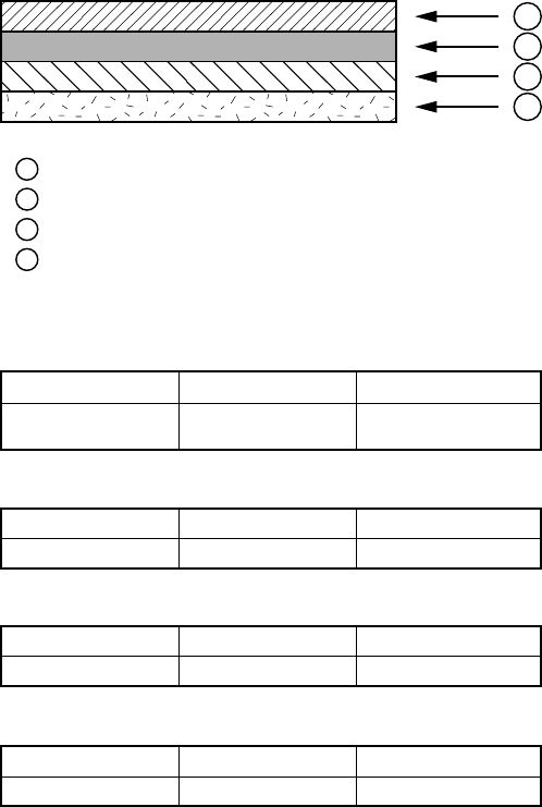
1. Structure
This article is composed of polyester film coated with heat-resistant layer,
matt layer and hot melt ink layer, leader film and paper core. Ink film
specification is "DNP standard ink film HC".
Heading Requirements Measuring method
Material Polyethylene-
terephthalate –
Heading Requirements Measuring method
Grade HR Mixer P-5 –
Heading Requirements Measuring method
Grade ML Sumi –
Heading Requirements Measuring method
Grade #507W –
2. Details of compositions
2-1. Base film
2-2. Heat resistant layer
2-3. Matt layer
2-4. Hot melt ink layer
1
2
3
4
1
2
3
4
Heat Resistant Layer
Base Film
Matt Layer
Hot melt Ink Layer
FO-CC500A
FO-K01A
4. Volume adjustment (Fax machine)
You can adjust the volume of the speaker and ringer using the UP and
DOWN arrow keys.
(1) Fax machine ringer
1. Press the UP or DOWN to select the desired volume level. (Make
sure SPEAKER key has not been pressed, and a document is not
loaded in the feeder.)
Display:
RINGER: HIGH
RINGER: MIDDLE
RINGER: LOW
RINGER OFF: OK?
2. If you selected RINGER OFF: OK?, to turn off the ringer, press START/
MEMORY key.
(2) Fax machine speaker
1. Press the SPEAKER key.
2. Press the UP or DOWN to select the desired volume level.
• Press SPEAKER key again to turn off the speaker.
CHAPTER 2. ADJUSTMENTS
[1] Adjustments
General
Since the following adjustments and settings are provided for this model,
make adjustments and/or setup as necessary.
1. Adjustments of output voltage (FACTORY ONLY)
1. Install the power supply unit in the machine.
2. Set the recording paper and document.
3. When the document is loaded, power is supplied to the output lines.
Confirm that outputs are within the limits below.
Output voltage settings
3. Settings
(1) Dial mode selector
DIAL mode (Soft Switch No. SW-B4 DATA No. 3)
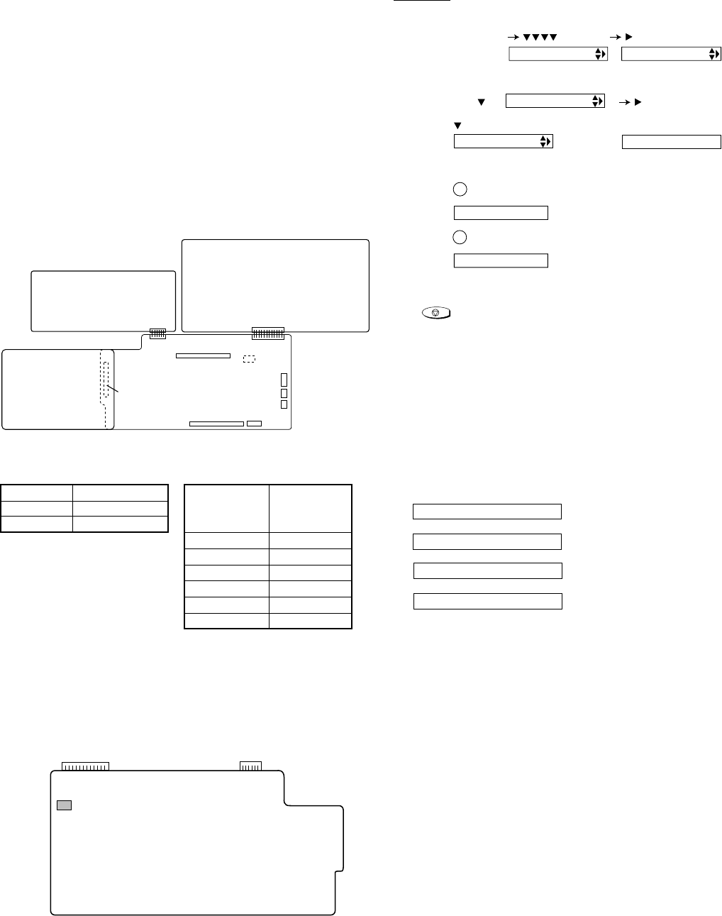
2. IC protectors replacement
ICPs (IC Protectors) are installed to protect the motor driver circuit.
ICPs protect various ICs and electronic circuits from an overcurrent con-
dition.
The location of ICPs are shown below:
2 – 1
CONTROL PWB
(BOTTOM SIDE)
CNLIUA
FU100
CNPW
LIU PWB
(BOTTOM SIDE)
POWER
SUPPLY
PWB
(BOTTOM SIDE)
CONTROL
PWB
(TOP SIDE)
CNMT
CNLIUA
CNLIUA
CNPW
CNPW
CNPN CNCIS
CNSP
CNCSW
CNTH CNPRG
CORDLESS PWB
(BOTTOM SIDE) CNDSS
(step 1) Select "OPTION SETTING".
KEY : FUNCTION
DISPLAY: OPTION SETTING NUMBER OF RING
(step 2) Select "DIAL MODE".
KEY: Push until DIAL MODE is
indicated because the number of
's changes by the model.
DISPLAY: DIAL MODE 1=TONE, 2=PULSE
(step 3) Select, using "1" or "2".
KEY: 1
DISPLAY: TONE SELECTED
KEY: 2
DISPLAY: PULSE SELECTED
(step 4) End, using the "STOP" key.
KEY:
STOP
(1)FU100 (KAB3202) is installed in order to protect IC’s from an over-
current generated in the motor drive circuit. If FU100 is open, re-
place it with a new one.
↔
↔
↔
• The ringer rings once at the
selected level, then the date
and time reappear in the
display.
Output Voltage limits
+5V 4.25V ~ 5.75V
+24V 23.3V ~ 24.7V
1 +24V
2 +24V
3MG
4MG
5DG
6 +5V
Connector
No. CNPW
Pin No.
FO-CC500A
FO-K01A
(2) Cordless handset ringer
1. When you are not talking on the cordless handset, press UP or DOWN
to select the desired ringer volume level.
Cordless handset display:
RINGER: HIGH
RINGER: MIDDLE
RINGER: LOW
RINGER OFF: OK?
OK: PRESS START
2. If you selected RINGER OFF: OK? to turn off the ringer, press START
key.
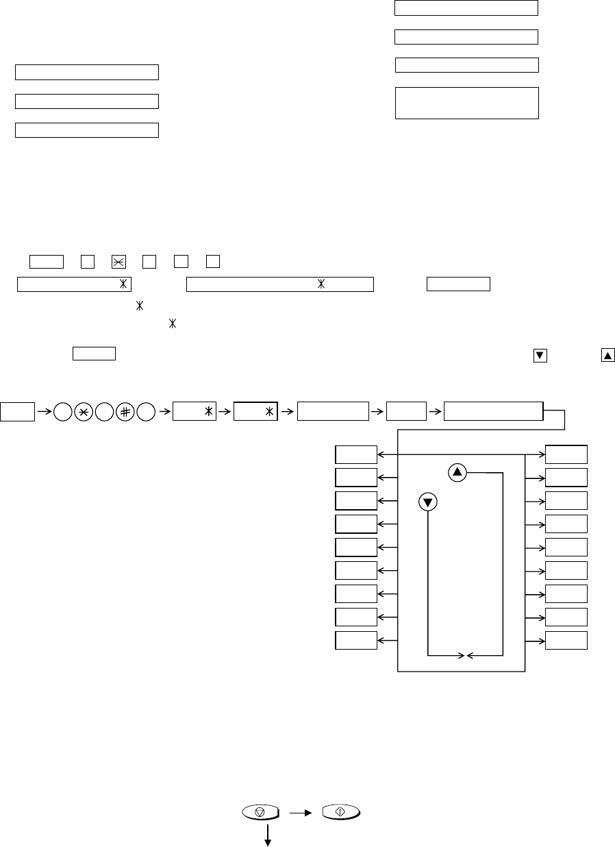
[2] Diagnostics and service soft switch
1. Operating procedure (Fax machine)
(1) Entering the diagnostic mode
Press FUNC → 9 → → 8 → # → 7 , and the following display will appear.
MAIN ROM Ver. TA83 After 2 sec: CORDLESS ROM Ver. TA85 SystemID After 2 sec: DIAG MODE
MAIN ROM Ver.: TA83
CORDLESS ROM Ver.: TA85
Then press the START key. Select country name is risen on display for 2 sec. Select the desired item with the key or the key or select with the
rapid key. Enter the mode with the START key.
(Diag•specifications)
If the diag mode cannot be set, repeat the diag mode operation, per-
forming the following operation.
After the power is turned on and "WAIT A MOMENT" is indicated, press
the STOP key.
2 – 2
In relation with the process response (request from Production Engi-
neering) "WAIT A MOMENT" clock indication may appear depending on
STOP key timing. If the STOP key is held down, "MEMORY CLEAR?"
appears.
START
KEY
STOP
KEY
+
"Power ON"
Memory clear
(Work + Backup)
FUNC DIAG MODE
9 8 7
STARTSoft switch mode
START
TA83 TA85 COUNTRY NAME
STARTROM & RAM check
STARTAging mode
STARTPanel key test
STARTCheck pattern
STARTSignal send mode
STARTMemory clear
STARTShading mode
STARTAll black print
START
START
START
START
START
START
START
START
START
Keypad test mode
DTMF CDL ID RX
RF RX mode
RF TX mode
Flash mem. clear
Flash mem. check
Entry data rcv.
Entry data send
Auto feeder mode
5. Volume adjustment (Cordless Handset)
You can adjust the volume of the ringer and handset, receiver using the
UP and DOWN arrow keys.
(1) Cordless handset receiver volume
1. When talking on the cordless handset, press UP or DOWN to select
the desired volume level.
Cordless handset display:
RECEIVER: HIGH
RECEIVER: MIDDLE
RECEIVER: LOW
↔
↔
↔
↔
↔
• The ringer will ring once at
the selected level.
• Note: The volume reverts to
MIDDLE each time
you hang up (press
OFF key).
FO-CC500A
FO-K01A
2. Diagnostic items (Fax machine)
1 SOFT SWITCH MODE Soft switches are displayed and changed. List can be output.
2 ROM & RAM CHECK ROM sum-check mand RAM read/write check.
3 AGING MODE 10 sheets of check patterns are output every 5 minutes per sheet.
4 PANEL KEY TEST Panel keys are tested. Result list is output.
5 CHECK PATTERN Check pattern is output.
6 SIGNAL SEND MODE Send the various signals. Signal is changed by pressing START key.
7 MEMORY CLEAR Back-up memory is cleared, and is set at delivery.
8 SHADING MODE Shading compensation is performed in this mode.
9 ALL BLACK PRINT To check the print head, whole dots are printed over the interval of 2 m.
10 AUTO FEEDER MODE Insertion and discharge of document are tested.
11 ENTRY DATA SEND Registered content is sent.
12 ENTRY DATA RCV. Registered content is received, and its list is output.
13 FLASH MEM. CHECK Checks flash memory write/read.
14 FLASH MEM. CLEAR Checks flash memory clearing.
15 RF TX MODE RF signal send test mode.
16 RF RX MODE RF signal receive test mode.
17 DTMF CDL ID RX Registered content is received, and its list is output.
18 KEYPAD TEST MODE I/F for DSS engine’s DIAG mode.
2 – 3
ITEM No. Contents Function
3. Diagnostic items description
3. 1. Soft switch mode
Used to change the soft switch settings.
The soft switch which is stored internally is set by using the keys.
The available soft switches are SW-A1 to SW-N3.
The content of soft switches is shown in page 2-10 to 2-23.
The contents are set to factory default settings.
The contents of the soft switch setting backed up.
3. 2. ROM & RAM check
Used to do the ROM sum check and the RAM read/write test and to
clear the RAM. The test results will be given by means of beeps. A long
beep means “all checked successful”. A short beep or beeps mean an
IC in error, with the number of beeps indicating which IC failed. The test
results also be printed.
System ID of FAX machine and Cordless Handset preserves.
1 beep → ROM
2 beeps → S-RAM/D-RAM
3. 3. Aging mode
If any document is first present, copying will be executed sheet by sheet.
If no document is present, the check pattern will be printed sheet by
sheet. This operation will be executed at a rate of one sheet per 5 min-
utes, and will be ended at a total of 10 sheets.
3. 4. Panel key test
This mode is used to check whether each key operates properly or not.
Press the key on the operation panel, and the key will be displayed on
the display. Therefore, press all keys. At this time, finally press the STOP
key.
When the STOP key is pressed, the keys which are not judged as
"pressed" will be printed on the result list.
•LED part of the contact image sensor (CIS) is kept on during the term
from when "START" of the panel test mode to end with the STOP
key.
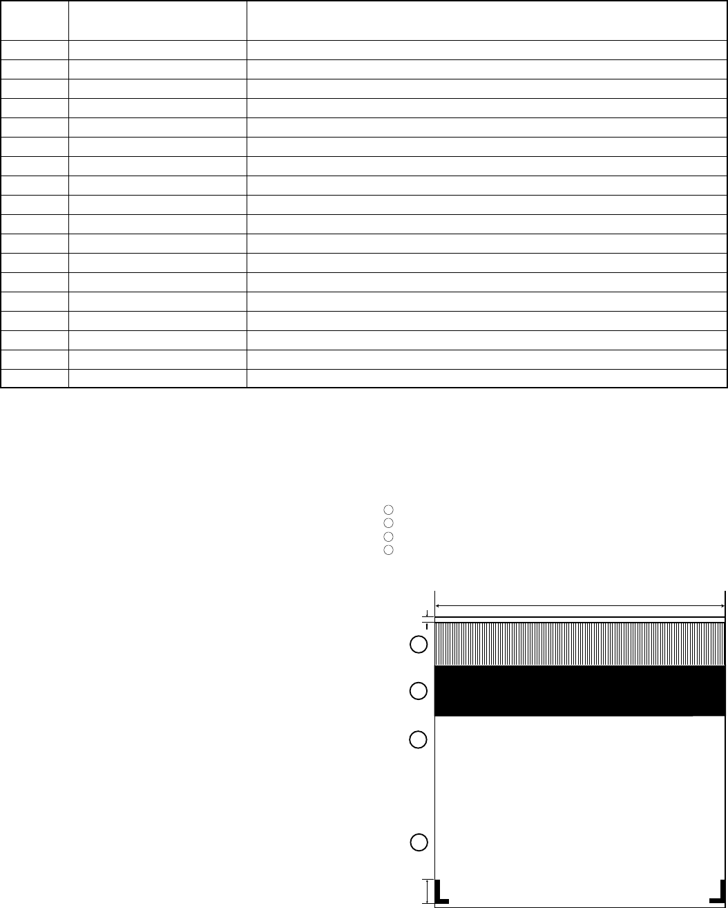
3. 5. Check pattern
This mode is used to check the state of the printing head. It is ended
with the following pattern printed on one printing sheet.
White/Black(3/8 mm alternately) >>> About 30 mm long.
All Black >>> About 30 mm long
All White >>> From All Black end to Pin OFF
End White >>> From Pin OFF to 16.5 mm long
Pin off
16.5 mm
Void area
4 mm
LETTER: 216 mm
LEGAL: 216 mm
A4: 210 mm
1
2
3
4
FO-CC500A
FO-K01A
3. 6. Signal send mode
This mode is used to send various signals to the circuit during FAX
communication. Every push of START key sends a signal in the follow-
ing sequence. Moreover, the signal sound is also output to the speaker
when the line monitor of the soft switch is on.
[1] No signals (CML signal turn on)
[2] 14400BPS (V.33)
[3] 12000BPS (V.33)
[4] 14400BPS (V.17)
[5] 12000BPS (V.17)
[6] 9600BPS (V.17)
[7] 7200BPS (V.17)
[8] 9600BPS (V.29)
[9] 7200BPS (V.29)
[10] 4800BPS (V27ter)
[11] 2400BPS (V27ter)
[12] 300BPS (FLAG)
[13] 2100Hz (CED)
[14] 1100Hz (CNG)
3. 7. Memory clear
This mode is used to clear the backup memory and reset to the default
settings. (Various registrations are cleared.)
• The registered Cordless Handset information is not deleted by “Memory
clear”.
3. 8. Shading mode
The mode is used for the shading compensation. For reading, set up
the special original paper.
The compensation memorizes the reference data of white and black for
reading.
Moreover, the memorized data is not erased even if memory clear mode
is executed.
3. 9. All black print
This mode is used to check the state of the printing head and to inten-
tionally overheat it. Whole dots are printed over the interval of 2 m. If it is
overheated or the printing sheet is jammed, press STOP key for the
end.
3. 10. Auto feeder mode
In this mode, a document is inserted and discharged to check the auto
feed function.
After this mode is started, set a document, and the document feed will
be automatically tested.
3. 11. Entry data send
This mode is used to send the registered data to another machine and
make the other machine copy the registered content.
Before sending in this mode, it is necessary to set the other machine at
the entry data receive mode.
The following, information will be sent to the remote machine:
1. Telephone list data
2. Sender register data
3. Optional setting content
4. Soft switch content
5. Junk fax number list
6. Timer reservation data (Only on the model which timer reserva-
tion is possible.)
7. Recording setting list data
2 – 4
3. 12. Entry data receive
In this mode, the registered data sent from the other machine is receiv-
ed and the received data is registered in the machine. When this mode
is used for receiving, the other machine must be in the entry data send
mode.
After receiving is completed, the following lists are printed.
1. Telephone list data
2. Sender register data (The passcode No. is also printed if the poll-
ing function is provided.) (*)
3. Optional setting list (*)
4. Soft switch content
5. Junk fax number list (*)
6. Timer reservation data (Only on the model which timer reserva-
tion is possible.)
7. Recording setting list data (*)
(*): Refer to SETUP LIST
3. 13. Flash memory check
Data is written into and read from the flash memory to check data con-
formity. When the unit enters this mode, the check is started.
3. 14. Flash memory clear
Data in the flash memory is cleared (memory clear). When the unit en-
ters this mode, the check is started.
*Operation of hardware and signal in the flash memory check mode and
flash memory clear mode, and the result of check.
The result is announced by the buzzer beeps. The result of check is
printed.
Beeps 1 → Memory error
3. 15. RF TX mode
This mode is for measurement of RF signal send level. When you press
START key, the DSS unit move to be in the continuous signal send mode
until you press STOP key. It needs exclusive measuring device.
3. 16. RF RX mode
This mode is for measurement of RF signal send level. When you press
START key, the DSS unit move to be in the continuous signal receive
mode until you press STOP key. It needs exclusive measuring device.
3. 17. DTMF CDL ID RX
When you press START key, the display change to ‘LINE STANDBY’.
And, it waits for the start signal (DTMF) of the System ID input protocol.
The exclusive writer at the product line only corresponds to the protocol.
3. 18. Keypad test mode
From this mode, you can enter the diag mode of the DSS unit
(CONEXANT Merlin). The purpose of these items is to measure the wire-
less communication specification of this unit. By enter the access code
written in Conexant’s user guide, you can start the desired menu. To
implement this menu, this user guide is necessary.
FO-CC500A
FO-K01A
2 – 5
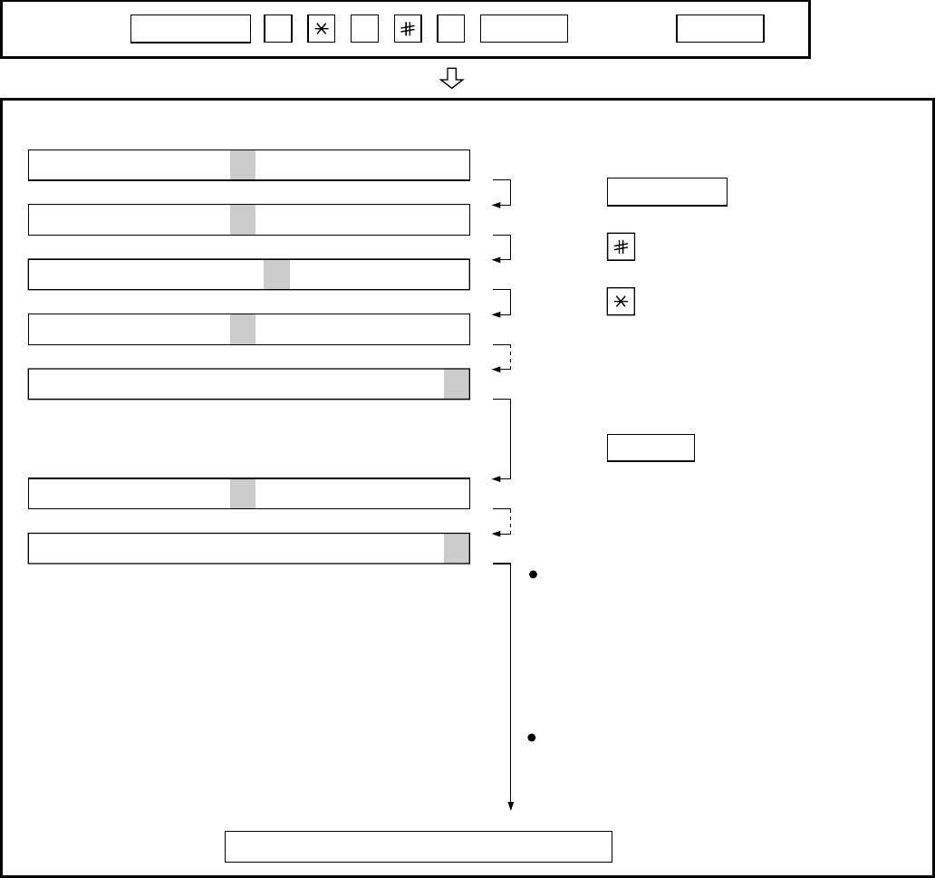
Press FUNCTION 9 8 7 START START
Press FUNCTION key.
Press key.
Press key.
Bit1 - 8 are set.
Soft SW-A2 - SW-N3 are set.
S F T SW-A1 = 1 0 0 0 0 0 0 0
S F T SW-A1 = 1 0 0 0 0 0 0 0
S F T SW-A1 = 1 0 0 0 0 0 0 0
S F T SW-A1 = 1 0 0 0 0 0 0 0
S F T SW-A2 = 0 0 0 0 0 0 0 0
S F T SW-N3 = 0 0 0 0 0 0 0 0
Press key during setting.
To finish the settings halfway between
SW-A1 and SW-N3, press the STOP
key. In this case, the setting being done
to the SW No. on display will be nullified
while settings done to the preceding
SW No. remain in effect.
The soft switch mode is terminated.
S F T SW-A1 = 0 0 0 0 0 0 0 0
START
DATA No. 1 2 3 4 5 6 7 8
When the COPY key is pressed, the
contents of soft switches are printed.
4. How to make soft switch setting
To enter the soft switch mode, press the following key entries in se-
quence.
FO-CC500A
FO-K01A
2 – 6
5. Operating procedure (Cordless handset)
5.1. Entering the diagnostic mode
The following key is simultaneously inputted after a power supply on. 2 + + #
5.2. Escape method from production mode
The off key is inputted from stand-by state of Production mode.
5.3. Each inspection mode
It performs from a stand-by state.
5.3.1 Sending RF signal mode
After going into the mode, RF signal is sending out.
Sending channel is selected by inputting two ten-keys.
Sending power is selected by inputting Up of Down keys. (3 levels)
By inputting off key, it goes to stand-by state of Production mode.
0 1 1 2404.8 UP Power Up OFF
0 2 2 2406.6 DOWN Power Down
0 3 3 2408.4
0 4 4 2410.2
0 5 5 2412.0
0 6 6 2413.8
0 7 7 2415.6
0 8 8 2417.4
0 9 9 2419.2
1 0 10 2421.0
1 1 11 2422.8
1 2 12 2424.6
1 3 13 2426.4
1 4 14 2428.2
1 5 15 2430.0
1 6 16 2431.8
1 7 17 2433.6
1 8 18 2435.4
1 9 19 2437.2
2 0 20 2439.0
2 1 21 2440.8
2 2 22 2442.6
2 3 23 2444.4
2 4 24 2446.2
2 5 25 2448.0
2 6 26 2449.8
2 7 27 2451.6
2 8 28 2453.4
2 9 29 2455.2
3 0 30 2457.0
3 1 31 2458.8
3 2 32 2460.6
3 3 33 2462.4
3 4 34 2464.2
3 5 35 2466.0
3 6 36 2467.8
3 7 37 2469.6
3 8 38 2471.4
3 9 39 2473.2
4 0 40 2475.0
Mode No. Channel selection Power level selection End of mode
Input key Input key CH Frequency(MHz) Input key Input key
01
FO-CC500A
FO-K01A
2 – 7
5.3.2 Receiving RF signal mode
After going into the mode, this cordless handset can receive RF signal.
Receiving channel is selected by inputting two ten-keys.
RF input Gain can be selected by Up/Down keys. (2 levels)
By inputting off key, it goes to stand-by state of Production mode.
0 1 1 2404.8 UP AGC High OFF
0 2 2 2406.6 DOWN AGC Low
0 3 3 2408.4
0 4 4 2410.2
0 5 5 2412.0
0 6 6 2413.8
0 7 7 2415.6
0 8 8 2417.4
0 9 9 2419.2
1 0 10 2421.0
1 1 11 2422.8
1 2 12 2424.6
1 3 13 2426.4
1 4 14 2428.2
1 5 15 2430.0
1 6 16 2431.8
1 7 17 2433.6
1 8 18 2435.4
1 9 19 2437.2
2 0 20 2439.0
2 1 21 2440.8
2 2 22 2442.6
2 3 23 2444.4
2 4 24 2446.2
2 5 25 2448.0
2 6 26 2449.8
2 7 27 2451.6
2 8 28 2453.4
2 9 29 2455.2
3 0 30 2457.0
3 1 31 2458.8
3 2 32 2460.6
3 3 33 2462.4
3 4 34 2464.2
3 5 35 2466.0
3 6 36 2467.8
3 7 37 2469.6
3 8 38 2471.4
3 9 39 2473.2
4 0 40 2475.0
Mode No. Channel selection AGC level selection End of mode
Input key Input key CH Frequency(MHz) Input key Input key
02
5.3.3 Speaker test mode
After going into the mode, speaker test can be tested.
Speaker volume is selected by using Up/Down keys. (3 levels)
By inputting off key, it goes to stand-by state of Production mode.
UP Volume Up OFF
DOWN Volume Down
Mode No. Channel volume End of mode
Input key Input key Input key
03
FO-CC500A
FO-K01A
5.3.4 Panel key test mode
After going into the mode, cordless handset is waiting for a key to be pressed.
All keys should been pressed except for off key.
• After pressing all keys, off key should been pressed. If any keys that are not pressed exist, it will be displayed on LCD.
• Press the NG keys. If another NG keys exists, it will also be displayed.
• If all keys are pressed, cordless handset will going to stand-by state.
* If you want to cancel the Panel Test, press the and # key simultaneously.
2 – 8
5.3.5 LED test mode
After going into the mode, backlight is switched on.
By inputting off key, it goes to stand-by state of Production mode.
OFF
04
Mode No.
Input key
Press all keys End of mode
Input key
OFF
Mode No. End of mode
Input key Input key
05
5.3.6 LCD test mode
After going into the mode, check patterns are displayed on the LCD.
By inputting off key, it goes to stand-by state of Production mode.
OFF
Mode No. End of mode
Input key Input key
06
5.3.7 SX test mode
After going into the mode, sidetone root is enabled.
Receiver volume is selected by using Up/Down keys. (3levels)
By inputting off key, it goes to stand-by state of Production mode.
UP Volume Up OFF
DOWN Volume Down
Mode No. Volume change End of mode
Input key Input key Input key
07
5.3.8 Battery test mode
After going into the mode, cordless handset will check the Battery level.
• If it is less than 3.4V, “LOW BATT” will be displayed. ................. The input from the battery is turned off to create the “LOW BATT” state.
Maintain this mode.
• If it is more than 3.3V, “BATT OK” will be displayed.
• If cordless handset is put on the cordless handset charger, “Cradle Power” will be displayed.
By inputting off key, it goes to stand-by state of Production mode.
OFF
Mode No. End of mode
Input key Input key
08
FO-CC500A
FO-K01A
2 – 9
5.3.9 Headset test mode
After going into the mode, cordless handset will check the jack of headset.
• If headset are put in the jack, “DETECT HEADSET” will be displayed.
By inputting off key, it goes to stand-by state of Production mode.
OFF
Mode No. End of mode
Input key Input key
09
5.3.10 Bit rate test mode
After going into the mode, cordless handset will test the Bit Rate.
By inputting off key, it goes to stand-by state of Production mode.
OFF
Mode No. End of mode
Input key Input key
1 0
5.3.11 INTERCOM test mode between cordless handsets (FO-K01 ONLY)
After going into the mode, please enter the system ID. (1digit, 0 ~ 9)
NOTE: You have to enter the same number for both partner cordless handsets do this test.
If this test is done at more than 2 places in the communication area, please use the different System ID between each place.
This rule is necessary to avoid the jamming.
Please enter the cordless handsets number.
NOTE: You have to set the different number for the partner cordless handsets.
After above, cordless handset returns to the stand-by mode.
You can call the partner cordless handset by pressing INTERCOM + its cordless handsets number.
The operation after this is equal to the INTERCOM communication specification.
CAUTION: After this test, before packing, you have to do “MEMORY CLEAR”.
OFF
Mode No. System ID Cordless handsets No. End of mode
Input key Input key Input key Input key
2 0 0 ~ 9 1 ~ 4
FO-CC500A
FO-K01A
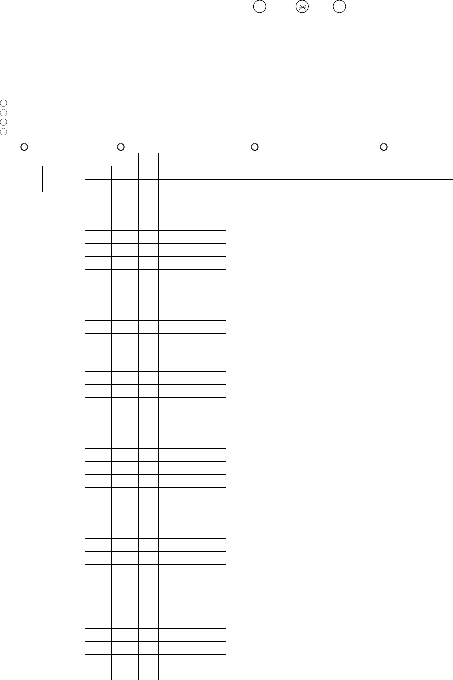
6. Soft switch description
• Soft switch
2 – 10
1 Protect from echo No Yes 0
2 Forced 4800 BPS reception Yes No 0
3 Footer print Yes No 0
4 Length limitation of copy/send/receive No limit Copy/send: 60cm 0
Receive: 1m
5 CSI transmission No transmitted Transmitted 0
6 DIS receive acknowledgement during G3 Twice NSF: Once 0
transmission DIS: Twice
7 Non-modulated carrier for V29 transmission Yes No 0
mode
8 EOL detect timer 25 s 13 s 0
Modem speed V.33 V.17 V.29 V.27 ter
14400 12000 14400 12000 9600 7200 9600 7200 4800 2400
1 0011110000 1
2 1100000000 0
3 0101010110 0
4 0000111100 0
5 Sender’s information transmit No Yes 0
6 Reserved 0
7 Communication error treatment in RTN No communication error Communication error 0
sending mode (reception)
8 CNG transmission No Yes 0
CED tone signal interval 1000ms 750ms 500ms 75ms
1 No. 1 1 1 0 0 0
2 No. 2 1 0 1 0 0
3 MR coding No Yes 0
4 ECM mode No Yes 0 OPTION
5 ECM MMR mode No Yes 0
6 Reserved 0
7 Reserved 0
8 Reserved 0
1 Signal transmission level Binary input 0
2 No. = 16 8 4 2 1 1
3 1 2 3 4 5 1
4 0 1 1 1 0 1
5 0
6 Protocol monitor (error print) Printed at com. error Not printed 0
7 Protocol monitor Yes No 0
8 Line monitor Yes No 0
Digital line equalization setting (Reception) 7.2km 3.6km 1.8km 0km
1 No. 1 11000
2 No. 2 10101
Digital line equalization setting 7.2km 3.6km 1.8km 0km
3 (Transmission) No. 3 11000
4 No. 4 10100
Digital cable equalizer setting (Reception 7.2km 0km
5 for Caller ID) No. 5 1 0 0
6 No. 6 1 0 0
7 Error criterion 10 ~ 20 % 5 ~ 10 % 0
8 Anti junk fax check Yes No 1
SW
NO. DATA
NO. ITEM Switch setting and function
10
Remarks
Initial
setting
SW
l
A1
SW
l
A2
SW
l
A3
SW
l
A5
SW
l
A4

FO-CC500A
FO-K01A
2 – 11
1 Reserved 0
2 End Buzzer Yes No 1
3 Disconnect the line when DIS is received in No Yes 1
RX mode
4 Equalizer freeze control (MODEM) On Off 0
5 Equalizer freeze control 7200 BPS only No Yes 0
6 CNG transmission in manual TX mode Yes No 1
7 Reserved 0
8 Modem speed automatic fallback when RX Yes No 0
level is under -40dBm
1 Recall interval Binary input 0
2 No. = 8 4 2 1 1
3 1 2 3 4 0
4 0 1 0 1 1
5 Recall times Binary input 0
6 No. = 8 4 2 1 0
7 5 6 7 8 1
8 0 0 1 0 0
1 Dial pausing (sec/pause) 4 sec 2 sec 0
2 Dial tone detection (before auto dial) No Yes 1
3 Reserved 0
4 Busy tone detection (after auto dial) No Yes 1
Waiting time after dialing
45 seconds 55 seconds 90 seconds 140 seconds
5 No.5 00110
6 No.6 01010
7 Reserved 0
8 Reserved 0
1 Reserved 0
2 Reserved 0
3 Reserved 0
4 Reserved 0
5 Reserved 0
Auto dial mode delay timer of before line
0 second 1.5 seconds 3.0 seconds 4.5 seconds
6 connect No.6 00111
7 No.7 01010
8 Reserved 0
Auto dial mode delay timer of after line
1.7 seconds 3.0 seconds 3.6 seconds 4.0 seconds
1 connect No.1 00110
2 No.2 01011
3 Dial mode Tone Pulse 1 OPTION
4 Pulse → Tone change function by key Enable Disable 1
5 Dial pulse make/break ratio (%) 40/60 33/67 0
6 Reserved 0
7 Reserved 0
8
Recalling fixed only one time when dialing was
Yes No 0
unsuccessful without detecting busy tone signal
1 DTMF signal transmission level (Low) Binary input 1
2 No. = 16 8 4 2 1 0
3 1 2 3 4 5 0
4 1 0 0 1 0 1
5 0
6 Reserved 0
7 FLASH send time Long time(450ms) Short time(100ms) 0
8 Reserved 0
SW
NO. DATA
NO. ITEM Switch setting and function
10
Remarks
Initial
setting
SW
l
B5
SW
l
B4
SW
l
B3
SW
l
B2
SW
l
B1
SW
l
A6

FO-CC500A
FO-K01A
2 – 12
1 DTMF signal transmission level (High) Binary input 0
2 No. = 16 8 4 2 1 1
3 1 2 3 4 5 1
4 0 1 1 1 1 1
5 1
6 Reserved 0
7 Reserved 0
8 Reserved 0
Reading slice (Binary) Factory Light Dark Darker in
setting dark
1 No. 1 0 1 0 1 0
2 No. 2 0 0 1 1 0
Reading slice (Half tone) Factory Light Dark Darker in
setting dark
3 No. 3 0 1 0 1 0
4 No. 4 0 0 1 1 0
5 Line density selection Fine Standard 0
6 Reserved 0
7 MTF correction in half tone mode No Yes 0
8 Reserved 0
1 Number of rings for auto receive Binary input 0 OPTION
2 No. = 8 4 2 1 0
3 1 2 3 4 1
4 0 0 1 0 0
5 Automatic switching manual to auto receive Reception after 4 rings No reception 0
mode
6 Reserved 0
Cl detect frequency
As PTT 11.5Hz 13.0Hz 20.0Hz
7 No.7 0 0 1 1 0
8 No.8 0 1 0 1 0
1 Reserved 0
2 Reserved 0
3 Reserved 0
4 Distinctive ringing detection Yes No 0 OPTION
5 Caller ID function Yes No 0 OPTION
6 Caller ID detect during CI off All times Only first 1
7 Reserved 0
8 Reserved 0
1 Cl off detection timer (0-1550ms setting by Binary input 0
2 50ms step) No. = 16 8 4 2 1 1
3 1 2 3 4 5 1
4 0 1 1 1 0 1
5 0
6 Country select for Caller ID New Zealand Australia 0 OPTION
7 Reserved 0
8 Reserved 0
SW
NO. DATA
NO. ITEM Switch setting and function
10
Remarks
Initial
setting
SW
l
B6
SW
l
C1
SW
l
D2
SW
l
D1
SW
l
D3
FO-CC500A
FO-K01A
1 Tel/Fax Automatic switching mode Tel/Fax auto switch Switch to Fax 1
Pseudo ringing time at the tel/fax automatic 15 sec 60 sec 30 sec 120 sec OPTION
2 switching mode No.2 0 0 1 1 0
3 No.3 0 1 0 1 0
4 Number of CNG singnal detection at the Twice Once 1
Tel/Fax automatic switching mode
5 CNG detection when TEL/FAX mode 3 sec 5 sec 0
6 Pseudo ringer ON/OFF cycle 1 sec ON/4 sec OFF 1 sec ON/2 sec OFF 0
7 Post answer tone (Tel/Fax mode) No Yes 0
8 Type of post answer tone LA-SI-DO tone 800Hz single tone 1
1 Pseudo ringer sound volume Binary input 1
2 (0 to -15dBm setting by 1dBm step) No. = 8 4 2 1 0
3 1 2 3 4 1
4 1 0 1 0 0
5 Post answer tone transmission level Binary input 1
6 (0 to -15dBm setting by 1dBm step) No. = 8 4 2 1 0
7 5 6 7 8 0
8 1 0 0 0 0
1 Reserved 0
Action select when DTMF “#” is received
No Action No Action A.M. Remote Disconnect
during tel/fax automatic Operation Line
2 No.2 0 0 1 1 1
3 No.3 0 1 0 1 0
4 Reserved 0
5 Reserved 0
6 Reserved 0
7 Reserved 0
8 Reserved 0
DTMF detection time 50ms 80ms 100ms 120ms
1 No. 1 0 0 1 1 0
2 No. 2 0 1 0 1 0
3 Protection of remote reception (5 ) detect Yes No 1
4 Remote reception with GE telephone Compatible Not compatible 1
5 Remote operation code figure by external Binary input 0
6 TEL (0~9) No. = 8 4 2 1 1
7 5 6 7 8 0
8 0 1 0 1 1
1 CNG detection in STAND-BY mode Yes No 1 OPTION
Number of CNG detect (AM mode) 1pulse 2pulses 3pulses 4pulses
2 No. 2 0 0 1 1 0
3 No. 3 0 1 0 1 1
Number of CNG detect (STAND-BY mode) 1pulse 2pulses 3pulses 4pulses
4 No. 4 0 0 1 1 0
5 No. 5 0 1 0 1 1
6 Reserved 0
7 Reserved 0
8 Reserved 0
1 Reserved 0
2 Reserved 0
3 Reserved 0
4 Reserved 0
5 Reserved 0
6 Reserved 0
7 Reserved 0
8 Reserved 0
2 – 13
SW
l
E1
SW
NO. DATA
NO. ITEM Switch setting and function
10Remarks
Initial
setting
SW
l
E2
SW
l
E3
SW
l
F1
SW
l
F2
SW
l
G1

FO-CC500A
FO-K01A
2 – 14
1 Reserved 0
2 Reserved 0
3 Reserved 0
4 Reserved 0
5 Reserved 0
6 Reserved 0
7 Reserved 0
8 Reserved 0
1 Reserved 0
2 Reserved 0
3 Reserved 0
4 Reserved 0
5 Reserved 0
6 Reserved 0
7 Reserved 0
8 Reserved 0
Busy tone detection ON/OFF time (Lower 150ms 200ms 250ms 350ms
1 duration) No. 1 0 0 1 1 0
2 No. 2 0 1 0 1 0
Busy tone detection ON/OFF time (Upper 650ms 900ms 1500ms 2700ms
3 duration) No. 3 0 0 1 1 0
4 No. 4 0 1 0 1 1
5 Busy tone detect continuation sound detect No Yes 0
during OGM
6 Busy tone detect continuation sound detect No Yes 0
7 Busy tone detect intermittent sound detect No Yes 0
during OGM
8 Busy tone detect intermittent sound detect No Yes 0
Busy tone detection pulse number 2pulses 4pulses 6pulses 10pulses
1 No. 1 0 0 1 1 0
2 No. 2 0 1 0 1 1
3 Fax switching when A.M. full Yes No 0 OPTION
4 Busy tone detect continuation sound detect 320Hz - 570Hz 320Hz - 460Hz 0
frequency
5 Reserved 0
6 Reserved 0
7 AM OGM announce only mode Yes No 0 OPTION
8 Busy tone continuous sound detect time 5s 10s 1
ICM recording time 4min 15s 30s 60s OPTION
1 No. 1 0 0 1 1 0
2 No. 2 0 1 0 1 0
A.M. quiet time 1 2s 3s 4s 5s
3 No. 3 0 0 1 1 0
4 No. 4 0 1 0 1 0
A.M. quiet time 2 0s 1s 2s 3s
5 No. 5 0 0 1 1 1
6 No. 6 0 1 0 1 0
7 Key input buzzer on/off switch (Two way On Off 0
recording mode)
8 Reserved 0
SW
l
G2
SW
NO. DATA
NO. ITEM Switch setting and function
10Remarks
Initial
setting
SW
l
G3
SW
l
H1
SW
l
H2
SW
l
I1

FO-CC500A
FO-K01A
1 A.M. quiet detect time Binary input 0
2 No. = 16 8 4 2 1 0
3 1 2 3 4 5 1
4 00110 1
5 0
6 Reserved 0
7 Reserved 0
8 Reserved 0
1 Reserved 0
2 Max OGM record time 15s 60s 0
3 Two way record function Disable Enable 1
4 Toll saver Disable Enable 0 OPTION
5 Reserved 0
6 Reserved 0
7 Reserved 0
8 Transfer dial recall No Yes 0
1 AGC maximum gain (line) Binary input 0
2 (10 ~ 25 dB) (1 dB step) No. = 8 4 2 1 1
3 1 2 3 4 0
4 0101 1
5 AGC maximum gain (Mic) Binary input 0
6 (10 ~ 25 dB) (1 dB step) No. = 8 4 2 1 1
7 5 6 7 8 1
8 0110 0
1 AGC eref access code (line) Binary input 1
2 (-0 ~ -30 dB) (2 dB step) No. = 8 4 2 1 0
3 1 2 3 4 1
4 1011 1
5 AGC eref access code (Mic) Binary input 1
6 (-0 ~ -30 dB) (2 dB step) No. = 8 4 2 1 1
7 5 6 7 8 0
8 1101 1
1 AGC again adaptation threshold (line) Binary input 1
2 No. = 8 4 2 1 1
3 1 2 3 4 1
4 1111 1
5 AGC again adaptation threshold (Mic) Binary input 1
6 No. = 8 4 2 1 1
7 5 6 7 8 1
8 1111 1
AGC slew rate (line) Slow Normal Little fast Fast
1 No. 1 0 0 1 1 1
2 No. 2 0 1 0 1 1
AGC slew rate (Mic) Slow Normal Little fast Fast
3 No. 3 0 0 1 1 1
4 No. 4 0 1 0 1 1
5 Reserved 0
6 Reserved 0
7 Reserved 0
8 Reserved 0
2 – 15
SW
l
I3
SW
l
I4
SW
l
I5
SW
l
I6
SW
NO. DATA
NO. ITEM Switch setting and function
10Remarks
Initial
setting
SW
l
I7
SW
l
I2
FO-CC500A
FO-K01A
2 – 16
1 Reserved 0
2 Reserved 0
3 Sender’s phone number setting Cannot change Change allowed 0
4 Reserved 0
5 Reserved 0
6 Reserved 0
Ringer volume Off Low Middle High OPTION
7 No. 7 0 0 1 1 1
8 No. 8 0 1 0 1 0
1 Reserved 0
2 Reserved 0
3 Reserved 0
4 Reserved 0
5 Reserved 0
Speaker volume (5 stages)
Very Low
Low Middle High
Very High
OPTION
6 No. 6 000010
7 No. 7 001101
8 No. 8 010100
1 Reserved 0
Communication results printout E/T/M
Send only
Always No print Err only OPTION
2(Transaction report) No. 2 000011
3 No. 3 001100
4 No. 4 010100
5 OGM/ICM output level to speaker Binary input 0
6 (0 dB ~ -15 dB) (1 dB step) No. = 8 4 2 1 0
7 5 6 7 8 1
800111
1 Reserved 0
2 Reserved 0
3 OGM/ICM output level Binary input 0
4 (0 dB ~ -32 dB) (1 dB step) No. = 32 16 8 4 2 1 0
5 3 4567 8 1
6 0 0100 0 0
7 0
8 0
1 Reserved 0
2 Reserved 0
3 Reserved 0
4 Reserved 0
5 Cut off mode (COPY mode) Yes No 1 OPTION
6 A4 paper enable Enable Disable 1
7 LEGAL & LETTER paper enable Enable Disable 0
8 Reserved 0
SW
l
J2
SW
l
J3
SW
l
K1
SW
l
L1
SW
NO. DATA
NO. ITEM Switch setting and function
10Remarks
Initial
setting
SW
l
J1

FO-CC500A
FO-K01A
2 – 17
Paper set size LETTER LEGAL A4
1 No. 1 0 0 1 1
2 No. 2 0 1 0 0
3 Automatic reduce of receive Auto 100 % 1 OPTION
Print contrast Normal Lighter Light Dark Darker OPTION
4 No. 4 000011
5 No. 5 001100
6 No. 6 010100
7
Reception reduction ratio in case of memory ful
100 % 93 % 0
8 Reserved 0
1 Reserved 0
2 Reserved 0
3 Reserved 0
Default speaker volume in speaker monitor function
Low Low Middle High
4 No. 4 0 0 0 0 0
5 No. 5 0 0 0 0 0
6 No. 6 0 0 1 1 0
7 No. 7 0 1 0 1 0
8 Reserved 0
1 Reserved 0
2 Reserved 0
3 Reserved 0
4 Reserved 0
5 Reserved 0
6 Reserved 0
7 Reserved 0
8 Reserved 0
1 Reserved 0
2 Reserved 0
3 Reserved 0
4 Reserved 0
5 Reserved 0
6 Reserved 0
7 Reserved 0
8 Reserved 0
1 Reserved 0
2 Reserved 0
3 Reserved 0
4 Reserved 0
5 Reserved 0
6 Reserved 0
7 Reserved 0
8 Reserved 0
1 Reserved 0
2 Reserved 0
3 Reserved 0
4 Reserved 0
5 Reserved 0
6 Reserved 0
7 Reserved 0
8 Reserved 0
SW
l
M2
SW
l
N1
SW
NO. DATA
NO. ITEM Switch setting and function
10Remarks
Initial
setting
SW
l
N2
SW
l
N3
SW
l
M1
SW
l
L2
FO-CC500A
FO-K01A
TX RX
CED
DIS
T
2 – 18
• Soft switch function description
SW-A1 No. 1 Protect from echo
Used to protect from echo in reception.
SW-A1 No. 2 Forced 4800BPS reception
When line conditions warrant that receptions take place at 4800 BPS
repeatedly.
It may improve the success of receptions by setting at 4800BPS.
This improves the receiving document quality and reduces handshake
time due to fallback during training.
SW-A1 No. 3 Footer print
When set to "1", the date of reception, the sender machine No., and the
page No. are automatically recorded at the end of reception.
SW-A1 No. 4 Length limitation of copy/send/receive
Used to set the maximum page length.
To avoid possible paper jam, the page length is normally limited to 0.6
meter for copy or transmit, and 1 meters for receive.
It is possible to set it to "No limit" to transmit a long document, such as a
computer print form, etc. (In this case, the receiver must also be set to
no limit.)
SW-A1 No. 5 CSI transmission
(CSI TRANSMISSION) is a switch to set whether the machine sends or
does not send the signal (CSI signal) informing its own telephone No. to
the remote fax machine when information is received. When "nonsending"
is set, the telephone No. is not output on the remote transmitting ma-
chine if the remote transmitting machine has the function to display or
print the telephone No. of receiving machine, using this CSI signal.
SW-A1 No. 6 DIS receive acknowledgment during G3 transmission
Used to make a choice of whether reception of DIS (NSF) is acknowl-
edged after receiving two DISs (NSFs) or receiving one DIS (two NSFs).
It may be useful for overseas communication to avoid an echo sup-
pression problem, if set to 1.
SW-A1 No. 7 Non-modulated carrier for V29 transmission mode
Though transmission of a non-modulated carrier is not required for trans-
mission by the V29 modem according to the CCITT recommendation, it
may be permitted to a send non-modulated carrier before the image
signal to avoid an echo suppression problem. It may be useful for over-
seas communication to avoid an echo suppression problem, if set to 1.
SW-A1 No. 8 EOL (End Of Line) detect timer
Used to make a choice of whether to use the 25-second or 13-second
timer for detection of EOL.
This is effective to override communication failures with some facsimile
models that have longer EOL detection.
SW-A2 No. 1 ~ No. 4 Modem speed
Used to set the initial modem speed. The default is 14400BPS.
It may be necessary to program it to a slower speed when frequent line
fallback is encountered, in order to save the time required for fallback
procedure.
SW-A2 No. 5 Sender’s information transmit
(SENDER’S INFORMATION TRANSMISSION) is a switch to set the
function to print the content of HEADER PRINT described in the passcode
list at the front end of receiver’s original when original is sent to the
remote machine.
If this switch is set to "NO", the HEADER PRINT is not output at the
receiving machine.
SW-A2 No. 6 Reserved
Set to "0".
SW-A2 No. 7 Communication error treatment in RTN sending mode
(Reception)
Used to determine communication error treatment when RTN is sent by
occurrence of a received image error in G3 reception. When it is set to
"1", communication error is judged as no error.
SW-A2 No. 8 CNG transmission
When set to "0" , this model allows CNG transmission by pressing the
Start key in the key pad dialing mode. When set to "1", CNG transmis-
sion in the key pad dialing mode cannot be performed. In either case.
CNG transmission can be performed in the auto dial mode.
SW-A3 No. 1, No. 2 CED tone signal interval
For international communication, the 2100Hz CED tone may act as an
echo suppression switch, causing a communication problem.
Though SW-A3 No. 1 and No. 2 are normally set to 0, this setting is used
to change the time between the CED tone signal to eliminate the com-
munication caused by echo.
SW-A3 No. 3 MR Coding
MR Coding is enable.
SW-A3 No. 4 ECM mode
Used to determine ECM mode function. Refer to following table.
(Depending on remote machine)
SW-A3 No. 5 ECM MMR mode
See SW-A3 No. 4.
SW-A3 No. 6 ~ No. 8 Reserved
Set to "0".
SW-A4 No. 1 ~ No. 5 Signal transmission level
Used to control the signal transmission level in the range of-0dB to-
31dB.
SW-A4 No. 6 Protocol monitor (Error print)
If set to "1", protocol is printed at communication error.
SW-A4 No. 7 Protocol monitor
Normally set to "0". If set to "1", communication can be checked, in case
of trouble, without using a G3 tester or other tools.
When communication FSK data transmission or reception is made, the
data is taken into the buffer. When communication is finished, the data
is analyzed and printed out. When data is received with the line monitor
(SW-A4 No. 8) set to "1" the reception level is also printed out.
SW-A4 No. 8 Line monitor
Normally set to "0". If set to "1", the transmission speed and the recep-
tion level are displayed on the LCD. Used for line tests.
SW-A5 No. 1, No. 2 Digital line equalization setting (Reception)
Line equalization when reception is to be set according to the line char-
acteristics.
Setting should be made according to distance between the telephone
and the telephone company central switching station.
SW-A5 No. 3, No. 4 Digital line equalization setting (Transmission)
Line equalization when transmitter is to be set according to the line
characteristics.
Setting should be made according to distance between the telephone
and the telephone company central switching station.
SW-A5 No. 5, No. 6 Digital cable equalizer setting
(Reception for Caller ID)
Line equalization when reception for CALLER ID is to be set according
to the line characteristics.
Setting should be made according to distance between the telephone
and the telephone company central switching station.
SW-A3 No.4 ECM MODE 0 0 1 1
SW-A3 No.5 ECM MMR MODE 0 1 0 1
Compression ECM MMR mode Yes No No No
method ECM MH mode Yes Yes No No
MR Mode Yes Yes Yes Yes
FO-CC500A
FO-K01A
RAPID01 CML RELAY ON
DIALLING
No.6 No.7
0 0 0sec
0 1 1.5sec
1 0 3.0sec
1 1 4.5sec
RAPID01 CML RELAY ON DIAL DATA
No.1 No.2
0 0 1.7sec
0 1 3.0sec
1 0 3.6sec
1 1 4.0sec
2 – 19
SW-A5 No. 7 Error criterion
Used to select error criterion for sending back RTN when receiving im-
age data.
SW-A5 No. 8 Anti junk fax check
When using the Anti junk fax function, set to "1".
SW-A6 No. 1 Reserved
Set to "0".
SW-A6 No. 2 End buzzer
Setting this bit to 0 will disable the end buzzer (including the error buzzer/
on-hook buzzer).
SW-A6 No. 3 Disconnect the line when DIS is received in RX mode
Bit1= 0: When DIS signal is received during RX mode, the line is discon-
nected immediately.
Bit1= 1: When DIS signal is received during RX mode, the line is discon-
nected on the next tone.
SW-A6 No. 4 Equalizer freeze control (MODEM)
This switch is used to perform reception operation by fixing the equal-
izer control of modem for the line which is always in an unfavorable
state and picture cannot be received.
* Usually, the control is executed according to the state of line where
the equalizer setting is changed always.
SW-A6 No. 5 Equalizer freeze control 7200BPS only
Setting which specifies SW-A3 No. 6 control only in the condition of
7200BPS modem speed.
SW-A6 No. 6 CNG transmission in manual TX mode
When set to "1", fax transmit the CNG signal in case of manual trans-
mission mode (User press the START key after waiting for the fax an-
swering signal from handset or speaker).
SW-A6 No. 7 Reserved
Set to "0".
SW-A6 No. 8 Modem speed automatic fallback when RX level is
under -40dBm
When set to "1", if fax signal level is under -40dBm during reception,
machine selects the slower modem speed automatically.
It is effective when noises occur on the received document due to the
long distance communications.
SW-B1 No. 1 ~ No. 4 Recall interval
Choice is made for a redial interval for speed and rapid dial calls.
Use a binary number to program this. If set to 0 accidentally, 1 will be
assumed.
SW-B1 No. 5 ~ No. 8 Recall times
Choice is made as to how many redials there should be.
SW-B2 No. 1 Dialing pause (sec/pause)
Pauses can be inserted between telephone numbers of direct dial con-
nection. Selection of 4 sec or 2 sec pause is available.
SW-B2 No. 2 Dial tone detection (before auto dial)
Used to set YES/NO of dial tone detection in auto dialing.
SW-B2 No. 3 Reserved
Set to "0".
SW-B2 No. 4 Busy tone detection (after auto dial)
Used to set busy tone detection in auto dialing.
SW-B2 No. 5, No. 6 Waiting time after dialing
This is time waiting for the opponent’s signals after dialing.
SW-B2 No. 7, No. 8 Reserved
Set to "0".
SW-B3 No. 1 ~ No. 5 Reserved
Set to "0".
SW-B3 No. 6, No. 7 Auto dial mode Delay timer of before line con-
nect
Delay time between the dial key input and line connection under the
auto dial mode.
SW-B3 No. 8 Reserved
Set to "0".
SW-B4 No. 1, No. 2 Auto dial mode Delay timer of after line connect
Delay time between the line connection and dial data output under the
auto dial mode.
SW-B4 No. 3 Dial mode
When using the pulse dial, set to 1. When using the tone dial, set to 0.
SW-B4 No. 4 Pulse → Tone change function by key
When setting to 1, the mode is changed by pressing the key from the
pulse dial mode to the tone dial mode.
SW-B4 No. 5 Dial pulse make/break ratio (%)
When using the 33% make ratio pulse dial, set to "0".
When using the 40% make ratio pulse dial, set to "1".
SW-B4 No. 6, No. 7 Reserved
Set to "0".
SW-B4 No. 8 Recalling fixed only one time when dialing was un-
successful without detecting busy tone signal
When dialing results in failure since the busy tone cannot be detected,
recalling is fixed to one time.
Supplementary explanation
If time-out termination is made when dialing, only single recall is possi-
ble even if the setting time of recalls (SW-B1 No. 5 - No. 8) has been set
to some times. This soft switch is added in order to meet FCC regula-
tions.
SW-B5 No. 1 ~ No. 5 DTMF signal transmission level (Low)
The transmission level of DTMF signal is adjusted. (lower frequency)
00000: 0dBm
↓
11111: -15.5dBm (-0.5dBm x 31)
SW-B5 No. 6 Reserved
Set to "0".
SW-B5 No. 7 FLASH send mode
The Brake time when REMOTE/FLASH key on the Cordless Handset is
pressed. Set to “0”.
SW-B5 No. 8 Reserved
Set to "0".
SW-B6 No. 1 ~ No. 5 DTMF signal transmission level (High)
The transmission level of DTMF signal is adjusted. (higher frequency)
00000: 0dBm
↓
11111: -15.5 dBm (-0.5dBm x 31)
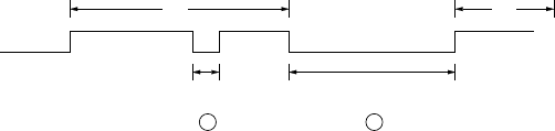
FO-CC500A
FO-K01A
2 – 20
SW-B6 No. 6 ~ No. 8 Reserved
Set to "0".
SW-C1 No. 1, No. 2 Reading slice (Binary)
Used to determine the set value of reading density in standard/fine mode.
The standard setting is "00" (Factory setting is "00")
SW-C1 No. 3, No. 4 Reading slice (Half tone)
Used to determine the set value of reading density in half tone mode.
The standard setting is "00" (Factory setting is "00")
SW-C1 No. 5 Line density selection
Used to set the transmission mode which is automatically selected when
the Resolution key is not pressed. In the copy mode, however, the fine
mode is automatically selected unless the Resolution key is manually
set to another mode.
SW-C1 No. 6 Reserved
Set to "0".
SW-C1 No. 7 MTF correction in half tone mode
This allows selection of MTF correction (dimness correction) in the half
tone mode.
When "NO" (=1) is selected, the whole image becomes soft and mild.
Clearness of characters will be reduced. Normally set to "YES" (=0).
SW-C1 No. 8 Reserved
Set to "0".
SW-D1 No. 1 ~ No. 4 Number of rings for auto receive
When the machine is set in the auto receive mode, the number of rings
before answering can be selected. It may be set from one to four rings
using a binary number. Since the facsimile telephone could be used as
an ordinary telephone if the handset is taken off the hook, it should be
programmed to the user’s choice. If the soft switch was set to 1, direct
connection is made to the facsimile. If a facsimile calling beep was heard
when the handset is taken off the hook, press the START key and put
the handset on the hook to have the facsimile start receiving. If it was
set to 0 accidentally, receive ring is set to 1.
NOTE: If the machine is set to answer after a large number of rings, it
may not be able to receive faxes successfully. If you have diffi-
culty receiving faxes, reduce the number of rings to a maximum
of 6.
SW-D1 No. 5 Automatic switching manual to auto receive mode
This soft switch is used to select whether the machine should switch to
the auto receive mode after 4 rings in the manual receive mode or re-
main in the same way as SW-D1 No. 1, No. 2, No. 3 and No. 4 "0"0"1"0"
(4 rings).
SW-D1 No. 6 Reserved
Set to "0".
SW-D1 No. 7, No. 8 CI detect frequency
Detection frequency of ring signal for auto reception is set.
When set to No. 6=0, No. 7=0, frequency is set to PTT recommenda-
tion.
When set to No. 6=0, No. 7=1, frequency is set to 11.5Hz or more.
When set to No. 6=1, No. 7=0, frequency is set to 13.0Hz or more.
When set to No. 6=1, No. 7=1, frequency is set to 20.0Hz or more.
SW-D2 No. 1 ~ No. 3 Reserved
Set to "0".
SW-D2 No. 4 Distinctive ringing detection
When set to "1", machine recognize the Cl signal FAX ringing or TEL
ringing automatically.
SW-D2 No. 5 Caller ID function
Used for Caller ID function.
SW-D2 No. 6 Caller ID detect during CI off
Detection of caller ID signal is performed as follows:
0:First CI OFF only
1:All of CI OFF
AB
400msec 2000msec
1 2
SW-D2 No. 7, No. 8 Reserved
Set to "0".
SW-D3 No. 1 ~ No. 5 CI off detection timer (0-1550ms setting by
50ms step)
Set the minimum time period of CI signal interruption.
(Example)
01110 (50ms ~ 14):
700ms (CI interruption>700ms:Judged as a CI OFF section)
The section 1 is not judged as a CI OFF section, the CI signal A
is counted as one signal.
The section 2 is judged as a CI OFF section, the CI signal B is
considered as the second signal.
00111 (50ms ~ 7):
350ms (CI interruption>350ms:Judged as a CI OFF section)
The section 1 is judged as a CI OFF section, and the CI signal A
is counted as two signals.
The section 2 is judged as a CI OFF section, and the CI signal B
is considered as the third signal.
SW-D3 No. 6 Country select for Caller ID
When machine using in Australia, set to "0".
When machine using in New Zealand, set to "1".
SW-D3 No. 7, No. 8 Reserved
Set to "0".
SW-E1 No. 1 Tel/Fax Automatic switching mode
Used to set auto TEL/FAX switching mode or to set the normal fax mode.
SW-E1 No. 2, No. 3 Pseudo ringing time at the tel/fax automatic
switching mode
Choise is made as to how long to rumble the dummy ringer on TEL/FAX
automatic switching mode.
SW-E1 No. 4 Number of CNG signal detection at the tel/fax auto-
matic switching mode
Used for detection of CNG in one or two tones in the TEL/FAX auto-
matic switching mode.
SW-E1 No. 5 CNG detection when TEL/FAX mode
The switch which sets the time from the start of CNG detection to the
end of detection.
SW-E1 No. 6 Pseudo ringer ON/OFF cycle
When set to "0", pseudo ringer is 1 sec ON and 2 sec OFF cycles.
When set to "1", pseudo ringer is 1 sec ON and 4 sec OFF cycles.
SW-E1 No. 7 Post answer tone (TEL/FAX mode)
When set to "0", machine send the tones in TEL/FAX auto changeover
mode.
SW-E1 No. 8 Type of post answer tone
When set to "0", post answer tone is 800Hz single tone.
When set to "1", post answer tone is 880Hz/988Hz/1046Hz(LA-SI-DO)
tone.
SW-E2 No. 1 ~ No. 4 Pseudo ringer sound volume
(0 ~ -15dBm setting by 1dBm step)
Used to adjust the sound volume of pseudo ringer to the line (ring back
tone) generated on selecting TEL/FAX.
SW-E2 No. 5 ~ No. 8 Post answer tone transmission level
(0 ~ -15dBm setting by 1dBm step)
Used to adjust the sound volume of post answer tone to the line gener-
ated on selecting TEL/FAX.
SW-E3 No. 1 Reserved
Set to "0".

FO-CC500A
FO-K01A
2 – 21
SW-E3 No. 2, No.3 Action select when DTMF "#" is received during
tel/fax automatic switching mode
When set to No. 2-1, No. 3-1, if machine detects the DTMF code #
during tel/fax automatic switching mode, stop the pseudo ringer and
disconnect the
line.
This effect when operator wants to stop the pseudo ringer from exten-
sion phone connected with parallel.
SW-E3 No. 4 ~ No. 8 Reserved
Set to "0".
SW-F1 No. 1, No. 2 DTMF detect time
Used to set detect time of DTMF (Dual Tone Multi Frequency) used in
remote reception (5 ).
The longer the detect time is, the less the error detection is caused by
noises.
SW-F1 No. 3 Protection of remote reception (5 ) detect
Used to set the function of remote reception (5 ). When set to "1",
the remote reception function is disabled.
SW-F1 No. 4 Remote reception with GE telephone
(Corresponding to TEL made by GE) P. B. X.
"1": Compatible with TEL mode by GE
"0": Not compatible
•When sending (5 ) for remote reception with a GE manufactured
telephone remote reception may not take place because of special
specifications in their DTMF.
To overcome this, a soft SW is provided to change the modem set-
ting to allow for remote reception.
•If this soft SW is set to "1", other telephone sets may be adversely
affected.
SW-F1 No. 5 ~ No. 8 Remote operation code figure by external TEL
(0 ~ 9)
Remote operation codes can be changed from 0 through 9. If set to
greater than 9, it defaults to 9. The "5 " is not changed.
Ex-7 (Default: 5 )
SW-F2 No. 1 CNG detection in STAND-BY mode
When setting to "1", the CNG signal detection function during stand-by
stops.
SW-F2 No. 2, No. 3 Number of CNG detect (AM mode)
Used for detection of CNG in 1 to 4 pulses.
SW-F2 No. 4, No. 5 Number of CNG detect (STAND-BY mode)
Used for detection of CNG in 1 to 4 pulses.
SW-F2 No. 6 ~ No. 8 Reserved
Set to "0".
SW-G1 No. 1 ~ No. 8 Reserved
Set to "0".
SW-G2 No. 1 ~ No. 8 Reserved
Set to "0".
SW-G3 No. 1 ~ No. 8 Reserved
Set to "0".
SW-H1 SW-H1 SW-H1 SW-H1 Detection range
No. 1 No. 2 No. 3 No. 4
0 0 0 0 150msec ~ 650msec
0 0 0 1 150msec ~ 900msec
0 0 1 0 150msec ~ 1500msec
0 0 1 1 150msec ~ 2700msec
0 1 0 0 200msec ~ 650msec
0 1 0 1 200msec ~ 900msec
0 1 1 0 200msec ~ 1500msec
0 1 1 1 200msec ~ 2700msec
1 0 0 0 250msec ~ 650msec
1 0 0 1 250msec ~ 900msec
1 0 1 0 250msec ~ 1500msec
1 0 1 1 250msec ~ 2700msec
1 1 0 0 350msec ~ 650msec
1 1 0 1 350msec ~ 900msec
1 1 1 0 350msec ~ 1500msec
1 1 1 1 350msec ~ 2700msec
SW-H1 No. 5 Busy tone detect continuation sound detect during
OGM
Used to detect the continuous tone of specific frequency during OGM
output.
SW-H1 No. 6 Busy tone detect continuation sound detect
Used to select detection of the continuous sound of certain frequency.
SW-H1 No. 7 Busy tone detect intermittent sound detect during OGM
Used to detect the intermittent tone of specific frequency during OGM
output.
SW-H1 No. 8 Busy tone detect intermittent sound detect
Used to select detection of the intermittent sound of certain frequency.
SW-H2 No. 1, No. 2 Busy tone detection pulse number
Used to set detection of Busy tone intermittent sounds.
SW-H2 No. 3 Fax switching when A.M. full
If the answering machine’s memory is full and there is no response, the
machine automatically switches to Fax reception.
SW-H2 No. 4 Busy tone detect continuation sound detect frequency
Set detecting frequency of busy tone continuation sound for 320 ~ 570
Hz of 320 ~ 460 Hz.
SW-H2 No. 5, No. 6 Reserved
Set to "0".
SW-H2 No. 7 AM OGM announce only mode
If this switch is set to 1, the machine will not record ICM.
(disconnect the line after OGM output)
SW-H1 No. 1, No. 2 Busy tone detection ON/OFF time (Lower dura-
tion)
The initial value of detection is set according to electric condition.
The set value is changed according to the local switch board. (Erro-
neous detection of sound is reduced.)
Normally the upper limit is set to 900msec, and the lower limit to 200msec.
If erroneous detection is caused by sound, etc., adjust the detection
range.
The lower limit can be set in the range of 350msec to 150msec.
SW-H1 No. 3, No. 4 Busy tone detection ON/OFF time (Upper dura-
tion)
Similarly to SW-H1 No. 1, the set value can be varied.
The upper limit can be set in the range of 650msec to 2700msec.
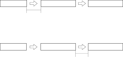
FO-CC500A
FO-K01A
2 – 22
SW-I5 No. 1 ~ No. 4 AGC eref access code (Line)
(-0 ~ -30dB) (2dB step)
The AGC Energy Reference Level controls the playback level. Any
message having average speech energy above the energy reference level has
its playback level attenuated, and any level has its playback level increased. If
the playback level is too high (low), then decreasing (increasing) the AGC En-
ergy Reference Level will achieve the desired level.
SW-I5 No. 5 ~ No. 8 AGC eref access code (Mic)
(-0 ~ -30dB) (2dB step)
The AGC Energy Reference Level controls the playback level. Any
message having average speech energy above the energy reference level has
its playback level attenuated, and any level has its playback level increased. If
the playback level is too high (low), then decreasing (increasing) the AGC En-
ergy Reference Level will achieve the desired level.
SW-I6 No. 1 ~ No. 4 AGC gain adaptation threshold (Line)
The AGC adjusts the amount of gain applied to the incoming message only
when the average energy exceeds the AGC Gain Adaptation
Threshold. The AGC Gain Adaptation Threshold prevents message
background noise from corrupting the gain provided that the AGC Gain Adapta-
tion Threshold is greater than the background noise energy. In the event that a
message has background noise energy greater than the AGC Gain Adaptation
Threshold, the AGC Gain can be no greater than the AGC Maximum Gain. Note
that the AGC Gain Adaptation Threshold must always be greater than the RPACS
VOX Turn-On Threshold.
SW-I6 No. 5 ~ No. 8 AGC gain adaptation threshold (Mic)
The AGC adjusts the amount of gain applied to the incoming message only
when the average energy exceeds the AGC Gain Adaptation
Threshold. The AGC Gain Adaptation Threshold prevents message
background noise from corrupting the gain provided that the AGC Gain Adapta-
tion Threshold is greater than the background noise energy. In the event that a
message has background noise energy greater than the AGC Gain Adaptation
Threshold, the AGC Gain can be no greater than the AGC Maximum Gain. Note
that the AGC Gain Adaptation Threshold must always be greater than the RPACS
VOX Turn-On Threshold.
SW-I7 No. 1, No. 2 AGC slew rate (Line)
The AGC Slew Rate controls the convergence of the message playback level to
the desired playback level. A large slew rate will allow faster convergence and a
small slew rate will allow slower convergence.
SW-I7 No. 3, No. 4 AGC slew rate (Mic)
The AGC Slew Rate controls the convergence of the message playback
level to the desired playback level. A large slew rate will allow faster
convergence and a small slew rate will allow slower convergence.
SW-I7 No. 5 ~ No. 8 Reserved
Set to "0".
SW-J1 No. 1, No. 2 Reserved
Set to "0".
SW-J1 No. 3 Sender’s phone number setting
Used to make a choice of whether the registered sender’s phone number
can be changed or not. If the switch is set to "1", new registration of the
sender’s phone number is disabled to prevent accidental wrong input.
SW-J1 No. 4 ~ No. 6 Reserved
Set to "0".
SW-J1 No. 7, No. 8 Ringer volume
Used to adjust ringing volume.
SW-J2 No. 1 ~ No. 5 Reserved
Set to "0".
SW-J2 No. 6 ~ No. 8 Speaker volume (5 stages)
Used to adjust sound volume from a speaker.
SW-J3 No. 1 Reserved
Set to "0".
SW-H2 No. 8 Busy tone continuous sound detect time
Set detecting time busy tone continuous sound for 5 or 10 seconds.
SW-I1 No. 1, No. 2 ICM recording time
Used to select the incoming message recording time to 15sec/30sec/
60sec/4min.
SW-I1 No. 3, No. 4 A.M. quiet time 1
Used to select four kinds of no sound time (2 sec ~ 5 sec) after reception
in the T.A.D mode until OGM is output.
SW-I1 No. 5, No. 6 A.M. quiet time 2
Used to select four kinds of no sound time (0 sec ~ 3 sec) after OGM
output the T.A.D mode until ICM recording is started.
SW-I1 No. 7
Key input buzzer on/off switch (Two way recording mode)
Used to turn ON/OFF key input buzzer in the TWO-WAY recording mode.
SW-I1 No. 8 Reserved
Set to "0".
SW-I2 No. 1 ~ No. 5 A.M. quiet detect time
Used to set no sound time (0 sec ~ 32 sec) during the T.A.D. mode
operation.
SW-I2 No. 6 ~ No. 8 Reserved
Set to "0".
SW-I3 No. 1 Reserved
Set to "0".
SW-I3 No. 2 Max OGM record time
Used select the outgoing message recording time to 60sec or 15sec.
SW-I3 No. 3 Two way record function
If this switch is set to "1", the machine disables two way recording.
SW-I3 No. 4 Toll saver
Used to turn on the toll saver function. If it is off, the reception frequency
in the AM mode is identical with that in the FAX mode.
SW-I3 No. 5 ~ No. 7 Reserved
Set to "0".
SW-I3 No. 8 Transfer dial recall
If this switch is set to "1", machine disables redial in Transfer function.
SW-I4 No. 1 ~ No. 4 AGC maximum gain (Line)
(10 ~ 25dB) (1dB step)
The AGC Maximum Gain limits the gain applied by the AGC. Messages with
average energy below the AGC Energy Reference Level will have their average
energy level increased by no more than the AGC Maximum Gain. The AGC
Maximum Gain should average energy of the message with the lowest average
energy to the AGC Energy Reference Level.
SW-I4 No. 5 ~ No. 8 AGC maximum gain (Mic)
(10 ~ 25dB) (1dB step)
The AGC Maximum Gain limits the gain applied by the AGC. Messages with
average energy below the AGC Energy Reference Level will have their average
energy level increased by no more than the AGC Maximum Gain. The AGC
Maximum Gain should average energy of the message with the lowest average
energy to the AGC Energy Reference Level.
Reception OGM output ICM recording
2 sec~ 5 sec ( SW-I1No. 3, No. 4)
Reception OGM output ICM recording
0 sec~3 sec (SW-I1 No. 5, No. 6)
FO-CC500A
FO-K01A
2 – 23
SW-J3 No. 2 ~ No. 4 Communication result printout (Transaction
report)
Every communication, the result can be output. As usual, it is set to print
the timer sending communication error alone. If No. 2: 0 No. 3: 1 No. 4:
0 are set, printing is always on (printed even if it is normally ended).
000: Error, timer and memory sending/receiving
001: Sending
010: Continuous printing
011: Not printed
100: Communication error
SW-J3 No. 5 ~ No. 8 OGM/ICM output level to speaker
(0dB ~ -15dB) (1dB step)
Used to control OGM and ICM output level to speaker.
SW-K1 No.1, No. 2 Reserved
Set to "0".
SW-K1 No. 3 ~ No. 8 OGM/ICM output level to Line
(0dB ~ -32dB) (1dB step)
Used to control OGM and ICM output level to Line.
SW-L1 No. 1 ~ No. 4 Reserved
Set to "0".
SW-L1 No. 5 Cut off mode (COPY mode)
Whether the excessive part is printed on the next recording paper or
discarded is selected to copy a document which is longer than the re-
cording paper.
SW-L1 No. 6 A4 Paper enable
The use of recording paper of A4 is enabled.
SW-L1 No. 7 LEGAL and LETTER paper enable
The use of recording paper of LEGAL and LETTER is enabled.
SW-L1 No. 8 Reserved
Set to "0".
SW-L2 No. 1, No. 2 Paper set size
At present size of the recording paper.
SW-L2 No. 3 Automatic reduce of receive
If set to 1, it is reduced automatically when receiving.
SW-L2 No. 4 ~ No. 6 Print contrast
Used for adjustment of print contrast.
SW-L2 No. 7 Reception reduction ratio in case of memory full
This model is designed so that the print is started according to the set-
ting of SW-L2 No.3 when reception of one page is completed. However,
if the memory is filled with data before completion of reception of one
page, the print is started with the reduction ratio which is set with this
switch.
SW-L2 No. 8 Reserved
Set to "0".
SW-M1 No. 1 ~ No. 3 Reserved
Set to "0".
SW-M1 No. 4 ~ No. 7 Default speaker volume in speaker monitor
function
Used to decide the speaker volume level when speaker monitor func-
tion is started.
SW-M1 No. 8 Reserved
Set to "0".
SW-M2 No. 1 ~ No. 8 Reserved
Set to "0".
SW-N1 No. 1 ~ No. 8 Reserved
Set to "0".
SW-N2 No. 1 ~ No. 8 Reserved
Set to "0".
SW-N3 No. 1 ~ No. 8 Reserved
Set to "0".
FO-CC500A
FO-K01A
2 – 24
[3] Troubleshooting
Refer to the following actions to troubleshoot any of the problems men-
tioned in 1-4.
[1] A communication error occurs.
[2] Image distortion produced.
[3] Unable to do overseas communication.
[4] Communication speed slow due to FALLBACK.
•Increase the transmission level SOFT SWITCH A4-1, 2, 3, 4, 5.
May be used in case [1] [2] [3].
•Decrease the transmission level SOFT SWITCH A4-1, 2, 3, 4,
5. May be used in case [3].
•Apply line equalization SOFT SWITCH A5-1, 2.
May be used in case [1] [2] [3] [4].
•Slow down the transmission speed SOFT SWITCH A2-1, 2, 3,
4. May be used in case [2] [3].
•Replace the LIU PWB.
May be used in all cases.
•Replace the control PWB.
May be used in all cases.
* If transmission problems still exist on the machine, use the following
format and check the related matters.
TO: ATT: Ref.No. :
CC: ATT: Date :
FM: Dept :
Sign :
* Please complete this report before calling the “TAC” hotline if problem still occurs.
***** Facsimile communication problem ***** Ref.No.:
Date:From: Mr. Fax Tel No.:
Our customer Name Tel No.
Address Fax No.
Contact person Model name
Other party Name Tel No.
Address Fax No.
Contact person Model name
Problem mode Line: Domestic / international Model: G3 Phase: A, B, C, D.
Reception / Transmission Automatic reception / Manual reception
Automatic dialing / Manual dialing / Others
Frequency: % ROM version:
Confirmation
item
Please mark problem with an X.
No problem is: 0.
A1 A2 B1 B2 C1 C2 D1 D2 E1 E2
Transmission level setting is ( ) dB at our
customer
Transmission level ( ) dBm
Reception level ( ) dBm
By level meter at B1 and B2
Comment
**** Please attach the G3 data and activity report on problem. ****
Countermeasure
Our customer
Our service
A1 A2 C1 D2
B1
B2
E1
E2
C2 D1
Other party
Other
p
art
y
's service

FO-CC500A
FO-K01A
2 – 25
[4] Error code table
1. Communication error code table
G3 Transmission
Code Final received signal Error Condition (Receiver side)
0 Incomplete signal frame Cannot recognize bit stream after flag
1 NSF, DIS Cannot recognize DCS signal by echo etc.
Cannot recognize NSS signal (FIF code etc)
2 CFR Disconnects line during reception (carrier missing etc)
3 FTT Disconnects line by fall back
4 MCF Disconnects line during reception of multi page
Cannot recognize NSS, DCS signal in the case of mode change
5 PIP or PIN The line is hung up without replying to telephone request from the receiving party.
6 RTN or RTP Cannot recognize NSS, DCS signal after transmit RTN or RTP signal.
7 No signal or DCN No response in receiver side or DCN signal received* (transmitter side)
8−Owing to error in some page the error could not be corrected although the specified number of
error retransmissions were attempted.
11 −Error occurred after or while reception by the remote (receiving) machine was revealed to be
impossible.
12 −Error occurred just after fallback.
13 −Error occurred after a response to retransmission end command was received.
G3 Reception
Code Final received signal Error Condition (Receiver side)
0 Incomplete signal frame Cannot recognize bit stream after flag
1 NSS, DCS Cannot recognize CFR or FTT signal
Disconnects line during transmission (line error)
2 NSC, DTC Cannot recognize NSS signal (FIF code etc)
3 EOP Cannot recognize MCF, PIP, PIN, RTN, RTP signal
4 EOM Cannot recognize MCF, PIP, PIN, RTN, RTP signal in the case of mode change
5 MPS The line is hung up without replying to communication request.
6 PR1-Q Cannot recognize PIP, PIN signal in the case of TALK request
7 No signal or DCN No response in transmitter (cannot recognize DIS signal) or DCN signal received* (receiver side)
8−Error occurred upon completion of reception of all pages.
9−Error occurred when mode was changed or Transmission/Reception switching was performed.
10 −Error occurred during partial page or physical page reception.
11 −Error occurred after or during inquiry from the remote (transmitting) machine as to whether
reception is possible or not.
12 −Error occurred during or just after fallback.
13 −Error occurred after the retransmission end command was received.
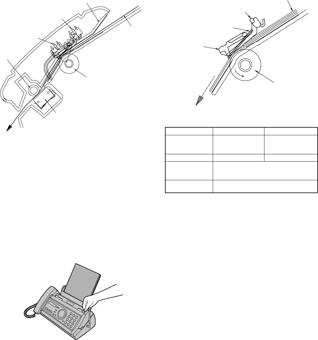
FO-CC500A
FO-K01A
CHAPTER 3. MECHANISM BLOCKS
[1] General description
1. Document feed block and diagram
Fig. 1
2. Document feed operation
1) The original, which is set in the document hopper, feeds automati-
cally when the front sensor is activated. This in turn activates the
pulse motor which drives the document supply roller. The document
stops when the lead edge is detected by the document sensor.
2) The lead edge of the original is fed a specified number of pulses after
the lead edge of the document is detected for the reading process to
begin.
3) The trailing edge of the original is fed a specific number of pulses
after the trailing edge of the document deactivates the document
sensor. The read process then stops and the original is discharged.
4) When the front sensor is in the OFF state (any document is not set
up in the hopper guide), the drive will be stopped when the docu-
ment is discharged.
3. Hopper mechanism
3-1. General view
Fig. 2
The hopper section contains document guides that are used to adjust
the hopper to the width of the original document. This ensures that the
original feeds straight into the fax machine for scanning.
Document width: 148 mm to 216 mm (A5 longitudinal size to Letter
longitudinal size)
NOTE: Adjust the document guide after setting up the document.
3-2. Automatic document feed
1) Use of the paper feed roller and separate plate ensures error-free
transport and separation of documents. The plate spring presses the
document to the paper feed roller to assure smooth feeding of the
document.
2) Document separation method: Separate plate
Fig. 3
3-3. Documents applicable for automatic feed
NOTE: Double-side coated documents and documents on facsimile re-
cording paper should be inserted manually. The document feed
quantity may be changed according to the document thickness.
Documents corresponding to a paper weight heavier than 70 kg (81.4g/
m2 ) and lighter than 135 kg (157 g/m2 ) are acceptable for manual feed.
Documents heavier than 135 kg in terms of the paper weight must be
duplicated on a copier to make it operative in the facsimile.
3-4. Loading the documents
1) Make sure that the documents are of suitable size and thickness,
and free from creases, folds, curls, wet glue, wet ink, clips, staples
and pins.
2) Place documents face down in the hopper.
i) Adjust the document guides to the document size.
ii) Align the top edge of documents and gently place them into the
hopper. The first page under the stack will be taken up by the
feed roller to get ready for transmission.
NOTES: 1) Curled edge of documents, if any, must be straightened
out.
2) Do not load the documents of different sizes and/or
thicknesses together.
3 – 1
Paper feed plate
Paper feed roller
Separate rubber
Separate plate
Document
Document guide upper
Document
Front sensor
Document
sensor
Back roller
Paper feed roller
CIS
10 sheets 1sheet(Manual)
Paper weight 70 kg 70 kg ~ 135 kg
21.5 lbs. 14 lbs. ~ 42 lbs.
(80 g/m2) (52 g/m2
~ 157g/
m2)
Paper thickness (ref.)
0.1 mm 0.1 mm ~ 0.18mm
Paper size LGL 8.5” x 14”(216 mm x 355.6 mm)
A4 8.27” x 11.7”(210 mm x 297 mm)
LTR 8.5” x 11”(216 mm x 279 mm)
Feeder capacity A4/LTR: 10 sheets
LGL : 1 sheet

FO-CC500A
FO-K01A
Fig. 4
3-5. Documents requiring use of document carrier
1) Documents smaller than 148mm (W) x 140mm (L).
2) Documents thinner than the thickness of 0.06mm.
3) Documents containing creases, folds, or curls, especially those whose
surface is curled (maximum allowable curl is 5mm).
4) Documents containing tears.
5) Carbon-backed documents. (Insert a white sheet of paper between
the carbon back and the document carrier to avoid transfer of carbon
to the carrier.)
6) Documents containing an easily separable writing material (e.g., those
written with a lead pencil).
7) Transparent documents.
8) Folded or glued documents.
Document in document carrier should be inserted manually into the
feeder.
4. Document release
4-1. General
To correct a jammed document or to clean the document running sur-
face, pull the insertion side of document center of the operation panel.
To open the upper document guide, the operation panel must be opened
first.
5. Recording block
5-1. Driving
In the drive mechanism, the rotating force of the pulse motor for both
transmission and reception is transmitted to the paper supply roller, the
recording paper feed roller and imaging film drive gear through the pulse
motor axle gear, reduction gear and planetary gear.
5-2. Recording
This equipment employs the thermal transcription system which uses
the thermal head imaging film.
1) Thermal head
The thermal head is composed of 2,016 heating elements in traverse
line, and the resolution power is 8 dots/mm. The maximum speed is 10
ms/line.
3 – 2
Paper feed plate
Paper feed roller
Separate
rubber
Separate
plate
First page of
document
Back of
document
Last page of
document
2) Structure of recording mechanism
Recording is achieved by applying a suitable pressure to the thermal
head through the imaging film of the recording paper feed roller and the
recording paper.
The main scanning is electronically performed, and the sub-scanning is
mechanically performed (by sending the recording paper with the re-
cording paper feed roller).
3) Recording paper transfer sequence
a) The recording paper stored in the paper tray ass’y is fed with the PU
roller, and is stopped when the P-IN sensor is turned on by sensing
its lead edge.
b) Hereafter, the imaging film and recording paper are transferred with
the recording paper feed roller, and thermal transcription is performed
on the recording paper.
c) After thermal transcription, the imaging film is taken up by the roller
on the take-up side, and the recording paper is discharged by the
back roller.
Uneven image density can be caused by a longitudinal misalignment
of the thermal head to the heater line. Otherwise, the head is in un-
even contact with the recording paper feed roller, or the imaging film
is wrinkled.
The following items are described as the simplified checking method.
Are the power and signal cables of the thermal head suitably treated?
Does the same symptom appear even if the thermal head pressure
spring is replaced?
Is the feed roller of the recording paper concentric? (Density is un-
even at intervals.)
Does the same symptom appear even if the thermal head is replaced?
Is the imaging film stained or wrinkled?
5-3. General view
Fig. 5
Paper
tray
extension
(Accessory)
Paper
tray ass'y
(Accessory)
Release lever
P-IN sensor lever
(Upper)
Film sensor lever
Thermal head
Platen roller
PU roller
Imaging film
(Supply side)
Imaging film
(Take-up side)
Separate rubber
Feed plate
FO-CC500A
FO-K01A
[2] Disassembly and assembly procedures
•This chapter mainly describes the disassembly procedures. For the assembly procedures, reverse the disassembly procedures.
•Easy and simple disassembly/assembly procedures of some parts and units are omitted. For disassembly and assembly of such parts and units,
refer to the Parts List.
•The numbers in the illustration, the parts list and the flowchart in a same section are common to each other.
•To assure reliability of the product, the disassembly and the assembly procedures should be performed with care.
Bottom plate, PWB’s and drive unit
1
Parts list (Fig. 1)
Fig. 1
3 – 3
14
Push
2
2
2
6
3
4
20
20
21 21
22
1
18
7
AC cord
5
8
9
16
15
17
17
11 11
10
13
12
19
16
17
17
5
Pull
1 Mechanism unit 1
2 Screw (3×10) 5
3 Screw 1
4 Washer 1
5 AC cord earth cable 1
6 Bottom plate 1
7 Hook 1
8 Connector 1
9
Power supply PWB unit
1
10 Antenna cable 1
11 Screw (3×10) 2
12 Connector 1
No. Part name Q’ty No. Part name Qty
13 Cordless PWB unit 1
14 Screw (3×10) 1
15 Connector 1
16 LIU PWB unit 1
17 Connector 6
18 Hook 1
19 Control PWB unit 1
20 Wire hold PWB 1
21 Screw (3×10) 2
22 Drive unit 1
No. Part name Q’ty No. Part name Qty
FO-CC500A
FO-K01A
Fig. 2
Operation panel unit, top cover unit
and sub frame unit
2Parts list (Fig. 2)
3 – 4
6
8
8
8
8
8
8
8
9
5
5
7
557
10
3
P-IN
lever
Operation
panel unit
Top cover
unit
Sub frame
unit
Hook
4
1
2
Screwdriver
Screwdriver
6 Operation panel unit 1
7 Screw (3×10) 2
8 Hook 7
9 Top cover unit 1
10 Sub frame unit 1
No. Part name Qty No. Part name Qty
1 Mechanism unit 1
2 Stopper plate 1
3 Operation panel unit/
top cover unit/ sub frame unit
1
4 Interface PWB cover 1
5 Screw (3×12) 4
NOTE: For disassembly of the inside of the unit,
refer to the exploded view in the parts
guide.
NOTE: When removing the operation
panel unit, detach the stopper
plate at first.
FO-CC500A
FO-K01A
CIS unit and thermal head unit
3
Fig. 3
3 – 5
Parts list (Fig. 3)
(400 g)
(700 g)
(800 g)
(700 g) (200 g)
(200 g)
(400 g)
Hook
Hook
Hook
Screwdriver
1
2
5
3
4
6
7
CIS unit
Thermal head unit
NOTE: For disassembly of the inside of the unit,
refer to the exploded view in the parts
guide.
No. Part name Qty No. Part name Qty
1 Mechanism unit 1
2 Screw (3×10) 1
3 Earth sheet 1
4 Static brush 1
5 CIS unit 1
6 Head cover 1
7 Thermal head unit 1
FO-CC500A
FO-K01A
Fig. 6
Wire treatment
4
3 – 6
Parts list (Fig. 6)
: The Interface cable pass
to the core 3 times.
4
3
3
Panel cable
Rib
Wire hold PWB
2
AC cord
Bottom plate
AC cord earth cable
Wire hold PWB
Control
PWB
Cordless
PWB
Power supply PWB
Speaker
Motor cable
Cam switch cable
Speaker cable
CIS cable
Panel
cable
Head cable
Antenna
cable
Rib
Cam
switch
cable
Rib Motor cable
Drive unit Top cover unit Operation panel unit
Panel cable
Thermal head
Head cable
Head cable
Tape
Rib
Rib
Rib
CIS cable
Scanner
frame
Tape
1
2
2
Figure for setting the
Speaker Hold Spring
Speaker
Hold
Spring
Speaker
LIU PWB
Drive unit
1 Screw (4×6) 1
2 Band (100mm) 3
3 Core (F2125) 1
4 Screw 1
No. Part name Qty
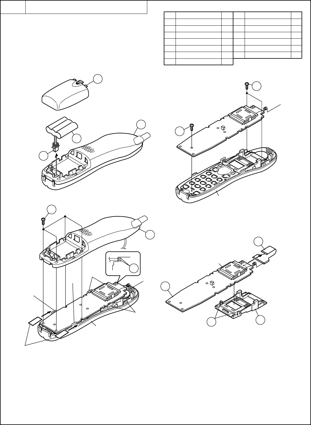
FO-CC500A
FO-K01A
Fig. 7
Cordless handset
5
3 – 7
Parts list (Fig. 7)
Plastic plate
(About 0.5mm)
Hook
Hook
Hook
Hook
2
4
5
6
7
9
Front cabinet
11
12
10
13
8
Front cabinet
3
1
RF unit
NOTE: Insert the plastic plate between the front
and back cabinets and move it in the di-
rection indicated by the arrow until it clicks
and move it further until it clicks again. (3
places for one side)
8 Screw (2x6) 1
9 Screw (2x8) 2
10 Hook 2
11 LCD flat cable 1
12 LCD holder 1
13
Cordless handset PWB unit
1
No. Part name Qty No. Part name Qty
1 Cordless handset unit 1
2 Battery cover 1
3 Connector 1
4 Battery 1
5 Screw (2x8) 4
6 Solder 2
7 Back cabinet 1
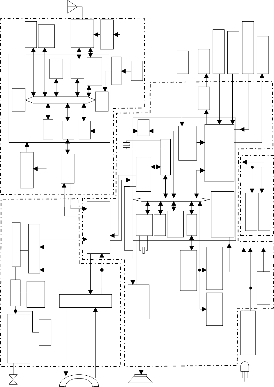
FO-CC500A
FO-K01A
4 – 1
CHAPTER 4. DIAGRAMS
LINE
HANDSET
SPEAKER
LIU PWB
CONTROL PWB
32.768kHz RTC
32.256MHz
SIO
DRIVER
CIS
MOTOR
ORG/FRT SENSOR
CAM SW SENSOR
P-IN/FILM SENSOR
THERMAL HEAD
SIO
SRAM
SIO
MODEM
CODEC
IA(20438)
CODEC
IA(20438)
+3.3V
REGULATOR
CPU
MC24 READING
PROCESSOR
(PADC)
FAX ENGINE SCE214V
SPEAKER
AMPLIFIER
FLASH MEMORY
4MBIT(SERIAL I/F)
FLASH ROM
4MBIT(PROGRAM)
DRAM
4MBIT
POWER SUPPLY
UNIT
CI
+24V
+3.3V KEY
INI CONTROLLER
TIMER
WATCH DOG TIMER
PIO
CIS I/F
MOTOR I/F
SENSOR I/F
THERMAL HEAD I/F
PANEL I/F
PANEL PWB
LCD
VREG
+3.3V
REGULATOR
SURGE PROTECT/
FILTER
CML TRANSFORMER
AMPLIFIER
AMPLIFIER
ANALOG SW
BLOCK
CI
DETECT
DSP
VREG
CPU
MC19
I/F
OSC
RF IF
VREG
RAM
ANTENNA
FLASH
ROM
RF
MODULE
EEPROM
19.2MHz
TCXO
BASE BAND
MODEM
CORDLESS PWB MERLIN
+3.3V
REGULATOR
CPC
DETECT
INVERTER
[1] Block diagram (Fax machine)
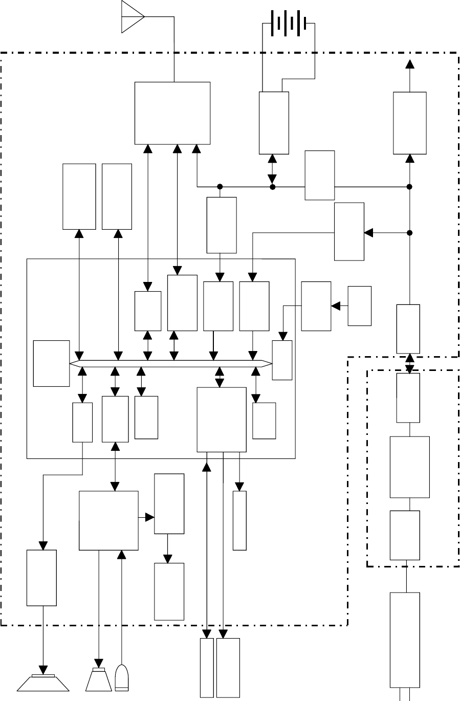
FO-CC500A
FO-K01A
4 – 2
SPEAKER
RECEIVER
MICROPHONE
KEY
LCD
LED
SIO
OSC
19.2MHz
TCXO
CORDLESS HANDSET PWB
EARPHONE
JACK
SPEAKER
AMPLIFIER
AMPLIFIER
RAM
KEYPAD GPIO
RF IF
BASE BAND
MODEM
LOW BAT
DETECT
PARK
DETECT
PARK
DETECTOR
TERMINAL
TERMINAL
POWER
REGULATOR
+6.0V
RCA
JACK
AC ADAPTOR
CRADLE UNIT
BATTERY
CHARGER
BATTERY
CONNECTOR
RF
MODULE
FLASH ROM
512KBITS
EEPROM
4KBITS
ANTENNA
BATTERY
REGULATOR
+3.3V
VCC
LOW BAT
DETECTOR
DSP
CPU
MC19
MERLIN
CODEC
IF
CODEC
IA(20438)
INVERTER
Block diagram (Cordless handset)
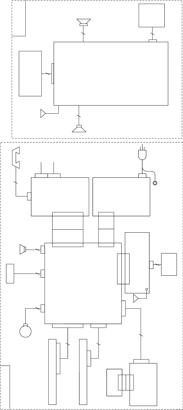
FO-CC500A
FO-K01A
4 – 3
[2] Wiring diagram
6
CAM SW
SPEAKER
22
THERMAL HEAD
CONTACT IMAGE SENSOR
LCD UNIT
CNLCD
OPERATION
PANEL PWB
UNIT
14
CNPN-A
15
7
13
2
CNCSW CNSPCNMT
CNTH
CNCIS
CNPN
CNDSS
CN1
CN4
CNLIUA
CNPW
14
6
CONTROL PWB UNIT
LIU
PWB UNIT
POWER SUPPLY
PWB UNIT
CORDLESS
PWB UNIT
CNLIUA
CNPW
TEL LINE
CNLNJ
CNHJ
AC CORD
TX/RX MOTOR
HANDSET
4
16
UNIT1
RF
MODULE
CN101
ANTENNA
CNTLJ EXTERNAL
LINE
CORDLESS
HANDSET
PWB UNIT
LCD UNIT
CORDLESS
HANDSET
ANTENNA
SPEAKER
RECEIVER
2
2
2
22
BATTERY
CN101
CN1
FAX MACHINE
FO-CC500A
FO-K01A
4 – 4
TX/RX
MOTOR
TPBD-
TPAD-
TPBD
TPAD
VMT
VMT
1
2
3
4
5
6
1
2
3
4
5
6
7
8
9
10
11
12
13
14
15
16
1
2
3
4
5
6
7
8
9
10
11
12
13
14
15
1
2
3
4
5
6
7
8
9
10
11
12
13
14
15
16
1
2
3
4
5
6
OPERATION
PANEL
PWB
TPBD-
TPAD-
TPBD
TPAD
VMT
VMT
THERMAL
HEAD
VTH
VTH
STRB1-
STRB2-
THI
RANK
THG
THG
THG
THVDD
STRB3-
STRB4-
LATCH-
PCLK
DATA
VTH
VTH
STRB1-
STRB2-
THI
RANK
THG
THG
THG
THVDD
STRB3-
STRB4-
LATCH-
PCLK
DATA
VTH
1
2
3
4
5
6
7
1
2
3
4
5
6
7
VO
VG
CISVDD
øT
CISCLK
GLED
+24V
VO
VG
CISVDD
øT
CISCLK
GLED
+24V
KEN4A
KEN3A
KEN2A
KEN1A
DG
+3.3V
ORGSNS-
FRSNS-
E
SEN0
SEN1
SEN2
SEN3
SEN4
SEN5
SEN6
CNPN
CNCIS
1
2
3
4
5
6
7
8
9
10
11
12
13
14
1
2
3
4
5
6
7
8
9
10
11
12
13
14
LIU PWB
RHS-
DG
+24VL
MICMUTE
TELIN
TELMUTE
RXIN
TXOUT
CML
PIN
FILM
CI
HS-(N.C.)
TELOUT
RHS-
MAG
+24VL
MICMUTE
TELIN
TELMUTE
RXIN
TXOUT
CML
PIN
FILM
CI-
HS-
TELOUT
CNLIUACNLIUA
CNMT
CNTH
1
2
3
4
5
6
1
2
3
4
5
6
POWER
SUPPLY
PWB
+24V
+24V
MG
MG
DG
+5V
+24V
+24V
MG
MG
DG
+5V
CNPW
CNPW
CNCSW
CNSP
CIS
1
2CSW-
DG
CAM
SWITCH
1
2
1
2
1
2SP+
SP–
CSW-
DG
SP+
SP–SPEAKER
CONTROL
PWB
1
2
3
4
5
6
7
8
9
10
11
12
13
14
15
16
KEN4A
KEN3A
KEN2A
KEN1A
DG
+3.3V
ORGSNS-
FRSNS-
E
SEN0
SEN1
SEN2
SEN3
SEN4
SEN5
SEN6
CNPN-A
1
2
3
4
5
6
7
8
9
10
11
12
13
1
2
3
4
5
6
7
8
9
10
11
12
13
CORDLESS
PWB
DG
DG
VREG
VREG
CI
SRLRX
SRLTX
PARK
DSSIN
DSSOUT
INCOM
DSSTX
DSSRX
DG
DG
VREG
VREG
CI
SRLRX
SRLTX
PARK
DSSIN
DSSOUT
INCOM
DSSTX
DSSRX
CNDSS CN1
[3] Point-to-point diagram (Fax machine)
FO-CC500A
FO-K01A
4 – 5
Point-to-point diagram (Cordless handset)
1
2
3
4
5
6
7
8
9
10
11
12
13
14
15
16
17
18
19
20
21
22
1
2
3
4
5
6
7
8
9
10
11
12
13
14
15
16
17
18
19
20
21
22
LCD UNIT
LCDRS
LCDRW
LCDE
LCDCS
ROW7
ROW6
ROW5
ROW4
+3.3V
V4
V3
V2
V1
V0
VR
VOUT
CAP2–
CAP2+
CAP1–
CAP1+
VSS
RESETB
LCDRS
LCDRW
LCDE
LCDCS
ROW7
ROW6
ROW5
ROW4
+3.3V
V4
V3
V2
V1
V0
VR
VOUT
CAP2–
CAP2+
CAP1–
CAP1+
VSS
RESETB
CN101 CORDLESS
HANDSET
PWB
CN1 1
2VBAT
DG
1
2
1
2
SP+
SP–
VBAT
DG
SPEAKER
HEADSET
JACK
BATTERY
MIC1
MICROPHONE
RECEIVER
1
2
3
4
5
AG
LINOUT
LINEIN
N.C.
EMJCHK
J1
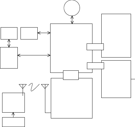
FO-CC500A
FO-K01A
CHAPTER 5. CIRCUIT DESCRIPTION
[1] Circuit description
1. General description
The compact design of the control PWB is obtained by using CONEXANT
fax engine in the main control section and high density printing of sur-
face mounting parts. Each PWB is independent according to its function
as shown in Fig. 1.
2. PWB configuration
Fig. 1
1) Control PWB
The control PWB controls peripheral PWBs, mechanical parts, trans-
mission, and performs overall control of the unit.
This machine employs a 1-chip modem (SCE214V) which is installed
on the control PWB.
2) LIU PWB
This PWB controls connection of the telephone line to the unit.
3) Power supply PWB
This PWB provides voltages of +5V and +24V to the other PWBs.
4) Panel PWB
The panel PWB allows input of the operation keys.
5) LCD PWB
This PWB controls the LCD display.
6) Cordless PWB
This PWB performs a communication with remote cordless handset by
2.4 GHz radio frequency and is connected with FAX MACHINE on the
control PWB by using it is serial I/F.
7) Cordless handset PWB
This PWB is for a cordless handset and is communicated with cordless
PWB by 2.4 GHz radio frequency. To communicate, both Cordless PWB
and Cordless Handset PWB have common system ID.
8) Cradle unit
This PWB has a 3-terminals regulator. The input voltage AC adaptor is
transformed about +6.5 volt output.
3. Operational description
Operational descriptions are given below:
•Transmission operation
When a document is loaded in stand-by mode, the state of the docu-
ment sensor is sensed via the 1 chip fax engine (SCE214V). With
depression of the START key in the off-hook state, transmission takes
place. Then, the procedure is sent out from the modem and the mo-
tor is rotated to move the document down to the scan line. In the
scan processor, the signal scanned by the CIS is sent to the internal
image processor and the AD converter to convert the analog signal
into binary data. This binary data is transferred from the scan proc-
essor to the image buffer within the RAM and encoded and stored in
the transmit buffer of the RAM. The data is then converted from par-
allel to serial form by the modem where the serial data is modulated
and sent onto the line.
•Receive operation
There are two ways of starting reception, manual and automatic.
Depression of the START key in the off-hook mode in the case of
manual receive mode, or CI signal detection by the LIU in the auto-
matic receive mode.
First, the SCE214V controls the procedure signals from the modem
to be ready to receive data. When the program goes into phase C,
the serial data from the modem is converted to parallel form in the
modem interface of the 1 chip fax engine (SCE214V) which is stored
in the receive buffer of the RAM. The data in the receive buffer is
decoded software-wise to reproduce it as binary image data in the
image buffer. The data is DMA transferred to the recording processor
within the SCE214V which is then converted from parallel to serial
form to be sent to the thermal head. The data is printed line by line by
the SCE214V which is assigned to control the motor rotation and
strobe signal.
•Copy operation
To make a copy on this facsimile, the COPY key is pressed when the
machine is in stand-by with a document on the document table and
the telephone set is in the on-hook state. First, depression of the
COPY key advances the document to the scan line. Similar to the
transmitting operation, the image signal from the CIS is converted to
a binary signal in the DMA mode via the 1 chip fax engine (SCE214V)
which is then sent to the image buffer of the RAM. Next, the data is
transferred to the recording processor in the DMA mode to send the
image data to the thermal head which is printed line by line. The
copying takes place as the operation is repeated.
5 – 1
MOTOR
CISLCD
AC CORD
CONTROL
PWB
PANEL
PWB
CORDLESS
HANDSET
PWB
CRADLE
UNIT
CORDLESS
PWB
POWER
SUPPLY
PWB
LIU PWB
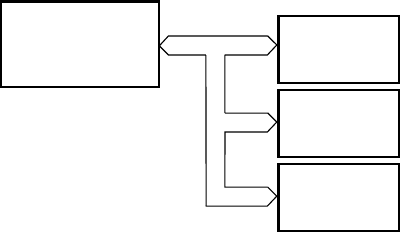
FO-CC500A
FO-K01A
[2] Circuit description of control PWB
1. General description
Fig. 2 shows the functional blocks of the control PWB, which is com-
posed of 4 blocks.
Fig. 2 Control PWB functional block diagram
2. Description of each block
(1) Main control block
The main control block is composed of CONEXANT 1 chip fax engine
(SCE214V), FLASH ROM (4Mbit), DRAM (4Mbit) and FLASH MEMORY
(4Mbit).
Devices are connected to the bus to control the whole unit.
1) SCE214V (IC3) : pin-176 QFP (FAX CONTROLLER)
1 chip fax engine has Internal Integrated Analog (20438) and Internal
memory (SRAM : 32kbit).
2) SST39VF040P (IC1): pin-32 TSOP (FLASH ROM)
FLASH of 4Mbit equipped with software for the main CPU.
3) MSM51V4800E (IC2): pin-28 SOJ (DRAM)
• Image memory for recording process.
4) K9F4008W0A (IC8): pin-44 TSOP (FLASH MEMORY)
A 512 k x 8bit NAND FLASH MEMORY to store the voice and image
data when using memory function.
5 – 2
(1) SCE214V
IA(20438)
MEMORY(SRAM)
(2) FLASH
ROM
(3) DRAM
(4) FLASH
MEMORY
(2) IC3 (SCE214V) Hardware description
A) CONTROL BLOCK
1) Integrated Controller (SCC)
The Controller contains an internal MC24 Processor with a 16-MB ad-
dress space and dedicated circuitry optimized for facsimile image
processing and monitoring and for thermal or thermal transfer printer
support.
The CPU provides fast instruction (up to 10 MHz clock speed) execu-
tion and memory efficient input/output bit manipulation. The CPU con-
nects to other internal functions over an 8-bit data bus and 24-bit ad-
dress bus and dedicated control lines.
The 24-bit external address bus, 8-bit data bus, control, status and de-
coded chip select signals support connection to external ROM, SRAM,
DRAM, and FLASH memory.
2) DRAM Controller
The CX06835 includes a DRAM controller with signal and page mode
access support which supports fast, normal, or slow refresh time. DRAM
memory space is provided in one block up to 4 MB. A maximum of 4 MB
of DRAM is supported. This space has a programmable size and start-
ing address. Refresh is performed automatically and is supported in
stand-by mode. CAS and RAS signal support is provided for one-DRAM
banks for both 4-bit and 8-bit organizations. Access speeds from 50ns
to 70ns can be supported.
3) DMA Channels
Six internal DMA channels support memory access for scanner, T.4/T.6,
and resolution conversion. DMA Channel 2 can be reprogrammed for
external access to thermal printing, thermal transfer, or plain paper inkjet
printing.
4) External RAM and ROM
Moveable and programmable size external SRAM memory of up to 1
MB, DRAM memory of up to 4 MB, and ROM of up to 4 MB can be
directly connected to the SCE214V. By using an external address de-
coder, the size of SRAM and/or ROM can be extended. The ROM stores
all the program object code.
5) Flash Memory Controller
The SCE214V includes a flash memory controller that supports NOR,
NAND, and Serial NAND-type flash memory. The supported size of NOR-
type memory is up to 1 MB and the supported size of NAND-type memory
is unlimited.
6) Stepper Motor Control
Eight outputs are provided to external current drivers: four to the scan-
ner motor and four to the printer motor. The stepping patterns are pro-
grammable and selectable line times are supported. A timeout circuit
controls the power control of the motors. The printer or scanner motor
outputs can be programmed as GPOs for applications using single mo-
tor or paper printers.
7) T.4/T.6 Compressor/Decompressor
MH, MR and MMR compression and decompression are provided in
hardware. T.4 line lengths of up to 8192 pixels are supported. MMR and
Alternating Compression/Decompression (ACD) on a line by line basis
provide support for up to three independent compression and decom-
pression processes.
8) Bi-level Resolution Conversion
One independent programmable bi-level 1D-resolution conversion block
is provided to perform expansion or reduction on the T.4 decompressed
data and scan image data. Image expansion can be programmed up to
200% and reduction down to 33%. Vertical line O-Ring and data output
bit order reversal is also provided.
9) Printer IF
The Printer Interface provides a standard connection between the
SCE214V and a thermal printhead to support thermal printing or thermal
transfer. The thermal printer interface consists of programmable data,
latch, clock, and up to four strobe signals. Programmable timing sup-
ports traditional thermal printers, as well as the latchless split mode print-
ers, and line lengths of up to 2048 pixels. Line times from 5 ms to 40 ms
are supported.
The SCE214V includes a thermal ADC (TADC) function utilizing a D/A
converter and a comparator to monitor the printhead temperature. Ex-
ternal terminating resistors must be supplied; the values are determined
by the specific printhead selected.
As an option, plain paper inkjet printing can be supported.
10) TPH Hardware Timer
The TPH hardware timer provides a 500 ms timer that can be re-trig-
gered or reset.
11) Scanner and Video Control
Five programmable control and timing signals support common CCD
and CIS scanners. The video control function provides signals for con-
trolling the scanner and for processing its video output. Three program-
mable control signals (START, CLK1n, and CLK2) provide timing re-
lated to line and pixel timing. These are programmable with regard to
start time, relative delay and pulse width.
Two video control output signals (VIDCTL[1:0]) provide digital control
for external signal pre-processing circuitry. These signals provide a per
pixel period, or per line period, timing with programmable polarity con-
trol for each signal.
FO-CC500A
FO-K01A
12) Video Processing
The CX06835 supports two modes of shading correction for scanner
data non-uniformity arising from uneven sensor output or uneven illumi-
nation. Corrections are provided on either an 8-pixel group or are ap-
plied separately to each pixel. Dark level correction and gamma correc-
tion are also provided.
Two-dimensional Error Diffusion/Dithering is performed on halftone im-
ages.
The CX06835 includes an 8 x 8 dither table, which is programmable and
stored internally (8-bit per table entry). The table is arranged in a matrix
of 8 rows by 8 columns. The video processing circuit provides mixed-
mode detection/processing and multi-level Resolution Conversion for
the scanner multi-level data. The conversion ratio of the multi-level Reso-
lution Conversion is fixed to B4-A4 conversion.
13) Operator Panel Interface
Operation Panel functions are supported by the operator output bus
OPO[6:0], the operator input bus OP[3:0], and two control outputs
(LCDCS and LEDCTRL).
The CX06835 can directly interface to a 28-key keypad.
A 2-line LCD display module with 20 characters per line can be sup-
ported.
14) Synchronous Serial Interface (SSIF)
One or optionally two Synchronous only Serial Interfaces (SSIF) are
built into the CX06835, which allows it to communicate with external
peripherals. Each SSIF provides separate signals for Data (SSTXD,
SSRXD), Clock (SSCLK), and Status (SSSTAT). Each SSIF is a duplex,
three-wire system. The SSIF may be configured to operate as either a
master or a slave interface. The bit rate, clock polarity, clock phase, and
data shifting order are programmable.
15) Synchronous/Asynchronous Serial Interface (SASIF)
One or optionally two Synchronous/Asynchronous Serial Interface
(SASIF) performs the following:
• Serial-parallel conversion of data received from a peripheral device.
• Parallel-to-serial conversion of data for transmission to a peripheral
device.
This interface consists of serial transmit data (SASTXD), serial receive
data (SASRXD), and a serial clock(SASCLK). The SASIF includes a
programmable bit rate generator for asynchronous and synchronous
operations. The data shifting order, data bit number, and the SASCLK
polarity are programmable.
The optional SASIF 2 has an additional pin called DSS_AVAIL. This
signal can be used to tristate the SASCLK2 and SASTXD2 signals.
16) Real Time Clock (RTC)
The CX06835 includes a battery backup real time clock. The RTC will
automatically maintain the proper date and time for 32 years. Leap year
compensation is included. A 32.768 kHz or 65.536 kHz crystal is re-
quired by the RTC.
17) Tone Generator (ALT_TONE)
The CX06835 provides a programmable tone generator output. The fre-
quency of the tone generator is programmable from 400 Hz to 4 kHz. By
using a PWM programmable high frequency as a modulation frequency,
the output level can be made programmable.
18) Watchdog Timer
The Programmable Watchdog Timer is intended to guard against
firmware lockup on the part of either executive-controlled background
tasks or interrupt-driven tasks, and can only be enabled by a sequence
of events under control of the Watchdog Control Logic. Once the Watch-
dog Timer has been enabled, it can not be disabled unless a system
reset occurs.
19) Reset and Power Control
The RESETn I/O pin provides an internally generated reset output to
external circuits, or it can accept an externally generated reset signal.
This reset signal will not reset the RTC. Separate RTC battery power
inputs are provided for battery-backup functions. A BATRSTn pin is pro-
vided, which resets the RTC circuits and other SCC circuits.
5 – 3
20) Power Up/Down Control
Power Up/Down detection is provided internally. The threshold voltages
are:
• Power Up detection level = 2.83V to 2.95V.
An internally generated power down signal controls internal switching
between primary and battery power. This control signal is also provided
as an output on the PWRDWNn pin. An externally generated power
down detector (optional) can be provided as an input on the PWRDWNn
pin by setting the INTPWRDWNEn pin.
21) Stand-by and Sleep Modes
Two power saving modes are provided to reduce the power consump-
tion. In stand-by mode, the CPU is functional, but the modem clock is
turned off to save power. When this occurs, the modem may be acti-
vated by software under different conditions. In sleep mode, the clock is
cut off from both the modem and the CPU to increase the power sav-
ings.
The system can be activated by paper insertion, key pressing events,
and telephone ring detection.
22) Embedded Modem DSP
The embedded modem DSP is a synchronous 9600 bps half-duplex
modem with error detection and DTMF generation/reception. It provides
data transmission/reception from regular PSTN lines, PBX, or private
lines.
The modem can operate at any standard V.29 data speed up to 9600
bps as well as in V.21 and V.23 modes.
The modem is designed for use in Group 3 facsimile machines. It satis-
fies the requirements specified in ITU-T recommendations V.29, V.27ter,
V.21 Channel 2, and T.4 , and meets the signaling requirements of T.30.
It also performs HDLC framing according to T.30 at all speeds.
Note: For technical details, refer to the FM209/FM214 Designer’s Guide,
(document 1175).
23) Software and Firmware Support Features
Available software and embedded firmware provides the following:
• Modem support for speeds up to 9600 bps.
• ECM under conditional assembly.
• DRAM memory support under conditional assembly.
• MH, MR and MMR support.
• Page memory receiving.
• 5 ms minimum scan line time.
• Conditional Error Diffusion or Dither table (8x8) support.
• Dark Level Correction support.
• Single motor support.
• 28-key operator panel support.
• Call progress support for Europe and U.S.A.
• Monochrome inkjet print engine support.
FO-CC500A
FO-K01A
B) Modem block
1) Facsimile Modem
The modem can operate at 14400, 12000, 9600, 7200, 4800, 2400, or
300 bps, and can perform HDLC framing per T.30 at all rates. A pro-
grammable DTMF detector, three programmable tone detectors, V.21
Channel 2 FSK 7E flag detector, Caller ID demodulator and ring detec-
tor are provided.
2) Voice and Audio Codecs
The voice coder/decoder (codec) compresses voice at an average rate of
2.9 kbps which provides 24 minutes of stored voice messages in 4 Mbits
of memory. But for FO-CC500A, a part of memory is used for other uses.
So the total recording time is shortened at about 20 minutes. This voice
codec allows the host controller to efficiently store and playback digital
incoming messages (ICMs), outgoing messages (OGMs).
The ADPCM audio codec compresses audio signals (music/voice) at 32
kbps or 24 kbps and the PCM audio codec records audio signals at 128
kbps or 64 kbps for highest fidelity coding and reproduction.
Selectable error correction coding allows storage in audio grade RAMs
(ARAMs). Echo cancellation techniques employed during playback
allow DTMF tone and Type II Caller ID CAS detection during voice/audio
codec operation to support user selectable features. The coder can record
messages from the PIA or SIA. The decoder can playback messages to
the PIA or both the PIA and SIA. Dual/signal tone transmission is avail-
able when the decoder is disabled.
3) V.23 Full-duplex Modem and Caller ID
Both full-duplex transmit and receive (with asymmetric 1200/75 bps con-
nection) and half-duplex (1200 bps) asynchronous V.23 are supported,
as will as both serial and parallel interfaces to the modem. The V.23
algorithm includes an optional, programmable. receive compromise
equalizer which is active in both V.23 and Caller ID (V.23 Receive only)
modes.
Common applications for V.23 include France’s Minitel and Japan’s Lowest
Cost Routing.
5 – 4
4) Features
•Group 3 facsimile transmission/reception
- ITU-T V.17 and V.33
- ITU-T V.29, V.27 ter, T.30, V.21 Channel 2, T.4
- ITU-T V.17 and V.27 ter short train
- HDLC framing at all speeds
- Receive dynamic range: 0 dBm to -43 dBm
- Automatic adaptive equalization
- Fixed and programmable digital compromise equalization
- DTMF detect and tone detect
- ITU-T V.21 Channel 2 FSK 7E Flag Detect
- Ring detector
- Programmable transmits level
- Programmable single/dual tone transmission
•Voice codec
- 24 minutes of voice storage per 4 Mbit memory
- Near toll quality voice recording and playback
- Programmable AGCs
-
Programmable line/microphone input and line/speaker output filters
- Error correction coding allows ARAM usage
- DTMF detect, tone detect, and tone transmit
- Type II Caller ID CAS detection
- Pitch synchronized fast and slow playback
- Near-end echo cancellation
•ADPCM Audio codec
- High fidelity recording and playback of audio signals
- 32 kbps and 24 kbps
- Programmable AGCs
-
Programmable line/microphone input and line/speaker output filters
- DTMF detect, tone detect, and tone transmit
- Type II Caller ID CAS detection
- Near-end echo cancellation
•PCM audio codec
- 128 kbps and 64 kbps
- DTMF detect and tone detect
- Type II Caller ID CAS detection
- Near-end echo cancellation
•V.23 and Type I Caller ID
- Full-duplex modes:
TX = 75 bps. RX = 1200 bps
TX = 1200 bps. RX = 75 bps
- Half-duplex mode:
TX = RX = 1200 bps
- Serial and parallel data modes
- Programmable parallel data mode
- 5, 6, 7, or 8 data bits
- 1 or 2 Stop bits
- Mark, Space, Even, or Odd Parity
- Break function
- Transmitter squelch
- Compromise equalizer
•3.3V/5V operation
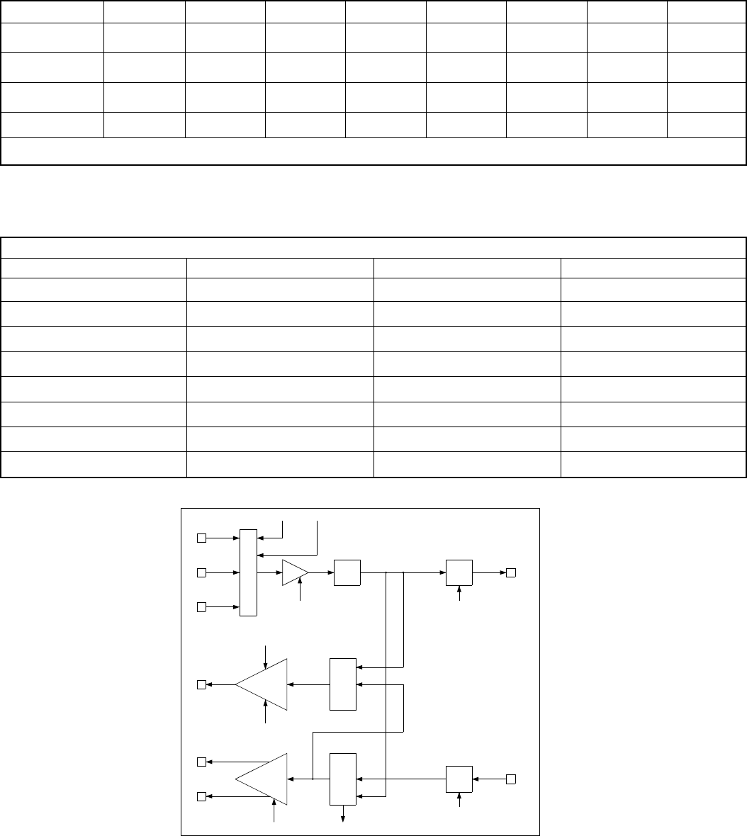
FO-CC500A
FO-K01A
IACR1 0 0 0 0 0 D0 0 1
IACR2 0 0 0 0 0 D4 0 1
IACR3 0 0 0 0 0 D5 0 1
IAADD 0 0 0 0 0 CE 0, 1 0, 1
NOTES: *Registers to use when x=1. When x=2, add 10h.
5) Integrated Analog Control Resisters for 20438
The 20438 IA can be used as a Primary Integrated Analog (PIA) codec or as a Secondary Integrated Analog (SIA) codec, depending on the signal
connection with the SCE Controller ASIC device. In the SCE100 product, both the PIA and the SIA are packaged external to the SCE Controller device,
whereas in the SCE214V, the PIA is packaged with the SCE214V Controller and the SIA is external.
The 20438 IA provides gain, filtering, internal analog switching, and an internally sourced microphone bias output. The IA is controlled by three control
registers and an address register located in internal RAM space which are accessed via the modem interface memory. These registers provide indi-
vidual controls for the IA’s inputs, outputs, gain settings, and switching.
The registers are located in internal DSP RAM. Each bit of each 8-bit IA control register has exactly the same meaning for the PIA and the SIA. The LSB
of each 16-bit address contents is used to control the PIA. The MSB of each 16-bit address contents is used to control the SIA.
The following table the PIA/SIA control register RAM access code.
5 – 5
Fig. 3 PIA/SIA Signal Flow Control
Register SBRAMx BRx Crx IOx AREXx ADDx PIA Reg* SIA Reg*
• For changes made to IACR1 tobe effective, the host must write to IAADD with a value of 0002h.
• For changes made to IACR2 tobe effective, the host must write to IAADD with a value of 0006h.
• For changes made to IACR3 tobe effective, the host must write to IAADD with a value of 0007h.
Configuration default values are shown below.
DEFAULT VALUE
CONFIGURATION IACR1 IACR2 IACR3
V.17/V.33 1D9Eh 0008h 0000h
V.29 1D9Eh 0008h 0000h
V.27ter 1D9Eh 0008h 0000h
V.21 Ch. 2 1D9Eh 0008h 0000h
V.23/Caller ID 1D9Eh 0008h 0000h
Tone Transmit/Detect 1D9Eh 0008h 0000h
Voice/Audio Codec 0D16h 0008h 0000h
Speakerphone 0D16h 0008h 0000h
The following signal flow block diagram is for a signal IA and it applies to both PIA and SIA.
MICP
MICM
LINEIN
MIC/LINE SELECT
LINE IN ENABLE MIC ENABLE
GAIN
LINE OUT ENABLE
LPF ADC SOUT
0, 20, 25, 30 dB(MIC IN)
0dB(LINE IN)
LINE OUT LINE
DRIVER
Mute, 0, -6, -12 dB
LINE IN
SELECT
SPKRP
SPEAKER
DRIVER
SPEAKER OUT ENABLE
SPKRM
RT
Loop
(1,1)
(1,0)
(1,0)
(1,1)
(0,1)
DAC SIN
0, +4 dB
0, 6 dB
(0,0)
(0,0)

FO-CC500A
FO-K01A
1 VDDPLL ———PLL Power
2 VSSPLL ———PLL GND
3 ROMCSn O —13Xs —
4 SYNC/GPO[20] O —13Xs —
5 WRn O —13Xs —
6 RDn O —13Xs —
7 DEBUGn I Hu ——
8 TSTCLK O —13Xs —
9 VSS ———Digital GND
10 SXIN I Osc0 ——
11 SXOUT O —Osc0 —
12 OPO[0]/GPO[8]/SMPWRCTRL O —13Xs —
13 OPO[1]/GPO[9]/PMPWRCTRL O —13Xs —
14 OPO[2]/GPO[10]/RINGER OZ —13Xs —
15 OPO[3]/GPO[11] O —13Xs —
16 OPO[4]/GPO[12]/SSTXD1 O —13Xs —
17 OPO[5]/GPO[13] O —13Xs —
18 OPO[6]/GPO[14] O —13Xs —
19 OPI[0]/GPIO[21]/SSRXD1 I/O Hu 13Xs —
20 OPI[1]/GPIO[22]/SSSTAT1 I/O Hu 13Xs —
21 OPI[2]/GPIO[23]/SSCLK1 I/O Hu 13Xs —
22 OPI[3]/GPIO[24] I/O Hu 13Xs —
23 LCDCS/GPO[17] O —1XC —
24 VDD ———Digital Power
25 RASn O —13Xs —
26 CAS[0]n O —13Xs —
27 DWRn O —13Xs —
28 VBAT ———RTC Battery Power
29 XIN I Osc1 ——
30 XOUT O —Osc1 —
31 WRPROTn O —1XC —
32 TEST[1] I Hd ——
33 TEST[0] I Hd ——
34 BATRSTn I H ——
35 INTPWRDWNEn I H ——
36 PWRDWNn I/O H 13Xs —
37 N.C. ————
38 ADGA —VADG —PADC Analog GND
39 VREFn/CLREF I VR- —PADC
40 VIN I VA —PADC
41 ADGA —VADG —PADC Analog GND
42 ADVA —VADV —PADC Analog Power
43 ADXG —VXG —PADC
44 VREFp I VR —PADC
45 VSS ———VSS Digital GND
46 IVREFn O —VR- PADC
47 IVREFp O —VR+ PADC
48 VDD ———Digital Power
49 THADI I Analog —TADC
50 VSS ———Digital GND
51 GPIO[17]/DSPIRQn I/O Hu 13Xs —
52 GPIO[16]/IRQ[8] I/O Hu 13Xs —
53 GPIO[15]/CS[5]n I/O Hu 13Xs —
54 GPIO[13]/CS[3]n I/O Hu 13Xs —
55 GPIO[37]/IRQ15n/DSPCSn I Hu 13Xs —
56
GPIO[4]/CPCIN/TPHPWRCTRL/DMAREQ
I/O Hu 13Xs —
57 STRB[0] O —1XC —
58 STRB[1] O —1XC —
59 STRB[2] O —1XC —
60 STRB[3] O —1XC —
61 PLAT O —3XC —
62 PDAT O —2XC —
63 PCLK/DMAACK O —3XC —
SCE214V (IC3) Terminal descriptions
5 – 6
Pin Pin List I/O Input Output Pin Description
No. Type Type

FO-CC500A
FO-K01A
5 – 7
64 VDD ———Digital Power
65 GPIO[11]/BE/SERINP/SR4IN I/O Hu 13Xs —
66 GPIO[19]/RDY/SEROUT I/O Hu 13Xs —
67 START O —2XC —
68 CLK1n/GPO[25] O —13Xs —
69 CLK2/GPO[24] O —13Xs —
70 GND ———IA GND
71 MCLK ID ——Main Clock from DSP
72 CTRLI ID d —Control Data from DSP
73 TESTC ID d —IA Test
74 SOUT OD —T Serial Data to DSP
75 SIN ID d —Serial Data to DSP
76 FSYNC I/OD d —Frame Sync Signal (IA)
77 POR IA d —Hardware Reset
78 GND ———IA GND
79 LINE_INP IA ——Analog Input to Line Pre-Amp.
80 MIC_INP IA ——Positive differential Analog Input to Microphone Pre-Amp.
81 MIC_INM IA ——Negative differential Analog Input to Microphone Pre-Amp.
82 MIC_BIAS OA ——2.2 V Nominal DC Bias Source for Electret Microphone
83 BG OA ——Analog reference Voltage Output
84 VC OA ——Analog Ground Bias Output
85 AVDD PWR ——IA Analog Power
86 GND ———IA GND
87 LINE_OUTP OA ——Line Driver Output
88 SPKR_OUTP OA ——Positive Speaker Driver Output
89 SPKR_OUTM OA ——Negative Speaker Driver Output
90 DVDD PWD ——IA Digital Power
91 MODE_0 ID u —Connect to VSS (IA Mode Selection)
92 ICLK I/OD ——IA Bit Clock Input/Output
93 VSS ———VSS Digital GND
94 FCSn[1]/VIDCTL[0]/GPO[23] O —13Xs —
95 IARESET O —13Xs DSP to EXTIA POR
96 IACLK O —13Xs DSP to EXTIA MCLK
97 VDD ———Digital Power
98 IA1CLK I H —DSP from EXTIA ICLK
99 SR3IN/DSPIRQn I H —DSP from primary EXTIA SOUT/EXT. Modem IRQn
100 SR4OUT O —13Xs DSP to primary EXTIA SIN
101 SR1IO O —13Xs DSP to EXTIA CTRL1
102 SA1CLK I H —DSP from EXTIA FSYNC
103 GPIO[7]/SSRXD2/SASRXD2 I/O Hu 13Xs —
104 GPIO[6]/SSTXD2/SASTXD2 I/O Hu 13Xs —
105 GPIO[5]/SSCLK2/SASCLK2 I/O Hu 13Xs —
106 GPIO[10]/SSSTAT2/DSS_AVAIL I/O Hu 13Xs —
107 VSS ———Digital GND
108 RESETn I/O Hu 2XC —
109 GPIO[3]/SASCLK I/O Hu 13Xs —
110 GPIO[2]/SASRXD I/O Hu 13Xs —
111 GPIO[1]/SASTXD I/O Hu 13Xs —
112 GPIO[9]/FRDn I/O Hu 13Xs —
113 GPIO[8]/FWRn I/O Hu 13Xs —
114 A[0] I/O Tu 13Xs CPU Address Bus
115 A[1] I/O Tu 13Xs CPU Address Bus
116 A[2] I/O Tu 13Xs CPU Address Bus
117 A[3] I/O Tu 13Xs CPU Address Bus
118 A[4] I/O Tu 13Xs CPU Address Bus
119 VDD ———Digital power
120 A[5] I/O Tu 13Xs CPU Address Bus
121 A[6] I/O Tu 13Xs CPU Address Bus
122 A[7] I/O Tu 13Xs CPU Address Bus
123 A[8] I/O Tu 13Xs CPU Address Bus
124 A[9] I/O Tu 13Xs CPU Address Bus
125 A[10] I/O Tu 13Xs CPU Address Bus
126 A[11] I/O Tu 13Xs CPU Address Bus
SCE214V (IC3) Terminal descriptions
Pin Pin List I/O Input Output Pin Description
No. Type Type

FO-CC500A
FO-K01A
5 – 8
127 A[12] I/O Tu 13Xs CPU Address Bus
128 A[13] I/O Tu 13Xs CPU Address Bus
129 A[14] I/O Tu 13Xs CPU Address Bus
130 A[15] I/O Tu 13Xs CPU Address Bus
131 A[16] I/O Tu 13Xs CPU Address Bus
132 VDD ———Digital Power
133 VSS ———Digital GND
134 A[17] I/O Tu 13Xs CPU Address Bus
135 A[18] I/O Tu 13Xs CPU Address Bus
136 A[19] I/O Tu 13Xs CPU Address Bus
137 A[20] I/O Tu 13Xs CPU Address Bus
138 A[21]/EYECLK I/O Tu 13Xs CPU Address Bus
139 A[22]/EYESYNC I/O Tu 13Xs CPU Address Bus
140 A[23]/EYEXY I/O Tu 13Xs CPU Address Bus
141 D[0] I/O Tu 13Xs CPU Data Bus
142 D[1] I/O Tu 13Xs CPU Data Bus
143 D[2] I/O Tu 13Xs CPU Data Bus
144 D[3] I/O Tu 13Xs CPU Data Bus
145 D[4] I/O Tu 13Xs CPU Data Bus
146 D[5] I/O Tu 13Xs CPU Data Bus
147 D[6] I/O Tu 13Xs CPU Data Bus
148 D[7] I/O Tu 13Xs CPU Data Bus
149 GPIO[20]/ALTTONE I/O Hu 13Xs —
150 GPIO[26] I/O Hu 13Xs —
151 GPIO[27] I/O Hu 13Xs —
152 GPIO[28] I/O Hu 13Xs —
153 GPO[26] O —13Xs —
154 GPO[27] O —13Xs —
155 GPO[28] O —13Xs —
156 GPO[29] O —13Xs —
157 GPO[30]/SR3OUT O —13Xs —
158 GPIO[29] I/O Hu 13Xs —
159 GPIO[31] I/O Hu 13Xs —
160 GPIO[32] I/O Hu 13Xs —
161 VDD ———Digital power
162 GPIO[34] I/O Hu 13Xs —
163 GPIO[35] I/O Hu 13Xs —
164 GPIO[36] I/O Hu 13Xs —
165 Vss ———Digital GND
166 VDD ———Digital Power
167 PM[0]/GPO[0] O —13Xs —
168 PM[1]/GPO[1] O —13Xs —
169 PM[2]/GPO[2] O —13Xs —
170 PM[3]/GPO[3] O —13Xs —
171 SM[0]/GPO[4] O —13Xs —
172 SM[1]/GPO[5] O —13Xs —
173 SM[2]/GPO[6] O —13Xs —
174 SM[3]/GPO[7] O —13Xs —
175 REGDMA/GPO[18]/CLKDIV[0] I/O T 13Xs —
176 WAITn/GPO[19]/CLKDIV[1] I/O T 13Xs —
SCE214V (IC3) Terminal descriptions
Pin Pin List I/O Input Output Pin Description
No. Type Type
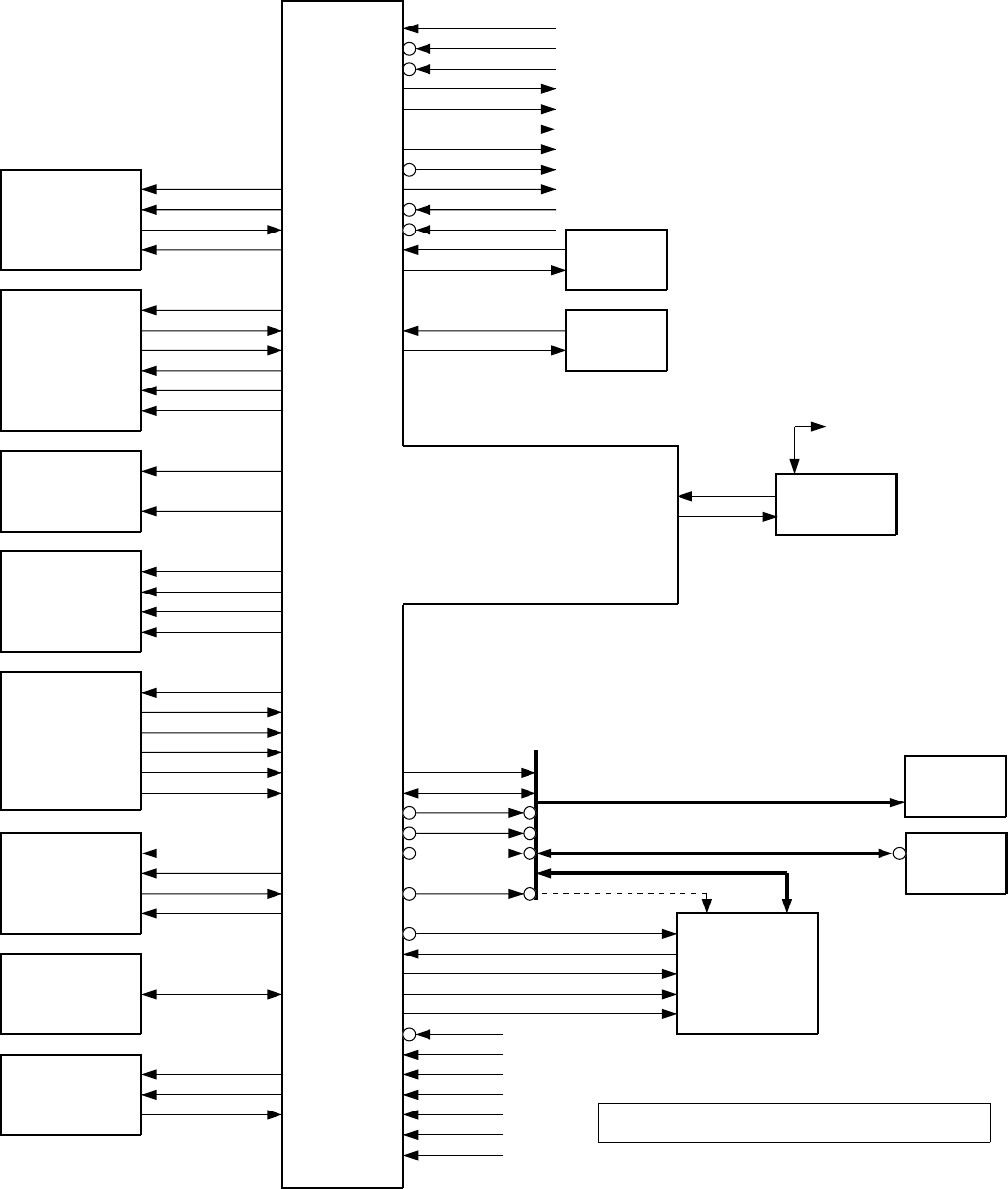
FO-CC500A
FO-K01A
(3) Panel control block
The following controls are performed by the SCE214V.
•Operation panel key scanning
•Operation panel LCD display
(4) Mechanism/recording control block
•Recording control block diagram (1)
Fig. 4
5 – 9
OPERATOR
PANEL,
KEYPAD,
LEDS & LCD
PRINTER DATA
CONTROL &
SENSORS
OPO[7:0]*
OPI[3:0]*
LEDCTL*
LCDCS*
TEST[1:0]
BATRSTN
RESETN
STRB[3:0]
STRBPOL
THADI
PDAT
PCLK
PLAT
ALTTONE
TSTCLK
REGDMA
WAITN
SYNC
PWRDWNN
PRINTER &
SCANNER
MOTOR DRIVERS
PM[3:0]*
SM[3:0]*
RTC
CRYSTAL
SCANNER
CONTROLS &
SENSORS
START
CLK2
CLK1
CLK1N
VIDCTL[1:0]
XIN
XOUT
INTERNAL
IA
LINE
INTERFACE
DRAM
SCANNER
VIDEO
PREPROCESSING
SERIAL SYNC
PORTS
(SSIF)
VIN
VREFP
VREFN
SSCLK[2:1]*
SSTXD[2:1]*
SSRXD[2:1]*
SSSTAT[2:1]*
SYNC/ASYNC
SERIAL PORT
SASIF
SASCLK*
SASTXD*
SASRXD*
GPIOGENERAL
PURPOSE I/O
DEBUGN
VDD
VDRAM
VBAT
VSS
FLASH MEMORY
(OPTION)
WRPROTN
FRDN*
FRWN*
FCLE*
FCSN[2:0]
D[7:0]
RDN
A[23:0]
WRN
ROMCSN
CS[5:0]N*
CAS[0,1]N, RASN, DWRN
SCE214V
1-CHIP
FAX ENGINE
EXTERNAL BUS
IVREFP
IVREFN
ADVA
ADGA
CS3N,
CS4N**
D7[7:0]
TONE
INTPWRDWNEN
SYSCLK
CRYSTAL
SXIN
SXOUT
TELEPHONE
LINE
TXOUT
RXIN
FLASH
ROM
RDN, ROMCSN
NOTES: * ALTERNATIVE GPO, GPI OR GPIO LINES
**FOR SAMSUNG NAND-TYPE FLASH
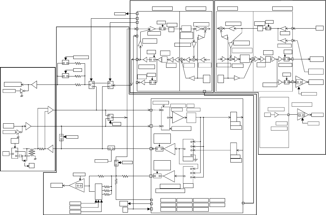
FO-CC500A
FO-K01A
[3] Circuit description of LIU PWB
(1) LIU block operational description
1) Block diagram
2) Circuit description
The LIU PWB is composed of the following 6 blocks.
1. Speech circuit section
2. Dial transmission section
3. Speaker amplifier section
4. Ringer circuit section
5. CI detection circuit
6. Signal/DTMF transmission level & receiving level
Fig. 5
3) Block description
1. Speech circuit section
•This circuit is composed by IC101.IC102 and that circumference
circuit.
2. Dial transmission section
•D.P. transmission: The CML relay is turned on and off for control in
the DP calling system. (Refer to the attached sheet.)
•DTMF transmission: It is formed in the modem, and is output.
3. Speaker amplifier section
•Ringer volume :It is controlled by the combination of the
attenuator value of the LINE DRIVER in the
modem and the ringer sending level sent from
the modem.
•Speaker volume :It is controlled by the attenuator value of the
IC5 and IC3 (VOL-A,B,C)
4. Ringer circuit section
•The ringer sound is formed in the tone of modem when CI signal is
detected. The amplifier circuit drives the speaker of the main body.
5 – 10
LIU PWB
HS RECEIVER
TEL MUTE
HS MIC
Q102
CML
LINE
CI
MIC MUTE
IC101
2904
IC101
2904
IC102
2904
IC102
2904
CONTROL PWB
CORDLESS
HANDSET PWB
CORDLESS
PWB
IC12A
IC12B
IC10A IC10B
IC10C
IC11
IC5
4051
IC7
2113
IC4
TX AMP
SP AMP
IC3:SCE214V
IC12D
DTMF MUTE
RCVOL
1
0
1
RLYCONT
SIG MUTE
SP MUTE
SPEAKER
VOLA CML
TONE
CML
CI DTMF MUTE
RCVOL
TEL MUTE
MIC ENABLE
MIC GAIN
GAIN LPF ADC
DAC
LINE IN ENABLE
LININ GAIN
0,20,25,30dB 0dB
0,–4dB
0,6dB
ADC GAIN
DAC GAIN
RX AMP(MIC AMP)
SIGRX
TELOUT
SIGTX SPKRP
MUTE,0,–6,–12dB
LINE OUT ATTENUATION
SP
DRIVER
LINE
DRIVER
LINEOUT
LNINSEL
RT LOOP
MICP
LINEIN
SPEAKER
OUT ENABLE
LINE OUT
ENABLE
W-TONE
SIG MUTE
SP MUTE MIC MUTE
SASTXD,SASRXD
RLYCONT
VOLA
VOLB
VOLC
CI
VOLB
VOLC
W-TONE
0
DSSIN
0
1
0,0
1,0
1,1
1,1
0,0
0,1
1,0
DSSIN DSSIN
MICIN
LINEIN GN
DAC GN
DAC
FF
SPKOP
LINE
LINE ATTN
SPKROUT GN TXCTRL
RF AUDIOIN 1 GN
RF AUDIOIN 1 GN
VOLUME 1
TG1,
TG2
GPIO
TG1,
TG2
VOLUME 1
ADC GN ADC GN
AUDIOIN 1 GN AUDIOIN 1 GN
PRE
SCALER
PRESCALE
SETTING
POSTSCALE
SETTING
POST
SCALER
TXCTRL
SIDE TONE 1 GN SIDE TONE 1 GN
ADC ADC
MIC IN
MIC GN
LINEIN GN
SPKR OUT GN
SPKOP
LINE O
DAC
DAC GN
LINE ATTEN
AUX VOLUME
TG3 AUXDAC
SP MUTE SP MUTE
SPEAKER
EMJSP MUTE
EMJSP MUTE
EMJSP
EMJMIC
RECEIVER
MIC
EMJSP AMP
ECHOATTN
C
INCOM
DSSOUT
IC1:20438 IC2:MERLIN IC5:MERLIN IC8:20438
FF
IC5:MERLIN
IC6
IC7
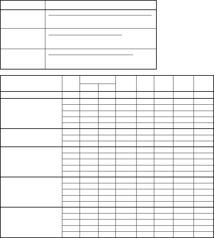
FO-CC500A
FO-K01A
4) Signal selection
The following signals are used to control the transmission line of TEL/
FAX signal. For details, refer to the signal selector matrix table.
[Control signals from output port]
5 – 11
5. CI detection circuit
•CI is detected by the photo coupler which is integrated in series in
the primary side TEL circuit well proven in the existing unit.
6. Signal/DTMF transmission level & receiving level
•
Signal transmission level setting: According to soft switch list.
•DTMF transmission level setting:
According to soft switch list.
Signal Name Description
CML Line connecting relay and DP generating relay
(The circuit is located H: Line make
in the LIU PWB.) L: Line break
SP MUTE Speaker tone mute control signal
(The circuit is located H: Muting (Power down mode)
in the LIU PWB.) L: Muting cancel (Normal operation)
Handset reception mute control signal
TELMUTE H: Muting
L: Muting cancel
VOLUME SETTING LINEOUT A RCVOL DTME VOL A VOL B VOL C
(HIGH) (LOW) MUTE
Key buzzer volume setting Fixed 1 1 1
Speaker volume setting Level1 0 1 1
Level2 0 0 1
Level3 1 1 0
Level4 0 1 0
Level5 1 0 0
Ringer volume setting Low 1 1 1
Middle 0 0 1
High 0 0 0
DTMF speaker volume Level1 1 0 1
setting Level2 1 0 1
Level3 1 0 1
Level4 1 0 1
Level5 1 0 1
OGM playback speaker Level1 0 0 1
volume setting Level2 1 1 0
Level3 0 1 0
Level4 1 0 0
Level5 0 0 0
ICM record speaker Level1 0 0 1
volume setting Level2 1 1 0
Level3 0 1 0
Level4 1 0 0
Level5 0 0 0
FO-CC500A
FO-K01A
5 – 12
(Example: SENDING/RECEIVING)
[Signals for status recognition according to input signals]
[Other signals]
LIU PWB
HS RECEIVER
TEL MUTE
HS MIC
Q102
CML
LINE
CI
MIC MUTE
IC101
2904
IC101
2904
IC102
2904
IC102
2904
CONTROL PWB
CORDLESS
HANDSET PWB
CORDLESS
PWB
IC12A
IC12B
IC10A IC10B
IC10C
IC11
IC5
4051
IC7
2113
IC4
TX AMP
SP AMP
IC3:SCE214V
IC12D
DTMF MUTE
RCVOL
1
0
1
RLYCONT
SIG MUTE
SP MUTE
SPEAKER
VOLA CML
TONE
CML
CI DTMF MUTE
RCVOL
TEL MUTE
MIC ENABLE
MIC GAIN
GAIN LPF ADC
DAC
LINE IN ENABLE
LININ GAIN
0,20,25,30dB 0dB
0,–4dB
0,6dB
ADC GAIN
DAC GAIN
RX AMP(MIC AMP)
SIGRX
TELOUT
SIGTX SPKRP
MUTE,0,–6,–12dB
LINE OUT ATTENUATION
SP
DRIVER
LINE
DRIVER
LINEOUT
LNINSEL
RT LOOP
MICP
LINEIN
SPEAKER
OUT ENABLE
LINE OUT
ENABLE
W-TONE
SIG MUTE
SP MUTE MIC MUTE
SASTXD,SASRXD
RLYCONT
VOLA
VOLB
VOLC
CI
VOLB
VOLC
W-TONE
0
DSSIN
0
1
0,0
1,0
1,1
1,1
0,0
0,1
1,0
DSSIN DSSIN
MICIN
LINEIN GN
DAC GN
DAC
FF
SPKOP
LINE
LINE ATTN
SPKROUT GN TXCTRL
RF AUDIOIN 1 GN
RF AUDIOIN 1 GN
VOLUME 1
TG1,
TG2
GPIO
TG1,
TG2
VOLUME 1
ADC GN ADC GN
AUDIOIN 1 GN AUDIOIN 1 GN
PRE
SCALER
PRESCALE
SETTING
POSTSCALE
SETTING
POST
SCALER
TXCTRL
SIDE TONE 1 GN SIDE TONE 1 GN
ADC ADC
MIC IN
MIC GN
LINEIN GN
SPKR OUT GN
SPKOP
LINE O
DAC
DAC GN
LINE ATTEN
AUX VOLUME
TG3 AUXDAC
SP MUTE SP MUTE
SPEAKER
EMJSP MUTE
EMJSP MUTE
EMJSP
EMJMIC
RECEIVER
MIC
EMJSP AMP
ECHOATTN
C
INCOM
DSSOUT
IC1:20438 IC2:MERLIN IC5:MERLIN IC8:20438
FF
IC5:MERLIN
IC6
IC7
: FAX SENDING/RECEIVING
Fig. 6
NO Signal Name (CNLIUA)
1 RHS-
2DG
3 +24VL
4 MICMUTE
5TELIN
6 TELMUTE
7 RXIN
NO Signal Name (CNLIUA)
8 TXOUT
9 CML
10 PIN
11 FILM
12 CI
13 HS-(N.C.)
14 TELOUT
Signal Name Function
RHS- H: The handset is in the on-hook state.
L: The handset is in the off-hook state.
CI Incoming call (CI) detection signal
Signal Name Function
TEL IN Receiving signal from line or modem
SPOUT Speaker output signal
TXOUT Transmission (DTMF) analog signal output
from modem
RXIN Reception (DTMF, others) analog signal input
into modem
TELOUT Voice input to MODEM from handset.
FO-CC500A
FO-K01A
5 – 13
[4] Circuit description of Cordless PWB
(1) This 2.4GHz cordless machine use DSSS(Direct
Sequence Spread Spectrum) technology.
DSSS feature
• The communication is little influenced by noise.
• The ability of keeping a secret is high level.
And the communication using the radio frequency is performed TDD
operation between the sets of keeping a common system ID.
The system ID is stored nonvolatile memory of each set.
The ID code are kinds of 224.
1) Transmission
Voice signal is inputted from mic and headset is adjusted the level of
signal and converted from analog signal to digital in the CODEC, and
is sent to Merlin (Baseband IC).
In Merlin, the inputted signal is converted ADPCM data and scram-
bled by XORed PN sequence.
The scrambled signal is differentially encoded and spreaded.
A 12chip spreading code is used to meet FCC part 15.247 require-
ments for a DSS(Digital Spread Spectrum) system.
The spreaded signal is modulated by DBPSK (Differential Binary Phase
Shift Keying) and is sent to RF109(2.4GHz Digital Spread Spectrum
Transceiver) into a RF MODULE.
RF109 generates the Local Oscillator(LO) frequencies using a
PLL(Phase Look Loop) frequency synthesizer and external 2.4GHz
VCO(Voltage Controlled Oscillator).
The baseband signal from Merlin is mixed LO frequency.
The mixed signal pass through Matching Network Circuits and is sent
to RF110(RF Power Amplifier).
The Amplified signal in RF110 pass through Antenna Matching Circuit
and is sent to Antenna.
2) Reception
The signal from radio pass through BPF (Band Pass Filter) of 2.4GHz
band width and is sent to RF109.
RF109 adjust the level of signal in LNA(Low Noise Amplifier) and
downconverted to Baseband I/Q signals.
Baseband I/Q signals is sent to the Merlin and despread, demodu-
lated and descrambled to ADPCM data.
The ADPCM data is converted analog signal in CODEC.
3) Stand-by
When the cordless handset(HS) put on the cradle, the system be-
come stand-by mode.
In this mode FAX(BS) monitor a present using channel and other chan-
nel to choice best channel.
HS is sleep mode. but it wakes up every 1second, and monitor the
signal from BS.
And it checks link establishment with BS every 10 second.
4) Serial communication with FAX ENGINE
The merlin and fax engine is connected by serial interface.
Example) If user push Talk key, the Talk command from merlin is sent
to fax engine through the serial interface and the fax engine control
the connection to line.
(2) Audio data flow
Data flow in transmission and reception mode are shown as Fig. 8.
Example) FAX(BS)
Fig. 7 Fig. 8
VCC
RF109
RF110
3-TERMINALS
REGULATOR
LPF
BALUN
TX DATA
RXI,RXQ
TXEN
RXEN
ANTENNA
ANTENNA
MATCHING
NETWORK
MATCHING
NETWORK
TX/RX SW
2450MHz
BPF
VCO
RF MODULE BLOCK DIAGRAM (TMX964A:UNIT1)
LINE
TRANSMISSION
LIU
CODEC
MERLIN
LPF
TX/RX SW
ANTENNA
ANTENNA
TX/RX SW
RF109 TRANSCEIVER
2450MHz BPF
RF109 TRANSCEIVER
MATCHING NETWORK
RF110 POWER
AMPLIFIER
LIU
LINE
MERLIN
CODEC
LINE IMPEDANCE
MATCHING
ANTENNA MATCHING
NETWORK
ANTENNA MATCHING
NETWORK
RF MODULE
RF MODULE
LINE IMPEDANCE
MATCHING
RECEPTION
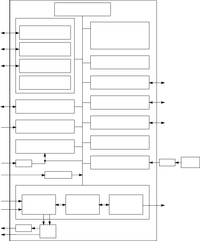
FO-CC500A
FO-K01A
5 – 14
1) Technical Overview
This section provides a technical description of the Merlin device set
and how it is used to implement all 900 MHz and 2.4 GHz cordless
telephone features. The device set is used both in the handset and
the base station as shown in Fig. 9.
Fig. 9 Merlin ASIC Block Diagram
2) System Controller
The system controller handles all telephone features, the DSS en-
gine, the RF module settings, and the link between the base station
and the handset.
The system controller provides a microcontroller, interrupt controller,
wait-state generator, and system timer support. The system control-
ler also provides General Purpose I/O (GPIO) and serial ports for
peripheral control, a baseband modem (DSS engine) for signal
processing of the received and transmitted data, and a DSP core for
ADPCM conversion and CID support.
Microcontroller. The microcontroller is the 65C02-based MC19CPU.
It is supported by 2 kB of on-chip RAM and 48 kB of on-chip ROM.
The CPU communicates with the internal memory via a 16-bit ad-
dress/8-bit data bus and dedicated control lines.
The 128-pin Merlin XROM also has an address/data bus available for
accessing external memory.
MC19 Controller
& Address Decoder Logic
DSP Core
ADPCM,tone generation,
CAS detection,SDT detection
CID demodulation,
HDX speakerphone support
ROM(48kB)
RAM(2kB)
RF GPIO
configurable Port C
RF Interface
Power control
Synthesizer control
Telephone Interface
Hook/Ringer/LEDs/
Other miscellaneous
Emulator/Test/
Parallel Interface
(128-pin ASIC only)
Data bus,Address bus
Bus control signals
Phone GPIO
configurable Port A
Controller Interface
Keypad GPIO
Low Battery Detector
Watchdog/Sleep Timer
RX Data Path
demodulator
descrambler
Reset
GPIO Configurable
Port B
Serial EEPROM
Second Codec
BS/HS interface
Keypad/LCD/
Switches/LEDs
Vbattery
Resetln
Park
RXI
RXQ
AGC
LNA
Codec Codec Serial Port
ART/Timer B
Timer A
DAC
OSC
Serial Ports/Timers
TXD
AGC
Logic
Park Detect
Baseband Modem
(Digital Spread - Spectrum Engine)
Time Division
dupiex controller
& clock
generator
TX Data Path
modulator
scrambler
spreader
DAC
Inverter 19.2MHz
TCXO
Interrupt Controller. Interrupts are latched, prioritized, and passed
to the microcontroller. Interrupts are used to interface with the Codec,
the DSS engine, serial ports, and timers.
Wait-State Generator. Slower access times for off-chip RAM and ROM
are handled separately with programmable wait states. Off-chip reads/
writes can be extended up to seven clock cycles.
Watchdog/Sleep/Wake-Up Timers. These timers perform two basic
functions. They provide a reset if the software malfunctions (watch-
dog). They also minimize power consumption by keeping a low-fre-
quency clock active to duty-cycle the system between normal mode
and stand-by mode (sleep and wake-up timer).
Emulator/Test Interface. A standard 65C02-family parallel interface
supports an external emulator for code development.
ROM is mapped off-chip when operating with an emulator.
Emulator functions are only provided with the Merlin XROM ASIC.
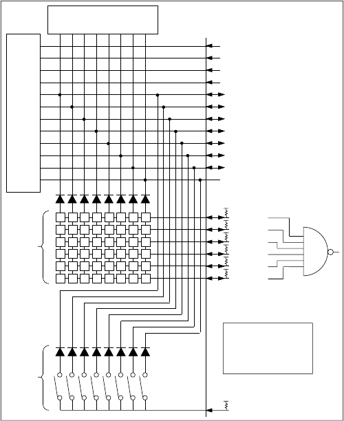
FO-CC500A
FO-K01A
5 – 15
3) Controller Peripheral Functions
Several peripheral phone functions are supported via the
microcontroller registers or dedicated hardware.
General purpose timers are configured to provide the timing required
for firmware execution. An asynchronous serial port and a dedicated
Codec serial port are also available. GPIOs are provided for periph-
eral control. Several GPIOs are dedicated to interface to peripherals
such as the LEDs, keypad, RF control, and serial EEPROM control.
GPIOs are also used as dedicated interfaces for phone functions such
as ring detection and hook relay control.
General Purpose Timer A. Timer A is used for various firmware needs
such as link timing. It generates either single or continuous interrupts
and consists of an 8-bit interval register (TmrA) for the interval value,
an 8-bit counter for generating the timer interrupt, and a divide-by-
256 prescaler. Timer A uses the main 9.6 MHz clock divided by 256.
General Purpose Timer B. Timer B may be configured as a general
purpose timer or as an ART serial port. When configured as a timer,
its operation is similar to that of Timer A.
Timer B consists of an 8-bit interval register (TmrB), a divide-by-5
prescaler and an 8-bit counter. Timer B uses the main 9.6 MHz clock
divided by 5.
Asynchronous Receiver/Transmitter. An asynchronous serial port
with a programmable baud rate can be configured using Timer B. The
ART logic controls the two-pin asynchronous serial port of the ASIC.
The ART port is used for base/handset data transfer and as the test
interface.
Keypad/Switch/LCD/ITAD/Seven Segment Interface. This interface
is used to provide multiplexed control for a 6x8 keypad, up to eight
switches, and a parallel interface for an LCD (see Fig. 10). For a
keypad interface, the eight KEYPADR[7:0] control signals are driven
low, one at a time, and the six KEYPADC[5:0] inputs, with internal
pullup resistors, are read to determine which key in the 48-key matrix
is closed. The firmware scans the keypad at 10 ms intervals and
debounces the key presses.
D7 D6 D5 D4 D3 D2 D1 D0
D7
keypad
switches
D6 D5 D4 D3 D2 D1 D0
keypadR7
keypadR6
keypadR5
keypadR4
LCDPWR
LCDRW
LCDRS
LCDEN
keypadR3
keypadR2
keypadR1
keypadR0
keypadC5
key
press
wakeup
&
status
flag
keypadC4
keypadC3
keypadC2
keypadC1
keypadC0
SWCTL/GPIOC0
Diodes D7-D0 are
required for isolation
if KEYPADC pins are
used to also drive LCD
or switches.
ITAD
PWR
R/W
RS
E
DB7
LCD display
DB6
DB5
DB4
DB3
DB2
DB1
DB0
For a switch interface, the eight KEYPADR[7:0] control signals are
driven, one at a time, and GPIOC0, with an internal pullup resistor, is
read to determine if a switch is open or closed.
KEYPADC0 is used to select either 900 MHz or 2.4 GHz control.
Not connecting KEYPADC0 and SWCTL (GPIOC0) selects 900 MHz
radio control. A diode connected between KEYPADC0 and SWCTL
(GPIOC0) selects 2.4 GHz radio control.
An LCD interface can be implemented as shown in Fig. 10.
Keypad signals are used for the LCD data interface and GPIOs are
used for the LCD control lines. The LCD driver and LCD management
software must be written by the OEM.
An ITAD interface can be implemented by multiplexing KEYPADR[7:0]
as ITAD data lines and using GPIOs as ITAD control lines.
A seven-segment interface can be implemented by multiplexing
KEYPADR[7:0] as data lines and GPIOs as control lines to switch
between different bank of LEDs.
Codec Serial Port. Digitized voice-band audio is supported through
an interrupt-driven, 5-pin serial Codec interface. Clock and frame tim-
ing for the Codec are internally generated and externally output to the
device. The Codec serial port interfaces to the Merlin Codec. The
Codec serial port uses three memory-mapped locations to interface
with the controller. They consist of high and low Codec data bytes,
which are used to write out 16 bits of Tx data and read 16 bits of Rx
data, and an 8-bit Codec configuration/status register.
The ASIC can interface with up to two Codecs by sharing the clock
and control signals between the two Codecs, and by using GPIOs as
the serial data input and output for the second Codec.
RF Transceiver Control. The ASIC allocates several GPIOs to con-
trol all necessary radio transceiver functions. Two pins control the
Power Amplifier (PA) output levels. Four pins make up the synthe-
sizer serial port, clock data, strobe, and synthesizer enable. One pin
is used as the LNA attenuation control and two pins are used for TR
switch control and Tx/Rx enable. The OEM can select ASIC support
for either the 900 MHz or 2.4 GHz radio.
The firmware protocol for programming the Conexant synthesizer in
the RF105 and RF109 and the radio link parameter settings are auto-
matically configured with the selection of the 900 MHz or 2.4 GHz
radio. The OEM can select the radio type using the keypad switch
control, or by the OEM configuration settings in serial EEPROM or
external ROM. If the radio type is selected using serial EEPROM or
external ROM, the keypad switch control radio selection is not used.
Battery Detector. This analog function performs A/D conversion on
the battery voltage and makes it available to the microcontroller for
battery quality estimation. External level shifting resistors set the in-
put level to the ASIC. The low battery threshold can be set by the
OEM in EEPROM.
Two multiplexed inputs are available to monitor more than one volt-
age supply level.
General Purpose Inputs/Outputs (GPIOs). GPIOs are available on
all Merlin ASICs. GPIOs are software bit-configurable as inputs or
outputs. The GPIOs may be used as dedicated control signals for
LED drivers, LCD control, hook relay control, ring detection, RF con-
trol, half-duplex speakerphone device control, serial EEPROM inter-
face, ITAD device control, and seven-segment LED control, depend-
ing on the system configuration. The recommended GPIO assign-
ments.
Ringer/Buzzer Control. A ringer/buzzer can be driven by either the
Codec LINEO, the ASIC AUXDAC, or a GPIO.
Fig. 10 Keypad/Switch/LCD/ITAD Interface
FO-CC500A
FO-K01A
MIC/line
select
Modulator
and filter
Modulator
and filter
16-bit
register
CDCMCLK
MICIN
LINEIN
MICBIAS
SPKRO
LINEO
FSYNC
CDCICLK
SIN
SOUT
Control
register
16-bit
register
5 – 16
4) Baseband Modem
The baseband modem section in each of the Merlin ASICs performs
all of the spread spectrum modulation and demodulation, data timing
recovery, AFC, AGC, framing, and rate adaptation required for a DSS
system.
Transmit/Receive Data Paths. The transmit data path consists of a
parallel-to-serial converter, scrambler, differential encoder, spreader,
and modulator. The receive data path comprises A/D converters,
matched filter with frequency compensation insertion, data
demodulator, descrambler, and a serial-to-parallel converter.
Scrambler/Descrambler. The scrambler/descrambler is a 16-bit maxi-
mum length Pseudorandom Noise (PN) sequence generator. The PN
sequence is XORed with Tx data for scrambling and XORed with Rx
data for descrambling. The voice and supervisory bits are scrambled.
The PN sequence generator’s starting location is programmable us-
ing one memory mapped register along with the two ID registers. This
starting location is used to initialize the PN generator at the start of
each link. The MSB of the PN generator is used to scramble/
descramble. The first frame bit scrambled/descrambled uses the ini-
tialized value of the MSB.
Differential Encoder. When this block is enabled, data is differen-
tially encoded. The encoder is initialized to zero during the Tx frame’s
first “zero bit.” In DBPSK, a data symbol is inferred by the presence or
absence of a 180-degree phase shift or inversion in the carrier signal
at regular intervals. A phase shift therefore indicates a change of state
from one to zero, or zero to one. To determine which of these two
possibilities was intended, the spread data is differentially encoded.
Spread Spectrum Spreader. A 12-chip spreading code is used to
meet FCC part 15.247 requirements for a DSS system. The spread-
ing code cyclic duration is 12 times that of the encoded data. The
code starts and stops on encoded bit boundaries. The spreading code
may be configured by the controller.
Modulation. The data from the differential encoder is input to the
modulator. An analog block exists at the Tx output that maintains a
constant voltage level independent of supply operation.
Receiver A/D Converters. Baseband I/Q signals from the radio are
sampled at 1.92 MHz and converted to digital with 3-bit flash A/D
converters.
AFC/Timing. Internal AFC allows a crystal tolerance of up to ±90
ppm for a 900 MHz radio or ±40 ppm for a 2.4 GHz radio.
This allows for a total system clock error of 180 ppm for a 900 MHz
radio or 80 ppm for a 2.4 GHz radio. The modem uses a standard
early-late mechanism to maintain timing locks.
Matched Filters. The spreading code is removed (despread) from
the received, digitized I/Q signals with matched filters.
Data Demodulation. This block determines the value for the received
bit and determines a frequency error estimate used for the AFC. Data
is demodulated by using I/Q matched filter data which is exactly one
bit time apart.
Signal Quality. A signal quality metric is accumulated over each frame
and can be read by the microcontroller at any time.
ID Detector. A 32-bit ID word (16-bit programmable) is used during
acquisition to verify the RF link and initialize frame timing.
Time Division Duplex Controller (TDDC). The TDDC handles the
spread spectrum protocol.
AGC and Gain Imbalance. The signal energy is compared to a pro-
grammable threshold and scaled with programmable gain.
The digital AGC value is output to the radio by an 8-bit D/A converter.
The gain imbalance of the I/Q system is automatically calculated and
removed during calibration of the system.
Clock Oscillator. A highly accurate crystal oscillator (TCXO etc.) is
needed to register multi cordless handsets to fax machine by wire-
less. And its output level convert to meet Merlin specification using
high speed inverter or high speed rail-to-rail input and output opera-
tional amplifiers. A 19.2 MHz crystal oscillator generates a 19.2 MHz
clock and a 9.6 MHz clock. The 19.2 MHz clock is used only for the
DSP core. The 9.6 MHz clock is the main system clock used by the
controller and the rest of the system.
5) DSP Core Audio Coprocessor
The DSP audio coprocessor is connected to the microcontroller via
the internal data bus and memory mapped registers. The DSP con-
verts ADPCM data to/from 16-bit linear Codec data, generates audio
tones, and performs CID signal processing.
ADPCM Coder/Decoder. The ADPCM coder/decoder is the DSP core
main block. This block performs the processing that encodes linear
speech data, passes it to the radio as ADPCM compressed speech,
and decodes ADPCM data received from the radio into linear speech
data.
Using the ITU G.726 32 kbps ADPCM audio compression algorithm,
14-bit linear samples are compressed to 4 bits at a rate of 8 k samples
per second.
Tone Generators. The DSP core also contains three independent
tone generators. The tone generators are used to create DTMF
signaling as required by the telephone system, and to create all MMI
audio alert signals.
CID Processing. The DSP core contains a demodulator for decoding
CID FSK signals. The DSP core also performs CPE Alert Signal (CAS)
detection for CID type ll, stutter dial tone detection, and Visual Mes-
sage Waiting Indication (VMWI) processing. No external CID devices
are required. The DSP CID processing supports the following:
• CID types 1, 2, and 2.5
• VMWI
• Synchronous Call Logging (SCL)
• Stutter dial tone detection
6) Audio Codec
The audio Codec is a monolithic CMOS integrated circuit packaged
in all of the Merlin devices except for the XROM ASIC. The Codec
consists of an A/D and D/A converter path, with digital filtering and
analog signal processing circuits to realize a compliant ITU G.714-
compatible voice frequency linear coder/decoder (see Fig. 11). The
user word rate to and from the device is 8 k words per second.
ASIC Interface Port. Six interface lines are used to link the audio
Codec and ASIC. Two lines are used for clocks (CDCMCLK and
CDCICLK) and a third creates an 8 kHz framing pulse. The remaining
lines are for data in and data out lines as well as a reset line. The
clocks and framing pulse are synchronous to each other. The data I/O
port will be time-multiplexed between data and control words.
Fig. 11 Merlin Codec Block Diagram
FO-CC500A
FO-K01A
5 – 17
Microphone Input. The Codec provides a microphone interface for
an electret microphone. The microphone input is differential to reduce
common mode noise pickup. The microphone must be AC-coupled to
the MICINP and MICINN inputs. A quiet, clean voltage (MICBIAS) is
available to provide a bias for the electret microphone. The micro-
phone input amplifier has programmable gains from -4 to 28 dB (-4, 0,
6, 12, 18, 24, and 28 dB), to accommodate a wide range of micro-
phone sensitivities. The microphone input is multiplexed with the line
input signal before the A/D conversion.
Line Input. The Codec line input is an auxiliary input which may be
used as an alternative analog interface. For example, this interface
may be used between the base station Codec and the PSTN. The
line input, before final A/D conversion, is multiplexed with the micro-
phone input signal.
Fig. 12 Typical System Block Diagram for the 128-pin Merlin XROM ASIC
MVCS
MVDI
MVDO
MVCLK
OHP
RINGP
LINEIN
SPKROP
SPKRON
MICINN
MICINP
LINEO
(on handset,AUXDAC and
GPIOA6 may be used)
earpiece
microphone
Serial
EEPROM
32-Pin
Merlin
Codec
External
ROM
External
device
LNAATN
RXEN
RXIP
RXIN
RXQP
RXQN
AGC
SYNEN
REFOSC
SYNSTB
SYNDATA
SYNCLK
TXDATA
TXEN
TXPWR0
TXPWR1
TRSW
Keypad
LCD
DATA
LCDRS
LCDPWR
LCDRW
DATA[7:0]
ADDR[15:0]
ROMCSP
RDP
HOSTCSP
HOSTIRQ
HOSTACK
optional
Base station only
Handset only
WRP
LCDEN
Emulator
(Development
System Only)
EMUCLK
SYNC
NMIP
Keypad
column 1-6
Keypad
row 1-8
CDCDATAI
CDCDATAO
CDCFRAME
ICLK
MCLK
RESETOP
Base Station
/PSTN
Interface
128-Pin
Merlin
XROM
900MHz
or
2.4GHz
Radio
Line output. LINEO is a single-ended output capable of driving a 1
kΩ load. The output amplifier has programmable gains from -35 dB to
1.1 dB in 6 dB steps.
Speaker Output. The SPKROP and SPKRON signals form a differ-
ential output capable of driving a 150 Ω resistive load or a highly ca-
pacitive (100 nF) ceramic receiver via dual 150 Ω series resistors.
This output may be used to drive either the PSTN or the handset
earpiece. The output amplifier has programmable gains from -29 dB
to 3 dB.
7) Power Requirements
All six of the ASICs in the Merlin family of spread spectrum devices
operate within +2.7 to +3.3 V. Each of the ASICs has an active, low
power consumption of less than 60 mW (+3.3 V) and a very low power
stand-by consumption of less than 3 mW (+3.3 V).

FO-CC500A
FO-K01A
5 – 18
Controller Interface
122 DATA0 B-PUP Data bit 0
121 DATA1 B-PUP Data bit 1
120 DATA2 B-PUP Data bit 2
119 DATA3 B-PUP Data bit 3
118 DATA4 B-PUP Data bit 4
117 DATA5 B-PUP Data bit 5
116 DATA6 B-PUP Data bit 6
115 DATA7 B-PUP Data bit 7
15 ADDR0 T Address bit 0
16 ADDR1 T Address bit 1
17 ADDR2 T Address bit 2
18 ADDR3 T Address bit 3
19 ADDR4 T Address bit 4
20 ADDR5 T Address bit 5
21 ADDR6 T Address bit 6
22 ADDR7 T Address bit 7
51 ADDR8 T Address bit 8
52 ADDR9 T Address bit 9
55 ADDR10 T Address bit 10
53 ADDR11 T Address bit 11
46 ADDR12 T Address bit 12
50 ADDR13 T Address bit 13
49 ADDR14 T Address bit 14
47 ADDR15 T Address bit 15
48 WRP (Note 2) T Write; active low
54 RDP T Read; active low
112 ROMCSP O2 ROM chip select; active low
79 RAMCSP O2 RAM chip select; active low
83 HOSTCSP O2 Host chip select; active low
84 HOSTACK IS-PUP Host input acknowledge
82 SYNC (Note 2) O2 Synchronize, CPU fetching OP code
81 NMIP IS-PUP Non-maskable interrupt; active low
85 XCODEP I-PUP Emulator select; active low
80 EMUCLK (Note 2) O2 Phase 2 clock output from MC19
RF Interface
89 REFOSC B4 9.6 MHz clock used by synthesizer
102 RXIN I-A Receiver I negative differential input
101 RXIP I-A Receiver I positive differential input
104 RXQN I-A Receiver Q negative differential input
103 RXQP I-A Receiver Q positive differential input
106 AUXREF B-A AUXDAC reference
100 TXDATA O-A Transmitter data
105 AGC O-A AGC control
110 TRSW O Transmit=1/receive=0 select
108 TXEN O Transmit enable
76 RXEN O Receive enable
75 GPIOC1 O General purpose I/O. Can be configured as LNA select (LNAATN).
111 GPIOC2 O General purpose I/O. Can be configured as PA power level select (TXPWR0).
MERLIN ASIC XROM (R6815): Terminal description
Pin No. Pin Name Type (Note 1) Description

FO-CC500A
FO-K01A
5 – 19
RF Interface
109 GPIOC3 O General purpose I/O. Can be configured as PA power level select (TXPWR1).
88 GPIOC4 O2 General purpose I/O. Can be configured as synthesizer power (SYNEN).
87 GPIOC5 O2 General purpose I/O. Can be configured as synthesizer strobe (SYNSTB).
77 GPIOC6 O2 General purpose I/O. Can be configured as synthesizer data (SYNDATA).
76 GPIOC7 O2 General purpose I/O. Can be configured as synthesizer clock (SYNCLK).
Codec Interface
43 CDCDATAO B2 Codec data output
44 CDCDATAI I-PDN Codec data input
42 CDCFRAME T-PDN Codec frame
58 ICLK T-PDN Codec serial port clock
45 MCLK T-PDN Codec clock
59 RESETOP O4 Codec reset
GPIO Interface
123 GPIOA0 B4 General purpose I/O
124 GPIOA1 B4 General purpose I/O
125 GPIOA2 B4 General purpose I/O
126 GPIOA3 B4 General purpose I/O
127 GPIOA4 B4 General purpose I/O
128 GPIOA5 B4 General purpose I/O
1 GPIOA6 B4 General purpose I/O
8 GPIOA7 B4 General purpose I/O
38 GPIOB0 B4 General purpose I/O
37 GPIOB1 B4 General purpose I/O
36 GPIOB2 B4 General purpose I/O
31 GPIOB3 B4 General purpose I/O
30 GPIOB4 B4 General purpose I/O
26 GPIOB5 B4 General purpose I/O
25 GPIOB6 B4 General purpose I/O
24 GPIOB7 B4 General purpose I/O
9 GPIOC0 B4-PUP General purpose I/O. Can be configured as switch control read input (SWCTL).
Keypad Interface
60 KEYPADR0 BIS Keypad bidirectional control
61 KEYPADR1 BIS Keypad bidirectional control
62 KEYPADR2 BIS Keypad bidirectional control
63 KEYPADR3 BIS Keypad bidirectional control
64 KEYPADR4 BIS Keypad bidirectional control
65 KEYPADR5 BIS Keypad bidirectional control
66 KEYPADR6 BIS Keypad bidirectional control
67 KEYPADR7 BIS Keypad bidirectional control
23 KEYPADC0 BIS-PUP Keypad read input
14 KEYPADC1 BIS-PUP Keypad read input
13 KEYPADC2 BIS-PUP Keypad read input
12 KEYPADC3 BIS-PUP Keypad read input
11 KEYPADC4 BIS-PUP Keypad read input
10 KEYPADC5 BIS-PUP Keypad read input
Phone Interface
40 PARKP IS Park input; active low on base station, active high on handset.
Analog Support
95 AGND O-A Analog ground.
Pin No. Pin Name Type (Note 1) Description
MERLIN ASIC XROM (R6815): Terminal description

FO-CC500A
FO-K01A
5 – 20
Note 1: pin type:
B2 Digital Bidirectional: 2 mA driver and CMOS receiver
B4 Digital Bidirectional: 4 mA driver and CMOS receiver
B4-PUP Digital Bidirectional: 4 mA driver and CMOS receiver with
pullup
BIS Digital Bidirectional: 4 mA driver and CMOS Schmitt receiver
BIS-PUP Digital Bidirectional: 4 mA driver with pullup and CMOS
Schmitt receiver
B-A Analog Bidirectional: Analog receiver/driver
B-PUP Digital Bidirectional: 2 mA driver with pullup and CMOS
receiver
I Digital Input: CMOS receiver
IS Digital Input: CMOS Schmitt receiver
Miscellaneous
41 ARTO O-OD ART output
39 ARTI I-PUP ART input
107 AUXDAC O-A Auxiliary DAC output
94 RESETIP I-PUP POR input; active low
91 OSCI I 19.2 MHz crystaloscillator input
90 OSCO O 19.2 MHz crystaloscillator output
96 BATT1 I-A Battery voltage input
97 BATT0 I-A Battery voltage input
86 VISP (Note 2) I-PUP Visibility mode select; active low
72 NC No connect
3 NC No connect
4 NC No connect
34 NC No connect
35 NC No connect
68 NC No connect
69 NC No connect
98 NC No connect
99 NC No connect
Supply Pins
6 VDDP VDD VDD supply to pad ring
28 VDDP VDD VDD supply to pad ring
56 VDDP VDD VDD supply to pad ring
74 VDDP VDD VDD supply to pad ring
113 VDDP VDD VDD supply to pad ring
7 VSSP VSS VSS supply to pad ring
29 VSSP VSS VSS supply to pad ring
57 VSSP VSS VSS supply to pad ring
73 VSSP VSS VSS supply to pad ring
114 VSSP VSS VSS supply to pad ring
2 VDDC VDD VDD supply to core
32 VDDC VDD VDD supply to core
71 VDDC VDD VDD supply to core
5 VSSC VSS VSS supply to core
33 VSSC VSS VSS supply to core
70 VSSC VSS VSS supply to core
92 AVDD VDD-A VDD supply to analog
93 AVSS VSS-A VSS supply to analog
27 VDDP VDD VDD supply to pad ring
MERLIN ASIC XROM (R6815): Terminal description
Pin No. Pin Name Type (Note 1) Description
IS-PDN Digital Input: CMOS Schmitt receiver with pulldown
IS-PUP Digital Input: CMOS Schmitt receiver with pullup
I-A Analog Input: Analog receiver
I-PDN Digital Input: CMOS receiver with pulldown
I-PUP Digital Input: CMOS receiver with pullup
O Digital Output: 4 mA driver
O2 Digital Output: 2 mA driver
O-A Analog Output: Analog driver
O-OD Digital Output: Open drain
T Digital Tristate: 2 mA driver
T-PDN Digital Tristate: 2 mA driver with pulldown
T-PUP Digital Tristate: 4 mA driver with pullup
Note 2: Available only for the emulation version; defined as NC for the production version.

FO-CC500A
FO-K01A
Note 1: pin type: I Digital Input: CMOS receiver
I-A Analog Input: Analog receiver
O Digital Output: 4 mA driver
O-A Analog Output: Analog driver
Note 2: Do not connect. Use of this pin may cause malfunction and/or damage to the device.
5 – 21
1 NC No connect (Note 2)
2 NC No connect (Note 2)
3 NC No connect (Note 2)
4 SOUT O Serial data output
5 SIN I Serial data input
6 FSYNC I/O Frame sync
7 CDCPOR I Reset input, active low
8 AVSS I Analog 0 V power supply
9 LINEIN I-A Analog input to line pre-amp, ADC channel
10 MICNP I-A Positive differential analog input to microphone pre-amp, ADC channel
11 MICINN I-A Negative differential analog input to microphone pre-amp, ADC channel
12 MICBIAS O-A 2.2 V nominal DC bias source for electret microphone
13 VREF O-A Analog reference voltage output. Bypass to AVSS with 0.1 µF capacitor.
14 AGND O-A Analog ground bias output. Bypass to AVSS with 0.1 µF capacitor.
15 AVDD I-A Analog power supply, 2.7-3.3 V
16 AVSS I-A Analog 0 V power supply
17 LINEO O-A Line driver output, DAC channel
18 SPKROP O-A Positive speaker driver output, DAC channel
19 SPKPON O-A Negative speaker driver output, DAC channel
20 DVSS I Digital 0 V power supply
21 DVDD I Digital power supply, 2.7-3.3 V
22 NC No connect (Note 2)
23 NC No connect (Note 2)
24 NC No connect (Note 2)
25 NC No connect (Note 2)
26 CDCICLK I Bit clock input/output for digital serial interface
27 NC No connect (Note 2)
28 NC No connect (Note 2)
29 NC No connect (Note 2)
30 NC No connect (Note 2)
31 CDCMCLK I Main clock input
32 NC No connect (Note 2)
20438: Terminal description
Pin No. Pin Name Type (Note 1) Description
FO-CC500A
FO-K01A
5 – 22
[5] Circuit description of Cordless
handset PWB
1. Cordless handset configuration
Fig. 13
Fig. 14
1) Cordless handset PWB
The block diagram is shown below.
MERLIN (R6815)(IC5): pin-128 QFP
The MERLIN is mainly consist of MC19 controller, DSP core,
Baseband Modem and internal RAM.
Crystal frequency is 19.2 MHz.
The system clock is 9.6 MHz.
SST39LF512P(IC3): pin-32 TSOP (FLASH ROM)
This memory store the program for MERLIN.
It is able to change the program by using download tool.
S-24C04(IC4): pin-8 SOP (EEPROM)
This is nonvolatile memory. The memory size is 4 Kbits.
It is stored the system ID, channel number etc.
20438(IC8): pin-32 QFP (CODEC)
This part is adjust the signal level from mic/to receiver.
And it convert the signal from analog to digital or from digital to
analog.
TMX964A(UNIT1): pin-26 SOP (RF MODULE)
This part is modulated the baseband signal to 2.4 GHz band radio
frequency.
It consist of RF109, RF110 made by CONEXANT and VCO for
oscillating 2.4 GHz etc.
RF109 is 2.4 GHz DSS Transceiver. The main function are that
LNA/Quadrature mixer from RF down to baseband and mixer for
baseband to RF modulation.
Transmitter output levels are selectable for high, medium, and low
power modes.
LNA gains are selectable for high and low modes.
RF110 is a three stage class AB power amplifier for 2.4 GHz band.
2) LCD(GPM190A0)
This LCD is COG type.
Its display format is 15charactor × 3line dot matrix and display mode
is STN.
3) RECEIVER(DTR-208H)
This part is Dynamic receiver with Hearing Aid to meet FCC regu-
lation.
4) SPEAKER(DSH-305)
This is Dynamic Mylar Speaker. Output impedance is 32 Ω at
1 kHz.
5) BATTERY(3HR-5/4AAAU)
This is Nickel Metal Hydride Rechargeable Battery.
It consists of 3cell battery, poly switch, cable and 2pin connector.
The normal voltage is 3.6 V, and the typical capacity is 850 mAh.
6) HANDSET
Handset is able to communicate with hands free by using Hand-
set.
The meat plug size is φ 2.5.
7) ANTENNA
Antenna type is Whip antenna.
CORDLESS
HANDSET
PWB
RECEIVER
SPEAKER
HEADSET
(OPTION)
BATTERY
ANTENNA
LCD
MERLIN
FLASH
ROM
EEPROM
RF
MODULE
CODEC
FO-CC500A
FO-K01A
5 – 23
Fig. 15
This system use two methods of charging to the battery.
One is quick charge, another is trikle charge.
The quick charge is that HSCHG signal level is high.
The current of quick charge is about 160mA - 92mA.
The control of trikle charge is shown as below.
Fig. 16
Fig. 17
2. Charger circuit 4. Channel Frequency
Using channel are shown as below.
The frequency spacing is 1.8MHz, not overlapping.
5. TX Wideband Response
Fig. 18 shows a typical plot of random spread spectrum data as viewed
at the antenna. This plot can be used to check that the system per-
forms to the FCC out-of-band emission requirements.
Fig. 18 RF Spectrum of Merlin 2400 MHz
CHARGER CIRCUIT
HSCHG
F1
R10
VCC BAT
TO REGULATOR
R9
TERMINAL
CONNECTOR
FOR BATTERY
+
–
HSCHG
1
0
CURRENT
5.8SEC 54.2SEC
about 100mA
8mA
CHARGER CIRCUIT
HSCHG
F1
R10
VCC BAT
TO REGULATOR
R9
TERMINAL
CONNECTOR
FOR BATTERY
+
–
3. 2.4GHz DSSS Technical Specifications
1 FREQUENCY 2.4GHz ISM BAND
2 NUMBER OF CHANNEL 40CH
3 CHANNEL SPACING 1.8MHz
4 ACCESS METHOD FDMA-TDD
(Frequency Division Multiple
Access, Time Division Duplex)
5 SPREAD METHOD DSSS
(Direct Sequence Spread Spectrum)
6 CHIP RATE 12chips/bit
7 DATA TRANSFER RATE 100kbps
8
RATE OF BASE BAND DATA
1200kbps
9 MODULATION METHOD DBPSK
(Differential Binary Phase Shift Keying)
No. Item Specifications
1 2404.8 21 2440.8
2 2406.6 22 2442.6
3 2408.4 23 2444.4
4 2410.2 24 2446.2
5 2412.0 25 2448.0
6 2413.8 26 2449.8
7 2415.6 27 2451.6
8 2417.4 28 2453.4
9 2419.2 29 2455.2
10 2421.0 30 2457.0
11 2422.8 31 2458.8
12 2424.6 32 2460.6
13 2426.4 33 2462.4
14 2428.2 34 2464.2
15 2430.0 35 2466.0
16 2431.8 36 2467.8
17 2433.6 37 2469.6
18 2435.4 38 2471.4
19 2437.2 39 2473.2
20 2439.0 40 2475.0
Channel
Number Channel Center
Frequency (MHz) Channel
Number Channel Center
Frequency (MHz)
-10
-20
-30
-40
-50
-60
0
10
20
Ref Level
40 dBm
RBW
VBW
SWT
RF Att
Center 2439.0 MHz
Test Conditions:
High Power Mode
VBATT: +3.6 V 500 kHz Span 5 MHz
Unit
100 kHz
1 MHz
5 ms
30
10.9 dB Offset
40 dB
dBm
Ex.) The current of quick charge mode to the battery
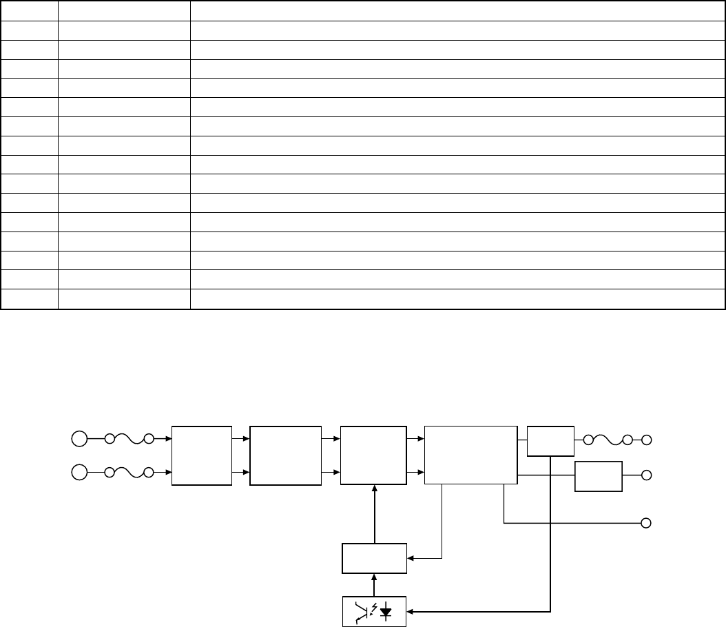
FO-CC500A
FO-K01A
5 – 24
6. RUNTZ2099XHZZ LCD Terminal description (Cordless handset)
1 RS Register selection input
2 RW-WR This pin is connected to R/W pin of MPU
3 E-RD This pin is connected to E pin of MPU
4 CSB Chip selection input
5-8 DB7-DB4 Data bus
9 VDD Power supply for logic
10-14 V4-V0 Bias voltage level for LCD driving
15 VR Voltage adjust pin
16 VOUT DC/DC voltage converter output
17 CAP2- Capacitor connecting pin for the internal voltage converter
18 CAP2+ Capacitor connecting pin for the internal voltage converter
19 CAP1- Capacitor connecting pin for the internal voltage converter
20 CAP1+ Capacitor connecting pin for the internal voltage converter
21 VSS Ground
22 RESETB Hardware reset input
Pin No. Symbol Functions
[6]
Circuit description of power supply PWB
This power supply unit has the function to convert the AC 220 - 240 V
50/60 Hz to DC +24 V, and provide these outputs to the equipment. The
following explains the function of each block. (See Fig. 20)
1. Block diagram
Fig. 20
2-1. Filter circuit
This circuit reduces the outgoing noise through the input lines which is
generated in the power supply unit, and prevents the invasion of the
noise from the lines.(the excessive surge such as the thunder is pre-
vented by the varistor(Z1).)
2-2. Rectifying/smoothing circuit
This circuit rectifies and smoothes the AC input, and provides the DC
voltage to the switching circuit block.
2-3. Switching circuit
This circuit converts the DC voltage(provided from the Rectification and
smoothing circuit block) to the high frequency pulse voltage by FET(Q1)’s
switching(on/off repeat), and provides the energy to the transformer(T1).
It discharges the energy(charged during the FET ON time) to the sec-
ondary side during the FET OFF time through the secondary windings.
The output voltage on the secondary side provided by the energy de-
pend on the ratio of the winding turns(primary : secondary) etc.
2-4. Control circuit
This circuit block controls the output voltage by transmitting the detected
+24 V voltage to the primary control circuit through the photo-
coupler(PC1). In case of the over-current, this circuit reduces providing
the energy to the transformer. In case of the over-voltage, this circuit
reduces providing the energy to the transformer by letting the Power-
Zener(D104; connected between the +24 V output voltage and GND)
into the short mode and letting the over-current protection circuit work.
2-5. +24V circuit
This circuit block rectifies and smoothes the high-frequency pulse volt-
age provided by the transformer, and provides the DC +24 V output to
the equipment. The output voltage is adjusted by the variable
resistor(VR101).
2-6. +5V circuit
This circuit block rectifies and smoothes the high-frequency pulse volt-
age provided by the transformer, and provides about DC +6 V output to
the regulator IC, and provides the DC +5 V output to the equipment.
Filter
Circuit
Rectifying/
Smoothing
Circuit
Switching
Circuit
+24V
AC IN
Photo Coupler
F1
T2.5A/250V
Control
Circuit
F2
T2.5A/250V
TRANSFORMER
+5V
Circuit +5V
GND
F101
T4A/250V
+24V
Circuit
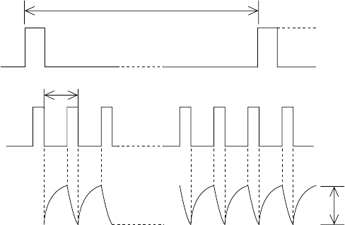
FO-CC500A
FO-K01A
5 – 25
Fig. 21
[7] Circuit description of CIS unit
1. CIS
CIS is an image sensor which puts the original paper in close contact
with the full-size sensor for scanning, being a monochromatic type
with the pixel number of 1,728 dots and the main scanning density of
8 dots/mm.
It is composed of sensor, rod lens, LED light source, light-conductive
plate, control circuit and so on, and the reading line and focus are
previously adjusted as the unit.
Due to the full-size sensor, the focus distance is so short that the set
is changed from the light weight type to the compact type.
5ms
2µs0V
0.8V~2.9V
(White original paper)
Approx.3.3V
øT
CISCLK
VO
2. Waveforms
The following clock is supplied from SCE214V of the control board,
and VO is output.
FO-CC500A
FO-K01A
CHAPTER 6. CIRCUIT SCHEMATICS AND PARTS LAYOUT
[1] Control PWB circuit 1/6
Main control block
6 – 1
A
A
B
B
C
C
D
D
E
E
F
F
G
G
H
H
I
I
66
55
44
33
22
11
WR-
THADI
BZOUT1
CNTH-10
CNTH-2
CNTH-12
CNCIS-5
CNTH-3
CNPN-10
CNPN-12
CNPN-9
CNPN-13
PWRDWN-
TPB-
TPA-
TPA
TPB
CNTH-14
CNTH-13
CNCIS-4
CNPN-14
CNPN-11
CNPN-2
CNPN-3
CNPN-4
CNPN-15
CNPN-16
CNPN-1
D[7:0]
RD-
CAS-
ROMCS-
VIN
DW R-
RAS-
RLYCONT
WP-
CNTH-11
A[18:0]
+3.3V
VBAT
DG
+3.3V
+3.3V
STRB3-
STRB2-
STRB1-
PCLK
DATA
LATCH-
DG
DG
D0
D1
D2
D3
D4
D5
D7
DG
(2-4G)
(2-5A)
DG
ØT
STRB4-
SEN3
SEN2
SEN1
E
SEN4
SEN0
DG DGDG
DG
D6
A0
A3
A13
A11
A15
(2-6A)
A8
A7
A18
A9
A16
A14
A17
A5
A4
A10
A12
A1
A6
A2
DG
DG
DG
DG
DG DG
CISC LK
KEN1A
KEN4A
KEN2A
KEN3A
SEN6
SEN5
(2-4A)
(2-3A)
(2-3A)
(4-2D)
(5-2I)
(6-1E)
(5-5E)
(5-5E)
(5-5E)
(5-5E)
DG
DG
(5-6D)
N.M.
<G>
DG
DG
(2-4G)
(2-4G)
(6-2A)
(2-3F)
DG
R157
10M
C176 100p/50V
C200 1000p/50V
C111
C144
1u/10V
C138
0.1u/50V
C154
100px4
R108
470
C121
0.1u/50V
R117 150
R118
1K R135
1K
C199 1000p/50V
RA2
470
5
1
8
7
62
3
4
R104 0
C123
0.1u/50V
<F>
R187
100
C175
R128
220K
C110
100pFX5
<BATRST>
C122
0.1u/50V
C143
1u/10V
C107
C177 100p/50V
C104
C115
100p
C194 100p/50V
R132
1K
C145
1u/10V
<A>
R105
470
<<ØT>>
C109
C103
C113
100p
C170
1u/10V
<E>
<B>
C198 100p/50V
DG
R130
1K
C197 100p/50V
R156
10K
<C>
C174
C195 100p/50V
C167 N.M
C102
220px4 C142
1u/10V
<K>
<D>
C101
C108
<H>
C112
C148
1u/10V
C166
1u/10V
<J>
R101
10K
C119
0.1u/50V
C130
0.1u/50V
32.768KHz
X2
RA1
470
5
1
8
7
62
3
4
R175 270
<L>
<I>
C132
22p/50V
RA3
470
5
1
8
7
62
3
4
<<CCIISSCCLLKK>>
C116
N.M.
C118
N.M.
R173 270
R116 270
C196 100p/50V
R133
1M
C131
22p/50V
C152
R134
220
C147 1u/10V
R106
470
32.256MHz
X1
<M>
C146
20p/50V
IC 3
SCE214V(1/2)
FAX CONTROLLER
TEST0
33
TEST1
32
D0 141
D1 142
D2 143
D3 144
D4 145
D5 146
D6 147
D7 148
A23 140
A22 139
A21 138
A20 137
A19 136
A18 135
A17 134
A16 131
A15 130
A14 129
A13 128
A12 127
A11 126
A10 125
A9 124
A8 123
A7 122
A6 121
A5 120
A4 118
A0 114
A3 117
A2 116
A1 115
RD 6
WR 5
ROMCS 3
SYNC 4
REGDMA/GPO18/CLKDIV0 175
WAIT/GPO19/CLKDIV1 176
RAS 25
CAS 26
DWR 27
WRPROT 31
BATRST
34
VBAT
28
PWRDWN
36
INTPWRDOWNE
35
XOUT
30
XIN
29
VREFp
44
VREFn/CLREF
39 VIN
40 THADI
49
ALTTONE (BZ)
149
OPI0
19 OPI1
20 OPI2
21 OPI3
22
SM0
171 SM1
172 SM2
173 SM3
174
OPO0
12 OPO1
13 OPO2
14 OPO3
15 OPO4
16 OPO5
17 OPO6
18
SXIN
10
SXOUT
11
CLK2
69
START
67
STRB0
57 STRB1
58 STRB2
59 STRB3
60
PCLK
63
PDAT
62
PLAT
61
VSS 165
VSS 133
VSS 107
VSS 70
VSS 50
VSS 45
VSS 9
VSSPLL 2
TSTCLK 8
RESET 108
DEBUGn 7
VDDPLL 1
VDD 166
VDD 161
VDD 132
VDD 119
VDD 64
VDD 48
VDD 24
IVREFp 47
IVREFn 46
ADXG 43
ADGA 38,41
ADVA 42
LCDCS
23
VDD 97
C1401u/10V
C141
0.1u/50V
C129
0.1u/50V
C149
20p/50V
R155 0
C168
0.1u/50V
FO-CC500A
FO-K01A
A
A
B
B
C
C
D
D
E
E
F
F
G
G
H
H
I
I
66
55
44
33
22
11
DW R-
CAS-
ROMCS-
A[18:0]
D[7:0]
RD-
WR-
FRD-
FCLE
FCS-
FW R-
FALE
READY
RAS-
WP-
+3.3V
+3.3V
+3.3V
+3.3V
+3.3V
+3.3V
+3.3V
A0
A1
A2
A3
A4
A5
A6
A7
A8
A9
A10
A11
A12
A13
A14
A15
A16
A17
A18
D0
D1
D2
D3
D4
D6
D7
D5
A0
A1
A3
A2
A4
A5
A7
A6
A8
A9
D0
D1
D2
D3
D4
D5
D6
D7
DG DG
(1-5I)
(1-6I)
(1-3I)
(1-4I)
(1-3I)
(1-3I)
(1-3I)
(1-4I)
D7
D4
D1
(3-2A)
(3-2A)
(3-2A)
(3-2A)
D5
D6
D2
DG
(3-2A)
D3
D0
(3-2A)
(1-6H)
DG
DG
IC1
SST39VF040P
FLASH ROM
A0
20
A1
19
A2
18
A3
17
A4
16
A5
15
A6
14
A7
13
A8
3
A9
2
A10
31
A11
1
A12
12
A13
4
A14
5
A15
11
A16
10
A17
6
CE
30 OE 32
WE 7
D0 21
D1 22
D2 23
D3 25
D4 26
D5 27
D6 28
D7 29
VDD 8
GND 24
N.C.(A18)
9
R125
10k
L110
0
R112
10k
C100
0.1u/50V
IC2
MSM51V4800E
DRAM
VCC 1
WE
7
RAS
8
A9
9
VCC 14
GND 15
OE
22
CAS
23 GND 28
DQ0 2
DQ1 3
DQ2 4
DQ3 5
DQ4 24
DQ5 25
DQ6 26
DQ7 27
A0
10
A1
11
A2
12
A3
13
A4
16
A5
17
A6
18
A7
19
A8
20
NC
6
NC 21
R115
0
C126
0.1u/50V
R113
0
R204
N.M.
R114
N.M.
R205
N.M.
C210
N.M.
R199
N.M.
C135
0.1u/50V
C217
N.M.
IC8
K9F4008W0A
FLASH MEMORY
VSS 22
CLE
2
ALE
3
WE-
4
WP-
5
N.C.
6
N.C.
7
N.C.
8
N.C.
9
N.C.
10
N.C.
12
N.C.
13
N.C.
14
N.C.
15
N.C.
16
I/O0 18
I/O1 19
I/O2 20
I/O3 21
VSS 1
VCC 44
I/O4 24
I/O5 25
I/O6 26
I/O7 27
N.C.
11
N.C.
30 N.C.
29 N.C.
28 N.C.
17
N.C.
31
N.C.
32
N.C. 33
N.C. 34
N.C. 35
GND 40
R/B-
41
RE-
42
CE-
43
VCC 23
N.C. 38
N.C. 37
N.C. 36
N.C. 39
Memory block 2/6
6 – 2
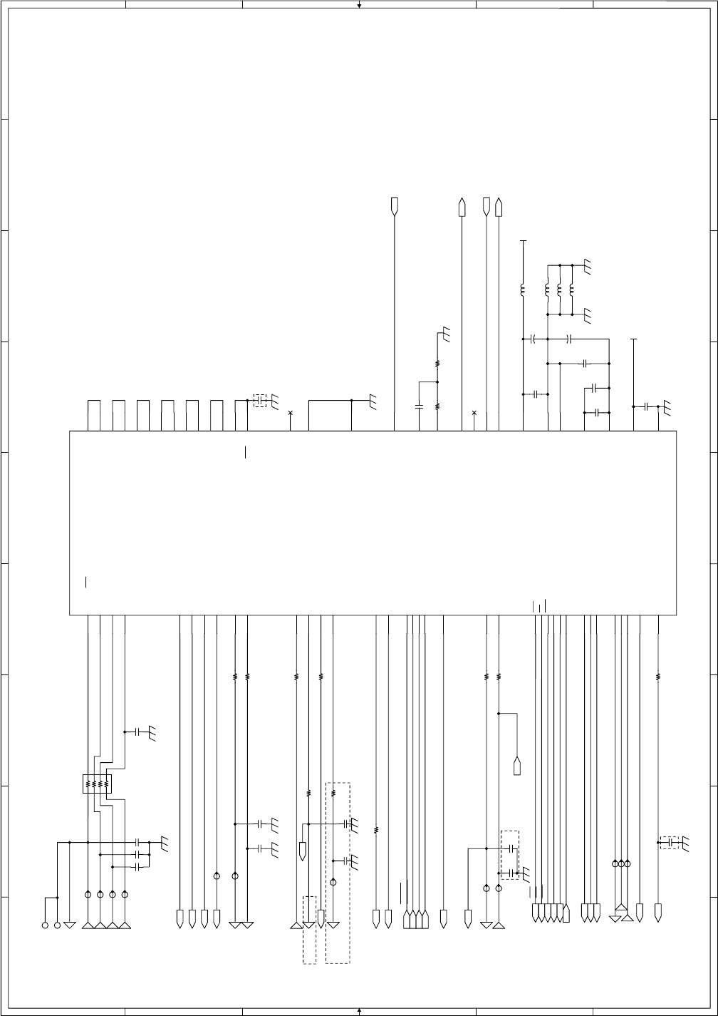
FO-CC500A
FO-K01A
FAX Modem block 3/6
6 – 3
A
A
B
B
C
C
D
D
E
E
F
F
G
G
H
H
I
I
66
55
44
33
22
11
CNLIUA-15
CNLIUA-12
CNLIUA-13
CNLIUA-10
SPMUTE
RCVOL
SIGMUTE
DTMFMUTE
CNLIU A-6
CNLIUA-16
ORGSNS-
CSWI
LEDON
VTHON
DR/RBN
FRSNS-
CNPRG-1
CNPRG-3
READY
FCLE
FALE
FRD-
FW R-
FCS-
VOLB
VOLC
VOLA
CNDSS-5
CNLIUA- 1
CNDSS-7
W-TONE
THLOOK
CNTH-5
CNDSS-8
SPOUT
CNLIU A-9
TELOUT1
SIGTX
CNLIU A-4
SIGRX
CNDSS-6
THCHK
DPON
WA RNING
TMICHK +3.3V
+3.3V
DG
DG
DG
MAG
(6-1C)
(6-6E)
(6-2E)
(6-4E)
DG
THRANK
DPON
DG
PIN
RHS-
HS-
CI-
DTMFMUTE
SIGMUTE
DG
(6-3E)
CML
SPMUTE
RCVOL
TELMUTE
(6-1A)
(6-3E)
DG
(6-1I)
DPMUTE
DG DG
DG
(4-5C)
(4-4C)
(4-6C)
(5-5E)
(4-3C)
(5-3D)
FLRXD
FLTXD
DG
<CS5A>
CI-
SRLTX
SRLRX
PARK
VOL C
VOL B
LEDON
VTHON
FRSNS
ORGSNS
DR/ RBN
CSWI
FCS
FRD
FW R
FCLE
FALE
READY
VOL A
(2-2G)
(2-2G)
(2-3G)
(2-3G)
(2-3G)
(2-2G)
(6-1G)
(6-1G)
(6-1G)
(5-2D)
<CS5>
(6-2D)
MICMUTE
N.M.
(5-5E)
NOT MOUNTED
(6-5A)
N.M.
DG
N.M.
(5-1i)
(6-2C)
MAG
IC3
SCE214V(2/2)
MODEM BLOCK
GPIO15 / CS5
53
GPIO16
52
AVDD (IIA) 85
GPIO37
55
GPO28
155
GPIO31
159
GPO27
154
GPO25
68
GPIO34
162
GPO30
157
GPIO32
160
GPIO13
54
GPIO17
51
SPKR_OUTP (IIA) 88
GPO1
168
MIC_INM (IIA) 81
MIC_INP (IIA) 80
GPO29
156
MCDE0 91
GPO0
167
LINE_INP (IIA) 79
N.C. 37
SASRXD
110
GPIO3
109
GPIO19
66 GPIO11
65 GPIO36
164 GPIO35
163
VTHON
56
MIC_BIAS (IIA) 82
TESTC 73
FCS
94
GPIO29
158
SASCLK2
105
DSS_PARK
106 SASRXD2
103
LINE_OUTP (IIA) 87
SASTXD2
104
VOL-C
170 VOL-B
169 VOL-A
150
READY
151 FALE
153
FRD
112
SOUT (IIA) 74
POR (IIA) 77
FSYNC (IIA) 76
ICLK (IIA) 92
MCLK (IIA) 71
CTRLI (IIA) 72
SIN (IIA) 75
SA1CLK 102
IA1CLK 98
IACLK 96
SR1IO 101
SR4OUT 100
SR3IN 99
IARESET 95
DVSS(IIA) 93
DVDD (IIA) 90
SPKR_OUTM (IIA) 89
AGND (IIA) 84
VREF (IIA) 83
AVSS2 (IIA) 78
AVSS1 (IIA) 86
FWR
113
FCLE
152
SASTXD
111
L107 0
R189 270
C203
R176
R186 270
C190
C202
+C7
10u/50V
R190 150
+C4
10u/50V
C162
0.1u/50V
C127
R154
2.2K
C165
0.1u/50V
R153
1K
C209
100p/50V
R191 150
R129 1K
C169
1000p/50V
R177 270
R183 270
C220
C163
0.1u/50V
R174 1K
C137
N.M.
+
C6
10u/50V
R178 470
C139
0.1u/50V
C206
100p/50V.
RA4
270
5
1
8
7
62
3
4
C128
C205
100px3
C204
L105 0
C164 0.1u/16V-K
L104
15
L106 0
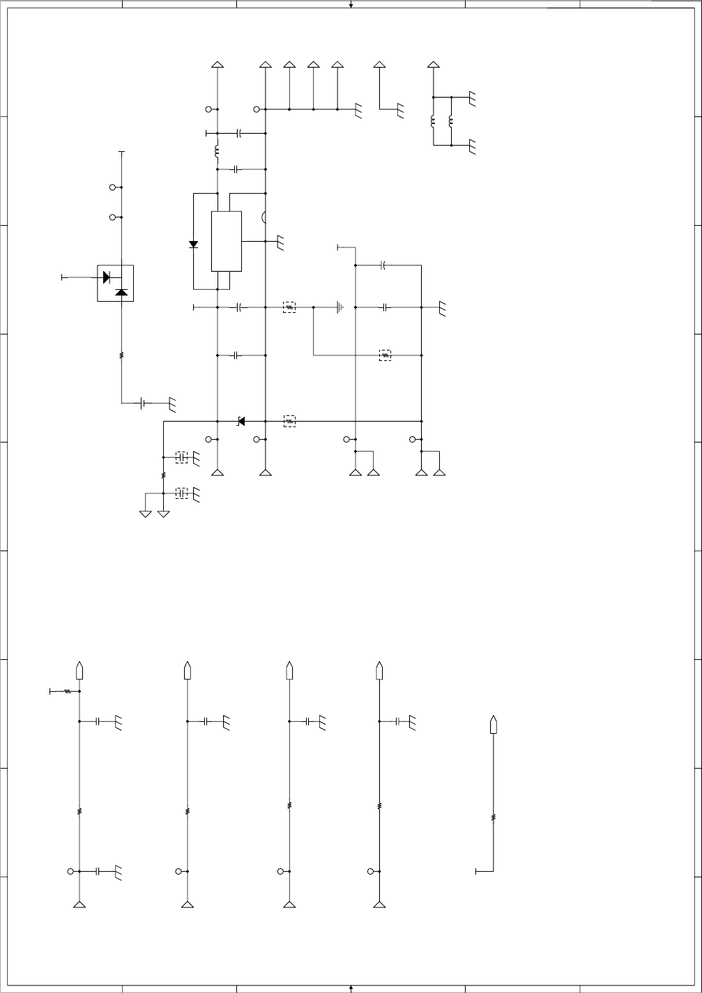
FO-CC500A
FO-K01A
A
A
B
B
C
C
D
D
E
E
F
F
G
G
H
H
I
I
66
55
44
33
22
11
CSWi-
ORGSNSi-
PWRDWN -
CNPN-8
CNPW-6
CNPW-5
CNPW-1
CNPW-2
CNPW-3
CNPW-4
CNCSW-2
CNPN-6
CNCSW-1
CNPN-7
CNLIUA-11 DR/RBN
CNPR G-2
FRSNSi-
CNDSS-1
CNDSS-2
CNDS S-3
CNDS S-4
CNPN-5
CNLIU A-2
+3.3V
+3.3V
VBAT
+24V
VREG
+3.3V
+3.3V
CSW-
FRSNS-
ORGSNS-
DG
DG
MG
FG
VREG
DG
+24V
+24V
DG
MG
MG
(3-3A)
(1-1G)
DG
DG
DG
(3-3A)
(3-3A)
(3-3A)
DG
FILM
DG
DG
DG
+3.3V
DGD G
DG
<TP22>
<FILM>
<TP104>
<TP113>
<+24V>
<TP140>
<TP139>
<TP19-132>
PDG
MAG
DG
MAG
DG PDG
C193
0.1u/50V
R100
5.6K
L102
0
C207
1000p/50V <+3.3V>
R111
N.M.
+C8
220u/6.3V
R109
N.M.
L108 0
R168
270
L109 0
D100
HRW0202
A1
A2 K
C106
1000p/50V
C158
N.M.
C159
1u/10V
C171
100p/50V
R179
270
ZD 2
MTZJ5.6B
C105
1000p/50V
R170
N.M.
C192
0.1u/50V
<VBT>
+C10
22u/50V
+
C9
220u/16V
BAT1
CR2032
+
D101
1SS355
A
K
C157
N.M.
C211
470p/50V
<DG>
R103
270
REG1
S-814A33AUC-BCX
Vin
5Vout 1
VSS
2
NC 3
ON/OFF
4
<DG>
R166
20k
R127
51K
R102
270
R147
0
<VBT1>
Sensor/Reset/Power supply block 4/6
6 – 4
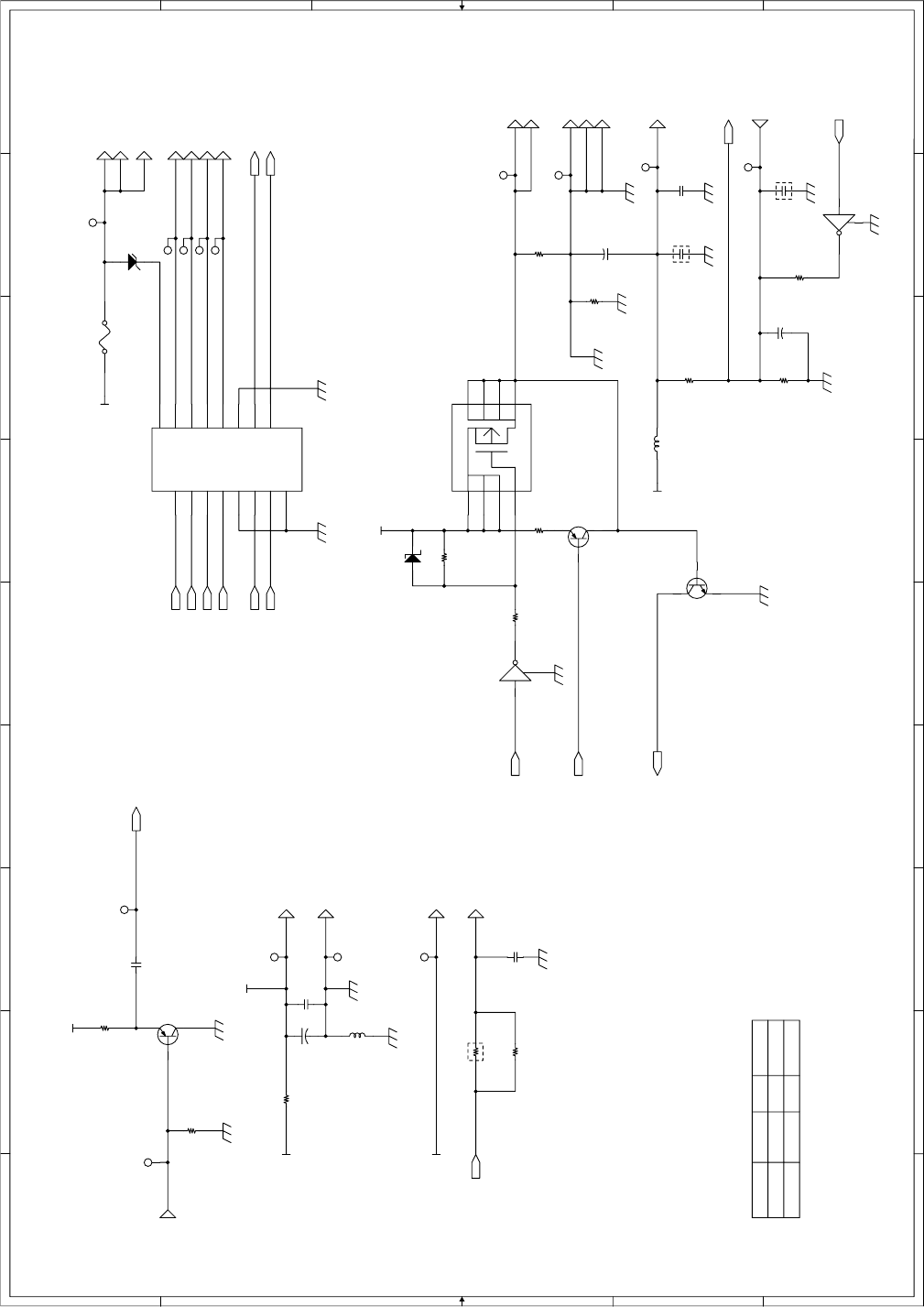
FO-CC500A
FO-K01A
Video processing/Motor drive/Thermal block 5/6
6 – 5
A
A
B
B
C
C
D
D
E
E
F
F
G
G
H
H
I
I
66
55
44
33
22
11
VIN
TPA
TPB
TPA-
TPB-
VTHON
CNCIS-1
CNCIS-3
CNCIS-2
CNMT-5
CNMT-6
CNMT-4
CNMT-3
CNMT-2
CNMT-1
CNTH-1
CNTH-15
CNTH-6
CNTH-7
CNTH-8
LEDON
CNCIS-6
LEDON-
LEDON-
CNTH-4
THADI
CNTH-9
CNLIU A-3
CNCIS-7
THCHK-
THCHK THCHK-
THLOOK
TMICHK
CISV DD
+24V
+24V
+3.3V
+3.3V
+24V
CISV DD
VG VG
VO
DG
VG MG MG
VMT
VMT
TPAD
TPBD
TPAD-
TPBD-
THG
THG
THG
MG
VTH
VTH
DG
(1-2F)
(3-3A)
(3-3A)
(1-1F)
(1-1E)
(1-1E)
(1-1E)
DG
+24V
GLED
DG
(5-5I)
(5-3A)
VG
THG
THI
THVDD
THADI
DG
(1-2F)
DG
CISV DD
THG
THG
+24VL
(3-4A) (5-3D)
(3-2B)
DG
D Y NA
ROHM
0Ω
N.M.
N.M 0.01 u/ 50V
300Ω( 2W) 1000p/ 50V
R1 R192 C124
CIS Maker
<TP109>
<TP141>
<TP17>
<TP138>
<TP137>
<TP136>
<TP135>
<TP134>
<TP133>
<TP131>
(5-5H)
<TP20>
DG
(3-1A)
R149
100k
+C3
10u/50V
R206
100K
C178
N.M.
C161
N.M.
ZD1
1N4748
Q102
1N436C
BC
E
R150
470K
R192
0
L103
0
ZD100
02CZ1 8-Y
Q113
1N141C
B
C
E
Q111
KRA102S
B
CE
<VG>
C114
0.1u/50V
R1 N.M.
L100
0
R120
5.1K
R163
0.1u/50V
R171
120K
Q100
2SA1530A
B
CE
R172
22K
Q110
1N141C
B
C
E
R107
10K
<VIN>
R119
0
<VO>
C160
1u/10V
C124
0.01u/50V
C1
220u/6.3V
R152
20K
C117
0.1u/50V
+
C5
100u/25V
R151 100k
D1
D2
D3
D4S1
S2
S3
G
Q108
SI4431ADY
45
8
3
1
2
6
7
FU100
KAB3202
IC6
KID65001AP
E
8
1B
1
2B
2
3B
3
4B
4
5B
5
6B
6
7B
77C 10
6C 11
5C 12
4C 13
3C 14
2C 15
1C 16
COM 9
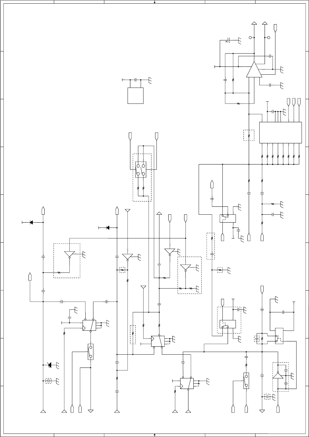
FO-CC500A
FO-K01A
A
A
B
B
C
C
D
D
E
E
F
F
G
G
H
H
I
I
66
55
44
33
22
11
CNDSS-10
VOLA
DTMFMUTE
RCVOL
TELOUT
CNLIU A-8
WA RNING
SPMUTE
TELOUT1
CNSP-1
SIGTX
W-TONE
CNDSS-11
CNLIUA-14
DTMFMUTE
SPOUT
VOLB
CNLIU A-5
SIGRX
VOLC
CNSP-2
CNLIU A-9
CNDSS-12
BZOUT1
ICM
RCVOL
CNDS S-9
ICM
CNLIU A-7
DPON
CNDSS-13
TELOUT
RLYCONT
SIGMUTE
+3.3V
+3.3V
+3.3V
VREG
+3.3V
+3.3V
+3.3V +3.3V
+3.3V
+3.3V
+3.3V
(6-2A)
CML
(3-5A)
IC12C
MAG
TELIN
MAG
DG
(3-1A)
(3-1A)
DG
SP+
(3-3A)
(3-3H)
MAG
/B
(3-5A)
MAG
(3-1A)
DSSOUT
DG
MAG
MAG
NOT MOUNTED
MAGMAG
TXOUT
DG
NOT MOUNTED
(3-5A)
MAG
MAG
DSSTX
14
SP-
MAG
4066
(3-3A)
(3-3H)
MAG
MAG
MAG
DSSIN
(1-1F)
(3-5A)
MAG
MAG
MAG
MAG
(3-2H)
TELOUT
7
DG
SIGRX
(6-5A)
I NCOM
(3-4A)
(3-5A)
(3-5A)
SIGTX
DG
(3-2H)
NOT MOUNTED
(3-4A)
(6-2F)
DSSRX
RXIN
(6-6C)
(1-3I)
MAG
NOT MOUNTED
MAG
C125
1u/10V
Q104
B
C
E
C185
1u/10V-K
IC11
KIC7S66F
2
1
53
4
A
C
LV4051
X0
X1
X2
X3
X4
X5
X6
X7
X
B
VDD
GND
VEE
E-
IC5
16
7
11
10
9
6
3
13
14
15
12
1
5
2
4
8
C150
1u/10V
-
+
NJM2113
IC7
5
4
3
2
1
7
86
R136
3K
C208
0.1u/16V-K
ZD101
HZU2 .7B1
Q105
1N141C
B
C
E
R138
N.M.
R121
150K
IC12D
4066
10 11
12
C221
N.M.
IC12A 4066
34
5
12
13
R143 39K
C213
0.1u/50V
R194
2K
C188
0.022u/50V
C214
1u/10V-K
IC4
KIC7S66F
2
1
53
4
C156
0.1uF/ 50V
R139 220K
R142 200K
Q106
B
C
E
C182
1u/10V-K
R137
20K
C2
47u/25V
1
2
R182
N.M.
C180Not mounted
C222
N.M.
R146 91K
Q112
1N141C
B
C
E
C223
Not mounted
C218
C181 0
R165
C224
1u/10V-K
R195
2K
C219
IC10C
LV4053
14
12
13
11
7
6
8
16
R196
3K
R124 220K
C189
1u/10V
R184
D102
1SS355
C215
1u/10V-K
C216
0.1u/50V
R145 6.2K
IC10A
LV4053
4
5
3
9
7
6
8
16
R181
0.1u/16V-K
C133
0.01u/50V
C186
1u/10V
C151
4700p/50V
C184
0.01u/50V
C183
1u/10V-K
C212
0.1u/50V
C225
N.M.
IC13
(KIC7S66F)
2
1
5
3
4
C187
15K
C155
0.1u/50V
R160
R193
1M
R198
R203100
R140 470K
IC12C
4066
89
6
R200
N.M.
Q103
BC
E
C172
0.1u/50V
R131
15K
R164
R201
100
R180 N.M.
R197
D103
1SS355
R122
100K
C179
0
R202
100
R144 24K
C134 220p/50V
IC10B
LV4053
15
1
2
10
7
6
8
16
R167
2.4K
R141 1.5M
Analog signal block 6/6
6 – 6
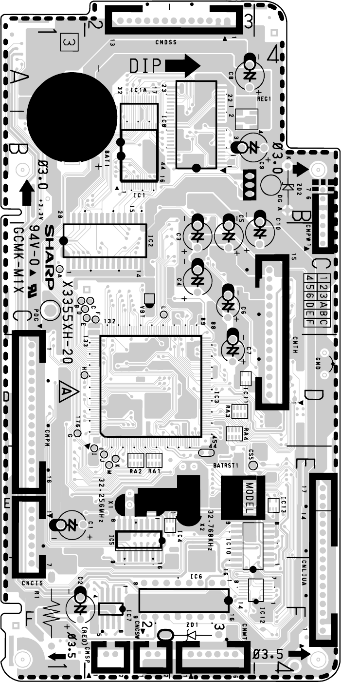
FO-CC500A
FO-K01A
Control PWB parts layout (Top side)
6 – 7
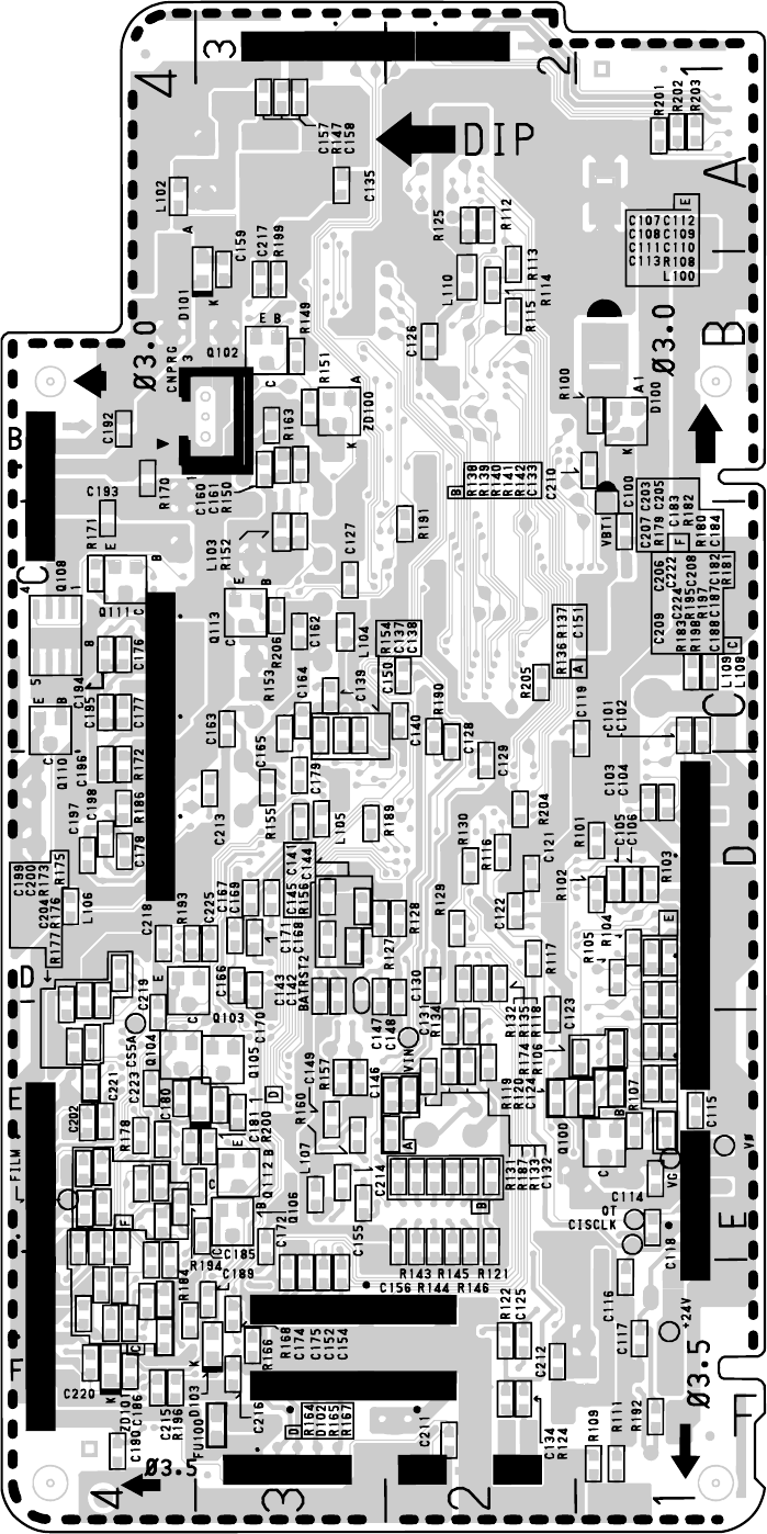
FO-CC500A
FO-K01A
Control PWB parts layout (Bottom side)
6 – 8
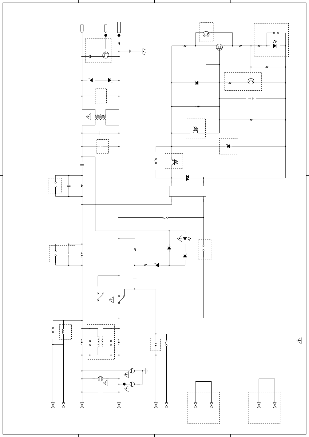
FO-CC500A
FO-K01A
[2] LIU PWB circuit 1/3
5
5
4
4
3
3
2
2
1
1
DD
CC
BB
AA
DG
ARG
CNTLJ-3
CNLNJ-3
CNTLJ-2
CNLNJ- 4
CNLNJ- 1
CNLNJ- 2
CNLNJ- 6
CNLNJ- 5
CNTLJ-4
CNTLJ-5
(2 -5D)
L2
E
S
EX-T2
EX-T1
N.C.
E
S
L1
N.C.
T1
T2
(2 -5D)
( 2125)
JP21
N.M
AR1
RA501P-C6
JP20
N.M
Q104
N.M.
G
D
S
ZD3
HZ2A1
JP6 N. M.
VA1
CSS-301M
Vre f A
CML(2/3)
98
10
Q3
BS108
G
D
S
IN/OUT
ZD2
HZ2A1
R118
1K
C10
0.56u/250V
JP5 N. M.
L6 R-5C
R4
22k(1W)
C124
N.M.
R117(2125)
43k
L5
N.M
L9
N.M
C11
0.33u
C20
N.M
C6
TN07G181
C9
1u/250
D4
1SS133/1SS270
+
C15
10u/50V
VA2
TN07G270
C122(2125)
0.068u/25
PC3(1/2)
N.M
4
3
ZD8
MTZJ6.8B
PC1(1/2)
TLP621
21
ZD9
N.M
R115
300(1/10W)
T1
2165
R140(2125)
15k
+
C12
22u/50
L4
4.7mH
R10
10k (1/4W)
R145
N.M (2125)
ZD6
J.P
JP1
JP
REC1
S1ZB60
ZD4
MTZJ20B
JP4
JP
CML(1/3)
A3X-24E-908
45
3
C118(2125)
N.M
JP25
N.M
R144
0 (2125)
L8 R-5C
Q 5
N.M
B
C
E
R9
15 (1/ 4W)
Q 4
N.M
B
C
E
L7 N.M.
R143
N.M (2125)
AR2
RA501P-C6
JP24
51(1W)
PC4(1/2)
N.M
21
R5
15(1/4W)
PC2(1/2)
N.M
43
JP23
JP
~
~
+
-
C125(2125)
N.M.
JP22
N.M
A
NOTE:
This mark indicates a safety-critical part(s).
6 – 9
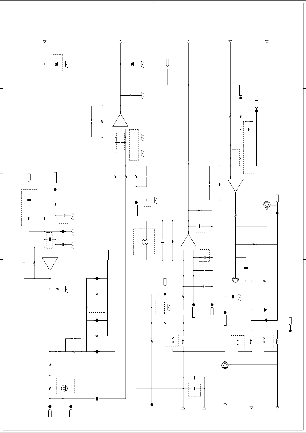
FO-CC500A
FO-K01A
LIU PWB circuit 2/3
5
5
4
4
3
3
2
2
1
1
DD
CC
BB
AA
DG
DG
DG
DG
DG
DG
DG
DG
DG DG
DG
DG
CNLIU A-8
CNHJ -3
CNLIU A-4
CNHJ -4
CNLIU A-7
CNHJ -1
CNHJ -2
CNLIU A-5
CNLIU A-6
CNLIUA-14
( 1-1D)
RXIN
RX+
(3-2A)
TXOUT
RX- (3-2A)
(3-2A)
TX+
(3-2A)
( 3-5D)
TX-
( 1-1D)
MICMUTE
TELOUT
(3-2A)
TELIN
TELMUTE
NOT MOUNTED
R120
1k
C117 1000p
C137 820p
R135 30k
R132
1K
R110 24k
R100
3.3k
C109 1500p
C142
N.M
R125
10K
C106
N.M
C143
0
R142
N.M
C135
0.01uF
DG1
C144
0
E
Q101
RT1N436C
B
C
DG1
R133 47k
C145
0
C105
N.M
L3
N.M
ZD5
MTZJ10B
JP29
N.M
C134
N.M
D1
N.M
R134 22k
JP30
N.M
R137
3.3k
L1R-5C
R105
150(2125)
JP31
JP
R121
6.8k
R130
390
Vre f A
+C 22
N.M
C131
N.M
Vre f B
+ C13
10uF/50V
+C 23
N.M
C133
0.056uF
C136
N.M
DG1
Q100
KTC3875GR
B
C
E
C103
220p
D2
N.M
HSDG
DG1
C113
0.01u
C130
100pF
R111 150k
C115
N.M
R136 22k
C108
N.M
C140
N.M
C119
N.M
(2-1B)
C102
1000p
R103
0
C101
1000p
R109 8.2k
R101
1k
R106
2.2k
L2R-5C
C116
N.M
Vref A
-
+
IC102
NJM2904M
1
2
3
C104
0.1u
Vref A
-
+
IC102
NJM2904M
7
6
5
Vref B
Q6
N.M
B
CE
R131
N.M
C132
N.M
E
Q102
RT1N436C
B
C
R102 16k
C138
N.M
R107
1k
+
C2
N.M
ZD7
N.M
Vre f A
Vre f A
-
+
IC101
NJM2904M
7
6
5
C127
0
R126
3.9K
-
+
IC101
NJM2904M
1
2
3
+
C1
4.7u/50V
R112
1.5k
C139 1000p
R104
3.3k
Q106
N.M.
G
D
S
C100
N.M.
IN/OUT
R122 220k
C129
N.M
C112
N.M
A
R127
0
R124
620
+
C4
22u/50V
(2-3D)
6 – 10
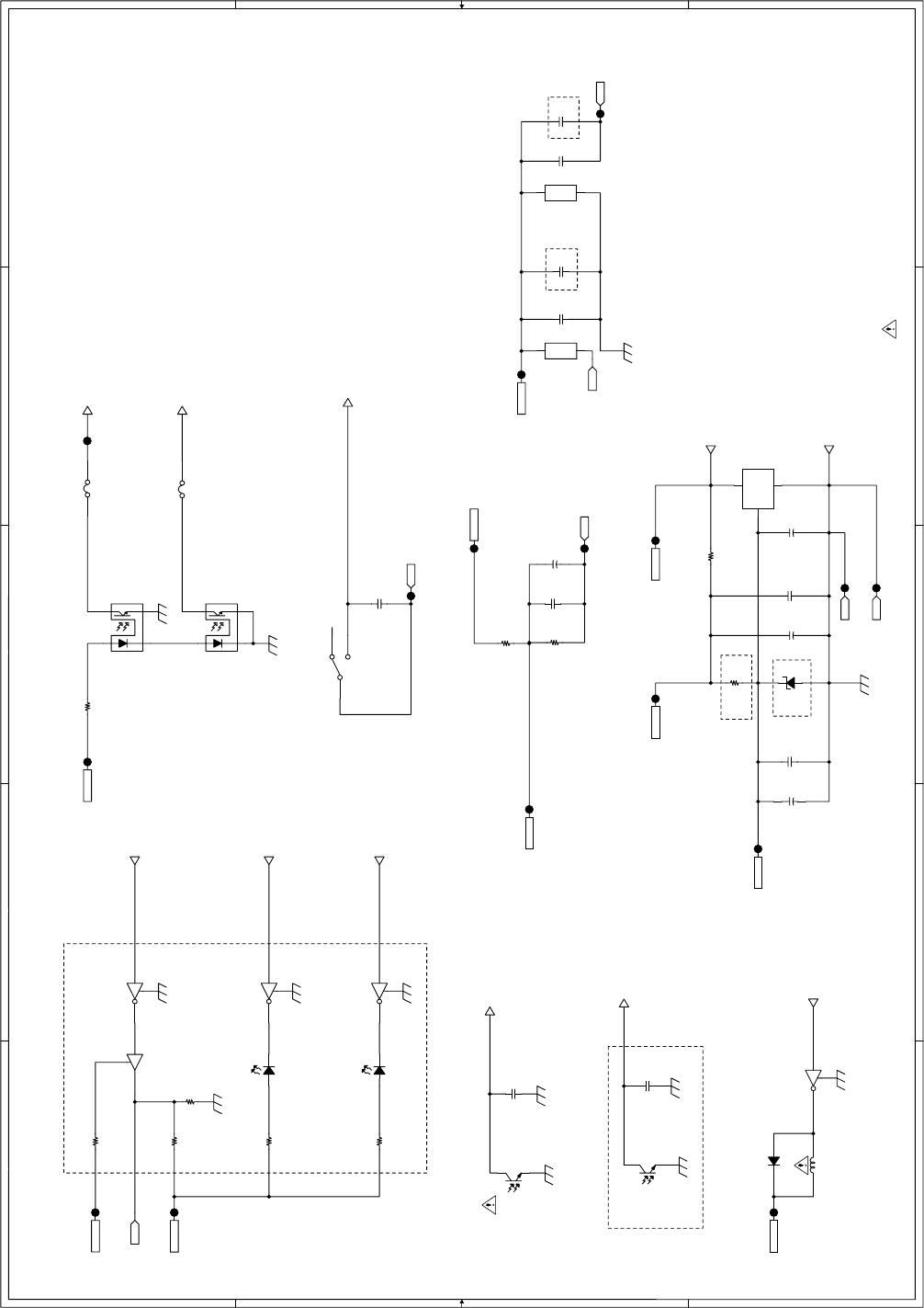
FO-CC500A
FO-K01A
LIU PWB circuit 3/3
5
5
4
4
3
3
2
2
1
1
DD
CC
BB
AA
DG
DG
DG
DG
DG
DG
DG
DG
DG
DG
DG
DG
DG
CNLIUA-11
CNLIUA-13
CNLIU A-2
CNLIU A-9
CNLIU A-3
CNLIUA-17
CNLIUA-15
CNLIUA-12
CNLIUA-10
CNLIUA-16
CNLIU A-1
RHS
+24VL
DG
PIN
DPON
HS
CML
( 2-5D)
DPMUTE
FILM
( 1-1D)
Ci
RLYCNT
(3-2A) (3-2A)
NOT MOUNTED
NOT MOUNTED NOT MOUNTED
Q105
N.M.
B
C
E
R2
100(1/4W)
+24VL
+24VA
DG1
R128
N.M
C128
N.M
PC1(2/2)
TLP621
4
3
R1
N.M
C123
0.1u
Q107
N.M
B
C
E
ZD1
N.M
IC102
NJM2904M
8
4
C126
0.1u/50V
PC3(2/2) N.M
2
1
R119
N.M.
C141
N.M
R116
N.M.
+24VL
PC2(2/2) N.M
2
1
+C3
47u/25V
HSDG
D3
1SS133/1SS270
Vre f A
DG1
Q103
RT1N436C
B
C
E
TP1
JP
IC101
NJM2904M
8
4
C107
0.1u/50V
Q109
N.M
B
C
E
C111
0.1u
R123
N.M.
REG1
NJM78L05A
Vout
1
GND
2
Vin
3
TP2
JP
PH2
SG206
+
C14
100uF/25V
+24VA
CML(3/3)
A5X-24E-908
Vre f A
PC4(2/2)
N.M
4
3
Vre f A
24VL
C121
0.1u
R113
20K
C114
1000p
R129
N.M
SW1
HOOK SW
31
2
PH1
SG206
C120
0.1u
Vre f B
+
C8
100u/50V
R108
20K
DG1
DG1
DG2
C110
N.M
+24VL
A
R3
1.2k(1W)
Q108
N.M.
B
C
E
+
C5
22u/50V
NOTE:
This mark indicates a safety-critical part(s).
6 – 11
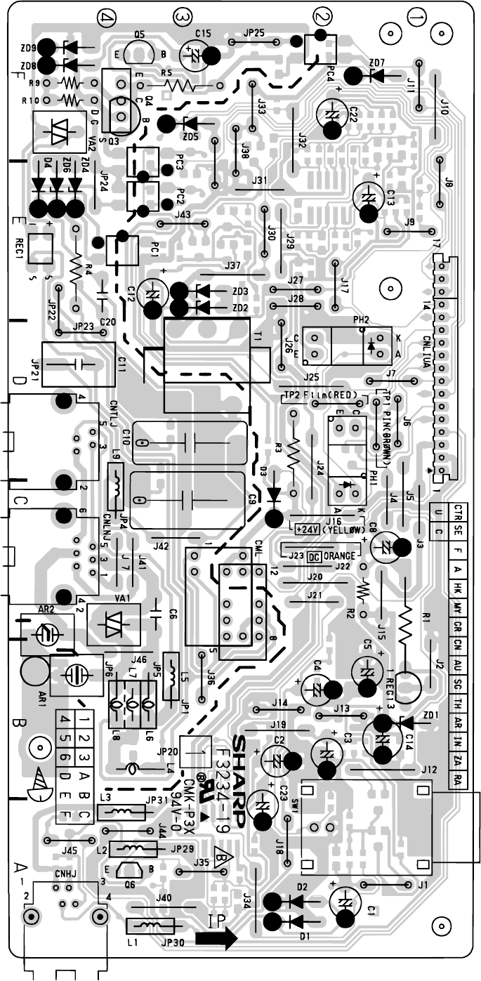
FO-CC500A
FO-K01A
LIU PWB parts layout (Top side)
6 – 12
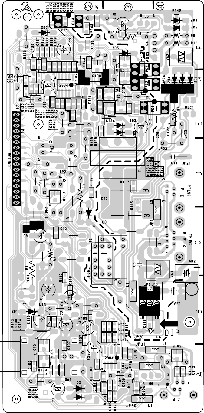
FO-CC500A
FO-K01A
LIU PWB parts layout (Bottom side)
6 – 13
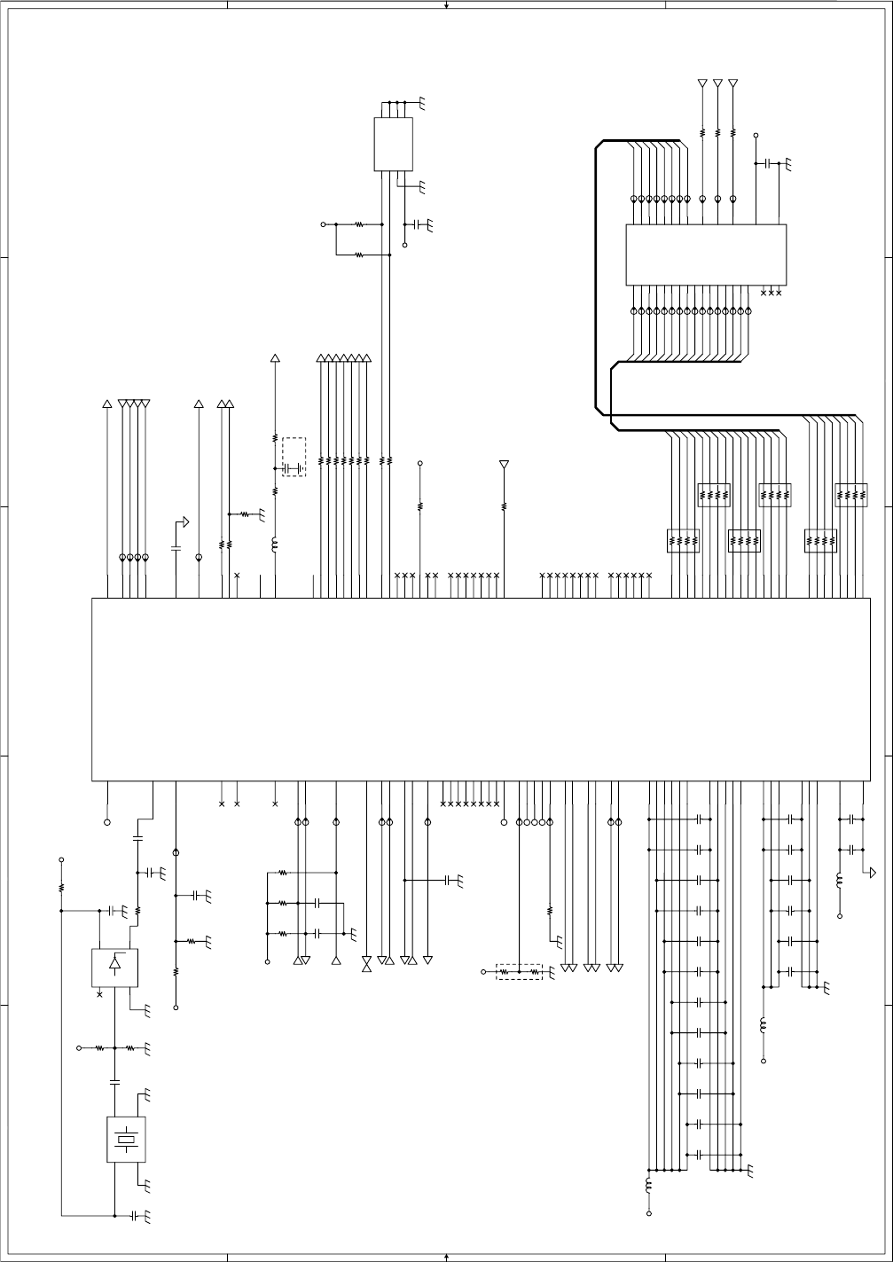
FO-CC500A
FO-K01A
6 – 14
5
5
4
4
3
3
2
2
1
1
DD
CC
BB
AA
A14
A6
A8
A3
A7
A14
A0
A0
A[0..15]
A10
A1
D5
D3
D1
A7
A5
A11
A6
A12
A1
A4
A5
D7
D0
A12
A9
D[0 .. 7]D[0 .. 7]
A15
D2
A3
A4
A9 A15
D6
A2
A13
A8
A13
A11
D4
A2
A10
D0
D3
D2
D5
D4
D7
D6
D1
DG
VVCCCC__33..33VV
DG
DG
VVCCCC__33..33VV
VVCCCC__33..33VV
DG DG
DG
AG
VVCCCC__33..33VV
DG
VVCCCC__33..33VV
VVCCCC__33..33VVDG
RFG
AG
VVCCCC__33..33VVDG
VVCCCC__33..33VV
DG
VVCCCC__33..33VV
DG
VVCCCC__33..33VV
DG
VVCCCC__33..33VV
DG
VVCCCC__33..33VV
DG
DG
DG DG DG
DG
DG
D
CDDAT AIN
D
DSSOUT
D
ROMCS
D
INCOM
D
CDDATAO UT
C
ICLK
D
FRAME
C
MCLK
D
MONIN
D
PARK
D
WRITE
D
READ
D
RESETO
D
DSS IN
D
MONOUT
D
SYNEN
D
SYNDA TA
A
AGC
D
SYNSTB
C
REFOSC
A
RXIN
D
RXEN
A
RXIP
C
SYNCLK
A
TXDATA
A
RXQP
A
RXQN
D
TXPWR1
D
TXPWR0
D
TXEN
D
LNATTN
A
CI
D
ROMCS
D
READ
D
WRITE
TDD Control
TXEN = High : Transmit Data
RXEN = High : Receiver Data
Power Level Control
TXPWR1 = Low , TXPWR0 = Low : High Power
TXPWR1 = Hihg, TXPWR0 = Low : Medium Power
TXPWR1 = Low , TXPWR0 = High : Low Power
TXPWR1 = Hihg, TXPWR0 = Hihg : Undefined
Reset
Turn on Vcc_BAT = 2.76V
(RESETIP Input Voltage = 1.257 V[ +36mV,-36mV])
Turn off Vcc_BAT = 2.96V
(RESETIP Input Voltage = 1.35 V[ +36mV,-36mV] )
( 3-5B)
( 3-3B)
( 3-5D)
( 3-5D)
( 3-5D)
to NMI
( 3-5B)
( 1-1A)
Codec Control
to EMUSYNC
( 3-5B)
( 1-1A)
to RESET
( 3-5D)
( 3-5B)( 3-3B) ( 3-5B)
( 1-1A)
( 3-5D)
( 3-5B)
( 3-3B)
to EMUCLK
( 3-5D)
(2 -4C)
I2 C Clock
(2 -2C)
(PLL Clock 9.6MHz)
I2 C Serial Data
(2 -5C)
(2 -4C)
(2 -4C)
(2 -5C)
(2 -4C)
(2 -2D)
( 2-2C)
( 2-2D)
( 2-2D)
( 2-5C)
( 2-2C)
( 2-5C)
( 2-2C)
( 3-5B)
( 1-5B)
( 1-5B)
( 1-5B)
Low Noise Amp attenuation
LNATTN = Low : receiver High Gain mode
LNATTN = High : receiver Low Gain mode
Common Round
X1
Crystal [K SS]
4
2
1
3
R130 100
C119
0.1u
C113
100p
TP17
TP26
R148 0
C 8
8p
C112
100p
IC2
CX80705-13
Merlin ASIC XROM
AUX DAC
107
ARTO
41
ARTI
39
RESETIP
94
OSCI
91
OSCO
90
BATT1
96
BATT0
97
NC
99
VDDP
56
VDDP
74
VDDP
113
VSSP
7
VSSP
29
VSSP
57
VDDC
2
VDDC
32
VDDC
71
VSSC
5
VSSC
33
VSSC
70
AVDD
92
AVSS
93
AGND
95
PARKP
40
KEYPADR0
60
KEYPADR1
61
KEYPADR2
62
KEYPADR3
63
KEYPADR4
64
KEYPADR5
65
KEYPADR6
66
KEYPADR7
67
KEYPADC5
10
KEYPADC3
12
KEYPADC4
11
KEYPADC2
13
KEYPADC1
14
KEYPADC0
23
GPIOA0
123
GPIOA1
124
GPIOA2
125
GPIOA3
126
GPIOA4
127
GPIOA5
128
GPIOA6
1
GPIOA7
8
GPIOB0
38
GPIOB1
37
GPIOB2
36
GPIOB3
31
GPIOB4
30
GPIOB5
26
GPIOB6
25
GPIOB7
24
GPIOC0/SWCTL
9
MCLK/CDCMCLK
45
CDCDATAO
43
CDCDATAI
44
CDCFRAME
42
CDCICLK/ICLK
58
RESETOP/CDCPOR
59
REFOSC
89
RXIN
102
RXIP
101
RXQP
103
RXQN
104
AGC
105
TXDATA
100
TRSW
110
TXEN
108
RXEN
76
GPIOC1
75
GPIOC2
111
GPIOC3
109
GPIOC4
88
GPIOC5
87
GPIOC6
77
GPIOC7
78
AUXREF
106
DATA0
122
DATA1
121
DATA2
120
DATA3
119
DATA4
118
DATA5
117
DATA6
116
DATA7
115
ADDR0
15
ADDR1
16
ADDR2
17
ADDR3
18
ADDR4
19
ADDR5
20
ADDR6
21
ADDR7
22
ADDR8
51
ADDR9
52
ADDR10
55
ADDR11
53
ADDR12
46
ADDR13
50
ADDR14
49
ADDR15
47
WPR~3
48
RDP
54
ROMCSP
112
RAMCSP
79
HOSTCSP
83
HOSTACK
84
SYNC~3
82
NMIP
81
XCODEP
85
EMUCLK~3
80
VSSP
73
VSSP
114
VDDP
28
VDDP
6
VDDP
27
NC
98
NC
69
NC
68
NC
35
NC
34
NC
3
NC
72
NC
4
VISP~3
86
R141 100
TP41
C 60
1u
RA 6
100
5
1
8
7
6
2
3
4
TP40
R124 56k(F)
R5
270
L102 0
TP34
TP35
TP49
TP31
TP37
R119
10k
TP48
C 4
0.1u
TP24
IC 6
TC7SZ04F
NC
1
IN
2
GND
3
OUT
4
Vcc
5
C 39
8p
TP21
TP20
TP3
TP4
TP1
R156
56k(F)
R131 100
TP46
R105 0
C 40
0.1u
R112 100
L101 0
TP18
RA 1
100
5
1
8
7
6
2
3
4
R120
10k
C 37
8p
C 59
0.01u(K )
R144 100
TP23
C 42
8p
TP12
C 3
0.1u C 32
0.1u
TP5
R127 100
IC 3
SST39LF512 [SST]
A0
20
A1
19
A2
18
A3
17
A4
16
A5
15
A6
14
A7
13
A8
3
A9
2
A10
31
A11
1
A12
12
A13
4
A14
5
A15
11
DQ0
21
DQ1
22
DQ2
23
DQ3
25
DQ4
26
DQ5
27
DQ6
28
DQ7
29
CE#
30
OE#
32
WE#
7
NC
9
NC
10
NC
6
VSS
24
VDD
8
L111
BLM 11HB102SD
TP32
TP42 TP22
R109 100
IC 4
S-24C04 [SII]
A0
1
A1
2
A2
3
GND
4
SDA
5
SCL
6
TEST
7
VCC
8
R138 100
TP50
R125
47k(F)
R142
10k
R106
N.M
TP52
R140 100
TP6
RA 5
100
5
1
8
7
6
2
3
4
TP14
TP30
C 31
0.1u
C 33
8p
TP54
R123 100k
C118
0.1u
C 56
0.01u(K )
L104 0
TP28
TP43
TP33
R126 100
TP51
C114
N.M
TP53
C130
33p
R129
22k
TP15 R139 100
R111 100
R128 100
R155
56k(F)
C 41
8p
C 9
0.1u
R121
10k
C 30
8p
RA 2
100
5
1
8
7
6
2
3
4
C 43
0.1u
RA 3
100
5
1
8
7
6
2
3
4
C 2
8p
TP62
TP11
C 7
N.M
TP47
C 35
8p C 38
0.1u
C 36
0.1u
C 61
0.1u
TP25
TP36
R143
10k
R108 100
R154 10
TP13
C 5
8p
TP39
TP16
RA 4
100
5
1
8
7
6
2
3
4
R107
N.M
TP44
R132 100
C 34
0.1u TP27
TP38
C102
0.22u
R110 100
TP2
C 55 0.1u
[3] Cordless PWB circuit Main control block 1/3
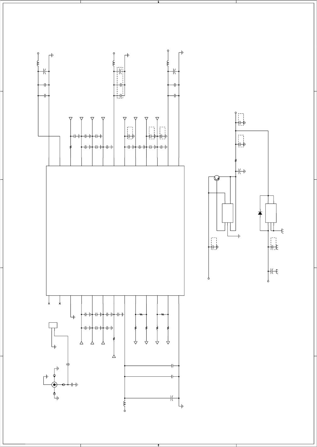
FO-CC500A
FO-K01A
6 – 15
5
5
4
4
3
3
2
2
1
1
DD
CC
BB
AA
RFG
RFG
RFG
RFG
RFG
RFG
RFG
RFG
RFG
RFG
RFG
RFG
RFG
RFG
RFG
RFG
RFG
RFG
VCC_3.3VRF RFG
RFG
VCC_3.3VRF
VCC_3.3VRF
VCC_3.3VRF
RFG RFG
RFG
RFG
RFG RFG
RFG
RFG
RFG
RFG
RFG
DG
DG
DG
VCC_5.0V
VCC_3.3VRF
RFG
RFG
RFG
VCC_3.3V
RFG
A
TXDATA
D
SYNEN
D
SYNSTB
C
SYNCLK
C
REFOSC
D
SYNDATA
D
RXEN
D
LNATTN
A
RXQN
A
RXQP
A
RXIN
A
RXIP
A
AGC
D
TXPWR0
D
TXPWR1
D
TXEN
( 1-2D)
( 1-2D)
( 1-2D)
( 1-2D)
( 1-2D)
( 1-2D)
( 1-2C)
( 1-2C)
( 1-2D)
( 1-2C)
( 1-2C)
( 1-2C)
( 1-2C)
( 1-2C)
( 1-2D)
( 1-2C)
C21
+C47
220u/6.3V
L105
3
C129
1000p
C117
N.M
+C46
1000u/10V
C17
8p
C105
1000p
CN4
Connector 2pin
1
2
C14
8p
R121 k
D101 1SS355
AK
R101 k
TP65
C11
8p
R13
3k
R7 4.7k
C12
0.1u
C52
8p
TP66
C23
8p
C124
1000p
IC5
S-814(SOT-89-5)[SII]
Vout
1
NC
3
Vss
2
On/Off
4
Vin
5
C122
N.M
R137 3(1/2W)[ 5025]
TP67
+C25
1000u/10V
C126
0.75p
+
C18
N.M
C16
8p
C125
1000p
C15
8p
C20
C127 3p
R8 1k
L112
3[2012]
R141 k
C53
8p
C123
1000p
C13
N.M
C24
8p
C50
8p
C19
N.M
R11
3k
C49
8p
C57
N.M
L107
3[2012]
C27
8p
+C54
1000u/10V C48
0.1u
IC101
S-816(SOT-23-5)[SII]
EXT
1
Cont
3
Vss
2
Vin
4
Vout
5
+C10
220u/6.3V
C26
8p
Q101
2SB1427
C
E
B
C51
8p
C28
0.1u
R9 1k
C121
N.M
C104
N.M
UNIT1
2.4GHz RF Module
GND
1
ANTENNA
2
GND
3
TXPWR0
4
TXPWR1
5
TXEN
6
AGC
7
VCC
8
RXQN
9
RXQP
10
RXIN
11
RXIP
12
GND
13
GND
14
VCC
15
LNAATTN
16
RXEN
17
SYNDATA
18
REFOSC
19
VCC
20
SYNCLK
21
SYNSTB
22
SYNEN
23
TXDATA
24
VCC
25
GND
26
L106
3
CN101
H,FL-R
1
2
3
4
C22
8p
RF module/power supply block 2/3
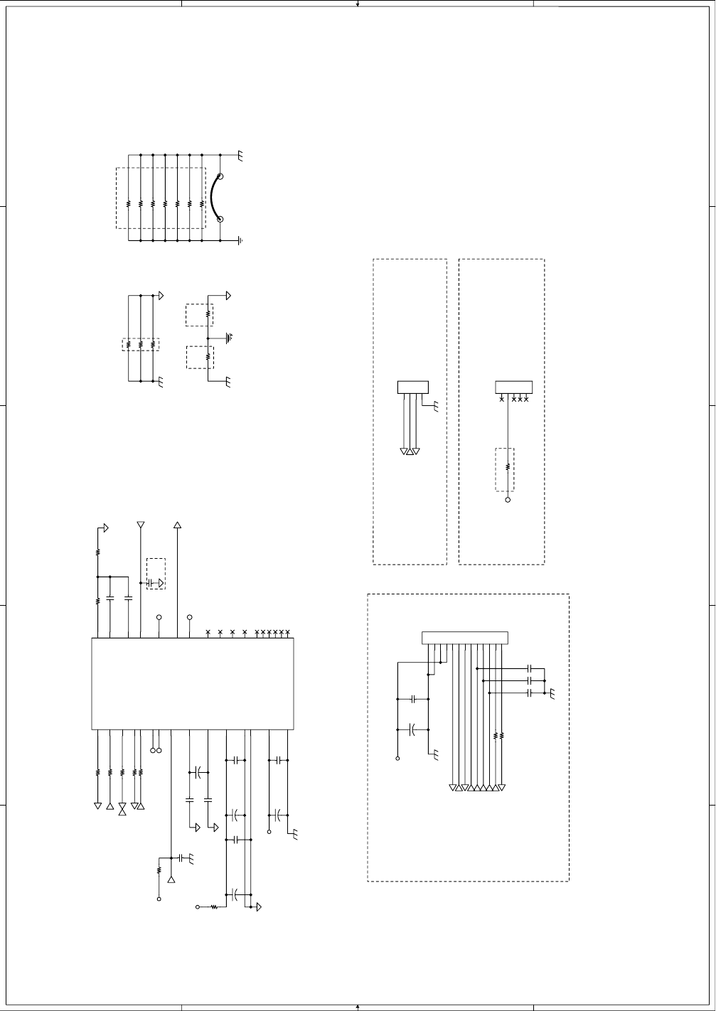
FO-CC500A
FO-K01A
6 – 16
5
5
4
4
3
3
2
2
1
1
DD
CC
BB
AA
AG
DG
AG
AG
VCC_3.3V
VCC_3.3V
DG
AG
DG AG
VCC_5.0V
DG
DG AG
FG
DG
AG
RFG DG
VCC_3.3V
DG
D
CDDAT AIN
D
CDDATAO UT
D
FRAME
C
MCLK
C
ICLK
D
RESETO
A
DSSRX
A
DSSTX
A
DSSTX
A
CI
A
DSSRX
D
MONOUT
D
MONIN
D
PARK
D
DSS IN
D
DSSOUT
D
INCOM
D
MONOUT
D
MONIN
D
PARK
CNMAIN
CNDLCNEMU
f rom NMI
f rom EMUSYNC
fr om RESET Use to EMURATOR
R106 for N.M
R107 for 10k ohm
R136 for 10k ohm
Common Ground Plane
Main Control Connector Block Down Load Connector Block
Emurator Connector Block
( 3-3B)( 1-5C)
(1 -5C) ( 3-5B)
(1 -5C)
( 1-5C) ( 3-3B)
(3 -5B)
( 1-5C) ( 3-3B)
(1 -5C) ( 3-5B)
( 1-5C)
( 1-5C)
( 1-5C)
( 1-5C)
( 1-5C)
( 1-5C)
( 1-5B)
( 1-5B)
( 1-5B)
( 3-3D)
( 3-3D)
( 3-5B)
( 3-5B)
( 1-2B)
Jumper
CN2
Connector 4pin
1
2
3
4
R115 Short(2012)
IC1
20438
Merlin Codec
DVSS
20
DVDD
21
AVSS_TX
16
AVSS_RX
8
AVDD
15
AGND
14
NC6
32
NC1
25
NC2
27
NC3
28
NC4
29
NC5
30
VREF
13
MICINP
10
MICINN
11
LINEIN
9
SPKRON
19
SPKROP
18
LINEO
17
XCLOKO
22
MODE1
23
MODE0
24
TEST
3
DATAO
4
DATAI
5
MICBIAS
12
FRAME
6
ICLK
26
MCLK
31
CTRLSOUT
2
CTRLSIN
1
RESETB
7
CT1
RFG1
R122 0
R149 0
R118 100
R153 0
C133
100p
R136 N.M
R116 2.2k
C132
100p
C110 0.1u
C107 0.1u
C131
100p
R117 100
R101
N.M
R114 1k
TP59
C109 0.1u
R102
N.M
R134 N.M[ 2012]
TP55
R151 N.M[ 2012]
R113 N.M[ 2012]
R3 3.3k
R146 N.M[ 2012]
C115
0.1u
R104 Short(2012)
C101
0.1u
TP56
C116
0.1u
R135
10
+C44
47u/25V
C106 0.1u
TP58
C108
0.1u
+C45
220u/6.3V
+C29
220u/6.3V
CN3
Connector 5pin
1
2
3
4
5
CN1
Connector 13pin
1
2
3
4
5
6
7
8
9
10
11
12
13
R147 N.M[ 2012]
R103 Short(2012)
TP57
+C58
10u/10V[3216]
C111
0.1u
R150 0
R133 N.M[ 2012]
CT2
RFG2
C128
N.M
R152 18k
+C1
220u/6.3V
R145 N.M[ 2012]
Analog codec/connector block 3/3
FO-CC500A
FO-K01A
6 – 17
Cordless PWB parts layout (Top side)
FO-CC500A
FO-K01A
6 – 18
Cordless PWB parts layout (Bottom side)
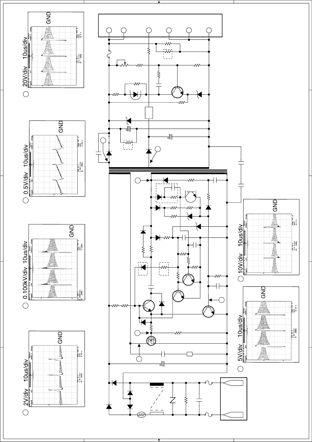
FO-CC500A
FO-K01A
[4] Power supply PWB circuit 1/1
1234
56
21
3
4
5
6
L1
PLA10A2230R4
NTC1
NTH7D8R0
Q1
2SK2717
R19
33
Q2
2SC1741AS
Q22
2SC4081
Q21
2SC1741AS
D18
1SS133
C9
0.01
N.M.
N.M.
R29
4.7K
R24
100K
R7
390
R6
470
D7
1SS133 D102
EC31QS04
C110
0.1
R112
47K
F101
T4A/250V
GND
+5V
MG
MG
+24V
1
2
6
3
4
5
+24V
CNPW
D101
YG911S2
BEA101
JUMPER
C111
1000P
T1
2D84
D14
1SS133
C7
4700P C15
4700P
R10
6.8K
Q23
2SC4081
C1
0.1
C5
56/400
C8
47P
D17
1SS133
R5
22K
R26
47K
R28
D21
D20
1SS133
D22
HZS11
D5
HZS9
D6
1SS133
D9
1SS133
R25
270
R12
20K
R13
1K
R11
9.1K
R9
R17
680
PC1
PC123
C102
330/16
R123
C101
220/35
D104
HZ-30CP
R117
4.7K
PC1
PC123
Q101
2SC4081
D105
HZS7
R113
7.5K
R122
R115
15K
R111
1K
R110
470
VR101
5K(1/10W)
R121
R27
56K
C13
100P
C14
0.1
C12
C11
100P
C10
4700P
R8
33K
BEA1
BL02RN1
R1
4.7M(1/2W)
R2
680K R3
680K
Z1
ENC471
D11
ERA15-06
D13
ERA15-06
D10
ERA15-06 D12
ERA15-06
F2
T2.5A/250V
F1
T2.5A/250V
CNAC 12
N.M. IC101
PQ05RD11
N.M.
N.M.
F102
0
D4
5
5
4
4
3
3
2
2
1
1
D D
C C
B B
A A
6 – 19
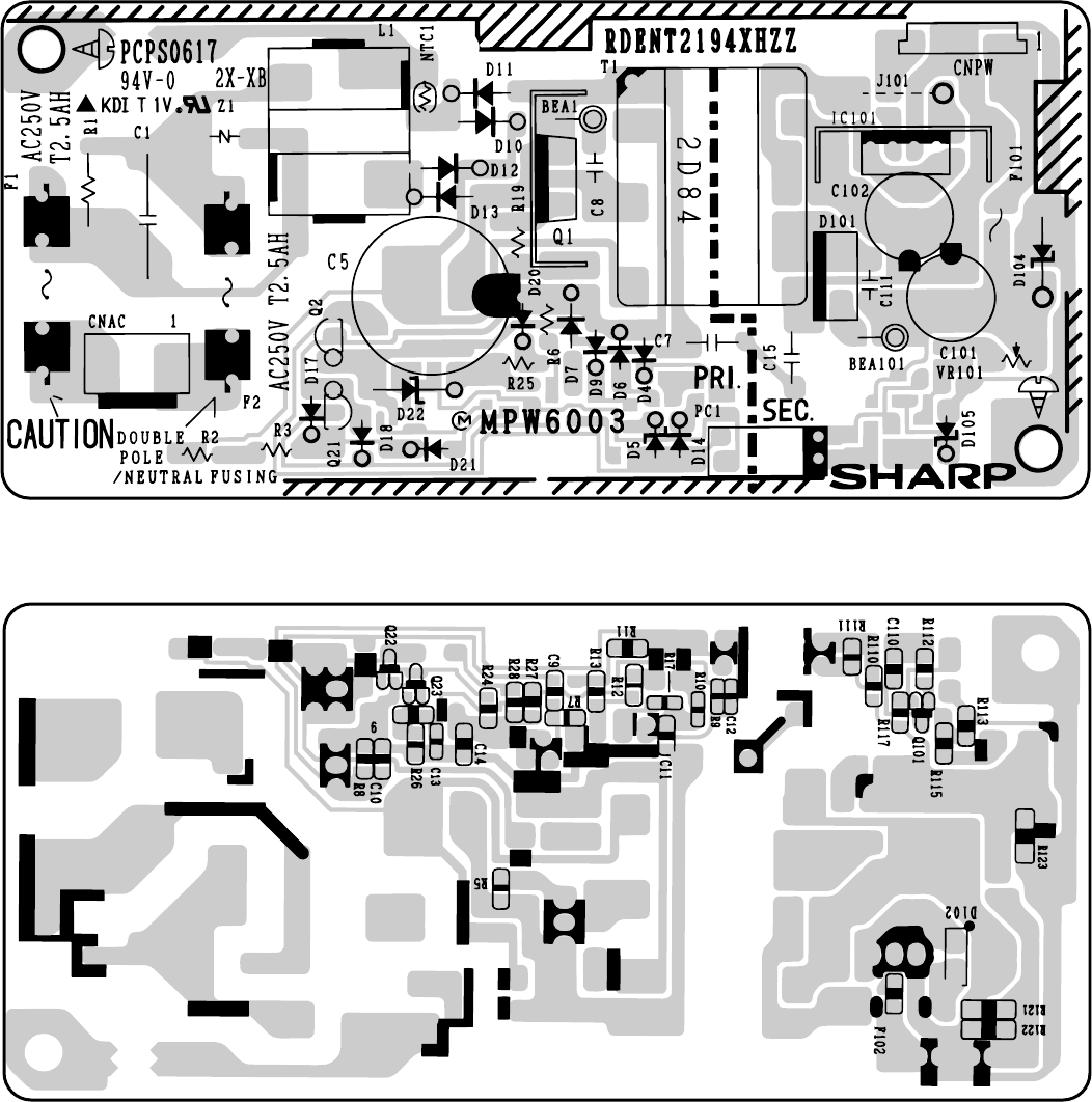
FO-CC500A
FO-K01A
Power supply PWB parts layout (Top side)
6 – 20
Power supply PWB parts layout (Bottom side)
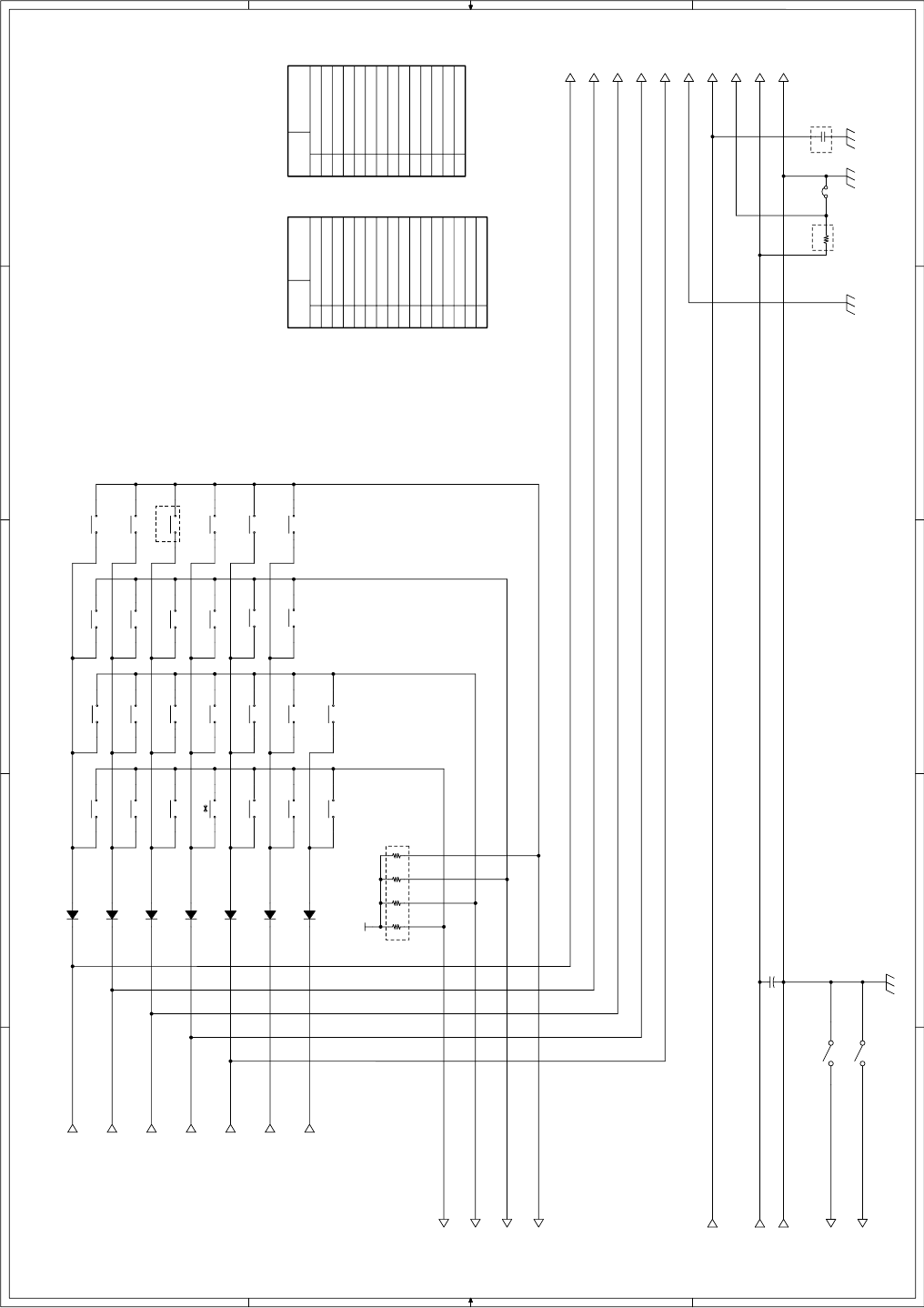
FO-CC500A
FO-K01A
5
5
4
4
3
3
2
2
1
1
D D
C C
B B
A A
D1
1SS133
5
0
SW2
8
START
SW1
R4
C2
22/50
+
UP
R1
1
DOWN
R5
4
A
R6
7
REC/MEMO
INTERCOM
R3
JP
D6
1SS133
C1
N.M.
REDIAL
D7
1SS133
N.M.
STOP COPY
D3
1SS133
PLAY
D2
1SS133
D4
1SS133
3FUNCTION
6RESOLUTION
D5
1SS133
#SPEAKER
9
2
OP LCR
R2
N.M.
DG
DGDG DG
+3.3V
E
+3.3V
VO
+3.3V
DG
LD3
LD1
LD0
LD2
E
RS
R/W
ORGSNS
FRSNS
DG
KEN1A
SEN6
KEN2A
KEN3A
KEN4A
SEN0
SEN1
SEN2
SEN3
SEN4
SEN5
CNPN_A-10
CNPN_A-11
CNPN_A-13
CNPN_A-14
CNLCD-11
CNLCD-12
CNLCD-13
CNLCD-14
CNLCD-4
CNLCD-5
CNLCD-6
CNLCD-3
CNLCD-2
CNLCD-1
CNPN_A-3
CNPN_A-2
CNPN_A-1
CNPN_A-4
CNPN_A-15
CNPN_A-16
CNPN_A-9
CNPN_A-6
CNPN_A-5
CNPN_A-7
CNPN_A-8
CNPN_A-12
2
6
11
14
4
12
8
LD2
N.C.
N.C.
LD0
E
1
3
5
7
9
10
13
N.C.
LD1
LD3
N.C.
R/W
DG
RS
VO
+3.3V
CNPN
2
6
11
14
4
12
16
8
SEN3
ORGSNS-
E
SEN1
+3.3V
1
3
5
7
9
10
13
15
SEN0
SEN2
SEN4
SEN5
SEN6
FRSNS-
DG
KEN4A
KEN1A
KEN2A
KEN3A
CNPN-A
N.M.
6 – 21
[5] Operation Panel PWB circuit 1/1
Note: Since the parts of PWB cannot be supplied, change it as a unit.
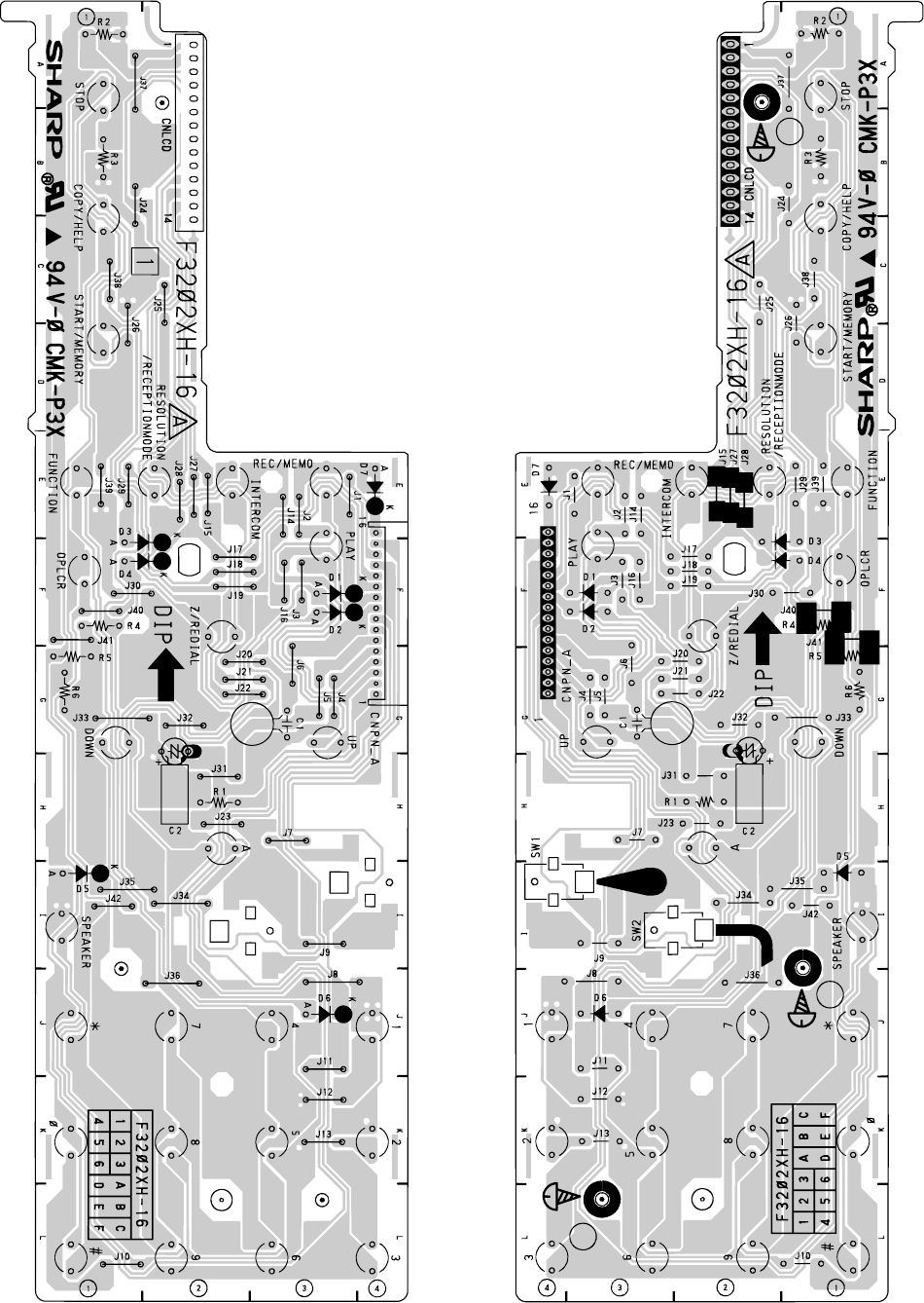
FO-CC500A
FO-K01A
6 – 22
Operation panel PWB parts layout
(Top side) Operation panel PWB parts layout
(Bottom side)
Note: Since the parts of PWB cannot be supplied, change it as a unit.
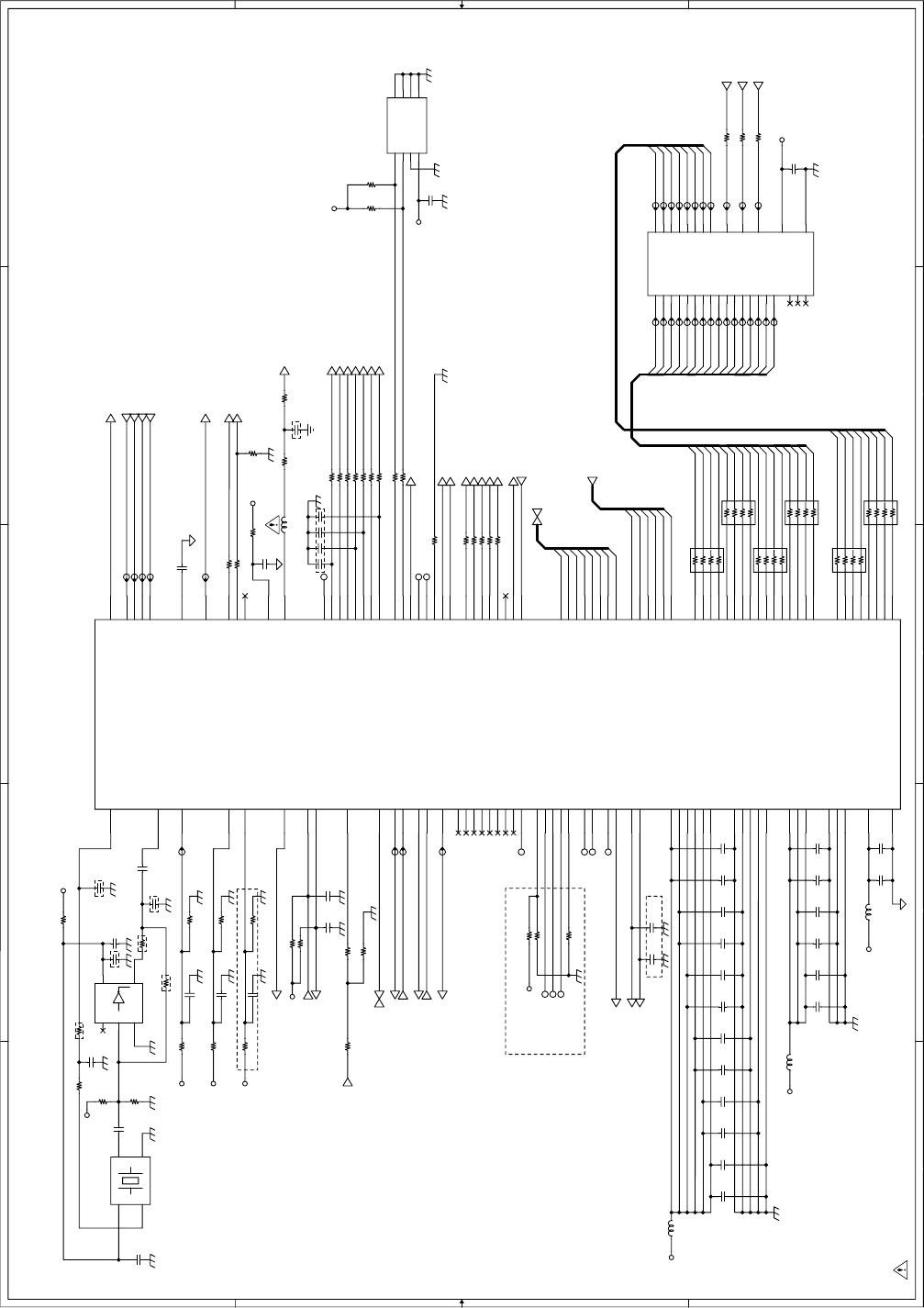
FO-CC500A
FO-K01A
6 – 23
[6] Cordless handset PWB circuit Main control block 1/5
5
5
4
4
3
3
2
2
1
1
DD
CC
BB
AA
D1
D7
A12
A13
A10
A15
A9
ROW3
D3
D5
D[0 .. 7]
COL5
COL1
ROW7
D4
A2
A5
A1
ROW6
D7
A15
A10
D4
A11
A8
A7
A5
ROW2
D2
D1
A13
D0
COL3
A1
D2
A0
A7
D6
A2
D5
ROW1
ROW0
D6
A11
A8
A6
A14
A12
A3
A4
COL2
COL0
D0
A14
A9
COL4
A6
D3
ROW5
ROW4
A0
A[0..15]
A4
A3
DG
DG
VCC_3.3V
DG
VCC_3.3V
DG
VCC_3.3V
VCC_3.3V
VCC_BAT
VCC_BAT
VCC_3.3V DG
AG
DG
VCC_3.3V
DG
DG
VCC_3.3V
DG
VCC_3.3V
DG
RFG
DG
DG
DG
DG
DG
DG
AG
VCC_BAT
DG
VCC_3.3V
DG
DG
AG
DG
DG
DG
DG
VCC_3.3V
DG
DG
DG
VCC_3.3V
DG
DG
DG
DG
C
SYNCLK
D
SYNDATA
D
ROMCS
D
READ
D
WRITE
D
SYNEN
C
REFOSC
D
TXPWR1
D
SYNSTB
A
RXQP
D
LNATTN
D
EMJMUTE
A
TXDATA
D
LCDR S
D
MONIN
A
SPOUT
C
ICLK
D
ROMCS
D
RXEN
D
LCDE
D
TXEN
D
READ
A
AGC
D
HSC HG
D
LCDRST
ROW [0.. 7]
D
PARK
A
RXIN
D
COL[0. .5]
D
MONOUT
A
RXQN
D
LEDEN
D
EMJCHK
D
SPMUTE
D
FRAME
D
LCDR W
D
CDDATAO UT
D
WRITE
D
LCDC S
C
MCLK
D
CDDAT AIN
D
TXPWR0
A
RXIP
D
RESETO
Low Noise Amp attenuation
LNATTN = Low : receiver High Gain mode
LNATTN = High : receiver Low Gain mode
TDD Control
TXEN = High : Transmit Data
RXEN = High : Receiver Data
Power Level Control
TXPWR1 = Low , TXPWR0 = Low : High Power
TXPWR1 = Hihg, TXPWR0 = Low : Medium Power
TXPWR1 = Low , TXPWR0 = High : Low Power
TXPWR1 = Hihg, TXPWR0 = Hihg : Undefined
(PLL Clock 9.6MHz)
( 1-5B)
( 1-5B)
( 1-5B)
I2 C Serial Data
I2 C Clock
(2 -5C)
(2 -4C)
(2 -4C)
(2 -4C)
(2 -4C)
(2 -2D)
(2 -2C)
(2 -5C)
(2 -2C)
(2-2C)
( 2-2D)
( 2-2C)
( 2-5C)
( 2-2C)
( 2-2D)
( 2-5C)
(3 -2C)
( 3-5D)
(5 -3C)
( 4-3D)
( 1-1A)
( 5-2D)
(3 -3C)
( 3-5D)
(5 -5D)
(5 -3C)
( 5-2B)
( 1-1A)
ROW [0-3] to Key Matrix
ROW [4-7] to LCD Data
Charge
Turn on PARK = 6.6V (PARK = 3.0 V)
Turn off PARK = 0.0V (PARK = 0.0 V)
[PARK Port High Level is 2.0V]
( 3-5D)
Low Battery
Turn on Vcc_BAT = 3.33V
(BATT0 Input Voltage = 1.75 V[+25mV,-25mV] )
Turn off Vcc_BAT = 3.52V
(BATT0 Input Voltage = 1.85 V[+25mV,-25mV] )
f or Emulator
(5 -3C)
( 3-4B)
Codec Control
(5 -5A)
( 3-5D)
(Codec Input Clock 4.8MHz)
(5 -3C)
(3 -3C)
(Codec Output Clock 1.2MHz)
(5 -3B)
( 3-5D)
( 5-3B)
Reset
Turn on Vcc_BAT = 2.97V
(RESETIP Input Voltage = 1.257 V[ +36mV,-36mV] )
Turn off Vcc_BAT = 3.19V
(RESETIP Input Voltage = 1.35 V[+36mV,-36mV])
(3 -3B)
( 3-5D)
( 4-3D)
( 5-3B)
( 4-4C)
( 1-1A)
( 5-2C)
Common Round
N.M
TP36
C308
N.M
TP(R)
R57 100
L3 0[1608]
IC5
CX80705-13
Merlin ASIC XROM
AUX DAC
107
ARTO
41 ARTI
39
RESETIP
94
OSCI
91
OSCO
90
BATT1
96
BATT0
97
NC
99
VDDP
56
VDDP
74
VDDP
113
VSSP
7
VSSP
29
VSSP
57
VDDC
2
VDDC
32
VDDC
71
VSSC
5
VSSC
33
VSSC
70
AVDD
92
AVSS
93
AGND 95
PARKP
40
KEYPADR0 60
KEYPADR1 61
KEYPADR2 62
KEYPADR3 63
KEYPADR4 64
KEYPADR5 65
KEYPADR6 66
KEYPADR7 67
KEYPADC5 10
KEYPADC3 12
KEYPADC4 11
KEYPADC2 13
KEYPADC1 14
KEYPADC0 23
GPIOA0 123
GPIOA1 124
GPIOA2 125
GPIOA3 126
GPIOA4 127
GPIOA5 128
GPIOA6 1
GPIOA7 8
GPIOB0 38
GPIOB1 37
GPIOB2 36
GPIOB3 31
GPIOB4 30
GPIOB5 26
GPIOB6 25
GPIOB7 24
GPIOC0/SWCTL 9
MCLK/CDCMCLK
45
CDCDATAO
43
CDCDATAI
44
CDCFRAME
42
CDCICLK/ICLK
58
RESETOP/CDCPOR
59
REFOSC 89
RXIN 102
RXIP 101
RXQP 103
RXQN 104
AGC 105
TXDATA 100
TRSW 110
TXEN 108
RXEN 76
GPIOC1 75
GPIOC2 111
GPIOC3 109
GPIOC4 88
GPIOC5 87
GPIOC6 77
GPIOC7 78
AUXREF 106
DATA0 122
DATA1 121
DATA2 120
DATA3 119
DATA4 118
DATA5 117
DATA6 116
DATA7 115
ADDR0 15
ADDR1 16
ADDR2 17
ADDR3 18
ADDR4 19
ADDR5 20
ADDR6 21
ADDR7 22
ADDR8 51
ADDR9 52
ADDR10 55
ADDR11 53
ADDR12 46
ADDR13 50
ADDR14 49
ADDR15 47
WPR~3
48
RDP
54
ROMCSP
112 RAMCSP
79
HOSTCSP
83 HOSTACK
84
SYNC~3
82 NMIP
81
XCODEP
85
EMUCLK~3
80
VSSP
73
VSSP
114
VDDP
28
VDDP
6
VDDP
27
NC
98 NC
69 NC
68 NC
35 NC
34
NC
3
NC
72
NC
4
VISP~3
86
TP32
R50 160k(F)
TP5
R58 100
C23
N.M
R48 N.M
TP4
C38
8p
R56 100
R40
TP10
C31
N.M
R25
10k
TP35
C34
0.1u
R55 100
R54 N.M
C13
8p
R33 100
TP3
R45 56k(F)
TP43
R42 120k(F)
TP38
C14
0.1u
TP40
R34 100
R28 10k
R35 62k(F)
R59 N.M
TP44
C306
0.1u
C21
8p
R60 100
C33
100p
IC9
TC7SZ04F
NC
1
IN
2
GND
3OUT 4
Vcc 5
R43
TP2
R31
22k[1608]
C22
0.1u
C37 0.1u
TP27
TP23
C41
8p
C39
0.1u
TP29
R470
TP19
C32 1000p
C305
0.01u(K)
R221 N.M
C36 0.1u
C15
8p
L5
BLM11HB102SD[1608]
C119
0.1u
C24
100p
C42
8p
C43
N.M
C16
0.1u
C40
0.1u
R51 100
C25
100p
R224
100
TP15
C17
8p
C11
0.1u
C313 C312
R53 100
TP(C)
R29 100k
C27
8p
R200 100[1608]
C19
0.1u
C311
R24
10k
C45
N.M
TP(N)
C26
0.1u
RA2
100
5
1
8
7
62
3
4
C18
8p
R23 100
C310
TP33
TP(S)
RA5
100
5
1
8
7
62
3
4
C20
0.1u
R222
56k(F)
R201 100[1608]
R22 100
RA3
100
5
1
8
7
62
3
4
C29
8p
R91
R202 100[1608]
R30 120k
X1
Crys tal [KSS]
4
2
1
3
TP20
TP22
TP37
L6 0[1608]
C309
N.M.
R6 100
TP18
TP24
RA4
100
5
1
8
7
62
3
4
C30
0.1u
R41 N.M
R203 100[1608]
TP26
TP16
R7 100
RA1
100
5
1
8
7
62
3
4
C118
0.01u(K)
TP14
TP28
R204 100[1608]
L4 0[1608]
R14 100
RA6
100
5
1
8
7
62
3
4
TP30
TP39
TP7
R52 100
TP6
TP1
C12
0.1u
TP13
TP25
C35 N.M
TP31
R32 100
C44
0
IC3
SST39LF512 [S ST]
A0
20
A1
19
A2
18
A3
17
A4
16
A5
15
A6
14
A7
13
A8
3
A9
2
A10
31
A11
1
A12
12
A13
4
A14
5
A15
11
DQ0 21
DQ1 22
DQ2 23
DQ3 25
DQ4 26
DQ5 27
DQ6 28
DQ7 29
CE# 30
OE# 32
WE# 7
NC
9
NC
10
NC
6
VSS 24
VDD 8
TP12
R223
56k(F)
TP21
TP8
IC4
S-24C04 [SII]
A0 1
A1 2
A2 3
GND 4
SDA
5
SCL
6
TEST
7
VCC
8
TP34
TP11
R27 10k
R20 100k
R49 N.M
TP17
R26 10k
TP9
NOTE:
This mark indicates a safety-critical part(s).
0
0
0
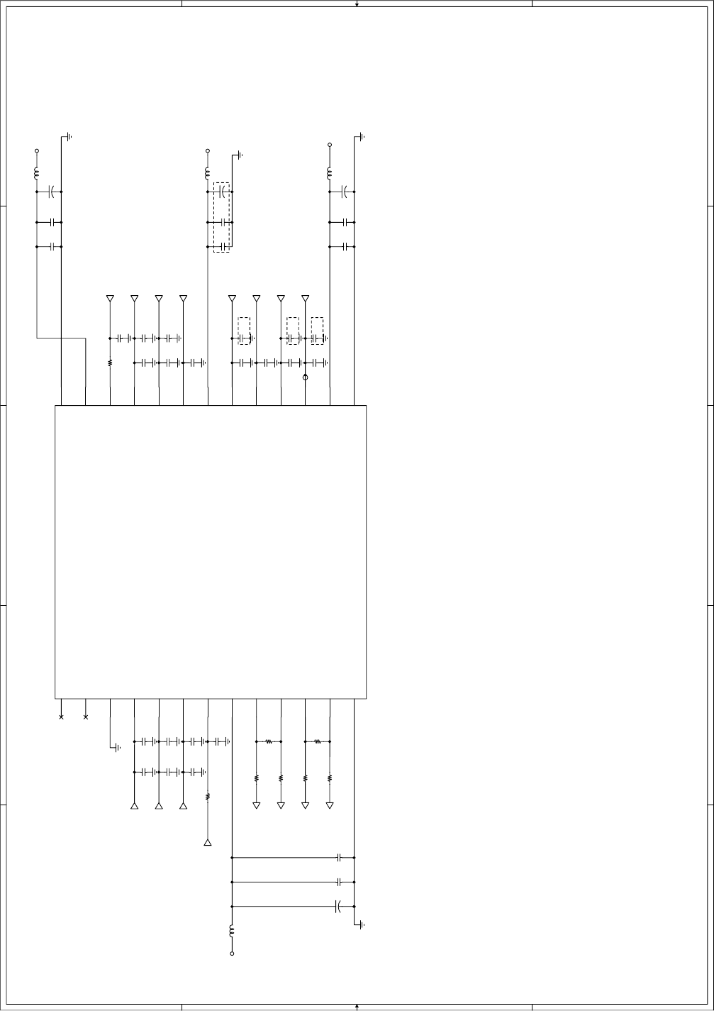
FO-CC500A
FO-K01A
6 – 24
RF module block 2/5
5
5
4
4
3
3
2
2
1
1
DD
CC
BB
AA
RFG
RFG
RFG
RFG
RFG
RFG
RFG
RFG
RFG
RFG
RFG
RFG
RFG
RFG
RFG
RFG
RFG
RFG
VCC_3. 3VRF RFG
RFG
VCC_3. 3VRF
VCC_3. 3VRF
VCC_3. 3VRF
RFG
RFG
RFG
RFG
RFG
A
TXDATA
D
SYNEN
D
SYNSTB
C
SYNCLK
C
REFOSC
D
SYNDATA
D
RXEN
D
LNATTN
A
RXQN
A
RXQP
A
RXIN
A
RXIP
A
AGC
D
TXPWR0
D
TXPWR1
D
TXEN
( 1-2D)
( 1-2D)
( 1-2D)
( 1-2D)
(1 -2D)
(1 -2C)
(1 -2C)
(1 -2C)
(1 -2C)
(1 -2C)
(1 -2C)
(1 -2D)
( 1-2C)
( 1-2C)
( 1-2D)
( 1-2D)
C114
8p C98
8p
R208 1k
C117
8p
R209 1k
C300
1000p
R210 1k
C116
1000p
R39 1k
C105
8p
R206
3k
+C89
33u/10V[pai5.0 x 4.5L]
C93
8p
C109
0.1u
C91
8p C94
N.M
C97
N.M C101
N.M
C99
8p
+C107
100u/6.3V[pai6.3 x 4.5L]
R205
3k
C110
8p
UNIT1
2.4GHz RF Module
GND
1
ANTENNA
2
GND
3
TXPWR0
4
TXPWR1
5
TXEN
6
AGC
7
VCC
8
RXQN
9
RXQP
10
RXIN
11
RXIP
12
GND
13 GND 14
VCC 15
LNAATTN 16
RXEN 17
SYNDATA 18
REFOSC 19
VCC 20
SYNCLK 21
SYNSTB 22
SYNEN 23
TXDATA 24
VCC 25
GND 26
C90
0.1u
C95
N.M
C102
8p
R88 4.7k
L14 3[2012]
C92
8p
C96
8p
L10
3
C112
1000p
C113
8p
L13 3[1608]
C115
8p
L15 3[2012]
C106
0.1u
C104
1000p
+
C108
470u/6.3V[pai6.3 x 11]
C100
N.M
+
C79
N.M[3216]
TP60
C103
8p
R207 1k
C111
1000p
C88
8p
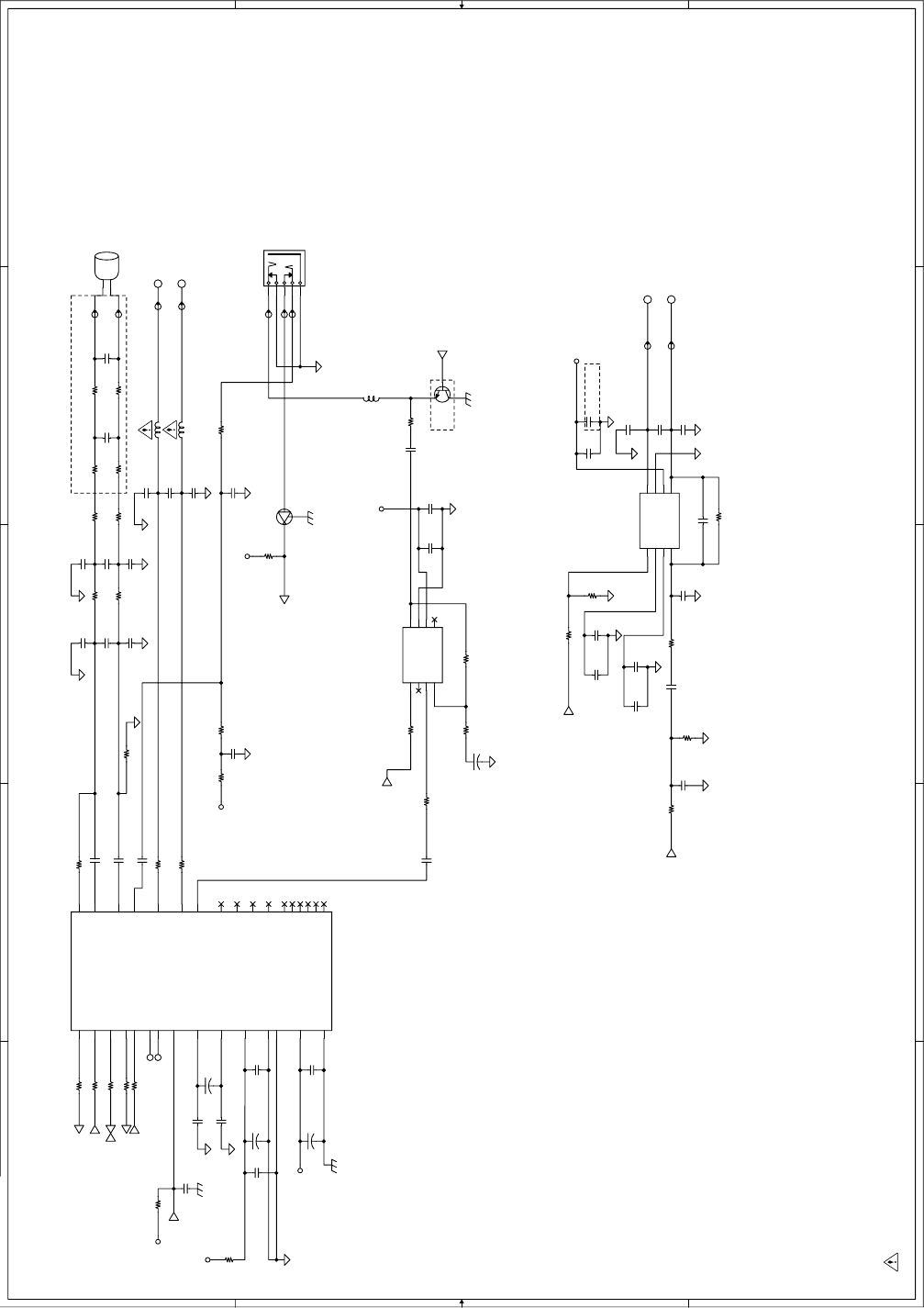
FO-CC500A
FO-K01A
6 – 25
Analog codec block 3/5
5
5
4
4
3
3
2
2
1
1
DD
CC
BB
AA
AG
DG
AG
AG
VCC_3.3V
VCC_3.3V
DG
AG
AG
AG
AG
AG
AG
AG
AG
DG
VCC_3.3V AG
VCC_3.3V
AG
AG
AG
AG
AG
AG
AG
AG
AG
AG
DG
AG
VCC_BAT
VCC_BAT
AG AG
VCC_3.3V
D
CDDAT AIN
D
CDDATAO UT
D
FRAME
C
MCLK
C
ICLK
D
RESETO
D
EMJCHK
D
SPMUTE
A
SPOUT
D
EMJMUTE
D
EMJMUTE
Near The Microphone
( 1-5C)
( 1-5C)
( 1-5C)
( 1-5C)
( 1-5C)
( 1-5C)
( 1-3B)
( 1-3B)
(1 -3C)
(1 -3B) (3 -3C)
( 3-2C)
( 1-5C)
HeadSet Reciver Control
EMJMUTE = High : Stand-By (Mute)
EMJMUTE = Low : Active
Backside Speaker Control
SPMUTE = High : Active
SPMUTE = Low : Stand-By (Mute)
HeadSet Detector Control
EMJCHK = High : Headset On
EMJCHK = Low : Headset Off
TP85
R67 15k
R83 1k
TP84
R80 47
C59
1u[1608]
+C67
10u/10V[3216/2012]
C84
8p
R74 22
C69 0.1u
TP87
TP41
R213 100
TP42
R212 0
C65
0.1u
R78
10
R85
10k
C68 0.1u
C55
8p
C86
0.1u
C75
8p
C83
8p
R82 47
+C85
4.7u/10V[3216]
C72
8p
Q6
N.M
C
E
B
C82
8p
R71 47
R81 47
+C302
10u/10V[3216] C77
8p
TP82
C66
0.1u(K)[1608] C58
8p
C52
8p
C64
8p
L11 BLM11HB102SD[1608]
C73
8p
R65 120k
L12 BLM11HB102SD[1608]
C61 0.1u(K)[1608]
C53
N.M[1608]
C54 1000p(K)
C76
8p
C46
4.7u/10V[2012]
C74
8p
+
Speaker Rand +
R211 0
C60 0.1u(K)[1608]
R79 2.2k C63
8p
C51
0.1u
R72 47
C70 0.1u(K)[1608]
R69 100
-
Speake r Rand -
R89 3.3k
IC7
NJU708 1R [JRC]
STBY
1
NC
2
+Vin
3
-Vin
4NC 5
VCC 6
GND 7
Vout 8
R216 20k
C47
1u/10V[1608]
C62
0.1u
L9
0[1608]
C301
0.01u(K)
IC6
NJM2149R [JR C]
CD
1
+Vref
2
+Vin
3
-Vin
4Vout1 5
VCC 6
GND 7
Vout2 8
R86 200
Q7
DTC114EU
3
2
1
R87 200
C71
0.1u
C56
0.1u(K)[1608]
TP88
CT3
Speake r Rand -
C81
0.1u
C2
8p
C50
8p
C57
10u(K)
+C80
4.7u/10V[3216]
R3 47
R66 3k
TP81
IC8
Merlin Codec
DVSS
20
DVDD
21
AVSS_TX
16 AVSS_RX
8
AVDD
15
AGND
14
NC6 32
NC1 25
NC2 27
NC3 28
NC4 29
NC5 30
VREF
13
MICINP 10
MICINN 11
LINEIN 9
SPKRON 19
SPKROP 18
LINEO 17
XCLOKO 22
MODE1 23
MODE0 24
TEST 3
DATAO
4
DATAI
5
MICBIAS 12
FRAME
6
ICLK
26
MCLK
31
CTRLSOUT
2
CTRLSIN
1
RESETB
7
MIC1
Microphone
+
-
R2 47
C78
22u/ V[ 3216]
R70
R219 47
R76
20k
CT4
Speaker Rand +
R77 100
TP89
C49
8p
R218 47
R214 100
R64
10k
TP83
R215
56k
J1
MJC-012
1
2
3
4
5
C48
8p
R68 27k
R84 1.5k
R73 2.2k
TP90
NOTE:
This mark indicates a safety-critical part(s).
0
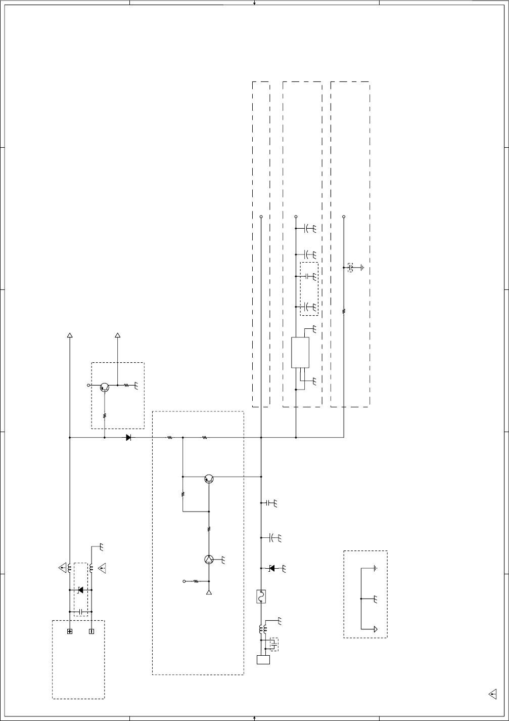
FO-CC500A
FO-K01A
6 – 26
Power supply block 4/5
5
5
4
4
3
3
2
2
1
1
DD
CC
BB
AA
VCC_3.3V
DG
RFG
DG
DG
DG
DG
VCC_BAT
DG
DG
DG
DG DG
DG
VCC_3.3V
AG RFG
DG
VCC_3.3V
DG DG
VCC_3. 3VRF
D
PARK
D
HSC HG
D
MONIN
Cradle Contacts
High Speed CHarGe
High = High Speed Charge ON
Supply Current (Ave.) = 160 mA
Low = High Speed Charge OFF
Supply Current (Ave.) = 10 mA
Charge Control
High Speed Charge
[HSCHG = Al ways Hi gh]
160 mA/h Charge
Trickl e Charge
[H SCHG Hi gh time = msec, Low ti me = msec ]
mA/h Charge
Charge Control Block
Main Core Power Supply
RF Module Power Supply
Sub Block Power Supply
Audio AMP, LED, etc...
Merlin ASIC, Codec, Flash Memory,
EEPROM, LCD, etc...
Radio Frequency Module Only
Common Ground Plane
Power Supply Voltage
= 6.5 V (max)
Powe Supply Current
= 500 mA (max)
( 1-5C) ( 5-2B)
( 1-5C) ( 5-2C)
N.M
( 1-3C)
R5
160[5025]
+C9
N.M[3225]
CN1
Connector 2pin
1
2
C10
N.M
R90
N.M
IC1
S-L2980(SOT-23-5)[SII]
Vin
1
On/Off
3Vss
2
NC 4
Vout 5
L16
0
C1
N.M
L2 BLM41A102SG[4516]
R8
N.M
C307
N.M.
L17
0
D1
N.M[PT Z]
CT1
Contact +
R220 0
CT2
Contac t -
Q2
DTC114EU
32
1
Q3
KTA1298Y
C
E
B
+C303
150u/6.3 V[SMD]
D3
U1GC44
A
K
C8
N.M
R4
N.M
R111 k
+C304
330u/6.3 V[SMD]
+C4
22u[3225]
L1
BLM41A102SG[4516]
R10 10k
Q1
N.M
C
E
B
F1
Chip Fuse 1.0A[2012] C3
8p
D2
UDZS 4. 7B
R9
10[5025]
NOTE:
This mark indicates a safety-critical part(s).
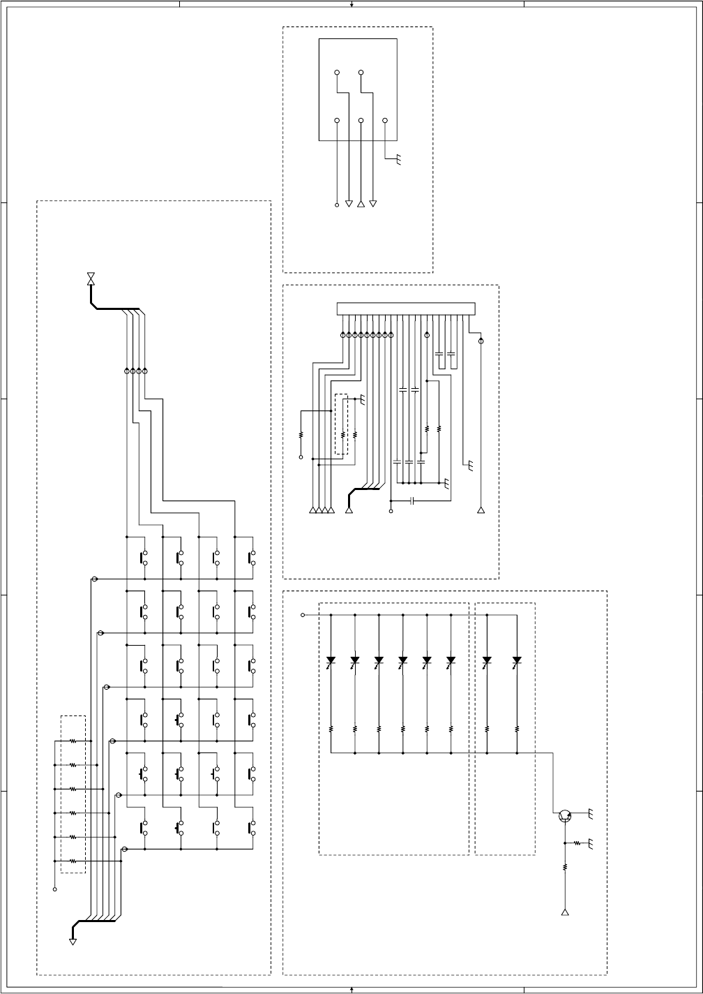
FO-CC500A
FO-K01A
6 – 27
Keypad/LED/LCD/remote contact block 5/5
5
5
4
4
3
3
2
2
1
1
DD
CC
BB
AA
ROW2
ROW1
ROW0
ROW3
COL4
COL0
COL1
COL3
COL5
COL2
ROW6
ROW5
ROW7
ROW4
VCC_+3.0V
VCC_BAT
DG
DG
DG
VCC_BAT
VCC_3.3V
DG
VCC_3.3V
DG
DG
COL[0.. 5]
ROW [3.. 0]
LEDEN
D
PARK
D
MONIN
D
MONOUT
LCDR S
LCDR W
LCDE
ROW [4.. 7]
LCDRST
LCDC S
Keypad Block
LCD Back Lights
Key Lights
(TALK Key)
(OFF Key)
Supply Current
Vcc_BAT = 4.5V
R = 130 ohm 17.5mA x 3
R = 220 ohm 10.5mA x 3
Total Supply Current =
84 mA
Supply Current
Vcc_BAT = 4.5V
R = 390 ohm 6mA x 2
Total Supply Current =
12 mA
LED Total Supply Current
Vcc_BAT = 4.5V
LCD Back Li ght Current + Key Li ght Current
= 96 mA
LED ENable
High = LED ON
Low = LED OFF
( 1-3C)
( 1-3B)
( 1-3B)
Handset LED Block
Remote Contacts
for Flash Download
ID Calib ration
RS-232C Connect
Emulator
Remote Contact Block
(1 -5C)
(1 -5C)
(1 -5C)
LCD Interface Block
(4 -3D)
(4 -3D)
( 1-3C)
( 1-3C)
( 1-3C)
( 1-3C)
( 1-3C)
( 1-3B)
CNLCD
R124 430k (F)[ 1608]
TP57
TP73
LED122 CL-195YG
A
C
CA14
3
12
TP80
R217 10k[1608]
TP52
CA15
2
12
TP59 TP58
LED115 CL-195YG
A
C
CA16
1
12
CA11
6
12
TP72
C201
0.47u[2012]
CP5 (DG)
LED116 CL-195YG
A
C
CA12
5
12
CN101
Connect or 22pin
1
2
3
4
5
6
7
8
9
10
11
12
13
14
15
16
17
18
19
20
21
22
CA13
4
12
C208 0.1u(K)[1608]
R126 10k[1608]
LED118 CL-195YG
A
C
R113 390 [ 1608]
CP4 (MONOUT)
TASW1
Up
12
C207 0.1u(K)[1608]
TP53
R114 390 [ 1608]
TP78
TP71
TP74
TASW3
Start
12
TP50
TP76
TASW5
Down
12
CA9
Talk Off
12
R125 820k (F)[ 1608]
CA10
Talk
12
R15
N.M
Q5
KTC3876Y
C
E
B
TASW2
Search
12
R118 130 [ 1608]
R16
N.M
CA1
Remote
12
C205 0.1u(K)[2012]
CA17
9
12
R121 130 [ 1608]
R17
N.M
TASW4
Review
12
CA18
8
12
R123 130 [ 1608]
R18
N.M
CP3 (MONIN)
CA2
Functi on
12
CA19
7
12
LED120 CL-195YG
A
C
R119 220 [ 1608]
R19
N.M
C204 0.1u(K)[2012]
TP79
R120 220 [ 1608]
R21
N.M
R62
100k
C202 0.47u(K)[2012]
TP51
LED117 CL-195YG
A
C
CA8
Hold
12
R122 220 [ 1608]
CA5
#
12
R61 1.8k
CA7
Volume
12
CA4
0
12
CA6
Interco m
12
TP77
CA3
*
12
CP1 (PAR K)
TP75
C206 0.1u(K)[2012]
LED119 CL-195YG
A
C
TP55
C203 0.47u(K)[2012]
TP54
CP2 (BAT)
R127 N.M[1608]
TP56
LED121 CL-195YG
A
C
TP70
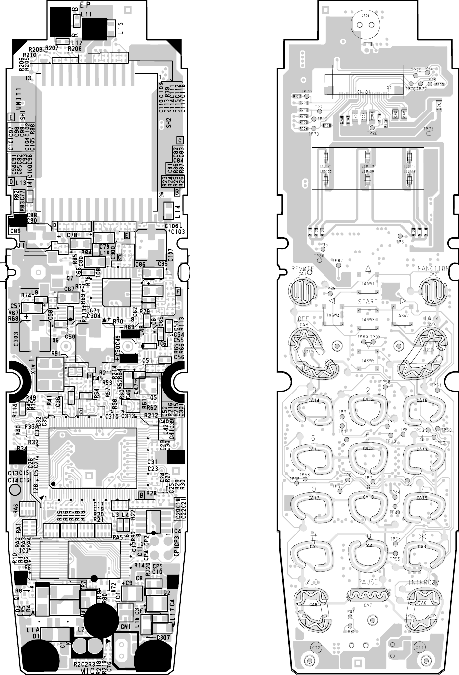
FO-CC500A
FO-K01A
6 – 28
Cordless handset PWB parts layout
(Top side) Cordless handset PWB parts layout
(Bottom side)
FO-CC500A
FO-K01A
7 – 1
CHAPTER 7. OPERATION FLOWCHART
[1] Protocol
NSF
DIS
NSS
TCF
CED
NSF
DIS
NSS
TCF
RTC
MPS
CFR
RTC
MPS
MCF
RTC
EOP
MCF
MCF
DCN
CFR
TSI
CSI
CSI
TSI
RTC
EOP
MCF
DCN
IMAGE
SIGNAL
Document ejectedRecording paper ejected
Receive side
G3 communication
CED
Transmitter side
(Document inserted into
document sensor during
standby)
To recording
position
(DCS)
Cut line printed
IMAGE
SIGNAL
Cut line printed
IMAGE
SIGNAL
IMAGE
SIGNAL
Next page insert
command
1st page
Document inserted to
the reading position
(DCS)

FO-CC500A
FO-K01A
7 – 2
[2] Power on sequence
2
1YES
YES
CPU initialized
MODEM initialized
STOP key ?
“WAIT A MOMENT” display
START
NO
YES
STAND-BY
3 sec ? NO
“MEMORY CLEAR ?” display
NO
YES
STAND-BY
3 sec ? NO
NO
START key ?
COPY key ?
STOP key ?
NO
Memory clear
STAND-BY
21
“MEMORY CLEARED” display
Memory clear
PROCESS CHECK MODE
“MEMORY CLEARED” display
YES
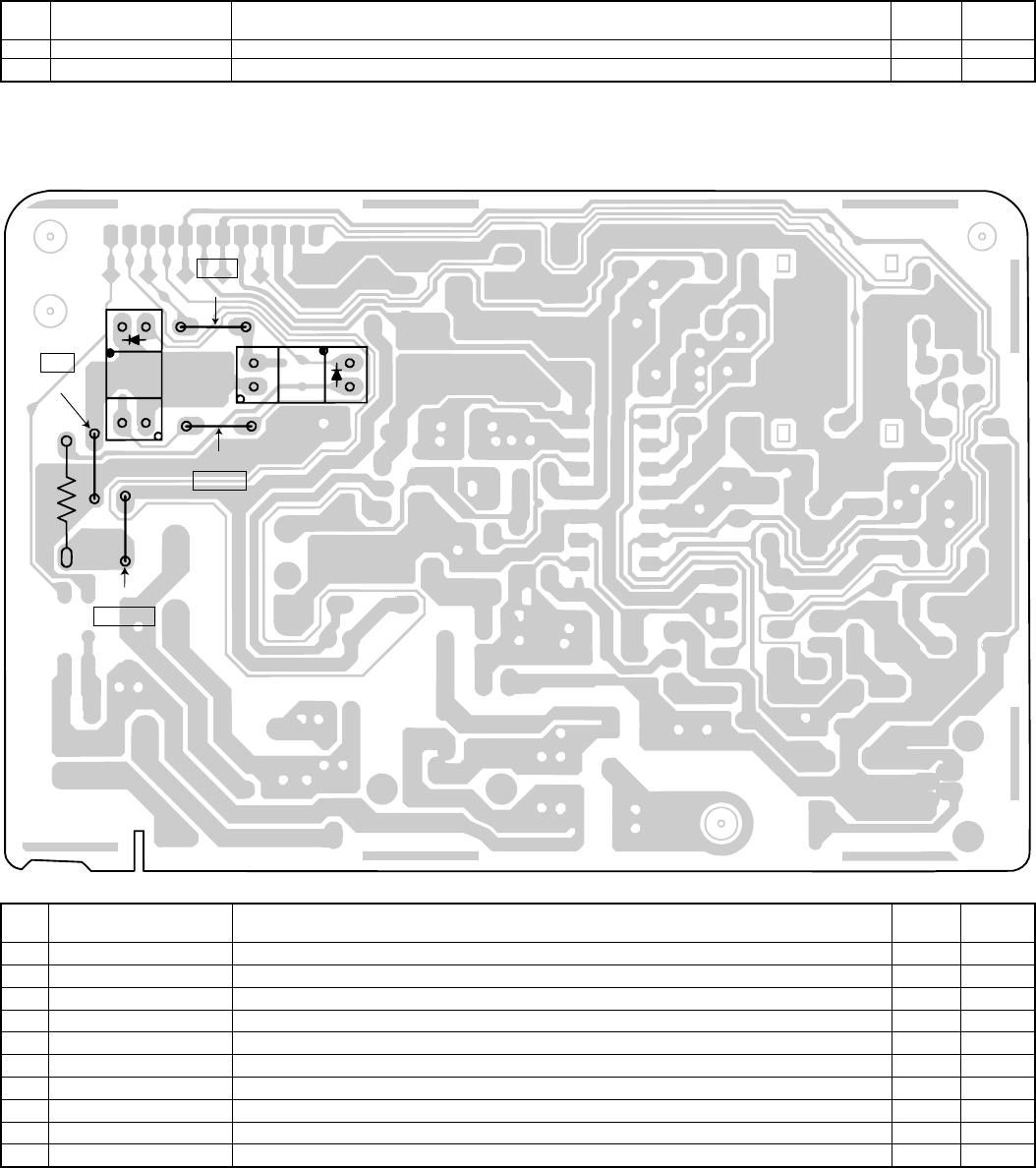
FO-CC500A
FO-K01A
8 – 1
CHAPTER 8. OTHERS
[1] Service tools
1. List
Extension board unit
NO. PARTS CODE DESCRIPTION Q’TY PRICE
RANK
1 CPWBF3201SCS1 Extension board unit (LIU PWB) 1BA
2 PSHEZ3579SCZZ Shading wave memory standard paper 1AD
1 QCNWG203BSCZZ SPEAKER RELAY CABLE 1AG
2 QCNWG206BSCZZ PANEL RELAY CABLE 1AT
3 QCNWG202BSCZZ CIS RELAY CABLE 1AN
4 QCNWG205BSCZZ HEAD RELAY CABLE 1AS
5 QCNWG204BSCZZ CAM SWITCH RELAY CABLE 1AG
6 QCNWG242BSCZZ MOTOR RELAY CABLE 1AM
7 QCNWG201BSCZZ SENSOR RELAY CABLE 1BB
8 VRS-RE3AA122J RESISTOR (1W 1.2KΩ ±5%)[R30]1AC
9 VHPSG206S//-1 PHOTO TRANSISTOR [PH1]1AG
10 VHPSG206S//-1 PHOTO TRANSISTOR [PH2]1AG
NO. PARTS CODE DESCRIPTION Q’TY PRICE
RANK
LIU PWB
PH2
PH1
R30
TP3
DG
(ORANGE)
TP4
+24VL
(YELLOW)
CE
KA
TP1
PIN
(BROWN)
TP2
FILM
(RED)
K
A
C
E
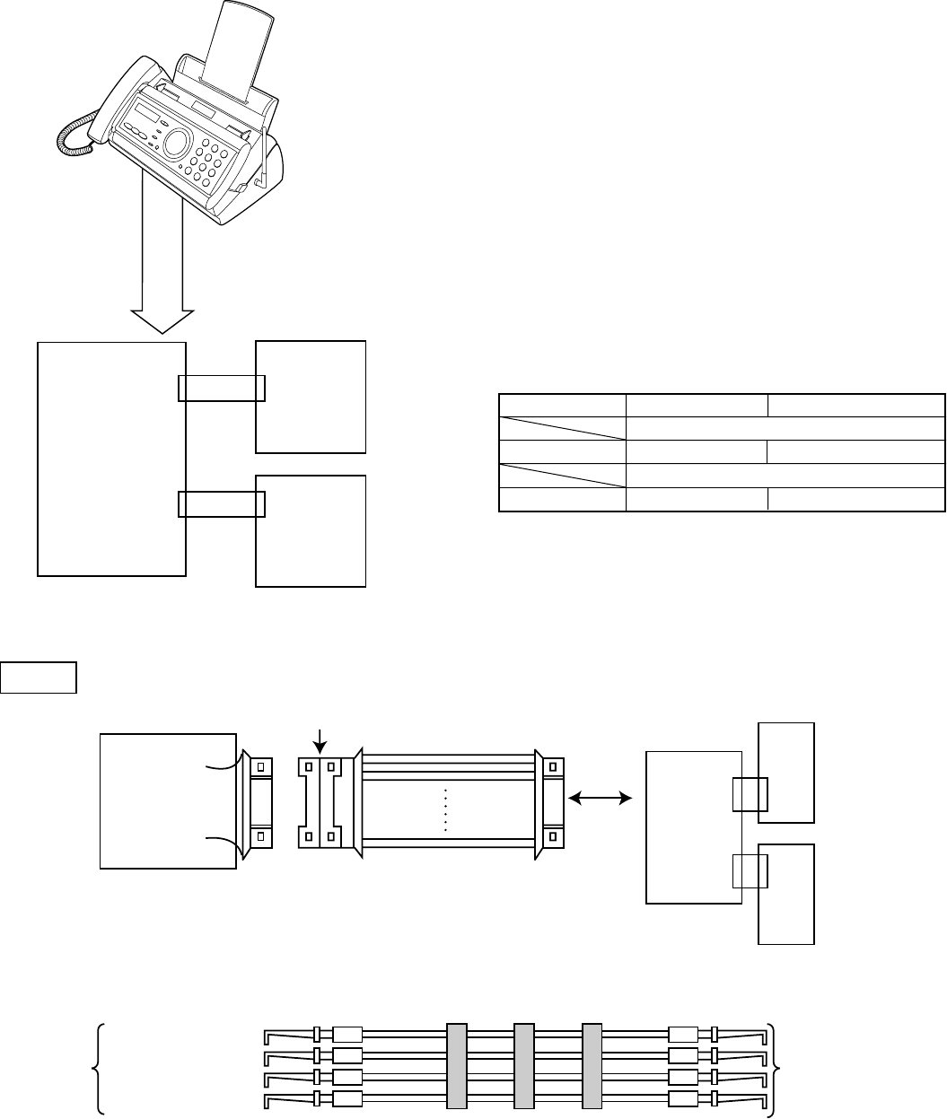
FO-CC500A
FO-K01A
8 – 2
2. Description
2-1. Relay board unit
1. Remove the LIU PWB, control PWB and Power Supply PWB from
this unit, and mount the relay board unit instead.
•Before connecting the wiring to the relay board unit, set the test
PWB switches to the fixed position.
2. The setting is as follows.
The hook switch is operated by the mechanical unit switch and the test
PWB switch. When performing installation in the machine unit, set the
test PWB switches to the fixed position.
Mechanical unit PWB to be tested
Actual operation with mechanical unit
PWB sensor check
POWER
SUPPLY
PWB
CHECK
LIU PWB
CHECK
CONTROL
PWB
RELAY CABLE
DON'T SEPARATE
UNIT
NOTE
PAPER SENSOR RELAY CABLE (QCNWG201BSCZZ)
TO
CHECK
PWB
TO
EXTENSION
PWB
PIN(TP1)
FILM(TP2)
DG(TP3)
+24VL(TP4)
(LIU)
(LIU)
(LIU)
(LIU)
BROWN
RED
ORANGE
YELLOW
ON/OFF operation ON-HOOK
ON/OFF operationHook SW ON-HOOK
Hook SW
Relay
cable
CNLIUA
CHECK
CONTROL
PWB
CHECK
LIU PWB
1
14
CNPW
CNLIUA
POWER
SUPPLY
PWB
• The relay cables are used as one pair.
• The hook switch is manually operated.
CNPW

FO-CC500A
FO-K01A
8 – 3
3. Shading paper
The white and black basis is applied to remember the shading wave-
form. Be sure to perform this operation when replacing the battery or
replacing the control PWB. Execute in the shading mode of DIAG mode.
SHADING WAVE MEMORY STANDARD PAPER (PSHEZ3579SCZZ)

FO-CC500A
FO-K01A
8 – 4
[2] IC signal name
CONTROL PWB UNIT
IC3: VHiSCE214V/-1 (SCE214V)
11
2
3
4
5
6
7
8
9
10
11
12
13
14
15
16
17
18
19
20
21
22
23
24
25
26
27
28
29
30
31
32
33
34
35
36
37
38
39
40
41
42
43
44
45
46
47
48
49
50
51
52
53
54
55
56
57
58
59
60
61
62
63
64
65
66
67
68
69
70
71
72
73
74
75
76
77
78
79
80
81
82
83
84
85
86
87
88 133
134
135
136
137
138
139
140
141
142
143
144
145
146
147
148
149
150
151
152
153
154
155
156
157
158
159
160
161
162
163
164
165
166
167
168
169
170
171
172
173
174
175
176
89
90
91
92
93
94
95
96
97
98
99
100
101
102
103
104
105
106
107
108
109
110
111
112
113
114
115
116
117
118
119
120
121
122
123
124
125
126
127
128
129
130
131
132
VDDPLL
VSSPLL
ROMCSn
SYNC/GPO[20]
WRn
RDn
DEBUGn
TSTCLK
VSS
SXIN
SXOUT
OPO[0]/GPO[8]/SMPWRCTRL
OPO[1]/GPO[9]/PMPWRCTRL
OPO[2]/GPO[10]/RINGER
OPO[3]/GPO[11]
OPO[4]/GPO[12]/SSTXD1
OPO[5]/GPO[13]
OPO[6]/GPO[14]
OPI[0]/GPIO[21]/SSRXD1
OPI[1]/GPIO[22]/SSSTAT1
OPI[2]/GPIO[23]/SSCLK1
OPI[3]/GPIO[24]
LCDCS/GPO[17]
VDD
RASn
CAS[0]n
DWRn
VBAT
XIN
XOUT
WRPROTn
TEST[1]
TEST[0]
BATRSTn
INTPWRDWNEn
PWRDWNn
RESERVED
ADGA
VREFn/CLREF
VIN
ADGA
ADXG
VREFp
ADVA
VSS
IVREFn
IVREFp
VDD
THADI
VSS
GPIO[17]/DSPIRQn
GPIO[16]/IRQ[8]
GPIO[15]/CS[5]n
GPIO[13]/CS[3]n
GPIO[37]/IRQ15n/DSPCSn
GPIO[4]/CPCIN/TPHPWRCTRL/DMAREQ
STRB[0]
STRB[1]
STRB[2]
STRB[3]
PLAT
PDAT
PCLK/DMAACK
VDD
GPIO[11]/BE/SERINP/SR4IN
GPIO[19]/RDY/SEROUT
START
CLK1n/GPO[25]
CLK2/GPO[24]
GND
MCLK
CTRLI
TESTC
SOUT
SIN
FSYNC
POR
GND
LINE_INP
MIC_INP
MIC_INM
MIC_BIAS
BG
VC
AVDD
GND
LINE_OUTP
SPKR_OUTP
SPKR_OUTM
DVDD
MODE0
ICLK
VSS
FCSn[1]/VIDCTL[0]/GPO[23]
IARESET
IACLK
VDD
IA1CLK
SR3IN
SR4OUT
SR1IO
SA1CLK
GPIO[7]/SSRXD2/SASRXD2
GPIO[6]/SSTXD2/SASTXD2
GPIO[5]/SSCLK2/SASCLK2
GPIO[10]/SSSTAT2/DSS_AVAIL
VSS
RESETn
GPIO[3]/SASCLK
GPIO[2]/SASRXD
GPIO[1]/SASTXD
GPIO[9]/FRDn
GPIO[8]/FWRn
A[0]
A[1]
A[2]
A[3]
A[4]
A[5]
VDD
A[6]
A[7]
A[8]
A[9]
A[10]
A[11]
A[12]
A[13]
A[14]
A[15]
A[16]
VDD
VSS
A[17]
A[18]
A[19]
A[20]
A[21]/EYECLK
A[22]/EYESYNC
A[23]/EYEXY
D[0]
D[1]
D[2]
D[3]
D[4]
D[5]
D[6]
D[7]
GPIO[20]/ALTTONE
GPIO[26]
GPIO[27]
GPIO[28]
GPO[26]
GPO[27]
GPO[28]
GPO[29]
GPO[30]/SR3OUT
GPIO[31]
GPIO[29]
GPIO[32]
VDD
GPIO[34]
GPIO[35]
GPIO[36]
VSS
VDD
PM[0]/GPO[0]
PM[1]/GPO[1]
PM[2]/GPO[2]
PM[3]/GPO[3]
SM[0]/GPO[4]
SM[1]/GPO[5]
SM[2]/GPO[6]
SM[3]/GPO[7]
REGDMA/GPO[18]/CLKDIV[0]
WAITn/GPO[19]/CLKDIV[1]
SCE214V
1 CHIP FAX ENGINE
176 Pin LQFP

FO-CC500A
FO-K01A
8 – 5
[3] Rewriting version up to the FLASH ROM
Step 1 File setting
Execute “DSS_LOADER.EXE” and extract the compressed file.
File contents:
¥DSS_LOADER¥----+----¥CMD¥-----+---- Atd.cmd
| +---- Atl0.cmd
| +---- FF.cmd
| +---- FF_6000.cmd
| +---- flash144.ver
| +---- RECOVERY.VER
|
----+----¥
CONFIG
¥--+---- DSS144_DOWNLOAD.txt
| +---- DSS144_RECOVERY.txt
| +---- FAX_DOWNLOAD.txt
|
----+----¥
DATA
¥----+---- ¥FAX¥
+---- ¥koki¥
+---- ¥oyaki¥
Step 2 File setting
Copy the downloaded file ( .ver) to the designated directory shown below (the target directory may be optional).
¥DSS_LOADER¥DATA¥FAX¥
¥DSS_LOADER¥DATA¥koki¥
¥DSS_LOADER¥DATA¥oyaki¥
Step 3 Flash ROM rewriting
Description for application is detailed in the attached document below.
· Rewriting the Flash ROM for the FAX engine (with software (TeraTerm) for the PC)
· Rewriting the Flash ROM for the DSS PWB (with software (TeraTerm) for the PC)
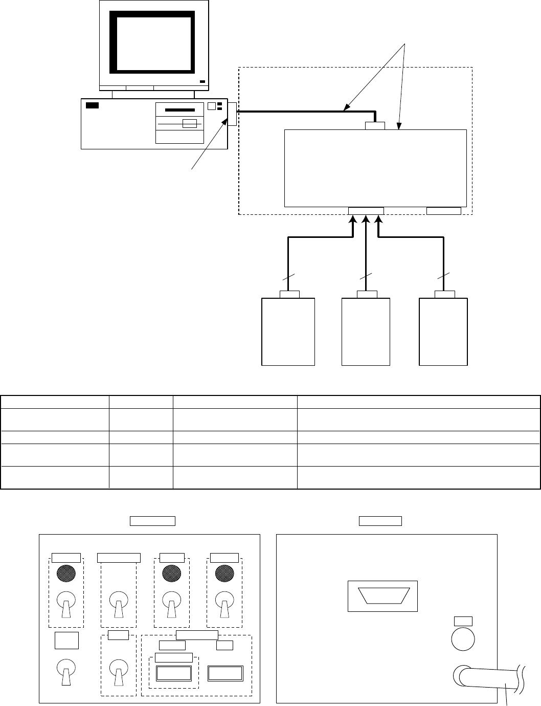
FO-CC500A
FO-K01A
8 – 6
Fig. 1. Connected chart
CN2
FAX
Machine
Cordless
PWB
5PIN HOLES
Handset
Cordless
PWB
CN2CN1
5PIN 4PIN 3PIN
RS-232C DSUB 9PIN
RS-232C
Cable
DUNTK404CSCZZ
Com
Port
CNPRG
PC
FO-CC500
Program Loader BOX
FAX
Machine
Control
PWB
Main Cable
QCNW-306BSCZZ
RM Cable
QCNW-308BSCZZ
RF Cable
QCNW-307BSCZZ
Table 1. FO-CC500 Program loader and Calibration unit
PART CORD PRICE RANK NAME REMARKS
DUNTK404CSCZZ DG FO-CC500 Program loader BOX Includes RS-232C cable
and Calibration UNIT
QCNW-306BSCZZ BF FO-CC500 Main cable Connects FO-CC500 Program loader BOX and FAX machine.
QCNW-307BSCZZ BF FO-CC500 RF cable Connects FO-CC500 Program loader BOX and the DSS PWB
(Cordless Handset PWB) of the Cordless Handset.
QCNW-308BSCZZ BF FO-CC500 RM cable Connects FO-CC500 Program loader BOX and the DSS PWB
(Cordless PWB) of the FAX machine.
FRONT PANEL BACK PANEL
AC
CORD
FUSE
MAIN SW
IC
Voltage
ON
OFF
5V
3.3V
PARK SW
ON
OFF
RS-232C
DSUB 9PN
BAT SW
ON
OFF
CALIBRATION
ON
OFF
MODE CALIBRATION
Cordless
DOWNLOAD
CN1 CN2
MAIN
CALIBRATION
DOWNLOAD
Fig. 2. FO-CC500 Program loader BOX

FO-CC500A
FO-K01A
8 – 7
Table 2. FO-CC500 Program loader BOX connection procedures (FAX PWB Rewriting)
FAX PWB rewriting
Before connecting the PC
and Program loader BOX
with RS-232C cable.
Set the switches of Program
loader BOX as follows.
(a) MAIN SW OFF (down)
(b) CALIBRATION OFF (down)
(c) BAT SW OFF (down)
(d) PARK SW OFF (down)
(e) IC Voltage to 3.3V (down)
(f)
MODE to DOWNLOAD (down)
After connecting the PC
and Program loader BOX
with RS-232C cable. (1*)
Set the switch of Program
loader BOX as follows.
(g) MAIN SW ON (up)
Power supply to the FAX
machine.
Plug the AC power cord of the
FAX machine to the outlet.
(2*)
Connect Program loader
BOX and the Control
PWB of the FAX machine
(CNPRG) with FO-CC500
Main cable. (3*)
---
1*: Connect one end of RS-232C cable to the COM port of the PC and the other end to RS-232C DSUB 9PIN of
FO-CC500 Program loader BOX.
2*: Press and hold down the keys 1 and 3 simultaneously while turning on the FAX machine and until “DOWNLOAD
MODE” appears.
3*: Perform the procedure before . (Turn on the Program loader BOX and the FAX machine before connecting
FO-CC500 Main cable and the FAX machine.)
Connect one end of FO-CC500 Main cable to the connector of the control PWB connector for the FAX machine
(CNPRG) (refer to Fig. 3), and the other end to CN1 of FO-CC500 Program loader BOX.
Set the switches of Program
loader BOX as follows.
(a) MAIN SW OFF (down)
(b) CALIBRATION OFF (down)
(c) BAT SW OFF (down)
(d) PARK SW OFF (down)
(e) IC Voltage to 3.3V (down)
(f)
MODE to DOWNLOAD (down)
Cordless Handset
DSS PWB (Cordless
Handset PWB)
Before connecting the PC
and Program loader BOX
with RS-232C cable.
After connecting the PC
and Program loader BOX
with RS-232C cable. (1*)
Set the switch of Program
loader BOX as follows.
(g) MAIN SW ON (up)
Connecting Program
loader BOX and DSS PWB
with FO-CC500 RF cable
or FO-CC500 RM cable.
(2*)
---
When supplying power to
DSS PWB.
Set the switch of Program
loader BOX as follows.
(h) BAT SW to ON (up)
Table 3. FO-CC500 Program loader BOX connection procedures (DSS PWB Rewriting)
Set the switches of Program
loader BOX as follows.
(a) MAIN SW OFF (down)
(b) CALIBRATION OFF (down)
(c) BAT SW OFF (down)
(d) PARK SW OFF (down)
(e) IC Voltage to 3.3V (down)
(f)
MODE to DOWNLOAD (down)
Set the switch of Program
loader BOX as follows.
(g) MAIN SW ON (up)
--- Connect the AC power cord
cable of the FAX machine to
the socket. (3*)
FAX machine DSS
PWB (built into FAX
machine) (Cordless
PWB)
Set the switches of Program
loader BOX as follows.
(a) MAIN SW OFF (down)
(b) CALIBRATION OFF (down)
(c) BAT SW OFF (down)
(d) PARK SW OFF (down)
(e) IC Voltage to 3.3V (down)
(f)
MODE to DOWNLOAD (down)
Set the switch of Program
loader BOX as follows.
(g) MAIN SW ON (up)
--- Set the switch of Program
loader BOX as follows.
(h) PARK SW to ON (up)
FAX machine DSS
PWB (Unit)
(Cordless PWB)
1*: Connect one end of RS-232C cable to the COM port of the PC and the other end to RS-232C DSUB 9PIN of
FO-CC500 Program loader BOX.
2*: Each one end of FO-CC500 RF cable and FO-CC500 RM cable is connected to the connector of the DSS PWB (refer
to Figs. 4, 5 and 6) and the other end to the CN1 of the Program loader BOX.
3*: Press and hold down the keys 1 and 3 simultaneously while turning on the FAX machine and until “DOWNLOAD
MODE” appears.
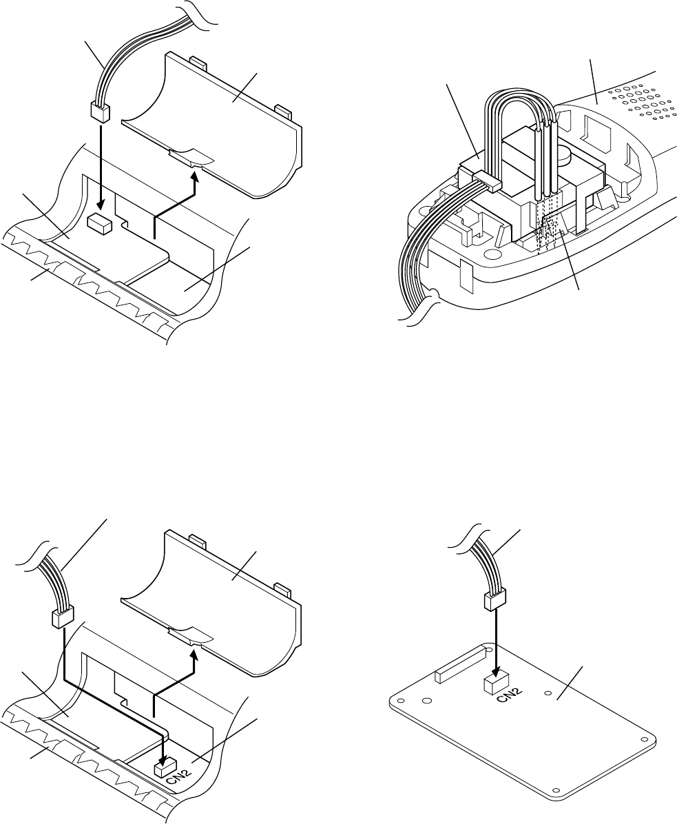
FO-CC500A
FO-K01A
8 – 8
Control
PWB unit
FAX machine
ROM Cover
CNPRG
Cordless Handset
RF Cable
QCNW-307BSCZZ
Main Cable
QCNW-306BSCZZ
5 Pin Holes
Cordless
PWB unit
Control
PWB unit
FAX machine
ROM Cover
Cordless
PWB unit
RM Cable
QCNW-308BSCZZ RM Cable
QCNW-308BSCZZ
Cordless
PWB unit
From FO-CC500
Program Loader BOX
(CN1)
From FO-CC500
Program Loader BOX
(CN1)
From FO-CC500
Program Loader BOX
(CN1)
From FO-CC500
Program Loader BOX
(CN1)
Fig. 3. FAX machine
(FO-CC500 Main cable connection) Fig. 4. Cordless Handset (5 pin holes)
(FO-CC500 RF cable connection)
Fig. 5. FAX machine DSS PWB (Cordless PWB)
built into the FAX machine
(FO-CC500 RM cable connection)
Fig. 6. FAX machine DSS PWB (Cordless PWB)(Unit)
(FO-CC500 RM cable connection)
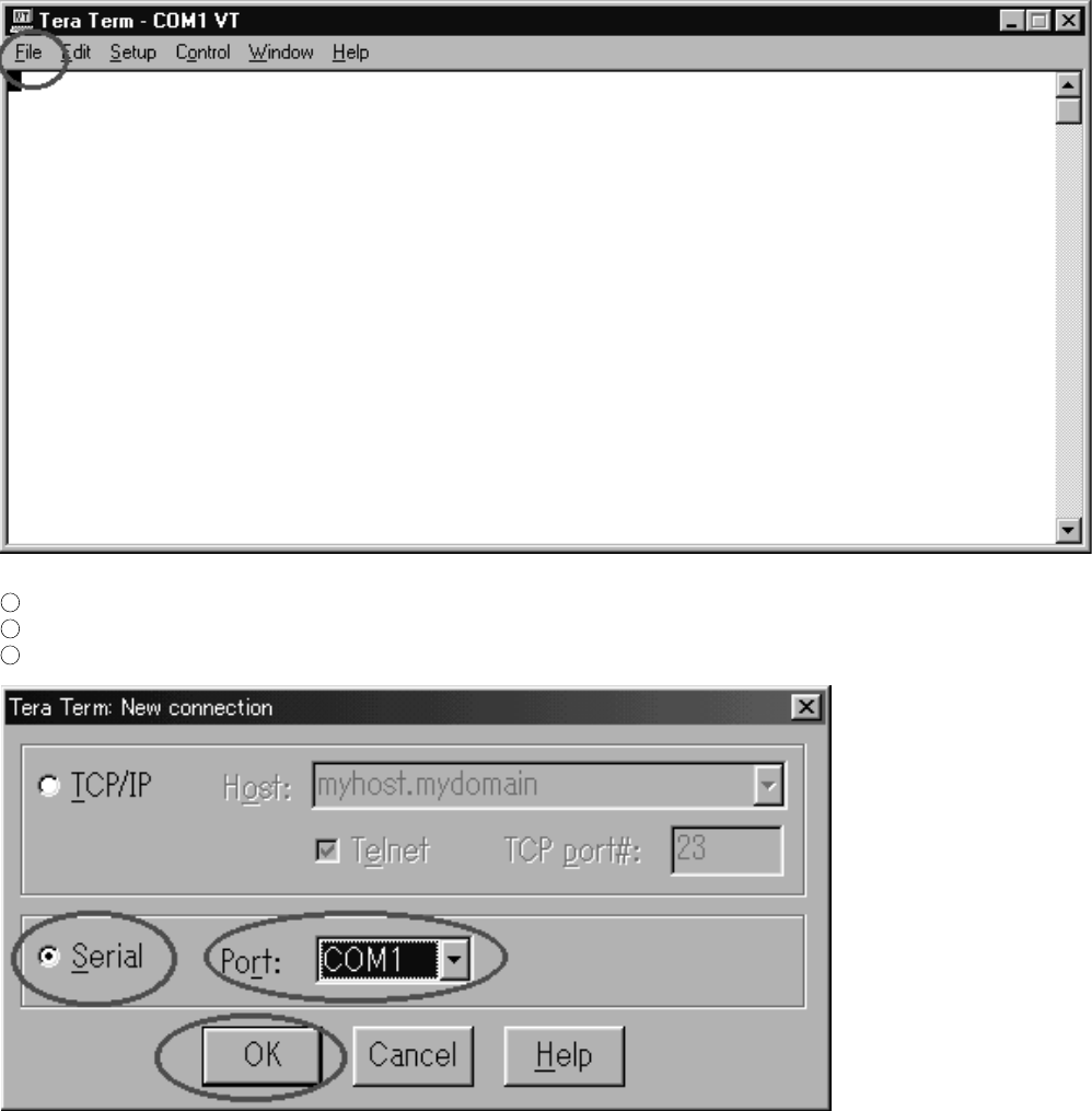
FO-CC500A
FO-K01A
8 – 9
1) Rewriting the flash ROM for the FAX engine
Using software for the PC (TeraTerm)
Uncompress the compressed file of TeraTerm.
Execute the “SETUP.EXE” from compressed files to install TeraTerm.
Execute the “ttermpro.exe” to start TeraTerm.
1-1. Select “New connection” from the pull-down menu of “File”.
Check “Serial”.
Select the port number in which the RS-232C cable is connected to.
Click “OK” for confirmation.
↓
Proceed to 1-2.
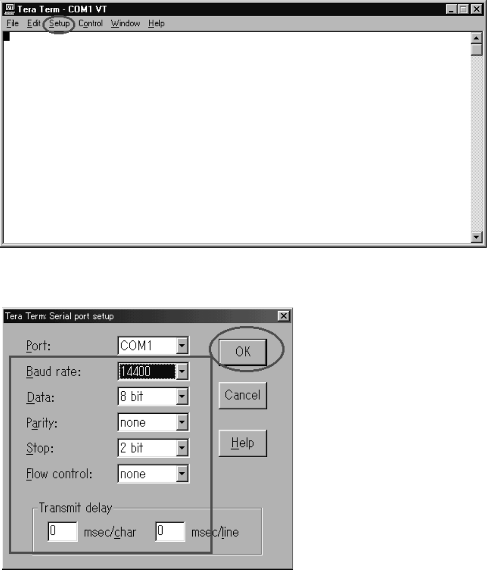
FO-CC500A
FO-K01A
8 – 10
1-2. Select “Serial port” from the pull-down menu of “Setup”.
Select the port number which the RS-232C cable is connected to.
Set the other parameters as follows and click “OK” for confirmation.
↓
Proceed to 1-3.

FO-CC500A
FO-K01A
8 – 11
1-3. Perform procedures described in Table 4.
Table 4. FO-CC500 Program loader BOX connection procedures
After performing procedures described in Table 4, press down the START key on the FAX machine.
“DOWNLOAD MODE WT” appears on the LCD.
↓
Proceed to 1-4.
FAX PWB rewriting
Before connecting the PC
and Program loader BOX
with RS-232C cable.
Set the switches of Program
loader BOX as follows.
(a) MAIN SW OFF (down)
(b) CALIBRATION OFF
(down)
(c) BATSW OFF (down)
(d) PARK SW OFF (down)
(e) IC Voltage to 3.3V (down)
(f) MODE to DOWNLOAD
(down)
After connecting the PC
and Program loader BOX
with RS-232C cable. (1*)
Set the switch of Program
loader BOX as follows.
(g) MAIN SW ON (up)
Power supply to the FAX
machine.
Plug the AC power cord of the
FAX machine to the outlet.
(2*)
Connect Program loader
BOX and the Control PWB
of the FAX machine
(CNPRG) with FO-CC500
Main cable. (3*)
---
1*: Connect one end of RS-232C cable to the COM port of the PC and the other end to RS-232C DSUB 9PIN of
FO-CC500 Program loader BOX.
2*: Press and hold down the keys 1 and 3 simultaneously while turning on the FAX machine and until “DOWNLOAD
MODE” appears.
3*: Perform the procedure before . (Turn on the Program loader BOX and the FAX machine before connecting
FO-CC500 Main cable and the FAX machine.)
Connect one end of FO-CC500 Main cable to the connector of the Control PWB connector for the FAX machine
(CNPRG) (refer to Fig. 3), and the other end to CN1 of FO-CC500 Program loader BOX.

FO-CC500A
FO-K01A
8 – 12
1-4. Select “Send file” from the pull-down menu of “File”.
Enable the Binary in “Option” and open “Atl0. cmd”.
↓
Proceed to 1-5.
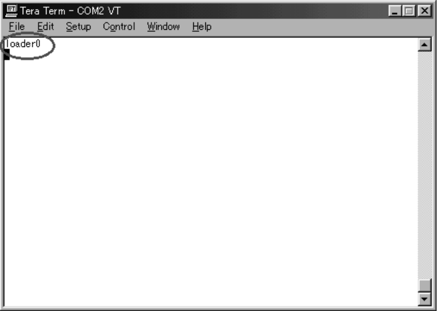
FO-CC500A
FO-K01A
8 – 13
1-5.
If the description above does not appear, return to 1-4.
If the description above appears, proceed to 1-6.
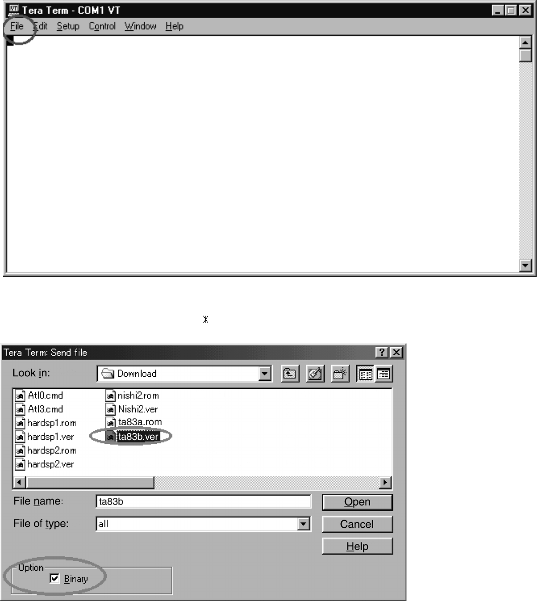
FO-CC500A
FO-K01A
8 – 14
1-6. Select “Send file” from the pull-down menu of “File”.
Enable the Binary in “Option” and open “ta .ver”.
(Select a file you want to download here.)
↓
Proceed to 1-7.
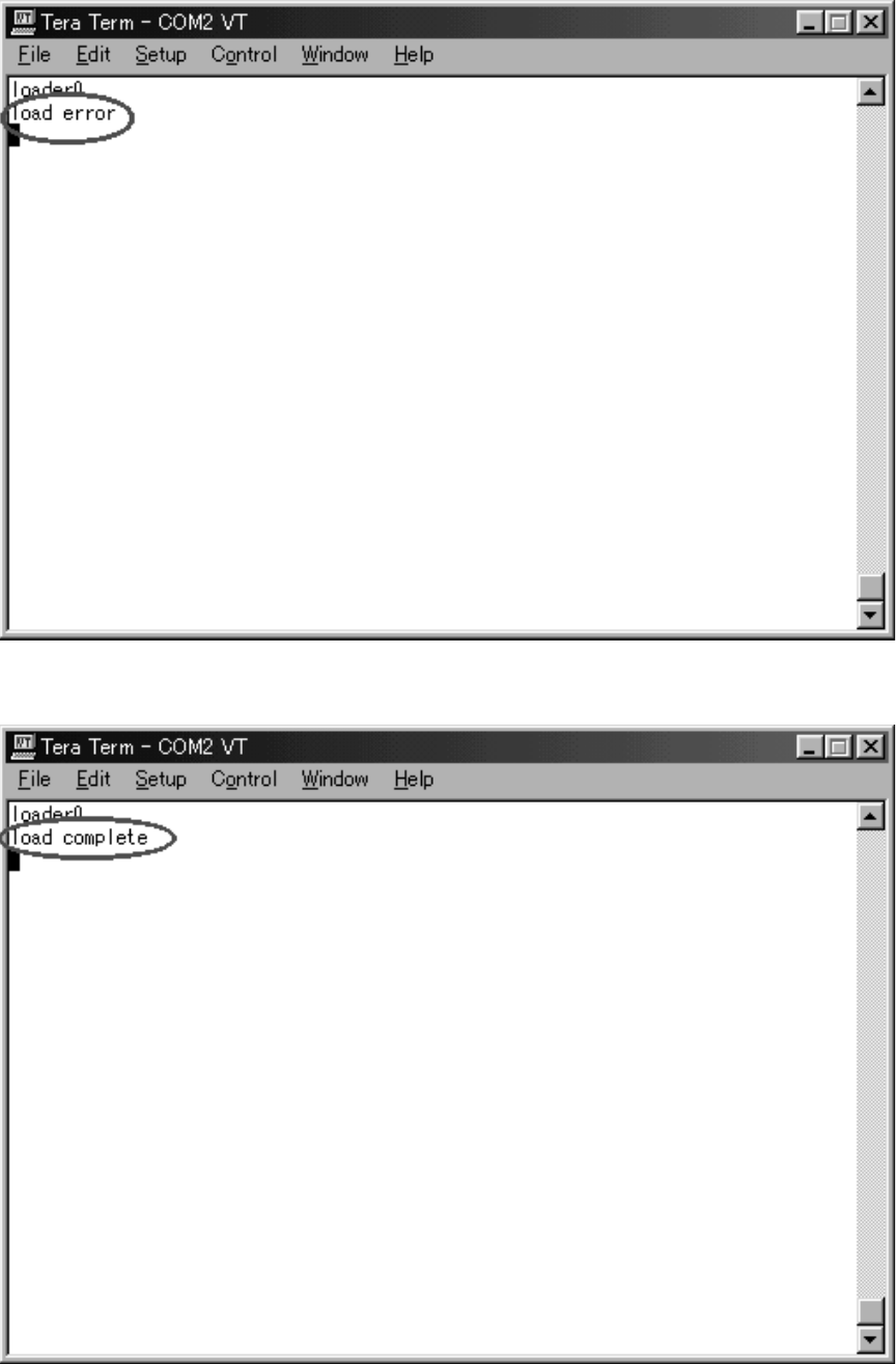
FO-CC500A
FO-K01A
8 – 15
1-7.
If the description above appears, return to 1-4.
If the description above appears, downloading was completed normally.
↓
Proceed to 1-8.
FO-CC500A
FO-K01A
8 – 16
1-8.
1. To go on to download FLASH ROM, perform the following procedures.
1-1. Only perform procedures and described in Table 5.
1-2. Return to 1-3.
2. To complete downloading FLASH ROM, perform the following procedures.
2-1. Perform procedures through described in Table 5.
2-2. Terminate “TeraTerm”.
Table 5. Termination procedures (1*)
1*. Perform procedures through in numerical order.
FAX PWB rewriting
Remove the connector from the
Control PWB (CNPRG) of the
FAX machine.
Turn off the FAX machine. Turn off the Program loader BOX.
--- Turn off the FAX machine. Set the switch of Program loader
BOX as follows.
(a) MAIN SW OFF (down)
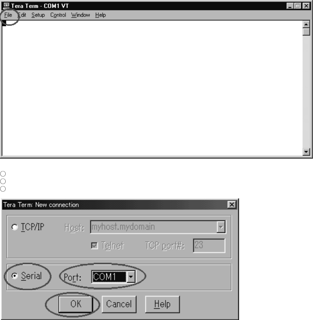
FO-CC500A
FO-K01A
8 – 17
2) Rewriting the flash ROM for the DSS PWB
Using software for the PC (TeraTerm)
Uncompress the compressed file of TeraTerm.
Execute the “SETUP.EXE” from compressed files to install TeraTerm.
Execute the “ttermpro.exe” to start TeraTerm.
2-1. Select “New connection” from the pull-down menu of “File”.
Check “Serial”.
Select the port number in which the RS-232C cable is connected to.
Click “OK” for confirmation.
↓
Proceed to 2-2.
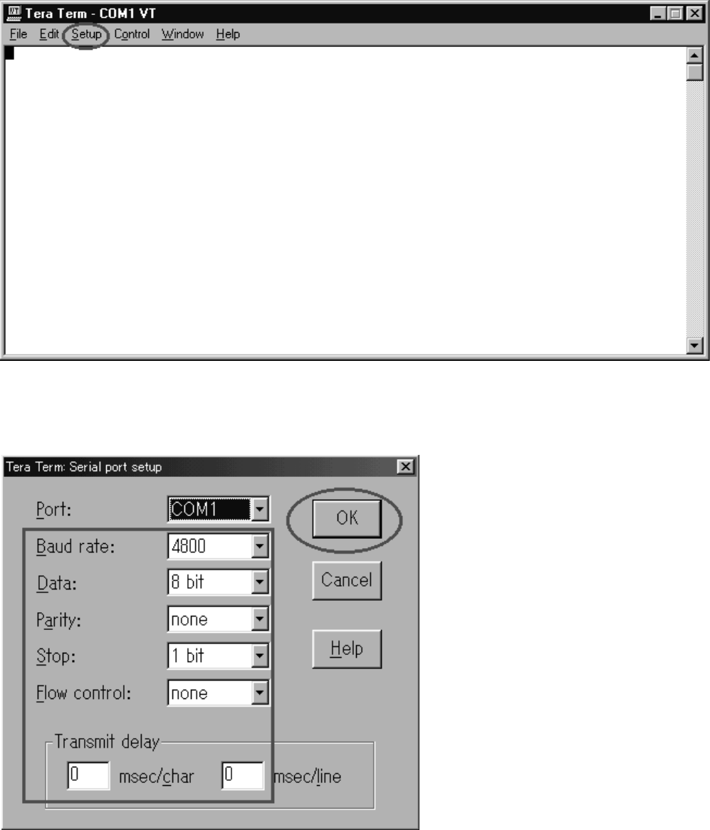
FO-CC500A
FO-K01A
8 – 18
2-2. Select “Serial port” from the pull-down menu of “Setup”.
Select the port number which the RS-232C cable is connected to.
Set the other parameters as follows and click “OK” for confirmation.
↓
Proceed to 2-3.

FO-CC500A
FO-K01A
8 – 19
2-3. Select “Send file” from the pull-down menu of “File”.
Enable the Binary in “Option” and open “¥DSS_LOADER¥CMD¥FF_6000.cmd”.
Before starting the work above, perform 2-4 and Table 6.
↓
Proceed to 2-4.
FO-CC500A
FO-K01A
8 – 20
2-4. Supply the power to the DSS PWB while the following is displayed (approx. 10 seconds) (refer to Table 6).
(If the power cannot be supplied, return to step 2-3.)
↓
Proceed to 2-5.
Set the switches of Program
loader BOX as follows.
(a) MAIN SW OFF (down)
(b) CALIBRATION OFF (down)
(c) BAT SW OFF (down)
(d) PARK SW OFF (down)
(e) IC Voltage to 3.3V (down)
(f)
MODE to DOWNLOAD (down)
Cordless Handset
DSS PWB (Cordless
Handset PWB)
Before connecting the PC
and Program loader BOX
with RS-232C cable.
After connecting the PC
and Program loader BOX
with RS-232C cable. (2*)
Set the switch of Program
loader BOX as follows.
(g) MAIN SW ON (up)
Connecting Program
loader BOX and DSS PWB
with FO-CC500 RF cable
or FO-CC500 RM cable.
(3*)
---
When supplying power to
DSS PWB.
Set the switch of Program
loader BOX as follows.
(h) BAT SW to ON (up)
Table 6. Power supply to the DSS PWB (1*)
Set the switches of Program
loader BOX as follows.
(a) MAIN SW OFF (down)
(b) CALIBRATION OFF (down)
(c) BAT SW OFF (down)
(d) PARK SW OFF (down)
(e) IC Voltage to 3.3V (down)
(f)
MODE to DOWNLOAD (down)
Set the switch of Program
loader BOX as follows.
(g) MAIN SW ON (up)
--- Connect the AC power cord
cable of the FAX machine to
the socket. (4*)
FAX machine DSS
PWB (built into FAX
machine) (Cordless
PWB)
Set the switches of Program
loader BOX as follows.
(a) MAIN SW OFF (down)
(b) CALIBRATION OFF (down)
(c) BAT SW OFF (down)
(d) PARK SW OFF (down)
(e) IC Voltage to 3.3V (down)
(f)
MODE to DOWNLOAD (down)
Set the switch of Program
loader BOX as follows.
(g) MAIN SW ON (up)
--- Set the switch of Program
loader BOX as follows.
(h) PARK SW to ON (up)
FAX machine DSS
PWB (Unit)
(Cordless PWB)
1*: Complete , and before performing items of 2-3.
2*: Connect one end of RS-232C cable to the COM port of the PC and the other end to RS-232C DSUB 9PIN of
FO-CC500 Program loader BOX.
3*: Each one end of FO-CC500 RF cable and FO-CC500 RM cable is connected to the connector of the DSS PWB (refer
to Figs. 4, 5 and 6) and the other end to the CN1 of the Program loader BOX.
4*: Press and hold down the keys 1 and 3 simultaneously while turning on the FAX machine and until “DOWNLOAD
MODE” appears.
FO-CC500A
FO-K01A
8 – 21
2-5. Select “Serial port” from the pull-down menu of “Setup”.
↓
Proceed to 2-6.
Set the “Baud rate” to 14400 and click “OK”.
FO-CC500A
FO-K01A
8 – 22
2-6. Select “Send file” from the pull-down menu of “File”.
Enable the Binary in “Option” and open “¥DSS_LOADER¥CMD¥Atd.cmd”.
↓
Proceed to 2-7.

FO-CC500A
FO-K01A
8 – 23
2-7.
If the following message appears, proceed to 2-8.
If not the following message appears, return to 2-2.
FO-CC500A
FO-K01A
8 – 24
2-8. Select “Send file” from the pull-down menu of “File”.
Enable the Binary in “Option” and open “¥DSS_LOADER¥CMD¥flash144.ver”.
↓
Proceed to 2-9.
FO-CC500A
FO-K01A
8 – 25
2-9.
If the following message appears, proceed to 2-10.
If not the following message appears, return to 2-2.

FO-CC500A
FO-K01A
8 – 26
2-10. Select “Send file” from the pull-down menu of “File”.
Enable the Binary in “Option” and open “¥DSS_LOADER¥CMD¥Atl0.cmd”.
↓
Proceed to 2-11.
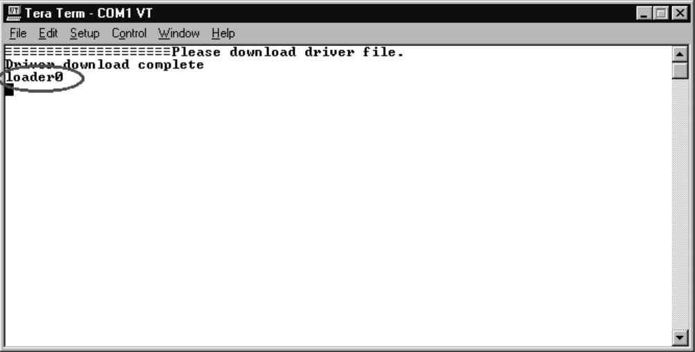
FO-CC500A
FO-K01A
8 – 27
2-11.
If the following message appears, proceed to 2-12.
If not the following message appears, return to 2-10.
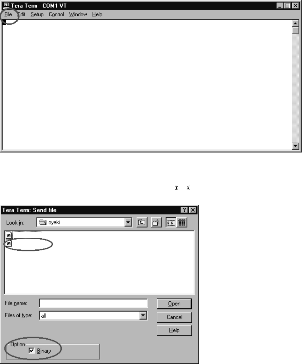
FO-CC500A
FO-K01A
8 – 28
TA85ot.VER
ta85c.ver
2-12. Select “Send file” from the pull-down menu of “File”.
Enable the Binary in “Option” and open “¥DSS_LOADER¥DATA¥ ¥ta .ver”.
(Select a file you want to download here.)
↓
Proceed to 2-13.
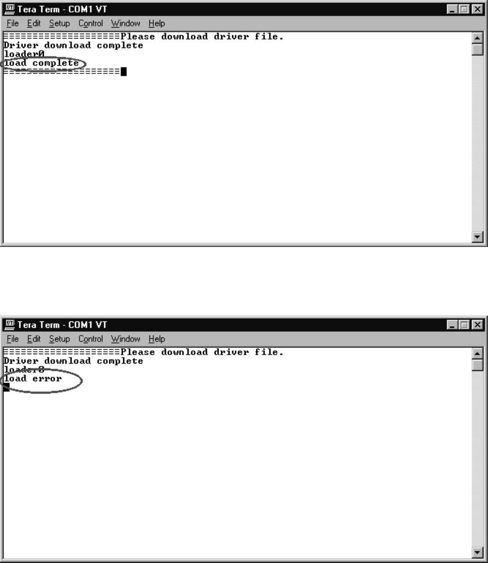
FO-CC500A
FO-K01A
8 – 29
2-13.
If “load complete” appears, rewriting is completed properly. Although other messages may be indicated after “load
complete” appears, proceed to the step 2-16.
If not, return to 2-14.
2-14.
If the following message appears, proceed to 2-10.
If not the following message appears, return to 2-15.
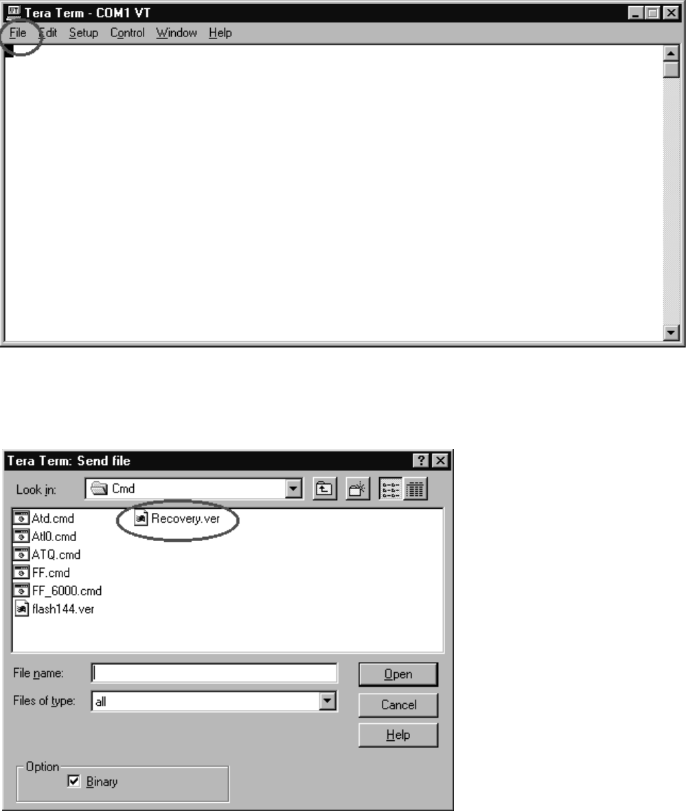
FO-CC500A
FO-K01A
8 – 30
2-15. Select “Send file” from the pull-down menu of “File”.
Enable the Binary in “Option” and open “¥DSS_LOADER¥CMD¥Recovery.ver”.
↓
Return to 2-14.

FO-CC500A
FO-K01A
8 – 31
2-16.
1. To go on to download FLASH ROM, perform the following procedures.
1-1. Only perform procedures and described in Table 7.
1-2. Return to 2-1.
2. To complete downloading FLASH ROM, perform the following procedures.
2-1. Perform procedures described in Table 7.
2-2. Terminate “TeraTerm”.
Table 7. Termination procedures
Cordless Handset DSS PWB (Cordless Handset PWB) Set the BAT SW of the Program loader BOX to OFF (down).
Remove the connector jointed to the Cordless Handset DSS PWB
(Cordless Handset PWB).
FAX machine DSS PWB (built into FAX machine) Turn off the FAX machine.
(Cordless PWB) Remove the connector jointed to the FAX machine DSS PWB
(Cordless PWB).
FAX machine DSS PWB (Unit) (Cordless PWB) Set the (h) PARK SW of the Program loader BOX to OFF (down).
Remove the connector jointed to the FAX machine DSS PWB
(Cordless PWB).
3) System ID
Refer to the Operation Manual of FO-K01 as for writing the system ID on the Cordless Handset. (When you add a
Cordless Handset, the system ID is automatically written.)
FO-CC500A
FO-K01A
CONTENTS
PARTS GUIDE
Because parts marked with " " are indispensable for the machine safety maintenance and operation, it must be
replaced with the parts specific to the product specification.
1 Cabinet, etc.
2 Top cover/Sub frame
3 Upper cabinet/Document guide upper
4Drive unit
5 Cordless handset
(FO-CC500K/FO-K01)
6 Packing material & Accessories
(FO-CC500)
7 Packing material & Accessories,
Accessory Cordless handset
(FO-K01)
8 Control PWB unit
9 LIU PWB unit
10 Cordless PWB unit
11 Power supply PWB unit
12 Operation panel PWB unit
13 Cordless handset PWB unit
(FO-CC500K/FO-K01)
Index
FACSIMILE
FO-CC500
ACCESSORY CORDLESS HANDSET
FO-K01
MODEL
MODEL
FO-CC500 Facsimile System cosisting of FO-CC500 (Facsimile Unit)
and FO-CC500K (Cordless Handset).
MODEL SELECTION CODE DESTINATION
FO-CC500 A Australia/
New Zealand
FO-K01 A Australia/
New Zealand
FO-CC500A
FO-K01A
[1] Cabinet,etc.
– 1 –
55 39 38 39 40
75
75
OPERATION
PANEL UNIT
DOCUMENT
GUIDE UPPER
TOP COVER/
SUB FRAME
DRIVE
UNIT
62
27 22
30
31
28
25
26
26
29
457
35
54
46 50
52
51 53
3
5
36
37
67
58
48
47
8
6
16
66
17
49 41
42
45
7
61
44
43 59
29
25
24
33
34
32
63
23
16
64
65
70
74
B1
B2
B1
B1
B1
B1
B1
B6
B1
B2
B3
B2
W1
B4
B5
B1
W2

NO. PARTS CODE PRICE
RANK NEW
MARK PART
RANK DESCRIPTION
FO-CC500A
FO-K01A
– 2 –
[1] Cabinet,etc.
3 CCNWN484AXH01 AL C Speaker ass’y
4 CLEVP2358XH01 AD C Hook switch lever ass’y
5 CROLR2481XH01 AQ C PO roller ass’y
6 DCEKC087SXHZZ CA N E Control PWB unit(Within ROM)
7 DCEKL460CXH01 BH N E LIU PWB unit
8 QPWBF3206XHZ2 AH N E Wire hold PWB(PWB only)
16 QCNWN332BXHZZ AK N C Panel cable
17 LBNDJ2006XHZZ AA C Band(100mm)
22 LBSHP2140XHZA AC N C Back bearing,left
23 LBSHP2143XHZZ AC C Back bearing,right
24 LFRM-2225XHSE AN N C Scanner frame
25 MSPRC3295XHZZ AB C CIS spring
26 MSPRD3379XHZZ AD N C PO pinch roller spring
27 NGERH2569XHZZ AC C Back gear
28 NGERH2570XHZZ AD C Reduction gear,21/37Z
29 NROLP2332XHZZ AD C PO pinch roller
30 NROLR2482XHZZ AR C Back roller
31 PGIDM2617XHZZ AD C CIS guide,left
32 PGIDM2618XHZZ AD C CIS guide,right
33 QCNWN485AXHZZ AG C CIS cable
34 RUNTZ2124XHZZ BP N B CIS unit
35 GCABB2393XHSW BA N D Lower cabinet
36 LHLDZ2227XHZZ AD C Ink ribbon spool 1
37 LHLDZ2228XHZZ AD C Ink ribbon spool 2
38 MSPRC3287XHZZ AB C Head spring A
39 MSPRC3288XHZZ AB C Head spring B
40 MSPRC3340XHZA AD C Head spring C
41 PCOVP2130XHZZ AE C Head cover
42 PGIDM2615XHZZ AD C Head guide,left
43 PGIDM2616XHZZ AD C Head guide,right
44 QCNWN486AXHZZ AM C Head cable
45 RHEDZ2065XHZZ BP B Thermal head
46 GCOVA2447XHSE AH N D Front cover
47 GLEGG2078XHZZ AD C Rubber leg
48 LPLTM3178XHZZ AF C Bottom plate
49 LPLTP3177XHZZ AD C Stopper plate
50 MLEVP2357XHZZ AD C Film sensor lever
51 MLEVP2356XHZZ AD C P-IN sensor lever,lower
52 MSPRD3286XHZA AB C Film sensor lever spring
53 MSPRD3285XHZZ AB C P-IN sensor lever spring,lower
54 MSPRD3291XHZZ AD C Speaker hold spring
55 MSPRD3292XHZA AB C Head earth spring
57 PCOVP2131XHSE AE N C Interface PWB cover
58 PCOVP2132XHZZ AD C ROM cover
159 QACCL2045XHZZ AR B AC cord ass’y
161 RDENT2194XHZZ BN N E Power supply PWB unit
62 HPNLH2418XHS2 AL N D Decoration panel
63 PBRS-2055XHZZ AN C Static brush
64 PSHEZ3687XHZZ AD C Earth sheet
65 MSPRD3341XHZZ AD C Up spring
66 DROMR375CXH03 N E Cordless PWB unit(Within ROM and ID label x 2pcs.)
67 QANTH2020SCZA AV N C Antenna with cable
170 RCORF2125XHZZ AE B Core
74 MSPRC3357XHZZ AD N C PO roller spring
75 MSPRC3346XHZZ AD N C Head spring D
B1 XEBSD30P10000 AA C Screw(3x10)
B2 XEBSD30P12000 AA C Screw(3x12)
B3 LX-BZ2282XHZZ AB C Screw
B4 XEPSD30P08000 AA C Screw(3x8)
B5 LX-BZ2205XHZZ AC C Screw
B6 LX-BZ2286XHZZ AE C Screw(3x14)
W1 XWHSN40-08100 AA C Washer
W2 LX-WZ2290XHZZ AE N C Washer
FO-CC500A
FO-K01A
[2] Top cover/Sub frame
1 GCOVA2448XHSE AS N C Top cover
2 MSPRC3301XHZZ AB C Hopper spring
3 NGERP2318XHZZ AD C Pinion gear
4 PGIDM2619XHSE AF N C Hopper guide,left
5 PGIDM2620XHSE AF N C Hopper guide,right
6 LFRM-2227XHZZ AQ C Sub frame
7 LFRM-2232XHZZ AT C Sub frame plate
8 MLEVP2363XHZZ AD C P-IN sensor lever,upper
9 MSPRC3305XHZZ AB C Release lever spring
10 MSPRD3302XHZZ AB C P-IN sensor lever spring,upper
11 NGERH2580XHZZ AC C Reduction gear,15/22Z
12 NGERH2581XHZZ AC C Idler gear,25Z
13 NROLR2483XHZZ AL C Paper feed roller
14 NROLR2484XHZZ AL C PU roller
15 NSFTP2357XHZZ AG C Paper feed roller shaft
16 NSFTP2358XHZZ AG C PU roller shaft
17 PGIDM2621XHSE AT N C Release lever
18 LHLDZ2224XHZZ AL C RP feed plate holder
19 LPLTG3181XHZZ AD C RP separate rubber
20 LPLTP3179XHZZ AD C RP separate base
21 LPLTP3180XHZZ AH C RP separate plate
22 LPLTP3182XHZZ AH C RP feed plate
23 MSPRC3299XHZZ AB C RP separate spring
24 MSPRC3300XHZZ AB C RP feed spring
25 LBSHP2148XHZZ AE N C Platen bearing,left
26 LBSHP2149XHZZ AE N C Platen bearing,right
27 NGERH2579XHZZ AD C Platen gear
28 NROLR2485XHZZ AQ C Platen roller
29 LBNDJ2006XHZZ AA C Band
30 MSPRC3335XHZZ AD C Paper feed roller spring
31 TLABH319DXHZZ AD D Imaging film set label
32 TLABH468DXHZA AE N D Maximum 10 label
B1 LX-BZ2234XHZZ AD C Screw
B2 XEBSD30P10000 AA C Screw(3x10)
B3 LX-BZ2222XHZZ AC C Screw
[2] Top cover/Sub frame
– 3 –
NO. PARTS CODE PRICE
RANK NEW
MARK PART
RANK DESCRIPTION
27 25
28
26
15
30
20 23 19
21
24
24
22
22
18
11
1
4
325
29
13
17
8
9
10
12
16
14
6
7
31
32 B2
B3
B2
B1
B1
B2
B2
B2
FO-CC500A
FO-K01A
NO. PARTS CODE PRICE
RANK NEW
MARK PART
RANK DESCRIPTION
[3] Upper cabinet/Document guide upper
– 4 –
[3] Upper cabinet/Document guide upper
1 GCASP2145XHST AV N D Panel case
2 JBTN-2339XHSA AF C 12 key
3 JBTN-2340XHSC AE C Start key
4 JBTN-2341XHSD AG C Function key
5 DCEKP336CXH08 BG N E Operation panel PWB unit
6 QSW-K0005AWZZ AC C Tact switch [SW]
7 QSW-M2246AXZZ AH C FRSNS sensor [SW1]
8 QSW-M2294XHZZ AE C ORGSNS sensor [SW2]
9 QCNWN332BXHZZ AK N C Panel cable
10 RUNTZ2080XH01 BA E LCD unit
11 LPLTG2911XHZZ AE C Separate rubber
12 LPLTP3175XHZZ AD C Separate plate
13 LPLTP3176XHZZ AD C Feed plate
14 MSPRD3293XHZZ AB C Separate spring
15 MSPRT3294XHZZ AB C Feed spring
16 PGIDM2614XHSE AQ N C Document guide upper
17 PSHEP3660XHZZ AE C Separate rubber sheet
18 JBTN-2342XHSA AE N C TAD key
B1 XEBSD20P06000 AA C Screw(2x6)
(Unit)
901 DCEKP334CXH26 BG N E Operation panel unit
901
1
6
10
9
34
2
5
7
8
13
12
15
17 11
14
16
18
B1
FO-CC500A
FO-K01A
– 5 –
[4] Drive unit
NO. PARTS CODE PRICE
RANK NEW
MARK PART
RANK DESCRIPTION
[4] Drive unit
1 CGERH2314XH05 AS N C Slip gear ass’y
2 CLEVP2359XH01 AD C Planet gear lever ass’y A
3 CLEVP2360XH01 AD C Planet gear lever ass’y B
4 CLEVP2361XH01 AD C Planet gear lever ass’y C
5 CLEVP2362XH01 AD C Planet gear lever ass’y D
6 LFRM-2226XHZZ AQ C Drive unit frame
7 LPLTM3190XHZZ AG C Motor plate
8 MCAMP2028XHZZ AE C Cam
9 MSPRD3298XHZZ AE C Cam hold spring
10 NGERH2380XHZZ AC C Reduction gear,17/36Z
11 NGERH2409XHZZ AB C Idler gear,23Z
12 NGERH2571XHZZ AD C Slip gear
13 NGERH2572XHZZ AD C Reduction gear,25/63Z
14 NGERH2573XHZZ AD C Reduction gear,20/40Z
15 NGERH2574XHZZ AD C Reduction gear,15/30Z
16 NGERH2575XHZZ AD C Idler gear,40Z
17 NGERH2576XHZZ AD C Idler gear,21Z
18 NGERH2577XHZZ AD C Idler gear,20Z
19 NGERH2582XHZZ AC C Idler gear,15Z
20 QCNWN483AXHZZ AD C Cam switch cable
21 QSW-F2224SCZZ AE C Cam switch
22 RMOTS2175XHZZ AX B Motor
23 MSPRP3297XHZZ AD C Earth spring
B1 XEBSD30P08000 AA C Screw(3x8)
22
21 20
7
14 3
10 2
13
5
11
8
9
4
16
10
17
19
12
6
15
18
15
1
23
B1
FO-CC500A
FO-K01A
– 6 –
[5] Cordless handset (FO-CC500K/FO-K01)
NO. PARTS CODE PRICE
RANK NEW
MARK PART
RANK DESCRIPTION
[5] Cordless handset (FO-CC500K/FO-K01)
1 DCYO-373CXH05 CA N E Cordless handset PWB unit(Within ROM)
2 GCABA2399XHVC AU N D Front cabinet
3 GCABB2400XHSC AL N D Back cabinet
4 GCOVA2457XHSC N C LCD panel
5 GCOVH2456XHZZ AG C Headset cover
6 JKNBZ0309XHSA AL N C Cursor key
7 JKNBZ0310XHSD AL C Start key
8 LHLDZ2234XHZA AK N C LCD holder
9 LHLDZ2235XHZZ AF C Speaker holder
10 PCAPH2092XHSB AE N C Antenna cap
11 PCUSS2172XHZZ AK C LCD cushion
12 PCUSS2173XHZZ AE C Speaker cushion
13 PSHEP3695XHZZ AE C LCD diffuse sheet
14 PSHEZ3696XHZZ AD C LCD reflect sheet
16 PTPEH0003XHZZ AC C Cursor key both tape
17 PTPEH2091XHZZ AD C LCD panel both tape
18 QANTH2022XHZZ AE N C Antenna
19 QCNTM0045XHSC BA C Rubber key
20 QTANB9013BXZZ AF C Charge terminal,left
21 QTANB9014BXZZ AF C Charge terminal,right
22 RMICC2012SCZZ AN B Mic
23 RPHOA2012XHZZ AR B Receiver
24 RUNTZ2099XHZZ BG B LCD
25 CCNW-255BXH01 AT C Speaker ass’y
27 TLABM407FXHTZ N D Model name label [FO-CC500K]
TLABM408FXHTZ N D Model name label [FO-K01]
31 RUNTZ2098XHZB BW N B RF unit
B1 XEBSD20P06000 AA C Screw(2x6)
B2 XEBSD20P08000 AA C Screw(2x8)
B3 XEBSF20P08000 AA C Screw(2x8)
(Unit)
901 DSOGO373CXHE5 CC N E Cordless handset unit
A
B
A
B
4
76
11
24
14
B2
B3
18
8
23
31
16
19
2
21
20
13
25
9
12
3
1
5
B1
10
17
B1
22
27
901
FO-CC500A
FO-K01A
– 7 –
[6] Packing material & Accessories, Facsimile (FO-CC500)
NO. PARTS CODE PRICE
RANK NEW
MARK PART
RANK DESCRIPTION
[6] Packing material & Accessories, Facsimile (FO-CC500)
1 DUNTK443CXHGY AY N E Handset
2 QCNWG209BXHGY AN N C Handset cord
3 LPLTP3184XHZZ AH C Paper tray extension
4 NGERH2568XHZZ AB C Imaging film gear
5 PRBNN2033SC10 AL S Imaging film(Initial starter roll 10m)
6 QCNWG0376AFZZ AM C Telephone line cord
7 SPAKA429EXHZZ N D Packing add.,A
8 SPAKA430EXHZZ N D Packing add.,B
9 QCNWG0381AFZZ AM C New Zealand cable
10 TLABZ446DXHZZ AC D Caution label
11 TINSE4319XHTZ AU N D Operation manual
12 TLABM234FXHZZ N D Pop card
13 UBATM2099XHZZ BG B Battery pack
14 SPAKA465CXHZZ AF D Packing add.,left
15 SPAKA301DXHZZ AK D Packing add.,right
16 QPLGZ9065AFZZ AP C Australia plug
17 CPAKC356EXH01 N D Packing case with label
18 SPAKP329DXHZZ AF D Vinyl cover
19 RUNTZ2100XHE3 AZ N E Cordless handset charger
20 CPLTP3183XHR2 AM C Paper tray ass’y
21 CGERH2566XH01 AG C Imaging film gear ass’y
22 RADPA2067XHZZ BB N B AC adaptor
23 SPAKA324DXHZZ AE D Antenna protector
24 GCOVH2455XHSB AH N C Battery cover
25 PCUSS0685XHZZ AC C Battery cover cushion
26 TCADZ3496XHZZ N D Operation manual correction sheet
27 DSOGO373CXHE5 CC N E Cordless handset unit [FO-CC500K]
R
R
9
16
7
AC CORD
11
21
3
5
20
1
4
19 6
2
18
14
15
17
TAPE
AC CORD
TAPE
TAPE
22
12
TAPE
23
27
10
25
24
13
TAPE
8
26
(1) (3)
(4) (2)
FO-CC500A
FO-K01A
[7]Packing material & Accessories, Accessory cordless handset (FO-K01)
1 TCADH3527XHZZ N D Operation manual
2 RADPA2067XHZZ BB N B AC adaptor
3 RUNTZ2100XHE3 AZ N E Cordless handset charger
4 SPAKA427EXHZZ N D Packing add.,A
5 SPAKC364EXHTZ N D Packing case
6 UBATM2099XHZZ BG B Battery pack
7 GCOVH2455XHSB AH N C Battery cover
8 PCUSS0685XHZZ AC C Battery cover cushion
9 DSOGO373CXHE5 CC N E Cordless handset unit [FO-K01]
10 TLABZ446DXHZZ AC D Caution label
11 SPAKA428EXHZZ N D Packing add.,B
12 TCADZ3496XHZZ N D Operation manual correction sheet
– 8 –
[7] Packing material & Accessories,Accessory cordless handset (FO-K01)
NO. PARTS CODE PRICE
RANK NEW
MARK PART
RANK DESCRIPTION
10
1
2
3
4
5
6
7
8
9
11
12

NO. PARTS CODE PRICE
RANK NEW
MARK PART
RANK DESCRIPTION
FO-CC500A
FO-K01A
– 9 –
[8] Control PWB unit
1 UBATL2049SCZZ AF B Battery(CR2032T23) [BAT1]
2 VCEAGA0JW227M AD C Capacitor(6.3WV 220µF) [C1]
3 VCEAGA1EW476M AA C Capacitor(25WV 47µF) [C2]
4 VCEAGA1HW106M AA C Capacitor(50WV 10µF) [C3]
5 VCEAGA1HW106M AA C Capacitor(50WV 10µF) [C4]
6 VCEAGA1EW107M AB C Capacitor(25WV 100µF) [C5]
7 VCEAGA1HW106M AA C Capacitor(50WV 10µF) [C6]
8 VCEAGA1HW106M AA C Capacitor(50WV 10µF) [C7]
9 VCEAGA0JW227M AD C Capacitor(6.3WV 220µF) [C8]
10 VCEAGA1CW227M AB C Capacitor(16WV 220µF) [C9]
11 VCEAGA1HW226M AB C Capacitor(50WV 22µF) [C10]
12 VCKYCY1HF104Z AA C Capacitor(50WV 0.1µF) [C100]
13 VCCCCY1HH221J AA C Capacitor(50WV 220PF) [C101]
14 VCCCCY1HH221J AA C Capacitor(50WV 220PF) [C102]
15 VCCCCY1HH221J AA C Capacitor(50WV 220PF) [C103]
16 VCCCCY1HH221J AA C Capacitor(50WV 220PF) [C104]
17 VCKYCY1HB102K AA C Capacitor(50WV 1000PF) [C105]
18 VCKYCY1HB102K AA C Capacitor(50WV 1000PF) [C106]
19 VCCCCY1HH101J AA C Capacitor(50WV 100PF) [C108]
20 VCCCCY1HH101J AA C Capacitor(50WV 100PF) [C109]
21 VCCCCY1HH101J AA C Capacitor(50WV 100PF) [C110]
22 VCCCCY1HH101J AA C Capacitor(50WV 100PF) [C111]
23 VCCCCY1HH101J AA C Capacitor(50WV 100PF) [C112]
24 VCCCCY1HH101J AA C Capacitor(50WV 100PF) [C113]
25 VCKYCY1HF104Z AA C Capacitor(50WV 0.1µF) [C114]
26 VCCCCY1HH101J AA C Capacitor(50WV 100PF) [C115]
27 VCKYCY1HF104Z AA C Capacitor(50WV 0.1µF) [C117]
28 VCKYCY1HF104Z AA C Capacitor(50WV 0.1µF) [C119]
29 VCKYCY1HF104Z AA C Capacitor(50WV 0.1µF) [C121]
30 VCKYCY1HF104Z AA C Capacitor(50WV 0.1µF) [C122]
31 VCKYCY1HF104Z AA C Capacitor(50WV 0.1µF) [C123]
32 VCKYCY1HB103K AA C Capacitor(50WV 0.01µF) [C124]
33 VCKYCY1AF105Z AC C Capacitor(10WV 1µF) [C125]
34 VCKYCY1HF104Z AA C Capacitor(50WV 0.1µF) [C126]
35 VCKYCY1HF104Z AA C Capacitor(50WV 0.1µF) [C129]
36 VCKYCY1HF104Z AA C Capacitor(50WV 0.1µF) [C130]
37 VCCCCY1HH220J AA C Capacitor(50WV 22PF) [C131]
38 VCCCCY1HH220J AA C Capacitor(50WV 22PF) [C132]
39 VCKYCY1HB103K AA C Capacitor(50WV 0.01µF) [C133]
40 VCCCCY1HH221J AA C Capacitor(50WV 220PF) [C134]
41 VCKYCY1HF104Z AA C Capacitor(50WV 0.1µF) [C135]
42 VCKYCY1HF104Z AA C Capacitor(50WV 0.1µF) [C138]
43 VCKYCY1HF104Z AA C Capacitor(50WV 0.1µF) [C139]
44 VCKYCY1AF105Z AC C Capacitor(10WV 1µF) [C140]
45 VCKYCY1HF104Z AA C Capacitor(50WV 0.1µF) [C141]
46 VCKYCY1AF105Z AC C Capacitor(10WV 1µF) [C142]
47 VCKYCY1AF105Z AC C Capacitor(10WV 1µF) [C143]
48 VCKYCY1AF105Z AC C Capacitor(10WV 1µF) [C144]
49 VCKYCY1AF105Z AC C Capacitor(10WV 1µF) [C145]
50 VCCCCY1HH200J AA C Capacitor(50WV 20PF) [C146]
51 VCKYCY1AF105Z AC C Capacitor(10WV 1µF) [C147]
52 VCKYCY1AF105Z AC C Capacitor(10WV 1µF) [C148]
53 VCCCCY1HH200J AA C Capacitor(50WV 20PF) [C149]
54 VCKYCY1AF105Z AC C Capacitor(10WV 1µF) [C150]
55 VCKYCY1HB472K AA C Capacitor(50WV 4700PF) [C151]
56 VCCCCY1HH101J AA C Capacitor(50WV 100PF) [C152]
57 VCCCCY1HH101J AA C Capacitor(50WV 100PF) [C154]
58 VCKYCY1HF104Z AA C Capacitor(50WV 0.1µF) [C155]
59 VCKYCY1HF104Z AA C Capacitor(50WV 0.1µF) [C156]
60 VCKYCY1AF105Z AC C Capacitor(10WV 1µF) [C159]
61 VCKYCY1AF105Z AC C Capacitor(10WV 1µF) [C160]
62 VCKYCY1HF104Z AA C Capacitor(50WV 0.1µF) [C162]
63 VCKYCY1HF104Z AA C Capacitor(50WV 0.1µF) [C163]
64 VCKYCY1CB104K AB C Capacitor(16WV 0.1µF) [C164]
65 VCKYCY1HF104Z AA C Capacitor(50WV 0.1µF) [C165]
66 VCKYCY1AF105Z AC C Capacitor(10WV 1µF) [C166]
67 VCKYCY1HF104Z AA C Capacitor(50WV 0.1µF) [C168]
68 VCKYCY1HB102K AA C Capacitor(50WV 1000PF) [C169]
69 VCKYCY1AF105Z AC C Capacitor(10WV 1µF) [C170]
70 VCCCCY1HH101J AA C Capacitor(50WV 100PF) [C171]
71 VCKYCY1HF104Z AA C Capacitor(50WV 0.1µF) [C172]
72 VCCCCY1HH101J AA C Capacitor(50WV 100PF) [C174]
73 VCCCCY1HH101J AA C Capacitor(50WV 100PF) [C175]
74 VCCCCY1HH101J AA C Capacitor(50WV 100PF) [C176]
75 VCCCCY1HH101J AA C Capacitor(50WV 100PF) [C177]
76 VRS-CY1JB000J AA C Resistor(1/16W 0Ω ±5%) [C179]
77 VRS-CY1JB000J AA C Resistor(1/16W 0Ω ±5%) [C181]
78 VCKYCY1AB105K AB C Capacitor(10WV 1.0µF) [C182]
79 VCKYCY1AB105K AB C Capacitor(10WV 1µF) [C183]
80 VCKYCY1HB103K AA C Capacitor(50WV 0.01µF) [C184]

NO. PARTS CODE PRICE
RANK NEW
MARK PART
RANK DESCRIPTION
FO-CC500A
FO-K01A
– 10 –
[8] Control PWB unit
81 VCKYCY1AB105K AB C Capacitor(10WV 1µF) [C185]
82 VCKYCY1AF105Z AC C Capacitor(10WV 1µF) [C186]
83 VRS-CY1JB153J AA C Resistor(1/16W 150KΩ ±5%) [C187]
84 VCKYCY1HB223K AC C Capacitor(50WV 0.022µF) [C188]
85 VCKYCY1AF105Z AC C Capacitor(10WV 1µF) [C189]
86 VCCCCY1HH101J AA C Capacitor(50WV 100PF) [C190]
87 VCKYCY1HF104Z AA C Capacitor(50WV 0.1µF) [C192]
88 VCKYCY1HF104Z AA C Capacitor(50WV 0.1µF) [C193]
89 VCCCCY1HH101J AA C Capacitor(50WV 100PF) [C194]
90 VCCCCY1HH101J AA C Capacitor(50WV 100PF) [C195]
91 VCCCCY1HH101J AA C Capacitor(50WV 100PF) [C196]
92 VCCCCY1HH101J AA C Capacitor(50WV 100PF) [C197]
93 VCCCCY1HH101J AA C Capacitor(50WV 100PF) [C198]
94 VCKYCY1HB102K AA C Capacitor(50WV 1000PF) [C199]
95 VCKYCY1HB102K AA C Capacitor(50WV 1000PF) [C200]
96 VCCCCY1HH101J AA C Capacitor(50WV 100PF) [C203]
97 VCCCCY1HH101J AA C Capacitor(50WV 100PF) [C205]
98 VCCCCY1HH101J AA C Capacitor(50WV 100PF) [C206]
99 VCKYCY1HB102K AA C Capacitor(50WV 1000PF) [C207]
100 VCKYCY1CB104K AB C Capacitor(16WV 0.1µF) [C208]
101 VCCCCY1HH101J AA C Capacitor(50WV 100PF) [C209]
102 VCKYCY1HB471K AB C Capacitor(50WV 470PF) [C211]
103 VCKYCY1HF104Z AA C Capacitor(50WV 0.1µF) [C212]
104 VCKYCY1HF104Z AA C Capacitor(50WV 0.1µF) [C213]
105 VCKYCY1AB105K AB C Capacitor(10WV 1.0µF) [C214]
106 VCKYCY1AB105K AB C Capacitor(10WV 1.0µF) [C215]
107 VCKYCY1HF104Z AA C Capacitor(50WV 0.1µF) [C216]
108 VCKYCY1AB105K AB C Capacitor(10WV 1µF) [C224]
109 QCNCM7014SC0G AB C Connector(7pin) [CNCIS]
110 QCNCM7014SC0B AD C Connector(2pin) [CNCSW]
111 QCNCM2508SC1C AG C Connector(13pin) [CNDSS]
112 QCNCM2508SC1D AF C Connector(14pin) [CNLIUA]
113 QCNCM7014SC0F AB C Connector(6pin) [CNMT]
114 QCNCM7014SC1F AD C Connector(16pin) [CNPN]
115 QCNCM7014SC0C AA C Connector(3pin) [CNPRG]
116 QCNCM2638SC0F AE C Connector(6pin) [CNPW]
117 QCNCM2401SC0B AA C Connector(2pin) [CNSP]
118 QCNCM7014SC1E AC C Connector(15pin) [CNTH]
119 VHDHRW0202B-1 AD B Diode(HRW0202B) [D100]
120 VHD1SS355//-1 AB B Diode(1SS355) [D101]
121 VHD1SS355//-1 AB B Diode(1SS355) [D102]
122 VHD1SS355//-1 AB B Diode(1SS355) [D103]
123 QFS-L1037YCZZ AD A IC protector(KAB3202) [FU100]
124 VHIF004/TA83B N B IC,Main FLASH ROM(4MB)(Ver.:TA83B)(DROM-087SXH0A) [IC1]
125 RH-IX2168SCZZ BB B IC(MSM51V4800E) [IC2]
126 VHISCE214V/-1 AF B IC(SCE214V) [IC3]
127 VHIKIC7S66F-1 AK B IC(KIC7S66F) [IC4]
128 RH-IX2270XHZZ AL B IC(SN74LV4051ANSR) [IC5]
129 VHIKID65001AP AE B IC(KID65001AP) [IC6]
130 VHINJM2113M-1 AG B IC(NJM2113M) [IC7]
131 VHIKM29W040-1 AV B IC(K9F4008W0A) [IC8]
132 RH-IX2262XHZZ AP B IC(SN74LV4053) [IC10]
133 VHIKIC7S66F-1 AK B IC(KIC7S66F) [IC11]
134 RH-IX2273XHZZ AP B IC(SN74LV4066) [IC12]
135 VRS-CY1JB000J AA C Resistor(1/16W 0Ω ±5%) [L100]
136 VRS-CY1JB000J AA C Resistor(1/16W 0Ω ±5%) [L102]
137 VRS-CY1JB000J AA C Resistor(1/16W 0Ω ±5%) [L103]
138 VRS-CY1JB150J AA C Resistor(1/16W 15Ω ±5%) [L104]
139 VRS-CY1JB000J AA C Resistor(1/16W 0Ω ±5%) [L105]
140 VRS-CY1JB000J AA C Resistor(1/16W 0Ω ±5%) [L106]
141 VRS-CY1JB000J AA C Resistor(1/16W 0Ω ±5%) [L107]
142 VRS-CY1JB000J AA C Resistor(1/16W 0Ω ±5%) [L108]
143 VRS-CY1JB000J AA C Resistor(1/16W 0Ω ±5%) [L109]
144 VRS-CY1JB000J AA C Resistor(1/16W 0Ω ±5%) [L110]
145 VS2SA1530AS-1 AC N B Transistor(2SA1530AS) [Q100]
146 VSRT1N436C/-1 AD N B Transistor(1N436C) [Q102]
147 VSRT1N141C/-1 AB N B Transistor(1N141C) [Q105]
148 VSSI4431ADY-1 AF N B FET(SI4431ADY) [Q108]
149 VSRT1N141C/-1 AB N B Transistor(1N141C) [Q110]
150 VSKRA102S//-1 AD N B Transistor(KRA102S) [Q111]
151 VSRT1N141C/-1 AB N B Transistor(1N141C) [Q112]
152 VSRT1N141C/-1 AB N B Transistor(1N141C) [Q113]
153 VRS-CY1JB562J AA C Resistor(1/16W 5.6KΩ ±5%) [R100]
154 VRS-CY1JB103J AA C Resistor(1/16W 10KΩ ±5%) [R101]
155 VRS-CY1JB271J AA C Resistor(1/16W 270Ω ±5%) [R102]
156 VRS-CY1JB271J AA C Resistor(1/16W 270Ω ±5%) [R103]
157 VRS-CY1JB000J AA C Resistor(1/16W 0Ω ±5%) [R104]
158 VRS-CY1JB471J AA C Resistor(1/16W 470Ω ±5%) [R105]
159 VRS-CY1JB471J AA C Resistor(1/16W 470Ω ±5%) [R106]
160 VRS-CY1JB103J AA C Resistor(1/16W 10KΩ ±5%) [R107]

NO. PARTS CODE PRICE
RANK NEW
MARK PART
RANK DESCRIPTION
FO-CC500A
FO-K01A
– 11 –
[8] Control PWB unit
161 VRS-CY1JB471J AA C Resistor(1/16W 470Ω ±5%) [R108]
162 VRS-CY1JB103J AA C Resistor(1/16W 10KΩ ±5%) [R112]
163 VRS-CY1JB000J AA C Resistor(1/16W 0Ω ±5%) [R113]
164 VRS-CY1JB000J AA C Resistor(1/16W 0Ω ±5%) [R115]
165 VRS-CY1JB271J AA C Resistor(1/16W 270Ω ±5%) [R116]
166 VRS-CY1JB151J AA C Resistor(1/16W 150Ω ±5%) [R117]
167 VRS-CY1JB102J AA C Resistor(1/16W 1KΩ ±5%) [R118]
168 VRS-CY1JB000J AA C Resistor(1/16W 0Ω ±5%) [R119]
169 VRS-CY1JB512J AA C Resistor(1/16W 5.1KΩ ±5%) [R120]
170 VRS-CY1JB154J AA C Resistor(1/16W 150KΩ ±5%) [R121]
171 VRS-CY1JB104J AA C Resistor(1/16W 100KΩ ±5%) [R122]
172 VRS-CY1JB224J AA C Resistor(1/16W 220KΩ ±5%) [R124]
173 VRS-CY1JB103J AA C Resistor(1/16W 10KΩ ±5%) [R125]
174 VRS-CY1JB513J AA C Resistor(1/16W 51KΩ ±5%) [R127]
175 VRS-CY1JB224J AA C Resistor(1/16W 220KΩ ±5%) [R128]
176 VRS-CY1JB102J AA C Resistor(1/16W 1KΩ ±5%) [R129]
177 VRS-CY1JB102J AA C Resistor(1/16W 1KΩ ±5%) [R130]
178 VRS-CY1JB153J AA C Resistor(1/16W 15KΩ ±5%) [R131]
179 VRS-CY1JB102J AA C Resistor(1/16W 1KΩ ±5%) [R132]
180 VRS-CY1JB105J AA C Resistor(1/16W 1.0MΩ ±5%) [R133]
181 VRS-CY1JB221J AA C Resistor(1/16W 220Ω ±5%) [R134]
182 VRS-CY1JB102J AA C Resistor(1/16W 1KΩ ±5%) [R135]
183 VRS-CY1JB302J AA C Resistor(1/16W 3KΩ ±5%) [R136]
184 VRS-CY1JB203J AA C Resistor(1/16W 20KΩ ±5%) [R137]
185 VRS-CY1JB224J AA C Resistor(1/16W 220KΩ ±5%) [R139]
186 VRS-CY1JB474J AA C Resistor(1/16W 470KΩ ±5%) [R140]
187 VRS-CY1JB155J AB C Resistor(1/16W 1.5MΩ ±5%) [R141]
188 VRS-CY1JB204J AA C Resistor(1/16W 200KΩ ±5%) [R142]
189 VRS-CY1JB393J AA C Resistor(1/16W 39KΩ ±5%) [R143]
190 VRS-CY1JB243J AA C Resistor(1/16W 24KΩ ±5%) [R144]
191 VRS-CY1JB622J AA C Resistor(1/16W 6.2KΩ ±5%) [R145]
192 VRS-CY1JB913J AA C Resistor(1/16W 91KΩ ±5%) [R146]
193 VRS-CY1JB000J AA C Resistor(1/16W 0Ω ±5%) [R147]
194 VRS-CY1JB104J AA C Resistor(1/16W 100KΩ ±5%) [R149]
195 VRS-CY1JB474J AA C Resistor(1/16W 470KΩ ±5%) [R150]
196 VRS-CY1JB104J AA C Resistor(1/16W 100KΩ ±5%) [R151]
197 VRS-CY1JB203J AA C Resistor(1/16W 20KΩ ±5%) [R152]
198 VRS-CY1JB102J AA C Resistor(1/16W 1KΩ ±5%) [R153]
199 VRS-CY1JB222J AA C Resistor(1/16W 2.2KΩ ±5%) [R154]
200 VRS-CY1JB000J AA C Resistor(1/16W 0Ω ±5%) [R155]
201 VRS-CY1JB103J AA C Resistor(1/16W 10KΩ ±5%) [R156]
202 VRS-CY1JB106J AA C Resistor(1/16W 10MΩ ±5%) [R157]
203 VCKYCY1HF104Z AA C Capacitor(50WV 0.1µF) [R163]
204 VRS-CY1JB203J AA C Resistor(1/16W 20KΩ ±5%) [R166]
205 VRS-CY1JB242J AA C Resistor(1/16W 2.4KΩ ±5%) [R167]
206 VRS-CY1JB271J AA C Resistor(1/16W 270Ω ±5%) [R168]
207 VRS-CY1JB124J AA C Resistor(1/16W 120KΩ ±5%) [R171]
208 VRS-CY1JB223J AA C Resistor(1/16W 22KΩ ±5%) [R172]
209 VRS-CY1JB271J AA C Resistor(1/16W 270Ω ±5%) [R173]
210 VRS-CY1JB102J AA C Resistor(1/16W 1KΩ ±5%) [R174]
211 VRS-CY1JB271J AA C Resistor(1/16W 270Ω ±5%) [R175]
212 VRS-CY1JB271J AA C Resistor(1/16W 270Ω ±5%) [R177]
213 VRS-CY1JB471J AA C Resistor(1/16W 470Ω ±5%) [R178]
214 VRS-CY1JB271J AA C Resistor(1/16W 270Ω ±5%) [R179]
215 VCKYCY1CB104K AB C Capacitor(16WV 0.1µF) [R181]
216 VRS-CY1JB271J AA C Resistor(1/16W 270Ω ±5%) [R183]
217 VRS-CY1JB271J AA C Resistor(1/16W 270Ω ±5%) [R186]
218 VRS-CY1JB101J AA C Resistor(1/16W 100Ω ±5%) [R187]
219 VRS-CY1JB271J AA C Resistor(1/16W 270Ω ±5%) [R189]
220 VRS-CY1JB151J AA C Resistor(1/16W 150Ω ±5%) [R190]
221 VRS-CY1JB151J AA C Resistor(1/16W 150Ω ±5%) [R191]
222 VRS-CY1JB000J AA C Resistor(1/16W 0Ω ±5%) [R192]
223 VRS-CY1JB105J AA C Resistor(1/16W 1MΩ ±5%) [R193]
224 VRS-CY1JB202J AA C Resistor(1/16W 2KΩ ±5%) [R194]
225 VRS-CY1JB202J AA C Resistor(1/16W 2KΩ ±5%) [R195]
226 VRS-CY1JB302J AA C Resistor(1/16W 3KΩ ±5%) [R196]
227 VRS-CY1JB101J AA C Resistor(1/16W 100Ω ±5%) [R201]
228 VRS-CY1JB101J AA C Resistor(1/16W 100Ω ±5%) [R202]
229 VRS-CY1JB101J AA C Resistor(1/16W 100Ω ±5%) [R203]
230 VRS-CY1JB104J AA C Resistor(1/16W 100KΩ ±5%) [R206]
231 RR-TZ3018SCZZ AC C Block resistor(470Ωx4) [RA1]
232 RR-TZ3018SCZZ AC C Block resistor(470Ωx4) [RA2]
233 RR-TZ3018SCZZ AC C Block resistor(470Ωx4) [RA3]
234 RR-TZ3017SCZZ AC C Block resistor(270Ωx4) [RA4]
235 VHIS814A33AUC AH B IC(S-814A33AUC-BCX-T2) [REG1]
236 RCRSP2176SCZZ AG B Crystal(32.256MHz) [X1]
237 RCRSB0297AFZZ AD B Crystal(32.768kHz) [X2]
238 VHE1N4748A/-1 AC B Diode(1N4748A) [ZD1]
239 VHEMTZJ5R6B-1 AB B Zener diode(MTZJ5.6B) [ZD2]
240 VHE02CZ180Y-1 AC B Zener diode(02CZ180Y) [ZD100]

FO-CC500A
FO-K01A
– 12 –
NO. PARTS CODE PRICE
RANK NEW
MARK PART
RANK DESCRIPTION
[8] Control PWB unit
241 VHEHZU2R7B1-1 AE B Zener diode(HZU2.7B1) [ZD101]
(Unit)
901 DCEKC087SXHZZ CA N E Control PWB unit(Within ROM)
[9] LIU PWB unit
11 VHVRA501PC6-1 AG B Varistor(RA501P-C6) [AR1]
12 VHVRA501PC6-1 AG B Varistor(RA501P-C6) [AR2]
3 VCEAGA1HW475M AA C Capacitor(50WV 4.7µF) [C1]
4 VCEAGA1EW476M AA C Capacitor(25WV 47µF) [C3]
5 VCEAGA1HW226M AB C Capacitor(50WV 22µF) [C4]
6 VCEAGA1HW226M AB C Capacitor(50WV 22µF) [C5]
7 VHVTN07G181-1 AC B Varistor(TNR7G181) [C6]
8 VCEAGA1HW107M AA C Capacitor(50WV 100µF) [C8]
9 RC-FZ3079SCZZ AG C Capacitor(250WV 1µF) [C9]
10 RC-FZ3078SCZZ AF C Capacitor(250WV 0.56µF) [C10]
11 VCFYDA1HA334J AC C Capacitor(50WV 0.33µF) [C11]
12 VCEAGA1HW226M AB C Capacitor(50WV 22µF) [C12]
13 VCEAGA1HW106M AA C Capacitor(50WV 10µF) [C13]
14 VCEAGA1EW107M AB C Capacitor(25WV 100µF) [C14]
15 VCEAGA1HW106M AA C Capacitor(50WV 10µF) [C15]
16 VCKYCY1HB102K AA C Capacitor(50WV 1000PF) [C101]
17 VCKYCY1HB102K AA C Capacitor(50WV 1000PF) [C102]
18 VCCCCY1HH221J AA C Capacitor(50WV 220PF) [C103]
19 VCKYCY1CB104K AB C Capacitor(16WV 0.1µF) [C104]
20 VCKYCY1HF104Z AA C Capacitor(50WV 0.1µF) [C107]
21 VCKYCY1HB152K AB C Capacitor(50WV 1500PF) [C109]
22 VCKYCY1HF104Z AA C Capacitor(50WV 0.1µF) [C111]
23 VCKYCY1HB103K AA C Capacitor(50WV 0.01µF) [C113]
24 VCKYCY1HB102K AA C Capacitor(50WV 1000PF) [C114]
25 VCKYCY1HB102K AA C Capacitor(50WV 1000PF) [C117]
26 VCKYCY1HF104Z AA C Capacitor(50WV 0.1µF) [C120]
27 VCKYCY1HF104Z AA C Capacitor(50WV 0.1µF) [C121]
28 VCKYTV1HB683K AB C Capacitor(50WV 0.068µF) [C122]
29 VCKYCY1HF104Z AA C Capacitor(50WV 0.1µF) [C123]
30 VCKYCY1HF104Z AA C Capacitor(50WV 0.1µF) [C126]
31 VRS-CY1JB000J AA C Resistor(1/16W 0Ω ±5%) [C127]
32 VCCCCY1HH101J AA C Capacitor(50WV 100PF) [C130]
33 VCKYCY1HB563K N C Capacitor(50WV 0.056µF) [C133]
34 VCKYCY1HB103K AA C Capacitor(50WV 0.01µF) [C135]
35 VCKYCY1HB821K AA C Capacitor(50WV 820PF) [C137]
36 VCKYCY1HB102K AA C Capacitor(50WV 1000PF) [C139]
37 VRS-CY1JB000J AA C Resistor(1/16W 0Ω ±5%) [C143]
38 VRS-CY1JB000J AA C Resistor(1/16W 0Ω ±5%) [C144]
39 VRS-CY1JB000J AA C Resistor(1/16W 0Ω ±5%) [C145]
140 RRLYD3436XHZZ AP N B Relay(A5X-24E-908) [CML]
41 QJAKZ2079XH0D AD C Jack [CNHJ]
42 QCNCW715PAFZZ AG N C Connector(14pin) [CNLIUA]
43 QJAKZ2073SCFD AE C Jack [CNLNJ]
44 VHDDSS133//-1 AA B Diode(1SS133) [D3]
45 VHDDSS133//-1 AA B Diode(1SS133) [D4]
46 VHINJM2904M-2 AG B IC(NJM2904M) [IC101]
47 VHINJM2904M-2 AG B IC(NJM2904M) [IC102]
48 VRS-HT3AA510J AA C Resistor(1W 51Ω ±5%) [JP24]
49 RFILN2027XHZZ AC C Coil(R-5C) [L1]
50 RFILN2027XHZZ AC C Coil(R-5C) [L2]
51 RCILF2125SCZZ AF C Coil(4.7mH) [L4]
52 RFILN2027XHZZ AC C Coil(R-5C) [L6]
53 RFILN2027XHZZ AC C Coil(R-5C) [L8]
154 VHPTLP621-1BL AD B Photo coupler(TLP621) [PC1]
55 VHPSG206S//-1 AG B Photo transistor(SG206S) [PH1]
56 VHPSG206S//-1 AG B Photo transistor(SG206S) [PH2]
57 VSBS108////-1 AE B FET(BS108) [Q3]
58 VSKTC3875GR-1 AB B Transistor(KTC3875GR) [Q100]
59 VSRT1N436C/-1 AD B Transistor(RT1N436C) [Q101]
60 VSRT1N436C/-1 AD B Transistor(RT1N436C) [Q102]
61 VSRT1N436C/-1 AD B Transistor(RT1N436C) [Q103]
62 VRD-HT2EY101J AA C Resistor(1/4W 100Ω ±5%) [R2]
63 VRS-RE3AA122J AC C Resistor(1W 1.2KΩ ±5%) [R3]
64 VRS-HT3AA223J AA C Resistor(1W 22KΩ ±5%) [R4]
65 VRD-HT2EY150J AA C Resistor(1/4W 15Ω ±5%) [R5]
66 VRD-HT2EY150J AA C Resistor(1/4W 15Ω ±5%) [R9]
67 VRD-HT2EY103J AA C Resistor(1/4W 10KΩ ±5%) [R10]
68 VRS-CY1JB332J AA C Resistor(1/16W 3.3KΩ ±5%) [R100]
69 VRS-CY1JB102J AA C Resistor(1/16W 1KΩ ±5%) [R101]
70 VRS-CY1JB163J AA C Resistor(1/16W 16KΩ ±5%) [R102]
71 VRS-CY1JB000J AA C Resistor(1/16W 0Ω ±5%) [R103]
72 VRS-CY1JB332J AA C Resistor(1/16W 3.3KΩ ±5%) [R104]
73 VRS-TS2AD151J AA C Resistor(1/10W 150Ω ±5%) [R105]
74 VRS-CY1JB222J AA C Resistor(1/16W 2.2KΩ ±5%) [R106]
75 VRS-CY1JB102J AA C Resistor(1/16W 1KΩ ±5%) [R107]

FO-CC500A
FO-K01A
– 13 –
NO. PARTS CODE PRICE
RANK NEW
MARK PART
RANK DESCRIPTION
[9] LIU PWB unit
76 VRS-CY1JB203J AA C Resistor(1/16W 20KΩ ±5%) [R108]
77 VRS-CY1JB822J AA C Resistor(1/16W 8.2KΩ ±5%) [R109]
78 VRS-CY1JB243J AA C Resistor(1/16W 24KΩ ±5%) [R110]
79 VRS-CY1JB154J AA C Resistor(1/16W 150KΩ ±5%) [R111]
80 VRS-CY1JB152J AA C Resistor(1/16W 1.5KΩ ±5%) [R112]
81 VRS-CY1JB203J AA C Resistor(1/16W 20KΩ ±5%) [R113]
82 VRS-TS2AD301J AA C Resistor(1/10W 300Ω ±5%) [R115]
83 VRS-TS2AD433J AA C Resistor(1/10W 43KΩ ±5%) [R117]
84 VRS-CY1JB102J AA C Resistor(1/16W 1KΩ ±5%) [R118]
85 VRS-CY1JB102J AA C Resistor(1/16W 1KΩ ±5%) [R120]
86 VRS-CY1JB682J AA C Resistor(1/16W 6.8KΩ ±5%) [R121]
87 VRS-CY1JB224J AA C Resistor(1/16W 220KΩ ±5%) [R122]
88 VRS-CY1JB621J AA C Resistor(1/16W 620Ω ±5%) [R124]
89 VRS-CY1JB103J AA C Resistor(1/16W 10KΩ ±5%) [R125]
90 VRS-CY1JB392J AA C Resistor(1/16W 3.9KΩ ±5%) [R126]
91 VRS-CY1JB000J AA C Resistor(1/16W 0Ω ±5%) [R127]
92 VRS-CY1JB391J AA C Resistor(1/16W 390Ω ±5%) [R130]
93 VRS-CY1JB102J AA C Resistor(1/16W 1KΩ ±5%) [R132]
94 VRS-CY1JB473J AA C Resistor(1/16W 47KΩ ±5%) [R133]
95 VRS-CY1JB223J AA C Resistor(1/16W 22KΩ ±5%) [R134]
96 VRS-CY1JB303J AA C Resistor(1/16W 30KΩ ±5%) [R135]
97 VRS-CY1JB223J AA C Resistor(1/16W 22KΩ ±5%) [R136]
98 VRS-CY1JB332J AA C Resistor(1/16W 3.3KΩ ±5%) [R137]
99 VRS-TS2AD153J AA C Resistor(1/10W 15KΩ ±5%) [R140]
100 VRS-TS2AD000J AA C Resistor(1/10W 0Ω ±5%) [R144]
101 RH-DX2007SCZZ AC B Diode bridge(S1ZB60) [REC1]
102 VHINJM78L05A1 AD B IC(NJM78L05A) [REG1]
103 QSW-Z2317XHZZ AF C Hook switch [SW1]
1104 RTRNI2165XHZZ AG B Transformer(I2165) [T1]
1105 VHVCSS301M/-U AL N B Varistor(CSS-301M) [VA1]
106 VHVTN07G270-1 AC B Varistor(TNR7G270K) [VA2]
107 VHEHZ2A1///-1 AC B Zener diode(HZ2A1) [ZD2]
108 VHEHZ2A1///-1 AC B Zener diode(HZ2A1) [ZD3]
109 VHEMTZJ200B-1 AC B Zener diode(MTZJ20B) [ZD4]
110 VHEMTZJ100B-1 AC B Zener diode(MTZJ10B) [ZD5]
111 VHEMTZJ6R8B-1 AC B Zener diode(MTZJ6.8B) [ZD8]
(Unit)
901 DCEKL460CXH01 BH N E LIU PWB unit
[10] Cordless PWB unit
1 VCEAGA0JW227M AD C Capacitor(6.3WV 220µF) [C1]
2 VCCCCY1HH8R0D AA C Capacitor(50WV 8PF) [C2]
3 VCKYCY1HF104Z AA C Capacitor(50WV 0.1µF) [C3]
4 VCKYCY1HF104Z AA C Capacitor(50WV 0.1µF) [C4]
5 VCCCCY1HH8R0D AA C Capacitor(50WV 8PF) [C5]
6 VCCCCY1HH8R0D AA C Capacitor(50WV 8PF) [C8]
7 VCKYCY1HF104Z AA C Capacitor(50WV 0.1µF) [C9]
8 VCEAGA0JW227M AD C Capacitor(6.3WV 220µF) [C10]
9 VCCCCY1HH8R0D AA C Capacitor(50WV 8PF) [C11]
10 VCKYCY1HF104Z AA C Capacitor(50WV 0.1µF) [C12]
11 VCCCCY1HH8R0D AA C Capacitor(50WV 8PF) [C14]
12 VCCCCY1HH8R0D AA C Capacitor(50WV 8PF) [C15]
13 VCCCCY1HH8R0D AA C Capacitor(50WV 8PF) [C16]
14 VCCCCY1HH8R0D AA C Capacitor(50WV 8PF) [C17]
15 VCCCCY1HH8R0D AA C Capacitor(50WV 8PF) [C22]
16 VCCCCY1HH8R0D AA C Capacitor(50WV 8PF) [C23]
17 VCCCCY1HH8R0D AA C Capacitor(50WV 8PF) [C24]
18 VCEAGU1AW108M AC N C Capacitor(10WV 1000µF) [C25]
19 VCCCCY1HH8R0D AA C Capacitor(50WV 8PF) [C26]
20 VCCCCY1HH8R0D AA C Capacitor(50WV 8PF) [C27]
21 VCKYCY1HF104Z AA C Capacitor(50WV 0.1µF) [C28]
22 VCEAEA0JW227M AB C Capacitor(6.3WV 220µF) [C29]
23 VCCCCY1HH8R0D AA C Capacitor(50WV 8PF) [C30]
24 VCKYCY1HF104Z AA C Capacitor(50WV 0.1µF) [C31]
25 VCKYCY1HF104Z AA C Capacitor(50WV 0.1µF) [C32]
26 VCCCCY1HH8R0D AA C Capacitor(50WV 8PF) [C33]
27 VCKYCY1HF104Z AA C Capacitor(50WV 0.1µF) [C34]
28 VCCCCY1HH8R0D AA C Capacitor(50WV 8PF) [C35]
29 VCKYCY1HF104Z AA C Capacitor(50WV 0.1µF) [C36]
30 VCCCCY1HH8R0D AA C Capacitor(50WV 8PF) [C37]
31 VCKYCY1HF104Z AA C Capacitor(50WV 0.1µF) [C38]
32 VCCCCY1HH8R0D AA C Capacitor(50WV 8PF) [C39]
33 VCKYCY1HF104Z AA C Capacitor(50WV 0.1µF) [C40]
34 VCCCCY1HH8R0D AA C Capacitor(50WV 8PF) [C41]
35 VCCCCY1HH8R0D AA C Capacitor(50WV 8PF) [C42]
36 VCKYCY1HF104Z AA C Capacitor(50WV 0.1µF) [C43]
37 VCEAGA1EW476M AA C Capacitor(25WV 47µF) [C44]
38 VCEAEA0JW227M AB C Capacitor(6.3WV 220µF) [C45]
39 RC-EZ3089SCZZ AC N C Capacitor(10WV 1000µF) [C46]
40 VCEAEA0JW227M AB C Capacitor(6.3V 220µF) [C47]

NO. PARTS CODE PRICE
RANK NEW
MARK PART
RANK DESCRIPTION
FO-CC500A
FO-K01A
– 14 –
[10] Cordless PWB unit
41 VCKYCY1HF104Z AA C Capacitor(50WV 0.1µF) [C48]
42 VCCCCY1HH8R0D AA C Capacitor(50WV 8PF) [C49]
43 VCCCCY1HH8R0D AA C Capacitor(50WV 8PF) [C50]
44 VCCCCY1HH8R0D AA C Capacitor(50WV 8PF) [C51]
45 VCCCCY1HH8R0D AA C Capacitor(50WV 8PF) [C52]
46 VCCCCY1HH8R0D AA C Capacitor(50WV 8PF) [C53]
47 VCEAGU1AW108M AC N C Capacitor(10WV 1000µF) [C54]
48 VCKYCY1HF104Z AA C Capacitor(50WV 0.1µF) [C55]
49 VCKYCY1HB103K AA C Capacitor(50WV 0.01µF) [C56]
50 VCKYTQ1AF106Z AD C Capacitor(10WV 10µF) [C58]
51 VCKYCY1HB103K AA C Capacitor(50WV 0.01µF) [C59]
52 VCKYCY1AF105Z AC C Capacitor(10WV 1µF) [C60]
53 VCKYCY1HF104Z AA C Capacitor(50WV 0.1µF) [C61]
54 VCKYCY1HF104Z AA C Capacitor(50WV 0.1µF) [C101]
55 VCKYCY1CB224K AE C Capacitor(16WV 0.22µF) [C102]
56 VCKYCY1HB102K AA C Capacitor(50WV 1000PF) [C105]
57 VCKYCY1HF104Z AA C Capacitor(50WV 0.1µF) [C106]
58 VCKYCY1HF104Z AA C Capacitor(50WV 0.1µF) [C107]
59 VCKYCY1HF104Z AA C Capacitor(50WV 0.1µF) [C108]
60 VCKYCY1HF104Z AA C Capacitor(50WV 0.1µF) [C109]
61 VCKYCY1HF104Z AA C Capacitor(50WV 0.1µF) [C110]
62 VCKYCY1HF104Z AA C Capacitor(50WV 0.1µF) [C111]
63 VCCCCY1HH101J AA C Capacitor(50WV 100PF) [C112]
64 VCCCCY1HH101J AA C Capacitor(50WV 100PF) [C113]
65 VCKYCY1HF104Z AA C Capacitor(50WV 0.1µF) [C115]
66 VCKYCY1HF104Z AA C Capacitor(50WV 0.1µF) [C116]
67 VCKYCY1HF104Z AA C Capacitor(50WV 0.1µF) [C118]
68 VCKYCY1HF104Z AA C Capacitor(50WV 0.1µF) [C119]
69 VCKYCY1HB102K AA C Capacitor(50WV 1000PF) [C123]
70 VCKYCY1HB102K AA C Capacitor(50WV 1000PF) [C124]
71 VCKYCY1HB102K AA C Capacitor(50WV 1000PF) [C125]
72 VCCCCY1HHR75C AE C Capacitor(50WV 0.75PF) [C126]
73 VCCCCY1HH3R0C AA C Capacitor(50WV 3PF) [C127]
74 VCKYCY1HB102K AA C Capacitor(50WV 1000PF) [C129]
75 VCCCCY1HH330J AA C Capacitor(50WV 33PF) [C130]
76 VCCCCY1HH101J AA C Capacitor(50WV 100PF) [C131]
77 VCCCCY1HH101J AA C Capacitor(50WV 100PF) [C132]
78 VCCCCY1HH101J AA C Capacitor(50WV 100PF) [C133]
79 QCNCW715NAFZZ AK C Connector(13pin) [CN1]
80 QCNCM7014SC0D AB C Connector(4pin) [CN2]
81 QCNCM2646XH0B AG C Connector(2pin) [CN4]
82 QCNCW754AAFZZ AG C Antenna jack [CN101]
83 VHD1SS355//-1 AB B Diode(1SS355) [D101]
84 RH-IX2264XHZZ BN B IC(20438)(Within IC1 and IC2 pair) [IC1]
85 RH-IX2264XHZZ BN B IC(CX80705-13)(Within IC1 and IC2 pair) [IC2]
86 VHIF512KTA85C N B IC,Cordless FLASH ROM(512KB)(Ver.:TA85C)(DROM-375CXH03) [IC3]
87 RH-IX2322XHZZ AM N B IC(S-24C04BFJ-TB-S) [IC4]
88 VHIS814A33AUC AH B IC(S-814A33AUC-BCX-T2) [IC5]
89 VHITC7SZ04A-1 AD N B IC(TC7SZ04AFE) [IC6]
90 RH-IX2267XHZZ AL B IC(S-816A33AMC-BAI-T2) [IC101]
91 VRS-CY1JB000J AA C Resistor(1/16W 0Ω ±5%) [L101]
92 VRS-CY1JB000J AA C Resistor(1/16W 0Ω ±5%) [L102]
93 VRS-CY1JB000J AA C Resistor(1/16W 0Ω ±5%) [L104]
94 VRS-CY1JB3R0J AA C Resistor(1/16W 3Ω ±5%) [L105]
95 VRS-CY1JB3R0J AA C Resistor(1/16W 3Ω ±5%) [L106]
96 VRS-TS2AD3R0J AA C Resistor(1/10W 3Ω ±5%) [L107]
97 RFILN2033XHZZ AE C Coil(BLM11HB102SD) [L111]
98 VRS-TS2AD3R0J AA C Resistor(1/10W 3Ω ±5%) [L112]
99 VS2SB1427E/-1 AD B Transistor(2SB1427E) [Q101]
100 VRS-CY1JB332J AA C Resistor(1/16W 3.3KΩ ±5%) [R3]
101 VRS-CY1JB271J AA C Resistor(1/16W 270Ω ±5%) [R5]
102 VRS-CY1JB472J AA C Resistor(1/16W 4.7KΩ ±5%) [R7]
103 VRS-CY1JB102J AA C Resistor(1/16W 1KΩ ±5%) [R8]
104 VRS-CY1JB102J AA C Resistor(1/16W 1KΩ ±5%) [R9]
105 VRS-CY1JB102J AA C Resistor(1/16W 1KΩ ±5%) [R10]
106 VRS-CY1JB302J AA C Resistor(1/16W 3KΩ ±5%) [R11]
107 VRS-CY1JB102J AA C Resistor(1/16W 1KΩ ±5%) [R12]
108 VRS-CY1JB302J AA C Resistor(1/16W 3KΩ ±5%) [R13]
109 VRS-CY1JB102J AA C Resistor(1/16W 1KΩ ±5%) [R14]
110 VRS-CY1JB000J AA C Resistor(1/16W 0Ω ±5%) [R105]
111 VRS-CY1JB101J AA C Resistor(1/16W 100Ω ±5%) [R108]
112 VRS-CY1JB101J AA C Resistor(1/16W 100Ω ±5%) [R109]
113 VRS-CY1JB101J AA C Resistor(1/16W 100Ω ±5%) [R110]
114 VRS-CY1JB101J AA C Resistor(1/16W 100Ω ±5%) [R111]
115 VRS-CY1JB101J AA C Resistor(1/16W 100Ω ±5%) [R112]
116 VRS-CY1JB102J AA C Resistor(1/16W 1KΩ ±5%) [R114]
117 VRS-CY1JB222J AA C Resistor(1/16W 2.2KΩ ±5%) [R116]
118 VRS-CY1JB101J AA C Resistor(1/16W 100Ω ±5%) [R117]
119 VRS-CY1JB101J AA C Resistor(1/16W 100Ω ±5%) [R118]
120 VRS-CY1JB103J AA C Resistor(1/16W 10KΩ ±5%) [R119]

FO-CC500A
FO-K01A
– 15 –
NO. PARTS CODE PRICE
RANK NEW
MARK PART
RANK DESCRIPTION
[10] Cordless PWB unit
121 VRS-CY1JB103J AA C Resistor(1/16W 10KΩ ±5%) [R120]
122 VRS-CY1JB103J AA C Resistor(1/16W 10KΩ ±5%) [R121]
123 VRS-CY1JB000J AA C Resistor(1/16W 0Ω ±5%) [R122]
124 VRS-CY1JB104J AA C Resistor(1/16W 100KΩ ±5%) [R123]
125 VRS-CY1JB563F AC C Resistor(1/16W 56KΩ ±1%) [R124]
126 VRS-CY1JB473F AC C Resistor(1/16W 47KΩ ±1%) [R125]
127 VRS-CY1JB101J AA C Resistor(1/16W 100Ω ±5%) [R126]
128 VRS-CY1JB101J AA C Resistor(1/16W 100Ω ±5%) [R127]
129 VRS-CY1JB101J AA C Resistor(1/16W 100Ω ±5%) [R128]
130 VRS-CY1JB223J AA C Resistor(1/16W 22KΩ ±5%) [R129]
131 VRS-CY1JB101J AA C Resistor(1/16W 100Ω ±5%) [R130]
132 VRS-CY1JB101J AA C Resistor(1/16W 100Ω ±5%) [R131]
133 VRS-CY1JB101J AA C Resistor(1/16W 100Ω ±5%) [R132]
134 VRS-CY1JB100J AA C Resistor(1/16W 10Ω ±5%) [R135]
135 VRS-TW2HF3R0J AC C Resistor(1/2W 3Ω ±5%) [R137]
136 VRS-CY1JB101J AA C Resistor(1/16W 100Ω ±5%) [R138]
137 VRS-CY1JB101J AA C Resistor(1/16W 100Ω ±5%) [R139]
138 VRS-CY1JB101J AA C Resistor(1/16W 100Ω ±5%) [R140]
139 VRS-CY1JB101J AA C Resistor(1/16W 100Ω ±5%) [R141]
140 VRS-CY1JB103J AA C Resistor(1/16W 10KΩ ±5%) [R142]
141 VRS-CY1JB103J AA C Resistor(1/16W 10KΩ ±5%) [R143]
142 VRS-CY1JB101J AA C Resistor(1/16W 100Ω ±5%) [R144]
143 VRS-CY1JB000J AA C Resistor(1/16W 0Ω ±5%) [R148]
144 VRS-CY1JB000J AA C Resistor(1/16W 0Ω ±5%) [R149]
145 VRS-CY1JB000J AA C Resistor(1/16W 0Ω ±5%) [R150]
146 VRS-CY1JB183J AA C Resistor(1/16W 18KΩ ±5%) [R152]
147 VRS-CY1JB000J AA C Resistor(1/16W 0Ω ±5%) [R153]
148 VRS-CY1JB100J AA C Resistor(1/16W 10Ω ±5%) [R154]
149 VRS-CY1JB563F AC C Resistor(1/16W 56KΩ ±1%) [R155]
150 VRS-CY1JB563F AC C Resistor(1/16W 56KΩ ±1%) [R156]
151 RR-TZ3012SCJ0 AB B Block resistor(100Ωx4) [RA1]
152 RR-TZ3012SCJ0 AB B Block resistor(100Ωx4) [RA2]
153 RR-TZ3012SCJ0 AB B Block resistor(100Ωx4) [RA3]
154 RR-TZ3012SCJ0 AB B Block resistor(100Ωx4) [RA4]
155 RR-TZ3012SCJ0 AB B Block resistor(100Ωx4) [RA5]
156 RR-TZ3012SCJ0 AB B Block resistor(100Ωx4) [RA6]
157 QCNW-287BXHZZ AE C RFG jumper wire [RFG1]
158 RUNTZ2098XHZB BW N B RF unit [UNIT1]
159 RCRUA2001XHZZ BC N B Crystal(19.2MHz) [X1]
(Unit)
901 DROMR375CXH03 N E Cordless PWB unit(Within ROM and ID label x 2pcs.)
[11] Power supply PWB unit
1 0KY0L551A0010 AE C Ferrite beads(BL02RN1) [BEA1]
2 0KY0W000A0050 AC C Jumper [BEA101]
3 0KY0C245Q1040 AM C Capacitor(275VW 0.1µF) [C1]
4 0KYC3126MS560 AR C Electrolytic capacitor(400VW 56µF) [C5]
5 0KY0C176Q4720 AL C Capacitor(4700PF) [C7]
6 0KY0C1B2S4700 AF C Capacitor(2KWV 47PF) [C8]
7 0KYC1103EC103 AC C Capacitor(50VW 0.01µF) [C9]
8 0KYC1103EC472 AC C Capacitor(50VW 4700PF) [C10]
9 0KY0C194E1010 AC C Capacitor(50VW 100PF) [C11]
10 0KY0C1Q1E1010 AD C Capacitor(50VW 100PF) [C13]
11 0KY0C195E1040 AD C Capacitor(50VW 0.1µF) [C14]
12 0KY0C176Q4720 AL C Capacitor(4700PF) [C15]
13 0KY0C3A0D2210 AM C Electrolytic capacitor(35VW 220µF) [C101]
14 0KY0C3A0B3310 AL C Electrolytic capacitor(16VW 330µF) [C102]
15 0KY0C195E1040 AD C Capacitor(50VW 0.1µF) [C110]
16 0KY0C1A9Y1020 AG C Capacitor(500VW 1000PF) [C111]
17 0KY0K251A0020 AK C Connector(B2P3-VH) [CNAC]
18 0KYK2101LS006 AK C Connector(IMSA-9110S-06) [CNPW]
19 0KY0D466A0600 AE B Zener diode(HZS9) [D5]
20 0KY0D251A0020 AD B Diode(1SS133) [D6]
21 0KY0D251A0020 AD B Diode(1SS133) [D7]
22 0KY0D251A0020 AD B Diode(1SS133) [D9]
23 0KY0D157A0060 AG B Diode(ERA15-06) [D10]
24 0KY0D157A0060 AG B Diode(ERA15-06) [D11]
25 0KY0D157A0060 AG B Diode(ERA15-06) [D12]
26 0KY0D157A0060 AG B Diode(ERA15-06) [D13]
27 0KY0D251A0020 AD B Diode(1SS133) [D14]
28 0KY0D251A0020 AD B Diode(1SS133) [D17]
29 0KY0D251A0020 AD B Diode(1SS133) [D18]
30 0KY0D251A0020 AD B Diode(1SS133) [D20]
31 0KY0D466A0720 AE B Zener diode(HZS11) [D22]
32 0KY0D221B0020 AT B Diode(YG911S2) [D101]
33 0KYD3110AC004 AN N B Diode(EC31QS04) [D102]
34 0KY0D461A3200 AL B Zener diode(HZ-30P) [D104]
35 0KY0D466A0480 AE B Zener diode(HZS7) [D105]
36 0KYK7125AS2R5 AN A Fuse(T2.5A/250V) [F1]
37 0KYK7125AS2R5 AN A Fuse(T2.5A/250V) [F2]

FO-CC500A
FO-K01A
– 16 –
NO. PARTS CODE PRICE
RANK NEW
MARK PART
RANK DESCRIPTION
[11] Power supply PWB unit
38 0KY0K758A4R00 AT A Fuse(T4A/250V) [F101]
39 0KYR3121TC000 AC N C Resistor(1/8W 0Ω ±5%) [F102]
40 0KY0MPS901200 AE C Heat sink [HS1]
41 0KY0H135A5R00 AV B IC(PQ05RD11) [IC101]
42 0KY0W000A0100 AC C Jumper [J101]
43 0KY0L110K2230 AS C Inductor(PLA10A2230R4) [L1]
44 0KY0D763A8R00 AN B Thermistor(NTH7D8R0) [NTC1]
45 0KYH7138AS001 AP N B Photo coupler(PC123) [PC1]
46 0KY0T645A0020 AX B FET(2SK2717) [Q1]
47 0KY0T358A0040 AG B Transistor(2SC1741AS) [Q2]
48 0KY0T358A0040 AG B Transistor(2SC1741AS) [Q21]
49 0KY0T394A0010 AF B Transistor(2SC4081) [Q22]
50 0KY0T394A0010 AF B Transistor(2SC4081) [Q23]
51 0KY0T394A0010 AF B Transistor(2SC4081) [Q101]
52 0KY0R166B4750 AE C Resistor(1/2W 4.7MΩ ±5%) [R1]
53 0KY0R353U6840 AD C Resistor(1/4W 680KΩ ±5%) [R2]
54 0KY0R353U6840 AD C Resistor(1/4W 680KΩ ±5%) [R3]
55 0KYR3120TC223 AD N C Resistor(1/8W 22KΩ ±5%) [R5]
56 0KY0R153U4710 AC C Resistor(1/4W 470Ω ±5%) [R6]
57 0KYR3121TC391 AC N C Resistor(1/8W 390Ω ±5%) [R7]
58 0KYR3121TC333 AC N C Resistor(1/8W 33KΩ ±5%) [R8]
59 0KYR3111VC682 AB C Resistor(1/16W 6.8KΩ ±5%) [R10]
60 0KYR3120TC912 AC N C Resistor(1/8W 9.1KΩ ±5%) [R11]
61 0KYR3120TC203 AC N C Resistor(1/8W 20KΩ ±5%) [R12]
62 0KY0R3Q0V1020 AC C Resistor(1/8W 1KΩ ±5%) [R13]
63 0KYR3111VC681 AB C Resistor(1/16W 680Ω ±5%) [R17]
64 0KY0R153U3300 AC C Resistor(1/4W 33Ω ±5%) [R19]
65 0KYR3120TC104 AC N C Resistor(1/8W 100KΩ ±5%) [R24]
66 0KY0R153U2710 AC C Resistor(1/4W 270Ω ±5%) [R25]
67 0KYR3120TC473 AC N C Resistor(1/8W 47KΩ ±5%) [R26]
68 0KYR3120TC563 AC N C Resistor(1/8W 56KΩ ±5%) [R27]
69 0KYR3120TC472 AC N C Resistor(1/8W 4.7KΩ ±5%) [R29]
70 0KYR3121TC471 AC N C Resistor(1/8W 470Ω ±5%) [R110]
71 0KYR3111VC102 AB C Resistor(1/16W 1KΩ ±5%) [R111]
72 0KYR3121TC473 AC N C Resistor(1/8W 47KΩ ±5%) [R112]
73 0KYR3120TC752 AC N C Resistor(1/8W 7.5KΩ ±5%) [R113]
74 0KYR3120TC153 AB C Resistor(1/8W 15KΩ ±5%) [R115]
75 0KYR3121TC472 AC N C Resistor(1/8W 4.7KΩ ±5%) [R117]
76 0KYR3131AC562 AC C Resistor(1/4W 5.6KΩ ±5%) [R121]
77 0KY0M135A0050 AE C Screw [SR1]
78 0KYL2000DS084 AZ B Transformer(2D84) [T1]
79 0KY0R854E5020 AK C Variable resistor(1/10W 5KΩ) [VR101]
80 0KY0D754A4710 AK B Transient voltage surge suppressor(ENC471) [Z1]
(Unit)
1901 RDENT2194XHZZ BN N E Power supply PWB unit
[12] Operation panel PWB unit
1 QSW-K0005AWZZ AC C Tact switch [SW]
2 QSW-M2246AXZZ AH C FRSNS sensor [SW1]
3 QSW-M2294XHZZ AE C ORGSNS sensor [SW2]
(Unit)
901 DCEKP336CXH08 BG N E Operation panel PWB unit
[13] Cordless handset PWB unit (FO-CC500K/FO-K01)
1 VCCCCZ1HH8R0D AA C Capacitor(50WV 8.0PF) [C2]
2 VCCCCZ1HH8R0D AA C Capacitor(50WV 8.0PF) [C3]
3 VCKYTM1AF226Z AN C Capacitor(10WV 22µF) [C4]
4 VCKYCZ1CF104Z AB C Capacitor(16WV 0.1µF) [C11]
5 VCKYCZ1CF104Z AB C Capacitor(16WV 0.1µF) [C12]
6 VCCCCZ1HH8R0D AA C Capacitor(50WV 8.0PF) [C13]
7 VCKYCZ1CF104Z AB C Capacitor(16WV 0.1µF) [C14]
8 VCCCCZ1HH8R0D AA C Capacitor(50WV 8.0PF) [C15]
9 VCKYCZ1CF104Z AB C Capacitor(16WV 0.1µF) [C16]
10 VCCCCZ1HH8R0D AA C Capacitor(50WV 8.0PF) [C17]
11 VCCCCZ1HH8R0D AA C Capacitor(50WV 8.0PF) [C18]
12 VCKYCZ1CF104Z AB C Capacitor(16WV 0.1µF) [C19]
13 VCKYCZ1CF104Z AB C Capacitor(16WV 0.1µF) [C20]
14 VCCCCZ1HH8R0D AA C Capacitor(50WV 8.0PF) [C21]
15 VCKYCZ1CF104Z AB C Capacitor(16WV 0.1µF) [C22]
16 VCCCCZ1HH101J AA C Capacitor(50WV 100PF) [C24]
17 VCCCCZ1HH101J AA C Capacitor(50WV 100PF) [C25]
18 VCKYCZ1CF104Z AB C Capacitor(16WV 0.1µF) [C26]
19 VCCCCZ1HH8R0D AA C Capacitor(50WV 8.0PF) [C27]
20 VCCCCZ1HH8R0D AA C Capacitor(50WV 8.0PF) [C29]
21 VCKYCZ1CF104Z AB C Capacitor(16WV 0.1µF) [C30]
22 VCKYCZ1HB102K AA C Capacitor(50WV 1000PF) [C32]
23 VCCCCZ1HH101J AA C Capacitor(50WV 100PF) [C33]
24 VCKYCZ1CF104Z AB C Capacitor(16WV 0.1µF) [C34]
25 VCKYCZ1CF104Z AB C Capacitor(16WV 0.1µF) [C36]
26 VCKYCZ1CF104Z AB C Capacitor(16WV 0.1µF) [C37]

NO. PARTS CODE PRICE
RANK NEW
MARK PART
RANK DESCRIPTION
FO-CC500A
FO-K01A
– 17 –
[13] Cordless handset PWB unit (FO-CC500K/FO-K01)
27 VCCCCZ1HH8R0D AA C Capacitor(50WV 8.0PF) [C38]
28 VCKYCZ1CF104Z AB C Capacitor(16WV 0.1µF) [C39]
29 VCKYCZ1CF104Z AB C Capacitor(16WV 0.1µF) [C40]
30 VCCCCZ1HH8R0D AA C Capacitor(50WV 8.0PF) [C41]
31 VCCCCZ1HH8R0D AA C Capacitor(50WV 8.0PF) [C42]
32 VRS-CZ1JB000J AA C Resistor(1/16W 0Ω ±5%) [C44]
33 VCKYTV1AF475Z AD C Capacitor(10WV 4.7µF) [C46]
34 VCKYCY1AF105Z AC C Capacitor(10WV 1µF) [C47]
35 VCCCCZ1HH8R0D AA C Capacitor(50WV 8.0PF) [C48]
36 VCCCCZ1HH8R0D AA C Capacitor(50WV 8.0PF) [C49]
37 VCCCCZ1HH8R0D AA C Capacitor(50WV 8.0PF) [C50]
38 VCKYCZ1CF104Z AB C Capacitor(16WV 0.1µF) [C51]
39 VCCCCZ1HH8R0D AA C Capacitor(50WV 8.0PF) [C52]
40 VCKYCZ1HB102K AA C Capacitor(50WV 1000PF) [C54]
41 VCCCCZ1HH8R0D AA C Capacitor(50WV 8.0PF) [C55]
42 VCKYCY1CB104K AB C Capacitor(16WV 0.1µF) [C56]
43 VCKYTQ0JB106K AE C Capacitor(6.3WV 10µF) [C57]
44 VCCCCZ1HH8R0D AA C Capacitor(50WV 8.0PF) [C58]
45 VCKYCY1AF105Z AC C Capacitor(10WV 1µF) [C59]
46 VCKYCY1CB104K AB C Capacitor(16WV 0.1µF) [C60]
47 VCKYCY1CB104K AB C Capacitor(16WV 0.1µF) [C61]
48 VCKYCZ1CF104Z AB C Capacitor(16WV 0.1µF) [C62]
49 VCCCCZ1HH8R0D AA C Capacitor(50WV 8.0PF) [C63]
50 VCCCCZ1HH8R0D AA C Capacitor(50WV 8.0PF) [C64]
51 VCKYCZ1CF104Z AB C Capacitor(16WV 0.1µF) [C65]
52 VCKYCY1CB104K AB C Capacitor(16WV 0.1µF) [C66]
53 VCKYTQ1AF106Z AD C Capacitor(10WV 10µF) [C67]
54 VCKYCZ1CF104Z AB C Capacitor(16WV 0.1µF) [C68]
55 VCKYCZ1CF104Z AB C Capacitor(16WV 0.1µF) [C69]
56 VCKYCY1CB104K AB C Capacitor(16WV 0.1µF) [C70]
57 VCKYCZ1CF104Z AB C Capacitor(16WV 0.1µF) [C71]
58 VCCCCZ1HH8R0D AA C Capacitor(50WV 8.0PF) [C72]
59 VCCCCZ1HH8R0D AA C Capacitor(50WV 8.0PF) [C73]
60 VCCCCZ1HH8R0D AA C Capacitor(50WV 8.0PF) [C74]
61 VCCCCZ1HH8R0D AA C Capacitor(50WV 8.0PF) [C75]
62 VCCCCZ1HH8R0D AA C Capacitor(50WV 8.0PF) [C76]
63 VCCCCZ1HH8R0D AA C Capacitor(50WV 8.0PF) [C77]
64 VCKYTQ1AF226Z AL C Capacitor(10WV 22µF) [C78]
65 VCKYTQ1AF475Z AD C Capacitor(10WV 4.7µF) [C80]
66 VCKYCZ1CF104Z AB C Capacitor(16WV 0.1µF) [C81]
67 VCCCCZ1HH8R0D AA C Capacitor(50WV 8.0PF) [C82]
68 VCCCCZ1HH8R0D AA C Capacitor(50WV 8.0PF) [C83]
69 VCCCCZ1HH8R0D AA C Capacitor(50WV 8.0PF) [C84]
70 VCKYTQ1AF475Z AD C Capacitor(10WV 4.7µF) [C85]
71 VCKYCZ1CF104Z AB C Capacitor(16WV 0.1µF) [C86]
72 VCCCCZ1HH8R0D AA C Capacitor(50WV 8.0PF) [C88]
73 VCEAPW1AW336M AG C Capacitor(10WV 33µF) [C89]
74 VCKYCZ1CF104Z AB C Capacitor(16WV 0.1µF) [C90]
75 VCCCCZ1HH8R0D AA C Capacitor(50WV 8.0PF) [C91]
76 VCCCCZ1HH8R0D AA C Capacitor(50WV 8.0PF) [C92]
77 VCCCCZ1HH8R0D AA C Capacitor(50WV 8.0PF) [C93]
78 VCCCCZ1HH8R0D AA C Capacitor(50WV 8.0PF) [C96]
79 VCCCCZ1HH8R0D AA C Capacitor(50WV 8.0PF) [C98]
80 VCCCCZ1HH8R0D AA C Capacitor(50WV 8.0PF) [C99]
81 VCCCCZ1HH8R0D AA C Capacitor(50WV 8.0PF) [C102]
82 VCCCCZ1HH8R0D AA C Capacitor(50WV 8.0PF) [C103]
83 VCKYCZ1HB102K AA C Capacitor(50WV 1000PF) [C104]
84 VCCCCZ1HH8R0D AA C Capacitor(50WV 8.0PF) [C105]
85 VCKYCZ1CF104Z AB C Capacitor(16WV 0.1µF) [C106]
86 VCEAPW0JW107M AG C Capacitor(6.3WV 100µF) [C107]
87 VCEAGU0JW477M AB C Capacitor(6.3WV 470µF) [C108]
88 VCKYCZ1CF104Z AB C Capacitor(16WV 0.1µF) [C109]
89 VCCCCZ1HH8R0D AA C Capacitor(50WV 8.0PF) [C110]
90 VCKYCZ1HB102K AA C Capacitor(50WV 1000PF) [C111]
91 VCKYCZ1HB102K AA C Capacitor(50WV 1000PF) [C112]
92 VCCCCZ1HH8R0D AA C Capacitor(50WV 8.0PF) [C113]
93 VCCCCZ1HH8R0D AA C Capacitor(50WV 8.0PF) [C114]
94 VCCCCZ1HH8R0D AA C Capacitor(50WV 8.0PF) [C115]
95 VCKYCZ1HB102K AA C Capacitor(50WV 1000PF) [C116]
96 VCCCCZ1HH8R0D AA C Capacitor(50WV 8.0PF) [C117]
97 VCKYCZ1EB103K AB C Capacitor(25WV 0.01µF) [C118]
98 VCKYCZ1CF104Z AB C Capacitor(16WV 0.1µF) [C119]
99 VCKYTV1CB474K AC C Capacitor(16WV 0.47µF) [C201]
100 VCKYTV1CB474K AC C Capacitor(16WV 0.47µF) [C202]
101 VCKYTV1CB474K AC C Capacitor(16WV 0.47µF) [C203]
102 VCKYTV1HB104K AA C Capacitor(50WV 0.1µF) [C204]
103 VCKYTV1HB104K AA C Capacitor(50WV 0.1µF) [C205]
104 VCKYTV1HB104K AA C Capacitor(50WV 0.1µF) [C206]
105 VCKYCY1CB104K AB C Capacitor(16WV 0.1µF) [C207]
106 VCKYCY1CB104K AB C Capacitor(16WV 0.1µF) [C208]

NO. PARTS CODE PRICE
RANK NEW
MARK PART
RANK DESCRIPTION
FO-CC500A
FO-K01A
– 18 –
[13] Cordless handset PWB unit (FO-CC500K/FO-K01)
107 VCKYCZ1HB102K AA C Capacitor(50WV 1000PF) [C300]
108 VCKYCZ1EB103K AB C Capacitor(25WV 0.01µF) [C301]
109 VCKYTQ1AF106Z AD C Capacitor(10WV 10µF) [C302]
110 VCEAPS0JC157M AF N C Capacitor(6.3WV 150µF) [C303]
111 VCEAPS0JC337M AH N C Capacitor(6.3WV 330µF) [C304]
112 VCKYCZ1EB103K AB C Capacitor(25WV 0.01µF) [C305]
113 VCKYCZ1CF104Z AB C Capacitor(16WV 0.1µF) [C306]
114 QCNCM742BAFZZ AB C Connector(2pin) [CN1]
115 QCNCW2644XHZZ AQ C Connector(22pin) [CN101]
116 VHEUDZS4R7B-1 AE B Zener diode(UDZ4.7B) [D2]
117 VHDU1GC44//-1 AC B Diode(1GC44) [D3]
118 QFS-L102ACFNZ AE A Fuse(1A/250V) [F1]
119 RH-IX2268XHZZ AN B IC(S-L2980A33MC-C6STF) [IC1]
120 VHIF512KTA84C N B IC,Cordless handset FLASH ROM(512KB)(Ver.:TA84C)(DROM-376CXH05) [IC3]
121 RH-IX2322XHZZ AM N B IC(S-24C04BFJ-TB-S) [IC4]
122 RH-IX2264XHZZ BN B IC(CX80705-13)(Within IC5 and IC8 pair) [IC5]
123 VHINJM2149R-1 AF B IC(NJM2149R) [IC6]
124 VHINJU7081R-1 AR B IC(NJU7081R) [IC7]
125 RH-IX2264XHZZ BN B IC(20438)(Within IC5 and IC8 pair) [IC8]
126 VHITC7SZ04A-1 AD N B IC(TC7SZ04AFE) [IC9]
127 QJAKM0214AFZZ AN C Jack [J1]
1128 RFILN2034XHZZ AG C Coil(BLM41A102SG) [L1]
1129 RFILN2034XHZZ AG C Coil(BLM41A102SG) [L2]
130 VRS-CY1JB000J AA C Resistor(1/16W 0Ω ±5%) [L3]
131 VRS-CY1JB000J AA C Resistor(1/16W 0Ω ±5%) [L4]
1132 RFILN2033XHZZ AE C Coil(BLM11HB102SD) [L5]
133 VRS-CY1JB000J AA C Resistor(1/16W 0Ω ±5%) [L6]
134 VRS-CY1JB000J AA C Resistor(1/16W 0Ω ±5%) [L9]
135 VRS-CY1JB3R0J AA C Resistor(1/16W 3Ω ±5%) [L10]
1136 RFILN2033XHZZ AE C Coil(BLM11HB102SD) [L11]
1137 RFILN2033XHZZ AE C Coil(BLM11HB102SD) [L12]
138 VRS-CY1JB3R0J AA C Resistor(1/16W 3Ω ±5%) [L13]
139 VRS-TS2AD3R0J AA C Resistor(1/10W 3Ω ±5%) [L14]
140 VRS-TS2AD3R0J AA C Resistor(1/10W 3Ω ±5%) [L15]
141 VRS-TP2BD000J AA C Resistor(1/8W 0Ω ±5%) [L16]
142 VRS-TP2BD000J AA C Resistor(1/8W 0Ω ±5%) [L17]
143 VHPCL195YG/-1 AC B Photo transistor(CL195YG) [LED115]
144 VHPCL195YG/-1 AC B Photo transistor(CL195YG) [LED116]
145 VHPCL195YG/-1 AC B Photo transistor(CL195YG) [LED117]
146 VHPCL195YG/-1 AC B Photo transistor(CL195YG) [LED118]
147 VHPCL195YG/-1 AC B Photo transistor(CL195YG) [LED119]
148 VHPCL195YG/-1 AC B Photo transistor(CL195YG) [LED120]
149 VHPCL195YG/-1 AC B Photo transistor(CL195YG) [LED121]
150 VHPCL195YG/-1 AC B Photo transistor(CL195YG) [LED122]
151 VSDTC114EU/-1 AB B Transistor(DTC114EU) [Q2]
152 VSKTA1298Y/-1 AC B Transistor(KTA1298Y) [Q3]
153 VSKTC3876Y/-1 AC B Transistor(KTC3876Y) [Q5]
154 VSDTC114EU/-1 AB B Transistor(DTC114EU) [Q7]
155 VRS-CZ1JB470J AA C Resistor(1/16W 47Ω ±5%) [R2]
156 VRS-CZ1JB470J AA C Resistor(1/16W 47Ω ±5%) [R3]
157 VRS-TW2HF161J AE C Resistor(1/2W 160Ω ±5%) [R5]
158 VRS-CZ1JB101J AA C Resistor(1/16W 100Ω ±5%) [R6]
159 VRS-CZ1JB101J AA C Resistor(1/16W 100Ω ±5%) [R7]
160 VRS-TW2HF100J AE C Resistor(1/2W 10Ω ±5%) [R9]
161 VRS-CZ1JB103J AA C Resistor(1/16W 10KΩ ±5%) [R10]
162 VRS-CZ1JB102J AA C Resistor(1/16W 1KΩ ±5%) [R11]
163 VRS-CZ1JB101J AA C Resistor(1/16W 100Ω ±5%) [R14]
164 VRS-CZ1JB104J AA C Resistor(1/16W 100KΩ ±5%) [R20]
165 VRS-CZ1JB101J AA C Resistor(1/16W 100Ω ±5%) [R22]
166 VRS-CZ1JB101J AA C Resistor(1/16W 100Ω ±5%) [R23]
167 VRS-CZ1JB103J AA C Resistor(1/16W 10KΩ ±5%) [R24]
168 VRS-CZ1JB103J AA C Resistor(1/16W 10KΩ ±5%) [R25]
169 VRS-CZ1JB103J AA C Resistor(1/16W 10KΩ ±5%) [R26]
170 VRS-CZ1JB103J AA C Resistor(1/16W 10KΩ ±5%) [R27]
171 VRS-CZ1JB103J AA C Resistor(1/16W 10KΩ ±5%) [R28]
172 VRS-CZ1JB104J AA C Resistor(1/16W 100KΩ ±5%) [R29]
173 VRS-CZ1JB124J AE C Resistor(1/16W 120KΩ ±5%) [R30]
174 VRS-CY1JB223J AA C Resistor(1/16W 22KΩ ±5%) [R31]
175 VRS-CZ1JB101J AA C Resistor(1/16W 100Ω ±5%) [R32]
176 VRS-CZ1JB101J AA C Resistor(1/16W 100Ω ±5%) [R33]
177 VRS-CZ1JB101J AA C Resistor(1/16W 100Ω ±5%) [R34]
178 VRS-CZ1JB623F AD C Resistor(1/16W 62KΩ ±1%) [R35]
179 VRS-CZ1JB102J AA C Resistor(1/16W 1KΩ ±5%) [R39]
180 VRS-CZ1JB000J AA C Resistor(1/16W 0Ω ±5%) [R40]
181 VRS-CZ1JB124F AD C Resistor(1/16W 120KΩ ±1%) [R42]
182 VRS-CZ1JB000J AA C Resistor(1/16W 0Ω ±5%) [R43]
183 VRS-CZ1JB563F AD C Resistor(1/16W 56KΩ ±1%) [R45]
184 VRS-CZ1JB000J AA C Resistor(1/16W 0Ω ±5%) [R47]
185 VRS-CZ1JB164F AD C Resistor(1/16W 160KΩ ±1%) [R50]
186 VRS-CZ1JB101J AA C Resistor(1/16W 100Ω ±5%) [R51]

NO. PARTS CODE PRICE
RANK NEW
MARK PART
RANK DESCRIPTION
FO-CC500A
FO-K01A
[13] Cordless handset PWB unit (FO-CC500K/FO-K01)
187 VRS-CZ1JB101J AA C Resistor(1/16W 100Ω ±5%) [R52]
188 VRS-CZ1JB101J AA C Resistor(1/16W 100Ω ±5%) [R53]
189 VRS-CZ1JB101J AA C Resistor(1/16W 100Ω ±5%) [R55]
190 VRS-CZ1JB101J AA C Resistor(1/16W 100Ω ±5%) [R56]
191 VRS-CZ1JB101J AA C Resistor(1/16W 100Ω ±5%) [R57]
192 VRS-CZ1JB101J AA C Resistor(1/16W 100Ω ±5%) [R58]
193 VRS-CZ1JB101J AA C Resistor(1/16W 100Ω ±5%) [R60]
194 VRS-CZ1JB182J AA C Resistor(1/16W 1.8KΩ ±5%) [R61]
195 VRS-CZ1JB104J AA C Resistor(1/16W 100KΩ ±5%) [R62]
196 VRS-CZ1JB103J AA C Resistor(1/16W 10KΩ ±5%) [R64]
197 VRS-CZ1JB124J AE C Resistor(1/16W 120KΩ ±5%) [R65]
198 VRS-CZ1JB302J AD C Resistor(1/16W 3KΩ ±5%) [R66]
199 VRS-CZ1JB153J AD C Resistor(1/16W 15KΩ ±5%) [R67]
200 VRS-CZ1JB273J AD C Resistor(1/16W 27KΩ ±5%) [R68]
201 VRS-CZ1JB101J AA C Resistor(1/16W 100Ω ±5%) [R69]
202 VRS-CZ1JB000J AA C Resistor(1/16W 0Ω ±5%) [R70]
203 VRS-CZ1JB470J AA C Resistor(1/16W 47Ω ±5%) [R71]
204 VRS-CZ1JB470J AA C Resistor(1/16W 47Ω ±5%) [R72]
205 VRS-CZ1JB222J AD C Resistor(1/16W 2.2KΩ ±5%) [R73]
206 VRS-CZ1JB220J AA C Resistor(1/16W 22Ω ±5%) [R74]
207 VRS-CZ1JB203J AD C Resistor(1/16W 20KΩ ±5%) [R76]
208 VRS-CZ1JB101J AA C Resistor(1/16W 100Ω ±5%) [R77]
209 VRS-CZ1JB100J AA C Resistor(1/16W 10Ω ±5%) [R78]
210 VRS-CZ1JB222J AD C Resistor(1/16W 2.2KΩ ±5%) [R79]
211 VRS-CZ1JB470J AA C Resistor(1/16W 47Ω ±5%) [R80]
212 VRS-CZ1JB470J AA C Resistor(1/16W 47Ω ±5%) [R81]
213 VRS-CZ1JB470J AA C Resistor(1/16W 47Ω ±5%) [R82]
214 VRS-CZ1JB102J AA C Resistor(1/16W 1KΩ ±5%) [R83]
215 VRS-CZ1JB152J AA C Resistor(1/16W 1.5KΩ ±5%) [R84]
216 VRS-CZ1JB103J AA C Resistor(1/16W 10KΩ ±5%) [R85]
217 VRS-CZ1JB201J AA C Resistor(1/16W 200Ω ±5%) [R86]
218 VRS-CZ1JB201J AA C Resistor(1/16W 200Ω ±5%) [R87]
219 VRS-CZ1JB472J AA C Resistor(1/16W 4.7KΩ ±5%) [R88]
220 VRS-CZ1JB332J AA C Resistor(1/16W 3.3KΩ ±5%) [R89]
221 VRS-CZ1JB000J AA C Resistor(1/16W 0Ω ±5%) [R91]
222 VRS-CY1JB391J AA C Resistor(1/16W 390Ω ±5%) [R113]
223 VRS-CY1JB391J AA C Resistor(1/16W 390Ω ±5%) [R114]
224 VRS-CY1JB131J AA C Resistor(1/16W 130Ω ±5%) [R118]
225 VRS-CY1JB221J AA C Resistor(1/16W 220Ω ±5%) [R119]
226 VRS-CY1JB221J AA C Resistor(1/16W 220Ω ±5%) [R120]
227 VRS-CY1JB131J AA C Resistor(1/16W 130Ω ±5%) [R121]
228 VRS-CY1JB221J AA C Resistor(1/16W 220Ω ±5%) [R122]
229 VRS-CY1JB131J AA C Resistor(1/16W 130Ω ±5%) [R123]
230 VRS-CY1JB434F AC C Resistor(1/16W 430KΩ ±1%) [R124]
231 VRS-CY1JB824F AD C Resistor(1/16W 820KΩ ±1%) [R125]
232 VRS-CY1JB103J AA C Resistor(1/16W 10KΩ ±5%) [R126]
233 VRS-CY1JB101J AA C Resistor(1/16W 100Ω ±5%) [R200]
234 VRS-CY1JB101J AA C Resistor(1/16W 100Ω ±5%) [R201]
235 VRS-CY1JB101J AA C Resistor(1/16W 100Ω ±5%) [R202]
236 VRS-CY1JB101J AA C Resistor(1/16W 100Ω ±5%) [R203]
237 VRS-CY1JB101J AA C Resistor(1/16W 100Ω ±5%) [R204]
238 VRS-CZ1JB302J AD C Resistor(1/16W 3KΩ ±5%) [R205]
239 VRS-CZ1JB302J AD C Resistor(1/16W 3KΩ ±5%) [R206]
240 VRS-CZ1JB102J AA C Resistor(1/16W 1KΩ ±5%) [R207]
241 VRS-CZ1JB102J AA C Resistor(1/16W 1KΩ ±5%) [R208]
242 VRS-CZ1JB102J AA C Resistor(1/16W 1KΩ ±5%) [R209]
243 VRS-CZ1JB102J AA C Resistor(1/16W 1KΩ ±5%) [R210]
244 VRS-CZ1JB000J AA C Resistor(1/16W 0Ω ±5%) [R211]
245 VRS-CZ1JB000J AA C Resistor(1/16W 0Ω ±5%) [R212]
246 VRS-CZ1JB101J AA C Resistor(1/16W 100Ω ±5%) [R213]
247 VRS-CZ1JB101J AA C Resistor(1/16W 100Ω ±5%) [R214]
248 VRS-CZ1JB563J AD C Resistor(1/16W 56KΩ ±5%) [R215]
249 VRS-CZ1JB203J AD C Resistor(1/16W 20KΩ ±5%) [R216]
250 VRS-CY1JB103J AA C Resistor(1/16W 10KΩ ±5%) [R217]
251 VRS-CZ1JB470J AA C Resistor(1/16W 47Ω ±5%) [R218]
252 VRS-CZ1JB470J AA C Resistor(1/16W 47Ω ±5%) [R219]
253 VRS-TV2AB000J AA C Resistor(1/10W 0Ω ±5%) [R220]
254 VRS-CZ1JB563F AD C Resistor(1/16W 56KΩ ±1%) [R222]
255 VRS-CZ1JB563F AD C Resistor(1/16W 56KΩ ±1%) [R223]
256 VRS-CY1JB101J AA C Resistor(1/16W 100Ω ±5%) [R224]
257 RR-TZ3012SCJ0 AB B Block resistor(100Ωx4) [RA1]
258 RR-TZ3012SCJ0 AB B Block resistor(100Ωx4) [RA2]
259 RR-TZ3012SCJ0 AB B Block resistor(100Ωx4) [RA3]
260 RR-TZ3012SCJ0 AB B Block resistor(100Ωx4) [RA4]
261 RR-TZ3012SCJ0 AB B Block resistor(100Ωx4) [RA5]
262 RR-TZ3012SCJ0 AB B Block resistor(100Ωx4) [RA6]
263 PSHEM3720XHZZ AC C Earth sheet [SHEET1]
264 PSHEM3720XHZZ AC C Earth sheet [SHEET2]
265 QSW-K0237AFZZ AC C Tact switch [TASW1]
266 QSW-K0237AFZZ AC C Tact switch [TASW2]
– 19 –

NO. PARTS CODE PRICE
RANK NEW
MARK PART
RANK DESCRIPTION
FO-CC500A
FO-K01A
[13] Cordless handset PWB unit (FO-CC500K/FO-K01)
267 QSW-K0237AFZZ AC C Tact switch [TASW3]
268 QSW-K0237AFZZ AC C Tact switch [TASW4]
269 QSW-K0237AFZZ AC C Tact switch [TASW5]
270 RUNTZ2098XHZB BW N B RF unit [UNIT1]
271 RCRUA2001XHZZ BC N B Crystal(19.2MHz) [X1]
(Unit)
901 DCYO-373CXH05 CA N E Cordless handset PWB unit(Within ROM)
– 20 –

No.
NEW
MARK PART
RANK
PRICE
RANK
PARTS CODE No.
NEW
MARK PART
RANK
PRICE
RANK
PARTS CODE
No.
NEW
MARK PART
RANK
PRICE
RANK
PARTS CODE
FO-CC500A
FO-K01A
– 21 –
I n d e x
[C]
CCNW-255BXH01 5-25 AT C
CCNWN484AXH01 1-3 AL C
CGERH2314XH05 4-1 AS N C
CGERH2566XH01 6-21 AG C
CLEVP2358XH01 1-4 AD C
CLEVP2359XH01 4-2 AD C
CLEVP2360XH01 4-3 AD C
CLEVP2361XH01 4-4 AD C
CLEVP2362XH01 4-5 AD C
CPAKC356EXH01 6-17 N D
CPLTP3183XHR2 6-20 AM C
CROLR2481XH01 1-5 AQ C
[D]
DCEKC087SXHZZ 1-6 CA N E
″ 8-901 CA N E
DCEKL460CXH01 1-7 BH N E
″ 9-901 BH N E
DCEKP334CXH26 3-901 BG N E
DCEKP336CXH08 3-5 BG N E
″12-901 BG N E
DCYO-373CXH05 5-1 CA N E
″13-901 CA N E
DROMR375CXH03 1-66 N E
″10-901 N E
DSOGO373CXHE5 5-901 CC N E
″ 6-27 CC N E
″ 7-9 CC N E
DUNTK443CXHGY 6-1 AY N E
[G]
GCABA2399XHVC 5-2 AU N D
GCABB2393XHSW 1-35 BA N D
GCABB2400XHSC 5-3 AL N D
GCASP2145XHST 3-1 AV N D
GCOVA2447XHSE 1-46 AH N D
GCOVA2448XHSE 2-1 AS N C
GCOVA2457XHSC 5-4 N C
GCOVH2455XHSB 6-24 AH N C
″ 7-7 AH N C
GCOVH2456XHZZ 5-5 AG C
GLEGG2078XHZZ 1-47 AD C
[H]
HPNLH2418XHS2 1-62 AL N D
[J]
JBTN-2339XHSA 3-2 AF C
JBTN-2340XHSC 3-3 AE C
JBTN-2341XHSD 3-4 AG C
JBTN-2342XHSA 3-18 AE N C
JKNBZ0309XHSA 5-6 AL N C
JKNBZ0310XHSD 5-7 AL C
[L]
LBNDJ2006XHZZ 1-17 AA C
″ 2-29 AA C
LBSHP2140XHZA 1-22 AC N C
LBSHP2143XHZZ 1-23 AC C
LBSHP2148XHZZ 2-25 AE N C
LBSHP2149XHZZ 2-26 AE N C
LFRM-2225XHSE 1-24 AN N C
LFRM-2226XHZZ 4-6 AQ C
LFRM-2227XHZZ 2-6 AQ C
LFRM-2232XHZZ 2-7 AT C
LHLDZ2224XHZZ 2-18 AL C
LHLDZ2227XHZZ 1-36 AD C
LHLDZ2228XHZZ 1-37 AD C
LHLDZ2234XHZA 5-8 AK N C
LHLDZ2235XHZZ 5-9 AF C
LPLTG2911XHZZ 3-11 AE C
LPLTG3181XHZZ 2-19 AD C
LPLTM3178XHZZ 1-48 AF C
LPLTM3190XHZZ 4-7 AG C
LPLTP3175XHZZ 3-12 AD C
LPLTP3176XHZZ 3-13 AD C
LPLTP3177XHZZ 1-49 AD C
LPLTP3179XHZZ 2-20 AD C
LPLTP3180XHZZ 2-21 AH C
LPLTP3182XHZZ 2-22 AH C
LPLTP3184XHZZ 6-3 AH C
LX-BZ2205XHZZ 1-B5 AC C
LX-BZ2222XHZZ 2-B3 AC C
LX-BZ2234XHZZ 2-B1 AD C
LX-BZ2282XHZZ 1-B3 AB C
LX-BZ2286XHZZ 1-B6 AE C
LX-WZ2290XHZZ 1-W2 AE N C
[M]
MCAMP2028XHZZ 4-8 AE C
MLEVP2356XHZZ 1-51 AD C
MLEVP2357XHZZ 1-50 AD C
MLEVP2363XHZZ 2-8 AD C
MSPRC3287XHZZ 1-38 AB C
MSPRC3288XHZZ 1-39 AB C
MSPRC3295XHZZ 1-25 AB C
MSPRC3299XHZZ 2-23 AB C
MSPRC3300XHZZ 2-24 AB C
MSPRC3301XHZZ 2-2 AB C
MSPRC3305XHZZ 2-9 AB C
MSPRC3335XHZZ 2-30 AD C
MSPRC3340XHZA 1-40 AD C
MSPRC3346XHZZ 1-75 AD N C
MSPRC3357XHZZ 1-74 AD N C
MSPRD3285XHZZ 1-53 AB C
MSPRD3286XHZA 1-52 AB C
MSPRD3291XHZZ 1-54 AD C
MSPRD3292XHZA 1-55 AB C
MSPRD3293XHZZ 3-14 AB C
MSPRD3298XHZZ 4-9 AE C
MSPRD3302XHZZ 2-10 AB C
MSPRD3341XHZZ 1-65 AD C
MSPRD3379XHZZ 1-26 AD N C
MSPRP3297XHZZ 4-23 AD C
MSPRT3294XHZZ 3-15 AB C
[N]
NGERH2380XHZZ 4-10 AC C
NGERH2409XHZZ 4-11 AB C
NGERH2568XHZZ 6-4 AB C
NGERH2569XHZZ 1-27 AC C
NGERH2570XHZZ 1-28 AD C
NGERH2571XHZZ 4-12 AD C
NGERH2572XHZZ 4-13 AD C
NGERH2573XHZZ 4-14 AD C
NGERH2574XHZZ 4-15 AD C
NGERH2575XHZZ 4-16 AD C
NGERH2576XHZZ 4-17 AD C
NGERH2577XHZZ 4-18 AD C
NGERH2579XHZZ 2-27 AD C
NGERH2580XHZZ 2-11 AC C
NGERH2581XHZZ 2-12 AC C
NGERH2582XHZZ 4-19 AC C
NGERP2318XHZZ 2-3 AD C
NROLP2332XHZZ 1-29 AD C
NROLR2482XHZZ 1-30 AR C
NROLR2483XHZZ 2-13 AL C
NROLR2484XHZZ 2-14 AL C
NROLR2485XHZZ 2-28 AQ C
NSFTP2357XHZZ 2-15 AG C
NSFTP2358XHZZ 2-16 AG C
[P]
PBRS-2055XHZZ 1-63 AN C
PCAPH2092XHSB 5-10 AE N C
PCOVP2130XHZZ 1-41 AE C
PCOVP2131XHSE 1-57 AE N C
PCOVP2132XHZZ 1-58 AD C
PCUSS0685XHZZ 6-25 AC C
″ 7-8 AC C
PCUSS2172XHZZ 5-11 AK C
PCUSS2173XHZZ 5-12 AE C
PGIDM2614XHSE 3-16 AQ N C
PGIDM2615XHZZ 1-42 AD C
PGIDM2616XHZZ 1-43 AD C
PGIDM2617XHZZ 1-31 AD C
PGIDM2618XHZZ 1-32 AD C
PGIDM2619XHSE 2-4 AF N C
PGIDM2620XHSE 2-5 AF N C
PGIDM2621XHSE 2-17 AT N C
PRBNN2033SC10 6-5 AL S
PSHEM3720XHZZ 13-263 AC C
″13-264 AC C
PSHEP3660XHZZ 3-17 AE C
PSHEP3695XHZZ 5-13 AE C
PSHEZ3687XHZZ 1-64 AD C
PSHEZ3696XHZZ 5-14 AD C
PTPEH0003XHZZ 5-16 AC C
PTPEH2091XHZZ 5-17 AD C
[Q]
QACCL2045XHZZ 1-59 AR B
QANTH2020SCZA 1-67 AV N C
QANTH2022XHZZ 5-18 AE N C
QCNCM2401SC0B 8-117 AA C
QCNCM2508SC1C 8-111 AG C
QCNCM2508SC1D 8-112 AF C
QCNCM2638SC0F 8-116 AE C
QCNCM2646XH0B 10-81 AG C
QCNCM7014SC0B 8-110 AD C
QCNCM7014SC0C 8-115 AA C
QCNCM7014SC0D 10-80 AB C
QCNCM7014SC0F 8-113 AB C
QCNCM7014SC0G 8-109 AB C
QCNCM7014SC1E 8-118 AC C
QCNCM7014SC1F 8-114 AD C
QCNCM742BAFZZ 13-114 AB C
QCNCW2644XHZZ 13-115 AQ C
QCNCW715NAFZZ 10-79 AK C
QCNCW715PAFZZ 9-42 AG N C
QCNCW754AAFZZ 10-82 AG C
QCNTM0045XHSC 5-19 BA C
QCNW-287BXHZZ 10-157 AE C
QCNWG0376AFZZ 6-6 AM C
QCNWG0381AFZZ 6-9 AM C
QCNWG209BXHGY
6-2 AN N C
QCNWN332BXHZZ 1-16 AK N C
″ 3-9 AK N C
QCNWN483AXHZZ 4-20 AD C
QCNWN485AXHZZ 1-33 AG C
QCNWN486AXHZZ 1-44 AM C
QFS-L102ACFNZ 13-118 AE A
QFS-L1037YCZZ 8-123 AD A
QJAKM0214AFZZ 13-127 AN C
QJAKZ2073SCFD 9-43 AE C
QJAKZ2079XH0D 9-41 AD C
QPLGZ9065AFZZ 6-16 AP C
QPWBF3206XHZ2 1-8 AH N E
QSW-F2224SCZZ 4-21 AE C
QSW-K0005AWZZ 3-6 AC C
″12-1 AC C
QSW-K0237AFZZ 13-265 AC C
″13-266 AC C
″13-267 AC C
″13-268 AC C
″13-269 AC C
QSW-M2246AXZZ 3-7 AH C
″12-2 AH C
QSW-M2294XHZZ 3-8 AE C
″12-3 AE C
QSW-Z2317XHZZ 9-103 AF C
QTANB9013BXZZ 5-20 AF C
QTANB9014BXZZ 5-21 AF C
[R]
RADPA2067XHZZ 6-22 BB N B
″ 7-2 BB N B
RC-EZ3089SCZZ 10-39 AC N C
RC-FZ3078SCZZ 9-10 AF C
RC-FZ3079SCZZ 9-9 AG C
RCILF2125SCZZ 9-51 AF C
RCORF2125XHZZ 1-70 AE B
RCRSB0297AFZZ 8-237 AD B
RCRSP2176SCZZ 8-236 AG B
RCRUA2001XHZZ 10-159 BC N B
″13-271 BC N B
RDENT2194XHZZ 1-61 BN N E
″11-901 BN N E
RFILN2027XHZZ 9-49 AC C
″ 9-50 AC C
″ 9-52 AC C
″ 9-53 AC C
RFILN2033XHZZ 10-97 AE C
″13-132 AE C
″13-136 AE C
″13-137 AE C
RFILN2034XHZZ 13-128 AG C
″13-129 AG C
RH-DX2007SCZZ 9-101 AC B

No.
NEW
MARK PART
RANK
PRICE
RANK
PARTS CODE No.
NEW
MARK PART
RANK
PRICE
RANK
PARTS CODE No.
NEW
MARK PART
RANK
PRICE
RANK
PARTS CODE
FO-CC500A
FO-K01A
– 22 –
RH-IX2168SCZZ 8-125 BB B
RH-IX2262XHZZ 8-132 AP B
RH-IX2264XHZZ 10-84 BN B
″10-85 BN B
″13-122 BN B
″13-125 BN B
RH-IX2267XHZZ 10-90 AL B
RH-IX2268XHZZ 13-119 AN B
RH-IX2270XHZZ 8-128 AL B
RH-IX2273XHZZ 8-134 AP B
RH-IX2322XHZZ 10-87 AM N B
″13-121 AM N B
RHEDZ2065XHZZ 1-45 BP B
RMICC2012SCZZ 5-22 AN B
RMOTS2175XHZZ 4-22 AX B
RPHOA2012XHZZ 5-23 AR B
RR-TZ3012SCJ0 10-151 AB B
″10-152 AB B
″10-153 AB B
″10-154 AB B
″10-155 AB B
″10-156 AB B
″13-257 AB B
″13-258 AB B
″13-259 AB B
″13-260 AB B
″13-261 AB B
″13-262 AB B
RR-TZ3017SCZZ 8-234 AC C
RR-TZ3018SCZZ 8-231 AC C
″ 8-232 AC C
″ 8-233 AC C
RRLYD3436XHZZ 9-40 AP N B
RTRNI2165XHZZ 9-104 AG B
RUNTZ2080XH01 3-10 BA E
RUNTZ2098XHZB 5-31 BW N B
″10-158 BW N B
″13-270 BW N B
RUNTZ2099XHZZ 5-24 BG B
RUNTZ2100XHE3 6-19 AZ N E
″ 7-3 AZ N E
RUNTZ2124XHZZ 1-34 BP N B
[S]
SPAKA301DXHZZ 6-15 AK D
SPAKA324DXHZZ 6-23 AE D
SPAKA427EXHZZ 7-4 N D
SPAKA428EXHZZ 7-11 N D
SPAKA429EXHZZ 6-7 N D
SPAKA430EXHZZ 6-8 N D
SPAKA465CXHZZ 6-14 AF D
SPAKC364EXHTZ 7-5 N D
SPAKP329DXHZZ 6-18 AF D
[T]
TCADH3527XHZZ 7-1 N D
TCADZ3496XHZZ 6-26 N D
″ 7-12 N D
TINSE4319XHTZ 6-11 AU N D
TLABH319DXHZZ 2-31 AD D
TLABH468DXHZA 2-32 AE N D
TLABM234FXHZZ 6-12 N D
TLABM407FXHTZ 5-27 N D
TLABM408FXHTZ 5-27 N D
TLABZ446DXHZZ 6-10 AC D
″ 7-10 AC D
[U]
UBATL2049SCZZ 8-1 AF B
UBATM2099XHZZ 6-13 BG B
″ 7-6 BG B
[V]
VCCCCY1HHR75C 10-72 AE C
VCCCCY1HH101J 8-19 AA C
″ 8-20 AA C
″ 8-21 AA C
″ 8-22 AA C
″ 8-23 AA C
″ 8-24 AA C
″ 8-26 AA C
″ 8-56 AA C
″ 8-57 AA C
″ 8-70 AA C
VCCCCY1HH101J 8-72 AA C
″ 8-73 AA C
″ 8-74 AA C
″ 8-75 AA C
″ 8-86 AA C
″ 8-89 AA C
″ 8-90 AA C
″ 8-91 AA C
″ 8-92 AA C
″ 8-93 AA C
″ 8-96 AA C
″ 8-97 AA C
″ 8-98 AA C
″ 8-101 AA C
″ 9-32 AA C
″10-63 AA C
″10-64 AA C
″10-76 AA C
″10-77 AA C
″10-78 AA C
VCCCCY1HH200J 8-50 AA C
″ 8-53 AA C
VCCCCY1HH220J 8-37 AA C
″ 8-38 AA C
VCCCCY1HH221J 8-13 AA C
″ 8-14 AA C
″ 8-15 AA C
″ 8-16 AA C
″ 8-40 AA C
″ 9-18 AA C
VCCCCY1HH3R0C 10-73 AA C
VCCCCY1HH330J 10-75 AA C
VCCCCY1HH8R0D 10-2 AA C
″10-5 AA C
″10-6 AA C
″10-9 AA C
″10-11 AA C
″10-12 AA C
″10-13 AA C
″10-14 AA C
″10-15 AA C
″10-16 AA C
″10-17 AA C
″10-19 AA C
″10-20 AA C
″10-23 AA C
″10-26 AA C
″10-28 AA C
″10-30 AA C
″10-32 AA C
″10-34 AA C
″10-35 AA C
″10-42 AA C
″10-43 AA C
″10-44 AA C
″10-45 AA C
″10-46 AA C
VCCCCZ1HH101J 13-16 AA C
″13-17 AA C
″13-23 AA C
VCCCCZ1HH8R0D 13-1 AA C
″13-2 AA C
″13-6 AA C
″13-8 AA C
″13-10 AA C
″13-11 AA C
″13-14 AA C
″13-19 AA C
″13-20 AA C
″13-27 AA C
″13-30 AA C
″13-31 AA C
″13-35 AA C
″13-36 AA C
″13-37 AA C
″13-39 AA C
″13-41 AA C
″13-44 AA C
″13-49 AA C
″13-50 AA C
VCCCCZ1HH8R0D 13-58 AA C
″13-59 AA C
″13-60 AA C
″13-61 AA C
″13-62 AA C
″13-63 AA C
″13-67 AA C
″13-68 AA C
″13-69 AA C
″13-72 AA C
″13-75 AA C
″13-76 AA C
″13-77 AA C
″13-78 AA C
″13-79 AA C
″13-80 AA C
″13-81 AA C
″13-82 AA C
″13-84 AA C
″13-89 AA C
″13-92 AA C
″13-93 AA C
″13-94 AA C
″13-96 AA C
VCEAEA0JW227M 10-22 AB C
″10-38 AB C
″10-40 AB C
VCEAGA0JW227M 8-2 AD C
″ 8-9 AD C
″10-1 AD C
″10-8 AD C
VCEAGA1CW227M 8-10 AB C
VCEAGA1EW107M 8-6 AB C
″ 9-14 AB C
VCEAGA1EW476M 8-3 AA C
″ 9-4 AA C
″10-37 AA C
VCEAGA1HW106M 8-4 AA C
″ 8-5 AA C
″ 8-7 AA C
″ 8-8 AA C
″ 9-13 AA C
″ 9-15 AA C
VCEAGA1HW107M 9-8 AA C
VCEAGA1HW226M 8-11 AB C
″ 9-5 AB C
″ 9-6 AB C
″ 9-12 AB C
VCEAGA1HW475M 9-3 AA C
VCEAGU0JW477M 13-87 AB C
VCEAGU1AW108M 10-18 AC N C
″10-47 AC N C
VCEAPS0JC157M 13-110 AF N C
VCEAPS0JC337M 13-111 AH N C
VCEAPW0JW107M 13-86 AG C
VCEAPW1AW336M 13-73 AG C
VCFYDA1HA334J 9-11 AC C
VCKYCY1AB105K 8-78 AB C
″ 8-79 AB C
″ 8-81 AB C
″ 8-105 AB C
″ 8-106 AB C
″ 8-108 AB C
VCKYCY1AF105Z 8-33 AC C
″ 8-44 AC C
″ 8-46 AC C
″ 8-47 AC C
″ 8-48 AC C
″ 8-49 AC C
″ 8-51 AC C
″ 8-52 AC C
″ 8-54 AC C
″ 8-60 AC C
″ 8-61 AC C
″ 8-66 AC C
″ 8-69 AC C
″ 8-82 AC C
″ 8-85 AC C
″10-52 AC C
″13-34 AC C

No.
NEW
MARK PART
RANK
PRICE
RANK
PARTS CODE No.
NEW
MARK PART
RANK
PRICE
RANK
PARTS CODE
No.
NEW
MARK PART
RANK
PRICE
RANK
PARTS CODE
FO-CC500A
FO-K01A
– 23 –
VCKYCY1AF105Z 13-45 AC C
VCKYCY1CB104K 8-64 AB C
″ 8-100 AB C
″ 8-215 AB C
″ 9-19 AB C
″13-42 AB C
″13-46 AB C
″13-47 AB C
″13-52 AB C
″13-56 AB C
″13-105 AB C
″13-106 AB C
VCKYCY1CB224K 10-55 AE C
VCKYCY1HB102K 8-17 AA C
″ 8-18 AA C
″ 8-68 AA C
″ 8-94 AA C
″ 8-95 AA C
″ 8-99 AA C
″ 9-16 AA C
″ 9-17 AA C
″ 9-24 AA C
″ 9-25 AA C
″ 9-36 AA C
″10-56 AA C
″10-69 AA C
″10-70 AA C
″10-71 AA C
″10-74 AA C
VCKYCY1HB103K 8-32 AA C
″ 8-39 AA C
″ 8-80 AA C
″ 9-23 AA C
″ 9-34 AA C
″10-49 AA C
″10-51 AA C
VCKYCY1HB152K 9-21 AB C
VCKYCY1HB223K 8-84 AC C
VCKYCY1HB471K 8-102 AB C
VCKYCY1HB472K 8-55 AA C
VCKYCY1HB563K 9-33 N C
VCKYCY1HB821K 9-35 AA C
VCKYCY1HF104Z 8-12 AA C
″ 8-25 AA C
″ 8-27 AA C
″ 8-28 AA C
″ 8-29 AA C
″ 8-30 AA C
″ 8-31 AA C
″ 8-34 AA C
″ 8-35 AA C
″ 8-36 AA C
″ 8-41 AA C
″ 8-42 AA C
″ 8-43 AA C
″ 8-45 AA C
″ 8-58 AA C
″ 8-59 AA C
″ 8-62 AA C
″ 8-63 AA C
″ 8-65 AA C
″ 8-67 AA C
″ 8-71 AA C
″ 8-87 AA C
″ 8-88 AA C
″ 8-103 AA C
″ 8-104 AA C
″ 8-107 AA C
″ 8-203 AA C
″ 9-20 AA C
″ 9-22 AA C
″ 9-26 AA C
″ 9-27 AA C
″ 9-29 AA C
″ 9-30 AA C
″10-3 AA C
″10-4 AA C
″10-7 AA C
″10-10 AA C
″10-21 AA C
VCKYCY1HF104Z 10-24 AA C
″10-25 AA C
″10-27 AA C
″10-29 AA C
″10-31 AA C
″10-33 AA C
″10-36 AA C
″10-41 AA C
″10-48 AA C
″10-53 AA C
″10-54 AA C
″10-57 AA C
″10-58 AA C
″10-59 AA C
″10-60 AA C
″10-61 AA C
″10-62 AA C
″10-65 AA C
″10-66 AA C
″10-67 AA C
″10-68 AA C
VCKYCZ1CF104Z 13-4 AB C
″13-5 AB C
″13-7 AB C
″13-9 AB C
″13-12 AB C
″13-13 AB C
″13-15 AB C
″13-18 AB C
″13-21 AB C
″13-24 AB C
″13-25 AB C
″13-26 AB C
″13-28 AB C
″13-29 AB C
″13-38 AB C
″13-48 AB C
″13-51 AB C
″13-54 AB C
″13-55 AB C
″13-57 AB C
″13-66 AB C
″13-71 AB C
″13-74 AB C
″13-85 AB C
″13-88 AB C
″13-98 AB C
″13-113 AB C
VCKYCZ1EB103K 13-97 AB C
″13-108 AB C
″13-112 AB C
VCKYCZ1HB102K 13-22 AA C
″13-40 AA C
″13-83 AA C
″13-90 AA C
″13-91 AA C
″13-95 AA C
″13-107 AA C
VCKYTM1AF226Z 13-3 AN C
VCKYTQ0JB106K 13-43 AE C
VCKYTQ1AF106Z 10-50 AD C
″13-53 AD C
″13-109 AD C
VCKYTQ1AF226Z 13-64 AL C
VCKYTQ1AF475Z 13-65 AD C
″13-70 AD C
VCKYTV1AF475Z 13-33 AD C
VCKYTV1CB474K 13-99 AC C
″13-100 AC C
″13-101 AC C
VCKYTV1HB104K 13-102 AA C
″13-103 AA C
″13-104 AA C
VCKYTV1HB683K 9-28 AB C
VHDDSS133//-1 9-44 AA B
″ 9-45 AA B
VHDHRW0202B-1 8-119 AD B
VHDU1GC44//-1 13-117 AC B
VHD1SS355//-1 8-120 AB B
″ 8-121 AB B
VHD1SS355//-1 8-122 AB B
″10-83 AB B
VHEHZU2R7B1-1 8-241 AE B
VHEHZ2A1///-1 9-107 AC B
″ 9-108 AC B
VHEMTZJ100B-1 9-110 AC B
VHEMTZJ200B-1 9-109 AC B
VHEMTZJ5R6B-1 8-239 AB B
VHEMTZJ6R8B-1 9-111 AC B
VHEUDZS4R7B-1 13-116 AE B
VHE02CZ180Y-1 8-240 AC B
VHE1N4748A/-1 8-238 AC B
VHIF004/TA83B 8-124 N B
VHIF512KTA84C 13-120 N B
VHIF512KTA85C 10-86 N B
VHIKIC7S66F-1 8-127 AK B
″ 8-133 AK B
VHIKID65001AP 8-129 AE B
VHIKM29W040-1 8-131 AV B
VHINJM2113M-1 8-130 AG B
VHINJM2149R-1 13-123 AF B
VHINJM2904M-2 9-46 AG B
″ 9-47 AG B
VHINJM78L05A1 9-102 AD B
VHINJU7081R-1 13-124 AR B
VHISCE214V/-1 8-126 AF B
VHIS814A33AUC 8-235 AH B
″10-88 AH B
VHITC7SZ04A-1 10-89 AD N B
″13-126 AD N B
VHPCL195YG/-1 13-143 AC B
″13-144 AC B
″13-145 AC B
″13-146 AC B
″13-147 AC B
″13-148 AC B
″13-149 AC B
″13-150 AC B
VHPSG206S//-1 9-55 AG B
″ 9-56 AG B
VHPTLP621-1BL 9-54 AD B
VHVCSS301M/-U 9-105 AL N B
VHVRA501PC6-1 9-1 AG B
″ 9-2 AG B
VHVTN07G181-1 9-7 AC B
VHVTN07G270-1 9-106 AC B
VRD-HT2EY101J 9-62 AA C
VRD-HT2EY103J 9-67 AA C
VRD-HT2EY150J 9-65 AA C
″ 9-66 AA C
VRS-CY1JB000J 8-76 AA C
″ 8-77 AA C
″ 8-135 AA C
″ 8-136 AA C
″ 8-137 AA C
″ 8-139 AA C
″ 8-140 AA C
″ 8-141 AA C
″ 8-142 AA C
″ 8-143 AA C
″ 8-144 AA C
″ 8-157 AA C
″ 8-163 AA C
″ 8-164 AA C
″ 8-168 AA C
″ 8-193 AA C
″ 8-200 AA C
″ 8-222 AA C
″ 9-31 AA C
″ 9-37 AA C
″ 9-38 AA C
″ 9-39 AA C
″ 9-71 AA C
″ 9-91 AA C
″10-91 AA C
″10-92 AA C
″10-93 AA C
″10-110 AA C
″10-123 AA C
″10-143 AA C

No.
NEW
MARK PART
RANK
PRICE
RANK
PARTS CODE No.
NEW
MARK PART
RANK
PRICE
RANK
PARTS CODE No.
NEW
MARK PART
RANK
PRICE
RANK
PARTS CODE
FO-CC500A
FO-K01A
– 24 –
VRS-CY1JB000J 10-144 AA C
″10-145 AA C
″10-147 AA C
″13-130 AA C
″13-131 AA C
″13-133 AA C
″13-134 AA C
VRS-CY1JB100J 10-134 AA C
″10-148 AA C
VRS-CY1JB101J 8-218 AA C
″ 8-227 AA C
″ 8-228 AA C
″ 8-229 AA C
″10-111 AA C
″10-112 AA C
″10-113 AA C
″10-114 AA C
″10-115 AA C
″10-118 AA C
″10-119 AA C
″10-127 AA C
″10-128 AA C
″10-129 AA C
″10-131 AA C
″10-132 AA C
″10-133 AA C
″10-136 AA C
″10-137 AA C
″10-138 AA C
″10-139 AA C
″10-142 AA C
″13-233 AA C
″13-234 AA C
″13-235 AA C
″13-236 AA C
″13-237 AA C
″13-256 AA C
VRS-CY1JB102J 8-167 AA C
″ 8-176 AA C
″ 8-177 AA C
″ 8-179 AA C
″ 8-182 AA C
″ 8-198 AA C
″ 8-210 AA C
″ 9-69 AA C
″ 9-75 AA C
″ 9-84 AA C
″ 9-85 AA C
″ 9-93 AA C
″10-103 AA C
″10-104 AA C
″10-105 AA C
″10-107 AA C
″10-109 AA C
″10-116 AA C
VRS-CY1JB103J 8-154 AA C
″ 8-160 AA C
″ 8-162 AA C
″ 8-173 AA C
″ 8-201 AA C
″ 9-89 AA C
″10-120 AA C
″10-121 AA C
″10-122 AA C
″10-140 AA C
″10-141 AA C
″13-232 AA C
″13-250 AA C
VRS-CY1JB104J 8-171 AA C
″ 8-194 AA C
″ 8-196 AA C
″ 8-230 AA C
″10-124 AA C
VRS-CY1JB105J 8-180 AA C
″ 8-223 AA C
VRS-CY1JB106J 8-202 AA C
VRS-CY1JB124J 8-207 AA C
VRS-CY1JB131J 13-224 AA C
″13-227 AA C
″13-229 AA C
VRS-CY1JB150J 8-138 AA C
VRS-CY1JB151J 8-166 AA C
″ 8-220 AA C
″ 8-221 AA C
VRS-CY1JB152J 9-80 AA C
VRS-CY1JB153J 8-83 AA C
″ 8-178 AA C
VRS-CY1JB154J 8-170 AA C
″ 9-79 AA C
VRS-CY1JB155J 8-187 AB C
VRS-CY1JB163J 9-70 AA C
VRS-CY1JB183J 10-146 AA C
VRS-CY1JB202J 8-224 AA C
″ 8-225 AA C
VRS-CY1JB203J 8-184 AA C
″ 8-197 AA C
″ 8-204 AA C
″ 9-76 AA C
″ 9-81 AA C
VRS-CY1JB204J 8-188 AA C
VRS-CY1JB221J 8-181 AA C
″13-225 AA C
″13-226 AA C
″13-228 AA C
VRS-CY1JB222J 8-199 AA C
″ 9-74 AA C
″10-117 AA C
VRS-CY1JB223J 8-208 AA C
″ 9-95 AA C
″ 9-97 AA C
″10-130 AA C
″13-174 AA C
VRS-CY1JB224J 8-172 AA C
″ 8-175 AA C
″ 8-185 AA C
″ 9-87 AA C
VRS-CY1JB242J 8-205 AA C
VRS-CY1JB243J 8-190 AA C
″ 9-78 AA C
VRS-CY1JB271J 8-155 AA C
″ 8-156 AA C
″ 8-165 AA C
″ 8-206 AA C
″ 8-209 AA C
″ 8-211 AA C
″ 8-212 AA C
″ 8-214 AA C
″ 8-216 AA C
″ 8-217 AA C
″ 8-219 AA C
″10-101 AA C
VRS-CY1JB3R0J 10-94 AA C
″10-95 AA C
″13-135 AA C
″13-138 AA C
VRS-CY1JB302J 8-183 AA C
″ 8-226 AA C
″10-106 AA C
″10-108 AA C
VRS-CY1JB303J 9-96 AA C
VRS-CY1JB332J 9-68 AA C
″ 9-72 AA C
″ 9-98 AA C
″10-100 AA C
VRS-CY1JB391J 9-92 AA C
″13-222 AA C
″13-223 AA C
VRS-CY1JB392J 9-90 AA C
VRS-CY1JB393J 8-189 AA C
VRS-CY1JB434F 13-230 AC C
VRS-CY1JB471J 8-158 AA C
″ 8-159 AA C
″ 8-161 AA C
″ 8-213 AA C
VRS-CY1JB472J 10-102 AA C
VRS-CY1JB473F 10-126 AC C
VRS-CY1JB473J 9-94 AA C
VRS-CY1JB474J 8-186 AA C
″ 8-195 AA C
VRS-CY1JB512J 8-169 AA C
VRS-CY1JB513J 8-174 AA C
VRS-CY1JB562J 8-153 AA C
VRS-CY1JB563F 10-125 AC C
″10-149 AC C
″10-150 AC C
VRS-CY1JB621J 9-88 AA C
VRS-CY1JB622J 8-191 AA C
VRS-CY1JB682J 9-86 AA C
VRS-CY1JB822J 9-77 AA C
VRS-CY1JB824F 13-231 AD C
VRS-CY1JB913J 8-192 AA C
VRS-CZ1JB000J 13-32 AA C
″13-180 AA C
″13-182 AA C
″13-184 AA C
″13-202 AA C
″13-221 AA C
″13-244 AA C
″13-245 AA C
VRS-CZ1JB100J 13-209 AA C
VRS-CZ1JB101J 13-158 AA C
″13-159 AA C
″13-163 AA C
″13-165 AA C
″13-166 AA C
″13-175 AA C
″13-176 AA C
″13-177 AA C
″13-186 AA C
″13-187 AA C
″13-188 AA C
″13-189 AA C
″13-190 AA C
″13-191 AA C
″13-192 AA C
″13-193 AA C
″13-201 AA C
″13-208 AA C
″13-246 AA C
″13-247 AA C
VRS-CZ1JB102J 13-162 AA C
″13-179 AA C
″13-214 AA C
″13-240 AA C
″13-241 AA C
″13-242 AA C
″13-243 AA C
VRS-CZ1JB103J 13-161 AA C
″13-167 AA C
″13-168 AA C
″13-169 AA C
″13-170 AA C
″13-171 AA C
″13-196 AA C
″13-216 AA C
VRS-CZ1JB104J 13-164 AA C
″13-172 AA C
″13-195 AA C
VRS-CZ1JB124F 13-181 AD C
VRS-CZ1JB124J 13-173 AE C
″13-197 AE C
VRS-CZ1JB152J 13-215 AA C
VRS-CZ1JB153J 13-199 AD C
VRS-CZ1JB164F 13-185 AD C
VRS-CZ1JB182J 13-194 AA C
VRS-CZ1JB201J 13-217 AA C
″13-218 AA C
VRS-CZ1JB203J 13-207 AD C
″13-249 AD C
VRS-CZ1JB220J 13-206 AA C
VRS-CZ1JB222J 13-205 AD C
″13-210 AD C
VRS-CZ1JB273J 13-200 AD C
VRS-CZ1JB302J 13-198 AD C
″13-238 AD C
″13-239 AD C
VRS-CZ1JB332J 13-220 AA C
VRS-CZ1JB470J 13-155 AA C
″13-156 AA C
″13-203 AA C

FO-CC500A
FO-K01A
VRS-CZ1JB470J 13-204 AA C
″13-211 AA C
″13-212 AA C
″13-213 AA C
″13-251 AA C
″13-252 AA C
VRS-CZ1JB472J 13-219 AA C
VRS-CZ1JB563F 13-183 AD C
″13-254 AD C
″13-255 AD C
VRS-CZ1JB563J 13-248 AD C
VRS-CZ1JB623F 13-178 AD C
VRS-HT3AA223J 9-64 AA C
VRS-HT3AA510J 9-48 AA C
VRS-RE3AA122J 9-63 AC C
VRS-TP2BD000J 13-141 AA C
″13-142 AA C
VRS-TS2AD000J 9-100 AA C
VRS-TS2AD151J 9-73 AA C
VRS-TS2AD153J 9-99 AA C
VRS-TS2AD3R0J 10-96 AA C
″10-98 AA C
″13-139 AA C
″13-140 AA C
VRS-TS2AD301J 9-82 AA C
VRS-TS2AD433J 9-83 AA C
VRS-TV2AB000J 13-253 AA C
VRS-TW2HF100J 13-160 AE C
VRS-TW2HF161J 13-157 AE C
VRS-TW2HF3R0J 10-135 AC C
VSBS108////-1 9-57 AE B
VSDTC114EU/-1 13-151 AB B
″13-154 AB B
VSKRA102S//-1 8-150 AD N B
VSKTA1298Y/-1 13-152 AC B
VSKTC3875GR-1 9-58 AB B
VSKTC3876Y/-1 13-153 AC B
VSRT1N141C/-1 8-147 AB N B
″ 8-149 AB N B
″ 8-151 AB N B
″ 8-152 AB N B
VSRT1N436C/-1 8-146 AD N B
″ 9-59 AD B
″ 9-60 AD B
″ 9-61 AD B
VSSI4431ADY-1 8-148 AF N B
VS2SA1530AS-1 8-145 AC N B
VS2SB1427E/-1 10-99 AD B
[X]
XEBSD20P06000 3-B1 AA C
″ 5-B1 AA C
XEBSD20P08000 5-B2 AA C
XEBSD30P08000 4-B1 AA C
XEBSD30P10000 1-B1 AA C
″ 2-B2 AA C
XEBSD30P12000 1-B2 AA C
XEBSF20P08000 5-B3 AA C
XEPSD30P08000 1-B4 AA C
XWHSN40-08100 1-W1 AA C
[0]
0KYC1103EC103 11-7 AC C
0KYC1103EC472 11-8 AC C
0KYC3126MS560 11-4 AR C
0KYD3110AC004 11-33 AN N B
0KYH7138AS001 11-45 AP N B
0KYK2101LS006 11-18 AK C
0KYK7125AS2R5 11-36 AN A
″11-37 AN A
0KYL2000DS084 11-78 AZ B
0KYR3111VC102 11-71 AB C
0KYR3111VC681 11-63 AB C
0KYR3111VC682 11-59 AB C
0KYR3120TC104 11-65 AC N C
0KYR3120TC153 11-74 AB C
0KYR3120TC203 11-61 AC N C
0KYR3120TC223 11-55 AD N C
0KYR3120TC472 11-69 AC N C
0KYR3120TC473 11-67 AC N C
0KYR3120TC563 11-68 AC N C
0KYR3120TC752 11-73 AC N C
0KYR3120TC912 11-60 AC N C
0KYR3121TC000 11-39 AC N C
0KYR3121TC333 11-58 AC N C
0KYR3121TC391 11-57 AC N C
0KYR3121TC471 11-70 AC N C
0KYR3121TC472 11-75 AC N C
0KYR3121TC473 11-72 AC N C
0KYR3131AC562 11-76 AC C
0KY0C1A9Y1020 11-16 AG C
0KY0C1B2S4700 11-6 AF C
0KY0C1Q1E1010 11-10 AD C
0KY0C176Q4720 11-5 AL C
″11-12 AL C
0KY0C194E1010 11-9 AC C
0KY0C195E1040 11-11 AD C
0KY0C195E1040 11-15 AD C
0KY0C245Q1040 11-3 AM C
0KY0C3A0B3310 11-14 AL C
0KY0C3A0D2210 11-13 AM C
0KY0D157A0060 11-23 AG B
″11-24 AG B
″11-25 AG B
″11-26 AG B
0KY0D221B0020 11-32 AT B
0KY0D251A0020 11-20 AD B
″11-21 AD B
″11-22 AD B
″11-27 AD B
″11-28 AD B
″11-29 AD B
″11-30 AD B
0KY0D461A3200 11-34 AL B
0KY0D466A0480 11-35 AE B
0KY0D466A0600 11-19 AE B
0KY0D466A0720 11-31 AE B
0KY0D754A4710 11-80 AK B
0KY0D763A8R00 11-44 AN B
0KY0H135A5R00 11-41 AV B
0KY0K251A0020 11-17 AK C
0KY0K758A4R00 11-38 AT A
0KY0L110K2230 11-43 AS C
0KY0L551A0010 11-1 AE C
0KY0MPS901200 11-40 AE C
0KY0M135A0050 11-77 AE C
0KY0R153U2710 11-66 AC C
0KY0R153U3300 11-64 AC C
0KY0R153U4710 11-56 AC C
0KY0R166B4750 11-52 AE C
0KY0R3Q0V1020 11-62 AC C
0KY0R353U6840 11-53 AD C
″11-54 AD C
0KY0R854E5020 11-79 AK C
0KY0T358A0040 11-47 AG B
″11-48 AG B
0KY0T394A0010 11-49 AF B
″11-50 AF B
″11-51 AF B
0KY0T645A0020 11-46 AX B
0KY0W000A0050 11-2 AC C
0KY0W000A0100 11-42 AC C
No.
NEW
MARK PART
RANK
PRICE
RANK
PARTS CODE No.
NEW
MARK PART
RANK
PRICE
RANK
PARTS CODE No.
NEW
MARK PART
RANK
PRICE
RANK
PARTS CODE
SHARP CORPORATION
Communication Systems Group
Quality & Reliability Control Center
Higashihiroshima, Hiroshima 739-0192, Japan
A0303-DS•IS•T
No part of this publication may be reproduced,
stored in a retrieval system, or transmitted in
any form or by any means, electronic, mechanical,
photocopying, recording, or otherwise, without
prior written permission of the publisher.
COPYRIGHT © 2003 BY SHARP CORPORATION
ALL RIGHTS RESERVED.
