FS725 Manual
User Manual:
Open the PDF directly: View PDF ![]() .
.
Page Count: 115 [warning: Documents this large are best viewed by clicking the View PDF Link!]

FS725 Rubidium Frequency Standard
Operation and Service Manual
!"#$%&'()*+,--.'/0)12)
321140*5)6'7*589-:18*'#;$<#
=>-1)?'@;$<A'B;;%#$;$''C''D*E?'@;$<A'B;;%#$;#
)+*85?'819-FG>81H3(3IJ-+''C'',,,IG>81H3(3IJ-+
7-K4:8L>G'M'"$$"'N4'3(36'O1JI
/55'(8L>GP'()P):0).I
Version 1.1 (11/2005)

FS725 Rubidium Frequency Standard

Table of Contents 1
FS725 Rubidium Frequency Standard
Table of Contents
Specifications 3
Q2GK2GP R
D:-1G'=*1)5 ;
()*:'=*1)5 ;
S)1):*5 T
Overview 6
Operation 8
=-,): <
U*:+%2K <
7-11)JG8-1 <
3(3'81PG:2+)1GP #
D:)V2)1J4'7-1G:-5 !$
!'KKP'81K2G !!
Monitor and Control 14
3)GG81L'2K'(3"R" !;
S)GG81L'7-11)JG). !;
W)PG81L'J-11)JG8-1 !T
W):+81*5'K:-L:*+ !T
(2N8.82+'3G*GP !X
D*JG-:4'3)GG81LP'G*N !B
/1*5-L'Y*52)P'G*N !<
!'KKP'J-1G:-5'G*N !<
7-5-:).'N-E)P !<
D85)'Z)12 !#
[)5K'Z)12 !#
W):+81*5'K:-L:*+ !#
Calibration 20
U8G>'*'9:)V2)1J4'J-21G): "$
U8G>'*'!'KKP':)9):)1J) ""
W8+)%G*L'-99P)G'K*:*+)G): ";
Circuit description
=(3!$'J-11)JG-: "T
!'KKP'81K2G "T
\-JH'*1.'!'KKP'-2GK2G "X
(3%"R"'81G):9*J) "X
D:-1G'K*1)5'\]&P "X
=-,):'P2KK58)P "B
!$'Z[^'-2GK2G "B
T'Z[^'-2GK2G "<
38L1*5P'G-'-KG8-1'J*:.P "<
QKG8-1'J*:.P "<
Component parts list
D3B"T'+*81'N-*:. R$
D3B"T'-KG8-1'N-*:. R!
D3B"T'>*:.,*:) R"
Circuit Schematics 35
Z*81'N-*:.'@!_"A RX
Z*81'N-*:.'@"_"A RB
QKG8-1'N-*:.' R<
Addendum: PRS10 Manual

2 Table of Contents
FS725 Rubidium Frequency Standard

Specifications 3
FS725 Rubidium Frequency Standard
Specifications
Standard outputs W,-'!$'Z[^'P81)',*0)P6'-1)'T'Z[^'P81)',*0)6'-1)'!'KKP
,8G>'!$'`P',8.G>
Optional outputs aK'G-'R'.8PG:8N2G8-1'+-.25)P6')*J>',8G>'9-2:'!$'Z[^6'-1)'T
Z[^6'*1.'-1)'!'KKP
1 pps output "IT'Y'81G-'T$'b'6'T'Y'81G-'>8L>'8+K).*1J)6'!$'`P'K25P)',8.G>
Sine outputs $IT'Y:+P6'c!$d'@!I;!'YKK'-:'eB'.f+A
Phase noise g%!R$'.fJ_[^'F'!$'[^
(5 MHz & 10 MHz) g%!;$'.fJ_[^'F'!$$'[^
g%!T$'.fJ_[^'F'!'H[^
g%!TT'.fJ_[^'F'!$'H[^
Spurious g%!$$'.fJ'@,8G>81'!$$'H[^A
Harmonics g%X$'.fJ
Return loss h"T'.f'F'!$'Z[^
Accuracy cT'× !$%!!'
Aging gT'× !$%!!'@+-1G>546'*9G):'!PG'+-1G>A
gT'× !$%!$'@4)*:546'*9G):'98:PG'4)*:A
Allan variance g"'× !$%!!'@!'PA
g!'× !$%!!'@!$'PA
g"'× !$%!"'@!$$'PA
Holdover B"'>-2:'3G:*G2+'!'@!×!$%!!A
Frequency retrace cT'i!$%!!'@B"'>:P'-99'G>)1'B"'>:P'-1A
Settability gT'× !$%!"
Trim range c"'× !$%#'@K-G'-:'N4'$%T'Y&7'81K2GA
c$IT'KK+'@08*'(3%"R"A
Warm-up time gX'+812G)P'@G8+)'G-'5-JHA
gB'+812G)P'@G8+)'G-'!'i'!$%#A

4 Specifications
FS725 Rubidium Frequency Standard
Front Panel Indicators
Power jQ1k',>)1'/7'K-,):'8P'*KK58).
Locked jQ1k',>)1'9:)V2)1J4'8P'5-JH).'G-':2N8.82+'>4K):981)'G:*1P8G8-1
1 PPS input f581HP',8G>')*J>'!'KKP':)9):)1J)'81K2G'*KK58).'G-':)*:'K*1)5
1 PPS sync jQ1k',>)1'!'KKP'-2GK2G'8P'P41J>:-18^).'G-',8G>81'c!`P'-9'!'KKP'81K2G
Receive f581HP'j-1k',>)1'(3%"R"'J>*:*JG):P'*:)':)J)80).'N4'D3B"T
Send f581HP'j-1k',>)1'(3%"R"'J>*:*JG):P'*:)'P)1G'N4'D3B"T
Rear Panel Connections
FREQ ADJ $%T'Y&7'G-'*.l2PG'9:)V2)1J4'N4'e_%'$I$$"'KK+'@1-:+*554
21J-11)JG).A
1 PPS Input Q1) !$$'Hb'81K2GI'()V28:)P'7ZQ3'5)0)5'K25P)P'@$%T'Y&7IA O9'*1
)EG):1*5'!'KKP'81K2G'8P'*KK58).6'5-JH'8P'+*81G*81).'N)G,))1'G>)'!'KKP
81K2G'*1.'!'KKP'-2GK2G',8G>'J-+K2G):'*.l2PG*N5)'1*G2:*5'G8+)'J-1PG*1G
9:-+'<'+812G)P'G-'!<'>-2:PI'@&)9*25G'8P'"I"T'>-2:PIA
10 MHz Out W,-'8P-5*G).'T$'b'!$'Z[^'P81)'-2GK2GP
5 MHz Out Q1)'T$'b'T'Z[^'P81)'-2GK2G
1 PPS Out Q1)'T$'b'K25P)'-2GK2GI
Optional ]*J>'-KG8-1'N-*:.'K:-08.)P'9-2:'!$'Z[^6'-1)'T'Z[^'*1.'-1)'!'KKP
-2GK2GPI'aK'G-'R'N-*:.P'+*4'N)'81PG*55).'*G'G>)'G8+)'-9'-:.):I
Relays Z*E'J2::)1G6'R/I'3=&W6'1-:+*554%-K)1'-:'1-:+*554%J5-P).I'Z*4'N)
,8:).'81'K*:*55)5',8G>'-G>):':)5*4P'G-'j,8:)%-:k'*'P81L5)'*5*:+I
Rb Lock ()5*4'PG*G2P'+*GJ>)P'9:-1G'K*1)5'j\-JH).k'\]&I
1 PPS ()5*4'PG*G2P'+*GJ>)P'9:-1G'K*1)5'j!'KKP'P41Jk'\]&
RS-232 #'K81'J-11)JG-:'J-198L2:).'*P'&7]6'#X$$'N*2.I'/'U81.-,Pm'7-1G:-5
K:-L:*+'8P'K:-08.).I

Specifications 5
FS725 Rubidium Frequency Standard
Environmental
Operating temperature e!$'n7'G-'e;$'n7
Storage temperature %TT'n7'G-'e<T'n7
Temperature stability o9_9'gc!'× !$%!$'''@e!$'n7'G-'e;$'n7A
Magnetic field' o9_9'g'c"'× !$%!$'9-:'!'S*2PP'98)5.':)0):P*5
Relative humidity #Td'@1-1%J-1.)1P81LA
General
AC Power #$'G-'!R"'Y/7'-:'!BT'G-'"X;'Y/76';B'G-'XR'[^6'T$'Y/
Dimensions <ITk'E'RITk'E'!Rk'@U[\A
Weight #'5NP
Warranty Q1)'4)*:'K*:GP'*1.'5*N-:'-1'+*G):8*5P'*1.',-:H+*1P>8K

6 Overview
FS725 Rubidium Frequency Standard
Overview
W>)'D3B"T'8P'*'PG*1.%*5-1)'!$'Z[^'9:)V2)1J4'PG*1.*:.',8G>'*1')PG8+*G).'"$%4)*:'*L81L'-9
5)PP'G>*1'$I$$T'KK+I'W>)'218G'81G)L:*G)P'*1'3(3'=(3!$'(2N8.82+'D:)V2)1J4'3G*1.*:.6'*
2180):P*5'/7'81K2G'K-,):'P2KK546'*1.'.8PG:8N2G8-1'*+K5898):P'81'*'>*59%,8.G>'"a'J>*PP8P'@RITk
>)8L>GAI'W>)'218GpP'5-,'*L81L')58+81*G)P'G>)'1)).'9-:'*1')EG):1*5'9:)V2)1J4':)9):)1J)'81'+*14
*KK58J*G8-1Pq'>-,)0):'218GP'J*1'K>*P)%5-JH'G-'*1')EG):1*5'!'KKP'S=3'P8L1*5'9-:'*L)5)PP
K):9-:+*1J)'-:'K):8-.8J'J*58N:*G8-1'*P':)V28:).I
W>)'D3B"T'K:-08.)P')EJ)KG8-1*554'5-,'K>*P)'1-8P)'T'Z[^'r'!$'Z[^'P81)'-2GK2GP'*P',)55'*P
*'5-,%l8GG):'!'KKP'-2GK2GI'W>)'!$'Z[^'-2GK2GP'>*0)'*'K>*P)'1-8P)'-9'g%!R$'.fJ_[^'*G'!$[^
-99P)G'9:-+'J*::8):6'.:-KK81L'G-'gs!TT'.fJ_[^'*G'!$'H[^'-99P)GI'W>)'/55*1'Y*:8*1J)'8P'5)PP
G>*1'"E!$%!!'*G'-1)'P)J-1.'*1.'"'× !$%!"'*G'!$$'P)J-1.PI'W>)'!'==3'WW\'-2GK2G'>*P'5)PP'G>*1
!1P'-9'l8GG):'*1.'+*4'N)'P)G',8G>'!1P':)P-52G8-1I
W>)'PG*1.*:.'D3B"T'>*P'G,-'!$'Z[^'-2GK2GP6'-1)'T'Z[^'-2GK2G6'*1.'-1)'!'==3'-2GK2GI'aK
G-'G>:))'.8PG:8N2G8-1'+-.25)P'J*1'N)'*..).'G-'G>)'218GI']*J>'+-.25)'K:-08.)P'P8E'*..8G8-1*5
-2GK2GP?'9-2:'!$'Z[^'-2GK2GP6'-1)'T'Z[^'-2GK2G6'*1.'-1)'!'==3'-2GK2GI'U8G>'G>:))'+-.25)P
81PG*55).'G>)'D3B"T',855'K:-08.)'9-2:G))1'!$'Z[^'-2GK2GP6'9-2:'T'Z[^'-2GK2GP6'*1.'9-2:'!
==3'-2GK2GP6')*J>',8G>'G>)'P*+)'5-,'K>*P)'1-8P)6'>*:+-18J'.8PG-:G8-1'*1.'l8GG):I
/1'(3%"R"'81G):9*J)'*55-,P'9-:'.8:)JG'J-++218J*G8-1',8G>'G>)'=(3!$'(2N8.82+'9:)V2)1J4
PG*1.*:.I'W>8P'81G):9*J)'8P'2P).'9-:'9:)V2)1J4'J*58N:*G8-16'!'==3'G8+81L6'PG*G2P'.)G):+81*G8-16
*1.'G-'*PP8PG'81'G>)')0*52*G8-1'-9'G>)'=(3!$':2N8.82+'9:)V2)1J4'PG*1.*:.'*P'*'J-+K-1)1G'9-:
Q]Z'*KK58J*G8-1PI'/'U81.-,P'*KK58J*G8-1'K:-L:*+'8P'K:-08.).I
D3B"T',855'G8+)%G*L'G>)':8P81L').L)'-9'*'2P):'P2KK58).'!'KKP'81K2G6',>8J>'2P2*554'J-+)P'9:-+
*'S=3':)J)80):I'W>)'218G'J*1'K>*P)%5-JH'G-'G>8P'81K2G'G-'J*1J)5'5-1L%G):+'*L81LI''W>)'G8+)%G*L
:)P25GP'+*4'N)':)*.'N*JH'08*'G>)'(3%"R"'81G):9*J)I'W8+81L'8P':)9):)1J).'G-'G>)'5)*.81L').L)
-9'G>)'!'KKP'-2GK2G'K25P)I'W>)'!'KKP'-2GK2G'K25P)',855'N)'+-0).'81G-'J-81J8.)1J)',8G>'G>)
2P):'P2KK58).'!'KKP'81K2G'*9G):'"TX'81K2G'K25P)PI'W>):)*9G):6'G>)'=(3!$',855'*.l2PG'8GP
9:)V2)1J4'G-'+*81G*81'G>)'K>*P)'5-JH'N)G,))1'G>)'!'KKP'81K2G'*1.'G>)'!'KKP'-2GK2GI'W>)'K>*P)
5-JH'*5L-:8G>+'2P)P'*1'*.l2PG*N5)'1*G2:*5'G8+)'J-1PG*1G'@9:-+'*'<'+812G)P'G-'!<'>-2:PA',>8J>
+*4'N)'*.l2PG).'08*'G>)'(3%"R"I
W,-'*5*:+':)5*4P'*:)'K:-08.).'G-'P8L1*5'G>)'PG*G2P'-9'G>)'=(3!$':2N8.82+'9:)V2)1J4'PG*1.*:.
*1.'8GP'P41J>:-18^*G8-1'G-'*1')EG):1*5'!'KKP'81K2GI'f-G>':)5*4P'*:)'3=&W'K:-08.81L'N-G>
1-:+*554%-K)1'*1.'1-:+*554%J5-P).'-K):*G8-1I'3)0):*5'G>-2P*1.'=(3!$P'>*0)'N))1'-K):*G81L
81'0*:8-2P'Q]Z'*KK58J*G8-1P',8G>'*'.)+-1PG:*G).'ZWfD'P)0):*5'>21.:).'G>-2P*1.'>-2:P'*1.
P-'*'+*5921JG8-1'-9'G>)'=(3!$'8P'0):4'2158H)54I'O1'G>)')0)1G'-9'*'9*852:)'G>)'*5*:+':)5*4',855
*JG80*G)'N2G'G>)'!$'Z[^'-2GK2G',855'N)'K:-08.).'N4'G>)'218GpP'-0)18^).'37%J2G'!$'Z[^
J:4PG*5'-PJ855*G-:',8G>'G4K8J*5'*L81L'-9'$I$T'KK+_4)*:I
W>)'D3B"T',855'981.'*KK58J*G8-1'*P'*1'*2G-1-+-2P'9:)V2)1J4'PG*1.*:.'81'08:G2*554'*14
J*58N:*G8-1'*1.'(r&'5*N-:*G-:8)P',>):)'K:)J8P8-1'G8+)'-:'9:)V2)1J4'+)*P2:)+)1GP'*:)'+*.)6
-:'81'*14'-G>):'9*J858G4':)V28:81L'*1'*JJ2:*G)'9:)V2)1J4'PG*1.*:.I'W>)'5-,'J-PG'-9'G>)'218G6

Overview 7
FS725 Rubidium Frequency Standard
G-L)G>):',8G>'8GP')EG:)+)54'5-,'*L81L6',855'*55-,'J2PG-+):P'G-'.)K5-4'K:)J8P8-1'9:)V2)1J4
:)9):)1J)P'G>:-2L>-2G'*'9*J858G4',8G>-2G'G>)'1)).'G-'81PG*55'J*N5)P'-:'*1G)11*PI

8 Operation
FS725 Rubidium Frequency Standard
Operational Description
Power
W>)'218G'8P'K-,):).'9:-+'G>)'/7'+*81PI'W>)'2180):P*5'81K2G'K-,):'P2KK54'*JJ-++-.*G)P
*14'0-5G*L)'81'G>)':*1L)P'#$'G-'!R"Y/7'-:'!BT'G-'"X;Y/7',8G>'*'9:)V2)1J4'81'G>)':*1L)'-9
;B'G-'XR[^I'W>):)'8P'1-'K-,):'P,8GJ>'*P'G>)'218G'P>-25.'N)'5)9G'j-1k'*55'G>)'G8+)I'W>)
:2N8.82+'9:)V2)1J4'PG*1.*:.'8P'-K):*G81L'*1.'-2GK2GP'*:)'*0*85*N5)',>)1)0):'/7'K-,):'8P
*KK58).I
Warm-up
W>)'9:-1G'K*1)5'j=QU](k'\]&'P>-25.'N)'-1',>)1)0):'K-,):'8P'*KK58).'G-'G>)'218GI'W>)
9:-1G'K*1)5'j\Q7t]&k'\]&'P>-25.'J-+)'-1',8G>81'P8E'+812G)P'*9G):'K-,):'8P'*KK58).'89'G>)
218G'8P'PG*:G).'9:-+':--+'G)+K):*G2:)I'U*:+%2K'*1.'5-JH81L',855'G*H)'5-1L):'89'G>)'218G'8P
PG*:G).'9:-+'*'5-,):'G)+K):*G2:)I'QK):*G8-1'-9'G>)'j\Q7t]&k'\]&'J-::)PK-1.P'G-'G>)'PG*G)
-9'G>)':)*:'K*1)5'j(f'\Q7tk'*5*:+':)5*4I'U>)1'K-,):'8P'98:PG'*KK58).6'G>)'j\Q7t]&k'\]&
,855'N)'-99'*1.'G>)'j(f'\Q7t]&k':)5*4',855'N)'81'G>)'j*5*:+k'K-P8G8-1I'Q1J)'G>)'218G
,*:+P'2K'*1.'5-JHP'8GP'J:4PG*5'-PJ855*G-:'G-'G>)':2N8.82+'K>4P8JP'K*JH*L)6'G>)'j\Q7t]&k
\]&',855'G2:1'-1'*1.'G>)'j(f'\Q7tk':)5*4',855'+-0)'G-'G>)'1-1%*5*:+'PG*G)I
W>)'-2GK2G'9:)V2)1J4',855'N)'*N-2G'"$$'KK+'N)5-,'1-+81*5',>)1'K-,):'8P'98:PG'*KK58).'G-'*
J-5.'218GI'W>)'9:)V2)1J4',855'L:*.2*554'J-10):L)'-1'!$'Z[^'*P'G>)'218G',*:+P'2KI'/9G):
*N-2G';'+812G)P'@G4K8J*554A'G>)'218G',855':)*J>'-K):*G81L'G)+K):*G2:)'*1.'5-JH'G>)'J:4PG*5
-PJ855*G-:'G-'G>)':2N8.82+'>4K):981)'G:*1P8G8-1I'U8G>81'P)0)1'+812G)P6'G>)'218G',855'N)'5-JH).
G-',8G>'$I$$!KK+'-9'!$'Z[^I
Connection to other instruments
/55'-9'G>)'-2GK2GP'-1'G>)':)*:'-9'G>)'D3B"T'>*0)'*'P-2:J)'8+K).*1J)'-9'T$'b'*1.'*:)'81G)1.).
G-'.:80)'T$'b'5-*.PI'381J)'G>)'-2GK2GP'>*0)'*'P-2:J)'8+K).*1J)'-9'T$'b6'G):+81*G8-1'81G-'*
T$'b'5-*.'8P'1-G'J:8G8J*5'81'+-PG'*KK58J*G8-1PI'S)1):*5546'G>)'*+K58G2.)',855'*KK:-E8+*G)54
.-2N5)'89'G>)'-2GK2G'8P'1-G'G):+81*G).'81G-'*'T$'b'5-*.I'=:-K):54'G):+81*G81L'81G-'*'T$'b'5-*.
,855':).2J)'J>*11)5%G-%J>*11)5'J:-PP%G*5H'*1.',855':).2J)'G>)'K:-N*N54'-9'+25G8K5)'G:8LL):81L
-1'G>)'!'KKP'-2GK2GI
O9'*'P81L5)'T'Z[^'-:'!$'Z[^'-2GK2G'8P'j.*8P4%J>*81).k'G-'P)0):*5'81PG:2+)1GP'8G',855'N)
8+K-:G*1G'G>*G'*55'-9'G>)'81PG:2+)1GP'>*0)'*'>8L>%8+K).*1J)'81K2G'@h!'HbA'*1.'G>*G'*'T$'b
G):+81*G-:'N)'K5*J).'*G'G>)'9*:')1.'-9'G>)'581)I'S)1):*5546'8G'8P'N)GG):'K:*JG8J)'G-'2P)'*'P)K*:*G)
-2GK2G'G-')*J>'81PG:2+)1G'G-'*0-8.'J:-PP%G*5H'*1.'*+K58G2.)'0*:8*G8-1P'.2)'G-'21J):G*81
5-*.81L'*1.'PG*1.81L',*0)P'*5-1L'G>)'581)I
Z*14'81PG:2+)1GP',>8J>'L)1):*G)'-:'+)*P2:)'K:)J8P)'9:)V2)1J8)P'-:'G8+)%81G):0*5P'>*0)'*'!$
Z[^'81K2G6'2P2*554'5-J*G).'-1'G>)':)*:'-9'G>)'81PG:2+)1GI'Z-PG'-9'G>)P)'81PG:2+)1GP'*JJ)KG'*
P81)'81K2G',8G>'G>)'*+K58G2.)'K:-08.).'N4'G>)'D3B"TI'3-+)G8+)P'*':)*:'K*1)5'P,8GJ>'-:'9:-1G
K*1)5'J-198L2:*G8-1'+)12'8P':)V28:).'G-'jG)55k'G>)'81PG:2+)1G'G-'2P)'G>)'!$'Z[^'81K2G'*P'*

Operation 9
FS725 Rubidium Frequency Standard
:)9):)1J)'81PG)*.'-9'2P81L'G>)'81PG:2+)1GpP'-,1'G8+)'N*P)I'O+K:-0).'*JJ2:*J4'J*1'N)
*J>8)0).'N4'2P81L'G>)'D3B"T'*P'*1')EG):1*5'G8+)'N*P)'G-'*55'-9'G>)'81PG:2+)1GP'81'*'K*:G8J25*:
5*N-:*G-:4I'O1'*..8G8-16'*55')::-:P'*PP-J8*G).',8G>'G>)'J*58N:*G8-1'-9'*1'81.808.2*5'81PG:2+)1GpP
G8+)'N*P)'*:)')58+81*G).I
Connection to SRS Instruments
SR620 Time Interval Counter. W>8P'81PG:2+)1G'8P'jG-5.k'G-'2P)'G>)')EG):1*5'!$'Z[^'81K2G
08*'G>)'9:-1G'K*1)5'7QuDOS'+)12I'W-'J-198L2:)'G>)'3(X"$'G-'2P)'*1')EG):1*5'G8+)'N*P)
K:)PP'G>)'3]\'H)4'81'G>)'7QuDOS'P)JG8-1'-1J)'G-'.8PK5*4'7QuDOS'+)12P6'G>)1'K:)PP'3]\
-1)'+-:)'G8+)'G-'P)5)JG'G>)'jJ/\k'+)126',>8J>',855'95*P>',>)1'P)5)JG).I'=:)PP'G>)'3]W'H)4
G,8J)'G-'*JJ)PP'G>)'jJ\-J'3-2:J]k'P2N+)12I'=:)PP'G>)'*::-,'H)4P'8++).8*G)54'G-'G>)'5)9G'-9
G>)'7QuDOS'+)12'@81'G>)'37Q=]'/u&'7[/(W'P)JG8-1A'G-'P)5)JG'j:]/:k6',>8J>'8P'G>)':)*:
K*1)5'G8+)'N*P)'81K2GI'=:)PP'G>)'3]W'H)4'81'G>)'7QuDOS'P)JG8-1'-1J)'+-:)'G-'0):894'G>)
)EK)JG).'G8+)'N*P)'9:)V2)1J4'@T'Z[^'-:'!$'Z[^AI'=:)PP'G>)'*::-,'H)4P'G-'P)5)JG'G>)
9:)V2)1J4'-9'G>)'G8+)'N*P)',>8J>'4-2',855'N)'2P81LI
DS345 Synthesized Function Generator.
W>)'&3R;T'*2G-+*G8J*554'.)G)JGP'G>)'*KK58J*G8-1'-9'*1')EG):1*5'G8+)'N*P)'*1.'K>*P)'5-JHP'G-
8GI'/9G):'*KK5481L'*'T'Z[^'-:'!$'Z[^'P81)'G-'G>)':)*:'K*1)5'G8+)'N*P)'81K2G6'*'9:-1G'K*1)5
81.8J*G-:',855'G2:1'j-1kI
DG535 Digital Delay Generator
/':)*:'K*1)5'P,8GJ>'8P'2P).'G-'PK)J894'*1')EG):1*5'!$'Z[^'G8+)'N*P)'81K2GI'3-+)':)08P8-1P'-9
G>)'&STRT':)V28:).'*'!$'Z[^'PV2*:)',*0)'81K2G6'*1.'+*4'1-G'-K):*G)'K:-K):54',8G>'G>)'!$
Z[^'P81)',*0)'-2GK2G'9:-+'G>)'D3B"TI'W>)'2P):'P>-25.'0):894'K:-K):'-K):*G8-1'-9'G>)
&STRT',>)1'5-JH).'G-'*1')EG):1*5'G8+)'N*P)',8G>'*1'3(X"$'W8+)'O1G):0*5'7-21G):I

10 Operation
FS725 Rubidium Frequency Standard
Direct Frequency Control of the FS725
W>)'9:)V2)1J4'-9'G>)':2N8.82+'>4K):981)'G:*1P8G8-1'8P'*.l2PG).'08*'*'P+*55'+*L1)G8J'98)5.'81
G>)'K>4P8JP'K*JH*L)I'W>)'+*L18G2.)'-9'G>)'+*L1)G8J'98)5.'8P'P)G'N4'G>)'+8J:-J-1G:-55):'81'G>)
=(3!$I'W>)'9:)V2)1J4'-99P)G'8P'V2*.:*G8J'81'G>)'+*L1)G8J'98)5.'N2G'98:+,*:)'81'G>)'=(3!$
581)*:8^)P'G>)'*.l2PG+)1GI'W>)'+8J:-J-1G:-55):':)*.P'G>)'K-P8G8-1'-9'*'J*58N:*G8-1
K-G)1G8-+)G):'@*JJ)PP8N5)'-1'G>)'P8.)'K*1)5'-9'G>)'81PG:2+)1GA6'-:':)PK-1.P'G-'P-9G,*:)
J-++*1.P'08*'G>)'(3%"R"6'G-'P)G'G>)'+*L1)G8J'98)5.',>8J>'J-1G:-5P'G>)'-K):*G81L'9:)V2)1J4I
W>)'-K):*G81L'9:)V2)1J4'+*4'N)'.8:)JG54'J-1G:-55).'-0):'G>)':*1L)'-9'c$I$$"KK+'81'9-2:
,*4P?
!I f4'G>)'*.l2PG+)1G'-9'*'!T'G2:1'K-G)1G8-+)G):'*JJ)PP8N5)'-1'G>)'P8.)'-9'G>)'81PG:2+)1GI
W2:181L'G>)'K-G)1G8-+)G):'J5-JH,8P)',855'81J:)*P)'G>)'9:)V2)1J4'N4'*N-2G'$I$$"T[^'K):
G2:1I'W>)'*.l2PG+)1G'K:-J).2:)'8P'.)G*85).'81'G>)'J*58N:*G8-1'P)JG8-1I
"I f4'*KK5481L'*'0-5G*L)'81'G>)':*1L)'-9'$'G-'T'Y&7'G-'G>)':)*:'K*1)5'D(]v'/&w'fu7I'W>)
1-+81*5'0-5G*L)'8P'"IT$'Y&7I'W>)'0-5G*L)'-1'G>8P'fu7'J-::)PK-1.P'G-'G>)'K-P8G8-1'-9'G>)
!T'G2:1'K-G)1G8-+)G):'.)PJ:8N).'*N-0)I'W>)'0-5G*L)'+*4'N)'-0)::8..)1'N4'*'2P):'81K2GI
W>)'G2181L':*G)'*G'!$'Z[^'8P'$I$$<'[^_0-5GI'W>)'81K2G_P-2:J)'8+K).*1J)'8P'N)G,))1'!$
Hb'*1.'RT'Hb'.)K)1.81L'-1'G>)'K-G)1G8-+)G):'K-P8G8-1I
RI f4'P-9G,*:)'J-++*1.'08*'G>)'(3%"R"I'W>)'3D'@3)G'D:)V2)1J4A'K*:*+)G):'*55-,P'G>)'2P):
G-'P)G'G>)'9:)V2)1J4',8G>'*':)P-52G8-1'-9'!?!$%!"I'W>)'K*:*+)G):'>*P'*':*1L)'-9'c"$$$
,>8J>'*55-,P'9:)V2)1J4'J-1G:-5'-0):'G>)':*1L)'-9'c$I$$"'KK+I'W>)'K-P8G8-1'-9'G>)
9:)V2)1J4'*.l2PG+)1G'K-G)1G8-+)G):'8P'2P).'G-'P)G'G>)'3D'K*:*+)G):'21G85'*'3D'J-++*1.
8P':)J)80).'08*'G>)'(3%"R"'-:'21G85'K>*P)'5-JH81L'G-'*1')EG):1*5'P-2:J)'8P'*JG80*G).'N4'G>)
*KK58J*G8-1'-9'!'KKP'81K2GP'G-'G>)':)*:'K*1)5'fu7I'7-1G:-5'8P':)G2:1).'G-'G>)'K-G)1G8-+)G):
,>)1'G>)'K-,):'8P'J4J5).I'&)G*85P'*:)'*0*85*N5)'81'G>)'=(3!$'-K):*G8-1'*1.'P):08J)
+*12*5I
;I f4'P-9G,*:)'J*58N:*G8-1'08*'G>)'ZQ'@Z*L1)G8J'Q99P)GA'K*:*+)G):I'W>)'ZQ'K*:*+)G):'8P
P2++).'81'V2*.:*G2:)',8G>'G>)'3D'K*:*+)G):'G-'J-1G:-5'G>)'9:)V2)1J4'-9'-K):*G8-1I'/G'G>)
9*JG-:46'G>)'ZQ'K*:*+)G):'8P'J*58N:*G).'P-'G>*G'G>)'218G',855'-K):*G)'*G'!$'Z[^',8G>'*1
3D'0*52)'-9'$I'W>)'3D'K*:*+)G):'8P'P)G'N4')8G>):'G>)'K-G)1G8-+)G):'-:'08*'(3%"R"
J-++*1.P6'*1.',855'N)'^):-',>)1'G>)'K-G)1G8-+)G):'8P'J)1G):).I'W>)'ZQ'K*:*+)G):'+*4
N)'*.l2PG).'*1.':)G*81).'81'G>)'=(3!$']]=(QZ6'*55-,81L'9:)V2)1J4'J*58N:*G8-1'08*'G>)
(3%"R"I'&)G*85P'*:)'*0*85*N5)'81'G>)'=(3!$'-K):*G8-1'*1.'P):08J)'+*12*5I

Operation 11
FS725 Rubidium Frequency Standard
Using an External 1 pps Reference.
W>)'D3B"T'>*P'P2998J8)1G'*JJ2:*J4'@$I$$T'KK+')PG8+*G).'-0):'"$'4)*:PA'G>*G'+-PG'2P):P',855
1-G'1)).'G-'2P)'*1')EG):1*5'G8+81L':)9):)1J)I'[-,)0):6'9-:'J:8G8J*5'*KK58J*G8-1P':)V28:81L'*
9:)V2)1J4'*JJ2:*J4',>8J>'8P'N)GG):'G>*1'!i!$%#6'-:'G-'K:-08.)'J-1G812-2P'G:*J)*N58G46'G>)
D3B"T'+*4'N)'5-JH).'G-'*1')EG):1*5'!'KKP':)9):)1J)I
U>)1'*'K:)J8P)'!'KKP'P8L1*5'8P'*KK58).'G-'G>)'!'KKP'81K2G'-1'G>)':)*:'K*1)5'-9'G>)'D3B"T6'G>)
:2N8.82+'9:)V2)1J4'PG*1.*:.',855'K>*P)%5-JH'G-'G>)'P8L1*5I'W>)'!'KKP'P8L1*5'2P2*554'J-+)P
9:-+'*'S=3':)J)80):',>8J>'J*1'>*0)'*'5-1L%G):+'*JJ2:*J4'-9'*'9),'K*:GP'81'!$!"I'f)J*2P)'G>)
PG*N858G4'-9'G>)'!'KKP':)9):)1J)'81'G>)'P>-:G'G):+'J*1'N)'+2J>',-:P)'G>*1'G>*G'-9'G>)'=(3!$6
G>)'=(3!$'K>*P)%5-JHP'G-'G>)'!'KKP',8G>'*1'*.l2PG*N5)'G8+)'J-1PG*1G'-9'9:-+'<'+812G)P'G-'!<
>-2:P6',>8J>':).2J)P'G>)'1-8P)'-9'G>)':)9):)1J)'!'KKP'N4'*0):*L81LI
W>)':)*:%K*1)5'!'KKP'81K2G'G-'G>)'D3B"T'8P'*'>8L>'8+K).*1J)'81K2G'G>*G'8P'.8PJ:8+81*G).'N4'*
7ZQ3'3J>+8GG'G:8LL):6',8G>'*'G>:)P>-5.'-9'*N-2G'"ITY&7I'OG'8P'8+K-:G*1G'G-'K:-08.)'*'!'KKP
81K2G',8G>'7ZQ3'5)0)5P'@$%TY&7IA'W>)'!'KKP'81K2G'+*4'1-G',-:H':)58*N54',8G>'*'WW\'81K2G
-:'G>)'!'KKP'-2GK2G'9:-+'*1-G>):'81PG:2+)1G'@P2J>'*P'*1-G>):'D3B"TA'89'G>)'P8L1*5'8P
G):+81*G).'81G-'T$'bI'@W>)'!'KKP'9:-+'*1-G>):'D3B"T',855',-:H'981)6'K:-08.81L'8G'8P'1-G
G):+81*G).'81G-'T$'bIA
/'J5*PP8J*5'"1.'-:.):'K>*P)%5-JH'J-1G:-5'5--K'8P'8+K5)+)1G).'81'98:+,*:)I'W>)'jK>*P)
J-+K*:*G-:k'8P'*'G8+)%G*LL81L'J8:J28G',>8J>'+)*P2:)P'G>)'G8+81L'-9'G>)'!'KKP'81K2G',8G>
1*1-P)J-1.':)P-52G8-1I'/'K:-K-:G8-1*5%81G)L:*5'K>*P)%5-JH'*5L-:8G>+'J-1G:-5P'G>)'9:)V2)1J4
-9'G>)':2N8.82+'9:)V2)1J4'PG*1.*:.'08*'G>)'K*:*+)G):'3D'@3)G'D:)V2)1J4AI'u-:+*5546'G>)'3D
K*:*+)G):'8P'P)G'N4'G>)'98:+,*:)':)*.81L'G>)'J*58N:*G8-1'K-G)1G8-+)G):I'[-,)0):6',>)1'*'!
KKP'P8L1*5'8P'P))16'G>)'K>*P)%5-JH'*5L-:8G>+'x>8l*JHPp'G>)'3D'K*:*+)G):'G-'K>*P)%5-JH'G>)
:2N8.82+'9:)V2)1J4'PG*1.*:.'G-'G>)'!'KKP'81K2GI
W>)'5-JH81L'*5L-:8G>+'-9'G>)'=(3!$'K:-J)).P'*P'9-55-,P?
•'W>)'!'KKP'=\\'8P')1*N5).',>)1'G>)'218G'8P'G2:1).%-1'-:':)PG*:G).'89'G>)'=\'K*:*+)G):'PG-:).
81'G>)'218GpP']]=(QZ'8P'j!kI'@W>8P'8P'G>)'.)9*25G'0*52)IA
•'W>)'=\\',855'N)L81'G-'J-1G:-5'G>)'9:)V2)1J4'-9'G>)':2N8.82+'9:)V2)1J4'PG*1.*:.',>)1'"TX
J-1P)J2G80)'jL--.k'!'KKP'81K2GP'@8I)I6'!'KKP'81K2GP',>8J>'*:)',8G>81'±"$;<'1P'-9'G>)'98:PG
G8+)%G*L':)P25G6'+-.25-'!'PA'*:)':)J)80).I
•'/9G):':)J)8081L'"TX'J-1P)J2G80)'jL--.k'!'KKP'81K2GP6'G>)'!'KKP'-2GK2G'K25P)'8P'+-0).'G-
J-81J8.)',8G>'G>)'5*PG'-9'G>)'"TX'G8+)%G*L'0*52)PI'W>)'9:-1G'K*1)5'j!'KKP'P41J>:-18^).k'\]&
,855'G2:1'-16'*P'G>)'!'KKP'81K2G'*1.'G>)'!'KKP'-2GK2G'*:)'1-,',8G>81'c!`P'-9')*J>'-G>):I
•'W>)'218G',855'5-JH'G>)'9:)V2)1J4'-9'G>)'=(3!$'G-'G>)'jL--.k'!'KKP'81K2G'K25P)PI'jf*.k'!
KKP'81K2GP'@!'KKP'81K2GP',8G>'G8+)%G*LP'L:)*G):'G>*1'!6$";'1P'9:-+'G>)'5*PG'jL--.k'!'KKP
81K2GA',855'N)':)l)JG).I'/'.8L8G*5'985G):'8P'2P).'G-'8+K5)+)1G'G>)'J5*PP8J*5'"1.'-:.):

12 Operation
FS725 Rubidium Frequency Standard
K:-K-:G8-1*5_81G)L:*5'K>*P)'5-JH'5--KI'W>)'-2GK2G'-9'G>)'.8L8G*5'985G):'J-1G:-5P'G>)'9:)V2)1J4'-9
-K):*G8-1'08*'G>)'3D'@P)G'9:)V2)1J4A'J-++*1.6',>8J>'8P'2K.*G).'-1J)'*'P)J-1.I
•'W>)'=\\',855'N)'*N-:G).'*1.':)PG*:G).'89'G>):)'*:)'"TX'J-1P)J2G80)'jN*.k'!'KKP'81K2GPI
@W>8P'J-25.'>*KK)1'89'G>)'!'KKP'81K2G'8P'+-0).'P2..)154'N4'+-:)'G>*1'!6$";'1PIA
W>)'G8+)'J-1PG*1G'-9'G>)'=\\'8P'P)G',8G>'G>)'=W'J-++*1.I'W>)'.)9*25G'0*52)'8P'<6'K:-08.81L'*
x1*G2:*5'G8+)'J-1PG*1Gp'-9'*N-2G'"I"T'>-2:PI'W>)'=W'0*52)'P>-25.'N)'P)G'G-'*'P+*55):'12+N):
89'G>)'!'KKP':)9):)1J)'8P'0):4'J5)*16'9-:')E*+K5)6'89'G>)'!'KKP':)9):)1J)'8P'K:-08.).'N4'*1-G>):
D3B"TI'aP81L'*'P+*55):'=W'0*52)',855':).2J)'G>)'K)*H%G-%K)*H'0*:8*G8-1P'@xP,8++81LpA
N)G,))1'G>)'!'KKP'81K2G'*1.'G>)'218GpP'!'KKP'-2GK2GI'U8G>'*'J5)*1':)9):)1J)'*1.'*'P>-:G'G8+)
J-1PG*1G6'G>)'!'KKP'-2GK2G'G4K8J*554'G:*JHP'G>)'!'KKP'81K2G',8G>81'*'c!1P',81.-,I
W>)'.)9*25G'G8+)%J-1PG*1G'-9'"I"T'>-2:P'8P'*KK:-K:8*G)'9-:'5-JH81L'G-'G>)'G4K8J*5'S=3':)J)80):I
[-,)0):6'89'G>):)'8P'*':*K8.'J>*1L)'81'G>)'*+N8)1G'G)+K):*G2:)',>8J>'J*2P)P'G>)'=(3!$'G-
J>*1L)'9:)V2)1J4'N4'!i!$%!!6'G>)'J>*1L)',855'1-G'N)'*KK:)J8*N54')99)JG).'N4'G>)'=\\'.2:81L
G>)'98:PG'>-2:6'*1.'-1)',-25.')EK)JG'G-'P))'*'.:89G'N)G,))1'G>)'!'KKP'81K2G'*1.'G>)'!'KKP
-2GK2G'-1'G>)'-:.):'-9'RX$$'i'!$%!!6'-:'RX'1PI
W>)'D3B"T'81.8J*G)P'G>*G'8G'8P'P41J>:-18^).'G-'G>)'!'KKP'81K2G'N4'*'9:-1G'K*1)5'\]&'*1.'*':)*:
K*1)5'*5*:+':)5*4I'W>)'218G',855'81.8J*G)'G>*G'8G'8P'P41J>:-18^).',>)1'G>)'!'KKP'81K2G'8P
K:)P)1G'*1.'89'8G'-JJ2:P',8G>81'c!'`P'-9'G>)'!'KKP'-2GK2GI'@/'P81L5)'.:-KK).'K25P)'-1'G>)'!'KKP
81K2G',855'J*2P)'G>)'218G'G-'81.8J*G)'G>*G'8G'8P'1-G'P41J>:-18^).6'N2G'G>):)'8P'1-'.)G:8+)1G*5
)99)JG'9:-+'+8PP81L'*'P+*55'12+N):'-9'!'KKP'81K2GPIA
OG'8P'V28G)'J-++-1'9-:'*'218G'G-'81.8J*G)'G>*G'8G'>*P'*JV28:).6'*1.'G>)1'5-PG6'P41J>:-18^*G8-1
.)K)1.81L'-1'G>)'818G8*5'9:)V2)1J4'-99P)G'N)G,))1'G>)'D3B"T'*1.'G>)'!'KKP':)9):)1J)I
32KK-P)'G>*G'*'D3B"T'8P'-2G'-9'J*58N:*G8-1'N4'!i!$%#'*1.'*'!'KKP'81K2G'8P'*KK58).',>85)'2P81L
G>)'.)9*25G'=\\'G8+)'J-1PG*1G'-9'j=W<k'-:'"I"T'>-2:PI'U8G>'G>8P'G8+)%J-1PG*1G6'G>)'=\\
*5L-:8G>+'>*P'58GG5)')99)JG'-1'G>)'D3B"TpP'9:)V2)1J4'-9'-K):*G8-1'.2:81L'G>)'98:PG'>-2:'-9
K>*P)'5-JH81L6'*1.'G>)'!'KKP'-2GK2G',855'PG:*4'9:-+'G>)'!'KKP'81K2G'N4'*N-2G'RX$$'i'!$%#6'-:
RIX'`PI'W>8P'8P'5*:L):'G>*1'G>)'c!'`P'P41J>:-18^*G8-1',81.-,6'*1.'P-'G>)'218G',855'81.8J*G)
G>*G'8G'8P'1-G'P41J>:-18^).I'U8G>'G>)'.)9*25G'G8+)'J-1PG*1G6'G>)'218G',855'K255'8GP'!'KKP'-2GK2G'G-
,8G>81'G>)'c!'`P'P41J>:-18^*G8-1',81.-,',8G>81'*'9),'>-2:P6'*1.',855'G>):)*9G):'81.8J*G)'G>*G
8G'8P'K:-K):54'P41J>:-18^).I

Operation 13
FS725 Rubidium Frequency Standard
W>)'G*N5)'N)5-,'P>-,P'G>)'=\\'K*:*+)G):P'9-:'G>)'*55-,).'0*52)P'-9'G>)'=W'K*:*+)G):I'W>)
:8L>G%+-PG'J-52+16'ju*G2:*5'W8+)'7-1PG*1Gk6'8P'G>)'N)PG'+)*P2:)'-9'G>)'=\\':)PK-1P)
J>*:*JG):8PG8JPI'@W>)'0*52)P'P>-,1'*:)'9-:'G>)'.)9*25G'PG*N858G4'K*:*+)G):6'yz!IA
PT Parameter
Parameter
set by PT
command
Integrator Time-
Constant
(hours)
Integral Gain
(SF bits per
hour per ns
of time-tag)
Proportional
Gain
(SF bits per ns
of time-tag)
Natural Time-
Constant
Characterizes
PLL response
(hours)
0 0.07 -14.063 -3.95 0.14
1 0.14 -7.031 -2.80 0.20
2 0.28 -3.516 -1.98 0.28
3 0.57 -1.758 -1.40 0.40
4 1.14 -0.879 -0.99 0.56
5 2.28 -0.439 -0.70 0.80
6 4.55 -0.220 -0.49 1.12
7 9.10 -0.110 -0.35 1.59
8 18.20 -0.055 -0.25 2.25
9 36.41 -0.027 -0.17 3.18
10 72.82 -0.014 -0.12 4.50
11 145.64 -0.007 -0.09 6.36
12 291.27 -0.003 -0.06 8.99
13 582.54 -0.002 -0.04 12.72
14 1,165.08 -0.001 -0.03 17.99
D2:G>):'.)G*85P'-9'G>)'K>*P)%5-JH81L'*5L-:8G>+'*:)'K:-08.).'81'G>)'=(3!$'(2N8.82+
D:)V2)1J4'3G*1.*:.'+*12*5I

14 Monitoring and Control
FS725 Rubidium Frequency Standard
Monitoring and Control via the RS-232
/'U81.-,Pm'N*P).'K:-L:*+6'(NZ-16'8P'K:-08.).'-1'*'R{k'95-KK4'.8PJI'W>)'K:-L:*+'+*4
*5P-'N)'.-,15-*.).'9:-+'G>)'3(3',)N'P8G)'*G',,,IG>81H3(3IJ-+I''W>)'K:-L:*+'9*J858G*G)P
+-18G-:81L6'J-1G:-56'*1.'J*58N:*G8-1'-9'G>)'D3B"T'(2N8.82+'D:)V2)1J4'3G*1.*:.'08*'G>)
J-+K2G):pP'7QZ'K-:G'-0):'*'P):8*5'(3%"R"'81G):9*J)I
(21181L'G>)'O1PG*55'K:-L:*+',855'K5*J)'G>)'(NZ-1'8J-1'-1'G>)'&)PHG-K'*1.'81'G>)'3G*:G
=:-L:*+P'58PG'*1.'K5*J)'G>)'K:-L:*+'J-+K-1)1GP'81'G>)'9-5.):'j(NZ-1kI'W>)'@K:-08.).A
a181PG*55'2G858G4'P>-25.'N)'2P).'G-':)+-0)'G>)'K:-L:*+'*1.'8GP'8J-1P'9:-+'4-2:'J-+K2G):I
34PG)+':)V28:)+)1GP'81J52.)'|!T$Z[^'=)1G82+'-:'J-+K*:*N5)6'U81.-,Pm'#T'-:'5*G):6'*1.
*1'*0*85*N5)'7QZ'K-:GI
W>)'.)9*25G'7QZ'K-:G'8P'7QZ!I'O9'4-2:'J-+K2G):'2P)P'7QZ!'*P'*'+-2P)'K-:G6'4-2',855
1)).'G-'J>*1L)'G>)'7QZ'K-:G'G-'7QZ"I
W>)'D3B"T'2P)P'G>)'=(3!$':2N8.82+'9:)V2)1J4'PG*1.*:.6'*5P-'+*129*JG2:).'N4'3G*19-:.
()P)*:J>'34PG)+PI'/55'J-++*1.P'P)1G'G-'G>)'D3B"T'*:)'K*PP).'.8:)JG54'G-'G>)'=(3!$I'/55
J-++*1.P':)J)80).'9:-+'G>)'D3B"T'J-+)'.8:)JG54'9:-+'G>)'=(3!$I'u-'N299):81L'-:'985G):81L
-9'J-++*1.P'8P'K):9-:+).'N4'G>)'D3B"TI'W>)'=(3!$'-K):*G8-1'*1.'P):08J)'+*12*56',>8J>'8P
*1'*..)1.2+'G-'G>8P'.-J2+)1G6'P):0)P'*P'*'K:-L:*++81L':)9):)1J)'9-:'G>)'D3B"TI
Setting up Communications
W>)'=(3!$'9:)V2)1J4'PG*1.*:.'J*1'J-++218J*G)'-K):*G81L'*1.'J*58N:*G8-1'P)GG81LP6'P2J>'*P
5-JH'81.8J*G-:P6'P8L1*5'5)0)5P6'>)*G):'J-1G:-5'PG*G2P6'!'KKP'G8+)'G*LP6'PG*G2P'95*LP6'*1.
J*58N:*G8-1'K*:*+)G):PI'W>8P'K:-08.)P'G>)'P4PG)+Pp'81G)L:*G-:',8G>'G>)'*N858G4'G-'+-18G-:'*1.
J-1G:-5'G>)'-K):*G8-1'-9'G>)'=(3!$I
7-++218J*G81L',8G>'G>)'=(3!$'8P'1-G':)V28:).'81'+-PG'*KK58J*G8-1PI'W>)'=(3!$'J-+)P'9:-+
G>)'9*JG-:4'J*58N:*G).'G-'cTi!$%!!6'*1.'G>)'D3B"T'K:-08.)P'9:-1G'K*1)5'\]&P'G-'81.8J*G)
K-,):6'5-JH6'*1.'!'KKP'P41J>:-18^*G8-1I
}-2'+*4',*1G'G-'J-++218J*G)',8G>'G>)'=(3!$'G-'*JJ)PP'*.0*1J).'9)*G2:)P'-:'9-:')0*52*G8-1
-9'G>)'=(3!$'81'*1'Q]Z'*KK58J*G8-1I'D-:'81PG*1J)6',>)1'5-JH81L'G>)'=(3!$'G-'*1')EG):1*5'!
KKP':)9):)1J)'4-2'+*4',*1G'G-'-KG8+8^)'G>)'G8+)'J-1PG*1G'*1.'5-JH'+-.)'-9'G>)'.8L8G*5'=\\
G-'+*GJ>'G>)'PG*N858G4'J>*:*JG):8PG8JP'-9'4-2:':)9):)1J)I
Getting Connected
W>)'=(3!$'2P)P'G>)'(3%"R"'K:-G-J-5'9-:'J-++218J*G8-1I'Z-PG'J-+K2G):P'>*0)'-1)'-:'+-:)
J-++218J*G8-1P'K-:GP'9-:'G>8P'K2:K-P)I'W-')PG*N58P>'J-++218J*G8-1',8G>'G>)'=(3!$'4-2',855
1)).'*'PG*1.*:.6'PG:*8L>G%G>:-2L>'#%K81'(3%"R"'J*N5)'J-11)JG).'N)G,))1'4-2:'J-+K2G):pP
J-++218J*G8-1P'K-:G'*1.'G>)'&f#'J-11)JG-:'-1'G>)'N*JH'-9'G>)'D3B"TI
Q1J)'G>)'J*N5)'8P'81'K5*J)6'4-2'1)).'G-'G)55'G>)'P-9G,*:)',>8J>'7QZ'K-:G'4-2',855'N)'2P81L'G-
J-++218J*G)',8G>'G>)'D3B"TI'W>8P'8P'.-1)',8G>'G>)'K255'.-,1'58PG'N-E'5-J*G).'81'G>)'2KK):
Monitoring and Control 15
FS725 Rubidium Frequency Standard
:8L>G'K-:G8-1'-9'G>)'+*81',81.-,I'aP)'G>)'K255'.-,1'58PG'N-E'G-'P)5)JG'G>)'7QZ'K-:GI'D-:
+-PG'J-+K2G):P'G>8P',855'N)')8G>):'7QZ!'-:'7QZ"I'Z*H)'P2:)'G>*G'G>)'j7-11)JG).k'N-E'8P
J>)JH).I'W>8P',855'*JG80*G)'G>)'J-++218J*G8-1P'K-:GI
Testing the Connection
W)PG'G>)'J-11)JG8-1'N4'P)1.81L'*'J-++*1.'G-'G>)'=(3!$'G-'P))'G>*G'8G':)PK-1.P'K:-K):54I
W4K)'G>)'J-++*1.'O&~'*1.'K:)PP'g]uW](hI'W>)'=(3!$'P>-25.':)PK-1.',8G>'8GP'8.)1G898):
PG:81LI'/'G4K8J*5'PJ:))1'P>-G',8G>'*55'G>)'K):G81)1G')5)+)1GP'K-81G).'-2G'8P'P>-,1'N)5-,I
RS-232 Communications
aP)'G>)'G*N'5*N)5).'(3%"R"'7-++218J*G8-1P'G-'P)1.'J-++*1.P'G-'G>)'=(3!$'+*12*554I'W>8P
G*N'8P'+)*1G'G-'K:-08.)'G>)'2P):',8G>'*1')*P4'+)G>-.'9-:'+*12*554'G4K81L'J-++*1.P'G-'G>)
=(3!$I'W-'2P)'8G6'+*H)'P2:)'G>*G'G>)'K:-K):'J-++218J*G8-1P'K-:G'8P'P)5)JG).6'*1.'G>*G'G>)
j7-11)JG).k'N-E'8P'J>)JH).I'Q1J)'G>*G'8P'J-+K5)G)6'P)1.81L'*'J-++*1.'G-'G>)'=(3!$'8P'*P
P8+K5)'*P'G4K81L'8G'81'*1.'K:)PP81L'g]uW](hI
D-:')*P)'-9'81G):K:)G*G8-16'J-++*1.P'G>*G'4-2'G4K)',855'N)'9-:+*GG).'81'boldI'()PK-1P)P
9:-+'G>)'=(3!$',855'>*0)'1-:+*5'9-:+*GG81LI't))K'81'+81.'G>*G'G>)'=(3!$',855'1-G':)PK-1.
G-'*55'J-++*1.PI'OG'-154':)PK-1.P'G-'V2):4'J-++*1.P•-1)P')1.81L',8G>'*'V2)PG8-1
+*:H'@~AI
Q1)'8+K-:G*1G'K-81G'G-'H))K'81'+81.'8P'G>*G'J-++*1.P'J*1'-154'N)')1G):).'-1'G>)'5*PG'581)I
\81)P'*N-0)'G>)'5*PG'581)'P>-,'G>)'K:)08-2P'J-++*1.P'P)1G'*1.':)PK-1P)P':)J)80).I'W>)P)
581)P'J*1'1-G'N)'-0):,:8GG)1I'Q154'G>)'5*PG'581)'8P'*0*85*N5)'9-:'G4K81L'81'1),'J-++*1.PI

16 Monitoring and Control
FS725 Rubidium Frequency Standard
[):)'8P'*'P*+K5)'PJ:))1'P>-G'K-81G81L'-2G'G>)'K):G81)1G'8G)+P'-9'81G):)PGI
Rb Stats
W>)'G*N'5*N)5).'(N'3G*GP'8P'2P).'G-'+-18G-:'08:G2*554'*55'-9'G>)'=(3!$pP'P)GG81LPI'W-'08),'G>)
J2::)1G'=(3!$'P)GG81LP6'J58JH'-1'G>)'(N'3G*GP'G*N6'+*H)'P2:)'G>*G'G>)'P)5)JG).
J-++218J*G8-1P'K-:G'8P'J-::)JG6'*1.'J58JH'G>)'j7-11)JG).k'J>)JH'N-E'G-')1*N5)'G>)
J-11)JG8-1I'W>)'PJ:))1'P>-25.'9855'81',8G>'G>)'J2::)1G'=(3!$'P)GG81LPI'W>)'P)GG81LP',855'N)
J-1G812-2P54'2K.*G).'21G85'4-2'.8PJ-11)JG'9:-+'G>)'J-++218J*G8-1P'K-:G'N4'J58JH81L'-1'G>)
j7-11)JG).k'J>)JH'N-E'*'P)J-1.'G8+)'G-'21J>)JH'8GI
Monitoring and Control 17
FS725 Rubidium Frequency Standard
/'P*+K5)'PJ:))1'P>-G6'G*H)1',>85)'G>)'=(3!$',*P',*:+81L'2K6'8P'P>-,1'N)5-,I
W>)'PJ:))1'8P'.808.).'81G-'G>:))'+*81'P)JG8-1P'5*N)5).'D*JG-:4'3)GG81LP6'/1*5-L'Q2GK2G
Y*52)P6'*1.'!'KKP'7-1G:-5I']*J>'P)JG8-1'>*P'G>:))'J-52+1PI'W>)'98:PG'J-52+1'J-1G*81P'G>)
J-++*1.'1*+)6'G>)'P)J-1.'J-1G*81P'G>)'J2::)1G'0*52)'-9'G>*G'K*:*+)G):6'*1.'G>)'G>8:.
J-1G*81P'*'N:8)9'.)PJ:8KG8-1'-9'G>)'K*:*+)G):I'7-5-:).'N-E)P'>8L>58L>G'0*:8-2P'K*:*+)G):P'G>*G
*:)'-2G'-9'G>)'1-:+*5'-K):*G81L':*1L)I'W>)'G>:))'P)JG8-1P'*1.'G>)'+)*181LP'-9'G>)'J-5-:).
N-E)P'*:)'N:8)954'.)PJ:8N).'N)5-,I'D-:'.)G*85).'.)PJ:8KG8-1P'-9')*J>'-9'G>)'J-++*1.P6
J-1P25G'G>)'=(3!$'+*12*5I
Factory Settings
W>8P'P)JG8-1'81J52.)P'J*58N:*G8-1'0*52)P'*1.'K*:*+)G):P'9-:'J-1G:-5581L'G>)'9:)V2)1J4'-9'G>)
=(3!$I'W>)'+-PG'8+K-:G*1G'K*:*+)G):'>):)'8P'j\Qk6',>8J>'81.8J*G)P',>)G>):'G>)'=(3!$'>*P
5-JH).'G-'G>)'(N'*G-+8J'>4K):981)'G:*1P8G8-1I'O1'G>)'PJ:))1'P>-G6'G>)'0*52)'-9'\Q'8P'^):-6
81.8J*G81L'G>*G'G>)'218G'>*P'1-G'4)G'5-JH).'G-'G>)'*G-+8J'G:*1P8G8-1I'OG'8P'>8L>58L>G).',8G>'*
N52)'N-E'G-'81.8J*G)'G>*G'G>8P'0*52)'8P'5-,):'G>*1'1-:+*5I

18 Monitoring and Control
FS725 Rubidium Frequency Standard
Analog Output Values
W>8P'P)JG8-1'J-1G*81P'G>)'J2::)1G'0*52)P'-9'"$'81G):1*5'0-5G*L)'G)PG'K-81GP',8G>81'G>)'=(3!$I
W>)P)'0*52)P'*55-,'4-2'G-'+-18G-:'G>)'>)*G):P6'G)+K):*G2:)P6'K-,):'P2KK58)P6'K>*P)'5-JH
5--KP6'*1.'5*+K'J>*:*JG):8PG8JP'-9'G>)'=(3!$I'O1'G>)')E*+K5)'PJ:))1'P>-G6'G>)'0*52)P'/&T6
/&X6'*1.'/&B'*:)'>8L>58L>G).',8G>':).'N-E)P'G-'81.8J*G)'G>*G'G>)'>)*G):P'*:)'*G'+*E8+2+
K-,):I'Y*52)P'/&!!6'/&!"6'*1.'/&!R'81.8J*G)'G>)'J2::)1G'0-5G*L)P'-1'G>)'G)+K):*G2:)
P)1P8G80)'G>):+8PG-:PI'Y*52)P'/&!!'*1.'/&!R'*:)'>8L>58L>G).',8G>':).'N-E)P'G-'81.8J*G)'G>*G
G>)P)'0-5G*L)P'*:)'*N-0)'1-:+*5I'O1'G>)'*N-0)'PJ:))1'P>-G6'/&!"'8P'1-G'>8L>58L>G).'N)J*2P)
G>)'J)55'>*P'*5+-PG':)*J>).'G>)'J-::)JG'-K):*G81L'G)+K):*G2:)I'[8L>58L>G).'N-E)P'*:)'*'1-:+*5
-JJ2::)1J)'.2:81L'G>)',*:+%2K'-9'G>)'=(3!$I
1 pps Control
W>8P'P)JG8-1'J-1G*81P'J*58N:*G8-1'K*:*+)G):P'G>*G'J-1G:-5'G>)'=(3!$pP'N)>*08-:',>)1'5-JH81L
G-'*1')EG):1*5'!'KKP':)9):)1J)I'O1'G>)')E*+K5)'PJ:))1'P>-G6'=W'8P'>8L>58L>G).',8G>'*'N5*JH'N-EI
W>8P'8P'+)*1G'G-'81.8J*G)'G>*G'8GP'J2::)1G'0*52)6'!;6'8P'.899):)1G'9:-+'G>)'0*52)'PG-:).'81
]]=(QZ6',>8J>'8P'G>)'0*52)'8G',855'>*0)'*G'PG*:G'2KI'O1'G>8P'K*:G8J25*:'J*P)6'G>)'J-++*1.
=W!;',*P')1G):).'+*12*554'81'G>)'(3%"R"'7-++218J*G8-1P'G*N'G-'J>*1L)'G>)'J2::)1G'0*52)
-9'=W'9:-+'<'G-'!;I'W>)'0*52)'9-:'WW6'G>)'5*PG'0*58.'G8+)'G*L6'8P'N5*1H'N)J*2P)'G>)'218G'>*P'1-G
4)G':)J)80).'*'K25P)'-1'8GP'!'KKP'81K2GI'U>)1'*'K25P)'8P':)J)80).6'G>)'WW'J-++*1.',855':)K-:G
G>)'G8+)'.899):)1J)'81'1*1-P)J-1.P'N)G,))1'G>)'81K2G'K25P)'*1.'G>)'!'KKP'-2GK2GI
Colored Boxes
W>)'J-5-:).'N-E)P'*:)'08P2*5'J2)P'G-'5)G'G>)'2P):'H1-,'G>*G'*'L80)1'K*:*+)G):'8P'-2GP8.)'G>)
1-:+*5'-K):*G81L':*1L)I'W>8P'+-PG'J-++-154'-JJ2:P'*G'PG*:G'2K6',>85)'G>)'218G'8P',*:+81L
2KI'/9G):'*N-2G'!T'+812G)P'-9'-K):*G8-16'G>)'218G'P>-25.'N)'92554',*:+).'2K6'*1.'*55':).'*1.
N52)'N-E)P'P>-25.'.8P*KK)*:I'/9G):'G>)'818G8*5',*:+2K6'G>)'*KK)*:*1J)'-9'*'J-5-:).'N-E
G4K8J*554'P8L1*5P'P-+)G>81L'212P2*5'G>*G'P>-25.'N)'5--H).'81G-I'O9'G>)'218G',*P'N)81L'-K):*G).
81'*1'-0)16'9-:')E*+K5)6'G>)'218G'+*4'1-G'N)'*N5)'G-'K:-K):54':)L25*G)'G>)'G)+K):*G2:)P'-9'G>)
J:4PG*56'J)556'*1.'5*+KI'a1.):'G>)P)'J8:J2+PG*1J)P6'-1)',-25.')EK)JG'N52)'N-E)P'G-'*KK)*:
1)EG'G-'/&T6'/&X6'*1.'/&B6'*P'G>)'>)*G):P'*:)'P>2G'-99I
W>)'81G):K:)G*G8-1'-9'G>)'N-E)P'8P'*P'9-55-,P?
'@().A'Y*52)'8P'>8L>):'G>*1'1-:+*5I
'@f52)A'Y*52)'8P'5-,):'G>*1'1-:+*5I
'@f5*JHAY*52)'8P'.899):)1G'9:-+'G>)'0*52)'PG-:).'81']]=(QZ

Monitoring and Control 19
FS725 Rubidium Frequency Standard
File Menu
Print
W>)'K:-L:*+'J*1'K:81G'-2G'G>)'J2::)1G'P)GG81LP'P>-,1'81'G>)'(N'3G*GP'G*NI'W-'.-'G>8P6'+*H)
P2:)'G>*G'G>)'(N'3G*GP'G*N'8P'08P8N5)'*1.'G>)1'P)5)JG'=:81G'9:-+'G>)'D85)'+)12I'W>)'J2::)1G
0*52)P'.8PK5*4).'81'(N'3G*GP',855'N)'P)1G'G-'G>)'K:81G):I'W>)'9-:+*GG81L'-9'G>)'K:81G).'-2GK2G'8P
81G)1.).'9-:'PG*1.*:.'<'{'N4'!!'81J>6'\)GG):'P8^)'K*K):I'=:81G81L'-1'K*K):'-9'-G>):'P8^)P'8P'1-G
P2KK-:G).6'N2G'1-G'K:)0)1G).I
Print Setup
=:81G'3)G2K')1*N5)P'4-2'G-'J-198L2:)'4-2:'K:81G):'9-:'K:81G81LI'}-2'P>-25.'J>--P)'\)GG):'P8^)
K*K):'@<'{'N4'!!'81J>A'*1.'G>)'=-:G:*8G'-:8)1G*G8-1I'\*1.PJ*K)'-:8)1G*G8-1'8P'1-G'P2KK-:G).I
Exit
W>)']E8G'+)12'8G)+',855'J5-P)'G>)'K:-L:*+I
Help Menu
Contents
7>--P)'G>8P'+)12'8G)+'G-'.8PK5*4'>)5K'819:-+*G8-1I
About
7>--P)'G>8P'+)12'8G)+'G-'.8PK5*4'G>)'K:-L:*+'1*+)'*1.'0):P8-1'819-:+*G8-1I
Communicating with Other Devices
(NZ-1',*P'.)P8L1).'G-'J-++218J*G)',8G>'G>)'=(3!$6'>-,)0):'+*14'K)-K5)'>*0)'2P).'G>)
(3%"R"'7-++218J*G8-1P'G*N'*P'*'L)1):*5'K2:K-P)'.2+N'G):+81*5'9-:'J-++218J*G81L',8G>
-G>):'81PG:2+)1GP'*1.'.)08J)PI'O9'4-2',8P>'G-'.-'G>8P6'H))K'81'+81.'G>)'9-55-,81L'G)J>18J*5
58+8G*G8-1P?
• W>)'J-++218J*G8-1P'K-:G'J-198L2:*G8-1'8P'98E).'*G'#X$$'N*2.6'<'N8GP'K):'N4G)6'1-'K*:8G46
*1.'!'PG-K'N8GI
• /'J*::8*L)':)G2:16'g7(h6'8P'*KK)1.).'G-')*J>'J-++*1.'P)1GI
• 7-++*1.P'*:)'P)1G'-1'*'581)'N4'581)'N*P8PI'u-G>81L'8P'P)1G'21G85'G>)'2P):'>8GP'G>)
g]uW](h'H)46'*9G):',>8J>'G>)')1G8:)'581)'8P'P)1G',8G>'*'g7(h'*KK)1.).'G-'G>)')1.I
• ()PK-1P)P'G-'J-++*1.P'9:-+'G>)'.)08J)'*:)')EK)JG).'G-'N)'G):+81*G).'N4'*'J*::8*L)
:)G2:16'g7(hI
• a1K:81G*N5)'J>*:*JG):P',855'1-G'N)'.8PK5*4).
• W>)'K:-L:*+'.-)P'1-G'K:-08.)'*14'9*J858G4'9-:'J2PG-+8^81L'G>)'7QZ'K-:G'P)GG81LP'9-:
J-++218J*G8-1',8G>'-G>):'.)08J)PI

20 Calibration
FS725 Rubidium Frequency Standard
Calibration
W>):)'8P'*'!T%G2:1'K-G)1G8-+)G):'81'G>)'=(3!$':2N8.82+'9:)V2)1J4'PG*1.*:.',>8J>'*.l2PGP'G>)
-K):*G81L'9:)V2)1J4I'W>)'K-G)1G8-+)G):'8P'*JJ)PP8N5)'N)1)*G>'*'J*58N:*G8-1'PG8JH):'-1'G>)'5)9G
P8.)'-9'G>)'81PG:2+)1GI'W>)'G-G*5'*.l2PG+)1G':*1L)'2P81L'G>)'K-G)1G8-+)G):'8P'c$I$$"'KK+'-:
c$I$"'[^'*G'!$'Z[^I'W2:181L'G>)'K-G)1G8-+)G):'J5-JH,8P)',855'81J:)*P)'G>)'!$'Z[^'-2GK2G
N4'*N-2G'$I$$"T'[^'K):'G2:1I
W>)'K-P8G8-1'-9'G>)'K-G)1G8-+)G):'+*4'N)'.)G):+81).'N4'+)*P2:81L'G>)'.J'0-5G*L)'-1'G>)
J)1G):'K81'-9'G>)':)*:'K*1)5'D(]v'/&w'fu7I'W>)'0-5G*L)',855':)*.'$'Y&7'*G'G>)'J-21G):%
J5-JH,8P)')EG:)+)6'eT'Y&7'*G'G>)'J5-JH,8P)')EG:)+)6'*1.'e"IT$'Y&7',>)1'G>)
K-G)1G8-+)G):'8P'J)1G):).I'W>8P'0-5G*L)'P>-25.'N)':)J-:.).'N)9-:)'*14'J*58N:*G8-1'8P
*GG)+KG).I'W>8P',855'*55-,'4-2'G-':)G2:1'G-'G>)'K:)08-2P'J*58N:*G8-1'89'1)J)PP*:4'*1.'P):0)P'*P
*':)J-:.'-9'G>)'9:)V2)1J4'*L81L'-9'G>)'218GI
U>)1'G>)'D3B"T'8P'P>8KK).'9:-+'G>)'9*JG-:46'G>)'K-G)1G8-+)G):'8P'P)G'G-'8GP'J)1G):'K-P8G8-1
*1.'G>)'9:)V2)1J4'8P'J*58N:*G).'08*'G>)'(3%"R"I'W>)'2P):'J*1':)G2:1'G>)'K-G)1G8-+)G):'G-'G>)
J)1G):'K-P8G8-1'N4'*.l2PG81L'G>)'K-G)1G8-+)G):'21G85'G>)'.J'0-5G*L)'-1'G>)'J)1G):'K81'-9'G>)
:)*:'K*1)5'D(]v'/&w'fu7'+)*P2:)P'e"IT$Y&7I
W>)'K:-J).2:)'8P'G-'*.l2PG'G>)'J*58N:*G8-1'K-G)1G8-+)G):'P-'G>*G'G>)'D3B"T'K:-.2J)P'!$'Z[^
G-',8G>81'c!'i'!$%!!'-:'!$'Z[^'c'$I$$$![^I'O+K-:G*1G'.)G*85P'*:)'58PG'N)5-,?
!I f)'J):G*81'G>*G'G>)'D3B"T'>*P'N))1'-K):*G).'J-1G812-2P54'9-:'*G'5)*PG'";'>-2:PI
"I O9'G>)'D3B"T'>*P'N))1'-99'9-:'+-:)'G>*1'-1)',))H6'8G'P>-25.'N)'-K):*G).'J-1G812-2P54'9-:
*G'5)*PG'B"'>-2:P'N)9-:)'G>)'*.l2PG+)1G'8P'+*.)I
RI f)'J):G*81'G>*G'1-G>81L'8P'J-11)JG).'G-'G>)':)*:%K*1)5'D(]v'/&w'81K2GI
;I f)'J):G*81'G>*G'1-G>81L'8P'J-11)JG).'G-'G>)':)*:%K*1)5'!'KKP'81K2GI
TI Z)*P2:)'*1.':)J-:.'G>)'.J'0-5G*L)'-1'G>)'J)1G):'K81'-9'G>)'D(]v'/&w'fu7I
XI =-,):'J4J5)'G>)'D3B"T'N4'21K52LL81L'8G'9-:'*G'5)*PG'G>:))'P)J-1.PI'W>8P',855'+*H)'J):G*81
G>*G'G>)'218G',855'G:*JH'G>)'J*58N:*G8-1'K-G)1G8-+)G):'@,>8J>'J*1'N)'8L1-:).'89'G>)'218G',*P
K>*P)%5-JH).'G-'*'!'KKP'81K2G'-:'G>)'9:)V2)1J4'>*.'N))1'K:)08-2P54'P)G'08*'G>)'3D
J-++*1.IA'W>)'218G'P>-25.'5-JH'81'5)PP'G>*1'*'+812G)'*P'8G'8P',*:+'9:-+'K:)08-2P
-K):*G8-1I'U*8G'9-:'*G'5)*PG'-1)'>-2:'N)9-:)'K:-J)).81L',8G>'G>)'J*58N:*G8-1I
BI W>)'9:)V2)1J4'PG*1.*:.'2P).'81'G>)'J*58N:*G8-1'+2PG'>*0)'*1'*JJ2:*J4'-9'N)GG):'G>*1'c!'i
!$%!!'-:'!$'Z[^'c'$I$$$!'[^I'/'J)P82+'PG*1.*:.'-:'*',)55'J>*:*JG):8^).':2N8.82+'-:
V2*:G^'PG*1.*:.':)9):)1J).'G-'S=3'+*4'N)'2P).I
<I W>)'9:)V2)1J4'J-21G):'+2PG'>*0)'P2998J8)1G':)P-52G8-1'*1.'*JJ2:*J4'G-'K):9-:+'G>)
+)*P2:)+)1GI'W>8P'+*4':)V28:)'5-1L'L*G)'G8+)P'81'G>)'9:)V2)1J4'+)*P2:)+)1G'+-.)'-9
-K):*G8-1I'/'!$$P'L*G)'8P':)J-++)1.).',>)1'2P81L'*1'3(X"$'W8+)'O1G):0*5'7-21G):'81
G>)'9:)V2)1J4'+-.)I
#I aP2*5546'G>)'+)*P2:)+)1G'J*1'N)'.-1)'+-:)'V28JH54'*1.'*JJ2:*G)54'N4'J-+K*:81L'G>)
K>*P)'-9'*'!$'Z[^':)9):)1J)'G-'G>)'K>*P)'-9'G>)'D3B"T'!$'Z[^'-2GK2GI'/'G8+)%81G):0*5
J-21G):'+*4'N)'2P).'9-:'G>8P'K2:K-P)I'O1'G>8P'J*P)6'G>)'!$'Z[^':)9):)1J)'8P'2P).'*P'*
G8+)N*P)'9-:'G>)'G8+)%81G):0*5'J-21G):I'W>)'81K2GP'G-'G>)'G8+)%81G):0*5'J-21G):',855'N)'G,-
!$'Z[^'P8L1*5Pq'-1)'9:-+'G>)'!$'Z[^':)9):)1J)'*1.'-1)'9:-+'G>)'D3B"TI'W>)'G8+)%

Calibration 21
FS725 Rubidium Frequency Standard
81G):0*5'J-21G):'P>-25.'N)'P)G%2K'G-':)K-:G'G>)'*0):*L)'-9'!$$$'+)*P2:)+)1GPI'W>)
:)K-:G).'G8+)%81G):0*5'+)*P2:)+)1GP',855'N)'N)G,))1'$'*1.'!$$'1P'@G>)'K):8-.'-9'*'!$
Z[^'P8L1*5IA'aP81L'G>)'3(X"$6'G>)':)P-52G8-1'*1.'l8GG):'-9'G>)'*0):*L)'-9'!$$$'G8+)%
81G):0*5'+)*P2:)+)1GP',855'N)'5)PP'G>*1'!'KP':+P6'*1.'0*52)P',855'N)':)K-:G).'*N-2G'-1J)
*'P)J-1.I'QNP):0)'>-,'G>)'*0):*L)'G8+)%81G):0*5'+)*P2:)+)1G'J>*1L)P',8G>'G8+)I'O9'G>)
:)K-:G).'G8+)%81G):0*5P'*:)'J>*1L81L'N4'!1P'K):'P)J-1.'G>)1'G>)'G,-'!$'Z[^'P-2:J)'*:)
j-99k'N4'!'i'!$%#'-:'$I$$!'KK+I'/.l2PG'G>)'J*58N:*G8-1'K-G)1G8-+)G):'21G85'G>)'.:89G
N)G,))1'G8+)%81G):0*5'+)*P2:)+)1GP'P5-,P'G-'5)PP'G>*1'!'i'!$%!!'-:'!$'KP'K):'P)J-1.I
!$I Z)*P2:)'*1.':)J-:.'G>)'.J'0-5G*L)'-1'G>)'J)1G):'K81'-9'G>)'D(]v'/&w'fu7I

22 Calibration
FS725 Rubidium Frequency Standard
Calibration using a 1 pps signal (such as from a GPS receiver)
W>)'D3B"T'+*4'*5P-'N)'J*58N:*G).'N4'K>*P)%5-JH81L'G>)'218G'G-'G>)'!'KKP'P8L1*5'9:-+'*'S=3
:)J)80):I'W>)'J*58N:*G8-1'K-G)1G8-+)G):',855'N)'*.l2PG).'P-'G>*G'G>)'9:)V2)1J4'J-1G:-5
K*:*+)G):6'3D6'+*GJ>)P'G>)'0*52)'.)G):+81).'N4'G>)'K>*P)%5-JH81L'*5L-:8G>+I
U>)1'*'K:)J8P)'!'KKP'P8L1*5'8P'*KK58).'G-'G>)'!'KKP'81K2G'-1'G>)':)*:'K*1)5'-9'G>)'D3B"T6'G>)
:2N8.82+'9:)V2)1J4'PG*1.*:.',855'K>*P)%5-JH'G-'G>)'P8L1*5I'W>)'!'KKP'P8L1*5'2P2*554'J-+)P
9:-+'*'S=3':)J)80):',>8J>'J*1'>*0)'*'5-1L%G):+'*JJ2:*J4'-9'*'9),'K*:GP'81'!$!"I'f)J*2P)'G>)
PG*N858G4'-9'G>)'!'KKP':)9):)1J)'81'G>)'P>-:G'G):+'J*1'N)'+2J>',-:P)'G>*1'G>*G'-9'G>)'=(3!$6
G>)'=(3!$'K>*P)%5-JHP'G-'G>)'!'KKP',8G>'*'0):4'5-1L'G8+)'J-1PG*1G'-9'P)0):*5'>-2:P'-:'+-:)I
/'J5*PP8J*5'"1.'-:.):'K>*P)%5-JH'J-1G:-5'5--K'8P'8+K5)+)1G).'81'98:+,*:)I'W>)'jK>*P)
J-+K*:*G-:k'8P'*'G8+)%G*LL81L'J8:J28G',>8J>'+)*P2:)P'G>)'G8+81L'-9'G>)'!'KKP'81K2G',8G>
1*1-P)J-1.':)P-52G8-1I'/'K:-K-:G8-1*5%81G)L:*5'K>*P)%5-JH'*5L-:8G>+'J-1G:-5P'G>)'9:)V2)1J4
-9'G>)':2N8.82+'9:)V2)1J4'PG*1.*:.',8G>'G>)'3D'K*:*+)G):'@3)G'D:)V2)1J4AI'u-:+*5546'G>)'3D
K*:*+)G):'8P'P)G'N4'G>)'98:+,*:)':)*.81L'G>)'J*58N:*G8-1'K-G)1G8-+)G):I'[-,)0):6',>)1'*'!
KKP'P8L1*5'8P'P))16'G>)'K>*P)%5-JH'*5L-:8G>+'x>8l*JHPp'G>)'3D'K*:*+)G):'G-'K>*P)%5-JH'G>)
:2N8.82+'9:)V2)1J4'PG*1.*:.'G-'G>)'!'KKP'81K2GI
W-'J*58N:*G)',8G>'*'K:)J8P)'!'KKP'81K2G6'G>)'D3B"T',855'N)'K>*P)%5-JH).'G-'G>)'!'KKP'81K2G'*1.
G>)'3D'K*:*+)G):',855'N)':)*.'08*'G>)'(3%"R"'81G):9*J)I'W>)16'G>)'!'KKP'81K2G',855'N)
:)+-0).6'G>)'218G',855'N)'K-,):'J4J5).'@P-'G>*G'G>)'3D'8P'*L*81'P)G'N4'G>)'J*58N:*G8-1
K-G)1G8-+)G):A6'*1.'G>)'K-G)1G8-+)G):',855'N)'*.l2PG).'G-'K:-08.)'G>)'P*+)'3D'0*52)'*P',*P
P))1',>)1'G>)'D3B"T',*P'K>*P)'5-JH).'G-'G>)'!'KKPI
W-'2P)'G>8P'K:-J).2:)'4-2',855'1)).'*'P-2:J)'-9'*'K:)J8P)'!'KKP'P8L1*56'P2J>'*P'*'S=3'G8+81L
:)J)80):I'}-2',855'*5P-'1)).'*',*4'G-'J-++218J*G)',8G>'G>)'D3B"T'08*'G>)'(3%"R"6'P2J>'*P'*
=7'-:'5*KG-K'J-+K2G):',8G>'*'P):8*5'K-:G'-K):*G81L'*G'#X$$'N*2.I'/14'U81.-,P'J-+K2G):
G-L)G>):',8G>'G>)'D3B"T'*KK58J*G8-1'K:-L:*+6'(NZ-16',855',-:H',)55I

Calibration 23
FS725 Rubidium Frequency Standard
Procedure for frequency calibration using a precise 1 pps input
! f)'J):G*81'G>*G'1-G>81L'8P'J-11)JG).'G-'G>)':)*:%K*1)5'D(]v'/&w'81K2GI
" f)'J):G*81'G>*G'1-G>81L'8P'J-11)JG).'G-'G>)':)*:%K*1)5'!'KKP'81K2GI
R =-,):'J4J5)'G>)'D3B"T'N4'21K52LL81L'8G'9-:'*G'5)*PG'G>:))'P)J-1.PI'W>8P',855'+*H)'J):G*81
G>*G'G>)'218G',855'G:*JH'G>)'J*58N:*G8-1'K-G)1G8-+)G):'@,>8J>'J*1'N)'8L1-:).'89'G>)'218G',*P
K>*P)%5-JH).'G-'*'!'KKP'81K2G'-:'G>)'9:)V2)1J4'>*.'N))1'K:)08-2P54'P)G'08*'G>)'3D
J-++*1.IA'W>)'218G'P>-25.'5-JH'81'5)PP'G>*1'*'+812G)'*P'8G'8P',*:+'9:-+'K:)08-2P
-K):*G8-1I
; W>)'K-P8G8-1'-9'G>)'J*58N:*G8-1'K-G)1G8-+)G):'+*4'N)'.)G):+81).'N4'+)*P2:81L'G>)'.J
0-5G*L)'-1'G>)'J)1G):'K81'-9'G>)':)*:'K*1)5'D(]v'/&w'fu7I'W>)'0-5G*L)',855':)*.'$Y'*G
G>)'J-21G):%J5-JH,8P)')EG:)+)'-:'eT'Y&7'*G'G>)'J5-JH,8P)')EG:)+)'*1.',855':)*.
e"IT$Y&7',>)1'G>)'K-G)1G8-+)G):'8P'J)1G):).I'W>8P'0-5G*L)'P>-25.'N)':)J-:.).'N)9-:)
*14'J*58N:*G8-1'8P'*GG)+KG).I'W>8P',855'*55-,'4-2'G-':)G2:1'G-'G>)'K:)08-2P'J*58N:*G8-1'89
1)J)PP*:4'*1.'P):0)P'*P'*':)J-:.'-9'G>)'9:)V2)1J4'*L81L'-9'G>)'218GI
T 7-11)JG'G>)'(3%"R"'P):8*5'J*N5)'N)G,))1'G>)'D3B"T'*1.'G>)'=7'-:'5*KG-K'J-+K2G):'*1.
0):894'G>*G'4-2'J*1'jG*5Hk'G-'G>)'D3B"TI
X f)'J):G*81'G>*G'G>)'D3B"T'>*P'N))1'-K):*G).'J-1G812-2P54'9-:'*G'5)*PG'";'>-2:P'@)EJ52.81L
G>)'N:8)9'K-,):%J4J581LIA
B 3)1.'G>)'J-++*1.?'LM1I'W>8P')1*N5)P'G>)'!'KKP'81K2G'.8L8G*5'K:)%985G):'G-':).2J)'G>)
1-8P)'-9'G>)'!'KKP':)9):)1J)I'@\Z!'8P'G>)'.)9*25G'0*52)IA
< 3)1.'G>)'J-++*1.?'PT8I'W>8P'P)GP'G>)'x1*G2:*5'G8+)%J-1PG*1Gp'-9'G>)'=\\'G-'*N-2G'"I"T
>-2:P6',>8J>':).2J)P'G>)'1-8P)'-9'G>)'!'KKP':)9):)1J)'N4'*0):*L81LI'@=W<'8P'G>)'.)9*25G
0*52)IA
# O9'G>)'D3B"T'>*P'N))1'-99'9-:'+-:)'G>*1'-1)',))H6'8G'P>-25.'N)'-K):*G).'J-1G812-2P54'9-:
*G'5)*PG'B"'>-2:P'N)9-:)'G>)'*.l2PG+)1G'8P'+*.)I
!$ /KK54'G>)'!'KKP'P8L1*5'G-'G>)':)*:'K*1)5'-9'G>)'D3B"TI'W>)'9:-1G'K*1)5'j!'KKP'81K2Gk'\]&
P>-25.'N581H'*G'!'KKP6'*1.'G>)'j!'KKP'P41Jk'\]&'P>-25.'58L>G'81'*N-2G'T'+812G)PI
!! W[]'D3B"T'3[Qa\&'f]'=[/3]%\Q7t]&'DQ('/W'\]/3W'";'[Qa(3'f]DQ(]
=(Q7]&OuS'WQ'W[]'u]€W'3W]=I
!" v2):4'G>)'3D'K*:*+)G):'08*'G>)'(3%"R"I'@SF?'W>)':)PK-1P)',855'N)'*'12+N):'N)G,))1
c"$$$AI'U:8G)'G>)'12+N):'.-,1I'W>)'3D'K*:*+)G):'8P'N)81L'J-1G:-55).'N4'G>)'K>*P)%5-JH
5--K'*5L-:8G>+'*1.'>*P'*':)P-52G8-1'-9'!?!$!"6'P-'c"$$$'J-::)PK-1.P'G-'c$I$$"KK+I'W-
P)G'G>)'D3B"T'G-'!?!$!!6'4-2',*1G'G-'.)G):+81)'G>)'J-::)JG'0*52)'-9'3D'G-'c!$6'P-'J>)JH
N*JH'81'*'9),'>-2:P'G-'.)G):+81)'89'G>)'3D'K*:*+)G):'>*P'P)GG5).I'()K)*G'*P'1)J)PP*:4I
!R U>)1'4-2'>*0)'*'P*G8P9*JG-:4'3D'0*52)6'21K52L'G>)'!'KKP'81K2G'*1.'K-,):'J4J5)'G>)
D3B"T'G-':)G2:1'J-1G:-5'-9'G>)'3D'K*:*+)G):'G-'G>)'K-G)1G8-+)G):I'U>85)'+-18G-:81L'G>)
3D'K*:*+)G):'08*'G>)'(3%"R"6'*.l2PG'G>)'J*58N:*G8-1'K-G)1G8-+)G):'G-'P)G'G>)'3D'0*52)'G-
G>)'0*52)'P))1',>)1'G>)'218G',*P'K>*P)'5-JH).'G-'G>)'!'KKP':)9):)1J)I'u-,6')*J>'G8+)'G>)
218G'G2:1P'j-1k6'8G',855'N)'-K):*G81L'*G'G>)'P*+)'9:)V2)1J4'*P',>)1'8G'.8.',>)1'8G',*P
K>*P)%5-JH).'G-'G>)'!'KKP':)9):)1J)I

24 Calibration
FS725 Rubidium Frequency Standard
Calibration of the time-tag offset parameter
W>)'D3B"T'J*1'G8+)%G*L'G>)'5)*.81L').L)'-9'*':)*:%K*1)5'!'KKP'81K2GI'()P25GP'-9'G>)'G8+)%G*L
*:)':)G2:1).'-0):'G>)'(3%"R"6'81':)PK-1P)'G-'G>)'WW~'J-++*1.6'81'81G)L):'1*1-P)J-1.P',8G>
:)PK)JG'G-'G>)'!'KKP'-2GK2GI'O9'G>)'!'KKP'81K2G'*::80)P'T1P'*9G):'G>)'!'KKP'-2GK2G6'G>)'WW~
P>-25.':)G2:1'*'0*52)'-9'TI'O9'G>)'!'KKP'81K2G'*::80)P'T1P'N)9-:)'G>)'!'KKP'-2GK2G6'G>)'WW~
P>-25.':)G2:1'*'0*52)'-9'########TI'O9'1-'81K2G',*P'*KK58).6'*1.'P-'1-'G8+)%G*L':)P25G'8P
*0*85*N5)6'G>)'WW~',855':)G2:1'*'0*52)'-9'%!I
W>):)'8P'*'J*58N:*G8-1'K*:*+)G):6'jWQk6',>8J>'8P'*..).'G-'G>)'+)*P2:).'G8+)%G*L'N)9-:)'G>)
:)P25G'8P':)G2:1).'-0):'G>)'(3%"R"I'Q99P)GP'81'G8+)%G*L':)P25GP'J*1'N)')58+81*G).'N4'*.l2PG81L
G>)'WQ'K*:*+)G):I
D),'2P):P',855'1)).'G-'K):9-:+'G>8P'J*58N:*G8-16'*P'98E).'-99P)GP'-9'*'9),'1*1-P)J-1.P'81'G>)
:)K-:G).'G8+)%G*LP',855'>*0)'58GG5)'J-1P)V2)1J)I'32NPG*1G8*5'-99P)GP'*:)'2P2*554'J*2P).'N4'5-,
-:'P5-,'K25P)P'K:-08.).'G-'G>)'!'KKP'81K2G?'W>)'!'KKP'81K2G'P>-25.'+*H)'*'J5)*1'G:*1P8G8-1
9:-+'$'G-'TY&7',8G>'*':8P)'G8+)'-9'5)PP'G>*1'!$1PI
W-'J*58N:*G)'G>)'WQ'K*:*+)G):?
!I 7-11)JG'G-'G>)'D3B"TpP'P):8*5'K-:G'2P81L'G>)'(NZ-1'K:-L:*+I
"I 3)5)JG'G>)'(3%"R"'7-++218J*G8-1P'G*NI
RI Y):894'G>)'J-11)JG8-1'N4'G4K81L'G>)'O&~'J-++*1.I
;I 3)1.'G>)'=\$'G-'.8P*N5)'K>*P)'5-JH81L'G-'G>)'!'KKP'81K2GI
TI Y):894'G>*G'G>)'=\$'J-++*1.',*P':)J)80).'N4'G4K81L'G>)'=\~'J-++*1.6',>8J>
P>-25.':)G2:1'*'j$k6'81.8J*G81L'G>*G'!'KKP'K>*P)'5-JH81L'8P'.8P*N5).I
XI 7-11)JG'G>)'!'KKP'-2GK2G'.8:)JG54'G-'G>)'!'KKP'81K2G',8G>'*'Rp'(ST<'J-*E'J*N5)I'&-
1-G'2P)'*14'T$'b'G):+81*G-:PI
BI v2):4'G>)'G8+)%G*L',8G>'G>)'WW~'J-++*1.I'O9'G>)':)P25G'8P'T1P6',>8J>'8P'G>)'G8+)
.)5*4'-9'Rp'-9'(ST<'J-*E'J*N5)6'G>)1'4-2'*:)'.-1)I
<I O9'G>)':)P25G'-9'G>)'WW~'8P'1-G'T1P6'G>)1'V2):4'G>)'WQ'K*:*+)G):',8G>'*'WQ~'/'G4K8J*5
0*52)'-9'G>)'WQ'K*:*+)G):'8P'%!B$$1PI'W>8P'0*52)'8P'*..).'G-'G>)'G8+)%G*L
+)*P2:)+)1G'N)9-:)'8P'8G':)G2:1).'08*'(3%"R"I
#I O9'G>)':)P25G'-9'G>)'WW~',*P'L:)*G):'G>*1'T1P6'G>)1'81J:)*P)'G>)'+*L18G2.)'-9'G>)'WQ
K*:*+)G):'@+*H81L'8G'+-:)'1)L*G80)IA'D-:')E*+K5)6'89'WW~':)G2:1).'!T1P6'*1.'WQ~
:)G2:1).'%!B$$6'G>)1'P)1.'WQ%!B!$I
!$I O9'G>)':)P25G'-9'G>)'WW~'5)PP'L:)*G):'G>*1'T1P6'G>)1'.)J:)*P)'G>)'+*L18G2.)'-9'G>)'WQ
K*:*+)G):'@+*H81L'8G'5)PP'1)L*G80)IA'D-:')E*+K5)6'89'WW~':)G2:1).'!1P6'*1.'WQ~
:)G2:1).'%!B$$6'G>)1'P)1.'WQ%!X#XI
!!I OG):*G)'*P'1)J)PP*:46'*.l2PG81L'WQ6'21G85'G>)'WW~':)G2:1P'T1PI
!"I 3*0)'G>)'WQ'K*:*+)G):'G-']]=(QZ'N4'P)1.81L'G>)'J-++*1.'WQ•
!RI Y):894'G>*G'G>)'WQ',*P'P*0).'G-']]=(QZ'N4':)*.81L'8G'N*JH'9:-+']]=(QZ',8G>
G>)'WQ•~'J-++*1.I

Circuit Description 25
FS725 Rubidium Frequency Standard
FS725 Circuit Description
W>)'D3B"T'K:-08.)P'*1'-K):*G81L')108:-1+)1G'9-:'G>)'=(3!$'(2N8.82+'D:)V2)1J4'3G*1.*:.I
W>)'=(3!$'-K):*G8-1'*1.'P):08J)'+*12*5'.)G*85P'-K):*G8-16'J8:J28GP6'*1.'P-9G,*:)'81G):9*J)
9-:'G>)':2N8.82+'9:)V2)1J4'PG*1.*:.'*P'*1'*..)1.2+'G-'G>8P'+*12*5I
Rubidium Logic Interface (Sheet 1 of 2)
w!$$'8P'G>)'J-11)JG-:'G-'G>)'=(3!$':2N8.82+'9:)V2)1J4'PG*1.*:.I'W>)'K81%-2G'9-:'w!$$'8P
.)G*85).'81'G>)'G*N5)'N)5-,?
Pin No. Name Function
! \Q7t_!'KKP'QaW WW\'[OS[zau\Q7tI'=a\3]3'[OS['/W'!'KKP
" =QW'UO=]( $%TY&7'/u/\QS'D(]va]u7}'/&wa3W
R =QW'@%A /u/\QS'S(Qau&'YQ\W/S]'(]D](]u7]
; W€& (3%"R"'W(/u3ZOW'QaW=aW'@7ZQ3'\]Y]\3A
T !'KKP'Ou !'KKP'WOZ]%W/S'Ou=aW'DQ('=[/3]%\Q7tOuS
X e";Y'[]/W]( e";Y&7'3a==\}'DQ('[]/W](3
B (€& (3%"R"'(]7]OY]('Ou=aW'@7ZQ3'\]Y]\3A
< =QW'@eA eTI$$Y&7'/u/\QS'(]D](]u7]
# e";']\]7W(QuO73 e";Y&7'3a==\}'DQ(']\]7W(QuO73
!$ S(Qau& =QU]('3a==\}'7a((]uW'(]Wa(u
O1'*..8G8-16'G>):)'8P'*1'(D'J-11)JG-:',>8J>'8P'K*:G'-9'w!$$6',>8J>'8P'2P).'9-:'G>)'!$'Z[^
P81)'-2GK2G'9:-+'G>)'218GI'W>)'J-11)JG-:'P>)55'-9'w!$$'8P'*5P-'L:-21.).I
1 pps Input
W>)':)*:'K*1)5'!'KKP'81K2G'8P'J-11)JG).'.8:)JG54'G-'G>)'!'KKP'81K2G'G-'G>)'=(3!$I'W>)'=(3!$
J*1'G8+)%G*L'G>)':8P81L').L)'-9'G>8P'81K2G'*1.':)K-:G'G>)'G8+)%G*L'0*52)P'08*'G>)'(3%"R"',8G>
!1P':)P-52G8-1I'W>)'=(3!$'J*1'*5P-'K>*P)%5-JH'G-'G>)')EG):1*5'!'KKP'81K2G'N4'*.l2PG81L'8GP
9:)V2)1J4'-9'-K):*G8-1I
W>)':)*:'K*1)5'!'KKP'81K2G'*5P-'G:8LL):P'*'!`P'-1)%P>-G'@a!$"fA'G-'.)G)JG'G>)'P41J>:-18^*G8-1
-9'G>)'!'KKP'81K2G'G-'G>)'!'KKP'-2GK2G'G-',8G>81'*'!`P',81.-,I'@W>)'!'KKP'-2GK2G'*5P-'G:8LL):P
*'!`P'-1)%P>-G'@a!$"/AI'O9'G>)'G,-'!'KKP'K25P)P'>*0)':8P81L').L)P',8G>81'!`P'-9')*J>'-G>):
G>)'u/u&'L*G)'@a!$!fA',855':)%G:8LL):'G>)'!IXP'-1)%P>-G'@a!$R/A',>8J>'>-5.P'G>)'!'KKP
3}u7':)5*4'@a!$BA'j-1IkA
W>)'!`P'-1)%P>-G'G:8LL):).'N4'G>)'!'KKP'81K2G'*5P-'G:8LL):P'*'B$+P'-1)%P>-G'@a!$RfA',>8J>
8P'2P).'G-'N581H'G>)'9:-1G'K*1)5'j!'KKP'81K2Gk'\]&I'W>)'B$+P'-1)%P>-G'*5P-'>-5.P'-99
*..8G8-1*5'G:8LL):P'-9'G>)'!`P'-1)%P>-G'21G85'8G'G8+)P%-2G6':).2J81L'G>)'K:-N*N858G4'-9'9*5P)
P41J'.)G)JG8-1'81'G>)'J*P)'G>*G'G>)'2P):pP'!'KKP'81K2G'8P':21181L'+2J>'9*PG):'G>*1'!'KKPI

26 Circuit Description
FS725 Rubidium Frequency Standard
Lock and 1 pps output
W>)'=(3!$'-2GK2GP'5-JH'PG*G2P'*1.'!'KKP'-1'=81'!I'W>8P'-2GK2G',855'>*0)'*'7ZQ3'>8L>'5)0)5
@TYA'21G85'G>)'218G'5-JHP'8GP'J:4PG*5'-PJ855*G-:'G-'G>)':2N8.82+'K>4P8JP'K*JH*L)I'U>)1'G>)'218G
5-JHP6'=81'!',855'L-'G-'*'7ZQ3'5-,'5)0)5'@$YA'*1.'K25P)'>8L>'9-:'!$`P'*G'!'KKPI
/1'(7'985G):'@(!$$'r'7!$$A'G-L)G>):',8G>'G>)'3J>+8GG'G:8LL):'@a!$;/A':)J-0):P'G>)'5-JH
PG*G2P'*1.'L*G)P'G>)'!'KKP'-2GK2G'j-99k',>)1'G>)'218G'8P'215-JH).I'W>)'3J>+8GG'G:8LL):'-2GK2G
>-5.P'G>)'\Q7t':)5*4'j-1k',>)1'G>)'218G'8P'5-JH).I
W>)'!'KKP'-2GK2G'9:-+'G>)'=(3!$'8P'L*G).'N4'a!$!/'*1.'N299):).'N4'G>)'-JG*5'.:80):'a!$$I
W>)'L*G).'!'KKP'8P'*5P-'K*PP).'G-'G>)'-KG8-1*5'-2GK2G'+-.25)PI'W>)'<'-2GK2GP'-9'a!$$'*:)
L*1L).'G-L)G>):'G>:-2L>'G,-'!$$b':)P8PG-:P'@(!$!'r'(!$"A'G-'.:80)'G>)':)*:'K*1)5'!'KKP
QaW'08*'*'N*521'@W!$$AI''W>)'!'KKP'-2GK2G'8P'81G)1.).'G-'.:80)'T$'b'5-*.P'G-'"ITY&7
:)V28:81L'T$+/'-9'J2::)1G'.2:81L'G>)'!$`P'K25P)I'7*:)',*P'G*H)1'G-'J-1981)'G>8P'5*:L)'J2::)1G
K25P)'G-'G>)'8++).8*G)'*:)*'*:-21.'G>)'!'KKP'.:80):?'G>):)'8P'*1'8P-5*G).'L:-21.'K5*1)',>8J>
8P'5-J*554'N4K*PP).'N4'*'RR$`D'J*K*J8G-:'@7!$"A'*1.'*'I!`D'J*K*J8G-:'@7!$!A6'G>)'P4PG)+pP
eTY&7'P2KK54'8P'8P-5*G).'N4'*';Bb':)P8PG-:'@(!!"A6'*1.'G>)'N*521'@W!$$A'j:)V28:)Pk'G>*G'*55
-9'G>)'-2GK2G'J2::)1G':)G2:1P'G-'G>)'5-J*5'L:-21.I
RS-232 Interface
W>)'=(3!$'J*1':)J)80)'P):8*5'.*G*'-1'=81'B'*1.'G:*1P+8G'P):8*5'.*G*'-1'=81';I'W>)'7ZQ3
5)0)5P'9:-+'G>)'=(3!$'*:)'5)0)5'P>89G).'N4'*1'(3%"R"'81G):9*J)'@a!$TA',>8J>'>*P'*'J>*:L)
K2+K'G-'L)1):*G)'G>)'c!$Y&7':)V28:).'N4'G>)'(3%"R"I'/JG808G4'-1'G>)'(3%"R"'581)P'8P
.)G)JG).'N4'.8-.)P'@&!$$'*1.'&!$!A'*1.'(7'1)G,-:HP'@(!$<6'7!$B'r'(!$#6'*1.'7!$<A
,>8J>'.:80)'G>)'9:-1G'K*1)5'\]&P'@(3%"R"'()J)80)'*1.'3)1.A'08*'3J>+8GG'G:8LL):'@a!$;&
*1.'a!$;]AI'W>)'J>*:L)'K2+K'(3%"R"'81G):9*J)'>*P'*'P)K*:*G)'L:-21.'K5*1)'*1.'8P'5-J*554
N4K*PP).'*1.'8P-5*G).'9:-+'G>)'P4PG)+pP'eTY&7'P2KK54I
Front Panel LEDs
/'P+*55'=7f'+-21G).'-1'G>)'9:-1G'K*1)5'J*1'>-5.'2K'G-'#'\]&P'*1.'G>)8:'J2::)1G'58+8G81L
:)P8PG-:P'@-154'P8E'*:)'2P).'81'G>8P'K:-.2JGIA'/1'\]&'8P'58G',>)1'G>)'J-::)PK-1.81L'581)'8P
K255).'5-,'08*'*'!$'J-1.2JG-:':8NN-1'J*N5)I

Circuit Description 27
FS725 Rubidium Frequency Standard
Rubidium Power Supplies and RF Amplifiers (Sheet 2 of 2)
Power Supplies
/'2180):P*5'81K2G6'e";Y&7_TTU'-2GK2G6'P,8GJ>81L'P2KK54'K-,):P'G>)'D3B"TI'/9G):',*:+%2K
G>)'D3B"T'.:*,P'-154'*N-2G'!_R:.'-9'G>)':*G).'K-,):'9:-+'G>)'P2KK54',>8J>'8+K:-0)P
:)58*N858G4'*1.':).2J)P':8KK5)I'W>)'-2GK2G'-9'G>)'K-,):'P2KK54'8P'92:G>):'985G):).'N4'K*PP80)
\7'1)G,-:HP'@\!6'\"6'7"$$6'\"$$'*1.'7"$!A'N)9-:)'N)81L'*KK58).'G-'G>)'=(3!$':2N8.82+
9:)V2)1J4'PG*1.*:.I
W>:))%G):+81*5':)L25*G-:P'@a"$$6'a"$!'*1.'a"$RA'*:)'2P).'G-'L)1):*G)'P4PG)+P'0-5G*L)P'-9
e"$Y&76'e!$Y&7'*1.'eTY&7I'/'0):4'V28)G'eTI$$Y&7':)9):)1J)'8P'K:-08.).'N4'a"$"I'/
G:*1P8PG-:'@v"$$A'8P'2P).'*P'*'J2::)1G'N--PG'9-:'G>)'eTI$$Y&7':)9):)1J)I
10 MHz Outputs
W>)'=(3!$'K:-08.)P'*'!$'Z[^'P81)',*0)'-2GK2G'-1'*1'(D'J-11)JG-:I'W>)'-2GK2G'>*P'*
P-2:J)'8+K).*1J)'-9'T$'b'*1.'*+K58G2.)'-9'!I;!YKK',8G>'0):4'5-,'K>*P)'1-8P)I'W>)'D3B"TpP
!$'Z[^'-2GK2G'.:80):P',):)'.)P8L1).'G-'+*81G*81'G>)'5-,'K>*P)'1-8P)'-9'G>)'=(3!$pP
-2GK2GP'*1.'G-':).2J)'G>)'>*:+-18J'.8PG-:G8-1',8G>'>8L>'-2GK2G%G-%-2GK2G'8P-5*G8-1I
W>)'-2GK2G'*+K5898):P'@\ZB!B!pP'a"$;'r'a"$XA'>*0)'>8L>'N*1.,8.G>6'5-,'.8PG-:G8-16'5-,
J2::)1G'1-8P)6'N2G':*G>):'>8L>'0-5G*L)'1-8P)'@!;1Y_√[^AI'/'G21).'G:*1P9-:+):'@W"$$A'8P'2P).
G-'81J:)*P)'G>)'0-5G*L)'@*1.'P-2:J)'8+K).*1J)A'-9'G>)'=(3!$pP'!$'Z[^'-2GK2G'G-'*0-8.
.)L:*.81L'G>)'-2GK2G'1-8P)I'W>)'!$IBZ[^'G:*1P9-:+):'8P'G21).'.-,1'G-'!$'Z[^'N4'*1
*..8G8-1*5'J*K*J8G-:'-1'G>)'K:8+*:4'P8.)'-9'G>)'G:*1P9-:+):I'@W>)'G:*1P9-:+):P'>*0)'*';BKD
J*K*J8G-:'81G):1*554IA'W>)'RIT?!'G:*1P9-:+):'81J:)*P)P'G>)'!$'Z[^'*+K58G2.)'G-'*N-2G'TYKK6
G>)'P-2:J)'8+K).*1J)'G-'*N-2G'X$$Ω6'*1.':).2J)P'>*:+-18J'.8PG-:G8-1I'/'!$Y&7'N8*P'@9:-+
a"$TA'8P'*..).'G-'G>)'G:*1P9-:+):'P)J-1.*:4'P-'G>*G'G>)'TYKK'-2GK2G'8P'J)1G):).'81'G>)
J-++-1'+-.)'81K2G':*1L)'-9'G>)'-K'*+KP'@,>8J>'*:)'-K):*G).'9:-+'e"$Y&7IA
W>)'-K'*+KP'@a"$;'*1.'a"$XA'*:)'-K):*G).',8G>'*'1-+81*5'L*81'-9'"I;I'W>)'L*81'J*1'N)
*.l2PG).',8G>'="$$'-:'="$!'G-'J*58N:*G)'G>)'*+K58G2.)'-9'G>)':)*:'K*1)5'!$'Z[^'-2GK2GPI'W>)
-K'*+KP'.:80)'T$'Ω'5-*.P'08*'*'G21).'-2GK2G'G:*1P9-:+):'*1.'*'R:.'.)L:))'7*2):'5-,'K*PP
985G):I'W>)'G:*1P9-:+):'8+K).*1J)'+*GJ>)P'G>)'2P):'5-*.'G-'G>)'*+K5898):6':).2J)P'0-5G*L)
1-8P)6'*1.'81P2:)P'G>*G'*55'-9'G>)'-2GK2G'J2::)1G',855':)G2:1'G-'G>)'8P-5*G).'L:-21.I'=*PP80)'\7
985G):P'-1')*J>'K-,):'P2KK54'*5P-'8+K:-0)P'J>*11)5%G-%J>*11)5'8P-5*G8-1I'W>)'-2GK2G'985G):
:).2J)P'G>)'>*:+-18J'.8PG-:G8-1'N4'*1'*..8G8-1*5'!T'.fI
/1-G>):'*+K5898):'@a"$<A'K:-08.)P'*'N299):).'!$'Z[^'P81)',*0)'G-'G>)'-KG8-1*5'-2GK2G
+-.25)PI'W>8P'*+K5898):'8P'-K):*G).',8G>'1-+81*5'L*81'-9'"I;',>8J>'8P'*.l2PG).'G-'K:-08.)'T
YKK'G-'G>)'-KG8-1*5'-2GK2G'+-.25)PI'W>)'P-2:J)'8+K).*1J)'-9'G>)'581)'8P'"T$'Ω'*1.'8G'>*P'*1
-99P)G'-9'!$'Y&7I

28 Circuit Description
FS725 Rubidium Frequency Standard
5 MHz Output
/'T'Z[^'-2GK2G'8P'J:)*G).'N4'J-10):G81L'G>)'!$'Z[^'P81)'81G-'*'PV2*:)',*0)6'J5-JH81L'*'&%
G4K)'958K%95-K'G-'.808.)'G>)'9:)V2)1J4'N4'G,-6'*1.'985G):81L'G>)'T'Z[^'PV2*:)',*0)'G-'K:-.2J)
*'5-,'.8PG-:G8-1'T'Z[^'P81)',*0)'-2GK2GI
OG'8P'1)J)PP*:4'G-'81J:)*P)'G>)'P5),':*G)'-9'G>)'!$'Z[^'J5-JH'P8L1*5'G-'G>)'958K%95-K'P-'G>*G'G>)
1-8P)'*G'G>)'J5-JH'81K2G'.-)P'1-G'K:-.2J)'l8GG):'*1.'P-'.)L:*.)'G>)'K>*P)'1-8P)I'/'5-,%1-8P)6
>8L>'N*1.,8.G>6'581)*:'J5*+K81L'*+K5898):'8P'2P).'G-'J-1.8G8-1'G>)'!$'Z[^'J5-JH'@81PG)*.'-9
*'J-+K*:*G-:IA'W>)'J5*+K'*+K5898):'8P'-K):*G).',8G>'*'L*81'-9'BE6'P-'G>*G'G>)'P5),':*G)'-9'8GP
!$'Z[^'-2GK2G',855'N)'*N-2G'!Y_1PI'W>)'J5*+K81L'-K):*G8-1':)PG:8JGP'G>)'-2GK2G'G-'*1
*+K58G2.)'-9';IT'YKK',8G>'*'&7'-99P)G'-9'TI$$Y&7I'W>8P'P8L1*5'8P'/7'J-2K5).'81G-'G>)'J5-JH
-9'G>)'&%G4K)'958K%95-K',8G>'*'N8*P'-9'YJJ_"I'W>)'J5-JH'81K2G'-9'G>)'958K%95-K'>*P'*'1-+81*5
G>:)P>-5.'-9'YJJ_"I'W>)'958K%95-K'8P'K-,):).'9:-+'G>)'V28)G'eTI$$Y':)9):)1J)'9-:'G,-
:)*P-1P?'G-':).2J)'G>)'1-8P)'-9'G>)'J5-JH'G>:)P>-5.'*1.'G-':).2J)'*+K58G2.)'+-.25*G8-1'-9'G>)
-2GK2GI'@W>)'-2GK2GP'-9'G>)'958K%95-K'P,81L'N)G,))1'$'*1.'YJJ'*1.'P-'*14'1-8P)'-1'YJJ
G:*1P5*G)P'.8:)JG54'81G-'*+K58G2.)'1-8P)6'G>):)N4'.)L:*.81L'G>)'K>*P)'1-8P)'-9'G>)'-2GK2GIA
W,-'958K%95-KP'*:)'J5-JH).',8G>'G>)'-2GK2G'-9'G>)'J5*+K81L'*+K5898):I'Q1)'-9'G>)'958K%95-KP
.:80)P'G>)':)*:'K*1)5'T'Z[^'-2GK2G'08*'("R!'r'("R"6'*'G21).'G:*1P9-:+):'@W"$RA6'*1.'*'TG>
-:.):'7*2):'5-,%K*PP'985G):'@7";!%";<'r'\"$#%"!$AI'/'PG*1.*:.'!$IB'Z[^'G:*1P9-:+):'8P
G21).'.-,1'G-'T'Z[^'N4'*..8G8-1*5'J*K*J8G*1J)'-1'G>)'K:8+*:4'-9'G>)'G:*1P9-:+):I'W>)'G21).
G:*1P9-:+):'*1.'985G):'*GG)12*G)'>*:+-18JP'-9'G>)'T'Z[^'PV2*:)',*0)'N4'+-:)'G>*1'X$.f
K:-.2J81L'*'5-,'.8PG-:G8-1'T'Z[^'P81)',*0)'*G'G>)':)*:'K*1)5'-2GK2GI'W>)'-G>):'T'Z[^
PV2*:)',*0)'8P'2P).'*P'*'J5-JH':)9):)1J)'9-:'G>)'-KG8-1*5'-2GK2G'+-.25)PI
Signals to the Optional Output Modules
/'!$%581)'N2P'J-11)JGP'P8L1*5P'9:-+'G>)'+*81'N-*:.'G-')*J>'-9'-KG8-1*5'-2GK2G'+-.25)PI
38L1*5P'*1.'L:-21.'K5*1)P'-1'G>8P'N2P'*:)'*::*1L).'G-':).2J)'J:-PP'G*5HI'W>:))'K-,):'P2KK58)P
@e"$Y6'eTY'*1.'G>)'eTI$$Y':)9):)1J)A6'G>:))'L:-21.P'@*55'81'J-++-1A6'*1.'9-2:'P8L1*5P'@!$
Z[^'P81)6'T'Z[^'*1.'8GP'J-+K58+)1G6'*1.'G>)'L*G).'!'KKP'P8L1*5A'*:)'K*PP).'G-'*55'G>)'-KG8-1
+-.25)PI
Optional Output Modules
aK'G-'G>:))'-KG8-1*5'-2GK2G'+-.25)P'J*1'N)'81PG*55).'81'G>)'D3B"TI']*J>'+-.25)'K:-08.)P
9-2:'!$'Z[^'P81)'-2GK2GP6'-1)'T'Z[^'P81)'-2GK2G6'*1.'-1)'!'KKP'WW\'-2GK2GI'/55'-9'G>)
-2GK2GP'*:)'81G)1.).'G-'.:80)'T$'Ω'5-*.P'*1.'*55'>*0)'G>)'P*+)'.:80)'5)0)5P6'K>*P)'1-8P)6'*1.
.8PG-:G8-1'*P'G>)'PG*1.*:.'-2GK2GPI
38L1*5P'K*PP).'9:-+'G>)'+*81'N-*:.'*:)'N299):).'-1')*J>'-KG8-1'+-.25)I'W>)'!$'Z[^'P81)
,*0)'8P'N299):).'N4'aR$$',>8J>'-K):*G)P',8G>'*'L*81'-9'"'G-'-0):J-+)'G>)'*GG)12*G8-1'-9'G>)
81K2G'.808.):'2P).'-1')*J>'J>*11)5I'W-'8+K:-0)'.8PG-:G8-16'N8*P)P'*:)'*::*1L).'P-'G>*G'1-1)
-9'G>)'!$'Z[^'*+K5898):P'>*P'*14'.J'J2::)1G'*G'G>)8:'-2GK2GI

Circuit Description 29
FS725 Rubidium Frequency Standard
W>)'T'Z[^'PV2*:)',*0)P'*:)'N299):).'N4'aR$TI'W>)'!'KKP'P8L1*5'8P'N299):).'N4'aR$XI'W-
:).2J)'J>*11)5%G-%J>*11)5'J:-PP'G*5H6'*55'J>*11)5P'*:)'K5*J).'-1'P)K*:*G)'L:-21.'K5*1)P'*1.
-K):*G)'9:-+'5-J*554'N4K*PP).'K-,):'P2KK58)PI

30 Component Parts List
FS725 Rubidium Frequency Standard
FS725 Component Parts List
FS725 (REV B) MAIN BOARD PARTS LIST
Item Quantity Reference Part SRS P/N
! T 7!$$67!$R67!$;67"TX67"TB I$$!a T%R<B
" R$ 7!$!67!$X67!$B67!$<67!$#6 I!a T%"##
7!!$67!!!67!!R67!!;67!!T6
7!!X67!!B67"!!67"!"67"!R6
7"!;67""!67"""67""#67"R!6
7"R"67"R;67"RT67"RX67"RB6
7"R<67"R#67"T$67"TR67"T;
R R 7!$"67"$$67"$! RR$aD T%T!X
; !$ 7!$T67!!"67"$"67"$R67"$;6 "I"a%RTY T%R!<
7"$T67"$X67"$B67"$<67";#
T X 7"!$67"!B67""T67";"67";R6 "B= T%RX<
7";T
X R 7"!T67""R67"R$ I$!a T%"#<
B ; 7"!X67"!#67"";67""B !$$= T%RBT
< ; 7"!<67""$67""X67""< ""$= T%RB#
# ! 7";$ !<$= T%RB<
!$ ! 7";! R#$= T%R<"
!! ! 7";; <"$= T%R<X
!" ! 7";X X<= T%RBR
!R ! 7";B RR$= T%R<!
!; ! 7";<6'7"TT R#= T%RB$
!T " 7"T!67"T" ;IB= T%RT#
!X
!B R 7"T<67"X$67"X" != T%RT!
!< R 7"T#67"X!67"XR "I"= T%RTT
!# " &!$$6&!$! Zf/YB$\ R%T;;
"$ X &!T$6&!T!6&!T"6&!TR6&!T;6'&!TT \]& R%$!$
"! ! w!$$ &/Z!!U!3& !%!$"B
"" ! 7Q/€'=/(W'QD'w!$$ &Z!"!$BR%"$" !%!$"<
"R X w!$!6w!$"6w!$<6w"$"6w"$R6'w"$; fu7‚(W !%TB#
"; ! w!$R f\Q7tX !%!$"#
"T ! ]€W](u/\'=/(W'QD'w!$R !%!$R$
"X ! w!$; &f#DR!< !%!$R!
"B ! w"$T []/&!$D%(W !%!$R"
"< ; w"T$6w"T!6w"T"6w"TR []/&!$Z !%!$RR
"# ; w"T;6w"TT6w"TX6w"TB Da3]‚7\O= $%!$;;
R$ ; \!$"6\"$X6\"$<6\"!! f]/& X%"RX
R! ! \"$$ !$$a[%[ X%T#;
R" " \"$"6\"$; ITXa[ X%T#T
RR ! \"$# !I<a[ X%T#X
R; ! \"!$ !ITa[ X%T#B
RT R ="$$6="$!6="$" !$$ ;%RTR
RX ; ("$#6("!B6("R;6(";$ !$$ ;%!;TT
RB " v!$$6v!$! ZZfWR#$; R%X$!
R< ! v"$$ ZZfWR#$X R%T<$
R# ! (!$$ !$$t ;%!T"B
;$ X (!$!6(!$"6("$;6("$X6("""6'(""T !$$_!d ;%!$"!

Component Parts List 31
FS725 Rubidium Frequency Standard
Item Quantity Reference Part SRS P/N
;! B (!$R6(!$;6(!$B6("$T6("$B6 !t ;%!;B#
("!R6("!;
;" ; (!$T6(!$X6(!$<6(!$# !Z ;%!TT!
;R " (!!$6(!!! !$t ;%!T$R
;; X (!!"6(""#6("R$6(";!6(";"6'(";R ;B ;%!;;B
;T # (!T$6(!T!6(!T"6(!TR6(!T;6 RR$ ;%!;XB
(!TT6(!TX6(!TB6(!T<
;X ; ("$$6("$"6("R!6("R" ";# ;%!$T#
;B ! ("$! RIB;t ;%!!B"
;< ! ("$R !IB;t ;%!!;$
;# R ("$<6("!"6(""$ X$; ;%!$#X
T$ R ("!$6("!<6("RT B!T ;%!!$R
T! T ("!!6("!#6("RX6("RB6("R< ;## ;%!$<<
T" ; ("!T6("!X6(""B6(""< !I$$t ;%!!!B
TR " (""!6(""X !IT$t ;%!!R;
T; ! (""R ;#I# ;%##"
TT ! (""; R$! ;%!$XB
TX ! W!$$ W!%! X%$$$#
TB ; W"$$6W"$!6W"$"6W"$R WQtQB= X%!#T
T< ! a!$$ B;[7T;$ R%B;<
T# ! a!$! B;/7$$ R%!;$T
X$ " a!$"6a!$R B;[7;TR< R%!;XB
X! ! a!$; B;[7!; R%XX"
X" ! a!$T Z/€"R"/73] R%!;X<
XR " a!$X6a!$B [3%"!" R%!#X
X; " a"$$6a"$! \ZR!B R%!;#
XT ! a"$" Z/€X"T$f73/ R%!;X#
XX ! a"$R \ZR;$%T R%!!"
XB R a"$;6a"$X6a"$< \ZB!B! R%<!#
X< ! a"$T Q="B R%XX$
X# ! a"$B /&<$RB R%<#B
B$ ! a"$# B;[7B; R%B;"
B! ! =7f'(]Y%f B%!RRB
FS725 OPTION BOARD PARTS LIST (REV-B)
Item Quantity Reference Part SRS P/N
! ! 7R$$ "I"a%RTY T%R!<
" < 7R$!67R$"67R$;67R!"67R"$6 I!a T%"##
7R"<67RRX67R;X
R # 7R$R67R$T67R$<67R!R67R!T6 I$!a T%"#<
7R"!67R"R67R"#67RR"
; < 7R$X67R!$67R!;67R!<67R""6 !$$= T%RBT
7R"X67RR$67RR;
T B 7R$B67R!X67R";67RR!67RR#6 "B= T%RX<
7R;$67R;"
X < 7R$#67R!!67R!B67R!#67R"T6 ""$= T%RB#
7R"B67RRR67RRT
B ! 7RRB !<$= T%RB<
< ! 7RR< R#$= T%R<"
# ! 7R;! <"$= T%R<X
!$ ! 7R;R X<= T%RBR

32 Component Parts List
FS725 Rubidium Frequency Standard
Item Quantity Reference Part SRS P/N
!! ! 7R;; RR$= T%R<!
!" ! 7R;T R#= T%RB$
!R ! 7R;B RR$aD T%T!X
!; " 7R;<67R;# I$$!a T%R<B
!T T 7RT$67RT"67RT;67RTX67RT< != T%R!R
!X T 7RT!67RTR67RTT67RTB67RT# "I"= T%RTT
!B ! wR$$ []/&!$ !%!$R"
!< X wR$!6wR$"6wR$R6wR$;6wR$T6 fu7‚(W !%TB#
wR$X
!# " wR$B6wR$< 3W/u&QDD3 $%"#R
"$ ; \R$T6\R$X6\R$B6\R$< ITXa[ X%T#T
"! ! \R$# f]/& X%"RX
"" ! \R!$ !I<a[ X%T#X
"R ! \R!! !ITa[ X%T#B
"; !$ (R$$6(R$!6(R$T6(R$B6(R!$6 ;## ;%!$<<
(R!"6(R!T6(R!B6(R"$6(R""
"T < (R$R6(R$;6(R$<6(R$#6(R!R6 "I$$t ;%!!;X
(R!;6(R!<6(R!#
"X ; (R$X6(R!!6(R!X6(R"! X$; ;%!$#X
"B " (R"R6(R"T ";# ;%!$T#
"< " (R"X6(R"B !$$_!d ;%!$"!
"# ! (R"< !$$ ;%!;TT
R$ X (R"#6(RR$6(RR!6(RR"6(RRR6 ;B ;%!;;B
(RR;
R! T WR$!6WR$"6WR$R6WR$;6WR$T WQtQB= X%!#T
R" ! WR$X W!%! X%$$#
RR T aR$$6aR$!6aR$"6aR$R6aR$; \ZB!B! R%<!#
R; ! aR$T B;[7$; R%B;!
RT ! aR$X B;[7T;$ R%B;<
RX ! =7f (]Y'f B%!RR<
FS725 (REV B) HARDWARE PART LIST
Item Qnt Description SRS P/N
! " 3W/u&QDD'DQ('=_3 $%TT$
" ! WQ='3tOu B%"X$
R ! fQWWQZ'3tOu B%"T#
; " X%R"'D\/W'[]/&'DQ('=_3 $%!#T
T " X%R"'=/u'[]/&'DQ('=_3 $%!<T
X " U/3[]('DQ('=_3'ZQauWOuS $%#B6'$%##
B ! (OS[W'D(QuW'DQQW $%!B#
< ! \]DW'D(QuW'DQQW $%!<$
# " (]/('D]]W $%"$;
!$ ! f/O\'UO(] B%!""
!! ; fOS'3tOu'37(]U3 $%";<
!" ; \OWW\]'3tOu'37(]U3
!R " (]/('DQQW'37(]U3 $%!XB
!; ; D(QuW'DQQW'37(]U3 $%!<T
!T ; f]ƒ]\'37(]U3 $%!T$
!X ! f]ƒ]\ B%"!B
!B !" fu7'U/3[](3
!< !" fu7'uaW3

Component Parts List 33
FS725 Rubidium Frequency Standard
Item Qnt Description SRS P/N
!# ! Ou3O&]'D(QuW'7[/33O3'@(]Y%fA B%!R"$
"$ ! Ou3O&]'(]/('7[/33O3'@(]Y%fA B%!R"!
"! ! 7Q(7QZ'R]]/!6'&OSOt]}'77Z!X""%u& $%!$;T
"" ! R„'f\/7t $%T;<
"R ! R„'U[OW] $%T;#
"; " R„'S(]]u_}]\\QU $%T"!
"T ! !B„'f\/7t'@W[(]]'Wa(u3'W[(QaS['D]((OW]A $%""T
"X ! !B„'(]&'@W[(]]'Wa(u3'W[(QaS['D]((OW]A $%""B
"B " fOS'D]((OW]'f]/&3'DQ('=QU]('\]/&3 X%T#<
"< ! /&[]3OY]'7\O= $%;!<
"# ! 7[/33O3'fOu&OuS'=Q3W $%T!B
R$ ! \aS'DQ('fOu&OuS'=Q3W
R! < ;%;$'=/u'€'!_;„'=7fP'/u&'(Qau&'3W/u&QDD3 $%!<B
R" B ;%;$'D\/W[]/&'=[O\\O=3'€'!_;„ $%!;#
RR ; X%R"€!_;„'D\/W'[]/&'7[/33O3'37(]U3 $%!<!
R; " &f%#'7[/33O3'[/(&U/(] $%B#~
RT T ;%;$'t]='uaW3 $%;R
RX ; ;%;$'(Qau&'W[(]/&]&'3W/u&QDD $%"#R
RB " ;%;$'D\/W'[]/&'f\/7t'37(]U3'DQ('=]Z $%";$6'$%;$!
R< ! Z/=TT%!$";'e";Y&7'=QU]('3a==\} X%!<"
R# ! \Ou]'7Q(& !%$TR
;$ ! (3%"R"'3](O/\'7/f\] !%"BB
;! ! !"„6'!$'7Qu&a7WQ(6'7/f\]'UOW['$I!„'=OW7[
;" " ;%;$'u}\Qu'3[Qa\&]('U/3[]( $%"R!
;R " WQ%""$'Ou3a\/WQ('=/&3 $%";R
;; " [Q\]'7QY](OuS'f(/7t]W'@u]U'D/fA B%!R;T
;T ! D(QuW'=/u]\'\]€/u B%!RXX
;X ! =(3!$'D(QZ'3(3'DOuO3[]&'SQQ&3 =(3!$

34 Component Parts List
FS725 Rubidium Frequency Standard

Version 1.3 (November 8, 2005)
Model PRS10
Rubidium Frequency Standard
Operation and Service Manual
1290-D Reamwood Avenue
Sunnyvale, California 94089
Phone: (408) 744-9040 • Fax: (408) 744-9049
email: info@thinkSRS.com • www.thinkSRS.com
Copyright © 2002 by Stanford Research Systems, Inc.
All Rights Reserved.

PRS10 Rubidium Frequency Standard

Table of Contents 1
PRS10 Rubidium Frequency Standard
Introduction 3
Specifications 4
Abridged Command List 5
Theoretical Overview 8
Rubidium Frequency Standards 8
PRS10 Overview 11
Block Diagram 11
Ovenized Oscillator 11
Frequency Synthesizer 11
Physics Package 13
Control Algorithm 13
Initial Locking 14
Locking to External 1pps 14
CPU Tasks 18
Applications 19
Interface Connector 19
Configuration Notes 19
Hardware Notes 20
Operating Temperature 21
Frequency Adjustment 21
RS-232 Instruction Set 22
Syntax 22
Initialization 22
Frequency Lock-loop Parameters 24
Frequency Synthesizer Control 28
Magnetic field Control 29
Frequency Control 31
One pulse per second control 31
1PPS Locking Control 33
Analog Control 36
Analog Test Voltages 37
Status Bytes 38
Calibration Procedures 41
Circuit Description 42
Schematic RB_F1 (sheet 1 of 6) 42
Input Power 42
Voltage Reference 42
Crystal Oscillator 42
Crystal Heater 44
Schematic RB_F2 (Sheet 2 of 6) 44
Temperature Control Servos 44
Conversion to 10MHz TTL 45
Photocell Amplifier 46
Signal Filters for Oscillator Control 47
Analog Multiplexers 47
Schematic RB_F3 (Sheet 3 of 6) 48
Microcontroller 48
RS-232 50
12 Bit A/D Conversion 50
12-Bit Digital to Analog Converters 50
Magnetic Field Control 50
Phase Modulation 51
1PPS Output 51
1PPS Input Time-Tag 51
Schematic RB_F4. (Sheet 4 of 6) 52
High Resolution, Low Phase Noise,
RF Synthesizer 52
RF Output Amplifier 53
Step Recovery Diode Matching 53
Analog Control 54
Schematic RB_F5 (Sheet 5 of 6) 54
Power Supply, Lamp Control and
1PPS Timing PCB 54
Linear Power Supplies 54
Lamp Regulator 55
1PPS Input Time-Tag 55
1PPS Output Pulse Delay 56
Baseplate Temperature Sensor 57
Schematic RB_F6 (Sheet 6 of 6) 57
Resonance Cell and Lamp Heaters 57
Resonance Cell 57
Discharge Lamp 57
Schematic RB_F7 (Sheet 1 of 1) 59
Connector Interface Board 59
Appendix A: Frequency Synthesizer
Table 60
Appendix B: Precision Frequency
Measurement 62
Set-up for an SR620 63
Four input connections: 63

2 Table of Contents
PRS10 Rubidium Frequency Standard
Four input setups: 63
“Coarse” Frequency
Measurements 63
“Fine” Frequency
Measurements 63
Parts List for Revision H 65

Introduction 3
PRS10 Rubidium Frequency Standard
PRS10 Rubidium Frequency Standard Introduction
The PRS10 is a ultra-low noise 10 MHz frequency standard which disciplines an SC-cut
ovenized oscillator to a hyperfine transition in the ground state of rubidium.
The PRS10 was designed to fill a variety of communication, synchronization, and
instrumentation requirements. The phase noise of the 10 MHz output is low enough to be
used as the reference source for cellular synthesizers. The unit’s short-term stability and low
environmental coefficients make it an ideal component in network synchronization systems.
Also, the low aging rate makes it an excellent choice as a timebase for precision frequency
measurements.
The unit is compatible in fit, form, and function to the Efratom FRS frequency standards,
with improvements in features and performance. The PRS10 allows closed case diagnostics
and calibration via an RS-232 interface, its digital synchronous detection and filtering
eliminate spurs on the 10 MHz output, and the PRS10 has 1000x less phase noise than the
Efratom unit (-130 dBc vs. –90 dBc at 10 Hz).
The PRS10 can time-tag an external 1pps input with very high resolution. These values may
be reported back via RS-232 and/or used to phase lock the unit to an external reference (such
as GPS) with a time-constant of several hours. This feature can provide Stratum 1
performance at a very low cost.
In addition to reading time-tag results, the RS-232 interface allows the user to set the
frequency, adjust the phase of the 1pps output, read the value of virtually every parameter
(lamp drive level, rf level, temperature set point of the crystal, lamp, and resonance cell, and
10 MHz output level) and measure many “test-points” (lamp light level, heater currents,
power supply voltages, and case temperature.)
The PRS10 establishes a new level of features and performance in atomic frequency
standards. Its design provides for the lowest phase noise and easiest path to system
integration of any rubidium frequency standard available.

4 Specifications
PRS10 Rubidium Frequency Standard
Units
Output
Frequency 10 (Sine wave into 50Ω) MHz
Amplitude 0.5 ± 10% (about 1.41Vpp or +7 dBm) Vrms
Accuracy ±5x10-11 (at shipment) ∆f/f
Allan variance < 2x10-11(1s), < 1x10-11(10s), < 2x10-12(100s) ∆f/f
SSB phase noise <-130 (10Hz), <-140 (100Hz), <-150 (1kHz) dBc/Hz
Spurious <-130 (100kHz B.W.) dBc
Harmonics <-25 dBc
Aging (after 30 days) <5x10-11 (monthly)
<5x10⁻¹⁰ (yearly)
∆f/f
∆f/f
Return loss > 25 (at 10MHz) dB
Temperature ±1x10⁻¹⁰ over -20°C to +65°C baseplate ∆f/f
Voltage < 2x10-11 for a 1Vdc supply change ∆f/f
Magnetic field < 2x10⁻¹⁰ for 1 Gauss field reversal ∆f/f
Retrace ±5x10-11 (72 hr off then 72 hr on) ∆f/f
Settability < 5x10-12 ∆f/f
Trim Range ±2x10⁻⁹ ∆f/f
Time to lock < 6 (starting at 25°C) minutes
Time to 1x10⁻⁹ < 7 (starting at 25°C) minutes
Other Electrical
Power supply +24.0 (nom), +22 (min), +30 (max) Vdc
Supply current 2.2 (warmup) , 0.6 (steady-state at 25°C) A
Protection ± 30 (to any pin except rf output) Vdc
RF protection 100 (stable with any termination) mA
Ext calibration 0-5.00 Vdc
Cal reference out 5.00 ± 0.05 Vdc
RS-232 9600 (8 bits, no parity, 1 stop bit, 0V/5V levels with x
on/x off protocol)
baud
1pps measurement ±10 (accuracy), 1 (resolution) ns
1pps output set ±10 (accuracy), 1 (resolution) ns
Miscellaneous
Temperature -20 to +65 (baseplate) °C
Storage -55 to +85 °C
Size 2.00 x 3.00 x 4.00 inches
Weight 1.32 lbs
Warranty 2 years
Baseplate threads 4-40 (4 places)
Connector Mates with ITT/Cannon DAM11W1S series

Abridged Command List 5
PRS10 Rubidium Frequency Standard
Abridged Command List
Commands consist of two-letter ASCII mnemonics. A command may be followed one or
more numeric values, and punctuation. Command sequences end with a carriage return
(ASCII 1310). All commands are case insensitive. Spaces (ASCII 3210) and linefeeds (ASCII
1010) are ignored.
A command followed by a value is used to set a parameter to the value. A command
followed by an exclamation point (! or ASCII 3310) indicates that the current value should be
saved to EEPROM to be used as the initial value after the next reset. A command followed
by a question mark (? or ASCII 6310) is used to request that the current value be returned. A
command followed by an exclamation point and a question mark is used to return the
EEPROM value.
For example, the gain parameter determines the time constant used to lock the 10MHz
oscillator to the rubidium hyperfine transition. Examples of the four forms of the gain
parameter command are:
GA? ;returns the current value of the frequency lock loop gain parameter.
GA7 ;sets the frequency lock loop gain parameter to 7.
GA! ;writes the value of the gain parameter to EEPROM for use after reset.
GA!? ;returns the value of the gain parameter which is stored in EEPROM.
All strings returned by the unit are terminated with a carriage return (ASCII 1310). In the
verbose mode, strings are preceded with a linefeed (ASCII 1010) and terminated with a
carriage return and a linefeed. If more than one value is returned by a command the values
will be separated by a comma (ASCII 4410).
When a unit is first turned “on”, it will send the string “PRS_10” (without the quotes)
followed by a carriage return.
Only commands in bold type are available to the end-user. The other commands are “factory
only” commands which disabled at the factory.

6 Abridged Command List
PRS10 Rubidium Frequency Standard
Query
Value
Set Value or
Activate
Write
EEPROM
Query
EEPROM
Description
Initialize
RS? RS 1 Restart
VB? VB value Verbose mode
ID? Read ID string
SN? SN value SN! SN!? Read unit serial number
ST? Read six status values
LM? LM value LM! LM!? Lock pin mode
RC 1
RC! Recall factory calibration
Freq. Lock
LO? LO value Frequency lock loop status
FC? FC high,low FC! FC!? Frequency control values
DS? Read detected signals (ω and 2ω)
SF? SF value Set frequency offset
SS? SS value SS! SS!? Set Slope (SF calibration)
GA? GA value GA! GA!? FLL Gain parameter
PH? PH value PH! PH!? Phase angle parameter
SP? SP r,n,a SP! SP!?
Set synthesizer parameters
Magnetic
Tuning
MS? MS value Magnetic switching
MO? MO value MO! MO!? Magnetic Offset
MR? Magnet read
1PPS Lock
TT? Time-tag (1pps input)
TS? TS value TS! TS!? Time slope cal. (1pps input)
TO? TO value TO! TO!? Time-tag offset
PP value Place pulse (1pps output)
PS? PS value PS! PS!? Pulse slope cal. (1pps output)
PL? PL value PL! PL!? Phase lock (to 1pps input)
PT? PT value PT! PT!? Phase lock time constant
PF? PF value PF! PF!? Phase lock stability factor
PI? PI value Phase lock integral term

Abridged Command List 7
PRS10 Rubidium Frequency Standard
Query
Value
Set Value Write
EEPROM
Query
EEPROM
Description
D/A Control
SD0? SD0,value SD0! SD0!? Set DAC (RF amplitude)
SD1? SD1,value SD1! SD1!? Set DAC (1pps delay)
SD2? SD2,value SD2! SD2!? Set DAC (lamp intensity)
SD3? SD3,value SD3! SD3!? Set DAC (lamp temperature)
SD4? SD4,value SD4! SD4!? Set DAC (crystal temperature)
SD5? SD5,value SD5! SD5!? Set DAC (cell temperature)
SD6? SD6,value SD6! SD6!? Set DAC (10 MHz amplitude)
SD7? SD7,value SD7! SD7!? Set DAC (RF deviation)
Analog Test (12-bit
values)
AD0? Spare (J204)
AD1? +24V(heater supply) / 10.
AD2? +24V(electronics supply) /10
AD3? Drain voltage to lamp FET / 10
AD4? Gate voltage to lamp FET / 10
AD5? Crystal heater control voltage
AD6? Resonance cell heater control
AD7? Discharge lamp heater control
AD8? Amplified ac photosignal
AD9? Photocell’s I/V converter / 4
AD10? Case temperature (10 mV/°C)
AD11? Crystal thermistors
AD12? Cell thermistors
AD13? Lamp thermistors
AD14? Frequency calibration pot
AD15? Analog ground
Analog Test (8bit values)
AD16? VCXO varactor voltage
AD17? VCO varactor voltage
AD18? AGC for RF
AD19? RF PLL lock signal

8 Theoretical Overview
PRS10 Rubidium Frequency Standard
Theoretical Overview of Rubidium Frequency Standards
Rubidium is an alkali metal (like lithium, sodium, potassium and cesium). There are two
naturally occurring isotopes of rubidium, Rb85 and Rb87, which have relative abundances of
72% and 28% respectively. The metal has a melting point of 39°C.
The alkali metals behave similarly: they have one electron outside an inert core. Most of the
chemical, electronic and spectroscopic properties of these elements are determined by this
outer electron. The deep red glow of a low power rubidium discharge lamp is due to the
resonance line transitions of the outer electron as it emits a red photon and drops back to the
ground state.
The ground state of Rb87 is split by a very small energy due to the relative orientation of the
magnetic spins of the electron and the nucleus. The split corresponds to the energy of a
photon with a (microwave) frequency of 6.834,682,612,8 GHz. It is this hyperfine transition
frequency which will be used to stabilize the 10 MHz output of the PRS10.
To see how this is might be done, Figure 1 shows a typical physics package which uses a
discharge lamp, an isotopic filter, and a resonance cell. We will see that the amount of light
which passes through the resonance cell to the photodetector can be reduced when the
resonance cell is exposed to microwaves at the hyperfine transition frequency.
To simplify the discussion, we will assume that the light from the Rb87 discharge lamp
consists of just two lines corresponding to transitions from a single excited state to the split
ground state. The filter cell contains Rb85 vapor which also has a split ground state and an
isotopic shift (relative to Rb87) as well. An important coincidence exists: one of the lines
from the Rb87 discharge corresponds one of the transitions in Rb85. This will allow us to
reduce the intensity of this line by passing the Rb87 discharge light through the Rb85 vapor.
Normally, atoms in the ground state will be equally distributed between the split states, as the
splitting is much less than the thermal energy of the atoms in the vapor. This distribution is
modified by the filtered light from the discharge, by a process called “optical pumping”.
Suppose that the filter can completely remove one of the two discharge lines. The remaining
light can be absorbed by Rb87 atoms in the resonance cell which are in the lower ground
state, moving them to the upper state. When they decay from the upper state, they fall with
equal probability into either ground state. As this continues, population will be moved from
the lower ground state to the upper ground state, circulating through the upper state. As the
population in the lower ground state is decreased, the amount of light which reaches the
photodetector will increase, as the number of atoms which can absorb the radiation is
reduced.
Theoretical Overview 9
PRS10 Rubidium Frequency Standard
Now, if we apply a microwave field at the frequency corresponding to the hyperfine
transition frequency (6.834,682,612,8 GHz), the populations in the ground state will mix, and
the amount of light reaching the photodetector will decrease.
The PRS10 uses the “integrated filter” topology: rather than a separate filter cell, the
resonance cell contains a mixture of the two rubidium isotopes, along with a buffer gas. The
lamp also contains a mixture of isotopes. The isotopic mixtures, buffer gases, and operating
conditions are chosen so as to minimize temperature coefficients and intensity shifts of the
apparent hyperfine transition frequency.
Rb87
Discharge
lamp
RF @ 6.834GHz
5p
Rb87
Emission
Rb87
Optical
Pumpin
Rb85
Scattering
6,834,682,612.8Hz
Rb85 Isotopic
Filter
Rb87
Resonance
Cell
Photocell
Figure 1. Hypothetical Rubidium Physics Package
5s
≅780nm
Photons

10 Theoretical Overview
PRS10 Rubidium Frequency Standard
The apparent transition frequency will be shifted by about 3 kHz from the natural transition
frequency by the buffer gas and discharge lamp spectral profile. The transition frequency
differs slightly for each unit, depending on the fill pressure, etc. The transition frequency is
also tuned over a few Hertz by a magnetic field which may be varied.
In the PRS10, the rubidium physics package acts as a very stable frequency detector for a
frequency around 6.834 GHz. By using a microwave frequency synthesizer which is
referenced to the 10 MHz OCXO, the 10 MHz may be stabilized to the rubidium hyperfine
transition frequency.

PRS10 Overview 11
PRS10 Rubidium Frequency Standard
PRS10 Overview
All compact rubidium frequency standards discipline a crystal oscillator to the hyperfine
transition frequency in the ground state of rubidium. Several different topologies have been
developed. A major difference in these designs is the method chosen to lock a standard
output frequency (usually 10 MHz) to the (essentially arbitrary) hyperfine transition
frequency at about 6.834 GHz.
Block Diagram
Figure 2 shows a block diagram for the PRS10 Rubidium Frequency Standard. The design of
the PRS10 is quite different from other rubidium frequency standards leading to several
feature and performance benefits.
Ovenized Oscillator
The output from PRS10 comes directly from a 10 MHz oven stabilized, 3rd overtone,
varactor tuned, SC-cut crystal oscillator. The varactor is tuned by a 22bit digital-to-analog
converter which provides a full scale tuning range of ±2 ppm. The very fine step size
(≈1:10-12) maintains the low noise inherent to the SC-cut resonator, yet the full-scale range is
sufficient to compensate for crystal aging over the lifetime of the unit. This approach
provides a 10 MHz output with extremely low phase noise which is virtually free of spurs.
Frequency Synthesizer
The 10 MHz also serves as the reference source to the frequency synthesizer which generates
RF at about 359.72 MHz. The RF is multiplied by a factor of 19x in a step recovery diode to
provide the microwave frequency (at about 6.834 GHz) which is used to interrogate the
physics package. (The apparent hyperfine transition frequency varies with each physic
package due to variations in buffer gas fill pressure, etc.)
The frequency synthesizer has two important characteristics: a step size of about 1:10-9 and
very low phase noise output. The small step size is required so that only small magnetic
fields will be needed to tune the apparent hyperfine transition frequency between the steps of
the synthesizer. The low phase noise is required so as not to degrade the signal from the
physics package, which would lead to a noisy frequency lock, and degraded output stability.
These two characteristics require a dual loop design for the frequency synthesizer. The inner
loop consists of the 359.72 MHz VCO which is directly phase locked to a 3rd overtone
22.48252 MHz crystal oscillator. This loop has a large natural frequency of about 400,000r/s.
The VCO’s phase noise at 359.72 MHz is very close to the phase noise of the crystal (plus 24
dB for the multiplication factor of 16).

12 PRS10 Overview
PRS10 Rubidium Frequency Standard
The outer loop compares the RF frequency to the 10 MHz. This loop provides high resolution
by dividing the RF and 10 MHz by large numbers, and consequently operates at a low
comparison rate (typically 4 kHz). This loop has a low natural frequency (about 10 r/s) so the
phase noise of the RF more than a few Hz from carrier will be determined by the inner loop.
The outer loop slowly disciplines the frequency of the inner loop’s crystal, keeping it locked
to the 10 MHz reference.
Figure 2. Rubidium Frequency Standard Block Diagram
Data
to
CPU
Step Recovery Diode
Matching
Transformer
50Ω
Output
10MHz Low Noise
Ovenized Oscillato
r
22-bit DAC
(
10-12 /bit
)
22.4825MHz VCXO
359.72MHz
RF VCO
1/16
Dual Modulus
Synthesizer
359.72MHz
10MHz Synthesizer Reference
Temperature Controlled
150MHz Lam
p
Oscillato
r
Rb87 Enriched
Discharge Lamp Resonance Cell
Gain Leveling Amp
Photo-
cell
Transimpedance
Amplifier
CPU
Control
∆f≅1E-9 / step
ωn≅10r/s
ω
n≅400,000r/s
12-bit
ADC

PRS10 Overview 13
PRS10 Rubidium Frequency Standard
The frequency synthesizer is set to the nearest frequency above the apparent hyperfine
transition for the unit’s physics package. A magnetic field is used to tune the physics
package’s apparent hyperfine transition frequency up to the synthesizer frequency. A 70 Hz
digitally synthesized sine wave is used to phase modulate the inner loop. (The outer loop
bandwidth is too small to suppress this modulation.) This generates an RF output, which
when multiplied to 6.834 GHz, sweeps by about 300 Hz around the apparent hyperfine
transition frequency. By sweeping through the transition at 70 Hz, the output from the
photocell will have an ac component at 140 Hz, when centered on the transition. There will
be an ac component at 70 Hz if we are off to one side of the transition: the phase of the 70 Hz
component is used to determine if the RF is above or below the transition.
Physics Package
The physics package consists of a discharge lamp (enriched with Rb87) and an integrated
filter and resonance cell. The discharge lamp operates at about 150 MHz. The lamp oscillator
can provide up to 300 Vpp to start the lamp, which drops to about 100 Vpp during normal
operation. The lamp oscillator voltage and current are carefully regulated to provide a
consistent intensity and low noise.
The resonance cell is inside a mu-metal shell to reduce the frequency pulling effects of
external magnetic fields. The apparent hyperfine transition frequency may be quadratically
tuned over a range of about ±2 x 10⁻⁹ by the magnetic field coil. (The frequency shift is
always positive, regardless of the direction of the magnetic field.)
To further reduce the effects of external magnetic fields, the current in the field coil is
switched at 5 Hz. An external field which adds to the coil’s field will increase the apparent
transition frequency, and an external field which opposes the coil’s field will decrease it. By
alternating the coil’s field and averaging, the effect of an external field can be reduced.
Control Algorithm
The microcontroller is responsible for (1) generating the 70 Hz phase modulation of the RF
to probe the physics package, (2) synchronously detecting the amplitude and phase of the
photosignals at 70 Hz and 140 Hz, and (3) digitally filtering the error signal to lock the 10
MHz SC-cut ovenized oscillator to the rubidium hyperfine transition.
The 70 Hz digitally synthesized phase modulation waveform is generated via a 12-bit DAC
in 32 discrete steps. A low pass filter is used to remove image frequencies from the
modulation waveform. The microcontroller’s hardware timers are used synchronize updating
of the DAC so as to eliminate sample jitter. The modulation waveform has very little
distortion, noise or spurs, and is precisely 70 Hz.
The photosignal is amplified and bandpass filtered before being converted by a 12-bit ADC.
The microcontroller multiplies the ADC samples by table data corresponding to sines and
cosines at 70 Hz and 140 Hz. The products are summed over a frame of 14 modulation cycles

14 PRS10 Overview
PRS10 Rubidium Frequency Standard
which completely eliminates signal components at 5 Hz, (and at any integer multiple of 5 Hz
including 50 Hz, 60 Hz, 70 Hz and 140 Hz) from the error signal, so that there will be no
spurs at the modulation frequency in the 10 MHz output.
The summed product corresponding to the detected signal at 70 Hz and 0° is used to
frequency lock the 10 MHz oscillator to the Rb hyperfine transition frequency. This value is
filtered in a simple, first order, IIR digital filter. The filter coefficient determines the
frequency lock loop time constant. Time constants from 1 s to 128 s are available to optimize
the output stability of the 10 MHz.
Initial Locking
When power is first applied to the unit, the EFC (the electronic frequency control, or, the
voltage applied to the varactor in the 10 MHz SC-cut oscillator) is set to the last value for
which the unit was locked. As the 10 MHz oscillator heats to its operating temperature, the
output frequency will increase smoothly to converge on 10 MHz. In most cases, the output
frequency will be within 0.1 Hz of 10 MHz even before the lock to rubidium is achieved.
After the lamp starts, and the physics package settles to its operating temperature, a
resonance signal will be detected by the processor, and used to lock the crystal oscillator to
rubidium. In the case that no signal is detected, or if the signal is lost during normal
operation, the processor will suspend the frequency lock loop, and maintain the varactor
voltage to the 10 MHz ovenized oscillator at a fixed level. Any of the following conditions
would cause the CPU to suspend lock:
1) The detected signal at 140Hz is very low.
2) The discharge lamp light level is outside an acceptable range.
3) The RF synthesizer is unlocked.
4) The RF AGC level is pinned high or low.
5) The VXCO varactor voltage is outside the acceptable range.
Suspending lock will prevent a radical change in output frequency in the case of a physics
package failure. So, in the case of most failures which cause loss of the lock to rubidium, the
10 MHz will maintain a stable output, with an aging of a few parts in 1010 per day.
Locking to External 1pps
The PRS10 may be locked to an external 1pps source (from a GPS or LORAN receiver, for
example) by applying a 1pps pulse to the 1pps input (pin 5 on the main connector). A second
order digital phase lock loop (PLL) is used to adjust the frequency of the PRS10 to match the
frequency of the 1pps source over long time intervals.
The block diagram of this PLL is shown in Figure 3. The “phase detector” is the time-tagging
circuit and firmware, which has a gain of Kdet = 1bit/ns. The loop filter is a digital filter
consisting of an optional pre-filter and a standard proportional-integral controller
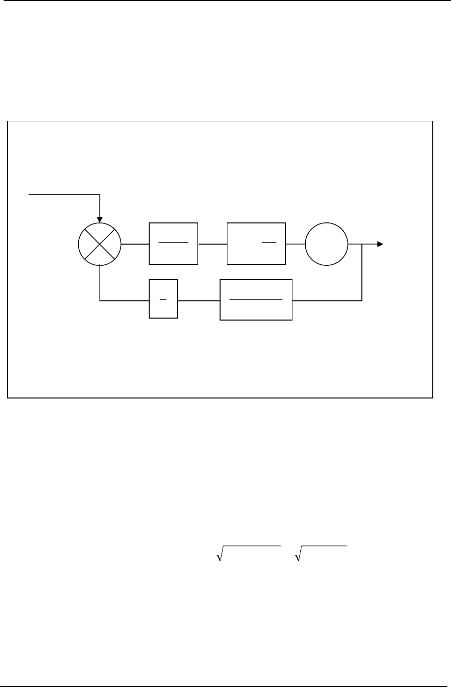
PRS10 Overview 15
PRS10 Rubidium Frequency Standard
(PI controller) with programmable proportional and integral gains. The VCO is the rubidium
frequency standard, whose frequency, f, is tuned by the magnetic field via the SF command
parameter with a sensitivity for its 1pps output of Kvco = 0.001 ns / bit-s, or (1 part in 1012) /
bit. The response function for each of the elements of the digital PLL is also indicated in the
figure in terms of the standard Laplace variable s.
The PI controller is programmed by choosing an appropriate integrator time constant, τ1, and
a stability factor, ζ. τ1 determines the natural time constant, τn, of the PLL for following a
step in phase of the reference, while ζ determines the relative rise time and ringing of the
PLL in response to the step. The value of ζ also represents the tradeoff in the equivalent
noise bandwidth verses peaking in the passband near the natural frequency of the response
function.
The PRS10 accepts integrator time constants, τ1, ranging from 28 to 222 seconds in powers of
2. The natural time constant is given by
ττ τ
nvco
KK==
11
1000/()
det s . Thus, the PRS10
provides natural time constants ranging from 506 seconds to 18.0 hours. While the integrator
time constant ( τ1 ) determines the natural time constant ( τn ), it is the natural time constant
which characterizes the loop response.
The PRS10 accepts stability factors ranging from 0.25 to 4.0 in powers of 2. The default
value of ζ = 1.0 corresponds to a critically damped response; ζ < 1.0 and ζ > 1.0 correspond
to under-damped and over-damped responses respectively.
Figure 3. External 1pps Phase Locking Block Diagram
External 1pps input
Time-tag
circui
t
VCO
10MHz
Output
1
s
1
1
3
τ
s+As
p+1
1
τ
Pre-filter
Proportional
and Integral
Gains
Kvco
Kdet
1
10 000 000,,
Figure 3. External 1pps Phase Locking Block Diagram

16 PRS10 Overview
PRS10 Rubidium Frequency Standard
With τ1 and ζ specified, the proportional gain, Ap, of the controller is given by the
equation AKK
pvco
==2 2 0 001
11
ζτζ τ
//(.)
det s-1 . With the default time constant, τ1, of
65,536 seconds and a stability factor, ζ, of 1.0, the proportional gain will be about 0.25. In
this case the instantaneous frequency of the rubidium source will be adjusted by about 0.25
parts in 1012 per nanosecond of time-tag measured.
The PRS10 also provides an optional pre-filter. The pre-filter is enabled by default, but it can
be disabled by sending the command LM0, which puts the PRS10 into lock mode 0. When
the pre-filter is enabled, the PRS10 will exponentially average the time tags output by the
“phase detector” before passing the result to the PI controller. The time constant of the pre-
filter, τ3, is hard coded to be τn/6.0 in order to obtain the maximum benefits of the averaging
while simultaneously insuring that the PLL will be stable
Use of the pre-filter is recommended when locking to references that have poorer short term
stability than the PRS10, but better long term stability. Locking to the 1pps output by GPS is
a prime example of such a case. Use of the pre-filter dramatically reduces the digital PLL’s
sensitivity to the sort term jitter of 50 to 300 ns present on the GPS reference 1pps. The GPS
reference also has a significant amount of 1/f noise associated with it. Very long time
constants are therefore required to prevent the PRS10 from following this noise too closely.
The PRS10 provides natural time constants of up to 18.0 hours, which will allow the PRS10
to follow GPS over time scales on the order of a day, but retain the superior short term
stability of the rubidium clock. When locking to a reference that has short term stability
comparable to the PRS10, disabling the pre-filter is recommended because it will allow the
PRS10 to better track the phase of the reference.
In lock mode 0, the PRS10’s digital PLL will approximate one of the following three
equations depending on the value of ζ:
∆∆∆Tt FT etTe t
n
n
t
n
t
n
nn
() ()/
/sin( / ) ( ) cos( / )=−
−−+ −
−−
0
2
22
0
1101
ζτ
ζτ ζτ ζτ
ζ
τ
ζ
τ
for ζ < 1
∆∆ ∆Tt tF T e T e
n
tt
nn
() [ ( )/ ] ( )=− +
−−
000
τ
ττ
for ζ = 1
[]
∆∆
Tt
FT
e
n
n
t
n
()
()()/
/
()
=−−+ −
−+
−+ −
0
2
2
1
10
21
2
ζζ τ
ζτ
ζζ
τ
[]
FT
e
n
n
t
n
0
2
2
1
10
21
2
−− −
−
−− −
()()/
/
()
ζζ τ
ζτ
ζζ
τ
∆ for ζ > 1
∆
T(0) is the initial offset in phase of the PRS10 from the reference. F0 is the initial offset in
frequency of the PRS10 from the reference before the digital PLL is enabled.
∆
T(t) details
how the PRS10 approaches the phase of the reference as a function of time. With the default

PRS10 Overview 17
PRS10 Rubidium Frequency Standard
time constant, τ1 = 65,536s, and stability factor, ζ = 1, the PRS10’s 1pps output will
exponentially approach the phase of the reference 1pps input with a time constant τn = 8,095
seconds or approximately 2¼ hours. In lock mode 1, the equations describing
∆
T(t) are
qualitatively similar to those presented above, but generally can only be solved numerically.
The locking algorithm of the PRS10 proceeds as follows:
• The 1pps PLL is enabled when the unit is turned-on or restarted if the PL parameter stored
in the unit’s EEPROM is “1”.
• The PLL will begin to control the frequency of the rubidium frequency standard when 256
consecutive “good” 1pps inputs (i.e., 1pps inputs which are within ±2048 ns of the first time-
tag result, modulo 1 s) are received.
• After receiving 256 consecutive “good” 1pps inputs, the 1pps pulse delay is set to the last
of the 256 time-tag values. (For example, if the last of the 256 “good” time tag values is
123,456,789 ns then the program will set the 1pps output delay to 123,456,789 ns, which
moves the 1pps output by 123,456,789 ns, so that new time-tag values will be about zero.)
Also, the current value of the SF parameter (which adjusts the frequency of the rubidium
frequency standard over the range of ± 2000 parts in 1012) is used to initialize the integrator,
Int(0). (The current value of the SF parameter may be from the internal calibration pot
position, an external calibration voltage, the value from a previously received SF command,
or the value left over from a previous PLL lock.) If the pre-filter is enabled, the exponential
filter for the time tags is zeroed.
• The unit will lock the frequency of the PRS10 to the “good” 1pps input pulses. “Bad” 1pps
inputs (1pps inputs with time-tags greater than 1,024 ns from the last “good” 1pps input) will
be rejected. The frequency parameter, f, to the SF command will be updated with each
“good” time-tag result, ∆T(n), as follows:
The pre-filter : if LM0 ∆T(n+1) = ∆T(n)
The pre-filter : if LM1 ∆T(n+1) = (1.0 – ∆t/τ3)∆T(n) + (∆t / τ3) ∆T(n)
The integral term: Int(n+1) = Int(n) – ( ∆T(n+1) / τ1)Kdet∆t
The proportional term: Pro(n+1) = -Ap∆T(n+1)Kdet
The frequency setting:f(n+1) = Pro(n+1) + Int(n+1)
In the above equations, ∆t is the time between phase comparisons, which is one second for
the PRS10. The frequency control value, f, ranges over ±2000 bits. If the new f value exceeds
2000, it is set to 2000. If the new f value is less than -2000, it is set to -2000.
If the new integral term exceeds 2000, it is set to 2000. If the new integral term is less than -
2000, it is set to -2000. This will prevent “integrator wind-up” in the case that the f-value is
pinned for a long time to slew the 1pps output in line with the 1pps input.

18 PRS10 Overview
PRS10 Rubidium Frequency Standard
The output of the digital filter, f, is used as the frequency control parameter for the SF (set
frequency) command, which is updated once a second.
• The PLL will be aborted and restarted if there are 256 consecutive “bad” 1pps inputs. (This
could happen if the 1pps input is moved suddenly by more than 1,024 ns.) The PLL will also
be aborted and restarted if the measured time-tag value for a “good” 1pps input exceeds ±4
ns/s * τ 1. (For τ 1’s default value of 65,536 seconds, the PLL will restart if the absolute value
of a “good” time-tag is greater than 262,144 ns. This could happen if the 1pps input is more
than a few parts in 10-9 off the correct frequency for a long time.)
CPU Tasks
In addition to the frequency lock loop control, the microprocessor is responsible for a variety
of other tasks. The CPU sets D/A values which control the microwave amplitude, the lamp
intensity, the 10 MHz output amplitude, and set the temperature of the crystal, lamp and
resonance cell. The CPU will also controls peripheral electronics to output a 1pps pulse (with
1ns placement) and measure the time for a 1pps input pulse (with 1 ns resolution).
There is an RS-232 interface which allows closed-case calibration of the PRS10. This
capability may also be used to servo the 10 MHz or 1pps outputs to another frequency or
time source in a system. For example, this would allow the PRS10 to be locked to the 1pps
from a GPS receiver with a long time constant to eliminate aging.

Applications 19
PRS10 Rubidium Frequency Standard
PRS10 Applications
In virtually all cases, the PRS10 may be “dropped into” applications which use the Efratom
FRS-C-1A8A4C (10 MHz sine output, -5°C to +65°C) or the FRS-N-1A8A4B (10 MHz sine
output, -55°C to +65°C).
Some customers may wish to evaluate the PRS10 on the bench. To facilitate this, SRS can
provide a connector adapter, power supply and RS-232 cable. The adapter breaks-out the
Cannon plug on the PRS10 to a power connector (2.1 mm with +24 V to center pin), three
BNCs (10 MHz and 1pps output and 1pps input), and a DB9 (for the RS-232). The adapter
also has status indicators for power, lock and RS-232 activity. This kit allows the PRS10 to
be operated from 110-240 Vac (50/60 Hz), provides for a direct connection to a PC via a
serial port (typically COM2:), and allows the use of standard BNC cables.
The PRS10 may also be operated with a customer supplied connector (Cannon series
DAM11W1S with coaxial insert DM53740-5008 for RG178 cable) from a bench dc power
supply. The power supply should be able to supply 2.2 A at +24 Vdc.
Interface Connector
Pin Name Description
1 LOCK/1PPS Lock indication and 1pps output. (See LM command)
2 POT WIPER Ext. freq. calibration. Nom:+2.50 V. 0-5 V for ±2x10⁻⁹
3 POT - Ground reference for external frequency calibration.
4 TXD/PHOTO RS-232 data output or photo I/V monitor output
5 1PPS_IN/PHOTO 1pps input for time-tagging or photo-amp output
6 +24(HEAT) +24 Vdc supply for discharge lamp and heaters
7 RXD/EFC RS-232 data input or EFC monitor output
8 POT + +5.00 Vdc reference output for external freq. cal. pot.
9 +24(CLEAN) +24 Vdc supply for electronics (not heaters or lamp)
10 GROUND Case ground and power supply return
coax 10MHz 10 MHz sine output on center conductor
Configuration Notes
The functions of three pins (4, 5 and 7) on the interface connector may be modified by
internal hardware jumpers. The function of the LOCK output may be modified via RS-232.
Pin 1: LOCK/1PPS output. The default configuration is: +5 V indicates that the unit is not
locked to rubidium (as during warm-up), 0 V indicates a successful lock of the 10 MHz
oscillator to rubidium, pulsing high for 10 µs at a 1pps rate. The 1pps output may be moved
earlier by any interval from 1ns to 999,999,999 ns via RS-232 command. The unit may be
configured to omit the 1pps output via the LM command (via RS-232).

20 Applications
PRS10 Rubidium Frequency Standard
Pin 4: TXD/PHOTO The default configuration uses this pin as an output for RS-232 data.
Many system parameters (including the lamp intensity) may be monitored via the RS-232
interface. The function of this pin may be changed to an analog monitor for the lamp
intensity by removing one resistor (R347) and installing a 10 kΩ resistor for another (R348)
on the microcontroller PCB.
Pin 7: RXD/EFC The default configuration uses this pin as an input for RS-232 data. Many
system parameters (including the EFC, electronic frequency control) may be monitored via
the RS-232 interface. The function of this pin may be changed to an analog monitor for the
EFC by removing one resistor (R354) and installing a 10 kΩ resistor for another (R353) on
the microcontroller PCB.
Pin 5: 1PPS_IN/PHOTO The default configuration uses this pin as a 1pps input to allow
time-tagging or phase locking to an external 1pps source. The function of this pin may be
changed to allow monitoring of the amplified photo-signal. When configured as a 1PPS_IN,
R241 will be omitted on the top PCB, and a 1 kΩ resistor will be installed for R242. When
configured for PHOTO_AMP output, R242 will be omitted on the top PCB, and a 1 kΩ
resistor will be installed for R241.
10 MHz coax shield The default configuration floats the shield of the 10 MHz coaxial
connector with respect to ground. The 10 MHz output is transformer coupled, and the shield
may be ground referenced by installing the jumper between J101 and J102 (located near the
connector on the 10 MHz oscillator PCB.)
Hardware Notes
All of the pins on the interface connector are protected against continuous connection to any
potential up to 24 Vdc. The power supply pins are protected against polarity reversal and may
be operated up to +30 Vdc. In most applications, both +24 Vdc supplies (heater and electronic
supplies) will be connected together and operated from a +24 Vdc supply.
Logic outputs (LOCK/1PPS and TXD/PHOTO) have a 1 kΩ output resistance driven by a
CMOS logic device operating between +5 Vdc and ground. Logic inputs (RXD/EFC and
1PPS_IN) have 100 kΩ to ground and 3.9 kΩ CMOS gate inputs (which have input
protection diodes to +5 V and ground).
RS-232 data is sent to the host on pin 4, received from the host on pin 7. The baud rate is
fixed at 9600 baud, 8 bits, no parity, with 1 start and 1 stop bit. No DTR or CTS controls are
used; rather, the XON/XOFF protocol has been implemented. The transmit drive level is 0
and 5 V, not the +/-12 V normally associated with RS-232. These levels are compatible with
most RS-232 line receivers, but does not require their use (a TTL inverter may be used
instead), hence simplifies the interface when used inside an instrument at the sacrifice of
degraded noise immunity over long lines.

Applications 21
PRS10 Rubidium Frequency Standard
The PRS10 may be connected directly to a PC’s COM2: port with three wires: TXD, RXD,
and ground. As the PRS10 sources only +5/0 V for the RS-232 (via 1 kΩ) the connecting
cable should be kept short.
PRS10 PC’s COM: (DB9 Connector) PC’s COM: (DB25 Connector)
Pin 7 (RXD) Pin 3 (TXD) Pin 3 (TXD)
Pin 4 (TXD) Pin 2 (RXD) Pin 2 (RXD)
Pin 10 (GND) Pin 5 (GND) Pin 7 (GND)
Operating Temperature
The unit should be operated so that the baseplate temperature stays below +65 °C. This
requirement is usually met by units operating on the bench at room temperature when
powered by +24 Vdc.
Frequency Adjustment
A magnetic field coil inside the resonance cell is used to tune the hyperfine transition
frequency. The magnetic field is controlled by a 12-bit DAC. The output frequency (at
10MHz) tunes quadratically with the DAC setting (0 ≤ DAC ≤ 4095), and ∆f(Hz) ≈ 5x10⁻⁹ x
DAC2 . The DAC setting is changed from the nominal calibration value (see MO command)
in various ways, including, calibration pot position, external calibration voltage, direct setting
(see SF command), and external 1pps PLL control.
When the unit is first turned on (or restarted), the internal frequency calibration pot position
will be used to set the DAC relative to the calibration value stored in EEPROM. (If a voltage
is applied to pin 2 of J100 (POT_W) then this voltage will override the pot position.) An SF
command may be sent, or a 1pps input may be applied, to control the frequency offset
directly. If either the SF command or the 1pps input control the frequency offset, then the pot
position (or external control voltage) will not be used again until the power is cycled or the
unit is restarted. All the various ways to adjust the frequency of the 10 MHz output are
linearized, and they have a span of ±2000 x 10-12 or ±0.020 Hz.

22 RS-232 Instruction Set
PRS10 Rubidium Frequency Standard
RS-232 Instruction Set
Syntax
Commands consist of a two letter mnemonic and one or more parameters. Commands which
end with a question mark (?) will return a value. Commands which end with an exclamation
point (!) write the current parameter value to EEPROM for use after the next restart.
Commands which end in an exclamation point and a question mark (!?) return the value
stored in EEPROM.
All data is communicated in ASCII codes. Commands are case insensitive, and spaces
(ASCII 3210) are ignored. Commands are processed when a carriage return (ASCII1310) is
received. Returned values are delimited with commas (in the case of multiple returned
values) or a carriage return (in the case of a single or the last returned value). Commands
available to the end user are in bold: some commands are for factory use only and a special
code must be transmitted to enable these commands. Parameter lists are enclosed in curly
brackets { }, the brackets are not part of the command.
On reset, the unit will transmit the characters: PRS_10 with a carriage return.
Initialization
RS 1
Restart. This command will restart the PRS10’s microcontroller just like power-on. (It is not
necessary to send a RS command on power-up.) All values will return to the values stored in
EEPROM. (verbose mode disabled, 10 MHz set to last stored value, etc.) The frequency
lock-loop will be disabled until the microcontroller verifies that the unit is warmed-up and
that a useful signal level is present. Example: RS 1 will cause the unit to restart.
VB{0 or 1}
VB?
Set verbose mode. The verbose mode is useful when a human is communicating with the
PRS10 using a terminal program (the PRS10 will provide an “OK”, command prompts, etc.)
The verbose mode should be disabled when a computer program is communicating with the
PRS10 (where format characters would interfere.) Examples: VB0 disables the verbose
mode (this is the power-on default mode.) VB1 will enable the verbose mode.
ID?
Identify. This command returns an identification string which includes the serial number and
firmware version of the PRS10. Example: ID? will return the identification string
PRS10_3.15_SN_12345 (model _firmware version_serial-number).

RS-232 Instruction Set 23
PRS10 Rubidium Frequency Standard
SN?
SN{value}
SN!
SN!?
Serial number. This command returns the unit’s serial number. Example: SN? will return
21567 for a unit with serial number 21567. The command to write and burn a serial number
are for factory use only.
ST?
Status. This command will return a six number string corresponding to the values of the six
status bytes. Each number will range between 0 and 255, and will be separated by commas.
(For definitions of the status bytes, refer to the end of the detailed command descriptions.)
LM{value} value = 0, 1, 2, or 3
LM?
LM!
LM!?
Lock mode pin configuration. This command is used to configure the LOCK/1PPS output
(pin 1 on the main connector, J100.) The LOCK/1PPS pin may be configured per the
following table:
LM Description of LOCK/1pps Output
0 Output goes low when locked to Rb, pulses high for 10 µs at 1 Hz
1pps locking pre-filter disabled
1 Output goes low when locked to Rb, pulses high for 10 µs at 1 Hz
1pps locking pre-filter enabled (default)
2 Output goes low when locked to Rb, 1pps is disabled
3 Output goes high when locked to Rb, 1pps is disabled
The default value is 1, so that pin 1 will go low when the unit is locked to rubidium, and will
pulse high for 10 µs at a 1 Hz rate. The position of the 1pps pulse may be moved with the PP
command. Example: LM? Could return 1, indicating that the unit is in its default
configuration so that the lock pin goes low when locked to Rb, pulsing high for 10 µs at a 1
Hz rate. To configure the unit for no 1pps output, the command string LM 2 followed by LM
! will change the unit’s power on default for no 1pps output.

24 RS-232 Instruction Set
PRS10 Rubidium Frequency Standard
RC 1
RC!
Recall. This command is used to return all values in EEPROM to the values which were
present when the unit was first shipped from the factory (except for the unit-start and lamp-
start counters.) This command should be used if you have been writing values to EEPROM
and have somehow corrupted the operation of the device. Executing this command may
require calibration of the unit, as the frequency calibration values are also returned to their
factory values. The unit will be restarted after the values in EEPROM have been restored to
their factory values. Example: RC 1 will return all calibration values to the values which
were determined for the unit when it was manufactured and restart the unit. The RC!
command is a factory-only command which writes all of the current parameter values to the
EEPROM.
Frequency Lock-loop Parameters
LO{value} value = 0 or 1
LO?
Lock. This command can be used to stop the frequency lock-loop (FLL). It is essentially the
same as setting the gain parameter to zero. It may be desirable in a particular application to
stop the FLL and set the frequency control value for the 10MHz oscillator manually. (See the
FC command.) Example: LO 0 will stop the FLL. LO? will return a value of 0 (if the FLL is
not active) or 1 (if the FLL is active.)
FC?
FC{high,low} 0 ≤ high ≤ 4095 1024 ≤ low ≤ 3072
FC!
FC!?
Frequency control. These commands allow direct control of the 22bit value which controls
the frequency of the 10 MHz ovenized oscillator. Normally, this value is controlled by the
FLL control algorithm, however, the FLL may be stopped, and the value adjusted manually.
(See the LO command.)
Two 12-bit DACs are scaled (by 1000:1) and summed to provide a varactor voltage which
controls the frequency of the 10 MHz oscillator. The low DAC, which operates over half its
range (to avoid FFL oscillations at the roll-over to the high DAC) provides a LSB frequency
resolution of 1.5:10-12. The high DAC, which has a nominal value of 2048, has a LBS
resolution of 1.5:10-9. These DACs provide a total tuning range of about ±3 ppm.
Example: Suppose a unit’s FLL has been operating for some time and has settled. An FC?
will return the current value of the DAC pair which might be 2021,1654. (Tracking the FC
value over a long period of time tells you about the frequency variations of the 10MHz

RS-232 Instruction Set 25
PRS10 Rubidium Frequency Standard
crystal. The FC values will change to correct for variations in the crystal frequency due to
aging and ambient conditions.)
Both DACs may be set to any value in the range specified above. Example: FC 2048,2048
will set the 10MHz oscillator back to the middle of its tuning range. However, it is possible
to set the frequency of the 10 MHz oscillator so far from the correct frequency that the FLL
signal disappears, making the lock impossible. If this happens, the last saved FC value may
be read from EEPROM with the FC!? command and restored with the FC{high,low}
command.
The FC! command is used to save the current FC values in the unit’s EEPROM. The FC!?
Command may be used to read the value which is stored in the EEPROM. The value stored
in EEPROM is used to set the 10 MHz at startup, before the FLL can be established.
Occasionally while the unit is operating (at about 20 minutes after power-on and once a day
there after) the program will write a new value to EEPROM to correct the value for crystal
aging. Example: FC!? will return four values (separated by commas), the number of power
cycles the unit has undergone, the number of times the FC pair has been written to EEPROM,
and the value of the FC pair (high, low) which is used at turn-on and restart.
DS?
Detected signals. This command returns two numbers corresponding to the synchronously
detected signals at the modulation frequency, ωmod, and at twice the modulation frequency,
2ωmod.
The first number, the amplitude of the signal at ωmod, is the error signal in the rubidium
frequency lock loop. The value is proportional to the instantaneous frequency error of the 10
MHz oscillator as detected by the physics package. The value may be large when the unit is
first locking, and will bobble around zero in steady state. Each LSB corresponds to about 15
µVrms of signal at ωmod.
The second number is the amplitude (in millivolts rms) of the synchronously detected signal
at twice the modulation frequency, 2ωmod. The amplitude of this signal is proportional to the
strength of the rubidium hyperfine transition signal.
The returned value is a spot measurement taken over just one cycle of the modulation
frequency. Since the signals have several Hz of equivalent noise bandwidth, they will be
rather noisy.
Example: DS? could return 55,800 indicating a small error signal and a strong resonance
signal.

26 RS-232 Instruction Set
PRS10 Rubidium Frequency Standard
SF{value} -2000 ≤ value ≤ +2000
SF?
Set frequency. This command is used to override the internal calibration pot (or external
calibration voltage) to set the frequency directly, relative to the calibration values in
EEPROM (see the SP and MO commands.) The command sets the frequency offset in units
of parts in 10-12 (corresponding to a frequency resolution of 10 µHz at 10 MHz.) The SF?
command will return the currently set relative frequency value (with a range of ±2000)
whether the value comes from the internal calibration pot position, an external frequency
control voltage, an SF command, or from the external 1pps phase lock loop control
algorithm. However, SF set command is ignored if the unit is phase-locked to an external
1pps signal. (To re-establish direct control via the SF command, the PLL must be disabled.
See PL 0 command.)
Example: SF 100 will set the frequency 100 x 10-12 (or 0.001 Hz) above the stored
calibration value, and the SF? command will return 100.
Data from the SF command cannot be saved when the power is turned off. (To do this type of
calibration, see the SP and MO commands.) Once executed, the SF command will disable the
analog channels (internal calibration pot and external calibration voltage) until the power is
cycled or the unit is restarted.
SS?
SS{value} 1000 ≤ value ≤ 1900
SS!
SS!?
Set slope. This command is used to read the slope calibration parameter for the SF command.
This parameter compensates for a variety of factors which affect the magnitude of the
coefficient between magnetic coil current and transition frequency. Example: SS? might
return 1450, the nominal parameter value. This calibration parameter may not be altered by
the end user.
The (factory only) SS! command is used to store the current value of the SS parameter to the
unit’s EEPROM. The SS!? will return the value of the SS parameter which is used on power-
up or restart.
GA?
GA{value} 0≤ value ≤ 10
GA!
GA!?
Gain. This command sets the gain parameter in the frequency lock-loop algorithm. Higher
gain values have shorter time constants, (the time constant is the time it takes for the
frequency lock-loop to remove 67% of the frequency error) but have larger equivalent noise

RS-232 Instruction Set 27
PRS10 Rubidium Frequency Standard
bandwidths (which will reduce the short-term stability of the 10 MHz output.) A gain of 0
will stop the frequency lock-loop so that the frequency of the output is determined by the
10MHz ovenized oscillator alone. The gain setting, approximate time constants, and
approximate equivalent noise bandwidths are detailed in the following table. The gain
parameter is set automatically by the program, however, the user may want control over the
parameter in special circumstances. Example: GA7 will set the gain parameter to 7, which
has a time constant of about 2 s, which is a typical value for normal operation. GA? could
return a value of 8 just after restart, which has a short time constant of about 1 s to assist the
initial frequency locking. Setting the gain parameter during the first 6 minutes after turn-on
or restart will abort the automatic gain sequencing.
Command Time Constant (seconds) Noise Bandwidth (Hz)
GA 0 Infinite 0
GA 1 128 0.002
GA 2 64 0.004
GA 3 32 0.008
GA 4 16 0.016
GA 5 8 0.032
GA 6 4 0.064
GA 7 2 0.128
GA 8 1 0.256
GA 9 0.5 0.512
GA 10 0.25 1.024
The GA! command stores the current value of the frequency lock loop gain parameter into
the unit’s EEPROM. Example: If the current value of the gain is 6, the command GA! will
write 6 to the unit’s EEPROM which will be used to initialize the gain parameter after the
next power-on or restart. Then GA!? will return a 6.
PH?
PH{value} 0≤ value ≤ 31
PH!
PH!?
Phase. This command is used to set the phase of the synchronous detection algorithm. The
frequency lock-loop (FLL) uses the in-phase component of the photo-signal at the
modulation frequency (70 Hz) as the error signal for the FLL. The phase between modulation
source and the error signal is affected by phase shifts in the modulation and signal filters and
by optical pumping time constants. This parameter corrects for the accumulation of all of
these phase shifts. Each modulation cycle consists of 32 phase slots, so each phase increment
corresponds to 11.25°. Example: PH? would typically return a value of 24.

28 RS-232 Instruction Set
PRS10 Rubidium Frequency Standard
The PH! command is used to write the current phase parameter into the unit’s EEPROM.
This is a factory only command. The value which is burned in EEPROM is used on power-on
and restart, and may be queried by the PH!? command. Example: PH!? could return a
typical value of 24.
Frequency Synthesizer Control
A frequency synthesizer, which uses the 10 MHz OCXO as a frequency reference, is used to
generate the RF which sweeps the rubidium hyperfine transition. The frequency synthesizer
multiplies the 10 MHz by a factor M = 19 * (64*N + A) / R, to generate a frequency near
6.834 GHz. (The factor of 19 is from frequency multiplication in the step recovery diode, and
the other terms come from the operation of the dual modulus frequency synthesizer
integrated circuit.)
The apparent transition frequency is different for each physics package, due mostly to
variations in the fill pressure of the resonance cell. The frequency synthesizer parameters, R,
N and A, are used to adjust the frequency synthesizer’s output frequency to the closest
frequency just above the apparent transition frequency, then the magnetic field is set to move
the transition frequency up to the synthesizer frequency.
During frequency locking, the frequency of the 10 MHz OCXO is adjusted to maintain the
output of the frequency synthesizer on the rubidium hyperfine transition frequency. Initial
calibration of the unit will involve finding the synthesizer parameters and magnetic field
value which will lock the 10 MHz OCXO at exactly 10 MHz.
During the lifetime of the unit, there will be some aging of the physics package, which will
cause the apparent transition frequency to change. This is usually corrected by minor
calibration adjustments of the magnetic field strength, which provides a setting resolution of
a few parts in 10-12. (See the MO command.) However, if the magnetic field strength reaches
its lower or upper limit, it is necessary to change the frequency synthesizer parameters, which
can change the output frequency in steps of about one part in 10-9.
The table in Appendix A details the values for R, N and A for the range of frequencies
needed.
SP?
SP {R,N,A} 1500≤ R ≤ 8191 800≤ N ≤ 4095 0≤ A ≤ 63
SP!
SP!?
Set Parameters. This command is used to set or query the frequency synthesizer’s
parameters, which will coarsely adjust the unit’s output frequency. These parameters may
need to be adjusted if the unit cannot be calibrated by magnetic field adjustment.

RS-232 Instruction Set 29
PRS10 Rubidium Frequency Standard
Example: During calibration, a unit’s 10 MHz output frequency is found to be low by 0.010
Hz, and the magnetic field offset adjustment is already at its maximum. (See the MO
command.) Sending the SP? command returns the current values of R, N and A which are
2610,1466,63 in this example. This corresponds to line 38 in the table in Appendix A. To
increase the frequency of the 10 MHz output, we select the next higher setting, line 37,
which will increase the frequency by 0.01986 Hz. To do this, we send the command
SP 5363,3014,22 (which are the parameters from line 37). Waiting for the frequency to
settle, we now measure the output to be about 0.0098 Hz high. Now the magnetic field is
adjusted down to calibrate the unit to exactly 10 MHz. (The SP! command is used to save
these new values in EEPROM for the next power-on or restart. Also see the MO command
for adjusting the magnetic field.)
The SP! command is used to write the current frequency synthesizer parameters to the unit’s
EEPROM for use after the nest restart or power-on cycle. This command is used after the SP
command is used during the calibration of the unit. Example: SP! will write the frequency
synthesizer parameters (R, N and A) which are currently in use to the unit’s EEPROM. SP!?
will return the values for R, N and A which are currently in the unit’s EEPROM. The SP!?
command may be used to verify that the SP! write command executed correctly.
Magnetic field Control
A magnetic field coil inside the resonance cell is used to tune the apparent hyperfine
transition frequency. The magnetic field is controlled by a 12-bit DAC. Increasing the
magnetic field will increase the hyperfine transition frequency, which will increase the
frequency of the 10 MHz output. The transition frequency may be tuned over about ±3 x 10⁻⁹
by the magnetic field, which corresponds to ±0.030 Hz at 10 MHz. The output frequency (at
10 MHz) tunes quadratically with field strength, and ∆f(Hz) ≈ 0.08 * (DAC/4096) 2 .
A minimum magnetic field should always be present to avoid locking to the wrong Zeeman
component of the hyperfine transition, so the 12-bit DAC may be set from 1000 to 4095 with
3000 being the nominal midscale value. (A DAC value of 1000 corresponds to about 6% of
the full-scale frequency tuning range, 3000 corresponds to about 53%, while 4095 is 100% of
the full-scale range.)
To help cancel frequency shifts due to external magnetic fields, the current in the coil is
switched at a 5 Hz rate. The frequency lock-loop averages over a full period of the switch
rate to avoid injecting a spur at 5 Hz onto the 10 MHz control signal. The switching of the
magnetic field is enabled at power-on and restart, but may be turned on or off by RS-232
command. (see MS command.)
The commands associated with magnetic field control (MO, MS, and MR) allow direct
control of the magnetic field circuitry. Most users will not want to control the magnetic field
directly, but will instead allow the program to read the frequency calibration pot or external
control voltage and then control the magnetic field. If they want software control of the unit’s

30 RS-232 Instruction Set
PRS10 Rubidium Frequency Standard
calibration, they may choose to use the SF commands, which disable the analog control and
allow the frequency to be adjusted over a range of ±2000x10-12. (The program will linearize
the magnetic field control of the frequency offset with either analog or software control.)
MS?
MS{0 or 1}
Magnetic switching. The MS command is used to turn off or on the 5Hz switching of the
frequency tuning magnetic field. Magnetic switching is enabled when the unit is powered-on
or after a restart. (Since the PRS10 is calibrated with the field switching enabled, turning off
the field switching may alter the calibration.) Example: MS 1 will turn on the magnetic field
switching, and MS 0 will turn it off. MS? will return a “1” if the field switching is currently
enabled.
MO?
MO{value} 2300 ≤ value ≤ 3600
MO!
MO!?
Magnetic offset. The magnetic offset is the value, determined when the unit is calibrated,
which calibrates the unit to 10 MHz. The restricted range is necessary to allow room for user
calibration via the internal frequency calibration pot or by an external voltage. If the unit
cannot be calibrated to 10 MHz within the allowed range of MO values, then a different
setting for the frequency synthesizer is required. (See SP command and the table in Appendix
A. Example: MO 3000 sets the magnetic offset to 3000, which is its nominal (mid-linear
scale) value. The MO? command reads back the current value of the magnetic offset. MO! is
used to store the current value of the magnetic offset parameter to EEPROM for use after the
next restart. MO!? may be used to query the value stored in EEPROM. This value is used on
power-up or restarts.
MR?
Magnetic read. This command returns the value that the 12-bit DAC is using to control the
magnetic field. This value is computed from the magnetic offset value (see MO command)
and the position of the internal frequency calibration pot, external calibration voltage, or
value sent by the SF command.
The value is computed from the equation DAC = √(SF*SLOPE + MO2) where SF is the
desired frequency offset in parts per 10-12 (from the cal pot position, the SF command, or the
1pps PLL and is in the range –2000 < SF < 2000), SLOPE is the SF calibration factor with a
nominal value of 1450 (see SS command), and MO is the magnetic offset value. The returned
value should be in the range of 1000 to 4095.

RS-232 Instruction Set 31
PRS10 Rubidium Frequency Standard
Example: MR? would return a value of 3450 if the magnetic offset is at 3000, the SF
command requested an offset of +2000 x 10-12, and the SS CAL factor has the nominal value
of 1450.
Frequency Control
The frequency of the 10 MHz output may be adjusted in a number of ways: the internal
calibration potentiometer may be set (accessible via a hole in the bottom plate), an external
voltage (0 to +5.00 Vdc, applied to the interface connector pin 2) can override the internal
pot, or, these analog channels may be overridden with a software command which sets the
frequency directly.
When the unit turns on, or after a restart command, the control program will default to
reading the analog channel for frequency calibration. (This is important to maintain
compatibility with existing sockets.) The calibration pot and the external voltage control
provide a full-scale tuning range of ± 2000 x 10-12, with a worst case resolution of 5 x 10-12.
All of the channels for calibrating the unit are linearized, so that the frequency characteristic
will be linear with applied voltage, pot setting, or SF value even though the transition
frequency changes quadratically with field strength.
One pulse per second (1pps) control
To facilitate system integration, the PRS10 provides a 1pps output which may be set over an
interval from 0 to 999,999,999 ns with 1ns resolution. The unit also has the ability to
measure the arrival time of a 1pps input over the same interval and with the same resolution.
The ability to time-tag a 1pps input allows the PRS10 to be phase-locked to other clock
sources (such as the 1pps output from a GPS receiver) with very long time-constants. This is
a very useful feature for network synchronization, and allows the configuration of a reliable
Stratum I source at a very low cost.
TT?
Time-tag. This command returns the value of the most recent time-tag result in units of
nanoseconds. If a new time-tag value is not available then -1 (the only case for which the
returned value is negative) will be returned. Example: TT? would return the value
123456789 to indicate that the most recent 1pps input arrived 123,456,789ns after the 1pps
output. Returned values range from 0 to 999999999.

32 RS-232 Instruction Set
PRS10 Rubidium Frequency Standard
TS?
TS{value} 7000 ≤ value ≤ 25000
TS!
TS!?
Time slope. This command is used to calibrate the analog portion of the time-tagging circuit.
The analog portion is used to digitize the time of arrival with 1 ns resolution and 400 ns full-
scale. (Counters are used for the portion of a time interval longer than 400 ns.) The analog
circuit stretches the time interval between the 1pps input and the next edge of a internal 2.5
MHz clock by a factor of about 2000, and measures the duration of the stretched pulse by
counting a 2.5 MHz clock. The analog portion of the time-tag result is calculated from the
equation ∆T(ns) = counts * TS / 216, where TS is the time slope value, which has a nominal
value of 13,107.
Example: TS? might return 14,158 which is a time slope parameter value a bit above the
nominal value, which would be required if the analog portion of the time-tagging circuit
stretched the pulse by a bit less than a factor of 2000. TS? will return the current value of the
time slope.
The TS! command is used to write the current value of the time slope parameter into the
unit’s EEPROM. The TS {value} and TS! are factory only commands. Example: TS! will
write the current value of the time slope (which may be queried with the TS? command) to
the unit’s EEPROM. TS!? will return the time slope calibration factor which is in the unit’s
EEPROM.
TO?
TO{value} -32767 ≤ value ≤ 32768
TO!
TO!?
Time offset. This calibration value (in ns) is added to the measured time-tag value to
reference the result to the 1pps output. To calibrate, the 1pps output is connected to the 1pps
input and the time-tag is read with the TT? command. The returned value is subtracted from
the current TO value and sent with the TO command to calibrate the offset.
Example: Suppose: the 1pps output is connected to the 1pps input. A time tag value, read
with the TT? query, returns a value of 25ns. The TO parameter, read via the TO? query,
returns a value of -1750ns. The command TO -1775 is sent to correct for the offset. After
waiting about one second (to allow another time-tag value to be acquired) the next TT? query
returns a value of 2ns (indicating a measurement of 2ns after the 1pps output) Waiting
another second, the next TT? query returns the value 999,999,999ns (indicating 1 ns before
the 1pps output). These values are consistent with a well calibrated time-tag offset.
Following calibration of the TO parameter, the TO! command is used to write the current
value of the time offset to the unit’s EEPROM. Example: TO! will write the current time-tag

RS-232 Instruction Set 33
PRS10 Rubidium Frequency Standard
offset value to the unit’s EEPROM for use after the next power-up cycle or restart command.
TO!? will return the value which is burned in the unit’s EEPROM. (Note: Firmware
revisions prior to Rev 3.23 do not allow user TO! commands. Check the firmware revision
with the ID? command.
PP{value} 0 ≤ value ≤ 999999999
Place pulse. This command is used to move the 1pps output from its current position. The
1pps output can be moved earlier in time by 1 ns to 999999999 ns. Since the 1pps input time-
tag is referenced to the 1pps output, changing the 1pps output placement will change the
report time-tag values as well. (See the TT and TO commands.) Example: PP 123456789
will move the 1pps pulse train earlier by 123,456,789 ns.
PS?
PS{value} 100 ≤ value ≤ 255
PS!
PS!?
Pulse slope calibration. This command is used to calibrate the analog portion of the 1pps
output time delay circuit. This circuit is used to delay the 1pps pulse train with 1 ns
resolution and 100 ns full-scale. (Counting logic is used for the portion of the time interval
longer than 100 ns.) The pulse slope value corresponds to the DAC8 value which provides a
delay closest to (but not exceeding) 100 ns. Example: PS 200 set the pulse slope to its
nominal value of 200. (PS{value} is a factory only command.) The PS? command will return
the current value of the pulse slope.
The PS! command writes the current value of the pulse slope to the unit’s EEPROM for use
after the next power-on or restart. This command is used after the pulse output analog output
is calibrated. Example: PS! will write the current value of the pulse slope (which calibrates
the 100 ns analog delay portion of the 1pps pulse delay circuit) to the unit’s EEPROM. Note
that PS! is a factory-only command.
1PPS Locking Control
To facilitate integration into systems which require very low aging, automatic calibration, or
a traceable frequency standard, the PRS10 may be locked to an external 1pps input.
A second-order digital PLL is used to lock the unit’s frequency (both the 10 MHz and 1pps
outputs) to an external 1pps input with time constants ranging from 256 s to 65536s (about 4
minutes to about 18 hours).
When provided with an accurate and stable 1pps source, the unit will automatically align its
1pps output to the 1pps input and then adjust the frequency of the rubidium reference to

34 RS-232 Instruction Set
PRS10 Rubidium Frequency Standard
maintain the alignment over time. A typical application would lock the PRS10 to the 1pps
output from a GPS receiver with a time constant of several hours.
Several commands and one status byte may be used to control and monitor the PLL,
however, default values will allow units to lock to clean 1pps inputs without any software
interaction.
PL?
PL{0 or 1}
PL!
PL!?
Phase lock control. This command may be used to disable the 1pps PLL, or to re-enable (and
so restart) the 1pps PLL. The unit is shipped with the phase lock control enabled. This
command would be used if the 1pps time-tagging were being used to measure the position of
1pps inputs and phase locking is not desired. Example: PL 0 will disable the PLL to the
1pps inputs so that the frequency of the rubidium standard will not be affected by the 1pps
inputs. PL? will return a “1” if the PLL to the 1pps is enabled. PL! is used to write the
current value (0 or 1) to the EEPROM for use after the next start up. PL!? is used to query
the value of the phase lock control parameter which is stored in the unit’s EEPROM.
PT?
PT{value} 0 ≤ value ≤ 14 ; τ1 = 2(value+8) seconds (256, 512, ... 4,194,304)
PT!
PT!?
Phase-lock integrator time constant. This command is used to set the PLL’s integrator’s time
constant, τ1, which phase-locks the PRS10 to an external 1pps input. The integrator time
constant is equal to 2(value+8) seconds. The default value is 8, which provides an integrator
time constant of 2(8+8) or 65536 seconds. Integrator’s time constants can range from 256 to
4,194,304 seconds, or from about 4 minutes to 18 days. It is important to note that the natural
time constant, τn, is different from the integrator time constant, as shown in the table below.
The natural time constant is the best measure of the loop response. The PLL natural time
constant spans between 8 minutes and 18 hours for PT values between 0 and 14.
Example: PT10 sets the integrator time constant to 2(10+8) seconds, or about 72 hours. (Refer
to Table below.) For PT10 the natural time constant is about 4.5 hours. PT? will return the
current value of the time constant parameter. A phase lock time constant may be stored in
EEPROM as a new default with the PT! command. The PT!? command may be used to
verify the value stored in EEPROM.
The following case will illustrate the operation of the PLL: Suppose that the PRS10 has been
phase locked to a stable 1pps reference for a very long time (several periods of τn) when the
1pps reference input makes an abrupt shift of +100ns (moving later in time). The PRS10’s
1pps PLL algorithm will reduce the PRS10’s frequency of operation (by adjusting its SF

RS-232 Instruction Set 35
PRS10 Rubidium Frequency Standard
parameter) to eliminate the 100ns phase shift between the 1pps reference input and the 1pps
output. After the phase shift is eliminated, the PRS10 will settle to the “correct” operating
frequency.
The PLL algorithm computes integral and proportional terms from time-tag measurements,
adjusting the SF parameter to phase lock the 1pps output to the 1pps input. The table below
shows the integral and proportional gain terms. For the nominal PT value of 8, the integral
term is -0.055 SF bits per hour per ns of time-tag and the proportional gain is -0.25 SF bits
per ns of time-tag.
Per the table below for PT8, if the input reference shifts by +100ns, the proportional term
will adjust the SF by -0.25bits/ns * 100ns = -25 bits. Each SF bit corresponds to 1:10-12 of the
operating frequency, and so the PRS10 frequency will be shifted by about -25 x 10-12. The
integral term will begin ramping by (-0.055bits/hour/ns) * 100ns, or by -5.5 bits per hour.
The phase shift between the 1pps input and 1pps output will be gradually eliminated.
(Phase jumps of 100ns are quite common on 1pps outputs from GPS receivers, which are a
likely 1pps reference to the PRS10. The corresponding frequency jumps of 25 x 10-12 may be
excessive in some applications, and so a digital pre-filter is used to smooth the time-tag
values before they are used by the PLL algorithm. See LM command.)
PLL Table for all PT values, assuming a stability factor, ζ
ζζ
ζ=1.
PT Parameter
Parameter
set by PT
command
Integrator Time-
Constant
(hours)
Integral Gain
(SF bits per
hour per ns
of time-tag)
Proportional
Gain
(SF bits per ns
of time-tag)
Natural Time-
Constant
Characterizes
PLL response
(hours)
0 0.07 -14.063 -3.95 0.14
1 0.14 -7.031 -2.80 0.20
2 0.28 -3.516 -1.98 0.28
3 0.57 -1.758 -1.40 0.40
4 1.14 -0.879 -0.99 0.56
5 2.28 -0.439 -0.70 0.80
6 4.55 -0.220 -0.49 1.12
7 9.10 -0.110 -0.35 1.59
8 18.20 -0.055 -0.25 2.25
9 36.41 -0.027 -0.17 3.18
10 72.82 -0.014 -0.12 4.50
11 145.64 -0.007 -0.09 6.36
12 291.27 -0.003 -0.06 8.99
13 582.54 -0.002 -0.04 12.72
14 1,165.08 -0.001 -0.03 17.99

36 RS-232 Instruction Set
PRS10 Rubidium Frequency Standard
PF?
PF{value} 0 ≤ value ≤ 4 ; (value:ζ) : (0:1/4, 1:1/2, 2:1, 3:2, or 4:4)
PF!
PF!?
Phase-lock stability factor. This command is used to set the stability factor, ζ, of the 1pps
PLL. The stability factor is equal to 2(value-2). The default value is 2, which provides a stability
factor of 2(2-2) = 20 = 1. Stability factors can range from 0.25 to 4.0. Example: PF 1 sets the
stability factor to 0.5, which will reduce the equivalent noise bandwidth of the PLL at the
cost of increasing the ringing near the natural frequency (relative to the default settings). PF?
will return the current value of the stability factor parameter. PF! may be used to write the
current stability factor to the EEPROM for use as the new default. PF!? may be used to read
the value of the stability factor which is stored in EEPROM.
PI?
PI {value} -2000 ≤ value ≤ 2000
Phase-lock integrator. This command is used to set the value of the integral term in the PLL’s
digital filter. It is not necessary to set this value, as it will be initialized by the PLL routine to
the current frequency setting parameter when the PLL begins. Users may want access to the
value to alter the PLL characteristics, or to investigate its operation. Example: PI 0 will set
the integrator in the PLL’s digital filter to 0, which is the center of the ±2000 bit range. PI?
will return the current value of the PLL integrator. (There are two terms which control the
phase locking of the PRS10 to an external 1pps source: the integral term and the proportional
term. The proportional term is equal to the value returned by an SF? minus the value
returned by the PI?.)
Analog Control
SD{port}?
SD{port,value} 0 ≤ port ≤ 7 and 0 ≤ value ≤ 255 (factory only)
SD{port}!
SD{port}!?
Set DAC. This command is used to set (or read the settings of) an octal 8bit DAC which
provides analog signals to control systems parameters. The command which sets values is
only available to the factory. The command to query values may be used by all. The query
command returns a single integer in the range of 0 to 255.
Port Function
0 Controls the amplitude of the RF to multiplier in resonance cell
1 Controls the analog portion (0 to 99 ns) of the delay for the 1pps output
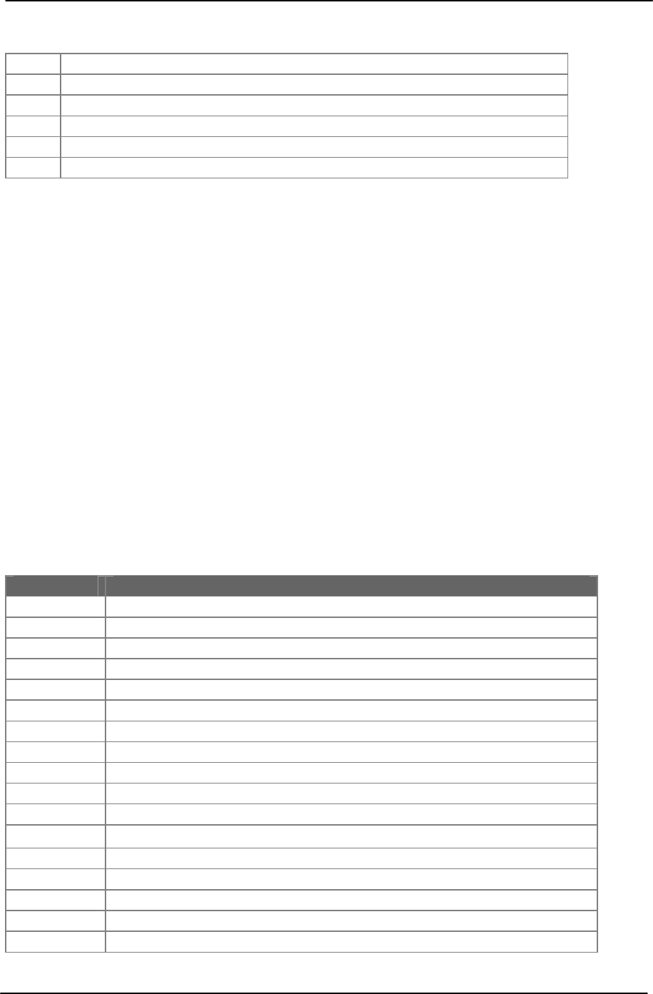
RS-232 Instruction Set 37
PRS10 Rubidium Frequency Standard
2 Controls the drain voltage for the discharge lamp’s FET oscillator
3 Controls the temperature of the discharge lamp
4 Controls the temperature of the 10 MHz SC-cut crystal
5 Controls the temperature of the resonance cell
6 Controls the amplitude of the 10 MHz oscillator
7 Controls the peak deviation for the RF phase modulation
Example: SD2? could return the value 255 indicating that the unit has set the discharge
lamp’s FET drain voltage to the maximum (which it does while it is trying to start the lamp.)
The SD{port}! is a factory only command which writes the data from the corresponding SD
port to the unit’s EEPROM for use on subsequent restarts. Example: SD3!? will return the
start-up value for SD3 (lamp temperature control value) which is stored in the unit’s
EEPROM.
Analog Test Voltages
AD{port}? port = 0,1,2,...15
Analog to digital. This command reads the voltage at the corresponding 12-bit ADC port and
returns the voltage as a floating point number. Values can range from 0.000 to 4.998. The
voltages correspond to various test points in the system per the following table. Note that this
command can only query. Examples: AD10? could return the value 0.710 indicating that the
case temperature sensor is at 71 °C (this sensor indicates a temperature which is about
midway between the baseplate temperature and the lamp temperature.)
Command Returned voltage
AD 0? Spare (J204)
AD 1? +24V(heater supply) divided by 10.
AD 2? +24V(electronics supply) divided by 10
AD 3? Drain voltage to lamp FET divided by 10
AD 4? Gate voltage to lamp FET divided by 10
AD 5? Crystal heater control voltage
AD 6? Resonance cell heater control voltage
AD 7? Discharge lamp heater control voltage
AD 8? Amplified ac photosignal
AD 9? Photocell’s I/V converter voltage divided by 4
AD 10? Case temperature (10 mV/°C)
AD 11? Crystal thermistors
AD 12? Cell thermistors
AD 13? Lamp thermistors
AD 14? Frequency calibration pot / external calibration voltage
AD 15? Analog ground

38 RS-232 Instruction Set
PRS10 Rubidium Frequency Standard
AD{port}? 16 ≤ port ≤ 19
A/D via CPU’s E-port. This command returns a value corresponding to the voltage present at
the input to the microcontroller’s octal 8bit ADC (port E on the MC68HC11). Only the first
four ports are in use. The voltage corresponds to various test point in the system per the
following table. Example: AD17? could return a value of 4.81 indicating that the 360 MHz
RF synthesizer has acquired lock.
Command Returned voltage
AD 16? Varactor voltage for 22.48 MHz VCXO (inside RF synthesizer) / 4
AD 17? Varactor voltage for 360 MHz VCO (output of RF synthesizer) / 4
AD 18? Gain control voltage for amplifier which drives frequency multiplier / 4
AD 19? RF synthesizer’s lock indicator voltage (nominally 4.8 V when locked )
Status Bytes
ST?
Status query. This command returns the six system status bytes which are used to indicate the
health and status of the unit. The values ranges from 0 to 255. The six status bytes are
detailed in the tables below. A status bit will remained set until it is read, even though the
condition which caused the error has been removed. Some status bits are not errors: for
example, during warmup the status bytes may indicate that the lamp is not lit, temperatures
are low, and the unit is not locked.
Example: Immediately after power is applied to a unit, the command ST? returns 16, 3, 21,
1, 2, 129. From the status byte definitions below, we see that the following conditions exist:
16… the lamp has not yet started
3… the RF VCXO has not yet locked
21… the lamp, crystal, and cells are all below their set point temperatures
1… the frequency lock has not been established
2… fewer than 256 1pps inputs have been qualified
129.. both the lamp and unit have been restarted
ST1 : Power supplies and Discharge Lamp
ST1 bit Condition which sets bit Corrective Action
0 +24 for electronic < +22 Vdc Increase supply voltage
1 +24 for electronics > +30 Vdc Decrease supply voltage
2 +24 for heaters <+22 Vdc Increase supply voltage

RS-232 Instruction Set 39
PRS10 Rubidium Frequency Standard
3 +24 for heaters > +30 Vdc Decrease supply voltage
4 Lamp light level too low Wait: check SD2 setting
5 Lamp light level too high Check SD2 setting
6 Gate voltage too low Wait: check SD2 setting
7 Gate voltage too high Check SD2 setting
ST2: RF Synthesizer
ST2 bit Condition which sets bit Corrective Action
0 RF synthesizer PLL unlocked Query SP? verify values
1 RF crystal varactor too low Query SP? verify values
2 RF crystal varactor too high Query SP? verify values
3 RF VCO control too low Query SP? verify values
4 RF VCO control too high Query SP? verify values
5 RF AGC control too low Check SD0? values
6 RF AGC control too high Check SD0? values
7 Bad PLL parameter Query SP? verify values
ST3: Temperature Controllers
ST3 bit Condition which sets bit Corrective Action
0 Lamp temp below set point Wait for warm-up
1 Lamp temp above set point Check SD3, ambient
2 Crystal temp below set point Wait for warm-up
3 Crystal temp above set point Check SD4, ambient
4 Cell temp below set point Wait for warm-up
5 Cell temp above set point Check SD5, ambient
6 Case temperature too low Wait for warm-up
7 Case temperature too high Reduce ambient
ST4: Frequency Lock-Loop Control
ST4 bit Condition which sets bit Corrective Action
0 Frequency lock control is off Wait for warm-up
1 Frequency lock is disabled Enable w/LO1 command
2 10 MHz EFC is too high SD4,SP,10MHz cal,Tamb
3 10 MHz EFC is too low SP, 10 MHz cal

40 RS-232 Instruction Set
PRS10 Rubidium Frequency Standard
4 Analog cal voltage > 4.9 V Int cal. pot, ext cal. volt
5 Analog cal voltage < 0.1 Int cal. pot, ext cal. volt
6
7
ST5: Frequency Lock to External 1pps
ST5 bit Condition which sets bit Corrective Action
0 PLL disabled Send PL 1 to enable
1 < 256 good 1pps inputs Provide stable 1pps inputs
2 PLL active
3 > 256 bad 1pps inputs Provide stable 1pps inputs
4 Excessive time interval Provide accurate 1pps
5 PLL restarted Provide stable 1pps inputs
6 f control saturated Wait, check 1pps inputs
7 No 1pps input Provide 1pps input
ST6: System Level Events
ST6 bit Condition which sets bit
0 Lamp restart
1 Watchdog time-out and reset
2 Bad interrupt vector
3 EEPROM write failure
4 EEPROM data corruption
5 Bad command syntax
6 Bad command parameter
7 Unit has been reset

PRS10 Calibration Procedures 41
PRS10 Rubidium Frequency Standard
Calibration Procedures
Many applications for the PRS10 only require that the frequency of the 10 MHz output be
calibrated. This may be done by adjusting a potentiometer, which is accessible through a hole
in the bottom of the unit. The unit should be operating for at least 24 hours before it is
calibrated. The 15 turn pot has a range of ±0.020 Hz. The frequency increases if the pot is
turned clockwise, by about 0.001 Hz for 3/8’s of a turn.
Note: the potentiometer position will not affect the frequency of operation if : (1) it is turned
to either extreme, (2) an external control voltage is applied to pin 2 of the main connector,
J100, (3) an SF (set frequency) command has been sent via the RS-232 interface, or, (4) the
unit is locked to an external 1pps input. The time constant for pot adjustments depend on the
setting of the frequency lock-loop gain (see GA command: the default is about 2 seconds.)
In the case that the unit cannot be calibrated because the internal pot has reached an extreme
position, it will be necessary to modify a calibration values which are stored in the unit’s
EEPROM. To verify that the pot has been turned to a limit of its motion, measure the voltage
on pin 2 (POT_W) of J100 (the main connector) with respect to the chassis. Zero volts on pin
2 indicates that the pot has been adjusted for the lowest frequency, and +5.0 Vdc indicates
that the pot has been adjusted for the highest frequency.
To modify EEPROM calibration values, it will be necessary to establish RS-232
communications with the PRS10. This can be done with a three wire connection between the
PC COM: port and the PRS10’s main connector. A communication program (see Windows
Accessories or other) will be needed as well. (See MO and SP commands.)

42 Circuit Descriptions
PRS10 Rubidium Frequency Standard
Circuit Descriptions
Schematic RB_F1 (sheet 1 of 6)
Components shown on this schematic are located on the vertical PCB which holds the main
connector to the outside. This board has a 10MHz SC-cut ovenized oscillator which is
frequency locked by the microprocessor to the hyperfine transition in rubidium via a high
resolution DAC. This will overcome two important shortcomings of the oscillator circuit:
frequency aging of a few parts in 10-10/day , and a sensitivity of a few parts in 10-9 over the
ambient temperature range of 0°C to 65°C.
Input Power
D101 and D102 (MBRD660CT Schottky diodes in DPAKs) protect the unit from input
power supply polarity reversals on +24_CLEAN and +24_HEAT. The supplies are filtered
by L104 and L105 (ferrite beads with about 3µH and Q=15 at 100kHz) and C115 and C116.
These filters are designed to reduce EMI emission and susceptibility but they have a low Q
resonance at about 40kHz.
Voltage Reference
U100 provides a 10.00V low noise reference for the entire unit and various biases for the
crystal oscillator. The reference voltage is divided by two and buffered by U102B to provide
a +5.00V reference for the internal calibration pot and for the POT+ output.
Crystal Oscillator
The crystal oscillator uses a Colpitts configuration. The 3rd overtone SC-cut crystal is
specified to operate at 10.0MHz with a series load of 20pF. (Hence the crystal will operate
slightly above its series resonance to contribute an inductive reactance equal in magnitude to
the series capacitive reactance.) At 10MHz, the network L100, L101 and C102 has a
capacitive reactance equivalent to an 87pF capacitor. At the fundamental (3.3MHz) and at
the B-mode frequency (10.8MHz) this network is inductive, and so there will be no gain
provided by Q100. In addition to this network, C103, C104, the varactor D100, and C106
(which connects to the ac ground at the emitter of Q101) are all in series with the crystal.
C104 is selected when the unit is calibrated so that the crystal will operate at 10.0MHz with
the nominal EFC voltage applied to the varactor.
The crystal frequency tunes linearly with the net series reactance, with a tuning coefficient of
-1Hz/20Ω. Series capacitors tune the crystal to higher frequencies, series inductors tune the
crystal to lower frequencies. Only NPO capacitors are to be used and inductors should be
either air or iron powder core (no ferrites) in order to preserve the relative insensitivity to
ambient temperature variations. To move the oscillator to higher frequencies,
C(pF)=808/∆f(Hz). To move the oscillator to lower frequencies, L(µH)=0.29∆f(Hz).

Circuit Descriptions 43
PRS10 Rubidium Frequency Standard
The MMBV609 varactor provides an approximate linear tuning characteristic over ±2 ppm.
This will allow the unit to correct for aging of the crystal for a nominal 27 year life, given a
daily aging of 2 parts in 10-10.
The crystal is operated at its temperature plateau of about 80°C. (The plateau temperature is
determined at calibration for each unit. ) The frequency is a maximum at the plateau and so
the oscillator will typically be a few hundred Hertz low when the unit is turned on at room
temperature. Near the plateau top, the frequency deviation verses temperature is about ∆f(Hz)
= -0.061x ∆T(°C)2. Note that if the crystal oven were to lose regulation by 12.8°C (perhaps
the baseplate is too hot) that this would cause a 1ppm frequency error, which could be
corrected by the Rb frequency lock loop.
Power to overcome losses (to sustain oscillation) is provided by Q100. The dominate loss is
the series resistance of the crystal (about 80Ω). Q100 provides power by injecting a current at
the top of L100 which is in phase with the 10MHz voltage at this node. The amount of
current injected depends on the size of C103 and R103: the current injected is equal to the ac
voltage across C103 divided by the resistance of R103 (assuming emitter following action of
Q100). The magnitude of the oscillation will grow until the peak voltage at the base exceeds
the collector voltage, causing Q100 to saturate.
The circuit is designed to allow about 1mA(rms) to circulate through the crystal. The ac
current is high enough to provide low phase noise, but low enough to minimize aging. This
ac current is cascoded to the inverting input of the high speed op-amp, U101, by Q101. Q101
provides a good ac ground for the crystal circuit (to maintain high in-circuit Q). With an
emitter current of 4mA the emitter resistance of Q101 will be about 6Ω. Q101 also helps to
isolate the crystal circuit from variations from the external 10MHz load (as does U101) so
that the frequency of operation of the circuit will not be pulled by the load.
The op-amp operates as a transconductance amplifier with a transconductance gain of about
2000Ω at 10MHz. The dc output of the op-amp is midway between the supplies (at about
8.25Vdc), which is controlled by the current drawn by Q101 and the value of R111. There is
a 10Vpp sine at 10MHz at the output which is ac coupled, reverse terminated, and matched to
a 50Ω load by C111, R114, and T100. The primary of T100 is tuned to 10MHz, so that spurs
and harmonics are attenuated. The 7:2 turns ratio transforms the 50Ω into a 612Ω load at
10MHz. The output amplitude into 50Ω is 0.50Vrms (1.414Vpp or +7dBm).
Extremely low phase noise is an important specification for this oscillator. The phase noise
close to carrier (10Hz offset and below) is dominated by 1/f components, including, crystal
parameters, temperature stabilization, amplitude limiting, and gain mixing. Far away from
carrier (>1kHz) the noise floor is determined by ratio of broadband noise sources to the
signal current at 10MHz. Examples of broadband sources include the shot noise current on
base currents, the Johnson noise current from bias resistors, and the op-amp’s input current
and voltage noise. It is also important to maintain very low noise on the EFC and amplitude

44 Circuit Descriptions
PRS10 Rubidium Frequency Standard
control signals. Typical phase noise is -125dBc/Hz @ 10Hz, -145dBc/Hz @ 100Hz, and -
155dBc/Hz @ >1kHz.
Circuit elements and operating points were chosen to reduce noise sources. An SC-cut
resonator was chosen for high Q and stable motional impedances. The transistors are
operated at a few mA, trading off base bias current noise against emitter resistance. Metal
film resistors are used to reduce 1/f noise. Series 100µH inductors are used to reduce the
Johnson noise current of bias resistors. The op-amp was chosen for low input current noise,
and it is operated with sufficient gain so that its voltage noise would not degrade the phase
noise floor. Finally, the crystal is operated at its plateau temperature to reduce the frequency
instability associated with temperature fluctuations.
Crystal Heater
The crystal heater has the same design as the two other heaters (resonance cell and lamp) in
the system. There are two heaters in TO-220 packages: an LM340-12 (a +12Vdc voltage
regulator) and a TIP107 (a pnp power Darlington). The tabs of both TO-220 heaters are at
ground, so they are bolted directly to the block. All of the heater current passes through three
parallel 1Ω shunt resistors to sense current. The block temperature is sensed by two series
100kΩ thermistors, which are directly beneath the TO-220 heaters in the oven block. (Two
sensors are used because the division of power will depend on the heater voltage applied to
the unit.) At the operating temperature of 75°C, each thermistor will have a resistance of
about 15kΩ. The control circuit will allow operation up to 90°C. (For the lamp, the nominal
operating temperature is 105°C, for which each thermistor will have a resistance of about
5.5kΩ. The maximum setpoint for the lamp is 122°C.) The control circuits for all of the
heaters are on the top (analog) PCB. The control circuit can vary the heater current from 0 to
0.7A to maintain the set point. In the case of a control failure, the LM340-12 will turn off the
current if the junction temperature reaches 125°C.
Schematic RB_F2 (Sheet 2 of 6)
The components contained on this schematic are all located on the top (analog) PCB. This
board contains most of the analog circuitry for the system, including, temperature servos,
photodiode amplifier and filter, analog signal multiplexers, and noise filters for the crystal’s
EFC and amplitude control signals.
Temperature Control Servos
There are three temperature control servos (for the crystal oven, the Rb discharge lamp, and
the Rb resonance cell). The three servos are identical except for the maximum set point
(122°C for the lamp, and 90°C for the others.) The circuit description will refer to the crystal
temperature controller.

Circuit Descriptions 45
PRS10 Rubidium Frequency Standard
The controller is a proportional-integral controller. The output of the error amplifier (U200A)
is used to control the current flowing in the heater circuit, with a range from 0 to 500mA (to
provide heater powers from 0 to 12W). The error amplifier has a proportional gain of
(R205/R204)+1=6.5 and an integration time constant of R204xC201=1 s for the signal at its
non-inverting input. The inverting input is biased near 1.00Vdc, so that the servo will try to
maintain the temperature so that there is 1.00Vdc on the thermistors.
For a set point of 75°C the series thermistor pair will have a resistance of 30kΩ. To get
1.00Vdc at the non-inverting input of U200A, XTAL_SET is set to 170 bits (full-scale of
4V/255=0.01568V/bit, so 170 bits=2.66Vdc).
After settling, a LSB step in XTAL_SET (15.6mV) will become about 5.8mV at the on-
inverting input, and cause an immediate change of 2x5.8mV = 11.6mV at the output of
U200A, followed by a ramp of 5.8mV per second. This quickly increases the power by about
0.27W, then by 0.14W/S thereafter. The servo will settle when the thermistors heat-up,
decreasing their resistance, so that the voltage at the non-inverting input returns to 1.00Vdc.
The thermistor resistance decreases by about 3%/°C. An LSB increase in XTAL_SET near
the nominal 2.66Vdc will cause the current to increase by .0156/(2.66-1.00) or about 0.9%.
So the servo will settle when the temperature of the block increases by 0.9%/3%/°C =0.3°C.
There is a small temperature offset between the temperature sensor and the device whose
temperature we wish to control. Since the sensor is located very near the heat source, the
sensor will be warmer, and the temperature offset will increase as more heat is required. To
compensate for this effect, a small portion of a voltage proportional to the baseplate
temperature (10mV/°C) is summed to the voltage at the inverting input of the error amplifier.
This is the electronic equivalent of a double oven, as the errors due to changes in ambient
temperature are greatly reduced.
U200B controls the current in the heaters in proportion to the signal from error amplifier
(U200A). When the output of the error amplifier goes up, the output of U200B goes down,
increasing the current in the heaters, causing the signal XTAL_SHUNT- to go down. The
gain (from error amplifier to shunt voltage) is set by R207 and R208. Offsets are arranged so
that the heaters will be off when the output of the error amplifier is less than +5Vdc.
Conversion to 10MHz TTL
U205 converts a 10MHz offset sinewave from the crystal oscillator into complimentary
10MHz TTL level signals. The +10MHZ signal is used as a reference for the microwave
frequency synthesizer and the -10MHZ signal is used as a clock for the microprocessor.
Separate signals are used to improve the isolation between the CPU and the synthesizer.
The 10MHz sine has an offset of 8.2Vdc and an amplitude of 10Vpp and is sourced via a
2.0kΩ resistor. After attenuation by R249, R250 and C210, the non-inverting input to U205

46 Circuit Descriptions
PRS10 Rubidium Frequency Standard
sees a signal with 0.91Vdc offset and an amplitude of 0.91Vpp, while the inverting input is
biased at 0.91Vdc.
Photocell Amplifier
The output from the photocell is a sink current which is proportional to the light intensity of
the discharge lamp as attenuated by the resonance cell. The light transmission through the
resonance cell decreases slightly (by about 1 part in 1000) when the microwave synthesizer
sweeps through the hyperfine transition frequency. The microwave frequency is modulated at
70Hz, so the light output will dip at 140Hz when centered on the hyperfine transition.
The S/N of the photocell is limited by shot noise: the shot noise current on a dc current of I
amps is given by √(2qI) (amps/√Hz) where q=1.6x10⁻¹⁹. On a 50µA dc current the best we
can do is 4pA/√Hz of noise. A good design requires that the shot noise be the dominate noise
term.
U206A is a low noise bipolar input op-amp whose input range includes ground. A 150kΩ
metal film resistor shunted by a 1nF film capacitor is used in feedback, providing a
transconductance bandwidth of 1kHz. The input current noise of the op-amp (0.4pA/√Hz)
and the Johnson noise current of the feedback resistor (0.33pA/√Hz) are not important noise
terms. Also, the voltage noise of the op amp (3nv/√Hz) times the noise gain (which is about
10x for a photocell whose shunt resistance is 1MΩ at 25°C, but drops to 15kΩ at the
operating temperature of 80°C) is not important as the expected shot noise current times the
transconductance gain is about 600nV/√Hz.
The transconductance amplifier is followed by a high gain amplifier (x288 for ac signals).
This amplifier has a pass band from 16Hz to 1.6kHz. The non-inverting input to this
amplifier is biased to place the output of the following bandpass filter at midscale.
A two-pole Butterworth low pass filter (300Hz bandwidth) is used to reduce noise at the A/D
input, while preserving gain between 70Hz and 140Hz. The filter has a gain of 1.59 for
signals in the pass band.
The input voltage noise specifications for the high gain and filter amplifiers are not
particularly important as there is about 600nV/√Hz of noise on the output of the
transconductance amplifier. With an noise equivalent bandwidth of about 400Hz, we expect a
total noise (from the shot noise of the photocell’s dc current) of about 3.4mVrms or about
17mVpp. This is much larger than the LSB (1.25mV) of the A/D converter, so the
quantization noise of the A/D will not be important.

Circuit Descriptions 47
PRS10 Rubidium Frequency Standard
Signal Filters for Oscillator Control
The amplitude and frequency of the crystal oscillator are controlled by signals from D/A
converters. In order to preserve low phase noise, these signals must have very little voltage
noise.
The EFC signal has a full scale of 17Vdc, and a resolution of 22 bits. A LSB represents a
step of about 4µV which is a fractional frequency step of about 1:10-12. We would like for
noise on the EFC to be less than one LSB. To arrange this, the DAC22 signal is filtered with
a time constant of 1s and buffered by a FET input op-amp (U210B, an AD822). The FET op-
amp has 1/f noise of about 2µVpp in the two decade band from 0.1Hz to 10Hz. Both the op-
amp and the 10.0kΩ feed back resistor will have noise of about 30nV/√Hz at 10Hz, which is
well under the target of 1.6µV/√Hz required to meet the specification of -125dBc/Hz at
10Hz offset.
The oscillator’s amplitude control is filtered is a similar fashion, using U210A. Noise on this
signal would be detrimental to the phase noise spectrum, but would not affect zero-crossings
of the sine output.
Analog Multiplexers
There are 16 analog signals which may be multiplexed to the 12-bit A/D converter. One of
these signals, PHOTO_AMP, is be digitized 32 times during each cycle of the 70Hz
modulation (2240 Hz) in order to lock the crystal to the Rb hyperfine transition. The other 15
signals are monitored intermittently and in response to RS-232 requests.
A0 Amplified and filtered photocell signal
A1 Photocurrent (x150kΩ/4) (37.5mV/µA)
A2 Case temperature (10mV/°C)
A3 Crystal thermistor voltage
A4 Resonance cell thermistor voltage
A5 Lamp thermistor voltage
A6 Calibration voltage (Pot or user input)
A7 Signal Ground
B0 J204 (Spare)
B1 +24_HEAT/10
B2 +24_CLEAN/10
B3 Discharge lamp FET’s drain voltage
B4 Discharge lamp FET’s gate voltage
B5 Crystal heater control signal
B6 Resonance cell heater control signal
B7 Discharge lamp heater control signal

48 Circuit Descriptions
PRS10 Rubidium Frequency Standard
Schematic RB_F3 (Sheet 3 of 6)
All of the components shown on this schematic reside on the vertical PCB on the left side of
the unit. The large hole in this PCB allows access to an SMB connector to sample the
microwave field in the resonance cell.
Power on reset, low voltage protection, and a watch-dog time-out is provided by U300, a
MAX705. The RESET input to the microcontroller is asserted on power-up. The reset will be
asserted for about 1 second after power is applied (to allow time for the 10MHz crystal
oscillator to start.). A non-maskable interrupt (XIRQ) is asserted if the SPI clock is inactive
for more than 1.6 seconds, which should never occur. A maskable interrupt (IRQ) is asserted
(which will also retrigger the reset cycle) when the +18V supply drops below 16.0Vdc.
Microcontroller
The system is controlled by U302, a MC68HC11E9, which is an 8-bit microcontroller with
RAM, ROM, EEPROM, A/Ds, UART, serial interface, timers, and I/O control bits. The
controller is clocked by the 10 MHz timebase which is to be disciplined to the atomic
transition frequency.
The microcontroller communicates with external devices via a the serial peripheral interface
(SPI). Data is clocked by SPI_CLK to (or from) these devices on SPI_DATA. To reduced
digital crosstalk to the most sensitive devices, the SPI data and clock are gated, so that these
outputs are only active when necessary.
The microcontroller is also responsible for a variety of housekeeping tasks: power on circuit
checks, setting and reading temperatures, boost-starting the discharge lamp, digitally filtering
the frequency-lock error signal, passing the filtered error signal to the 22 bit D/A converter,
and responding to commands and queries via the RS-232 interface.
A description of I/O from the controller follows:
Name Function
CLK 10MHz TTL clock input
RESET TTL low to assert system reset
XIRQ Non-maskable interrupt on watch-dog time-out (SPI dead)
IRQ Maskable interrupt on power failure (+18 goes below +16V)
MODA Configure for internal program memory
MODB Configure for internal program memory
PORT A Mixed inputs and outputs
PA0 Time tag input to measure 1PPS input to 400ns
PA1 Interpolation input to measure 1PPS input to 0.2ns

Circuit Descriptions 49
PRS10 Rubidium Frequency Standard
PA2 ADC_BUSY input is high during 12-bit A/D conversions
PA3 MAG_SIGN output controls sign of magnetic field
PA4 -CONV strobe low to initiate 12-bit A/D conversion
PA5 EN/-CLR control for 1PPS time-tagging
PA6 1PPS output strobe (400ns resolution)
PA7 Spare output (connected to J305)
PORT B Eight TTL outputs
PB0 MPX0 Select bit for analog multiplexer
PB1 MPX1 Select bit for analog multiplexer
PB2 MPX2 Select bit for analog multiplexer
PB3 MPX3 Low to select MPX-A, high for MPX-B
PB4 1PPS_SEL0 Low bit for 100ns 1PPS output delay
PB5 1PPS_SEL1 High bit for 100ns 1PPS output delay
PB6 Spare (connected to J306)
PB7 LOCKED bit is set high to indicate Rb frequency lock
PORT C Chip select outputs
PC0 -CS_PLL
PC1 -STB_DAC8
PC2 -CS_EFC_HIGH
PC3 -CS_MAGNET
PC4 Spare (connected to J308)
PC5 -CS_EFC_LOW
PC6 -CS_PHASE_MOD
PC7 EN_ADC_CLK
PORT D SPI and RS-232
PD0 RS-232_IN
PD1 RS-232_OUT
PD2 SPI_IN
PD3 SPI_DATA
PD4 SPI_CLK
PD5 SPI_GATE
PORT E Octal 8-bit A/D converter with +5.12V full-scale
PE0 RF_XVCO. Should be between 0.2 and 3.5Vdc
PE1 RF_VCO. Should be between 3.0 and 4.0Vdc
PE2 RF_AGC. Should be 1.0 and 3.75Vdc

50 Circuit Descriptions
PRS10 Rubidium Frequency Standard
PE3 PLL_LOCK. Should be >4.0Vdc
PE4 Ground
PE5 Spare analog input (J302 with 100kΩ to ground)
PE6 Spare analog input (J303 with 100kΩ to ground)
PE7 Spare analog input (J304 with 100kΩ to ground)
RS-232
The system may be controlled by commands sent via the RS-232. Two pins on the system
connector (J100) are used for transmit and receive. Data is sent to the host on pin 4, received
from the host on pin 7. The baud rate is fixed at 9600 baud, 8 bits, no parity, with 1 start and
2 stop bits. No DTR or CTS controls have been used, rather, the XON/XOFF protocol has
been implemented. The transmit drive level is 0 and 5V, not the +/-12V normally associated
with RS-232. These levels are compatible with RS-232 line receivers, but does not require
their use (a TTL inverter may be used instead), hence simplifies the interface when used
inside an instrument at the sacrifice of degraded noise immunity over long lines.
12 Bit A/D Conversion
A serially interfaced 12 bit A/D converter is used to measure the ac and dc components of the
photocell signal. The analog input to the ADC is buffered by U309A, a FET input op-amp
configured as a unit follower. The quantization noise of this converter will not degrade the
S/N of the ac signal, even in the case when the ac signal occupies a relatively small portion
of the converter's full scale range. The A/D converter can also measure the position of a 10
turn "user cal" pot, which has a (software defined) range of +-2E-9. The 12 bits of resolution
will provide a frequency trim of 1E-12.
12-Bit Digital to Analog Converters
There are four 12-bit DACs. Two of the DACs are scaled, summed, and offset to provide a
level with 22-bits of resolution to control the crystal frequency. One of the DACs is used to
control the magnitude of the magnetic field in the resonance cell. The forth DAC is used to
digitally synthesize the 70Hz phase modulation of the 6.834GHz microwave field.
Two of the DACs ( the upper DAC of the 22-bit pair and the DAC which controls the
magnetic field ) are rarely changed and would be very sensitive to digital crosstalk and so are
communicated with via the gated SPI interface.
Magnetic Field Control
R331, a 348Ω shunt resistor, is used to measure the current through the magnetic field coil
which is in the resonance cell. U307B, an LM358 op amp, maintains a current through the
field coil so that the voltage across the shunt resistor matches the output from the 12-bit DAC
(U310, an LTC1452). The coil current can be programmed from 0 to 8mA, but a minimum
level (3mA) is always maintained to spread out the non 0-0 Zeeman transitions. The

Circuit Descriptions 51
PRS10 Rubidium Frequency Standard
frequency offset is quadratic in the field strength, with a fractional frequency resolution of
about 1x10-12 at 3mA, and of 2.5x10⁻¹² at 8mA.
To reduce the susceptibility of the transition frequency to external magnetic fields, the
polarity of the magnetic field is chopped at 5Hz by the CPU control signal (MAG_SIGN)
and U306 (a DG211 quad analog switch). The apparent transition frequency is synchronously
filtered by the CPU over the field reversal period so as to notch out any 5Hz noise from the
EFC signal.
Phase Modulation
The main task for the microcontroller is to modulate the microwave carrier to sweep through
the Rb hyperfine transition frequency. The microcontroller will A/D the optical signal via a
12 bit A/D converter, synchronously detect the components of the optical signal at the sweep
rate and at twice the sweep rate, and adjust the frequency of the 10 MHz timebase so as to
null the component at the sweep rate (which keeps the optical dip centered in the middle of
the sweep).
The CPU digitally synthesizes the 70Hz sinewave which phase modulates the RF frequency
synthesizer. U313, an 12-bit DAC, outputs 32 samples during each cycle of the 70Hz
sinewave. The amplitude of the sinewave is controlled by the signal “PHASE_DEV”, which
comes from an 8-bit DAC on the frequency synthesizer PCB. The amplitude of the sinewave
controls the magnitude of the frequency deviation (which is adjusted to optimize the
deviation sensitivity of the resonance cell). The frequency deviation is about ±300Hz at
6.834GHz.
1PPS Output
A port bit on the microcontroller (PA7) may be used to output a 10µs pulse at a rate of 1Hz.
This pulse is combined with the LOCK output signal on the main connector (pin 1 of J100).
(The function of the LOCK/1PPS output may be configured via RS-232.)
This port bit is controlled by the microcontroller’s timer which has a resolution of one
E_CLK cycle (400ns). Hardware on the bottom circuit board provides delays in 100ns steps
(under control of the port bits 1PPS_SEL0 and 1PPS_SEL1) and in steps of about 0.5ns via
an analog signal from an 8-bit DAC. The combination of these three delays allows the 1PPS
output pulse to be placed with an accuracy, resolution, and differential non-linearity of about
1ns.
1PPS Input Time-Tag
The rising edge of a 1PPS input signal on pin 5 of the main connector can be time-tagged
with 1ns resolution. The time may reported via RS-232, or used to servo the unit to another
frequency standard (such as GPS).

52 Circuit Descriptions
PRS10 Rubidium Frequency Standard
Hardware on the bottom board provides two signals: TIME_LATCH and INTERPOLATE.
These signals latch the value of a free-running counter (clocked by the E_CLK) which is part
of the microcontroller. TIME_LATCH is just the 1PPS input re-synchronized to the CPU’s
E_CLK, which allows the processor to time-tag the input to 400ns resolution.
INTERPOLATE will go low for a time equal to about 2000 times the interval between the
1PPS input and the next E_CLK. Measuring the duration of INTERPOLATE allows the
position of the 1PPS input to be measured to about 400ns/2000=0.2ns.
Schematic RB_F4. (Sheet 4 of 6)
High Resolution, Low Phase Noise, RF Synthesizer
The pressure tuned Rb hyperfine transition lies at about 6,834,685,850Hz. This will vary
depending on the fill pressure and gas composition of the Rb resonance cell. In order to lock
the crystal oscillator to this transition, we need to synthesize and sweep frequencies in this
region.
In order to minimize the amount of magnetic field tuning needed, the frequency synthesizer
should be capable of being set with high resolution (about 1:10-9). In order to detect the
transition with good signal to noise, the synthesizer will need to have very low phase noise
(on the order of -70dBc/Hz at 6.8GHz).
Since we want to stabilize a 10.000MHz crystal to an (essentially) arbitrary frequency with
low phase noise, we will need a dual loop synthesizer: a fast loop to stabilize an RF VCO to a
crystal (for good phase noise), and a slow loop to stabilize the crystal to the 10.000MHz
reference.
Typical numbers:
A typical microwave frequency is 6,834,685,853Hz
Which is the 19th harmonic of the RF frequency: 359,720,308Hz
Which is 16 times the crystal frequency: 22,482,519Hz
In this case, dividing the RF frequency by (1386*64+39)=4053.5Hz
Which equals the reference frequency (10,000,000Hz) divided by 2467.
The dual modulus frequency synthesizer will be programmed with R=2467, N=1386, and
A=39.
The microwave frequency is generated by frequency multiplication of the RF frequency in a
step recovery diode (SRD). The RF frequency was chosen to give good conversion
efficiency, with favorable “numerology” (so that the gaps between available frequency steps
from the dual modulus synthesizer are small).
A reasonable crystal frequency is the RF frequency divided by 16 (dividers and
oscillator/mixers are available in this frequency range). A third overtone crystal resonator
with a nominal frequency of 22.48252MHz is used to provide a low-noise “flywheel”. We

Circuit Descriptions 53
PRS10 Rubidium Frequency Standard
only need to tune over a range of 0.1ppm to accommodate for fill pressure variations of the
resonance cell.
The varactor tuned crystal oscillator has a tuning coefficient of about 2 ppm/V. The RF VCO
is phase locked to this oscillator by a mixer/loop filter combination with a high natural
frequency (about 400,000r/s), a high comparison frequency (22.48MHz), and a damping
factor of one. Low noise components (metal film resistors, film capacitors and an OP27 op
amp) help achieve the low phase noise.
The varactor for the crystal is tuned by the dual modulus frequency synthesizer (U400, an
MC145190) which compares the divided reference (10.00MHz) to the divided RF (at about
359.72MHz). Since large divisors must be used to achieve the high frequency resolution, the
comparison frequency will be low (a few kHz), but the crystal oscillator provides good
frequency stability in spite of the low comparison rate.
The gain of U400’s phase detector may be set (coarsely) by the CPU, and it is adjusted to
maintain roughly the same PLL damping factor as divisors are changed. This loop has a very
low natural frequency (about 10 r/s) and a damping factor which ranges from 0.84 to 1.19.
After multiplication to 6.834GHz, the phase noise has been measured at -72dBc/Hz. This is
low enough so that the S/N of the dip signal is not adversely affected by the microwave
phase noise.
RF Output Amplifier
The 359.720MHz RF must be amplified to drive the SRD. It is important to maintain a
constant RF level, optimized to provide a large frequency deviation sensitivity and immunity
to RF level variations.
The variable gain output amplifier is designed to provide a conjugate match of Q400 (an
MFR5812 medium power RF transistor) to the 50Ω source (U404, the VCO) and to the 50Ω
load (the SRD, which has its own matching network).
The gain of Q400 is adjusted by changing its dc collector current. U406A compares the
DAC signal (RF_LEVEL) to the rectified RF current in the SRD (which is the dc current
sourced by R444). If the detected RF is low, the output of U406A will ramp up, increasing
the output of U406B, which increases the base current to Q400, increasing the available
power from Q400. The output of U406A linearly controls the collector current of Q400 from
0 to about 35mA. U406A’s output settles when the detected RF signal on R444 is exactly
1/10th of the RF_LEVEL DAC signal.
Step Recovery Diode Matching
The output of the RF amplifier is connected to the SRD via an SMB connector. The SRD can
be modeled at RF frequencies and at our drive level as a resistor (20-40Ω, depending on

54 Circuit Descriptions
PRS10 Rubidium Frequency Standard
drive level) with a shunt capacitor (about 1pF) and a series inductor (a few nH). Matching
(for best return loss) is achieved by adding a shunt capacitor (5pF) across the SMB and with
a series inductor (10nH) to the SRD.
The SRD is inside the mu-metal can which encloses the resonance cell and photodetector.
The can is not resonant at the microwave frequency (as is common practice), and so there is
no need to tune the length of the cavity or worry about the affect of coming off resonance.
Sufficient field strength at 6.834GHz is available without resonant enhancement due to the
high RF drive frequency and efficient coupling into the SRD.
The SRD loop is oriented inside the can in such a way as to minimize the drive level required
for a good hyperfine optical signal.
Analog Control
Various analog voltages are provided by an octal 8-bit DAC to control temperatures,
intensities, and for system tests. U407, a TLC5628, is connected to the microcontroller via
the gated serial interface. Each of the eight analog outputs may be set from 0 to 4.00V with
10mV resolution. (Except for the PHASE_DEV output, which has a full scale of 2.00V and a
step size of 5mV.) The outputs are dedicated as follows:
OUTPUT NAME DESCRIPTION
A RF_LEVEL Controls the RF power level to the SRD
B 1PPS_DELAY Analog control of 1PPS output delay (0.5ns/bit)
C LAMP_DRAIN Drain voltage (x6) to lamp FET
D LAMP_TSET
Controls the lamp temperature (Tmax=122°C)
E XTAL_TSET
Controls the crystal temperature (Tmax=90°C)
F CELL_TSET
Controls the cell temperature (Tmax=90°C)
G OSC_AMPL Controls the 10.00MHz output amplitude
H PHASE_DEV Controls the frequency deviation of RF
Schematic RB_F5 (Sheet 5 of 6)
Power Supply, Lamp Control and 1PPS Timing PCB
Components shown on this schematic are located on the bottom PCB. Three TO-220 power
regulators are mounted to the back wall of the device.
Linear Power Supplies
All of the power supplies operate from the +24_CLEAN input (pin 9 of the main connector).
U503, an LM317 adjustable voltage regulator, is used to supply +18Vdc to the system. The
+18V is used on the analog PBC, on the frequency synthesizer, for the crystal oscillator, and
for the analog switches and ADC buffer on the CPU PCB.

Circuit Descriptions 55
PRS10 Rubidium Frequency Standard
U504, an LM340-5 three terminal regulator is used to provide +5.0Vdc. This supply is used
for all logic circuits and for analog circuits which interface to analog devices which must not
be driven above their logic supplies.
Lamp Regulator
A discharge is ignited and maintained by a MOSFET powered oscillator operating at about
150MHz inside the lamp enclosure. It is very important that the voltage provided to the lamp
circuit be well regulated, as the lamp intensity is nearly proportional to this voltage. Since the
synchronously detected light signal at 70Hz is used to lock to the hyperfine transition, noise
at 70Hz will add noise to the frequency lock-loop. Also, noise at other frequencies may be
heterodyned by the 2ω signal (140Hz), which is really a modulation of the attenuation of
light through the resonance cell. For example, if the power supply has noise at 210Hz, the
lamp will have an intensity fluctuation at 210Hz, which when mixed by the 140Hz
attenuation modulation will create a component at 70Hz, which will interfere with the
frequency lock loop.
Long term stability (thermal and aging) of the lamp voltage regulator is also important. The
voltage provided to the lamp oscillator affects the operating conditions of the lamp
(temperature, Rb vapor pressure, and discharge intensity) which will affect the apparent
hyperfine transition frequency.
The drain voltage and current are controlled by the lamp regulator. The gate voltage to the
MOSFET is controlled so that the drain current is about 60mA + (10mA/V)*Vdrain. The gate
voltage is supplied by U502B which measures the drain current through the shunt resistors
R504, R505, R552 and R553. The offset and slope of the drain current vs. drain voltage is set
by R510 and R511.
The drain voltage is controlled by an 8bit DAC whose output is multiplied by 6 and buffered
by U502 and Q500. An adjustable regulator, U501, is bootstrapped at 1.75Vdc above the
drain voltage. This regulator will provide the drain current for drain voltages above 6.25Vdc.
When the drain voltage is set below 6.25Vdc, the drain current is sourced from a +8V
regulator, which is part of the lamp heater circuit. (This is done to reduce the power required
by the unit by redirecting the heat of the regulator to the lamp block which needs to operate
at a high temperature.)
To start the discharge, the drain voltage to the MOSFET is set to about 20Vdc, which is
regulated from the +24_HEAT supply. The drain voltage is reduced to about 5V after the
lamp starts.
1PPS Input Time-Tag
The rising edge of a 1PPS input signal on pin 5 of the main connector can be time-tagged
with 1ns resolution. The time may reported via RS-232, or used to servo the unit to another
frequency standard (such as GPS).

56 Circuit Descriptions
PRS10 Rubidium Frequency Standard
Hardware on this board provides two signals: TIME_LATCH and INTERPOLATE. These
signals latch the value of a free-running counter (clocked by the E_CLK) which is part of the
microcontroller. TIME_LATCH is just the 1PPS input re-synchronized to the CPU’s
E_CLK, which allows the processor to time-tag the input to 400ns resolution.
INTERPOLATE will go low for a time equal to about 2000 times the interval between the
1PPS input and the next E_CLK. Measuring the duration of INTERPOLATE allows the
position of the 1PPS input to be measured to about 400ns/2000=0.2ns.
The E_CLK is synchronized to the 10MHz clock, and four phases are generated by U500, an
octal latch. E_0 is used to synchronize EN/-CLR (U506A), and E_90 is used to arm the time-
tagging circuit (U507A). A gate pulse (the output of U507B) will start with the first 1PPS
input after U507A is set, and end synchronously with the first E_180 rising edge after the
first E_90 rising edge after the 1PPS input. This will generate a gate pulse of 100ns to 500ns
duration that is a measure of the position of the 1PPS input relative to the E_CLK.
The width of the gate pulse is multiplied by a factor of about 2000 by the pulse stretcher
circuit. Initially, C509 is charged to 11.4Vdc. C509 is rapidly discharged by Q502’s collector
current (about 10.8mA) during the gate pulse, driving the output of the comparator (U509)
low. C509 is then recharged by Q501, a 5.4µA constant current source. When C509 reaches
11.0V, the output of the comparator goes high. The ratio of the collector currents of Q501
and Q502 sets the stretch multiplier.
The circuit is temperature compensated against variations in the transistors’ base-emitter
voltages as both the charge and discharge currents are equally affected by their junction
temperature, leaving the ratio unchanged.
1PPS Output Pulse Delay
A port bit on the microcontroller (PA7) may be used to output a 10µs pulse at a rate of 1Hz.
This port bit is controlled by the microcontroller’s timer which has a resolution of one
E_CLK cycle (400ns). Hardware on this circuit board provides delays in 100ns steps (under
control of the port bits 1PPS_SEL0 and 1PPS_SEL1) and in steps of about 0.5ns via an
analog signal from an 8-bit DAC. The combination of these three delays allows the 1PPS
output pulse to be placed with an accuracy, resolution, and differential non-linearity of about
1ns.
The 1PPS port bit from the CPU is synchronized to E_0 by U506B, then synchronized and
delayed by U500. The multiplexer, U510, selects one of the four phases of the 1PPS output,
delayed in steps of 100ns by the 10MHz clock.
The selected 1PPS pulse may be delayed by an analog control signal. C513 is charged to a
level of 10+Vdac/2 by Q503’s collector current, which turns on D503, connecting C513 to
the output of U512B. The selected 1PPS output turns Q503’s current down, and turns Q504’s
current up, discharging C513. As C513 passes through 9.0Vdc, the comparator output (U514)
is forced low. C513 continues to discharge down to 8- Vdac/2, where it stays until the 1PPS

Circuit Descriptions 57
PRS10 Rubidium Frequency Standard
pulse goes low. When the 1PPS pulse goes low, the process is reversed, and Q504’s current
is reduced while Q503’s current is increased, charging C513 back towards 10+Vdac/2. This
time, as C513 passes through 9.0V, the comparator’s output is set high. In this way, both the
leading and trailing edges off the 1PPS output are delayed the same amount.
Baseplate Temperature Sensor
U505, an LM45 centigrade temperature sensor, has an output of 10mV/°C. This sensor is in
thermal contact with one of the baseplate standoffs that hold the thermal shield which
encloses the lamp. The sensor’s output may be read by the CPU via the 12-bit DAC so that
the baseplate temperature may be read with 0.125°C resolution.
The output of the temperature sensor is also used to tweak the setpoints of the temperature
control servos, which will reduce the affect of ambient temperature changes on the
temperatures of the lamp, resonance cell, and crystal ovens.
Schematic RB_F6 (Sheet 6 of 6)
Resonance Cell and Lamp Heaters
The heater and control circuits for the lamp and resonance cell are identical to the circuit
described for the crystal oscillator. (See Sheet 1 of 1.) The resonance cell heaters (U600 and
Q600) are located on the back of the resonance cell. The lamp heaters (U800 and Q800) are
located on the bottom of the lamp block. The other passive components are located on the
small vertical PBCs attached to the back of the resonance cell and lamp blocks. The control
circuits of the heaters are located on the top PCB.
Resonance Cell
Components shown inside the resonance cell include: L700, a 50 turn magnetic field coil,
D700, the SRD with its input matching network mounted on an SMB connector, and D701,
the photodiode. Another SMB connector, J701, is used to pick-up some of the microwave
field to allow diagnostic tests with an RF spectrum analyzer.
Discharge Lamp
A plasma discharge is maintained inside a small bulb (filled with a few Torr of an inert gas
and some Rb metal) by an RF oscillator. The oscillator operates at about 150MHz, with a
peak-to-peak voltage of about 10 times the dc voltage applied to the FET’s drain.
Q900, an MRF134 medium power n-channel FET, is used as the active element in the
oscillator circuit. This part is characterized for operation at +28Vdc and 150MHz, and is
rated for a dissipation of 9.5W (derated for our 105°C operation). Our most severe operation
is during lamp ignition, with an total input power of about 3.2W. The total input power

58 Circuit Descriptions
PRS10 Rubidium Frequency Standard
during normal operation is 0.5W. (The power dissipated in the MRF134 is probably about
1/2 the total input power.)
The oscillator current circulates through the series LC network consisting of C903-906 and
L903. The coil, L903, is in contact with the bulb. The high voltage end of the coil connects to
C905. When oscillating, the drain of the FET swings between ground and twice the dc drain
voltage. C903 is in parallel with the FET’s drain-source capacitance (about 10pF), for a total
capacitance of 78pF (or a reactance of about –j13.6Ω at 150MHz). With a drain voltage of
20Vdc, the drain will have about 40V peak-to-peak, so there will be a circulating current of
2.9A, peak-to-peak. The series capacitance of C904/C905 is 9pF (a reactance of about -
j118Ω), so they will have about 340Vpp across the pair (due to the circulating current),
which is in phase with the 40Vpp drain voltage, for a total of 380Vpp at the top of the coil.
It is very important that C903-906 be very low loss and high stability capacitors. Porcelain
capacitors are used in this circuit: they have Qs of about 500, for ESRs of about 0.03Ω (for
the 56pF part at 150MHz). Low loss is important to reduce self-heating (which can destroy
other types of capacitors), and high stability is important to maintain a constant discharge
intensity.
The operation of the oscillator depends somewhat on the conditions of the discharge. Over
certain temperature ranges (which are carefully avoided) the losses caused by the discharge
can quench the oscillation, which stops the discharge, which allows the oscillation to start
again. This cycle can occur at several kHz, which makes frequency locking impossible.

Circuit Descriptions 59
PRS10 Rubidium Frequency Standard
Schematic RB_F7 (Sheet 1 of 1)
Connector Interface Board (Not part of standard product)
This board is not part of the standard product and is available from the factory at and
additional charge. It is intended to facilitate customer evaluation of the product by adapting
the standard product’s interface connector to connector types which are more readily
available in the laboratory (such as BNCs and DB9 for RS-232).
This board connects to the outside of the unit. Three BNCs are used to source 10MHz and the
1PPS outputs, and to receive the 1PPS input. A DB9(female) allows direct connection to a
computer (usually via COM2:). A 2.1mm power connector allows the unit to be connected to
a standard +24V/2.5A power supply (center conductor must be positive).
The 10MHz output should be terminated into a 50Ω load. The output will be about 0.5Vrms
(about 1.41Vpp).
The RS-232 interface uses CMOS logic levels (0V and +5V) which will work with standard
RS-232 line drivers and receivers. The ±12V of the standard RS-232 line driver will not harm
the logic input, and the 0/+5V RS-232 output from the rubidium standard will work with
virtually all computers, provided the cable is less than 25 feet long. The RS-232 control lines,
CD, DSR and CTS are all pulled high via 10kΩ resistors. An XON/XOFF protocol is used to
pause communications as needed.
The LOCK/1PPS function may be configured via RS-232. The factory default is a low level
to indicate lock, with a 10µs pulse to +5V at 1PPS, with the leading edge being defined as
the 1PPS timing reference. This BNC output is a CMOS logic output via a 1kΩ resistor.
LEDs are used to indicate +24 power (electronics and heaters), lock status, and RS-232 data
received and RS-232 data transmitted.

60 Appendix A
PRS10 Rubidium Frequency Standard
Appendix A: Frequency Synthesizer Table
This table provides a list of frequency synthesizer parameters and the frequency offset
relative to the settings for a nominal cell. Also listed is the frequency step between adjacent
settings.
This information is needed to calibrate units which have aged by more than ± 2x10⁻⁹, or in
the case that an application may require operating the unit at a frequency up to 0.6Hz away
from 10MHz.
Number R N A f-fo(Hz) df(hz)
1 6900 3878 15 0.000000
2 6757 3797 55 -0.005963 0.005963
3 6614 3717 31 -0.012183 0.006220
4 6471 3637 7 -0.018678 0.006495
5 6328 3556 47 -0.025467 0.006789
6 6185 3476 23 -0.032570 0.007103
7 6042 3395 63 -0.040009 0.007439
8 5899 3315 39 -0.047809 0.007800
9 5756 3235 15 -0.055996 0.008187
10 5613 3154 55 -0.064600 0.008604
11 5470 3074 31 -0.073654 0.009054
12 5327 2994 7 -0.083195 0.009540
13 5184 2913 47 -0.093261 0.010067
14 5041 2833 23 -0.103899 0.010638
15 4898 2752 63 -0.115158 0.011259
16 4755 2672 39 -0.127094 0.011936
17 4612 2592 15 -0.139771 0.012676
18 4469 2511 55 -0.153258 0.013488
19 4326 2431 31 -0.167638 0.014379
20 4183 2351 7 -0.183000 0.015362
21 4040 2270 47 -0.199450 0.016450
22 3897 2190 23 -0.217108 0.017657
23 3754 2109 63 -0.236110 0.019002
24 3611 2029 39 -0.256618 0.020508
25 7079 3978 54 -0.267493 0.010875
26 3468 1949 15 -0.278816 0.011324
27 6793 3818 6 -0.290617 0.011800
28 3325 1868 55 -0.302924 0.012308
29 6507 3657 22 -0.315773 0.012849
30 3182 1788 31 -0.329199 0.013426
31 6221 3496 38 -0.343243 0.014043
32 3039 1708 7 -0.357947 0.014704
33 5935 3335 54 -0.373360 0.015413
34 2896 1627 47 -0.389534 0.016174
35 5649 3175 6 -0.406527 0.016993
36 2753 1547 23 -0.424402 0.017875
Number R N A f-fo(Hz) df(hz)
37 5363 3014 22 -0.443231 0.018829
38 2610 1466 63 -0.463091 0.019860
39 5077 2853 38 -0.484071 0.020979
40 2467 1386 39 -0.506266 0.022195
41 7258 4079 29 -0.521791 0.015526
42 4791 2692 54 -0.529786 0.007995
43 7115 3999 5 -0.537941 0.008155
44 2324 1306 15 -0.554753 0.016812
45 6829 3838 21 -0.572269 0.017516
46 4505 2532 6 -0.581306 0.009036
47 6686 3757 61 -0.590535 0.009229
48 2181 1225 55 -0.609599 0.019064
49 6400 3597 13 -0.629515 0.019916
50 4219 2371 22 -0.639810 0.010295
51 6257 3516 53 -0.650341 0.010531
52 2038 1145 31 -0.672141 0.021800
53 5971 3356 5 -0.694986 0.022845
54 3933 2210 38 -0.706824 0.011838
55 5828 3275 45 -0.718952 0.012128
56 1895 1065 7 -0.744123 0.025171
57 5542 3114 61 -0.770593 0.026470
58 3647 2049 54 -0.784348 0.013754
59 5399 3034 37 -0.798466 0.014118
60 7151 4019 20 -0.805666 0.007200
61 1752 984 47 -0.827855 0.022189
62 6865 3858 36 -0.850968 0.023113
63 5113 2873 53 -0.858888 0.007920
64 3361 1889 6 -0.875065 0.016177
65 4970 2793 29 -0.891707 0.016642
66 6579 3697 52 -0.900209 0.008502
67 1609 904 23 -0.926471 0.026261
68 6293 3537 4 -0.953926 0.027455
69 4684 2632 45 -0.963357 0.009431
70 3075 1728 22 -0.982657 0.019301
71 4541 2552 21 -1.002566 0.019908
72 6007 3376 20 -1.012757 0.010191
73 1466 823 63 -1.044325 0.031568

Appendix A 61
PRS10 Rubidium Frequency Standard
Number R N A f-fo(Hz) df(hz)
74 7187 4039 35 -1.070709 0.026385
75 5721 3215 36 -1.077471 0.006761
76 4255 2391 37 -1.088890 0.011420
77 7044 3959 11 -1.098166 0.009275
78 2789 1567 38 -1.112316 0.014150
79 6901 3878 51 -1.126759 0.014444
80 4112 2311 13 -1.136556 0.009796
81 5435 3054 52 -1.148995 0.012439
82 6758 3798 27 -1.156563 0.007569
83 1323 743 39 -1.187656 0.031093
84 6472 3637 43 -1.220123 0.032467
85 5149 2894 4 -1.228465 0.008342
86 3826 2150 29 -1.242576 0.014111
87 6329 3557 19 -1.254056 0.011480
88 2503 1406 54 -1.271605 0.017548
89 6186 3476 59 -1.289559 0.017954
90 3683 2070 5 -1.301761 0.012202
91 4863 2733 20 -1.317282 0.015521
92 6043 3396 35 -1.326742 0.009460
93 7223 4059 50 -1.333111 0.006369
94 1180 663 15 -1.365727 0.032616
95 6937 3899 2 -1.399688 0.033961
96 5757 3235 51 -1.406649 0.006961
97 4577 2572 36 -1.417199 0.010550
98 3397 1909 21 -1.435079 0.017880
99 5614 3155 27 -1.449656 0.014577
100 2217 1246 6 -1.471991 0.022336

62 Appendix B
PRS10 Rubidium Frequency Standard
Appendix B: Precision Frequency Measurement
One goal for the calibration of the PRS10 is to set the frequency to within 1 part in 1011 of
10MHz (which is 10MHz ± 0.0001Hz, or 10MHz ±100µHz). Two things are required to
make this measurement: (1) a very good 10MHz frequency reference, and, (2) a very good
time-interval counter.
The frequency reference should be stable and accurate to a few parts in 1012. Another PRS10
locked to the 1pps from a GPS receiver, or a cesium beam standard (such as HP 5071A), are
two possibilities.
The time-interval counter needs to measure time intervals with a resolution of better than
50ps, and should be able to do fast averaging of the time-interval measurements. Suitable
instruments include the SR620 or an HP5370B.
The time-interval counter may be used to directly measure the frequency of the device under
test (DUT). In this case, the frequency reference is used as the timebase for the time-interval
counter. Unfortunately, the time-interval counter will require about 100 seconds to measure
the frequency to a resolution of 1 part in 1012 when used in the frequency measurement
mode.
A faster way to make the comparison between the reference frequency and the DUT is to use
the time interval measurement mode of the counters. In this case, the time intervals between
the 10MHz zero crossings of the reference frequency and the DUT are measured and
averaged. If this time interval changes by less than 10ps per second, then the DUT is within 1
part in 1011 of the frequency reference.
This technique is very similar to the technique of offsetting the reference frequency from the
DUT, mixing the two sources, amplifying and filtering and measuring the frequency of the
beatnote. (Often referred to as a heterodyne measurement.) However, the time interval
measurement technique does not require mixers or amplifiers or offsetting the reference from
the DUT.
The resolution of the time-interval technique is remarkable. Each time-interval measurement
has an rms jitter of about 25ps (in the case of the SR620). As the jitter is randomly
distributed, the jitter of the mean is reduced by the square root of the number of samples. For
a 1000 sample measurement, (which takes less than one second to complete) the rms jitter of
the mean will be less than 1ps, and the difference between two time interval measurements
will have a jitter of less than 2ps. This provides a relative frequency measurement to 2 parts
in 1012 in 2 seconds.

Appendix B 63
PRS10 Rubidium Frequency Standard
Set-up for an SR620
Described here is the set-up for an SR620 Time Interval Counter to make precision frequency
measurements. For a detailed description for the operation of the SR620, refer to the
instrument’s operation and service manual.
Four input connections:
The 10MHz reference frequency is connected to both the rear panel 10MHz input and to the
“A” (START) input. (Place the tee on the rear panel input.)
Connect the 10MHz from the DUT to the “B” (STOP) input.
Connect the 1kHz TTL square wave from “REF” output to gate “EXT” input BNC.
Four input setups:
From the front panel “CONFIG” menu, use “SET” to choose the “cAL” menu, then use
“SELECT” to select the “cLoc SourcE”. Use the arrow keys to set the clock source to
“rEAr”. This will allow the SR620 to use the 10MHz reference frequency which has been
applied to the rear panel 10MHz input as the timebase for all measurements.
Set the “EXT” gate input “LOGIC” to POS, “TERM” to 50Ω, and “LEVEL” to +1.0V. The
“TRIG” LED will go on when the “GATE/ARM” is setup properly.
Both “A” (START) and “B” (STOP) are AC coupled and terminated into 50Ω. The
“SLOPE” is set to “+”, and the “LEVEL” is turned full counter-clockwise to “AUTO” and
the “UHF” LED should be off. The “TRIG” LEDs will be on when the 10MHz sources are
present.
“Coarse” Frequency Measurements
You should verify that the DUT is very close (within 0.1Hz) to 10MHz. To measure the
frequency, set “MODE” to “FREQ”, set “SOURCE” to “B”, set the “GATE/ARM” to 1s, and
set the “SAMPLE SIZE” to 1. Hold the “START” button down for a few seconds to start
continuous measurements. Set the display to “MEAN” to display the frequency of the
10MHz output from the DUT.
“Fine” Frequency Measurements
If the 10MHz from the DUT is within 0.1Hz of 10MHz, you may use the “fine” frequency
measurement technique to make measurements to a few parts in 1012 in a one second interval.
As explained above, the frequency offset between the reference and the DUT is inferred by
time-interval measurements between their zero-crossings.
To carry out these measurements: Set the “MODE” to “TIME”, select the “SOURCE” (of
START) to “A”, set the “GATE/ARM” mode to “+TIME” and “EXT”, and set the

64 Appendix B
PRS10 Rubidium Frequency Standard
“SAMPLE SIZE” to 1000. With the external gate triggered by the SR620’s 1kHz reference
output, the unit will display a new “MEAN” every second. If the DUT is adjusted so that the
mean of the time interval measurements changes by less than 10ps per second, then the DUT
is within 1 part of 1011 of the reference frequency.

PRS10 Parts List 65
PRS10 Rubidium Frequency Standard
Parts list for Revision H
Part reference numbers may be used to help locate the part per the following table:
Reference Designator Location
100 to 149 10MHz oven oscillator (front vertical) PCB
150 to 199 Crystal heater PCB (front vertical)
200 to 299 Analog servos and amplifiers (top) PCB
300 to 399 Microcontroller (left-side, vertical) PCB
400 to 499 Frequency synthesizer (right side, vert) PCB
500 to 599 P/S and 1PPS circuits (bottom) PCB
600 to 699 Cell heater PCB (rear vertical)
700 to 799 Inside the resonance cell
800 to 899 Lamp heater PCB (center vertical)
900 to 999 Inside lamp enclosure
Rubidium Oscillator PC Board Assembly Parts List
REF. SRS PART VALUE DESCRIPTION
C 100 5-00595-569 2.2U/50V Cap, Tantalum, SMT (all case sizes)
C 101 5-00299-568 .1U Cap, Ceramic 50V SMT (1206) +/-10% X7R
C 102 5-00370-552 39P Capacitor, Chip (SMT1206), 50V, 5%, NPO
C 103 5-00375-552 100P Capacitor, Chip (SMT1206), 50V, 5%, NPO
C 106 5-00298-568 .01U Cap, Ceramic 50V SMT (1206) +/-10% X7R
C 107 5-00298-568 .01U Cap, Ceramic 50V SMT (1206) +/-10% X7R
C 109 4-01146-462 2.00K Thin Film, 1%, 50 ppm, MELF Resistor
C 110 5-00299-568 .1U Cap, Ceramic 50V SMT (1206) +/-10% X7R
C 111 5-00387-552 1000P Capacitor, Chip (SMT1206), 50V, 5%, NPO
C 112 5-00361-552 6.8P Capacitor, Chip (SMT1206), 50V, 5%, NPO
C 113 5-00375-552 100P Capacitor, Chip (SMT1206), 50V, 5%, NPO
C 114 5-00299-568 .1U Cap, Ceramic 50V SMT (1206) +/-10% X7R
C 115 5-00586-569 4.7UF/50V Cap, Tantalum, SMT (all case sizes)
C 116 5-00586-569 4.7UF/50V Cap, Tantalum, SMT (all case sizes)
C 151 5-00299-568 .1U Cap, Ceramic 50V SMT (1206) +/-10% X7R
C 152 5-00299-568 .1U Cap, Ceramic 50V SMT (1206) +/-10% X7R
C 200 5-00387-552 1000P Capacitor, Chip (SMT1206), 50V, 5%, NPO
C 201 5-00466-572 .1U SMT Film Capacitors, 50V, 5%, All Sizes
C 202 5-00299-568 .1U Cap, Ceramic 50V SMT (1206) +/-10% X7R
C 203 5-00387-552 1000P Capacitor, Chip (SMT1206), 50V, 5%, NPO
C 204 5-00466-572 .1U SMT Film Capacitors, 50V, 5%, All Sizes
C 205 5-00299-568 .1U Cap, Ceramic 50V SMT (1206) +/-10% X7R
C 206 5-00387-552 1000P Capacitor, Chip (SMT1206), 50V, 5%, NPO
C 207 5-00466-572 .1U SMT Film Capacitors, 50V, 5%, All Sizes

66 PRS10 Parts List
PRS10 Rubidium Frequency Standard
REF. SRS PART VALUE DESCRIPTION
C 208 5-00299-568 .1U Cap, Ceramic 50V SMT (1206) +/-10% X7R
C 210 5-00387-552 1000P Capacitor, Chip (SMT1206), 50V, 5%, NPO
C 212 5-00299-568 .1U Cap, Ceramic 50V SMT (1206) +/-10% X7R
C 216 5-00387-552 1000P Capacitor, Chip (SMT1206), 50V, 5%, NPO
C 217 5-00466-572 .1U SMT Film Capacitors, 50V, 5%, All Sizes
C 218 5-00299-568 .1U Cap, Ceramic 50V SMT (1206) +/-10% X7R
C 219 5-00375-552 100P Capacitor, Chip (SMT1206), 50V, 5%, NPO
C 220 5-00466-572 .1U SMT Film Capacitors, 50V, 5%, All Sizes
C 221 5-00454-572 .01U SMT Film Capacitors, 50V, 5%, All Sizes
C 222 5-00454-572 .01U SMT Film Capacitors, 50V, 5%, All Sizes
C 223 5-00299-568 .1U Cap, Ceramic 50V SMT (1206) +/-10% X7R
C 224 5-00299-568 .1U Cap, Ceramic 50V SMT (1206) +/-10% X7R
C 226 5-00466-572 .1U SMT Film Capacitors, 50V, 5%, All Sizes
C 227 5-00466-572 .1U SMT Film Capacitors, 50V, 5%, All Sizes
C 228 5-00299-568 .1U Cap, Ceramic 50V SMT (1206) +/-10% X7R
C 229 5-00299-568 .1U Cap, Ceramic 50V SMT (1206) +/-10% X7R
C 230 5-00299-568 .1U Cap, Ceramic 50V SMT (1206) +/-10% X7R
C 231 5-00375-552 100P Capacitor, Chip (SMT1206), 50V, 5%, NPO
C 232 5-00355-552 2.2P Capacitor, Chip (SMT1206), 50V, 5%, NPO
C 301 5-00299-568 .1U Cap, Ceramic 50V SMT (1206) +/-10% X7R
C 302 5-00299-568 .1U Cap, Ceramic 50V SMT (1206) +/-10% X7R
C 304 5-00299-568 .1U Cap, Ceramic 50V SMT (1206) +/-10% X7R
C 306 5-00299-568 .1U Cap, Ceramic 50V SMT (1206) +/-10% X7R
C 308 5-00298-568 .01U Cap, Ceramic 50V SMT (1206) +/-10% X7R
C 309 5-00375-552 100P Capacitor, Chip (SMT1206), 50V, 5%, NPO
C 310 5-00375-552 100P Capacitor, Chip (SMT1206), 50V, 5%, NPO
C 311 5-00586-569 4.7UF/50V Cap, Tantalum, SMT (all case sizes)
C 400 5-00299-568 .1U Cap, Ceramic 50V SMT (1206) +/-10% X7R
C 401 5-00299-568 .1U Cap, Ceramic 50V SMT (1206) +/-10% X7R
C 402 5-00387-552 1000P Capacitor, Chip (SMT1206), 50V, 5%, NPO
C 403 5-00387-552 1000P Capacitor, Chip (SMT1206), 50V, 5%, NPO
C 404 5-00299-568 .1U Cap, Ceramic 50V SMT (1206) +/-10% X7R
C 405 5-00299-568 .1U Cap, Ceramic 50V SMT (1206) +/-10% X7R
C 406 5-00387-552 1000P Capacitor, Chip (SMT1206), 50V, 5%, NPO
C 407 5-00466-572 .1U SMT Film Capacitors, 50V, 5%, All Sizes
C 408 5-00298-568 .01U Cap, Ceramic 50V SMT (1206) +/-10% X7R
C 409 5-00466-572 .1U SMT Film Capacitors, 50V, 5%, All Sizes
C 410 5-00462-572 .047U SMT Film Capacitors, 50V, 5%, All Sizes
C 411 5-00299-568 .1U Cap, Ceramic 50V SMT (1206) +/-10% X7R
C 413 5-00299-568 .1U Cap, Ceramic 50V SMT (1206) +/-10% X7R
C 414 5-00373-552 68P Capacitor, Chip (SMT1206), 50V, 5%, NPO
C 415 5-00375-552 100P Capacitor, Chip (SMT1206), 50V, 5%, NPO
C 416 5-00387-552 1000P Capacitor, Chip (SMT1206), 50V, 5%, NPO
C 417 5-00387-552 1000P Capacitor, Chip (SMT1206), 50V, 5%, NPO
C 418 5-00375-552 100P Capacitor, Chip (SMT1206), 50V, 5%, NPO
C 419 5-00456-572 .015U SMT Film Capacitors, 50V, 5%, All Sizes
C 420 5-00456-572 .015U SMT Film Capacitors, 50V, 5%, All Sizes
C 421 5-00299-568 .1U Cap, Ceramic 50V SMT (1206) +/-10% X7R

PRS10 Parts List 67
PRS10 Rubidium Frequency Standard
REF. SRS PART VALUE DESCRIPTION
C 422 5-00298-568 .01U Cap, Ceramic 50V SMT (1206) +/-10% X7R
C 423 5-00299-568 .1U Cap, Ceramic 50V SMT (1206) +/-10% X7R
C 424 5-00387-552 1000P Capacitor, Chip (SMT1206), 50V, 5%, NPO
C 425 5-00387-552 1000P Capacitor, Chip (SMT1206), 50V, 5%, NPO
C 426 5-00299-568 .1U Cap, Ceramic 50V SMT (1206) +/-10% X7R
C 427 5-00375-552 100P Capacitor, Chip (SMT1206), 50V, 5%, NPO
C 428 5-00387-552 1000P Capacitor, Chip (SMT1206), 50V, 5%, NPO
C 429 5-00298-568 .01U Cap, Ceramic 50V SMT (1206) +/-10% X7R
C 430 5-00359-552 4.7P Capacitor, Chip (SMT1206), 50V, 5%, NPO
C 431 5-00356-552 2.7P Capacitor, Chip (SMT1206), 50V, 5%, NPO
C 432 5-00299-568 .1U Cap, Ceramic 50V SMT (1206) +/-10% X7R
C 433 5-00364-552 12P Capacitor, Chip (SMT1206), 50V, 5%, NPO
C 434 5-00366-552 18P Capacitor, Chip (SMT1206), 50V, 5%, NPO
C 436 5-00299-568 .1U Cap, Ceramic 50V SMT (1206) +/-10% X7R
C 437 5-00299-568 .1U Cap, Ceramic 50V SMT (1206) +/-10% X7R
C 438 5-00466-572 .1U SMT Film Capacitors, 50V, 5%, All Sizes
C 439 5-00298-568 .01U Cap, Ceramic 50V SMT (1206) +/-10% X7R
C 440 5-00466-572 .1U SMT Film Capacitors, 50V, 5%, All Sizes
C 500 5-00595-569 2.2U/50V Cap, Tantalum, SMT (all case sizes)
C 502 5-00595-569 2.2U/50V Cap, Tantalum, SMT (all case sizes)
C 504 5-00387-552 1000P Capacitor, Chip (SMT1206), 50V, 5%, NPO
C 506 5-00595-569 2.2U/50V Cap, Tantalum, SMT (all case sizes)
C 507 5-00595-569 2.2U/50V Cap, Tantalum, SMT (all case sizes)
C 508 5-00595-569 2.2U/50V Cap, Tantalum, SMT (all case sizes)
C 509 5-00387-552 1000P Capacitor, Chip (SMT1206), 50V, 5%, NPO
C 510 5-00356-552 2.7P Capacitor, Chip (SMT1206), 50V, 5%, NPO
C 511 5-00387-552 1000P Capacitor, Chip (SMT1206), 50V, 5%, NPO
C 512 5-00299-568 .1U Cap, Ceramic 50V SMT (1206) +/-10% X7R
C 513 5-00376-552 120P Capacitor, Chip (SMT1206), 50V, 5%, NPO
C 514 5-00299-568 .1U Cap, Ceramic 50V SMT (1206) +/-10% X7R
C 515 5-00387-552 1000P Capacitor, Chip (SMT1206), 50V, 5%, NPO
C 516 5-00299-568 .1U Cap, Ceramic 50V SMT (1206) +/-10% X7R
C 517 5-00299-568 .1U Cap, Ceramic 50V SMT (1206) +/-10% X7R
C 518 5-00299-568 .1U Cap, Ceramic 50V SMT (1206) +/-10% X7R
C 519 5-00299-568 .1U Cap, Ceramic 50V SMT (1206) +/-10% X7R
C 520 5-00299-568 .1U Cap, Ceramic 50V SMT (1206) +/-10% X7R
C 521 5-00299-568 .1U Cap, Ceramic 50V SMT (1206) +/-10% X7R
C 600 5-00299-568 .1U Cap, Ceramic 50V SMT (1206) +/-10% X7R
C 601 5-00299-568 .1U Cap, Ceramic 50V SMT (1206) +/-10% X7R
C 602 5-00299-568 .1U Cap, Ceramic 50V SMT (1206) +/-10% X7R
C 700 5-00480-574 5.6P 500V SMT, High Voltage Porcelain Cap.
C 800 5-00299-568 .1U Cap, Ceramic 50V SMT (1206) +/-10% X7R
C 801 5-00299-568 .1U Cap, Ceramic 50V SMT (1206) +/-10% X7R
C 802 5-00387-552 1000P Capacitor, Chip (SMT1206), 50V, 5%, NPO
C 803 5-00387-552 1000P Capacitor, Chip (SMT1206), 50V, 5%, NPO
C 804 5-00299-568 .1U Cap, Ceramic 50V SMT (1206) +/-10% X7R
C 805 5-00387-552 1000P Capacitor, Chip (SMT1206), 50V, 5%, NPO
C 900 5-00100-517 2.2U Capacitor, Tantalum, 35V, 20%, Rad

68 PRS10 Parts List
PRS10 Rubidium Frequency Standard
REF. SRS PART VALUE DESCRIPTION
C 903 5-00487-574 68P 500V SMT, High Voltage Porcelain Cap.
C 904 5-00479-574 18P 500V SMT, High Voltage Porcelain Cap.
C 905 5-00479-574 18P 500V SMT, High Voltage Porcelain Cap.
C 906 5-00487-574 68P 500V SMT, High Voltage Porcelain Cap.
D 100 3-00803-360 MMBV609 Integrated Circuit (Surface Mount Pkg)
D 101 3-00648-360 MBRD660CT Integrated Circuit (Surface Mount Pkg)
D 102 3-00648-360 MBRD660CT Integrated Circuit (Surface Mount Pkg)
D 202 3-00538-360 MMBD352L Integrated Circuit (Surface Mount Pkg)
D 203 3-00854-313 ZMM5230B Diode, SMT
D 204 3-00854-313 ZMM5230B Diode, SMT
D 205 3-00854-313 ZMM5230B Diode, SMT
D 400 3-00803-360 MMBV609 Integrated Circuit (Surface Mount Pkg)
D 401 3-00803-360 MMBV609 Integrated Circuit (Surface Mount Pkg)
D 500 3-00648-360 MBRD660CT Integrated Circuit (Surface Mount Pkg)
D 501 3-00806-360 BAV170LT1 Integrated Circuit (Surface Mount Pkg)
D 502 3-00649-360 BAW56LT1 Integrated Circuit (Surface Mount Pkg)
D 503 3-00544-360 BAV70LT1 Integrated Circuit (Surface Mount Pkg)
D 504 3-00806-360 BAV170LT1 Integrated Circuit (Surface Mount Pkg)
D 700 3-00235-308 MP4025 Diode, Step Recovery
J 100 1-00319-166 10 PIN MALE Connector, D-Sub, Male
J 100X 1-00320-100 COAX INSERT Connector, Misc.
J 400 1-00224-141 STRAIGHT PLUG SMB Connector
J 700 1-00222-141 REAR MT JACK SMB Connector
J 701 1-00222-141 REAR MT JACK SMB Connector
J 800 6-00017-630 FB43-301 Ferrite Beads
J 801 6-00017-630 FB43-301 Ferrite Beads
J 802 6-00017-630 FB43-301 Ferrite Beads
JP500 1-00323-130 64 PIN STRIP Connector, Male
JP501 1-00324-130 64 HDR PIN R/A Connector, Male
L 100 6-00171-606 4.7UH-5PH Inductor, Variable
L 101 6-00171-606 4.7UH-5PH Inductor, Variable
L 102 6-00264-609 100UH - SMT Inductor, Fixed, SMT
L 103 6-00264-609 100UH - SMT Inductor, Fixed, SMT
L 104 6-00174-630 6611 TYPE 43 Ferrite Beads
L 105 6-00174-630 6611 TYPE 43 Ferrite Beads
L 200 6-00236-631 FR47 Ferrite bead, SMT
L 300 6-00236-631 FR47 Ferrite bead, SMT
L 301 6-00236-631 FR47 Ferrite bead, SMT
L 302 6-00236-631 FR47 Ferrite bead, SMT
L 400 6-00530-609 .027UH - SMT Inductor, Fixed, SMT
L 401 6-00513-609 .012UH - SMT Inductor, Fixed, SMT
L 402 6-00266-609 .18UH - SMT Inductor, Fixed, SMT
L 403 6-00281-609 2.2U - SMT Inductor, Fixed, SMT
L 902 6-00011-603 1.0U Inductor, Axial
LX104 0-00772-000 1.5" WIRE Hardware, Misc.
LX105 0-00772-000 1.5" WIRE Hardware, Misc.
P 100 4-01576-459 50K 9MM SIDE Pot, Multi-Turn Cermet, Various sizes
PC1 7-00767-701 RB MULTIPLES Printed Circuit Board

PRS10 Parts List 69
PRS10 Rubidium Frequency Standard
REF. SRS PART VALUE DESCRIPTION
Q 100 3-00808-360 MMBR5179 Integrated Circuit (Surface Mount Pkg)
Q 101 3-00555-360 MMBR941L Integrated Circuit (Surface Mount Pkg)
Q 150 3-00325-329 TIP107 Voltage Reg., TO-220 (TAB) Package
Q 400 3-00895-360 NE461M02 Integrated Circuit (Surface Mount Pkg)
Q 500 3-00807-360 MJD47 Integrated Circuit (Surface Mount Pkg)
Q 501 3-00540-360 MMBT5087 Integrated Circuit (Surface Mount Pkg)
Q 502 3-00808-360 MMBR5179 Integrated Circuit (Surface Mount Pkg)
Q 503 3-00809-360 MMBTH81LT1 Integrated Circuit (Surface Mount Pkg)
Q 504 3-00810-360 MMBTH10LT1 Integrated Circuit (Surface Mount Pkg)
Q 600 3-00325-329 TIP107 Voltage Reg., TO-220 (TAB) Package
Q 800 3-00325-329 TIP107 Voltage Reg., TO-220 (TAB) Package
Q 900 3-00665-360 MRF134 Integrated Circuit (Surface Mount Pkg)
R 100 4-01242-462 20.0K Thin Film, 1%, 50 ppm, MELF Resistor
R 101 4-01184-462 4.99K Thin Film, 1%, 50 ppm, MELF Resistor
R 102 4-01309-462 100K Thin Film, 1%, 50 ppm, MELF Resistor
R 103 4-00954-462 20 Thin Film, 1%, 50 ppm, MELF Resistor
R 104 4-01280-462 49.9K Thin Film, 1%, 50 ppm, MELF Resistor
R 105 4-01213-462 10.0K Thin Film, 1%, 50 ppm, MELF Resistor
R 106 4-01447-461 47 Thick Film, 5%, 200 ppm, Chip Resistor
R 107 4-01088-462 499 Thin Film, 1%, 50 ppm, MELF Resistor
R 108 4-01184-462 4.99K Thin Film, 1%, 50 ppm, MELF Resistor
R 109 4-01213-462 10.0K Thin Film, 1%, 50 ppm, MELF Resistor
R 110 4-01184-462 4.99K Thin Film, 1%, 50 ppm, MELF Resistor
R 111 4-01067-462 301 Thin Film, 1%, 50 ppm, MELF Resistor
R 112 4-01447-461 47 Thick Film, 5%, 200 ppm, Chip Resistor
R 113 4-01146-462 2.00K Thin Film, 1%, 50 ppm, MELF Resistor
R 114 4-01096-462 604 Thin Film, 1%, 50 ppm, MELF Resistor
R 115 4-01251-462 24.9K Thin Film, 1%, 50 ppm, MELF Resistor
R 116 4-01251-462 24.9K Thin Film, 1%, 50 ppm, MELF Resistor
R 117 4-01479-461 1.0K Thick Film, 5%, 200 ppm, Chip Resistor
R 118 4-01503-461 10K Thick Film, 5%, 200 ppm, Chip Resistor
R 119 4-01503-461 10K Thick Film, 5%, 200 ppm, Chip Resistor
R 120 4-01503-461 10K Thick Film, 5%, 200 ppm, Chip Resistor
R 121 4-01213-462 10.0K Thin Film, 1%, 50 ppm, MELF Resistor
R 123 4-00925-462 10 Thin Film, 1%, 50 ppm, MELF Resistor
R 150 4-01407-461 1 Thick Film, 5%, 200 ppm, Chip Resistor
R 151 4-01407-461 1 Thick Film, 5%, 200 ppm, Chip Resistor
R 153 4-00899-431 P1H104-T-NTC Thermistor, various
R 154 4-00899-431 P1H104-T-NTC Thermistor, various
R 200 4-01280-462 49.9K Thin Film, 1%, 50 ppm, MELF Resistor
R 201 4-01305-462 90.9K Thin Film, 1%, 50 ppm, MELF Resistor
R 202 4-01295-462 71.5K Thin Film, 1%, 50 ppm, MELF Resistor
R 203 4-01213-462 10.0K Thin Film, 1%, 50 ppm, MELF Resistor
R 204 4-01557-461 1.8M Thick Film, 5%, 200 ppm, Chip Resistor
R 205 4-01575-461 10M Thick Film, 5%, 200 ppm, Chip Resistor
R 206 4-01213-462 10.0K Thin Film, 1%, 50 ppm, MELF Resistor
R 207 4-01376-462 499K Thin Film, 1%, 50 ppm, MELF Resistor
R 208 4-01230-462 15.0K Thin Film, 1%, 50 ppm, MELF Resistor

70 PRS10 Parts List
PRS10 Rubidium Frequency Standard
REF. SRS PART VALUE DESCRIPTION
R 209 4-01280-462 49.9K Thin Film, 1%, 50 ppm, MELF Resistor
R 210 4-01230-462 15.0K Thin Film, 1%, 50 ppm, MELF Resistor
R 211 4-01278-462 47.5K Thin Film, 1%, 50 ppm, MELF Resistor
R 213 4-01280-462 49.9K Thin Film, 1%, 50 ppm, MELF Resistor
R 214 4-01305-462 90.9K Thin Film, 1%, 50 ppm, MELF Resistor
R 215 4-01309-462 100K Thin Film, 1%, 50 ppm, MELF Resistor
R 216 4-01213-462 10.0K Thin Film, 1%, 50 ppm, MELF Resistor
R 217 4-01557-461 1.8M Thick Film, 5%, 200 ppm, Chip Resistor
R 218 4-01575-461 10M Thick Film, 5%, 200 ppm, Chip Resistor
R 219 4-01213-462 10.0K Thin Film, 1%, 50 ppm, MELF Resistor
R 220 4-01376-462 499K Thin Film, 1%, 50 ppm, MELF Resistor
R 221 4-01230-462 15.0K Thin Film, 1%, 50 ppm, MELF Resistor
R 222 4-01280-462 49.9K Thin Film, 1%, 50 ppm, MELF Resistor
R 223 4-01230-462 15.0K Thin Film, 1%, 50 ppm, MELF Resistor
R 224 4-01278-462 47.5K Thin Film, 1%, 50 ppm, MELF Resistor
R 226 4-01238-462 18.2K Thin Film, 1%, 50 ppm, MELF Resistor
R 227 4-01305-462 90.9K Thin Film, 1%, 50 ppm, MELF Resistor
R 228 4-01363-462 365K Thin Film, 1%, 50 ppm, MELF Resistor
R 229 4-01213-462 10.0K Thin Film, 1%, 50 ppm, MELF Resistor
R 230 4-01557-461 1.8M Thick Film, 5%, 200 ppm, Chip Resistor
R 231 4-01575-461 10M Thick Film, 5%, 200 ppm, Chip Resistor
R 232 4-01213-462 10.0K Thin Film, 1%, 50 ppm, MELF Resistor
R 233 4-01309-462 100K Thin Film, 1%, 50 ppm, MELF Resistor
R 234 4-01376-462 499K Thin Film, 1%, 50 ppm, MELF Resistor
R 235 4-01251-462 24.9K Thin Film, 1%, 50 ppm, MELF Resistor
R 236 4-01280-462 49.9K Thin Film, 1%, 50 ppm, MELF Resistor
R 237 4-01251-462 24.9K Thin Film, 1%, 50 ppm, MELF Resistor
R 238 4-01278-462 47.5K Thin Film, 1%, 50 ppm, MELF Resistor
R 240 4-01479-461 1.0K Thick Film, 5%, 200 ppm, Chip Resistor
R 241 4-01117-462 1.00K Thin Film, 1%, 50 ppm, MELF Resistor
R 248 4-01439-461 22 Thick Film, 5%, 200 ppm, Chip Resistor
R 249 4-01059-462 249 Thin Film, 1%, 50 ppm, MELF Resistor
R 250 4-01479-461 1.0K Thick Film, 5%, 200 ppm, Chip Resistor
R 252 4-01479-461 1.0K Thick Film, 5%, 200 ppm, Chip Resistor
R 256 4-01503-461 10K Thick Film, 5%, 200 ppm, Chip Resistor
R 261 4-01335-462 187K Thin Film, 1%, 50 ppm, MELF Resistor
R 262 4-01355-462 301K Thin Film, 1%, 50 ppm, MELF Resistor
R 263 4-01309-462 100K Thin Film, 1%, 50 ppm, MELF Resistor
R 264 4-01309-462 100K Thin Film, 1%, 50 ppm, MELF Resistor
R 265 4-01098-462 634 Thin Film, 1%, 50 ppm, MELF Resistor
R 266 4-01309-462 100K Thin Film, 1%, 50 ppm, MELF Resistor
R 267 4-01309-462 100K Thin Film, 1%, 50 ppm, MELF Resistor
R 268 4-01405-462 1.00M Thin Film, 1%, 50 ppm, MELF Resistor
R 269 4-01280-462 49.9K Thin Film, 1%, 50 ppm, MELF Resistor
R 270 4-01347-462 249K Thin Film, 1%, 50 ppm, MELF Resistor
R 271 4-01213-462 10.0K Thin Film, 1%, 50 ppm, MELF Resistor
R 272 4-01280-462 49.9K Thin Film, 1%, 50 ppm, MELF Resistor
R 273 4-01455-461 100 Thick Film, 5%, 200 ppm, Chip Resistor

PRS10 Parts List 71
PRS10 Rubidium Frequency Standard
REF. SRS PART VALUE DESCRIPTION
R 274 4-01191-462 5.90K Thin Film, 1%, 50 ppm, MELF Resistor
R 275 4-01213-462 10.0K Thin Film, 1%, 50 ppm, MELF Resistor
R 276 4-01305-462 90.9K Thin Film, 1%, 50 ppm, MELF Resistor
R 277 4-01213-462 10.0K Thin Film, 1%, 50 ppm, MELF Resistor
R 278 4-01305-462 90.9K Thin Film, 1%, 50 ppm, MELF Resistor
R 279 4-01213-462 10.0K Thin Film, 1%, 50 ppm, MELF Resistor
R 280 4-01305-462 90.9K Thin Film, 1%, 50 ppm, MELF Resistor
R 281 4-01213-462 10.0K Thin Film, 1%, 50 ppm, MELF Resistor
R 282 4-01305-462 90.9K Thin Film, 1%, 50 ppm, MELF Resistor
R 283 4-01213-462 10.0K Thin Film, 1%, 50 ppm, MELF Resistor
R 284 4-01294-462 69.8K Thin Film, 1%, 50 ppm, MELF Resistor
R 285 4-01280-462 49.9K Thin Film, 1%, 50 ppm, MELF Resistor
R 286 4-01294-462 69.8K Thin Film, 1%, 50 ppm, MELF Resistor
R 287 4-01280-462 49.9K Thin Film, 1%, 50 ppm, MELF Resistor
R 288 4-01294-462 69.8K Thin Film, 1%, 50 ppm, MELF Resistor
R 289 4-01280-462 49.9K Thin Film, 1%, 50 ppm, MELF Resistor
R 290 4-01479-461 1.0K Thick Film, 5%, 200 ppm, Chip Resistor
R 291 4-01575-461 10M Thick Film, 5%, 200 ppm, Chip Resistor
R 292 4-01479-461 1.0K Thick Film, 5%, 200 ppm, Chip Resistor
R 293 4-01213-462 10.0K Thin Film, 1%, 50 ppm, MELF Resistor
R 294 4-01251-462 24.9K Thin Film, 1%, 50 ppm, MELF Resistor
R 295 4-01575-461 10M Thick Film, 5%, 200 ppm, Chip Resistor
R 296 4-01213-462 10.0K Thin Film, 1%, 50 ppm, MELF Resistor
R 297 4-01280-462 49.9K Thin Film, 1%, 50 ppm, MELF Resistor
R 298 4-01213-462 10.0K Thin Film, 1%, 50 ppm, MELF Resistor
R 299 4-01280-462 49.9K Thin Film, 1%, 50 ppm, MELF Resistor
R 300 4-01405-462 1.00M Thin Film, 1%, 50 ppm, MELF Resistor
R 301 4-01302-462 84.5K Thin Film, 1%, 50 ppm, MELF Resistor
R 303 4-01479-461 1.0K Thick Film, 5%, 200 ppm, Chip Resistor
R 304 4-01479-461 1.0K Thick Film, 5%, 200 ppm, Chip Resistor
R 305 4-01527-461 100K Thick Film, 5%, 200 ppm, Chip Resistor
R 324 4-01249-462 23.7K Thin Film, 1%, 50 ppm, MELF Resistor
R 325 4-01230-462 15.0K Thin Film, 1%, 50 ppm, MELF Resistor
R 326 4-01213-462 10.0K Thin Film, 1%, 50 ppm, MELF Resistor
R 327 4-01455-461 100 Thick Film, 5%, 200 ppm, Chip Resistor
R 329 4-01455-461 100 Thick Film, 5%, 200 ppm, Chip Resistor
R 331 4-01073-462 348 Thin Film, 1%, 50 ppm, MELF Resistor
R 332 4-01117-462 1.00K Thin Film, 1%, 50 ppm, MELF Resistor
R 333 4-01405-462 1.00M Thin Film, 1%, 50 ppm, MELF Resistor
R 334 4-01251-462 24.9K Thin Film, 1%, 50 ppm, MELF Resistor
R 335 4-01213-462 10.0K Thin Film, 1%, 50 ppm, MELF Resistor
R 336 4-01575-461 10M Thick Film, 5%, 200 ppm, Chip Resistor
R 337 4-01455-461 100 Thick Film, 5%, 200 ppm, Chip Resistor
R 338 4-01503-461 10K Thick Film, 5%, 200 ppm, Chip Resistor
R 339 4-01479-461 1.0K Thick Film, 5%, 200 ppm, Chip Resistor
R 340 4-01479-461 1.0K Thick Film, 5%, 200 ppm, Chip Resistor
R 341 4-01503-461 10K Thick Film, 5%, 200 ppm, Chip Resistor
R 342 4-01479-461 1.0K Thick Film, 5%, 200 ppm, Chip Resistor

72 PRS10 Parts List
PRS10 Rubidium Frequency Standard
REF. SRS PART VALUE DESCRIPTION
R 343 4-01503-461 10K Thick Film, 5%, 200 ppm, Chip Resistor
R 344 4-01464-461 240 Thick Film, 5%, 200 ppm, Chip Resistor
R 345 4-01464-461 240 Thick Film, 5%, 200 ppm, Chip Resistor
R 346 4-01464-461 240 Thick Film, 5%, 200 ppm, Chip Resistor
R 347 4-01464-461 240 Thick Film, 5%, 200 ppm, Chip Resistor
R 348 0-00000-000 UNDECIDED PART Hardware, Misc.
R 349 4-01464-461 240 Thick Film, 5%, 200 ppm, Chip Resistor
R 350 4-01464-461 240 Thick Film, 5%, 200 ppm, Chip Resistor
R 351 4-01464-461 240 Thick Film, 5%, 200 ppm, Chip Resistor
R 352 4-01464-461 240 Thick Film, 5%, 200 ppm, Chip Resistor
R 353 0-00000-000 UNDECIDED PART Hardware, Misc.
R 354 4-01493-461 3.9K Thick Film, 5%, 200 ppm, Chip Resistor
R 355 4-01527-461 100K Thick Film, 5%, 200 ppm, Chip Resistor
R 356 4-01493-461 3.9K Thick Film, 5%, 200 ppm, Chip Resistor
R 357 4-01527-461 100K Thick Film, 5%, 200 ppm, Chip Resistor
R 358 0-00000-000 UNDECIDED PART Hardware, Misc.
R 359 0-00000-000 UNDECIDED PART Hardware, Misc.
R 360 4-01213-462 10.0K Thin Film, 1%, 50 ppm, MELF Resistor
R 400 4-01347-462 249K Thin Film, 1%, 50 ppm, MELF Resistor
R 401 4-01405-462 1.00M Thin Film, 1%, 50 ppm, MELF Resistor
R 402 4-01447-461 47 Thick Film, 5%, 200 ppm, Chip Resistor
R 403 4-01463-461 220 Thick Film, 5%, 200 ppm, Chip Resistor
R 404 4-01527-461 100K Thick Film, 5%, 200 ppm, Chip Resistor
R 405 4-01201-462 7.50K Thin Film, 1%, 50 ppm, MELF Resistor
R 406 4-01561-461 2.7M Thick Film, 5%, 200 ppm, Chip Resistor
R 407 4-01213-462 10.0K Thin Film, 1%, 50 ppm, MELF Resistor
R 408 4-01259-462 30.1K Thin Film, 1%, 50 ppm, MELF Resistor
R 409 4-01355-462 301K Thin Film, 1%, 50 ppm, MELF Resistor
R 410 4-01309-462 100K Thin Film, 1%, 50 ppm, MELF Resistor
R 411 4-01527-461 100K Thick Film, 5%, 200 ppm, Chip Resistor
R 412 4-01088-462 499 Thin Film, 1%, 50 ppm, MELF Resistor
R 413 4-01088-462 499 Thin Film, 1%, 50 ppm, MELF Resistor
R 414 4-01088-462 499 Thin Film, 1%, 50 ppm, MELF Resistor
R 415 4-01251-462 24.9K Thin Film, 1%, 50 ppm, MELF Resistor
R 416 4-01251-462 24.9K Thin Film, 1%, 50 ppm, MELF Resistor
R 417 4-01117-462 1.00K Thin Film, 1%, 50 ppm, MELF Resistor
R 418 4-01117-462 1.00K Thin Film, 1%, 50 ppm, MELF Resistor
R 419 4-01467-461 330 Thick Film, 5%, 200 ppm, Chip Resistor
R 420 4-01467-461 330 Thick Film, 5%, 200 ppm, Chip Resistor
R 421 4-01088-462 499 Thin Film, 1%, 50 ppm, MELF Resistor
R 422 4-01355-462 301K Thin Film, 1%, 50 ppm, MELF Resistor
R 423 4-01309-462 100K Thin Film, 1%, 50 ppm, MELF Resistor
R 424 4-01479-461 1.0K Thick Film, 5%, 200 ppm, Chip Resistor
R 425 4-01471-461 470 Thick Film, 5%, 200 ppm, Chip Resistor
R 426 4-01479-461 1.0K Thick Film, 5%, 200 ppm, Chip Resistor
R 427 4-01479-461 1.0K Thick Film, 5%, 200 ppm, Chip Resistor
R 428 4-01447-461 47 Thick Film, 5%, 200 ppm, Chip Resistor
R 429 4-01503-461 10K Thick Film, 5%, 200 ppm, Chip Resistor

PRS10 Parts List 73
PRS10 Rubidium Frequency Standard
REF. SRS PART VALUE DESCRIPTION
R 430 4-01280-462 49.9K Thin Film, 1%, 50 ppm, MELF Resistor
R 431 4-01117-462 1.00K Thin Film, 1%, 50 ppm, MELF Resistor
R 432 4-01447-461 47 Thick Film, 5%, 200 ppm, Chip Resistor
R 433 4-01447-461 47 Thick Film, 5%, 200 ppm, Chip Resistor
R 434 4-01447-461 47 Thick Film, 5%, 200 ppm, Chip Resistor
R 435 4-01213-462 10.0K Thin Film, 1%, 50 ppm, MELF Resistor
R 436 4-01280-462 49.9K Thin Film, 1%, 50 ppm, MELF Resistor
R 437 4-01503-461 10K Thick Film, 5%, 200 ppm, Chip Resistor
R 438 4-01355-462 301K Thin Film, 1%, 50 ppm, MELF Resistor
R 439 4-01309-462 100K Thin Film, 1%, 50 ppm, MELF Resistor
R 440 4-01280-462 49.9K Thin Film, 1%, 50 ppm, MELF Resistor
R 441 4-01213-462 10.0K Thin Film, 1%, 50 ppm, MELF Resistor
R 442 4-01184-462 4.99K Thin Film, 1%, 50 ppm, MELF Resistor
R 443 4-01439-461 22 Thick Film, 5%, 200 ppm, Chip Resistor
R 444 4-00992-462 49.9 Thin Film, 1%, 50 ppm, MELF Resistor
R 445 4-01511-461 22K Thick Film, 5%, 200 ppm, Chip Resistor
R 446 4-01503-461 10K Thick Film, 5%, 200 ppm, Chip Resistor
R 447 4-01455-461 100 Thick Film, 5%, 200 ppm, Chip Resistor
R 448 4-01447-461 47 Thick Film, 5%, 200 ppm, Chip Resistor
R 449 4-01551-461 1.0M Thick Film, 5%, 200 ppm, Chip Resistor
R 450 4-01439-461 22 Thick Film, 5%, 200 ppm, Chip Resistor
R 500 4-01059-462 249 Thin Film, 1%, 50 ppm, MELF Resistor
R 501 4-01021-462 100 Thin Film, 1%, 50 ppm, MELF Resistor
R 502 4-01280-462 49.9K Thin Film, 1%, 50 ppm, MELF Resistor
R 503 4-01213-462 10.0K Thin Film, 1%, 50 ppm, MELF Resistor
R 504 4-00925-462 10 Thin Film, 1%, 50 ppm, MELF Resistor
R 505 4-00925-462 10 Thin Film, 1%, 50 ppm, MELF Resistor
R 506 4-01213-462 10.0K Thin Film, 1%, 50 ppm, MELF Resistor
R 507 4-01213-462 10.0K Thin Film, 1%, 50 ppm, MELF Resistor
R 508 4-01309-462 100K Thin Film, 1%, 50 ppm, MELF Resistor
R 509 4-01309-462 100K Thin Film, 1%, 50 ppm, MELF Resistor
R 510 4-01347-462 249K Thin Film, 1%, 50 ppm, MELF Resistor
R 511 4-01280-462 49.9K Thin Film, 1%, 50 ppm, MELF Resistor
R 512 4-01479-461 1.0K Thick Film, 5%, 200 ppm, Chip Resistor
R 513 4-01059-462 249 Thin Film, 1%, 50 ppm, MELF Resistor
R 514 4-01167-462 3.32K Thin Film, 1%, 50 ppm, MELF Resistor
R 515 4-01487-461 2.2K Thick Film, 5%, 200 ppm, Chip Resistor
R 516 4-01213-462 10.0K Thin Film, 1%, 50 ppm, MELF Resistor
R 517 4-01405-462 1.00M Thin Film, 1%, 50 ppm, MELF Resistor
R 518 4-01242-462 20.0K Thin Film, 1%, 50 ppm, MELF Resistor
R 519 4-01146-462 2.00K Thin Film, 1%, 50 ppm, MELF Resistor
R 520 4-01088-462 499 Thin Film, 1%, 50 ppm, MELF Resistor
R 521 4-01230-462 15.0K Thin Film, 1%, 50 ppm, MELF Resistor
R 522 4-01117-462 1.00K Thin Film, 1%, 50 ppm, MELF Resistor
R 523 4-01251-462 24.9K Thin Film, 1%, 50 ppm, MELF Resistor
R 524 4-01447-461 47 Thick Film, 5%, 200 ppm, Chip Resistor
R 525 4-01479-461 1.0K Thick Film, 5%, 200 ppm, Chip Resistor
R 526 4-01242-462 20.0K Thin Film, 1%, 50 ppm, MELF Resistor

74 PRS10 Parts List
PRS10 Rubidium Frequency Standard
REF. SRS PART VALUE DESCRIPTION
R 527 4-01230-462 15.0K Thin Film, 1%, 50 ppm, MELF Resistor
R 528 4-01213-462 10.0K Thin Film, 1%, 50 ppm, MELF Resistor
R 529 4-01213-462 10.0K Thin Film, 1%, 50 ppm, MELF Resistor
R 530 4-01213-462 10.0K Thin Film, 1%, 50 ppm, MELF Resistor
R 531 4-01213-462 10.0K Thin Film, 1%, 50 ppm, MELF Resistor
R 532 4-01213-462 10.0K Thin Film, 1%, 50 ppm, MELF Resistor
R 533 4-01493-461 3.9K Thick Film, 5%, 200 ppm, Chip Resistor
R 534 4-01213-462 10.0K Thin Film, 1%, 50 ppm, MELF Resistor
R 536 4-01213-462 10.0K Thin Film, 1%, 50 ppm, MELF Resistor
R 537 4-01213-462 10.0K Thin Film, 1%, 50 ppm, MELF Resistor
R 538 4-01213-462 10.0K Thin Film, 1%, 50 ppm, MELF Resistor
R 539 4-01489-461 2.7K Thick Film, 5%, 200 ppm, Chip Resistor
R 540 4-01184-462 4.99K Thin Film, 1%, 50 ppm, MELF Resistor
R 541 4-01184-462 4.99K Thin Film, 1%, 50 ppm, MELF Resistor
R 542 4-01184-462 4.99K Thin Film, 1%, 50 ppm, MELF Resistor
R 543 4-01146-462 2.00K Thin Film, 1%, 50 ppm, MELF Resistor
R 544 4-01218-462 11.3K Thin Film, 1%, 50 ppm, MELF Resistor
R 545 4-01117-462 1.00K Thin Film, 1%, 50 ppm, MELF Resistor
R 546 4-01146-462 2.00K Thin Film, 1%, 50 ppm, MELF Resistor
R 547 4-01447-461 47 Thick Film, 5%, 200 ppm, Chip Resistor
R 548 4-01469-461 390 Thick Film, 5%, 200 ppm, Chip Resistor
R 550 4-01405-462 1.00M Thin Film, 1%, 50 ppm, MELF Resistor
R 551 4-01479-461 1.0K Thick Film, 5%, 200 ppm, Chip Resistor
R 552 4-00925-462 10 Thin Film, 1%, 50 ppm, MELF Resistor
R 553 4-00925-462 10 Thin Film, 1%, 50 ppm, MELF Resistor
R 600 4-01407-461 1 Thick Film, 5%, 200 ppm, Chip Resistor
R 601 4-01407-461 1 Thick Film, 5%, 200 ppm, Chip Resistor
R 602 4-01407-461 1 Thick Film, 5%, 200 ppm, Chip Resistor
R 603 4-00899-431 P1H104-T-NTC Thermistor, various
R 604 4-00899-431 P1H104-T-NTC Thermistor, various
R 605 4-01407-461 1 Thick Film, 5%, 200 ppm, Chip Resistor
R 800 4-01407-461 1 Thick Film, 5%, 200 ppm, Chip Resistor
R 801 4-01407-461 1 Thick Film, 5%, 200 ppm, Chip Resistor
R 803 4-00899-431 P1H104-T-NTC Thermistor, various
R 804 4-00899-431 P1H104-T-NTC Thermistor, various
R 900 4-01597-405 10K Resistor, Carbon Film, 1/8W, 5%
T 100 6-00195-610 10.7 MHZ Transformer
U 100 3-00542-360 AD587JR Integrated Circuit (Surface Mount Pkg)
U 101 3-00819-360 LM7171AIM Integrated Circuit (Surface Mount Pkg)
U 102 3-00773-360 LM358 Integrated Circuit (Surface Mount Pkg)
U 150 3-00346-329 7812 Voltage Reg., TO-220 (TAB) Package
U 200 3-00774-360 LMC662C Integrated Circuit (Surface Mount Pkg)
U 201 3-00774-360 LMC662C Integrated Circuit (Surface Mount Pkg)
U 202 3-00774-360 LMC662C Integrated Circuit (Surface Mount Pkg)
U 205 3-00653-360 AD8561AR Integrated Circuit (Surface Mount Pkg)
U 206 3-00659-360 OP284FS Integrated Circuit (Surface Mount Pkg)
U 207 3-00774-360 LMC662C Integrated Circuit (Surface Mount Pkg)
U 208 3-00661-360 74HC4051 Integrated Circuit (Surface Mount Pkg)

PRS10 Parts List 75
PRS10 Rubidium Frequency Standard
REF. SRS PART VALUE DESCRIPTION
U 209 3-00661-360 74HC4051 Integrated Circuit (Surface Mount Pkg)
U 210 3-00581-360 AD822 Integrated Circuit (Surface Mount Pkg)
U 300 3-00563-360 MAX705CSA Integrated Circuit (Surface Mount Pkg)
U 301 3-00662-360 74HC14 Integrated Circuit (Surface Mount Pkg)
U 303 3-00663-360 74HC08 Integrated Circuit (Surface Mount Pkg)
U 304 3-00662-360 74HC14 Integrated Circuit (Surface Mount Pkg)
U 306 3-00643-360 DG211BDY Integrated Circuit (Surface Mount Pkg)
U 307 3-00773-360 LM358 Integrated Circuit (Surface Mount Pkg)
U 308 3-00659-360 OP284FS Integrated Circuit (Surface Mount Pkg)
U 309 3-00581-360 AD822 Integrated Circuit (Surface Mount Pkg)
U 310 3-00652-360 LTC1452CS8 Integrated Circuit (Surface Mount Pkg)
U 311 3-00652-360 LTC1452CS8 Integrated Circuit (Surface Mount Pkg)
U 312 3-00652-360 LTC1452CS8 Integrated Circuit (Surface Mount Pkg)
U 313 3-00652-360 LTC1452CS8 Integrated Circuit (Surface Mount Pkg)
U 314 3-00658-360 AD7896AR Integrated Circuit (Surface Mount Pkg)
U 400 3-00946-360 MC145193F Integrated Circuit (Surface Mount Pkg)
U 401 3-00581-360 AD822 Integrated Circuit (Surface Mount Pkg)
U 402 3-00654-360 SA602D Integrated Circuit (Surface Mount Pkg)
U 403 3-00660-360 OP27GS Integrated Circuit (Surface Mount Pkg)
U 404 6-00193-625 380 MHZ Voltage Controlled Crystal Oscillator
U 405 3-00650-360 MC12026AD Integrated Circuit (Surface Mount Pkg)
U 406 3-00773-360 LM358 Integrated Circuit (Surface Mount Pkg)
U 407 3-00655-360 TLC5628 Integrated Circuit (Surface Mount Pkg)
U 500 3-00751-360 74HC574 Integrated Circuit (Surface Mount Pkg)
U 501 3-00149-329 LM317T Voltage Reg., TO-220 (TAB) Package
U 502 3-00581-360 AD822 Integrated Circuit (Surface Mount Pkg)
U 503 3-00149-329 LM317T Voltage Reg., TO-220 (TAB) Package
U 504 3-00112-329 7805 Voltage Reg., TO-220 (TAB) Package
U 505 3-00775-360 LM45CIM3 Integrated Circuit (Surface Mount Pkg)
U 506 3-00742-360 74HC74 Integrated Circuit (Surface Mount Pkg)
U 507 3-00742-360 74HC74 Integrated Circuit (Surface Mount Pkg)
U 508 3-00742-360 74HC74 Integrated Circuit (Surface Mount Pkg)
U 509 3-00813-360 LM311M Integrated Circuit (Surface Mount Pkg)
U 510 3-00812-360 74HC153 Integrated Circuit (Surface Mount Pkg)
U 511 3-00581-360 AD822 Integrated Circuit (Surface Mount Pkg)
U 512 3-00581-360 AD822 Integrated Circuit (Surface Mount Pkg)
U 514 3-00534-360 AD790JR Integrated Circuit (Surface Mount Pkg)
U 600 3-00346-329 7812 Voltage Reg., TO-220 (TAB) Package
U 800 3-00561-329 7808 Voltage Reg., TO-220 (TAB) Package
Y 100 6-00132-620 10 MHZ SC-CUT Crystal
Y 400 6-00194-620 22.4825 MHZ Crystal
Z 0 0-00045-013 4-40 MINI Nut, Mini
Z 0 0-00096-041 #4 SPLIT Washer, Split
Z 0 0-00098-042 #6 LOCK Washer, lock
Z 0 0-00231-043 1-32, #4 SHOULD Washer, nylon
Z 0 0-00243-003 TO-220 Insulators
Z 0 0-00605-025 4-40X1/4 SOCKET Screw, Allen Head
Z 0 0-00606-025 4-40X1/4 BUTTON Screw, Allen Head

76 PRS10 Parts List
PRS10 Rubidium Frequency Standard
REF. SRS PART VALUE DESCRIPTION
Z 0 0-00607-025 4-40X1/2 SOCKET Screw, Allen Head
Z 0 0-00608-025 6-32X1/4 BUTTON Screw, Allen Head
Z 0 0-00609-025 6-32X5/8 SOCKET Screw, Allen Head
Z 0 0-00629-066 FOIL;CU 1/2" Copper Foil Tape, Self Adhesive
Z 0 0-00630-034 #22 INSULATING Tubing
Z 0 0-00641-031 4-40X3/16 M/F Standoff
Z 0 0-00642-031 4-40X3/8 M/F Standoff
Z 0 0-00643-020 4-40X3/16PF UND Screw, Flathead Phillips
Z 0 0-00644-020 4-40X1/4PF UNDR Screw, Flathead Phillips
Z 0 0-00645-055 #34AWG MAGNET Wire, Other
Z 0 0-00902-034 S/S SEAMLESS Tubing
Z 0 0-00908-030 PROTO MATERIAL Spacer
Z 0 0-00915-034 CU TUBING 1/16 Tubing
Z 0 1-00323-130 64 PIN STRIP Connector, Male
Z 0 1-00324-130 64 HDR PIN R/A Connector, Male
Z 0 3-00668-312 PHOTODIODE Photodiode
Z 0 7-00557-717 RB-10 Deep-Drawn or Stamping
Z 0 7-00560-721 RB-1 Machined Part
Z 0 7-00636-720 RB-4 Fabricated Part
Z 0 7-00638-721 RB-6 Machined Part
Z 0 7-00639-721 RB-7 Machined Part
Z 0 7-00641-721 RB-9 Machined Part
Z 0 7-00862-720 RB SPACER Fabricated Part
Z 0 9-00571-924 SPECIALTY #56 Tape, All types
Miscellaneous Parts List
REF. SRS PART VALUE DESCRIPTION
R 901 4-01620-409 536-2W Resistor, Wire Wound
U 302 3-00646-360 68HC711E20CFN Integrated Circuit (Surface Mount Pkg)
Z 0 0-00096-041 #4 SPLIT Washer, Split
Z 0 0-00602-060 4-40X3/32 SET Screw, Misc
Z 0 0-00606-025 4-40X1/4 BUTTON Screw, Allen Head
Z 0 0-00628-065 4-40X10-32X1/4" Inserts, Threaded
Z 0 0-00644-020 4-40X1/4PF UNDR Screw, Flathead Phillips
Z 0 0-00659-044 LAMP WINDOW Window
Z 0 0-00668-025 4-40X3/16 HEX Screw, Allen Head
Z 0 0-00669-025 4-40X5/16 HEX Screw, Allen Head
Z 0 0-00670-025 4-40X3/8 BUTTON Screw, Allen Head
Z 0 1-00355-150 LAMP Socket, THRU-HOLE
Z 0 6-00505-600 RB CLOCK Misc. Components
Z 0 7-00556-717 RB-12 Deep-Drawn or Stamping
Z 0 7-00637-720 RB-5 Fabricated Part
Z 0 7-00640-720 RB-8 Fabricated Part
Z 0 7-00764-720 RB-15 Fabricated Part
Z 0 9-00805-917 RUBIDIUM SERIAL Product Labels
PRS10 Parts List 77
PRS10 Rubidium Frequency Standard
Figure 4. Mechanical Dimensions
BOTTOM VIEW
BASEPLATE END VIEW
4.00
2.00
3.00
MOUNTING HOLES
#4-40 UNC-2B x 0.25 DEEP (4 PLACES)
3.60
2.60
10 7
61
CONNECTOR MATES WITH
1. POSITRONIC CBM11W1F2
WITH COAX INSERT MS4104D
2. CANNON DAM11W1S
WITH COAX INSERT DM53740-5000
FREQUENCY ADJUSTMENT
1.637
0.20 TYP.
0.144
0.30
1.03
MOUNTING PLATE
NOTE: ALL DIMENSIONS IN INCHES.
