CRT2740 FXM2317
User Manual: FXM2317
Open the PDF directly: View PDF ![]() .
.
Page Count: 75
PIONEER CORPORATION 4-1, Meguro 1-Chome, Meguro-ku, Tokyo 153-8654, Japan
PIONEER ELECTRONICS (USA) INC. P.O.Box 1760, Long Beach, CA 90801-1760 U.S.A.
PIONEER EUROPE NV Haven 1087 Keetberglaan 1, 9120 Melsele, Belgium
PIONEER ELECTRONICS ASIACENTRE PTE.LTD. 253 Alexandra Road, #04-01, Singapore 159936
C PIONEER CORPORATION 2001 K-ZZY. AUG. 2001 Printed in Japan
ORDER NO.
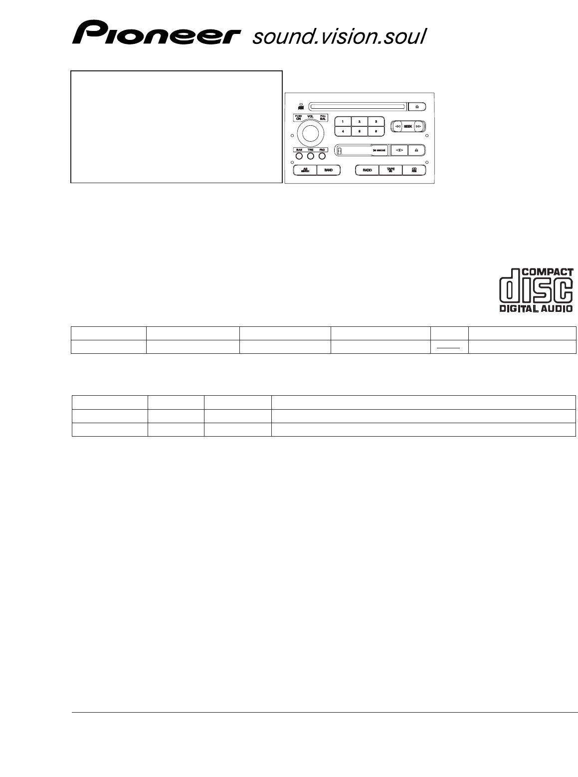
CRT2740
HEAD UNIT(3 in 1)
SAAB
-This service manual should be used together with the following manual(s):
Model No. Order No. Mech. Module Remarks
CX-1011 CRT2406 3L Cassette Mech. Module:Mech.Description, Disassembly
CX-958 CRT2423 S8.1 CD Mech. Module:Circuit Description, Mech.Description, Disassembly
CONTENTS
1. SAFETY INFORMATION ............................................2
2. EXPLODED VIEWS AND PARTS LIST.......................3
3. BLOCK DIAGRAM AND SCHEMATIC DIAGRAM ...10
4. PCB CONNECTION DIAGRAM ................................28
5. ELECTRICAL PARTS LIST ........................................44
6. ADJUSTMENT..........................................................52
7. GENERAL INFORMATION .......................................58
7.1 DIAGNOSIS ........................................................58
7.1.1 TEST MODE..............................................58
7.1.2 DISASSEMBLY .........................................59
7.1.3 PCB LOCATIONS ......................................64
7.1.4 CONNECTOR FUNCTION DESCRIPTION65
7.2 IC .......................................................................66
7.3 EXPLANATION ...................................................72
7.3.1 OPERATIONAL FLOW CHART .................72
7.3.2 SYSTEM BLOCK DIAGRAM.....................73
7.3.3 JIG CONNECTION DIAGRAM..................73
8. OPERATIONS AND SPECIFICATIONS.....................74
-Dolby noise reduction manufactured under license from Dolby Laboratories Licensing Corporation.
"Dolby" and the double-D symbol are trademarks of Dolby Laboratories Licensing Corporation.
VEHICLE DESTINATION PRODUCED AFTER SAAB PART No. ID No. PIONEER MODEL No.
SAAB 9-5 GENERAL AREA 2001 5038153 FX-M2317ZSA/X1B/ES
FX-M2317ZSA X1B/ES
Service
Manual

2
FX-M2317ZSA
1. SAFETY INFORMATION
CAUTION
This service manual is intended for qualified service technicians; it is not meant for the casual do-it-yourselfer.
Qualified technicians have the necessary test equipment and tools, and have been trained to properly and safely repair
complex products such as those covered by this manual.
Improperly performed repairs can adversely affect the safety and reliability of the product and may void the warranty.
If you are not qualified to perform the repair of this product properly and safely, you should not risk trying to do so
and refer the repair to a qualified service technician.
-CD Player Service Precautions
1. For pickup unit(CXX1285) handling, please refer
to"Disassembly"(see page 59).
During replacement, handling precautions shall be
taken to prevent an electrostatic discharge(protection
by a short pin).
2. During disassembly, be sure to turn the power off
since an internal IC might be destroyed when a con-
nector is plugged or unplugged.
3. Please checking the grating after changing the ser-
vice pickup unit(see page 56).
3
FX-M2317ZSA
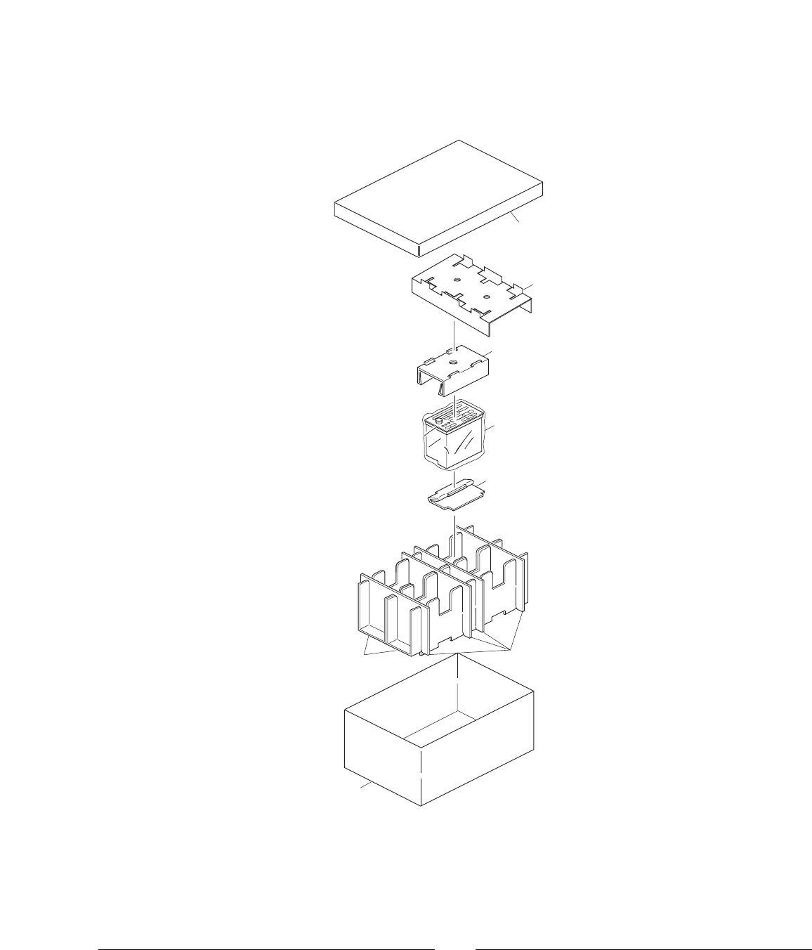
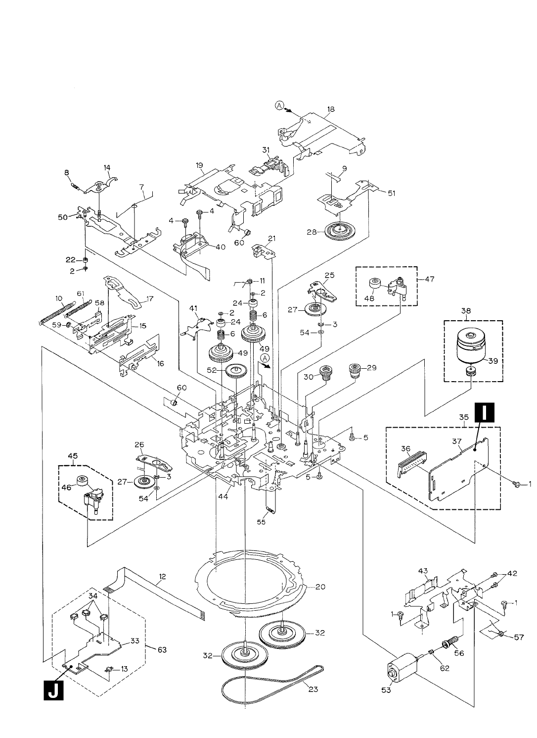
2. EXPLODED VIEWS AND PARTS LIST
2.1 PACKING
2
3
4
8
56
1
7
1 Cover UHW1584
2 Protector UHP1912
3 Polyethylene Bag UEG1057
4 Protector UHP1823
5 Protector UHP1825
6 Protector UHP1826
7 Protector UHP1824
8 Contain Box UHL-085
-PACKING SECTION PARTS LIST
Mark No. Description Part No. Mark No. Description Part No.
NOTE:
-Parts marked by “*” are generally unavailable because they are not in our Master Spare Parts List.
-Screws adjacent to ∇mark on the product are used for disassembly.
4
FX-M2317ZSA
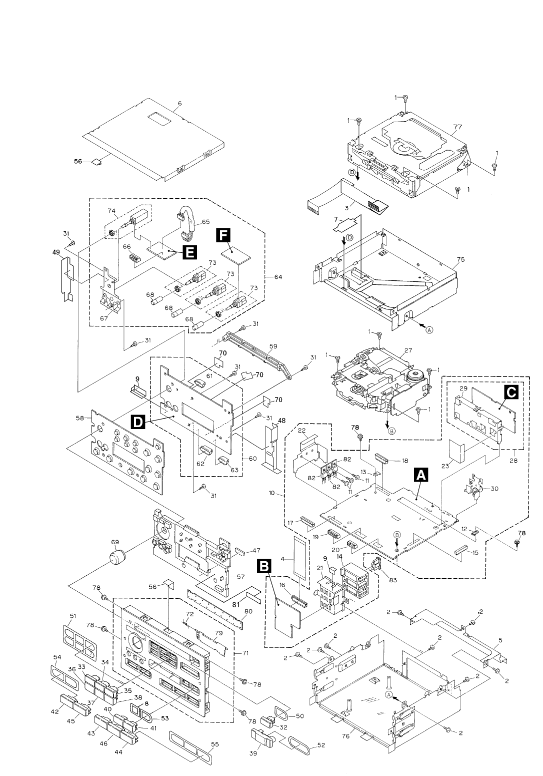
2.2 EXTERIOR

5
FX-M2317ZSA
1 Screw BSZ26P050FMC
2 Screw BMZ30P050FMC
3 Connector UDE-039
4 Connector CDE4952
5 Case CNB1958
6 Case CNB1959
7 Cover CNM5914
8 Insulator CNM5298
9 Insulator CNM5454
10 Tuner Mother Assy UWM-018
11 Screw BMZ30P060FMC
12 Terminal(CN803) CKF1059
13 Terminal(CN804) CKF1059
14 Connector(CN851) CKM1258
15 Connector(CN651) CKS3568
16 Connector(CN852) CKS1963
17 Connector(CN701) CKS3706
18 Connector(CN801) CKS3866
19 Plug(CN601) CKS3537
20 Plug(CN602) CKS3535
21 Holder CNC5906
22 Holder CNC5986
* 23 Insulator CNM4912
24-26 •••••
27 Cassette Mechanism ModuleEXK4220
28 Tuner Unit CWE1422
29 Holder CNC6122
30 Antenna Unit(CN501) CXA9328
31 Screw BPZ26P100FMC
32 Button(CD EJECT) CAC5703
33 Button(1) CAC5704
34 Button(2) CAC5705
35 Button(3) CAC5706
36 Button(4) CAC5707
37 Button(5) CAC5708
38 Button(6) CAC5709
39 Button(SEEK) CAC5710
40 Button(<>) CAC5711
41 Button(TAPE EJECT) CAC5712
42 Button(AS) CAC5713
43 Button(RADIO) CAC5721
44 Button(CD) CAC5717
45 Button(BAND) CAC5720
46 Button(TAPE) CAC5716
47 Spacer CNM4949
48 Insulator CNM5452
49 Insulator CNM5453
50 Insulator CNM5135
51 Insulator CNM5136
52 Insulator CNM5137
53 Insulator CNM5297
54 Insulator CNM5139
55 Insulator CNM5140
56 Insulator CNM5247
57 Lighting Conductor CNV4220
58 Rubber CNV5020
59 Holder CNV4535
60 Keyboard Unit UWM-021
61 Socket(CN903) CKS3548
62 Socket(CN901) CKS3550
63 Socket(CN902) CKS3548
64 Volume Unit UWM-020
65 Cord(CN904) CDE4761
66 Plug(CN905) CKS3535
67 Holder CNC6818
68 Knob Assy CXA7840
69 Knob Assy CXB5608
70 Spacer CNM5455
71 Grille Unit CXB1843
72 Spring CBH1371
73 Volume(VR902,903,904) CCS1089
74 Volume(VR901) CSD1036
75 Chassis UNA-004
76 Chassis Unit CXB7507
77 CD Mechanism Module(S8.1) CXK5224
78 Screw IMS30P050FMC
* 79 Door CAT1684
80 Cover CNM4768
81 Film CNM5299
82 Transistor(Q802,815,818) 2SB1185
83 Fuse(FU851) CEK1005
-EXTERIOR SECTION PARTS LIST
Mark No. Description Part No. Mark No. Description Part No.
6
FX-M2317ZSA
2.3 CD MECHANISM MODULE

7
FX-M2317ZSA
1 Control Unit CWX2411
2 Connector(CN802) CKS2192
3 Connector(CN801) CKS2193
4 Connector(CN701) CKS2773
5 Connector(CN101) CKS3486
6 Screw BMZ20P030FMC
7 Screw BSZ20P040FMC
8 Screw(M2x3) CBA1077
9 Screw(M2x5) EBA1028
10 Screw CBA1554
11 Screw(M2x4) CBA1362
12 Washer CBF1037
13 Washer CBF1038
14 Washer CBF1060
15 •••••
16 Spring CBH2079
17 Spring CBH2117
18 Spring CBH2314
19 Spring CBH2373
20 Spring CBH2282
21 Spring CBH2318
22 •••••
23 Spring CBH2324
24 Spring CBH2118
25 Spring CBH2161
26 Spring CBH2163
27 Spring CBH2189
28 Spring CBH2377
29 Spring CBH2260
30 Spring CBH2262
31 Bracket CNC8568
32 Spring CBL1531
33 Connector CDE5531
34 Connector CDE5532
35 Shaft CLA3894
36 Screw(M2.6x6) CBA1458
37 Frame CNC9159
38 Frame CNC9160
39 Lever CNC8694
40 Arm CNC8663
41 Bracket CNC8567
42 •••••
43 Spacer CNM3315
44 Sheet CNM6659
45 •••••
46 •••••
47 Ball CNR1189
48 Belt CNT1086
49 Roller CNV4509
50 Arm CNV6037
51 Arm CNV5247
52 Arm CNV5248
53 Arm CNV5249
54 Guide CNV5254
55 Guide CNV5255
56 Gear CNV5257
57 Gear CNV5256
58 Guide CNV6272
59 Damper CNV5266
60 Arm CNV6096
61 Arm CNV6031
62 Arm CNV6853
63 Guide CNV6012
64 Guide CNV5510
65 •••••
66 Guide CNV5751
67 Clamper CNV6013
68 Gear CNV5813
69 Motor Unit(M1) CXB2190
70 Screw Unit CXB5892
71 Chassis Unit CXB5811
72 Gear Unit CXB4728
73 Arm Unit CXB5753
74 Motor Unit(M2) CXB2195
75 Lever Unit CXB4730
* 76 Arm Unit CXB7754
77 Motor Unit(M3) CXB2562
78 Arm Unit CXB4732
79 Bracket Unit CXB4795
80 Screw JFZ20P025FMC
81 Screw JGZ17P025FZB
82 Washer YE20FUC
83 Pickup Unit(Service)(P8) CXX1285
84 Screw IMS26P030FMC
* 85 PCB CNX2982
86 Photo-transistor(Q1, 2) CPT230SX-TU
87 Spring CBH2372
88 Rack CNV6014
89 Spring CBH2315
Mark No. Description Part No. Mark No. Description Part No.
-CD MECHANISM MODULE SECTION PARTS LIST
8
FX-M2317ZSA
2.4 CASSETTE MECHANISM MODULE

9
FX-M2317ZSA
1 Screw BSZ20P040FMC
2 Washer CBF1037
3 Washer CBG1003
4 Screw EBA1028
5 Screw CBA1037
6 Spring EBH1653
7 Spring EBH1642
8 Spring EBH1641
9 Spring EBH1626
10 Spring EBH1627
11 Spring EBH1648
12 Cord EDD1024
13 Photo-reflector(Q101) EGN1004
14 Arm ENC1526
15 Lever Unit EXA1610
16 Lever ENC1543
17 Arm ENC1532
18 Frame ENC1533
19 Holder ENC1547
20 Gear ENC1535
21 Arm ENC1550
22 Roller ENR1040
23 Belt ENT1027
24 Collar ENV1508
25 Arm ENV1539
26 Arm ENV1540
27 Gear ENV1569
28 Gear ENV1547
29 Gear ENR1044
30 Worm Wheel ENV1559
31 Lever ENV1551
32 Flywheel ENV1554
33 Gathering PCB ENX1071
34 Switch(S101,S102,S103) ESG1007
35 Deck Unit EWM1037
36 Plug(CN251) CKS3540
37 Gathering PCB ENX1069
38 Motor Unit(M1) EXA1491
39 Motor EXM1028
40 Head Assy(HD1) EXA1506
41 Arm ENC1537
42 Screw JGZ20P025FNI
43 Guide ENC1545
44 Chassis Unit EXA1609
45 Pinch Holder Unit EXA1608
46 Pinch Roller ENV1518
47 Pinch Holder Unit EXA1607
48 Pinch Roller ENV1518
49 Reel Unit EXA1585
50 Head Base Unit EXA1611
51 Lever Unit EXA1587
52 Gear Unit EXA1596
53 Motor Unit(M2) EXA1623
54 Washer HBF-179
55 Spring EBH1537
56 Gear ENV1544
57 Spring EBH1654
58 Lever ENC1548
59 Washer YE15FUC
60 Tube ENM1039
61 Spring EBH1645
62 Spring EBH1647
63 Sensor Unit EWM1036
Mark No. Description Part No. Mark No. Description Part No.
-CASSETTE MECHANISM MODULE SECTION PARTS LIST
Q473
Q471
Q472
telon
SL
SD
SL
SD
47 76
Q503
Q502
Q504
SYSB
FM+B
AM+B
TUN+B
TUNER PLL
IC 501
LC72146MQ2 fm
am 11
10
17
13
FM-AM VCO
AM IFC
PDI/PCK/PDO/PCE
124
X501
Q507 Q506 EO0
AIN
EO1
19
21
20
22 AOUT
FM
LOOP FILTER AM
LOOP FILTER
B.U
Q510
Q508
DIVERSTY
POWER SUPPLY
7
DV CONT
DV CONT
DV CONT
AM ANT
FM ANT
FM IF OUT
FM IF FILTER
7
19
9
18
6
43
FMSL
40
12
FM PROCESSOR
IC2 PA4024A
L52
4719
CF53
FM IF
CF52
171514
Q31 CF51
FM IF
T31
FM MIX
109
FM/AM PROCESSOR
IC1 PA4023B
41
Q3
FM RF
Q201
11
25
26
FM
OSC
AM
OSC
AMRF/AGC
AMTV
34
386
Q51
FMTV
AMIFC
VCO
32 36 16 18 31 30 28
23 25
CF232 AM IF
FM+B
AM+B
TUN+B
AMSL
FMSD
19 20 15 17 13 14 21
DVCONT
DINC
EJTD
EJET
LOAD
CD5VON
VDSENS
clamp
8
50
49
11
12
34
48
DINC
EJTD
EJET
LOAD
CD5VON
clamp
Q815
Q816
CD POWER SUPPLY
B.U
VD
VDCON
33 4142
X701
X1
X2
CD CONTROLLER
IC 701
PE5239A
TAPE Lch
SYSB
TAPE+B
CN651
CN701
reset
60
VDD 21
SYSTEM
RESET
IC 801
S-80735ANDZI
35
reset
PCE
PCE
2
VDD
BACK U
SENSO
IC 802
S-80763A
Q80
Q80
SYSB
8.5
POWER S
ejsw 37 ejsw
load
stby
17
4
2
3
20
19
18
1
4
3
19
11
FM IF
CN501
STBY
LOAD
5
1
4
2
1
IC251
CXA2560Q
IC351
PA2020A
EQ AMP
MECHANISM
DRIVER
CN251
CN252
CN254
CN255
CN253
7
5TAPE+B
Lch
FWD
L-ch
REV
L-ch
37
36
39
17
315 6
87
10
CN256 315 6
S101
LOAD
S102
MODE
EGN1004
REEL
SENSE
M
M
M2
SUB
MOTOR
M1
MAIN
MOTOR
5
2
1
4
3
19
11
B.U
2020
B.U
S103
70µs
18
M
M
M
LD
MD
HOLOGRAM
UNIT
FOCUS ACT
TRACKING ACT
LD+
MD
FO+
TO+
14
5
4
3
SPINDLE
MOTOR
CARRIAGE
MOTOR
LOADING
MOTOR
1
2
3
4
3
1
2
SELECT
SENSE
DISC SENSE
CN801
CN802
D802
D801
VD
S802
CLAMP
1
28
21
CDLOAD
CDEJET
CONT
EJTSNS
DSCSNS
CLAMP
CD5VON
VDD IC 701
BA05SFP
IN
+5V REGULATOR
2
41
VD
Q101
CN101
FOP
TOP
A+C/F
B+D/E
98 LD
L_OUT
PD
HOME
97
24
23
39
X201
TD/FD
SD/MD
RF-AMP, DSP,
SERVO, DAC
IC 201
UPD63711GC
16
CN701
IC 301
BA5985FM S801
HOME
12
16
18
11
14
13
10
9
SOP
TOP
FOP
SOM
COP
COM
LOP
LOM
FWD
REV
MUTE
CD DRIVER
4
PICKUP UNIT(SERVICE)(P8)
8
21
23
22
5
6
7
24
VD
CONT
14
11 CONT
13
CDS Lch
4
4
CF230
ATUNER MOTHER PCB
CTUNER UNIT
GCONTROL UNIT
H
PHOTO UNIT(S8) IDECK UNIT
JSENSOR UNIT
10
FX-M2317ZSA
A
1234
B
C
D
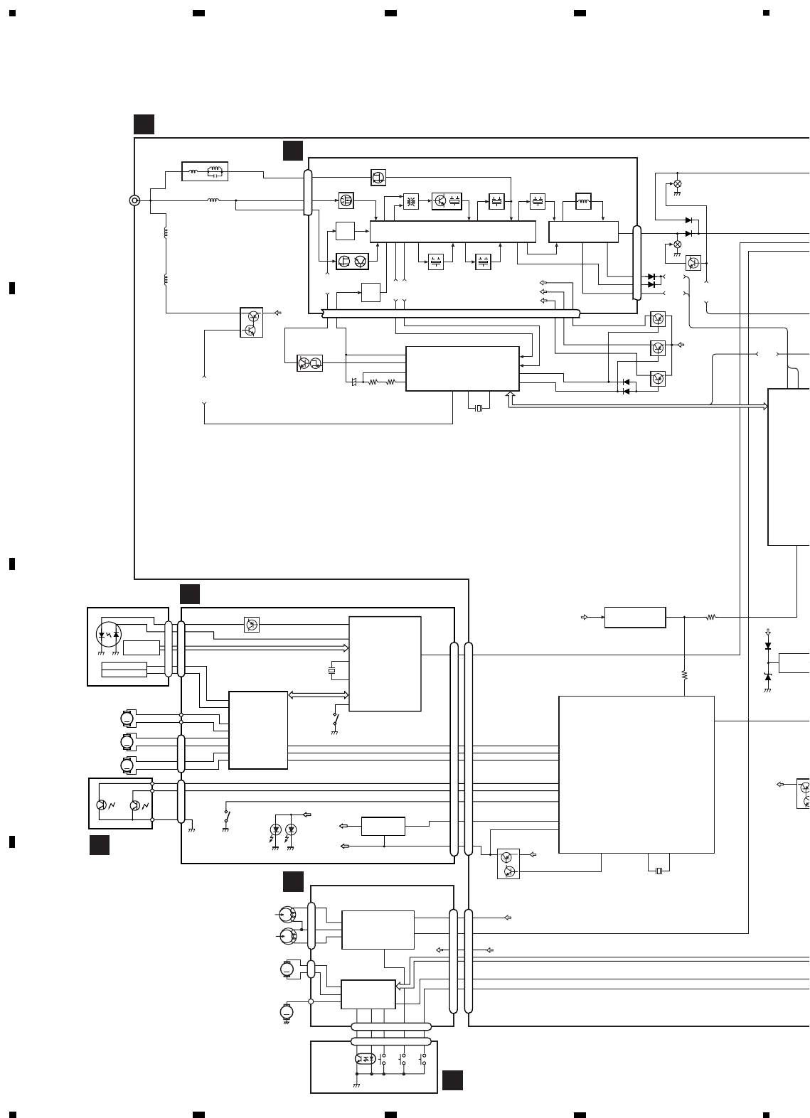
1234
3. BLOCK DIAGRAM AND SCHEMATIC DIAGRAM
3.1 BLOCK DIAGRAM
22 23 24 25 26
17 18 19 20 21
13 14 15 16
9101112
5678
1234
FUSE
FU851
5A
CON A
CON B
CON C
Q851
23 25 26
17
18
12
16
11
13
5
6
278
EF851
CN852
1
2
3
6
9
11
10
19
18
17
16
8
7
20
21
25
13.2V
ANTB
IG(+5V)
TELMUTE
AMPMUTE
RL-
RL+
FL-
FL+
CANL
CANH
CDML-
CDML+
TELAU
1
2
3
6
9
11
10
19
18
17
16
8
7
20
21
25
B.U
B.U
Q814
Q813
ANTB
ANTENNA BOOSTER
IGSEN
Q811
telmt
TELM
Q812
ampmt
SMUT
RL-
RL+
FL-
FL+
CANL
CANH
CDM-
CDM+
L653
Q652
Q651
B.U
IC 652
PCA82C250T
CAN BUS DRIVER
7
6
IC 403
NJM4558MD
REAR AUDIO OUTPUT
1
7
IC 401
NJM4558MD
FRONT AUDIO OUTPUT
1
7
6
6
19
20
IC 405
SN761029DL
ELECTRONIC VOLUME CONTROL
WAKE UP DRIVER
AMPB
FL
RL
SYSTEM
CONTROLLER
IC 601
PE5223B
SMUT
TELM
igsen
AMPB 50
63
65
48
EEP ROM
IC 602
S-29220A
VST/VCK/VDT
EDI/EDO/
ECK/ECE
1
4
RXD
TXD
WKUP
TX0
RX1
WKUP
6141
CAN BUS
IC 651
UPD72005GC
CDM+
TU/TEL
CDS
TAPE
5
2
4
13
telon
46
SL
SD
47 76
reset
60
EPCE
1
2
DD
BACK UP
SENSOR
IC 802
S-80763ANJT
62
BSEN
4847
X651
X1
X2
B.U
Q802
Q801
SB
SWVDD
8.5V
POWER SUPPLY
power
csej
64
66
POWER
CSEJ
ejsw
ejsw
CDEJ CDEJ
VOL1/VOL2/VOL3/BAL
FAD/TRE/BASS
DINJ
DINJ 6
ILLCON
ILLCON
B.U
SWVDD
SYSB
Q818
Q819
LAMP CONTROL
KDT0-KDT3
KST0-KST3
Q805
Q804
VDD
VDD
32
45
B.U
CAN VDD
POWER SUPPLY
CANVDD
SWVDD
SW
VDD
Q809Q806
VDD
49
SYSPW
load
36
SW5V
POWER
SUPPLY
Q807
Q808
stby
40
B.U
IC 803
S-81250PGRD
B.U 5V
REFERENCE
32
CN601 CN901
POWER
CDEJ
CSEJ SW902
SW901
IL901-IL907
ILL+B
DINJ
D901
Q901
VERF
SYSB
KEY
LED
KDT0-KDT3
KST0-KST3
CN903 CN905
BALANCE
POWER
BALANCE
SW904 VOLUME
BALANCE
VR901
SW903
POWER
SWITCH
VREF
CN904
VR902
FADER VR904
TREBLE VR903
BASS
3
4
5
1
2
3
4
5
1
2
1
12
1
12
8
5
9
8
5
9
1
1
CN602 CN902
CN801
CDM-
6
5
IC 471
NJM4558MD
TEL AUDIO ISOLATOR
TELAU
TELG
22
2424 TELG
12
3
BCONNECTOR PCB
EVOLUME PCB(A)
FVOLUME PCB(B)
DKEYBOARD UNIT
11
FX-M2317ZSA
5678
A
B
C
D
5678
0R0
0R0
0R0
CD CONTRO
DIVERSITY
POWER SUPPLY
FM IF FILTER
FM LOOP FILTER
AM LOOP
FILTER
PLL IC
CDS1031 : 50k(B)
T
T
D
T
D
C
A
: FM, AM SIGNAL
: TAPE SIGNAL
: CD SIGNAL
: AUDIO SIGNAL
TUNER MOTHER ASSY
Consists of
TUNER MOTHER PCB
CONNECTOR PCB
ATUNER MOTHER PCB
CTUNER UNIT
D
KEYBOARD UNIT E
VOLUME PCB
GCONTROL
CN601
CN901
CN501
47K
0R0
51
0R0
0R0
R033
R033
FM : -30dBs
CD : 3.8dBs
AM : -26dBs C
12
FX-M2317ZSA
A
1234
B
C
D
1234
A
A-a A-b
A-a A-b
A-b
A-a
Large size
SCH diagram
Guide page
Detailed page
3.2 OVERALL CONNECTION DIAGRAM(GUIDE PAGE)
Note: When ordering service parts, be sure to refer to “EXPLODED VIEWS AND PARTS LIST” or “ELECTRICAL
PARTS LIST”.
D
A-a
E
(1/4W)
(1/4W)
360 360
27K 27K
4R7/35 4R7/35
2700P
2700P
2mH
CAN BUS CONTROL
CAN BUS DRIVER CD POWER SUPPLY LAMP CONTROL
WAKE UP
DRIVER
B.U 5V POWER SUPPLY
SW5V POWER SUPPLY
MUTE
DRIVER
TEL
MUTE
ANTENNA BOOSTER
POWER SUPPLY
POWER
FILTER
B.U VOLTAGE
SENSOR
B.U 5V
REFERENCE
8.5V
POWER SUPPLY
SYSTEM
RESET
EEPROM
SYSTEM CONTROL
IG VOLTAGE SENSOR
AUDIO OUTPUT (UNBAL/BAL)
ELECTRONIC VOLUME
OL
CCS1089 : 50k(B)
CEL1449 : 8V 80mA
T
T
C
C C
D
D
DD
A
A
A
A
A
Decimal points for resistor
and capacitor fixed values
are expressed as :
2.2 2R2
0.022 R022
←
←
The > mark found on some component parts indicates
the importance of the safety factor of the part.
Therefore, when replacing, be sure to use parts of
identical designation.
Symbol indicates a resistor.
No differentiation is made between chip resistors and
discrete resistors.
NOTE :
Symbol indicates a capacitor.
No differentiation is made between chip capacitors and
discrete capacitors.
>
VOLUME UNIT
Consists of
VOLUME PCB(A)
VOLUME PCB(B)
B(A) F
VOLUME PCB(B)
IDECK UNIT
CN251
CN651
UNIT CN701
CN701
CN602
CN902
CN903
CN905
CN904
CN801
CN852
BCONNECTOR PCB
1R6K 1R6K
2R7K
6R8K
0R0
PE5223B
CSS1503
TAPE : -7.9dBs
FM : -30dBs
CD : 3.8dBs
TAPE : -7.9dBs
AM : -26dBs FM : -8dBs
CD : 7.8dBs
TAPE : 0.6dBs
AM : -4dBs
FM : -3.4dBs
CD : 12.4dBs
TAPE : 5.2dBs
AM : 0.6dBs
R471 R470
4R7K 15K
15K 4R7K
IC471 NJM4558MD
C479
4R7/16
R469
6R8K
C480
100P
R468
470
R495
0R0 (1/4W)
R496
0R0 (1/4W)
13
FX-M2317ZSA
5678
A
B
C
D
5678
A
A-b
B F
0R0
0R0
0R0
DIVERSITY
POWER SUPPLY
FM IF FILTER
FM LOOP FILTER
AM LOOP
FILTER
PLL IC
T
TT
C
C
D
D
T
D
C
A
: FM, AM SIGNAL
: TAPE SIGNAL
: CD SIGNAL
: AUDIO SIGNAL
ATUNER MOTHER PCB
CTUNER UNIT
GCONTROL UNIT CN701
CN701
CN501
47K
0R0
51
0R0
0R0
R033
R033
CSS1
FM : -30dBs
CD : 3.8dBs
AM : -26dBs C
R471 R470
4R7K 15K
15K 4R7K
IC471 NJM4558MD
C479
4R7/16
R469
6R8K
C480
100P
14
FX-M2317ZSA
A
1234
B
C
D
1234
A-a A-b
A-a
1
2
3
(1/4W)
(1/4W)
360 360
27K 27K
4R7/35 4R7/35
2700P
2700P
EEPROM
IG VOLTAGE SENSOR
AUDIO OUTPUT (UNBAL/BAL)
ELECTRONIC VOLUME
T
T
C C
DD
A
A
A
A
A
>
1
CN701
CN801
CN852
B
1R6K 1R6K
2R7K
6R8K
0R0
PE5223B
CSS1503
FM : -30dBs
CD : 3.8dBs
TAPE : -7.9dBs
AM : -26dBs FM : -8dBs
CD : 7.8dBs
TAPE : 0.6dBs
AM : -4dBs
FM : -3.4dBs
CD : 12.4dBs
TAPE : 5.2dBs
AM : 0.6dBs
15K 4R7K
C479
4R7/16
R469
6R8K
R468
470
R495
0R0 (1/4W)
R496
0R0 (1/4W)
16
FX-M2317ZSA
A
1234
B
C
D
1234
A-a A-b
A-b
B
1
2
3
2mH
CAN BUS CONTROL
CAN BUS DRIVER CD POWER SUPPLY LAMP CONTROL
WAKE UP
DRIVER
B.U 5V POWER SUPPLY
SW5V POWER SUPPLY
MUTE
DRIVER
TEL
MUTE
ANTENNA BOOSTER
POWER SUPPLY
POWER
FILTER
B.U VOLTAGE
SENSOR
B.U 5V
REFERENCE
8.5V
POWER SUPPLY
SYSTEM
RESET
SYSTEM CONTROL
89 : 50k(B)
: 8V 80mA
D
D
Decimal points for resistor
and capacitor fixed values
are expressed as :
2.2 2R2
0.022 R022
←
←
The > mark found on some component parts indicates
the importance of the safety factor of the part.
Therefore, when replacing, be sure to use parts of
identical designation.
Symbol indicates a resistor.
No differentiation is made between chip resistors and
discrete resistors.
NOTE :
Symbol indicates a capacitor.
No differentiation is made between chip capacitors and
discrete capacitors.
VOLUME UNIT
Consists of
VOLUME PCB(A)
VOLUME PCB(B)
ME PCB(B)
IDECK UNIT
CN251
CN651
602
02
BCONNECTOR PCB
PE5223B
CSS1503
TAPE : -7.9dBs
TAPE : 5.2dBs
17
FX-M2317ZSA
5678
A
B
C
D
5678
A-a A-b
A-b
B
4
22
FX-M2317ZSA
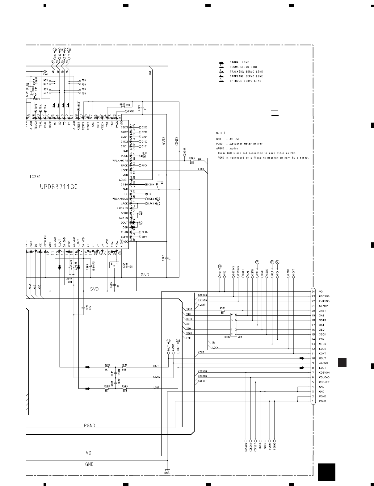
1RFI 0.5V/div. 0.5µs/div.
Normal mode: play
1CH1: RFI 1V/div.
2CH2: MIRR 5V/div.
Test mode: Tracking open
0.5ms/div. 1CH1: RFI 1V/div.
2CH2: MIRR 5V/div.
Normal mode: The defect part
passes 800µm
0.5ms/div.
3CH1: FD 0.5V/div.
4CH2: FO+ 2V/div.
Test mode: No disc, Focus close
0.2s/div. 3CH1: FD 0.5V/div.
5CH2: FOK 2V/div.
Normal mode: Focus close
0.2s/div. 6CH1: FE 0.5V/div.
7CH2: XSI 2V/div.
Normal mode: Focus close
1ms/div.
REFO →
8CH1: TE 0.5V/div.
9CH2: TD 0.5V/div.
Test mode: 32 tracks jump (FWD)
0.5ms/div. 8CH1: TE 0.5V/div.
9CH2: TD 0.5V/div.
Test mode: Single jump (FWD)
0.5ms/div. 8CH1: TE 0.5V/div.
9CH2: TD 0.5V/div.
Test mode: 100 tracks jump (FWD)
5ms/div.
6CH1: FE 0.1V/div.
3CH2: FD 0.2V/div.
Normal mode: Play
20ms/div. 3CH1: FD 0.5V/div.
0CH2: MD 1V/div.
Normal mode: Focus close (12cm)
0.5s/div. 3CH1: FD 0.5V/div.
0CH2: MD 1V/div.
Normal mode: Focus close (8cm)
0.5s/div.
REFO →
REFO →
REFO →
REFO →
REFO →
REFO →
GND →
REFO →
REFO →
REFO →
REFO →
REFO →
REFO →
REFO →
REFO →
REFO →
REFO →
REFO →
REFO →
-Waveforms
Note:1. The encircled numbers denote measuring pointes in the circuit diagram.
2. Reference voltage
REFO:2.5V
REFO →
REFO →
REFO →
REFO →
23
FX-M2317ZSA
8CH1: TE 0.2V/div.
9CH2: TD 0.2V/div.
Normal mode: play
8CH1: TE 0.5V/div.
!CH2: SD 0.5V/div.
TEST mode: 100 Tracks jump(FWD)
5ms/div. 0MD 0.5V/div. 0.1s/div.
Normal mode: Play (12cm)
0MD 1V/div. 10ms/div.
Normal mode:
Long Search (12cm)
@EFM 1V/div. 5µs/div.
Normal mode: play
8CH1: TE 1V/div.
#CH2: TEC 1V/div.
Test mode: Focus close
Tracking open
2ms/div.
8CH1: TE 0.5V/div.
6CH2: FE 0.5V/div.
Normal mode:
AGC after focus close
0.2s/div. $PLCK 2V/div. 0.5µs/div.
Normal mode: play
20ms/div.
%SCKO 2V/div. 1µs/div.
Normal mode: play
^Dout 2V/div. 10µs/div.
Normal mode: play
&LRCK 2V/div. 20µs/div.
Normal mode: play
*VD 5V/div. 50ms/div.
Normal mode: No disc
GND →
REFO →
REFO →
GND →
REFO →
REFO →
REFO →
REFO →REFO →
REFO →
REFO →
REFO →
REFO →
GND →
REFO →
GND →
REFO →
GND →
REFO →
GND →
REFO →
24
FX-M2317ZSA
(CH1: R OUT 1V/div.
)CH2: L OUT 1V/div.
Normal mode: Play (1kHz 0dB)
6CH1: FE 0.2V/div.
3CH2: FD 0.5V/div.
Normal mode: During AGC
1ms/div. 8CH1: TE 0.2V/div.
9CH2: TD 0.5V/div.
Normal mode: During AGC
1CH1: RFI 1V/div.
⁄CH2: HOLD 5V/div.
Normal mode: The defect part passes
800µm(B.D)
0.2ms/div. 1ms/div.
0.5ms/div. 3CH1: FD 0.5V/div.
⁄CH2: HOLD 5V/div.
Normal mode: The defect part passes
800µm(B.D)
0.5ms/div. 9CH1: TD 0.1V/div.
⁄CH2: HOLD 5V/div.
Normal mode: The defect part passes
800µm(B.D)
0.5ms/div.
REFO →
REFO →
REFO →
REFO →
REFO →
REFO →
REFO →
REFO →REFO →
REFO →
REFO →
REFO →

25
FX-M2317ZSA
26
FX-M2317ZSA
A
1234
B
C
D
1234
I
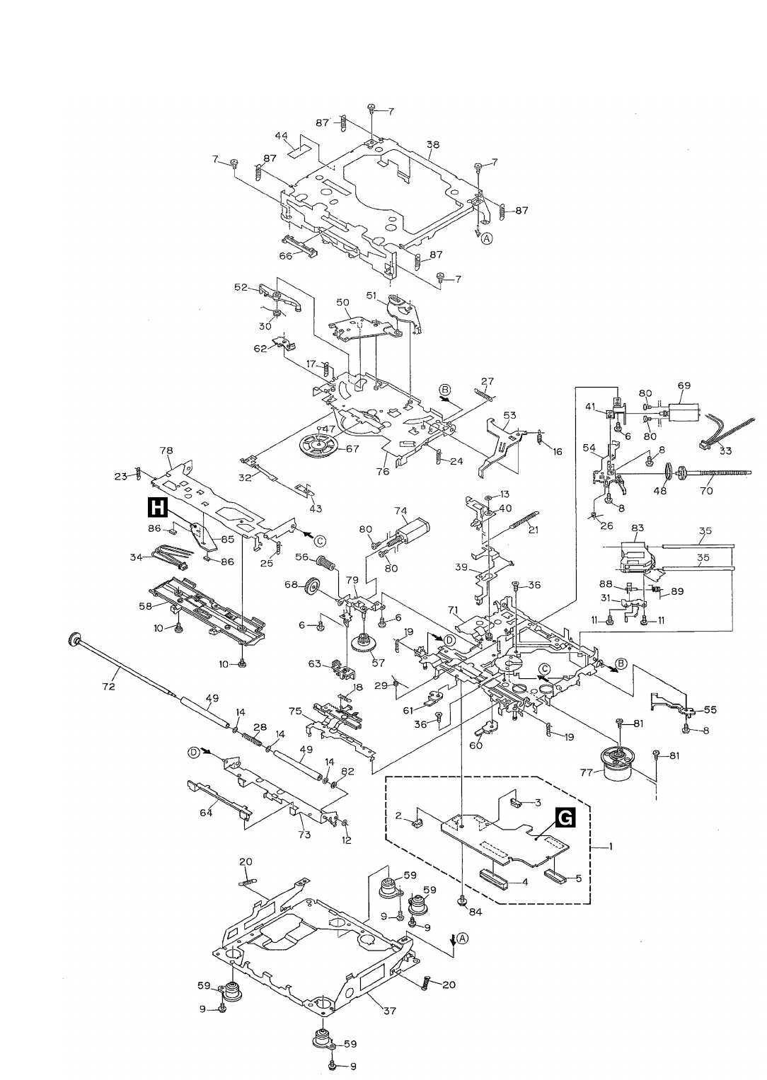
3.5 CASSETTE MECHANISM MODULE
DECK UNIT
MUTE
CXA2560Q
11
12
13
14
15
16
17
18
19
20
40
39
38
37
36
35
34
33
32
31
30
29
28
27
26
25
24
23
22
21
1
2
3
4
5
6
7
8
9
10
R256 220
R287
0R0
C273
220/50
R283 0R0
R284 0R0
R282 0R0
C253 330P
C254 330P
C252 330P
C251 330P
R281 0R0
R255 220
C256
R01
R258
1K
R301
18K
R273 1K
R271 1K
R272 1K
R
C4
39
C4
R
R257
1K
C255
R01
C272 R1
C313 100P
R286 0R0
R285 0R0
HD1
HEAD ASSY
EXA1506
TEST TAPE
NCT-150
(400Hz, 200nWb/m)
RL
RR
FR
FL
C302
R1
C301
R1
VR302 33K(B)
-6dBs(388mV)±1dB
Fwd-R
Fwd-L
Rev-R
Rev-L
PBFB2
PBRIN2
PBGND
PBFIN2
VCT
PBREF
PBFIN1
PBGND
PBRIN1
PBFB1
PBTC1
PBOUT1
OUTREF1
TAPEIN1
VCC
LINEOUT1
TCH1
MSLPF
MSMODE
DRSW
TAPESW
MUTESW
MSOUT
MSTC
G1FB
G2FB
PBTC2
PBOUT2
OUTREF2
TAPEIN2
GND
DIREF
LINEOUT2
TCH2
MSSW
CN252
CN251
DOLBY B NR
IC251
VR301 33K(B)
C310
R1
C309
R1
R322 1K
NRSW
CCP1280
CCP1280
ACN651
I
27
FX-M2317ZSA
5678
A
B
C
D
5678
JI
SENSOR UNIT
SWITCHES:
SENSOR UNIT
S101:LOAD SWITCH..........EJECT-PLAY
S102:MODE SWITCH............ON-OFF
S103:70µs SWITCH...............ON-OFF
The underlined indicates the switch position.
R290 0R0
C403 R068
R403 82K
C402
3900P
C401
R33
R402 18K
R401
4R7K
R351 1K
R352 1K
R353 1K
R354 1K
R373 0R0
R355
270K
C352
3900P
R362 300
C351 R22
C353 R01
C354 R01
R374 0R0
C356 R01
C355 R1
D352 1SS355
M1 MOTOR UNIT
(MAIN MOTOR)
EXA1491
S101 LOAD
ESG1007x3
S102 MODE
REEL SENSE
Q101
EGN1004
M2
MOTOR UNIT
(SUB MOTOR)
EXA1623
RS3
RS2
RS1
SC2
SC1
TAB
MC
CE
VCC2
NC
VCC
MCS
RRS
FRS
RSB
C
TAB
MS2
NC
NC
MM
SM1
RSB
GND
RS
mtl
MCS
load
CN255 CN253 CN256
CN254
MECHANISM
DRIVER
IC351 PA2020A
R375 0R0 S103 70µs
CN651
J
28
FX-M2317ZSA
A
1234
B
C
D
1234
BCN852
GCN701
A
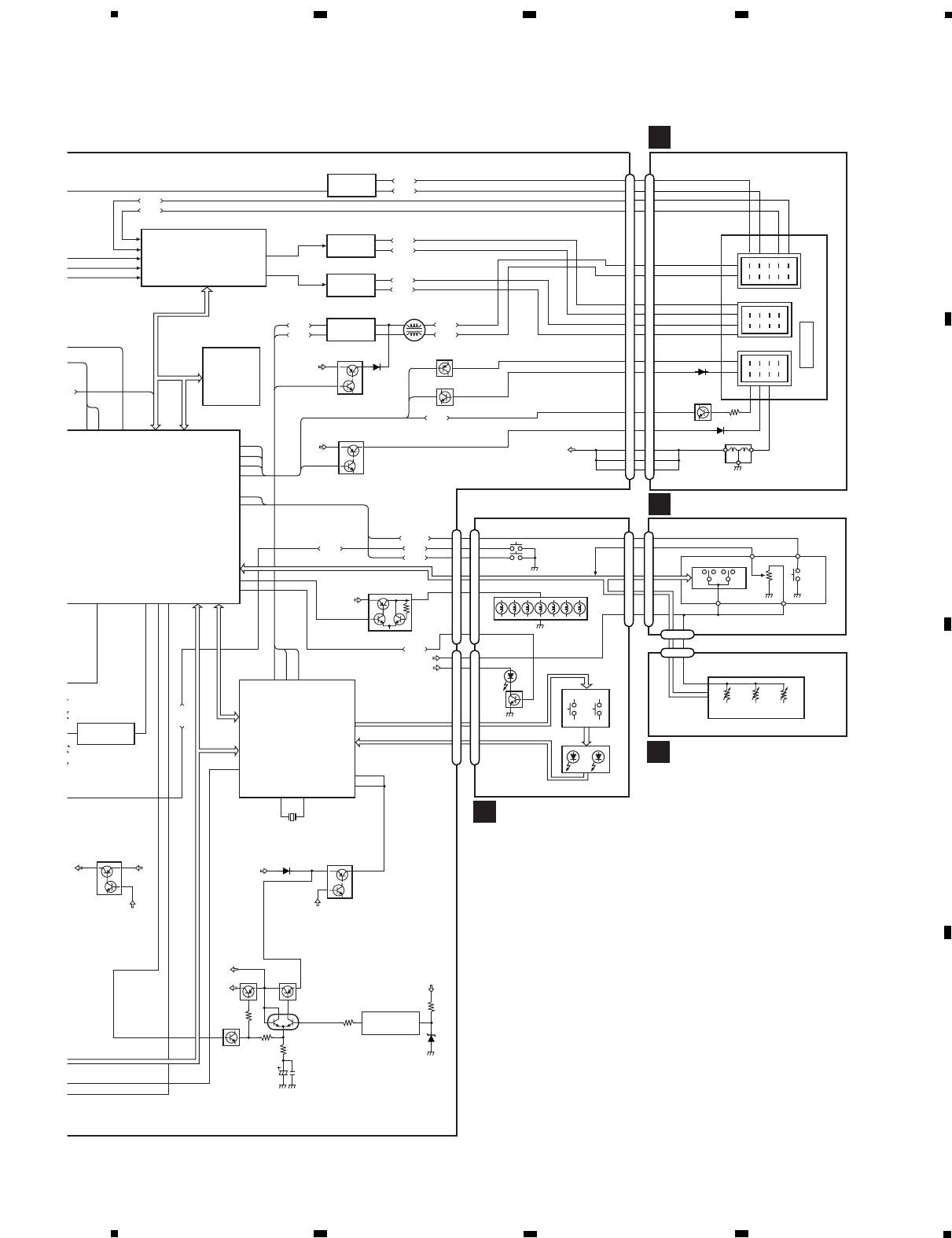
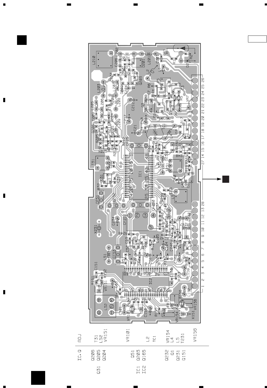
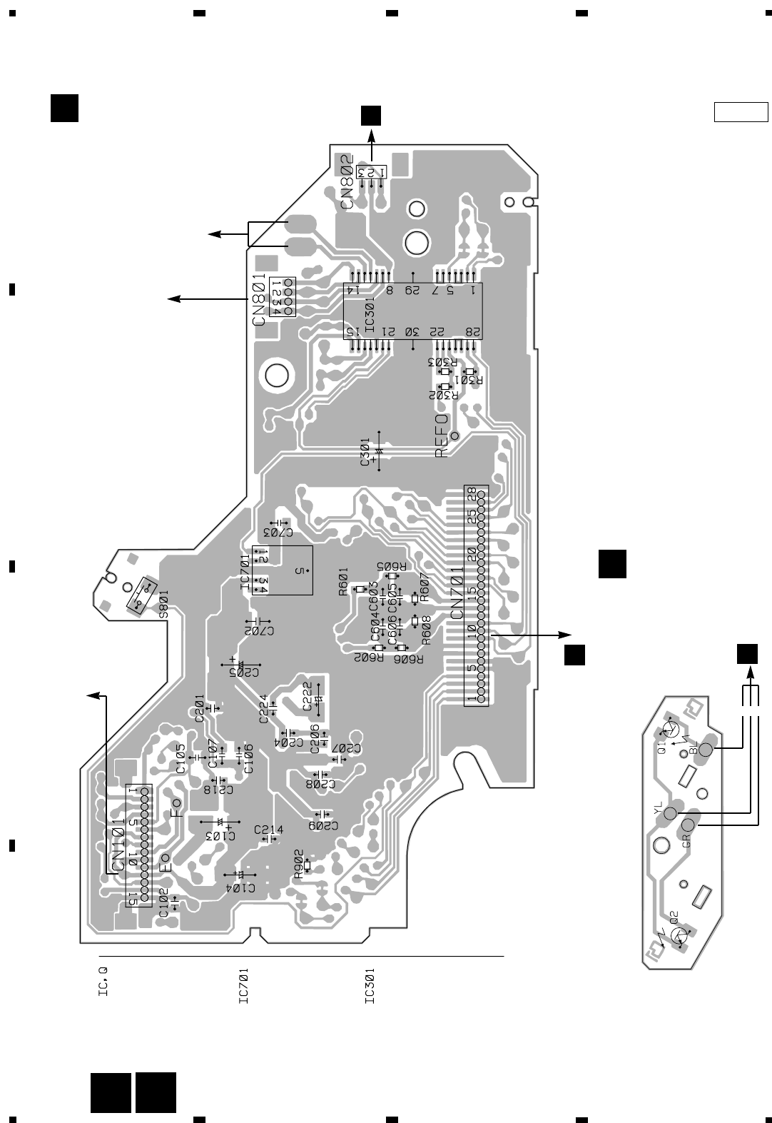
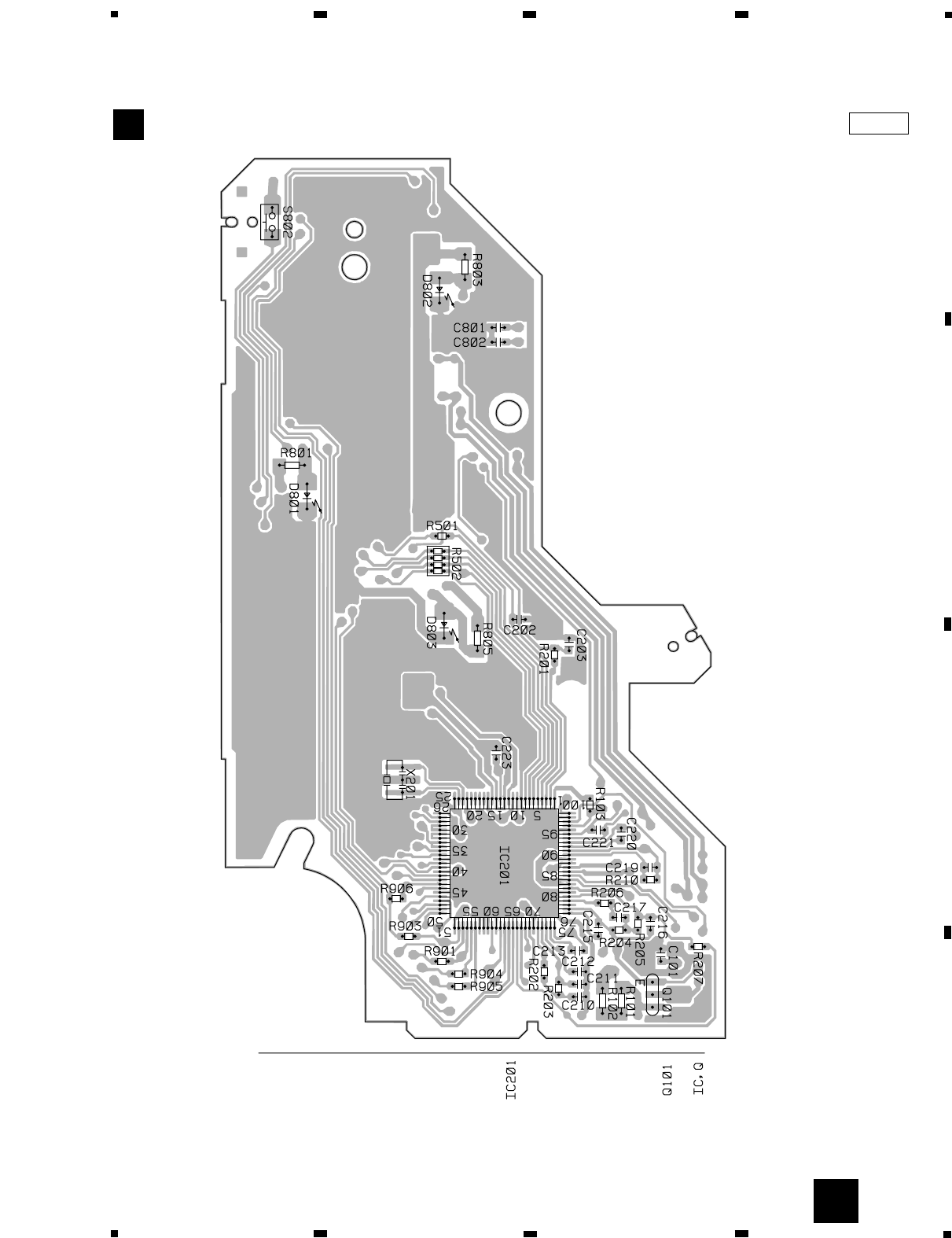
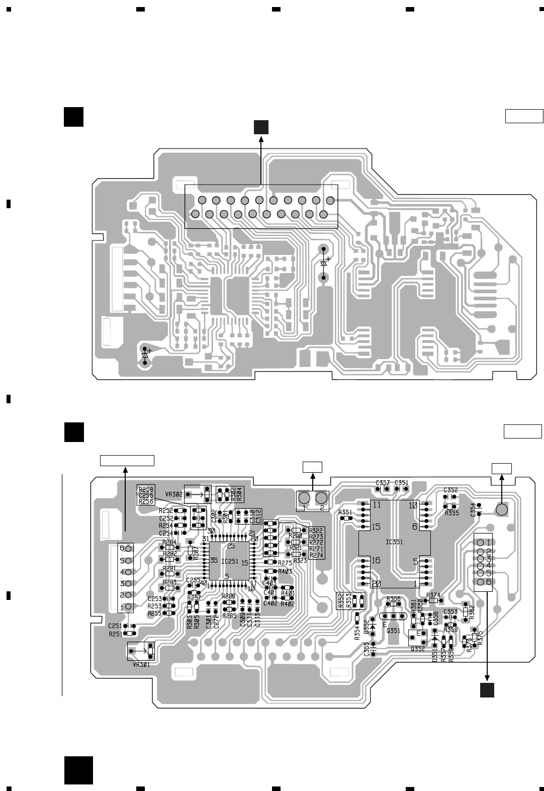
4. PCB CONNECTION DIAGRAM
4.1 TUNER MOTHER PCB
Capacitor
Connector
P.C.Board Chip Part
SIDE A
SIDE B
NOTE FOR PCB DIAGRAMS
1. The parts mounted on this PCB
include all necessary parts for
several destination.
For further information for
respective destinations, be sure
to check with the schematic dia-
gram.
2. Viewpoint of PCB diagrams
TUNER MOTHER PCB
A
FRONT
ACN801
32
FX-M2317ZSA
A
1234
B
C
D
1234
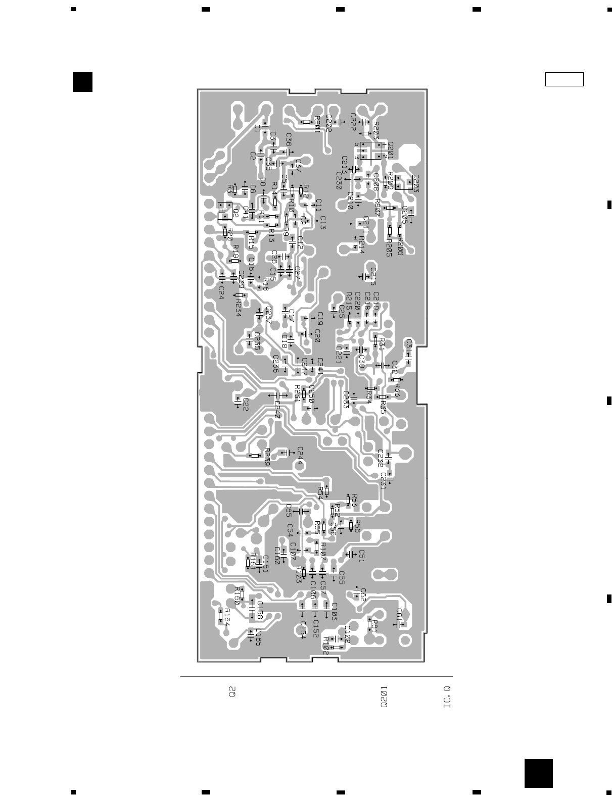
4.2 CONNECTOR PCB
SIDE A
B
CONNECTOR PCB
B
33
FX-M2317ZSA
1234
A
B
C
D
1234
B
CONNECTOR PCB
BSIDE B
34
FX-M2317ZSA
A
1234
B
C
D
1234
4.3 TUNER UNIT
SIDE A
C
TUNER UNIT
C
A
35
FX-M2317ZSA
1234
A
B
C
D
1234
SIDE B
C
TUNER UNIT
C
123
456
CD EJECT
SEEK << SEEK >>
<> TAPE EJECT
CDTAPERADIOBANDAS
36
FX-M2317ZSA
A
1234
B
C
D
1234
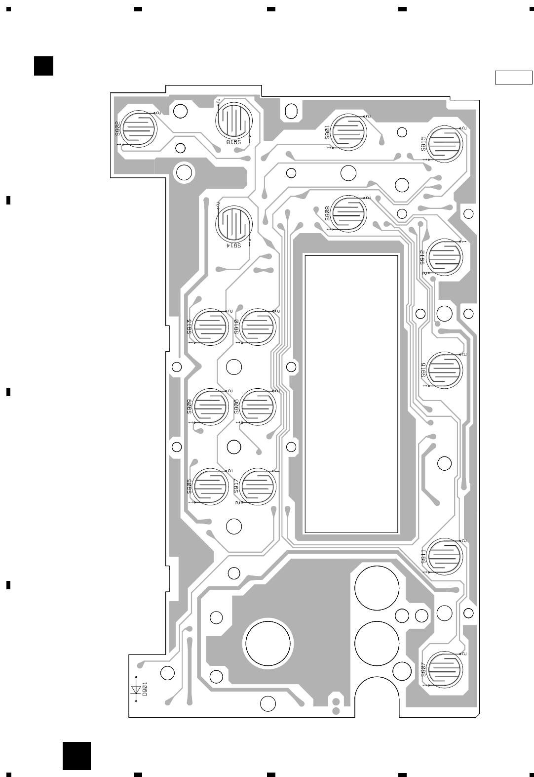
4.4 KEYBOARD UNIT
KEYBOARD UNIT
D
SIDE A
D
AA
CN602 CN601
ECN905
KEYBOARD UNIT
D
37
FX-M2317ZSA
1234
A
B
C
D
1234
D
SIDE B
F
CN904
D
CN903
38
FX-M2317ZSA
A
1234
B
C
D
1234
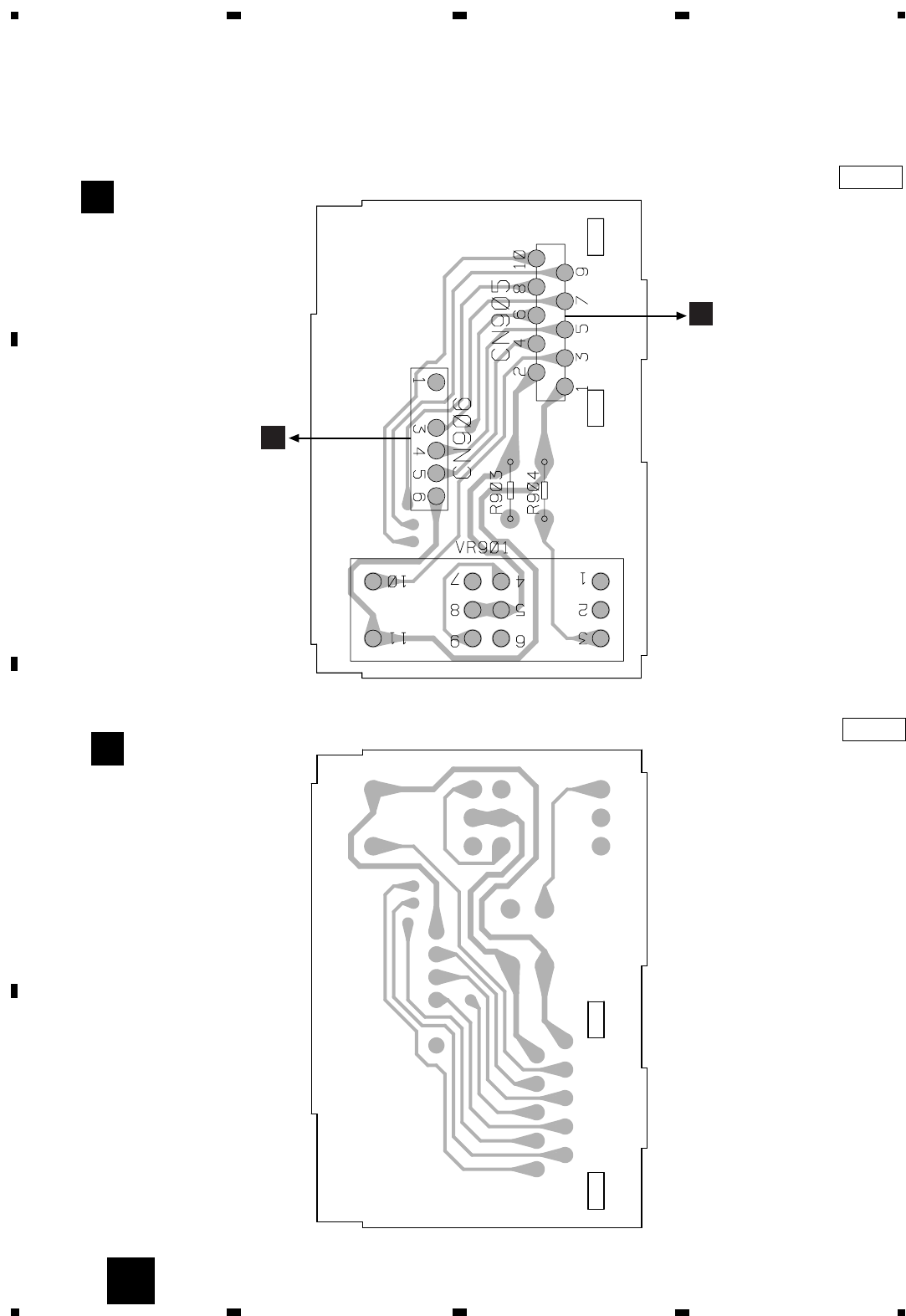
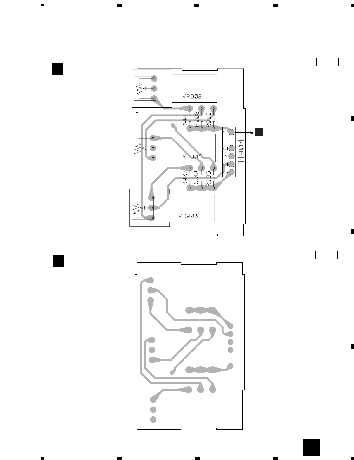
4.5 VOLUME PCB(A)
SIDE A
E
SIDE B
VOLUME PCB(A)
E
VOLUME PCB(A)
E
39
FX-M2317ZSA
1234
A
B
C
D
1234
F
4.6 VOLUME PCB(B)
E
CN906
SIDE A
SIDE B
VOLUME PCB(B)
F
VOLUME PCB(B)
F
40
FX-M2317ZSA
A
1234
B
C
D
1234
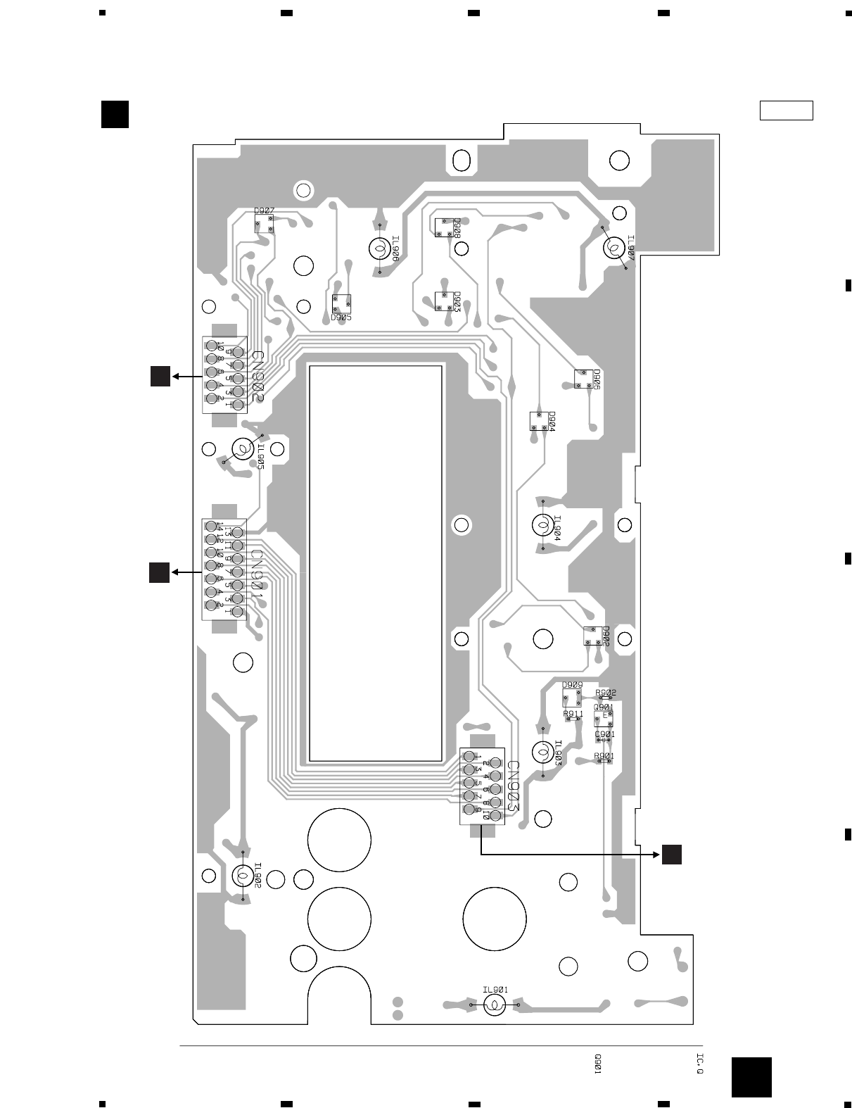
G
4.7 CD MECHANISM MODULE
SIDE A
H
HOME
CONTROL UNIT
M1 CARRIAGE MOTOR
M2 LOADING MOTOR
M3 SPINDLE MOTOR
PICKUP UNIT(SERVICE)(P8)
CN802
CN681
3
2
1
PHOTO UNIT(S8)
G
H
A
G
H
41
FX-M2317ZSA
1234
A
B
C
D
1234
SIDE B
G
CLAMP
CONTROL UNIT
G
42
FX-M2317ZSA
A
1234
B
C
D
1234
I
4.8 DECK UNIT
C321
1
3
15
CN251
19 17 9
13 11 75
2
4
16
20 18 10
14 12 86
C273
ACN651
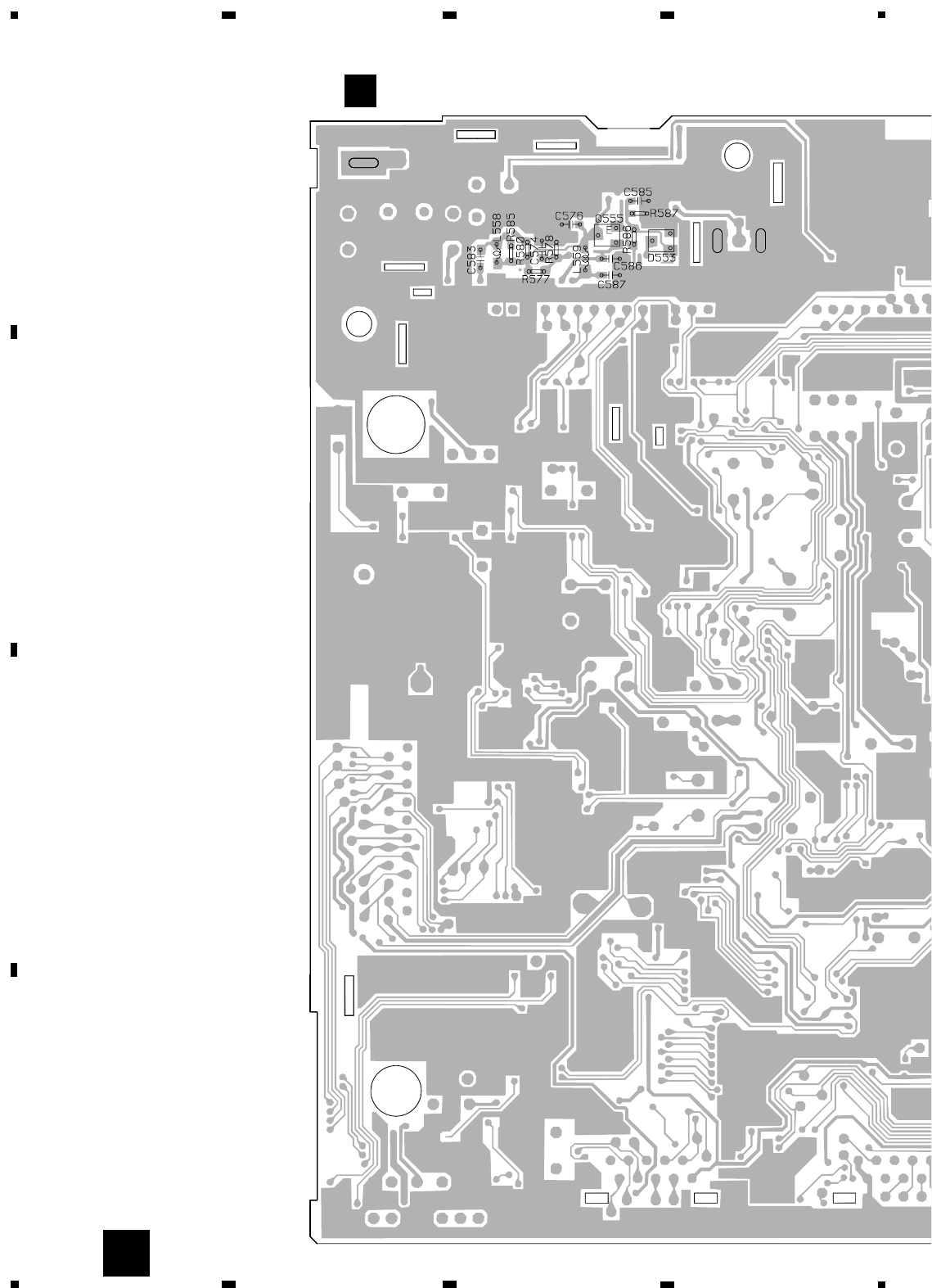
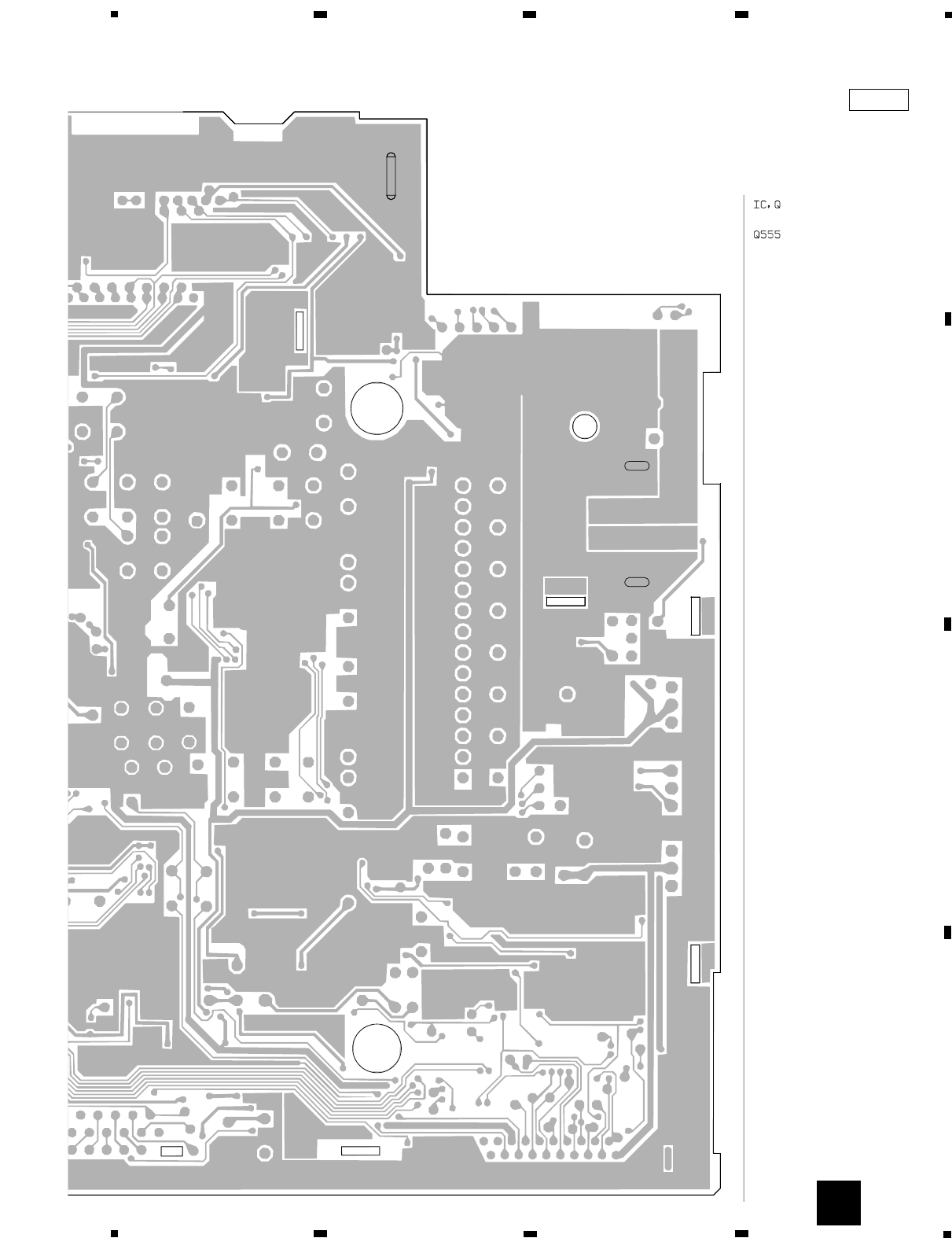
IC,Q
IC251
Q351
Q352
ADJ
VR302
VR301
IC351 CN252
CN254 CN253
CN255
M1
M2
HEAD ASSY
21
22
JCN256
DECK UNIT
I
DECK UNIT
I
SIDE A
SIDE B
43
FX-M2317ZSA
1234
A
B
C
D
1234
J
4.9 SENSOR UNIT
1
2
3
4
5
6
S101
LOAD
S102
MODE
S103
70µs
CN256
Q1
REEL SENSE
ICN253
SENSOR UNIT
J

44
FX-M2317ZSA
Unit Number : UWM-018
Unit Name : Tuner Mother Assy
MISCELLANEOUS
IC 401 IC NJM4558MD
IC 402 IC NJM4558MD
IC 403 IC NJM4558MD
IC 404 IC NJM4558MD
IC 405 IC SN761029DL
IC 471 IC NJM4558MD
IC 501 IC LC72146MQ2
IC 601 IC PE5223B
IC 602 IC S-29220A
IC 651 IC UPD72005GC
IC 652 IC PCA82C250T
IC 701 IC PE5239A
IC 801 IC S-80735ANDZI
IC 802 IC S-80763ANJT
IC 803 IC S-81250PGPD
Q 471 Transistor DTC114EK
Q 472 Transistor DTC144EK
Q 473 Transistor IMH2A
Q 501 Transistor DTC144EK
Q 502 Transistor 2SB1132
Q 503 Transistor 2SB1132
Q 504 Transistor 2SB1132
Q 506 Transistor 2SK208
Q 507 Transistor 2SC2712
Q 508 Transistor DTC114EK
Q 509 Transistor DTA114TK
Q 510 Transistor 2SB1238
Q 511 Transistor 2SC2712
Q 651 Transistor 2SC2712
Q 652 Transistor 2SA1162
Q 701 Transistor DTA144EK
Q 801 Transistor IMX1
Q 802 Transistor 2SB1185
Q 804 Transistor IMX1
Q 805 Transistor 2SB1260
Q 806 Transistor 2SA1162
Q 807 Transistor DTC114EK
Q 808 Transistor IMX1
Q 809 Transistor 2SB1260
Q 811 Transistor 2SA1162
Q 812 Transistor 2SC2712
Q 813 Transistor 2SC2712
Q 814 Transistor 2SB1243
Q 815 Transistor 2SB1185
Q 816 Transistor IMX1
Q 817 Transistor DTC114TK
Q 818 Transistor 2SB1185
Q 819 Transistor IMX1
Q 851 Transistor 2SC2712
D 409 Chip Diode MA151WK
D 410 Chip Diode MA151WK
D 471 Diode RD4R7JS(B3)
D 501 Chip Diode MA151WK
D 502 Diode 1SS133
D 503 Diode 1SS133
D 504 Diode RD2R7M(B2)
D 601 Diode IMN10
D 651 Diode RD4R7ES(B3)
D 652 Zener Diode RD16ES(B3)
D 653 Diode RD4R7ES(B3)
D 654 Zener Diode RD16ES(B3)
D 655 Diode RD13ES(B2)
D 656 Diode MA151WA
D 801 Diode RD8R2JS(B1)
D 803 Zener Diode RD16ES(B3)
D 804 Diode 1SS133
D 805 Zener Diode RD16ES(B3)
D 806 Diode 1SS133
D 807 Diode ERA15-02VH
D 808 Diode RD7R5JS(B3)
D 809 Diode ERA15-02VH
D 851 Diode ERA15-02VH
D 853 Diode ERA15-10VH
D 854 Zener Diode RD16ES(B3)
D 855 Diode 1SS133
L 501 Ferri-Inductor LAU4R7K
L 502 Resistor RD1/4PU0R0J
L 503 Resistor RD1/4PU0R0J
L 504 Ferri-Inductor LAU4R7K
L 506 Ferri-Inductor LAU4R7K
L 507 Inductor CTF1053
L 508 Inductor CTF1374
L 509 Coil CTE1123
L 510 Inductor LCTBR27K2125
L 511 Coil LCTBR22K2125
L 512 Resistor RD1/4PU0R0J
L 601 Ferri-Inductor LAU4R7K
L 602 Ferri-Inductor LAU4R7K
L 651 Ferri-Inductor LAU220K
L 652 Ferri-Inductor LAU220K
L 653 Choke Coil CTH1180
L 701 Ferri-Inductor LAU4R7K
L 801 Choke Coil 2mH CTH1074
TH 701 Thermistor CCX1015
X 501 Crystal Resonator 7.2MHz CSS1030
X 601 Ceramic Resonator 4.194MHz CSS1071
X 651 Radiator 2.00MHz CSS1393
X 701 Radiator 8.380MHz CSS1503
FU 851 Fuse 5A CEK1005
EF 851 EMI Filter CCG1006
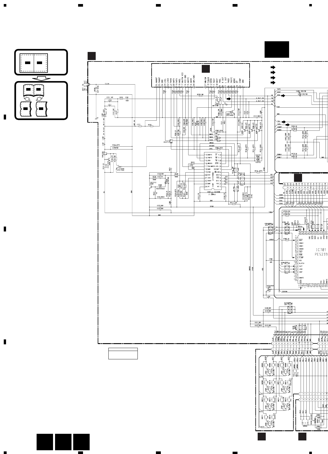
5. ELECTRICAL PARTS LIST
NOTE:
-Parts whose parts numbers are omitted are subject to being not supplied.
-The part numbers shown below indicate chip components.
Chip Resistor
RS1/_S___J,RS1/__S___J
Chip Capacitor (except for CQS.....)
CKS....., CCS....., CSZS.....
=====Circuit Symbol and No.===Part Name Part No.
--- ------ ------------------------------------------ -------------------------
=====Circuit Symbol and No.===Part Name Part No.
--- ------ ------------------------------------------ -------------------------
A
Tuner Mother Assy
Consists of
Tuner Mother PCB
Connector PCB
B

45
FX-M2317ZSA
AR 501 Arrester DSP-201M
Tuner Unit CWE1422
RESISTORS
R 403 RS1/10S222J
R 404 RS1/10S222J
R 405 RS1/10S162J
R 406 RS1/10S162J
R 409 RS1/10S102J
R 410 RS1/10S102J
R 411 RS1/10S102J
R 412 RS1/10S102J
R 413 RS1/10S102J
R 414 RS1/10S102J
R 415 RS1/10S361J
R 416 RS1/10S361J
R 417 RS1/10S273J
R 418 RS1/10S273J
R 419 RS1/10S473J
R 420 RS1/10S473J
R 421 RS1/10S562J
R 422 RS1/10S562J
R 423 RS1/10S562J
R 424 RS1/10S562J
R 425 RS1/10S472J
R 426 RS1/10S472J
R 427 RS1/10S472J
R 428 RS1/10S472J
R 429 RS1/10S472J
R 430 RS1/10S472J
R 431 RS1/10S472J
R 432 RS1/10S472J
R 433 RS1/10S470J
R 434 RS1/10S470J
R 435 RS1/10S470J
R 436 RS1/10S470J
R 437 RS1/10S472J
R 438 RS1/10S472J
R 439 RS1/10S472J
R 440 RS1/10S472J
R 441 RS1/10S470J
R 442 RS1/10S470J
R 443 RS1/10S470J
R 444 RS1/10S470J
R 468 RS1/10S471J
R 469 RS1/10S682J
R 470 RS1/10S153J
R 471 RS1/10S472J
R 472 RS1/10S153J
R 473 RS1/10S472J
R 474 RS1/10S182J
R 475 RS1/10S182J
R 476 RS1/10S182J
R 477 RS1/10S182J
R 478 RS1/10S102J
R 479 RS1/10S102J
R 480 RS1/10S473J
R 481 RS1/10S102J
R 482 RS1/10S102J
R 486 RS1/10S103J
R 490 RS1/10S102J
R 491 RS1/10S102J
R 495 RD1/4PU0R0J
R 496 RD1/4PU0R0J
R 501 RS1/10S103J
R 502 RS1/10S102J
R 503 RS1/10S681J
R 504 RS1/10S393J
R 505 RS1/10S222J
R 506 RS1/10S222J
R 507 RS1/10S473J
R 508 RS1/10S473J
R 509 RS1/10S473J
R 510 RS1/10S472J
R 511 RS1/10S472J
R 512 RS1/10S392J
R 513 RS1/10S223J
R 514 RAB4C103J
R 515 RAB4C102J
R 516 RS1/10S472J
R 517 RS1/10S223J
R 519 RS1/10S473J
R 520 RS1/10S562J
R 521 RS1/10S222J
R 522 RS1/10S222J
R 523 RS1/10S152J
R 524 RS1/10S472J
R 525 RS1/10S102J
R 526 RS1/10S102J
R 527 RS1/10S102J
R 528 RS1/10S562J
R 529 RS1/10S103J
R 530 RS1/10S223J
R 531 RD1/4PU180J
R 532 RS1/10S0R0J
R 533 RS1/10S510J
R 534 RS1/10S0R0J
R 535 RS1/10S0R0J
R 536 RS1/10S472J
R 537 RD1/4PU100J
R 538 RS1/10S103J
R 601 RS1/10S272J
R 602 RS1/10S682J
R 603 RS1/10S472J
R 604 RS1/10S222J
R 605 RS1/10S222J
R 606 RS1/10S473J
R 607 RS1/10S473J
R 608 RS1/10S473J
R 609 RAB4C222J
R 610 RS1/10S184J
R 611 RAB4C102J
R 612 RAB4C102J
R 613 RAB4C681J
R 614 RAB4C102J
R 615 RS1/10S473J
R 616 RS1/10S473J
R 617 RAB4C472J
R 618 RS1/10S222J
R 619 RS1/10S472J
R 620 RS1/10S473J
R 621 RS1/10S473J
R 622 RS1/10S222J
R 623 RS1/10S222J
R 625 RS1/10S222J
R 626 RS1/10S222J
R 627 RS1/10S473J
R 628 RS1/10S222J
R 629 RAB4C222J
=====Circuit Symbol and No.===Part Name Part No.
--- ------ ------------------------------------------ ------------------------- =====Circuit Symbol and No.===Part Name Part No.
--- ------ ------------------------------------------ -------------------------

46
FX-M2317ZSA
R 630 RAB4C472J
R 631 RAB4C223J
R 632 RS1/16S0R0J
R 651 RS1/10S681J
R 652 RS1/10S681J
R 653 RAB4C681J
R 654 RAB4C473J
R 655 RAB4C681J
R 656 RAB4C473J
R 657 RAB4C472J
R 658 RAB4C223J
R 659 RAB4C102J
R 660 RAB4C102J
R 661 RAB4C102J
R 662 RAB4C473J
R 663 RS1/10S103J
R 664 RS1/10S681J
R 667 RS1/10S681J
R 668 RS1/10S473J
R 669 RS1/10S222J
R 670 RS1/10S152J
R 671 RS1/10S822J
R 672 RS1/10S103J
R 673 RS1/10S103J
R 674 RS1/10S270J
R 675 RAB4C473J
R 701 RAB4C473J
R 702 RAB4C102J
R 703 RS1/10S102J
R 704 RAB4C102J
R 705 RS1/10S102J
R 706 RS1/10S222J
R 707 RS1/10S222J
R 708 RS1/10S222J
R 709 RS1/10S473J
R 710 RS1/10S105J
R 711 RS1/10S222J
R 712 RS1/10S473J
R 713 RS1/10S222J
R 714 RS1/10S122J
R 715 RS1/10S303J
R 716 RS1/10S472J
R 717 RS1/10S473J
R 718 RS1/10S473J
R 719 RS1/10S102J
R 720 RS1/10S102J
R 721 RAB4C102J
R 722 RAB4C681J
R 723 RS1/10S681J
R 724 RS1/10S473J
R 725 RS1/10S473J
R 726 RS1/10S473J
R 801 RS1/10S152J
R 802 RS1/10S471J
R 803 RS1/10S471J
R 804 RS1/10S103J
R 806 RS1/10S223J
R 807 RD1/4PU223J
R 808 RD1/4PU472J
R 809 RD1/4PU223J
R 810 RS1/10S222J
R 811 RS1/10S472J
R 812 RS1/10S822J
R 813 RS1/10S102J
R 814 RS1/10S222J
R 815 RS1/10S223J
R 816 RS1/10S102J
R 817 RS1/10S473J
R 818 RS1/10S222J
R 819 RS1/10S103J
R 820 RS1/10S102J
R 821 RS1/10S223J
R 822 RS1/10S223J
R 823 RS1/10S223J
R 824 RS1/10S103J
R 825 RS1/10S223J
R 826 RS1/10S122J
R 827 RS1/10S681J
R 828 RS1/10S152J
R 829 RS1/10S222J
R 830 RS1/10S471J
R 831 RS1/10S331J
R 832 RS1/10S223J
R 833 RS1/10S103J
R 834 RS1/10S472J
R 835 RS1/10S223J
R 836 RS1/10S681J
R 837 RS1/10S242J
R 838 RS1/10S152J
R 839 RS1/10S153J
R 840 RD1/4PU100J
R 851 RD1/4PU112J
R 852 RS1/10S121J
R 853 RS1/10S103J
R 856 RD1/4PU221J
R 857 RD1/4PU222J
R 858 RD1/4PU470J
R 859 RD1/4PU470J
R 860 RD1/4PU470J
R 861 RD1/4PU470J
R 862 RD1/4PU470J
R 863 RD1/4PU470J
R 864 RD1/4PU470J
R 865 RD1/4PU470J
CAPACITORS
C 401 Resistor RD1/4PU102J
C 402 Resistor RD1/4PU102J
C 403 CEAL4R7M35
C 404 CEAL4R7M35
C 405 CEAL2R2M50
C 406 CEAL2R2M50
C 407 CEAL4R7M35
C 408 CEAL4R7M35
C 409 CEAL2R2M50
C 410 CEAL2R2M50
C 411 CEALNP4R7M16
C 412 CEALNP4R7M16
C 413 CEAL4R7M35
C 414 CEAL4R7M35
C 415 CKSQYB272K50
C 416 CKSQYB272K50
C 417 CEALNP4R7M16
C 418 CEALNP4R7M16
C 419 CKSQYB472K50
C 420 CKSQYB472K50
C 421 CKSQYB474K16
C 422 CKSQYB474K16
C 423 CKSQYB224K16
C 424 CKSQYB224K16
C 425 CEALNP4R7M16
=====Circuit Symbol and No.===Part Name Part No.
--- ------ ------------------------------------------ ------------------------- =====Circuit Symbol and No.===Part Name Part No.
--- ------ ------------------------------------------ -------------------------

47
FX-M2317ZSA
C 426 CEALNP4R7M16
C 427 CEAL2R2M50
C 428 CKSQYB104K50
C 429 CKSQYB104K50
C 430 CKSQYB184K16
C 431 CKSQYB184K16
C 433 CEAL100M16
C 434 CEAL100M16
C 435 CEAL100M16
C 436 CEAL100M16
C 437 CCSQCH101J50
C 438 CCSQCH101J50
C 439 CCSQCH101J50
C 440 CCSQCH101J50
C 441 CCSQCH101J50
C 442 CCSQCH101J50
C 443 CCSQCH101J50
C 444 CCSQCH101J50
C 445 CKSQYB102K50
C 446 CKSQYB102K50
C 447 CKSQYB102K50
C 448 CKSQYB102K50
C 449 CKSQYB102K50
C 450 CKSQYB102K50
C 451 CKSQYB102K50
C 452 CKSQYB102K50
C 453 CEAS100M50
C 454 CEAS100M50
C 455 CEAS100M50
C 456 CEAS100M50
C 457 CEAS100M50
C 458 CEAS100M50
C 459 CEAS100M50
C 460 CEAS100M50
C 472 CKSQYB473K50
C 473 CEAL4R7M35
C 474 CKSQYB103K50
C 475 CEAL101M10
C 476 CEAL330M10
C 477 CKSQYB103K50
C 478 CKSQYB102K50
C 479 CEALNP4R7M16
C 480 CCSQCH101J50
C 481 CCSQCH221J50
C 482 CCSQCH221J50
C 483 CCSQCH221J50
C 484 CCSQCH221J50
C 485 CEAL4R7M35
C 486 CEAL4R7M35
C 488 CEAL1R0M50
C 489 CEAL2R2M50
C 490 CEAL2R2M50
C 501 CKSQYB102K50
C 502 CKSQYB223K50
C 503 CKSQYB103K50
C 504 CKSQYB102K50
C 505 CKSQYB223K50
C 507 CKSQYB104K50
C 508 CKSQYB223K50
C 509 CKSQYB223K50
C 510 CKSQYB471K50
C 511 CKSQYB223K50
C 512 CKSQYB102K50
C 513 CKSQYB223K50
C 514 CKSQYB471K50
C 515 CKSQYB333K25
C 516 CKSQYB333K25
C 517 CKSQYB223K50
C 518 CKSQYB223K50
C 519 CEAL100M16
C 520 CCSQCH270J50
C 521 CCSQCH270J50
C 522 CCSQCH101J50
C 524 CKSQYB103K50
C 525 4.7µF/10V CCH1280
C 526 CKSQYB223K50
C 527 CFTNA104J50
C 528 CKSQYB103K50
C 529 CKSQYB103K50
C 530 CKSQYB103K50
C 531 CCSQCH100D50
C 532 CCSQCH100D50
C 533 CKSQYB103K50
C 601 CKSQYB103K50
C 602 CKSQYB103K50
C 603 CKSQYB103K50
C 604 CKSQYB103K50
C 605 0.047F/5.5V CCL1040
C 606 CEAL100M16
C 607 CKSQYB103K50
C 608 CKSYB223K25
C 609 CKSQYB102K50
C 610 CKSQYB102K50
C 611 CKSQYB223K50
C 612 CKSQYB103K50
C 613 CKSQYB103K50
C 614 CKSQYB103K50
C 615 CKSQYB103K50
C 616 CKSQYB103K50
C 617 CKSQYB103K50
C 618 CKSQYB103K50
C 619 CKSQYB103K50
C 620 CKSQYB103K50
C 621 CKSQYB103K50
C 622 CKSQYB223K50
C 623 CKSQYB471K50
C 624 CKSQYB103K50
C 651 CKSQYB103K50
C 652 CASAQ4R7M10
C 653 CKSQYB102K50
C 654 CKSQYB102K50
C 655 CKSQYB102K50
C 656 CKSQYB102K50
C 657 CEAL4R7M35
C 658 CKSQYB103K50
C 659 CKSQYB103K50
C 660 CKSQYB103K50
C 661 CKSQYB103K50
C 662 CKSQYB103K50
C 663 CEAL2R2M50
C 664 CKSQYB103K50
C 665 CKSQYB103K50
C 666 CKSQYB103K50
C 667 CKSQYB223K50
C 668 CCSQCH101J50
C 669 CCSQCH101J50
C 671 CEAS331M6R3
C 672 CKSQYB223K50
C 673 CCSQCH270J50
C 674 CCSQCH270J50
=====Circuit Symbol and No.===Part Name Part No.
--- ------ ------------------------------------------ -------------------------
=====Circuit Symbol and No.===Part Name Part No.
--- ------ ------------------------------------------ -------------------------

48
FX-M2317ZSA
C 701 CKSQYB102K50
C 702 CKSQYB223K50
C 703 CEAL100M16
C 704 CKSQYB103K50
C 801 100µF/10V CCH1282
C 802 CKSQYB472K50
C 803 CKSQYB223K50
C 804 CEAS471M25
C 805 CKSQYB223K50
C 806 CEAL330M25
C 807 CEAL4R7M35
C 808 CEAL330M10
C 809 CKSQYB223K50
C 810 CEAL100M16
C 811 CKSQYB223K50
C 812 CKSQYB223K50
C 813 CKSQYB102K50
C 814 CKSQYB103K50
C 815 CEAS101M10
C 816 CKSQYB472K50
C 817 CKSQYB103K50
C 818 CEAS101M10
C 819 CKSQYB103K50
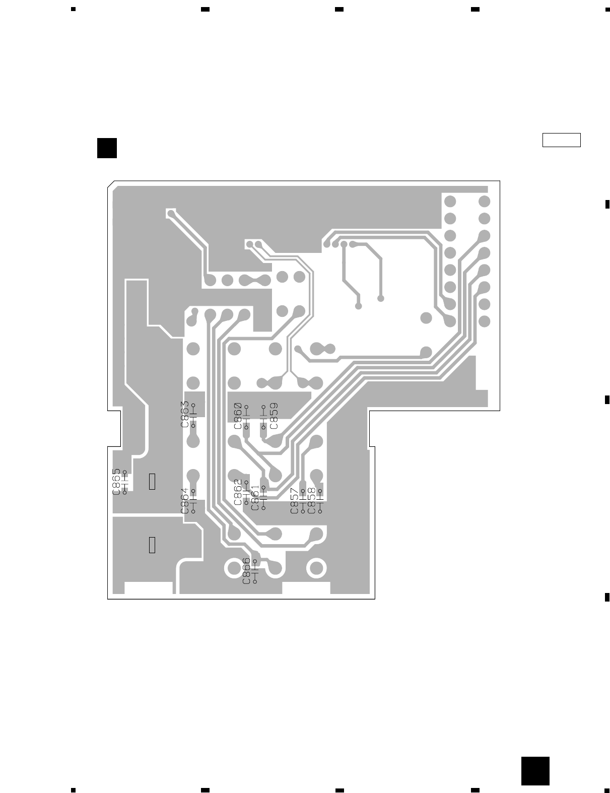
C 851 CKSQYB223K50
C 856 CEAL4R7M35
Unit Number : UWM-021
Unit Name : Keyboard Unit
MISCELLANEOUS
Q 901 Transistor 2SC2712
D 901 LED AA2222S-B1
D 902 Chip Diode MA151WK
D 903 Chip Diode MA151WK
D 904 Chip Diode MA151WK
D 905 Chip Diode MA151WK
D 906 Chip Diode MA151WK
D 907 Chip Diode MA151WK
D 908 Chip Diode MA151WK
IL 901 Lamp 8V 80mA CEL1449
IL 902 Lamp 8V 80mA CEL1449
IL 903 Lamp 8V 80mA CEL1449
IL 904 Lamp 8V 80mA CEL1449
IL 905 Lamp 8V 80mA CEL1449
IL 906 Lamp 8V 80mA CEL1449
IL 907 Lamp 8V 80mA CEL1449
RESISTORS
R 901 RS1/10S102J
R 902 RS1/10S821J
CAPACITORS
C 901 CKSQYB103K50
Unit Number : UWM-020
Unit Name : Volume Unit
MISCELLANEOUS
VR 901 Volume 50kΩ(B) CSD1036
VR 902 Volume 50kΩ(B) CCS1089
VR 903 Volume 50kΩ(B) CCS1089
VR 904 Volume 50kΩ(B) CCS1089
RESISTORS
R 903 RD1/4PU182J
R 904 RD1/4PU182J
R 905 RD1/4PU182J
R 906 RD1/4PU182J
R 907 RD1/4PU182J
R 908 RD1/4PU182J
R 909 RD1/4PU182J
R 910 RD1/4PU182J
Unit Number : EWM1037
Unit Name : Deck Unit
MISCELLANEOUS
IC 251 IC CXA2560Q
IC 351 IC PA2020A
D 352 Diode 1SS355
VR 301 Semi-fixed 33kΩ(B) CCP1280
VR 302 Semi-fixed 33kΩ(B) CCP1280
RESISTORS
R 255 RS1/16S221J
R 256 RS1/16S221J
R 257 RS1/16S102J
R 258 RS1/16S102J
R 271 RS1/16S102J
R 272 RS1/16S102J
R 273 RS1/16S102J
R 281 RS1/8S0R0J
R 282 RS1/8S0R0J
R 283 RS1/8S0R0J
R 284 RS1/8S0R0J
R 285 RS1/16S0R0J
R 286 RS1/16S0R0J
R 287 RS1/8S0R0J
R 290 RS1/8S0R0J
R 301 RS1/16S183J
R 322 RS1/16S102J
R 351 RS1/16S102J
R 352 RS1/16S102J
R 353 RS1/16S102J
R 354 RS1/16S102J
R 355 RS1/16S274J
R 362 RS1/8S301J
R 373 RS1/16S0R0J
R 374 RS1/8S0R0J
R 375 RS1/8S0R0J
R 401 RS1/16S472J
R 402 RS1/16S183J
R 403 RS1/16S823J
CAPACITORS
C 251 CKSRYB331K50
C 252 CKSRYB331K50
C 253 CKSRYB331K50
C 254 CKSRYB331K50
C 255 CKSRYB103K50
C 256 CKSRYB103K50
C 272 CKSRYB104K16
C 273 220µF/50V ECH0001
C 301 CKSRYB104K16
C 302 CKSRYB104K16
C 309 CKSRYB104K16
C 310 CKSRYB104K16
C 313 CCSRCH101J50
C 351 CKSQYB224K25
C 352 CKSRYB392K50
=====Circuit Symbol and No.===Part Name Part No.
--- ------ ------------------------------------------ ------------------------- =====Circuit Symbol and No.===Part Name Part No.
--- ------ ------------------------------------------ -------------------------
D
Volume Unit
Consists of
Volume PCB(A)
Volume PCB(B)
EF
I

49
FX-M2317ZSA
C 353 CKSRYB103K50
C 354 CKSRYB103K50
C 355 CKSQYB104K50
C 356 CKSRYB103K50
C 401 CKSRYB334K10
C 402 CKSRYB392K50
C 403 CKSRYB683K16
Unit Number : EWM1036
Unit Name : Sensor Unit
MISCELLANEOUS
Q 101 Photo-reflector EGN1004
S 101 Switch(LOAD) ESG1007
S 102 Switch(MODE) ESG1007
S 103 Switch(70µs) ESG1007
Unit Number : CWE1422
Unit Name : Tuner Unit
MISCELLANEOUS
IC 1 IC PA4023B
IC 2 IC PA4024A
Q 1 Transistor 2SC2712
Q 3 FET 3SK263
Q 31 Transistor 2SC2712
Q 51 Transistor 2SK1067
Q 151 Transistor DTC124EU
Q 201 Transistor FC12
Q 203 Transistor DTC124EU
D 3 Diode 1SV251
D 4 Diode 1SV250
D 5 Diode KV1410-F1
D 6 Diode MA157
D 7 Diode KV1410-F1
D 8 Diode KV1410-F1
D 201 Diode MA157
D 202 Diode 1SV251
D 231 Diode SVC253
L 1 Inductor LCTBR12K2125
L 2 Coil CTC1145
L 3 Inductor LCTB4R7K2125
L 4 Coil CTC1131
L 5 Coil CTC1147
L 51 Ferri-Inductor LAU150K
L 52 Coil CTC1136
L 201 Ferri-Inductor LAU4R7K
L 202 Ferri-Inductor LAU330K
L 203 Inductor CTF1371
L 208 Inductor LAU390K
L 209 Ferri-Inductor LAU680K
L 210 Coil CTB1103
L 231 Inductor LAU3R3J
T 31 Coil CTE1116
CF 25 Ceramic Filter CTF1290
CF 51 Ceramic Filter CTF1290
CF 52 Ceramic Filter CTF1290
CF 53 Ceramic Filter CTF1290
CF 230 Crystal Filter CTF1262
CF 232 Ceramic Filter CTF1348
X 151 Radiator 918.5Hz CSS1365
X 231 Crystal Resonator 10.26MHz CSS1111
VR 101 Semi-fixed 15kÉ∂(B) CCP1230
VR 154 Semi-fixed 150kÉ∂(B) CCP1236
VR 156 Semi-fixed 68kÉ∂(B) CCP1234
VR 157 Semi-fixed 47kÉ∂(B) CCP1233
RESISTORS
R 3 RS1/16S223J
R 4 RS1/16S101J
R 5 RS1/16S101J
R 6 RS1/16S101J
R 7 RS1/10S331J
R 8 RS1/16S473J
R 9 RS1/16S473J
R 10 RS1/16S223J
R 11 RS1/16S124J
R 12 RS1/16S474J
R 15 RS1/16S271J
R 16 RS1/16S104J
R 17 RS1/16S473J
R 18 RS1/16S473J
R 19 RS1/16S154J
R 27 RS1/16S0R0J
R 31 RS1/16S470J
R 32 RS1/16S912J
R 33 RS1/16S912J
R 34 RS1/16S331J
R 35 RS1/16S331J
R 39 RS1/16S0R0J
R 51 RS1/16S331J
R 52 RS1/16S104J
R 53 RS1/16S104J
R 54 RS1/16S331J
R 55 RS1/16S102J
R 56 RS1/16S823J
R 61 RS1/16S392J
R 62 RS1/16S273J
R 103 RS1/16S333J
R 104 RS1/16S334J
R 105 RS1/16S683J
R 107 RS1/16S222J
R 151 RS1/10S102J
R 152 RS1/16S393J
R 155 RS1/16S333J
R 160 RS1/16S222J
R 161 RS1/16S563J
R 162 RS1/16S225J
R 163 RS1/16S222J
R 164 RS1/16S104J
R 165 RS1/16S102J
R 202 RS1/16S223J
R 203 RS1/16S225J
R 204 RS1/16S103J
R 205 RS1/16S471J
R 206 RS1/16S220J
R 207 RS1/16S101J
R 208 RS1/16S102J
R 209 RS1/16S0R0J
R 214 RS1/16S563J
R 215 RS1/16S473J
R 217 RS1/16S393J
R 220 RS1/10S0R0J
R 231 RS1/16S242J
R 232 RS1/16S473J
R 233 RS1/16S0R0J
R 234 RS1/16S0R0J
R 237 RS1/16S562J
R 238 RS1/16S104J
R 239 RS1/16S104J
R 240 RS1/16S472J
R 241 RS1/16S202J
R 243 RS1/16S183J
=====Circuit Symbol and No.===Part Name Part No.
--- ------ ------------------------------------------ ------------------------- =====Circuit Symbol and No.===Part Name Part No.
--- ------ ------------------------------------------ -------------------------
J
C

50
FX-M2317ZSA
R 244 RS1/16S472J
R 247 RS1/10S153J
CAPACITORS
C 1 CCSRCH220J50
C 2 CKSRYB222K50
C 3 CCSRCH6R0D50
C 5 CKSRYB222K50
C 6 CKSQYB473K16
C 7 CKSQYB473K16
C 8 CKSQYB104K16
C 9 CCSRCJ3R0C50
C 10 CEJA1R0M50
C 11 CCSRCH470J50
C 12 CCSRCH820J50
C 13 CKSRYB222K50
C 14 CCSRCH4R0C50
C 15 CCSRCH7R0D50
C 16 CCSRCH120J50
C 17 CKSRYB222K50
C 18 CKSRYB103K25
C 19 CKSRYB222K50
C 20 CKSRYB222K50
C 21 CEJA100M16
C 22 CCSRRH100D50
C 23 CCSRRH120J50
C 24 CKSRYB103K25
C 30 CCSRRH201J50
C 31 CKSRYB103K25
C 32 CKSQYB473K16
C 33 CCSRCK2R0C50
C 35 CCSRCH270J50
C 36 CCSRCH120J50
C 40 CKSRYB222K50
C 41 CKSQYB104K16
C 51 CKSRYB223K25
C 52 CKSRYB103K25
C 53 CKSRYB222K50
C 54 CCSRCH470J50
C 55 CKSQYB223K25
C 56 CKSQYB104K16
C 57 CKSRYB472K50
C 58 CEJA330M10
C 59 CKSRYB103K25
C 60 CKSRYB102K50
C 61 CCSRCH270J50
C 62 CKSRYB103K25
C 63 CEJAR22M50
C 65 CKSQYB104K16
C 101 CEJANP100M10
C 102 CKSRYB182K50
C 103 CKSQYB682K50
C 104 CEJA2R2M50
C 105 CKSRYB103K25
C 106 CCSRCH151J50
C 107 CKSRYB103K25
C 151 CKSRYB392K50
C 152 CKSQYB104K16
C 153 CEJA3R3M50
C 154 CKSQYB104K16
C 157 CEJA3R3M50
C 158 CKSYB474K16
C 159 CEJA220M6R3
C 160 CKSQYB104K16
C 161 CKSQYB104K16
C 162 CEJA3R3M50
C 163 CKSRYB102K50
C 165 CCSRCH100D50
C 201 CKSRYB103K25
C 202 CCSRCH100D50
C 203 CKSRYB332K50
C 204 CKSQYB473K16
C 205 CKSQYB473K16
C 206 CKSQYB103K25
C 207 CCSRCH120J50
C 211 CCSRCH560J50
C 212 CEJA101M10
C 213 CKSRYB103K25
C 215 CCSRCH680J50
C 216 CCSRCH101J50
C 217 CEJAR47M50
C 219 CKSRYB223K25
C 220 CKSRYB103K25
C 221 CKSRYB103K25
C 230 CKSQYB104K16
C 231 CCSRCH330J50
C 232 CCSRCH150J50
C 233 CKSRYB103K25
C 234 CEJA330M10
C 235 CKSRYB332K50
C 236 CKSQYB473K16
C 237 CCSRTH180J50
C 239 CKSRYB103K25
C 240 CKSYB104K16
C 241 CKSQYB104K16
C 242 CEJAR47M50
C 243 CEJAR33M50
C 244 CKSQYB473K16
C 245 CKSQYB223K25
C 246 CKSQYB224K16
C 250 CCSRCJ3R0C50
Unit Number : CWX2411
Unit Name : Control Unit
MISCELLANEOUS
IC 201 IC UPD63711GC
IC 301 IC BA5985FM
IC 701 IC BA05SFP
Q 101 Transistor 2SB1132
D 801 Chip LED CL203IRXTU
D 802 Chip LED CL203IRXTU
X 201 Ceramic Resonator 16.934MHz CSS1456
S 801 Spring Switch(HOME) CSN1051
S 802 Spring Switch(CLAMP) CSN1052
RESISTORS
R 101 RS1/8S120J
R 102 RS1/8S100J
R 103 RS1/16S222J
R 201 RS1/16S104J
R 202 RS1/16S103J
R 203 RS1/16S393J
R 204 RS1/16S103J
R 205 RS1/16S103J
R 206 RS1/16S182J
R 207 RS1/16S123J
=====Circuit Symbol and No.===Part Name Part No.
--- ------ ------------------------------------------ ------------------------- =====Circuit Symbol and No.===Part Name Part No.
--- ------ ------------------------------------------ -------------------------
G

51
FX-M2317ZSA
R 302 RS1/16S153J
R 303 RS1/16S103J
R 501 RS1/16S102J
R 502 RA4C681J
R 601 RS1/16S102J
R 602 RS1/16S102J
R 605 RS1/16S0R0J
R 606 RS1/16S0R0J
R 801 RS1/8S751J
R 803 RS1/8S751J
R 902 RS1/16S0R0J
R 906 RS1/16S0R0J
CAPACITORS
C 101 CKSRYB102K50
C 102 CKSRYB104K16
C 103 CEV101M6R3
C 104 CEV470M6R3
C 105 CKSQYB334K16
C 106 CKSQYB334K16
C 107 CKSQYB334K16
C 201 CKSRYB104K16
C 202 CKSRYB471K50
C 203 CKSRYB104K16
C 205 CEV101M6R3
C 206 CKSRYB104K16
C 207 CKSRYB104K16
C 208 CKSRYB104K16
C 209 CKSRYB104K16
C 210 CKSRYB332K50
C 211 CKSRYB104K16
C 212 CKSRYB104K16
C 213 CKSRYB392K50
C 214 CKSRYB104K16
C 215 CKSRYB104K16
C 216 CCSRCJ3R0C50
C 217 CCSRCH270J50
C 218 CKSRYB104K16
C 219 CCSRCH181J50
C 220 CCSRCH510J50
C 221 CKSRYB682K25
C 222 CEV220M6R3
C 223 CKSRYB103K25
C 224 CKSRYB224K10
C 301 CEV101M10
C 603 CCSQSL152J50
C 604 CCSQSL152J50
C 702 10µF/10V CCH1349
C 703 CKSQYB334K16
Unit Number :
Unit Name : Photo Unit(S8)
Q 1 Photo-transistor CPT230SX-TU
Q 2 Photo-transistor CPT230SX-TU
Miscellaneous Parts List
Pickup Unit(Service)(P8) CXX1285
M 1 Motor Unit(CARRIAGE) CXB2190
M 2 Motor Unit(LOADING) CXB2195
M 3 Motor Unit(SPINDLE) CXB2562
M 1 Motor Unit(MAIN) EXA1491
M 2 Motor Unit(SUB) EXA1623
HD 1 Head Assy EXA1506
=====Circuit Symbol and No.===Part Name Part No.
--- ------ ------------------------------------------ -------------------------
H
52
FX-M2317ZSA
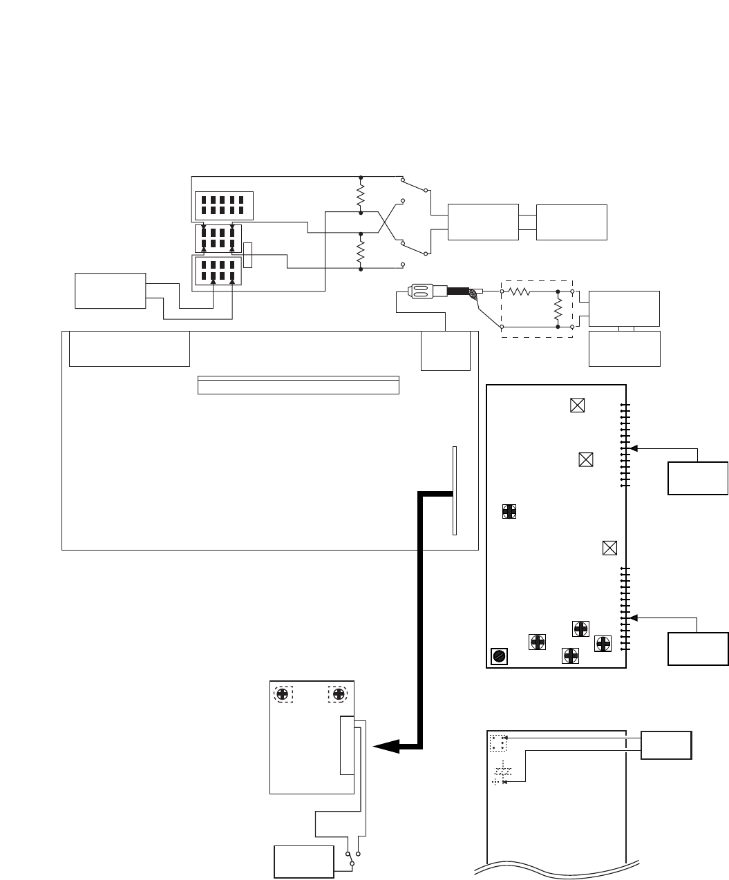
Antenna
Jack
DC Regulated
Power Supply
GND
+13.2V
FUSE
4Ω
4Ω
Lch+
Lch-
Rch+
Rch-
mV Meter(1) Osilloscope
FM SSG
Stereo
Modulator
Dummy Antenna
50Ω(37.5Ω)
50Ω(75Ω)
TUNER MOTHER PCB
TUNER UNIT
DECK UNIT
DC V
Meter(1)
Pin 1
Pin 14
Pin 13
Pin26
TUNER UNIT (SIDE A)
DC V
Meter(2)
L5
L52
VR157
VR101
VR154
VR156
T31
L4
Pin 6(FMSD)
Pin 19(FMTV)
Pin 27
Pin 28
Center
Meter
C63
L52
L2
TUNER UNIT(SIDE B)
VR302
mV
Meter(2)
VR301
L-CH
R-CH
Pin2
Pin3
CN251
DECK UNIT
Extention Cord GGD1121
6.1 TUNER, CASSETTE SECTION
-Connection Diagram
6. ADJUSTMENT
53
FX-M2317ZSA
DOLBY B NR ADJUSTMENT
No. Test Tape Adjustment Point Adjustment Method
(Switch Position)
1 NCT-150 VR301(Lch),VR302(Rch) mV Meter(2) : –6dBm(388mV)±1dB
(400Hz,200nwb/m) (DOLBY NR Switch : OFF)
FM ADJUSTMENT
Modulation M:MONO MOD., 400Hz 30%(22.5kHz Dev.)
S1:STEREO MOD., 1kHz, L or R=30%(20.25kHz+7.5kHz Dev.)
NOTE:Before proceeding to further adjustments after switching power ON, let the tuner run for ten minutes to allow
the circuits to stabilize.
FM SSG Displayed Adjustment Adjustment Method
No. Frequency(MHz) Level(dBf) Frequency(MHz) Point (Switch Position)
TUN Volt 1 ••••• ••••• 108.0 L5 DC V Meter(1) : 6.5V
Center 1 98.1 M 65-85 98.1 L52 Center Meter : 0
Meter
IFT 1 98.1 M 5-15 98.1 T31 mV Meter(1) : Maximum
ANT 1 89.9 M 5-15 89.9 L2 mV Meter(1) : Maximum
Coil
RF Coil 1 89.9 M 5-15 89.9 L4 mV Meter(1) : Maximum
Soft 1 98.1 M 65 98.1 ••••• mV Meter(1) : AdB
Mute 2 98.1 M 14 98.1 VR157 mV Meter(1) : A-3dB
Search 1 98.1 M 24 98.1 VR156 DC V Meter(2) : more than 3.5V
Sensitivity 2 98.1 M 23 98.1 VR156 DC V Meter(2) : 0V
3 Repeat steps 1 and 2 until the adjustment standards are satisfied.
Separation 1 98.1 S 65 98.1 VR101 mV Meter(1) : Maximum
ARC 1 98.1 S 39 98.1 VR154 mV Meter(1) : Separation 5dB
Separation

54
FX-M2317ZSA
1) Precautions
• This unit uses a single power supply (+5V) for the reg-
ulator. The signal reference potential, therefore, is
connected to REFO(approx. 2.5V) instead of GND.
If REFO and GND are connected to each other by mis-
take during adjustments, not only will it be impossi-
ble to measure the potential correctly, but the servo
will malfunction and a severe shock will be applied to
the pick-up. To avoid this, take special note of the fol-
lowing.
Do not connect the negative probe of the measuring
equipment to REFO and GND together. It is especially
important not to connect the channel 1 negative
probe of the oscilloscope to REFO with the channel 2
negative probe connected to GND.
Since the frame of the measuring instrument is usual-
ly at the same potential as the negative probe, change
the frame of the measuring instrument to floating sta-
tus.
If by accident REFO comes in contact with GND,
immediately switch the regulator or power OFF.
• Always make sure the regulator is OFF when connect-
ing and disconnecting the various filters and wiring
required for measurements.
• Before proceeding to further adjustments and mea-
surements after switching regulator ON, let the player
run for about one minute to allow the circuits to stabi-
lize.
• Since the protective systems in the unit's software are
rendered inoperative in test mode, be very careful to
avoid mechanical and /or electrical shocks to the sys-
tem when making adjustment.
• Disc detection during loading and eject operations is
performed by means of a photo transistor in this
unit.Consequently, if the inside of the unit is exposed
to a strong light source when the outer casing is
removed for repairs or adjustment, the following mal-
functions may occur.
*During PLAY, even if the eject button is
pressed,the disc will not be ejected and the unit
will remain in the PLAY mode.
*The unit will not load a disc.
When the unit malfunctions this way, either re-posi-
tion the light source, move the unit or cover the photo
transistor.
2) Test Mode
This mode is used for adjusting the CD mechanism
module of the device.
• Test mode starting procedure
Reset while pressing the 4 and 6 keys together.
• Test mode cancellation
Switch ACC, back-up OFF.
• After pressing the EJECT key, do not press any other
key until the disk is completely ejected.
• If the ]] or [[ key is pressed while focus search is
in progress, immediately turn the power off (other-
wise the actuator may be damaged due to adhesion
of the lenses).
• Jump operation of TRs other than 100TR continues
after releasing the key. CRG move and 100TR jump
operations are brought into the “Tracking close” sta-
tus when the key is released.
• Powering Off/On resets the jump mode to “Single TR
(91)”, the RF AMP gain setting to 0 dB, and the auto-
matic adjustment value to the initial value.
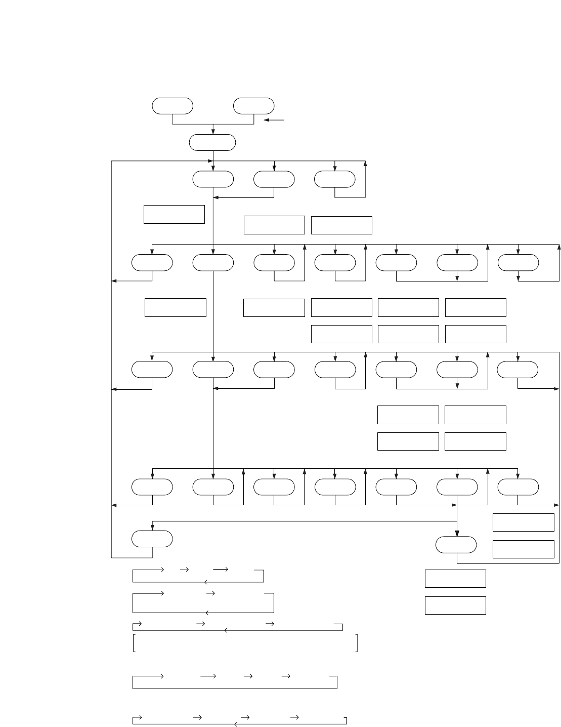
6.2 CD ADJUSTMENT
55
FX-M2317ZSA
-Flow Chart
Focus Close
*2 S Curve Check
01 01 0100 00 00
(99 99 99)
Display
TYP
POWER
5
Backup on
CD
[
5
*2
*1 +6dB +12dB
*4
*5
3
3
3
1
2
1
2]
][
06 06 06 12 12 12
Sourse CD
Single TR 32TRK
92(82) CRG Move
94(84)
100TRK
93(83)
Focus Mode
Select
Focus Close/
S Curve Check CRG- Auto Adjustment
Display Select
<Tracking Servo Close> CRG+
RF AGC Coefficient Display/
Rough Servo and RF AGC
Tracking
Open
Display
Tracking
Open
T. Close and
Fit Servo
*3 F.Offset Display RF.Offset Display F.Cansel Display
*7
Single TR/32TR/100TR
Voltage of CRG Motor = 2 [V]
(F,T.AGC Gain = (Present Value/Initial Value) x 20)
*6
][
1
5
Display
2
5
Display
or
8x 8x 8x
TRK SECMIN
9x 9x 9x
TRK SECMIN
or
CRG-CRG+ T.Balance
Adjustment
*7
F, T, RF AGC/
F.Bias Display Select
F, T AGC and
RF AGC
CRG Move, 100TR Jump Only
TRK, MIN, SEC F.AGC Gain RF AGC Gain
T.AGC Gain
*8
Power ON
(Adjustment for T.Offset)
*5 *4 *4
*6
CRG/TR Jump NO.
Select
CRG+/TR Jump+
CRG-/TR Jump-
Power OFF
Display
Display
Display
T.Close and
F,T AGC and
RF AGC and
Fit Servo
Display
Power ON
(Not adjustment for T.Offset)
Display
Display
2
RF AMP Gain Select
2
Power OFF
Power OFF
Power OFF 8x 8x 8x
TRK SECMIN
9x 9x 9x
TRK SECMIN
8x 8x 8x
TRK SECMIN
9x 9x 9x
TRK SECMIN
or
8x 8x 8x
TRK SECMIN
9x 9x 9x
TRK SECMIN
or
00 00 00
TRK SECMIN
99 99 99
TRK SECMIN
or
00 00 00
TRK SECMIN
99 99 99
TRK SECMIN
or
00 00 00
TRK SECMIN
99 99 99
TRK SECMIN
or
91 91 91
TRK SECMIN 0x 0x 0x
TRK SECMIN
00 00 00
TRK SECMIN
99 99 99
TRK SECMIN GG GG GG
TRK SECMIN
Test Mode In
*1
*8 *3*8
F.Cancel Value = {Top Rank 8bit of Set Value (7F [H] to 80 [H] ) + 128} / 4
= 63 [D] to (32 [D] ) to 00 [D]
9x(8x):91(81)
CD
]
]
][
[
[
[]
[]
[]
[]
[]
56
FX-M2317ZSA
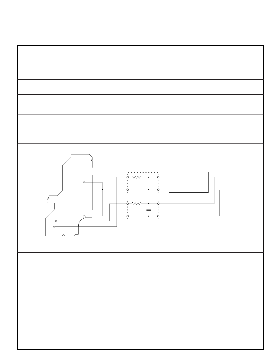
• Note :
The grating angle of the PU unit cannot be adjusted after the PU unit is changed. The PU unit in the CD mecha-
nism module is adjusted on the production line to match the CD mechanism module and is thus the best adjusted
PU unit for the CD mechanism module. Changing the PU unit is thus best considered as a last resort. However, if
the PU unit must be changed, the grating should be checked using the procedure below.
• Purpose :
To check that the grating is within an acceptable range when the PU unit is changed.
• Symptoms of Mal-adjustment :
If the grating is off by a large amount symptoms such as being unable to close tracking, being unable to perform
track search operations, or taking a long time for track searching.
• Method :
• Measuring Equipment • Oscilloscope, Two L.P.F.
• Measuring Points • E, F, REFO
• Disc • ABEX TCD-784
• Mode • TEST MODE
• Checking Procedure
1. In test mode, load the disc and switch the 5V regulator on.
2. Using the ]] and [[ buttons, move the PU unit to the innermost track.
3. Press key 3to close focus, the display should read "91". Press key 2to implement the tracking balance adjust-
ment the display should now read "81". Press key 32 times. The display will change, returning to "81" on the
fourth press.
4. As shown in the diagram above, monitor the LPF outputs using the oscilloscope and check that the phase differ-
ence is within 75° . Refer to the photographs supplied to determine the phase angle.
5. If the phase difference is determined to be greater than 75° try changing the PU unit to see if there is any
improvement. If, after trying this a number of times, the grating angle does not become less than 75° then the
mechanism should be judged to be at fault.
• Note
Because of eccentricity in the disc and a slight misalignment of the clamping center the grating waveform may be
seen to "wobble" ( the phase difference changes as the disc rotates). The angle specified above indicates the aver-
age angle.
• Hint
Reloading the disc changes the clamp position and may decrease the "wobble".
F
REFO
E
100kΩ
390pF
100kΩ
390pF
E
REFO
F
REFO
L.P.F.
L.P.F.
CONTROL UNIT
Xch Ych
Oscilloscope
6.3 CHECKING THE GRATING AFTER CHANGING THE PICKUP UNIT
57
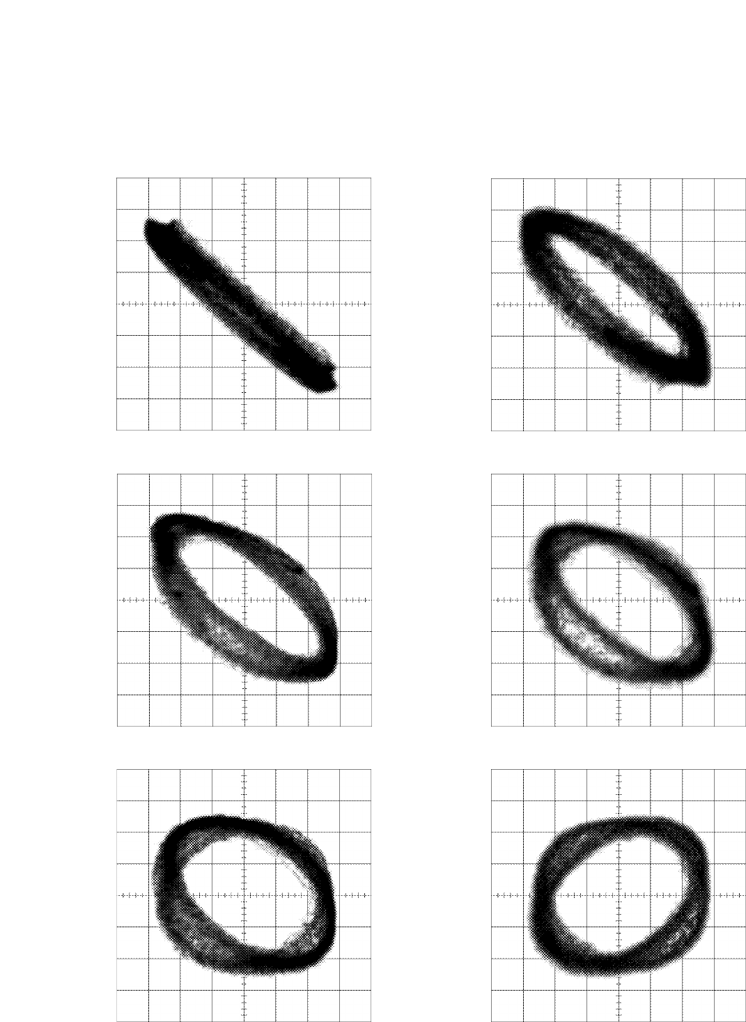
FX-M2317ZSA
Grating waveform Ech →Xch 20mV/div, AC
Fch →Ych 20mV/div, AC
45°
0°
75°
60°
30°
90°
58
FX-M2317ZSA
7. GENERAL INFORMATION
7.1 DIAGNOSIS
7.1.1 TEST MODE
-Error Messages
If a CD is not operative or stopped during operation due to an error, the error mode is turned on and cause(s) of the
error is indicated with a corresponding number. This arrangement is intended at reducing nonsense calls from the
users and also for facilitating trouble analysis and repair work in servicing.
(1) Basic Indication Method
1) When SERRORM is selected for the CSMOD (CD mode area for the system), error codes are written to DMIN (min-
utes display area) and DSEC (seconds display area). The same data is written to DMIN and DSEC. DTNO remains
in blank as before.
2) Main unit display examples
Depending on display capability of LCD used, display will vary as shown below. xx contains the error number.
8-digit display 6-digit display 4-digit display
ERROR–xx ERR–xx E–xx
OR
Err–xx
(2) Error Code List
Code Class Displayed error code Description of the code and potential cause(s)
10 Electricity Carriage Home NG CRG can't be moved to inner diameter.
CRG can't be moved from inner diameter.
→Failure on home switch or CRG move mechanism.
11 Electricity Focus Servo NG Focusing not available.
→Stains on rear side of disc or excessive vibrations on REWRITABLE.
12 Electricity Spindle Lock NG Spindle not locked. Sub-code is strange (not readable).
→Failure on spindle, stains or damages on disc, or excessive vibrations.
Subcode NG A disc not containing CD-R data is found. Turned over disc are found,
though rarely.
→Failure on home switch or CRG move mechanism.
RF AMP NG An appropriate RF AMP gain can't be determined.
→CD signal error.
17 Electricity Setup NG APC protection doesn't work. Focus can be easily lost.
→Damages or stains on disc, or excessive vibrations.
30 Electricity Search Time Out Failed to reach target address.
→CRG tracking error or damages on disc.
A0 System Power Supply NG Power (VD) is ground faulted.
→Failure on SW transistor or power supply (failure on connector).
Remarks: Mechanical errors are not displayed (because a CD is turned off in these errors).
Unreadable TOC does not constitute an error. An intended operation continues in this case.
A newly designed main unit must conform to the example given above.
Upper digits of an error code are subdivided as shown below:
1x: Setup relevant errors, 3x: Search relevant errors, 3x: Search relevant errors, Ax: Other errors.
59
FX-M2317ZSA
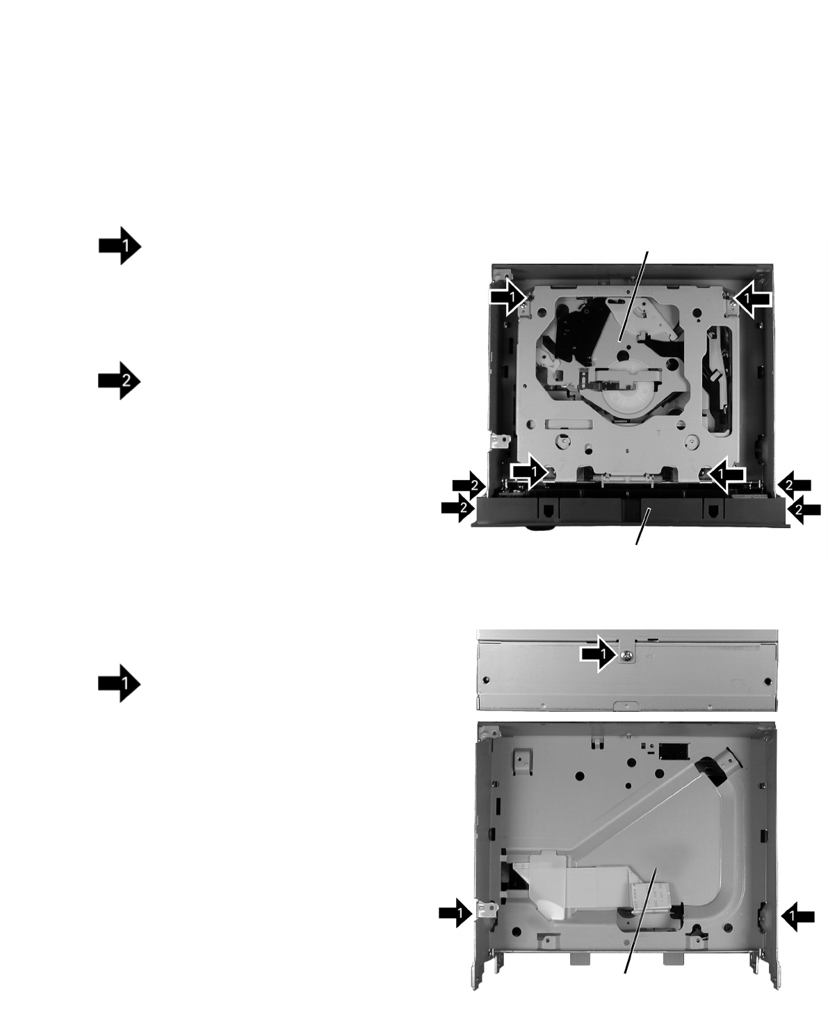
-Removing the Chassis (Fig.2)
Remove the three screws and then remove the
Chassis.
-Removing the Case (not shown)
1. Remove the Case.
-Removing the CD Mechanism Module (Fig.1)
Remove the four screws.
Disconnect the connector and then remove the CD
Mechanism Module.
-Removing the Grille Assy (Fig.1)
Remove the four screws and then remove the
Grille Assy.
Fig.1
7.1.2 DISASSEMBLY
Fig.2
Chassis
CD Mechanism Module
Grille Assy
60
FX-M2317ZSA
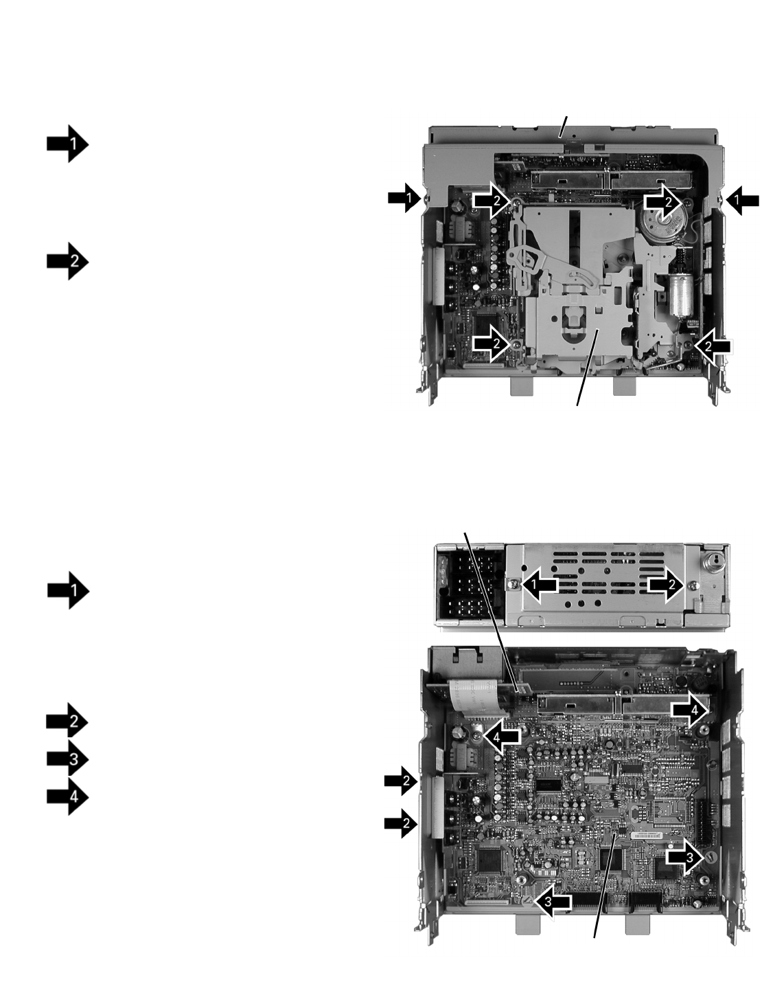
-Removing the Connector PCB (Fig.4)
Remove the screw.
Disconnect the connector and then remove the
Connector PCB.
-Removing the Tuner Mother PCB (Fig.4)
Remove the three screws.
Straight the tabs at two locations indicated.
Remove the two screws and then remove the
Tuner Mother PCB.
-Removing the Case (Fig.3)
Remove the two screws and then remove the
Case.
-Removing the Cassette Mechanism Module
(Fig.3)
Remove the four screws and then remove the
Cassette Mechanism Module.
Fig.3
Fig.4
Tuner Mother PCB
Cassette Mechanism Module
Case
Connector PCB
61
FX-M2317ZSA
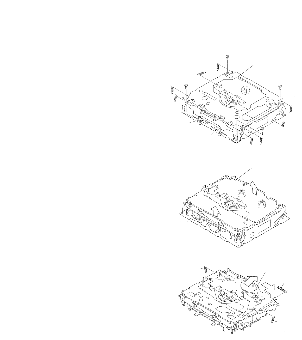
-Removing the Upper Frame
1. Remove six Springs A, two Springs B and four
Screws.
2. Remove two Tabs situated on rear side of the Upper
Frame, remove two Arms on the front side, then
remove two Tabs on the front side.
-Removing the Carriage Mechanism Section
1. Disengage the Carriage Mechanism Section from the
two dampers situated in the front side by driving it
up, then disengage and remove the mechanism from
the one damper by driving it up aslant into front side
direction.
Note : When assembling the Carriage Mechanism
Section, coat the dampers with alcohol prior
to the assembly.
-Removing the Clamp Arm Assy Section
1. Remove a Spring A, a B and a Spring C.
2. Drive the Clamp Arm Assy Section up into rear side
direction, then disengage the arm from its current
position Finally, drive the assembly approximately 45
degrees upward, then slide the assembly toward
right side to remove it.
B
A
BA
A
A
Arm
Arm
Upper Frame
A
A
A
B
C
Carriage Mechanism Section
Clamp Arm Assy Section
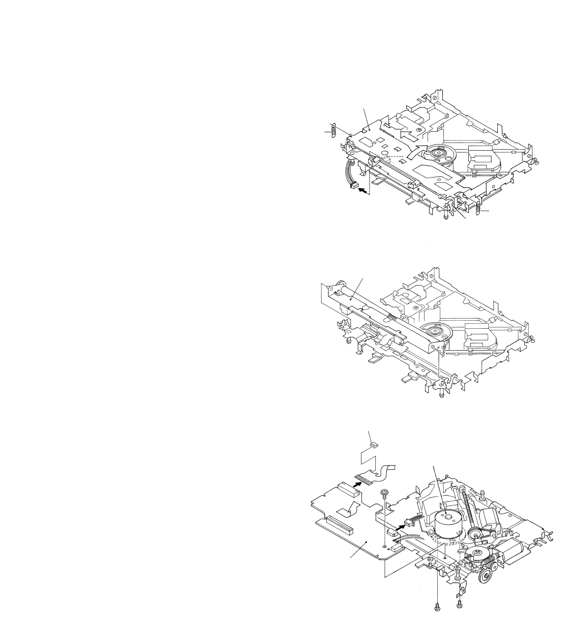
62
FX-M2317ZSA
-Removing the Guide Arm Assy Section
1. Remove a connector, a spring A and B
2. Drive the Guide Arm Assy Section up aslant into rear
side direction, then remove it from a Pin. Finally, drive
the assembly approximately 45 degrees upward, then
slide the assembly toward left side to remove it.
Note : When assembling the Guide Arm Assy Section,
route the cord inside the assembly. In this opera-
tion, care must be exercised so that cord may be
caught by the gear.
-Removing the LO Arm Assy Section
1. Remove two Pins to dismount the LO Arm Assy
Section.
-Removing the Control Unit and the Spindle
Motor
1. Remove from the connector after mounting the short
pin on the flexible PCB of the pickup unit.
2. Remove two Soldered joints, then remove two Screws
A.
3. Remove two connectors and a Screw B.
4. Disengage the Control Unit from two Tabs, then dis-
mount the unit by sliding it toward left.
5. Dismount the Spindle Motor.
A
Guide Arm Assy Section
B
Pin
LO Arm Assy Section
Spindle Motor
AA
Control Unit
Short Pin
B
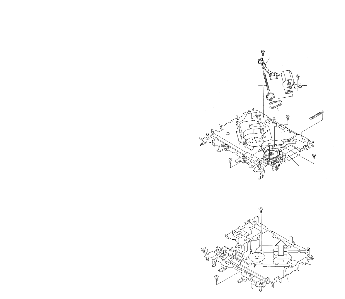
63
FX-M2317ZSA
-Removing the Loading Motor and Carriage
Motor
1. Remove the Spring and two Screws A.
2. Dismount the Loading Motor.
3. Remove the Belt, a Screw B, two Screws C, a Guide
and a Screw Unit.
4. Dismount the Carriage Motor.
Note : When assembling the Belt, use care so that it may
not be contaminated by grease.
-Removing the Pickup Unit
1. Remove two Screws and a Shaft.
2. Dismount the Pickup Unit.
Pickup Unit
Shaft
C
Guide
B
Screw Unit Carriage Motor
AA
C
Belt
Loading Motor
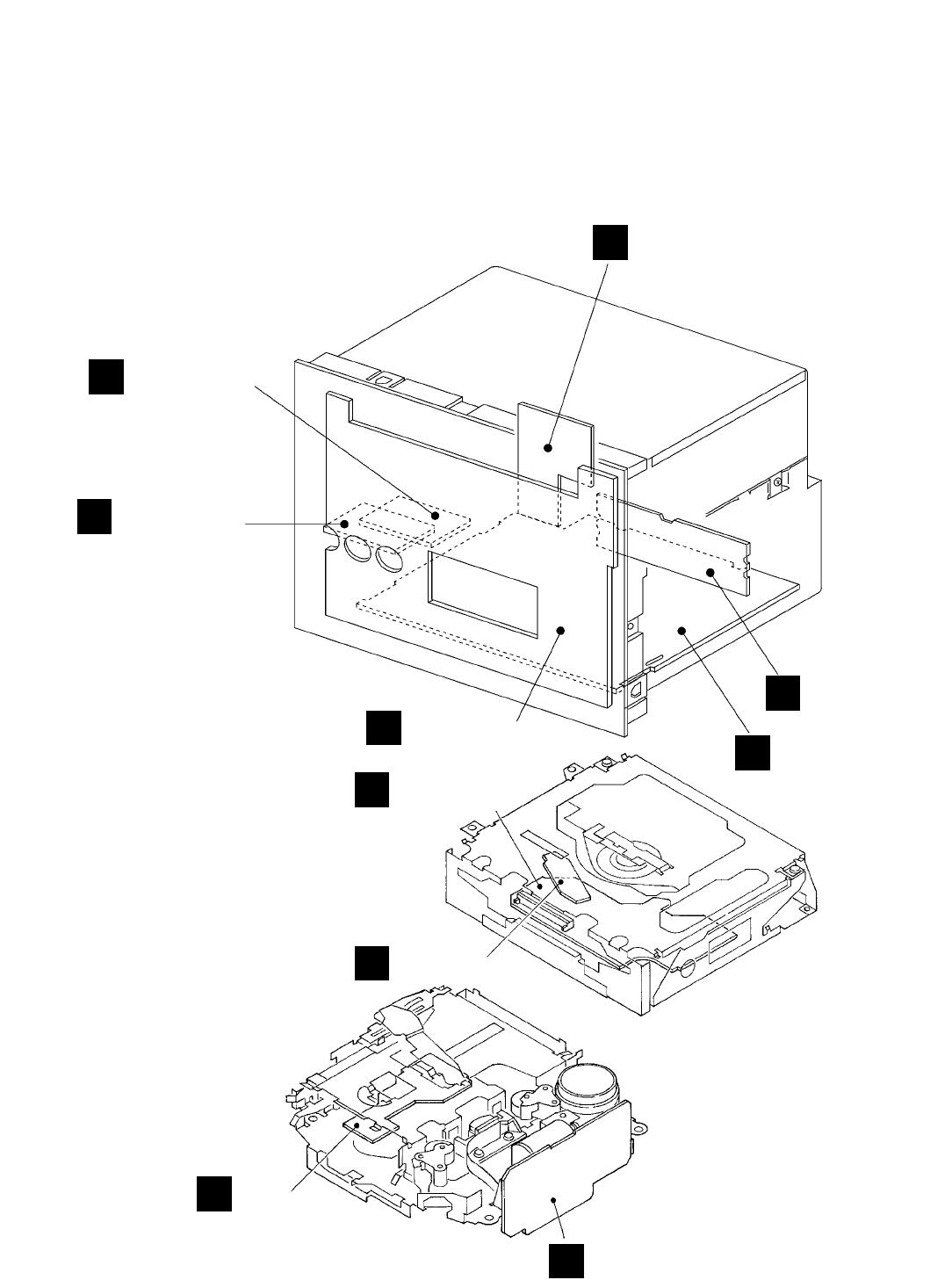
64
FX-M2317ZSA
7.1.3 PCB LOCATIONS
ATUNER MOTHER PCB
CTUNER UNIT
BCONNECTOR PCB
DKEYBOARD UNIT
GCONTROL UNIT
HPHOTO UNIT(S8)
IDECK UNIT
JSENSOR UNIT
EVOLUME PCB(A)
FVOLUME PCB(B)
65
FX-M2317ZSA
7.1.4 CONNECTOR FUNCTION DESCRIPTION
22 23 24 25 26
17 18 19 20 21
13 14 15 16
9 101112
5678
1234
FUSE
5A
NC
+15 (IG)
NC
GND
AMPMUT
TELMUT
ANTREM
+30 (BU)
RR-
FR-
FL-
RL-
RR+
FR+
FL+
RL+
CANL
CANH
NC
CDMR-
CDMR+
TELGND
TELAU
NC
CDML-
CDML+
1
2
3
4
5
6
7
8
9
10
11
12
13
14
15
16
17
18
19
20
21
22
23
24
25
26
NO. Pin name NO. Pin name NO. Pin name
ANTENNA
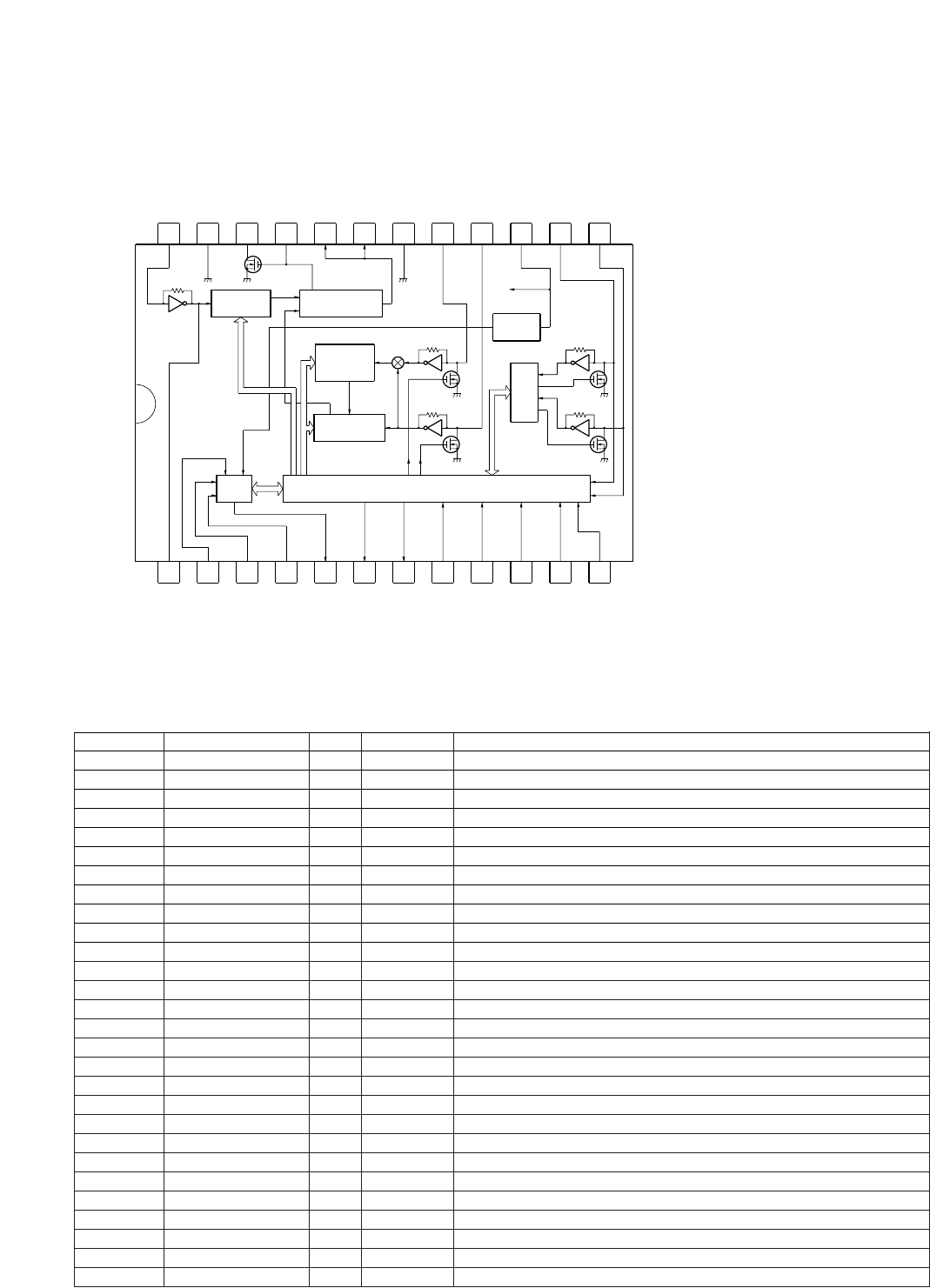
66
FX-M2317ZSA
-Pin Functions(PE5223B)
Pin No. Pin Name I/O Format Function and Operation
1 MOD I Destination sense analog input
2 RSL I Sub tuner signal level analog input
3 RSD I Sub tuner station detect input
4 AVSS A/D GND
5 ILLCON O C Illumination power analog output
6 DINJ O C Disc set indicator control output
7 AVREF1 (D/A converter standard voltage)
8 PDI I PLL data input
9 PDO O C PLL data output
10 pck O C PLL clock output
11 RDI I Serial data input for RDS IC
12 RDO O C Serial data output for RDS IC
13 rck O C Serial clock output for RDS IC
14 bsrq I P-BUS serial pole request input
15 BRXEN I/O C P-BUS reception enable input/output
16 brest/TSI O C P-BUS reset output
17 BDATA/TSO I/O C P-BUS serial data input/output
18 bsck/TCK I/O C P-BUS serial clock input/output
19-26 D0-7 I/O C Address/Data input/output
27 A8 O C Address output
28 cs O C CAN BUS chip select output
29 rst O C CAN BUS IC reset output
30-32 VOL1-3 I Rotary encoder input
33 VSS GND
34 MS I Cassette mechanism MS sense input
35 mtl I Cassette mechanism metal detect input
36 load I Cassette mechanism loading detect input
37 POS I Cassette mechanism position sense input
24
X1
GND
AOUT
AIN
EO1
EO0
GND
FM AMVCO
WBVCO
VDD
FMIFC
AMIFC
X0
PCE
DI
pck
DO
wb/LW
DVCONT
LOCL
seek
fm
am
st
23 22 21 20 19 18 17 16 15 14 13
123456789101112
REFERRENCE
DIVIDER
C2 B
I/F
PHASE DETECTOR
CHARGE PUMP
SWALLOW
COUNTER
1/16,1/17
4bits
12bits
PROGRAMABLE
DIVIDER
DATA SHIFT REGISTER
LATCH
POWER
ON
RESET
UNIVERSAL
COUNTER
*LC72146MQ2
IC's marked by * are MOS type.
Be careful in handling them because they are very
liable to be damaged by electrostatic induction.
7.2 IC
67
FX-M2317ZSA
Pin No. Pin Name I/O Format Function and Operation
38 NC Not used
39 ES I Cassette mechanism end sense input
40 rd O C Read signal output
41 wr O C Write signal output
42 wait I External wait signal input
43 ASTB O C Timing output for external RAM
44 RPCE O C RDS PLL chip enable output
45 B.C/TUMUT O C Tuner mute output/Dolby C output
46 telon O C Select output of external input
47 SD I Station detect input
48 SMUT O C Mute output
49 SYSPW O C System power supply control output
50 AMPB O C Amplifier power output
51 ECE O C EEPROM chip enable output
52 ECK/VCK O C EEPROM/E.VOL clock output
53 EDO/VDT O C EEPROM/E.VOL data output
54 EDI I Data input from EEPROM
55 PCE/VST O C PLL chip enable/E.VOL strobe output
56 NC Not used
57 rrst O C Reset output for RDS IC
58 RSEL O C Select output for RDS IC
59 RRDY I Ready input for RDS IC
60 reset I Reset input
61 INT I CAN BUS squeeze signal input
62 BSEN I Back Up power sense input
63 igsen I ACC power sense input
64 power I CD +5 control input
65 TELM I Telephone mute input
66 csej I Tape eject switch input
67 VOL0 I Rotary encoder edge input
68 VDD Power supply
69 X2 Crystal oscillator connection pin
70 X1 Crystal oscillator connection pin
71 IC GND
72 XT2 Open
73 TESTIN I Test program mode input
74 AVDD Positive power supply terminal for analog circuit
75 AVREF0 GND
76 SL I Signal level input
77 BASS I A/D converter input from BASS volume
78 TRE I A/D converter input from TREBLE volume
79 BAL I A/D converter input from BALANCE volume
80 FAD I A/D converter input from FADER volume
*PE5223B
1
20
21 40
41
60
61
80
Format Meaning
C C MOS
68
FX-M2317ZSA
-Pin Functions(PE5239A)
Pin No. Pin Name I/O Format Function and Operation
1 NC Not used
2xrst O C CD LSI reset output
3-7 NC Not used
8clamp I Disc clamp sense input
9 VSS GND
10 NC Not used
11 EJET O C Loading motor eject control output
12 LOAD O C Loading motor load control output
13 CONT O C Servo driver power supply control output
14 NC Not used
15 CDMUTE O C CD mute output
16 NC Not used
17 aden O C A/D reference voltage output
18-23 NC Not used
24 VSS GND
25-30 NC Not used
31 BRXEN I/O C P-BUS reception enable input/output
32 bsrq O C P-BUS serial pole request output
33 VDCON O C VD control output
34 CD5VON O C CD +5V power supply control output
35 reset I Reset input
36 TXARJ I Set up of TX output select input
37 ejsw I Eject switch input
38 brest I P-BUS reset input
39 CMPARI I Compression select input
40 VDD Power supply
41 X2 Crystal oscillator connection pin
42 X1 Crystal oscillator connection pin
43 IC GND
44 NC Not used
45 testin I Test program mode input
46 AVSS A/D GND
47 TEMP I Temperature detect input
48 VDSENS I Over voltage sense input
49 EJTD I Disc eject position detect input
50 DINC I Disc detect input
51 NC Not used
52 FOK I FOK signal input
53 MIRR I MIRR detect signal input
54 LOCK I Spindle lock detect input
55 AVDD Positive power supply terminal for analog circuit
56 AVREF I A/D converter reference voltage input
57 XSO I LSI data input
58 XSI O C LSI data output
59 xsck O C LSI clock output
60 xstb O C CD LSI strobe output
61 XA0 O C Control signal distinguishing data output
62 NC Not used
63 BDATA I/O C P-BUS serial data input/output
64 bsck I/O C P-BUS serial clock input/output
*PE5239A
1
20
21 40
41
60
61
80
Format Meaning
C C MOS

69
FX-M2317ZSA
-Pin Functions (UPD63711GC)
Pin No. Pin Name I/O Function and Operation
1 D.GND Logic circuit GND
2 RFOK O RFOK signal output
3rst I Reset signal input
4 A0 I Command/parameter identification signal input
5stb I Data strobe signal input
6sck I Clock signal input for serial data input/output
7 SO O Serial data and status signal output
8 SI I Serial data input
9xtalen I Crystal oscillation control pin
10 D.VDD Positive power supply terminal to logic circuit
11 DA.VDD Positive power supply terminal to D/A converter
12 R_OUT O Right channel audio output signal
13 DA.GND D/A converter GND
14 REGC I The outside putting capacitor connection pin for SCF regulator
15 DA.GND D/A converter GND
16 L_OUT O Left channel audio output signal
17 DA.VDD Positive power supply terminal to D/A converter
18 R+ O Right channel audio data output
19 R- O Right channel audio data output
20 L- O Left channel audio data output
21 L+ O Left channel audio data output
22 X.VDD Positive power supply terminal to crystal oscillation circuit
23 XTAL I Crystal oscillator connect pin
24 xtal O Crystal oscillator connect pin
25 X.GND Crystal oscillation circuit GND
26 D.VDD Positive power supply terminal to logic circuit
27 EMPH O Output pin for the pre-emphasis data in the sub-Q code
28 FLAG O Flag output pin to indicate that audio data currently being output consists
of noncorrectable data
29 DIN I Serial data input to internal DAC
30 DOUT O Serial audio data output
31 SCKIN I Serial clock input to internal DAC
32 SCKO O Audio data that is output from DOUT changes at rising edge of this clock
33 LRCKIN I LRCK signal input to internal DAC
34 LRCK O Signals to distinguish the right and left channels of the audio data output
from DOUT
35 HOLD O Defect detection output
36 TX O Digital audio interface data output
37 D.GND Logic circuit GND
38 C16M O Oscillator clock buffering output
39 LIMIT I Status of the pin is output at Bit 5 of the status output
40 D.VDD Positive power supply terminal to logic circuit
41 LOCK O EFM synchronous detection signal
42 RFCK O Frame synchronous signal of XTAL-system
43 MIRR O MIRR output
44 PLCK O Monitor pin of bit clock
45 D.GND Logic circuit GND
46 C1D1 O Output pin for indicating the C1 error correction results
47 C1D2 O Output pin for indicating the C1 error correction results
48 C2D1 O Output pin for indicating the C2 error correction results
49 C2D2 O Output pin for indicating the C2 error correction results
50 C2D3 O Output pin for indicating the C2 error correction results
51 D.VDD Positive power supply terminal to logic circuit
52 PACK O CD-TEXT PACK synchronous signal
53 TSO O CD-TEXT data serial output
54 TSI I CD-TEXT control parameter serial input
55 tsck I CD-TEXT serial clock input
56 TSTB I CD-TEXT parameter strobe signal input
57 D.GND Logic circuit GND
70
FX-M2317ZSA
Pin No. Pin Name I/O Function and Operation
58 TEST0 I Test pin
59 TEST1 I Test pin
60 ATEST O Test pin
61 A.GND Analog circuit GND
62 FD O Focus drive output
63 TD O Tracking drive output
64 SD O Sled drive output
65 MD O Spindle drive output
66 DAC0 O DAC output for adjustment
67 DAC1 O DAC output for adjustment
68 DAC2 O DAC output for adjustment
69 DAC3 O DAC output for adjustment
70 A.VDD Positive power supply terminal to analog circuit
71 EFM O EFM signal output
72 ASY I EFM comparator reference voltage input
73 C3T 3T detection capacitor additional pin
74 RFI I RF signal input for EFM data regulation
75 AGCO O RF signal output of after gain adjustment
76 AGCI I RF-AGC amplifier input
77 RFO O RF summing amplifier output
78 EQ2 RF amplifier equalizer parts additional pin
79 EQ1 RF amplifier equalizer parts additional pin
80 RF- I RF summing amplifier inverted input
81 A.GND Analog circuit GND
82 A I Photo detector A input
83 C I Photo detector C input
84 B I Photo detector B input
85 D I Photo detector D input
86 F I Photo detector F input
87 E I Photo detector E input
88 A.VDD Positive power supply terminal to analog circuit
89 REFOUT O Reference electric potential output
90 FE- I Focus error amplifier inverted input
91 FEO O Focus error amplifier output
92 TE- I Tracking error amplifier inverted input
93 TEO O Tracking error amplifier output
94 TE2 O Tracking error output of after amplification
95 TEC I Tracking comparator input
96 A.GND Analog circuit GND
97 PD I PD detection signal input for LD output monitor
98 LD O LD control current output
99 PN I APC circuit control polarity set pin
100 A.VDD Positive power supply terminal to analog circuit
25
26
50
51
75
76
100
1
*UPD63711GC
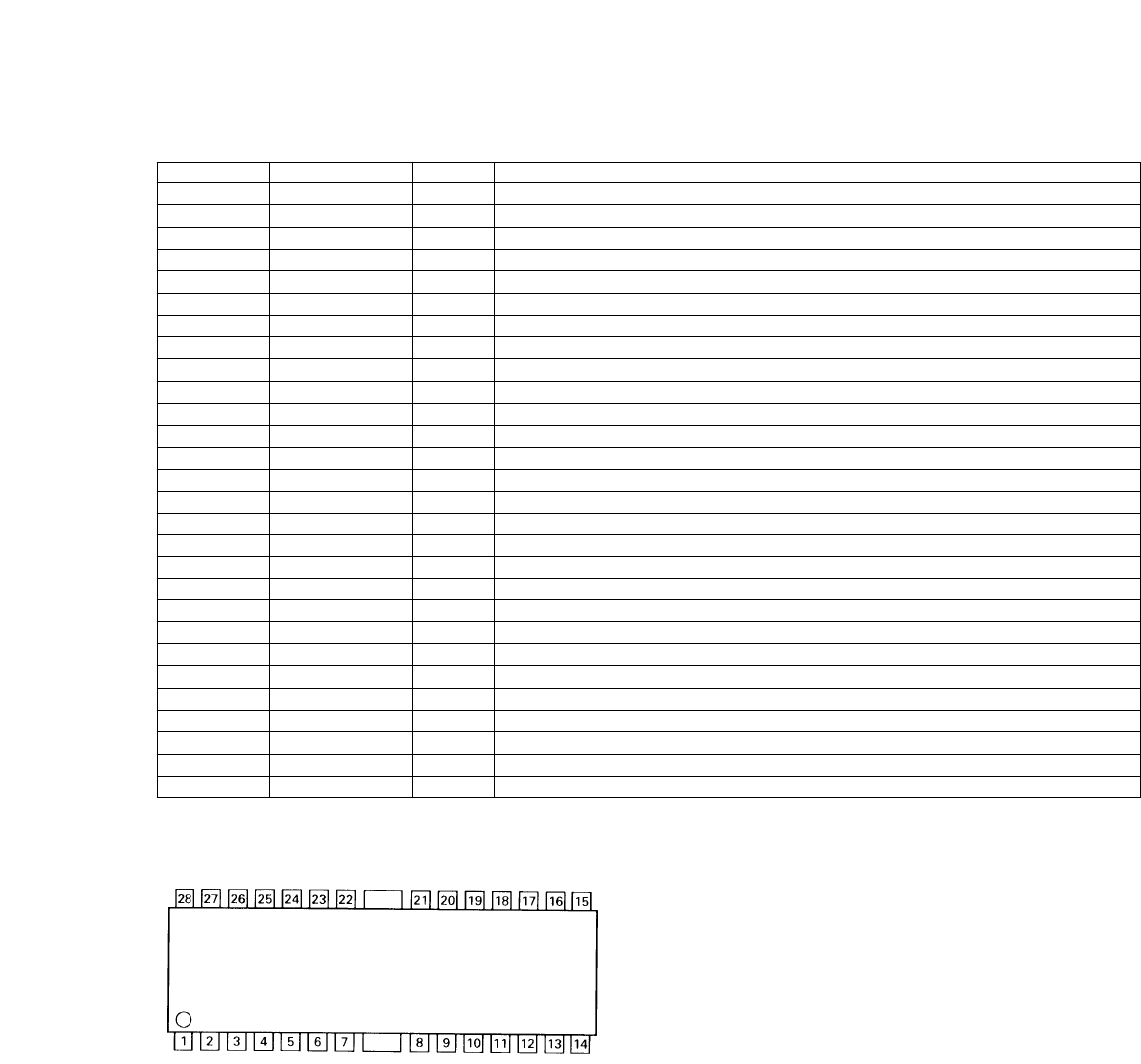
71
FX-M2317ZSA
-Pin Functions (BA5985FM)
Pin No. Pin Name I/O Function and Operation
1 FWD I Loading driver FWD input
2 OPIN1(+) I CH1 pre-amplifier input
3 OPIN1(−) I CH1 pre-amplifier inverted input
4 OPOUT1 O CH1 pre-amplifier output
5 OPIN2(+) I CH2 pre-amplifier input
6 OPIN2(−) I CH2 pre-amplifier inverted input
7 OPOUT2 O CH2 pre-amplifier output
8 VCC Power supply
9 VOL(−) O Loading driver negative output
10 VOL(+) O Loading driver positive output
11 VO2(−) O Driver CH2 negative output
12 VO2(+) O Driver CH2 positive output
13 VO1(−) O Driver CH1 negative output
14 VO1(+) O Driver CH1 positive output
15 VO4(+) O Driver CH4 positive output
16 VO4(−) O Driver CH4 negative output
17 VO3(+) O Driver CH3 positive output
18 VO3(−) O Driver CH3 negative output
19 GND GND
20 BIAS I Bias input
21 MUTE Mute control
22 OPOUT3 O CH3 pre-amplifier output
23 OPIN3(−) I CH3 pre-amplifier inverted input
24 OPIN3(+) I CH3 pre-amplifier input
25 OPOUT4 O CH4 pre-amplifier output
26 OPIN4(−) I CH4 pre-amplifier inverted input
27 OPIN4(+) I CH4 pre-amplifier input
28 REV I Loading driver REV input
BA5985FM
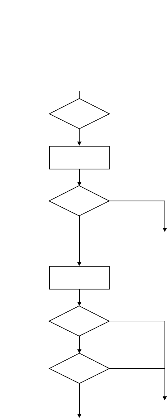
72
FX-M2317ZSA
7.3 EXPLANATION
7.3.1 OPERATIONAL FLOW CHART
BATT ON
igsen
Pin 63
VDD=5V
Pin 68
Initial Part
Port settings
TESTIN
Pin 73
TESTIN=L
Test mode
Stand-by
Loading
EPROM data
BSEN
Pin 62
BSEN=H
igsen=L
Start the proper source
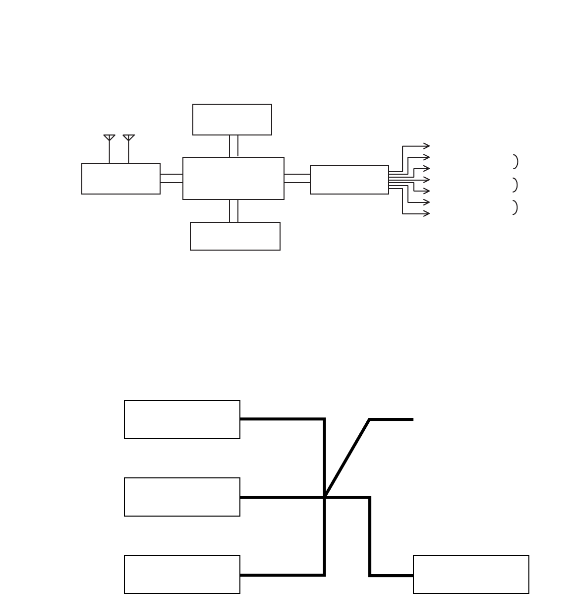
73
FX-M2317ZSA
7.3.2 SYSTEM BLOCK DIAGRAM
FX-M2317ZSA/X1B/ES
CDX-M2516ZSA/WL
DISPLAY
by NOKIA
GM-2416ZSA/WL
FRONT CENTER
FRONT Lch
FRONT Rch
FRONT DOOR Lch
FRONT DOOR Rch
REAR DOOR Lch
REAR DOOR Rch
SAAB PART No.
4617049
4616850
4616926
4616934
DIVER UNIT
by Fuba
The diversity system is
optional.
A single-antenna booster
is also available.
The antenna is of
window-glass built-in
type.
The amplifier provides 7 channel outputs.
FX-M2317ZSA/X1B/ES
DISPLAY by NOKIA
GGF1296
CDX-M2516ZSA/WL GM-2416ZSA/WL
SPEAKERS
GGD1120
7.3.3 JIG CONNECTION DIAGRAM
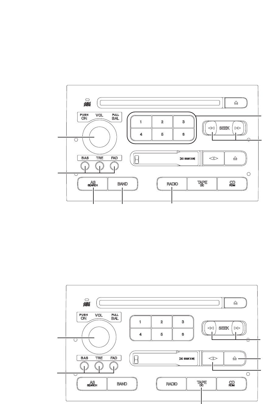
74
FX-M2317ZSA
8. OPERATIONS AND SPECIFICATIONS
8.1 OPERATIONS
BASS
TREBLE
FADER
RADIO
MANUAL SEEK
BAND
PRESET RECALL
PRESET CH.MEMORY
AUTO STORE
POWER ON/OFF
VOLUME
BALANCE
-RADIO
-TAPE
POWER ON/OFF
VOLUME
BALANCE
BASS
TREBLE
FADER
TAPE
DOLBY
DIRECTION
TAPE EJECT
REWIND/FAST FORWARD
AUTO PROGRAM SEARCH
BLANK SKIP
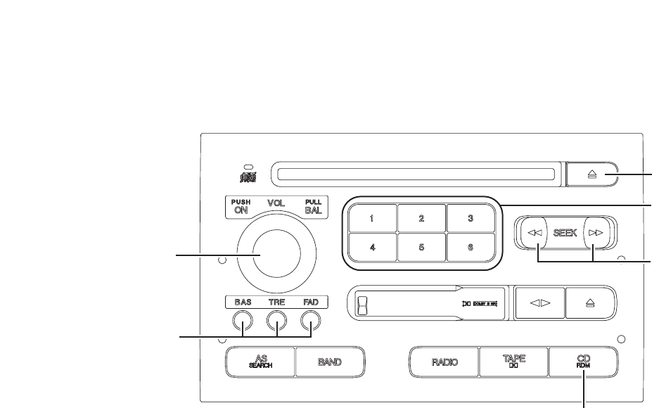
75
FX-M2317ZSA
-CD
BASS
TREBLE
FADER
CD
RANDOM
SINGLE/MULTI SELECT
TRACK UP/DOWN
REVERSE/FAST FORWARD
MANUAL/SEEK CHANGE
DISC SELECT
(MULTI CD)
CD EJECT
POWER ON/OFF
VOLUME
BALANCE
8.2 SPECIFICATIONS
Power source.....................................................13.5V±0.1V
Grounding system........................................Negative type
Dimensions.....................195.6(W)x118.2(H)x183.5(D)mm
Weight ........................................................................2280g
Backup current..............................................0.3mA or less
AUDIO
Tone control
Tone charact bass........................................................±9dB
Tone charact treble......................................................±9dB
Fader charact..................................................-30dB or less
Balance charact..............................................-30dB or less
CD
System ...................................Compact disc audio system
Usable discs ..................................................Compact disc
Signal ...................................Sampling frequency:44.1kHz
Number of quantization bits:16;linear
S/N .................................................................80dB or more
Distortion........................................................0.03% or less
Separation.....................................................70dB or more
TAPE
Tape................................Compact cassette tape(C30-C90)
Tape speed ......4.76 cm/sec.(+0.14 cm/sec.,-0.05 cm/sec.)
Crosstalk ..........................................................40dB or less
Separation.....................................................35dB or more
S/N .................................................................45dB or more
Distortion.............................................................2% or less
FM TUNER
Frequency ...................................................87.5-108.0 MHz
Usable sensitivity.........................................................9dBf
S/N .................................................................50dB or more
Distortion..........................................................1.0% or less
Separation.....................................................25dB or more
AM TUNER
Frequency ............................................531-1602 kHz(9kHz)
530-1710 kHz(10kHz)
Selectivity .........................................45dB or more(±9kHz)
S/N .................................................................45dB or more
Distortion..........................................................1.0% or less
