MainCover GM Series/GM328 GM338 GM398 Detailed Service Manual 6804112J18 E GM328
User Manual: -GM Series/GM328 GM338 GM398 Detailed service manual 6804112J18-E
Open the PDF directly: View PDF ![]() .
.
Page Count: 556 [warning: Documents this large are best viewed by clicking the View PDF Link!]
- DOCUMENT HISTORY
- gmSerMaint.pdf
- SAFETY INFORMATION
- Product Safety and RF Exposure for Mobile Two-Way Radios Installed in Vehicles or as Fixed Site C...
- RF Energy Exposure Awareness and Control Information, and Operational Instructions for FCC Occupa...
- Compliance and Control Guidelines and Operating Instructions for Mobile Two-Way Radios Installed ...
- Electromagnetic Interference/Compatibility
- Facilities
- Vehicles
- 1. Refer to the manufacturer’s instructions or other technical bulletins for recommendations on r...
- 2. Before installing the radio, determine the location of the electronic control modules and thei...
- 3. Route all radio wiring, including the antenna transmission line, as far away as possible from ...
- Driver Safety
- Operational Warnings
- Section 1
- Section 2
- Maintenance
- 1.0 Introduction
- 2.0 Preventive Maintenance
- 3.0 Safe Handling of CMOS and LDMOS
- 4.0 General Repair Procedures and Techniques
- 1. Use a hot-air hand piece and position the nozzle of the hand piece approximately 0.3 cm (1/ 8"...
- 2. Begin applying the hot air. Once the solder reflows, remove the component using a pair of twee...
- 3. Using a solder wick and a soldering iron or a power desoldering station, remove the excess sol...
- 1. Select the appropriate micro-tipped soldering iron and apply fresh solder to one of the solder...
- 2. Using a pair of tweezers, position the new chip component in place while heating the fresh sol...
- 3. Once solder wicks onto the new component, remove the heat from the solder.
- 4. Heat the remaining pad with the soldering iron and apply solder until it wicks to the componen...
- 1. Use the hot-air hand piece and reflow the solder on the solder pads to smooth it.
- 2. Apply a drop of solder paste flux to each pad.
- 3. Using a pair of tweezers, position the new component in place.
- 4. Position the hot-air hand piece approximately 0.3 cm (1/8” ) above the component and begin app...
- 5. Once the solder wicks to the component, remove the heat and inspect the repair. All joints sho...
- 1. Place the circuit board in the R1070 circuit board holder.
- 2. Select the proper heat focus head and attach it to the heater chimney.
- 3. Add solder paste flux around the base of the shield.
- 4. Position the shield under the heat-focus head.
- 5. Lower the vacuum tip and attach it to the shield by turning on the vacuum pump.
- 6. Lower the focus head until it is approximately 0.3 cm (1/8”) above the shield.
- 7. Turn on the heater and wait until the shield lifts off the circuit board.
- 8. Once the shield is off, turn off the heat, grab the part with a pair of tweezers, and turn off...
- 9. Remove the circuit board from the R1070 circuit board holder.
- 1. Add solder to the shield if necessary, using a micro-tipped soldering iron.
- 2. Next, rub the soldering iron tip along the edge of the shield to smooth out any excess solder....
- 3. Place the circuit board back in the R1070 circuit board holder.
- 4. Place the shield on the circuit board using a pair of tweezers.
- 5. Position the heat-focus head over the shield and lower it to approximately 0.3 cm (1/8”) above...
- 6. Turn on the heater and wait for the solder to reflow.
- 7. Once complete, turn off the heat, raise the heat-focus head and wait approximately one minute ...
- 8. Remove the circuit board and inspect the repair. No cleaning should be necessary.
- 5.0 Notes For All Schematics and Circuit Boards
- Section 3
- SAFETY INFORMATION
- gmcntlhd.pdf
- Section 1 overview
- Section 2 Theory of Operation
- Section 3 Troubleshooting Charts
- Section 4 Controlhead PCBs / Schematics / Parts lists
- Section 1
- Section 2
- Theory of Operation
- 1.0 Introduction
- 2.0 Controlhead Model for GM328
- 3.0 Controlhead Model for GM338
- 4.0 Controlhead Model for GM398
- 4.1 Power Supplies
- 4.2 Voltage Regulator Circuit
- 4.3 Power On / Off
- 4.4 Microprocessor Circuit
- 4.5 SBEP Serial Interface
- 4.6 Keypad Keys
- 4.7 Status LED and Back Light Circuit
- 4.8 Liquid Crystal Display (LCD)
- 4.9 Microphone Connector Signals
- 4.10 Speaker (Remote Mount Configuration only)
- 4.11 Electrostatic Transient Protection
- Section 3
- Section 4
- gmcntrller.pdf
- Section 1 Theory of Operation
- Section 2 Troubleshooting Charts
- Section 3 Controller Schematics / Parts Lists
- Section 1
- Theory of Operation
- 1.0 Controller Circuits
- 1.1 Overview
- 1.2 General
- 1.3 Radio Power Distribution
- 1.4 Electronic ON/OFF
- 1.5 Emergency
- 1.6 Mechanical ON/OFF
- 1.7 Ignition
- 1.8 Microprocessor Clock Synthesizer
- 1.9 Serial Peripheral Interface (SPI)
- 1.10 SBEP Serial Interface
- 1.11 General Purpose Input/Output
- 1.12 Normal Microprocessor Operation
- 1.13 FLASH Electronically Erasable Programmable Memory(FLASH EEPROM)
- 1.14 Electrically Erasable Programmable Memory (EEPROM)
- 1.15 Static Random Access Memory (SRAM)
- 2.0 Controller Board Audio and Signalling Circuits
- Section 2
- Section 3
- gmvhf.pdf
- Section 1 Model Chart and Technical Specifications
- Section 2 Theory of Operation
- Section 3 Troubleshooting Charts
- Section 4 VHF PCBs/Schematics/Parts Lists
- Section 1
- Section 2
- Section 3
- Section 4
- gmUHF1.pdf
- Section 1 Model Chart and Technical Specifications
- Section 2 Theory of Operation
- Section 3 Troubleshooting Charts
- Section 4 UHF PCB/Schematics/Parts Lists
- Section 1
- Section 2
- Section 3
- Section 4
- gmUHF2.pdf
- Section 1 Model Chart and Technical Specifications
- Section 2 Theory of Operation
- Section 3 Troubleshooting Charts
- Section 4 UHF PCB/Schematics/Parts Lists
- Section 1
- Section 2
- Section 3
- Section 4
- gmLB.pdf
- Section 1 Model Chart and Technical Specifications
- Section 2 Theory of Operation
- Section 3 Troubleshooting Charts
- Section 4 Low Band PCBs/Schematics/Parts Lists
- Section 1
- Section 2
- Theory of Operation
- 1.0 Introduction
- 2.0 Low Band Receiver
- 3.0 Transmitter Power Amplifier (PA) 60 W
- 4.0 Frequency Synthesis
- Section 3
- Section 4
- Low Band PCBs/Schematics/Parts Lists
- 1.0 Allocation of Schematics and Circuit Boards
- Low Band Range 1 PCB 8486206B06 Parts List
- Low Band Range 2 PCB 8486207B05 Parts List
- Low Band Range 3 PCB 8486908Z02 Parts List
- Low Band Range 1 PCB 8486206B08 Parts List
- Low Band Range 2 PCB 8486207B07 Parts List
- Low Band Range 3 PCB 8486908Z04 Parts Lis
- gmVHFhp.pdf
- Section 1 Model Chart and Technical Specifications
- Section 2 Theory of Operation
- Section 3 Troubleshooting Charts
- Section 4 VHF PCB/Schematics/Parts List
- Section 1
- Section 2
- Section 3
- Section 4
- gmUHF1hp.pdf
- Section 1 Model Chart and Technical Specifications
- Section 2 Theory of Operation
- Section 3 Troubleshooting Charts
- Section 4 UHF PCB/Schematics/Parts Lists
- Section 1
- Section 2
- Section 3
- Section 4
- gmUHF2hp.pdf
- Section 1 Model Chart and Technical Specifications
- Section 2 Theory of Operation
- Section 3 Troubleshooting Charts
- Section 4 UHF PCB/Schematics/Parts Lists
- Section 1
- Section 2
- Section 3
- Section 4
- gmUHF1hpLD.pdf
- Section 1 Model Chart and Technical Specifications
- Section 2 Theory of Operation
- Section 3 Troubleshooting Charts
- Section 4 UHF PCB/Schematics/Parts Lists
- Section 1
- Section 2
- Section 3
- Section 4
- gmUHF2hpLD.pdf
- Section 1 Model Chart and Technical Specifications
- Section 2 Theory of Operation
- Section 3 Troubleshooting Charts
- Section 4 UHF PCB/Schematics/Parts Lists
- Section 1
- Section 2
- Section 3
- Section 4
- gmfeedback.pdf
- Technical Information Updates
- Service Manual Feedback Form
- 1. Please check all the appropriate boxes:
- 2. How do you rate this particular Service Manual?
- 3. Did this Service manual provide you with the information necessary to service and maintain the...
- 4. We would appreciate any corrections or recommendations for improving this manual. Please inclu...
- 5. General comments/suggestions:

GM328/GM338/GM398
Mobile Radios
Detailed Service Manual
6804112J18-E
December, 2003

Computer Software Copyrights
The Motorola products described in this manual may include copyrighted Motorola computer programs stored
in semiconductor memories or other media. Laws in the United States and other countries preserve for
Motorola certain exclusive rights for copyrighted computer programs, including the exclusive right to copy or
reproduce in any form, the copyrighted computer program. Accordingly, any copyrighted Motorola computer
programs contained in the Motorola products described in this manual may not be copied or reproduced in
any manner without the express written permission of Motorola. Furthermore, the purchase of Motorola prod-
ucts shall not be deemed to grant, either directly or by implication, estoppel or otherwise, any license under
the copyrights, patents or patent applications of Motorola, except for the normal non-exclusive royalty-free
license to use that arises by operation of law in the sale of a product.

DOCUMENT HISTORY
The following major changes have been implemented in this manual since the previous edition:
Edition Description Date
6804112J18-O Initial edition
6804112J18-E Added Document History section. Dec. 2003
Changed to latest Safety Information (Feb. 2002)
Added GM328 model information to VHF, UHF1
and UHF2 bands.

THIS PAGE INTENTIONALLY LEFT BLANK

December, 2003
GM328/GM338/GM398
Mobile Radios
Detailed Service Manual
Contents
Section 1 Service Maintainability
Section 2 Controlhead Service Information
Section 3 Controller Service Information
Section 4 VHF Service Information
Section 5 UHF Band 1 Service Information
Section 6 UHF Band 2 Service Information
Section 7 Low Band Service Information
Section 8 VHF 45W Bipolar Service Information
Section 9 UHF Band 1 40W Bipolar Service Information
Section 10 UHF Band 2 40W Bipolar Service Information
Section 11 UHF Band 1 40W LDMOS Service Information
Section 12 UHF Band 2 40W LDMOS Service Information

THIS PAGE INTENTIONALLY LEFT BLANK

GM328/GM338/GM398
Mobile Radios
Service Maintainability
Issue: December, 2003

Computer Software Copyrights
The Motorola products described in this manual may include copyrighted Motorola computer programs stored
in semiconductor memories or other media. Laws in the United States and other countries preserve for
Motorola certain exclusive rights for copyrighted computer programs, including the exclusive right to copy or
reproduce in any form, the copyrighted computer program. Accordingly, any copyrighted Motorola computer
programs contained in the Motorola products described in this manual may not be copied or reproduced in
any manner without the express written permission of Motorola. Furthermore, the purchase of Motorola
products shall not be deemed to grant, either directly or by implication, estoppel or otherwise, any license
under the copyrights, patents or patent applications of Motorola, except for the normal non-exclusive
royalty-free license to use that arises by operation of law in the sale of a product.
i
SAFETY INFORMATION
Product Safety and RF Exposure for Mobile Two-Way Radios Installed in
Vehicles or as Fixed Site Control Stations
The information provided in this document supersedes the general safety information contained in
user guides published prior to February 2002.
RF Energy Exposure Awareness and Control Information, and
Operational Instructions for FCC Occupational Use Requirements
NOTICE: This radio is intended for use in occupational/controlled conditions, where users
have full knowledge of their exposure and can exercise control over their exposure
to meet FCC limits. This radio device is NOT authorized for general population,
consumer or any other use.
This 2-way radio uses electromagnetic energy in the radio frequency (RF) spectrum to provide
communications between two or more users over a distance. It uses radio frequency (RF) energy or
radio waves to send and receive calls. RF energy is one from of electromagnetic energy. Other
forms include, but are not limited to, sunlight and x-rays. RF energy, however, should not be
confused with these other forms of electromagnetic energy, which when used improperly, can cause
biological damage. Very high levels of x-rays, for example, can damage tissues and genetic
material.
Experts in science, engineering, medicine, health, and industry work with organizations to develop
standards for safe exposure to RF energy. These standards provide recommended levels of RF
exposure for both workers and the general public. These recommended RF exposure levels include
substantial margins of protection.
All Motorola 2-way radios are designed, manufactured, and tested to ensure they meet government-
established RF exposure levels. In addition, manufacturers also recommend specific operating
instructions to users of 2-way radios. These instructions are important because they inform users
about RF energy exposure and provide simple procedures on how to control it.
Please refer to the following Web sites for more information on what RF energy exposure is and how
to control your exposure to assure compliance with established RF exposure limits.
http://www.fcc.gov/oet/rfsafety/rf-fags.html
http://www.osha.gov/SLTC/radiofrequencyradiation/index.html
BEFORE USING THIS RADIO, READ THIS BOOKLET WHICH CONTAINS IMPORTANT OPERAT-
ING INSTRUCTIONS FOR SAFE USAGE AND RF ENERGY AWARENESS AND CONTROL
INFORMATION FOR COMPLIANCE WITH RF ENERGY EXPOSURE LIMITS IN APPLICABLE
NATIONAL AND INTERNATIONAL STANDARDS.

ii
Federal Communication Commission (FCC) Regulations
The FCC rules require manufacturers to comply with the FCC RF energy exposure limits for mobile
2-way radios before they can be marketed in the U.S. When 2-way radios are used as a
consequence of employment, the FCC requires users to be fully aware of and able to control their
exposure to meet occupational requirements. Exposure awareness can be facilitated by the use of a
label directing users to specific user awareness information. Your Motorola 2-way radio has a RF
exposure product label. Also, your Motorola user manual, or separate safety booklet, includes
information and operating instructions required to control your RF exposure and to satisfy
compliance requirements.
Compliance with RF Exposure Standard
Your Motorola two-way radio is designed and tested to comply with a number of national and
international standards and guidelines (listed below) regarding human exposure to radio frequency
electromagnetic energy. This radio complies with the IEEE and ICNIRP exposure limits for
occupational/controlled RF exposure environment at duty factors of up to 50% talk–50% listen and
is authorized by the FCC for occupational use. In terms of measuring RF energy for compliance with
the FCC exposure guidelines, your radio antenna radiates measurable RF energy only while it is
transmitting (during talking), not when it is receiving (listening) or in standby mode.
Your Motorola two-way radio complies with the following RF energy exposure standards and
guidelines:
• United States Federal Communications Commission, Code of Federal Regulations; 47 CFR part
2 sub-part J
• American National Standards Institute (ANSI) / Institute of Electrical and Electronic Engineers
(IEEE) C95. 1-1992
• Institute of Electrical and Electronic Engineers (IEEE) C95.1-1999 Edition
• International Commission on Non-Ionizing Radiation Protection (ICNIRP) 1998
• Ministry of Health (Canada) Safety Code 6. Limits of Human Exposure to Radiofrequency Elec-
tromagnetic Fields in the Frequency Range from 3 kHz to 300 GHz, 1999
• Australian Communications Authority Radiocommunications (Electromagnetic Radiation -
Human Exposure) Standard, 2003
• ANATEL, Brasil Regulatory Authority, Resolution 256 (April 11, 2001) “additional requirements
for SMR, cellular and PCS product certification.”
RF Exposure Compliance and Control Guidelines and Operating Instructions
To control exposure to yourself and others and to ensure compliance with the RF exposure limits,
always adhere to the following procedures.
Guidelines
• User awareness instructions should accompany device when transferred to other users.
• Do not use this device if the operational requirements described herein are not met.
Instructions
•Transmit no more than the rated duty factor of 50% of the time. To transmit (talk), push the
Push-To-Talk (PTT) button. To receive calls, release the PTT button. Transmitting 50% of the
time, or less, is important because this radio generates measurable RF energy exposure only
when transmitting (in terms of measuring for standards compliance).
•Transmit only when people outside the vehicle are at least the recommended minimum
laterial distance away, as shown in Table 1, from the body of a vehicle with a properly
installed antenna. This separation distance will ensure that there is sufficient distance from a
iii
properly installed (according to installation instructions) externally-mounted antenna to satisfy
the RF exposure requirements in the standards listed above.
NOTE: Table 1 below lists the recommended lateral distance for bystanders in an uncontrolled
environment from the body of a vehicle with an approved, properly installed transmitting
antenna (i.e., monopoles overa a ground plane, or dipoles) at several different ranges of
rated radio power for mobile radios installed in a vehicle.
NOTE:If you are not sure of the rated power of your radio, contact your Motorola representative or
dealer and supply the radio model number found on the radio model label. If you cannot
determine the rated power out, then assure 3-feet separation from the body of the vehicle.
Mobile Antenna Installation Guidelines
• These mobile antenna installation guidelines are limited to metal body motor vehicles or vehicles
with appropriate ground planes.
• Antennas should be installed in the center area of the roof or the trunk lid taking into account the
bystander exposure conditions of backseat passengers and according to the specific instructions
and restrictions in the Radio Installation Manual along with the requirements of the antenna sup-
plier.
• Trunk lid installations are limited to vehicles with clearly defined flat trunk lide, and in some
cases, to specific radio models and antennas. See the Radio Installation Manual for specific
information on how and where to install specific types of approved antennas to facilitate recom-
mended operating distances to all potentially exposed persons.
•Use only the Motorola-approved, supplied antenna or a Motorola-approved replacement
antenna. Unauthorized antennas, modifications, or attachments could damage the radio and
may result in non-compliance with RF Safety Standards.
Approved Accessories
• This radio has been tested and meets RF Safety Standards when used with the Motorola acces-
sories supplied or designated for this product. Use of other accessories may result in non-compli-
ance with RF Safety Standards.
• For a list of Motorola-approved antennas, visit the following Web site, which lists approved
accessories for your radio model: http://ap.cgiss.motorola.com/AAD/index.html
Additional Information
For additional information on exposure requirements or other training information,
visit http://www.motorola.com/rfhealth.
Table 1: Rated Power of Vehicle-Installed Mobile Two-Way Radio and
Recommended Minimum Lateral Distance from Vehicle Body
Mobile Radio Rated
Power (see Note) Minimum Lateral Distance
from Vehicle Body
Less than 7 watts 8 inches (20 centimeters)
7 to 15 watts 1 foot (30 centimeters)
16 to 39 watts 2 feet (60 centimeters)
40 to 110 watts 3 feet (90 centimeters)

iv
Compliance and Control Guidelines and Operating Instructions for
Mobile Two-Way Radios Installed as Fixed Site Stations
If mobile radio equipment is installed at a fixed location and operated as a control station or as a
fixed unit, the antenna installation must comply with the following requirements in order to ensure
optimal performance and compliance with the RF energy exposure limits in the standards and
guidelines listed on page ii:
• The antenna should be mounted outside the building on the roof or a tower if at all possible.
• As with all fixed site antenna installations, it is the responsibility of the licensee to manage the
site in accordance with applicable regulatory requirements and may require additional compli-
ance actions such as site survey measurements, signage, and site access restrictions in order to
ensure that exposure limits are not exceeded.
Electromagnetic Interference/Compatibility
NOTE:Nearly every electronic device is susceptible to electromagnetic interference (EMI) if
inadequately shielded, designed, or otherwise configured for electromagnetic compatibility. It
may be necessary to conduct compatibility testing to determine if any electronic equipment
used in or around vehicles or near fixed site antenna is sensitive to external RF energy or if
any procedures need to be followed to eliminate or mitigate the potential for interaction
between the radio transmitter and the equipment or device.
Facilities
To avoid electromagnetic interference and/or compatibility conflicts, turn off your radio in any
facility where posted notices instruct you to do so. Hospitals or health care facilities may be
using equipment that is sensitive to external RF energy.
Vehicles
To avoid possible interaction between the radio transmitter and any vehicle electronic control
modules, such as ABS, engine, or transmission controls, the radio should be installed only by an
experienced installer and the following precautions should be used when installing the radio:
1. Refer to the manufacturer’s instructions or other technical bulletins for recommendations on
radio installation.
2. Before installing the radio, determine the location of the electronic control modules and their
harnesses in the vehicle.
3. Route all radio wiring, including the antenna transmission line, as far away as possible from
the electronic control units and associated wiring.
Driver Safety
Check the laws and regulations on the use of radios in the area where you drive. Always obey them.
When using your radio while driving, please:
• Give full attention to driving and to the road.
• Pull off the road and park before making or answering a call if driving conditions so require.

v
Operational Warnings
For Vehicles With An Air Bag
Do not mount or place a mobile radio in the area over an air bag or in the air bag deployment
area. Air bags inflate with great force. If a radio is placed in the air bag deployment area and
the air bag inflates, the radio may be propelled with great force and cause serious injury to
occupants of the vehicle.
Potentially Explosive Atmospheres
Turn off your radio prior to entering any area with a potentially explosive atmosphere.
Sparks in a potentially explosive atmosphere can cause an explosion or fire resulting in
bodily injury or even death.
The areas with potentially explosive atmospheres include fueling areas such as below decks
on boats, fuel or chemical transfer or storage facilities, and areas where the air contains
chemicals or particles such as grain, dust or metal powders. Areas with potentially
explosive atmospheres are often, but not always, posted.
Blasting Caps And Blasting Areas
To avoid possible interference with blasting operations, turn off your radio when you are
near electrical blasting caps, in a blasting area, or in areas posted: “Turn off two-way radio.”
Obey all signs and instructions.
For radios installed in vehicles fueled by liquefied petroleum gas, refer to the (U.S.) National
Fire Protection Association standard, NFPA 58, for storage, handling, and/or container
information. For a copy of the LP-gas standard, NFPA 58, contact the National Fire
Protection Association, One Battery Park, Quincy, MA.

vi
THIS PAGE INTENTIONALLY LEFT BLANK

vii
Table of Contents
SAFETY INFORMATION......................................................................................... i
Section 1 Introduction
1.0 Scope of Manual..................................................................................................1-1
2.0 Warranty and Service Support.............................................................................1-1
2.1 Warranty Period and Return Instructions .......................................................1-1
2.2 After Warranty Period.....................................................................................1-1
2.3 Piece Parts Availability ...................................................................................1-2
2.4 Technical Support...........................................................................................1-2
2.5 Further Assistance From Motorola .................................................................1-2
3.0 Radio Model Information......................................................................................1-3
Section 2 Maintenance
1.0 Introduction ..........................................................................................................2-1
2.0 Preventive Maintenance ......................................................................................2-1
2.1 Inspection .......................................................................................................2-1
2.2 Cleaning .........................................................................................................2-1
3.0 Safe Handling of CMOS and LDMOS..................................................................2-2
4.0 General Repair Procedures and Techniques.......................................................2-2
5.0 Notes For All Schematics and Circuit Boards......................................................2-5
Section 3 Service Aids
1.0 Recommended Test Tools...................................................................................3-1
2.0 Test Equipment....................................................................................................3-2

viii
THIS PAGE INTENTIONALLY LEFT BLANK

1-1
Section 1
INTRODUCTION
1.0 Scope of Manual
This manual is intended for use by service technicians familiar with similar types of equipment. It
contains service information required for the equipment described and is current as of the printing
date. Changes which occur after the printing date may be incorporated by a complete manual
revision or alternatively as additions.
2.0 Warranty and Service Support
Motorola offers support which includes: full exchange and/or repair of the product during the
warranty period; and service/repair or spare parts support out of warranty. Any “return for exchange”
or “return for repair” to an authorized Motorola Dealer must be accompanied by a Warranty Claim
Form. Warranty Claim Forms are obtained by contacting an Authorized Motorola Dealer.
2.1 Warranty Period and Return Instructions
The terms and conditions of warranty are defined fully in the Motorola Dealer or Distributor or
Reseller contract. These conditions may change from time to time, and the following subsections
are for guidance purposes only.
In instances where the product is covered under a “return for replacement” or “return for repair”
warranty, a check of the product should be performed prior to shipping the unit back to Motorola.
This is to ensure that the product has been correctly programmed or has not been subjected to
damage outside the terms of the warranty.
Prior to shipping any radio back to the appropriate Motorola warranty depot, please contact
Customer Resources. All returns must be accompanied by a Warranty Claim Form, available from
your Customer Resources representative. Products should be shipped back in the original
packaging, or correctly packaged to ensure that no damage occurs in transit.
2.2 After Warranty Period
After the Warranty period, Motorola continues to support its products in two ways:
1. Motorola's Accessories and Aftermarket Division (AAD) offers a repair service to both end
users and dealers at competitive prices.
2. AAD supplies individual parts and modules that can be purchased by dealers who are techni-
cally capable of performing fault analysis and repair.
NOTE Before operating or testing these units, please read the Safety Information section in the
front of this manual.

1-2 Warranty and Service Support
2.3 Piece Parts Availability
Some replacement parts, spare parts, and/or product information can be ordered directly. If a
complete Motorola part number is assigned to the part, it is available from Motorola’s Accessories
and Aftermarket Division (AAD). If no part number is assigned, the part is not normally available
from Motorola. If the part number is appended with an asterisk, the part is serviceable by Motorola
Depot only. If a parts list is not included, this generally means that no user-serviceable parts are
available for that kit or assembly.
All orders for parts/information should include the complete Motorola identification number. All part
orders should be directed to your local AAD office. Please refer to your latest price pages.
2.4 Technical Support
Technical support is available to assist the dealer/distributor in resolving any malfunction which may
be encountered. Initial contact should be by telephone wherever possible. When contacting
Motorola Technical Support, be prepared to provide the product model number and the unit’s
serial number.
2.5 Further Assistance From Motorola
You can also call the CGISS Indirect Business Customer Help Desk number, (604)-6302525 or
send an email to customercare.asia@motorola.com.
1-3 Radio Model Information
3.0 Radio Model Information
The model number and serial number are located on a label attached to the back of your radio. You
can determine the RF output power, frequency band, protocols, and physical packages. The
example below shows one mobile radio model number and its specific characteristics.
Table 1-1 Radio Model Number (Example: AZM25KHF9AA5)
Type of
Unit Model
Series Freq.
Band Power
Level Physical
Packages Channel
Spacing Protocol Feature
Level
AZ M25 K
VHF
(136-
174MHz)
H
1-25W C
GM328 9
Program-
mable
AA
Conventional 1
GM328
R
UHF1
(403-
470MHz)
K
25-60W F
GM338 5
GM338
S
UHF2
(450-
527MHz)
N
GM398 8
GM398
B
LB, R1
(29.7-
36MHz)
C
LB, R2
(36-
40MHz)
D
LB, R3
(42-
50MHz)
AZ = Country Code
M = Mobile

1-4 Radio Model Information
THIS PAGE INTENTIONALLY LEFT BLANK

2-1
Section 2
MAINTENANCE
1.0 Introduction
This chapter of the manual describes:
•preventive maintenance
•safe handling of CMOS devices
•repair procedures and techniques
2.0 Preventive Maintenance
The radios do not require a scheduled preventive maintenance program; however, periodic visual
inspection and cleaning is recommended.
2.1 Inspection
Check that the external surfaces of the radio are clean, and that all external controls and switches
are functional. It is not recommended to inspect the interior electronic circuitry.
2.2 Cleaning
The following procedures describe the recommended cleaning agents and the methods to be used
when cleaning the external and internal surfaces of the radio. External surfaces include the front
cover, housing assembly, and battery case. These surfaces should be cleaned whenever a periodic
visual inspection reveals the presence of smudges, grease, and/or grime.
The only recommended agent for cleaning the external radio surfaces is a 0.5% solution of a mild
dishwashing detergent in water. The only factory recommended liquid for cleaning the printed circuit
boards and their components is isopropyl alcohol (70% by volume).
1. Cleaning External Plastic Surfaces
The detergent-water solution should be applied sparingly with a stiff, non-metallic, short-bris-
tled brush to work all loose dirt away from the radio. A soft, absorbent, lintless cloth or tissue
should be used to remove the solution and dry the radio. Make sure that no water remains
entrapped near the connectors, cracks, or crevices.
NOTE Internal surfaces should be cleaned only when the radio is disassembled for servicing or
repair.
CAUTION: The effects of certain chemicals and their vapors can have harmful results on
certain plastics. Aerosol sprays, tuner cleaners, and other chemicals should be avoided.
!

2-2 Safe Handling of CMOS and LDMOS
2. Cleaning Internal Circuit Boards and Components
Isopropyl alcohol may be applied with a stiff, non-metallic, short-bristled brush to dislodge
embedded or caked materials located in hard-to-reach areas. The brush stroke should direct
the dislodged material out and away from the inside of the radio. Make sure that controls or
tunable components are not soaked with alcohol. Do not use high-pressure air to hasten the
drying process since this could cause the liquid to collect in unwanted places. Upon comple-
tion of the cleaning process, use a soft, absorbent, lintless cloth to dry the area. Do not brush
or apply any isopropyl alcohol to the frame, front cover, or back cover.
3.0 Safe Handling of CMOS and LDMOS
Complementary metal-oxide semiconductor (CMOS) devices are used in this family of radios.
CMOS characteristics make them susceptible to damage by electrostatic or high voltage charges.
Damage can be latent, resulting in failures occurring weeks or months later. Therefore, special
precautions must be taken to prevent device damage during disassembly, troubleshooting, and
repair.
Handling precautions are mandatory for CMOS circuits and are especially important in low humidity
conditions. DO NOT attempt to disassemble the radio without first referring to the CMOS CAUTION
paragraph in the Disassembly and Reassembly section of the manual.
4.0 General Repair Procedures and Techniques
Parts Replacement and Substitution
When damaged parts are replaced, identical parts should be used. If the identical replacement
component is not locally available, check the parts list for the proper Motorola part number and
order the component from the nearest Motorola Communications parts center listed in the “Piece
Parts” section of this manual.
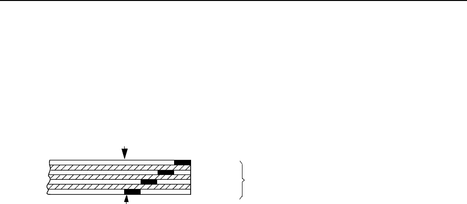
Rigid Circuit Boards
The family of radios uses bonded, multi-layer, printed circuit boards. Since the inner layers are not
accessible, some special considerations are required when soldering and unsoldering components.
The through-plated holes may interconnect multiple layers of the printed circuit. Therefore, care
should be exercised to avoid pulling the plated circuit out of the hole.
When soldering near the 18-pin and 40-pin connectors:
•avoid accidentally getting solder in the connector.
•be careful not to form solder bridges between the connector pins
•closely examine your work for shorts due to solder bridges.
NOTE Always use a fresh supply of alcohol and a clean container to prevent contamination by
dissolved material (from previous usage).

General Repair Procedures and Techniques 2-3
Chip Components
Use either the RLN4062 Hot-Air Repair Station or the Motorola 0180381B45 Repair Station for chip
component replacement. When using the 0180381B45 Repair Station, select the TJ-65 mini-
thermojet hand piece. On either unit, adjust the temperature control to 370 °C (700 °F), and adjust
the airflow to a minimum setting. Airflow can vary due to component density.
•To remove a chip component:
1. Use a hot-air hand piece and position the nozzle of the hand piece approximately 0.3 cm (1/
8") above the component to be removed.
2. Begin applying the hot air. Once the solder reflows, remove the component using a pair of
tweezers.
3. Using a solder wick and a soldering iron or a power desoldering station, remove the excess
solder from the pads.
•To replace a chip component using a soldering iron:
1. Select the appropriate micro-tipped soldering iron and apply fresh solder to one of the solder
pads.
2. Using a pair of tweezers, position the new chip component in place while heating the fresh
solder.
3. Once solder wicks onto the new component, remove the heat from the solder.
4. Heat the remaining pad with the soldering iron and apply solder until it wicks to the compo-
nent. If necessary, touch up the first side. All solder joints should be smooth and shiny.
•To replace a chip component using hot air:
1. Use the hot-air hand piece and reflow the solder on the solder pads to smooth it.
2. Apply a drop of solder paste flux to each pad.
3. Using a pair of tweezers, position the new component in place.
4. Position the hot-air hand piece approximately 0.3 cm (1/8” ) above the component and begin
applying heat.
5. Once the solder wicks to the component, remove the heat and inspect the repair. All joints
should be smooth and shiny.

2-4 General Repair Procedures and Techniques
Shields
Removing and replacing shields will be done with the R1070 station with the temperature control set
to approximately 215°C (415°F) [230°C (445°F) maximum].
•To remove the shield:
1. Place the circuit board in the R1070 circuit board holder.
2. Select the proper heat focus head and attach it to the heater chimney.
3. Add solder paste flux around the base of the shield.
4. Position the shield under the heat-focus head.
5. Lower the vacuum tip and attach it to the shield by turning on the vacuum pump.
6. Lower the focus head until it is approximately 0.3 cm (1/8”) above the shield.
7. Turn on the heater and wait until the shield lifts off the circuit board.
8. Once the shield is off, turn off the heat, grab the part with a pair of tweezers, and turn off the
vacuum pump.
9. Remove the circuit board from the R1070 circuit board holder.
•To replace the shield:
1. Add solder to the shield if necessary, using a micro-tipped soldering iron.
2. Next, rub the soldering iron tip along the edge of the shield to smooth out any excess solder.
Use solder wick and a soldering iron to remove excess solder from the solder pads on the cir-
cuit board.
3. Place the circuit board back in the R1070 circuit board holder.
4. Place the shield on the circuit board using a pair of tweezers.
5. Position the heat-focus head over the shield and lower it to approximately 0.3 cm (1/8”) above
the shield.
6. Turn on the heater and wait for the solder to reflow.
7. Once complete, turn off the heat, raise the heat-focus head and wait approximately one
minute for the part to cool.
8. Remove the circuit board and inspect the repair. No cleaning should be necessary.

Notes For All Schematics and Circuit Boards 2-5
5.0 Notes For All Schematics and Circuit Boards
* Component is frequency sensitive. Refer to the Electrical Parts List for value and usage.
1. Unless otherwise stated, resistances are in Ohms (K = 1000), and capacitances are in picofarads
(pF) or microfarads (µF).
2. DC voltages are measured from point indicated to chassis ground using a Motorola DC
multimeter or equivalent. Transmitter measurements should be made with a 1.2 µH choke in
series with the voltage probe to prevent circuit loading.
3. Interconnect Tie Point Legend:
16_8MHz 16.8MHz Reference Frequency
3V3 Regulated 3.3V Supply Voltage for Voice Storage
5V Regulated 5V Supply Voltage for RF Circuitry
5V Regulated 5V Supply Voltage (Control Head)
5V RF Regulated 5V Supply Voltage for RF Circuitry
5V SOURCE 5V Signal to Switch On Control Head
5VD Regulated 5V Supply Voltage for Digital Circuitry
9V3 Regulated 9.3V Supply Voltage
9V3FLT Filtered 9.3V Supply Voltage
A+ 13.2V Supply Voltage
ADDR µP Address Lines
AN Analog Lines to Analog to Digital Converter
ANALOG INPUT 2 External Keypad Matrix Column Signal
ANALOG INPUT 3 External Keypad Matrix Row Signal
BATTERY VOLTAGE Battery Voltage Sense Line
BL A GREEN Back Light Anode Green
BL A RED Back Light Anode Red
BL GREEN Green Back Light Control
BL K GREEN Back Light Cathode Green
BL K RED Back Light Cathode Red
BL KP Green Green Keypad Back Light Control

2-6 Notes For All Schematics and Circuit Boards
BL KP RED Red Keypad Back Light Control
BL LCD GREEN Green Display Back Light Control
BL LCD RED Red Display Back Light Control
BL RED Red Back Light Control
BOOT CNTRL Bootstrap Mode Enable Signal
BOOT MODE Boot Mode Select
BOOT PWR ON Control Head Switch On Signal
BOOT SCI RX Serial Communication Interface Receive Line
BOOT SCI TX Serial Communication Interface Transmit Line
BOOT VPP Boot Mode Select
BUS+ Bi-directional Serial Communication Line
BWSELECT Signal to select between the Ceramic Filter Pairs
CH ACT Channel Activity Indicator Signal (Fast Squelch)
CH KP ID Control Head Keypad ID (Data) Lines
CH REQUEST Control Head Request from Control Head µP
CLK Clock Signal
CNTLVLTG PA Power Control Voltage
CNTR AUDIO Audio Lines of the Controller
COL x Keypad Matrix Column x
CSX Chip Select Line PCIC / FRACN
DATA Data Signal
DC POWER ON Electronic Switching On or Off of the Radio's Voltage Regulators
DISCAUDIO Audio Output Signal from the Receiver IC
ECLK Clock (not used)
EE CS EEPROM Chip Select
EMERGENCY CONTROL Emergency Line to switch on the Radio's Voltage Regulators
EXP BD REQ Service Request Line from Expansion Board

Notes For All Schematics and Circuit Boards 2-7
EXP1 CS Expansion Board Chip Select 1
EXP2 CS Expansion Board Chip Select 2
EXT KP COL External Keypad Matrix Column Signal
EXT KP ROW External Keypad Matrix Row Signal
EXT MIC External (from Accessory Connector) Microphone Input
EXT SWB+ External Switched 13.2V Supply Voltage
F1200 Interrupt Line from ASFIC CMP
FECTRL 1 Control Voltage for Front End Filter
FECTRL 2 Control Voltage for Front End Attenuator Switch
FLASH CS Flash Chip Select
FLASH OE Flash Output Enable
FLAT RX SND Option Board Audio Output Signal
FLAT TX RTN Flat TX Input from Option Board and Accessory Connector
FLT A+ Filtered 13.2 V Supply Voltage
GP x IN General Purpose Input x
GP x IN ACC y General Purpose Input x from Accessory Connector Pin y
GP x IN OUT ACC y General Purpose Input/Output x from Accessory Connector Pin y
GP x OUT General Purpose Output x
GP x OUT ACC y General Purpose Input x from Accessory Connector Pin y
GPIO General Purpose Input Output Lines
HANDSET AUDIO Handset Audio Output
HOOK Hang-up Switch Input
HSIO High Speed Clock In / Data Out
IF First Intermediate Frequency Signal
IGNITION CONTROL Ignition Line to switch on the Radio's Voltage Regulators
IN 5V RF REG Supply Voltage for 5V Regulator in RF Section
INT KP COL Internal Keypad Matrix Column Signal

2-8 Notes For All Schematics and Circuit Boards
INT KP ROW Internal Keypad Matrix Row Signal
INT MIC Internal (from Control Head) Microphone Input
INT SWB Internal Switched 13.2V Supply Voltage
INT SWB+ Internal Switched 13.2V Supply Voltage
IRQ Interrupt Request from Control Head
K9V1 9.1V in Transmit Mode
KEYPAD ID Keypad Identification Line
LCD A0 LCD Control / Display Data Select
LCD CS LCD Chip Select
LCD DATA LCD Data Lines
LCD E RD LCD Enable Read
LCD RW WR LCD Read Write Control
LED CNTRL LED Control Lines
LED GREEN Green LED Control
LED RED Red LED Control
LED YELLOW Yellow LED Control
LOCK Lock Detect Signal from Synthesizer
LSIO Low Speed Clock In / Data Out
LVZIF CS LVZIF Chip Select (not used)
MIC Microphone Input
MISO Serial Peripheral Interface Receive Line
MODIN Modulation Signal into the Synthesizer
MOSBIAS 2 PA Bias Voltage for second Stage
MOSBIAS 3 PA Bias Voltage for third Stage
NOISE BLNKR Noise Blanker Enable (Low Band only)
ON OFF CONTROL Service Request Line from Control Head / Manual Switching On
of the Radio's Voltage Regulators
ON OFF SENSE (Control Head) On/Off Sense Line to Control Head µP

Notes For All Schematics and Circuit Boards 2-9
ON OFF SENSE (Controller) Service Request Line from Control Head
OPT CS Option Board Chip Select
OPT PTT PTT from Option Board
PA PWR SET ASFIC Output Voltage to set the Transmitter Power
PA SWB Switches Supply Voltage for PA Current Control Circuitry
PA SUPVLTG 13.2 V Supply Voltage of the Transmitter PA
PCIC MOSBIAS 1 PA Bias Voltage for first Stage
PRESC Prescaler Signal from VCO to Synthesizer
PTT IRDEC Microphone PTT Input
PTT IRDECODER Microphone PTT Input
R W Read Write Signal for RAM / Flash
RAM CS RAM Chip Select
RDY Service Request Line from Option Board
REF CS Reference Chip Select (not used)
RESET Reset Line
ROW x Keypad Matrix Row x
RSSI Received Signal Strength Indicator
RX ADAPT Flat TX Path Disable during Transmitter Key-up
RX AUD RTN Option Board Input / Output of Receiver Audio Path
RX FLAT FILTERED AUDIO Flat or Filtered Audio to Accessory Connector
RXIN RF Signal from Antenna Switch into the Receiver
RXINJ RF Signal from the VCO into the Mixer
SCI RX Serial Communication Interface Receive Line
SCI TX Serial Communication Interface Transmit Line
SPI Serial Peripheral Interface Bus
SPKR- Negative Audio PA Speaker Output
SPKR+ Positive Audio PA Speaker Output

2-10 Notes For All Schematics and Circuit Boards
SQ DET Squelch Detect Signal
SYN µP Clock Signal
TEMP SENSE Temperature Sense Line for LCD
TEMPSENSE Temperature Sense Line from PA to µP
TRB TX/RX VCO Switch Signal
TX AUD RTN Option Board Output to Transmit Audio Path
TX AUD SND Microphone Audio to Option Board
TXINJ RF Signal from the VCO into the Transmitter PA
U DRIVER Supply Voltage for PA Driver
U PREDRIVER Supply Voltage for PA Pre-driver
UNSW 5V Permanent 5V Supply
URX SND Filtered Audio Signal to Option Board
VAG 2.5V Reference Voltage for Analog Circuitry
VCOBIAS 1 Switch Signal from Synthesizer
VCOBIAS 2 Switch Signal from Synthesizer
VCOMOD Modulation Signal into VCO
VCTRL VCO Frequency Control Voltage
VDDA Regulated 5V for Digital Circuitry in RF Section
VOLTAGE SENSE Voltage Sense Line from LCD
VOLUME Volume Pot Output
VOX Voice Operated Transmit Level
VPP Boot Mode Select
VS AUDIOSEL Switch Signal to Enable Option Board Audio Output Signal
VS GAINSEL Voice Storage Gain Select Line
VS INT Voice Storage Interrupt Line
VS MIC Voice Storage Audio Signal into Microphone Path
VS RAC Voice Storage Row Address Clock Signal
Notes For All Schematics and Circuit Boards 2-11
VSF Voltage Super Filtered (5V)
VSTBY 5V Supply for µP when the Radio is switched off
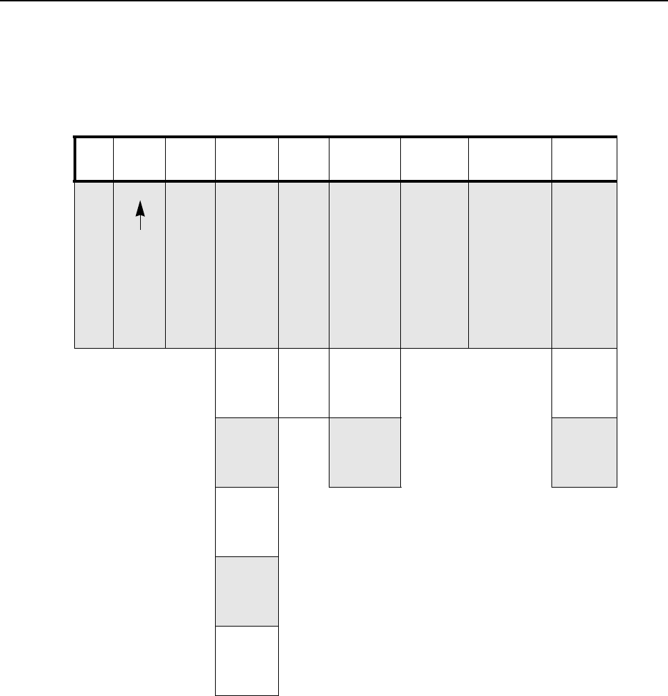
4-LAYER CIRCUIT BOARD DETAIL VIEWING
COPPER STEPS IN PROPER LAYER SEQUENCE
LAYER 1 (L1)
LAYER 2 (L2)
LAYER 3 (L3)
LAYER 4 (L4)
INNER LAYERS
SIDE 1
SIDE 2

2-12 Notes For All Schematics and Circuit Boards
THIS PAGE INTENTIONALLY LEFT BLANK
3-1
Section 3
SERVICE AIDS
1.0 Recommended Test Tools
Table 3-1 lists the service aids recommended for working on the radio. While all of these items are
available from Motorola, most are standard workshop equipment items, and any equivalent item
capable of the same performance may be substituted for the item listed.
Table 3-1 Service Aids
Motorola Part
Number Description Application
RLN4460_ Portable Test Set Enables connection to audio/accessory jack.
Allows switching for radio testing.
RKN4081_ Programming Cable with
Internal RIB Includes radio interface box (RIB) capability.
RLN4853_ 10 to 20 Pin Adapter Connects RKN4081_ to the radio accessory
connector.
RKN4083_ Mobile Programming/Test
Cable Connects radio to RIB (RLN4008_).
GTF374_ Program Cable Connects RIB to Radio microphone input
RLN4008_ Radio Interface Box Enables communications between radio and
computer’s serial communications adapter.
HLN8027_ Mini UHF to BNC Adaptor Adapts radio antenna port to BNC cabling of
test equipment.
GPN6133_ Power Supply Provides the radio with power when bench test-
ing.
EPN4040_ Wall-Mounted Power Supply Used to supply power to the RIB (UK).
EPN4041_ Wall-Mounted Power Supply Used to supply power to the RIB (Euro)
8180384J59 Housing Eliminator (short) Test Fixture used to bench test the radio PCB
8180384L95 Housing Eliminator
(short + top) Test Fixture used to bench test the radio PCB.
(Radio using pressure pads to retain PCB)
8180384J60 Housing Eliminator (medium) Test Fixture used to bench test the radio PCB
8180384J61 Housing Eliminator (long) Test Fixture used to bench test the radio PCB
3080369B71 Computer Interface Cable Connects the RIB to the Computer (25-pin)
3080369B72 Computer Interface Cable Connects the RIB to the Computer 9-pin
(Use for IBM PC AT - other IBM models use the
B71 cable above)
6686119B01 Removal Tool Assists in the removal of radio control head.

3-2 Test Equipment
2.0 Test Equipment
Table 3-2 lists test equipment required to service the radio and other two-way radios.
Table 3-2 Recommended Test Equipment
Motorola Part
Number Description Characteristics Application
R2600_NT Comms System Analyzer
(non MPT) This monitor will sub-
stitute for items with
an asterisk*
Frequency/deviation
meter and signal gen-
erator for widerange
troubleshooting and
alignment
R2680_NT Comms System Analyzer
( MPT1327) to be ordered
with
RLN1022_ (H/W) RLN1023_
(S/W)
This monitor will sub-
stitute for items with
an asterisk*.
Frequency/deviation
meter and signal gen-
erator for widerange
troubleshooting and
alignment
*R1072_ Digital Multimeter AC/DC voltage and
current measure-
ments
*R-1377_ AC Voltmeter 100µV to 300V, 5Hz -
1MHz, 10Megohm
input impedance
Audio voltage mea-
surements
WADN133 Delay Oscilloscope 2 Channel 40MHz
bandwidth,
5mV/cm - 20 V/cm
Waveform measure-
ments
R1440_
0180305F17
0180305F31
0180305F39
RLN4610
T1013_
Wattmeter,
Plug-in Elements
Plug-in Elements
Plug-in Elements
Carry case
RF Dummy Load
Thruline 50-Ohm,
±5% accuracy
100W, 25 - 60MHz
25W, 100-250MHz
10W, 200-250MHz
Wattmeter and
6 elements
Transmitter power
output measurements
S1339_ RF Millivolt Meter 100mV to 3 VRF.
10kHz to 1.2GHz RF level measure-
ments
R1011_/220V 220V Power Supply 0 - 40V 0 - 40A Programmable

GM328/GM338/GM398
Mobile Radios
Controlhead
Service Information
Issue: December, 2003

Computer Software Copyrights
The Motorola products described in this manual may include copyrighted Motorola computer programs stored
in semiconductor memories or other media. Laws in the United States and other countries preserve for
Motorola certain exclusive rights for copyrighted computer programs, including the exclusive right to copy or
reproduce in any form, the copyrighted computer program. Accordingly, any copyrighted Motorola computer
programs contained in the Motorola products described in this manual may not be copied or reproduced in
any manner without the express written permission of Motorola. Furthermore, the purchase of Motorola
products shall not be deemed to grant, either directly or by implication, estoppel or otherwise, any license
under the copyrights, patents or patent applications of Motorola, except for the normal non-exclusive royalty-
free license to use that arises by operation of law in the sale of a product.

i
Table of Contents
Section 1 overview
1.0 GM328 Model (GCN6112_).................................................................................1-1
2.0 GM338 Model (GCN6114_).................................................................................1-2
3.0 GM398 Model (GCN6115_).................................................................................1-3
Section 2 Theory of Operation
1.0 Introduction ..........................................................................................................2-1
2.0 Controlhead Model for GM328.............................................................................2-1
2.1 Power Supplies...............................................................................................2-1
2.2 Power On / Off................................................................................................2-1
2.3 Microprocessor Circuit....................................................................................2-2
2.4 SBEP Serial Interface.....................................................................................2-2
2.5 Keypad Keys ..................................................................................................2-3
2.6 Status LED and Back Light Circuit .................................................................2-3
2.7 Microphone Connector Signals ......................................................................2-3
2.8 Speaker ..........................................................................................................2-4
2.9 Electrostatic Transient Protection...................................................................2-4
3.0 Controlhead Model for GM338.............................................................................2-4
3.1 Power Supplies...............................................................................................2-4
3.2 Power On / Off................................................................................................2-4
3.3 Microprocessor Circuit....................................................................................2-5
3.4 SBEP Serial Interface.....................................................................................2-5
3.5 Keypad Keys ..................................................................................................2-6
3.6 Status LED and Back Light Circuit .................................................................2-6
3.7 Liquid Crystal Display (LCD) ..........................................................................2-7
3.8 Microphone Connector Signals ......................................................................2-7
3.9 Speaker ..........................................................................................................2-8
3.10 Electrostatic Transient Protection...................................................................2-8
4.0 Controlhead Model for GM398.............................................................................2-9
4.1 Power Supplies...............................................................................................2-9
4.2 Voltage Regulator Circuit................................................................................2-9
4.3 Power On / Off................................................................................................2-9
4.4 Microprocessor Circuit..................................................................................2-10
4.5 SBEP Serial Interface...................................................................................2-10
4.6 Keypad Keys ................................................................................................2-11
4.7 Status LED and Back Light Circuit ...............................................................2-11
4.8 Liquid Crystal Display (LCD) ........................................................................2-12
4.9 Microphone Connector Signals ....................................................................2-12

ii
4.10 Speaker (Remote Mount Configuration only) ...............................................2-13
4.11 Electrostatic Transient Protection.................................................................2-13
Section 3 Troubleshooting Charts
1.0 Controlhead GM328 Troubleshooting Flow Chart ...............................................3-1
1.1 On/Off ............................................................................................................3-1
1.2 Microprocessor...............................................................................................3-2
2.0 Controlhead GM338 Troubleshooting Flow Chart ...............................................3-3
2.1 On/Off ............................................................................................................3-3
2.2 Microprocessor...............................................................................................3-4
2.3 Display............................................................................................................3-5
2.4 Backlight.........................................................................................................3-6
3.0 Controlhead GM398 Troubleshooting Flow Chart ...............................................3-7
3.1 On/Off ............................................................................................................3-7
3.2 Microprocessor ..............................................................................................3-8
3.3 Microprocessor (cont.)....................................................................................3-9
3.4 Display .........................................................................................................3-10
3.5 Keypad Backlight .........................................................................................3-11
3.6 Display Backlight .........................................................................................3-12
Section 4 Controlhead PCBs / Schematics / Parts lists
1.0 Allocation of Schematics and Circuit Boards.......................................................4-1
2.0 Controlhead GM328 - PCB 8486146B07 / Schematics.......................................4-3
Controlhead GM328 - PCB 8486146B07..............................................................4-3
Controlhead GM328 - Schematic Sheet 1 of 2.......................................................4-4
Controlhead GM328 - Schematic Sheet 2 of 2.......................................................4-5
Controlhead PCB 8486146B07 Parts List ..............................................................4-6
3.0 Controlhead GM338 - PCB 8486155B06 / Schematics.......................................4-7
Controlhead GM338 - PCB 8486155B06..............................................................4-7
Controlhead GM338 - Schematic Sheet 1 of 4.......................................................4-8
Controlhead GM338 - Schematic Sheet 2 of 4.......................................................4-9
Controlhead GM338 - Schematic Sheet 3 of 4.....................................................4-10
Controlhead GM338 - Schematic Sheet 4 of 4.....................................................4-11
Controlhead PCB 8486155B06 Parts List ............................................................4-12
4.0 Controlhead GM398 - PCB 8486178B03 / Schematics.....................................4-13
Controlhead GM398 - PCB 8486178B03 .............................................................4-13
Controlhead GM398 - Schematic Sheet 1 of 4.....................................................4-14
Controlhead GM398 - Schematic Sheet 2 of 4.....................................................4-15
Controlhead GM398 - Schematic Sheet 3 of 4.....................................................4-16
Controlhead GM398 - Schematic Sheet 4 of 4.....................................................4-17
Controlhead PCB 8486178B03 Parts List ............................................................4-18

1-1
Section 1
OVERVIEW
1.0 GM328 Model (GCN6112_)
The Controlhead contains the internal speaker, the on/off/volume knob, the microphone connector,
several buttons to operate the radio and several indicator Light Emitting Diodes (LED) to inform the
user about the radio status. To control the LED’s and to communicate with the host radio the control
head uses the Motorola 68HC11E9 microprocessor.

1-2 GM338 Model (GCN6114_)
2.0 GM338 Model (GCN6114_)
The Controlhead contains the internal speaker, the On/Off/Volume knob, the microphone connector,
several buttons to operate the radio, several indicator Light Emitting Diodes (LED) to inform the user
about the radio status, and a 14 character Liquid Crystal Display (LCD) for alpha - numerical
information e.g. channel number or call address name. To control the LED’s and the LCD, and to
communicate with the host radio the control head uses the Motorola 68HC11E9 microprocessor.

GM398 Model (GCN6115_) 1-3
3.0 GM398 Model (GCN6115_)
The Controlhead contains the On/Off/Volume knob, the microphone connector, several buttons to
operate the radio, several indicator Light Emitting Diodes (LED) to inform the user about the radio
status, and a Liquid Crystal Display (LCD) with 21 pre - defined symbols and a 32*96 dot matrix for
graphical or alpha - numerical information e.g. channel number, select code, call address name. To
control the LEDs and the LCD, and to communicate with the host radio the control head uses the
Motorola 68HC11K4 microprocessor.

1-4 GM398 Model (GCN6115_)
THIS PAGE INTENTIONALLY LEFT BLANK

2-1
Section 2
THEORY OF OPERATION
1.0 Introduction
This Chapter provides a detailed theory of operation for the Controlhead circuits. For details of the
trouble shooting refer to the related Section of this manual.
2.0 Controlhead Model for GM328
The controlhead contains the internal speaker, the On/Off/Volume knob, the microphone connector,
several buttons to operate the radio and several indicator Light Emitting Diodes (LED) to inform the
user about the radio status. To control the LED’s and to communicate with the host radio the control-
head uses the Motorola 68HC11E9 microprocessor.
2.1 Power Supplies
The power supply to the controlhead is taken from the host radio’s FLT A+ voltage via connector
J0801 pin 3 and the regulated +5V via connector J0801 pin 7. The voltage FLT A+ is at supply
voltage level and is used for the LED’s, the back light and to power up the radio via on / off / volume
knob. The stabilized +5 volt is used for the microprocessor and the keypad buttons. The voltage
USW 5V derived from the FLT A+ voltage and stabilized by the series combination of R0822,
VR0822 is used to buffer the internal RAM of the microprocessor (U0831). C0822 allows the supply
voltage level to be disconnected for a couple of seconds without losing RAM parameters. Dual diode
D0822 prevents radio circuitry from discharging this capacitor. When the supply voltage is applied to
the radio, C0822 is charged via R0822 and D0822. To avoid, that the µP enters the wrong mode
when the radio is switched on while the voltage across C0822 is still too low, the regulated 5V charge
C0822 via diode D0822.
2.2 Power On / Off
The On/Off/Volume knob when pressed switches the radio’s voltage regulators on by connecting line
ON OFF CONTROL to line UNSW 5V via D0821. Additionally, 5 volts at the base of digital transistor
Q0822 informs the controlhead’s microprocessor about the pressed knob. The microprocessor
asserts pin 62 and line CH REQUEST low to hold line ON OFF CONTROL at 5 volts via Q0823 and
D0821. The high line ON OFF CONTROL also informs the host radio, that the controlhead’s
microprocessor wants to send data via SBEP bus. When the radio returns a data request message,
the microprocessor will inform the radio about the pressed knob. If the radio was switched off, the
radio’s µP will switch it on and vice versa. If the On/Off/Volume knob is pressed while the radio is on,
the software detects a low state on line ON OFF SENSE, the radio is alerted via line ON OFF
CONTROL and sends a data request message. The controlhead µP will inform the radio about the
pressed knob and the radio’s µP will switch the radio off.

2-2 Controlhead Model for GM328
2.3 Microprocessor Circuit
The controlhead uses the Motorola 68HC11E9 microprocessor (µP) (U0831) to control the LED’s
and to communicate with the host radio. RAM and ROM are contained within the microprocessor
itself.
The microprocessor generates it’s clock using the oscillator inside the microprocessor along with a 8
MHz ceramic resonator (U0833) and R0920.
The microprocessor’s RAM is always powered to maintain parameters such as the last operating
mode. This is achieved by maintaining 5V at µP pin 25. Under normal conditions, when the radio is
off, USW 5V is formed by FLT A+ running to D0822. C0822 allows the battery voltage to be
disconnected for a couple of seconds without losing RAM parameters. Diode D0822 prevents radio
circuitry from discharging this capacitor.
There are 8 analogue to digital converter ports (A/D) on the µP . They are labeled within the device
block as PE0-PE7. These lines sense the voltage level ranging from 0 to 5V of the input line and
convert that level to a number ranging from 0 to 255 which can be read by the software to take
appropriate action.
Pin VRH is the high reference voltage for the A/D ports on the µP . If this voltage is lower than +5V
the A/D readings will be incorrect. Likewise pin VRL is the low reference for the A/D ports. This line is
normally tied to ground. If this line is not connected to ground, the A/D readings will be incorrect.
The microprocessor can determine the used keypad type and the controlhead ID by reading the
levels at ports PC0 – PC7. Connections JU0852/3/4 are provided by the individual keypads.
The MODB / MODA input of the µP must be at a logic „1" for it to start executing correctly. The XIRQ
and the IRQ pins should also be at a logic „1".
Voltage sense device U0832 provides a reset output that goes to 0 volts if the regulated 5 volts goes
below 4.5 volts. This is used to reset the controller to prevent improper operation.
2.4 SBEP Serial Interface
The host radio (master) communicates to the controlhead µP (slave) through its SBEP bus. This bus
uses only line BUS+ for data transfer. The line is bi-directional meaning that either the radio or the
controlhead µP can drive the line. The microprocessor sends serial data via pin 50 and D0831 and it
reads serial data via pin 47. Whenever the microprocessor detects activity on the BUS+ line, it starts
communication.
When the host radio needs to communicate to the controlhead µP , it sends data via line BUS+. Any
transition on this line generates an interrupt and the µP starts communication. The host radio may
send data like LED and back light status or it may request the controlhead ID or the keypad ID.
When the controlhead µP wants to communicate to the host radio, the µP brings request line CH
REQUEST to a logic „0" via µP pin 62. This switches on Q0823, which pulls line ON OFF CONTROL
high through diode D0821. A low to high transition on this line informs the radio, that the controlhead
requires service. The host radio then sends a data request message via BUS+ and the controlhead
µP replies with the data it wanted to send. This data can be information like which key has been
pressed or that the volume knob has been rotated.
The controlhead µP monitors all messages sent via BUS+, but ignores any data communication
between host radio and CPS or Universal Tuner.

Controlhead Model for GM328 2-3
2.5 Keypad Keys
The controlhead keypad is a 6-key keypad. All keys are configured as 2 analogue lines read by µP
pins 13 and 15 . The voltage on the analogue lines varies between 0 volts and +5 volts depending on
which key has been pressed. If no key is pressed, the voltage at both lines will be 5 volts. The key
configuration can be thought of as a matrix, where the two lines represent one row and one column.
Each line is connected to a resistive divider powered by +5 volts. If a button is pressed, it will connect
one specific resistor of each divider line to ground level and thereby reduce the voltages on the
analogue lines The voltages of the lines are A/D converted inside the µP (ports PE 0 - 1) and specify
the pressed button. To determine which key is pressed, the voltage of both lines must be
considered.An additional pair of analogue lines and A/D µP ports (PE 3 – 2) is available to support a
keypad microphone, connected to the microphone connector J0811. Any microphone key press is
processed the same way as a key press on the controlhead.
2.6 Status LED and Back Light Circuit
All indicator LED’s (red, yellow, green) are driven by current sources. To change the LED status the
host radio sends a data message via SBEP bus to the controlhead µP . The controlhead µP
determines the LED status from the received message and switches the LED’s on or off via port PB
7 – 0 and port PA4. The LED status is stored in the µP ’s memory. The LED current is determined by
the resistor at the emitter of the respective current source transistor.
The back light for the keypad is controlled by the host radio the same way as the indicator LED’s
using µP port PA 5. The µP can switch the back light on and off under software control. The keypad
back light current is drawn from the FLT A+ source and controlled by 2 current sources. The LED
current is determined by the resistor at the emitter of the respective current source transistor.
2.7 Microphone Connector Signals
Signals BUS+, PTT IRDEC, HOOK, MIC, HANDSET AUDIO, FLT A+, +5V and 2 A/D converter
inputs are available at the microphone connector J0811. Signal BUS+ (J0811-7) connects to the
SBEP bus for communication with the CPS or the Universal Tuner. Line MIC (J0811-5) feeds the
audio from the microphone to the radio’s controller via connector J0801-4. Line HANDSET AUDIO
(J0811-8) feeds the receiver audio from the controller (J0801-6) to a connected handset. FLT A+,
which is at supply voltage level, and +5V are used to supply any connected accessory like a
microphone or a handset.
The 2 A/D converter inputs (J0811-9/10) are used for a microphone with keypad. A pressed key will
change the dc voltage on both lines. The voltages depend on which key is pressed. The µP
determines from the voltage on these lines which key is pressed and sends the information to the
host radio.
Line PTT IRDEC (J0811-6) is used to key up the radio’s transmitter. While the PTT button on a
connected microphone is released, line PTT IRDEC is pulled to +5 volts level by R0843. Transistor
Q0843 is switched on and causes a low at µP port PA2. When the PTT button is pressed, signal
PTT IRDEC is pulled to ground level. This switches off Q0843 and the resulting high level at µP port
PA2 informs the µP about the pressed PTT button. The µP will inform the host radio about any
status change on the PTT IRDEC line via SBEP bus.
When line PTT IRDEC is connected to FLT A+ level, transistor Q0821 is switched on through diode
VR0821 and thereby pulls the level on line ON OFF CONTROL to FLT A+ level. This switches on the
radio and puts the radio’s µP in bootstrap mode. Bootstrap mode is used to load the firmware into
the radio’s flash memory (See controller subsection for more details).

2-4 Controlhead Model for GM338
The HOOK input (J0811-3) is used to inform the µP when the microphone´s hang-up switch is
engaged. Dependent on the CPS programming the µP may take actions like turning the audio PA on
or off. While the hang up switch is open, line HOOK is pulled to +5 volts level by R0841. Transistor
Q0841 is switched on and causes a low at µP port PA1. When the HOOK switch is closed, signal
HOOK is pulled to ground level. This switches off R0841and the resulting high level at µP port PA1
informs the µP about the closed hang up switch. The µP will inform the host radio about any status
change on the HOOK line via SBEP bus.
2.8 Speaker
The controlhead contains a speaker for the receiver audio. The receiver audio signal from the
differential audio output of the audio amplifier located on the radio’s controller is fed via connector
J0801-10, 11 to the speaker connector P0801 pin 1 and pin 2. The speaker is connected to the
speaker connector P0801. The controlhead speaker can be disconnected if an external speaker,
connected on the accessory connector, is used.
2.9 Electrostatic Transient Protection
Electrostatic transient protection is provided for the sensitive components in the controlhead by
diodes VR0811 VR00812 VR0816 - VR0817. The diodes limit any transient voltages to tolerable
levels. The associated capacitors provide Radio Frequency Interference (RFI) protection.
3.0 Controlhead Model for GM338
The controlhead contains the internal speaker, the On/Off/Volume knob, the microphone connector,
several buttons to operate the radio, several indicator Light Emitting Diodes (LED) to inform the user
about the radio status, and a 14 character Liquid Crystal Display (LCD) for alpha - numerical
information e.g. channel number or call address name. To control the LEDs and the LCD, and to
communicate with the host radio the controlhead uses the Motorola 68HC11E9 microprocessor.
3.1 Power Supplies
The power supply to the controlhead is taken from the host radio’s FLT A+ voltage via connector
J0801 pin 3 and the regulated +5V via connector J0801 pin 7. The voltage FLT A+ is at battery level
and is used for the LEDs, the back light and to power up the radio via On /Off /Volume knob. The
stabilized +5 volt is used for the microprocessor, the display, the display driver and the keypad
buttons. The voltage USW 5V derived from the FLT A+ voltage and stabilized by the series
combination of R0822, VR0822 is used to buffer the internal RAM of the microprocessor (U0831).
C0822 allows the battery voltage to be disconnected for a couple of seconds without losing RAM
parameters. Dual diode D0822 prevents radio circuitry from discharging this capacitor. When the
supply voltage is applied to the radio, C0822 is charged via R0822 and D0822. To avoid that the µP
enters the wrong mode when the radio is switched on while the voltage across C0822 is still too low,
the regulated 5V charge C0822 via diode D0822.
3.2 Power On / Off
The On/Off/Volume knob when pressed switches the radio’s voltage regulators on by connecting
line ON OFF CONTROL to line UNSW 5V via D0821. Additionally, 5 volts at the base of digital
transistor Q0822 informs the controlhead’s microprocessor about the pressed knob. The
microprocessor asserts pin 62 and line CH REQUEST low to hold line ON OFF CONTROL at 5 volts
via Q0823 and D0821. The high line ON OFF CONTROL also informs the host radio, that the

Controlhead Model for GM338 2-5
controlhead’s microprocessor wants to send data via SBEP bus. When the radio returns a data
request message, the microprocessor will inform the radio about the pressed knob. If the radio was
switched off, the radio’s µP will switch it on and vice versa. If the On/Off/Volume knob is pressed
while the radio is on, the software detects a low state on line ON OFF SENSE, the radio is alerted
via line ON OFF CONTROL and sends a data request message. The controlhead µP will inform the
radio about the pressed knob and the radio’s µP will switch the radio off.
3.3 Microprocessor Circuit
The controlhead uses the Motorola 68HC11E9 microprocessor (µP) (U0831) to control the LEDs
and the LCD and to communicate with the host radio. RAM and ROM are contained within the
microprocessor itself.
The microprocessor generates it’s clock using the oscillator inside the microprocessor along with a 8
MHz ceramic resonator (U0833) and R0920 .
The microprocessor’s RAM is always powered to maintain parameters such as the last operating
mode. This is achieved by maintaining 5V at µP pin 25 . Under normal conditions, when the radio is
off, USW 5V is formed by FLT A+ running to D0822. C0822 allows the battery voltage to be
disconnected for a couple of seconds without losing RAM parameters. Diode D0822 prevents radio
circuitry from discharging this capacitor.
There are 8 analogue to digital converter ports (A/D) on the µP . They are labeled within the device
block as PE0-PE7. These lines sense the voltage level ranging from 0 to 5V of the input line and
convert that level to a number ranging from 0 to 255 which can be read by the software to take
appropriate action.
Pin VRH is the high reference voltage for the A/D ports on the µP . If this voltage is lower than +5V
the A/D readings will be incorrect. Likewise pin VRL is the low reference for the A/D ports. This line
is normally tied to ground. If this line is not connected to ground, the A/D readings will be incorrect.
The microprocessor can determine the used keypad type and the controlhead ID by reading the
levels at ports PC0 – PC7. Connections JU0852/3/4 are provided by the individual keypads.
The MODB / MODA input of the µP must be at a logic “1” for it to start executing correctly. The
XIRQ and the IRQ pins should also be at a logic “1”.
Voltage sense device U0832 provides a reset output that goes to 0 volts if the regulated 5 volts goes
below 4.5 volts. This is used to reset the controller to prevent improper operation.
3.4 SBEP Serial Interface
The host radio (master) communicates to the controlhead µP (slave) through its SBEP bus. This
bus uses only line BUS+ for data transfer. The line is bi-directional, meaning that either the radio or
the controlhead µP can drive the line. The microprocessor sends serial data via pin 50 and D0831
and it reads serial data via pin 47. Whenever the microprocessor detects activity on the BUS+ line, it
starts communication.
When the host radio needs to communicate to the controlhead µP , it sends data via line BUS+. Any
transition on this line generates an interrupt and the µP starts communication. The host radio may
send data like display information, LED and back light status or it may request the controlhead ID or
the keypad ID.

2-6 Controlhead Model for GM338
When the controlhead µP wants to communicate to the host radio, the µP brings request line CH
REQUEST to a logic “0” via µP pin 62. This switches on Q0823, which pulls line ON OFF
CONTROL high through diode D0821. A low to high transition on this line informs the radio, that the
controlhead requires service. The host radio then sends a data request message via BUS+ and the
controlhead µP replies with the data it wanted to send. This data can be information like which key
has been pressed or that the volume knob has been rotated.
The controlhead µP monitors all messages sent via BUS+, but ignores any data communication
between host radio and CPS or Universal Tuner.
3.5 Keypad Keys
The controlhead keypad is a 6-key kepad (Model B) or a 10- key keypad (model C). All keys are
configured as 2 analogue lines read by µP pins 13 and 15. The voltage on the analogue lines varies
between 0 volts and +5 volts depending on which key has been pressed. If no key is pressed, the
voltage at both lines will be 5 volts. The key configuration can be thought of as a matrix, where the
two lines represent one row and one column. Each line is connected to a resistive divider powered
by +5 volts. If a button is pressed, it will connect one specific resistor of each divider line to ground
level and thereby reduce the voltages on the analogue lines The voltages of the lines are A/D
converted inside the µP (ports PE 0 - 1) and specify the pressed button. To determine which key is
pressed, the voltage of both lines must be considered.
An additional pair of analogue lines and A/D µP ports (PE 3 – 2) is available to support a keypad
microphone, connected to the microphone connector J0811. Any microphone key press is
processed the same way as a key press on the controlhead.
3.6 Status LED and Back Light Circuit
All the indicator LEDs (red, yellow, green) are driven by current sources. To change the LED status
the host radio sends a data message via SBEP bus to the controlhead µP . The controlhead µP
determines the LED status from the received message and switches the LEDs on or off via port PB
7 – 0 and port PA4. The LED status is stored in the µP ’s memory. The LED current is determined by
the resistor at the emitter of the respective current source transistor.
The back light for the LCD and the keypad is controlled by the host radio the same way as the
indicator LEDs using µP port PA 5. This port is a Pulse Width Modulator (PWM) output. The output
signal charges capacitor C0843 through R0847. By changing the pulse width under software
control, the dc voltage of C0843 and thereby, the brightness of the back light can be changed in four
steps. The keypad back light current is drawn from the FLT A+ source and controlled by transistor
Q0933. The current flowing through the LEDs cause a proportional voltage drop across the parallel
resistors R0947, R0948. This voltage drop is amplified by the op-amp U0931-2. U0931-2 and
Q0934 form a differential amplifier. The voltage difference between the base of Q0934 and the
output of U0931-2 determines the current from the base of the LED control transistor Q0933 and in
turn the brightness of the LEDs. The µP can control the LEDs by changing the dc level at the base
of Q0934. If the base of Q0934 is at ground level, Q0934 is switched off and no current flows
through Q0933 and the LEDs. If the base voltage of Q0934 rises a current flows through Q0934 and
in turn through Q0933 causing the LEDs to turn on and a rising voltage drop across R0947, R0948.
The rising voltage causes the output of the op-amp to rise and to reduce the base to emitter voltage
of Q0934. This decreases the current of Q0933 until the loop has settled.

Controlhead Model for GM338 2-7
3.7 Liquid Crystal Display (LCD)
The LCD H0971 uses the display driver U0971. The display is a single layer super twist nematic
(STN) LCD display. It has 14 characters with a 5*8 dot matrix for displaying alpha - numerical
information and a line with 21 pre - defined icons above the dot matrix
The driver contains a data interface to the µP, an LCD segment driver, an LCD power circuit, an
oscillator, data RAM and control logic. At power up the driver’s control logic is reset by a logic “0” at
input SR2 (U0971-15). The driver’s internal oscillator is set to about 20 kHz and can be measured at
pin 22. The driver’s µP interface is configured to accept 8 bit parallel data input (U0971-D0-D7) from
the controlhead µP (U0831 port PC0-PC7).
To write data to the driver’s RAM the µP sets chip select (U0971-20) to logic “0” via U0831-11, RD
(U0971-18) to logic “1” via (U0831-10) and WR (U0971-17) to logic “0” via U0831-9. With input A0
(U0971-21) set to logic “0” via U0831-12 the µP writes control data to the driver. Control data
includes the RAM start address for the following display data. With input A0 set to logic “1” the µP
then writes the display data to the display RAM. When data transfer is complete the µP terminates
the chip select, RD and WD activities.
The display driver’s power circuit provides the voltage supply for the display. This circuit consists of
a voltage multiplier, voltage regulator and a voltage follower. The external capacitors C0971 -
C0973 configure the multiplier to double the supply voltage. In this configuration the multiplier output
VOUT (U0971-8) supplies a voltage of -5V (2* -5V below VDD). The multiplied voltage VOUT is sent
to the internal voltage regulator. To set the voltage level of the regulator output V5 (U0971-5) this
voltage is divided by the resistors R0973 and R0974 and fed back to the reference input VR (U0971-
6). In addition the regulator output voltage V5 can be controlled electronically by a control command
sent to the driver. With the used configuration the voltage V5 is about –2V. The voltage V5 is
resistively divided by the driver’s voltage follower to provide the voltages V1 - V4. These voltages
are needed for driving the liquid crystals. The level of V5 can be measured by one of the µP’s
analogue to digital converters (U0831-20) via resistive divider R0975, R0976. To stabilize the
display brightness over a large temperature range the µP measures the temperature via analogue to
digital converter (U0831-18) using temperature sensor U0834. Dependent on the measured
temperature the µP adjusts the driver output voltage V5, and in turn the display brightness, via
parallel interface.
3.8 Microphone Connector Signals
Signals BUS+, PTT IRDEC, HOOK, MIC, HANDSET AUDIO, FLT A+, +5V and 2 A/D converter
inputs are available at the microphone connector J0811. Signal BUS+ (J0811-7) connects to the
SBEP bus for communication with the CPS or the Universal Tuner. Line MIC (J0811-5) feeds the
audio from the microphone to the radio’s controller via connector J0801-4. Line HANDSET AUDIO
(J0811-8) feeds the receiver audio from the controller (J0801-6) to a connected handset. FLT A+,
which is at supply voltage level, and +5V are used to supply any connected accessory like a
microphone or a handset.
The 2 A/D converter inputs (J0811-9/10) are used for a microphone with keypad. A pressed key will
change the dc voltage on both lines. The voltages depend on which key is pressed. The µP
determines from the voltage on these lines which key is pressed and sends the information to the
host radio.

2-8 Controlhead Model for GM338
Line PTT IRDEC (J0811-6) is used to key up the radio’s transmitter. While the PTT button on a
connected microphone is released, line PTT IRDEC is pulled to +5 volts level by R0843. Transistor
Q0843 is switched on and causes a low at µP port PA2. When the PTT button is pressed, signal
PTT IRDEC is pulled to ground level. This switches off Q0843 and the resulting high level at µP port
PA2 informs the µP about the pressed PTT button. The µP will inform the host radio about any
status change on the PTT IRDEC line via SBEP bus.
When line PTT IRDEC is connected to FLT A+ level, transistor Q0821 is switched on through diode
VR0821 and thereby pulls the level on line ON OFF CONTROL to FLT A+ level. This switches on
the radio and puts the radio’s µP in bootstrap mode. Bootstrap mode is used to load the firmware
into the radio’s flash memory (See controller sub section for more details).
The HOOK input (J0811-3) is used to inform the µP when the microphone´s hang-up switch is
engaged. Dependent on the CPS programming the µP may take actions like turning the audio PA on
or off. While the hang up switch is open, line HOOK is pulled to +5 volts level by R0841. Transistor
Q0841 is switched on and causes a low at µP port PA1. When the HOOK switch is closed, signal
HOOK is pulled to ground level. This switches off R0841 and the resulting high level at µP port PA1
informs the µP about the closed hang up switch. The µP will inform the host radio about any status
change on the HOOK line via SBEP bus.
3.9 Speaker
The controlhead contains a speaker for the receiver audio. The receiver audio signal from the
differential audio output of the audio amplifier located on the radio’s controller is fed via connector
J0801-10, 11 to the speaker connector P0801 pin 1 and pin 2. The speaker is connected to the
speaker connector P0801. The controlhead speaker can be disconnected if an external speaker,
connected on the accessory connector, is used.
3.10 Electrostatic Transient Protection
Electrostatic transient protection is provided for the sensitive components in the controlhead by
diodes VR0811 VR00812 VR0816 - VR0817. The diodes limit any transient voltages to tolerable
levels. The associated capacitors provide Radio Frequency Interference (RFI) protection.

Controlhead Model for GM398 2-9
4.0 Controlhead Model for GM398
The controlhead contains the On/Off/Volume knob, the microphone connector, several buttons to
operate the radio, several indicator Light Emitting Diodes (LED) to inform the user about the radio
status, and a Liquid Crystal Display (LCD) with 21 pre - defined symbols and a 32*96 dot matrix for
graphical or alpha - numerical information e.g. channel number, select code, call address name. To
control the LEDs and the LCD, and to communicate with the host radio the controlhead uses the
Motorola 68HC11K4 microprocessor.
4.1 Power Supplies
The power supply to the controlhead is taken from the host radio’s FLT A+ voltage via connector
J0801 pin 3. The voltage FLT A+ is at battery level and is used for the LEDs, the back light, to power
up the radio via On/Off/Volume knob and to supply the voltage regulator circuitry. The regulator
circuitry provides the stabilized +5 volts which is used for the microprocessor circuitry, the display,
the display driver and the keypad buttons. The regulated +5V taken from the host radio via
connector J0801 pin 7 (line 5V SOURCE) is only used to switch on or off the voltage regulator in the
control-head.
4.2 Voltage Regulator Circuit
Voltage regulator U0861provides 5V for the controlhead. The supply voltage FLT A+ for the voltage
regulator is fed via parallel resistors R0861/2 and dual diode D0861 to pin 8 of U0861. The +5 volt
output is switched on and off by the host radios’s 5 volt source via line 5V SOURCE and control
transistor Q0866. When the host radio is switched off the voltage on line +5V SOURCE is at ground
level and switches off transistor Q0866. Pull up resistor R0863 pulls input SHUTDOWN (pin 3) of the
voltage regulator U0861 to FLT A+ level and switches off the output of U0861 (pin 1). When the host
radio is switched on the voltage on line 5V SOURCE of about +5 volts switches on transistor Q0866
which in turn pulls input SHUTDOWN (pin 3) to ground and switches on the output of U0861. Input
and output capacitors (C0861 / C0862 and C0864 / C0865) are used to reduce high frequency noise
and provide proper operation during battery transients. Diode D0861 prevents discharge of C0862
by negative spikes on the FLT A+ voltage. This regulator provides a reset output (pin 5) that goes to
0 volts if the regulator output goes out of regulation. This is used to reset the microprocessor
(U0871) and the display driver (J0821-5) to prevent improper operation.
The voltage USW 5V derived from voltage FLT A+ is stabilized using resistor R0855 and diode
VR0855 This voltage is used to buffer the microprocessor’s internal RAM. C0856 allows the battery
voltage to be disconnected for a couple of seconds without losing RAM parameters. Diode D0855
prevents radio circuitry from discharging this capacitor. The +5V at the second anode of D0855
speeds up charging of C0856, when the host radio is turned on by a high level at the ignition input
while the supply voltage is applied to the radio. This prevents the microprocessor from accidently
entering bootstrap mode.
4.3 Power On / Off
The On/Off/Volume knob when pressed switches the radio’s and the controlhead’s voltage
regulators on by connecting line ON OFF CONTROL to line UNSW 5V via D0852. Additionally, 5
volts at the base of digital transistor Q0853 informs the controlhead’s microprocessor about the
pressed knob. The microprocessor asserts pin 8 and line CH REQUEST low to hold line ON OFF
CONTROL at 5 volts via Q0852 and D0852. The high line ON OFF CONTROL also informs the host
radio, that the controlhead’s microprocessor wants to send data via SBEP bus. When the radio
returns a data request message, the microprocessor will inform the radio about the pressed knob.

2-10 Controlhead Model for GM398
If the radio was switched off, the radio’s µP will switch it on and vice versa. If the On/Off/Volume
knob is pressed while the radio is on, the software detects a low state on line ON OFF SENSE, the
radio is alerted via line ON OFF CONTROL and sends a data request message. The controlhead µP
will inform the radio about the pressed knob and the radio’s µP will switch the radio off. If the radio is
switched on either manually or automatically it’s +5V source switches on the controlhead’s voltage
regulator U0861 via line 5 SOURCE and transistor Q0866 and the controlhead’s microprocessor
starts execution.
4.4 Microprocessor Circuit
The controlhead uses the Motorola 68HC11K4 microprocessor (µP) (U0871) to control the LEDs
and the LCD and to communicate with the host radio. RAM and ROM are contained within the
microprocessor itself.
The microprocessor generates it’s clock using the oscillator inside the microprocessor along with a 8
MHz ceramic resonator (U0873) and R0873.
The microprocessor’s RAM is always powered to maintain parameters such as the last operating
mode. This is achieved by maintaining 5V at µP pin 76. Under normal conditions, when the radio is
off, USW 5V is formed by FLT A+ running to D0855. C0856 allows the battery voltage to be
disconnected for a couple of seconds without losing RAM parameters. Diode D0855 prevents radio
circuitry from discharging this capacitor.
There are 8 analogue to digital converter ports (A/D) on the µP. They are labeled within the device
block as PE0-PE7. These lines sense the voltage level ranging from 0 to 5V of the input line and
convert that level to a number ranging from 0 to 255 which can be read by the software to take
appropriate action.
Pin VRH is the high reference voltage for the A/D ports on the µP. If this voltage is lower than +5V
the A/D readings will be incorrect. Likewise pin VRL is the low reference for the A/D ports. This line
is normally tied to ground. If this line is not connected to ground, the A/D readings will be incorrect.
The microprocessor can determine the used keypad type by reading the level at port PE5.
Connections S0931 – S0935 are provided by the individual keypads.
The MODB / MODA input of the µP must be at a logic “1” for it to start executing correctly. The XIRQ
and the IRQ pins should also be at a logic “1”.
4.5 SBEP Serial Interface
The host radio (master) communicates to the controlhead µP (slave) through its SBEP bus. This bus
uses only line BUS+ for data transfer. The line is bi-directional, meaning that either the radio or the
controlhead µP can drive the line. The microprocessor sends serial data via pin 79 and D0872 and it
reads serial data via pin 78. Whenever the microprocessor detects activity on the BUS+ line, it starts
communication.
When the host radio needs to communicate to the controlhead µP, it sends data via line BUS+. Any
transition on this line generates an interrupt and the µP starts communication. The host radio may
send data like display information, LED and back light status or it may request the controlhead ID or
the keypad ID.

Controlhead Model for GM398 2-11
When the controlhead µP wants to communicate to the host radio, the µP brings request line CH
REQUEST to a logic “0” via µP pin 8. This switches on Q0852, which pulls line ON OFF CONTROL
high through diode D0852. A low to high transition on this line informs the radio, that the controlhead
requires service. The host radio then sends a data request message via BUS+ and the controlhead
µP replies with the data it wanted to send. This data can be information like which key has been
pressed or that the volume knob has been rotated.
The controlhead µP monitors all messages sent via BUS+, but ignores any data communication
between host radio and CPS or Universal Tuner.
4.6 Keypad Keys
The controlhead keypad is a 25 - key keypad. All keys are configured as 2 analogue lines read by
µP pins 49 and 48. The voltage on the analogue lines varies between 0 volts and +5 volts
depending on which key has been pressed. If no key is pressed, the voltage at both lines will be 5
volts. The key configuration can be thought of as a matrix, where the two lines represent one row
and one column. Each line is connected to a resistive divider powered by +5 volts. If a button is
pressed, it will connect one specific resistor of each divider line to ground level and thereby reduce
the voltages on the analogue lines The voltages of the lines are A/D converted inside the µP (ports
PE 0 - 1) and specify the pressed button. To determine which key is pressed, the voltage of both
lines must be considered.
An additional pair of analogue lines and A/D µP ports (PE 3 – 2) is available to support a keypad
microphone, connected to the microphone connector J0811. Any microphone key press is
processed the same way as a key press on the controlhead.
4.7 Status LED and Back Light Circuit
All the indicator LEDs (red, yellow, green) are driven by current sources. To change the LED status
the host radio sends a data message via SBEP bus to the controlhead µP. The controlhead µP
determines the LED status from the received message and switches the LEDs on or off via port PA
6 - 4. The LED status is stored in the µP’s memory. The LED current is determined by the resistor at
the emitter of the respective current source transistor.
The back light for keypad is controlled by the host radio the same way as the indicator LEDs using
µP port PH 3. This port is a Pulse Width Modulator (PWM) output. The output signal charges
capacitor C0943 through R0945. By changing the pulse width under software control, the dc voltage
of C0943 and thereby, the brightness of the back light can be changed in 16 steps. The keypad back
light current is drawn from the FLT A+ source and controlled by transistor Q0941. The current
flowing through the LEDs cause a proportional voltage drop across the parallel resistors R0955,
R0957. This voltage drop is amplified by the op-amp U0941-1. U0941-1 and Q0943 form a
differential amplifier. The voltage difference between the base of Q0943 and the output of U0941-1
determines the current from the base of the LED control transistor Q0941 and in turn the brightness
of the LEDs. The µP can control the LEDs by changing the dc level at the base of Q0943. If the base
of Q0943 is at ground level, Q0943 is switched off and no current flows through Q0941 and the
LEDs. If the base voltage of Q0943 rises a current flows through Q0943 and in turn through Q0941
causing the LEDs to turn on and a rising voltage drop across R0955, R0957. The rising voltage
causes the output of the op-amp to rise and to reduce the base to emitter voltage of Q0943. This
decreases the current of Q0941 until the loop has settled.

2-12 Controlhead Model for GM398
The back light for the LCD module uses a similar circuitry. The only differences are that µP port PH2
controls the back light brightness and that the LEDs are located on the LCD module which is
connected via J0821. Control line BL A GREEN connects to the anodes and control line BL K
GREEN connects to the cathodes of the LEDs.
4.8 Liquid Crystal Display (LCD)
The LCD module consists of the display and the display driver and is connected via connector
J0821. The display is a single layer super twist nematic (STN) LCD display. It has a dot matrix of 32
* 96 dots for displaying graphics and alpha - numerical information and a line with 21 pre - defined
icons above the dot matrix
The driver contains a data interface to the µP, an LCD segment driver, an LCD power circuit, an
oscillator, data RAM and control logic. At power up the driver’s control logic is reset by a logic “0” via
pin 5 of J0821. The driver’s µP interface is configured to accept 8 bit parallel data input (J0821-D0-
D7) from the controlhead µP (U0871 port PC0-PC7).
To write data to the driver’s RAM the µP sets chip select (J0821-6) to logic “0” via U0871-26, RD
(J0821-10) to logic “1” via (U0871-40) and WR (U0821-9) to logic “0” via U0871-33. With input A0
(J0821-8) set to logic “0” via U0871-34 the µP writes control data to the driver. Control data includes
the RAM start address for the following display data. With input A0 set to logic “1” the µP then writes
the display data to the display RAM. When data transfer is complete the µP terminates the chip
select and the clock activities.
The display driver’s power circuit provides the voltage supply for the display. This circuit consists of
a voltage multiplier, voltage regulator and a voltage follower. The regulator output voltage for the
display can be controlled electronically by a control command sent to the driver. The voltage level
can be measured by one of the µP’s analogue to digital converters (U0871-42) via J0821-21. To
stabilize the display brightness over a large temperature range the µP measures the temperature
via analogue to digital converter (U0871-43) using a temperature sensor on the module (J0821-4).
Dependent on the measured temperature the µP adjusts the driver output voltage, and in turn the
display brightness, via parallel interface.
4.9 Microphone Connector Signals
Signals BUS+, PTT IRDEC, HOOK, MIC, HANDSET AUDIO, FLT A+, +5V and 2 A/D converter
inputs are available at the microphone connector J0811. Signal BUS+ (J0811-7) connects to the
SBEP bus for communication with the CPS or the Universal Tuner. Line MIC (J0811-5) feeds the
audio from the microphone to the radio’s controller via connector J0801-4. Line HANDSET AUDIO
(J0811-8) feeds the receiver audio from the controller (J0801-6) to a connected handset. FLT A+,
which is at supply voltage level, and +5V are used to supply any connected accessory like a
microphone or a handset.
The 2 A/D converter inputs (J0811-9/10) are used for a microphone with keypad. A pressed key will
change the dc voltage on both lines. The voltages depend on which key is pressed. The µP
determines from the voltage on these lines which key is pressed and sends the information to the
host radio.

Controlhead Model for GM398 2-13
Line PTT IRDEC (J0811-6) is used to key up the radio’s transmitter. While the PTT button on a
connected microphone is released, line PTT IRDEC is pulled to +5 volts level by R0880. Transistor
Q0871 is switched on and causes a low at µP port PA2. When the PTT button is pressed, signal
PTT IRDEC is pulled to ground level. This switches off Q0871 and the resulting high level at µP port
PA2 informs the µP about the pressed PTT button. The µP will inform the host radio about any
status change on the PTT IRDEC line via SBEP bus.
When line PTT IRDEC is connected to FLT A+ level, transistor Q0851 is switched on through diode
VR0851 and thereby pulls the level on line ON OFF CONTROL to FLT A+ level. This switches on
the radio and puts the radio’s µP in bootstrap mode. Bootstrap mode is used to load the firmware
into the radio’s flash memory (See controller sub section for more details).
The HOOK input (J0811-3) is used to inform the µP when the microphone´s hang-up switch is
engaged. Dependent on the CPS programming the µP may take actions like turning the audio PA on
or off. While the hang up switch is open, line HOOK is pulled to +5 volts level by R0883. Transistor
Q0872 is switched on and causes a low at µP port PA1. When the HOOK switch is closed, signal
HOOK is pulled to ground level. This switches off R0883 and the resulting high level at µP port PA1
informs the µP about the closed hang up switch. The µP will inform the host radio about any status
change on the HOOK line via SBEP bus.
4.10 Speaker (Remote Mount Configuration only)
The remote mount controlhead contains a speaker for the receiver audio. The receiver audio signal
from the differential audio output of the audio amplifier located on the radio’s controller is fed via
connector J0801-10,11 to the speaker connector P0801 pin 1 and pin 2. The speaker is connected
to the speaker connector P0801. The controlhead speaker can be disconnected if only an external
speaker, connected on the accessory connector, should be used. If the controlhead is mounted
directly on the radio, an external speaker is required.
4.11 Electrostatic Transient Protection
Electrostatic transient protection is provided for the sensitive components in the controlhead by
diodes VR0811 - VR0814. The diodes limit any transient voltages to tolerable levels. The associated
capacitors provide Radio Frequency Interference (RFI) protection.

2-14 Controlhead Model for GM398
THIS PAGE INTENTIONALLY LEFT BLANK
3-1
Section 3
TROUBLESHOOTING CHARTS
1.0 Controlhead GM328 Troubleshooting Flow Chart
1.1 On/Off
Radio cannot be switched on via ON/OFF/Volume Knob
NO
YES
YES
NO
R0823 Pin TAB
= 5V ?
R0823 Pin TAB1
when pressed
= 5V ?
Check / Replace
Volume Pot R0823
Check / Replace
R0822 / VR0822 /
D0822
NO
YES
J0801 Pin 2
> 10V ?
Check / Replace
Q0821
Check / Replace
Q0822 / R0821
YES
NO
J0801 Pin 2
=5V ?
Check / Replace
D0821 / R0852
Press and hold
On/Off/Volume Knob

3-2 Controlhead GM328 Troubleshooting Flow Chart
1.2 Microprocessor
Power Up Alert Tone is OK but volume knob does
not operate and no indicator is on
NO
YES
YES
NO
YES
NO
YES
NO
YES
EXTAL
U0831 Pin 31
= 8.00 MHz ?
RESET
TP0833
= HIGH ?
Check / Replace
C0833 / R0832 / U0831
Check radio controller
Data Signal
on J0801 Pin 5
BUS+ ?
Data Signal
on TP0836
SCI_RX ?
NO
Data Signal
on TP0837
SCI_TX ?
Check / Replace
R0831 / U0833 / U0831
Check / Replace
R0837 / R0836
Check / Replace
U0831
Check / Replace
D0831 / R0838
Measure with scope while
rotating Volume Pot
Controlhead GM338 Troubleshooting Flow Chart 3-3
2.0 Controlhead GM338 Troubleshooting Flow Chart
2.1 On/Off
Radio cannot be switched on via ON/OFF/Volume Knob
NO
YES
YES
NO
R0823 Pin TAB
= 5V ?
R0823 Pin TAB1
when pressed
= 5V ?
Check / Replace
Volume Pot R0823
Check / Replace
R0822 / VR0822 /
D0822 / C0822
NO
YES
J0801 Pin 2
> 10V ?
Check / Replace
Q0821
Check / Replace
Q0822 / R0821
YES
NO
J0801 Pin 2
=5V ?
Check / Replace
D0821 / R0852
Press and hold
On/Off/Volume Knob
3-4 Controlhead GM338 Troubleshooting Flow Chart
2.2 Microprocessor
Power Up Alert Tone is OK but volume knob does
not operate and no indicator is on
NO
YES
YES
NO
YES
NO
YES
NO
YES
EXTAL
U0831 Pin 31
= 8.00 MHz ?
RESET
TP0833
= HIGH ?
Check / Replace
C0833 / R0832 / U0831
Check radio controller
Data Signal
on J0801 Pin 5
BUS+ ?
Data Signal
on TP0836
SCI_RX ?
NO
Data Signal
on TP0837
SCI_TX ?
Check / Replace
R0831 / U0833 / U0831
Check / Replace
R0837 / R0836
Check / Replace
U0831
Check / Replace
D0831 / R0838
Measure with scope while
rotating Volume Pot
Controlhead GM338 Troubleshooting Flow Chart 3-5
2.3 Display
Power Up Alert Tone is OK, volume knob does operate,
indicator/backlight is on but nothing on display
YES
NO
YES
NO
V5 (against 5V)
TP0973 between
-6V and -7V ?
Activity on
Address & Data lines
A0 / D0..D7 / CS1
of U0971?
Check for shortage
U0831 / U0971
Check LCD Assembly
Check / Replace
C0971 / C0973 / R0972
R0973 / R0974 / U0971
3-6 Controlhead GM338 Troubleshooting Flow Chart
2.4 Backlight
Power Up Alert Tone is OK, volume knob does operate,
indicator/display is on but no backlight
NO
YES
YES
NO
U0831 Pin 58
is toggling ?
Base of
Q0934
> 0.7V ?
Check / Replace
R0847 / C0843 / R0943
Check for shortage
U0831
YES
NO
Collector of
Q0934
>5V and < 11V ?
Check / Replace
Q0934 U0931 /R0941 /
R0942 / R0944 / R0945
Check / Replace
Q0933 / R0947 / R0948
Controlhead GM398 Troubleshooting Flow Chart 3-7
3.0 Controlhead GM398 Troubleshooting Flow Chart
3.1 On/Off
R0854
Pin TAB1
when pressed
=5V ?
J0801 PIN2
> 10V ?
J0801 PIN2
=5V?
Check / Replace
Q0853 / R0853
YES
NO
YES
NO
YES
NO Check / Replace
D0852 / R0852
Check / Replace
Volume Pot R0854
Check / Replace
Q0851
Radio can not be switched on via ON/OFF/Volume Knob
YES
R0854
Pin TAB
= 5V?
NO Check / Replace
R0855 / VR0855 / D0855
C0856
Press and hold
On/Off/
Volume Knob
3-8 Controlhead GM398 Troubleshooting Flow Chart
3.2 Microprocessor
Power Up Alert Tone is audible on external speaker but volume
knob does not operate and no indicators are on
TP0876
=5V ?
NO
YES
U0871
Pin 73 EXTAL
= 8 MHz
TP0866
= 0V
NO
Check / Replace
R0873 / U0873 /
U0871
Check / Replace
R0866 / C0866 /
Q0866 / R0863
Check / Replace
R0861 / R0862 / D0861
C0861 / C0862 / U0861
C0863 / C0864 / C0865
NO
YES YES
A
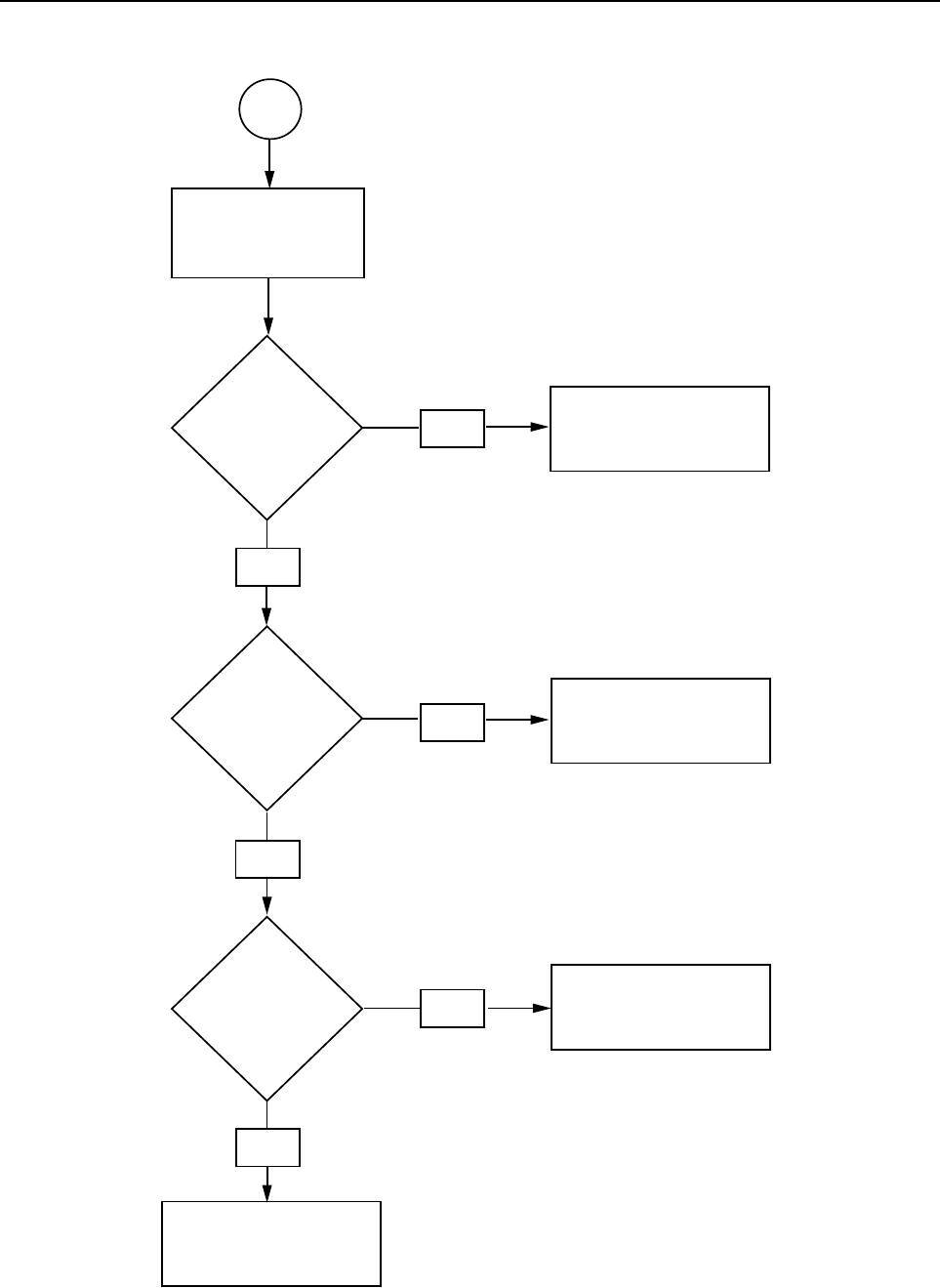
Controlhead GM398 Troubleshooting Flow Chart 3-9
3.3 Microprocessor (cont.)
Data Signal
on J0801
Pin 5 BUS+
?
Data Signal
on TP0877
SCI_RX
?
Data Signal
on TP0878
SCI_TX
?
Check / Replace
D0872 / R0887
YES
YES
YES
NO
NO
NO Check / Replace
U0871
Check
Radio Controller
Check / Replace
R0888 / R0889
Measure with scope
while rotating
Volume Pot
A
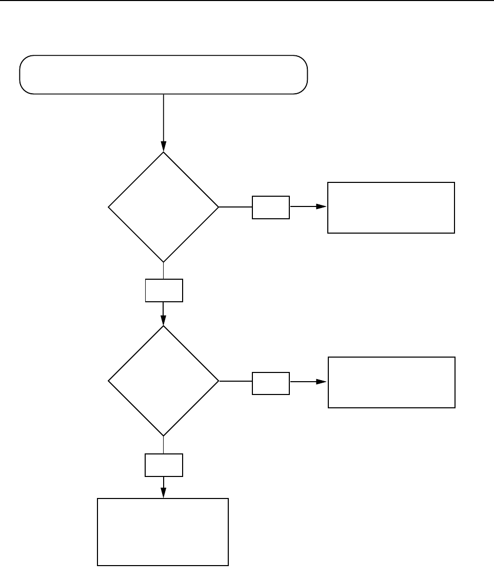
3-10 Controlhead GM398 Troubleshooting Flow Chart
3.4 Display
TP0973
Voltage Sense
between
2V and 2.4V
?
Activity on
Address & Data lines
A0 / D0...D7 / CS1
of U0971
?
NO
YES
YES
NO
Check / Replace
Flex connection
Resistors on Address & Data
lines and LCD Module
Check / Replace
LCD Module
Check for shortage
U0871
Power Up Alert Tone is audible, volume knob does operate,
indicator/backlight is on but nothing is seen on the display.
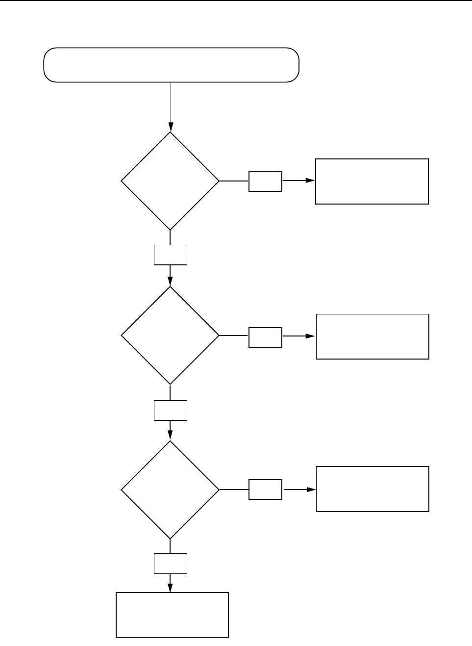
Controlhead GM398 Troubleshooting Flow Chart 3-11
3.5 Keypad Backlight
U0871 Pin 25
is toggling ?
Base of Q0943
> 0.7V ?
Collector of
Q0943
>5V & < 11V
?
Check / Replace
Q0941 / R0955 / R0957
YES
YES
YES
NO
NO
NO
Check / Replace
Q0943 / U0941 / R0941
R0943 / R0949 / R0951
Check for shortage
U0871
Check / Replace
R0945 / C0943 / R0947
Power Up Alert Tone is audible, volume knob does operate,
display is on but no keypad backlight.
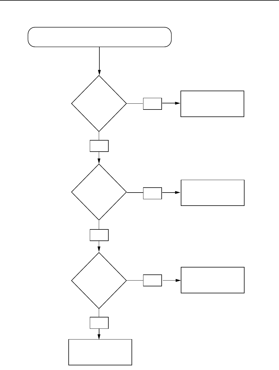
3-12 Controlhead GM398 Troubleshooting Flow Chart
3.6 Display Backlight
U0871 Pin 24
is toggling ?
Base of Q0963
> 0.7V ?
Collector of
Q0963
>5V & < 11V
?
Check / Replace
Q0961 / R0975 / R0977
YES
YES
YES
NO
NO
NO
Check / Replace
Q0963 / U0941 / R0961
R0963 / R0969 / R0971
Check for shortage
U0871
Check / Replace
R0965 / C0963 / R0967
Power Up Alert Tone is audible, volume knob does operate,
display is on but no display backlight.
4-1
Section 4
CONTROLHEAD PCBS / SCHEMATICS / PARTS LISTS
1.0 Allocation of Schematics and Circuit Boards
.
Table 4-1 Controlhead Diagrams and Parts Lists
PCB :
Controlhead GM328
8486146B07 Main Board Top Side
8486146B07 Main Board Bottom Side
Page 4-3
Page 4-3
SCHEMATICS
Sheet 1 of 2
Sheet 2 of 2 Page 4-4
Page 4-5
Parts List
8486146B07 Page 4-6
Table 4-2 Controlhead Diagrams and Parts Lists
PCB :
Controlhead GM338
8486155B06 Main Board Top Side
8486155B06 Main Board Bottom Side
Page 4-7
Page 4-7
SCHEMATICS
Sheet 1 of 4
Sheet 2 of 4
Sheet 3 of 4
Sheet 4 of 4
Page 4-8
Page 4-9
Page 4-10
Page 4-11
Parts List
8486155B06 Page 4-12
Table 4-3 Controlhead Diagrams and Parts Lists
PCB :
Controlhead GM398
8486178B03 Main Board Top Side
8486178B03 Main Board Bottom Side
Page 4-13
Page 4-13
SCHEMATICS
Sheet 1 of 4
Sheet 2 of 4
Sheet 3 of 4
Sheet 4 of 4
Page 4-14
Page 4-15
Page 4-16
Page 4-17
Parts List
8486178B03 Page 4-18

4-2 Allocation of Schematics and Circuit Boards
THIS PAGE INTENTIONALLY LEFT BLANK
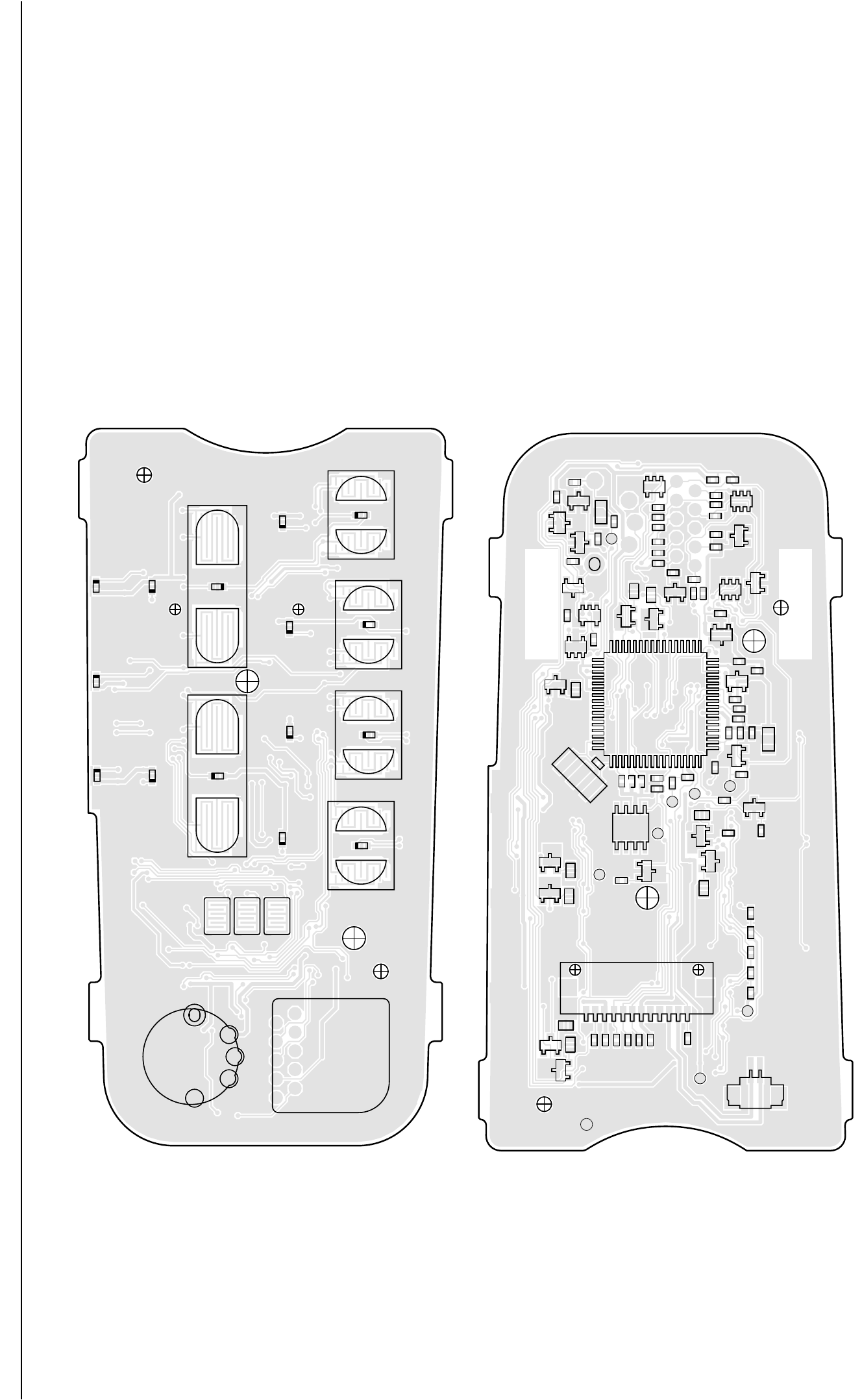
Controlhead GM328 - PCB 8486146B07 / Schematics 4-3
2.0 Controlhead GM328 - PCB 8486146B07 / Schematics
D0871
D0872
D0873
D0874 D0875 D0876
D0877 D0878 D0879
D0881
D0884
D0885
D0886
D0887 D0888
2
3579
864 10
J0811
JU0852
JU0853
JU0854
4
123
5
R0823
S0861
S0862
S0863
S0864
S0865
S0866
ZWG0130114-A
C0802
C0803
C0804
C0805
C0806
C0808
C0809
C0810
C0811
C0813
C0815
C0816
C0817
C0818
C0819
C0821
C0822
C0823
C0824
C0831
C0832
C0833
C0843
D0821
D0822
D0831
12
J0801
1
2
P0801
Q0821
Q0822
Q0823
Q0841
Q0843
Q0871
Q0872
Q0873
Q0874
Q0875
Q0876
Q0877
Q0878
Q0879
Q0881
Q0885
R0810
R0811
R0812
R0813
R0814
R0815
R0816
R0821
R0822
R0824
R0825
R0831
R0832
R0833
R0834
R0835
R0836
R0837
R0838
R0839
R0841
R0842R0843 R0844
R0845
R0847
R0849
R0852
R0853
R0854
R0861 R0862
R0864
R0866 R0867
R0871
R0872
R0873
R0874
R0875
R0876
R0877
R0878
R0879
R0880
R0881
R0885
TP0831
TP0832
TP0833
TP0834
TP0835
TP0836
TP0837
TP0838
1
49
17
33
U0831
1
45
8
U0832
3
U0833
U0835
VR0811
VR0816
VR0817
VR0821
VR0822
VR0823
64
1
1
MOTOROLA
c
8486146B07-0
Controlhead GM328 - PCB 8486146B07
ZWG0130114-A Top Side
ZWG0130113-B Bottom Side
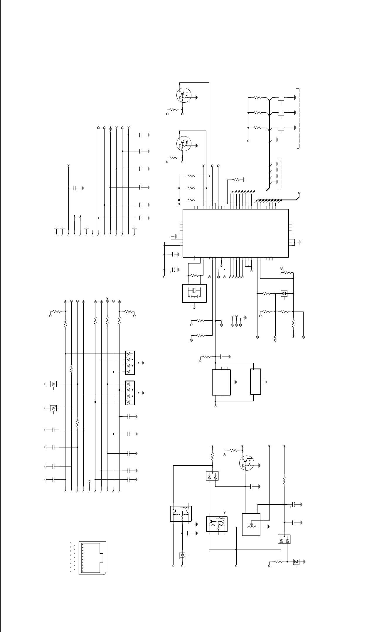
4-4 Controlhead GM328 - PCB 8486146B07 / Schematics
HOOK
GROUND
MIC
10
GM300
CONTROL HEAD
PTT_IRDECODER
7
CONNECTOR
8
J0801
9
MICROPHONE
CONNECTOR
SCI_RX
BOOT_VPP
J0811
RESET BOOT_MODE
WARIS
HANDSET_AUDIO
1
CONTROLLER
KEYPAD ID
CONTROL HEAD ID
SCI_TX
EXT_KP_ROW
EXT_KP_COL
FLT_A+
456
BUS+
23 5V
VR0822
5.6V
R0843
2.2K
NU
GND
INPUT RESET_
7
U0835
MC33464N-45ATR
J0801-8
JU0853
SWITCH
C0833
R0833
0.1uF
2
47K
10K
R0844
55
VDD 22
VRH 21
VRL
23 VSS1
VSS2
24
49 VSS3
45 XIRQ
33 XTAL
PE3_AN3
19
PE4_AN4
14
16 PE5_AN5
PE6_AN6
18
PE7_AN7
20
43 RESET
28
STRA_AS 30
STRB_RW*
PD1_TXD
50
PD2_MISO
51
PD3_MOSI
52
53 PD4_SCK
PD5_SS*
54
PE0_AN0
13
PE1_AN1
15
PE2_AN2
17 PC1_AD1 36
PC2_AD2 37
PC3_AD3 38
PC4_AD4 39
40
PC5_AD5
PC6_AD6 41
PC7_AD7 42
PD0_RXD
47
PB1_A9 11
PB2_A10 10
PB3_A11 9
PB4_A12 8
7
PB5_A13
PB6_A14 6
PB7_A15 5
PC0_AD0 34
64
PA1_IC2 63
PA2_IC1 62
PA3_OC5_OC1 59
PA4_OC4_OC1 58
PA5_OC3_OC1 57
PA6_OC2_OC1 56
PA7_PA1_OC1
PB0_A8 12
NC3
4
NC4
26
NC5
32
35
NC6 44
NC7
NC8 48
60
NC9
1
PA0_IC3
29 CLK_E
31 EXTAL
46 IRQ
27 MODA_LIR*
25 MODB_VSTBY
NC1
2
NC10 61
3NC2
MC68HC711E9
U0831
7
J0801-11
J0801-7
3
TP0832
50K
NEG
POS
TAB
TAB1
VAR
R0823
4.7K
R0824
J0811-5
1
0
Q0843
NU
R0835
100
0
R0839
R0847
22
J0811-4
270
R0814
R0815
0.1uF
C0832
13K
C0831
3.3uF
J0811-1
1
C0823
.01uF
2
06
2
C0809
NU
82pF
Q0823
D0822
10
R0813
1
C1
3
C2
2
GND
4
R0812
CSTCC8.00MG
U0833
22
5.6V
5
VR0821
100K
R0853
8
5.6V
VR0823
J0811-10
0
P0801-2
5
4
J0801-9
TP0837
INPUT
2
NC1
3
NC2
5NC3 6
NC4 7
8
NC5
RESET 1
U0832
MC33064
GND
4
Q0821
J0811-6
J0801-10
J0801-6
JU0852 SWITCH
JU0854
6
1
SWITCH
C0804
470pF
0
R0852
100K
C0817
82pF
J0811-8
7
R0845
4.7K
NU
VR0811
33V
470pF
NU
470pF
C0818
C0816
33K
R0837
NU
C0808
470pF 470pF
C0806
10K
3
R0841
R0811
51K
J0811-3
J0811-2
1MEG
R0831
VR0816
20V
13K
J0811-9
R0810
4
TP0833
10K
R0821
47K
J0801-14
R0849
P0801-1
2.2K
R0832
J0801-3
J0801-5
TP0838
TP0834
NU
470pF
NU
C0810
470pF
32
C0819
100K
R0854
6
1
J0801-12
R0838
10K
J0811-7
R0834
270
20V
VR0817
2.2uF
J0801-4
C0822
470pF
NU
5
13K
C0821
R0816
R0822
51K
470pF
C0815
C0811
470pF
TP0831
R0836
10K
TP0836
J0801-13
J0801-1
NU
J0801-2
470pF
C0802
C0803
470pF
470pF
C0843 C0813
TP0835
470pF
NU
C0824
.01uF
R0825
1K
D0821
C0805
82pF
Q0822
R0842
47K
Q0841
INT_KP_ROW
INT_KP_COL
USW_5V
5V
5V
5V
5V
FLT_A+
BUS+
EXT_KP_ROW
MIC
EXT_KP_COL
FLT_A+
D0831
5V
CH_KP_ID(0:7)
LED_CNTRL(0:8)
CH_REQUEST
5V
CH_REQUEST
5V
5V
5V
5V
PTT_IRDEC
HOOK
ON_OFF_SENSE
ON_OFF_CONTROL
5V
USW_5V
VOLUME
VOLUME
EXT_KP_ROW
EXT_KP_COL
PTT_IRDEC
FLT_A+
FLT_A+
5V
5V
PTT_IRDEC
SCI_TX
SCI_TX
BUS+
5V
5V
BL_GREEN
ON_OFF_SENSE
5V
HOOK
5V
5V
HANDSET_AUDIO
ON_OFF_CONTROL
FLT_A+
MIC
BUS+
HANDSET_AUDIO
5V
Shown from Front Side
ZWG0130239-B
Controlhead GM328 - Schematic Sheet 1 of 2
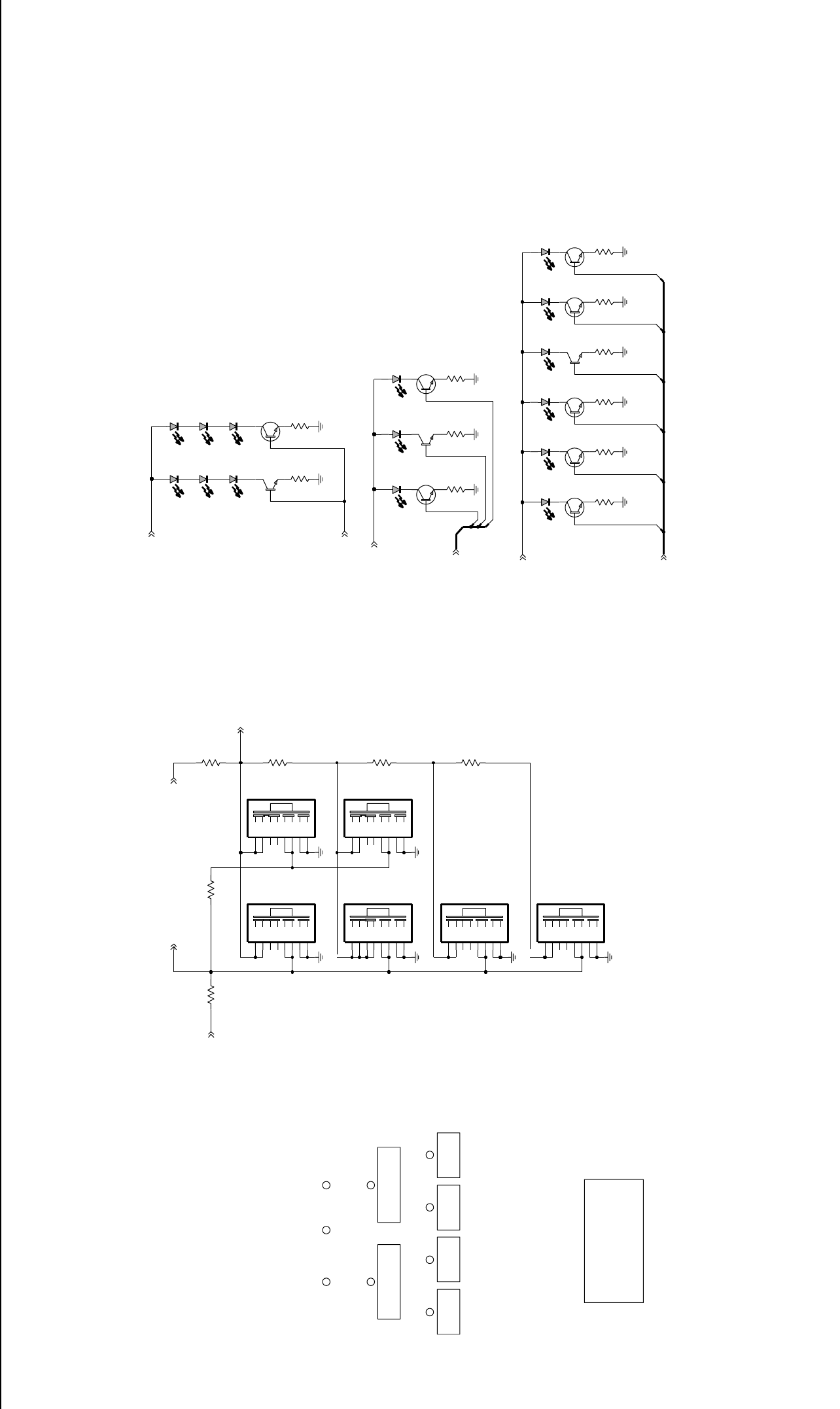
Controlhead GM328 - PCB 8486146B07 / Schematics 4-5
S0862
LED5LED4 LED6LED1 LED2 LED3
F4 P2
F3 P1
F2
F1
F1 F2 F3 F4
P1 P2
LED1 LED2 LED3
1V/1V
0V/0V
0V/1V
LED4
LED6 LED5
S0864 S0863 S0861
S0866 S0865
KEYPAD
red yellow green
0V/2V
0V/3V
1V/0V
R0867
green
D0885
13K green
D0888
D0886
green
green
D0887
green
D0884
green
D0881
270
R0885
270
R0881
Q0885
1P1
2P2
3P3
4P4
5P5
6P6
7P7
8P8
8P8
S0865
1P1
2P2
3P3
P4
4
5P5
6P6
7P7
R0864
S0861
43K
R0866
51K
R0861
51K
R0880
22K
7
P8
8
13K
R0862
P1
1
P2
2
P3
3
P4
4P5
5
P6
6
P7
6P6
7P7
8P8
S0864
1P1
2P2
3P3
P4
4
5P5
P5
5
P6
6
P7
7
P8
8
S0863
P1
1
P2
2
P3
3
P4
4P4
4P5
5
P6
6
7P7
P8
8
S0862 S0866
P1
1
P2
2
P3
3
270
green
R0877
D0877 D0879
Q0877
red
270
R0878
Q0879
Q0878
yellow
D0878
Q0873
R0879
270
R0871
270
Q0871 Q0872
82
red
D0876
7
D0875
red
red
D0874
R0876
270
R0875
270
R0874
Q0876
270
Q0875Q0874
6
CH_A
sheet 2
5
43
red
Q0881
D0872 D0873
red red
R0873
D0871
270
10
R0872
FLT_A+
LED_CNTRL(0:8)
BL_GREEN
FLT_A+
FLT_A+
LED_CNTRL(0:8)
5V
5V
INT_KP_COL
INT_KP_ROW
270
Controlhead GM328 - Schematic Sheet 2 of 2
ZWG0130240-A
4-6 Controlhead GM328 - PCB 8486146B07 / Schematics
Controlhead PCB 8486146B07 Parts List
* Motorola Depot Servicing only
Reference designators with an asterisk indicate
components which are not fieldreplaceable
because they need to be calibrated with
specialized factory equipment after installation.
Radios in which these parts have been replaced in
the field will be off frequency at temperature
extremes.
Circuit
Ref Motorola
Part No Description
C0802 2113741F17 470pF 50V
C0803 2113741F17 470pF 50V
C0804 2113741F17 470pF 50V
C0805 2113740F49 82pF 5% 50V
C0806 2113741F17 470pF 50V
C0808 2113741F17 470pF 50V
C0810 2113741F17 470pF 50V
C0811 2113741F17 470pF 50V
C0813 2113741F17 470pF 50V
C0815 2113741F17 470pF 50V
C0816 2113741F17 470pF 50V
C0817 2113740F49 82pF 5% 50V
C0818 2113741F17 470pF 50V
C0821 2113741F17 470pF 50V
C0822 2311049A40 TANT CP 2.2uF 10% 10V
C0823 2113741F49 10nF 50V
C0824 2113741F49 10nF 50V
C0831 2311049A42 TANT CP 3.3uF 10% 6V
C0832 2113743E20 100nF 16V
C0833 2113743E20 100nF 16V
C0843 2113741F17 470pF 50V
D0821 4813833C02 DUAL SOT MMBD6100
D0822 4813833C02 DUAL SOT MMBD6100
D0831 4880236E05 DIODE CHIP SCHOTTKY
D0871 4886171B01 LED RED
D0872 4886171B01 LED RED
D0873 4886171B01 LED RED
D0874 4886171B01 LED RED
D0875 4886171B01 LED RED
D0876 4886171B01 LED RED
D0877 4886171B01 LED RED
D0878 4886171B03 LED YELLOW
D0879 4886171B04 LED GREEN
D0881 4886171B04 LED GREEN
D0884 4886171B04 LED GREEN
D0885 4886171B04 LED GREEN
D0886 4886171B04 LED GREEN
D0887 4886171B04 LED GREEN
D0888 4886171B04 LED GREEN
J0801 0902636Y02 CONNECTOR FLEX 12 PIN
J0811 2864287B01 CONN TELCO 10 PIN JACK
P0801 2809926G01 CONN 1.25MM 2PIN SURMT
Q0821 4805921T02 TSTR DUAL ROHM FMC2 RH
Q0822 4880048M01 TSTR NPN DIG 47k/47k
Q0823 4805921T02 TSTR DUAL ROHM FMC2 RH
Q0841 4880048M01 TSTR NPN DIG 47k/47k
Q0843 4880048M01 TSTR NPN DIG 47k/47k
Q0871 4813824A10 TSTR NPN 40V .2A B=50-150
Q0872 4813824A10 TSTR NPN 40V .2A B=50-150
Q0873 4813824A10 TSTR NPN 40V .2A B=50-150
Q0874 4813824A10 TSTR NPN 40V .2A B=50-150
Q0875 4813824A10 TSTR NPN 40V .2A B=50-150
Q0876 4813824A10 TSTR NPN 40V .2A B=50-150
Q0877 4813824A10 TSTR NPN 40V .2A B=50-150
Q0878 4813824A10 TSTR NPN 40V .2A B=50-150
Q0879 4813824A10 TSTR NPN 40V .2A B=50-150
Q0881 4813824A10 TSTR NPN 40V .2A B=50-150
Q0885 4813824A10 TSTR NPN 40V .2A B=50-150
R0810 0662057A76 13k 1/16W 5%
R0811 0662057A90 51k 1/16W 5%
R0812 0662057A09 22 1/16W 5%
R0813 0662057A01 10 1/16W 5%
R0814 0662057A35 270 1/16W 5%
R0815 0662057A76 13k 1/16W 5%
R0816 0662057A90 51k 1/16W 5%
R0821 0662057A73 10k 1/16W 5%
R0822 0662057A76 13K 1/16W 5%
R0823 1805911V02 POT VOL
R0824 0662057A65 4k7 1/16W 5%
R0825 0662057A49 1k 1/16W 5%
R0831 0662057B22 1M 1/16W 5%
R0832 0662057A57 2k2 1/16W 5%
R0833 0662057A89 47k 1/16W 5%
R0834 0662057A35 270 1/16W 5%
R0835 0662057A25 100 1/16W 5%
R0836 0662057A73 10k 1/16W 5%
R0837 0662057A85 33k 1/16W 5%
R0838 0662057A73 10k 1/16W 5%
R0841 0662057A73 10k 1/16W 5%
R0842 0662057A89 47k 1/16W 5%
R0843 0662057A57 2.2k 1/16W 5%
R0844 0662057A73 10k 1/16W 5%
R0845 0662057A65 4k7 1/16W 5%
R0847 0662057A09 22 1/16W 5%
R0849 0662057A89 47k 1/16W 5%
R0852 0662057A97 100k 1/16W
R0853 0662057A97 100k 1/16W
R0854 0662057A97 100k 1/16W
R0861 0662057A90 51k 1/16W 5%
R0862 0662057A76 13k 1/16W 5%
R0864 0662057A88 43k 1/16W 5%
R0866 0662057A90 51k 1/16W 5%
R0867 0662057A76 13k 1/16W 5%
R0873 0660076A35 270 5 1/8
R0874 0660076A35 270 5 1/8
R0875 0660076A35 270 5 1/8
R0876 0660076A35 270 5 1/8
R0877 0660076A35 270 5 1/8
R0878 0660076A35 270 5 1/8
Circuit
Ref Motorola
Part No Description
R0879 0660076A35 270 5 1/8
R0880 0662057A81 22k 1/16W 5%
R0881 0662057A35 270 1/16W 5%
R0885 0662057A35 270 1/16W 5%
*U0831 5113802A24 IC 68HC11 W/SCI,SPI,A/D
U0832 5113815A02 IC
U0833 4886061B01 CER RESONATOR 8MHZ
CSTCC8.00MG
VR0816 4805656W09 DIODE ZENER QUAD
MMQA20VT1
VR0817 4805656W09 DIODE ZENER QUAD
MMQA20VT1
VR0821 4813830A15 DIODE 5.6V 5% 225mW
VR0822 4813830A15 DIODE 5.6V 5% 225mW
VR0823 4813830A15 DIODE 5.6V 5% 225mW
Circuit
Ref Motorola
Part No Description
Controlhead GM338 - PCB 8486155B06 / Schematics 4-7
3.0 Controlhead GM338 - PCB 8486155B06 / Schematics
D0877 D0879
D0880
D0931
D0932
D0933
D0934
D0935
D0936 D0937
D0938
D0939
D0940
D0941
D0942
D0943
D0944 D0945
D0946
D0947
D0948
D0949
D0950 D0951
D0952 D0953
D0954
D0955
D0956
D0957
D0958
D0961
D0962
D0963
D0964
D0965
D0966 D0967
D0968
D0969
D0970
D0971
D0972
D0973
D0974 D0975
D0976
D0977
D0978
D0979
D0980 D0981
D0982 D0983
D0984
D0985
D0986
D0987
D0988
40
41 80
H0971
2
3579
864 10
J0811
4
1
23
5
R0823
S0852
S0853
S0854
S0901
S0902
S0903
S0904
S0905
S0906
S0907 S0908
S0909 S0910
U0834
110 30
20
60 70
50
1
ZWG0130136-A
C0802
C0803
C0804
C0805
C0806
C0807
C0808
C0810
C0811
C0812
C0813 C0815
C0816
C0817
C0818
C0819
C0821
C0822
C0823
C0831
C0832
C0833
C0842
C0843
C0931
C0932
C0933
C0971
C0972
C0973
C0974
C0975
C0976 C0977
C0978 C0979
C0980 C0981
C0982
C0983
C0984
C0985
D0821
D0822
D0831
12
J0801
1
2
P0801
Q0821
Q0822
Q0823
Q0841
Q0843
Q0877
Q0878
Q0879
1
2
3
4Q0931 Q0932
1
2
3
4Q0933
Q0934
R0810
R0811
R0812 R0813 R0814
R0815
R0816
R0817
R0821
R0822
R0824
R0825
R0831
R0832
R0833
R0834
R0835
R0836
R0837
R0838
R0841
R0842
R0843
R0844
R0845
R0847
R0848
R0849
R0850
R0851
R0852
R0853
R0854
R0855
R0856
R0857
R0858
R0859
R0860
R0861
R0862
R0863
R0864 R0865
R0877
R0878
R0879
R0901
R0902
R0903
R0904
R0905
R0906
R0907
R0908
R0909
R0910
R0931
R0932
R0933 R0934
R0935
R0936
R0937
R0938
R0941 R0942
R0943
R0944 R0945
R0946
R0947
R0948
R0972
R0973 R0974
R0975
R0976
R0977
R 0978
TP0831
TP0832
TP0833
TP0834
TP0835
TP0836
TP0837
TP0838
TP0971
TP0972
TP0973
TP0974 TP0975 1
49
17
33
U0831
1
4
58
U0832
3U0833
U0835
14
58
U0931
128
103
102
65
64 38
39
U0971
VR0811
VR0812
VR0816
VR0817
VR0821
VR0822
1
1
64
1
MOTOROLA
c8486155B06-0
Controlhead GM338 - PCB 8486155B06
ZWG0130136-A Top Side
ZWG0130137-B Bottom Side
4-8 Controlhead GM338 - PCB 8486155B06 / Schematics
MIC
PTT_IRDECODER
CONNECTOR
C
BUS+
KEYPAD ID
CONTROLLER
B
NOT PLACED
1
PLACED
J0811
VPP
67
HANDSET_AUDIO
ANALOG_INPUT_3
5V
GM300
MICROPHONE
BOOT_MODE
SCI_RX
SCI_TX
FLT_A+
RESET
TEMP_SENSE
CONTROL HEAD ID
5V
GND
HOOK
8910
WARIS
CONTROLHEAD
CONNECTOR
GROUND
3
ANALOG_INPUT_2
FLT_A+
2J0801
45
J0801-8
4.7K
R0864
270
R0814
R081513K
R0810 13K
Q0841
J0801-5
6
0
R0833
47K
R0832
2.2K
R0837
33K
270
R0877
7
J0811-8
R0852
47K
GND
INPUT RESET_
NU
U0835
MC33464N-45ATR
S0854
SWITCH
SWITCH
S0853
J0801-3
S0852
SWITCH
J0801-10
J0801-13
J0811-9
J0801-14
J0811-10
10
6
7
R0813
J0801-7
5.6V
VR0822
D0831
Q0821
U0833
CSTCC8.00MG
C1 1
C2 3
GND
2
4
8
J0811-6
3
J0801-4
470pF
C0812
22
R0817
47K
7
NU
R0851
green
D0879
R0857
1
1
NU
47K
D0880
yellow
47K
NU
R0854
47K
R0859
10K
R0841
2.2K
R0843
51K
R0816
J0811-7
Q0823
R0831
TAB1
VAR
1MEG
R0823
50K
NEG
POS
TAB
J0801-12
J0801-9
R0848
68K
C0831
NU
NC4
NC5 8
1
RESET
3.3uF
MC33064
4
GND
2INPUT
3NC1
5NC2
6
NC3 7
U0832
R0812 22
5
0
R0879
270
R0878
270
D0822
J0811-5
R0844
10K
3
R0865
4.7K
100K
R0860
47K
NU
R0853
5
7
0
J0801-11
4
Q0822
4.7K
R0845
C0842
NU
2.2uF
Q0879Q0878
red
D0877
R0811
Q0877
51K
3
TP0833
1K
R0825
470pF
C0804
22K
TP0836
R0822
TP0834
470pF
C0821
4
NU
VR0812
5.6V
R0863
4.7K
NU
R0850
47K
4
R0856
47K
2
82pF
C0805
VDD 22
VRH 21
VRL
23 VSS1
24 VSS2
49 VSS3
45 XIRQ
33 XTAL
19
PE4_AN4
14
PE5_AN5
16
PE6_AN6
18
PE7_AN7
20
RESET
43
28
STRA_AS 30
STRB_RW*
55
50
PD2_MISO
51
PD3_MOSI
52
PD4_SCK
53
PD5_SS*
54
PE0_AN0
13
PE1_AN1
15
PE2_AN2
17
PE3_AN3
36
PC2_AD2 37
PC3_AD3 38
PC4_AD4 39
PC5_AD5 40
PC6_AD6 41
PC7_AD7 42
PD0_RXD
47
PD1_TXD 11
PB2_A10 10
PB3_A11 9
PB4_A12 8
PB5_A13 7
PB6_A14 6
PB7_A15 5
PC0_AD0 34
PC1_AD1
PA1_IC2 63
PA2_IC1 62
PA3_OC5_OC1 59
PA4_OC4_OC1 58
PA5_OC3_OC1 57
PA6_OC2_OC1 56
PA7_PA1_OC1
PB0_A8 12
PB1_A9
NC3
26 NC4
32 NC5
35
NC6 44
NC7 48
NC8 60
NC9
1
PA0_IC3 64
CLK_E
31 EXTAL
46 IRQ
27 MODA_LIR*
25 MODB_VSTBY
2NC1
61
NC10
3NC2
4
4
MC68HC711E9
U0831
29
J0811-4
J0811-3
J0811-2
1
C0822
2.2uF
R0838
10K
R0836
10K
VR0816
20V
VR0817
20V
2.2uF
C0843
0.1uF
2
C0832
C0833
0
0.1uF
47K
R0842
VR0821
10V
C0819
C0816
NU
470pF
470pF 82pF
C0817
TP0831
3
P0801-2
P0801-1
TP0835
C0806
470pF
47K
NU
R0849
47K
R0855
7
470pF
C0803
1
R084768K
470pF
C0813
C0815
470pF
47K
C0807
R0858
470pF
Q0843
VOUT
D0821
U0834
LM50
3
GND
1
POS
2
R0821
10K 6
6
3
5
J0801-1
270
R0834
1
0
5
3
2
2
J0801-6
R0824
4.7K
NU
470pF
C0802
470pF
C0810
VR0811
33V
NU
C0811 NU
470pF
470pF
C0818
2
NU
100K
R0862
TP0837
TP0832
TP0838
100
4
R0835
100K
R0861
56
J0801-2
J0811-1
82pF
C0808
NU
2
C0823
.01uF
BL_RED
BL_GREEN
5V
5V
5V
BUS+ 5V
RESET
5V
HOOK
MIC
5V
FLT_A+
5V
SCI_TX
5V
VOLTAGE_SENSE
HANDSET_AUDIO
PTT_IRDEC
BUS+
AN(0:4)
AN(0:4)
USW_5V
FLT_A+
5V
CH_REQUEST
ON_OFF_CONTROL
5V
5V
PTT_IRDEC
HOOK
5V
CH_REQUEST
ON_OFF_SENSE
5V
SCI_TX
5V
HANDSET_AUDIO
BUS+
MIC
FLT_A+
ON_OFF_CONTROL
5V
FLT_A+
LED_CNTRL(0:8)
LED_CNTRL(0:8)
ON_OFF_SENSE
PTT_IRDEC
FLT_A+
5V
AN(0:4)
USW_5V
FLT_A+
AN(0:4)
CH_KP_ID(0:7)
5V
CONTROLHEAD B NU NU NU USED USED USED USED NU
CONTROLHEAD C NU NU USED NU USED USED NU USED
R0850 R0851 R0852 R0853 R0855 R0856 R0857 R0858
ZWG0130241-A
Controlhead GM338 - Schematic Sheet 1 of 4
ZWG0130241-A
Controlhead GM338 - PCB 8486155B06 / Schematics 4-9
P4
SW0906 SW0904
SW0903 SW0901
SW0909 SW0910
SW0908SW0907
SW0902
SW0905
KEYPAD C
SW0908
SW0905
SW0902
P3P1
P2 P4
P6
7P7
8P8
SW0906 SW0910
SW0903
P1
P2
P3
1P1
2P2
3P3
4P4
5P5
6
P5
6P6
7P7
8P8
SWITCH
S0901
1P1
2P2
3P3
4P4
5
4P4
5P5
6P6
7P7
8P8
SWITCH
S0905
1P1
2P2
3P3
3P3
4P4
5P5
6P6
7P7
8P8
SWITCH
S0902
SWITCH
S0910
1P1
2P2
2P2
3P3
4P4
5P5
6P6
7P7
8P8
P8
SWITCH
S0908
1P1
1P1
2P2
3P3
4P4
5P5
6P6
7P7
8
7P7
8P8
SWITCH
S0906
1P1
2P2
3P3
4P4
5P5
6P6
SWITCH
S0903
43K
0
1
R0909
43K
130K
R0904
130K
NU
R0910
NU
R0905
R0906
51K
R0901
51K
R0908
22K
R0903
22K
R0902
13K R0907
13K
P4
5P5
6P6
7P7
8P8
CH_C
sheet 2
CH_B
o
1P1
2P2
3P3
4
P3
4P4
5P5
6P6
7P7
8P8
SWITCH
S0909
1P1
2P2
3
P2
3P3
4P4
5P5
6P6
7P7
8P8
SWITCH
S0907
SWITCH
S0904
1P1
2
COL2
COL1
ROW2
ROW1
ROW3 COL3
5V
ROW5
ROW4
COL5
COL4
AN(0:4)
COL3 COL2
ROW1
ROW2
ROW3
ROW4
COL4
Controlhead GM338 - Schematic Sheet 2 of 4
ZWG0130242-A
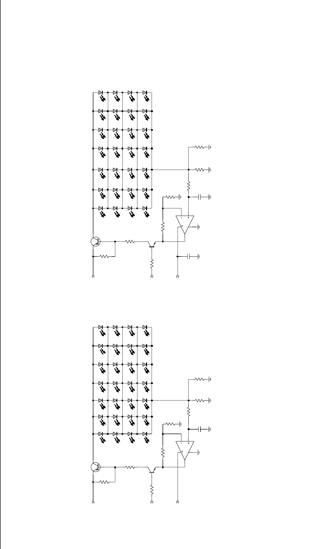
4-10 Controlhead GM338 - PCB 8486155B06 / Schematics
BACKLIGHT REDBACKLIGHT GREEN
NU
Q0931
D0980
D0979
D0978
R0946
D0977
R0945
10K
33K
10K
R0942
10K
R0941
D0972
R0944
10
100K
R0947 R0948
4
10
U0931-2
MC33072
6
5
78
100K
Q0933
D0987
NU
R0934
D0986
D0985
D0984
10K
R0935
D0969 NU
D0951
D0967
D0966
D0964
D0965
NU
NU
D0963
D0970
NU
D0962
D0971
NU
D0947
NU
D0943
Q0934
NU
D0932
4.7K
NU
D0931
R0943
C0931
0.1uF
10
R0938
R0937
10 NU
NU
C0932
0.1uF
R0936
10K
R0932 NU
D0949
NU
33K
NU
R0931
10K
Q0932
MC33072
U0931-1
2
3
18
4
NU
D0942
NU
NU
D0941
NU
D0940
NU
D0938
NU
D0937
NU
D0958
NU
D0957
NU
D0956
D0954
D0953
NU
D0952
NU
D0950
NU
NU
D0975
D0976
D0974
D0973 NU
D0939
NU
D0935
D0933
NU
D0934
NU
0.1uF
C0933
D0936
D0968
NU
D0988
4.7K
NU
R0933
NU
D0961
D0983
D0982
D0981 D0955
D0948
NU
D0946
NU
NU
D0944
NU
D0945
FLT_A+
FLT_A+
FLT_A+
BL_GREEN BL_RED
FLT_A+
NU
Controlhead GM338 - Schematic Sheet 3 of 4
ZWG0130243-A
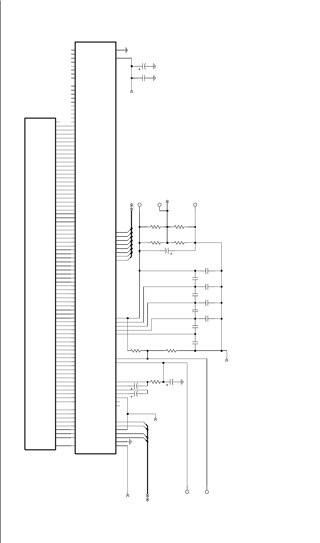
Controlhead GM338 - PCB 8486155B06 / Schematics 4-11
THE LCD IS PART OF HARDWAREKITS GLN7358A (EUR) AND GLN7359A (US)
R0974
1.8MEG
R0973
1.2MEG
R0972
C0972
0
NU
1uF
1uF
C0971
2.2uF
C0985
.01uF
1uF
C0984
C0973
0.1uF
C0980
0.1uF
C0976C0975
0.1uF
C0974
0.1uF
NU
C0982
0.1uF
0.1uF
C0981C0979
0.1uF NU
0.1uF
C0977
NU
1
2
NU
3
4
5
6
7
0
100K
R0978
200K
R0977
NU
NU
1
100K
R0976
SEG69_C70
SEG6_C7
SEG7_C8
SEG8_C9
SEG9_C10
0
SEG61_C62
SEG62_C63
SEG63_C64
SEG64_C65
SEG65_C66
SEG66_C67
SEG67_C68
SEG68_C69
SEG54_C55
SEG55_C56
SEG56_C57
SEG57_C58
SEG58_C59
SEG59_C60
SEG5_C6
SEG60_C61
SEG47_C48
SEG48_C49
SEG49_C50
SEG4_C5
SEG50_C51
SEG51_C52
SEG52_C53
SEG53_C54
SEG3_C4
SEG40_C41
SEG41_C42
SEG42_C43
SEG43_C44
SEG44_C45
SEG45_C46
SEG46_C47
SEG32_C33
SEG33_C34
SEG34_C35
SEG35_C36
SEG36_C37
SEG37_C38
SEG38_C39
SEG39_C40
SEG25_C26
SEG26_C27
SEG27_C28
SEG28_C29
SEG29_C30
SEG2_C3
SEG30_C31
SEG31_C32
SEG18_C19
SEG19_C20
SEG1_C2
SEG20_C21
SEG21_C22
SEG22_C23
SEG23_C24
SEG24_C25
SEG10_C11
SEG11_C12
SEG12_C13
SEG13_C14
SEG14_C15
SEG15_C16
SEG16_C17
SEG17_C18
COM3_R4
COM4_R5
COM5_R6
COM6_R7
COM7_NC
COMS
NC
SEG0_C1
04B01
H0971
COM0_R1
COM1_R2
COM2_R3
5V5
7VDD
8VOUT
6VR
13 VSS
17 WR
NU
57
SEG8 58
SEG9
16 SR1
15 SR2
1V1
2V2
3V3
4V4
121
SEG72 122
SEG73 123
SEG74 124
SEG75 125
SEG76 126
SEG77 127
SEG78 128
SEG79
114
SEG65 115
SEG66 116
SEG67 117
SEG68 118
SEG69
56
SEG7
119
SEG70 120
SEG71
107
SEG58 108
SEG59
55
SEG6
109
SEG60 110
SEG61 111
SEG62 112
SEG63 113
SEG64
99
SEG50 100
SEG51 101
SEG52 102
SEG53 103
SEG54 104
SEG55 105
SEG56 106
SEG57
92
SEG43 93
SEG44 94
SEG45 95
SEG46 96
SEG47 97
SEG48
SEG49 98
54
SEG5
85
SEG36 86
SEG37 87
SEG38 88
SEG39
53
SEG4
89
SEG40 90
SEG41 91
SEG42
78
SEG29
52
SEG3
79
SEG30 80
SEG31 81
SEG32 82
SEG33 83
SEG34 84
SEG35
70
SEG21 71
SEG22 72
SEG23 73
SEG24 74
SEG25 75
SEG26 76
SEG27 77
SEG28
63
SEG14 64
SEG15 65
SEG16 66
SEG17 67
SEG18 68
SEG19
51
SEG2
69
SEG20
14 M_S
18 RD
49
SEG0 50
SEG1
59
SEG10 60
SEG11 61
SEG12 62
SEG13
25 D1
26 D2
27 D3
28 D4
29 D5
30 D6
31 D7
22 FR
38
COM6 39
COM7
40
COM8 41
COM9
48
COMS
20 CS1
19 CS2
24 D0
44
COM12 45
COM13 46
COM14 47
COM15
34
COM2 35
COM3 36
COM4 37
COM5
12 CAP1_POS
9CAP2_NEG
10 CAP2_POS
23 CL
32
COM0 33
COM1
42
COM10 43
COM11
SED1526F0A
U0971
21 A0
11 CAP1_NEG
C0978
0.1uF
3
TP0974
TP0973
1
TP0975
1
TP0972
TP0971
2.2uF
C0983
200K
R0975
5V
RESET 5VCH_KP_ID(0:7)
LED_CNTRL(0:8)
5V
VOLTAGE_SENSE
2
Controlhead GM338 - Schematic Sheet 4 of 4
ZWG0130244-A
4-12 Controlhead GM338 - PCB 8486155B06 / Schematics
Controlhead PCB 8486155B06 Parts List
* Motorola Depot Servicing only
Reference designators with an asterisk indicate
components which are not fieldreplaceable
because they need to be calibrated with
specialized factory equipment after installation.
Radios in which these parts have been replaced in
the field will be off frequency at temperature
extremes.
Circuit
Ref Motorola
Part No Description
C0803 2113741F17 470pF 50V
C0804 2113741F17 470pF 50V
C0805 2113740F49 82pF 5% 50V NP0
C0807 2113741F17 470pF 50V
C0811 2113741F17 470pF 50V
C0812 2113741F17 470pF 50V
C0813 2113741F17 470pF 50V
C0815 2113741F17 470pF 50V
C0816 2113741F17 470pF 50V
C0817 2113740F49 82pF 5% 50V
C0822 2311049A40 TANT CP 2.2uF 10% 10V
C0823 2113741F49 10nF 50V
C0831 2311049A42 TANT CP 3.3uF 10% 6V
C0832 2113743E20 100nF 16V
C0843 2311049A40 TANT CP 2.2uF 10% 10V
C0931 2113743E20 100nF 16V
C0933 2113743E20 100nF 16V
C0971 2311049A07 TANT CP 1uF 10% 16V
C0973 2311049A07 TANT CP 1uF 10% 16V
C0974 2113743E20 100nF 16V
C0975 2113743E20 100nF 16V
C0976 2113743E20 100nF 16V
C0978 2113743E20 100nF 16V
C0980 2113743E20 100nF 16V
C0983 2311049A09 TANT CP 2.2uF 10% 20V
C0984 2113741F49 10nF 50V
C0985 2311049A40 TANT CP 2.2uF 10% 10V
D0821 4813833C02 DIODE DUAL SOT
MMBD6100
D0822 4813833C02 DIODE DUAL SOT
MMBD6100
D0831 4880236E05 DIODE CHIP SCHOTTKY
D0877 4886171B01 LED RED
D0879 4886171B04 LED GREEN
D0880 4886171B03 LED YELLOW
D0951 4886171B02
Not used in LED ORANGE
Controlhead B
D0952 4886171B02
Not used in LED ORANGE
Controlhead B
D0953 4886171B02
Not used in LED ORANGE
Controlhead B
D0954 4886171B02
Not used in LED ORANGE
Controlhead B
D0965 4886171B04 LED GREEN
D0966 4886171B04 LED GREEN
D0967 4886171B04 LED GREEN
D0968 4886171B04 LED GREEN
D0969 4886171B04 LED GREEN
D0970 4886171B04 LED GREEN
D0971 4886171B04 LED GREEN
D0972 4886171B04 LED GREEN
D0973 4886171B04 LED GREEN
D0974 4886171B04 LED GREEN
D0975 4886171B04 LED GREEN
D0976 4886171B04 LED GREEN
D0977 4886171B04 LED GREEN
D0978 4886171B04 LED GREEN
D0979 4886171B04 LED GREEN
D0980 4886171B04 LED GREEN
D0981 4886171B04
Not used in LED GREEN
Controlhead B
D0982 4886171B04
Not used in LED GREEN
Controlhead B
D0983 4886171B04
Not used in LED GREEN
Controlhead B
D0984 4886171B04
Not used in LED GREEN
Controlhead B
D0985 4886171B04 LED GREEN
D0986 4886171B04 LED GREEN
D0987 4886171B04 LED GREEN
D0988 4886171B04 LED GREEN
J0801 0902636Y02 CONNECTOR FLEX 12 PIN
J0811 2864287B01 CONN TELCO 10 PIN JACK
P0801 2809926G01 CONN 1.25MM 2PIN SUR MT
Q0821 4805921T02 TSTR DUAL ROHM FMC2 RH
Q0822 4880048M01 TSTR NPN DIG 47k/47k
Q0823 4805921T02 TSTR DUAL ROHM FMC2 RH
Q0841 4880048M01 TSTR NPN DIG 47k/47k
Q0843 4880048M01 TSTR NPN DIG 47k/47k
Q0877 4813824A10 TSTR NPN 40V .2A B=50-150
Q0878 4813824A10 TSTR NPN 40V .2A B=50-150
Q0879 4813824A10 TSTR NPN 40V .2A B=50-150
Q0933 4813822A08 TSTR PNP 25V 5AMJD210T4
Q0934 4813824A10 TSTR NPN 40V .2A B=50-150
R0810 0662057A76 13k 1/16W 5%
R0811 0662057A90 51k 1/16W 5%
R0812 0662057A09 22 1/16W 5%
R0813 0662057A01 10 1/16W 5%
R0814 0662057A35 270 1/16W 5%
R0815 0662057A76 13k 1/16W 5%
R0816 0662057A90 51k 1/16W 5%
R0817 0662057A09 22 1/16W 5%
R0821 0662057A73 10k 1/16W 5%
R0822 0662057A81 22k 1/16W 5%
R0823 1805911V02 POT VOL
R0824 0662057A65 4k7 1/16W 5%
R0825 0662057A49 1k 1/16W 5%
R0831 0662057B22 1M 1/16W 5%
R0832 0662057A57 2k2 1/16W 5%
Circuit
Ref Motorola
Part No Description
R0833 0662057A89 47k 1/16W 5%
R0834 0662057A35 270 1/16W 5%
R0835 0662057A25 100 1/16W 5%
R0836 0662057A73 10k 1/16W 5%
R0837 0662057A85 33k 1/16W 5%
R0838 0662057A73 10k 1/16W 5%
R0841 0662057A73 10k 1/16W 5%
R0842 0662057A89 47k 1/16W 5%
R0843 0662057A57 2.2k 1/16W 5%
R0844 0662057A73 10k 1/16W 5%
R0845 0662057A65 4k7 1/16W 5%
R0847 0662057A93 68k 1/16W 5%
R0849 0662057A89 47k 1/16W 5%
R0853 0662057A89 47k 1/16W 5%
R0855 0662057A89 47k 1/16W 5%
R0856 0662057A89 47k 1/16W 5%
R0857 0662057A89
Not used in 47k 1/16W 5%
Controlhead C
R0858 0662057A89
Not used in 47k 1/16W 5%
Controlhead B
R0859 0662057A89 47k 1/16W 5%
R0860 0662057A97 100k 1/16W
R0861 0662057A97 100k 1/16W
R0862 0662057A97 100k 1/16W
R0863 0662057A65 4k7 1/16W 5%
R0864 0662057A65 4k7 1/16W 5%
R0865 0662057A65 4k7 1/16W 5%
R0877 0660076A35 270 5 1/8
R0878 0660076A35 270 5 1/8
R0879 0660076A35 270 5 1/8
R0901 0662057A90 51k 1/16W 5%
R0902 0662057A76 13k 1/16W 5%
R0903 0662057A81 22k 1/16W 5%
R0904 0662057A88 43k 1/16W 5%
R0906 0662057A90 51k 1/16W 5%
R0907 0662057A76 13k 1/16W 5%
R0908 0662057A81 22k 1/16W 5%
R0909 0662057A88
Not used in 43k 1/16W 5%
Controlhead B
R0935 0662057A73 10k 1/16W 5%
R0936 0662057A73 10k 1/16W 5%
R0937 0660076A01 10 5 1/8
R0941 0662057A73 10k 1/16W 5%
R0942 0662057A85 33k 1/16W 5%
R0943 0662057A65 4k7 1/16W 5%
R0944 0662057A97 100k 1/16W
R0945 0662057A73 10k 1/16W 5%
R0946 0662057A73 10k 1/16W 5%
R0947 0660076A01 10 5 1/8
R0948 0660076A01 10 5 1/8
R0972 0662057B47 0 1/16W
Circuit
Ref Motorola
Part No Description
R0973 0662057B24 1.2M 1/16W 5%
R0974 0662057B28 1.8M 1/16W 5%
R0975 0662057G29 200k 0.1W 1%
R0976 0662057G13 100k 0.1W 1%
*U0831 5113802A24 IC 68HC11 W/SCI,SPI,A/D
U0832 5113815A02 MC33064
UNDER VLTG SENSING
U0833 4886061B01 CER RESONATOR 8MHZ
CSTCC8.00MG
U0834 5185963A15 TEMP SENSOR 1M5
U0931 5113818A03 IC HIGH PERFORMANCE SI
U0971 5186158B01 LCD DRIVER SED1526F0A
VR0812 4813830A15 DIODE 5.6V 5% 225mW
VR0816 4805656W09 DIODE ZENER QUAD
MMQA20VT1
VR0817 4805656W09 DIODE ZENER QUAD
MMQA20VT1
VR0821 4813830A23 DIODE 10V 5% 20mA 350mW
VR0822 4813830A15 DIODE 5.6V 5% 225mW
Circuit
Ref Motorola
Part No Description
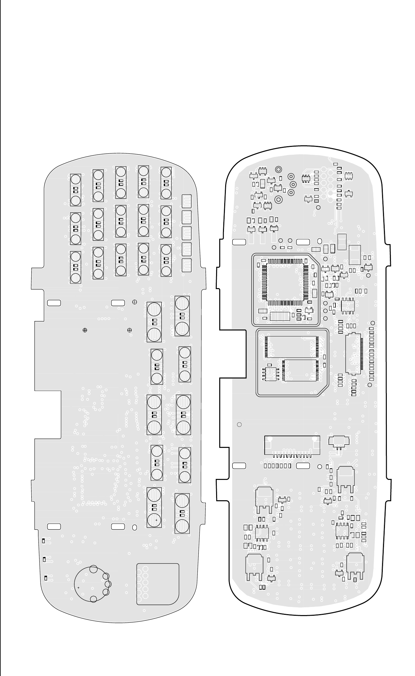
Controlhead GM398 - PCB 8486178B03 / Schematics 4-13
4.0 Controlhead GM398 - PCB 8486178B03 / Schematics
ZWG0130368-A
D0941
D0942
D0943
D0944
D0945
D0946
D0947
D0948
D0949
D0950
D0951
D0952
D0953
D0954
D0955
D0956
D0957
D0958
D0959
D0960
D0961
D0962
D0963
D0964
D0965
D0966
D0967
D0968
D0969
D0970
D0971
D0972
D0973
D0974
D0975
D0976
D0977
D0978
D0979
D0980
D0981
D0982
D0983
D0984
D0985
D0986
D0987
D0988
D0989
D0990
D0991 D0992 D0993
2
3579
864 10
4
123
5
S0901
S0902
S0903 S0904 S0905
S0906
S0907
S0908 S0909 S0910
S0911
S0912
S0913 S0914 S0915
S0916
S0917
S0918 S0919 S0920
S0921
S0922
S0923 S0924 S0925
S0931 S0932 S0933 S0934 S0935
1
J0811
Microphone
Connector
R0854
Volume
Pot
C0802
C0803
C0804
C0805
C0806
C0807
C0808
C0810
C0811
C0812 C0813
C0815
C0816
C0817
C0818
C0819
C0823
C0824
C0825
C0826
C0827
C0828
C0829
C0830
C0831
C0832
C0833
C0834
C0835
C0836
C0837
C0838
C0840
C0851
C0853
C0855
C0856
C0861
C0862
C0863
C0864
C0865
C0866
C0870
C0871
C0872
C0873
C0874
C0875
C0941
C0942
C0943
C0944
C0945
C0946
C0963
C0964
C0965
C0966
C0991
D0852
D0855
D0861
D0871
D0872
12
24 1
1
2P0801
Q0851
Q0852
Q0853
Q0866 Q0871
Q0872
1
2
3
4
Q0941
1
2
3
4
Q0942
Q0943
Q0944
1
2
3
4
Q0961
1
2
3
4
Q0962
Q0963
Q0964
Q0991
Q0992
Q0993
R0811
R0812 R0813
R0814
R0815
R0816
R0817
R0818
R0821
R0822
R0823
R0824
R0825
R0826
R0827
R0828
R0831
R0832
R0833
R0834
R0835
R0836
R0837
R0838
R0840
R0852
R0853
R0855 R0856
R0861
R0862
R0863
R0866
R0870
R0871
R0872
R0873
R0874
R0875
R0876
R0877
R0878
R0879
R0880
R0881
R0882
R0883
R0884
R0885
R0886
R0887
R0888
R0889
R0890
R0901
R0902
R0903
R0904
R0905
R0911
R0912
R0913
R0914
R0915
R0931
R0932
R0933
R0934
R0935
R0941
R0942
R0943
R0944
R0945
R0946
R0947
R0948
R0949
R0950
R0951
R0952
R0953
R0954
R0955
R0956
R0957
R0958
R0961
R0962
R0963
R0964
R0965
R0966
R0967
R0968
R0969
R0970
R0971
R0972
R0973
R0974
R0975
R0976
R0977
R0978
R0991
R0992
R0993
R0995
R0996
R0997
SH0871
SH0872
TP0804
TP0821
TP0866
TP0871
TP0872
TP0873
TP0874
TP0875
TP0876
TP0877
TP0878
1
45
8
U0861
1
61
21
41
32 17
16
1
3
U0873
1
4
58
22
21
8
71
1
4
5
8
U0941
1
45
8
U0942
VR0811
VR0812
VR0813
VR0814
VR0851 VR0855
1
J0801
to
Radio
Box
J0821
to LCD -Module
U0871
HC11K4
µP
U0872
FLASH
U0874
EEPROM
U0875
SRAM
1
MOTOROLA 99
c
8486178B03-T1
Controlhead GM398 - PCB 8486178B03
ZWG0130368-A Top Side
ZWG0130369-B Bottom Side
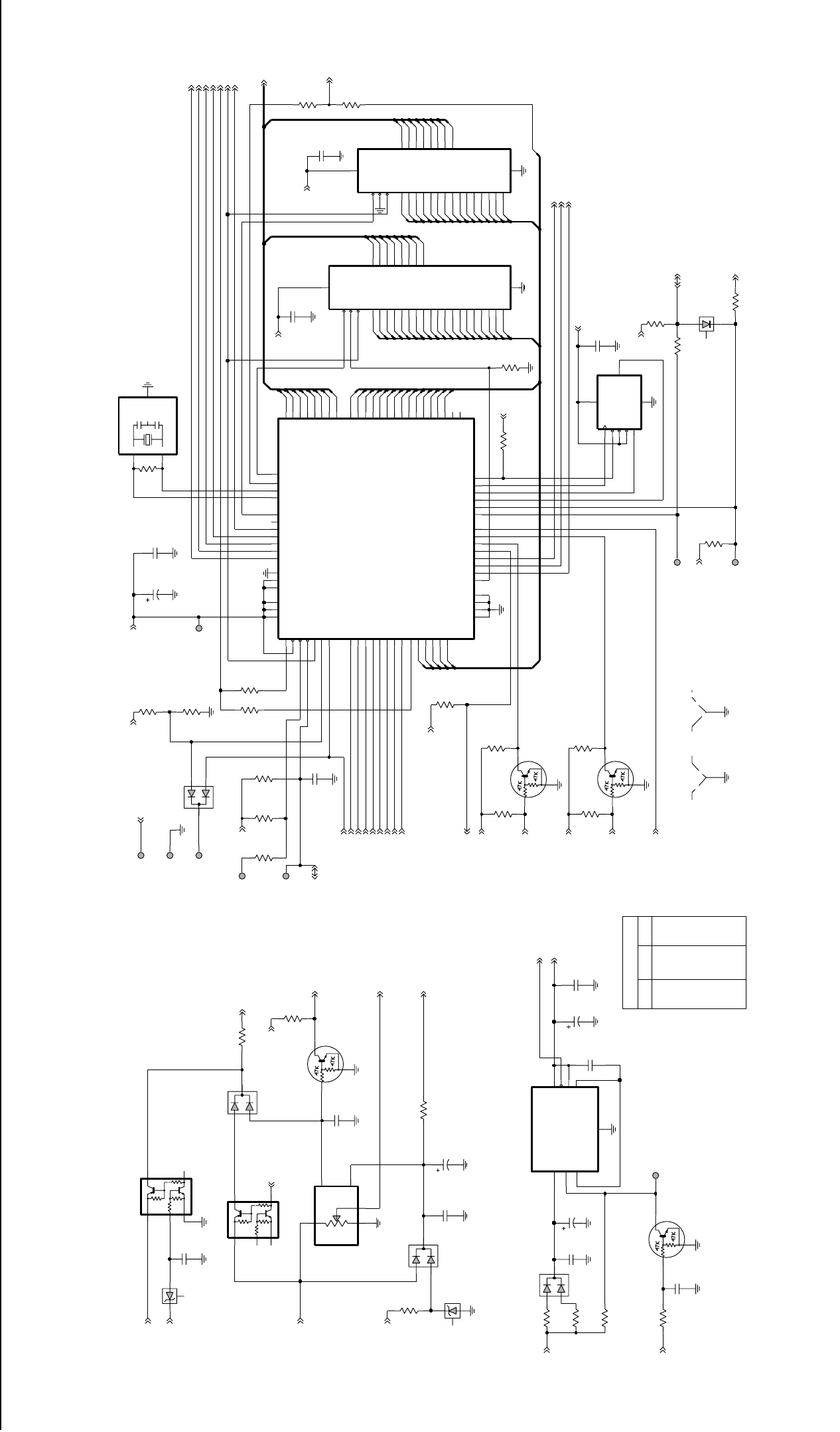
4-14 Controlhead GM398 - PCB 8486178B03 / Schematics
ZWG0130370-A
OUT
CONTROLLER
OUT
OUT
CLOSED
BOOT_MODE
BOOT_VPP
ARCHITECTURE
R0871
BOOT_SCI_RX
BOOT_SCI_TX
BOOT_PWR
BOOT_GND
RESET
5V
BOOT_PWR_ON
OPEN
R0872
R0876
R0877
R0878
R0879
IN
IN
IN
IN
IN
IN
OUT
OUT
OUT
D0871
0.1uF
1
2
3
4
8
9
NU
C0870
1
TP0876
TP0871
33K
R0889
10K
R0888
10K
R0887
C0856
5
1
2
2.2uF
4
7
NU
0.1uF
C0875
4.7K
15
16
NU
R0871
NU
SH0872
SHIELD
VCC
28
6
7
NU
SH0871
SHIELD
IO1 11
IO2 12
IO3 13
IO4 15
IO5 16
IO6 17
IO7 18
IO8 19
A6
4
A7
3
A8
25
A9
24
EN_CS
20
EN_OE
22
EN_WE
27
GND
14
A11
23
A12
2
A13
26
A14
1
A2
8
A3
7
A4
6
A5
5
U0875
A0
10
A1
9
A10
21 NU
D0872
C0861
0.1uF 10uF
C0862
R0866
10K
2
0
NU
0.1uF
C0874
0.1uF
0
14
29
IO7
8
VCC
12
13
C0865
24
GND
21
IO0 22
IO1 23
IO2 25
IO3 26
IO4 27
IO5 28
IO6
15 A5
14 A6
13 A7
3A8
2A9
30 EN_CE
32 EN_OE
7EN_WE
5A14
11 A15
10 A16
6A17
9A18
18 A2
17 A3
16 A4
20 A0
19 A1
31 A10
1A11
12 A12
4A13
10
NU
U0872
.01uF
C0851
VR0851
10V
71
VRH 51
VRL 50
VSS
13
VSS1
32
VSS3
70
XIRQ
30
XTAL 74
25
PH4_CSIO 26
PH5_CSGP1 27
PH6_CSGP2 28
PH7_CSPROG 29
RESET
75
VDD 12
VDD1 31
VDD2
37
PG4_XA17
36
PG5_XA18
35
PG6 34
PG7_R_W*
33
PH0_PW1 22
PH1_PW2 23
PH2_PW3 24
PH3_PW4
56
PF5_ADDR5 55
PF6_ADDR6 54
PF7_ADDR7 53
PFO_ADDR0 60
PG0_XA13
40
PG1_XA14
39
PG2_XA15
38
PG3_XA16
46
PE4_AN4
45
PE5_AN5
44
PE6_AN6
43
PE7_AN7
42
PF1_ADDR1 59
PF2_ADDR2 58
PF3_ADDR3 57
PF4_ADDR4
79
PD2_MISO
80
PD3_MOSI
1
PD4_SCK
2
PD5_SS*
3
PE0_AN0
49
PE1_AN1
48
PE2_AN2
47
PE3_AN3
63
PC2_DATA2 64
PC3_DATA3 65
PC4_DATA4 66
PC5_DATA5 67
PC6_DATA6 68
PC7_DATA7 69
PD0_RXD
78
PD1_TXD
19
PB3_ADDR11 18
PB4_ADDR12 17
PB5_ADDR13 16
PB6_ADDR14 15
PB7_ADDR15 14
PBO_ADDR8 21
PC0_DATA0 62
PC1_DATA1
10 PA2_IC1
9PA3_IC4_OC5_OC1
8PA4_OC4_OC1
7PA5_OC3_OC1
6PA6_OC2_OC1
5PA7_PA1_OC1
4
PB1_ADDR9 20
PB2_ADDR10
41
AVSS
52
E
72
EXTAL 73
IRQ
61
MODA_LIR*
77
MODB_VSTBY
76
PA0_IC3
11 PA1_IC2
MC68HC11K4
U0871
AVDD
TP0872
GND 2
TP0878
U0873
CSTCC8.00MG
C1
1
C2
3
R0886
47K
2.2K
5
R0870
D0861
10
R0862
R0861
10
ERROR
7
FEEDBACK
4
GND
8
INPUT
1
OUTPUT
2
SENSE
3
SHUTDOWN
LP2951C
U0861
6
5V_TAP
5
6CLK
1CS
7HOLD
5SI
2
SO
8
VCC
4
VSS
3WP
NU
X25320_2.7V
U0874
Q0872
100K
R0863
R0877
0
VR0855
NU
18
0
0
5.6V
17 6
14
15
16
17
R0875
47K
R0855
24K 14
0.1uF
34
5
NU
C0872
3
4
5
6
7
0
3
R0890
270
6
C0864
47uF
Q0852
R0874
3
1
2
R0881
100
10K
Q0871
Q0853
11
R0852
0
1
1K
0
R0879
POS
TAB
TAB1
VAR
NU
R0854
50K
NEG
4.7K
R0856
NU
C0855
470pF
0
R0872
R0880
2.2K
1MEG
R0873
TP0866
6
18
C0873
0.1uF
R0876
0
R0878
0
.022uF
2
0
1
2
C0863
9
10
11
12
13
NU
.01uF
C0853
R0882
4
11
12
13
47K
D0855
10
9
10K
R0883 R0884
10K
0.1uF TP0877
C0866
TP0873
10K
5
6
7
8
R0885
7
83
4
5
Q0866
TP0875
D0852
Q0851
7
3.3uF
C0871
R0853
10K
TP0874
5V
5V
5V
CH_REQUEST
SCI_TX
BUS+
5V
LCD_RW_WR
5V
LCD_DATA_(0:7)
RESET
FLT_A+
ON_OFF_CONTROL
PTT_IRDEC
VOLTAGE_SENSE
5V
USW_5V
KEYPAD_ID
BL_LCD_RED
BL_KP_RED
BL_LCD_GREEN
BL_KP_GREEN
LCD_CS
5V
LCD_A0
LED_RED
LED_YELLOW
LED_GREEN
LCD_E_RD
5V
RESET
5V
FLT_A+
5V_SOURCE
INT_KP_COL
INT_KP_ROW
EXT_KP_COL
EXT_KP_ROW
VOLUME
TEMP_SENSE
PTT_IRDEC ADDR(0:18)
5V
5V
FLT_A+
5V
CH_REQUEST
FLT_A+
5V
USW_5V
VOLUME
HOOK
5V
ON_OFF_SENSE
5V
ON_OFF_SENSE
Controlhead GM398 - Schematic Sheet 1 of 4
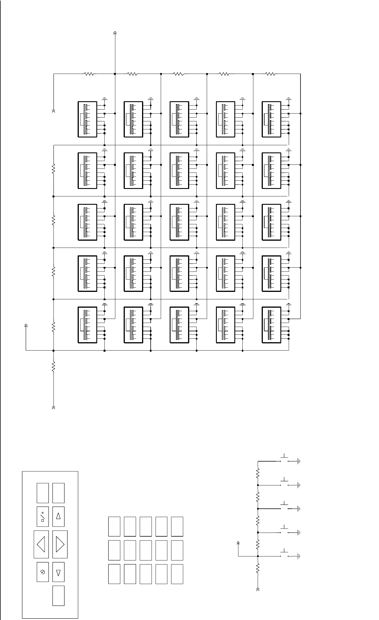
Controlhead GM398 - PCB 8486178B03 / Schematics 4-15
P6
SW0924 P7
SW0925
DOWN
P3
MENU
1
SW0903 2
SW0904
SW0910
7
SW0913 8
SW0914
SW0901 SW0906
1V/1V
1V/2V
1V/3V
3V/2V
3V/3V
SW0917
SW0911
SW0912
0V/0V
3V/4V
2V/0V
SW0918 0
SW0919
1V/4V
3V/0V
RIGHT
12
P2
LEFT
4
SW0908 5
SW0909 2V/1V
2V/2V
4V/0V
4V/1V
4V/2V
4V/3V
4V/4V
789
0*
P1
3
4
P2
3
SW0905
P4
P1
P3 P4
EXIT
6
9
SW0915
SW0902 SW0907
SW0916 SW0921
SW0922
*
2V/3V
2V/4V
UP
5
0V/1V
0V/2V
0V/3V
0V/4V
1V/0V
6
#
P5 P6 P7
3V/1V
#
SW0920
P5
SW0923
4P4
5P5
6P6
7P7
8P8
SWITCH
S0924
1P1
2P2
3P3
S0933
1
2
SWITCH
130K
R0915
130K
NU
R0935
P6
6
P7
7
P8
8
S0917
SWITCH
P1
1
P2
2
P3
3
P4
4P5
55
P5
6P6
7P7
8P8
SWITCH
S0907
1P1
2P2
3P3
4P4
P3
3
P4
4P5
5
P6
6
P7
7
P8
8
S0903
SWITCH
P1
1
P2
2
2P2
3P3
4P4
5P5
6P6
7P7
8P8
8P8
SWITCH
S0911
1P1
1P1
2P2
3P3
4P4
5P5
6P6
7P7
P7
7
P8
8
SWITCH
S0904
P1
1
P2
2
P3
3
P4
4P5
5
P6
6
S0905
SWITCH
R0933
22K
1
2
R0914
43K
SWITCH
S0932
R0934
43K
R0931
51K NU
R0903R0902
22K13K
R0912
13K
R0932
13K
S0931
SWITCH
1
2
2P2
3P3
4P4
5P5
6P6
7P7
8P8
SWITCH
S0912
1P1
43K
R0904 R0905
130K
R0911
51K
51K
R0901
R0913
22K
P2
2
P3
3
P4
4P5
5
P6
6
P7
7
P8
88 P8
S0910
SWITCH
P1
11 P1
2P2
3P3
4P4
5P5
6P6
7P7P7
7
P8
8
SWITCH
S0915
P1
1
P2
2
P3
3
P4
4P5
5
P6
6
5P5
6P6
7P7
8P8
S0920
SWITCH
S0925
1P1
2P2
3P3
4P4
6P6
P7
7
8P8
SWITCH
SWITCH
1P1
2P2
3P3
4P4
5P5 P4
4P5
5
P6
6
P7
7
P8
8
S0916
S0906
SWITCH
P1
1
P2
2
P3
3
3P3
4P4
5P5
6P6
7P7
8P8
SWITCH
S0923
1P1
2P2
P1
1
P2
2
P3
3
P4
4P5
5
P6
6
P7
7
P8
88 P8
S0909
SWITCH
1P1
2P2
3P3
4P4
5P5
6P6
7P7
P6
6
P7
7
P8
8
SWITCH
S0914
S0919
SWITCH
P1
1
P2
2
P3
3
P4
4P5
5
SWITCH
S0935
1
2
SWITCH
1
2
6P6
7P7
8P8
S0934
1P1
2P2
3P3
4P4
5P5
P4
4P5
5
P6
6
P7
7
P8
8
SWITCH
S0922S0921
SWITCH
P1
1
P2
2
P3
3P3
3
P4
4P5
5
P6
6
P7
7
P8
8
S0901
SWITCH
P1
1
P2
2
1P1
2P2
3P3
4P4
5P5
6P6
7P7
8P8
SWITCH
S0902
P5
6P6
7P7
8P8
1P1
2P2
3P3
4P4
5
4P4
5P5
6P6
7P7
8P8
SWITCH
S0908
SWITCH
S0913
1P1
2P2
3P3
2
P3
3
P4
4P5
5
P6
6
P7
7
P8
8
S0918
SWITCH
P1
1
P2
5V
INT_KP_ROW
INT_KP_COL
5V 5V
KEYPAD_ID
Controlhead GM398 - Schematic Sheet 2 of 4
ZWG0130371-A

4-16 Controlhead GM398 - PCB 8486178B03 / Schematics
NU
Q0964
MC33072
U0942-2
6
5
78
4
Q0962
NU
4.7K
NU
R0967
100K
R0969
R0977
1010
R0975
0.1uF
C0965
D0958
D0946
NU D0960
NU
NU
NU
D0948
10
R0957
D0981
68K
R0945
2.2uF
C0943
R0949
100K
D0947
R0948
4.7K R0950
NU
NU
100K
NU
D0990
NU
D0988
D0943
D0952
D0986
NU
D0974
NU
D0962
NU
D0950
NU
D0984
NU
R0974
NU
NU
10K
NU
R0972
10K
D0983
D0993
green
R0955
10
C0945
0.1uF
R0954
10K
R0952
NU
NU
10K
33K
R0944
10K
R0942
NU
Q0944
NU
U0942-1
MC33072
2
3
18
4
NU
NU
NU
Q0942
R0973
10K
10K
R0971
R0964
33K
NU
Q0991
68K
R0965
D0971
D0959
D0977
D0965
D0953
D0941
R0947
4.7K
Q0992
NU
R0962
10K
D0992
yellow
D0991
red
D0956
D0944
NU
D0954
NU
D0942
NU
D0989
NU
D0987
D0955
D0967
R0946
NU
68K
NU
C0944
2.2uF
R0963
R0961
33K
10K
6
5
78
4
Q0963
U0941-2
MC33072
8
4
Q0961
MC33072
U0941-1
2
3
1
Q0941
C0964
C0941
NU
2.2uF
0.1uF
D0969
D0957
D0945
D0979
NU
D0972
C0963
2.2uF
CH_D
sheet 3
NU
R0966
68K
10K
R0953
R0951
10K
R0943
33K
10K
Q0943
R0941 D0949
D0961
NU
D0982
NU
D0970
C0991
470pF
C0942
NU
D0975
NU
0.1uF
D0963
D0951
D0985
D0973
R0956
C0946
NU
10
NU
0.1uF
D0980
D0968
NU
270
NU
270
R0991 R0992
R0958
10
D0978
NU
D0966
NU
R0968
NU
NU
4.7K
NU
R0970
100K
10
R0978
R0976
10 NU
0.1uF NU
NU
C0966
270
R0993
Q0993
R0997
47K47K
R0996R0995
47K
NU
D0976
NU
D0964
BL_KP_GREEN
BL_KP_RED
BL_LCD_GREEN
BL_LCD_RED
FLT_A+
FLT_A+FLT_A+
LED_RED
LED_YELLOW
LED_GREEN
FLT_A+
BL_A_GREENFLT_A+
BL_K_GREEN
BL_A_REDFLT_A+
BL_K_RED
FLT_A+
FLT_A+
FLT_A+
ZWG0130372-A
Controlhead GM398 - Schematic Sheet 3 of 4
ZWG0130372-A
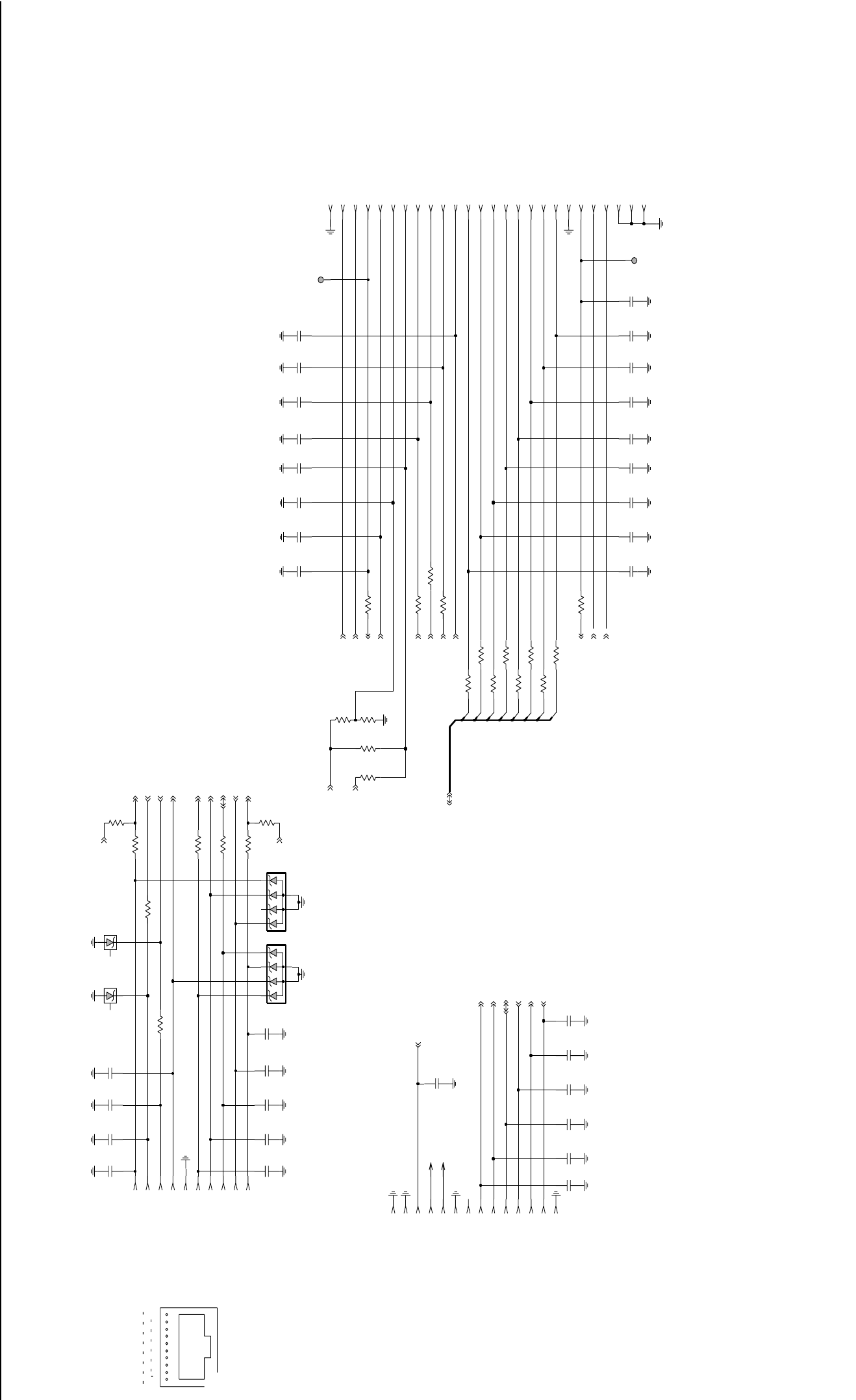
Controlhead GM398 - PCB 8486178B03 / Schematics 4-17
ANALOG_INPUT_2
J0821
GND
VDD
D0
D1
D2
MIC
Backlight_Anode GREEN
Backlight_Anode RED
CS1
CS2
A0 (Command)
CONNECTOR
HANDSET_AUDIO
ANALOG_INPUT_3
D3
D4
D5
CONTROLHEAD
CONNECTOR
GND
Voltage_Sense
Backlight_Cathode RED
Backlight_Cathode GREEN
GND
GND
GND
HOOK
GROUND
Temp_Sense
Reset
Temp_Sense
Voltage_Sense
FLT_A+
5V
R/W (WR)
E (RD)
PTT_IRDECODER
BUS+
D6
D7
J0801
LCD MODULE
R0822
0
NU
470pF
NU
C0804
C0835
100pF100pF
C0834
NU
100pF
NUNU
C0833
100pF
C0832
NU
R0815
10
100pF
C0827C0826
100pF
NU
C0825
NU
J0801-14
100pF
J0801-1
J0801-2
J0801-3
J0821-25
J0821-24
J0821-10
R0833
100
R0832
100
J0821-21
J0801-5
2
J0821-20
J0801-6
J0801-7
100pF
NU
C0816
C0824
J0811-8
470pF
J0811-7
J0811-6
J0821-13
J0821-11
J0821-12
J0801-9
J0801-12
P0801-2
NU
P0801-1
NU
J0801-8
J0811-10
C0815
470pF
C0813
C0811 470pF
470pF
R0816
270
R0817
13K
R0812
13K
C0805
82pF
VR0814
20V
VR0813
20V
R0838
100
100
R0834
R0831
100
R0828
100
J0801-4
R0826
100
R0825
100
R0824
0
NU
J0821-23
C0806
470pF
NU
470pF
C0807
6
0
1
3
4
5
VR0812
5.6V
J0801-13
470pF
C0812
22
R0814
C0836
NU
C0808
NU
100pF
82pF
R0813
22
J0821-4
J0821-2
J0821-3
J0811-9
C0823
NU NU
100pF NU 100pF
C0829C0828
100pF
R0840
100
J0811-5
R0837
100
R0836
100
R0835
100
C0817
R0818
82pF
51K
R0827
100
J0821-18
J0821-17
0
J0821-16
J0821-14
R0821
0
R0823
51K
R0811
7
J0821-5
J0821-1
J0821-9
J0821-7
J0821-8
J0821-6
C0831
100pF
NU
NU
NU
470pF
C0810
NU 470pF
C0819
470pF
C0818
C0830
100pF
NU
NU
J0821-22
C0840
100pF
C0838
NU
100pF
NU 100pF
J0821-26
C0837
J0811-4
J0811-3
J0811-1
J0811-2
TP0821
J0821-15
TP0804
VR0811
33V
NU
J0801-10
J0801-11
J0821-19
470pF
C0802
NU
C0803
EXT_KP_ROW
MIC
FLT_A+
EXT_KP_COL
HOOK
470pF
LCD_CS
RESET
LCD_DATA_(0:7)
VOLTAGE_SENSE
TEMP_SENSE
BL_A_GREEN
BL_A_RED
BL_K_GREEN
BL_K_RED
LCD_A0
LCD_RW_WR
LCD_E_RD
5V
5V
PTT_IRDEC
HANDSET_AUDIO
BUS+
5V
SCI_TX
5V_SOURCE
HANDSET_AUDIO
BUS+
MIC
FLT_A+
ON_OFF_CONTROL
5V
5V
43
WARIS
9GM300
MICROPHONE
12567810
J0811
CONNECTOR
Controlhead GM398 - Schematic Sheet 4 of 4
ZWG0130373-A
4-18 Controlhead GM398 - PCB 8486178B03 / Schematics
Controlhead PCB 8486178B03 Parts List
Circuit
Ref Motorola
Part No Description
C0803 2113741F17 470pF 50V
C0804 2113741F17 470pF 50V
C0805 2113740F49 82pF 5% 50V
C0807 2113741F17 470pF 50V
C0811 2113741F17 470pF 50V
C0812 2113741F17 470pF 50V
C0813 2113741F17 470pF 50V
C0815 2113741F17 470pF 50V
C0816 2113741F17 470pF 50V
C0817 2113740F49 82pF 5% 50V
C0851 2113741F49 10nF 50V
C0856 2311049A40 TANT CP 2.2uF 10% 10V
C0861 2113743E20 100nF 16V
C0862 2311049A45 TANT CP 10uF 10% 35V
C0863 2113743E07 22nF 16V
C0864 2311049A99 TANT CP 47uF 20% 10V
C0865 2113743E20 100nF 16V
C0866 2113743E20 100nF 16V
C0871 2311049A42 TANT CP 3.3uF 10% 6V
C0873 2113743E20 100nF 16V
C0941 2113743E20 100nF 16V
C0942 2113743E20 100nF 16V
C0943 2311049A40 TANT CP 2.2uF 10% 10V
C0944 2311049A40 TANT CP 2.2uF 10% 10V
C0945 2113743E20 100nF 16V
C0946 2113743E20 100nF 16V
C0963 2311049A40 TANT CP 2.2uF 10% 10V
C0964 2311049A40 TANT CP 2.2uF 10% 10V
C0965 2113743E20 100nF 16V
C0966 2113743E20 100nF 16V
D0852 4813833C02 DUAL SOT MMBD6100
D0855 4813833C02 DUAL SOT MMBD6100
D0861 4813833C02 DUAL SOT MMBD6100
D0871 4813833C02 DUAL SOT MMBD6100
D0872 4880236E05 DIODECHIP SCHOTTKY
D0941 4886171B04 LED GREEN
D0942 4886171B01 LED RED
D0943 4886171B04 LED GREEN
D0944 4886171B01 LED RED
D0945 4886171B04 LED GREEN
D0946 4886171B01 LED RED
D0947 4886171B04 LED GREEN
D0948 4886171B01 LED RED
D0949 4886171B04 LED GREEN
D0950 4886171B01 LED RED
D0951 4886171B04 LED GREEN
D0952 4886171B01 LED RED
D0953 4886171B04 LED GREEN
D0954 4886171B01 LED RED
D0955 4886171B04 LED GREEN
D0956 4886171B01 LED RED
D0957 4886171B04 LED GREEN
D0958 4886171B01 LED RED
D0959 4886171B04 LED GREEN
D0960 4886171B01 LED RED
D0961 4886171B04 LED GREEN
D0962 4886171B01 LED RED
D0963 4886171B04 LED GREEN
D0964 4886171B01 LED RED
D0965 4886171B04 LED GREEN
D0966 4886171B01 LED RED
D0967 4886171B04 LED GREEN
D0968 4886171B01 LED RED
D0969 4886171B04 LED GREEN
D0970 4886171B01 LED RED
D0971 4886171B04 LED GREEN
D0972 4886171B01 LED RED
D0973 4886171B04 LED GREEN
D0974 4886171B01 LED RED
D0975 4886171B04 LED GREEN
D0976 4886171B01 LED RED
D0977 4886171B04 LED GREEN
D0978 4886171B01 LED RED
D0979 4886171B04 LED GREEN
D0980 4886171B01 LED RED
D0981 4886171B04 LED GREEN
D0982 4886171B01 LED RED
D0983 4886171B04 LED GREEN
D0984 4886171B01 LED RED
D0985 4886171B04 LED GREEN
D0986 4886171B01 LED RED
D0987 4886171B04 LED GREEN
D0988 4886171B01 LED RED
D0989 4886171B04 LED GREEN
D0990 4886171B01 LED RED
D0991 4886171B01 LED RED
D0992 4886171B03 LED YELLOW
D0993 4886171B04 LED GREEN
J0801 0902636Y02 CONN FLEX 12 PIN
J0811 2864287B01 CONN TELCO 10 PIN JACK
J0821 0986197B01 CONN ZIF HOR 24PIN
P0801 2809926G01 CONN1.25MM 2PIN SUR MT
Q0851 4805921T02 DUAL ROHM FMC2 RH
Q0852 4805921T02 DUAL ROHM FMC2 RH
Q0853 4880048M01 NPN DIG 47k/47k
Q0866 4880048M01 NPN DIG 47k/47k
Q0871 4880048M01 NPN DIG 47k/47k
Q0872 4880048M01 NPN DIG 47k/47k
Q0941 4813822A08 PNP 25V 5A MJD210T4
Circuit
Ref Motorola
Part No Description
Q0942 4813822A08 PNP 25V 5A MJD210T4
Q0943 4813824A10 NPN 40V .2A B=50-150
Q0944 4813824A10 NPN 40V .2A B=50-150
Q0961 4813822A08 PNP 25V 5A MJD210T4
Q0962 4813822A08 PNP 25V 5A MJD210T4
Q0963 4813824A10 NPN 40V .2A B=50-150
Q0964 4813824A10 NPN 40V .2A B=50-150
Q0991 4813824A10 NPN 40V .2A B=50-150
Q0992 4813824A10 NPN 40V .2A B=50-150
Q0993 4813824A10 NPN 40V .2A B=50-150
R0811 0662057A90 51k 1/16W 5%
R0812 0662057A76 13k 1/16W 5%
R0813 0662057A09 22 1/16W 5%
R0814 0662057A09 22 1/16W 5%
R0815 0662057A01 10 1/16W 5%
R0816 0662057A35 270 1/16W 5%
R0817 0662057A76 13k 1/16W 5%
R0818 0662057A90 51k 1/16W 5%
R0821 0662057B47 0 1/16W
R0823 0662057B47 0 1/16W
R0825 0662057A25 100 1/16W 5%
R0826 0662057A25 100 1/16W 5%
R0827 0662057A25 100 1/16W 5%
R0828 0662057A25 100 1/16W 5%
R0831 0662057A25 100 1/16W 5%
R0832 0662057A25 100 1/16W 5%
R0833 0662057A25 100 1/16W 5%
R0834 0662057A25 100 1/16W 5%
R0835 0662057A25 100 1/16W 5%
R0836 0662057A25 100 1/16W 5%
R0837 0662057A25 100 1/16W 5%
R0838 0662057A25 100 1/16W 5%
R0840 0662057A25 100 1/16W 5%
R0852 0662057A49 1k 1/16W 5%
R0853 0662057A73 10k 1/16W 5%
R0854 1805911V02 POT VOL
R0855 0662057A82 24K 1/16W 5%
R0856 0662057A65 4k7 1/16W 5%
R0861 0662057A01 10 1/16W 5%
R0862 0662057A01 10 1/16W 5%
R0863 0662057A97 100k 1/16W
R0866 0662057A73 10k 1/16W 5%
R0870 0662057A57 2k2 1/16W 5%
R0872 0662057B47 0 1/16W
R0873 0662057B22 1M 1/16W 5%
R0874 0662057A25 100 1/16W 5%
R0875 0662057A89 47k 1/16W 5%
R0876 0662057B47 0 1/16W
R0878 0662057B47 0 1/16W
R0880 0662057A57 2k2 1/16W 5%
R0881 0662057A73 10k 1/16W 5%
Circuit
Ref Motorola
Part No Description
R0882 0662057A89 47k 1/16W 5%
R0883 0662057A73 10k 1/16W 5%
R0884 0662057A73 10k 1/16W 5%
R0885 0662057A73 10k 1/16W 5%
R0886 0662057A89 47k 1/16W 5%
R0887 0662057A73 10k 1/16W 5%
R0888 0662057A73 10k 1/16W 5%
R0889 0662057A85 33k 1/16W 5%
R0890 0662057A35 270 1/16W 5%
R0901 0662057A90 51k 1/16W 5%
R0902 0662057A76 13k 1/16W 5%
R0903 0662057A81 22k 1/16W 5%
R0904 0662057A88 43k 1/16W 5%
R0905 0662057B01 130K 1/16W 5%
R0911 0662057A90 51k 1/16W 5%
R0912 0662057A76 13k 1/16W 5%
R0913 0662057A81 22k 1/16W 5%
R0914 0662057A88 43k 1/16W 5%
R0915 0662057B01 130K 1/16W 5%
R0931 0662057A90 51k 1/16W 5%
R0932 0662057A76 13k 1/16W 5%
R0933 0662057A81 22k 1/16W 5%
R0941 0662057A73 10k 1/16W 5%
R0942 0662057A73 10k 1/16W 5%
R0943 0662057A85 33k 1/16W 5%
R0944 0662057A85 33k 1/16W 5%
R0945 0662057A93 68k 1/16W 5%
R0946 0662057A93 68k 1/16W 5%
R0947 0662057A65 4k7 1/16W 5%
R0948 0662057A65 4k7 1/16W 5%
R0949 0662057A97 100k 1/16W
R0950 0662057A97 100k 1/16W
R0951 0662057A73 10k 1/16W 5%
R0952 0662057A73 10k 1/16W 5%
R0953 0662057A73 10k 1/16W 5%
R0954 0662057A73 10k 1/16W 5%
R0955 0660076A01 10 5 1/8
R0956 0660076A01 10 5 1/8
R0957 0660076A01 10 5 1/8
R0958 0660076A01 10 5 1/8
R0961 0662057A73 10k 1/16W 5%
R0962 0662057A73 10k 1/16W 5%
R0963 0662057A85 33k 1/16W 5%
R0964 0662057A85 33k 1/16W 5%
R0965 0662057A93 68k 1/16W 5%
R0966 0662057A93 68k 1/16W 5%
R0967 0662057A65 4k7 1/16W 5%
R0968 0662057A65 4k7 1/16W 5%
R0969 0662057A97 100k 1/16W
R0970 0662057A97 100k 1/16W
R0971 0662057A73 10k 1/16W 5%
Circuit
Ref Motorola
Part No Description

Controlhead GM398 - PCB 8486178B03 / Schematics 4-19
* Motorola Depot Servicing only
Reference designators with an asterisk indicate
components which are not fieldreplaceable
because they need to be calibrated with
specialized factory equipment after installation.
Radios in which these parts have been replaced in
the field will be off frequency at temperature
extremes.
R0972 0662057A73 10k 1/16W 5%
R0973 0662057A73 10k 1/16W 5%
R0974 0662057A73 10k 1/16W 5%
R0975 0660076A01 10 5 1/8
R0976 0660076A01 10 5 1/8
R0977 0660076A01 10 5 1/8
R0978 0660076A01 10 5 1/8
R0991 0660076A35 270 5 1/8
R0992 0660076A35 270 5 1/8
R0993 0660076A35 270 5 1/8
R0995 0662057A89 47k 1/16W 5%
R0996 0662057A89 47k 1/16W 5%
R0997 0662057A89 47k 1/16W 5%
U0861 5105469E65 IC VLTG REGLTR LP2951C
*U0871 5113802A32 68HC11 W/SCI SPI A/D
U0873 4886061B01 CER RESONATOR 8MHZ
U0941 5113818A03 IC HIGH PERFORMANCE SI
U0942 5113818A03 IC HIGH PERFORMANCE SI
VR0812 4813830A15 DIODE 5.6V 5% 225mW
VR0813 4805656W09 ZENER QUAD MMQA20VT1
VR0814 4805656W09 ZENER QUAD MMQA20VT1
VR0851 4813830A23 DIODE 10V 5% 20mA 350mW
VR0855 4813830A15 DIODE 5.6V 5% 225mW
Circuit
Ref Motorola
Part No Description

4-20 Controlhead GM398 - PCB 8486178B03 / Schematics
THIS PAGE INTENTIONALLY LEFT BLANK

GM328/GM338/GM398
Mobile Radios
Controller
Service Information
Issue: December, 2003

Computer Software Copyrights
The Motorola products described in this manual may include copyrighted Motorola computer programs stored
in semiconductor memories or other media. Laws in the United States and other countries preserve for
Motorola certain exclusive rights for copyrighted computer programs, including the exclusive right to copy or
reproduce in any form, the copyrighted computer program. Accordingly, any copyrighted Motorola computer
programs contained in the Motorola products described in this manual may not be copied or reproduced in
any manner without the express written permission of Motorola. Furthermore, the purchase of Motorola
products shall not be deemed to grant, either directly or by implication, estoppel or otherwise, any license
under the copyrights, patents or patent applications of Motorola, except for the normal non-exclusive royalty-
free license to use that arises by operation of law in the sale of a product.

i
Table of Contents
Section 1 Theory of Operation
1.0 Controller Circuits ................................................................................................1-1
1.1 Overview.........................................................................................................1-1
1.2 General...........................................................................................................1-1
1.3 Radio Power Distribution................................................................................1-2
1.4 Electronic ON/OFF .........................................................................................1-4
1.5 Emergency .....................................................................................................1-4
1.6 Mechanical ON/OFF.......................................................................................1-5
1.7 Ignition............................................................................................................1-5
1.8 Microprocessor Clock Synthesizer .................................................................1-5
1.9 Serial Peripheral Interface (SPI).....................................................................1-6
1.10 SBEP Serial Interface.....................................................................................1-7
1.11 General Purpose Input/Output........................................................................1-7
1.12 Normal Microprocessor Operation..................................................................1-8
1.13 FLASH Electronically Erasable Programmable Memory(FLASH EEPROM)1-10
1.14 Electrically Erasable Programmable Memory (EEPROM)............................1-10
1.15 Static Random Access Memory (SRAM)......................................................1-10
2.0 Controller Board Audio and Signalling Circuits..................................................1-11
2.1 General - Audio Signalling Filter IC with Compander (ASFIC CMP)............1-11
2.2 Transmit Audio Circuits ................................................................................1-11
2.3 Transmit Signalling Circuits..........................................................................1-14
2.4 Receive Audio Circuits .................................................................................1-16
2.5 Receive Signalling Circuits...........................................................................1-19
2.6 Voice Storage (optional)...............................................................................1-20
Section 2 Troubleshooting Charts
1.0 Controller Troubleshooting Chart.........................................................................2-1

ii
Section 3 Controller Schematics / Parts Lists
1.0 Allocation of Schematics and Circuit Boards .......................................................3-1
1.1 Controller Circuits...........................................................................................3-1
1.2 Voice Storage Facility.....................................................................................3-1
2.0 Controller T5 / Schematic Diagrams....................................................................3-3
Controller T5 Schematic Diagram - Controller Overall ...........................................3-3
Controller T5 Schematic Diagram - Supply Voltage...............................................3-4
Controller T5 Schematic Diagram - Audio..............................................................3-5
Controller T5 Schematic Diagram - I/O ..................................................................3-6
Controller T5 Schematic Diagram - Microprocessor...............................................3-7
Controller T5 Schematic Diagram - Voice Storage.................................................3-8
2.1 Controller T5 Parts List...................................................................................3-9
3.0 Controller T7/T9 Schematic Diagrams...............................................................3-12
Controller T7/T9 Schematic Diagram - Overall.....................................................3-12
Controller T7/T9 Schematic Diagram - Supply Voltage........................................3-13
Controller T7/T9 Schematic Diagram - Audio.......................................................3-14
Controller T7 only Schematic Diagram - I/O.........................................................3-15
Controller T9 only Schematic Diagram - I/O........................................................3-16
Controller T7 only Schematic Diagram - Microprocessor.....................................3-17
Controller T9 only Schematic Diagram - Microprocessor.....................................3-18
Controller T7/T9 Schematic Diagram - Voice Storage .........................................3-19
3.1 Controller T7 Parts List.................................................................................3-20
3.2 Controller T9 Parts List.................................................................................3-23

1-1
Section 1
THEORY OF OPERATION
1.0 Controller Circuits
1.1 Overview
This section provides a detailed theory of operation for the radio and its components. The main radio
is a single board design, consisting of the transmitter, receiver, and controller circuits. The main
board is designed to accept one additional option board. This may provide functions such as secure
voice/data, voice storage or signalling decoder.
A controlhead is either mounted directly or connected by an extension cable. The controlhead
contains, LED indicators, a microphone connector, buttons and dependant of the radio type, a
display and a speaker. These provide the user with interface control over the various features of the
radio.
If no controlhead is mounted directly on the front of the radio, an expansion board containing
circuitry for special applications can be mounted on the front of the radio. An additional controlhead
can be connected by an extension cable.
In addition to the power cable and antenna cable, an accessory cable can be attached to a
connector on the rear of the radio. The accessory cable provides the necessary connections for
items such as external speaker, emergency switch, foot operated PTT, and ignition sensing, etc.
1.2 General
The radio controller consists of 3 main subsections:
•Digital Control
•Audio Processing
•Voltage Regulation.
The digital control section of the radio is based upon an open architecture controller configuration. It
consists of a microprocessor, support memory, support logic, signal MUX ICs, the On/Off circuit, and
general purpose Input/Output circuitry.
The controller uses the Motorola 68HC11FL0 microprocessor (U0101). In addition to the
microprocessor, the controller has 3 external memory devices. The 3 memory devices consist of a
32KByte SRAM (U0122), a 512KByte FLASH EEPROM (U0121), and a 16KByte EEPROM
(U0111).
Note: From this point on the 68HC11FL0 microprocessor will be referred to as µP. References to a
controlhead will be to the controlheads with display.
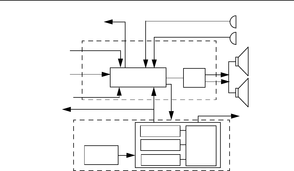
1-2 Controller Circuits
Figure 1-1 Controller Block Diagram
1.3 Radio Power Distribution
The DC power distribution throughout the radio board is shown in Figure 1-2. Voltage regulation for
the controller is provided by 4 separate devices; U0651 (MC78M05) +5V, U0641 (LM2941) +9.3V,
U0611 (LM2941) SWB+ limited to 16.5V and VSTBY 5V (a combination of R0621 and VR0621). An
additional 5V regulator is located on the RF section.
The DC voltage applied to connector J0601 supplies power directly to the electronic on/off control,
RF power amplifier, 16.5V limiter, 9.3V regulator, Audio PA and 5.6V stabilization circuit. The 9.3V
regulator (U0641) supplies power to the 5V regulator (U0651) and the 6V voltage divider Q0681.
Regulator U0641 is used to generate the 9.3 volts required by some audio circuits, the RF circuitry
and power control circuitry. Input and output capacitors (C0641 and C0644 / C0645) are used to
reduce high frequency noise. R0642 / R0643 set the output voltage of the regulator. If the voltage at
pin 1 is greater than 1.3 volts the regulator output decreases and if the voltage is less than 1.3 volts
the regulator output increases. This regulator output is electronically enabled by a 0 volt signal on
pin 2. Q0661, Q0641 and R0641 are used to disable the regulator when the radio is turned off.
Voltage regulation providing 5V for the digital circuitry is done by U0651. Operating voltage is from
the regulated 9.3V supply. Input and output capacitors (C0651 / C0652 and C0654 / C0655) are
used to reduce high frequency noise and provide proper operation during battery transients. Voltage
sense device U0652 or alternatively U0653 provides a reset output that goes to 0 volts if the
regulator output goes below 4.5 volts. This is used to reset the controller to prevent improper
operation. Diode D0651 prevents discharge of C0652 by negative spikes on the 9V3 voltage.
External
Microphone
Internal
Microphone
External
Speaker
Internal
Speaker
SCI to
Controlhead
Audio
PA
Audio/Signalling
Architecture
To Synthesizer
Mod
Out
16.8 MHz
Reference Clock
from Synthesizer
Recovered Audio
To RF Section SPI
Digital
Architecture
µP Clock
5V
Regulator
(5VD)
RAM
EEPROM
FLASH
HC11FL0
ASFIC_CMP
Accessory &
5V
from Synthesizer
Section (5V_RF)
Connector
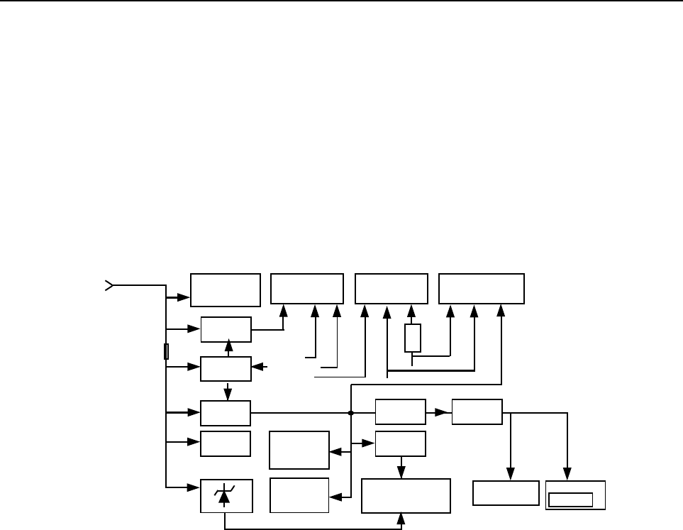
Controller Circuits 1-3
Transistor Q0681 and resistors R0681 / R0682 divide the regulated 9.3V down to about 6 volts. This
voltage supplies the 5V regulator, located on the RF section. By reducing the supply voltage of the
regulator, the power dissipation is divided between the RF section and the controller section.
The voltage VSTBY, which is derived directly from the supply voltage by components R0621 and
VR0621, is used to buffer the internal RAM. C0622 allows the battery voltage to be disconnected for
a couple of seconds without losing RAM parameters. Dual diode D0621 prevents radio circuitry from
discharging this capacitor. When the supply voltage is applied to the radio, C0622 is charged via
R0621 and D0621. To avoid that the µP enters the wrong mode when the radio is switched on while
the voltage across C0622 is still too low, the regulated 5V charges C0622 via diode D0621.
Figure 1-2 DC Power Distribution Block Diagram
The voltage INT SW B+ from switching transistor Q0661 provides power to the circuit controlling the
audio PA output. The voltage INT SW B+ voltage is monitored by the µP through voltage divider
R0671 / R0672 and line BATTERY VOLTAGE. Diode VR0671 limits the divided voltage to 5.6V to
protect the µP.
Regulator U0611 is used to generate the voltage for the switched supply voltage output (SWB+) at
the accessory connector J0501 pin 13. U0611 is configured to operate as a switch with voltage and
current limit. R0611 / R0612 set the maximum output voltage to 16.5 volts. This limitation is only
active at high supply voltage levels. The regulator output is electronically enabled by a 0 volt signal
on pin 2. Q0661, Q0641 and R0641 are used to disable the regulator when the radio is turned off.
Input and output capacitors (C0603 and C0611 / C0612) are used to reduce high frequency noise.
Diode VR0601 acts as protection against transients and wrong polarity of the supply voltage.
Fuse F0401 prevents damage of the board in case the FLT A+ line is shorted at the controlhead
connector.
VCOBIC
FRACTN
VSTBY
5V_RF
9V3
FLT_A+
5VD
SWB+
Option Board
40 Pin Connector
PA, Driver
Antenna Switch
Controlhead
12 Pin Connector
Accessories
20 Pin Connector
J0601
13.2V
PASUPVLTG
FLT_A+
16.5V
Limiter
ON / OFF
Control
ASFIC_CMP
5.6V
Ignition
Emergency
ON/OFF
9.3V
Regulator
Audio PA
6V
Regulator 5V
Regulator
5VD
5V
Regulator 5V/
VDDA
MCU
µP, RAM,
FLASH & EEPROM
PCIC,
TX Amp
Tem p Sense
RX RF Amp
IF Amp
F0401

1-4 Controller Circuits
1.4 Electronic ON/OFF
The radio has circuitry which allows radio software and/or external triggers to turn the radio on or off
without direct user action. For example, automatic turn on when ignition is sensed and off when
ignition is off.
Q0661 is used to provide INT SW B+ to the various radio circuits and to enable the voltage
regulators via transistor Q0641. Q0661 contains an pnp and an npn transistor and acts as an
electronic on/off switch. The switch is on when the collector of the npn transistor within Q0661 is low.
When the radio is off the collector is at supply voltage level. This effectively prevents current flow
from emitter to collector of the pnp transistor. When the radio is turned on the voltage at the base of
the npn transistor is pulled high and the pnp transistor switches on (saturation). With voltage INT
SWB+ now at supply voltage level, transistor Q0641 pulls pin 2 of the voltage regulators U0611 and
U 0641 to ground level and thereby enables their outputs.
The electronic on/off circuitry can be enabled by the microprocessor (through ASFIC CMP port
GCB2, line DC POWER ON), the emergency switch (line EMERGENCY CONTROL), the
mechanical On/Off/Volume knob on the controlhead (line ON OFF CONTROL), or the ignition sense
circuitry (line IGNITION CONTROL). If any of the 4 paths cause a low at the collector of the npn
transistor within Q0661, the electronic "ON" is engaged.
1.5 Emergency
The emergency switch (J0501 pin 9), when engaged, grounds the base of Q0662 via line
EMERGENCY CONTROL. This switches Q0662 off and resistor R0662 pulls the collector of Q0662
and the base of Q0663 to levels above 2 volts. Transistor Q0663 switches on and pulls the collector
of the npn transistor within Q0661 to ground level and thereby enables the voltage regulators via
Q0641. When the emergency switch is released R0541 pulls the base of Q0662 up to 0.6 volts. This
causes the collector of transistor Q0662 to go low (0.2V), thereby switching Q0663 off.
While the radio is switched on, the microprocessor monitors the voltage at the emergency input on
the accessory connector via pin 60 and line GP5 IN ACC9. Three different conditions are
distinguished, no emergency, emergency, and open connection to the emergency switch. If no
emergency switch is connected or the connection to the emergency switch is broken, the resistive
divider R0541 / R0512 will set the voltage to about 4.7 volts. If an emergency switch is connected, a
resistor to ground within the emergency switch will reduce the voltage on line GP5 IN ACC9 to
inform the microprocessor that the emergency switch is operational. An engaged emergency switch
pulls line GP5 IN ACC9 to ground level. Diode D0179 limits the voltage to protect the
microprocessor input.
While EMERGENCY CONTROL is low, INT SW B+ is on, the microprocessor starts execution,
reads that the emergency input is active through the voltage level of line GP5 IN ACC9, and sets the
DC POWER ON output of the ASFIC CMP pin 13 to a logic high. This high will keep Q0661 and
Q0641 switched on. This operation allows a momentary press of the emergency switch to power up
the radio. When the microprocessor has finished processing the emergency press, it sets the DC
POWER ON line to a logic 0. This turns off Q0661 and the radio turns off. Notice that the
microprocessor is alerted to the emergency condition via line GP5 IN ACC9. If the radio was already
on when emergency was triggered then DC POWER ON would already be high.

Controller Circuits 1-5
1.6 Mechanical ON/OFF
This refers to the typical On/Off/Volume knob, located on the controlhead, and which turns the radio
on and off.
If the radio is turned off and the On/Off/Volume knob is pressed, line ON OFF CONTROL (J0401 pin
11) goes high and switches the radio’s voltage regulators on as long as the button is pressed. The
microprocessor is alerted through line ON OFF SENSE (U0101 pin 6) which is pulled to low by
Q0110 while the On/Off /Volume knob is pressed. In addition, an interrupt is generated at µP pin 96.
The µP asserts line DC POWER ON via ASFIC CMP, pin 13 high which keeps Q0661 and Q0641,
and in turn the radio, switched on. When the On/Off/Volume knob is released again the controlhead
informs the µP via SBEP bus about the knob release. (See SBEP Serial Interface subsection for
more details). This informs the µP to keep the radio switched on and continue with normal operation.
If the On/Off/Volume knob is pressed while the radio is on, the controlhead informs the µP via SBEP
bus about the knob status. (See SBEP Serial Interface subsection for more details). After a short
delay time the microprocessor switches the radio off by setting DC POWER ON to low via ASFIC
CMP pin 13.
1.7 Ignition
Ignition sense is used to prevent the radio from draining the vehicle’s battery because the engine is
not running.
When the IGNITION input (J0501 pin 10) goes above 5 volts Q0661 is turned on via line IGNITION
CONTROL. Q0661 turns on INT SW B+ and the voltage regulators by turning on Q0641 and the
microprocessor starts execution. The microprocessor is alerted through line GP6 IN ACC10. The
voltage at the IGNITION input turns Q0181 on, which pulls microprocessor pin 74 to low. If the
software detects a low state it asserts DC POWER ON via ASFIC pin 13 high which keeps Q0661
and Q0641, and in turn the radio switched on.
When the IGNITION input goes below 3 volts, Q0181 switches off and R0181 pulls microprocessor
pin 74 to high. This alerts the software to switch off the radio by setting DC POWER ON to low. The
next time the IGNITION input goes above 5 volts the above process will be repeated.
1.8 Microprocessor Clock Synthesizer
The clock source for the microprocessor system is generated by the ASFIC CMP (U0221). Upon
power-up the synthesizer IC (FRAC-N) generates a 16.8 MHz waveform that is routed from the RF
section to the ASFIC CMP pin 34. For the main board controller the ASFIC CMP uses 16.8 MHz as
a reference input clock signal for its internal synthesizer. The ASFIC CMP, in addition to audio
circuitry, has a programmable synthesizer which can generate a synthesized signal ranging from
1200Hz to 32.769MHz in 1200Hz steps.
When power is first applied, the ASFIC CMP will generate its default 3.6864MHz CMOS square
wave UP CLK (on U0221 pin 28) and this is routed to the microprocessor (U0101 pin 90). After the
microprocessor starts operation, it reprograms the ASFIC CMP clock synthesizer to a higher UP
CLK frequency (usually 7.3728 or 14.7456 MHz) and continues operation.
The ASFIC CMP may be reprogrammed to change the clock synthesizer frequencies at various
times depending on the software features that are executing. In addition, the clock frequency of the
synthesizer is changed in small amounts if there is a possibility of harmonics of this clock source
interfering with the desired radio receive frequency.

1-6 Controller Circuits
The ASFIC CMP synthesizer loop uses C0245, C0246 and R0241 to set the switching time and jitter
of the clock output. If the synthesizer cannot generate the required clock frequency it will switch
back to its default 3.6864MHz output.
Because the ASFIC CMP synthesizer and the µP system will not operate without the 16.8 MHz
reference clock it (and the voltage regulators) should be checked first in debugging the system.
The microprocessor uses XTAL Y0131 and associated components to form a Real Time Clock
(RTC). It may be used to display the time on controlheads with display or as time stamp for incoming
calls or messages. The real time clock is powered from the voltage VSTBY to keep it running while
the radio is switched off. When the radio was disconnected from its supply voltage, the time must be
set again.
1.9 Serial Peripheral Interface (SPI)
The µP communicates to many of the ICs through its SPI port. This port consists of SPI TRANSMIT
DATA (MOSI) (U0101-100), SPI RECEIVE DATA (MISO) (U0101-99), SPI CLK (U0101-1) and chip
select lines going to the various ICs, connected on the SPI PORT (BUS). This BUS is a
synchronous bus, in that the timing clock signal CLK is sent while SPI data (SPI TRANSMIT DATA
or SPI RECEIVE DATA) is sent. Therefore, whenever there is activity on either SPI TRANSMIT
DATA or SPI RECEIVE DATA there should be a uniform signal on CLK. The SPI TRANSMIT DATA
is used to send serial from a µP to a device, and SPI RECEIVE DATA is used to send data from a
device to a µP.
On the controller there are two ICs on the SPI BUS, ASFIC CMP (U0221-22), and EEPROM
(U0111-5). In the RF sections there are 2 ICs on the SPI BUS, the FRAC-N Synthesizer, and the
Power Control IC (PCIC). The SPI TRANSMIT DATA and CLK lines going to the RF section are
filtered by L0481 / R0481 and L0482 / R0482 to minimize noise. The chip select line CSX from
U0101 pin 2 is shared by the ASFIC CMP, FRAC-N Synthesizer and PCIC. Each of these ICs check
the SPI data and when the sent address information matches the IC’s address, the following data is
processed. The chip select lines for the EEPROM (EE CS), Voice Storage (VS CS), expansion
board (EXP1 CS, EXP2 CS) and option board (OPT CS) are decoded by the address decoder
U0141.
When the µP needs to program any of these ICs it brings the chip select line CSX to a logic 0 and
then sends the proper data and clock signals. The amount of data sent to the various ICs are
different, for example the ASFIC CMP can receive up to 19 bytes (152 bits) while the PCIC can
receive up to 6 bytes (48 bits). After the data has been sent the chip select line is returned to logic 1.
The Option board interfaces are different in that the µP can also read data back from devices
connected.The timing and operation of this interface is specific to the option connected, but
generally follows the pattern:
1. an option board device generates a service request via J0551-29, line RDY and µP pin 79,
2. the main board asserts a chip select for that option board device via U0141-14, line OPT CS,
J0551-30,
3. the main board µP generates the CLK (J0551-3),
4. the main board µP writes serial data via J0551-15 and reads serial data via J0551-16 and,
5. when data transfer is complete the main board terminates the chip select and CLK activity.

Controller Circuits 1-7
1.10 SBEP Serial Interface
The SBEP serial interface allows the radio to communicate with the Customer Programming
Software (CPS), or the Universal Tuner via the Radio Interface Box (RIB). This interface connects to
the microphone connector via controlhead connector (J0401-8) and to the accessory connector
J0501-17 and comprises BUS+. The line is bidirectional, meaning that either the radio or the RIB
can drive the line. The microprocessor sends serial data via pin 98 and D0101 and it reads serial
data via pin 97. Whenever the microprocessor detects activity on the BUS+ line, it starts
communication.
In addition, the SBEP serial interface is used to communicate with a connected controlhead. When a
controlhead key is pressed or the volume knob is rotated, the line ON OFF CONTROL goes high.
This turns on transistor Q0110 which pulls line ON OFF SENSE and µP pin 6 to ground level. In
addition, an interrupt is generated at µP pin 96. This indicates that the controlhead wants to start
SBEP communication. The microprocessor then requests the data from the controlhead. The
controlhead starts sending and after all data has been send, the ON OFF CONTROL line goes low.
The controlhead ignores any data on BUS+ during SBEP communication with the CPS or Universal
Tuner.
1.11 General Purpose Input/Output
The controller provides eight general purpose lines (DIG1 through DIG8) available on the accessory
connector J0501 to interface to external options. Lines DIG IN 1,3,5,6, are inputs, DIG OUT 2 is an
output and DIG IN OUT 4,7,8 are bidirectional. The software and the hardware configuration of the
radio model define the function of each port.
DIG IN 1 can be used as external PTT input, DATA PTT input or others, set by the CPS.
The µP reads this port via pin 77 and Q0171.
DIG OUT 2 can be used as normal output or external alarm output, set by the CPS. Transistor
Q0173 is controlled by the µP via ASFIC CMP pin 14.
DIG IN 3 is read by µP pin 61 via resistor R0176
DIG IN 5 can be used as normal input or emergency input, set by the CPS. The µP reads this port
via R0179 and µP pin 60. Diode D0179 limits the voltage to protect the µP input.
DIG IN 6 can be used as normal input, set by the CPS. The µP reads this port via pin 74 and Q0181.
DIG IN OUT 4,7,8 are bi-directional and use the same circuit configuration. Each port uses an
output transistor Q0177, Q0183, Q0185 controlled by µP pins 46, 47, 53. The ports are read by µP
pins 75, 54, 76. To use one of the ports as input the µP must turn off the corresponding output
transistor.
In addition the signals from DIG IN 1, DIG IN OUT 4 are fed to the option board connector J0551
and the expansion board connector J0451.

1-8 Controller Circuits
1.12 Normal Microprocessor Operation
For this radio, the µP is configured to operate in one of two modes, expanded and bootstrap. In
expanded mode the µP uses external memory devices to operate, whereas in bootstrap operation
the µP uses only its internal memory. In normal operation of the radio the µP is operating in
expanded mode as described below.
In expanded mode on this radio, the µP (U0101) has access to 3 external memory devices; U0121
(FLASH EEPROM), U0122 (SRAM), U0111 (EEPROM). Also, within the µP there are 3 KBytes of
internal RAM, as well as logic to select external memory devices.
The external EEPROM (U0111) space contains the information in the radio which is customer
specific, referred to as the codeplug. This information consists of items such as: 1) what band the
radio operates in, 2) what frequencies are assigned to what channel, and 3) tuning information. (See
the particular device subsection for more details.)
The external SRAM (U0122) as well as the µP’s own internal RAM space are used for temporary
calculations required by the software during execution. All of the data stored in both of these
locations is lost when the radio powers off (See the particular device subsection for more details).
The FLASH EEPROM contains the actual Radio Operating Software. This software is common to all
open architecture radios within a given model type. For example Trunking radios may have a
different version of software in the FLASH EEPROM than a non Trunking radio (See the particular
device subsection for more details).
The µP provides an address bus of 16 address lines (ADDR 0 - ADDR 15), and a data bus of 8 data
lines (DATA 0 - DATA 7). There are also 3 control lines; CSPROG (U0101-38) to chip select U0121-
30 (FLASH EEPROM), CSGP2 (U0101-41) to chip select U0122-20 (SRAM) and PG7 R W (U0101-
4) to select whether to read or to write. The external EEPROM (U0111-1), the OPTION BOARD and
EXPANSION BOARD are selected by 3 lines of the µP using address decoder U0141. The chips
ASFIC CMP / FRAC-N / PCIC are selected by line CSX (U0101-2).
When the µP is functioning normally, the address and data lines should be toggling at CMOS logic
levels. Specifically, the logic high levels should be between 4.8 and 5.0V, and the logic low levels
should be between 0 and 0.2V. No other intermediate levels should be observed, and the rise and
fall times should be <30ns.
The low-order address lines (ADDR 0 - ADDR 7) and the data lines (DATA 0-DATA 7) should be
toggling at a high rate, e. g. , you should set your oscilloscope sweep to 1us/div. or faster to observe
individual pulses. High speed CMOS transitions should also be observed on the µP control lines.
On the µP the lines XIRQ (U0101-48), MODA LIR (U0101-58), MODB VSTPY (U0101-57) and
RESET (U0101-94) should be high at all times during normal operation. Whenever a data or
address line becomes open or shorted to an adjacent line, a common symptom is that the RESET
line goes low periodically, with the period being in the order of 20ms. In the case of shorted lines you
may also detect the line periodically at an intermediate level, i.e. around 2.5V when 2 shorted lines
attempt to drive to opposite rails.
The MODA LIR (U0101-58) and MODB VSTPY (U0101-57) inputs to the µP must be at a logic 1 for
it to start executing correctly. After the µP starts execution it will periodically pulse these lines to
determine the desired operating mode. While the Central Processing Unit (CPU) is running, MODA
LIR is an open-drain CMOS output which goes low whenever the µP begins a new instruction (an
instruction typically requires 2-4 external bus cycles, or memory fetches). However, since it is an
open-drain output, the waveform rise assumes an exponential shape similar to an RC circuit.

Controller Circuits 1-9
There are 8 analogue to digital converter ports (A/D) on U0101. They are labelled within the device
block as PE0-PE7. These lines sense the voltage level ranging from 0 to 5V of the input line and
convert that level to a number ranging from 0 to 255 which can be read by the software to take
appropriate action.
For example U0101-67 is the battery voltage detect line. R0671 and R0672 form a resistor divider
on INT SWB+. With 30K and 10K and a voltage range of 11V to 17V, that A/D port would see 2.74V
to 4.24V which would then be converted to ~140 to 217 respectively.
U0101-69 is the high reference voltage for the A/D ports on the µP. Capacitor C0101 filters the +5V
reference. If this voltage is lower than +5V the A/D readings will be incorrect. Likewise U0101-68 is
the low reference for the A/D ports. This line is normally tied to ground. If this line is not connected to
ground, the A/D readings will be incorrect.

1-10 Controller Circuits
1.13 FLASH Electronically Erasable Programmable Memory(FLASH EEPROM)
The 512KByte FLASH EEPROM (U0121) contains the radio’s operating software. This software is
common to all open architecture radios within a given model type. For example Trunking radios may
have a different version of software in the FLASH EEPROM than a non Trunking radio. This is, as
opposed to the codeplug information stored in EEPROM (U0111) which could be different from one
user to another in the same company.
In normal operating mode, this memory is only read, not written to. The memory access signals (CE,
OE and WE) are generated by the µP.
To upgrade/reprogram the FLASH software, the µP must be set in bootstrap operating mode. This is
done by pulling microprocessor pins MODA LIR (U0101-58) and MODB VSTBY (U0101-57) to low
during power up. When accessory connector pin 18 is at ground level, diode D0151 will pull both
microprocessor pins to low. The same can be done by a level of 12 volts on line ON OFF CONTROL
from the controlhead. Q0151 pulls diode D0151 and in turn both microprocessor pins to low. Diode
VR0151 prevents entering bootstrap operating mode during normal power up.
In bootstrap operating mode the µP controls the FLASH EN OE (U0121-32) input by µP pin 86. Chip
select (U0121-30) and read or write operation (U0121-7) are controlled by µP pins 38 and 4.
The FLASH device may be reprogrammed 1,000 times without issue. It is not recommended to
reprogram the FLASH device at a temperature below 0°C.
Capacitor C0121 serves to filter out any AC noise which may ride on +5V at U0121.
1.14 Electrically Erasable Programmable Memory (EEPROM)
The external 16 KByte EEPROM (U0111) contains additional radio operating parameters such as
operating frequency and signalling features, commonly know as the codeplug. It is also used to
store radio operating state parameters such as current mode and volume. This memory can be
written to in excess of 100,000 times and will retain the data when power is removed from the radio.
The memory access signals (SI, SO and SCK) are generated by the µP and chip select (CS) is
generated by address decoder U0141-15.
1.15 Static Random Access Memory (SRAM)
The SRAM (U0121) contains temporary radio calculations or parameters that can change very
frequently, and which are generated and stored by the software during its normal operation. The
information is lost when the radio is turned off.
The device allows an unlimited number of write cycles. SRAM accesses are indicated by the CS
signal U0122-20 (which comes from U0101-CSGP2) going low. U0122 is commonly referred to as
the external RAM as opposed to the internal RAM which is the 3 KBytes of RAM which is part of the
68HC11FL0. Both RAM spaces serve the purpose. However, the internal RAM is used for the
calculated values which are accessed most often.
Capacitor C0122 serves to filter out any ac noise which may ride on +5V at U0122.
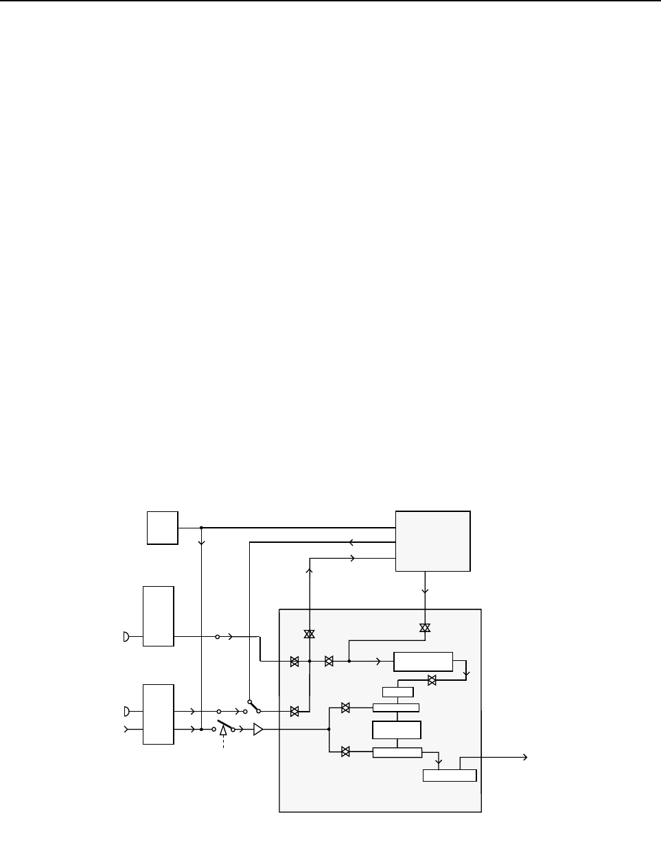
Controller Board Audio and Signalling Circuits 1-11
2.0 Controller Board Audio and Signalling Circuits
2.1 General - Audio Signalling Filter IC with Compander (ASFIC CMP)
The ASFIC CMP (U0221) used in the controller has 4 functions;
1) RX/TX audio shaping, i.e. filtering, amplification, attenuation
2) RX/TX signalling, PL/DPL/HST/MDC/MPT
3) Squelch detection
4) Microprocessor clock signal generation (see Microprocessor Clock Synthesizer Description).
The ASFIC CMP is programmable through the SPI BUS (U0221-20/21/22), normally receiving 19
bytes. This programming sets up various paths within the ASFIC CMP to route audio and/or
signalling signals through the appropriate filtering, gain and attenuator blocks. The ASFIC CMP also
has 6 General Control Bits GCB0-5 which are CMOS level outputs and used for NOISE BLANKER
(GCB0) in Low Band radios, EXTERNAL ALARM (GCB1) and DC POWER ON (GCB2) to switch
the voltage regulators (and the radio) on and off. GCB3 controls U0251 pin 11 to output either RX
FLAT AUDIO or RX FILTERED AUDIO on the accessory connector pin 11. GCB4 controls U0251
pin 10 to use either the external microphone input or the voice storage playback signal. GCB5 is
used to switch the audio PA on and off.
2.2 Transmit Audio Circuits
Refer to Figure 1-3 for reference for the following sections.
Figure 1-3 Transmit Audio Paths
MIC
IN
MOD IN TO
RF
SECTION
(SYNTHESIZER)
36
44
33
40
J0501
ACCESSORY
CONNECTOR
J0401
CONTROL HEAD
CONNECTOR
MIC
EXT MIC
FLAT TX
AUDIO
42
32
5
48
46
9
2
IN OUT
OPTION
BOARD
FILTERS AND
PREEMPHASIS
HS SUMMER
SPLATTER
FILTER
LS SUMMER
LIMITER
ATTENUATOR
VCO
ATN
TX RTN
TX SND
MIC
INT
AUX
TX
ASFIC_CMP
U0221
TP0221
TP0222
MIC
EXT
J0451 J0551
18
FLAT
TX RTN
EXPANSION BOARD
31 IN/OUT
39 OUT
FROM
µP Pin3
U0211-4

1-12 Controller Board Audio and Signalling Circuits
2.2.1 Mic/Data Input Path
The radio supports 2 distinct microphone paths known as internal (from controlhead) and external
mic (from accessory connector J0501-2) and an auxiliary path (FLAT TX AUDIO, from accessory
connector J0501-5). The microphones used for the radio require a DC biasing voltage provided by a
resistive network.
These two microphone audio input paths enter the ASFIC CMP at U0221-48 (external mic) and
U0221-46 (internal mic). Following the internal mic path; the microphone is plugged into the radio
controlhead and is connected to the controller board via J0401-9.
From here the signal is routed via R0409 and line INT MIC to R0205. R0201 and R0202 provide the
9.3VDC bias. Resistive divider R0205 / R0207 divide the input signal by 5.5 and provide input
protection for the CMOS amplifier input. R0202 and C0201 provide a 560 ohm AC path to ground
that sets the input impedance for the microphone and determines the gain based on the emitter
resistor in the microphone’s amplifier circuit.
C0204 serves as a DC blocking capacitor. The audio signal at U0221-46 (TP0221) should be
approximately 14mV for 1.5kHz or 3kHz of deviation with 12.5kHz or 25kHz channel spacing.
The external microphone signal enters the radio on accessory connector J0501 pin 2 and is routed
via line EXT MIC to R0206. R0203 and R0204 provide the 9.3VDC bias. Resistive divider R0206 /
R0208 divide the input signal by 5.5 and provide input protection for the CMOS amplifier input.
R0204 and C0202 provide a 560 ohm AC path to ground that sets the input impedance for the
microphone and determines the gain based on the emitter resistor in the microphone’s amplifier
circuit.
C0254 serves as a DC blocking capacitor. Multi switch U0251 controlled by ASFIC CMP port GCB4
selects either the external microphone input signal or the voice storage playback signal for entering
the ASFIC CMP at pin 48. The audio signal at U0221-48 (TP0222) should be approximately 14mV
for 1.5kHz or 3kHz of deviation with 12.5kHz or 25kHz channel spacing.
The FLAT TX AUDIO path is used for transmitting data signals and has therefore no limiter or filters
enabled inside the ASFIC CMP. When this path is enabled via CPS and DATA PTT is asserted, any
signal on this path is directly fed to the modulator. Signals applied to this path either via accessory
connector J0501, expansion board connector J0451 or option board connector J0551 must be
filtered and set to the correct level externally or on the option board in order not to exceed the
maximum specified transmit deviation and transmitted power in the adjacent channels. The
attenuator inside the ASFIC CMP changes the FM deviation of the data signal according to the
channel spacing of the active transmit channel.
The FLAT TX AUDIO signal from accessory connector J0501-5 is fed to the ASFIC CMP (U0221)
pin 42 through C0541 and line FLAT TX RTN, switch U0251 and buffer U0211-4. When the radio
switches from receive to transmit mode the µP opens switch U0251 for a short period to prevent that
any applied signal can cause a transmit frequency offset. Buffer U0211-4 sets the correct DC level
and ensures a short settle period when the radio is switched on. Inside the ASFIC CMP the signal is
routed directly to the attenuator, which sets the FM deviation according to the channel spacing of the
active transmit channel and emerges from the ASFIC CMP at U0221-40, at which point it is routed
to the RF section.

Controller Board Audio and Signalling Circuits 1-13
The ASFIC has an internal AGC that can control the gain in the mic audio path. The AGC can be
disabled / enabled by the µP. Another feature that can be enabled or disabled in the ASFIC is the
VOX. This circuit, along with the capacitor at U0221-7, provides a DC voltage that can allow the µP
to detect microphone audio. The ASFIC can also be programmed to route the microphone audio to
the speaker for public address operation.
2.2.2 PTT Sensing and TX Audio Processing
Microphone PTT coming from the controlhead is sent via SBEP bus to the microprocessor. An
external PTT can be generated by grounding pin 3 on the accessory connector if this input is
programmed for PTT by the CPS. When microphone PTT is sensed, the µP will always configure
the ASFIC CMP for the "internal" mic audio path, and external PTT will result in the external mic
audio path being selected.
Inside the ASFIC CMP, the mic audio is filtered to eliminate frequency components outside the 300-
3000Hz voice band, and pre-emphasized if pre-emphasis is enabled. The signal is then limited to
prevent the transmitter from over deviating. The limited mic audio is then routed through a summer,
which is used to add in signalling data, and then to a splatter filter to eliminate high frequency
spectral components that could be generated by the limiter. The audio is then routed to an
attenuator, which is tuned in the factory or the field to set the proper amount of FM deviation. The TX
audio emerges from the ASFIC CMP at U0221-40 MOD IN, at which point it is routed to the RF
section.
Dependent on the radio model, input pin 3 on the accessory connector can be programmed for
DATA PTT by the CPS. When DATA PTT is sensed, the µP will always configure the ASFIC CMP for
the flat TX audio path. Limiter and any filtering will be disabled. The signal is routed directly to the
attenuator, which sets the FM deviation according to the channel spacing of the active transmit
channel and emerges from the ASFIC CMP at U0221-40, at which point it is routed to the RF
section.
2.2.3 TX Secure Audio (optional)
The audio follows the normal transmit audio processing until it emerges from the ASFIC CMP TX
SND pin (U0221-44), which is fed to the Secure board residing at option connector J0551-33. The
Secure board contains circuitry to amplify, encrypt, and filter the audio. The encrypted signal is then
fed back from J0551-32 to the ASFIC CMP TX RTN input (U0221-36). The signal level at this pin
should be about 65mVrms. The signal is then routed through the TX path in the ASFIC CMP and
emerges at MOD IN pin 40.
2.2.4 Option Board Transmit Audio
The audio follows the normal transmit audio processing until it emerges from the ASFIC CMP TX
SND pin (U0221-44), which is fed to the option board residing at option connector J0551-33. The
option board contains circuitry to process the audio. The processed signal is then fed back from
J0551-32 to the ASFIC CMP TX RTN input (U0221-36). The signal level at this pin should be about
65mVrms. The signal is then routed through the TX path in the ASFIC CMP and emerges at MOD IN
pin 40.
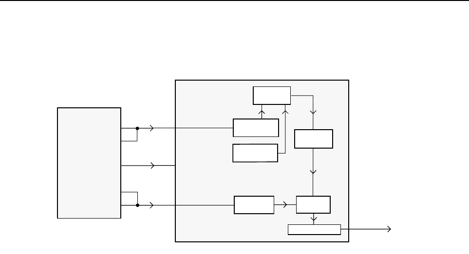
1-14 Controller Board Audio and Signalling Circuits
2.3 Transmit Signalling Circuits
Refer to 1-4 for reference for the following sections.
Figure 1-4 Transmit Signalling Paths
From a hardware point of view, there are 3 types of signalling:
1) Sub-audible data (PL / DPL / Connect Tone) that gets summed with transmit voice or signalling,
2) DTMF data for telephone communication in trunked and conventional systems, and
3) Audible signalling including Select 5, MPT-1327, MDC, High speed Trunking.
NOTE: All three types are supported by the hardware while the radio software determines which
signalling type is available.
2.3.1 Sub-audible Data (PL/DPL)
Sub-audible data implies signalling whose bandwidth is below 300Hz. PL and DPL waveforms are
used for conventional operation and connect tones for trunked voice channel operation. The
trunking connect tone is simply a PL tone at a higher deviation level than PL in a conventional
system. Although it is referred to as "sub-audible data", the actual frequency spectrum of these
waveforms may be as high as 250 Hz, which is audible to the human ear. However, the radio
receiver filters out any audio below 300Hz, so these tones are never heard in the actual system.
Only one type of sub-audible data can be generated by U0221 (ASFIC CMP) at any one time. The
process is as follows, using the SPI BUS, the µP programs the ASFIC CMP to set up the proper low-
speed data deviation and select the PL or DPL filters. The µP then generates a square wave which
strobes the ASFIC PL / DPL encode input LSIO U0221-18 at twelve times the desired data rate. For
example, for a PL frequency of 103Hz, the frequency of the square wave would be 1236Hz.
19
18
40
MOD IN
TO RF
SECTION
(SYNTHESIZER)
80
44 HIGH SPEED
CLOCK IN
(HSIO)
LOW SPEED
CLOCK IN
(LSIO)
ASFIC_CMP U0221
MICRO
CONTROLLER
U0101
HS
SUMMER
5-3-2 STATE
ENCODER
DTMF
ENCODER
SPLATTER
FILTER
PL
ENCODER LS
SUMMER
ATTENUATOR
85
82
SPI
BUS

Controller Board Audio and Signalling Circuits 1-15
This drives a tone generator inside U0221 which generates a staircase approximation to a PL sine
wave or DPL data pattern. This internal waveform is then low-pass filtered and summed with voice
or data. The resulting summed waveform then appears on U0221-40 (MOD IN), where it is sent to
the RF board as previously described for transmit audio. A trunking connect tone would be
generated in the same manner as a PL tone.
2.3.2 High Speed Data
High speed data refers to the 3600 baud data waveforms, known as Inbound Signalling Words
(ISWs) used in a trunking system for high speed communication between the central controller and
the radio. To generate an ISW, the µP first programs the ASFIC CMP (U0221) to the proper filter and
gain settings. It then begins strobing U0221-19 (HSIO) with a pulse when the data is supposed to
change states. U0221’s 5-3-2 State Encoder (which is in a 2-state mode) is then fed to the post-
limiter summer block and then the splatter filter. From that point it is routed through the modulation
attenuators and then out of the ASFIC CMP to the RF board. MPT 1327 and MDC are generated in
much the same way as Trunking ISW. However, in some cases these signals may also pass through
a data pre-emphasis block in the ASFIC CMP. Also these signalling schemes are based on sending
a combination of 1200 Hz and 1800 Hz tones only. Microphone audio is muted during High Speed
Data signalling.
2.3.3 Dual Tone Multiple Frequency (DTMF) Data
DTMF data is a dual tone waveform used during phone interconnect operation. It is the same type of
tones which are heard when using a "Touch Tone" telephone.
There are seven frequencies, with four in the low group (697, 770, 852, 941Hz) and three in the high
group (1209, 1336, 1477Hz).
The high-group tone is generated by the µP (U0101-44) strobing U0221-19 at six times the tone
frequency for tones less than 1440Hz or twice the frequency for tones greater than 1440Hz. The low
group tone is generated by the ASFIC CMP, controlled by the µP via SPI bus. Inside U0221 the low-
group and high-group tones are summed (with the amplitude of the high group tone being
approximately 2 dB greater than that of the low group tone) and then pre-emphasized before being
routed to the summer and splatter filter. The DTMF waveform then follows the same path as was
described for high-speed data.
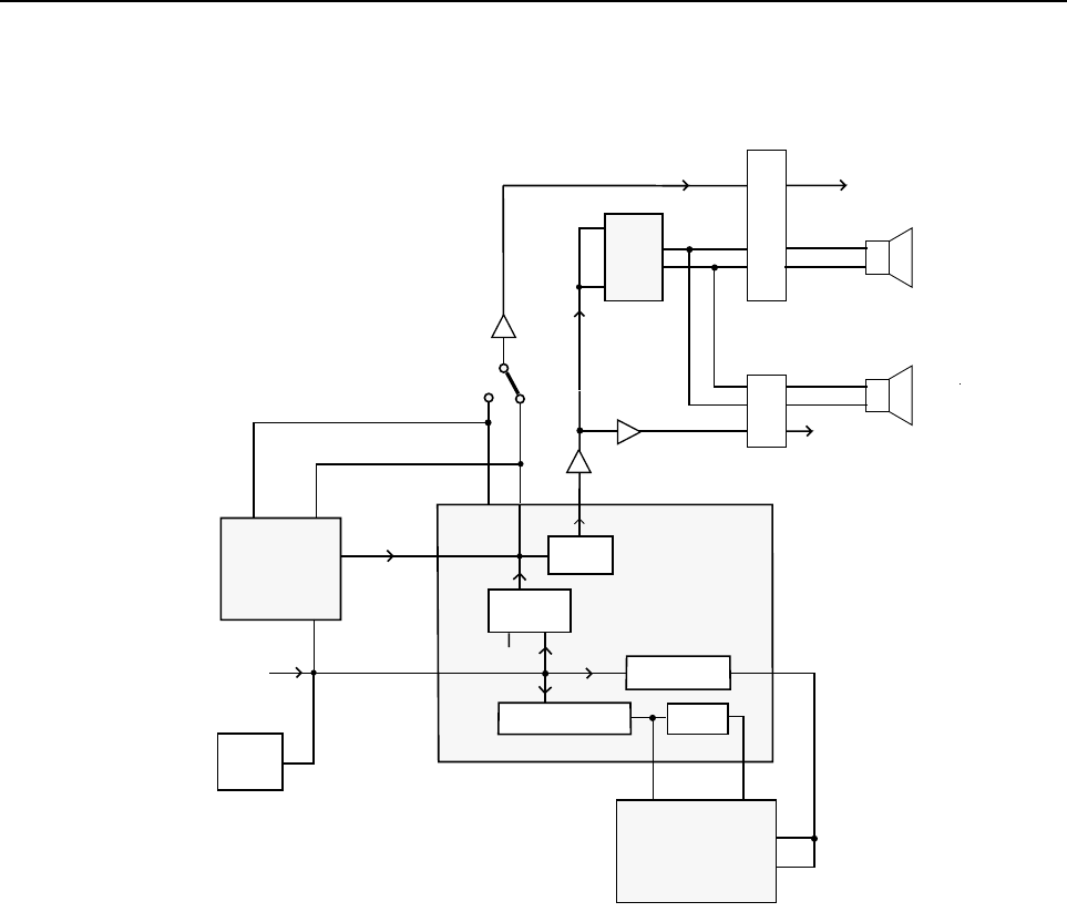
1-16 Controller Board Audio and Signalling Circuits
2.4 Receive Audio Circuits
Refer to 1-5 for reference for the following sections.
Figure 1-5 Receive Audio Paths
2.4.1 Squelch Detect
The radio’s RF circuits are constantly producing an output at the discriminator (IF IC). This signal
(DISC AUDIO) is routed to the ASFIC CMP’s squelch detect circuitry input DISC (U0221-2). All of
the squelch detect circuitry is contained within the ASFIC CMP. Therefore from a user’s point of
view, DISC AUDIO enters the ASFIC CMP, and the ASFIC CMP produces two CMOS logic outputs
based on the result. They are CH ACT (U0221-16) and SQ DET (U0221-17).
The squelch signal entering the ASFIC CMP is amplified, filtered, attenuated, and rectified. It is then
sent to a comparator to produce an active high signal on CH ACT. A squelch tail circuit is used to
produce SQ DET (U0221-17) from CH ACT. The state of CH ACT and SQ DET is high (logic 1)
when carrier is detected, otherwise low (logic 0).
CH ACT is routed to the µP pin 84 while SQ DET is routed to the µP pin 83.
FLT/FLAT RX AUDIO
J0501
11
16
1EXTERNAL
SPEAKER
INTERNAL
SPEAKER
ACCESSORY
CONNECTOR
CONTROLHEAD
CONNECTOR
HANDSET
AUDIO
7
2
3
J0401
INT
SPKR-
SPKR +
SPKR -
1
9
2
J0551
4110
INT
SPKR+
4
6
DISC
ASFIC_CMP
U0221
AUDIO
PA
U0271
IN
OPTION
BOARD
IN
OUT VOLUME
ATTEN.
FILTER AND
DEEMPHASIS
17
MICRO
CONTROLLER
U0101
80
FROM
RF
SECTION
(IF IC) LIMITER, RECTIFIER
FILTER, COMPARATOR
SQ DET
SQUELCH
CIRCUIT
16
PL FILTER
LIMITER
CH ACT
AUX RX
43
18
LS IO
U IO AUDIO
83
84
39
URX OUT
17
J0451
EXPANSION
BOARD
DISC
AUDIO
34
28
35
85
IN
7

Controller Board Audio and Signalling Circuits 1-17
SQ DET is used to determine all audio mute / unmute decisions except for Conventional Scan. In
this case CH ACT is a pre-indicator as it occurs slightly faster than SQ DET.
2.4.2 Audio Processing and Digital Volume Control
The receiver audio signal enters the controller section from the IF IC on DISC AUDIO. The signal is
DC coupled by R0228 and enters the ASFIC CMP via the DISC pin U0221-2.
Inside the ASFIC CMP, the signal goes through 2 paths in parallel, the audio path and the PL/DPL
path.
The audio path has a programmable amplifier, whose setting is based on the channel bandwidth
being received, then a LPF filter to remove any frequency components above 3000Hz and then an
HPF to strip off any sub-audible data below 300Hz. Next, the recovered audio passes through a de-
emphasis filter if it is enabled (to compensate for Pre-emphasis which is used to reduce the effects
of FM noise). The IC then passes the audio through the 8-bit programmable attenuator whose level
is set depending on the value of the volume control. Finally the filtered audio signal passes through
an output buffer within the ASFIC CMP. The audio signal exits the ASFIC CMP at pin AUDIO
(U0221-41).
The µP programs the attenuator, using the SPI BUS, based on the volume setting. The minimum /
maximum settings of the attenuator are set by codeplug parameters.
Since sub-audible signalling is summed with voice information on transmit, it must be separated
from the voice information before processing. Any sub-audible signalling enters the ASFIC CMP
from the IF IC at DISC U0221-2. Once inside it goes through the PL/DPL path. The signal first
passes through one of 2 low pass filters, either PL low pass filter or DPL/LST low pass filter. Either
signal is then filtered and goes through a limiter and exits the ASFIC CMP at LSIO (U0221-18). At
this point the signal will appear as a square wave version of the sub-audible signal which the radio
received. The microprocessor U0101-80 will decode the signal directly to determine if it is the tone /
code which is currently active on that mode.
2.4.3 Audio Amplification Speaker (+) Speaker (-)
The output of the ASFIC CMP’s digital volume pot, U0221-41 is routed through DC blocking
capacitor C0265 to a buffer formed by U0211-1. Resistors R0265 and R0268 set the correct input
level to the audio PA (U0271). This is necessary because the gain of the audio PA is 46 dB, and the
ASFIC CMP output is capable of overdriving the PA unless the maximum volume is limited. Resistor
R0267 and capacitor C0267 increase frequency components below 350Hz.
The audio then passes through R0269 and C0272 which provides AC coupling and low frequency
roll-off. C0273 provides high frequency roll-off as the audio signal is routed to pins 1 and 9 of the
audio power amplifier U0271.
The audio power amplifier has one inverted and one non-inverted output that produces the
differential audio output SPK+ / SPK- (U0271-4/6). The inputs for each of these amplifiers are pins 1
and 9 respectively; these inputs are both tied to the received audio. The audio PA’s DC biases are
not activated until the audio PA is enabled at pin 8.
The audio PA is enabled via the ASFIC CMP (U0221-38). When the base of Q0271 is low, the
transistor is off and U0271-8 is high, using pull up resistor R0273, and the Audio PA is ON. The
voltage at U0273-8 must be above 8.5VDC to properly enable the device.

1-18 Controller Board Audio and Signalling Circuits
If the voltage is between 3.3 and 6.4V, the device will be active but has its input (U0273-1/9) off. This
is a mute condition which is used to prevent an audio pop when the PA is enabled.
The SPK+ and SPK- outputs of the audio PA have a DC bias which varies proportionately with FLT
A+ (U0271-7). FLT A+ of 11V yields a DC offset of 5V, and FLT A+ of 17V yields a DC offset of 8.5V.
If either of these lines is shorted to ground, it is possible that the audio PA will be damaged. SPK+
and SPK- are routed to the accessory connector (J0501-16 and 1) and to the controlhead
(connector J0401-2 and 3).
2.4.4 Handset Audio
Certain hand held accessories have a speaker within them which require a different voltage level
than that provided by U0271. For those devices HANDSET AUDIO is available at controlhead
connector J0401-7.
The received audio from the output of the ASFIC CMP’s digital volume attenuator and buffered by
U0211-1 is also routed to U0211-3 pin 9 where it is amplified 20 dB; this is set by the 10k/100k
combination of R0261 and R0262. This signal is routed from the output of the op amp U0211-3 pin 8
to J0401-7. The controlhead sends this signal directly out to the microphone jack. The maximum
value of this output is 6.6Vp-p.
2.4.5 Filtered Audio and Flat Audio
The ASFIC CMP has an audio whose output at U0221-39 has been filtered and de-emphasized, but
has not gone through the digital volume attenuator. From ASFIC CMP U0221-39 the signal is routed
via R0251 through gate U0251-12 and AC coupled to U0211-2. The gate controlled by ASFIC CMP
port GCB3 (U0221-35) selects between the filtered audio signal from the ASFIC CMP pin 39
(URXOUT) or the unfiltered (flat) audio signal from the ASFIC CMP pin 10 (UIO). R0251 and R0253
determine the gain of op-amp U0211-2 for the filtered audio while R0252 and R0253 determine the
gain for the flat Audio. The output of U0253-7 is then routed to J0501-11 via DC blocking capacitor
C0542 and R0531. Note that any volume adjustment of the signal on this path must be done by the
accessory
2.4.6 RX Secure Audio (optional)
Discriminator audio, which is now encrypted audio, follows the normal receive audio processing until
it emerges from the ASFIC CMP UIO pin (U0221-10), which is fed to the Secure board residing at
option connector J0551-35. On the Secure board, the encrypted signal is converted back to normal
audio format, and then fed back through (J0551-34) to AUX RX of the ASFIC CMP (U0221-43).
From then on it follows a path identical to conventional receive audio, where it is filtered (0.3 - 3kHz)
and de-emphasized. The signal URX SND from the ASFIC CMP (U0221-39), also routed to option
connector J0551-28, is not used for the Secure board but for other option boards.
2.4.7 Option Board Receive Audio
Unfiltered audio from the ASFIC CMP pin UIO (U0221-10) enters the option board at connector
J0551-35. Filtered audio from the ASFIC CMP pin URXOUT (U0221-39) enters the option board at
connector J0551-28. On the option board, the signal may be processed, and then fed back through
J0551-34 to AUX RX of the ASFIC CMP (U0221-43). From then on it follows a path identical to
conventional receive audio, where it may be filtered (0.3 - 3kHz) and de-emphasized.
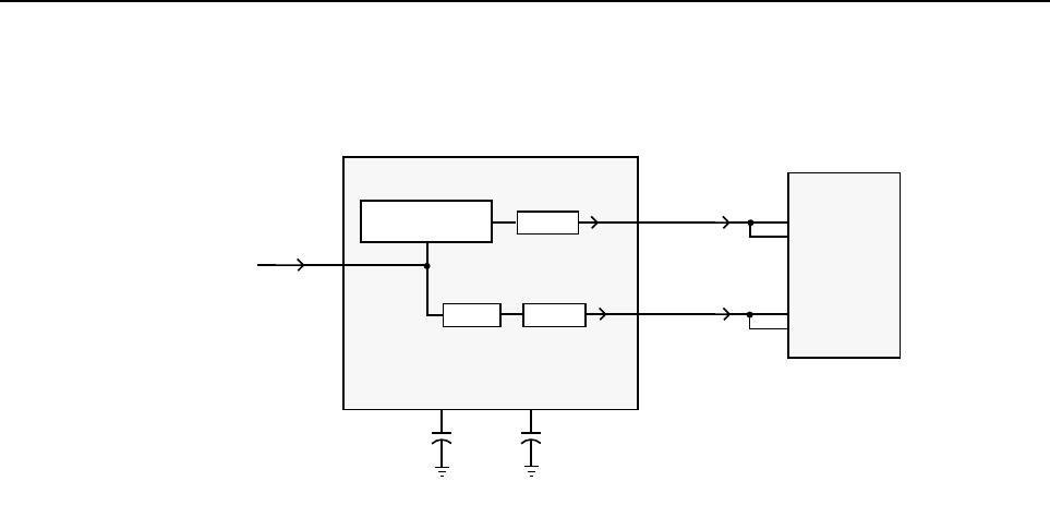
Controller Board Audio and Signalling Circuits 1-19
2.5 Receive Signalling Circuits
Refer to 1-6 for reference for the following sections.
Figure 1-6 Receive Signalling Paths
2.5.1 Sub-audible (PL/DPL) and High Speed Data Decoder
The ASFIC CMP (U0221) is used to filter and limit all received data. The data enters the ASFIC
CMP at input DISC (U0221-2). Inside U0221 the data is filtered according to data type (HS or LS),
then it is limited to a 0-5V digital level. The MDC and trunking high speed data appear at U0221-19,
where it connects to the µP U0101-82
The low speed limited data output (PL, DPL, and trunking LS) appears at U0221-18, where it
connects to the µP U0101-80.
The low speed data is read by the µP at twice the frequency of the sampling waveform; a latch
configuration in the ASFIC CMP stores one bit every clock cycle. The external capacitors C0236,
and C0244 set the low frequency pole for a zero crossings detector in the limiters for PL and HS
data. The hysterisis of these limiters is programmed based on the type of received data.
2.5.2 Alert Tone Circuits
When the software determines that it needs to give the operator an audible feedback (for a good key
press, or for a bad key press), or radio status (trunked system busy, phone call, circuit failures), it
sends an alert tone to the speaker. It does so by sending SPI BUS data to U0221 which sets up the
audio path to the speaker for alert tones. The alert tone itself can be generated in one of two ways:
internally by the ASFIC CMP, or externally using the µP and the ASFIC CMP.
The allowable internal alert tones are 304, 608, 911, and 1823Hz. In this case a code contained
within the SPI BUS load to the ASFIC CMP sets up the path and determines the tone frequency, and
at what volume level to generate the tone. (It does not have to be related to the voice volume
setting).
For external alert tones, the µP can generate any tone within the 100-3000Hz audio band. This is
accomplished by the µP generating a square wave which enters the ASFIC CMP at U0221-19.
Inside the ASFIC CMP this signal is routed to the alert tone generator.
DET AUDIO
DISCRIMINATOR AUDIO
FROM RF SECTION
(IF IC)
19
18
25
2
82
80
DISC
PLCAP2
LSIO
HSIO
DATA FILTER
AND DEEMPHASIS LIMITER
FILTER LIMITER
ASFIC_CMP
U0221
MICRO
CONTROLLER
U0101
85
44
8
PLCAP

1-20 Controller Board Audio and Signalling Circuits
The output of the generator is summed into the audio chain just after the RX audio de-emphasis
block. Inside U0221 the tone is amplified and filtered, then passed through the 8-bit digital volume
attenuator, which is typically loaded with a special value for alert tone audio. The tone exits at
U0221-41 and is routed to the audio PA like receive audio
2.6 Voice Storage (optional)
The Voice Storage (VS) option can be used to store audio signals coming from the receiver or from
the microphone. Any stored audio signal can be played back over the radio’s speaker or sent out via
the radio’s transmitter.
The Voice Storage option can by placed on the controller section or on an additional option board
which resides on option board connector J0551. Voice Storage IC U0301 provides all required
functionality and is powered from 3.3 volts regulator U0351 which,is powered from the regulated 5
volts. Dual shottky diode D0301 reduces the supply voltage for U0301 to 3 volts. The
microprocessor controls U0301 via SPI bus lines CLK (U0301-8), DATA (U0301-10) and MISO
(U0301-11). To transfer data, the µP first selects the U0301 via address decoder U0141, line VS CS
and U0301 pin 9. Then the µP sends data through line DATA and receives data through line MISO.
Pin 2 (RAC) of U0301 indicates the end of a message row by a low state for 12.5 ms and connects
to µP pin 52. A low at pin 5 (INT), which is connected to µP pin 55 indicates that the Voice Storage
IC requires service from the µP.
Audio, either from the radio’s receiver or from one of the microphone inputs, emerges the ASFIC
CMP (U0221) at pin 39, is buffered by op-amp U0341-1 and enters the Voice Storage IC U0301 at
pin 25. During playback, the stored audio emerges U0301 at pin 20. To transmit the audio signal it is
fed through resistive divider R0344 / R0345 and line VS MIC to input selector IC U0251. When this
path is selected by the µP via ASFIC CMP port GCB 4, the audio signal enters the ASFIC CMP at
pin 48 and is processed like normal transmit audio. To play the stored audio over the radio’s
speaker, the audio from U0301 pin 20 is buffered by op-amp U0341-2 and fed via switch U0342 and
line FLAT RX SND to ASFIC CMP pin 10 (UIO). In this case, this ASFIC CMP pin is programmed as
input and feeds the audio signal through the normal receiver audio path to the speaker or handset.
Switch U0342 is controlled by the µP via ASFIC CMP port GCB 4 and feeds the stored audio only to
the ASFIC CMP port UIO when it is programmed as input.
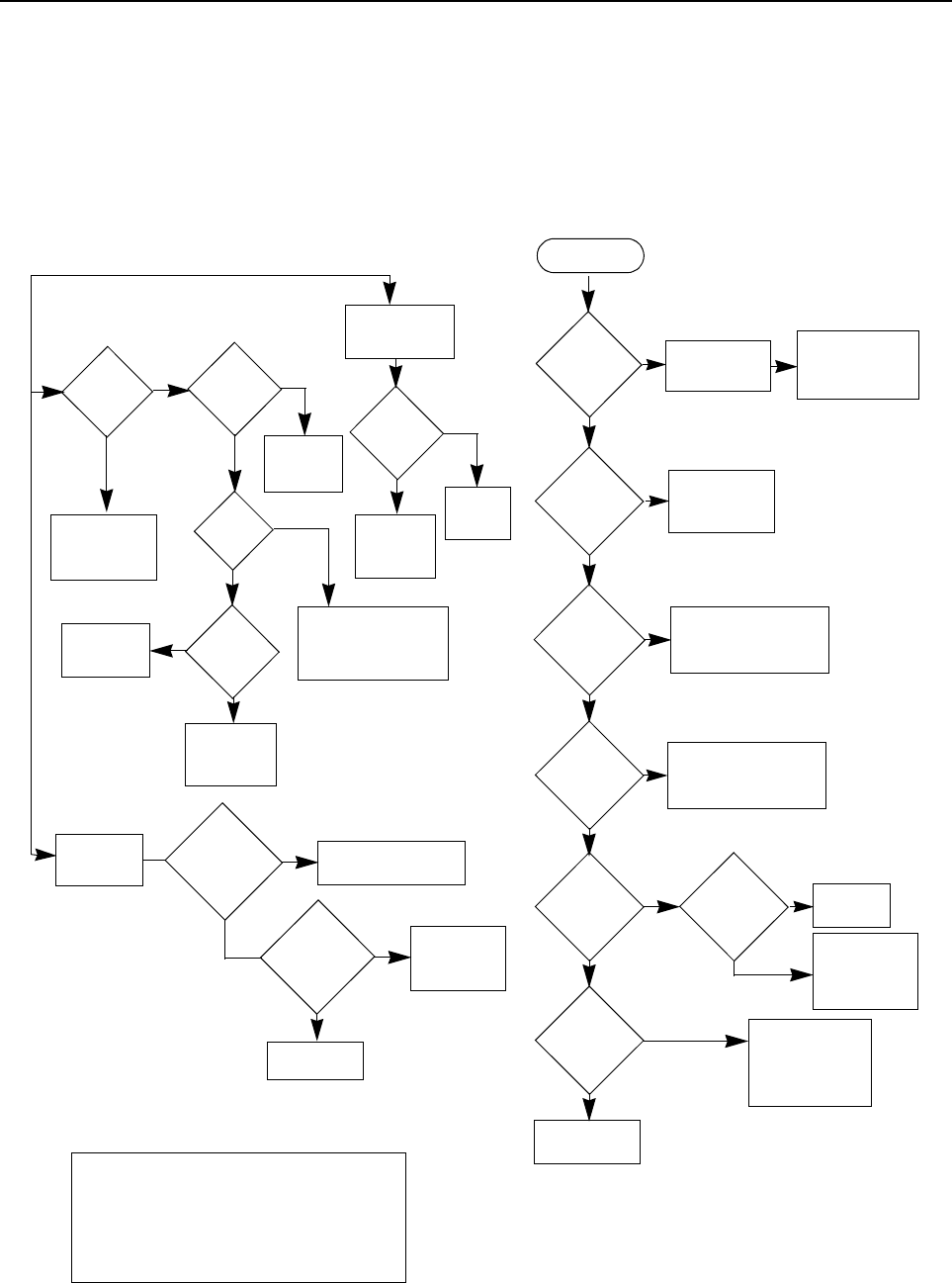
2-1
Section 2
TROUBLESHOOTING CHARTS
1.0 Controller Troubleshooting Chart
Power Up
Alert Tone
OK?
Speaker &
Control-
head OK?
U0101
EXTAL=
7.3728 MHz/
14.7456
MHz?
BUS+
activity when
volume knob
rotated?
MCU is OK
Not able to
program
RF Board ICs
Before replacing
MCU, check SPI
clock, SPI data,
and RF IC select
Replace
Speaker / Con-
trolhead
U0221 Pin 34 =
16.8 MHz?
Check
FGU
Reprogram the
correct data. &
Check ASFIC
and MCU
Check Control-
head and MCU
(U0101, U0121,
U0122, U0111)
Press PTT. No
RF Output
Power.
Red LED
lights up?
Check
Control-
head
Check
FGU &
Transmitter
Audio
at Pin 41
U0221?
Enable External PTT
with CPS
External PTT
enabled with
CPS?
Radio could
not PTT
externally
DC
at assigned
Acc. Con.
Pin DC
changes?
Check Components
between U0221 and
U0271
Check Con-
nection to µP
port
PTT
NO
YES
NO
YES YES
YES
YES
NO
NO
YES
NO
YES
NO
YES
NO
YES
EXT
PTT
RX
AUDIO
Check
Accessories
J0501
Audio at Pin
16 &
Pin 1
Check Spk.
Flex Connec-
tion & Control-
head
Audio
at Audio PA
(U0271)
input
Check
ASFIC
U0221
Check
Audio PA
(U0271)
Check
Receiver &
IF IC
Audio at
Pin 2
U0221?
NO
NO
NO
YES
YES
NO
YES
NO
Before troubleshooting the controller section
according to this chart please check the follow-
ing:
1. Check tuning and CPS settings
2. Check if Alert Tones are enabled
3. Check if Controlhead is OK
4. Check board visually
9.3V
DC at Pin 5
of U0641?
YES
NO
5V DC at
Pin OUT of
U0651?
YES
NO
Check U0641, Q0641,
Q0661, D0660 &
D0661
Check U0651, D0651,
D0621
Controller
Check

2-2 Controller Troubleshooting Chart
THIS PAGE INTENTIONALLY LEFT BLANK

3-1
Section 3
CONTROLLER SCHEMATICS / PARTS LISTS
1.0 Allocation of Schematics and Circuit Boards
1.1 Controller Circuits
This Chapter shows the Schematics and the Parts Lists for the Controller circuits.
1.2 Voice Storage Facility
The Voice Storage is fitted on all MPT radios GM338/GM398 as standard.
The schematics, component layout and parts list for these circuits are shown in this chapter.
The Voice Storage schematic is shown in Tables below.
.
.
Table 3-1 Controller T5 Diagrams and Parts Lists
Controller T5 used on PCB :
8486172B06 VHF, 1-25W
SCHEMATICS
Controller Overall
Supply Voltage
Audio
I/O
Microprocessor
Voice Storage (if fitted)
Page 3-3
Page 3-4
Page 3-5
Page 3-6
Page 3-7
Page 3-8
Parts List
Controller T5 Page 3-9
Table 3-2 Controller T7 Diagrams and Parts Lists
Controller T7 used on PCB :
T7 on 8486172B07 VHF, 1-25W
T7 on 8485670Z02 UHF B1, 1-25W
SCHEMATICS
Controller Overall
Supply Voltage
Audio
I/O
Microprocessor
Voice Storage (if fitted)
Page 3-12
Page 3-13
Page 3-14
Page 3-15
Page 3-17
Page 3-19
Parts List
Controller T7 Page 3-20

3-2 Allocation of Schematics and Circuit Boards
Table 3-3 Controller T9 Diagrams and Parts Lists
Controller T9 used on PCB :
T9 on 8485670Z03 UHF B1, 1-25W
SCHEMATICS
Controller Overall
Supply Voltage
Audio
I/O
Microprocessor
Voice Storage (if fitted)
Page 3-12
Page 3-13
Page 3-14
Page 3-16
Page 3-18
Page 3-19
Parts List
Controller T9 Page 3-23
Controller T5 / Schematic Diagrams 3-3
2.0 Controller T5 / Schematic Diagrams
T5 0102727B49 T5 0102727B50 T5 0102727B51 MPT
T5 0102727B52 SELV/MDC T5 0102727B54 SEL5/MDC
T5 0102727B53 MPT
T5 0102727B55
T3 0102727B39 T3 0102727B40 MPT
P7 0102727B13 P7 0102727B14
P7 0102727B17 MPT
P7 0102727B18 SEL5/MDC
P6 0102727B07
P6 0102727B04 SELV/MDC
P6 0102727B03 MPT
P1 0102726B33
P1 0102726B32
P6 0102727B02
P4 0102726B88
T2 0102727B25 SELV/MDC
P4 0102726B87
P6 0102727B05 MPT
P6 0102727B06 SEL5/MDC
P6 0102727B01
P5 0102726B97 SEL5/MDC P5 0102726B96
P5 0102726B95 MPT
T2 0102727B26 MPT
T2 0102727B28
P3 0102726B68 P2 0102726B65
P1 0102726B30
P7 0102727B19
P5 0102726B94
P5 0102726B93
T3 0102727B41 SELV/MDC T3 0102727B43 SEL5/MDC
P4 0102726B86
P4 0102726B85
P4 0102726B84
P3 0102726B35
P2 0102726B35
T2 0102727B22 T2 0102727B23
T2 0102727B24 MPT
T2 0102727B27 SEL5/MDC
T3 0102727B38 T3 0102727B42 MPT
IN_5V_RF_REG
ON_OFF_CONTROL
PASUPVLTG
RESET
VSTBY
T3 0102727B44
P2 0102726B64
P2 0102726B66 P3 0102726B71
P3 0102726B70
P3 0102726B69
P1 0102726B35
P2 0102726B67
P1 0102726B31
P7 0102727B16 SELV/MDC
P7 0102727B15 MPT
T4 0102727B50
T4 0102727B49 T4 0102727B51 MPT
T4 0102727B52 SELV/MDC T4 0102727B54 SEL5/MDC
T4 0102727B53 MPT
T4 0102727B55
P5 0102726B92
TX_AUD_SND
URX_SND
VS_AUDSEL
VS_GAINSEL VS_INT
VS_MIC
VS_RAC
SUPPLY_VOLTAGE
5VD
9V3
BATTERY_VOLTAGE
DC_POWER_ON
EMERGENCY_CONTROL
EXT_SWB+
FLT_A+
IGNITION_CONTROL
INT_SWB+
ON_OFF_CONTROL
OPT_PTT
PASUPVLTG
PA_PWR_SET
RDY
RESET
RSSI
RX_ADAPT
RX_AUD_RTN
RX_FLAT_FILTERED_AUDIO
SCI_TX
SPI(0:10)
SPKR+
SPKR-
TEMPSENSE
TX_AUD_RTN
GP3_IN_ACC6
GP4_IN_OUT_ACC8
GP5_IN_ACC9
GP6_IN_ACC10
GP7_IN_OUT_ACC12
GP8_IN_OUT_ACC14
HANDSET_AUDIO
IGNITION_CONTROL
INT_MIC
INT_SWB+
IN_5V_RF_REG
LOCKMODIN
MOSBIAS_2
MOSBIAS_3
NOISE_BLNKR
5V_RF
9V3 BOOT_CNTRL
BUS+
CH_ACT
CNTLVLTG
DISCAUDIO
EMERGENCY_CONTROL
EXP_BD_REQ
EXT_MIC
EXT_SWB+
FLAT_RX_SND
FLAT_TX_RTN
FLT_A+
GP1_IN_ACC3
GP2_OUT_ACC4
TEMPSENSE
VSTBY
VS_GAINSEL
VS_INT
VS_RAC
VOICE_STORAGE
5VD
FLAT_RX_SND
RX_AUD_RTN
SPI(0:10)
VS_AUDSEL
VS_INT VS_MIC
VS_RAC
IO
16_8MHZ
5VD
GP3_IN_ACC6
GP4_IN_OUT_ACC8
GP5_IN_ACC9
GP6_IN_ACC10
GP7_IN_OUT_ACC12
GP8_IN_OUT_ACC14
GPIO(0:13)
LOCK
ON_OFF_CONTROL
OPT_PTT
RDY
RESET
RSSI
RX_ADAPT
SCI_TX
SPI(0:10)
TX_AUD_RTN
TX_AUD_SND
URX_SND
VS_AUDSEL
VS_MIC
CONTROLLER
5VD
BATTERY_VOLTAGE
BOOT_CNTRL
BUS+
CNTLR_AUDIO(0:7)
CNTLVLTG
EXT_BD_REQ
FLT_A+
GP1_IN_ACC3
GP2_OUT_ACC4
FLAT_TX_RTN
FLT_A+
GPIO(0:13)
HANDSET_AUDIO
INT_MIC
INT_SWB+
MODIN
MOSBIAS_2
MOSBIAS_3
NOISE_BLNKR
PA_PWR_SET
RX_AUD_RTN
RX_FLAT_FILTERED_AUDIO
SPI(0:10)
SPKR+
SPKR-
EXT_SWB+EXT_SWB+
PASUPVLTGPASUPVLTG FLT_A+FLT_A+
AUDIO
16_8MHZ
5VD
5V_RF
9V3
CH_ACT
CNTLR_AUDIO(0:7)
DC_POWER_ON
DISCAUDIO
EXT_MIC
FLAT_RX_SND
OPT_PTT OPT_PTT
CH_ACT CH_ACT
URX_SND URX_SND
VS_GAINSEL VS_GAINSEL
MOSBIAS_3MOSBIAS_3
INT_SWB+ INT_SWB+
EXT_MIC EXT_MIC
IN_5V_RF_REGIN_5V_RF_REG
SCI_TX SCI_TX
VS_MICVS_MIC
5VD5VD 9V39V3
HANDSET_AUDIOHANDSET_AUDIO SPKR+SPKR+ SPKR-SPKR-
EMERGENCY_CONTROLEMERGENCY_CONTROL IGNITION_CONTROLIGNITION_CONTROL
DC_POWER_ONDC_POWER_ON ON_OFF_CONTROLON_OFF_CONTROL
BATTERY_VOLTAGEBATTERY_VOLTAGE
VSTBYVSTBY
RDY RDY
PA_PWR_SET
MOSBIAS_2MOSBIAS_2
MODINMODIN
TX_AUD_SNDTX_AUD_SND
FLAT_RX_SNDFLAT_RX_SND
16_8MHZ16_8MHZ
TX_AUD_RTNTX_AUD_RTN FLAT_TX_RTNFLAT_TX_RTN
RX_AUD_RTNRX_AUD_RTN DISCAUDIODISCAUDIO
INT_MICINT_MIC
5V_RF5V_RF
RX_FLAT_FILTERED_AUDIORX_FLAT_FILTERED_AUDIO
GP1GP1
EXP_BD_REQ EXP_BD_REQ
BOOT_CNTRLBOOT_CNTRL
VS_AUDSEL VS_AUDSEL
TEMPSENSETEMPSENSE CNTLVLTGCNTLVLTG
VS_RACVS_RAC VS_INTVS_INT
RSSIRSSI
LOCKLOCK
RX_ADAPTRX_ADAPT
NOISE_BLNKRNOISE_BLNKR PA_PWR_SET
CNTRL_AUDIO(0:7)CNTRL_AUDIO(0:7)
GPIO(0:13)GPIO(0:13)
SPI(0:10) SPI(0:10)
BUS+BUS+
RESETRESET
GP8GP8
GP7GP7
GP6GP6
GP5GP5
GP4GP4
GP3GP3
GP2GP2
ZWG0130510-O
Controller T5 Schematic Diagram - Controller Overall
3-4 Controller T5 / Schematic Diagrams
470pF
C0661
47uF
C0601
R0642
7.5K 33uF
C0641
470pF C0644
0.1uF
C0681
J0601-2
C0612
0.1uF
R0641
J0601-1
10K
R0662
C0662
.01uF
150K
D0660
R0652
10
24K
Q0641
R0621
GND
3
INPUT
2RESET_1
C0654
U0653
MC33464N-45ATR
10uF
U0651
MC78M05
GND
2
IN
13
OUT
TP0661
C0663
0.1uF
R0643
1.2K
0.1uF
C0655
D0651
Q0661
R0611
56K
NU
5.6V
VR0671
Q0681
68K
R0682
18K
R0681
E0631
57R01
22uF
C0611
10
R0651
33uF
C0652
0.1uF
NU
C0651
0.1uF
C0645
24V
VR0601
470pF
C0621 C0622
47uF
NU
6
GND2
2ON_OFF
VIN
4VOUT 5
LM2941
U0641
ADJ 1
3
GND1
4.7K
R0612
D0661
Q0662
R0671
R0672
30K
3
GND1 6
GND2
ON_OFF
2
4VIN 5
VOUT
10K
U0611
LM2941
1
ADJ
0.1uF
C0671
J0601-3
Q0663
D0621
C0603
10uF
R0661
VR0621
1K
6
NC3 7
NC4
NC5 8
1
RESET
5.6V
MC33064
U0652
4
GND
2INPUT
3NC1
5NC2
9V3
FLT_A+
IN_5V_RF_REG
RESET
5VD
NU
DC_POWER_ON
IGNITION_CONTROL
EMERGENCY_CONTROL
BATTERY_VOLTAGE
ON_OFF_CONTROL
EXT_SWB+
INT_SWB+
PASUPVLTG
VSTBY
ZWG0130506-O
0V (13,8VDC when radio off)
6VDC
5VDC
5VDC (0VDC during reset)
5VDC
ZWG0130506-O
Controller T5 Schematic Diagram - Supply Voltage
Controller T5 / Schematic Diagrams 3-5
CH_ACT
SQ_DET
LSIO
F1200
SYN
CLK
HSIO
VOX
GP2_OUT
CSX
DATA
R0251
47K
24K
R0222
C0222
0.1uF
C0226
0.1uF
R0269
470
9
NU
R0220
8.2K
R0225
8.2K
R0224
8.2K NU
0
C0243
100pF
R0242
14
4
11
NU
0.1uF
C0242
MC3403
U0211-4
13
12
10uF
C0202
R0203
100
0.1uF
C0265
D0201 5
3
1
2
4
0.1uF
NU
C0254
C0234
0.1uF
C0272
0.1uF
3300pF
C0273
100K
R0253
C0253
100pF
1uF
NU
7
C0252
M_SS
8
NINV
1OUT1 4
OUT2 6
3RR
VCC
7
TDA1519C
GND1
25
GND2
INV
9
C0225
0.1uF
U0271
0.1uF
NU
C0274
C0232
0.1uF
1MEG
R0227
100
NU
R0229
C0244
0.1uF
.022uF
C0212
C0235
10uF
NU
1MEG
R0226
5
1uF
C0228
10K
R0275 Q0271
R0228
0
C0221
0.1uF
0.1uF
C0223
56K
R0252
C0261
0.1uF
R0212
7.5K
R0211
7.5K
.033uF MC3403
U0211-3
9
10 8
4
11
C0236
8
10uF
C0201
MC3403
U0211-2
6
57
4
11
11
47uF
C0275
R0273
24K
4
R0206
C0205
10K
NU
2200pF
R0266
NU
C0266
0.1uF
NU
24K C0267
.01uF
1000pF
C0277 E0272
57R01
57R01
E0271
0.1uF
C0245
C0241
0.1uF
R0207
TP0221
1
4
11
2.2K
MC3403
U0211-1
2
3
0.1uF
C0227
10K
NU C0224
NU
R0274
100pF
NU
0.22uF
C0233
2.2uF
C0237 47K
NU
10K
R0267
R0265
R0268
24K
45
VDDRC
27
VDDSYN
7VOX
1
36
TXRTN
44
TXSND
10 UIO
39
URXOUT
1VDDA
32
VDDCP
33
VDDD
11 VDDDAC
46
MICINT
40
MOD
26
NC
8PLCAP
25
PLCAP2
17 SQDET
9SQIN 28
SYN
31
GNDD 30
GNDD0
47
GNDRC
23 GNDSYN
19 HSIO
LCAP
24
18 LSIO
48
MICEXT
29
F1200
15 GCB0
14 GCB1
13 GCB2
35
GCB3
GCB4 37
38
GCB5
3GNDA
21 CLK
34
CLK168
20 CSX
6DACG
5DACR
DACU
4
22 DATA
2DISC
12 AGCCAP
41
AUDIO
AUXRX 43
42
AUXTX
16 CHACT
6
U0221
63A53
2.2K
R0208
0.1uF
C0211
R0204 NU
560
R0202
560
10K
C0262
82pF
R0261
100
R0201
R0205
10K
R0223
30K
TP0222
1uF
C0231
15K
R0276
C0276
7
1000pF
2
C0251
0.1uF
3
NU
.01uF
0.1uF
C0255
C0271
R0241
47K
.01uF
C0246
13 X1
15
Y
2Y0
1Y1
4
Z
5Z0
Z1
3
10
B
9
C
6
EN
8
GND
16
VCC
7
VEE
14
X
12 X0
U0251 MC14053B
A11
C0203
2200pF
0.1uF
NU
C0204
R0221
24K
R0262
100K
5VD
5V_RF
5V_RF5V_RF
TX_AUD_RTN
5V_RF
TX_AUD_SND
5V_RF
DISCAUDIO
5V_RF
9V3
9V3
9V3
MODIN
INT_SWB+
CH_ACT
VAG
9V3 9V3
9V3
VS_MIC
MOSBIAS_3
16_8MHZ
VAG
EXT_MIC
5V_RF
5V_RF
5VD
SPKR-
RX_AUD_RTN
INT_MIC
URX_SND
FLAT_RX_SND
DC_POWER_ON
FLT_A+
5VD
SPKR+
5VD
PA_PWR_SET
MOSBIAS_2
FLAT_TX_RTN
NOISE_BLNKR
VS_AUDSEL
SPI(0:10)
GPIO(0:13)
CNTLR_AUDIO(0:7)
VAG
VAG
HANDSET_AUDIO
RX_FLAT_FILTERED_AUDIO
80mV RMS
80mV RMS
5VDC (0VDC during radio off) 13VDC unmuted
5VDC muted
300mV RMS
200mV RMS
145mV RMS @25kHz
72mV RMS @12.5kHz 5VDC RX Filtered
Audio (0V DC Flat)
630mV RX Filtered
330mV Flat
0 VDC
ZWG0130507-O
Controller T5 Schematic Diagram - Audio
3-6 Controller T5 / Schematic Diagrams
NC
RST*
7
8
14
INT_EXT_Vdd
NC
7
9
A0
EXT_BD_REQ
EXT_BD_CS
GP4_IN_OUT
SPI_CLK
SPI_MOSI
SPI_MISO
RESET
FLT_A+
DISCAUDIO
CH_ACT
26
FLAT_TX_RTN
6
CSX
29
12-PIN CONNECTOR
13
FAST_SQ
DISCAUDIO
PCB
23
21
GPIO
DATA
EXP1_CS
VS_AUDSEL
17
GROUND
SrD_Rtn
5
DIG_IN_5 WITH WAKEUP (EMERGENCY)
13
37
DIG_IN_OUT_7
2
EXP_BD_PTT
DATA
36
8
EXP2_CS
BOOT_CNTRL
Rx_Aud_Snd
ON
VS_INT
RX_ADAPT
VS_RAC
6
1
20
SCI_TX
INT_MIC
DIG_IN_3
Tx_Aud_Snd
8
NC
10
11
Key_Row
Key_Intrp
DIG_IN_OUT_4
9V3
VS_MIC
5VD
GM300
SPEAKER-
CLK
30
13
NC
NC
NC
6
NC
DB6
ACCESSORY
16
DB3
19
DB7
FLAT_TX_AUDIO
Opt_Bd_En
NC
13
10
33
OPT_CS
22
18
40-PIN CONNECTOR
DB5
12
SCK_Snd
35
NC
NC
DATA
VS_GAINSEL
Gnd
11
DB2
NC
EXT_BD_PTT
GND
5VD
EXP_BD_PTT
GND
CLK
MISO
GND
16
SPEAKER+
14
3
2
1
WARIS
TO/FROM RF
7
24
CS*
3
1
NC
NC
DIG_OUT2 (EXTERNAL_ALARM)
NC
HANSET_AUDIO
ON_OFF_CONTROL
20-PIN CONNECTOR
J0501
J0451
DIG_IN_6 WITH WAKEUP (IGNITION)
FLAT/FILTERED_RX_AUDIO
19
9
VS_CS
7
4
11
9
R/W*
39
38
9
4
GROUND
DB111
7
17
12
18
RSSI
NC
J0552
NC
NC
GROUND
GROUND
CLK
DIG_IN1
3
EXP1_CS
5
9V3
5VD
EXT_BD_PTT
EXT_MIC_AUDIO
4
VS_CS
DB4
CLK
1
2
SrD_Snd
EXT_BD_PTT
27
19
Det_Aud_Snd
12
Rx_Aud_Rtn
NC
1
MISO
2
5
6
7
8
LED_EN
NC
8
18
17
20
NC
15
14
16
RDY
OPT_PTT
34
INTERNAL OPTION BOARD
25
32
31
SPEAKER+
BUS+
4
12
18-PIN CONNECTOR
NC
GND
1
2
3
5
15 17
15
9
J0551
28
FLT_A+
6
SPEAKER-
DIG_IN_OUT_8
SWB+
20 16
Flat_Tx_Rtn
NC
3
4
EXP_BD_REQ
EXT_BD_PTT
EXT_BD_PTT
5
15
16
17
18
4
1
2
3
9
10
11
12
13
14
DB0
DATA
11
CONTROL HEAD
NC
10
OPT_CS
NC
Tx_Aud_Rtn
PTT
18
Vddd
2
GROUND
10 12 14
REAR VIEW
15
NC
BUS+
5
6
7
8
9
10
11
12
13
14
6
40
18-PIN CONNECTOR
RS232 INTERFACE BOARD
Key_Col
TO/FROM RF
8
3
OFF_BATT_DATA_OUT
15
16
17
18
J0401
5
4
EXPANSION BOARD
10
Rdy/Req DISCAUDIO_CNTLR_1
0.1uF
LOCK_CNTLR_1
C0591
J0451-10
C0509
470pF
0
R0412
470pF
C0514
VR0505
20V
NU
J0451-3
9V3
C0554
0.1uF
J0401-6
C0421
82pF
INT_SWB_CNTLR_1
470pF
C0445
CLK
INT_SWB
J0451-8
RSSI_CNTLR_1
470pF
C0497
R0531
DATA
560
470pF
C0491
J0551-13
470pF
C0483
470pF
J0401-1
C0446
470pF
C0478
0
R0482
0
R0481
NU
10
R0468
470pF
C0443
C0477
2
J0401-9
470pF
C0447
470pF
3
J0551-22
16_8MHZ
J0551-1
J0451-9
20V
VR0503
J0401-8
CSX
47K
R0529
C0495
J0551-41
470pF
C0493
4
J0401-11
470pF
J0451-5
470pF
C0431
VR0501
20V
J0551-14
VR0510
33V
J0551-4
TEMPSENSE
9
J0451-12
470pF
C0506
5V_CNTLR_1
J0451-1
C0592
0.1uF
J0551-21
J0551-24
C0430
C0593 0.1uF
470pF
PASUPVLTG_CNTRL_1
RESET_CNTLR_1
NU
7
L0482
390nH
J0551-18
100K
R0511
CSX_CNTLR_1J0552-3
J0552-8
8
J0552-10
J0552-9
J0552-11
J0401-10
J0551-40
IN_5V_RF_REG
IN_5V_RF_REG_CNTLR_1
82pF
C0472
C0484
DISCAUDIO
RESET
470pF
14V
VR0541
R0407
10
470pF
J0551-5
C0496
TEMPSENSE_CNTLR_1
C0510
470pF
470pF
C0505
470pF
J0551-20
C0429
1
R0538
220
J0451-6
C0485
470pF
R0408
J0451-2
100
C0488
J0551-23
PASUPVLTG
470pF
C0513
470pF
J0551-26
1TP0530
J0552-16
DATA_CNTLR_1
J0552-18
J0552-17
J0552-19
R0467
MOSBIAS_2_CNTLR_1
J0401-2
10
470pF
NU
C0441
J0551-15
J0551-19
1K
R0535
C0511 470pF
C0512
470pF
CLK
J0551-42
J0551-25
J0451-13
470pF
C0515
J0552-12
J0552-14
J0552-13
470pF
J0552-15
MOSBIAS_2
C0508
J0401-12
0
R0530
VR0509
33V
9V3_CNTLR_1
NU
8
9
470pF
C0558
TP0497
470pF
C0426
.01uF
C0501
J0451-16
15K
R0512
470pF
C0487
4.7K
R0510
470pF
100K
R0525
C0492
CLK_CNTLR_2
RSSI
MOSBIAS_3_CNTLR_1
8
J0451-18
J0451-7
C0422
J0401-5
470pF
J0551-31
J0451-15
R0537 220
J0551-38
82pF
C0428
DATA_CNTLR_2
C0503
J0552-1
470pF
C0502
470pF
1
TP0481
C0504
470pF
VR0504
33V
J0551-9
C0474
J0551-27
470pF
CNTLVLTG
J0551-28 5V
C0471
82pF
J0551-10
C0575
470pF
NU
CSX_CNTLR_2
470pF
C0470
R0541
MOSBIAS_3
27K
J0551-2
J0551-16
J0551-35
J0551-30
L0481
NU
J0451-14
390nH
NOISE_BLNKR
LOCK
C0448
470pF
J0552-6
CSX
470pF
C0482
J0552-7
J0551-8
MODIN
PA_PWR_SET_1_CNTLR_1
C0490
470pF
C0427
470pF
J0551-36
C0517
82pF 470pF
C0518
J0451-17
10
J0551-3
470pF
C0486
470pF
NU
DATA
C0499
J0551-29
C0559
470pF
C0423
470pF
47uF
C0542
R0533 0
PA_PWR_SET
J0551-37
C0494
470pF
J0552-20
J0552-4
J0552-2
470pF
NU
J0552-5
NU
C0442
0
R0410
R0539
4.7K
J0551-39
J0551-33
TP0492
470pF
C0576
NU
J0551-34
R0409
10
NOISE_BLNKR_CNTLR_1
VR0537
5.6V
82pF
C0473
J0451-4
24K
R0591
J0551-17
470pF
CNTLVLTG_CNTLR_1
C0449
J0401-3
J0551-11
47K
R0542
NU
470pF
C0560
NU
0.47uF
R0441
C0541
9
0
J0551-6
.01uF
C0516
MODIN_CNTLR_1
16_8MHZ_CNTLR_1
J0551-32 CLK_CNTLR_1
J0551-7
470pF
C0476
J0401-4
J0401-7
R0592 10
220
R0401
J0551-12
J0451-11
CH_ACT
GP1_IN_ACC3
SPI_DATA
SPI_MISO
SPI_CLK
EXP_BD_REQ
5VD
SPKR-
SPKR+
ON_OFF_CONTROL
EXP_BD_REQ
GP1_IN_ACC3
SPI_CLK
SPI_DATA
SPKR-
EXT_MIC
GP1_IN_ACC3
GP2_OUT_ACC4
GP5_IN_ACC9
GP6_IN_ACC10
GP7_IN_OUT_ACC12
GP8_IN_OUT_ACC14
SPKR+
GP3_IN_ACC6
GP4_IN_OUT_ACC8
EXP2_CS
EXP1_CS
GP4_IN_OUT_ACC8
OPT_CS
RDY
OPT_PTT
EXP2_CS
9V3
SPI_MISO
DISCAUDIO
MODIN
FLAT_TX_RTN
CH_ACT
5VD
9V3
5VD
SPI_MISO
RESET
FLT_A+
DISCAUDIO
GP4_IN_OUT_ACC8
EXP1_CS
RDY
RDY
OPT_PTTOPT_PTT
OPT_PTT
INT_MIC INT_MIC
INT_MIC SPKR+SPKR+
DISCAUDIO DISCAUDIO
HANDSET_AUDIOHANDSET_AUDIO
HANDSET_AUDIO
RSSI RSSI
BOOT_CNTRL
5VD
IN_5V_RF_REG
BUS+
GP1_IN_ACC3
GP1_IN_ACC3 GP1_IN_ACC3
INT_SWB+
FLAT_TX_RTN
5VD
GP4_IN_OUT_ACC8
EXP1_CS
EXP_BD_REQEXP_BD_REQ
EXP_BD_REQ
GP1_IN_ACC3
CH_ACT CH_ACT
CH_ACT
DISCAUDIO
FLT_A+
SCI_TX
RX_FLAT_FILTERED_AUDIO
EMERGENCY_CONTROL
FLT_A+
RSSI
EXT_SWB+
RDY
16_8MHZ
5V_RF
NOISE_BLNKR
MOSBIAS_2
PA_PWR_SETEXP1_CS
9V3
FLAT_TX_RTN FLAT_TX_RTN
GP4_IN_OUT_ACC8 GP4_IN_OUT_ACC8
DISCAUDIO
SPI(0:10)
RX_ADAPT
MOSBIAS_3
VS_MIC VS_MIC
FLT_A+
BUS+ BUS+
RESETRESET
ON_OFF_CONTROL ON_OFF_CONTROL
FLAT_TX_RTN
5VD5VD FLT_A+FLT_A+
SPI_DATA
SPI_CLK
SPI_MISO
VS_CS
OPT_CS
RESET
EXT_MICEXT_MIC
SPKR-SPKR-
RESET
PASUPVLTG
BUS+
TEMPSENSE
CNTLVLTG
RSSI
LOCK
OPT_CS
SPI_DATA
TX_AUD_RTN
VS_CS
VS_MIC
SPI_CLK
FLAT_RX_SND
RX_AUD_RTN
URX_SND
TX_AUD_SND
VS_INT
5VD
VS_AUDSEL
VS_GAINSEL
SPI_MISO
VS_RAC
IGNITION_CONTROL
FLT_A+
J0501-3
J0501-10
J0501-8
J0501-7
J0501-6
J0501-15
J0501-5
J0501-16
J0501-18
J0501-13
J0501-1
J0501-11
J0501-12
J0501-2
J0501-20
J0501-19
J0501-9
J0501-14
J0501-4
J0501-17
ZWG0130508-O
Controller T5 Schematic Diagram - I/O
Controller T5 / Schematic Diagrams 3-7
HSIO
GP4_IN
ON_OFF_SENSE
GP8_OUT
CHACT
HC138_A1
HSIO
GP7_IN
CLK
GP5_IN
32kx8bit
OPT_CS
LVZIF_CS
16Kx8bit
GP4_OUT
GP7_OUT
(EXT_BD_PTT & DATA_PTT)
EE_CS
HC138_A0
GP3_IN
GP8_IN
512kx8bit
RAM
GP6_IN
GP6_IN
MISO
EXP2_CS
GP4_OUT
GP7_OUT
HC138_A2
GP1_IN
GP8_OUT
SQ_DET
HC138_A1
H/W-Version & Memory size
FLASH ROM
SYN
HC138_A2
GP2_OUT
LSIO
MICROPROCESSOR
DATA
MISO
F1200
GP4_IN
EEPROM
DATA
EE_CS
VS_CS
EXP1_CS
GP1_IN
CLK
CSX
GP5_IN
GP4_OUT
GP7_OUT
GP3_IN
GP8_IN
PE6
VOX
LSIO
GP7_IN
HC138_A0
REF_CS
VR0151
15
9
7
5.6V
Q0183
14
TP0104
15
14
4
5
0
2
Q0171
R0121
100K
47K
Q0177
10
R0186
R0176
0
6
1
13
0
30K
2
NC
3
NC1
4OUT 1
IN
9
XTAL
Y0131
38.40KHz
0
R0112
R0182
47K
NU
4.7K
4
3
R0181
5
8
16
R0178
47K
R0131
10MEG
NU
C0111
100pF
4.7K
R0102
100pF
NU
C0103
4
C0131
22pF
D0101
3.9K
14
13
16
5
R0117
7
2
5
C0123
100pF
C0112
NU
5
0.1uF
2
0
3
Q0151
IO1 22
IO2 23
IO3 25
IO4 26
IO5 27
IO6 28
IO7 29
8
VCC
A7
13
A8
3
A9
2
EN_CE
30
EN_OE
32
EN_WE
7
24
GND
21
IO0
A16
10
A17
6
A18
9
A2
18
A3
17
A4
16
15 A5
14 A6
A0
20
A1
19
A10
31
A11
1
A12
12
4A13
A14
5
11 A15
3
U0121
AT49F040
6
6
13
4
5
5
7
R0101
10K
TP0101
Q0110
47K
3
18
NU
R0107
7
R0177
4.7K
10K
NU
R0110
9
R0105
4
2
7
10
9
C0105
100pF
4.7K
NU
1
10
R0171
1
8
8
4
11
R0108
2.2K
6
1
17
3
10
1
4
5
1
7
TP0151
C0121
0.1uF
0.1uF
8
C0122
18
3
2
TP0103
R0184
47K
10K
R0174
C0132
22pF
0
Q0185
SI 5
SO
2
VCC
8
VSS
4
WP 3
U0111
X25128-2.7
CS 1
HOLD 7
SCK 6
.01uF
Q0173
C0151
13
C0106
1
12
0
NU
100pF
D0151
6
5
12
10
TP0102
4.7K
R0185
6
8
2
6
12 IO2
13 IO3
15 IO4
16 IO5
17 IO6
18 IO7
19 IO8
28
VCC
3
A725
A824
A9
20
EN_CS 22
EN_OE 27
EN_WE
GND
14
11 IO1
2
A1226
A13 1
A14
8
A2 7
A3 6
A4
A5 5
4
A6
63A21 U0122
10
A0 9
A1
A1021
23
A11
11
6
Q0181
8
6
6
9
VRL
13 VSS
40 VSSL
87 VSSR
XFC 93
48
XIRQ
91
XTAL
77
PJ6 78
PJ7
94
RESET
12
VDD
39
VDDL
88
VDDR
92
VDDSYN
69
VRH
68
PI6
49 PI7
71
PJ0_CSGP3 72
PJ1_CSGP4 73
PJ2 74
PJ3 75
PJ4 76
PJ5
41 PH6_CSGP2
38 PH7_CSPROG
56 PI0
55 PI1
54 PI2
53 PI3
52 PI4
51 PI5
50
PG6_AS
4
PG7_R_W
47 PH0_PW1
46 PH1_PW2
45 PH2_PW3
44 PH3_PW4
43 PH4_CSIO
42 PH5_CSGP1
22 PF7_ADDR7
29 PFO_ADDR0
6PG0_XA13
16 PG1_XA14
20 PG2_XA15
19 PG3_XA16
17 PG4_XA17
18 PG5_XA18
5
61
PE7_AN7 60
28 PF1_ADDR1
27 PF2_ADDR2
26 PF3_ADDR3
25 PF4_ADDR4
24 PF5_ADDR5
23 PF6_ADDR6
2
PD5_SS
PD6_LVIN 3
PE0_AN0 67
PE1_AN1 66
PE2_AN2 65
PE3_AN3 64
PE4_AN4 63
PE5_AN5 62
PE6_AN6
PC5_DATA5
36 PC6_DATA6
37 PC7_DATA7
97
PD0_RXD
98
PD1_TXD
99
PD2_MISO
100
PD3_MOSI
1
PD4_SCK
8PB6_ADDR14
7PB7_ADDR15
14 PBO_ADDR8
30 PC0_DATA0
31 PC1_DATA1
32 PC2_DATA2
33 PC3_DATA3
34 PC4_DATA4
35
PA5_OC3_OC1
85
PA6_OC2_OC1
86
PA7_PA1_OC1
10 PB1_ADDR9
11 PB2_ADDR10
9PB3_ADDR11
21 PB4_ADDR12
15 PB5_ADDR13
LVOUT 95
58
MODA_LIR 57
MODB_VSTBY
79
PA0_IC3
80
PA1_IC2
81
PA2_IC1
82
PA3_IC4_OC5_OC1
83
PA4_OC4_OC1
84
59
AVDD
70 AVSS
89
ECLK
90
EXTAL
96
IRQ
U0101
MC68HC11FL0
NU
100pF
C0102 100pF
C0104
0
4
10
NU
R0179
47K
0
7
4
NU
R0116
C0141
0.1uF
7
24K
R0152
330K
R0132
Y2
13
Y3
12
Y4
11
Y5
10
Y6
9
Y7
7
12
3
A2 3
EN_CS1 6
EN_CS2 4
EN_CS3 5
GND
8
VCC
16
Y0
15
Y1
14
U0141
MC74HC138A
A0 1
A1 2
12
6
2
R017210K
10K
7
R0175
R0115
10K
R0111
0
7
10
1
C0101
100pF
1000pF
90
C0107
10K
R0114
10K
R0104
5
11
R0170
10K
2
R0183
1
11
12
3
1
4.7K
10K
R0113
4
8
3
0
24K
R0151
2
3
0
13
4.7K
17
9
D0179
3
R0173
RAM_CS
BUS+
CNTLVLTG
5VD
SCI_TX
GP1_IN_ACC3
GP6_IN_ACC10
GP2_OUT_ACC4
R_W
FLASH_CE
FLASH_OE
5VD
IRQ
IRQ
ADDR_BUS(0:18)
DATA_BUS(0:7)
2
FROM_U0101_47
VS_RAC
5VD
VS_INT
GP4_IN_OUT_ACC8
5VD
BOOT_CNTRL
GP3_IN_ACC6
5VD
ON_OFF_CONTROL
R_W
5VD
5VD
5VD
RESET
RESET
5VD
OPT_PTT
5VD
GP5_IN_ACC9
5VD
SPI(0:10) SPI(0:10) SPI(0:10) SPI(0:10) SPI(0:10)
GPIO(0:13)
GPIO(0:13)
CNTLR_AUDIO(0:7) CNTLR_AUDIO(0:7)CNTLR_AUDIO(0:7)
CNTLR_AUDIO(0:7)
FROM_U0101_47
FROM_U0101_46
FROM_U0101_46
5VD
5VD
FLT_A+
TEMPSENSE
RAM_CS
5VD
VS_GAINSEL
EXT_BD_REQ
RSSI
5VD
RX_ADAPT
5VD
5VD5VD
FLT_A+ FLT_A+
FLASH_OE
NC_XTAL
ECLK
NC
NC
LOCK
RDY
ON_OFF_CONTROL
GP7_IN_OUT_ACC12
GP8_IN_OUT_ACC14
5VD
5VD
5VD
5VD
FLASH_CE
R_W
VSTBY
5VD
BATTERY_VOLTAGE 100K
Used in
standard
only
R0106
0
Used in
prime
only
5VDC (0VDC during On/Off pressed
and during head request)
5VDC (0VDC during boot mode)
ZWG0130509-A
Controller T5 Schematic Diagram - Microprocessor
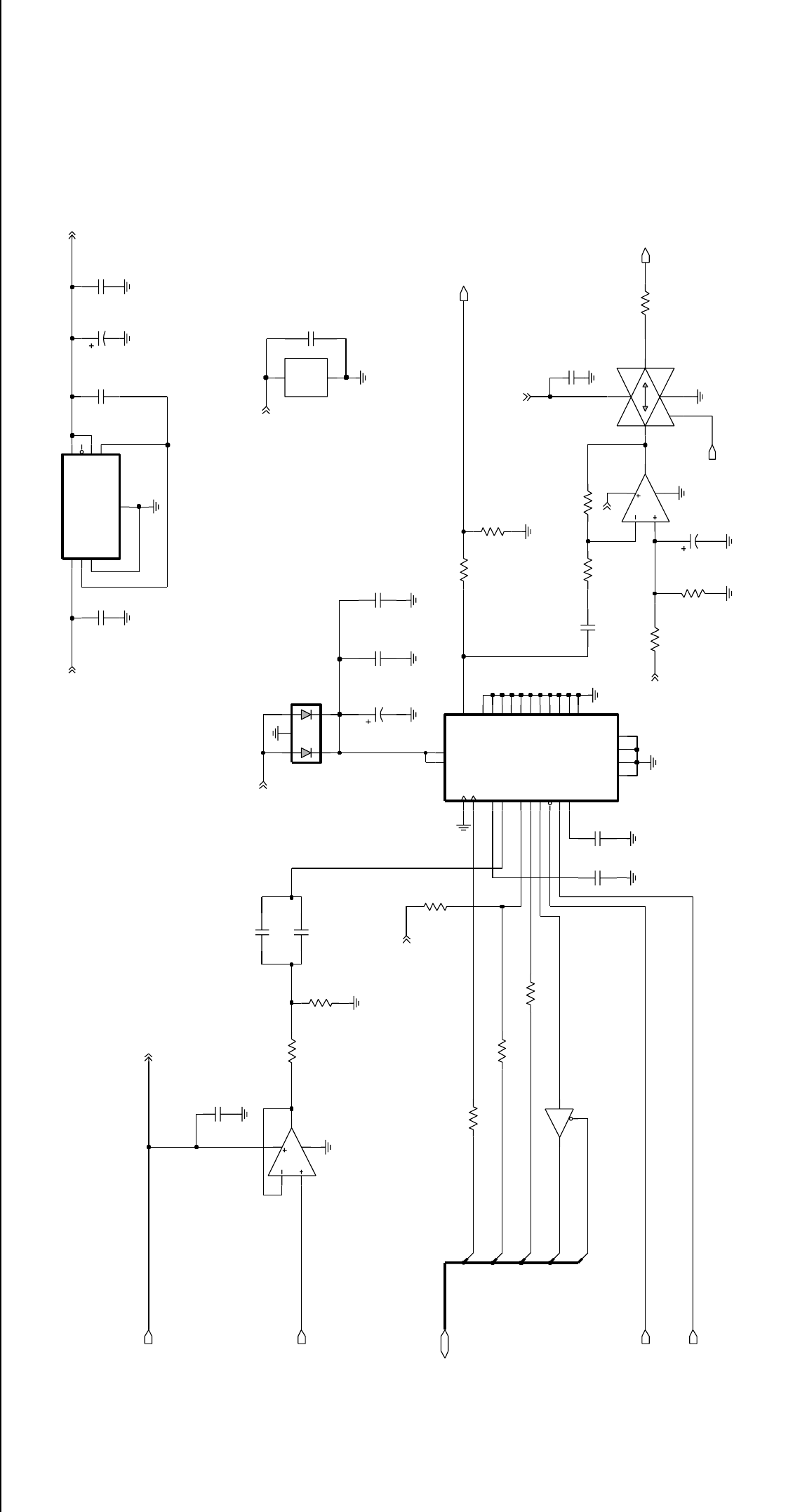
3-8 Controller T5 / Schematic Diagrams
5109152M01
VS_CS
MISO
VS_CS
DATA
CLK
0
R0343
0.1uF
10
INPUT 1
OUTPUT
2
SENSE
3SHUTDOWN 6
VTAP
C0302
LP2951ACMM-3.3
U0351
5
ERROR
7FEEDBACK
4
GND
8
0.1uF
0.1uF
2
C0351
C0305
R0347
47K
C0341
1uF
R0323
18K
C0304
0.1uF
100pF
C0303
5.1K
1
VSSA1
17
VSSA2
18
VSSA3
12
VSSD
6XCLK
R0345
19
NC7 21
NC8 23
NC9
2RAC
8SCLK
9SS
26
VCCA
7
VCCD
3
NC1
27
NC10 28
NC11
4
NC2 13
NC3 14
NC4 15
NC5 16
NC6
AMCAP
22
24 ANA_NEG
25 ANA_POS
20
AUDOUT
INT
5
11 MISO
10 MOSI
U0301
U0342
CNTL
4
12
VDD
5
VSS
3
U0341-1
LM2904
2
31
8
4
TC4S66F
R0346
47K
0.1uF
C0344
10K
6
57
8
4
R0331
LM2904
U0341-2
5
3
1
2
4
R0342
1.8K
D0301
R0324
18K
8
C0342
0.1uF
C0343
0.1uF
R0344
56K
10K
1uF
C0301
R0333
C0325
9
0.1uF
C0353
33uF
C0352
.022uF
150K
R0335
0.1uF
C0354
U0331-1
74AHCT1G125
A
2
OE 1
Y
4
PWR_GND
U0331-2
GND
3
VCC
5
2
0.1uF
C0331
R0332
10K
0.1uF
C0324
RX_AUD_RTN
5VD
FLAT_RX_SND
3V3
SPI(0:10)
R0341
10K
VS_MIC
VS_RAC
3V3
3V3
5VD
5VD5VD
VS_INT
5VD
5VD
VS_AUDSEL
5VD
ZWG0130505-O
Controller T5 Schematic Diagram - Voice Storage
ZWG0130505-O
Controller T5 / Schematic Diagrams 3-9
2.1 Controller T5 Parts List
Circuit
Ref Motorola
Part No Description
C0101 2113740F51 100pF 5% 50V
C0107 2113741F25 1nF 50V
C0112 2113743E20 100nF 16V
C0121 2113743E20 100nF 16V
C0122 2113743E20 100nF 16V
C0131 2113740F35 22pF 5% 50V
C0132 2113740F35 22pF 5% 50V
C0141 2113743E20 100nF 16V
C0151 2113741F49 10nF 50V
C0201 2311049A57 TANT CP 10uF 10% 16V
C0202 2311049A57 TANT CP 10uF 10% 16V
C0204 2113743E20 100nF 16V
C0212 2311049A57 TANT CP 10uF 10% 16V
C0221 2113743E20 100nF 16V
C0222 2113743E20 100nF 16V
C0223 2113743E20 100nF 16V
C0224 2113740F51 100pF 5% 50V NP0
C0225 2113743E20 100nF 16V
C0226 2113743E20 100nF 16V
C0228 2311049A07 TANT CP 1uF 10% 16V
C0231 2113743B29 1 UF 10% 16V
C0232 2113743E20 100nF 16V
C0234 2113743E20 100nF 16V
C0235 2113743E07 22nF 16V
C0236 2113743E10 .033UF 10%
C0241 2113743E20 100nF 16V
C0243 2113740F51 100pF 5% 50V
C0244 2113743E20 100nF 16V
C0245 2113743E20 100nF 16V
C0246 2113741F49 10nF 50V
C0252 2311049A07 TANT CP 1uF 10%
C0254 2113743E20 100nF 16V
C0255 2113743E20 100nF 16V
C0261 2113743E20 100nF 16V
C0262 2113740F49 82pF 5% 50V
C0265 2113743E20 100nF 16V
C0267 2113741F49 10nF 50V
C0271 2113741F49 10nF 50V
C0272 2113743E20 100nF 16V
C0273 2113741F37 3.3nF 50V
C0275 2311049A99 TANT CP 47uF 20% 10V
C0276 2113741F25 1nF 50V
C0277 2113741F25 1nF 50V
C0301
Used in 2311049A07
GM398 only 1uF 10% 16V
C0302
Used in 2113743E20
GM398 only 100nF 16V
C0303
Used in 2113740F51
GM398 only 100pF 5% 50V
C0304
Used in 2113743E20
GM398 only 100nF 16V
C0305
Used in 2113743E20
GM398 only 100nF 16V
C0324
Used in 2113743E20
GM398 only 100nF 16V
C0331
Used in 2113743E20
GM398 only 100nF 16V
C0341
Used in 2311049A07
GM398 only TANT CP 1uF 10% 16V
C0342
Used in 2113743E20
GM398 only 100nF 16V
C0343
Used in 2113743E20
GM398 only 100nF 16V
C0344
Used in 2113743E20
GM398 only 100nF 16V
C0351
Used in 2113743E20
GM398 only 100nF 16V
Circuit
Ref Motorola
Part No Description
C0352
Used in 2113743E07
GM398 only 22nF 16V
C0353
Used in 2311049A97
GM398 only TANT CHIP 33 UF 16
C0354
Used in 2113743E20
GM398 only 100nF 16V
C0421 2113743N48 82.0 PF 5%
C0422 2113741F17 470pF 50V
C0423 2113741F17 470pF 50V
C0426 2113743L09 470 PF 10%
C0427 2113743L09 470 PF 10%
C0428 2113743N48 82.0 PF 5%
C0429 2113743L09 470 PF 10%
C0430 2113741F17 470pF 50V
C0431 2113741F17 470pF 50V
C0445 2113743L09 470 PF 10%
C0446 2113743L09 470 PF 10%
C0447 2113743L09 470 PF 10%
C0448 2113743L09 470 PF 10%
C0449 2113743L09 470 PF 10%
C0470 2113743L09 470 PF 10%
C0471 2113743N48 82.0 PF 5%
C0472 2113743N48 82.0 PF 5%
C0473 2113743N48 82.0 PF 5%
C0474 2113743L09 470 PF 10%
C0476 2113743L09 470 PF 10%
C0477 2113743L09 470 PF 10%
C0478 2113743L09 470 PF 10%
C0482 2113743L09 470 PF 10%
C0483 2113743L09 470 PF 10%
C0484 2113741F17 470 pF 50V
C0485 2113743L09 470 PF 10%
C0486 2113743L09 470 PF 10%
Circuit
Ref Motorola
Part No Description
C0487 2113743L09 470 PF 10%
C0488 2113743L09 470 PF 10%
C0490 2113743L09 470 PF 10%
C0491 2113743L09 470 PF 10%
C0492 2113743L09 470 PF 10%
C0493 2113743L09 470 PF 10%
C0494 2113743L09 470 PF 10%
C0495 2113743L09 470 PF 10%
C0496 2113743L09 470 PF 10%
C0497 2113743L09 470 PF 10%
C0499 2113743L09 470 PF 10%
C0501 2113741F49 10nF 50V
C0502 2113743L09 470 PF 10%
C0503 2113743L09 470 PF 10%
C0504 2113743L09 470 PF 10%
C0505 2113743L09 470 PF 10%
C0506 2113743L09 470 PF 10%
C0508 2113743L09 470 PF 10%
C0509 2113743L09 470 PF 10%
C0510 2113741F17 470 pF 50V
C0511 2113743L09 470 PF 10%
C0512 2113743L09 470 PF 10%
C0513 2113741F17 470 pF 50V
C0514 2113743L09 470 PF 10%
C0515 2113743L09 470 PF 10%
C0516 2113741F49 10nF 50V
C0517 2113743N48 82.0 PF 5%
C0518 2113743L09 470 PF 10%
C0541 2311049A05 TANT CP 470nF 10% 25V
C0542 2311049A99 TANT CP 47uF 20% 10V
C0591 2113743E20 100nF 16V
C0592 2113743E20 100nF 16V
Circuit
Ref Motorola
Part No Description
3-10 Controller T5 / Schematic Diagrams
C0593 2113741B69 100nF 50V
C0601 2113741F17 470pF 50V
C0603 2380090M24 LYT 10uF 50V 20%
C0611 2311049C06 TANT CP 22uF 20% 35V
C0612 2113743E20 100nF 16V
C0622 2311049A99 TANT CP 47uF 20% 10V
C0641 2113741F17 470pF 50V
C0644 2311049A97 TANT CHIP 33 UF 16
C0645 2113743E20 100nF 16V
C0652 2311049A97 TANT CHIP 33 UF 16
C0654 2311049A57 TANT CP 10uF 10% 16V
C0655 2113743E20 100nF 16V
C0661 2311049C05 TANT CP 47uF 10% 16V
C0662 2113741F49 10nF 50V
C0663 2113743E20 100nF 16V
C0671 2113743E20 100nF 16V
C0681 2113743E20 100nF 16V
D0101 4880236E05 CHIP SCHOTTKY
D0151 4813833C02 DUAL SOT MMBD6100
D0179 4813833C02 DUAL SOT MMBD6100
D0301
Used in 4802245J47
GM398 only SCHOTTKY BARRIER
(RB471E)
D0621 4813833C02 DUAL SOT MMBD6100
D0651 4813833C02 DUAL SOT MMBD6100
D0660 4813833C02 DUAL SOT MMBD6100
D0661 4813833C02 DUAL SOT MMBD6100
E0271 2484657R01 Ferrite Bead
E0272 2484657R01 Ferrite Bead
E0631 2484657R01 Ferrite Bead
J0401 0902636Y02 CONN FLEX 12 PIN
J0451 0902636Y01 CONN FLEX SIDE ENTRY
J0501 0986105B01 CONN SMD 20 PIN
Circuit
Ref Motorola
Part No Description
J0551 0905505Y04 CONN ZIF HORIZONTAL
J0552 0905505Y03 CONN ZIF 18PIN
J0601 0986165B01 DC PWR CONN
Q0110 4880048M01 NPN DIG 47k/47k
Q0151 4880048M01 NPN DIG 47k/47k
Q0171 4880048M01 NPN DIG 47k/47k
Q0173 4880052M01 NPN DRLNGTN MXTA
Q0177 4880048M01 NPN DIG 47k/47k
Q0181 4880048M01 NPN DIG 47k/47k
Q0183 4880048M01 NPN DIG 47k/47k
Q0185 4880048M01 NPN DIG 47k/47k
Q0271 4813824A10 NPN 40V .2A
Q0641 4880048M01 NPN DIG 47k/47k
Q0661 4805921T02 DUAL ROHM FMC2 RH
Q0662 4813824A10 NPN 40V .2A B=50-150
Q0663 4880048M01 NPN DIG 47k/47k
Q0681 4880052M01 NPN DRLNGTN MXTA
R0101 0662057A73 10k 1/16W 5%
R0102 0662057A65 4k7 1/16W 5%
R0104 0662057A73 10k 1/16W 5%
R0105
Used in 0662057A97
GM338 only 100k 1/16W
R0106
Used in 0662057B47
GM398 only 0 1/16W
R0108 0662057A57 2k2 1/16W 5%
R0111 0662057B47 0 1/16W
R0113 0662057A73 10k 1/16W 5%
R0114 0662057A73 10k 1/16W 5%
R0115 0662057A73 10k 1/16W 5%
R0117 0662057A63 3k9 1/16W 5%
R0121 0662057A97 100k 1/16W
R0131 0662057B46 10.0 MEG OHMS 5%
R0132 0662057B10 330k 1/16W 5%
Circuit
Ref Motorola
Part No Description
R0151 0662057A82 24K 1/16W 5%
R0152 0662057A82 24K 1/16W 5%
R0170 0662057A73 10k 1/16W 5%
R0171 0662057A65 4k7 1/16W 5%
R0172 0662057A73 10k 1/16W 5%
R0173 0662057A65 4k7 1/16W 5%
R0174 0662057A73 10k 1/16W 5%
R0175 0662057A73 10k 1/16W 5%
R0176 0662057A84 30k 1/16W 5%
R0177 0662057A65 4k7 1/16W 5%
R0178 0662057A89 47k 1/16W 5%
R0179 0662057A89 47k 1/16W 5%
R0181 0662057A65 4k7 1/16W 5%
R0182 0662057A89 47k 1/16W 5%
R0183 0662057A65 4k7 1/16W 5%
R0184 0662057A89 47k 1/16W 5%
R0185 0662057A65 4k7 1/16W 5%
R0186 0662057A89 47k 1/16W 5%
R0201 0662057A25 100 1/16W 5%
R0202 0662057A43 560 1/16W 5%
R0203 0662057A25 100 1/16W 5%
R0204 0662057A43 560 1/16W 5%
R0205 0662057A73 10k 1/16W 5%
R0206 0662057A73 10k 1/16W 5%
R0207 0662057A57 2k2 1/16W 5%
R0208 0662057A57 2k2 1/16W 5%
R0211 0660076E70 FILM 7500
R0212 0660076E70 FILM 7500
R0221 0662057A82 24K 1/16W 5%
R0222 0662057A82 24K 1/16W 5%
R0223 0662057A84 30k 1/16W 5%
R0224 0662057A71 8k2 1/16W 5%
Circuit
Ref Motorola
Part No Description
R0228 0662057B47 0 1/16W
R0229 0662057A25 100 1/16W 5%
R0241 0662057A89 47k 1/16W 5%
R0242 0662057B47 0 1/16W
R0251 0662057A89 47k 1/16W 5%
R0252 0662057A91 56K 1/16W 5%
R0253 0662057A97 100k 1/16W
R0261 0662057A73 10k 1/16W 5%
R0262 0662057A97 100k 1/16W
R0265 0662057A82 24K 1/16W 5%
R0267 0662057A89 47k 1/16W 5%
R0268 0662057A73 10k 1/16W 5%
R0269 0662057A41 470 1/16W 5%
R0273 0662057A82 24K 1/16W 5%
R0275 0662057A73 10k 1/16W 5%
R0276 0662057A77 15k 1/16W 5%
R0323
Used in 0662057A79
GM398 only 18k 1/16W 5%
R0324
Used in 0662057A79
GM398 only 18k 1/16W 5%
R0331
Used in 0662057A73
GM398 only 10k 1/16W 5%
R0332
Used in 0662057A73
GM398 only 10k 1/16W 5%
R0333
Used in 0662057A73
GM398 only 10k 1/16W 5%
R0335
Used in 0662057B02
GM398 only 150k 1/16W
R0341
Used in 0662057A73
GM398 only 10k 1/16W 5%
R0342
Used in 0662057A55
GM398 only 1k8 1/16W 5%
R0343
Used in 0662057B47
GM398 only 0 1/16W
R0344
Used in 0662057A91
GM398 only 56K 1/16W 5%
Circuit
Ref Motorola
Part No Description
Controller T5 / Schematic Diagrams 3-11
* Motorola Depot Servicing only
Reference designators with an asterisk indicate
components which are not fieldreplaceable
because they need to be calibrated with
specialized factory equipment after installation.
Radios in which these parts have been replaced in
the field will be off frequency at temperature
extremes.
R0345
Used in 0662057A66
GM398 only 5k1 1/16W 5%
R0346
Used in 0662057A89
GM398 only 47k 1/16W 5%
R0347
Used in 0662057A89
GM398 only 47k 1/16W 5%
R0401 0662057A33 220 1/16W 5%
R0407 0662057M26 10 5%
R0408 0662057A25 100 1/16W 5%
R0409 0662057M26 10 5%
R0412 0662057B47 0 1/16W
R0441 0662057B47 0 1/16W
R0467 0662057M26 10 5%
R0468 0662057M26 10 5%
R0481 0662057B47 0 1/16W
R0482 0662057B47 0 1/16W
R0510 0662057A65 4k7 1/16W 5%
R0511 0662057A97 100k 1/16W
R0512 0662057A77 15k 1/16W 5%
R0525 0662057A97 100k 1/16W
R0529 0662057A89 47k 1/16W 5%
R0530 0662057B47 0 1/16W
R0531 0662057A43 560 1/16W 5%
R0533 0662057B47 0 1/16W
R0535 0662057A49 1k 1/16W
R0537 0662057A33 220 1/16W 5%
R0538 0662057A33 220 1/16W 5%
R0539 0662057A65 4k7 1/16W 5%
R0541 0662057A83 27k 1/16W 5%
R0591 0662057A82 24K 1/16W 5%
R0592 0662057A01 10 1/16W 5%
R0611 0662057A91 56K 1/16W 5%
R0612 0662057A65 4k7 1/16W 5%
Circuit
Ref Motorola
Part No Description
R0621 0662057A82 24K 1/16W 5%
R0641 0662057A73 10k 1/16W 5%
R0642 0660076E70 FILM 7500 1 1
R0643 0660076E51 FILM 1200 1 1
R0651 0662057A01 10 1/16W 5%
R0652 0662057A01 10 1/16W 5%
R0661 0662057A49 1k 1/16W 5%
R0662 0662057B02 150k 1/16W
R0671 0662057A84 30k 1/16W 5%
R0672 0662057A73 10k 1/16W 5%
R0681 0662057A79 18k 1/16W 5%
R0682 0662057A93 68k 1/16W 5%
U0101 5102226J56 MICRO PROCESSOR
MC68HC1
* U0111 5102463J64 EEPROM X25128-2.7 SO8
* U0121 5186137B01 IC 512KX8 FLASH ROM
(AT49BV020)
U0122 5185963A21 IC 32K x 8 SRAM
U0141 5113805A30 IC 10F8 DCDR/REMUX
74HC138
U0211 5183222M49 IC QUAD OPAMP __3403
U0221 5185963A53 ASFICCMP 0.5MM TQFP
U0251 5113806A20 MUX/DEMUX,TRIPLE 2-
U0271 5109699X01 AUDIO PA TDA1519C
U0301
Used in 5109152M01
GM398 only EEPROM ANALOG
ISD33120EI
U0331
Used in 5186204B01
GM398 only BUFFER/DRIVER
74AHCT1G125
U0341
Used in 5180932W01
GM398 only LINEAR IC OP AMP
U0342
Used in 5105750U28
GM398 only SNGL ANALOG SWITCH
U0351
Used in 5102463J40
GM398 only REGULATOR, 3.3V
U0611 5183308X01 ADJ VLTG REG LM2941
TO263
Circuit
Ref Motorola
Part No Description
U0641 5183308X01 ADJ VLTG REG LM2941
TO263
U0651 5113816A07 REG 5V POS 500MA
MC78M05
U0653 5186205B01 MC33464N-45ATR
SOT23-5-RB
VR0151 4813830A15 5.6V 5% 225mW
VR0501 4805656W09 ZENER QUAD
MMQA20VT1
VR0503 4805656W09 ZENER QUAD
MMQA20VT1
VR0504 4813830A40 SOC23 AUTO SDN
VR0505 4805656W09 ZENER QUAD
MMQA20VT1
VR0509 4813830A40 SOC23 AUTO SDN
VR0510 4813830A40 SOC23 AUTO SDN
VR0537 4813830A15 5.6V 5% 225mW
VR0541 4813830A27 14V 5% 225MW
VR0601 4813832C77 TRANS SUP. 24V HIG-
PWR
VR0621 4813830A15 DIODE 5.6V 5% 225mW
Y0131 4880113R19 CRYSTAL 38.4KHZ
Circuit
Ref Motorola
Part No Description
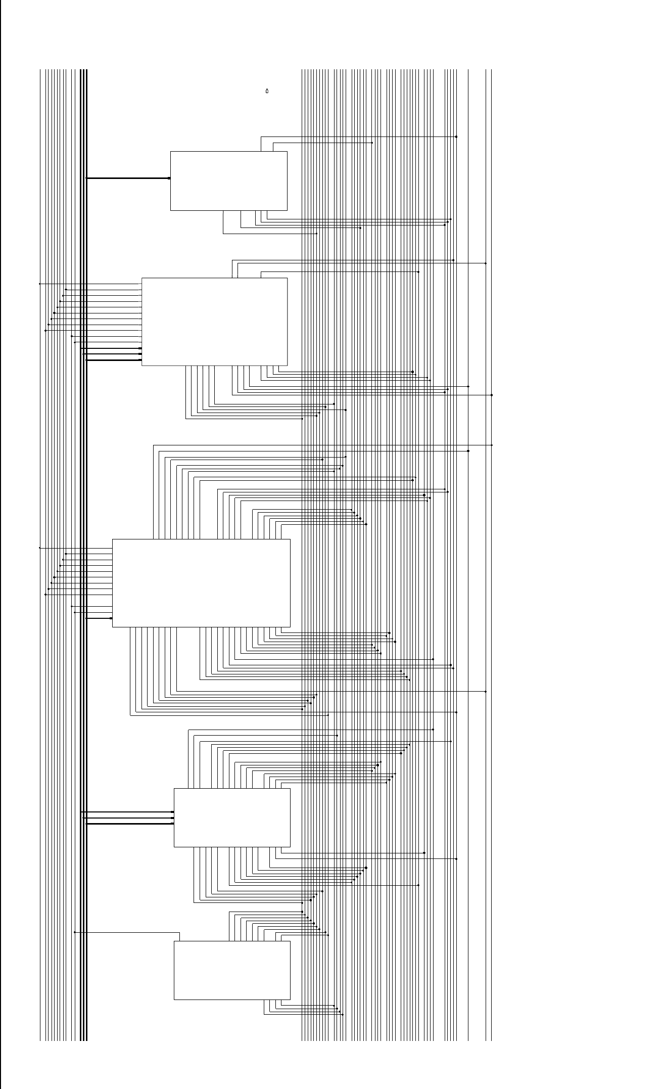
3-12 Controller T7/T9 Schematic Diagrams
3.0 Controller T7/T9 Schematic Diagrams
T2 0102727B24 MPT T2 0102727B27 SEL5/MDCT3 0102727B38
T3 0102727B42 MPT
T3 0102727B44
P2 0102726B64
P2 0102726B66 P3 0102726B71
P3 0102726B70
P3 0102726B69 P1 0102726B35
P2 0102726B67
P1 0102726B31
P7 0102727B16 SELV/MDC
P7 0102727B15 MPT
T4 0102727B50T4 0102727B49
T4 0102727B51 MPT
T4 0102727B52 SELV/MDC T4 0102727B54 SEL5/MDC
T4 0102727B53 MPT T4 0102727B55
P5 0102726B92 P6 0102727B04 SELV/MDC
P6 0102727B03 MPT
P1 0102726B33
P1 0102726B32
P6 0102727B02 P4 0102726B88
T2 0102727B25 SELV/MDC
P4 0102726B87
P6 0102727B05 MPT
P6 0102727B06 SEL5/MDC
P6 0102727B01
P5 0102726B97 SEL5/MDC
P5 0102726B96
P5 0102726B95 MPT
T2 0102727B26 MPT
T2 0102727B28
P3 0102726B68 P2 0102726B65
P1 0102726B30
P7 0102727B19
P5 0102726B94
P5 0102726B93
T3 0102727B41 SELV/MDC T3 0102727B43 SEL5/MDC
P4 0102726B86
P4 0102726B85P4 0102726B84
P3 0102726B35
P2 0102726B35
T2 0102727B22 T2 0102727B23
INT_SWB+
IN_5V_RF_REGON_OFF_CONTROL
PASUPVLTG
RESET
VSTBY
T7 0102727B62 T7 0102727B63
T7 0102727B68 T7 0102727B66 STANDARD
T7 0102727B65 PRIME
T6 0102727B67
one for LDMOS PA CHASSIS and one for BIPOLAR PA CHASSIS
T5 0102727B49 T5 0102727B50
T5 0102727B51 MPT
T5 0102727B52 SELV/MDC T5 0102727B54 SEL5/MDC
T5 0102727B53 MPT
T5 0102727B55
T3 0102727B39
T3 0102727B40 MPT
P7 0102727B13 P7 0102727B14
P7 0102727B17 MPT
P7 0102727B18 SEL5/MDC
P6 0102727B07
TX_AUD_SND
URX_SND
VS_AUDSEL
VS_GAINSEL VS_INT
VS_MIC
VS_RAC
SUPPLY_VOLTAGE
5VD
9V3
BATTERY_VOLTAGEDC_POWER_ON
EMERGENCY_CONTROL
EXT_SWB+
FLT_A+
IGNITION_CONTROL
NOISE_BLNKR
ON_OFF_CONTROL
OPT_PTT
PASUPVLTG
PA_PWR_SET
RDY
RESET
RSSI
RX_AUD_RTN
RX_FLAT_FILTERED_AUDIO
SCI_TX
SPI(0:10)
SPKR+
SPKR-
TEMPSENSE
TX_AUD_RTN
GP2_OUT_ACC4
GP3_IN_ACC6
GP4_IN_OUT_ACC8
GP5_IN_ACC9
GP6_IN_ACC10
GP7_IN_OUT_ACC12
GP8_IN_OUT_ACC14
HANDSET_AUDIO
IGNITION_CONTROL
INT_MIC
INT_SWB+
IN_5V_RF_REG
LOCKMODIN
MOSBIAS_2
MOSBIAS_3
5VD 5V_RF
9V3 BOOT_CNTRL
BUS+
CH_ACT
CNTLVLTG
DISCAUDIO
EMERGENCY_CONTROL
EXP_BD_REQ
EXT_MIC
EXT_SWB+
FLAT_RX_SND
FLAT_TX_RTN
FLT_A+
GP1_IN_ACC3
SPI(0:10)
TEMPSENSE
VSTBY
VS_GAINSEL
VS_INT
VS_RAC
VOICE_STORAGE
5VD
FLAT_RX_SND
RX_AUD_RTN
SPI(0:10)
VS_AUDSEL
VS_INT VS_MIC
VS_RAC
IO
16_8MHZ
GP2_OUT_ACC4
GP3_IN_ACC6
GP4_IN_OUT_ACC8
GP5_IN_ACC9
GP6_IN_ACC10
GP7_IN_OUT_ACC12
GP8_IN_OUT_ACC14
GPIO(0:13)
LOCK
ON_OFF_CONTROL
OPT_PTT
RDY
RESET
RSSI RX_ADAPT
SCI_TX
SPKR+
SPKR-
TX_AUD_RTN
TX_AUD_SND
URX_SND
VS_AUDSEL
VS_MIC
CONTROLLER
5VD
BATTERY_VOLTAGE
BOOT_CNTRL
BUS+
CNTLR_AUDIO(0:7)
CNTLVLTG
EXT_BD_REQ
FLT_A+
GP1_IN_ACC3
FLAT_RX_SND
FLAT_TX_RTN
FLT_A+
GPIO(0:13)
HANDSET_AUDIO
INT_MIC
INT_SWB+
MODIN
MOSBIAS_2
MOSBIAS_3
NOISE_BLNKR
PA_PWR_SET
RX_ADAPT
RX_AUD_RTN
RX_FLAT_FILTERED_AUDIO
SPI(0:10)
PASUPVLTGPASUPVLTG FLT_A+FLT_A+
RX_ADAPT RX_ADAPT
AUDIO
16_8MHZ
5VD
5V_RF
9V3
CH_ACT
CNTLR_AUDIO(0:7)
DC_POWER_ON
DISCAUDIO
EXT_MIC
CH_ACT CH_ACT
URX_SND URX_SND
VS_GAINSEL VS_GAINSEL
MOSBIAS_3MOSBIAS_3
INT_SWB+ INT_SWB+
EXT_MIC EXT_MIC
IN_5V_RF_REGIN_5V_RF_REG
SCI_TX SCI_TX
VS_MICVS_MIC
5VD5VD 9V39V3
EXT_SWB+EXT_SWB+
SPKR+SPKR+ SPKR-SPKR-
EMERGENCY_CONTROLEMERGENCY_CONTROL IGNITION_CONTROLIGNITION_CONTROL DC_POWER_ONDC_POWER_ON ON_OFF_CONTROLON_OFF_CONTROL
BATTERY_VOLTAGEBATTERY_VOLTAGE
VSTBYVSTBY
RDY RDY
OPT_PTT OPT_PTT
MODINMODIN
TX_AUD_SNDTX_AUD_SND FLAT_RX_SNDFLAT_RX_SND
16_8MHZ16_8MHZ
TX_AUD_RTNTX_AUD_RTN FLAT_TX_RTNFLAT_TX_RTN
RX_AUD_RTNRX_AUD_RTN DISCAUDIODISCAUDIO
INT_MICINT_MIC
5V_RF5V_RF
RX_FLAT_FILTERED_AUDIORX_FLAT_FILTERED_AUDIO HANDSET_AUDIOHANDSET_AUDIO
GP1GP1
EXP_BD_REQ EXP_BD_REQ
BOOT_CNTRLBOOT_CNTRL
VS_AUDSEL VS_AUDSEL
TEMPSENSETEMPSENSE CNTLVLTGCNTLVLTG
VS_RACVS_RAC VS_INTVS_INT
RSSIRSSI LOCKLOCK
NOISE_BLNKRNOISE_BLNKR PA_PWR_SETPA_PWR_SET MOSBIAS_2MOSBIAS_2
DUMMY
CNTRL_AUDIO(0:7)CNTRL_AUDIO(0:7) GPIO(0:13)GPIO(0:13)
SPI(0:10) SPI(0:10)
BUS+BUS+ RESETRESET
GP8GP8 GP7GP7 GP6GP6 GP5GP5 GP4GP4 GP3GP3 GP2GP2
ZWG0130525-O
ZWG0130525-O
Controller T7/T9 Schematic Diagram - Overall
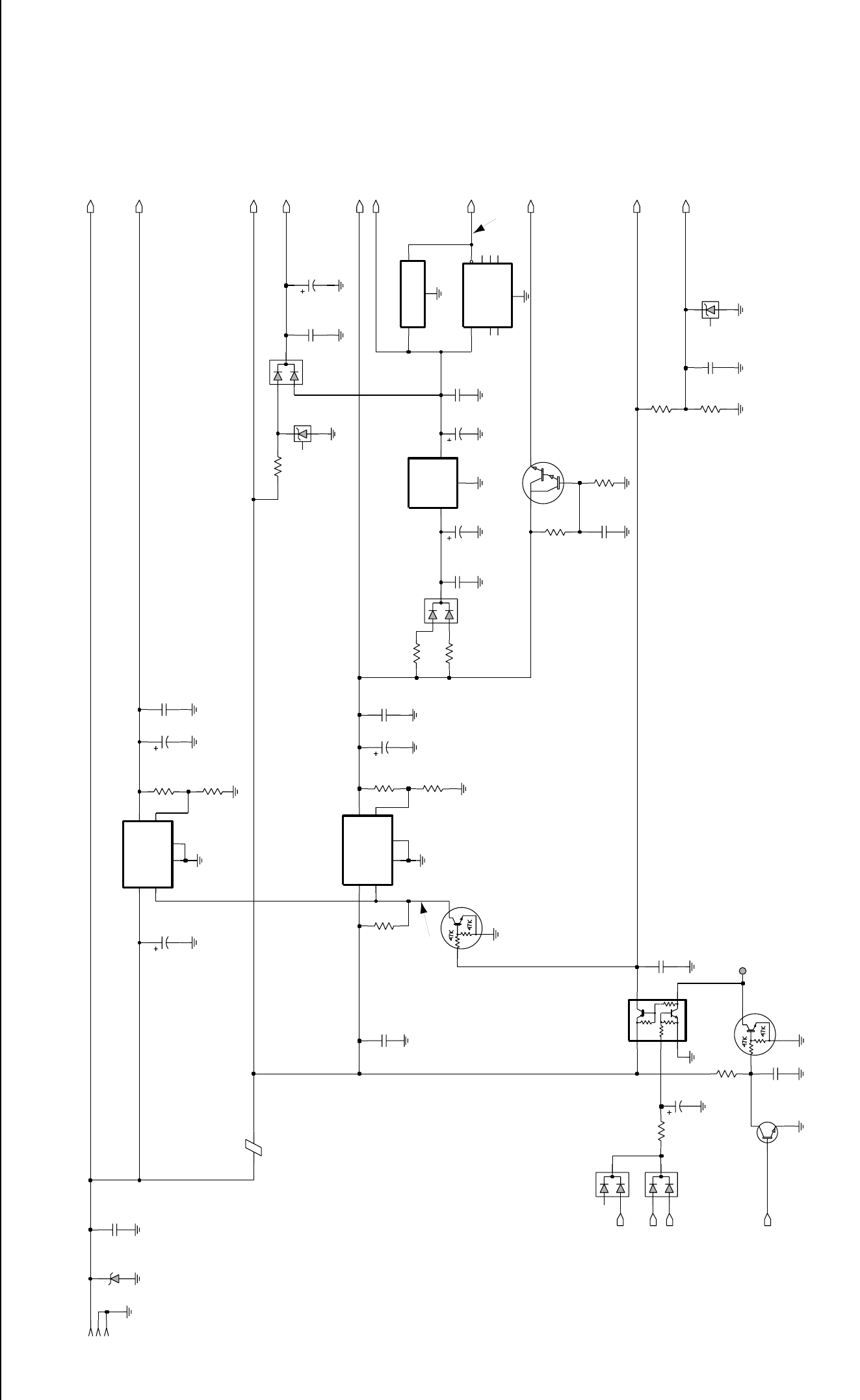
Controller T7/T9 Schematic Diagrams 3-13
C0621
NU
2
GND
1IN OUT 3
TP0661
NU
0.1uF
NU
NU
J0601-3
Q0663
D0621
C0603
10uF
R0661
1K
VR0621
5.6V
2
NC1
3
NC2
5
NC3 6
NC4 7
8
NC5
RESET 1
U0652
MC33064
GND
4
INPUT
MC78M05
U0651
0.1uF
C0663
R0643
0.1uF
1.2K
C0651 C0655
0.1uF
C0645
24V
470pF
VR0601
ON_OFF
2
4VIN 5
VOUT
47uF
C0622
U0641
LM2941
1
ADJ
GND1
3
GND2
6
Q0661
R0611
56K
VR0671
5.6V
68K
Q0681
R0682
R0681
18K
57R01
E0631
22uF
C0611
R0651
10
C0652
33uF
R0612
4.7K
D0661
Q0662
R0671
30K
R0671
30K
10K
6
2ON_OFF
VIN
4VOUT 5
R0672
LM2941
U0611
ADJ 1
GND1
3
GND2
0.1uF
10K
C0671
R0641
C0662
J0601-1
.01uF
R0662
150K
D0660
R0652
R0621
10
24K
2INPUT 1
RESET_
Q0641
MC33464N-45ATR
U0653
3
GND
C0654
10uF
470pF
C0601
C0661
47uF
R0642
7.5K
470pF
C0641
33uF
C0644
D0651
C0681
0.1uF
J0601-2
0.1uF
C0612
9V3
FLT_A+
IN_5V_RF_REG
RESET
5VD
DC_POWER_ON
IGNITION_CONTROL
EMERGENCY_CONTROL
BATTERY_VOLTAGE
ON_OFF_CONTROL
EXT_SWB+
INT_SWB+
PASUPVLTG
VSTBY
0V (13,8VDC when radio off)
6VDC
5VDC
5VDC (0VDC during reset)
5VDC
ZWG0130529-A
Controller T7/T9 Schematic Diagram - Supply Voltage
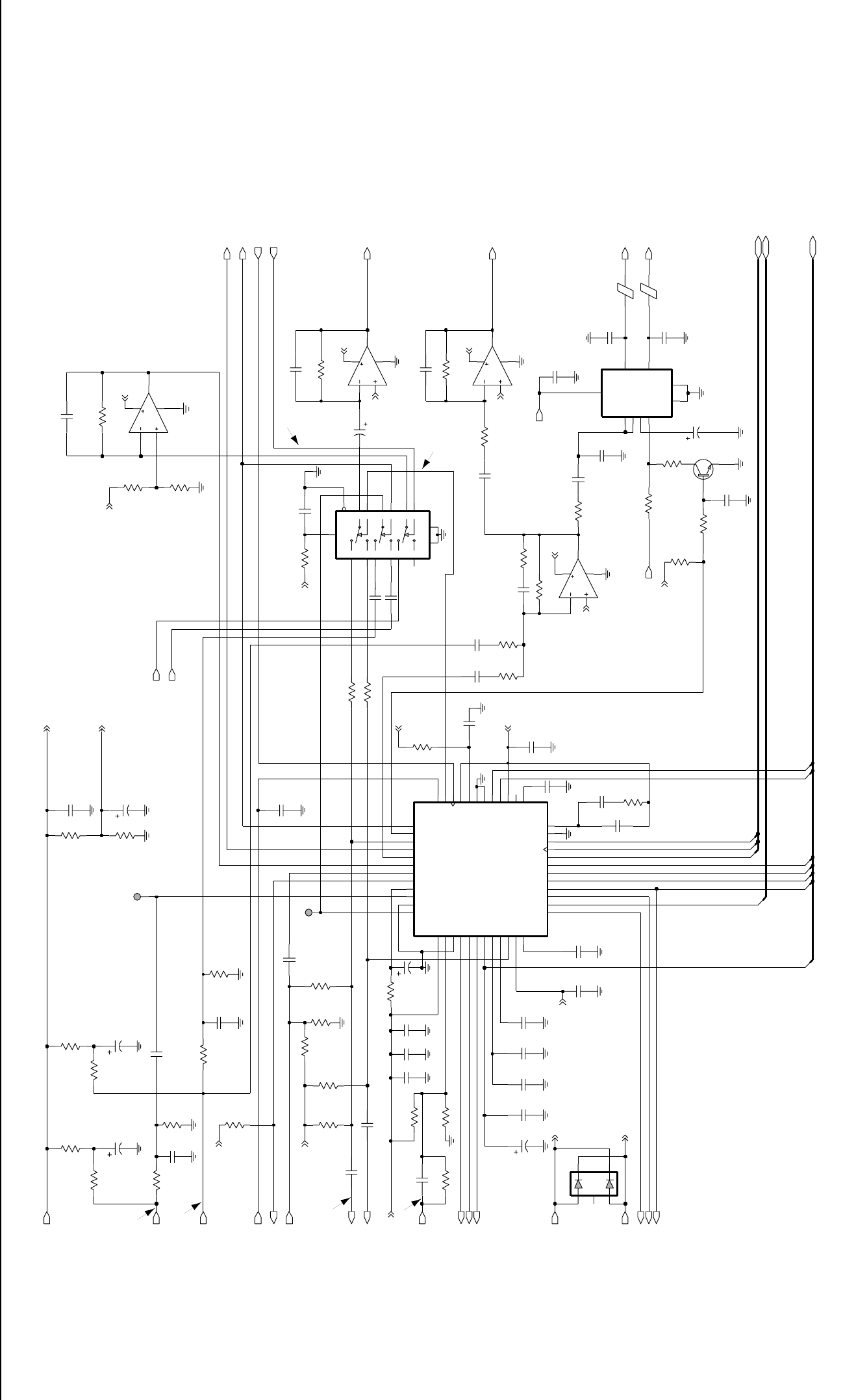
3-14 Controller T7/T9 Schematic Diagrams
C0204
NU
C0211
NU
C0237
2.2uF
NU
NU
10K
NU
R0274
C0227
NU
R0266
24K
NU
NU
0.1uF
C0266
NU
NU
R0227
1MEG
NU
0.1uF
C0232
NU
100pF
C0253
NU
D0201
8
C0242
NU
8.2K
R0225
NU
NU
100pF
C0256
NU
SYN
CLK
HSIO
VOX
GP2_OUT
CSX
DATA
CH_ACT
SQ_DET
LSIO
F1200
TP0222
30K
R0223
C0228
4,7uF
R0275
10K
Q0271
0
R0228
0.1uF
C0221
0.1uF
R0252
C0223
56K
0.1uF
C0261
7.5K
R0212
7.5K
R0211
.033uF
C0236
9
10 8
4
11 U0211-3
MC3403
47K
R0267
10K
R0268
24K
R0265
VDDDAC
11
VDDRC 45
VDDSYN 27
VOX
7
1
SYN 28
TXRTN 36
TXSND 44
UIO
10
URXOUT 39
VDDA
1
VDDCP 32
VDDD 33
MICEXT 48
MICINT 46
MOD 40
NC 26
PLCAP
8
PLCAP2 25
SQDET
17
SQIN
9
GNDA
3
GNDD 31
GNDD0 30
GNDRC 47
GNDSYN
23
HSIO
19
LCAP
24
LSIO
18
DISC
2
F1200 29
GCB0
15 GCB1
14 GCB2
13
GCB3 35
GCB4 37
GCB5 38
CHACT
16
CLK
21
CLK168 34
CSX
20
DACG
6DACR
5DACU
4
DATA
22
AGCCAP
12
AUDIO 41
AUXRX 43
AUXTX 42
63A53
U0221
VCC
GND2
5
9INV
8M_SS
1NINV
4
OUT1
6
OUT2
RR
3
7
TDA1519C
U0271
2
GND1
C0225
0.1uF
C0274
0.1uF
R0208
2.2K
6
0.1uF
560
R0204
10K
R0261
560
R0202
82pF
C0262
R0201
R0205
100
5
10K
8.2K
R0220
9
8.2K
R0224
100pF
C0243
0
R0242
0.1uF
C0201
10uF
6
57
4
11
11
U0211-2
MC3403
C0275
47uF
24K
R0273
100K
4
R0253
1uF
C0252
10K
R0255
7
C0205
2200pF
.01uF
C0267
C0277
1000pF 57R01
E0272
57R01
E0271
0.1uF
C0245
10
R0229
0.1uF
C0244
.022uF
C0235
C0212
10uF
R0226
1MEG
R0206
10K
10K
R0254
1uF
15K
C0231
1000pF
R0276
7
C0276
2
13
12 14
4
11
10uF
U0211-4
MC3403
R0203
C0202
0.1uF
100
5
3
1
2
4
C0265
C0254
C0234
0.1uF
C0272
0.1uF
0.1uF
C0273
3300pF
24K
R0221
R0262
100K
R0256
2.2K
R0257
100K
47K
R0251
R0222
24K
0.1uF
C0222
0.1uF
C0226
470
R0269
0.1uF
C0241
TP0221
2.2K
U0211-1
MC3403
2
31
4
11
R0207
0.1uF
C0224
100pF
C0233
0.22uF
3
0.1uF
C0251
C0255
0.1uF
C0271
.01uF
47K
R0241
Z1
C0246
.01uF
14
X0
12
X1
13
Y15
Y0
2
Y1
1
Z4
Z0
5
3
U0251
11
A
B10
C9
EN 6
GND
8
VCC
16
VEE
7
X
MC14053B
2200pF
C0203
TX_AUD_RTN
5V_RF
TX_AUD_SND
5V_RF
DISCAUDIO
5V_RF
RX_ADAPT
FLAT_TX_RTN
5V_RF
0.1uF
MODIN
INT_SWB+
CH_ACT
VAG
9V3 9V3
9V3
VS_MIC
MOSBIAS_3
16_8MHZ
VAG
EXT_MIC
5V_RF
5V_RF
5VD5VD
5V_RF
5V_RF5V_RF
SPKR-
RX_AUD_RTN
INT_MIC
URX_SND
FLAT_RX_SND
DC_POWER_ON
FLT_A+
5VD
SPKR+
5VD
PA_PWR_SET
MOSBIAS_2
9V3
9V3
9V3
NOISE_BLNKR
VS_AUDSEL
SPI(0:10)
GPIO(0:13)
CNTLR_AUDIO(0:7)
VAG
VAG
HANDSET_AUDIO
RX_FLAT_FILTERED_AUDIO
80mV RMS
80mV RMS
5VDC (0VDC during radio off) 13VDC unmuted
5VDC muted
300mV RMS
200mV RMS
145mV RMS @25kHz
72mV RMS @12.5kHz
5VDC RX Filtered
Audio (0V DC Flat)
630mV RX Filtered
330mV Flat
0 VDC
ZWG0130528-A
Controller T7/T9 Schematic Diagram - Audio
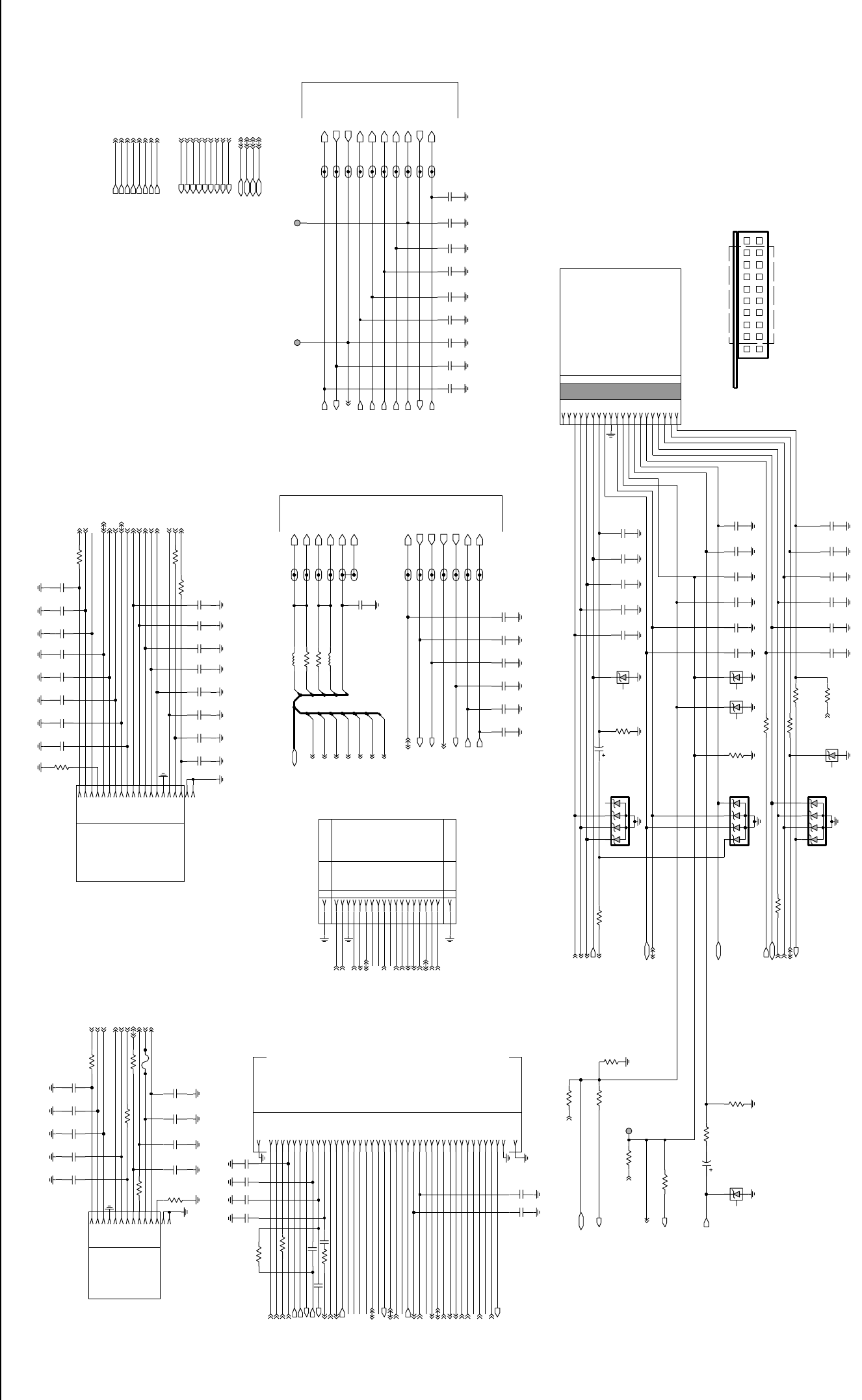
Controller T7/T9 Schematic Diagrams 3-15
470pF
C0560
NU
R0542
NU
470pF
C0576
C0442
470pF
NU
C0559
470pF
NU
J0451-14
J0551-3
NU
C0558
NU
470pF
J0401-2
NU
390nH
NU
L0482
NU
C0554
0.1uF
NU INTERNAL OPTION BOARD
39
38
9
4
VS_CS
NC
GROUND
GROUND
FAST_SQ
DISCAUDIO
4DB7
FLAT_TX_AUDIO
DIG_IN_OUT_4
DATA
EXP1_CS
11
DB2
DIG_IN1
3
EXP1_CS
5
9V3
5VD
EXT_BD_PTT
EXT_MIC_AUDIO
EXP_BD_PTT
DATA
36
21
NC
BOOT_CNTRL
Rx_Aud_Snd
ON
VS_INT
VS_RAC
16
DB3
23
6
1
RST*
7
8
14
INT_EXT_Vdd
GROUND
DB111
7
17
12
18
RSSI
NC
J0552
SPI_MISO
RESET
FLT_A+
26
FLAT_TX_RTN
6
CSX
29
12-PIN CONNECTOR
13
CLK
MISO
PCB
16
20
SCI_TX
INT_MIC
DIG_IN_3
Tx_Aud_Snd
VS_AUDSEL
17
GROUND
SrD_Rtn
5
DIG_IN_5 WITH WAKEUP (EMERGENCY)
13
37
DIG_IN_OUT_7
2
GM300
SPEAKER-
CLK
DISCAUDIO
CH_ACT
NC
NC
NC
6
NC
DB6
ACCESSORY
7
4
19
9
R/W*
Opt_Bd_En
NC
13
10
33
NC
7
9
A0
EXT_BD_REQ
EXT_BD_CS
GP4_IN_OUT
SPI_CLK
SPI_MOSI
DATA
VS_GAINSEL
Gnd
8
EXP2_CS
NC
EXT_BD_PTT
GND
5VD
EXP_BD_PTT
GND
RDY
OPT_PTT
GND
DB4
CLK
SPEAKER+
14
3
2
8
NC
10
11
Key_Row
Key_Intrp
DIG_IN_OUT_4
9V3
VS_MIC
5VD
DIG_OUT2 (EXTERNAL_ALARM)
NC
HANSET_AUDIO
30
13
J0501
J0451
DIG_IN_6 WITH WAKEUP (IGNITION)
FLAT/FILTERED_RX_AUDIO
19
9
VS_CS
SWB+
20
11
Flat_Tx_Rtn
NC
1
2
SrD_Snd
EXT_BD_PTT
27
OPT_CS
22
18
40-PIN CONNECTOR
DB5
12
SCK_Snd
35
NC
NC
7
8
LED_EN
ON_OFF_CONTROL
20-PIN CONNECTOR
18
17
20
NC
15
14
16
DIG_IN_6 WITH WAKEUP
Tx_Aud_Rtn
34
18
Vddd
25
32
31
SPEAKER+
1
WARIS
TO/FROM RF
7
24
CS*
3
1
NC
NC
3
5
15
CLK
9
J0551
28
FLT_A+
6
SPEAKER-
DIG_IN_OUT_8
16
3
OFF_BATT_DATA_OUT
3
4
EXP_BD_REQ
EXT_BD_PTT
EXT_BD_PTT
19
Det_Aud_Snd
12
Rx_Aud_Rtn
NC
1
MISO
2
5
6
10
11
12
EXP2_CS
8
DB0
DATA
11
CONTROL HEAD
NC
10
OPT_CS
EXPANSION BOARD
10
PTT
Rdy/Req
2
GROUND
10 12 14
REAR VIEW
BUS+
4
12
18-PIN CONNECTOR
NC
GND
1
2
11
12
13
17
15
6
40
18-PIN CONNECTOR
RS232 INTERFACE BOARD
Key_Col
TO/FROM RF
8
5
6
7
8
9
10
5
15
16
17
18
4
1
2
3
9
14
13
14
15
16
17
18
J0401
5
4
15
GND
BUS+
0
R0482
0
R0481
J0501-8
470pF
C0443
100K
R0468
J0552-20
J0552-2
J0552-5
J0552-4
R0539
4.7K
J0551-39
J0551-33
TP0492
J0551-34
82pF
C0428
DATA_CNTLR_2
J0451-7
J0552-1
C0422
J0551-18
7
470pF
100K
R0511
CSX_CNTLR_1
J0501-15
J0552-3
VR0510
33V
8
TEMPSENSE
9
J0451-12
5V_CNTLR_1
470pF
C0506
0.1uF
J0451-1
C0592
470pF
C0478
15K
R0512
C0487
470pF
R0510
10
4.7K
NOISE_BLNKR_CNTLR_1
R0409
5.6V
VR0537
C0473
82pF
8
470pF
J0451-18
C0502
J0401-5
J0551-31
J0451-15
220
R0537
J0551-38
RESET
14V
VR0541
R0407 10
470pF
J0551-5
J0501-19
C0496
VR0504
33V
J0551-9
J0551-27
470pF
C0474
470pF
J0551-20
C0429
.01uF
C0501
470pF
J0451-16
C0426 470pF
C0445
J0501-10
J0451-8
RSSI_CNTLR_1 470pF
C0497
R0531
560
DATA
C0421
82pF
R0525
470pF
100K
MOSBIAS_3_CNTLR_1
C0492
CLK_CNTLR_2
RSSI
C0446
470pF
IN_5V_RF_REG_CNTLR_1
J0501-5
IN_5V_RF_REG
C0472
DISCAUDIO
82pF
470pF
C0484
100K
R0543
100K
R0593
R0442 1K
DISCAUDIO_CNTLR_1
LOCK_CNTLR_1
C0591 0.1uF
TEMPSENSE_CNTLR_1
C0510
470pF
J0501-16
J0451-3
J0401-6
9V3
CLK
INT_SWB
INT_SWB_CNTLR_1
J0551-32 CLK_CNTLR_1
J0551-7
470pF
C0476
470pF
C0491
J0551-13
470pF
C0483
J0451-11
J0401-1
C0505
C0504
470pF 470pF
470pF
C0503
J0551-24
C0593
0.1uF
470pF
C0430
PASUPVLTG_CNTRL_1
470pF
J0451-10
C0509
0
R0412
C0514
470pF
J0501-3
VR0505
20V
J0552-8
J0552-10
J0552-9
J0552-11
J0401-10
J0551-40
CSX
16_8MHZ_CNTLR_1
R0529
C0495
47K
470pF
J0551-41
J0401-4
J0401-7
10
R0592
R0401
220
J0551-12
16_8MHZ
J0451-9
J0551-1
VR0503
J0501-7
20V
J0551-21
RESET_CNTLR_1
1
J0451-6
J0501-18
C0485
470pF
R0408
C0477
2
100
J0401-9
470pF
470pF
C0447
J0551-22
3
J0551-26
J0501-13
TP0530
DATA_CNTLR_1
J0552-17
J0552-16
J0401-8
J0501-6
MOSBIAS_2_CNTLR_1
10
R0467
C0441
J0501-1
4
J0551-15
C0493
J0401-11
470pF
J0451-5
470pF
C0431
VR0501
20V
J0551-14
J0551-4
J0501-12
J0551-25
J0501-2
470pF
C0515
J0451-13
J0552-12
J0552-14
J0552-13
J0552-15
R0538
220
MOSBIAS_2
J0501-20
R0530
J0401-12
J0451-2
0
C0488
J0551-23
PASUPVLTG
470pF
C0513
9V3_CNTLR_1
470pF
8
9
TP0497
470pF
J0552-18
J0551-28
CNTLVLTG
J0552-19
C0471
82pF
5V
J0551-10
J0551-19
1K
R0535
470pF
C0511 470pF
C0512
J0551-42
CLK
J0501-11
J0551-16
J0551-2
J0551-30
J0551-35
390nH
L0481
470pF
NOISE_BLNKR
C0508
C0448
470pF
LOCK
J0552-6
CSX
470pF
C0482
J0552-7
VR0509
33V
C0490
470pF
C0427
470pF
J0551-36
J0501-9
470pF
J0451-17
C0518
10
C0575
470pF
CSX_CNTLR_2
470pF
C0470
27K
R0541
MOSBIAS_3
J0551-37
C0494
470pF
47K 0.47uF
C0541
J0551-8
J0501-14
MODIN
PA_PWR_SET_1_CNTLR_1
0
R0441
J0501-4
9
J0551-6
.01uF
C0516
J0501-17
MODIN_CNTLR_1
C0517
82pF
C0486
470pF
DATA
C0499
470pF
J0551-29
C0542
C0423
470pF
47uF
PA_PWR_SET
R0533 0
J0451-4
24K
R0591
CNTLVLTG_CNTLR_1
J0551-17
470pF
C0449
J0551-11
J0401-3
EXP_BD_REQ
5VD
SPKR-
SPKR+
ON_OFF_CONTROL
SPKR-
GP6_IN_ACC10
FLAT_TX_RTN
GP6_IN_ACC10GP6_IN_ACC10
GP6_IN_ACC10
FLAT_TX_RTN
SPI_DATA
EXT_MIC
GP1_IN_ACC3
GP2_OUT_ACC4
GP5_IN_ACC9
GP7_IN_OUT_ACC12
GP8_IN_OUT_ACC14
SPKR+
GP3_IN_ACC6
GP4_IN_OUT_ACC8
EXP2_CS
EXP1_CS
GP4_IN_OUT_ACC8
OPT_CS
RDY
OPT_PTT
EXP2_CS
CH_ACT
GP1_IN_ACC3
SPI_DATA
SPI_MISO
SPI_CLK
9V3
SPI_MISO
DISCAUDIO
MODIN
CH_ACT
5VD
9V3
5VD
SPI_MISO
RESET
FLT_A+
DISCAUDIO
GP4_IN_OUT_ACC8
EXP1_CS
EXP_BD_REQ
GP1_IN_ACC3
SPI_CLK
OPT_PTTOPT_PTT
OPT_PTT
INT_MIC INT_MIC
INT_MIC SPKR+SPKR+
DISCAUDIO DISCAUDIO
HANDSET_AUDIOHANDSET_AUDIO
HANDSET_AUDIO
RSSI RSSI
BOOT_CNTRL
5VD
IN_5V_RF_REG
BUS+
GP1_IN_ACC3
GP1_IN_ACC3 GP1_IN_ACC3
INT_SWB+
5VD
GP4_IN_OUT_ACC8
EXP1_CS
EXP_BD_REQEXP_BD_REQ
EXP_BD_REQ
GP1_IN_ACC3
CH_ACT CH_ACT
CH_ACT
DISCAUDIO
FLT_A+
SCI_TX
RX_FLAT_FILTERED_AUDIO
EMERGENCY_CONTROL
FLT_A+
RSSI
EXT_SWB+
RDYRDY
RDY 5V_RF
NOISE_BLNKR
MOSBIAS_2
PA_PWR_SETEXP1_CS
9V3
FLAT_TX_RTN FLAT_TX_RTN
GP4_IN_OUT_ACC8 GP4_IN_OUT_ACC8
DISCAUDIO
SPI(0:10)
MOSBIAS_3
VS_MIC VS_MIC
FLAT_TX_RTN
FLT_A+
BUS+ BUS+
RESETRESET
ON_OFF_CONTROL ON_OFF_CONTROL
16_8MHZ
5VD5VD FLT_A+FLT_A+
SPI_DATA
SPI_CLK
SPI_MISO
VS_CS
OPT_CS
RESET
EXT_MICEXT_MIC
SPKR-SPKR-
RESET
PASUPVLTG
BUS+
TEMPSENSE
CNTLVLTG
RSSI
LOCK
OPT_CS
SPI_DATA
TX_AUD_RTN
VS_CS
VS_MIC
SPI_CLK
FLAT_RX_SND
RX_AUD_RTN
URX_SND
TX_AUD_SND
VS_INT
5VD
VS_AUDSEL
VS_GAINSEL
SPI_MISO
VS_RAC
IGNITION_CONTROL
FLT_A+
F0401
3A
ZWG0130563-A
Controller T7 only Schematic Diagram - I/O
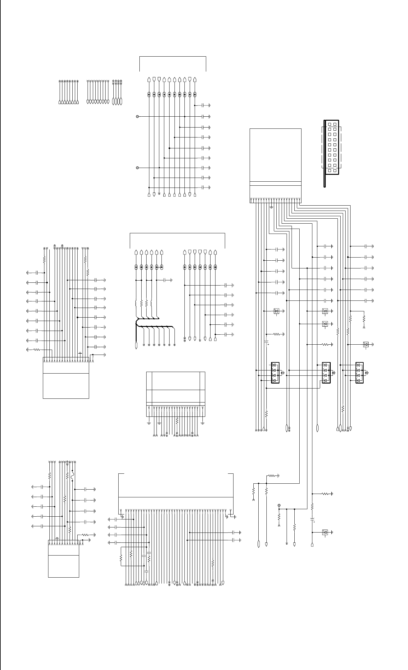
3-16 Controller T7/T9 Schematic Diagrams
470pF
C0560
NU
R0542
NU
470pF
C0576
C0442
470pF
NU
C0559
470pF
NU
J0451-14
J0551-3
NU
C0558
NU
470pF
J0401-2
NU
390nH
NU
L0482
NU
C0554
0.1uF
NU INTERNAL OPTION BOARD
39
38
9
4
VS_CS
NC
GROUND
GROUND
FAST_SQ
DISCAUDIO
4DB7
FLAT_TX_AUDIO
DIG_IN_OUT_4
DATA
EXP1_CS
11
DB2
DIG_IN1
3
EXP1_CS
5
9V3
5VD
EXT_BD_PTT
EXT_MIC_AUDIO
EXP_BD_PTT
DATA
36
21
NC
BOOT_CNTRL
Rx_Aud_Snd
ON
VS_INT
VS_RAC
16
DB3
23
6
1
RST*
7
8
14
INT_EXT_Vdd
GROUND
DB111
7
17
12
18
RSSI
BUS+
J0552
SPI_MISO
RESET
FLT_A+
26
FLAT_TX_RTN
6
CSX
29
12-PIN CONNECTOR
13
CLK
MISO
PCB
16
20
SCI_TX
INT_MIC
DIG_IN_3
Tx_Aud_Snd
VS_AUDSEL
17
GROUND
SrD_Rtn
5
DIG_IN_5 WITH WAKEUP (EMERGENCY)
13
37
DIG_IN_OUT_7
2
GM300
SPEAKER-
CLK
DISCAUDIO
CH_ACT
NC
NC
BUS+
6
NC
DB6
ACCESSORY
7
4
19
9
R/W*
Opt_Bd_En
NC
13
10
33
NC
7
9
A0
EXT_BD_REQ
EXT_BD_CS
GP4_IN_OUT
SPI_CLK
SPI_MOSI
DATA
VS_GAINSEL
Gnd
8
EXP2_CS
BUS+
EXT_BD_PTT
GND
5VD
EXP_BD_PTT
GND
RDY
OPT_PTT
GND
DB4
CLK
SPEAKER+
14
3
2
8
NC
10
11
Key_Row
Key_Intrp
DIG_IN_OUT_4
9V3
VS_MIC
5VD
DIG_OUT2 (EXTERNAL_ALARM)
NC
HANSET_AUDIO
30
13
J0501
J0451
DIG_IN_6 WITH WAKEUP (IGNITION)
FLAT/FILTERED_RX_AUDIO
19
9
VS_CS
SWB+
20
11
Flat_Tx_Rtn
NC
1
2
SrD_Snd
EXT_BD_PTT
27
OPT_CS
22
18
40-PIN CONNECTOR
DB5
12
SCK_Snd
35
NC
NC
7
8
LED_EN
ON_OFF_CONTROL
20-PIN CONNECTOR
18
17
20
NC
15
14
16
DIG_IN_6 WITH WAKEUP
Tx_Aud_Rtn
34
18
Vddd
25
32
31
SPEAKER+
1
WARIS
TO/FROM RF
7
24
CS*
3
1
NC
NC
3
5
15
CLK
9
J0551
28
FLT_A+
6
SPEAKER-
DIG_IN_OUT_8
16
3
OFF_BATT_DATA_OUT
3
4
EXP_BD_REQ
EXT_BD_PTT
EXT_BD_PTT
19
Det_Aud_Snd
12
Rx_Aud_Rtn
NC
1
MISO
2
5
6
10
11
12
EXP2_CS
8
DB0
DATA
11
CONTROL HEAD
NC
10
OPT_CS
EXPANSION BOARD
10
PTT
Rdy/Req
2
GROUND
10 12 14
REAR VIEW
BUS+
4
12
18-PIN CONNECTOR
NC
GND
1
2
11
12
13
17
15
6
40
18-PIN CONNECTOR
RS232 INTERFACE BOARD
Key_Col
TO/FROM RF
8
5
6
7
8
9
10
5
15
16
17
18
4
1
2
3
9
14
13
14
15
16
17
18
J0401
5
4
15
GND
BUS+
0
R0482
0
R0481
J0501-8
470pF
C0443
100K
R0468
J0552-20
J0552-2
J0552-5
J0552-4
R0539
4.7K
J0551-39
J0551-33
TP0492
J0551-34
82pF
C0428
DATA_CNTLR_2
J0451-7
J0552-1
C0422
J0551-18
7
470pF
100K
R0511
CSX_CNTLR_1
J0501-15
J0552-3
VR0510
33V
8
TEMPSENSE
9
J0451-12
5V_CNTLR_1
470pF
C0506
0.1uF
J0451-1
C0592
470pF
C0478
15K
R0512
C0487
470pF
R0510
10
4.7K
NOISE_BLNKR_CNTLR_1
R0409
5.6V
VR0537
C0473
82pF
8
470pF
J0451-18
C0502
J0401-5
J0551-31
J0451-15
220
R0537
J0551-38
RESET
14V
VR0541
R0407 10
470pF
J0551-5
J0501-19
C0496
VR0504
33V
J0551-9
J0551-27
470pF
C0474
470pF
J0551-20
C0429
.01uF
C0501
470pF
J0451-16
C0426
470pF
C0445
J0501-10
J0451-8
RSSI_CNTLR_1 470pF
C0497
R0531
560
DATA
C0421
82pF
R0525
470pF
100K
MOSBIAS_3_CNTLR_1
C0492
CLK_CNTLR_2
RSSI
C0446
470pF
IN_5V_RF_REG_CNTLR_1
J0501-5
IN_5V_RF_REG
C0472
DISCAUDIO
82pF
470pF
C0484
100K
R0543
100K
R0593
R0442 1K
DISCAUDIO_CNTLR_1
LOCK_CNTLR_1
C0591 0.1uF
TEMPSENSE_CNTLR_1
C0510
470pF
J0501-16
J0451-3
J0401-6
9V3
CLK
INT_SWB
INT_SWB_CNTLR_1
J0551-32 CLK_CNTLR_1
J0551-7
470pF
C0476
470pF
C0491
J0551-13
470pF
C0483
J0451-11
J0401-1
C0505
C0504
470pF 470pF
470pF
C0503
J0551-24
C0593
0.1uF
470pF
C0430
PASUPVLTG_CNTRL_1
470pF
J0451-10
C0509
0
R0412
C0514
470pF
J0501-3
VR0505
20V
J0552-8
J0552-10
J0552-9
J0552-11
J0401-10
J0551-40
CSX
16_8MHZ_CNTLR_1
R0529
C0495
47K
470pF
J0551-41
J0401-4
J0401-7
10
R0592
R0401
220
J0551-12
16_8MHZ
J0451-9
J0551-1
VR0503
J0501-7
20V
J0551-21
RESET_CNTLR_1
1
J0451-6
J0501-18
C0485
470pF
R0408
C0477
2
100
J0401-9
470pF
470pF
C0447
J0551-22
3
J0551-26
J0501-13
TP0530
DATA_CNTLR_1
J0552-17
J0552-16
J0401-8
J0501-6
MOSBIAS_2_CNTLR_1
10
R0467
C0441
J0501-1
4
J0551-15
C0493
J0401-11
470pF
J0451-5
470pF
C0431
VR0501
20V
J0551-14
J0551-4
J0501-12
J0551-25
J0501-2
470pF
C0515
J0451-13
J0552-12
J0552-14
J0552-13
J0552-15
R0538
220
MOSBIAS_2
J0501-20
R0530
J0401-12
J0451-2
0
C0488
J0551-23
PASUPVLTG
470pF
C0513
9V3_CNTLR_1
470pF
8
9
TP0497
470pF
J0552-18
J0551-28
CNTLVLTG
J0552-19
C0471
82pF
5V
J0551-10
J0551-19
1K
R0535
470pF
C0511 470pF
C0512
J0551-42
CLK
J0501-11
J0551-16
J0551-2
J0551-30
J0551-35
390nH
L0481
470pF
NOISE_BLNKR
C0508
C0448
470pF
LOCK
J0552-6
CSX
470pF
C0482
J0552-7
VR0509
33V
C0490
470pF
C0427
470pF
J0551-36
J0501-9
470pF
J0451-17
C0518
10
C0575
470pF
CSX_CNTLR_2
470pF
C0470
27K
R0541
MOSBIAS_3
J0551-37
C0494
470pF
47K 0.47uF
C0541
J0551-8
J0501-14
MODIN
PA_PWR_SET_1_CNTLR_1
0
R0441
J0501-4
9
J0551-6
.01uF
C0516
J0501-17
MODIN_CNTLR_1
C0517
82pF
C0486
470pF
DATA
C0499
470pF
J0551-29
C0542
C0423
470pF
47uF
PA_PWR_SET
R0533 0
J0451-4
24K
R0591
CNTLVLTG_CNTLR_1
J0551-17
470pF
C0449
J0551-11
J0401-3
EXP_BD_REQ
5VD
SPKR-
SPKR+
ON_OFF_CONTROL
SPKR-
GP6_IN_ACC10
FLAT_TX_RTN
GP6_IN_ACC10GP6_IN_ACC10
GP6_IN_ACC10
FLAT_TX_RTN
SPI_DATA
EXT_MIC
GP1_IN_ACC3
GP2_OUT_ACC4
GP5_IN_ACC9
GP7_IN_OUT_ACC12
GP8_IN_OUT_ACC14
SPKR+
GP3_IN_ACC6
GP4_IN_OUT_ACC8
EXP2_CS
EXP1_CS
GP4_IN_OUT_ACC8
OPT_CS
RDY
OPT_PTT
EXP2_CS
CH_ACT
GP1_IN_ACC3
SPI_DATA
SPI_MISO
SPI_CLK
9V3
SPI_MISO
DISCAUDIO
MODIN
CH_ACT
5VD
9V3
5VD
SPI_MISO
RESET
FLT_A+
DISCAUDIO
GP4_IN_OUT_ACC8
EXP1_CS
EXP_BD_REQ
GP1_IN_ACC3
SPI_CLK
OPT_PTTOPT_PTT
OPT_PTT
INT_MIC INT_MIC
INT_MIC SPKR+SPKR+
DISCAUDIO DISCAUDIO
HANDSET_AUDIOHANDSET_AUDIO
HANDSET_AUDIO
RSSI RSSI
BOOT_CNTRL
5VD
IN_5V_RF_REG
BUS+
GP1_IN_ACC3
GP1_IN_ACC3 GP1_IN_ACC3
INT_SWB+
5VD
GP4_IN_OUT_ACC8
EXP1_CS
EXP_BD_REQEXP_BD_REQ
EXP_BD_REQ
GP1_IN_ACC3
CH_ACT CH_ACT
CH_ACT
DISCAUDIO
FLT_A+
SCI_TX
RX_FLAT_FILTERED_AUDIO
EMERGENCY_CONTROL
FLT_A+
RSSI
EXT_SWB+
RDYRDY
RDY 5V_RF
NOISE_BLNKR
MOSBIAS_2
PA_PWR_SETEXP1_CS
9V3
FLAT_TX_RTN FLAT_TX_RTN
GP4_IN_OUT_ACC8 GP4_IN_OUT_ACC8
DISCAUDIO
SPI(0:10)
MOSBIAS_3
VS_MIC VS_MIC
FLAT_TX_RTN
FLT_A+
BUS+ BUS+
RESETRESET
ON_OFF_CONTROL ON_OFF_CONTROL
16_8MHZ
5VD5VD FLT_A+FLT_A+
SPI_DATA
SPI_CLK
SPI_MISO
VS_CS
OPT_CS
RESET
EXT_MICEXT_MIC
SPKR-SPKR-
RESET
PASUPVLTG
BUS+
TEMPSENSE
CNTLVLTG
RSSI
LOCK
OPT_CS
SPI_DATA
TX_AUD_RTN
VS_CS
VS_MIC
SPI_CLK
FLAT_RX_SND
RX_AUD_RTN
URX_SND
TX_AUD_SND
VS_INT
5VD
VS_AUDSEL
VS_GAINSEL
SPI_MISO
VS_RAC
IGNITION_CONTROL
FLT_A+
ZWG0130586-O
F0401
3A
Fuse P/N
6580542Z01
100
R0556
100
R0556
Controller T9 only Schematic Diagram - I/O
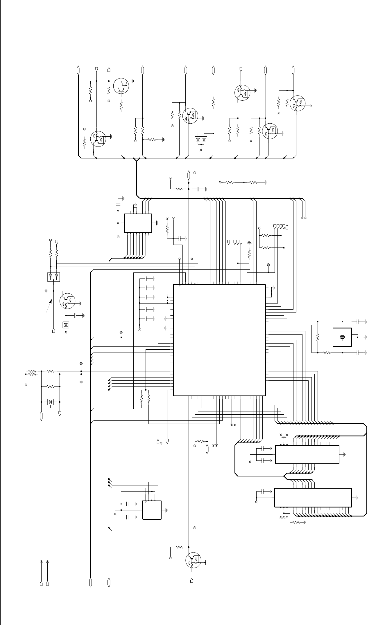
Controller T7/T9 Schematic Diagrams 3-17
4
0
18
100pF
C0104
NU
C0102
100pF
NU
12
0
NU
4.7K
R0171
NU
R0110
10K
NU
18
NU
0.1uF
100pF
NU
NU
R0102
4.7K
NU
R0182
NU
8
16
R0106
0
Used in
prime
only
NU
GP3_IN
GP8_IN
PE6
VOX
LSIO
GP7_IN
HC138_A0
REF_CS
HC138_A2
GP1_IN
GP8_OUT
SQ_DET
HC138_A1
FLASH ROM
SYN
HC138_A2
GP2_OUT
LSIO
MICROPROCESSOR
DATA
MISO
F1200
GP4_IN
EEPROM
DATA
EE_CS
VS_CS
EXP1_CS
GP1_IN
CLK
CSX
GP5_IN
GP4_OUT
GP7_OUT
GP7_IN
CLK
GP5_IN
32kx8bit
OPT_CS
LVZIF_CS
16Kx8bit
GP4_OUT
GP7_OUT
(EXT_BD_PTT & DATA_PTT)
EE_CS
HC138_A0
GP3_IN
GP8_IN
512kx8bit
RAM
GP6_IN
GP6_IN
MISO
EXP2_CS
GP4_OUT
GP7_OUT
HSIO
GP4_IN
ON_OFF_SENSE
GP8_OUT
CHACT
HC138_A1
HSIO
10K
R0172
6
2
10K
R0175
7
R0111
10K
R0115
10
1
0
C0101
7
9
100pF
0
1000pF
C0107
R0114
10K
R0104
10K
10K
R0170
4
10
5
11
0
47K
R0179
R0116
0.1uF
C0141
7
7
R0152
24K
R0132
330K
9Y6
7Y7
12
3
8
GND
16
VCC
15 Y0
14 Y1
13 Y2
12 Y3
11 Y4
10 Y5
MC74HC138A
U0141 1
A0 2
A1 3
A2
6
EN_CS1 4
EN_CS2 5
EN_CS3
5
12
TP0102
6
6
10
2
6
R0185
4.7K
IO4
15
IO5
16
IO6
17
IO7
18
IO8
19
VCC
28
8
A924
EN_CS 20
EN_OE 22
EN_WE 27
14
GND
IO1
11
IO2
12
IO3
13
A14 1
A2 8
A3 7
A4 6
5
A5
A6 4
A7 3
A825
A010
A1 9
21
A10
A1123
A12 2
A1326
11
6
U0122
63A21
8
6
6
9
Q0181
VSSL
40 VSSR
87
93
XFC
XIRQ 48
XTAL 91
RESET 94
VDD 12
VDDL 39
VDDR 88
VDDSYN 92
VRH 69
VRL 68
VSS
13
PJ0_CSGP3 71
PJ1_CSGP4 72
PJ2 73
PJ3 74
PJ4 75
PJ5 76
PJ6 77
PJ7 78
56 PI1
55 PI2
54 PI3
53 PI4
52 PI5
51 PI6
50 PI7
49
PH0_PW1
47
PH1_PW2
46
PH2_PW3
45
PH3_PW4
44
PH4_CSIO
43
PH5_CSGP1
42
PH6_CSGP2
41
PH7_CSPROG
38
PI0
PG0_XA13
6
PG1_XA14
16
PG2_XA15
20
PG3_XA16
19
PG4_XA17
17
PG5_XA18
18
PG6_AS
5
PG7_R_W 4
PF1_ADDR1
28 PF2_ADDR2
27 PF3_ADDR3
26 PF4_ADDR4
25 PF5_ADDR5
24 PF6_ADDR6
23 PF7_ADDR7
22
PFO_ADDR0
29
67
PE0_AN0 66
PE1_AN1 65
PE2_AN2 64
PE3_AN3 63
PE4_AN4 62
PE5_AN5 61
PE6_AN6 60
PE7_AN7
PC7_DATA7
37
PD0_RXD 97
PD1_TXD 98
PD2_MISO 99
PD3_MOSI 100
PD4_SCK 1
PD5_SS 2
3
PD6_LVIN
PBO_ADDR8
14
PC0_DATA0
30
PC1_DATA1
31
PC2_DATA2
32
PC3_DATA3
33
PC4_DATA4
34
PC5_DATA5
35
PC6_DATA6
36
PA7_PA1_OC1 86
PB1_ADDR9
10 PB2_ADDR10
11 PB3_ADDR11
9PB4_ADDR12
21 PB5_ADDR13
15 PB6_ADDR14
8PB7_ADDR15
7
MODB_VSTBY 57
PA0_IC3 79
PA1_IC2 80
PA2_IC1 81
PA3_IC4_OC5_OC1 82
PA4_OC4_OC1 83
PA5_OC3_OC1 84
PA6_OC2_OC1 85
AVDD 59
AVSS
70
ECLK 89
EXTAL 90
IRQ 96
95
LVOUT
MODA_LIR 58
MC68HC11FL0
U0101
47K
R0184
10K
R0174
22pF
C0132
0
Q0185
7
HOLD
6
SCK
5
SI
2SO
8
VCC
4
VSS
3
WP
X25128-2.7
U0111
1
CS
.01uF
C0151
1
13
Q0173
C0106
100pF
D0151
R0173
12
2
3
4.7K
1
8
8
4
6
1
1
17
3
2.2K
R0108
10
1
4
5
7
TP0151
C0121
0.1uF 0.1uF
C0122
TP0103
8
1
10
3
2
2
3
11
4.7K
1
11
12
3
1
R0183
10K
R0113
R0151
24K
0
3
0
13
4
8
D0179
2
6
17
9
10K
R0101
5
7
TP0101
3
Q0110
47K
R0107
7
4.7K
R0177
99
100K
Used in
standard
only
R0105
4
2
7
10
100pF
C0105
4
D0101
3.9K
R0117
5
14
13
16
5
C0123
7
2
5
C0112
Q0151
28
IO6 29
IO7
VCC
8
2
0
3
7EN_WE
GND
24
IO0 21
22
IO1 23
IO2 25
IO3 26
IO4 27
IO5
16 A4
A5
15
A6
14
13 A7
3A8
2A9
30 EN_CE
32 EN_OE
A13
4
5A14
A15
11
10 A16
6A17
9A18
18 A2
17 A3
AT49F040
U0121
20 A0
19 A1
31 A10
1A11
12 A12
4
5
3
1
13
6
13
2
NC1
3
OUT
4IN 1
9
0
6
38.40KHz
Y0131
XTAL
NC
R0112
0
47K
4.7K
R0181
4
3
R0178
5
47K
10MEG
R0131
100pF
C0111
100pF
C0103
22pF
C0131
15
9
7
VR0151
5.6V
14
TP0104
Q0183
15
14
4
5
0
2
Q0171
100K
R0121
Q0177
10
47K
R0186
R0176
30K
R_W
RAM_CS
BUS+
CNTLVLTG
5VD
SCI_TX
GP1_IN_ACC3
GP6_IN_ACC10
GP2_OUT_ACC4
R_W
FLASH_CE
FLASH_OE
5VD
IRQ
IRQ
ADDR_BUS(0:18)
DATA_BUS(0:7)
0
FROM_U0101_47
VS_RAC
5VD
VS_INT
GP4_IN_OUT_ACC8
5VD
BOOT_CNTRL
GP3_IN_ACC6
5VD
ON_OFF_CONTROL
5VD
5VD
5VD
RESET
RESET
5VD
OPT_PTT
5VD
GP5_IN_ACC9
5VD
SPI(0:10) SPI(0:10) SPI(0:10) SPI(0:10) SPI(0:10)
GPIO(0:13)
GPIO(0:13)
CNTLR_AUDIO(0:7) CNTLR_AUDIO(0:7)CNTLR_AUDIO(0:7)
CNTLR_AUDIO(0:7)
FROM_U0101_47
FROM_U0101_46
FROM_U0101_46
5VD
5VD
FLT_A+
TEMPSENSE
RAM_CS
5VD
VS_GAINSEL
EXT_BD_REQ
RSSI
5VD
RX_ADAPT
5VD
5VD5VD
FLT_A+ FLT_A+
FLASH_OE
NC_XTAL
ECLK
LOCK
RDY
ON_OFF_CONTROL
GP7_IN_OUT_ACC12
GP8_IN_OUT_ACC14
5VD
5VD
5VD
5VD
FLASH_CE
R_W
VSTBY
5VD
BATTERY_VOLTAGE
5VDC (0VDC during On/Off pressed
and during head request)
5VDC (0VDC during boot mode)
ZWG0130526-A
Controller T7 only Schematic Diagram - Microprocessor
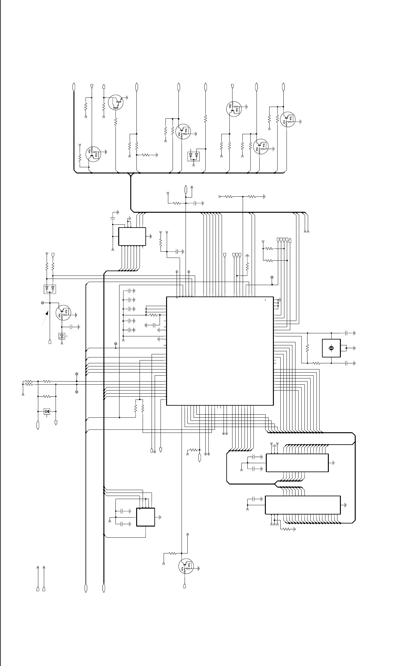
3-18 Controller T7/T9 Schematic Diagrams
4
0
18
100pF
C0104
NU
C0102
100pF
NU
12
0
NU
4.7K
R0171
NU
R0110
10K
NU
18
NU
0.1uF
100pF
NU
NU
R0102
4.7K
NU
R0182
NU
8
16
R0106
0
Used in
prime
only
NU
GP3_IN
GP8_IN
PE6
VOX
LSIO
GP7_IN
HC138_A0
REF_CS
HC138_A2
GP1_IN
GP8_OUT
SQ_DET
HC138_A1
FLASH ROM
SYN
HC138_A2
GP2_OUT
LSIO
MICROPROCESSOR
DATA
MISO
F1200
GP4_IN
EEPROM
DATA
EE_CS
VS_CS
EXP1_CS
GP1_IN
CLK
CSX
GP5_IN
GP4_OUT
GP7_OUT
GP7_IN
CLK
GP5_IN
32kx8bit
OPT_CS
LVZIF_CS
16Kx8bit
GP4_OUT
GP7_OUT
(EXT_BD_PTT & DATA_PTT)
EE_CS
HC138_A0
GP3_IN
GP8_IN
512kx8bit
RAM
GP6_IN
GP6_IN
MISO
EXP2_CS
GP4_OUT
GP7_OUT
HSIO
GP4_IN
ON_OFF_SENSE
GP8_OUT
CHACT
HC138_A1
HSIO
10K
R0172
6
2
10K
R0175
7
R0111
10K
R0115
10
1
0
C0101
7
9
100pF
0
1000pF
C0107
R0114
10K
R0104
10K
10K
R0170
4
10
5
11
0
47K
R0179
R0116
0.1uF
C0141
7
7
R0152
24K
R0132
330K
9Y6
7Y7
12
3
8
GND
16
VCC
15 Y0
14 Y1
13 Y2
12 Y3
11 Y4
10 Y5
MC74HC138A
U0141
1
A0 2
A1 3
A2
6
EN_CS1 4
EN_CS2 5
EN_CS3
5
12
TP0102
6
6
10
2
6
R0185
4.7K
IO4
15
IO5
16
IO6
17
IO7
18
IO8
19
VCC
28
8
A924
EN_CS 20
EN_OE 22
EN_WE 27
14
GND
IO1
11
IO2
12
IO3
13
A14 1
A2 8
A3 7
A4 6
5
A5
A6 4
A7 3
A825
A010
A1 9
21
A10
A1123
A12 2
A1326
11
6
U0122
63A21
8
6
6
9
Q0181
VSSL
40 VSSR
87
93
XFC
XIRQ 48
XTAL 91
RESET 94
VDD 12
VDDL 39
VDDR 88
VDDSYN 92
VRH 69
VRL 68
VSS
13
PJ0_CSGP3 71
PJ1_CSGP4 72
PJ2 73
PJ3 74
PJ4 75
PJ5 76
PJ6 77
PJ7 78
56 PI1
55 PI2
54 PI3
53 PI4
52 PI5
51 PI6
50 PI7
49
PH0_PW1
47
PH1_PW2
46
PH2_PW3
45
PH3_PW4
44
PH4_CSIO
43
PH5_CSGP1
42
PH6_CSGP2
41
PH7_CSPROG
38
PI0
PG0_XA13
6
PG1_XA14
16
PG2_XA15
20
PG3_XA16
19
PG4_XA17
17
PG5_XA18
18
PG6_AS
5
PG7_R_W 4
PF1_ADDR1
28 PF2_ADDR2
27 PF3_ADDR3
26 PF4_ADDR4
25 PF5_ADDR5
24 PF6_ADDR6
23 PF7_ADDR7
22
PFO_ADDR0
29
67
PE0_AN0 66
PE1_AN1 65
PE2_AN2 64
PE3_AN3 63
PE4_AN4 62
PE5_AN5 61
PE6_AN6 60
PE7_AN7
PC7_DATA7
37
PD0_RXD 97
PD1_TXD 98
PD2_MISO 99
PD3_MOSI 100
PD4_SCK 1
PD5_SS 2
3
PD6_LVIN
PBO_ADDR8
14
PC0_DATA0
30
PC1_DATA1
31
PC2_DATA2
32
PC3_DATA3
33
PC4_DATA4
34
PC5_DATA5
35
PC6_DATA6
36
PA7_PA1_OC1 86
PB1_ADDR9
10 PB2_ADDR10
11 PB3_ADDR11
9PB4_ADDR12
21 PB5_ADDR13
15 PB6_ADDR14
8PB7_ADDR15
7
MODB_VSTBY 57
PA0_IC3 79
PA1_IC2 80
PA2_IC1 81
PA3_IC4_OC5_OC1 82
PA4_OC4_OC1 83
PA5_OC3_OC1 84
PA6_OC2_OC1 85
AVDD 59
AVSS
70
ECLK 89
EXTAL 90
IRQ 96
95
LVOUT
MODA_LIR 58
MC68HC11FL0
U0101
47K
R0184
10K
R0174
22pF
C0132
0
Q0185
7
HOLD
6
SCK
5
SI
2SO
8
VCC
4
VSS
3
WP
X25128-2.7
U0111
1
CS
.01uF
C0151
1
13
Q0173
C0106
100pF
D0151
R0173
12
2
3
4.7K
1
8
8
4
6
1
1
17
3
2.2K
R0108
10
1
4
5
7
TP0151
C0121
0.1uF 0.1uF
C0122
TP0103
8
1
10
3
2
2
3
11
4.7K
1
11
12
3
1
R0183
10K
R0113
R0151
24K
0
3
0
13
4
8
D0179
2
6
17
9
10K
R0101
5
7
TP0101
3
Q0110
47K
R0107
7
4.7K
R0177
99
100K
Used in
standard
only
R0105
4
2
7
10
100pF
C0105
4
D0101
3.9K
R0117
5
14
13
16
5
C0123
7
2
5
C0112
Q0151
28
IO6 29
IO7
VCC
8
2
0
3
7EN_WE
GND
24
IO0 21
22
IO1 23
IO2 25
IO3 26
IO4 27
IO5
16 A4
A5
15
A6
14
13 A7
3A8
2A9
30 EN_CE
32 EN_OE
A13
4
5A14
A15
11
10 A16
6A17
9A18
18 A2
17 A3
AT49F040
U0121
20 A0
19 A1
31 A10
1A11
12 A12
4
5
3
1
13
6
13
2
NC1
3
OUT
4IN 1
9
0
6
38.40KHz
Y0131
XTAL
NC
R0112
0
47K
4.7K
R0181
4
3
R0178
5
47K
10MEG
R0131
100pF
C0111
100pF
C0103
22pF
C0131
15
9
7
VR0151
5.6V
14
TP0104
Q0183
15
14
4
5
0
2
Q0171
100K
R0121
Q0177
10
47K
R0186
R0176
30K
R_W
RAM_CS
BUS+
CNTLVLTG
5VD
SCI_TX
GP1_IN_ACC3
GP6_IN_ACC10
GP2_OUT_ACC4
R_W
FLASH_CE
FLASH_OE
5VD
IRQ
IRQ
ADDR_BUS(0:18)
DATA_BUS(0:7)
0
FROM_U0101_47
VS_RAC
5VD
VS_INT
GP4_IN_OUT_ACC8
5VD
BOOT_CNTRL
GP3_IN_ACC6
5VD
ON_OFF_CONTROL
5VD
5VD
5VD
RESET
RESET
5VD
OPT_PTT
5VD
GP5_IN_ACC9
5VD
SPI(0:10) SPI(0:10) SPI(0:10) SPI(0:10) SPI(0:10)
GPIO(0:13)
GPIO(0:13)
CNTLR_AUDIO(0:7) CNTLR_AUDIO(0:7)CNTLR_AUDIO(0:7)
CNTLR_AUDIO(0:7)
FROM_U0101_47
FROM_U0101_46
FROM_U0101_46
5VD
5VD
FLT_A+
TEMPSENSE
RAM_CS
5VD
VS_GAINSEL
EXT_BD_REQ
RSSI
5VD
RX_ADAPT
5VD
5VD5VD
FLT_A+ FLT_A+
FLASH_OE
NC_XTAL
ECLK
LOCK
RDY
ON_OFF_CONTROL
GP7_IN_OUT_ACC12
GP8_IN_OUT_ACC14
5VD
5VD
5VD
5VD
FLASH_CE
R_W
VSTBY
5VD
BATTERY_VOLTAGE
ZWG0130585-O
NU 0
R0103
C0108
0,1uF
5VDC (0VDC during On/Off pressed
and during head request)
5VDC (0VDC during boot mode)
Controller T9 only Schematic Diagram - Microprocessor
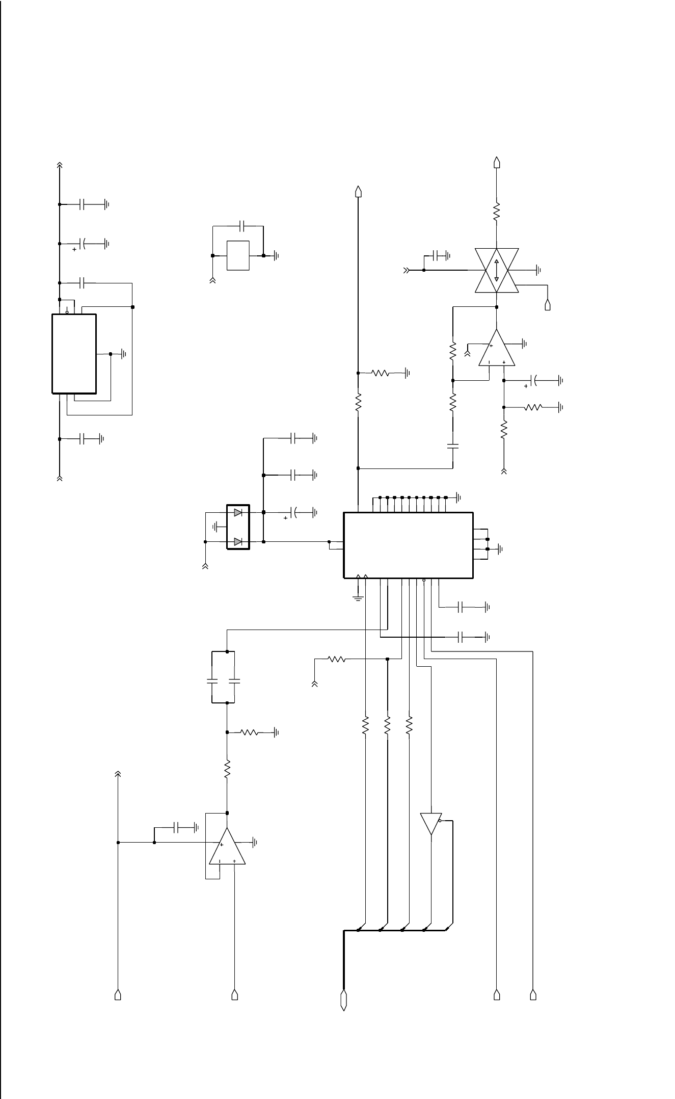
Controller T7/T9 Schematic Diagrams 3-19
9
C0325
0.1uF NU
10K
R0332
C0331
0.1uF
U0331-2
PWR_GND
3
GND
5
VCC
2
C0354
0.1uF
C0342
18K
U0341-2
LM2904
6
57
8
4
2
5
VDD
3
VSS
6
0.1uF
C0302
10
R0343
0
RX_AUD_RTN
5VD
FLAT_RX_SND
3V3
SPI(0:10)
R0324
C0303
100pF
0.1uF
C0305 0.1uF
C0343
0.1uF
1uF
C0324
U0351
LP2951ACMM-3.3
2
C0351
0.1uF
74AHCT1G125
U0331-1
2
A
1
OE
4
Y
33uF
C0353
.022uF
C0352
10K
R0333 SS
9
VCCA
26
VCCD
7
VSSA1
1
VSSA2
17
VSSA3
18
VSSD
12
XCLK
6
10K
R0341
D0301
5
3
1
2
4
8
4
U0342
TC4S66F
4
CNTL
1
47K
R0346
47K
R0347
1uF
C0341
0.1uF
C0304
LM2904
U0341-1
2
31
C0344
0.1uF
8
0.1uF
C0301
CLK
DATA
5109152M01
VS_CS
MISO
VS_CS
56K
R0344
R0335
150K
5.1K
R0345
NC4 14
NC5 15
NC6 16
NC7 19
NC8 21
NC9 23
RAC
2
SCLK
8
INT
MISO
11 MOSI
10
NC1 3
NC10 27
NC11 28
NC2 4
NC3 13
U0301
22 AMCAP
ANA_NEG
24
ANA_POS
25
AUDOUT 20
5
10K
R0331
1.8K
R0342
ERROR 5
FEEDBACK
7
GND
4
INPUT
8OUTPUT 1
SENSE 2
SHUTDOWN
3
VTAP
18K
R0323
VS_MIC
VS_RAC
3V3
3V3
5VD
5VD5VD
VS_INT
5VD
5VD
VS_AUDSEL
5VD
ZWG0130530-O
Controller T7/T9 Schematic Diagram - Voice Storage
3-20 Controller T7/T9 Schematic Diagrams
3.1 Controller T7 Parts List
Circuit
Ref Motorola
Part No Description
C0101 2113740F51 100pF 5% 50V
C0107 2113741F25 1nF 50V
C0112 2113743E20 100nF 16V
C0121 2113743E20 100nF 16V
C0122 2113743E20 100nF 16V
C0131 2113740F35 22pF 5% 50V
C0132 2113740F35 22pF 5% 50V
C0141 2113743E20 100nF 16V
C0151 2113741F49 10nF 50V
C0201 2311049A57 10uF 10% 16V
C0202 2311049A57 10uF 10% 16V
C0204 2113743E20 100nF 16V
C0212 2311049A57 10uF 10% 16V
C0221 2113743E20 100nF 16V
C0222 2113743E20 100nF 16V
C0223 2113743E20 100nF 16V
C0224 2113740F51 100pF 5% 50V
C0225 2113743E20 100nF 16V
C0226 2113743E20 100nF 16V
C0228 2311049A56 4.7uF 10% 16V
C0231 2113743B29 1 UF 10% 16V
C0232 2113743E20 100nF 16V
C0234 2113743E20 100nF 16V
C0235 2113743E07 22nF 16V
C0236 2113743E10 .033UF 10%
C0241 2113743E20 100nF 16V
C0243 2113740F51 100pF 5% 50V
C0244 2113743E20 100nF 16V
C0245 2113743E20 100nF 16V
C0246 2113741F49 10nF 50V
C0251
Used in 2113743E20 100nF 16V
CNTRL T7 only
C0252 2311049A07 1uF 10% 16V
C0254 2113743E20 100nF 16V
C0255 2113743E20 100nF 16V
C0256 2113740F51 100pF 5% 50V
C0261 2113743E20 100nF 16V
C0262 2113740F49 82pF 5% 50V NP0
C0265 2113743E20 100nF 16V
C0267 2113741F49 10nF 50V
C0271 2113741F49 10nF 50V
C0272 2113743E20 100nF 16V
C0273 2113741F37 3.3nF 50V
C0275 2311049A99 47uF 20% 10V
C0276 2113741F25 1nF 50V X7R
C0277 2113741F25 1nF 50V X7R
C0301
Used in 2311049A07
GM398 only TANT CP 1uF 10% 16V
C0302
Used in 2113743E20
GM398 only 100nF 16V
C0303
Used in 2113740F51
GM398 only 100pF 5% 50V
C0304
Used in 2113743E20
GM398 only 100nF 16V
C0305
Used in 2113743E20
GM398 only 100nF 16V
C0324
Used in 2113743E20
GM398 only 100nF 16V
C0331
Used in 2113743E20
GM398 only 100nF 16V
C0341
Used in 2311049A07
GM398 only TANT CP 1uF 10% 16V
C0342
Used in 2113743E20
GM398 only 100nF 16V
C0343
Used in 2113743E20
GM398 only 100nF 16V
Circuit
Ref Motorola
Part No Description
C0344
Used in 2113743E20
GM398 only 100nF 16V
C0351
Used in 2113743E20
GM398 only 100nF 16V
C0352
Used in 2113743E07
GM398 only 22nF 16V
C0353
Used in 2311049A97
GM398 only TANT CHIP 33 UF
C0354
Used in 2113743E20
GM398 only 100nF 16V
C0421 2113743N48 82.0 PF 5%
C0422 2113741F17 470pF 50V
C0423 2113741F17 470pF 50V
C0426 2113743L09 470 PF 10%
C0427 2113743L09 470 PF 10%
C0428 2113743N48 82.0 PF 5%
C0429 2113743L09 470 PF 10%
C0430 2113741F17 470pF 50V
C0431 2113741F17 470pF 50V
C0441 2113743L09 470 PF 10%
C0442 2113743L09 470 PF 10%
C0445 2113743L09 470 PF 10%
C0446 2113743L09 470 PF 10%
C0447 2113743L09 470 PF 10%
C0448 2113743L09 470 PF 10%
C0449 2113743L09 470 PF 10%
C0470 2113743L09 470 PF 10%
C0471 2113743N48 82.0 PF 5%
C0472 2113743N48 82.0 PF 5%
C0473 2113743N48 82.0 PF 5%
C0474 2113743L09 470 PF 10%
C0476 2113743L09 470 PF 10%
C0477 2113743L09 470 PF 10%
C0478 2113743L09 470 PF 10%
Circuit
Ref Motorola
Part No Description
C0482 2113743L09 470 PF 10%
C0483 2113743L09 470 PF 10%
C0484 2113741F17 470pF 50V
C0485 2113743L09 470 PF 10%
C0486 2113743L09 470 PF 10%
C0487 2113743L09 470 PF 10%
C0488 2113743L09 470 PF 10%
C0490 2113743L09 470 PF 10%
C0491 2113743L09 470 PF 10%
C0492 2113743L09 470 PF 10%
C0493 2113743L09 470 PF 10%
C0494 2113743L09 470 PF 10%
C0495 2113743L09 470 PF 10%
C0496 2113743L09 470 PF 10%
C0497 2113743L09 470 PF 10%
C0499 2113743L09 470 PF 10%
C0501 2113741F49 10nF 50V
C0502 2113743L09 470pF 10% (CNTRL T6)
C0502 2113741F17 470pF 50V (CNTRL T7)
C0503 2113743L09 470pF 10% (CNTRL T6)
C0503 2113741F17 470pF 50V (CNTRL T7)
C0504 2113741F17 470pF 50V
C0505 2113743L09 470pF 10% (CNTRL T6)
C0505 2113741F17 470pF 50V (CNTRL T7)
C0506 2113743L09 470pF 10% (CNTRL T6)
C0506 2113741F17 470pF 50V (CNTRL T7)
C0508 2113743L09 470pF 10% (CNTRL T6)
C0508 2113741F17 470pF 50V (CNTRL T7)
C0509 2113743L09 470pF 10% (CNTRL T6)
C0509 2113741F17 470pF 50V (CNTRL T7)
C0510 2113741F17 470pF 50V
C0511 2113743L09 470pF 10% (CNTRL T6)
Circuit
Ref Motorola
Part No Description
Controller T7/T9 Schematic Diagrams 3-21
C0511 2113741F17 470pF 50V (CNTRL T7)
C0512 2113743L09 470pF 10% (CNTRL T6)
C0512 2113741F17 470pF 50V (CNTRL T7)
C0513 2113741F17 470pF 50V
C0514 2113743L09 470pF 10% (CNTRL T6)
C0514 2113741F17 470pF 50V (CNTRL T7)
C0515 2113743L09 470pF 10% (CNTRL T6)
C0515 2113741F17 470pF 50V (CNTRL T7)
C0516 2113741F49 10nF 50V
C0517 2113743N48 82.0 PF 5%
C0518 2113743L09 470pF 10% (CNTRL T6)
C0518 2113741F17 470pF 50V (CNTRL T7)
C0541 2311049A05 470nF 10% 25V
C0542 2311049A99 47uF 20% 10V
C0591 2113743E20 100nF 16V
C0592 2113743E20 100nF 16V
C0593 2113741B69 100nF 50V
C0601 2113741F17 470pF 50V
C0603 2380090M24 LYT 10uF 50V 20%
C0611 2311049C06 CP 22uF 20% 35V
C0612 2113743E20 100nF 16V
C0622 2311049A99 CP 47uF 20%
C0641 2113741F17 470pF 50V
C0644 2311049A97 CHIP 33 UF
C0645 2113743E20 100nF 16VD
C0652 2311049A97 CHIP 33 UF 16
C0654 2311049A57 CP 10uF 10% 16V
C0655 2113743E20 100nF 16V
C0661 2311049C05 CP 47uF 10% 16V
C0662 2113741F49 10nF 50V
C0663 2113743E20 100nF 16V
C0671 2113743E20 100nF 16V
Circuit
Ref Motorola
Part No Description
C0681 2113743E20 100nF 16V
D0101 4880236E05 CHIP SCHOTTKY
D0151 4813833C02 DUAL SOT MMBD6100
D0179 4813833C02 DUAL SOT MMBD6100
D0301
Used in 4802245J47
GM398 only SCHOTTKY BARRIER
(RB471E)
D0621 4813833C02 DUAL SOT MMBD6100
D0651 4813833C02 DUAL SOT MMBD6100
D0660 4813833C02 DUAL SOT MMBD6100
D0661 4813833C02 DUAL SOT MMBD6100
E0271 2484657R01 Ferrite Bead
E0272 2484657R01 Ferrite Bead
E0631 2484657R01 Ferrite Bead
F0401 6580542Z01 3A 24V
J0401 0902636Y02 CONN FLEX 12 PIN
J0451 0902636Y01 CONN FLEX SIDE ENTRY
J0501 0986105B01 CONN SMD 20 PIN
J0551 0905505Y04 CONN ZIF HORIZONTAL
J0552 0905505Y03 CONN ZIF 18PIN
J0601 0986165B01 DC PWR CONN
Q0110 4880048M01 NPN DIG 47k/47k
Q0151 4880048M01 NPN DIG 47k/47k
Q0171 4880048M01 NPN DIG 47k/47k
Q0173 4880052M01 NPN DRLNGTN MXTA
Q0177 4880048M01 NPN DIG 47k/47k
Q0181 4880048M01 NPN DIG 47k/47k
Q0183 4880048M01 NPN DIG 47k/47k
Q0185 4880048M01 NPN DIG 47k/47k
Q0271 4813824A10 NPN 40V .2A
Q0641 4880048M01 NPN DIG 47k/47k
Q0661 4805921T02 DUAL ROHM FMC2 RH
Q0662 4813824A10 NPN 40V .2A B=50-150
Circuit
Ref Motorola
Part No Description
Q0663 4880048M01 NPN DIG 47k/47k
Q0681 4880052M01 NPN DRLNGTN MXTA
R0101 0662057A73 10k 1/16W 5%
R0102 0662057A65 4k7 1/16W 5%
R0104 0662057A73 10k 1/16W 5%
R0105
Used in 0662057A97
GM338 only 100k 1/16W
R0106
Used in 0662057B47
GM398 only 0 1/16W
R0108 0662057A57 2k2 1/16W 5%
R0111 0662057B47 0 1/16W 0306
R0113 0662057A73 10k 1/16W 5%
R0114 0662057A73 10k 1/16W 5%
R0115 0662057A73 10k 1/16W 5%
R0117 0662057A63 3k9 1/16W 5%
R0121 0662057A97 100k 1/16W
R0131 0662057B46 10.0 MEG OHMS 5%
R0132 0662057B10 330k 1/16W 5%
R0151 0662057A82 24K 1/16W 5%
R0152 0662057A82 24K 1/16W 5%
R0170 0662057A73 10k 1/16W 5%
R0171 0662057A65 4k7 1/16W 5%
R0172 0662057A73 10k 1/16W 5%
R0173 0662057A65 4k7 1/16W 5%
R0174 0662057A73 10k 1/16W 5%
R0175 0662057A73 10k 1/16W 5%
R0176 0662057A84 30k 1/16W 5%
R0177 0662057A65 4k7 1/16W 5%
R0178 0662057A89 47k 1/16W 5%
R0179 0662057A89 47k 1/16W 5%
R0181 0662057A65 4k7 1/16W 5%
R0182 0662057A89 47k 1/16W 5%
R0183 0662057A65 4k7 1/16W 5%
Circuit
Ref Motorola
Part No Description
R0184 0662057A89 47k 1/16W 5%
R0185 0662057A65 4k7 1/16W 5%
R0186 0662057A89 47k 1/16W 5%
R0201 0662057A25 100 1/16W 5%
R0202 0662057A43 560 1/16W 5%
R0203 0662057A25 100 1/16W 5%
R0204 0662057A43 560 1/16W 5%
R0205 0662057A73 10k 1/16W 5%
R0206 0662057A73 10k 1/16W 5%
R0207 0662057A57 2k2 1/16W 5%
R0208 0662057A57 2k2 1/16W 5%
R0211 0660076E70 FILM 7500
R0212 0660076E70 FILM 7500
R0221 0662057A82 24K 1/16W 5%
R0222 0662057A82 24K 1/16W 5%
R0223 0662057A84 30k 1/16W 5%
R0224 0662057A71 8k2 1/16W 5%
R0228 0662057B47 0 1/16W
R0229 0662057A01 10 1/16W 5%
R0241 0662057A89 47k 1/16W 5%
R0242 0662057B47 0 1/16W
R0251 0662057A89 47k 1/16W 5%
R0252 0662057A91 56K 1/16W 5%
R0253 0662057A97 100k 1/16W
R0254 0662057A73 10k 1/16W 5%
(CNTRL T7 only)
R0255 0662057A73 10k 1/16W 5%
(CNTRL T7 only)
R0256 0662057A97 100k 1/16W
(CNTRL T7 only)
R0257 0662057A57 2k2 1/16W 5%
(CNTRL T7 only)
R0261 0662057A73 10k 1/16W 5%
R0262 0662057A97 100k 1/16W
Circuit
Ref Motorola
Part No Description
3-22 Controller T7/T9 Schematic Diagrams
* Motorola Depot Servicing only
Reference designators with an asterisk indicate
components which are not fieldreplaceable
because they need to be calibrated with
specialized factory equipment after installation.
Radios in which these parts have been replaced in
the field will be off frequency at temperature
extremes.
R0265 0662057A82 24K 1/16W 5%
R0267 0662057A89 47k 1/16W 5%
R0268 0662057A73 10k 1/16W 5%
R0269 0662057A41 470 1/16W 5%
R0273 0662057A82 24K 1/16W 5%
R0275 0662057A73 10k 1/16W 5%
R0276 0662057A77 15k 1/16W 5%
R0323
Used in 0662057A79
GM398 only 18k 1/16W 5%
R0324
Used in 0662057A79
GM398 only 18k 1/16W 5%
R0331
Used in 0662057A73
GM398 only 10k 1/16W 5%
R0332
Used in 0662057A73
GM398 only 10k 1/16W 5%
R0333
Used in 0662057A73
GM398 only 10k 1/16W 5%
R0335
Used in 0662057B02
GM398 only 150k 1/16W
R0341
Used in 0662057A73
GM398 only 10k 1/16W
R0342
Used in 0662057A55
GM398 only 1k8 1/16W
R0343
Used in 0662057B47
GM398 only 0 1/16W
R0344
Used in 0662057A91
GM398 only 56K 1/16W
R0345
Used in 0662057A66
GM398 only 5k1 1/16W
R0346
Used in 0662057A89
GM398 only 47k 1/16W
R0347
Used in 0662057A89
GM398 only 47k 1/16W
R0401 0662057A33 220 1/16W
R0407 0662057M26 10 5% 20X40
R0408 0662057A25 100 1/16W 5%
R0409 0662057M26 10 5% 20X40
Circuit
Ref Motorola
Part No Description
R0412 0662057B47 0 1/16W
R0441 0662057B47 0 1/16W
R0442
Used in 0662057A49 1k 1/16W 5%
CNTRL T7 only
R0467 0662057M26 10 5% 20X40
R0468 0662057M26 10 5% 20X40 (CNTRL T6)
R0468 0662057A97 100k 1/16W (CNTRL T7)
R0481 0662057B47 0 1/16W
R0482 0662057B47 0 1/16W
R0510 0662057A65 4k7 1/16W 5%
R0511 0662057A97 100k 1/16W
R0512 0662057A77 15k 1/16W 5%
R0525 0662057A97 100k 1/16W
R0529 0662057A89 47k 1/16W 5%
R0530 0662057B47 0 1/16W
R0531 0662057A43 560 1/16W 5%
R0533 0662057B47 0 1/16W
R0535 0662057A49 1k 1/16W 5%
R0537 0662057A33 220 1/16W 5%
R0538 0662057A33 220 1/16W 5%
R0539 0662057A65 4k7 1/16W 5%
R0541 0662057A83 27k 1/16W 5%
R0543 0662057A97 100k 1/16W
(CNTRL T7 only)
R0591 0662057A82 24K 1/16W 5%
R0592 0662057A01 10 1/16W 5%
R0593 0662057A97 100k 1/16W
(CNTRL T7 only)
R0611 0662057A91 56K 1/16W
R0612 0662057A65 4k7 1/16W
R0621 0662057A82 24K 1/16W
R0641 0662057A73 10k 1/16W
R0642 0660076E70 FILM 7500
Circuit
Ref Motorola
Part No Description
R0643 0660076E51 FILM 1200
R0651 0662057A01 10 1/16W 5%
R0652 0662057A01 10 1/16W 5%
R0661 0662057A49 1k 1/16W 5%
R0662 0662057B02 150k 1/16W
R0671 0662057A84 30k 1/16W 5%
R0672 0662057A73 10k 1/16W 5%
R0681 0662057A79 18k 1/16W 5%
R0682 0662057A93 68k 1/16W 5%
U0101 5102226J56 MICRO PROCESSOR
MC68HC1 1FLO
* U0111 5102463J64 EEPROM X25128-2.7 SO8
* U0121 5186137B01 512KX8 FLASH ROM
(AT49BV020)
U0122 5185963A21 32K x 8 SRAM
U0141 5113805A30 10F8 DCDR/REMUX
74HC138
U0211 5183222M49 QUAD OPAMP __3403
U0221 5185963A53 ASFICCMP 0.5MM TQFP
U0251 5113806A20 MUX/DEMUX,TRIPLE 2-
U0271 5109699X01 AUDIO PA TDA1519C
U0301
Used in 5109152M01
GM398 only EEPROM ANALOG
ISD33120EI
U0331
Used in 5186204B01
GM398 only BUFFER/DRIVER
74AHCT1G125
U0341
Used in 5180932W01
GM398 only LINEAR IC OP AMP
U0342
Used in 5105750U28
GM398 only SNGL ANALOG SWITCH
SMD
U0351
Used in 5102463J40
GM398 only REGULATOR, 3.3V,
LP2951CM-3.3
U0611 5183308X01 ADJ VLTG REG LM2941
TO263
U0641 5183308X01 ADJ VLTG REG LM2941
TO263
Circuit
Ref Motorola
Part No Description
U0651 5113816A07 REG 5V POS 500MA
MC78M05
U0652 5113815A02 MC33064
VR0151 4813830A15 5.6V 5% 225mW
VR0501 4805656W09 ZENER QUAD
MMQA20VT1
VR0503 4805656W09 ZENER QUAD
MMQA20VT1
VR0504 4813830A40 SOC23 AUTO SDN
VR0505 4805656W09 ZENER QUAD
MMQA20VT1
VR0509 4813830A40 SOC23 AUTO SDN
VR0510 4813830A40 SOC23 AUTO SDN
VR0537 4813830A15 5.6V 5% 225mW
VR0541 4813830A27 14V 5% 225MW
VR0601 4813832C77 TRANS SUP. 24V HIGH
POWER
VR0621 4813830A15 5.6V 5% 225mW
Y0131 4880113R19 CRYSTAL 38.4KHz
Circuit
Ref Motorola
Part No Description
Controller T7/T9 Schematic Diagrams 3-23
3.2 Controller T9 Parts List
Circuit
Ref Motorola
Part No Description
C0101 2113740F51 100pF
C0107 2113741F25 1000pF
C0112 2113743E20 10uF
C0121 2113743E20 10uF
C0122 2113743E20 10uF
C0131 2113740F35 22pF
C0132 2113740F35 22pF
C0141 2113743E20 10uF
C0151 2113741F49 10nF
C0201 2311049A57 10uF
C0202 2311049A57 10uF
C0204 2113743E20 10uF
C0212 2311049A57 10uF
C0221 2113743E20 10uF
C0222 2113743E20 10uF
C0223 2113743E20 10uF
C0224 2113740F51 100pF
C0225 2113743E20 10uF
C0226 2113743E20 10uF
C0228 2311049A56 4.7uF
C0231 2113743B29 1uF
C0232 2113743E20 10uF
C0234 2113743E20 10uF
C0235 2113743E07 0.022uF
C0236 2113743E10 0.033uF
C0241 2113743E20 10uF
C0243 2113740F51 100pF
C0244 2113743E20 10uF
C0245 2113743E20 10uF
C0246 2113741F49 10nF
C0251 2113743E20 10uF
C0252 2311049A07 1uF
C0254 2113743E20 10uF
C0255 2113743E20 10uF
C0256 2113740F51 100pF
C0261 2113743E20 10uF
C0262 2113740F49 82pF
C0265 2113743E20 10uF
C0267 2113741F49 10nF
C0271 2113741F49 10nF
C0272 2113743E20 10uF
C0273 2113741F37 3300pF
C0275 2311049A99 47uF
C0276 2113741F25 1000pF
C0277 2113741F25 1000pF
C0301 2311049A07 1uF
C0302 2113743E20 10uF
C0303 2113740F51 100pF
C0304 2113743E20 10uF
C0305 2113743E20 10uF
C0324 2113743E20 10uF
C0331 2113743E20 10uF
C0341 2311049A07 1uF
C0342 2113743E20 10uF
C0343 2113743E20 10uF
C0344 2113743E20 10uF
C0351 2113743E20 10uF
C0352 2113743E07 0.022uF
C0353 2311049A97 33uF
C0354 2113743E20 10uF
C0421 2113743N48 82pF
C0422 2113741F17 470pF
C0423 2113741F17 470pF
Circuit
Ref Motorola
Part No Description
C0426 2113743L09 470pF
C0427 2113743L09 470pF
C0428 2113743N48 82pF
C0429 2113743L09 470pF
C0430 2113741F17 470pF
C0431 2113741F17 470pF
C0441 2113743L09 470pF
C0442 2113743L09 470pF
C0445 2113743L09 470pF
C0446 2113743L09 470pF
C0447 2113743L09 470pF
C0448 2113743L09 470pF
C0449 2113743L09 470pF
C0470 2113743L09 470pF
C0471 2113743N48 82pF
C0472 2113743N48 82pF
C0473 2113743N48 82pF
C0474 2113743L09 470pF
C0476 2113743L09 470pF
C0477 2113743L09 470pF
C0478 2113743L09 470pF
C0482-
C0488 2113743L09 470pF
C0490-
C0497 2113743L09 470pF
C0499 2113743L09 470pF
C0501 2113741F49 10nF
C0502 2113741F17 470pF
C0503 2113741F17 470pF
C0504 2113741F17 470pF
C0505 2113741F17 470pF
C0506 2113741F17 470pF
Circuit
Ref Motorola
Part No Description
C0508 2113741F17 470pF
C0509 2113741F17 470pF
C0510 2113741F17 470pF
C0511 2113741F17 470pF
C0512 2113741F17 470pF
C0513 2113741F17 470pF
C0514 2113741F17 470pF
C0515 2113741F17 470pF
C0516 2113741F49 10nF
C0517 2113743N48 82pF
C0518 2113741F17 470pF
C0541 2311049A05 0.47uF
C0542 2311049A99 47uF
C0560 2113741F25 1000pF
C0591 2113743E20 10uF
C0592 2113743E20 10uF
C0593 2113741B69 100K F
C0601 2113741F17 470pF
C0603 2380090M24 10uF
C0611 2311049C06 47uF
C0612 2113743E20 10uF
C0622 2311049A99 47uF
C0641 2113741F17 470pF
C0644 2311049A97 33uF
C0645 2113743E20 10uF
C0652 2311049A97 33uF
C0654 2311049A57 10uF
C0655 2113743E20 10uF
C0661 2311049C05 47uF
C0662 2113741F49 10nF
C0663 2113743E20 10uF
C0671 2113743E20 10uF
Circuit
Ref Motorola
Part No Description
3-24 Controller T7/T9 Schematic Diagrams
C0681 2113743E20 10uF
D0101 4813825A05 DIODE
D0151 4813833C02 DIODE, DUAL 70V
D0179 4813833C02 DIODE, DUAL 70V
D0301 4802245J47 DIODE, SCHOTTKY
D0621 4813833C02 DIODE, DUAL 70V
D0651 4813833C02 DIODE, DUAL 70V
D0660 4813833C02 DIODE, DUAL 70V
D0661 4813833C02 DIODE, DUAL 70V
E0271 2484657R01 Ferrite Bead
E0272 2484657R01 Ferrite Bead
E0631 2484657R01 Ferrite Bead
F0401 6580542Z01 FUSE 3A
J0401 0902636Y02 12 POS. FLEX CONN
J0451 0902636Y01 CONN, FLEX, SIDE
ENTRY
J0501 0986105B01 CONN, SMD, 20 Pin
J0551 0905505Y04 CONN ZIF HORIZONTAL
J0552 0905505Y03 CONN ZIF HORIZONTAL
J0601 0986165B01 MOBILE DC PWR CONN
Q0110 4880048M01 NPN
Q0151 4880048M01 NPN
Q0171 4880048M01 NPN
Q0173 4880052M01 NPN DARLINGTON
Q0177 4880048M01 NPN
Q0181 4880048M01 NPN
Q0183 4880048M01 NPN
Q0185 4880048M01 NPN
Q0271 4880214G02 NPN
Q0641 4880048M01 NPN
Q0661 4805921T02 TRANSISTOR DUAL DIGI-
TAL NPN/PNP
Q0662 4880214G02 NPN
Circuit
Ref Motorola
Part No Description
Q0663 4880048M01 NPN
Q0681 4880052M01 NPN DARLINGTON
R0101 0662057A73 10K Ohm
R0102 0662057A65 4700 Ohm
R0103 0662057B47 0 Ohm
R0104 0662057A73 10K Ohm
R0106 0662057B47 0 Ohm
R0108 0662057A57 2200 Ohm
R0111 0662057B47 0 Ohm
R0113 0662057A73 10K Ohm
R0114 0662057A73 10K Ohm
R0115 0662057A73 10K Ohm
R0117 0662057A63 3900 Ohm
R0121 0662057A97 100K Ohm
R0131 0662057B46 10M Ohm
R0132 0662057B10 330K Ohm
R0151 0662057A82 24K Ohm
R0152 0662057A82 24K Ohm
R0170 0662057A73 10K Ohm
R0171 0662057A65 4700 Ohm
R0172 0662057A73 10K Ohm
R0173 0662057A65 4700 Ohm
R0174 0662057A73 10K Ohm
R0175 0662057A73 10K Ohm
R0176 0662057A84 30K Ohm
R0177 0662057A65 4700 Ohm
R0178 0662057A89 47K Ohm
R0179 0662057A89 47K Ohm
R0181 0662057A65 4700 Ohm
R0182 0662057A89 47K Ohm
R0183 0662057A65 4700 Ohm
R0184 0662057A89 47K Ohm
Circuit
Ref Motorola
Part No Description
R0185 0662057A65 4700 Ohm
R0186 0662057A89 47K Ohm
R0201 0662057A25 100 Ohm
R0202 0662057A43 560 Ohm
R0203 0662057A25 100 Ohm
R0204 0662057A43 560 Ohm
R0205 0662057A73 10K Ohm
R0206 0662057A73 10K Ohm
R0207 0662057A57 2200 Ohm
R0208 0662057A57 2200 Ohm
R0211 0660076E70 7500 Ohm
R0212 0660076E70 7500 Ohm
R0221 0662057A82 24K Ohm
R0222 0662057A82 24K Ohm
R0223 0662057A84 30K Ohm
R0224 0662057A71 8200 Ohm
R0228 0662057B47 0 Ohm
R0229 0662057A01 10 Ohm
R0241 0662057A89 47K Ohm
R0242 0662057B47 0 Ohm
R0251 0662057A89 47K Ohm
R0252 0662057A91 56K Ohm
R0253 0662057A97 100K Ohm
R0254 0662057A73 10K Ohm
R0255 0662057A73 10K Ohm
R0256 0662057A97 100K Ohm
R0257 0662057A57 2200 Ohm
R0261 0662057A73 10K Ohm
R0262 0662057A97 100K Ohm
R0265 0662057A82 24K Ohm
R0267 0662057A89 47K Ohm
R0268 0662057A73 10K Ohm
Circuit
Ref Motorola
Part No Description
R0269 0662057A41 470 Ohm
R0273 0662057A82 24K Ohm
R0275 0662057A73 10K Ohm
R0276 0662057A77 15K Ohm
R0323 0662057A79 18K Ohm
R0324 0662057A79 18K Ohm
R0331 0662057A73 10K Ohm
R0332 0662057A73 10K Ohm
R0333 0662057A73 10K Ohm
R0335 0662057B02 150K Ohm
R0341 0662057A73 10K Ohm
R0342 0662057A55 1800 Ohm
R0343 0662057B47 0 Ohm
R0344 0662057A91 56K Ohm
R0345 0662057A66 5100 Ohm
R0346 0662057A89 47K Ohm
R0347 0662057A89 47K Ohm
R0401 0662057A33 220 Ohm
R0407 0662057M26 10 Ohm
R0408 0662057A25 100 Ohm
R0409 0662057M26 10 Ohm
R0412 0662057B47 0 Ohm
R0441 0662057B47 0 Ohm
R0442 0662057A49 1000 Ohm
R0467 0662057M26 10 Ohm
R0468 0662057A97 100K Ohm
R0481 0662057B47 0 Ohm
R0482 0662057B47 0 Ohm
R0510 0662057A65 4700 Ohm
R0511 0662057A97 100K Ohm
R0512 0662057A77 15K Ohm
R0525 0662057A97 100K Ohm
Circuit
Ref Motorola
Part No Description
Controller T7/T9 Schematic Diagrams 3-25
* Motorola Depot Servicing only
Reference designators with an asterisk indicate
components which are not field replaceable
because they need to be calibrated with
specialized factory equipment after installation.
Radios in which these parts have been replaced in
the field will be off frequency at temperature
extremes.
R0529 0662057A89 47K Ohm
R0530 0662057B47 0 Ohm
R0531 0662057A43 560 Ohm
R0533 0662057B47 0 Ohm
R0535 0662057A49 1000 Ohm
R0537 0662057A33 220 Ohm
R0538 0662057A33 220 Ohm
R0539 0662057A65 4700 Ohm
R0541 0662057A83 27K Ohm
R0543 0662057A97 100K Ohm
R0555 0662057A25 100 Ohm
R0556 0662057A25 100 Ohm
R0591 0662057A82 24K Ohm
R0592 0662057A01 10 Ohm
R0593 0662057A97 100K Ohm
R0611 0662057A91 56K Ohm
R0612 0662057A65 4700 Ohm
R0621 0662057A82 24K Ohm
R0641 0662057A73 10K Ohm
R0642 0660076E70 7500 Ohm
R0643 0660076E51 1200 Ohm
R0651 0662057A01 10 Ohm
R0652 0662057A01 10 Ohm
R0661 0662057A49 1000 Ohm
R0662 0662057B02 150K Ohm
R0671 0662057A84 30K Ohm
R0672 0662057A73 10K Ohm
R0681 0662057A79 18K Ohm
R0682 0662057A93 68K Ohm
U0101 5102226J56 MICROPROCESSOR
U0111 5102463J64 EEPROM
U0121 5186137B01 IC, FLASH ROM
Circuit
Ref Motorola
Part No Description
U0122 5185748L01 SRAM
U0141 5113805A30 IC 10F8 DCDR/REMUX
74HC138
U0211 5183222M49 IC, QUAD OPAMP
U0221 5185130C53 IC, ASFIC
U0251 5184704M60 IC-CMOS ANALOG
U0271 5109699X01 AUDIO PA
U0301 5109152M01 IC, EEPROM ANALOG
U0331 5186204B01 IC, BUFFER DRIVER
U0341 5113818A01 LOW POWER SUPPLY
U0342 5105750U28 IC CMOS SWITCH
U0351 5102463J40 REGULATOR, 3.3V
U0611 5183308X01 ADJUSTABLE VOLTAGE
REGULATOR
U0641 5183308X01 ADJUSTABLE VOLTAGE
REGULATOR
U0651 5113816A07 REGULATOR, 5V
U0652 5113815A02 UNDERVOLT SENSOR
VR0151 4813830A15 DIODE, 5.6V
VR0501 4805656W09 DIODE, ZENER
VR0503 4805656W09 DIODE, ZENER
VR0504 4813830A40 DIODE, ZENER
VR0505 4805656W09 DIODE, ZENER
VR0509 4813830A40 DIODE, ZENER
VR0510 4813830A40 DIODE, ZENER
VR0537 4813830A15 DIODE, 5.6V
VR0541 4813830A27 DIODE, 14V
VR0601 4813832C77 DIODE
VR0621 4813830A15 DIODE, 5.6V
Y0131 4880113R19 CRYSTAL 38.4KHZ
Circuit
Ref Motorola
Part No Description

3-26 Controller T7/T9 Schematic Diagrams
THIS PAGE INTENTIONALLY LEFT BLANK

GM328/GM338/GM398
Mobile Radios
VHF (136-174MHz)
Service Information
Issue: December, 2003

Computer Software Copyrights
The Motorola products described in this manual may include copyrighted Motorola computer programs stored
in semiconductor memories or other media. Laws in the United States and other countries preserve for
Motorola certain exclusive rights for copyrighted computer programs, including the exclusive right to copy or
reproduce in any form, the copyrighted computer program. Accordingly, any copyrighted Motorola computer
programs contained in the Motorola products described in this manual may not be copied or reproduced in
any manner without the express written permission of Motorola. Furthermore, the purchase of Motorola
products shall not be deemed to grant, either directly or by implication, estoppel or otherwise, any license
under the copyrights, patents or patent applications of Motorola, except for the normal non-exclusive royalty-
free license to use that arises by operation of law in the sale of a product.

i
Table of Contents
Section 1 Model Chart and Technical Specifications
1.0 GM328/GM338/GM398 Model Chart...................................................................1-1
2.0 Technical Specifications ......................................................................................1-2
Section 2 Theory of Operation
1.0 Introduction ..........................................................................................................2-1
2.0 VHF (136-174 MHz) Receiver..............................................................................2-1
2.1 Receiver Front-End ........................................................................................2-1
2.2 Front-End Band-Pass Filters & Pre-Amplifier.................................................2-2
2.3 First Mixer and High Intermediate Frequency (IF)..........................................2-2
2.4 Low Intermediate Frequency (IF) and Receiver Back End.............................2-3
3.0 VHF (136-174 MHz) Transmitter Power Amplifier (PA) 25 W..............................2-3
3.1 First Power Controlled Stage..........................................................................2-4
3.2 Power Controlled Driver Stage.......................................................................2-4
3.3 Final Stage .....................................................................................................2-4
3.4 Directional Coupler.........................................................................................2-5
3.5 Antenna Switch...............................................................................................2-5
3.6 Harmonic Filter ...............................................................................................2-5
3.7 Power Control.................................................................................................2-5
4.0 VHF (136-174 MHz) Frequency Synthesis ..........................................................2-6
4.1 Reference Oscillator.......................................................................................2-6
4.2 Fractional-N Synthesizer ................................................................................2-6
4.3 Voltage Controlled Oscillator (VCO)...............................................................2-7
4.4 Synthesizer Operation....................................................................................2-8
Section 3 Troubleshooting Charts
1.0 Troubleshooting Flow Chart for Receiver ............................................................3-1
2.0 Troubleshooting Flow Chart for 25W Transmitter................................................3-3
3.0 Troubleshooting Flow Chart for Synthesizer........................................................3-6
4.0 Troubleshooting Flow Chart for VCO...................................................................3-7

ii
Section 4 VHF PCBs/Schematics/Parts Lists
1.0 Allocation of Schematics and Circuit Boards .......................................................4-1
1.1 Controller Circuits...........................................................................................4-1
2.0 VHF 1-25W PCBs / Schematics / Parts Lists ......................................................4-3
VHF (136-174 MHz) 1-25W 8486172B06 Top Side..............................................4-3
VHF (136-174 MHz) 1-25W 8486172B06 Bottom Side.........................................4-4
VHF (136-174 MHz) Power Amplifier 1-25W..........................................................4-5
VHF (136-174 MHz) FRACN..................................................................................4-6
VHF (136-174 MHz) Voltage Controlled Oscillator.................................................4-7
VHF (136-174 MHz) Receiver Front End ...............................................................4-8
VHF (136-174 MHz) IF ...........................................................................................4-9
VHF PCB 8486172B06 Parts List 1-25W.............................................................4-10
VHF (136-174 MHz) 1-25W 8486172B07 Top Side............................................4-13
VHF (136-174 MHz) 1-25W 8486172B07 Bottom Side.......................................4-14
VHF (136-174 MHz) IF .........................................................................................4-15
VHF (136-174 MHz) FRACN................................................................................4-16
VHF PCB 8486172B07 Parts List 1-25W.............................................................4-17
1-1
Section 1
MODEL CHART AND TECHNICAL SPECIFICATIONS
1.0 GM328/GM338/GM398 Model Chart
GM Series, VHF 136-174 MHz
Model Description
AZM25KHC9AA1 GM328 136-174 MHz 1-25W
AZM25KHF9AA5 GM338 136-174 MHz 1-25W
AZM25KHN9AA8 GM398 136-174 MHz 1-25W
Item Description
X GCN6112_ GM328 Control Head Direct Mount
XGCN6114_ GM338 Control Head Direct Mount
X GCN6115_ GM398 Control Head Direct Mount
X X IMUD6010_ Tanapa WM 136-174 MHz 1-25W
X IMUD6023_ Tanapa WM 136-174 MHz 1-25W
XXXRAD4198_ BNC 136-144 MHz, 1/4 Wave Roof Mount
XXXRAD4199_ BNC 146-150.8 MHz, 1/4 Wave Roof Mount
XXXRAD4200_ BNC 150.8-162 MHz, 1/4 Wave Roof Mount
XXXRAD4201_ BNC 162-174 MHz, 1/4 Wave Roof Mount
XXXRAD4202_ BNC 146-172 MHz, 3dB Gain Roof Mount
X 6804113J74 GM328 User Guide
X6804112J06 GM338 User Guide
X 6804112J07 GM398 User Guide
x = Indicates one of each is required.

1-2 Technical Specifications
2.0 Technical Specifications
Data is specified for +25°C unless otherwise stated.
General Specifications
Channel Capacity
GM328
GM338
GM398
4
128
160
Power Supply 13.2Vdc (10.8 - 15.6Vdc)
Dimensions: H x W x D (mm) Depth excluding knobs GM328
56mm x 176mm x 177mm
(add 8mm for Volume Knob)
Dimensions: H x W x D (mm) Depth excluding knobs GM338
59mm x 179mm x 186mm (1 - 25W)
59mm x 179mm x 198mm (25 - 45W)
(add 9mm for Volume Knob)
Dimensions: H x W x D (mm) Depth excluding knobs GM398
72mm x 185mm x 188mm
(add 7mm for Volume Knob)
Weight GM328/GM338 1400 g
Weight GM398 1500 g
Sealing: Withstands rain testing per
MIL STD 810 C/D /E and IP54
Shock and Vibration: Protection provided via impact
resistant housing exceeding MIL STD
810-C/D /E
Dust, Salt & Fog Protection provided via environment
resistant housing exceeding MIL STD
810 C/D /E
Technical Specifications 1-3
*Availability subject to the laws and regulations of individual countries.
Transmitter VHF
*Frequencies - Full Bandsplit VHF 136-174 MHz
Channel Spacing 12.5/20/25 kHz
Frequency Stability
(-30°C to +60°C, +25° Ref.) ±2.5 ppm
Power 1-25W
Modulation Limiting ±2.5 @ 12.5 kHz
±4.0 @ 20 kHz
±5.0 @ 25 kHz
FM Hum & Noise -40 dB @ 12.5kHz
-45 dB @ 20/25kHz
Conducted/Radiated Emission (ETS) -36 dBm <1 GHz
-30 dBm >1 GHz
Adjacent Channel Power -60 dB @ 12.5 kHz
-70 dB @ 25 kHz
Audio Response (300 - 3000Hz) +1 to -3 dB
Audio Distortion @1000Hz, 60%
Rated Maximum Deviation <3% typical
Receiver VHF
*Frequencies - Full Bandsplit VHF 136-174 MHz
Channel Spacing 12.5/20/25 kHz
Sensitivity (12 dB SINAD) 0.30 µV (0.22 µV typical)
Intermodulation (ETS) >65 dB
Base Mode: >70dB
(1-25W model only)
Adjacent Channel Selectivity (ETS) 65 dB @ 12.5 kHz
75 dB @ 20 kHz
80 dB @ 25 kHz
Spurious Rejection (ETS) 75 dB @ 12.5 kHz
80 dB @ 20/25 kHz
Rated Audio 3W Internal
13W External
Audio Distortion @ Rated Audio <3% typical
Hum & Noise -40 dB @ 12.5 kHz
-45 dB @ 20/25 kHz
Audio Response (300 - 3000Hz @ 20/25kHz)
(300 - 2550Hz @12.5kHz) +1 to -3 dB
Conducted Spurious Emission (ETS) -57 dBm <1 GHz
-47 dBm >1 GHz

1-4 Technical Specifications
THIS PAGE INTENTIONALLY LEFT BLANK
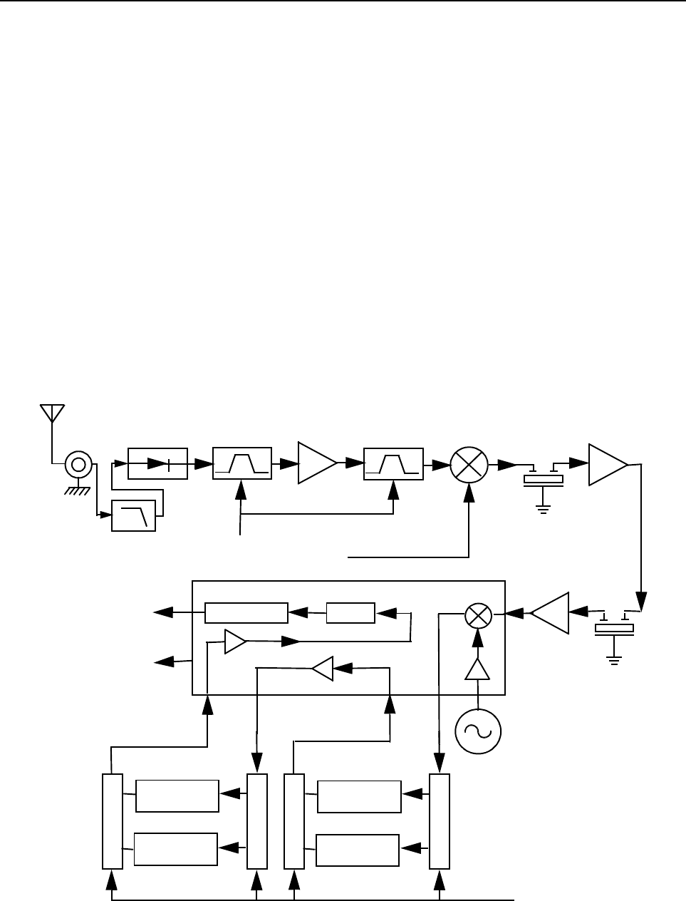
2-1
Section 2
THEORY OF OPERATION
1.0 Introduction
This Chapter provides a detailed theory of operation for the VHF circuits in the radio. For details of
the theory of operation and troubleshooting for the the associated Controller circuits refer to the
Controller Section of this manual.
2.0 VHF (136-174 MHz) Receiver
2.1 Receiver Front-End
The receiver is able to cover the VHF range from 136 to 174 MHz. It consists of four major blocks:
front-end bandpass filters and pre-amplifier, first mixer, high-IF, low-IF and receiver back-end. Two
varactor-tuned bandpass filters perform antenna signal pre-selection. A cross over quad diode mixer
converts the signal to the first IF of 44.85 MHz. High-side first injection is used.
Figure 2-1 VHF Receiver Block Diagram
Demodulator
1. Crystal
Filter
Mixer
Varactor
Tuned Filter
RF Amp
Varactor
Tuned Filter
Antenna
Control Voltage
from PCIC First LO
from FGU
Recovered Audio
RSSI
IF
Second LO
2. Crystal
Filter
455kHz Filter
(25kHz)
455kHz Filter
(25kHz)
455kHz Filter
(12.5kHz)
455kHz Filter
(12.5kHz)
Switch
Switch
Switch
Switch
Limiter
1. IF Amp
2. IF Amp
Filter Bank Selection
from Synthesizer IC
Pin Diode
Antenna
Switch
RF Jack
Harmonic
Filter

2-2 VHF (136-174 MHz) Receiver
There are two 2-pole 44.85 MHz crystal filters in the high-IF section and 2 pairs of 455 kHz ceramic
filters in the low-IF section to provide the required adjacent channel selectivity. The correct pair of
ceramic filters for 12.5 or 25kHz channel spacing is selected via control line BWSELECT. The
second IF at 455 kHz is mixed, amplified and demodulated in the IF IC. The processing of the
demodulated audio signal is performed by an audio processing IC located in the controller section.
2.2 Front-End Band-Pass Filters & Pre-Amplifier
The received signal from the radio’s antenna connector is first routed through the harmonic filter and
antenna switch, which are part of the RF power amplifier circuitry, before being applied to the
receiver pre-selector filter (C3001, C3002, D3001 and associated components). The 2-pole pre-
selector filter tuned by the dual varactor diode D3001 pre-selects the incoming signal (RXIN) from
the antenna switch to reduce spurious effects to following stages. The tuning voltage (FECNTL_1)
ranging from 2 volts to 8 volts is controlled by pin 20 of PCIC (U3501) in the Transmitter section. A
dual hot carrier diode (D3003) limits any inband signal to 0 dBm to prevent damage to the pre-
amplifier.
The RF pre-amplifier is an SMD device (Q3001) with collector-base feedback to stabilize gain,
impedance, and intermodulation. Transistor Q3002 compares the voltage drop across resistor
R3002 with a fixed base voltage from divider R3011, R3000 and R3012, and adjusts the base
current of Q3001 as necessary to maintain its collector current constant at approximately 15-20 mA.
Operating voltage is from the regulated 9.3V supply (9V3). During transmit, 9.1 volts (K9V1) turns off
both transistors Q3002 and Q3001. This protects the RF pre-amplifier from excessive dissipation
during transmit mode. A switchable 3dB pad (R3022, R3024, R3016 and R3018) controlled via Line
FECNTL_2 and Q3021 stabilizes the output impedance and intermodulation performance.
A second 2-pole varactor tuned bandpass filter provides additional filtering of the amplified signal.
The dual varactor diode D3004 is controlled by the same signal FECNTL_1, which controls the pre-
selector filter.
2.3 First Mixer and High Intermediate Frequency (IF)
The signal coming from the front-end is converted to the high-IF frequency of 44.85 MHz using a
cross over quad diode mixer (D3031). Its ports are matched for incoming RF signal conversion to the
44.85 MHz IF using high side injection. The high-side injection signal (RXINJ) from the frequency
synthesizer circuitry has a level of approximately 13 dBm and is injected via matching transformer
T3002.
The mixer IF output signal (IF) from transformer T3001 pin 2 is fed to the first two pole crystal filter
FL3101. The filter output in turn is matched to the following IF amplifier.
The IF amplifier Q3101 is actively biased by a collector base feedback (R3101, R3106) to a current
drain of approximately 5 mA drawn from the voltage 5V. Its output impedance is matched to the
second two pole crystal filter FL3102. The signal is further amplified by a preamplifier (Q3102) before
going into pin 1 of IFIC (U3101).
A dual hot carrier diode (D3101) limits the filter output voltage swing to reduce overdrive effects at
RF input levels above -27 dBm.
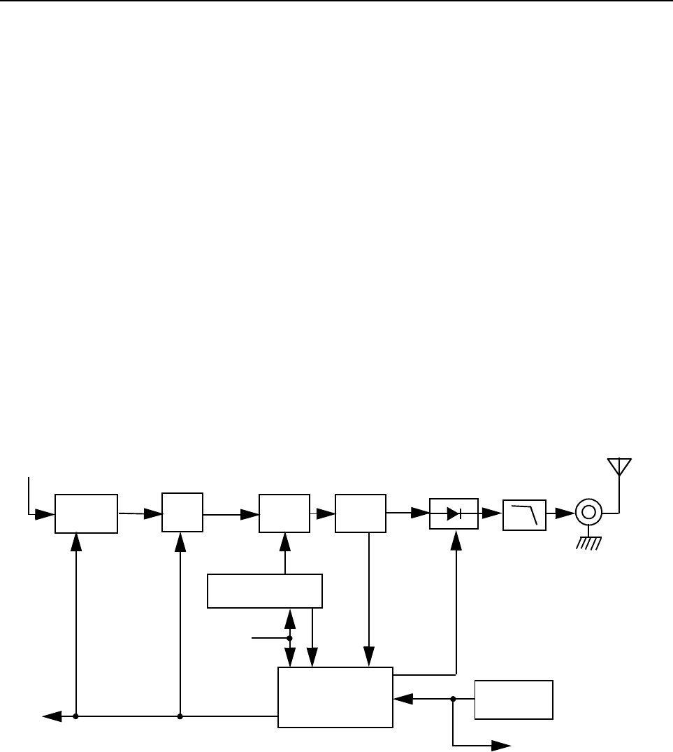
VHF (136-174 MHz) Transmitter Power Amplifier (PA) 25 W 2-3
2.4 Low Intermediate Frequency (IF) and Receiver Back End
The 44.85 MHz high-IF signal from the second IF amplifier feeds the IF IC (U3101) at pin 1. Within
the IF IC, the 44.85 MHz high IF signal mixes with the 44.395 MHz second local oscillator (2nd LO)
to produce the low-IF signal at 455 kHz. The 2nd LO frequency is determined by crystal Y3101. The
low IF signal is amplified and filtered by an external pair of 455 kHz ceramic filters FL3112, FL3114
for 20/25 kHz channel spacing or FL3111, FL3113/F3115 for 12.5 kHz channel spacing. These pairs
are selectable via BWSELECT. The filtered output from the ceramic filters is applied to the limiter
input pin of the IF IC (pin 14).
The IF IC contains a quadrature detector using a ceramic phase-shift element (Y3102) to provide
audio detection. Internal amplification provides an audio output level of 120 mVrms (at 60%
deviation) from U3101 pin 8 (DISCAUDIO) which is fed to the ASFIC_CMP (U0221) pin 2 (part of
the Controller circuitry).
A Received Signal Strength Indicator (RSSI) signal is available at U3101 pin 5, having a dynamic
range of 70 dB. The RSSI signal is interpreted by the microprocessor (U0101 pin 63) and in addition
is available at accessory connector J0501-15.
3.0 VHF (136-174 MHz) Transmitter Power Amplifier (PA) 25 W
The radio’s 25 W PA is a three stage amplifier used to amplify the output from the VCOBIC to the
radio transmit level. All three stages utilize LDMOS technology. The gain of the first stage (U3401)
and the second stage (Q3421) is adjustable, controlled by pin 4 of PCIC (U3501) via U3402-1 and
U3402-2. It is followed by an LDMOS final stage (Q3441).
Figure 2-2 VHF Transmitter Block Diagram
Devices U3401, Q3421 and Q3441 are surface mounted. A pressure pad between board and the
radio's cover provides good thermal contact between the devices and the chassis.
PCIC
Pin Diode
Antenna
Switch RF Jack
Antenna
Harmonic
Filter
Power
Sense
PA-Final
Stage
From VCO
Controlled
Stage
Controlvoltage
Bias 2
To Microprocessor
Temperature
Sense
SPI BUS
ASFIC_CMP
PA
PWR
SET
To Microprocessor
PA
Driver

2-4 VHF (136-174 MHz) Transmitter Power Amplifier (PA) 25 W
3.1 First Power Controlled Stage
The first stage (U3401) is a 20dB gain integrated circuit containing two LDMOS FET amplifier
stages. It amplifies the RF signal from the VCO (TXINJ). The output power of stage U3401 is
controlled by a DC voltage applied to pin 1 from the op-amp U3402-1, pin 1. The control voltage
simultaneously varies the bias of two FET stages within U3401. This biasing point determines the
overall gain of U3401 and therefore its output drive level to Q3421, which in turn controls the output
power of the PA.
Op-amp U3402-1 monitors the drain current of U3401 via resistor R3444 and adjusts the bias
voltage of U3401 so that the current remains constant. The PCIC (U3501) provides a DC output
voltage at pin 4 (INT) which sets the reference voltage of the current control loop. A raising power
output causes the DC voltage from the PCIC to fall, and U3402-1 adjusts the bias voltage for a lower
drain current to lower the gain of the stage.
In receive mode the DC voltage from PCIC pin 23 (RX) turns on Q3442, which in turn switches off
the biasing voltage to U3401.
Switch S3440 is a pressure pad with a conductive strip which connects two conductive areas on the
board when the radio's cover is properly screwed to the chassis. When the cover is removed, S3440
opens and the resulting high voltage level at the inverting inputs of the current control op-amps
U3402-1 & 2 switches off the biasing of U3401 and Q3421. This prevents transmitter key up while
the devices do not have proper thermal contact to the chassis.
3.2 Power Controlled Driver Stage
The next stage is an LDMOS device (Q3421) providing a gain of 12dB. This device requires a
positive gate bias and a quiescent current flow for proper operation. The bias is set during transmit
mode by the drain current control op-amp U3402-2, and fed to the gate of Q3421 via the resistive
network R3429, R3418, R3415 and R3416.
Op-amp U3402-2 monitors the drain current of U3421 via resistors R3424-27 and adjusts the bias
voltage of Q3421 so that the current remains constant. The PCIC (U3501) provides a DC output
voltage at pin 4 (INT) which sets the reference voltage of the current control loop. A raising power
output causes the DC voltage from the PCIC to fall, and U3402-2 adjusts the bias voltage for a lower
drain current to lower the gain of the stage.
In receive mode the DC voltage from PCIC pin 23 (RX) turns on Q3422, which in turn switches off
the biasing voltage to Q3421.
3.3 Final Stage
The final stage is an LDMOS device (Q3441) providing a gain of 12dB. This device also requires a
positive gate bias and a quiescent current flow for proper operation. The voltage of the line
MOSBIAS_2 is set in transmit mode by the ASFIC and fed to the gate of Q3441 via the resistive
network R3404, R3406, and R3431-5. This bias voltage is tuned in the factory. If the transistor is
replaced, the bias voltage must be tuned using the Customer Programming Software (CPS). Care
must be taken not to damage the device by exceeding the maximum allowed bias voltage. In receive
mode U3402-2 pulls the bias voltage to low via D3401. The device’s drain current is drawn directly
from the radio’s DC supply voltage input, PASUPVLTG, via L3436 and L3437.
A matching network consisting of C3441-49, L3443, and two striplines, transforms the impedance to
50 ohms and feeds the directional coupler.

VHF (136-174 MHz) Transmitter Power Amplifier (PA) 25 W 2-5
3.4 Directional Coupler
The directional coupler is a microstrip printed circuit, which couples a small amount of the forward
power delivered by Q3441. The coupled signal is rectified by D3451. The DC voltage is proportional
to the RF output power and feeds the RFIN port of the PCIC (U3501 pin 1). The PCIC controls the
gain of stage U3401 and Q3421 as necessary to hold this voltage constant, thus ensuring the
forward power out of the radio to be held to a constant value.
3.5 Antenna Switch
The antenna switch consists of two PIN diodes, D3471 and D3472. In the receive mode, both diodes
are off. Signals applied at the antenna jack J3401 are routed, via the harmonic filter, through
network L3472, C3474 and C3475, to the receiver input. In the transmit mode, K9V1 turns on
Q3471 which enables current sink Q3472, set to 96 mA by R3473 and VR3471. This completes a
DC path from PASUPVLTG, through L3437, D3471, L3472, D3472, L3471, R3474 and the current
sink, to ground. Both diodes are forward biased into conduction. The transmitter RF from the
directional coupler is routed via D3471 to the harmonic filter and antenna jack. D3472 also
conducts, shunting RF power and preventing it from reaching the receiver port (RXIN). L3472 is
selected to appear as a lambda / 4 wave transmission line, making the short circuit presented by
D3472 appear as an open circuit at the junction of D3472 and the receiver path.
3.6 Harmonic Filter
Components L3491-L3493 and L3472, C3491-C3499 form a Chebychev low-pass filter to attenuate
harmonic energy of the transmitter to specifications level. R3491 is used to drain electrostatic
charge that might otherwise build up on the antenna. The harmonic filter also prevents high level RF
signals above the receiver passband from reaching the receiver circuits, improving spurious
response rejection.
3.7 Power Control
The transmitter uses the Power Control IC (PCIC, U3501) to control the power output of the radio. A
portion of the forward RF power from the transmitter is sampled by the directional coupler and
rectified, to provide a DC voltage to the RFIN port of the PCIC (pin 1) which is proportional to the
sampled RF power.
The ASFIC (U0221) has internal digital to analog converters (DACs) which provide a reference
voltage of the control loop to the PCIC via R3505. The reference voltage level is programmable
through the SPI line of the PCIC. This reference voltage is proportional to the desired power setting
of the transmitter, and is factory programmed at several points across the frequency range of the
transmitter to offset frequency response variations of the transmitter’s power detector circuit.
The PCIC provides a DC output voltage at pin 4 (INT) which sets the drain current of the first
(U3401) and second (Q3421) transmitter stage via current control op-amps U3402-1 and U3402-2.
This adjusts the transmitter power output to the intended value. Variations in forward transmitter
power cause the DC voltage at pin 1 to change, and the PCIC adjusts the control voltage above or
below its nominal value to raise or lower output power. Capacitors C3502-4, in conjunction with
resistors and integrators within the PCIC, control the transmitter power-rise (key-up) and power-
decay (de-key) characteristic to minimize splatter into adjacent channels. U3502 is a temperature-
sensing device, which monitors the circuit board temperature in the vicinity of the transmitter driver
and final devices, and provides a DC voltage to the PCIC (TEMP, pin 30) proportional to
temperature. If the DC voltage produced exceeds the set threshold in the PCIC, the transmitter
output power will be reduced so as to reduce the transmitter temperature.
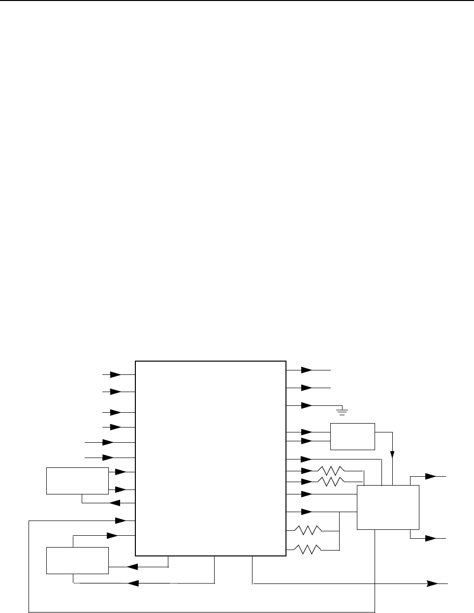
2-6 VHF (136-174 MHz) Frequency Synthesis
4.0 VHF (136-174 MHz) Frequency Synthesis
The frequency synthesizer subsystem consists of the reference oscillator (Y3261 or Y3263), the
Low Voltage Fractional-N synthesizer (LVFRAC-N, U3201), and the voltage-controlled oscillators
and buffer amplifiers (U3301, Q3301-2 and associated circuitry).
4.1 Reference Oscillator
The reference oscillator (Y3263) contains a temperature compensated crystal oscillator with a
frequency of 16.8 MHz. An analog to digital (A/D) converter internal to U3201 (LVFRAC-N) and
controlled by the microprocessor via serial interface (SRL) sets the voltage at the warp output of
U3201 (pin 25) to set the frequency of the oscillator. The output of the oscillator (U3263 pin 3) is
applied to pin 23 (XTAL1) of U3201 via R3263 and C3235.
In applications were less frequency stability is required, the oscillator inside U3201 is used along
with an external crystal Y3261, varactor diode D3261, C3261, C3262 and R3262. In this case,
Y3263, R3263, C3235 and C3251 are not used. When Y3263 is used, Y3261, D3261, C3261,
C3262 and R3262 are not used, and C3263 is increased to 0.1 uF.
4.2 Fractional-N Synthesizer
The LVFRAC-N synthesizer IC (U3201) consists of a pre-scaler, a programmable loop divider,
control divider logic, a phase detector, a charge pump, an A/D converter for low frequency digital
modulation, a balance attenuator to balance the high frequency analog modulation and low
frequency digital modulation, a 13V positive voltage multiplier, a serial interface for control, and
finally a super filter for the regulated 5 volts.
Figure 2-3 VHF Synthesizer Block Diagram
DATA
CLK
CEX
MODIN
VCC, DC5V
XTAL1
XTAL2
WARP
PREIN
VCP
REFERENCE
OSCILLATOR
VOLTAGE
MULTIPLIER
DATA (U0101 PIN 100)
CLOCK (U0101 PIN 1)
CSX (U0101 PIN 2)
MOD IN (U0221 PIN 40)
+5V (U3211 PIN 1)
7
8
9
10
13, 30
23
24
25
32
47
VMULT2 VMULT1
BIAS1
SFOUT
AUX3
AUX4
IADAPT
IOUT
GND
FREFOUT
LOCK 4
19
6, 22, 33, 44
43
45
3
2
28
14 15
40
FILTERED 5V
STEERING
LOCK (U0101 PIN 56)
PRESCALER IN
FREF (U0221 PIN 34)
39
BIAS2
41
48
5, 20, 34, 36
+5V (U3211 PIN 1)
AUX1
VDD, DC5V MODOUT
U3201
LOW VOLTAGE
FRACTIONAL-N
SYNTHESIZER
AUX2
BW SELECT
TX RF INJECTION
(1ST STAGE OF PA)
LO RF INJECTION
VOLTAGE
CONTROLLED
OSCILLATOR
LINE
2-POLE
LOOP
FILTER
1
TRB
TO IF SECTION
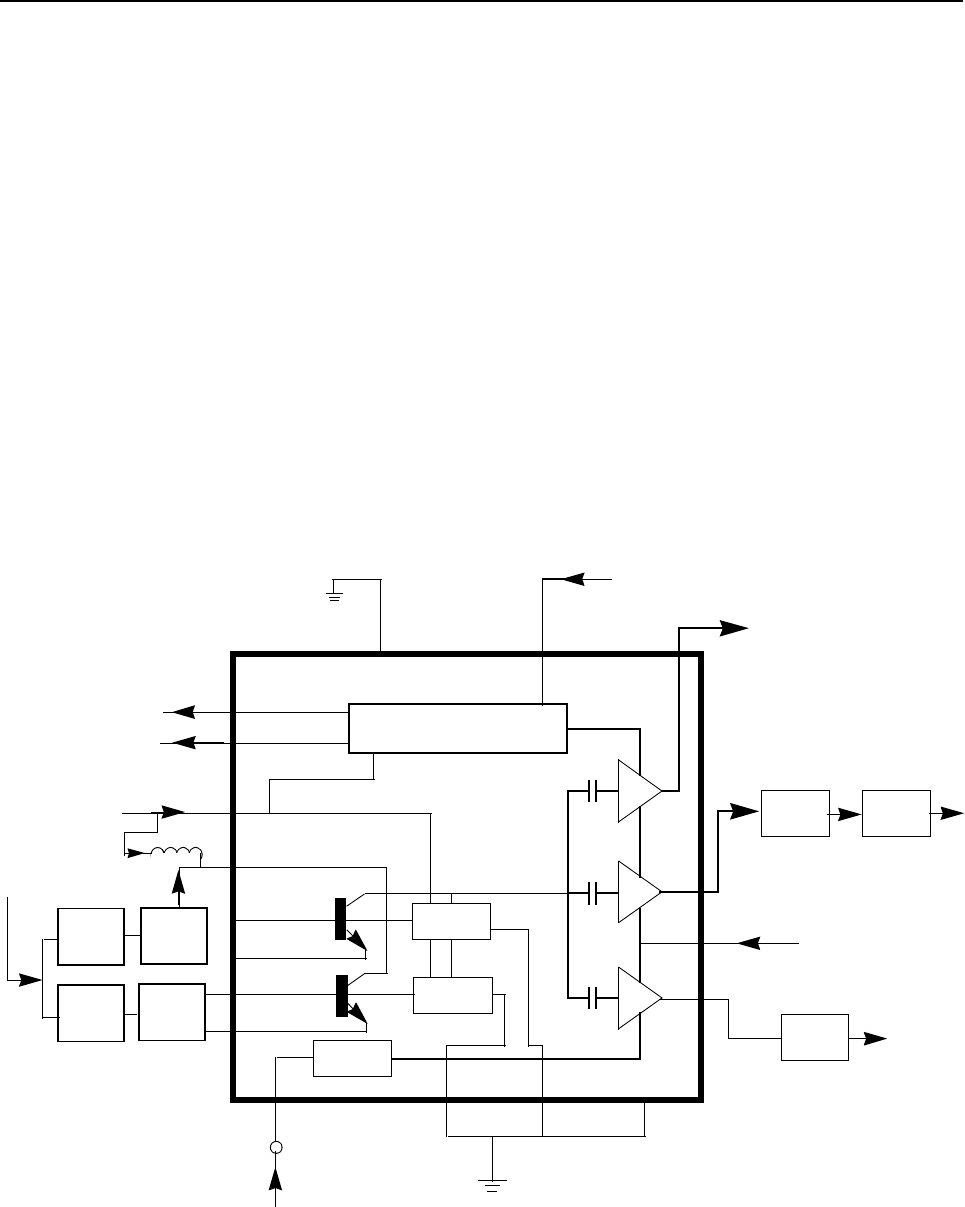
VHF (136-174 MHz) Frequency Synthesis 2-7
A voltage of 5V applied to the super filter input (U3201 pin 30) supplies an output voltage of 4.5 VDC
(VSF) at pin 28. It supplies the VCO, VCO modulation bias circuit (via R3363) and the synthesizer
charge pump resistor network (R3251, R3252). The synthesizer supply voltage is provided by the
5V regulator U3211.
In order to generate a high voltage to supply the phase detector (charge pump) output stage at
pin 47 VCP (U3201-47), a voltage of 13 VDC is being generated by the positive voltage multiplier
circuitry (D3201, C3202, C3203). This voltage multiplier is basically a diode capacitor network driven
by two (1.05MHz) 180 degrees out of phase signals (U3201-14 and -15).
Output LOCK (U3201-4) provides information about the lock status of the synthesizer loop. A high
level at this output indicates a stable loop. IC U3201 provides the 16.8 MHz reference frequency at
pin 19.
The serial interface (SRL) is connected to the microprocessor via the data line DATA (U3201-7),
clock line CLK (U3201-8), and chip enable line CSX (U3201-9).
4.3 Voltage Controlled Oscillator (VCO)
The Voltage Controlled Oscillator (VCO) consists of the VCO/Buffer IC (VCOBIC, U3301), the TX
and RX tank circuits, the external RX buffer stages, and the modulation circuitry.
Figure 2-4 VHF VCO Block Diagram
Presc
RX
TX
Matching
Network Low Pass
Filter
Attenuator
Pin8
Pin14
Pin10
(U3211 Pin1)
VCC Buffers
TX RF Injection
U3201 Pin 32
AUX3 (U3201 Pin2)
Prescaler Out
Pin 12Pin 19
Pin 20
TX/RX/BS
Switching Network
U3301
VCOBIC
Rx
Active Bias
Tx
Active Bias
Pin2
Rx-I adjust
Pin1
Tx-I adjust
Pins 9,11,17
Pin18
Vsens
Circuit
Pin15
Pin16
RX VCO
Circuit
TX VCO
Circuit
RX Tank
TX Tank
Pin7
Vcc-Superfilter
Collector/RF in
Pin4
Pin5
Pin6
RX
TX
(U3201 Pin28)
Rx-SW
Tx-SW
Vcc-Logic
(U3211 Pin1)
Steer Line
Voltage
(VCTRL)
Pin13
Pin3
TRB IN
LO RF INJECTION
Q3304
Q3301

2-8 VHF (136-174 MHz) Frequency Synthesis
The VCOBIC together with the Fractional-N synthesizer (U3201) generates the required frequencies
in both the transmit and receive modes. The TRB line (U3301 pin 19) determines which tank circuits
and internal buffers are to be enabled. A high level on TRB enables the TX tank and TX output (pin
10), and a low enables the RX tank and RX output (pin 8). A sample of the signal from the enabled
RF output is routed from U3301 pin 12 (PRESC_OUT), via a low pass filter, to pin 32 of U3201
(PREIN).
A steering line voltage (VCTRL) between 2.5V and 11V at varactor diode D3361 will tune the full TX
frequency range (TXINJ) from 136 MHz to 174 MHz, and at varactor diode D3341 will tune the full
RX frequency range (RXINJ) from 181 MHz to 219 MHz. The RX tank circuit uses a Hartley
configuration for wider bandwidth. For the RX tank circuit, an external transistor Q3304 is used for
better side-band noise.
The external RX buffers (Q3301 and Q3302) are enabled by a high at U3301 pin 7 (RX_SWITCH)
via transistor switch Q3303. In the TX mode, the modulation signal (VCOMOD) from the LVFRAC-N
synthesizer IC (U3201 pin 41) is applied to varactor diode D3362, which modulates the TX VCO
frequency via capacitor C3362. Varactor D3362 is biased for linearity from VSF.
4.4 Synthesizer Operation
The complete synthesizer subsystem consists of the low voltage FRAC-N (LVFRACN), the
reference oscillator (a crystal oscillator with temperature compensation), charge pump circuitry, loop
filter circuitry and a DC supply. The output signal PRESC from the VCOBIC (U3301 pin 12) is fed to
U3201 pin 32 (PREIN) via a low pass filter (C3318, L3318 and C3226) which attenuates harmonics
and provides the correct level to close the synthesizer loop.
The pre-scaler in the synthesizer (U3201) is a dual modulus type with selectable divider ratios. The
divider ratio of the pre-scaler is controlled by the loop divider, which in turn receives its inputs via the
SRL. The output of the pre-scaler is applied to the loop divider. The output of the loop divider is
connected to the phase detector, which compares the loop divider´s output signal with the reference
signal. The reference signal is generated by dividing down the signal of the reference oscillator
(Y3261 or Y3263).
The output signal of the phase detector is a pulsed DC signal which is routed to the charge pump.
The charge pump outputs a current at U3201 pin 43 (IOUT). The loop filter (which consists of R3221-
R3223 and C3221-C3224) transforms this current into a voltage that is applied to the varactor diodes
(D3361 for transmit, D3341 for receive) to alter the output frequency of the appropriate VCO. The
current can be set to a value fixed within the LVFRAC-N IC, or to a value determined by the currents
flowing into BIAS 1 (U3201-40) or BIAS 2 (U3201-39). The currents are set by the value of R3251
and R3252 respectively. The selection of the three different bias sources is done by software
programming.
To reduce synthesizer lock time when new frequency data has been loaded into the synthesizer, the
magnitude of the loop current is increased by enabling the IADAPT pin (U3201-45) for a certain
software programmable time (adapt mode). The adapt mode timer is started by a low to high
transient of the CSX line. When the synthesizer is within the lock range, the current is determined
only by the resistors connected to BIAS 1 and BIAS 2, or by the internal current source. A settled
synthesizer loop is indicated by a high level signal at U3201-4 (LOCK).
The LOCK signal is routed to one of the µP´s ADC inputs (U0101-56). From the measured voltage,
the µP determines whether LOCK is active.

VHF (136-174 MHz) Frequency Synthesis 2-9
In order to modulate the PLL, the two spot modulation method is utilized. Via U3201 pin 10 (MODIN),
the audio signal is applied to both the A/D converter (low frequency path) as well as the balance
attenuator (high frequency path). The A/D converter changes the low frequency analog modulating
signal into a digital code that is applied to the loop divider, thereby causing the carrier to deviate. The
balance attenuator is used to adjust the VCO’s deviation sensitivity to high frequency modulating
signals. The output of the balance attenuator is present at the MODOUT port (U3201-41) and
connected to the VCO modulation diode D3362 via R3364.

2-10 VHF (136-174 MHz) Frequency Synthesis
THIS PAGE INTENTIONALLY LEFT BLANK

3-1
Section 3
TROUBLESHOOTING CHARTS
1.0 Troubleshooting Flow Chart for Receiver (Sheet 1 of 2)
Bad SINAD
Bad 20dB Quieting
No Recovered Audio
START
Audio at
pin 8 of
U3101 ?
Check Controller
(in the case of no audio)
OR ELSE go to “B”
Yes
No
Spray or inject 44.85MHz
into XTAL Filter FL3101
Audio heard ?BYes
No
Check 2nd LO
(44.395MHz) at C3135
LO present ?
BYes
Check voltages on
U3101
Biasing OK ?
No
No
A
Yes
Check Q3102 bias
for faults
Replace Q3102
Go to B
Yes
No
Check circuitry
around U3101.
Replace
U3101 if defect
Check circuitry around Y3101.
Replace Y3101 if defect
Voltages
OK?
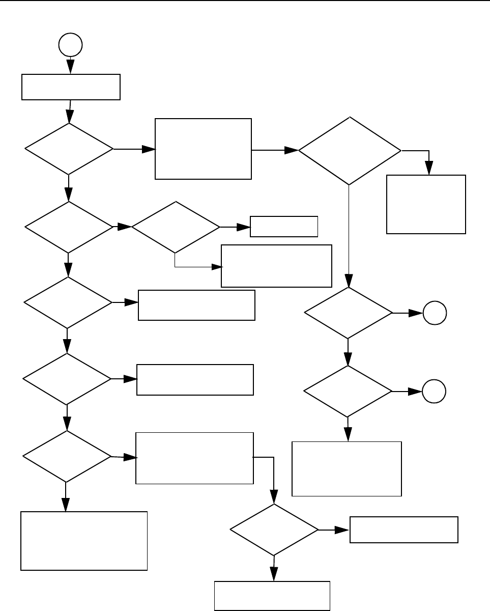
3-2 Troubleshooting Flow Chart for Receiver
1.1 Troubleshooting Flow Chart for Receiver (Sheet 2 of 2)
IF Signal at
C3035?
No
RF Signal at
T3001?
RF Signal at
C3012?
No
RF Signal at
C3008?
No
RF Signal at
C3474?
No or
Check Harmonic Filter
J3401 and
Antenna Switch
D3471,D3472,L3472
Check filter between C3474
& C3008. Check tuning
voltage at R3019
Inject RF into J3401
Is tuning
voltage OK?
No
Yes
Check RF amp
(Q3001) Stage
Check filter between
C3012 & T3001
Yes
Check T3001, T3002,
D3031, R3030-R3034,
L3032, C3034 and C3035
Yes
1st
LO level OK?
Locked?
Yes
Check FGU
Yes
Trace IF signal from
C3035 to Q3101.
Check for bad XTAL
filter
No
Yes
IF signal at Q3102
collector?
Before replacing
U3101, check
U3101 voltages
Yes
Check for 5VDC
Is 9V3 present?
Check Supply Voltage
circuitry. Check Q0681,
U3211 and U0641
No
No
No
Check U3501
Check varactor filter
No
Yes
Yes
Yes
A
A
B
weak RF
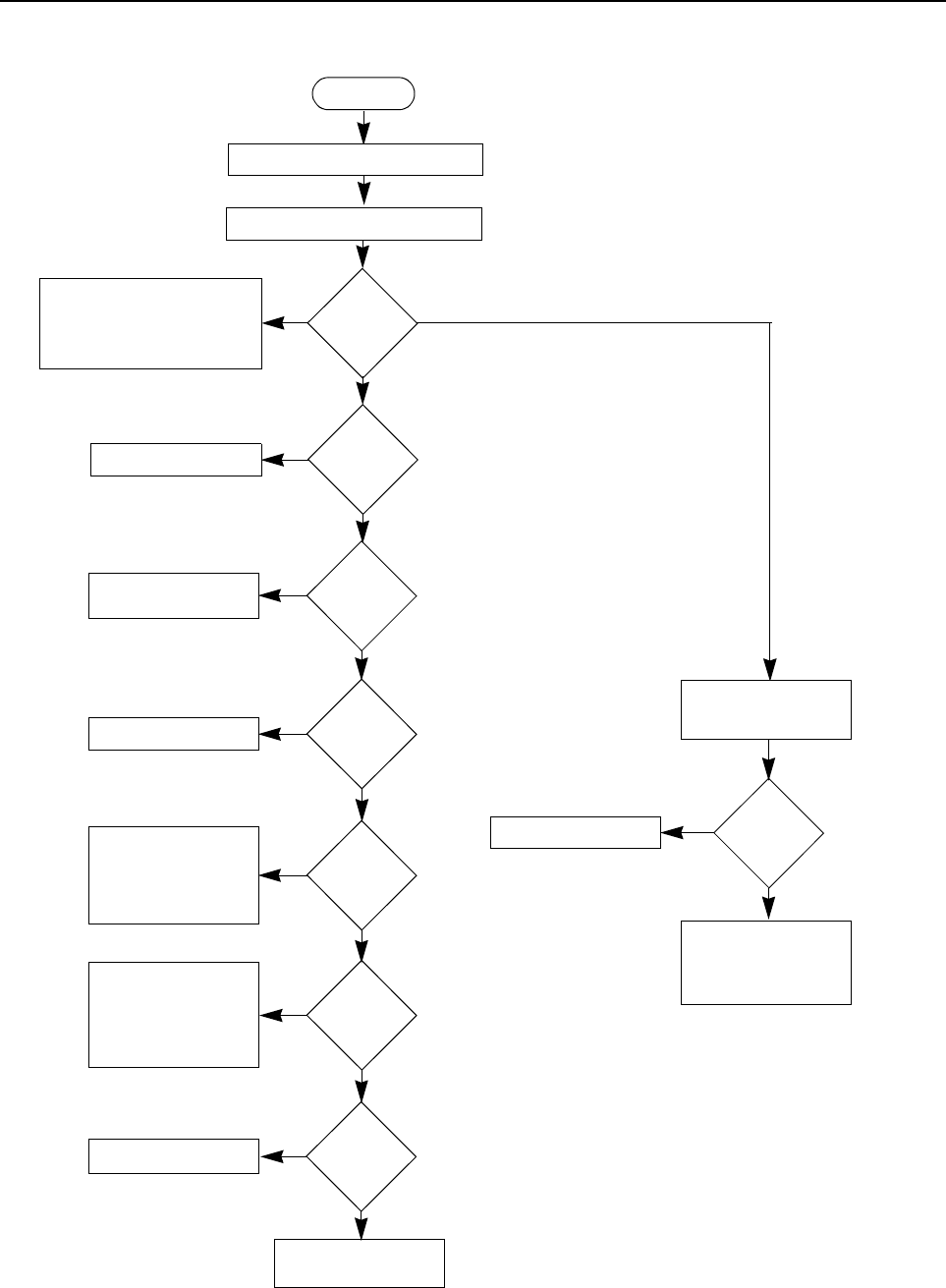
Troubleshooting Flow Chart for 25W Transmitter 3-3
2.0 Troubleshooting Flow Chart for 25W Transmitter (Sheet 1 of 3)
Current
increase
when
keyed?
NO
YES
START
Check if Pressure Pad closes S3440
Check Components between
Q3441 and RF Output,
Antenna Switch
D3471,D3472,Q3472
VR3471,Q3471
>500mA & <4A
>4A
<500mA
Check PA Stages Control Volt-
age at
TP3402
>1V
Short TP3403 to
Ground
NO
YES
Voltage at
TP3402
rises?
Check PA Stages
NO
YES
PCIC U3501
Pin 14 9.3V
DC?
Check 9.3 V Regulator
U0641
NO
YES
PCIC U3501
Pin 16 >4V
DC
Replace PCIC U3501
NO
YES
TP3404
9.1V DC
If U3201 Pin 2 is high,
replace PCIC
U3501,otherwise
check controller and
FGU
YES
NO
TP3403
>0.5V DC?
Replace PCIC U3501
Check Forward Power
Sense Circuit (D3451)
Check Forward Power
Sense Circuit (D3451)
NO
YES
PCIC U3501
Pin 5 > 1V
DC?
Check Power Setting,
Tuning & Components
between PCIC Pin 5
and ASFIC (U0221)
Pin 4 before replacing
ASFIC
No or too low Power when keyed
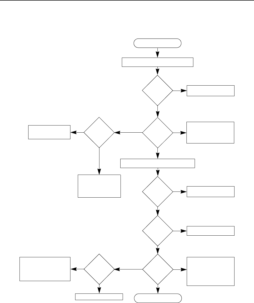
3-4 Troubleshooting Flow Chart for 25W Transmitter
2.1 Troubleshooting Flow Chart for 25W Transmitter (Sheet 2 of 3)
Check PA Stages
No or too low Power when keyed
Measure DC Voltage at Pin 2 & 3 of U3401
>6
YES
DC Voltage
at U3501
Pin 23 =0?
2-6
DC Voltage
at U3402-1
Pin 1?
YES
Pin 2 Volt-
age 0.62 *
Voltage at
Pin 1?
If U3201 Pin 2 is high,
replace PCIC
NO Replace U3401
YES
NO DC
Voltage at
U3402-1 Pin
3 = 8.8V?
Check S3440,
R3442 and R3443
YES
Pin 3 Volt-
age 0.51 *
Voltage at
Pin 1?
NO Replace U3401
<2V DC Voltage
at U3402-2
Pin 7?
>6V
Check Components
between U3402-2 Pin 7
and Q3421. Check
Resistive Network at
Pins 5 & 6 before
replacing Q3421
YES
DC Voltage
at U3402-2
Pin 5 <8.8V?
Check Components
between U3402-2 Pin 7
and Q3421. Check Resis-
tive Network at Pins 5 & 6
before replacing Q3421
NO
Check Q3422
NO
Check Final PA Stage
2-6V
<2V Check Resistive Net-
work at Pins 2 & 3 of
U3402-1 before replac-
ing U3401
Check Q3442 and
Resistive Network at
U3402-1 Pin 3
before replacing
U3401
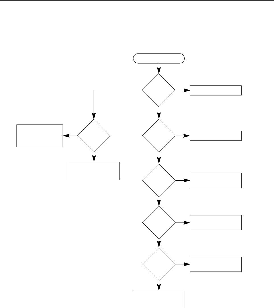
Troubleshooting Flow Chart for 25W Transmitter 3-5
2.2 Troubleshooting Flow Chart for 25W Transmitter (Sheet 3 of 3)
Check Final PA Stage
NO
0V
1-4V
Bias 2 DC
Voltage at
TP3406?
YES
RF Voltage
at TP3401
>100mV?
YES
RF Voltage
U3401 Pin 6
>3V?
Supply
Replace Q3441
Check FGU (U3301)
NO Check Components
between TP3401 &
C3417
NO
YES ASFIC
U0221 Pin 6
1-4V DC?
Check Bias Tuning
before replacing ASFIC
U0221
Check Components
between ASFIC and
Q3441 before
replacing Q3441
YES
RF Voltage
Q3421 Gate
>1V?
NO Check Components
between C3417 &
Q3421
YES
RF Voltage
Q3441 Gate
>4V?
NO Check Components
between Q3421 &
Q3441
Check Components
between Q3441 &
Antenna Connector
Voltage
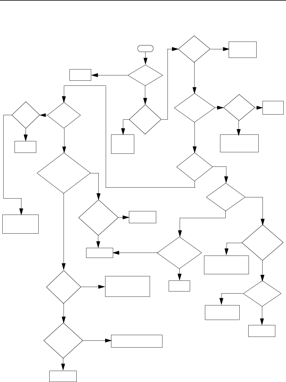
3-6 Troubleshooting Flow Chart for Synthesizer
3.0 Troubleshooting Flow Chart for Synthesizer
+5V at
U3201 Pins
13 & 30?
5V
at pin 6 of
D3201
Is information
from µP U0101
correct?
Is U3201
Pin 47
= 13VDC ?
Is U3301 Pin 19
<40 mVDC in RX &
>4.5 VDC in TX?
(at VCO section)
Start
Visual
check of the
Board OK?
Correct
Problem
Check 5V
Regulator
U3211
Is 16.8MHz
Signal at
U3201 Pin
19?
Check
Y3261, Y3263 and
associated parts
Are signals
at Pins 14 &
15 of U3201?
Check
R3201
Check C3319
Is U3201 pin 2
>4.5 VDC in Tx &
<40 mVDC in Rx
Replace
U3201
Remove
Shorts
Is there a short
between Pin 47 and
Pins 14 & 15 of
U3201?
Replace or resolder
necessary components
Is RF level at
U3201 Pin 32
-12 < x <-25
dBm?
Are
R3221,
R3222, R3223,
C3221, C3222,
& C3224
OK?
Replace
U3201
If R3227, C3226 & C3227
are OK, then see VCO
troubleshooting chart
Are Waveforms
at Pins 14 & 15
triangular?
Do Pins
7,8 & 9 of
U3201 toggle
when channel is
changed?
Check programming
lines between U0101
and U3201 Pins 7,8 & 9
Replace
U3201
Check µP U0101
Troubleshooting
Chart
No
Yes
No
Yes
No
Yes
No
No
No
Yes
Yes
No
Yes
Yes
No
Yes
Yes
Yes
No
No
No
No
Yes
No
Yes
Yes
Check D3201,
C3202, C3203,
C3205 & C3206
5V at
U3201 pins 5,
20, 34 & 36
C h e c k 5 V
Regulator
U3211, R3211
Is
16.8MHz
signal at
U3201 pin
23?
Replace
U3201
Yes
No
No
Yes
No
Yes
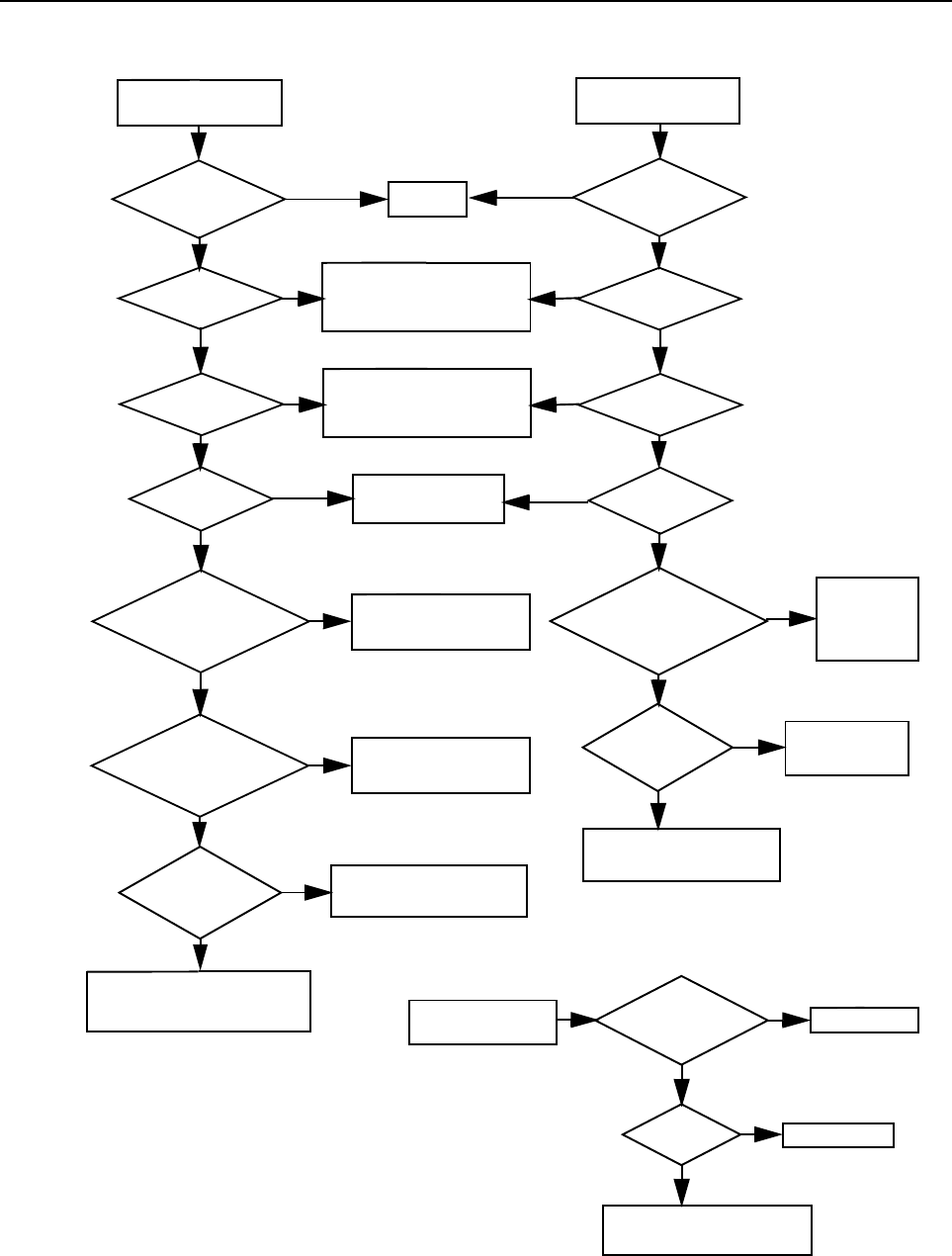
Troubleshooting Flow Chart for VCO 3-7
4.0 Troubleshooting Flow Chart for VCO
Are Q3301
Base at 0.7V
Collector at 4.5V
Emitter at 110mV
Are Q3304
Base at 2.4V
Collector at 4.5V
Emitter at 1.7V
Are U3301 Pins
13 at 4.4V
15 at 1.1V
10 at 4.5V
16 at 1.9V
Low or no RF Signal
at TP3001
Visual check
of board
OK?
35mV DC at
U3301 Pin 19
NO
YES
at base of Q3301
NO
NO
NO
NO
NO
YES
YES
YES
YES
YES
Low or no RF Signal
at input to PA
5V DC at U3301
Pin 14 & 18 OK ?
4.8V DC at
U3301 Pin 19
Is RF available
at TP3401
YES
YES
YES
YES
YES
NO
NO
NO
NO
NO
Audio =180mVrms
at “-” side of
D3362
2.5VDC
at D3362
If C3362 and R3363 are OK,
then replace D3362
Replace R3363
Replace R3364
NO
NO
YES
YES
If R3402 and
C3315 are OK,
replace U3301
TX VCO
RX VCO
Correct
Problem
Visual check
of board
OK?
Make sure U3211 is working
correctly and runner
between U3211 Pin 1 and
U3301 Pin 14 & 18 is OK
Check runner
between U3201 Pin 2
and U3301 Pin 19
Is RF available If all parts from U3301 Pin 8
to Base of Q3301 are OK,
replace U3301
If all parts associated
with the pins are OK,
replace Q3301
Check parts between
T3001 and Q3301 Power OK but
no modulation
If all parts from TP3401 of
U3401 Pin 16 are OK,
replace U3401
If all parts
associated
with the pins
are OK,
replace U3301
4.5V DC at
U3301 Pin 3 OK?
YES
NO 4.5V DC at
U3301 Pin 3 OK?
YES
NO
Make sure Synthesizer is
working correctly and runner
between U3201 Pin 28 and
U4301 Pin 3 is OK
5V DC at U3301
Pin 14 & 18 OK ?
OK? OK?
If all parts associated
with the pins are OK,
replace Q3301

3-8 Troubleshooting Flow Chart for VCO
THIS PAGE INTENTIONALLY LEFT BLANK
4-1
Section 4
VHF PCBS/SCHEMATICS/PARTS LISTS
1.0 Allocation of Schematics and Circuit Boards
1.1 Controller Circuits
The VHF circuits are contained on the Printed Circuit Board (PCB) which also contains the
Controller circuits. This Chapter shows the schematics for the VHF circuits only, refer to the
Controller section for details of the related Controller circuits . The PCB component layouts and the
Parts Lists in this Chapter show both the Controller and VHF circuit components. The VHF
schematics and the related PCB and parts list are shown in the tables below.
Table 4-1 VHF 1-25W Diagrams and Parts Lists
PCB : 8486172B06 Main Board Top Side
8486172B06 Main Board Bottom Side Page 4-3
Page 4-4
SCHEMATICS
Power Amplifier 1 - 25W
FRACN
Voltage Controlled Oscillator
Receiver Front End
IF
Page 4-5
Page 4-6
Page 4-7
Page 4-8
Page 4-9
Parts List
8486172B06 Page 4-10
Table 4-2 VHF 1-25W Diagrams and Parts Lists
PCB : 8486172B07 Main Board Top Side
8486172B07 Main Board Bottom Side Page 4-13
Page 4-14
SCHEMATICS
Power Amplifier 1 - 25W
Voltage Controlled Oscillator
Receiver Front End
IF
FRACN
Page 4-5
Page 4-7
Page 4-8
Page 4-15
Page 4-16
Parts List
8486172B07 Page 4-17

4-2 Allocation of Schematics and Circuit Boards
THIS PAGE INTENTIONALLY LEFT BLANK
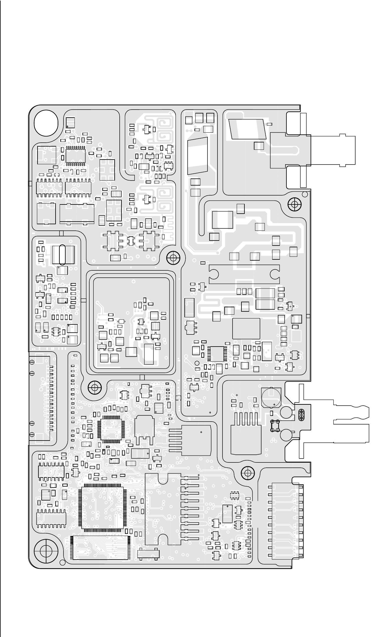
VHF 1-25W PCBs / Schematics / Parts Lists 4-3
2.0 VHF 1-25W PCBs / Schematics / Parts Lists
VCO-REV-T3
PA-REV-T1
FE-REV-T3
IF-REV-T4
FRAC-T4
CNTL-REV-T6
C0101C0102
C0104
C0106
C0107
C0131
C0132
C0211
C0212
C0221
C0222
C0223
C0224
C0225
C0226
C0227
C0228
C0231
C0232
C 0233
C0234
C0235
C0236
C0237
C0241
C0242
C0243
C0244
C0245
C0246
C0251
C0252
C0253
C0261
C0262
C0267
C0421
C0441
C 0442
C 0443
C 0445
C 0446
C 0447
C 0448
C 0449
C 0470
C 0471
C 0472
C 0473
C 0474
C 0476
C 0477
C 0478
C0482
C0483
C0484
C0486
C0487
C0488
C0490
C0493
C0494
C0495
C0496
C0501
C0502
C0503
C0504
C0505
C0506
C0508
C0509
C0510
C0511
C0512
C 0513
C0514
C0515
C 0516
C0517
C0518
C0542
C0601
C0603
C0612
C0651
C0652
C0654
C0655
C0681
C3002
C3004
C3005
C3006
C3007
C3008
C3009
C3010
C3011
C3012
C3013
C3014
C3015
C3016
C3017
C3018
C3019
C3020
C3021
C3027
C3028
C3032
C3034
C3100
C3101 C3102
C3103
C3114
C3115
C3131
C3132
C3133
C3134
C3135
C3136
C3137
C3139
C3140
C3141
C3142
C3143
C3145
C3148
C3210
C3211
C3213
C3214
C3215
C3221
C3222
C3223 C3224
C3226
C3227 C3229
C3231
C3232
C3233
C3234
C3240
C3242
C3243
C3244
C3245
C3246
C3252
C3253
C3254
C3255
C3324
C3336
C3337
C3341
C3342
C3344
C3345
C3346 C3347
C3357 C3361
C3362
C3363
C3364
C3365
C3400
C3401 C3403
C3404
C3410
C3411
C3412
C3417
C3418
C3419
C3420
C3422
C3423
C3424
C3425
C3426
C3428
C3431
C3432
C3433
C3434
C3435
C3441C3442
C3443
C3444
C3445
C3446
C3447
C3448 C3449
C3453
C3472
C3473
C3474
C3497
C3507 C3508
C3509
D0201
D0651
D3001
D3003
D3004
D3031
D3221
D3341
D3361
D3362
D3401
D3471
D3472
2
3
456
FL3101
2
3
456
FL3102
4
32
FL3112
FL3114
18
1
J0451
2011
10
J0501
J0601
23
J3401
L0481
L0482
L3002
L3031
L3032
L3034
L3100
L3101
L3201
L3232
L3333
L3341
L3343 L3344
L3346
L3361
L3362
L3363
L3364
L3401
L3403
L3411
L3412
L3413
L3414
L3422
L3443
L3471
L3472
L3493
M3421
Q0110
Q0177
Q0181
Q0185
Q0681
Q3001
Q3021
Q3221
Q3304
Q3411
Q3422
2
3
4
5
6
7
8
Q3441
Q3442
Q3471
Q3472
R0101
R0102
R0104
R0105
R0106
R0108
R0110
R0114
R0115
R0116
R0131
R0132
R0170
R0181
R0182
R0185
R0186
R0211
R0212
R0220
R0221
R0222
R0223
R0224
R0225
R0226
R0227
R0228 R0229
R0241
R0242
R0251
R0252
R0253
R0261
R0262
R0267
R0268
R0269
R0510
R0533
R0535
R0538
R0539
R0611
R0612
R0651
R0652
R0681
R0682
R3001
R3002
R3003
R3004
R3009
R3013
R3014
R3015
R3016
R3024
R3025 R3026
R3027
R3028
R3031
R3101
R3106 R3111
R3117
R3130
R3132
R3135
R3142
R3144
R3145
R3211
R3221
R3222
R3223
R3224
R3225
R3227
R3242
R3251
R3252
R3335
R3336
R3341
R3342
R3361
R3362
R3363
R3364
R3400
R3401
R3402
R3403
R3404
R3405
R3406
R3414
R3415
R3416
R3424
R3425
R3426
R3427
R3431R3432
R3433
R 3434
R3435
R3471
R3473
R3491
R3505
R3506
R3507
R3508
R3509
SH3301
3
46
1
2
T3001
3
46
12
T3002
TP3401
1
76
51
26
32
17
16 1
8
7
114
U0211
137
25
13
16
1
89
U0251
9
U0271
1
6
5
1
6
5
3
2
1
11
1
20
10
U3101
87
1
14
U3111
87
1
14
U3115
U3211
1
16
8
9
U3401
U3502
VR0501
VR0503
VR0505 VR0510
23
4
Y0131
2
Y3102
1
1
100 1
1
1
1
U0101
Microprocessor
U0121
Flashrom
U0221
ASFIC CMP
U0611
B+ Switch
U0641
9,6V Regulator
U0651
5V Regulator
1
4
5
ZWG0130397-O
ZWG0130397-O
VHF (136-174 MHz) 1-25W 8486172B06 Top Side
4-4 VHF 1-25W PCBs / Schematics / Parts Lists
C0103
C0105
C0111
C0112
C0121
C0122
C0123
C0141
C0151
C0201
C0202
C0203
C0204
C0205
C0254
C0255
C0265
C0266
C0271
C0272
C0273
C0274
C0275
C0276 C0277
C0301
C0302
C0303
C0304
C0305
C0324 C0325
C0331
C0341
C0342
C0343
C0344
C0351
C0352
C0353
C0354
C0422
C0423
C 0426
C 0427
C 0428
C 0429
C0430 C0431
C0485
C0491
C0492
C0497
C0499
C0541
C0554
C0558
C0559
C0560 C0575 C0576
C0591
C0592 C0593
C0611
C0621
C0622
C0641
C0644
C0645
C0661
C0662
C0663
C0671
C3000
C3001
C3003
C3022
C3023
C3024
C3025
C3026
C3029
C3030
C3031
C3033
C3035
C3036
C3104
C3110
C3111
C3112
C3113
C3116
C3121
C3122
C3123
C3144
C3146
C3147
C3151
C3152
C3202
C3203
C3205
C3206
C3207
C3208
C3209
C3225
C3228
C3235
C3241
C3251
C3261
C3262
C3263
C3301
C3302
C3303
C3304
C3305
C3306 C3311
C3312
C3313
C3314
C3315
C3316
C3317
C3318
C3319
C3331
C3332
C3333
C3334
C3335
C3348
C3351
C3352
C3355
C3356
C3402
C3405
C3406
C3413
C3414
C3415
C3416
C3421
C3427
C3436
C3437
C3438
C3439
C3440
C3450
C3451
C3452
C3471
C3475 C3491
C3492
C3493
C3494
C3495
C3496
C3498
C3499
C 3501
C3502
C3503
C3504
C3505
C3506
C3510
D0101
D0151
D0179
D0301
D0621
D0660 D0661
D3000
D3011
D3101
D3201
D3261
D3451
E0271 E0272
E0631
43
2
FL3111
FL3113
43
2
FL3115 12
J0401
1
40
J0551
1
18
J0552
L3025
L3111
L3112
L3231
L3301
L3302
L3311
L3317
L3318
L3331
L3332
L3345
L3351
L3402
L3421
L3436
L3437
L3491
L3492
Q0151
Q0171
Q0173 Q0183
Q0271
Q0641
Q0661
Q0662
Q0663
Q3002
Q3101
Q3102
Q3141
Q3151
Q3152
Q3301
Q3302
43
Q3303
12
3
Q3421
R0107
R0111 R0112
R0113
R0117
R0121
R0151 R0152
R0171
R0172
R0173
R0174
R0175
R0176
R0177
R0178
R0179
R0183
R0184
R0201
R0202
R0203
R0204
R0205
R0206
R0207
R0208
R0265
R0266
R0273
R0274
R0275
R0276
R0323
R0324
R0331
R0332
R0333
R0335
R0341
R0342
R0343
R0344
R0345
R0346
R0347
R0401
R0407
R0408
R0409 R0410
R0412
R0441
R0467
R0468
R0481
R0482
R0511
R0512
R0525 R0529
R0530
R0531 R0537
R0541
R0542
R0591
R0592
R0621
R0641
R0642
R0643
R0661
R0662 R0671 R0672
R3000
R3006
R3010
R3011
R3012
R3018
R3019
R3021
R3023 R3030
R3032
R3033
R3034
R3035
R3036
R3102
R3104
R3105
R3107
R3108
R3112
R3113
R3114
R3115
R3116 R3118
R3133
R3134
R3141
R3146 R3147
R3151
R3152
R3153
R3154
R3201
R3203
R3204
R3206
R3226
R3228
R3241
R3261 R3262
R3263
R3301
R3302
R3303
R3304
R3305
R3306
R3307
R3308
R3311
R3312
R3313
R3314
R3315
R3316
R3317
R3318
R3319
R3321
R3323
R3331
R3343
R3351
R3352
R3353
R3354
R3355
R3356
R3411
R3412
R3413
R3417
R3418
R3421
R3422
R3423
R3428
R3429
R3440
R3441
R3442 R3443
R3444
R3445
R3446
R3450
R3452
R3454
R3455
R3457
R3474 R3475
R3501
R3502 R3504
S3440
TP0101
TP0102
TP0103
TP0104
TP0151
TP0221
TP0222
TP0481
TP0492
TP0497
TP0530
TP0661
TP3001
TP3201
TP3202
TP3402
TP3403 TP3404
TP3405
TP3406
1
4
58
U0111
22
21 8
7
1
16
1
8
9
U0141
28 15
14
1
U0301
U0331
1
45
8
U0341
U0342
4
58
U0351
14
58
U0652
U0653
1
37
25 13
11
1
20
10
1
4
58
U3402
1
17
9
25
U3501
VR0151
VR0504 VR0509
VR0537
VR0541
VR0601
VR0621
VR0671
VR3471
4
3
2
Y3101
6
4
3
1
Y3261
2
34
Y3263
1
1
1
1
1
48
U0122
RAM
U3201
FRACN
U3301
VCOIC
15
8486172B06_T1
VCO-REV-T3
PA-REV-T1
C
99
FE-REV-T3
IF-REV-T4
FRAC-T4
CNTL-REV-T6
WARIS VHF RF 1-25W Bot Side
8486172B06-T1 BOT SIDE
CHECK
ONE
( )
ILLUSTRATOR DATEENGINEERDATE PROGRAM DISK
DWG. NO.
Illustrator
RK 15. Oct 2000
ZWG0130398
ZWG0130398-O
ZWG01300398-O
VHF (136-174 MHz) 1-25W 8486172B06 Bottom Side
VHF 1-25W PCBs / Schematics / Parts Lists 4-5
RXIN_VHF_PA_1
NU
NU
17nH
L3437
NU
NU
0
R3440
NU
C3427
56pF
NU
39K
10K
NU
6.8K
R3411
NU
R3506
10K
NU
C3508
C3443
120pF
C3444
6.2pF
C3509
1uF
C3423
0.8x25
width 2.032
1.542x4
2.216x J3401
7.5
R3427
R3426
2.7
2.7
2.7 R3428
R3425
C3506
2200pF
2.4K
120
R3414
2.4K
R3502
39K
MOSBIAS_2_VHF_PA_1
R3445
L3412
C3432
15nH
C3404
33pF
2200pF
C3410
.022uF
PASUPVLTG_VHF_PA_1
C3473
270pF
R3415
100
330pF
C3426
Q3421
R3417
39K
R3443
10K
R3491
R3441
C3416
330pF
100pF
330pF
C3400
C3507
R3400
470
RESET_VHF_PA_1
51
R3432
.033uF
C3437 L3436
57R01
C3504
.01uF
470pF
C3503
470pF
C3419
TP3402
TP3403
57R01
L3402
C3406
470pF
R3401
300
C3428 FECNTL_2
C3435
2200pF
C3449
330pF
120pF
C3502
2200pF
25nH
L3443
10K
R3504
470
R3471 Q3472
C3434
.01uF
MOSBIAS_2 47K
R3404
47pF
RESET
C3431
C3421
.033uF
CLK
51
R3431
R3435 2.7
INT_SWB
C3425
.022uF
U3502
3
GND
POS
1
2
VOUT
C3492
68pF
LM50
C3493
6.8pF
DATA_VHF_PA_1
2.2K
20pF
C3445
R3442
C3422
330pF
1
R3444
4.7
5.6V
VR3471
23
39K
R3421
DATA
C3505
1uF
33pF
C3403
6.8pF
C3475
TEMPSENSE
TEMPSENSE_CNTLR_1
1K
R3507
20K
PA_PWR_SET
R3509
C3451
1000pF
.022uF
C3471
C3495
C3497
CSX
3.3pF
C3474
220pF
6
5
7
8
4
TXINJ_VHF_PA_1
18pF
LM2904
U3402-2
470pF
R3413
3.3K
9V3
C3501
2200pF
FECNTL_2_VHF_PA_1
INT_SWB_VHF_PA_1
D3401
CSX_VHF_PA_1
D3472
33pF
C3446
100pF
C3418
D3451
51nH
L3493
R3474
51
L3411
68nH
R3473
51
C3491
15pF
.022uF
C3411
D3471
R3403
300
470pF
C3405
L3471
1.2uH
100K
R3406
51nH
R3508
100K
L3491
11.03nH
5.6K
R3412
L3413
R3505
300K
270pF
120pF
C3448
C3472
2.7
R3424
47pF
C3417
C3439
470pF
0
R3446
150pF
C3496
C3442
R3455
36pF
C3510
100K
CNTLVLTG_VHF_PA_1
470pF
PA_PWR_SET_VHF_PA_1
470pF
C3453
10uF
C3436
R3429
220
R3433 2.7
C3433
56pF
R3501
L3492
51nH
6.8K
22K
R3418
2
3
1
8
4
C3440
1000pF
RXIN
U3402-1
LM2904
13pF
C3494
20
VAR1
18
VAR2
24
VAR3
VG 15
6VL 19
VLIM
TXINJ
21
RS
31 RSET
23
RX
2T1
30 TEMP
14
V10
16
V45
17
V5EXT
9
F168
8GND1
25 GND2
4INT
22
NA
11
Q10
QX
1RFIN
29 CEX
3CI
5CJ
7CL
26 CLK
12
CQ
CQX 1328 DATA
H99S-4
U3501
32 ANO
27 BPOS
FECNTL_1_VHF_PA_1
Q3442
R3402
16pF
C3447
15
39K
R3423
Q3411
TP3406 CLK_VHF_PA_1
470pF
TP3401
L3422
13.85nH
470pF
470pF
C3424
30K
C3438
R3452
R3454
12K
R3405
100
330pF
C3401 RFIN
16
RFOUT1
6
RFOUT2 7
VCNTRL
1
VD1
14 2
VG1
VG2 3
GND1
4
GND2
5
GND3
12
GND4
13
NC1
8
NC2
9
NC3
10
NC4
15
09Z67
U3401
G2
11
C3498
13pF
CNTLVLTG
16pF
C3499
470pF
C3450
470
R3450
TP3405
PASUPVLTG
100
L3403
R3416
Q3422
68nH 330pF
9V3_VHF_PA_1
C3412
SWITCH
S3440
7.66nH
L3414
C3413
.022uF
C3441
150pF
R3434 2.7
10K
R3475
R3457
R3422
120
2.2K
51nH
L3472
Q3471
57R01
L3421
330pF
C3414
12pF
C3452
K9V1
K9V1_VHF_PA_1
D
G
GND1
GND2
S1
S2
S3
S4
Q3441
.022uF
C3415 TP3404
100pF
C3420
FECNTL_1
C3402
.022uF
NC
PA_SWB
A+
L3401
4.22nH
9V3FLT
NC
9V3FLT
U_DRIVER
9V3FLT
PA_SWB
U_DRIVER9V3FLT
9V3FLT
A+
U_PREDRIVER
NC
PA_SWB
A+
NC
9V3FLT
U_PREDRIVER
9V3FLT 9V3FLT
MOSBIAS_1
NC
NC
NC
NC
NC
NC
NC
NC
2
NU
ZWG0130392-A
VHF (136-174 MHz) Power Amplifier 1-25W
4-6 VHF 1-25W PCBs / Schematics / Parts Lists
SOURCE)
3.63VDC
Temp.Comp.Xtal
Ref.Osz.
R3203
A1
5
A2
4
A3
K1
1K2
2K3
3
47
D3201
6
47K
NU
TRB L3232
2.2uH
NU
R3228
C3231
C3225
.01uF
L3201
390nH
0.1uF
C3202
.01uF
100
R3223
C3229
D3221
0.1uF
.047uF
CLK
C3251
C3207
22pF
NU
47K
VCOBIAS_2
R3225
C3226
8.2pF
MODIN_VHF_FN_1
TP3201
R3252
VCOBIAS_1_VHF_FN_1
330K
16_8MHz_VHF_FN_1
PRESC_VHF_FN_1
R3242
0
100
R3241
VSF_VHF_FN_1
DATA
VCOMOD_VHF_FN_1
CSX_VHF_FN_1
100pF
C3227
22pF
NU
CSX
IN_5V_RF_REG_VHF_FN_1
C3240
NU
1
GND 4
GND1
3
OUT
6IN
16.8MHz
75Z04
Y3261
100K
R3227
0.1uF
C3254
C3208
0.1uF
NU
.01uF
C3232
47K
R3226
PRESC
C3214
2.2uF
C3221
0.1uF
1uF
C3224
C3263
0.1uF
VMULT1
15
14 VMULT2
12 VMULT3
11 VMULT4
VRO
13
25
WARP
23 XTAL1
XTAL2
24
27
SFBASE 26
SFCAP
30
SFIN
28 SFOUT
37 TEST1
38 TEST2
21
VBPASS
47
VCP
31
NC3
44
PD_GND
PD_VDD
5
PREIN 32
33
PRE_GND
34 PRE_VDD
35
PVREF
18
REFSEL
45 IADAPT
16 INDMULT
43 IOUT
LOCK
4
10
MODIN
41 MODOUT
17
NC1
29
NC2
39
BIAS2
42
CCOMP
9
CEX 8
CLK
7
DATA
DGND 6
36 DVDD
19 FREFOUT
46 ADAPTSW
22
AGND
48 AUX1
1AUX2
2AUX3
3AUX4
20 AVDD
40
BIAS1
VCOBIAS_1
63A27
U3201
47
R3201
VSF
C3222
0
R3211
0.1uF
L3231
0.1uF
C3211
TP3202
1
2.2uH
C3243
220pF
16_8MHz
VDDA
VDDA_VHF_FN_1
VCOBIAS_2_VHF_FN_1
0.1uF
C3209 C3246
220pF
NU
C3206
10uF
5V_VHF_FN_2
33K
R3206
Q3221
R3251
180K
.01uF
C3228
0.1uF
C3235
2.2uF
C3210
VCTRL_VHF_FN_1
R3204
LOCK_VHF_FN_1
47
1uF
C3223
NU
220pF
R3262
NU
C3245
BWSELECT
6.2K
C3215
R3224
47K
C3213
2.2uF
1
GND
5
IN
2NR
4OUT
3
SD
2.2uF
VCC
4
VCNTL
1
ADP3300
U3211
6
ERR
Y3263
TTS05V
16.8MHz
GND
2
OUT
3
MODIN
VCTRL
C3255
DATA_VHF_FN_1
220pF
C3242
2.2uF
5V_VHF_FN_1
.01uF
R3222
680
TRB_VHF_FN_1
C3205
C3262
330pF
NU
NU
VCOMOD
C3241
56pF
R3261
47K
2.2uF
C3233
R3221
CLK_VHF_FN_1
C3252
390
1000pF
.01uF
C3234
C3253
4.7uF
NU
IN_5V_RF_REG5V
D3261
C3261
NU
LOCK
C3244
39pF
BWSELECT_VHF_FN_1
220pF
C3203
4,7k
.01uF
NC
5V
5V
R3263
NC
NC
NC
NC
NC NC
NC
NC
NC
NC
VDDA
VDDA
NC
NC
NC
In case Y3261 is used instead of Y3263,
replacement of the following parts requires
new temperature compensation of the frequency:
Y3261, U3201, R3261, R3262, C3262, D3261
5VDC
-2 to +7dBm
13.30VDC
6.83VDC
4.52VDC (R)
+1dBm
0VDC (R)
4.95VDC (R)
2.90VDC
3.42VDC
2.5VDC
1.1-4.1VDC
0VDC (T)
2.62VDC (T)
4.91VDC (T)
11.28VDC
4.97VDC
2.5-11VDC
5VDC (LOCKED)
0VDC (UNLOCKED)
3.63VDC
0VDC
5VDC
HF (136-174 MHz) FRACN
ZWG0130393-A
VHF 1-25W PCBs / Schematics / Parts Lists 4-7
4.22VDC (T)
0VDC (R)
1.92VDC (T)
4.52VDC (R)
2.62VDC (T)
4.52VDC (R)
0VDC (T)
1.42VDC (R)
0VDC (T)
4.97VDC
4.40VDC
1.53VDC (R)
0VDC (T)
0.92VDC (R)
0VDC (T)
0VDC (R)
0-5dBm (T)
7.44VDC (R)
9.14VDC (R)
0VDC (T)
0VDC (T)
11-14dBm (R)
-2 to 7dBm
0VDC (T)
2.18VDC (R)
0VDC (T)
1.49VDC (R)
2.56VDC (R)
0VDC (R)
2.5-11VDC
4.54VDC
0VDC (T)
4.78VDC (R)
2.66VDC (T)
4.52VDC (T)
WARISMOBILE VHF_VCO
4.78VDC (R)
4.27VDC (T)
4.91VDC (T)
9.21VDC
3.83VDC (R)
L3333
R3356
12K
VCOBIAS_2_VHF_VCO_1
1uH
D3361
R3335
33
9V3_VHF_VCO_2
220
R3361
C3331
VDDA_VHF_VCO_1
10K
NU
10pF
35.5nH
R3321
15K
L3346
L3331
68nH
R3336
100nH
NU
C3312
0.1uF
10 TX_OUT
13 TX_SWITCH
14
VCC_BUFFERS
18
VCC_LOGIC
NU
L3311
2
RX_IADJ
8RX_OUT
7RX_SWITCH
3
SUPER_FLTR
TRB_IN 19
16
TX_BASE 15
TX_EMITTER
1
TX_IADJ
4
COLL_RFIN
20
FLIP_IN
11
GND_BUFFERS
9
GND_FLAG
GND_LOGIC
17
12 PRESC_OUT 5
RX_BASE 6
RX_EMITTER
U3301
50U54
R3362
47
NU
330pF
C3304
R3354
150K
RXINJ
VCOMOD_VHF_VCO_1
C3363
68pF
L3317
33nH
33pF
C3317
C3357
7.5pF
1uH
L3351
100
R3311
10K
R3317
22
R3318
NU
L3344
1uH
C3362
5.6pF
100nH
L3332
22
R3306
0
R3316
NU
18nH
L3301
C3344
1.8pF
Q3301
L3318
100nH
C3311
.022uF
6.8pF
C3314
C3315
.01uF
C3303
15pF
20K
R3351
Q3304
BFQ67W
NU
47K
R3319
3.3pF
C3316
56nH
L3361
0
R3308
TRB_VHF_VCO_1
1uH
L3364
C3351
.01uF 12K
R3352
PRESC
VCOMOD
VCOBIAS_1_VHF_VCO_1
R3323
1K
VCTRL
C3347
.01uF
C3337
0.1uF
NU
R3307
220
D3341
VCOBIAS_1
RXINJ_VHF_VCO_1
100K
R3353
C3324
.01uF
L3302
100nH
VCOBIAS_2
2.2K
R3303 C3345
20pF
L3362
68nH
15pF
C3364
8nH
L3341
C3333
0.1uF
56nH
L3363
100
0.1uF
C3332
NU
R3312
.022uF
C3352
C3305
VDDA
NU
5.6pF
TRB
100
R3343
C3334
VSF_VHF_VCO_1
.022uF
.01uF
C3355
VSF
C3342
3pF
D3362
1K
R3313
C3336
.01uF
NU
C3335
.01uF
R3341
220
R3355
20K
NU
R3363
39K
9V3_VHF_VCO_1 9V3
VCTRL_VHF_VCO_1
PRESC_VHF_VCO_1
75
6.8pF
R3301
C3302
C3306
5.1pF NU
15pF
C3301
NU
330pF
C3313
47
R3331
3
C3319
1000pF
UMC5N
2
4
1
C3346
Q3303
C3341
.01uF
1000pF
39
R3342
NU
Q3302
TXINJ_VHF_VCO_1
TXINJ
5.6pF
C3318
220
R3315
9V3_VHF_VCO_3
NU
C3361
C3356
.022uF
1000pF
180nH
1K
R3304
R3302
L3343
220
100
NU
R3305
C3365
1000pF
R3314
R3364
47K
NU
10
C3348
.01uF
VSF
1uH
L3345
VSF
VSF
NC
NC
NC
VHF (136-174 MHz) Voltage Controlled Oscillator
ZWG0130394-O
4-8 VHF 1-25W PCBs / Schematics / Parts Lists
3
120pF
C3021
D3004
12
RXINJ
FECNTL_1
SP_3_1
1000pF
C3020
100pF
C3016
1.5K
R3000
SP_4_2
IF_VHF_FE_1
D3003
1
2
3
SP_3_2 C3014
D3001
7.5pF
R3016
10
4
6
3
1
2
1000pF
C3036
XFMR
T3002
3300pF
C3003
4.7K
R3011
RXIN
K9V1__VHF_FE_1
NU
R3030
10
SP_4_3
NU
150nH
L3025
820
R3034
D3000
1
23
NU
1000pF
C3019
FECNTL_1_VHF_FE_1VLTG
C3006
3300pF
C3000
56pF
13pF
C3032
1.5K
R3025
NU
220
RXINJ_VHF_FE_1
R3018
3300pF
C3011
FECNTL_2
R3031
51
SP_4_1
330pF
C3009
C3001
9V3
C3013
4.7pF
Q3002
56pF
SP_3_3
100K
R3009
9V3_VHF_FE_2
R3002
1K
R3003
18pF
560
R3032
C3035
C3024
NU
820
NU
3300pF
NU
R3023
0
C3005
NU
4.7pF
C3018
100pF
C3030
1000pF
NU
330pF
C3023
C3027
.01uF
R3028
390
560nH
L3031
56pF
C3004
SP_1_2
R3012
1K
NU
33nH
L3034
Q3021
NU
0
R3035
1.5K
R3004
0
R3033
3300pF
C3007
330pF
C3029
K9V1
390
R3024
NU
.01uF
C3028
10K
1K
R3036
R3006
R3026
NU
SP_2_2
10K
R3014
SP_2_1
51 C3015
C3002
9.1pF
56pF
82pF
C3034
NU
18pF
C3031
IO3
IO4
5.1pF
C3033
D3031
IO1 IO2
560
R3021
10
R3015
1000pF
C3008
SP_1_1 .01uF
C3022
680
R3010
C3017
150nH
L3032
43pF
1000pF
IF
FECNTL_2_VHF_FE_1
Q3001
SP_1_3 SP_2_3
R3013
R3027
3.3K
47K
R3019
10K
L3002
2.7pF
470nH
NU
C3025
TP3001
100K
R3001
C3026
D3011
4
6
3
1
2
0.1uF
RXIN_VHF_FE_1 XFMR
T3001
9V3_VHF_FE_1
9V3
330pF
C3010
NC
NC_D3011_2
9V3
3.0-7.5V
3.6VDC
C3012
VHF (136-174 MHz) Receiver Front End
ZWG0130395-A
VHF 1-25W PCBs / Schematics / Parts Lists 4-9
9180469V03
3.9VDC
12.5kHz 0VDC
20/25kHz 5VDC
0.75VDC
0.75VDC 3VDC
9180469V06
9180469V04
9180468v04
9180468V06
3VDC
6.8K
R3107
9V3
R3135
1.2K
390
1GND1
GND2
2
GND3
4
5GND4
3IN 6
OUT
R3115
FL3101
12R16
R3117
27K
Q3102
Q3151
680
R3146
620nH
L3111
620
R3108
R3118
6.8K
R3111
12K
C3101
5V_VHF_IF_1
GND2
4
1IN 2
OUT
NU
2.2pF
FL3111
3
GND1
U3115-1
CNTL
13
1
2VDD
14
VSS
7
DISCAUDIO_VHF_IF_1
15K
R3132
0.1uF
C3144
120pF
C3143
C3139
C3141
0.1uF
0.1uF
13
1
2VDD
14
VSS
7
Q3141
U3111-1
CNTL
R3116
330
10
9V3_VHF_IF_2
3
GND
1IN 2
OUT
R3102
C3110
27pF
FL3113
0.1uF
C3142
9.1pF
IFIN_VHF_IF_1
100
R3104
NU
C3113
1
2GND2
4GND3
GND4
5
IN
3OUT 6
NU
DISCAUDIO
12R16
FL3102
GND1
1000pF
R3151
C3100
C3140
0.1uF
10K
11 10
VDD
14
VSS
7
3
14
VDD
7
VSS
U3111-4
CNTL
12
U3115-2
5
CNTL
4
Q3152
C3152
.01uF
.01uF
C3151
R3133
8.2K
4700pF
C3146
27K
R3106
C3112
390
R3141
82pF
10
R3112
1.8K
R3142
R3154
10K
C3122
.039uF
Q3101
6
VCC
330
R3113
20 MIXOUT 4
OSCIN
3OSCOUT
10
QUADIN
1
RFIN
2
RFIN_DEC
5RSSIOUT
9
RSSI_FEED
15
18
IFAMPIN
16 IFAMPOUT
19
IFAMP_DEC1
17
IFAMP
_DEC2
14
LIMIN
11 LIMOUT
13 LIM_DEC1
12 LIM_DEC2
SA616
U3101
8AUDIOOUT
7
AUDIO_FEED
GND
51
44.395MHz
12R17
Y3101
2
GND
4
GND1
3OUT 1
IN
R3130
C3136
30pF
C3135
33pF
12K
R3101
R3147
12K
C3133
10uF
C3115
100
R3105
22pF
620nH
L3100
0.1uF
NU
C3137
.039uF
C3134
455KHz
3
2
1
BWSELECT_VHF_IF_1
BWSELECT
45B02
Y3102
C3103
33pF
C3132
0.1uF
10K
R3152
0.1uF
C3111
U3115-3
6
CNTL
89
14
VDD
7
VSS
18pF
C3114
L3112
620nH
9V3_VHF_IF_1
5V
D3101
RSSI_VHF_IF_1
OUT
.039uF
C3123
FL3112
3
GND1
GND2
4
1IN 2
R3114
100
R3134
10K
NU
2.4K
R3144
U3111-2
5
CNTL
4
3
14
VDD
7
VSS
3.3K
R3145
C3145
C3147
0.1uF
620nH
L3101
0.1uF
220pF
C3148
NU
10
VDD
14
VSS
7
NU
1pF
C3131
U3115-4
CNTL
12
11
C3121
0.1uF
FL3115
GND1
34
GND2
IN
1OUT 2
15pF
C3102
NU
U3111-3
6
CNTL
89
14
VDD
7
VSS
3GND
1IN 2
OUT
RSSI
C3116
FL3114
0.1uF 0.1uF
R3153
C3104
5V
10K
5V
9V3
9V3
9V39V3
9V3
5V
9V3
5V
9V3
VHF (136-174 MHz) IF
ZWG0130396-O

4-10 VHF 1-25W PCBs / Schematics / Parts Lists
VHF PCB 8486172B06 Parts List 1-25W
Circuit
Ref Motorola Part
No. Description
C3000 2113741F37 3.3nF 50V
C3001 2113740F19 4.7pF 5%
C3002 2113740F26 9.1pF 5%
C3003 2113741F37 3.3nF 50V
C3004 2113740F45 56pF 5%
C3005 2113740F51 100pF 5%
C3006 2113740F45 56pF 5%
C3007 2113741F37 3.3nF 50V
C3008 2113741F25 1nF 50V
C3009 2113741F13 330pF 50V
C3010 2113741F13 330pF 50V
C3011 2113741F37 3.3nF 50V
C3012 2113741F25 1nF 50V
C3013 2113740F45 56pF 5%
C3014 2113740F24 7.5pF 5%
C3015 2113740F45 56pF 5%
C3016 2113740F51 100pF 5% 50V
C3017 2113740F42 43pF 5% 50V
C3019 2113741F25 1nF 50V
C3020 2113741F25 1nF 50V
C3021 2113740F53 120pF 5% 50V
C3022 2113741F49 10nF 50V
C3026 2113743E20 100nF 16V
C3027 2113741F49 10nF 50V
C3028 2113741F49 10nF 50V
C3030 2113741F25 1nF 50V
C3033 2113740F20 5.1pF 5% 50V
C3034 2113740F49 82pF 5% 50V
C3035 2113740F33 18pF 5% 50V
C3036 2113741F25 1nF 50V
C3100 2113741F25 1nF 50V
C3102 2113740F31 15pF 5% 50V
C3103 2113740F39 33pF 5% 50V
C3104 2113743E20 100nF 16V
C3110 2113740F37 27pF 5% 50V
C3111 2113743E20 100nF 16V
C3112 2113740F49 82pF 5% 50V
C3114 2113740F33 18pF 5% 50V
C3115 2113740F35 22pF 5% 50V
C3116 2113743E20 100nF 16V
C3121 2113743E20 100nF 16V
C3122 2113743E11 39nF 10%
C3123 2113743E11 39nF 10%
C3132 2113743E20 100nF 16V
C3133 2311049A57 TANT CP 10uF 10% 16V
C3134 2113743E20 100nF 16V
C3135 2113740L30 33pF 2%
C3136 2113740L29 30pF 2%
C3137 2113743E11 39nF 10%
C3139 2113743E20 100nF 16V
C3140 2113743E20 100nF 16V
C3141 2113743E20 100nF 16V
C3142 2113743E20 100nF 16V
C3143 2113740F53 120pF 5% 50V
C3144 2113743E20 100nF 16V
C3145 2113743E20 100nF 16V
C3146 2113741F41 4.7nF 50V
C3147 2113743E20 100nF 16V
C3151 2113741F49 10nF 50V
C3152 2113741F49 10nF 50V
C3202 2113741F49 10nF 50V
C3203 2113741F49 10nF 50V
C3205 2113741F49 10nF 50V
C3206 2311049A57 TANT CP 10uF 10% 16V
C3208 2113743E20 100nF 16V
C3209 2113743E20 100nF 16V
C3210 2311049A40 TANT CP 2.2uF 10% 10V
C3211 2113743E20 100nF 16V
C3213 2311049A40 TANT CP 2.2uF 10% 10V
C3214 2311049A09 TANT CP 2.2uF 10% 20V
C3215 2311049A09 TANT CP 2.2uF 10% 20V
C3221 2113743E20 100nF 16V
C3222 2113743E20 100nF 16V
C3224 0882422W23 FILM SM 1.0uF 15V 5%
C3225 2113743E20 100nF 16V
C3226 2113740F25 8.2pF 5% 50V
C3227 2113740F51 100pF 5% 50V
C3228 2113743E20 100nF 16V
C3229 2113743E12 47nF 10%
C3231 2113741F49 10nF 50V
C3232 2113741F49 10nF 50V
C3233 2311049A40 TANT CP 2.2uF 10%
C3234 2113741F49 10nF 50V
C3235 2113741F49 10nF 50V
C3242 2113740F59 220pF 5% 50V
C3243 2113740F59 220pF 5% 50V
C3244 2113740F59 220pF 5% 50V
C3245 2113740F59 220pF 5% 50V
C3246 2113740F59 220pF 5% 50V
C3251 2113743E20 100nF 16V
C3252 2113741F25 1nF 50V
C3253 2311049A56 TANT CP 4.7uF 20% 10V
C3254 2113743E20 100nF 16V
C3255 2311049A40 TANT CP 2.2uF 10% 10V
C3263 2113743E20 100nF 16V
C3302 2113740F23 6.8pF 5% 50V
C3303 2113741F49 10nF 50V
C3306 2113740F20 5.1pF 5% 50V
C3311 2113743E07 22nF 16V
C3314 2113740F23 6.8pF 5% 50V
C3315 2113740F31 15pF 5% 50V
Circuit
Ref Motorola Part
No. Description
C3316 2113740F15 3.3pF 5% 50V
C3317 2113740F39 33pF 5% 50V
C3318 2113740F21 5.6pF 5% 50V
C3319 2113741F25 1nF 50V
C3324 2113741F49 10nF 50V
C3332 2113743E20 100nF 16V
C3333 2113743E20 100nF 16V
C3334 2113743E07 22nF 16V
C3335 2113741F49 10nF 50V
C3336 2113741F49 10nF 50V
C3337 2113743E20 100nF 16V
C3341 2113741F25 1nF 50V
C3342 2113740L05 3.0pF +-0.1pF
C3344 2113740F09 1.8pF 5% 50V
C3345 2113740L25 20pF +-0.25pF
C3346 2113741F49 10nF 50V
C3347 2113741F49 10nF 50V
C3348 2113741F49 10nF 50V
C3351 2113741F49 10nF 50V
C3352 2113743E07 22nF 16V
C3355 2113741F49 10nF 50V
C3356 2113743E07 22nF 16V
C3357 2113740F24 7.5pF 5% 50V
C3361 2113741F25 1nF 50V
C3362 2113740F21 5.6pF 5% 50V
C3363 2113740F47 68pF 5% 50V
C3364 2113740F31 15pF 5% 50V
C3365 2113741F25 1nF 50V
C3400 2113740F63 330pF 5% 50V
C3401 2113740F63 330pF 5% 50V
C3402 2113743E07 22nF 16V
C3403 2113740F39 33pF 5% 50V
C3404 2113740F39 33pF 5% 50V
C3405 2113740F67 470pF 5% 50V
C3406 2113740F67 470pF 5% 50V
C3410 2113743E07 22nF 16V
C3411 2113743E07 22nF 16V
C3412 2113740F63 330pF 5% 50V
C3414 2113740F63 330pF 5% 50V
C3415 2113743E07 22nF 16V
C3416 2113740F63 330pF 5% 50V
C3417 2113740F43 47pF 5% 50V
C3418 2113740F39 33pF 5% 50V
C3419 2113740F57 180pF 5% 50V
C3420 2113740F57 180pF 5% 50V
C3421 2113741A57 33nF 50V
C3422 2113740A67 330pF 5% 50V
C3423 2311049A08 TANT CP 1uF 10% 35V
C3424 2113740F67 470pF 5% 50V
C3425 2113743E07 22nF 16V
C3426 2113740F63 330pF 5% 50V
Circuit
Ref Motorola Part
No. Description
C3427 2113741F33 2.2nF 50V
C3428 2113741F33 2.2nF 50V
C3431 2111078B34 HQ 47pF 5%
C3433 2111078B36 HQ 56pF 5%
C3434 2113741A45 10nF 50V
C3435 2113740A67 330pF 5% 50V
C3436 2311049A45 TANT CP 10uF 10% 35V
C3437 2113741A57 33nF 50V
C3438 2111078B59 HQ 470pF 5%
C3439 2111078B59 HQ 470pF 5%
C3440 2113741F25 1nF 50V
C3441 2111078B47 HQ 150pF 5%
C3442 2111078B47 HQ 150pF 5%
C3445 2111078B21 HQ 20pF 5%
C3446 2111078B42 HQ 100pF 5%
C3447 2111078B19 HQ 16pF 5%
C3448 2111078B44 HQ 120pF 5%
C3449 2111078B44 HQ 120pF 5%
C3450 2113740F67 470pF 5% 50V
C3451 2113741F25 1nF 50V
C3452 2113740F29 12pF 5% 50V
C3453 2113740F67 470pF 5% 50V
C3471 2113743E07 22nF 16V
C3472 2111078B53 HQ 270pF 5%
C3473 2111078B53 HQ 270pF 5%
C3474 2113740F59 220pF 5% 50V
C3475 2113740F23 6.8pF 5% 50V
C3491 2111078B18 HQ 15pF 5%
C3492 2111078B38 HQ 68pF 5%
C3493 2111078B09 HQ 6.8pF 5%
C3494 2111078B16 HQ 13pF 5%
C3495 2111078B01 HQ 3.3pF 5%
C3496 2111078B31 HQ 36pF 5%
C3498 2111078B16 HQ 13pF 5%
C3499 2111078B19 HQ 16pF 5%
C3501 2113741F33 2.2nF 50V
C3502 2113741F33 2.2nF 50V
C3503 2113740F67 470pF 5% 50V
C3504 2113741F49 10nF 50V
C3505 2311049A07 TANT CP 1uF 10% 16V
C3506 2113741F33 2.2nF 50V X7R
C3507 2113740F51 100pF 5% 50V
C3508 2113740F67 470pF 5% 50V
C3510 2113740F67 470pF 5% 50V
D3000 4813833C02 DUAL SOT MMBD6100
D3001 4805649Q13 VCTR 1SV228 SOT23
D3003 4880154K03 DUAL SCHOTTKY SOT23
D3004 4805649Q13 VCTR 1SV228 SOT23
D3011 4880142L01 PIN
D3031 4886143B01 MIXER DIODE CROSSOVER
D3101 4880154K03 DIODE DUAL SCHOTTKY
Circuit
Ref Motorola Part
No. Description
VHF 1-25W PCBs / Schematics / Parts Lists 4-11
D3201 4802233J09 TRIPLE SOT143-RH
D3221 4880236E05 CHIP SCHOTTKY
D3341 4805649Q13 VCTR 1SV228 SOT23
D3361 4805649Q13 VCTR 1SV228 SOT23
D3362 4862824C01 VARACTOR CHIP
D3401 4813833C02 DUAL SOT MMBD6100
D3451 4880236E05 CHIP SCHOTTKY
D3471 4802482J02 PIN MA/COM
D3472 4802482J02 PIN MA/COM
FL3101 9180112R16 44.85 MHZ XTAL FLTR 80dB
FL3102 9180112R16 44.85 MHZ XTAL FLTR 80dB
FL3111 9180469V03 CER FLTR 6EL 455 KHZ
SMD
FL3112 9180469V06 CER FLTR 6EL 455 KHZ
SMD
FL3113 9180468V04 CER FLTR 4EL 455 KHZ
SMD
FL3114 9180468V06 CER FLTR 4EL 455 KHZ
SMD
J3401 0986166B02 RF CONN MINI UHF
L3002 2462587T23 COIL CHIP 470nH
L3031 2462587T24 COIL CHIP 560nH
L3032 2462587T17 COIL CHIP 150nH
L3101 2462587T25 COIL CHIP 620nH
L3111 2462587T25 COIL CHIP 620nH
L3112 2462587T25 COIL CHIP 620nH
L3201 2462587Q42 IND CHIP 390nH 10%
L3231 2462587Q20 IND CHIP 2.2uH 20%
L3301 2462587N44 CHIP IND 18 NH 5%
L3302 2462587N53 CHIP IND 100 nH 5%
L3317 2462587V28 CHIP IND 33 NH 5%
L3318 2462587V34 IND CHIP 100nH 5%
L3331 2462587V32 CHIP IND 68NH 5%
L3332 2462587V15 IND CHIP 100nH 10%
L3333 2462587Q47 IND CHIP 1uH 10%
L3341 2484562T13 MINI-SPRING AW IND 8NH
2%
L3343 2462587N56 COIL CHIP 180nH 5%
L3344 2462587N68 CHIP IND 1 uH 5%
L3345 2462587N68 CHIP IND 1 uH 5%
L3346 2484562T18 MINI-SPRING AW IND
35.5NH 2%
L3351 2462587N68 CHIP IND 1 uH 5%
L3361 2462587N50 CHIP IND 56 nH 5%
L3362 2462587N51 CHIP IND 68 nH 5%
L3363 2462587N50 CHIP IND 56 nH 5%
L3364 2462587N68 CHIP IND 1 uH 5%
L3401 2460591A01 SQUARE COIL 4.22nH 3T
L3402 2484657R01 Ferrite Bead
L3403 2462587T13 COIL CHIP 68nH
L3411 2462587T13 COIL CHIP 68nH
Circuit
Ref Motorola Part
No. Description
L3412 2462587X43 IND CHIP LO-PRO 15.0
L3413 2460591B04 SQUARE COIL 11.03nH 4T
L3414 2460591A11 SQUARE COIL 7.66nH 3T
L3421 2484657R01 Ferrite Bead
L3422 2460591C23 SQUARE COIL 16nH 3T
L3436 2484657R01 Ferrite Bead
L3437 2460592A01 COIL AW 17nH 2T
L3443 2460591X02 COIL SQUARE 25nH
L3471 2462587X69 IND CHIP 1.2uH 5%
L3472 2460592B01 COIL AW 51nH 4T
L3491 2460592B01 COIL AW 51nH 4T
L3492 2460592B01 COIL AW 51nH 4T
L3493 2460592B01 COIL AW 51nH 4T
M3421 2686201B01 HEAT SPREADER
Q3001 4813827A07 TSTR NPN SML SIG MMBR9
Q3002 4813824A17 TSTR PNP 40V .2A B=100-
Q3021 4805921T02 TSTR DUAL ROHM FMC2
Q3101 4813827A07 TSTR NPN SML SIG MMBR9
Q3102 4813827A07 TSTR NPN SML SIG MMBR9
Q3141 4813824A10 TSTR NPN 40V .2A B=50-150
Q3151 4880048M01 TSTR NPN DIG 47k/47k
Q3152 4880048M01 TSTR NPN DIG 47k/47k
Q3221 4880048M01 TSTR NPN DIG 47k/47k
Q3301 4813827A07 TSTR NPN SML SIG MMBR9
Q3303 4802245J50 TSTR DUAL NPN/PNP
UMC5N
Q3304 4805218N63 RF TRANS SOT 323
BFQ67W
Q3411 4805921T02 DUAL ROHM FMC2 RH
Q3421 4802245J55 MRF1507
Q3422 4880048M01 NPN DIG 47k/47k
Q3441 4886136B01 LDMOS PWR TSTR
MRF1565 MRF1550
Q3442 4880048M01 NPN DIG 47k/47k
Q3471 4880048M01 NPN DIG 47k/47k
Q3472 4805128M27 PNP SOT89 BSR33 LH
R3000 0662057A53 1k5 1/16W 5%
R3001 0662057A97 100k 1/16W
R3002 0662057A43 560 1/16W 5%
R3003 0662057A49 1k 1/16W 5%
R3004 0662057A53 1k5 1/16W 5%
R3006 0662057A73 10k 1/16W 5%
R3009 0662057A97 100k 1/16W
R3010 0662057A45 680 OHMS 5%
R3011 0662057A65 4k7 1/16W 5%
R3012 0662057A49 1k 1/16W 5%
R3013 0662057A61 3k3 1/16W 5%
R3014 0662057A18 51 1/16W 5%
R3015 0662057A01 10 1/16W 5%
R3016 0662057A01 10 1/16W 5%
R3018 0662057A33 220 1/16W 5%
Circuit
Ref Motorola Part
No. Description
R3019 0662057A89 47k 1/16W 5%
R3021 0662057A43 560 1/16W 5%
R3024 0662057A39 390 1/16W 5%
R3025 0662057A53 1k5 1/16W 5%
R3026 0662057A73 10k 1/16W 5%
R3027 0662057A73 10k 1/16W 5%
R3028 0662057A39 390 1/16W 5%
R3031 0662057A18 51 1/16W 5%
R3033 0662057B47 0 1/16W
R3101 0662057A75 12k 1/16W 5%
R3102 0662057A01 10 1/16W 5%
R3105 0662057A25 100 1/16W 5%
R3106 0662057A83 27k 1/16W 5%
R3107 0662057A69 6k8 1/16W 5%
R3108 0662057A44 620 OHMS 5%
R3111 0662057A75 12k 1/16W 5%
R3112 0662057A01 10 1/16W 5%
R3113 0662057A37 330 1/16W 5%
R3115 0662057A39 390 1/16W 5%
R3116 0662057A37 330 1/16W 5%
R3117 0662057A83 27k 1/16W 5%
R3118 0662057A69 6k8 1/16W 5%
R3130 0662057A18 51 1/16W 5%
R3132 0662057A77 15k 1/16W 5%
R3133 0662057A71 8k2 1/16W 5%
R3134 0662057A73 10k 1/16W 5%
R3135 0662057A51 1k2 1/16W 5%
R3141 0662057A39 390 1/16W 5%
R3142 0662057A55 1k8 1/16W 5%
R3144 0662057A58 2k4 1/16W 5%
R3145 0662057A61 3k3 1/16W 5%
R3146 0662057A45 680 OHMS 5%
R3147 0662057A75 12k 1/16W 5%
R3151 0662057A73 10k 1/16W 5%
R3152 0662057A73 10k 1/16W 5%
R3153 0662057A73 10k 1/16W 5%
R3154 0662057A73 10k 1/16W 5%
R3201 0662057A17 47 1/16W 5%
R3203 0662057A17 47 1/16W 5%
R3204 0662057A17 47 1/16W 5%
R3211 0662057B47 0 1/16W
R3221 0662057A39 390 1/16W 5%
R3222 0662057A45 CHIP RES 680 OHMS 5%
R3223 0662057A25 100 1/16W 5%
R3224 0662057A89 47k 1/16W 5%
R3225 0662057A89 47k 1/16W 5%
R3227 0662057A97 100k 1/16W
R3241 0662057A25 100 1/16W 5%
R3242 0662057B47 0 1/16W
R3251 0662057B04 180k 1/16W 5%
R3252 0662057B10 330k 1/16W 5%
Circuit
Ref Motorola Part
No. Description
R3261 0662057A89 47k 1/16W 5%
R3263 0662057A65 4k7 1/16W 5%
R3301 0662057A22 75 1/16W 5%
R3302 0662057A25 100 1/16W 5%
R3303 0662057A57 2k2 1/16W 5%
R3304 0662057A49 1k 1/16W 5%
R3308 0662057B47 0 1/16W
R3311 0662057A25 100 1/16W 5%
R3316 0662057B47 0 1/16W
R3318 0662057A09 22 1/16W 5%
R3321 0662057A73 10k 1/16W 5%
R3323 0662057A49 1k 1/16W 5%
R3331 0662057A17 47 1/16W 5%
R3335 0662057A13 33 1/16W 5%
R3336 0662057A77 15k 1/16W 5%
R3341 0662057A33 220 1/16W 5%
R3342 0662057A15 39 1/16W 5%
R3343 0662057A25 100 1/16W 5%
R3351 0662057A80 20k 1/16W 5%
R3352 0662057A75 12k 1/16W 5%
R3353 0662057A97 100k 1/16W
R3354 0662057B02 150k 1/16W
R3355 0662057A80 20k 1/16W 5%
R3356 0662057A75 12k 1/16W 5%
R3361 0662057A33 220 1/16W 5%
R3362 0662057A17 47 1/16W 5%
R3364 0662057A89 47k 1/16W 5%
R3400 0662057A41 470 1/16W 5%
R3401 0662057A36 300 1/16W 5%
R3402 0662057A05 15 1/16W 5%
R3403 0662057A36 300 1/16W 5%
R3404 0662057A89 47k 1/16W 5%
R3405 0662057A25 100 1/16W 5%
R3406 0662057A97 100k 1/16W
R3412 0662057A67 5k6 1/16W 5%
R3413 0662057A61 3k3 1/16W 5%
R3414 0683962T51 120 1W 5%
R3415 0662057A25 100 1/16W 5%
R3416 0662057A25 100 1/16W 5%
R3418 0662057A81 22k 1/16W 5%
R3421 0662057A87 39k 1/16W 5%
R3422 0662057A57 2k2 1/16W 5%
R3423 0662057A87 39k 1/16W 5%
R3424 0662057C13 2R7 1/10W 5%
R3425 0662057C13 2R7 1/10W 5%
R3426 0662057C13 2R7 1/10W 5%
R3427 0662057C13 2R7 1/10W 5%
R3428 0662057A58 2k4 1/16W 5%
R3429 0662057A33 220 1/16W 5%
R3431 0680194M18 51 1W 5%
R3432 0680194M18 51 1W 5%
Circuit
Ref Motorola Part
No. Description

4-12 VHF 1-25W PCBs / Schematics / Parts Lists
* Motorola Depot Servicing only
Reference designators with an asterisk indicate
components which are not fieldreplaceable
because they need to be calibrated with
specialized factory equipment after installation.
Radios in which these parts have been replaced in
the field will be off frequency at temperature
extremes.
R3433 0662057C13 2R7 1/10W 5%
R3434 0662057C13 2R7 1/10W 5%
R3435 0662057C13 2R7 1/10W 5%
R3441 0662057A87 39k 1/16W 5%
R3442 0662057A57 2k2 1/16W 5%
R3443 0662057A87 39k 1/16W 5%
R3444 0662057C19 4R7 1/10W 5%
R3445 0662057A58 2k4 1/16W 5%
R3446 0662057B47 0 1/16W
R3450 0662057A41 470 1/16W 5%
R3452 0662057A75 12k 1/16W 5%
R3454 0662057A84 30k 1/16W 5%
R3455 0662057A97 100k 1/16W
R3457 0683962T51 120 1W 5%
R3471 0662057A41 470 1/16W 5%
R3473 0680194M18 51 1W 5%
R3474 0680194M18 51 1W 5%
R3475 0662057A73 10k 1/16W 5%
R3491 0662057A73 10k 1/16W 5%
R3501 0662057A69 6k8 1/16W 5%
R3502 0662057A87 39k 1/16W 5%
R3504 0662057A73 10k 1/16W 5%
R3505 0662057B09 300k 1/16W 5%
R3507 0662057A80 20k 1/16W 5%
R3508 0662057A97 100k 1/16W
R3509 0662057A49 1k 1/16W 5%
T3001 2508396X02 TRANSFORMER
T3002 2508397X02 TRANSFORMER
U3101 5186144B01 FM IF IC SA616
U3111 5113805A86 IC QUAD ANALOG MUX/
DEMUX
U3115 5113805A86 IC QUAD ANALOG MUX/
DEMUX
U3201 5185963A27 IC TESTED AT25016 48 PIN
GFP
U3211 5105739X05 IC SOT 5V HI-PRECISION
REGULAT
U3301 5105750U54 VCO BUFFER PKG DIE
U3401 5105109Z67 LDMOS DRIVER VHF/UHF
U3402 5180932W01 LINEAR IC OP AMP
U3501 5185765B01 IC POWER CONTROL
U3502 5185963A15 TEMP SENSOR 1M5
VR3471 4813830A15 5.6V 5% 225mW
Y3101 4880606B09 CRYSTAL 44.395 MHZ
Y3102 9186145B02 CERAMIC DISCRIMINATOR
455kHz
Y3263 4886182B01 VCTCXO 16.8MHz 2ppm
TTSO5V
* Y3261 Not Used 16.8MHz 75Z04
Circuit
Ref Motorola Part
No. Description
VHF 1-25W PCBs / Schematics / Parts Lists 4-13
C0101 C0102
C0104
C0106
C0107
C0131
C0132
C0211
C0212
C0221 C0222
C0223
C0224
C0225
C0226
C0227
C0228
C0231
C0232
C0233
C0234
C0235
C0236
C0237
C0241
C0242
C0243
C0244
C0245
C0246
C0251
C0252
C0253
C0256
C0261
C0262
C0421
C0441
C0442
C0443
C0445
C0446
C0447
C0448
C0449
C0470
C0471
C0472
C0473
C0474
C0476
C0477
C0478
C0482
C0483
C0484
C0486
C0487
C0488
C0490
C0493
C0494
C0495
C0496
C0501
C0502
C0503
C0504
C0505
C0506
C0508
C0509
C0510
C0511
C0512
C0513
C0514
C0515
C0516
C0517
C0518
C0542
C0601
C0603
C0612
C0651
C0652
C0654
C0655
C0681
C3002
C3004
C3005
C3006
C3007
C3008
C3009
C3010
C3011
C3012
C3013
C3014
C3015
C3016
C3017
C3018
C3019
C3020
C3021
C3027
C3028
C3032
C3034
C3100
C3101 C3102
C3103
C3114
C3115
C3124
C3131
C3132
C3133
C3134
C3135
C3136
C3137
C3139
C3140
C3141
C3142
C3143
C3145
C3148
C3210
C3211
C3212 C3213
C3215
C3221
C3222
C3223
C3224
C3226
C 3227 C3229
C3231
C3232
C3233
C3234
C3240
C3242
C3243
C3244
C3245
C3246
C3247
C3252
C3253
C3254
C3255
C3324
C3336
C3337
C3341
C3342
C3344
C3345
C3346 C3347
C3357
C3361
C3362
C3363
C3364
C3365
C3400
C3401 C3403
C3404
C3410
C3411
C3412
C3417
C3418
C3419
C3420
C3422
C3423
C3424
C3425
C3426
C3428
C3431
C3432
C3433
C3434
C3435
C3441C3442
C3443
C3444
C3445
C3446
C3447
C3448
C3449
C3453
C3472
C3473
C3474
C3497
C3507 C3508
C3509
D0201
D0651
D3001
D3003
D3004
D3031
D3221
D3341
D3361
D3362
D3401
D3471
D3472
2
3
456
FL3101
2
3
456
FL3102
4
32
FL3112
FL3114
18
1
2011
10
J0601
23
J3401
L0481
L0482
L3002
L3031
L3032
L3034
L3100
L3101
L3124
L3201
L3232
L3333
L3341
L3343 L3344
L3346
L3361
L3362
L3363
L3364
L3401
L3403
L3411
L3412
L3413
L3414
L3422
L3443
L3471
L3472
L3493
M3421
Q0110
Q0177
Q0181
Q0185
Q0681
Q3001
Q3021
Q3221
Q3304
Q3411
Q3422
2
3
4
5
6
7
8
Q3441
Q3442
Q3471
Q3472
R0101
R0102
R0104
R0105
R0106
R0108
R0110
R0114
R0115
R0116
R0131
R0132
R0170
R0181
R0182
R0185
R0186
R0211
R 0212
R 0220
R0221
R0222
R0223
R0224
R0225
R0226
R0227
R0228 R 0229
R0241
R0242
R0251
R0252
R0253
R0254
R0255
R0256
R0257
R0261
R0262
R0268
R0269
R0442
R0510
R0533
R0535
R0538
R0539
R0543
R0611
R0612
R0651
R0652
R0681
R0682
R3001
R3002
R3003
R3004
R3009
R 3013
R3014
R3015
R3016
R3024
R3025 R3026
R3027
R3028
R3031
R3101
R3106
R3111
R3117
R3123
R3124
R3130
R3132
R3135
R3142
R3144
R3145
R3202
R3211
R3221
R3222
R3223
R3224
R3225
R3227
R3242
R3251
R3252
R3335
R3336
R 3341
R3342
R3361
R3362
R3363
R3364
R3400
R3401
R3402
R3403
R3404
R3405
R3406
R3414
R3415
R3416
R3424
R3425
R3426
R3427
R3431
R3432
R3433
R3434
R3435
R3471
R3473
R3491
R3505
R3506
R3507
R3508
R3509
SH3301
3
46
1
2
T3001
3
46
12
T3002
TP3401
1
76
51
26
32
17
16 1
8
7
114
U0211
137
25
13
16
1
89
9
1
6
5
1
6
5
3
2
1
11
1
20
10
U3101
87
1
14
U3111
87
1
14
U3115
U3211
1
16
8
9
U3401
U3502
VR0501
VR0503
VR0505
VR0510
23
4
Y0131
2
Y3102
1
1
100
1
C3214
1
1
48
J0451
J0501
U0251
U0271
U0101
Microprocessor
U0121
Flashrom
U0221
ASFIC CMP
U0611
B+ Switch
U0641
9,6V Regulator
U0651
5V Regulator
ZWG0130397-A
VHF (136-174 MHz) 1-25W 8486172B07 Top Side
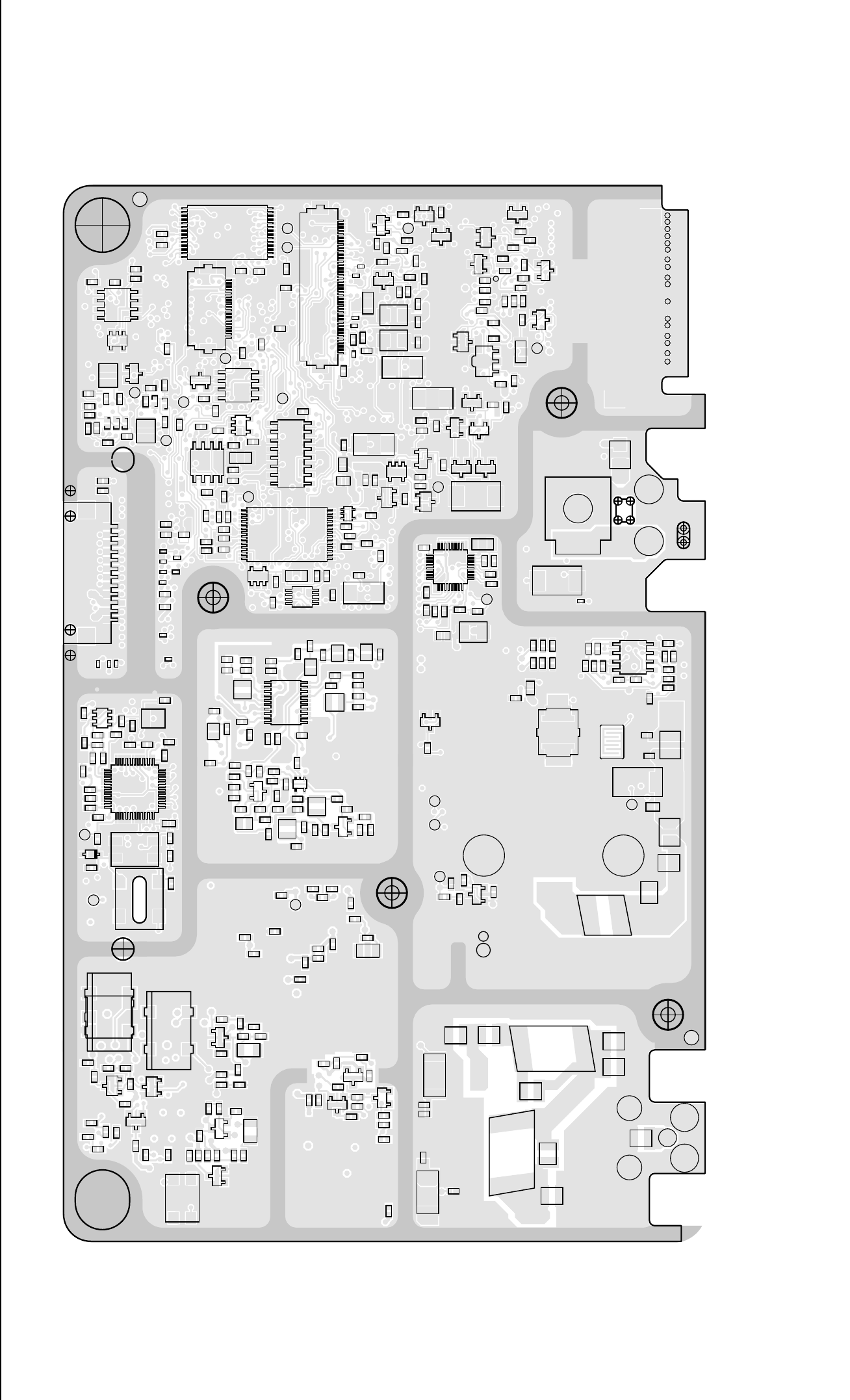
4-14 VHF 1-25W PCBs / Schematics / Parts Lists
C0103
C0105
C0111
C0112
C0121
C0122
C0123
C0141
C0151
C0201
C0202
C0203 C0204
C0205
C0254
C0255
C0265
C0266
C0267
C0271
C0272
C0273
C0274
C0275
C0276 C0277
C0301
C0302
C0303
C0304
C0305
C0324 C0325
C0331
C0341
C0342
C0343
C0344
C0351
C0352
C0353
C0354
C0422 C0423
C0426
C0427
C0428
C0429
C0430 C0431
C0485
C0491
C0492
C0497
C0499
C0541
C0554
C0558 C0559 C0560 C0575
C0576
C0591
C0592 C0593
C0611
C0621
C0622
C0641
C0644
C0645
C0661
C0662
C0663
C0671
C3000
C3001
C3003
C3022
C3023
C3024
C3025
C3026
C3029 C3030
C3031
C3033
C3035
C3036
C3104
C3110
C3111 C3112
C3113
C3116
C3121
C3122
C 3123
C3144
C3146 C3147
C3151
C3152
C3202
C3203
C3205
C3206
C3207
C3208
C3209
C3225
C3228
C3235
C3241
C3251
C3261
C3262
C3263
C3301
C3302
C3303
C3304
C3305
C3306 C3311
C3312
C3313
C3314
C3315
C3316
C3317
C3318
C3319
C3331
C3332
C3333
C3334
C3335
C3348
C3351
C3352
C3355
C3356
C3402
C3405
C3406
C3413
C3414
C3415
C3416
C3421
C3427
C3436
C3437
C3438
C3439
C3440
C3450
C3451
C3452
C3471
C3475 C3491
C3492
C3493
C3494
C3495
C3496
C3498
C3499
C3501
C3502 C3503
C3504
C3505
C3506
C3510
D0101
D0151
D0179
D0301
D0621
D0660 D0661
D3000
D3011
D3101
D3201
D3261
D3451
E0271 E0272
E0631
43
2
FL3111
FL3113
43
2
FL3115
12
J0401
1
40
J0551
1
18
J0552
L3025
L3111
L3112
L3231
L3301
L3302
L3311
L3317
L3318
L3331
L3332
L3345
L3351
L3402
L3421
L3436
L3437
L3491
L3492
Q0151
Q0171
Q0173 Q0183
Q0271
Q0641
Q0661
Q0662
Q0663
Q3002
Q3101
Q3102
Q3141
Q3151
Q3152
Q3301
Q3302
43
Q3303
12
3
Q3421
R0107
R0111 R0112
R0113
R0117
R0121
R0151
R0152
R0171
R0172
R0173
R0174
R0175
R0176
R0177
R0178
R0179 R0183
R0184
R0201
R0202
R0203
R0204
R0205
R0206
R0207
R0208
R0265
R0266
R0267
R0273
R 0274
R0275
R 0276
R0323
R0324
R0331
R0332
R0333
R0335
R0341
R0342
R0343
R0344
R0345
R0346
R0347
R0401
R0407 R0408
R0409
R0410
R0412 R0441
R0467
R0468
R0481
R0482
R0511
R0512
R0525 R0529
R0530
R0531
R0537
R0541
R0542
R0591
R0592
R0593
R0621
R0641
R0642
R0643
R0661
R0662 R0671 R0672
R3000
R3006
R3010
R3011
R3012
R3018
R3019
R3021
R3023 R3030
R3032
R3033
R3034
R3035
R3036
R3102
R3104
R3105
R3107
R3108
R3112
R3113
R3114
R3115
R 3116 R3118
R3133
R3134
R3141
R3146
R3147
R3151
R3152
R3153
R3154
R3201
R3203
R3204
R3206
R3226
R3228
R3241
R3261 R3262
R3263
R3301
R3302
R3303
R3304
R3305
R3306
R3307
R3308
R3311
R3312
R3313
R3314
R3315
R3316
R3317
R3318
R3319
R3321
R3323
R3331
R3343
R3351
R3352
R3353
R3354
R3355
R3356
R3411
R3412
R3413
R3417
R3418
R3421
R3422
R3423
R3428
R3429
R3440
R3441
R3442 R3443
R3444
R3445
R3446
R3450
R3452
R3454
R3455
R3457
R3474
R3475
R3501
R3502 R3504
S3440
TP0101
TP0102
TP0103
TP0104
TP0151
TP0221
TP0222
TP0492
TP0497
TP0530
TP0661
TP3001
TP3201
TP3202
TP3402
TP3403 TP3404
TP3405
TP3406
1
4
58
U0111
22
21 8
7
1
16
1
8
9
U0141
28 15
14
1
U0301
U0331
1
45
8
U0341
U0342
4
58
U0351
14
58
U0652
U0653
1
37
25 13
11
1
20
10
1
4
58
U3402
1
17
9
25
U3501
VR0151
VR0504 VR0509
VR0537
VR0541
VR0601
VR0621
VR0671
VR3471
43
2
Y3101
6
4
3
1
Y3261
2
34
Y3263
1
48
1
1
1
U0122
RAM
U3201
FRACN
U3301
VCOIC
ZWG0130398-A
8486172B07_0
C99
CNTL-REV-T7
PA-REV-T1
VCO-REV-T3
IF-REV-T5
FE-REV-T4
FRAC-T7
ZWG0130398-A
VHF (136-174 MHz) 1-25W 8486172B07 Bottom Side
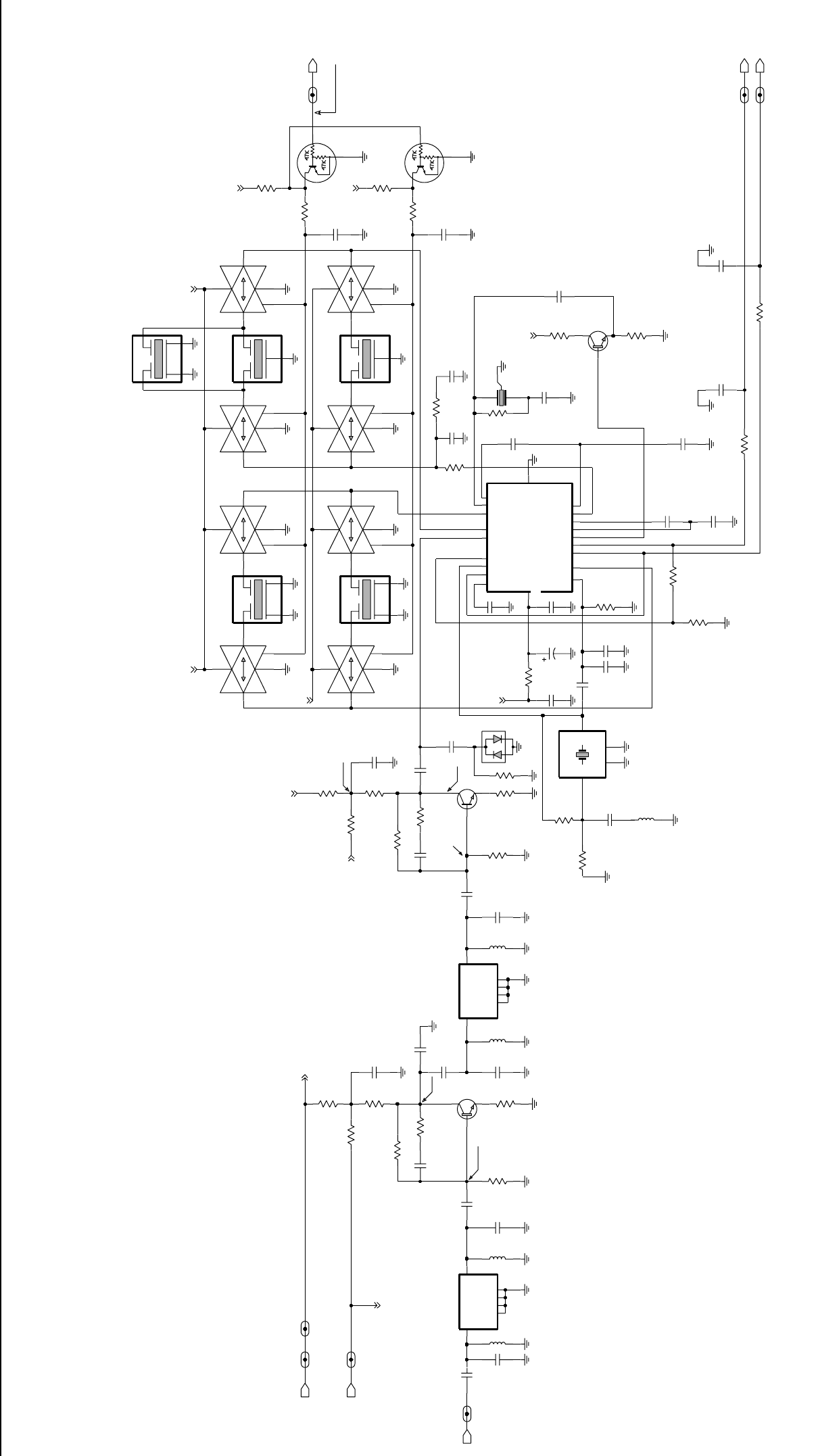
VHF 1-25W PCBs / Schematics / Parts Lists 4-15
ZWG0130565-O
9180469V03
3.9VDC
12.5kHz 0VDC
20/25kHz 5VDC
0.75VDC
0.75VDC 3VDC
9180469V06
9180469V04
9180468v04
9180468V06
3VDC
6.8K
R3107
9V3
R3135
1.2K
390
1GND1
GND2
2
GND3
4
5GND4
3IN 6
OUT
R3115
FL3101
12R16
R3117
27K
Q3102
Q3151
680
R3146
620nH
L3111
620
R3108
R3118
6.8K
R3111
12K
C3101
5V_VHF_IF_1
GND2
4
1IN 2
OUT
NU
2.2pF
FL3111
3
GND1
U3115-1
CNTL
13
1
2VDD
14
VSS
7
DISCAUDIO_VHF_IF_1
15K
R3132
0.1uF
C3144
120pF
C3143
C3139
C3141
0.1uF
0.1uF
13
1
2VDD
14
VSS
7
Q3141
U3111-1
CNTL
R3116
330
10
9V3_VHF_IF_2
3
GND
1IN 2
OUT
R3102
C3110
27pF
FL3113
0.1uF
C3142
9.1pF
IFIN_VHF_IF_1
100
R3104
NU
C3113
1
2GND2
4GND3
GND4
5
IN
3OUT 6
NU
DISCAUDIO
12R16
FL3102
GND1
1000pF
R3151
C3100
C3140
0.1uF
10K
11 10
VDD
14
VSS
7
3
14
VDD
7
VSS
U3111-4
CNTL
12
U3115-2
5
CNTL
4
Q3152
C3152
.01uF
.01uF
C3151
R3133
8.2K
4700pF
C3146
27K
R3106
C3112
390
R3141
82pF
10
R3112
1.8K
R3142
R3154
10K
C3122
.039uF
Q3101
6
VCC
330
R3113
20 MIXOUT 4
OSCIN
3OSCOUT
10
QUADIN
1
RFIN
2
RFIN_DEC
5RSSIOUT
9
RSSI_FEED
15
18
IFAMPIN
16 IFAMPOUT
19
IFAMP_DEC1
17
IFAMP
_DEC2
14
LIMIN
11 LIMOUT
13 LIM_DEC1
12 LIM_DEC2
SA616
U3101
8AUDIOOUT
7
AUDIO_FEED
GND
51
44.395MHz
12R17
Y3101
2
GND
4
GND1
3OUT 1
IN
R3130
C3136
30pF
C3135
33pF
12K
R3101
R3147
12K
C3133
10uF
C3115
100
R3105
22pF
620nH
L3100
0.1uF
NU
C3137
.039uF
C3134
455KHz
3
2
1
BWSELECT_VHF_IF_1
BWSELECT
45B02
Y3102
C3103
33pF
C3132
0.1uF
10K
R3152
0.1uF
C3111
U3115-3
6
CNTL
89
14
VDD
7
VSS
18pF
C3114
L3112
620nH
9V3_VHF_IF_1
5V
D3101
RSSI_VHF_IF_1
OUT
.039uF
C3123
FL3112
3
GND1
GND2
4
1IN 2
R3114
100
R3134
10K
NU
2.4K
R3144
U3111-2
5
CNTL
4
3
14
VDD
7
VSS
3.3K
R3145
C3145
C3147
0.1uF
620nH
L3101
0.1uF
220pF
C3148
NU
10
VDD
14
VSS
7
NU
1pF
C3131
U3115-4
CNTL
12
11
C3121
0.1uF
FL3115
GND1
34
GND2
IN
1OUT 2
15pF
C3102
NU
U3111-3
6
CNTL
89
14
VDD
7
VSS
3GND
1IN 2
OUT
RSSI
C3116
FL3114
0.1uF 0.1uF
R3153
C3104
5V
10K
5V
9V3
9V3
9V39V3
9V3
5V
9V3
5V
9V3
0
R3123
1uH
NU
L3124
33pF
C3124
820
R3124
VHF (136-174 MHz) IF
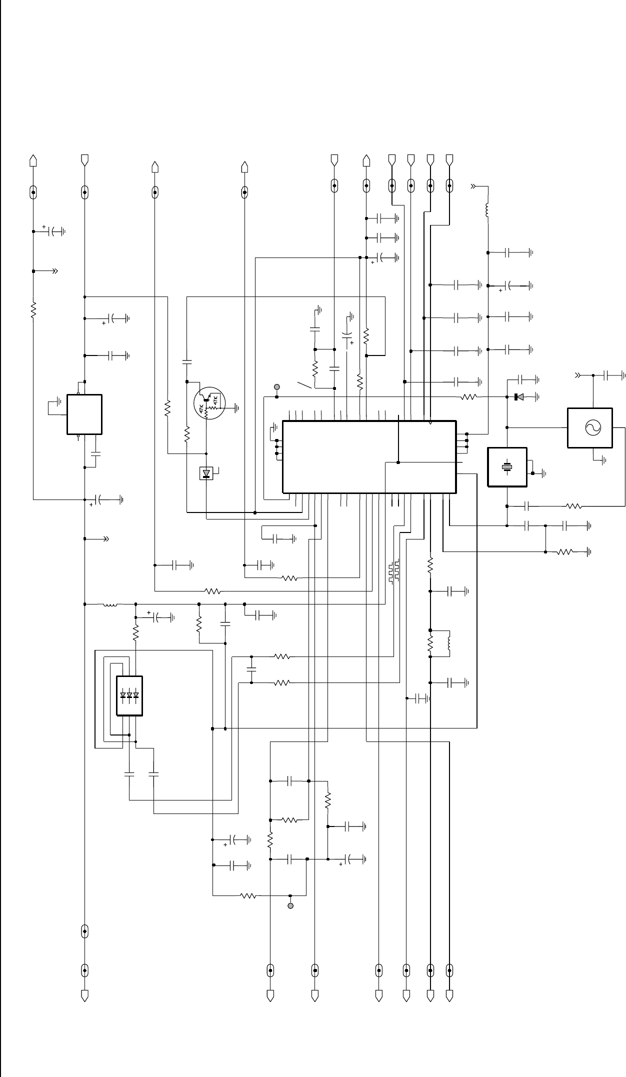
4-16 VHF 1-25W PCBs / Schematics / Parts Lists
0VDC
5VDC
5VDC
(SOURCE)
-2 to +7dBm
13.30VDC
6.83VDC
4.52VDC (R)
+1dBm
0VDC (R)
4.95VDC (R)
2.90VDC
3.42VDC
3.63VDC
2.5VDC
1.1-4.1VDC
0VDC (T)
2.62VDC (T)
4.91VDC (T)
Temp.
Comp.
Xtal
Ref.Osz.
11.28VDC
4.97VDC
2.5-11VDC
5VDC (LOCKED)
0VDC (UNLOCKED)
R3203
A1
5
A2
4
A3
K1
1K2
2K3
3
47
D3201
6
47K
NU
TRB L3232
2.2uH
NU
R3228
C3231
C3225
.01uF
L3201
390nH
0.1uF
C3202
.01uF
100
R3223
C3229
D3221
0.1uF
.047uF
CLK
C3251
C3207
22pF
NU
47K
VCOBIAS_2
R3225
C3226
8.2pF
MODIN_VHF_FN_1
TP3201
R3252
VCOBIAS_1_VHF_FN_1
330K
16_8MHz_VHF_FN_1
PRESC_VHF_FN_1
R3242
0
100
R3241
VSF_VHF_FN_1
DATA
VCOMOD_VHF_FN_1
CSX_VHF_FN_1
100pF
C3227
22pF
NU
CSX
IN_5V_RF_REG_VHF_FN_1
C3240
NU
1
GND 4
GND1
3
OUT
6IN
16.8MHz
75Z04
Y3261
100K
R3227
0.1uF
C3254
C3208
0.1uF
NU
.01uF
C3232
47K
R3226
PRESC
C3214
2.2uF
C3221
0.1uF
1uF
C3224
C3263
0.1uF
VMULT1
15
14 VMULT2
12 VMULT3
11 VMULT4
VRO
13
25
WARP
23 XTAL1
XTAL2
24
27
SFBASE 26
SFCAP
30
SFIN
28 SFOUT
37 TEST1
38 TEST2
21
VBPASS
47
VCP
31
NC3
44
PD_GND
PD_VDD
5
PREIN 32
33
PRE_GND
34 PRE_VDD
35
PVREF
18
REFSEL
45 IADAPT
16 INDMULT
43 IOUT
LOCK
4
10
MODIN
41 MODOUT
17
NC1
29
NC2
39
BIAS2
42
CCOMP
9
CEX 8
CLK
7
DATA
DGND 6
36 DVDD
19 FREFOUT
46 ADAPTSW
22
AGND
48 AUX1
1AUX2
2AUX3
3AUX4
20 AVDD
40
BIAS1
VCOBIAS_1
63A27
U3201
47
R3201
VSF
C3222
0
R3211
0.1uF
L3231
0.1uF
C3211
TP3202
2.2uH
C3243
220pF
16_8MHz
VDDA
VDDA_VHF_FN_1
VCOBIAS_2_VHF_FN_1
0.1uF
C3209 C3246
220pF
NU
C3206
10uF
5V_VHF_FN_2
150K
R3206
Q3221
R3251
180K
.01uF
C3228
0.1uF
C3235
2.2uF
C3210
VCTRL_VHF_FN_1
R3204
LOCK_VHF_FN_1
47
1uF
C3223
NU
220pF
R3262
NU
C3245
BWSELECT
6.2K
C3215
R3224
47K
C3213
2.2uF
1
GND
5
IN
2NR
4OUT
3
SD
2.2uF
VCC
4
VCNTL
1
ADP3300
U3211
6
ERR
Y3263
TTS05V
16.8MHz
GND
2
OUT
3
MODIN
VCTRL
C3255
DATA_VHF_FN_1
220pF
C3242
2.2uF
5V_VHF_FN_1
.01uF
R3222
680
TRB_VHF_FN_1
C3205
C3262
330pF
NU
NU
VCOMOD
C3241
56pF
R3261
47K
2.2uF
C3233
R3221
CLK_VHF_FN_1
C3252
390
1000pF
.01uF
C3234
C3253
4.7uF
NU
IN_5V_RF_REG5V
D3261
C3261
NU
LOCK
C3244
39pF
BWSELECT_VHF_FN_1
220pF
C3203
4,7k
.01uF
NC
5V
5V
R3263
NC
NC
NC
NC
NC NC
NC
NC
NC
NC
VDDA
VDDA
NC
NC
NC
.022uF
C3212
R3202
10MEG
NU
10pF
C3247
In case Y3261 is used instead of Y3263,
replacement of the following parts requires
new temperature compensation of the frequency:
Y3261, U3201, R3261, R3262, C3262, D3261
ZWG0130564-O
VHF (136-174 MHz) FRACN
VHF 1-25W PCBs / Schematics / Parts Lists 4-17
VHF PCB 8486172B07 Parts List 1-25W
Circuit
Ref Motorola Part
No. Description
C3000 2113741F37 3.3nF 50V
C3001 2113740F19 4.7pF 5%
C3002 2113740F26 9.1pF 5%
C3003 2113741F37 3.3nF 50V
C3004 2113740F45 56pF 5%
C3005 2113740F51 100pF 5%
C3006 2113740F45 56pF 5%
C3007 2113741F37 3.3nF 50V
C3008 2113741F25 1nF 50V
C3009 2113741F13 330pF 50V
C3010 2113741F13 330pF 50V
C3011 2113741F37 3.3nF 50V
C3012 2113741F25 1nF 50V
C3013 2113740F45 56pF 5%
C3014 2113740F24 7.5pF 5%
C3015 2113740F45 56pF 5%
C3016 2113740F51 100pF 5% 50V
C3017 2113740F42 43pF 5% 50V
C3019 2113741F25 1nF 50V
C3020 2113741F25 1nF 50V
C3021 2113740F53 120pF 5% 50V
C3022 2113741F49 10nF 50V
C3026 2113743E20 100nF 16V
C3027 2113741F49 10nF 50V
C3028 2113741F49 10nF 50V
C3030 2113741F25 1nF 50V
C3033 2113740F20 5.1pF 5% 50V
C3034 2113740F49 82pF 5% 50V
C3035 2113740F33 18pF 5% 50V
C3036 2113741F25 1nF 50V
C3100 2113741F25 1nF 50V
C3102 2113740F31 15pF 5% 50V
C3103 2113740F39 33pF 5% 50V
C3104 2113743E20 100nF 16V
C3110 2113740F37 27pF 5% 50V
C3111 2113743E20 100nF 16V
C3112 2113740F49 82pF 5% 50V
C3114 2113740F33 18pF 5% 50V
C3115 2113740F35 22pF 5% 50V
C3116 2113743E20 100nF 16V
C3121 2113743E20 100nF 16V
C3122 2113743E11 39nF 10%
C3123 2113743E11 39nF 10%
C3124 2113740L30 33pF 2%
C3132 2113743E20 100nF 16V
C3133 2311049A57 TANT CP 10uF 10% 16V
C3134 2113743E20 100nF 16V
C3135 2113740L30 33pF 2%
C3136 2113740L29 30pF 2%
C3137 2113743E11 39nF 10%
C3139 2113743E20 100nF 16V
C3140 2113743E20 100nF 16V
C3141 2113743E20 100nF 16V
C3142 2113743E20 100nF 16V
C3143 2113740F53 120pF 5% 50V
C3144 2113743E20 100nF 16V
C3145 2113743E20 100nF 16V
C3146 2113741F41 4.7nF 50V
C3147 2113743E20 100nF 16V
C3151 2113741F49 10nF 50V
C3152 2113741F49 10nF 50V
C3202 2113741F49 10nF 50V
C3203 2113741F49 10nF 50V
C3205 2113741F49 10nF 50V
C3206 2311049A57 TANT CP 10uF 10% 16V
C3208 2113743E20 100nF 16V
C3209 2113743E20 100nF 16V
C3210 2311049A40 TANT CP 2.2uF 10% 10V
C3211 2113743E20 100nF 16V
C3212 2113743E07 22nF 16V
C3312 2113743E07 22nF 16V
C3213 2311049A40 TANT CP 2.2uF 10% 10V
C3214 2311049A09 TANT CP 2.2uF 10% 20V
C3215 2311049A09 TANT CP 2.2uF 10% 20V
C3221 2113743E20 100nF 16V
C3222 2113743E20 100nF 16V
C3224 0882422W23 FILM SM 1.0uF 15V 5%
C3225 2113743E20 100nF 16V
C3226 2113740F25 8.2pF 5% 50V
C3227 2113740F51 100pF 5% 50V
C3228 2113743E20 100nF 16V
C3229 2113743E12 47nF 10%
C3231 2113741F49 10nF 50V
C3232 2113741F49 10nF 50V
C3233 2311049A40 TANT CP 2.2uF 10%
C3234 2113741F49 10nF 50V
C3235 2113741F49 10nF 50V
C3242 2113740F59 220pF 5% 50V
C3243 2113740F59 220pF 5% 50V
C3244 2113740F59 220pF 5% 50V
C3245 2113740F59 220pF 5% 50V
C3246 2113740F59 220pF 5% 50V
C3247 2113740F27 10pF 5% 50V
C3251 2113743E20 100nF 16V
C3252 2113741F25 1nF 50V
C3253 2311049A56 TANT CP 4.7uF 20% 10V
C3254 2113743E20 100nF 16V
C3255 2311049A40 TANT CP 2.2uF 10% 10V
C3263 2113743E20 100nF 16V
C3302 2113740F23 6.8pF 5% 50V
C3303 2113741F49 10nF 50V
Circuit
Ref Motorola Part
No. Description
C3306 2113740F20 5.1pF 5% 50V
C3311 2113743E07 22nF 16V
C3314 2113740F23 6.8pF 5% 50V
C3315 2113740F31 15pF 5% 50V
C3316 2113740F15 3.3pF 5% 50V
C3317 2113740F39 33pF 5% 50V
C3318 2113740F21 5.6pF 5% 50V
C3319 2113741F25 1nF 50V
C3324 2113741F49 10nF 50V
C3332 2113743E20 100nF 16V
C3333 2113743E20 100nF 16V
C3334 2113743E07 22nF 16V
C3335 2113741F49 10nF 50V
C3336 2113741F49 10nF 50V
C3337 2113743E20 100nF 16V
C3341 2113741F25 1nF 50V
C3342 2113740L05 3.0pF +-0.1pF
C3344 2113740F09 1.8pF 5% 50V
C3345 2113740L25 20pF +-0.25pF
C3346 2113741F49 10nF 50V
C3347 2113741F49 10nF 50V
C3348 2113741F49 10nF 50V
C3351 2113741F49 10nF 50V
C3352 2113743E07 22nF 16V
C3355 2113741F49 10nF 50V
C3356 2113743E07 22nF 16V
C3357 2113740F24 7.5pF 5% 50V
C3361 2113741F25 1nF 50V
C3362 2113740F21 5.6pF 5% 50V
C3363 2113740F47 68pF 5% 50V
C3364 2113740F31 15pF 5% 50V
C3365 2113741F25 1nF 50V
C3400 2113740F63 330pF 5% 50V
C3401 2113740F63 330pF 5% 50V
C3402 2113743E07 22nF 16V
C3403 2113740F39 33pF 5% 50V
C3404 2113740F39 33pF 5% 50V
C3405 2113740F67 470pF 5% 50V
C3406 2113740F67 470pF 5% 50V
C3410 2113743E07 22nF 16V
C3411 2113743E07 22nF 16V
C3412 2113740F63 330pF 5% 50V
C3414 2113740F63 330pF 5% 50V
C3415 2113743E07 22nF 16V
C3416 2113740F63 330pF 5% 50V
C3417 2113740F43 47pF 5% 50V
C3418 2113740F39 33pF 5% 50V
C3419 2113740F57 180pF 5% 50V
C3420 2113740F57 180pF 5% 50V
C3421 2113741A57 33nF 50V
C3422 2113740A67 330pF 5% 50V
Circuit
Ref Motorola Part
No. Description
C3423 2311049A08 TANT CP 1uF 10% 35V
C3424 2113740F67 470pF 5% 50V
C3425 2113743E07 22nF 16V
C3426 2113740F63 330pF 5% 50V
C3427 2113741F33 2.2nF 50V
C3428 2113741F33 2.2nF 50V
C3431 2111078B34 HQ 47pF 5%
C3433 2111078B36 HQ 56pF 5%
C3434 2113741A45 10nF 50V
C3435 2113740A67 330pF 5% 50V
C3436 2311049A45 TANT CP 10uF 10% 35V
C3437 2113741A57 33nF 50V
C3438 2111078B59 HQ 470pF 5%
C3439 2111078B59 HQ 470pF 5%
C3440 2113741F25 1nF 50V
C3441 2111078B47 HQ 150pF 5%
C3442 2111078B47 HQ 150pF 5%
C3445 2111078B21 HQ 20pF 5%
C3446 2111078B42 HQ 100pF 5%
C3447 2111078B19 HQ 16pF 5%
C3448 2111078B44 HQ 120pF 5%
C3449 2111078B44 HQ 120pF 5%
C3450 2113740F67 470pF 5% 50V
C3451 2113741F25 1nF 50V
C3452 2113740F29 12pF 5% 50V
C3453 2113740F67 470pF 5% 50V
C3471 2113743E07 22nF 16V
C3472 2111078B53 HQ 270pF 5%
C3473 2111078B53 HQ 270pF 5%
C3474 2113740F59 220pF 5% 50V
C3475 2113740F23 6.8pF 5% 50V
C3491 2111078B18 HQ 15pF 5%
C3492 2111078B38 HQ 68pF 5%
C3493 2111078B09 HQ 6.8pF 5%
C3494 2111078B16 HQ 13pF 5%
C3495 2111078B01 HQ 3.3pF 5%
C3496 2111078B31 HQ 36pF 5%
C3498 2111078B16 HQ 13pF 5%
C3499 2111078B19 HQ 16pF 5%
C3501 2113741F33 2.2nF 50V
C3502 2113741F33 2.2nF 50V
C3503 2113740F67 470pF 5% 50V
C3504 2113741F49 10nF 50V
C3505 2311049A07 TANT CP 1uF 10% 16V
C3506 2113741F33 2.2nF 50V X7R
C3507 2113740F51 100pF 5% 50V
C3508 2113740F67 470pF 5% 50V
C3510 2113740F67 470pF 5% 50V
D3000 4813833C02 DUAL SOT MMBD6100
D3001 4805649Q13 VCTR 1SV228 SOT23
D3003 4880154K03 DUAL SCHOTTKY SOT23
Circuit
Ref Motorola Part
No. Description

4-18 VHF 1-25W PCBs / Schematics / Parts Lists
D3004 4805649Q13 VCTR 1SV228 SOT23
D3011 4880142L01 PIN
D3031 4886143B01 MIXER DIODE CROSSOVER
D3101 4880154K03 DIODE DUAL SCHOTTKY
D3201 4802233J09 TRIPLE SOT143-RH
D3221 4880236E05 CHIP SCHOTTKY
D3341 4805649Q13 VCTR 1SV228 SOT23
D3361 4805649Q13 VCTR 1SV228 SOT23
D3362 4862824C01 VARACTOR CHIP
D3401 4813833C02 DUAL SOT MMBD6100
D3451 4880236E05 CHIP SCHOTTKY
D3471 4802482J02 PIN MA/COM
D3472 4802482J02 PIN MA/COM
FL3101 9180112R16 44.85 MHZ CRYSTAL FLTR
80dB
FL3102 9180112R16 44.85 MHZ CRYSTAL FLTR
80dB
FL3111 9180469V03 CER FLTR 6EL 455 KHZ
SMD
FL3112 9180469V06 CER FLTR 6EL 455 KHZ
SMD
FL3113 9180468V04 CER FLTR 4EL 455 KHZ
SMD
FL3114 9180468V06 CER FLTR 4EL 455 KHZ
SMD
J3401 0986166B02 RF CONN MINI UHF
L3002 2462587T23 COIL CHIP 470nH
L3031 2462587T24 COIL CHIP 560nH
L3032 2462587T17 COIL CHIP 150nH
L3101 2462587T25 COIL CHIP 620nH
L3111 2462587T25 COIL CHIP 620nH
L3112 2462587T25 COIL CHIP 620nH
L3124 2462587N68 1uH
L3201 2462587Q42 IND CHIP 390nH 10%
L3231 2462587Q20 IND CHIP 2.2uH 20%
L3301 2462587N44 CHIP IND 18 NH 5%
L3302 2462587N53 CHIP IND 100 nH 5%
L3317 2462587V28 CHIP IND 33 NH 5%
L3318 2462587V34 IND CHIP 100nH 5%
L3331 2462587V32 CHIP IND 68NH 5%
L3332 2462587V15 IND CHIP 100nH 10%
L3333 2462587Q47 IND CHIP 1uH 10%
L3341 2484562T13 MINI-SPRING AW IND 8NH
2%
L3343 2462587N56 COIL CHIP 180nH 5%
L3344 2462587N68 CHIP IND 1 uH 5%
L3345 2462587N68 CHIP IND 1 uH 5%
L3346 2484562T18 MINI-SPRING AW IND
35.5NH 2%
L3351 2462587N68 CHIP IND 1 uH 5%
L3361 2462587N50 CHIP IND 56 nH 5%
Circuit
Ref Motorola Part
No. Description
L3362 2462587N51 CHIP IND 68 nH 5%
L3363 2462587N50 CHIP IND 56 nH 5%
L3364 2462587N68 CHIP IND 1 uH 5%
L3401 2460591A01 SQUARE COIL 4.22nH 3T
L3402 2484657R01 Ferrite Bead
L3403 2462587T13 COIL CHIP 68nH
L3411 2462587T13 COIL CHIP 68nH
L3412 2462587X43 IND CHIP LO-PRO 15.0
L3413 2460591B04 SQUARE COIL 11.03nH 4T
L3414 2460591A11 SQUARE COIL 7.66nH 3T
L3421 2484657R01 Ferrite Bead
L3422 2460591C23 SQUARE COIL 16nH 3T
L3436 2484657R01 Ferrite Bead
L3437 2460592A01 COIL AW 17nH 2T
L3443 2460591X02 COIL SQUARE 25nH
L3471 2462587X69 IND CHIP 1.2uH 5%
L3472 2460592B01 COIL AW 51nH 4T
L3491 2460592B01 COIL AW 51nH 4T
L3492 2460592B01 COIL AW 51nH 4T
L3493 2460592B01 COIL AW 51nH 4T
M3421 2686201B01 HEAT SPREADER
Q3001 4813827A07 TSTR NPN SML SIG MMBR9
Q3002 4813824A17 TSTR PNP 40V .2A B=100-
Q3021 4805921T02 TSTR DUAL ROHM FMC2
Q3101 4813827A07 TSTR NPN SML SIG MMBR9
Q3102 4813827A07 TSTR NPN SML SIG MMBR9
Q3141 4813824A10 TSTR NPN 40V .2A B=50-150
Q3151 4880048M01 TSTR NPN DIG 47k/47k
Q3152 4880048M01 TSTR NPN DIG 47k/47k
Q3221 4880048M01 TSTR NPN DIG 47k/47k
Q3301 4813827A07 TSTR NPN SML SIG MMBR9
Q3303 4802245J50 TSTR DUAL NPN/PNP
UMC5N
Q3304 4805218N63 RF TRANS SOT 323
BFQ67W
Q3411 4805921T02 DUAL ROHM FMC2 RH
Q3421 4802245J55 MRF1507
Q3422 4880048M01 NPN DIG 47k/47k
Q3441 4886136B01 LDMOS PWR TSTR
MRF1565 MRF1550
Q3442 4880048M01 NPN DIG 47k/47k
Q3471 4880048M01 NPN DIG 47k/47k
Q3472 4805128M27 PNP SOT89 BSR33 LH
R3000 0662057A53 1k5 1/16W 5%
R3001 0662057A97 100k 1/16W
R3002 0662057A43 560 1/16W 5%
R3003 0662057A49 1k 1/16W 5%
R3004 0662057A53 1k5 1/16W 5%
R3006 0662057A73 10k 1/16W 5%
R3009 0662057A97 100k 1/16W
R3010 0662057A45 680 OHMS 5%
Circuit
Ref Motorola Part
No. Description
R3011 0662057A65 4k7 1/16W 5%
R3012 0662057A49 1k 1/16W 5%
R3013 0662057A61 3k3 1/16W 5%
R3014 0662057A18 51 1/16W 5%
R3015 0662057A01 10 1/16W 5%
R3016 0662057A01 10 1/16W 5%
R3018 0662057A33 220 1/16W 5%
R3019 0662057A89 47k 1/16W 5%
R3021 0662057A43 560 1/16W 5%
R3024 0662057A39 390 1/16W 5%
R3025 0662057A53 1k5 1/16W 5%
R3026 0662057A73 10k 1/16W 5%
R3027 0662057A73 10k 1/16W 5%
R3028 0662057A39 390 1/16W 5%
R3031 0662057A18 51 1/16W 5%
R3033 0662057B47 0 1/16W
R3101 0662057A75 12k 1/16W 5%
R3102 0662057A01 10 1/16W 5%
R3105 0662057A25 100 1/16W 5%
R3106 0662057A83 27k 1/16W 5%
R3107 0662057A69 6k8 1/16W 5%
R3108 0662057A44 620 OHMS 5%
R3111 0662057A75 12k 1/16W 5%
R3112 0662057A01 10 1/16W 5%
R3113 0662057A37 330 1/16W 5%
R3115 0662057A39 390 1/16W 5%
R3116 0662057A37 330 1/16W 5%
R3117 0662057A83 27k 1/16W 5%
R3118 0662057A69 6k8 1/16W 5%
R3123 0662057B47 0 1/16W
R3124 0662057A47 820 1/16W
R3130 0662057A18 51 1/16W 5%
R3132 0662057A77 15k 1/16W 5%
R3133 0662057A71 8k2 1/16W 5%
R3134 0662057A73 10k 1/16W 5%
R3135 0662057A51 1k2 1/16W 5%
R3141 0662057A39 390 1/16W 5%
R3142 0662057A55 1k8 1/16W 5%
R3144 0662057A58 2k4 1/16W 5%
R3145 0662057A61 3k3 1/16W 5%
R3146 0662057A45 680 OHMS 5%
R3147 0662057A75 12k 1/16W 5%
R3151 0662057A73 10k 1/16W 5%
R3152 0662057A73 10k 1/16W 5%
R3153 0662057A73 10k 1/16W 5%
R3154 0662057A73 10k 1/16W 5%
R3201 0662057A17 47 1/16W 5%
R3202 0662057B46 10MEG
R3203 0662057A17 47 1/16W 5%
R3204 0662057A17 47 1/16W 5%
R3206 0662057B02 150k 1/16W
Circuit
Ref Motorola Part
No. Description
R3211 0662057B47 0 1/16W
R3221 0662057A39 390 1/16W 5%
R3222 0662057A45 CHIP RES 680 OHMS 5%
R3223 0662057A25 100 1/16W 5%
R3224 0662057A89 47k 1/16W 5%
R3225 0662057A89 47k 1/16W 5%
R3227 0662057A97 100k 1/16W
R3241 0662057A25 100 1/16W 5%
R3242 0662057B47 0 1/16W
R3251 0662057B04 180k 1/16W 5%
R3252 0662057B10 330k 1/16W 5%
R3261 0662057A89 47k 1/16W 5%
R3263 0662057A65 4k7 1/16W 5%
R3301 0662057A22 75 1/16W 5%
R3302 0662057A25 100 1/16W 5%
R3303 0662057A57 2k2 1/16W 5%
R3304 0662057A49 1k 1/16W 5%
R3308 0662057B47 0 1/16W
R3311 0662057A25 100 1/16W 5%
R3316 0662057B47 0 1/16W
R3318 0662057A09 22 1/16W 5%
R3321 0662057A73 10k 1/16W 5%
R3323 0662057A49 1k 1/16W 5%
R3331 0662057A17 47 1/16W 5%
R3335 0662057A13 33 1/16W 5%
R3336 0662057A77 15k 1/16W 5%
R3341 0662057A33 220 1/16W 5%
R3342 0662057A15 39 1/16W 5%
R3343 0662057A25 100 1/16W 5%
R3351 0662057A80 20k 1/16W 5%
R3352 0662057A75 12k 1/16W 5%
R3353 0662057A97 100k 1/16W
R3354 0662057B02 150k 1/16W
R3355 0662057A80 20k 1/16W 5%
R3356 0662057A75 12k 1/16W 5%
R3361 0662057A33 220 1/16W 5%
R3362 0662057A17 47 1/16W 5%
R3364 0662057A89 47k 1/16W 5%
R3400 0662057A41 470 1/16W 5%
R3401 0662057A36 300 1/16W 5%
R3402 0662057A05 15 1/16W 5%
R3403 0662057A36 300 1/16W 5%
R3404 0662057A89 47k 1/16W 5%
R3405 0662057A25 100 1/16W 5%
R3406 0662057A97 100k 1/16W
R3412 0662057A67 5k6 1/16W 5%
R3413 0662057A61 3k3 1/16W 5%
R3414 0683962T51 120 1W 5%
R3415 0662057A25 100 1/16W 5%
R3416 0662057A25 100 1/16W 5%
R3418 0662057A81 22k 1/16W 5%
Circuit
Ref Motorola Part
No. Description

VHF 1-25W PCBs / Schematics / Parts Lists 4-19
* Motorola Depot Servicing only
Reference designators with an asterisk indicate
components which are not fieldreplaceable
because they need to be calibrated with
specialized factory equipment after installation.
Radios in which these parts have been replaced in
the field will be off frequency at temperature
extremes.
R3421 0662057A87 39k 1/16W 5%
R3422 0662057A57 2k2 1/16W 5%
R3423 0662057A87 39k 1/16W 5%
R3424 0662057C13 2R7 1/10W 5%
R3425 0662057C13 2R7 1/10W 5%
R3426 0662057C13 2R7 1/10W 5%
R3427 0662057C13 2R7 1/10W 5%
R3428 0662057A58 2k4 1/16W 5%
R3429 0662057A33 220 1/16W 5%
R3431 0680194M18 51 1W 5%
R3432 0680194M18 51 1W 5%
R3433 0662057C13 2R7 1/10W 5%
R3434 0662057C13 2R7 1/10W 5%
R3435 0662057C13 2R7 1/10W 5%
R3441 0662057A87 39k 1/16W 5%
R3442 0662057A57 2k2 1/16W 5%
R3443 0662057A87 39k 1/16W 5%
R3444 0662057C19 4R7 1/10W 5%
R3445 0662057A58 2k4 1/16W 5%
R3446 0662057B47 0 1/16W
R3450 0662057A41 470 1/16W 5%
R3452 0662057A75 12k 1/16W 5%
R3454 0662057A84 30k 1/16W 5%
R3455 0662057A97 100k 1/16W
R3457 0683962T51 120 1W 5%
R3471 0662057A41 470 1/16W 5%
R3473 0680194M18 51 1W 5%
R3474 0680194M18 51 1W 5%
R3475 0662057A73 10k 1/16W 5%
R3491 0662057A73 10k 1/16W 5%
R3501 0662057A69 6k8 1/16W 5%
R3502 0662057A87 39k 1/16W 5%
R3504 0662057A73 10k 1/16W 5%
R3505 0662057B09 300k 1/16W 5%
R3507 0662057A80 20k 1/16W 5%
R3508 0662057A97 100k 1/16W
R3509 0662057A49 1k 1/16W 5%
T3001 2508396X02 TRANSFORMER
T3002 2508397X02 TRANSFORMER
U3101 5186144B01 FM IF IC SA616
U3111 5113805A86 IC QUAD ANALOG MUX/
DEMUX
U3115 5113805A86 IC QUAD ANALOG MUX/
DEMUX
U3201 5185963A27 IC TESTED AT25016 48 PIN
GFP
U3211 5105739X05 IC SOT 5V HI-PRECISION
REGULAT
U3301 5105750U54 VCO BUFFER PKG DIE
U3401 5105109Z67 LDMOS DRIVER VHF/UHF
U3402 5180932W01 LINEAR IC OP AMP
Circuit
Ref Motorola Part
No. Description
U3501 5185765B01 IC POWER CONTROL
U3502 5185963A15 TEMP SENSOR 1M5
VR3471 4813830A15 5.6V 5% 225mW
Y3101 4880606B09 CRYSTAL 44.395 MHZ
Y3102 9186145B02 CERAMIC DISCRIMINATOR
455kHz
Y3263 4886182B01 VCTCXO 16.8MHz 2ppm
TTSO5V
* Y3261 Not Used 16.8MHz 75Z04
Circuit
Ref Motorola Part
No. Description

4-20 VHF 1-25W PCBs / Schematics / Parts Lists
THIS PAGE INTENTIONALLY LEFT BLANK

GM328/GM338/GM398
Mobile Radios
UHF (403-470MHz)
Service Information
Issue: December, 2003

Computer Software Copyrights
The Motorola products described in this manual may include copyrighted Motorola computer programs stored
in semiconductor memories or other media. Laws in the United States and other countries preserve for
Motorola certain exclusive rights for copyrighted computer programs, including the exclusive right to copy or
reproduce in any form, the copyrighted computer program. Accordingly, any copyrighted Motorola computer
programs contained in the Motorola products described in this manual may not be copied or reproduced in
any manner without the express written permission of Motorola. Furthermore, the purchase of Motorola
products shall not be deemed to grant, either directly or by implication, estoppel or otherwise, any license
under the copyrights, patents or patent applications of Motorola, except for the normal non-exclusive royalty-
free license to use that arises by operation of law in the sale of a product.

i
Table of Contents
Section 1 Model Chart and Technical Specifications
1.0 GM328/GM338/GM398 Model Chart...................................................................1-1
2.0 Technical Specifications ......................................................................................1-2
Section 2 Theory of Operation
1.0 Introduction ..........................................................................................................2-1
2.0 UHF (403-470 MHz) Receiver .............................................................................2-1
2.1 Receiver Front-End ........................................................................................2-1
2.2 Front-End Band-Pass Filters & Pre-Amplifier.................................................2-2
2.3 First Mixer and High Intermediate Frequency (IF)..........................................2-2
2.4 Low Intermediate Frequency (IF) and Receiver Back End.............................2-3
3.0 UHF (403-470 MHz) Transmitter Power Amplifier (PA) 25 W..............................2-3
3.1 First Power Controlled Stage..........................................................................2-4
3.2 Power Controlled Driver Stage.......................................................................2-4
3.3 Final Stage .....................................................................................................2-4
3.4 Directional Coupler.........................................................................................2-5
3.5 Antenna Switch...............................................................................................2-5
3.6 Harmonic Filter ...............................................................................................2-5
3.7 Power Control.................................................................................................2-5
4.0 UHF (403-470 MHz) Frequency Synthesis..........................................................2-6
4.1 Reference Oscillator.......................................................................................2-6
4.2 Fractional-N Synthesizer ................................................................................2-7
4.3 Voltage Controlled Oscillator (VCO)...............................................................2-8
4.4 Synthesizer Operation....................................................................................2-9
Section 3 Troubleshooting Charts
1.0 Troubleshooting Flow Chart for Receiver ............................................................3-1
2.0 Troubleshooting Flow Chart for 25W Transmitter................................................3-3
3.0 Troubleshooting Flow Chart for Synthesizer........................................................3-6
4.0 Troubleshooting Flow Chart for VCO...................................................................3-7

ii
Section 4 UHF PCB/Schematics/Parts Lists
1.0 Allocation of Schematics and Circuit Boards .......................................................4-1
1.1 Controller Circuits...........................................................................................4-1
2.0 UHF 1-25W PCBs / Schematics / Parts Lists ......................................................4-3
UHF (403-470 MHz) 1-25W 8485670Z02 Top Side...............................................4-3
UHF (403-470 MHz) 1-25W 8485670Z02 Bottom Side.........................................4-4
UHF (403-470 MHz) Power Amplifier 1 - 25W .......................................................4-5
UHF (403-470 MHz) FRACN..................................................................................4-6
UHF (403-470 MHz) Voltage Controlled Oscillator.................................................4-7
UHF (403-470 MHz) Receiver Front End ...............................................................4-8
UHF (403-470 MHz) IF...........................................................................................4-9
UHF PCB 8485670Z02 Parts List 1-25W.............................................................4-10
UHF (403-470 MHz) 1-25W 8485670Z03 Top Side.............................................4-13
UHF (403-470 MHz) 1-25W 8485670Z03 Bottom Side.......................................4-14
UHF (403-470 MHz) Power Amplifier 1 - 25W .....................................................4-15
UHF (403-470 MHz) FRACN................................................................................4-16
UHF (403-470 MHz) Voltage Controlled Oscillator...............................................4-17
UHF (403-470 MHz) Receiver Front End .............................................................4-18
UHF (403-470 MHz) IF.........................................................................................4-19
UHF PCB 8485670Z03 Parts List 1-25W.............................................................4-20
1-1
Section 1
MODEL CHART AND TECHNICAL SPECIFICATIONS
1.0 GM328/GM338/GM398 Model Chart
GM Series, UHF Band 1, 403-470 MHz
Model Description
AZM25RHC9AA1 GM328 403-470 MHz 1-25W
AZM25RHF9AA5 GM338 403-470 MHz 1-25W
AZM25RHN9AA8 GM398 403-470 MHz 1-25W
Item Description
X GCN6112_ GM328 Control Head Direct Mount
XGCN6114_ GM338 Control Head Direct Mount
X GCN6115_ GM398 Control Head Direct Mount
X X IMUE6021_ Tanapa WM 403-470 MHz 1-25W
X IMUE6039_ Tanapa WM 403-470 MHz 1-25W
XXXRAE4151_ BNC 403-430 MHz, 1/4 Wave Roof Mount
XXXRAE4158_ BNC 406-420 MHz, 3.5dB Gain Roof Mount
XXXRAE4152_ BNC 450-470 MHz, 1/4 Wave Roof Mount
XXXRAE4153_ BNC 450-470 MHz, 3.5dB Gain Roof Mount
XXXRAE4154_ BNC 450-470 MHz, 5dB Gain Roof Mount
X 6804113J74 GM328 User Guide
X6804112J06 GM338 User Guide
X 6804112J07 GM398 User Guide
x = Indicates one of each is required.

1-2 Technical Specifications
2.0 Technical Specifications
Data is specified for +25°C unless otherwise stated.
General Specifications
Channel Capacity
GM328
GM338
GM398
4
128
160
Power Supply 13.2Vdc (10.8 - 15.6Vdc)
Dimensions: H x W x D (mm) Depth excluding knobs GM328
56mm x 176mm x 177mm
(add 8mm for Volume Knob)
Dimensions: H x W x D (mm) Depth excluding knobs GM338
59mm x 179mm x 186mm (1 - 25W)
59mm x 179mm x 198mm (25 - 45W)
(add 9mm for Volume Knob)
Dimensions: H x W x D (mm) Depth excluding knobs GM398
72mm x 185mm x 188mm
(add 8mm for Volume Knob)
Weight: GM328/GM338 1400 g
Weight: GM398 1500 g
Sealing: Withstands rain testing per
MIL STD 810 C/D/E and IP54
Shock and Vibration: Protection provided via impact
resistant housing exceeding MIL STD
810-C/D/E
Dust, Salt & Fog: Protection provided via environment
resistant housing exceeding MIL STD
810 C/D/E

Technical Specifications 1-3
Transmitter UHF
*Frequencies - Full Bandsplit UHF 403-470 MHz
Channel Spacing 12.5/20/25 kHz
Frequency Stability
(-30°C to +60°C, +25° Ref.) ±2.0 ppm
Power 1-25W
Modulation Limiting ±2.5 @ 12.5 kHz
±4.0 @ 20 kHz
±5.0 @ 25 kHz
FM Hum & Noise -40 dB @ 12.5kHz
-45 dB @ 20/25kHz
Conducted/Radiated Emission (ETS) -36 dBm <1 GHz
-30 dBm >1 GHz
Adjacent Channel Power -60 dB @ 12.5 kHz
-70 dB @ 25 kHz
Audio Response (300 - 3000 Hz) +1 to -3 dB
Audio Distortion @1000Hz, 60%
Rated Maximum Deviation <3% typical
Receiver UHF
*Frequencies - Full Bandsplit UHF 403-470 MHz
Channel Spacing 12.5/20/25 kHz
Sensitivity (12 dB SINAD) 0.30 µV (0.22 µV typical)
Intermodulation (ETS) >65 dB
Base Mode: >70dB
(1-25W model only)
Adjacent Channel Selectivity (ETS) 65 dB @ 12.5 kHz
70 dB @ 20 kHz
75 dB @ 25 kHz
Spurious Rejection (ETS) 70 dB @ 12.5 kHz
75 dB @ 20/25 kHz
Rated Audio 3W Internal
13W External
Audio Distortion @ Rated Audio <3% typical
Hum & Noise -40 dB @ 12.5 kHz
-45 dB @ 20/25 kHz

1-4 Technical Specifications
*Availability subject to the laws and regulations of individual countries.
Audio Response (300 - 3000Hz @ 20/25kHz)
(300 - 2550Hz @12.5kHz) +1 to -3 dB
Conducted Spurious Emission (ETS) -57 dBm <1 GHz
-47 dBm >1 GHz
Receiver UHF
2-1
Section 2
THEORY OF OPERATION
1.0 Introduction
This Chapter provides a detailed theory of operation for the UHF circuits in the radio. For details of
the theory of operation and troubleshooting for the the associated Controller circuits refer to the
Controller Section of this manual.
2.0 UHF (403-470 MHz) Receiver
2.1 Receiver Front-End
The receiver is able to cover the UHF range from 403 to 470 MHz. It consists of four major blocks:
front-end bandpass filters and pre-amplifier, first mixer, high-IF, low-IF and receiver back-end . Two
varactor-tuned bandpass filters perform antenna signal pre-selection. A cross over quad diode
mixer converts the signal to the first IF of 44.85 MHz. Low-side first injection is used.
Figure 2-1 UHF Receiver Block Diagram
Demodulator
1. Crystal
Filter
Mixer
Varactor
Tuned Filter
RF Amp
Varactor
Tuned Filter
Pin Diode
Antenna
Switch
RF Jack
Antenna
Control Voltage
from PCIC First LO
from FGU
Recovered Audio
RSSI
Second LO
2. Crystal
Filter
455kHz Filter
(25kHz)
455kHz Filter
(25kHz)
455kHz Filter
(12.5kHz)
455kHz Filter
(12.5kHz)
Switch
Switch
Switch
Switch
Limiter
1. IF Amp
2. IF Amp
Filter Bank Selection
from Synthesizer IC
Harmonic
Filter
BWSELECT

2-2 UHF (403-470 MHz) Receiver
There are two 2-pole 44.85 MHz crystal filters in the high-IF section and 2 pairs of 455 kHz ceramic
filters in the low-IF section to provide the required adjacent channel selectivity .The correct pair of
ceramic filters for 12.5 or 25KHz channel spacing is selected via control line BWSELECT. The
second IF at 455 kHz is mixed, amplified and demodulated in the IF IC. The processing of the
demodulated audio signal is performed by an audio processing IC located in the controller section.
2.2 Front-End Band-Pass Filters & Pre-Amplifier
The received signal from the radio’s antenna connector is first routed through the harmonic filter and
antenna switch, which are part of the RF power amplifier circuitry, before being applied to the
receiver pre-selector filter (C4001, C4002, D4001 and associated components). The 2-pole pre-
selector filter tuned by the varactor diodes D4001 and D4002 pre-selects the incoming signal (RXIN)
from the antenna switch to reduce spurious effects to following stages. The tuning voltage
(FECTRL_1) ranging from 2 volts to 8 volts is controlled by pin 20 of PCIC (U4501) in the
Transmitter section. A dual hot carrier diode (D4003) limits any inband signal to 0 dBm to prevent
damage to the pre-amplifier.
The RF pre-amplifier is an SMD device (Q4003) with collector base feedback to stabilize gain,
impedance, and intermodulation. The collector current of approximately 11-16 mA is drawn from the
voltage 9V3 via L4003 and R4002. A switchable 3dB pad (R4066,R4007,R4063, R4064 and
R4070), controlled via line FECTRL_2 and Q4004 stabilizes the output impedance and
intermodulation performance.
A second 2-pole varactor tuned bandpass filter provides additional filtering of the amplified signal.
The varactor diodes D4004 and D4005 are controlled by the same signal FECTRL_1, which
controls the pre-selector filter. A following 1 dB pad (R4013 - R4015) stabilizes the output
impedance and intermodulation performance.
2.3 First Mixer and High Intermediate Frequency (IF)
The signal coming from the front-end is converted to the first IF (44.85 MHz) using a cross over
quad diode mixer (D4051). Its ports are matched for incoming RF signal conversion to the 44.85
MHz IF using low side injection via matching transformers T4051 and T4052. The injection signal
(RXINJ) coming from the RX VCO buffer (Q4332) is filtered by the lowpass filter consisting of
(L4053, L4054, C4053 - C4055) followed by a matching transformer T4052 and has a level of
approximately 15dBm.
The mixer IF output signal (IF) from transformer T4501pin 2 is fed to the first two pole crystal filter
FL3101. The filter output in turn is matched to the following IF amplifier.
The IF amplifier Q3101 is actively biased by a collector base feedback (R3101, R3106) to a current
drain of approximately 5 mA drawn from the voltage 5V. Its output impedance is matched to the
second two pole crystal filter FL3102. The signal is further amplified by a preamplifier (Q3102)
before going into pin 1 of IFIC (U3101).
A dual hot carrier diode (D3101) limits the filter output voltage swing to reduce overdrive effects at
RF input levels above -27 dBm.
UHF (403-470 MHz) Transmitter Power Amplifier (PA) 25 W 2-3
2.4 Low Intermediate Frequency (IF) and Receiver Back End
The 44.85 high IF signal from the second IF amplifier feeds the IF IC (U3101) at pin1. Within the IF
IC the 44.85 MHz high IF signal mixes with the 44.395 MHz second local oscillator (2nd LO) to
produce the low IF signal at 455 kHz. The 2nd LO frequency is determined by crystal Y3101. The
low IF signal is amplified and filtered by an external pair of 455 kHz ceramic filters FL3112, FL3114
for 20/25 kHz channel spacing or FL3111,FL3113/F3115 for 12.5 kHz channel spacing. These pairs
are selectable via BWSELECT. The filtered output from the ceramic filters is applied to the limiter
input pin of the IF IC (pin 14).
The IF IC contains a quadrature detector using a ceramic phase-shift element (Y3102) to provide
audio detection. Internal amplification provides an audio output level of 120 mV rms (at 60%
deviation) from U3103 pin 8 (DISCAUDIO) which is fed to the ASFIC_CMP (U0221) pin 2 (part of
the Controller circuitry).
A Received Signal Strength Indicator (RSSI) signal is available at U3101 pin 5, having a dynamic
range of 70 dB. The RSSI signal is interpreted by the microprocessor (U0101 pin 63) and in addition
is available at accessory connector J0501-15.
3.0 UHF (403-470 MHz) Transmitter Power Amplifier (PA) 25 W
The radio’s 25W PA is a three stage amplifier used to amplify the output from the VCOBIC to the
radio transmit level. All three stages utilize LDMOS technology. The gain of the first stage (U4401) is
adjustable, controlled by pin 4 of PCIC (U4501) via U4402-1. It is followed by an LDMOS stage
(Q4421) and LDMOS final stage (Q4441).
Figure 2-2 UHF Transmitter Block Diagram
Devices U4401, Q4421 and Q4441 are surface mounted. A pressure pad between board and the
radio's cover provides good thermal contact between the devices and the chassis.
PCIC
Pin Diode
Antenna
Switch RF Jack
Antenna
Harmonic
Filter
Power
Sense
PA-Final
Stage
From VCO
Controlled
Stage
Vcontrol
Bias 1
Bias 2
To Microprocessor
Temperature
Sense
SPI BUS
ASFIC_CMP
PA
PWR
SET
To Microprocessor
PA
Driver

2-4 UHF (403-470 MHz) Transmitter Power Amplifier (PA) 25 W
3.1 First Power Controlled Stage
The first stage (U4401) is a 20dB gain integrated circuit containing two LDMOS FET amplifier
stages. It amplifies the RF signal from the VCO (TXINJ). The output power of stage U4401 is
controlled by a DC voltage applied to pin 1 from the op-amp U4402-1, pin 1. The control voltage
simultaneously varies the bias of two FET stages within U4401. This biasing point determines the
overall gain of U4401 and therefore its output drive level to Q4421, which in turn controls the output
power of the PA.
Op-amp U4402-1 monitors the drain current of U4401 via resistor R4444 and adjusts the bias
voltage of U4401 so that the current remains constant. The PCIC (U4501) provides a DC output
voltage at pin 4 (INT) which sets the reference voltage of the current control loop. A raising power
output causes the DC voltage from the PCIC to fall, and U4402-1 adjusts the bias voltage for a lower
drain current to lower the gain of the stage.
In receive mode the DC voltage from PCIC pin 23 (RX) turns on Q4442, which in turn switches off
the biasing voltage to U4401.
Switch S5440 is a pressure pad with a conductive strip which connects two conductive areas on the
board when the radio's cover is properly screwed to the chassis. When the cover is removed, S5440
opens and the resulting high voltage level at the inverting inputs of the current control op-amps
U4402-1 & 2 switches off the biasing of U4401 and Q4421. This prevents transmitter key up while
the devices do not have proper thermal contact to the chassis.
3.2 Power Controlled Driver Stage
The next stage is an LDMOS device (Q4421) providing a gain of 12dB. This device requires a
positive gate bias and a quiescent current flow for proper operation. The bias is set during transmit
mode by the drain current control op-amp U4402-2, and fed to the gate of Q4421 via the resistive
network R4429, R4418, R4415 and R4416.
Op-amp U4402-2 monitors the drain current of U4421 via resistors R4424-27 and adjusts the bias
voltage of Q4421 so that the current remains constant. The PCIC (U4501) provides a DC output
voltage at pin 4 (INT) which sets the reference voltage of the current control loop. A raising power
output causes the DC voltage from the PCIC to fall, and U4402-2 adjusts the bias voltage for a lower
drain current to lower the gain of the stage.
In receive mode the DC voltage from PCIC pin 23 (RX) turns on Q4422, which in turn switches off
the biasing voltage to Q4421.
3.3 Final Stage
The final stage is an LDMOS device (Q4441) providing a gain of 12dB. This device also requires a
positive gate bias and a quiescent current flow for proper operation. The voltage of the line
MOSBIAS_2 is set in transmit mode by the ASFIC and fed to the gate of Q4441 via the resistive
network R4404, R4406, and R4431-2. This bias voltage is tuned in the factory. If the transistor is
replaced, the bias voltage must be tuned using the Global Tuner. Care must be taken not to
damage the device by exceeding the maximum allowed bias voltage. The device’s drain current is
drawn directly from the radio’s DC supply voltage input, PASUPVLTG, via L4436 and L4437.
A matching network consisting of C4441-49 and striplines transforms the impedance to 50 ohms
and feeds the directional coupler.

UHF (403-470 MHz) Transmitter Power Amplifier (PA) 25 W 2-5
3.4 Directional Coupler
The directional coupler is a microstrip printed circuit, which couples a small amount of the forward
power delivered by Q4441. The coupled signal is rectified by D4451. The DC voltage is proportional
to the RF output power and feeds the RFIN port of the PCIC (U4501 pin 1). The PCIC controls the
gain of stages U4401 and Q4421 as necessary to hold this voltage constant, thus ensuring the
forward power out of the radio to be held to a constant value.
3.5 Antenna Switch
The antenna switch consists of two PIN diodes, D4471 and D4472. In the receive mode, both diodes
are off. Signals applied at the antenna jack J4401 are routed, via the harmonic filter, through
network L4472, C4474 and C4475, to the receiver input. In the transmit mode, K9V1 turns on
Q4471 which enables current sink Q4472, set to 96 mA by R4473 and VR4471. This completes a
DC path from PASUPVLTG, through L4437, D4471, L4472, D4472, L4471, R4474 and the current
sink, to ground. Both diodes are forward biased into conduction. The transmitter RF from the
directional coupler is routed via D4471 to the harmonic filter and antenna jack. D4472 also
conducts, shunting RF power and preventing it from reaching the receiver port (RXIN). L4472 is
selected to appear as a broadband lambda/4 wave transmission line, making the short circuit
presented by D4472 appear as an open circuit at the junction of D4472 and the receiver path.
3.6 Harmonic Filter
Components L4491-L4493 and L4472, C4491, C4496-98 form a Butterworth low-pass filter to
attenuate harmonic energy of the transmitter to specifications level. R4491 is used to drain
electrostatic charge that might otherwise build up on the antenna. The harmonic filter also prevents
high level RF signals above the receiver passband from reaching the receiver circuits, improving
spurious response rejection.
3.7 Power Control
The transmitter uses the Power Control IC (PCIC, U4501) to control the power output of the radio. A
portion of the forward RF power from the transmitter is sampled by the directional coupler and
rectified, to provide a DC voltage to the RFIN port of the PCIC (pin 1) which is proportional to the
sampled RF power.
The ASFIC (U0221) has internal digital to analog converters (DACs) which provide a reference
voltage of the control loop to the PCIC via R4505. The reference voltage level is programmable
through the SPI line of the PCIC. This reference voltage is proportional to the desired power setting
of the transmitter, and is factory programmed at several points across the frequency range of the
transmitter to offset frequency response variations of the transmitter’s power detector circuit.
The PCIC provides a DC output voltage at pin 4 (INT) which sets the drain current of the first
(U4401) and second (Q4421) transmitter stage via current control op-amps U3402-1 and U3402-2.
This adjusts the transmitter power output to the intended value. Variations in forward transmitter
power cause the DC voltage at pin 1 to change, and the PCIC adjusts the control voltage above or
below its nominal value to raise or lower output power.
Capacitors C4502-4, in conjunction with resistors and integrators within the PCIC, control the
transmitter power-rise (key-up) and power-decay (de-key) characteristic to minimize splatter into
adjacent channels.

2-6 UHF (403-470 MHz) Frequency Synthesis
U4502 is a temperature-sensing device, which monitors the circuit board temperature in the vicinity
of the transmitter driver and final devices, and provides a DC voltage to the PCIC (TEMP, pin 30)
proportional to temperature. If the DC voltage produced exceeds the set threshold in the PCIC, the
transmitter output power will be reduced so as to reduce the transmitter temperature.
4.0 UHF (403-470 MHz) Frequency Synthesis
The synthesizer subsystem consists of the reference oscillator (Y4261 or Y4262), the Low Voltage
Fractional-N synthesizer (LVFRAC-N, U4201), and the Voltage Controlled Oscillator VCO.
4.1 Reference Oscillator
The reference oscillator (Y4262) contains a temperature compensated crystal oscillator with a
frequency of 16.8 MHz. An Analogue to Digital (A/D) converter internal to U4201 (LVFRAC-N) and
controlled by the microprocessor via serial interface (SRL) sets the voltage at the warp output of
U4201 pin 25 to set the frequency of the oscillator. The output of the oscillator (pin 3 of Y4262) is
applied to pin 23 (XTAL1) of U4201 via a RC series combination.
In applications where less frequency stability is required the oscillator inside U4201 is used along
with an external crystal Y4261, varactor diode D4261, C4261, C4262 and R4262. In this case,
Y4262, R4263, C4235 and C4251 are not used. When Y4262 is used, Y4261, D4261, C4261,
C4262 and R4262 are not used, and C4263 is increased to 0.1 uF.

UHF (403-470 MHz) Frequency Synthesis 2-7
4.2 Fractional-N Synthesizer
The LVFRAC-N synthesizer IC (U4201) consists of a pre-scaler, a programmable loop divider,
control divider logic, a phase detector, a charge pump, an A/D converter for low frequency digital
modulation, a balance attenuator to balance the high frequency analogue modulation and low
frequency digital modulation, a 13V positive voltage multiplier, a serial interface for control, and
finally a super filter for the regulated 5 volts.
Figure 2-3 UHF Synthesizer Block Diagram
A voltage of 5V applied to the super filter input (U4201 pin 30) supplies an output voltage of 4.5
VDC(VSF) at pin 28. It supplies the VCO, VCO modulation bias circuit (via R4322) and the
synthesizer charge pump resistor network (R4251, R4252). The synthesizer supply voltage is
provided by the 5V regulator U4211.
In order to generate a high voltage to supply the phase detector (charge pump) output stage at
pin 47 VCP (U4201-47), a voltage of 13 VDC is being generated by the positive voltage multiplier
circuitry (D4201, C4202, C4203). This voltage multiplier is basically a diode capacitor network driven
by two (1.05MHz) 180 degrees out of phase signals (U4201-14 and -15).
Output LOCK (U4201-4) provides information about the lock status of the synthesizer loop. A high
level at this output indicates a stable loop. IC U4201 provides the 16.8 MHz reference frequency at
pin 19.
The serial interface (SRL) is connected to the microprocessor via the data line DATA (U4201-7),
clock line CLK (U4201-8), and chip enable line CSX (U4201-9).
DATA
CLK
CEX
MODIN
VCC, DC5V
XTAL1
XTAL2
WARP
PREIN
VCP
REFERENCE
OSCILLATOR
VOLTAGE
MULTIPLIER
DATA (U0101 PIN 100)
CLOCK (U0101 PIN 1)
CSX (U0101 PIN 2)
MOD IN (U0221 PIN 40)
+5V (U4211 PIN 1)
7
8
9
10
13, 30
23
24
25
32
47
VMULT2 VMULT1
BIAS1
SFOUT
AUX3
AUX4
IADAPT
IOUT
GND
FREFOUT
LOCK 4
19
6, 22, 33, 44
43
45
3
2
28
14 15
40
FILTERED 5V
STEERING
LOCK (U0101 PIN 56)
PRESCALER IN
FREF (U0221 PIN 34)
39
BIAS2
41
48
5, 20, 34, 36
+5V (U4211 PIN 1)
AUX1
VDD, DC5V MODOUT
U4201
LOW VOLTAGE
FRACTIONAL-N
SYNTHESIZER
AUX2 1 (NU)
BWSELECT
VCO Bias
TRB
To IF
Section
TX RF INJECTION
(1ST STAGE OF PA)
LO RF INJECTION
VOLTAGE
CONTROLLED
OSCILLATOR
LINE
2-POLE
LOOP
FILTER

2-8 UHF (403-470 MHz) Frequency Synthesis
4.3 Voltage Controlled Oscillator (VCO)
The Voltage Controlled Oscillator (VCO) consists of the VCO/Buffer IC (VCOBIC, U4301), the TX
and RX tank circuits, the external RX buffer stages, and the modulation circuitry.
Figure 2-4 UHF VCO Block Diagram
The VCOBIC together with Fractional-N synthesizer (U4201) generates the required frequencies in
both transmit and receive modes. The TRB line (U4301 pin 19) determines which tank circuits and
internal buffers are to be enabled. A high level on TRB enables TX tank and TX output (pin 10), and
a low enables RX tank and RX output (pin 8). A sample of the signal from the enabled output is
routed from U4301 pin 12 (PRESC_OUT), via a low pass filter, to pin 32 of U4201 (PREIN).
A steering line voltage (VCTRL) between 3.0V and 10.0V at varactor diode CR4311 will tune the full
TX frequency range (TXINJ) from 403 MHz to 470 MHz, and at varactor diodes CR4301, CR4302
and CR4303 will tune the full RX frequency range (RXINJ) from 358 MHz to 425 MHz. The tank
circuits uses the Hartley configuration for wider bandwidth. For the RX tank circuit, an external
transistor Q4301 is used in conjunction with the internal transistor for better side-band noise.
Presc
RX
TX
Matching
Network Low Pass
Filter
Attenuator
Pin8
Pin14
Pin10
(U4201 Pin28)
VCC Buffers
TX RF Injection
U4201 Pin 32
AUX3 (U4201 Pin 2)
Prescaler Out
Pin 12Pin 19
Pin 20
TX/RX/BS
Switching Network
U4301
VCOBIC
Rx
Active Bias
Tx
Active Bias
Pin2
Rx-I adjust
Pin1
Tx-I adjust
Pins 9,11,17
Pin18
Vsens
Circuit
Pin15
Pin16
RX VCO
Circuit
TX VCO
Circuit
RX Tank
TX Tank
Pin7
Vcc-Superfilter
Collector/RF in
Pin4
Pin5
Pin6
RX
TX
(U4201 Pin 28)
Rx-SW
Tx-SW
Vcc-Logic
(U4201 Pin 28)
Steer Line
Voltage
(VCTRL)
Pin13
Pin3
TRB IN
LO RF INJECTION
Q4301
Q4332

UHF (403-470 MHz) Frequency Synthesis 2-9
The external RX buffers (Q4332) are enabled by a high at U4201 pin 3 (AUX4) via transistor switch
Q4333. In TX mode the modulation signal (VCOMOD) from the LVFRAC-N synthesizer IC (U4201
pin41) is applied modulation circuitry CR4321, R4321, R4322 and C4324, which modulates the TX
VCO frequency via coupling capacitor C4321. Varactor CR4321 is biased for linearity from VSF.
4.4 Synthesizer Operation
The complete synthesizer subsystem comprises mainly of low voltage FRAC-N (LVFRACN) IC,
Reference Oscillator (crystal oscillator with temperature compensation), charge pump circuitry, loop
filter circuitry and DC supply. The output signal PRESC_OUT of the VCOBIC (U4301 pin 12) is fed
to pin 32 of U4201 (PREIN) via a low pass filter (C4229, L4225) which attenuates harmonics and
provides the correct level to close the synthesizer loop.
The pre-scaler in the synthesizer (U4201) is basically a dual modulus pre-scaler with selectable
divider ratios. This divider ratio of the pre-scaler is controlled by the loop divider, which in turn
receives its inputs via the SRL. The output of the pre-scaler is applied to the loop divider. The output
of the loop divider is connected to the phase detector, which compares the loop divider´s output
signal with the reference signal.The reference signal is generated by dividing down the signal of the
reference oscillator (Y4261 or Y4262).
The output signal of the phase detector is a pulsed DC signal which is routed to the charge pump.
The charge pump outputs a current at pin 43 of U4201 (IOUT). The loop filter (which consists of
R4221-R4223, C4221-C4225,L4221) transforms this current into a voltage that is applied to the
varactor diodes CR4311 for transmit, CR4301, CR4302 & CR4303 for receive and alters the output
frequency of the VCO .The current can be set to a value fixed in the LVFRAC-N IC or to a value
determined by the currents flowing into BIAS 1 (U4201-40) or BIAS 2 (U4201-39). The currents are
set by the value of R4251 or R4252 respectively. The selection of the three different bias sources is
done by software programming.
To reduce synthesizer lock time when new frequency data has been loaded into the synthesizer the
magnitude of the loop current is increased by enabling the IADAPT (U4201-45) for a certain
software programmable time (Adapt Mode). The adapt mode timer is started by a low to high
transient of the CSX line. When the synthesizer is within the lock range the current is determined
only by the resistors connected to BIAS 1, BIAS 2, or the internal current source. A settled
synthesizer loop is indicated by a high level of signal LOCK (U4201-4).
The LOCK (U4201-4) signal is routed to one of the µP´s ADCs input U101-56. From the voltage the
µP determines whether LOCK is active. In order to modulate the PLL the two spot modulation
method is utilized. Via pin 10 (MODIN) on U4201 the audio signal is applied to both the A/D
converter (low freq path) as well as the balance attenuator (high freq path). The A/D converter
converts the low frequency analogue modulating signal into a digital code that is applied to the loop
divider, thereby causing the carrier to deviate. The balance attenuator is used to adjust the VCO’s
deviation sensitivity to high frequency modulating signals. The output of the balance attenuator is
present at the MODOUT port (U4201-41) and connected to the VCO modulation diode CR4321 via
R4321, C4325.

2-10 UHF (403-470 MHz) Frequency Synthesis
THIS PAGE INTENTIONALLY LEFT BLANK

3-1
Section 3
TROUBLESHOOTING CHARTS
1.0 Troubleshooting Flow Chart for Receiver (Sheet 1 of 2)
Bad SINAD
Bad 20dB Quieting
No Recovered Audio
START
Audio at
pin 8 of
U3101 ?
Check Controller
(in the case of no audio)
OR ELSE go to “B”
Yes
No
Spray or inject 44.85MHz
into XTAL Filter FL3101
Audio heard ?
BYes
No
Check 2nd LO
(44.395MHz) at C3135
LO present ?
B
Yes
Check voltages on
U3101
Biasing OK ?
No
No
A
Yes
Check Q3102 bias
for faults
Replace Q3102
Go to B
Yes
No
Check circuitry
around U3101.
Replace
U3101 if defect
Check circuitry around Y3101.
Replace Y3101 if defect
Voltages
OK?

3-2 Troubleshooting Flow Chart for Receiver
1.1 Troubleshooting Flow Chart for Receiver (Sheet 2 of 2)
IF Signal at
C3101?
No
RF
Signal at
T4051?
RF
Signal at
C4015?
No
No
RF
Signal at
C4025?
No or
Check harmonic filter
L4491-L4493, C4492, J4401
and ant. switch
D4471, D4472, L4472.
Check filter between
C4025 & C4009.
Check tuning voltage
at R4060.
Inject RF into J4401
Is
tuning voltage
OK?
No
Yes
Check RF amp (Q4003)
Stage.
Check filter between
C4015 & T4051.
Yes
Check T4051, T4052,
D4051, R4052, L4008.
Yes
1st LO level
OK?
Locked?
Yes
Check FGU
Yes
Trace IF signal
from C3101 to
Q3101. Check for
bad XTAL filter.
No
Yes IF
signal at Q3102
collector?
Before replacing
U3101, check
U3101 voltages.
Yes
Check for
5VDC
Is 9V3
present?
Check Supply Voltage
circuitry. Check Q0681,
U4211 and U0641.
No
No
No
Check U4501.
Check varactor filter.
No
Yes
Yes
Yes
A
A
B
weak RF
RF
Signal at
C4009?
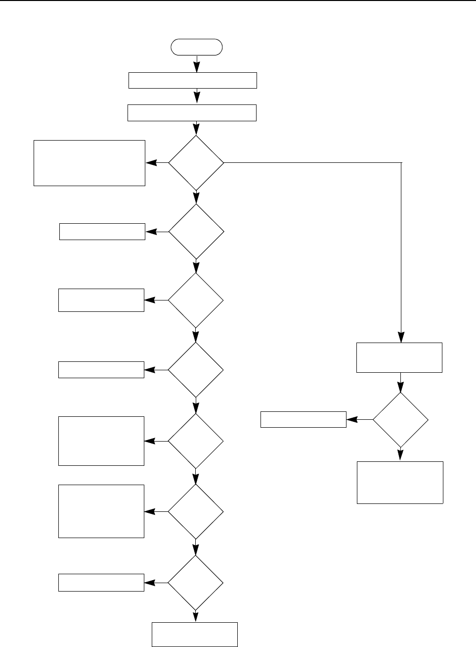
Troubleshooting Flow Chart for 25W Transmitter 3-3
2.0 Troubleshooting Flow Chart for 25W Transmitter (Sheet 1 of 3)
Current
increase
when
keyed?
NO
YES
START
Check if Pressure Pad closes S5440
Check Components between
Q4441 and RF Output,
Antenna Switch
D4471,D4472,Q4472,
VR3471,Q3471
>500mA & <4A
>4A
<500mA
Check PA Stages Control Volt-
age at
TP4402
>1V
Short TP4403 to
Ground
NO
YES
Voltage at
TP4402
rises?
Check PA Stages NO
YES
PCIC U4501
Pin 14 9.3V
DC?
Check 9.3 V Regulator
U0641
NO
YES
PCIC U4501
Pin 16 >4V
DC
Replace PCIC U4501
NO
YES
TP4404
9.1V DC
If U4201 Pin 2 is high,
replace PCIC
U4501,otherwise
check controller and
FGU
YES
NO
TP4403
>0.5V DC?
Replace PCIC U4501
Check Forward Power
Sense Circuit (D4451)
Check Forward Power
Sense Circuit (D4451)
NO
YES
PCIC U4501
Pin 5 > 1V
DC?
Check Power Setting,
Tuning & Components
between PCIC Pin 5
and ASFIC (U0221)
Pin 4 before replacing
ASFIC
No or too low Power when keyed

3-4 Troubleshooting Flow Chart for 25W Transmitter
2.1 Troubleshooting Flow Chart for 25W Transmitter (Sheet 2 of 3)
Check PA Stages
No or too low Power when keyed
Measure DC Voltage at Pin 2 & 3 of U4401
>6
YES
DC Voltage
at U4501
Pin 23 =0?
2-6
DC Voltage
at U4402-1
Pin 1?
YES
Pin 2
Voltage 0.62
* Voltage at
Pin 1?
If U4201 Pin 2 is high,
replace PCIC
NO Replace U4401
YES
NO DC
Voltage at
U4402-1 Pin
3 = 8.8V?
Check S4440,
R4442 and R4443
YES
Pin 3
Voltage 0.51
* Voltage at
Pin 1?
NO Replace U4401
<2V DC
Voltage at
U4402-2
Pin 7?
>6V
Check Components
between U4402-2 Pin 7
and Q4421. Check
Resistive Network at
Pins 5 & 6 before
replacing Q4421
YES
DC
Voltage at
U4402-2 Pin 5
<8.8V?
Check Components
between U4402-2 Pin 7
and Q4421. Check Resis-
tive Network at Pins 5 & 6
before replacing Q4421
NO
Check Q4422
NO
Check Final PA Stage
2-6V
<2V Check Resistive Net-
work at Pins 2 & 3 of
U4402-1 before replac-
ing U4401
Check Q4442 and
Resistive Network at
U4402-1 Pin 3
before replacing
U4401

Troubleshooting Flow Chart for 25W Transmitter 3-5
2.2 Troubleshooting Flow Chart for 25W Transmitter (Sheet 3 of 3)
Check Final PA Stage
NO
0V
1-4V
Bias 2 DC
Voltage at
TP4406?
YES
RF Voltage
at TP4401
>100mV?
YES
RF Voltage
U4401 Pin 6
>3V?
Supply
Replace Q4441
Check FGU (U4301)
NO Check Components
between
TP4401 &C4417
NO
YES ASFIC
U0221 Pin 6
1-4V DC?
Check Bias Tuning
before replacing ASFIC
U0221
Check Components
between ASFIC and
Q4441 before
replacing Q4441
YES
RF Voltage
Q4421 Gate
>1V?
NO Check Components
between
C4417 & Q4421
YES
RF Voltage
Q4441 Gate
>4V?
NO Check Components
between
Q4421 & Q4441
Check Components
between Q4441 &
Antenna Connector
Voltage
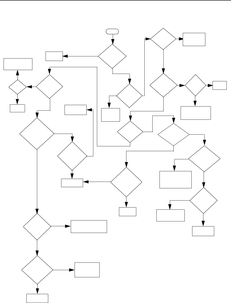
3-6 Troubleshooting Flow Chart for Synthesizer
3.0 Troubleshooting Flow Chart for Synthesizer
5V
at pin 6 of
D4201
Is
information
from µP U0101
correct
?
Is
U4201 Pin 47
at = 13VDC
?
Is
U4301 Pin 19
<40 mVDC in RX &
>4.5 VDC in TX?
(at VCO section)
?
Start
Visual
check of the
Board
OK?
Correct
Problem
Check 5V
Regulator
U4211
+5V
at U4201
Pins
13 & 30
?
Is
16.8MHz
Signal at U4201
Pin 19
?
Check
Y4261 / Y4262 and
associated parts
Are
signals
at Pins 14 &15
of U4201
?
Check
R4201 Check C4381
Is
U4201
Pin 2 >4.5 VDC in
Tx & <40 mVDC
in Rx
?
Replace
U4201
Remove
Shorts
Is
there a short
between Pin 47 and
Pins 14 & 15 of
U4201
?
Replace or
resolder
necessary
components
Is
RF level at
U4201 Pin 32
-12 < x <-25
dBm
?
Are
R4221,R4222,
R4223,C4221,
C4222,& C4223
OK?
Replace
U4201
If L4225, C4229 & C4227
are OK, then see VCO
troubleshooting chart
Are
Waveforms
at Pins 14 & 15
triangular
?
Do
Pins 7,8 & 9
of U4201 toggle
when channel is
changed?
Check programming
lines between
U0101 and U4201
Pins 7,8 & 9
Replace
U4201
Check µP U0101
Troubleshooting
Chart
NO
YES
NO
YES
NO
YES
NO
NO
NO
YES
YES
NO
YES
YES
NO
YES
YES
YES
NO
NO
NO
NO
YES
NO
YES
YES
Check D4201,
C4202, C4203, &
C4206
5V
at U4201
pins 5, 20, 34
& 36
C h e c k 5 V
Regulator
U4211
Is
16.8MHz
signal at
U4201 Pin
23?
Replace
U4201
YES
NO
NO
YES
NO
YES

Troubleshooting Flow Chart for VCO 3-7
4.0 Troubleshooting Flow Chart for VCO
Are Q4332
Base at 0.7V
Collector at 4.5V
Emitter at 110mV
Are Q4301
Base at 2.4V
Collector at 4.5V
Emitter at 1.7V
Are U4301 Pins
13 at 4.4V
15 at 1.1V
10 at 4.5V
16 at 1.9V
Low or no RF Signal
at TP4003
Visual check
of board
OK?
35mV DC at
U4301 Pin 19
NO
YES
Replace Q4301
at base of Q4332
NO
NO
NO
NO
YES
YES
YES
YES
Low or no RF Signal
at input to PA
4.8V DC at
U4301 Pin 19
Is RF available
at C4402
YES
YES
YES
YES
NO
NO
NO
NO
NO
Audio =180mVrms
at “-” S
ide of
4.5VDC
at CR4321
If C4321 and R4321 are OK,
then replace CR4321
Replace C4322
Replace C4325
NO
NO
YES
YES
If parts between
R4402 & U4301 Pin10
are OK, replace U4301
TX VCO
RX VCO
Correct
Problem
Visual check
of board
OK?
Check runner
between U4201 Pin 2
and U4301 Pin 19
Is RF available If all parts from U4301 Pin 8
to Base of Q4332 are OK,
replace U4301
If all parts associated
with the pins are OK,
replace Q4332
If all parts from collector
of Q4332 to TP4003 are
OK, Replace Q4332
Power OK but
no modulation
Check parts from
R4402 to U4401 Pin16
If all parts
associated
with the pins
are OK,
replace U4301
YES
YES
Make sure Synthesizer is
working correctly and runner
between U4201 Pin 28 and
U4301 Pin 14 & 18 are OK
4.5V DC
OK ?
OK? OK?
C4325
at U4301 Pin 14 & 18
4.5V DC
OK ?
at U4301 Pin 14 &18
NO

3-8 Troubleshooting Flow Chart for VCO
THIS PAGE INTENTIONALLY LEFT BLANK
4-1
Section 4
UHF PCB/SCHEMATICS/PARTS LISTS
1.0 Allocation of Schematics and Circuit Boards
1.1 Controller Circuits
The UHF circuits are contained on the Printed Circuit Board (PCB) which also contains the
Controller circuits. This Chapter shows the schematics for the UHF circuits only, refer to the
Controller section for details of the related Controller circuits . The PCB component layouts and the
Parts Lists in this Chapter show both the Controller and UHF circuit components. The UHF
schematics and the related PCB and parts list are shown in the tables below.
Table 4-1 UHF 1-25W Diagrams and Parts Lists
PCB : 8485670z02 Main Board Top Side
8485670z02 Main Board Bottom Side Page 4-3
Page 4-4
SCHEMATICS
Power Amplifier 1 - 25W
FRACN
Voltage Controlled Oscillator
Receiver Front End
IF
Page 4-5
Page 4-6
Page 4-7
Page 4-8
Page 4-9
Parts List
8485670z02 Page 4-10
Table 4-2 UHF 1-25W Diagrams and Parts Lists
PCB : 8485670Z03 Main Board Top Side
8485670Z03 Main Board Bottom Side Page 4-13
Page 4-14
SCHEMATICS
Power Amplifier 1 - 25W
FRACN
Voltage Controlled Oscillator
Receiver Front End
IF
Page 4-15
Page 4-16
Page 4-17
Page 4-18
Page 4-19
Parts List
8485670Z03 Page 4-20

4-2 Allocation of Schematics and Circuit Boards
THIS PAGE INTENTIONALLY LEFT BLANK
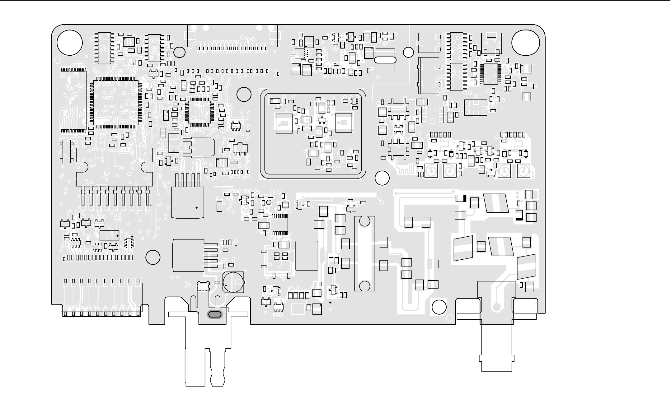
UHF 1-25W PCBs / Schematics / Parts Lists 4-3
2.0 UHF 1-25W PCBs / Schematics / Parts Lists
TOP METAL
C0101 C0102
C0104
C0106
C0107
C0131
C0132
C0211
C0212
C0221 C0222
C0223
C0224
C0225
C0226
C0227
C0228
C0231
C0232
C0233
C0234
C0235
C0236
C0237
C0241
C0242
C0243
C0244
C0245
C0246
C0251
C0252 C0253
C0256
C0261
C0262
C0421
C0441
C0442
C0443
C0445
C0446
C0447
C0448
C0449
C0470
C0471
C0472
C0473
C0474
C0476
C0477
C0478
C0482
C0483
C0484
C0486
C0487
C0488
C0490
C0493
C0494
C0495
C0496
C0501
C0502
C0503
C0504
C0505
C0506
C0508
C0509
C0510
C0511
C0512
C0513
C0514
C0515
C0516
C0517
C0518
C0542
C0601
C0603
C0612
C0651
C0652
C0654
C0655
C0681
C3101
C3102
C3103
C3114
C3115
C3124
C3131
C3132
C3133
C3134
C3135
C3136
C3137
C3139
C3140
C3141
C3142
C3143
C3145
C3148
C4001C4002
C4003
C4004
C4005
C4006
C4007
C4008
C4009
C4014
C4015
C4016
C4017
C4018
C4019
C4020
C4021
C4022
C4023
C4026
C4027
C4029
C4030
C4031
C4051
C4052
C4053
C4054
C4055 C4065
C4068
C4210
C4212
C4213
C4214
C4215
C4216
C4221
C4222
C4223
C4224
C4225
C4226
C4227
C4229
C4230
C4231
C4232
C4233
C4234
C4236
C4242
C4243
C4244
C4245
C4246
C4251
C4252
C4253
C4254
C4255
C4289
C4308 C4309
C4317C4318
C4322
C4323
C4325
C4331
C4332
C4335
C4337
C4339
C4351 C4352
C4353
C4354
C4355
C4371
C4372 C4373 C4374
C4375
C4382 C4383
C4401
C4402
C4403
C4404
C4407
C4417
C4418
C4419
C4420
C4422
C4423
C4424
C4425
C4426
C4428
C4431
C4432
C4434
C4435
C4441
C4442
C4443
C4444
C4445
C4446
C4447
C4448
C4449
C4454
C4455
C4457
C4458
C4472
C4473
C4474
C4491
C4492
C4496
C4497
C4498
C4505
C4507 C4508
C4509
D0201
D0651
D4001
D4002
D4003
D4004
D4005
D4006
D4051
D4221
D4401
D4471
D4472
2
3
456
FL3101
2
3
456
FL3102
4
32
FL3112
FL3114
18
1
J0451
2011
10
J0501
J0601
23
J4401
L0481
L0482
L3100
L3101
L3124
L4001
L4002
L4003
L4004
L4005
L4006
L4008
L4051
L4053
L4054
L4201 L4221
L4225
L4303
L4304
L4305
1
3
L4312 L4313
L4331
L4371
L4401
L4403
L4411
L4422
L4471
L4472
L4491 L4492
L4493
M3421
Q0110
Q0177
Q0181
Q0185
Q0681
Q4001
Q4003
Q4221
Q4301
43
Q4333
Q4411
Q4422
2
3
4
5
6
7
8
Q4441
Q4442
Q4471
R0101
R0102
R0104
R0105
R0106
R0108
R0110
R0114
R0115
R0116
R0131
R0132
R0170
R0181
R0182
R0185
R0186
R0211
R0212
R0220
R0221
R0222
R0223
R0224
R0225
R0226
R0227
R0228
R0229
R0241
R0242
R0251
R0252
R0253
R0254
R0255
R0256
R0257
R0261
R0262
R0268
R0269
R0442
R0510
R0533
R0535
R0538
R0539
R0543
R0611
R0612
R0651
R0652
R0681
R0682
R3101
R3106
R3111
R3117 R3123
R3124
R3130
R3132
R3135
R3142
R3144
R3145
R3148
R4001
R4003
R4004
R4005
R4007
R4012
R4013
R4014
R4015
R4020
R4022
R4051
R4064
R4066
R4211
R4221
R4222
R4223
R4224
R4225
R4251
R4252
R4301
R4302
R4305
R4311
R4312
R4321
R4331
R4332
R4333
R4337
R4341 R4343
R4345
R4346
R4401
R4402
R4403
R4404
R4406
R4415
R4416
R4424
R4425
R4426
R4427
R4431
R4432
R4450
R4471
R4475
R4491
R4505
R4506
R4507
R4508
R4509
SH4301
21
54
3
T4051
2
1
54
3
T4052
TP4401
1
76
51
26
U0101
Microprocessor
32
17
16 1
U0121
Flashrom
8
7
114
U0211
137
25
13
U0221
ASFIC CMP
16
1
89
U0251
9
U0271
1
6
5
U0611
1
6
5
U0641
9,6V Regulator
3
2
1
U0651
5V Regulator
11
1
20
10
U3101
87
1
14
U3111
87
1
14
U3115
4
5
8
U4211
9
8
16
1
U4401
U4502
VR0501
VR0503
VR0505
VR0510
VR4471
23
4
Y0131
2
Y3102
48
1
1
1
1
6
1
1
1
1
1
100
B+ Switch
UHF (403-470 MHz) 1-25W 8485670Z02 Top Side
ZWG0130518-A
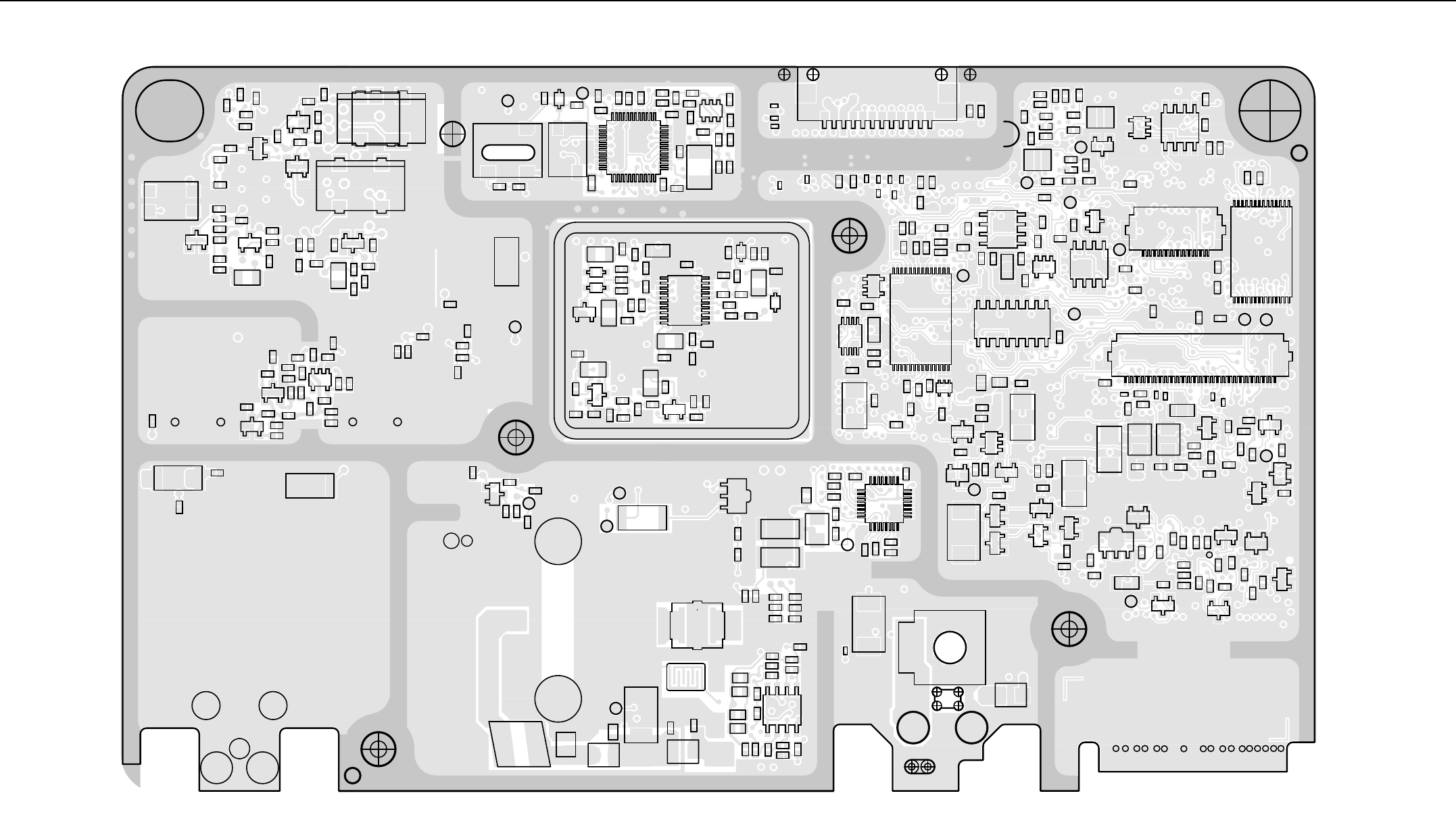
4-4 UHF 1-25W PCBs / Schematics / Parts Lists
C0103
C0105
C0111
C0112
C0121
C0122
C0123
C0141
C0151
C0201
C0202
C0203 C0204
C0205
C0254
C0255
C0265
C0266
C0267
C0271
C0272
C0273
C0274
C0275
C0276 C0277
C0301
C0302
C0303
C0304
C0305
C0324 C0325
C0331
C0341
C0342
C0343
C0344
C0351
C0352
C0353
C0354
C0422
C0423
C0426
C0427
C0428
C0429
C0430 C0431
C0485
C0491
C0492
C0497
C0499
C0541
C0554
C0558 C0559 C0560 C0575 C0576
C0591
C0592 C0593
C0611
C0621
C0622
C0641
C0644
C0645
C0661
C0662
C0663
C0671
C3104
C3110
C3111 C3112
C3113
C3116
C3121
C3122
C3123
C3144
C3146 C3147
C3151
C3152
C4010
C4011
C4012
C4013
C4024
C4025
C4028 C4060
C4061
C4062
C4064
C4066
C4067
C4069
C4201
C4202
C4203
C4204
C4205
C4206
C4207
C4208
C4209
C4211
C4228
C4235
C4241
C4261
C4262
C4263
C4287
C4288
C4301
C 4302
C 4303
C 4304
C4305
C4306
C4307
C4311
C4312
C4313
C4314
C4315
C4316
C4321
C4324
C4333
C4334
C4336
C4338
C4361
C4362
C4363
C4381
C4400
C4405
C4406
C4411
C4412
C4413
C4414
C4415
C4416
C4421
C4427
C4436
C4437
C4439
C4440
C4451
C4452
C4453
C4471
C4475
C4501
C4502 C4503
C4504
C4506
C4510
CR4301
CR4302
CR4303
CR4311
CR4321
D0101
D0151
D0179
D0301
D0621
D0660 D0661
D3101
D4007
D4201
D4261
D4451
E0271
E0272
E0631
43
2
FL3111
FL3113
43
2
FL3115 12
J0401
1
40
J0551
1
18
J0552
L3111
L3112
L4231
L4301
L4302
L4311
L4332
L4333
L4361
L4402
L4421
L4436
L4437
Q0151
Q0171
Q0173 Q0183
Q0271
Q0641
Q0661
Q0662
Q0663
Q3101
Q3102
Q3141
Q3151
Q3152
Q4002
Q4004
Q4331
Q4332
12
3
Q4421
Q4472
R0107
R0111 R0112
R0113
R0117
R0121
R0151 R0152
R0171
R0172
R0173
R0174
R0175
R0176
R0177
R0178
R0179 R0183
R0184
R0201
R0202
R0203
R0204
R0205
R0206
R0207
R0208 R0265
R0266
R0267
R0273 R0274
R0275
R0276
R0323
R0324
R0331
R0332
R0333
R0335
R0341
R0342
R0343
R0344
R0345
R0346
R0347
R0401
R0407
R0408
R0409 R0410
R0412 R0441
R0467
R0468
R0481
R0482
R0511
R0512
R0525 R0529
R 0530
R0531
R0537
R 0541
R 0542
R0591
R0592
R0593
R0621
R0641
R0642
R0643
R0661
R0662 R0671 R0672
R3102R3104R3105
R3107
R3108
R3112
R3113
R3114
R3115
R3116 R3118
R3133
R3134
R3141
R3146
R3147
R3151
R3152
R3153
R3154
R4002
R4016
R4017
R4018
R4019
R4052
R4053
R4054
R4055
R4060
R4061
R4062
R4063
R4068
R4069
R4070
R4071
R4072
R4201
R4203
R4204
R4206
R4228
R4241
R4261
R4262
R4263
R4303
R4304
R4313
R4314
R4315 R4322 R4323
R4334
R4335
R4336
R4338
R4339
R4340
R4342
R4344
R4347
R4361
R4400
R4411
R4412
R4413
R4417
R4418
R4421
R4422
R4423
R4428
R4429
R4440
R4441
R4442 R4443
R4444
R4445
R4446
R4452
R4454
R4455
R4457
R4473
R4474 R4501
R4502 R4504
R4510
R4511
R4512
R4513
R4514
S5440
SH4302
TP0101
TP0102
TP0103
TP0104
TP0151
TP0221
TP0222
TP0492
TP0497
TP0530
TP0661
TP4003
TP4201
TP4202
TP4402
TP4403
TP4404
TP4405
TP4406
1
4
58
U0111
EEPROM
22
21 8
7
1
U0122
RAM
16
1
8
9
U0141
28 15
14
1
U0301
U0331
1
45
8
U0341
U0342
4
58
U0351
14
58
U0652
U0653
1
37
25 13
U4201
11
120
10
U4301
1
4
58
U4402
1
17
9
25
U4501
VR0151
VR0504 VR0509
VR0537
VR0541
VR0601
VR0621
VR0671
43
2Y3101
6
4
3
1
Y4261
2
34
Y4262
1
1
1
1
28
32
1
ZWG0130519-A
FRACN
C99
CNTL-REV-T2
8485670Z02_A
ZWG01305
UHF (403-470 MHz) 1-25W 8485670Z02 Bottom Side
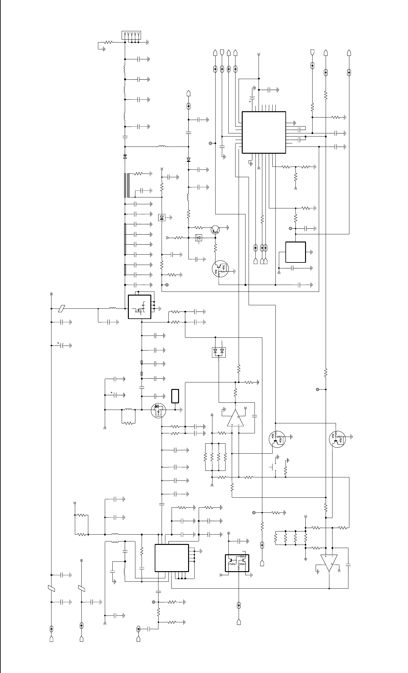
UHF 1-25W PCBs / Schematics / Parts Lists 4-5
ZWG0130520-B
NU
NU
NU
NU
NU
width 2.032
0.8x25
1.542x4
2.216x__ J4401 - BNC
7.5
NU
A
NU
NU
RXIN
9V3
NU
NU
INT_SWB_UHF_PA_1
L4437
17nH
8.2pF
R4475
10K
C4441
15
100
R4402
2.7
R4432
R4427
2.7
R4425
R4501
6.8K
2200pF
C4427
C4424
15pF C4453
100pF
39K
R4443
MOSBIAS_2
22pF
C4431
C4506
2200pF
100pF
C4406
36pF
C4472
1uF
C4505
C4413
NU
C4434
C4455
13pF
0.1uF
10K
R4454
FECTRL_2_UHF_PA_1
2.7K
R4452
R4421
27K
L4402
57R01
0.1uF
C4425
20K
R4507
C4423
1uF
LM50
GND
3
1
POS
VOUT 2
FECTRL_2
U4502
DATA_UHF_PA_1
J4401-1
L4401
C4445
3.3pF
11.03nH
100pF
C4439
120
R4457
RESET_UHF_PA_1
MOSBIAS_2_UHF_PA_1
C4436
10uF
C4503
470pF
NU
100
R4506
CLK
R4431
9V3_UHF_PA_1
2.4K
100pF
C4412
R4428
Q4442
100pF
C4492
R4417
CNTLVLTG_UHF_PA_1
PA_PWR_SET_UHF_PA_1
R4422
3.6K
R4404
10K
8.2pF
C4454
C4440
100pF
C4416
1000pF
C4400
470pF
3.3K
R4413
NU
C4419
C4428
2200pF
L4472
17nH
C4496
11pF
PASUPVLTG
2.7
R4426
L4403
47nH
U4402-2
MC33072
6
57
8
4
C4432
22pF
C4444
J4401-3
8.2pF
17nH
L4492
300
L4493
17nH
R4401
RESET
51
R4400
C4404
51pF
100pF
C4417
Q4421
16
V5EXT 17
VAR1 20
VAR2 18
VAR3 24
15
VG
VL
6VLIM 19
10
RFIN
1
RS 21
RSET
31
RX 23
T1
2
TEMP
30
V10 14
V45
CQXDATA
28
F168 9
GND1
8
GND2
25
INT
4NA 22
Q11
QX
32
BPOS
27
CEX
29
CI
3
CJ
5
CL
7
CLK
26
CQ 12
13
U4501
H99S-4
ANO
C4420
18pF
.033uF
C4421
100pF
C4435
R4446
0
9.1pF
C4403
Q4411
C4405
100pF
TP4406
Q4422
TP4403
15pF
C4504
FECTRL_1
FECTRL_1_UHF_PA_1
TXINJ
R4504 10K
CLK_UHF_PA_1
INT_SWB
TP4401
R4455
100K
2pF
C4475
D4472
CSX_UHF_PA_1
D4401
Kit_0102727B46
11pF
C4498
CNTLVLTG
C4457
56pF
.022uF
C4402
C4497
5.6pF
R4505
NU
300K
R4411
C4415
.022uF
C4501
C4452
2200pF
13pF
51
R4514
17nH
L4491
R4471
470
51
R4474
DATA
36pF
C4473 12pF
C4474
PASUPVLTG_UHF_PA_1
51
R4415
NU
C4443
C4449
43pF
100pF
TEMPSENSE
C4414
R4423
39K
C4426
100pF
PA_PWR_SET
1K
R4509
1000pF
C4451
22K
R4418
2
3
1
8
4
TP4402
MC33072
U4402-1
R4424 2.7
C4407
100pF
R4473
J4401-5
51
J4401-4
K9V1_UHF_PA_1
6.61nH
L4422
C4442
43pF
C4448
22pF
C4458
56pF
C4510
100pF
6.8pF
C4491
.022uF
C4411
D4471
300
R4403 C4418
57R01
4.3pF
L4421
51
R4416
C4446
TXINJ_UHF_PA_1
R4412
C4508
100pF
15
NC4
16
RFIN
6
RFOUT1
7
RFOUT2
1
VCNTRL
14
VD1 VG1
2
3
VG2
11
G2
4
GND1
5
GND2
12
GND3
13
GND4
8
NC1
9
NC2
10
NC3
30C65
U4401
17
EP
51
R4513
43.67nH
L4471
R4510
C4437
.033uF
23
1
57R01
L4436
VR4471 5.6V
L4411
R4444
47nH
C4507
100pF
RXIN_UHF_PA_1
R4491
10K
Q4472
100pF
12
C4401
R4441
S5440
SWITCH
39K
2.2K
R4442
C4471
100pF
TP4404
NU
470pF
C4509
100pF
C4422
R4440
Kit_0102727B46
K9V1
HEATSINK
POS
1M3421
C4447
10
R4450
10
R4511
R4512
TP4405
Q4471
CSX
1K
R4429
R4406
22K
100K
R4508
J4401-2
U4508
D4451
3300pF
C4502
S2
S3
S4
Q4441
D
G
GND1
GND2
S1
100K
R4502
R4445
9V3FLT
U_PREDRIVER
9V3FLT
2.4K
PA_SWB
U_DRIVER9V3FLT
9V3FLT
A+
U_PREDRIVER
NC
PA_SWB
NC
PA_SWB
A+
9V3FLT
9V3FLT
NC
9V3FLT
U_DRIVER
A+
9V3FLT
MOSBIAS_1
NC NC
NC
NC
NC
NC
NC
NC
9V3FLT
NC
NU
UHF (403-470 MHz) Power Amplifier 1 - 25W
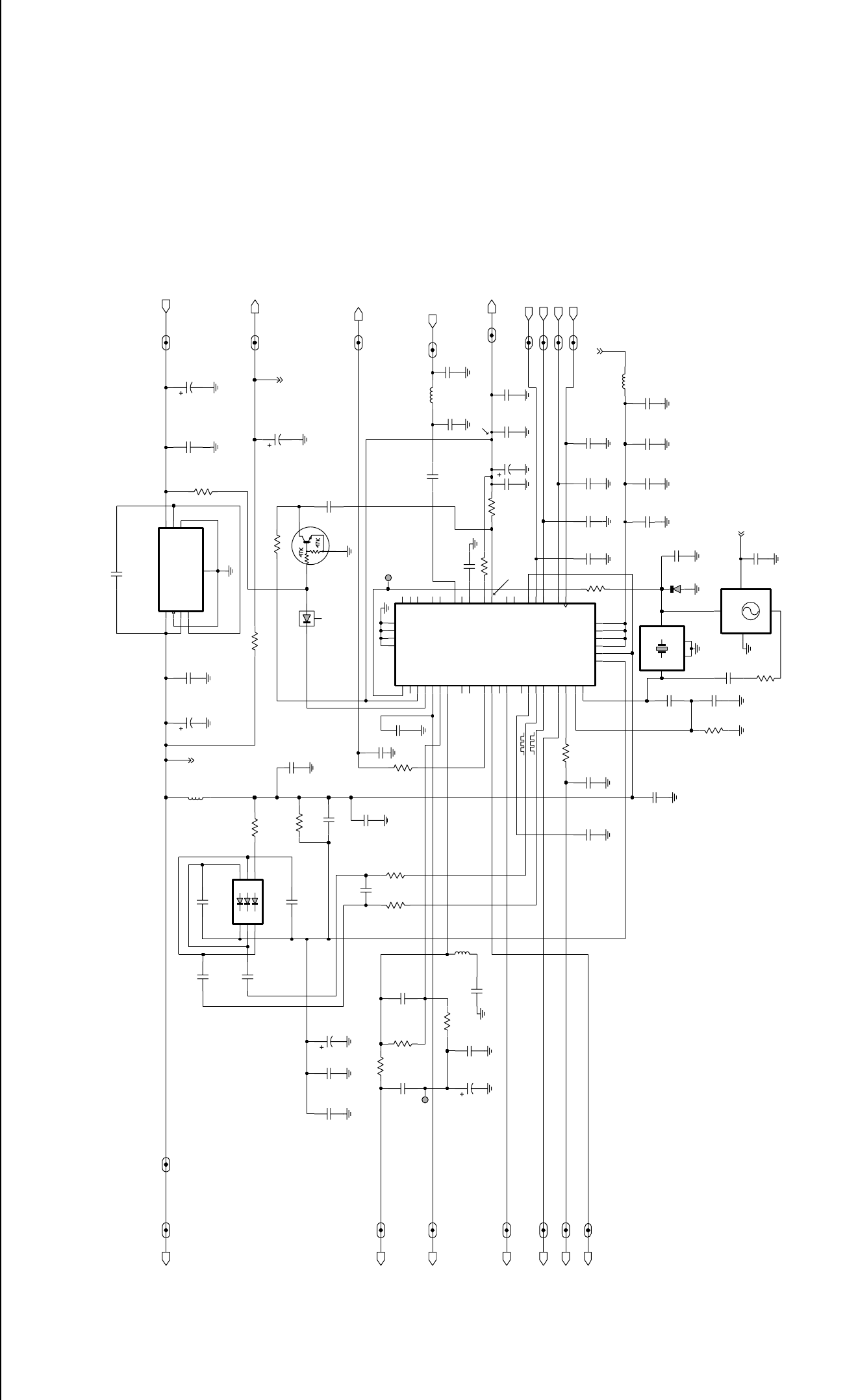
4-6 UHF 1-25W PCBs / Schematics / Parts Lists
NU
0 VDC (RX)
NU
NU
3.43 VDC
3.05 VDC (RX)
NU
4.97 VDC
2.48 VDC
NU
NU
4.58 VDC
3.79 VDC
2.48 VDC
4.97 VDC (25KHZ Chan. Spacing)
1.78 VDC (Rx)
4.97 VDC (TX)
5 VDC (Locked)
10.87 VDC
1.28 VDC
NU NU
NU
0 VDC (Unlocked)
2.63 VDC (TX)
VDC
4.97 VDC
NU
0 VDC (12.5KHZ Chan. Spacing)
2.52 VDC
2.5 to 11 VDC
1.76 VDC (Tx)
30mV - 80mV RMS
12.7 VDC
0 VDC
4.97 VDC
NU
1.8pF
(SOURCE)
NU
3.48
6.68 VDC
TP4201
C4204
100pF
R4204
47
2.2uF
C4214
INPUT 8
OUTPUT
1
SENSE
2SHUTDOWN 3
U4211
LP2951
5V_TAP
6
ERROR
5FEEDBACK 7
GND
4
TRB_UHF_FN_1
D4201
A1 6
A2 5
A3 4
1K1
2K2
3K3
16.8MHz
GND
2
OUT
3
4
VCC
1
VCNTL
C4211
Y4262
C4228
0.1uF
.01uF
C4205
VCTRL
47
R4203
C4216
5V
C4224
1uF
DATA
C4236
.047uF
VCOMOD_UHF_FN_1
IN_5V_RF_REG
0.1uF
C4208
C4233
2.2uF
R4228
47K
10uF
C4206
C4254
0.1uF
VCOBIAS_2_UHF_FN_1
C4226
C4209
0.1uF
47K
R4261
.01uF
C4203
VCTRL_UHF_FN_1
C4210
2.2uF
100
R4263
39K
R4251
510
R4222
C4201
100pF
R4252
30K
16_8MHz
C4232
.01uF
R4224
47K
C4223
R4262
100pF
C4245
2.2uH
C4229
L4231
R4201
150
C4262
CLK_UHF_FN_1
150
PRESC
R4221
16_8MHz_UHF_FN_1
100pF
VCOBIAS_2
VSF
C4244
D4261
.01uF
C4231
PRESC_UHF_FN_1
.018uF
C4212
390nH
L4201
C4242
100pF
4.7uF
C4253
BWSELECT_UHF_FN_1
MODINVCOMOD
.01uF
C4221
0
C4222
0.1uF
R4211
2.2uF
C4215
C4207
12uH
L4221
0.1uF
C4251
100pF
C4241 C4243
1000pF
VSF_UHF_FN_1
C4252
.01uF
C4235
LOCK
2.2uF
C4213
C4261
MODIN_UHF_FN_1
XTAL1
23
24
XTAL2
5V_UHF_FN_1
VBPASS
21
VCP
47
15 VMULT1
VMULT2
14 VMULT3
12 VMULT4
11
13 VRO
WARP
25
PVREF
35
REFSEL
18
SFBASE
27
SFCAP
26
SFIN
30
SFOUT
28
TEST1
37 TEST2
38
NC1
17
NC2
29
NC3
31
PD_GND 44
5PD_VDD
32
PREIN
PRE_GND 33
PRE_VDD
34
DGND
DVDD
36
FREFOUT
19
IADAPT
45
INDMULT
16
IOUT
43
4
LOCK
MODIN
10
MODOUT
41
AVDD
20
BIAS1
40
BIAS2
39
CCOMP
42
CEX
9
CLK
8
DATA
7
6
ADAPTSW
46
AGND 22
AUX1
48 AUX2
1AUX3
2AUX4
3
U4201
63A27
R4206
VDDA_UHF_FN_1
5V_UHF_FN_2
R4225
47K
100pF
C4246
C4225
510pF
LOCK_UHF_FN_1
D4221
.01uF
C4202
L4225
15nH
IN_5V_RF_REG_UHF_FN_1
2.2uF
C4230
100pF
C4255
CSX
R4223
68
CSX_UHF_FN_1
DATA_UHF_FN_1
OUT
3
IN
6
VDDA
Y4261
75Z04 16.8MHz
1
GND
4
GND1
0.1uF
C4263
TRB
CLK
R4241
220
C4234
.01uF
C4227
8.2pF
C4288
TP4202
BWSELECT
Q4221
C4287
100pF
C4289
5V
5V
0.1uF
VDDA
VDDA
In case Y3261 is used instead of Y3263,
replacement of the following parts requires
new temperature compensation of the frequency:
Y3261, U3201, R3261, R3262, C3262, D3261
HF (403-470 MHz) FRACN
ZWG0130521-B
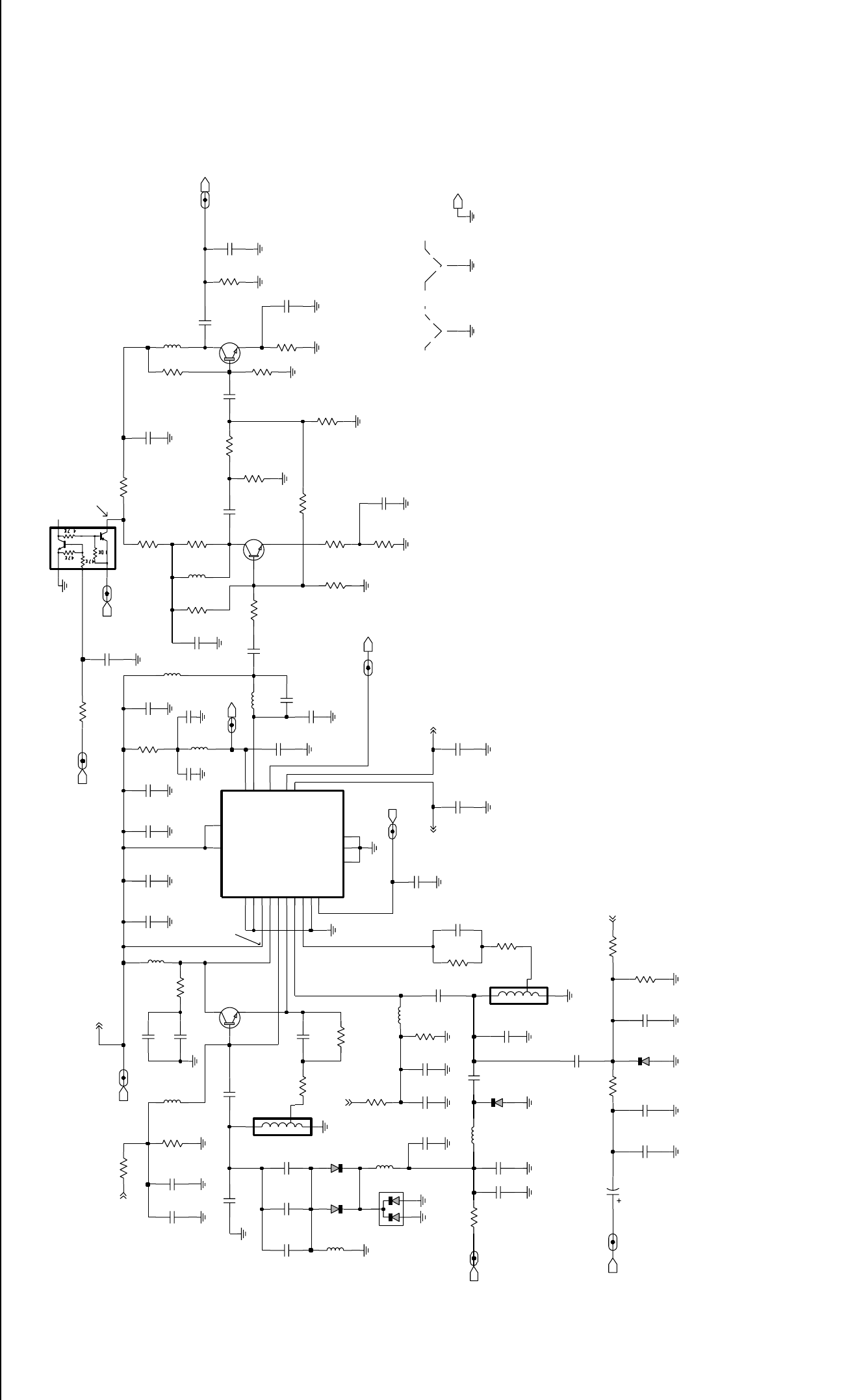
UHF 1-25W PCBs / Schematics / Parts Lists 4-7
NU
NU
NU
0 VDC (Tx)
NU
NU
NU
NU
2.5 - 11 VDC
0 VDC (Rx)
4.58 VDC
4.58 VDC
NU
NU 13.5 to 16 dBm
NU
0 VDC (Tx)
3.1 VDC (Rx)
0 VDC (Tx)
4.7 VDC (Rx)
NU
(Tx)
4.54 VDC
0 VDC (Tx)
2.35 VDC
NU
0 VDC (Rx)
4.42 VDC (Rx)
NU
NU
NU NU
NU
NU
NU
NU
NU
NU
NU
NU NU
NU
NU NU
4.97 VDC (Tx)
-18 to -16 dBm (Rx)
-16 to -11 dBm (Tx)
4 to 6 dBm
4.54 VDC
4.54 VDC (Tx)
2.6 VDC (Tx)
1.91 VDC (Tx)
0 VDC (Rx)
2.45 VDC (Rx) (Rx)
2.43 VDC (Rx)
NU NU
GND
C4301
100pF
30
R4313
C4372
VCTRL_UHF_VCO
L4331
33nH
VSF_UHF_VC0
C4318
0.1uF
Q4301
R4361
180
C4305 51pF
C4337
R4332
CR4303
C4382
VCOBIAS_2
5V_UHF_VCO
C4332
0
R4315
CR4311
C4381
C4313
.022uF
C4336
R4345
SH4301
SHIELD
R4302
10K
C4383
C4363
R4333
R4312
5.6K
C4309
100pF
C4315
100pF
19 TRB_IN
16 TX_BASE
15 TX_EMITTER
1TX_IADJ 10
TX_OUT
13
TX_SWITCH
14
VCC_BUFFERS
18
VCC_LOGIC
GND_LOGIC
17
12
PRESC_OUT
5RX_BASE
6RX_EMITTER
2RX_IADJ 8
RX_OUT
7
RX_SWITCH
3SUPER_FLTR
U4301
4COLL_RFIN
20 FLIP_IN
11
GND_BUFFERS
9
GND_FLAG
R4346
10K
50U54
L4312
RESONATOR
1P1
2
P2
3P3
C4314
1.5pF
C4307
100pF
C4352
0.1uF
C4321
Q4331
1pF
4
1
3
CR4301
Q4333
2
6
C4339
C4375
L4332
L4361
390nH
VCTRL
0
R4341
C4324
2.4pF
2.2K
R4342
6.8pF
TRB_UHF_VCO
C4331
C4304
3.9pF
C4333
C4374
C4335
100pF
270
R4314
7.5K
R4311
TXINJ_UHF_VCO
R4334
R4301
L4301
390nH
R4323
5.6K
100K
1K
R4343
C4353
0.1uF
C4312
12pF
390nH
L4305
C4323
R4337
C4317
PRESC
Q4332
68nH
L4333
390nH
L4371
56K
R4321
R4305
C4316
10
0
5V
0.1uF
R4347
C4338
R4336
51pF
2.2uF
C4354
C4351
100pF
22
R4331
C4373
R4339
PRESC_UHF_VCO
390nH
L4311
R4335
180
R4304
CR4321 10K
R4322
100pF
C4311
100pF
C4361
30
R4303
L4302
390nH
C4362
C4303
8.2pF
R4338
RXINJ
RXINJ_UHF_VCO
L4303
RESONATOR
1P1
2
P2
3P3
0.1uF
C4371
TXINJ
390nH
L4313
SHIELD
SH4302
TRB
C4334
C4306
2pF
C4355
2.2uF
VSF
VCOBIAS_2_UHF_VCO
VCOMOD
C4308
0.1uF
390nH
L4304
C4302
8.2pF
CR4302
10
R4344
C4322
4.7uF
C4325
VCOMOD_UHF_VCO
GROUND
R4340
5V
VSF
TXSW
TXSW
RXSW
RXSW
VSF
ZWG0130523-A
UHF (403-470 MHz) Voltage Controlled Oscillator
ZWG0130523-A
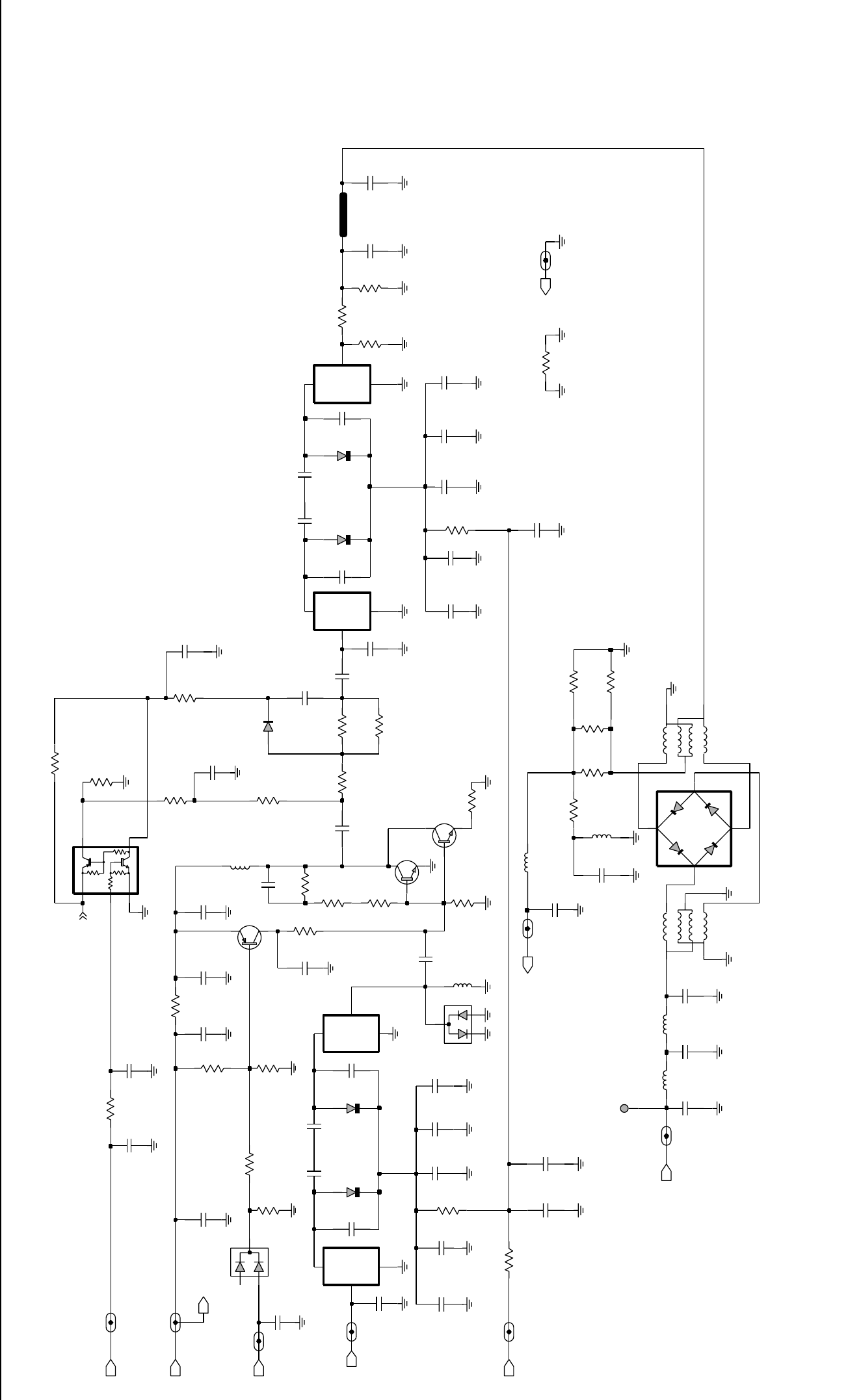
4-8 UHF 1-25W PCBs / Schematics / Parts Lists
R4066
C4069
R4070 .01uF
C4068
100pF
C4065
390
C4064
0.1uF
0
100pF
390
R4064
R4062
1.5K
R4063
R4072
10K
R4071
10K
C4062
0.1uF
R4061
10K
C4061
330pF
R4069
1K
R4068
C4066
1.5K
C4067
3300pF
R4054
R4055
R4053
R4052
0
C4060
R4060
330K L4008
470nH
R4022
L4006
0
R4020
C4051
15nH
10pF
L4054
C4031
13pF
15nH
L4053
27nH
C4055
6.2pF
NU
C4054
16pF
C4053
R4051
16pF
C4052
51
L4051
82pF 150nH
L4005
L4001 L4002 L4004
C4010
1.8pF
330pF
C4029
C4027 C4030
1.8pF
1.8pF 1.8pF
C4026
R4013
R4015
270
C4016
1pF
C4019
R4019
12pF
C4003
36pF
C4025
R4017
3.3K
R4016
R4018
C4028
.01uF
C4020
33pF
3.3K
C4004 33pF
C4005
1.8pF 33pF
C4001 C4002
C4006
33pF C4007
FECTRL_1_UHF_FE
30pF
100K
R4001
C4009
10pF
R4003
3.9K
R4004
2.7K
D4007
10K
IF_UHF_FE
R4005
C4014
100pF
470nH
K9V1_UHF_FE
L4003
R4007
100
RXIN_UHF_FE
330pF 3300pF
C4012 C4013
100pF
C4015
GND_UHF_FE
C4011
3300pF
330
RXINJ_UHF_FE
R4002
Q4004
33pF
C4021
T4052
C4017
D4051
1.8pF 12pF
Q4003
Q4001
C4018
C4022
33pF
T4051
TP4003
12pF
100K
C4023
D4005 10
R4012
R4014
C4008
1000pF 1000pF
D4001
C4024
33pF
NU
NU
NU
NU
NU
3 to 6.5 VDC
NU
NU
NU
NU
NU
NU
0.7 VDC
4.6 VDC
NU
NU
Q4002
D4006
D4004
9V3_UHF_FE
D4003
D4002
FECTRL_2_UHF_FE
10
10
0
820
820
10
0
0
20pF
2.2pF
1pF
IN
NEG
POS
IN
NEG
POS
IN
NEG
POS
IN
NEG
POS
UHF (403-470 MHz) Receiver Front End
ZWG0130524-B

UHF 1-25W PCBs / Schematics / Parts Lists 4-9
9180468v04
9180468V06
3.9VDC 12.5kHz 0VDC
20/25kHz 5VDC
9180469V03
3VDC
9180469V06
9180469V04
0.75VDC 0.75VDC
3VDC
R3117
27K
Q3102
10
R3112
IF
1.8K
R3142
10K
27pF
R3154
C3140
0.1uF
C3110
620nH
L3111
620
R3108
5
CNTL
4
3
14
VDD
7
VSS
C3144
U3115-2
C3143
0.1uF
120pF
R3115
390
R3118
6.8K
R3111
12K
5V_VHF_IF_1 Q3151
NU
C3113
NU
R3104
22pF
C3115
VDD
14
VSS
7
Q3141
MC74HC4066
U3111-1
CNTL
13
1
2
R3116
330
82pF
C3112
Q3152
R3135
1.2K
DISCAUDIO_VHF_IF_1
BWSELECT_VHF_IF_1
R3101
IFIN_VHF_IF_1
12K
C3133
10uF
C3152
.01uF
0.1uF
C3142
DISCAUDIO
R3132
15K
680
R3146
10K
R3151
0.1uF
C3139
C3132
0.1uF
10K
R3152
0.1uF
C3111
20pF
C3101
3
GND1
GND2
4
1IN 2
OUT
FL3111
C3141
0.1uF
GND3
4
5GND4
3IN 6
OUT
R3133
8.2K
FL3101
12R16
1GND1
GND2
2
0
7
R3148
U3111-4
CNTL
12
11 10
VDD
14
VSS
9V3_VHF_IF_2
R3102
10
FL3113
3
GND
1IN 2
OUT
27K
R3106
R3141
390
14
VDD
7
VSS
2.4K
R3144
U3111-2
5
CNTL
43
NU
C3131
C3122
.039uF
R3107
5RSSIOUT 9
RSSI_FEED
6
VCC
6.8K
13 LIM_DEC1
12 LIM_DEC2
20 MIXOUT 4
OSCIN
3OSCOUT
10
QUADIN
1
RFIN 2
RFIN_DEC
AUDIO_FEED
GND
15
18
IFAMPIN
16 IFAMPOUT 19
IFAMP_DEC1
17 IFAMP_DEC2
14
LIMIN
11 LIMOUT
SA616
U3101
8AUDIOOUT
7
CNTL
13
12 VDD
14
VSS
7
5V
U3115-1
R3105
L3100
100
0.1uF
9V3
NU
3
2
1
C3134
BWSELECT
45B02
Y3102
455KHz
C3103
33pF
C3147
0.1uF
0.1uF
C3145
620nH
L3101
6
CNTL
89
14
VDD
7
VSS
9
14
VDD
7
VSS
U3111-3 U3115-3
6
CNTL
8
GND1
1
2GND2
4GND3
GND4
5
IN
3OUT 6
30pF
12R16
FL3102
33pF
C3136
C3135
NU
L3124
NU
C3124
NU
R3124
C3114
18pF
C3104
0.1uF
C3121
0.1uF
Q3101 .039uF
C3123
.01uF
C3151
51
4700pF
C3146
R3130
10K
R3153
C3148
R3147
NU
D3101
0
R3123
330
R3113
15pF
C3102
3.3K
R3145
C3137
.039uF
3
GND
1IN 2
OUT
RSSI
FL3114
10
VDD
14
VSS
7
0.1uF
C3116
2
OUT
U3115-4
CNTL
12
11
FL3112
3
GND1
GND2
4
1IN
R3114
R3134
10K
NU
FL3115
GND1
34
GND2
IN
1OUT 2
NU
9V3_VHF_IF_1
L3112
620nH
Y3101
2
GND
4
GND1
3OUT 1
IN
5V
44.395MHz
12R17
5V
9V3
9V3
9V39V3
9V3
5V
9V3
5V
9V3
12k
ZWG0130522-A
UHF (403-470 MHz) IF

4-10 UHF 1-25W PCBs / Schematics / Parts Lists
UHF PCB 8485670Z02 Parts List 1-25W
Circuit
Ref Motorola
Part No. Description
C3000 2113741F37 3.3nF 50V
C3001 2113740F19 4.7pF 5%
C3002 2113740F26 9.1pF 5%
C3003 2113741F37 3.3nF 50V
C3004 2113740F45 56pF 5%
C3005 2113740F51 100pF 5%
C3006 2113740F45 56pF 5%
C3007 2113741F37 3.3nF 50V
C3008 2113741F25 1nF 50V
C3009 2113741F13 330pF 50V
C3010 2113741F13 330pF 50V
C3011 2113741F37 3.3nF 50V
C3012 2113741F25 1nF 50V
C3013 2113740F45 56pF 5%
C3014 2113740F24 7.5pF 5%
C3015 2113740F45 56pF 5%
C3016 2113740F51 100pF 5% 50V
C3017 2113740F42 43pF 5% 50V
C3019 2113741F25 1nF 50V
C3020 2113741F25 1nF 50V
C3021 2113740F53 120pF 5% 50V
C3022 2113741F49 10nF 50V
C3026 2113743E20 100nF 16V
C3027 2113741F49 10nF 50V
C3028 2113741F49 10nF 50V
C3030 2113741F25 1nF 50V
C3033 2113740F20 5.1pF 5% 50V
C3034 2113740F49 82pF 5% 50V
C3035 2113740F33 18pF 5% 50V
C3036 2113741F25 1nF 50V
C3100 2113741F25 1nF 50V
C3102 2113740F31 15pF 5% 50V
C3103 2113740F39 33pF 5% 50V
C3104 2113743E20 100nF 16V
C3110 2113740F37 27pF 5% 50V
C3111 2113743E20 100nF 16V
C3112 2113740F49 82pF 5% 50V
C3114 2113740F33 18pF 5% 50V
C3115 2113740F35 22pF 5% 50V
C3116 2113743E20 100nF 16V
C3121 2113743E20 100nF 16V
C3122 2113743E11 39nF 10%
C3123 2113743E11 39nF 10%
C3132 2113743E20 100nF 16V
C3133 2311049A57 TANT CP 10uF 10% 16V
C3134 2113743E20 100nF 16V
C3135 2113740L30 33pF 2%
C3136 2113740L29 30pF 2%
C3137 2113743E11 39nF 10%
C3139 2113743E20 100nF 16V
C3140 2113743E20 100nF 16V
C3141 2113743E20 100nF 16V
C3142 2113743E20 100nF 16V
C3143 2113740F53 120pF 5% 50V
C3144 2113743E20 100nF 16V
C3145 2113743E20 100nF 16V
C3146 2113741F41 4.7nF 50V
C3147 2113743E20 100nF 16V
C3151 2113741F49 10nF 50V
C3152 2113741F49 10nF 50V
C3202 2113741F49 10nF 50V
C3203 2113741F49 10nF 50V
C3205 2113741F49 10nF 50V
C3206 2311049A57 TANT CP 10uF 10% 16V
C3208 2113743E20 100nF 16V
C3209 2113743E20 100nF 16V
C3210 2311049A40 TANT CP 2.2uF 10% 10V
C3211 2113743E20 100nF 16V
C3213 2311049A40 TANT CP 2.2uF 10% 10V
C3214 2311049A09 TANT CP 2.2uF 10% 20V
C3215 2311049A09 TANT CP 2.2uF 10% 20V
C3221 2113743E20 100nF 16V
C3222 2113743E20 100nF 16V
C3224 0882422W23 FILM SM 1.0uF 15V 5%
C3225 2113743E20 100nF 16V
C3226 2113740F25 8.2pF 5% 50V
C3227 2113740F51 100pF 5% 50V
C3228 2113743E20 100nF 16V
C3229 2113743E12 47nF 10%
C3231 2113741F49 10nF 50V
C3232 2113741F49 10nF 50V
C3233 2311049A40 TANT CP 2.2uF 10%
C3234 2113741F49 10nF 50V
C3235 2113741F49 10nF 50V
C3242 2113740F59 220pF 5% 50V
C3243 2113740F59 220pF 5% 50V
C3244 2113740F59 220pF 5% 50V
C3245 2113740F59 220pF 5% 50V
C3246 2113740F59 220pF 5% 50V
C3251 2113743E20 100nF 16V
C3252 2113741F25 1nF 50V
C3253 2311049A56 TANT CP 4.7uF 20% 10V
C3254 2113743E20 100nF 16V
C3255 2311049A40 TANT CP 2.2uF 10% 10V
C3263 2113743E20 100nF 16V
C3302 2113740F23 6.8pF 5% 50V
C3303 2113741F49 10nF 50V
C3306 2113740F20 5.1pF 5% 50V
C3311 2113743E07 22nF 16V
C3314 2113740F23 6.8pF 5% 50V
C3315 2113740F31 15pF 5% 50V
Circuit
Ref Motorola
Part No. Description
C3316 2113740F15 3.3pF 5% 50V
C3317 2113740F39 33pF 5% 50V
C3318 2113740F21 5.6pF 5% 50V
C3319 2113741F25 1nF 50V
C3324 2113741F49 10nF 50V
C3332 2113743E20 100nF 16V
C3333 2113743E20 100nF 16V
C3334 2113743E07 22nF 16V
C3335 2113741F49 10nF 50V
C3336 2113741F49 10nF 50V
C3337 2113743E20 100nF 16V
C3341 2113741F25 1nF 50V
C3342 2113740L05 3.0pF +-0.1pF
C3344 2113740F09 1.8pF 5% 50V
C3345 2113740L25 20pF +-0.25pF
C3346 2113741F49 10nF 50V
C3347 2113741F49 10nF 50V
C3348 2113741F49 10nF 50V
C3351 2113741F49 10nF 50V
C3352 2113743E07 22nF 16V
C3355 2113741F49 10nF 50V
C3356 2113743E07 22nF 16V
C3357 2113740F24 7.5pF 5% 50V
C3361 2113741F25 1nF 50V
C3362 2113740F21 5.6pF 5% 50V
C3363 2113740F47 68pF 5% 50V
C3364 2113740F31 15pF 5% 50V
C3365 2113741F25 1nF 50V
C3400 2113740F63 330pF 5% 50V
C3401 2113740F63 330pF 5% 50V
C3402 2113743E07 22nF 16V
C3403 2113740F39 33pF 5% 50V
C3404 2113740F39 33pF 5% 50V
C3405 2113740F67 470pF 5% 50V
C3406 2113740F67 470pF 5% 50V
C3410 2113743E07 22nF 16V
C3411 2113743E07 22nF 16V
C3412 2113740F63 330pF 5% 50V
C3414 2113740F63 330pF 5% 50V
C3415 2113743E07 22nF 16V
C3416 2113740F63 330pF 5% 50V
C3417 2113740F43 47pF 5% 50V
C3418 2113740F39 33pF 5% 50V
C3419 2113740F57 180pF 5% 50V
C3420 2113740F57 180pF 5% 50V
C3421 2113741A57 33nF 50V
C3422 2113740A67 330pF 5% 50V
C3423 2311049A08 TANT CP 1uF 10% 35V
C3424 2113740F67 470pF 5% 50V
C3425 2113743E07 22nF 16V
C3426 2113740F63 330pF 5% 50V
Circuit
Ref Motorola
Part No. Description
C3427 2113741F33 2.2nF 50V
C3428 2113741F33 2.2nF 50V
C3431 2111078B34 HQ 47pF 5%
C3433 2111078B36 HQ 56pF 5%
C3434 2113741A45 10nF 50V
C3435 2113740A67 330pF 5% 50V
C3436 2311049A45 TANT CP 10uF 10% 35V
C3437 2113741A57 33nF 50V
C3438 2111078B59 HQ 470pF 5%
C3439 2111078B59 HQ 470pF 5%
C3440 2113741F25 1nF 50V
C3441 2111078B47 HQ 150pF 5%
C3442 2111078B47 HQ 150pF 5%
C3445 2111078B21 HQ 20pF 5%
C3446 2111078B42 HQ 100pF 5%
C3447 2111078B19 HQ 16pF 5%
C3448 2111078B44 HQ 120pF 5%
C3449 2111078B44 HQ 120pF 5%
C3450 2113740F67 470pF 5% 50V
C3451 2113741F25 1nF 50V
C3452 2113740F29 12pF 5% 50V
C3453 2113740F67 470pF 5% 50V
C3471 2113743E07 22nF 16V
C3472 2111078B53 HQ 270pF 5%
C3473 2111078B53 HQ 270pF 5%
C3474 2113740F59 220pF 5% 50V
C3475 2113740F23 6.8pF 5% 50V
C3491 2111078B18 HQ 15pF 5%
C3492 2111078B38 HQ 68pF 5%
C3493 2111078B09 HQ 6.8pF 5%
C3494 2111078B16 HQ 13pF 5%
C3495 2111078B01 HQ 3.3pF 5%
C3496 2111078B31 HQ 36pF 5%
C3498 2111078B16 HQ 13pF 5%
C3499 2111078B19 HQ 16pF 5%
C3501 2113741F33 2.2nF 50V
C3502 2113741F33 2.2nF 50V
C3503 2113740F67 470pF 5% 50V
C3504 2113741F49 10nF 50V
C3505 2311049A07 TANT CP 1uF 10% 16V
C3506 2113741F33 2.2nF 50V X7R
C3507 2113740F51 100pF 5% 50V
C3508 2113740F67 470pF 5% 50V
C3510 2113740F67 470pF 5% 50V
D3000 4813833C02 DUAL SOT MMBD6100
D3001 4805649Q13 VCTR 1SV228 SOT23
D3003 4880154K03 DUAL SCHOTTKY SOT23
D3004 4805649Q13 VCTR 1SV228 SOT23
D3011 4880142L01 PIN
D3031 4886143B01 MIXER DIODE CROSSOVER
D3101 4880154K03 DIODE DUAL SCHOTTKY
Circuit
Ref Motorola
Part No. Description
UHF 1-25W PCBs / Schematics / Parts Lists 4-11
D3201 4802233J09 TRIPLE SOT143-RH
D3221 4880236E05 CHIP SCHOTTKY
D3341 4805649Q13 VCTR 1SV228 SOT23
D3361 4805649Q13 VCTR 1SV228 SOT23
D3362 4862824C01 VARACTOR CHIP
D3401 4813833C02 DUAL SOT MMBD6100
D3451 4880236E05 CHIP SCHOTTKY
D3471 4802482J02 PIN MA/COM
D3472 4802482J02 PIN MA/COM
FL3101 9180112R16 44.85 MHZ XTAL FLTR 80dB
FL3102 9180112R16 44.85 MHZ XSTAL FLTR 80dB
FL3111 9180469V03 CER FLTR 6EL 455 KHZ SMD
FL3112 9180469V06 CER FLTR 6EL 455 KHZ SMD
FL3113 9180468V04 CER FLTR 4EL 455 KHZ SMD
FL3114 9180468V06 CER FLTR 4EL 455 KHZ SMD
J3401 0986166B02 RF CONN MINI UHF
L3002 2462587T23 COIL CHIP 470nH
L3031 2462587T24 COIL CHIP 560nH
L3032 2462587T17 COIL CHIP 150nH
L3101 2462587T25 COIL CHIP 620nH
L3111 2462587T25 COIL CHIP 620nH
L3112 2462587T25 COIL CHIP 620nH
L3201 2462587Q42 IND CHIP 390nH 10%
L3231 2462587Q20 IND CHIP 2.2uH 20%
L3301 2462587N44 CHIP IND 18 NH 5%
L3302 2462587N53 CHIP IND 100 nH 5%
L3317 2462587V28 CHIP IND 33 NH 5%
L3318 2462587V34 IND CHIP 100nH 5%
L3331 2462587V32 CHIP IND 68NH 5%
L3332 2462587V15 IND CHIP 100nH 10%
L3333 2462587Q47 IND CHIP 1uH 10%
L3341 2484562T13 MINI-SPRING AW IND 8NH2%
L3343 2462587N56 COIL CHIP 180nH 5%
L3344 2462587N68 CHIP IND 1 uH 5%
L3345 2462587N68 CHIP IND 1 uH 5%
L3346 2484562T18 MINI-SPRING AW IND 35.5NH
2%
L3351 2462587N68 CHIP IND 1 uH 5%
L3361 2462587N50 CHIP IND 56 nH 5%
L3362 2462587N51 CHIP IND 68 nH 5%
L3363 2462587N50 CHIP IND 56 nH 5%
L3364 2462587N68 CHIP IND 1 uH 5%
L3401 2460591A01 SQUARE COIL 4.22nH 3T
L3402 2484657R01 Ferrite Bead
L3403 2462587T13 COIL CHIP 68nH
L3411 2462587T13 COIL CHIP 68nH
L3412 2462587X43 IND CHIP LO-PRO 15.0
L3413 2460591B04 SQUARE COIL 11.03nH 4T
L3414 2460591A11 SQUARE COIL 7.66nH 3T
L3421 2484657R01 Ferrite Bead
L3422 2460591C23 SQUARE COIL 16nH 3T
Circuit
Ref Motorola
Part No. Description
L3436 2484657R01 Ferrite Bead
L3437 2460592A01 COIL AW 17nH 2T
L3443 2460591X02 COIL SQUARE 25nH
L3471 2462587X69 IND CHIP 1.2uH 5%
L3472 2460592B01 COIL AW 51nH 4T
L3491 2460592B01 COIL AW 51nH 4T
L3492 2460592B01 COIL AW 51nH 4T
L3493 2460592B01 COIL AW 51nH 4T
M3421 2686201B01 HEAT SPREADER
Q3001 4813827A07 TSTR NPN SML SIG MMBR9
Q3002 4813824A17 TSTR PNP 40V .2A B=100-
Q3021 4805921T02 TSTR DUAL ROHM FMC2
Q3101 4813827A07 TSTR NPN SML SIG MMBR9
Q3102 4813827A07 TSTR NPN SML SIG MMBR9
Q3141 4813824A10 TSTR NPN 40V .2A B=50-150
Q3151 4880048M01 TSTR NPN DIG 47k/47k
Q3152 4880048M01 TSTR NPN DIG 47k/47k
Q3221 4880048M01 TSTR NPN DIG 47k/47k
Q3301 4813827A07 TSTR NPN SML SIG MMBR9
Q3303 4802245J50 TSTR DUAL NPN/PNP UMC5N
Q3304 4805218N63 RF TRANS SOT 323 BFQ67W
Q3411 4805921T02 DUAL ROHM FMC2 RH
Q3421 4802245J55 MRF1507
Q3422 4880048M01 NPN DIG 47k/47k
Q3441 4886136B01 LDMOS PWR TSTR MRF1565
MRF1550
Q3442 4880048M01 NPN DIG 47k/47k
Q3471 4880048M01 NPN DIG 47k/47k
Q3472 4805128M27 PNP SOT89 BSR33 LH
R3000 0662057A53 1k5 1/16W 5%
R3001 0662057A97 100k 1/16W
R3002 0662057A43 560 1/16W 5%
R3003 0662057A49 1k 1/16W 5%
R3004 0662057A53 1k5 1/16W 5%
R3006 0662057A73 10k 1/16W 5%
R3009 0662057A97 100k 1/16W
R3010 0662057A45 680 OHMS 5%
R3011 0662057A65 4k7 1/16W 5%
R3012 0662057A49 1k 1/16W 5%
R3013 0662057A61 3k3 1/16W 5%
R3014 0662057A18 51 1/16W 5%
R3015 0662057A01 10 1/16W 5%
R3016 0662057A01 10 1/16W 5%
R3018 0662057A33 220 1/16W 5%
R3019 0662057A89 47k 1/16W 5%
R3021 0662057A43 560 1/16W 5%
R3024 0662057A39 390 1/16W 5%
R3025 0662057A53 1k5 1/16W 5%
R3026 0662057A73 10k 1/16W 5%
R3027 0662057A73 10k 1/16W 5%
R3028 0662057A39 390 1/16W 5%
Circuit
Ref Motorola
Part No. Description
R3031 0662057A18 51 1/16W 5%
R3033 0662057B47 0 1/16W
R3101 0662057A75 12k 1/16W 5%
R3102 0662057A01 10 1/16W 5%
R3105 0662057A25 100 1/16W 5%
R3106 0662057A83 27k 1/16W 5%
R3107 0662057A69 6k8 1/16W 5%
R3108 0662057A44 620 OHMS 5%
R3111 0662057A75 12k 1/16W 5%
R3112 0662057A01 10 1/16W 5%
R3113 0662057A37 330 1/16W 5%
R3115 0662057A39 390 1/16W 5%
R3116 0662057A37 330 1/16W 5%
R3117 0662057A83 27k 1/16W 5%
R3118 0662057A69 6k8 1/16W 5%
R3130 0662057A18 51 1/16W 5%
R3132 0662057A77 15k 1/16W 5%
R3133 0662057A71 8k2 1/16W 5%
R3134 0662057A73 10k 1/16W 5%
R3135 0662057A51 1k2 1/16W 5%
R3141 0662057A39 390 1/16W 5%
R3142 0662057A55 1k8 1/16W 5%
R3144 0662057A58 2k4 1/16W 5%
R3145 0662057A61 3k3 1/16W 5%
R3146 0662057A45 680 OHMS 5%
R3147 0662057A75 12k 1/16W 5%
R3151 0662057A73 10k 1/16W 5%
R3152 0662057A73 10k 1/16W 5%
R3153 0662057A73 10k 1/16W 5%
R3154 0662057A73 10k 1/16W 5%
R3201 0662057A17 47 1/16W 5%
R3203 0662057A17 47 1/16W 5%
R3204 0662057A17 47 1/16W 5%
R3211 0662057B47 0 1/16W
R3221 0662057A39 390 1/16W 5%
R3222 0662057A45 CHIP RES 680 OHMS 5%
R3223 0662057A25 100 1/16W 5%
R3224 0662057A89 47k 1/16W 5%
R3225 0662057A89 47k 1/16W 5%
R3227 0662057A97 100k 1/16W
R3241 0662057A25 100 1/16W 5%
R3242 0662057B47 0 1/16W
R3251 0662057B04 180k 1/16W 5%
R3252 0662057B10 330k 1/16W 5%
R3261 0662057A89 47k 1/16W 5%
R3263 0662057A65 4k7 1/16W 5%
R3301 0662057A22 75 1/16W 5%
R3302 0662057A25 100 1/16W 5%
R3303 0662057A57 2k2 1/16W 5%
R3304 0662057A49 1k 1/16W 5%
R3308 0662057B47 0 1/16W
Circuit
Ref Motorola
Part No. Description
R3311 0662057A25 100 1/16W 5%
R3316 0662057B47 0 1/16W
R3318 0662057A09 22 1/16W 5%
R3321 0662057A73 10k 1/16W 5%
R3323 0662057A49 1k 1/16W 5%
R3331 0662057A17 47 1/16W 5%
R3335 0662057A13 33 1/16W 5%
R3336 0662057A77 15k 1/16W 5%
R3341 0662057A33 220 1/16W 5%
R3342 0662057A15 39 1/16W 5%
R3343 0662057A25 100 1/16W 5%
R3351 0662057A80 20k 1/16W 5%
R3352 0662057A75 12k 1/16W 5%
R3353 0662057A97 100k 1/16W
R3354 0662057B02 150k 1/16W
R3355 0662057A80 20k 1/16W 5%
R3356 0662057A75 12k 1/16W 5%
R3361 0662057A33 220 1/16W 5%
R3362 0662057A17 47 1/16W 5%
R3364 0662057A89 47k 1/16W 5%
R3400 0662057A41 470 1/16W 5%
R3401 0662057A36 300 1/16W 5%
R3402 0662057A05 15 1/16W 5%
R3403 0662057A36 300 1/16W 5%
R3404 0662057A89 47k 1/16W 5%
R3405 0662057A25 100 1/16W 5%
R3406 0662057A97 100k 1/16W
R3412 0662057A67 5k6 1/16W 5%
R3413 0662057A61 3k3 1/16W 5%
R3414 0683962T51 120 1W 5%
R3415 0662057A25 100 1/16W 5%
R3416 0662057A25 100 1/16W 5%
R3418 0662057A81 22k 1/16W 5%
R3421 0662057A87 39k 1/16W 5%
R3422 0662057A57 2k2 1/16W 5%
R3423 0662057A87 39k 1/16W 5%
R3424 0662057C13 2R7 1/10W 5%
R3425 0662057C13 2R7 1/10W 5%
R3426 0662057C13 2R7 1/10W 5%
R3427 0662057C13 2R7 1/10W 5%
R3428 0662057A58 2k4 1/16W 5%
R3429 0662057A33 220 1/16W 5%
R3431 0680194M18 51 1W 5%
R3432 0680194M18 51 1W 5%
R3433 0662057C13 2R7 1/10W 5%
R3434 0662057C13 2R7 1/10W 5%
R3435 0662057C13 2R7 1/10W 5%
R3441 0662057A87 39k 1/16W 5%
R3442 0662057A57 2k2 1/16W 5%
R3443 0662057A87 39k 1/16W 5%
R3444 0662057C19 4R7 1/10W 5%
Circuit
Ref Motorola
Part No. Description

4-12 UHF 1-25W PCBs / Schematics / Parts Lists
* Motorola Depot Servicing only
Reference designators with an asterisk indicate
components which are not field replaceable
because they need to be calibrated with
specialized factory equipment after installation.
Radios in which these parts have been replaced in
the field will be off frequency at temperature
extremes.
R3445 0662057A58 2k4 1/16W 5%
R3446 0662057B47 0 1/16W
R3450 0662057A41 470 1/16W 5%
R3452 0662057A75 12k 1/16W 5%
R3454 0662057A84 30k 1/16W 5%
R3455 0662057A97 100k 1/16W
R3457 0683962T51 120 1W 5%
R3471 0662057A41 470 1/16W 5%
R3473 0680194M18 51 1W 5%
R3474 0680194M18 51 1W 5%
R3475 0662057A73 10k 1/16W 5%
R3491 0662057A73 10k 1/16W 5%
R3501 0662057A69 6k8 1/16W 5%
R3502 0662057A87 39k 1/16W 5%
R3504 0662057A73 10k 1/16W 5%
R3505 0662057B09 300k 1/16W 5%
R3507 0662057A80 20k 1/16W 5%
R3508 0662057A97 100k 1/16W
R3509 0662057A49 1k 1/16W 5%
T3001 2508396X02 TRANSFORMER
T3002 2508397X02 TRANSFORMER
U3101 5186144B01 FM IF IC SA616
U3111 5113805A86 IC QUAD ANALOG MUX/
DEMUX
U3115 5113805A86 IC QUAD ANALOG MUX/
DEMUX
U3201 5185963A27 IC TESTED AT25016 48 PIN
GFP
U3211 5105739X05 IC SOT 5V HI-PRECISION
REGULAT
U3301 5105750U54 VCO BUFFER PKG DIE
U3401 5105109Z67 LDMOS DRIVER VHF/UHF
U3402 5180932W01 LINEAR IC OP AMP
U3501 5185765B01 IC POWER CONTROL
U3502 5185963A15 TEMP SENSOR 1M5
VR3471 4813830A15 5.6V 5% 225mW
Y3101 4880606B09 CRYSTAL 44.395 MHZ
Y3102 9186145B02 CERAMIC DISCRIMINATOR
455kHz
Y3263 4886182B01 VCTCXO 16.8MHz 2ppm
TTSO5V
Circuit
Ref Motorola
Part No. Description
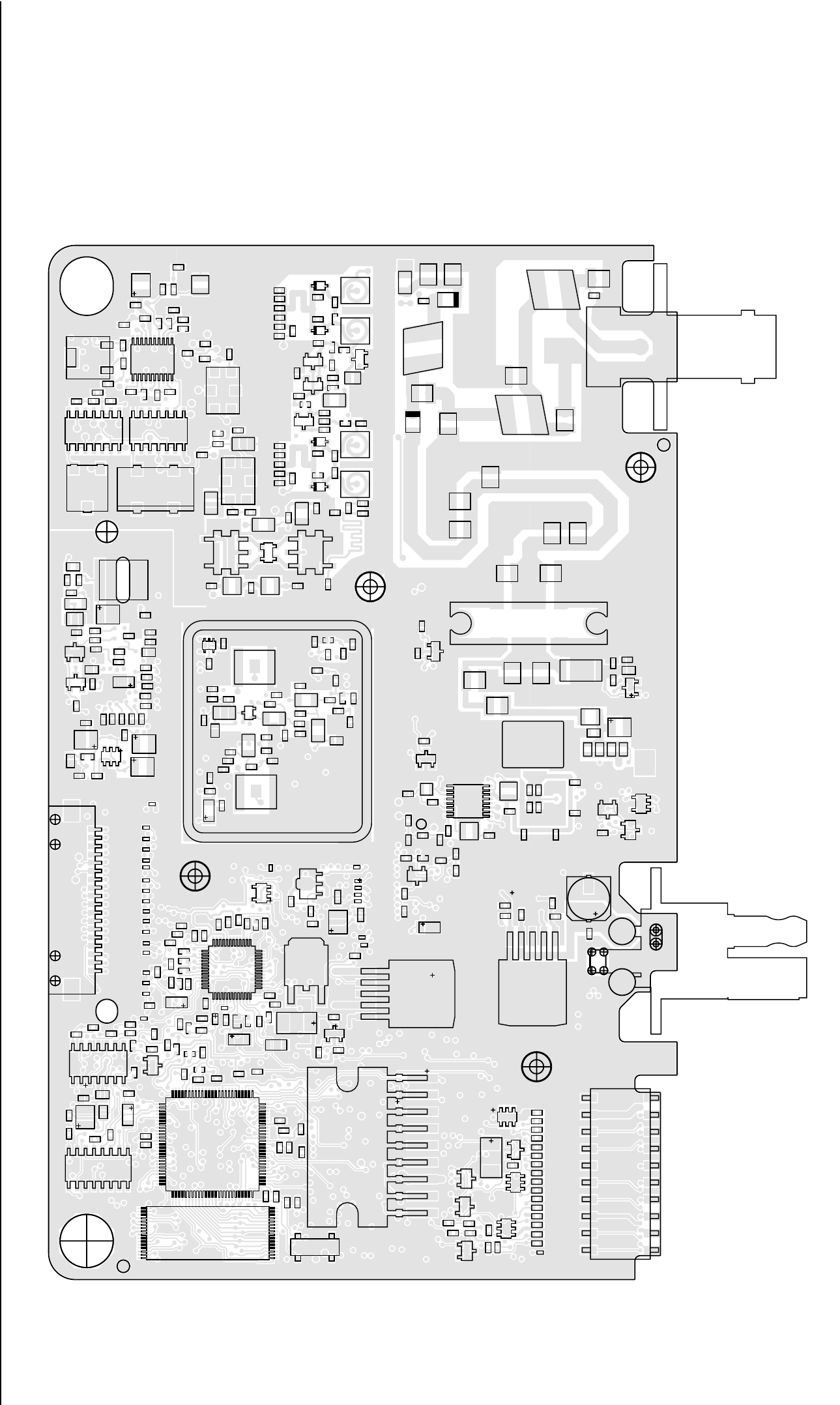
UHF 1-25W PCB / Schematics / Parts List 4-13
TOP METALTOP METAL
C0101C0102
C0104
C0106
C0107
C0108
C0131
C0132
C0211
C0212
C0221
C0222
C0223
C0224
C0225
C0226
C0227
C0228
C0231
C0232
C0233
C0234
C0235
C0236
C0237
C0241
C0242
C0243
C0244
C0245
C0246
C0251
C0252 C0253
C0256
C0261
C0262 C0421
C0441
C0442
C0443
C0445
C0446
C0447
C0448
C0449
C0470
C0471
C0472
C0473
C0474
C0476
C0477
C0478
C0482
C0483
C0484
C0486
C0487
C0488
C0490
C0493
C0494
C0495
C0496
C0501
C0502
C0503
C0504
C0505
C0506
C0508
C0509
C0510
C0511
C0512
C0513
C0514
C0515
C0516
C0517
C0518
C0542
C0601
C0603
C0612
C0651
C0652
C0654
C0655
C0681
C3101 C3102
C3103
C3114
C3115
C3124
C3131
C3132
C3133
C3134
C3135
C3136
C3137
C3139
C3140
C3141
C3142
C3143
C3145
C3148
C4001
C4002
C4003
C4004
C4005
C4006
C4007
C4008
C4009
C4014
C4015
C4016
C4017
C4018
C4019
C4020
C4021
C4022
C4023
C4026
C4027
C4029
C4030
C4031
C4051
C4052
C4053
C4054
C4055 C4065
C4068
C4210
C4213
C4214
C4215
C4216
C4217
C4221
C4222
C4223
C4224
C4225
C4226
C4227
C4229
C4230
C4231
C4232
C4233
C4234
C4236
C4242
C4243
C4244
C4245
C4246
C4251
C4252
C4253
C4254
C4255
C4289
C4308 C4309
C4317 C4318
C4322
C4323
C4325
C4331
C4332
C4335
C4337
C4339
C4351 C4352
C4353
C4354
C4355
C4371
C4372 C4373 C4374
C4375
C4382
C4383
C4401
C4402
C4403
C4404
C4407
C4417
C4418
C4419
C4420 C4422
C4423
C4424
C4425
C4426
C4428
C4431
C4434
C4435
C4441
C4442
C4443
C4444
C4446
C4448 C4449
C4455
C4457
C4458
C4472
C4473
C4474
C4491
C4492
C4496
C4497
C4498
C4505
C4507 C4508
C4509
D0201
D0651
D4001
D4002
D4003
D4004
D4005
D4006
D4051
D4221
D4401
D4471
D4472
2
3
456
FL3101
2
3
456
FL3102
4
32
FL3112
FL3114
18
1
J0451
2011
10
J0501
J0601
23
J4401
L0481
L0482
L3100
L3101
L3124
L4001
L4002
L4003
L4004
L4005 L4006
L4008
L4051
L4053
L4054
L4201
L4221
1
3
L4303
L4304 L4305
1
3
L4312
L4313
L4331
L4371
L4401
L4403
L4411
L4422
L4471
L4472
L4491
L4493
M3421
Q0110
Q0177
Q0181
Q0185
Q0681
Q4001
Q4003
Q4221
Q4301
43
Q4333
Q4411
Q4422
2
3
4
5
6
7
8
Q4441
Q4442
Q4471
R0101
R0102
R0103
R0104
R0105
R0106
R0108
R0110
R0114
R0115
R0116
R0131
R0132
R0170
R0181
R0182
R0185
R0186
R0211
R0212
R0220
R0221
R0222
R0223
R0224
R0225
R0226
R0227
R0228
R0229
R0241
R0242
R0251
R0252
R0253
R0254
R0255
R0256
R0257
R0261
R0262
R0268
R0269
R0442
R0510
R0533
R0535
R0538
R0539
R0611
R0612
R0651
R0652
R0681
R0682
R3101
R3106 R3111
R3117
R3123
R3124
R3130
R3132
R3135
R3142
R3144
R3145
R3148
R4001
R4003
R4004
R4005
R4007
R4012
R4013
R4014
R4015
R4020
R4022
R4051
R4064
R4066
R4211
R4221
R4222
R4223
R4224
R4225
R4227
R4251
R4252
R4301
R4302
R4305
R4311
R4312
R4321
R4331
R4332
R4333
R4337
R4341 R4343
R4345
R4346
R4401
R4402
R4403
R4404
R4406
R4415
R4416
R4424
R4425
R4426
R4427
R4431
R4471
R4475
R4491
R4505
R4506
R4507
R4508
R4509
SH4301
21
54
3
T4051
2
1
54
3
T4052
TP4401
1
76
51
26
32
17
16 1
8
7
114
U0211
137
25
13
16
1
89
U0251
9
U0271
1
6
5
U0611
1
6
5
3
2
1
11
1
20
10
U3101
87
1
14
U3111
87
1
14
U3115
U4211
1
16
8
9
U4401
U4502
VR0501
VR0503
VR0505
VR0510
VR4471
23
4
Y0131
2
Y3102
1
1
1
1
100
U0101
Microprocessor
U0121
Flashrom
U0221
ASFIC CMP
U0641
9,6V Regulator
U0651
5V Regulator
B+ Switch
UHF (403-470 MHz) 1-25W 8485670Z03 Top Side
ZWG0130626-O
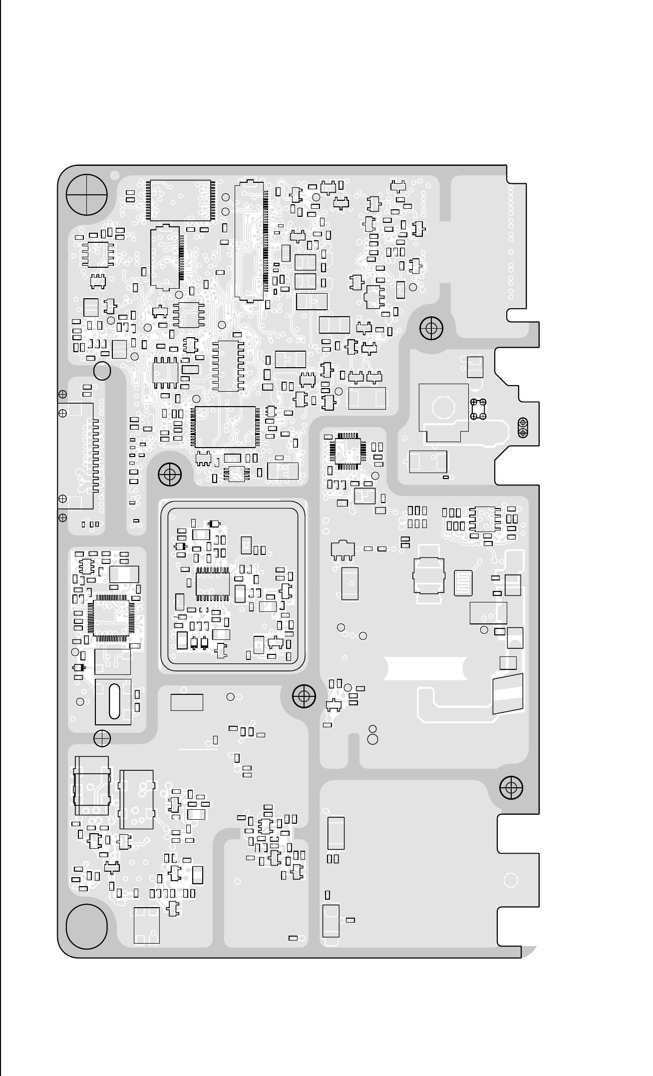
4-14 UHF 1-25W PCB / Schematics / Parts List
C0103
C0105
C0111
C0112
C0121
C0122
C0123
C0141
C0151
C0201
C0202
C0203 C0204
C0205
C0254
C0255
C0265
C0266
C0267
C0271
C0272
C0273
C0274
C0275
C0276
C0277
C0301
C0302
C0303
C0304 C0305
C0324 C0325
C0331
C0341
C0342
C0343
C0344
C0351
C0352
C0353
C0354
C0422
C0423
C0426
C0427
C0428
C0429
C0430
C0431
C0485
C0491
C0492
C0497
C0499
C0541
C0554
C0558 C0559
C0560 C0575 C0576
C0591
C0592 C0593
C0611
C0621
C0622
C0641
C0644
C0645
C0661
C0662 C0663
C0671
C3104
C3110
C3111 C3112
C3113
C3116
C3121
C3122
C3123
C3144
C3146
C3147
C3151
C3152
C4010
C4011
C4012
C4013
C4024
C4025
C4028 C4060
C4061
C4062
C4064
C4066
C4067
C4069
C4201
C4202
C4203
C4204
C4205
C4206
C4207
C4208 C4209
C4211
C4228
C4235
C4241
C4261
C4262
C4263
C4287
C4288
C4301
C4302
C4303
C4304
C4305
C4306
C4307
C4311
C4312
C4313
C4314
C4315
C4316
C4319
C4321
C4324
C4333
C4334
C4336
C4338
C4361
C4362
C4363
C4364 C4365
C4381
C4400
C4405
C4406
C4408
C4411
C4412
C4413
C4414
C4415
C4416
C4421
C4427
C4436
C4437
C4439
C4440
C4451
C4452
C4453
C4459
C4471
C4475
C4501
C4502 C4503
C4504
C4506
C4510
CR4301
CR4302
CR4303
CR4311
CR4321
D0101
D0151
D0179
D0301
D0621
D0660 D0661
D3101
D4007
D4201
D4261
D4451
E0271
E0272
E0631
F0401
43
2
FL3111
FL3113
43
2
FL3115 12
J0401
1
40
J0551
1
18
J0552
L3111
L3112
L4231
L4301
L4302
L4311
L4332
L4333
L4361
L4362
L4402
L4421
L4436
L4437
Q0151
Q0171
Q0173 Q0183
Q0271
Q0641
Q0661
Q0662
Q0663
Q3101
Q3102
Q3141
Q3151
Q3152
Q4002
Q4004
Q4331
Q4332
12
3
Q4421
Q4472
R0107
R0111 R0112
R0113
R0117
R0121
R0151
R0152
R0171
R0172
R0173
R0174
R0175
R0176
R0177
R0178
R0179
R0183
R0184
R0201
R0202
R0203
R0204
R0205
R0206
R0207
R0208 R0265
R0266
R0267
R0273
R0274
R0275
R0276
R0323
R0324
R0331
R0332
R0333
R0335
R0341
R0342
R0343
R0344
R0345
R0346
R0347
R0401
R0407
R0408
R0409
R0412
R0441
R0467
R0468
R0481
R0482
R0511
R0512
R0525 R0529
R0530
R0531
R0537
R0541
R0542
R0543
R0555
R0556
R0591
R0592
R0593
R0621
R0641
R0642
R0643
R0661
R0662 R0671 R0672
R3102
R3104R3105
R3107
R3108
R3112
R3113
R3114
R3115
R3116 R3118
R3133
R3134
R3141
R3146
R3147
R3151
R3152
R3153
R3154
R4002
R4016
R4017
R4018
R4019
R4052
R4053
R4054
R4055
R4060
R4061
R4062
R4063
R4068
R4069
R4070
R4071
R4072
R4201
R4203
R4204
R4206
R4228
R4241
R4261
R4262
R4263
R4303
R4304 R4313
R4314
R4315 R4322 R4323
R4334
R4335
R4336
R4338
R4339
R4340
R4342
R4344
R4347
R4360
R4361
R4362
R4363
R4381
R4400
R4411
R4412
R4413
R4417
R4418
R4421
R4422
R4423
R4428
R4429
R4440
R4441
R4442
R4443
R4445
R4446
R4452
R4454
R4455
R4457
R4458
R4473
R4474 R4501
R4502 R4504
R4511
S5440
SH4302
TP0101
TP0102
TP0103
TP0104
TP0151
TP0221
TP0222
TP0492
TP0497
TP0530
TP0661
TP4003
TP4201 TP4202
TP4402
TP4403
TP4404
TP4405
TP4406
1
4
58
22
21 8
7
1
16
1
8
9
U0141
28 15
14
1
U0301
U0331
1
45
8
U0341
U0342
4
58
U0351
14
58
U0652
U0653
1
37
25 13
U4201
11
120
10
U4301
1
4
58
U4402
1
17
9
25
U4501
VR0151
VR0504 VR0509
VR0537
VR0541
VR0601
VR0621
VR0671
43
2Y3101
6
4
3
1
Y4261
2
34
Y4262
1
1
1
1
1
1
U0111
EEPROM
U0122
RAM
FRACN
C99
CNTL-REV-T9
8485670Z03_B
ZWG0130627-O
UHF (403-470 MHz) 1-25W 8485670Z03 Bottom Side
ZWG0130627-O
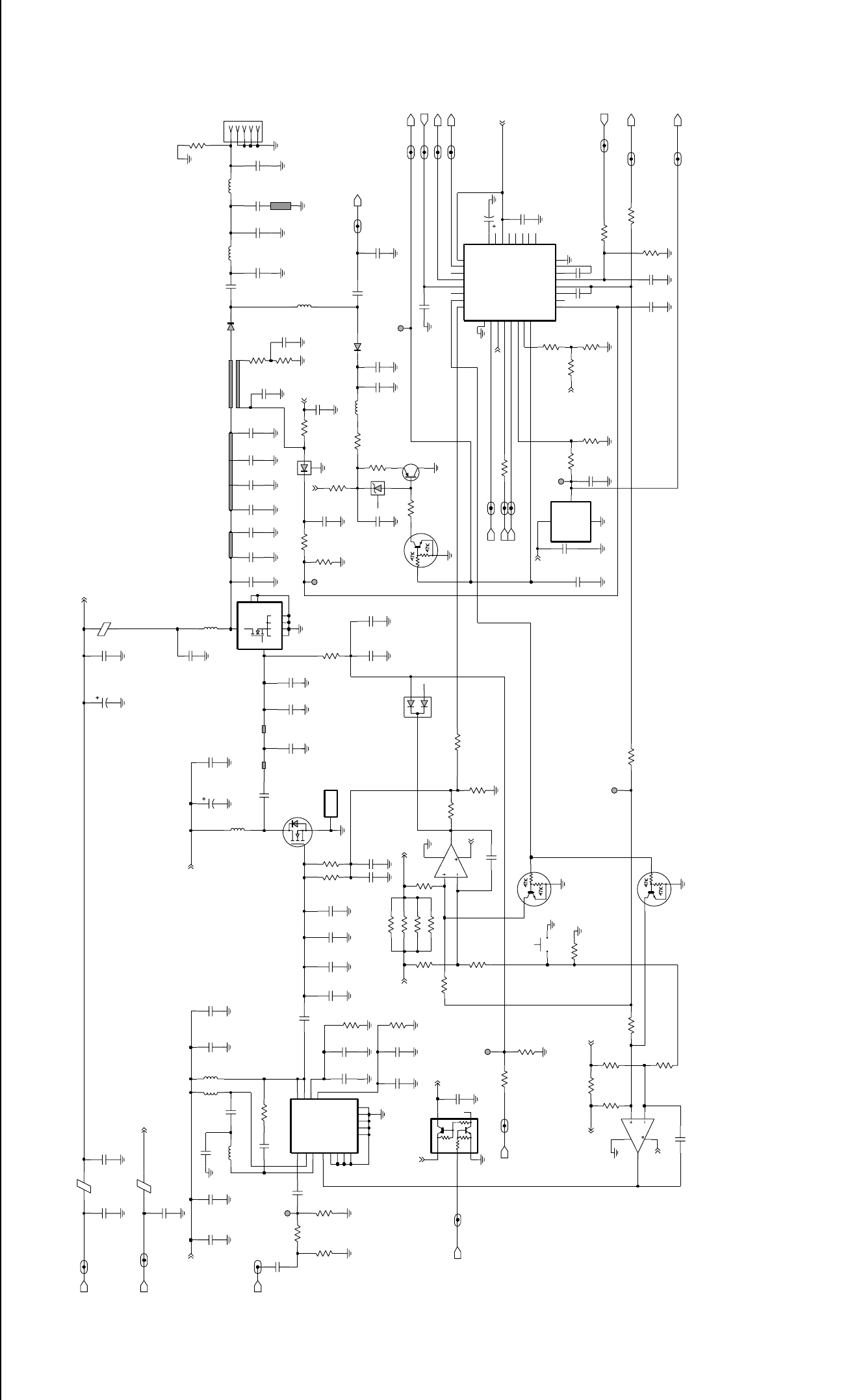
UHF 1-25W PCB / Schematics / Parts List 4-15
ZWG0130520-B
1.542x4
2.216x??
width 2.0327.5 J3401 - BNC/miniUHF
0.8x25 NU
NU
NU
NU NU
NU
NU
R4417
NU
17nH
L4472
NU
11pF J4401-5
NU
470pF
C4400
NU
C4413
.022uF
C4505
NU
51
RESET
NU
R4400 22pF
L4422
4.22nH
C4509
470pF
470pF
C4503
R4411
R4505
R4413
3.3K
C4446
9.1pF
DATA
100pF
C4473
36pF
PASUPVLTG_UHF_PA_1
C4474
R4415
51
C4498
10K
R4491
J4401-3
J4401-2
51
R4473
C4458
CNTLVLTG
D4401
TEMPSENSE
33pF
17nH
L4491
R4442
2.2K
C4425
.01uF
R4507
20K
30pF
C4455 C4459
100pF
FECTRL_2
470
R4458
GND
POS
1
2
VOUT
DATA_UHF_PA_1
LM50
U4502
3
L4401
11.03nH
C4439
100pF
J4401-1
C4414
17nH
L4493
100pF
RXIN
C4492
39pF
L4437
INT_SWB_UHF_PA_1
17nH
33pF
C4449
57R01
L4402
C4427
15pF
C4424
3300pF
100pF
C4453
39K
1uF
R4443
C4436
R4401
10uF
9V3
300
C4448
33pF 120pF
C4443
R4424
C4407
2.7
100pF
470
R4471
51
D4451
R4474
33pF
C4457
47K
R4404
R4428
100pF
2.4K
1000pF
C4416
39K
C4440
R4502
C4435
C4421
.033uF
R4446
100pF
13pF
0
C4403
C4452
9.1pF
Q4411
100pF
C4405
100pF
C4471
Q4422
TP4406
TP4403
Q4442
5.6pF
C4497
57R01
L4421
R4416
51
9.1pF
C4441
R4501
MOSBIAS_2
100pF
6.8K
C4506
2200pF
C4431
100pF
C4406 .033uF
C4437
C4472
36pF
L4436
57R01
5.6V
VR4471
2
3
1
L4411
18nH
C4507
100pF
RXIN_UHF_PA_1
D4471
R4403
300
120
R4457
K9V1_UHF_PA_1
2
3
18
4
C4442
TP4402
U4402-1
LM2904
CNTLVLTG_UHF_PA_1
PA_PWR_SET_UHF_PA_1
TP4401
2.2K
R4422
U4508
INT_SWB
2200pF
G
GND1
GND2
S1
S2
S3
S4
C4502
Q4441
D
10K
FECTRL_2_UHF_PA_1
R4454
12K
R4452
39K
R4421
18nH
L4403
TP4404
FECTRL_1
18pF
C4420
R4506
10K
CLK
51
R4431
10K
R4475
15
R4402
C4423
R4427
1uF
2.7
2.7
R4425
C4415
C4444
8.2pF
1POS
.022uF
HEATSINK
M3421
R4511
4.7
C4404
100pF
4.3pF
TP4405
RESET_UHF_PA_1
C4418
MOSBIAS_2_UHF_PA_1
100K
R4406
2.7K
100K
R4508
100K
R4455
5.6pF
C4475
D4472
CSX_UHF_PA_1
PASUPVLTG
C4434
.01uF
R4426
FECTRL_1_UHF_PA_1
2.4K
2.7
R4445
Q4472
12
100pF
C4401
39K
SWITCH
S5440
R4441
6
5
7
8
4
C4491
9.1pF
2200pF
LM2904
U4402-2
C4496
C4501
VAR3
VG 15
6VL 19
VLIM
6.2pF
RX
2T1
30 TEMP
14
V10
16
V45
17
V5EXT
20
VAR1
18
VAR2
24
GND2
4INT
22
NA
11
Q
10
QX
1RFIN
21
RS
31 RSET
23
CJ
7CL
26 CLK
12
CQ
CQX 13
28 DATA
9
F168
8
GND1
25
U4501
32 ANO
27 BPOS
29 CEX
3CI
5
9V3_UHF_PA_1
H99S-4
C4412
100pF C4422
100pF
.022uF
K9V1
C4402
Q4421
22pF
C4417
300K
6.8K
100pF
C4408
CSX
L4471
390nH
Q4471
100pF
C4510
39K
R4423
.022uF
C4411
TXINJ
J4401-4
CLK_UHF_PA_1
10K
R4504
2.7K
C4426
R4429
1K
100pF
PA_PWR_SET
R4509
C4451
1000pF
2.7K
R4418
C4504
.01uF
39pF
C4419
2200pF
C4428
R4440
0
R4412
TXINJ_UHF_PA_1
C4508
6.8K
VCNTRL
1
VD1
14 2
VG1
VG2 3
100pF
GND4
13
NC1
8
NC2
9
NC3
10
NC4
15
RFIN
16 RFOUT1
6
RFOUT2 7
EP
17
G2
11
GND1
4
GND2
5
GND3
12
9V3FLT
U4401
30C65
PA_SWB
A+
U_PREDRIVER
9V3FLT
9V3FLT
U_DRIVER
PA_SWB
U_DRIVER9V3FLT
9V3FLT
A+
U_PREDRIVER
NC_D3401_2
PA_SWB
A+
9V3FLT
9V3FLT
MOSBIAS_1
9V3FLT
ZWG0130621-O
UHF (403-470 MHz) Power Amplifier 1 - 25W
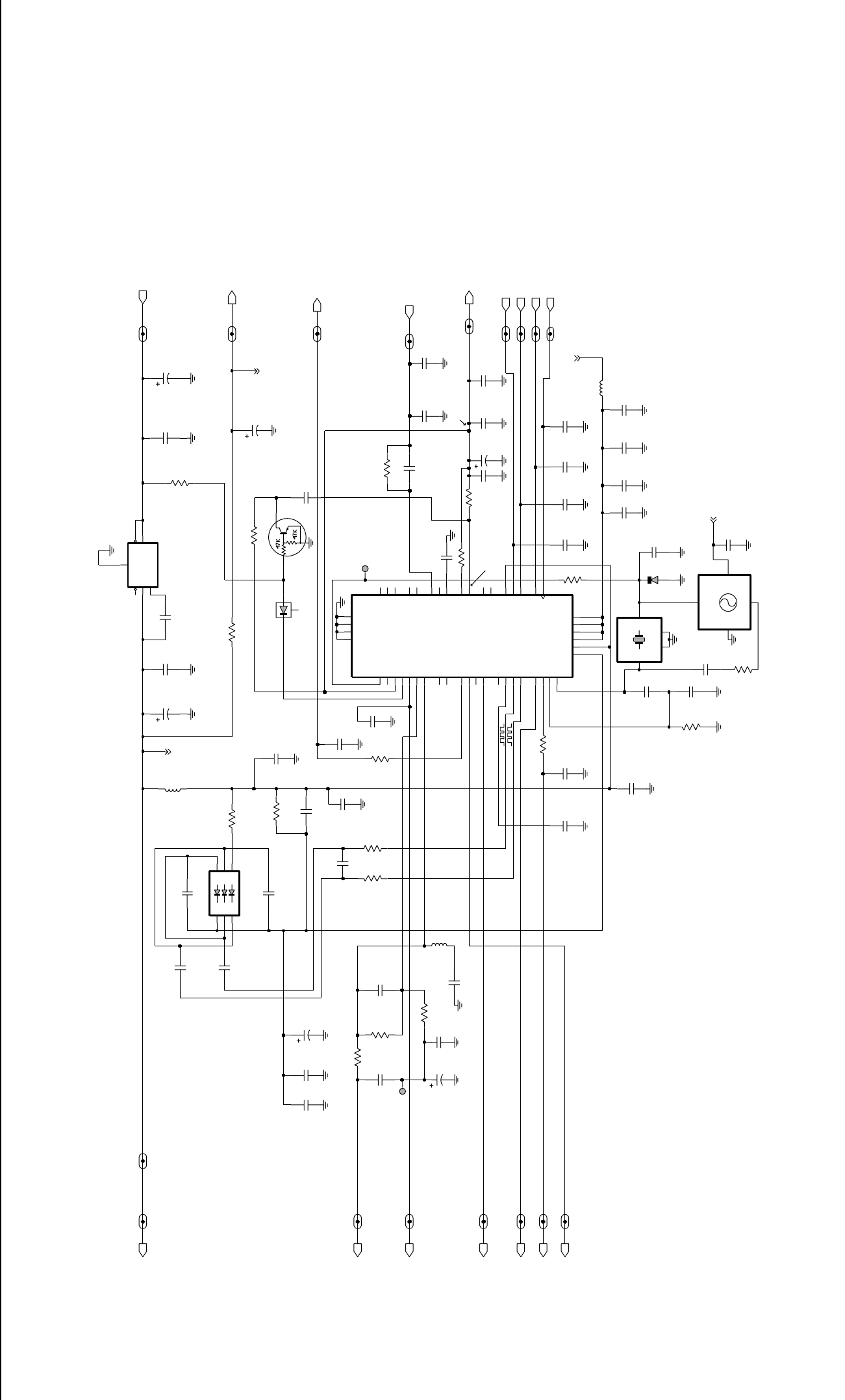
4-16 UHF 1-25W PCB / Schematics / Parts List
2.63 VDC (TX)
4.97 VDC (TX)
4.97 VDC (25KHZ Chan. Spacing)
4.97 VDC
0 VDC (12.5KHZ Chan. Spacing)
4.97 VDC
0 VDC (Unlocked)
(SOURCE)
2.48 VDC
0 VDC
4.97 VDC
3.48
5 VDC (Locked)
10.87 VDC
1.28 VDC
12.7 VDC
2.5 to 11 VDC
1.76 VDC (Tx)
3.05 VDC (RX)
6.68 VDC
VDC
1.78 VDC (Rx)
4.58 VDC
2.52 VDC
2.48 VDC
0 VDC (RX)
NU
NU
TRB
CLK
220
R4241
.01uF
C4234
TP4202
10pF
C4227
NU
0.1uF
C4288
Q4221
100pF
C4287
BWSELECT
C4289
0.1uF
C4251
0.1uF
VCOBIAS_2_UHF_FN_1
C4255
100pF
CSX_UHF_FN_1
0.1uF
C4209
VCTRL_UHF_FN_1
R4261
47K
R4263
100
39K
R4251
R4222
510
100pF
C4201
16_8MHz
30K
R4252
C4232
47K
R4224
.01uF
R4262
NU
C4223
100pF
NU
6.2K
C4229
C4245
NU
2pF
2.2uH
L4231
100pF
C4204
100pF
C4243
C4214
2.2uF
TRB_UHF_FN_1
DATA_UHF_FN_1
C4211
0.1uF
VDDA
C4228
0.1uF
Y4261
GND
1GND1
4
3
OUT
6IN
NU
0.1uF
NU
16.8MHz
75Z04
VCTRL
C4263
C4205
.01uF
5V
47
R4203
C4216
.01uF
1uF
C4224
.047uF
C4236
VCOMOD_UHF_FN_1
IN_5V_RF_REG
DATA
C4208
0.1uF
2.2uF
C4233
R4228
10K
CLK_UHF_FN_1
C4206
10uF
150
R4221
C4226
2.4pF
C4262
330pF
C4203
NU
100pF
C4244
.01uF
C4210
VSF
2.2uF
NU
D4261
PRESC_UHF_FN_1
.01uF
C4231
150
R4201
L4201
390nH
C4242
C4253
4.7uF
100pF
MODINVCOMOD
BWSELECT_UHF_FN_1
C4221
.01uF
0
R4211
0.1uF
C4222
2.2uF
C4215
NU
C4207
100pF
L4221
12uH
?X ERR
?X
GND
?X
IN
?X NR
?X OUT ?X
SD
TP4201
ADP3300
U4211
R4204
PRESC
47
C4252
VSF_UHF_FN_1
6
A1
5
A2
4
A3
K1
1K2
2K3
3
1000pF
VCNTL
1
D4201
16.8MHz
Y4262
TTS05V
2GND
3
OUT
VCC 4
C4235
.01uF
2.2uF
C4213
C4261
33pF
XTAL2
24
5V_UHF_FN_1
NU
47
VCP
VMULT1
15
14 VMULT2
12 VMULT3
11 VMULT4
VRO
13
25 WARP
23 XTAL1
18
REFSEL
27
SFBASE
26
SFCAP
30
SFIN
28 SFOUT
37 TEST1
38 TEST2
21
VBPASS
29
NC2 31
NC3
44
PD_GND
PD_VDD
5
PREIN 32
33
PRE_GND
34 PRE_VDD
35
PVREF
19 FREFOUT
45 IADAPT
16 INDMULT
43 IOUT
LOCK
4
10
MODIN
41 MODOUT
17
NC1
40
BIAS1 39
BIAS2
42
CCOMP
9
CEX
8
CLK
7
DATA
DGND 6
36 DVDD
46 ADAPTSW
22
AGND
48 AUX1
1AUX2
2AUX3
3AUX4
20 AVDD
63A27
U4201
VDDA_UHF_FN_1
33K
R4206
5V_UHF_FN_2
47K
R4225
C4246
100pF
LOCK_UHF_FN_1
510pF
C4225
D4221
C4202
.01uF
100pF
IN_5V_RF_REG_UHF_FN_1
NU
C4241
C4230
CSX
2.2uF
0.1uF
C4254
68
R4223
.01uF
C4217
100K
R4227
VCOBIAS_2
LOCK
16_8MHz_UHF_FN_1
5V
MODIN_UHF_FN_1
5V
VDDA
VDDA
HF (403-470 MHz) FRACN
ZWG0130622-O
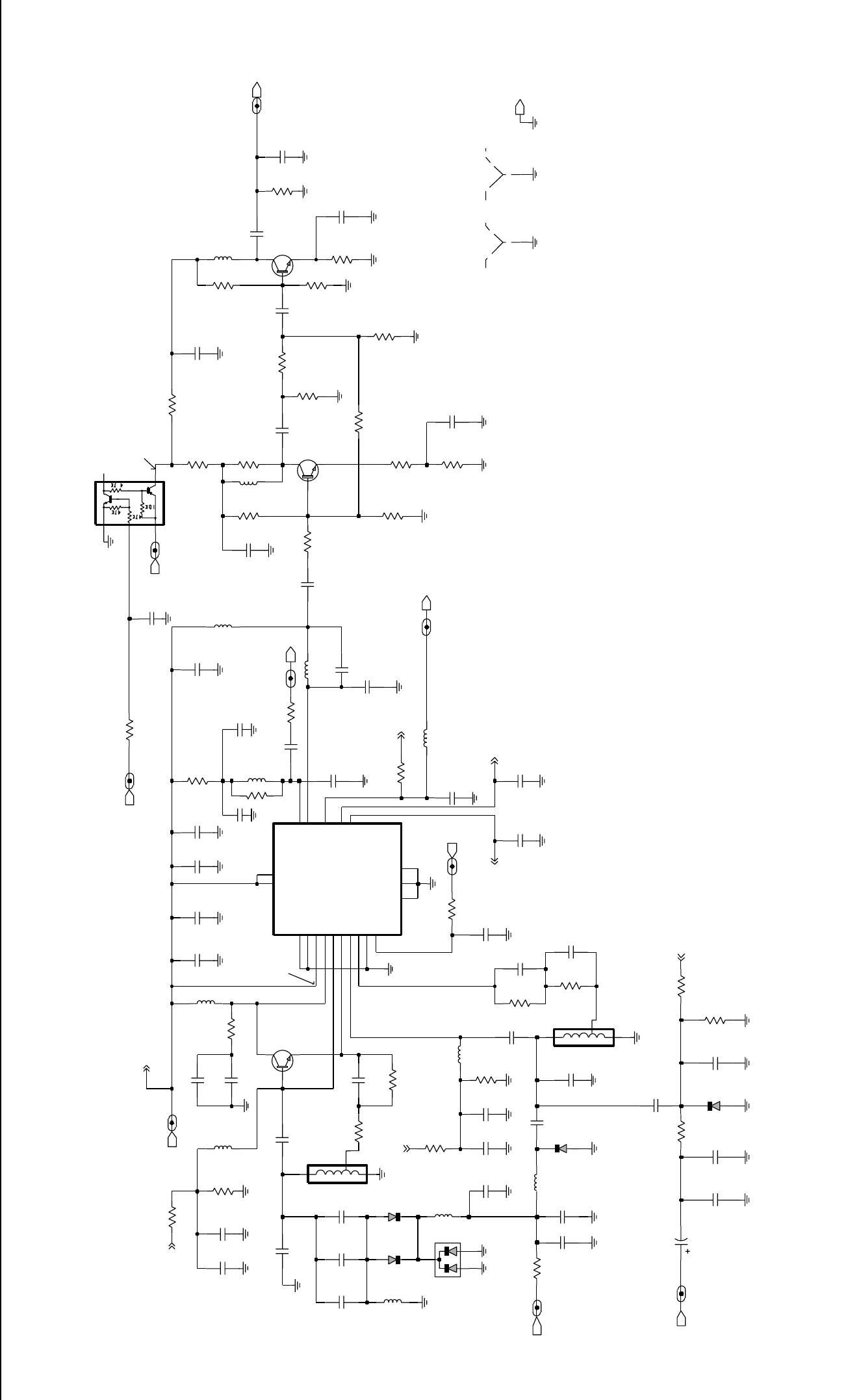
UHF 1-25W PCB / Schematics / Parts List 4-17
C4307
1pF
NU
Q4331
MMBR941
NU
100pF
C4372
NU
2pF
R4334
NU
0
R4335
L4371
1pF
NU
C4373
R4337
NU
C4331
6.8pF
C4334
51pF
NU
C4335
0.1uF
C4332 C4337
1pF
C4339
NU
R4338
NU
220
R4340
220
NU
22
NU
R4344
R4345
0
NU
R4336
NU
1K
NU
1pF
C4313
NU
0.1uF
C4381
NU
22K
R4332
R4333
10K
NU
10
R4362
NU
L4362
33nH
NU
470
R4381
1pF
C4374
NU
100pF NU
C4382 100pF
NU
C4317
100pF
NU
C4375
0.1uF
NU
1pF
C4363
NU
NU
100pF
C4322
C4323
NU
0.22uF
NU
0 VDC (Tx)
2.35 VDC
0 VDC (Tx)
4.42 VDC (Rx)
NU
NU
(Tx)
4.54 VDC
-16 to -11 dBm (Tx)
4 to 6 dBm
4.54 VDC
4.54 VDC (Tx)
2.6 VDC (Tx)
1.91 VDC (Tx)
0 VDC (Rx)
2.45 VDC (Rx) (Rx)
2.43 VDC (Rx)
NU
0 VDC (Tx)
4.7 VDC (Rx)
0 VDC (Tx)
3.1 VDC (Rx)
NU
0 VDC (Rx)
2.5 - 11 VDC
0 VDC (Rx)
4.58 VDC
4.58 VDC
13.5 to 16 dBm
4.97 VDC (Tx)
-18 to -16 dBm (Rx)
TRB
VCOMOD
VSF
CR4302
RESONATOR
L4303
P11
P2
2
P3
3
RXINJ_UHF_VCO_1
SH4302
SHIELD
VCOMOD_UHF_VCO
R4311
7.5K
R4312
5.6K
L4301
390nH
390nH
C4301
100pF
8.2pF
L4302
Q4332
C4302
12pF
C4312
R4313
30
R4314
270
PRESC
C4304
C4303
8.2pF
C4305
3.9pF
100pF
180
R4304
CR4321
PRESC_UHF_VCO
RXINJ
30
R4303
1.5pF
100pF
C4315
5.6K
C4314
L4304
390nH
R4301
VCOBIAS_2_UHF_VCO
TXINJ
1
3
TRB_UHF_VCO
Q4333
2
6
4
CR4301
VCTRL
390nH
TXINJ_UHF_VCO
C4308
0.1uF L4305
C4309
100pF 10
R4305
C4351
100pF C4353
0.1uF
Q4301
VSF_UHF_VC0
VCOBIAS_2
5V
GND
2.2uF
C4354 R4361
180
L4361
1000pF
C4361
L4331
33nH
C4352
33nH
0.1uF
10
TX_SWITCH 13
VCC_BUFFERS
14
VCC_LOGIC
18
SHIELD
SH4301
2RX_OUT 8
RX_SWITCH 7
SUPER_FLTR
3
TRB_IN
19
TX_BASE
16
TX_EMITTER
15
TX_IADJ
1TX_OUT
4
FLIP_IN
20
GND_BUFFERS
11
GND_FLAG
917
GND_LOGIC
PRESC_OUT 12
RX_BASE
5
RX_EMITTER
6
RX_IADJ
U4301
50U54
COLL_RFIN
P2
2
P3
3
CR4311
RESONATOR
L4312
P11
10
5V_UHF_VCO
10K
C4306
R4331
R4302
22
390nH
L4311
390nH
100pF
C4311
15nH
L4332
L4333
R4343
10
1K
R4339
2.2K
R4342
.022uF
C4336
51pF
C4338
51pF
C4333
51pF 100pF
0
0
R4341
1pF
VCTRL_UHF_VCO
68nH
56K
C4321
R4321
C4362
CR4303
R4346
10K
1000pF
R4347
0
L4313
C4318
0.1uF
C4383
390nH
3.9pF
C4319
3.3pF
C4365
1K
R4363
C4364
5.6pF
R4360
270
C4324
2.4pF
C4325
4.7uF
R4323
100K
2.2uF
C4355
0.1uF
C4316
0.1uF
C4371
R4322
10K
R4315
0
TXSW
GROUND
VSF
5V
VSF
TXSW
RXSW
RXSW
VSF
UHF (403-470 MHz) Voltage Controlled Oscillator
ZWG0130624-O
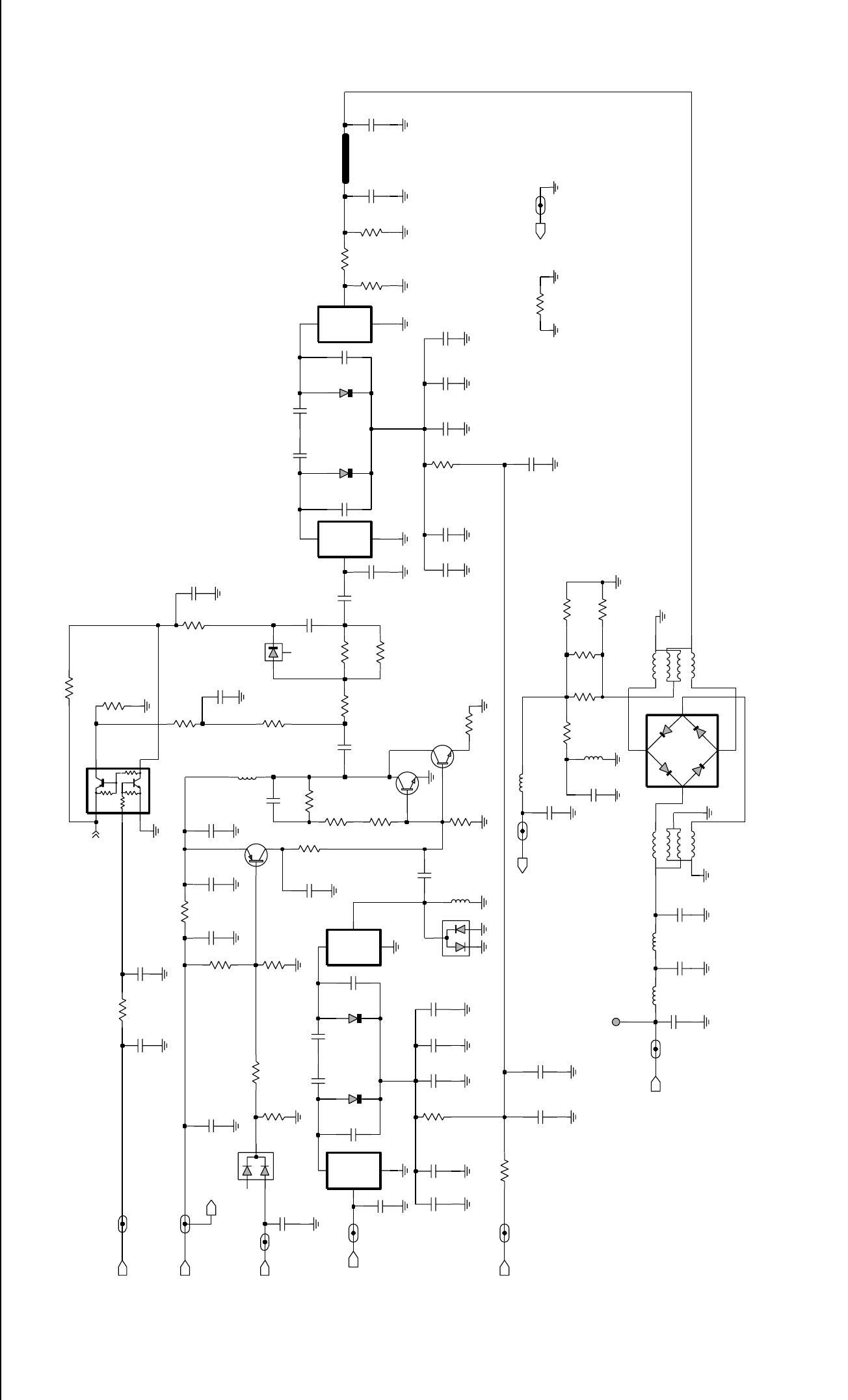
4-18 UHF 1-25W PCB / Schematics / Parts List
C4060
1pF
NU
R4066
10
NU
NU
100pF
NU
R4015
NU
L4054
R4054
820 NU
0
NU
R4019
NU
12pF
NU
16pF
1pF
NU
Q4001
NU
0
R4020
NU
2.2pF
C4025
NU
RXINJ
NU
NU
3 to 6.5 VDC
0.7 VDC
4.6 VDC
D4005
3300pF
C4067
D4006
R4061
10K
K9V1
C4061
330pF
1K
R4069
D4004
10pF
C4009
100K
5
4
R4001
XFMR
T4052
1
2
3
51
R4051
C4051
C4004
10pF
33pF
330
R4002
3.9K
R4003
10
R4014
K9V1_UHF_FE
IF_UHF_FE
D4002
RXIN
1000pF
C4024
L4008
470nH
C4011
3300pF
6.2pF
C4055
C4014
10K
R4005
33pF
C4020
R4053
10
33pF
C4022
FECTRL_2 FECTRL_2_UHF_FE
150nH
L4051
Q4004
C4062
0.1uF
C4012
330pF
C4001
470nH
L4003
1.8pF
C4064
0.1uF
12pF
R4064
0
C4018
12pF
C4023
0
D4007
IN
NEG
POS
R4022
R4017
TBD
L4005
R4016
3.3K
3.3K
C4028
.01uF R4018
Q4002
1.8pF
9V3_UHF_FE
C4026
9V3
15nH
Q4003
R4004
2.7K C4031
13pF
0
IN
NEG
POS
D4003
L4004
TBD
C4007
30pF
33pF
TP4003
IF
C4006
R4060
1
2
3
5
4
330K
XFMR
T4051
C4069
.01uF
FECTRL_1_UHF_FE
1.8pF
0
C4027
20pF
C4066
R4052
C4019
R4072
10K
R4071
10K
FECTRL_1
R4070
390
RXIN_UHF_FE
D4001
C4005
10
33pF
1.8pF
100pF
C4065 C4029
GND_UHF_FE
R4063
390
R4062
1.5K
NEG
POS
GND
TBD
L4002
IN
C4052
RXINJ_UHF_FE
330pF
82pF
C4010
36pF
C4003
100pF
C4015
R4013
270
R4012
100K
3300pF
15nH
C4013
1.5K
R4068
L4006
C4021
C4030
1.8pF
33pF
100
L4001
IN
NEG
POS
R4007
27nH
L4053
TBD
C4016
1000pF
C4054 IO2 2
IO3
3
IO4
4
C4008
D4051
IO1
1
16pF
C4053
C4017
1.8pF
R4055
820
C4068
100pF
C4002
9V3
9V3
33pF
UHF (403-470 MHz) Receiver Front End
ZWG0130625-O
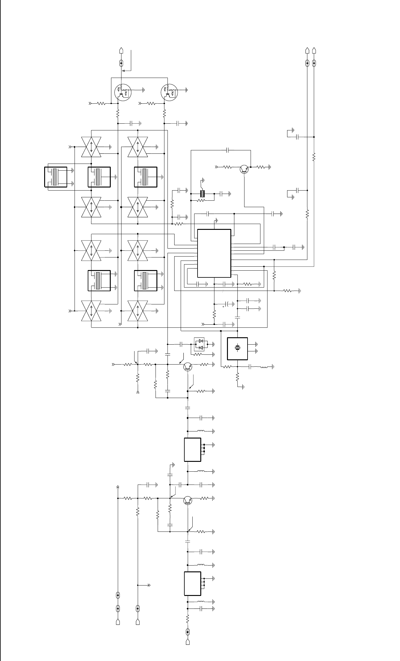
UHF 1-25W PCB / Schematics / Parts List 4-19
9180469V03
3VDC
3.9VDC
12.5kHz 0VDC
20/25kHz 5VDC
9180469V06
9180469V04
0.75VDC 0.75VDC
3VDC
9180468v04
9180468V06
U3111-1
CNTL
13
1
2VDD
14
VSS
7
R3116
330
MC74HC4066
82pF
C3112 Q3152
R3135
1.2K
BWSELECT_UHF_IF_1
R3132
DISCAUDIO_UHF_IF_1
15K
680
R3146
10K
R3151
0.1uF
C3139
C3132
0.1uF
R3117
27K
IF
Q3102
10
R3112
1.8K
R3142
R3154
10K
C3110
27pF
C3140
0.1uF
620nH
L3111
VDD
7
VSS
620
R3108
U3115-2
MC74HC4066
5
CNTL
4
3
14
0.1uF
C3144
FL3111
CFWC455G
3
GND1
GND2
4
1IN 2
OUT
C3141
0.1uF
R3133
8.2K
1GND1
GND2
2
GND3
4
5GND4
3IN 6
OUT
FL3101
12R16
R3148
0
120pF
C3143
R3115
390
R3118
6.8K
R3111
12K
5V_UHF_IF_1 Q3151
1IN 2
OUT
R3102
10
NU
FL3113
CFUCJ455F
3
GND
27K
R3106
390
R3141
2.4K
R3144
R3104
NU
C3113
NU
Q3141
22pF
C3115
C3122
.039uF
R3107
RFIN_DEC
5RSSIOUT 9
RSSI_FEED
6VCC
6.8K
13 LIM_DEC1
12 LIM_DEC2
20 MIXOUT
4
OSCIN
3OSCOUT
10
QUADIN
1
RFIN
2
AUDIOOUT 7
AUDIO_FEED
GND
15
18
IFAMPIN
16 IFAMPOUT
19
IFAMP_DEC1
17 IFAMP_DEC2
14
LIMIN
11 LIMOUT
7
SA616
U3101
8
MC74HC4066
U3115-1
CNTL
13
1
2VDD
14
VSS
12K
R3101
IFIN_U HF_IF_1
C3133
10uF
C3152
.01uF
0.1uF
C3142
DISCAUDIO
L3100
0.1uF
9V3
NU
455KHz
3
2
1
C3134
33pF
BWSELECT
Y3102
C3103
R3152
C3147
0.1uF
10K
0.1uF
C3111
OUT 6
20pF
C3101
GND1
1
2GND2
4GND3
GND4
5
IN
3
30pF
12R16
FL3102
33pF
C3136
C3135
NU
L3124
CNTL
12
11 10
VDD
14
VSS
7
U3111-4
.039uF
C3123
9V3_VHF_IF_2
.01uF
C3151
51
4700pF
C3146
R3130
10K
R3153
12K
C3148
R3147
5
CNTL
4
3
14
VDD
7
VSS
NU
U3111-2
MC74HC4066
NU
C3131
C3137
.039uF
3
GND
1IN 2
OUT
RSSI
FL3114
CFUCJ455D
11 10
VDD
14
VSS
7
0.1uF
C3116
1IN 2
OUT
MC74HC4066
U3115-4
CNTL
12
5V
FL3112
CFWC455D
3
GND1
GND2
4
100
R3105
NU
R3114
2
R3134
10K
CFWC455F
FL3115
GND1
34
GND2
IN
1OUT
620nH
1
IN
9V3_UHF_IF_1
L3112
44.395MHz
Y3101
2
GND
4
GND1
3OUT
0.1uF
C3145
620nH
L3101
6
CNTL
89
14
VDD
7
VSS
RSSI_UHF_IF_1
9
14
VDD
7
VSS
U3111-3 U3115-3
MC74HC4066
6
CNTL
8
NU
C3124
NU
R3124
C3114
18pF
C3104
0.1uF
C3121
0.1uF
Q3101
D3101
0
R3123
330
R3113
15pF
C3102
R3145
5V
3.3K
5V
9V3
9V3
9V39V3
9V3
5V
9V3
5V
9V3
UHF (403-470 MHz) IF
ZWG0130623-O
4-20 UHF 1-25W PCB / Schematics / Parts List
UHF PCB 8485670Z03 Parts List 1-25W
Circuit
Ref Motorola
Part No. Description
C3101 2113740F34 20pF
C3102 2113740F31 15pF
C3103 2113740F39 33pF
C3104 2113743E20 10uF
C3110 2113740F37 27pF
C3111 2113743E20 10uF
C3112 2113740F49 82pF
C3114 2113740F33 18pF
C3115 2113740F35 22pF
C3116 2113743E20 10uF
C3121 2113743E20 10uF
C3122 2113743E11 0.039uF
C3123 2113743E11 0.039uF
C3132 2113743E20 10uF
C3133 2311049A57 10uF
C3134 2113743E20 10uF
C3135 2113740L30 33pF
C3136 2113740L29 30pF
C3137 2113743E11 0.039uF
C3139 2113743E20 10uF
C3140 2113743E20 10uF
C3141 2113743E20 10uF
C3142 2113743E20 10uF
C3143 2113740F53 120pF
C3144 2113743E20 10uF
C3145 2113743E20 10uF
C3146 2113741F41 4700pF
C3147 2113743E20 10uF
C3151 2113741F49 10nF
C3152 2113741F49 10nF
C4001 2113740F09 1.8pF
C4002 2113740F39 33pF
C4003 2113740F40 36pF
C4004 2113740F39 33pF
C4005 2113740F39 33pF
C4006 2113740F39 33pF
C4007 2113740F38 30pF
C4008 2113741F25 1000pF
C4009 2113740F27 10pF
C4010 2113741F13 330pF
C4011 2113741F37 3300pF
C4012 2113741F13 330pF
C4013 2113741F37 3300pF
C4014 2113740F51 100pF
C4015 2113740F51 100pF
C4017 2113740F09 1.8pF
C4018 2113740F29 12pF
C4019 2113740F29 12pF
C4020 2113740F39 33pF
C4021 2113740F39 33pF
C4022 2113740F39 33pF
C4023 2113740F29 12pF
C4024 2113741F25 1000pF
C4026 2113740F09 1.8pF
C4027 2113740F09 1.8pF
C4028 2113741F49 10nF
C4029 2113740F09 1.8pF
C4030 2113740F09 1.8pF
C4031 2113740F30 13pF
C4051 2113740F27 10pF
C4052 2113740F49 82pF
C4053 2113740F32 16pF
C4054 2113740F32 16pF
C4061 2113740F63 330pF
C4062 2113743E20 10uF
C4064 2113743E20 10uF
C4065 2113740F51 100pF
C4067 2113741F37 3300pF
C4068 2113740F51 100pF
C4069 2113741F49 10nF
C4201 2113740F51 100pF
C4202 2113741F49 10nF
C4203 2113741F49 10nF
C4204 2113740F51 100pF
C4205 2113741F49 10nF
C4206 2311049J25 10uF
C4208 2113743E20 10uF
C4209 2113743E20 10uF
C4210 2104993J02 2.2uF
C4211 2113743E20 10uF
C4213 2311049A09 2.2uF
C4214 2311049A09 2.2uF
C4215 2311049A09 2.2uF
C4217 2113741F49 10nF
C4221 2109720D01 0.01uF
C4222 2109720D14 0.1uF
C4224 0882422W23 1uF
C4225 2113741F18 510pF
C4226 2113740L03 2.4pF
C4227 2113740F27 10pF
C4230 2104993J02 2.2uF
C4231 2113741F49 10nF
C4232 2113741F49 10nF
C4233 2104993J02 2.2uF
C4234 2113741F49 10nF
C4235 2113741F49 10nF
C4236 2113743E12 0.047uF
C4242 2113740F51 100pF
C4243 2113740F51 100pF
C4244 2113740F51 100pF
C4245 2113740F51 100pF
Circuit
Ref Motorola
Part No. Description
C4246 2113740F51 100pF
C4251 2113743E20 10uF
C4252 2113741F25 1000pF
C4253 2311049A56 4.7uF
C4254 2113743E20 10uF
C4255 2113740F51 100pF
C4263 2113743E20 10uF
C4287 2113740F51 100pF
C4289 2113743E20 10uF
C4301 2113740F51 100pF
C4302 2113740L16 8.2pF
C4303 2113740L16 8.2pF
C4304 2113740L08 3.9pF
C4306 2113740L01 2pF
C4307 2113740F51 100pF
C4308 2113743E20 10uF
C4309 2113740F51 100pF
C4311 2113740F51 100pF
C4312 2113740F29 12pF
C4314 2113740F07 1.5pF
C4315 2113740F51 100pF
C4316 2109720D14 0.1uF
C4318 2113743E20 10uF
C4321 2113740F03 1pF
C4324 2113740L03 2.4pF
C4325 2311049A56 4.7uF
C4331 2113740L14 6.8pF
C4335 2113740F51 100pF
C4336 2113743E07 0.022uF
C4337 2113740F44 51pF
C4338 2113740F44 51pF
C4351 2113740F51 100pF
C4352 2113743E20 10uF
C4353 2113743E20 10uF
C4354 2104993J02 2.2uF
C4355 2104993J02 2.2uF
C4361 2113741F25 1000pF
C4364 2113740F21 5.6pF
C4365 2113740F07 1.5pF
C4371 2113743E20 10uF
C4400 2113740F67 470pF
C4401 2113740F51 100pF
C4402 2113741F37 3300pF
C4403 2113740F23 6.8pF
C4404 2113740F51 100pF
C4405 2113740F51 100pF
C4406 2113740F51 100pF
C4407 2113740F51 100pF
C4408 2113740F51 100pF
C4411 2113741F37 3300pF
C4412 2113740F51 100pF
Circuit
Ref Motorola
Part No. Description
C4414 2113740F51 100pF
C4415 2113743E07 0.022uF
C4416 2113740F51 100pF
C4417 2113740F38 30pF
C4419 2113740F33 18pF
C4420 2113740F28 11pF
C4421 2113741A57 33K F
C4422 2113740A55 100pF
C4423 2311049A08 1uF
C4425 2113741F49 10nF
C4426 2113740F51 100pF
C4427 2113741F37 3300pF
C4428 2113741F33 2200pF
C4431 2111078B23 24pF
C4434 2113741F49 10nF
C4435 2113740A55 100pF
C4436 2311049A45 10uF
C4437 2113741A57 33K F
C4439 2111078B42 100pF
C4440 2113741F25 1000pF
C4441 2111078B18 15pF
C4446 2111078B09 6.8pF
C4448 2111078B29 33pF
C4449 2111078B29 33pF
C4451 2113741F25 1000pF
C4452 2113740F30 13pF
C4453 2113740F51 100pF
C4455 2111078B12 9.1pF
C4457 2111078B27 30pF
C4458 2111078B32 39pF
C4459 2113740F51 100pF
C4471 2113740F51 100pF
C4472 2111078B31 36pF
C4473 2111078B31 36pF
C4474 2113740F51 100pF
C4475 2113740F21 5.6pF
C4491 2111078B12 9.1pF
C4492 2111078B32 39pF
C4496 2111078B09 6.8pF
C4497 2111078B07 5.6pF
C4501 2113741F33 2200pF
C4502 2113741F33 2200pF
C4503 2113740F67 470pF
C4504 2113741F49 10nF
C4505 2311049A07 1uF
C4506 2113741F33 2200pF
C4507 2113740F51 100pF
C4508 2113740F51 100pF
C4510 2113740F51 100pF
CR4301 4805649Q13 DIODE, VARACTOR
CR4302 4862824C01 DIODE, VARACTOR
Circuit
Ref Motorola
Part No. Description
UHF 1-25W PCB / Schematics / Parts List 4-21
CR4303 4862824C01 DIODE, VARACTOR
CR4311 4802245J22 DIODE, VARACTOR
CR4321 4862824C01 DIODE, VARACTOR
D3101 4880154K03 DIODE DUAL SCHOTTKY
D4001 4862824C01 DIODE, VARACTOR
D4002 4862824C01 DIODE, VARACTOR
D4003 4880154K03 DIODE DUAL SCHOTTKY
D4004 4862824C01 DIODE, VARACTOR
D4005 4862824C01 DIODE, VARACTOR
D4006 4880142L01 DIODE
D4007 4813833C02 DIODE, DUAL 70V
D4051 4886143B01 DIODE, MIXER
D4201 4802233J09 DIODE, TRIPLE
D4221 4813825A05 DIODE
D4401 4813833C02 DIODE, DUAL 70V
D4451 4813825A05 DIODE
D4471 4802482J02 DIODE
D4472 4802482J02 DIODE
FL3101 9180112R16 2 POLE 44.85 MHZ CRYSTAL
FILTER
FL3102 9180112R16 2 POLE 44.85 MHZ CRYSTAL
FILTER
FL3111 9180469V03 6 ELEMENT CER FILTER,
455KHz
FL3112 9180469V06 6 ELEMENT CER FILTER,
455KHz
FL3114 9180468V06 4 ELEMENT CER FILTER,
455KHz
FL3115 9180469V04 6 ELEMENT CER FILTER,
455KHz
J4401 0986166B01 MOBILE RF CONNECTOR
(BNC)
L3101 2462587T25 620nH
L3111 2462587T25 620nH
L3112 2462587T25 620nH
L4003 2462587T23 470nH
L4006 2462587V24 15nH
L4008 2462587T23 470nH
L4051 2462587T17 150nH
L4053 2462587N46 27nH
L4054 2462587N43 15nH
L4201 2462587Q42 390nH
L4221 2462587P25 12000nH
L4231 2462587Q20 2200nH
L4301 2462587T22 390nH
L4302 2462587T22 390nH
L4303 2460593C01 RESONATOR
L4304 2462587T22 390nH
L4305 2462587T22 390nH
L4311 2462587T22 390nH
L4312 2460593C01 RESONATOR
Circuit
Ref Motorola
Part No. Description
L4313 2462587T22 390nH
L4331 2462587T09 33nH
L4333 2462587T22 390nH
L4361 2462587T09 33nH
L4362 2462587T09 33nH
L4371 2462587T13 68nH
L4401 2460591B04 11.03nH
L4402 2484657R01 Ferrite Bead
L4403 2462587N50 56nH
L4411 2462587N44 18nH
L4421 2484657R01 Ferrite Bead
L4422 2460591A01 4.22nH
L4436 2484657R01 Ferrite Bead
L4437 2460592A01 17nH
L4471 2462587T22 390nH
L4472 2460592A01 17nH
L4491 2460592A01 17nH
L4493 2460592A01 17nH
M3421 2686201B01 HEAT SPREADER
Q3101 4813827A07 NPN
Q3102 4813827A07 NPN
Q3141 4880214G02 NPN
Q3151 4880048M01 NPN
Q3152 4880048M01 NPN
Q4002 4813824A17 PNP
Q4003 4813827A07 NPN
Q4004 4805921T02 TRANSISTOR DUAL DIGITAL
NPN/PNP
Q4221 4880048M01 NPN
Q4301 4805218N63 DIODE DUAL SCHOTTKY
Q4332 4813827A07 NPN
Q4333 4802245J50 TRANSISTOR DUAL NPN/PNP
Q4411 4805921T02 TRANSISTOR DUAL DIGITAL
NPN/PNP
Q4421 4886212B01 MRF1518
Q4422 4880048M01 NPN
Q4441 4886163B01 MRF1535
Q4442 4880048M01 NPN
Q4471 4880048M01 NPN
Q4472 4805128M27 PNP
R3101 0662057A75 12K Ohm
R3102 0662057A01 10 Ohm
R3105 0662057A25 100 Ohm
R3106 0662057A83 27K Ohm
R3107 0662057A69 6800 Ohm
R3108 0662057A44 620 Ohm
R3111 0662057A75 12K Ohm
R3112 0662057A01 10 Ohm
R3113 0662057A37 330 Ohm
R3115 0662057A39 390 Ohm
R3116 0662057A37 330 Ohm
Circuit
Ref Motorola
Part No. Description
R3117 0662057A83 27K Ohm
R3118 0662057A69 6800 Ohm
R3123 0662057B47 0 Ohm
R3130 0662057A18 51 Ohm
R3132 0662057A77 15K Ohm
R3133 0662057A71 8200 Ohm
R3134 0662057A73 10K Ohm
R3135 0662057A51 1200 Ohm
R3141 0662057A39 390 Ohm
R3142 0662057A55 1800 Ohm
R3144 0662057A58 2400 Ohm
R3145 0662057A61 3300 Ohm
R3146 0662057A45 680 Ohm
R3147 0662057A75 12K Ohm
R3148 0662057B47 0 Ohm
R3151 0662057A73 10K Ohm
R3152 0662057A73 10K Ohm
R3153 0662057A73 10K Ohm
R3154 0662057A73 10K Ohm
R4001 0662057A97 100K Ohm
R4002 0662057A37 330 Ohm
R4003 0662057A63 3900 Ohm
R4004 0662057A59 2700 Ohm
R4005 0662057A73 10K Ohm
R4007 0662057A25 100 Ohm
R4012 0662057A97 100K Ohm
R4013 0662057A35 270 Ohm
R4014 0662057A01 10 Ohm
R4016 0662057A61 3300 Ohm
R4018 0662057A61 3300 Ohm
R4022 0662057B47 0 Ohm
R4051 0662057A18 51 Ohm
R4052 0662057B47 0 Ohm
R4060 0662057B10 330K Ohm
R4061 0662057A73 10K Ohm
R4062 0662057A53 1500 Ohm
R4063 0662057A39 390 Ohm
R4064 0662057B47 0 Ohm
R4068 0662057A53 1500 Ohm
R4069 0662057A49 1000 Ohm
R4070 0662057A39 390 Ohm
R4071 0662057A73 10K Ohm
R4072 0662057A73 10K Ohm
R4201 0662057A29 150 Ohm
R4203 0662057A17 47 Ohm
R4204 0662057A17 47 Ohm
R4211 0662057B47 0 Ohm
R4221 0662057A29 150 Ohm
R4222 0662057A42 510 Ohm
R4223 0662057A21 68 Ohm
R4224 0662057A89 47K Ohm
Circuit
Ref Motorola
Part No. Description
R4225 0662057A89 47K Ohm
R4228 0662057A73 10K Ohm
R4241 0662057A33 220 Ohm
R4251 0662057A87 39K Ohm
R4252 0662057A84 30K Ohm
R4261 0662057A89 47K Ohm
R4263 0662057A25 100 Ohm
R4301 0662057A67 5600 Ohm
R4302 0662057A73 10K Ohm
R4303 0662057A12 30 Ohm
R4304 0662057A31 180 Ohm
R4305 0662057A01 10 Ohm
R4311 0662057A70 7500 Ohm
R4312 0662057A67 5600 Ohm
R4313 0662057A12 30 Ohm
R4314 0662057A35 270 Ohm
R4315 0662057B47 0 Ohm
R4321 0662057A91 56K Ohm
R4322 0662057A73 10K Ohm
R4323 0662057A97 100K Ohm
R4331 0662057A09 22 Ohm
R4341 0662057B47 0 Ohm
R4342 0662057A57 2200 Ohm
R4343 0662057A49 1000 Ohm
R4344 0662057A01 10 Ohm
R4346 0662057A73 10K Ohm
R4347 0662057B47 0 Ohm
R4360 0662057A35 270 Ohm
R4361 0662057A31 180 Ohm
R4362 0662057A01 10 Ohm
R4363 0662057A49 1000 Ohm
R4381 0662057A41 470 Ohm
R4400 0662057A43 560 Ohm
R4401 0662057A36 300 Ohm
R4402 0662057A05 15 Ohm
R4403 0662057A36 300 Ohm
R4404 0662057A89 47K Ohm
R4406 0662057A97 100K Ohm
R4412 0662057A69 6800 Ohm
R4413 0662057A61 3300 Ohm
R4415 0662057A18 51 Ohm
R4416 0662057A18 51 Ohm
R4418 0662057A59 2700 Ohm
R4421 0662057A87 39K Ohm
R4422 0662057A57 2200 Ohm
R4423 0662057A87 39K Ohm
R4424 0662057C13 2.7 Ohm
R4425 0662057C13 2.7 Ohm
R4426 0662057C13 2.7 Ohm
R4427 0662057C13 2.7 Ohm
R4428 0662057A58 2400 Ohm
Circuit
Ref Motorola
Part No. Description

4-22 UHF 1-25W PCB / Schematics / Parts List
* Motorola Depot Servicing only
Reference designators with an asterisk indicate
components which are not field replaceable
because they need to be calibrated with
specialized factory equipment after installation.
Radios in which these parts have been replaced in
the field will be off frequency at temperature
extremes.
R4429 0662057A59 2700 Ohm
R4431 0680194M18 51 Ohm
R4441 0662057A87 39K Ohm
R4442 0662057A57 2200 Ohm
R4443 0662057A87 39K Ohm
R4445 0662057A58 2400 Ohm
R4446 0662057B47 0 Ohm
R4452 0662057A75 12K Ohm
R4454 0662057A73 10K Ohm
R4455 0662057A97 100K Ohm
R4457 0683962T51 120 Ohm
R4458 0662057A41 470 Ohm
R4471 0662057A41 470 Ohm
R4473 0680194M18 51 Ohm
R4474 0680194M18 51 Ohm
R4475 0662057A73 10K Ohm
R4491 0662057A73 10K Ohm
R4501 0662057A69 6800 Ohm
R4502 0662057A83 27K Ohm
R4504 0662057A73 10K Ohm
R4505 0662057B09 300K Ohm
R4507 0662057A80 20K Ohm
R4508 0662057A97 100K Ohm
R4509 0662057A49 1000 Ohm
R4511 0662057C19 4.7 Ohm
SH4301 2602641Y02 SHIELD
SH4302 2602641Y02 SHIELD
T4051 2505515V03 XFMR MIXER 4:1
T4052 2505515V04 XMFR MIXER 5:1
U3101 5186144B01 IC, IF
U3111 5102463J52 QUAD ANALOG SWITCH
U3115 5102463J52 QUAD ANALOG SWITCH
U4201 5185963A27 IC FRACTN
U4211 5105739X05 IC, VOLTAGE REGULATOR
U4301 5105750U54 IC, VCO
U4401 5185130C65 IC LDMOS DRIVER
U4402 5113818A01 LOW POWER SUPPLY
U4501 5185765B28 IC POWER CONTROL
U4502 5185963A15 IC TEMPERATURE SENSOR
VR4471 4813830A15 DIODE, 5.6V
Y3101 4880606B09 2ND OSC XTAL 44.395 MHZ
Y3102 9186145B02 455KHz DISCRIMINATOR
Y4262 4886182B01 TCXO 16.8MHZ
Circuit
Ref Motorola
Part No. Description

GM328/GM338/GM398
Mobile Radios
UHF Band 2 (450-527MHz)
Service Information
Issue: December, 2003

Computer Software Copyrights
The Motorola products described in this manual may include copyrighted Motorola computer programs stored
in semiconductor memories or other media. Laws in the United States and other countries preserve for
Motorola certain exclusive rights for copyrighted computer programs, including the exclusive right to copy or
reproduce in any form, the copyrighted computer program. Accordingly, any copyrighted Motorola computer
programs contained in the Motorola products described in this manual may not be copied or reproduced in
any manner without the express written permission of Motorola. Furthermore, the purchase of Motorola
products shall not be deemed to grant, either directly or by implication, estoppel or otherwise, any license
under the copyrights, patents or patent applications of Motorola, except for the normal non-exclusive royalty-
free license to use that arises by operation of law in the sale of a product.

i
Table of Contents
Section 1 Model Chart and Technical Specifications
1.0 GM328/GM338/GM398 Model Chart...................................................................1-1
2.0 Technical Specifications ......................................................................................1-2
Section 2 Theory of Operation
1.0 Introduction ..........................................................................................................2-1
2.0 UHF (450-527 MHz) Receiver .............................................................................2-1
2.1 Receiver Front-End ........................................................................................2-1
2.2 Front-End Band-Pass Filters & Pre-Amplifier.................................................2-2
2.3 First Mixer and High Intermediate Frequency (IF)..........................................2-2
2.4 Low Intermediate Frequency (IF) and Receiver Back End.............................2-3
3.0 UHF (450-527 MHz) Transmitter Power Amplifier (PA) 25 W..............................2-3
3.1 First Power Controlled Stage..........................................................................2-4
3.2 Power Controlled Driver Stage.......................................................................2-4
3.3 Final Stage .....................................................................................................2-4
3.4 Directional Coupler.........................................................................................2-5
3.5 Antenna Switch...............................................................................................2-5
3.6 Harmonic Filter ...............................................................................................2-5
3.7 Power Control.................................................................................................2-5
4.0 UHF (450-527 MHz) Frequency Synthesis..........................................................2-6
4.1 Reference Oscillator.......................................................................................2-6
4.2 Fractional-N Synthesizer ................................................................................2-7
4.3 Voltage Controlled Oscillator (VCO)...............................................................2-8
4.4 Synthesizer Operation....................................................................................2-9
Section 3 Troubleshooting Charts
1.0 Troubleshooting Flow Chart for Receiver ............................................................3-1
2.0 Troubleshooting Flow Chart for 25W Transmitter................................................3-3
3.0 Troubleshooting Flow Chart for Synthesizer........................................................3-6
4.0 Troubleshooting Flow Chart for VCO...................................................................3-7

ii
Section 4 UHF PCB/Schematics/Parts Lists
1.0 Allocation of Schematics and Circuit Boards .......................................................4-1
1.1 Controller Circuits...........................................................................................4-1
2.0 UHF Band 2 1-25W PCBs / Schematics / Parts List............................................4-3
UHF Band 2 (450-527 MHz) 1-25W 8485671Z03 Top Side...................................4-3
UHF Band 2 (450-527 MHz) 1-25W 8485671Z03 Bottom Side ............................4-4
UHF Band 2 (450-527 MHz) Power Amplifier 1 - 25W...........................................4-5
UHF Band 2 (450-527 MHz) FRACN .....................................................................4-6
UHF Band 2 (450-527 MHz) Voltage Controlled Oscillator ....................................4-7
UHF Band 2 (450-527 MHz) Receiver Front End...................................................4-8
UHF Band 2 (450-527 MHz) IF...............................................................................4-9
UHF Band 2 PCB 8485671Z03 Parts List 1-25W................................................4-10
1-1
Section 1
MODEL CHART AND TECHNICAL SPECIFICATIONS
1.0 GM328/GM338/GM398 Model Chart
GM Series, UHF Band 2, 450-527 MHz
Model Description
AZM25SHC9AA1 GM328 450-527 MHz 1-25W
AZM25SHF9AA5 GM338 450-527 MHz 1-25W
AZM25SHN9AA8 GM398 450-527 MHz 1-25W
Item Description
X GCN6112_ GM328 Control Head Direct Mount
XGCN6114_ GM338 Control Head Direct Mount
X GCN6115_ GM398 Control Head Direct Mount
X X IMUE6022_ Tanapa WM 450-527 MHz 1-25W
X IMUE6043 Tanapa WM 450-527 MHz 1-25W
XXXRAE4155_ BNC 470-512 MHz, 1/4 Wave Roof Mount
XXXRAE4156_ BNC 470-494 MHz, 3.5 Gain Roof Mount
XXXRAE4157_ BNC 494-512 MHz, 5dB Gain Roof Mount
X 6804113J74 GM328 User Guide
X6804112J06 GM338 User Guide
X 6804112J07 GM398 User Guide
x = Indicates one of each is required.

1-2 Technical Specifications
2.0 Technical Specifications
Data is specified for +25°C unless otherwise stated.
General Specifications
Channel Capacity
GM328
GM338
GM398
4
128
160
Power Supply 13.2Vdc (10.8 - 15.6Vdc)
Dimensions: H x W x D (mm) Depth excluding knobs GM328
56mm x 176mm x 177mm
(add 8mm for Volume Knob)
Dimensions: H x W x D (mm) Depth excluding knobs GM338
59mm x 179mm x 186mm (1 - 25W)
59mm x 179mm x 198mm (25 - 45W)
(add 9mm for Volume Knob)
Dimensions: H x W x D (mm) Depth excluding knobs GM398
72mm x 185mm x 188mm
(add 8mm for Volume Knob)
Weight GM328/GM338 1400 g
Weight GM398 1500 g
Sealing: Withstands rain testing per
MIL STD 810 C/D/E and IP54
Shock and Vibration: Protection provided via impact
resistant housing exceeding MIL STD
810-C/D/E
Dust, Salt & Fog: Protection provided via environment
resistant housing exceeding MIL STD
810 C/D/E
Technical Specifications 1-3
Transmitter UHF
*Frequencies - Full Bandsplit UHF 450-527 MHz
Channel Spacing 12.5/20/25 kHz
Frequency Stability
(-30°C to +60°C, +25° Ref.) ±2.0 ppm
Power 1-25W
Modulation Limiting ±2.5 @ 12.5 kHz
±4.0 @ 20 kHz
±5.0 @ 25 kHz
FM Hum & Noise -40 dB @ 12.5kHz
-45 dB @ 20/25kHz
Conducted/Radiated Emission (ETS) -36 dBm <1 GHz
-30 dBm >1 GHz
Adjacent Channel Power -60 dB @ 12.5 kHz
-70 dB @ 25 kHz
Audio Response (300 - 3000 Hz) +1 to -3 dB
Audio Distortion @1000Hz, 60%
Rated Maximum Deviation <3% typical
Receiver UHF
*Frequencies - Full Bandsplit UHF 450-527 MHz
Channel Spacing 12.5/20/25 kHz
Sensitivity (12 dB SINAD) 0.30 µV (0.22 µV typical)
Intermodulation (ETS) >65 dB
Base Mode: >70dB
(1-25W model only)
Adjacent Channel Selectivity (ETS) 65 dB @ 12.5 kHz
70 dB @ 20 kHz
75 dB @ 25 kHz
Spurious Rejection (ETS) 70 dB @ 12.5 kHz
75 dB @ 20/25 kHz
Rated Audio 3W Internal
13W External
Audio Distortion @ Rated Audio <3% typical
Hum & Noise -40 dB @ 12.5 kHz
-45 dB @ 20/25 kHz

1-4 Technical Specifications
*Availability subject to the laws and regulations of individual countries.
Audio Response (300 - 3000Hz @ 20/25kHz)
(300 - 2550Hz @12.5kHz) +1 to -3 dB
Conducted Spurious Emission (ETS) -57 dBm <1 GHz
-47 dBm >1 GHz
Receiver UHF

2-1
Section 2
THEORY OF OPERATION
1.0 Introduction
This Chapter provides a detailed theory of operation for the UHF circuits in the radio. For details of
the theory of operation and troubleshooting for the the associated Controller circuits refer to the
Controller Section of this manual.
2.0 UHF (450-527 MHz) Receiver
2.1 Receiver Front-End
The receiver is able to cover the UHF range from 450 to 527 MHz. It consists of four major blocks:
front-end bandpass filters and pre-amplifier, first mixer, high-IF, low-IF and receiver back-end . Two
varactor-tuned bandpass filters perform antenna signal pre-selection. A cross over quad diode
mixer converts the signal to the first IF of 44.85 MHz. Low-side first injection is used.
Figure 2-1 UHF Receiver Block Diagram
Demodulator
1. Crystal
Filter
Mixer
Varactor
Tuned Filter
RF Amp
Varactor
Tuned Filter
Pin Diode
Antenna
Switch
RF Jack
Antenna
Control Voltage
from PCIC First LO
from FGU
Recovered Audio
RSSI
Second LO
2. Crystal
Filter
455kHz Filter
(25kHz)
455kHz Filter
(25kHz)
455kHz Filter
(12.5kHz)
455kHz Filter
(12.5kHz)
Switch
Switch
Switch
Switch
Limiter
1. IF Amp
2. IF Amp
Filter Bank Selection
from Synthesizer IC
Harmonic
Filter
BWSELECT

2-2 UHF (450-527 MHz) Receiver
There are two 2-pole 44.85 MHz crystal filters in the high-IF section and 2 pairs of 455 kHz ceramic
filters in the low-IF section to provide the required adjacent channel selectivity .The correct pair of
ceramic filters for 12.5 or 25 kHz channel spacing is selected via control line BWSELECT. The
second IF at 455 kHz is mixed, amplified and demodulated in the IF IC. The processing of the
demodulated audio signal is performed by an audio processing IC located in the controller section.
2.2 Front-End Band-Pass Filters & Pre-Amplifier
The received signal from the radio’s antenna connector is first routed through the harmonic filter and
antenna switch, which are part of the RF power amplifier circuitry, before being applied to the
receiver pre-selector filter (C5001, C5002, D5001 and associated components). The 2-pole pre-
selector filter tuned by the varactor diodes D5001 and D5002 pre-selects the incoming signal (RXIN)
from the antenna switch to reduce spurious effects to following stages. The tuning voltage
(FECTRL_1) ranging from 2 volts to 8 volts is controlled by pin 20 of PCIC (U5501) in the
Transmitter section. A dual hot carrier diode (D5003) limits any inband signal to 0 dBm to prevent
damage to the pre-amplifier.
The RF pre-amplifier is an SMD device (Q5003) with collector base feedback to stabilize gain,
impedance, and intermodulation. The collector current of approximately 11-16 mA is drawn from the
voltage 9V3 via L5003 and R5002. A switchable 3dB pad (R5066,R5007,R5063, R5064 and
R5070), controlled via line FECTRL_2 and Q5004 stabilizes the output impedance and
intermodulation performance.
A second 2-pole varactor tuned bandpass filter provides additional filtering of the amplified signal.
The varactor diodes D5004 and D5005 are controlled by the same signal FECTRL_1, which
controls the pre-selector filter. A following 1 dB pad (R5013 - R5015) stabilizes the output
impedance and intermodulation performance.
2.3 First Mixer and High Intermediate Frequency (IF)
The signal coming from the front-end is converted to the first IF (44.85 MHz) using a cross over
quad diode mixer (D5051). Its ports are matched for incoming RF signal conversion to the 44.85
MHz IF using low side injection via matching transformers T5051 and T5052. The injection signal
(RXINJ) coming from the RX VCO buffer (Q5332) is filtered by the lowpass filter consisting of
(L5053, L5054, C5053 - C5055) followed by a matching transformer T5052 and has a level of
approximately 15dBm.
The mixer IF output signal (IF) from transformer T5501 pin 2 is fed to the first two pole crystal filter
FL3101. The filter output in turn is matched to the following IF amplifier.
The IF amplifier Q3101 is actively biased by a collector base feedback (R3101, R3106) to a current
drain of approximately 5 mA drawn from the voltage 5V. Its output impedance is matched to the
second two pole crystal filter FL3102. The signal is further amplified by a preamplifier (Q3102)
before going into pin 1 of IFIC (U3101).
A dual hot carrier diode (D3101) limits the filter output voltage swing to reduce overdrive effects at
RF input levels above -27 dBm.

UHF (450-527 MHz) Transmitter Power Amplifier (PA) 25 W 2-3
2.4 Low Intermediate Frequency (IF) and Receiver Back End
The 44.85 high IF signal from the second IF amplifier feeds the IF IC (U3101) at pin1. Within the IF
IC the 44.85 MHz high IF signal mixes with the 44.395 MHz second local oscillator (2nd LO) to
produce the low IF signal at 455 kHz. The 2nd LO frequency is determined by crystal Y3101. The
low IF signal is amplified and filtered by an external pair of 455 kHz ceramic filters FL3112, FL3114
for 20/25 kHz channel spacing or FL3111,FL3113/F3115 for 12.5 kHz channel spacing. These pairs
are selectable via BWSELECT. The filtered output from the ceramic filters is applied to the limiter
input pin of the IF IC (pin 14).
The IF IC contains a quadrature detector using a ceramic phase-shift element (Y3102) to provide
audio detection. Internal amplification provides an audio output level of 120 mV rms (at 60%
deviation) from U3103 pin 8 (DISCAUDIO) which is fed to the ASFIC_CMP (U0221) pin 2 (part of
the Controller circuitry).
A Received Signal Strength Indicator (RSSI) signal is available at U3101 pin 5, having a dynamic
range of 70 dB. The RSSI signal is interpreted by the microprocessor (U0101 pin 63) and in addition
is available at accessory connector J0501-15.
3.0 UHF (450-527 MHz) Transmitter Power Amplifier (PA) 25 W
The radio’s 25W PA is a three stage amplifier used to amplify the output from the VCOBIC to the
radio transmit level. All three stages utilize LDMOS technology. The gain of the first stage (U5401) is
adjustable, controlled by pin 4 of PCIC (U5501) via U5402-1. It is followed by an LDMOS stage
(Q5421) and LDMOS final stage (Q5441).
Figure 2-2 UHF Transmitter Block Diagram
Devices U5401, Q5421 and Q5441 are surface mounted. A pressure pad between board and the
radio's cover provides good thermal contact between the devices and the chassis.
PCIC
Pin Diode
Antenna
Switch RF Jack
Antenna
Harmonic
Filter
Power
Sense
PA-Final
Stage
From VCO
Controlled
Stage
Vcontrol
Bias 1
Bias 2
To Microprocessor
Temperature
Sense
SPI BUS
ASFIC_CMP
PA
PWR
SET
To Microprocessor
PA
Driver

2-4 UHF (450-527 MHz) Transmitter Power Amplifier (PA) 25 W
3.1 First Power Controlled Stage
The first stage (U5401) is a 20dB gain integrated circuit containing two LDMOS FET amplifier
stages. It amplifies the RF signal from the VCO (TXINJ). The output power of stage U5401 is
controlled by a DC voltage applied to pin 1 from the op-amp U5402-1, pin 1. The control voltage
simultaneously varies the bias of two FET stages within U5401. This biasing point determines the
overall gain of U5401 and therefore its output drive level to Q5421, which in turn controls the output
power of the PA.
Op-amp U5402-1 monitors the drain current of U5401 via resistor R5444 and adjusts the bias
voltage of U5401 so that the current remains constant. The PCIC (U5501) provides a DC output
voltage at pin 4 (INT) which sets the reference voltage of the current control loop. A raising power
output causes the DC voltage from the PCIC to fall, and U5402-1 adjusts the bias voltage for a lower
drain current to lower the gain of the stage.
In receive mode the DC voltage from PCIC pin 23 (RX) turns on Q5442, which in turn switches off
the biasing voltage to U5401.
Switch S5440 is a pressure pad with a conductive strip which connects two conductive areas on the
board when the radio's cover is properly screwed to the chassis. When the cover is removed, S5440
opens and the resulting high voltage level at the inverting inputs of the current control op-amps
U5402-1 & 2 switches off the biasing of U5401 and Q5421. This prevents transmitter key up while
the devices do not have proper thermal contact to the chassis.
3.2 Power Controlled Driver Stage
The next stage is an LDMOS device (Q5421) providing a gain of 12dB. This device requires a
positive gate bias and a quiescent current flow for proper operation. The bias is set during transmit
mode by the drain current control op-amp U5402-2, and fed to the gate of Q5421 via the resistive
network R5429, R5418, R5415 and R5416.
Op-amp U5402-2 monitors the drain current of U5421 via resistors R5424-27 and adjusts the bias
voltage of Q5421 so that the current remains constant. The PCIC (U5501) provides a DC output
voltage at pin 4 (INT) which sets the reference voltage of the current control loop. A raising power
output causes the DC voltage from the PCIC to fall, and U5402-2 adjusts the bias voltage for a lower
drain current to lower the gain of the stage.
In receive mode the DC voltage from PCIC pin 23 (RX) turns on Q5422, which in turn switches off
the biasing voltage to Q5421.
3.3 Final Stage
The final stage is an LDMOS device (Q5441) providing a gain of 12dB. This device also requires a
positive gate bias and a quiescent current flow for proper operation. The voltage of the line
MOSBIAS_2 is set in transmit mode by the ASFIC and fed to the gate of Q5441 via the resistive
network R5404, R5406, and R5431-2. This bias voltage is tuned in the factory. If the transistor is
replaced, the bias voltage must be tuned using the Global Tuner. Care must be taken not to
damage the device by exceeding the maximum allowed bias voltage. The device’s drain current is
drawn directly from the radio’s DC supply voltage input, PASUPVLTG, via L5436 and L5437.
A matching network consisting of C5441-49 and striplines transforms the impedance to 50 ohms
and feeds the directional coupler.

UHF (450-527 MHz) Transmitter Power Amplifier (PA) 25 W 2-5
3.4 Directional Coupler
The directional coupler is a microstrip printed circuit, which couples a small amount of the forward
power delivered by Q5441. The coupled signal is rectified by D5451. The DC voltage is proportional
to the RF output power and feeds the RFIN port of the PCIC (U5501 pin 1). The PCIC controls the
gain of stages U5401 and Q5421 as necessary to hold this voltage constant, thus ensuring the
forward power out of the radio to be held to a constant value.
3.5 Antenna Switch
The antenna switch consists of two PIN diodes, D5471 and D5472. In the receive mode, both diodes
are off. Signals applied at the antenna jack J5401 are routed, via the harmonic filter, through
network L5472, C5474 and C5475, to the receiver input. In the transmit mode, K9V1 turns on
Q5471 which enables current sink Q5472, set to 96 mA by R5473 and VR5471. This completes a
DC path from PASUPVLTG, through L5437, D5471, L5472, D5472, L5471, R5474 and the current
sink, to ground. Both diodes are forward biased into conduction. The transmitter RF from the
directional coupler is routed via D5471 to the harmonic filter and antenna jack. D5472 also
conducts, shunting RF power and preventing it from reaching the receiver port (RXIN). L5472 is
selected to appear as a broadband lambda/4 wave transmission line, making the short circuit
presented by D5472 appear as an open circuit at the junction of D5472 and the receiver path.
3.6 Harmonic Filter
Components L5491-L5493 and L5472, C5491, C5496-98 form a Butterworth low-pass filter to
attenuate harmonic energy of the transmitter to specifications level. R5491 is used to drain
electrostatic charge that might otherwise build up on the antenna. The harmonic filter also prevents
high level RF signals above the receiver passband from reaching the receiver circuits, improving
spurious response rejection.
3.7 Power Control
The transmitter uses the Power Control IC (PCIC, U5501) to control the power output of the radio. A
portion of the forward RF power from the transmitter is sampled by the directional coupler and
rectified, to provide a DC voltage to the RFIN port of the PCIC (pin 1) which is proportional to the
sampled RF power.
The ASFIC (U0221) has internal digital to analog converters (DACs) which provide a reference
voltage of the control loop to the PCIC via R5505. The reference voltage level is programmable
through the SPI line of the PCIC. This reference voltage is proportional to the desired power setting
of the transmitter, and is factory programmed at several points across the frequency range of the
transmitter to offset frequency response variations of the transmitter’s power detector circuit.
The PCIC provides a DC output voltage at pin 4 (INT) which sets the drain current of the first
(U5401) and second (Q5421) transmitter stage via current control op-amps U5402-1 and U5402-2.
This adjusts the transmitter power output to the intended value. Variations in forward transmitter
power cause the DC voltage at pin 1 to change, and the PCIC adjusts the control voltage above or
below its nominal value to raise or lower output power.
Capacitors C5502-4, in conjunction with resistors and integrators within the PCIC, control the
transmitter power-rise (key-up) and power-decay (de-key) characteristic to minimize splatter into
adjacent channels.

2-6 UHF (450-527 MHz) Frequency Synthesis
U5502 is a temperature-sensing device, which monitors the circuit board temperature in the vicinity
of the transmitter driver and final devices, and provides a DC voltage to the PCIC (TEMP, pin 30)
proportional to temperature. If the DC voltage produced exceeds the set threshold in the PCIC, the
transmitter output power will be reduced so as to reduce the transmitter temperature.
4.0 UHF (450-527 MHz) Frequency Synthesis
The synthesizer subsystem consists of the reference oscillator (Y5261 or Y5262), the Low Voltage
Fractional-N synthesizer (LVFRAC-N, U5201), and the Voltage Controlled Oscillator VCO.
4.1 Reference Oscillator
The reference oscillator (Y5262) contains a temperature compensated crystal oscillator with a
frequency of 16.8 MHz. An Analogue to Digital (A/D) converter internal to U5201 (LVFRAC-N) and
controlled by the microprocessor via serial interface (SRL) sets the voltage at the warp output of
U5201 pin 25 to set the frequency of the oscillator. The output of the oscillator (pin 3 of Y5262) is
applied to pin 23 (XTAL1) of U5201 via a RC series combination.
In applications where less frequency stability is required the oscillator inside U5201 is used along
with an external crystal Y5261, varactor diode D5261, C5261, C5262 and R5262. In this case,
Y5262, R5263, C5235 and C5251 are not used. When Y5262 is used, Y5261, D5261, C5261,
C5262 and R5262 are not used, and C5263 is increased to 0.1 uF.

UHF (450-527 MHz) Frequency Synthesis 2-7
4.2 Fractional-N Synthesizer
The LVFRAC-N synthesizer IC (U5201) consists of a pre-scaler, a programmable loop divider,
control divider logic, a phase detector, a charge pump, an A/D converter for low frequency digital
modulation, a balance attenuator to balance the high frequency analogue modulation and low
frequency digital modulation, a 13V positive voltage multiplier, a serial interface for control, and
finally a super filter for the regulated 5 volts.
Figure 2-3 UHF Synthesizer Block Diagram
A voltage of 5V applied to the super filter input (U5201 pin 30) supplies an output voltage of 4.5
VDC(VSF) at pin 28. It supplies the VCO, VCO modulation bias circuit (via R5322) and the
synthesizer charge pump resistor network (R5251, R5252). The synthesizer supply voltage is
provided by the 5V regulator U5211.
In order to generate a high voltage to supply the phase detector (charge pump) output stage at
pin 47 VCP (U5201-47), a voltage of 13 VDC is being generated by the positive voltage multiplier
circuitry (D5201, C5202, C5203). This voltage multiplier is basically a diode capacitor network driven
by two (1.05MHz) 180 degrees out of phase signals (U5201-14 and -15).
Output LOCK (U5201-4) provides information about the lock status of the synthesizer loop. A high
level at this output indicates a stable loop. IC U5201 provides the 16.8 MHz reference frequency at
pin 19.
The serial interface (SRL) is connected to the microprocessor via the data line DATA (U5201-7),
clock line CLK (U5201-8), and chip enable line CSX (U5201-9).
DATA
CLK
CEX
MODIN
VCC, DC5V
XTAL1
XTAL2
WARP
PREIN
VCP
REFERENCE
OSCILLATOR
VOLTAGE
MULTIPLIER
DATA (U0101 PIN 100)
CLOCK (U0101 PIN 1)
CSX (U0101 PIN 2)
MOD IN (U0221 PIN 40)
+5V (U5211 PIN 1)
7
8
9
10
13, 30
23
24
25
32
47
VMULT2 VMULT1
BIAS1
SFOUT
AUX3
AUX4
IADAPT
IOUT
GND
FREFOUT
LOCK 4
19
6, 22, 33, 44
43
45
3
2
28
14 15
40
FILTERED 5V
STEERING
LOCK (U0101 PIN 56)
PRESCALER IN
FREF (U0221 PIN 34)
39
BIAS2
41
48
5, 20, 34, 36
+5V (U5211 PIN 1)
AUX1
VDD, DC5V MODOUT
U5201
LOW VOLTAGE
FRACTIONAL-N
SYNTHESIZER
AUX2 1 (NU)
BWSELECT
VCO Bias
TRB
To IF
Section
TX RF INJECTION
(1ST STAGE OF PA)
LO RF INJECTION
VOLTAGE
CONTROLLED
OSCILLATOR
LINE
2-POLE
LOOP
FILTER

2-8 UHF (450-527 MHz) Frequency Synthesis
4.3 Voltage Controlled Oscillator (VCO)
The Voltage Controlled Oscillator (VCO) consists of the VCO/Buffer IC (VCOBIC, U5301), the TX
and RX tank circuits, the external RX buffer stages, and the modulation circuitry.
Figure 2-4 UHF VCO Block Diagram
The VCOBIC together with Fractional-N synthesizer (U5201) generates the required frequencies in
both transmit and receive modes. The TRB line (U5301 pin 19) determines which tank circuits and
internal buffers are to be enabled. A high level on TRB enables TX tank and TX output (pin 10), and
a low enables RX tank and RX output (pin 8). A sample of the signal from the enabled output is
routed from U5301 pin 12 (PRESC_OUT), via a low pass filter, to pin 32 of U5201 (PREIN).
A steering line voltage (VCTRL) between 3.0V and 10.0V at varactor diode CR5311 will tune the full
TX frequency range (TXINJ) from 450 MHz to 527 MHz, and at varactor diodes CR5301, CR5302
and CR5303 will tune the full RX frequency range (RXINJ) from 405 MHz to 482 MHz. The tank
circuits uses the Hartley configuration for wider bandwidth. For the RX tank circuit, an external
transistor Q5301 is used in conjunction with the internal transistor for better side-band noise.
Similarly, an external transistor Q5311 is used in the Tx tank circuit.
Presc
RX
TX
Matching
Network Low Pass
Filter
Attenuator
Pin8
Pin14
Pin10
(U5201 Pin28)
VCC Buffers
TX RF Injection
U5201 Pin 32
AUX3 (U5201 Pin 2)
Prescaler Out
Pin 12Pin 19
Pin 20
TX/RX/BS
Switching Network
U5301
VCOBIC
Rx
Active Bias
Tx
Active Bias
Pin2
Rx-I adjust
Pin1
Tx-I adjust
Pins 9,11,17
Pin18
Vsens
Circuit
Pin15
Pin16
RX VCO
Circuit
TX VCO
Circuit
RX Tank
TX Tank
Pin7
Vcc-Superfilter
Collector/RF in
Pin4
Pin5
Pin6
RX
TX
(U5201 Pin 28)
Rx-SW
Tx-SW
Vcc-Logic
(U5201 Pin 28)
Steer Line
Voltage
(VCTRL)
Pin13
Pin3
TRB IN
LO RF INJECTION
Q5301
Q5332

UHF (450-527 MHz) Frequency Synthesis 2-9
The external RX buffers (Q5332) are enabled by a high at U5201 pin 3 (AUX4) via transistor switch
Q5333. In TX mode the modulation signal (VCOMOD) from the LVFRAC-N synthesizer IC (U5201
pin41) is applied modulation circuitry CR5321, R5321, R5322 and C5324, which modulates the TX
VCO frequency via coupling capacitor C5321. Varactor CR5321 is biased for linearity from VSF.
4.4 Synthesizer Operation
The complete synthesizer subsystem comprises mainly of low voltage FRAC-N (LVFRACN) IC,
Reference Oscillator (crystal oscillator with temperature compensation), charge pump circuitry, loop
filter circuitry and DC supply. The output signal PRESC_OUT of the VCOBIC (U5301 pin 12) is fed
to pin 32 of U5201 (PREIN) via a low pass filter (C5229, L5225) which attenuates harmonics and
provides the correct level to close the synthesizer loop.
The pre-scaler in the synthesizer (U5201) is basically a dual modulus pre-scaler with selectable
divider ratios. This divider ratio of the pre-scaler is controlled by the loop divider, which in turn
receives its inputs via the SRL. The output of the pre-scaler is applied to the loop divider. The output
of the loop divider is connected to the phase detector, which compares the loop divider´s output
signal with the reference signal.The reference signal is generated by dividing down the signal of the
reference oscillator (Y5261 or Y5262).
The output signal of the phase detector is a pulsed DC signal which is routed to the charge pump.
The charge pump outputs a current at pin 43 of U5201 (IOUT). The loop filter (which consists of
R5221-R5223, C5221-C5225,L5221) transforms this current into a voltage that is applied to the
varactor diodes CR5311 for transmit, CR5301, CR5302 & CR5303 for receive and alters the output
frequency of the VCO .The current can be set to a value fixed in the LVFRAC-N IC or to a value
determined by the currents flowing into BIAS 1 (U5201-40) or BIAS 2 (U5201-39). The currents are
set by the value of R5251 or R5252 respectively. The selection of the three different bias sources is
done by software programming.
To reduce synthesizer lock time when new frequency data has been loaded into the synthesizer the
magnitude of the loop current is increased by enabling the IADAPT (U5201-45) for a certain
software programmable time (Adapt Mode). The adapt mode timer is started by a low to high
transient of the CSX line. When the synthesizer is within the lock range the current is determined
only by the resistors connected to BIAS 1, BIAS 2, or the internal current source. A settled
synthesizer loop is indicated by a high level of signal LOCK (U5201-4).
The LOCK (U5201-4) signal is routed to one of the µP´s ADCs input U101-56. From the voltage the
µP determines whether LOCK is active. In order to modulate the PLL the two spot modulation
method is utilized. Via pin 10 (MODIN) on U5201 the audio signal is applied to both the A/D
converter (low freq path) as well as the balance attenuator (high freq path). The A/D converter
converts the low frequency analogue modulating signal into a digital code that is applied to the loop
divider, thereby causing the carrier to deviate. The balance attenuator is used to adjust the VCO’s
deviation sensitivity to high frequency modulating signals. The output of the balance attenuator is
present at the MODOUT port (U5201-41) and connected to the VCO modulation diode CR5321 via
R5321, C5325.

2-10 UHF (450-527 MHz) Frequency Synthesis
THIS PAGE INTENTIONALLY LEFT BLANK

3-1
Section 3
TROUBLESHOOTING CHARTS
1.0 Troubleshooting Flow Chart for Receiver (Sheet 1 of 2)
Bad SINAD
Bad 20dB Quieting
No Recovered Audio
START
Audio at
pin 8 of
U3101 ?
Check Controller
(in the case of no audio)
OR ELSE go to “B”
Yes
No
Spray or inject 44.85MHz
into XTAL Filter FL3101
Audio heard ?
BYes
No
Check 2nd LO
(44.395MHz) at C3135
LO present ?
B
Yes
Check voltages on
U3101
Biasing OK ?
No
No
A
Yes
Check Q3102 bias
for faults
Replace Q3102
Go to B
Yes
No
Check circuitry
around U3101.
Replace
U3101 if defect
Check circuitry around Y3101.
Replace Y3101 if defect
Voltages
OK?

3-2 Troubleshooting Flow Chart for Receiver
1.1 Troubleshooting Flow Chart for Receiver (Sheet 2 of 2)
IF Signal at
C3101?
No
RF
Signal at
T5051?
RF
Signal at
C5015?
No
No
RF
Signal at
C5025?
No or
Check harmonic filter
L5491-L5493, C5492, J5401
and ant. switch
D5471, D5472, L5472.
Check filter between
C5025 & C5009.
Check tuning voltage
at R5060.
Inject RF into J5401
Is
tuning voltage
OK?
No
Yes
Check RF amp (Q5003)
Stage.
Check filter between
C5015 & T5051.
Yes
Check T5051, T5052,
D5051, R5052, L5008.
Yes
1st LO level
OK?
Locked?
Yes
Check FGU
Yes
Trace IF signal
from C3101 to
Q3101. Check for
bad XTAL filter.
No
Yes IF
signal at Q3102
collector?
Before replacing
U3101, check
U3101 voltages.
Yes
Check for
5VDC
Is 9V3
present?
Check Supply Voltage
circuitry. Check Q0681,
U5211 and U0641.
No
No
No
Check U5501.
Check varactor filter.
No
Yes
Yes
Yes
A
A
B
weak RF
RF
Signal at
C5009?

Troubleshooting Flow Chart for 25W Transmitter 3-3
2.0 Troubleshooting Flow Chart for 25W Transmitter (Sheet 1 of 3)
Current
increase
when
keyed?
NO
YES
START
Check if Pressure Pad closes S5440
Check Components between
Q5441 and RF Output,
Antenna Switch
D5471,D5472,Q5472,
VR3471,Q3471
>500mA & <4A
>4A
<500mA
Check PA Stages Control Volt-
age at
TP5402
>1V
Short TP5403 to
Ground
NO
YES
Voltage at
TP5402
rises?
Check PA Stages NO
YES
PCIC U5501
Pin 14 9.3V
DC?
Check 9.3 V Regulator
U0641
NO
YES
PCIC U5501
Pin 16 >4V
DC
Replace PCIC U5501
NO
YES
TP5404
9.1V DC
If U5201 Pin 2 is high,
replace PCIC
U5501,otherwise
check controller and
FGU
YES
NO
TP5403
>0.5V DC?
Replace PCIC U5501
Check Forward Power
Sense Circuit (D5451)
Check Forward Power
Sense Circuit (D5451)
NO
YES
PCIC U5501
Pin 5 > 1V
DC?
Check Power Setting,
Tuning & Components
between PCIC Pin 5
and ASFIC (U0221)
Pin 4 before replacing
ASFIC
No or too low Power when keyed

3-4 Troubleshooting Flow Chart for 25W Transmitter
2.1 Troubleshooting Flow Chart for 25W Transmitter (Sheet 2 of 3)
Check PA Stages
No or too low Power when keyed
Measure DC Voltage at Pin 2 & 3 of U5401
>6
YES
DC Voltage
at U5501
Pin 23 =0?
2-6
DC Voltage
at U5402-1
Pin 1?
YES
Pin 2
Voltage 0.62
* Voltage at
Pin 1?
If U5201 Pin 2 is high,
replace PCIC
NO Replace U5401
YES
NO DC
Voltage at
U5402-1 Pin
3 = 8.8V?
Check S5440,
R5442 and R5443
YES
Pin 3
Voltage 0.51
* Voltage at
Pin 1?
NO Replace U5401
<2V DC
Voltage at
U5402-2
Pin 7?
>6V
Check Components
between U5402-2 Pin 7
and Q5421. Check
Resistive Network at
Pins 5 & 6 before
replacing Q5421
YES
DC
Voltage at
U5402-2 Pin 5
<8.8V?
Check Components
between U5402-2 Pin 7
and Q5421. Check Resis-
tive Network at Pins 5 & 6
before replacing Q5421
NO
Check Q5422
NO
Check Final PA Stage
2-6V
<2V Check Resistive Net-
work at Pins 2 & 3 of
U5402-1 before replac-
ing U5401
Check Q5442 and
Resistive Network at
U5402-1 Pin 3
before replacing
U5401
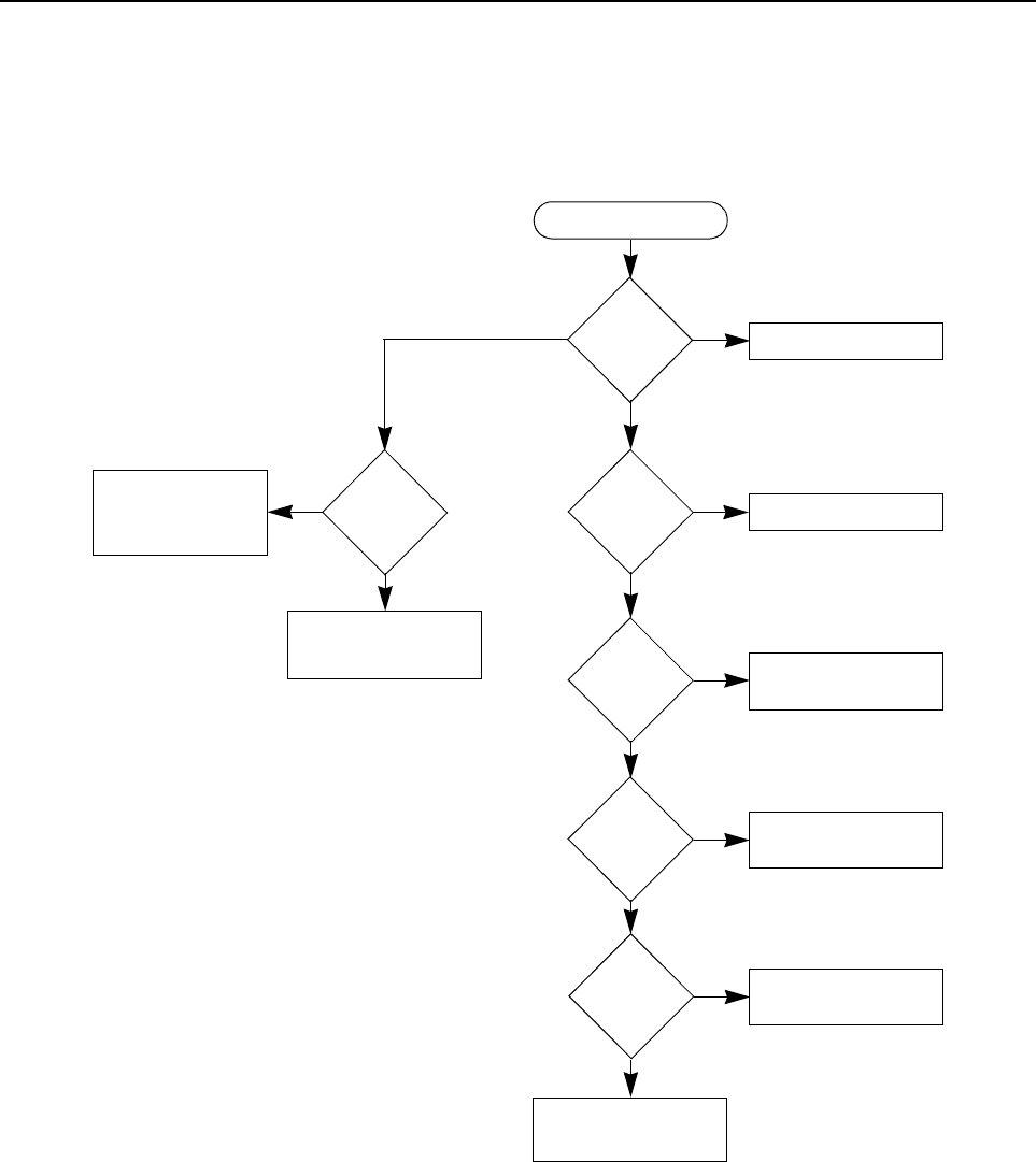
Troubleshooting Flow Chart for 25W Transmitter 3-5
2.2 Troubleshooting Flow Chart for 25W Transmitter (Sheet 3 of 3)
Check Final PA Stage
NO
0V
1-4V
Bias 2 DC
Voltage at
TP5406?
YES
RF Voltage
at TP5401
>100mV?
YES
RF Voltage
U5401 Pin 6
>3V?
Supply
Replace Q5441
Check FGU (U5301)
NO Check Components
between
TP5401 &C5417
NO
YES ASFIC
U0221 Pin 6
1-4V DC?
Check Bias Tuning
before replacing ASFIC
U0221
Check Components
between ASFIC and
Q5441 before
replacing Q5441
YES
RF Voltage
Q5421 Gate
>1V?
NO Check Components
between
C5417 & Q5421
YES
RF Voltage
Q5441 Gate
>4V?
NO Check Components
between
Q5421 & Q5441
Check Components
between Q5441 &
Antenna Connector
Voltage

3-6 Troubleshooting Flow Chart for Synthesizer
3.0 Troubleshooting Flow Chart for Synthesizer
5V
at pin 6 of
D5201
Is
information
from µP U0101
correct
?
Is
U5201 Pin 47
at = 13VDC
?
Is
U5301 Pin 19
<40 mVDC in RX &
>4.5 VDC in TX?
(at VCO section)
?
Start
Visual
check of the
Board
OK?
Correct
Problem
Check 5V
Regulator
U5211
+5V
at U5201
Pins
13 & 30
?
Is
16.8MHz
Signal at U5201
Pin 19
?
Check
Y5261 / Y5262 and
associated parts
Are
signals
at Pins 14 &15
of U5201
?
Check
R5201 Check C5381
Is
U5201
Pin 2 >4.5 VDC in
Tx & <40 mVDC
in Rx
?
Replace
U5201
Remove
Shorts
Is
there a short
between Pin 47 and
Pins 14 & 15 of
U5201
?
Replace or
resolder
necessary
components
Is
RF level at
U5201 Pin 32
-12 < x <-25
dBm
?
Are
R5221,R5222,
R5223,C5221,
C5222,& C5223
OK?
Replace
U5201
If C5227
is OK, then see VCO
troubleshooting chart
Are
Waveforms
at Pins 14 & 15
triangular
?
Do
Pins 7,8 & 9
of U5201 toggle
when channel is
changed?
Check programming
lines between
U0101 and U5201
Pins 7,8 & 9
Replace
U5201
Check µP U0101
Troubleshooting
Chart
NO
YES
NO
YES
NO
YES
NO
NO
NO
YES
YES
NO
YES
YES
NO
YES
YES
YES
NO
NO
NO
NO
YES
NO
YES
YES
Check D5201,
C5202, C5203, &
C5206
5V
at U5201
pins 5, 20, 34
& 36
C h e c k 5 V
Regulator
U5211
Is
16.8MHz
signal at
U5201 Pin
23?
Replace
U5201
YES
NO
NO
YES
NO
YES

Troubleshooting Flow Chart for VCO 3-7
4.0 Troubleshooting Flow Chart for VCO
Are Q5332
Base at 0.7V
Collector at 4.5V
Emitter at 110mV
Are Q5301
Base at 2.4V
Collector at 4.5V
Emitter at 1.7V
Are Q5311
Base = 1.9V
Collector = 4.5V
Emitter = 1.3V
Low or no RF Signal
at TP5003
Visual check
of board
OK?
35mV DC at
U5301 Pin 19
NO
YES
Replace Q5301
at base of Q5332
NO
NO
NO
NO
YES
YES
YES
YES
Low or no RF Signal
at input to PA
4.8V DC at
U5301 Pin 19
Is RF available
at U5401
YES
YES
YES
YES
NO
NO
NO
NO
NO
Audio =180mVrms
at “-” S
ide of
4.5VDC
at CR5321
If C5321 and R5321 are OK,
then replace CR5321
Replace C5322
Replace C5325
NO
NO
YES
YES
TX VCO
RX VCO
Correct
Problem
Visual check
of board
OK?
Check runner
between U5201 Pin 2
and U5301 Pin 19
Is RF available If all parts from U5301 Pin 8
to Base of Q5332 are OK,
replace U5301
If all parts associated
with the pins are OK,
replace Q5332
If all parts from collector
of Q5332 to TP5003 are
OK, Replace U5301
Power OK but
no modulation
If all parts from U5301 Pin 10
U5401 Pin 16 are OK,
replace U5301
Replace
Q5311
YES
YES
Make sure Synthesizer is
working correctly and runner
between U5201 Pin 28 and
U5301 Pin 14 & 18 are OK
4.5V DC
OK ?
OK? OK?
C5325
at U5301 Pin 14 & 18
4.5V DC
OK ?
at U5301 Pin 14 &18
NO
Pin 16
If R5361 and
L5361 are OK,
replace U5301

3-8 Troubleshooting Flow Chart for VCO
THIS PAGE INTENTIONALLY LEFT BLANK

4-1
Section 4
UHF PCB/SCHEMATICS/PARTS LISTS
1.0 Allocation of Schematics and Circuit Boards
1.1 Controller Circuits
The UHF circuits are contained on the Printed Circuit Board (PCB) which also contains the
Controller circuits. This Chapter shows the schematics for the UHF circuits only, refer to the
Controller section for details of the related Controller circuits . The PCB component layouts and the
Parts Lists in this Chapter show both the Controller and UHF circuit components. The UHF
schematics and the related PCB and parts list are shown in the tables below.
Table 4-1 UHF 1-25W Diagrams and Parts Lists
PCB : 8485671Z03 Main Board Top Side
8485671Z03 Main Board Bottom Side Page 4-3
Page 4-4
SCHEMATICS
Power Amplifier 1 - 25W
FRACN
Voltage Controlled Oscillator
Receiver Front End
IF
Page 4-5
Page 4-6
Page 4-7
Page 4-8
Page 4-9
Parts List
8485671Z03 Page 4-10

4-2 Allocation of Schematics and Circuit Boards
THIS PAGE INTENTIONALLY LEFT BLANK
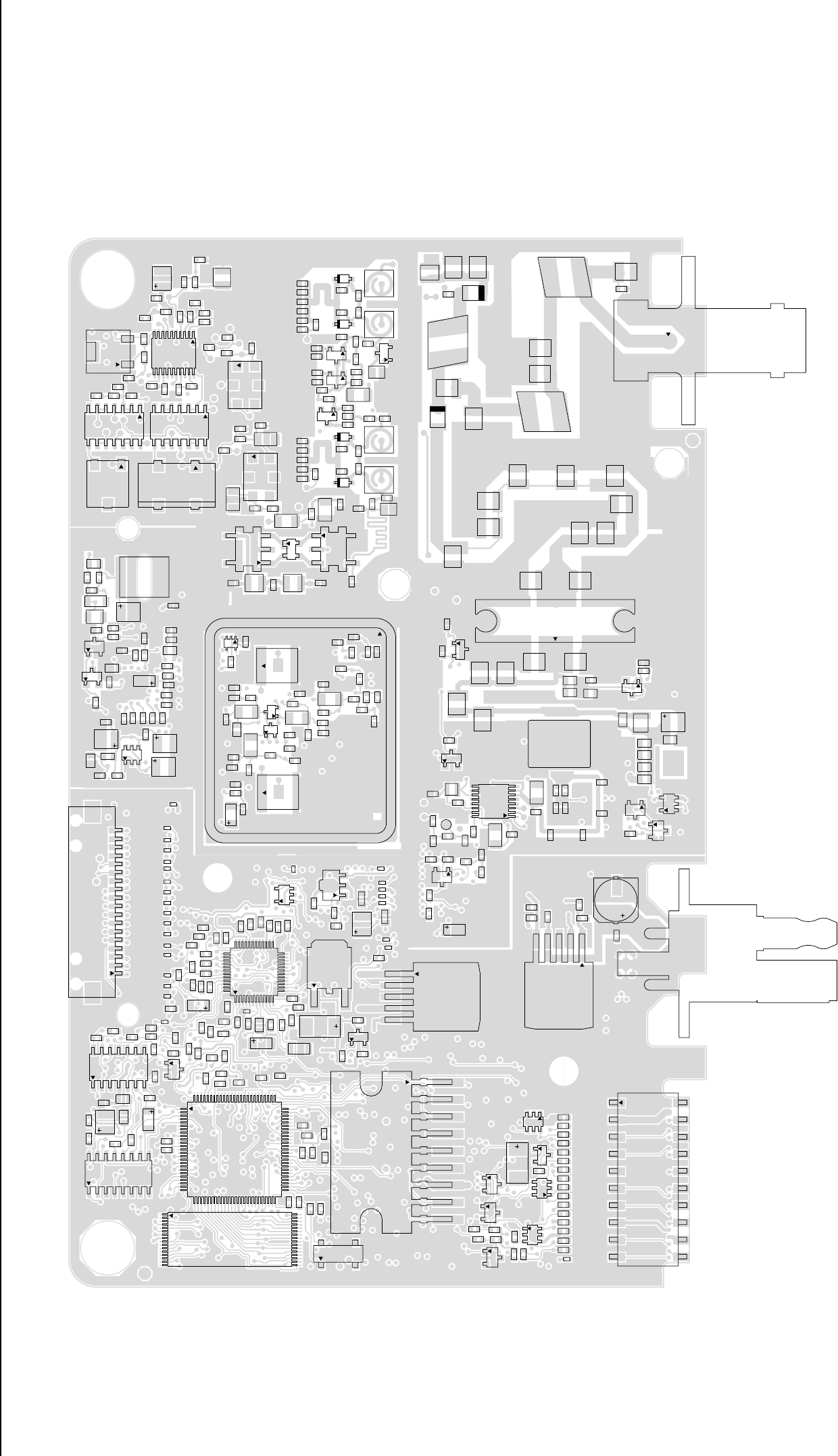
UHF Band 2 1-25W PCBs / Schematics / Parts List 4-3
2.0 UHF Band 2 1-25W PCBs / Schematics / Parts List
ZMY0130677-O
U0251
9
8
116
R0103
C0108
C0252
R0251 R0212
R0257
R0252
C0251
C0212
14
1
78
U0211
R0211
R0253
C0211
R0256
R0268
C0256
R0269
C0261
C0262
C0253
U0121
1
16
17 32
U0101
26
51 76
1
R0132
R0131
R0105
R0114
R0170
R0106
C0101
C0102
C0131
C0132
13 25
37
1
U0221
Q0110
R0221
R0222
R0220
R0224
R0225
R0241
R0108
R0223
R0226
R0227
R0229
R0442
R0262
R0101
R0104
R0110
R0115
R0254
R0255
R0261
R0116
R0228
R0242
R0102
C0236
C0221
C0222
C0223
C0225
C0226
C0227
C0232
C0234
C0241
C0242
C0244
C0245
C0231
C0235 C0228
C0233
C0237
C0441
C0442
C0443
C0445
C0446
C0447
C0448
C0449
C0495
C0421
C0246
C0104C0106
C0224
C0243
C0107
Q0681
R0681
D0201
C0681
C0496
R0682
U0651
12
3
R0651
C0652
C0470
C0474
C0476
C0477
C0478
C0490
C0471
C0472
C0473
U0641
5
6
1
U0271
9
R0652
D0651
C0651
Q0177
Q0181
C0542
4
3
2
Y0131
Q0185
R0182
R0186
R0538
R0535
R0181
R0185
R0539
VR0505 R0510
VR0503 VR0510
J0501
10
11 20
VR0501
C0502
C0503
C0504
C0505
C0506
C0508
C0509
C0510
C0511
C0512
C0513
C0514
C0515
C0518
C0517
C0501
C0516
L0481
L0482
C0655
C0654
C0482
C0483
C0486
C0487
C0488
C0493
C0494
U5401
9
16
1
Q5471
R5507
R5471
R5509
R5506
R5508
R5505R5401
R5403
R5402
TP5401
L5401
L5403
C5505
C5403
C5401
C5404
C5407
C5509
8
R5475
VR5471
C5402
M3421
R5415
R5416
L5411
C5425
C5417
C5426
C5418
C5419
U0611
5
6
1R0611
R0533
R0612
C0612
C0601
C0484 C0603
J0601
C5422
Q5422
Q5442
Q5411
R5424
R5425
R5426
R5427
R5450
L5422
C5428
C5423
C5424 C5420
C5435
R5431
R5432
C5434
C5458
C5431
C5454
C5457
C5455
C5432
8
7
6
5
4
3
2
Q5431
C5448
C5449
R5404
R5406
D5401
U5502
C5507 C5508
C5441
C5461
C5446
C5443
C5445 C5447
C5442
C5444
L5491
C5491
C5462 L5472
D5471 C5492
C5496
C5498
32
J5401
R5491
C5497
L5493
L5002 L5001
Q5001 Q5003
R5020
R5021
R5007
R5001
R5005
R5022
R5064
R5003
R5004
L5006
L5003
D5003
D5002
C5009
C5014
C5033
C5034
C5065
C5003
C5008
C5001
C5004
C5005
C5006
C5007
C5026
C5027
C5002
L5004
R5066
D5004
C5015
C5068
C5017
C5016
C5029
D5006
D5005
C5030
C5018
R5012
C5020
C5022
C5023
C5019
C5021
L5005
R5013
L5009
C5032
R5015
R5051
L5051
C5052
L5471
D5472
C5472
C5473
C5474
D5001
6
5
4
32
FL3101
R3148
L3100
C3101
2
T5052
1
64
3
D5051 L5008
L5053
L5054
C5053
C5054
3
45
1
T5051
2
C5031
C5055
6
5
4
32
FL3102
R3106
R3101
L3101
C3102
C3103
14 1
78
U3111
14 1
78
U3115 2
Y3102
R3132
R3142
R3117
R3123
R3124
R3130
R3135
R3144
R3145
R3111 L3124
U3101
10
20 1
11
C3132
C3134
C3139
C3140
C3141
C3142
C3145
C3133
C3115
C3131
C3148
C3137 C3124
C3135
C3143
C3136
FL3112
23
4
FL3114
C3114
C5224
Q5221
R5224
R5225
R5227
R5223
R5222
R5221
L5221
D5221
C5251
C5253
C5231
C5225
C5229
C5221
C5230
C5236
C5223
C5226
C5227
C5222
R5252
R5251
C5254
C5232
C5234
C5255
C5252
C5233
R5211
L5201
U5211
C5242
C5243
C5244
C5245
C5246
C5213
C5214
C5215
C5210
C5216
C5289
C5217
1
J0451
18
Q5333
3
4
R5346
C5375
L5303
3
L5312
3
Q5301
Q5311
R5321
R5305
R5302
R5301
R5311
R5312
L5304 L5305
L5313
C5308
C5352
C5353
C5325
C5309
C5317
C5322
C5351
C5372
C5382
C5383
C5323
C5373
C5374
C5355
C5318
C5371
L5371
SH5301
R5343
R5333
R5337
R5341
R5345
R5332
R5331
C5332
C5335 C5339
C5331
C5337
UHF Band 2 (450-527 MHz) 1-25W 8485671Z03 Top Side
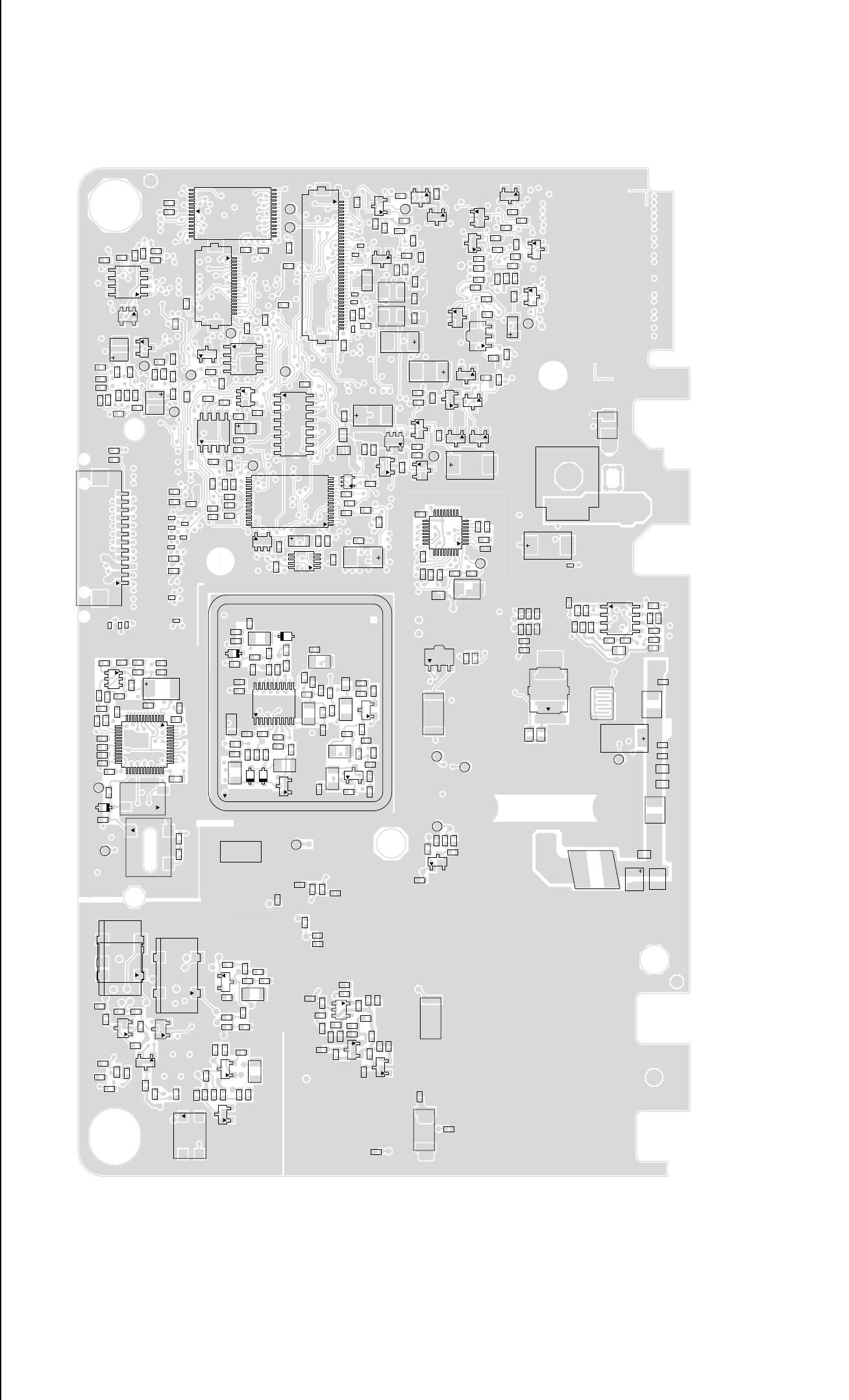
4-4 UHF Band 2 1-25W PCBs / Schematics / Parts List
ZMY0130678-D
Y3101
2
34
Q3102
R3112
R3114
R3115
R3113
R3116 R3118
L3112
D3101 C3116
C3121
C3122
C3123
Q3141
Q3151
Q3152
R3133
R3134
R3151
R3152
R3153
R3154
R3141
R3147
R3146
C3144
C3147
C3151
C3152
C3146
FL3111
2
3
4
FL3115
2
3
4
FL3113
Q3101
R3102
R3104
R3105
R3108 R3107
L3111
C3104
C311111
C3112
C3110
C3113
R5474
C5471
C5025
C5475
R5457
Q5004
Q5002
R5069
R5062
R5068
R5061
R5071
R5072
R5063
R5070
R5017
R5002
R5016
R5018
D5007
C5062
C5064
C5011
C5013
C5067
C5028
C5069
C5061
C5010
C5012
R5053
R5060
R5052
R5054
R5055 TP5003
C5066
C5024
C5060
R5019
R5455
R5454
R5452 TP5403
D5451 C5453
C5451
C5452
TP5404
TP5405
S5440
L5402
L5436
TP5406
L5437
C5406
C5438
C5421
C5437
C5481
C5439
C5482
C5436
C5405
32
Q5421
1
R5420
C5429
R5442
R5429
R5417
R5440
R5421
R5423
R5441
R5443
R5428
R5445
R5411
R5418
R5422
R5412
R5511
8
5
41
U5402
C5411
C5413
C5415
C0499
C5427
C5412
C5414
C5416
C5440
C0611
43
2
Y5262
R5228
R5261
R5241
R5263
R5203
R5204
R5201
R5206
R5262
Y5261
1
34
6
TP5201 TP5202
L5231
13
25
37 1
U5201
D5201
D5261
C5208C5209
C5211
C5228
C5263
C5288
C5202
C5203
C5205
C5235
C5201
C5204
C5207
C5241
C5287
C5206
C5262
C5261
Q5472
R5400
R5473
C5400
R5502 R5504
R5446 R5413
R5501
L5421
TP5402
25
9
17
U5501
1
C5501
C5502
C5506
C5503
C5510
C5483
C5504
12
J0401
R0407
R0409
R0467
R0412
R0441
F0401
C0426
C0427
C0429
C0485
C0491
C0492
C0497
C0422
C0423
C0430
C0431
C0428
R0344
R0323
R0324
R0345
R0341
C0304
C0305
C0324
C0325
C0343
U0351
85
4
U0301
114
15
28
D0301
C0302
C0351
C0354C0352
C0301
C0303
U0331
Q0641
R0642
R0335
R0643
R0331
R0332
R0333
R0641
R0481
R0482
C0331
C0645
C0353
C0644
C0641
C0662
U0141
9
81
16
TP0101
C0141
R0468
R0543
R0593
85
4
1U0652
C0255
C0121
C0122
C0105
C0123
U0122
17
8
21
22
R0117
R0121
R01
R0111 R011212
TP0103
TP0104
TP0492
J0552
18 1
C0103
C0111
8
5
4
1
U0341
R0346
R0347
R0342
R0343
TP0497 U0342
C0342
C0344
C0341
R0401
D0101
C0112
8
5
41
U0111
E0631
VR0601
R5315
R5304
R5303
L5302
L5301
10
CR5302
CR5303
CR5301
C5301
C5307
C5305
C5306
C5316
C5304
C5302
C5303
U5301
20
1
11
R5381
R5314
R5323
R5322
R5313
L5311
CR5311
CR5321
C5381
C5311
C5315
C5313 C5321
C5312
C5314
C5324
Q5331
Q5332
R5342
R5335
R5344
R5362
R5338
R5340
R5336
R5363
R5334
R5347
R5339
R5360
R5361
L5333
L5361
L5332
L5362
L5331
C5336 C5361
C5363
C5354
C5365
C5364
C5333
C5334
C5338
C5362
SH5302
Q0662
Q0663
Q0661
R0671
R0662
R0661
TP0661
D0621
D0660
D0661
VR0671
C0663
C0671
C0661 R0621
R0672
VR0621
C0622
C0621 R0174
R0173
Q0171
Q0173
R0178
R0176
R0172
R0175
R0171
R0177
R0512
R0529
R0542
R0541
R0525
R0530
TP0530 VR0504
C0541
Q0183
R0179
R0184
R0531
R0537
R0511
R0183
D0179
VR0537
VR0509
Q0271
R0151 R0152
R0273
R0591
R0276
R0592
R0556
13
R0274
E0271 E0272
D0151
40
J0551
1
C0272
C0274
C0554
C0591
C0592
C0275
C0558
C0559
C0560
C0575
C0576
C0593
Q0151
R0275 TP0151
VR0151
C0273
C0151
C0271
C0276 C0277
U0653
R0265
R0266
R0107
R0267
R0207
R0208
R0202
R0204
R0201
R0203
R0408 R0555
R0205
R0206
TP0102
TP0221
TP0222
VR0541
C0204
C0254 C0265
C0266
C0203
C0205
C0201
C0202
C0267
UHF Band 2 (450-527 MHz) 1-25W 8485671Z03 Bottom Side
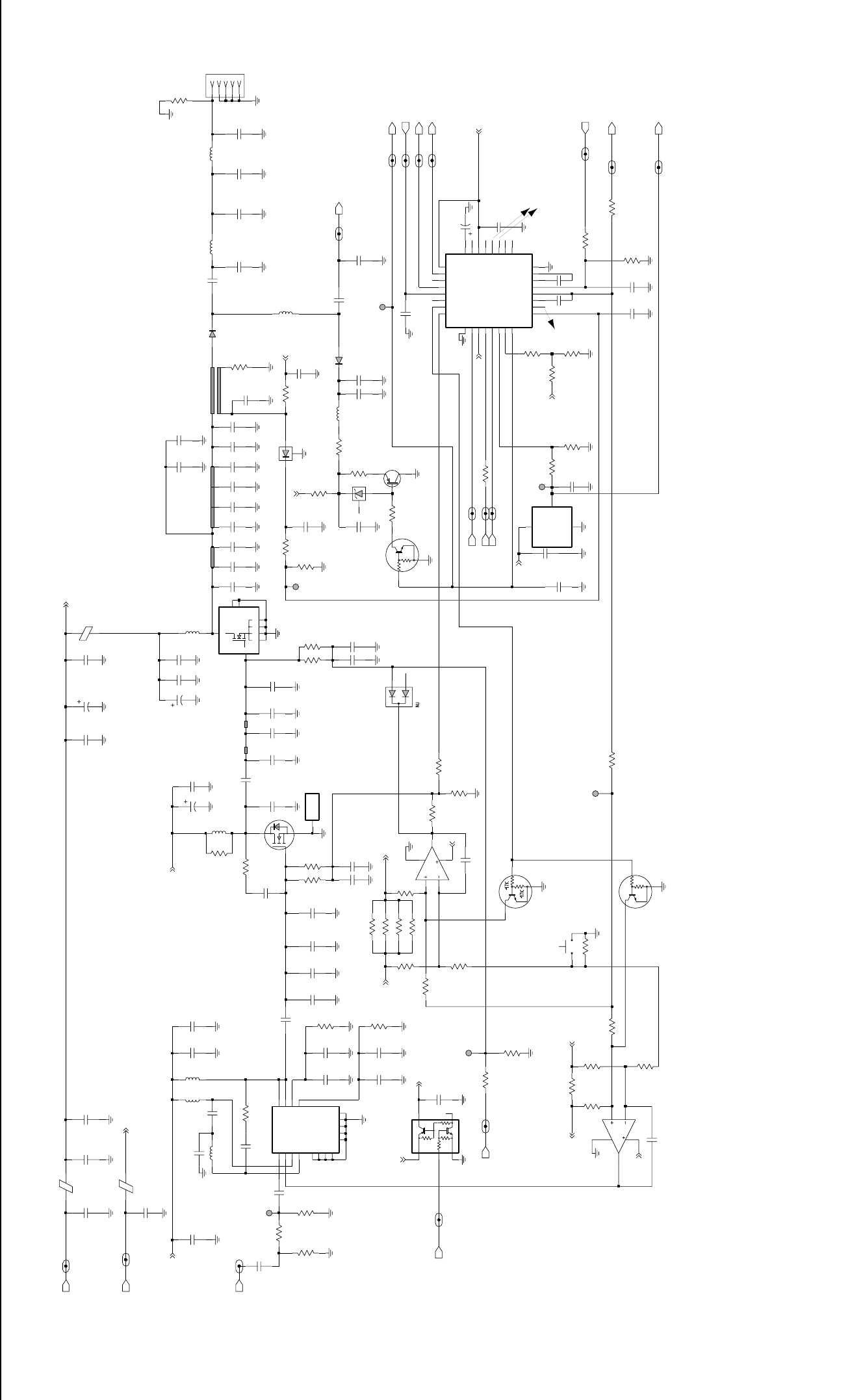
UHF Band 2 1-25W PCBs / Schematics / Parts List 4-5
ZMY0130676-O
L5402
57R01
PASUPVLTG_UHF_PA_1
100pF
C5405 100pF
C5406 .033uF
C5421
PASUPVLTG
C5483
.033uF
9V3 L5421
57R01
9V3_UHF_PA_1 9V3FLT
U_PREDRIVER
R5402
15
300
R5403
C5407
100pF TP5401
1
C5401
100pF
TXINJ_UHF_PA_1
.022uF
C5402
300
R5401
TXINJ
100pF
C5404 47nH
L5403 47nH
L5411 C5411
.022uF
C5400
180pF
100pF
C5412
11.03nH
L5401
82
R5400
C5403
6.8pF
VG2
NC3
15 NC4
16 RFIN 6
RFOUT1 7
RFOUT2
1VCNTRL
14 VD1 VG1 2
3
EP
11 G2
4GND1
5GND2
12 GND3
13 GND4
8NC1
9NC2
10
30C65
U5401
17
NU
R5411 24pF
C5420
C5418
C5414
100pF 10pF
C5424 51
R5416
.022uF
C5413 C5419
NU
NU
C5425
0.1uF
C5426
100pF
51
R5415
100pF
C5417
Q5411
NC_Q3411_1
A+
C5428
2200pF
INT_SWB_UHF_PA_1
PA_SWB
C5415
.022uF C5416
100pF
10K
R5404
MOSBIAS_2
1
MOSBIAS_2_UHF_PA_1
R5406
22K
TP5406
39K
R5443
2.7
R5511
8
4
LM2904
U5402-1
2
3
1
39K
R5441
1000pF
C5440
R5445
2.4K 2.2K
R5442
9V3FLT
U_PREDRIVER
PA_SWB
R5440
SWITCH
S5440
NU
12
Q5442
47K
47K
INT_SWB
R5422
22K
R5418
R5424 2.2
R5421
39K
R5412
R5427 2.2
2.2
R5425
C5427
3300pF
U5402-2
LM2904
6
57
8
4
R5426 2.2
R5423
39K
R5428
R5429
1K R5417
PA_SWB
U_DRIVER
9V3FLT
NU
NU NU
NU
Q5422
0.8x25
1.542x4
24pF
C5431
C5454 C5455
20pF
C5458
47pF
C5457
47pF
NU
Q5421 C5432
33pF
100pF
C5422
L5422
13.85nH
R5420
C5429
C5423
1uF
R5450
U_DRIVER
NU
NU
NU
M3421
HEATSINK
POS
1
C5435
100pF
100
R5431 100
R5432
0.1uF
C5434
D5401
NC_D3401_2
100pF
C5439
L5437
17nH
1uF
C5438
C5481
.033uF
S3
S4
Q5431
D
G
GND1
GND2
S1
S2
2.216x??
width 2.032
C5461 NU
C5462
NU
R5475
10K
C5453
100pF
10K
R5454
2.7K
R5452
R5455
100K
51
R5474 D5472
TP5403
1
1000pF
C5451
43.67nH
L5471
D5451
9V3FLT
A+
30pF
C5473
30pF
C5472
C5452
11pF 120
R5457
R5473
51
5.6V
23
1
C5471
100pF
VR3471
NC
Q5472
R5471
470
Q5471
47K
47K
MOSBIAS_1
1
TP5402
R5446
0
C5437
.033uF
C5436
10uF 57R01
L5436
C5482
30pF
A+
J3401 - BNC
J5401-2
L5493
17nH J5401-1
J5401-5
J5401-4
J5401-3
C5497
5.6pF
10K
R5491
4.7pF
C5496
17nH
L5472
17nH
L5491
3.3pF
C5498
100pF
C5492
6.8pF
C5491
D5471
RESET_UHF_PA_1 K9V1
FECTRL_2
FECTRL_1_UHF_PA_1
FECTRL_2_UHF_PA_1 FECTRL_1
K9V1_UHF_PA_1
RESET
9V3FLT
RXIN_UHF_PA_1
C5475
5.1pF
C5474
RXIN
NU
1
TP5404
C5509
NU
470pF
24
19
23
17
20
18
22
21 NC_U3501_22
NC_U3501_19
47K
R5507
9V3FLT
3.9K
R5509
R5508
200K
C5502
2200pF
NC_U3501_2
.015uF
C5504 300K
R5505
2200pF
C5506
VAR3
15
VG
VL
6VLIM
RX
T1
2
TEMP
30
14
V10
V45 16
V5EXT
VAR1
VAR2
GND2
25
INT
4NA
Q11
QX 10
RFIN
1
RS
RSET
31
CJ
5
CL
7
CLK
26
CQ 12
13
CQX
DATA
28
F168 9
GND1
8
U5501
H99S-4
ANO
32
BPOS
27
CEX
29
CI
3
C5505
1uF
NC_U3501_15
NC_U3501_13
NC_U3501_12
NC_U3501_11
NC_U3501_10
NC_U3501_9
9V3FLT
10K
R5504
CLK DATA_UHF_PA_1
CLK_UHF_PA_1
CSX_UHF_PA_1
DATA
CSX
CNTLVLTG
CNTLVLTG_UHF_PA_1
R5413
3.3K
PA_PWR_SET_UHF_PA_1
PA_PWR_SET
TEMPSENSE
NU
R5506
U5508
C5503
470pF
100pF
C5510
1
POS
VOUT 2
U5502
LM50
GND
3
100pF
C5507
100K
R5502
1
TP5405
6.8K
R5501
C5508
100pF
2200pF
C5501
9V3FLT
7.5
C5447
C5441
4.7pF 7.5pF
C5445
C5443
NU30pF
C5448
C5449
27pF
C5446
C5444
C5442
18pF NU
NU
NU
UHF Band 2 (450-527 MHz) Power Amplifier 1 - 25W
4-6 UHF Band 2 1-25W PCBs / Schematics / Parts List
5V_UHF_FN_2
5V_UHF_FN_1
5V
(SOURCE)
C5204
100pF
C5201
100pF
6
A2 5
A3 4
1
K1
2
K2
3
K3
D5201
A1
6.6 Vdc
10.87 Vdc
12.7 Vdc
C5203
.01uF
.01uF
C5202
150
R5201
LOCK
LOCK_UHF_FN_1
VCTRL
VCTRL_UHF_FN_1
2.5 to 10 Vdc
5 Vdc (locked)
0 Vdc (unlocked) 1
TP5201
150
R5221
.01uF
C5221 510
R5222
C5287
100pF .01uF
C5205
C5223
1uF C5224
1uF
NU
R5223
68
C5225
510pF
C5222
0.1uF
12uH
L5221
VCOMOD_UHF_FN_1
TRB_UHF_FN_1
TRB
BWSELECT_UHF_FN_1
BWSELECT
16_8MHz
VCOMOD
16_8MHz_UHF_FN_1
4.97 Vdc (25KHz Cha, Spa)
0 Vdc (12.5KHz Cha, Spa)
3.09 Vdc (Rx)
2.65 Vdc (Tx)
0 Vdc (Rx)
4.97 Vdc (Tx)
10uF
C5206
47
R5204
C5207
R5203
47
NU 0.1uF
C5208
R5206
NU
C5209
0.1uF
C5213
2.2uF
390nH
L5201
5V
2.2uF
C5210
R5211
0
.01uF
C5217
C5216
.01uF
OUT
3
SD
ADP3300
U5211
6ERR
1
GND
5
IN
2NR
4
NU
4.97 Vdc
R5224
47K
IN_5V_RF_REG
IN_5V_RF_REG_UHF_FN_1
C5215
2.2uF
C5211
0.1uF
47K
R5228
C5228 C5246
100pF
NU
D5221
WARP
25
27
SFCAP 26
SFOUT
28
TEST1
37
TEST2
38
VBPASS 21
PD_GND 44
32
PREIN
PRE_GND 33
REFSEL 18
SFBASE
INDMULT
16
IOUT
43
4LOCK
NC1 17
NC2 29
NC3 31
CCOMP 42
6
DGND
IADAPT
45
AGND 22
AUX1
48
AUX2
1
AUX3
2
AUX4
3BIAS1 40
BIAS2 39
ADAPTSW
46
VMULT1
VMULT2
14
VMULT3
12
VMULT4
11
13 VRO
XTAL1
23
24 XTAL2
SFIN 30
VCP
47
15
5PD_VDD
PRE_VDD
34
PVREF 35
MODIN 10
MODOUT
41 CEX 9
CLK 8
DATA 7
DVDD
36
FREFOUT
19
AVDD
20
U5201
63A27
C5244
100pF 100pF
C5242
4.98 Vdc
2.51 Vdc
4.95 Vdc
0 Vdc
47K
R5261
R5241
220
1.25 Vdc
1.97 Vdc
C5241
100pF
NU
2.48 Vdc
2.48 Vdc
0.1uF
C5289
C5288
0.1uF
NU
C5262
1GND
4GND1
3
OUT
6IN
16.8MHz
C5261
R5263
100
R5262
1.2K
.01uF
D5261
C5251
0.1uF
2GND
3OUT
4
VCC
1
VCNTL
16.8MHz
TTS05V
Y5262
.01uF
C5235
C5263
0.1uF
5V
NU
NU
NU
NU
75Z04
Y5261
NU C5234
.01uF
C5231 C5232
.01uF 2.2uF
C5233
Q5221 C5236
.047uF
R5225
47K
47K
47K
R5252
30K
C5230
2.2uF
1TP5202
C5227
10pF
100K
R5227
39K
R5251
3.03 Vdc
-19 to -17 dBn (Rx)
-17 to -12 dBn (Tx)
3.76 Vdc
1.76 Vdc
1.69 Vdc (Rx)
4.7uF
C5253 C5254
0.1uF
C5252
1000pF
100pF
C5255
4.57 Vdc
C5226
2.4pF 2pF
C5229
U4506
NU
2.2uH
L5231
100pF
C5243
C5245
100pF VDDA
MODIN_UHF_FN_1
DATA_UHF_FN_1
CSX
VSF_UHF_FN_1
CSX_UHF_FN_1
VSF
CLK
DATA
MODIN
CLK_UHF_FN_1
VCOBIAS_2
VDDA
PRESC
VDDA_UHF_FN_1
U4507
2.2uF
C5214
VDDA
ZMY0130675-O
HF Band 2 (450-527 MHz) FRACN
UHF Band 2 1-25W PCBs / Schematics / Parts List 4-7
ZMY0130674-O
R5301
5.6K
RXSW
4.2 Vdc (Rx)
0 Vdc (Tx)
R5302
10K
0.22uF
C5371
C5372
100pF
NU
C5305
NU C5306
2pF
L5304
390nH
4.3pF
C5303 C5304
5.6pF
C5302
4.3pF
CR5302
CR5303
220nH
L5302
CR5301
L5301
68nH
68nH
L5311
C5317
100pF
100pF
C5301
NU
VCTRL_UHF_VCO R5315
0
2.5 to 10 Vdc
100pF
C5311 CR5311
C5316
0.1uF
15pF
C5312
VCOMOD
VCOMOD_UHF_VCO 4.7uF
C5325
VCTRL
C5323
1000pF
56K
R5321
C5322
100pF
NU NU
C5321
1pF
R5322
6.8K
CR5321
3pF
C5324 R5323
10K
VSF
NU
4.5 Vdc
P2
2
P3
3
RESONATOR
L5303
P1
1
R5303
30
R5304
150
100pF
C5307
R5311
TXSW 0 Vdc (Rx)
4.5 Vdc (Tx)
7.5K
0.22uF
C5318
L5313
390nH
R5312
7.5K
3pF
C5314
100pF
C5315
R5314
220
Q5311
0 Vdc (Rx)
1.9 Vdc (Tx)
P1
1
P2
2
P3
3
RESONATOR
L5312
C5313
NU R5313
30
C5382
100pF
0.1uF
C5381
TXSW
0 Vdc (Rx)
4.5 Vdc (Tx)
NU
TRB_UHF_VCO
R5381
470 TRB
0 Vdc (Rx)
4.5 Vdc (Tx)
TX_OUT
TX_SWITCH
VCC_BUFFERS 14
VCC_LOGIC 18
RX_IADJ
2RX_OUT
RX_SWITCH
SUPER_FLTR
3
TRB_IN
19
TX_BASE
16
TX_EMITTER
15
TX_IADJ
1
COLL_RFIN
4
FLIP_IN
20
GND_BUFFERS
11 GND_FLAG
9
17 GND_LOGIC
PRESC_OUT
RX_BASE
5
RX_EMITTER
6
U5301
50U54
10
13
8
7
12
4.5 Vdc (Rx)
2.58 Vdc (Tx)
100pF
C5383
39nH
C5365
L5362
3.3pF
RXSW
NU
4.2 Vdc (Rx)
0 Vdc (Tx)
10
R5335
PRESC
PRESC_UHF_VCO NU
NU
R5347
0
R5333
10K R5334
0
C5334
51pF
NU
NU
0.1uF
C5308
L5305
390nH
C5309
100pF R5305
10
VSF VSF_UHF_VC0
VSF
4.5 Vdc
Q5301
2.3 Vdc (Rx)
0 Vdc (Tx)
100pF
C5351
0.1uF
C5352 2.2uF
C5354
2.2uF
C5355
C5361
100pF
0.1uF
C5353
33nH
L5331
R5361
180
390nH
L5361 0.22uF
C5362
270
R5360
C5364
5.6pF
NU
1K
R5363
VSF
C5374
C5363
NU
NU
NU
C5373
L5371
68nH 5.6pF
C5331
4 dBn (Tx)
R5362
10
C5332
0.1uF
C5333
22K
R5332 L5332
15nH R5336
1K
NU NU NU NU
51pF
NU
TXINJ_UHF_VCO
Q5331
R5331
22
TXINJ
NU
R5337
0
NU
5V_UHF_VCO
VCOBIAS_2_UHF_VCO
C5375
10K
R5346
VCOBIAS_2
5V
NU
Q5333
0
R5341
4.7K
47K
47K
10K 4.5 Vdc (Rx)
0 Vdc (Tx)
51pF
C5337
R5342
2.2K L5333
390nH
C5336
.022uF
R5344
10
22
R5339
R5343
1K
220
R5338
100pF
C5335
Q5332
NU
NU
51pF
C5338
220
R5340
NU
R5345 C5339
RXINJ
RXINJ_UHF_VCO
>14 dBn (Rx)
NU
NU
SHIELD
SH5302
1
SHIELD
SH5301
1
GND
UHF Band 2 (450-527 MHz) Voltage Controlled Oscillator
4-8 UHF Band 2 1-25W PCBs / Schematics / Parts List
ZMY0130672-O
FECTRL_2
9V3
RXIN
K9V1
9V3
C5067
3300pF
K9V1_UHF_FE
RXIN_UHF_FE
9V3_UHF_FE
D5007
IN
NEG POS
C5025
NU
TBD
L5001
C5026
1pF
1K
R5069
C5001
1.5pF
1.5K
R5068
C5010
330pF
C5002
33pF
D5002D5001
1pF
C5027
FECTRL_2_UHF_FE 10K
R5061
C5062
0.1uF
330pF
C5061
3.3K
R5016
TBD
IN
NEG POS
L5002
R5017
NU
C5003
22pF C5005
16pF
C5004
16pF C5006
16pF
100K
R5001 16pF
C5007
FECTRL_1
FECTRL_1_UHF_FE 330K
R5060
C5060 C5008
1000pF
NU
RXINJ
RXINJ_UHF_FE 15nH
15nH L5054L5053
16pF
C5054 C5053
6.8pF
C5055
TP5003
NU
T5052
XFMR
4
6
3
1
2
1IO1 2
IO2
3
IO3
4IO4
D5051 T5051
XFMR
1
2
3
5
4
C5052
82pF
R5051
51
470nH
L5008
C5066
IF_UHF_FE
L5051
150nH
IF
NU
0
R5052 R5053
R5055
R5054
NU
NU
NU
0.7 VDC
4.6 VDC
L5006
15nH
2.7K
R5004
C5009
8.2pF
D5003
R5003
4.7K
100pF
C5034
Q5001
R5020
10 R5021 C5033
10 100pF
Q5003 C5020
16pF
C5019
27pF C5021
18pF C5022
16pF C5023
R5012
100K NU
1000pF
C5024
R5019
NU GND_UHF_FE
GND
Q5002
270nH
L5003
.01uF
C5028 R5018
3.3K
C5013
3300pF330pF
C5012
0
R5022
330
R5002
3300pF
C501
100pF
C5014
10K
R5005
0
R5064
R5063
390
C5065
100pF R5007
100
R5066
D5006
NU
L5004
IN
NEG POS
TBD
100pF
C5068
C5016
C5015
100pF
NU
C5029
1pF
D5004
1.5pF
C5017
D5005
C5018
33pF
1pF
C5030
TBD
IN
NEG POS
L5005
8.2pF
C5032
L5009
15nH
R5015
R5013
NU NU 8.2pF
C5031
Q5004
1.5K
R5062
0.1uF
C5064
10K
R5072
10K
R5071
.01uF
C5069
390
R5070
9V3
3 to 6.5 VDC
UHF Band 2 (450-527 MHz) Receiver Front End
UHF Band 2 1-25W PCBs / Schematics / Parts List 4-9
ZMY0130673-O
5V_VHF_IF_1
9V3
9V3_VHF_IF_2
5V
9V3_VHF_IF_1
5V
IF IFIN_VHF_IF_1 3IN 6
OUT
FL3101
12R16
1GND1
GND2
2
GND3
4
5GND4
620nH
L3100
NU
20pF
C3101
R3148
0
C3103
33pF
15pF
C3102
L3101
620nH
R3101
12K
3VDC
0.75VDC
620
R3108
R3102
10
27K
R3106
6.8K
R3107
Q3101
0.1uF
C3104
0.1uF
C31
GND1
1
2GND2
4GND3
GND4
5
IN
3OUT 6
12R16
FL3102
C3112
82pF
C3110
27pF
620nH
L3111
NU
C3113
9.1pF
22pF
C3115
L3112
620nH 18pF
C3114
R3117
27K
6.8K
R3118
0.1uF
C3116
3VDC
Q3102
0.75VDC
12K
R3111
C3122
.039uF
10
R3112
.039uF
C3123
D3101
330
R3113
3.9VDC
330
R3116
R3115
390
NU
R3114
100
0.1uF
C3121
5V
9V3
9180469V03
3GND1
GND2
4
1IN 2
OUT
FL3111 CFWC455G
CNTL
13
12 VDD
14
VSS
7
MC74HC4066
U3111-1
VSS
7
U3111-4
CNTL
12
VDD
14
11
5
CNTL
43
14
VDD
7
VSS
U3112-1
MC74HC4066
9V3
9180469V06 2
OUT
FL3112 CFWC455D
3GND1
GND2
4
1IN
U3111-3
6
CNTL
14
VDD
7
VSS
89
10
MC74HC4066
U3115-1
CNTL
13
12 VDD
14
VSS
7
U3115-2
5
CNTL
43
14
VDD
7
VSS
MC74HC4066
9180468V06
3GND
1IN OUT
FL3114
2.01uF
C3151
CFUCJ455D
U3115-3
MC74HC4066
6
CNTL
14
VDD
7
VSS
89
10K
R3151
9180468v042
OUT
FL3113CFUCJ455F
3GND
1IN
NU
10
VDD
14
VSS
7
MC74HC4066
U3115-4
CNTL
12
11
10K
R3153
9V3
9V3
20/25kHz 5VDC
12.5kHz 0VDC
BWSELECT_VHF_IF_1
BWSELECT
R3154
10K
Q3151
Q3152
C3152
.01uF
10K
R3152
9V3
47K
47K
47K
47K
100
R3104
NU
R3105
100
9V3
L3124
NU
1uH
0
R3123
C3124
R3124
NU
33pF
NU
820
Y3101
2GND
4GND1
3OUT 1
IN
44.395MHz
06B09
C3132
0.1uF
C3134
30pF
C3136
51
R3130
NU
1pF
C3131
C3133
10uF
C3135
33pF
5RSSIOUT 9
RSSI_FEED
6VCC
13 LIM_DEC1
12 LIM_DEC2
20 MIXOUT
4
OSCIN
3OSCOUT
10
QUADIN
1
RFIN 2
RFIN_DEC
AUDIO_FEED
GND
18
IF AMPIN
16 IF AMPOUT 19
IF AMP_DEC1
17 IF
AMP_DEC2
14
LIMIN
11 LIMOUT
SA616
U3101
8AUDIOOUT 7
0.1uF
C3137
.039uF
15K
R3132
15
C3144
0.1uF
R3135
1.2K
0.1uF
C3142
3
45B02
Y3102
455KHz
2
Q3141
R3141
390
5V
120pF
C3143
1.8K
R3142
C3141
0.1uF
0.1uF
C3139
0.1uF
C3140 C3146
4700pF
680
R3146
12K
R3147
5V
R3133
8.2K
R3134
10K
9V3
2.4K
R3144
3.3K
220pF
C3148
NU 0.1uF
C3145
R3145
9180469V04
4GND2
IN
1OUT 2
CFWC455F
FL3115
GND1
3
C3147
0.1uF
DISCAUDIO_VHF_IF_1
DISCAUDIO
RSSI
RSSI_VHF_IF_1
UHF Band 2 (450-527 MHz) IF

4-10 UHF Band 2 1-25W PCBs / Schematics / Parts List
UHF Band 2 PCB 8485671Z03 Parts List 1-25W
Circuit
Ref Motorola
Part No. Description
C0101 2113740F51 100pF
C0107 2113741F25 1000pF
C0112 2113743E20 0.1uF
C0121 2113743E20 0.1uF
C0122 2113743E20 0.1uF
C0131 2113740F35 22pF
C0132 2113740F35 22pF
C0141 2113743E20 0.1uF
C0151 2113741F49 10nF
C0201 2311049A57 10uF
C0202 2311049A57 10uF
C0204 2113743E20 0.1uF
C0212 2311049A57 10uF
C0221 2113743E20 0.1uF
C0222 2113743E20 0.1uF
C0223 2113743E20 0.1uF
C0224 2113740F51 100pF
C0225 2113743E20 0.1uF
C0226 2113743E20 0.1uF
C0228 2311049A56 4.7uF
C0231 2113743B29 1uF
C0232 2113743E20 0.1uF
C0234 2113743E20 0.1uF
C0235 2113743E07 0.022uF
C0236 2113743E10 0.033uF
C0241 2113743E20 0.1uF
C0243 2113740F51 100pF
C0244 2113743E20 0.1uF
C0245 2113743E20 0.1uF
C0246 2113741F49 10nF
C0251 2113743E20 0.1uF
C0252 2311049A07 1uF
C0254 2113743E20 0.1uF
C0255 2113743E20 0.1uF
C0256 2113740F51 100pF
C0261 2113743E20 0.1uF
C0262 2113740F49 82pF
C0265 2113743E20 0.1uF
C0267 2113741F49 10nF
C0271 2113741F49 10nF
C0272 2113743E20 0.1uF
C0273 2113741F37 3300pF
C0275 2311049A99 47uF
C0276 2113741F25 1000pF
C0277 2113741F25 1000pF
C0301 2311049A07 1uF
C0302 2113743E20 0.1uF
C0303 2113740F51 100pF
C0304 2113743E20 0.1uF
C0305 2113743E20 0.1uF
C0324 2113743E20 0.1uF
C0331 2113743E20 0.1uF
C0341 2311049A07 1uF
C0342 2113743E20 0.1uF
C0343 2113743E20 0.1uF
C0344 2113743E20 0.1uF
C0351 2113743E20 0.1uF
C0352 2113743E07 0.022uF
C0353 2311049A97 33uF
C0354 2113743E20 0.1uF
C0421 2113743N48 82pF
C0422 2113741F17 470pF
C0423 2113741F17 470pF
C0426 2113743L09 470pF
C0427 2113743L09 470pF
C0428 2113743N48 82pF
C0429 2113743L09 470pF
C0430 2113741F17 470pF
C0431 2113741F17 470pF
C0441 2113743L09 470pF
C0442 2113743L09 470pF
C0445 2113743L09 470pF
C0446 2113743L09 470pF
C0447 2113743L09 470pF
C0448 2113743L09 470pF
C0449 2113743L09 470pF
C0470 2113743L09 470pF
C0471 2113743N48 82pF
C0472 2113743N48 82pF
C0473 2113743N48 82pF
C0474 2113743L09 470pF
C0476 2113743L09 470pF
C0477 2113743L09 470pF
C0478 2113743L09 470pF
C0482 2113743L09 470pF
C0483 2113743L09 470pF
C0484 2113741F17 470pF
C0485 2113743L09 470pF
C0486 2113743L09 470pF
C0487 2113743L09 470pF
C0488 2113743L09 470pF
C0490 2113743L09 470pF
C0491 2113743L09 470pF
C0492 2113743L09 470pF
C0493 2113743L09 470pF
C0494 2113743L09 470pF
C0495 2113743L09 470pF
C0496 2113743L09 470pF
C0497 2113743L09 470pF
C0499 2113743L09 470pF
C0501 2113741F49 10nF
Circuit
Ref Motorola
Part No. Description
C0502 2113741F17 470pF
C0503 2113741F17 470pF
C0504 2113741F17 470pF
C0505 2113741F17 470pF
C0506 2113741F17 470pF
C0508 2113741F17 470pF
C0509 2113741F17 470pF
C0510 2113741F17 470pF
C0511 2113741F17 470pF
C0512 2113741F17 470pF
C0513 2113741F17 470pF
C0514 2113741F17 470pF
C0515 2113741F17 470pF
C0516 2113741F49 10nF
C0517 2113743N48 82pF
C0518 2113741F17 470pF
C0541 2311049A05 0.47uF
C0542 2311049A99 47uF
C0560 2113743L17 1000pF
C0591 2113743E20 0.1uF
C0592 2113743E20 0.1uF
C0593 2113741B69 0.1uF
C0601 2113741F17 470pF
C0603 2380090M24 10uF
C0611 2311049C06 22uF
C0612 2113743E20 0.1uF
C0622 2311049A99 47uF
C0641 2113741F17 470pF
C0644 2311049A97 33uF
C0645 2113743E20 0.1uF
C0652 2311049A97 33uF
C0654 2311049A57 10uF
C0655 2113743E20 0.1uF
C0661 2311049C05 47uF
C0662 2113741F49 10nF
C0663 2113743E20 0.1uF
C0671 2113743E20 0.1uF
C0681 2113743E20 0.1uF
C3101 2113740F34 20pF
C3102 2113740F31 15pF
C3103 2113740F39 33pF
C3104 2113743E20 0.1uF
C3110 2113740F37 27pF
C3111 2113743E20 0.1uF
C3112 2113740F49 82pF
C3114 2113740F33 18pF
C3115 2113740F35 22pF
C3116 2113743E20 0.1uF
C3121 2113743E20 0.1uF
C3122 2113743E11 0.039uF
C3123 2113743E11 0.039uF
Circuit
Ref Motorola
Part No. Description
C3132 2113743E20 0.1uF
C3133 2311049A57 10uF
C3134 2113743E20 0.1uF
C3135 2113740L30 33pF
C3136 2113740L29 30pF
C3137 2113743E11 0.039uF
C3139 2113743E20 0.1uF
C3140 2113743E20 0.1uF
C3141 2113743E20 0.1uF
C3142 2113743E20 0.1uF
C3143 2113740F53 120pF
C3144 2113743E20 0.1uF
C3145 2113743E20 0.1uF
C3146 2113741F41 4700pF
C3147 2113743E20 0.1uF
C3151 2113741F49 10nF
C3152 2113741F49 10nF
C5001 2113740F07 1.5pF
C5002 2113740F39 33pF
C5003 2113740F35 22pF
C5004 2113740F32 16pF
C5005 2113740F32 16pF
C5006 2113740F32 16pF
C5007 2113740F32 16pF
C5008 2113741F25 1000pF
C5009 2113740F25 8.2pF
C5010 2113741F13 330pF
C5011 2113741F37 3300pF
C5012 2113741F13 330pF
C5013 2113741F37 3300pF
C5014 2113740F51 100pF
C5015 2113740F51 100pF
C5017 2113740F07 1.5pF
C5018 2113740F39 33pF
C5019 2113740F37 27pF
C5020 2113740F32 16pF
C5021 2113740F33 18pF
C5022 2113740F32 16pF
C5024 2113741F25 1000pF
C5026 2113740F03 1pF
C5027 2113740F03 1pF
C5028 2113741F49 10nF
C5029 2113740F03 1pF
C5030 2113740F03 1pF
C5031 2113740F25 8.2pF
C5032 2113740F25 8.2pF
C5033 2113740F51 100pF
C5034 2113740F51 100pF
C5052 2113740F49 82pF
C5053 2113740F23 6.8pF
C5054 2113740F32 16pF
Circuit
Ref Motorola
Part No. Description

UHF Band 2 1-25W PCBs / Schematics / Parts List 4-11
C5061 2113740F63 330pF
C5062 2113743E20 0.1uF
C5064 2113743E20 0.1uF
C5065 2113740F51 100pF
C5067 2113741F37 3300pF
C5068 2113740F51 100pF
C5069 2113741F49 10nF
C5201 2113740F51 100pF
C5202 2113741F49 10nF
C5203 2113741F49 10nF
C5204 2113740F51 100pF
C5205 2113741F49 10nF
C5206 2311049J25 10uF
C5208 2113743E20 0.1uF
C5209 2113743E20 0.1uF
C5210 2104993J02 2.2uF
C5211 2113743E20 0.1uF
C5213 2311049A09 2.2uF
C5214 2311049A09 2.2uF
C5215 2311049A09 2.2uF
C5217 2113741F49 10nF
C5221 2109720D01 0.01uF
C5222 2109720D14 0.1uF
C5224 0882422W23 1uF
C5225 2113741F18 510pF
C5227 2113740F27 10pF
C5230 2104993J02 2.2uF
C5231 2113741F49 10nF
C5232 2113741F49 10nF
C5233 2104993J02 2.2uF
C5234 2113741F49 10nF
C5235 2113741F49 10nF
C5236 2113743E12 0.047uF
C5242 2113740F51 100pF
C5243 2113740F51 100pF
C5244 2113740F51 100pF
C5245 2113740F51 100pF
C5246 2113740F51 100pF
C5251 2113743E20 0.1uF
C5252 2113741F25 1000pF
C5253 2311049A56 4.7uF
C5254 2113743E20 0.1uF
C5255 2113740F51 100pF
C5263 2113743E20 0.1uF
C5287 2113740F51 100pF
C5289 2113743E20 0.1uF
C5301 2113740F51 100pF
C5302 2113740L09 4.3pF
C5303 2113740L09 4.3pF
C5304 2113740L12 5.6pF
C5306 2113740L01 2pF
Circuit
Ref Motorola
Part No. Description
C5307 2113740F51 100pF
C5308 2113743E20 0.1uF
C5309 2113740F51 100pF
C5311 2113740F51 100pF
C5312 2113740F33 18pF
C5314 2113740L01 2pF
C5315 2113740F51 100pF
C5316 2109720D14 0.1uF
C5318 2113743E20 0.1uF
C5321 2113740F03 1pF
C5324 2113740F07 1.5pF
C5325 2311049A56 4.7uF
C5331 2113740L12 5.6pF
C5335 2113740F51 100pF
C5336 2113743E07 0.022uF
C5337 2113740F44 51pF
C5338 2113740F44 51pF
C5351 2113740F51 100pF
C5352 2113743E20 0.1uF
C5353 2113743E20 0.1uF
C5354 2104993J02 2.2uF
C5355 2104993J02 2.2uF
C5361 2113740F51 100pF
C5364 0662057B47 0
C5371 2113743E20 0.1uF
C5381 2113743E20 0.1uF
C5400 2113740F57 180pF
C5401 2113740F51 100pF
C5402 2113743E07 0.022uF
C5403 2113740F23 6.8pF
C5404 2113740F51 100pF
C5405 2113740F51 100pF
C5406 2113740F51 100pF
C5407 2113740F51 100pF
C5411 2113743E07 0.022uF
C5412 2113740F51 100pF
C5413 2113743E07 0.022uF
C5414 2113740F51 100pF
C5415 2113743E07 0.022uF
C5416 2113740F51 100pF
C5417 2113740F51 100pF
C5420 2113740F36 24pF
C5421 2113741A57 0.033uF
C5422 2113740A55 100pF
C5423 2311049A08 1uF
C5424 2113740F27 10pF
C5425 2113743E20 0.1uF
C5426 2113740F51 100pF
C5427 2113741F37 3300pF
C5428 2113741F33 2200pF
C5431 2111078B25 27pF
Circuit
Ref Motorola
Part No. Description
C5432 2111078B29 33pF
C5434 2113743E20 0.1uF
C5435 2113740A55 100pF
C5436 2311049A45 10uF
C5437 2113741A57 0.033uF
C5438 2311049A08 1uF
C5439 2111078B42 100pF
C5440 2113741F25 1000pF
C5441 2111078B05 4.7pF
C5442 2111078B19 16pF
C5448 2111078B29 33pF
C5449 2111078B29 33pF
C5451 2113741F25 1000pF
C5452 2113740F28 11pF
C5453 2113740F51 100pF
C5454 2111078B01 3.3pF
C5455 2111078B19 16pF
C5457 2111078B34 47pF
C5458 2111078B35 51pF
C5461 2111078B11 8.2pF
C5471 2113740F51 100pF
C5472 2111078B27 30pF
C5473 2111078B27 30pF
C5474 2113740F18 4.3pF
C5475 2113740F10 2pF
C5481 2113741A57 0.033uF
C5482 2113740F38 30pF
C5483 2113741A57 0.033uF
C5491 2111078B09 6.8pF
C5492 2111078B42 100pF
C5496 2111078B05 4.7pF
C5497 2111078B01 3.3pF
C5498 2111078B01 3.3pF
C5501 2113741F33 2200pF
C5502 2113741F33 2200pF
C5503 2113741F33 2200pF
C5504 2113741F46 7500pF
C5505 2311049A07 1uF
C5506 2113741F33 2200pF
C5507 2113740F51 100pF
C5508 2113740F51 100pF
C5510 2113740F51 100pF
CR5301 4805649Q13 DIODE VCTR ISV 228
CR5302 4862824C01 DIODE VARACTOR
CR5303 4862824C01 DIODE VARACTOR
CR5311 4862824C01 DIODE VARACTOR
CR5321 4802245J22 DIODE, VARACTOR
D0101 4813825A05 DIODE
D0151 4813833C02 DIODE, DUAL 70V
D0179 4813833C02 DIODE, DUAL 70V
D0301 4802245J47 DIODE, SCHOTTKY
Circuit
Ref Motorola
Part No. Description
D0621 4813833C02 DIODE, DUAL 70V
D0651 4813833C02 DIODE, DUAL 70V
D0660 4813833C02 DIODE, DUAL 70V
D0661 4813833C02 DIODE, DUAL 70V
D3101 4880154K03 DIODE DUAL SCHOTTKY
D5001 4862824C01 DIODE VARACTOR
D5002 4862824C01 DIODE VARACTOR
D5003 4880154K03 DIODE DUAL SCHOTTKY
D5004 4862824C01 DIODE VARACTOR
D5005 4862824C01 DIODE VARACTOR
D5006 4880142L01 DIODE
D5007 4813833C02 DIODE, DUAL 70V
D5051 4886143B01 DIODE, MIXER
D5201 4802233J09 DIODE, TRIPLE
D5221 4813825A05 DIODE
D5401 4813833C02 DIODE, DUAL 70V
D5451 4813825A05 DIODE
D5471 4802482J02 DIODE, SMD PIN
D5472 4802482J02 DIODE, SMD PIN
E0271 2484657R01 FERRITE BEAD
E0272 2484657R01 FERRITE BEAD
E0631 2484657R01 FERRITE BEAD
F0401 6580542Z01 FUSE 3A
FL3101 9180112R16 2 POLE 44.85 MHZ CRYSTAL
FILTER
FL3102 9180112R16 2 POLE 44.85 MHZ CRYSTAL
FILTER
FL3111 9180469V03 CERAMIC FILTER, 455KHz
FL3112 9180469V06 CERAMIC FILTER, 455KHz
FL3114 9180468V06 CERAMIC FILTER, 455KHz
FL3115 9180469V04 CERAMIC FILTER, 455KHz
J0401 0902636Y02 FLEX CONNECTOR
J0451 0902636Y01 FLEX CONNECTOR
J0501 0986105B01 ACCESSORY CONNECTOR
J0551 0905505Y04 FLEX CONNECTOR
J0552 0905505Y03 FLEX CONNECTOR
J0601 0986165B01 DC POWER CONNECTOR
J5401 0986166B01 RF CONNECTOR (BNC)
L3101 2462587T25 620nH
L3111 2462587T25 620nH
L3112 2462587T25 620nH
L5003 2462587T20 270nH
L5006 2462587V24 15nH
L5008 2462587T23 470nH
L5009 2462587V24 15nH
L5051 2462587T17 150nH
L5053 2462587N43 15nH
L5054 2462587N43 15nH
L5201 2462587Q42 390nH
L5221 2462587P25 12uH
L5231 2462587Q20 2.2uH
Circuit
Ref Motorola
Part No. Description
4-12 UHF Band 2 1-25W PCBs / Schematics / Parts List
L5301 2462587T13 68nH
L5302 2462587T19 220nH
L5303 2460593C03 RESONATOR
L5304 2462587T22 390nH
L5305 2462587T22 390nH
L5311 2462587T22 390nH
L5312 2460593C03 RESONATOR
L5313 2462587T22 390nH
L5331 2462587T09 33nH
L5333 2462587T22 390nH
L5361 2462587T22 390nH
L5362 2462587T38 22nH
L5371 2462587T13 68nH
L5401 2460591B04 11.03nH
L5402 2484657R01 FERRITE BEAD
L5403 2462587T11 47nH
L5411 2462587T11 47nH
L5421 2484657R01 FERRITE BEAD
L5422 2460591C23 13.85nH
L5436 2484657R01 FERRITE BEAD
L5437 2460592A01 17nH
L5471 2460591N36 43.67nH
L5472 2460592A01 17nH
L5491 2460592A01 17nH
L5493 2460592A01 17nH
M3421 2686201B01 HEAT SPREADER
Q0110 4880048M01 NPN
Q0151 4880048M01 NPN
Q0171 4880048M01 NPN
Q0173 4880052M01 NPN DARLINGTON
Q0177 4880048M01 NPN
Q0181 4880048M01 NPN
Q0183 4880048M01 NPN
Q0185 4880048M01 NPN
Q0271 4880214G02 NPN
Q0641 4880048M01 NPN
Q0661 4805921T02 DUAL NPN/PNP
Q0662 4880214G02 NPN
Q0663 4880048M01 NPN
Q0681 4880052M01 NPN DARLINGTON
Q3101 4813827A07 NPN
Q3102 4813827A07 NPN
Q3141 4880214G02 NPN
Q3151 4880048M01 NPN
Q3152 4880048M01 NPN
Q5001 4813827A07 NPN
Q5002 4813824A17 PNP
Q5003 4813827A07 NPN
Q5004 4805921T02 DUAL NPN/PNP
Q5221 4880048M01 NPN
Q5301 4805218N63 DIODE DUAL SCHOTTKY
Circuit
Ref Motorola
Part No. Description
Q5311 4805218N63 DIODE DUAL SCHOTTKY
Q5332 4813827A07 NPN
Q5333 4802245J50 DUAL NPN/PNP
Q5411 4805921T02 DUAL NPN/PNP
Q5421 4886212B01 POWER TRANSISTOR -
MRF1518
Q5422 4880048M01 NPN
Q5431 4886163B01 POWER TRANSISTOR -
MRF1535
Q5442 4880048M01 NPN
Q5471 4880048M01 NPN
Q5472 4805128M27 PNP
R0101 0662057A73 10K
R0102 0662057A65 4.7K
R0103 0662057B47 0
R0104 0662057A73 10K
R0105 0662057A97 10K (used in GM338 only)
R0106 0662057B47 0 (used in GM398 only)
R0108 0662057A57 2.2K
R0111 0662057B47 0
R0113 0662057A73 10K
R0114 0662057A73 10K
R0115 0662057A73 10K
R0117 0662057A63 3.9K
R0121 0662057A97 100K
R0131 0662057B46 10M
R0132 0662057B10 330K
R0151 0662057A82 24K
R0152 0662057A82 24K
R0170 0662057A73 10K
R0171 0662057A65 4.7K
R0172 0662057A73 10K
R0173 0662057A65 4.7K
R0174 0662057A73 10K
R0175 0662057A73 10K
R0176 0662057A84 30K
R0177 0662057A65 4.7K
R0178 0662057A89 47K
R0179 0662057A89 47K
R0181 0662057A65 4.7K
R0182 0662057A89 47K
R0183 0662057A65 4.7K
R0184 0662057A89 47K
R0185 0662057A65 4.7K
R0186 0662057A89 47K
R0201 0662057A25 100
R0202 0662057A43 560
R0203 0662057A25 100
R0204 0662057A43 560
R0205 0662057A73 10K
R0206 0662057A73 10K
Circuit
Ref Motorola
Part No. Description
R0207 0662057A57 2.2K
R0208 0662057A57 2.2K
R0211 0660076E70 7.5K
R0212 0660076E70 7.5K
R0221 0662057A82 24K
R0222 0662057A82 24K
R0223 0662057A84 30K
R0224 0662057A71 8.2K
R0228 0662057B47 0
R0229 0662057A01 10
R0241 0662057A89 47K
R0242 0662057B47 0
R0251 0662057A89 47K
R0252 0662057A91 56K
R0253 0662057A97 100K
R0254 0662057A73 10K
R0255 0662057A73 10K
R0256 0662057A97 100K
R0257 0662057A57 2.2K
R0261 0662057A73 10K
R0262 0662057B08 270K
R0265 0662057A82 24K
R0267 0662057A89 47K
R0268 0662057A73 10K
R0269 0662057A41 470
R0273 0662057A82 24K
R0275 0662057A73 10K
R0276 0662057A77 15K
R0323 0662057A79 18K
R0324 0662057A79 18K
R0331 0662057A73 10K
R0332 0662057A73 10K
R0333 0662057A73 10K
R0335 0662057B02 150K
R0341 0662057A73 10K
R0342 0662057A55 1.8K
R0343 0662057B47 0
R0344 0662057A91 56K
R0345 0662057A66 5.1K
R0346 0662057A89 47K
R0347 0662057A89 47K
R0401 0662057A33 220
R0407 0662057M26 10
R0408 0662057A25 100
R0409 0662057M26 10
R0412 0662057B47 0
R0441 0662057B47 0
R0442 0662057A49 1K
R0467 0662057M26 10
R0468 0662057A97 100K
R0481 0662057B47 0
Circuit
Ref Motorola
Part No. Description
R0482 0662057B47 0
R0510 0662057A65 4.7K
R0511 0662057A97 100K
R0512 0662057A77 15K
R0525 0662057A97 100K
R0529 0662057A89 47K
R0530 0662057B47 0
R0531 0662057A43 560
R0533 0662057B47 0
R0535 0662057A49 1K
R0537 0662057A33 220
R0538 0662057A33 220
R0539 0662057A65 4.7K
R0541 0662057A83 27K
R0543 0662057A97 100K
R0555 0662057A25 100
R0556 0662057A25 100
R0591 0662057A82 24K
R0592 0662057A01 10
R0593 0662057A97 100K
R0611 0662057A91 56K
R0612 0662057A65 4.7K
R0621 0662057A82 24K
R0641 0662057A73 10K
R0642 0660076E70 7.5K
R0643 0660076E51 1.2K
R0651 0662057A01 10
R0652 0662057A01 10
R0661 0662057A49 1K
R0662 0662057B02 150K
R0671 0662057A84 30K
R0672 0662057A73 10K
R0681 0662057A79 18K
R0682 0662057A93 68K
R3101 0662057A75 12K
R3102 0662057A01 10
R3105 0662057A25 100
R3106 0662057A83 27K
R3107 0662057A69 6.8K
R3108 0662057A44 620
R3111 0662057A75 12K
R3112 0662057A01 10
R3113 0662057A37 330
R3115 0662057A39 390
R3116 0662057A37 330
R3117 0662057A83 27K
R3118 0662057A69 6.8K
R3123 0662057B47 0
R3130 0662057A18 51
R3132 0662057A77 15K
R3133 0662057A71 8.2K
Circuit
Ref Motorola
Part No. Description
UHF Band 2 1-25W PCBs / Schematics / Parts List 4-13
* Motorola Depot Servicing only
Reference designators with an asterisk indicate
components which are not field replaceable
because they need to be calibrated with
specialized factory equipment after installation.
Radios in which these parts have been replaced in
the field will be off frequency at temperature
extremes.
R3134 0662057A73 10K
R3135 0662057A51 1.2K
R3141 0662057A39 390
R3142 0662057A55 1.8K
R3144 0662057A58 2.4K
R3145 0662057A61 3.3K
R3146 0662057A45 680
R3147 0662057A75 12K
R3148 0662057B47 0
R3151 0662057A73 10K
R3152 0662057A73 10K
R3153 0662057A73 10K
R3154 0662057A73 10K
R5001 0662057A97 100K
R5002 0662057A37 330
R5003 0662057A65 4.7K
R5004 0662057A59 2.7K
R5005 0662057A73 10K
R5007 0662057A25 100
R5012 0662057A97 100K
R5016 0662057A61 3.3K
R5018 0662057A61 3.3K
R5020 0662057A01 10
R5021 0662057A01 10
R5022 0662057B47 0
R5051 0662057A18 51
R5052 0662057B47 0
R5060 0662057B10 330K
R5061 0662057A73 10K
R5062 0662057A53 1.5K
R5063 0662057A39 390
R5064 0662057B47 0
R5068 0662057A53 1.5K
R5069 0662057A49 1K
R5070 0662057A39 390
R5071 0662057A73 10K
R5072 0662057A73 10K
R5201 0662057A29 150
R5203 0662057A17 47
R5204 0662057A17 47
R5211 0662057B47 0
R5221 0662057A29 150
R5222 0662057A42 510
R5223 0662057A21 68
R5224 0662057A89 47K
R5225 0662057A89 47K
R5228 0662057A89 47K
R5241 0662057A33 220
R5251 0662057A87 39K
R5252 0662057A84 30K
R5261 0662057A89 47K
Circuit
Ref Motorola
Part No. Description
R5263 0662057A25 100
R5301 0662057A67 5.6K
R5302 0662057A73 10K
R5303 0662057A12 30
R5304 0662057A29 150
R5305 0662057A01 10
R5311 0662057A70 7.5K
R5312 0662057A70 7.5K
R5313 0662057A12 30
R5314 0662057A33 220
R5315 0662057B47 0
R5321 0662057A91 56K
R5322 0662057A69 6.8K
R5323 0662057A97 100K
R5331 0662057A09 22
R5341 0662057B47 0
R5342 0662057A57 2.2K
R5343 0662057A49 1K
R5344 0662057A01 10
R5346 0662057A73 10K
R5347 0662057B47 0
R5361 0662057A31 180
R5362 0662057A01 10
R5363 0662057A49 1K
R5381 0662057A41 470
R5400 0662057A23 82
R5401 0662057A36 300
R5402 0662057A05 15
R5403 0662057A36 300
R5404 0662057A73 10K
R5406 0662057A81 22K
R5411 0662057A67 5.6K
R5413 0662057A61 3.3K
R5415 0662057A18 51
R5416 0662057A18 51
R5418 0662057A57 2.2K
R5421 0662057A86 36K
R5422 0662057A58 2.4K
R5423 0662057A87 39K
R5424 0662057C11 2.2
R5425 0662057C11 2.2
R5426 0662057C11 2.2
R5427 0662057C11 2.2
R5428 0662057A58 2.4K
R5429 0662057A49 1K
R5431 0662057C51 100
R5432 0662057C51 100
R5441 0662057A87 39K
R5442 0662057A57 2.2K
R5443 0662057A87 39K
R5445 0662057A58 2.4K
Circuit
Ref Motorola
Part No. Description
R5446 0662057B47 0
R5452 0662057A59 2.7K
R5454 0662057A73 10K
R5455 0662057A97 100K
R5457 0683962T51 120
R5471 0662057A41 470
R5473 0680194M18 51
R5474 0680194M18 51
R5475 0662057A73 10K
R5491 0662057A73 10K
R5501 0662057A69 6.8K
R5502 0662057A97 100K
R5504 0662057A73 10K
R5505 0662057B09 300K
R5507 0662057A89 47K
R5508 0662057B05 200K
R5509 0662057A63 3.9K
R5511 0662057C13 2.7
SH5301 2602641Y02 SHIELD
SH5302 2602641Y02 SHIELD
T5051 2505515V03 TRANSFORMER 4:1
T5052 2508397X02 TRANSFORMER 1:1
U0101 5102226J56 MICROPROCESSOR
U0111 5102463J64 EEPROM
U0121 5186137B01 IC, FLASH ROM
U0122 5185748L01 SRAM
U0141 5113805A30 REMUX
U0211 5183222M49 IC, QUAD OPAMP
U0221 5185130C53 IC, ASFIC
U0251 5184704M60 IC-CMOS ANALOG
U0271 5109699X01 AUDIO PA
U0301 5109152M01 EEPROM ANALOG
U0331 5186204B01 BUFFER / DRIVER
U0341 5113818A01 LINEAR IC OP AMP
U0342 5105750U28 IC CMOS SWITCH
U0351 5102463J40 REGULATOR, 3.3V
U0611 5183308X01 ADJUSTABLE VOLTAGE REG-
ULATOR
U0641 5183308X01 ADJUSTABLE VOLTAGE REG-
ULATOR
U0651 5113816A07 REGULATOR, 5V
U0652 5113815A02 UNDERVOLT SENSOR
U3101 5186144B01 IC, IF
U3111 5102463J52 QUAD ANALOG SWITCH
U3115 5102463J52 QUAD ANALOG SWITCH
U5201 5185963A27 IC FRACTN
U5211 5105739X05 IC, VOLTAGE REGULATOR
U5301 5105750U54 IC, VCO
U5401 5185130C65 IC LDMOS DRIVER
U5402 5113818A01 DUAL OP-AMP
U5501 5185765B28 IC POWER CONTROL
Circuit
Ref Motorola
Part No. Description
U5502 5185963A15 IC TEMPERATURE SENSOR
VR0151 4813830A15 DIODE, 5.6V
VR0501 4805656W09 DIODE, ZENER
VR0503 4805656W09 DIODE, ZENER
VR0504 4813830A40 DIODE, ZENER
VR0505 4805656W09 DIODE, ZENER
VR0509 4813830A40 DIODE, ZENER
VR0510 4813830A40 DIODE, ZENER
VR0537 4813830A15 DIODE, 5.6V
VR0541 4813830A27 DIODE, 14V
VR0601 4813832C77 DIODE
VR0621 4813830A15 DIODE, 5.6V
VR5471 4813830A15 DIODE, 5.6V
Y0131 4880113R19 CRYSTAL 38.4KHZ
Y3101 4880606B09 2ND OSC XTAL 44.395 MHZ
Y3102 9186145B02 455KHz DISCRIMINATOR
Y5262 4886182B01 TCXO 16.8MHZ
Circuit
Ref Motorola
Part No. Description

4-14 UHF Band 2 1-25W PCBs / Schematics / Parts List
THIS PAGE INTENTIONALLY LEFT BLANK

GM338/GM398
Mobile Radios
Low Band
Service Information
Issue: December, 2003

Computer Software Copyrights
The Motorola products described in this manual may include copyrighted Motorola computer programs stored
in semiconductor memories or other media. Laws in the United States and other countries preserve for
Motorola certain exclusive rights for copyrighted computer programs, including the exclusive right to copy or
reproduce in any form, the copyrighted computer program. Accordingly, any copyrighted Motorola computer
programs contained in the Motorola products described in this manual may not be copied or reproduced in
any manner without the express written permission of Motorola. Furthermore, the purchase of Motorola
products shall not be deemed to grant, either directly or by implication, estoppel or otherwise, any license
under the copyrights, patents or patent applications of Motorola, except for the normal non-exclusive royalty-
free license to use that arises by operation of law in the sale of a product.

i
Table of Contents
Section 1 Model Chart and Technical Specifications
1.0 GM338 Model Chart.............................................................................................1-1
2.0 Technical Specifications ......................................................................................1-2
Section 2 Theory of Operation
1.0 Introduction ..........................................................................................................2-1
2.0 Low Band Receiver..............................................................................................2-1
2.1 Receiver Front-End ........................................................................................2-1
2.2 Front-End Band-Pass Filters and Pre-Amplifier .............................................2-2
2.3 First Mixer and High Intermediate Frequency (IF)..........................................2-2
2.4 High Intermediate Frequency (IF) and Blanker Switches...............................2-2
2.5 Low Intermediate Frequency (IF) and Receiver Back End.............................2-3
2.6 “Extender” (Noise Blanker).............................................................................2-3
3.0 Transmitter Power Amplifier (PA) 60 W...............................................................2-4
3.1 Power Controlled Stage..................................................................................2-4
3.2 Driver Stage....................................................................................................2-5
3.3 Final Stage .....................................................................................................2-5
3.4 Antenna Switch...............................................................................................2-5
3.5 Harmonic Filter ...............................................................................................2-5
3.6 Power Control.................................................................................................2-6
3.7 TX Safety Switch ............................................................................................2-6
4.0 Frequency Synthesis ...........................................................................................2-7
4.1 Fractional-N Synthesizer ................................................................................2-7
4.2 Voltage Controlled Oscillator (VCO) and Buffers ...........................................2-8
4.3 Synthesizer Operation....................................................................................2-9
Section 3 Troubleshooting Charts
1.0 Troubleshooting Flow Chart for Receiver (Sheet 1 of 2)......................................3-1
2.0 Troubleshooting Flow Chart for Transmitter ........................................................3-3
3.0 Troubleshooting Flow Chart for Synthesizer........................................................3-4
4.0 Troubleshooting Flow Chart for VCO...................................................................3-5

ii
Section 4 Low Band PCBs/Schematics/Parts Lists
1.0 Allocation of Schematics and Circuit Boards .......................................................4-1
1.1 Controller Circuits...........................................................................................4-1
2.0 Low Band PCBs / Schematics / Parts Lists .........................................................4-3
Low Band Range 1 (29.7-36.0 MHz) 8486206B06 Top Side.................................4-3
Low Band Range 1 (29.7-36.0 MHz) 8486206B06 Bottom Side............................4-4
Low Band Range 1 (29.7-36.0 MHz) 8486206B08 Top Side.................................4-5
Low Band Range 1 (29.7-36.0 MHz) 8486206B08 Bottom Side............................4-6
Low Band Range 2 (36.0-42.0 MHz) 8486207B05 Top Side.................................4-7
Low Band Range 2 (36.0-42.0 MHz) 8486207B05 Bottom Side............................4-8
Low Band Range 2 (36.0-42.0 MHz) 8486207B07 Top Side.................................4-9
Low Band Range 2 (36.0-42.0 MHz) 8486207B07 Bottom Side..........................4-10
Low Band Range 3 (42-50 MHz) 8486908Z02 Top Side .....................................4-11
Low Band Range 3 (42-50 MHz) 8486908Z02 Bottom Side ................................4-12
Low Band Range 3 (42-50 MHz) 8486908Z04 Top Side .....................................4-13
Low Band Range 3 (42-50 MHz) 8486908Z04 Bottom Side ................................4-14
Low Band Range 1 (29.7-36.0 MHz) Synthesizer FRACN...................................4-15
Low Band Range 2 (36.0-42.0 MHz) Synthesizer FRACN...................................4-16
Low Band Range 3 (42-50 MHz) Synthesizer FRACN.........................................4-17
Low Band Range 1 (29.7-36.0 MHz) Voltage Controlled Oscillator .....................4-18
Low Band Range 2 (36.0-42.0 MHz) Voltage Controlled Oscillator .....................4-19
Low Band Range 3 (42-50 MHz) Voltage Controlled Oscillator ...........................4-20
Low Band Range 1 (29.7-36.0 MHz) Power Amplifier - Sheet 1 of 2 ...................4-21
Low Band Range 1 (29.7-36.0 MHz) Power Amplifier - Sheet 2 of 2 ...................4-22
Low Band Range 2 (36.0-42.0 MHz) Power Amplifier - Sheet 1 of 2 ...................4-23
Low Band Range 2 (36.0-42.0 MHz) Power Amplifier - Sheet 2 of 2 ...................4-24
Low Band Range 3 (42-50 MHz) Power Amplifier - Sheet 1 of 2 .........................4-25
Low Band Range 3 (42-50 MHz) Power Amplifier - Sheet 2 of 2 .........................4-26
Low Band Range 1 (29.7-36.0 MHz) Receiver Front End....................................4-27
Low Band Range 2 (36.0-42.0 MHz) Receiver Front End....................................4-28
Low Band Range 3 (42-50 MHz) Receiver Front End..........................................4-29
Low Band Range 1/2 Controller - T6
(for PC Boards 8486206B06 & 8486207B05) ..............................................4-30
Low Band Range 3 Controller-T9 (for PC Board 8486908Z02)............................4-31
Low Band Range 1/2/3 Controller - T11 (for PC Boards 8486206B08, 8486207B07 &
8486908Z04 )...............................................................................................4-32
Low Band Range 1 and 2 IO - T6 (for PC Boards 8486206B06 & 8486207B05..4-33
Low Band Range 3 IO - T9 (for PC Board 8486908Z02) .....................................4-34
Low Band Range 1/2/3 IO - T11 (for PC Boards 8486206B08, 8486207B07 &
8486908Z04 .................................................................................................4-35
Low Band Range 1/2/3 (29.7-36.0/36.0-42.0/42-50 MHz) - Audio .......................4-36
Low Band Range 1/2/3 (29.7-36.0/36.0-42.0/42-50 MHz) - Supply Voltage ........4-37

iii
Low Band Range 1/2/3 - IF sheet 1 of 2 (for PC Boards 8486206B06, 8486207B05 &
8486908Z02) ................................................................................................4-38
Low Band Range 1/2/3 - IF sheet 2 of 2 (for PC Boards 8486206B06, 8486207B05 &
8486908Z02) ................................................................................................4-39
Low Band Range 1/2/3 - IF sheet 1 of 2 (for PC Boards 8486206B08, 8486207B07 &
8486908Z04) ................................................................................................4-40
Low Band Range 1/2/3 - IF sheet 2 of 2 (for PC Boards 8486206B08, 8486207B07 &
8486908Z04) ................................................................................................4-41
Low Band Range 1/2/3 (29.7-36.0/36.0-42.0/42-50 MHz) - Noise Blanker ..........4-42
Low Band Range 1 PCB 8486206B06 Parts List .................................................4-43
Low Band Range 2 PCB 8486207B05 Parts List ................................................4-49
Low Band Range 3 PCB 8486908Z02 Parts List .................................................4-54
Low Band Range 1 PCB 8486206B08 Parts List .................................................4-60
Low Band Range 2 PCB 8486207B07 Parts List .................................................4-66
Low Band Range 3 PCB 8486908Z04 Parts Lis ..................................................4-72

iv
THIS PAGE INTENTIONALLY LEFT BLANK
1-1
Section 1
MODEL CHART AND TECHNICAL SPECIFICATIONS
1.0 GM338 Model Chart
GM Series, Low Band
Model Description
AZM25BKF9AA5 GM338 29.7-36.0 MHz 40-60W
AZM25CKF9AA5 GM338 36.0-42.0 MHz 40-60W
AZM25DKF9AA5 GM338 42.0-50.0 MHz 40-60W
Item Description
X X X GCN6114_ Preferred Control Head Direct Mount
XIMUB6000_ Tanapa WM 29.7-36.0 MHz 40-60W
X IMUB6001_ Tanapa WM 36.0-42.0 MHz 40-60W
XIMUB6002_ Tanapa WM 42.0-50.0 MHz 40-60W
X RAB4002 Low Band 29.7-36.0 MHz, 1/4 Wave Base Loaded
XRAB4003 Low Band 36.0-42.0 MHz, 1/4 Wave Base Loaded
X RAB4004 Low Band 42.0-50.0 MHz, 1/4 Wave Base Loaded
XXX6804112J06 GM338 User Guide
x = Indicates one of each is required.

1-2 Technical Specifications
2.0 Technical Specifications
Data is specified for +25°C unless otherwise stated.
General Specifications
Channel Capacity
GM338 128
Power Supply 13.2Vdc (10.8 - 15.6Vdc)
Dimensions: H x W x D (mm) Depth excluding knobs GM338
60mm x 179mm x 250mm (45 - 60W)
Weight GM338 2064 g
Sealing: Withstands rain testing per
MIL STD 810 C/D /E and IP54
Shock and Vibration: Protection provided via impact
resistant housing exceeding MIL STD
810-C/D /E
Dust, Salt & Fog Protection provided via environment
resistant housing exceeding MIL STD
810 C/D /E
Technical Specifications 1-3
*Availability subject to the laws and regulations of individual countries.
Transmitter Low Band
*Frequencies - Full Bandsplit Low Band 1 29.7-36.0 MHz
Low Band 2 36.0-42.0 MHz
Low Band 3 42.0-50.0 MHz
Channel Spacing 12.5/20/30 kHz
Frequency Stability
(-30°C to +60°C, +25° Ref.) ±5 ppm
Power 40-60W
Modulation Limiting ±2.5 @ 12.5 kHz
±5.0 @ 20/30 kHz
FM Hum & Noise -40 dB @ 12.5kHz
-45 dB @ 20/30kHz
Conducted/Radiated Emission -26 dBm <1 GHz
Adjacent Channel Power -60 dB @ 12.5 kHz
-70 dB @ 20/30 kHz
Audio Response (300 - 3000Hz) +1 to -3 dB
Audio Distortion
@1000Hz, 60%
Rated Maximum Deviation <3% typical
Receiver Low Band
*Frequencies - Full Bandsplit Low Band 1 29.7-36.0 MHz
Low Band 2 36.0-42.0 MHz
Low Band 3 42.0-50.0 MHz
Channel Spacing 12.5/20/30 kHz
Sensitivity (12 dB SINAD) 0.25 µV (0.22 µV typical)
Intermodulation >80 dB
Base Mode: >70dB
(1-25W model only)
Adjacent Channel Selectivity 65 dB @ 12.5 kHz
80 dB @ 20/30 kHz
Spurious Rejection 70 dB @ 12.5 kHz
80 dB @ 20/30 kHz
Rated Audio 7.5W and 13W External
Audio Distortion @ Rated Audio <3% typical
Hum & Noise -40 dB @ 12.5 kHz
-45 dB @ 20/30 kHz
Audio Response (300 - 3000Hz @ 20kHz) +1 to -3 dB
Conducted Spurious Emission (ETS) -57 dBm <1 GHz
-47 dBm >1 GHz

1-4 Technical Specifications
THIS PAGE INTENTIONALLY LEFT BLANK
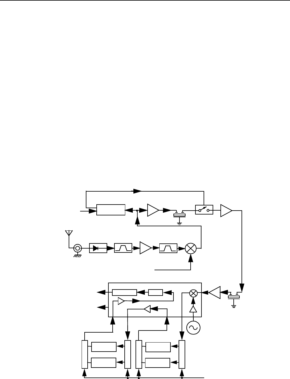
2-1
Section 2
THEORY OF OPERATION
1.0 Introduction
This Chapter provides a detailed theory of operation for the Low Band circuits in the radio. For
details of the theory of operation and troubleshooting for the the associated Controller circuits refer
to the Controller Section of this manual.
2.0 Low Band Receiver
2.1 Receiver Front-End
The low band receiver, shown in Figure 2-1, is bandsplit into three ranges depending on radio
model, covering frequencies from 29.7 to 36.0 MHz, 36.0 to 42.0 MHz, or 42.0 to 50.0 MHz. The
circuitry of the three models is identical except for component value differences. The receiver
consists of five major blocks: front-end bandpass filters and pre-amplifier, first mixer, high-IF and
blanker switches, low-IF and receiver back-end, and “Extender” (noise blanker). Two fixed-tuned
bandpass filters perform antenna signal pre-selection. A cross over quad diode mixer converts the
signal to the high-IF of 10.7 MHz. High-side first injection is used.
Figure 2-1 Low Band Receiver Block Diagram
Demodulator
Delay
Filter
Mixer
Fixed
Tuned Filter
RF Amp
Tuned Filter
Pin Diode
Antenna
Switch
RF Jack
Antenna
First LO
RXINJ
Recovered Audio
RSSI
IF
Second LO
Crystal
Filter
455kHz Filter
455kHz Filter
455kHz Filter
(12.5kHz)
455kHz Filter
(12.5kHz)
Switch
Switch
Switch
Switch
Limiter
IF Amp
IF Amp
Filter Bank Selection
from Synthesizer IC
Blanker
Noise
Blanking Pulses
Gate
Buffer
Enable
1st
Fixed
(25/20kHz)
BWSELECT
(U1201 Pin 48)
4-pole
(25/20kHz)

2-2 Low Band Receiver
There are two 2-pole 10.7 MHz crystal filters in the high-IF section and two switched pairs of 455
kHz ceramic filters in the low-IF section to provide the required adjacent channel selectivity.The
second IF at 455 kHz is mixed, amplified and demodulated in the IF IC. The processing of the
demodulated audio signal is performed by an audio processing IC located in the controller section.
2.2 Front-End Band-Pass Filters and Pre-Amplifier
The received signal from the radio’s antenna connector is first routed through the harmonic filter and
antenna switch, which are part of the RF power amplifier circuits, before being applied to the
receiver 5-pole antenna filter (L1001-L1005 and associated components). This filter configuration
provides more rapid attenuation above the passband to provide better rejection of the half-IF
spurious response. A dual hot carrier diode (D1001) limits any inband signal to 0 dBm to prevent
damage to the RF pre-amplifier.
The RF pre-amplifier is an SMD device (Q1001) with collector-base feedback to stabilize gain,
impedance, and intermodulation. Transistor Q1002 compares the voltage drop across resistor
R1005 with a fixed base voltage from divider R1006 and R1007, and adjusts the base current of
Q1001 as necessary to maintain its collector current constant at 25 mA. Operating voltage is from
the regulated 9.3V supply (9V3). During transmit, 9.1 volts (9T1) turns on both transistors in U1001,
turning off Q1003 and therefore Q1001-2. This protects the RF pre-amplifier from excessive
dissipation during transmit mode.
A second 5-pole fixed-tuned bandpass filter provides additional filtering of the amplified signal. This
filter configuration also provides steeper attenuation above its passband for best half-IF attenuation.
2.3 First Mixer and High Intermediate Frequency (IF)
The signal coming from the front-end is converted to the high-IF frequency of 10.7 MHz using a
cross over quad diode mixer (U1051). The high-side injection signal (RXINJ) from the frequency
synthesizer circuitry is filter by a 7-pole low-pass filter (L1012-14 and associated circuitry) which
removes second harmonic content from the injection signal and improves half-IF rejection. The 50-
ohm output of the first mixer is applied to the input of the high-IF circuit block.
2.4 High Intermediate Frequency (IF) and Blanker Switches
The first mixer IF output signal (IF) is applied to diplexer network consisting of L1101, L1111 and
associated components. This network has three functions: it terminates the mixer output at
frequencies other than 10.7 MHz into 51-ohm resistor R1101; it matches the 50-ohm mixer output to
the first IF amplifier (Q1101) input; and it provides bandpass filtering at 10.7 MHz to prevent the 5.35
MHz half-IF component of the mixer output from creating a second harmonic at 10.7 MHz in Q1101,
which degrades half-IF rejection.
The IF amplifier Q1101 uses ac and dc feedback to stabilize gain and quiescent current
(approximately 28 mA). Operating voltage is from the regulated 9.3V supply (9V3). Its output is
applied to a 10.7 MHz ceramic filter FL1101 which has a 3 dB bandwidth of 270 kHz and provides a
time delay of 2.6 usec. This delay allows enough time for the “Extender” to respond to impulse noise
present at the input of Q1101 and operate the blanker switches Q1102 and Q1103, muting the IF
signal for the duration of the noise pulse. L1104 and L1105 also provide additional selectivity and
time delay. Operation of the “Extender” circuit is explained in Section 1.0.5 below.
When the blanker switches turn “on” to mute the IF signal, they momentarily change the impedance
of resonant circuits L1104 and L1105 from high to very low. This abrupt impedance change, if

Low Band Receiver 2-3
presented to the high-Q crystal filter FL1102, would cause ringing of the filter response, stretching
an otherwise narrow impulse into a long and audible output waveform. Therefore, source follower
stage Q1104 isolates the blanker switches from the crystal filters, providing a consistent source
impedance via matching network L1106, L1107 and associated components. Q1104 has unity
voltage gain in this configuration.
Crystal filter F1102 is a module which consists of two 2-pole, 10.7 MHz units configured to provide
an overall 4-pole response having a 3 dB bandwidth of approximately 12 kHz. The output is
amplified by second IF amplifier Q1106 and applied to the low-IF circuitry, pin 1 of IF IC (U1103). A
dual hot carrier diode (D1101) limits the amplifier output voltage swing to prevent overdriving the IF
IC at RF input levels above -27 dBm.
2.5 Low Intermediate Frequency (IF) and Receiver Back End
The 10.7 MHz high-IF signal from the second IF amplifier feeds the IF IC (U1103) at pin 1. Within
the IF IC, the 10.7 MHz high-IF signal mixes with the 10.245 MHz second local oscillator (2nd LO) to
produce the low-IF signal at 455 kHz. The 2nd LO frequency is determined by crystal Y1101. The
low-IF signal is amplified and filtered by external pairs of 455 kHz ceramic filters (FL1105 and
FL1107 for 20kHz channel spacing, or FL1104 and FL1106 for 12.5 kHz channel spacing).
Selection of the appropriate filter pair is accomplished by U1101 and U1102, controlled by the
BWSELECT line from pin 48 of the synthesizer IC U1201. The filtered output from the ceramic filters
is applied to the limiter input pin of the IF IC (pin 14).
The IF IC contains a quadrature detector using a ceramic phase-shift element (Y1102) to provide
audio detection. Internal amplification provides an audio output level of 120 mV rms (at 60%
deviation) from U1103 pin 8 (AUDIOOUT) which is fed to the ASFIC_CMP (U0221) pin 2 (part of the
Controller circuitry).
A received signal strength indicator (RSSI) signal is available at U1103 pin 5, having a dynamic
range of 70 dB. The RSSI is interpreted by the microprocessor (U0101 pin 63) and in addition is
available at accessory connector J0501-15.
2.6 “Extender” (Noise Blanker)
The 10.7 MHz output from the first mixer, which is present at the input of the first IF amp Q1101, is
also routed to the input of the “Extender” (noise blanker) circuitry and amplified by FET Q1610. The
high input impedance of the FET stage minimizes loading of the signal in the receiver path. The
output of Q1610 is further amplified by U1601, which is a wide-bandwidth, high gain differential
amplifier (used in a single-ended configuration) incorporating an AGC gain control input. This gain
block provides linear amplification of the instantaneous amplitude of the 10.7 MHz signal at the first
mixer output. The output of U1601 is coupled to biased-detector Q1603. The bias is set so that
noise impulses of a significant amplitude cause Q1603 to conduct. The following stages (Q1604
through Q1606) provide additional gain and pulse shaping which slows the turn-on and turn-off
waveform applied to IF blanker switches Q1102 and Q1103. The result is that, for each noise
impulse, the IF signal is smoothly ramped off and then on again, preventing the pulse from reaching
the narrow IF selectivity, where ringing would cause an objectionable spike at the detector of a
much longer duration than the original impulse.
If the repetition rate of noise impulses is so rapid that the noise blanker can no longer blank them
individually, as indicated by a large increase in high-frequency content at the output of Q1604, stage
Q1607 amplifies this level and turns on level detector Q1609. Its output is highly filtered into a DC
voltage level which is proportional to the repetition rate of noise impulses, and this is applied to the
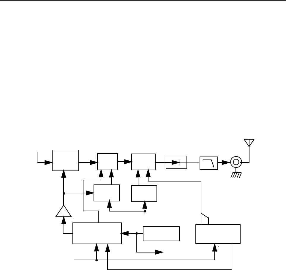
2-4 Transmitter Power Amplifier (PA) 60 W
AGC input pin 5 of U1601, reducing its gain and therefore the amount of noise pulses which are
detected and processed.
3.0 Transmitter Power Amplifier (PA) 60 W
The radio’s 60W power amplifier (PA), shown in Figure 2-2, is a three-stage amplifier used to
amplify the output from the VCO to the radio transmit level. The line -up consists of three stages
which utilize LDMOS technology. The first stage is pre-driver (U1401) that is controlled by pin 4 of
PCIC (U1503) via Q1504 and Q1505 (CNTLVLTG). It is followed by driver stage Q1401, and final
stage utilizing two devices (Q1402 and Q1403) connected in parallel. Q1402 and Q1403 are in
direct contact with the heat sink.
To prevent damage to the final stage devices, a safety switch has been installed to prevent the
transmitter from being keyed with the cover removed.
Figure 2-2 Low Band Transmitter Block Diagram
3.1 Power Controlled Stage
The first stage (U1401) is a 20dB gain integrated circuit containing two LDMOS FET amplifier
stages. It amplifies the RF signal from the VCO (TXINJ). The output power of stage U1401 is
controlled by a DC voltage applied to pin 1 from the power control circuit (U1503 pin 4, with
transistor Q1504-5 providing current gain and level-shifting). The control voltage simultaneously
varies the bias of two FET stages within U1401. This biasing point determines the overall gain of
U1401 and therefore its output drive level to Q1401, which in turn controls the output power of the
PA.
Pin Diode
Antenna
Switch RF Jack
Antenna
Harmonic
Filter
PA-Final
Stage
PA
Driver
From VCO
Controlled
Stage
BIAS
To Microprocessor
Temperature
Sense
DC AMP
PASUPLVLTG
(2 Lines)
SPI Bus
TXINJ
Sense
Current
Sense
Current
ASFIC_CMP
PCIC
INT
24
429 56
BIAS
Power
Power Adjust

Transmitter Power Amplifier (PA) 60 W 2-5
3.2 Driver Stage
The next stage is an LDMOS device (Q1401) providing a gain of 13dB. This device requires a
positive gate bias and a quiescent current flow for proper operation. The voltage of the line
MOSBIAS_1 is set during transmit mode by the PCIC pin 24, and fed to the gate of Q1401 via
resistors R1402, R1447, R1449, R1458, R1459, and R1463. The bias voltage is tuned in the
factory.
The circuitry associated with U1402-2 and Q1404 limits the variation in the output power of the
driver stage resulting from changes in the input impedance of the final stage due to changes at the
antenna of the radio. The variation in the driver’s output power is limited by controlling its DC
current. The driver’s DC current is monitored by measuring the voltage drop across current-sense
resistors R1473-6, and this voltage is compared to a reference voltage on pin 6 of U1402-2. If the
current through the sense resistors decreases, the circuit increases the bias voltage on the gate of
Q1401 via Q1404. If the current increases, then the bias voltage decreases in order to keep the
driver’s current constant. Since the current must increase with increasing control voltage, an input
path is provided to U1402-2 pin 5 from control line VCNTRL to enable this.
3.3 Final Stage
The final stage uses two LDMOS FET devises operating in parallel. Each device has its own
adjustable gate bias voltage, MOSBIAS_2 and MOSBIAS_3, obtained from D/A outputs of the
ASFIC. These bias voltages are also factory-tuned. If these transistors are replaced, the bias
voltage must be tuned using the Tuner software. Care must be taken not to damage the device by
exceeding the maximum allowed bias current. The device’s drain current is drawn directly from the
radio’s DC supply voltage input, PASUPVLTG, via current-measurement resistor R1409.
A matching network combines the output of the two devices and provides a 50-ohm source for the
antenna switch and harmonic filter.
3.4 Antenna Switch
The antenna switch is operated by the 9T1 voltage source which forward biases diodes D1401 and
D1402 during transmit, causing them to appear as low impedance. D1401 allows the RF output from
final stages Q1402 and Q1403 to be applied to the input of the low-pass harmonic filter (L1421-3
and associated components). D1402 appears as a short circuit at the input of the receiver (RXINJ),
preventing transmitter RF power from entering the receiver. L1420 and C1456 appears as a
broadband-wave transmission line, making the short circuit presented by D1402 appear as open
circuit at the junction of D1401 and the harmonic filter input.
During receive mode, the 9T1 voltage is not present, and D1401 and D1402 do not conduct and
appear as open circuits. This allows signals from the antenna jack to pass to the receiver input, and
disconnects the transmitter final stages from this path.
3.5 Harmonic Filter
Components L1421- L1423 and C1449-C1455 form a seven-pole elliptic low-pass filter to attenuate
harmonic energy of the transmitter to specifications level. R1411 is used to drain electrostatic
charge that might otherwise build up on the antenna. The harmonic filter also prevents high level RF
signals above the receiver passband from reaching the receiver circuits, improving spurious
response rejection.

2-6 Transmitter Power Amplifier (PA) 60 W
3.6 Power Control
The transmitter uses the Power Control IC (PCIC, U1503) to control the power output of the radio. A
differential DC amplifier U1502-1 compares the voltage drop across current-measuring resistor
R1409, which is proportional to the transmitter final stage DC current, with the voltage drop across
resistors R1508 and R1535, which is proportional to the current through transistor Q1503. This
transistor is controlled by the output of the differential amplifier, which varies the transistor Q1503.
This transistor is controlled by the output of the differential amplifier, which varies the transistor
current until equilibrium of the two compared voltages is reached. The current through Q1503
develops a voltage across R1513 which is exactly proportional to the DC current of the final stages.
This voltage is applied to the RF IN port of the PCIC (pin 1).
The PCIC has internal digital to analog converters (DACs) which provide a reference voltage of the
control loop. The reference voltage level is programmable through the SPI line of the PCIC. This
reference voltage is proportional to the desired power setting of the transmitter, and is factory
programmed at several points across the frequency range of the transmitter to offset frequency
response variations of the transmitter’s power detector circuitry.
The PCIC provides a DC output voltage at pin 4 (INT) which is amplified and shifted in DC level by
stages Q1504 and Q1505. The 0 to 4 volt DC range at pin 4 of U1503 is transferred to a 0 to 8 volt
DC range at the output of Q1505, and applied as VCNTRL to the power-adjust input pin of the first
transmitter stage U1401. This adjusts the transmitter power output to the intended value. Variations
in antenna impedance cause variations in the DC current of the final stages, and the PCIC adjust
the control voltage above or below its normal value to reduce power if current drain increases, or
raise power if current drain decreases.
Capacitors C1503-4 and C1525, in conjunction with resistors and integrators within the PCIC,
control the transmitter power-rise (key-up) and power-decay (de-key) characteristic to minimize
splatter into adjacent channels.
U1501 is a temperature-sensing device which monitors the circuit board temperature in the vicinity
of the transmitter circuits and provide a dc voltage to the PCIC (TEMP, pin 29) proportional to
temperature. If the DC voltage produced exceeds the set threshold in the PCIC, the transmitter
output power will be reduced so as to reduce the transmitter temperature.
3.7 TX Safety Switch
The TX Safety Switch consists of S1501, Q1506, and diode pairs D1502 and D1503 providing
protection to the final stage divices Q1402 and Q1403. These final stage devices can be degraded
or destroyed if the radio is keyed without the cover in place due to the lack of a good thermal path to
the chassis.
Switch S1501 is closed when the radio’s cover is screwed in place by means of the carbonized
reqion on the cover’s pressure pad making contact with the finger plating on the radio’s PCB. With
the cover in place, transistor Q1506 is off, back-biasing diodes D1502 and D1503, enabling proper
transmitter operation. When the cover is not in place, S1501 opens, causing Q1506 to rurn on,
pulling the cathodes of D1502 and D1503 to ground, resulting in the shorting of the transmitter’s
bias lines and control voltage.
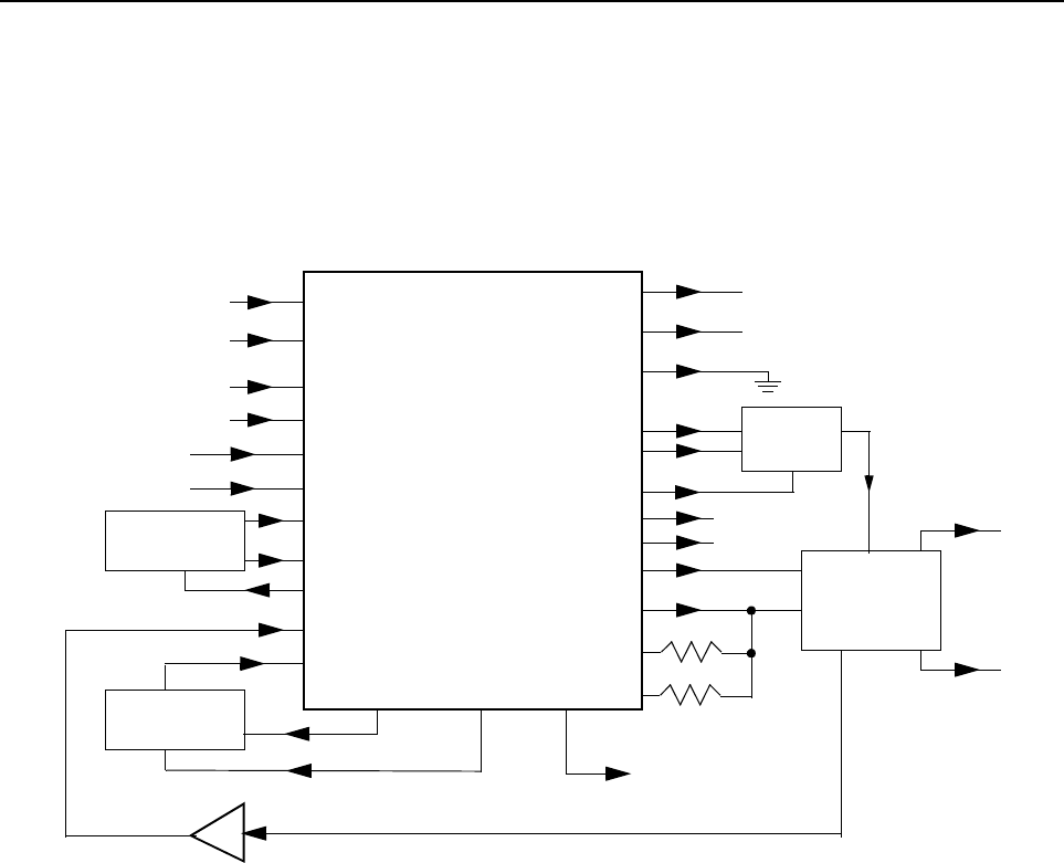
Frequency Synthesis 2-7
4.0 Frequency Synthesis
The frequency synthesizer subsystem, shown in Figure 2-3, consists of the reference oscillator
crystal (Y1201), the Low Voltage Fractional-N synthesizer (LVFRAC-N, U1201), and the receive and
transmit VCOs and buffers (Q1303 through Q1308 and associated components).
Figure 2-3 Low Band Synthesizer Block Diagram
4.1 Fractional-N Synthesizer
The LVFRAC-N synthesizer IC (U1201) consists of a reference oscillator, pre-scaler, a
programmable loop divider, control divider logic, phase detector, a charge pump, A/D converter for
low frequency digital modulation, a balance attenuator to balance the high frequency analog
modulation and low frequency digital modulation, a 13V positive voltage multiplier, a serial interface
for control, and finally a super filter for the regulated 9.3 volt supply.
Regulated 9.3 volts DC applied to the super filter input (U1201, pin 30) delivers a very low noise
output voltage of 8.3 volts DC (VSF) at pin 28. External device Q1201 allows greater current
sourcing capability. The VSF source supplies the receive and transmit VCOs and first buffer stages.
The synthesizer IC supply voltage is provided by a dedicated 5V regulator (U1250) to minimize
power supply noise.
In order to generate a high voltage to supply the phase detector (charge pump) output stage at pin
VCP (U1201 pin 47), a capacitive voltage multiplier circuit (CR1202 and C1209) generates a voltage
DATA
CLK
CEX
MODIN
SFIN
XTAL1
XTAL2
WARP
PREIN
VCP
REFERENCE
OSCILLATOR
VOLTAGE
MULTIPLIER
DATA (U0101 PIN 100)
CLOCK (U0101 PIN 1)
CSX (U0101 PIN 2)
MOD IN (U0221 PIN 40)
9,3V (U641 PIN 5)
7
8
9
10
30
23
24
25
32
47
VMULT2 VMULT1
BIAS1
SFOUT
AUX3
AUX4
IADAPT
IOUT
GND
FREFOUT
LOCK 4
19
6, 22, 33, 44
43
45
3
2
28
14 15
40
FILTERED 8,3V
STEERING
LOCK (U0101 PIN 56)
PRESCALER IN
FREF (U0221 PIN 34)
39
BIAS2
41
48
5, 13, 20, 34, 36
+5V (U3211 PIN 1)
AUX1
VDD, DC5V MODOUT
U1201
LOW VOLTAGE
FRACTIONAL-N
SYNTHESIZER
AUX2
TX RF INJECTION
(1ST STAGE OF PA)
LO RF INJECTION
VOLTAGE
CONTROLLED
OSCILLATOR
LINE
2-POLE
LOOP
FILTER
1
Q1202
BUFFER
BWSELECT
VCTRL
N.C.
N.C.
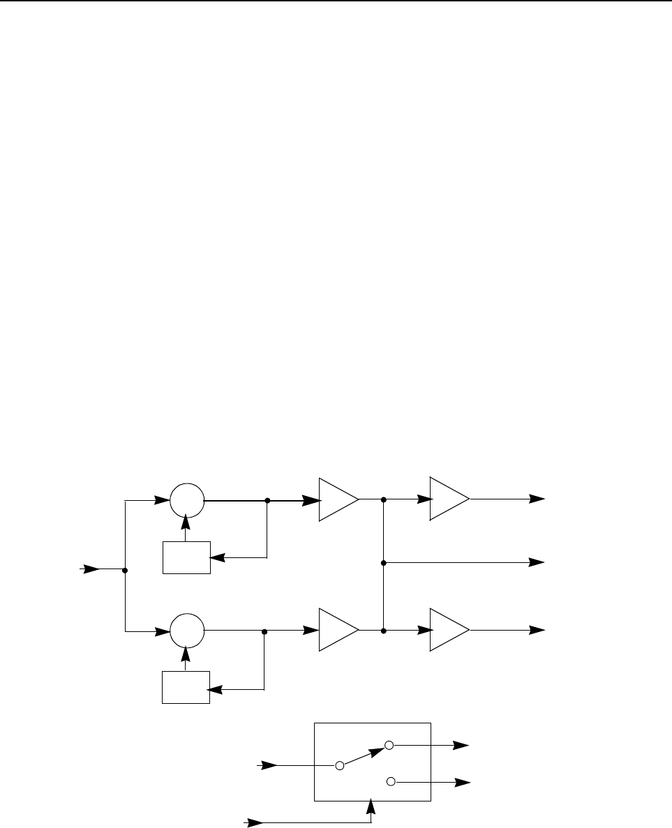
2-8 Frequency Synthesis
of 13 volts DC. This multiplier is driven by two 1.05 MHz clock signals from U1201 pins 15 and 14
(VMULTI1 and VMULTI2) which are 180 degree out of phase.
Output LOCK (U1201-4) provides information about the lock status of the synthesizer loop. A high
level at this output indicates a stable loop. A buffered output of the 16.8 MHz reference frequency is
provided at pin 19.
The operating frequency of the synthesizer is loaded serially from the microprocessor via the data
line (DATA, U1201-7), clock line (CLK, U1201-8) and chip select line (CSX, U1201-9).
The reference oscillator circuit within U1201 uses an external 16.8 MHz crystal (Y1201). Varactor
CR1201 allows software-controlled frequency adjustments (warp) and temperature compensation of
the oscillator frequency. Warp adjustment is performed using serial data from the microprocessor.
This controls the setting of an A/D converter, with its output (WARP, pin 25) applied to CR1201.
4.2 Voltage Controlled Oscillator (VCO) and Buffers
Separate voltage controlled oscillator (VCO) and buffer circuits, shown in Figure 2-4, are used for
receiver injection and transmitter carrier frequency generation. Since the receiver uses high-side
injection, the receiver VCO frequency range is 10.7 MHz above the transmit VCO range. The VCO/
buffers are bandsplit into three ranges depending on radio model, covering radio operating
frequencies of 29.7 to 36.0 MHz, 36.0 to 42.0 MHz, or 42.0 to 50.0 MHz. The corresponding three
frequency ranges from the receive VCO are 40.4 to 46.7 MHz, 46.7 to 52.7 MHz, and 52.7 to 60.7
MHz.
Figure 2-4 Low Band VCO Block Diagram
STEERING
LINE
(VCTRL)
RXVCO
Q1303
Q1306
TXVCO
AGC
AGC
Q1304
Q1307 Q1308
Q1305
BUFFER BUFFER
BUFFER
BUFFER
1ST RX 2ND RX
2ND TX
1ST TX
TXINJ
RXINJ
TO Q1202
PRESCALER BUFFER
(TO 1ST MIXER)
(TO U1401 PIN16)
SFOUT
(U1201 PIN28)
U1377-8
DC SWITCH
RX (TO Q1303-5)
TX (TO Q1306-8)
(U1201 PIN2)
~
~

Frequency Synthesis 2-9
The VCOs, together with Fractional-N synthesizer U1201, generates the required frequencies for
transmit and receive modes. The TRB line (U1201, pin 2) determines which VCO/buffer circuit is to
be enabled. A high level on TRB will turn on the transistors in U1378 to turn on via R1376, applying
the 8.3 volt VSF source to the receiver VCO and first buffer. The second buffer in each string
operates from the 9V3 source and become active when RF is applied to their inputs.
The RF signal at the bases of the second buffers are combined and fed back to the Fractional-N
synthesizer via PRE_IN where it is compared to the reference frequency as described below in
“Synthesizer Operation”. The Fractional-N IC provides a DC steering voltage VCTRL to adjust and
maintain the VCO at the correct frequency.
With a steering voltage from 2.5V to 11V at the appropriate varactor diode (CR1302 for the RX
VCO, or CR1310 for the TX VCO), the full VCO tuning range is obtained. Each VCO uses and AGC
circuit to maintain a constant VCO output level across the frequency band. A diode (CR1306 in the
receive VCO, or CR1314 in the transmit VCO) is configured as a voltage doubler which rectifies the
RF level sampled at the VCO drain and applies a proportional negative DC voltage to the VCO gate.
Increased RF level reduces the VCO gain to compensate.
The VCO output is taken from the source and applied to the first buffer transistor (Q1304 receive,
Q1307 transmit). The first buffer output is further amplified by the second buffer transistor (Q1305
receive, Q1308 transmit) before being applied to the receiver first mixer or transmitter first stage
input.
In TX mode the modulation signal coming from the LVFRAC-N synthesizer IC (MODOUT, U1201
pin 41) is superimposed on the DC steering line voltage by capacitive divider C1215, C1208 and
C1212, causing modulation of the TX VCO using the same varactor as used for frequency control.
4.3 Synthesizer Operation
The complete synthesizer subsystem comprises mainly of low voltage LVFRAC-N synthesizer IC,
Reference Oscillator (crystal oscillator with temperature compensation), charge pump circuitry, loop
filter circuitry, and voltage controlled-controlled oscillators and buffers. A sample of the VCO
operating signal PRE_IN is amplified by feedback buffer Q1202, low-pass filtered by L1205, C1222
and C1224, and fed to U1201 pin 32 (PREIN).
The pre-scaler in the synthesizer (U1201) is basically a dual modulus pre-scaler with selectable
divider ratios. The divider ratio of the pre-scaler is controlled by the loop divider, which in turn
receives its inputs via the serial interface to the microprocessor. The output of the pre-scaler is
applied to the loop divider. The output of the loop divider is connected to the phase detector, which
compares the loop divider´s output signal with the reference signal.The reference signal is
generated by dividing down the signal of the reference oscillator, whose frequency is controlled by
Y1201.
The output signal of the phase detector is a pulsed DC signal which is routed to the charge pump.
The charge pump outputs a current at pin 43 of U1201 (IOUT). The loop filter (consisting of R1205-
6, R1208, and C1212-14) transforms this current into a voltage that is applied to varactor diodes
(CR1310 for transmit, CR1302, for receive) and alters the output frequency of the appropriate
VCO.The current can be set to a value fixed in the LVFRAC-N IC or to a value determined by the
currents flowing into BIAS 1 (U1201-40) or BIAS 2 (U1201-39). The currents are set by the value of
R1211 or R1207 respectively. The selection of the three different bias sources is done by software
programming.

2-10 Frequency Synthesis
To reduce synthesizer lock time when new frequency data has been loaded into the synthesizer the
magnitude of the loop current is increased by enabling the IADAPT (U1201-45) for a certain
software programmable time (Adapt Mode). The adapt mode timer is started by a low to high
transient of the CSX line. When the synthesizer is within the lock range, the current is determined
only by the resistors connected to BIAS 1, BIAS 2, or the internal current source. A settled
synthesizer loop is indicated by a high level of signal LOCK (U1201-4).
In order to modulate the PLL the two-spot modulation method is utilized. Via pin 10 (MODIN) on
U1201, the audio signal is applied to both the A/D converter (low frequency path) and the balanced
attenuator (high frequency path). The A/D converter converts the low frequency analog modulating
signal into a digital code that is applied to the loop divider, thereby causing the carrier to deviate.
The balance attenuator is used to adjust the VCO’s deviation sensitivity to high frequency
modulating signals. The output of the balance attenuator is present at the MODOUT port (U1201-
41) and superimposed on the VCO steering line voltage by a divider consisting of C1215, C1208
and C1212.
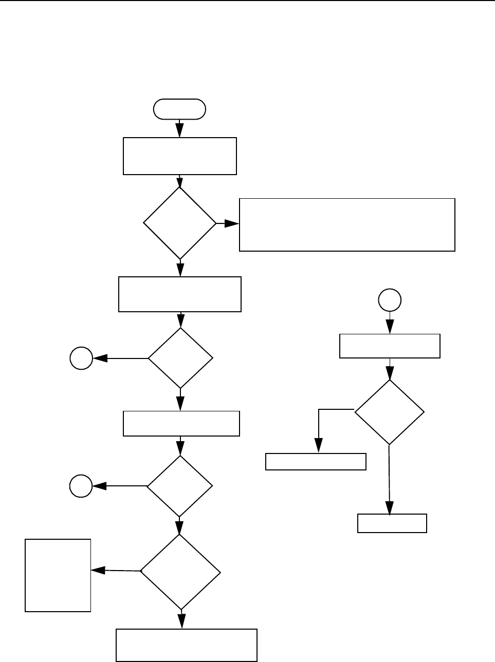
3-1
Section 3
TROUBLESHOOTING CHARTS
1.0 Troubleshooting Flow Chart for Receiver (Sheet 1 of 2)
Bad SINAD
Bad 20dB Quieting
No Recovered Audio
START
Audio at pin 8
of U1103? Check Controller (in the case of no audio).
Or else go to “B”
Yes
No
Spray or inject 10.7MHz
into XTAL Filter FL1102.
Audio heard?
BYes
No
Check 2nd LO
(10.245MHz) at C1129.
LO present?
BYes
Check volt-
ages on
U1103. OK?
Biasing OK?
No
No
A
Yes
Check Q1106 bias
for faults.
Replace Q1106.
Go to B
Yes
No
Check cir-
cuitry around
U1103.
Replace
U1103 if
defect.
Check circuitry around Y1101.
Replace Y1101 if defect.
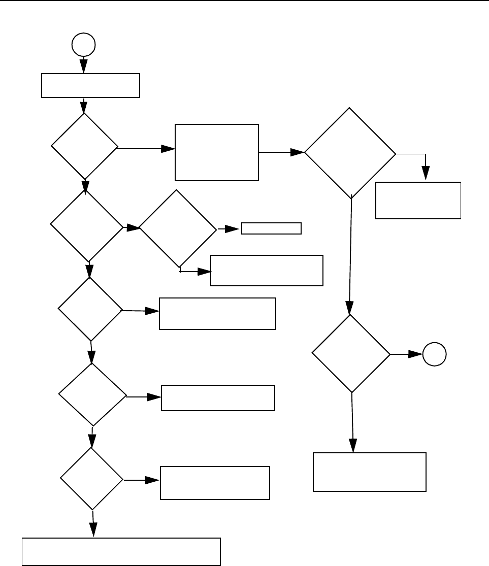
3-2 Troubleshooting Flow Chart for Receiver (Sheet 1 of 2)
1.1 Troubleshooting Flow Chart for Receiver (Sheet 2 of 2)
IF Signal at
pin 2 of
U1051
No
RF Signal
at pin 3 of
U1051?
RF Signal at
C1017?
No
RF Signal at
C1013?
No
RF Signal at
C1002?
No or
Check harmonic filters J1401 and ant.switch
Check preselector and RF
amp.
Inject RF into J1401
No
Yes
Check RF amp (Q1001)
Stage.
Check filter between C1017
& mixer U1051
Yes
Check for detailed mixer.
Yes
1st LO level
OK?
Locked?
Yes
Check FGU
Yes
Trace IF signal from
C1036 to Q1106.
Check for bad
XTAL filter.
No
Yes IF signal at
Q1106 collec-
tor?
Before replacing
U1103, check
U1103 voltages.
Yes
Is 9V3 present?
Check Supply Voltage cir-
cuitry. Check U0681,
U3211 and U0641.
No
No
Yes
A
B
weak RF
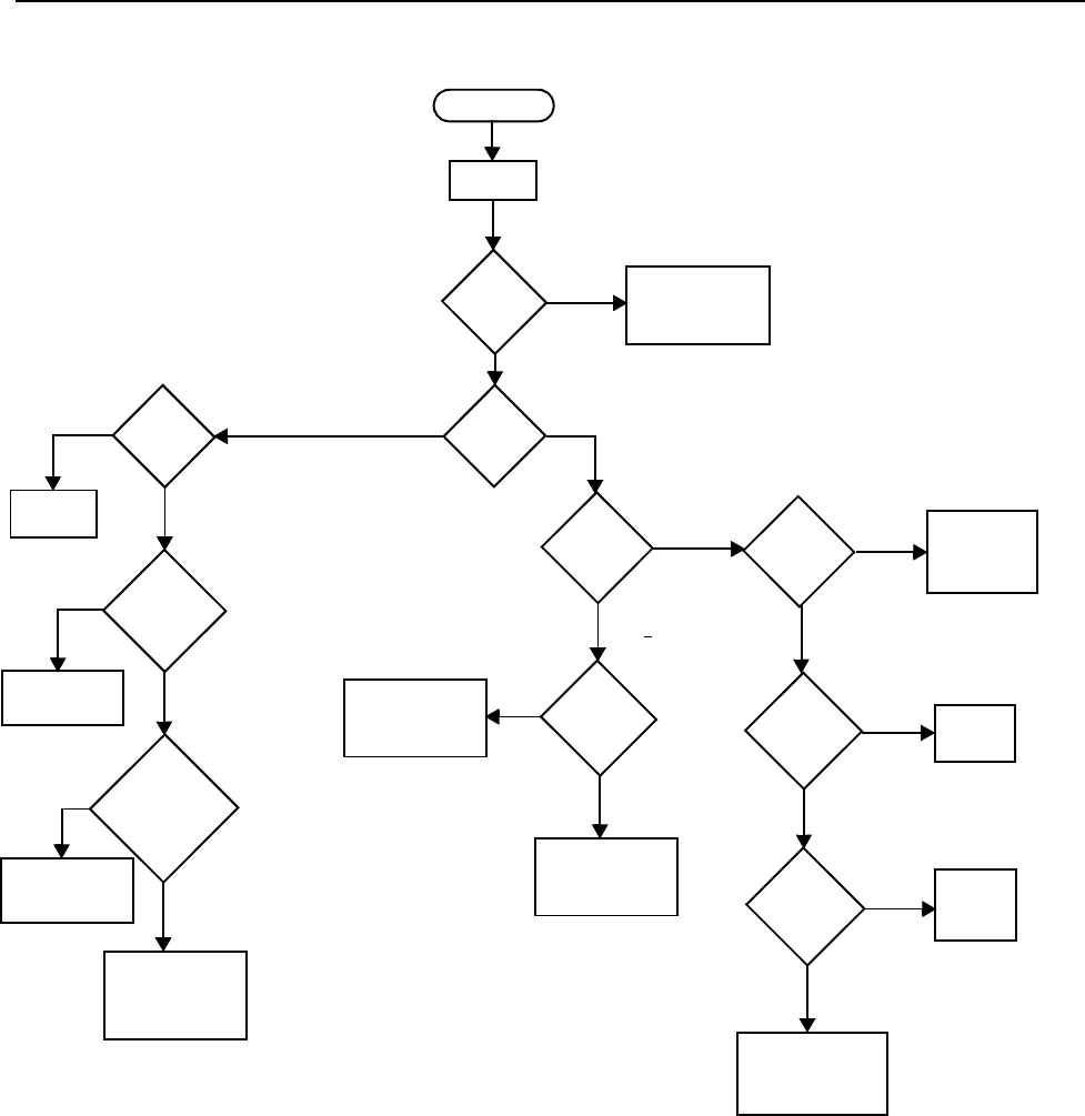
Troubleshooting Flow Chart for Transmitter 3-3
2.0 Troubleshooting Flow Chart for Transmitter
No
DC Voltage
@ Gate of
Q1401
No
Yes
START
No or Low
TX
DC Voltage
@Drains of
Q1402 &
Q1403
@ Cathode of
D1401 &
D1402
DC Voltage
Drains of Q1402 &
AC Voltages @
Q1403 both sine or
both distorted
Check 9T1 and
Diode Bias Circuit
Verify RF Continuity
to gates of
Q1402 & Q1403
Check circuitry
between Q1402 &
Q1403 and
Antenna Port
Check
MOSBIAS_1
Supply and
Feed Network
No
<<18V pp
Yes
No
Yes
< 1 A
No
Check
Q1401
Device
Yes
CURRENT
RF @
Junction
R1413 & R1414
DC Voltage
@ TP1402 &
TP1403
Yes
Check
MOSBIAS_2
MOSBIAS_3
and Feed Networks
Check DC/AC
Gate Circuits
of Q1402 & Q1403
Check Supply Feed
and/or PowerControl
Circuits.
No
>18V pp
Check
U1401
Device
AC Voltage
@ Gate of
Q1401
Yes
DC Voltage
@ U1401
Yes
No
Power Out
> 1 A
Look for
short on
Supply Line
Check Pressure Pad
and/or
Switch Circuitry
Yes
No
TX
Safefy
Switch
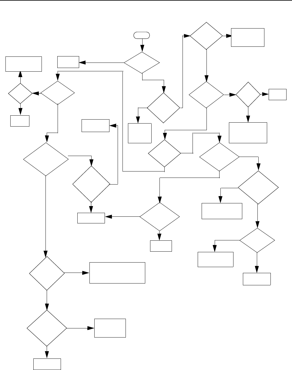
3-4 Troubleshooting Flow Chart for Synthesizer
3.0 Troubleshooting Flow Chart for Synthesizer
5V
at pin 6 of
CR1202
Is information
from uP U0101
correct?
Is U1201 Pin 47
at = 13VDC
Is U1377, Pin 2
<.1VDC in RX &
>4.5 VDC in TX? (at
VCO section)
Start
Visual
check of the
Board OK?
Correct
Problem
Check 9.3V
Regulator
U0641
+9.3V at
U1201
Pin 30?
Is 16.8MHz
Signal at
U1201 Pin 19?
Check Y1201, C1204,
C1206,C1207,
CR1201. & R1203
Are signals
at Pin’s 14 &
15 of U1201?
Check
R1218 Check C3319
Is U1201 pin 2>4.5
VDC in Tx & <.1
VDC in Rx
Replace U1201
Remove
Shorts
Is there a short
between Pin 47 and
Pins 14 & 15 of
U1201?
Replace or
resolder
necessary
components
Is RF level at
U1201, Pin 32
-5 < x < 0 dBm?
Are R1205, R1206,
R1208, C1212,
C1213 & C1214 OK?
Replace
U1201
If Q1202 Feedback Amp stage is
OK, Then see VCO troubleshoot-
ing chart
Are Waveforms
at Pins 14 & 15
triangular?
Do Pins 7,8 & 9
of U1201 toggle
when channel is
changed?
Check programming
lines between U0101
and U1201 Pins 7,8 & 9
Replace U1201
Check uP U0101
Troubleshooting
Chart
NO
YES
NO
YES
NO
YES
NO
NO
NO
YES
YES
NO
YES
YES
NO
YES
YES
YES
NO
NO
NO
NO
YES
NO
YES
YES
Check D3201, C3203,
C3205, & C3206
5V at U1201
pins 5, 13, 20,
24 & 36
Check 5V Reg-
ulator U1250, L1201
& R1201
Is
16.8MHz
signal at
U1201 pin
23?
Replace
U1201
YES
NO
NO
YES
NO
YES
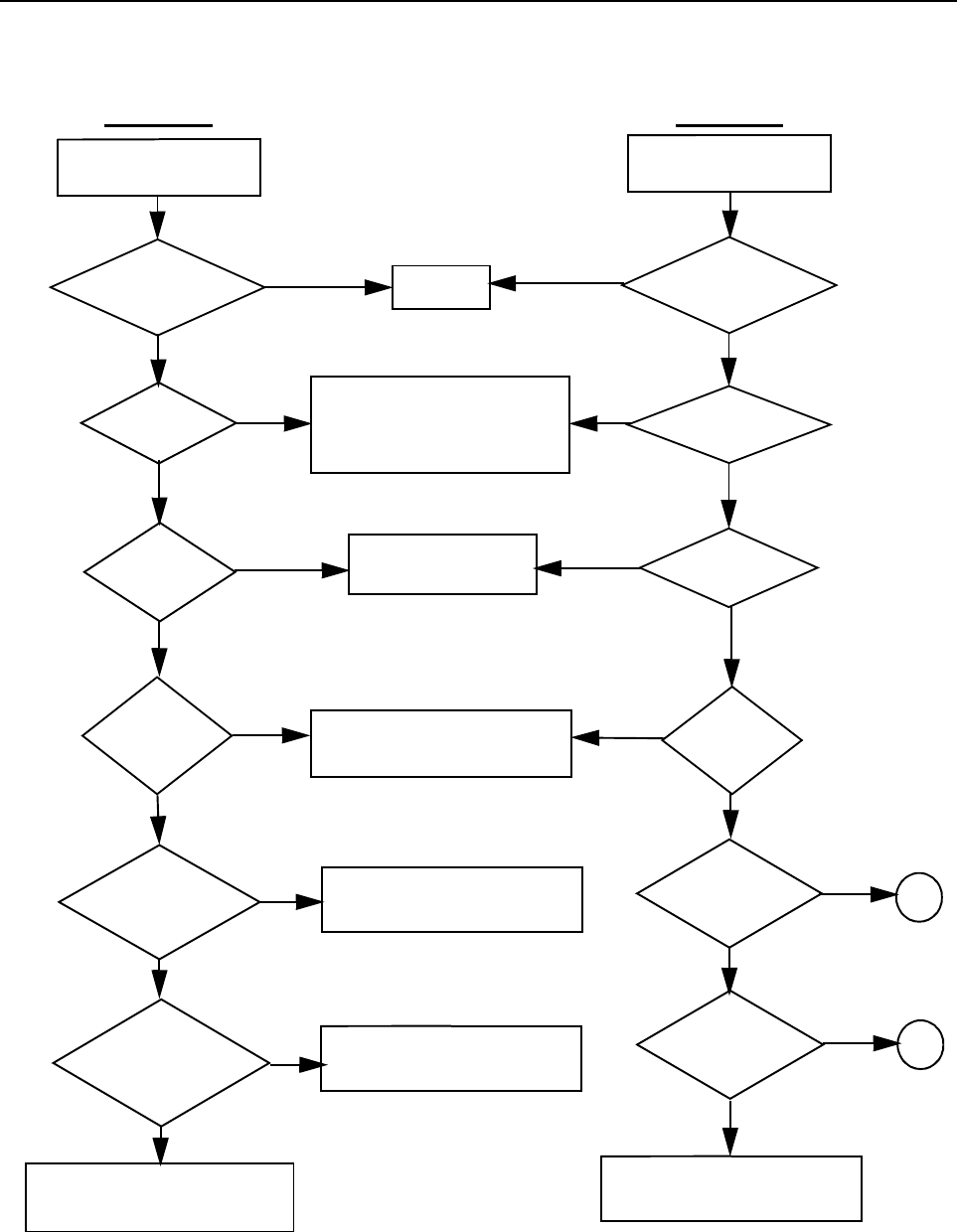
Troubleshooting Flow Chart for VCO 3-5
4.0 Troubleshooting Flow Chart for VCO
LOW OR NO RF SIGNAL
AT U1051
VISUAL CHECK
OF BOARD
OK?
8.5V DC AT
U1378 PIN 3
<,1 V DC AT
U1377 PIN 2
8.5V DC AT
U1378 PIN 4
CORRECT
PROBLEM
NO
YES
MAKE SURE SYNTHESIZER IS
WORKING CORRECTLY AND
RUNNER BETWEEN U1201 PIN
3 of U1377 & U1378.
CHECK RUNNER
BETWEEN U1201 PIN 2
AND U1377 PIN 2
IS RF AVAILABLE
AT BASE OF Q1304
TROUBLESHOOT Q1303
OSCILLATOR STAGE CIRCUITRY
IS RF AVAILABLE
CHECK PARTS BETWEEN U1051
NO
NO
NO
NO
NO
YES
YES
YES
YES
YES
RX VCO
LOW OR NO RF SIGNAL
AT INPUT TO PA
VISUAL CHECK
OF BOARD
OK?
8.5V DC AT
U1378 PIN 3
4.5V DC AT
U1377 PIN 2
8.5V DC AT
U1377 PIN 4
IS RF AVAILABLE
AT BASE OF Q1307
YES
YES
YES
YES
YES
NO
NO
NO
NO
NO
TX VCO
AND Q1305
AT BASE Q1305 TROUBLESHOOT Q1304
BUFFER STAGE CIRCUITRY
MAKE SURE U1377 AND U1378
ARE WORKING CORRECTLY.
IS RF AVAILABLE
AT BASE OF Q1308
A
B
NO
YES
CHECK PARTS BETWEEN
U1401 AND Q1308

3-6 Troubleshooting Flow Chart for VCO
THIS PAGE INTENTIONALLY LEFT BLANK
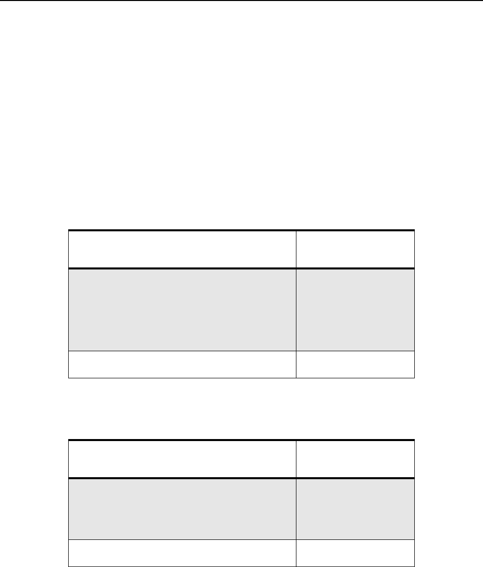
4-1
Section 4
LOW BAND PCBS/SCHEMATICS/PARTS LISTS
1.0 Allocation of Schematics and Circuit Boards
1.1 Controller Circuits
The Low Band circuits are contained on the Printed Circuit Board (PCB) which also contains the
Controller circuits. This Chapter shows the schematics for the Low Band circuits only, refer to the
Controller section for details of the related Controller circuits . The PCB component layouts and the
Parts Lists in this Chapter show both the Controller and Low Band circuit components. The Low
Band schematics and the related PCB and parts list are shown in the tables below.
Table 4-1 Low Band Range 1 (29.7-36.0MHz) Diagrams and Parts Lists
PCB : 8486206B06 Main Board Top Side
8486206B06 Main Board Bottom Side Page 4-3
Page 4-4
SCHEMATICS
Power Amplifier 40 - 60W
FRACN
Voltage Controlled Oscillator
Receiver Front End
Controller - T6
IO - T6
Page 4-15 and Page 4-16
Page 4-9
Page 4-12
Page 4-21
Page 4-24
Page 4-26
Parts List
8486206B06 Page 4-33
Table 4-2 Low Band Range 2 (36-42 MHz) Diagrams and Parts Lists
PCB : 8486207B05 Main Board Top Side
8486207B05 Main Board Bottom Side Page 4-5
Page 4-6
SCHEMATICS
Power Amplifier 40 - 60W
Voltage Controlled Oscillator
Receiver Front End
FRACN
Page 4-17 and Page 4-18
Page 4-13
Page 4-22
Page 4-10
Parts List
8486207B05 Page 4-39

4-2 Allocation of Schematics and Circuit Boards
Table 4-3 Low Band Range 3 (42-50MHz) Diagrams and Parts Lists
PCB : 848608Z02 Main Board Top Side
848608Z02 Main Board Bottom Side Page 4-7
Page 4-8
SCHEMATICS
Power Amplifier 40 - 60W
Voltage Controlled Oscillator
Receiver Front End
Controller - T9
FRACN
IO - T9
Page 4-19 and Page 4-20
Page 4-14
Page 4-23
Page 4-25
Page 4-11
Page 4-27
Parts List
848608Z02 Page 4-44
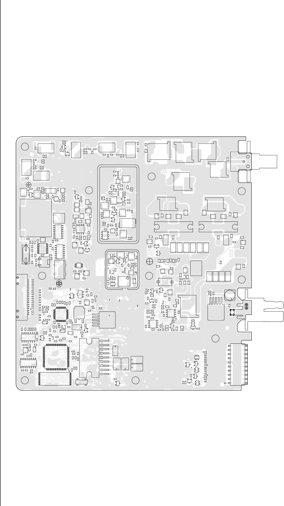
Low Band PCBs / Schematics / Parts Lists 4-3
2.0 Low Band PCBs / Schematics / Parts Lists
C0101 C0102
C0104
C0105
C0106
C0107
C0121
C0131
C0132
C0211
C0212
C0221 C0222
C0223
C0225
C0226
C0227
C0228
C0231
C0232
C0233
C0234 C0235
C0236
C0237
C0241
C0242
C0243
C0244
C0245
C0246
C0251
C0252
C0253
C0254
C0255
C0256
C0261
C0262
C0275
C0290
C0291
C0292 C0293
C0331
C0401
C0441
C0442
C0443
C0445
C0446
C0447
C0448
C0449
C0451
C0452
C0453
C0455
C0456
C0457
C0458
C0459
C0460
C0461
C0462
C0463
C0464
C0466
C0467
C0468
C0470
C0471
C0472
C0473
C0474
C0476
C0477
C0478
C0482
C0483
C0484
C0486 C0487
C0488
C0490
C0493
C0494
C0495
C0496
C0501
C0502
C0503
C0504
C0505
C0506
C0508
C0509
C0510
C0511
C0512
C0513
C0514
C0515
C0516
C0517
C0518
C0601
C0603
C0612
C0651
C0652
C0654
C0655
C0681
C1001 C1002
C1003
C1004
C1006
C1007
C1008
C1009
C1010
C1011
C1012
C1015
C1019
C1020
C1021
C1022
C1023
C1024
C1025
C1037
C1038
C1039
C1040
C1041
C1042
C1101
C1103
C1106
C1107
C1109
C1110
C1111
C1125
C1129 C1130
C1131
C1133
C1134
C1136
C1137
C1138
C1139
C1141
C1142
C1145
C1149
C1153
C1212
C1213
C1214
C1215
C1216
C1217
C1218
C1224
C1225
C1226
C1227
C1228
C1229
C1230
C1250
C1251
C1252
C1253
C1254
C1304
C1305
C1306
C1307
C1308
C1309
C1311
C1312
C1314
C1315
C1316
C1340
C1344
C1345
C1346
C1347
C1348
C1349
C1350
C1351
C1352
C1356
C1360
C1403
C1404
C1405
C1406
C1407
C1408
C1410
C1414
C1419
C1420
C1421
C1422
C1423
C1424
C1425
C1426
C1427
C1428 C1429
C1430
C1431
C1432
C1433
C1434
C1435
C1436
C1468
C1473
C1475
C1477
C1478
C1482
C1484
C1485
C1501
C1505
C1510
C1511
C1512
C1525
C1526
C1527
C1528
C1529
C1530
C1531
C1601
C1602
C1603
C1604
C1605
C1618
C1619
C1620 C1621
C1622
C1623
C1624
C1628
C1631
C1633
CR1202
5
8
14
CR1302
CR1306
D0201
D0651
D1001
D1501
D1502
D1601
E1401
FL1101
IN
GNDA
GNDB
OUT
FL1102
FL1104
43
2
FL1106
18
1
J0451
20
11
10
J0501
J0601
3
2
J1401
L0481
L0482
L1001
L1003
L1005
L1006
L1008
L1010
L1101
L1103
L1104
L1107
L1112
L1204
L1206
L1207
L1302
L1303
L1304
L1305
L1306 L1318
L1321
L1322
L1324
L1402
L1403
L1406
L1413
L1414
L1418
L1420
L1421
L1422
L1423
L1601
L1602
L1603
L1604
L1606
L1607
M1401
Q0110
Q0177
Q0181
Q0185
Q0681
Q1001
Q1102
Q1201
Q1303
Q1307
Q1308
2
3
4
5
6
7
8
Q1402
2
3
4
5
6
7
8
Q1403
Q1501
Q1502
Q1504
Q1505
Q1601
Q1609
R0101
R0102
R0104
R0105
R0106
R0108
R0110
R0114
R0115
R0116
R0131
R0132
R0170
R0181
R0182
R0186
R0211
R 0212
R0220
R0221
R0222
R0223
R0224
R0225
R0226
R0227
R0228
R0229
R0241
R0242
R0251
R0252
R0253
R0256
R0261
R0262
R0269
R0343
R0441
R0510
R0533
R0651
R0652 R0681
R0682
R1001
R1002
R1003
R1010
R1011
R1101
R1102
R1108
R1110
R1113
R1114
R1122
R1123
R1127
R1131
R1136
R1137
R1204
R1205
R1206
R1207
R1208
R1209R1210
R1211
R1216
R1217
R1218 R1219
R1220
R1306
R1307 R1308
R1309
R1311
R1331
R1332
R1333
R1334
R1335
R1336
R1337
R1338
R1339
R1344 R1345
R1346
R1347
R1402
R1404
R1405
R1406
R1407
R1411
R1413
R1415
R1417
R1419
R1421
R1423
R1425
R1444
R1445
R1446
R1447
R1448 R1449R1457
R1463
R1464
R1465
R1466
R1467 R1468
R1471
R1472
R1473
R1474
R1475
R1476
R1477
R1478
R1479
R1481
R1482
R1483
R1484
R1501
R1502
R1503
R1504
R1507
R1510
R1514
R1516
R1517
R1518
R1519
R1524
R1525
R1526
R1527
R1528
R1532
R1533
R1537
R1541
R1601
R1602
R1604
R1626
R1627
R1628
R1629
R1630
R1638
SH1201
SH1301
1
76
51
26
U0101
32
17
16 1
U0121
8
7
114
U0211
137
25
13
U0221
16
1
89
U0251
9
U0271
1
6
5
U0611
1
6
5
U0641
3
2
1
U0651
8
71
14
U1101
8
71
14
U1102
11
1
20
10
U1103
4
58
U1250
4
3U1377
1
4
58
U1402
U1501
1
4
58
U1502
1
4
5
8
U1601
VR0501
VR0503 VR0504
VR0505VR0510
23
4
Y0131
Y1101
2
Y1102
1
1
1
1
1
1
ZWG0130593-O
Low Band Range 1 (29.7-36.0 MHz) 8486206B06 Top Side
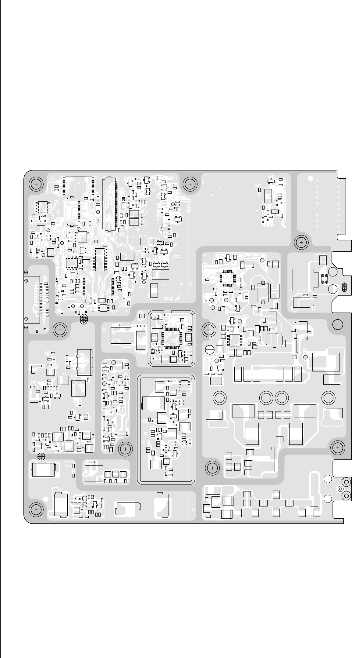
4-4 Low Band PCBs / Schematics / Parts Lists
C0103
C0111
C0112
C0122
C0123
C0141
C0151
C0201
C0202
C0203 C0204
C0205
C0224
C0265
C0266 C0267
C0271
C0272
C0273
C0274
C0276 C0277
C0301
C0302
C0303
C0304
C0305
C0324 C0325
C0341
C0342
C0343
C0344
C0351
C0352
C0353
C0354
C0402
C0403
C0406
C0407
C0408
C0409
C0410
C0411
C0421
C0422
C0423
C0426
C0427
C0428
C0429
C0430
C0431
C0485
C0491
C0492
C0497
C0499
C0541
C0542
C0554
C0558
C0559
C0560 C0575
C0576
C0591
C0592
C0593
C0611
C0621
C0622
C0641
C0644
C0645
C0661
C0662
C0663
C0671
C1013
C1014
C1016
C1017
C1026C1027
C1028
C1029
C1030
C1031
C1032
C1033
C1034
C1035
C1036
C1102
C1104
C1105
C1108
C1112
C1113
C1114
C1115
C1116 C1119
C1120
C1121
C1122
C1123
C1124
C1126
C1127
C1128
C1135
C1140
C1143
C1144
C1146
C1147
C1148
C1150 C1151
C1152
C1201
C1202
C1203
C1204
C1205
C1206
C1207
C1208
C1209 C1210
C1211
C1219
C1220
C1221
C1222
C1223
C1231
C1232
C1233
C1234
C1313
C1317
C1318
C1319
C1320
C1321
C1323
C1325
C1326 C1333
C1334
C1335
C1336
C1337
C1338
C1339
C1341
C1342
C1343
C1354
C1361
C1362
C1401
C1402
C1413
C1415
C1416
C1417
C1418
C1437
C1438
C1439
C1440
C1441
C1442
C1443
C1444
C1445
C1446
C1447
C1448
C1449
C1450
C1451
C1452
C1453
C1454
C1455
C1456
C1457
C1458
C1459
C1460
C1461
C1462
C1463
C1464
C1465
C1466
C1467
C1469
C1470
C1471
C1472
C1474
C1476
C1479
C1480
C1481
C1486
C1491
C1502
C1503
C1504
C1506
C1507
C1508
C1509
C1606
C1607
C1608
C1609
C1610
C1611
C1612
C1613
C1614
C1615
C1616
C1625
C1626
C1627
C1629 C1632
C1634
CR1201
58
1
4
CR1310
CR1314
D0101
D0151
D0179
D0301
D0621
D0660
D0661
D1101
D1401
D1402
D1503
E0271
E0272
E0631
E1403
F0401
FL1105
43
2
FL1107
12
J0401
1
40
J0551
1
18
J0552
L1002
L1004
L1007
L1009
L1011
L1012
L1013
L1014
L1102
L1105
L1106
L1108
L1109
L1110
L1111
L1201
L1202
L1205
L1307
L1309
L1310
L1311 L1313
L1314
L1315
L1316
L1317
L1401
L1404
L1405
L1408
L1415
L1416
L1417
L1419
L1424
L1425
L1426
L1605
Q0151
Q0171
Q0173
Q0183
Q0271
Q0641 Q0661
Q0662
Q0663
Q1002
Q1003
Q1101
Q1103
Q1104
Q1105
Q1106
Q1202
Q1304
Q1305
Q1306
1
2
3
Q1401
Q1404
Q1503
Q1506
Q1602
Q1603
Q1604
Q1605
Q1606
Q1607
Q1610
R0107
R0111
R0112
R0113
R0117 R0121
R0151
R0152
R0171
R0172
R0173
R0174
R0175
R0176
R0177 R0178
R0179
R0183R0184
R0185
R0201
R0202
R0203
R0204
R0205
R0206
R0207
R0208
R0254
R0255
R0257
R0265
R0266
R0267
R0268
R0273
R0274
R0275
R0276
R0323
R0324
R0331R0332
R0333
R0335
R0341
R0342
R0344
R0345 R0346
R0347
R0401
R0407 R0408
R0409
R0412
R0442
R0467
R0468
R0481 R0482
R0511
R0512
R0525
R0529
R0530
R0531 R0535 R0537
R0538
R0539
R0541
R0542
R0543
R0591
R0592
R0593
R0611
R0612
R0621
R0641
R0642
R0643
R0661
R0662
R0671
R0672
R1004
R1005
R1006
R1007
R1008
R1009 R1103
R1104
R1106
R1107
R1109
R1111
R1115
R1116
R1117 R1118
R1119
R1120
R1121
R1124
R1125
R1126
R1128
R1129
R1130
R1132R1133
R1134
R1135
R1138
R1139
R1201
R1202
R1203
R1212
R1213
R1214
R1215
R1221
R1222
R1312
R1313
R1314
R1315
R1316
R1317
R1318
R1319
R1320
R1325
R1326
R1327
R1328
R1330
R1340
R1341
R1342
R1343
R1376
R1409
R1410
R1412
R1414
R1416
R1418
R1420
R1422
R1424
R1440
R1441
R1442
R1443
R1450
R1451
R1453
R1454
R1455
R1458
R1459
R1460
R1469
R1470
R1480
R1505
R1506
R1508
R1509
R1511
R1512
R1513 R1515
R1522
R1523
R1535
R1542
R1543 R1544
R1545
R1605
R1606
R1607
R1608
R1609
R1610 R1611
R1612 R1613 R1614
R1615
R1616
R1617
R1620
R1621
R1622
R1631
R1632
R1633
R1635
R1636 R1637
S1501
SH1202
SH1302
TP0101
TP0102
TP0103
TP0104
TP0151
TP0221
TP0222
TP0492
TP0497
TP0530
TP0661
TP1201
TP1401
TP1402
TP1403
TP1501
TP1502
TP1503 TP1505
TP1601
TP1602
1
4
58
U0111
22
21 8
7
1
U0122
16
1
8
9
U0141
28 15
14
1
U0301
U0331
1
45
8
U0341
U0342
4
58
U0351
14
58
U0652
U0653
43
U1001
16
43
U1051
1
37
25 13
U1201
4
3
U1378
16
8
9
U1401
1
17
9
25
U1503
VR0151
VR0509
VR0537
VR0541
VR0601
VR0621
VR0671
Y1201
23
4
Y1202
1
1
1
1
1
8486206B06 T1
ZWG0130594-O
Low Band Range 1 (29.7-36.0 MHz) 8486206B06 Bottom Side
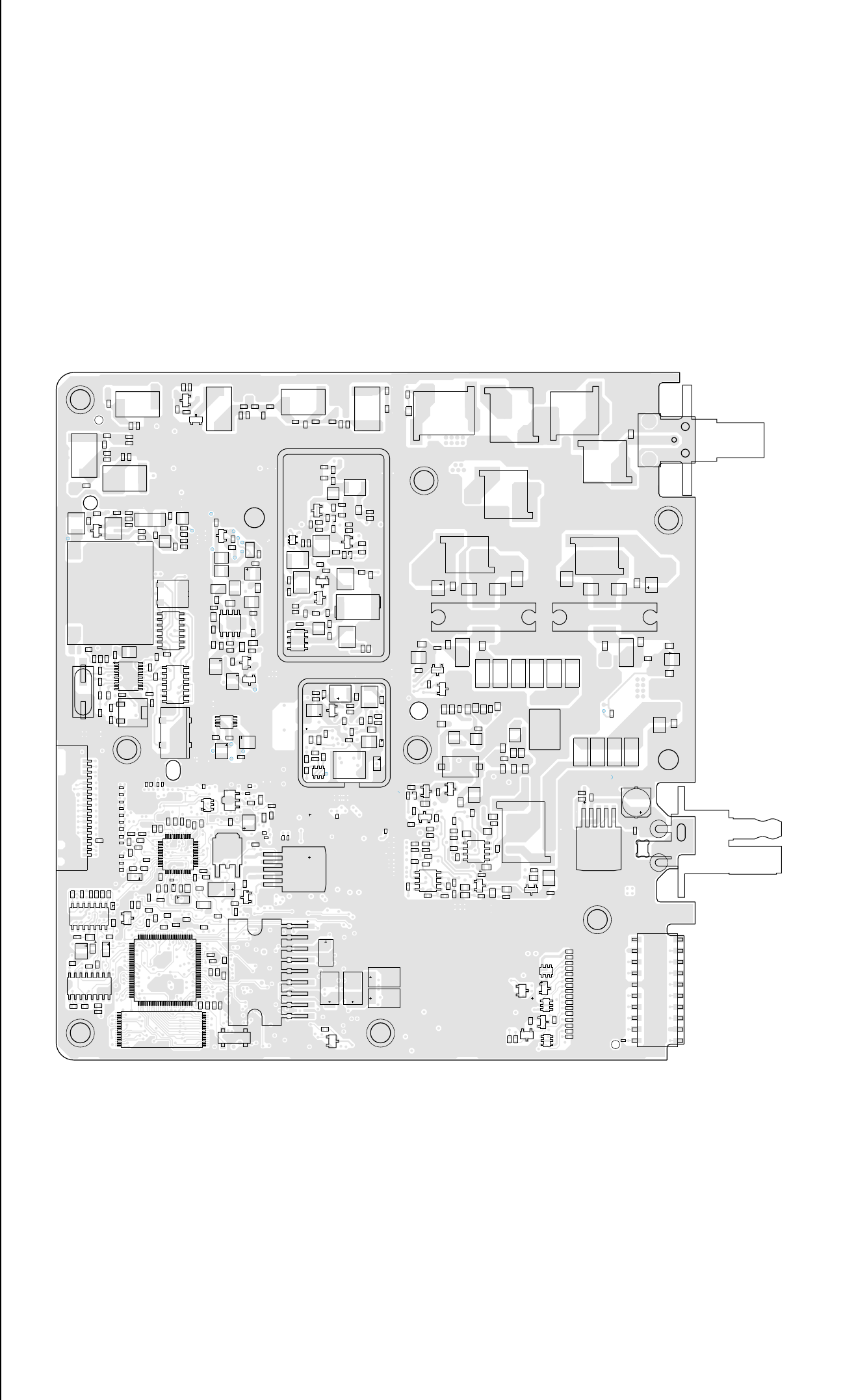
Low Band PCBs / Schematics / Parts Lists 4-5
1
1
C0101 C0102
C0104
C0105
C0106
C0107
C0121
C0131
C0132
C0211
C0212
C0221 C0222
C0223
C0225
C0226
C0227
C0228
C0231
C0232
C0233
C0234 C0235
C0236
C0237
C0241
C0242
C0243
C0244
C0245
C0246
C0251
C0252 C0253
C0254
C0255
C0256
C0261
C0262
C0275
C0290
C0291
C0292 C0293
C0331
C0441
C0442
C0443
C0445
C0446
C0447
C0448
C0449
C0470
C0471
C0472
C0473
C0474
C0476
C0477
C0478
C0482
C0483
C0484
C0486
C0487
C0488
C0490
C0493
C0494
C0495
C0496
C0501
C0502
C0503
C0504
C0505
C0506
C0508
C0509
C0510
C0511
C0512
C0513
C0514
C0515
C0516
C0517
C0518
C0601
C0603
C0612
C0651
C0652
C0654
C0655
C0681
C1001 C1002
C1003
C1004
C1006
C1007
C1008
C1009
C1010
C1011
C1012
C1015
C1019
C1020
C1021
C1022
C1023
C1024
C1025
C1037
C1038
C1039
C1040
C1041
C1042
C1101
C1103
C1106
C1107
C1109
C1110
C1111
C1125
C1129 C1130
C1131
C1133
C1134
C1136
C1137
C1138
C1139
C1141
C1142
C1145
C1149
C1153
C1212
C1213
C1214
C1215
C1216
C1217
C1218
C1224
C1225
C1226
C1227
C1228
C1229
C1230
C1250
C1251
C1252
C1253
C1254
C1304
C1305
C1306 C1307
C1308
C1309
C1311
C1312
C1314
C1315
C1316
C1340
C1344
C1345
C1346
C1347
C1348
C1349
C1350
C1351
C1352
C1356
C1360
C1403
C1404
C1405
C1406
C1407
C1408
C1410
C1414
C1419
C1420
C1421
C1422
C1423
C1424
C1425
C1426
C1427
C1428
C1429
C1430
C1431
C1432
C1433
C1434
C1435
C1436
C1468
C1473
C1475
C1477
C1478
C1482
C1484
C1485
C1501
C1505
C1510
C1511
C1512
C1525
C1526
C1527
C1528
C1529
C1530
C1531
C1532
C1601
C1602
C1603
C1604
C1605
C1618
C1619
C1620 C1621
C1622
C1623
C1624
C1628
C1631
C1633
CR1202
5
8
14
CR1302
CR1306
D0201
D0651
D1001
D1501
D1502
D1601
E1401
FL1101
IN
GNDA
GNDB
OUT
FL1102
FL1104
43
2
FL1106
18
1
J0451
2011
10
J0501
J0601
3
2
J1401
L0481
L0482
L1001
L1003
L1005
L1006
L1008
L1010
L1101
L1103
L1104
L1107
L1112
L1204
L1206
L1207
L1302
L1303
L1304
L1305
L1306
L1318
L1321
L1322
L1324
L1402
L1403
L1406
L1413
L1414
L1418
L1420
L1421
L1422
L1423
L1601
L1602
L1603
L1604
L1606
L1607
M1401
Q0110
Q0177
Q0181
Q0185
Q0681
Q1001
Q1102
Q1201
Q1303
Q1307
Q1308
2
3
4
5
6
7
8
Q1402
2
3
4
5
6
7
8
Q1403
Q1501
Q1502
Q1504
Q1505
Q1601
Q1609
R0101
R0102
R0104
R0105
R0106
R0108
R0110
R0114
R0115
R0116
R0131
R0132
R0170
R0181
R0182
R0186
R0211
R0212
R0220
R0221
R0222
R0223
R0224
R0225
R0226
R0227
R0228
R0229
R0241
R0242
R0251
R0252
R0253
R0256
R0261
R0262
R0269
R0343
R0441
R0508
R0510
R0533
R0651
R0652
R0681
R0682
R1001
R1002
R1003
R1010
R1011
R1101
R1102
R1108
R1110
R1113
R1122
R1123
R1127
R1131
R1136
R1137
R1204
R1205
R1206
R1207
R1208
R1209
R1210
R1211
R1216
R1217
R1218
R1219
R1220
R1306
R1307 R1308
R1309
R1311
R1331
R1332 R1333
R1334
R1335
R1336
R1337
R1338
R1339
R1344 R1345
R1346
R1347
R1402
R1404
R1405
R1406
R1407
R1411
R1413
R1415
R1417
R1419
R1421
R1423
R1425
R1444
R1445
R1446
R1447
R1448 R1449
R1457
R1463
R1464
R1465
R1466
R1467
R1468
R1471
R1472
R1473
R1474
R1475
R1476
R1477
R1478
R1479
R1481
R1482
R1483
R1484
R1501
R1502
R1503
R1504
R1507
R1510
R1514
R1516
R1517
R1518
R1519
R1524
R1525
R1526
R1527R1528
R1532
R1533
R1537
R1541
R1544
R1601
R1602
R1604
R1626
R1627
R1628
R1629
R1630
R1638
SH1201
SH1301
1
76
51
26
U0101
32
17
16 1
U0121
8
7
114
U0211
137
25
13
U0221
16
1
89
U0251
9
U0271
1
6
5
U0611
1
6
5
U0641
3
2
1
U0651
8
71
14
U1101
8
71
14
U1102
11
1
20
10
U1103
4
58
U1250
4
3
U1377
1
4
58
U1402
U1501
1
4
58
U1502
1
4
5
8
U1601
VR0501
VR0503 VR0504
VR0505 VR0510
23
4
Y0131
Y1101
2
Y1102
1
1
100
1
ZWG0131043-O
Low Band Range 1 (29.7-36.0 MHz) 8486206B08 Top Side
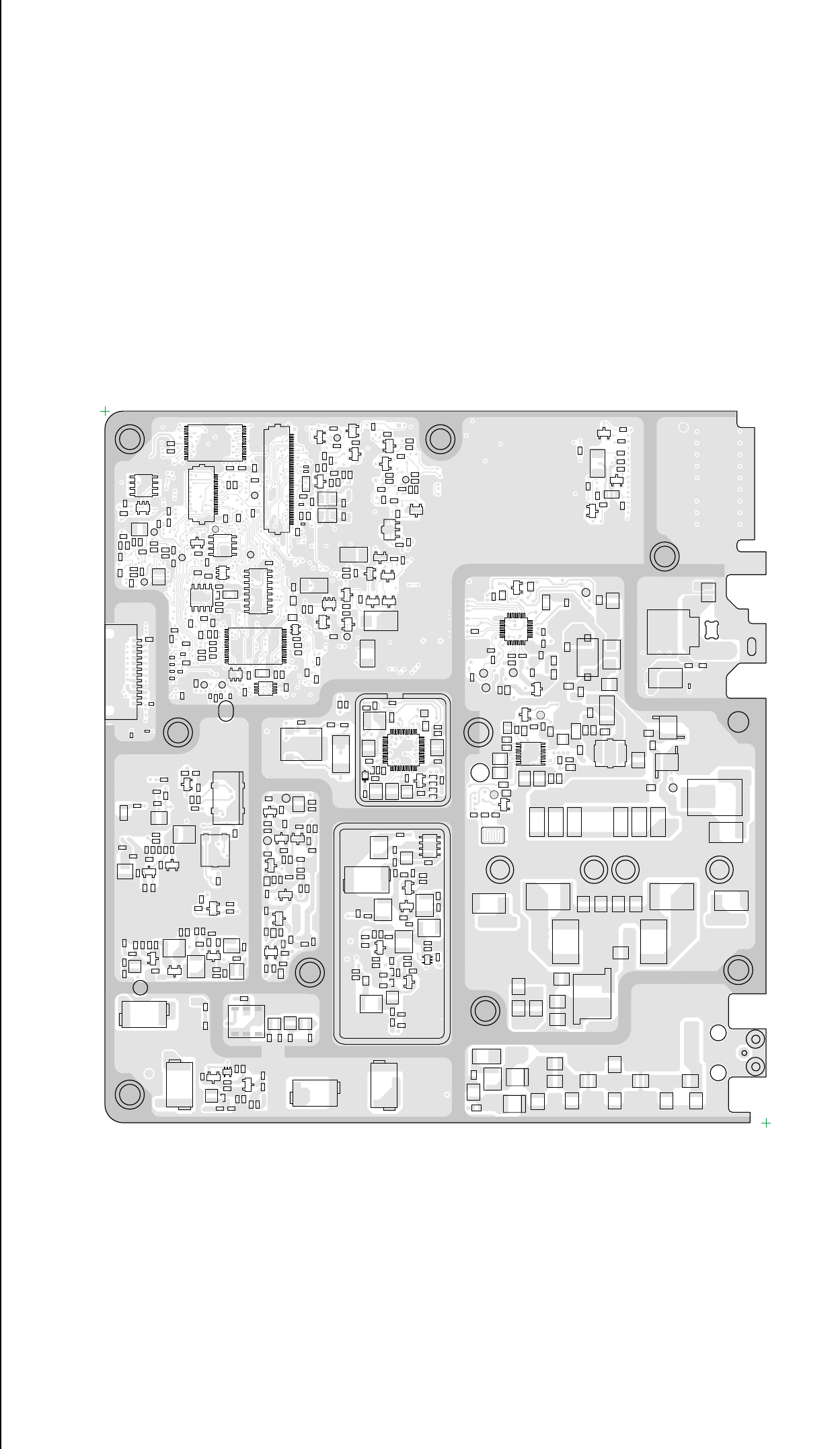
4-6 Low Band PCBs / Schematics / Parts Lists
C0103
C0108
C0111
C0112
C0122
C0123
C0141
C0151
C0201
C0202
C0203 C0204
C0205
C0224
C0265
C0266 C0267
C0271
C0272
C0273
C0274
C0276 C0277
C0301
C0302
C0303
C0304 C0305
C0324 C0325
C0341
C0342
C0343
C0344
C0351
C0352
C0353
C0354
C0421
C0422
C0423
C0426 C0427
C0428C0429 C0430
C0431
C0485
C0491
C0492
C0497
C0499
C0541
C0542
C0554
C0558
C0559C0560 C0575 C0576
C0591
C0592 C0593
C0611
C0621
C0622
C0641
C0644
C0645
C0661
C0662
C0663
C0671
C1013
C1014
C1016
C1017
C1026
C1027
C1028
C1029
C1030
C1031
C1032
C1033
C1034
C1035
C1036
C1102
C1104
C1105
C1108
C1112
C1113
C1114
C1115
C1116 C1119
C1120
C 1121
C1122
C 1123
C1124
C1126
C1127
C1128
C1135
C1140
C1143
C1144
C1146
C1147
C1148
C1150
C1151
C1152
C 1201
C1202
C1203
C1204
C1205
C1206
C1207
C1208
C1209 C1210
C1211
C1219
C1220
C1221
C1222
C1223
C1231
C1232
C1233
C1234
C1313
C1317
C1318
C1319
C1320
C1321
C1323
C1325
C1326 C1333
C1334
C1335
C1336
C1337
C1338
C1339
C1341
C1342
C1343
C1354
C1361
C1362
C1401
C 1402
C1413
C1415
C1416
C1417
C1418
C1437
C1438
C1439
C1440
C1441
C1442
C1443
C1444
C1445
C1446
C1447 C1448
C1449
C1450
C1451
C1452
C1453
C1454
C1455
C1456
C1457
C1458
C1459
C1460
C1461
C1462
C1463
C1464
C1465
C1466
C1467
C1469 C1470
C1471
C1472
C1474
C1476
C1479 C1480
C1481
C1486
C1491
C1502
C1503
C1504
C1506
C1507
C1508
C1509
C1606
C1607
C1608
C1609
C1610
C1611
C1612
C1613
C1614
C1615
C1616
C1625
C1626
C1627
C1629 C1632
C1634
CR1201
58
1
4
CR1310
CR1314
D0101
D0151
D0179
D0301
D0621
D0660 D0661
D1101
D1401
D1402
D1503
E0271 E0272
E0631
E1403
F0401
FL1105
4
3
2
FL1107
12
J0401
1
40
J0551
1
18
J0552
L1002
L1004
L1007
L1009
L1011
L1012
L1013
L1014
L1102
L1105
L1106
L1108
L1109
L1110
L1111
L1201
L1202
L1205
L1307
L1309
L1310
L1311 L1313
L1314
L1315
L1316
L1317
L1401
L1404
L1405
L1408
L1415
L1416
L1417
L1419
L1424
L1425
L1426
L1605
Q0151
Q0171
Q0173 Q0183
Q0271
Q0641
Q0661
Q0662
Q0663
Q1002
Q1003
Q1101
Q1103
Q1104
Q1105
Q1106
Q1107
Q1202
Q1304
Q1305
Q1306
1
2
3
Q1401
Q1404
Q1503
Q1506
Q1602
Q1603
Q1604
Q1605
Q1606
Q1607
Q1610
R0103
R0107
R0111
R0112
R0113
R0117 R0121
R0151
R0152
R0171
R0172
R0173
R0174
R0175
R0176
R0177
R0178
R0179
R0183
R0184
R0185
R0201R0202
R0203
R0204
R0205
R0206
R0207
R0208
R0254
R0255 R0257
R0265
R0266 R0267
R0268
R0273
R0274
R0275
R0276
R0323
R0324
R0331
R0332
R0333
R0335
R0341
R0342
R0344
R0345
R0346 R0347
R0401
R0407 R0408R0409
R0412
R0442
R0467
R0468
R0481 R0482
R0509
R0511
R0512
R0525
R0529
R0530
R0531 R0535 R0537
R0538
R0539
R0541
R0542
R0543
R0555
R0556
R0591
R0592
R0593
R0611
R0612
R0621
R0641
R0642
R0643
R0661
R0662 R0671 R0672
R1004
R1005
R1006
R1007
R1008
R1009 R1103
R1104
R1106
R1107
R1109
R1111
R1115
R1116
R 1117
R1118
R1119
R1120
R1121
R1124
R1125
R1126
R1128
R1129
R1130
R1132 R1133
R1134 R1135
R1138
R1139
R1140
R1141
R1201
R1202
R1203
R1212
R1213
R1214
R1215
R1221
R1222
R1312 R1313
R1314
R1315
R1316
R1317
R1318
R1319
R1320
R1325
R1326
R1327
R1328
R1330
R1340R1341
R1342
R1343
R1376
R1409
R1410
R1412
R1414
R1416
R1418
R1420
R1422
R1424
R1440
R1441
R1442
R1443
R1450
R1451
R1453
R1454
R1455
R1458
R1459
R1460
R1469
R1470
R1480
R1505 R1506
R1508
R1509
R1511
R1512
R 1513 R1515
R1522
R1523
R1535
R1542
R1543
R1545
R1605
R1606
R1607R1608
R1609
R1610
R1611
R1612
R1613 R1614
R1615
R1616
R1617
R1620
R1621
R1622
R1631
R1632
R1633
R1635
R1636 R1637
S1501
SH1202
SH1302
TP0101
TP0102
TP0103
TP0104
TP0151
TP0221
TP0222
TP0492
TP0497
TP0530
TP0661
TP1201
TP1401
TP1402
TP1403
TP1501
TP1502
TP1503 TP1505
TP1601
TP1602
1
4
58
U0111
22
21 8
7
1
U0122
16
1
8
9
U0141
28 15
14
1
U0301
U0331
1
45
8
U0341
U0342
4
5
8
U0351
14
5
8
U0652
U0653
43
U1001
16
43
U1051
1
37
25 13
U1201
4
3
U1378
1
16
8
9
U1401
1
17
9
25
U1503
VR0151
VR0509
VR0537
VR0541
VR0601
VR0621
VR0671
Y1201
23
4
Y1202
32
1
28
1
1
48
1
ZWG0131044-O
Low Band Range 1 (29.7-36.0 MHz) 8486206B08 Bottom Side
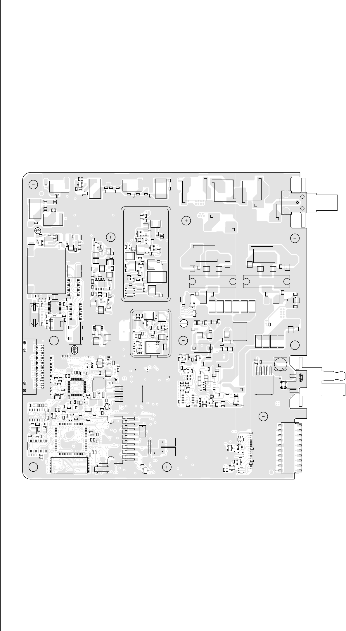
Low Band PCBs / Schematics / Parts Lists 4-7
C0101
C0102
C0104
C0105
C0106
C0107
C0121
C0131
C0132
C0211
C0212
C0221 C0222
C0223
C0225
C0226
C0227
C0228
C0231
C0232
C0233
C0234 C0235
C0236
C0237
C0241
C0242
C0243
C0244
C0245
C0246
C0251
C0252
C0253
C0254
C0255
C0256
C0261
C0262
C0275
C0290
C0291
C0292 C0293
C0331
C0401
C0441
C0442
C0443
C0445
C0446
C0447
C0448
C0449
C0451
C0452
C0453
C0455
C0456
C0457
C0458
C0459
C0460
C0461
C0462
C0463
C0464
C0466
C0467
C0468
C0470
C0471
C0472
C0473
C0474
C0476
C0477
C0478
C0482
C0483
C0484
C0486
C0487
C0488
C0490
C0493
C0494
C0495
C0496
C0501
C0502
C0503
C0504
C0505
C0506
C0508
C0509
C0510
C0511
C0512
C0513
C0514
C0515
C0516
C0517
C0518
C0601
C0603
C0612
C0651
C0652
C0654
C0655
C0681
C1001 C1002
C1003
C1004
C1006
C1007
C1008
C1009
C1010
C1011
C1012
C1015
C1019
C1020
C1021
C1022
C1023
C1024
C1025
C1037
C1038
C1039
C1040
C1101
C1103
C1106
C1107
C1109
C1110
C1111
C1125
C1129 C1130
C1131
C1133
C1134
C1136
C1137
C1138
C1139
C1141
C1142
C1145
C1149
C1153
C1212
C1213
C1214
C1215
C1216
C1217
C1218
C1224
C1225
C1226
C1227
C1228
C1229
C1230
C1250
C1251
C1252
C1253
C1254
C1304
C1305
C1306
C1307
C1308
C1309
C1311
C1312
C1314
C1315
C1316
C1340
C1344
C1345
C1346
C1347
C1348
C1349
C1350
C1351
C1352
C1356
C1360
C1403
C1404
C1405
C1406
C1407
C1408
C1410
C1414
C1419
C1420
C1421
C1422
C1423
C1425
C1426
C1427
C1428
C1429
C1430
C1431
C1432
C1433
C1434
C1435
C1436
C1468 C1473
C1475
C1477
C1478
C1482
C1484
C1501
C1505
C1510
C1511
C1512
C1525
C1526
C1527
C1528
C1529
C1530
C1531
C1601
C1602
C1603
C1604
C1605
C1618
C1619
C1620 C1621
C1622
C1623
C1624
C1628
C1631
C1633
CR1202
58
14
CR1302
CR1306
D0201
D0651
D1001
D1501
D1502
D1601
E1401
FL1101
IN
GNDA
GNDB
OUT
FL1102
FL1104
43
2
FL1106
18
1
J0451
2011
10
J0501
J0601
3
2
J1401
L0481
L0482
L1001
L1003
L1005
L1006
L1008
L1010
L1101
L1103
L1104
L1107
L1112
L1204
L1206
L1207
L1302
L1303
L1304
L1305
L1306 L1318
L1321
L1322
L1324
L1402
L1403
L1406
L1413
L1414
L1418
L1420
L1421
L1422
L1423
L1601
L1602
L1603
L1604
L1606
L1607
M1401
Q0110
Q0177
Q0181
Q0185
Q0681
Q1001
Q1102
Q1201
Q1303
Q1307
Q1308
2
3
4
5
6
7
8
Q1402
2
3
4
5
6
7
8
Q1403
Q1501
Q1502
Q1504
Q1505
Q1601
Q1609
R0101
R0102
R0104
R0105
R0106
R0108
R0110
R0114
R0115
R0116
R0131
R0132
R0170
R0181
R0182
R0186
R0211
R0212
R0220
R0221
R0222
R0223
R0224
R0225
R0226
R0227
R0228
R0229
R0241
R0242
R0251
R0252
R0253
R0256
R0261
R0262
R0269
R0343
R0441
R0510
R0533
R0651
R0652 R0681
R0682
R1001
R1002
R1003
R1010
R1011
R1101
R1102
R1108
R1110
R1113
R1114
R1122
R1123
R1127
R1131
R1136
R1137
R1204
R1205
R1206
R1207
R1208
R1209
R1210
R1211 R1216
R1217
R1218 R1219
R1220
R1306
R1307 R1308
R1309
R1311
R1331
R1332
R1333
R1334
R1335
R1336
R1337
R1338
R1339
R1344 R1345
R1346
R1347
R1402
R1404
R1405
R1406
R1407
R1411
R1413
R1415
R1417
R1419
R1421
R1423
R1425
R1444
R1445
R1446
R1447
R1448 R1449 R1457
R1463
R1464
R1465
R1466
R1467
R1468
R1471
R1472
R1473
R1474
R1475
R1476
R1477R1478
R1479
R1482
R1483
R1484
R1501
R1502
R1503
R1504
R1507
R1510
R1514
R1516
R1517
R1518
R1519
R1524
R1525R1526
R1527
R1528
R1532
R1533
R1539
R1540
R1601
R1602
R1604
R1626
R1627
R1628
R1629
R1630
R1638
SH1201
SH1301
1
76
51
26
U0101
32
17
16 1
U0121
8
7
114
U0211
137
25
13
U0221
16
1
89
U0251
9
U0271
1
6
5
U0611
1
6
5
U0641
3
2
1
U0651
8
71
14
U1101
8
71
14
U1102
11
1
20
10 U1103
4
58 U1250
4
3U1377
1
4
58
U1402
U1501
1
4
58
U1502
1
4
5
8
U1601
VR0501
VR0503VR0504
VR0505 VR0510
23
4
Y0131
Y1101
2
Y1102
1
1
1
1
1
1
ZWG0130595-O
Low Band Range 2 (36.0-42.0 MHz) 8486207B05 Top Side
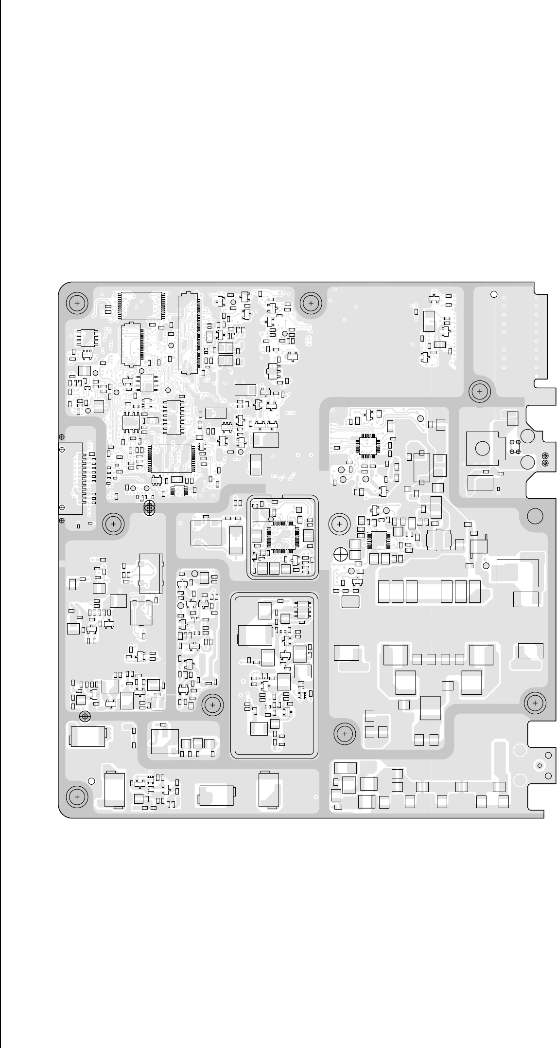
4-8 Low Band PCBs / Schematics / Parts Lists
C0103
C0111
C0112
C0122
C0123
C0141
C0151
C0201
C0202
C0203 C0204
C0205
C0224
C0265
C0266
C0267
C0271
C0272
C0273
C0274
C0276 C0277
C0301
C0302
C0303
C0304
C0305
C0324 C0325
C0341
C0342
C0343
C0344
C0351
C0352
C0353
C0354
C0402
C0403
C0406
C0407
C0408
C0409
C0410
C0411
C0421
C0422
C0423
C0426
C0427
C0428
C0429
C0430
C0431
C0485
C0491
C0492
C0497
C0499
C0541
C0542
C0554
C0558
C0559
C0560 C0575
C0576
C0591
C0592
C0593
C0611
C0621
C0622
C0641
C0644
C0645
C0661
C0662
C0663
C0671
C1013
C1014
C1016
C1017
C1026
C1027
C1028
C1029
C1030
C1031
C1032
C1033
C1034
C1035
C1036
C1102
C1104
C1105
C1108
C1112
C1113
C1114
C1115
C1116 C1119
C1120
C1121
C1122
C1123
C1124
C1126
C1127
C1128
C1135
C1140
C1143
C1144
C1146
C1147
C1148
C1150 C1151
C1152
C1201
C1202
C1203
C1204
C1205 C1206
C1207
C1208
C1209 C1210
C1211
C1219
C1220
C1221
C1222
C1223
C1231
C1232
C1233
C1234
C1313
C1317
C1318
C1319
C1320
C1321
C1323
C1325
C1326
C1333
C1334
C1335
C1336
C1337
C1338
C1339
C1341
C1342
C1343
C1354
C1361
C1362
C1401
C1402
C1409
C1412
C1413
C1415
C1416
C1417
C1418
C1437
C1438
C1439
C1440
C1441
C1442
C1443
C1444
C1445
C1446
C1447
C1448
C1449
C1450
C1451
C1452
C1453
C1454
C1455
C1456
C1457
C1458
C1459
C1460
C1461
C1462
C1463
C1464
C1465
C1466
C1467
C1469
C1470
C1471
C1472
C1474
C1476
C1479
C1480
C1481
C1485
C1502
C1503
C1504
C1506
C1507
C1508
C1509
C1606
C1607
C1608
C1609
C1610
C1611
C1612
C1613
C1614
C1615
C1616
C1625
C1626
C1627
C1629 C1632
C1634
CR1201
58
1
4
CR1310
CR1314
D0101
D0151
D0179
D0301
D0621
D0660
D0661
D1101
D1401
D1402 D1503
E0271
E0272
E0631
E1403
F0401
FL1105
43
2
FL1107
12
J0401
1
40
J0551
1
18
J0552
L1002
L1004
L1007
L1009
L1011
L1012
L1013
L1014
L1102
L1105
L1106
L1108
L1109
L1110
L1111
L1201
L1202
L1205
L1307
L1309
L1310
L1311
L1313
L1314
L1315
L1316
L1317
L1401
L1404
L1405
L1415
L1416
L1417
L1419
L1424
L1425
L1426
L1605
Q0151
Q0171
Q0173
Q0183
Q0271
Q0641 Q0661
Q0662
Q0663
Q1002
Q1003
Q1101
Q1103
Q1104
Q1105
Q1106
Q1202
Q1304
Q1305
Q1306
1
2
3
Q1401
Q1404
Q1503
Q1506
Q1602
Q1603
Q1604
Q1605
Q1606
Q1607
Q1610
R0107
R0111
R0112
R0113
R0117 R0121
R0151
R0152
R0171
R0172
R0173
R0174
R0175
R0176
R0177
R0178
R0179R0183
R0184
R0185
R0201
R0202
R0203
R0204
R0205
R0206
R0207
R0208
R0254
R0255
R0257
R0265
R0266
R0267
R0268
R0273
R0274
R0275
R0276
R0323
R0324
R0331
R0332
R0333
R0335
R0341
R0342
R0344
R0345 R0346
R0347
R0401
R0407
R0408
R0409
R0412
R0442
R0467
R0468
R0481 R0482
R0511
R0512
R0525
R0529
R0530
R0531 R0535 R0537
R0538
R0539
R0541
R0542
R0543
R0591
R0592
R0593
R0611
R0612
R0621
R0641
R0642
R0643
R0661
R0662
R0671
R0672
R1004
R1005
R1006
R1007
R1008
R1009 R1103
R1104
R1106
R1107
R1109
R1111
R1115
R1116
R1117
R1118
R1119
R1120
R1121
R1124
R1125
R1126
R1128
R1129
R1130
R1132R1133
R1134
R1135
R1138
R1139
R1201
R1202
R1203
R1212
R1213
R1214
R1215
R1221
R1222
R1312
R1313
R1314
R1315
R1316
R1317
R1318
R1319
R1320
R1325
R1326
R1327
R1328
R1330
R1340
R1341
R1342
R1343
R1376
R1409
R1410
R1412
R1414
R1416
R1418
R1420
R1422
R1424
R1440
R1441
R1442
R1443
R1450
R1451
R1453
R1454
R1455
R1458
R1459
R1460
R1469
R1470
R1480
R1505 R1506
R1508
R1509 R1511
R1512
R1513 R1515
R1522
R1523
R1535
R1542
R1543
R1544
R1545
R1605
R1606
R1607
R1608
R1609
R1610
R1611
R1612 R1613
R1614
R1615
R1616
R1617
R1620
R1621
R1622
R1631
R1632
R1633
R1635
R1636 R1637
S1501
SH1202
SH1302
TP0101
TP0102
TP0103
TP0104
TP0151
TP0221
TP0222
TP0492
TP0497
TP0530
TP0661
TP1201
TP1401
TP1402
TP1403
TP1501
TP1502
TP1503
TP1505
TP1601
TP1602
1
4
58
U0111
22
21 8
7
1
U0122
16
1
8
9
U0141
28 15
14
1
U0301
U0331
1
45
8
U0341
U0342
4
58
U0351
14
58
U0652
U0653
4
3
U1001
1
6
43
U1051
1
37
25 13
U1201
4
3
U1378
1
16
8
9
U1401
1
17
9
25
U1503
VR0151
VR0509
VR0537
VR0541
VR0601
VR0621
VR0671
Y1201
23
4
Y1202
1
1
8486207B05 T1
ZWG0130596-O
Low Band Range 2 (36.0-42.0 MHz) 8486207B05 Bottom Side
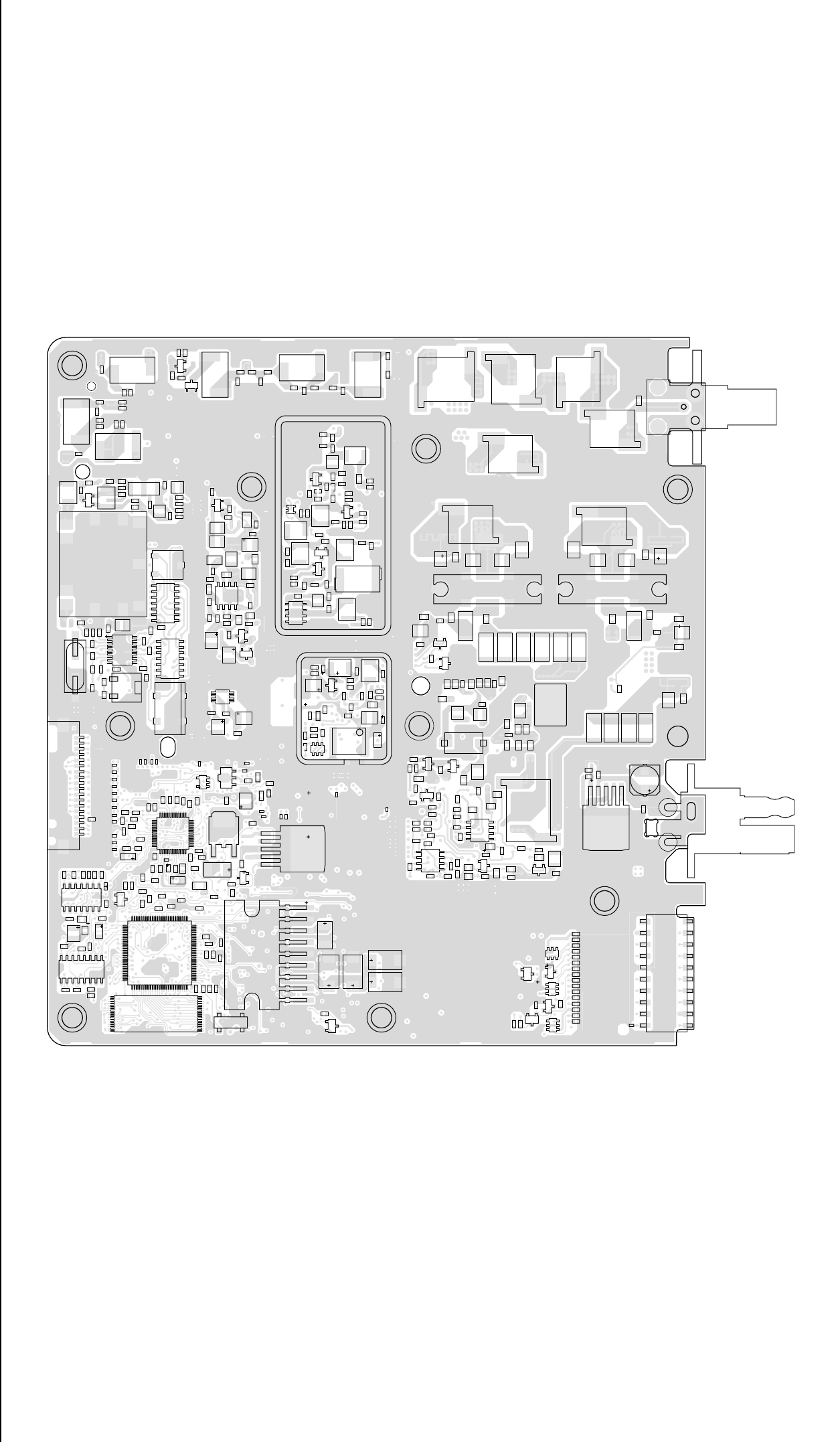
Low Band PCBs / Schematics / Parts Lists 4-9
C0101 C0102
C0104
C0105
C0106
C0107
C0121
C0131
C0132
C0211
C0212
C0221
C0222
C0223
C0225
C0226
C0227
C0228
C0231
C0232
C0233
C0234 C0235
C0236
C0237
C0241
C0242
C0243
C0244
C0245
C0246
C0251
C0252 C0253
C0254
C0255
C0256
C0261
C0262
C0275
C0290
C0291
C0292 C0293
C0331
C0441
C0442
C0443
C0445
C0446
C0447
C0448
C0449
C0470
C0471
C0472
C0473
C0474
C0476
C0477
C0478
C0482
C0483
C0484
C0486 C0487
C0488
C0490 C0493
C0494
C0495
C0496
C0501
C0502
C0503
C0504
C0505
C0506
C0508
C0509
C0510
C0511
C0512
C0513
C0514
C0515
C0516
C0517
C0518
C0601
C0603
C0612
C0651
C0652
C0654
C0655
C0681
C1001 C1002
C1003
C1004
C1006
C1007
C1008
C1009
C1010
C1011
C1012
C1015
C1019
C1020
C1021
C1022
C1023
C1024
C1025
C1037
C1038
C1039
C1040
C1101
C1103
C1106
C1107
C1109
C1110
C1111
C1125
C1129
C1130
C1131
C1133
C1134
C1136
C1137
C1138
C1139
C1141
C1142
C1145
C1149
C1153
C1212
C1213
C1214
C1215
C1216
C1217
C1218
C1224
C1225
C1226
C1227
C1228
C1229
C1230
C1250
C1251
C1252
C1253
C1254
C1304
C1305
C1306 C1307
C1308
C1309
C1311
C1312
C1314
C1315
C1316
C1340
C1344
C1345
C1346
C1347 C1348
C1349
C1350
C1351
C1352
C1356
C1360
C1403
C1404
C1405
C1406
C1407
C1408
C1410
C1414
C1419
C1420
C1421
C1422
C1423
C1424
C1425
C1426
C1427
C1428
C1429
C1430
C1431
C1432
C1433
C1434
C1435
C1436
C1468
C1473
C1475
C1477
C1478
C1482
C1484
C1501
C1505
C1510
C1511
C1512
C1525
C1526
C1527
C1528
C1529
C1530
C1531
C1532
C1601
C1602
C1603
C1604
C1605
C1618
C1619
C1620 C1621
C1622
C1623
C1624
C1628
C1631
C1633
CR1202
58
14
CR1302
CR1306
D0201
D0651
D1001
D1501
D1502
D1601
E1401
FL1101
IN
GNDA
GNDB
OUT
FL1102
FL1104
4
3
2
FL1106
18
1
J0451
2011
10
J0501
J0601
3
2
J1401
L0481
L0482
L1001
L1003
L1005
L1006
L1008
L1010
L1101
L1103
L1104
L1107
L1112
L1204
L1206
L1207
L1302
L1303
L1304
L1305
L1306
L1318
L1321
L1322
L1324
L1402
L1403
L1406
L1413
L1414
L1418
L1420
L1421
L1422
L1423
L1601
L1602
L1603
L1604
L1606
L1607
M1401
Q0110
Q0177
Q0181
Q0185
Q0681
Q1001
Q1102
Q1201
Q1303
Q1307
Q1308
2
3
4
5
6
7
8
Q1402
2
3
4
5
6
7
8
Q1403
Q1501
Q1502
Q1504
Q1505
Q1601
Q1609
R0101
R0102
R0104
R0105
R0106
R0108
R0110
R0114
R0115
R0116
R0131
R0132
R0170
R0181
R0182
R0186
R0211
R0212
R0220
R0221
R0222
R0223
R0224
R0225
R0226
R0227
R0228
R0229
R0241
R0242
R0251
R0252
R0253
R0256
R0261
R0262
R0269
R0343
R0441
R0508
R0510
R0533
R0651
R0652
R0681
R0682
R1001
R1002
R1003
R1010
R1011
R1101
R1102
R1108
R1110
R1113
R1114
R1122
R1123
R1127
R1131
R1136
R1137
R1204
R1205
R1206
R1207
R1208
R1209
R1210
R1211
R1216
R1217
R1218 R1219
R1220
R1306
R1307 R1308
R1309
R1311
R1331
R1332
R1333
R1334
R1335
R1336
R1337
R1338
R1339
R1344 R1345
R1346
R1347
R1402
R1404
R1405
R1406
R1407
R1411
R1413
R1415
R1417
R1419
R1421
R1423
R1425
R1444
R1445
R1446
R1447
R1448
R1449
R1457
R1463
R1464
R1465
R1466
R1467
R1468
R1471
R1472
R1473
R1474
R1475
R1476
R1477R1478
R1479
R1482
R1483
R1484
R1501
R1502 R1503
R1504
R1507
R1510
R1514
R1516
R1517
R1518
R1519
R1524
R1525R1526
R1527
R1528
R1532
R1533
R1539
R1540
R1544
R1601
R1602
R1604
R1626
R1627
R1628
R1629
R1630
R1638
SH1201
SH1301
1
76
51
26
U0101
32
17
16 1
U0121
8
7
114
U0211
137
25
13
U0221
16
1
89
U0251
9
U0271
1
6
5
U0611
1
6
5
U0641
3
2
1
U0651
8
71
14
U1101
8
71
14
U1102
11
1
20
10
U1103
4
58
U1250
4
3U1377
1
4
58
U1402
U1501
1
4
58
U1502
1
4
5
8
U1601
VR0501
VR0503 VR0504
VR0505
VR0510
23
4
Y0131
Y1101
2
Y1102
1
1
48
1
1
1
1
100
ZWG0131045-O
Low Band Range 2 (36.0-42.0 MHz) 8486207B07 Top Side
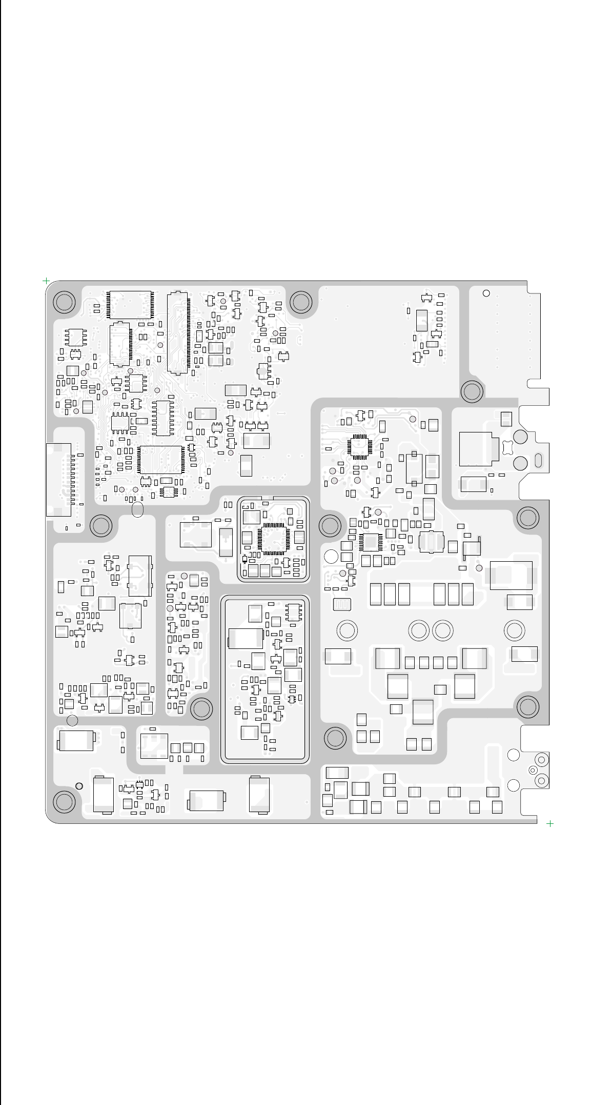
4-10 Low Band PCBs / Schematics / Parts Lists
ZWG0131046-O
C0103
C0108
C0111
C0112
C0122
C0123
C0141
C0151
C0201
C0202
C0203 C0204
C0205
C0224
C0265
C0266 C0267
C0271
C0272
C0273
C0274
C0276 C0277
C0301
C0302
C0303
C0304 C0305
C0324 C0325
C0341
C0342
C0343
C0344
C0351
C0352
C0353
C0354
C0421
C0422
C0423
C0426
C0427
C0428
C0429
C0430
C0431
C0485
C0491
C0492
C0497
C0499
C0541
C0542
C0554
C0558
C0559 C0560
C0575 C0576
C0591
C0592 C0593
C0611
C0621
C0622
C0641
C0644
C0645
C0661
C0662
C0663
C0671
C1013
C1014
C1016
C1017
C1026C1027
C1028
C1029
C1030
C1031
C1032
C1033
C1034
C1035
C1036
C1102
C1104
C1105
C1108
C1112
C1113
C1114
C1115
C1116 C1119
C1120
C1121
C1122
C1123
C1124
C1126
C1127
C1128
C1135
C1140
C1143
C1144
C1146
C1147
C1148
C1150
C1151
C1152
C1201
C1202
C1203
C1204
C1205
C1206
C1207
C1208
C1209 C1210
C1211
C1219
C1220
C1221
C1222
C1223
C1231
C1232
C1233
C1234
C1313
C1317
C1318
C1319
C1320
C1321
C1323
C1325
C1326 C1333
C1334
C1335
C1336
C1337
C1338
C1339
C1341
C1342
C1343
C1354
C1361 C1362
C1401
C 1402
C1409
C1412
C1413
C1415
C1416
C1417
C1418
C1437
C1438
C1439
C1440
C1441
C1442
C1443
C1444
C1445
C1446
C1447 C1448
C1449
C1450
C1451
C1452
C1453
C1454
C1455
C1456
C1457
C1458
C1459
C1460
C1461
C1462
C1463
C1464
C1465
C1466
C1467
C1469
C1470
C1471
C1472
C1474
C1476
C1479
C1480
C1481
C1485
C1502
C1503
C1504
C1506
C1507
C1508
C1509
C1606
C1607
C1608
C1609
C1610
C1611
C1612
C1613
C1614
C1615
C1616
C1625
C1626
C 1627
C1629 C1632
C 1634
CR1201
58
1
4
CR1310
CR1314
D0101
D0151
D0179
D0301
D0621
D0660 D0661
D1101
D1401
D1402
D1503
E0271 E0272
E0631
E1403
F0401
FL1105
43
2
FL1107
12
J0401
1
40
J0551
1
18
J0552
L1002
L1004
L1007
L1009
L1011
L1012
L1013
L1014
L1102
L1105
L1106
L1108
L1109
L1110
L1111
L1201
L1202
L1205
L1307
L1309
L1310
L1311
L1313
L1314
L1315
L1316
L1317
L1401
L1404
L1405
L1415
L1416
L1417
L1419
L1424
L1425
L1426
L1605
Q0151
Q0171
Q0173 Q0183
Q0271
Q0641
Q0661
Q0662
Q0663
Q1002
Q1003
Q1101
Q1103
Q1104
Q1105
Q1106
Q1107
Q1202
Q1304
Q1305
Q1306
1
2
3
Q1401
Q1404
Q1503
Q1506
Q1602
Q1603
Q1604
Q1605
Q1606
Q1607
Q1610
R0103
R0107
R0111
R0112
R0113
R0117
R0121
R0151 R0152
R0171
R0172
R0173
R0174
R0175
R0176
R0177
R0178
R0179
R0183
R0184
R0185
R0201
R0202
R0203
R0204
R0205
R0206
R0207
R0208
R0254
R0255 R0257
R0265
R0266 R0267
R0268
R0273
R0274
R0275
R0276
R0323
R0324
R0331
R0332
R0333
R0335
R0341
R0342
R0344
R0345
R0346
R0347
R0401
R0407
R0408
R0409
R0412
R0442
R0467
R0468
R0481 R0482
R0509
R0511
R0512
R0525
R0529
R0530
R0531 R0535 R0537
R0538
R0539
R0541
R0542
R0543
R0555
R0556
R0591
R0592
R0593
R0611
R0612
R0621
R0641
R0642
R0643
R0661
R0662 R0671 R0672
R1004
R1005
R1006
R1007
R1008
R1009
R1103
R1104
R1106
R1107
R1109
R1111
R1115
R1116
R1117
R1118
R1119
R1120
R1121
R1124
R1125
R1126
R1128
R1129
R1130
R1132 R1133
R1134 R1135
R1138
R1139
R1140
R1141
R1201
R1202
R1203
R1212
R1213
R1214
R1215
R1221
R1222
R1312
R 1313
R1314
R1315
R1316
R1317
R1318
R1319
R1320
R1325
R1326
R1327
R1328
R1330
R1340
R1341
R1342
R1343
R1376
R1409
R1410
R1412
R1414
R1416
R1418
R1420
R1422
R1424
R1440
R1441
R1442
R1443
R1450
R1451
R1453
R1454
R1455
R 1458
R 1459
R1460
R1469
R1470
R1480
R1505 R1506
R1508
R1509
R1511
R1512
R1513 R1515
R1522
R1523
R1535
R1542
R1543
R1545
R1605
R1606
R1607
R1608
R1609
R1610
R1611
R1612
R1613 R1614
R1615
R1616
R1617
R1620
R1621
R1622
R1631
R1632
R1633
R1635
R1636 R1637
S1501
SH1202
TP0101
TP0102
TP0103
TP0104
TP0151
TP0221
TP0222
TP0492
TP0497
TP0530
TP0661
TP1201
TP1401
TP1402
TP1403
TP1501
TP1502
TP1503 TP1505
TP1601
TP1602
1
4
58
U0111
22
21 8
7
1
U0122
16
1
8
9
U0141
28 15
14
1
U0301
U0331
1
45
8
U0341
U0342
4
5
8
U0351
14
5
8
U0652
U0653
4
3
U1001
1
6
43
U1051
1
37
25 13
U1201
4
3
U1378
1
16
8
9
U1401
1
17
9
25
U1503
VR0151
VR0509
VR0537
VR0541
VR0601
VR0621
VR0671
Y1201
23
4
Y1202
48
1
1
32
Low Band Range 2 (36.0-42.0 MHz) 8486207B07 Bottom Side
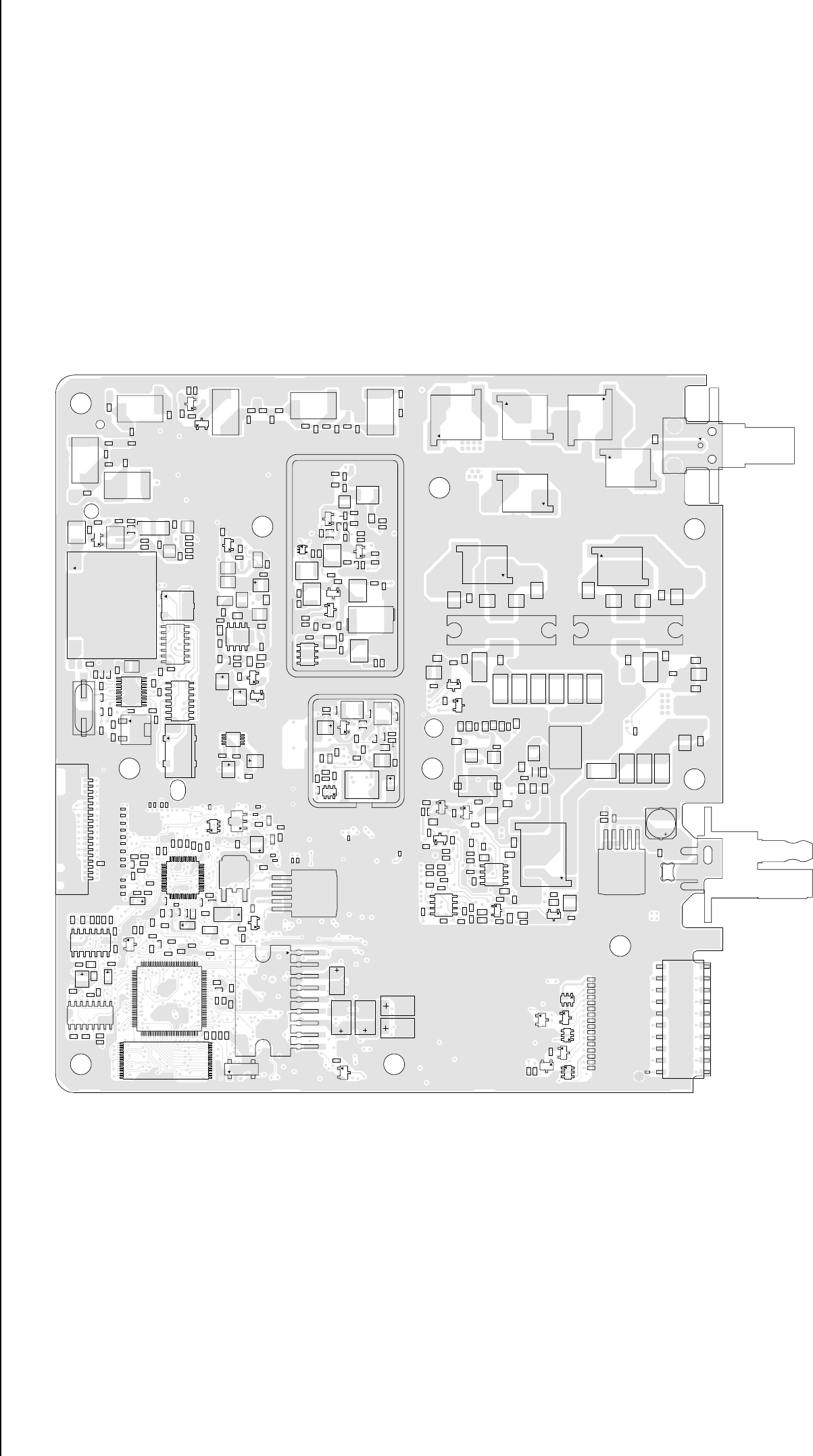
Low Band PCBs / Schematics / Parts Lists 4-11
C0101
C0102
C0104
C0105
C0106
C0107
C0121
C0131
C0132
C0211
C0212
C0221
C0222
C0223
C0225
C0226
C0227
C0228
C0231
C0232
C0233
C0234
C0235
C0236
C0237
C0241
C0242
C0243
C0244
C0245
C0246
C0251
C0252 C0253
C0254
C0255
C0256
C0261
C0262
C0275
C0290
C0291
C0292 C0293
C0331
C0441
C0442
C0443
C0445
C0446
C0447
C0448
C0449
C0470
C0471
C0472
C0473
C0474
C0476
C0477
C0478
C0482
C0483
C0484
C0486
C0487
C0488
C0490
C0493
C0494
C0495
C0496
C0501
C0502
C0503
C0504
C0505
C0506
C0508
C0509
C0510
C0511
C0512
C0513
C0514
C0515
C0516
C0517 C0518
C0601
C0603
C0612
C0651
C0652
C0654
C0655
C0681
C1001 C1002
C1003
C1004
C1005
C1006
C1007
C1008
C1009
C1010 C1011
C1012
C1015
C1018
C1019
C1020
C1021
C1022
C1023
C1024
C1025
C1101
C1103
C1106
C1107
C1109
C1110
C1111
C1125
C1129 C1130
C1131
C1133
C1134
C1136
C1137
C1138
C1139
C1141
C1142
C1145
C1149
C1153
C1212
C1213
C1214
C1215
C1216
C1217
C1218
C1224
C1225
C1226
C1227
C1228
C1229
C1230
C1250
C1251
C1252
C1253
C1254
C1304
C1305
C1306 C1307
C1308
C1309
C1311
C1312
C1314
C1315
C1316
C1340
C1344
C1345
C1346
C1347 C1348
C1349
C1350
C1351
C1352
C1356
C1360
C1403
C1404
C1405
C1406
C1407
C1408
C1410
C1414
C1419
C1420
C1421
C1422
C1423
C1424
C1425
C1426
C1427
C1428
C1429
C1430
C1431
C1432
C1433
C1434
C1435
C1436
C1468
C1473
C1475
C1477
C1478
C1482
C1484
C1486
C1501
C1505
C1510
C1511
C1512
C1523
C1525
C1526
C1527
C1528
C1530
C1531
C1532
C1601
C1602
C1603
C1604
C1605
C1618
C1619 C1620
C1621
C1622
C1623
C1624
C1628
C1631
C1633
CR1202
5
8
14
CR1302
CR1306
D0201
D0651
D1001
D1501 D1502
D1601
E1401
FL1101
IN
GNDA
GNDB
OUT
FL1102
FL1104
43
2
FL1106
18
1
J0451
20
11
10 1
J0501
J0601
32
J1401
L0481
L0482
L1001
L1003
L1005
L1006
L1008
L1010
L1101
L1103
L1104
L1107
L1112
L1204
L1206
L1207
L1302
L1303
L1304
L1305
L1306
L1318
L1321
L1322
L1324
L1402
L1403
L1406
L1413
L1414
L1418
L1420
L1421
L1422
L1423
L1601
L1602
L1603
L1604
L1606
L1607
M1401
Q0110
Q0177
Q0181
Q0185
Q0681
Q1001
Q1102
Q1201
Q1303
Q1307
Q1308
21
3
4
5
6
7
8
Q1402
21
3
4
5
6
7
8
Q1403
Q1501
Q1502
Q1504
Q1505
Q1601
Q1609
R0101
R0102
R0104
R0105
R0106
R0108
R0110
R0114
R0115
R0116
R0131
R0132
R0170
R0181
R0182
R0186
R0211
R0212
R0220
R0221
R0222
R0223
R0224
R0225
R0226
R0227
R0228
R0229
R0241
R0242
R0251
R0252
R0253
R0256
R0261
R0262
R0269
R0343
R0441
R0510
R0533
R0651
R0652
R0681
R0682
R1001
R1002
R1003
R1010
R1011
R1101
R1102
R1108
R1110
R1113
R1114
R1122
R1123
R1127
R1131
R1136
R1137
R1204
R1205
R1206
R1207
R1208
R1209
R1210
R1211
R1216
R1217
R1218 R1219
R1220
R1306
R1307
R1308
R1309
R1311
R1331
R1332
R1333
R1334
R1335
R1336
R1337
R1338 R1339
R1344
R1345
R1346
R1347
R1402
R1404
R1405
R1406
R1407
R1411
R1413
R1415
R1417
R1419
R1421
R1423
R1425
R1444
R1445
R1446
R1447
R1448 R1449
R1457
R1463
R1464
R1465
R1466
R1467
R1468
R1471
R1472
R1473
R1474
R1475
R1476
R1477
R1478
R1479
R1482
R1483
R1484
R1501
R1502
R1503
R1504
R1507
R1510
R1514
R1516
R1517
R1518
R1519
R1524
R1525
R1526
R1527
R1528
R1532
R1533
R1537
R1541
R1544
R1601
R1602
R1604
R1626 R1627
R1628
R1629
R1630
R1638
SH1201
SH1301
1
76
51
26
U0101
32
17
16 1
U0121
8
7
114
U0211
137
25
13
U0221
16
1
89
U0251
9
U0271
1
6
5
U0611
1
6
5
U0641
3
2
1U0651
8
71
14
U1101
8
71
14
U1102
11
1
20
10
U1103
41
58 U1250
4
3U1377
1
4
58
U1402
U1501
1
4
58
U1502
1
4
5
8
U1601
VR0501
VR0503
VR0504
VR0505 VR0510
23
4
Y0131
Y1101
2Y1102
FL0830651O
Low Band Range 3 (42-50 MHz) 8486908Z02 Top Side
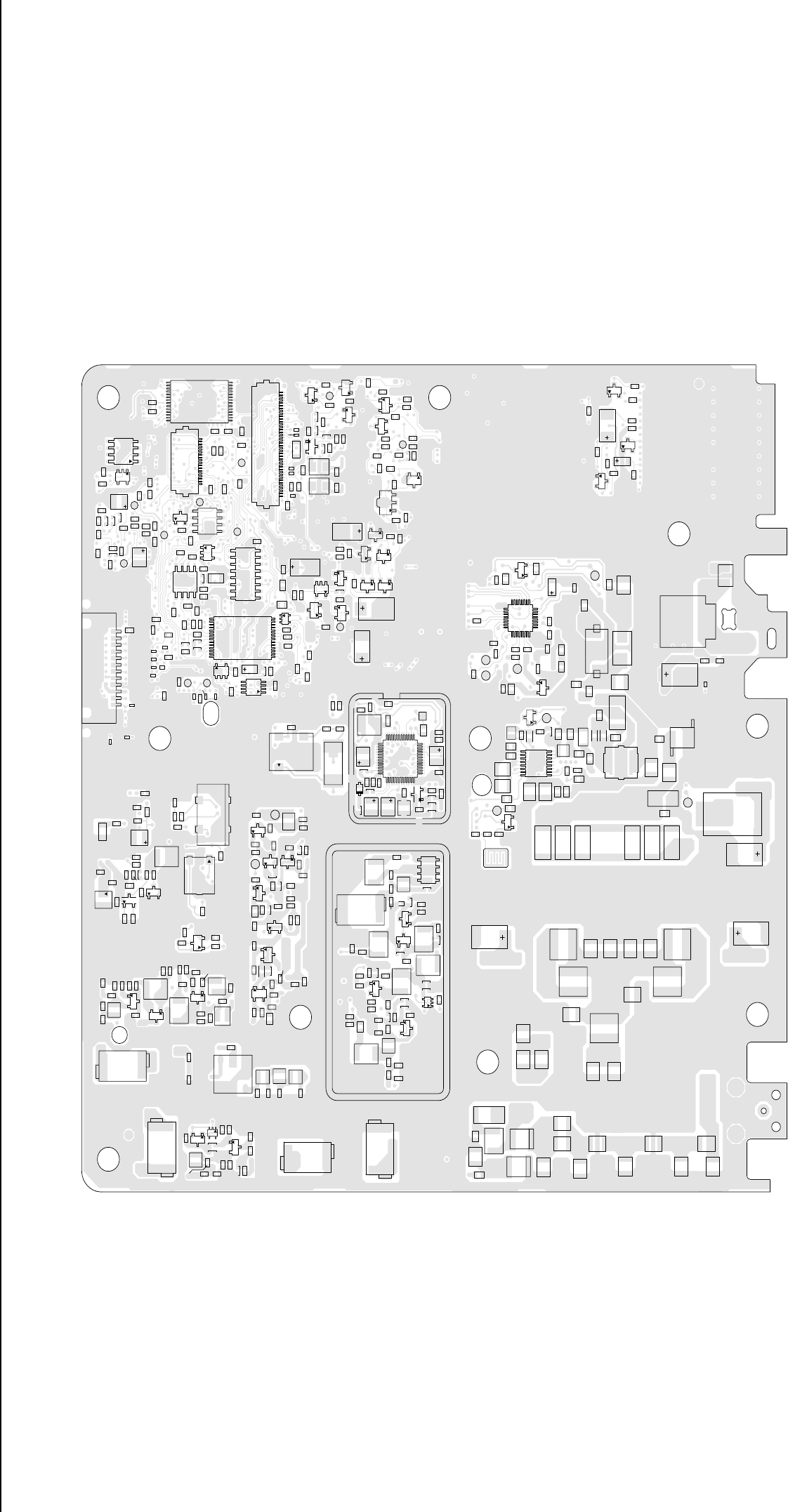
4-12 Low Band PCBs / Schematics / Parts Lists
C0103
C0108
C0111
C0112
C0122
C0123
C0141
C0151
C0201
C0202
C0203 C0204
C0205
C0224
C0265
C0266
C0267
C0271
C0272
C0273
C0274
C0276 C0277
C0301
C0302
C0303
C0304
C0305
C0324
C0325
C0341
C0342
C0343
C0344
C0351
C0352
C0353
C0354
C0421
C0422
C0423
C0426
C0427
C0428
C0429
C0430
C0431
C0485
C0491
C0492
C0497
C0499
C0541
C0542
C0554
C0558
C0559
C0560
C0575
C0576
C0591
C0592
C0593
C0611
C0621
C0622
C0641
C0644
C0645
C0661
C0662
C0663
C0671
C1013
C1014
C1016 C1017
C1026
C1027
C1028
C1029
C1030
C1031
C1032
C1033
C1034
C1035
C1036
C1102
C1104
C1105
C1108
C1112
C1113
C1114
C1115
C1116
C1119
C1120
C1121
C1122 C1123
C1124
C1126
C1127
C1128
C1135
C1140
C1143
C1144
C1146
C1147
C1148
C1150 C1151
C1152
C1201
C1202
C1203
C1204
C1205
C1206
C1207
C1208
C1209 C1210
C1211
C1219
C1220
C1221
C1222
C1223
C1231
C1232
C1233
C1234
C1313
C1317
C1318
C1319
C1320
C1321
C1323
C1325
C1326
C1333
C1334C1335
C1336
C1337
C1338
C1339
C1341
C1342
C1343
C1354
C1361
C1362
C1401
C1402
C1409
C1412
C1413
C1415
C1416
C1417
C1418
C1437
C1438
C1439
C1440
C1441
C1442
C1443
C1444
C1445
C1446
C1447
C1448
C1449
C1450
C1451
C1452
C1453
C1454
C1455
C1456
C1457
C1458
C1459
C1460
C1461
C1462
C1463
C1464
C1465
C1466
C1467
C1469
C1470
C1471
C1472
C1474
C1476
C1479
C1480
C1481
C1485
C1502
C1503
C1504
C1506
C1507
C1508
C1509
C1606
C1607
C1608
C1609
C1610
C1611
C1612
C1613
C1614
C1615
C1616
C1625
C1626
C1627
C1629 C1632
C1634
CR1201
58
1
4
CR1310
CR1314
D0101
D0151
D0179
D0301
D0621
D0660
D0661
D1101
D1401
D1402
D1503
E0271
E0272
E0631
E1403
F0401
FL1105
43
21
FL1107
121
J0401
1
40
J0551
1
18
J0552
L1002
L1004
L1007
L1009
L1011
L1012
L1013
L1014
L1102
L1105
L1106
L1108
L1109
L1110
L1111
L1201
L1202
L1205
L1307
L1309
L1310
L1311
L1313
L1314
L1315
L1316
L1317
L1401
L1404
L1405
L1408
L1415
L1416
L1417
L1419
L1424
L1425
L1426
L1605
Q0151
Q0171
Q0173
Q0183
Q0271
Q0641 Q0661
Q0662
Q0663
Q1002
Q1003
Q1101
Q1103
Q1104
Q1105
Q1106
Q1202
Q1304
Q1305
Q1306
1
2
3
Q1401
Q1404
Q1503
Q1506
Q1602
Q1603
Q1604
Q1605
Q1606
Q1607
Q1610
R0103
R0107
R0111
R0112
R0113
R0117 R0121
R0151
R0152
R0171
R0172
R0173
R0174
R0175
R0176
R0177
R0178
R0179
R0183
R0184
R0185
R0201
R0202
R0203
R0204
R0205
R0206
R0207
R0208
R0254
R0255
R0257
R0265
R0266
R0267
R0268
R0273
R0274
R0275
R0276
R0323
R0324
R0331
R0332
R0333
R0335
R0341
R0342
R0344R0345
R0346
R0347
R0401
R0407
R0408
R0409 R0412
R0442
R0467
R0468
R0481 R0482
R0511
R0512
R0525
R0529
R0530
R0531
R0535
R0537
R0538
R0539
R0541
R0542
R0543
R0555
R0556
R0591
R0592
R0593
R0611
R0612
R0621
R0641
R0642
R0643
R0661
R0662
R0671
R0672
R1004
R1005
R1006
R1007
R1008
R1009
R1103
R1104
R1106
R1107
R1109
R1111
R1115 R1116
R1117
R1118
R1119
R1120
R1121
R1124
R1125
R1126
R1128
R1129
R1130
R1132
R1133
R1134
R1135
R1138
R1139
R1201
R1202
R1203
R1212
R1213
R1214
R1215
R1221
R1222
R1312
R1313
R1314
R1315
R1316
R1317
R1318
R1319
R1320
R1325
R1326
R1327
R1328
R1330
R1340
R1341
R1342
R1343
R1376
R1409
R1410
R1412
R1414
R1416
R1418
R1420
R1422
R1424
R1440
R1441
R1442
R1443
R1450
R1451
R1453
R1454
R1455
R1458
R1459
R1460
R1469
R1470
R1480
R1505
R1506
R1508
R1509
R1511
R1512
R1513
R1515
R1522
R1523
R1535
R1542
R1543
R1545
R1605
R1606
R1607
R1608
R1609
R1610
R1611
R1612
R1613
R1614
R1615
R1616
R1617
R1620
R1621
R1622
R1631
R1632
R1633
R1635
R1636
R1637
S1501
SH1202
SH1302
TP0101
TP0102
TP0103
TP0104
TP0151
TP0221
TP0222
TP0492
TP0497
TP0530
TP0661
TP1201
TP1401
TP1402
TP1403
TP1501
TP1502
TP1503 TP1505
TP1601
TP1602
1
4
58
U0111
22
21 8
7
1
U0122
16
1
8
9
U0141
28 15
14
1
U0301
U0331
1
45
8
U0341
U0342
4
58
U0351
4
58
U0652
U0653
43
U1001
1
64
3
U1051
1
37
25 13
U1201
4
3
U1378
1
16
8
9
U1401
1
17
9
25
U1503
VR0151
VR0509
VR0537
VR0541
VR0601
VR0621
VR0671
Y1201
23
4
Y1202
FL0830652O
Low Band Range 3 (42-50 MHz) 8486908Z02 Bottom Side
Low Band PCBs / Schematics / Parts Lists 4-13
1
1
1
1
1
1
C0101 C0102
C0104
C0105
C0106
C0107
C0121
C0131
C0132
C0211
C0212
C0221
C0222
C0223
C0225
C0226
C0227
C0228
C0231
C0232
C 0233
C0234 C0235
C0236
C0237
C0241
C0242
C0243
C0244
C0245
C0246
C0251
C0252 C0253
C0254
C0255
C0256
C0261
C0262
C0275
C0290
C0291
C0292 C0293
C0331
C0441
C0442
C0443
C0445
C0446
C0447
C0448
C0449
C0470
C0471
C0472
C0473
C0474
C0476
C0477
C0478
C0482
C0483
C0484
C0486C0487
C0488
C0490
C0493
C0494
C0495
C0496
C0501
C0502
C0503
C0504
C0505
C0506
C0508
C0509
C0510
C0511
C0512
C0513
C0514
C0515
C0516
C0517
C0518
C0601
C0603
C0612
C0651
C0652
C0654
C0655
C0681
C1001 C1002
C1003
C1004
C1005
C1006
C1007
C1008
C1009
C1010
C1011
C1012
C1015
C1018
C1019
C1020
C1021
C1022
C1023
C1024
C1025
C1101
C1103
C1106
C1107
C1109
C1110
C1111
C1125
C1129
C1130
C1131
C1133
C1134
C1136
C1137
C1138
C1139
C1141
C1142
C1145
C1149
C1153
C1212
C1213
C1214
C1215
C1216
C1217
C1218
C1224
C1225
C1226
C1227
C1228
C1229
C1230
C1250
C1251
C1252
C1253
C1254
C1304
C1305
C1306
C1307
C1308
C1309
C1311
C1312
C1314
C1315
C1316
C1340
C1344
C1345
C1346
C1347
C1348
C1349
C1350
C1351
C1352
C1356
C1360
C1403
C1404
C1405
C1406
C1407
C1408
C1410
C1414
C1419
C1420
C1421
C1422
C1423
C1424
C1425
C1426
C1427
C1428
C1429
C1430
C1431
C1432
C1433
C1434
C1435
C1436
C1468 C1473
C1475
C1477
C1478
C1482
C1484
C1486
C1501
C1505
C1510
C1511
C1512
C1523
C1525
C1526
C1527
C1528
C1530
C1531
C1532
C1601
C1602
C1603
C1604
C1605
C1618
C1619
C1620 C1621
C1622
C1623
C1624
C1628
C1631
C1633
CR1202
58
14
CR1302
CR1306
D0201
D0651
D1001
D1501
D1502
D1601
E1401
FL1101
IN
GNDA
GNDB
OUT
FL1102
FL1104
43
2
FL1106
18
1
J0451
2011
10
J0501
J0601
3
2
J1401
L0481
L0482
L1001
L1003
L1005
L1006
L1008
L1010
L1101
L1103
L1104
L1107
L1112
L1204
L1206
L1207
L1302
L1303
L1304
L1305
L1306
L1318
L1321
L1322
L1324
L1402
L1403
L1406
L1413
L1414
L1418
L1420
L1421
L1422
L1423
L1601
L1602
L1603
L1604
L1606
L1607
M1401
Q0110
Q0177
Q0181
Q0185
Q0681
Q1001
Q1102
Q1201
Q1303
Q1307
Q1308
2
3
4
5
6
7
8
Q1402
2
3
4
5
6
7
8
Q1403
Q1501
Q1502
Q1504
Q1505
Q1601
Q1609
R0101
R0102
R0104
R0105
R0106
R0108
R0110
R0114
R0115
R0116
R0131
R0132
R0170
R0181
R0182
R0186
R0211
R 0212
R0220
R0221
R0222
R0223 R0224
R0225
R0226
R0227
R0228
R0229
R0241
R0242
R0251
R0252
R0253
R0256
R0261
R0262
R0269
R0343
R0441
R0508
R0510
R0533
R0651
R0652
R0681
R0682
R1001
R1002
R1003
R1010
R1011
R1101
R1102
R1108
R1110
R1113
R1114
R1122
R1123
R1127
R1131
R1136
R1137
R1204
R1205
R1206
R1207
R1208
R1209
R1210
R1211
R1216
R1217
R1218 R1219
R1220
R1306
R1307
R1308
R1309
R1311
R1331
R1332 R1333
R1334
R1335
R1336
R1337
R1338
R1339
R1344 R1345
R1346
R1347
R1402
R1404
R1405
R1406
R1407
R1411
R1413
R1415
R1417
R1419
R1421
R1423
R1425
R1444
R1445
R1446
R1447
R1448 R1449
R1457
R1463
R1464
R1465
R1466
R1467
R1468
R1471
R1472
R1473
R1474
R1475
R1476
R1477
R1478
R1479
R1482
R1483
R1484
R1501
R1502
R1503
R1504
R1507
R1510
R1514
R1516
R1517
R1518
R1519
R1524
R1525
R1526
R1527
R1528
R1532
R1533
R1537
R1541
R1544
R1601
R1602
R1604
R1626
R1627
R1628
R1629
R1630
R1638
SH1201
SH1301
1
76
51
26
U0101
32
17
16 1
U0121
8
7
114
U0211
137
25
13
U0221
16
1
89
U0251
9
U0271
1
6
5
U0611
1
6
5
U0641
3
2
1
U0651
8
71
14
U1101
8
71
14
U1102
11
1
20
10
U1103
4
58
U1250
4
3
U1377
1
4
58
U1402
U1501
1
4
58
U1502
1
4
5
8
U1601
VR0501
VR0503 VR0504
VR0505 VR0510
23
4
Y0131
Y1101
2
Y1102
1
48
100
ZWG0131047-O
Low Band Range 3 (42-50 MHz) 8486908Z04 Top Side
4-14 Low Band PCBs / Schematics / Parts Lists
C0103
C0108
C0111
C0112
C0122
C0123
C0141
C0151
C0201
C0202
C0203 C0204
C0205
C0224
C0265
C0266
C0267
C0271
C0272
C0273
C0274
C0276 C0277
C0301
C0302
C0303
C0304
C0305
C0324 C0325
C0341
C0342
C0343
C0344
C0351
C0352
C0353
C0354
C0421
C0422
C0423
C0426 C0427
C0428
C0429 C0430
C0431
C0485
C0491
C0492
C0497
C0499
C0541
C0542
C0554
C0558
C0559C0560 C0575C0576
C0591
C0592 C0593
C0611
C0621
C0622
C0641
C0644
C0645
C0661
C0662
C0663
C0671
C1013
C1014
C1016
C1017
C1026
C1027
C1028
C1029
C1030
C1031
C1032
C1033
C1034
C1035
C1036
C1102
C1104
C1105
C1108
C1112
C1113
C1114
C1115
C1116 C1119
C1120
C1121
C1122
C1123
C1124
C1126
C1127
C1128
C1135
C1140
C1143
C1144
C1146
C1147
C1148
C1150
C1151
C1152
C 1201
C1202
C1203
C1204
C1205
C1206
C1207
C1208
C1209 C1210
C1211
C1219
C1220
C1221
C1222
C1223
C1231
C1232
C1233
C1234
C1313
C1317
C1318
C1319
C1320
C1321
C1323
C1325
C1326 C1333
C1334
C1335
C1336
C1337
C1338
C1339
C1341
C1342
C1343
C1354
C1361
C1362
C1401
C 1402
C1409
C1412
C1413
C1415
C1416
C1417
C1418
C1437
C1438
C1439
C1440
C1441
C1442
C1443
C1444
C1445
C1446
C1447 C1448
C1449
C1450
C1451
C1452
C1453
C1454
C1455
C1456
C1457
C1458
C1459
C1460
C1461
C1462
C1463
C1464
C1465
C1466
C1467
C1469 C1470
C1471
C1472
C1474
C1476
C1479
C1480
C1481
C1485
C1502
C1503
C1504
C1506
C1507
C1508
C1509
C1606
C1607
C1608
C1609
C1610
C1611
C1612
C1613
C1614
C1615
C1616
C1625
C1626
C 1627
C1629 C1632
C1634
CR1201
58
1
4CR1310
CR1314
D0101
D0151
D0179
D0301
D0621
D0660 D0661
D1101
D1401
D1402
D1503
E0271 E0272
E0631
E1403
F0401
FL1105
4
3
2
FL1107
12
J0401
1
40
J0551
1
18
J0552
L1002
L1004
L1007
L1009
L1011
L1012
L1013
L1014
L1102
L1105
L1106
L1108
L1109
L1110
L1111
L1201
L1202
L1205
L1307
L1309
L1310
L1311
L1313
L1314
L1315
L1316
L1317
L1401
L1404
L1405
L1408
L1415
L1416
L1417
L1419
L1424
L1425
L1426
L1605
Q0151
Q0171
Q0173 Q0183
Q0271
Q0641
Q0661
Q0662
Q0663
Q1002
Q1003
Q1101
Q1103
Q1104
Q1105
Q1106
Q1107
Q1202
Q1304
Q1305
Q1306
1
2
3
Q1401
Q1404
Q1503
Q1506
Q1602
Q1603
Q1604
Q1605
Q1606
Q1607
Q1610
R0103
R0107
R0111
R0112
R0113
R0117 R0121
R0151 R0152
R0171
R0172
R0173
R0174
R0175
R0176
R0177
R0178
R0179 R0183 R0184
R0185
R0201
R0202
R0203
R0204
R0205
R0206
R0207
R0208
R0254
R0255 R0257
R0265
R0266 R0267
R0268
R0273
R0274
R0275
R0276
R0323
R0324
R0331 R0332
R0333
R0335
R0341
R0342
R0344 R0345 R0346
R0347
R0401
R0407
R0408
R0409
R0412
R0442
R0467
R0468
R0481 R0482
R0509
R0511
R0512
R0525
R0529
R0530
R0531 R0535 R0537
R0538
R0539
R0541
R0542
R0543
R0555
R0556
R0591
R0592
R0593
R0611
R0612
R0621
R0641
R0642
R0643
R0661
R0662
R0671 R0672
R1004
R1005
R1006
R1007
R1008
R1009 R1103
R1104
R1106
R1107
R1109
R1111
R1115
R1116
R1117
R1118
R1119
R1120
R1121
R1124
R1125
R1126
R1128
R1129
R1130
R1132 R1133
R1134 R1135
R1138
R1139
R1140
R1141
R1201
R1202
R1203
R1212
R1213
R1214
R1215
R1221
R1222
R1312
R1313
R1314
R1315
R1316
R1317
R1318
R1319
R1320
R1325
R1326
R1327
R1328
R1330
R1340
R1341
R1342
R1343
R1376
R1409
R1410
R1412
R1414
R1416
R1418
R1420
R1422
R1424
R1440
R1441
R1442
R1443
R1450
R1451
R1453
R1454
R1455
R 1458
R 1459
R1460
R1469
R1470
R1480
R1505 R1506
R1508
R1509
R1511
R1512
R1513 R1515
R1522
R1523
R1535
R1542
R1543
R1545
R1605
R1606
R1607 R1608
R1609
R1610
R1611
R1612
R1613 R1614
R1615
R1616
R1617
R1620
R1621
R1622
R1631
R1632
R1633
R1635
R1636 R1637
S1501
SH1202
SH1302
TP0101
TP0102
TP0103
TP0104
TP0151
TP0221
TP0222
TP0492
TP0497
TP0530
TP0661
TP1201
TP1401
TP1402
TP1403
TP1501
TP1502
TP1503 TP1505
TP1601
TP1602
1
4
58
U0111
22
21 8
7
1
U0122
16
1
8
9
U0141
28 15
14
1
U0301
U0331
1
45
8
U0341
U0342
4
5
8
U0351
14
58
U0652
U0653
4
3
U1001
16
43
U1051
1
37
25 13
U1201
4
3
U1378
1
16
8
9
U1401
1
17
9
25
U1503
VR0151
VR0509
VR0537
VR0541
VR0601
VR0621
VR0671
Y1201
23
4
Y1202
1
1
1
1
32
ZWG0131048-O
Low Band Range 3 (42-50 MHz) 8486908Z04 Bottom Side
Low Band PCBs / Schematics / Parts Lists 4-15
Comment: The NOISE_BLNKR line is required because it
is routed through the FracN from the Controller.
2.2VDC
1.5VDC
7.6VDC
-5 to 0 dBm
8.7VDC
13.1VDC
2 - 3 VDC
2.9VDC, 0.46Vpp
0VDC (R), 4.7VDC (T)
2.5 - 11 VDC
2.5 - 11 VDC
4.9VDC (LOCKED)
0VDC (UNLOCKED)
FN0:NP
C1232
.039uF FN0:NP
820K
R1207
21
.01uF
C1254
.033uF
16.8MHz
XTAL
Y1201
C1214
R1219
47
1uF
9V3 9V3_FRACN_1
CLK_FRACN_1
FN0:NP
C1226
LOCK_FRACN_1
C1223
FN0:NP
1pF
C1205
5V_FRACN_2
.01uF
R1208
51
L1207
2.2uH
1.6K
R1214
LOCK
FN0:NP
VMULT3 12
VMULT4 11
13
VRO
WARP 25
XTAL1 23
XTAL2 24
SFIN
30
SFOUT 28
TEST1 37
TEST2 38
VBPASS
21
VCP 47
VMULT1 15
VMULT2 14
5
PD_VDD
PREIN
32
PRE_GND
33
PRE_VDD 34
PVREF
35
REFSEL
18
SFBASE
27 SFCAP
26
IOUT 43
4
LOCK
MODIN
10
MODOUT 41
NC1
17
NC2
29
NC3
31
PD_GND
44
42
CEX
9CLK
8
DATA
7
DGND
6
DVDD 36
FREFOUT 19
IADAPT 45
INDMULT 16
AUX1 48
AUX2 1
AUX3 2
AUX4 3
AVDD 20
BIAS1
40
BIAS2
39
CCOMP
U1201
63A27
ADAPTSW 46
AGND
22
2.2uH
L1202
FN0:NP
27uH
L1204
K1
K2
K3
C1231
.01uF
CR1202
A1
A2
A3
680
R1213
100
R1212
C1211
.01uF
220pF
IN_5V_RF_REG
IN_5V_RF_REG_FRACN_1
C1204
C1217
.01uF
PRE_IN
4.7uF
C1216
FN0:NP
SH1201
SHIELD
MODIN
R1204
0
SH1202
SHIELD
16_8MHZ_FRACN_1
5V_FRACN_1
CLK
FN0:NP
1pF
C1221
FN0:NP
16_8MHZ
C1209
10uF
.01uF
C1225
C1201
0.1uF
R1210
220
R1205
680
L1201
C1218
0.1uF
1uF
27uH
C1212
.01uF
C1230
.01uF
C1229
R1218
47
CR1201
TRB_FRACN_1
0
R1201
5V
680nH
L1205
100
R1217
TP1201
TEST_POINT
Q1201
VCTRL_FRACN_1
CSX
100pF
C1224
C1210
0.1uF
C1206
62pF
.01uF
C1227
4.7uF
4.7uF
C1253
C1219
PRE_IN_FRACN_1
C1251
0.1uF
NOISE_BLNKR_FRACN_2
NOISE_BLNKR
BWSELECT_FRACN_1
NOISE_BLNKR_FRACN_1
Q1202
4.7uF
C1220
R1206
470
51
R1216
R1203
150K
27pF
C1222
0
R1221
DATA
.01uF
C1228
200pF
C1203
VSF_FRACN_1
FN0:NP
MODIN_FRACN_1
R1220
47
2.2uF
C1250
C1215
6800pF
16.8MHz
GND
2
OUT
3
4
VCC
1
VCNTL
L1206
VCTRL
FN0:NP
TTS05V
Y1202
R1202
FN0:NP
27uH
1
OUTPUT
2
SENSE
3SHUTDOWN
1.2K
U1250
LP2951
6
5V_TAP
5
ERROR
7FEEDBACK
GND
4
8INPUT
.018uF
C1252
CSX_FRACN_1
C1202
4.7uF
470K BWSELECT
R1211
68
R1215
TRB
C1208
1500pF
FN0:NP
R1222
100
C1234
0.1uF
FN0:NP
C1233
.01uF
FN0:NP
DATA_FRACN_1
3.3K
R1209
VSF
1.5pF
C1207
C1213
0.22uF
FL0830685O
Low Band Range 1 (29.7-36.0 MHz) Synthesizer FRACN
4-16 Low Band PCBs / Schematics / Parts Lists
8.7VDC
2.2VDC
7.6VDC
1.5VDC
-5 to 0 dBm
4.9VDC (LOCKED)
0VDC (UNLOCKED)
2.5 - 11 VDC
2.5 - 11 VDC
0VDC (R), 4.7VDC (T)
2.9VDC, 0.46Vpp
13.1VDC
2 - 3 VDC
COMMENT: THE NOISE_BLNKR LINE IS REQUIRED BECAUSE IT
IS ROUTED THROUGH THE FracN FROM THE CONTROLLER.
4.7uF
C1202
BWSELECT
TRB
470K
R1211
R1215
68
FN0:NP 2
GND
3OUT
4
VCC
1
VCNTL
FN0:NP
16.8MHz
TTS05V
Y1202
C1208
100
R1222
DATA_FRACN_1
1500pF
R1209
3.3K
1.5pF
VSF
C1207
R1206
0.22uF
C1213
470
R1216
51
150K
R1203
DATA
C1222
24pF
R1221
0
.01uF
C1203
VSF_FRACN_1
200pF
C1228
FN0:NP
MODIN_FRACN_1
47
R1220
2.2uF
C1215
C1250
FN0:NP
6800pF
FN0: NP 0.1uF
C1234
VCTRL
.01uF
C1233
1.2K
L1206
27uH
SENSE 2
SHUTDOWN
3
FN0:NP
R1202
5V_TAP 6
ERROR 5
FEEDBACK
7
4GND
INPUT
8OUTPUT 1
C1252
.018uF
LP2951
U1250
CSX_FRACN_1
L1205
560nH
5V
MMBT3906
Q1201
R1217
100
TEST_POINT
TP1201
VCTRL_FRACN_1
CSX
C1224
82pF
0.1uF
C1210
62pF
C1206
C1227
.01uF
C1219
4.7uF
4.7uF
PRE_IN_FRACN_1
C1253
0.1uF
C1251
NOISE_BLNKR_FRACN_2
NOISE_BLNKR
BWSELECT_FRACN_1
NOISE_BLNKR_FRACN_1
Q1202
MMBR951
PRE_IN
C1220
4.7uF
.01uF
C1217
FN0:NP
C1216
4.7uF
R1204
SHIELD
SH1201
16_8MHZ_FRACN_1
MODIN
0
SHIELD
SH1202
FN0:NP
16_8MHZ
5V_FRACN_1
CLK
FN0:NP
C1221
1pF
10uF
C1209
C1225
.01uF
0.1uF
C1201
220
R1210
680
R1205
0.1uF
C1218
27uH
C1212
L1201
.01uF
1uF
.01uF C1230
47
R1218
C1229
TRB_FRACN_1
CR1201
R1201
0
.039uF
C1232
FN0: NP
R1207
820K
FN0:NP
1
C1254
.01uF
Y1201
XTAL
16.8MHz
2
.033uF
C1214
9V3_FRACN_1
47
R1219
C1226
FN0:NOTPLACED
9V3
CLK_FRACN_1
1uF
FN0:NP
LOCK_FRACN_1
C1205
1pF
5V_FRACN_2
C1223
.01uF
R1208
L1207
FN0:NP
51
1.6K
LOCK
2.2uH
VMULT3 11
VMULT4
VRO 13
25
WARP
23
XTAL1 24
XTAL2
R1214
SFIN
28
SFOUT
37
TEST1 38
TEST2
21 VBPASS
47
VCP
15
VMULT1 14
VMULT2 12
5
32 PREIN
33 PRE_GND
34
PRE_VDD
35 PVREF
18 REFSEL
27 SFBASE
26 SFCAP
30
IOUT
LOCK 4
10 MODIN
41
MODOUT
17 NC1
29 NC2
31 NC3
44 PD_GND
PD_VDD
CEX
8CLK
7DATA
6DGND
36
DVDD
19
FREFOUT
45
IADAPT
16
INDMULT
43
AUX1 1
AUX2 2
AUX3 3
AUX4
20
AVDD
40 BIAS1
39 BIAS2
42 CCOMP
9
63A27
U1201
46
ADAPTSW
22 AGND
48
L1202
2.2uH
L1204
27uH
FN0:NP
K2
K3
.01uF
C1231
CR1202
A1
A2
A3
K1
R1213
680
R1212
100
C1211
C1204
.01uF
IN_5V_RF_REG
IN_5V_RF_REG_FRACN_1
220pF
FL0830608O
Low Band Range 2 (36.0-42.0 MHz) Synthesizer FRACN
Low Band PCBs / Schematics / Parts Lists 4-17
Comment: The NOISE_BLNKR line is required because it
is routed through the FracN from the Controller.
-5 to 0 dBm
8.7VDC
7.6VDC
1.5VDC
2.2VDC
13.1VDC
2-3 VDC
2.5 - 11 VDC
0VDC (R), 4.7VDC (T)
2.5 - 11 VDC
4.9VDC (LOCKED)
0VDC (UNLOCKED)
4.9VDC
2.9VDC, 0.46Vpp
C1211
.01uF
C1204
220pF
IN_5V_RF_REG
IN_5V_RF_REG_FRACN_1
FN0:NP
16_8MHZ
5V_FRACN_1
1pF
C1221
FN0:NP
C1209
10uF
OUTPUT
2
SENSE
3SHUTDOWN
1500pF
C1208
U1250
LP2951
6
5V_TAP
5
ERROR
7FEEDBACK
GND
4
8INPUT 1
680
R1213
CSX_FRACN_1
L1205
5V
100
FN0:NP
330nH
0.1uF
FN0:NP
R1222
.01uF
FN0:NP C1234
16.8MHz
FN0:NP GND
VCC
VCNTL
2
OUT
3
4
1
C1233
TTS05V
Y1202
100
R1217
TP1201
Q1201
16.8MHz
XTAL
Y1201
21
C1214
.033uF
R1219
47
9V3
9V3_FRACN_1
CLK_FRACN_1
FN0:NP
C1226
1uF
82pF
C1224
CSX
VCTRL_FRACN_1
C1210
0.1uF
C1202
4.7uF
BWSELECT
R1211
470K
68
R1215
TRB
5V_FRACN_2
R1208
51
FN0:NP
L1207
2.2uH
1.6K
R1214
LOCK
VMULT1 15
VMULT2 14
VMULT3 12
VMULT4 11
13
VRO
WARP 25
XTAL1 23
XTAL2 24
SFBASE
27 SFCAP
26
SFIN
30
SFOUT 28
TEST1 37
TEST2 38
VBPASS
21
VCP 47
NC3
31
PD_GND
44
5
PD_VDD
PREIN
32
PRE_GND
33
PRE_VDD 34
PVREF
35
REFSEL
18 IADAPT 45
INDMULT 16
IOUT 43
4
LOCK
MODIN
10
MODOUT 41
NC1
17
NC2
29
BIAS2
39
CCOMP
42
CEX
9CLK
8
DATA
7
DGND
6
DVDD 36
FREFOUT 19
ADAPTSW 46
AGND
22
AUX1 48
AUX2 1
AUX3 2
AUX4 3
AVDD 20
BIAS1
40
U1201
63A27
L1204
2.2uH
L1202
FN0:NP
27uH
A2
A3
K1
K2
K3
C1231
.01uF
CR1202
A1
FN0:NP
SH1201
SHIELD
MODIN
R1204
0
SH1202
SHIELD
16_8MHZ_FRACN_1
MODIN_FRACN_1
CLK
FN0:NP
.01uF
C1225
C1201
0.1uF
R1210
220
680
R1205
R1212
.018uF
C1252
L1206
VCTRL
100
FN0:NP
27uH
1.2K
R1202
.01uF
C1230
.01uF
C1229
TRB_FRACN_1
R1218
47
CR1201
0
R1201
FN0:NP
C1232
.039uF
FN0:NP
820K
R1207
.01uF
C1254
0
R1221
DATA
C1203
.01uF
C1228
200pF
VSF_FRACN_1
FN0:NP
0.1uF
PRE_IN_FRACN_1
62pF
C1251
C1227
C1206
.01uF
C1219
4.7uF
4.7uF
C1253
LOCK_FRACN_1
C1223
FN0:NP
1pF
C1205
NOISE_BLNKR_FRACN_2
NOISE_BLNKR
.01uF
NOISE_BLNKR_FRACN_1
Q1202
BWSELECT_FRACN_1
4.7uF
C1220
.01uF
PRE_IN
C1216
C1217
R1220
47
4.7uF
C1250
6800pF
2.2uF
C1215
L1201
C1218
0.1uF
1uF
27uH
C1212
DATA_FRACN_1
C1207
3.3K
R1209
VSF
1.5pF
C1213
0.22uF
R1206
470
51
R1216
R1203
150K
36pF
C1222
FL0830693O
Low Band Range 3 (42-50 MHz) Synthesizer FRACN
4-18 Low Band PCBs / Schematics / Parts Lists
2.5 - 11 VDC
8.2VDC (R)
-2.2VDC (R)
2.4VDC (R)
0VDC (R)
4.7VDC (T)
8.5VDC (R)
0VDC (T)
+14 dBm (R)
4.8VDC (R)
0.5VDC (R)
0.7VDC (R)
3.4VDC (R)
-1.9VDC (T)
2.4VDC (T)
4.3VDC (T) 3.5VDC (T)
0.7VDC (T)
3.7VDC (T)
4VDC (R)
8.2VDC (T)
0.5VDC (T)
+3 dBm (T)
C1318
.01uF
.01uF
C1312
C1313
2
4
1
3
.01uF
U1377
R1326
C1341
56pF
C1333
56
10K
56pF
R1311
1.2K
R1313
2
3
1
Q1305
4.7pF
CR1314
L1316
33uH
C1335
L1322
33uH
D
S
PRE_IN
TXINJ_VCO_1
Q1306
PRE_IN_VCO_1
R1341
100
.01uF
C1339
RXINJ
TRB_VCO_1
6
4
8
C1351
.01uF
CR1302
1
5
2
7
3
22
R1336
.01uF
C1347
Q1308
C1342
56pF
C1356
C1360
FN0:NP
3.9pF
FN0:NP
3.9pF
L1302
FN0:NP
3.9pF
C1361
L1313
491nH RXINJ_VCO_1
491nH
R1335
820
R1307
56
L1303
27uH
C1316
3.3pF
C1315
.01uF
C1311
51pF
C1337
.01uF
FN0:NP
C1314
51pF
3
6
4
8
.01uF
C1305
CR1310
1
5
2
7
L1307
27uH
L1317
33uH
9V3_VCO_1
L1306
27uH
FN0:NP
C1362
4.7pF
VCTRL_VCO_1
C1323
13pF
C1336
0.1uF
Q1307
C1320
.01uF
R1328
470
C1306
16pF
L1310
390nH
47pF
R1346
100
100
C1307
C1304
R1342
FN0:NP
.01uF
C1344
.01uF
10
R1319
R1343
150
VCTRL
9V3
470
R1318
FN0:NP
3.9pF
C1354
C1345
0.1uF
C1338
.01uF
SH1301
SHIELD
FN0:NP
L1311
SH1302
SHIELD
27uH
100
R1345
D
S
R1327
56
Q1303
R1309
470
470
R1320
FN0:NP
4.7pF
C1309
C1346
.01uF
.01uF
C1319
R1314
330
VSF_VCO_1
Q1304
3.3K
R1334
C1334
56pF
U1378
2
4
1
3
L1305
27uH
R1340
1K
56
R1308
R1312
1.2K
C1308
4.7pF
.01uF
C1340
TRB
3.9pF
C1348
1.2K
R1331
R1306
0R1315
3.3K
TXINJ
22
75
R1317
75
R1339
3.9pF
R1337
680
C1321
820nH
R1316
150
L1304
L1314
33uH R1347
10K
R1330
1K
R1344
120
R1338
.01uF
C1350
15pF
C1352
270nH
CR1306
2
3
1
L1321
L1324
33uH
1.2uH
L1315
R1332
1.2K
VSF
L1318
33uH
4.7K
4.7K
4.7K
47K
47K
10K
47K
47K
10K
C1343
R1376
R1333
3.3pF
0.1uF
C1317
330
C1349
R1325
0.1uF
FN0:NP
0
.01uF
C1325
L1309
27uH
C1326
.01uF
TX_8.5V
TX_8.5V
FL0830686O
Low Band Range 1 (29.7-36.0 MHz) Voltage Controlled Oscillator
Low Band PCBs / Schematics / Parts Lists 4-19
+14 dBm (R)
8.5VDC (R)
0VDC (T)
8.2VDC (T)
-2.4VDC (T)
2.4VDC (T)
4.3VDC (T) 3.5VDC (T)
3.7VDC (T)
0.7VDC (T)
+3dBm (T)
0.5VDC (T)
2.5 - 11 VDC
8.2VDC (R)
2.3VDC (R)
-2.3VDC (R)
0VDC (R)
4.7VDC (T)
3.4VDC (R)
4VDC (R)
4.8VDC (R)
0.5VDC (R)
0.7VDC (R)
SHIELD
SH1302 SHIELD
SH1301
L1311
27uH
R1345
100
56
R1327
D
S
R1309
Q1303
R1320
470
470
4.7pF
FN0:NP
L1317
C1309
L1306
33uH
9V3_VCO_1
27uH
4.7pF
C1362
FN0:NP
13pF
C1323
C1336
VCTRL_VCO_1
Q1307
0.1uF
.01uF
C1320
470
R1328
16pF
C1306
390nH
L1310
100
R1346
C1348
3.9pF
R1331
1.2K
0
R1306
R1315
TXINJ
R1317
3.3K
22
75
R1339
C1321
75
R1337
R1316
3.9pF
820nH
L1304
680
150
R1347
.01uF
C1351
1
5
2
7
3
6
4
8
22
CR1302
R1336
Q1308
C1347
.01uF
C1342
FN0: NP
56pF
FN0: NP C1356
3.9pF
C1360
3.9pF
C1361
3.9pF
FN0:NP
R1332
VSF
33uH
L1318
1.2K
4.7K
4.7K
4.7K
47K
47K
47K
47K
10K
10K
R1376
C1343
3.3pF
R1333
330
0.1uF
0.1uF
C1317
0
C1349
27uH
L1309
R1325
C1325
.01uF
.01uF
C1326
C1318
.01uF
.01uF
C1313
C1312
.01uF
U1377
2
4
1
3
56pF
C1341
R1326
56
C1333
27pF
10K
R1311
R1313
1.2K
1
Q1305
CR1314
23
4.7pF
C1335
33uH
L1316
33uH
L1322
10K
33uH
L1314
1K
R1330
R1344
C1352
R1338
120
C1350
.01uF
15pF
23
1
270nH
L1321
CR1306
33uH
L1324
S
PRE_IN
L1315
1.2uH
Q1306 D
PRE_IN_VCO_1
TXINJ_VCO_1
100
R1341
C1339
.01uF
.01uF
C1346
TRB_VCO_1
C1319
.01uF
330
R1314
Q1304
3.3K
VSF_VCO_1
C1334
R1334
2
4
1
3
56pF
L1305
U1378
27uH
1K
R1340
R1308
56
C1308 1.2K
R1312
TRB
4.7pF
491nH
C1340
.01uF
491nH
L1302
RXINJ_VCO_1
L1313
820
R1335
L1303
56
R1307 3.3pF
C1316
27uH
.01uF
24pF
C1311
.01uF
C1337
FN0: NP
FN0: NP
FN0: NP
C1315
24pF
C1314
7
3
6
48
FN0:NP
C1305
.01uF
CR1310
1
5
2
27uH
L1307
24pF
C1307
FN0:NP
100
R1342
C1344
C1304
.01uF
.01uF
R1319
10
150
R1343
VCTRL
9V3
R1318
470
C1354
3.9pF
FN0:NOTPLACED
0.1uF
C1345
.01uF
C1338
TX_8.5V
TX_8.5V
FL0830609O
Low Band Range 2 (36.0-42.0 MHz) Voltage Controlled Oscillator
4-20 Low Band PCBs / Schematics / Parts Lists
3.4VDC (R)
8.5VDC (R)
0VDC (T)
0VDC (R)
4.7VDC (T)
4.8VDC (R)
0.45VDC (R)
0.68VDC (R)
4VDC (R)
+14 dBm (R)
+3 dBm (T)
0.54VDC (T)
0.65VDC (T)
3.5VDC (T)
4.25VDC (T)
8.2VDC (T)
-2.6VDC (T)
2.8VDC (T)
2.5 - 11 VDC
8.2VDC (R)
-2.4VDC (R)
1.5VDC (R)
3.7VDC (T)
L1302
491nH
L1313
491nH
RXINJ_VCO_1
R1335
820
R1307
56
L1303
18uH
C1311
C1316
3.3pF
C1315
.01uF
.01uF
13pF
13pF
FN0:NP
C1337
C1305
FN0:NP
C1314
3
6
48
.01uF
CR1310
1
5
2
7
L1307
18uH
C1307
13pF
R1342
100
FN0:NP
.01uF
C1304
C1344
.01uF
10
R1319
R1343
150
9V3
470
R1318
3.9pF
C1354
VCTRL
C1345
0.1uF
FN0:NP
.01uF
D
S
PRE_IN
C1338 TXINJ_VCO_1
Q1306
PRE_IN_VCO_1
R1341
100
.01uF
C1339
RXINJ
TRB_VCO_1
C1346
.01uF
.01uF
C1319
R1314
330
VSF_VCO_1
Q1304
R1334
36pF
3.3K
2
4
1
3
C1334
18uH
U1378
R1340
1K
L1305
56
R1308
R1312
1.2K
C1308
4.7pF
.01uF
C1340
TRB
.01uF
C1318
C1313
.01uF
.01uF
C1312
U1377
2
4
47K
10K 47K
10K
47K
4.7K
47K
4.7K
1
3
36pF
56
R1326
C1341
C1333
R1311
10K
22pF
R1313
Q1305
1.2K
CR1314
2
3
1
C1335
4.7pF
L1316
27uH
L1322
27uH
L1314
27uH
10K
R1330
1K
R1344
120
R1338
C1352
.01uF
C1350
15pF
2
3
1
L1321
270nH
CR1306
L1324
27uH
820nH
L1315
3
6
48
C1351
.01uF
CR1302
1
5
2
7
22
R1336
.01uF
C1347
Q1308
C1342
36pF
C1356
C1360
FN0:NP
3.9pF
FN0:NP
3.9pF
VSF
FN0:NP
3.9pF
C1361
R1332
1.2K
L1318
27uH
R1376
4.7K
3.3pF
C1343
330
R1333
0.1uF
C1317
0.1uF
C1349
0
R1325
L1309
18uH
.01uF
C1325
27uH
C1326
.01uF
18uH
L1317
9V3_VCO_1
L1306
C1362
4.7pF
C1323
13pF
FN0:NP
VCTRL_VCO_1
C1336
0.1uF
.01uF
Q1307
R1328
470
C1320
16pF
390nH
C1306
100
L1310
C1348
R1346
R1331
3.9pF
0
1.2K
3.3K
TXINJ
R1306
22
R1315
R1317
R1339
75
R1337
75
680
C1321
3.9pF
R1316
150
L1304
820nH
FN0:NP
R1347
SH1302
SHIELD
SH1301
SHIELD
18uH
L1311
100
R1345
R1327
56
Q1303
D
S
R1309
470
470
R1320
C1309
TX_8.5V
TX_8.5V
FN0:NP
4.7pF
FL0830694O
Low Band Range 3 (42-50 MHz) Voltage Controlled Oscillator

Low Band PCBs / Schematics / Parts Lists 4-21
1.8V-2.2V
1.8-2.2V
1.75Vpp
1.8V-2.2V
12Vpp
J1401
L1423
430pF
124.327nH
130pF
C1481
C1422
FN0:NOTPLACED
C1449
4.7uH
.01uF
16 RFIN 6
RFOUT1 7
RFOUT2
1VCNTRL
14 VD1 2
VG1 3
VG2
L1402
4GND1
5GND2
12 GND3
13 GND4
8NC1
9NC2
10 NC3
15 NC4
U1401
30C65
17 EP
11 G2
C1413
.01uF
L1424
56nH
FN0:NP
1uF
C1425
10
R1421
.01uF
C1405
10uF
C1458
75pF
C1486
56pF
180
R1454
1uF
C1452
C1471
C1469
.01uF
C1468
.01uF
0
C1433
1uF
27Vpp
78Vpp
2Vdc
143Vpp
189Vpp
186Vpp
27Vpp
R1482
0.1uF
C1402
C1529
.01uF
C1423
.01uF
100pF
C1480
FN0:NP
R1441
10K
FN0:NP
C1430
470pF
217.576nH
L1421
C1491
1000pF
FN0:NP
FN0:NP
FN0:NP
R1472 10K
R1451
180
0.1uF
C1472
R1448
150K
R1478
10K
R1469
0
L1403
TXINJ_PA_1 4.7uH
51
100pF
C1456
27uH
R1404
6.2K
L1419
.01uF
R1445
TXINJ
C1420
220
R1444
R1479
3.3K
R1417
10
FN0:NP
C1441
200pF
C1421
DEVICE NEAR INSIDE OF RADIO
DEVICE NEAR OUTSIDE OF RADIO
.01uF
470pF
C1448
6
5
7
8
4
C1442
Peak-to-Peak voltages (Vpp) are typical values which would be
measured by an oscilloscope under the following conditons:
1) Battery Voltage = 13.6V
2) Pout =66W at 33MHz
75pF
MC33072
U1402
R1440
C1427
470pF
100
C1408
TP1402
56pF
C1454
FN0:NP
FN0:NP
330pF
C1482
220pF
1uF
C1451
250.974nH
L1420
D1401
10
R1457
FN0:NP
6.8nH
L1401
L1422
139.750nH
R1414
10
10
R1412
.01uF
C1445
C1439
470pF
FN0:NP
0.1uF
C1460
MOSBIAS_3
Q1404
R1442
FN0:NP
FN0:NP
100
0
R1415
10
FN0:NP
R1447
180
R1455
L1408
120nH
PASUPVLTG_PA_1
E1401
.01uF
MOSBIAS_2_PA_1
C1459
C1485
R1413
10uF
10
10
10
R1474
R1475
88.470nH
L1414
C1446
82pF
.01
C1443
470pF
C1444
R1409
.01uF
470pF
C1475
PASUPVLTG
C1401
R1477
1uF
1uF
3.3K
C1467
C1426
E1403
82pF
C1431
.01uF
G
GND1
GND2
S1
S2
S3
S4
Q1402
D
88.470nH
C1462
10uF
L1413
470pF
C1477
820
R1450
13Vpp
1.6Vpp
R1463
.01uF
12K
41nH
L1415
C1466
D1402
39K
FN0:NP
RXIN_PA_1
R1467
L1416
41nH
390
R1458
180nH
L1404
10K
R1411
1K
R1443
470pF
C1429
C1416
75pF
470pF
C1447
R1483
240
.01uF
C1434
FN0:NP
R1446
5.6K
MOSBIAS_3_PA_1
130
R1410
.01uF
Q1401
C1453
C1404
160pF
C1455
3.3K
R1464
18pF
C1470
C1476
.01uF
1%
0.1 1uF
10
R1460
R1465
R1416
3.3K
TP1403
TSENSE
C1407
.01uF
470pF
C1428
U1402
MC33072
2
3
1
8
4
120nH
FN0:NP
10
R1420
L1405
R1423
10
180
R1453
.01uF
390
R1449
C1419
1K
.01uF
R1484
M1401
HEATSINK
POS
C1414
R1418
51K
10
MOSBIAS_2
R1481
FN0:NP
470pF
C1440
R1470
2.4K
L1426
41nH
L1425
41nH
.01uF
C1461
10K
R1406
180pF
C1479
184.518nH
L1418
RXIN
0.1uF
C1410
C1418
.01uF
C1424
.01uF
72.462nH
L1417
.01uF
C1474
C1473
0.1uF 330pF
C1406
470pF
C1437
10
R1476
R1473
10
10
R1419
51
R1405
R1459
390
R1466
39K
FN0:NP
C1438
470pF
FN0:NP
1uF
C1432
C1450
3pF
.01uF
C1457
C1478
470pF
FN0:NP
C1403
6.2pF
FN0:NP
1uF
C1435
FN0:NP
R1471
0
R1468
2.2K
2200pF
C1484
R1422
10
1000pF
C1417
.01uF
C1464
R1480
27K
TP1401
27K
R1425
10K
R1407
.01uF
C1436
R1402
390
C1465
1uF
1uF
C1463
.01uF
R1424
C1415
250.974nH
27K
GND2
S1
S2
S3
S4
L1406
Q1403
D
G
GND1
9V3
PASUPVLTG
VCNTRL
FSWB2
Vint
U_PREDRIVER
U_DRIVER
PASUPVLTG
U_PREDRIVER
MOSBIAS_2_SW
MOSBIAS_3_SW
MOSBIAS_1_SW
PASUPVLTG
U_DRIVER
FSWB
PCIC_MOSBIAS_1
9T1
FL0830687O
Low Band Range 1 (29.7-36.0 MHz) Power Amplifier - Sheet 1 of 2
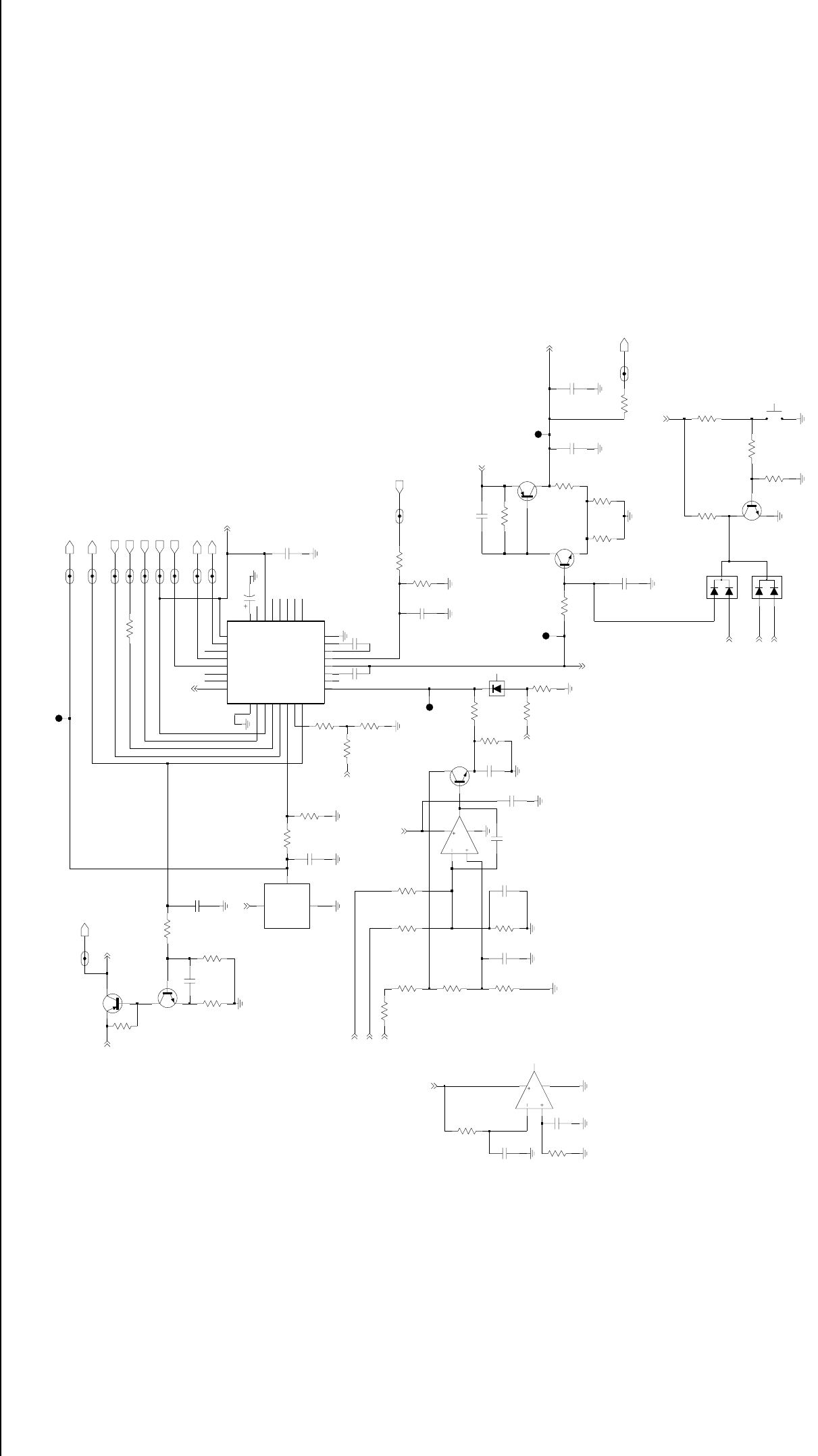
4-22 Low Band PCBs / Schematics / Parts Lists
6.00V (44W)
3.00V (72W)
2.90V (44W)
2.46V (72W)
1.86V (44W)
6.34V (72W)
2.51V (72W)
1.90V (44W)
0.825V
9V3
Q1504
Q1502
R1508
1%
43.2
D1503
D1502 R1545
4.7K
Q1506
C1532
10uF
TP1505
680
CSX
TEMPSENSE_PA_1
R1537
R1501
1000pF
C1531
1.5K
39.2
1%
R1535
.01uF
C1530
R1515
R1524
1K
680
100K
R1510
1.5K
R1541
R1511
100K
1000pF
C1505
100K
R1512
Q1503
82K
R1532
R1502
470
U1502
2
3
1
8
4
CLK_PA_1
DATA
7
8
4
FECNTL_1_PA_1
9T1_PA_1
U1502
6
5
9V3_PA_1
R1509
100K
C1512
R1522
10K
1uF
C1509
2200pF
1K
R1523
R1507
FN0:NP
FN0:NP
FN0:NP
FN0:NP
68K
1%
FECNTL_1
C1526
100pF
1
2
R1542
1K
VAR1
18
VAR2
24
VAR3
VG 15
VL
6VLIM 19
S1501
SWITCH
21
31 RSET
RX 23
T1
2
TEMP
30
V10 14
V45 16
17
V5EXT
20
9
GND1
8
GND2
25
INT
4
22
NA
Q11
QX 10
1RFIN
RS
29
CI
3
CJ
5
CL
7
CLK
26
CQ 12
CQX 13
DATA
28
F168
U1503
H99S-4
ANO
32
BPOS
27
CEX
CSX_PA_1
R1506
R1505
6.8K
R1516
39K
680
C1525
0.1uF
R1503
3.3K
C1510
2200pF
1K
R1543
Q1505
R1544
51K
R1527
100K
R1533
10K
FECNTL_2_PA_1
.01uF
C1528
C1527
.01uF
20K
R1528
PA_PWR_SET_PA_1
PA_PWR_SET
Q1501
100K
R1526
10K
R1525
FN0:NP
2200pF
C1501
R1514
100K
2200pF
C1503
R1504
10K
2200pF
RESET
2200pF
C1504
1.1K
C1508
TP1503
R1513
2200pF
C1502
TEMPSENSE
TP1502
DATA_PA_1
K9V1
K9V1_PA_1
FECNTL_2
2200pF
C1507
2200pF
TP1501
CNTLVLTG
C1511
9T1
CNTLVLTG_PA_1
680
R1519
680
R1517
R1518
3.3K
CLK
D1501
C1506
1000pF
LM50
GND
3
1
POS
VOUT 2
RESET_PA_1
9V3
Vint
PASUPVLTG
9V3
PASUPVLTG
PASUPVLTG
FSWB2
9V3
MOSBIAS_2_SW
MOSBIAS_1_SW
MOSBIAS_3_SW
U1501
9V3
FSWB
9V3
VCNTRL
9V3
PCIC_MOSBIAS_1
9T1
9V3
FN0:NP
FL0830688O
Low Band Range 1 (29.7-36.0 MHz) Power Amplifier - Sheet 2 of 2
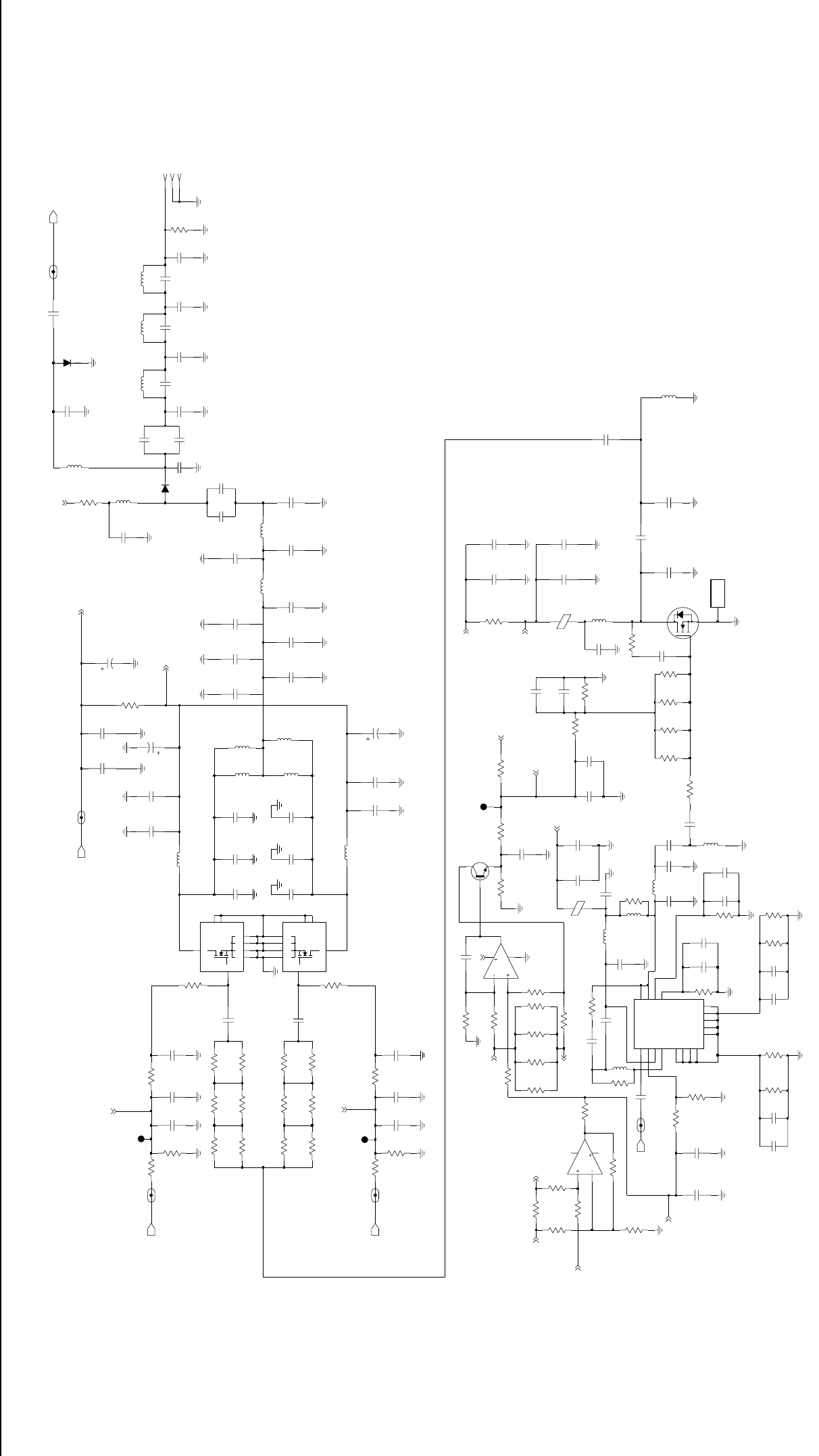
Low Band PCBs / Schematics / Parts Lists 4-23
J1401
1.8V-2.2V
1.8V-2.2V
470pF
C1443
MOSBIAS_2_PA_1
0.1uF
C1428
470pF
R1448
C1472
C1466
.01uF
FNO: NP
150K
30pF
C1452
C1455
C1469
27pF
C1402
.01uF
1uF
C1401
.01uF
1K
R1484
.01uF
C1414
R1414
10
FNO: NP
10
100
R1412
1.8V-2.2V
TP1402
R1440
R1418
10
C1448
240pF
130pF
C1442
.01uF
33 Vpp
33 Vpp
58 Vpp
169 Vpp
C1431
R1464
3.3K
R1445
RXIN
TP1403
10
6.2K
R1457
2.1Vpp
L1424
C1437
430pF
82nH
390
R1402
.01uF
C1434
C1460
0.1uF
10
R1415
FNO: NP
16 Vpp
.01uF
C1476
18 Vpp
L1423
175 Vpp
78.727nH
R1419
10
C1432
1uF
FNO: NP
3pF
C1450
R1476
10
R1424
27K
R1465
3.3K
TXINJ
.01uF
0
R1482
C1468
MOSBIAS_3_PA_1
U1402
MC33072
6
57
8
4
C1457
.01uF
C1429
430pF
L1406
1uF
C1426
250.974nH
C1447
240pF
150pF
C1417
FNO: NP
R1463
12K
240pF
C1441
96 Vpp
C1470
PEAK-TO-PEAK VOLTAGES (Vpp) ARE TYPICAL VALUES
WHICH WOULD BE MEASURED BY AN OSCILLOSCOPE
UNDER THE FOLLOWING CONDITIONS:
1) BATTERY VOLTAGE = 13.6V
2) POUT = 66W AT 39MHz
1uF
10
R1475
R1474
10
D1401
MOSBIAS_2
D1402
10uF
C1462
C1454
62pF
25nH
L1416
C1453
91pF
R1405
DEVICE NEAR INSIDE OF RADIO
51
C1482
1uF
47pF
C1467
FNO: NP
120nH
L1405
R1450
820
E1401
PASUPVLTG_PA_1
C1461
.01uF
88.470nH
L1413
C1419
L1414
88.47nH
C1438
.01uF
10 430pF
330pF
FNO: NP
C1406
R1420
.01uF
C1412
27K
C1408
FNO: NP
R1425
.01uF
330pF
470pF
C1427
C1474
0.1uF
C1473
FNO: NP
Q1404
560pF
C1418
RXIN_PA_1
FNO: NP
39K
R1466
R1407
10K 1uF
C1433
68pF
FNO: NP
C1409
25nH
L1426 C1480
300pF
.01uF
300pF
C1481
C1445
470pF
C1439
FNO: NP
C1416
75pF
10
R1417
R1477
3.3K
C1484
2200pF
R1413
10
R1404
E1403
C1451
51
DEVICE NEAR OUTSIDE OF RADIO
L1404
180pF
RFOUT2 7
VCNTRL
1
VD1
14 VG1 2
VG2 3180nH
GND3
12
GND4
13
NC1
8
NC2
9
NC3
10
NC4
15
RFIN
16 RFOUT1 6
30C65
U1401
17 EP
G2
11
GND1
4
GND2
5
27K
R1480
C1477
100pF
C1422
.01uF
4.7uH
L1402
FNO: NP
R1421
10
R1442
0
C1410
0.1uF
D
G
GND1
GND2
S1
S2
S3
S4
Q1403
POS
L1418
88.470nH
C1446
24pF
HEATSINK
M1401
.01uF
C1420
FNO: NP
L1422
10K
R1472
133.304nH
C1458
10uF
L1415
25nH
MOSBIAS_3
R1443
1K
R1406
10K
R1449
390
.01uF
C1404
C1459
10uF
L1425
C1435
1uF
25nH
C1465
1uF
C1471
.01uF
10
R1416
R1460
L1403
4.7uH
2.5Vpp
0.1
1%
FNO: NP
240R1483
6.2pF
C1403
C1423
.01uF
L1421
150.499nH
180pF
C1449
C1425
1uF
.01
R1409
L1420
196.876nH
10
R1422
C1444
470pF
FN0: NP
0
R1471
FNO: NP
2.2K
R1468
.01uF
C1424
L1417
25nH
.01uF
C1464
180
R1454
R1458
390
3.3K
R1479
.01uF
C1413
10
R1473
10K
FNO: NP
G
GND1
GND2
S1
S2
S3
S4
R1441
Q1402
D
R1467
TP1401
FNO: NP
39K
TXINJ_PA_1
R1446
FNO: NP
5.6K
C1463
1uF
R1470
C1440
470pF
FNO: NP
2.4K
FNO: NP
430pF
C1430
R1444
470
C1479
240pF
100pF
C1478
10
R1423
0.1uF
C1529
180
C1405
FNO: NP
R1451
.01uF
.01uF
10K
C1407
R1411
75pF
27uH
2 Vdc
L1419
1uF
PASUPVLTG
C1456
C1475
130
FNO: NP
.01uF
C1421
C1415
R1410
Q1401
0.1uF
R1459
R1447
390
C1436
.01uF
0
R1478
0
R1469
10K
.01uF
2
3
1
8
4
C1485
6.8nH
FNO: NP
MC33072 U1402
180
R1455
L1401
180
R1453
9V3
PASUPVLTG
VCNTRL
FSWB2
Vint
U_PREDRIVER
U_DRIVER
PASUPVLTG
U_PREDRIVER
MOSBIAS_2_SW
MOSBIAS_3_SW
MOSBIAS_1_SW
PASUPVLTG
U_DRIVER
FSWB
PCIC_MOSBIAS_1
9T1
FL0830607A
Low Band Range 2 (36.0-42.0 MHz) Power Amplifier - Sheet 1 of 2

4-24 Low Band PCBs / Schematics / Parts Lists
LM6142
6.20V (72W)
FN0: NP FN0:NP
LM6142
5.86V (44W)
2.95V (72W)
2.85V (44W)
2.48V (72W)
1.85V (44W)
2.51V (72W)
1.86V (44W)
0.825V
FN0:NOTPLACED
R1517
680
R1523
1%
68K
CNTLVLTG
100K
R1527
C1504
CNTLVLTG_PA_1
C1508
2200pF
R1513
2200pF
FECNTL_1
RESET
1.1K
FECNTL_1_PA_1
Q1502
CSX_PA_1
680
R1501
3.3K
R1518
1000pF
C1506
CLK
1
2
VOUT
RESET_PA_1
LM50
U1501
3GND
POS
R1510
100K
10K
R1533
CSX
9T1_PA_1
FECNTL_2_PA_1
R1508
9T1
R1509
43.2
1%
100K
C1527
9V3_PA_1
.01uF
.01uF C1528
FN0: NP
FN0:NOTPLACED
R1525
10K
C1531
1000pF .01uF
C1530
D1503
D1502 R1545
Q1506
MMBT3904
4.7K
R1543
1K
51K
R1544
100K
R1511
1000pF
R1512
100K C1505
Q1503
R1532
82K
100pF
C1526
R1528
20K
PA_PWR_SET_PA_1
PA_PWR_SET
Q1501
U1502
6
57
8
4
TP1505
DATA_PA_1
K9V1
K9V1_PA_1
R1505
C1507
2200pF
6.8K R1506
39K
R1516
680
6VL 19
VLIM
0.1uF
C1525
30 TEMP
14
V10
16
V45
V5EXT 17
VAR1 20
VAR2 18
VAR3 24
15
VG
NA 22
11
Q10
QX
RFIN
1
21
RS
RSET
31
23
RX
2T1
26 CLK
12
CQ
13
CQX
28 DATA
9
F168
8GND1
25 GND2
4INT
32 ANO
27 BPOS
29 CEX
3CI
5CJ
7CL
2200pF
C1510
H99S-4
U1503
Q1505
2200pF
C1511
1K
R1542
SWITCH
S1501
1
2
TP1503
39.2
1%
R1535
R1524
680
C1502
2200pF
DATA
TP1502
C1501
2200pF
100K
R1514
1.5K
R1540
2
31
8
4
R1539
1.5K
U1502
R1519
680
1K
R1507
470
R1502
R1526
100K
R1503
R1515
1K
3.3K
10K
R1522
C1512
2200pF
TEMPSENSE_PA_1
C1509
1uF
TEMPSENSE
D1501
C1503 2200pF
10K
R1504
TP1501
FECNTL_2
9V3
Q1504
9V3
Vint
9V3
PASUPVLTG
FSWB2
9V3
MOSBIAS_2_SW
MOSBIAS_1_SW
MOSBIAS_3_SW
PASUPVLTG
CLK_PA_1
9V3
FSWB
PASUPVLTG
9V3
VCNTRL
9V3
PCIC_MOSBIAS_1
9T1
9V3
FL0830607O
SHEET 2
Low Band Range 2 (36.0-42.0 MHz) Power Amplifier - Sheet 2 of 2
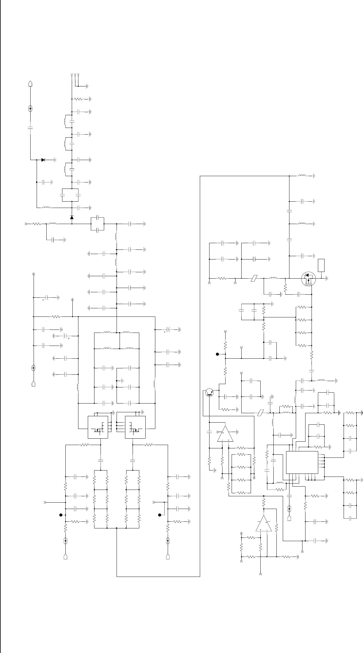
Low Band PCBs / Schematics / Parts Lists 4-25
20 Vpp
18 Vpp
25 Vpp
25 Vpp
190 Vpp 180 Vpp
J1401
1.8V-2.1V
1.8V-2.1V
3.7V-3.9V
2.5 Vpp
5 Vpp
90 Vpp
10 Vpp
Peak-to-Peak Voltages (Vpp) are typical values as
could be measured with an oscilloscope under
the following conditions:
1.) Battery Voltage = 13.6 Volts
2.) Test Channel 11, i.e. High Power @ 46.125 MHz
DEVICE NEAR INSIDE OF RADIO
DEVICE NEAR OUTSIDE OF RADIO
0
E1403
R1469
C1404
.01uF
C1476
0.1uF
C1416
30pF
137.876nH
L1421
FN0:NP
D1402
1uF
C1425
10
R1421
3.3K
R1464
120nH
FN0:NP
R1483
240
L1405
R1404
51
R1423
10
10uF
33pF
C1454
C1462
220
R1444
3.3K
0.1uF
C1460
R1479
C1458
C1473
0.1uF
10uF
300pF
180pF
MOSBIAS_2_PA_1
C1478
C1451
10uF
C1459
C1427
240pF
180
R1453
PASUPVLTG
3.3K
R1477
R1449
TP1402
390
430pF
C1417
390
R1458
270pF
C1412
27K
R1425
C1433
1uF
300pF
C1477
R1445
6.2K
L1426
18nH
MC33072
U1402-2
6
5
7
8
4
27K
R1424
1uF
C1475
10K
RXIN_PA_1
C1428
R1478
U1402-1
MC33072
2
3
1
8
4
240pF
.01uF
100
R1440
C1424
C1448
Q1404
FN0:NP
470pF
R1484
1K
220pF
C1479
C1406
470pF
C1437
FN0:NP
330pF
C1407
.01uF
24pF
C1469
1uF
C1452
R1473
10
R1457
10
R1463
12K
L1419
27uH
R1441
10K
FN0:NP
16pF
C1455
470pF
C1447
FN0:NP
L1424
36.54nH
R1414
10
10
R1412
FN0:NP
.01uF
C1461
C1485
10K
R1406
.01uF
D1401
MOSBIAS_2
.01uF
C1457
R1411
L1406
250.974nH
10K
C1414
.01uF
10K
R1407
L1416
18nH
R1415 10
FN0:NP
C1466
.01uF
51pF
C1456
R1482
0
R1416
10
.01uF
C1405
1uF
C1432
3pF
R1446
5.6K
C1450
C1401
.01uF
FN0:NP
68pF
C1467
180
R1455
MOSBIAS_3
TP1403
470pF
C1440
R1470
2.4K
FN0:NP
R1422
10
10
R1420
R1451
180
C1470
R1460
1%
0.1 1uF
88.470nH
L1414
180
R1454
C1426
1uF .01uF
C1422
FN0:NP
C1413
.01uF
L1413
88.470nH
C1430
240pF
.01uF
C1434
C1419
.01uF
R1448
150K
FN0:NP
10
R1418
39K
FN0:NP
C1486
R1466
C1408
0.1uF
FN0:NP
330pF
PASUPVLTG_PA_1
E1401
RXIN
.01uF
C1471
.01uF
C1468
R1417
10
18nH
L1415
C1443
130pF 130pF
C1444
172.891nH
L1420
C1431
.01uF
R1475
10
R1442
10
R1419
100
.01uF
24pF
C1446
66.389nH
L1418
C1420
C1403
6.2pF
R1443
FN0:NP
FN0:NP
1K
C1421
.01uF
820
R1450
C1442
120pF
R1402
390
10
R1413
R1468
2.2K
FN0:NP
TP1401
2200pF
C1484
R1447
0
L1402
4.7uH
S3
S4
.01uF
C1402
Q1402
D
G
GND1
GND2
S1
S2
MOSBIAS_3_PA_1
0.1uF
C1472
82pF
C1480
C1481
82pF
C1449
110pF
1uF
C1482
1uF
C1463
1uF
C1435
.01uF
C1445
FN0:NP
C1439
470pF
R1467
39K
FN0:NP
FN0:NP
6.8nH
L1401
L1422
115.581nH
R1472 10K
C1438
470pF
C1441
220pF
M1401
HEATSINK
POS
.01uF
C1474
TXINJ_PA_1
R1409
.01
18nH
L1417
R1474
10
100pF
C1453
51
R1405
R1476
10
3
VG2
81.930nH
L1423
10 NC3
15 NC4
16 RFIN 6
RFOUT1 7
RFOUT2
1VCNTRL
14 VD1 2
VG1
EP
17
11 G2
4GND1
5GND2
12 GND3
13 GND4
8NC1
9NC2
U1401
30C65
.01uF
C1464
R1459
390
L1403
C1465
1uF
180nH
4.7uH
L1408
120nH
L1404
FN0:NP R1471
0
FN0:NP
130
R1410
C1409
68pF
.01uF
C1436
240pF
C1429
.01uF
C1423
S4
FN0:NP
C1418
510pF
D
G
GND1
GND2
S1
S2
S3
0.1uF
Q1403
C1415
0.1uF
C1410
Q1401
18nH
27K
L1425
R1480
3.3K
R1465
PCIC_MOSBIAS_1
9V3
PASUPVLTG
VCNTRL
FSWB2
Vint
U_PREDRIVER
U_DRIVER
PASUPVLTG
MOSBIAS_2_SW
MOSBIAS_3_SW
MOSBIAS_1_SW
TXINJ
PASUPVLTG
U_DRIVER
U_PREDRIVER
FSWB
9T1
FL0830695O
Low Band Range 3 (42-50 MHz) Power Amplifier - Sheet 1 of 2
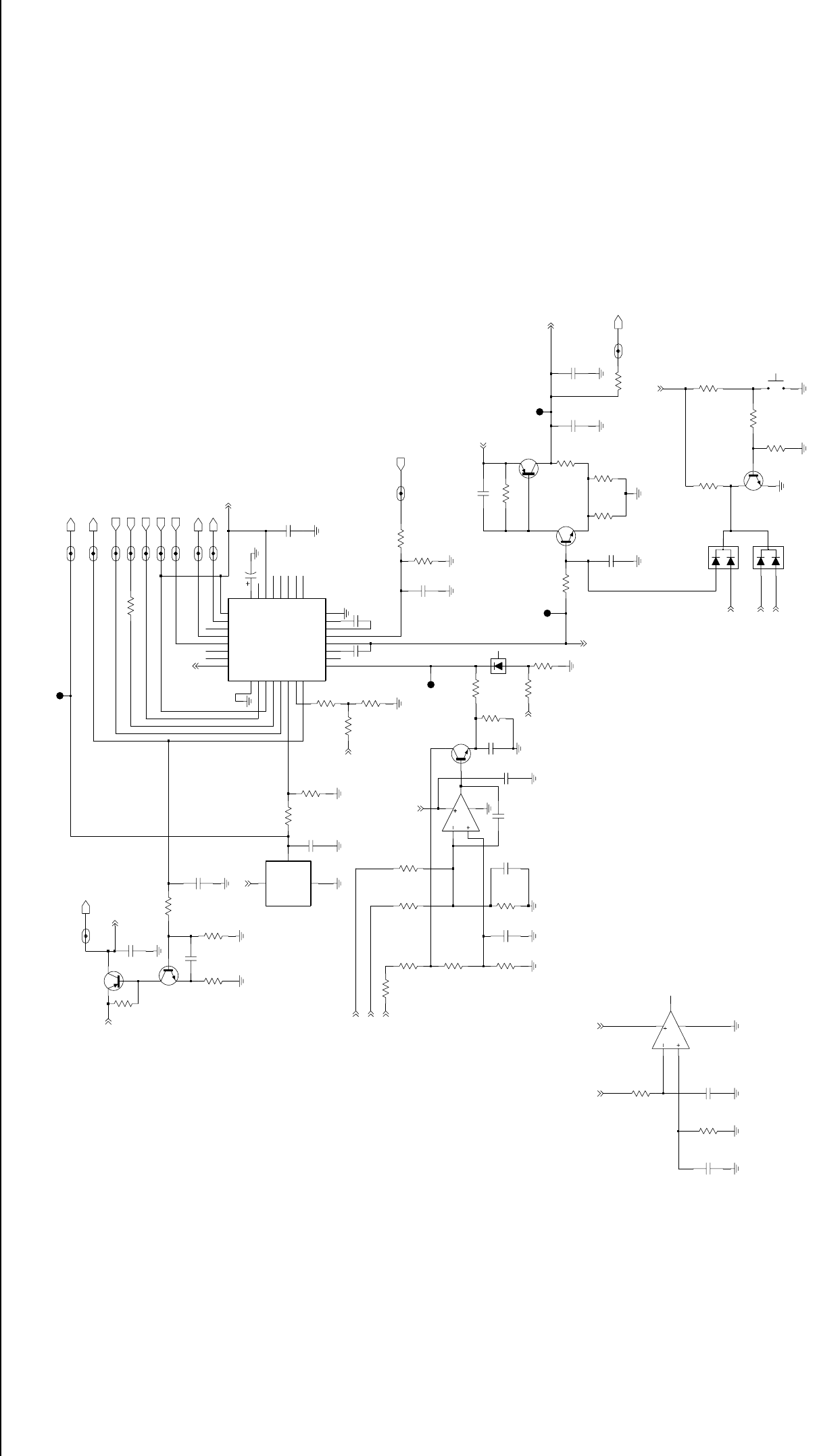
4-26 Low Band PCBs / Schematics / Parts Lists
2.10V (44W)
2.878V (72W)
2.137V (44W)
4.57V (44W)
2.54V (72W)
2.42V (44W)
2.85V (72W)
0.825V
4.93V (72W)
R1526
100K
680
R1501
R1524
680
10K
R1504
C1527
.01uF
470
R1502
51K
1K
R1537
R1542
Q1501
RESET_PA_1
0
R1535
R1532
82K
Q1502
FECNTL_1_PA_1
DATA_PA_1
R1519
680
TP1502
6.2K
R1541
Q1503
Q1504
2200pF
C1504
2200pF
C1508
1.1K
R1513
R1517
680
6
5
7
8
4
DATA
C1525
U1502-2
VAR2 18
VAR3 24
15
VG
6VL 19
VLIM
0.1uF
RSET
31
23
RX
2T1
30 TEMP
14
V10
16
V45
V5EXT 17
VAR1 20
8GND1
25 GND2
4INT
NA 22
11
Q
10
QX
RFIN
1
21
RS
3CI
5CJ
7CL
26 CLK
12
CQ 13
CQX
28 DATA
9
F168
H99S-4
U1503
32 ANO
27 BPOS
29 CEX
2200pF
C1510
Q1505
2200pF
C1511
1
2
CSX_PA_1
C1506
S1501
SWITCH
1000pF
C1523
0.1uF
100K
R1509
TP1505
PA_PWR_SET
9V3_PA_1
TEMPSENSE
TEMPSENSE_PA_1
C1503
2200pF
D1503
D1502 R1545
4.7K
Q1506
1K
R1543
R1544
51K
R1533
CSX
CNTLVLTG_PA_1
CNTLVLTG
10K
100K
R1511
1000pF
FECNTL_2
CLK_PA_1
9V3
C1505
K9V1
9T1
9T1_PA_1
680
K9V1_PA_1
10uF
C1532
R1516
100K
FN0:NP
1K
R1512
100K
FN0:NP
R1515
C1526
R1510
.01uF
100pF
FECNTL_2_PA_1
C1528
PA_PWR_SET_PA_1
CLK
FECNTL_1
1
2
VOUT
D1501
LM50
U1501
3GND POS
C1502
2200pF
3.3K
R1503
FN0:NP
1000pF
C1531
C1530
.01uF
3.3K
R1518
RESET
C1501
2200pF
100K
R1514
20K
2
3
1
8
4
R1528
U1502-1
C1512
2200pF
FN0:NP
C1509
1uF
R1523
1%
68K
100K
R1527
FN0:NP
R1525
10K
10K
R1522
100
1%
R1508
C1507
2200pF
TP1501
TP1503
1K
R1507
6.8K
R1505
R1506
39K
9V3
Vint9T1 PASUPVLTG
9T1
PASUPVLTG
FSWB2
MOSBIAS_2_SW
MOSBIAS_1_SW
MOSBIAS_3_SW
9V3
PASUPVLTG
VCNTRL
9V3
FSWB
9V3
9V3
PCIC_MOSBIAS_1
9V3
9V3
FL0830696O
Low Band Range 3 (42-50 MHz) Power Amplifier - Sheet 2 of 2
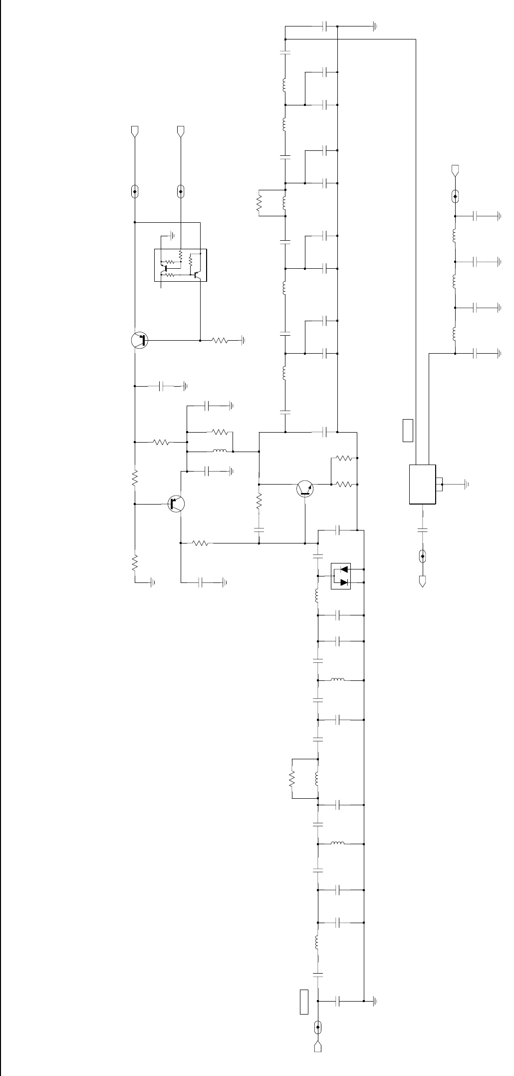
Low Band PCBs / Schematics / Parts Lists 4-27
AT ANTENNA PORT J1401
-47 dBm (1mVrms)
-50 dBm
-38 dBm
+14 dBm (R)
9.1VDC (T)
0VDC (R)
9.14VDC
8.36VDC (R)
9.1VDC (T)
9.03VDC (R)
0VDC (T)
4.60VDC
4.00VDC
1.47VDC
4.56VDC
0.18VDC
0.94VDC
C1041
L1003
9V3
220pF
10%
0.1uF
130nH
300pF
C1031
L1004
C1022
RXIN_FE_1
130nH
C1015
.01uF
360pF
C1021
L1009
130nH
130pF
C1034
C1026
.01uF
9T1_FE_1
C1016
200pF
C1024
C1035
330pF
9T1
91pF
L1014
C1003
220pF
C1006
220nH
C1013
91pF 0.1uF
C1017
.01uF
270pF
130nH
L1008
220pF
C1025
0.1uF C1012
RXINJ_FE_1
C1002
220pF
C1042
180pF
C1011
390pF
C1039
C1037
390pF
C1038
300pF
300pF
XIN
C1007
R1003
470
360pF
C1020
C1004
130nH
L1006
L1002
160pF
130nH
R1008
C1023
360pF
5GND3
2IF 6
LO
3
RF
4.7K
4.7K
47K
47K
10K
MIXER
U1051
1GND1
4GND2
FN0:NP
100
R1009
C1036
0.1uF
120pF
C1033
C1019
270pF
FN0:NP
R1010
0
300pF
C1040
Q1002
MMBT3906
RXINJ
130nH
L1005
IF_FE_1
Q1001
MMBR951
L1007
130nH
220pF
270pF
C1009 C1014
130nH
L1001
C1029
5%
.01uF
82pF
C1010
U1001
UMC5N
2
6
4
1
3
R1007
8.2K
L1010
130nH
D1001
MMBD353
2
3
1
180pF
C1027
15
R1002
C1032
100pF
R1006
10K
R1001
R1004
2.7K
15
C1028
5%
.01uF
330nH
L1013
FN0:NP
9V3_FE_1
IF
0
R1011
L1011
1uH
C1001
220pF
0.1uF
10%
C1030
R1005
180
220nH
L1012
0.1uF
C1008
Q1003
MMBT3906
FL0830689O
Low Band Range 1 (29.7-36.0 MHz) Receiver Front End
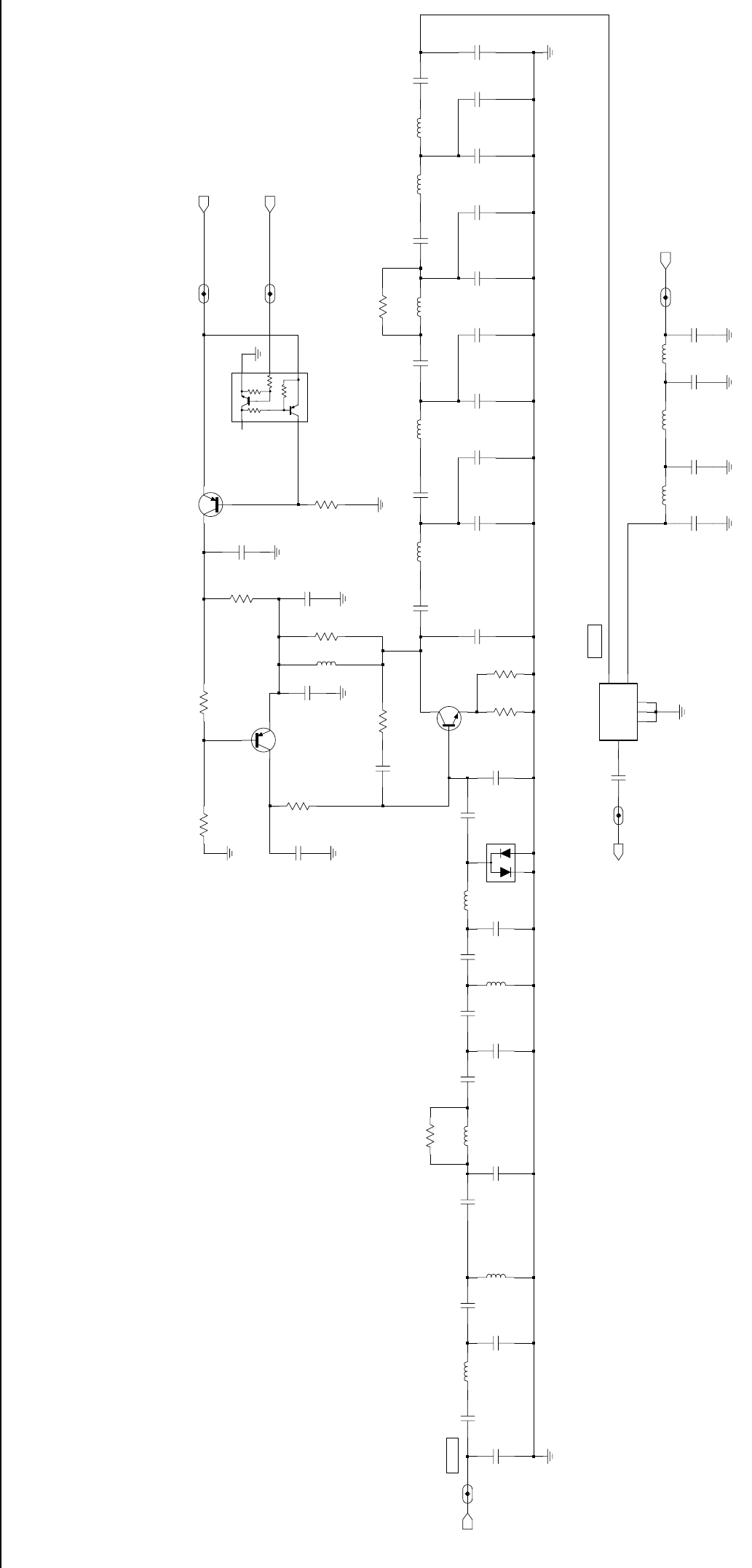
4-28 Low Band PCBs / Schematics / Parts Lists
4.61VDC
0.90VDC
0.15VDC
AT ANTENNA PORT J1401
-47 dBm (1mVrms)
-50 dBm
-38 dBm
+14 dBm (R)
4.64VDC
4.05VDC
1.33VDC
9.03VDC (R)
0VDC (T)
8.36VDC (R)
9.1VDC (T)
9.14VDC
9.1VDC (T)
0VDC (R)
300pF
C1021
150pF
9T1_FE_1
C1016
9T1
62pF
C1035
62pF
C1010
C1025
240pF
220pF
C1024
C1002
.01uF
220nH
L1014
C1028
5%
.01uF
330nH
L1013
4
1
3
RXINJ_FE_1
9V3_FE_1
U1001
UMC5N
2
6
100pF
C1034
R1007
8.2K
L1011
1uH
C1001
160pF
0.1uF
10%
C1030
C1032
75pF
R1006
10K
10
R1001
Q1003
MMBT3906
91pF
C1033
9V3
C1015
.01uF
1GND1
4GND2
5GND3
2IF 6
LO
3
RF
MIXER
U1051
FN0:NP
FN0:NP
100
R1009
IF
0
R1011
FN0:NP
R1010
0
120pF
C1004
R1005
180
Q1002
MMBT3906
C1011
120pF
IF_FE_1
RXINJ
L1007
130nH
220pF
C1020
L1004
C1022
220pF
RXIN
130nH
R1003
470
C1014
160pF
240pF
C1009
C1013
0.1uF
C1036
.01uF
C1017
1200pF 130nH
L1006
150pF
C1027
Q1001
MMBR951
R1002
15
R1004
2.7K
1200pF
130nH
L1008
300pF
C1026
300pF
C1012 300pF
C1039
C1003 300pF
C1038
220pF
C1037
C1019
240pF
1000pF
C1008
220nH
L1012
RXIN_FE_1
130nH
L1003
C1031
10%
0.1uF
L1001
C1007
240pF
130nH
130nH
5%
.01uF
L1005
C1006
C1029
L1002 62pF C1040
130nH
130nH
220pF
D1001
MMBD353
2
3
1
L1010
130nH
300pF
L1009
4.7K
4.7K
47K
47K
10K
R1008
C1023
FL0830599A
Low Band Range 2 (36.0-42.0 MHz) Receiver Front End
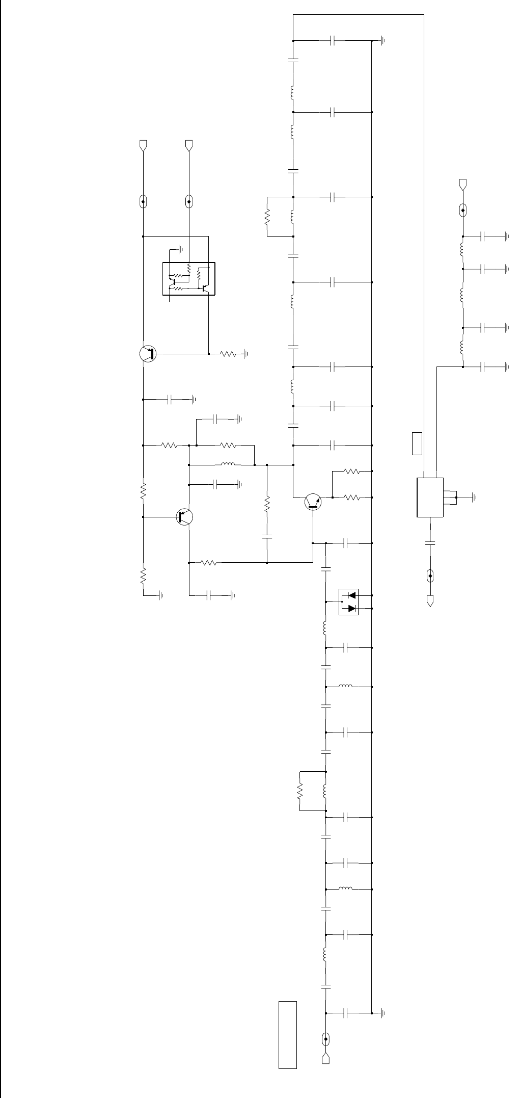
Low Band PCBs / Schematics / Parts Lists 4-29
-47 dBm (1mVrms)
0.94VDC
4.56VDC
1.47VDC 4.60VDC
4.00VDC 9.03VDC (R)
8.36VDC (R)
9.14VDC
9.1VDC (T)
0VDC (R)
+14 dBm (R)
-38 dBm
9.1VDC (T)
0VDC (T)
-50 dBm
AT ANTENNA PORT J1401
0.18VDC
9V3
.01uF
C1015
MMBR951
Q1001
RXINJ
IF_FE_1
160pF 130nH
L1007 C1022
C1020
150pF
RXIN_FE_1
L1004
130nH 130pF
C1014
C1009
180pF
L1001
130nH 130nH
L1005
470pF
C1017 L1006
130nH
3
1
FN0:NP
15pF
C1005
MMBD353
D1001
2
C1027
110pF
R1002
15
2.7K
R1004
LO 6
RF 3
R1008
4.7K
4.7K
47K
47K
10K
U1051
MIXER
GND1
1
GND2
4
GND3
5
IF
2
R1009
100
FN0:NP
L1008
130nH
330pF
C1019
0
R1010
FN0:NP
180pF
Q1002
C1004
C1036
0.1uF
240pF
C1012
9T1
C1035
51pF
75pF
C1011
C1034
75pF
300pF
C1025
C1024
160pF
91pF
C1003
L1014
220nH
.01uF
5%
C1028
L1013
330nH
.01uF
C1002
2
6
4
1
3
RXINJ_FE_1
43pF
UMC5N
U1001
9V3_FE_1
C1010
1uH
L1011
FN0:NP
130pF
C1001
8.2K
R1007
62pF
C1032
10K
R1006
C1030
10%
0.1uF
Q1003
C1033
68pF
R1001
15
R1011
0
180
R1005
IF
FN0:NP
L1012
220nH
130nH
C1008
560pF
C1031
L1003
C1007
0.1uF
10%
R1003
RXIN
180pF
C1029
470
56pF
.01uF
5%
C1006 C1013
680pF
L1002
130nH
FN0:NP
15pF
C1018
130nH
L1010L1009
C1021
390pF
C1023
130nH
390pF
C1016
1000pF
C1026
9T1_FE_1
130pF
FL0830697O
Low Band Range 3 (42-50 MHz) Receiver Front End
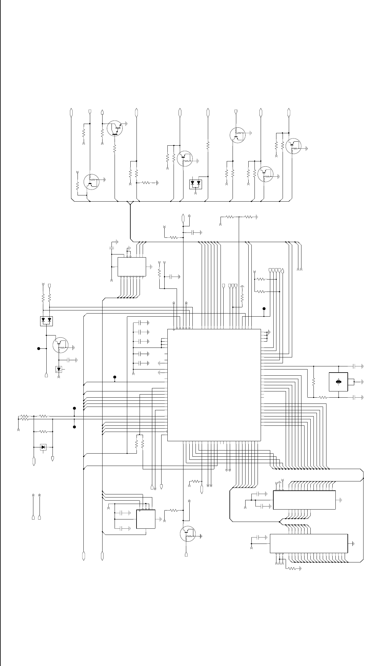
4-30 Low Band PCBs / Schematics / Parts Lists
HSIO
GP4_OUT
GP7_OUT
HC138_A2
GP1_IN
GP8_OUT
EXP1_CS
EE_CS
HSIO
GP7_IN
CLK
GP5_IN
GP1_IN
CLK
CSX
- R0105 USED IN
STANDARD ONLY
- R0106 USED IN
PRIME ONLY
GP7_OUT
VOX
LSIO
GP7_IN
HC138_A0
REF_CS
MISO
EXP2_CS
512kx8bit
RAM
GP6_IN
GP6_IN
HC138_A0
GP3_IN
GP8_IN
GP3_IN
GP8_IN
PE6
LVZIF_CS
GP4_IN
SQ_DET
HC138_A1
FLASH ROM
SYN
HC138_A2
GP2_OUT
LSIO
MICROPROCESSOR
DATA
MISO
F1200
GP4_IN
GP5_IN
GP4_OUT
VS_CS
ON_OFF_SENSE
GP8_OUT
EEPROM
DATA
32kx8bit
OPT_CS
HC138_A1
CHACT
16Kx8bit
GP4_OUT
GP7_OUT
(EXT_BD_PTT & DATA_PTT)
EE_CS
47K
47K
47K
47K
47K
47K
47K
R0179
0
R0116
NU
4
R0152
24K
R0132
330K
R0172
2
10K
R0175
6
7
10K
R0115
0
R0111
10K
7
10
1
100pF
C0101
C0107
90
1000pF
11
6
R0114
10K
10K
R0104
69
VRL 68
VSS
13
VSSL
40 VSSR
87
93
XFC
XIRQ 48
XTAL 91
76
PJ6 77
PJ7 78
RESET 94
VDD 12
VDDL 39
VDDR 88
VDDSYN 92
VRH
51 PI6
50 PI7
49
PJ0_CSGP3 71
PJ1_CSGP4 72
PJ2 73
PJ3 74
PJ4 75
PJ5
42
PH6_CSGP2
41
PH7_CSPROG
38
PI0
56 PI1
55 PI2
54 PI3
53 PI4
52 PI5
18
PG6_AS
5
PG7_R_W 4
PH0_PW1
47
PH1_PW2
46
PH2_PW3
45
PH3_PW4
44
PH4_CSIO
43
PH5_CSGP1
23 PF7_ADDR7
22
PFO_ADDR0
29
PG0_XA13
6
PG1_XA14
16
PG2_XA15
20
PG3_XA16
19
PG4_XA17
17
PG5_XA18
PE5_AN5 61
PE6_AN6 60
PE7_AN7
PF1_ADDR1
28 PF2_ADDR2
27 PF3_ADDR3
26 PF4_ADDR4
25 PF5_ADDR5
24 PF6_ADDR6
1
PD5_SS 2
3
PD6_LVIN
67
PE0_AN0 66
PE1_AN1 65
PE2_AN2 64
PE3_AN3 63
PE4_AN4 62
34
PC5_DATA5
35
PC6_DATA6
36
PC7_DATA7
37
PD0_RXD 97
PD1_TXD 98
PD2_MISO 99
PD3_MOSI 100
PD4_SCK
15 PB6_ADDR14
8PB7_ADDR15
7
PBO_ADDR8
14
PC0_DATA0
30
PC1_DATA1
31
PC2_DATA2
32
PC3_DATA3
33
PC4_DATA4
83
PA5_OC3_OC1 84
PA6_OC2_OC1 85
PA7_PA1_OC1 86
PB1_ADDR9
10 PB2_ADDR10
11 PB3_ADDR11
9PB4_ADDR12
21 PB5_ADDR13
96
95
LVOUT
MODA_LIR 58
MODB_VSTBY 57
PA0_IC3 79
PA1_IC2 80
PA2_IC1 81
PA3_IC4_OC5_OC1 82
PA4_OC4_OC1
U0101
AVDD 59
AVSS
70
ECLK 89
EXTAL 90
IRQ
R0170
5
11
10K
0
4
10
3
WP
1
CS
7
HOLD
6
SCK
5
SI
2SO
8
VCC
4
VSS
X25128-2.7
U0111
.01uF
C0151
47K
47K
0.1uF
C0141
7
1
7
C0106
100pF
NU
12
3
0
15 Y0
14 Y1
13 Y2
12 Y3
11 Y4
10 Y5
9Y6
7Y7
1
A0 2
A1 3
A2
6
EN_CS1 4
EN_CS2 5
EN_CS3
8GND 16
VCC
12
MC74HC138A
U0141
TP0102
6
5
6
10
R0185
4.7K
IO6
17
IO7
18
IO8
19
VCC
28
8
2
6
EN_OE 22
EN_WE 27
14 GND
IO1
11
IO2
12
IO3
13
IO4
15
IO5
16 A3 7
A4 6
5
A5
A6 4
A7 3
A8 25
A9 24
EN_CS 20
A0 10
A1 9
21
A10
A11 23
A12 2
A13 26
A14 1
A2 8
6
U0122
63A21
2.2K
R0108
8
17
3
9
Q0181
10
6
6
0.1uF
7
TP0151
C0121
C0102
100pF
NU NU
18
C0104
100pF
47K
R0184
10K
47K
47K
R0174
22pF
C0132
Q0185
0
12
3
1
R0183
4.7K
11
413
Q0173
12
013
D0151
R0173
12
2
3
4.7K
1
8
8
4
18
R0110
NU
7
4.7K
R0177
10K
9
1
4
5
1
1
C0122
7
10
9
8
0.1uF
3
2
TP0103
3
11 1
10
7
2
1
2
C0123
NU
0.1uF
100pF
C0112
10K
R0113
R0151
24K
2
8
0
22
IO1 23
IO2 25
IO3 26
IO4 27
IO5 28
IO6 29
IO7
VCC
8
13 A7
3A8
2A9
30 EN_CE
32 EN_OE
7EN_WE
GND
24
IO0 21
10 A16
6A17
9A18
18 A2
17 A3
16 A4
A5
15
A6
14
20 A0
19 A1
31 A10
1A11
12 A12
A13
4
5A14
A15
11
3
AT49F040
U0121
D0179
2
3
17
9
5
6
7
10K
R0101
TP0101
Q0110
47K
47K R0107
NU
3
47K
4.7K
R0181
4
3
100K
R0105
R0178
5
47K
47K
47K
10MEG
R0131
NU
4
2
100pF
C0105
4.7K
R0171
4
D0101
3.9K
R0117
15
5
14
13
16
5
Q0171
100K
5
R0121
3
Q0151
Q0177
0
R0186
30K
10
47K
0
R0176
13
6
13
4
5
IN 1
9
0
6
1
38.40KHz
Y0131
XTAL
NC
2
NC1
3
OUT
4
NU
R0112
0
47K
R0182
0
NU
8
16
R0106
100pF
C0111
NU
C0103
NU
R0102
4.7K
100pF
22pF
C0131
15
7
VR0151
14
9
Q0183
4
5
0
2
R_W
RAM_CS
BUS+
CNTLVLTG
5VD
SCI_TX
GP1_IN_ACC3
GP6_IN_ACC10
GP2_OUT_ACC4
R_W
FLASH_CE
FLASH_OE
5VD
IRQ
IRQ
ADDR_BUS(0:18)
DATA_BUS(0:7)
14
FROM_U0101_47
VS_RAC
5VD
VS_INT
GP4_IN_OUT_ACC8
5VD
BOOT_CNTRL
GP3_IN_ACC6
5VD
TP0104
ON_OFF_CONTROL
5VD
5VD
5VD
RESET
RESET
5VD
OPT_PTT
5VD
GP5_IN_ACC9
5VD
SPI(0:10) SPI(0:10) SPI(0:10) SPI(0:10)
GPIO(0:13)
GPIO(0:13)
CNTLR_AUDIO(0:7)CNTLR_AUDIO(0:7)
CNTLR_AUDIO(0:7)
FROM_U0101_47
FROM_U0101_46
FROM_U0101_46
5VD
5VD
FLT_A+
TEMPSENSE
RAM_CS
5VD
VS_GAINSEL
EXT_BD_REQ
RSSI
5VD
RX_ADAPT
5VD
5VD
5VD
FLT_A+ FLT_A+
FLASH_OE
NC
ECLK
NC
NC
LOCK
RDY
ON_OFF_CONTROL
GP7_IN_OUT_ACC12
GP8_IN_OUT_ACC14
5VD
5VD
5VD
5VD
FLASH_CE
R_W
VSTBY
5VD
BATTERY_VOLTAGE
FL0830683O
Low Band Range 1/2 Controller - T6
(for PC Boards 8486206B06 & 8486207B05)
Low Band PCBs / Schematics / Parts Lists 4-31
ON_OFF_SENSE
GP5_IN
GP4_OUT
VS_CS
EXP1_CS
GP1_IN
CLK
CSX
HC138_A1
OPT_CS
32kx8bit
- R0105 USED IN
STANDARD ONLY
- R0106 USED IN
PRIME ONLY
GP7_OUT
CLK
GP5_IN
GP8_IN
GP4_IN
GP3_IN
GP8_IN
PE6
LVZIF_CS
512kx8bit
RAM
GP6_IN
GP6_IN
HSIO
GP4_OUT
GP7_OUT
DATA
EEPROM
HC138_A2
SYN
HC138_A2
GP2_OUT
LSIO
MICROPROCESSOR
DATA
MISO
F1200
GP4_IN
GP8_OUT
VOX
LSIO
GP7_IN
HC138_A0
REF_CS
MISO
EXP2_CS
GP1_IN
GP8_OUT
SQ_DET
HC138_A1
FLASH ROM
NU
EE_CS
HSIO
GP7_IN
CHACT
16Kx8bit
GP4_OUT
GP7_OUT
(EXT_BD_PTT & DATA_PTT)
EE_CS
HC138_A0
GP3_IN
8
0
R0106
C0108
0.1uF
NU
R0103
10
NU
C0111
100pF
NU
4.7K
R0102
C0103
100pF
22pF
15
C0131
7
5.6V
VR0151
Q0183
14
9
14
4
5
0
2
15
5
0.1uF
C0112
Q0171
100K
R0121
Q0177
0
3
47K
10
R0186
0
30K
R0176
13
6
13
4
5
1
IN
9
0
6
1
38.40KHz
2
NC
3
NC1
4OUT
NU
XTAL
Y0131
0
R0112
R0182
47K 47K
47K
47K
47K
47K
47K
R0181
4.7K
NU
4
3
R0110
10K
47K
47K
100K
16
5
R0105
R0178
47K
47K
47K
10MEG
4
2
R0131
C0105
100pF
NU
R0171
4.7K
4
D0101
R0117 3.9K
5
14
13
16
5
100pF
NU
7
2
11
C0123 R0113
10K
Q0151
2
8
22
IO2 23
IO3 25
IO4 26
IO5 27
IO6 28
IO7 29
8
VCC
13
A8
3
A9
2
EN_CE
30
EN_OE
32
EN_WE
7
24 GND
21
IO0
IO1
10
A17
6
A18
9
A2
18
A3
17
A4
16
15 A5
14 A6
A7
20
A1
19
A10
31
A11
1
A12
12
4A13
A14
5
11 A15
A16
3
U0121
AT49F040
A0
2
3
17
9
D0179
5
6
7
R0101
10K
TP0101
Q0110
NU
3
18
R0107
47K
R0177
4.7K
1
4
1
17
7
7
10
99
8
C0122
0.1uF
2
TP0103
3
11 1
10
3
1
2
4.7K
R0183
12
3
1
0
24K
R0151
013
413
12
12
D0151
R0173
4.7K
8
8
4
2
3
6
1
3
R0108
2.2K
6
65
1
8
TP0151
10
C0121
7
NU
0.1uF
100pF
C0102 100pF
C0104
NU
47K
18
R0184
R0174
10K
22pF
Q0185
C0132
3
0
CS 1
HOLD 7
SCK 6
SI 5
SO
2
VCC 8
VSS
4
WP
U0111
X25128-2.7
C0151
47K
47K
.01uF
Q0173
7
4
1
7
100pF
C0106
NU
9
Y7
7
12
3
0
8
VCC
16
Y0
15
Y1
14
Y2
13
Y3
12
Y4
11
Y5
10
Y6
A0 1
A1 2
A2 3
EN_CS1 6
EN_CS2 4
EN_CS3 5
GND
5
12
U0141
MC74HC138A
6
6
10
TP0102
2
6
4.7K
R0185
15 IO4
16 IO5
17 IO6
18 IO7
19 IO8
28
VCC
8
24
A9
20
EN_CS 22
EN_OE 27
EN_WE
GND
14
11 IO1
12 IO2
13 IO3
1
A14
8
A2 7
A3 6
A4
A5 5
4
A6 3
A7 25
A8
U0122
10
A0 9
A1
A10 21
23
A11 2
A12 26
A13
11
6
63A21
Q0181
9
R0104
10K
40 VSSL
87 VSSR
XFC 93
48
XIRQ
91
XTAL
94
RESET
12
VDD
39
VDDL
88
VDDR
92
VDDSYN
69
VRH
68
VRL
13 VSS
71
PJ0_CSGP3 72
PJ1_CSGP4 73
PJ2 74
PJ3 75
PJ4 76
PJ5 77
PJ6 78
PJ7
56 PI0
55 PI1
54 PI2
53 PI3
52 PI4
51 PI5
50 PI6
49 PI7
47 PH0_PW1
46 PH1_PW2
45 PH2_PW3
44 PH3_PW4
43 PH4_CSIO
42 PH5_CSGP1
41 PH6_CSGP2
38 PH7_CSPROG
6PG0_XA13
16 PG1_XA14
20 PG2_XA15
19 PG3_XA16
17 PG4_XA17
18 PG5_XA18
5PG6_AS
4
PG7_R_W
28 PF1_ADDR1
27 PF2_ADDR2
26 PF3_ADDR3
25 PF4_ADDR4
24 PF5_ADDR5
23 PF6_ADDR6
22 PF7_ADDR7
29 PFO_ADDR0
PE0_AN0 67
PE1_AN1 66
PE2_AN2 65
PE3_AN3 64
PE4_AN4 63
PE5_AN5 62
PE6_AN6 61
PE7_AN7 60
37 PC7_DATA7
97
PD0_RXD
98
PD1_TXD
99
PD2_MISO
100
PD3_MOSI
1
PD4_SCK
2
PD5_SS
PD6_LVIN 3
14 PBO_ADDR8
30 PC0_DATA0
31 PC1_DATA1
32 PC2_DATA2
33 PC3_DATA3
34 PC4_DATA4
35 PC5_DATA5
36 PC6_DATA6
86
PA7_PA1_OC1
10 PB1_ADDR9
11 PB2_ADDR10
9PB3_ADDR11
21 PB4_ADDR12
15 PB5_ADDR13
8PB6_ADDR14
7PB7_ADDR15
57
MODB_VSTBY
79
PA0_IC3
80
PA1_IC2
81
PA2_IC1
82
PA3_IC4_OC5_OC1
83
PA4_OC4_OC1
84
PA5_OC3_OC1
85
PA6_OC2_OC1
59
AVDD
70 AVSS
89
ECLK
90
EXTAL
96
IRQ
LVOUT 95
58
MODA_LIR
U0101
MC68HC11FL0
R0170
10K
4
10
5
11
0
47K
NU
R0179
R0116
0
C0141
0.1uF
24K
R0152
330K
R0132
R0172
10K
47K
47K
10K
6
2
7
R0175
R0115
10K
7
10
1
R0111
0
100pF
9
C0101
0
C0107
1000pF
10K
R0114
RAM_CS
BUS+
CNTLVLTG
5VD
SCI_TX
GP1_IN_ACC3
GP6_IN_ACC10
GP2_OUT_ACC4
R_W
FLASH_CE
FLASH_OE
5VD
IRQ
IRQ
ADDR_BUS(0:18)
DATA_BUS(0:7)
5VD
TP0104
FROM_U0101_47
VS_RAC
5VD
VS_INT
GP4_IN_OUT_ACC8
5VD
BOOT_CNTRL
GP3_IN_ACC6
ON_OFF_CONTROL
R_W
5VD
5VD
5VD
RESET
RESET
5VD
OPT_PTT
5VD
GP5_IN_ACC9
5VD
SPI(0:10) SPI(0:10) SPI(0:10) SPI(0:10) SPI(0:10)
GPIO(0:13)
GPIO(0:13)
CNTLR_AUDIO(0:7) CNTLR_AUDIO(0:7)
CNTLR_AUDIO(0:7)
FROM_U0101_47
FROM_U0101_46
FROM_U0101_46
5VD
5VD
FLT_A+
TEMPSENSE
RAM_CS
5VD
VS_GAINSEL
EXT_BD_REQ
RSSI
5VD
RX_ADAPT
5VD
5VD5VD
FLT_A+ FLT_A+
FLASH_OE
NC
ECLK
NC
NC
LOCK
RDY
ON_OFF_CONTROL
NC
GP7_IN_OUT_ACC12
GP8_IN_OUT_ACC14
5VD
5VD
5VD
5VD
FLASH_CE
R_W
VSTBY
5VD
BATTERY_VOLTAGE
FL0830684O
Low Band Range 3 Controller-T9 (for PC Board 8486908Z02)
4-32 Low Band PCBs / Schematics / Parts Lists
GP3_IN
GP8_IN
PE6
LVZIF_CS
ON_OFF_SENSE
GP5_IN
GP4_OUT
VS_CS
EXP1_CS
HC138_A 2
SYN
HC138_A1
GP2_OUT
LSIO
MICROPROCESSOR
CLK
GP5_IN
CSX
HC138_A 1
OPT_CS
32kx8bit
R0105 USED IN STANDARD ONLY
GP7_OUT
GP8_OUT
SQ_DET
HC138_A1
R0106 USED IN PRIME ONLY
FLASH ROM
NU
EE_CS
HSIO
GP8_IN
GP4_IN
EE_CS
HC138_A0
GP3_IN
512kx8bit
RAM
GP6_IN
GP6_IN
HSIO
GP4_OUT
GP7_OUT
DATA
EEPROM
HC138_A 0REF_CS
MISO
EXP2_CS
GP1_IN
DATA
MISO
F1200
GP4_IN
GP8_OUT
VOX
LSIO
GP7_IN
GP1_IN
CLK
GP7_IN
CHACT
16Kx8bit
GP4_OUT
GP7_OUT
(EXT_BD_PTT & DATA_PTT)
0
R0112
NU
4.7K
R0181
0
R0106
0.1uF
NU
8
10
C0108
NU
R0103
C0111
100pF
4.7K
R0102
100pF
NU
C0103
15
C0131
22pF
VR0151
14
9
7
Q0183
0
2
15
14 14
13
4
5
7
2
5
0.1uF
C0112
Q0171
100K
R0121
0
3
47K
Q0177
10
R0186
R0176
6
13
4
5
0
30K
0
6
1
13
2
NC
3
NC1
4OUT 1
IN
9
XTAL
Y0131
38.40KHz
Q0110
R0182
47K
NU
4
3
18
R0110
10K
16
5
R0105
100K
R0178
47K
4
2
R0131
10MEG
C0105
100pF
NU
4.7K
4
R0171
D0101
16
5
R0117
3.9K
R0183
5
2
1
4.7K
C0123
100pF
NU
11
R0113
10K
Q0151
IO 6 28
IO 7 29
8
VCC
2
8
EN_WE
7
24
GND
21
IO 0
IO 1 22
IO 2 23
IO 3 25
IO 4 26
IO 5 27
A4
16
15 A5
14 A6
A7
13
A8
3
A9
2
EN_CE
30
EN_OE
32
4A13
A14
5
11 A15
A16
10
A17
6
A18
9
A2
18
A3
17
A0
20
A1
19
A10
31
A11
1
A12
12
2
3
3
U0121
AT49F040
6
17
9
D0179
10K
5
7
R0101
3
8
TP0101
47K
NU
2.2K
6
R0107
R0108
R0177
4.7K
1
4
1
17
7
7
10
99
8
C0122
0.1uF TP0103
3
11 1
10
3
2
1
0
CS 1
HOLD 7
SCK 6
SI 5
SO
2
VCC
8
VSS
4
WP 3
3
U0111
X25128-2.7
12
13
0
24K
R0151
12
0
13
4
D0151
4.7K
12
3
R0173
1
2
6
8
4
2
3
6
10
6
65
1
8
7
TP0151
C0121
C0102
NU
0.1uF
100pF 100pF
C0104
NU
47K
18
R0184
R0174
10K
22pF
Q0185
C0132
R0179
47K
7
4
C0151
.01uF
Q0173
C0106
NU
1
7
0
100pF
12
Y4
11
Y5
10
Y6
9
Y7
7
12
3
6
EN_CS2 4
EN_CS3 5
GND
8
VCC
16
Y0
15
Y1
14
Y2
13
Y3
A0 1
A1 2
A2 3
EN_CS1
6
5
12
U0141
MC74HC138
A
10
TP0102
4.7K
R0185
6
80
C0107
1000pF
12 IO 2
13 IO 3
15 IO 4
16 IO 5
17 IO 6
18 IO 7
19 IO 8
28
VCC
3
A7 25
A8 24
A9
20
EN_CS 22
EN_OE 27
EN_WE
GND
14
11 IO 1
2
A12 26
A13 1
A14
8
A2 7
A3 6
A4
A5 5
4
A6
63A21
U0122
10
A0 9
A1
A10 21
23
A11
11
10K
R0114
Q0181
9
R0104
10K
13 VSS
40 VSSL
87 VSSR
XFC 93
48
XIRQ
91
XTAL
PJ6 78
PJ7
94
RESET
12
VDD
39
VDDL
88
VDDR
92
VDDSYN
69
VRH
68
VRL
PI 6
49 PI 7
71
PJ0_CSGP3 72
PJ1_CSGP4 73
PJ2 74
PJ3 75
PJ4 76
PJ5 77
PH6_CSGP2
38 PH7_CSPROG
56 PI 0
55 PI 1
54 PI 2
53 PI 3
52 PI 4
51 PI 5
50
4
PG7_R_W
47 PH0_PW1
46 PH1_PW2
45 PH2_PW3
44 PH3_PW4
43 PH4_CSIO
42 PH5_CSGP1
41
PF7_ADDR7
29 PFO_ADDR0
6PG0_XA13
16 PG1_XA14
20 PG2_XA15
19 PG3_XA16
17 PG4_XA17
18 PG5_XA18
5PG6_AS
PE7_AN7 60
28 PF1_ADDR1
27 PF2_ADDR2
26 PF3_ADDR3
25 PF4_ADDR4
24 PF5_ADDR5
23 PF6_ADDR6
22
PD5_SS
PD6_LVIN 3
PE0_AN0 67
PE1_AN1 66
PE2_AN2 65
PE3_AN3 64
PE4_AN4 63
PE5_AN5 62
PE6_AN6 61
36 PC6_DATA6
37 PC7_DATA7
97
PD0_RXD
98
PD1_TXD
99
PD2_MISO
100
PD3_MOSI
1
PD4_SCK
2
PB6_ADDR14
7PB7_ADDR15
14 PBO_ADDR8
30 PC0_DATA0
31 PC1_DATA1
32 PC2_DATA2
33 PC3_DATA3
34 PC4_DATA4
35 PC5_DATA5
85
PA6_OC2_OC1
86
PA7_PA1_OC1
10 PB1_ADDR9
11 PB2_ADDR10
9PB3_ADDR11
21 PB4_ADDR12
15 PB5_ADDR13
8
95
58
MODA_LIR 57
MODB_VSTBY
79
PA0_IC3
80
PA1_IC2
81
PA2_IC1
82
PA3_IC4_OC5_OC1
83
PA4_OC4_OC1
84
PA5_OC3_OC1
59
AVDD
70 AVSS
89
ECLK
90
EXTAL
96
IRO
LVOUT
U0101
MC68HC11FL0
11
R0170
10K
0
4
10
5
NU
R0116
0
C0141
0.1uF
24K
R0152
330K
R0132
6
2
R0172 10K
R0175
10K
7
R0115
10K
R0111
0
7
10
1
C0101
100pF
RAM_CS
BUS+
CNTLVLTG
5VD
SCI_TX
GP1_IN_ACC3
GP6_IN_ACC10
GP2_OUT_ACC4
R_W
FLASH_CE
FLASH_OE
5VD
IRQ
IRQ
ADDR_BUS(0:18 )
DATA_BUS(0:7)
5VD
9
FROM_U0101_47
VS_RAC
5VD
VS_INT
GP4_IN_OUT_ACC8
5VD
BOOT_CNTRL
GP3_IN_ACC6
ON_OFF_CONTROL
R_W
5VD
5VD
5VD
RESET
RESET
5VD
OPT_PTT
5VD
GP5_IN_ACC9
5VD
SPI(0:10) SPI(0:10) SPI(0:10) SPI(0:10) SPI(0:10)
GPIO(0:13)
GPIO(0:13)
CNTLR_AUDIO(0:7) CNTLR_AUDIO(0:7)CNTLR_AUDIO(0:7)
CNTLR_AUDIO(0:7)
FROM_U0101_47
FROM_U0101_46
FROM_U0101_46
5VD
5VD
FLT_A+
TEMPSENSE
RAM_CS
5VD
VS_GAINSEL
EXT_BD_REQ
RSSI
5VD
RX_ADAPT
5VD
5VD5VD
FLT_A+ FLT_A+
FLASH_OE
NC_XTAL
ECLK
NC
NC
LOCK
RDY
ON_OFF_CONTROL
NC
GP7_IN_OUT_ACC12
GP8_IN_OUT_ACC14
5VD
5VD
5VD
5VD
FLASH_CE
R_W
VSTBY
5VD
BATTERY_VOLTAGE
ZWG0131049-O
Low Band Range 1/2/3 Controller - T11 (for PC Boards
8486206B08, 8486207B07 & 8486908Z04 )
Low Band PCBs / Schematics / Parts Lists 4-33
13
EXT_BD_PTT
EXT_BD_PTT
NC
FLAT/FILTERED_RX_AUDIO
4
14
REAR VIEW
15
4
RS232 INTERFACE BOARD
18-PIN CONNECTOR
NC
12
31
SPEAKER+
DIG_OUT2 (EXTERNAL_ALARM)
DATA
NC
10
5VD
Key_Row
13
37
DIG_IN_OUT_7
CS*
GND
BUS+
5
6
7
8
9
2
1
OPT_CS
VS_RAC
6
1
RST*
7
8
12
INT_EXT_Vdd
4
GROUND
GND
5
15
14
16
RDY
40
18-PIN CONNECTOR
11
DIG_IN_OUT_4
18
1
2
2
SrD_Snd
DIG_IN_OUT_8
SWB+
20 16
Flat_Tx_Rtn
NC
1
10
BOOT_CNTRL
10
11
36
8
EXP2_CS
NC
17
4
1
2
2
EXT_BD_PTT
GND
12
J0401
5
GROUND
17
18
10
EXT_BD_PTT
13
FAST_SQ
DISCAUDIO
PCB
23
21
14
38
9
Rx_Aud_Snd
5
Det_Aud_Snd
15 17
15
6
MISO
2
5
6
GROUND
GROUND
OPT_PTT
34
INTERNAL OPTION BOARD
FLT_A+
SPEAKER-
FLT_A+
DISCAUDIO
CH_ACT
NC
NC
NC
6
NC
9
VS_CS
7
BUS+
11
1
14
15
16
3
1
NC
NC
3
9
10
EXPANSION BOARD
10
Rdy/Req
2
15
16
NC
5VD
DB3
MISO
GND
16
20
SCI_TX
39
DIG_IN_3
Tx_Aud_Snd
8
DB1
22
12
Rx_Aud_Rtn
NC
12
SCK_Snd
35
NC
NC
18
8
LED_EN
CLK
9
J0551
28
11
CONTROL HEAD
6
RESET
WARIS
TO/FROM RF
7
24
RSSI
NC
J0552
19
32
EXT_BD_PTT
EXT_BD_REQ
EXT_BD_CS
7
17
12
Key_Intrp
13
DIG_IN_OUT_4
9V3
VS_MIC
3
NC
HANSET_AUDIO
11
12
13
14
20
NC
9V3
J0552-1
J0552-2
J0552-3
J0552-4
J0552-5
J0552-6
J0552-7
J0552-8
J0552-9
J0552-10
J0552-11
J0552-12
J0552-13
J0552-14
J0552-15
J0552-16
J0552-17
J0552-18
16
EXP1_CS
VS_AUDSEL
26
FLAT_TX_RTN
6
CSX
29
INT_MIC
DATA
ON
VS_INT
CLK
EXP_BD_PTT
18
40-PIN CONNECTOR
DB5
SPI_MISO
EXT_MIC_AUDIO
4
VS_CS
DB4
7
VS_GAINSEL
Gnd
EXP2_CS
8
DB0
DATA
EXP1_CS
5
SrD_Rtn
19
19
DIG_IN_6 WITHWAKEUP
CLK
Tx_Aud_Rtn
PTT
18
Vddd
25
FLAT_TX_AUDIO
3
10
33
OPT_CS
GP4_IN_OUT
SPI_CLK
SPI_MOSI
J0552-19
J0552-20
NC
TO/FROM RF
8
DATA
GM300
SPEAKER-
ON_OFF_CONTROL
20-PIN CONNECTOR
18
17
J0451
DIG_IN_6 WITH WAKEUP (IGNITION)
ACCESSORY
Opt_Bd_En
Key_Col
3
4
EXP_BD_REQ
NC
NC
DB6
5VD
3
OFF_BATT_DATA_OUT
CLK
30
13
J0501
4
11
9
R/W*
EXP_BD_PTT
SPEAKER+
14
11
DB2
DIG_IN1
3
17
GROUND
27
DB7
GND
A0
7
9 DIG_IN_5 WITH WAKEUP (EMERGENCY)
5
12-PIN CONNECTOR
J0551-36
82pF
C0517
J0401-1
10
CNTLVLTG_CNTLR_1
J0551-3
IN_5V_RF_REG_CNTLR_1
J0401-12
470pF
C0457
MOSBIAS_3
NU
NU
L0481
390nH
470pF
C0449
C0430
470pF
J0551-37
J0501-20
RESET_CNTLR_1
PASUPVLTG_CNTRL_1
J0501-6
J0401-2
VR0503
CLK_CNTLR_1
CSX
C0518
J0451-17
470pF
82pF
NU
C0461
J0451-3
9V3
NU
0.1uF
C0554
470pF
C0502
C0453
NU
470pF
R0510
4.7K
J0551-20
C0409
J0451-10
NU
470pF
C0509
470pF
J0551-5
470pF
C0496
J0451-13
470pF
C0515
J0551-25
J0401-11
VR0501
J0551-4
J0551-14
J0501-2
J0551-31
82pF
C0472
R0412
3A
0
470pF
J0451-5
C0431
10
R0592
J0551-23
J0551-18
R0511
100K
CSX_CNTLR_1
J0401-5
J0551-27
J0451-12
VR0510
TEMPSENSE
9
C0506
470pF
5V_CNTLR_1
470pF
C0429
82pF
C0471
5V
J0551-19
R0512
15K
C0426
470pF
C0501
.01uF
C0468
NU
470pF
470pF
C0514
J0501-3
VR0505
J0551-12
J0401-6
J0551-6
J0551-10
NU
470pF
C0575
470pF
C0487
470pF
C0464
J0551-34
NU
10
R0409
J0451-2
470pF
C0511
CLK
C0512
470pF
J0551-42
J0501-12
J0501-11
7
TP0497
TP0530
16_8MHZ
J0551-1
J0451-9
J0501-17
16_8MHZ_CNTLR_1
J0551-32
DATA_CNTLR_2
470pF
C0503
NU
C0462
82pF
C0486
470pF
470pF
C0499
CSX_CNTLR_2
C0470
470pF
27K
R0541
470pF
C0410
J0451-1
NU
0.1uF
C0592
J0551-21
NU
470pF
C0403
1K
R0442
2
J0501-8
470pF
DISCAUDIO_CNTLR_1
C0477
LOCK_CNTLR_1
0.1uF
C0591
R0529
47K
C0495
470pF
J0551-41
470pF
C0492
RSSI
MOSBIAS_3_CNTLR_1
470pF
C0456
470pF
NU NU
C0455
R0467
10
J0501-7
J0551-9
470pF
470pF
C0427
C0482
J0551-38
CSX
82pF
C0428 J0451-18
8CLK_CNTLR_2
J0451-7
470pF 470pF
C0452
C0422
INT_SWB_CNTLR_1
NU
470pF
CLK
INT_SWB
NU
C0407
J0451-8
220
R0538
J0451-6
1
100K
R0543
C0485
470pF
C0478
470pF
R0482
0
0
R0468
100K
R0481
470pF
NU
C0443
470pF
J0501-9
C0474
CNTLVLTG
J0551-28
9
9V3_CNTLR_1
470pF
8
NU
C0558
82pF
C0421
J0451-16
R0407
10
MOSBIAS_2
470pF
C0508
J0551-7
470pF
C0476
J0551-33
TP0492
NU
C0576
470pF
C0541
0.47uF
9
R0441
0
J0501-4
100
J0551-15
R0408
470pF
C0466
C0408
82pF
NU
J0551-40
NU
DATA_CNTLR_1
NU
390nH
L0482
J0551-22
C0447
470pF
3
C0488
470pF
470pF
PASUPVLTG
C0513
470pF
1K
NU
C0460
R0535
J0501-18
J0501-19
470pF
C0504
R0593
VR0504
100K
MODIN
J0551-8
J0501-14
PA_PWR_SET_1_CNTLR_1
J0551-2
J0551-16
470pF
C0441
J0501-1
VR0541
RESET
J0401-4
J0401-10
J0401-9
J0401-7
J0401-3
J0401-8
470pF
C0423
J0551-29
47uF
C0542
PA_PWR_SET
0
R0533
C0490
470pF
J0551-30
J0551-35
J0451-14
J0451-4
24K
J0551-17
R0591
4
C0493
470pF
R0531
560
DATA
IN_5V_RF_REG
J0501-10
C0445
470pF470pF
C0446
82pF
C0463
C0451
NU
NU
470pF
NOISE_BLNKR_CNTLR_1
82pF
C0401
J0551-24
NU
0.1uF
C0593
C0406
NU
470pF
DISCAUDIO
J0501-5
C0484
470pF
470pF
C0458C0459
NUNU
470pF
R0525
100K
470pF
C0491
J0551-13
470pF
C0483
NOISE_BLNKR
C0448
LOCK
470pF
220
R0401
J0451-11
J0551-11
470pF
C0467
C0559
DATA
NU
NU
470pF
C0560
470pF
NU
VR0509
MOSBIAS_2_CNTLR_1
470pF
C0494
MODIN_CNTLR_1
C0516
.01uF
RSSI_CNTLR_1
C0497
470pF
470pF
NU
C0411
NU
470pF
C0402
470pF
C0442
F0401
4.7K
R0539
J0551-39
J0551-26
J0501-13
R0537
220
J0451-15
47K
NU
R0542
VR0537
82pF
C0473
R0530
22K
TEMPSENSE_CNTLR_1
C0510
470pF
470pF
J0501-16
J0501-15
C0505
8
SPKR+
FLT_A+
5VD
GP1_IN_ACC3
ON_OFF_CONTROL
EXP1_CS
EXP_BD_REQ
GP1_IN_ACC3
SPI_CLK
SPI_DATA
SPKR-
EXT_MIC
GP1_IN_ACC3
GP2_OUT_ACC4
GP5_IN_ACC9
GP7_IN_OUT_ACC12
GP8_IN_OUT_ACC14
SPKR+
GP3_IN_ACC6
GP4_IN_OUT_ACC8
EXP2_CS
FLAT_TX_RTN
FLAT_TX_RTN
GP6_IN_ACC10GP6_IN_ACC10
GP6_IN_ACC10
GP6_IN_ACC10
SPKR-
INT_SWB+
9V3
SPI_MISO
DISCAUDIO
MODIN
CH_ACT
5VD
9V3
5VD
SPI_MISO
RESET
FLT_A+
DISCAUDIO
GP4_IN_OUT_ACC8
RDY
RDY
OPT_PTT
OPT_PTTOPT_PTT
OPT_PTT
INT_MIC INT_MIC
INT_MIC
SPKR+SPKR+
DISCAUDIO DISCAUDIO
HANDSET_AUDIOHANDSET_AUDIO
HANDSET_AUDIO
EXP2_CS
RSSI RSSI
BOOT_CNTRL
5VD
IN_5V_RF_REG
BUS+
GP1_IN_ACC3
GP1_IN_ACC3 GP1_IN_ACC3
FLAT_TX_RTN
5VD
P4_IN_OUT_ACC8
EXP1_CS
EXP_BD_REQEXP_BD_REQ
EXP_BD_REQ
GP1_IN_ACC3
CH_ACT CH_ACT
CH_ACT
DISCAUDIO
FLT_A+
SCI_TX
RX_FLAT_FILTERED_AUDIO
EMERGENCY_CONTROL
RSSI
EXT_SWB+
RDY
GP4_IN_OUT_ACC8 GP4_IN_OUT_ACC8
CH_ACT
SPI_DATA
SPI_MISO
EXP_BD_REQ
EXP1_CS
OPT_CS
RDY
GP4_IN_OUT_ACC8
SPI_CLK
DISCAUDIO
SPI(0:10)
MOSBIAS_3
VS_MIC VS_MIC
16_8MHZ
5V_RF
NOISE_BLNKR
MOSBIAS_2
PA_PWR_SET
EXP1_CS
9V3
FLAT_TX_RTN FLAT_TX_RTN
RESET
PASUPVLTG
BUS+
FLT_A+
BUS+ BUS+
RESETRESET
ON_OFF_CONTROL ON_OFF_CONTROL
CNTLVLTG
RSSI
LOCK
5VD5VD
FLT_A+FLT_A+
SPI_DATA
SPI_CLK
SPI_MISO
VS_CS
OPT_CS
RESET
EXT_MICEXT_MIC
SPKR-SPKR-
TEMPSENSE
OPT_CS
SPI_DATA
TX_AUD_RTN
VS_CS
VS_MIC
SPI_CLK
FLAT_RX_SND
RX_AUD_RTN
URX_SND
TX_AUD_SND
VS_INT
5VD
VS_AUDSEL
VS_GAINSEL
SPI_MISO
VS_RAC
IGNITION_CONTROL
FLT_A+
FL0830681O
Low Band Range 1 and 2 IO - T6 (for
PC Boards 8486206B06 & 8486207B05
4-34 Low Band PCBs / Schematics / Parts Lists
NC
BUS+10
9V3
VS_MIC
DATA
GM300
SPEAKER-
CLK
30
13
J0501
J0451
DIG_IN_6 WITH WAKEUP (IGNITION)
FLAT/FILTERED_RX_AUDIO
15
14
NC
7
VS_GAINSEL
Gnd
11
DB2
DIG_IN1
3
EXP1_CS
5
6
SPEAKER-
DIG_IN_OUT_8
SWB+
CLK
9
CS*
24
DISCAUDIO
9
R/W*
6
NC
13
DIG_IN_OUT_4
GND
5
15 17
15
6
40
18-PIN CONNECTOR
RS232 INTERFACE BOARD
GND
BUS+
5
NC
RSSI
16
1
PCB
23
21
SPI_CLK
SPI_MOSI
SCK_Snd
35
NC
3
4
EXP_BD_REQ
NC
NC
DB6
ACCESSORY
16
DB3
MISO
NC
9
10
11
14
Rdy/Req
2
GROUND
10
6
19
9
VS_CS
RDY
EXT_BD_REQ
EXT_BD_CS
12
18
Opt_Bd_En
6
1
2
13
14
15
16
17
18
REAR VIEW
15
16
34
INTERNAL OPTION BOARD
39
38
GND
J0552
NC
GROUND
GROUND
NC
BOOT_CNTRL
20
GROUND
DB1
22
GP4_IN_OUT
TO/FROM RF
8
SPI_MISO
5VD
3
OFF_BATT_DATA_OUT EXT_BD_PTT
GND
5VD
9V3
5VD
EXT_BD_PTT
13
10
Flat_Tx_Rtn
NC
1
2
SrD_Snd
12
13
EXT_BD_PTT
12
Rx_Aud_Rtn
12
31
4
12
18-PIN CONNECTOR
7
17
1
2
7
9
11
12
20
NC
NC
10
OPT_CS
VS_RAC
8
RST*
7
8
14
INT_EXT_Vdd
4
EXT_BD_PTT
9
2
1
NC
CLK
7
4
11
J0551
28
FLT_A+
Key_Col
DIG_OUT2 (EXTERNAL_ALARM)
DATA
8
EXP2_CS
FAST_SQ
CONTROL HEAD
J0401
5
4
EXPANSION BOARD
OPT_PTT
16
20
SCI_TX
INT_MIC
DIG_IN_3
Tx_Aud_Snd
Rx_Aud_Snd
SPEAKER+
BUS+
11
10
11
NC
1
14
15
16
17
4
NC
HANSET_AUDIO
3
20-PIN CONNECTOR
18
17
GROUND
SrD_Rtn
RESET
FLT_A+
DISCAUDIO
CH_ACT
DIG_IN_OUT_4
DATA
EXP1_CS
VS_AUDSEL
26
FLAT_TX_RTN
8
5
Det_Aud_Snd
18
40-PIN CONNECTOR
DB5
EXP_BD_PTT
GND
13
37
DIG_IN_OUT_7
2
LED_EN
EXP2_CS
36
DB0
DATA
11
CLK
Tx_Aud_Rtn
PTT
18
8
Vddd
25
32
EXT_BD_PTT
27 ON
VS_INT
DIG_IN_5 WITH WAKEUP (EMERGENCY)
5
Key_Row
Key_Intrp
3
1
NC
NC
3
7
10
A0
EXT_MIC_AUDIO
4
VS_CS
DB4
EXP_BD_PTT
SPEAKER+
14
3
ON_OFF_CONTROL
33
OPT_CS
17
12-PIN CONNECTOR
FLAT_TX_AUDIO
DB7
19
DIG_IN_6 WITHWAKEUP
7
9
6
CSX
29
12
MISO
2
5
6
18
8
19
WARIS
TO/FROM RF
10
TEMPSENSE_CNTLR_1
J0501-16
C0505
470pF
MODIN
J0551-8
20V
VR0505
CLK_CNTLR_1
C0518
470pF
33V
VR0509
470pF
C0423
J0501-20
1000pF
C0560
J0401-11
J0501-17
PA_PWR_SET
16_8MHZ_CNTLR_1
470pF
PASUPVLTG
C0488
C0513
470pF
470pF
DISCAUDIO
C0484
NU
R0542
47K
5.6V
VR0537
82pF
C0517
CNTLVLTG_CNTLR_1
J0401-1
J0501-4
9
J0551-3
J0551-10
470pF
C0510
470pF
C0487
C0431
470pF
10
R0592
J0451-5
J0501-14
470pF
C0514
J0501-3
R0525
100K
PA_PWR_SET_1_CNTLR_1
J0551-25
220
R0538
20V
VR0501
J0551-4
J0551-14
C0542
47uF
0
R0533
J0451-11
220
R0401
J0551-11
J0551-37
NOISE_BLNKR_CNTLR_1
3A
24V
F0401
470pF
J0501-5
J0551-41
C0495
J0551-32
J0451-1
J0551-36
R0530
22K
J0401-7
J0401-10
470pF
RSSI_CNTLR_1
C0497
R0441
0
470pF
C0575
C0541
NU
0.47uF
DATA_CNTLR_1
J0551-40
R0412
0
J0551-20
3
J0451-10
C0509
J0451-17
470pF
82pF
J0501-2
C0472
J0501-12
J0501-11
J0451-6
1
100K
R0543
J0551-23
100K
J0551-18
R0511
CSX_CNTLR_1
DATA
J0401-5
470pF
C0559
R0529
47K
NU
J0551-19
470pF
C0426
C0501
.01uF
J0451-16
82pF
C0421
82pF
C0473
J0551-21
J0401-4
J0401-9
J0401-3
J0401-8
470pF
DISCAUDIO_CNTLR_1
C0477
LOCK_CNTLR_1
0.1uF
C0591
C0447
470pF
MODIN_CNTLR_1
J0551-22
J0451-4
R0591
24K
J0551-31
C0512
470pF
CLK
MOSBIAS_2_CNTLR_1
J0551-42
470pF
C0442
IN_5V_RF_REG_CNTLR_1
J0401-12
470pF
C0485
J0451-12
33V
VR0510
J0551-27
TEMPSENSE
9
470pF
C0429
J0501-15
15K
R0512
8
0.1uF
C0592
R0407
5V
560
10
IN_5V_RF_REG
R0531
J0551-12
J0501-8
CLK_CNTLR_2
2
J0451-18
8L0482
J0451-7
NU
390nH
470pF
C0494
C0516
.01uF
100
J0551-15
R0408
470pF
7
C0511
J0551-29
4.7K
R0539
J0551-39
R0510
4.7K
J0551-13
470pF
C0483
J0501-1
470pF
5V_CNTLR_1
C0506
VR0541
14V
RESET
C0441
470pF
470pF
4CSX
C0493
DATA
TP0530
J0501-13
J0551-26
J0551-6
J0401-6
J0551-34
470pF
82pF
C0471
C0422
C0478
470pF
0
R0482
R0481
0
R0468
100K
NU
C0443
470pF
J0551-17
J0551-30
470pF
J0501-9
C0474
470pF
CNTLVLTG
C0491
NU
L0481
390nH
C0449
MOSBIAS_3
470pF
1K
R0442
DATA_CNTLR_2
C0503
470pF
PASUPVLTG_CNTRL_1
J0501-6
J0401-2
VR0503
20V
TP0497TP0492
220
R0537
CLK
J0451-15
INT_SWB
J0451-8
10
R0409
J0451-2
0.1uF
C0593
470pF
C0508
J0501-10
MOSBIAS_2
C0490
9V3
470pF
J0551-35
J0451-14
J0551-1
J0551-28
J0451-9
1K
R0535
J0501-19
C0430
470pF
VR0504
33V
100K
R0593
R0556
100
J0451-13
C0515
470pF
470pF
470pF
C0499
C0486
CSX_CNTLR_2
RESET_CNTLR_1
C0476
470pF
470pF
J0551-33
C0482
C0576
470pF
9
9V3_CNTLR_1
NU
470pF
NU
C0558
J0551-24
NOISE_BLNKR
INT_SWB_CNTLR_1
LOCK
RSSI
MOSBIAS_3_CNTLR_1
J0551-2
J0551-16
C0470
470pF
R0541
27K
470pF
C0502
C0492
470pF
J0501-18
470pF
C0504
J0551-5
C0496
470pF
16_8MHZ
CSX
J0551-7
J0551-38
82pF
8
C0428
470pF
C0448
470pF
C0446 C0445
470pF
0.1uF
C0554
J0451-3
NU
R0467
10
J0501-7
J0551-9
SPI_CLK
EXP1_CS
GP4_IN_OUT_ACC8
OPT_CS
RDY
OPT_PTT
EXP2_CS
EXP_BD_REQ
5VD
SPKR-
SPKR+
ON_OFF_CONTROL
BUS+
BUS+
470pF
C0427
GP2_OUT_ACC4
GP5_IN_ACC9
GP7_IN_OUT_ACC12
GP8_IN_OUT_ACC14
SPKR+
GP3_IN_ACC6
GP4_IN_OUT_ACC8
EXP2_CS
FLAT_TX_RTN
FLAT_TX_RTN
GP6_IN_ACC10GP6_IN_ACC10
GP6_IN_ACC10
GP6_IN_ACC10
GP1_IN_ACC3
FLT_A+
CH_ACT
GP1_IN_ACC3
SPI_DATA
SPI_MISO
9V3
SPI_MISO
DISCAUDIO
MODIN
CH_ACT
5VD
9V3
5VD
SPI_MISO
RESET
FLT_A+ R0555
100
DISCAUDIO
GP4_IN_OUT_ACC8
EXP1_CS
EXP_BD_REQ
GP1_IN_ACC3
SPI_CLK
SPI_DATA
SPKR-
EXT_MIC
GP1_IN_ACC3
INT_MIC INT_MIC
INT_MIC
SPKR+SPKR+
DISCAUDIO DISCAUDIO
HANDSET_AUDIOHANDSET_AUDIO
HANDSET_AUDIO
RSSI RSSI
BOOT_CNTRL
5VD
IN_5V_RF_REG
BUS+
GP1_IN_ACC3 GP1_IN_ACC3
INT_SWB+
GP4_IN_OUT_ACC8
EXP1_CS
EXP_BD_REQEXP_BD_REQ
EXP_BD_REQ
GP1_IN_ACC3
CH_ACT CH_ACT
CH_ACT
DISCAUDIO
FLT_A+
SCI_TX
RX_FLAT_FILTERED_AUDIO
EMERGENCY_CONTROL
RSSI
EXT_SWB+
RDYRDY
RDY
OPT_PTTOPT_PTT
OPT_PTT
NOISE_BLNKR
MOSBIAS_2
PA_PWR_SET
EXP1_CS
9V3
FLAT_TX_RTN FLAT_TX_RTN
GP4_IN_OUT_ACC8 GP4_IN_OUT_ACC8
DISCAUDIO
SPI(0:10)
MOSBIAS_3
VS_MIC VS_MIC
FLAT_TX_RTN
5VD
FLT_A+
BUS+ BUS+
RESETRESET
ON_OFF_CONTROL ON_OFF_CONTROL
16_8MHZ
5V_RF
5VD5VD
FLT_A+FLT_A+
SPI_DATA
SPI_CLK
SPI_MISO
VS_CS
OPT_CS
RESET
EXT_MICEXT_MIC
SPKR-SPKR-
RESET
PASUPVLTG
BUS+
TEMPSENSE
CNTLVLTG
RSSI
LOCK
OPT_CS
SPI_DATA
TX_AUD_RTN
VS_CS
VS_MIC
SPI_CLK
FLAT_RX_SND
RX_AUD_RTN
URX_SND
TX_AUD_SND
VS_INT
5VD
VS_AUDSEL
VS_GAINSEL
SPI_MISO
VS_RAC
IGNITION_CONTROL
FLT_A+
J0552-1
J0552-2
J0552-3
J0552-4
J0552-5
J0552-6
J0552-7
J0552-8
J0552-9
J0552-10
J0552-11
J0552-12
J0552-13
J0552-14
J0552-15
J0552-16
J0552-17
J0552-18
J0552-19
J0552-20
FL0830682O
Low Band Range 3 IO - T9 (for PC Board 8486908Z02)
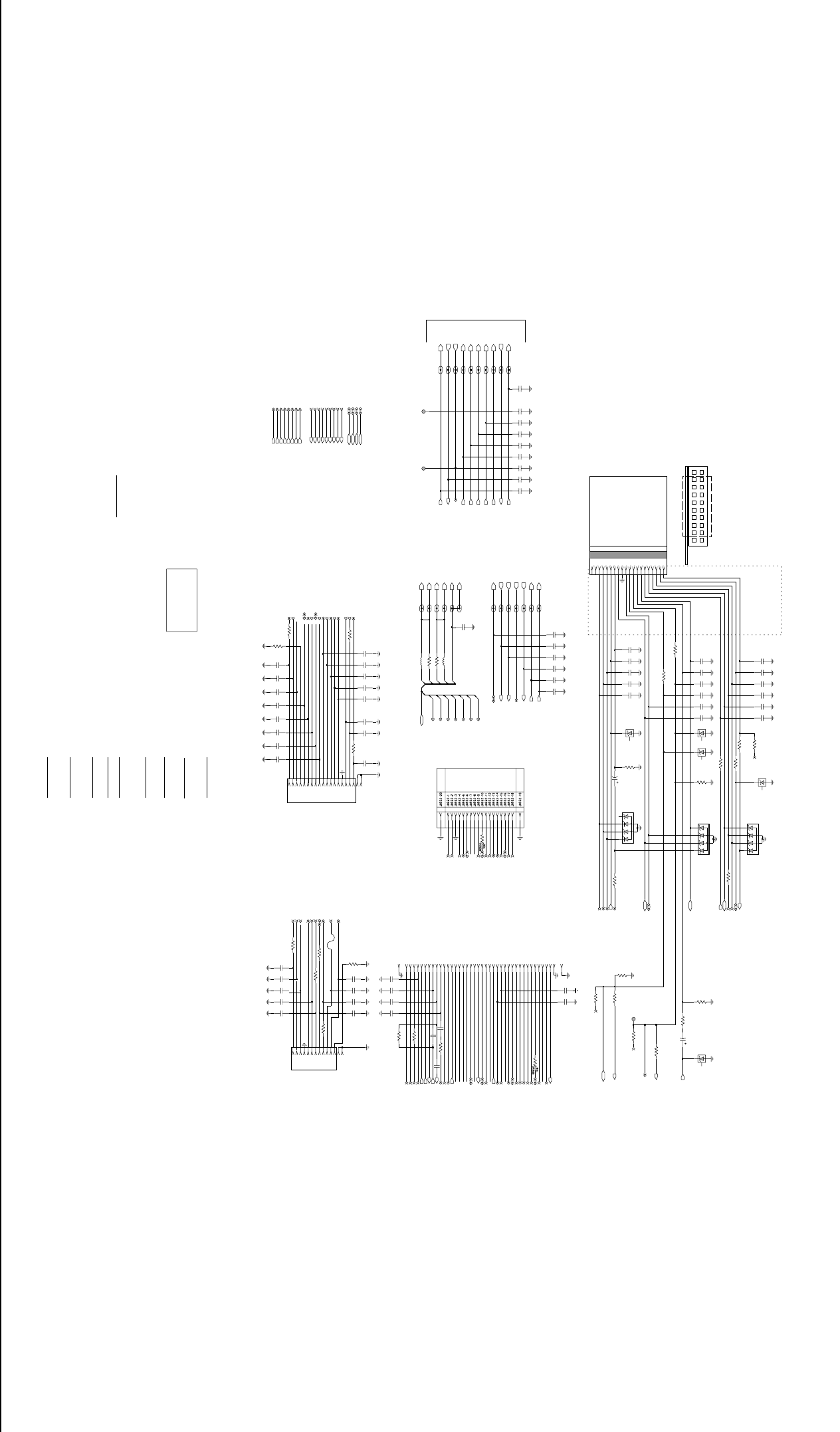
Low Band PCBs / Schematics / Parts Lists 4-35
R/W*
Changed C0593 back to 0.1uF
SPI_MOSI
T7 17. Februar 2000
Changed C05xx from 0402 to 0603 type where require d
NC
NC
7
T8 29. May 2000
Added Fuse 6580542Z01
T9 24. JULY 2000
Added trace from J0551-6 to new R0556 100 Ohms to BUS+
Added trace from J0552-10 to new R0555 100 Ohms to BUS +
T8 0102727B68
T9 0102727B68
P5 0102726B94
CLK
9
Fuse P/N
6580542Z01
P2 0102726B66
CS*
T6 0102727B64
T3 0102727B40/41
24
DISCAUDIO
NC
BUS+
Back to one controller for both chassi s
10
T4 18. November 1999
Removed Capacitors C0519 - C0540 &C0498 (never used)
DIG_IN_OUT_4
9
18
9V3
VS_MIC
13
2
GND
5
DATA
GM300
SPEAKER-
CLK
30
13
J0501
J0451
DIG_IN_6 WITH WAKEUP (IGNITION)
FLAT/FILTERED_RX_AUDIO
15
14
16
1
PCB
23
21
Added J0552 RS232 Interface Board Connector
Removed Resistors R0521 - R0524
T5 21. December 1999
Removed Capacitors C0401 - C0411 & C0451-C0468 (never used)
Attention: From now on there are two versions of controllers available,
one for LDMOS PA CHASSIS and one for BIPOLAR PA CHASSI S
T5 21. Januar 2000
SPI_CLK
8
Added R0442/R0543/R0593
Removed RX_ADAPT Testpoint
35
OFF_BATT_DATA_OUT
3
4
VS_GAINSEL
Gnd
11
DB2
DIG_IN1
3
EXP1_CS
5
6
SPEAKER-
DIG_IN_OUT_8
SWB+
14
Rdy/Req
2
GROUND
10
6
19
9
VS_CS
RDY
EXT_BD_REQ
EXT_BD_CS
12
2
6
NC
1
12
13
14
15 17
15
6
40
18-PIN CONNECTOR
RS232 INTERFACE BOARD
GND
BUS+
5
NC
RSSI
GND
J0552
NC
GROUND GROUND
NC
BOOT_CNTRL
20
GROUND
DB1
22
GP4_IN_OUT
TO/FROM RF
DATA
Assigned GP WITH WAKEUP on EXPANSION BOARD CONNECTOR
SCK_Snd
3
FAST_SQ
EXT_BD_PTT
GND
EXP_BD_REQ
NC
NC
DB6
ACCESSORY
16
DB3
MISO
NC
9
10
11
12
13
EXT_BD_PTT
12
Rx_Aud_Rtn
12
31
4
12
18-PIN CONNECTOR
7
17
1
HANSET_AUDIO
Opt_Bd_En
6
11
17
20
NC
15
16
17
18
REAR VIEW
15
16
34
INTERNAL OPTION BOARD
P6 0102727B03/04
39
38
9
2
1
NC
CLK
7
4
11
J0551
28
FLT_A+
Key_Col
DIG_OUT2 (EXTERNAL_ALARM)
EXP2_CS
SPI_MISO
5VD
EXP2_CS
11
CONTROL HEAD
J0401
5VD
9V3
5VD
EXT_BD_PTT
13
10
Flat_Tx_Rtn
NC
1
2
SrD_Snd
P4 0102726B86
SPEAKER+
BUS+
11
10
11
NC
1
14
15
16
17
4
NC
33
7
9
18
17
GROUND
SrD_Rtn
NC
10
OPT_CS
VS_RAC
8
RST*
7
8
14
INT_EXT_Vdd
4
EXT_BD_PTT
5
Det_Aud_Snd
18
40-PIN CONNECTOR
DB5
EXP_BD_PTT
GND
P3 0102726B70
13
37
DIG_IN_OUT_7
2
LED_EN
Added R0508 0662057A41 470
T4 0102727B51/52
8
DATA
DIG_IN_6 WITHWAKEUP
CLK
Tx_Aud_Rtn
P1 0102726B32
5
4
EXPANSION BOARD
OPT_PTT
16
20
SCI_TX
INT_MIC
DIG_IN_3
Tx_Aud_Snd
Rx_Aud_Snd
ON
VS_INT
T2 0102727B24/25
DIG_IN_5 WITH WAKEUP (EMERGENCY)
5
Key_Row
Key_Intrp
3
1
NC
NC
3
ON_OFF_CONTROL
T10 21.Feb. 2001
3
20-PIN CONNECTOR
OPT_CS
12-PIN CONNECTOR
FLAT_TX_AUDIO
DB7
RESET
FLT_A]
DISCAUDIO
CH_ACT
DIG_IN_OUT_4
DATA
I/O History
EXP1_CS
VS_AUDSEL
26
FLAT_TX_RTN
8
7
9
6
CSX
29
12
MISO
2
5
6
18
8
Change R0530 from 0662057B47 0 to 0662057A81 22K
Change T11 Controller I/O Kit No: from 0104012J96 to 0104013J52
Because of C0560 (603 Size)
Added R0509 0662057B47 0
36
DB0
19
PTT
18
8
T5 0102727B51/52
T7 0102727B68
T6 no changes
Vddd
25
P7 0102727B15/16
32
EXT_BD_PTT
27
19
WARI S
TO/FROM RF
7
10
A0
EXT_MIC_AUDIO
4
VS_CS
DB4
EXP_BD_PTT
SPEAKER+
14
3
PA_PWR_SET
CONTROLLER BIPOLAR PA
Klaus-Dieter Demant
WARIS MOBILE
INTERFACE / CONNECTORS 4 1 3 A
?
3 5
T9 08.12.18
12:36:17 pmMonday, February 26, 2001Prasethy Lee,IL26
Klaus-Dieter Demant
T10 23.May. 2001
470pF
PASUPVLTG
C0513
TEMPSENSE_CNTLR_1
J0501-16
10
C0505
470pF
MODIN
J0551-8
VR0505
CLK_CNTLR_1
C0518
470pF
VR0509
C0487
470pF
C0431
470pF
470pF
C0423
470pF
C0514
J0501-3
J0501-20
C0560
1000pF
J0401-11
J0501-17
J0451-11
16_8MHZ_CNTLR_1
220
R0401
J0551-11
C0488
470pF
3A
F0401
J0501-5
C0495
470pF
470pF
DISCAUDIO
47K
C0484
NU
R0542
VR0537
J0401-1
82pF
C0517
CNTLVLTG_CNTLR_1
J0501-4
9
J0551-3
J0551-10
470pF
C0510
0.47uF
C0541
J0551-40
10
R0592
J0451-5
J0501-14
3
J0551-20
R0525
100K
PA_PWR_SET_1_CNTLR_1
J0551-25
220
R0538
VR0501
J0551-4
J0551-14
C0542
47uF
R0533
J0551-23
0
J0551-18
R0511
100K
CSX_CNTLR_1
J0551-37
NOISE_BLNKR_CNTLR_1
R0529
47K
J0551-19
J0551-41
J0451-1
J0551-36
J0551-32
R0530
22K
J0401-10
J0401-7
470pF
RSSI_CNTLR_1
C0497
R0441
0
470pF
NU
470pF
C0575
DISCAUDIO_CNTLR_1
C0477
DATA_CNTLR_1
LOCK_CNTLR_1
0
R0412
C0447
470pF
J0551-22
MODIN_CNTLR_1
J0451-10
470pF
C0509
J0451-17
J0501-2
C0472
82pF
J0501-11
J0451-6
1
J0501-12
100K
R0543
J0451-12
VR0510
DATA
J0401-5
NU
470pF
C0559
470pF
C0429
J0501-15
R0512
15K
C0426
470pF
C0501
.01uF
C0421
J0451-16
82pF
82pF
C0473
J0401-4
J0551-21
J0401-9
J0401-3
J0401-8
J0451-18
8CLK_CNTLR_2
0.1uF
C0591
470pF
C0494
C0516
.01uF
J0451-4
R0591
24K
J0551-31
470pF
CLK
C0512
MOSBIAS_2_CNTLR_1
J0551-42
470pF
C0442
IN_5V_RF_REG_CNTLR_1
C0485
J0401-12
J0551-13
470pF
C0483
9
470pF
J0551-27
TEMPSENSE
RESET
VR0541
470pF
C0441
8
0.1uF
C0592
R0407
5V
560
10
IN_5V_RF_REG
R0531
J0551-12
2
J0501-8
L0482
J0451-7
NU
390nH
C0478
470pF
J0551-15
R0408
100
470pF
C0511
7
R0539
J0551-29
4.7K
J0551-39
R0510
4.7K
NU
L0481
390nH
J0501-1
C0506
470pF
C0449
5V_CNTLR_1
MOSBIAS_3
470pF 1K
R0442
STANDARD_MUHF
PRIME_MUHF
PRIME_BNC
STANDARD_MUHF
STANDARD_BNC
o
4
C0493
470pF
DATA
TP0530
CSX
J0551-26
J0501-13
J0401-6
CLK
J0551-6
J0451-8
J0551-34
470pF
82pF
C0471
C0422
0.1uF
C0593
R0482 0
R04810
R0468
100K
C0443
470pF
J0551-17
NU
J0551-30
C0474
470pF
J0501-9
470pF
CNTLVLTG
J0451-9
C0491
100K
R0593
VR0504
J0451-13
C0515
470pF
DATA_CNTLR_2
C0503
470pF
PASUPVLTG_CNTRL_1
J0501-6
J0401-2
VR0503
TP0492 TP0497
R0537
220
J0451-15
470pF
INT_SWB
NU
C0558
10
R0409
J0451-2
LOCK
RSSI
MOSBIAS_3_CNTLR_1 MOSBIAS_2
470pF
C0508
J0501-10
C0490
9V3
470pF
J0551-35
J0451-14
J0551-1
J0551-28
C0492
470pF
R0535
1K
J0501-19
470pF
J0551-5
C0430
C0496
470pF
470pF
C0486
470pF
C0499
RESET_CNTLR_1
CSX_CNTLR_2
C0476
470pF
J0551-33
C0482
470pF
NU
C0576
470pF
9
9V3_CNTLR_1
C0554
J0451-3
NU
0.1uF
J0551-24
NOISE_BLNKR
INT_SWB_CNTLR_1
10
R0467
J0551-9
J0501-7
470pF
C0427
J0551-2
J0551-16
C0470
470pF
R0541
27K
470pF
C0502
J0501-18
470pF
C0504
0
R0509
470
R0508
J0551-7
16_8MHZ
J0551-38
CSX
8
C0428
82pF
C0448
470pF C0445
470pF470pF
C0446
GP4_IN_OUT_ACC8
OPT_CS
RDY
OPT_PTT
EXP2_CS
EXP_BD_REQ
5VD
SPKR-
SPKR+
ON_OFF_CONTROL
BUS+
BUS+
GP6_IN_ACC10
GP5_IN_ACC9
GP2_OUT_ACC4
GP7_IN_OUT_ACC12
GP8_IN_OUT_ACC14
SPKR+
GP3_IN_ACC6
GP4_IN_OUT_ACC8
EXP2_CS
FLAT_TX_RTN
FLAT_TX_RTN
GP6_IN_ACC10
GP6_IN_ACC10
GP6_IN_ACC10
GP1_IN_ACC3
FLT_A+
CH_ACT
GP1_IN_ACC3
SPI_DATA
SPI_MISO
SPI_CLK
EXP1_CS
9V3
SPI_MISO
DISCAUDIO
MODIN
CH_ACT
5VD
9V3
5VD
SPI_MISO
RESET
FLT_A+
DISCAUDIO
GP4_IN_OUT_ACC8
EXP1_CS
EXP_BD_REQ
GP1_IN_ACC3
SPI_CLK
SPI_DATA
SPKR-
EXT_MIC
GP1_IN_ACC3
INT_MIC INT_MIC
INT_MIC
SPKR+SPKR+
DISCAUDIO ISCAUDIO
HANDSET_AUDIO
HANDSET_AUDIO
RSSI RSSI
BOOT_CNTRL
5VD
IN_5V_RF_REG
BUS+
GP1_IN_ACC3 GP1_IN_ACC3
INT_SWB+
GP4_IN_OUT_ACC8
EXP1_CS
EXP_BD_REQ
EXP_BD_REQ
EXP_BD_REQ
GP1_IN_ACC3
CH_ACT CH_ACT
CH_ACT
DISCAUDIO
FLT_A+
SCI_TX
RX_FLAT_FILTERED_AUDIO
EMERGENCY_CONTROL
RSSI
EXT_SWB+
RDYRDY
RDY
OPT_PTTOPT_PTT
OPT_PTT
NOISE_BLNKR
MOSBIAS_2
PA_PWR_SET
EXP1_CS
9V3
FLAT_TX_RTN FLAT_TX_RTN
GP4_IN_OUT_ACC8 GP4_IN_OUT_ACC8
DISCAUDIO
SPI(0:10)
MOSBIAS_3
VS_MIC VS_MIC
FLAT_TX_RTN
5VD
FLT_A+
BUS+ BUS+
RESET
RESET
ON_OFF_CONTROL ON_OFF_CONTROL
16_8MHZ
5V_RF
5VD
5VD
FLT_A+
SPI_DATA
SPI_CLK
SPI_MISO
VS_CS
OPT_CS
RESET
EXT_MICEXT_MIC
SPKR-SPKR-
RESET
PASUPVLTG
BUS+
TEMPSENSE
CNTLVLTG
RSSI
LOCK
OPT_CS
SPI_DATA
TX_AUD_RTN
VS_CS
VS_MIC
SPI_CLK
FLAT_RX_SND
RX_AUD_RTN
URX_SND
TX_AUD_SND
VS_INT
5VD
VS_AUDSEL
VS_GAINSEL
SPI_MISO
VS_RAC
IGNITION_CONTROL
FLT_A+
FLT_A+
HANDSET_AUDIO
ZWG0131050-O
Low Band Range 1/2/3 IO - T11 (for PC Boards
8486206B08, 8486207B07 & 8486908Z04
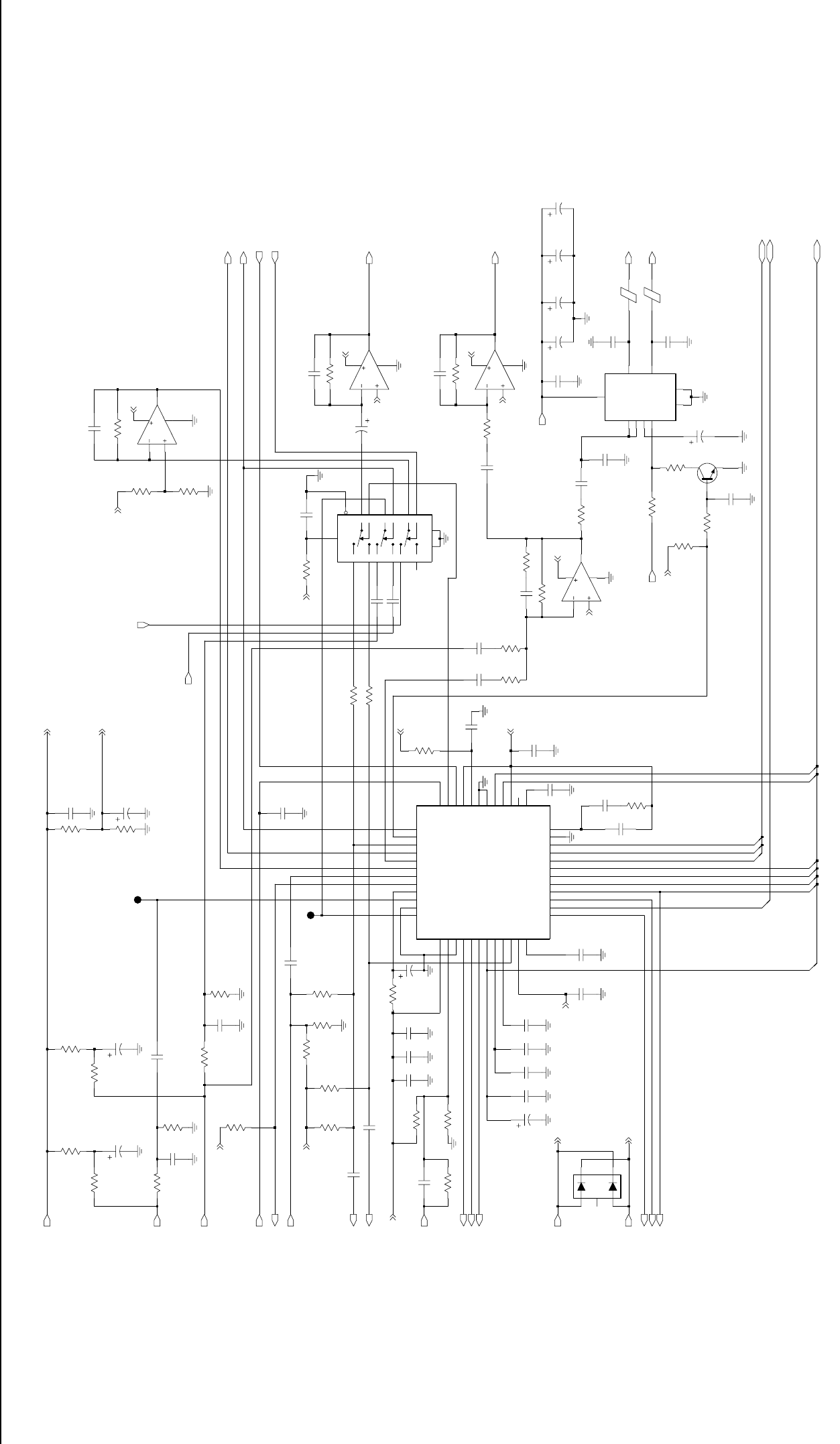
4-36 Low Band PCBs / Schematics / Parts Lists
LSIO
F1200
SYN
Check PIN Values on IC
CLK
GP2_OUT
CSX
DATA
VOX
CH_ACT
HSIO
SQ_DET
4
0.1uF
C0251
C0255
0.1uF
1
1
VDDCP 32
VDDD 33
VDDDAC
SQCAP
11
12
VDDRC 45
VDDSYN 27
VOX
7
SQDET
17
SQIN
9SYN 28
TXRTN 36
TXSND 44
UIO
10
VDDA
LSIO
18
MICEXT 48
MICINT 46
MOD 40
NC 26
PLCAP
8
PLCAP2 25
GCB5
RXSND
AUXTN
RXRTN
38
39
GNDA
3
GNDD
GNDD0
31
30
GNDRC 47
GNDSYN
23
HSIO
19
24 LCAP
DATA
22
DISC
2
F1200 29
GCB0
15 GCB1
14 GCB2
13
GCB3 35
37
GCB4
CHACT
16
CLK
21
CLK168 34
CSX
20
DACG
6DACR
5
4DACU
63A53
U0221
AUDIO 41
42
43
R0206
10K C0205
2200pF
NU
0.1uF
C0266
NU
C0267
C0231
1uF
.01uF
6
5
7
4
11
11
Y1
1
Z4
Z0
5
3Z1
U0211-2
MC3403
GND
8VCC 16
VEE
7
X14
X0
12
X1
13
Y15
Y0
2
U0251
11
A
B10
C9
EN 6
R0208
2.2K
6
MC14053B
NU
C0211
0.1uF
NU
9
R0266
24K
C0224
100pF
C0237
2.2uF
NU
47K
R0267
10K
R0268
10uF
C0202
10uF C0212
0.1uF
C0225
C0275
47uF
24K
R0273
10uF
C0201
23
8
NU
8.2K
R0225
8.2K
R0224
100pF
C0243
R0242
0.1uF
NU
0
12
14
4
11
C0242
U0211-4
MC3403
13
560
C0244
R0204
C0235
0.1uF
C0271
.022uF
.01uF
47K
R0241
.01uF
100pF
C0256
C0246
R0256
100K
10K
R0254
10K
R0255
0.1uF
C0241
TP0221
57R01
E0272
8.2K
R0220
NU
C0245
0.1uF
100
R0203
C0233
0.22uF
NU
15K
1000pF
R0276
7
VCC
C0276
GND1
GND2
5
9INV
8M_SS
1NINV
4
OUT1
6
OUT2
RR
3
TDA1519C
U0271
2
10K
R0261
0.1uF
C0274
NU
C0232
0.1uF
R0227
1MEG
NU
9
10
8
4
11 U0211-3
MC3403
5
0.1uF
C0222
100K
R0253
100pF
C0253
NU
1uF
C0252
7
C0291
10uF
C0290
10uF
NU
R0207
2.2K
R0226
1MEG
0.1uF
NU
10uF
C0227
C0292
10uF
C0293
C0221
0.1uF
0.1uF
R0252
C0223
56K
30K
R0223
0.1uF
C0261
R0212
R0211
7.5K
C0236
7.5K
.033uF
R0265
24K
C0265
0.1uF
NU
5
3
1
2
4
D0201
0.1uF
C0254
C0234
7
0.1uF
TP0222
C0273
3300pF
47K
R0251
2.2K
R0257
C0228
4.7uF
10K Q0271
R0275
R0228
C0272
0
0.1uF
560
R0202
C0262
R0222
82pF
24K
0.1uF
C0226
470
NU
R0269
2200pF
C0203
10
R0229
0.1uF
C0204
R0221
24K
270K
R0262
C0277
1000pF
U0211-1
MC3403
2
3
1
4
11
57R01
E0271
R0274
NU
10K
R0201
R0205
100
5V_RF5V_RF
TX_AUD_RTN
5V_RF
TX_AUD_SND
5V_RF
DISCAUDIO
5V_RF
5V_RF
RX_ADAPT
FLAT_TX_RTN
10K
9V3
9V3
MODIN
INT_SWB+
CH_ACT
VAG
9V3 9V3
9V3
VS_MIC
MOSBIAS_3
16_8MHZ
VAG
EXT_MIC
5V_RF
5V_RF
5VD5VD
5V_RF
SPKR-
RX_AUD_RTN
INT_MIC
URX_SND
FLAT_RX_SND
DC_POWER_ON
FLT_A+
5VD
SPKR+
5VD
PA_PWR_SET
MOSBIAS_2
9V3
NOISE_BLNKR
VS_AUDSEL
SPI(0:10)
GPIO(0:13)
CNTLR_AUDIO(0:7)
VAG
VAG
HANDSET_AUDIO
RX_FLAT_FILTERED_AUDIO
FL0830680O
Low Band Range 1/2/3 (29.7-36.0/36.0-42.0/42-50 MHz) - Audio
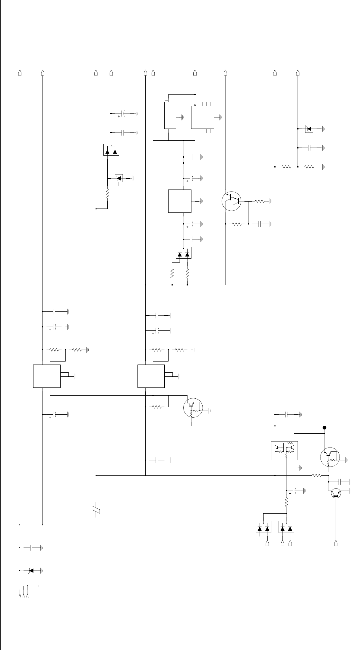
Low Band PCBs / Schematics / Parts Lists 4-37
10
22uF
C0611
R0651
C0652
33uF
R0612
4.7K
D0661
Q0662
R0671
30K
10K
VIN
4VOUT 5
R0672
LM2941
U0611
ADJ 1
GND1
3
GND2
6
2ON_OFF
10K
47K
47K
C0671
0.1uF
R0641
J0601-1
.01uF
C0662
R0662
150K Q0663
47K
47K
D0621
C0603
R0661
1K
10uF
RESET
RESET
1
VR0621
GND GND
4
INPUT
2
2
NP
NC1
3
NC2
5
NC3 6
NC4 7
8
NC5
U0652
MC33064
2
GND
1IN OUT3
TP0661
C0663
MC78M05
U0651
0.1uF
R0643
0.1uF
1.2K
C0651 C0655
NU
0.1uF
0.1uF
C0645
470pF
VR0601
NU
C0621
4VIN 5
VOUT
47uF
C0622
U0641
LM2941
1
ADJ
GND1
3
GND2
6
ON_OFF
2
Q0661
R0611
56K
VR0671
NU
Q0681
R0682
68K
R0681
18K
57R01
E0631
470pF
C0601
47uF
C0661
R0642
7.5K
470pF
C0641 C0644
33uF
D0651
0.1uF
J0601-2
C0681
C0612
0.1uF
J0601-3
D0660
R0652
R0621
10
24K
Q0641
MC33464N-45ATR
U0653
NU
10uF
9V3
FLT_A+
IN_5V_RF_REG
RESET
5VD
C0654
DC_POWER_ON
IGNITION_CONTROL
EMERGENCY_CONTROL
BATTERY_VOLTAGE
ON_OFF_CONTROL
EXT_SWB+
INT_SWB+
PASUPVLTG
VSTBY
FL0830679O
Low Band Range 1/2/3 (29.7-36.0/36.0-42.0/42-50 MHz) - Supply Voltage
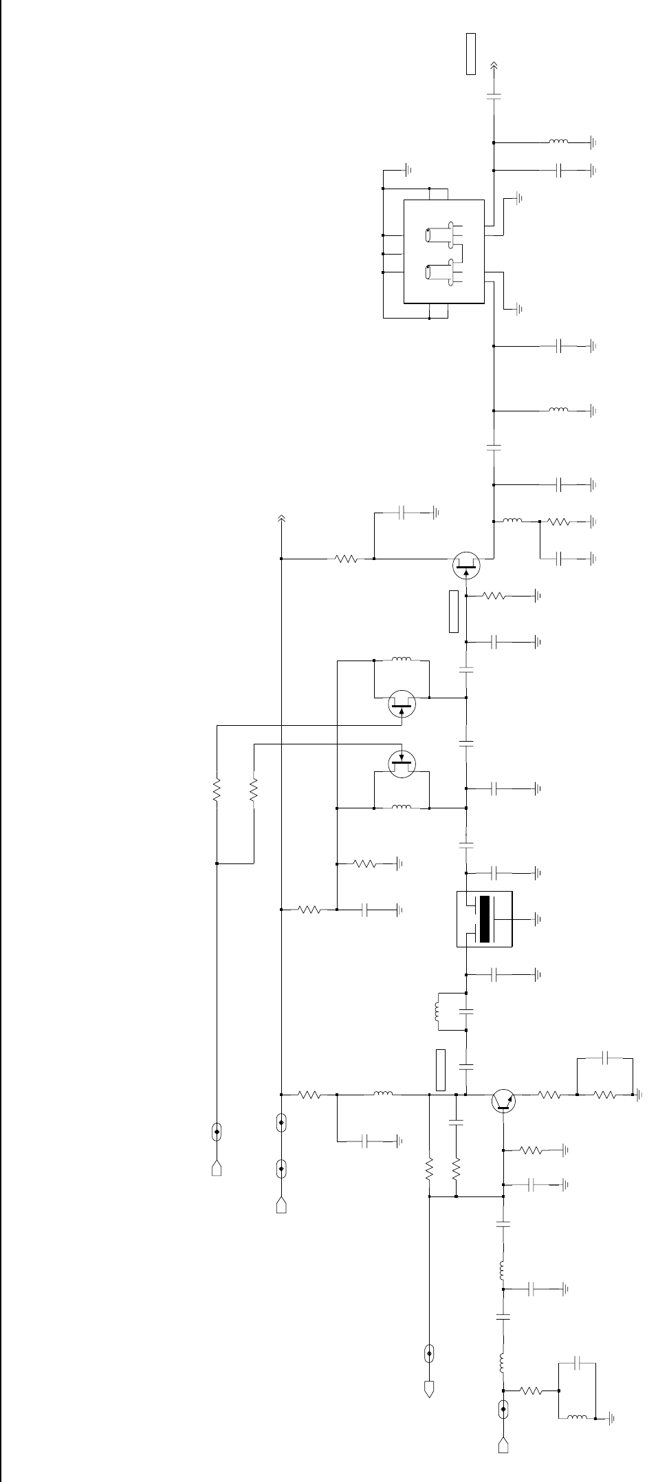
4-38 Low Band PCBs / Schematics / Parts Lists
-48.0 dBm
-34.0 dBm
-38 dBm
-34 dBm
3.10 V
2.25 V
5.94 V
7.50 V
1.10 V
6.40 V
R1109
330
36pF
C1115
120pF
C1112
R1135
R1108
3.3K
62
BLNKR_SWITCH_IF_1
R1111
47 FN0:NP
L1108
18uH
R1104
8.2K
15
R1134
33uH
L1110
100
R1106
S
L1104
6.8uH
Q1104
D
120pF
C1149
9V3_IF_1
200pF
C1103
L1105
6.8uH
NOISE_BLNKR_IF1
3.3uH
L1102
D
S
C1102
91pF C1110
FN0:NP
Q1102
S
BLNKR_SWITCH
62pF
Q1103
D
Q1101 82pF
C1107
C1116
39pF
9V3
0.1uF
C1114
36pF
C1109
L1103
1.8uH
R1110
100
FN0:NP
6.8pF
C1120
C1113
0.1uF
390pF
C1147
C1152
30pF
FN0:NP
4.3K
R1114
FL1101
CFEC10_7MG1
GND
2
IN
1OUT 3
16K
R1102
R1103
390
0.1uF
C1105
L1107
5.6uH
C1106
0.1uF
C1104
0.1uF
R1113
4.3K
L1111
3.3uH
GND7 11
GNDA
2
GNDB
3
INA
1
OUTB
4
IF
9V3_IF_2
GND1 5
6
GND2
7
GND3
GND4
BLUE
RED
8
GND5
9
GND6 10
0.1uF
C1144
FL1102
FILTER
R1107
6.2K
IF_IF_1
NOISE_BLNKR_IF1_IF_1
51
R1101
C1146
82pF
C1119
0.1uF
C1153
0.1uF
FN0:NP
L1101 120pF
C1101
1.8uH
0.1uF
C1108
2.4pF
C1150
130pF
L1106
C1111
9V3
PREAMP_IN
1.8uH
FL0830690O
Low Band Range 1/2/3 - IF sheet 1 of 2 (for PC Boards
8486206B06, 8486207B05 & 8486908Z02)
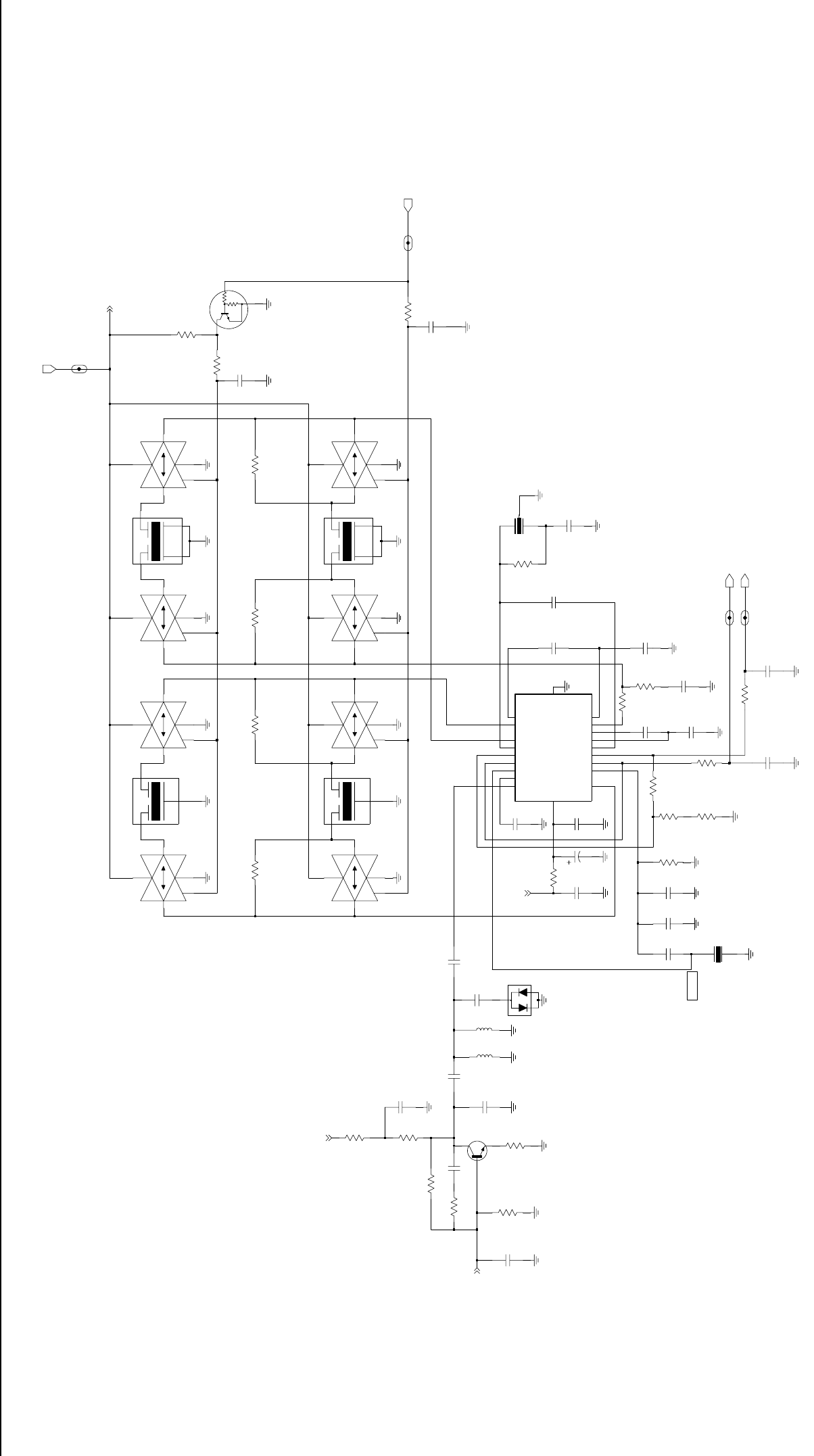
Low Band PCBs / Schematics / Parts Lists 4-39
3.10 V
5V (20KHz, 30KHz)
0V (12.5KHz)
+13 dBm
120 mV rms
0.78 V
0.025 V
-20 dBm
RSSI_IF_1
U1101-3
MC74HC4066
6
CNTL
89
14
VDD
7
VSS
R1137
12K
C1129
22pF
R1120
10K
R1130
51
.01uF
R1124
FN0:NP
C1140
11 10
14
VDD
7
VSS
0
U1102-4
MC74HC4066
12
CNTL
R1129
47K
47K
DISCAUDIO
C1139
10K
680
.01uF
0.1uF
R1136
C1130
C1135
0.1uF
68pF R1121
C1148
GND1
3
GND2
4
1IN 2
OUT
8.2K
R1132
CFWC455F
FL1106
R1131
2.4K
Q1105
15K
3.3K
R1133
0
R1126
FN0:NP
0
R1125
FN0:NP
2
3
1
120pF
D1101
Y1101
08W08
10.245
2
1
C1137
0
R1127
FN0:NP
GND1
3
4GND2
1IN 2
OUT
CFWC455E
FL1107
R1119
C1127
10uF
C1126
27K
1.2K
0.1uF
R1123
Q1106
FN0:NP
C1121
0.1uF
C1134
0.1uF
6.8uH
L1112
10
R1138
62pF
C1122
CNTL
5
43
VDD
14
VSS
7
FN0:NP
14
VDD
7
VSS
MC74HC4066
U1102-2
U1102-1
MC74HC4066
13
CNTL
12
0.1uF
C1142
3
2
1
DISCAUDIO_IF_1
R1115
455KHz
45B02
Y1102
R1122
12K
C1131
10K C1141
FN0:NP
1.5pF
C1124
0.1uF
C1136
0.1uF
0.1uF
C1133
.039uF
C1125
0.1uF
QUADIN 10
RFIN 1
RFIN_DEC 2
RSSIOUT
5RSSI_FEED 9
6VCC
IFAMP_DEC2
17
LIMIN 14
LIMOUT
11
LIM_DEC1
13
LIM_DEC2
12
20 MIXOUT
OSCIN 4
OSCOUT
3
AUDIOOUT
8AUDIO_FEED 7
GND 15
IFAMPIN 18
IFAMPOUT
16
IFAMP_DEC1 19
U1103
SA616
GND
3
IN
1OUT 2
R1128
10K
FL1104
CFUCJ455F
10
VDD
14
VSS
7
BWSELECT
R1139
2.7
MC74HC4066
U1101-4
CNTL
12
11
C1128
0.1uF
6
CNTL
89
14
VDD
7
VSS
GND
3
IN
1OUT 2
U1102-3
MC74HC4066
R1117
FL1105
CFUCJ455E
43
14
VDD
7
VSS
330
C1138
U1101-2
MC74HC4066
5
CNTL
0.1uF
6.8K
R1116
BWSELECT_IF_1
5V_IF_1
5V
FN0:NP
FN0:NP
L1109
6.8uH
FN0:NP
150pF
C1151
C1123
33pF
VDD
14
VSS
7
2K
R1118
MC74HC4066
U1101-1
CNTL
13
12
C1145
4700pF
RSSI
0.1uF
C1143
5V
5V
9V3
PREAMP_IN
FL0830691O
Low Band Range 1/2/3 - IF sheet 2 of 2 (for PC Boards
8486206B06, 8486207B05 & 8486908Z02)
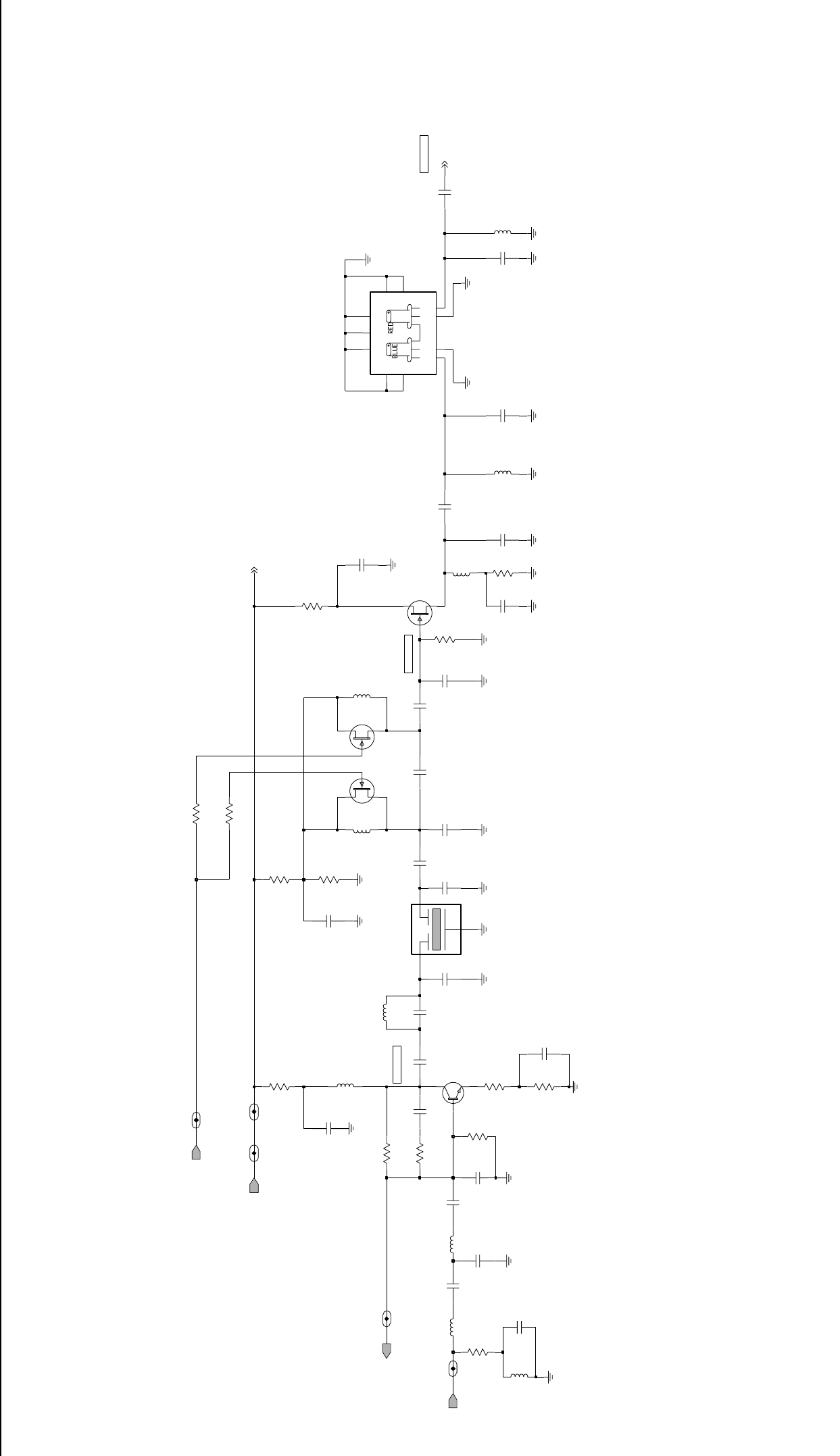
4-40 Low Band PCBs / Schematics / Parts Lists
G
G
G
G
6.40V
-48.0 dBm
-34.0 dBm
-38 dBm
-34 dBm
3.10 V
2.25V
5.94V
7.50V
1.10V
L1107
C1106
5.6uH
0.1uF
R1113
0.1uF
C1104
L1111
4.3K
9V3_IF_2
3.3uH
8GND4
9GND5
10
GND6
11
GND7
2
GNDA
3
GNDB
1
INA
4
OUTB
IF
FILTER
FL1102
5
GND1 GND2
6
GND3
7
C1144
0.1uF
6.2K
R1107
IF_IF_1
NOISE_BLNKR_IF1_IF_1
R1101
51
82pF
C1146
0.1uF
C1119
FN0:NOTPLACED
0.1uF
C1153
L1101
1.8uH C1101
120pF
0.1uF
C1108
130pF
C1150
2.4pF
C1111
1.8uH
91pF
C1102
L1106
Q1102
D
S
C1110
62pF
D
S
BLNKR_SWITCH
FN0:NOTPLACED
Q1103
Q1101 C1107
82pF 39pF
C1116
9V3
C1114
0.1uF
C1109
36pF
R1110
1.8uH
L1103
6.8pF
FN0:NOTPLACED
100
C1120
0.1uF
C1113
C1147
390pF
FN0:NOTPLACED
30pF
C1152
1IN 3
OUT
R1114
4.3K
CFEC10_7MG1
FL1101
2GND
R1102
16K
390
R1103
C1105
0.1uF
330
R1109
120pF
C1115
36pF
C1112
3.3K
R1108
R1135
62
47
R1111 18uH
L1108
FN0:NOTPLACED
BLNKR_SWITCH_IF_1
8.2K
R1104
R1134
15
L1110
33uH
R1106
100
6.8uH
L1104
Q1104
D
S
C1149
120pF
C1103
200pF
NOISE_BLNKR_IF1
9V3_IF_1
6.8uH
L1105
9V3
PREAMP_IN
3.3uH
L1102
ZWG0131051-O
Low Band Range 1/2/3 - IF sheet 1 of 2 (for PC Boards
8486206B08, 8486207B07 & 8486908Z04)
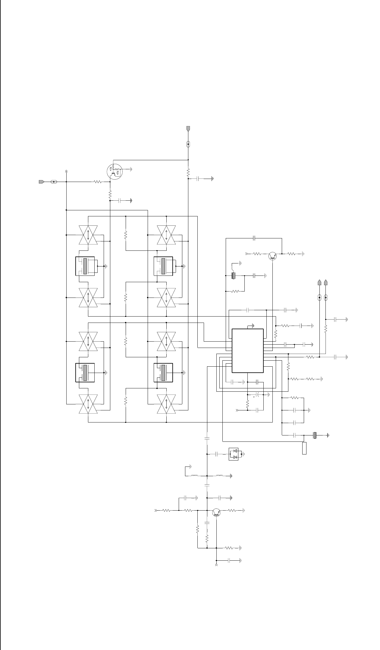
Low Band PCBs / Schematics / Parts Lists 4-41
G
G
G
G
0V (12.5KHz)
+13 dBm
120 mV rms
0.78 V
0.025V
-20 dBm
3.10V
5V (20KHz, 30KHz)
1IN 2
OUT
10K
R1128
CFUCJ455F
FL1104
3
GND
7
VSS
BWSELECT
2.7
R1139
U1101-4
MC74HC4066
12
CNTL
11 10
14
VDD
0.1uF
C1128
9
VDD
14
VSS
7
1IN 2
OUT
MC74HC4066
U1102-3
CNTL
6
8
CFUCJ455E
FL1105
3
GND
VDD
14
VSS
7
R1117
330
MC74HC4066
U1101-2
CNTL
5
43
0.1uF
6.8K
FN0:NOTPLACED
C1138
BWSELECT_IF_1
5V
R1116
6.8uH
L1109
FN0:NOTPLACED
C1151
150pF
FN0:NOTPLACED
33pF
C1123
VSS
R1118
2K
U1101-1
MC74HC4066
13
CNTL
12
14
VDD
7
4700pF
C1145
RSSI
0.1uF
C1121
FN0:NOTPLACED
C1143
C1134
0.1uF
0.1uF
L1112
6.8uH
R1138
10
C1122
62pF
FN0:NOTPLACED
5
CNTL
43
14
VDD
7
VSS
13
12
VDD
14
VSS
7
U1102-2
MC74HC4066
MC74HC4066
U1102-1
CNTL
DISCAUDIO_IF_1
C1142
0.1uF
Y1102
45B02
455KHz
3
R1115
12K
10K
1.5pF
FN0:NOTPLACED
R1122 C1141
0.1uF
C1131
C1124
0.1uF
0.1uF
C1136
C1133
0.1uF
C1125
.039uF
4
OSCIN
3OSCOUT
10
QUADIN
1
RFIN 2
RFIN_DEC
5RSSIOUT 9
RSSI_FEED
VCC
6
16 IFAMPOUT 19
IFAMP_DEC1
17 IFAMP_DEC2
14
LIMIN
11 LIMOUT
13 LIM_DEC1
12 LIM_DEC2
MIXOUT
20
SA616
U1103
8AUDIOOUT 7
AUDIO_FEED
15
GND
18
IFAMPIN
CNTL
12
11 10
VDD
14
VSS
7
DISCAUDIO
5V_IF_1
MC74HC4066
U1102-4
R1129
10K
C1139
.01uF
680
R1136
0.1uF
C1135
C1130
68pF
0.1uF
C1148
OUT 2
R1121
8.2K
FL1106
CFWC455F
3
GND1
4GND2
IN
1
R1132
2.4K
R1131
15K
Q1105
R1133
3.3K
FN0:NOTPLACED
R1126
0
FN0:NOTPLACED
R1125
0
D1101
2
3
1
1
120pF
C1137
10.245
08W08
Y1101
2
IN
1OUT 2
FN0:NOTPLACED
R1127
0
FL1107
CFWC455E
3
GND1
GND2
4
10uF
C1127
R1119
27K
C1126
0.1uF
R1123
Q1106
1.2K
R1141
390
R1140
1.8K
Q1107
14
VSS
7
RSSI_IF_1
MC74HC4066
U1101-3
CNTL
6
89
VDD
12K
R1137
22pF
C1129
R1120
51
R1130
10K
.01uF
C1140
FN0:NOTPLACED
R1124
0
5V
5V
9V3
PREAMP_IN
5V
1
2
ZWG0131052-O
Low Band Range 1/2/3 - IF sheet 2 of 2 (for PC Boards
8486206B08, 8486207B07 & 8486908Z04)
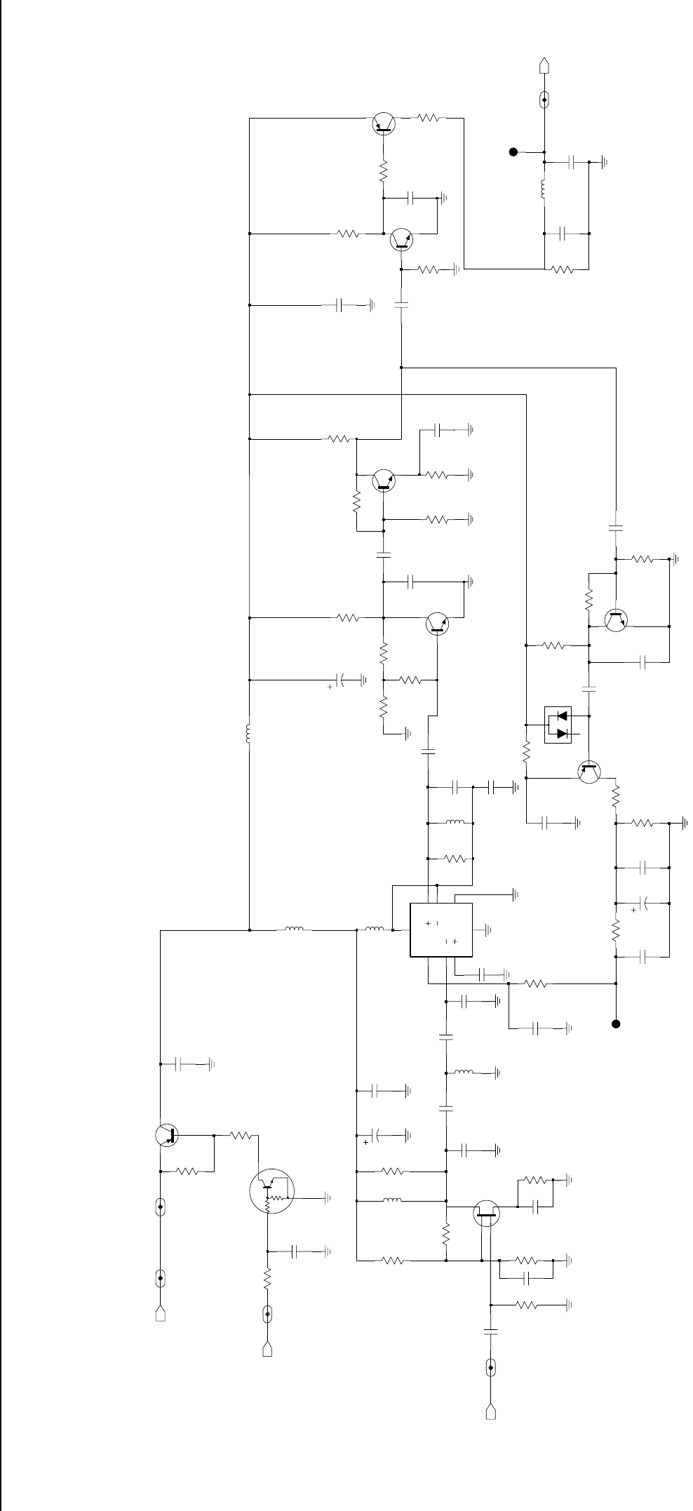
4-42 Low Band PCBs / Schematics / Parts Lists
3.8V
0V
9.1V
9.1V
0.45V
VAGC
1.5V
C1610
4700pF
0.1uF
C1628 C1607
100pF
Q1609
0.22uF
C1608
R1601
10K
R1628
1.8K
R1622
1K
220pF
C1626
9V3_NOISE_BLNKR_2
L1607
1uH
0.1uF
C1632
Q1602
47K
47K
0.22uF
C1627
3300pF
C1624
C1631
10uF
TP1601
4.7K
R1602
51
L1605
R1626
130pF
C1613 22uH
2200pF
C1612
L1604
9V3_NOISE_BLNKR_1
R1627
47uH
R1606
NOISE_BLNKR_IF1
10K
L1603
150K
0.1uF
1uH
R1604
C1601
0.22uF
1K
36pF
C1604
R1609
C1616
D1601
3
21
R1613
10K
FN0:NP
2.7K
9V3
R1633
27K
1.5K
R1630
Q1607
750K
2.2K
R1617
TP1602
R1607
5.6K
R1629
R1608
2.2K
Q1604
C1605
10uF
0.22uF
C1633
R1635
0
Q1610
D
S
47uH
L1601
C1603
0.22uF
1K
R1614
510
Q1606
33pF
R1636
C1629
2
VCC
2.7K
R1637
5AGCIN
7GND
4IN1
6IN2 3
NC_GND
8
OUT1 1
OUT2
NOISE_BLNKR
MC1350
U1601
1.2K
Q1605
.01uF
R1620
R1611
1K
C1634
NOISE_BLNKR_IF1_NOISE_BLNKR_1
C1602
220pF
Q1601
220pF
C1606
R1632
24K
L1602
47uH R1615
1K
C1622
0.1uF
10uF
C1619
BLNKR_SWITCH_NOISE_BLNKR_1
C1623
240pF
L1606
1uH
C1611
NOISE_BLNKR_NOISE_BLNKR_1
0.1uF
FN0:NP
51
R1631 0.22uF
C1621
100
R1612
6.2K 910pF
C1614
Q1603
R1621
R1610
24K
20pF
C1609
C1625
C1620
1000pF
12pF
C1618
0.22uF
R1638
1.8K
R1616
220
R1605
330K
BLNKR_SWITCH
20pF
C1615
FN0:NP
FL0830692O
Low Band Range 1/2/3 (29.7-36.0/36.0-42.0/42-50 MHz) - Noise Blanker
Low Band PCBs / Schematics / Parts Lists 4-43
Low Band Range 1 PCB 8486206B06 Parts List
Circuit
Ref Motorola
Part No. Description
C0101 2113740F51 CAP, 100pF
C0102 NOT PLACED
C0103 NOT PLACED
C0104 NOT PLACED
C0105 NOT PLACED
C0106 NOT PLACED
C0107 2113741F25 CAP, 1000pF
C0111 NOT PLACED
C0112 2113743E20 CAP, 0.1uF
C0121 2113743E20 CAP, 0.1uF
C0122 2113743E20 CAP, 0.1uF
C0123 NOT PLACED
C0131 2113740F35 CAP, 22pF
C0132 2113740F35 CAP, 22pF
C0141 2113743E20 CAP, 0.1uF
C0151 2113741F49 CAP, .01uF
C0201 2311049A57 CAPP, 10uF
C0202 2311049A57 CAPP, 10uF
C0203 NOT PLACED
C0204 2113743E20 CAP, 0.1uF
C0205 NOT PLACED
C0211 NOT PLACED
C0212 2311049A57 CAPP, 10uF
C0221 2113743E20 CAP, 0.1uF
C0222 2113743E20 CAP, 0.1uF
C0223 2113743E20 CAP, 0.1uF
C0224 2113740F51 CAP, 100pF
C0225 2113743E20 CAP, 0.1uF
C0226 2113743E20 CAP, 0.1uF
C0227 NOT PLACED
C0228 2311049A56 CAPP, 4.7uF
C0231 2113743B29 CAP, 1uF
C0232 2113743E20 CAP, 0.1uF
C0233 NOT PLACED
C0234 2113743E20 CAP, 0.1uF
C0235 2113743E07 CAP, .022uF
C0236 2113741F49 CAP, .01uF
C0237 NOT PLACED
C0241 2113743E20 CAP, 0.1uF
C0242 NOT PLACED
C0243 2113740F51 CAP, 100pF
C0244 2113743E20 CAP, 0.1uF
C0245 2113743E20 CAP, 0.1uF
C0246 2113741F49 CAP, .01uF‘
C0251 2113743E20 CAP, 0.1uF
C0252 2311049A07 CAPP, 1uF
C0253 NOT PLACED
C0254 2113743E20 CAP, 0.1uF
C0255 2113743E20 CAP, 0.1uF
C0256 2113740F51 CAP, 100pF
C0261 2113743E20 CAP, 0.1uF
C0262 2113740F49 CAP, 82pF
C0265 2113743E20 CAP, 0.1uF
C0266 NOT PLACED
C0267 2113741F49 CAP, .01uF
C0271 2113741F49 CAP, .01uF
C0272 2113743E20 CAP, 0.1uF
C0273 2113741F37 CAP,3300pF
C0274 NOT PLACED
C0275 2311049A99 CAPP,47uF
C0276 2113741F25 CAP, 1000pF
C0277 2113741F25 CAP, 1000pF
C0290 2311049C01 CAPP, 10uF
C0291 2311049C01 CAPP, 10uF
C0292 2311049C01 CAPP, 10uF
C0293 2311049C01 CAPP, 10uF
C0401 NOT PLACED
C0402 NOT PLACED
C0403 NOT PLACED
C0406 NOT PLACED
C0407 NOT PLACED
C0408 NOT PLACED
C0409 NOT PLACED
C0410 NOT PLACED
C0411 NOT PLACED
C0421 2113743N48 CAP, 82pF
C0422 2113741F17 CAP, 470pF
C0423 2113741F17 CAP, 470pF
C0426 2113743L09 CAP, 470pF
C0427 2113743L09 CAP, 470pF
C0428 2113743N48 CAP, 82pF
C0429 2113743L09 CAP, 470pF
C0430 2113741F17 CAP, 470pF
C0431 2113741F17 CAP, 470pF
C0441 2113743L09 CAP, 470pF
C0442 2113743L09 CAP, 470pF
C0443 NOT PLACED
C0445 2113743L09 CAP, 470pF
C0446 2113743L09 CAP, 470pF
C0447 2113743L09 CAP, 470pF
C0448 2113743L09 CAP, 470pF
C0449 2113743L09 CAP, 470pF
C0451 NOT PLACED
C0452 NOT PLACED
C0453 NOT PLACED
C0455 NOT PLACED
C0456 NOT PLACED
C0457 NOT PLACED
C0458 NOT PLACED
C0459 NOT PLACED
Circuit
Ref Motorola
Part No. Description
C0460 NOT PLACED
C0461 NOT PLACED
C0462 NOT PLACED
C0463 NOT PLACED
C0464 NOT PLACED
C0466 NOT PLACED
C0467 NOT PLACED
C0468 NOT PLACED
C0470 2113743L09 CAP, 470pF
C0471 2113743N48 CAP, 82pF
C0472 2113743N48 CAP, 82pF
C0473 2113743N48 CAP, 82pF
C0474 2113743L09 CAP, 470pF
C0476 2113743L09 CAP, 470pF
C0477 2113743L09 CAP, 470pF
C0478 2113743L09 CAP, 470pF
C0482 2113743L09 CAP, 470pF
C0483 2113743L09 CAP, 470pF
C0484 2113741F17 CAP, 470pF
C0485 2113743L09 CAP, 470pF
C0486 2113743L09 CAP, 470pF
C0487 2113743L09 CAP, 470pF
C0488 2113743L09 CAP, 470pF
C0490 2113743L09 CAP, 470pF
C0491 2113743L09 CAP, 470pF
C0492 2113743L09 CAP, 470pF
C0493 2113743L09 CAP, 470pF
C0494 2113743L09 CAP, 470pF
C0495 2113743L09 CAP, 470pF
C0496 2113743L09 CAP, 470pF
C0497 2113743L09 CAP, 470pF
C0499 2113743L09 CAP, 470pF
C0501 2113741F49 CAP, .01uF
C0502 2113743L09 CAP, 470pF
C0503 2113743L09 CAP, 470pF
C0504 2113743L09 CAP, 470pF
C0505 2113743L09 CAP, 470pF
C0506 2113743L09 CAP, 470pF
C0508 2113743L09 CAP, 470pF
C0509 2113743L09 CAP, 470pF
C0510 2113741F17 CAP, 470pF
C0511 2113743L09 CAP, 470pF
C0512 2113743L09 CAP, 470pF
C0513 2113741F17 CAP, 470pF
C0514 2113743L09 CAP, 470pF
C0515 2113743L09 CAP, 470pF
C0516 2113741F49 CAP, .01uF
C0517 2113743N48 CAP, 82pF
C0518 2113743L09 CAP, 470pF
C0541 2311049A05 CAPP, 0.47uF
C0542 2311049A99 CAPP, 47uF
Circuit
Ref Motorola
Part No. Description
C0554 NOT PLACED
C0558 NOT PLACED
C0559 NOT PLACED
C0560 NOT PLACED
C0575 NOT PLACED
C0576 NOT PLACED
C0591 2113743E20 CAP, 0.1uF
C0592 2113743E20 CAP, 0.1uF
C0593 2113741B69 CAP, 0.1uF
C0601 2113741F17 CAP, 470pF
C0603 2380090M24 CAPP, 10uF
C0611 2311049C06 CAPP, 22uF
C0612 2113743E20 CAP, 0.1uF
C0621 NOT PLACED
C0622 2311049A99 CAPP, 47uF
C0641 2113741F17 CAP, 470pF
C0644 2311049A97 CAPP, 33uF
C0645 2113743E20 CAP, 0.1uF
C0651 NOT PLACED
C0652 2311049A97 CAPP, 33uF
C0654 2311049A57 CAPP, 10uF
C0655 2113743E20 CAP, 0.1uF
C0661 2311049C05 CAPP, 47uF
C0662 2113741F49 CAP, .01uF
C0663 2113743E20 CAP, 0.1uF
C0671 2113743E20 CAP, 0.1uF
C0681 2113743E20 CAP, 0.1uF
C1001 2113740F59 CAP, 220pF
C1002 2113743E20 CAP, 0.1uF
C1003 2113740F59 CAP, 220pF
C1004 2113740F56 CAP, 160pF
C1006 2113740F50 CAP, 91pF
C1007 2113740F62 CAP, 300pF
C1008 2113743E20 CAP, 0.1uF
C1009 2113740F61 CAP, 270pF
C1010 2113740F49 CAP, 82pF
C1011 2113740F57 CAP, 180pF
C1012 2113740F59 CAP, 220pF
C1013 2113743E20 CAP, 0.1uF
C1014 2113740F59 CAP, 220pF
C1015 2113741F49 CAP, .01uF
C1016 2113740F58 CAP, 200pF
C1017 2113741F49 CAP, .01uF
C1019 2113740F61 CAP, 270pF
C1020 2113740F64 CAP, 360pF
C1021 2113740F64 CAP, 360pF
C1022 2113740F62 CAP, 300pF
C1023 2113740F64 CAP, 360pF
C1024 2113740F63 CAP, 330pF
C1025 2113740F61 CAP, 270pF
C1026 2113741F49 CAP, .01uF
Circuit
Ref Motorola
Part No. Description
4-44 Low Band PCBs / Schematics / Parts Lists
C1027 2113740F57 CAP, 180pF
C1028 2113741F49 CAP, .01uF
C1029 2113741F49 CAP, .01uF
C1030 2113743E20 CAP, 0.1uF
C1031 2113743E20 CAP, 0.1uF
C1032 2113740F51 CAP, 100pF
C1033 2113740F53 CAP, 120pF
C1034 2113740F54 CAP, 130pF
C1035 2113740F50 CAP, 91pF
C1036 2113743E20 CAP, 0.1uF
C1037 2113740F62 CAP, 300pF
C1038 2113740F65 CAP, 390pF
C1039 2113740F65 CAP, 390pF
C1040 2113740F62 CAP, 300pF
C1041 2113740F59 CAP, 220pF
C1042 2113740F59 CAP, 220pF
C1101 2113740F53 CAP, 120pF
C1102 2113740F50 CAP, 91pF
C1103 2113740F58 CAP, 200pF
C1104 2113743E20 CAP, 0.1uF
C1105 2113743E20 CAP, 0.1uF
C1106 2113743E20 CAP, 0.1uF
C1107 2113740F49 CAP, 82pF
C1108 2113743E20 CAP, 0.1uF
C1109 2113740F40 CAP, 36pF
C1110 NOT PLACED
C1111 2113740L03 CAP, 2.4pF
C1112 2113740F40 CAP, 36pF
C1113 2113743E20 CAP, 0.1uF
C1114 2113743E20 CAP, 0.1uF
C1115 2113740F53 CAP, 120pF
C1116 2113740F41 CAP, 39pF
C1119 2113743E20 CAP, 0.1uF
C1120 NOT PLACED
C1121 NOT PLACED
C1122 NOT PLACED
C1123 2113740F39 CAP, 33pF
C1124 2113743E20 CAP, 0.1uF
C1125 2113743E11 CAP, .039uF
C1126 2113743E20 CAP, 0.1uF
C1127 2311049A57 CAPP, 10uF
C1128 2113743E20 CAP, 0.1uF
C1129 2113740F35 CAP, 22pF
C1130 2113740F47 CAP, 68pF
C1131 NOT PLACED
C1133 2113743E20 CAP, 0.1uF
C1134 2113743E20 CAP, 0.1uF
C1135 2113743E20 CAP, 0.1uF
C1136 2113743E20 CAP, 0.1uF
C1137 2113740F53 CAP, 120pF
C1138 2113743E20 CAP, 0.1uF
Circuit
Ref Motorola
Part No. Description
C1139 2113741F49 CAP, .01uF
C1140 2113741F49 CAP, .01uF
C1141 2113743E20 CAP, 0.1uF
C1142 2113743E20 CAP, 0.1uF
C1143 2113743E20 CAP, 0.1uF
C1144 2113743E20 CAP, 0.1uF
C1145 2113741F41 CAP, 4700pF
C1146 2113740F49 CAP, 82pF
C1147 2113740F65 CAP, 390pF
C1148 2113743E20 CAP, 0.1uF
C1149 2113740F53 CAP, 120pF
C1150 2113740F54 CAP, 130pF
C1151 NOT PLACED
C1152 NOT PLACED
C1153 NOT PLACED
C1201 2113743E20 CAP, 0.1uF
C1202 2311049J11 CAPP, 4.7uF
C1203 2113741F49 CAP, .01uF
C1204 2113740F59 CAP, 220pF
C1205 NOT PLACED
C1206 2113740L37 CAP, 62pF
C1207 2113740F07 CAP, 1.5pF
C1208 2113740A82 CAP, 1500pF
C1209 2311049A57 CAPP, 10uF
C1210 2113743E20 CAP, 0.1uF
C1211 2113741F49 CAP, .01uF
C1212 2311049A07 CAPP, 1uF
C1213 2113743A23 CAP, 0.22uF
C1214 2113743E10 CAP, .033uF
C1215 2113740C37 CAP, 6800pF
C1216 2311049J11 CAPP, 4.7uF
C1217 2113741F49 CAP, .01uF
C1218 2113743E20 CAP, 0.1uF
C1219 2311049J11 CAPP, 4.7uF
C1220 2311049J11 CAPP, 4.7uF
C1221 NOT PLACED
C1222 2113740F37 CAP, 27pF
C1223 2113741F49 CAP, .01uF
C1224 2113740F51 CAP, 100pF
C1225 2113741F49 CAP, .01uF
C1226 NOT PLACED
C1227 2113741F49 CAP, .01uF
C1228 NOT PLACED
C1229 2113741F49 CAP, .01uF
C1230 2113741F49 CAP, .01uF
C1231 2113741F49 CAP, .01uF
C1232 NOT PLACED
C1233 NOT PLACED
C1234 NOT PLACED
C1250 2311049A09 CAPP, 2.2uF
C1251 2113743E20 CAP, 0.1uF
Circuit
Ref Motorola
Part No. Description
C1252 2113743E05 CAP, .018uF
C1253 2311049J11 CAPP, 4.7uF
C1254 2113741F49 CAP, .01uF
C1304 NOT PLACED
C1305 NOT PLACED
C1306 2113740L23 CAP, 16pF
C1307 2113740L34 CAP, 47pF
C1308 2113740F19 CAP, 4.7pF
C1309 NOT PLACED
C1311 2113741F49 CAP, .01uF
C1312 2113741F49 CAP, .01uF
C1313 2113741F49 CAP, .01uF
C1314 2113740L35 CAP, 51pF
C1315 2113740L35 CAP, 51pF
C1316 2113640F15 CAP, 3.3pF
C1317 2113743E20 CAP, 0.1uF
C1318 2113741F49 CAP, .01uF
C1319 2113741F49 CAP, .01uF
C1320 2113741F49 CAP, .01uF
C1321 2113740F17 CAP, 3.9pF
C1323 2113740L21 CAP, 13pF
C1325 2113741F49 CAP, .01uF
C1326 2113741F49 CAP, .01uF
C1333 2113740L36 CAP, 56pF
C1334 2113740L36 CAP, 56pF
C1335 2113740F19 CAP, 4.7pF
C1336 2113743E20 CAP, 0.1uF
C1337 2113741F49 CAP, .01uF
C1338 2113741F49 CAP, .01uF
C1339 2113741F49 CAP, .01uF
C1340 2113741F49 CAP, .01uF
C1341 2113740L36 CAP, 56pF
C1342 2113740L36 CAP, 56pF
C1343 2113740F15 CAP, 3.3pF
C1344 2113741F49 CAP, .01uF
C1345 2113743E20 CAP, 0.1uF
C1346 2113741F49 CAP, .01uF
C1347 2113741F49 CAP, .01uF
C1348 2113740F17 CAP, 3.9pF
C1349 2113743E20 CAP, 0.1uF
C1350 2113740F31 CAP, 15pF
C1351 2113741F49 CAP, .01uF
C1352 2113741F49 CAP, .01uF
C1354 NOT PLACED
C1356 NOT PLACED
C1360 NOT PLACED
C1361 NOT PLACED
C1362 NOT PLACED
C1401 2113741A45 CAP, .01uF
C1402 2113741A45 CAP, .01uF
C1403 NOT PLACED
Circuit
Ref Motorola
Part No. Description
C1404 2113741A45 CAP, .01uF
C1405 2113741A45 CAP, .01uF
C1406 NOT PLACED
C1407 2113741A45 CAP, .01uF
C1408 NOT PLACED
C1410 2113741M69 CAP, 0.1uF
C1413 2113741A45 CAP, .01uF
C1414 2113741A45 CAP, .01uF
C1415 2113741A45 CAP, .01uF
C1416 NOT PLACED
C1417 2113740A79 CAP, 1000pF
C1418 2113741A45 CAP, .01uF
C1419 2113741A45 CAP, .01uF
C1420 2113741A45 CAP, .01uF
C1421 NOT PLACED
C1422 NOT PLACED
C1423 2113741A45 CAP, .01uF
C1424 2113741A45 CAP, .01uF
C1425 2113741W01 CAP, 1uF
C1426 2113741W01 CAP, 1uF
C1427 2111078B59 CAP, 470pF
C1428 2111078B59 CAP, 470pF
C1429 2111078B59 CAP, 470pF
C1430 2111078B59 CAP, 470pF
C1431 2113741A45 CAP, .01uF
C1432 2113741W01 CAP, 1uF
C1433 2113741W01 CAP, 1uF
C1434 2113741A45 CAP, .01uF
C1435 2113741W01 CAP, 1uF
C1436 2113741A45 CAP, .01uF
C1437 2111078B59 CAP, 470pF
C1438 2111078B59 CAP, 470pF
C1439 2111078B59 CAP, 470pF
C1440 2111078B59 CAP, 470pF
C1441 2111078B50 CAP, 200pF
C1442 2111078B39 CAP, 75pF
C1443 2111078B59 CAP, 470pF
C1444 2111078B59 CAP, 470pF
C1445 2113741A45 CAP, .01uF
C1446 2180060M41 CAP, 82pF
C1447 2111078B59 CAP, 470pF
C1448 2111078B59 CAP, 470pF
C1449 2180060M46 CAP, 130pF
C1450 NOT PLACED
C1451 2180060M51 CAP, 220pF
C1452 2180060M37 CAP, 56pF
C1453 2180060M48 CAP, 160pF
C1454 2180060M37 CAP, 56pF
C1455 2180060M25 CAP, 18pF
C1456 2180060M43 CAP, 100pF
C1457 2113741A45 CAP, .01uF
Circuit
Ref Motorola
Part No. Description

Low Band PCBs / Schematics / Parts Lists 4-45
C1458 2311049C01 CAPP, 10uF
C1459 2311049C01 CAPP, 10uF
C1460 2113743E20 CAP, 0.1uF
C1461 2113741A45 CAP, .01uF
C1462 2311049C01 CAPP, 10uF
C1463 2113928E01 CAP, 1uF
C1464 2113741A45 CAP, .01uF
C1465 2113928E01 CAP, 1uF
C1466 2113741A45 CAP, .01uF
C1467 2113740A53 CAP, 82pF
C1468 2113741A45 CAP, .01uF
C1469 2113741W01 CAP, 1uF
C1470 2113741W01 CAP, 1uF
C1471 2113741A45 CAP, .01uF
C1472 2113741M69 CAP, 0.1uF
C1473 2113741M69 CAP, 0.1uF
C1474 2113741A45 CAP, .01uF
C1475 2113741W01 CAP, 1uF
C1476 2113741A45 CAP, .01uF
C1477 2111078B59 CAP, 470pF
C1478 2111078B59 CAP, 470pF
C1479 2111078B49 CAP, 180pF
C1480 NOT PLACED
C1481 2111078B58 CAP, 430pF
C1482 2113928E01 CAP, 1uF
C1484 2113741F33 CAP, 2200pF
C1485 2113741A45 CAP, .01uF
C1486 2180060M40 CAP, 75pF
C1491 NOT PLACED
C1501 2113741F33 CAP, 2200pF
C1502 2113741F33 CAP, 2200pF
C1503 2113741F33 CAP, 2200pF
C1504 2113741F33 CAP, 2200pF
C1505 2113741F25 CAP, 1000pF
C1506 2113741F25 CAP, 1000pF
C1507 2113741F33 CAP, 2200pF
C1508 2113741F33 CAP, 2200pF
C1509 2311049A07 CAPP, 1uF
C1510 2113741F33 CAP, 2200pF
C1511 2113741F33 CAP, 2200pF
C1512 2113741F33 CAP, 2200pF
C1525 2113743E20 CAP, 0.1uF
C1526 2113740F51 CAP, 100pF
C1527 2113741A45 CAP, .01uF
C1528 2113741A45 CAP, .01uF
C1529 2113741M69 CAP, 0.1uF
C1530 2113741A45 CAP, .01uF
C1531 NOT PLACED
C1532 NOT PLACED
C1601 2113743E20 CAP, 0.1uF
C1602 2113740F59 CAP, 220pF
Circuit
Ref Motorola
Part No. Description
C1603 2113743A23 CAP, 0.22uF
C1604 2113743A23 CAP, 0.22uF
C1605 2311049A57 CAPP, 10uF
C1606 2113740F59 CAP, 220pF
C1607 2113740F51 CAP, 100pF
C1608 2113743A23 CAP, 0.22uF
C1609 2113740F34 CAP, 20pF
C1610 2113741F41 CAP, 4700pF
C1611 2113743E20 CAP, 0.1uF
C1612 2113741F33 CAP, 2200pF
C1613 2113740F54 CAP, 130pF
C1614 2113741F24 CAP, 910pF
C1615 NOT PLACED
C1616 2113740F40 CAP, 36pF
C1618 2113743A23 CAP, 0.22uF
C1619 2311049A57 CAP, 10uF
C1620 2113741F25 CAP, 1000pF
C1621 NOT PLACED
C1622 2113743E20 CAP, 0.1uF
C1623 2113740F60 CAP, 240pF
C1624 2113741F37 CAP, 3300pF
C1625 2113740F29 CAP, 12pF
C1626 2113740F59 CAP, 220pF
C1627 2113743A23 CAP, 0.22uF
C1628 2113743E20 CAP, 0.1uF
C1629 2113740F39 CAP, 33pF
C1631 2311049A57 CAPP, 10uF
C1632 2113743E20 CAP, 0.1uF
C1633 2113743A23 CAP, 0.22uF
C1634 2113741A45 CAP, .01uF
CR1201 4802245J22 1T363
CR1202 4802233J09 IMN10
CR1302 4805649Q14 HN1V02H
CR1306 4880154K03 MMBD353
CR1310 4805649Q14 HN1V02H
CR1314 4880154K03 MMBD353
D0101 4880236E05 MMBD301
D0151 4813833C02 MMBD6100
D0179 4813833C02 MMBD6100
D0201 NOT PLACED
D0621 4813833C02 MMBD6100
D0651 4813833C02 MMBD6100
D0660 4813833C02 MMBD6100
D0661 4813833C02 MMBD6100
D1001 4880154K03 MMBD353
D1101 4880154K03 MMBD353
D1401 4808379X02 MA4P1450
D1402 4808379X02 MA4P1450
D1501 4880236E05 MMBD301
D1502 4813833C02 MMBD6100
D1503 4813833C02 MMBD6100
Circuit
Ref Motorola
Part No. Description
D1601 4880154K03 MMBD353
E0271 2484657R01 FERRITE BEAD
E0272 2484657R01 FERRITE BEAD
E0631 2484657R01 FERRITE BEAD
E1401 2408380X02 FERRITE BEAD
E1403 2408380X02 FERRITE BEAD
F0401 6580542Z01 FUSE
FL1102 9180656U03 CFEC10_7MG1
FL1102 9180022M09 CRYSTAL FILTER, 10.7MHZ
FL1104 9180468V04 CFUCJ455F
FL1105 9180468V05 CFUCJ455E
FL1106 9180468V04 CFUCJ455F
FL1107 9180468V05 CFUCJ455E
J0401 0902636Y02 CONN, FLEX, 12-PIN
J0451 0902636Y01 CONN, FLEX, SIDE ENTRY
J0501 0986105B01 CONN, SMD, 20-PIN
J0551 0905505Y04 CONN, ZIF
J0552 0905505Y03 CONN, 18-PIN
J0601 0986105B01 DC POWER CONNECTOR
J1401 0986605B02 MINI-U ANTENNA CONN
L0481 NOT PLACED
L0482 NOT PLACED
L1001 2408382A11 IDCTR, 130nH
L1002 2408382C11 IDCTR, 130nH
L1003 2408382A11 IDCTR, 130nH
L1004 2408382C11 IDCTR, 130nH
L1005 2408382A11 IDCTR, 130nH
L1006 2408382A11 IDCTR, 130nH
L1007 2408382C11 IDCTR, 130nH
L1008 2408382A11 IDCTR, 130nH
L1009 2408382C11 IDCTR, 130nH
L1010 2408382A11 IDCTR, 130nH
L1011 2462587N68 IDCTR, 1uH
L1012 2462587N57 IDCTR, 220nH
L1013 2462587N59 IDCTR, 330nH
L1014 2462587N57 IDCTR, 220nH
L1101 2462587N33 IDCTR, 1.8uH
L1102 2408383X07 IDCTR, 3.3uH
L1103 2462587N33 IDCTR, 1.8uH
L1104 2480289M10 IDCTR, 6.8uH
L1105 2480289M10 IDCTR, 6.8uH
L1106 2462587N33 IDCTR, 1.8uH
L1107 2480289M09 IDCTR, 5.6uH
L1108 NOT PLACED
L1109 NOT PLACED
L1110 2480289M18 IDCTR, 33uH
L1111 2408383X07 IDCTR, 3.3uH
L1112 2483411T35 IDCTR, 6.8uH
L1201 2480289M17 IDCTR, 27uH
L1202 2462587Q20 IDCTR, 2.2uH
L1204 NOT PLACED
Circuit
Ref Motorola
Part No. Description
L1205 2462587N64 IDCTR, 680nH
L1206 2480289M17 IDCTR, 27uH
L1207 NOT PLACED
L1302 2408382D19 IDCTR, 491nH
L1303 2480289M17 IDCTR, 27uH
L1304 2462587N66 IDCTR, 820nH
L1305 2480289M17 IDCTR, 27uH
L1306 2480289M17 IDCTR, 27uH
L1307 2480289M17 IDCTR, 27uH
L1309 2480289M17 IDCTR, 27uH
L1310 2462587N60 IDCTR, 390nH
L1311 2480289M17 IDCTR, 27uH
L1313 2408382D19 IDCTR, 491nH
L1314 2480289M18 IDCTR, 33uH
L1315 2462587N69 IDCTR, 1.2uH
L1316 2480289M18 IDCTR, 33uH
L1317 2480289M18 IDCTR, 33uH
L1318 2480289M18 IDCTR, 33uH
L1321 2462587N58 IDCTR, 270nH
L1322 2480289M18 IDCTR, 33uH
L1324 2480289M18 IDCTR, 33uH
L1401 NOT PLACED
L1402 2462587U09 IDCTR, 4.7uH
L1403 2462587U09 IDCTR, 4.7uH
L1404 2462587X56 IDCTR, 180nH
L1405 NOT PLACED
L1406 2408381X36 IDCTR, 250.974nH
L1408 2408384A10 IDCTR, 120nH
L1413 2408381X17 IDCTR, 88.470nH
L1414 2408381X17 IDCTR, 88.470nH
L1415 2485873L04 IDCTR, 41nH
L1416 2485873L04 IDCTR, 41nH
L1417 2408381X14 IDCTR, 72.462nH
L1418 2408381X30 IDCTR, 184.518nH
L1419 2480289M17 IDCTR, 27uH
L1420 2408381X36 IDCTR, 250.974nH
L1421 2408381X33 IDCTR, 217.576nH
L1422 2408381X26 IDCTR, 139.750nH
L1423 2408381X23 IDCTR, 124.327nH
L1424 NOT PLACED
L1425 2485873L04 IDCTR, 41nH
L1426 2485873L04 IDCTR, 41nH
L1601 2483411T45 IDCTR, 47uH
L1602 2483411T45 IDCTR, 47uH
L1603 2483411T73 IDCTR, 1uH
L1604 2483411T45 IDCTR, 47uH
L1605 2483411T41 IDCTR, 22uH
L1606 2462587T30 IDCTR, 1uH
L1607 2462587T30 IDCTR, 1uH
M1401 2686201B01 HEATSINK
Q0110 4880048M01 DTC144EKA
Circuit
Ref Motorola
Part No. Description

4-46 Low Band PCBs / Schematics / Parts Lists
Q0151 4880048M01 DTC144EKA
Q0171 4880048M01 DTC144EKA
Q0173 4880052M01 RXT-A28
Q0177 4880048M01 DTC144EKA
Q0181 4880048M01 DTC144EKA
Q0183 4880048M01 DTC144EKA
Q0185 4880048M01 DTC144EKA
Q0271 4813824A10 MMBT3904
Q0641 4880048M01 DTC144EKA
Q0661 4805921T02 FMC2A
Q0662 4813824A10 MMBT3904
Q0663 4880048M01 DTC144EKA
Q0681 4880052M01 RXT-A28
Q1001 4880173R01 MMBR951
Q1002 4813824A17 MMBT3906
Q1003 4813824A17 MMBT3906
Q1101 4813827A07 MMBR941
Q1102 4813823A05 MMBFU310L
Q1103 4813823A05 MMBFU310L
Q1104 4813823A05 MMBFU310L
Q1105 4880048M01 DTC144EKA
Q1106 4813827A07 MMBR941
Q1201 4813824A17 MMBT3906
Q1202 4880173R01 MMBR951
Q1303 4884235R02 MMBFU310
Q1304 4880173R01 MMBR951
Q1305 4880173R01 MMBR951
Q1306 4884235R02 MMBFU310
Q1307 4880173R01 MMBR951
Q1308 4880173R01 MMBR951
Q1401 4886212B01 MRF1518
Q1402 4886136B01 MRF1550
Q1403 4886136B01 MRF1550
Q1404 NOT PLACED
Q1501 4880141L03 BCW68G
Q1502 4813824A10 MMBT3904
Q1503 4813824A10 MMBT3904
Q1504 4813824A10 MMBT3904
Q1505 4813824A17 MMBT3906
Q1506 4813824A10 MMBT3904
Q1601 4813824A17 MMBT3906
Q1602 4880048M01 DTC144EKA
Q1603 4813824A10 MMBT3904
Q1604 4813824A10 MMBT3904
Q1605 4813824A10 MMBT3904
Q1606 4813824A17 MMBT3906
Q1607 4813824A10 MMBT3904
Q1609 4813824A17 MMBT3906
Q1610 4805585Q17 NE25139
R0101 0662057A73 RES, 10K
R0102 0662057A65 RES, 4.7K
Circuit
Ref Motorola
Part No. Description
R0104 0662057A73 RES, 10K
R0105 0662057A97 RES, 100K
R0107 NOT PLACED
R0108 0662057A57 RES, 2.2K
R0110 NOT PLACED
R0111 0662057B47 RES, 0
R0112 NOT PLACED
R0113 0662057A73 RES, 10K
R0114 0662057A73 RES, 10K
R0115 0662057A73 RES, 10K
R0116 NOT PLACED
R0117 0662057A63 RES, 3.9K
R0121 0662057A97 RES, 100K
R0131 0662057B46 RES, 10MEG
R0132 0662057B10 RES, 330K
R0151 0662057A82 RES, 24K
R0152 0662057A82 RES, 24K
R0170 0662057A73 RES, 10K
R0171 0662057A65 RES, 4.7K
R0172 0662057A73 RES, 10K
R0173 0662057A65 RES, 4.7K
R0174 0662057A73 RES, 10K
R0175 0662057A73 RES, 10K
R0176 0662057A84 RES, 30K
R0177 0662057A65 RES, 4.7K
R0178 0662057A89 RES, 47K
R0179 0662057A89 RES, 47K
R0181 0662057A65 RES, 4.7K
R0182 0662057A89 RES, 47K
R0183 0662057A65 RES, 4.7K
R0184 0662057A89 RES, 47K
R0185 0662057A65 RES, 4.7K
R0186 0662057A89 RES, 47K
R0201 0662057A25 RES, 100
R0202 0662057A43 RES, 560
R0203 0662057A25 RES, 100
R0204 0662057A43 RES, 560
R0205 0662057A73 RES, 10K
R0206 0662057A73 RES, 10K
R0207 0662057A57 RES, 2.2K
R0208 0662057A57 RES, 2.2K
R0211 0660076E70 RES, 7.5K
R0212 0660076E70 RES, 7.5K
R0220 NOT PLACED
R0221 0662057A82 RES, 24K
R0222 0662057A82 RES, 24K
R0223 0662057A84 RES, 30K
R0224 0662057A71 RES, 8.2K
R0225 NOT PLACED
R0226 NOT PLACED
R0227 NOT PLACED
Circuit
Ref Motorola
Part No. Description
R0228 0662057B47 RES, 0
R0229 0662057A01 RES, 10
R0241 0662057A89 RES, 47K
R0242 0662057B47 RES, 0
R0251 0662057A89 RES, 47K
R0252 0662057A91 RES, 56K
R0253 0662057A97 RES, 100K
R0254 0662057A73 RES, 10K
R0255 0662057A73 RES, 10K
R0256 0662057A97 RES, 100K
R0257 0662057A57 RES, 2.2K
R0261 0662057A73 RES, 10K
R0262 0662057B08 RES, 270K
R0265 0662057A82 RES, 24K
R0266 NOT PLACED
R0267 0662057A89 RES, 47K
R0268 0662057A73 RES, 10K
R0269 0662057A41 RES, 470
R0273 0662057A82 RES, 24K
R0274 NOT PLACED
R0275 0662057A73 RES, 10K
R0276 0662057A77 RES, 15K
R0401 0662057A33 RES, 220
R0407 0662057M26 RES, 10
R0408 0662057A25 RES, 100
R0409 0662057M26 RES, 10
R0412 0662057B47 RES, 0
R0441 0662057B47 RES, 0
R0442 0662057A49 RES, 1K
R0467 0662057M26 RES, 10
R0468 0662057A97 RES, 100K
R0481 0662057B47 RES, 0
R0482 0662057B47 RES, 0
R0510 0662057A65 RES, 4.7K
R0511 0662057A97 RES, 100K
R0512 0662057A77 RES, 15K
R0525 0662057A97 RES, 100K
R0529 0662057A89 RES, 47K
R0530 0662057A81 RES, 22K
R0531 0662057A43 RES, 560
R0533 0662057B47 RES, 0
R0535 0662057A49 RES, 1K
R0537 0662057A33 RES, 220
R0538 0662057A33 RES, 220
R0539 0662057A65 RES, 4.7K
R0541 0662057A83 RES, 27K
R0542 NOT PLACED
R0543 0662057A97 RES, 100K
R0591 0662057A82 RES, 24K
R0592 0662057A01 RES, 10
R0593 0662057A97 RES, 100K
Circuit
Ref Motorola
Part No. Description
R0611 0662057A91 RES, 56K
R0612 0662057A65 RES, 4.7K
R0621 0662057A82 RES, 24K
R0641 0662057A73 RES, 10K
R0642 0660076E70 RES,7.5K
R0643 0660076E51 RES, 1.2K
R0651 0662057A01 RES, 10
R0652 0662057A01 RES, 10
R0661 0662057A49 RES, 1K
R0662 0662057B02 RES, 150K
R0671 0662057A84 RES, 30K
R0672 0662057A73 RES, 10K
R0681 0662057A79 RES, 18K
R0682 0662057A93 RES, 68K
R1001 0662057A05 RES, 15
R1002 0662057A05 RES, 15
R1003 0662057A41 RES, 470
R1004 0662057A59 RES, 2.7K
R1005 0662057A31 RES, 180
R1006 0662057A73 RES, 10K
R1007 0662057A71 RES, 8.2K
R1008 0662057A65 RES, 4.7K
R1009 NOT PLACED
R1010 NOT PLACED
R1011 NOT PLACED
R1101 0662057A18 RES, 51
R1102 0662057A78 RES, 16K
R1103 0662057A39 RES, 390
R1104 0662057A71 RES, 8.2K
R1106 0662057A25 RES, 100
R1107 0662057A68 RES, 6.2K
R1108 0662057A61 RES, 3.3K
R1109 0662057A37 RES, 330
R1110 0662057A25 RES, 100
R1111 0662057A17 RES, 47
R1113 0662057A64 RES, 4.3K
R1114 0662057A64 RES, 4.3K
R1115 0662057A75 RES, 12K
R1116 NOT PLACED
R1117 0662057A37 RES, 330
R1118 0662057A56 RES, 2K
R1119 0662057A83 RES, 27K
R1120 0662057A18 RES, 51
R1121 0662057A71 RES, 8.2K
R1122 0662057A73 RES, 10K
R1123 0662057A51 RES, 1.2K
R1124 NOT PLACED
R1125 NOT PLACED
R1126 NOT PLACED
R1127 NOT PLACED
R1128 0662057A73 RES, 10K
Circuit
Ref Motorola
Part No. Description

Low Band PCBs / Schematics / Parts Lists 4-47
R1129 0662057A73 RES, 10K
R1130 0662057A73 RES, 10K
R1131 0662057A77 RES, 15K
R1132 0662057A58 RES, 2.4K
R1133 0662057A61 RES, 3.3K
R1134 0662057A05 RES, 15
R1135 0662057A20 RES, 62
R1136 0662057A45 RES, 680
R1137 0662057A75 RES, 12K
R1138 0662057A01 RES, 10
R1139 0611077A12 RES, 2.7
R1201 0660257B47 RES, 0
R1202 NOT PLACED
R1203 0662057B02 RES, 150K
R1204 0662057B47 RES, 0
R1205 0662057A45 RES, 680
R1206 0662057A41 RES, 470
R1207 NOT PLACED
R1208 0662057A18 RES, 51
R1209 0662057A61 RES, 3.3K
R1210 0662057A33 RES, 220
R1211 0662057B14 RES, 470K
R1212 0662057A25 RES, 100
R1213 0662057A45 RES, 680
R1214 0662057A54 RES, 1.6K
R1215 0662057A21 RES, 68
R1216 0662057A18 RES, 51
R1217 0662057A25 RES, 100
R1218 0662057A17 RES, 47
R1219 0662057A17 RES, 47
R1220 0662057A17 RES, 47
R1221 0662057B47 RES, 0
R1222 NOT PLACED
R1306 0662057B47 RES, 0
R1307 0662057A19 RES, 56
R1308 0662057A19 RES, 56
R1309 0662057A41 RES, 470
R1311 0662057A73 RES, 10K
R1312 0662057A51 RES, 1.2K
R1313 0662057A51 RES, 1.2K
R1314 0662057A37 RES, 330
R1315 0662057A61 RES, 3.3K
R1316 0662057A45 RES, 680
R1317 0662057A09 RES, 22
R1318 0662057A41 RES, 470
R1319 0662057A01 RES, 10
R1320 0662057A41 RES, 470
R1325 NOT PLACED
R1326 0662057A19 RES, 56
R1327 0662057A19 RES, 56
R1328 0662057A41 RES, 470
Circuit
Ref Motorola
Part No. Description
R1330 0662057A73 RES, 10K
R1331 0662057A51 RES, 1.2K
R1332 0662057A51 RES, 1.2K
R1333 0662057A37 RES, 330
R1334 0662057A61 RES, 3.3K
R1335 0662057A47 RES, 820
R1336 0662057A09 RES, 22
R1337 0662057A22 RES, 75
R1338 0662057A27 RES, 120
R1339 0662057A22 RES, 75
R1340 0662057A49 RES, 1K
R1341 0662057A25 RES, 100
R1342 0662057A25 RES, 100
R1343 0662057C55 RES, 150
R1344 0662057A49 RES, 1K
R1345 0662057A25 RES, 100
R1346 0662057A25 RES, 100
R1347 0662057C55 RES, 150
R1376 0662057A65 RES, 4.7K
R1402 0611079A64 RES, 390
R1404 0680194M18 RES, 51
R1405 0680194M18 RES, 51
R1406 0662057A73 RES, 10K
R1407 0662057A73 RES, 10K
R1409 0682089V01 RES, .01
R1410 0683962T52 RES, 130
R1411 0662057C99 RES, 10K
R1412 NOT PLACED
R1413 0680194M01 RES, 10
R1414 0680194M01 RES, 10
R1415 NOT PLACED
R1416 0680194M01 RES, 10
R1417 0680194M01 RES, 10
R1418 0680194M01 RES, 10
R1419 0680194M01 RES, 10
R1420 0680194M01 RES, 10
R1421 0680194M01 RES, 10
R1422 0680194M01 RES, 10
R1423 0680194M01 RES, 10
R1424 0662057D10 RES, 27K
R1425 0662057D10 RES, 27K
R1440 0662057A25 RES, 100
R1441 NOT PLACED
R1442 0662057A25 RES, 100K
R1443 0662057A49 RES, 1K
R1444 0662057A33 RES, 220
R1445 0662057A68 RES, 6.2K
R1446 NOT PLACED
R1447 0662057B47 RES, 0
R1448 NOT PLACED
R1449 0611079A64 RES, 390
Circuit
Ref Motorola
Part No. Description
R1450 0683962T71 RES, 820
R1451 0662057K31 RES, 180
R1453 0662057K31 RES, 180
R1454 0662057K31 RES, 180
R1455 NOT PLACED
R1457 0662057K01 RES, 10
R1458 0611079A64 RES, 390
R1459 0611079A64 RES, 390
R1460 0680106R01 RES, 0.1
R1463 0662057A75 RES, 12K
R1464 0662057A61 RES, 3.3K
R1465 0662057A61 RES, 3.3K
R1466 NOT PLACED
R1467 NOT PLACED
R1468 NOT PLACED
R1469 0662057C01 RES, 0
R1470 NOT PLACED
R1471 NOT PLACED
R1472 0662057A73 RES, 10K
R1473 0680194M01 RES, 10
R1474 0680194M01 RES, 10
R1475 0680194M01 RES, 10
R1476 0680194M01 RES, 10
R1477 0662057A61 RES, 3.3K
R1478 0662057A73 RES, 10K
R1479 0662057A61 RES, 3.3K
R1480 0662057D10 RES, 27K
R1481 0662057A90 RES, 51K
R1482 0662057B47 RES, 0
R1483 0662057A34 RES, 240
R1484 0662057A49 RES, 1K
R1501 0662057A45 RES, 680
R1502 0662057C67 RES, 470
R1503 0662057A61 RES, 3.3K
R1504 0662057A73 RES, 10K
R1505 0662057A69 RES, 6.8K
R1506 0662057A87 RES, 39K
R1507 0662057A49 RES, 1K
R1508 0662057R17 RES, 43.2
R1509 0662057P95 RES, 100K
R1510 NOT PLACED
R1511 0662057P95 RES, 100K
R1512 NOT PLACED
R1513 0662057C76 RES, 1.1K
R1514 0662057A97 RES, 100K
R1515 0662057A49 RES, 1K
R1516 0662057C71 RES, 680
R1517 0662057C71 RES, 680
R1518 0662057A61 RES, 3.3K
R1519 0662057C71 RES, 680
R1522 0662057A73 RES, 10K
Circuit
Ref Motorola
Part No. Description
R1523 NOT PLACED
R1524 0662057C71 RES, 680
R1525 NOT PLACED
R1526 0662057A97 RES, 100K
R1527 0662057A97 RES, 100K
R1528 0662057A80 RES, 20K
R1532 0662057A95 RES, 82K
R1533 0662057A73 RES, 10K
R1535 0662057R16 RES, 39.2
R1537 0662057A53 RES, 1.5K
R1541 0662057A53 RES, 1.5K
R1542 0662057A49 RES, 1K
R1543 0662057A49 RES, 1K
R1544 0662057A90 RES, 51K
R1545 0662057A65 RES, 4.7K
R1601 0662057A73 RES, 10K
R1602 0662057A65 RES, 4.7K
R1604 0662057A49 RES, 1K
R1605 0662057B10 RES, 330K
R1606 0662057B02 RES, 150K
R1607 0662057B19 RES, 750K
R1608 0662057A57 RES, 2.2K
R1609 0662057A73 RES, 10K
R1610 0662057A82 RES, 24K
R1611 0662057A49 RES, 1K
R1612 0662057A25 RES, 100
R1613 0662057A59 RES, 2.7K
R1614 0662057A49 RES, 1K
R1615 0662057A49 RES, 1K
R1616 0662057A33 RES, 220
R1617 0662057A57 RES, 2.2K
R1620 0662057A51 RES, 1.2K
R1621 0662057A68 RES, 6.2K
R1622 0662057A49 RES, 1K
R1626 0662057A18 RES, 51
R1627 0662057A73 RES, 10K
R1628 0662057A55 RES, 1.8K
R1629 0662057A67 RES, 5.6K
R1630 0662057A53 RES, 1.5K
R1631 0662057A18 RES, 51
R1632 0662057A82 RES, 24K
R1633 NOT PLACED
R1635 0662057B47 RES, 0
R1636 0662057A42 RES, 510
R1637 0662057A59 RES, 2.7K
R1638 0662057A55 RES, 1.8K
SH1201 NOT PLACED
SH1202 NOT PLACED
SH1301 NOT PLACED
SH1302 2680473U01 VCO SHIELD
U0101 5102226J56 MC68HC11FL0
Circuit
Ref Motorola
Part No. Description

4-48 Low Band PCBs / Schematics / Parts Lists
U0111 5102463J64 EEPROM
U0121 5186137B01 FLASH ROM
U0122 5185963A21 SRAM
U0141 5113805A30 REMUX
U0211 5183222M49 MC3403
U0221 5185130C53 ASFIC COMPANDER
U0251 5113806A20 MUX/DEMUX
U0271 5109699X01 AUDIO PA
U0611 5183308X01 LM2941
U0641 5183308X01 LM2941
U0651 5113816A07 MC78M05
U0652 5113815A02 MC33064
U0653 NOT PLACED
U1001 4802245J50 UMC5N
U1051 5108278X01 MIXER
U1101 5113805A86 MC74HC4066
U1102 5113805A86 MC74HC4066
U1103 5186144B01 SA616
U1201 5185963A27 FRACN SYNTHESIZER
U1250 5185963A33 LP2951
U1377 4802245J50 UMC5N
U1378 4802245J50 UMC5N
U1401 5185130C65 LDMOS PREDRIVER IC
U1402 5113818A03 MC33072
U1501 5185963A15 LM50
U1502 5109731C21 LM6142BIM
U1503 5185765B28 POWER CONTOL IC
U1601 5180929W01 MC1350
VR0151 4813830A15 MMBZ5232B
VR0501 4805656W09 MMQA20VT1
VR0503 4805656W09 MMQA20VT1
VR0504 4813830A40 MMBZ5257B
VR0505 4805656W09 MMQA20VT1
VR0509 4813830A40 MMBZ5257B
VR0510 4813830A40 MMBZ5257B
VR0537 4813830A15 MMBZ5232B
VR0541 4813830A27 MMBZ5244B
VR0601 4813832C77 TRANSIENT SUPPRESSOR
VR0621 4813830A15 MMBZ5232B
VR0671 NOT PLACED
Y0131 4880113R19 CRYSTAL, 38.4KHZ
Y1101 4880908W08 CRYSTAL, 10.245 MHZ
Y1102 9186145B02 DISCRIMINATOR, 455KHZ
Y1201 4880114R04 CRYSTAL, 16.8MHZ
Y1202 NOT PLACED
Circuit
Ref Motorola
Part No. Description

Low Band PCBs / Schematics / Parts Lists 4-49
Low Band Range 2 PCB 8486207B05 Parts List
Circuit
Ref Motorola
Part No. Description
C0101 2113740F51 100pF
C0107 2113741F25 1nF
C0112 2113743E20 100nF
C0121 2113743E20 100nF
C0122 2113743E20 100nF
C0131 2113740F35 22pF
C0132 2113740F35 22pF
C0141 2113743E20 100nF
C0151 2113741F49 10nF
C0201 2311049A57 10uF
C0204 2113743E20 100nF
C0212 2311049A57 10uF
C0221 2113743E20 100nF
C0222 2113743E20 100nF
C0223 2113743E20 100nF
C0224 2113740F51 100pF
C0225 2113743E20 100nF
C0226 2113743E20 100nF
C0228 2311049A56 4.7uF
C0231 2113743B29 1uF
C0232 2113743E20 100nF
C0234 2113743E20 100nF
C0235 2113743E07 22nF
C0236 2113741F49 10nF
C0241 2113743E20 100nF
C0243 2113740F51 100pF
C0244 2113743E20 100nF
C0245 2113743E20 100nF
C0246 2113741F49 10nF
C0251 2113743E20 100nF
C0252 2311049A07 1uF
C0254 2113743E20 100nF
C0255 2113743E20 100nF
C0256 2113740F51 100pF
C0261 2113743E20 100nF
C0262 2113740F49 82pF
C0265 2113743E20 100nF
C0267 2113741F49 10nF
C0271 2113741F49 10nF
C0272 2113743E20 100nF
C0273 2113741F37 3.3nF
C0275 2311049A99 47uF
C0276 2113741F25 1nF
C0277 2113741F25 1nF
C0290 2311049C01 10uF
C0291 2311049C01 10uF
C0292 2311049C01 10uF
C0293 2311049C01 10uF
C0421 2113743N48 82pF
C0422 2113741F17 470pF
C0423 2113741F17 470pF
C0426 2113743L09 470pF
C0427 2113743L09 470pF
C0428 2113743N48 82pF
C0429 2113743L09 470pF
C0430 2113741F17 470pF
C0431 2113741F17 470pF
C0441 2113743L09 470pF
C0442 2113743L09 470pF
C0445 2113743L09 470pF
C0446 2113743L09 470pF
C0447 2113743L09 470pF
C0448 2113743L09 470pF
C0449 2113743L09 470pF
C0470 2113743L09 470pF
C0471 2113743N48 82pF
C0472 2113743N48 82pF
C0473 2113743N48 82pF
C0474 2113743L09 470pF
C0476 2113743L09 470pF
C0477 2113743L09 470pF
C0478 2113743L09 470pF
C0482 2113743L09 470pF
C0483 2113743L09 470pF
C0484 2113741F17 470pF
C0485 2113743L09 470pF
C0486 2113743L09 470pF
C0487 2113743L09 470pF
C0488 2113743L09 470pF
C0490 2113743L09 470pF
C0491 2113743L09 470pF
C0492 2113743L09 470pF
C0493 2113743L09 470pF
C0494 2113743L09 470pF
C0495 2113743L09 470pF
C0496 2113743L09 470pF
C0497 2113743L09 470pF
C0499 2113743L09 470pF
C0501 2113741F49 10nF
C0502 2113743L09 470pF
C0503 2113743L09 470pF
C0504 2113743L09 470pF
C0505 2113743L09 470pF
C0506 2113743L09 470pF
C0508 2113743L09 470pF
C0509 2113743L09 470pF
C0510 2113741F17 470pF
C0511 2113743L09 470pF
C0512 2113743L09 470pF
C0513 2113741F17 470pF
Circuit
Ref Motorola
Part No. Description
C0514 2113743L09 470pF
C0515 2113743L09 470pF
C0516 2113741F49 10nF
C0517 2113743N48 82pF
C0518 2113743L09 470 PF
C0541 2311049A05 470nF
C0542 2311049A99 47uF
C0591 2113743E20 100nF
C0592 2113743E20 100nF
C0593 2113741B69 100nF
C0601 2113741F17 470pF
C0603 2380090M24 10uF
C0611 2311049C06 22uF
C0612 2113743E20 100nF
C0622 2311049A99 47uF
C0641 2113741F17 470pF
C0644 2311049A97 33uF
C0645 2113743E20 100nF
C0652 2311049A97 33uF
C0654 2311049A57 10uF
C0655 2113743E20 100nF
C0661 2311049C05 47uF
C0662 2113741F49 10nF
C0663 2113743E20 100nF
C0671 2113743E20 100nF
C0681 2113743E20 100nF
C1001 2113740F56 CAP, 160pF
C1002 2113741F49 CAP, .01uF
C1003 2113740F62 CAP, 300pF
C1004 2113740F53 CAP, 120pF
C1006 2113740F46 CAP, 62pF
C1007 2113740F60 CAP, 240pF
C1008 2113741F25 CAP, 1000pF
C1009 2113740F60 CAP, 240pF
C1010 2113740F46 CAP, 62pF
C1011 2113740F53 CAP, 120pF
C1012 2113740F62 CAP, 300pF
C1013 2113741F49 CAP, .01uF
C1014 2113740F56 CAP, 160pF"
C1015 2113741F49 CAP, .01uF
C1016 2113740F55 CAP, 150pF
C1017 2113741F27 CAP, 1200pF
C1019 2113740F60 CAP, 240pF
C1020 2113740F59 CAP, 220pF
C1021 2113740F62 CAP, 300pF
C1022 2113740F58 CAP, 200pF
C1023 2113740F62 CAP, 300pF
C1024 2113740F59 CAP, 220pF
C1025 2113740F60 CAP, 240pF
C1026 2113741F27 CAP, 1200pF
C1027 2113740F55 CAP, 150pF
Circuit
Ref Motorola
Part No. Description
C1028 2113741F49 CAP, .01uF
C1029 2113741F49 CAP, .01uF
C1030 2113743E20 CAP, 0.1uF
C1031 2113743E20 CAP, 0.1uF
C1032 2113740F48 CAP, 75pF
C1033 2113740F50 CAP, 91pF
C1034 2113740F51 CAP, 100pF
C1035 2113740F46 CAP, 62pF
C1036 2113743E20 CAP, 0.1uF
C1037 2113740F59 CAP, 220pF
C1038 2113740F62 CAP, 300pF
C1039 2113740F62 CAP, 300pF
C1040 2113740F59 CAP, 220pF
C1101 2113740F53 CAP, 120pF
C1102 2113740F50 CAP, 91pF
C1103 2113740F58 CAP, 200pF
C1104 2113743E20 CAP, 0.1uF
C1105 2113743E20 CAP, 0.1uF
C1106 2113743E20 CAP, 0.1uF
C1107 2113740F49 CAP, 82pF
C1108 2113743E20 CAP, 0.1uF
C1109 2113740F40 CAP, 36pF
C1110 NOT PLACED
C1111 2113740L03 CAP, 2.4pF
C1112 2113740F40 CAP, 36pF
C1113 2113743E20 CAP, 0.1uF
C1114 2113743E20 CAP, 0.1uF
C1115 2113740F53 CAP, 120pF
C1116 2113740F41 CAP, 39pF
C1119 2113743E20 CAP, 0.1uF
C1120 NOT PLACED
C1121 NOT PLACED
C1122 NOT PLACED
C1123 2113740F39 CAP, 33pF
C1124 2113743E20 CAP, 0.1uF
C1125 2113743E11 CAP, .039uF
C1126 2113743E20 CAP, 0.1uF
C1127 2311049A57 CAP, 10uF
C1128 2113743E20 CAP, 0.1uF
C1129 2113740F35 CAP, 22pF
C1130 2113740F47 CAP, 68pF
C1131 NOT PLACED
C1133 2113743E20 CAP, 0.1uF
C1134 2113743E20 CAP, 0.1uF
C1135 2113743E20 CAP, 0.1uF
C1136 2113743E20 CAP, 0.1uF
C1137 2113740F53 CAP, 120pF
C1138 2113743E20 CAP, 0.1uF
C1139 2113741F49 CAP, .01uF
C1140 2113741F49 CAP, .01uF
C1141 2113743E20 CAP, 0.1uF
Circuit
Ref Motorola
Part No. Description

4-50 Low Band PCBs / Schematics / Parts Lists
C1142 2113743E20 CAP, 0.1uF
C1143 2113743E20 CAP, 0.1uF
C1144 2113743E20 CAP, 0.1uF
C1145 2113741F41 CAP, 4700pF
C1146 2113740F49 CAP, 82pF
C1147 2113740F65 CAP, 390pF
C1148 2113743E20 CAP, 0.1uF
C1149 2113740F53 CAP, 120pF
C1150 2113740F54 CAP, 130pF
C1151 NOT PLACED
C1152 NOT PLACED
C1153 NOT PLACED
C1201 2113743E20 CAP, 0.1uF
C1202 2311049J11 CAP, 4.7uF
C1203 2113741F49 CAP, .01uF
C1204 2113740F59 CAP, 220pF
C1205 NOT PLACED
C1206 2113740L37 CAP, 62pF
C1207 2113740F07 CAP, 1.5pF
C1208 2113740A82 CAP, 1500pF
C1209 2311049A57 CAP, 10uF
C1210 2113743E20 CAP, 0.1uF
C1211 2113741F49 CAP, .01uF
C1212 2311049A07 CAP, 1uF
C1213 2113743A23 CAP, 0.22uF
C1214 2113743E10 CAP, .033uF
C1215 2113740C37 CAP, 6800pF
C1216 2311049J11 CAP, 4.7uF
C1217 2113741F49 CAP, .01uF
C1218 2113743E20 CAP, 0.1uF
C1219 2311049J11 CAP, 4.7uF
C1220 2311049J11 CAP, 4.7uF
C1221 NOT PLACED
C1222 2113740F36 CAP, 24pF
C1223 2113741F49 CAP, .01uF
C1224 2113740F49 CAP, 82pF
C1225 2113741F49 CAP, .01uF
C1226 NOT PLACED
C1227 2113741F49 CAP, .01uF
C1228 NOT PLACED
C1229 2113741F49 CAP, .01uF
C1230 2113741F49 CAP, .01uF
C1231 2113741F49 CAP, .01uF
C1232 NOT PLACED
C1233 NOT PLACED
C1234 NOT PLACED
C1250 2311049A09 CAP, 2.2uF
C1251 2113743E20 CAP, 0.1uF
C1252 2113743E05 CAP, .018uF
C1253 2311049J11 CAP, 4.7uF
C1254 2113741F49 CAP, .01uF
Circuit
Ref Motorola
Part No. Description
C1304 NOT PLACED
C1305 NOT PLACED
C1306 2113740L23 CAP, 16pF
C1307 2113740L27 CAP, 24pF
C1308 2113740F19 CAP, 4.7pF
C1309 NOT PLACED
C1311 2113741F49 CAP, .01uF
C1312 2113741F49 CAP, .01uF
C1313 2113741F49 CAP, .01uF
C1314 2113740L27 CAP, 24pF
C1315 2113740L27 CAP, 24pF
C1316 2113740F15 CAP, 3.3pF
C1317 2113743E20 CAP, 0.1uF
C1318 2113741F49 CAP, .01uF
C1319 2113741F49 CAP, .01uF
C1320 2113741F49 CAP, .01uF
C1321 2113740F17 CAP, 3.9pF
C1323 2113740L21 CAP, 13pF
C1325 2113741F49 CAP, .01uF
C1326 2113741F49 CAP, .01uF
C1333 2113740L28 CAP, 27pF
C1334 2113740L36 CAP, 56pF
C1335 2113740F19 CAP, 4.7pF
C1336 2113743E20 CAP, 0.1uF
C1337 NOT PLACED
C1338 2113741F49 CAP, .01uF
C1339 2113741F49 CAP, .01uF
C1340 2113741F49 CAP, .01uF
C1341 2113740L36 CAP, 56pF
C1342 2113740L36 CAP, 56pF
C1343 2113740F15 CAP, 3.3pF
C1344 2113741F49 CAP, .01uF
C1345 2113743E20 CAP, 0.1uF
C1346 2113741F49 CAP, .01uF
C1347 2113741F49 CAP, .01uF
C1348 2113740F17 CAP, 3.9pF
C1349 2113743E20 CAP, 0.1uF
C1350 2113740F31 CAP, 15pF
C1351 2113741F49 CAP, .01uF
C1352 2113741F49 CAP, .01uF
C1354 NOT PLACED
C1356 NOT PLACED
C1360 NOT PLACED
C1361 NOT PLACED
C1362 NOT PLACED
C1401 2113741A45 CAP, .01uF
C1402 2113741A45 CAP, .01uF
C1403 NOT PLACED
C1404 2113741A45 CAP, .01uF
C1405 2113741A45 CAP, .01uF
C1406 NOT PLACED
Circuit
Ref Motorola
Part No. Description
C1407 2113741A45 CAP, .01uF
C1408 NOT PLACED
C1409 NOT PLACED
C1410 2113741M69 CAP, 0.1uF
C1412 2113741A45 CAP, .01uF
C1413 2113741A45 CAP, .01uF
C1414 2113741A45 CAP, .01uF
C1415 2113741M69 CAP, 0.1uF
C1416 NOT PLACED
C1417 NOT PLACED
C1418 2113740A73 CAP, 560pF
C1419 2113741A45 CAP, .01uF
C1420 2113741A45 CAP, .01uF
C1421 NOT PLACED
C1422 NOT PLACED
C1423 2113741A45 CAP, .01uF
C1424 2113741A45 CAP, .01uF
C1425 2113741W01 CAP, 1uF
C1426 2113741W01 CAP, 1uF
C1427 2111078B59 CAP, 470pF
C1428 2111078B59 CAP, 470pF
C1429 2111078B58 CAP, 430pF
C1430 2111078B58 CAP, 430pF
C1431 2113741A45 CAP, .01uF
C1432 2113741W01 CAP, 1uF
C1433 2113741W01 CAP, 1uF
C1434 2113741A45 CAP, .01uF
C1435 2113741W01 CAP, 1uF
C1436 2113741A45 CAP, .01uF
C1437 2111078B58 CAP, 430pF
C1438 2111078B58 CAP, 430pF
C1439 2111078B59 CAP, 470pF
C1440 2111078B59 CAP, 470pF
C1441 2111078B52 CAP, 240pF
C1442 2111078B45 CAP, 130pF
C1443 2111078B59 CAP, 470pF
C1444 2111078B59 CAP, 470pF
C1445 2113741A45 CAP, .01uF
C1446 NOT PLACED
C1447 2111078B52 CAP, 240pF
C1448 2111078B52 CAP, 240pF
C1449 2180060M49 CAP, 180pF
C1450 NOT PLACED
C1451 2180060M49 CAP, 180pF
C1452 2180060M29 CAP, 27pF
C1453 2180060M42 CAP, 91pF
C1454 2180060M38 CAP, 62pF
C1455 2180060M30 CAP, 30pF
C1456 2180060M40 CAP, 75pF
C1457 2113741A45 CAP, .01uF
C1458 2311049C01 CAP, 10uF
Circuit
Ref Motorola
Part No. Description
C1459 2311049C01 CAP, 10uF
C1460 2113743E20 CAP, 0.1uF
C1461 2113741A45 CAP, .01uF
C1462 2311049C01 CAP, 10uF
C1463 2113928E01 CAP, 1uF
C1464 2113741A45 CAP, .01uF
C1465 2113928E01 CAP, 1uF
C1466 2113741A45 CAP, .01uF
C1467 2113740A46 CAP, 47pF
C1468 2113741A45 CAP, .01uF
C1469 2113741W01 CAP, 1uF
C1470 2113741W01 CAP, 1uF
C1471 2113741A45 CAP, .01uF
C1472 2113741M69 CAP, 0.1uF
C1473 2113741M69 CAP, 0.1uF
C1474 2113741A45 CAP, .01uF
C1475 2113741W01 CAP, 1uF
C1476 2113741A45 CAP, .01uF
C1477 2111078B42 CAP, 100pF
C1478 2111078B42 CAP, 100pF
C1479 2111078B52 CAP, 240pF
C1480 2111078B54 CAP, 300pF
C1481 2111078B54 CAP, 300pF
C1482 2113928E01 CAP, 1uF
C1484 2113741F33 CAP, 2200pF
C1485 2113741A45 CAP, .01uF
C1501 2113741F33 CAP, 2200pF
C1502 2113741F33 CAP, 2200pF
C1503 2113741F33 CAP, 2200pF
C1504 2113741F33 CAP, 2200pF
C1505 2113741F25 CAP, 1nF
C1506 2113741F25 CAP, 1nF
C1507 2113741F33 CAP, 2200pF
C1508 2113741F33 CAP, 2200pF
C1509 2311049A07 CAP, 1uF
C1510 2113741F33 CAP, 2200pF
C1511 2113741F33 CAP, 2200pF
C1512 2113741F33 CAP, 2200pF
C1525 2113743E20 CAP, 0.1uF
C1526 2113740F51 CAP, 100pF
C1527 2113741A45 CAP, .01uF
C1528 2113741A45 CAP, .01uF
C1529 2113741M69 CAP, 0.1uF
C1530 2113741A45 CAP, .01uF
C1531 NOT PLACED
C1601 2113743E20 CAP, 0.1uF
C1602 2113740F59 CAP, 220pF
C1603 2113743A23 CAP, 0.22uF
C1604 2113743A23 CAP, 0.22uF
C1605 2311049A57 CAP, 10uF
C1606 2113740F59 CAP, 220pF
Circuit
Ref Motorola
Part No. Description

Low Band PCBs / Schematics / Parts Lists 4-51
C1607 2113740F51 CAP, 100pF
C1608 2113743A23 CAP, 0.22uF
C1609 2113740F34 CAP, 20pF
C1610 2113741F41 CAP, 4700pF
C1611 2113743E20 CAP, 0.1uF
C1612 2113741F33 CAP, 2200pF
C1613 2113740F54 CAP, 130pF
C1614 2113741F24 CAP, 910pF
C1615 NOT PLACED
C1616 2113740F40 CAP, 36pF
C1618 2113743A23 CAP, 0.22uF
C1619 2311049A57 CAP, 10uF
C1620 2113741F25 CAP, 1000pF
C1621 NOT PLACED
C1622 2113743E20 CAP, 0.1uF
C1623 2113740F60 CAP, 240pF
C1624 2113741F37 CAP, 3300pF
C1625 2113740F29 CAP, 12pF
C1626 2113740F59 CAP, 220pF
C1627 2113743A23 CAP, 0.22uF
C1628 2113743E20 CAP, 0.1uF
C1629 2113740F39 CAP, 33pF
C1631 2311049A57 CAP, 10uF
C1632 2113743E20 CAP, 0.1uF
C1633 2113743A23 CAP, 0.22uF
C1634 2113741A45 CAP, .01uF
CR1201 4802245J22 1T363
CR1202 4802233J09 IMN10
CR1302 4805649Q14 HN1V02H
CR1306 4880154K03 MMBD353
CR1310 4805649Q14 HN1V02H
CR1314 4880154K03 MMBD353
D0101 4880236E05 Schottky
D0151 4813833C02 Dual
D0179 4813833C02 Dual
D0621 4813833C02 Dual
D0651 4813833C02 Dual
D0660 4813833C02 Dual
D0661 4813833C02 Dual
D1001 4880154K03 MMBD353
D1101 4880154K03 MMBD353
D1401 4808379X02 MA4P1450
D1402 4808379X02 MA4P1450
D1501 4880236E05 MMBD301
D1502 4813833C02 MMBD6100
D1503 4813833C02 MMBD6100
D1601 4880154K03 MMBD353
E0271 2484657R01 Ferrite Bead
E0272 2484657R01 Ferrite Bead
E0631 2484657R01 Ferrite Bead
E1401 2408380X02 2773037446
Circuit
Ref Motorola
Part No. Description
E1403 2408380X02 2773037446
F0401 06580542Z01 FUSE
FL1101 9180656U03 CFEC10_7MG1
FL1102 9180022M09 FILTER
FL1104 9180468V04 CFUCJ455F
FL1105 9180468V05 CFUCJ455E
FL1106 9180469V04 CFWC455F
FL1107 9180469V05 CFWC455E
J0401 0902636Y02 Connector, Flex, 12-pin
J0451 0902636Y01 Conn, Flex, Side Entry
J0501 0986105B01 Connector, SMD, 20-pin
J0551 0905505Y04 Conn, ZIF
J0552 0905505Y03 Conn, 18-Pin
J0601 0986165B01 DC Power Connector
J1401 0986166B02 CONN_J
L1001 2408382A11 IDCTR, 130nH
L1002 2408382C11 IDCTR, 130nH
L1003 2408382A11 IDCTR, 130nH
L1004 2408382C11 IDCTR, 130nH
L1005 2408382A11 IDCTR, 130nH
L1006 2408382A11 IDCTR, 130nH
L1007 2408382C11 IDCTR, 130nH
L1008 2408382A11 IDCTR, 130nH
L1009 2408382C11 IDCTR, 130nH
L1010 2408382A11 IDCTR, 130nH
L1011 2462587N68 IDCTR, 1uH
L1012 2462587N57 IDCTR, 220nH
L1013 2462587N59 IDCTR, 330nH
L1014 2462587N57 IDCTR, 220nH
L1101 2462587N33 IDCTR, 1.8uH
L1102 2408383X07 IDCTR, 3.3uH
L1103 2462587N33 IDCTR, 1.8uH
L1104 2480289M10 IDCTR, 6.8uH
L1105 2480289M10 IDCTR, 6.8uH
L1106 2462587N33 IDCTR, 1.8uH
L1107 2480289M09 IDCTR, 5.6uH
L1108 NOT PLACED
L1109 NOT PLACED
L1110 2480289M18 IDCTR, 33uH
L1111 2408383X07 IDCTR, 3.3uH
L1112 2483411T35 IDCTR, 6.8uH
L1201 2480289M17 IDCTR, 27uH
L1202 2462587Q20 IDCTR, 2.2uH
L1204 NOT PLACED
L1205 2462587N62 IDCTR, 560nH
L1206 2480289M17 IDCTR, 27uH
L1207 NOT PLACED
L1302 2408382D19 IDCTR, 491nH
L1303 2480289M17 IDCTR, 27uH"
L1304 2462587N66 IDCTR, 820nH
L1305 2480289M17 IDCTR, 27uH
Circuit
Ref Motorola
Part No. Description
L1306 2480289M17 IDCTR, 27uH
L1307 2480289M17 IDCTR, 27uH
L1309 2480289M17 IDCTR, 27uH
L1310 2462587N60 IDCTR, 390nH
L1311 2480289M17 IDCTR, 27uH
L1313 2408382D19 IDCTR, 491nH
L1314 2480289M18 IDCTR, 33uH
L1315 2462587N69 IDCTR, 1.2uH
L1316 2480289M18 IDCTR, 33uH
L1317 2480289M18 IDCTR, 33uH
L1318 2480289M18 IDCTR, 33uH
L1321 2462587N58 IDCTR, 270nH
L1322 2480289M18 IDCTR, 33uH
L1324 2480289M18 IDCTR, 33uH
L1401 NOT PLACED
L1402 2462587U09 IDCTR, 4.7uH
L1403 2462587U09 IDCTR, 4.7uH
L1404 2462587N56 IDCTR, 180nH
L1405 NOT PLACED
L1406 2408381X36 IDCTR, 250.974nH
L1413 2408381X17 IDCTR, 88.470nH
L1414 2408381X17 IDCTR, 88.470nH
L1415 2460591X02 IDCTR, 25nH
L1416 2460591X02 IDCTR, 25nH
L1417 2460591X02 IDCTR, 25nH
L1418 2408381X17 IDCTR, 88.470nH
L1419 2480289M17 IDCTR, 27uH
L1420 2408381X31 IDCTR, 196.876nH
L1421 2408381X27 IDCTR, 150.499nH
L1422 2408381X24 IDCTR, 133.304nH
L1423 2408381X15 IDCTR, 78.727nH
L1424 2408384A08 IDCTR, 82nH
L1425 2460591X02 IDCTR, 25nH
L1426 2460591X02 IDCTR, 25nH
L1601 2483411T45 IDCTR, 47uH
L1602 2483411T45 IDCTR, 47uH
L1603 2483411T73 IDCTR, 1uH
L1604 2483411T45 IDCTR, 47uH
L1605 2483411T41 IDCTR, 22uH
L1606 2462587T30 IDCTR, 1uH
L1607 2462587T30 IDCTR, 1uH
M1401 2686201B01 HEATSINK
Q0110 4880048M01 NPN
Q0151 4880048M01 NPN
Q0171 4880048M01 NPN
Q0173 4880052M01 NPN
Q0177 4880048M01 NPN
Q0181 4880048M01 NPN
Q0183 4880048M01 NPN
Q0185 4880048M01 NPN
Q0271 4813824A10 NPN
Circuit
Ref Motorola
Part No. Description
Q0641 4880048M01 NPN
Q0661 4805921T02 DUAL
Q0662 4813824A10 NPN
Q0663 4880048M01 NPN
Q0681 4880052M01 NPN
Q1001 4880173R01 MMBR951
Q1002 4813824A17 MMBT3906
Q1003 4813824A17 MMBT3906
Q1101 4813827A07 MMBR941
Q1102 4813823A05 MMBFU310L
Q1103 4813823A05 MMBFU310L
Q1104 4813823A05 MMBFU310L
Q1105 4880048M01 DTC144EKA
Q1106 4813827A07 MMBR941
Q1201 4813824A17 MMBT3906
Q1202 4880173R01 MMBR951
Q1303 4884235R02 MMBFU310
Q1304 4880173R01 MMBR951
Q1305 4880173R01 MMBR951
Q1306 4884235R02 MMBFU310
Q1307 4880173R01 MMBR951
Q1308 4880173R01 MMBR951
Q1401 4886212B01 MRF1518
Q1402 4886136B01 36B01
Q1403 4886136B01 36B01
Q1404 NOT PLACED
Q1501 4880141L03 BCW68G
Q1502 4813824A10 MMBT3904
Q1503 4813824A10 MMBT3904
Q1504 4813824A10 MMBT3904
Q1505 4813824A17 MMBT3906
Q1506 4813824A10 MMBT3904
Q1601 4813824A17 MMBT3906
Q1602 4880048M01 DTC144EKA
Q1603 4813824A10 MMBT3904
Q1604 4813824A10 MMBT3904
Q1605 4813824A10 MMBT3904
Q1606 4813824A17 MMBT3906
Q1607 4813824A10 MMBT3904
Q1609 4813824A17 MMBT3906
Q1610 4805585Q17 NE25139
R0101 0662057A73 10K
R0102 0662057A65 4.7K
R0104 0662057A73 10K
R0105 0662057A97 100K
R0108 0662057A57 2.2K
R0111 0662057B47 0
R0113 0662057A73 10K
R0114 0662057A73 10K
R0115 0662057A73 10K
R0117 0662057A63 3.9K
Circuit
Ref Motorola
Part No. Description

4-52 Low Band PCBs / Schematics / Parts Lists
R0121 0662057A97 100K
R0131 0662057B46 10.0M
R0132 0662057B10 330K
R0151 0662057A82 24K
R0152 0662057A82 24K
R0170 0662057A73 10K
R0171 0662057A65 4.7K
R0172 0662057A73 10K
R0173 0662057A65 4.7K
R0174 0662057A73 10K
R0175 0662057A73 10K
R0176 0662057A84 30K
R0177 0662057A65 4.7K
R0178 0662057A89 47K
R0179 0662057A89 47K
R0181 0662057A65 4.7K
R0182 0662057A89 47K
R0183 0662057A65 4.7K
R0184 0662057A89 47K
R0185 0662057A65 4.7K
R0186 0662057A89 47K
R0201 0662057A25 100
R0202 0662057A43 560
R0203 0662057A25 100
R0204 0662057A43 560
R0205 0662057A73 10K
R0206 0662057A73 10K
R0207 0662057A57 2.2K
R0208 0662057A57 2.2K
R0211 0660076E70 7.5K
R0212 0660076E70 7.5K
R0221 0662057A82 24K
R0222 0662057A82 24K
R0223 0662057A84 30K
R0224 0662057A71 8.2K
R0228 0662057B47 0
R0229 0662057A01 10
R0241 0662057A89 47K
R0242 0662057B47 0
R0251 0662057A89 47K
R0252 0662057A91 56K
R0253 0662057A97 100K
R0254 0662057A73 10K
R0255 0662057A73 10K
R0556 0662057A97 100K
R0257 0662057A57 2.2K
R0261 0662057A73 10K
R0262 0662057A97 100K
R0265 0662057A82 24K
R0267 0662057A89 47K
R0268 0662057A73 10K
Circuit
Ref Motorola
Part No. Description
R0269 0662057A41 470
R0273 0662057A82 24K
R0275 0662057A73 10K
R0276 0662057A77 15K
R0401 0662057A33 220
R0407 0662057M26 10
R0408 0662057A25 100
R0409 0662057M26 10
R0412 0662057B47 0
R0441 0662057B47 0
R0242 0662057A49 1K
R0467 0662057M26 10
R0468 0662057M26 10
R0481 0662057B47 0
R0482 0662057B47 0
R0510 0662057A65 4.7K
R0511 0662057A97 100K
R0512 0662057A77 15K
R0525 0662057A97 100K
R0529 0662057A89 47K
R0530 0662057B47 0
R0531 0662057A43 560
R0533 0662057B47 0
R0535 0662057A49 1K
R0537 0662057A33 220
R0538 0662057A33 220
R0539 0662057A65 4.7K
R0541 0662057A83 27K
R0543 0662057A97 100K
R0591 0662057A82 24K
R0592 0662057A01 10
R0593 0662057A97 100K
R0611 0662057A91 56K
R0612 0662057A65 4.7K
R0621 0662057A82 24K
R0641 0662057A73 10K
R0642 0660076E70 7.5K
R0643 0660076E51 1.2K
R0651 0662057A01 10
R0652 0662057A01 10
R0661 0662057A49 1K
R0662 0662057B02 150K
R0671 0662057A84 30K
R0672 0662057A73 10K
R0681 0662057A79 18K
R0682 0662057A93 68K
R1001 0662057A05 RES, 15
R1002 0662057A05 RES, 15
R1003 0662057A41 RES, 470
R1004 0662057A59 RES, 2.7K
R1005 0662057A31 RES, 180
Circuit
Ref Motorola
Part No. Description
R1006 0662057A73 RES, 10K
R1007 0662057A71 RES, 8.2K
R1008 0662057A65 RES, 4.7K
R1009 NOT PLACED
R1010 NOT PLACED
R1011 NOT PLACED
R1101 0662057A18 RES, 51
R1102 0662057A78 RES, 16K
R1103 0662057A39 RES, 390
R1104 0662057A71 RES, 8.2K
R1106 0662057A25 RES, 100
R1107 0662057A68 RES, 6.2K
R1108 0662057A61 RES, 3.3K
R1109 0662057A37 RES, 330
R1110 0662057A25 RES, 100
R1111 0662057A17 RES, 47
R1113 0662057A64 RES, 4.3K
R1114 0662057A64 RES, 4.3K
R1115 0662057A75 RES, 12K
R1116 NOT PLACED
R1117 0662057A37 RES, 330
R1118 0662057A56 RES, 2K
R1119 0662057A83 RES, 27K
R1120 0662057A18 RES, 51
R1121 0662057A71 RES, 8.2K
R1122 0662057A73 RES, 10K
R1123 0662057A51 RES, 1.2K
R1124 NOT PLACED
R1125 NOT PLACED
R1126 NOT PLACED
R1127 NOT PLACED
R1128 0662057A73 RES, 10K
R1129 0662057A73 RES, 10K
R1130 0662057A73 RES, 10K
R1131 0662057A77 RES, 15K
R1132 0662057A58 RES, 2.4K
R1133 0662057A61 RES, 3.3K
R1134 0662057A05 RES, 15
R1135 0662057A20 RES, 62
R1136 0662057A45 RES, 680
R1137 0662057A75 RES, 12K
R1138 0662057A01 RES, 10
R1139 0611077A12 RES, 2.7
R1201 0662057B47 RES, 0
R1202 NOT PLACED
R1203 0662057B02 RES, 150K
R1204 0662057B47 RES, 0
R1205 0662057A45 RES, 680
R1206 0662057A41 RES, 470
R1207 NOT PLACED
R1208 0662057A18 RES, 51
Circuit
Ref Motorola
Part No. Description
R1209 0662057A61 RES, 3.3K
R1210 0662057A33 RES, 220
R1211 0662057B14 RES, 470K
R1212 0662057A25 RES, 100
R1213 0662057A45 RES, 680
R1214 0662057A54 RES, 1.6K
R1215 0662057A21 RES, 68
R1216 0662057A18 RES, 51
R1217 0662057A25 RES, 100
R1218 0662057A17 RES, 47
R1219 0662057A17 RES, 47
R1220 0662057A17 RES, 47
R1221 0662057B47 RES, 0
R1222 NOT PLACED
R1306 0662057B47 RES, 0
R1307 0662057A19 RES, 56
R1308 0662057A19 RES, 56
R1309 0662057A41 RES, 470
R1311 0662057A73 RES, 10K
R1312 0662057A51 RES, 1.2K
R1313 0662057A51 RES, 1.2K
R1314 0662057A37 RES, 330
R1315 0662057A61 RES, 3.3K
R1316 0662057A45 RES, 680
R1317 0662057A09 RES, 22
R1318 0662057A41 RES, 470
R1319 0662057A01 RES, 10
R1320 0662057A41 RES, 470
R1325 0662057B47 RES, 0
R1326 0662057A19 RES, 56
R1327 0662057A19 RES, 56
R1328 0662057A41 RES, 470
R1330 0662057A73 RES, 10K
R1331 0662057A51 RES, 1.2K
R1332 0662057A51 RES, 1.2K
R1333 0662057A37 RES, 330
R1334 0662057A61 RES, 3.3K
R1335 0662057A47 RES, 820
R1336 0662057A09 RES, 22
R1337 0662057A22 RES, 75
R1338 0662057A27 RES, 120
R1339 0662057A22 RES, 75
R1340 0662057A49 RES, 1K
R1341 0662057A25 RES, 100
R1342 0662057A25 RES, 100
R1343 0662057C55 RES, 150
R1344 0662057A49 RES, 1K
R1345 0662057A25 RES, 100
R1346 0662057A25 RES, 100
R1347 0662057C55 RES, 150
R1376 0662057A65 RES, 4.7K
Circuit
Ref Motorola
Part No. Description
Low Band PCBs / Schematics / Parts Lists 4-53
*Motorola Depot Servicing only
Reference designators with an asterisk indicate components
which are not field replaceable because they need to be cali-
brated with specialized factory equipment after installation.
Radios in which these parts have been replaced in the field will
be off frequency at temperature extremes.
R1402 0611079A64 RES, 390
R1404 0680194M18 RES, 51
R1405 0680194M18 RES, 51
R1406 0662057A73 RES, 10K
R1407 0662057A73 RES, 10K
R1409 0682089V01 RES, .01
R1410 0683962T52 RES, 130
R1411 0662057C99 RES, 10K
R1412 NOT PLACED
R1413 0680194M01 RES, 10
R1414 0680194M01 RES, 10
R1415 NOT PLACED
R1416 0680194M01 RES, 10
R1417 0680194M01 RES, 10
R1418 0680194M01 RES, 10
R1419 0680194M01 RES, 10
R1420 0680194M01 RES, 10
R1421 0680194M01 RES, 10
R1422 0680194M01 RES, 10
R1423 0680194M01 RES, 10
R1424 0662057D10 RES, 27K
R1425 0662057D10 RES, 27K
R1440 0662057A25 RES, 100
R1441 NOT PLACED
R1442 0662057B47 RES, 0
R1443 0662057A49 RES, 1K
R1444 0662057A33 RES, 220
R1445 0662057A68 RES, 6.2K
R1446 NOT PLACED
R1447 0662057B47 RES, 0
R1448 NOT PLACED
R1449 0611079A64 RES, 390
R1450 0683962T71 RES, 820
R1451 NOT PLACED
R1453 0662057K31 RES, 180
R1454 0662057K31 RES, 180
R1455 0662057K31 RES, 180
R1457 0662057K01 RES, 10
R1458 0611079A64 RES, 390
R1459 0611079A64 RES, 390
R1460 0680106R01 RES, 0.1
R1463 0662057A75 RES, 12K
R1464 0662057A61 RES, 3.3K
R1465 0662057A61 RES, 3.3K
R1466 NOT PLACED
R1467 NOT PLACED
R1468 NOT PLACED
R1469 0662057C01 RES, 0
R1470 NOT PLACED
R1471 NOT PLACED
R1472 0662057A73 RES, 10K
Circuit
Ref Motorola
Part No. Description
R1473 0680194M01 RES, 10
R1474 0680194M01 RES, 10"
R1475 0680194M01 RES, 10
R1476 0680194M01 RES, 10
R1477 0662057A61 RES, 3.3K
R1478 0662057A73 RES, 10K
R1479 0662057A61 RES, 3.3K
R1480 0662057D10 RES, 27K
R1482 0662057B47 RES, 0
R1483 0662057A34 RES, 240
R1484 0662057A49 RES, 1K
R1501 0662057A45 RES, 680
R1502 0662057C67 RES, 470
R1503 0662057A61 RES, 3.3K
R1504 0662057A73 RES, 10K
R1505 0662057A69 RES, 6.8K
R1506 0662057A87 RES, 39K
R1507 0662057A49 RES, 1K
R1508 0662057R17 RES, 43.2
R1509 0662057P95 RES, 100K
R1510 NOT PLACED
R1511 0662057P95 RES, 100K
R1512 NOT PLACED
R1513 0662057C76 RES, 1.1K
R1514 0662057A97 RES, 100K
R1515 0662057A49 RES, 1K
R1516 0662057C71 RES, 680
R1517 0662057C71 RES, 680
R1518 0662057A61 RES, 3.3K
R1519 0662057C71 RES, 680
R1522 0662057A73 RES, 10K
R1523 NOT PLACED
R1524 0662057C71 RES, 680
R1525 NOT PLACED
R1526 0662057A97 RES, 100K
R1527 0662057A97 RES, 100K
R1528 0662057A80 RES, 20K
R1532 0662057A95 RES, 82K
R1533 0662057A73 RES, 10K
R1535 0662057R16 RES, 39.2
R1539 0662057A53 RES, 1.5K
R1540 0662057A53 RES, 1.5K
R1542 0662057A49 RES, 1K
R1543 0662057A49 RES, 1K
R1544 0662057A90 RES, 51K
R1545 0662057A65 RES, 4.7K
R1601 0662057A73 RES, 10K
R1602 0662057A65 RES, 4.7K
R1604 0662057A49 RES, 1K
R1605 0662057B10 RES, 330K
R1606 0662057B02 RES, 150K
Circuit
Ref Motorola
Part No. Description
R1607 0662057B19 RES, 750K
R1608 0662057A57 RES, 2.2K
R1609 0662057A73 RES, 10K
R1610 0662057A82 RES, 24K
R1611 0662057A49 RES, 1K
R1612 0662057A25 RES, 100
R1613 0662057A59 RES, 2.7K
R1614 0662057A49 RES, 1K
R1615 0662057A49 RES, 1K
R1616 0662057A33 RES, 220
R1617 0662057A57 RES, 2.2K
R1620 0662057A51 RES, 1.2K
R1621 0662057A68 RES, 6.2K
R1622 0662057A49 RES, 1K
R1626 0662057A18 RES, 51
R1627 0662057A73 RES, 10K
R1628 0662057A55 RES, 1.8K
R1629 0662057A67 RES, 5.6K
R1630 0662057A53 RES, 1.5K
R1631 0662057A18 RES, 51
R1632 0662057A82 RES, 24K
R1633 NOT PLACED
R1635 0662057B47 RES, 0
R1636 0662057A42 RES, 510
R1637 0662057A59 RES, 2.7K
R1638 0662057A55 RES, 1.8K
SH1201 NOT PLACED
SH1202 NOT PLACED
SH1301 NOT PLACED
SH1302 NOT PLACED
U0101 5102226J56 Microprocessor_
* U0111 5102463J64 EEPROM
* U0121 5186137B01 Flash ROM
U0122 5185963A21 SRAM
U0141 5113805A30 Remux
U0211 5183222M49 Operational Amplifier
U0221 5109731C21 ASFIC Compander
U0251 5113806A20 Mux/Demux
U0271 5109699X01 Audio PA
U0611 5183308X01 Voltage Regulator
U0641 5183308X01 Voltage Regulator
U0651 5113816A07 Voltage Regulator
U0652 5113815A02 Undervoltage Sensor
U1001 4802245J50 UMC5N
U1051 5108278X01 MIXER
U1101 5113805A86 MC74HC4066
U1102 5113805A86 MC74HC4066
U1103 5186144B01 SA616
U1201 5185963A27 63A27
U1250 5185963A33 LP2951
U1377 4802245J50 UMC5N
Circuit
Ref Motorola
Part No. Description
U1378 4802245J50 UMC5N
U1401 5185130C65 30C65
U1402 5113818A03 MC33072
U1501 5185963A15 LM50
U1502 5109731C21 LM6142
U1503 5185765B28 H99S-4
U1601 5180929W01 MC1350
Y1101 4880908W08 08W08
Y1102 9186145B02 45B02
VR0151 4813830A15 5.6V
VR0501 4805656W09 Zener Quad
VR0503 4805656W09 Zener Quad
VR0504 4813830A40 Auto Shutdown
VR0505 4805656W09 Zener Quad
VR0509 4813830A40 Auto Shutdown
VR0510 4813830A40 Auto Shutdown
VR0537 4813830A15 5.6V
VR0541 4813830A27 14V
VR0601 4813832C77 Transient Suppresor
VR0621 4813830A15 5.6V
Y0131 4880113R19 Crystal 38.4KHZ
Y1201 4880114R04 XTAL
Y1202 NOT PLACED
Circuit
Ref Motorola
Part No. Description

4-54 Low Band PCBs / Schematics / Parts Lists
Low Band Range 3 PCB 8486908Z02 Parts List
Circuit
Ref Motorola
Part No. Description
C0101 2113740F51 CAP, 100pF
C0102 NOT PLACED
C0103 NOT PLACED
C0104 NOT PLACED
C0105 NOT PLACED
C0106 NOT PLACED
C0107 2113741F25 CAP, 1000pF
C0108 NOT PLACED
C0111 NOT PLACED
C0112 2113743E20 CAP, 0.1uF
C0121 2113743E20 CAP, 0.1uF
C0122 2113743E20 CAP, 0.1uF
C0123 NOT PLACED
C0131 2113740F35 CAP, 22pF
C0132 2113740F35 CAP, 22pF
C0141 2113743E20 CAP, 0.1uF
C0151 2113741F49 CAP, .01uF
C0201 2311049A57 CAPP, 10uF
C0202 2311049A57 CAPP, 10uF
C0203 NOT PLACED
C0204 2113743E20 CAP, 0.1uF
C0205 NOT PLACED
C0211 NOT PLACED
C0212 2311049A57 CAPP, 10uF
C0221 2113743E20 CAP, 0.1uF
C0222 2113743E20 CAP, 0.1uF
C0223 2113743E20 CAP, 0.1uF
C0224 2113740F51 CAP, 100pF
C0225 2113743E20 CAP, 0.1uF
C0226 2113743E20 CAP, 0.1uF
C0227 NOT PLACED
C0228 2311049A56 CAPP, 4.7uF
C0231 2113743B29 CAP, 1uF
C0232 2113743E20 CAP, 0.1uF
C0233 NOT PLACED
C0234 2113743E20 CAP, 0.1uF
C0235 2113743E07 CAP, .022uF
C0236 2113743E10 CAP, .033uF
C0237 NOT PLACED
C0241 2113743E20 CAP, 0.1uF
C0242 NOT PLACED
C0243 2113740F51 CAP, 100pF
C0244 2113743E20 CAP, 0.1uF
C0245 2113743E20 CAP, 0.1uF
C0246 2113741F49 CAP, .01uF‘
C0251 2113743E20 CAP, 0.1uF
C0252 2311049A07 CAPP, 1uF
C0253 NOT PLACED
C0254 2113743E20 CAP, 0.1uF
C0255 2113743E20 CAP, 0.1uF
C0256 2113740F51 CAP, 100pF
C0261 2113743E20 CAP, 0.1uF
C0262 2113740F49 CAP, 82pF
C0265 2113743E20 CAP, 0.1uF
C0266 NOT PLACED
C0267 2113741F49 CAP, .01uF
C0271 2113741F49 CAP, .01uF
C0272 2113743E20 CAP, 0.1uF
C0273 2113741F37 CAP,3300pF
C0274 NOT PLACED
C0275 2311049A99 CAPP,47uF
C0276 2113741F25 CAP, 1000pF
C0277 2113741F25 CAP, 1000pF
C0290 2311049C01 CAPP, 10uF
C0291 2311049C01 CAPP, 10uF
C0292 2311049C01 CAPP, 10uF
C0293 2311049C01 CAPP, 10uF
C0325 NOT PLACED
C0421 2113743N48 CAP, 82pF
C0422 2113741F17 CAP, 470pF
C0423 2113741F17 CAP, 470pF
C0426 2113743L09 CAP, 470pF
C0427 2113743L09 CAP, 470pF
C0428 2113743N48 CAP, 82pF
C0429 2113743L09 CAP, 470pF
C0430 2113741F17 CAP, 470pF
C0431 2113741F17 CAP, 470pF
C0441 2113743L09 CAP, 470pF
C0442 2113743L09 CAP, 470pF
C0443 NOT PLACED
C0445 2113743L09 CAP, 470pF
C0446 2113743L09 CAP, 470pF
C0447 2113743L09 CAP, 470pF
C0448 2113743L09 CAP, 470pF
C0449 2113743L09 CAP, 470pF
C0470 2113743L09 CAP, 470pF
C0471 2113743N48 CAP, 82pF
C0472 2113743N48 CAP, 82pF
C0473 2113743N48 CAP, 82pF
C0474 2113743L09 CAP, 470pF
C0476 2113743L09 CAP, 470pF
C0477 2113743L09 CAP, 470pF
C0478 2113743L09 CAP, 470pF
C0482 2113743L09 CAP, 470pF
C0483 2113743L09 CAP, 470pF
C0484 2113741F17 CAP, 470pF
C0485 2113743L09 CAP, 470pF
C0486 2113743L09 CAP, 470pF
C0487 2113743L09 CAP, 470pF
C0488 2113743L09 CAP, 470pF
Circuit
Ref Motorola
Part No. Description
C0490 2113743L09 CAP, 470pF
C0491 2113743L09 CAP, 470pF
C0492 2113743L09 CAP, 470pF
C0493 2113743L09 CAP, 470pF
C0494 2113743L09 CAP, 470pF
C0495 2113743L09 CAP, 470pF
C0496 2113743L09 CAP, 470pF
C0497 2113743L09 CAP, 470pF
C0499 2113743L09 CAP, 470pF
C0501 2113741F49 CAP, .01uF
C0502 2113741F17 CAP, 470pF
C0503 2113741F17 CAP, 470pF
C0504 2113741F17 CAP, 470pF
C0505 2113741F17 CAP, 470pF
C0506 2113741F17 CAP, 470pF
C0508 2113741F17 CAP, 470pF
C0509 2113741F17 CAP, 470pF
C0510 2113741F17 CAP, 470pF
C0511 2113741F17 CAP, 470pF
C0512 2113741F17 CAP, 470pF
C0513 2113741F17 CAP, 470pF
C0514 2113741F17 CAP, 470pF
C0515 2113741F17 CAP, 470pF
C0516 2113741F49 CAP, .01uF
C0517 2113743N48 CAP, 82pF
C0518 2113741F17 CAP, 470pF
C0541 2311049A05 CAPP, 0.47uF
C0542 2311049A99 CAPP, 47uF
C0554 NOT PLACED
C0558 NOT PLACED
C0559 NOT PLACED
C0560 NOT PLACED
C0575 NOT PLACED
C0576 NOT PLACED
C0591 2113743E20 CAP, 0.1uF
C0592 2113743E20 CAP, 0.1uF
C0593 2113741B69 CAP, 0.1uF
C0601 2113741F17 CAP, 470pF
C0603 2380090M24 CAPP, 10uF
C0611 2311049C06 CAPP, 22uF
C0612 2113743E20 CAP, 0.1uF
C0621 NOT PLACED
C0622 2311049A99 CAPP, 47uF
C0641 2113741F17 CAP, 470pF
C0644 2311049A97 CAPP, 33uF
C0645 2113743E20 CAP, 0.1uF
C0651 NOT PLACED
C0652 2311049A97 CAPP, 33uF
C0654 2311049A57 CAPP, 10uF
C0655 2113743E20 CAP, 0.1uF
C0661 2311049C05 CAPP, 47uF
Circuit
Ref Motorola
Part No. Description
C0662 2113741F49 CAP, .01uF
C0663 2113743E20 CAP, 0.1uF
C0671 2113743E20 CAP, 0.1uF
C0681 2113743E20 CAP, 0.1uF
C1001 NOT PLACED
C1002 2113741F49 CAP, .01uF
C1003 2113740F50 CAP, 91pF
C1004 2113740F57 CAP, 180pF
C1005 NOT PLACED
C1006 2113740F45 CAP, 56pF
C1007 2113740F57 CAP, 180pF
C1008 2113740F69 CAP, 560pF
C1009 2113740F57 CAP, 180pF
C1010 2113740F42 CAP, 43pF
C1011 2113740F48 CAP, 75pF
C1012 2113740F60 CAP, 240pF
C1013 2113741F21 CAP, 680pF
C1014 2113740F54 CAP, 130pF
C1015 2113741F49 CAP, .01uF
C1016 2113740F54 CAP, 130pF
C1017 2113740F67 CAP, 470pF
C1018 NOT PLACED
C1019 2113740F63 CAP, 330pF
C1020 2113740F56 CAP, 160pF
C1021 2113740F65 CAP, 390pF
C1022 2113740F55 CAP, 150pF
C1023 2113740F65 CAP, 390pF
C1024 2113740F56 CAP, 160pF
C1025 2113740F62 CAP, 300pF
C1026 2113741F25 CAP, 1000pF
C1027 2113740F52 CAP, 110pF
C1028 2113741F49 CAP, .01uF
C1029 2113741F49 CAP, .01uF
C1030 2113743E20 CAP, 0.1uF
C1031 2113743E20 CAP, 0.1uF
C1032 2113740F46 CAP, 62pF
C1033 2113740F47 CAP, 68pF
C1034 2113740F48 CAP, 75pF
C1035 2113740F44 CAP, 51pF
C1036 2113743E20 CAP, 0.1uF
C1037 2113740F62 CAP, 300pF
C1038 2113740F65 CAP, 390pF
C1039 2113740F65 CAP, 390pF
C1040 2113740F62 CAP, 300pF
C1041 2113740F59 CAP, 220pF
C1042 2113740F59 CAP, 220pF
C1101 2113740F53 CAP, 120pF
C1102 2113740F50 CAP, 91pF
C1103 2113740F58 CAP, 200pF
C1104 2113743E20 CAP, 0.1uF
C1105 2113743E20 CAP, 0.1uF
Circuit
Ref Motorola
Part No. Description
Low Band PCBs / Schematics / Parts Lists 4-55
C1106 2113743E20 CAP, 0.1uF
C1107 2113740F49 CAP, 82pF
C1108 2113743E20 CAP, 0.1uF
C1109 2113740F40 CAP, 36pF
C1110 NOT PLACED
C1111 2113740L03 CAP, 2.4pF
C1112 2113740F40 CAP, 36pF
C1113 2113743E20 CAP, 0.1uF
C1114 2113743E20 CAP, 0.1uF
C1115 2113740F53 CAP, 120pF
C1116 2113740F41 CAP, 39pF
C1119 2113743E20 CAP, 0.1uF
C1120 NOT PLACED
C1121 NOT PLACED
C1122 NOT PLACED
C1123 2113740F39 CAP, 33pF
C1124 2113743E20 CAP, 0.1uF
C1125 2113743E11 CAP, .039uF
C1126 2113743E20 CAP, 0.1uF
C1127 2311049A57 CAPP, 10uF
C1128 2113743E20 CAP, 0.1uF
C1129 2113740F35 CAP, 22pF
C1130 2113740F47 CAP, 68pF
C1131 NOT PLACED
C1133 2113743E20 CAP, 0.1uF
C1134 2113743E20 CAP, 0.1uF
C1135 2113743E20 CAP, 0.1uF
C1136 2113743E20 CAP, 0.1uF
C1137 2113740F53 CAP, 120pF
C1138 2113743E20 CAP, 0.1uF
C1139 2113741F49 CAP, .01uF
C1140 2113741F49 CAP, .01uF
C1141 2113743E20 CAP, 0.1uF
C1142 2113743E20 CAP, 0.1uF
C1143 2113743E20 CAP, 0.1uF
C1144 2113743E20 CAP, 0.1uF
C1145 2113741F41 CAP, 4700pF
C1146 2113740F49 CAP, 82pF
C1147 2113740F65 CAP, 390pF
C1148 2113743E20 CAP, 0.1uF
C1149 2113740F53 CAP, 120pF
C1150 2113740F54 CAP, 130pF
C1151 NOT PLACED
C1152 NOT PLACED
C1153 NOT PLACED
C1201 2113743E20 CAP, 0.1uF
C1202 2311049J11 CAPP, 4.7uF
C1203 2113741F49 CAP, .01uF
C1204 2113740F59 CAP, 220pF
C1205 NOT PLACED
C1206 2113740L37 CAP, 62pF
Circuit
Ref Motorola
Part No. Description
C1207 2113740F07 CAP, 1.5pF
C1208 NOT PLACED
C1209 2311049A57 CAPP, 10uF
C1210 2113743E20 CAP, 0.1uF
C1211 2113741F49 CAP, .01uF
C1212 2311049A07 CAPP, 1uF
C1213 2113743A23 CAP, 0.22uF
C1214 2113743E10 CAP, .033uF
C1215 2113740C37 CAP, 6800pF
C1216 2311049J11 CAPP, 4.7uF
C1217 2113741F49 CAP, .01uF
C1218 2113743E20 CAP, 0.1uF
C1219 2311049J11 CAPP, 4.7uF
C1220 2311049J11 CAPP, 4.7uF
C1221 NOT PLACED
C1222 2113740F40 CAP, 36pF
C1223 2113741F49 CAP, .01uF
C1224 2113740F49 CAP, 82pF
C1225 2113741F49 CAP, .01uF
C1226 NOT PLACED
C1227 2113741F49 CAP, .01uF
C1228 NOT PLACED
C1229 2113741F49 CAP, .01uF
C1230 2113741F49 CAP, .01uF
C1231 2113741F49 CAP, .01uF
C1232 NOT PLACED
C1233 NOT PLACED
C1234 NOT PLACED
C1250 2311049A09 CAPP, 2.2uF
C1251 2113743E20 CAP, 0.1uF
C1252 2113743E05 CAP, .018uF
C1253 2311049J11 CAPP, 4.7uF
C1254 2113741F49 CAP, .01uF
C1304 NOT PLACED
C1305 NOT PLACED
C1306 2113740L23 CAP, 16pF
C1307 2113740L21 CAP, 13pF
C1308 2113740F19 CAP, 4.7pF
C1309 NOT PLACED
C1311 2113741F49 CAP, .01uF
C1312 2113741F49 CAP, .01uF
C1313 2113741F49 CAP, .01uF
C1314 2113740L21 CAP, 13pF
C1315 2113740L21 CAP, 13pF
C1316 2113640F15 CAP, 3.3pF
C1317 2113743E20 CAP, 0.1uF
C1318 2113741F49 CAP, .01uF
C1319 2113741F49 CAP, .01uF
C1320 2113741F49 CAP, .01uF
C1321 2113740F17 CAP, 3.9pF
C1323 2113740L21 CAP, 13pF
Circuit
Ref Motorola
Part No. Description
C1325 2113741F49 CAP, .01uF
C1326 2113741F49 CAP, .01uF
C1333 2113740L26 CAP, 22pF
C1334 2113740L31 CAP, 36pF
C1335 2113740F19 CAP, 4.7pF
C1336 2133743E20 CAP, 0.1uF
C1337 NOT PLACED
C1338 2113741F49 CAP, .01uF
C1339 2113741F49 CAP, .01uF
C1340 2113741F49 CAP, .01uF
C1341 2113740L31 CAP, 36pF
C1342 2113740L31 CAP, 36pF
C1343 2113740F15 CAP, 3.3pF
C1344 2113741F49 CAP, .01uF
C1345 2113743E20 CAP, 0.1uF
C1346 2113741F49 CAP, .01uF
C1347 2113741F49 CAP, .01uF
C1348 2113740F17 CAP, 3.9pF
C1349 2113743E20 CAP, 0.1uF
C1350 2113740F31 CAP, 15pF
C1351 2113741F49 CAP, .01uF
C1352 2113741F49 CAP, .01uF
C1354 NOT PLACED
C1356 NOT PLACED
C1360 NOT PLACED
C1361 NOT PLACED
C1362 NOT PLACED
C1401 2113741A45 CAP, .01uF
C1402 2113741A45 CAP, .01uF
C1403 NOT PLACED
C1404 2113741A45 CAP, .01uF
C1405 2113741A45 CAP, .01uF
C1406 NOT PLACED
C1407 2113741A45 CAP, .01uF
C1408 NOT PLACED
C1409 NOT PLACED
C1410 2113741M69 CAP, 0.1uF
C1412 2113740A65 CAP, 270pF
C1413 2113741A45 CAP, .01uF
C1414 2113741A45 CAP, .01uF
C1415 2113741M69 CAP, 0.1uF
C1416 NOT PLACED
C1417 2111078B58 CAP, 430pF
C1418 NOT PLACED
C1419 2113741A45 CAP, .01uF
C1420 2113741A45 CAP, .01uF
C1421 NOT PLACED
C1422 NOT PLACED
C1423 2113741A45 CAP, .01uF
C1424 2113741A45 CAP, .01uF
C1425 2113741W01 CAP, 1uF
Circuit
Ref Motorola
Part No. Description
C1426 2113741W01 CAP, 1uF
C1427 2111078B52 CAP, 240pF
C1428 2111078B52 CAP, 240pF
C1429 2111078B52 CAP, 240pF
C1430 2111078B52 CAP, 240pF
C1431 2113741A45 CAP, .01uF
C1432 2113741W01 CAP, 1uF
C1433 2113741W01 CAP, 1uF
C1434 2113741A45 CAP, .01uF
C1435 2113741W01 CAP, 1uF
C1436 2113741A45 CAP, .01uF
C1437 2111078B59 CAP, 470pF
C1438 2111078B59 CAP, 470pF
C1439 2111078B59 CAP, 470pF
C1440 2111078B59 CAP, 470pF
C1441 2111078B51 CAP, 220pF
C1442 2111078B44 CAP, 120pF
C1443 2111078B45 CAP, 130pF
C1444 2111078B45 CAP, 130pF
C1445 NOT PLACED
C1446 2180060M28 CAP, 24pF
C1447 2111078B59 CAP, 470pF
C1448 2111078B59 CAP, 470pF
C1449 2180060M44 CAP, 110pF
C1450 2180060M05 CAP, 3pF
C1451 2180060M49 CAP, 180pF
C1452 2180060M28 CAP, 24pF
C1453 2180060M43 CAP, 100pF
C1454 2180060M31 CAP, 33pF
C1455 2180060M24 CAP, 16pF
C1456 2180060M36 CAP, 51pF
C1457 2113741A45 CAP, .01uF
C1458 2311049C01 CAPP, 10uF
C1459 2311049C01 CAPP, 10uF
C1460 2113743E20 CAP, 0.1uF
C1461 2113741A45 CAP, .01uF
C1462 2311049C01 CAPP, 10uF
C1463 2113828E01 CAP, 1uF
C1464 2113741A45 CAP, .01uF
C1465 2113828E01 CAP, 1uF
C1466 2113741A45 CAP, .01uF
C1467 2113740A53 CAP, 82pF
C1468 2113741A51 CAP, 68pF
C1469 2113741W01 CAP, 1uF
C1470 2113741W01 CAP, 1uF
C1471 2113741A45 CAP, .01uF
C1472 2113741M69 CAP, 0.1uF
C1473 2113741M69 CAP, 0.1uF
C1474 2113741A45 CAP, .01uF
C1475 2113741W01 CAP, 1uF
C1476 2113741M69 CAP, 0.1uF
Circuit
Ref Motorola
Part No. Description

4-56 Low Band PCBs / Schematics / Parts Lists
C1477 2111078B54 CAP, 300pF
C1478 2111078B54 CAP, 300pF
C1479 2111078B51 CAP, 220pF
C1480 2111078B40 CAP, 82pF
C1481 2111078B40 CAP, 82pF
C1482 2113928E01 CAP, 1uF
C1484 2113741F33 CAP, 2200pF
C1485 2113741A45 CAP, .01uF
C1486 2113741M69 CAP, 0.1uF
C1491 NOT PLACED
C1501 2113741F33 CAP, 2200pF
C1502 2113741F33 CAP, 2200pF
C1503 2113741F33 CAP, 2200pF
C1504 2113741F33 CAP, 2200pF
C1505 2113741F25 CAP, 1000pF
C1506 2113741F25 CAP, 1000pF
C1507 2113741F33 CAP, 2200pF
C1508 2113741F33 CAP, 2200pF
C1509 2311049A07 CAPP, 1uF
C1510 2113741F33 CAP, 2200pF
C1511 2113741F33 CAP, 2200pF
C1512 2113741F33 CAP, 2200pF
C1523 2113743E20 CAP, 0.1uF
C1525 2113743E20 CAP, 0.1uF
C1526 2113740F51 CAP, 100pF
C1527 2113741A45 CAP, .01uF
C1528 2113741A45 CAP, .01uF
C1529 2113741M69 CAP, 0.1uF
C1530 2113741A45 CAP, .01uF
C1531 NOT PLACED
C1532 2113743T19 CAP, 10uF
C1601 2113743E20 CAP, 0.1uF
C1602 2113740F59 CAP, 220pF
C1603 2113743A23 CAP, 0.22uF
C1604 2113743A23 CAP, 0.22uF
C1605 2311049A57 CAPP, 10uF
C1606 2113740F59 CAP, 220pF
C1607 2113740F51 CAP, 100pF
C1608 2113743A23 CAP, 0.22uF
C1609 2113740F34 CAP, 20pF
C1610 2113741F41 CAP, 4700pF
C1611 2113743E20 CAP, 0.1uF
C1612 2113741F33 CAP, 2200pF
C1613 2113740F54 CAP, 130pF
C1614 2113741F24 CAP, 910pF
C1615 NOT PLACED
C1616 2113740F40 CAP, 36pF
C1618 2113743A23 CAP, 0.22uF
C1619 2311049A57 CAP, 10uF
C1620 2113741F25 CAP, 1000pF
C1621 NOT PLACED
Circuit
Ref Motorola
Part No. Description
C1622 2113743E20 CAP, 0.1uF
C1623 2113740F60 CAP, 240pF
C1624 2113741F37 CAP, 3300pF
C1625 2113740F29 CAP, 12pF
C1626 2113740F59 CAP, 220pF
C1627 2113743A23 CAP, 0.22uF
C1628 2113743E20 CAP, 0.1uF
C1629 2113740F39 CAP, 33pF
C1631 2311049A57 CAPP, 10uF
C1632 2113743E20 CAP, 0.1uF
C1633 2113743A23 CAP, 0.22uF
C1634 2113741A45 CAP, .01uF
CR1201 4802245J22 1T363
CR1202 4802233J09 IMN10
CR1302 4805649Q14 HN1V02H
CR1306 4880154K03 MMBD353
CR1310 4805649Q14 HN1V02H
CR1314 4880154K03 MMBD353
D0101 4880236E05 MMBD301
D0151 4813833C02 MMBD6100
D0179 4813833C02 MMBD6100
D0201 NOT PLACED
D0621 4813833C02 MMBD6100
D0651 4813833C02 MMBD6100
D0660 4813833C02 MMBD6100
D0661 4813833C02 MMBD6100
D1001 4880154K03 MMBD353
D1101 4880154K03 MMBD353
D1401 4808379X02 MA4P1450
D1402 4808379X02 MA4P1450
D1501 4880236E05 MMBD301
D1502 4813833C02 MMBD6100
D1503 4813833C02 MMBD6100
D1601 4880154K03 MMBD353
E0271 2484657R01 FERRITE BEAD
E0272 2484657R01 FERRITE BEAD
E0631 2484657R01 FERRITE BEAD
E1401 2408380X02 FERRITE BEAD
E1403 2408380X02 FERRITE BEAD
F0401 6580542Z01 FUSE
FL1102 9180656U03 CFEC10_7MG1
FL1102 9180022M09 CRYSTAL FILTER, 10.7MHZ
FL1104 9180468V04 CFUCJ455F
FL1105 9180468V05 CFUCJ455E
FL1106 9180468V04 CFUCJ455F
FL1107 9180468V05 CFUCJ455E
J0401 0902636Y02 CONN, FLEX, 12-PIN
J0451 0902636Y01 CONN, FLEX, SIDE ENTRY
J0501 0986105B01 CONN, SMD, 20-PIN
J0551 0905505Y04 CONN, ZIF
J0552 0905505Y03 CONN, 18-PIN
Circuit
Ref Motorola
Part No. Description
J0601 0986105B01 DC POWER CONNECTOR
J1401 0986166B02 MINI-U ANTENNA CONN
L0481 NOT PLACED
L0482 NOT PLACED
L1001 2408382A11 IDCTR, 130nH
L1002 2408382C11 IDCTR, 130nH
L1003 2408382A11 IDCTR, 130nH
L1004 2408382C11 IDCTR, 130nH
L1005 2408382A11 IDCTR, 130nH
L1006 2408382A11 IDCTR, 130nH
L1007 2408382C11 IDCTR, 130nH
L1008 2408382A11 IDCTR, 130nH
L1009 2408382C11 IDCTR, 130nH
L1010 2408382A11 IDCTR, 130nH
L1011 2462587N68 IDCTR, 1uH
L1012 2462587N57 IDCTR, 220nH
L1013 2462587N59 IDCTR, 330nH
L1014 2462587N57 IDCTR, 220nH
L1101 2462587N33 IDCTR, 1.8uH
L1102 2408383X07 IDCTR, 3.3uH
L1103 2462587N33 IDCTR, 1.8uH
L1104 2480289M10 IDCTR, 6.8uH
L1105 2480289M10 IDCTR, 6.8uH
L1106 2462587N33 IDCTR, 1.8uH
L1107 2480289M09 IDCTR, 5.6uH
L1108 NOT PLACED
L1109 NOT PLACED
L1110 2480289M18 IDCTR, 33uH
L1111 2408383X07 IDCTR, 3.3uH
L1112 2483411T35 IDCTR, 6.8uH
L1201 2480289M17 IDCTR, 27uH
L1202 2462587Q20 IDCTR, 2.2uH
L1204 NOT PLACED
L1205 2462587N59 IDCTR, 330nH
L1206 2480289M17 IDCTR, 27uH
L1207 NOT PLACED
L1302 2408382D19 IDCTR, 491nH
L1303 2480289M15 IDCTR, 18uH
L1304 2462587N66 IDCTR, 820nH
L1305 2480289M15 IDCTR, 18uH
L1306 2480289M15 IDCTR, 18uH
L1307 2480289M15 IDCTR, 18uH
L1309 2480289M15 IDCTR, 18uH
L1310 2462587N60 IDCTR, 390nH
L1311 2480289M15 IDCTR, 18uH
L1313 2408382D19 IDCTR, 491nH
L1314 2480289M17 IDCTR, 27uH
L1315 2462587N66 IDCTR, 820uH
L1316 2480289M17 IDCTR, 18uH
L1317 2480289M17 IDCTR, 18uH
L1318 2480289M17 IDCTR, 18uH
Circuit
Ref Motorola
Part No. Description
L1321 2462587N58 IDCTR, 270nH
L1322 2480289M17 IDCTR, 18uH
L1324 2480289M17 IDCTR, 18uH
L1401 NOT PLACED
L1402 2462587U09 IDCTR, 4.7uH
L1403 2462587U09 IDCTR, 4.7uH
L1404 2462587N56 IDCTR, 180nH
L1405 NOT PLACED
L1406 2408381X36 IDCTR, 250.974nH
L1408 2408384A10 IDCTR, 120nH
L1413 2408381X17 IDCTR, 88.470nH
L1414 2408381X17 IDCTR, 88.470nH
L1415 2460591X01 IDCTR, 18nH
L1416 2460591X01 IDCTR, 18nH
L1417 2460591X01 IDCTR, 18nH
L1418 2408381X12 IDCTR, 66.389nH
L1419 2480289M17 IDCTR, 27uH
L1420 2408381X29 IDCTR, 172.89nH
L1421 2408381X25 IDCTR, 137.876nH
L1422 2408381X22 IDCTR, 115.581nH
L1423 2408381X16 IDCTR, 81.930nH
L1424 NOT PLACED
L1425 2460591X01 IDCTR, 18nH
L1426 2460591X01 IDCTR, 18nH
L1601 2483411T45 IDCTR, 47uH
L1602 2483411T45 IDCTR, 47uH
L1603 2483411T73 IDCTR, 1uH
L1604 2483411T45 IDCTR, 47uH
L1605 2483411T41 IDCTR, 22uH
L1606 2462587T30 IDCTR, 1uH
L1607 2462587T30 IDCTR, 1uH
M1401 2686201B01 HEATSINK
Q0110 4880048M01 DTC144EKA
Q0151 4880048M01 DTC144EKA
Q0171 4880048M01 DTC144EKA
Q0173 4880052M01 RXT-A28
Q0177 4880048M01 DTC144EKA
Q0181 4880048M01 DTC144EKA
Q0183 4880048M01 DTC144EKA
Q0185 4880048M01 DTC144EKA
Q0271 4813824A10 MMBT3904
Q0641 4880048M01 DTC144EKA
Q0661 4805921T02 FMC2A
Q0662 4813824A10 MMBT3904
Q0663 4880048M01 DTC144EKA
Q0681 4880052M01 RXT-A28
Q1001 4880173R01 MMBR951
Q1002 4813824A17 MMBT3906
Q1003 4813824A17 MMBT3906
Q1101 4813827A07 MMBR941
Q1102 4813823A05 MMBFU310L
Circuit
Ref Motorola
Part No. Description

Low Band PCBs / Schematics / Parts Lists 4-57
Q1103 4813823A05 MMBFU310L
Q1104 4813823A05 MMBFU310L
Q1105 4880048M01 DTC144EKA
Q1106 4813827A07 MMBR941
Q1201 4813824A17 MMBT3906
Q1202 4880173R01 MMBR951
Q1303 4884235R02 MMBFU310
Q1304 4880173R01 MMBR951
Q1305 4880173R01 MMBR951
Q1306 4884235R02 MMBFU310
Q1307 4880173R01 MMBR951
Q1308 4880173R01 MMBR951
Q1401 4886212B01 MRF1518
Q1402 4886136B01 MRF1550
Q1403 4886136B01 MRF1550
Q1404 NOT PLACED
Q1501 4880141L03 BCW68G
Q1502 4813824A10 MMBT3904
Q1503 4813824A10 MMBT3904
Q1504 4813824A10 MMBT3904
Q1505 4813824A17 MMBT3906
Q1506 4813824A10 MMBT3904
Q1601 4813824A17 MMBT3906
Q1602 4880048M01 DTC144EKA
Q1603 4813824A10 MMBT3904
Q1604 4813824A10 MMBT3904
Q1605 4813824A10 MMBT3904
Q1606 4813824A17 MMBT3906
Q1607 4813824A10 MMBT3904
Q1609 4813824A17 MMBT3906
Q1610 4805585Q17 NE25139
R0101 0662057A73 RES, 10K
R0102 0662057A65 RES, 4.7K
R0102 0662057A01 RES, 10
R0104 0662057A73 RES, 10K
R0105 0662057A97 RES, 100K
R0107 NOT PLACED
R0108 0662057A57 RES, 2.2K
R0110 NOT PLACED
R0111 0662057B47 RES, 0
R0112 NOT PLACED
R0113 0662057A73 RES, 10K
R0114 0662057A73 RES, 10K
R0115 0662057A73 RES, 10K
R0116 NOT PLACED
R0117 0662057A63 RES, 3.9K
R0121 0662057A97 RES, 100K
R0131 0662057B46 RES, 10MEG
R0132 0662057B10 RES, 330K
R0151 0662057A82 RES, 24K
R0152 0662057A82 RES, 24K
Circuit
Ref Motorola
Part No. Description
R0170 0662057A73 RES, 10K
R0171 0662057A65 RES, 4.7K
R0172 0662057A73 RES, 10K
R0173 0662057A65 RES, 4.7K
R0174 0662057A73 RES, 10K
R0175 0662057A73 RES, 10K
R0176 0662057A84 RES, 30K
R0177 0662057A65 RES, 4.7K
R0178 0662057A89 RES, 47K
R0179 0662057A89 RES, 47K
R0181 0662057A65 RES, 4.7K
R0182 0662057A89 RES, 47K
R0183 0662057A65 RES, 4.7K
R0184 0662057A89 RES, 47K
R0185 0662057A65 RES, 4.7K
R0186 0662057A89 RES, 47K
R0201 0662057A25 RES, 100
R0202 0662057A43 RES, 560
R0203 0662057A25 RES, 100
R0204 0662057A43 RES, 560
R0205 0662057A73 RES, 10K
R0206 0662057A73 RES, 10K
R0207 0662057A57 RES, 2.2K
R0208 0662057A57 RES, 2.2K
R0211 0660076E70 RES, 7.5K
R0212 0660076E70 RES, 7.5K
R0220 NOT PLACED
R0221 0662057A82 RES, 24K
R0222 0662057A82 RES, 24K
R0223 0662057A84 RES, 30K
R0224 0662057A71 RES, 8.2K
R0225 NOT PLACED
R0226 NOT PLACED
R0227 NOT PLACED
R0228 0662057B47 RES, 0
R0229 0662057A01 RES, 10
R0241 0662057A89 RES, 47K
R0242 0662057B47 RES, 0
R0251 0662057A89 RES, 47K
R0252 0662057A91 RES, 56K
R0253 0662057A97 RES, 100K
R0254 0662057A73 RES, 10K
R0255 0662057A73 RES, 10K
R0256 0662057A97 RES, 100K
R0257 0662057A57 RES, 2.2K
R0261 0662057A73 RES, 10K
R0262 0662057B08 RES, 270K
R0265 0662057A82 RES, 24K
R0266 NOT PLACED
R0267 0662057A89 RES, 47K
R0268 0662057A73 RES, 10K
Circuit
Ref Motorola
Part No. Description
R0269 0662057A41 RES, 470
R0273 0662057A82 RES, 24K
R0274 NOT PLACED
R0275 0662057A73 RES, 10K
R0276 0662057A77 RES, 15K
R0401 0662057A33 RES, 220
R0407 0662057M26 RES, 10
R0408 0662057A25 RES, 100
R0409 0662057M26 RES, 10
R0412 0662057B47 RES, 0
R0441 0662057B47 RES, 0
R0442 0662057A49 RES, 1K
R0467 0662057M26 RES, 10
R0468 0662057A97 RES, 100K
R0481 0662057B47 RES, 0
R0482 0662057B47 RES, 0
R0510 0662057A65 RES, 4.7K
R0511 0662057A97 RES, 100K
R0512 0662057A77 RES, 15K
R0525 0662057A97 RES, 100K
R0529 0662057A89 RES, 47K
R0530 0662057A81 RES, 22K
R0531 0662057A43 RES, 560
R0533 0662057B47 RES, 0
R0535 0662057A49 RES, 1K
R0537 0662057A33 RES, 220
R0538 0662057A33 RES, 220
R0539 0662057A65 RES, 4.7K
R0541 0662057A83 RES, 27K
R0542 NOT PLACED
R0543 0662057A97 RES, 100K
R0555 0662057A25 RES, 100
R0556 0662057A25 RES, 100
R0591 0662057A82 RES, 24K
R0592 0662057A01 RES, 10
R0593 0662057A97 RES, 100K
R0611 0662057A91 RES, 56K
R0612 0662057A65 RES, 4.7K
R0621 0662057A82 RES, 24K
R0641 0662057A73 RES, 10K
R0642 0660076E70 RES,7.5K
R0643 0660076E51 RES, 1.2K
R0651 0662057A01 RES, 10
R0652 0662057A01 RES, 10
R0661 0662057A49 RES, 1K
R0662 0662057B02 RES, 150K
R0671 0662057A84 RES, 30K
R0672 0662057A73 RES, 10K
R0681 0662057A79 RES, 18K
R0682 0662057A93 RES, 68K
R1001 0662057A05 RES, 15
Circuit
Ref Motorola
Part No. Description
R1002 0662057A01 RES, 15
R1003 0662057A41 RES, 470
R1004 0662057A59 RES, 2.7K
R1005 0662057A31 RES, 180
R1006 0662057A73 RES, 10K
R1007 0662057A71 RES, 8.2K
R1008 0662057A65 RES, 4.7K
R1009 NOT PLACED
R1010 NOT PLACED
R1011 NOT PLACED
R1101 0662057A18 RES, 51
R1102 0662057A78 RES, 16K
R1103 0662057A39 RES, 390
R1104 0662057A71 RES, 8.2K
R1106 0662057A25 RES, 100
R1107 0662057A68 RES, 6.2K
R1108 0662057A61 RES, 3.3K
R1109 0662057A37 RES, 330
R1110 0662057A25 RES, 100
R1111 0662057A17 RES, 47
R1113 0662057A64 RES, 4.3K
R1114 0662057A64 RES, 4.3K
R1115 0662057A75 RES, 12K
R1116 NOT PLACED
R1117 0662057A37 RES, 330
R1118 0662057A56 RES, 2K
R1119 0662057A83 RES, 27K
R1120 0662057A18 RES, 51
R1121 0662057A71 RES, 8.2K
R1122 0662057A73 RES, 10K
R1123 0662057A51 RES, 1.2K
R1124 NOT PLACED
R1125 NOT PLACED
R1126 NOT PLACED
R1127 NOT PLACED
R1128 0662057A73 RES, 10K
R1129 0662057A73 RES, 10K
R1130 0662057A73 RES, 10K
R1131 0662057A77 RES, 15K
R1132 0662057A58 RES, 2.4K
R1133 0662057A61 RES, 3.3K
R1134 0662057A05 RES, 15
R1135 0662057A20 RES, 62
R1136 0662057A45 RES, 680
R1137 0662057A75 RES, 12K
R1138 0662057A01 RES, 10
R1139 0611077A12 RES, 2.7
R1201 0660257B47 RES, 0
R1202 NOT PLACED
R1203 0662057B02 RES, 150K
R1204 0662057B47 RES, 0
Circuit
Ref Motorola
Part No. Description
4-58 Low Band PCBs / Schematics / Parts Lists
R1205 0662057A45 RES, 680
R1206 0662057A41 RES, 470
R1207 NOT PLACED
R1208 0662057A18 RES, 51
R1209 0662057A61 RES, 3.3K
R1210 0662057A33 RES, 220
R1211 0662057B14 RES, 470K
R1212 0662057A25 RES, 100
R1213 0662057A45 RES, 680
R1214 0662057A54 RES, 1.6K
R1215 0662057A21 RES, 68
R1216 0662057A18 RES, 51
R1217 0662057A25 RES, 100
R1218 0662057A17 RES, 47
R1219 0662057A17 RES, 47
R1220 0662057A17 RES, 47
R1221 0662057B47 RES, 0
R1222 NOT PLACED
R1306 0662057B47 RES, 0
R1307 0662057A19 RES, 56
R1308 0662057A19 RES, 56
R1309 0662057A41 RES, 470
R1311 0662057A73 RES, 10K
R1312 0662057A51 RES, 1.2K
R1313 0662057A51 RES, 1.2K
R1314 0662057A37 RES, 330
R1315 0662057A61 RES, 3.3K
R1316 0662057A45 RES, 680
R1317 0662057A09 RES, 22
R1318 0662057A41 RES, 470
R1319 0662057A01 RES, 10
R1320 0662057A41 RES, 470
R1325 0662057B47 RES, 0
R1326 0662057A19 RES, 56
R1327 0662057A19 RES, 56
R1328 0662057A41 RES, 470
R1330 0662057A73 RES, 10K
R1331 0662057A51 RES, 1.2K
R1332 0662057A51 RES, 1.2K
R1333 0662057A37 RES, 330
R1334 0662057A61 RES, 3.3K
R1335 0662057A47 RES, 820
R1336 0662057A09 RES, 22
R1337 0662057A22 RES, 75
R1338 0662057A27 RES, 120
R1339 0662057A22 RES, 75
R1340 0662057A49 RES, 1K
R1341 0662057A25 RES, 100
R1342 0662057A25 RES, 100
R1343 0662057C55 RES, 150
R1344 0662057A49 RES, 1K
Circuit
Ref Motorola
Part No. Description
R1345 0662057A25 RES, 100
R1346 0662057A25 RES, 100
R1347 0662057C55 RES, 150
R1376 0662057A65 RES, 4.7K
R1402 0611079A64 RES, 390
R1404 0680194M18 RES, 51
R1405 0680194M18 RES, 51
R1406 0662057A73 RES, 10K
R1407 0662057A73 RES, 10K
R1409 0682089V01 RES, .01
R1410 0683962T52 RES, 130
R1411 0662057C99 RES, 10K
R1412 NOT PLACED
R1413 0680194M01 RES, 10
R1414 0680194M01 RES, 10
R1415 NOT PLACED
R1416 0680194M01 RES, 10
R1417 0680194M01 RES, 10
R1418 0680194M01 RES, 10
R1419 0680194M01 RES, 10
R1420 0680194M01 RES, 10
R1421 0680194M01 RES, 10
R1422 0680194M01 RES, 10
R1423 0680194M01 RES, 10
R1424 0662057D10 RES, 27K
R1425 0662057D10 RES, 27K
R1440 0662057A25 RES, 100
R1441 NOT PLACED
R1442 0662057A25 RES, 100K
R1443 0662057A49 RES, 1K
R1444 0662057A33 RES, 220
R1445 0662057A68 RES, 6.2K
R1446 NOT PLACED
R1447 0662057B47 RES, 0
R1448 NOT PLACED
R1449 0611079A64 RES, 390
R1450 0683962T71 RES, 820
R1451 0662057K31 RES, 180
R1453 0662057K31 RES, 180
R1454 0662057K31 RES, 180
R1455 0662057K31 RES, 180
R1457 0662057K01 RES, 10
R1458 0611079A64 RES, 390
R1459 0611079A64 RES, 390
R1460 0680106R01 RES, 0.1
R1463 0662057A75 RES, 12K
R1464 0662057A61 RES, 3.3K
R1465 0662057A61 RES, 3.3K
R1466 NOT PLACED
R1467 NOT PLACED
R1468 NOT PLACED
Circuit
Ref Motorola
Part No. Description
R1469 0662057C01 RES, 0
R1470 NOT PLACED
R1471 NOT PLACED
R1472 0662057A73 RES, 10K
R1473 0680194M01 RES, 10
R1474 0680194M01 RES, 10
R1475 0680194M01 RES, 10
R1476 0680194M01 RES, 10
R1477 0662057A61 RES, 3.3K
R1478 0662057A73 RES, 10K
R1479 0662057A61 RES, 3.3K
R1480 0662057D10 RES, 27K
R1481 0662057A90 RES, 51K
R1482 0662057B47 RES, 0
R1483 0662057A34 RES, 240
R1484 0662057A49 RES, 1K
R1501 0662057A45 RES, 680
R1502 0662057C67 RES, 470
R1503 0662057A61 RES, 3.3K
R1504 0662057A73 RES, 10K
R1505 0662057A69 RES, 6.8K
R1506 0662057A87 RES, 39K
R1507 0662057A49 RES, 1K
R1508 0662057R19 RES, 100
R1509 0662057P95 RES, 100K
R1510 NOT PLACED
R1511 0662057P95 RES, 100K
R1512 NOT PLACED
R1513 0662057C76 RES, 1.1K
R1514 0662057A97 RES, 100K
R1515 0662057A49 RES, 1K
R1516 0662057C71 RES, 680
R1517 0662057C71 RES, 680
R1518 0662057A61 RES, 3.3K
R1519 0662057C71 RES, 680
R1522 0662057A73 RES, 10K
R1523 NOT PLACED
R1524 0662057C71 RES, 680
R1525 NOT PLACED
R1526 0662057A97 RES, 100K
R1527 0662057A97 RES, 100K
R1528 0662057A80 RES, 20K
R1532 0662057A95 RES, 82K
R1533 0662057A73 RES, 10K
R1535 0662057C01 RES, 0
R1537 0662057A90 RES, 51K
R1541 0662057A68 RES, 6.2K
R1542 0662057A49 RES, 1K
R1543 0662057A49 RES, 1K
R1544 0662057A90 RES, 51K
R1545 0662057A65 RES, 4.7K
Circuit
Ref Motorola
Part No. Description
R1601 0662057A73 RES, 10K
R1602 0662057A65 RES, 4.7K
R1604 0662057A49 RES, 1K
R1605 0662057B10 RES, 330K
R1606 0662057B02 RES, 150K
R1607 0662057B19 RES, 750K
R1608 0662057A57 RES, 2.2K
R1609 0662057A73 RES, 10K
R1610 0662057A82 RES, 24K
R1611 0662057A49 RES, 1K
R1612 0662057A25 RES, 100
R1613 0662057A59 RES, 2.7K
R1614 0662057A49 RES, 1K
R1615 0662057A49 RES, 1K
R1616 0662057A33 RES, 220
R1617 0662057A57 RES, 2.2K
R1620 0662057A51 RES, 1.2K
R1621 0662057A68 RES, 6.2K
R1622 0662057A49 RES, 1K
R1626 0662057A18 RES, 51
R1627 0662057A73 RES, 10K
R1628 0662057A55 RES, 1.8K
R1629 0662057A67 RES, 5.6K
R1630 0662057A53 RES, 1.5K
R1631 0662057A18 RES, 51
R1632 0662057A82 RES, 24K
R1633 NOT PLACED
R1635 0662057B47 RES, 0
R1636 0662057A42 RES, 510
R1637 0662057A59 RES, 2.7K
R1638 0662057A55 RES, 1.8K
SH1201 NOT PLACED
SH1202 NOT PLACED
SH1301 NOT PLACED
SH1302 2680473U01 VCO SHIELD
U0101 5102226J56 MC68HC11FL0
U0111 5102463J64 EEPROM
U0121 5186137B01 FLASH ROM
U0122 5185963A21 SRAM
U0141 5113805A30 REMUX
U0211 5183222M49 MC3403
U0221 5185130C53 ASFIC COMPANDER
U0251 5113806A20 MUX/DEMUX
U0271 5109699X01 AUDIO PA
U0611 5183308X01 LM2941
U0641 5183308X01 LM2941
U0651 5113816A07 MC78M05
U0652 5113815A02 MC33064
U0653 NOT PLACED
U1001 4802245J50 UMC5N
U1051 5108278X01 MIXER
Circuit
Ref Motorola
Part No. Description

Low Band PCBs / Schematics / Parts Lists 4-59
U1101 5113805A86 MC74HC4066
U1102 5113805A86 MC74HC4066
U1103 5186144B01 SA616
U1201 5185963A27 FRACN SYNTHESIZER
U1250 5185963A33 LP2951
U1377 4802245J50 UMC5N
U1378 4802245J50 UMC5N
U1401 5185130C65 LDMOS PREDRIVER IC
U1402 5113818A03 MC33072
U1501 5185963A15 LM50
U1502 5109731C21 LM6142BIM
U1503 5185765B28 POWER CONTOL IC
U1601 5180929W01 MC1350
VR0151 4813830A15 MMBZ5232B
VR0501 4805656W09 MMQA20VT1
VR0503 4805656W09 MMQA20VT1
VR0504 4813830A40 MMBZ5257B
VR0505 4805656W09 MMQA20VT1
VR0509 4813830A40 MMBZ5257B
VR0510 4813830A40 MMBZ5257B
VR0537 4813830A15 MMBZ5232B
VR0541 4813830A27 MMBZ5244B
VR0601 4813832C77 TRANSIENT SUPPRESSOR
VR0621 4813830A15 MMBZ5232B
VR0671 NOT PLACED
Y0131 4880113R19 CRYSTAL, 38.4KHZ
Y1101 4880908W08 CRYSTAL, 10.245 MHZ
Y1102 9186145B02 DISCRIMINATOR, 455KHZ
Y1201 4880114R04 CRYSTAL, 16.8MHZ
Y1202 NOT PLACED
Circuit
Ref Motorola
Part No. Description

4-60 Low Band PCBs / Schematics / Parts Lists
Low Band Range 1 PCB 8486206B08 Parts List
Circuit
Ref Motorola
Part No. Description
C0101 2113740F51 CAP, 100pF
C0102 Not Placed
C0103 Not Placed
C0104 Not Placed
C0105 Not Placed
C0106 Not Placed
C0107 2113741F25 CAP, 1000pF
C0108 Not Placed
C0111 Not Placed
C0112 2113743E20 CAP, 0.1uF
C0121 2113743E20 CAP, 0.1uF
C0122 2113743E20 CAP, 0.1uF
C0123 Not Placed
C0131 2113740F35 CAP, 22pF
C0132 2113740F35 CAP, 22pF
C0141 2113743E20 CAP, 0.1uF
C0151 2113741F49 CAP, .01uF
C0201 2311049A57 CAPP, 10uF
C0202 2311049A57 CAPP, 10uF
C0203 Not Placed
C0204 2113743E20 CAP, 0.1uF
C0205 Not Placed
C0211 Not Placed
C0212 2311049A57 CAPP, 10uF
C0221 2113743E20 CAP, 0.1uF
C0222 2113743E20 CAP, 0.1uF
C0223 2113743E20 CAP, 0.1uF
C0224 2113740F51 CAP, 100pF
C0225 2113743E20 CAP, 0.1uF
C0226 2113743E20 CAP, 0.1uF
C0227 Not Placed
C0228 2311049A56 CAPP, 4.7uF
C0231 2113743B29 CAP, 1uF
C0232 2113743E20 CAP, 0.1uF
C0233 Not Placed
C0234 2113743E20 CAP, 0.1uF
C0235 2113743E07 CAP, .022uF
C0236 2113743E10 CAP, .033uF
C0237 Not Placed
C0241 2113743E20 CAP, 0.1uF
C0242 Not Placed
C0243 2113740F51 CAP, 100pF
C0244 2113743E20 CAP, 0.1uF
C0245 2113743E20 CAP, 0.1uF
C0246 2113741F49 CAP, .01uF
C0251 2113743E20 CAP, 0.1uF
C0252 2311049A07 CAPP, 1uF
C0253 Not Placed
C0254 2113743E20 CAP, 0.1uF
C0255 2113743E20 CAP, 0.1uF
C0256 2113740F51 CAP, 100pF
C0261 2113743E20 CAP, 0.1uF
C0262 2113740F49 CAP, 82pF
C0265 2113743E20 CAP, 0.1uF
C0266 Not Placed
C0267 2113741F49 CAP, .01uF
C0271 2113741F49 CAP, .01uF
C0272 2113743E20 CAP, 0.1uF
C0273 2113741F37 CAP, 3300pF
C0274 Not Placed
C0275 2311049A99 CAPP, 47uF
C0276 2113741F25 CAP, 1000pF
C0277 2113741F25 CAP, 1000pF
C0290 2311049C01 CAPP, 10uF
C0291 2311049C01 CAPP, 10uF
C0292 2311049C01 CAPP, 10uF
C0293 2311049C01 CAPP, 10uF
C0301 Not Placed
C0302 Not Placed
C0303 Not Placed
C0304 Not Placed
C0305 Not Placed
C0324 Not Placed
C0325 Not Placed
C0331 Not Placed
C0341 Not Placed
C0342 Not Placed
C0343 Not Placed
C0344 Not Placed
C0351 Not Placed
C0352 Not Placed
C0353 Not Placed
C0354 Not Placed
C0421 2113743N48 CAP, 82pF
C0422 2113741F17 CAP, 470pF
C0423 2113741F17 CAP, 470pF
C0426 2113743L09 CAP, 470pF
C0427 2113743L09 CAP, 470pF
C0428 2113743N48 CAP, 82pF
C0429 2113743L09 CAP, 470pF
C0430 2113741F17 CAP, 470pF
C0431 2113741F17 CAP, 470pF
C0441 2113743L09 CAP, 470pF
C0442 2113743L09 CAP, 470pF
C0443 Not Placed
C0445 2113743L09 CAP, 470pF
C0446 2113743L09 CAP, 470pF
C0447 2113743L09 CAP, 470pF
C0448 2113743L09 CAP, 470pF
C0449 2113743L09 CAP, 470pF
Circuit
Ref Motorola
Part No. Description
C0470 2113743L09 CAP, 470pF
C0471 2113743N48 CAP, 82pF
C0472 2113743N48 CAP, 82pF
C0473 2113743N48 CAP, 82pF
C0474 2113743L09 CAP, 470pF
C0476 2113743L09 CAP, 470pF
C0477 2113743L09 CAP, 470pF
C0478 2113743L09 CAP, 470pF
C0482 2113743L09 CAP, 470pF
C0483 2113743L09 CAP, 470pF
C0484 2113741F17 CAP, 470pF
C0485 2113743L09 CAP, 470pF
C0486 2113743L09 CAP, 470pF
C0487 2113743L09 CAP, 470pF
C0488 2113743L09 CAP, 470pF
C0490 2113743L09 CAP, 470pF
C0491 2113743L09 CAP, 470pF
C0492 2113743L09 CAP, 470pF
C0493 2113743L09 CAP, 470pF
C0494 2113743L09 CAP, 470pF
C0495 2113743L09 CAP, 470pF
C0496 2113743L09 CAP, 470pF
C0497 2113743L09 CAP, 470pF
C0499 2113743L09 CAP, 470pF
C0501 2113741F49 CAP, .01uF
C0502 2113741F17 CAP, 470pF
C0503 2113741F17 CAP, 470pF
C0504 2113741F17 CAP, 470pF
C0505 2113741F17 CAP, 470pF
C0506 2113741F17 CAP, 470pF
C0508 2113741F17 CAP, 470pF
C0509 2113741F17 CAP, 470pF
C0510 2113741F17 CAP, 470pF
C0511 2113741F17 CAP, 470pF
C0512 2113741F17 CAP, 470pF
C0513 2113741F17 CAP, 470pF
C0514 2113741F17 CAP, 470pF
C0515 2113741F17 CAP, 470pF
C0516 2113741F49 CAP, .01uF
C0517 2113743N48 CAP, 82pF
C0518 2113741F17 CAP, 470pF
C0541 2311049A05 CAPP, 0.47uF
C0542 2311049A99 CAPP, 47uF
C0554 Not Placed
C0558 Not Placed
C0559 Not Placed
C0560 2113741F25 CAP, 1000pF
C0575 Not Placed
C0576 Not Placed
C0591 2113743E20 CAP, 0.1uF
C0592 2113743E20 CAP, 0.1uF
Circuit
Ref Motorola
Part No. Description
C0593 2113741B69 CAP, 0.1uF
C0601 2113741F17 CAP, 470pF
C0603 2380090M24 CAPP, 10uF
C0611 2311049C06 CAPP, 22uF
C0612 2113743E20 CAP, 0.1uF
C0621 Not Placed
C0622 2311049A99 CAPP, 47uF
C0641 2113741F17 CAP, 470pF
C0644 2311049A97 CAPP, 33uF
C0645 2113743E20 CAP, 0.1uF
C0651 Not Placed
C0652 2311049A97 CAPP, 33uF
C0654 2311049A57 CAPP, 10uF
C0655 2113743E20 CAP, 0.1uF
C0661 2311049C05 CAPP, 47uF
C0662 2113741F49 CAP, .01uF
C0663 2113743E20 CAP, 0.1uF
C0671 2113743E20 CAP, 0.1uF
C0681 2113743E20 CAP, 0.1uF
C1001 2113740F59 CAP, 220pF
C1002 2113743E20 CAP, 0.1uF
C1003 2113740F59 CAP, 220pF
C1004 2113740F56 CAP, 160pF
C1006 2113740F50 CAP, 91pF
C1007 2113740F62 CAP, 300pF
C1008 2113743E20 CAP, 0.1uF
C1009 2113740F61 CAP, 270pF
C1010 2113740F49 CAP, 82pF
C1011 2113740F57 CAP, 180pF
C1012 2113740F59 CAP, 220pF
C1013 2113743E20 CAP, 0.1uF
C1014 2113740F59 CAP, 220pF
C1015 2113741F49 CAP, .01uF
C1016 2113740F58 CAP, 200pF
C1017 2113741F49 CAP, .01uF
C1019 2113740F61 CAP, 270pF
C1020 2113740F64 CAP, 360pF
C1021 2113740F64 CAP, 360pF
C1022 2113740F62 CAP, 300pF
C1023 2113740F64 CAP, 360pF
C1024 2113740F63 CAP, 330pF
C1025 2113740F61 CAP, 270pF
C1026 2113741F49 CAP, .01uF
C1027 2113740F57 CAP, 180pF
C1028 2113741F49 CAP, .01uF
C1029 2113741F49 CAP, .01uF
C1030 2113743E20 CAP, 0.1uF
C1031 2113743E20 CAP, 0.1uF
C1032 2113740F51 CAP, 100pF
C1033 2113740F53 CAP, 120pF
C1034 2113740F54 CAP, 130pF
Circuit
Ref Motorola
Part No. Description

Low Band PCBs / Schematics / Parts Lists 4-61
C1035 2113740F50 CAP, 91pF
C1036 2113743E20 CAP, 0.1uF
C1037 2113740F62 CAP, 300pF
C1038 2113740F65 CAP, 390pF
C1039 2113740F65 CAP, 390pF
C1040 2113740F62 CAP, 300pF
C1041 2113740F59 CAP, 220pF
C1042 2113740F59 CAP, 220pF
C1101 2113740F53 CAP, 120pF
C1102 2113740F50 CAP, 91pF
C1103 2113740F58 CAP, 200pF
C1104 2113743E20 CAP, 0.1uF
C1105 2113743E20 CAP, 0.1uF
C1106 2113743E20 CAP, 0.1uF
C1107 2113740F49 CAP, 82pF
C1108 2113743E20 CAP, 0.1uF
C1109 2113740F40 CAP, 36pF
C1110 Not Placed
C1111 2113740L03 CAP, 2.4pF
C1112 2113740F40 CAP, 36pF
C1113 2113743E20 CAP, 0.1uF
C1114 2113743E20 CAP, 0.1uF
C1115 2113740F53 CAP, 120pF
C1116 2113740F41 CAP, 39pF
C1119 2113743E20 CAP, 0.1uF
C1120 Not Placed
C1121 Not Placed
C1122 Not Placed
C1123 2113740F39 CAP, 33pF
C1124 2113743E20 CAP, 0.1uF
C1125 2113743E11 CAP, .039uF
C1126 2113743E20 CAP, 0.1uF
C1127 2311049A57 CAPP, 10uF
C1128 2113743E20 CAP, 0.1uF
C1129 2113740F35 CAP, 22pF
C1130 2113740F47 CAP, 68pF
C1131 Not Placed
C1133 2113743E20 CAP, 0.1uF
C1134 2113743E20 CAP, 0.1uF
C1135 2113743E20 CAP, 0.1uF
C1136 2113743E20 CAP, 0.1uF
C1137 2113740F53 CAP, 120pF
C1138 2113743E20 CAP, 0.1uF
C1139 2113741F49 CAP, .01uF
C1140 2113741F49 CAP, .01uF
C1141 2113743E20 CAP, 0.1uF
C1142 2113743E20 CAP, 0.1uF
C1143 2113743E20 CAP, 0.1uF
C1144 2113743E20 CAP, 0.1uF
C1145 2113741F41 CAP, 4700pF
C1146 2113740F49 CAP, 82pF
Circuit
Ref Motorola
Part No. Description
C1147 2113740F65 CAP, 390pF
C1148 2113743E20 CAP, 0.1uF
C1149 2113740F53 CAP, 120pF
C1150 2113740F54 CAP, 130pF
C1151 Not Placed
C1152 Not Placed
C1153 Not Placed
C1201 2113743E20 CAP, 0.1uF
C1202 2311049J11 CAPP, 4.7uF
C1203 2113741F49 CAP, .01uF
C1204 2113740F59 CAP, 220pF
C1205 Not Placed
C1206 2113740L37 CAP, 62pF
C1207 2113740F07 CAP, 1.5pF
C1208 2113740A82 CAP, 1500pF
C1209 2311049A57 CAPP, 10uF
C1210 2113743E20 CAP, 0.1uF
C1211 2113741F49 CAP, .01uF
C1212 2311049A07 CAPP, 1uF
C1213 2113743A23 CAP, 0.22uF
C1214 2113743E10 CAP, .033uF
C1215 2113740C37 CAP, 6800pF
C1216 2311049J11 CAPP, 4.7uF
C1217 2113741F49 CAP, .01uF
C1218 2113743E20 CAP, 0.1uF
C1219 2311049J11 CAPP, 4.7uF
C1220 2311049J11 CAPP, 4.7uF
C1221 Not Placed
C1222 2113740F37 CAP, 27pF
C1223 2113741F49 CAP, .01uF
C1224 2113740F51 CAP, 100pF
C1225 2113741F49 CAP, .01uF
C1226 Not Placed
C1227 2113741F49 CAP, .01uF
C1228 Not Placed
C1229 2113741F49 CAP, .01uF
C1230 2113741F49 CAP, .01uF
C1231 2113741F49 CAP, .01uF
C1232 Not Placed
C1233 Not Placed
C1234 Not Placed
C1250 2311049A09 CAPP, 2.2uF
C1251 2113743E20 CAP, 0.1uF
C1252 2113743E05 CAP, .018uF
C1253 2311049J11 CAPP, 4.7uF
C1254 2113741F49 CAP, .01uF
C1304 Not Placed
C1305 Not Placed
C1306 2113740L23 CAP, 16pF
C1307 2113740L34 CAP, 47pF
C1308 2113740F19 CAP, 4.7pF
Circuit
Ref Motorola
Part No. Description
C1309 Not Placed
C1311 2113741F49 CAP, .01uF
C1312 2113741F49 CAP, .01uF
C1313 2113741F49 CAP, .01uF
C1314 2113740L35 CAP, 51pF
C1315 2113740L35 CAP, 51pF
C1316 2113740F15 CAP, 3.3pF
C1317 2113743E20 CAP, 0.1uF
C1318 2113741F49 CAP, .01uF
C1319 2113741F49 CAP, .01uF
C1320 2113741F49 CAP, .01uF
C1321 2113740F17 CAP, 3.9pF
C1323 2113740L21 CAP, 13pF
C1325 2113741F49 CAP, .01uF
C1326 2113741F49 CAP, .01uF
C1333 2113740L36 CAP, 56pF
C1334 2113740L36 CAP, 56pF
C1335 2113740F19 CAP, 4.7pF
C1336 2113743E20 CAP, 0.1uF
C1337 2113741F49 CAP, .01uF
C1338 2113741F49 CAP, .01uF
C1339 2113741F49 CAP, .01uF
C1340 2113741F49 CAP, .01uF
C1341 2113740L36 CAP, 56pF
C1342 2113740L36 CAP, 56pF
C1343 2113740F15 CAP, 3.3pF
C1344 2113741F49 CAP, .01uF
C1345 2113743E20 CAP, 0.1uF
C1346 2113741F49 CAP, .01uF
C1347 2113741F49 CAP, .01uF
C1348 2113740F17 CAP, 3.9pF
C1349 2113743E20 CAP, 0.1uF
C1350 2113740F31 CAP, 15pF
C1351 2113741F49 CAP, .01uF
C1352 2113741F49 CAP, .01uF
C1354 Not Placed
C1356 Not Placed
C1360 Not Placed
C1361 Not Placed
C1362 Not Placed
C1401 2113741A45 CAP, .01uF
C1402 2113741A45 CAP, .01uF
C1403 Not Placed
C1404 2113741A45 CAP, .01uF
C1405 2113741A45 CAP, .01uF
C1406 Not Placed
C1407 2113741A45 CAP, .01uF
C1408 Not Placed
C1410 2113741M69 CAP, 0.1uF
C1413 2113741A45 CAP, .01uF
C1414 2113741A45 CAP, .01uF
Circuit
Ref Motorola
Part No. Description
C1415 2113741A45 CAP, .01uF
C1416 Not Placed
C1417 2113740A79 CAP, 1000pF
C1418 2113741A45 CAP, .01uF
C1419 2113741A45 CAP, .01uF
C1420 2113741A45 CAP, .01uF
C1421 Not Placed
C1422 Not Placed
C1423 2113741A45 CAP, .01uF
C1424 2113741A45 CAP, .01uF
C1425 2113741W01 CAP, 1uF
C1426 2113741W01 CAP, 1uF
C1427 2111078B59 CAP, 470pF
C1428 2111078B59 CAP, 470pF
C1429 2111078B59 CAP, 470pF
C1430 2111078B59 CAP, 470pF
C1431 2113741A45 CAP, .01uF
C1432 2113741W01 CAP, 1uF
C1433 2113741W01 CAP, 1uF
C1434 2113741A45 CAP, .01uF
C1435 2113741W01 CAP, 1uF
C1436 2113741A45 CAP, .01uF
C1437 2111078B59 CAP, 470pF
C1438 2111078B59 CAP, 470pF
C1439 2111078B59 CAP, 470pF
C1440 2111078B59 CAP, 470pF
C1441 2111078B50 CAP, 200pF
C1442 2111078B39 CAP, 75pF
C1443 2111078B59 CAP, 470pF
C1444 2111078B59 CAP, 470pF
C1445 2113741A45 CAP, .01uF
C1446 2180060M41 CAP, 82pF
C1447 2111078B59 CAP, 470pF
C1448 2111078B59 CAP, 470pF
C1449 2180060M46 CAP, 130pF
C1450 Not Placed
C1451 2180060M51 CAP, 220pF
C1452 2180060M37 CAP, 56pF
C1453 2180060M48 CAP, 160pF
C1454 2180060M37 CAP, 56pF
C1455 2180060M25 CAP, 18pF
C1456 2180060M43 CAP, 100pF
C1457 2113741A45 CAP, .01uF
C1458 2311049C01 CAPP, 10uF
C1459 2311049C01 CAPP, 10uF
C1460 2113743E20 CAP, 0.1uF
C1461 2113741A45 CAP, .01uF
C1462 2311049C01 CAPP, 10uF
C1463 2113928E01 CAP, 1uF
C1464 2113741A45 CAP, .01uF
C1465 2113928E01 CAP, 1uF
Circuit
Ref Motorola
Part No. Description
4-62 Low Band PCBs / Schematics / Parts Lists
C1466 2113741A45 CAP, .01uF
C1467 2113740A53 CAP, 82pF
C1468 2113741A45 CAP, .01uF
C1469 2113741W01 CAP, 1uF
C1470 2113741W01 CAP, 1uF
C1471 2113741A45 CAP, .01uF
C1472 2113741M69 CAP, 0.1uF
C1473 2113741M69 CAP, 0.1uF
C1474 2113741A45 CAP, .01uF
C1475 2113741W01 CAP, 1uF
C1476 2113741A45 CAP, .01uF
C1477 2111078B59 CAP, 470pF
C1478 2111078B59 CAP, 470pF
C1479 2111078B49 CAP, 180pF
C1480 Not Placed
C1481 2111078B58 CAP, 430pF
C1482 2113928E01 CAP, 1uF
C1484 2113741F33 CAP, 2200pF
C1485 2113741A45 CAP, .01uF
C1486 2180060M40 CAP, 75pF
C1491 Not Placed
C1501 2113741F33 CAP, 2200pF
C1502 2113741F33 CAP, 2200pF
C1503 2113741F33 CAP, 2200pF
C1504 2113741F33 CAP, 2200pF
C1505 2113741F25 CAP, 1000pF
C1506 2113741F25 CAP, 1000pF
C1507 2113741F33 CAP, 2200pF
C1508 2113741F33 CAP, 2200pF
C1509 2311049A07 CAPP, 1uF
C1510 2113741F33 CAP, 2200pF
C1511 2113741F33 CAP, 2200pF
C1512 2113741F33 CAP, 2200pF
C1525 2113743E20 CAP, 0.1uF
C1526 2113740F51 CAP, 100pF
C1527 2113741A45 CAP, .01uF
C1528 2113741A45 CAP, .01uF
C1529 2113741M69 CAP, 0.1uF
C1530 2113741A45 CAP, .01uF
C1531 Not Placed
C1532 Not Placed
C1601 2113743E20 CAP, 0.1uF
C1602 2113740F59 CAP, 220pF
C1603 2113743A23 CAP, 0.22uF
C1604 2113743A23 CAP, 0.22uF
C1605 2311049A57 CAPP, 10uF
C1606 2113740F59 CAP, 220pF
C1607 2113740F51 CAP, 100pF
C1608 2113743A23 CAP, 0.22uF
C1609 2113740F34 CAP, 20pF
C1610 2113741F41 CAP, 4700pF
Circuit
Ref Motorola
Part No. Description
C1611 2113743E20 CAP, 0.1uF
C1612 2113741F33 CAP, 2200pF
C1613 2113740F54 CAP, 130pF
C1614 2113741F24 CAP, 910pF
C1615 Not Placed
C1616 2113740F40 CAP, 36pF
C1618 2113743A23 CAP, 0.22uF
C1619 2311049A57 CAPP, 10uF
C1620 2113741F25 CAP, 1000pF
C1621 Not Placed
C1622 2113743E20 CAP, 0.1uF
C1623 2113740F60 CAP, 240pF
C1624 2113741F37 CAP, 3300pF
C1625 2113740F29 CAP, 12pF
C1626 2113740F59 CAP, 220pF
C1627 2113743A23 CAP, 0.22uF
C1628 2113743E20 CAP, 0.1uF
C1629 2113740F39 CAP, 33pF
C1631 2311049A57 CAPP, 10uF
C1632 2113743E20 CAP, 0.1uF
C1633 2113743A23 CAP, 0.22uF
C1634 2113741A45 CAP, .01uF
CR1201 4862824C03 1SV232
CR1202 4802233J09 IMN10
CR1302 4805649Q14 HN1V02H
CR1306 4880154K03 MMBD353
CR1310 4805649Q14 HN1V02H
CR1314 4880154K03 MMBD353
D0101 4813825A05 MMBD301
D0151 4813833C02 MMBD6100
D0179 4813833C02 MMBD6100
D0201 Not Placed
D0301 Not Placed
D0621 4813833C02 MMBD6100
D0651 4813833C02 MMBD6100
D0660 4813833C02 MMBD6100
D0661 4813833C02 MMBD6100
D1001 4880154K03 MMBD353
D1101 4880154K03 MMBD353
D1401 4808379X02 MA4P1450
D1402 4808379X02 MA4P1450
D1501 4813825A05 MMBD301
D1502 4813833C02 MMBD6100
D1503 4813833C02 MMBD6100
D1601 4880154K03 MMBD353
E0271 2484657R01 FERRITE BEAD
E0272 2484657R01 FERRITE BEAD
E0631 2484657R01 FERRITE BEAD
E1401 2408380X02 FERRITE BEAD
E1403 2408380X02 FERRITE BEAD
F0401 6580542Z01 FUSE
Circuit
Ref Motorola
Part No. Description
FL1101 9180656U03 CFEC10_7MG1
FL1102 9180022M09 CRYSTAL FILTER, 10.7 MHz
FL1104 9180468V04 CFUCJ455F
FL1105 9180468V05 CFUCJ455E
FL1106 9180469V04 CFWC455F
FL1107 9180469V05 CFWC455E
J0401 0902636Y02 CONN, 12-PIN, CONTROL
HEAD
J0451 0902636Y01 CONN, 18-PIN, EXPANSION
BOARD
J0501 0986105B01 CONN, 20-PIN, ACCESSORY
J0551 0905505Y04 CONN, 40-PIN, INTERNAL
OPTION
J0552 0905505Y03 CONN, 18-PIN, RS232
J0601 0986165B01 DC POWER CONNECTOR
J1401 0986166B02 MINI-U ANTENNA CONNEC-
TOR
L0481 Not Placed
L0482 Not Placed
L1001 2408382A11 IDCTR, 130nH
L1002 2408382C11 IDCTR, 130nH
L1003 2408382A11 IDCTR, 130nH
L1004 2408382C11 IDCTR, 130nH
L1005 2408382A11 IDCTR, 130nH
L1006 2408382A11 IDCTR, 130nH
L1007 2408382C11 IDCTR, 130nH
L1008 2408382A11 IDCTR, 130nH
L1009 2408382C11 IDCTR, 130nH
L1010 2408382A11 IDCTR, 130nH
L1011 2462587N68 IDCTR, 1uH
L1012 2462587N57 IDCTR, 220nH
L1013 2462587N59 IDCTR, 330nH
L1014 2462587N57 IDCTR, 220nH
L1101 2462587N33 IDCTR, 1.8uH
L1102 2408383X07 IDCTR, 3.3uH
L1103 2462587N33 IDCTR, 1.8uH
L1104 2480289M10 IDCTR, 6.8uH
L1105 2480289M10 IDCTR, 6.8uH
L1106 2462587N33 IDCTR, 1.8uH
L1107 2480289M09 IDCTR, 5.6uH
L1108 Not Placed
L1109 Not Placed
L1110 2480289M18 IDCTR, 33uH
L1111 2408383X07 IDCTR, 3.3uH
L1112 2483411T35 IDCTR, 6.8uH
L1201 2480289M17 IDCTR, 27uH
L1202 2462587Q20 IDCTR, 2.2uH
L1204 Not Placed
L1205 2462587N64 IDCTR, 680nH
L1206 2480289M17 IDCTR, 27uH
L1207 Not Placed
Circuit
Ref Motorola
Part No. Description
L1302 2408382D19 IDCTR, 491nH
L1303 2480289M17 IDCTR, 27uH
L1304 2462587N66 IDCTR, 820nH
L1305 2480289M17 IDCTR, 27uH
L1306 2480289M17 IDCTR, 27uH
L1307 2480289M17 IDCTR, 27uH
L1309 2480289M17 IDCTR, 27uH
L1310 2462587N60 IDCTR, 390nH
L1311 2480289M17 IDCTR, 27uH
L1313 2408382D19 IDCTR, 491nH
L1314 2480289M18 IDCTR, 33uH
L1315 2462587N69 IDCTR, 1.2uH
L1316 2480289M18 IDCTR, 33uH
L1317 2480289M18 IDCTR, 33uH
L1318 2480289M18 IDCTR, 33uH
L1321 2462587N58 IDCTR, 270nH
L1322 2480289M18 IDCTR, 33uH
L1324 2480289M18 IDCTR, 33uH
L1401 Not Placed
L1402 2462587U09 IDCTR, 4.7uH
L1403 2462587U09 IDCTR, 4.7uH
L1404 2462587N56 IDCTR, 180nH
L1405 Not Placed
L1406 2408381X36 IDCTR, 250.974nH
L1408 2408384A10 IDCTR, 120nH
L1413 2408381X17 IDCTR, 88.470nH
L1414 2408381X17 IDCTR, 88.470nH
L1415 2485873L04 IDCTR, 41nH
L1416 2485873L04 IDCTR, 41nH
L1417 2408381X14 IDCTR, 72.462nH
L1418 2408381X30 IDCTR, 184.518nH
L1419 2480289M17 IDCTR, 27uH
L1420 2408381X36 IDCTR, 250.974nH
L1421 2408381X33 IDCTR, 217.576nH
L1422 2408381X26 IDCTR, 139.750nH
L1423 2408381X23 IDCTR, 124.327nH
L1424 Not Placed
L1425 2485873L04 IDCTR, 41nH
L1426 2485873L04 IDCTR, 41nH
L1601 2483411T45 IDCTR, 47uH
L1602 2483411T45 IDCTR, 47uH
L1603 2483411T73 IDCTR, 1uH
L1604 2483411T45 IDCTR, 47uH
L1605 2483411T41 IDCTR, 22uH
L1606 2462587T30 IDCTR, 1uH
L1607 2462587T30 IDCTR, 1uH
M1401 2686201B01 HEATSINK
Q0110 4880048M01 DTC144EKA
Q0151 4880048M01 DTC144EKA
Q0171 4880048M01 DTC144EKA
Q0173 4880052M01 RXT-A28
Circuit
Ref Motorola
Part No. Description

Low Band PCBs / Schematics / Parts Lists 4-63
Q0177 4880048M01 DTC144EKA
Q0181 4880048M01 DTC144EKA
Q0183 4880048M01 DTC144EKA
Q0185 4880048M01 DTC144EKA
Q0271 4880214G02 MMBT3904
Q0641 4880048M01 DTC144EKA
Q0661 4805921T02 FMC2A
Q0662 4880214G02 MMBT3904
Q0663 4880048M01 DTC144EKA
Q0681 4880052M01 RXT-A28
Q1001 4880182D44 MMBR951
Q1002 4813824A17 MMBT3906
Q1003 4813824A17 MMBT3906
Q1101 4813827A07 MMBR941
Q1102 4813823A05 MMBFU310L
Q1103 4813823A05 MMBFU310L
Q1104 4813823A05 MMBFU310L
Q1105 4880048M01 DTC144EKA
Q1106 4813827A07 MMBR941
Q1107 4880214G02 MMBT3904
Q1201 4813824A17 MMBT3906
Q1202 4880182D44 MMBR951
Q1303 4884235R02 MMBFU310
Q1304 4880182D44 MMBR951
Q1305 4880182D44 MMBR951
Q1306 4884235R02 MMBFU310
Q1307 4880182D44 MMBR951
Q1308 4880182D44 MMBR951
Q1401 4886212B01 MRF1518
Q1402 4886136B01 MRF1550
Q1403 4886136B01 MRF1550
Q1404 Not Placed
Q1501 4880141L03 BCW68G
Q1502 4880214G02 MMBT3904
Q1503 4880214G02 MMBT3904
Q1504 4880214G02 MMBT3904
Q1505 4813824A17 MMBT3906
Q1506 4880214G02 MMBT3904
Q1601 4813824A17 MMBT3906
Q1602 4880048M01 DTC144EKA
Q1603 4880214G02 MMBT3904
Q1604 4880214G02 MMBT3904
Q1605 4880214G02 MMBT3904
Q1606 4813824A17 MMBT3906
Q1607 4880214G02 MMBT3904
Q1609 4813824A17 MMBT3906
Q1610 4805585Q17 NE25139
R0101 0662057A73 RES, 10K
R0102 0662057A65 RES, 4.7K
R0103 0662057A01 RES, 10
R0104 0662057A73 RES, 10K
Circuit
Ref Motorola
Part No. Description
R0105 0662057A97 RES, 100K
R0106 Not Placed
R0107 Not Placed
R0108 0662057A57 RES, 2.2K
R0110 Not Placed
R0111 0662057B47 RES, 0
R0112 Not Placed
R0113 0662057A73 RES, 10K
R0114 0662057A73 RES, 10K
R0115 0662057A73 RES, 10K
R0116 Not Placed
R0117 0662057A63 RES, 3.9K
R0121 0662057A97 RES, 100K
R0131 0662057B46 RES, 10MEG
R0132 0662057B10 RES, 330K
R0151 0662057A82 RES, 24K
R0152 0662057A82 RES, 24K
R0170 0662057A73 RES, 10K
R0171 0662057A65 RES, 4.7K
R0172 0662057A73 RES, 10K
R0173 0662057A65 RES, 4.7K
R0174 0662057A73 RES, 10K
R0175 0662057A73 RES, 10K
R0176 0662057A84 RES, 30K
R0177 0662057A65 RES, 4.7K
R0178 0662057A89 RES, 47K
R0179 0662057A89 RES, 47K
R0181 0662057A65 RES, 4.7K
R0182 0662057A89 RES, 47K
R0183 0662057A65 RES, 4.7K
R0184 0662057A89 RES, 47K
R0185 0662057A65 RES, 4.7K
R0186 0662057A89 RES, 47K
R0201 0662057A25 RES, 100
R0202 0662057A43 RES, 560
R0203 0662057A25 RES, 100
R0204 0662057A43 RES, 560
R0205 0662057A73 RES, 10K
R0206 0662057A73 RES, 10K
R0207 0662057A57 RES, 2.2K
R0208 0662057A57 RES, 2.2K
R0211 0660076E70 RES, 7.5K
R0212 0660076E70 RES, 7.5K
R0220 Not Placed
R0221 0662057A82 RES, 24K
R0222 0662057A82 RES, 24K
R0223 0662057A84 RES, 30K
R0224 0662057A71 RES, 8.2K
R0225 Not Placed
R0226 Not Placed
R0227 Not Placed
Circuit
Ref Motorola
Part No. Description
R0228 0662057B47 RES, 0
R0229 0662057A01 RES, 10
R0241 0662057A89 RES, 47K
R0242 0662057B47 RES, 0
R0251 0662057A89 RES, 47K
R0252 0662057A91 RES, 56K
R0253 0662057A97 RES, 100K
R0254 0662057A73 RES, 10K
R0255 0662057A73 RES, 10K
R0256 0662057A97 RES, 100K
R0257 0662057A57 RES, 2.2K
R0261 0662057A73 RES, 10K
R0262 0662057B08 RES, 270K
R0265 0662057A82 RES, 24K
R0266 Not Placed
R0267 0662057A89 RES, 47K
R0268 0662057A73 RES, 10K
R0269 0662057A41 RES, 470
R0273 0662057A82 RES, 24K
R0274 Not Placed
R0275 0662057A73 RES, 10K
R0276 0662057A77 RES, 15K
R0323 Not Placed
R0324 Not Placed
R0331 Not Placed
R0332 Not Placed
R0333 Not Placed
R0335 Not Placed
R0341 Not Placed
R0342 Not Placed
R0343 Not Placed
R0344 Not Placed
R0345 Not Placed
R0346 Not Placed
R0347 Not Placed
R0401 0662057A33 RES, 220
R0407 0662057M26 RES, 10
R0408 0662057A25 RES, 100
R0409 0662057M26 RES, 10
R0412 0662057B47 RES, 0
R0441 0662057B47 RES, 0
R0442 0662057A49 RES, 1K
R0467 0662057M26 RES, 10
R0468 0662057A97 RES, 100K
R0481 0662057B47 RES, 0
R0482 0662057B47 RES, 0
R0508 0662057A41 RES, 470
R0509 0662057B47 RES, 0
R0510 0662057A65 RES, 4.7K
R0511 0662057A97 RES, 100K
R0512 0662057A77 RES, 15K
Circuit
Ref Motorola
Part No. Description
R0525 0662057A97 RES, 100K
R0529 0662057A89 RES, 47K
R0530 0662057A81 RES, 22K
R0531 0662057A43 RES, 560
R0533 0662057B47 RES, 0
R0535 0662057A49 RES, 1K
R0537 0662057A33 RES, 220
R0538 0662057A33 RES, 220
R0539 0662057A65 RES, 4.7K
R0541 0662057A83 RES, 27K
R0542 Not Placed
R0543 0662057A97 RES, 100K
R0555 0662057A25 RES, 100
R0556 0662057A25 RES, 100
R0591 0662057A82 RES, 24K
R0592 0662057A01 RES, 10
R0593 0662057A97 RES, 100K
R0611 0662057A91 RES, 56K
R0612 0662057A65 RES, 4.7K
R0621 0662057A82 RES, 24K
R0641 0662057A73 RES, 10K
R0642 0660076E70 RES, 7.5K
R0643 0660076E51 RES, 1.2K
R0651 0662057A01 RES, 10
R0652 0662057A01 RES, 10
R0661 0662057A49 RES, 1K
R0662 0662057B02 RES, 150K
R0671 0662057A84 RES, 30K
R0672 0662057A73 RES, 10K
R0681 0662057A79 RES, 18K
R0682 0662057A93 RES, 68K
R1001 0662057A05 RES, 15
R1002 0662057A05 RES, 15
R1003 0662057A41 RES, 470
R1004 0662057A59 RES, 2.7K
R1005 0662057A31 RES, 180
R1006 0662057A73 RES, 10K
R1007 0662057A71 RES, 8.2K
R1008 0662057A65 RES, 4.7K
R1009 Not Placed
R1010 Not Placed
R1011 Not Placed
R1101 0662057A18 RES, 51
R1102 0662057A78 RES, 16K
R1103 0662057A39 RES, 390
R1104 0662057A71 RES, 8.2K
R1106 0662057A25 RES, 100
R1107 0662057A68 RES, 6.2K
R1108 0662057A61 RES, 3.3K
R1109 0662057A37 RES, 330
R1110 0662057A25 RES, 100
Circuit
Ref Motorola
Part No. Description

4-64 Low Band PCBs / Schematics / Parts Lists
R1111 0662057A17 RES, 47
R1113 0662057A64 RES, 4.3K
R1114 0662057A64 RES, 4.3K
R1115 0662057A75 RES, 12K
R1116 Not Placed
R1117 0662057A37 RES, 330
R1118 0662057A56 RES, 2K
R1119 0662057A83 RES, 27K
R1120 0662057A18 RES, 51
R1121 0662057A71 RES, 8.2K
R1122 0662057A73 RES, 10K
R1123 0662057A51 RES, 1.2K
R1124 Not Placed
R1125 Not Placed
R1126 Not Placed
R1127 Not Placed
R1128 0662057A73 RES, 10K
R1129 0662057A73 RES, 10K
R1130 0662057A73 RES, 10K
R1131 0662057A77 RES, 15K
R1132 0662057A58 RES, 2.4K
R1133 0662057A61 RES, 3.3K
R1134 0662057A05 RES, 15
R1135 0662057A20 RES, 62
R1136 0662057A45 RES, 680
R1137 0662057A75 RES, 12K
R1138 0662057A01 RES, 10
R1139 0611077A12 RES, 2.7
R1140 0662057A39 RES, 390
R1141 0662057A55 RES, 1.8K
R1201 0662057B47 RES, 0
R1202 Not Placed
R1203 0662057B02 RES, 150K
R1204 0662057B47 RES, 0
R1205 0662057A45 RES, 680
R1206 0662057A41 RES, 470
R1207 Not Placed
R1208 0662057A18 RES, 51
R1209 0662057A61 RES, 3.3K
R1210 0662057A33 RES, 220
R1211 0662057B14 RES, 470K
R1212 0662057A25 RES, 100
R1213 0662057A45 RES, 680
R1214 0662057A54 RES, 1.6K
R1215 0662057A21 RES, 68
R1216 0662057A18 RES, 51
R1217 0662057A25 RES, 100
R1218 0662057A17 RES, 47
R1219 0662057A17 RES, 47
R1220 0662057A17 RES, 47
R1221 0662057B47 RES, 0
Circuit
Ref Motorola
Part No. Description
R1222 Not Placed
R1306 0662057B47 RES, 0
R1307 0662057A19 RES, 56
R1308 0662057A19 RES, 56
R1309 0662057A41 RES, 470
R1311 0662057A73 RES, 10K
R1312 0662057A51 RES, 1.2K
R1313 0662057A51 RES, 1.2K
R1314 0662057A37 RES, 330
R1315 0662057A61 RES, 3.3K
R1316 0662057A45 RES, 680
R1317 0662057A09 RES, 22
R1318 0662057A41 RES, 470
R1319 0662057A01 RES, 10
R1320 0662057A41 RES, 470
R1325 Not Placed
R1326 0662057A19 RES, 56
R1327 0662057A19 RES, 56
R1328 0662057A41 RES, 470
R1330 0662057A73 RES, 10K
R1331 0662057A51 RES, 1.2K
R1332 0662057A51 RES, 1.2K
R1333 0662057A37 RES, 330
R1334 0662057A61 RES, 3.3K
R1335 0662057A47 RES, 820
R1336 0662057A09 RES, 22
R1337 0662057A22 RES, 75
R1338 0662057A27 RES, 120
R1339 0662057A22 RES, 75
R1340 0662057A49 RES, 1K
R1341 0662057A25 RES, 100
R1342 0662057A25 RES, 100
R1343 0662057C55 RES, 150
R1344 0662057A49 RES, 1K
R1345 0662057A25 RES, 100
R1346 0662057A25 RES, 100
R1347 0662057C55 RES, 150
R1376 0662057A65 RES, 4.7K
R1402 0611079A64 RES, 390
R1404 0680194M18 RES, 51
R1405 0680194M18 RES, 51
R1406 0662057A73 RES, 10K
R1407 0662057A73 RES, 10K
R1409 0682089V01 RES, .01
R1410 0683962T52 RES, 130
R1411 0662057C99 RES, 10K
R1412 Not Placed
R1413 0680194M01 RES, 10
R1414 0680194M01 RES, 10
R1415 Not Placed
R1416 0680194M01 RES, 10
Circuit
Ref Motorola
Part No. Description
R1417 0680194M01 RES, 10
R1418 0680194M01 RES, 10
R1419 0680194M01 RES, 10
R1420 0680194M01 RES, 10
R1421 0680194M01 RES, 10
R1422 0680194M01 RES, 10
R1423 0680194M01 RES, 10
R1424 0662057D10 RES, 27K
R1425 0662057D10 RES, 27K
R1440 0662057A25 RES, 100
R1441 Not Placed
R1442 0662057A25 RES, 100
R1443 0662057A49 RES, 1K
R1444 0662057A33 RES, 220
R1445 0662057A68 RES, 6.2K
R1446 Not Placed
R1447 0662057B47 RES, 0
R1448 Not Placed
R1449 0611079A64 RES, 390
R1450 0683962T71 RES, 820
R1451 0662057K31 RES, 180
R1453 0662057K31 RES, 180
R1454 0662057K31 RES, 180
R1455 Not Placed
R1457 0662057K01 RES, 10
R1458 0611079A64 RES, 390
R1459 0611079A64 RES, 390
R1460 0680106R01 RES, 0.1
R1463 0662057A75 RES, 12K
R1464 0662057A61 RES, 3.3K
R1465 0662057A61 RES, 3.3K
R1466 Not Placed
R1467 Not Placed
R1468 Not Placed
R1469 0662057C01 RES, 0
R1470 Not Placed
R1471 Not Placed
R1472 0662057A73 RES, 10K
R1473 0680194M01 RES, 10
R1474 0680194M01 RES, 10
R1475 0680194M01 RES, 10
R1476 0680194M01 RES, 10
R1477 0662057A61 RES, 3.3K
R1478 0662057A73 RES, 10K
R1479 0662057A61 RES, 3.3K
R1480 0662057D10 RES, 27K
R1481 0662057A90 RES, 51K
R1482 0662057B47 RES, 0
R1483 0662057A34 RES, 240
R1484 0662057A49 RES, 1K
R1501 0662057A45 RES, 680
Circuit
Ref Motorola
Part No. Description
R1502 0662057C67 RES, 470
R1503 0662057A61 RES, 3.3K
R1504 0662057A73 RES, 10K
R1505 0662057A69 RES, 6.8K
R1506 0662057A87 RES, 39K
R1507 0662057A49 RES, 1K
R1508 0662057R17 RES, 43.2
R1509 0662057P95 RES, 100K
R1510 Not Placed
R1511 0662057P95 RES, 100K
R1512 Not Placed
R1513 0662057C76 RES, 1.1K
R1514 0662057A97 RES, 100K
R1515 0662057A49 RES, 1K
R1516 0662057C71 RES, 680
R1517 0662057C71 RES, 680
R1518 0662057A61 RES, 3.3K
R1519 0662057C71 RES, 680
R1522 0662057A73 RES, 10K
R1523 Not Placed
R1524 0662057C71 RES, 680
R1525 Not Placed
R1526 0662057A97 RES, 100K
R1527 0662057A97 RES, 100K
R1528 0662057A80 RES, 20K
R1532 0662057A95 RES, 82K
R1533 0662057A73 RES, 10K
R1535 0662057R16 RES, 39.2
R1537 0662057A53 RES, 1.5K
R1541 0662057A53 RES, 1.5K
R1542 0662057A49 RES, 1K
R1543 0662057A49 RES, 1K
R1544 0662057A90 RES, 51K
R1545 0662057A65 RES, 4.7K
R1601 0662057A73 RES, 10K
R1602 0662057A65 RES, 4.7K
R1604 0662057A49 RES, 1K
R1605 0662057B10 RES, 330K
R1606 0662057B02 RES, 150K
R1607 0662057B19 RES, 750K
R1608 0662057A57 RES, 2.2K
R1609 0662057A73 RES, 10K
R1610 0662057A82 RES, 24K
R1611 0662057A49 RES, 1K
R1612 0662057A25 RES, 100
R1613 0662057A59 RES, 2.7K
R1614 0662057A49 RES, 1K
R1615 0662057A49 RES, 1K
R1616 0662057A33 RES, 220
R1617 0662057A57 RES, 2.2K
R1620 0662057A51 RES, 1.2K
Circuit
Ref Motorola
Part No. Description

Low Band PCBs / Schematics / Parts Lists 4-65
R1621 0662057A68 RES, 6.2K
R1622 0662057A49 RES, 1K
R1626 0662057A18 RES, 51
R1627 0662057A73 RES, 10K
R1628 0662057A55 RES, 1.8K
R1629 0662057A67 RES, 5.6K
R1630 0662057A53 RES, 1.5K
R1631 0662057A18 RES, 51
R1632 0662057A82 RES, 24K
R1633 Not Placed
R1635 0662057B47 RES, 0
R1636 0662057A42 RES, 510
R1637 0662057A59 RES, 2.7K
R1638 0662057A55 RES, 1.8K
SH1201 Not Placed
SH1202 Not Placed
SH1301 Not Placed
SH1302 2680473U01 VCO SHIELD
U0101 5102226J56 MC68HC11FL0
U0111 5102463J64 EEPROM
U0121 5186137B01 FLASH ROM
U0122 5185748L01 SRAM
U0141 5113805A30 REMUX
U0211 5183222M49 MC3403
U0221 5185130C53 ASFIC COMPANDER IC
U0251 5184704M60 MUX/DEMUX
U0271 5109699X01 AUDIO PA
U0301 Not Placed
U0331 Not Placed
U0341 Not Placed
U0342 Not Placed
U0351 Not Placed
U0611 5183308X01 LM2941
U0641 5183308X01 LM2941
U0651 5113816A07 MC78M05
U0652 5113815A02 MC33064
U0653 Not Placed
U1001 4809939C05 UMC5N
U1051 5108278X01 MIXER
U1101 5102463J52 MC74HC4066
U1102 5102463J52 MC74HC4066
U1103 5186144B01 SA616
U1201 5185963A27 FRACN SYNTHESIZER IC
U1250 5185963A33 LP2951
U1377 4809939C05 UMC5N
U1378 4809939C05 UMC5N
U1401 5185130C65 LDMOS PREDRIVER IC
U1402 5113818A03 MC33072
U1501 5185963A15 LM50
U1502 5109731C21 LM6142BIM
U1503 5185765B26 POWER CONTROL IC
Circuit
Ref Motorola
Part No. Description
U1601 5180929W01 MC1350
VR0151 4813830A15 MMBZ5232B
VR0501 4805656W09 MMQA20VT1
VR0503 4805656W09 MMQA20VT1
VR0504 4813830A40 MMBZ5257B
VR0505 4805656W09 MMQA20VT1
VR0509 4813830A40 MMBZ5257B
VR0510 4813830A40 MMBZ5257B
VR0537 4813830A15 MMBZ5232B
VR0541 4813830A27 MMBZ5244B
VR0601 4813832C77 TRANSIENT SUPPRESSOR
VR0621 4813830A15 MMBZ5232B
VR0671 Not Placed
Y0131 4880113R19 CRYSTAL, 38.4 KHZ
Y1101 4880908W08 CRYSTAL, 10.245 MHZ
Y1102 9186145B02 DISCRIMINATOR, 455 KHZ
Y1201 4880114R04 CRYSTAL, 16.8 MHZ
Y1202 Not Placed
Circuit
Ref Motorola
Part No. Description

4-66 Low Band PCBs / Schematics / Parts Lists
Low Band Range 2 PCB 8486207B07 Parts List
Circuit
Ref Motorola
Part No. Description
C0101 2113740F51 CAP, 100pF
C0102 Not Placed
C0103 Not Placed
C0104 Not Placed
C0105 Not Placed
C0106 Not Placed
C0107 2113741F25 CAP, 1000pF
C0108 Not Placed
C0111 Not Placed
C0112 2113743E20 CAP, 0.1uF
C0121 2113743E20 CAP, 0.1uF
C0122 2113743E20 CAP, 0.1uF
C0123 Not Placed
C0131 2113740F35 CAP, 22pF
C0132 2113740F35 CAP, 22pF
C0141 2113743E20 CAP, 0.1uF
C0151 2113741F49 CAP, .01uF
C0201 2311049A57 CAPP, 10uF
C0202 2311049A57 CAPP, 10uF
C0203 Not Placed
C0204 2113743E20 CAP, 0.1uF
C0205 Not Placed
C0211 Not Placed
C0212 2311049A57 CAPP, 10uF
C0221 2113743E20 CAP, 0.1uF
C0222 2113743E20 CAP, 0.1uF
C0223 2113743E20 CAP, 0.1uF
C0224 2113740F51 CAP, 100pF
C0225 2113743E20 CAP, 0.1uF
C0226 2113743E20 CAP, 0.1uF
C0227 Not Placed
C0228 2311049A56 CAPP, 4.7uF
C0231 2113743B29 CAP, 1uF
C0232 2113743E20 CAP, 0.1uF
C0233 Not Placed
C0234 2113743E20 CAP, 0.1uF
C0235 2113743E07 CAP, .022uF
C0236 2113743E10 CAP, .033uF
C0237 Not Placed
C0241 2113743E20 CAP, 0.1uF
C0242 Not Placed
C0243 2113740F51 CAP, 100pF
C0244 2113743E20 CAP, 0.1uF
C0245 2113743E20 CAP, 0.1uF
C0246 2113741F49 CAP, .01uF
C0251 2113743E20 CAP, 0.1uF
C0252 2311049A07 CAPP, 1uF
C0253 Not Placed
C0254 2113743E20 CAP, 0.1uF
C0255 2113743E20 CAP, 0.1uF
C0256 2113740F51 CAP, 100pF
C0261 2113743E20 CAP, 0.1uF
C0262 2113740F49 CAP, 82pF
C0265 2113743E20 CAP, 0.1uF
C0266 Not Placed
C0267 2113741F49 CAP, .01uF
C0271 2113741F49 CAP, .01uF
C0272 2113743E20 CAP, 0.1uF
C0273 2113741F37 CAP, 3300pF
C0274 Not Placed
C0275 2311049A99 CAPP, 47uF
C0276 2113741F25 CAP, 1000pF
C0277 2113741F25 CAP, 1000pF
C0290 2311049C01 CAPP, 10uF
C0291 2311049C01 CAPP, 10uF
C0292 2311049C01 CAPP, 10uF
C0293 2311049C01 CAPP, 10uF
C0301 Not Placed
C0302 Not Placed
C0303 Not Placed
C0304 Not Placed
C0305 Not Placed
C0324 Not Placed
C0325 Not Placed
C0331 Not Placed
C0341 Not Placed
C0342 Not Placed
C0343 Not Placed
C0344 Not Placed
C0351 Not Placed
C0352 Not Placed
C0353 Not Placed
C0354 Not Placed
C0421 2113743N48 CAP, 82pF
C0422 2113741F17 CAP, 470pF
C0423 2113741F17 CAP, 470pF
C0426 2113743L09 CAP, 470pF
C0427 2113743L09 CAP, 470pF
C0428 2113743N48 CAP, 82pF
C0429 2113743L09 CAP, 470pF
C0430 2113741F17 CAP, 470pF
C0431 2113741F17 CAP, 470pF
C0441 2113743L09 CAP, 470pF
C0442 2113743L09 CAP, 470pF
C0443 Not Placed
C0445 2113743L09 CAP, 470pF
C0446 2113743L09 CAP, 470pF
C0447 2113743L09 CAP, 470pF
C0448 2113743L09 CAP, 470pF
C0449 2113743L09 CAP, 470pF
Circuit
Ref Motorola
Part No. Description
C0470 2113743L09 CAP, 470pF
C0471 2113743N48 CAP, 82pF
C0472 2113743N48 CAP, 82pF
C0473 2113743N48 CAP, 82pF
C0474 2113743L09 CAP, 470pF
C0476 2113743L09 CAP, 470pF
C0477 2113743L09 CAP, 470pF
C0478 2113743L09 CAP, 470pF
C0482 2113743L09 CAP, 470pF
C0483 2113743L09 CAP, 470pF
C0484 2113741F17 CAP, 470pF
C0485 2113743L09 CAP, 470pF
C0486 2113743L09 CAP, 470pF
C0487 2113743L09 CAP, 470pF
C0488 2113743L09 CAP, 470pF
C0490 2113743L09 CAP, 470pF
C0491 2113743L09 CAP, 470pF
C0492 2113743L09 CAP, 470pF
C0493 2113743L09 CAP, 470pF
C0494 2113743L09 CAP, 470pF
C0495 2113743L09 CAP, 470pF
C0496 2113743L09 CAP, 470pF
C0497 2113743L09 CAP, 470pF
C0499 2113743L09 CAP, 470pF
C0501 2113741F49 CAP, .01uF
C0502 2113741F17 CAP, 470pF
C0503 2113741F17 CAP, 470pF
C0504 2113741F17 CAP, 470pF
C0505 2113741F17 CAP, 470pF
C0506 2113741F17 CAP, 470pF
C0508 2113741F17 CAP, 470pF
C0509 2113741F17 CAP, 470pF
C0510 2113741F17 CAP, 470pF
C0511 2113741F17 CAP, 470pF
C0512 2113741F17 CAP, 470pF
C0513 2113741F17 CAP, 470pF
C0514 2113741F17 CAP, 470pF
C0515 2113741F17 CAP, 470pF
C0516 2113741F49 CAP, .01uF
C0517 2113743N48 CAP, 82pF
C0518 2113741F17 CAP, 470pF
C0541 2311049A05 CAPP, 0.47uF
C0542 2311049A99 CAPP, 47uF
C0554 Not Placed
C0558 Not Placed
C0559 Not Placed
C0560 2113741F25 CAP, 1000pF
C0575 Not Placed
C0576 Not Placed
C0591 2113743E20 CAP, 0.1uF
C0592 2113743E20 CAP, 0.1uF
Circuit
Ref Motorola
Part No. Description
C0593 2113741B69 CAP, 0.1uF
C0601 2113741F17 CAP, 470pF
C0603 2380090M24 CAPP, 10uF
C0611 2311049C06 CAPP, 22uF
C0612 2113743E20 CAP, 0.1uF
C0621 Not Placed
C0622 2311049A99 CAPP, 47uF
C0641 2113741F17 CAP, 470pF
C0644 2311049A97 CAPP, 33uF
C0645 2113743E20 CAP, 0.1uF
C0651 Not Placed
C0652 2311049A97 CAPP, 33uF
C0654 2311049A57 CAPP, 10uF
C0655 2113743E20 CAP, 0.1uF
C0661 2311049C05 CAPP, 47uF
C0662 2113741F49 CAP, .01uF
C0663 2113743E20 CAP, 0.1uF
C0671 2113743E20 CAP, 0.1uF
C0681 2113743E20 CAP, 0.1uF
C1001 2113740F56 CAP, 160pF
C1002 2113741F49 CAP, .01uF
C1003 2113740F62 CAP, 300pF
C1004 2113740F53 CAP, 120pF
C1006 2113740F46 CAP, 62pF
C1007 2113740F60 CAP, 240pF
C1008 2113741F25 CAP, 1000pF
C1009 2113740F60 CAP, 240pF
C1010 2113740F46 CAP, 62pF
C1011 2113740F53 CAP, 120pF
C1012 2113740F62 CAP, 300pF
C1013 2113741F49 CAP, .01uF
C1014 2113740F56 CAP, 160pF
C1015 2113741F49 CAP, .01uF
C1016 2113740F55 CAP, 150pF
C1017 2113741F27 CAP, 1200pF
C1019 2113740F60 CAP, 240pF
C1020 2113740F59 CAP, 220pF
C1021 2113740F62 CAP, 300pF
C1022 2113740F59 CAP, 220pF
C1023 2113740F62 CAP, 300pF
C1024 2113740F59 CAP, 220pF
C1025 2113740F60 CAP, 240pF
C1026 2113741F27 CAP, 1200pF
C1027 2113740F55 CAP, 150pF
C1028 2113741F49 CAP, .01uF
C1029 2113741F49 CAP, .01uF
C1030 2113743E20 CAP, 0.1uF
C1031 2113743E20 CAP, 0.1uF
C1032 2113740F48 CAP, 75pF
C1033 2113740F50 CAP, 91pF
C1034 2113740F51 CAP, 100pF
Circuit
Ref Motorola
Part No. Description

Low Band PCBs / Schematics / Parts Lists 4-67
C1035 2113740F46 CAP, 62pF
C1036 2113743E20 CAP, 0.1uF
C1037 2113740F59 CAP, 220pF
C1038 2113740F62 CAP, 300pF
C1039 2113740F62 CAP, 300pF
C1040 2113740F59 CAP, 220pF
C1101 2113740F53 CAP, 120pF
C1102 2113740F50 CAP, 91pF
C1103 2113740F58 CAP, 200pF
C1104 2113743E20 CAP, 0.1uF
C1105 2113743E20 CAP, 0.1uF
C1106 2113743E20 CAP, 0.1uF
C1107 2113740F49 CAP, 82pF
C1108 2113743E20 CAP, 0.1uF
C1109 2113740F40 CAP, 36pF
C1110 Not Placed
C1111 2113740L03 CAP, 2.4pF
C1112 2113740F40 CAP, 36pF
C1113 2113743E20 CAP, 0.1uF
C1114 2113743E20 CAP, 0.1uF
C1115 2113740F53 CAP, 120pF
C1116 2113740F41 CAP, 39pF
C1119 2113743E20 CAP, 0.1uF
C1120 Not Placed
C1121 Not Placed
C1122 Not Placed
C1123 2113740F39 CAP, 33pF
C1124 2113743E20 CAP, 0.1uF
C1125 2113743E11 CAP, .039uF
C1126 2113743E20 CAP, 0.1uF
C1127 2311049A57 CAPP, 10uF
C1128 2113743E20 CAP, 0.1uF
C1129 2113740F35 CAP, 22pF
C1130 2113740F47 CAP, 68pF
C1131 Not Placed
C1133 2113743E20 CAP, 0.1uF
C1134 2113743E20 CAP, 0.1uF
C1135 2113743E20 CAP, 0.1uF
C1136 2113743E20 CAP, 0.1uF
C1137 2113740F53 CAP, 120pF
C1138 2113743E20 CAP, 0.1uF
C1139 2113741F49 CAP, .01uF
C1140 2113741F49 CAP, .01uF
C1141 2113743E20 CAP, 0.1uF
C1142 2113743E20 CAP, 0.1uF
C1143 2113743E20 CAP, 0.1uF
C1144 2113743E20 CAP, 0.1uF
C1145 2113741F41 CAP, 4700pF
C1146 2113740F49 CAP, 82pF
C1147 2113740F65 CAP, 390pF
C1148 2113743E20 CAP, 0.1uF
Circuit
Ref Motorola
Part No. Description
C1149 2113740F53 CAP, 120pF
C1150 2113740F54 CAP, 130pF
C1151 Not Placed
C1152 Not Placed
C1153 Not Placed
C1201 2113743E20 CAP, 0.1uF
C1202 2311049J11 CAPP, 4.7uF
C1203 2113741F49 CAP, .01uF
C1204 2113740F59 CAP, 220pF
C1205 Not Placed
C1206 2113740L37 CAP, 62pF
C1207 2113740F07 CAP, 1.5pF
C1208 2113740A82 CAP, 1500pF
C1209 2311049A57 CAPP, 10uF
C1210 2113743E20 CAP, 0.1uF
C1211 2113741F49 CAP, .01uF
C1212 2311049A07 CAPP, 1uF
C1213 2113743A23 CAP, 0.22uF
C1214 2113743E10 CAP, .033uF
C1215 2113740C37 CAP, 6800pF
C1216 2311049J11 CAPP, 4.7uF
C1217 2113741F49 CAP, .01uF
C1218 2113743E20 CAP, 0.1uF
C1219 2311049J11 CAPP, 4.7uF
C1220 2311049J11 CAPP, 4.7uF
C1221 Not Placed
C1222 2113740F36 CAP, 24pF
C1223 2113741F49 CAP, .01uF
C1224 2113740F49 CAP, 82pF
C1225 2113741F49 CAP, .01uF
C1226 Not Placed
C1227 2113741F49 CAP, .01uF
C1228 Not Placed
C1229 2113741F49 CAP, .01uF
C1230 2113741F49 CAP, .01uF
C1231 2113741F49 CAP, .01uF
C1232 Not Placed
C1233 Not Placed
C1234 Not Placed
C1250 2311049A09 CAPP, 2.2uF
C1251 2113743E20 CAP, 0.1uF
C1252 2113743E05 CAP, .018uF
C1253 2311049J11 CAPP, 4.7uF
C1254 2113741F49 CAP, .01uF
C1304 Not Placed
C1305 Not Placed
C1306 2113740L23 CAP, 16pF
C1307 2113740L27 CAP, 24pF
C1308 2113740F19 CAP, 4.7pF
C1309 Not Placed
C1311 2113741F49 CAP, .01uF
Circuit
Ref Motorola
Part No. Description
C1312 2113741F49 CAP, .01uF
C1313 2113741F49 CAP, .01uF
C1314 2113740L27 CAP, 24pF
C1315 2113740L27 CAP, 24pF
C1316 2113740F15 CAP, 3.3pF
C1317 2113743E20 CAP, 0.1uF
C1318 2113741F49 CAP, .01uF
C1319 2113741F49 CAP, .01uF
C1320 2113741F49 CAP, .01uF
C1321 2113740F17 CAP, 3.9pF
C1323 2113740L21 CAP, 13pF
C1325 2113741F49 CAP, .01uF
C1326 2113741F49 CAP, .01uF
C1333 2113740L28 CAP, 27pF
C1334 2113740L36 CAP, 56pF
C1335 2113740F19 CAP, 4.7pF
C1336 2113743E20 CAP, 0.1uF
C1337 Not Placed
C1338 2113741F49 CAP, .01uF
C1339 2113741F49 CAP, .01uF
C1340 2113741F49 CAP, .01uF
C1341 2113740L36 CAP, 56pF
C1342 2113740L36 CAP, 56pF
C1343 2113740F15 CAP, 3.3pF
C1344 2113741F49 CAP, .01uF
C1345 2113743E20 CAP, 0.1uF
C1346 2113741F49 CAP, .01uF
C1347 2113741F49 CAP, .01uF
C1348 2113740F17 CAP, 3.9pF
C1349 2113743E20 CAP, 0.1uF
C1350 2113740F31 CAP, 15pF
C1351 2113741F49 CAP, .01uF
C1352 2113741F49 CAP, .01uF
C1354 Not Placed
C1356 Not Placed
C1360 Not Placed
C1361 Not Placed
C1362 Not Placed
C1401 2113741A45 CAP, .01uF
C1402 2113741A45 CAP, .01uF
C1403 Not Placed
C1404 2113741A45 CAP, .01uF
C1405 2113741A45 CAP, .01uF
C1406 Not Placed
C1407 2113741A45 CAP, .01uF
C1408 Not Placed
C1409 Not Placed
C1410 2113741M69 CAP, 0.1uF
C1412 2113741A45 CAP, .01uF
C1413 2113741A45 CAP, .01uF
C1414 2113741A45 CAP, .01uF
Circuit
Ref Motorola
Part No. Description
C1415 2113741M69 CAP, 0.1uF
C1416 Not Placed
C1417 Not Placed
C1418 2113740A73 CAP, 560pF
C1419 2113741A45 CAP, .01uF
C1420 2113741A45 CAP, .01uF
C1421 Not Placed
C1422 Not Placed
C1423 2113741A45 CAP, .01uF
C1424 2113741A45 CAP, .01uF
C1425 2113741W01 CAP, 1uF
C1426 2113741W01 CAP, 1uF
C1427 2111078B59 CAP, 470pF
C1428 2111078B59 CAP, 470pF
C1429 2111078B58 CAP, 430pF
C1430 2111078B58 CAP, 430pF
C1431 2113741A45 CAP, .01uF
C1432 2113741W01 CAP, 1uF
C1433 2113741W01 CAP, 1uF
C1434 2113741A45 CAP, .01uF
C1435 2113741W01 CAP, 1uF
C1436 2113741A45 CAP, .01uF
C1437 2111078B58 CAP, 430pF
C1438 2111078B58 CAP, 430pF
C1439 2111078B59 CAP, 470pF
C1440 2111078B59 CAP, 470pF
C1441 2111078B52 CAP, 240pF
C1442 2111078B45 CAP, 130pF
C1443 2111078B59 CAP, 470pF
C1444 2111078B59 CAP, 470pF
C1445 2113741A45 CAP, .01uF
C1446 Not Placed
C1447 2111078B52 CAP, 240pF
C1448 2111078B52 CAP, 240pF
C1449 2180060M49 CAP, 180pF
C1450 Not Placed
C1451 2180060M49 CAP, 180pF
C1452 2180060M29 CAP, 27pF
C1453 2180060M42 CAP, 91pF
C1454 2180060M38 CAP, 62pF
C1455 2180060M30 CAP, 30pF
C1456 2180060M40 CAP, 75pF
C1457 2113741A45 CAP, .01uF
C1458 2311049C01 CAPP, 10uF
C1459 2311049C01 CAPP, 10uF
C1460 2113743E20 CAP, 0.1uF
C1461 2113741A45 CAP, .01uF
C1462 2311049C01 CAPP, 10uF
C1463 2113928E01 CAP, 1uF
C1464 2113741A45 CAP, .01uF
C1465 2113928E01 CAP, 1uF
Circuit
Ref Motorola
Part No. Description
4-68 Low Band PCBs / Schematics / Parts Lists
C1466 2113741A45 CAP, .01uF
C1467 2113740A46 CAP, 47pF
C1468 2113741A45 CAP, .01uF
C1469 2113741W01 CAP, 1uF
C1470 2113741W01 CAP, 1uF
C1471 2113741A45 CAP, .01uF
C1472 2113741M69 CAP, 0.1uF
C1473 2113741M69 CAP, 0.1uF
C1474 2113741A45 CAP, .01uF
C1475 2113741W01 CAP, 1uF
C1476 2113741A45 CAP, .01uF
C1477 2111078B42 CAP, 100pF
C1478 2111078B42 CAP, 100pF
C1479 2111078B52 CAP, 240pF
C1480 2111078B54 CAP, 300pF
C1481 2111078B54 CAP, 300pF
C1482 2113928E01 CAP, 1uF
C1484 2113741F33 CAP, 2200pF
C1485 2113741A45 CAP, .01uF
C1501 2113741F33 CAP, 2200pF
C1502 2113741F33 CAP, 2200pF
C1503 2113741F33 CAP, 2200pF
C1504 2113741F33 CAP, 2200pF
C1505 2113741F25 CAP, 1000pF
C1506 2113741F25 CAP, 1000pF
C1507 2113741F33 CAP, 2200pF
C1508 2113741F33 CAP, 2200pF
C1509 2311049A07 CAPP, 1uF
C1510 2113741F33 CAP, 2200pF
C1511 2113741F33 CAP, 2200pF
C1512 2113741F33 CAP, 2200pF
C1525 2113743E20 CAP, 0.1uF
C1526 2113740F51 CAP, 100pF
C1527 2113741A45 CAP, .01uF
C1528 2113741A45 CAP, .01uF
C1529 2113741M69 CAP, 0.1uF
C1530 2113741A45 CAP, .01uF
C1531 Not Placed
C1532 Not Placed
C1601 2113743E20 CAP, 0.1uF
C1602 2113740F59 CAP, 220pF
C1603 2113743A23 CAP, 0.22uF
C1604 2113743A23 CAP, 0.22uF
C1605 2311049A57 CAPP, 10uF
C1606 2113740F59 CAP, 220pF
C1607 2113740F51 CAP, 100pF
C1608 2113743A23 CAP, 0.22uF
C1609 2113740F34 CAP, 20pF
C1610 2113741F41 CAP, 4700pF
C1611 2113743E20 CAP, 0.1uF
C1612 2113741F33 CAP, 2200pF
Circuit
Ref Motorola
Part No. Description
C1613 2113740F54 CAP, 130pF
C1614 2113741F24 CAP, 910pF
C1615 Not Placed
C1616 2113740F40 CAP, 36pF
C1618 2113743A23 CAP, 0.22uF
C1619 2311049A57 CAPP, 10uF
C1620 2113741F25 CAP, 1000pF
C1621 Not Placed
C1622 2113743E20 CAP, 0.1uF
C1623 2113740F60 CAP, 240pF
C1624 2113741F37 CAP, 3300pF
C1625 2113740F29 CAP, 12pF
C1626 2113740F59 CAP, 220pF
C1627 2113743A23 CAP, 0.22uF
C1628 2113743E20 CAP, 0.1uF
C1629 2113740F39 CAP, 33pF
C1631 2311049A57 CAPP, 10uF
C1632 2113743E20 CAP, 0.1uF
C1633 2113743A23 CAP, 0.22uF
C1634 2113741A45 CAP, .01uF
CR1201 4862824C03 1SV232
CR1202 4802233J09 IMN10
CR1302 4805649Q14 HN1V02H
CR1306 4880154K03 MMBD353
CR1310 4805649Q14 HN1V02H
CR1314 4880154K03 MMBD353
D0101 4813825A05 MMBD301
D0151 4813833C02 MMBD6100
D0179 4813833C02 MMBD6100
D0201 Not Placed
D0301 Not Placed
D0621 4813833C02 MMBD6100
D0651 4813833C02 MMBD6100
D0660 4813833C02 MMBD6100
D0661 4813833C02 MMBD6100
D1001 4880154K03 MMBD353
D1101 4880154K03 MMBD353
D1401 4808379X02 MA4P1450
D1402 4808379X02 MA4P1450
D1501 4813825A05 MMBD301
D1502 4813833C02 MMBD6100
D1503 4813833C02 MMBD6100
D1601 4880154K03 MMBD353
E0271 2484657R01 FERRITE BEAD
E0272 2484657R01 FERRITE BEAD
E0631 2484657R01 FERRITE BEAD
E1401 2408380X02 FERRITE BEAD
E1403 2408380X02 FERRITE BEAD
F0401 6580542Z01 FUSE
FL1101 9180656U03 CFEC10_7MG1
FL1102 9180022M09 CRYSTAL FILTER, 10.7 MHZ
Circuit
Ref Motorola
Part No. Description
FL1104 9180468V04 CFUCJ455F
FL1105 9180468V05 CFUCJ455E
FL1106 9180469V04 CFWC455F
FL1107 9180469V05 CFWC455E
J0401 0902636Y02 CONN, 12-PIN, CONTROL
HEAD
J0451 0902636Y01 CONN, 18-PIN, EXPANSION
BOARD
J0501 0986105B01 CONN, 20-PIN, ACCESSORY
J0551 0905505Y04 CONN, 40-PIN, INTERNAL
OPTION
J0552 0905505Y03 CONN, 18-PIN, RS232
J0601 0986165B01 DC POWER CONNECTOR
J1401 0986166B02 MINI-U ANTENNA CONNEC-
TOR
L0481 Not Placed
L0482 Not Placed
L1001 2408382A11 IDCTR, 130nH
L1002 2408382C11 IDCTR, 130nH
L1003 2408382A11 IDCTR, 130nH
L1004 2408382C11 IDCTR, 130nH
L1005 2408382A11 IDCTR, 130nH
L1006 2408382A11 IDCTR, 130nH
L1007 2408382C11 IDCTR, 130nH
L1008 2408382A11 IDCTR, 130nH
L1009 2408382C11 IDCTR, 130nH
L1010 2408382A11 IDCTR, 130nH
L1011 2462587N68 IDCTR, 1uH
L1012 2462587N57 IDCTR, 220nH
L1013 2462587N59 IDCTR, 330nH
L1014 2462587N57 IDCTR, 220nH
L1101 2462587N33 IDCTR, 1.8uH
L1102 2408383X07 IDCTR, 3.3uH
L1103 2462587N33 IDCTR, 1.8uH
L1104 2480289M10 IDCTR, 6.8uH
L1105 2480289M10 IDCTR, 6.8uH
L1106 2462587N33 IDCTR, 1.8uH
L1107 2480289M09 IDCTR, 5.6uH
L1108 Not Placed
L1109 Not Placed
L1110 2480289M18 IDCTR, 33uH
L1111 2408383X07 IDCTR, 3.3uH
L1112 2483411T35 IDCTR, 6.8uH
L1201 2480289M17 IDCTR, 27uH
L1202 2462587Q20 IDCTR, 2.2uH
L1204 Not Placed
L1205 2462587N62 IDCTR, 560nH
L1206 2480289M17 IDCTR, 27uH
L1207 Not Placed
L1302 2408382D19 IDCTR, 491nH
L1303 2480289M17 IDCTR, 27uH
Circuit
Ref Motorola
Part No. Description
L1304 2462587N66 IDCTR, 820nH
L1305 2480289M17 IDCTR, 27uH
L1306 2480289M17 IDCTR, 27uH
L1307 2480289M17 IDCTR, 27uH
L1309 2480289M17 IDCTR, 27uH
L1310 2462587N60 IDCTR, 390nH
L1311 2480289M17 IDCTR, 27uH
L1313 2408382D19 IDCTR, 491nH
L1314 2480289M18 IDCTR, 33uH
L1315 2462587N69 IDCTR, 1.2uH
L1316 2480289M18 IDCTR, 33uH
L1317 2480289M18 IDCTR, 33uH
L1318 2480289M18 IDCTR, 33uH
L1321 2462587N58 IDCTR, 270nH
L1322 2480289M18 IDCTR, 33uH
L1324 2480289M18 IDCTR, 33uH
L1401 Not Placed
L1402 2462587U09 IDCTR, 4.7uH
L1403 2462587U09 IDCTR, 4.7uH
L1404 2462587N56 IDCTR, 180nH
L1405 Not Placed
L1406 2408381X36 IDCTR, 250.974nH
L1413 2408381X17 IDCTR, 88.470nH
L1414 2408381X17 IDCTR, 88.470nH
L1415 2485873L02 IDCTR, 25nH
L1416 2485873L02 IDCTR, 25nH
L1417 2485873L02 IDCTR, 25nH
L1418 2408381X17 IDCTR, 88.470nH
L1419 2480289M17 IDCTR, 27uH
L1420 2408381X31 IDCTR, 196.876nH
L1421 2408381X27 IDCTR, 150.499nH
L1422 2408381X24 IDCTR, 133.304nH
L1423 2408381X15 IDCTR, 78.727nH
L1424 2408384A08 IDCTR, 82nH
L1425 2485873L02 IDCTR, 25nH
L1426 2485873L02 IDCTR, 25nH
L1601 2483411T45 IDCTR, 47uH
L1602 2483411T45 IDCTR, 47uH
L1603 2483411T73 IDCTR, 1uH
L1604 2483411T45 IDCTR, 47uH
L1605 2483411T41 IDCTR, 22uH
L1606 2462587T30 IDCTR, 1uH
L1607 2462587T30 IDCTR, 1uH
M1401 2686201B01 HEATSINK
Q0110 4880048M01 DTC144EKA
Q0151 4880048M01 DTC144EKA
Q0171 4880048M01 DTC144EKA
Q0173 4880052M01 RXT-A28
Q0177 4880048M01 DTC144EKA
Q0181 4880048M01 DTC144EKA
Q0183 4880048M01 DTC144EKA
Circuit
Ref Motorola
Part No. Description

Low Band PCBs / Schematics / Parts Lists 4-69
Q0185 4880048M01 DTC144EKA
Q0271 4880214G02 MMBT3904
Q0641 4880048M01 DTC144EKA
Q0661 4805921T02 FMC2A
Q0662 4880214G02 MMBT3904
Q0663 4880048M01 DTC144EKA
Q0681 4880052M01 RXT-A28
Q1001 4880182D44 MMBR951
Q1002 4813824A17 MMBT3906
Q1003 4813824A17 MMBT3906
Q1101 4813827A07 MMBR941
Q1102 4813823A05 MMBFU310L
Q1103 4813823A05 MMBFU310L
Q1104 4813823A05 MMBFU310L
Q1105 4880048M01 DTC144EKA
Q1106 4813827A07 MMBR941
Q1107 4880214G02 MMBT3904
Q1201 4813824A17 MMBT3906
Q1202 4880182D44 MMBR951
Q1303 4884235R02 MMBFU310
Q1304 4880182D44 MMBR951
Q1305 4880182D44 MMBR951
Q1306 4884235R02 MMBFU310
Q1307 4880182D44 MMBR951
Q1308 4880182D44 MMBR951
Q1401 4886212B01 MRF1518
Q1402 4886136B01 MRF1550
Q1403 4886136B01 MRF1550
Q1404 Not Placed
Q1501 4880141L03 BCW68G
Q1502 4880214G02 MMBT3904
Q1503 4880214G02 MMBT3904
Q1504 4880214G02 MMBT3904
Q1505 4813824A17 MMBT3906
Q1506 4880214G02 MMBT3904
Q1601 4813824A17 MMBT3906
Q1602 4880048M01 DTC144EKA
Q1603 4880214G02 MMBT3904
Q1604 4880214G02 MMBT3904
Q1605 4880214G02 MMBT3904
Q1606 4813824A17 MMBT3906
Q1607 4880214G02 MMBT3904
Q1609 4813824A17 MMBT3906
Q1610 4805585Q17 NE25139
R0101 0662057A73 RES, 10K
R0102 0662057A65 RES, 4.7K
R0103 0662057A01 RES, 10
R0104 0662057A73 RES, 10K
R0105 0662057A97 RES, 100K
R0106 Not Placed
R0107 Not Placed
Circuit
Ref Motorola
Part No. Description
R0108 0662057A57 RES, 2.2K
R0110 Not Placed
R0111 0662057B47 RES, 0
R0112 Not Placed
R0113 0662057A73 RES, 10K
R0114 0662057A73 RES, 10K
R0115 0662057A73 RES, 10K
R0116 Not Placed
R0117 0662057A63 RES, 3.9K
R0121 0662057A97 RES, 100K
R0131 0662057B46 RES, 10MEG
R0132 0662057B10 RES, 330K
R0151 0662057A82 RES, 24K
R0152 0662057A82 RES, 24K
R0170 0662057A73 RES, 10K
R0171 0662057A65 RES, 4.7K
R0172 0662057A73 RES, 10K
R0173 0662057A65 RES, 4.7K
R0174 0662057A73 RES, 10K
R0175 0662057A73 RES, 10K
R0176 0662057A84 RES, 30K
R0177 0662057A65 RES, 4.7K
R0178 0662057A89 RES, 47K
R0179 0662057A89 RES, 47K
R0181 0662057A65 RES, 4.7K
R0182 0662057A89 RES, 47K
R0183 0662057A65 RES, 4.7K
R0184 0662057A89 RES, 47K
R0185 0662057A65 RES, 4.7K
R0186 0662057A89 RES, 47K
R0201 0662057A25 RES, 100
R0202 0662057A43 RES, 560
R0203 0662057A25 RES, 100
R0204 0662057A43 RES, 560
R0205 0662057A73 RES, 10K
R0206 0662057A73 RES, 10K
R0207 0662057A57 RES, 2.2K
R0208 0662057A57 RES, 2.2K
R0211 0660076E70 RES, 7.5K
R0212 0660076E70 RES, 7.5K
R0220 Not Placed
R0221 0662057A82 RES, 24K
R0222 0662057A82 RES, 24K
R0223 0662057A84 RES, 30K
R0224 0662057A71 RES, 8.2K
R0225 Not Placed
R0226 Not Placed
R0227 Not Placed
R0228 0662057B47 RES, 0
R0229 0662057A01 RES, 10
R0241 0662057A89 RES, 47K
Circuit
Ref Motorola
Part No. Description
R0242 0662057B47 RES, 0
R0251 0662057A89 RES, 47K
R0252 0662057A91 RES, 56K
R0253 0662057A97 RES, 100K
R0254 0662057A73 RES, 10K
R0255 0662057A73 RES, 10K
R0256 0662057A97 RES, 100K
R0257 0662057A57 RES, 2.2K
R0261 0662057A73 RES, 10K
R0262 0662057B08 RES, 270K
R0265 0662057A82 RES, 24K
R0266 Not Placed
R0267 0662057A89 RES, 47K
R0268 0662057A73 RES, 10K
R0269 0662057A41 RES, 470
R0273 0662057A82 RES, 24K
R0274 Not Placed
R0275 0662057A73 RES, 10K
R0276 0662057A77 RES, 15K
R0323 Not Placed
R0324 Not Placed
R0331 Not Placed
R0332 Not Placed
R0333 Not Placed
R0335 Not Placed
R0341 Not Placed
R0342 Not Placed
R0343 Not Placed
R0344 Not Placed
R0345 Not Placed
R0346 Not Placed
R0347 Not Placed
R0401 0662057A33 RES, 220
R0407 0662057M26 RES, 10
R0408 0662057A25 RES, 100
R0409 0662057M26 RES, 10
R0412 0662057B47 RES, 0
R0441 0662057B47 RES, 0
R0442 0662057A49 RES, 1K
R0467 0662057M26 RES, 10
R0468 0662057A97 RES, 100K
R0481 0662057B47 RES, 0
R0482 0662057B47 RES, 0
R0508 0662057A41 RES, 470
R0509 0662057B47 RES, 0
R0510 0662057A65 RES, 4.7K
R0511 0662057A97 RES, 100K
R0512 0662057A77 RES, 15K
R0525 0662057A97 RES, 100K
R0529 0662057A89 RES, 47K
R0530 0662057A81 RES, 22K
Circuit
Ref Motorola
Part No. Description
R0531 0662057A43 RES, 560
R0533 0662057B47 RES, 0
R0535 0662057A49 RES, 1K
R0537 0662057A33 RES, 220
R0538 0662057A33 RES, 220
R0539 0662057A65 RES, 4.7K
R0541 0662057A83 RES, 27K
R0542 Not Placed
R0543 0662057A97 RES, 100K
R0555 0662057A25 RES, 100
R0556 0662057A25 RES, 100
R0591 0662057A82 RES, 24K
R0592 0662057A01 RES, 10
R0593 0662057A97 RES, 100K
R0611 0662057A91 RES, 56K
R0612 0662057A65 RES, 4.7K
R0621 0662057A82 RES, 24K
R0641 0662057A73 RES, 10K
R0642 0660076E70 RES, 7.5K
R0643 0660076E51 RES, 1.2K
R0651 0662057A01 RES, 10
R0652 0662057A01 RES, 10
R0661 0662057A49 RES, 1K
R0662 0662057B02 RES, 150K
R0671 0662057A84 RES, 30K
R0672 0662057A73 RES, 10K
R0681 0662057A79 RES, 18K
R0682 0662057A93 RES, 68K
R1001 0662057A01 RES, 10
R1002 0662057A05 RES, 15
R1003 0662057A41 RES, 470
R1004 0662057A59 RES, 2.7K
R1005 0662057A31 RES, 180
R1006 0662057A73 RES, 10K
R1007 0662057A71 RES, 8.2K
R1008 0662057A65 RES, 4.7K
R1009 Not Placed
R1010 Not Placed
R1011 Not Placed
R1101 0662057A18 RES, 51
R1102 0662057A78 RES, 16K
R1103 0662057A39 RES, 390
R1104 0662057A71 RES, 8.2K
R1106 0662057A25 RES, 100
R1107 0662057A68 RES, 6.2K
R1108 0662057A61 RES, 3.3K
R1109 0662057A37 RES, 330
R1110 0662057A25 RES, 100
R1111 0662057A17 RES, 47
R1113 0662057A64 RES, 4.3K
R1114 0662057A64 RES, 4.3K
Circuit
Ref Motorola
Part No. Description

4-70 Low Band PCBs / Schematics / Parts Lists
R1115 0662057A75 RES, 12K
R1116 Not Placed
R1117 0662057A37 RES, 330
R1118 0662057A56 RES, 2K
R1119 0662057A83 RES, 27K
R1120 0662057A18 RES, 51
R1121 0662057A71 RES, 8.2K
R1122 0662057A73 RES, 10K
R1123 0662057A51 RES, 1.2K
R1124 Not Placed
R1125 Not Placed
R1126 Not Placed
R1127 Not Placed
R1128 0662057A73 RES, 10K
R1129 0662057A73 RES, 10K
R1130 0662057A73 RES, 10K
R1131 0662057A77 RES, 15K
R1132 0662057A58 RES, 2.4K
R1133 0662057A61 RES, 3.3K
R1134 0662057A05 RES, 15
R1135 0662057A20 RES, 62
R1136 0662057A45 RES, 680
R1137 0662057A75 RES, 12K
R1138 0662057A01 RES, 10
R1139 0611077A12 RES, 2.7
R1140 0662057A39 RES, 390
R1141 0662057A55 RES, 1.8K
R1201 0662057B47 RES, 0
R1202 Not Placed
R1203 0662057B02 RES, 150K
R1204 0662057B47 RES, 0
R1205 0662057A45 RES, 680
R1206 0662057A41 RES, 470
R1207 Not Placed
R1208 0662057A18 RES, 51
R1209 0662057A61 RES, 3.3K
R1210 0662057A33 RES, 220
R1211 0662057B14 RES, 470K
R1212 0662057A25 RES, 100
R1213 0662057A45 RES, 680
R1214 0662057A54 RES, 1.6K
R1215 0662057A21 RES, 68
R1216 0662057A18 RES, 51
R1217 0662057A25 RES, 100
R1218 0662057A17 RES, 47
R1219 0662057A17 RES, 47
R1220 0662057A17 RES, 47
R1221 0662057B47 RES, 0
R1222 Not Placed
R1306 0662057B47 RES, 0
R1307 0662057A19 RES, 56
Circuit
Ref Motorola
Part No. Description
R1308 0662057A19 RES, 56
R1309 0662057A41 RES, 470
R1311 0662057A73 RES, 10K
R1312 0662057A51 RES, 1.2K
R1313 0662057A51 RES, 1.2K
R1314 0662057A37 RES, 330
R1315 0662057A61 RES, 3.3K
R1316 0662057A45 RES, 680
R1317 0662057A09 RES, 22
R1318 0662057A41 RES, 470
R1319 0662057A01 RES, 10
R1320 0662057A41 RES, 470
R1325 0662057B47 RES, 0
R1326 0662057A19 RES, 56
R1327 0662057A19 RES, 56
R1328 0662057A41 RES, 470
R1330 0662057A73 RES, 10K
R1331 0662057A51 RES, 1.2K
R1332 0662057A51 RES, 1.2K
R1333 0662057A37 RES, 330
R1334 0662057A61 RES, 3.3K
R1335 0662057A47 RES, 820
R1336 0662057A09 RES, 22
R1337 0662057A22 RES, 75
R1338 0662057A27 RES, 120
R1339 0662057A22 RES, 75
R1340 0662057A49 RES, 1K
R1341 0662057A25 RES, 100
R1342 0662057A25 RES, 100
R1343 0662057C55 RES, 150
R1344 0662057A49 RES, 1K
R1345 0662057A25 RES, 100
R1346 0662057A25 RES, 100
R1347 0662057C55 RES, 150
R1376 0662057A65 RES, 4.7K
R1402 0611079A64 RES, 390
R1404 0680194M18 RES, 51
R1405 0680194M18 RES, 51
R1406 0662057A73 RES, 10K
R1407 0662057A73 RES, 10K
R1409 0682089V01 RES, .01
R1410 0683962T52 RES, 130
R1411 0662057C99 RES, 10K
R1412 Not Placed
R1413 0680194M01 RES, 10
R1414 0680194M01 RES, 10
R1415 Not Placed
R1416 0680194M01 RES, 10
R1417 0680194M01 RES, 10
R1418 0680194M01 RES, 10
R1419 0680194M01 RES, 10
Circuit
Ref Motorola
Part No. Description
R1420 0680194M01 RES, 10
R1421 0680194M01 RES, 10
R1422 0680194M01 RES, 10
R1423 0680194M01 RES, 10
R1424 0662057D10 RES, 27K
R1425 0662057D10 RES, 27K
R1440 0662057A25 RES, 100
R1441 Not Placed
R1442 0662057B47 RES, 0
R1443 0662057A49 RES, 1K
R1444 0662057A33 RES, 220
R1445 0662057A68 RES, 6.2K
R1446 Not Placed
R1447 0662057B47 RES, 0
R1448 Not Placed
R1449 0611079A64 RES, 390
R1450 0683962T71 RES, 820
R1451 Not Placed
R1453 0662057K31 RES, 180
R1454 0662057K31 RES, 180
R1455 0662057K31 RES, 180
R1457 0662057K01 RES, 10
R1458 0611079A64 RES, 390
R1459 0611079A64 RES, 390
R1460 0680106R01 RES, 0.1
R1463 0662057A75 RES, 12K
R1464 0662057A61 RES, 3.3K
R1465 0662057A61 RES, 3.3K
R1466 Not Placed
R1467 Not Placed
R1468 Not Placed
R1469 0662057C01 RES, 0
R1470 Not Placed
R1471 Not Placed
R1472 0662057A73 RES, 10K
R1473 0680194M01 RES, 10
R1474 0680194M01 RES, 10
R1475 0680194M01 RES, 10
R1476 0680194M01 RES, 10
R1477 0662057A61 RES, 3.3K
R1478 0662057A73 RES, 10K
R1479 0662057A61 RES, 3.3K
R1480 0662057D10 RES, 27K
R1482 0662057B47 RES, 0
R1483 0662057A34 RES, 240
R1484 0662057A49 RES, 1K
R1501 0662057A45 RES, 680
R1502 0662057C67 RES, 470
R1503 0662057A61 RES, 3.3K
R1504 0662057A73 RES, 10K
R1505 0662057A69 RES, 6.8K
Circuit
Ref Motorola
Part No. Description
R1506 0662057A87 RES, 39K
R1507 0662057A49 RES, 1K
R1508 0662057R17 RES, 43.2
R1509 0662057P95 RES, 100K
R1510 Not Placed
R1511 0662057P95 RES, 100K
R1512 Not Placed
R1513 0662057C76 RES, 1.1K
R1514 0662057A97 RES, 100K
R1515 0662057A49 RES, 1K
R1516 0662057C71 RES, 680
R1517 0662057C71 RES, 680
R1518 0662057A61 RES, 3.3K
R1519 0662057C71 RES, 680
R1522 0662057A73 RES, 10K
R1523 Not Placed
R1524 0662057C71 RES, 680
R1525 Not Placed
R1526 0662057A97 RES, 100K
R1527 0662057A97 RES, 100K
R1528 0662057A80 RES, 20K
R1532 0662057A95 RES, 82K
R1533 0662057A73 RES, 10K
R1535 0662057R16 RES, 39.2
R1539 0662057A53 RES, 1.5K
R1540 0662057A53 RES, 1.5K
R1542 0662057A49 RES, 1K
R1543 0662057A49 RES, 1K
R1544 0662057A90 RES, 51K
R1545 0662057A65 RES, 4.7K
R1601 0662057A73 RES, 10K
R1602 0662057A65 RES, 4.7K
R1604 0662057A49 RES, 1K
R1605 0662057B10 RES, 330K
R1606 0662057B02 RES, 150K
R1607 0662057B19 RES, 750K
R1608 0662057A57 RES, 2.2K
R1609 0662057A73 RES, 10K
R1610 0662057A82 RES, 24K
R1611 0662057A49 RES, 1K
R1612 0662057A25 RES, 100
R1613 0662057A59 RES, 2.7K
R1614 0662057A49 RES, 1K
R1615 0662057A49 RES, 1K
R1616 0662057A33 RES, 220
R1617 0662057A57 RES, 2.2K
R1620 0662057A51 RES, 1.2K
R1621 0662057A68 RES, 6.2K
R1622 0662057A49 RES, 1K
R1626 0662057A18 RES, 51
R1627 0662057A73 RES, 10K
Circuit
Ref Motorola
Part No. Description
Low Band PCBs / Schematics / Parts Lists 4-71
R1628 0662057A55 RES, 1.8K
R1629 0662057A67 RES, 5.6K
R1630 0662057A53 RES, 1.5K
R1631 0662057A18 RES, 51
R1632 0662057A82 RES, 24K
R1633 Not Placed
R1635 0662057B47 RES, 0
R1636 0662057A42 RES, 510
R1637 0662057A59 RES, 2.7K
R1638 0662057A55 RES, 1.8K
SH1201 Not Placed
SH1202 Not Placed
SH1301 Not Placed
SH1302 2680473U01 VCO SHIELD
U0101 5102226J56 MC68HC11FL0
U0111 5102463J64 EEPROM
U0121 5186137B01 FLASH ROM
U0122 5185748L01 SRAM
U0141 5113805A30 REMUX
U0211 5183222M49 MC3403
U0221 5185130C53 ASFIC COMPANDER IC
U0251 5184704M60 MUX/DEMUX
U0271 5109699X01 AUDIO PA
U0301 Not Placed
U0331 Not Placed
U0341 Not Placed
U0342 Not Placed
U0351 Not Placed
U0611 5183308X01 LM2941
U0641 5183308X01 LM2941
U0651 5113816A07 MC78M05
U0652 5113815A02 MC33064
U0653 Not Placed
U1001 4809939C05 UMC5N
U1051 5108278X01 MIXER
U1101 5102463J52 MC74HC4066
U1102 5102463J52 MC74HC4066
U1103 5186144B01 SA616
U1201 5185963A27 FRACN SYNTHESIZER IC
U1250 5185963A33 LP2951
U1377 4809939C05 UMC5N
U1378 4809939C05 UMC5N
U1401 5185130C65 LDMOS PREDRIVER IC
U1402 5113818A03 MC33072
U1501 5185963A15 LM50
U1502 5109731C21 LM6142BIM
U1503 5185765B26 POWER CONTROL IC
U1601 5180929W01 MC1350
VR0151 4813830A15 MMBZ5232B
VR0501 4805656W09 MMQA20VT1
VR0503 4805656W09 MMQA20VT1
Circuit
Ref Motorola
Part No. Description
VR0504 4813830A40 MMBZ5257B
VR0505 4805656W09 MMQA20VT1
VR0509 4813830A40 MMBZ5257B
VR0510 4813830A40 MMBZ5257B
VR0537 4813830A15 MMBZ5232B
VR0541 4813830A27 MMBZ5244B
VR0601 4813832C77 TRANSIENT SUPPRESSOR
VR0621 4813830A15 MMBZ5232B
VR0671 Not Placed
Y0131 4880113R19 CRYSTAL, 38.4 KHZ
Y1101 4880908W08 CRYSTAL, 10.245 MHZ
Y1102 9186145B02 DISCRIMINATOR, 455 KHZ
Y1201 4880114R04 CRYSTAL, 16.8 MHZ
Y1202 Not Placed
Circuit
Ref Motorola
Part No. Description

4-72 Low Band PCBs / Schematics / Parts Lists
Low Band Range 3 PCB 8486908Z04 Parts Lis
Circuit
Ref Motorola
Part No. Description
C0101 2113740F51 CAP, 100pF
C0102 Not Placed
C0103 Not Placed
C0104 Not Placed
C0105 Not Placed
C0106 Not Placed
C0107 2113741F25 CAP, 1000pF
C0108 Not Placed
C0111 Not Placed
C0112 2113743E20 CAP, 0.1uF
C0121 2113743E20 CAP, 0.1uF
C0122 2113743E20 CAP, 0.1uF
C0123 Not Placed
C0131 2113740F35 CAP, 22pF
C0132 2113740F35 CAP, 22pF
C0141 2113743E20 CAP, 0.1uF
C0151 2113741F49 CAP, .01uF
C0201 2311049A57 CAPP, 10uF
C0202 2311049A57 CAPP, 10uF
C0203 Not Placed
C0204 2113743E20 CAP, 0.1uF
C0205 Not Placed
C0211 Not Placed
C0212 2311049A57 CAPP, 10uF
C0221 2113743E20 CAP, 0.1uF
C0222 2113743E20 CAP, 0.1uF
C0223 2113743E20 CAP, 0.1uF
C0224 2113740F51 CAP, 100pF
C0225 2113743E20 CAP, 0.1uF
C0226 2113743E20 CAP, 0.1uF
C0227 Not Placed
C0228 2311049A56 CAPP, 4.7uF
C0231 2113743B29 CAP, 1uF
C0232 2113743E20 CAP, 0.1uF
C0233 Not Placed
C0234 2113743E20 CAP, 0.1uF
C0235 2113743E07 CAP, .022uF
C0236 2113743E10 CAP, .033uF
C0237 Not Placed
C0241 2113743E20 CAP, 0.1uF
C0242 Not Placed
C0243 2113740F51 CAP, 100pF
C0244 2113743E20 CAP, 0.1uF
C0245 2113743E20 CAP, 0.1uF
C0246 2113741F49 CAP, .01uF
C0251 2113743E20 CAP, 0.1uF
C0252 2311049A07 CAPP, 1uF
C0253 Not Placed
C0254 2113743E20 CAP, 0.1uF
C0255 2113743E20 CAP, 0.1uF
C0256 2113740F51 CAP, 100pF
C0261 2113743E20 CAP, 0.1uF
C0262 2113740F49 CAP, 82pF
C0265 2113743E20 CAP, 0.1uF
C0266 Not Placed
C0267 2113741F49 CAP, .01uF
C0271 2113741F49 CAP, .01uF
C0272 2113743E20 CAP, 0.1uF
C0273 2113741F37 CAP, 3300pF
C0274 Not Placed
C0275 2311049A99 CAPP, 47uF
C0276 2113741F25 CAP, 1000pF
C0277 2113741F25 CAP, 1000pF
C0290 2311049C01 CAPP, 10uF
C0291 2311049C01 CAPP, 10uF
C0292 2311049C01 CAPP, 10uF
C0293 2311049C01 CAPP, 10uF
C0301 Not Placed
C0302 Not Placed
C0303 Not Placed
C0304 Not Placed
C0305 Not Placed
C0324 Not Placed
C0325 Not Placed
C0331 Not Placed
C0341 Not Placed
C0342 Not Placed
C0343 Not Placed
C0344 Not Placed
C0351 Not Placed
C0352 Not Placed
C0353 Not Placed
C0354 Not Placed
C0421 2113743N48 CAP, 82pF
C0422 2113741F17 CAP, 470pF
C0423 2113741F17 CAP, 470pF
C0426 2113743L09 CAP, 470pF
C0427 2113743L09 CAP, 470pF
C0428 2113743N48 CAP, 82pF
C0429 2113743L09 CAP, 470pF
C0430 2113741F17 CAP, 470pF
C0431 2113741F17 CAP, 470pF
C0441 2113743L09 CAP, 470pF
C0442 2113743L09 CAP, 470pF
C0443 Not Placed
C0445 2113743L09 CAP, 470pF
C0446 2113743L09 CAP, 470pF
C0447 2113743L09 CAP, 470pF
C0448 2113743L09 CAP, 470pF
C0449 2113743L09 CAP, 470pF
Circuit
Ref Motorola
Part No. Description
C0470 2113743L09 CAP, 470pF
C0471 2113743N48 CAP, 82pF
C0472 2113743N48 CAP, 82pF
C0473 2113743N48 CAP, 82pF
C0474 2113743L09 CAP, 470pF
C0476 2113743L09 CAP, 470pF
C0477 2113743L09 CAP, 470pF
C0478 2113743L09 CAP, 470pF
C0482 2113743L09 CAP, 470pF
C0483 2113743L09 CAP, 470pF
C0484 2113741F17 CAP, 470pF
C0485 2113743L09 CAP, 470pF
C0486 2113743L09 CAP, 470pF
C0487 2113743L09 CAP, 470pF
C0488 2113743L09 CAP, 470pF
C0490 2113743L09 CAP, 470pF
C0491 2113743L09 CAP, 470pF
C0492 2113743L09 CAP, 470pF
C0493 2113743L09 CAP, 470pF
C0494 2113743L09 CAP, 470pF
C0495 2113743L09 CAP, 470pF
C0496 2113743L09 CAP, 470pF
C0497 2113743L09 CAP, 470pF
C0499 2113743L09 CAP, 470pF
C0501 2113741F49 CAP, .01uF
C0502 2113741F17 CAP, 470pF
C0503 2113741F17 CAP, 470pF
C0504 2113741F17 CAP, 470pF
C0505 2113741F17 CAP, 470pF
C0506 2113741F17 CAP, 470pF
C0508 2113741F17 CAP, 470pF
C0509 2113741F17 CAP, 470pF
C0510 2113741F17 CAP, 470pF
C0511 2113741F17 CAP, 470pF
C0512 2113741F17 CAP, 470pF
C0513 2113741F17 CAP, 470pF
C0514 2113741F17 CAP, 470pF
C0515 2113741F17 CAP, 470pF
C0516 2113741F49 CAP, .01uF
C0517 2113743N48 CAP, 82pF
C0518 2113741F17 CAP, 470pF
C0541 2311049A05 CAPP, 0.47uF
C0542 2311049A99 CAPP, 47uF
C0554 Not Placed
C0558 Not Placed
C0559 Not Placed
C0560 2113741F25 CAP, 1000pF
C0575 Not Placed
C0576 Not Placed
C0591 2113743E20 CAP, 0.1uF
C0592 2113743E20 CAP, 0.1uF
Circuit
Ref Motorola
Part No. Description
C0593 2113741B69 CAP, 0.1uF
C0601 2113741F17 CAP, 470pF
C0603 2380090M24 CAPP, 10uF
C0611 2311049C06 CAPP, 22uF
C0612 2113743E20 CAP, 0.1uF
C0621 Not Placed
C0622 2311049A99 CAPP, 47uF
C0641 2113741F17 CAP, 470pF
C0644 2311049A97 CAPP, 33uF
C0645 2113743E20 CAP, 0.1uF
C0651 Not Placed
C0652 2311049A97 CAPP, 33uF
C0654 2311049A57 CAPP, 10uF
C0655 2113743E20 CAP, 0.1uF
C0661 2311049C05 CAPP, 47uF
C0662 2113741F49 CAP, .01uF
C0663 2113743E20 CAP, 0.1uF
C0671 2113743E20 CAP, 0.1uF
C0681 2113743E20 CAP, 0.1uF
C1001 Not Placed
C1002 2113741F49 CAP, .01uF
C1003 2113740F50 CAP, 91pF
C1004 2113740F57 CAP, 180pF
C1005 Not Placed
C1006 2113740F45 CAP, 56pF
C1007 2113740F57 CAP, 180pF
C1008 2113740F69 CAP, 560pF
C1009 2113740F57 CAP, 180pF
C1010 2113740F42 CAP, 43pF
C1011 2113740F48 CAP, 75pF
C1012 2113740F60 CAP, 240pF
C1013 2113741F21 CAP, 680pF
C1014 2113740F54 CAP, 130pF
C1015 2113741F49 CAP, .01uF
C1016 2113740F54 CAP, 130pF
C1017 2113740F67 CAP, 470pF
C1018 Not Placed
C1019 2113740F63 CAP, 330pF
C1020 2113740F56 CAP, 160pF
C1021 2113740F65 CAP, 390pF
C1022 2113740F55 CAP, 150pF
C1023 2113740F65 CAP, 390pF
C1024 2113740F56 CAP, 160pF
C1025 2113740F62 CAP, 300pF
C1026 2113741F25 CAP, 1000pF
C1027 2113740F52 CAP, 110pF
C1028 2113741F49 CAP, .01uF
C1029 2113741F49 CAP, .01uF
C1030 2113743E20 CAP, 0.1uF
C1031 2113743E20 CAP, 0.1uF
C1032 2113740F46 CAP, 62pF
Circuit
Ref Motorola
Part No. Description

Low Band PCBs / Schematics / Parts Lists 4-73
C1033 2113740F47 CAP, 68pF
C1034 2113740F48 CAP, 75pF
C1035 2113740F44 CAP, 51pF
C1036 2113743E20 CAP, 0.1uF
C1101 2113740F53 CAP, 120pF
C1102 2113740F50 CAP, 91pF
C1103 2113740F58 CAP, 200pF
C1104 2113743E20 CAP, 0.1uF
C1105 2113743E20 CAP, 0.1uF
C1106 2113743E20 CAP, 0.1uF
C1107 2113740F49 CAP, 82pF
C1108 2113743E20 CAP, 0.1uF
C1109 2113740F40 CAP, 36pF
C1110 Not Placed
C1111 2113740L03 CAP, 2.4pF
C1112 2113740F40 CAP, 36pF
C1113 2113743E20 CAP, 0.1uF
C1114 2113743E20 CAP, 0.1uF
C1115 2113740F53 CAP, 120pF
C1116 2113740F41 CAP, 39pF
C1119 2113743E20 CAP, 0.1uF
C1120 Not Placed
C1121 Not Placed
C1122 Not Placed
C1123 2113740F39 CAP, 33pF
C1124 2113743E20 CAP, 0.1uF
C1125 2113743E11 CAP, .039uF
C1126 2113743E20 CAP, 0.1uF
C1127 2311049A57 CAPP, 10uF
C1128 2113743E20 CAP, 0.1uF
C1129 2113740F35 CAP, 22pF
C1130 2113740F47 CAP, 68pF
C1131 Not Placed
C1133 2113743E20 CAP, 0.1uF
C1134 2113743E20 CAP, 0.1uF
C1135 2113743E20 CAP, 0.1uF
C1136 2113743E20 CAP, 0.1uF
C1137 2113740F53 CAP, 120pF
C1138 2113743E20 CAP, 0.1uF
C1139 2113741F49 CAP, .01uF
C1140 2113741F49 CAP, .01uF
C1141 2113743E20 CAP, 0.1uF
C1142 2113743E20 CAP, 0.1uF
C1143 2113743E20 CAP, 0.1uF
C1144 2113743E20 CAP, 0.1uF
C1145 2113741F41 CAP, 4700pF
C1146 2113740F49 CAP, 82pF
C1147 2113740F65 CAP, 390pF
C1148 2113743E20 CAP, 0.1uF
C1149 2113740F53 CAP, 120pF
C1150 2113740F54 CAP, 130pF
Circuit
Ref Motorola
Part No. Description
C1151 Not Placed
C1152 Not Placed
C1153 Not Placed
C1201 2113743E20 CAP, 0.1uF
C1202 2311049J11 CAPP, 4.7uF
C1203 2113741F49 CAP, .01uF
C1204 2113740F59 CAP, 220pF
C1205 Not Placed
C1206 2113740L37 CAP, 62pF
C1207 2113740F07 CAP, 1.5pF
C1208 Not Placed
C1209 2311049A57 CAPP, 10uF
C1210 2113743E20 CAP, 0.1uF
C1211 2113741F49 CAP, .01uF
C1212 2311049A07 CAPP, 1uF
C1213 2113743A23 CAP, 0.22uF
C1214 2113743E10 CAP, .033uF
C1215 2113740C37 CAP, 6800pF
C1216 2311049J11 CAPP, 4.7uF
C1217 2113741F49 CAP, .01uF
C1218 2113743E20 CAP, 0.1uF
C1219 2311049J11 CAPP, 4.7uF
C1220 2311049J11 CAPP, 4.7uF
C1221 Not Placed
C1222 2113740F40 CAP, 36pF
C1223 2113741F49 CAP, .01uF
C1224 2113740F49 CAP, 82pF
C1225 2113741F49 CAP, .01uF
C1226 Not Placed
C1227 2113741F49 CAP, .01uF
C1228 Not Placed
C1229 2113741F49 CAP, .01uF
C1230 2113741F49 CAP, .01uF
C1231 2113741F49 CAP, .01uF
C1232 Not Placed
C1233 Not Placed
C1234 Not Placed
C1250 2311049A09 CAPP, 2.2uF
C1251 2113743E20 CAP, 0.1uF
C1252 2113743E05 CAP, .018uF
C1253 2311049J11 CAPP, 4.7uF
C1254 2113741F49 CAP, .01uF
C1304 Not Placed
C1305 Not Placed
C1306 2113740L23 CAP, 16pF
C1307 2113740L21 CAP, 13pF
C1308 2113740F19 CAP, 4.7pF
C1309 Not Placed
C1311 2113741F49 CAP, .01uF
C1312 2113741F49 CAP, .01uF
C1313 2113741F49 CAP, .01uF
Circuit
Ref Motorola
Part No. Description
C1314 2113740L21 CAP, 13pF
C1315 2113740L21 CAP, 13pF
C1316 2113740F15 CAP, 3.3pF
C1317 2113743E20 CAP, 0.1uF
C1318 2113741F49 CAP, .01uF
C1319 2113741F49 CAP, .01uF
C1320 2113741F49 CAP, .01uF
C1321 2113740F17 CAP, 3.9pF
C1323 2113740L21 CAP, 13pF
C1325 2113741F49 CAP, .01uF
C1326 2113741F49 CAP, .01uF
C1333 2113740L26 CAP, 22pF
C1334 2113740L31 CAP, 36pF
C1335 2113740F19 CAP, 4.7pF
C1336 2113743E20 CAP, 0.1uF
C1337 Not Placed
C1338 2113741F49 CAP, .01uF
C1339 2113741F49 CAP, .01uF
C1340 2113741F49 CAP, .01uF
C1341 2113740L31 CAP, 36pF
C1342 2113740L31 CAP, 36pF
C1343 2113740F15 CAP, 3.3pF
C1344 2113741F49 CAP, .01uF
C1345 2113743E20 CAP, 0.1uF
C1346 2113741F49 CAP, .01uF
C1347 2113741F49 CAP, .01uF
C1348 2113740F17 CAP, 3.9pF
C1349 2113743E20 CAP, 0.1uF
C1350 2113740F31 CAP, 15pF
C1351 2113741F49 CAP, .01uF
C1352 2113741F49 CAP, .01uF
C1354 Not Placed
C1356 Not Placed
C1360 Not Placed
C1361 Not Placed
C1362 Not Placed
C1401 2113741A45 CAP, .01uF
C1402 2113741A45 CAP, .01uF
C1403 Not Placed
C1404 2113741A45 CAP, .01uF
C1405 2113741A45 CAP, .01uF
C1406 Not Placed
C1407 2113741A45 CAP, .01uF
C1408 Not Placed
C1409 Not Placed
C1410 2113741M69 CAP, 0.1uF
C1412 2113740A65 CAP, 270pF
C1413 2113741A45 CAP, .01uF
C1414 2113741A45 CAP, .01uF
C1415 2113741M69 CAP, 0.1uF
C1416 Not Placed
Circuit
Ref Motorola
Part No. Description
C1417 2111078B58 CAP, 430pF
C1418 Not Placed
C1419 2113741A45 CAP, .01uF
C1420 2113741A45 CAP, .01uF
C1421 Not Placed
C1422 Not Placed
C1423 2113741A45 CAP, .01uF
C1424 2113741A45 CAP, .01uF
C1425 2113741W01 CAP, 1uF
C1426 2113741W01 CAP, 1uF
C1427 2111078B52 CAP, 240pF
C1428 2111078B52 CAP, 240pF
C1429 2111078B52 CAP, 240pF
C1430 2111078B52 CAP, 240pF
C1431 2113741A45 CAP, .01uF
C1432 2113741W01 CAP, 1uF
C1433 2113741W01 CAP, 1uF
C1434 2113741A45 CAP, .01uF
C1435 2113741W01 CAP, 1uF
C1436 2113741A45 CAP, .01uF
C1437 2111078B59 CAP, 470pF
C1438 2111078B59 CAP, 470pF
C1439 2111078B59 CAP, 470pF
C1440 2111078B59 CAP, 470pF
C1441 2111078B51 CAP, 220pF
C1442 2111078B44 CAP, 120pF
C1443 2111078B45 CAP, 130pF
C1444 2111078B45 CAP, 130pF
C1445 Not Placed
C1446 2180060M28 CAP, 24pF
C1447 2111078B59 CAP, 470pF
C1448 2111078B59 CAP, 470pF
C1449 2180060M44 CAP, 110pF
C1450 2180060M05 CAP, 3pF
C1451 2180060M49 CAP, 180pF
C1452 2180060M28 CAP, 24pF
C1453 2180060M43 CAP, 100pF
C1454 2180060M31 CAP, 33pF
C1455 2180060M24 CAP, 16pF
C1456 2180060M36 CAP, 51pF
C1457 2113741A45 CAP, .01uF
C1458 2311049C01 CAPP, 10uF
C1459 2311049C01 CAPP, 10uF
C1460 2113743E20 CAP, 0.1uF
C1461 2113741A45 CAP, .01uF
C1462 2311049C01 CAPP, 10uF
C1463 2113928E01 CAP, 1uF
C1464 2113741A45 CAP, .01uF
C1465 2113928E01 CAP, 1uF
C1466 2113741A45 CAP, .01uF
C1467 2113740A51 CAP, 68pF
Circuit
Ref Motorola
Part No. Description
4-74 Low Band PCBs / Schematics / Parts Lists
C1468 2113741A45 CAP, .01uF
C1469 2113741W01 CAP, 1uF
C1470 2113741W01 CAP, 1uF
C1471 2113741A45 CAP, .01uF
C1472 2113741M69 CAP, 0.1uF
C1473 2113741M69 CAP, 0.1uF
C1474 2113741A45 CAP, .01uF
C1475 2113741W01 CAP, 1uF
C1476 2113741M69 CAP, 0.1uF
C1477 2111078B54 CAP, 300pF
C1478 2111078B54 CAP, 300pF
C1479 2111078B51 CAP, 220pF
C1480 2111078B40 CAP, 82pF
C1481 2111078B40 CAP, 82pF
C1482 2113928E01 CAP, 1uF
C1484 2113741F33 CAP, 2200pF
C1485 2113741A45 CAP, .01uF
C1486 2113741M69 CAP, 0.1uF
C1501 2113741F33 CAP, 2200pF
C1502 2113741F33 CAP, 2200pF
C1503 2113741F33 CAP, 2200pF
C1504 2113741F33 CAP, 2200pF
C1505 2113741F25 CAP, 1000pF
C1506 2113741F25 CAP, 1000pF
C1507 2113741F33 CAP, 2200pF
C1508 2113741F33 CAP, 2200pF
C1509 2311049A07 CAPP, 1uF
C1510 2113741F33 CAP, 2200pF
C1511 2113741F33 CAP, 2200pF
C1512 2113741F33 CAP, 2200pF
C1523 2113743E20 CAP, 0.1uF
C1525 2113743E20 CAP, 0.1uF
C1526 2113740F51 CAP, 100pF
C1527 2113741A45 CAP, .01uF
C1528 2113741A45 CAP, .01uF
C1530 2113741A45 CAP, .01uF
C1531 Not Placed
C1532 2113743T19 CAP, 10uF
C1601 2113743E20 CAP, 0.1uF
C1602 2113740F59 CAP, 220pF
C1603 2113743A23 CAP, 0.22uF
C1604 2113743A23 CAP, 0.22uF
C1605 2311049A57 CAPP, 10uF
C1606 2113740F59 CAP, 220pF
C1607 2113740F51 CAP, 100pF
C1608 2113743A23 CAP, 0.22uF
C1609 2113740F34 CAP, 20pF
C1610 2113741F41 CAP, 4700pF
C1611 2113743E20 CAP, 0.1uF
C1612 2113741F33 CAP, 2200pF
C1613 2113740F54 CAP, 130pF
Circuit
Ref Motorola
Part No. Description
C1614 2113741F24 CAP, 910pF
C1615 Not Placed
C1616 2113740F40 CAP, 36pF
C1618 2113743A23 CAP, 0.22uF
C1619 2311049A57 CAPP, 10uF
C1620 2113741F25 CAP, 1000pF
C1621 Not Placed
C1622 2113743E20 CAP, 0.1uF
C1623 2113740F60 CAP, 240pF
C1624 2113741F37 CAP, 3300pF
C1625 2113740F29 CAP, 12pF
C1626 2113740F59 CAP, 220pF
C1627 2113743A23 CAP, 0.22uF
C1628 2113743E20 CAP, 0.1uF
C1629 2113740F39 CAP, 33pF
C1631 2311049A57 CAPP, 10uF
C1632 2113743E20 CAP, 0.1uF
C1633 2113743A23 CAP, 0.22uF
C1634 2113741A45 CAP, .01uF
CR1201 4862824C03 1SV232
CR1202 4802233J09 IMN10
CR1302 4805649Q14 HN1V02H
CR1306 4880154K03 MMBD353
CR1310 4805649Q14 HN1V02H
CR1314 4880154K03 MMBD353
D0101 4813825A05 MMBD301
D0151 4813833C02 MMBD6100
D0179 4813833C02 MMBD6100
D0201 Not Placed
D0301 Not Placed
D0621 4813833C02 MMBD6100
D0651 4813833C02 MMBD6100
D0660 4813833C02 MMBD6100
D0661 4813833C02 MMBD6100
D1001 4880154K03 MMBD353
D1101 4880154K03 MMBD353
D1401 4808379X02 MA4P1450
D1402 4808379X02 MA4P1450
D1501 4813825A05 MMBD301
D1502 4813833C02 MMBD6100
D1503 4813833C02 MMBD6100
D1601 4880154K03 MMBD353
E0271 2484657R01 FERRITE BEAD
E0272 2484657R01 FERRITE BEAD
E0631 2484657R01 FERRITE BEAD
E1401 2408380X02 FERRITE BEAD
E1403 2408380X02 FERRITE BEAD
F0401 6580542Z01 FUSE
FL1101 9180656U03 CFEC10_7MG1
FL1102 9180022M09 CRYSTAL FILTER, 10.7 MHZ
FL1104 9180468V04 CFUCJ455F
Circuit
Ref Motorola
Part No. Description
FL1105 9180468V05 CFUCJ455E
FL1106 9180469V04 CFWC455F
FL1107 9180469V05 CFWC455E
J0401 0902636Y02 CONN, 12-PIN, CONTROL
HEAD
J0451 0902636Y01 CONN, 18-PIN, EXPANSION
BOARD
J0501 0986105B01 CONN, 20-PIN, ACCESSORY
J0551 0905505Y04 CONN, 40-PIN, INTERNAL
OPTION
J0552 0905505Y03 CONN, 18-PIN, RS232
J0601 0986165B01 DC POWER CONNECTOR
J1401 0986166B02 MINI-U ANTENNA CONNEC-
TOR
L0481 Not Placed
L0482 Not Placed
L1001 2408382A11 IDCTR, 130nH
L1002 2408382C11 IDCTR, 130nH
L1003 2408382A11 IDCTR, 130nH
L1004 2408382C11 IDCTR, 130nH
L1005 2408382A11 IDCTR, 130nH
L1006 2408382A11 IDCTR, 130nH
L1007 2408382C11 IDCTR, 130nH
L1008 2408382A11 IDCTR, 130nH
L1009 2408382C11 IDCTR, 130nH
L1010 2408382A11 IDCTR, 130nH
L1011 2462587N68 IDCTR, 1uH
L1012 2462587N57 IDCTR, 220nH
L1013 2462587N59 IDCTR, 330nH
L1014 2462587N57 IDCTR, 220nH
L1101 2462587N33 IDCTR, 1.8uH
L1102 2408383X07 IDCTR, 3.3uH
L1103 2462587N33 IDCTR, 1.8uH
L1104 2480289M10 IDCTR, 6.8uH
L1105 2480289M10 IDCTR, 6.8uH
L1106 2462587N33 IDCTR, 1.8uH
L1107 2480289M09 IDCTR, 5.6uH
L1108 Not Placed
L1109 Not Placed
L1110 2480289M18 IDCTR, 33uH
L1111 2408383X07 IDCTR, 3.3uH
L1112 2483411T35 IDCTR, 6.8uH
L1201 2480289M17 IDCTR, 27uH
L1202 2462587Q20 IDCTR, 2.2uH
L1204 Not Placed
L1205 2462587N59 IDCTR, 330nH
L1206 2480289M17 IDCTR, 27uH
L1207 Not Placed
L1302 2408382D19 IDCTR, 491nH
L1303 2480289M15 IDCTR, 18uH
L1304 2462587N66 IDCTR, 820nH
Circuit
Ref Motorola
Part No. Description
L1305 2480289M15 IDCTR, 18uH
L1306 2480289M15 IDCTR, 18uH
L1307 2480289M15 IDCTR, 18uH
L1309 2480289M15 IDCTR, 18uH
L1310 2462587N60 IDCTR, 390nH
L1311 2480289M15 IDCTR, 18uH
L1313 2408382D19 IDCTR, 491nH
L1314 2480289M17 IDCTR, 27uH
L1315 2462587N66 IDCTR, 820nH
L1316 2480289M17 IDCTR, 27uH
L1317 2480289M17 IDCTR, 27uH
L1318 2480289M17 IDCTR, 27uH
L1321 2462587N58 IDCTR, 270nH
L1322 2480289M17 IDCTR, 27uH
L1324 2480289M17 IDCTR, 27uH
L1401 Not Placed
L1402 2462587U09 IDCTR, 4.7uH
L1403 2462587U09 IDCTR, 4.7uH
L1404 2462587N56 IDCTR, 180nH
L1405 Not Placed
L1406 2408381X36 IDCTR, 250.974nH
L1408 2408384A10 IDCTR, 120nH
L1413 2408381X17 IDCTR, 88.470nH
L1414 2408381X17 IDCTR, 88.470nH
L1415 2460591X01 IDCTR, 18nH
L1416 2460591X01 IDCTR, 18nH
L1417 2460591X01 IDCTR, 18nH
L1418 2408381X12 IDCTR, 66.389nH
L1419 2480289M17 IDCTR, 27uH
L1420 2408381X29 IDCTR, 172.891nH
L1421 2408381X25 IDCTR, 137.876nH
L1422 2408381X22 IDCTR, 115.581nH
L1423 2408381X16 IDCTR, 81.930nH
L1424 Not Placed
L1425 2460591X01 IDCTR, 18nH
L1426 2460591X01 IDCTR, 18nH
L1601 2483411T45 IDCTR, 47uH
L1602 2483411T45 IDCTR, 47uH
L1603 2483411T73 IDCTR, 1uH
L1604 2483411T45 IDCTR, 47uH
L1605 2483411T41 IDCTR, 22uH
L1606 2462587T30 IDCTR, 1uH
L1607 2462587T30 IDCTR, 1uH
M1401 2686201B01 HEATSINK
Q0110 4880048M01 DTC144EKA
Q0151 4880048M01 DTC144EKA
Q0171 4880048M01 DTC144EKA
Q0173 4880052M01 RXT-A28
Q0177 4880048M01 DTC144EKA
Q0181 4880048M01 DTC144EKA
Q0183 4880048M01 DTC144EKA
Circuit
Ref Motorola
Part No. Description

Low Band PCBs / Schematics / Parts Lists 4-75
Q0185 4880048M01 DTC144EKA
Q0271 4880214G02 MMBT3904
Q0641 4880048M01 DTC144EKA
Q0661 4805921T02 FMC2A
Q0662 4880214G02 MMBT3904
Q0663 4880048M01 DTC144EKA
Q0681 4880052M01 RXT-A28
Q1001 4880182D44 MMBR951
Q1002 4813824A17 MMBT3906
Q1003 4813824A17 MMBT3906
Q1101 4813827A07 MMBR941
Q1102 4813823A05 MMBFU310L
Q1103 4813823A05 MMBFU310L
Q1104 4813823A05 MMBFU310L
Q1105 4880048M01 DTC144EKA
Q1106 4813827A07 MMBR941
Q1107 4880214G02 MMBT3904
Q1201 4813824A17 MMBT3906
Q1202 4880182D44 MMBR951
Q1303 4884235R02 MMBFU310
Q1304 4880182D44 MMBR951
Q1305 4880182D44 MMBR951
Q1306 4884235R02 MMBFU310
Q1307 4880182D44 MMBR951
Q1308 4880182D44 MMBR951
Q1401 4886212B01 MRF1518
Q1402 4886136B01 MRF1550
Q1403 4886136B01 MRF1550
Q1404 Not Placed
Q1501 4880141L03 BCW68G
Q1502 4880214G02 MMBT3904
Q1503 4880214G02 MMBT3904
Q1504 4880214G02 MMBT3904
Q1505 4813824A17 MMBT3906
Q1506 4880214G02 MMBT3904
Q1601 4813824A17 MMBT3906
Q1602 4880048M01 DTC144EKA
Q1603 4880214G02 MMBT3904
Q1604 4880214G02 MMBT3904
Q1605 4880214G02 MMBT3904
Q1606 4813824A17 MMBT3906
Q1607 4880214G02 MMBT3904
Q1609 4813824A17 MMBT3906
Q1610 4805585Q17 NE25139
R0101 0662057A73 RES, 10K
R0102 0662057A65 RES, 4.7K
R0103 0662057A01 RES, 10
R0104 0662057A73 RES, 10K
R0105 0662057A97 RES, 100K
R0106 Not Placed
R0107 Not Placed
Circuit
Ref Motorola
Part No. Description
R0108 0662057A57 RES, 2.2K
R0110 Not Placed
R0111 0662057B47 RES, 0
R0112 Not Placed
R0113 0662057A73 RES, 10K
R0114 0662057A73 RES, 10K
R0115 0662057A73 RES, 10K
R0116 Not Placed
R0117 0662057A63 RES, 3.9K
R0121 0662057A97 RES, 100K
R0131 0662057B46 RES, 10MEG
R0132 0662057B10 RES, 330K
R0151 0662057A82 RES, 24K
R0152 0662057A82 RES, 24K
R0170 0662057A73 RES, 10K
R0171 0662057A65 RES, 4.7K
R0172 0662057A73 RES, 10K
R0173 0662057A65 RES, 4.7K
R0174 0662057A73 RES, 10K
R0175 0662057A73 RES, 10K
R0176 0662057A84 RES, 30K
R0177 0662057A65 RES, 4.7K
R0178 0662057A89 RES, 47K
R0179 0662057A89 RES, 47K
R0181 0662057A65 RES, 4.7K
R0182 0662057A89 RES, 47K
R0183 0662057A65 RES, 4.7K
R0184 0662057A89 RES, 47K
R0185 0662057A65 RES, 4.7K
R0186 0662057A89 RES, 47K
R0201 0662057A25 RES, 100
R0202 0662057A43 RES, 560
R0203 0662057A25 RES, 100
R0204 0662057A43 RES, 560
R0205 0662057A73 RES, 10K
R0206 0662057A73 RES, 10K
R0207 0662057A57 RES, 2.2K
R0208 0662057A57 RES, 2.2K
R0211 0660076E70 RES, 7.5K
R0212 0660076E70 RES, 7.5K
R0220 Not Placed
R0221 0662057A82 RES, 24K
R0222 0662057A82 RES, 24K
R0223 0662057A84 RES, 30K
R0224 0662057A71 RES, 8.2K
R0225 Not Placed
R0226 Not Placed
R0227 Not Placed
R0228 0662057B47 RES, 0
R0229 0662057A01 RES, 10
R0241 0662057A89 RES, 47K
Circuit
Ref Motorola
Part No. Description
R0242 0662057B47 RES, 0
R0251 0662057A89 RES, 47K
R0252 0662057A91 RES, 56K
R0253 0662057A97 RES, 100K
R0254 0662057A73 RES, 10K
R0255 0662057A73 RES, 10K
R0256 0662057A97 RES, 100K
R0257 0662057A57 RES, 2.2K
R0261 0662057A73 RES, 10K
R0262 0662057B08 RES, 270K
R0265 0662057A82 RES, 24K
R0266 Not Placed
R0267 0662057A89 RES, 47K
R0268 0662057A73 RES, 10K
R0269 0662057A41 RES, 470
R0273 0662057A82 RES, 24K
R0274 Not Placed
R0275 0662057A73 RES, 10K
R0276 0662057A77 RES, 15K
R0323 Not Placed
R0324 Not Placed
R0331 Not Placed
R0332 Not Placed
R0333 Not Placed
R0335 Not Placed
R0341 Not Placed
R0342 Not Placed
R0343 Not Placed
R0344 Not Placed
R0345 Not Placed
R0346 Not Placed
R0347 Not Placed
R0401 0662057A33 RES, 220
R0407 0662057M26 RES, 10
R0408 0662057A25 RES, 100
R0409 0662057M26 RES, 10
R0412 0662057B47 RES, 0
R0441 0662057B47 RES, 0
R0442 0662057A49 RES, 1K
R0467 0662057M26 RES, 10
R0468 0662057A97 RES, 100K
R0481 0662057B47 RES, 0
R0482 0662057B47 RES, 0
R0508 0662057A41 RES, 470
R0509 0662057B47 RES, 0
R0510 0662057A65 RES, 4.7K
R0511 0662057A97 RES, 100K
R0512 0662057A77 RES, 15K
R0525 0662057A97 RES, 100K
R0529 0662057A89 RES, 47K
R0530 0662057A81 RES, 22K
Circuit
Ref Motorola
Part No. Description
R0531 0662057A43 RES, 560
R0533 0662057B47 RES, 0
R0535 0662057A49 RES, 1K
R0537 0662057A33 RES, 220
R0538 0662057A33 RES, 220
R0539 0662057A65 RES, 4.7K
R0541 0662057A83 RES, 27K
R0542 Not Placed
R0543 0662057A97 RES, 100K
R0555 0662057A25 RES, 100
R0556 0662057A25 RES, 100
R0591 0662057A82 RES, 24K
R0592 0662057A01 RES, 10
R0593 0662057A97 RES, 100K
R0611 0662057A91 RES, 56K
R0612 0662057A65 RES, 4.7K
R0621 0662057A82 RES, 24K
R0641 0662057A73 RES, 10K
R0642 0660076E70 RES, 7.5K
R0643 0660076E51 RES, 1.2K
R0651 0662057A01 RES, 10
R0652 0662057A01 RES, 10
R0661 0662057A49 RES, 1K
R0662 0662057B02 RES, 150K
R0671 0662057A84 RES, 30K
R0672 0662057A73 RES, 10K
R0681 0662057A79 RES, 18K
R0682 0662057A93 RES, 68K
R1001 0662057A05 RES, 15
R1002 0662057A05 RES, 15
R1003 0662057A41 RES, 470
R1004 0662057A59 RES, 2.7K
R1005 0662057A31 RES, 180
R1006 0662057A73 RES, 10K
R1007 0662057A71 RES, 8.2K
R1008 0662057A65 RES, 4.7K
R1009 Not Placed
R1010 Not Placed
R1011 Not Placed
R1101 0662057A18 RES, 51
R1102 0662057A78 RES, 16K
R1103 0662057A39 RES, 390
R1104 0662057A71 RES, 8.2K
R1106 0662057A25 RES, 100
R1107 0662057A68 RES, 6.2K
R1108 0662057A61 RES, 3.3K
R1109 0662057A37 RES, 330
R1110 0662057A25 RES, 100
R1111 0662057A17 RES, 47
R1113 0662057A64 RES, 4.3K
R1114 0662057A64 RES, 4.3K
Circuit
Ref Motorola
Part No. Description

4-76 Low Band PCBs / Schematics / Parts Lists
R1115 0662057A75 RES, 12K
R1116 Not Placed
R1117 0662057A37 RES, 330
R1118 0662057A56 RES, 2K
R1119 0662057A83 RES, 27K
R1120 0662057A18 RES, 51
R1121 0662057A71 RES, 8.2K
R1122 0662057A73 RES, 10K
R1123 0662057A51 RES, 1.2K
R1124 Not Placed
R1125 Not Placed
R1126 Not Placed
R1127 Not Placed
R1128 0662057A73 RES, 10K
R1129 0662057A73 RES, 10K
R1130 0662057A73 RES, 10K
R1131 0662057A77 RES, 15K
R1132 0662057A58 RES, 2.4K
R1133 0662057A61 RES, 3.3K
R1134 0662057A05 RES, 15
R1135 0662057A20 RES, 62
R1136 0662057A45 RES, 680
R1137 0662057A75 RES, 12K
R1138 0662057A01 RES, 10
R1139 0611077A12 RES, 2.7
R1140 0662057A39 RES, 390
R1141 0662057A55 RES, 1.8K
R1201 0662057B47 RES, 0
R1202 Not Placed
R1203 0662057B02 RES, 150K
R1204 0662057B47 RES, 0
R1205 0662057A45 RES, 680
R1206 0662057A41 RES, 470
R1207 Not Placed
R1208 0662057A18 RES, 51
R1209 0662057A61 RES, 3.3K
R1210 0662057A33 RES, 220
R1211 0662057B14 RES, 470K
R1212 0662057A25 RES, 100
R1213 0662057A45 RES, 680
R1214 0662057A54 RES, 1.6K
R1215 0662057A21 RES, 68
R1216 0662057A18 RES, 51
R1217 0662057A25 RES, 100
R1218 0662057A17 RES, 47
R1219 0662057A17 RES, 47
R1220 0662057A17 RES, 47
R1221 0662057B47 RES, 0
R1222 Not Placed
R1306 0662057B47 RES, 0
R1307 0662057A19 RES, 56
Circuit
Ref Motorola
Part No. Description
R1308 0662057A19 RES, 56
R1309 0662057A41 RES, 470
R1311 0662057A73 RES, 10K
R1312 0662057A51 RES, 1.2K
R1313 0662057A51 RES, 1.2K
R1314 0662057A37 RES, 330
R1315 0662057A61 RES, 3.3K
R1316 0662057A45 RES, 680
R1317 0662057A09 RES, 22
R1318 0662057A41 RES, 470
R1319 0662057A01 RES, 10
R1320 0662057A41 RES, 470
R1325 0662057B47 RES, 0
R1326 0662057A19 RES, 56
R1327 0662057A19 RES, 56
R1328 0662057A41 RES, 470
R1330 0662057A73 RES, 10K
R1331 0662057A51 RES, 1.2K
R1332 0662057A51 RES, 1.2K
R1333 0662057A37 RES, 330
R1334 0662057A61 RES, 3.3K
R1335 0662057A47 RES, 820
R1336 0662057A09 RES, 22
R1337 0662057A22 RES, 75
R1338 0662057A27 RES, 120
R1339 0662057A22 RES, 75
R1340 0662057A49 RES, 1K
R1341 0662057A25 RES, 100
R1342 0662057A25 RES, 100
R1343 0662057C55 RES, 150
R1344 0662057A49 RES, 1K
R1345 0662057A25 RES, 100
R1346 0662057A25 RES, 100
R1347 0662057C55 RES, 150
R1376 0662057A65 RES, 4.7K
R1402 0611079A64 RES, 390
R1404 0680194M18 RES, 51
R1405 0680194M18 RES, 51
R1406 0662057A73 RES, 10K
R1407 0662057A73 RES, 10K
R1409 0682089V01 RES, .01
R1410 0683962T52 RES, 130
R1411 0662057C99 RES, 10K
R1412 Not Placed
R1413 0680194M01 RES, 10
R1414 0680194M01 RES, 10
R1415 Not Placed
R1416 0680194M01 RES, 10
R1417 0680194M01 RES, 10
R1418 0680194M01 RES, 10
R1419 0680194M01 RES, 10
Circuit
Ref Motorola
Part No. Description
R1420 0680194M01 RES, 10
R1421 0680194M01 RES, 10
R1422 0680194M01 RES, 10
R1423 0680194M01 RES, 10
R1424 0662057D10 RES, 27K
R1425 0662057D10 RES, 27K
R1440 0662057A25 RES, 100
R1441 Not Placed
R1442 0662057A25 RES, 100
R1443 0662057A49 RES, 1K
R1444 0662057A33 RES, 220
R1445 0662057A68 RES, 6.2K
R1446 Not Placed
R1447 0662057B47 RES, 0
R1448 Not Placed
R1449 0611079A64 RES, 390
R1450 0683962T71 RES, 820
R1451 0662057K31 RES, 180
R1453 0662057K31 RES, 180
R1454 0662057K31 RES, 180
R1455 0662057K31 RES, 180
R1457 0662057K01 RES, 10
R1458 0611079A64 RES, 390
R1459 0611079A64 RES, 390
R1460 0680106R01 RES, 0.1
R1463 0662057A75 RES, 12K
R1464 0662057A61 RES, 3.3K
R1465 0662057A61 RES, 3.3K
R1466 Not Placed
R1467 Not Placed
R1468 Not Placed
R1469 0662057C01 RES, 0
R1470 Not Placed
R1471 Not Placed
R1472 0662057A73 RES, 10K
R1473 0680194M01 RES, 10
R1474 0680194M01 RES, 10
R1475 0680194M01 RES, 10
R1476 0680194M01 RES, 10
R1477 0662057A61 RES, 3.3K
R1478 0662057A73 RES, 10K
R1479 0662057A61 RES, 3.3K
R1480 0662057D10 RES, 27K
R1482 0662057B47 RES, 0
R1483 0662057A34 RES, 240
R1484 0662057A49 RES, 1K
R1501 0662057A45 RES, 680
R1502 0662057C67 RES, 470
R1503 0662057A61 RES, 3.3K
R1504 0662057A73 RES, 10K
R1505 0662057A69 RES, 6.8K
Circuit
Ref Motorola
Part No. Description
R1506 0662057A87 RES, 39K
R1507 0662057A49 RES, 1K
R1508 0662057R19 RES, 100
R1509 0662057P95 RES, 100K
R1510 Not Placed
R1511 0662057P95 RES, 100K
R1512 Not Placed
R1513 0662057C76 RES, 1.1K
R1514 0662057A97 RES, 100K
R1515 0662057A49 RES, 1K
R1516 0662057C71 RES, 680
R1517 0662057C71 RES, 680
R1518 0662057A61 RES, 3.3K
R1519 0662057C71 RES, 680
R1522 0662057A73 RES, 10K
R1523 Not Placed
R1524 0662057C71 RES, 680
R1525 Not Placed
R1526 0662057A97 RES, 100K
R1527 0662057A97 RES, 100K
R1528 0662057A80 RES, 20K
R1532 0662057A95 RES, 82K
R1533 0662057A73 RES, 10K
R1535 0662057C01 RES, 0
R1537 0662057A90 RES, 51K
R1541 0662057A68 RES, 6.2K
R1542 0662057A49 RES, 1K
R1543 0662057A49 RES, 1K
R1544 0662057A90 RES, 51K
R1545 0662057A65 RES, 4.7K
R1601 0662057A73 RES, 10K
R1602 0662057A65 RES, 4.7K
R1604 0662057A49 RES, 1K
R1605 0662057B10 RES, 330K
R1606 0662057B02 RES, 150K
R1607 0662057B19 RES, 750K
R1608 0662057A57 RES, 2.2K
R1609 0662057A73 RES, 10K
R1610 0662057A82 RES, 24K
R1611 0662057A49 RES, 1K
R1612 0662057A25 RES, 100
R1613 0662057A59 RES, 2.7K
R1614 0662057A49 RES, 1K
R1615 0662057A49 RES, 1K
R1616 0662057A33 RES, 220
R1617 0662057A57 RES, 2.2K
R1620 0662057A51 RES, 1.2K
R1621 0662057A68 RES, 6.2K
R1622 0662057A49 RES, 1K
R1626 0662057A18 RES, 51
R1627 0662057A73 RES, 10K
Circuit
Ref Motorola
Part No. Description
Low Band PCBs / Schematics / Parts Lists 4-77
R1628 0662057A55 RES, 1.8K
R1629 0662057A67 RES, 5.6K
R1630 0662057A53 RES, 1.5K
R1631 0662057A18 RES, 51
R1632 0662057A82 RES, 24K
R1633 Not Placed
R1635 0662057B47 RES, 0
R1636 0662057A42 RES, 510
R1637 0662057A59 RES, 2.7K
R1638 0662057A55 RES, 1.8K
SH1201 Not Placed
SH1202 Not Placed
SH1301 Not Placed
SH1302 2680473U01 VCO SHIELD
U0101 5102226J56 MC68HC11FL0
U0111 5102463J64 EEPROM
U0121 5186137B01 FLASH ROM
U0122 5185748L01 SRAM
U0141 5113805A30 REMUX
U0211 5183222M49 MC3403
U0221 5185130C53 ASFIC COMPANDER IC
U0251 5184704M60 MUX/DEMUX
U0271 5109699X01 AUDIO PA
U0301 Not Placed
U0331 Not Placed
U0341 Not Placed
U0342 Not Placed
U0351 Not Placed
U0611 5183308X01 LM2941
U0641 5183308X01 LM2941
U0651 5113816A07 MC78M05
U0652 5113815A02 MC33064
U0653 Not Placed
U1001 4809939C05 UMC5N
U1051 5108278X01 MIXER
U1101 5102463J52 MC74HC4066
U1102 5102463J52 MC74HC4066
U1103 5186144B01 SA616
U1201 5185963A27 FRACN SYNTHESIZER IC
U1250 5185963A33 LP2951
U1377 4809939C05 UMC5N
U1378 4809939C05 UMC5N
U1401 5185130C65 POWER CONTROL IC
U1402 5113818A03 MC33072
U1501 5185963A15 LM50
U1502 5109731C21 LM6142BIM
U1503 5185765B26 LDMOS PREDRIVER IC
U1601 5180929W01 MC1350
VR0151 4813830A15 MMBZ5232B
VR0501 4805656W09 MMQA20VT1
VR0503 4805656W09 MMQA20VT1
Circuit
Ref Motorola
Part No. Description
VR0504 4813830A40 MMBZ5257B
VR0505 4805656W09 MMQA20VT1
VR0509 4813830A40 MMBZ5257B
VR0510 4813830A40 MMBZ5257B
VR0537 4813830A15 MMBZ5232B
VR0541 4813830A27 MMBZ5244B
VR0601 4813832C77 TRANSIENT SUPPRESSOR
VR0621 4813830A15 MMBZ5232B
VR0671 Not Placed
Y0131 4880113R19 CRYSTAL, 38.4 KHZ
Y1101 4880908W08 CRYSTAL, 10.245 MHZ
Y1102 9186145B02 DISCRIMINATOR, 455 KHZ
Y1201 4880114R04 CRYSTAL, 16.8 MHZ
Y1202 Not Placed
Circuit
Ref Motorola
Part No. Description

4-78 Low Band PCBs / Schematics / Parts Lists
THIS PAGE INTENTIONALLY LEFT BLANK

GM338
Mobile Radios
VHF 45W Bipolar (136-174MHz)
Service Information
Issue: December, 2003

Computer Software Copyrights
The Motorola products described in this manual may include copyrighted Motorola computer programs stored
in semiconductor memories or other media. Laws in the United States and other countries preserve for
Motorola certain exclusive rights for copyrighted computer programs, including the exclusive right to copy or
reproduce in any form, the copyrighted computer program. Accordingly, any copyrighted Motorola computer
programs contained in the Motorola products described in this manual may not be copied or reproduced in
any manner without the express written permission of Motorola. Furthermore, the purchase of Motorola
products shall not be deemed to grant, either directly or by implication, estoppel or otherwise, any license
under the copyrights, patents or patent applications of Motorola, except for the normal non-exclusive royalty-
free license to use that arises by operation of law in the sale of a product.

i
Table of Contents
Section 1 Model Chart and Technical Specifications
1.0 GM338 Model Chart.............................................................................................1-1
2.0 Technical Specifications ......................................................................................1-1
Section 2 Theory of Operation
1.0 Introduction ..........................................................................................................2-1
2.0 VHF (136-174 MHz) Receiver..............................................................................2-1
2.1 Receiver Front-End ........................................................................................2-1
2.2 Front-End Band-Pass Filters & Pre-Amplifier.................................................2-2
2.3 First Mixer and 1st Intermediate Frequency (IF) ............................................2-2
2.4 2nd Intermediate Frequency (IF) and Receiver Back End .............................2-3
3.0 Transmitter Power Amplifier (PA) 45 W...............................................................2-3
3.1 Power Controlled Stage..................................................................................2-4
3.2 Pre Driver Stage.............................................................................................2-4
3.3 Driver Stage....................................................................................................2-4
3.4 Final Stage .....................................................................................................2-4
3.5 Directional Coupler.........................................................................................2-4
3.6 Antenna Switch...............................................................................................2-5
3.7 Harmonic Filter ...............................................................................................2-5
3.8 Power Control.................................................................................................2-5
4.0 Frequency Synthesis ...........................................................................................2-6
4.1 Reference Oscillator.......................................................................................2-6
4.2 Fractional-N Synthesizer ................................................................................2-6
4.3 Voltage Controlled Oscillator (VCO)...............................................................2-7
4.4 Synthesizer Operation....................................................................................2-8
Section 3 Troubleshooting Charts
1.0 Troubleshooting Flow Chart for Receiver ............................................................3-1
2.0 Troubleshooting Flow Chart for 45W Transmitter................................................3-3
3.0 Troubleshooting Flow Chart for Synthesizer........................................................3-5
4.0 Troubleshooting Flow Chart for VCO...................................................................3-6

ii
Section 4 VHF PCB/Schematics/Parts List
1.0 Allocation of Schematics and Circuit Boards .......................................................4-1
1.1 Controller Circuits...........................................................................................4-1
2.0 VHF 25-45W PCB / Schematics / Parts List........................................................4-3
VHF (136-174 MHz) 25-45W 8486140B13 Top Side.............................................4-3
VHF (136-174 MHz) 25-45W 8486140B13 Bottom Side.......................................4-4
VHF (136-174 MHz) Power Amplifier 25-45W........................................................4-5
VHF (136-174 MHz) FRACN..................................................................................4-6
VHF (136-174 MHz) Voltage Controlled Oscillator.................................................4-7
VHF (136-174 MHz) Receiver Front End ...............................................................4-8
VHF (136-174 MHz) IF ...........................................................................................4-9
VHF PCB 8486140B13 Parts List 25-45W...........................................................4-10

1-1
Section 1
MODEL CHART AND TECHNICAL SPECIFICATIONS
1.0 GM338 Model Chart
2.0 Technical Specifications
Data is specified for +25°C unless otherwise stated.
GM Series, VHF 136-174 MHz
Model Description
AZM25KKF9AA5 GM338 136-174 MHz 25-45W
Item Description
XGCN6114_ GM338 Control Head Direct Mount
X IMUD6011_ Tanapa WM 136-174 MHz 25-45W
XRAD4198_ BNC 136-144 MHz, 1/4 Wave Roof Mount
X RAD4199_ BNC 146-150.8 MHz, 1/4 Wave Roof Mount
XRAD4200_ BNC 150.8-162 MHz, 1/4 Wave Roof Mount
X RAD4201_ BNC 162-174 MHz, 1/4 Wave Roof Mount
XRAD4202_ BNC 146-172 MHz, 3dB Gain Roof Mount
X 6804112J06 GM338 User Guide
x = Indicates one of each is required.
General Specifications
Channel Capacity
GM338 128
Power Supply 13.2Vdc (10.8 - 15.6Vdc)
Dimensions: H x W x D (mm) Depth excluding knobs GM338
59mm x 179mm x 198mm (25 - 45W)
(add 9mm for Volume Knob)
Weight GM338 1400 g
Sealing: Withstands rain testing per
MIL STD 810 C/D /E and IP54
Shock and Vibration: Protection provided via impact
resistant housing exceeding MIL STD
810-C/D /E
Dust, Salt & Fog Protection provided via environment
resistant housing exceeding MIL STD
810 C/D /E
1-2 Technical Specifications
*Availability subject to the laws and regulations of individual countries.
Transmitter VHF
*Frequencies - Full Bandsplit VHF 136-174 MHz
Channel Spacing 12.5/20/25 kHz
Frequency Stability
(-30°C to +60°C, +25° Ref.) ±2.5 ppm
Power 25-45W
Modulation Limiting ±2.5 @ 12.5 kHz
±4.0 @ 20 kHz
±5.0 @ 25 kHz
FM Hum & Noise -40 dB @ 12.5kHz
-45 dB @ 20/25kHz
Conducted/Radiated Emission (ETS) -36 dBm <1 GHz
-30 dBm >1 GHz
Adjacent Channel Power -60 dB @ 12.5 kHz
-70 dB @ 25 kHz
Audio Response (300 - 3000Hz) +1 to -3 dB
Audio Distortion
@1000Hz, 60%
Rated Maximum Deviation <3% typical
Receiver VHF
*Frequencies - Full Bandsplit VHF 136-174 MHz
Channel Spacing 12.5/20/25 kHz
Sensitivity (12 dB SINAD) 0.30 µV (0.22 µV typical)
Intermodulation (ETS) >65 dB
Adjacent Channel Selectivity (ETS) 65 dB @ 12.5 kHz
75 dB @ 20 kHz
80 dB @ 25 kHz
Spurious Rejection (ETS) 75 dB @ 12.5 kHz
80 dB @ 20/25 kHz
Rated Audio 3W Internal
7.5W External
13W External
Audio Distortion @ Rated Audio <3% typical
Hum & Noise -40 dB @ 12.5 kHz
-45 dB @ 20/25 kHz
Audio Response (300 - 3000Hz @ 20/25kHz)
(300 - 2550Hz @12.5kHz) +1 to -3 dB
Conducted Spurious Emission (ETS) -57 dBm <1 GHz
-47 dBm >1 GHz
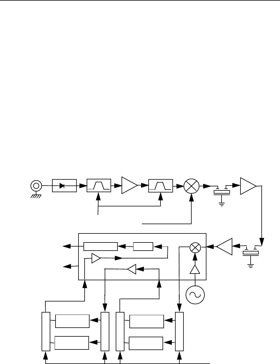
2-1
Section 2
THEORY OF OPERATION
1.0 Introduction
This Chapter provides a detailed theory of operation for the VHF circuits in the radio. For details of
the theory of operation and troubleshooting for the the associated Controller circuits refer to the
Controller Section of this manual.
2.0 VHF (136-174 MHz) Receiver
2.1 Receiver Front-End
The receiver is able to cover the VHF range from 136 to 174 MHz. It consists of four major blocks:
front-end bandpass filters and pre-amplifier, first mixer, 1st IF, 2nd IF, and receiver back-end. Two
varactor-tuned bandpass filters perform antenna signal pre-selection. A cross over quad diode mixer
converts the signal to the first IF of 44.85 MHz. High-side injection is used..
Figure 2-1 VHF Receiver Block Diagram
Demodulator
1. Crystal
Filter
Mixer
Varactor
Tuned Filter
RF Amp
Varactor
Tuned Filter
Pin Diode
Antenna
Switch
RF Jack
Control Voltage
from PCIC First LO
from FGU
Recovered Audio
RSSI
IF
Second LO
2. Crystal
Filter
455kHz Filter
(25kHz)
455kHz Filter
(25kHz)
455kHz Filter
(12.5kHz)
455kHz Filter
(12.5kHz)
Switch
Switch
Switch
Switch
Limiter
1. IF Amp
2. IF Amp
Filter Bank Selection
from Synthesizer IC

2-2 VHF (136-174 MHz) Receiver
There are two 2-pole 44.85 MHz crystal filters in the 1st IF section and 2 pairs of 455 kHz ceramic
filters in the 2nd IF section to provide the required adjacent channel selectivity. The correct pair of
ceramic filters for 12.5 or 25kHz channel spacing is selected via control line BWSELECT. The
second IF at 455 kHz is mixed, amplified and demodulated in the IF IC. The processing of the
demodulated audio signal is performed by an audio processing IC located in the controller section.
2.2 Front-End Band-Pass Filters & Pre-Amplifier
The received signal from the radio’s antenna connector is first routed through the harmonic filter and
antenna switch, which are part of the RF power amplifier circuits, before being applied to the receiver
pre-selector filter (C3001, C3002, D3001 and associated components). The 2-pole pre-selector filter
tuned by the dual varactor diode D3001 pre-selects the incoming signal (RXIN) from the antenna
switch to reduce spurious effects to following stages. The tuning voltage (FECTRL_1) ranging from 2
volts to 8 volts is controlled by pin 20 of PCIC (U3501) in the Transmitter section. A dual hot carrier
diode (D3003) limits any inband signal to 0 dBm to prevent damage to the pre-amplifier.
The RF pre-amplifier is a surface mount device (SMD) Q3001 with collector-base feedback to
stabilize gain, impedance, and intermodulation. Transistor Q3002 compares the voltage drop across
resistor R3002 with a fixed base voltage from divider R3011, R3000 and R3012, and adjusts the
base current of Q3001 as necessary to maintain its collector current constant at approximately 15-20
mA. Operating voltage is from the regulated 9.3V supply (9V3). During transmit, 9.1 volts (K9V1)
turns off both transistors Q3002 and Q3001. This protects the RF pre-amplifier from excessive
dissipation during transmit mode. A following 3dB pad (R3006 – R3008 and R3016 – R3018)
stabilizes the output impedance and intermodulation performance.
A second 2-pole varactor tuned bandpass filter provides additional filtering of the amplified signal.
The dual varactor diode D3004 is controlled by the same signal FECTRL_1, which controls the pre-
selector filter.
2.3 First Mixer and 1st Intermediate Frequency (IF)
The signal coming from the front-end is converted to the 1st IF frequency of 44.85 MHz using a cross
over quad diode mixer (D3031). Its ports are matched for incoming RF signal conversion to the 44.85
MHz IF using high side injection. The high-side injection signal (RXINJ) from the frequency
synthesizer circuit has a level of approximately +13 dBm and is injected via matching transformer
T3002.
The IF output signal (IF) from transformer T3001 pin 2 is fed to the first 2- pole crystal filter FL3101.
The filter output in turn is matched to IF amplifier Q3101 which is actively biased by a collector base
feedback (R3101, R3106) to a current drain of approximately 5 mA drawn from the 5 volt supply. Its
output impedance is matched to the second 2-pole crystal filter FL3102. The signal is further
amplified by a preamplifier (Q3102) before going into pin 1 of IFIC (U3101).
A dual hot carrier diode (D3101) limits the filter output voltage swing to reduce overdrive effects at
RF input levels above -27 dBm.
Transmitter Power Amplifier (PA) 45 W 2-3
2.4 2nd Intermediate Frequency (IF) and Receiver Back End
The 44.85 MHz 1st IF signal from the second IF amplifier feeds the IF IC (U3101) at pin1. Within the
IF IC, the 44.85 MHz high IF signal mixes with the 44.395 MHz second local oscillator (2nd LO) to
produce the 2nd IF signal at 455 kHz. The 2nd LO frequency is determined by crystal Y3101. The
2nd IF signal is amplified and filtered by an external pair of 455 kHz ceramic filters FL3112, FL3114
for 20/25 kHz channel spacing or FL3111, FL3113/F3115 for 12.5 kHz channel spacing. These pairs
are selectable via BWSELECT. The filtered output from the ceramic filters is applied to the limiter
input pin of the IF IC (pin 14).
The IF IC contains a quadrature detector using a ceramic phase-shift element (Y3102) to provide
audio detection. Internal amplification provides an audio output level of 120 mV rms (at 60%
deviation) from U3101 pin 8 (DISCAUDIO) which is fed to the ASFIC_CMP (U0221) pin 2 (part of the
Controller circuits).
A received signal strength indicator (RSSI) signal is available at U3101, pin 5, having a dynamic
range of 70 dB. The RSSI signal is interpreted by the µP (U0101, pin 63) and in addition is available
at accessory connector J0501-15.
3.0 Transmitter Power Amplifier (PA) 45 W
The radio’s 45 W PA is a four-stage amplifier used to amplify the output from the VCOBIC to the
radio transmit level. The line-up consists of three stages which utilize LDMOS technology, followed
by a final stage using a bipolar device. The gain of the first stage (U3401) is adjustable, controlled by
pin 4 of PCIC (U3501) via Q3501 and Q3502 (VCONT). It is followed by an LDMOS pre-driver stage
(Q3421), an LDMOS driver stage (Q3431) and a bipolar final stage (Q3441).
Figure 2-2 VHF Transmitter Block Diagram
Devices U3401 and Q3421 are surface mounted. The remaining devices are directly attached to the
heat sink.
Antenna
To Microprocessor
PCIC
Pin Diode
Antenna
Switch RF Jack
Harmonic
Filter
Power
Sense
PA-Final
Stage
PA
Driver
From VCO
Controlled
Stage
Vcontrol
Bias 1
Bias 2
To Microprocessor
Temperature
Sense
SPI BUS
ASFIC_CMP
PA
PWR
SET
To Microprocessor
Pre
Driver

2-4 Transmitter Power Amplifier (PA) 45 W
3.1 Power Controlled Stage
The first stage (U3401) is a 20 dB gain integrated circuit containing two LDMOS FET amplifier
stages. It amplifies the RF signal from the VCO (TXINJ). The output power of stage U3401 is
controlled by a dc voltage applied to pin 1 from the power control circuit (U3501 pin 4, with
transistors Q3501 and Q3502 providing current gain and level-shifting). The control voltage
simultaneously varies the bias of two FET stages within U3401. This biasing point determines the
overall gain of U3401 and therefore its output drive level to Q3421, which in turn controls the output
power of the PA.
In receive mode the voltage control line is at ground level and turns off Q3501-2, which in turn
switches off the biasing voltage to U3401.
3.2 Pre Driver Stage
The next stage is an LDMOS device (Q3421) providing a gain of +13 dB. This device requires a
positive gate bias and a quiescent current flow for proper operation. The voltage of the line
PCIC_MOSBIAS_1 is set during transmit mode by the PCIC pin 24, and fed to the gate of Q3421 via
the resistive network R3410, R3415, and R3416. The bias voltage is factory tuned.
3.3 Driver Stage
The following stage is an enhancement-mode N-Channel MOSFET device (Q3431) providing a gain
of 10 dB. This device also requires a positive gate bias and a quiescent current flow for proper
operation. The voltage of the line MOSBIAS_2 is set in transmit mode by the ASFIC and fed to the
gate of Q3431 via the resistive network R3404, R3406, and R3431-5. This bias voltage is also tuned
in the factory. If the transistor is replaced, the bias voltage must be tuned using the Customer
Programming Software (CPS). Care must be taken not to damage the device by exceeding the
maximum allowed bias voltage. The device’s drain current is drawn directly from the radio’s dc
supply voltage input, PASUPVLTG, via L3431 and L3432.
3.4 Final Stage
The final stage uses bipolar device Q3441. The device’s collector current is also drawn from the
radio’s dc supply voltage input. To maintain class C operation, the base is dc-grounded by a series
inductor (L3441) and a bead (L3442). A matching network consisting of C3446-52, C3467, L3444-
5, and two striplines, transforms the impedance to approximately 50 ohms and feeds the directional
coupler.
3.5 Directional Coupler
The directional coupler is a microstrip printed circuit, which couples a small amount of the forward
and reflected power delivered by Q3441. The coupled signals are rectified by D3451-2 and
combined by R3463-4. The resulting dc voltage is proportional to RF output power and feeds the
RFIN port of the PCIC (U3501, pin 1). The PCIC controls the gain of stage U3401 as necessary to
hold this voltage constant, thus ensuring the forward power out of the radio to be held to a constant
value.
An abnormally high reflected power level, such as may be caused by a damaged antenna, also
causes the dc voltage applied to the PCIC to increase, and this will cause a reduction in the gain of
U3401, reducing transmitter output power to prevent damage to the final device due to an improper
load.

Transmitter Power Amplifier (PA) 45 W 2-5
3.6 Antenna Switch
The antenna switch consists of two PIN diodes, D3471 and D3472. In the receive mode, both diodes
are off. Signals applied at the antenna jack J3401 are routed, via the harmonic filter, through
network L3472, C3474 and C3475, to the receiver input. In the transmit mode, the keyed 9 volts
turns on Q3471 which enables current sink Q3472, set to 96 mA by R3473 and VR3471. This
completes a dc path from PASUPVLTG, through L3473, D3471, L3477, L3472, D3472, L3471,
R3474 and the current sink, to ground. Both diodes are forward biased into conduction. The
transmitter RF from the directional coupler is routed via D3471 to the harmonic filter and antenna
jack. D3472 also conducts, shunting RF power and preventing it from reaching the receiver port
(RXIN). L3472 is selected to appear as a broadband guarter-wave transmission line, making the
short circuit presented by D3472 appear as an open circuit at the junction of D3472 and the receiver
path.
3.7 Harmonic Filter
Components L3491-L3494 and C3490-C3498 form a nine-pole Chebychev low-pass filter to
attenuate harmonic energy of the transmitter. R3490 is used to drain electrostatic charge that might
otherwise build up on the antenna. The harmonic filter also prevents high level RF signals above the
receiver passband from reaching the receiver circuits, improving spurious response rejection.
3.8 Power Control
The transmitter uses the power control IC (PCIC, U3501) to control the power output of the radio. A
portion of the forward and reflected RF power from the transmitter is sampled by the directional
coupler, rectified and summed, to provide a dc voltage to the RFIN port of the PCIC (pin 1) which is
proportional to the sampled RF power.
The ASFIC contains a digital to analog converter (DAC) which provides a reference voltage of the
control loop to the PCIC via R3517. The reference voltage level is programmable through the SPI
line of the PCIC. This reference voltage is proportional to the desired power setting of the transmitter,
and is factory programmed at several points across the frequency range of the transmitter to offset
frequency response variations of the transmitter’s power detector circuit.
The PCIC provides a dc output voltage at pin 4 (INT) which is amplified and shifted in dc level by
stages Q3501 and Q3502. The 0 to 4 Vdc range at U1503, pin 4 is translated to a 0 to 8.5 Vdc range
at the output of Q3501, and applied as VCONT to the power-adjust input pin of the first transmitter
stage U3401. This adjusts the transmitter power output to the intended value. Variations in forward
or reflected transmitter power cause the dc voltage at pin 1 to change, and the PCIC adjusts the
control voltage above or below its nominal value to raise or lower output power.
Capacitors C3502-4, in conjunction with resistors and integrators within the PCIC, control the
transmitter power-rise (key-up) and power-decay (de-key) characteristic to minimize splatter into
adjacent channels.
U3502 is a temperature-sensing device, which monitors the circuit board temperature in the vicinity
of the transmitter driver and final devices, and provides a dc voltage to the PCIC (TEMP, pin 29)
proportional to temperature. If the dc voltage produced exceeds the set threshold in the PCIC, the
transmitter output power is reduced so as to reduce the transmitter temperature.
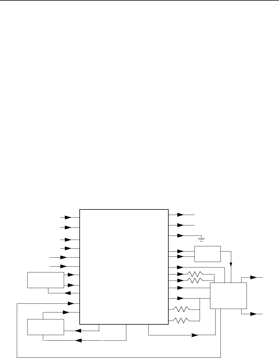
2-6 Frequency Synthesis
4.0 Frequency Synthesis
The frequency synthesizer subsystem consists of the reference oscillator (Y3261 or Y3262), the
Low Voltage Fractional-N synthesizer (LVFRAC-N, U3201), and the voltage-controlled oscillators
and buffer amplifiers (U3301, Q3301-2 and associated circuits).
4.1 Reference Oscillator
The reference oscillator (Y3262) contains a temperature compensated crystal oscillator with a
frequency of 16.8 MHz. An analog-to-digital (A/D) converter internal to U3201 (LVFRAC-N) and
controlled by the µP via serial interface (SRL) sets the voltage at the warp output of U3201 (pin 25)
to set the frequency of the oscillator. The output of the oscillator (U3262 pin 3) is applied to pin 23
(XTAL1) of U3201 via R3263 and C3235.
In applications were less frequency stability is required, the oscillator inside U3201 is used along
with an external crystal Y3261, varactor diode D3261, C3261, C3262 and R3262. In this case,
Y3262, R3263, C3235 and C3251 are not used. When Y3262 is used, Y3261, D3261, C3261,
C3262 and R3262 are not used, and C3263 is increased to 0.1 uF.
4.2 Fractional-N Synthesizer
The LVFRAC-N synthesizer IC (U3201) consists of a pre-scaler, a programmable loop divider,
control divider logic, a phase detector, a charge pump, an A/D converter for low frequency digital
modulation, a balance attenuator to balance the high frequency analog modulation and low
frequency digital modulation, a 13 volt positive voltage multiplier, a serial interface for control, and
finally a super filter for the regulated 5 volts.
Figure 2-3 VHF Synthesizer Block Diagram
DATA
CLK
CEX
MODIN
VCC, DC5V
XTAL1
XTAL2
WARP
PREIN
VCP
REFERENCE
OSCILLATOR
VOLTAGE
MULTIPLIER
DATA (U0101 PIN 100)
CLOCK (U0101 PIN 1)
CSX (U0101 PIN 2)
MOD IN (U0221 PIN 40)
+5V (U3211 PIN 1)
7
8
9
10
13, 30
23
24
25
32
47
VMULT2 VMULT1
BIAS1
SFOUT
AUX3
AUX4
IADAPT
IOUT
GND
FREFOUT
LOCK 4
19
6, 22, 33, 44
43
45
3
2
28
14 15
40
FILTERED 5V
STEERING
LOCK (U0101 PIN 56)
PRESCALER IN
FREF (U0221 PIN 34)
39
BIAS2
41
48
5, 20, 34, 36
+5V (U3211 PIN 1)
AUX1
VDD, DC5V MODOUT
U3201
LOW VOLTAGE
FRACTIONAL-N
SYNTHESIZER
AUX2
TRB
TX RF INJECTION
(1ST STAGE OF PA)
LO RF INJECTION
VOLTAGE
CONTROLLED
OSCILLATOR
LINE
2-POLE
LOOP
FILTER
1
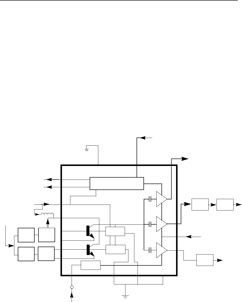
Frequency Synthesis 2-7
A voltage of 5V applied to the super filter input (U3201 pin 30) supplies an output voltage of 4.5 Vdc
(VSF) at pin 28. It supplies the VCO, VCO modulation bias circuit (via R3363) and the synthesizer
charge pump resistor network (R3251, R3252). The synthesizer supply voltage is provided by the 5V
regulator U3211.
In order to generate a high voltage to supply the phase detector (charge pump) output stage at pin
VCP (U3201-47), a voltage of 13 Vdc is being generated by the positive voltage multiplier circuits
(D3201, C3202, C3203). This voltage multiplier is basically a diode capacitor network driven by two
signals (1.05MHz) 180 degrees out of phase signals (U3201-14 and -15).
Output LOCK (U3201-4) provides information about the lock status of the synthesizer loop. A high
level at this output indicates a stable loop. IC U3201 provides the 16.8 MHz reference frequency at
pin 19.
The serial interface (SRL) is connected to the µP via the data line DATA (U3201-7), clock line CLK
(U3201-8), and chip enable line CSX (U3201-9).
4.3 Voltage Controlled Oscillator (VCO)
The Voltage Controlled Oscillator (VCO) consists of the VCO/Buffer IC (VCOBIC, U3301), the TX
and RX tank circuits, the external RX buffer stages, and the modulation circuits.
Figure 2-4 VHF VCO Block Diagram
Presc
RX
TX
Matching
Network Low Pass
Filter
Attenuator
Pin8
Pin14
Pin10
(U3211 Pin1)
VCC Buffers
TX RF Injection
U3201 Pin 32
AUX3 (U3201 Pin2)
Prescaler Out
Pin 12Pin 19
Pin 20
TX/RX/BS
Switching Network
U3301
VCOBIC
Rx
Active Bias
Tx
Active Bias
Pin2
Rx-I adjust
Pin1
Tx-I adjust
Pins 9,11,17
Pin18
Vsens
Circuit
Pin15
Pin16
RX VCO
Circuit
TX VCO
Circuit
RX Tank
TX Tank
Pin7
Vcc-Superfilter
Collector/RF in
Pin4
Pin5
Pin6
RX
TX
(U3201 Pin28)
Rx-SW
Tx-SW
Vcc-Logic
(U3211 Pin1)
Steer Line
Voltage
(VCTRL)
Pin13
Pin3
TRB IN
LO RF INJECTION
Q3304
Q3301

2-8 Frequency Synthesis
The VCOBIC together with the Fractional-N synthesizer (U3201) generates the required frequencies
in both the transmit and receive modes. The TRB line (U3301, pin 19) determines which tank circuits
and internal buffers are to be enabled. A high level on TRB enables the TX tank and TX output (pin
10), and a low enables the RX tank and RX output (pin 8). A sample of the signal from the enabled
RF output is routed from U3301, pin 12 (PRESC_OUT), via a low pass filter, to U3201, pin 32
(PREIN).
A steering line voltage (VCTRL) between 2.5 volts and 11 volts at varactor diode D3361 tune the full
TX frequency range (TXINJ) from 136 MHz to 174 MHz, and varactor diode D3341 tunes the full RX
frequency range (RXINJ) from 181 MHz to 219 MHz. The RX tank circuit uses a Hartley
configuration for wider bandwidth. For the RX tank circuit, an external transistor Q3304 is used for
better side-band noise.
The external RX buffers (Q3301 and Q3302) are enabled by a high at U3301, pin 7 (RX_SWITCH)
via transistor switch Q3303. In the TX mode, the modulation signal (VCOMOD) from the LVFRAC-N
synthesizer IC (U3201 pin 41) is applied to varactor diode D3362, which modulates the TX VCO
frequency via capacitor C3362. Varactor D3362 is biased for linearity from the VSF.
4.4 Synthesizer Operation
The complete synthesizer subsystem consists of the low voltage FRAC-N (LVFRACN), reference
oscillator (a crystal oscillator with temperature compensation), charge pump circuit, loop filter circuit
and a dc supply. The output signal PRESC from the VCOBIC (U3301 pin 12) is fed to U3201 pin 32
(PREIN) via a low pass filter (C3318, L3318 and C3226) which attenuates harmonics and provides
the correct level to close the synthesizer loop.
The pre-scaler in the synthesizer (U3201) is a dual modulus type with selectable divider ratios. The
divider ratio of the pre-scaler is controlled by the loop divider, which in turn receives its inputs via the
SRL. The output of the pre-scaler is applied to the loop divider. The output of the loop divider is
connected to the phase detector, which compares the loop divider´s output signal with the reference
signal. The reference signal is generated by dividing down the signal of reference oscillator Y3261 or
Y3262.
The output signal of the phase detector is a pulsed dc signal which is routed to the charge pump.
The charge pump outputs a current at U3201 pin 43 (IOUT). The loop filter (which consists of R3221-
R3223 and C3221-C3224) transforms this current into a voltage that is applied to the varactor diodes
(D3361 for transmit, D3341 for receive) to alter the output frequency of the appropriate VCO. The
current can be set to a value fixed within the LVFRAC-N IC, or to a value determined by the currents
flowing into BIAS 1 (U3201-40) or BIAS 2 (U3201-39). The currents are set by the value of R3251
and R3252 respectively. The selection of the three different bias sources is done by software
programming.
To reduce synthesizer lock time when new frequency data has been loaded into the synthesizer, the
magnitude of the loop current is increased by enabling the IADAPT pin (U3201-45) for a certain
software programmable time (adapt mode). The adapt mode timer is started by a low to high
transient of the CSX line. When the synthesizer is within the lock range, the current is determined
only by the resistors connected to BIAS 1 and BIAS 2, or by the internal current source. A settled
synthesizer loop is indicated by a high level signal at U3201-4 (LOCK).
The LOCK signal is routed to one of the µP´s ADC inputs (U0101-56). From the measured voltage,
the µP determines whether LOCK is active.
To modulate the PLL, the two spot modulation method is utilized. Via U3201, pin 10 (MODIN), the
audio signal is applied to both the A/D converter (low frequency path) as well as the balance
attenuator (high frequency path). The A/D converter changes the low frequency analog modulating
signal into a digital code that is applied to the loop divider, thereby causing the carrier to deviate. The
balance attenuator is used to adjust the VCO’s deviation sensitivity to high frequency modulating
signals. The output of the balance attenuator is present at the MODOUT port (U3201-41) and
connected to the VCO modulation diode D3362 via R3364.
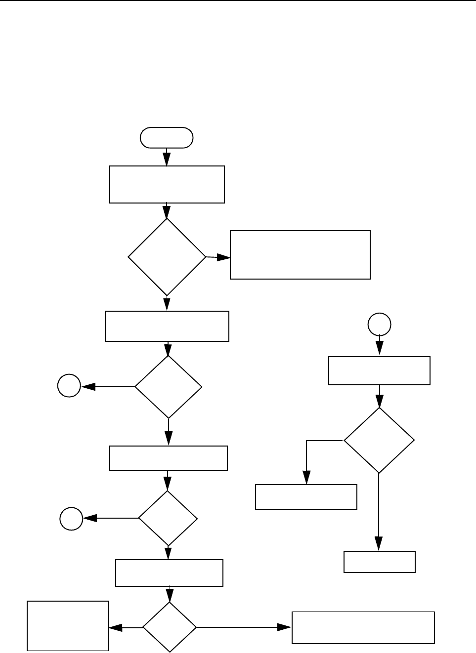
3-1
Section 3
TROUBLESHOOTING CHARTS
1.0 Troubleshooting Flow Chart for Receiver (Sheet 1 of 2)
Bad SINAD
Bad 20dB Quieting
No Recovered Audio
START
Audio at
pin 8 of
U3101 ?
Check Controller
(in the case of no audio)
OR ELSE go to “B”
Yes
No
Spray or inject 44.85MHz
into XTAL Filter FL3101
Audio heard ?BYes
No
Check 2nd LO
(44.395MHz) at C3135
LO present ?
BYes
Check voltages on
U3101
Biasing OK ?
No
No
A
Yes
Check Q3102 bias
for faults
Replace Q3102
Go to B
Yes
No
Check circuitry
around U3101.
Replace
U3101 if defect
Check circuitry around Y3101.
Replace Y3101 if defect
Voltages
OK?

3-2 Troubleshooting Flow Chart for Receiver
1.1 Troubleshooting Flow Chart for Receiver (Sheet 2 of 2)
IF Signal at
C3035?
No
RF Signal at
T3001?
RF Signal at
C3012?
No
RF Signal at
C3008?
No
RF Signal at
C3474?
No or
Check Harmonic Filter
J3401 and
Antenna Switch
D3471,D3472,L3472
Check filter between C3474
& C3008. Check tuning
voltage at R3019
Inject RF into J3401
Is tuning
voltage OK?
No
Yes
Check RF amp
(Q3001) Stage
Check filter between
C3012 & T3001
Yes
Check T3001, T3002,
D3031, R3030-R3034,
L3032, C3034 and C3035
Yes
1st
LO level OK?
Locked?
Yes
Check FGU
Yes
Trace IF signal from
C3035 to Q3101.
Check for bad XTAL
filter
No
Yes
IF signal at Q3102
collector?
Before replacing
U3101, check
U3101 voltages
Yes
Check for 5VDC
Is 9V3 present?
Check Supply Voltage
circuitry. Check Q0681,
U3211 and U0641
No
No
No
Check U3501
Check varactor filter
No
Yes
Yes
Yes
A
A
B
weak RF
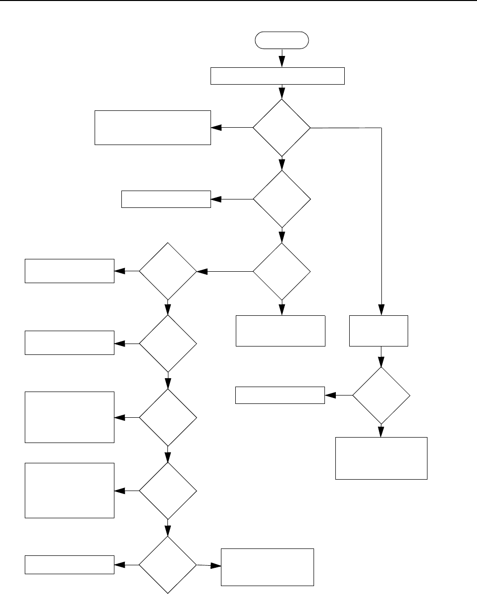
Troubleshooting Flow Chart for 45W Transmitter 3-3
2.0 Troubleshooting Flow Chart for 45W Transmitter (Sheet 1 of 2)
Current in-
crease when
keyed?
NO
YES
START
No or too low Power when keyed
Check Components between
Q3441 and RF Output, Antenna
Switch D3471,D3472
>500mA & <5A
>5A
<500mA
Check PA Stages
Control
Voltage at
TP3402
>1V
>1V
<1V Check
Voltage at
PCIC U3501
Pin 4
Check Components
between TP3402 and
U3501 Pin 4
Short TP3403
to Ground
NO
YES
Voltage at
TP3402 ris-
es?
Check PA Stages NO
YES
PCIC U3501
Pin 15 9.3V
DC?
Check 9.3 V Regulator
U0641
NO
YES
PCIC U3501
Pin 16 >4V
DC
Replace PCIC
U3501
NO
YES
TP3404
9.1V DC
If U3201 Pin 3 is high,
replace PCIC
U3501,otherwise
check controller and
FGU
YES NO
TP3403
>0.5V DC?
Replace PCIC U3501 Check Forward & Reverse
Power Sense Circuitry
(D3451 & D3452)
Check Forward & Reverse
Power Sense Circuitry
(D3451 & D3452)
NO
YES
PCIC U3501
Pin 5 > 1V
DC?
Check Power Setting,
Tuning & Components
between PCIC Pin 5
and ASFIC (U0221) Pin
4 before replacing AS-
FIC
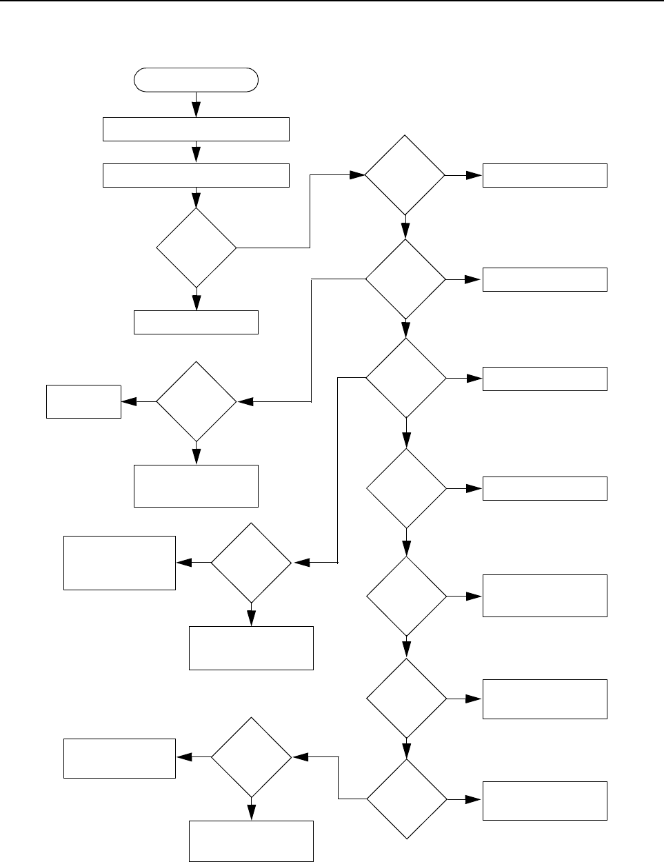
3-4 Troubleshooting Flow Chart for 45W Transmitter
2.1 Troubleshooting Flow Chart for 45W Transmitter (Sheet 2 of 2)
Pin 2
Voltage 0.62
* Voltage at
Pin 1?
NO
YES
Check PA Stages
No or too low Power when keyed
NO
YES
Replace U3401
Pin 3
Voltage 0.51
* Voltage at
Pin 1?
2-4V
Supply
0V Bias 1 DC
Voltage at
TP3406?
NO
YES PCIC U3501
Pin 24 2-4V
DC?
Check Bias Tuning be-
fore replacing
PCIC U3501
Check Voltage at Pin 2 & 3 of U3401
Replace U3401
Replace Q3421
NO
0V
1-4V
Bias 2 DC
Voltage at
TP3407?
YES
RF Voltage
at TP3401
>100mV?
YES
RF Voltage
U3401 Pin 6
>3V?
Replace
Q3421
Supply
Replace Q3431
Check FGU (U3301)
NO Check Components
between TP3401 &
C3417
NO
YES ASFIC
U0221 Pin 6
1-4V DC?
Check Bias Tuning be-
fore replacing
ASFIC U0221
Check Components
between ASFIC and
Q3431 before re-
placing Q3431
YES
RF Voltage
Q3421 Gate
>1V?
NO Check Components
between C3417 &
Q3421
YES RF Voltage
Q3431 Gate
>4V?
NO Check Components
between Q3421 &
Q3431
YES
RF Voltage
Q3441 Base
>5V?
Check Components
between Q3431 &
Q3441
NO
Check Components
between Q3441 & An-
tenna Connector
Voltage
Voltage
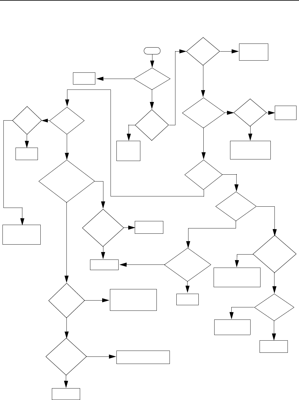
Troubleshooting Flow Chart for Synthesizer 3-5
3.0 Troubleshooting Flow Chart for Synthesizer
+5V at
U3201 Pins
13 & 30?
5V
at pin 6 of
D3201
Is information
from µP U0101
correct?
Is U3201
Pin 47
= 13VDC ?
Is U3301 Pin 19
<40 mVDC in RX &
>4.5 VDC in TX?
(at VCO section)
Start
Visual
check of the
Board OK?
Correct
Problem
Check 5V
Regulator
U3211
Is 16.8MHz
Signal at
U3201 Pin
19?
Check
Y3261, Y3263 and
associated parts
Are signals
at Pins 14 &
15 of U3201?
Check
R3201
Check C3319
Is U3201 pin 2
>4.5 VDC in Tx &
<40 mVDC in Rx
Replace
U3201
Remove
Shorts
Is there a short
between Pin 47 and
Pins 14 & 15 of
U3201?
Replace or resolder
necessary components
Is RF level at
U3201 Pin 32
-12 < x <-25
dBm?
Are
R3221,
R3222, R3223,
C3221, C3222,
& C3224
OK?
Replace
U3201
If R3227, C3226 & C3227
are OK, then see VCO
troubleshooting chart
Are Waveforms
at Pins 14 & 15
triangular?
Do Pins
7,8 & 9 of
U3201 toggle
when channel is
changed?
Check programming
lines between U0101
and U3201 Pins 7,8 & 9
Replace
U3201
Check µP U0101
Troubleshooting
Chart
No
Yes
No
Yes
No
Yes
No
No
No
Yes
Yes
No
Yes
Yes
No
Yes
Yes
Yes
No
No
No
No
Yes
No
Yes
Yes
Check D3201,
C3202, C3203,
C3205 & C3206
5V at
U3201 pins 5,
20, 34 & 36
C h e c k 5 V
Regulator
U3211, R3211
Is
16.8MHz
signal at
U3201 pin
23?
Replace
U3201
Yes
No
No
Yes
No
Yes
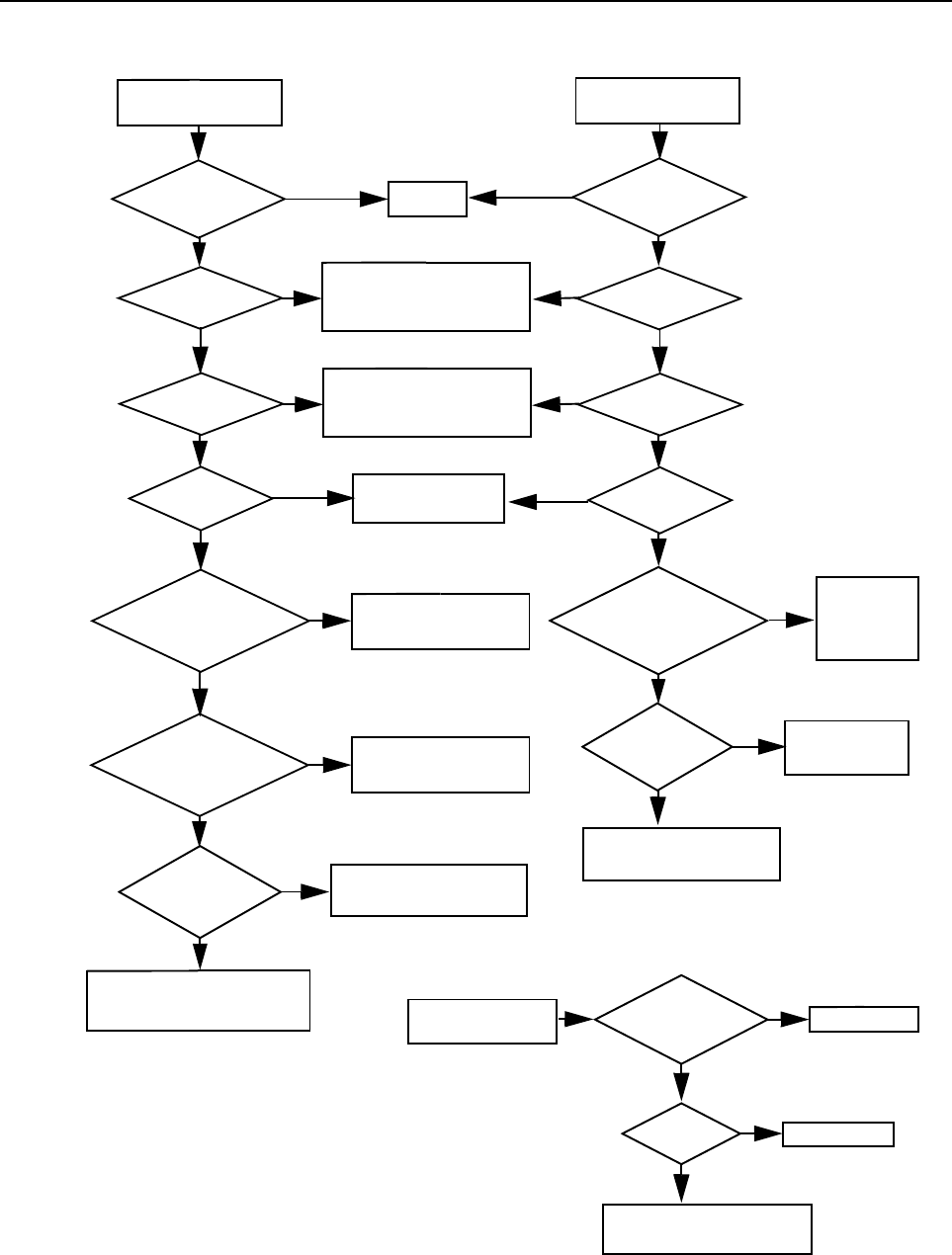
3-6 Troubleshooting Flow Chart for VCO
4.0 Troubleshooting Flow Chart for VCO
Are Q3301
Base at 0.7V
Collector at 4.5V
Emitter at 110mV
Are Q3304
Base at 2.4V
Collector at 4.5V
Emitter at 1.7V
Are U3301 Pins
13 at 4.4V
15 at 1.1V
10 at 4.5V
16 at 1.9V
Low or no RF Signal
at TP3001
Visual check
of board
OK?
35mV DC at
U3301 Pin 19
NO
YES
at base of Q3301
NO
NO
NO
NO
NO
YES
YES
YES
YES
YES
Low or no RF Signal
at input to PA
5V DC at U3301
Pin 14 & 18 OK ?
4.8V DC at
U3301 Pin 19
Is RF available
at TP3401
YES
YES
YES
YES
YES
NO
NO
NO
NO
NO
Audio =180mVrms
at “-” side of
D3362
2.5VDC
at D3362
If C3362 and R3363 are OK,
then replace D3362
Replace R3363
Replace R3364
NO
NO
YES
YES
If R3402 and
C3315 are OK,
replace U3301
TX VCO
RX VCO
Correct
Problem
Visual check
of board
OK?
Make sure U3211 is working
correctly and runner
between U3211 Pin 1 and
U3301 Pin 14 & 18 is OK
Check runner
between U3201 Pin 2
and U3301 Pin 19
Is RF available If all parts from U3301 Pin 8
to Base of Q3301 are OK,
replace U3301
If all parts associated
with the pins are OK,
replace Q3301
Check parts between
T3001 and Q3301 Power OK but
no modulation
If all parts from TP3401 of
U3401 Pin 16 are OK,
replace U3401
If all parts
associated
with the pins
are OK,
replace U3301
4.5V DC at
U3301 Pin 3 OK?
YES
NO 4.5V DC at
U3301 Pin 3 OK?
YES
NO
Make sure Synthesizer is
working correctly and runner
between U3201 Pin 28 and
U4301 Pin 3 is OK
5V DC at U3301
Pin 14 & 18 OK ?
OK? OK?
If all parts associated
with the pins are OK,
replace Q3301

4-1
Section 4
VHF PCB/SCHEMATICS/PARTS LIST
1.0 Allocation of Schematics and Circuit Boards
1.1 Controller Circuits
The VHF circuits are contained on the Printed Circuit Board (PCB) which also contains the
Controller circuits. This Chapter shows the schematics for the VHF circuits only, refer to the
Controller section for details of the related Controller circuits . The PCB component layouts and the
Parts Lists in this Chapter show both the Controller and VHF circuit components. The VHF
schematics and the related PCB and parts list are shown in the tables below.
Table 4-1 VHF 25-45W Diagrams and Parts Lists
PCB : 8486140B13 Main Board Top Side
8486140B13 Main Board Bottom Side Page 4-3
Page 4-4
SCHEMATICS
Power Amplifier 25 - 45W
FRACN
Voltage Controlled Oscillator
Receiver Front End
IF
Page 4-5
Page 4-6
Page 4-7
Page 4-8
Page 4-9
Parts List
8486140B13 Page 4-10

4-2 Allocation of Schematics and Circuit Boards
THIS PAGE INTENTIONALLY LEFT BLANK
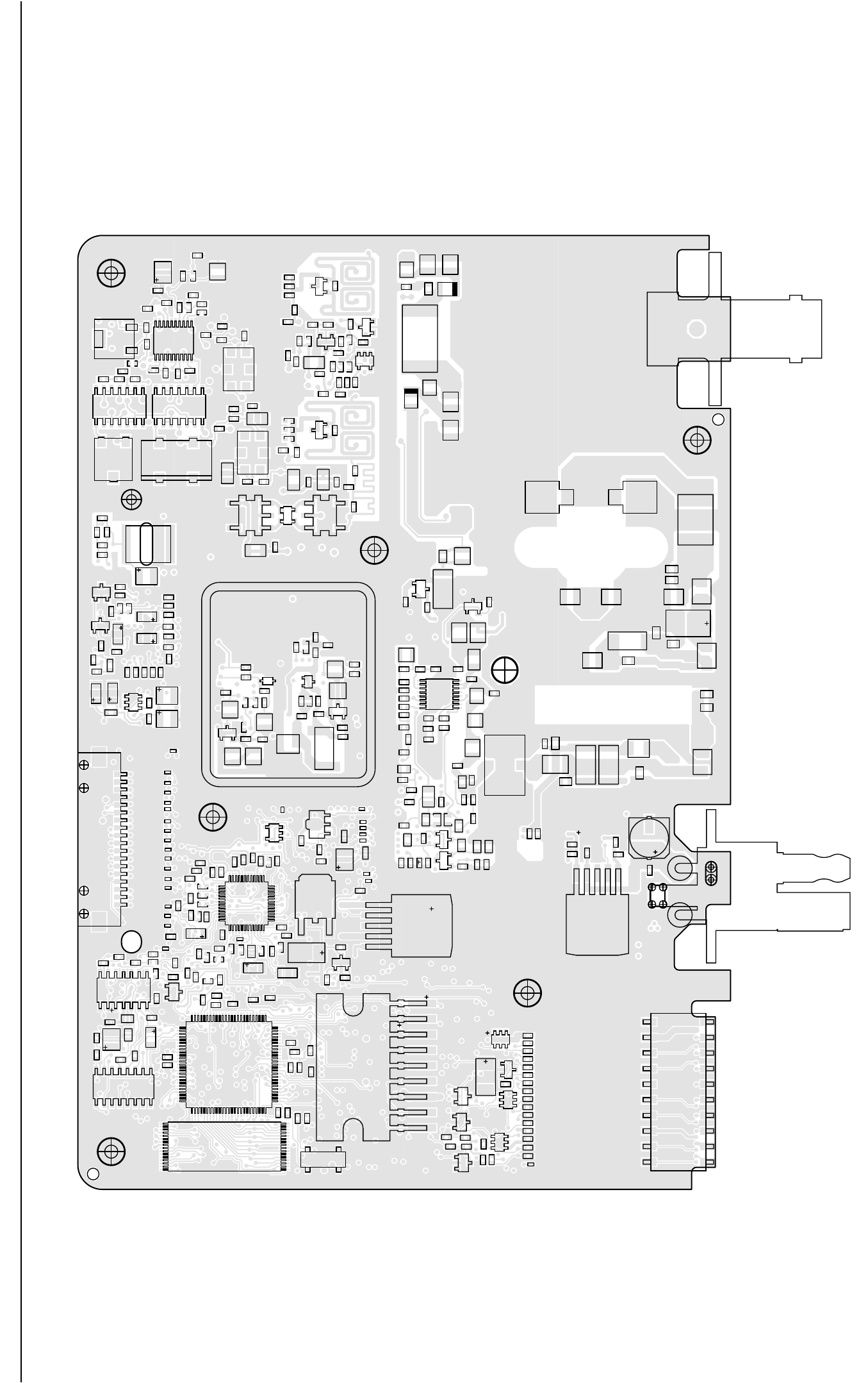
VHF 25-45W PCB / Schematics / Parts List 4-3
2.0 VHF 25-45W PCB / Schematics / Parts List
C0101C0102
C0104
C0106
C0107
C0108
C0131
C0132
C0211
C0212
C0221
C0222
C0223
C0224
C0225
C0226
C0227
C0228
C0231
C0232
C0233
C0234
C0235
C0236
C0237
C0241
C0242
C0243
C0244
C0245
C0246
C0251
C0252
C0253
C0256
C0261
C0262
C0421
C0441
C0442
C0443
C0445
C0446
C0447
C0448
C0449
C0470
C0471
C0472
C0473
C0474
C0476
C0477
C0478
C0482
C0483
C0484
C0486
C0487
C0488
C0490
C0493
C0494
C0495
C0496
C0501
C0502
C0503
C0504
C0505
C0506
C0508
C0509
C0510
C0511
C0512
C0513
C0514
C0515
C0516
C0517
C0518
C0542
C0601
C0603
C0612
C0651
C0652
C0654
C0655
C0681
C3002
C3004
C3005
C3006
C3007
C3008
C3009
C3010
C3011
C3012
C3013
C3014
C3015
C3016
C3017
C3018
C3019
C3020
C3021
C3027
C3028
C3032
C3034
C3100
C3101
C3102
C3103
C3114
C3115
C3124
C3131
C3132
C3133
C3134
C3135
C3136
C3137
C3139
C3140
C3141
C3142
C3143
C3145
C3148
C3210
C3211
C3213
C3214
C3215
C3221
C3222
C3223
C3224
C3226
C3227 C3229
C3231
C3232
C3233
C3234
C3240
C3242
C3243
C3244
C3245
C3246
C3247
C3252
C3253
C3254
C3255
C3324
C3336
C3337
C3341
C3342
C3344
C3345
C3346 C3347
C3357 C3361
C3362
C3363 C3364
C3365
C3400
C3401
C3402
C3403
C3404
C3407
C3408
C3409
C3410
C3411
C3412
C3413 C3414
C3417
C3418
C3420
C3422
C3423
C3425
C3426
C3428
C3434
C3435
C3436
C3437
C3438
C3439
C3440
C3441
C3443
C3444
C3445
C3446
C3447
C3455
C3456
C3458
C3472
C3473
C3474
C3475
C3478
C3491 C3492
C3501
C3506
C3507
C3508
C3509
C3510
D0201
D0651
D3001
D3003
D3004
D3031
D3221
D3341
D3361
D3362
D3471
D3472
2
3
456
FL3101
2
3
456
FL3102
4
32
FL3112
FL3114
18
1
J0451
20
11
10
J0501
J0601
23
J3401
L0481
L0482
L3002
L3031
L3032
L3034
L3100
L3101
L3124
L3201 L3232
L3333
L3341
L3343 L3344
L3346
L3361
L3362
L3363
L3364
L3401
L3403
L3411
L3412
L3413
L3414
L3421
L3422
L3431
L3432
L3433
L3443 L3444
L3471
L3472
L3474
L3477
Q0110
Q0177
Q0181
Q0185
Q0681 Q3001
Q3021
Q3221
Q3304
5
2
6
8
13
7
4 Q3421
Q3471
Q3501
Q 3502
R0101
R0102
R0103
R0104
R0105
R0106
R0108
R0110
R0114
R0115
R0116
R0131
R0132
R0170
R0181
R0182
R0185
R0186
R0211
R0212
R0220
R0221
R0222
R0223
R0224
R0225
R0226
R0227
R0228 R0229
R0241
R0242
R0251
R0252
R0253
R0254
R0255
R0256
R0257
R0261
R0262
R0268
R0269
R0442
R0510
R0533
R0535
R0538
R0539
R0611
R0612
R0651
R0652
R0681
R0682
R3001
R3002
R3003
R3004
R3009
R3013
R3014
R3015
R3016
R3024
R3025 R3026
R3027
R3028
R3031
R3101
R3106 R3111
R3117
R3123
R3124
R3130
R3132
R3135
R3142
R3144
R3145
R3211
R3221
R3222
R3223
R3224
R3225
R3227
R3242
R3251
R3252
R3335
R3336
R3341
R3342
R3361
R3362
R3363
R3364
R3400
R3401
R3402
R3403
R3404
R3405
R3406
R3408
R3409
R3410
R3411
R3413
R3415
R3416 R3418
R3419 R3424
R3425
R3431
R3432
R3458
R3461
R3471
R3505
R3506
R3507
R3508
R3512
R3513
R3514
R3515
R3516
SH3301
3
46
1
2
T3001
3
4
6
12
T3002
1
76
51
26
32
17
16 1
87
114
U0211
137
25
13
16
1
89
U0251
9
U0271
1
6
5
1
6
5
3
2
1
11
1
20
10
U3101
87
1
14
U3111
87
1
14
U3115
U3211
1
16
8
9
U3401
U3502
VR0501
VR0503
VR0505 VR0510
23
4
Y0131
2
Y3102
1
1
1
1
1
1
U0121
Flashrom U0101
Microprocessor
U0221
ASFIC CMP
U0651
5V Regulator
U0641
9,6V Regulator
U0611
B+ Switch
ZWG0130589-O
VHF (136-174 MHz) 25-45W 8486140B13 Top Side
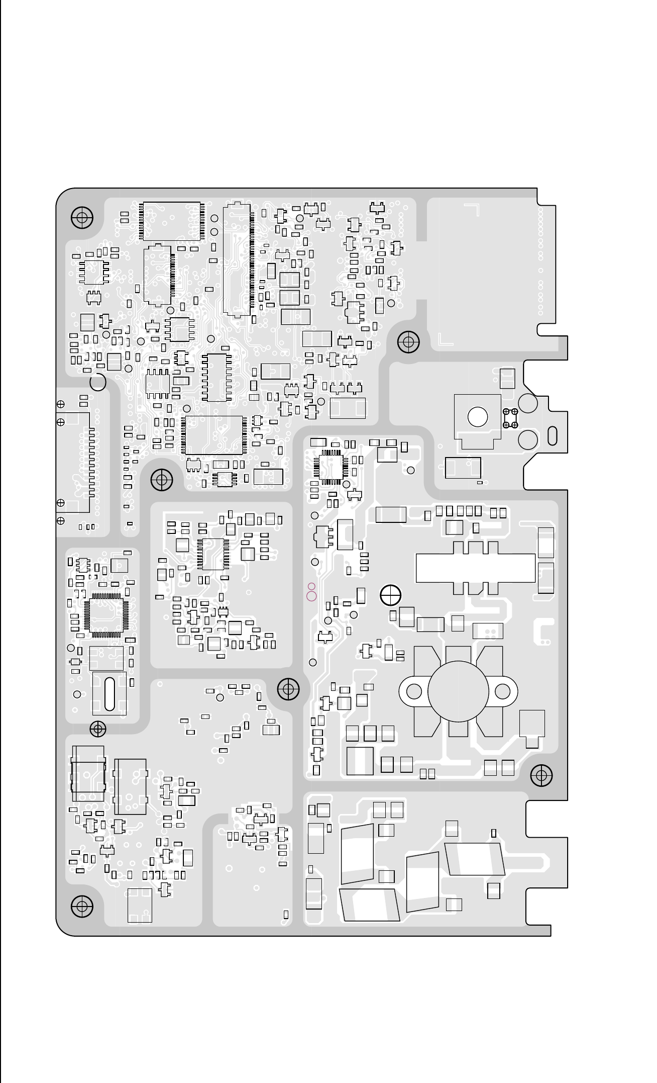
4-4 VHF 25-45W PCB / Schematics / Parts List
C0103
C0105
C0111
C0112
C0121 C0122
C0123
C0141
C0151
C0201
C0202
C0203 C0204
C0205
C0254
C0255
C0265
C0266
C0267
C0271
C0272
C0273
C0274
C0275
C0276
C0277
C0301
C0302
C0303
C0304
C0305
C0324 C0325
C0331
C0341
C0342
C0343
C0344
C0351
C0352
C0353
C0354
C0422
C0423
C0426
C0427
C0428
C0429
C0430 C0431
C0485
C0491
C0492
C0497
C0499
C0541
C0554
C0558 C0559
C0560 C0575C0576
C0591
C0592 C0593
C0611
C0621
C0622
C0641
C0644
C0645
C0661
C0662
C0663
C0671
C3000
C3001
C3003
C3022
C3023
C3024
C3025
C3026
C3029
C3030
C3031
C3033
C3035
C3036
C3104
C3110
C3111
C3112
C3113
C3116
C3121
C3122
C3123
C3144
C3146 C3147
C3151
C3152
C3202
C3203
C3205
C3206
C3207
C3208
C3209
C3225
C3228
C3235
C3241
C3251
C3261
C3262
C3263
C3301
C3302
C3303
C3304
C3305
C3306
C3311
C3312
C3313
C3314
C3315
C3316
C3317
C3318
C3319
C3331
C3332
C3333
C3334
C3335
C3348
C3351
C3352
C3355
C3356
C3405
C3406
C3415
C3416
C3421
C3424
C3429
C3430
C3431
C3432
C3433
C3442
C3448
C3449
C3450
C3451
C3452
C3453
C3457
C3459
C3460
C3461
C3464
C3465
C3466
C3467 C3468
C3471
C3477
C3488
C3489
C3490
C3494
C3496
C3497
C3498
C3502
C3503
C3504
C3505
D0101
D0151
D0179
D0301
D0621
D0660
D0661
D3000
D3011
D3101
D3201
D3261
D3451
D3452
D3455
E0271
E0272
E0631
F0401
43
2
FL3111
FL3113
43
2
FL3115 12
J0401
1
40
J0551
1
18
J0552
L3025
L3111
L3112
L3231
L3301
L3302
L3311
L3317
L3318
L3331
L3332
L3345
L3351
L3402
L3423
L3441
L3442
L3445 L3473
L3475
L3476
L3491
L3492
L3493
L3494
Q0151
Q0171
Q0173
Q0183
Q0271
Q0641
Q0661
Q0662
Q0663
Q3002
Q3101
Q3102
Q3141
Q3151
Q3152
Q3301
Q3302
43
Q3303
6
5
43
2
1
Q3431
6
5
4
3
2
1
Q3441
Q3472
Q3473
R0107
R0111 R0112
R0113
R0117 R0121
R0151 R0152
R0171
R0172
R0173
R0174
R0175
R0176
R0177
R0178
R0179
R0183
R0184
R0201
R0202
R0203
R0204
R0205
R0206
R0207
R0208
R0265
R0266
R0267
R0273
R0274
R0275
R0276
R0323
R0324
R0331
R0332
R0333
R0335
R0341
R0342
R0343
R0344
R0345
R0346
R0347
R0401
R0407 R0408
R0409
R0412 R0441
R0467
R0468
R0481
R0482
R0511
R0512
R0525
R0529
R0530
R0531 R0537
R0541
R0542
R0543
R0555
R0556
R0591
R0592
R0593
R0621
R0641
R0642
R0643
R0661
R0662
R0671
R0672
R3000
R3006
R3010
R3011
R3012
R3018
R3019
R3021
R3023 R3030
R3032
R3033
R3034
R3035
R3036
R3102
R3104
R3105
R3107
R3108
R3112
R3113
R3114
R3115
R3116 R3118
R3133
R3134
R3141
R3146
R3147
R3151
R3152
R3153
R3154
R3201
R3203
R3204
R3206
R3226
R3228
R3241
R3261
R3262
R3263
R3301
R3302
R3303
R3304
R3305
R3306
R3307
R3308
R3311
R3312
R3313
R3314
R3315
R3316
R3317
R3318
R3319
R3321
R3323
R3331
R3343
R3351
R3352
R3353
R3354
R3355
R3356
R3412
R3414
R3417
R3433
R3434
R3435
R3436R3437
R3441
R3442
R3443
R3444
R3453
R3455
R3457
R3459
R3460 R3462
R3463
R3464
R3465 R3473
R3474
R3475
R3476
R3477
R3490
R3501
R3502
R3503
R3504
R3509
R3510 R3511
R3517
R3518
RT3460
RT3471
TP0101
TP0102
TP0103
TP0104
TP0151
TP0221
TP0222
TP0492
TP0497
TP0530
TP0661
TP3001
TP3201
TP3401
TP3402
TP3403
TP3404 TP3406
TP3407
TP3501
1
4
58
U0111
22
21 8
7
1
16
1
8
9U0141
28 15
14
1
U0301
U0331
1
4
5
8
U0341
U0342
4
58
U0351
14
58
U0652
U0653
1
37
25 13
11
1
20
10
U3301
1
17
9
25
U3501 VR0151
VR0504
VR0509
VR0537
VR0541
VR0601
VR0621
VR0671
VR3471
4
3
2Y3101
6
4
3
1
Y3261
2
34
Y3263
1
1
1
1
1
5
U0122
RAM
U3201
FRACN
1
8486140B13_C
C00
CNTL-REV-T6
PA-REV-C
VCO-REV-T3
IF-REV-T5
FE-REV-T4
FRACN-T6
ZWG0130590-O
VHF (136-174 MHz) 25-45W 8486140B13 Bottom Side
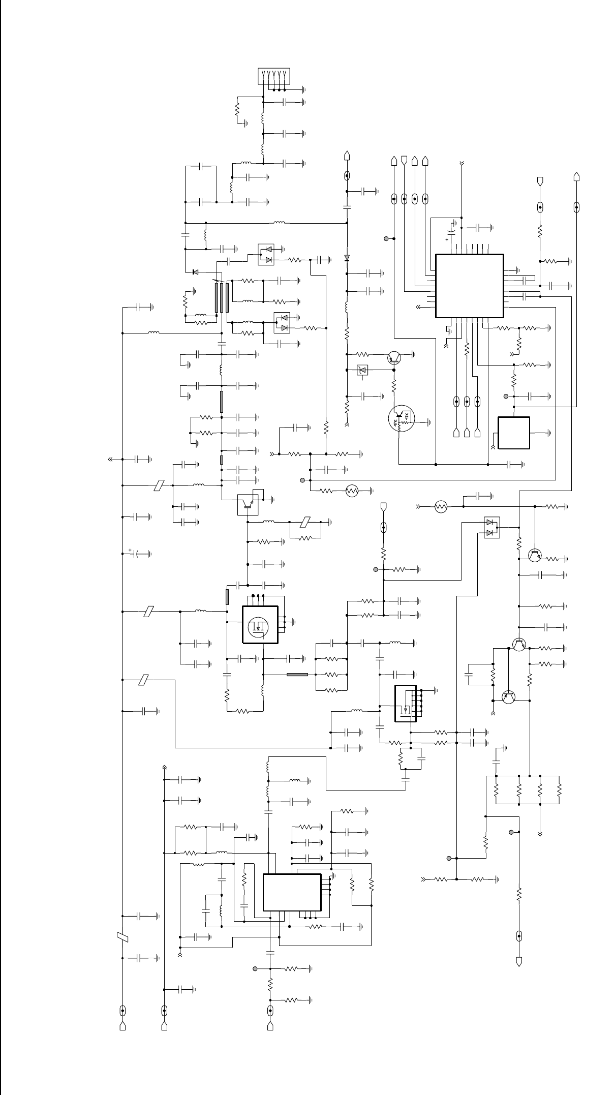
VHF 25-45W PCB / Schematics / Parts List 4-5
4.953x8.763
0 to 5 dBm J3401
1.524x8.751
Spacing: 0.254
2.68V (28W)
0.75V
3.77V (50W)
8.87V
2.77V (50W)
2.65V (28W)
5.20V (28W)
5.45V (50W)
3.70V-3.90V
2.75V-2.90V
2.66V (28W)
3.71V (50W)
1.524x20.696
1.905x15.685
C3489
130pF
.022uF
C3471
C3409
390pF
C3442
2200pF
NU
RT3471
50K
NU
R3476
220
Q3471
NU
R3459
0
NU
R3409
4.7K
DATA R3509
10K
C3492
470pF
R3441
51
150K
R3408
C3429
20pF
C3451
18pF
NU
C3430
33pF
1000pF
C3466
5.6K
R3417
NU
11pF
C3464
D3451
C3468
18pF
82K
5.6K
R3410
220pF
C3444
NU
R3418
620
R3453
R3515
0.1uF
820K
2200pF
C3460
C3461
R3512
100K
62
R3461
D3452
120
R3437
10pF
56pF
C3433
1.2uH
L3477
C3447
L3411
68nH
2200pF
C3414
51nH
C3494
NU
Q3473
Q3441
MRF247
2200pF
C3478
L3491
47pF
Q3472
2200pF
C3407
470
R3400
.022uF
C3411
680
R3507
R3518
10K
1MEG
NU
R3443
1MEG R3444
C3434
1uF
R3455
G4
S1
S2
S3
S4
100K
D
G
G1
G2
G3
180pF
MRF5015
Q3431
C3431
12.77nH 43
R3457
DATA_VHF_PA_1
L3433
TP3402
68pF
C3450
L3473
1.2uH
1000pF
C3457
R3432
30nH
L3441
57R01
51
1000pF
L3421
0.1uF
C3422
L3422
16.96nH
NU
C3423
L3475
L3443
57R01
150nH
C3438
0.1uF C3439
1uF
NU
C3491
16pF
L3472
NU
RXIN
48nH
9V3_VHF_PA_1
C3472
150pF
C3477
10K
R3475
NU
2200pF
C3510
C3446
56pF
0.1uF
RESET
D3471
D3472
150pF
C3473
150pF
R3474
NU
C3488
51
Q3421
220pF
C3443
R3414
820
MOSBIAS_2_VHF_PA_1
20K
R3510
CSX
NU
120nH
L3476
PA_PWR_SET_VHF_PA_1
CLK_VHF_PA_1
PASUPVLTG_VHF_PA_1
10
R3442
L3402
57R01
R3511
100K
R3401
68
R3425
130
47pF
TXINJ
9V3
Q3501
C3498
C3509
K9V1
2200pF
L3403
68nH
NU
10pF
C3453
2200pF
C3416
56
R3435
L3414
L3413
27nH
4.22nH
C3502
2200pF
1uF
C3505
R3434
56
R3502
6.8K
R3501
39K
1.2uH
36pF
L3471
36pF
C3449
R3431
C3448
23
1
51
.022uF
VR3471
R3473
C3402
51
TEMPSENSE
K9V1_VHF_PA_1
CSX_VHF_PA_1
CNTLVLTG_VHF_PA_1 R3413
3.3K
51nH
L3493
TP3404
L3492
51nH
C3410
.022uF
R3506
680
68
R3424
C3408
18pF
C3413
.022uF
.022uF
C3415
FECNTL_2
Q3502
D3455
FECNTL_1
R3471
NU
470
2200pF
C3428
C3426
2200pF
C3425
1uF
100
R3416
R3415
100
82pF
C3420
20
R3419
82pF
C3441
C3432
C3506
2200pF
1000pF L3432
36.54nH
1K
R3503
C3418
24pF
C3417
2200pF
1000pF
L3423
12.77nH
C3455
56pF
C3406
MOSBIAS_2
R3462
39K
2200pF
C3435
R3463
15K
2
VOUT
C3412
2200pF
LM50
U3502
3
GND
POS
CLK
0
R3460
5.6K
R3412
6.8K
R3411
100
R3405 NU
CNTLVLTG
TXINJ_VHF_PA_1
TP3501
R3508
680
R3517
R3505
680 100K
R3404
10K
82pF
C3467
R3436
120
18
VAR2
24
VAR3
VG 15
6
VL 19
VLIM
18pF
C3475
31 RSET
23
RX
2
T1
30 TEMP
14
V10
16
V45
17
V5EXT
20
VAR1
8
GND1
25 GND2
4
INT
22
NA
11
Q10
QX
1
RFIN
21
RS
3
CI
5
CJ
7
CL
26 CLK
12
CQ
CQX 13
28 DATA
9
F168
U3501
32 ANO
27 BPOS
29 CEX
43
H99S-4
33pF
R3402
NU
C3403
6
RFOUT2 7
VCNTRL
1
VD1
14
2
VG1
VG2 3
C3401
2200pF
GND3
12
GND4
13
NC1
8
NC2
9
NC3
10
NC4
15
RFIN
16 RFOUT1
U3401
G2
11
GND1
4
GND2
5
L3431
57R01
C3504
2200pF
C3440
0.1uF
2200pF
C3503
C3507
100pF
.01uF
C3424
R3490
47K
1000pF
C3445
1000pF
620
C3456
R3516
R3513
620
R3458
1000pF
C3465
12nH
NU
0
2200pF
L3474
FECNTL_2_VHF_PA_1
C3404
FECNTL_1_VHF_PA_1
620
RESET_VHF_PA_1
TEMPSENSE_CNTLR_1
R3514
2200pF
C3400
L3401
1K
39nH
C3458
R3504
C3490
36pF
.01uF
C3436
0
R3464
10uF
TP3406
PASUPVLTG
RT3460
50K
220K
R3465
C3501
2200pF
C3474
1000pF
33nH
L3412
L3494
51nH
L3442
57R01
1000pF
TP3407
C3405
L3445
18nH
68pF
C3452
TP3403
.01uF
C3421
TP3401
56
PA_PWR_SET
R3433
100pF
C3459
R3403
130
0.1uF
C3437
20pF
C3497
43pF
C3496
NU
R3477
43
33nH
L3444
C3508
RXIN_VHF_PA_1
150K
R3406
2200pF
9V3
9V3
A+
9V3
PCIC_MOSBIAS_1
PCIC_MOSBIAS_1 9V3
VCONT
9V3
VCONT
9V3
NC 9V3
9V3
A+
NC
NC
NC
NC
NC
NC
NCNC NC
NC
ZWG0130512-O
VHF (136-174 MHz) Power Amplifier 25-45W
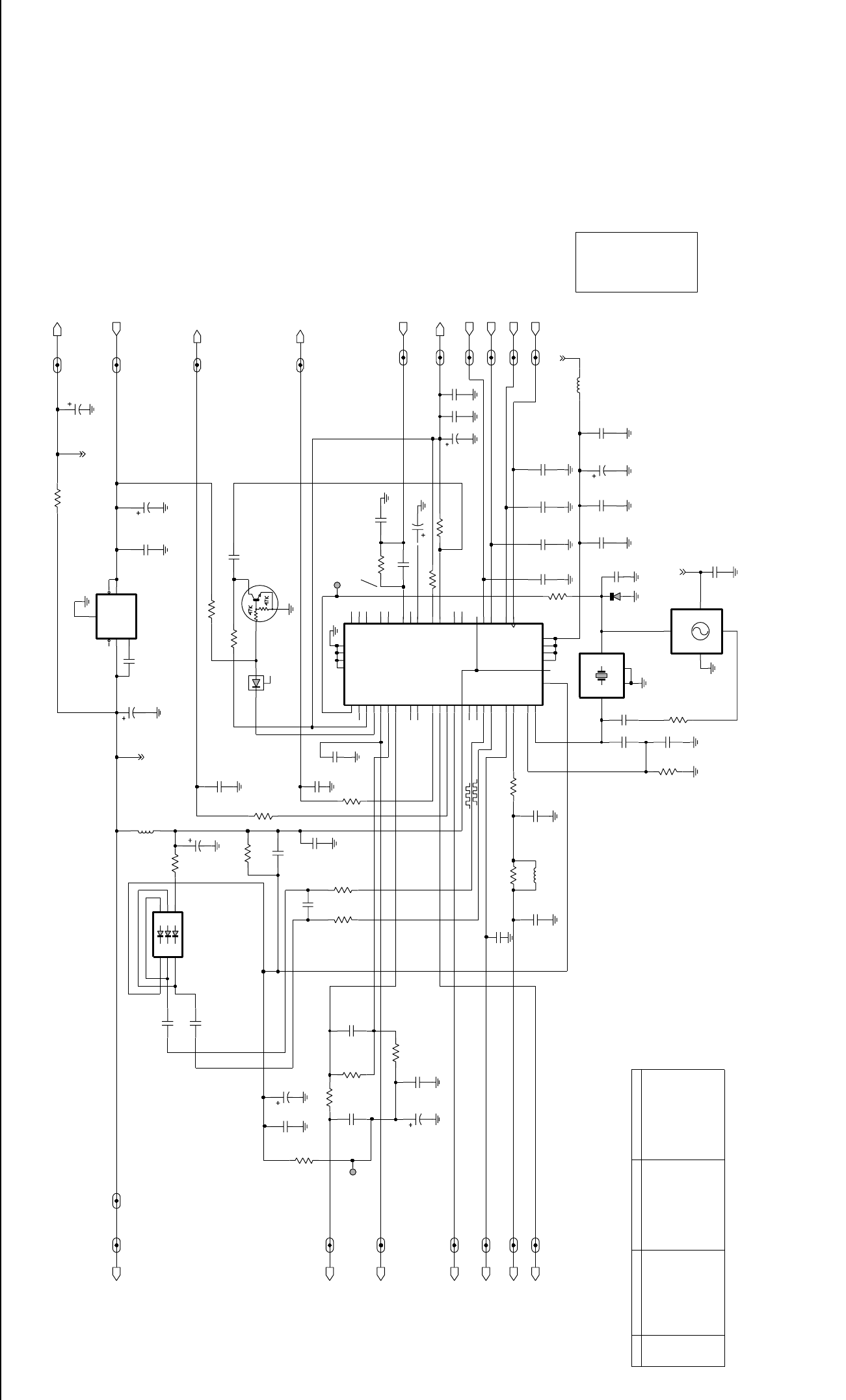
4-6 VHF 25-45W PCB / Schematics / Parts List
0VDC
5VDC
5VDC
(SOURCE)
-2 to +7dBm
13.30VDC
6.83VDC
4.52VDC (R)
+1dBm
0VDC (R)
4.95VDC (R)
2.90VDC
3.42VDC
3.63VDC
2.5VDC
1.1-4.1VDC
0VDC (T)
2.62VDC (T)
4.91VDC (T)
Temp.
Comp.
Xtal
Ref.Osz.
11.28VDC
4.97VDC
2.5-11VDC
5VDC (LOCKED)
0VDC (UNLOCKED)
R3203
A1
5
A2
4
A3
K1
1K2
2K3
3
47
D3201
6
47K
NU
TRB L3232
2.2uH
NU
R3228
C3231
C3225
.01uF
L3201
390nH
0.1uF
C3202
.01uF
100
R3223
C3229
D3221
0.1uF
.047uF
CLK
C3251
C3207
22pF
NU
47K
VCOBIAS_2
R3225
C3226
8.2pF
MODIN_VHF_FN_1
TP3201
R3252
VCOBIAS_1_VHF_FN_1
330K
16_8MHz_VHF_FN_1
PRESC_VHF_FN_1
R3242
0
100
R3241
VSF_VHF_FN_1
DATA
VCOMOD_VHF_FN_1
CSX_VHF_FN_1
100pF
C3227
22pF
NU
CSX
IN_5V_RF_REG_VHF_FN_1
C3240
NU
1
GND 4
GND1
3
OUT
6IN
16.8MHz
75Z04
Y3261
100K
R3227
0.1uF
C3254
C3208
0.1uF
NU
.01uF
C3232
47K
R3226
PRESC
C3214
2.2uF
C3221
0.1uF
1uF
C3224
C3263
0.1uF
VMULT1
15
14 VMULT2
12 VMULT3
11 VMULT4
VRO
13
25
WARP
23 XTAL1
XTAL2
24
27
SFBASE 26
SFCAP
30
SFIN
28 SFOUT
37 TEST1
38 TEST2
21
VBPASS
47
VCP
31
NC3
44
PD_GND
PD_VDD
5
PREIN 32
33
PRE_GND
34 PRE_VDD
35
PVREF
18
REFSEL
45 IADAPT
16 INDMULT
43 IOUT
LOCK
4
10
MODIN
41 MODOUT
17
NC1
29
NC2
39
BIAS2
42
CCOMP
9
CEX 8
CLK
7
DATA
DGND 6
36 DVDD
19 FREFOUT
46 ADAPTSW
22
AGND
48 AUX1
1AUX2
2AUX3
3AUX4
20 AVDD
40
BIAS1
VCOBIAS_1
63A27
U3201
47
R3201
VSF
C3222
0
R3211
0.1uF
L3231
0.1uF
C3211
TP3202
2.2uH
C3243
220pF
16_8MHz
VDDA
VDDA_VHF_FN_1
VCOBIAS_2_VHF_FN_1
0.1uF
C3209 C3246
220pF
NU
C3206
10uF
5V_VHF_FN_2
150K
R3206
Q3221
R3251
180K
.01uF
C3228
0.1uF
C3235
2.2uF
C3210
VCTRL_VHF_FN_1
R3204
LOCK_VHF_FN_1
47
1uF
C3223
NU
220pF
R3262
NU
C3245
BWSELECT
6.2K
C3215
R3224
47K
C3213
2.2uF
1
GND
5
IN
2NR
4OUT
3
SD
2.2uF
VCC
4
VCNTL
1
ADP3300
U3211
6
ERR
Y3263
TTS05V
16.8MHz
GND
2
OUT
3
MODIN
VCTRL
C3255
DATA_VHF_FN_1
220pF
C3242
2.2uF
5V_VHF_FN_1
.01uF
R3222
680
TRB_VHF_FN_1
C3205
C3262
330pF
NU
NU
VCOMOD
C3241
56pF
R3261
47K
2.2uF
C3233
R3221
CLK_VHF_FN_1
C3252
390
1000pF
.01uF
C3234
C3253
4.7uF
NU
IN_5V_RF_REG5V
D3261
C3261
NU
LOCK
C3244
39pF
BWSELECT_VHF_FN_1
220pF
C3203
4,7k
.01uF
NC
5V
5V
R3263
NC
NC
NC
NC
NC NC
NC
NC
NC
NC
VDDA
VDDA
NC
NC
NC
.022uF
C3212
R3202
10MEG
NU
10pF
C3247
In case Y3261 is used instead of Y3263,
replacement of the following parts requires
new temperature compensation of the frequency:
Y3261, U3201, R3261, R3262, C3262, D3261
ZWG0130564-O
(*)
(*)
(*)
(*)
(*) (*)
(*)
(*)
(*)
0662057A89
NOTPLACED
NOTPLACED
NOTPLACED
4805875Z04
39pF
330pF
47K
XtalNOTPLACED
4886182B01
C3262 NOTPLACED
100nF
100nF
47K
100
NOTPLACED
NOTPLACED
NOTPLACED
NOTPLACED
NOTPLACED
2113740L37
2113740F07
2113740F59
4802245J22
0662057B02
4880114R04
62pF 2%
220pF
1.5pF
150K
Xtal
RefOsc
Temp.Comp. new
NOTPLACED
NOTPLACED
2113740F41
2113740F63
NOTPLACED
4862824C03
Ref.Osz. Temp.Comp. org.Ref.No.
C3235
C3251
C3261
C3263
2113741F49 10nF
2113743E20
NOTPLACED
2113743E20
D3261
R3261
R3262
R3263
Y3261
Y3262
NOTPLACED
0662057A89
NOTPLACED
0662057A25
0102727B34
0102727B34
0102727B34
0102727B34
Board Kits Assemblies
PRIME_MUHF
PRIME_BNC
GUD6338A
GUD6336A
GUD6338A
HF (136-174 MHz) FRACN
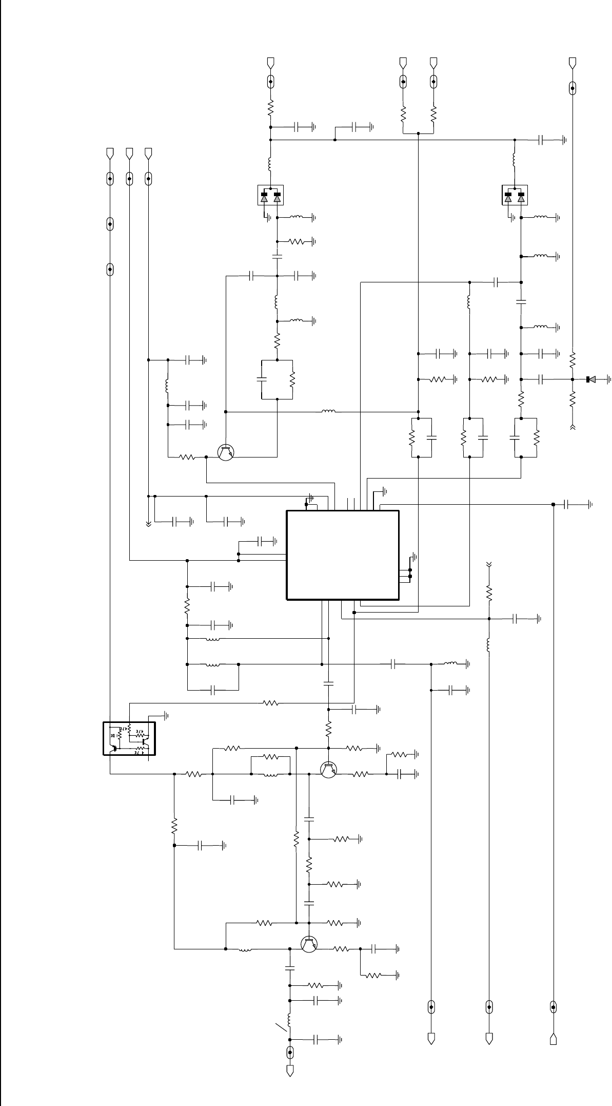
VHF 25-45W PCB / Schematics / Parts List 4-7
4.22VDC (T)
0VDC (R)
1.92VDC (T)
4.52VDC (R)
2.62VDC (T)
4.52VDC (R)
0VDC (T)
1.42VDC (R)
0VDC (T)
4.97VDC
4.40VDC
1.53VDC (R)
0VDC (T)
0.92VDC (R)
0VDC (T)
0VDC (R)
0-5dBm (T)
7.44VDC (R)
9.14VDC (R)
0VDC (T)
0VDC (T)
11-14dBm (R)
-2 to 7dBm
0VDC (T)
2.18VDC (R)
0VDC (T)
1.49VDC (R)
2.56VDC (R)
0VDC (R)
2.5-11VDC
4.54VDC
0VDC (T)
4.78VDC (R)
2.66VDC (T)
4.52VDC (T)
WARISMOBILE VHF_VCO
4.78VDC (R)
4.27VDC (T)
4.91VDC (T)
9.21VDC
3.83VDC (R)
L3333
R3356
12K
VCOBIAS_2_VHF_VCO_1
1uH
D3361
R3335
33
9V3_VHF_VCO_2
220
R3361
C3331
VDDA_VHF_VCO_1
10K
NU
10pF
35.5nH
R3321
15K
L3346
L3331
68nH
R3336
100nH
NU
C3312
0.1uF
10 TX_OUT
13 TX_SWITCH
14
VCC_BUFFERS
18
VCC_LOGIC
NU
L3311
2
RX_IADJ
8RX_OUT
7RX_SWITCH
3
SUPER_FLTR
TRB_IN 19
16
TX_BASE 15
TX_EMITTER
1
TX_IADJ
4
COLL_RFIN
20
FLIP_IN
11
GND_BUFFERS
9
GND_FLAG
GND_LOGIC
17
12 PRESC_OUT 5
RX_BASE 6
RX_EMITTER
U3301
50U54
R3362
47
NU
330pF
C3304
R3354
150K
RXINJ
VCOMOD_VHF_VCO_1
C3363
68pF
L3317
33nH
33pF
C3317
C3357
7.5pF
1uH
L3351
100
R3311
10K
R3317
22
R3318
NU
L3344
1uH
C3362
5.6pF
100nH
L3332
22
R3306
0
R3316
NU
18nH
L3301
C3344
1.8pF
Q3301
L3318
100nH
C3311
.022uF
6.8pF
C3314
C3315
.01uF
C3303
15pF
20K
R3351
Q3304
BFQ67W
NU
47K
R3319
3.3pF
C3316
56nH
L3361
0
R3308
TRB_VHF_VCO_1
1uH
L3364
C3351
.01uF 12K
R3352
PRESC
VCOMOD
VCOBIAS_1_VHF_VCO_1
R3323
1K
VCTRL
C3347
.01uF
C3337
0.1uF
NU
R3307
220
D3341
VCOBIAS_1
RXINJ_VHF_VCO_1
100K
R3353
C3324
.01uF
L3302
100nH
VCOBIAS_2
2.2K
R3303 C3345
20pF
L3362
68nH
15pF
C3364
8nH
L3341
C3333
0.1uF
56nH
L3363
100
0.1uF
C3332
NU
R3312
.022uF
C3352
C3305
VDDA
NU
5.6pF
TRB
100
R3343
C3334
VSF_VHF_VCO_1
.022uF
.01uF
C3355
VSF
C3342
3pF
D3362
1K
R3313
C3336
.01uF
NU
C3335
.01uF
R3341
220
R3355
20K
NU
R3363
39K
9V3_VHF_VCO_1 9V3
VCTRL_VHF_VCO_1
PRESC_VHF_VCO_1
75
6.8pF
R3301
C3302
C3306
5.1pF NU
15pF
C3301
NU
330pF
C3313
47
R3331
3
C3319
1000pF
UMC5N
2
4
1
C3346
Q3303
C3341
.01uF
1000pF
39
R3342
NU
Q3302
TXINJ_VHF_VCO_1
TXINJ
5.6pF
C3318
220
R3315
9V3_VHF_VCO_3
NU
C3361
C3356
.022uF
1000pF
180nH
1K
R3304
R3302
L3343
220
100
NU
R3305
C3365
1000pF
R3314
R3364
47K
NU
10
C3348
.01uF
VSF
1uH
L3345
VSF
VSF
NC
NC
NC
ZWG0130394-O
VHF (136-174 MHz) Voltage Controlled Oscillator
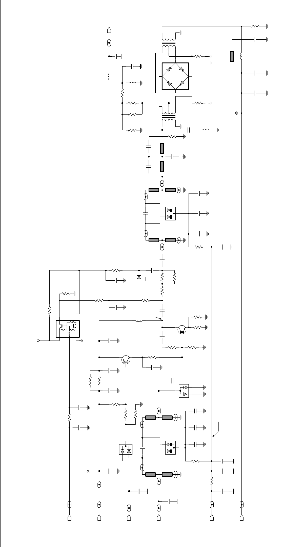
4-8 VHF 25-45W PCB / Schematics / Parts List
3
120pF
C3021
D3004
12
RXINJ
FECNTL_1
SP_3_1
1000pF
C3020
100pF
C3016
1.5K
R3000
SP_4_2
IF_VHF_FE_1
D3003
1
2
3
SP_3_2 C3014
D3001
7.5pF
R3016
10
4
6
3
1
2
1000pF
C3036
XFMR
T3002
3300pF
C3003
4.7K
R3011
RXIN
K9V1__VHF_FE_1
NU
R3030
10
SP_4_3
NU
150nH
L3025
820
R3034
D3000
1
23
NU
1000pF
C3019
FECNTL_1_VHF_FE_1VLTG
C3006
3300pF
C3000
56pF
13pF
C3032
1.5K
R3025
NU
220
RXINJ_VHF_FE_1
R3018
3300pF
C3011
FECNTL_2
R3031
51
SP_4_1
330pF
C3009
C3001
9V3
C3013
4.7pF
Q3002
56pF
SP_3_3
100K
R3009
9V3_VHF_FE_2
R3002
1K
R3003
18pF
560
R3032
C3035
C3024
NU
820
NU
3300pF
NU
R3023
0
C3005
NU
4.7pF
C3018
100pF
C3030
1000pF
NU
330pF
C3023
C3027
.01uF
R3028
390
560nH
L3031
56pF
C3004
SP_1_2
R3012
1K
NU
33nH
L3034
Q3021
NU
0
R3035
1.5K
R3004
0
R3033
3300pF
C3007
330pF
C3029
K9V1
390
R3024
NU
.01uF
C3028
10K
1K
R3036
R3006
R3026
NU
SP_2_2
10K
R3014
SP_2_1
51 C3015
C3002
9.1pF
56pF
82pF
C3034
NU
18pF
C3031
IO3
IO4
5.1pF
C3033
D3031
IO1 IO2
560
R3021
10
R3015
1000pF
C3008
SP_1_1 .01uF
C3022
680
R3010
C3017
150nH
L3032
43pF
1000pF
IF
FECNTL_2_VHF_FE_1
Q3001
SP_1_3 SP_2_3
R3013
R3027
3.3K
47K
R3019
10K
L3002
2.7pF
470nH
NU
C3025
TP3001
100K
R3001
C3026
D3011
4
6
3
1
2
0.1uF
RXIN_VHF_FE_1 XFMR
T3001
9V3_VHF_FE_1
9V3
330pF
C3010
NC
NC_D3011_2
9V3
ZWG0130395-A
3.0-7.5V
3.6VDC
C3012
VHF (136-174 MHz) Receiver Front End
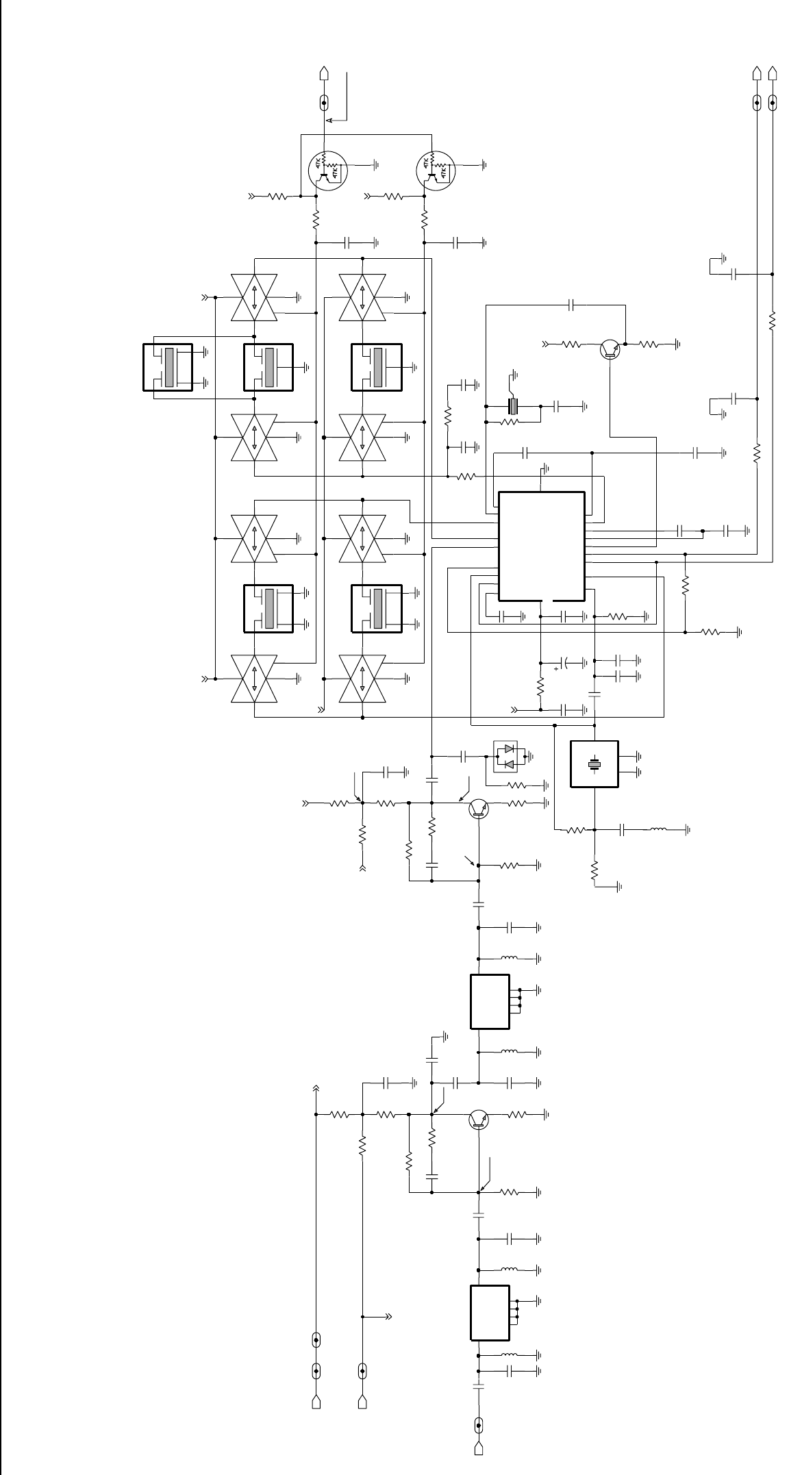
VHF 25-45W PCB / Schematics / Parts List 4-9
9180469V03
3.9VDC
12.5kHz 0VDC
20/25kHz 5VDC
0.75VDC
0.75VDC 3VDC
9180469V06
9180469V04
9180468v04
9180468V06
3VDC
6.8K
R3107
9V3
R3135
1.2K
390
1GND1
GND2
2
GND3
4
5GND4
3IN 6
OUT
R3115
FL3101
12R16
R3117
27K
Q3102
Q3151
680
R3146
620nH
L3111
620
R3108
R3118
6.8K
R3111
12K
C3101
5V_VHF_IF_1
GND2
4
1IN 2
OUT
NU
2.2pF
FL3111
3
GND1
U3115-1
CNTL
13
1
2VDD
14
VSS
7
DISCAUDIO_VHF_IF_1
15K
R3132
0.1uF
C3144
120pF
C3143
C3139
C3141
0.1uF
0.1uF
13
1
2VDD
14
VSS
7
Q3141
U3111-1
CNTL
R3116
330
10
9V3_VHF_IF_2
3
GND
1IN 2
OUT
R3102
C3110
27pF
FL3113
0.1uF
C3142
9.1pF
IFIN_VHF_IF_1
100
R3104
NU
C3113
1
2GND2
4GND3
GND4
5
IN
3OUT 6
NU
DISCAUDIO
12R16
FL3102
GND1
1000pF
R3151
C3100
C3140
0.1uF
10K
11 10
VDD
14
VSS
7
3
14
VDD
7
VSS
U3111-4
CNTL
12
U3115-2
5
CNTL
4
Q3152
C3152
.01uF
.01uF
C3151
R3133
8.2K
4700pF
C3146
27K
R3106
C3112
390
R3141
82pF
10
R3112
1.8K
R3142
R3154
10K
C3122
.039uF
Q3101
6
VCC
330
R3113
20 MIXOUT 4
OSCIN
3OSCOUT
10
QUADIN
1
RFIN
2
RFIN_DEC
5RSSIOUT
9
RSSI_FEED
15
18
IFAMPIN
16 IFAMPOUT
19
IFAMP_DEC1
17
IFAMP
_DEC2
14
LIMIN
11 LIMOUT
13 LIM_DEC1
12 LIM_DEC2
SA616
U3101
8AUDIOOUT
7
AUDIO_FEED
GND
51
44.395MHz
12R17
Y3101
2
GND
4
GND1
3OUT 1
IN
R3130
C3136
30pF
C3135
33pF
12K
R3101
R3147
12K
C3133
10uF
C3115
100
R3105
22pF
620nH
L3100
0.1uF
NU
C3137
.039uF
C3134
455KHz
3
2
1
BWSELECT_VHF_IF_1
BWSELECT
45B02
Y3102
C3103
33pF
C3132
0.1uF
10K
R3152
0.1uF
C3111
U3115-3
6
CNTL
89
14
VDD
7
VSS
18pF
C3114
L3112
620nH
9V3_VHF_IF_1
5V
D3101
RSSI_VHF_IF_1
OUT
.039uF
C3123
FL3112
3
GND1
GND2
4
1IN 2
R3114
100
R3134
10K
NU
2.4K
R3144
U3111-2
5
CNTL
4
3
14
VDD
7
VSS
3.3K
R3145
C3145
C3147
0.1uF
620nH
L3101
0.1uF
220pF
C3148
NU
10
VDD
14
VSS
7
NU
1pF
C3131
U3115-4
CNTL
12
11
C3121
0.1uF
FL3115
GND1
34
GND2
IN
1OUT 2
15pF
C3102
NU
U3111-3
6
CNTL
89
14
VDD
7
VSS
3GND
1IN 2
OUT
RSSI
C3116
FL3114
0.1uF 0.1uF
R3153
C3104
5V
10K
5V
9V3
9V3
9V39V3
9V3
5V
9V3
5V
9V3
0
R3123
1uH
NU
L3124
33pF
C3124
820
R3124
ZWG0130565-O
VHF (136-174 MHz) IF

4-10 VHF 25-45W PCB / Schematics / Parts List
VHF PCB 8486140B13 Parts List 25-45W
Circuit
Ref Motorola Part
No. Description
C3000 2113741F37 3.3nF 50V
C3001 2113740F19 4.7pF 5%
C3002 2113740F26 9.1pF 5%
C3003 2113741F37 3.3nF 50V
C3004 2113740F45 56pF 5%
C3005 2113740F51 100pF 5%
C3006 2113740F45 56pF 5%
C3007 2113741F37 3.3nF 50V
C3008 2113741F25 1nF 50V
C3009 2113741F13 330pF 50V
C3010 2113741F13 330pF 50V
C3011 2113741F37 3.3nF 50V
C3012 2113741F25 1nF 50V
C3013 2113740F45 56pF 5%
C3014 2113740F24 7.5pF 5%
C3015 2113740F45 56pF 5%
C3016 2113740F51 100pF 5% 50V
C3017 2113740F42 43pF 5% 50V
C3019 2113741F25 1nF 50V
C3020 2113741F25 1nF 50V
C3021 2113740F53 120pF 5% 50V
C3022 2113741F49 10nF 50V
C3026 2113743E20 100nF 16V
C3027 2113741F49 10nF 50V
C3028 2113741F49 10nF 50V
C3030 2113741F25 1nF 50V
C3033 2113740F20 5.1pF 5% 50V
C3034 2113740F49 82pF 5% 50V
C3035 2113740F33 18pF 5% 50V
C3036 2113741F25 1nF 50V
C3100 2113741F25 1nF 50V
C3102 2113740F31 15pF 5% 50V
C3103 2113740F39 33pF 5% 50V
C3104 2113743E20 100nF 16V
C3110 2113740F37 27pF 5% 50V
C3111 2113743E20 100nF 16V
C3112 2113740F49 82pF 5% 50V
C3114 2113740F33 18pF 5% 50V
C3115 2113740F35 22pF 5% 50V
C3116 2113743E20 100nF 16V
C3121 2113743E20 100nF 16V
C3122 2113743E11 39nF 10%
C3123 2113743E11 39nF 10%
C3132 2113743E20 100nF 16V
C3133 2311049A57 TANT CP 10uF 10% 16V
C3134 2113743E20 100nF 16V
C3135 2113740L30 33pF 2%
C3136 2113740L29 30pF 2%
C3137 2113743E11 39nF 10%
C3139 2113743E20 100nF 16V
C3140 2113743E20 100nF 16V
C3141 2113743E20 100nF 16V
C3142 2113743E20 100nF 16V
C3143 2113740F53 120pF 5% 50V
C3144 2113743E20 100nF 16V
C3145 2113743E20 100nF 16V
C3146 2113741F41 4.7nF 50V
C3147 2113743E20 100nF 16V
C3151 2113741F49 10nF 50V
C3152 2113741F49 10nF 50V
C3202 2113741F49 10nF 50V
C3203 2113741F49 10nF 50V
C3205 2113741F49 10nF 50V
C3206 2311049A57 TANT CP 10uF 10% 16V
C3208 2113743E20 100nF 16V
C3209 2113743E20 100nF 16V
C3210 2311049A40 TANT CP 2.2uF 10% 10V
C3211 2113743E20 100nF 16V
C3213 2311049A40 TANT CP 2.2uF 10% 10V
C3214 2311049A09 TANT CP 2.2uF 10% 20V
C3215 2311049A09 TANT CP 2.2uF 10% 20V
C3221 2113743E20 100nF 16V
C3222 2113743E20 100nF 16V
C3224 0882422W23 FILM SM 1.0uF 15V 5%
C3225 2113743E20 100nF 16V
C3226 2113740F25 8.2pF 5% 50V
C3227 2113740F51 100pF 5% 50V
C3228 2113743E20 100nF 16V
C3229 2113743E12 47nF 10%
C3231 2113741F49 10nF 50V
C3232 2113741F49 10nF 50V
C3233 2311049A40 TANT CP 2.2uF 10%
C3234 2113741F49 10nF 50V
C3235 2113741F49 10nF 50V
C3242 2113740F59 220pF 5% 50V
C3243 2113740F59 220pF 5% 50V
C3244 2113740F59 220pF 5% 50V
C3245 2113740F59 220pF 5% 50V
C3246 2113740F59 220pF 5% 50V
C3247 2113740F27 10pF 5% 50V
C3251 2113743E20 100nF 16V
C3252 2113741F25 1nF 50V
C3253 2311049A56 TANT CP 4.7uF 20% 10V
C3254 2113743E20 100nF 16V
C3255 2311049A40 TANT CP 2.2uF 10% 10V
C3263 2113743E20 100nF 16V
C3302 2113740F23 6.8pF 5% 50V
C3303 2113741F49 10nF 50V
C3306 2113740F20 5.1pF 5% 50V
C3311 2113743E07 22nF 16V
C3314 2113740F23 6.8pF 5% 50V
Circuit
Ref Motorola Part
No. Description
C3315 2113740F31 15pF 5% 50V
C3316 2113740F15 3.3pF 5% 50V
C3317 2113740F39 33pF 5% 50V
C3318 2113740F21 5.6pF 5% 50V
C3319 2113741F25 1nF 50V
C3324 2113741F49 10nF 50V
C3332 2113743E20 100nF 16V
C3333 2113743E20 100nF 16V
C3334 2113743E07 22nF 16V
C3335 2113741F49 10nF 50V
C3336 2113741F49 10nF 50V
C3337 2113743E20 100nF 16V
C3341 2113741F25 1nF 50V
C3342 2113740L05 3.0pF +-0.1pF
C3344 2113740F09 1.8pF 5% 50V
C3345 2113740L25 20pF +-0.25pF
C3346 2113741F49 10nF 50V
C3347 2113741F49 10nF 50V
C3348 2113741F49 10nF 50V
C3351 2113741F49 10nF 50V
C3352 2113743E07 22nF 16V
C3355 2113741F49 10nF 50V
C3356 2113743E07 22nF 16V
C3357 2113740F24 7.5pF 5% 50V
C3361 2113741F25 1nF 50V
C3362 2113740F21 5.6pF 5% 50V
C3363 2113740F47 68pF 5% 50V
C3364 2113740F31 15pF 5% 50V
C3365 2113741F25 1nF 50V
C3400 2113741F33 2.2nF 50V
C3401 2113741F33 2.2nF 50V
C3402 2113743E07 22nF 16V
C3404 2113741F33 2.2nF 50V
C3405 2113740A79 1nF 5% 50V
C3406 2113740A79 1nF 5% 50V
C3407 2113741F33 2.2nF 50V
C3408 2113740F33 18pF 5% 50V
C3409 2113741F33 2.2nF 50V
C3410 2113743E07 22nF 16V
C3411 2113743E07 22nF 16V
C3412 2113741F33 2.2nF 50V
C3413 2113743E07 22nF 16V
C3414 2113741F33 2.2nF 50V
C3415 2113743E07 22nF 16V
C3416 2113741F33 2.2nF 50V
C3417 2113741F33 2.2nF 50V
C3418 2113740F36 24pF 5% 50V
C3420 2113740F49 82pF 5% 50V
C3421 2113741A45 10nF 50V
C3422 2113740A79 1nF 5% 50V
C3424 2113741A45 10nF 50V
Circuit
Ref Motorola Part
No. Description
C3425 2113928E01 1uF 10% 10V
C3426 2113741F33 2.2nF 50V
C3428 2113741F33 2.2nF 50V
C3430 2113740A41 33pF 5% 50V
C3431 2113740A61 180pF 5% 50V
C3432 2113740A53 82pF 5% 50V
C3433 2113740A29 10pF 5% 50V
C3434 2113928E01 1uF 10% 10V
C3435 2113741F33 2.2nF 50V
C3436 2311049A45 TANT CP 10uF 10% 35V
C3437 2113741M69 0.1uF 50V
C3439 2113741W01 1uF 10% 25V
C3440 2113741M69 0.1uF 50V
C3441 2113740A79 1nF 5% 50V
C3442 2111078B57 HQ 390pF 5%
C3443 2111078B51 RF 220 5 NPO 100V
C3444 2111078B51 RF 220 5 NPO 100V
C3445 2113740A79 1nF 5% 50V
C3446 2180464E50 56pF 5% 250V
C3447 2180464E50 56pF 5% 250V
C3448 2111078B31 HQ 36pF 5%
C3449 2111078B31 HQ 36pF 5%
C3450 2111078B38 HQ 68pF 5%
C3451 2111078B20 HQ 18pF 5%
C3452 2111078B38 HQ 68pF 5%
C3455 2111078B36 HQ 56pF 5%
C3456 2113740A79 1nF 5% 50V
C3457 2113740A79 1nF 5% 50V
C3458 2113741A45 10nF 50V
C3459 2180464E16 100pF 5% 250V
C3460 2113743E20 100nF 16V
C3461 2113741F33 2.2nF 50V
C3464 2113740F28 11pF 5% 50V
C3465 2113740A79 1nF 5% 50V
C3466 2113740A79 1nF 5% 50V
C3467 2111078B40 HQ 82pF 5%
C3468 2111078B20 HQ 18pF 5%
C3471 2113743E07 22nF 16V
C3472 2111078B47 HQ 150pF 5%
C3473 2111078B47 HQ 150pF 5%
C3474 2113740A79 1nF 5% 50V
C3475 2113740F33 18pF 5% 50V
C3478 2113741F33 2.2nF 50V
C3489 2111078B45 HQ 130pF 5%
C3490 2111078B31 HQ 36pF 5%
C3492 2111078B59 HQ 470pF 5%
C3494 2111078B34 HQ 47pF 5%
C3496 2111078B33 HQ 43pF 5%
C3497 2111078B21 HQ 20pF 5%
C3498 2111078B34 HQ 47pF 5%
C3501 2113741F33 2.2nF 50V
Circuit
Ref Motorola Part
No. Description
VHF 25-45W PCB / Schematics / Parts List 4-11
C3502 2113741F33 2.2nF 50V
C3503 2113741F33 2.2nF 50V
C3504 2113741F33 2.2nF 50V
C3505 2311049A07 TANT CP 1uF 10% 16V
C3506 2113741F33 2.2nF 50V
C3507 2113740F51 100pF 5% 50V
C3508 2113741F33 2.2nF 50V
C3509 2113741F33 2.2nF 50V
C3510 2113743E20 100nF 16V
D3000 4813833C02 DUAL SOT MMBD6100
D3001 4805649Q13 VCTR 1SV228 SOT23
D3003 4880154K03 DUAL SCHOTTKY SOT23
D3004 4805649Q13 VCTR 1SV228 SOT23
D3011 4880142L01 PIN
D3031 4886143B01 MIXER DIODE CROSSOVER
D3101 4880154K03 DIODE DUAL SCHOTTKY
D3201 4802233J09 TRIPLE SOT143-RH
D3221 4880236E05 CHIP SCHOTTKY
D3341 4805649Q13 VCTR 1SV228 SOT23
D3361 4805649Q13 VCTR 1SV228 SOT23
D3362 4862824C01 VARACTOR CHIP
D3451 4882290T02 HOT CARRIER HSMS2802
D3452 4882290T02 HOT CARRIER HSMS2802
D3471 4802482J02 PIN MA/COM
D3472 4802482J02 PIN MA/COM
FL3101 9180112R16 44.85 MHZ XSTAL FLTR
80dB
FL3102 9180112R16 44.85 MHZ XSTAL FLTR
80dB
FL3111 9180469V03 CER FLTR 6EL 455 KHZ SMD
FL3112 9180469V06 CER FLTR 6EL 455 KHZ SMD
FL3113 9180468V04 CER FLTR 4EL 455 KHZ SMD
FL3114 9180468V06 CER FLTR 4EL 455 KHZ SMD
J3401 0986166B02 RF CONN MINI UHF
L3002 2462587T23 COIL CHIP 470nH
L3031 2462587T24 COIL CHIP 560nH
L3032 2462587T17 COIL CHIP 150nH
L3101 2462587T25 COIL CHIP 620nH
L3111 2462587T25 COIL CHIP 620nH
L3112 2462587T25 COIL CHIP 620nH
L3201 2462587Q42 IND CHIP 390nH 10%
L3231 2462587Q20 IND CHIP 2.2uH 20%
L3301 2462587N44 CHIP IND 18 NH 5%
L3302 2462587N53 CHIP IND 100 nH 5%
L3317 2462587V28 CHIP IND 33 NH 5%
L3318 2462587V34 IND CHIP 100nH 5%
L3331 2462587V32 CHIP IND 68NH 5%
L3332 2462587V15 IND CHIP 100nH 10%
L3333 2462587Q47 IND CHIP 1uH 10%
L3341 2484562T13 MINI-SPRING AW IND
8NH 2%
Circuit
Ref Motorola Part
No. Description
L3343 2462587N56 COIL CHIP 180nH 5%
L3344 2462587N68 CHIP IND 1 uH 5%
L3345 2462587N68 CHIP IND 1 uH 5%
L3346 2484562T18 MINI-SPRING AW IND
35.5NH 2%
L3351 2462587N68 CHIP IND 1 uH 5%
L3361 2462587N50 CHIP IND 56 nH 5%
L3362 2462587N51 CHIP IND 68 nH 5%
L3363 2462587N50 CHIP IND 56 nH 5%
L3364 2462587N68 CHIP IND 1 uH 5%
L3401 2462587X48 IND CHIP LO-PRO 39nH 5%
L3402 2484657R01 Ferrite Bead
L3403 2462587T13 COIL CHIP 68nH
L3411 2462587T13 COIL CHIP 68nH
L3412 2462587X47 IND CHIP LO-PRO 33.0 N
L3413 2462587X46 IND CHIP LO-PRO 27.0 N
L3414 2460591A01 SQUARE COIL 4.22nH 3T
L3421 2484657R01 Ferrite Bead
L3422 2460591C73 COIL AIRW 16.96nH 10%
5TNS
L3423 2460591B73 SQUARE COIL 12.77nH 10%
L3431 2484657R01 Ferrite Bead
L3432 2460591F77 SQUARE COIL 35.5nH 10%
8T AWG22 U
L3433 2460591B73 SQUARE COIL 12.77nH 10%
L3441 2460591E77 SQUARE COIL 30nH 10% 7T
L3442 2484657R01 Ferrite Bead
L3443 2484657R01 Ferrite Bead
L3444 2460591X03 COIL SQUARE 5 TNS
L3445 2460591X01 COIL SQUARE
L3471 2462587X69 IND CHIP 1.2uH 5%
L3472 2460591X05 COIL SQUARE 48nH 10%
7TNS
L3473 2462587X69 IND CHIP 1.2uH 5%
L3474 2462587N42 CHIP IND 12nH 5%
L3475 2462587N55 CHIP IND 150nH 5%
L3477 2462587X69 IND CHIP 1.2uH 5%
L3491 2460592B01 COIL AW 51nH 4T
L3492 2460592B01 COIL AW 51nH 4T
L3493 2460592B01 COIL AW 51nH 4T
L3494 2460592B01 COIL AW 51nH 4T
Q3001 4813827A07 NPN SML SIG MMBR9
Q3002 4813824A17 PNP 40V .2A B=100-
Q3021 4805921T02 DUAL ROHM FMC2
Q3101 4813827A07 NPN SML SIG MMBR9
Q3102 4813827A07 NPN SML SIG MMBR9
Q3141 4813824A10 NPN 40V .2A B=50-150
Q3151 4880048M01 NPN DIG 47k/47k
Q3152 4880048M01 NPN DIG 47k/47k
Q3221 4880048M01 NPN DIG 47k/47k
Q3301 4813827A07 NPN SML SIG MMBR9
Circuit
Ref Motorola Part
No. Description
Q3303 4802245J50 DUAL NPN/PNP UMC5N
Q3304 4805218N63 RF TRANS SOT 323
BFQ67W
Q3421 5105385Y91 LDMOS PWR MODULE
16 CELL
Q3431 4805537W01 MRF5015 MOS1
Q3441 4884411L04 RF PWR TSTR MRF247 75W
Q3471 4880048M01 NPN DIG 47k/47k
Q3472 4805128M27 PNP SOT89 BSR33 LH
Q3501 4813824A17 PNP 40V .2A B=100-
Q3502 4813824A10 NPN 40V .2A B=50-150
R3000 0662057A53 1k5 1/16W 5%
R3001 0662057A97 100k 1/16W
R3002 0662057A43 560 1/16W 5%
R3003 0662057A49 1k 1/16W 5%
R3004 0662057A53 1k5 1/16W 5%
R3006 0662057A73 10k 1/16W 5%
R3009 0662057A97 100k 1/16W
R3010 0662057A45 680 OHMS 5%
R3011 0662057A65 4k7 1/16W 5%
R3012 0662057A49 1k 1/16W 5%
R3013 0662057A61 3k3 1/16W 5%
R3014 0662057A18 51 1/16W 5%
R3015 0662057A01 10 1/16W 5%
R3016 0662057A01 10 1/16W 5%
R3018 0662057A33 220 1/16W 5%
R3019 0662057A89 47k 1/16W 5%
R3021 0662057A43 560 1/16W 5%
R3024 0662057A39 390 1/16W 5%
R3025 0662057A53 1k5 1/16W 5%
R3026 0662057A73 10k 1/16W 5%
R3027 0662057A73 10k 1/16W 5%
R3028 0662057A39 390 1/16W 5%
R3031 0662057A18 51 1/16W 5%
R3033 0662057B47 0 1/16W
R3101 0662057A75 12k 1/16W 5%
R3102 0662057A01 10 1/16W 5%
R3105 0662057A25 100 1/16W 5%
R3106 0662057A83 27k 1/16W 5%
R3107 0662057A69 6k8 1/16W 5%
R3108 0662057A44 620 OHMS 5%
R3111 0662057A75 12k 1/16W 5%
R3112 0662057A01 10 1/16W 5%
R3113 0662057A37 330 1/16W 5%
R3115 0662057A39 390 1/16W 5%
R3116 0662057A37 330 1/16W 5%
R3117 0662057A83 27k 1/16W 5%
R3118 0662057A69 6k8 1/16W 5%
R3130 0662057A18 51 1/16W 5%
R3132 0662057A77 15k 1/16W 5%
R3133 0662057A71 8k2 1/16W 5%
Circuit
Ref Motorola Part
No. Description
R3134 0662057A73 10k 1/16W 5%
R3135 0662057A51 1k2 1/16W 5%
R3141 0662057A39 390 1/16W 5%
R3142 0662057A55 1k8 1/16W 5%
R3144 0662057A58 2k4 1/16W 5%
R3145 0662057A61 3k3 1/16W 5%
R3146 0662057A45 680 OHMS 5%
R3147 0662057A75 12k 1/16W 5%
R3151 0662057A73 10k 1/16W 5%
R3152 0662057A73 10k 1/16W 5%
R3153 0662057A73 10k 1/16W 5%
R3154 0662057A73 10k 1/16W 5%
R3201 0662057A17 47 1/16W 5%
R3203 0662057A17 47 1/16W 5%
R3204 0662057A17 47 1/16W 5%
R3211 0662057B47 0 1/16W
R3221 0662057A39 390 1/16W 5%
R3222 0662057A45 CHIP RES 680 OHMS 5%
R3223 0662057A25 100 1/16W 5%
R3224 0662057A89 47k 1/16W 5%
R3225 0662057A89 47k 1/16W 5%
R3227 0662057A97 100k 1/16W
R3241 0662057A25 100 1/16W 5%
R3242 0662057B47 0 1/16W
R3251 0662057B04 180k 1/16W 5%
R3252 0662057B10 330k 1/16W 5%
R3261 0662057A89 47k 1/16W 5%
R3263 0662057A65 4k7 1/16W 5%
R3301 0662057A22 75 1/16W 5%
R3302 0662057A25 100 1/16W 5%
R3303 0662057A57 2k2 1/16W 5%
R3304 0662057A49 1k 1/16W 5%
R3308 0662057B47 0 1/16W
R3311 0662057A25 100 1/16W 5%
R3316 0662057B47 0 1/16W
R3318 0662057A09 22 1/16W 5%
R3321 0662057A73 10k 1/16W 5%
R3323 0662057A49 1k 1/16W 5%
R3331 0662057A17 47 1/16W 5%
R3335 0662057A13 33 1/16W 5%
R3336 0662057A77 15k 1/16W 5%
R3341 0662057A33 220 1/16W 5%
R3342 0662057A15 39 1/16W 5%
R3343 0662057A25 100 1/16W 5%
R3351 0662057A80 20k 1/16W 5%
R3352 0662057A75 12k 1/16W 5%
R3353 0662057A97 100k 1/16W
R3354 0662057B02 150k 1/16W
R3355 0662057A80 20k 1/16W 5%
R3356 0662057A75 12k 1/16W 5%
R3361 0662057A33 220 1/16W 5%
Circuit
Ref Motorola Part
No. Description

4-12 VHF 25-45W PCB / Schematics / Parts List
* Motorola Depot Servicing only
Reference designators with an asterisk indicate
components which are not fieldreplaceable
because they need to be calibrated with
specialized factory equipment after installation.
Radios in which these parts have been replaced in
the field will be off frequency at temperature
extremes.
R3362 0662057A17 47 1/16W 5%
R3364 0662057A89 47k 1/16W 5%
R3400 0662057A41 470 1/16W 5%
R3401 0662057A28 130 1/16W 5%
R3402 0662057A16 43 1/16W
R3403 0662057A28 130 1/16W
R3404 0662057A73 10k 1/16W
R3405 0662057A25 100 1/16W
R3406 0662057B02 150k 1/16W
R3408 0662057B02 150k 1/16W
R3410 0662057A95 82k 1/16W 5%
R3412 0662057A67 5k6 1/16W 5%
R3413 0662057A61 3k3 1/16W 5%
R3414 0683962T71 820 1W 5%
R3415 0662057A25 100 1/16W 5%
R3416 0662057A25 100 1/16W 5%
R3419 0662057C34 20 1/10W 5%
R3424 0662057K21 68 5% 1210
R3425 0662057K21 68 5% 1210
R3431 0680194M18 51 1W 5%
R3432 0680194M18 51 1W 5%
R3433 0662057C45 56 1/10W 5%
R3434 0662057C45 56 1/10W 5%
R3435 0662057C45 56 1/10W 5%
R3436 0683962T51 120 1W 5%
R3437 0683962T51 120 1W 5%
R3441 0680194M18 51 1W 5%
R3442 0662057C27 10R 1/10W 5%
R3443 0662057D48 1M 1/10W 5%
R3444 0662057D48 1M 1/10W 5%
R3453 0662057B20 820K 1/16W 5%
R3455 0662057A97 100k 1/16W
R3457 0680194M16 xx 1W 5%
R3460 0662057C01 0 1/10W 5%
R3461 0680194M20 62 1W 5%
R3462 0662057A87 39k 1/16W 5%
R3463 0662057D04 15kK 1/10W 5%
R3464 0662057C01 0 1/10W 5%
R3465 0662057B06 220k 1/16W
R3471 0662057A41 470 1/16W 5%
R3473 0680194M18 51 1W 5%
R3474 0680194M18 51 1W 5%
R3475 0662057A73 10k 1/16W 5%
R3490 0662057A89 47k 1/16W 5%
R3501 0662057A69 6k8 1/16W 5%
R3502 0662057A87 39k 1/16W 5%
R3503 0662057A49 1k 1/16W 5%
R3504 0662057A49 1k 1/16W 5%
R3505 0662057C71 680 1/10W 5%
R3506 0662057C71 680 1/10W 5%
R3507 0662057C71 680 1/10W 5%
Circuit
Ref Motorola Part
No. Description
R3508 0662057C71 680 1/10W 5%
R3509 0662057A73 10k 1/16W 5%
R3510 0662057A80 20k 1/16W 5%
R3511 0662057A97 100k 1/16W
R3512 0662057A97 100k 1/16W
R3513 0611079A69 6k8 1/16W 5%
R3514 0611079A69 6k8 1/16W 5%
R3515 0611079A69 6k8 1/16W 5%
R3516 0611079A69 6k8 1/16W 5%
R3517 0662057A97 100k 1/16W
RT3460 0605621T02 THERMISTOR CHIP
T3001 2508396X02 TRANSFORMER
T3002 2508397X02 TRANSFORMER
U3101 5186144B01 FM IF IC SA616
U3111 5113805A86 IC QUAD ANALOG MUX/
DEMUX
U3115 5113805A86 IC QUAD ANALOG MUX/
DEMUX
U3201 5185963A27 IC TESTED AT25016 48 PIN
GFP
U3211 5105739X05 IC SOT 5V HI-PRECISION
REGULAT
U3301 5105750U54 VCO BUFFER PKG DIE
U3401 5185130C65 IC VHF/UHF/800MHz
LDMOS DRIVER
U3501 5185765B01 IC POWER CONTROL
U3502 5185963A15 TEMP SENSOR 1M5
VR3471 4813830A15 5.6V 5% 225mW
Y3101 4880606B09 CRYSTAL 44.395 MHZ
Y3102 9186145B02 CERAMIC DISCRIMINATOR
455kHz
Y3263 4886182B01 VCTCXO 16.8MHz 2ppm
TTSO5V
* Y3261 Not Used 16.8MHz 75Z04
Circuit
Ref Motorola Part
No. Description

GM338
Mobile Radios
UHF1 40W Bipolar (403-470MHz)
Service Information
Issue: December, 2003

Computer Software Copyrights
The Motorola products described in this manual may include copyrighted Motorola computer programs stored
in semiconductor memories or other media. Laws in the United States and other countries preserve for
Motorola certain exclusive rights for copyrighted computer programs, including the exclusive right to copy or
reproduce in any form, the copyrighted computer program. Accordingly, any copyrighted Motorola computer
programs contained in the Motorola products described in this manual may not be copied or reproduced in
any manner without the express written permission of Motorola. Furthermore, the purchase of Motorola
products shall not be deemed to grant, either directly or by implication, estoppel or otherwise, any license
under the copyrights, patents or patent applications of Motorola, except for the normal non-exclusive royalty-
free license to use that arises by operation of law in the sale of a product.

i
Table of Contents
Section 1 Model Chart and Technical Specifications
1.0 GM338 Model Chart.............................................................................................1-1
2.0 Technical Specifications ......................................................................................1-1
Section 2 Theory of Operation
1.0 Introduction ..........................................................................................................2-1
2.0 UHF (403-470 MHz) Receiver .............................................................................2-1
2.1 Receiver Front-End ........................................................................................2-1
2.2 Front-End Band-Pass Filters & Pre-Amplifier.................................................2-2
2.3 First Mixer and 1st Intermediate Frequency (IF) ............................................2-2
2.4 2nd Intermediate Frequency (IF) and Receiver Back End .............................2-3
3.0 Transmitter Power Amplifier (PA) 40 W...............................................................2-3
3.1 Power Controlled Stage..................................................................................2-4
3.2 Pre Driver Stage.............................................................................................2-4
3.3 Driver Stage....................................................................................................2-4
3.4 Final Stage .....................................................................................................2-4
3.5 Bi-Directional Coupler.....................................................................................2-5
3.6 Antenna Switch...............................................................................................2-5
3.7 Harmonic Filter ...............................................................................................2-5
3.8 Power Control.................................................................................................2-5
4.0 Frequency Synthesis ...........................................................................................2-6
4.1 Reference Oscillator.......................................................................................2-6
4.2 Fractional-N Synthesizer ................................................................................2-7
4.3 Voltage Controlled Oscillator (VCO)...............................................................2-8
4.4 Synthesizer Operation....................................................................................2-9
Section 3 Troubleshooting Charts
1.0 Troubleshooting Flow Chart for Receiver ............................................................3-1
2.0 Troubleshooting Flow Chart for 40W Transmitter................................................3-3
3.0 Troubleshooting Flow Chart for Synthesizer........................................................3-4
4.0 Troubleshooting Flow Chart for VCO...................................................................3-5

ii
Section 4 UHF PCB/Schematics/Parts Lists
1.0 Allocation of Schematics and Circuit Boards .......................................................4-1
1.1 Controller Circuits...........................................................................................4-1
2.0 UHF 25-40W PCB / Schematics / Parts List........................................................4-3
UHF (403-470 MHz) 25-40W 8480643Z06 Top Side.............................................4-3
UHF (403-470 MHz) 25-40W 8480643Z06 Bottom Side.......................................4-4
UHF (403-470 MHz) Power Amplifier 25-40W .......................................................4-5
UHF (403-470 MHz) FRACN..................................................................................4-6
UHF (403-470 MHz) Voltage Controlled Oscillator.................................................4-7
UHF (403-470 MHz) Receiver Front End ...............................................................4-8
UHF (403-470 MHz) IF...........................................................................................4-9
UHF PCB 8480643Z06 Parts List 25-40W...........................................................4-10
1-1
Section 1
MODEL CHART AND TECHNICAL SPECIFICATIONS
1.0 GM338 Model Chart
2.0 Technical Specifications
Data is specified for +25°C unless otherwise stated.
GM Series, UHF Band 1, 403-470 MHz
Model Description
AZM25RKF9AA5 GM338 403-470 MHz 25-40W Conv Pref (Bipolar)
Item Description
XGCN6114_ GM338 Control Head Direct Mount
X IMUE6012_ Tanapa WM 403-470 MHz 25-40W
XRAE4151_ BNC 403-430 MHz, 1/4 Wave Roof Mount
X RAE4152_ BNC 450-470 MHz, 1/4 Wave Roof Mount
XRAE4153_ BNC 450-470 MHz, 3.5dB Gain Roof Mount
X RAE4154_ BNC 450-470 MHz, 5dB Gain Roof Mount
XRAE4158_ BNC 406-420 MHz, 3.5dB Gain Roof Mount
X 6804112J06 GM338 User Guide
x = Indicates one of each is required.
General Specifications
Channel Capacity
GM338 128
Power Supply 13.2Vdc (10.8 - 15.6Vdc)
Dimensions: H x W x D (mm) Depth excluding knobs GM338
59mm x 179mm x 198mm (25 - 40W)
(add 9mm for Volume Knob)
Weight GM338 1400 g
Sealing: Withstands rain testing per
MIL STD 810 C/D/E and IP54
Shock and Vibration: Protection provided via impact
resistant housing exceeding MIL STD
810-C/D/E
Dust, Salt & Fog: Protection provided via environment
resistant housing exceeding MIL STD
810 C/D/E
1-2 Technical Specifications
*Availability subject to the laws and regulations of individual countries.
Transmitter UHF
*Frequencies - Full Bandsplit UHF 403-470 MHz
Channel Spacing 12.5/20/25 kHz
Frequency Stability
(-30°C to +60°C, +25° Ref.) ±2.0 ppm
Power 25-40W
Modulation Limiting ±2.5 @ 12.5 kHz
±4.0 @ 20 kHz
±5.0 @ 25 kHz
FM Hum & Noise -40 dB @ 12.5kHz
-45 dB @ 20/25kHz
Conducted/Radiated Emission (ETS) -36 dBm <1 GHz
-30 dBm >1 GHz
Adjacent Channel Power -60 dB @ 12.5 kHz
-70 dB @ 25 kHz
Audio Response (300 - 3000 Hz) +1 to -3 dB
Audio Distortion
@1000Hz, 60%
Rated Maximum Deviation <3% typical
Receiver UHF
*Frequencies - Full Bandsplit UHF 403-470 MHz
Channel Spacing 12.5/20/25 kHz
Sensitivity (12 dB SINAD) 0.30 µV (0.22 µV typical)
Intermodulation (ETS) >65 dB
Adjacent Channel Selectivity (ETS) 65 dB @ 12.5 kHz
70 dB @ 20 kHz
75 dB @ 25 kHz
Spurious Rejection (ETS) 70 dB @ 12.5 kHz
75 dB @ 20/25 kHz
Rated Audio 3W Internal
7.5W External
13W External
Audio Distortion @ Rated Audio <3% typical
Hum & Noise -40 dB @ 12.5 kHz
-45 dB @ 20/25 kHz
Audio Response (300 - 3000Hz @ 20/25kHz)
(300 - 2550Hz @12.5kHz) +1 to -3 dB
Conducted Spurious Emission (ETS) -57 dBm <1 GHz
-47 dBm >1 GHz
2-1
Section 2
THEORY OF OPERATION
1.0 Introduction
This Chapter provides a detailed theory of operation for the UHF circuits in the radio. For details of
the theory of operation and troubleshooting for the the associated Controller circuits refer to the
Controller Section of this manual.
2.0 UHF (403-470 MHz) Receiver
2.1 Receiver Front-End
The receiver is able to cover the UHF range from 403 to 470 MHz. It consists of four major blocks:
front-end bandpass filters and pre-amplifier, first mixer, 1st IF, 2nd IF and receiver back-end . Two
varactor tuned bandpass filters perform antenna signal pre-selection. A cross over quad diode mixer
converts the signal to the 1st IF of 44.85 MHz. Low side first injection is used.
Figure 2-1 UHF Receiver Block Diagram
Demodulator
1. Crystal
Filter
Mixer
Varactor
Tuned Filter
RF Amp
Varactor
Tuned Filter
Pin Diode
Antenna
Switch
RF Jack
Control Voltage
from PCIC First LO
from FGU
Recovered Audio
RSSI
Second LO
2. Crystal
Filter
455kHz Filter
(25kHz)
455kHz Filter
(25kHz)
455kHz Filter
(12.5kHz)
455kHz Filter
(12.5kHz)
Switch
Switch
Switch
Switch
Limiter
1. IF Amp
2. IF Amp
Filter Bank Selection
from Synthesizer IC
Harmonic
Filter
BWSELECT

2-2 UHF (403-470 MHz) Receiver
The 2-pole 44.85 MHz crystal filters in the 1st IF section and two pairs of 455 kHz ceramic filters in
the 2nd IF section provide the required adjacent channel selectivity. The correct pair of ceramic
filters for 12.5 or 25 kHz channel spacing is selected via control line BWSELECT. The 2nd IF at 455
kHz is mixed, amplified, and demodulated in the IF IC. The processing of the demodulated audio
signal is performed by an audio processing IC located in the controller section.
2.2 Front-End Band-Pass Filters & Pre-Amplifier
The received signal from the radio’s antenna connector is first routed through the harmonic filter and
antenna switch, which are part of the RF power amplifier circuits, before being applied to the receiver
pre-selector filter (C4001, C4002, D4001 and associated components). The 2-pole pre-selector filter
tuned by the varactor diodes D4001 and D4002 pre-selects the incoming signal (RXIN) from the
antenna switch to reduce spurious effects to following stages. The tuning voltage (FECTRL_1)
ranging from 2 volts to 8 volts is controlled by pin 20 of PCIC (U4501) in the Transmitter section. A
dual hot carrier diode (D4003) limits any inband signal to 0 dBm to prevent damage to the pre-
amplifier.
The RF pre-amplifier is an SMD device (Q4003) with collector base feedback to stabilize gain,
impedance, and intermodulation. The collector current of approximately 11-16 mA is drawn from the
9.3 volt supply via L4003 and R4002. A 3dB pad (R4006,R4007,R4011 and R4008 - R4010)
stabilizes the output impedance and intermodulation performance.
A second 2-pole varactor tuned bandpass filter provides additional filtering of the amplified signal.
The varactor diodes D4004 and D4005 are controlled by the same signal FECTRL_1, which
controls the pre-selector filter. A following 1 dB pad (R4013 - R4015) stabilizes the output
impedance and intermodulation performance.
2.3 First Mixer and 1st Intermediate Frequency (IF)
The signal coming from the front-end is converted to the first IF (44.85 MHz) using a cross over quad
diode mixer (D4051). Its ports are matched for incoming RF signal conversion to the 44.85 MHz IF
using low side injection via matching transformers T4051 and T4052. The injection signal (RXINJ)
coming from the RX VCO buffer (Q4332) is filtered by the lowpass filter consisting of (L4053, L4054,
C4053 - C4055) followed by a matching transformer T4052 and has a level of approximately 15dBm.
The mixer IF output signal (IF) from transformer T4501pin 2 is fed to the first two pole crystal filter
FL3101. The filter output in turn is matched to the following IF amplifier.
The IF amplifier Q3101 is actively biased by a collector base feedback (R3101, R3106) to a current
drain of approximately 5 mA drawn from the 5 volt supply. Its output impedance is matched to the
second two pole crystal filter FL3102. The signal is further amplified by a preamplifier (Q3102) before
going into pin 1 of IFIC (U3101).
A dual hot carrier diode (D3101) limits the filter output voltage swing to reduce overdrive effects at
RF input levels above -27 dBm.
Transmitter Power Amplifier (PA) 40 W 2-3
2.4 2nd Intermediate Frequency (IF) and Receiver Back End
The 44.85 MHz 1st IF signal from the second IF amplifier feeds the IF IC (U3101) at pin1. Within the
IF IC the 44.85 MHz high IF signal mixes with the 44.395 MHz second local oscillator (2nd LO) to
produce the low IF signal at 455 kHz. The 2nd LO frequency is determined by crystal Y3101. The
2nd IF signal is amplified and filtered by an external pair of 455 kHz ceramic filters (FL3112, FL3114)
for 20/25 kHz channel spacing or FL3111 and FL3113/F3115 for 12.5 kHz channel spacing. These
pairs are selectable via BWSELECT. The filtered output from the ceramic filters is applied to the
limiter input pin of the IF IC (pin 14).
The IF IC contains a quadrature detector using a ceramic phase-shift element (Y3102) to provide
audio detection. Internal amplification provides an audio output level of 120 mV rms (at 60%
deviation) from U3103 pin 8 (DISCAUDIO) which is fed to the ASFIC_CMP (U0221) pin 2 (part of the
Controller circuits).
A received signal strength indicator (RSSI) signal is available at U3101 pin 5, having a dynamic
range of 70 dB. The RSSI signal is interpreted by the µP (U0101 pin 63) and is available at
accessory connector J0501-15.
3.0 Transmitter Power Amplifier (PA) 40 W
The radio’s 40W power amplifier (PA) is a four stage amplifier used to amplify the output from the
VCOBIC to the radio transmit level. It consists of the following four stages in the line-up. The first
stage is a LDMOS predriver (U4401) that is controlled by pin 4 of PCIC (U4501) via Q4473
(CNTLVLTG). It is followed by another LDMOS stage (Q4421), an LDMOS stage (Q4431), and a
bipolar final stage (Q4441).
Figure 2-2 UHF Transmitter Block Diagram
Device Q4401 is surface mounted. Q4421, Q4431 and Q4441 are directly attached to the heat sink.
PCIC
Pin Diode
Antenna
Switch RF Jack
Antenna
Harmonic
Filter
Power
Sense
PA-Final
Stage
PA
Driver
From VCO
Controlled
Stage
Vcontrol
Bias 1
Bias 2
To Microprocessor
Temperature
Sense
SPI BUS
ASFIC_CMP
PA
PWR
SET
To Microprocessor

2-4 Transmitter Power Amplifier (PA) 40 W
3.1 Power Controlled Stage
The first stage (U4401) amplifies the RF signal from the VCO (TXINJ) and controls the output power
of the PA. The output power of the transistor U4401 is controlled by a voltage control line feed from
the PCIC pin4(U4501). The control voltage simultaneously varies the bias of two FET stages within
U4401. This biasing point determines the overall gain of U4401 and therefore its output drive level to
Q4421, which in turn controls the output power of the PA.
In receive mode the voltage control line is at ground level and turns off Q4473 which in turn switches
off the biasing voltage to U4401.
3.2 Pre Driver Stage
The next stage is a 13dB gain LDMOS device (Q4421) which requires a positive gate bias and a
quiescent current flow for proper operation. The voltage of the line PCIC_MOSBIAS_1 is set in
transmit mode by PCIC pin 24 and fed to the gate of Q4421 via the resistive network R4407, R4408,
R4416 and R4415. The bias voltage is tuned in the factory.
3.3 Driver Stage
The following stage is an enhancement-mode N-Channel MOSFET device (Q4431) providing a gain
of 10dB. This device also requires a positive gate bias and a quiescent current flow for proper
operation. The voltage of the line Bias_2_UHF_PA_1 is set in transmit mode by the ASFIC and fed
to the gate of Q4431 via the resistive network R4630, R4631, and R4632. This bias voltage is also
tuned in the factory. If the transistor is replaced, the bias voltage must be tuned using the Customer
Programming Software (CPS). Care must be taken not to damage the device by exceeding the
maximum allowed bias voltage. The device’s drain current is drawn directly from the radio’s dc
supply voltage input, A+, via L4421.
3.4 Final Stage
The final stage uses the bipolar device Q4441. The device’s collector current is also drawn from the
radio’s dc supply voltage input. To maintain class C operation, the base is dc-grounded by a series
inductor (L4441) and a bead (L4440). A matching network consisting of C5541-C5544 and two
striplines transform the impedance to 50 Ohms and feeds the directional coupler.

Transmitter Power Amplifier (PA) 40 W 2-5
3.5 Bi-Directional Coupler
The Bi-directional coupler is a microstrip printed circuit, which couples a small amount of the forward
and reverse power of the RF power from Q4441. The coupled signal is rectified to an output power
proportional dc voltage by the diodes D4451 & D4452 and sent to the RFIN of the PCIC. The PCIC
controls the gain of stage U4401 as necessary to hold this voltage constant. This ensures the
forward power out of the radio is held to a constant value.
3.6 Antenna Switch
The antenna switch utilizes the existing dc feed (A+) to the last stage device (Q4441). Basic
operation is to have both PIN diodes D4471 and D4472 turns on during key-up by forward biasing
them. It is achieve by pulling down the voltage at the cathode end of D4472 to around 11.8V (0.7V
drop across each diode). The current through the diodes needs to be set around 80mA to fully open
the transmit path through resistor R4496. Q4472 is a current source controlled by Q4471 and is
eventually connected to pin ANO of PCIC. VR4471 ensures the voltage at the resistor R4511 never
exceeds 5.6V.
3.7 Harmonic Filter
Inductors L4491, L4492, L4493 and capacitors C4448, C4493,C4494, C4496 and C4498 form a
low-pass filter to attenuate harmonic energy from the transmitter. R4491 is used to drain any
electrostatic charges that might otherwise build up on the antenna. The harmonic filter also prevents
high level RF signals above the receiver passband from reaching the receiver circuits, improving
spurious response rejection.
3.8 Power Control
The transmitter uses the Power Control IC (PCIC, U4501) to control the power output of the radio. A
portion of the forward RF power from the transmitter is sampled by the bi-directional coupler and
rectified, to provide a dc voltage to the RFIN port of the PCIC (pin 1) which is proportional to the
sampled RF power.
The PCIC has internal digital to analog converters (DACs) which provide the reference voltage of the
control loop. The reference voltage level is programmable through the SPI line of the PCIC. This
reference voltage is proportional to the desired power setting of the transmitter, and is factory
programmed at several points across the frequency range of the transmitter to offset frequency
response variations of the transmitter’s power detector circuits.

2-6 Frequency Synthesis
The PCIC provides a dc output voltage at pin 4 (INT) and applied as CNTLVLTG to the power-adjust
input pin of the first transmitter stage U4401. This adjusts the transmitter power output to the
intended value. Variations in forward or reflected transmitter power cause the dc voltage at pin 1 to
change, and the PCIC adjusts the control voltage above or below its nominal value to raise or lower
output power.
Capacitors C4502-4, in conjunction with resistors and integrators within the PCIC, control the
transmitter power-rise (key-up) and power-decay (de-key) characteristic to minimize splatter into
adjacent channels.
U4502 is a temperature-sensing device, which monitors the circuit board temperature in the vicinity
of the transmitter driver and final devices, and provides a dc voltage to the PCIC (TEMP, pin 29)
proportional to temperature. If the dc voltage produced exceeds the set threshold in the PCIC, the
transmitter output power is reduced so as to reduce the transmitter temperature.
4.0 Frequency Synthesis
The synthesizer subsystem consists of the reference oscillator (Y4261 or Y4262), the low voltage
fractional-N synthesizer (LVFRAC-N, U4201), and the Voltage Controlled Oscillator VCO.
4.1 Reference Oscillator
The reference oscillator (Y4262) contains a temperature compensated crystal oscillator with a
frequency of 16.8 MHz. An Analog-to-Digital (A/D) converter internal to U4201 (LVFRAC-N) and
controlled by the µP via serial interface (SRL) sets the voltage at the warp output of U4201, pin 25 to
set the frequency of the oscillator. The output of the oscillator (pin 3 of Y4262) is applied to pin 23
(XTAL1) of U4201 via an RC series combination.
In applications where less frequency stability is required the oscillator inside U4201 is used along
with an external crystal Y4261, varactor diode D4261, C4261, C4262 and R4262. In this case,
Y4262, R4263, C4235 and C4251 are not used. When Y4262 is used, Y4261, D4261, C4261,
C4262 and R4262 are not used, and C4263 is increased to 0.1 uF.
Frequency Synthesis 2-7
4.2 Fractional-N Synthesizer
The LVFRAC-N synthesizer IC (U4201) consists of a pre-scaler, a programmable loop divider,
control divider logic, a phase detector, a charge pump, an A/D converter for low frequency digital
modulation, a balanced attenuator to balance the high frequency analog modulation and low
frequency digital modulation, a 13V positive voltage multiplier, a serial interface for control, and
finally a super filter for the regulated 5 volts.
A voltage of 5V applied to the super filter input (U4201 pin 30) supplies an output voltage of 4.5 Vdc
(VSF) at pin 28. It supplies the VCO, VCO modulation bias circuit (via R4322) and the synthesizer
charge pump resistor network (R4251, R4252). The synthesizer supply voltage is provided by the 5V
regulator U4211.
In order to generate a high voltage to supply the phase detector (charge pump) output stage at pin
VCP (U5701-32), a voltage of 13 Vdc is being generated by the positive voltage multiplier circuitry
(D4201, C4202, C4203). This voltage multiplier is basically a diode capacitor network driven by two
signals (1.05MHz) 180 degrees out of phase (U4201-14 and -15).
Figure 2-3 UHF Synthesizer Block Diagram
Output LOCK (U4201-4) provides information about the lock status of the synthesizer loop. A high
level at this output indicates a stable loop. IC U4201 provides the 16.8 MHz reference frequency at
pin 19.
The serial interface (SRL) is connected to the µP via the data line DATA (U4201-7), clock line CLK
(U4201-8), and chip enable line CSX (U4201-9).
DATA
CLK
CEX
MODIN
VCC, DC5V
XTAL1
XTAL2
WARP
PREIN
VCP
REFERENCE
OSCILLATOR
VOLTAGE
MULTIPLIER
DATA (U0101 PIN 100)
CLOCK (U0101 PIN 1)
CSX (U0101 PIN 2)
MOD IN (U0221 PIN 40)
+5V (U4211 PIN 1)
7
8
9
10
13, 30
23
24
25
32
47
VMULT2 VMULT1
BIAS1
SFOUT
AUX3
AUX4
IADAPT
IOUT
GND
FREFOUT
LOCK 4
19
6, 22, 33, 44
43
45
3
2
28
14 15
40
FILTERED 5V
STEERING
LOCK (U0101 PIN 56)
PRESCALER IN
FREF (U0221 PIN 34)
39
BIAS2
41
48
5, 20, 34, 36
+5V (U4211 PIN 1)
AUX1
VDD, DC5V MODOUT
U4201
LOW VOLTAGE
FRACTIONAL-N
SYNTHESIZER
AUX2 1 (NU)
BWSELECT
VCO Bias
TRB
To IF
Section
TX RF INJECTION
(1ST STAGE OF PA)
LO RF INJECTION
VOLTAGE
CONTROLLED
OSCILLATOR
LINE
2-POLE
LOOP
FILTER
2-8 Frequency Synthesis
4.3 Voltage Controlled Oscillator (VCO)
The Voltage Controlled Oscillator (VCO) consists of the VCO buffer IC (VCOBIC, U4301), the TX
and RX tank circuits, the external RX buffer stages, and the modulation circuits.
The VCOBIC together with Fractional-N synthesizer (U4201) generates the required frequencies in
both transmit and receive modes. The TRB line (U4301 pin 19) determines which tank circuits and
internal buffers are to be enabled. A high level on TRB enables TX tank and TX output (pin 10), and
a low enables RX tank and RX output (pin 8). A sample of the signal from the enabled output is
routed from U4301 pin 12 (PRESC_OUT), via a low pass filter, to pin 32 of U4201 (PREIN).
A steering line voltage (VCTRL) between 3.0V and 10.0V at varactor diode CR4311 will tune the full
TX frequency range (TXINJ) from 403 MHz to 470 MHz, and at varactor diodes CR4301, CR4302
and CR4303 will tune the full RX frequency range (RXINJ) from 358 MHz to 425 MHz. The tank
circuits uses the Hartley configuration for wider bandwidth. For the RX tank circuit, an external
transistor Q4301 is used in conjunction with the internal transistor for better side-band noise.
Figure 2-4 UHF VCO Block Diagram
The external RX buffers (Q4332) are enabled by a high at U4201 pin 3 (AUX4) via transistor switch
Q4333. In TX mode the modulation signal (VCOMOD) from the LVFRAC-N synthesizer IC (U4201
pin41) is applied to the modulation circuits CR4321, R4321, R4322 and C4324. These modulate the
TX VCO frequency via coupling capacitor C4321. Varactor CR4321 is biased for linearity from the
VSF.
Presc
RX
TX
Matching
Network Low Pass
Filter
Attenuator
Pin8
Pin14
Pin10
(U4201 Pin28)
VCC Buffers
TX RF Injection
U4201 Pin 32
AUX3 (U4201 Pin2)
Prescaler Out
Pin 12Pin 19
Pin 20
TX/RX/BS
Switching Network
U4301
VCOBIC
Rx
Active Bias
Tx
Active Bias
Pin2
Rx-I adjust
Pin1
Tx-I adjust
Pins 9,11,17
Pin18
Vsens
Circuit
Pin15
Pin16
RX VCO
Circuit
TX VCO
Circuit
RX Tank
TX Tank
Pin7
Vcc-Superfilter
Collector/RF in
Pin4
Pin5
Pin6
RX
TX
(U4201 Pin28)
Rx-SW
Tx-SW
Vcc-Logic
(U4201 Pin28)
Steer Line
Voltage
(VCTRL)
Pin13
Pin3
TRB IN
LO RF INJECTION
Q4301
Q4332

Frequency Synthesis 2-9
4.4 Synthesizer Operation
The complete synthesizer subsystem comprises mainly of a low voltage FRAC-N (LVFRACN) IC,
Reference Oscillator (crystal oscillator with temperature compensation), charge pump circuits, loop
filter circuits, and dc supply. The output signal (PRESC_OUT) of the VCOBIC (U4301, pin12) is fed
to of U4201, pin 32 (PREIN) via a low pass filter (C4229,L4225,C4226) which attenuates harmonics
and provides correct level to close the synthesizer loop.
The pre-scaler in the synthesizer (U4201) is basically a dual modulus pre-scaler with selectable
divider ratios. The divider ratio of the pre-scaler is controlled by the loop divider, which in turn
receives its inputs via the SRL. The output of the pre-scaler is applied to the loop divider. The output
of the loop divider is connected to the phase detector, which compares the loop divider´s output
signal with the reference signal.The reference signal is generated by dividing down the signal of the
reference oscillator (Y4261 or Y4262).
The output signal of the phase detector is a pulsed dc signal which is routed to the charge pump.
The charge pump outputs a current at pin 43 of U4201 (IOUT). The loop filter (which consists of
R4221-R4223, C4221-C4225,L4221) transforms this current into a voltage that is applied to the
varactor diodes CR4311 for transmit, CR4301, CR4302 & CR4303 for receive and alters the output
frequency of the VCO.The current can be set to a value fixed in the LVFRAC-N IC or to a value
determined by the currents flowing into BIAS 1 (U4201-40) or BIAS 2 (U4201-39). The currents are
set by the value of R4251 or R4252 respectively. The selection of the three different bias sources is
done by software programming.
To reduce synthesizer lock time when new frequency data has been loaded into the synthesizer the
magnitude of the loop current is increased by enabling the IADAPT (U4201-45) for a certain software
programmable time (Adapt Mode). The adapt mode timer is started by a low to high transient of the
CSX line. When the synthesizer is within the lock range the current is determined only by the
resistors connected to BIAS 1, BIAS 2, or the internal current source. A settled synthesizer loop is
indicated by a high level of signal LOCK (U4201-4).
LOCK (U4201-4) signal is routed to one of the µP´s ADCs input U101-56. From the voltage the µP
determines whether LOCK is active.
In order to modulate the PLL the two spot modulation method is utilized Via pin 10 (MODIN) on
U4201. The audio signal is applied to both the A/D converter (low frequency path) as well as the
balanced attenuator (high frequency path). The A/D converter converts the low frequency analog
modulating signal into a digital code which is applied to the loop divider, thereby causing the carrier
to deviate. The balance attenuator is used to adjust the VCO’s deviation sensitivity to high frequency
modulating signals. The output of the balance attenuator is present at the MODOUT port (U4201-
41) and connected to the VCO modulation diode CR4321 via R4321, C4325.

2-10 Frequency Synthesis
THIS PAGE INTENTIONALLY LEFT BLANK

3-1
Section 3
TROUBLESHOOTING CHARTS
1.0 Troubleshooting Flow Chart for Receiver (Sheet 1 of 2)
Bad SINAD
Bad 20dB Quieting
No Recovered Audio
START
Audio at
pin 8 of
U3101 ?
Check Controller
(in the case of no audio)
OR ELSE go to “B”
Yes
No
Spray or inject 44.85MHz
into XTAL Filter FL3101
Audio heard ?
BYes
No
Check 2nd LO
(44.395MHz) at C3135
LO present ?
B
Yes
Check voltages on
U3101
Biasing OK ?
No
No
A
Yes
Check Q3102 bias
for faults
Replace Q3102
Go to B
Yes
No
Check circuitry
around U3101.
Replace
U3101 if defect
Check circuitry around Y3101.
Replace Y3101 if defect
Voltages
OK?
3-2 Troubleshooting Flow Chart for Receiver
1.1 Troubleshooting Flow Chart for Receiver (Sheet 2 of 2)
IF Signal at
C3101?
No
RF
Signal at
T4051?
RF
Signal at
C4015?
No
No
RF
Signal at
C4025?
No or
Check harmonic filters
L4491-L4493, C4492, J4401
and ant. switch
D4471, D4472, L4472.
Check filter between
C4025 & C4009.
Check tuning voltage
at R4060.
Inject RF into J4401
Is
tuning voltage
OK?
No
Yes
Check RF amp (Q4003)
Stage.
Check filter between
C4015 & T4051.
Yes
Check T4051, T4052,
D4051, R4052, L4008.
Yes
1st LO level
OK?
Locked?
Yes
Check FGU
Yes
Trace IF signal
from C3101 to
Q3101. Check for
bad XTAL filter.
No
Yes IF
signal at Q3102
collector?
Before replacing
U3101, check
U3101 voltages.
Yes
Check for
5VDC
Is 9V3
present?
Check Supply Voltage
circuitry. Check U0611
and U0641.
No
No
No
Check U4501.
Check varactor filter.
No
Yes
Yes
Yes
A
A
B
weak RF
RF
Signal at
C4009?
Troubleshooting Flow Chart for 40W Transmitter 3-3
2.0 Troubleshooting Flow Chart for 40W Transmitter
No
Is Q4441 OK ?
Yes
Is drive from VCO
>+4dBm?
No
Is voltage drop across
R4497 >4.5V ?
No
Check Q4431 gate(open)
and drain resistances
(11kohm)
No
Check Q4421 gate(open)
and drain resistances
(11kohm)
No
Check
PCIC_MOSBIAS_1
No
No
Change
Q4573
START
No power
Is Vctrl
there?
Is Q4573
OK?
Check voltage
on pin 4 U4501
Check voltage
on pin 5 U4501
Check R4422-5
and go back to top
Troubleshoot
ASFIC
Check voltage
on TP4531
Change
PCIC
Check R4409 &
R4473 and go back
to top
Check
MOSBIAS_2 Check
ASFIC
Are D4471 &
D4472 OK? Change
D4471 &
D4472
No
NoNo
No No
Yes
Yes
Yes
Yes
Yes
Yes Yes
Yes
No
No Check
PCIC
Yes
Change Q4421
Change Q4431
Yes
Change U4401
Yes Do visual check
on all components
No
Change Q4441
Troubleshoot
VCO
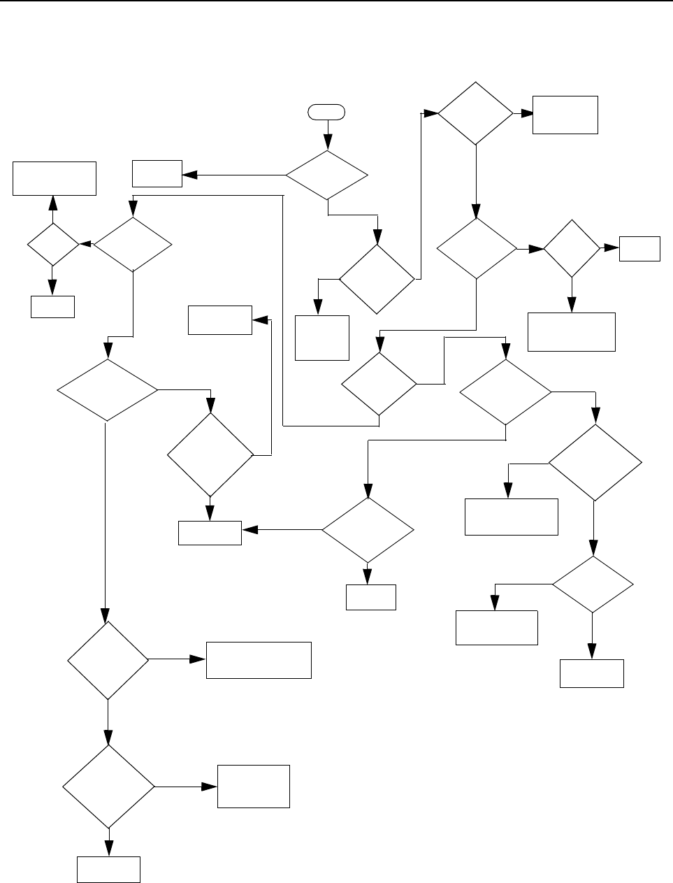
3-4 Troubleshooting Flow Chart for Synthesizer
3.0 Troubleshooting Flow Chart for Synthesizer
5V
at pin 6 of
D4201
Is information
from µP U0101
correct?
Is U4201 Pin 47
at = 13VDC
Is U4301 Pin 19
<40 mVDC in RX &
>4.5 VDC in TX? (at
VCO section)
Start
Visual
check of the
Board OK?
Correct
Problem
Check 5V
Regulator
U4211
+5V at U4201
Pin’s
13 & 30?
Is 16.8MHz
Signal at
U4201 Pin 19?
Check Y4261, C4261,
C4262, C4263, D4261
& R4261
Are signals
at Pin’s 14 &
15 of U4201?
Check
R4201 Check C4381
Is U4201 pin 2
>4.5 VDC in Rx &
<40 mVDC in Rx
Replace U4201
Remove
Shorts
Is there a short
between Pin 47 and
Pins 14 & 15 of
U4201?
Replace or
resolder
necessary
components
Is RF level at
U4201 Pin 32
-12 < x <-25
dBm?
Are R4221,R4222,
R4223,C4221,C4222,
& C4223 OK?
Replace U4201
If L4225, C4229 & C4227
are OK, then see VCO
troubleshooting chart
Are Waveforms
at Pins 14 & 15
triangular?
Do Pins 7,8 & 9
of U4201 toggle
when channel is
changed?
Check programming
lines between U0101
and U4201 Pins 7,8 & 9
Replace U4201
Check uP U0101
Troubleshooting
Chart
NO
YES
NO
YES
NO
YES
NO
NO
NO
YES
YES
NO
YES
YES
NO
YES
YES
YES
NO
NO
NO
NO
YES
NO
YES
YES
Check D4201, C4202,
C4203, & C4206
5V at U4201
pins 5, 20, 34 &
36
C h e c k 5 V
Regulator
U4211
Is
16.8MHz
signal at
U4201 pin
23?
Replace
U4201
YES
NO
NO
YES
NO
YES
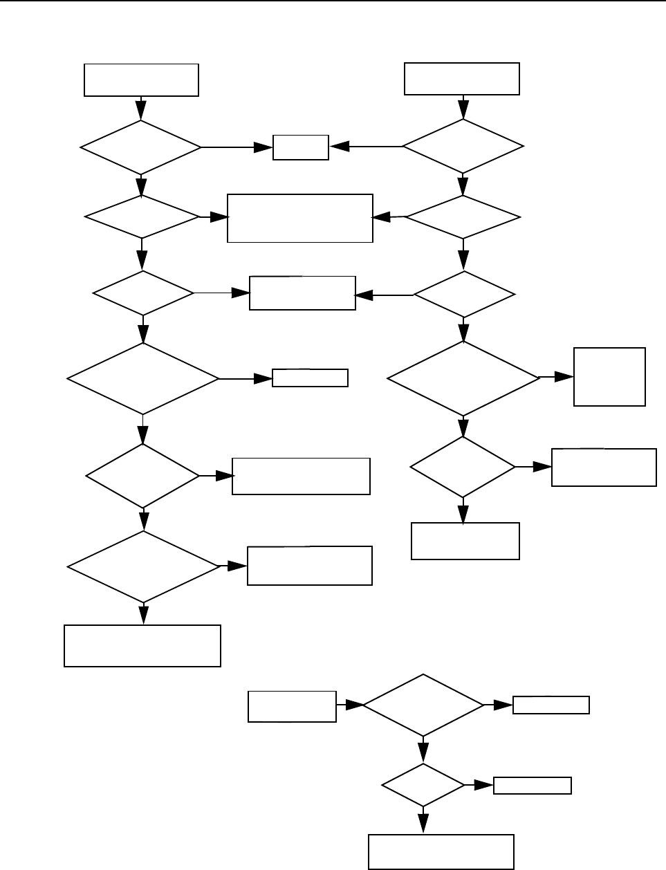
Troubleshooting Flow Chart for VCO 3-5
4.0 Troubleshooting Flow Chart for VCO
Are Q4332
Base at 0.7V
Collector at 4.5V
Emitter at 110mV
Are Q4301
Base at 2.4V
Collector at 4.5V
Emitter at 1.7V
Are U4301 Pins
13 at 4.4V
15 at 1.1V
10 at 4.5V
16 at 1.9V
Low or no RF Signal
at TP4003
Visual check
of board
OK?
35mV DC at
U4301 Pin 19
NO
YES
Replace Q4301
at base of Q4332
NO
NO
NO
NO
YES
YES
YES
YES
Low or no RF Signal
at input to PA
4.8V DC at
U4301 Pin 19
Is RF available
at C4402
YES
YES
YES
YES
NO
NO
NO
NO
NO
Audio =180mVrms
at “-” S
ide of
4.5VDC
at CR4321
If C4321 and R4321 are OK,
then replace CR4321
Replace C4322
Replace C4325
NO
NO
YES
YES
If parts between
R4402 & U4301 Pin10
are OK, replace U4301
TX VCO
RX VCO
Correct
Problem
Visual check
of board
OK?
Check runner
between U4201 Pin 2
and U4301 Pin 19
Is RF available If all parts from U4301 Pin 8
to Base of Q4332 are OK,
replace U4301
If all parts associated
with the pins are OK,
replace Q4332
If all parts from collector
of Q4332 to TP4003 are
OK, Replace Q4332
Power OK but
no modulation
Check parts from
R4402 to U4401 Pin16
If all parts
associated
with the pins
are OK,
replace U4301
YES
YES
Make sure Synthesizer is
working correctly and runner
between U4201 Pin 28 and
U4301 Pin 14 & 18 are OK
4.5V DC
OK ?
OK? OK?
C4325
at U4301 Pin 14 & 18
4.5V DC
OK ?
at U4301 Pin 14 &18
NO

3-6 Troubleshooting Flow Chart for VCO
THIS PAGE INTENTIONALLY LEFT BLANK

4-1
Section 4
UHF PCB/SCHEMATICS/PARTS LISTS
1.0 Allocation of Schematics and Circuit Boards
1.1 Controller Circuits
The UHF circuits are contained on the Printed Circuit Board (PCB) which also contains the
Controller circuits. This Chapter shows the schematics for the UHF circuits only, refer to the
Controller section for details of the related Controller circuits . The PCB component layouts and the
Parts Lists in this Chapter show both the Controller and UHF circuit components. The UHF
schematics and the related PCB and parts list are shown in the tables below.
Table 4-1 UHF 25-40W Diagrams and Parts Lists
PCB : 8480643Z06 Main Board Top Side
8480643Z06 Main Board Bottom Side Page 4-3
Page 4-4
SCHEMATICS
Power Amplifier 25 - 40W
FRACN
Voltage Controlled Oscillator
Receiver Front End
IF
Page 4-5
Page 4-6
Page 4-7
Page 4-8
Page 4-9
Parts List
8480643Z06 Page 4-10

4-2 Allocation of Schematics and Circuit Boards
THIS PAGE INTENTIONALLY LEFT BLANK
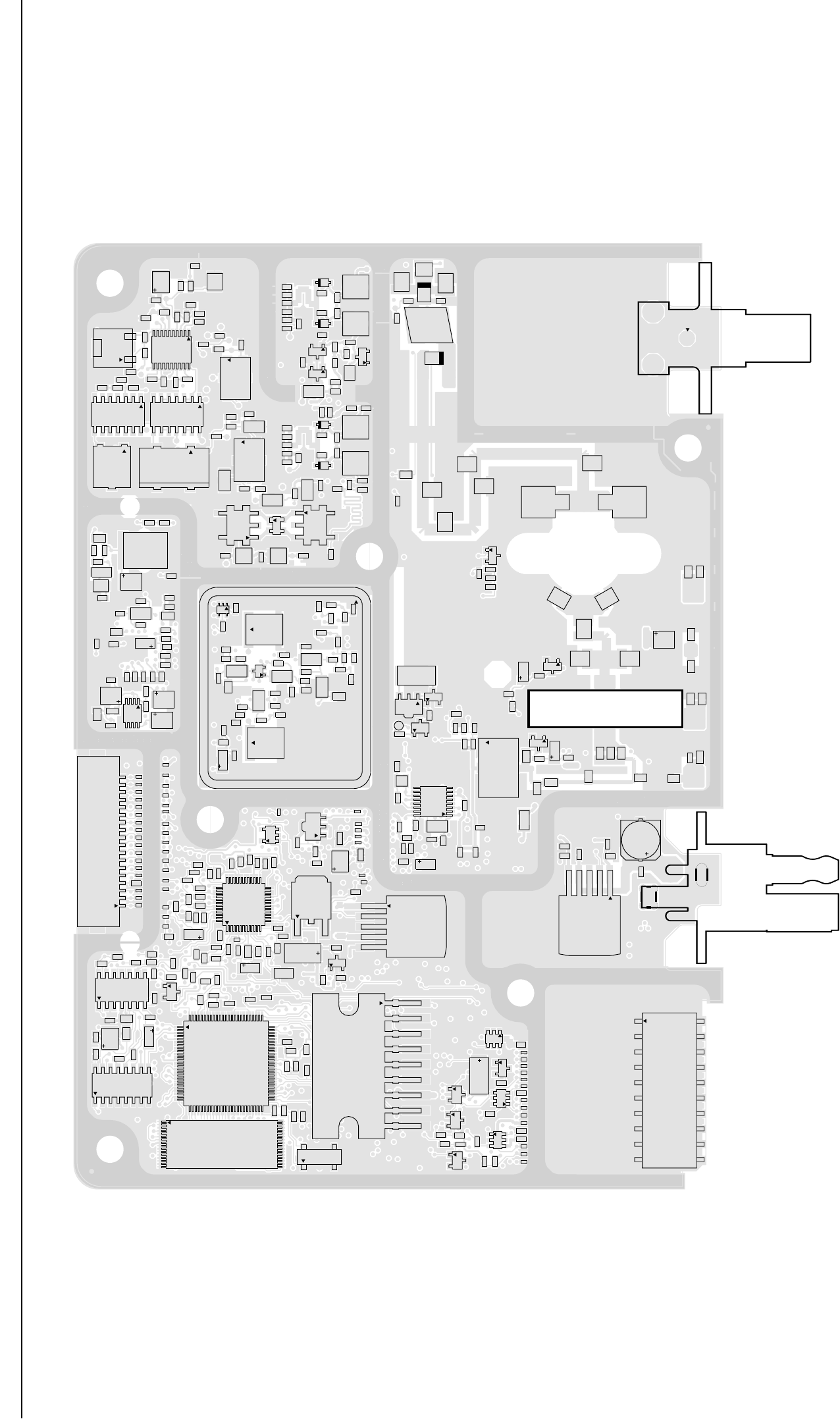
UHF 25-40W PCB / Schematics / Parts List 4-3
2.0 UHF 25-40W PCB / Schematics / Parts List
16
1
89
U0251
C0211
C0212
C0251
R0211
R0212
R0251
R0252
R0257
C0252 R0253 C0262
87
114
U0211
C0256
R0256
R0268
C0253
Q0110
R0102
R0261
R0262
C0261
R0269
18
1
J0451
C0421
C0451
C0452
C0453
C0455
C0456
C0457
C0458
C0459
C0460
C0461
C0462
C0463
C0464
C0466
C0467
C0468
R0441
C0441
C0442
C0443
C0445
C0446
C0447
C0448
C0449
C0470
C0471
C0472
C0473
C0474
C0476
C0477
C0478
C0490
C0221
C0222
C0225
C0241
C0243
R0220
R0221
R0223
R0224
R0229
R0254
R0255
R0222
R0442
C0242
C0244
C0245
C0246
C0496
D0201
R0241
R0242
137
25
13
U0221
3
2
1
U0651 C0681 Q0681
R0681
R0682
C0482
C0483
C0486
C0487
C0488
C0493
C0494
C0654
C0655
L0481
L0482
C0223
C0224
C0226
C0227
C0228
C0232
C0233
C0234
C0235
C0236
C0495
R0225
R0226
R0227
R0228
C0231
C0237
C0652
R0101
R0104
R0108
R0110
R0115
R0116
C0104
C0106
C0107
C0101
C0102
C0132
R0106
R0131
R0132
1
76
51
26
U0101
32
17
16 1
U0121
C0131
R0105
R0114
R0170
9
U0271
23
4
Y0131
C0501
C0502
C0503
C0504
C0505
C0506
C0508
C0509
C0510
C0511
C0512
C0513
C0514
C0515
C0516
C0517
C0518
C0542
Q0177
Q0181
Q0185
R0181 R0182
R0185 R0186
R0510
R0535
R0538
R0539 R0543 VR0501
VR0503
VR0505 VR0510
2011
10
J0501
C0651
D0651
R0651
R0652
1
6
5
U0641
1
6
5
U0611
C0484
C0601
C0603
C0612
R0533
R0611
R0612
J0601
C4210
C4212
C4213
C4214
C4215
C4216
C4225
C4226
C4227 C4229
C4230
C4231
C4241
C4242
C4243
C4244
C4245
C4246
C4253
C4289 L4201
L4225
R4211
45
8
U4211
C4221
C4222
C4223
C4224 C4235
L4221 R4221
R4222
R4223
R4263
32
J4401
C4444
C4459
C4465
C4466
C4491
C4507
C4521
C4522
R4501
R4502
U4502
C4423
C4432 C4435
C4449
C4450
C4460
C4478
C4490C4497
C4520
D4403
R4607
C4420
C4481
C4485 C4489
C4495
C4602
R4600
R4601
R4602
C4431
C4434
C4453 C4455
C4456
C4457
D4402
R4459
C4476
5
2
6
8
13
7
4Q4421
R4476
L4474
C4401
C4403
C4404
C4410
C4417
C4419
C4447
C4461
C4486
C4488
C4505
C4506
L4401
L4403
R4401
R4402
R4403
1
16
8
9
U4401
C4425
C4426
Q4471
Q4472
R4408
R4415
R4416
R4481
R4504
R4511
R4512
TP4530
VR4471
1
3
L4312
C4322
C4323
C4325
R4321
C4317
C4318
C4351
C4352
C4353
C4355
C4382
L4304
L4305
L4313 Q4301
R4311
R4312
C4383
R4301
R4302
C4308
C4309
C4375
1
3
L4303
43
Q4333
R4305
R4346
SH4301
C4331
C4332
C4335
C4337
C4339
C4354
C4371
C4372
C4373
C4374
L4331
L4371
R4331
R4332
R4333
R4337
R4341 R4343
R4345
C4493
C4441
C4442
C4443
FL3114
FL3112
4
32
C3139
C3145
C3148
R3142
R3144
R3145
87
1
14
U3115 2
Y3102
C3143 R3135
C3140
C3141
87
1
14
U3111
C3142
U3101
R3117
11
1
20
10
C3124
C3131
C3132
C3133
C3134
C3135
C3136
C3137
L3124
R3111
R3123
R3124
R3130
R3132
C3115
C3114
2
3
456
FL3102
C3101 C3102
C3103
2
3
456
FL3101
L3100
L3101
R3101
R3106
R3148
L4008
C4001C4002
C4003
C4004
C4005
C4006
C4007
C4008
C4009
C4014
C4015
C4016
C4026
C4027
D4001
D4002
D4003 L4001
L4002
L4003
L4006
Q4001
Q4003
R4001
R4003
R4004
R4005
R4007
R4018
R4020
R4022
R4066
C4017C4018
C4019
C4020
C4021
C4022
C4023
C4029
C4030
C4051
C4052
D4004
D4005
L4004
L4005
L4051
R4012
R4013
R4014
R4015
R4051
D4051
21
54
3
T4051
C4031
C4055
L4053
C4053
C4054
L4054 2
1
54
3
T4052
C4472
C4474
C4475
C4480
C4510
D4471 D4472
L4472 L4473
C4232
C4233
C4234
C4251
C4252
C4254
C4255
R4251
R4252
UHF (403-470 MHz) 25-40W 8480643Z06 Top Side
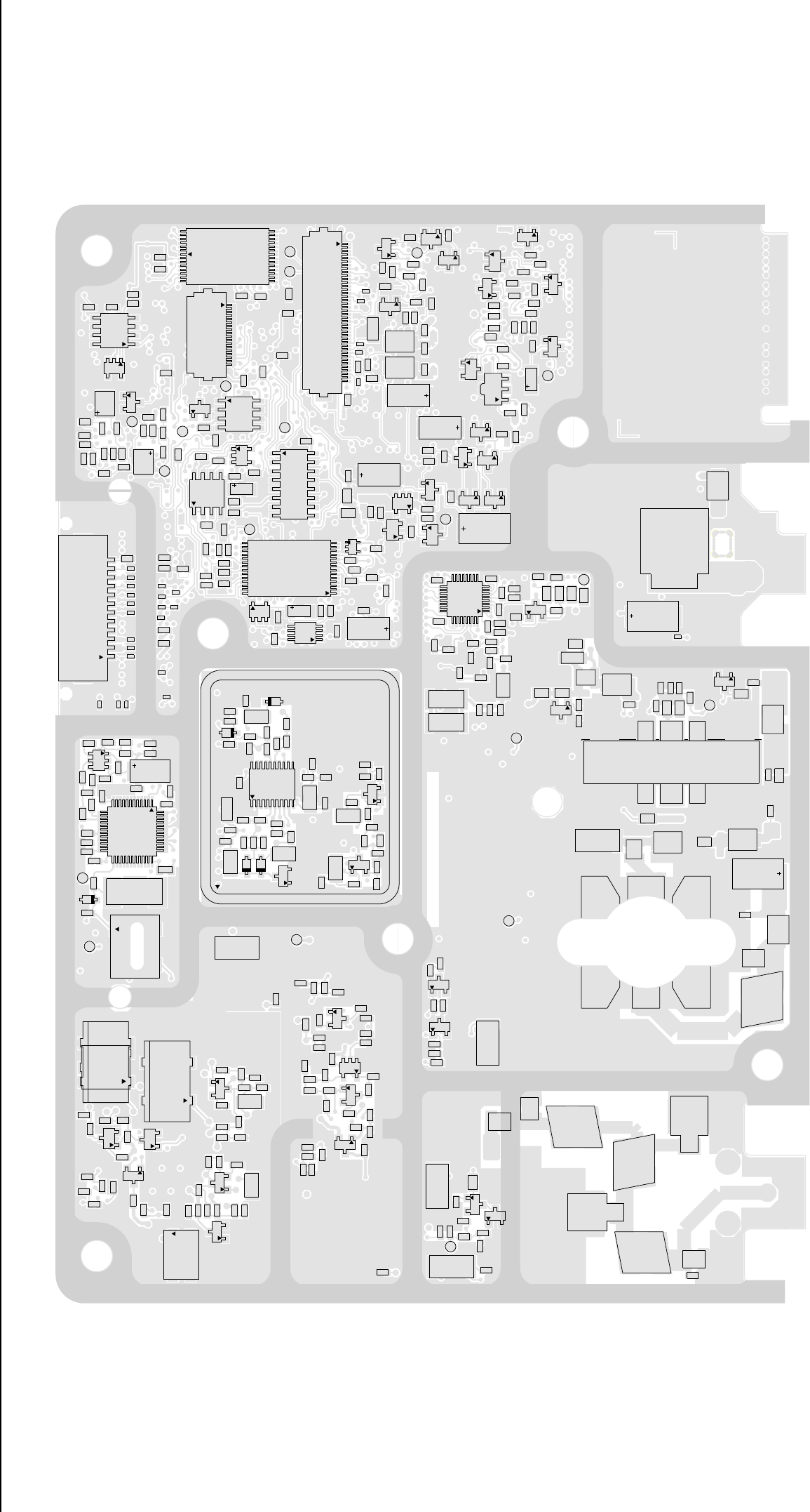
4-4 UHF 25-40W PCB / Schematics / Parts List
C3144
C3146
C3147
Q3141
R3134
R3141
R3146
R3147
R3154
R3113
R3133
C3151
C3152
Q3152
R3151
R3152
R3153
Q3151
43
2
FL3111
FL3113
43
2
FL3115
C4263
D4261
R4261
TP4201 TP4202
Y4261
2
34
Y4262
C4261
C4262
R4241
R4262
1
37
25 13
U4201
C4201
C4202
C4203
C4204
C4205
C4206
C4208
C4209
C4211
C4287
D4201
R4201
R4206
C4207
C4288
R4203
R4204
C4228
L4231 R4228
C0485
4
3
2Y3101
C3116
C3121
C3122
C3123
D3101
L3112
Q3102
R3112
R3114
R3115
R3116 R3118
C3104
C3110
C3111
C3112
C3113
L3111
Q3101
R3102
R3104
R3105
R3107
R3108
C4010
C4011
C4012
C4013
C4024
C4028
C4060
C4061
C4062
C4064
C4065
C4066
C4067
C4068
C4069
D4006
D4007
Q4002
Q4004
R4002
R4016
R4017
R4052
R4053
R4054
R4055
R4060
R4061
R4062
R4063
R4064
R4068
R4069
R4070
R4071
R4072
C0401
C0402
C0403
C0406
C0407
C0408
C0409
C0410
C0411
C0422
C0423
C0426
C0427
C0428
C0429
C0430
C0431
C0491
C0492
C0497
12
J0401
R0407
R0409
R0410
R0412
R0467
C0301
C0302
C0303
C0351
C0352
C0354
D0301
28 15
14
1
U0301
4
58
U0351
C0304
C0305
C0324
C0325
C0343
R0323
R0324
R0344
R0341
R0345
C0341
C0342
C0344
R0342
R0343
R0346
R0347
1
45
8
U0341
U0342
C0141
16
1
8
9U0141
TP0101
TP0497
C0201
C0202
C0203C0204
C0205
C0254 C0265
C0266
C0267
R0107
R0201
R0202
R0203
R0204
R0205
R0206
R0207
R0208
R0265
R0266
R0267
R0408 TP0102
TP0221
TP0222
U0653
VR0541
C0103
C0111
C0112
D0101
1
18
J0552
R0111 R0112
R0113
R0117
R0121
R0401
TP0103
TP0104
TP0492
1
4
58
U0111
22
21 8
7
1
U0122
C0105
C0121
C0122
C0123
C0255
R0468
14
58
U0652
R4019
TP4003
C4301
C4302
C4303
C4304
C4305
C4306
C4307
C4316
C4336
C4361
C4362
C4363
C4381
CR4301
CR4302
CR4303
L4301
L4302
L4333
L4361
R4303
R4304
R4315
R4361
SH4302
11
120
10
U4301
C4311
C4312
C4313
C4314
C4315
C4321
C4324
CR4311
CR4321
L4311
R4313
R4314
R4322
R4323
C4025
C4451
C4463
C4469
C4470
C4473 C4499 D4452
R4455
R4457
R4472
R4475
R4496
TP4531
VR4473
C4333
C4334
C4338
L4332
Q4331
Q4332
R4334
R4335
R4336
R4338
R4339
R4340
R4342
R4344 R4347
C4452
C4464
D4451 D4453
R4409
R4471
R4473
R4474
R4506 R4507
TP4532
C4492
C4498
C4448
C4496
L4491
L4492
R4491 C4494
L4493
1
24
6
Q4441
C4436
C4438
C4439
C4482
L4421
L4436
L4437
C4422
C4437
L4440
L4441
R4421
6
5
43
2
1
Q4431
35
C4632
L4402
R4633
TP4537
VR4472
C4421
C4484
C0499
C0611
C4446
C4630
R4485
R4486 R4630
R4631
R4632
C4424
L4541
L4543
Q4451
R4414
R4487
R4488
R4513
R4525
C4483
C4407
C4409
C4412
C4414
C4416
C4462
C4487
L4411
R4405
R4411
R4412
R4427
R4428
R4495
R4497
TP4536
R4433 C4479
C4502
C4503
C4504
R4480
R4482
R4483
R4484
R4492
R4503
R4523
1
17
9
25
U4501
C4418
Q4473
R4422
R4423
R4424
R4425
R4431
R4514
TP4533
E0631
VR0601
C0331
C0353
R0331
R0332
R0333
R0335
R0481
R0482
U0331
C0641
C0644
C0645
R0641
R0642
R0643
C0662
Q0641 Q0661
C0661
C0663
D0660
D0661
Q0662
Q0663
R0661
R0662
TP0661 C0622
C0671
R0671
R0672
VR0671
C0541
C0621
D0621
Q0171
Q0173
R0172
R0173
R0174
R0621
TP0530
VR0621
D0179
R0171
R0175
R0176
R0177
R0178
R0179
R0183
R0184
R0511
R0512
R0525
R0529
R0530
R0531
R0541
R0542
VR0151
VR0504 VR0509
Q0183
R0537
VR0537
C0271
C0275
C0276 C0277
C0558
C0559
C0560
C0591
C0592
C0593
E0271 E0272
R0591
R0592
C0151
C0272
C0273
C0274
C0554
C0575
C0576
D0151
Q0151
Q0271
R0151 R0152
R0273
R0274
R0275
R0276
R0593
TP0151
1
40
J0551
UHF (403-470 MHz) 25-40W 8480643Z06 Bottom Side
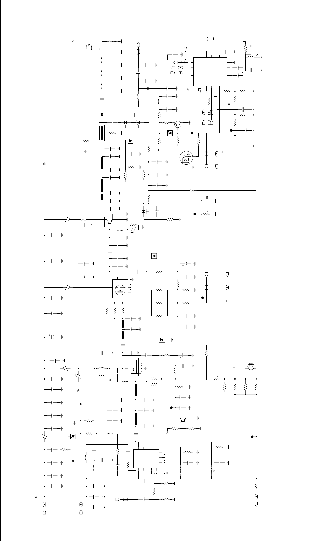
UHF 25-40W PCB / Schematics / Parts List 4-5
PASUPVLTG
PASUPVLTG_UHF_PA_1
PASUPVLTG
NU NU NU NU
NU
NU
R4633
C4632
30pF
C4485 3000pF
C4481
C4602
.033uF
ALT
L4402
5.6V
VR4472
30pF
C4484 .033uF
C4421 C4490
1000pF
C4495 C4489 C4436
10uF 1000pF
C4478
C4493
C4497
1000pF
L4421
C4423
1uF C4422
100pF
30pF
C4482
100pF
C4439
L4436
0.1uF
C4438
17nH
L4437
9V3
100pF
C4488 C4486
30pF C4404
100pF
390nH
L4403
9V3_UHF_PA_1
11.03nH
L4401
C4418
0.1uF
3.9pF
C4403
4 to 6 dBm
C4407
0.1uF
TXINJ R4405
200
TX_INJ_UHF_PA_1 R4433
NU NU
NU
NU
NU
NU
NU
NU
NU
NU NU
NU
NU NU
NU
NU
NU
NU
NU
NU
NU
NU
NU
NU
NU
NU
NU
NU
NU
NU
NU
NU
C4462
VD1
14 VG1 2
VG2 3
NC1
8
NC2
9
NC3
10
NC4
15
RFIN
16 RFOUT16
RFOUT27
VCNTRL
1
U4401
30C65
EP
17
G2
11
GND1
4
GND2
5
GND3
12
GND4
13
300
R4401 300
R4403
15
R4402
C4410
100pF
C4401
100pF
51
R4495
100pF
C4412
R4497
51
L4411
390nH
C4417
100pF
C4487
30pF 0.1uF
C4409
9V3
33pF
C4419
C4461 C4447
C4453
6
2
1
3
4
5
7
8
Q4421
BLM31A02PT
L4474
R4414
C4483
100pF
R4525
C4431
30pF
L4541
C4424
L4543
13.85nH
9V3
Load
51pF
C4420
C4434
39pF
4.7
R4600
4.7
R4602
R4601
4.7
C4630
0.1uF
R4486
120
R4632
24K
100pF
C4446
R4631
1K 120
R4485
R4476
R4480
10K
PCIC_MOSBIAS_1
2.4 to 2.6 VDC
TP4537
MOSBIAS_2
BIAS_2_UHF_PA_1
C4476 C4520
C4456
C4457
R4481
D4402
R4459
C4455
C4437
D4403
R4607
G1 7
G2 8
G3 9
10
G4
S1
S2
S3
S4
Q4431
MRF5015
D
G
39pF
C4460
4
2
1
3
MRF650
Q4441
27pF
C4435
30pF
C4432 16pF
C4450 C4449
33pF
13.85nH
L4441
L4440 10
R4421
39pF
C4442
C4441
30pF
C4470
D4453
C4464
C4499
100pF
100pF
C4507
R4474
100K
10K
R4507
10K
R4506
100K
R4409
4.3K
R4473
9V3
D4452
D4451
D4471
C4465
11pF
C4491
100pF
C4469
5.6V
VR4473
C4444
C4452
C4466
C4459
100pF
C4443
7.5pF
120
R4457
R4472
C4463
C4498
6.8pF
L4493
17nH
C4492
100pF
R4471
R4491
11K
J4401-1
1
L4491
17nH
L4492
17nH
C4448
12pF
J4401-3
3
10pF
C4494 5.6pF
C4496
J4401-2
2
DUMMY
12pF
C4474
2pF
C4475
17nH
L4472 RX_IN_VHF_PA_1
RXIN
C4480
D4472
FECTRL_1
FECTRL_2
C4479
100pF
RESET
FE_CNTL_1_VHF_PA_1
FE_CNTL_2_VHF_PA_1
RESET_VHF_PA_1
9V3
36pF
C4472
43.67nH
L4473
C4510
36pF
R4496
82
100pF
C4473
Q4472
51
R4511
PCIC_MOSBIAS_1
CSX
DATA
CSX_VHF_PA_1
DATA_VHF_PA_1
VLIM
TEMP
30
V10 14
V45 16
V5EXT
VAR1
VAR2
VAR3
15
VG
NA
Q11
QX 10
RS
31 RSET
RX
CLK
26
CQ 12
13
CQXDATA
28
F168 9
GND2
25
ANO
32
BPOS
27
CEX
29
U4501
1uF
C4505
R4492
10K
CLK
CLK_VHF_PA_1
9V3
19
17
20
18
24
22
21
23
VL
RFIN
T1
GND1
INT
CI
CJ
CL
3.1 VDC (44W)
2.2 VDC (28W)
0.75 VDC
R4484
68K
300K
R4482
TP4532
R4501
5.6K
C4521
100pF
6
1
2
8
4
3
5
7
.02uF
C4504
R4502
R4523
68K
C4503
2200pF
C4506
2200pF
R4483
100K
.015uF
C4502
1000pF
C4522
R4503
3.9K
ALT
PA_PWR_SET
9V3
10K
R4504
K9V1_UHF_PA_1
TEMPSENSE
TEMPSENSE_UHF_PA
K9V1
3GND 1
POS
VOUT2
U4502
9V3
100K
R4487
Q4451
R4488
2.7K
Load
3.7 to 3.9 VDC
C4426
100pF
TP4536
C4425
.022uF
R4408
20K
4.5 VDC (44W)
4.4 VDC (28W)
4.7K
R4428
R4411
C4414
1000pF
TP4533 620
R4424
620
620
R4422
R4425
620
R4423
6.2 VDC (28W)
6.5 VDC (44W)
Q4473
R4431
9V3
5.6K
R4412
C4416
.022uF
R4427
10K
CNTLVLTG_UHF_PA_1
3.3K
R4514
CNTLVLTG
PA_PWR_SET_1_UHF_PA_1
PA_PWR_SET
PA_PWR_SET
R4630
2.2 VDC (28W)
3.11 VDC (44W)
TP4531
R4455 C4451
0
R4475
9.2 VDC
470
R4512
Q4471
10K
R4513
TP4530
VR4471
5.6V
A+
100
R4415
100
R4416
A+
UHF (403-470 MHz) Power Amplifier 25-40W
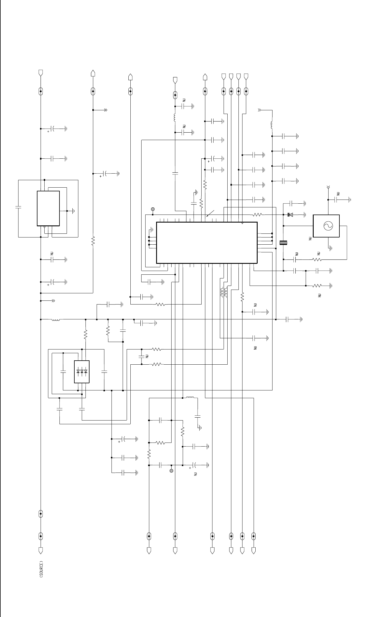
4-6 UHF 25-40W PCB / Schematics / Parts List
C4262
220pF
C4251
C4228
0.1uF
C4252
R4221
1000pF
150 TP4202
1
C4253
4.7uF
IN_5V_RF_REG
TRB
D4261
2.2uF
C4213
R4241
MODIN
220
C4221
.01uF
C4227
LOCK_UHF_FN_1
100pF
100pF
C4243
U4507
C4202
.01uF
BWSELECT
100pF
VSF_UHF_FN_1
C4255
0.1uF
C4209
2.2uF
C4210
16_8MHz_UHF_FN_1
C4204
5V_UHF_FN_1
100pF
R4222
510
VCOMOD
C4246
100pF
100pF
C4287
C4241
CLK_UHF_FN_1
C4242
VDDA
100pF
C4223
0.1uF
C4222
CSX_UHF_FN_1
C4207
C4289
0.1uF
Vac
VCTRL
R4263
C4244
47
R4204
CLK
VSF
100pF
5V
.01uF
C4203
30K
R4252
C4212
.018uF
15
14 VMULT2
12 VMULT3
11 VMULT4
VRO
13
25 WARP
23 XTAL1
XTAL2
24
SFBASE
26
SFCAP
30
SFIN
28 SFOUT
37 TEST1
38 TEST2
21
VBPASS
47 VCP
VMULT1
31
NC3
44
PD_GND
PD_VDD
5
PREIN 32
33
PRE_GND
34 PRE_VDD
35
PVREF
18
REFSEL
27
45 IADAPT
16 INDMULT
43 IOUT
LOCK
4
10
MODIN
41 MODOUT
17
NC1 29
NC2
39
BIAS2
42
CCOMP
9
CEX
8
CLK
7
DATA
DGND 6
36 DVDD
19 FREFOUT
46 ADAPTSW
22
AGND
48 AUX1
1AUX2
2AUX3
3AUX4
20 AVDD
40
BIAS1
63A27
U4201
C4231
DATA
.01uF
VDDA_UHF_FN_1
L4201
390nH
.01uF
C4232
BWSELECT_UHF_FN_1
2.2uF
C4233
VCOMOD_UHF_FN_1
510pF
C4225
C4208
0.1uF
0.1uF
C4254
TP4201 1
C4206
10uF
R4261
150K
33K
R4206
C4263
1.5pF
L4231
PRESC
CSX
2.2uH
MODIN_UHF_FN_1
C4261
62pF
5V_UHF_FN_2
DATA_UHF_FN_1
C4214
2.2uF
VCOBIAS_2
C4205
.01uF
150
R4201
C4288
IN_5V_RF_REG_UHF_FN_1
16_8MHz
2
GND
3
OUT
VCC 4
VCNTL
1
16.8MHz
Y4262
TTS05V
C4211
0.1uF
R4262
C4235
2.2uF
C4230
68
R4223
3
TRB_UHF_FN_1
6
A1
5
A2
4
A3
K1
1K2
2K3
D4201
65V_TAP
5ERROR 7
FEEDBACK
4
GND
8
INPUT
1OUTPUT
2SENSE 3
SHUTDOWN
LP2951
U4211
U4506
VCTRL_UHF_FN_1
.01uF
C4234
R4211
0
R4228
47K
2.2uF
C4215
R4251
R4203
39K
47
C4226
C4224
LOCK
1uF
21
C4216
16.8MHz
Y4261
100pF
C4245
L4225
33nH
C4229
C4201
100pF
ZWG0130270-A
2.63 VDC (TX)
4.97 VDC (25KHZ Chan. Spacing)
0 VDC (12.5KHZ Chan. Spacing)
5 VDC (Locked)
0 VDC (Unlocked)
10.87 VDC
-16 to -11 dBm (Tx)
12.7 VDC
4.97 VDC
6.68 VDC
2.5 to 11 VDC
1.76 VDC (Tx)
1.78 VDC (Rx)
3.79 VDC
2.48 VDC
3.43 VDC
-18 to -16 dBm (Rx)
2.48 VDC
1.28 VDC
3.48
VDC
0 VDC (RX)
4.97 VDC (TX)
3.05 VDC (RX)
0 VDC
4.97 VDC
2.52 VDC
4.97 VDC
4.58 VDC
HF (403-470 MHz) FRACN
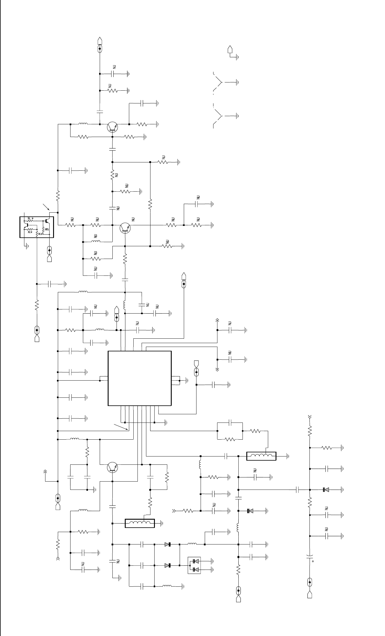
UHF 25-40W PCB / Schematics / Parts List 4-7
CR4302
R4361
180
CR4301
0
R4315
L4332
Vac
GND
RXINJ
VCOBIAS_2
100pF
VCTRL_UHF_VCO C4312
12pF
C4309
R4311
390nH
7.5K
Vac
L4361
.022uF
C4336
R4333
C4305
Vac C4339
Vac
CR4303
R4302
10K
R4346
10K
1pF
C4321
C4314
1.5pF
5V_UHF_VCO
C4318
0.22uF C4381
0.1uF
1K
R4343
C4323
Vac
30
R4313
R4344
10
Q4332
0.1uF
CR4311
100pF
C4352
C4363
Vac
C4301
C4333
Vac
C4372
Vac
SH4301
SHIELD
R4332
Vac
4.7uF
C4325
0
RXINJ_UHF_VCO
1P1
2
P2
3P3
R4347
TXINJ_UHF_VCO
L4312
RESONATOR
L4331
33nH
L4301
390nH TRB_UHF_VCO
C4315
100pF
Vac
22
R4331
C4313
TX_EMITTER
1TX_IADJ 10
TX_OUT
13
TX_SWITCH
14
VCC_BUFFERS
18
VCC_LOGIC
RX_BASE
6RX_EMITTER
2RX_IADJ 8
RX_OUT
7
RX_SWITCH
3SUPER_FLTR
19 TRB_IN
16 TX_BASE
15
1
4COLL_RFIN
20 FLIP_IN
11 GND_BUFFERS
9GND_FLAG
GND_LOGIC
17
12
PRESC_OUT
5
50U54
U4301
C4334
Vac
Q4301
R4341
100pF
0
2.4pF
C4307
68nH
C4324
56K
R4321
L4371
R4323
6.8pF
100K
C4331
R4339
Vac
C4351
100pF
VCOMOD
390nH
L4311
C4355
2.2uF
C4362
Vac
CR4321
C4322
Vac
SHIELD
SH4302
Vac
C4374
Vac
R4337
270
R4314
C4373
Vac
C43062pF
C4311
100pF
C4371
0.1uF
0.22uF
100pF
C4308
0.1uF
C4316
C4335
Vac
Vac R4345
C4383
Vac
R4336
8.2pF
C4337
C4303
C4354
51pF
C4382
Vac
2.2uF
R4312
5.6K
30
R4303
390nH
R4338
Vac
L4333
R4334
Vac
8.2pF
2.2K
R4342
C4302
390nH
C4332
Vac
PRESC
L4302
R4322
10K
2
6
4
1
3
C4361
100pF
TXINJ
Q4333
VCOBIAS_2_UHF_VCO
C4375
0.1uF
Q4331
Vac
10
R4305
390nH
L4304
390nH
L4305
R4335
Vac
Vac
VSF_UHF_VC0
3.9pF
C4317
VCOMOD_UHF_VCO
TRB
C4304
5.6K
R4301
51pF
C4338
VSF
3P3
5V
C4353
0.1uF
L4303
RESONATOR
1P1
2P2
R4340
Vac
180
R4304
390nH
L4313
GROUND
VCTRL
PRESC_UHF_VCO
5V
VSF
TXSW
TXSW
RXSW
RXSW
VSF
ZWG0130272-0
0 VDC (Tx)
4.58 VDC
4.58 VDC
13.5 to 16 dBm
0 VDC (Tx)
4.7 VDC (Rx)
2.5 - 11 VDC
0 VDC (Rx)
4.97 VDC (Tx)
-18 to -16 dBm (Rx)
-16 to -11 dBm (Tx)
4 to 6 dBm
4.54 VDC
4.54 VDC (Tx)
0 VDC (Rx)
4.42 VDC (Rx)
0 VDC (Tx)
3.1 VDC (Rx)
2.6 VDC (Tx)
1.91 VDC (Tx)
0 VDC (Rx)
2.45 VDC (Rx)
0 VDC (Tx)
2.35 VDC
(Tx)
4.54 VDC
(Rx)
2.43 VDC (Rx)
UHF (403-470 MHz) Voltage Controlled Oscillator
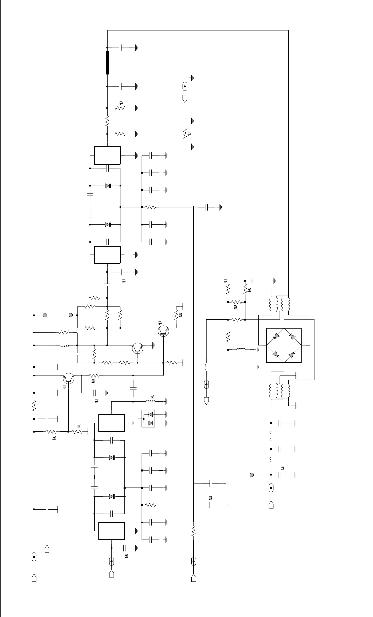
4-8 UHF 25-40W PCB / Schematics / Parts List
GND
51
R4051
C4009
100pF
33
R4008
D4005
Vac
R4017
XFMR
T4051
1
2
3
5
4
43pF
C4004
TBD
L4004
IN
NEG
POS
39pF
Q4001
Vac
C4007
270
R4011
C4024
1000pF
33pF
C4002
100K
NEG
POS
R4001
TBD
L4005IN
Vac
Q4002
FECTRL_1_UHF_FE
Q4003
27nH
L4053
100K
R4012
39pF
C4003
3300pF
TP4003
IF
C4013
470nH
L4003
Vac
150nH
L4051
3300pF
R4015
C4011
3
5
4
L4006
Vac
XFMR
T4052
1
2
1.8pF
C4017
D4004
C4028
Vac
R4060
330K
C4026
1.8pF
Vac
22pF
R4053
C4019
R4020 Vac
15nH
L4054
68
R4007
D4002
R4019
Vac
12pF
C4018
R4055
Vac
36pF
C4001
C4020
1.8pF
330pF
C4010
43pF
C4005
1.8pF
D4001
C4027
36pF
330pF
C4022
C4012
D4051
IO1
1IO2 2
IO3
3
IO4
4
470nH
Vac
L4008
R4016
RXIN
16pF
C4053
1.8pF
C4029
Vac
C4016
IF_UHF_FE
IN
NEG
POS
R4052
0
TBD
L4002
TP4001
R4003
3.9K
Vac
C4025
C4014
100pF
IN
NEG
POS
TBD
L4001
R4002
330
Vac
150
R4054
R4009
9V3_UHF_FE
13pF
C4031
RXINJ
100pF
C4015
270
R4013
36pF
TP4002
C4021
270
9V3
R4006
GND_UHF_FE
150
R4010
C4051
C4054
16pF
10pF
D4003
R4005
10K
0
Vac R4022
R4018
9V3
RXIN_UHF_FE
RXINJ_UHF_FE
43pF
FECTRL_1
C4006
R4014
10
C4055
Vac
C4030
1.8pF
82pF
C4052
1000pF
C4008
C4060
Vac
2.7K
22pF
R4004
C4023
ZWG0130269-O
4.6 VDC
3 to 6.5 VDC
0.7 VDC
UHF (403-470 MHz) Receiver Front End

UHF 25-40W PCB / Schematics / Parts List 4-9
9186176B01
9180469V04
9180469V03
9180469V06 9180468V06
R3144
2.4K
BWSELECT_VHF_IF_1
9V3_VHF_IF_2
C3113
9.1pF
NU
R3104
100
NU
100
620nH
NU
R3105
R3130
L3100
14
VDD
7
VSS
51
U3111-1
MC74HC4066
13
CNTL
1
2
C3116
L3112
0.1uF
620nH
9V3_VHF_IF_1
10uF
C3133
0.1uF
C3132
.01uF
C3151
OUT 2
C3137
.039uF
CFWC455D
FL3112
GND1
34
GND2
IN
1
620nH
C3121
L3101
0.1uF
R3101
12K
12K
R3147
15pF
DISCAUDIO
C3102
C3152
.01uF
0.1uF
C3139
7
VSS
0.1uF
C3141
U3115-1
MC74HC4066
MC74HC4066
13
CNTL
1
2
14
VDD
DISCAUDIO_VHF_IF_1
620nH
620
L3111
R3108
27pF
C3110
0.1uF
C3147
C3155
9V3
.01uF
NU
Q3155
FL3115
3
GND1GND2
4
1IN 2
OUT
BWSELECT
GND3
45
GND4
3IN 6
OUT
CFWC455F
12R16
FL3102
1
GND1
GND2
2
GND1
12
GND2
4
GND3
GND4
5
IN
3OUT 6
12R16
FL3101
7
C314 2
0.1uF
MC74HC4066
CNTL
6
89
VDD
14
VSS
GND
3
IN
1OUT 2
RSSI
U3111-3 FL3114
CFUCJ455D
4700pF
C3146
27K
GND1
34
GND2
IN
1OUT 2
R3106
OUT
3IN 1
FL3111
CFWC455G
Y3101
12R17
44.395MHz
GND
2
GND1
4
C3131
1pF
NU
0.1uF
C3145
5V_VHF_IF_1
IFIN_VHF_IF_1
IF
330
R3116
10K
R3134
0.1uF
C3144
18pF
C3114
10K
R3155
R3151
VDD
7
VSS
NU
1.2K
U3111-4
MC74HC4066
12
CNTL
14
CNTL
5
4
3VDD
14
VSS
7
U3115-2
MC74HC4066
0.1uF
C3104
C3135
33pF
12
CNTL
11
14
VDD
7
VSS
7
U3115-4
MC74HC4066
MC74HC4066
CNTL
5
4
3VDD
14
VSS
3.3K
U3111-2
R3145
0.1uF
C3140
390
R3115
Q3152
3
22pF
Y3102
455KHz
45B02
C3115
82pF
C3112 C3123
.039uF
R3112
10
0102727B45
0
R3148
0.1uF
C3111
Q3151
27K
R3117
Q3102
8.2K
R3133
Q3101
C3136
30pF
20pF R3102
C3101
33pF
10
C3103
C3134
0.1uF
RSSI_VHF_IF_1
6.8K
R3118
R3111
12K
C3122
.039uF
6.8K
R3107
NU
100
R3114
R3154
5V
10K
10K
R3153
D3101
120pF
C3143
R3152
10K
1.2K
CNTL
6
VDD
14
VSS
7
R3135
U3115-3
MC74HC4066
680
R3146
R3160
0
R3132
15K
FL3113
CS455G2 NU
GND
3
IN
1OUT 2
9V3
5V
5V
9V3
9V3
9V39V3
9V3
5V
9V3
89
10
11 10
OSCIN 4
OSCOUT
3
QUADIN 10
RFIN 1
RFIN_DEC 2
RSSIOUT
5RSSI_FEED 9
VCC
6
IFAMPOUT
16
IFAMP_DEC1 19
IFAMP_DEC2
17
LIMIN 14
LIMOUT
11
LIM_DEC1
13
LIM_DEC2
12
MIXOUT
20
SA616
SA616
AUDIOOUT
8AUDIO_FEED 7
GND 15
IFAMPIN 18
U3101
ZWG0130367-0
UHF (403-470 MHz) IF

4-10 UHF 25-40W PCB / Schematics / Parts List
UHF PCB 8480643Z06 Parts List 25-40W
Circuit
Ref Motorola
Part No. Description
C0101 2113740F51 100pF
C0107 2113741F25 1000pF
C0112 2113743E20 0.1uF
C0121 2113743E20 0.1uF
C0122 2113743E20 0.1uF
C0131 2113740F35 22pF
C0132 2113740F35 22pF
C0141 2113743E20 0.1uF
C0151 2113741F49 10000pF
C0201 2311049A57 10uF
C0202 2311049A57 10uF
C0204 2113743E20 0.1uF
C0212 2311049A57 10uF
C0221 2113743E20 0.1uF
C0222 2113743E20 0.1uF
C0223 2113743E20 0.1uF
C0224 2113740F51 100pF
C0225 2113743E20 0.1uF
C0226 2113743E20 0.1uF
C0228 2311049A56 4.7uF
C0231 2113743B29 1uF
C0232 2113743E20 0.1uF
C0234 2113743E20 0.1uF
C0235 2113743E07 0.022uF
C0236 2113743E10 0.033uF
C0241 2113743E20 0.1uF
C0243 2113740F51 100pF
C0244 2113743E20 0.1uF
C0245 2113743E20 0.1uF
C0246 2113741F49 10000pF
C0251 2113743E20 0.1uF
C0252 2311049A07 1uF
C0254 2113743E20 0.1uF
C0255 2113743E20 0.1uF
C0256 2113740F51 100pF
C0261 2113743E20 0.1uF
C0262 2113740F49 82pF
C0265 2113743E20 0.1uF
C0267 2113741F49 10000pF
C0271 2113741F49 10000pF
C0272 2113743E20 0.1uF
C0273 2113741F37 3300pF
C0275 2311049A99 47uF
C0276 2113741F25 1000pF
C0277 2113741F25 1000pF
C0301 2311049A07 1uF
C0302 2113743E20 0.1uF
C0303 2113740F51 100pF
C0304 2113743E20 0.1uF
C0305 2113743E20 0.1uF
C0324 2113743E20 0.1uF
C0331 2113743E20 0.1uF
C0341 2311049A07 1uF
C0342 2113743E20 0.1uF
C0343 2113743E20 0.1uF
C0344 2113743E20 0.1uF
C0351 2113743E20 0.1uF
C0352 2113743E07 0.022uF
C0353 2311049A97 33uF
C0354 2113743E20 0.1uF
C0421 2113743N48 82pF
C0422 2113741F17 470pF
C0423 2113741F17 470pF
C0426 2113743L09 470pF
C0427 2113743L09 470pF
C0428 2113743N48 82pF
C0429 2113743L09 470pF
C0430 2113741F17 470pF
C0431 2113741F17 470pF
C0445 2113743L09 470pF
C0446 2113743L09 470pF
C0447 2113743L09 470pF
C0448 2113743L09 470pF
C0449 2113743L09 470pF
C0470 2113743L09 470pF
C0471 2113743N48 82pF
C0472 2113743N48 82pF
C0473 2113743N48 82pF
C0474 2113743L09 470pF
C0476 2113743L09 470pF
C0477 2113743L09 470pF
C0478 2113743L09 470pF
C0482 2113743L09 470pF
C0483 2113743L09 470pF
C0484 2113741F17 470pF
C0485 2113743L09 470pF
C0486 2113743L09 470pF
C0487 2113743L09 470pF
C0488 2113743L09 470pF
C0490 2113743L09 470pF
C0491 2113743L09 470pF
C0492 2113743L09 470pF
C0493 2113743L09 470pF
C0494 2113743L09 470pF
C0495 2113743L09 470pF
C0496 2113743L09 470pF
C0497 2113743L09 470pF
C0499 2113743L09 470pF
C0501 2113741F49 10000pF
C0502 2113743L09 470pF
C0503 2113743L09 470pF
Circuit
Ref Motorola
Part No. Description
C0504 2113743L09 470pF
C0505 2113743L09 470pF
C0506 2113743L09 470pF
C0508 2113743L09 470pF
C0509 2113743L09 470pF
C0510 2113741F17 470pF
C0511 2113743L09 470pF
C0512 2113743L09 470pF
C0513 2113741F17 470pF
C0514 2113743L09 470pF
C0515 2113743L09 470pF
C0516 2113741F49 10000pF
C0517 2113743N48 82pF
C0518 2113743L09 470pF
C0541 2311049A05 0.47uF
C0542 2311049A99 47uF
C0591 2113743E20 0.1uF
C0592 2113743E20 0.1uF
C0593 2113741B69 0.1uF
C0601 2113741F17 470pF
C0603 2380090M24 10uF
C0611 2311049C06 22uF
C0612 2113743E20 0.1uF
C0622 2311049A99 47uF
C0641 2113741F17 470pF
C0644 2311049A97 33uF
C0645 2113743E20 0.1uF
C0652 2311049A97 33uF
C0654 2311049A57 10uF
C0655 2113743E20 0.1uF
C0661 2311049C05 47uF
C0662 2113741F49 10000pF
C0663 2113743E20 0.1uF
C0671 2113743E20 0.1uF
C0681 2113743E20 0.1uF
C3101 2113740F34 20pF
C3102 2113740F31 15pF
C3103 2113740F39 33pF
C3104 2113743E20 0.1uF
C3110 2113740F37 27pF
C3111 2113743E20 0.1uF
C3112 2113740F49 82pF
C3114 2113740F33 18pF
C3115 2113740F35 22pF
C3116 2113743E20 0.1uF
C3121 2113743E20 0.1uF
C3122 2113743E11 0.039uF
C3123 2113743E11 0.039uF
C3132 2113743E20 0.1uF
C3133 2311049A57 10uF
C3134 2113743E20 0.1uF
Circuit
Ref Motorola
Part No. Description
C3135 2113740L30 33pF
C3136 2113740L29 30pF
C3137 2113743E11 0.039uF
C3139 2113743E20 0.1uF
C3140 2113743E20 0.1uF
C3141 2113743E20 0.1uF
C3142 2113743E20 0.1uF
C3143 2113740F53 120pF
C3144 2113743E20 0.1uF
C3145 2113743E20 0.1uF
C3146 2113741F41 4700pF
C3147 2113743E20 0.1uF
C3151 2113741F49 10000pF
C3152 2113741F49 10000pF
C4001 2113740F09 1.8pF
C4002 2113740F39 33pF
C4003 2113740F42 43pF
C4004 2113740F42 43pF
C4005 2113740F42 43pF
C4006 2113740F42 43pF
C4007 2113740F42 43pF
C4008 2113741F25 1000pF
C4009 2113740F27 10pF
C4010 2113741F13 330pF
C4011 2113741F37 3300pF
C4012 2113741F13 330pF
C4013 2113741F37 3300pF
C4014 2113740F51 100pF
C4015 2113740F51 100pF
C4017 2113740F09 1.8pF
C4018 2113740F29 12pF
C4019 2113740F33 18pF
C4020 2113740F27 10pF
C4021 2113740F35 22pF
C4022 2113740F27 10pF
C4023 2113740F27 10pF
C4024 2113741F25 1000pF
C4026 2113740F09 1.8pF
C4027 2113740F09 1.8pF
C4028 2113741F49 10000pF
C4029 2113740F09 1.8pF
C4030 2113740F09 1.8pF
C4031 2113740F30 13pF
C4051 2113740F27 10pF
C4052 2113740F49 82pF
C4053 2113740F32 16pF
C4054 2113740F32 16pF
C4061 2113740F63 330pF
C4062 2113743E20 10uF
C4064 2113743E20 10uF
C4065 2113740F51 100pF
Circuit
Ref Motorola
Part No. Description

UHF 25-40W PCB / Schematics / Parts List 4-11
C4067 2113741F37 3300pF
C4069 2113741F49 10000pF
C4201 2113740F51 100pF
C4202 2113741F49 10000pF
C4203 2113741F49 10000pF
C4204 2113740F51 100pF
C4205 2113741F49 10000pF
C4206 2311049J25 10uF
C4208 2113743E20 10uF
C4209 2113743E20 10uF
C4210 2104993J02 2.2uF
C4211 2113743E20 10uF
C4212 2113743E05 0.018uUF
C4213 2311049A09 2.2uF
C4214 2311049A09 2.2uF
C4215 2311049A09 2.2uF
C4221 2109720D01 0.01uF
C4222 2109720D14 0.1uF
C4224 0882422W23 1uF
C4225 2113741F18 510pF
C4227 2113740F51 100pF
C4230 2104993J02 2.2uF
C4231 2113741F49 10000pF
C4232 2113741F49 10000pF
C4233 2104993J02 2.2uF
C4234 2113741F49 10000pF
C4235 2113741F49 10000pF
C4242 2113740F51 100pF
C4243 2113740F51 100pF
C4244 2113740F51 100pF
C4245 2113740F51 100pF
C4246 2113740F51 100pF
C4251 2113743E20 10uF
C4252 2113741F25 1000pF
C4253 2311049A56 4.7uF
C4254 2113743E20 10uF
C4255 2113740F51 100pF
C4263 2113743E20 10uF
C4287 2113740F51 100pF
C4289 2113743E20 10uF
C4301 2113740F51 100pF
C4302 2113740L16 8.2pF
C4303 2113740L16 8.2pF
C4304 2113740L08 3.9pF
C4306 2113740L01 2.0pF
C4307 2113740F51 100pF
C4308 2113743E20 10uF
C4309 2113740F51 100pF
C4311 2113740F51 100pF
C4312 2113740F29 12pF
C4314 2113740F07 1.5pF
Circuit
Ref Motorola
Part No. Description
C4315 2113740F51 100pF
C4316 2109720D14 0.1uF
C4318 2113743E20 10uF
C4321 2113740F03 1pF
C4324 2113740L03 2.4pF
C4325 2311049A56 4.7uF
C4331 2113740L14 6.8pF
C4335 2113740F51 100pF
C4336 2113743E07 0.022uF
C4337 2113740F44 51pF
C4338 2113740F44 51pF
C4351 2113740F51 100pF
C4352 2113743E20 10uF
C4353 2113743E20 10uF
C4354 2104993J02 2.2uF
C4355 2104993J02 2.2uF
C4361 2113740F51 100pF
C4371 2113743E20 10uF
C4401 2113740F51 100pF
C4403 2113740F17 3.9pF
C4404 2113740F51 100pF
C4407 2113743E20 10uF
C4409 2113743E20 10uF
C4410 2113740F51 100pF
C4412 2113740F51 100pF
C4414 2113741F25 1000pF
C4416 2113743E07 0.022uF
C4417 2113740F51 100pF
C4418 2113743E20 10uF
C4419 2113740F39 33pF
C4420 2113740A48 51pF
C4421 2113741A57 0.033uF
C4422 2113740A55 100pF
C4423 2311049A08 1uF
C4425 2113743E07 0.022uF
C4426 2113740F51 100pF
C4431 2113740A40 30pF
C4432 2111078B27 30pF
C4435 2111078B25 27pF
C4436 2311049A45 10uF
C4438 2113743E20 10uF
C4439 2111078B42 100pF
C4441 2180464E40 30pF
C4442 2180464E34 39pF
C4443 2111078B10 7.5pF
C4446 2113740F51 100pF
C4448 2180464E65 12pF
C4449 2111078B29 33pF
C4450 2111078B19 16pF
C4459 2113740A55 100pF
C4460 2111078B32 39pF
Circuit
Ref Motorola
Part No. Description
C4469 2113740A55 100pF
C4472 2111078B31 36pF
C4473 2113740F51 100pF
C4474 2113740F29 12pF
C4475 2113740F10 2.0pF
C4478 2113741A21 1000pF
C4479 2113740F51 100pF
C4481 2113741A32 3000pF
C4482 2113740F38 30pF
C4483 2113740A55 100pF
C4484 2113740F38 30pF
C4485 2113740F38 30pF
C4486 2113740F38 30pF
C4487 2113740F38 30pF
C4488 2113740F51 100pF
C4491 2111078B14 11pF
C4492 2111078B42 100pF
C4494 2180464E63 10pF
C4495 2113741A21 1000pF
C4496 2111078B07 5.6pF
C4497 2113741A21 1000pF
C4498 2111078B09 6.8pF
C4499 2113740F51 100pF
C4502 2113743E03 0.015uF
C4503 2113741F33 2200pF
C4504 2113743E06 0.020uF
C4505 2311049A07 1uF
C4506 2113741F33 2200pF
C4507 2113740F51 100pF
C4510 2111078B31 36pF
C4521 2113740F51 100pF
C4522 2113741F25 1000pF
C4602 2113741A57 0.033uF
C4630 2113743E20 10uF
C4632 2113741F25 1000pF
CR4301 4805649Q13 DIODE VCTR ISV 228
CR4302 4862824C01 DIODE VARACTOR
CR4303 4862824C01 DIODE VARACTOR
CR4311 4802245J22 DIODE, VARACTOR
CR4321 4862824C01 DIODE VARACTOR
D0101 4813825A05 DIODE
D0151 4813833C02 DIODE, DUAL 70V
D0179 4813833C02 DIODE, DUAL 70V
D0301 4802245J47 DIODE, SCHOTTKY
D0621 4813833C02 DIODE, DUAL 70V
D0651 4813833C02 DIODE, DUAL 70V
D0660 4813833C02 DIODE, DUAL 70V
D0661 4813833C02 DIODE, DUAL 70V
D4001 4862824C01 DIODE VARACTOR
D4002 4862824C01 DIODE VARACTOR
D4003 4880154K03 DIODE DUAL SCHOTTKY
Circuit
Ref Motorola
Part No. Description
D4004 4862824C01 DIODE VARACTOR
D4005 4862824C01 DIODE VARACTOR
D4007 4813833C02 DIODE, DUAL 70V
D4051 4886143B01 DIODE, MIXER
D4201 4802233J09 DIODE, TRIPLE
D4451 4813825A05 DIODE
D4452 4813825A05 DIODE
D4453 4813825A05 DIODE
D4471 4802482J02 DIODE, SMD PIN
D4472 4802482J02 DIODE, SMD PIN
E0271 2484657R01 FERRITE BEAD
E0272 2484657R01 FERRITE BEAD
E0631 2484657R01 FERRITE BEAD
FL3101 9180112R16 2 POLE 44.85 MHZ CRYSTAL
FILTER
FL3102 9180112R16 2 POLE 44.85 MHZ CRYSTAL
FILTER
FL3111 9180469V03 CERAMIC FILTER, 455KHz
FL3112 9180469V06 CERAMIC FILTER, 455KHz
FL3114 9180468V06 CERAMIC FILTER, 455KHz
FL3115 9180469V04 CERAMIC FILTER, 455KHz
J0401 0902636Y02 CONNECTOR
J0451 0902636Y01 CONNECTOR
J0501 0986105B01 CONNECTOR
J0551 0905505Y04 CONNECTOR
J0552 0905505Y03 CONNECTOR
J0601 0986165B01 DC POWER CONNECTOR
J4401 0986166B02 RF CONNECTOR (MINI UHF)
L3101 2462587T25 620nH
L3111 2462587T25 620nH
L3112 2462587T25 620nH
L4003 2462587T23 470nH
L4006 2462587V24 15nH
L4008 2462587T23 470nH
L4051 2462587T17 150nH
L4053 2462587N46 27nH
L4054 2462587N43 15nH
L4201 2462587Q42 390nH
L4221 2462587P25 12000nH
L4225 2462587T40 33nH
L4231 2462587Q20 2,200nH
L4301 2462587T22 390nH
L4302 2462587T22 390nH
L4303 2460593C01 RESONATOR
L4304 2462587T22 390nH
L4305 2462587T22 390nH
L4311 2462587T22 390nH
L4312 2460593C01 RESONATOR
L4313 2462587T22 390nH
L4331 2462587T09 33nH
L4333 2462587T22 390nH
Circuit
Ref Motorola
Part No. Description

4-12 UHF 25-40W PCB / Schematics / Parts List
L4361 2462587T22 390nH
L4371 2462587T13 68nH
L4401 2460591B04 11.03nH
L4402 2484657R01 FERRITE BEAD
L4403 2462587T22 390nH
L4411 2462587T22 390nH
L4421 2484657R01 FERRITE BEAD
L4436 2484657R01 FERRITE BEAD
L4437 2460592A01 17nH
L4440 2484657R01 FERRITE BEAD
L4441 2460591C23 13.85nH
L4472 2460592A01 17nH
L4473 2460591N36 43.67nH
L4474 2480067M01 FERRITE BEAD
L4491 2460592A01 17nH
L4492 2460592A01 17nH
L4493 2460592A01 17nH
L4543 2460591C23 13.85nH
Q0110 4880048M01 NPN
Q0151 4880048M01 NPN
Q0171 4880048M01 NPN
Q0173 4880052M01 NPN DARLINGTON
Q0177 4880048M01 NPN
Q0181 4880048M01 NPN
Q0183 4880048M01 NPN
Q0185 4880048M01 NPN
Q0271 4880214G02 NPN
Q0641 4880048M01 NPN
Q0661 4805921T02 DUAL NPN/PNP
Q0662 4880214G02 NPN
Q0663 4880048M01 NPN
Q0681 4880052M01 NPN DARLINGTON
Q3101 4813827A07 NPN
Q3102 4813827A07 NPN
Q3141 4880214G02 NPN
Q3151 4880048M01 NPN
Q3152 4880048M01 NPN
Q4002 4813824A17 PNP
Q4003 4813827A07 NPN
Q4004 4805921T02 DUAL NPN/PNP
Q4301 4805218N63 DIODE DUAL SCHOTTKY
Q4332 4813827A07 NPN
Q4333 4809939C05 DUAL NPN/PNP
Q4421 5105385Y91 MRF1508
Q4431 4805537W01 MRF5015
Q4441 4880225C30 MRF650
Q4451 4880214G02 NPN
Q4471 4880048M01 NPN
Q4472 4805128M27 PNP
Q4473 4880214G02 NPN
R0101 0662057A73 10K
Circuit
Ref Motorola
Part No. Description
R0102 0662057A65 4.7K
R0104 0662057A73 10K
R0105 0662057A97 97K
R0108 0662057A57 2.2K
R0111 0662057B47 0
R0113 0662057A73 10K
R0114 0662057A73 10K
R0115 0662057A73 10K
R0117 0662057A63 3.9K
R0121 0662057A97 97K
R0131 0662057B46 10M
R0132 0662057B10 330K
R0151 0662057A82 24K
R0152 0662057A82 24K
R0170 0662057A73 10K
R0171 0662057A65 4.7K
R0172 0662057A73 10K
R0173 0662057A65 4.7K
R0174 0662057A73 10K
R0175 0662057A73 10K
R0176 0662057A84 30K
R0177 0662057A65 4.7K
R0178 0662057A89 47K
R0179 0662057A89 47K
R0181 0662057A65 4.7K
R0182 0662057A89 47K
R0183 0662057A65 4.7K
R0184 0662057A89 47K
R0185 0662057A65 4.7K
R0186 0662057A89 47K
R0201 0662057A25 100
R0202 0662057A43 560
R0203 0662057A25 100
R0204 0662057A43 560
R0205 0662057A73 10K
R0206 0662057A73 10K
R0207 0662057A57 2.2K
R0208 0662057A57 2.2K
R0211 0660076E70 7.5K
R0212 0660076E70 7.5K
R0221 0662057A82 24K
R0222 0662057A82 24K
R0223 0662057A84 30K
R0224 0662057A71 8.2K
R0228 0662057B47 0
R0229 0662057A01 10
R0241 0662057A89 47K
R0242 0662057B47 0
R0251 0662057A89 47K
R0252 0662057A91 56K
R0253 0662057A97 97K
Circuit
Ref Motorola
Part No. Description
R0254 0662057A73 10K
R0255 0662057A73 10K
R0256 0662057A97 97K
R0257 0662057A57 2.2K
R0261 0662057A73 10K
R0262 0662057B08 270K
R0265 0662057A82 24K
R0267 0662057A89 47K
R0268 0662057A73 10K
R0269 0662057A41 470
R0273 0662057A82 24K
R0275 0662057A73 10K
R0276 0662057A77 15K
R0323 0662057A79 18K
R0324 0662057A79 18K
R0331 0662057A73 10K
R0332 0662057A73 10K
R0333 0662057A73 10K
R0335 0662057B02 150K
R0341 0662057A73 10K
R0342 0662057A55 1.8K
R0343 0662057B47 0
R0344 0662057A91 56K
R0345 0662057A66 5.1K
R0346 0662057A89 47K
R0347 0662057A89 47K
R0401 0662057A33 220
R0407 0662057M26 10
R0408 0662057A25 100
R0409 0662057M26 10
R0410 6580542Z01 FUSE 3A
R0412 0662057B47 0
R0441 0662057B47 0
R0442 0662057A49 1K
R0467 0662057M26 10
R0468 0662057A97 97K
R0481 0662057B47 0
R0482 0662057B47 0
R0510 0662057A65 4.7K
R0511 0662057A97 97K
R0512 0662057A77 15K
R0525 0662057A97 97K
R0529 0662057A89 47K
R0530 0662057B47 0
R0531 0662057A43 560
R0533 0662057B47 0
R0535 0662057A49 1K
R0537 0662057A33 220
R0538 0662057A33 220
R0539 0662057A65 4.7K
R0541 0662057A83 27K
Circuit
Ref Motorola
Part No. Description
R0543 0662057A97 97K
R0591 0662057A82 24K
R0592 0662057A01 10
R0593 0662057A97 97K
R0611 0662057A91 56K
R0612 0662057A65 4.7K
R0621 0662057A82 24K
R0641 0662057A73 10K
R0642 0660076E70 7.5K
R0643 0660076E51 1.2K
R0651 0662057A01 10
R0652 0662057A01 10
R0661 0662057A49 1K
R0662 0662057B02 150K
R0671 0662057A84 30K
R0672 0662057A73 10K
R0681 0662057A79 18K
R0682 0662057A93 68K
R3101 0662057A75 12K
R3102 0662057A01 10
R3105 0662057A25 100
R3106 0662057A83 27K
R3107 0662057A69 6.8K
R3108 0662057A44 620
R3111 0662057A75 12K
R3112 0662057A01 10
R3113 0662057A37 330
R3115 0662057A39 390
R3116 0662057A37 330
R3117 0662057A83 27K
R3118 0662057A69 6.8K
R3123 0662057B47 0
R3130 0662057A18 51
R3132 0662057A77 15K
R3133 0662057A71 8.2K
R3134 0662057A73 10K
R3135 0662057A51 1.2K
R3141 0662057A39 390
R3142 0662057A55 1.8K
R3144 0662057A58 2.4K
R3145 0662057A61 3.3K
R3146 0662057A45 680
R3147 0662057A75 12K
R3148 0662057B47 0
R3151 0662057A73 10K
R3152 0662057A73 10K
R3153 0662057A73 10K
R3154 0662057A73 10K
R4001 0662057A97 100K
R4002 0662057A37 330
R4003 0662057A63 3.9K
Circuit
Ref Motorola
Part No. Description
UHF 25-40W PCB / Schematics / Parts List 4-13
* Motorola Depot Servicing only
Reference designators with an asterisk indicate
components which are not field replaceable
because they need to be calibrated with
specialized factory equipment after installation.
Radios in which these parts have been replaced in
the field will be off frequency at temperature
extremes.
R4004 0662057A59 2.7K
R4005 0662057A73 10K
R4007 0662057A18 51
R4012 0662057A97 100K
R4013 0662057A35 270
R4014 0662057A01 10
R4016 0662057A61 3.3K
R4018 0662057A61 3.3K
R4022 0662057B47 0
R4051 0662057A18 51
R4052 0662057B47 0
R4060 0662057B10 330K
R4061 0662057A73 10K
R4062 0662057A53 1.5K
R4064 0662057B47 0
R4068 0662057A53 1.5K
R4069 0662057A49 1K
R4070 0662057A39 390
R4071 0662057A73 10K
R4072 0662057A73 10K
R4201 0662057A29 150
R4203 0662057A17 47
R4204 0662057A17 47
R4211 0662057B47 0
R4221 0662057A29 150
R4222 0662057A42 510
R4223 0662057A21 68
R4228 0662057A89 47K
R4241 0662057A33 220
R4251 0662057A87 39K
R4252 0662057A84 30K
R4261 0662057A89 47K
R4263 0662057A25 100
R4301 0662057A67 5.6K
R4302 0662057A73 10K
R4303 0662057A12 30
R4304 0662057A31 180
R4305 0662057A01 10
R4311 0662057A70 7.5K
R4312 0662057A67 5.6K
R4313 0662057A12 30
R4314 0662057A35 270
R4315 0662057B47 0
R4321 0662057A91 56K
R4322 0662057A73 10K
R4323 0662057A97 100K
R4331 0662057A09 22
R4341 0662057B47 0
R4342 0662057A57 2.2K
R4343 0662057A49 1K
R4344 0662057A01 10
Circuit
Ref Motorola
Part No. Description
R4346 0662057A73 10K
R4347 0662057B47 0
R4361 0662057A31 180
R4401 0662057A36 300
R4402 0662057A05 15
R4403 0662057A36 300
R4405 0662057A32 200
R4408 0662057A80 20K
R4409 0662057A97 100K
R4412 0662057A67 5.6K
R4415 0662057A25 100
R4416 0662057A25 100
R4421 0680194M01 10
R4422 0611079A69 620
R4423 0611079A69 620
R4424 0611079A69 620
R4425 0611079A69 620
R4427 0662057A73 10K
R4428 0662057A65 4.7K
R4457 0683962T51 120
R4473 0662057A64 4.3K
R4474 0662057A97 100K
R4475 0662057B47 0
R4480 0662057A73 10K
R4482 0662057B09 300K
R4483 0662057A97 100K
R4484 0662057A93 68K
R4485 0662057C53 120
R4486 0662057C53 120
R4487 0662057A97 100K
R4488 0662057A59 2.7K
R4491 0662057A74 11K
R4492 0662057A73 10K
R4495 0680195M18 51
R4496 0680194M23 82
R4497 0680195M18 51
R4501 0662057A67 5.6K
R4502 0662057A93 68K
R4503 0662057A63 3.9K
R4504 0662057A73 10K
R4506 0662057A73 10K
R4507 0662057A73 10K
R4511 0680194M18 51
R4512 0662057A41 470
R4513 0662057A73 10K
R4514 0662057A61 3.3K
R4600 0662057C19 4.7
R4601 0662057C19 4.7
R4602 0662057C19 4.7
R4631 0662057A49 1K
R4632 0662057A82 24K
Circuit
Ref Motorola
Part No. Description
SH4301 2602641Y02 SHIELD
SH4302 2602641Y02 SHIELD
T4051 2505515V03 TRANSFORMER 4:1
T4052 2505515V04 TRANSFORMER 5:1
U0101 5102226J56 MICROPROCESSOR
U0111 5102463J64 EEPROM
U0121 5186137B01 IC, FLASH ROM
U0122 5185748L01 SRAM
U0141 5113805A30 REMUX
U0211 5183222M49 IC, QUAD OPAMP
U0221 5185130C53 IC, ASFIC
U0251 5184704M60 IC-CMOS ANALOG
U0271 5109699X01 AUDIO PA
U0301 5109152M01 EEPROM ANALOG
U0331 5186204B01 BUFFER / DRIVER
U0341 5113818A01 LINEAR IC OP AMP
U0342 5105750U28 IC CMOS SWITCH
U0351 5102463J40 REGULATOR, 3.3V
U0611 5183308X01 ADJUSTABLE VOLTAGE
REGULATOR
U0641 5183308X01 ADJUSTABLE VOLTAGE
REGULATOR
U0651 5113816A07 REGULATOR, 5V
U0652 5113815A02 UNDERVOLT SENSOR
U3101 5186144B01 IC, IF
U3111 5102463J52 QUAD ANALOG SWITCH
U3115 5102463J52 QUAD ANALOG SWITCH
U4201 5185963A27 IC FRACTN
U4211 5185963A33 IC, VOLTAGE REGULATOR
U4301 5105750U54 IC, VCO
U4401 5185130C65 IC LDMOS DRIVER
U4501 5185765B26 IC POWER CONTROL
U4502 5185963A15 IC TEMPERATURE SENSOR
VR0151 4813830A15 DIODE, 5.6V
VR0501 4805656W09 DIODE, ZENER
VR0503 4805656W09 DIODE, ZENER
VR0504 4813830A40 DIODE, ZENER
VR0505 4805656W09 DIODE, ZENER
VR0509 4813830A40 DIODE, ZENER
VR0510 4813830A40 DIODE, ZENER
VR0537 4813830A15 DIODE, 5.6V
VR0541 4813830A27 DIODE, 14V
VR0601 4813832C77 DIODE
VR0621 4813830A15 DIODE, 5.6V
VR4471 4813830A15 DIODE, 5.6V
VR4473 4813830A15 DIODE, 5.6V
Y0131 4880113R19 CRYSTAL 38.4KHZ
Y3101 4880606B09 2ND OSC XTAL 44.395 MHZ
Y3102 9186145B02 455KHz DISCRIMINATOR
Y4262 4886182B01 TCXO 16.8MHZ
Circuit
Ref Motorola
Part No. Description

4-14 UHF 25-40W PCB / Schematics / Parts List
THIS PAGE INTENTIONALLY LEFT BLANK

GM338
Mobile Radios
UHF2 40W Bipolar (450-520MHz)
Service Information
Issue: December, 2003

Computer Software Copyrights
The Motorola products described in this manual may include copyrighted Motorola computer programs stored
in semiconductor memories or other media. Laws in the United States and other countries preserve for
Motorola certain exclusive rights for copyrighted computer programs, including the exclusive right to copy or
reproduce in any form, the copyrighted computer program. Accordingly, any copyrighted Motorola computer
programs contained in the Motorola products described in this manual may not be copied or reproduced in
any manner without the express written permission of Motorola. Furthermore, the purchase of Motorola
products shall not be deemed to grant, either directly or by implication, estoppel or otherwise, any license
under the copyrights, patents or patent applications of Motorola, except for the normal non-exclusive royalty-
free license to use that arises by operation of law in the sale of a product.

i
Table of Contents
Section 1 Model Chart and Technical Specifications
1.0 GM338 Model Chart.............................................................................................1-1
2.0 Technical Specifications ......................................................................................1-1
Section 2 Theory of Operation
1.0 Introduction ..........................................................................................................2-1
2.0 UHF (450-520 MHz) Receiver .............................................................................2-1
2.1 Receiver Front-End ........................................................................................2-1
2.2 Front-End Band-Pass Filters & Pre-Amplifier.................................................2-2
2.3 First Mixer and High Intermediate Frequency (IF)..........................................2-2
2.4 Low Intermediate Frequency (IF) and Receiver Back End.............................2-3
3.0 Transmitter Power Amplifier (PA) 40W................................................................2-3
3.1 Power Controlled Stage..................................................................................2-4
3.2 Pre-Driver Stage.............................................................................................2-4
3.3 Driver Stage....................................................................................................2-4
3.4 Final Stage .....................................................................................................2-4
3.5 Bi-Directional Coupler.....................................................................................2-4
3.6 Antenna Switch...............................................................................................2-5
3.7 Harmonic Filter ...............................................................................................2-5
3.8 Power Control.................................................................................................2-5
4.0 Frequency Synthesis ...........................................................................................2-6
4.1 Reference Oscillator.......................................................................................2-6
4.2 Fractional-N Synthesizer ................................................................................2-6
4.3 Voltage Controlled Oscillator (VCO)...............................................................2-8
4.4 Synthesizer Operation....................................................................................2-9
Section 3 Troubleshooting Charts
1.0 Troubleshooting Flow Chart for Receiver ............................................................3-1
2.0 Troubleshooting Flow Chart for 40W Transmitter................................................3-3
3.0 Troubleshooting Flow Chart for Synthesizer........................................................3-4
4.0 Troubleshooting Flow Chart for VCO...................................................................3-5

ii
Section 4 UHF PCB/Schematics/Parts Lists
1.0 Allocation of Schematics and Circuit Boards .......................................................4-1
1.1 Controller Circuits...........................................................................................4-1
2.0 UHF Band 2 25-40W PCB / Schematics / Parts List ...........................................4-3
UHF Band 2 (450-520 MHz) 40W 8480645Z04 Top Side......................................4-3
UHF Band 2 (450-520 MHz) 40W 8480645Z04 Bottom Side................................4-4
UHF Band 2 (450-520 MHz) Power Amplifier 40W ................................................4-5
UHF Band 2 (450-520 MHz) FRACN .....................................................................4-6
UHF Band 2 (450-520 MHz) Voltage Controlled Oscillator ....................................4-7
UHF Band 2 (450-520 MHz) Receiver Front End...................................................4-8
UHF Band 2 (450-520 MHz) IF...............................................................................4-9
UHF Band 2 PCB 8480645Z04 Parts List 25-40W..............................................4-10

1-1
Section 1
MODEL CHART AND TECHNICAL SPECIFICATIONS
1.0 GM338 Model Chart
2.0 Technical Specifications
Data is specified for +25°C unless otherwise stated.
GM Series, UHF Band 2, 450-520 MHz
Model Description
AZM25SKF9AA5 GM338 450-520 MHz 25-40W
Item Description
XGCN6114_ GM338 Control Head Direct Mount
X IMUE6019_ Tanapa WM 450-520 MHz 25-40W
XRAE4155_ BNC 470-512 MHz, 1/4 Wave Roof Mount
X RAE4156_ BNC 470-494 MHz, 3.5 Gain Roof Mount
XRAE4157_ BNC 494-512 MHz, 5dB Gain Roof Mount
X 6804112J06 GM338 User Guide
x = Indicates one of each is required.
General Specifications
Channel Capacity
GM338 128
Power Supply 13.2Vdc (10.8 - 15.6Vdc)
Dimensions: H x W x D (mm) Depth excluding knobs GM338
59mm x 179mm x 198mm (25 - 40W)
(add 9mm for Volume Knob)
Weight GM338 1400 g
Sealing: Withstands rain testing per
MIL STD 810 C/D/E and IP54
Shock and Vibration: Protection provided via impact
resistant housing exceeding MIL STD
810-C/D/E
Dust, Salt & Fog: Protection provided via environment
resistant housing exceeding MIL STD
810 C/D/E

1-2 Technical Specifications
*Availability subject to the laws and regulations of individual countries.
Transmitter UHF
*Frequencies - Full Bandsplit UHF 450-520 MHz
Channel Spacing 12.5/20/25 kHz
Frequency Stability
(-30°C to +60°C, +25° Ref.) ±2.0 ppm
Power 25-40W
Modulation Limiting ±2.5 @ 12.5 kHz
±4.0 @ 20 kHz
±5.0 @ 25 kHz
FM Hum & Noise -40 dB @ 12.5kHz
-45 dB @ 20/25kHz
Conducted/Radiated Emission (ETS) -36 dBm <1 GHz
-30 dBm >1 GHz
Adjacent Channel Power -60 dB @ 12.5 kHz
-70 dB @ 25 kHz
Audio Response (300 - 3000 Hz) +1 to -3 dB
Audio Distortion
@1000Hz, 60%
Rated Maximum Deviation <3% typical
Receiver UHF
*Frequencies - Full Bandsplit UHF 450-520 MHz
Channel Spacing 12.5/20/25 kHz
Sensitivity (12 dB SINAD) 0.30 µV (0.22 µV typical)
Intermodulation (ETS) >65 dB
Adjacent Channel Selectivity (ETS) 65 dB @ 12.5 kHz
70 dB @ 20 kHz
75 dB @ 25 kHz
Spurious Rejection (ETS) 70 dB @ 12.5 kHz
75 dB @ 20/25 kHz
Rated Audio 3W Internal
7.5W External
13W External
Audio Distortion @ Rated Audio <3% typical
Hum & Noise -40 dB @ 12.5 kHz
-45 dB @ 20/25 kHz
Audio Response (300 - 3000Hz @ 20/25kHz)
(300 - 2550Hz @12.5kHz) +1 to -3 dB
Conducted Spurious Emission (ETS) -57 dBm <1 GHz
-47 dBm >1 GHz
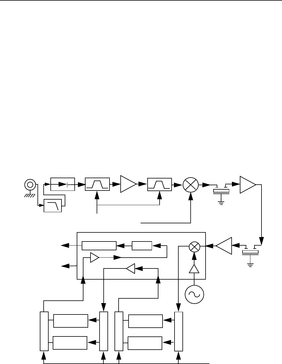
2-1
Section 2
THEORY OF OPERATION
1.0 Introduction
This Chapter provides a detailed theory of operation for the UHF circuits in the radio. For details of
the theory of operation and troubleshooting for the associated Controller circuits refer to the
Controller Section of this manual.
2.0 UHF (450-520 MHz) Receiver
2.1 Receiver Front-End
The UHF receiver, shown in Figure 2-1, is able to cover the UHF range from 450 to 520 MHz. It
consists of four major blocks: front-end bandpass filters and pre-amplifier, first mixer, high-IF, low-IF
and receiver back-end . Two varactor-tuned bandpass filters perform antenna signal pre-selection.
A cross over quad diode mixer converts the signal to the first IF of 44.85 MHz. Low-side first
injection is used.
Figure 2-1 UHF Receiver Block Diagram
Demodulator
1. Crystal
Filter
Mixer
Varactor
Tuned Filter
RF Amp
Varactor
Tuned Filter
Pin Diode
Antenna
Switch
RF Jack
Control Voltage
from PCIC First LO
from FGU
Recovered Audio
RSSI
Second LO
2. Crystal
Filter
455kHz Filter
(25kHz)
455kHz Filter
(25kHz)
455kHz Filter
(12.5kHz)
455kHz Filter
(12.5kHz)
Switch
Switch
Switch
Switch
Limiter
1. IF Amp
2. IF Amp
Filter Bank Selection
from Synthesizer IC
Harmonic
Filter
BWSELECT

2-2 UHF (450-520 MHz) Receiver
The two 2-pole 44.85 MHz crystal filters in the high-IF section and two pairs of 455 kHz ceramic
filters in the low-IF section provide the required adjacent channel selectivity .The correct pair of
ceramic filters for 12.5 or 25KHz channel spacing is selected via control line BWSELECT. The
second IF at 455 kHz is mixed, amplified, and demodulated in the IF IC. The processing of the
demodulated audio signal is performed by an audio processing IC located in the controller section.
2.2 Front-End Band-Pass Filters & Pre-Amplifier
The received signal from the radio’s antenna connector is first routed through the harmonic filter and
antenna switch, which are part of the RF power amplifier circuits, before being applied to the receiver
pre-selector filter (C5001, C5002, D5001, and related components). The 2-pole pre-selector filter,
tuned by the varactor diodes D5001 and D5002, pre-select the incoming signal (RXIN) from the
antenna switch to reduce spurious effects to the stages that follow. The tuning voltage (FECTRL_1),
ranging from 2 volts to 8 volts, is controlled by pin 20 of PCIC (U5501) in the transmitter section. A
dual hot carrier diode (D5003) limits any inband signal to 0 dBm to prevent damage to the pre-
amplifier.
The RF pre-amplifier is an SMD device (Q5003) with collector base feedback to stabilize gain,
impedance, and intermodulation. The collector current of approximately 11-16 mA is drawn from the
9.3 volt supply via L5003 and R5002. A 3dB pad (R5006,R5007, R5011, and R5008 - R5010)
stabilizes the output impedance and intermodulation performance.
A second 2-pole varactor tuned bandpass filter provides additional filtering of the amplified signal.
Varactor diodes D5004 and D5005 are controlled by the same signal, FECTRL_1, which controls
the pre-selector filter. A following 1 dB pad (R5013 - R5015) stabilizes the output impedance and
intermodulation performance.
2.3 First Mixer and High Intermediate Frequency (IF)
The signal from the front-end is converted to the first IF (44.85 MHz) using cross-over, quad diode
mixer D5051. Its ports are matched for incoming RF signal conversion to the 44.85 MHz IF using low
side injection via matching transformers T5051 and T5052. The injection signal (RXINJ) coming from
the RX VCO buffer (Q5332) is filtered by the lowpass filter consisting of L5053, L5054, and C5053 -
C5055 followed by matching transformer T5052 which has a level of approximately 15dBm.
The mixer IF output signal from transformer T5501, pin 2 is fed to the first two-pole crystal filter
(FL3101). The filter output in turn is matched to IF amplifier Q3101 which is actively biased using
collector-base feedback resistors R3101and R3106 to provide a current drain of approximately 5 mA
drawn from the 5 volt supply. The output impedance of this device is matched to the second two-pole
crystal filter FL3102. The signal is further amplified by a preamplifier Q3102 before going to pin 1 of
IFIC (U3101).
A dual, hot carrier diode (D3101) limits the filter output voltage swing to reduce overdrive effects at
RF input levels above -27 dBm.
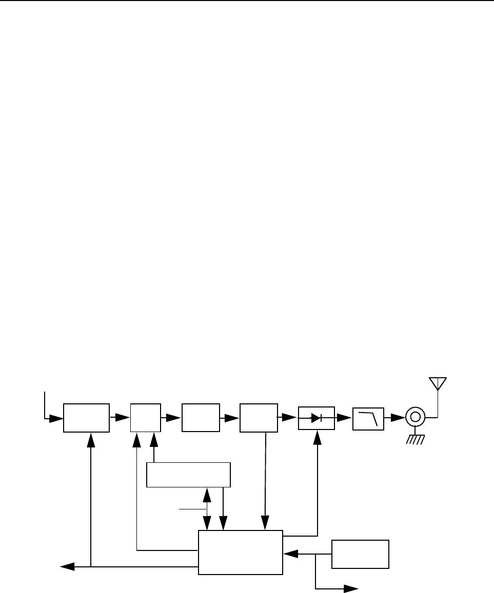
Transmitter Power Amplifier (PA) 40W 2-3
2.4 Low Intermediate Frequency (IF) and Receiver Back End
The 44.85 MHz first IF signal from the second IF amplifier feeds the IF IC (U3101) at pin1. Within the
IF IC the 44.85 MHz high IF signal mixes with the 44.395 MHz second local oscillator to produce a
low IF signal of 455 kHz. The second LO frequency is determined by crystal Y3101. The second IF
signal is amplified and filtered by an external pair of 455 kHz ceramic filters (FL3112 and FL3114) for
20/25 kHz channel spacing, or FL3111 and FL3113/F3115 for 12.5 kHz channel spacing. These
pairs are selectable via BWSELECT. The filtered output from the ceramic filters is applied to the
limiter input pin of the IF IC (pin 14).
The IF IC contains a quadrature detector using a ceramic phase-shift element (Y3102) to provide
audio detection. Internal amplification provides an audio output level of 120 mV rms (at 60%
deviation) from U3103, pin 8 (DISCAUDIO) which is fed to ASFIC_CMP U0221, pin 2 (part of the
controller circuits).
A received signal strength indicator (RSSI) signal is available at U3101, pin 5, which has a dynamic
range of 70 dB. The RSSI signal is interpreted by the µP (U0101, pin 63) and is available at
accessory connector J0501-15.
3.0 Transmitter Power Amplifier (PA) 40W
The radio’s 40W power amplifier (PA), shown in Figure 2-2, is a four-stage amplifier used to amplify
the output from the VCOBIC to the radio transmit level. The first stage is an LDMOS predriver
(U5401) controlled by pin 4 of PCIC (U5501) via Q5473 (CNTLVLTG). This stage is followed by
another LDMOS stage (Q5421), LDMOS stage Q5431, and a bipolar final stage (Q5441). Device
Q5401 is surface mounted and Q5421, Q5431, and Q5441 are directly attached to the heat sink.
Figure 2-2 UHF Transmitter Block Diagram
PCIC
Pin Diode
Antenna
Switch RF Jack
Antenna
Harmonic
Filter
Power
Sense
PA-Final
Stage
PA
Driver
From VCO
Controlled
Stage
Vcontrol
Bias 1
Bias 2
To Microprocessor
Temperature
Sense
SPI BUS
ASFIC_CMP
PA
PWR
SET
To Microprocessor

2-4 Transmitter Power Amplifier (PA) 40W
3.1 Power Controlled Stage
The first stage (U5401) amplifies the RF signal from the VCO (TXINJ) and controls the output power
of the PA. The output power of the transistor U5401 is controlled by a voltage control line feed from
the PCIC (U5501, pin 4). The control voltage simultaneously varies the bias of two FET stages within
U5401. This biasing point determines the overall gain of U5401 and therefore its output drive level to
Q5421, which in turn controls the output power of the PA.
In receive mode, the voltage control line is at ground level and turns off Q5473, which in turn
switches off the biasing voltage to U5401.
3.2 Pre-Driver Stage
The next stage is a 13dB gain LDMOS device (Q5421) which requires a positive gate bias and a
quiescent current flow for proper operation. The voltage of the line PCIC_MOSBIAS_1 is set in
transmit mode by PCIC, pin 24 and fed to the gate of Q5421 via the resistive network R5407,
R5408, R5416, and R5415. The bias voltage is factory tuned.
3.3 Driver Stage
This stage is an enhancement-mode N-Channel MOSFET device (Q5431) providing a gain of 10dB.
This device also requires a positive gate bias and a quiescent current flow for proper operation. The
voltage of the line Bias_2_UHF_PA_1 is set in transmit mode by the ASFIC and fed to the gate of
Q5431 via resistive network R5630, R5631, and R5632. This bias voltage is also factory tuned.
If the transistor is replaced, the bias voltage must be tuned using the Customer Programming
Software (CPS). Care must be taken not to damage the device by exceeding the maximum allowed
bias voltage. The device’s drain current is drawn directly from the radio’s dc supply voltage input, A+
via L5421.
3.4 Final Stage
The final stage uses bipolar device Q5441 whose collector current is also drawn from the radio’s dc
supply voltage input. To maintain class C operation, the base is dc-grounded by series inductor
L5441 and bead L5440. A matching network consisting of C5541-C5544 and two striplines
transform the impedance to 50 ohms and also feed the directional coupler.
3.5 Bi-Directional Coupler
The bi-directional coupler is a microstrip printed circuit, which couples a small amount of the forward
and reverse power of the RF power from Q5441. The coupled signal is rectified to an output power
proportional dc voltage by diodes D5451 and D5452 before being sent to the RFIN input of the
PCIC. The PCIC controls the gain of stage U5401 as necessary to hold this voltage constant. This
ensures the forward power out of the radio is held to a constant value.

Transmitter Power Amplifier (PA) 40W 2-5
3.6 Antenna Switch
The antenna switch utilizes the existing dc feed (A+) to the last stage device (Q5441). Basic
operation is to have both PIN diodes (D5471 and D5472) turned on during key-up by forward
biasing them. This is achieved by pulling down the voltage at the cathode end of D5472 to around
11.8V (0.7V drop across each diode). The current through the diodes needs to be set around 80mA
to fully open the transmit path through resistor R5496. Q5472 is a current source controlled by
Q5471 and is eventually connected to pin ANO of PCIC. VR5471 ensures the voltage at resistor
R4511 never exceeds 5.6V.
3.7 Harmonic Filter
Inductors L5491, L5492, and L4493 along with capacitors C5448, C5493, C5494, C5496, and
C5498 form a low-pass filter to attenuate harmonic energy from the transmitter. Resistor R5491
drains any electrostatic charges that might otherwise build up on the antenna. The harmonic filter
also prevents high level RF signals above the receiver passband from reaching the receiver circuits
to improve spurious response rejection.
3.8 Power Control
The transmitter uses the power control IC (PCIC, U5501) to control the power output of the radio. A
portion of the forward RF power from the transmitter is sampled by the bi-directional coupler and
rectified to provide a dc voltage to the RFIN port of the PCIC (pin 1) that is proportional to the
sampled RF power.
The PCIC has internal digital-to-analog converters (DACs) which provide a reference voltage to the
control loop. The reference voltage level is programmable through the SPI line of the PCIC and is
proportional to the desired power setting of the transmitter. Factory programming at several points
across the frequency range of the transmitter is used to offset frequency response variations of the
transmitter’s power detector circuits.
The PCIC provides a dc output voltage at pin 4 (INT) and applied as CNTLVLTG to the power-adjust
input pin of the first transmitter stage U5401. This adjusts the transmitter power output to the
intended value. Variations in forward or reflected transmitter power cause the dc voltage at pin 1 to
change, and the PCIC adjusts the control voltage above or below its nominal value to raise or lower
output power.
Capacitor C5502-4, in conjunction with resistors and integrators within the PCIC, control the
transmitter power rise (key-up) and power decay (de-key) characteristic to minimize splatter into
adjacent channels.
U5502 is a temperature-sensing device, which monitors the circuit board temperature in the vicinity
of the transmitter driver and final devices, and provides a dc voltage to the PCIC (TEMP, pin 29)
proportional to temperature. If the dc voltage produced exceeds the set threshold in the PCIC, the
transmitter output power is reduced to decrease the transmitter temperature.

2-6 Frequency Synthesis
4.0 Frequency Synthesis
The synthesizer, shown in Figure 2-3, consists of a reference oscillator (Y5261 or Y5262), low
voltage LVFRAC-N synthesizer (U5201), and a voltage controlled oscillator (VCO).
4.1 Reference Oscillator
The reference oscillator (Y5262) contains a temperature compensated crystal oscillator with a
frequency of 16.8 MHz. An analog-to-digital (A/D) converter internal to U5201 (LVFRAC-N) and
controlled by the µP via serial interface (SRL) sets the voltage at the warp output of U5201, pin 25 to
set the frequency of the oscillator. The output of the oscillator (Y5262, pin 3) is applied to pin 23
(XTAL1) of U5201 via an RC series combination.
In applications where less frequency stability is required, the oscillator inside U5201 is used along
with external crystal Y5261, varactor diode D5261, C5261, C5262, and R5262. In this case, Y5262,
R5263, C5235 and C5251 are not used. When Y5262 is used, Y5261, D5261, C5261, C5262 and
R5262 are not used, and C5263 is increased to 0.1 uF.
4.2 Fractional-N Synthesizer
The LVFRAC-N synthesizer IC (U5201) consists of a pre-scaler, programmable loop divider, control
divider logic, phase detector, charge pump, A/D converter for low frequency digital modulation,
balanced attenuator used to balance the high frequency analog modulation and low frequency digital
modulation, 13V positive voltage multiplier, serial interface for control, and a super filter for the
regulated 5 volts.
A voltage of 5V applied to the super filter input (U5201, pin 30) supplies an output voltage of 4.5 Vdc
(VSF) at pin 28. It supplies the VCO, VCO modulation bias circuit (via R5322), and synthesizer
charge pump resistor network (R5251, R5252). The synthesizer supply voltage is provided by 5V
regulator, U5211.
To generate a high voltage to supply the phase detector (charge pump) output stage at pin VCP
(U5701-32), a voltage of 13 Vdc is generated by the positive voltage multiplier circuit (D5201,
C5202, and C5203). This voltage multiplier is basically a diode capacitor network driven by two
signals (1.05MHz) 180 degrees out of phase (U5201, pins 14 and 15).

Frequency Synthesis 2-7
Figure 2-3 UHF Synthesizer Block Diagram
Output LOCK (U5201-4) provides information about the lock status of the synthesizer loop. A high
level at this output indicates a stable loop. IC U5201 provides the 16.8 MHz reference frequency at
pin 19.
The serial interface (SRL) is connected to the µP via data line DATA (U5201-7), clock line CLK
(U5201-8), and chip enable line CSX (U5201-9).
DATA
CLK
CEX
MODIN
VCC, DC5V
XTAL1
XTAL2
WARP
PREIN
VCP
REFERENCE
OSCILLATOR
VOLTAGE
MULTIPLIER
DATA (U0101 PIN 100)
CLOCK (U0101 PIN 1)
CSX (U0101 PIN 2)
MOD IN (U0221 PIN 40)
+5V (U4211 PIN 1)
7
8
9
10
13, 30
23
24
25
32
47
VMULT2 VMULT1
BIAS1
SFOUT
AUX3
AUX4
IADAPT
IOUT
GND
FREFOUT
LOCK 4
19
6, 22, 33, 44
43
45
3
2
28
14 15
40
FILTERED 5V
STEERING
LOCK (U0101 PIN 56)
PRESCALER IN
FREF (U0221 PIN 34)
39
BIAS2
41
48
5, 20, 34, 36
+5V (U4211 PIN 1)
AUX1
VDD, DC5V MODOUT
U5201
LOW VOLTAGE
FRACTIONAL-N
SYNTHESIZER
AUX2 1 (NU)
BWSELECT
VCO Bias
TRB
To IF
Section
TX RF INJECTION
(1ST STAGE OF PA)
LO RF INJECTION
VOLTAGE
CONTROLLED
OSCILLATOR
LINE
2-POLE
LOOP
FILTER
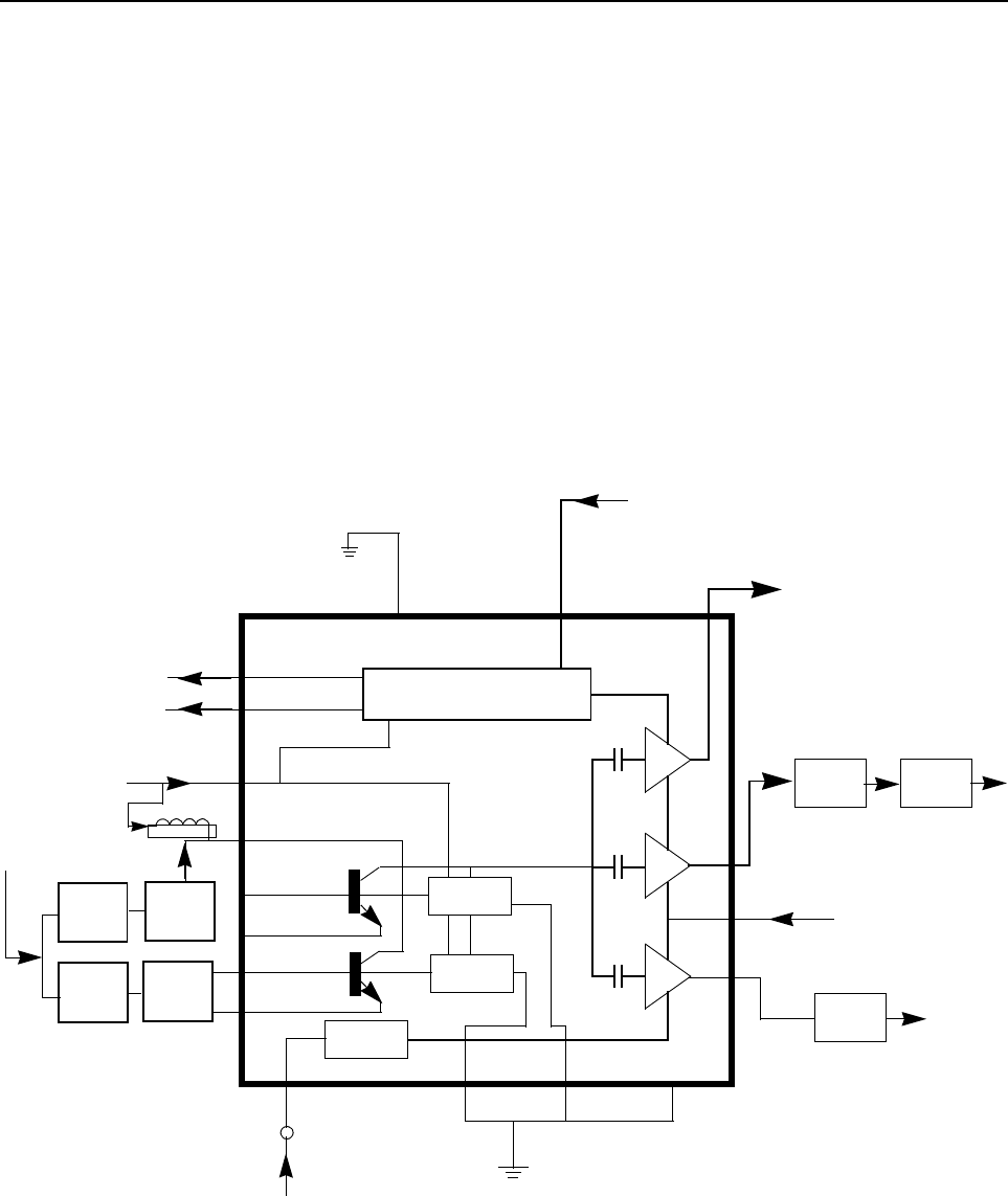
2-8 Frequency Synthesis
4.3 Voltage Controlled Oscillator (VCO)
The voltage controlled oscillator (VCO), shown in Figure 2-4, consists of a VCO buffer IC (VCOBIC,
U5301), TX and RX tank circuits, external RX buffer stages, and modulation circuits.
The VCOBIC together with Fractional-N synthesizer (U5201) generates the required frequencies in
both transmit and receive modes. The TRB line (U5301, pin 19) determines which tank circuits and
internal buffers are to be enabled. A high level on TRB enables TX tank and TX output (pin 10), and
a low enables RX tank and RX output (pin 8). A sample of the signal from the enabled output is
routed from U5301, pin 12 (PRESC_OUT), via a low pass filter of U5201, pin 32 (PREIN).
A steering line voltage (VCTRL) between 3.0V and 10.0V at varactor diode CR5311 tunes the full
TX frequency range (TXINJ) from 450 MHz to 520 MHz, and at varactor diodes CR5301, CR5302,
and CR5303 tunes the full RX frequency range (RXINJ) from 405 MHz to 475 MHz. The tank circuits
uses the Hartley configuration for wider bandwidth. For the RX tank circuit, external transistor
Q5301 is used in conjunction with the internal transistor for better side-band noise.
Figure 2-4 UHF VCO Block Diagram
Presc
RX
TX
Matching
Network Low Pass
Filter
Attenuator
Pin8
Pin14
Pin10
(U5201 Pin28)
VCC Buffers
TX RF Injection
U5201 Pin 32
AUX3 (U5201 Pin2)
Prescaler Out
Pin 12Pin 19
Pin 20
TX/RX/BS
Switching Network
U5301
VCOBIC
Rx
Active Bias
Tx
Active Bias
Pin2
Rx-I adjust
Pin1
Tx-I adjust
Pins 9,11,17
Pin18
Vsens
Circuit
Pin15
Pin16
RX VCO
Circuit
TX VCO
Circuit
RX Tank
TX Tank
Pin7
Vcc-Superfilter
Collector/RF in
Pin4
Pin5
Pin6
RX
TX
(U5201 Pin28)
Rx-SW
Tx-SW
Vcc-Logic
(U5201 Pin28)
Steer Line
Voltage
(VCTRL)
Pin13
Pin3
TRB IN
LO RF INJECTION
Q4301
Q4332

Frequency Synthesis 2-9
The external RX buffers (Q5332) are enabled by a high at U5201, pin 3 (AUX4) via transistor switch
Q5333. In TX mode, the modulation signal (VCOMOD) from the LVFRAC-N synthesizer IC (U5201,
pin 41) is applied to the modulation circuits CR5321, R5321, R5322, and C5324. These modulate
the TX VCO frequency via coupling capacitor C5321. Varactor CR5321 is biased for linearity from
the VSF.
4.4 Synthesizer Operation
The synthesizer consists of a low voltage FRAC-N (LVFRACN) IC, reference oscillator (crystal
oscillator with temperature compensation), charge pump circuits, loop filter circuits, and dc supply.
The output signal (PRESC_OUT) of the VCOBIC (U5301, pin12) is fed to of U5201, pin 32 (PREIN)
via a low pass filter (C5229,L5225,and C5226) which attenuates harmonics and provides correct
level to close the synthesizer loop.
The pre-scaler in the synthesizer (U5201) is a dual modulus pre-scaler with selectable divider ratios.
The divider ratio of the pre-scaler is controlled by the loop divider, which in turn receives its inputs via
the SRL. The output of the pre-scaler is applied to the loop divider. The output of the loop divider is
connected to the phase detector, which compares the loop divider´s output signal with the reference
signal.The reference signal is generated by dividing down the signal of the reference oscillator
(Y5261 or Y5262).
The output signal of the phase detector is a pulsed dc signal routed to the charge pump. The charge
pump outputs a current at U5201, pin 43 (IOUT). The loop filter (consisting of R5221-R5223, C5221-
C5225, and L5221) transforms this current into a voltage that is applied to varactor diodes CR5311
for transmit, CR5301, CR5302 and CR5303 for receive and alters the output frequency of the
VCO.The current can be set to a value fixed in the LVFRAC-N IC or to a value determined by the
currents flowing into BIAS 1 (U5201-40) or BIAS 2 (U5201-39). The currents are set by the value of
R5251 or R5252 respectively. The selection of the three different bias sources is done by software
programming.
To reduce synthesizer lock time, when new frequency data has been loaded into the synthesizer, the
magnitude of the loop current is increased by enabling the IADAPT (U5201-45) for a certain software
programmable time (Adapt Mode). The adapt mode timer is started by a low to high transistion of the
CSX line. When the synthesizer is within the lock range, the current is determined only by the
resistors connected to BIAS 1, BIAS 2, or the internal current source. A settled synthesizer loop is
indicated by a high level of signal LOCK (U5201-4) which is routed to one of the µP´s ADCs input
U101-56. From the voltage the µP determines whether LOCK is active.
To modulate the PLL, the two-spot modulation method is utilized via pin 10 (MODIN) on U5201. The
audio signal is applied to both the A/D converter (low frequency path) and the balanced attenuator
(high frequency path). The A/D converter converts the low frequency analog modulating signal into
a digital code which is applied to the loop divider, thereby causing the carrier to deviate. The
balance attenuator is used to adjust the VCO’s deviation sensitivity to high frequency modulating
signals. The output of the balance attenuator is present at the MODOUT port (U5201-41) and
connected to the VCO modulation diode CR5321 via R5321 and C5325.

2-10 Frequency Synthesis
THIS PAGE INTENTIONALLY LEFT BLANK

3-1
Section 3
TROUBLESHOOTING CHARTS
1.0 Troubleshooting Flow Chart for Receiver (Sheet 1 of 2)
Bad SINAD
Bad 20dB Quieting
No Recovered Audio
START
Audio at
pin 8 of
U3101 ?
Check Controller
(in the case of no audio)
OR ELSE go to “B”
Yes
No
Spray or inject 44.85MHz
into XTAL Filter FL3101
Audio heard ?
BYes
No
Check 2nd LO
(44.395MHz) at C3135
LO present ?
B
Yes
Check voltages on
U3101
Biasing OK ?
No
No
A
Yes
Check Q3102 bias
for faults
Replace Q3102
Go to B
Yes
No
Check circuitry
around U3101.
Replace
U3101 if defect
Check circuitry around Y3101.
Replace Y3101 if defect
Voltages
OK?

3-2 Troubleshooting Flow Chart for Receiver
1.1 Troubleshooting Flow Chart for Receiver (Sheet 2 of 2)
IF Signal at
C3101?
No
RF
Signal at
T5051?
RF
Signal at
C5015?
No
No
RF
Signal at
C5025?
No or
Check harmonic filter
L5491-L5493, C5492, J5401
and ant. switch
D5471, D5472, L5472.
Check filter between
C5025 & C5009.
Check tuning voltage
at R5060.
Inject RF into J5401
Is
tuning voltage
OK?
No
Yes
Check RF amp (Q5003)
Stage.
Check filter between
C5015 & T5051.
Yes
Check T5051, T5052,
D5051, R5052, L5008.
Yes
1st LO level
OK?
Locked?
Yes
Check FGU
Yes
Trace IF signal
from C3101 to
Q3101. Check for
bad XTAL filter.
No
Yes IF
signal at Q3102
collector?
Before replacing
U3101, check
U3101 voltages.
Yes
Check for
5VDC
Is 9V3
present?
Check Supply Voltage
circuitry. Check Q0681,
U5211 and U0641.
No
No
No
Check U5501.
Check varactor filter.
No
Yes
Yes
Yes
A
A
B
weak RF
RF
Signal at
C5009?

Troubleshooting Flow Chart for 40W Transmitter 3-3
2.0 Troubleshooting Flow Chart for 40W Transmitter
No
Is Q5441 OK ?
Yes
Is drive from VCO
>+4dBm?
No
Is voltage drop across
R5497 >4.5V ?
No
Check Q5431 gate(open)
and drain resistances
(11kohm)
No
Check Q5421 gate(open)
and drain resistances
(11kohm)
No
PCIC_MOSBIAS_1
Check
No
No
Change
Q4573
START
No power
Is Vctrl
there?
Is Q5573
OK?
Check voltage
n U5501, pin 4
Check voltage
on U5501, pin 5
Check R5422-5
and go back to top
Troubleshoot
ASFIC
Change
PCIC
Check R5409 and
R5473 and go back
to top
Check
MOSBIAS_2 Check
ASFIC
Are D5471 &
D5472 OK? Change
D5471 &
D5472
NoNo No
Yes
Yes
Yes
Yes
Yes
Yes Yes
Yes
No
No Check
PCIC
Yes
Change Q5421
Change Q5431
Yes
Change U5401
Yes Do visual check
on all components
No
Change Q5441
Troubleshoot
VCO
Check voltage
on TP5531

3-4 Troubleshooting Flow Chart for Synthesizer
3.0 Troubleshooting Flow Chart for Synthesizer
5V
at pin 6 of
D5201
Is
information
from µP U0101
correct
?
Is
U5201 Pin 47
at = 13VDC
?
Is
U5301 Pin 19
<40 mVDC in RX &
>4.5 VDC in TX?
(at VCO section)
?
Start
Visual
check of the
Board
OK?
Correct
Problem
Check 5V
Regulator
U5211
+5V
at U5201
Pins
13 & 30
?
Is
16.8MHz
Signal at U5201
Pin 19
?
Check
Y5261 / Y5262 and
associated parts
Are
signals
at Pins 14 &15
of U5201
?
Check
R5201 Check C5381
Is
U5201
Pin 2 >4.5 VDC in
Tx & <40 mVDC
in Rx
?
Replace
U5201
Remove
Shorts
Is
there a short
between Pin 47 and
Pins 14 & 15 of
U5201
?
Replace or
resolder
necessary
components
Is
RF level at
U5201 Pin 32
-12 < x <-25
dBm
?
Are
R5221,R5222,
R5223,C5221,
C5222,& C5223
OK?
Replace
U5201
If C5227
is OK, then see VCO
troubleshooting chart
Are
Waveforms
at Pins 14 & 15
triangular
?
Do
Pins 7,8 & 9
of U5201 toggle
when channel is
changed?
Check programming
lines between
U0101 and U5201
Pins 7,8 & 9
Replace
U5201
Check µP U0101
Troubleshooting
Chart
NO
YES
NO
YES
NO
YES
NO
NO
NO
YES
YES
NO
YES
YES
NO
YES
YES
YES
NO
NO
NO
NO
YES
NO
YES
YES
Check D5201,
C5202, C5203, &
C5206
5V
at U5201
pins 5, 20, 34
& 36
C h e c k 5 V
Regulator
U5211
Is
16.8MHz
signal at
U5201 Pin
23?
Replace
U5201
YES
NO
NO
YES
NO
YES

Troubleshooting Flow Chart for VCO 3-5
4.0 Troubleshooting Flow Chart for VCO
Are Q5332
Base at 0.7V
Collector at 4.5V
Emitter at 110mV
Are Q5301
Base at 2.4V
Collector at 4.5V
Emitter at 1.7V
Are Q5311
Base = 1.9V
Collector = 4.5V
Emitter = 1.3V
Low or no RF Signal
at TP5003
Visual check
of board
OK?
35mV DC at
U5301 Pin 19
NO
YES
Replace Q5301
at base of Q5332
NO
NO
NO
NO
YES
YES
YES
YES
Low or no RF Signal
at input to PA
4.8V DC at
U5301 Pin 19
Is RF available
at U5401
YES
YES
YES
YES
NO
NO
NO
NO
NO
Audio =180mVrms
at “-” S
ide of
4.5VDC
at CR5321
If C5321 and R5321 are OK,
then replace CR5321
Replace C5322
Replace C5325
NO
NO
YES
YES
TX VCO
RX VCO
Correct
Problem
Visual check
of board
OK?
Check runner
between U5201 Pin 2
and U5301 Pin 19
Is RF available If all parts from U5301 Pin 8
to Base of Q5332 are OK,
replace U5301
If all parts associated
with the pins are OK,
replace Q5332
If all parts from collector
of Q5332 to TP5003 are
OK, Replace U5301
Power OK but
no modulation
If all parts from U5301 Pin 10
U5401 Pin 16 are OK,
replace U5301
Replace
Q5311
YES
YES
Make sure Synthesizer is
working correctly and runner
between U5201 Pin 28 and
U5301 Pin 14 & 18 are OK
4.5V DC
OK ?
OK? OK?
C5325
at U5301 Pin 14 & 18
4.5V DC
OK ?
at U5301 Pin 14 &18
NO
Pin 16
If R5361 and
L5361 are OK,
replace U5301

3-6 Troubleshooting Flow Chart for VCO
THIS PAGE INTENTIONALLY LEFT BLANK

4-1
Section 4
UHF PCB/SCHEMATICS/PARTS LISTS
1.0 Allocation of Schematics and Circuit Boards
1.1 Controller Circuits
The UHF circuits are contained on the Printed Circuit Board (PCB) which also contains the
Controller circuits. This Chapter shows the schematics for the UHF circuits only, refer to the
Controller section for details of the related Controller circuits . The PCB component layouts and the
Parts Lists in this Chapter show both the Controller and UHF circuit components. The UHF
schematics and the related PCB and parts list are shown in the tables below.
Table 4-1 UHF B2 40W Diagrams and Parts Lists
PCB : 8480645Z04 Main Board Top Side
8480645Z04 Main Board Bottom Side Page 4-3
Page 4-4
SCHEMATICS
Power Amplifier 40W
FRACN
Voltage Controlled Oscillator
Receiver Front End
IF
Page 4-5
Page 4-6
Page 4-7
Page 4-8
Page 4-9
Parts List
8480645Z04 Page 4-10

4-2 Allocation of Schematics and Circuit Boards
THIS PAGE INTENTIONALLY LEFT BLANK
UHF Band 2 25-40W PCB / Schematics / Parts List 4-3
2.0 UHF Band 2 25-40W PCB / Schematics / Parts List
C0211
C0212
C0251
C0252
R0211
R0212
R0251
R0252
R0253
R0257
16
1
89
U0251
C0253
C0256
C0261
C0262
R0256
R0268
R0269
8
7
114
U0211
J0451
1
C0421
C0451
C0452
C0453
C0455
C0456
C0457
C0458
C0459
C0460
C0461
C0462
C0463
C0464
C0466
C0467
R0441
C0468
18
32
17
16 1
U0121
C0132
R0131
51
26
U0101
1
76
R0106
C0106
R0101
R0102
R0104
R0108
R0110
R0115
R0116
C0224
R0226
R0227
R0228
Q0110 R0261
R0262
R0442
C0441
C0442
C0443
C0445
C0446
C0447
C0448
C0449
C0470
C0471
C0472
C0473
C0221
C0222
C0225
C0228
C0243
R0220
R0221
R0223
R0224
R0229
R0254
R0255
R0222
C0101
C0102
R0105
R0114
R0170
C0131
R0132
23
4
Y0131
C0104
C0107
C0237
C0223
C0227
C0232
C0233
C0236
R0225
C0226
C0495
C0234
C0235
C0231
9
U0271
C0542
Q0177
Q0181
Q0185
R0181 R0182
R0185 R0186
R0510
R0535
R0538
R0539
R0543
VR0501
VR0503
VR0505
VR0510
2011
10
J0501
C0484
C0601
C0603
C0612
R0533
R0611
R0612
1
6
5
U0611
J0601
C0651
C0652
D0651
R0651
R0652
3
2
1
U0651
C0241
C0242
C0244
C0245
C0246
R0241
R0242
137
25
13
U0221
C0496
D0201
C0482
C0483
C0486
C0487
C0488
C0493
C0494
C0654
C0655
C0681
L0481
L0482
Q0681
R0681
R0682
1
6
5
U0641
C5401
C5403
C5404
C5410
C5417
C5419
C5447
C5461
C5486
C5488
C5505
C5506
L5401
L5403
23
R5401 R5402
R5403
9
8
16
1
U5401
C5425
C5426
1
R5408
R5415
R5416
R5481
Q5471
Q5472
R5504
R5511
R5512
TP5530
VR5471
C5431
C5434
C5453
C5455
C5456
C5457
D5402
56
8
7
4 Q5421
R5459
C5476
R5476
L5474
R5600
R5601
R5602
C5420
C0474
C0476
C0477
C0478
C0490
C5472
C5474
C5475
C5480
C5510
D5471
D5472
L5472 L5473
C5432 C5435
C5449
C5450
C5460
C5520
D5403
R5607
C5423
C5481
C5485 C5489 C5490
C5495
C5497
C5602
C5478
C5493
C5444
C5465
C5466
C5491
C5521
C5522
R5501
R5502
U5502
C5459
C5507
32
J5401
C5441
C5442
C5443
C3124
C3131
C3132
C3133
C3134
C3135
C3136
C3137
L3124
R3123
R3124
R3130
R3132
C3115 R3111
R3117
11
1
20
10
U3101
C3143 R3135
C3139
C3140
C3141
C3142
C3145
C3148
R3142
R3144
R3145
87
1
14
U3115
2
Y3102
87
1
14
U3111
4
32
FL3112
FL3114
C3101 2
3
456
FL3101
L3100
R3148
C3102
C3103
L3101
R3101
R3106
2
3
456
FL3102
C3114
C5031
C5052
C5053
C5054
C5055
D5051
L5008
L5051
L5053
L5054
R5015
R5051
21
54
3
T5051
3
46
12
T5052
C5017C5018
C5019
C5020
C5021
C5022
C5023
C5029
C5030 D5004
D5005
R5012
C5001C5002
C5003
C5004
C5005
C5006
C5007
C5008
C5009
C5014
C5026
C5027
C5033
C5034
D5001
D5002
D5003
L5001
L5002
L5003
L5006
Q5001
Q5003
R5001
R5003
R5004
R5005
R5018
R5020
R5021
R5022
C5015C5016
L5004
R5007
R5066
C5032
L5005
L5009
R5013
C5210
C5212
C5213
C5214
C5215
C5216
C5242
C5243
C5244
C5245
C5246
C5289 L5201
R5211
4
5
8
U5211
C5222
C5223
C5225
C5226
C5227
C5229
C5230
C5231
C5241
C5253
L5221
L5225
C5221
R5221
R5222
R5223
C5232
C5233
C5234
C5251
C5252
C5254
C5255
R5251
R5252
C5224
C5235
R5263
C5317
C5318
C5322
C5323
C5325
C5351
C5352
C5382
3
L5312
L5313
R5311
R5312
R5321
C5308
C5309
C5353
C5355
C5383
L5304
L5305
Q5301
Q5311
R5301
R5302
R5305
C5331
C5332
C5371
C5372
C5373
C5374
L5371
R5331
R5332
R5333
R5337
R5341
C5375
L5303
43
Q5333
R5346
3
SH5301
C5335
C5337
C5339 R5343
R5345
C0504
C0505
C0506
C0508
C0509
C0510
C0511
C0512
C0513
C0514
C0515
C0516
C0517
C0518
C0501
C0502
C0503
UHF Band 2 (450-520 MHz) 40W 8480645Z04 Top Side
4-4 UHF Band 2 25-40W PCB / Schematics / Parts List
C99
CNTL-REV-T6
C3144
C3146
C3147
C3151
C3152
Q3141
Q3151
Q3152
R3134
R3141
R3146
R3147
R3151
R3152
R3153
R3154
R3133
4
3
2
Y3101
C3122
C3123
R3113
R3116
D3101 R3115 Q3102 C3116
R3118
C3111
R3104
R3105
R3108
R3102
C3104
C3110
C3112C3113
L3111
Q3101
R3107
C3121
L3112
R3112
R3114
43
2
FL3111
FL3113
43
2
FL3115
C5028
C5068
Q5002
R5016
R5017 R5068
C5010
C5011
C5012
C5013
R5002
C5064
C5065
C5069
D5006
Q5004
R5062
R5063R5064
R5070
R5072
C5024
C5060
C5067 R5052
R5053
R5054
R5055
R5060
R5071
TP5003
C5061
C5062
D5007
R5061
R5069
C5451
C5463
C5469
C5470
C5473
C5499
D5452
D5454
R5455
R5457
R5472 R5475
R5496
TP5531
C5025
C5452
C5464
D5451
D5453
R5409
R5471
R5473
R5474
R5506
R5507
C5448
C5492
C5498
L5491
L5493
L5492
C5496
R5491
C5494
C5263
D5261
L5231
R5261
TP5201
TP5202
Y5261
2
34
Y5262
C5261
C5262
R5241
R5262
1
37
25 13
U5201
C5228
C5287
R5228
C5201
C5202
C5203
C5204
C5205
C5206
C5207
C5208 C5209
C5211
C5288 D5201
R5201
R5203
R5204
R5206
C5066
R5019
C5301
C5302
C5303
C5304
C5305
C5306
C5307
C5316
CR5301
CR5302
CR5303
L5301
L5302
R5303
R5304
R5315
C5381
11
120
10
U5301
C5311
C5312
C5313
C5314
C5315
C5321
C5324
CR5311
CR5321
L5311
R5313
R5314
R5322
R5323
C5336
C5338
L5332
L5333
Q5332
R5336
R5338
R5339
R5340
R5342
R5344 R5347
SH5302
C5333
C5363
C5334
C5354
C5361
C5362
L5331
L5361
Q5331
R5334
R5335
R5361
6
5
4
3
2
1
Q5441
C5437
L5440
L5441
6
5
4
R5421
C5422
C5436
C5482
L5421
C5438
C5439
L5436
L5437
TP5532
C0401
C0402
C0403
C0406
C0407
C0408
C0409
C0410
C0411
R0412
12
C5407
C5409
C5412
C5414
C5416
C5462
C5487
L5411
R5405
R5411
R5412
R5427
R5428
R5433
R5495
R5497
TP5536
C5424
C5483
L5541
L5543
Q5451
R5414
R5487R5488
R5513
C5446
C5630
3
2
1
R5485
R5486
R5630
R5631
R5632
TP5537
C5632
R5633
VR5472
C5421
C5484 L5402
Q5431
C0499
C0611
VR0601
C5418 C5479
C5502
C5503
C5504
Q5473
R5422
R5423
R5424
R5425
R5431
R5480
R5482
R5483
R5484
R5492
R5503
R5514
R5523
TP5533
1
17
9
25
U5501
C0422
C0423
C0485
R0467
C0491
C0492
C0497
C0301
C0303
C0352
C0354
1
4
58
U0351
C0302
C0351
D0301
28 15
C0304
C0305
C0324
C0325
C0343
R0323
R0324
R0344
C0426
C0427
C0428
C0429
C0430
C0431
R0407
R0409
R0410
C0353
R0331
R0332
R0333
R0335
R0481
R0482
J0401
C0201
C0202
C0203 C0204
C0205
C0254 C0265
C0266
C0267
R0201
R0202
R0203
R0204
R0205
R0206
R0207
R0208
R0265
R0266
R0267
TP0221
TP0222
VR0541
14
U0301
C0341
C0344
R0341
R0345
R0346
TP0497
1
45
8
U0341
C0141
TP0101
16
1
8
9U0141
C0342
R0342
R0343 R0347
U0342
C0331
C0641
C0644
C0645
C0662
Q0641
Q0661
R0641
R0642
R0643
U0331
C0661
C0663
D0660 D0661
Q0662
Q0663
R0661
R0662
TP0661 C0622
C0671
D0621 R0671
R0672
VR0621
VR0671
C0621
R0621
C0541
Q0171
Q0173
R0171
R0172
R0173
R0174
R0175
R0176
R0177
R0178
R0179
R0512
R0525
R0529
R0530
R0541
R0542
R0408 TP0102
C0111
C0112
D0101
R0111
R0401 TP0104
1
4
58
U0111
1
18
J0552
R0107
C0105
C0121
C0255
R0468
14
58
U0652
U0653
C0103
R0112
R0113
R0117
R0121
TP0103
TP0492
22
21 8
7
1
U0122
C0122
C0123
C0558
C0559
C0560
C0575
C0576
C0591
C0592
C0593
40
J0551
R0591
R0592
C0271
C0275
C0276 C0277
E0271 E0272
Q0271
R0273
R0276
C0151
C0272
C0273
C0274
C0554 D0151
Q0151
R0151
R0152
R0274
R0275
R0593
TP0151
VR0151
D0179
Q0183
R0183
R0184
R0511
R0531
R0537
VR0509
VR0537
TP0530
VR0504
E0631
1
UHF Band 2 (450-520 MHz) 40W 8480645Z04 Bottom Side
UHF Band 2 25-40W PCB / Schematics / Parts List 4-5
9V3
PASUPVLTG
PASUPVLTG_UHF_PA_1
9V3_UHF_PA_1
C5485
30pF
5.6V
VR5472
R5633
820K
C5602
.033uF
L5402
C5481
3000pF
C5632
1000pF
ALT
PASUPVLTG
C5484
30pF .033uF
C5421 C5497
1000pF
3000pF
C5489
1000pF
C5495 C5436
10uF C5493
3000pF
C5490
3000pF
L5541
C5478
1000pF C5482
30pF
L5421
0.1uF
C5438
L5436
A+
C5486
30pF
C5418
0.1uF
100pF
C5488
L5401
11.03nH
C5404
100pF
390nH
L5403
1.8pF
C5403
C5407
0.1uF R5405
200
30pF
C5487
0.1uF
C5409
100pF
C5412
Load
L5411
390nH
> 4 dBm (Tx)
TXINJ
TX_INJ_UHF_PA_1
51
R5497 R5495
51
9V3
L5474
57R01
9V3
300
R5401
C5410
100pF
C5401
100pF
R5403
300
R5402
15
6
RFOUT2 7
VCNTRL
1
VD1
14 VG1 2
VG2 3
5
GND3
12
GND4
13
NC1
8
NC2
9
NC3
10
NC4
15
RFIN
16 RFOUT1
U5401
30C65
EP
17
G2
11
GND1
4
GND2
C5462
R5433
C5417
100pF
C5461
R5415
100
C5447
7.5pF 36pF
C5419
R5416
100
C5453
47pF
C5431
C5483
100pF
13.85nH
L5543
R5414
C5424
8
Q5421
6
2
1
3
4
5
7
C5455
Load
3.7 to 3.9 VDC
Q5451
TP5536
R5487
100K
R5408
200K
C5425
.022uF
R5488
2.7K 100pF
C5426 C5456
C5457
R5481
D5402
R5459
R5485
120
120
R5486 1K
R5631 R5607
R5476
C5520
C5476
R5632
24K
C5446
100pF
C5630
0.1uF R5630
2.4 to 2.6 VDC
BIAS_2_UHF_PA_1 MOSBIAS_2
TP5537
R5412
5.6K
C5416
.022uF
10K
R5427
R5411
C5414
1000pF 4.7K
R5428
100K
R5480
PCIC_MOSBIAS_1
6.5 VDC (44W)
6.2 VDC (28W)
R5424
620
R5423
620
R5431
620
R5422
Q5473
9V3
R5425
620
R5514
3.3K
CNTLVLTG_UHF_PA_1
CNTLVLTG
4.57 VDC (44W)
4.32 VDC (28W)
TP5533
PA_PWR_SET_1_UHF_PA_1 PA_PWR_SET
PA_PWR_SET
C5420
39pF
16pF
C5434
R5601
4.7
4.7
R5600
R5602
4.7
100pF
C5422 C5423
1uF
G4
S1
S2
S3
S4 D
G
G1 7
G2 8
G3 9
10
Q5431
MRF5015
15pF
C5432
20pF
C5435
20pF
C5450
39pF
C5460 C5449
20pF
C5437
L5440
D5403
10
R5421
13.85nH
L5441
3
MRF650
Q5441
4
2
1NU
NU
NU
NU
C5443
C5444
C5466
C5465
7.5pF
C5491
30pF
C5442
C5441
27pF C5459
100pF
D5471
R5457
120
C5469
100pF
120
R5471
D5452
D5454
D5451
C5452
R5473
4.3K
9V3
R5506
10K
100K
R5409
D5453
C5464 100K
R5474
C5439
100pF
L5437
17nH
2.20 VDC (28W)
3.11 VDC (44W)
0
R5475
1000pF
C5451
100K
R5455
TP5531
10K
R5507
K9V1
TEMPSENSE_UHF_PA
1
POS
U5502
K9V1_UHF_PA_1
TEMPSENSE
R5504
10K
9V3
100pF
C5499
C5470
100pF
C5507
A+
VR5471
5.6V
R5472
10K
R5513
470
R5512
9.2 VDC
Q5471
TP5530
3J5401-3
9pF
C5448
J5401-2
2
C5494
7pF
L5491
17nH
1J5401-1
100pF
C5492
17nH
L5492
17nH
L5493
4.7pF
C5498 3.3pF
C5496
R5491
11K
C5463
RXIN
RX_IN_VHF_PA_1
17nH
L5472 C5474
12pF
D5472 C5480
2pF 2pF
C5475
C5479
100pF
51
R5511
82
R5496
Q5472
C5472
30pF
30pF
C5510
100pF
C5473
43.67nH
L5473
CLK CLK_VHF_PA_1
CSX_VHF_PA_1
DATA
CSX
DATA_VHF_PA_1
10K
R5492
9V3
0.75 VDC
R5501
5.6K
100pF
C5521
1000pF
TP5532
C5522
3GND
VOUT 2
R5502
68K
300K
R5482
68K
R5484
9V3
R5503
3.9K
3.1 VDC (44W)
2.2 VDC (28W)
R5523
R5483
100K
ALT
PA_PWR_SET
C5503
2200pF
.02uF
C5504
.015uF
C5502
2200pF
C5506
VLIM 19
30
V10 14
V45 16
17
V5EXT
20
VAR1
18
VAR2
24
VAR3
15
VG
VL
6
Q11
QX 10
1RFIN
RS 21
31 RSET
RX 23
T1
2
TEMP
26
CQ 12
13
CQX
DATA
28
F168 9
GND1
8
GND2
25
INT
4
22
NA
ANO
32
BPOS
27
CEX
29
CI
3
CJ
5
CL
7
CLK
U5501
1uF
C5505
PCIC_MOSBIAS_1
9V3
RESET
FE_CNTL_2_VHF_PA_1
FECTRL_2
FE_CNTL_1_VHF_PA_1
FECTRL_1
RESET_VHF_PA_1
UHF Band 2 (450-520 MHz) Power Amplifier 40W

4-6 UHF Band 2 25-40W PCB / Schematics / Parts List
16_8MHz
C5202
.01uF
IN_5V_RF_REG_UHF_FN_1
TRB
MODIN
220
R5241
C5251
0.1uF
TP5202
1
.01uF
C5232
LOCK_UHF_FN_1
C5243
100pF
R5222
510
C5253
4.7uF
o
2.2uF
C5213
C5209
0.1uF
U4506
.01uF
C5231
CLK_UHF_FN_1
L5221
12uH
47K
R5228
1000pF
C5252
150
R5221
R5261
150K
100
R5263
VDDA
CLK
16.8MHz
XTAL
Y5261
1uF
C5223
VCNTL
1
VSF_UHF_FN_1
Y5262
TTS05V
16.8MHz
GND
2
OUT
3
VCC 4
MODIN_UHF_FN_1
2.2uF
C5214
0.1uF
C5254
D 5261
5V_UHF_FN_1
150
R5201
C5288
0.1uF
DATA
100pF
C5227
VDDA_UHF_FN_1
C5246
100pF
C5205
.01uF
1.5pF
C5263
68
R5223
C5235
.01uF
C5255
100pF
C5222
0.1uF
1.2K
R5262
C5245
100pF
C5244
47nH
L5225
100pF
TRB_UHF_FN_1
U4507
16_8MHz_UHF_FN_1 CSX_UHF_FN_1
C5204
0
R5211
100pF
BWSELECT_UHF_FN_1
C5207
100pF
C5228
0.1uF
5V_UHF_FN_2
VSF
C5211
0.1uF
2.4pF
C5226
C5206
10uF
2.2uF
C5210
220pF
C5262
47
R5203
LOCK
C5208
0.1uF
1uF
C5224
510pF
C5225
R5204
R5206
47
33K
C5216
.01uF
LP2951
U5211
VCOBIAS_2
C5212
.018uF
100pF
C5287
100pF
C5201
2pF
C5229
C5230
2.2uF
2.2uF
C5233
0.1uF
C5289
39K
R5251
VCTRL
TP5201
C5242
PRESC
CSX
100pF
L5231
VCOMOD_UHF_FN_1
IN_5V_RF_REG
2.2uH
C5241
100pF
5
A2
4
A3
K1
1
K2
2
K3
3
DATA_UHF_FN_1
6
A1
D5201
C5221
.01uF
.01uF
C5203
R5252
30K
VCTRL_UHF_FN_1
.01uF
C5234
L5201
390nH
62pF
C5261
5V
5V
2.2uF
C5215
VDDA
VDDA
U5201
4.57 VDC
-19 to -17 dBm (Rx)
-17 to -12 dBm (Tx)
4.98 VDC
0 VDC (Rx)
3.09 VDc (Rx)
2.65 VDC (Tx)
4.97 VDC (25KHz Chan. Spacing)
4.97 VDC (Tx)
2.48 VDC
1.76 VDC (Tx)
1.69 VDC (Rx)
0 VDc (12.5KHz Chan. Spacing)
5 VDC (Locked)
0 VDC (Unlocked)
2.5 to 10 Vdc
6.6 VDC
10.87 VDC
12.7 VDC
4.97 VDC
3.03 VDC
3.76 VDC
2.51 VDC
4.95 VDC
0 VDC
2.48 VDC
1.25 VDC
1.97
VDC
5V
VCOMOD
BWSELECT
23 XTAL1
XTAL2
24
21
VBPASS
47 VCP
VMULT1
15
14 VMULT2
12 VMULT3
11 VMULT4
VRO
13
25 WARP
35
PVREF
18
REFSEL
27
SFBASE 26
SFCAP
30
SFIN
28 SFOUT
37 TEST1
38 TEST2
17
NC1
29
NC2
31
NC3
44
PD_GND
PD_VDD
5
PREIN 32
33
PRE_GND
34 PRE_VDD
36 DVDD
19 FREFOUT
45 IADAPT
16 INDMULT
43 IOUT
LOCK
4
10
MODIN
41 MODOUT
20 AVDD
40
BIAS1
39
BIAS2
42
CCOMP
9
CEX 8
CLK
7
DATA
DGND 6
46 ADAPTSW
22
AGND
48 AUX1
1AUX2
2AUX3
3AUX4
INPUT
1OUTPUT
2SENSE 3
SHUTDOWN
65V_TAP
5ERROR 7
FEEDBACK
4
GND
8
ZWG0130364-0
HF Band 2 (450-520 MHz) FRACN
UHF Band 2 25-40W PCB / Schematics / Parts List 4-7
3pF
Q5331
VCOMOD
C5314
CR5303
R5345
C5334
C5303
4.3pF
220
51pF
100pF
R5340
C5323
C5315
RXINJ
1000pF
VSF_UHF_VC0
CR5301
R5361
180
GND
C5317
100pF
0
R5337
VCOBIAS_2
R5311
7.5K
390nH
L5304
C5381
0.1uF
C5351
100pF
C5353
0.1uF
L5313
L5331
33nH
0.1uF
390nH
C5308
0.1uF
C5352
390nH
L5305
CR5311
1
R5304
RXINJ_UHF_VCO
PRESC_UHF_VCO
150
R5312
7.5K
4.7uF
C5325
Q5333
10
R5335
10K
100pF
R5333
L5301
68nH
C5309
C5302
4.3pF
C5337
0
R5341
51pF
51pF
C5338
R5346
10K
SHIELD
SH5301
1
VCOBIAS_2_UHF_VCO
56K
R5321
30
R5303
R5314
SHIELD
1
220
.022uF
C5336
SH5302
1K
TXINJ
390nH
R5336
C5313
L5333
C5331
5.6pF
VCTRL_UHF_VCO
C5373
0.1uF
C5332
R5302
10K
390nH
TRB_UHF_VCO
TXINJ_UHF_VCO
L5361
CR5321
2.2uF
C5354
C5304
5.6pF
C5374
C5301
100pF
Q5301
30
R5313
P2
3
P3
L5302
220nH
L5303
RESONATOR
P1
2
C5339
51pF
10
R5305
R5334
C5333
TRB
0
220
R5338
5V
100pF
C5382 100pF
C5383
15nH
L5332
PRESC
C5311
100pF
10K
R5323
C5305
VSF
C5375
0.1uF
C5316
2.2K
R5342
2.2uF
C5363
C5355
22K
R5332
C5361
100pF
6.8K
R5322
1pF
C5321
22
R5331
1
P1
2
P2
3
P3
Q5332
L5312
RESONATOR
50U54
U5301
C5307
100pF
CR5302
5.6K
R5301
C5306
2pF
R5347
0
0.22uF
C5371
C5318
0.22uF
10
R5344
15pF
R5339
22
R5315 C5312
VCOMOD_UHF_VCO
0
1K
R5343
0.22uF
C5362
5V_UHF_VCO
68nH
L5311
100pF
C5372
C5335
68nH
100pF
C5324
L5371
VCTRL
3pF
100pF
C5322
Q5311
VSF
TXSW
$P
TXSW
RXSW
RXSW
VSF
ZWG0130365-0
4.2 VDC (Rx)
0 VDC (Tx)
0 VDC (Rx)
4.5 VDC (Tx)
4.2 VDC (Rx)
0 VDC (Tx)
4.5 VDC
2.3 VDC (Rx)
0 VDC (Tx)
2.5 to 10 VDC
4.5 VDC
0 VDC (Rx)
4.5 VDC (Tx)
4.5 VDC (Tx)
0 VDC (Rx)
0 VDC (Rx)
1.9 VDC (Tx)
4.5 VDc (Rx)
0 VDc (Tx)
> 14 dBm (Rx)
> 4 dBm (Tx)
2.58 VDC
4.5 VDC
(Rx)
TX_SWITCH
14
VCC_BUFFERS
18
VCC_LOGIC
RX_OUT
7
RX_SWITCH
3SUPER_FLTR
19 TRB_IN
16 TX_BASE
15 TX_EMITTER
1TX_IADJ 10
TX_OUT
13
FLIP_IN
11
GND_BUFFERS
9
GND_FLAG GND_LOGIC
17
12
PRESC_OUT
5RX_BASE
6RX_EMITTER
2RX_IADJ 8
4COLL_RFIN
20
(Tx)
UHF Band 2 (450-520 MHz) Voltage Controlled Oscillator
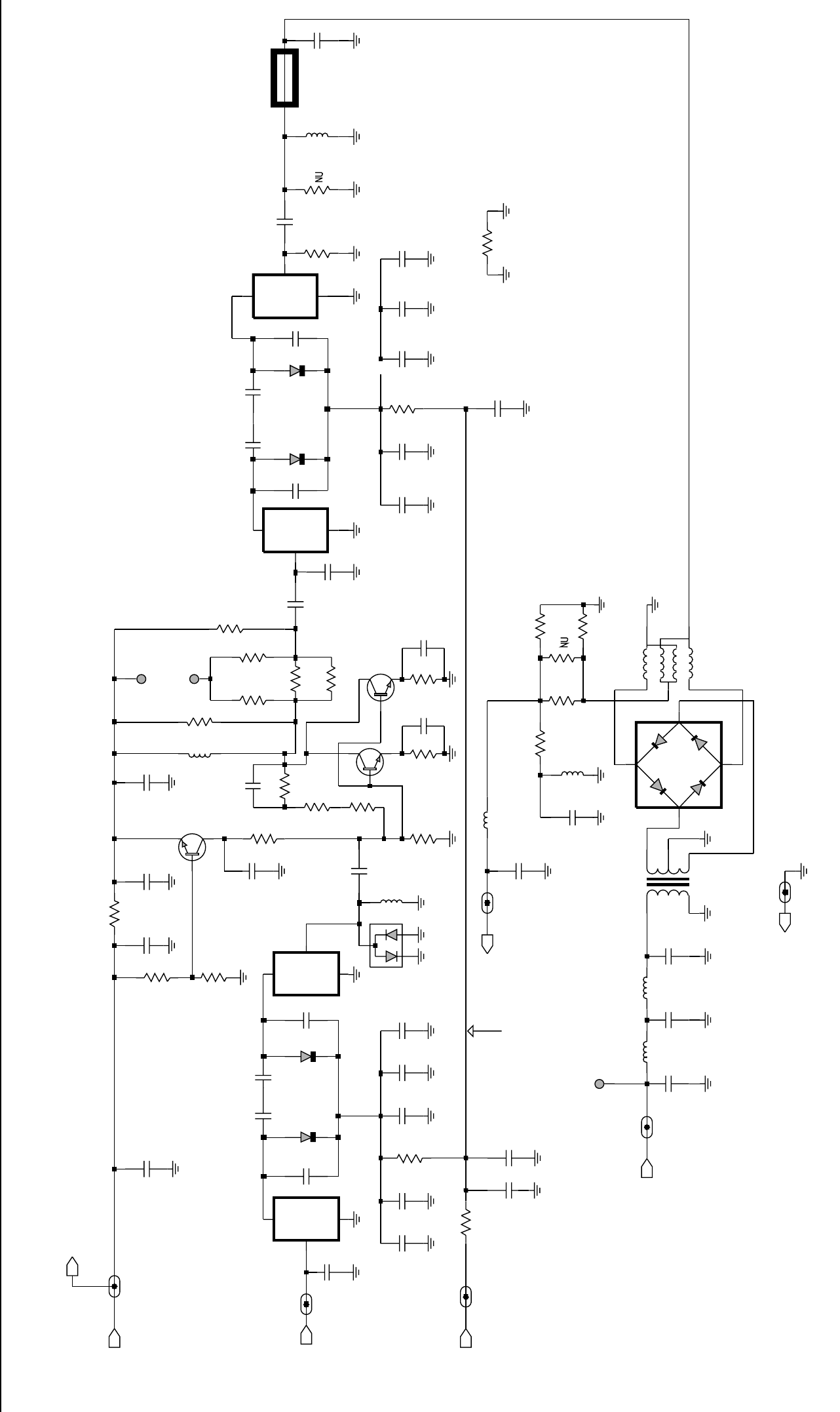
4-8 UHF Band 2 25-40W PCB / Schematics / Parts List
C5055
L5053
C5002
15nH
33pF
16pF
8.2pF
C5031
C5020
Q5002
GND
15nH
L5054
C5024
1000pF
D5002
C5026
1pF
GND_UHF_FE
1000pF
C5008
R5015
100K
R5001
R5017
330K
R5060
3300pF
RXINJ
C5011
C5021
24pF
L5004
IN
NEG
TBD
C5025
D5004
82pF
C5052
150
R5019
R5010
8.2pF
C5032
33
R5008
15nH
L5006
4
C5030
1pF
XFMR
T5051
1
2
3
5
R5022
0
270
R5006
1.5pF
C5017
RXIN_UHF_FE
9V3
C5016
D5001
C5066
TP5003
TBD L5005
IN
NEG
TBD
L5001
IN
NEG
150nH
L5051
L5008
470nH
10K
9V3
2
R5005
T5052
XFMR
4
6
3
1
100K
27pF R5012
C5007
68
R5007
270
TBD
L5002
IN
NEG
R5011
Q5001
FECTRL_1_UHF_FE
1pF
C5029
R5020
10
C5060
R5016
C5023
C5054
16pF
C5009
8.2pF
IF
D5003
0.1uF
C5034
FECTRL_1
C5004
16pF C5006
Q5003
L5009
10
R5021
R5051
15nH
51
20pF
C5003
330
R5002
C5013
3300pF
0
R5052
270nH
R5054
RXIN
L5003
330pF
C5012
C5027
1pF
R5018
R5053
R5003
4.7K
R5013
150
R5009
C5028
100pF
C5015
R5055
9V3_UHF_FE
IF_UHF_FE
C5001
1.5pF
18pF
C5005
100pF
C5014
6.8pF
C5053
R5004
2.7K
C5033
TP5001
0.1uF
RXINJ_UHF_FE
16pF
C5022
TP5002
C5018
33pF
D5051
IO1
1IO2 2
IO3
3
IO4
4
C5019
24pF
330pF
C5010
D5005
GROUND
POS
15pF
POS
POS
POS
3.4 VDC @ 450MHz
4.7 VDC @ 450MHz
6.5 VDC @ 450MHz
0.7 VDC
4.6 VDC
UHF Band 2 (450-520 MHz) Receiver Front End

UHF Band 2 25-40W PCB / Schematics / Parts List 4-9
9186176B01
9180469V04
9180469V03
9180469V06 9180468V06
R3144
2.4K
BWSELECT_VHF_IF_1
9V3_VHF_IF_2
C3113
9.1pF
NU
R3104
100
NU
100
620nH
NU
R3105
R3130
L3100
14
VDD
7
VSS
51
U3111-1
MC74HC4066
13
CNTL
1
2
C3116
L3112
0.1uF
620nH
9V3_VHF_IF_1
10uF
C3133
0.1uF
C3132
.01uF
C3151
OUT 2
C3137
.039uF
CFWC455D
FL3112
GND1
34
GND2
IN
1
620nH
C3121
L3101
0.1uF
R3101
12K
12K
R3147
15pF
DISCAUDIO
C3102
C3152
.01uF
0.1uF
C3139
7
VSS
0.1uF
C3141
U3115-1
MC74HC4066
MC74HC4066
13
CNTL
1
2
14
VDD
DISCAUDIO_VHF_IF_1
620nH
620
L3111
R3108
27pF
C3110
0.1uF
C3147
C3155
9V3
.01uF
NU
Q3155
FL3115
3
GND1GND2
4
1IN 2
OUT
BWSELECT
GND3
45
GND4
3IN 6
OUT
CFWC455F
12R16
FL3102
1
GND1
GND2
2
GND1
12
GND2
4
GND3
GND4
5
IN
3OUT 6
12R16
FL3101
7
C314 2
0.1uF
MC74HC4066
CNTL
6
89
VDD
14
VSS
GND
3
IN
1OUT 2
RSSI
U3111-3 FL3114
CFUCJ455D
4700pF
C3146
27K
GND1
34
GND2
IN
1OUT 2
R3106
OUT
3IN 1
FL3111
CFWC455G
Y3101
12R17
44.395MHz
GND
2
GND1
4
C3131
1pF
NU
0.1uF
C3145
5V_VHF_IF_1
IFIN_VHF_IF_1
IF
330
R3116
10K
R3134
0.1uF
C3144
18pF
C3114
10K
R3155
R3151
VDD
7
VSS
NU
1.2K
U3111-4
MC74HC4066
12
CNTL
14
CNTL
5
4
3VDD
14
VSS
7
U3115-2
MC74HC4066
0.1uF
C3104
C3135
33pF
12
CNTL
11
14
VDD
7
VSS
7
U3115-4
MC74HC4066
MC74HC4066
CNTL
5
4
3VDD
14
VSS
3.3K
U3111-2
R3145
0.1uF
C3140
390
R3115
Q3152
3
22pF
Y3102
455KHz
45B02
C3115
82pF
C3112 C3123
.039uF
R3112
10
0102727B45
0
R3148
0.1uF
C3111
Q3151
27K
R3117
Q3102
8.2K
R3133
Q3101
C3136
30pF
20pF R3102
C3101
33pF
10
C3103
C3134
0.1uF
RSSI_VHF_IF_1
6.8K
R3118
R3111
12K
C3122
.039uF
6.8K
R3107
NU
100
R3114
R3154
5V
10K
10K
R3153
D3101
120pF
C3143
R3152
10K
1.2K
CNTL
6
VDD
14
VSS
7
R3135
U3115-3
MC74HC4066
680
R3146
R3160
0
R3132
15K
FL3113
CS455G2 NU
GND
3
IN
1OUT 2
9V3
5V
5V
9V3
9V3
9V39V3
9V3
5V
9V3
89
10
11 10
OSCIN 4
OSCOUT
3
QUADIN 10
RFIN 1
RFIN_DEC 2
RSSIOUT
5RSSI_FEED 9
VCC
6
IFAMPOUT
16
IFAMP_DEC1 19
IFAMP_DEC2
17
LIMIN 14
LIMOUT
11
LIM_DEC1
13
LIM_DEC2
12
MIXOUT
20
SA616
SA616
AUDIOOUT
8AUDIO_FEED 7
GND 15
IFAMPIN 18
U3101
ZWG0130367-0
UHF Band 2 (450-520 MHz) IF
4-10 UHF Band 2 25-40W PCB / Schematics / Parts List
UHF Band 2 PCB 8480645Z04 Parts List 25-
40W
Circuit
Ref Motorola
Part No. Description
C0101 2113740F51 100pF
C0107 2113741F25 1000pF
C0112 2113743E20 0.1uF
C0121 2113743E20 0.1uF
C0122 2113743E20 0.1uF
C0131 2113740F35 22pF
C0132 2113740F35 22pF
C0141 2113743E20 0.1uF
C0151 2113741F49 10000pF
C0201 2311049A57 10uF
C0202 2311049A57 10uF
C0204 2113743E20 0.1uF
C0212 2311049A57 10uF
C0221 2113743E20 0.1uF
C0222 2113743E20 0.1uF
C0223 2113743E20 0.1uF
C0224 2113740F51 100pF
C0225 2113743E20 0.1uF
C0226 2113743E20 0.1uF
C0228 2311049A56 4.7uF
C0231 2113743B29 1uF
C0232 2113743E20 0.1uF
C0234 2113743E20 0.1uF
C0235 2113743E07 0.022uF
C0236 2113743E10 0.033uF
C0241 2113743E20 0.1uF
C0243 2113740F51 100pF
C0244 2113743E20 0.1uF
C0245 2113743E20 0.1uF
C0246 2113741F49 10000pF
C0251 2113743E20 0.1uF
C0252 2311049A07 1uF
C0254 2113743E20 0.1uF
C0255 2113743E20 0.1uF
C0256 2113740F51 100pF
C0261 2113743E20 0.1uF
C0262 2113740F49 82pF
C0265 2113743E20 0.1uF
C0267 2113741F49 10000pF
C0271 2113741F49 10000pF
C0272 2113743E20 0.1uF
C0273 2113741F37 3300pF
C0275 2311049A99 47uF
C0276 2113741F25 1000pF
C0277 2113741F25 1000pF
C0301 2311049A07 1uF
C0302 2113743E20 0.1uF
C0303 2113740F51 100pF
C0304 2113743E20 0.1uF
C0305 2113743E20 0.1uF
C0324 2113743E20 0.1uF
C0331 2113743E20 0.1uF
C0341 2311049A07 1uF
C0342 2113743E20 0.1uF
C0343 2113743E20 0.1uF
C0344 2113743E20 0.1uF
C0351 2113743E20 0.1uF
C0352 2113743E07 0.022uF
C0353 2311049A97 33uF
C0354 2113743E20 0.1uF
C0421 2113743N48 82pF
C0422 2113741F17 470pF
C0423 2113741F17 470pF
C0426 2113743L09 470pF
C0427 2113743L09 470pF
C0428 2113743N48 82pF
C0429 2113743L09 470pF
C0430 2113741F17 470pF
C0431 2113741F17 470pF
C0445 2113743L09 470pF
C0446 2113743L09 470pF
C0447 2113743L09 470pF
C0448 2113743L09 470pF
C0449 2113743L09 470pF
C0470 2113743L09 470pF
C0471 2113743N48 82pF
C0472 2113743N48 82pF
C0473 2113743N48 82pF
C0474 2113743L09 470pF
C0476 2113743L09 470pF
C0477 2113743L09 470pF
C0478 2113743L09 470pF
C0482 2113743L09 470pF
C0483 2113743L09 470pF
C0484 2113741F17 470pF
C0485 2113743L09 470pF
C0486 2113743L09 470pF
C0487 2113743L09 470pF
C0488 2113743L09 470pF
C0490 2113743L09 470pF
C0491 2113743L09 470pF
C0492 2113743L09 470pF
C0493 2113743L09 470pF
C0494 2113743L09 470pF
C0495 2113743L09 470pF
C0496 2113743L09 470pF
C0497 2113743L09 470pF
C0499 2113743L09 470pF
C0501 2113741F49 10000pF
C0502 2113743L09 470pF
Circuit
Ref Motorola
Part No. Description
C0503 2113743L09 470pF
C0504 2113743L09 470pF
C0505 2113743L09 470pF
C0506 2113743L09 470pF
C0508 2113743L09 470pF
C0509 2113743L09 470pF
C0510 2113741F17 470pF
C0511 2113743L09 470pF
C0512 2113743L09 470pF
C0513 2113741F17 470pF
C0514 2113743L09 470pF
C0515 2113743L09 470pF
C0516 2113741F49 10000pF
C0517 2113743N48 82pF
C0518 2113743L09 470pF
C0541 2311049A05 0.47uF
C0542 2311049A99 47uF
C0591 2113743E20 0.1uF
C0592 2113743E20 0.1uF
C0593 2113741B69 0.1uF
C0601 2113741F17 470pF
C0603 2380090M24 10uF
C0611 2311049C06 22uF
C0612 2113743E20 0.1uF
C0622 2311049A99 47uF
C0641 2113741F17 470pF
C0644 2311049A97 33uF
C0645 2113743E20 0.1uF
C0652 2311049A97 33uF
C0654 2311049A57 10uF
C0655 2113743E20 0.1uF
C0661 2311049C05 47uF
C0662 2113741F49 10000pF
C0663 2113743E20 0.1uF
C0671 2113743E20 0.1uF
C0681 2113743E20 0.1uF
C3101 2113740F34 20pF
C3102 2113740F31 15pF
C3103 2113740F39 33pF
C3104 2113743E20 0.1uF
C3110 2113740F37 27pF
C3111 2113743E20 0.1uF
C3112 2113740F49 82pF
C3114 2113740F33 18pF
C3115 2113740F35 22pF
C3116 2113743E20 0.1uF
C3121 2113743E20 0.1uF
C3122 2113743E11 0.039uF
C3123 2113743E11 0.039uF
C3132 2113743E20 0.1uF
C3133 2311049A57 10uF
Circuit
Ref Motorola
Part No. Description
C3134 2113743E20 0.1uF
C3135 2113740L30 33pF
C3136 2113740L29 30pF
C3137 2113743E11 0.039uF
C3139 2113743E20 0.1uF
C3140 2113743E20 0.1uF
C3141 2113743E20 0.1uF
C3142 2113743E20 0.1uF
C3143 2113740F53 120pF
C3144 2113743E20 0.1uF
C3145 2113743E20 0.1uF
C3146 2113741F41 4700pF
C3147 2113743E20 0.1uF
C3151 2113741F49 10000pF
C3152 2113741F49 10000pF
C5001 2113740F07 1.5pF
C5002 2113740F39 33pF
C5003 2113740F36 24pF
C5004 2113740F32 16pF
C5005 2113740F33 18pF
C5006 2113740F31 15pF
C5007 2113740F37 27pF
C5008 2113741F25 1000pF
C5009 2113740F25 8.2pF
C5010 2113741F13 330pF
C5011 2113741F37 3300pF
C5012 2113741F13 330pF
C5013 2113741F37 3300pF
C5014 2113740F51 100pF
C5015 2113740F51 100pF
C5017 2113740F07 1.5pF
C5018 2113740F39 33pF
C5019 2113740F31 15pF
C5020 2113740F25 8.2pF
C5021 2113740F25 8.2pF
C5022 2113740F25 8.2pF
C5024 2113741F25 1000pF
C5026 2113740F03 1pF
C5027 2113740F03 1pF
C5028 2113741F49 10000pF
C5029 2113740F03 1pF
C5030 2113740F03 1pF
C5031 2113740F25 8.2pF
C5032 2113740F22 6.2pF
C5033 2113740F51 100pF
C5034 2113740F51 100pF
C5052 2113740F49 82pF
C5053 2113740F23 6.8pF
C5054 2113740F32 16pF
C5065 2113740F51 100pF
C5067 2113741F37 3300pF
Circuit
Ref Motorola
Part No. Description

UHF Band 2 25-40W PCB / Schematics / Parts List 4-11
C5201 2113740F51 100pF
C5202 2113741F49 10000pF
C5203 2113741F49 10000pF
C5204 2113740F51 100pF
C5205 2113741F49 10000pF
C5206 2311049J25 10uF
C5208 2113743E20 0.1uF
C5209 2113743E20 0.1uF
C5210 2104993J02 2.2uF
C5211 2113743E20 0.1uF
C5212 2113743E05 0.018uF
C5213 2311049A09 2.2uF
C5214 2311049A09 2.2uF
C5215 2311049A09 2.2uF
C5221 2109720D01 0.01uF
C5222 2109720D14 0.1uF
C5224 0882422W23 1uF
C5225 2113741F18 510pF
C5226 2113740L03 2.4pF
C5227 2113740F51 100pF
C5230 2104993J02 2.2uF
C5231 2113741F49 10000pF
C5232 2113741F49 10000pF
C5233 2104993J02 2.2uF
C5234 2113741F49 10000pF
C5235 2113741F49 10000pF
C5242 2113740F51 100pF
C5243 2113740F51 100pF
C5244 2113740F51 100pF
C5245 2113740F51 100pF
C5246 2113740F51 100pF
C5251 2113743E20 0.1uF
C5252 2113741F25 1000pF
C5253 2311049A56 4.7uF
C5254 2113743E20 0.1uF
C5255 2113740F51 100pF
C5263 2113743E20 0.1uF
C5287 2113740F51 100pF
C5289 2113743E20 0.1uF
C5301 2113740F51 100pF
C5302 2113740L09 4.3pF
C5303 2113740L09 4.3pF
C5304 2113740L12 5.6pF
C5306 2113740L01 2pF
C5307 2113740F51 100pF
C5308 2113743E20 0.1uF
C5309 2113740F51 100pF
C5311 2113740F51 100pF
C5312 2113740F31 15pF
C5314 2113740L05 3pF
C5315 2113740F51 100pF
Circuit
Ref Motorola
Part No. Description
C5316 2109720D14 0.1uF
C5318 2113743E20 0.1uF
C5321 2113740F03 1pF
C5324 2113740L05 3pF
C5325 2311049A56 4.7uF
C5331 2113740L12 5.6pF
C5335 2113740F51 100pF
C5336 2113743E07 0.022uF
C5337 2113740F44 51pF
C5338 2113740F44 51pF
C5351 2113740F51 100pF
C5352 2113743E20 0.1uF
C5353 2113743E20 0.1uF
C5354 2104993J02 2.2uF
C5355 2104993J02 2.2uF
C5361 2113740F51 100pF
C5371 2113743E20 0.1uF
C5381 2113743E20 0.1uF
C5401 2113740F51 100pF
C5403 2113740F09 1.8pF
C5404 2113740F51 100pF
C5407 2113743E20 0.1uF
C5409 2113743E20 0.1uF
C5410 2113740F51 100pF
C5412 2113740F51 100pF
C5414 2113741F25 1000pF
C5416 2113743E07 0.022uF
C5417 2113740F51 100pF
C5418 2113743E20 0.1uF
C5419 2113740F40 36pF
C5420 2113740A43 39pF
C5421 2113741A57 0.033uF
C5422 2113740A55 100pF
C5423 2311049A08 1uF
C5425 2113743E07 0.022uF
C5426 2113740F51 100pF
C5431 2113740A46 47pF
C5432 2111078B18 15pF
C5434 2113740A34 16pF
C5435 2111078B21 20pF
C5436 2311049A45 10uF
C5438 2113743E20 0.1uF
C5439 2111078B42 100pF
C5441 2180464E42 27pF
C5442 2180464E40 30pF
C5446 2113740F51 100pF
C5448 2180464E62 9pF
C5449 2111078B21 20pF
C5450 2111078B21 20pF
C5459 2113740A55 100pF
C5460 2111078B32 39pF
Circuit
Ref Motorola
Part No. Description
C5469 2113740A55 100pF
C5472 2111078B27 30pF
C5473 2113740F51 100pF
C5474 2113740F29 12pF
C5475 2113740F10 2pF
C5478 2113741A21 1000pF
C5479 2113740F51 100pF
C5481 2113741A32 3000pF
C5482 2113740F38 30pF
C5483 2113740A55 100pF
C5484 2113740F38 30pF
C5485 2113740F38 30pF
C5486 2113740F38 30pF
C5487 2113740F38 30pF
C5488 2113740F51 100pF
C5489 2113741A32 3000pF
C5490 2113741A32 3000pF
C5491 2111078B10 7.5pF
C5492 2111078B42 100pF
C5493 2113741A32 3000pF
C5494 2180464E60 7pF
C5495 2113741A21 1000pF
C5496 2111078B01 3.3pF
C5497 2113741A21 1000pF
C5498 2111078B05 4.7pF
C5499 2113740F51 100pF
C5502 2113743E03 0.015uF
C5503 2113741F33 2200pF
C5504 2113743E06 0.02uF
C5505 2311049A07 1uF
C5506 2113741F33 2200pF
C5507 2113740F51 100pF
C5510 2111078B27 30pF
C5521 2113740F51 100pF
C5522 2113741F25 1000pF
C5602 2113741A57 0.033uF
C5630 2113743E20 0.1uF
C5632 2113741F25 1000pF
CR5301 4805649Q13 DIODE
CR5302 4862824C01 DIODE VARACTOR
CR5303 4862824C01 DIODE VARACTOR
CR5311 4862824C01 DIODE VARACTOR
CR5321 4802245J22 DIODE VARACTOR
D0101 4813825A05 DIODE
D0151 4813833C02 DIODE, DUAL 70V
D0179 4813833C02 DIODE, DUAL 70V
D0301 4802245J47 DIODE, SCHOTTKY
D0621 4813833C02 DIODE, DUAL 70V
D0651 4813833C02 DIODE, DUAL 70V
D0660 4813833C02 DIODE, DUAL 70V
D0661 4813833C02 DIODE, DUAL 70V
Circuit
Ref Motorola
Part No. Description
D3101 4880154K03 DIODE DUAL SCHOTTKY
D5001 4862824C01 DIODE VARACTOR
D5002 4862824C01 DIODE VARACTOR
D5003 4880154K03 DIODE DUAL SCHOTTKY
D5004 4862824C01 DIODE VARACTOR
D5005 4862824C01 DIODE VARACTOR
D5007 4813833C02 DIODE, DUAL 70V
D5051 4886143B01 DIODE, MIXER
D5201 4802233J09 DIODE
D5451 4813825A05 DIODE
D5452 4813825A05 DIODE
D5453 4813825A05 DIODE
D5454 4813825A05 DIODE
D5471 4802482J02 DIODE
D5472 4802482J02 DIODE
E0271 2484657R01 FERRITE BEAD
E0272 2484657R01 FERRITE BEAD
E0631 2484657R01 FERRITE BEAD
FL3101 9180112R16 2 POLE 44.85 MHZ CRYSTAL
FILTER
FL3102 9180112R16 2 POLE 44.85 MHZ CRYSTAL
FILTER
FL3111 9180469V03 CERAMIC FILTER, 455KHz
FL3112 9180469V06 CERAMIC FILTER, 455KHz
FL3114 9180468V06 CERAMIC FILTER, 455KHz
FL3115 9180469V04 CERAMIC FILTER, 455KHz
J0401 0902636Y02 CONNECTOR
J0451 0902636Y01 CONNECTOR
J0501 0986105B01 CONNECTOR
J0551 0905505Y04 CONNECTOR
J0552 0905505Y03 CONNECTOR
J0601 0986165B01 DC POWER CONNECTOR
J5401 0986166B02 RF CONNECTOR (MINI UHF)
L3101 2462587T25 620nH
L3111 2462587T25 620nH
L3112 2462587T25 620nH
L5003 2462587T20 270nH
L5006 2462587V24 15nH
L5008 2462587T23 470nH
L5009 2462587V24 15nH
L5051 2462587T17 150nH
L5053 2462587N43 15nH
L5054 2462587N43 15nH
L5201 2462587Q42 390nH
L5221 2462587P25 12000nH
L5225 2462587T42 47nH
L5231 2462587Q20 2,200nH
L5301 2462587T13 68nH
L5302 2462587T19 220nH
L5303 2460593C03 RESONATOR
L5304 2462587T22 390nH
Circuit
Ref Motorola
Part No. Description

4-12 UHF Band 2 25-40W PCB / Schematics / Parts List
L5305 2462587T22 390nH
L5311 2462587T13 68nH
L5312 2460593C03 RESONATOR
L5313 2462587T22 390nH
L5331 2462587T09 33nH
L5333 2462587T22 390nH
L5361 2462587T22 390nH
L5371 2462587T13 68nH
L5401 2460591B04 11.03nH
L5402 2484657R01 FERRITE BEAD
L5403 2462587T22 390nH
L5411 2462587T22 390nH
L5421 2484657R01 FERRITE BEAD
L5436 2484657R01 FERRITE BEAD
L5437 2460592A01 17nH
L5440 2484657R01 FERRITE BEAD
L5441 2460591C23 13.85nH
L5472 2460592A01 17nH
L5473 2460591N36 43.67nH
L5491 2460592A01 17nH
L5492 2460592A01 17nH
L5493 2460592A01 17nH
L5541 2484657R01 FERRITE BEAD
L5543 2460591C23 13.85nH
Q0110 4880048M01 NPN
Q0151 4880048M01 NPN
Q0171 4880048M01 NPN
Q0173 4880052M01 NPN DARLINGTON
Q0177 4880048M01 NPN
Q0181 4880048M01 NPN
Q0183 4880048M01 NPN
Q0185 4880048M01 NPN
Q0271 4880214G02 NPN
Q0641 4880048M01 NPN
Q0661 4805921T02 DUAL NPN/PNP
Q0662 4880214G02 NPN
Q0663 4880048M01 NPN
Q0681 4880052M01 NPN DARLINGTON
Q3101 4813827A07 NPN
Q3102 4813827A07 NPN
Q3141 4880214G02 NPN
Q3151 4880048M01 NPN
Q3152 4880048M01 NPN
Q5001 4813827A07 NPN
Q5002 4813824A17 PNP
Q5003 4813827A07 NPN
Q5301 4805218N63 DIODE DUAL SCHOTTKY
Q5311 4805218N63 DIODE DUAL SCHOTTKY
Q5332 4813827A07 NPN
Q5333 4809939C05 DUAL NPN/PNP
Q5421 5105385Y91 MRF1508
Circuit
Ref Motorola
Part No. Description
Q5431 4805537W01 MRF5015
Q5441 4880225C30 MRF650
Q5451 4880214G02 NPN
Q5471 4880048M01 NPN
Q5472 4805128M27 PNP
Q5473 4880214G02 NPN
R0101 0662057A73 10K
R0102 0662057A65 4.7K
R0104 0662057A73 10K
R0105 0662057A97 97K
R0108 0662057A57 2.2K
R0111 0662057B47 0
R0113 0662057A73 10K
R0114 0662057A73 10K
R0115 0662057A73 10K
R0117 0662057A63 3.9K
R0121 0662057A97 97K
R0131 0662057B46 10M
R0132 0662057B10 330K
R0151 0662057A82 24K
R0152 0662057A82 24K
R0170 0662057A73 10K
R0171 0662057A65 4.7K
R0172 0662057A73 10K
R0173 0662057A65 4.7K
R0174 0662057A73 10K
R0175 0662057A73 10K
R0176 0662057A84 30K
R0177 0662057A65 4.7K
R0178 0662057A89 47K
R0179 0662057A89 47K
R0181 0662057A65 4.7K
R0182 0662057A89 47K
R0183 0662057A65 4.7K
R0184 0662057A89 47K
R0185 0662057A65 4.7K
R0186 0662057A89 47K
R0201 0662057A25 100
R0202 0662057A43 560
R0203 0662057A25 100
R0204 0662057A43 560
R0205 0662057A73 10K
R0206 0662057A73 10K
R0207 0662057A57 2.2K
R0208 0662057A57 2.2K
R0211 0660076E70 7.5K
R0212 0660076E70 7.5K
R0221 0662057A82 24K
R0222 0662057A82 24K
R0223 0662057A84 30K
R0224 0662057A71 8.2K
Circuit
Ref Motorola
Part No. Description
R0228 0662057B47 0
R0229 0662057A01 10
R0241 0662057A89 47K
R0242 0662057B47 0
R0251 0662057A89 47K
R0252 0662057A91 56K
R0253 0662057A97 97K
R0254 0662057A73 10K
R0255 0662057A73 10K
R0256 0662057A97 97K
R0257 0662057A57 2.2K
R0261 0662057A73 10K
R0262 0662057B08 270K
R0265 0662057A82 24K
R0267 0662057A89 47K
R0268 0662057A73 10K
R0269 0662057A41 470
R0273 0662057A82 24K
R0275 0662057A73 10K
R0276 0662057A77 15K
R0323 0662057A79 18K
R0324 0662057A79 18K
R0331 0662057A73 10K
R0332 0662057A73 10K
R0333 0662057A73 10K
R0335 0662057B02 150K
R0341 0662057A73 10K
R0342 0662057A55 1.8K
R0343 0662057B47 0
R0344 0662057A91 56K
R0345 0662057A66 5.1K
R0346 0662057A89 47K
R0347 0662057A89 47K
R0401 0662057A33 220
R0407 0662057M26 10
R0408 0662057A25 100
R0409 0662057M26 10
R0410 6580542Z01 FUSE 3A
R0412 0662057B47 0
R0441 0662057B47 0
R0442 0662057A49 1K
R0467 0662057M26 10
R0468 0662057A97 97K
R0481 0662057B47 0
R0482 0662057B47 0
R0510 0662057A65 4.7K
R0511 0662057A97 97K
R0512 0662057A77 15K
R0525 0662057A97 97K
R0529 0662057A89 47K
R0530 0662057B47 0
Circuit
Ref Motorola
Part No. Description
R0531 0662057A43 560
R0533 0662057B47 0
R0535 0662057A49 1K
R0537 0662057A33 220
R0538 0662057A33 220
R0539 0662057A65 4.7K
R0541 0662057A83 27K
R0543 0662057A97 97K
R0591 0662057A82 24K
R0592 0662057A01 10
R0593 0662057A97 97K
R0611 0662057A91 56K
R0612 0662057A65 4.7K
R0621 0662057A82 24K
R0641 0662057A73 10K
R0642 0660076E70 7.5K
R0643 0660076E51 1.2K
R0651 0662057A01 10
R0652 0662057A01 10
R0661 0662057A49 1K
R0662 0662057B02 150K
R0671 0662057A84 30K
R0672 0662057A73 10K
R0681 0662057A79 18K
R0682 0662057A93 68K
R3101 0662057A75 12K
R3102 0662057A01 10
R3105 0662057A25 100
R3106 0662057A83 27K
R3107 0662057A69 6.8K
R3108 0662057A44 620
R3111 0662057A75 12K
R3112 0662057A01 10
R3113 0662057A37 330
R3115 0662057A39 390
R3116 0662057A37 330
R3117 0662057A83 27K
R3118 0662057A69 6.8K
R3123 0662057B47 0
R3130 0662057A18 51
R3132 0662057A77 15K
R3133 0662057A71 8.2K
R3134 0662057A73 10K
R3135 0662057A51 1.2K
R3141 0662057A39 390
R3142 0662057A55 1.8K
R3144 0662057A58 2.4K
R3145 0662057A61 3.3K
R3146 0662057A45 680
R3147 0662057A75 12K
R3148 0662057B47 0
Circuit
Ref Motorola
Part No. Description
UHF Band 2 25-40W PCB / Schematics / Parts List 4-13
* Motorola Depot Servicing only
Reference designators with an asterisk indicate
components which are not field replaceable
because they need to be calibrated with
specialized factory equipment after installation.
Radios in which these parts have been replaced in
the field will be off frequency at temperature
extremes.
R3151 0662057A73 10K
R3152 0662057A73 10K
R3153 0662057A73 10K
R3154 0662057A73 10K
R5001 0662057A97 97K
R5002 0662057A37 330
R5003 0662057A65 4.7K
R5004 0662057A59 2.7K
R5005 0662057A73 10K
R5007 0662057A21 68
R5012 0662057A97 97K
R5016 0662057A61 3.3K
R5018 0662057A61 3.3K
R5020 0662057A01 10
R5021 0662057A01 10
R5022 0662057B47 0
R5051 0662057A18 51
R5052 0662057B47 0
R5060 0662057B10 330K
R5064 0662057B47 0
R5068 0662057A53 1.5K
R5069 0662057A49 1K
R5201 0662057A29 150
R5203 0662057A17 47
R5204 0662057A17 47
R5211 0662057B47 0
R5221 0662057A29 150
R5222 0662057A42 510
R5223 0662057A21 68
R5228 0662057A89 47K
R5241 0662057A33 220
R5251 0662057A87 39K
R5252 0662057A84 30K
R5261 0662057A89 47K
R5263 0662057A25 100
R5301 0662057A67 5.6K
R5302 0662057A73 10K
R5303 0662057A12 30
R5304 0662057A29 150
R5305 0662057A01 10
R5311 0662057A70 7.5K
R5312 0662057A70 7.5K
R5313 0662057A12 30
R5314 0662057A33 220
R5315 0662057B47 0
R5321 0662057A91 56K
R5322 0662057A69 6.8K
R5331 0662057A09 22
R5341 0662057B47 0
R5342 0662057A57 2.2K
R5343 0662057A49 1K
Circuit
Ref Motorola
Part No. Description
R5344 0662057A01 10
R5346 0662057A73 10K
R5347 0662057B47 0
R5361 0662057A31 180
R5401 0662057A36 300
R5402 0662057A05 15
R5403 0662057A36 300
R5405 0662057A32 200
R5408 0662057B05 200K
R5409 0662057A97 97K
R5412 0662057A67 5.6K
R5415 0662057A25 100
R5416 0662057A25 100
R5421 0680194M01 10
R5422 0611079A69 620
R5423 0611079A69 620
R5424 0611079A69 620
R5425 0611079A69 620
R5427 0662057A73 10K
R5428 0662057A65 4.7K
R5457 0683962T51 120
R5473 0662057A64 4.3K
R5474 0662057A97 97K
R5475 0662057B47 0
R5480 0662057A97 97K
R5482 0662057B09 300K
R5483 0662057A97 97K
R5484 0662057A93 68K
R5485 0662057C53 120
R5486 0662057C53 120
R5487 0662057A97 97K
R5488 0662057A59 2.7K
R5491 0662057A74 11K
R5492 0662057A73 10K
R5495 0680195M18 51
R5496 0680194M23 82
R5497 0680195M18 51
R5501 0662057A67 5.6K
R5502 0662057A93 68K
R5503 0662057A63 3.9K
R5504 0662057A73 10K
R5506 0662057A73 10K
R5507 0662057A73 10K
R5511 0680194M18 51
R5512 0662057A41 470
R5513 0662057A73 10K
R5514 0662057A61 3.3K
R5600 0662057C19 4.7
R5601 0662057C19 4.7
R5602 0662057C19 4.7
R5631 0662057A49 1K
Circuit
Ref Motorola
Part No. Description
R5632 0662057A82 24K
SH5301 2602641Y02 SHIELD
SH5302 2602641Y02 SHIELD
T5051 2505515V03 TRANSFORMER 4:1
T5052 2508397X02 TRANSFORMER 1:1
U0101 5102226J56 MICROPROCESSOR
U0111 5102463J64 EEPROM
U0121 5186137B01 IC, FLASH ROM
U0122 5185748L01 SRAM
U0141 5113805A30 REMUX
U0211 5183222M49 IC, QUAD OPAMP
U0221 5185130C53 IC, ASFIC
U0251 5184704M60 IC-CMOS ANALOG
U0271 5109699X01 AUDIO PA
U0301 5109152M01 EEPROM ANALOG
U0331 5186204B01 BUFFER / DRIVER
U0341 5113818A01 LINEAR IC OP AMP
U0342 5105750U28 IC CMOS SWITCH
U0351 5102463J40 REGULATOR, 3.3V
U0611 5183308X01 ADJUSTABLE VOLTAGE
REGULATOR
U0641 5183308X01 ADJUSTABLE VOLTAGE
REGULATOR
U0651 5113816A07 REGULATOR, 5V
U0652 5113815A02 UNDERVOLT SENSOR
U3101 5186144B01 IC, IF
U3111 5102463J52 QUAD ANALOG SWITCH
U3115 5102463J52 QUAD ANALOG SWITCH
U5201 5185963A27 IC FRACTN
U5211 5185963A33 IC, VOLTAGE REGULATOR
U5301 5105750U54 IC, VCO
U5401 5185130C65 IC LDMOS DRIVER
U5501 5185765B26 IC POWER CONTROL
U5502 5185963A15 IC TEMPERATURE SENSOR
VR0151 4813830A15 DIODE, 5.6V
VR0501 4805656W09 DIODE, ZENER
VR0503 4805656W09 DIODE, ZENER
VR0504 4813830A40 DIODE, ZENER
VR0505 4805656W09 DIODE, ZENER
VR0509 4813830A40 DIODE, ZENER
VR0510 4813830A40 DIODE, ZENER
VR0537 4813830A15 DIODE, 5.6V
VR0541 4813830A27 DIODE, 14V
VR0601 4813832C77 DIODE
VR0621 4813830A15 DIODE, 5.6V
VR5471 4813830A15 DIODE, 5.6V
Y0131 4880113R19 CRYSTAL 38.4KHZ
Y3101 4880606B09 2ND OSC XTAL 44.395 MHZ
Y3102 9186145B02 455KHz DISCRIMINATOR
Y5262 4886182B01 TCXO 16.8MHZ
Circuit
Ref Motorola
Part No. Description

4-14 UHF Band 2 25-40W PCB / Schematics / Parts List
THIS PAGE INTENTIONALLY LEFT BLANK

GM338
Mobile Radio
UHF B1 HIGH POWER LDMOS
(403-470MHz)
Service Information
Issue: December, 2003

Computer Software Copyrights
The Motorola products described in this manual may include copyrighted Motorola computer programs stored
in semiconductor memories or other media. Laws in the United States and other countries preserve for
Motorola certain exclusive rights for copyrighted computer programs, including the exclusive right to copy or
reproduce in any form, the copyrighted computer program. Accordingly, any copyrighted Motorola computer
programs contained in the Motorola products described in this manual may not be copied or reproduced in
any manner without the express written permission of Motorola. Furthermore, the purchase of Motorola
products shall not be deemed to grant, either directly or by implication, estoppel or otherwise, any license
under the copyrights, patents or patent applications of Motorola, except for the normal non-exclusive royalty-
free license to use that arises by operation of law in the sale of a product.

i
Table of Contents
Section 1 Model Chart and Technical Specifications
1.0 GM338 Model Chart.............................................................................................1-1
2.0 Technical Specifications ......................................................................................1-1
Section 2 Theory of Operation
1.0 Introduction ..........................................................................................................2-1
2.0 UHF (403-470 MHz) Receiver .............................................................................2-1
2.1 Receiver Front-End ........................................................................................2-1
2.2 Front-End Band-Pass Filters & Pre-Amplifier.................................................2-2
2.3 First Mixer and High Intermediate Frequency (IF)..........................................2-2
2.4 Low Intermediate Frequency (IF) and Receiver Back End.............................2-3
3.0 UHF (403-470 MHz) Transmitter Power Amplifier (PA) 40 W..............................2-3
3.1 First Power Controlled Stage..........................................................................2-4
3.2 Power Controlled Driver Stage.......................................................................2-4
3.3 Final Stage .....................................................................................................2-4
3.4 Directional Coupler.........................................................................................2-5
3.5 Antenna Switch...............................................................................................2-5
3.6 Harmonic Filter ...............................................................................................2-5
3.7 Power Control.................................................................................................2-5
4.0 UHF (403-470 MHz) Frequency Synthesis..........................................................2-6
4.1 Reference Oscillator.......................................................................................2-6
4.2 Fractional-N Synthesizer ................................................................................2-7
4.3 Voltage Controlled Oscillator (VCO)...............................................................2-8
4.4 Synthesizer Operation....................................................................................2-9
Section 3 Troubleshooting Charts
1.0 Troubleshooting Flow Chart for Receiver ............................................................3-1
2.0 Troubleshooting Flow Chart for 40W Transmitter................................................3-3
3.0 Troubleshooting Flow Chart for Synthesizer........................................................3-5
4.0 Troubleshooting Flow Chart for VCO...................................................................3-6

ii
Section 4 UHF PCB/Schematics/Parts Lists
1.0 Allocation of Schematics and Circuit Boards .......................................................4-1
1.1 Controller Circuits...........................................................................................4-1
2.0 UHF 25-40W PCB / Schematics / Parts List........................................................4-3
UHF (403-470 MHz) 25-40W 8486127Z01 Top Side.............................................4-3
UHF (403-470 MHz) 25-40W 8486127Z01 Bottom Side.......................................4-4
UHF (403-470 MHz) Power Amplifier 25-40W .......................................................4-5
UHF (403-470 MHz) FRACN..................................................................................4-6
UHF (403-470 MHz) Voltage Controlled Oscillator.................................................4-7
UHF (403-470 MHz) Receiver Front End ...............................................................4-8
UHF (403-470 MHz) IF...........................................................................................4-9
UHF PCB 8486127Z01 Parts List 25-40W...........................................................4-10
1-1
Section 1
MODEL CHART AND TECHNICAL SPECIFICATIONS
1.0 GM338 Model Chart
2.0 Technical Specifications
Data is specified for +25°C unless otherwise stated.
GM Series, UHF Band 1, 403-470 MHz
Mode Description
AZM25RKF9AA5 GM338 403-470 MHz 25-40W Conv Pref (LDMOS)
Item Description
X GCN6114_ GM338 Control Head Direct Mount
XIMUE6012_ Tanapa WM 403-470 MHz 25-40W
X RAE4151_ BNC 403-430 MHz, 1/4 Wave Roof Mount
XRAE4152_ BNC 450-470 MHz, 1/4 Wave Roof Mount
X RAE4153_ BNC 450-470 MHz, 3.5dB Gain Roof Mount
XRAE4154_ BNC 450-470 MHz, 5dB Gain Roof Mount
X RAE4158_ BNC 406-420 MHz, 3.5dB Gain Roof Mount
X6804112J06 GM338 User Guide
x = Indicates one of each is required.
General Specifications
Channel Capacity
GM338 128
Power Supply 13.2Vdc (10.8 - 15.6Vdc)
Dimensions: H x W x D (mm) Depth excluding knobs GM338
59mm x 179mm x 198mm (25 - 45W)
(add 9mm for Volume Knob)
Weight GM338 1400 g
Sealing: Withstands rain testing per
MIL STD 810 C/D/E and IP54
Shock and Vibration: Protection provided via impact
resistant housing exceeding MIL STD
810-C/D/E
Dust, Salt & Fog: Protection provided via environment
resistant housing exceeding MIL STD
810 C/D/E

1-2 Technical Specifications
*Availability subject to the laws and regulations of individual countries.
Transmitter UHF
*Frequencies - Full Bandsplit UHF 403-470 MHz
Channel Spacing 12.5/20/25 kHz
Frequency Stability
(-30°C to +60°C, +25° Ref.) ±2.0 ppm
Power 25-40W
Modulation Limiting ±2.5 @ 12.5 kHz
±4.0 @ 20 kHz
±5.0 @ 25 kHz
FM Hum & Noise -40 dB @ 12.5kHz
-45 dB @ 20/25kHz
Conducted/Radiated Emission (ETS) -36 dBm <1 GHz
-30 dBm >1 GHz
Adjacent Channel Power -60 dB @ 12.5 kHz
-70 dB @ 25 kHz
Audio Response (300 - 3000 Hz) +1 to -3 dB
Audio Distortion
@1000Hz, 60%
Rated Maximum Deviation <3% typical
Receiver UHF
*Frequencies - Full Bandsplit UHF 403-470 MHz
Channel Spacing 12.5/20/25 kHz
Sensitivity (12 dB SINAD) 0.30 µV (0.22 µV typical)
Intermodulation (ETS) >65 dB
Adjacent Channel Selectivity (ETS) 65 dB @ 12.5 kHz
70 dB @ 20 kHz
75 dB @ 25 kHz
Spurious Rejection (ETS) 70 dB @ 12.5 kHz
75 dB @ 20/25 kHz
Rated Audio 3W Internal
7.5W External
13W External
Audio Distortion @ Rated Audio <3% typical
Hum & Noise -40 dB @ 12.5 kHz
-45 dB @ 20/25 kHz
Audio Response (300 - 3000Hz @ 20/25kHz)
(300 - 2550Hz @12.5kHz) +1 to -3 dB
Conducted Spurious Emission (ETS) -57 dBm <1 GHz
-47 dBm >1 GHz

2-1
Section 2
THEORY OF OPERATION
1.0 Introduction
This Chapter provides a detailed theory of operation for the UHF circuits in the radio. For details of
the theory of operation and troubleshooting for the the associated Controller circuits refer to the
Controller Section of this manual.
2.0 UHF (403-470 MHz) Receiver
2.1 Receiver Front-End
The receiver is able to cover the UHF range from 403 to 470 MHz. It consists of four major blocks:
front-end bandpass filters and pre-amplifier, first mixer, high-IF, low-IF and receiver back-end . Two
varactor-tuned bandpass filters perform antenna signal pre-selection. A cross over quad diode
mixer converts the signal to the first IF of 44.85 MHz. Low-side first injection is used.
Figure 2-1 UHF Receiver Block Diagram
Demodulator
1. Crystal
Filter
Mixer
Varactor
Tuned Filter
RF Amp
Varactor
Tuned Filter
Pin Diode
Antenna
Switch
RF Jack
Antenna
Control Voltage
from PCIC First LO
from FGU
Recovered Audio
RSSI
Second LO
2. Crystal
Filter
455kHz Filter
(25kHz)
455kHz Filter
(25kHz)
455kHz Filter
(12.5kHz)
455kHz Filter
(12.5kHz)
Switch
Switch
Switch
Switch
Limiter
1. IF Amp
2. IF Amp
Filter Bank Selection
from Synthesizer IC
Harmonic
Filter
BWSELECT

2-2 UHF (403-470 MHz) Receiver
There are two 2-pole 44.85 MHz crystal filters in the high-IF section and 2 pairs of 455 kHz ceramic
filters in the low-IF section to provide the required adjacent channel selectivity .The correct pair of
ceramic filters for 12.5 or 25KHz channel spacing is selected via control line BWSELECT. The
second IF at 455 kHz is mixed, amplified and demodulated in the IF IC. The processing of the
demodulated audio signal is performed by an audio processing IC located in the controller section.
2.2 Front-End Band-Pass Filters & Pre-Amplifier
The received signal from the radio’s antenna connector is first routed through the harmonic filter and
antenna switch, which are part of the RF power amplifier circuitry, before being applied to the
receiver pre-selector filter (C4001, C4002, D4001 and associated components). The 2-pole pre-
selector filter tuned by the varactor diodes D4001 and D4002 pre-selects the incoming signal (RXIN)
from the antenna switch to reduce spurious effects to following stages. The tuning voltage
(FECTRL_1) ranging from 2 volts to 8 volts is controlled by pin 20 of PCIC (U4501) in the
Transmitter section. A dual hot carrier diode (D4003) limits any inband signal to 0 dBm to prevent
damage to the pre-amplifier.
The RF pre-amplifier is an SMD device (Q4003) with collector base feedback to stabilize gain,
impedance, and intermodulation. The collector current of approximately 11-16 mA is drawn from the
voltage 9V3 via L4003 and R4002. A switchable 3dB pad (R4066,R4007,R4063, R4064 and
R4070), controlled via line FECTRL_2 and Q4004 stabilizes the output impedance and
intermodulation performance.
A second 2-pole varactor tuned bandpass filter provides additional filtering of the amplified signal.
The varactor diodes D4004 and D4005 are controlled by the same signal FECTRL_1, which
controls the pre-selector filter. A following 1 dB pad (R4013 - R4015) stabilizes the output
impedance and intermodulation performance.
2.3 First Mixer and High Intermediate Frequency (IF)
The signal coming from the front-end is converted to the first IF (44.85 MHz) using a cross over
quad diode mixer (D4051). Its ports are matched for incoming RF signal conversion to the 44.85
MHz IF using low side injection via matching transformers T4051 and T4052. The injection signal
(RXINJ) coming from the RX VCO buffer (Q4332) is filtered by the lowpass filter consisting of
(L4053, L4054, C4053 - C4055) followed by a matching transformer T4052 and has a level of
approximately 15dBm.
The mixer IF output signal (IF) from transformer T4501pin 2 is fed to the first two pole crystal filter
FL3101. The filter output in turn is matched to the following IF amplifier.
The IF amplifier Q3101 is actively biased by a collector base feedback (R3101, R3106) to a current
drain of approximately 5 mA drawn from the voltage 5V. Its output impedance is matched to the
second two pole crystal filter FL3102. The signal is further amplified by a preamplifier (Q3102)
before going into pin 1 of IFIC (U3101).
A dual hot carrier diode (D3101) limits the filter output voltage swing to reduce overdrive effects at
RF input levels above -27 dBm.

UHF (403-470 MHz) Transmitter Power Amplifier (PA) 40 W 2-3
2.4 Low Intermediate Frequency (IF) and Receiver Back End
The 44.85 high IF signal from the second IF amplifier feeds the IF IC (U3101) at pin1. Within the IF
IC the 44.85 MHz high IF signal mixes with the 44.395 MHz second local oscillator (2nd LO) to
produce the low IF signal at 455 kHz. The 2nd LO frequency is determined by crystal Y3101. The
low IF signal is amplified and filtered by an external pair of 455 kHz ceramic filters FL3112, FL3114
for 20/25 kHz channel spacing or FL3111,FL3113/F3115 for 12.5 kHz channel spacing. These pairs
are selectable via BWSELECT. The filtered output from the ceramic filters is applied to the limiter
input pin of the IF IC (pin 14).
The IF IC contains a quadrature detector using a ceramic phase-shift element (Y3102) to provide
audio detection. Internal amplification provides an audio output level of 120 mV rms (at 60%
deviation) from U3103 pin 8 (DISCAUDIO) which is fed to the ASFIC_CMP (U0221) pin 2 (part of
the Controller circuitry).
A Received Signal Strength Indicator (RSSI) signal is available at U3101 pin 5, having a dynamic
range of 70 dB. The RSSI signal is interpreted by the microprocessor (U0101 pin 63) and in addition
is available at accessory connector J0501-15.
3.0 UHF (403-470 MHz) Transmitter Power Amplifier (PA) 40 W
The radio’s 40W PA is a three stage amplifier used to amplify the output from the VCOBIC to the
radio transmit level. All three stages utilize LDMOS technology. The gain of the first stage (U4401) is
adjustable, controlled by pin 4 of PCIC (U4501). It is followed by an LDMOS stage (Q4421) and
LDMOS final stage (Q4441).
Figure 2-2 UHF Transmitter Block Diagram
Devices U4401, Q4421 and Q4441 are surface mounted. A pressure pad between board and the
radio's cover provides good thermal contact between the devices and the chassis.
PCIC
Pin Diode
Antenna
Switch RF Jack
Antenna
Harmonic
Filter
Power
Sense
PA-Final
Stage
From VCO
Controlled
Stage
Vcontrol
Bias 1
Bias 2 & Bias 3
To Microprocessor
Temperature
Sense
SPI BUS
ASFIC_CMP
PA
PWR
SET
To Microprocessor
PA
Driver

2-4 UHF (403-470 MHz) Transmitter Power Amplifier (PA) 40 W
3.1 First Power Controlled Stage
The first stage (U4401) is a 20dB gain integrated circuit containing two LDMOS FET amplifier
stages. It amplifies the RF signal from the VCO (TXINJ). The output power of stage U4401 is
controlled by a DC voltage applied to pin 1 from Q4473. The control voltage simultaneously varies
the bias of two FET stages within U4401. This biasing point determines the overall gain of U4401
and therefore its output drive level to Q4421, which in turn controls the output power of the PA.
Switch S4440 is a pressure pad with a conductive strip which connects two conductive areas on the
board when the radio's cover is properly screwed to the chassis. When the cover is removed, S4440
opens and cuts the supply voltage to Q4473 thus disabling control voltage to U4401. This prevents
transmitter key up while the devices do not have proper thermal contact to the chassis.
3.2 Power Controlled Driver Stage
The next stage is an LDMOS device (Q4421) providing a gain of 12dB. This device requires a
positive gate bias and a quiescent current flow for proper operation. The bias is set during transmit
mode by U4501-24 and fed to the gate of Q4421 via the resistive network R4480, R4408, R4415
and R4416.
3.3 Final Stage
The final stage is an LDMOS MRF 1570 device Q4441. It provides a gain of 11dB. It integrates two
MRF1535 die inside. These two die are being run in parallel. The output of each of the device (die)
inside are combined to constitute the total output power. This device also requires a positive gate
bias and a quiescent current flow for proper operation. The voltage of the line MOSBIAS_2 and
MOSBIAS_3 are set in transmit mode by the ASFIC and fed to the gate of Q4441 via two resistive
network R4631, R4634, R4485, R4486 and R4632, R4635, R4481, R4489. These bias voltages are
tuned in the factory. If the transistor is replaced, the bias voltage must be tuned using the Global
Tuner. Care must be taken not to damage the device by exceeding the maximum allowed bias
voltage. The device’s drain current is drawn directly from the radio’s DC supply voltage input,
PASUPVLTG, via L4421, L4437 and L4436, L4438.
A matching network consisting of C4440-45, C4466-67, C4476-77, C4487, C4491, C4489, C4490,
C4455-56, C4449-50 and striplines transforms the impedance to 50 ohms and feeds the directional
coupler.

UHF (403-470 MHz) Transmitter Power Amplifier (PA) 40 W 2-5
3.4 Directional Coupler
The directional coupler is a microstrip printed circuit, which couples a small amount of the forward
power delivered by Q4441. The coupled signal is rectified by D4451. The DC voltage is proportional
to the RF output power and feeds the RFIN port of the PCIC (U4501 pin 1). The PCIC controls the
gain of stage U4401 as necessary to hold this voltage constant, thus ensuring the forward power out
of the radio to be held to a constant value.
3.5 Antenna Switch
The antenna switch consists of two PIN diodes, D4471 and D4472. In the receive mode, both diodes
are off. Signals applied at the antenna jack J4401 are routed, via the harmonic filter, through
network L4472, C4474 and C4475, to the receiver input. In the transmit mode, K9V1 turns on
Q4471 which enables current sink Q4472, set to 96 mA by R4512 and VR4471. This completes a
DC path from PASUPVLTG, through L4437, D4471, L4472, D4472, L4473, R4496 and the current
sink, to ground. Both diodes are forward biased into conduction. The transmitter RF from the
directional coupler is routed via D4471 to the harmonic filter and antenna jack. D4472 also
conducts, shunting RF power and preventing it from reaching the receiver port (RXIN). L4472 is
selected to appear as a broadband lambda/4 wave transmission line, making the short circuit
presented by D4472 appear as an open circuit at the junction of D4472 and the receiver path.
3.6 Harmonic Filter
Components L4491-L4493 and L4472, C4448, C4494, C4496 and C4498 form a Butterworth low-
pass filter to attenuate harmonic energy of the transmitter to specifications level. R4491 is used to
drain electrostatic charge that might otherwise build up on the antenna. The harmonic filter also
prevents high level RF signals above the receiver passband from reaching the receiver circuits,
improving spurious response rejection.
3.7 Power Control
The transmitter uses the Power Control IC (PCIC, U4501) to control the power output of the radio. A
portion of the forward RF power from the transmitter is sampled by the directional coupler and
rectified, to provide a DC voltage to the RFIN port of the PCIC (pin 1) which is proportional to the
sampled RF power.
The ASFIC (U0221) has internal digital to analog converters (DACs) which provide a reference
voltage of the control loop to the PCIC via R4483. The reference voltage level is programmable
through the SPI line of the PCIC. This reference voltage is proportional to the desired power setting
of the transmitter, and is factory programmed at several points across the frequency range of the
transmitter to offset frequency response variations of the transmitter’s power detector circuit.
The PCIC provides a DC output voltage at pin 4 (INT) which sets the drain current of the first
(U4401). This adjusts the transmitter power output to the intended value. Variations in forward
transmitter power cause the DC voltage at pin 1 to change, and the PCIC adjusts the control voltage
above or below its nominal value to raise or lower output power.
Capacitors C4502-4, in conjunction with resistors and integrators within the PCIC, control the
transmitter power-rise (key-up) and power-decay (de-key) characteristic to minimize splatter into
adjacent channels.

2-6 UHF (403-470 MHz) Frequency Synthesis
U4502 is a temperature-sensing device, which monitors the circuit board temperature in the vicinity
of the transmitter driver and final devices, and provides a DC voltage to the PCIC (TEMP, pin 30)
proportional to temperature. If the DC voltage produced exceeds the set threshold in the PCIC, the
transmitter output power will be reduced so as to reduce the transmitter temperature.
4.0 UHF (403-470 MHz) Frequency Synthesis
The synthesizer subsystem consists of the reference oscillator (Y4261 or Y4262), the Low Voltage
Fractional-N synthesizer (LVFRAC-N, U4201), and the Voltage Controlled Oscillator VCO.
4.1 Reference Oscillator
The reference oscillator (Y4262) contains a temperature compensated crystal oscillator with a
frequency of 16.8 MHz. An Analogue to Digital (A/D) converter internal to U4201 (LVFRAC-N) and
controlled by the microprocessor via serial interface (SRL) sets the voltage at the warp output of
U4201 pin 25 to set the frequency of the oscillator. The output of the oscillator (pin 3 of Y4262) is
applied to pin 23 (XTAL1) of U4201 via a RC series combination.
In applications where less frequency stability is required the oscillator inside U4201 is used along
with an external crystal Y4261, varactor diode D4261, C4261, C4262 and R4262. In this case,
Y4262, R4263, C4235 and C4251 are not used. When Y4262 is used, Y4261, D4261, C4261,
C4262 and R4262 are not used, and C4263 is increased to 0.1 uF.
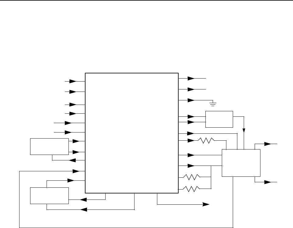
UHF (403-470 MHz) Frequency Synthesis 2-7
4.2 Fractional-N Synthesizer
The LVFRAC-N synthesizer IC (U4201) consists of a pre-scaler, a programmable loop divider,
control divider logic, a phase detector, a charge pump, an A/D converter for low frequency digital
modulation, a balance attenuator to balance the high frequency analogue modulation and low
frequency digital modulation, a 13V positive voltage multiplier, a serial interface for control, and
finally a super filter for the regulated 5 volts.
Figure 2-3 UHF Synthesizer Block Diagram
A voltage of 5V applied to the super filter input (U4201 pin 30) supplies an output voltage of 4.5
VDC(VSF) at pin 28. It supplies the VCO, VCO modulation bias circuit (via R4322) and the
synthesizer charge pump resistor network (R4251, R4252). The synthesizer supply voltage is
provided by the 5V regulator U4211.
In order to generate a high voltage to supply the phase detector (charge pump) output stage at
pin 47 VCP (U4201-47), a voltage of 13 VDC is being generated by the positive voltage multiplier
circuitry (D4201, C4202, C4203). This voltage multiplier is basically a diode capacitor network driven
by two (1.05MHz) 180 degrees out of phase signals (U4201-14 and -15).
Output LOCK (U4201-4) provides information about the lock status of the synthesizer loop. A high
level at this output indicates a stable loop. IC U4201 provides the 16.8 MHz reference frequency at
pin 19.
The serial interface (SRL) is connected to the microprocessor via the data line DATA (U4201-7),
clock line CLK (U4201-8), and chip enable line CSX (U4201-9).
DATA
CLK
CEX
MODIN
VCC, DC5V
XTAL1
XTAL2
WARP
PREIN
VCP
REFERENCE
OSCILLATOR
VOLTAGE
MULTIPLIER
DATA (U0101 PIN 100)
CLOCK (U0101 PIN 1)
CSX (U0101 PIN 2)
MOD IN (U0221 PIN 40)
+5V (U4211 PIN 1)
7
8
9
10
13, 30
23
24
25
32
47
VMULT2 VMULT1
BIAS1
SFOUT
AUX3
AUX4
IADAPT
IOUT
GND
FREFOUT
LOCK 4
19
6, 22, 33, 44
43
45
3
2
28
14 15
40
FILTERED 5V
STEERING
LOCK (U0101 PIN 56)
PRESCALER IN
FREF (U0221 PIN 34)
39
BIAS2
41
48
5, 20, 34, 36
+5V (U4211 PIN 1)
AUX1
VDD, DC5V MODOUT
U4201
LOW VOLTAGE
FRACTIONAL-N
SYNTHESIZER
AUX2 1 (NU)
BWSELECT
VCO Bias
TRB
To IF
Section
TX RF INJECTION
(1ST STAGE OF PA)
LO RF INJECTION
VOLTAGE
CONTROLLED
OSCILLATOR
LINE
2-POLE
LOOP
FILTER
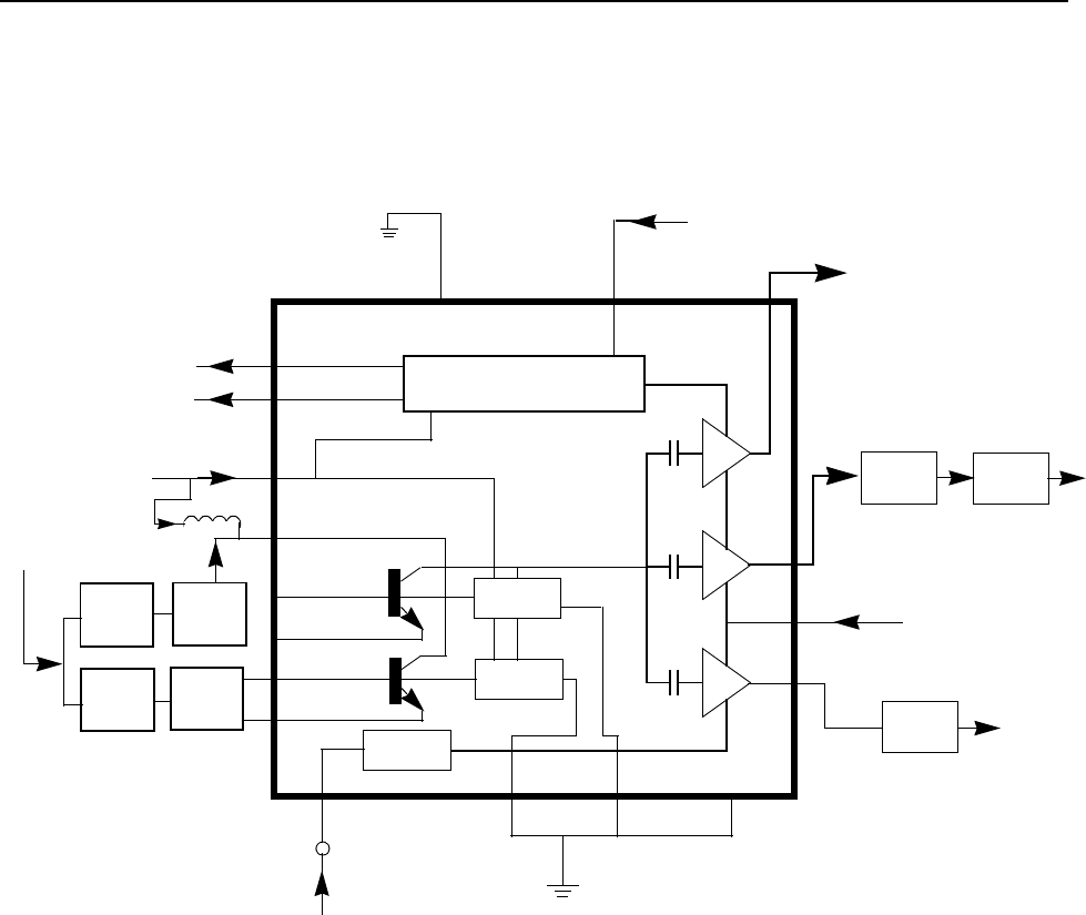
2-8 UHF (403-470 MHz) Frequency Synthesis
4.3 Voltage Controlled Oscillator (VCO)
The Voltage Controlled Oscillator (VCO) consists of the VCO/Buffer IC (VCOBIC, U4301), the TX
and RX tank circuits, the external RX buffer stages, and the modulation circuitry.
Figure 2-4 UHF VCO Block Diagram
The VCOBIC together with Fractional-N synthesizer (U4201) generates the required frequencies in
both transmit and receive modes. The TRB line (U4301 pin 19) determines which tank circuits and
internal buffers are to be enabled. A high level on TRB enables TX tank and TX output (pin 10), and
a low enables RX tank and RX output (pin 8). A sample of the signal from the enabled output is
routed from U4301 pin 12 (PRESC_OUT), via a low pass filter, to pin 32 of U4201 (PREIN).
A steering line voltage (VCTRL) between 3.0V and 10.0V at varactor diode CR4311 will tune the full
TX frequency range (TXINJ) from 403 MHz to 470 MHz, and at varactor diodes CR4301, CR4302
and CR4303 will tune the full RX frequency range (RXINJ) from 358 MHz to 425 MHz. The tank
circuits uses the Hartley configuration for wider bandwidth. For the RX tank circuit, an external
transistor Q4301 is used in conjunction with the internal transistor for better side-band noise.
Presc
RX
TX
Matching
Network Low Pass
Filter
Attenuator
Pin8
Pin14
Pin10
(U4201 Pin28)
VCC Buffers
TX RF Injection
U4201 Pin 32
AUX3 (U4201 Pin 2)
Prescaler Out
Pin 12Pin 19
Pin 20
TX/RX/BS
Switching Network
U4301
VCOBIC
Rx
Active Bias
Tx
Active Bias
Pin2
Rx-I adjust
Pin1
Tx-I adjust
Pins 9,11,17
Pin18
Vsens
Circuit
Pin15
Pin16
RX VCO
Circuit
TX VCO
Circuit
RX Tank
TX Tank
Pin7
Vcc-Superfilter
Collector/RF in
Pin4
Pin5
Pin6
RX
TX
(U4201 Pin 28)
Rx-SW
Tx-SW
Vcc-Logic
(U4201 Pin 28)
Steer Line
Voltage
(VCTRL)
Pin13
Pin3
TRB IN
LO RF INJECTION
Q4301
Q4332

UHF (403-470 MHz) Frequency Synthesis 2-9
The external RX buffers (Q4332) are enabled by a high at U4201 pin 3 (AUX4) via transistor switch
Q4333. In TX mode the modulation signal (VCOMOD) from the LVFRAC-N synthesizer IC (U4201
pin41) is applied modulation circuitry CR4321, R4321, R4322 and C4324, which modulates the TX
VCO frequency via coupling capacitor C4321. Varactor CR4321 is biased for linearity from VSF.
4.4 Synthesizer Operation
The complete synthesizer subsystem comprises mainly of low voltage FRAC-N (LVFRACN) IC,
Reference Oscillator (crystal oscillator with temperature compensation), charge pump circuitry, loop
filter circuitry and DC supply. The output signal PRESC_OUT of the VCOBIC (U4301 pin 12) is fed
to pin 32 of U4201 (PREIN) via a low pass filter (C4229, L4225) which attenuates harmonics and
provides the correct level to close the synthesizer loop.
The pre-scaler in the synthesizer (U4201) is basically a dual modulus pre-scaler with selectable
divider ratios. This divider ratio of the pre-scaler is controlled by the loop divider, which in turn
receives its inputs via the SRL. The output of the pre-scaler is applied to the loop divider. The output
of the loop divider is connected to the phase detector, which compares the loop divider´s output
signal with the reference signal.The reference signal is generated by dividing down the signal of the
reference oscillator (Y4261 or Y4262).
The output signal of the phase detector is a pulsed DC signal which is routed to the charge pump.
The charge pump outputs a current at pin 43 of U4201 (IOUT). The loop filter (which consists of
R4221-R4223, C4221-C4225,L4221) transforms this current into a voltage that is applied to the
varactor diodes CR4311 for transmit, CR4301, CR4302 & CR4303 for receive and alters the output
frequency of the VCO .The current can be set to a value fixed in the LVFRAC-N IC or to a value
determined by the currents flowing into BIAS 1 (U4201-40) or BIAS 2 (U4201-39). The currents are
set by the value of R4251 or R4252 respectively. The selection of the three different bias sources is
done by software programming.
To reduce synthesizer lock time when new frequency data has been loaded into the synthesizer the
magnitude of the loop current is increased by enabling the IADAPT (U4201-45) for a certain
software programmable time (Adapt Mode). The adapt mode timer is started by a low to high
transient of the CSX line. When the synthesizer is within the lock range the current is determined
only by the resistors connected to BIAS 1, BIAS 2, or the internal current source. A settled
synthesizer loop is indicated by a high level of signal LOCK (U4201-4).
The LOCK (U4201-4) signal is routed to one of the µP´s ADCs input U101-56. From the voltage the
µP determines whether LOCK is active. In order to modulate the PLL the two spot modulation
method is utilized. Via pin 10 (MODIN) on U4201 the audio signal is applied to both the A/D
converter (low freq path) as well as the balance attenuator (high freq path). The A/D converter
converts the low frequency analogue modulating signal into a digital code that is applied to the loop
divider, thereby causing the carrier to deviate. The balance attenuator is used to adjust the VCO’s
deviation sensitivity to high frequency modulating signals. The output of the balance attenuator is
present at the MODOUT port (U4201-41) and connected to the VCO modulation diode CR4321 via
R4321, C4325.

2-10 UHF (403-470 MHz) Frequency Synthesis
THIS PAGE INTENTIONALLY LEFT BLANK

3-1
Section 3
TROUBLESHOOTING CHARTS
1.0 Troubleshooting Flow Chart for Receiver (Sheet 1 of 2)
Bad SINAD
Bad 20dB Quieting
No Recovered Audio
START
Audio at
pin 8 of
U3101 ?
Check Controller
(in the case of no audio)
OR ELSE go to “B”
Yes
No
Spray or inject 44.85MHz
into XTAL Filter FL3101
Audio heard ?
BYes
No
Check 2nd LO
(44.395MHz) at C3135
LO present ?
B
Yes
Check voltages on
U3101
Biasing OK ?
No
No
A
Yes
Check Q3102 bias
for faults
Replace Q3102
Go to B
Yes
No
Check circuitry
around U3101.
Replace
U3101 if defect
Check circuitry around Y3101.
Replace Y3101 if defect
Voltages
OK?

3-2 Troubleshooting Flow Chart for Receiver
1.1 Troubleshooting Flow Chart for Receiver (Sheet 2 of 2)
IF Signal at
C3101?
No
RF
Signal at
T4051?
RF
Signal at
C4015?
No
No
RF
Signal at
C4025?
No or
Check harmonic filter
L4491-L4493, C4492, J4401
and ant. switch
D4471, D4472, L4472.
Check filter between
C4025 & C4009.
Check tuning voltage
at R4060.
Inject RF into J4401
Is
tuning voltage
OK?
No
Yes
Check RF amp (Q4003)
Stage.
Check filter between
C4015 & T4051.
Yes
Check T4051, T4052,
D4051, R4052, L4008.
Yes
1st LO level
OK?
Locked?
Yes
Check FGU
Yes
Trace IF signal
from C3101 to
Q3101. Check for
bad XTAL filter.
No
Yes IF
signal at Q3102
collector?
Before replacing
U3101, check
U3101 voltages.
Yes
Check for
5VDC
Is 9V3
present?
Check Supply Voltage
circuitry. Check Q0681,
U4211 and U0641.
No
No
No
Check U4501.
Check varactor filter.
No
Yes
Yes
Yes
A
A
B
weak RF
RF
Signal at
C4009?
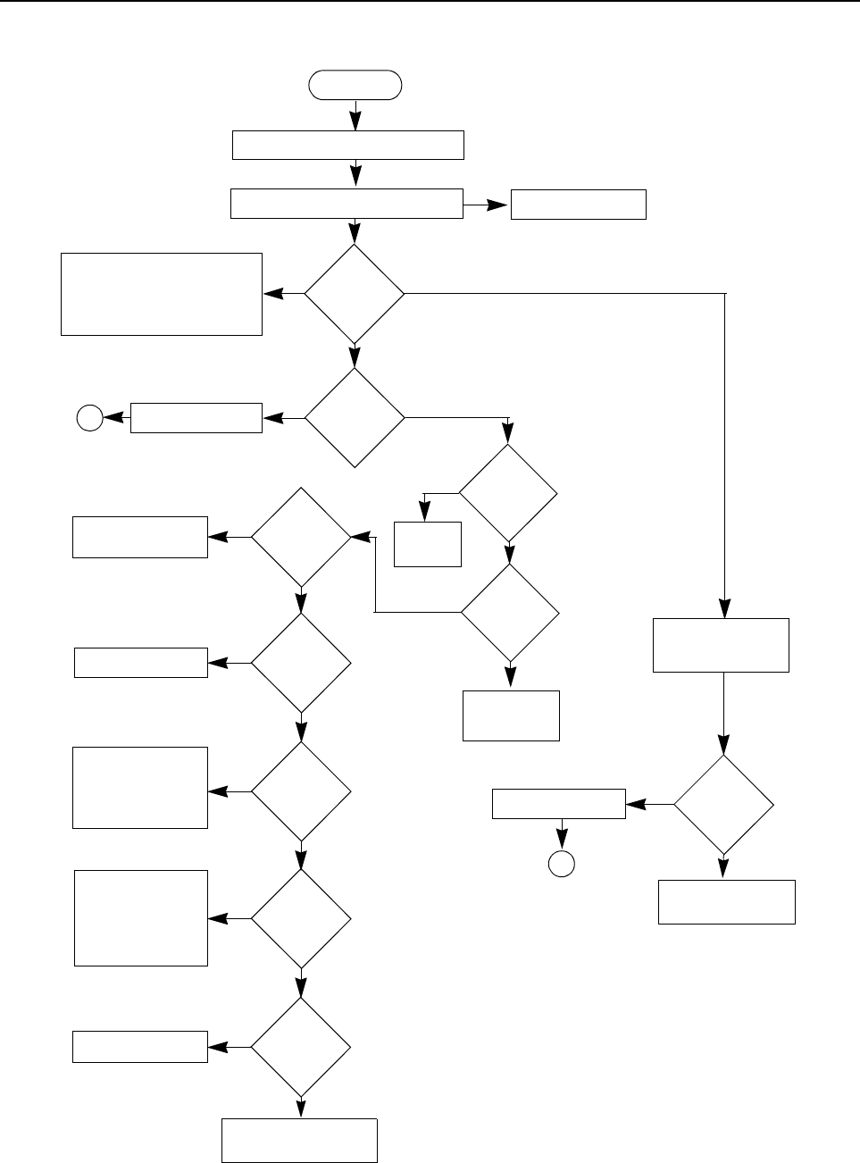
Troubleshooting Flow Chart for 40W Transmitter 3-3
2.0 Troubleshooting Flow Chart for 40W Transmitter (Sheet 1 of 2)
Control Volt-
age at
TP4533
>1V
Current
increase
when
keyed?
NO
YES
START
Check if Pressure Pad closes S5440
Check Components between
Q4441 and RF Output,
Antenna Switch
D4471,D4472,Q4472,
VR4471,Q4471
>500mA & <6A
>6A
<500mA
Check PA Stages
Short TP4531 to
Ground
NO
NO
Voltage at
TP4533
rises?
Check PA Stages YES
YES
PCIC U4501
Pin 14 9.3V
DC?
Check 9.3 V Regulator
U0641
NO
YES
PCIC U4501
Pin 16 >4V
DC
Replace PCIC U4501
NO
YES
TP4530
9.1V DC
If U4201 Pin 2 is high,
replace PCIC
U4501,otherwise
check controller and
FGU
YES
NO
TP4531
>0.5V DC?
Replace PCIC U4501
Check Forward Power
Sense Circuit (D4451)
Check Forward Power
Sense Circuit (D4451)
NO
YES
PCIC U4501
Pin 5 > 1V
DC?
Check Power Setting,
Tuning & Components
between PCIC Pin 5
and ASFIC (U0221)
Pin 4 before replacing
ASFIC
No or too low Power when keyed
Put in pressure pad
YES
NO
1
Is Q4473
OK?
Change
Q4473
NO
YES
Check voltage
on pin 4
U4501
NO
YES
Check
R4422-5 and
go back to top
1
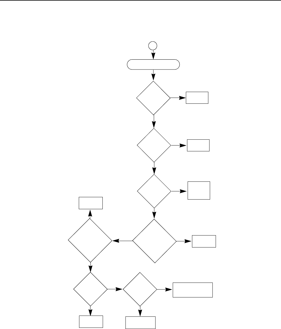
3-4 Troubleshooting Flow Chart for 40W Transmitter
2.1 Troubleshooting Flow Chart for 40W Transmitter (Sheet 2 of 2)
Check PA Stages
YES
Check
MOSBIAS_2/
MOSBIAS_3
YES
Are D4471 &
D4472 OK?
Check
ASFIC
NO
YES
Check Q4421
gate (12kohm)
and drain resis-
tances (15kohm)
NO Change
Q4421
Is drive from
VCO
>+4dBm?
Do visual check on
all components
YES
Is voltage drop
across R4497
>4.5V?
NO
1
Check
PCIC_MOS
BIAS_1
Check
PCIC
Change
D4471 &
D4472
Check Q4441
gate (63kohm)
and drain resis-
tances (15kohm)
NO
YES
Change
Q4441
NO
Change
U4401
YES
YES
NO
NO
Troubleshoot
VCO
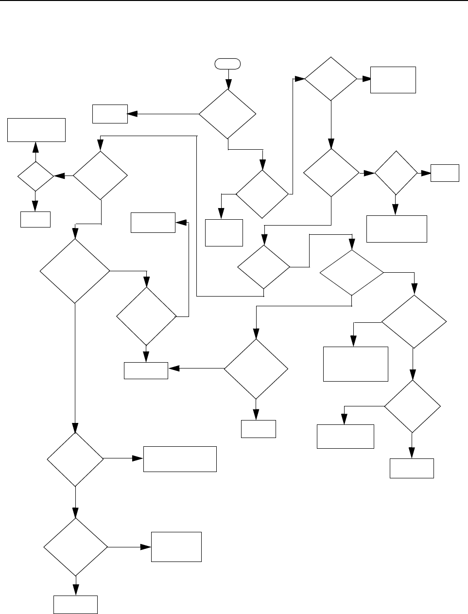
Troubleshooting Flow Chart for Synthesizer 3-5
3.0 Troubleshooting Flow Chart for Synthesizer
5V
at pin 6 of
D4201
Is
information
from µP U0101
correct
?
Is
U4201 Pin 47
at = 13VDC
?
Is
U4301 Pin 19
<40 mVDC in RX &
>4.5 VDC in TX?
(at VCO section)
?
Start
Visual
check of the
Board
OK?
Correct
Problem
Check 5V
Regulator
U4211
+5V
at U4201
Pins
13 & 30
?
Is
16.8MHz
Signal at U4201
Pin 19
?
Check
Y4261 / Y4262 and
associated parts
Are
signals
at Pins 14 &15
of U4201
?
Check
R4201 Check C4381
Is
U4201
Pin 2 >4.5 VDC in
Tx & <40 mVDC
in Rx
?
Replace
U4201
Remove
Shorts
Is
there a short
between Pin 47 and
Pins 14 & 15 of
U4201
?
Replace or
resolder
necessary
components
Is
RF level at
U4201 Pin 32
-12 < x <-25
dBm
?
Are
R4221,R4222,
R4223,C4221,
C4222 & C4223
OK?
Replace
U4201
If L4225, C4229 & C4227
are OK, then see VCO
troubleshooting chart
Are
Waveforms
at Pins 14 & 15
triangular
?
Do
Pins 7,8 & 9
of U4201 toggle
when channel is
changed?
Check programming
lines between
U0101 and U4201
Pins 7, 8 & 9
Replace
U4201
Check µP U0101
Troubleshooting
Chart
NO
YES
NO
YES
NO
YES
NO
NO
NO
YES
YES
NO
YES
YES
NO
YES
YES
YES
NO
NO
NO
NO
YES
NO
YES
YES
Check D4201,
C4202, C4203, &
C4206
5V
at U4201
pins 5, 20, 34
& 36
C h e c k 5 V
Regulator
U4211
Is
16.8MHz
signal at
U4201 Pin
23?
Replace
U4201
YES
NO
NO
YES
NO
YES
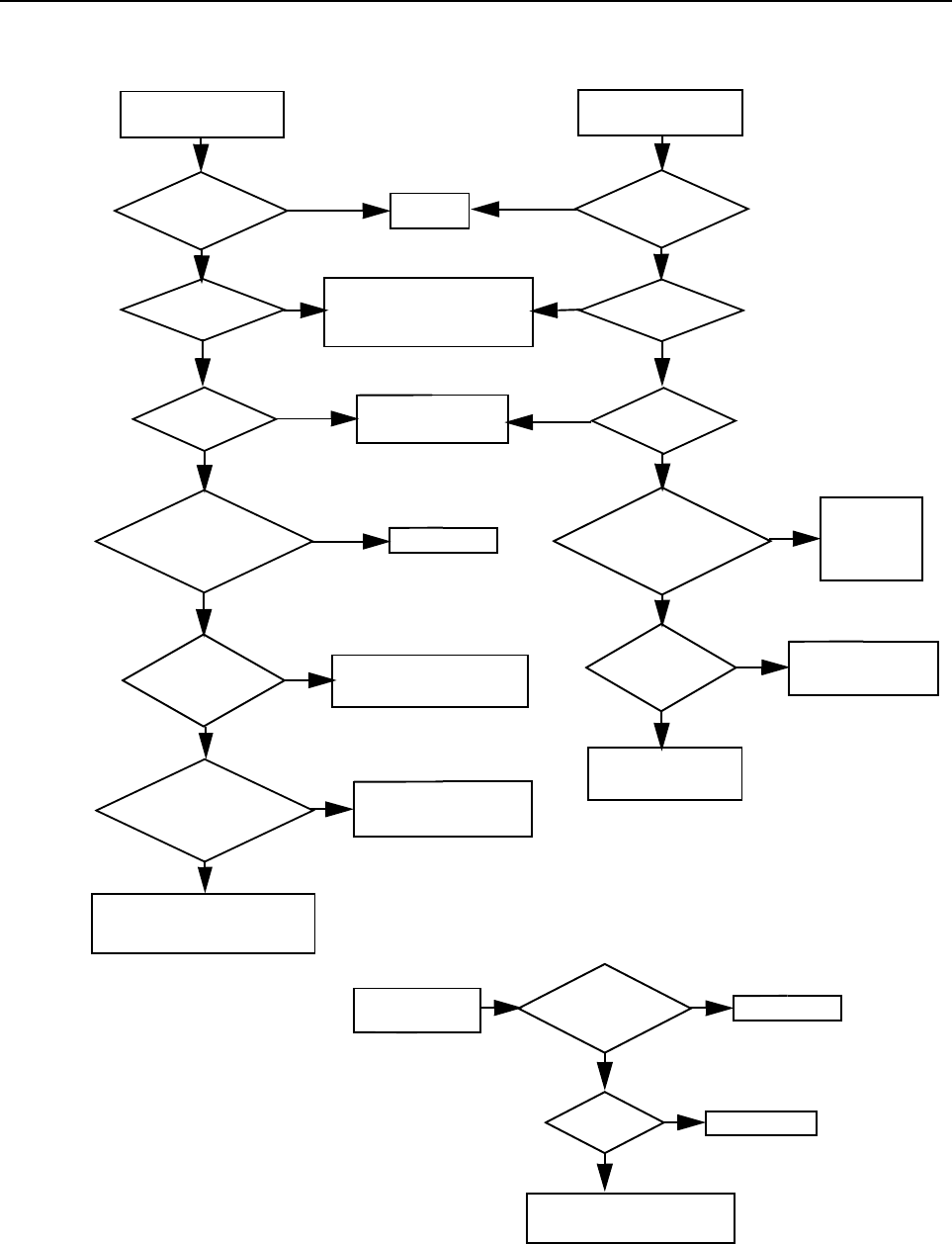
3-6 Troubleshooting Flow Chart for VCO
4.0 Troubleshooting Flow Chart for VCO
Are Q4332
Base at 0.7V
Collector at 4.5V
Emitter at 110mV
Are Q4301
Base at 2.4V
Collector at 4.5V
Emitter at 1.7V
Are U4301 Pins
13 at 4.4V
15 at 1.1V
10 at 4.5V
16 at 1.9V
Low or no RF Signal
at TP4003
Visual check
of board
OK?
35mV DC at
U4301 Pin 19
NO
YES
Replace Q4301
at base of Q4332
NO
NO
NO
NO
YES
YES
YES
YES
Low or no RF Signal
at input to PA
4.8V DC at
U4301 Pin 19
Is RF available
at C4402
YES
YES
YES
YES
NO
NO
NO
NO
NO
Audio =180mVrms
at “-” S
ide of
4.5VDC
at CR4321
If C4321 and R4321 are OK,
then replace CR4321
Replace C4322
Replace C4325
NO
NO
YES
YES
If parts between
R4402 & U4301 Pin10
are OK, replace U4301
TX VCO
RX VCO
Correct
Problem
Visual check
of board
OK?
Check runner
between U4201 Pin 2
and U4301 Pin 19
Is RF available If all parts from U4301 Pin 8
to Base of Q4332 are OK,
replace U4301
If all parts associated
with the pins are OK,
replace Q4332
If all parts from collector
of Q4332 to TP4003 are
OK, Replace Q4332
Power OK but
no modulation
Check parts from
R4402 to U4401 Pin16
If all parts
associated
with the pins
are OK,
replace U4301
YES
YES
Make sure Synthesizer is
working correctly and runner
between U4201 Pin 28 and
U4301 Pin 14 & 18 are OK
4.5V DC
OK ?
OK? OK?
C4325
at U4301 Pin 14 & 18
4.5V DC
OK ?
at U4301 Pin 14 &18
NO

4-1
Section 4
UHF PCB/SCHEMATICS/PARTS LISTS
1.0 Allocation of Schematics and Circuit Boards
1.1 Controller Circuits
The UHF circuits are contained on the Printed Circuit Board (PCB) which also contains the
Controller circuits. This Chapter shows the schematics for the UHF circuits only, refer to the
Controller section for details of the related Controller circuits . The PCB component layouts and the
Parts Lists in this Chapter show both the Controller and UHF circuit components. The UHF
schematics and the related PCB and parts list are shown in the tables below.
Table 4-1 UHF 25-40W Diagrams and Parts Lists
PCB : 8486127Z01 Main Board Top Side
8486127Z01 Main Board Bottom Side Page 4-3
Page 4-4
SCHEMATICS
Power Amplifier 25 - 40W
FRACN
Voltage Controlled Oscillator
Receiver Front End
IF
Page 4-5
Page 4-6
Page 4-7
Page 4-8
Page 4-9
Parts List
8486127Z01 Page 4-10

4-2 Allocation of Schematics and Circuit Boards
THIS PAGE INTENTIONALLY LEFT BLANK
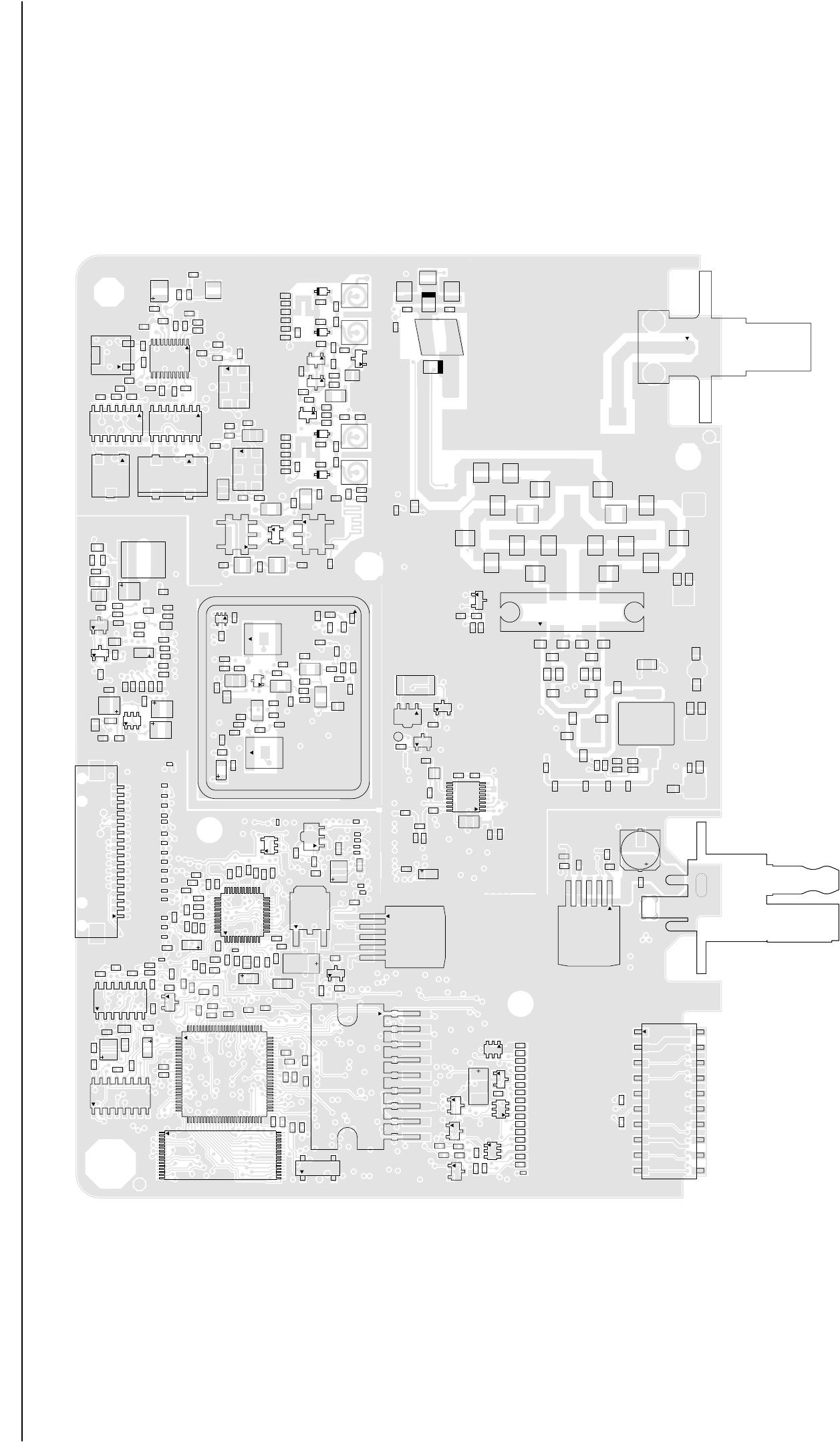
UHF 25-40W PCB / Schematics / Parts List 4-3
2.0 UHF 25-40W PCB / Schematics / Parts List
C0108
C0211
C0212
C0251
C0252
R0103
R0211
R0212
R0251
R0252
R0253
R0257
16
1
89
U0251
C0253
C0256
C0261
C0262
R0256
R0268
R0269
87
114
U0211
C0421 C0441
C0442
C0443 C0445
C0446
C0447
Q0110 R0222
R0261
R0262 R0442
C0104
C0106
C0224
C0226
C0227
C0228
C0232
C0233
C0236
C0237
C0495
R0101
R0102
R0104
R0108
R0110
R0115
R0116
R0226
R0227
R0228
C0221 C0222
C0225
C0241
C0243
R0220
R0221
R0223
R0224
R0229
R0254
R0255
C0235
C0242
C0244
C0245
C0246
C0496
D0201
R0241
R0242
137
25
13
U0221
R0681
C0101
C0102
C0131
C0132
R0105
R0106
R0114
R0131
R0132
R0170
51
32
17
4
Y0131
16 1
U0121
1
26
U0101
C0223
C0231
C0234
C0651
C0652
D0651
R0225
R0651
R0652
3
2
1
U0651
C0482
C0483
C0487 C0488
C0493
C0494
C0654
C0681
L0481
L0482
Q0681
R0682
C0486
C0655
C0542
Q0177
Q0181
Q0185 R0181
R0182
R0185
R0186
R0510
R0535
R0538
R0539
VR0501
VR0503
VR0505
VR0510
C0501
C0502
C0503
C0504
C0505
C0506
C0508
C0509
C0510
C0511
C0512
C0513
C0514
C0515
C0516
C0517
C0518
U0271
76
2011
10
J0501
R0508R0509
J0601
C0484
C0601
C0603
C0612
R0533
R0611
R0612
1
6
5
U0611
C4417
C4419
C4425
C4426
C4431
C4447
C4453
C4454
C4457
C4461
C4462
C4481
M3421
R4408
R4415
R4416
R4480
C4420
C4427
C4428
C4429
C4430
C4432
C4433
C4434
C4435
C4440
C4441
C4446
C4458
L4474
3
2
1
45
6
7
8
Q4441
R4417
R4418
C4485 C4489
C4490
C4495
C4497
C4602
C4442
C4443
C4449
C4466
C4476
C4478 C4491
C4493
L4489
C4401
C4403
C4404
C4407
C4410
C4418
C4488
C4505
C4506
L4401
L4403
Q4471
R4401 R4402
R4403
R4405
R4504
TP4530
1
16
8
9
U4401
Q4472
R4511
R4512
VR4471
C4444
C4445
C4450
C4455
C4456
C4467
C4477
C4487
C4521
C4522
L4490
R4501
R4502 U4502
C4459
C4507
18
1
J0451
C0448
C0449
C0470
C0471
C0472
C0473
C0474
C0476
C0477
C0478
C0490
C4472
C4474
C4475
C4480
C4510
D4471 D4472
L4472
L4473
C4001C4002
C4009
C4014
C4026
C4027 D4001
D4002
D4003 L4001
L4002
L4006
Q4001 Q4003 R4003
R4004
R4020
R4022
C4317
C4318
C4322
C4323
C4325
C4351 C4352
C4355
C4382
1
3
L4312
L4313
R4302
R4311
R4312
R4321 C4308 C4309
C4353
C4383
1
3
L4303
L4304
L4305
Q4301
R4301
R4305
R4346
C4375
43
Q4333
C4331
C4332
C4335
C4337
C4339
C4354
C4371
C4372 C4373 C4374
L4331
L4371
R4331
R4332
R4333
R4337
R4341 R4343
R4345
SH4301
C4031
C4053
C4054
C4055
D4051
L4008
L4053
L4054
R4051
21
54
3
T4051
2
1
54
3
T4052 C3101 2
3
45
FL3101
L3100
R3148
C4051
C4052
L4051
R4013
R4014
R4015
C4015
C4016
C4017C4018
C4019
C4020
C4021
C4022
C4023
C4029
C4030
C4065
C4068
D4004
D4005
D4006
L4003
L4004
L4005
R4005
R4007
R4012
R4064
R4066
C4003
C4004
C4005
C4006
C4007
C4008
6
C3102
C3103 2
3
456
FL3102
L3101
R3101
R3106
C3114
C3115
C3124
C3131
C3132
C3133
C3134
C3135
C3136
C3137
C3143
L3124
R3111
R3117
R3124
R3130
R3132
R3135
11
1
20
10
U3101
R3123
C3140
C3141
C3142
87
1
14
U3111
2
C3139
R4001
C3145
C3148
4
3
FL3112
FL3114
R3142
R3144
R3145
87
1
14
U3115 2
Y3102
C4221
C4222
C4223
C4224
C4225
C4226
C4227
C4229
C4230
C4231
C4236
C4253
D4221
L4221
Q4221
R4221
R4222
R4223
R4224
R4225
R4227
C4210
C4213
C4216
C4217
C4242
C4243
C4245
C4289
L4201
R4211
U4211
C4214
C4215
C4244
C4246
C4232
C4233
C4234
C4251
C4252
C4254
C4255
R4251
R4252
23
9
1
6
5
U0641
C0107
32
J4401
UHF (403-470 MHz) 25-40W 8486127Z01 Top Side
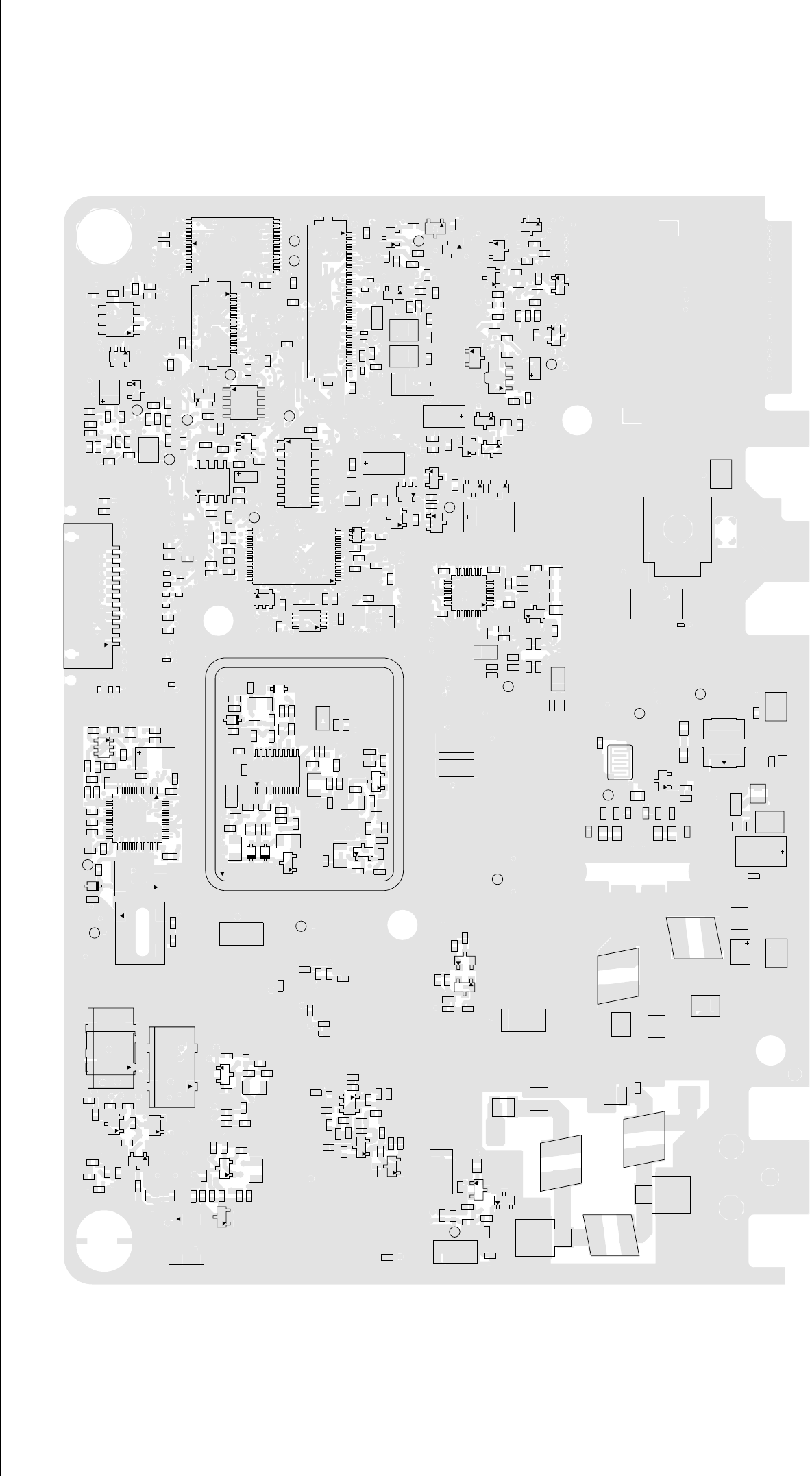
4-4 UHF 25-40W PCB / Schematics / Parts List
4
3
2
Y3101
C3122
C3123
D3101 Q3102
R3113
R3114
R3115
R3116
R3133
C3116
R3118
C3121
L3112
R3112
C3104
C3110
C3111 C3112
C3113
L3111
Q3101
R3102
R3104
R3105
R3107
R3108
C3144
C3146C3147
C3151
C3152
Q3141
Q3151
Q3152
R3134
R3141
R3146
R3147
R3151
R3152
R3153
R3154
43
2
FL3111
FL3113
43
2
FL3115
C4261
C4262
C4263 D4261
R4261
TP4201
TP4202
4
3
1
Y4261
2
34
Y4262
6
C4235
R4263
L4231
C4201
C4202
C4203
C4204
C4205
C4206
C4207
C4208
C4209
C4211
C4228
C4241
C4287
C4288 D4201
R4201
R4203
R4204
R4206
R4228
R4241
R4262
1
37
25 13
U4201
C0422 C0423
C0426
C0427
C0428
C0429
C0485
C0491
C0492
C0497
J0401
R0407 R0409
R0467
12
C0430C0431
F0401
R0412R0441
C0201
C0202
C0203 C0204
C0205
C0254
C0265
C0266
C0267
R0201
R0202
R0203
R0204
R0205
R0206
R0207
R0208
R0265
R0266 R0267
R0408 TP0102
TP0221
TP0222
VR0541 C0105C0121
C0122
C0123
C0255
R0107
R0468
R0543
R0555
R0593
14
58
U0652
U0653
C4301
C4302
C4303
C4304
C4305
C4306
C4307
C4316
CR4301
CR4302
CR4303
L4301
L4302
R4303
R4304
R4315
11
120
10
U4301
C4311
C4312
C4313
C4314
C4315
C4319
C4321
C4324
C4381
CR4311
CR4321
L4311
R4313
R4314
R4322
R4323
R4381
C4010
C4011
C4012
C4013
C4028
C4061
C4062
C4064
C4067
C4069
D4007
Q4002
Q4004
R4002
R4016
R4017
R4018
R4061
R4062
R4063
R4068
R4069
R4070
R4071
R4072
C4025
C4024
C4060
C4066
R4052
R4053
R4054
R4055
R4060
C4451
C4463
C4469
C4470
C4473 C4499 D4452
R4455
R4457
R4472
R4475
R4496
TP4531
VR4473
C4494 C4498
L4491
L4493
C4448
C4496
L4492
R4491
C4452
C4464
D4451
D4453
R4409R4473
R4474
R4506
R4507
R4471
TP4532
C4492
C4336
L4333
R4019
SH4302
TP4003
C4333
C4334
C4338
C4361
C4362
C4363
C4364 C4365
L4332
L4361
L4362
Q4331
Q4332
R4334
R4335
R4336
R4338
R4339
R4340
R4342
R4344
R4347
R4360
R4361
R4362
R4363
C4422
C4423
C4437 C4439
L4421
L4436
L4437
L4438
C4424
C4629
C4630
C4631
C4632
Q4451
R4414
R4440
R4481
R4485
R4486
R4487
R4488
R4489
R4630
R4631
R4632
R4634
R4635
S4440
TP4537
TP4538
C4421
C4436
C4438
C4483
C4484
L4402
L4541
L4543
12
3
Q4421
R4513
R4525
TP4536
C0499
C0611
E0631
VR0601
R4495 R4497
C4402
C4405
C4409
C4412
C4413
C4414
C4415
C4416
L4404
L4411
Q4473
R4412R4428
R4431
R4482
R4484
R4503
TP4533 C4502
C4503
R4422
R4423
R4424
R4425
R4483
R4514
R4523
C4504
C4479
1
17
9
25
U4501
R4492
C0304C0305
C0324C0325
C0343
R0323
R0324
R0341
R0344 R0345
TP0497
28 15
C0331
C0353
C0354
C0641
C0644
C0645
C0662
C0663
C0671
Q0641 Q0661
Q0662
Q0663
R0331
R0332
R0333
R0335
R0481
R0482 R0641
R0642
R0643
R0661
R0662 R0671 R0672
TP0661
U0331
C0301
C0302
C0303
C0351
C0352
D0301
14
1
U0301
4
58
U0351
C0344R0346
1
45
8
U0341
C0111
C0112
C0141
C0341
C0342
D0101
R0342
R0343
R0347
R0401
TP0101
TP0104
1
4
58
U0111
16
1
U0141
U0342
8
9
R0111
R0117
C0103
1
18
J0552
R0112
R0113 R0121 TP0103
TP0492
21 8
U0122
22 7
1
C0151
C0271
C0272
C0273
C0274
C0554
C0593
D0151
Q0151
Q0271
R0151 R0152
R0273
R0274
R0275
R0276
TP0151
VR0151
C0558 C0559
C0560
C0591
C0592
R0591
R0592
C0575
C0576
C0275
C0276 C0277
E0271 E0272
1
40
J0551
C0621
C0622
C0661 D0621
D0660
D0661
R0173
R0174
R0621
VR0621
VR0671
C0541
D0179
Q0171
Q0173
Q0183
R0171
R0172 R0175
R0176
R0177
R0178
R0179
R0183
R0184
R0511
R0512
R0525 R0529
R0530
R0531
R0537
R0541
R0542
TP0530
VR0504 VR0509
VR0537
R0556
UHF (403-470 MHz) 25-40W 8486127Z01 Bottom Side
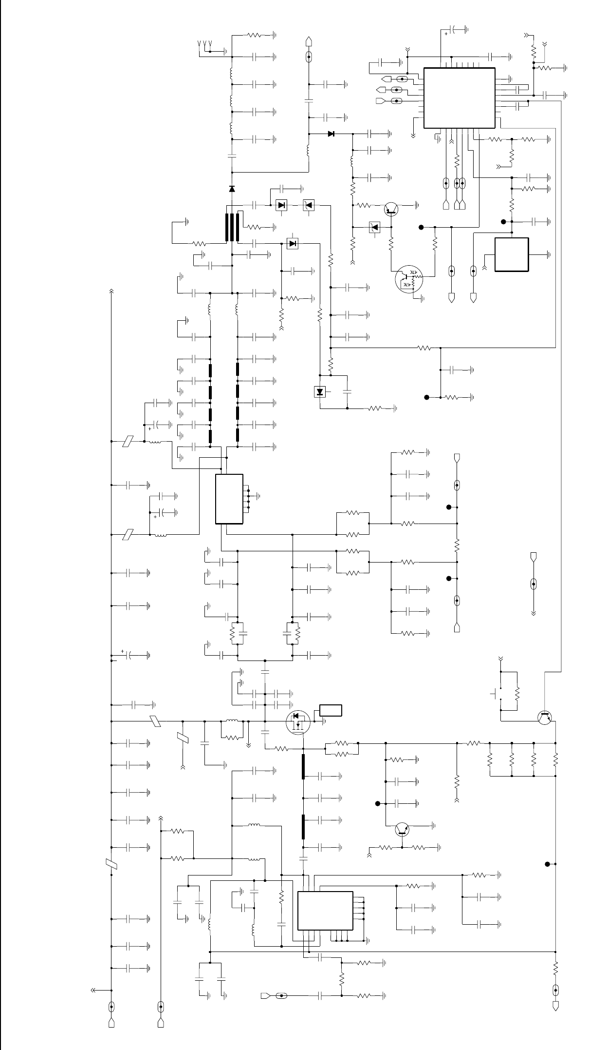
UHF 25-40W PCB / Schematics / Parts List 4-5
PASUPVLTG_UHF_PA_1
PASUPVLTG
PASUPVLTG
9V3
9V3_UHF_PA_1
C4602
.033uF 3000pF
C4481
C4485
30pF
L4402
30pF
C4484
.033uF
C4421
1000pF
C4495
NU
NU
C4490
1000pF
C4497
C4489
BLM31A02PT
L4474
L4541
NU
C4493 1000pF
C4478
C4436
10uF
NU
0.1uF
C4438
17nH
L4437
L4421
C4423 100pF
C4422 NU 100pF
C4439
L4438
17nH
C4437
L4436
NU
NU
13pF
C4442 C446630pF
C4441 6.8pF
C4443 C4491
3.3pF C4476
NU NU
C4445
6.8pF 3.3pF
C4487
13pF
C4444 C4467
C4440
30pF
C4477
100K
R4409
9V3
L4490
12.77nH
12.77nH
L4489
NU
C4455
C4449
3.9pF
NU
R4471
NU
C4450
3.9pF C4456 120
R4457
100pF
C4459
100pF
C4469
D4471
C4492
100pF 17nH
L4492
L4491
17nH
17nH
L4493
10pF
C4494 C4448
12pF
6.2pF
C4498 C4496
6.2pF
R4491
11K
RXIN
RX_IN_VHF_PA_1
NU
12pF
C4474
C4480 2pF
C4475
L4472
17nH
D4472
NU
5.6V
VR4473
D4452 C4463
D4451
NU
R4473
4.3K
C4452
NU
NU
100pF
C4499
R4472
100pF
C4507
R4506
10K
10K
R4513
C4470
A+
9.2 VDC
TP4530
CLK
R4504
10K
Q4471
K9V1_UHF_PA_1
470
R4512
K9V1
TEMPSENSE
0
R4475
TEMPSENSE_UHF_PA
9V3
1
POS
VOUT 2
U4502
3GND
NU
NU
C4405
C4402
TXINJ
NU
L4404
3.9pF
C4403
L4401
11.03nH C4404
100pF
0.1uF
C4407 R4405
200
4 to 6 dBm
TX_INJ_UHF_PA_1
100pF
C4410 100pF
C4401
R4402
15
300
R4401 300
R4403
CNTLVLTG
CNTLVLTG_UHF_PA_1
3.3K
R4514
C4418
0.1uF
51
R4497
C4488
100pF
390nH
L4403 100pF
C4412
390nH
L4411
NU
NU
NU NU
NU
C4409
0.1uF
1
C4431
27pF
L4543
13.85nH
C4453
R4525
C4424
C4454
4.7pF
R4414
C4458
C4457
36pF
Load
POS 1
Q4421
2
3
NU
C4483
100pF
9V3
1
VD1
14 VG1 2
VG2 3
13
NC1
8
NC2
9
NC3
10
NC4
15
RFIN
16 RFOUT1 6
RFOUT2 7
VCNTRL
U4401
30C65
EP
17
G2
11
GND1
4
GND2
5
GND3
12
GND4
C4417
100pF
NU NU
NU
C4447 C4419
C4461 C4462
39pF
100
R4415 R4416
100 M3421
HEATSINK
.022uF
C4416
.022uF
C4414
100pF
C4415
100pF
C4413
1.8K
R4428
R4412
2K
3.7 to 3.9 VDC
NU
NU
NU
Q4451
.022uF
C4425 20K
R4408
100pF
C4426
R4488
R4487
TP4536
Load
10K
R4480
PCIC_MOSBIAS_1
620
R4424
620
R4423
620
R4422
NU
R4431
R4425
620
6.2 VDC (28W)
6.5 VDC (44W)
Q4473
R4440
NU
S4440
SWITCH
9V3
PA_PWR_SET
PA_PWR_SET_1_UHF_PA_1
PA_PWR_SET
NU
BIAS_2_UHF_PA_1
TP4537
R4630
MOSBIAS_2
100pF
C4632
0.1uF
C4631
100K
R4634
4.4 VDC (28W)
4.5 VDC (44W)
TP4533
NU
NU
C4434
3.9pF C4446
150pF
R4417
C4429
C4433
47pF
12pF
C4420
51
R4495
9V3
NU
NU
3.9pF
C4427 C4435
12pF
C4430
R4418
150pF
C4428
47pF
C4432
51
R4485
R4486
51 51
R4481 R4489
51
C4630
0.1uF
R4635
100pF 100K
C4629
47K
R4631
47K
R4632
MOSBIAS_3
BIAS_3_UHF_PA_1
TP4538
GND5
GND6
IN1
IN2
OUT1
OUT2
Q4441
GND1
GND2
GND3
GND4
NU
D4453
C4464 100K
R4474
R4507
10K
NU
2.2 VDC (28W)
3.11 VDC (44W)
NU
TP4531
R4455 C4451
36pF
C4472
C4510
36pF
82
R4496
C4473
100pF
51
R4511
VR4471
5.6V
43.67nH
L4473
Q4472
PCIC_MOSBIAS_1
CSX
DATA
DATA_VHF_PA_1
10K
R4492
CSX_VHF_PA_1
CLK_VHF_PA_1
9V3
0.75 VDC
TP4532
R4501
24
VAR3
15
VG
VL
6VLIM 19
RX 23
T1
2
TEMP
30
V10 14
V45 16
17
V5EXT
20
VAR1
18
VAR2
GND2
25
INT
4
22
NA
Q11
QX 10
1RFIN
RS 21
31 RSET
CJ
5
CL
7
CLK
26
CQ 12
13
CQXDATA
28
F168 9
GND1
8
U4501
ANO
32
BPOS
27
CEX
29
CI
3
C4522
1000pF
20K
R4484
100pF
C4521
6.8K
27K
R4502 R4503
1K
100K
R4482
9V3
NU
3.1 VDC (44W)
2.2 VDC (28W)
R4483
100K
R4523
C4503
470pF
2200pF
C4502
.01uF
C4504
ALT
PA_PWR_SET
C4506
2200pF
1uF
C4505
9V3
C4479
100pF
FE_CNTL_1_VHF_PA_1
RESET
FECTRL_1
RESET_VHF_PA_1
FE_CNTL_2_VHF_PA_1
FECTRL_2
J4401-3
3
J4401-2
2
J4401-1
1
A+
UHF (403-470 MHz) Power Amplifier 25-40W

4-6 UHF 25-40W PCB / Schematics / Parts List
NU
0 VDC (RX)
NU
NU
3.43 VDC
3.05 VDC (RX)
NU
4.97 VDC
2.48 VDC
NU
NU
4.58 VDC
3.79 VDC
2.48 VDC
4.97 VDC (25KHZ Chan. Spacing)
1.78 VDC (Rx)
4.97 VDC (TX)
5 VDC (Locked)
10.87 VDC
1.28 VDC
NU NU
NU
0 VDC (Unlocked)
2.63 VDC (TX)
VDC
4.97 VDC
NU
0 VDC (12.5KHZ Chan. Spacing)
2.52 VDC
2.5 to 11 VDC
1.76 VDC (Tx)
30mV - 80mV RMS
12.7 VDC
0 VDC
4.97 VDC
NU
1.8pF
(SOURCE)
NU
3.48
6.68 VDC
TP4201
C4204
100pF
R4204
47
2.2uF
C4214
INPUT 8
OUTPUT
1
SENSE
2SHUTDOWN 3
U4211
LP2951
5V_TAP
6
ERROR
5FEEDBACK 7
GND
4
TRB_UHF_FN_1
D4201
A1 6
A2 5
A3 4
1K1
2K2
3K3
16.8MHz
GND
2
OUT
3
4
VCC
1
VCNTL
C4211
Y4262
C4228
0.1uF
.01uF
C4205
VCTRL
47
R4203
C4216
5V
C4224
1uF
DATA
C4236
.047uF
VCOMOD_UHF_FN_1
IN_5V_RF_REG
0.1uF
C4208
C4233
2.2uF
R4228
47K
10uF
C4206
C4254
0.1uF
VCOBIAS_2_UHF_FN_1
C4226
C4209
0.1uF
47K
R4261
.01uF
C4203
VCTRL_UHF_FN_1
C4210
2.2uF
100
R4263
39K
R4251
510
R4222
C4201
100pF
R4252
30K
16_8MHz
C4232
.01uF
R4224
47K
C4223
R4262
100pF
C4245
2.2uH
C4229
L4231
R4201
150
C4262
CLK_UHF_FN_1
150
PRESC
R4221
16_8MHz_UHF_FN_1
100pF
VCOBIAS_2
VSF
C4244
D4261
.01uF
C4231
PRESC_UHF_FN_1
.018uF
C4212
390nH
L4201
C4242
100pF
4.7uF
C4253
BWSELECT_UHF_FN_1
MODINVCOMOD
.01uF
C4221
0
C4222
0.1uF
R4211
2.2uF
C4215
C4207
12uH
L4221
0.1uF
C4251
100pF
C4241 C4243
1000pF
VSF_UHF_FN_1
C4252
.01uF
C4235
LOCK
2.2uF
C4213
C4261
MODIN_UHF_FN_1
XTAL1
23
24
XTAL2
5V_UHF_FN_1
VBPASS
21
VCP
47
15 VMULT1
VMULT2
14 VMULT3
12 VMULT4
11
13 VRO
WARP
25
PVREF
35
REFSEL
18
SFBASE
27
SFCAP
26
SFIN
30
SFOUT
28
TEST1
37 TEST2
38
NC1
17
NC2
29
NC3
31
PD_GND 44
5PD_VDD
32
PREIN
PRE_GND 33
PRE_VDD
34
DGND
DVDD
36
FREFOUT
19
IADAPT
45
INDMULT
16
IOUT
43
4
LOCK
MODIN
10
MODOUT
41
AVDD
20
BIAS1
40
BIAS2
39
CCOMP
42
CEX
9
CLK
8
DATA
7
6
ADAPTSW
46
AGND 22
AUX1
48 AUX2
1AUX3
2AUX4
3
U4201
63A27
R4206
VDDA_UHF_FN_1
5V_UHF_FN_2
R4225
47K
100pF
C4246
C4225
510pF
LOCK_UHF_FN_1
D4221
.01uF
C4202
L4225
15nH
IN_5V_RF_REG_UHF_FN_1
2.2uF
C4230
100pF
C4255
CSX
R4223
68
CSX_UHF_FN_1
DATA_UHF_FN_1
OUT
3
IN
6
VDDA
Y4261
75Z04 16.8MHz
1
GND
4
GND1
0.1uF
C4263
TRB
CLK
R4241
220
C4234
.01uF
C4227
8.2pF
C4288
TP4202
BWSELECT
Q4221
C4287
100pF
C4289
5V
5V
0.1uF
VDDA
VDDA
In case Y3261 is used instead of Y3263,
replacement of the following parts requires
new temperature compensation of the frequency:
Y3261, U3201, R3261, R3262, C3262, D3261
HF (403-470 MHz) FRACN
ZWG0130521-B

UHF 25-40W PCB / Schematics / Parts List 4-7
NU
NU
NU
0 VDC (Tx)
NU
NU
NU
NU
2.5 - 11 VDC
0 VDC (Rx)
4.58 VDC
4.58 VDC
NU
NU 13.5 to 16 dBm
NU
0 VDC (Tx)
3.1 VDC (Rx)
0 VDC (Tx)
4.7 VDC (Rx)
NU
(Tx)
4.54 VDC
0 VDC (Tx)
2.35 VDC
NU
0 VDC (Rx)
4.42 VDC (Rx)
NU
NU
NU NU
NU
NU
NU
NU
NU
NU
NU
NU NU
NU
NU NU
4.97 VDC (Tx)
-18 to -16 dBm (Rx)
-16 to -11 dBm (Tx)
4 to 6 dBm
4.54 VDC
4.54 VDC (Tx)
2.6 VDC (Tx)
1.91 VDC (Tx)
0 VDC (Rx)
2.45 VDC (Rx) (Rx)
2.43 VDC (Rx)
NU NU
GND
C4301
100pF
30
R4313
C4372
VCTRL_UHF_VCO
L4331
33nH
VSF_UHF_VC0
C4318
0.1uF
Q4301
R4361
180
C4305 51pF
C4337
R4332
CR4303
C4382
VCOBIAS_2
5V_UHF_VCO
C4332
0
R4315
CR4311
C4381
C4313
.022uF
C4336
R4345
SH4301
SHIELD
R4302
10K
C4383
C4363
R4333
R4312
5.6K
C4309
100pF
C4315
100pF
19 TRB_IN
16 TX_BASE
15 TX_EMITTER
1TX_IADJ 10
TX_OUT
13
TX_SWITCH
14
VCC_BUFFERS
18
VCC_LOGIC
GND_LOGIC
17
12
PRESC_OUT
5RX_BASE
6RX_EMITTER
2RX_IADJ 8
RX_OUT
7
RX_SWITCH
3SUPER_FLTR
U4301
4COLL_RFIN
20 FLIP_IN
11
GND_BUFFERS
9
GND_FLAG
R4346
10K
50U54
L4312
RESONATOR
1P1
2
P2
3P3
C4314
1.5pF
C4307
100pF
C4352
0.1uF
C4321
Q4331
1pF
4
1
3
CR4301
Q4333
2
6
C4339
C4375
L4332
L4361
390nH
VCTRL
0
R4341
C4324
2.4pF
2.2K
R4342
6.8pF
TRB_UHF_VCO
C4331
C4304
3.9pF
C4333
C4374
C4335
100pF
270
R4314
7.5K
R4311
TXINJ_UHF_VCO
R4334
R4301
L4301
390nH
R4323
5.6K
100K
1K
R4343
C4353
0.1uF
C4312
12pF
390nH
L4305
C4323
R4337
C4317
PRESC
Q4332
68nH
L4333
390nH
L4371
56K
R4321
R4305
C4316
10
0
5V
0.1uF
R4347
C4338
R4336
51pF
2.2uF
C4354
C4351
100pF
22
R4331
C4373
R4339
PRESC_UHF_VCO
390nH
L4311
R4335
180
R4304
CR4321 10K
R4322
100pF
C4311
100pF
C4361
30
R4303
L4302
390nH
C4362
C4303
8.2pF
R4338
RXINJ
RXINJ_UHF_VCO
L4303
RESONATOR
1P1
2
P2
3P3
0.1uF
C4371
TXINJ
390nH
L4313
SHIELD
SH4302
TRB
C4334
C4306
2pF
C4355
2.2uF
VSF
VCOBIAS_2_UHF_VCO
VCOMOD
C4308
0.1uF
390nH
L4304
C4302
8.2pF
CR4302
10
R4344
C4322
4.7uF
C4325
VCOMOD_UHF_VCO
GROUND
R4340
5V
VSF
TXSW
TXSW
RXSW
RXSW
VSF
ZWG0130523-A
UHF (403-470 MHz) Voltage Controlled Oscillator
ZWG0130523-A

4-8 UHF 25-40W PCB / Schematics / Parts List
R4066
C4069
R4070 .01uF
C4068
100pF
C4065
390
C4064
0.1uF
0
100pF
390
R4064
R4062
1.5K
R4063
R4072
10K
R4071
10K
C4062
0.1uF
R4061
10K
C4061
330pF
R4069
1K
R4068
C4066
1.5K
C4067
3300pF
R4054
R4055
R4053
R4052
0
C4060
R4060
330K L4008
470nH
R4022
L4006
0
R4020
C4051
15nH
10pF
L4054
C4031
13pF
15nH
L4053
27nH
C4055
6.2pF
NU
C4054
16pF
C4053
R4051
16pF
C4052
51
L4051
82pF 150nH
L4005
L4001 L4002 L4004
C4010
1.8pF
330pF
C4029
C4027 C4030
1.8pF
1.8pF 1.8pF
C4026
R4013
R4015
270
C4016
1pF
C4019
R4019
12pF
C4003
36pF
C4025
R4017
3.3K
R4016
R4018
C4028
.01uF
C4020
33pF
3.3K
C4004 33pF
C4005
1.8pF 33pF
C4001 C4002
C4006
33pF C4007
FECTRL_1_UHF_FE
30pF
100K
R4001
C4009
10pF
R4003
3.9K
R4004
2.7K
D4007
10K
IF_UHF_FE
R4005
C4014
100pF
470nH
K9V1_UHF_FE
L4003
R4007
100
RXIN_UHF_FE
330pF 3300pF
C4012 C4013
100pF
C4015
GND_UHF_FE
C4011
3300pF
330
RXINJ_UHF_FE
R4002
Q4004
33pF
C4021
T4052
C4017
D4051
1.8pF 12pF
Q4003
Q4001
C4018
C4022
33pF
T4051
TP4003
12pF
100K
C4023
D4005 10
R4012
R4014
C4008
1000pF 1000pF
D4001
C4024
33pF
NU
NU
NU
NU
NU
3 to 6.5 VDC
NU
NU
NU
NU
NU
NU
0.7 VDC
4.6 VDC
NU
NU
Q4002
D4006
D4004
9V3_UHF_FE
D4003
D4002
FECTRL_2_UHF_FE
10
10
0
820
820
10
0
0
20pF
2.2pF
1pF
IN
NEG
POS
IN
NEG
POS
IN
NEG
POS
IN
NEG
POS
UHF (403-470 MHz) Receiver Front End
ZWG0130524-B
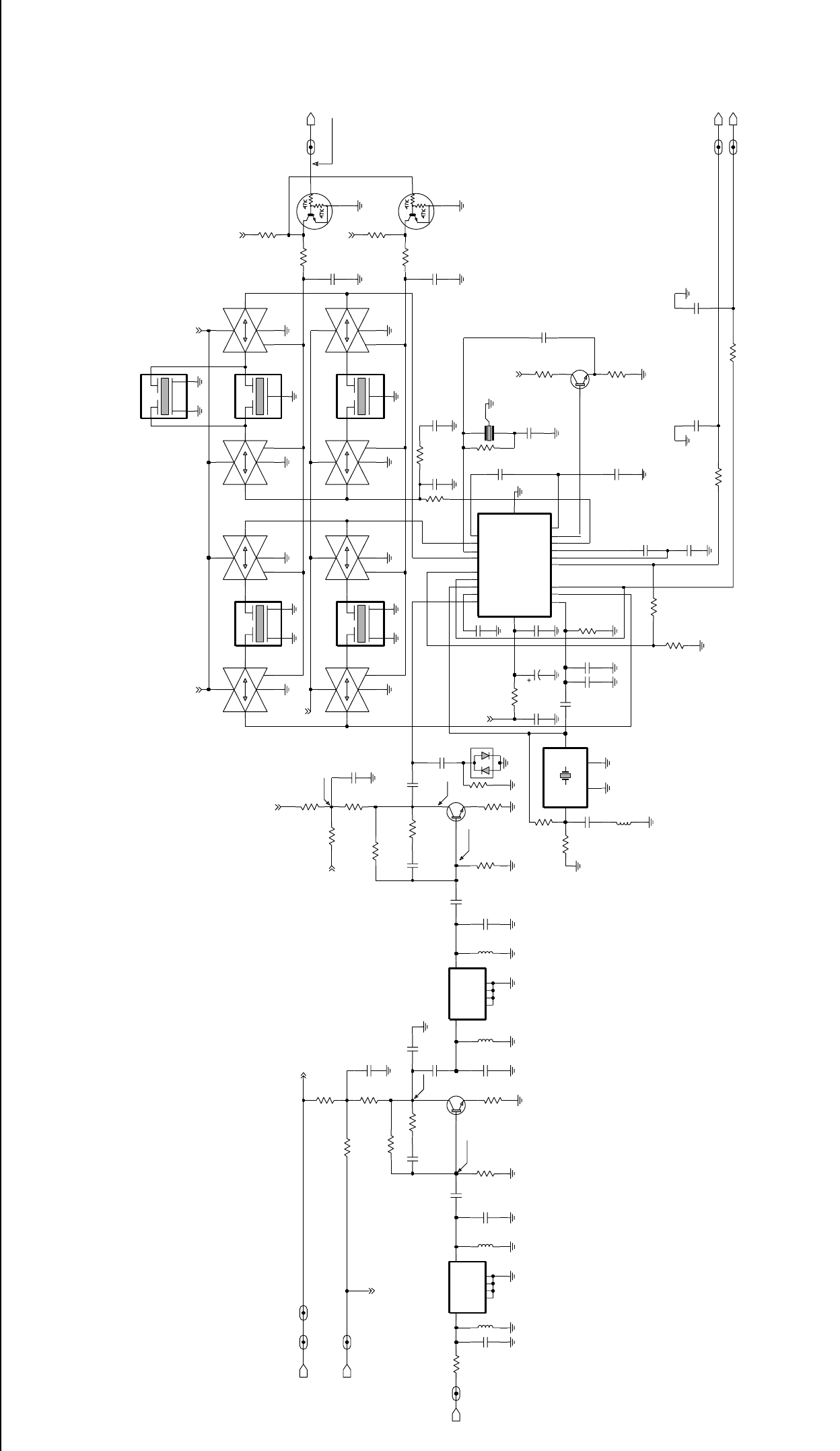
UHF 25-40W PCB / Schematics / Parts List 4-9
9180468v04
9180468V06
3.9VDC 12.5kHz 0VDC
20/25kHz 5VDC
9180469V03
3VDC
9180469V06
9180469V04
0.75VDC 0.75VDC
3VDC
R3117
27K
Q3102
10
R3112
IF
1.8K
R3142
10K
27pF
R3154
C3140
0.1uF
C3110
620nH
L3111
620
R3108
5
CNTL
4
3
14
VDD
7
VSS
C3144
U3115-2
C3143
0.1uF
120pF
R3115
390
R3118
6.8K
R3111
12K
5V_VHF_IF_1 Q3151
NU
C3113
NU
R3104
22pF
C3115
VDD
14
VSS
7
Q3141
MC74HC4066
U3111-1
CNTL
13
1
2
R3116
330
82pF
C3112
Q3152
R3135
1.2K
DISCAUDIO_VHF_IF_1
BWSELECT_VHF_IF_1
R3101
IFIN_VHF_IF_1
12K
C3133
10uF
C3152
.01uF
0.1uF
C3142
DISCAUDIO
R3132
15K
680
R3146
10K
R3151
0.1uF
C3139
C3132
0.1uF
10K
R3152
0.1uF
C3111
20pF
C3101
3
GND1
GND2
4
1IN 2
OUT
FL3111
C3141
0.1uF
GND3
4
5GND4
3IN 6
OUT
R3133
8.2K
FL3101
12R16
1GND1
GND2
2
0
7
R3148
U3111-4
CNTL
12
11 10
VDD
14
VSS
9V3_VHF_IF_2
R3102
10
FL3113
3
GND
1IN 2
OUT
27K
R3106
R3141
390
14
VDD
7
VSS
2.4K
R3144
U3111-2
5
CNTL
43
NU
C3131
C3122
.039uF
R3107
5RSSIOUT 9
RSSI_FEED
6
VCC
6.8K
13 LIM_DEC1
12 LIM_DEC2
20 MIXOUT 4
OSCIN
3OSCOUT
10
QUADIN
1
RFIN 2
RFIN_DEC
AUDIO_FEED
GND
15
18
IFAMPIN
16 IFAMPOUT 19
IFAMP_DEC1
17 IFAMP_DEC2
14
LIMIN
11 LIMOUT
SA616
U3101
8AUDIOOUT
7
CNTL
13
12 VDD
14
VSS
7
5V
U3115-1
R3105
L3100
100
0.1uF
9V3
NU
3
2
1
C3134
BWSELECT
45B02
Y3102
455KHz
C3103
33pF
C3147
0.1uF
0.1uF
C3145
620nH
L3101
6
CNTL
89
14
VDD
7
VSS
9
14
VDD
7
VSS
U3111-3 U3115-3
6
CNTL
8
GND1
1
2GND2
4GND3
GND4
5
IN
3OUT 6
30pF
12R16
FL3102
33pF
C3136
C3135
NU
L3124
NU
C3124
NU
R3124
C3114
18pF
C3104
0.1uF
C3121
0.1uF
Q3101 .039uF
C3123
.01uF
C3151
51
4700pF
C3146
R3130
10K
R3153
C3148
R3147
NU
D3101
0
R3123
330
R3113
15pF
C3102
3.3K
R3145
C3137
.039uF
3
GND
1IN 2
OUT
RSSI
FL3114
10
VDD
14
VSS
7
0.1uF
C3116
2
OUT
U3115-4
CNTL
12
11
FL3112
3
GND1
GND2
4
1IN
R3114
R3134
10K
NU
FL3115
GND1
34
GND2
IN
1OUT 2
NU
9V3_VHF_IF_1
L3112
620nH
Y3101
2
GND
4
GND1
3OUT 1
IN
5V
44.395MHz
12R17
5V
9V3
9V3
9V39V3
9V3
5V
9V3
5V
9V3
12k
ZWG0130522-A
UHF (403-470 MHz) IF

4-10 UHF 25-40W PCB / Schematics / Parts List
UHF PCB 8486127Z01 Parts List 25-40W
Circuit
Ref Motorola
Part No. Description
C0101 2113740F51 100pF
C0107 2113741F25 1000pF
C0112 2113743E20 0.1uF
C0121 2113743E20 0.1uF
C0122 2113743E20 0.1uF
C0131 2113740F35 22pF
C0132 2113740F35 22pF
C0141 2113743E20 0.1uF
C0151 2113741F49 10nF
C0201 2311049A57 10uF
C0202 2311049A57 10uF
C0204 2113743E20 0.1uF
C0212 2311049A57 10uF
C0221 2113743E20 0.1uF
C0222 2113743E20 0.1uF
C0223 2113743E20 0.1uF
C0224 2113740F51 100pF
C0225 2113743E20 0.1uF
C0226 2113743E20 0.1uF
C0228 2311049A56 4.7uF
C0231 2113743B29 1uF
C0232 2113743E20 0.1uF
C0234 2113743E20 0.1uF
C0235 2113743E07 0.022uF
C0236 2113743E10 0.033uF
C0241 2113743E20 0.1uF
C0243 2113740F51 100pF
C0244 2113743E20 0.1uF
C0245 2113743E20 0.1uF
C0246 2113741F49 10nF
C0251 2113743E20 0.1uF
C0252 2311049A07 1uF
C0254 2113743E20 0.1uF
C0255 2113743E20 0.1uF
C0256 2113740F51 100pF
C0261 2113743E20 0.1uF
C0262 2113740F49 82pF
C0265 2113743E20 0.1uF
C0267 2113741F49 10nF
C0271 2113741F49 10nF
C0272 2113743E20 0.1uF
C0273 2113741F37 3300pF
C0275 2311049A99 47uF
C0276 2113741F25 1000pF
C0277 2113741F25 1000pF
C0301 2311049A07 1uF
C0302 2113743E20 0.1uF
C0303 2113740F51 100pF
C0304 2113743E20 0.1uF
C0305 2113743E20 0.1uF
C0324 2113743E20 0.1uF
C0331 2113743E20 0.1uF
C0341 2311049A07 1uF
C0342 2113743E20 0.1uF
C0343 2113743E20 0.1uF
C0344 2113743E20 0.1uF
C0351 2113743E20 0.1uF
C0352 2113743E07 0.022uF
C0353 2311049A97 33uF
C0354 2113743E20 0.1uF
C0421 2113743N48 82PF
C0422 2113741F17 470pF
C0423 2113741F17 470pF
C0426 2113743L09 470pF
C0427 2113743L09 470pF
C0428 2113743N48 82pF
C0429 2113743L09 470pF
C0430 2113741F17 470pF
C0431 2113741F17 470pF
C0441 2113743L09 470pF
C0442 2113743L09 470pF
C0445 2113743L09 470pF
C0446 2113743L09 470pF
C0447 2113743L09 470pF
C0448 2113743L09 470pF
C0449 2113743L09 470pF
C0470 2113743L09 470pF
C0471 2113743N48 82pF
C0472 2113743N48 82pF
C0473 2113743N48 82pF
C0474 2113743L09 470pF
C0476 2113743L09 470pF
C0477 2113743L09 470pF
C0478 2113743L09 470pF
C0482 2113743L09 470pF
C0483 2113743L09 470pF
C0484 2113741F17 470pF
C0485 2113743L09 470pF
C0486 2113743L09 470pF
C0487 2113743L09 470pF
C0488 2113743L09 470pF
C0490 2113743L09 470pF
C0491 2113743L09 470pF
C0492 2113743L09 470pF
C0493 2113743L09 470pF
C0494 2113743L09 470pF
C0495 2113743L09 470pF
C0496 2113743L09 470pF
C0497 2113743L09 470pF
C0499 2113743L09 470pF
C0501 2113741F49 10nF
Circuit
Ref Motorola
Part No. Description
C0502 2113741F17 470pF
C0503 2113741F17 470pF
C0504 2113741F17 470pF
C0505 2113741F17 470pF
C0506 2113741F17 470pF
C0508 2113741F17 470pF
C0509 2113741F17 470pF
C0510 2113741F17 470pF
C0511 2113741F17 470pF
C0512 2113741F17 470pF
C0513 2113741F17 470pF
C0514 2113741F17 470pF
C0515 2113741F17 470pF
C0516 2113741F49 10nF
C0517 2113743N48 82pF
C0518 2113741F17 470pF
C0541 2311049A05 0.47uF
C0542 2311049A99 47uF
C0560 2113743L17 1000pF
C0591 2113743E20 0.1uF
C0592 2113743E20 0.1uF
C0593 2113741B69 0.1uF
C0601 2113741F17 470pF
C0603 2380090M24 10uF
C0611 2311049C06 22uF
C0612 2113743E20 0.1uF
C0622 2311049A99 47uF
C0641 2113741F17 470pF
C0644 2311049A97 33uF
C0645 2113743E20 0.1uF
C0652 2311049A97 33uF
C0654 2311049A57 10uF
C0655 2113743E20 0.1uF
C0661 2311049C05 47uF
C0662 2113741F49 10nF
C0663 2113743E20 0.1uF
C0671 2113743E20 0.1uF
C0681 2113743E20 0.1uF
C3101 2113740F34 20pF
C3102 2113740F31 15pF
C3103 2113740F39 33pF
C3104 2113743E20 0.1uF
C3110 2113740F37 27pF
C3111 2113743E20 0.1uF
C3112 2113740F49 82pF
C3114 2113740F33 18pF
C3115 2113740F35 22pF
C3116 2113743E20 0.1uF
C3121 2113743E20 0.1uF
C3122 2113743E11 0.039uF
C3123 2113743E11 0.039uF
Circuit
Ref Motorola
Part No. Description
C3132 2113743E20 0.1uF
C3133 2311049A57 10uF
C3134 2113743E20 0.1uF
C3135 2113740L30 33pF
C3136 2113740L29 30pF
C3137 2113743E11 0.039uF
C3139 2113743E20 0.1uF
C3140 2113743E20 0.1uF
C3141 2113743E20 0.1uF
C3142 2113743E20 0.1uF
C3143 2113740F53 120pF
C3144 2113743E20 0.1uF
C3145 2113743E20 0.1uF
C3146 2113741F41 4700pF
C3147 2113743E20 0.1uF
C3151 2113741F49 10nF
C3152 2113741F49 10nF
C4001 2113740F09 1.8pF
C4002 2113740F39 33pF
C4003 2113740F40 36pF
C4004 2113740F39 33pF
C4005 2113740F39 33pF
C4006 2113740F39 33pF
C4007 2113740F38 30pF
C4008 2113741F25 1000pF
C4009 2113740F27 10pF
C4010 2113741F13 330pF
C4011 2113741F37 3300pF
C4012 2113741F13 330pF
C4013 2113741F37 3300pF
C4014 2113740F51 100pF
C4015 2113740F51 100pF
C4017 2113740F09 1.8pF
C4018 2113740F29 12pF
C4019 2113740F29 12pF
C4020 2113740F39 33pF
C4021 2113740F39 33pF
C4022 2113740F39 33pF
C4023 2113740F29 12pF
C4024 2113741F25 1000pF
C4026 2113740F09 1.8pF
C4027 2113740F09 1.8pF
C4028 2113741F49 10nF
C4029 2113740F09 1.8pF
C4030 2113740F09 1.8pF
C4031 2113740F30 13pF
C4051 2113740F27 10pF
C4052 2113740F49 82pF
C4053 2113740F32 16pF
C4054 2113740F32 16pF
C4061 2113740F63 330pF
Circuit
Ref Motorola
Part No. Description

UHF 25-40W PCB / Schematics / Parts List 4-11
C4062 2113743E20 0.1uF
C4064 2113743E20 0.1uF
C4065 2113740F51 100pF
C4067 2113741F37 3300pF
C4068 2113740F51 100pF
C4069 2113741F49 10nF
C4201 2113740F51 100pF
C4202 2113741F49 10nF
C4203 2113741F49 10nF
C4204 2113740F51 100pF
C4205 2113741F49 10nF
C4206 2311049J25 10uF
C4208 2113743E20 0.1uF
C4209 2113743E20 0.1uF
C4210 2104993J02 2.2uF
C4211 2113743E20 0.1uF
C4213 2311049A09 2.2uF
C4214 2311049A09 2.2uF
C4215 2311049A09 2.2uF
C4217 2113741F49 10nF
C4221 2109720D01 0.01uF
C4222 2109720D14 0.1uF
C4224 0882422W23 1.0 uF
C4225 2113741F18 510pF
C4226 2113740L03 2.4pF
C4227 2113740F27 10pF
C4230 2104993J02 2.2uF
C4231 2113741F49 10nF
C4232 2113741F49 10nF
C4233 2104993J02 2.2uF
C4234 2113741F49 10nF
C4235 2113741F49 10nF
C4236 2113743E12 0.047uF
C4242 2113740F51 100pF
C4243 2113740F51 100pF
C4244 2113740F51 100pF
C4245 2113740F51 100pF
C4246 2113740F51 100pF
C4251 2113743E20 0.1uF
C4252 2113741F25 1000pF
C4253 2311049A56 4.7uF
C4254 2113743E20 0.1uF
C4255 2113740F51 100pF
C4263 2113743E20 0.1uF
C4287 2113740F51 100pF
C4289 2113743E20 0.1uF
C4301 2113740F51 100pF
C4302 2113740L16 8.2pF
C4303 2113740L16 8.2pF
C4304 2113740L08 3.9pF
C4306 2113740L01 2pF
Circuit
Ref Motorola
Part No. Description
C4307 2113740F51 100pF
C4308 2113743E20 0.1uF
C4309 2113740F51 100pF
C4311 2113740F51 100pF
C4312 2113740F29 12pF
C4314 2113740F07 1.5pF
C4315 2113740F51 100pF
C4316 2109720D14 0.1uF
C4318 2113743E20 0.1uF
C4321 2113740F03 1pF
C4324 2113740L03 2.4pF
C4325 2311049A56 4.7uF
C4331 2113740L14 6.8pF
C4335 2113740F51 100pF
C4336 2113743E07 0.022uF
C4337 2113740F44 51pF
C4338 2113740F44 51pF
C4351 2113740F51 100pF
C4352 2113743E20 0.1uF
C4353 2113743E20 0.1uF
C4354 2104993J02 2.2uF
C4355 2104993J02 2.2uF
C4361 2113741F25 1000pF
C4364 2113740F21 5.6pF
C4365 2113740F07 1.5pF
C4371 2113743E20 0.1uF
C4401 2113740F51 100pF
C4403 2113740F17 3.9pF
C4404 2113740F51 100pF
C4407 2113743E20 0.1uF
C4409 2113743E20 0.1uF
C4410 2113740F51 100pF
C4412 2113740F51 100pF
C4413 2113740F51 100pF
C4414 2113743E07 0.022uF
C4415 2113740F51 100pF
C4416 2113743E07 0.022uF
C4417 2113740F44 51pF
C4418 2113743E20 0.1uF
C4420 2113740A31 12pF
C4421 2113741A57 0.033uF
C4422 2111078B42 100pF
C4425 2113743E07 0.022uF
C4426 2113740F51 100pF
C4427 2113740A18 4.3pF
C4428 2113740A61 180pF
C4429 2113740A61 180pF
C4431 2113740A39 27pF
C4432 2113740A46 47pF
C4433 2113740A46 47pF
C4434 2113740A18 4.3pF
Circuit
Ref Motorola
Part No. Description
C4435 2113740A31 12pF
C4436 2311049A45 10uF
C4438 2113743E20 0.1uF
C4439 2111078B42 100pF
C4440 2111078B29 33pF
C4441 2111078B29 33pF
C4442 2111078B16 13pF
C4443 2111078B09 6.8pF
C4444 2111078B16 13pF
C4445 2111078B09 6.8pF
C4448 2180464E65 12pF
C4449 2111078B03 3.9pF
C4450 2111078B03 3.9pF
C4454 2113740A18 4.3pF
C4457 2113740A42 36pF
C4459 2113740A55 100pF
C4462 2113740F41 39pF
C4469 2113740A55 100pF
C4472 2111078B31 36pF
C4473 2113740F51 100pF
C4474 2113740F29 12pF
C4475 2113740F10 2pF
C4478 2113741A21 1000pF
C4479 2113740F51 100pF
C4481 2113741A32 3000pF
C4483 2113740A55 100pF
C4484 2113740F38 30pF
C4485 2113740F38 30pF
C4487 2111078B01 3.3pF
C4488 2113740F51 100pF
C4491 2111078B01 3.3pF
C4492 2111078B42 100pF
C4494 2180464E63 10pF
C4495 2113741A21 1000pF
C4496 2111078B08 6.2pF
C4497 2113741A21 1000pF
C4498 2111078B08 6.2pF
C4499 2113740F51 100pF
C4502 2113743E01 0.012uF
C4503 2113741F17 470pF
C4504 2113741F49 10nF
C4505 2311049A07 1uF
C4506 2113741F33 2200pF
C4507 2113740F51 100pF
C4510 2111078B31 36pF
C4521 2113740F51 100pF
C4522 2113741F25 1000pF
C4602 2113741A57 0.033uF
C4629 2113740F51 100pF
C4630 2113743E20 0.1uF
C4631 2113743E20 0.1uF
Circuit
Ref Motorola
Part No. Description
C4632 2113740F51 100pF
CR4301 4805649Q13 DIODE VCTR ISV 228
CR4302 4862824C01 DIODE VARACTOR
CR4303 4862824C01 DIODE VARACTOR
CR4311 4802245J22 DIODE, VARACTOR
CR4321 4862824C01 DIODE VARACTOR
D0101 4813825A05 DIODE
D0151 4813833C02 DIODE, DUAL 70V
D0179 4813833C02 DIODE, DUAL 70V
D0301 4802245J47 DIODE, SCHOTTKY
D0621 4813833C02 DIODE, DUAL 70V
D0651 4813833C02 DIODE, DUAL 70V
D0660 4813833C02 DIODE, DUAL 70V
D0661 4813833C02 DIODE, DUAL 70V
D3101 4880154K03 DIODE DUAL SCHOTTKY
D4001 4862824C01 DIODE VARACTOR
D4002 4862824C01 DIODE VARACTOR
D4003 4880154K03 DIODE DUAL SCHOTTKY
D4004 4862824C01 DIODE VARACTOR
D4005 4862824C01 DIODE VARACTOR
D4006 4880142L01 DIODE
D4007 4813833C02 DIODE, DUAL 70V
D4051 4886143B01 DIODE, MIXER
D4201 4802233J09 DIODE, TRIPLE
D4221 4813825A05 DIODE
D4451 4813825A05 DIODE
D4452 4813825A05 DIODE
D4453 4813825A05 DIODE
D4471 4802482J02 DIODE, SMD PIN
D4472 4802482J02 DIODE, SMD PIN
E0271 2484657R01 FERRITE BEAD
E0272 2484657R01 FERRITE BEAD
E0631 2484657R01 FERRITE BEAD
F0401 6580542Z01 FUSE 3A
FL3101 9180112R16 2 POLE 44.85 MHZ CRYSTAL
FILTER
FL3102 9180112R16 2 POLE 44.85 MHZ CRYSTAL
FILTER
FL3111 9180469V03 CERAMIC FILTER, 455KHz
FL3112 9180469V06 CERAMIC FILTER, 455KHz
FL3114 9180468V06 CERAMIC FILTER, 455KHz
FL3115 9180469V04 CERAMIC FILTER, 455KHz
J0401 0902636Y02 FLEX CONNECTOR
J0451 0902636Y01 FLEX CONNECTOR
J0501 0986105B01 ACCESSORY CONNECTOR
J0551 0905505Y04 FLEX CONNECTOR
J0552 0905505Y03 FLEX CONNECTOR
J0601 0986165B01 DC POWER CONNECTOR
J4401 0986166B02 RF CONNECTOR (MINI UHF)
L3101 2462587T25 620nH
L3111 2462587T25 620nH
Circuit
Ref Motorola
Part No. Description
4-12 UHF 25-40W PCB / Schematics / Parts List
L3112 2462587T25 620nH
L4003 2462587T23 470nH
L4006 2462587V24 15nH
L4008 2462587T23 470nH
L4051 2462587T17 150nH
L4053 2462587N46 27nH
L4054 2462587N43 15nH
L4201 2462587Q42 390nH
L4221 2462587P25 12uH
L4231 2462587Q20 2.2uH
L4301 2462587T22 390nH
L4302 2462587T22 390nH
L4303 2460593C01 RESONATOR
L4304 2462587T22 390nH
L4305 2462587T22 390nH
L4311 2462587T22 390nH
L4312 2460593C01 RESONATOR
L4313 2462587T22 390nH
L4331 2462587T09 33nH
L4333 2462587T22 390nH
L4361 2462587T09 33nH
L4362 2462587T09 33nH
L4371 2462587T13 68nH
L4401 2460591B04 11.03nH
L4402 2484657R01 FERRITE BEAD
L4403 2462587T22 390nH
L4411 2462587T22 390nH
L4421 2484657R01 FERRITE BEAD
L4436 2484657R01 FERRITE BEAD
L4437 2460592A01 17nH
L4438 2460592A01 17nH
L4472 2460592A01 17nH
L4473 2460591N36 43.67nH
L4489 2460591B77 13.9nH
L4490 2460591B77 13.9nH
L4491 2460592A01 17nH
L4492 2460592A01 17nH
L4493 2460592A01 17nH
L4541 2484657R01 FERRITE BEAD
L4543 2460591C23 13.85nH
M3421 2686201B01 HEAT SPREADER
Q0110 4880048M01 NPN
Q0151 4880048M01 NPN
Q0171 4880048M01 NPN
Q0173 4880052M01 NPN DARLINGTON
Q0177 4880048M01 NPN
Q0181 4880048M01 NPN
Q0183 4880048M01 NPN
Q0185 4880048M01 NPN
Q0271 4880214G02 NPN
Q0641 4880048M01 NPN
Circuit
Ref Motorola
Part No. Description
Q0661 4805921T02 DUAL NPN/PNP
Q0662 4880214G02 NPN
Q0663 4880048M01 NPN
Q0681 4880052M01 NPN DARLINGTON
Q3101 4813827A07 NPN
Q3102 4813827A07 NPN
Q3141 4880214G02 NPN
Q3151 4880048M01 NPN
Q3152 4880048M01 NPN
Q4002 4813824A17 PNP
Q4003 4813827A07 NPN
Q4004 4805921T02 DUAL NPN/PNP
Q4221 4880048M01 NPN
Q4301 4805218N63 DIODE DUAL SCHOTTKY
Q4332 4813827A07 NPN
Q4333 4809939C05 DUAL NPN/PNP
Q4421 4886212B01 POWER TRANSISTOR -
MRF1518
Q4441 4813828C32 POWER TRANSISTOR -
MRF1570
Q4471 4880048M01 NPN
Q4472 4805128M27 PNP
Q4473 4880214G02 NPN
R0101 0662057A73 10K
R0102 0662057A65 4.7K
R0103 0662057A01 10
R0104 0662057A73 10K
R0106 0662057B47 0
R0108 0662057A57 2.2K
R0111 0662057B47 0
R0113 0662057A73 10K
R0114 0662057A73 10K
R0115 0662057A73 10K
R0117 0662057A63 3.9K
R0121 0662057A97 100K
R0131 0662057B46 10M
R0132 0662057B10 330K
R0151 0662057A82 24K
R0152 0662057A82 24K
R0170 0662057A73 10K
R0171 0662057A65 4.7K
R0172 0662057A73 10K
R0173 0662057A65 4.7K
R0174 0662057A73 10K
R0175 0662057A73 10K
R0176 0662057A84 30K
R0177 0662057A65 4.7K
R0178 0662057A89 47K
R0179 0662057A89 47K
R0181 0662057A65 4.7K
R0182 0662057A89 47K
Circuit
Ref Motorola
Part No. Description
R0183 0662057A65 4.7K
R0184 0662057A89 47K
R0185 0662057A65 4.7K
R0186 0662057A89 47K
R0201 0662057A25 100
R0202 0662057A43 560
R0203 0662057A25 100
R0204 0662057A43 560
R0205 0662057A73 10K
R0206 0662057A73 10K
R0207 0662057A57 2.2K
R0208 0662057A57 2.2K
R0211 0660076E70 7.5K
R0212 0660076E70 7.5K
R0221 0662057A82 24K
R0222 0662057A82 24K
R0223 0662057A84 30K
R0224 0662057A71 8.2K
R0228 0662057B47 0
R0229 0662057A01 10
R0241 0662057A89 47K
R0242 0662057B47 0
R0251 0662057A89 47K
R0252 0662057A91 56K
R0253 0662057A97 100K
R0254 0662057A73 10K
R0255 0662057A73 10K
R0256 0662057A97 100K
R0257 0662057A57 2.2K
R0261 0662057A73 10K
R0262 0662057B08 270K
R0265 0662057A82 24K
R0267 0662057A89 47K
R0268 0662057A73 10K
R0269 0662057A41 470
R0273 0662057A82 24K
R0275 0662057A73 10K
R0276 0662057A77 15K
R0323 0662057A79 18K
R0324 0662057A79 18K
R0331 0662057A73 10K
R0332 0662057A73 10K
R0333 0662057A73 10K
R0335 0662057B02 150K
R0341 0662057A73 10K
R0342 0662057A55 1.8K
R0343 0662057B47 0
R0344 0662057A91 56K
R0345 0662057A66 5.1K
R0346 0662057A89 47K
R0347 0662057A89 47K
Circuit
Ref Motorola
Part No. Description
R0401 0662057A33 220
R0407 0662057M26 10
R0408 0662057A25 100
R0409 0662057M26 10
R0412 0662057B47 0
R0441 0662057B47 0
R0442 0662057A49 1K
R0467 0662057M26 10
R0468 0662057A97 100K
R0481 0662057B47 0
R0482 0662057B47 0
R0508 0662057A41 470
R0509 0662057B47 0
R0510 0662057A65 4.7K
R0511 0662057A97 100K
R0512 0662057A77 15K
R0525 0662057A97 100K
R0529 0662057A89 47K
R0530 0662057A81 22K
R0531 0662057A43 560
R0533 0662057B47 0
R0535 0662057A49 1K
R0537 0662057A33 220
R0538 0662057A33 220
R0539 0662057A65 4.7K
R0541 0662057A83 27K
R0543 0662057A97 100K
R0555 0662057A25 100
R0556 0662057A25 100
R0591 0662057A82 24K
R0592 0662057A01 10
R0593 0662057A97 100K
R0611 0662057A91 56K
R0612 0662057A65 4.7K
R0621 0662057A82 24K
R0641 0662057A73 10K
R0642 0660076E70 7.5K
R0643 0660076E51 1.2K
R0651 0662057A01 10
R0652 0662057A01 10
R0661 0662057A49 1K
R0662 0662057B02 150K
R0671 0662057A84 30K
R0672 0662057A73 10K
R0681 0662057A79 18K
R0682 0662057A93 68K
R3101 0662057A75 12K
R3102 0662057A01 10
R3105 0662057A25 100
R3106 0662057A83 27K
R3107 0662057A69 6.8K
Circuit
Ref Motorola
Part No. Description
UHF 25-40W PCB / Schematics / Parts List 4-13
* Motorola Depot Servicing only
Reference designators with an asterisk indicate
components which are not field replaceable
because they need to be calibrated with
specialized factory equipment after installation.
Radios in which these parts have been replaced in
the field will be off frequency at temperature
extremes.
R3108 0662057A44 620
R3111 0662057A75 12K
R3112 0662057A01 10
R3113 0662057A37 330
R3115 0662057A39 390
R3116 0662057A37 330
R3117 0662057A83 27K
R3118 0662057A69 6.8K
R3123 0662057B47 0
R3130 0662057A18 51
R3132 0662057A77 15K
R3133 0662057A71 8.2K
R3134 0662057A73 10K
R3135 0662057A51 1.2K
R3141 0662057A39 390
R3142 0662057A55 1.8K
R3144 0662057A58 2.4K
R3145 0662057A61 3.3K
R3146 0662057A45 680
R3147 0662057A75 12K
R3148 0662057B47 0
R3151 0662057A73 10K
R3152 0662057A73 10K
R3153 0662057A73 10K
R3154 0662057A73 10K
R4001 0662057A97 100K
R4002 0662057A37 330
R4003 0662057A63 3.9K
R4004 0662057A59 2.7K
R4005 0662057A73 10K
R4007 0662057A25 100
R4012 0662057A97 100K
R4013 0662057A35 270
R4014 0662057A01 10
R4016 0662057A61 3.3K
R4018 0662057A61 3.3K
R4022 0662057B47 0
R4051 0662057A18 51
R4052 0662057B47 0
R4060 0662057B10 330K
R4061 0662057A73 10K
R4062 0662057A53 1.5K
R4063 0662057A39 390
R4064 0662057B47 0
R4068 0662057A53 1.5K
R4069 0662057A49 1K
R4070 0662057A39 390
R4071 0662057A73 10K
R4072 0662057A73 10K
R4201 0662057A29 150
R4203 0662057A17 47
Circuit
Ref Motorola
Part No. Description
R4204 0662057A17 47
R4211 0662057B47 0
R4221 0662057A29 150
R4222 0662057A42 510
R4223 0662057A21 68
R4224 0662057A89 47K
R4225 0662057A89 47K
R4228 0662057A73 10K
R4241 0662057A33 220
R4251 0662057A87 39K
R4252 0662057A84 30K
R4261 0662057A89 47K
R4263 0662057A25 100
R4301 0662057A67 5.6K
R4302 0662057A73 10K
R4303 0662057A12 30
R4304 0662057A31 180
R4305 0662057A01 10
R4311 0662057A70 7.5K
R4312 0662057A67 5.6K
R4313 0662057A12 30
R4314 0662057A35 270
R4315 0662057B47 0
R4321 0662057A91 56K
R4322 0662057A73 10K
R4323 0662057A97 100K
R4331 0662057A09 22
R4341 0662057B47 0
R4342 0662057A57 2.2K
R4343 0662057A49 1K
R4344 0662057A01 10
R4346 0662057A73 10K
R4347 0662057B47 0
R4360 0662057A35 270
R4361 0662057A31 180
R4362 0662057A01 10
R4363 0662057A49 1K
R4381 0662057A41 470
R4401 0662057A36 300
R4402 0662057A05 15
R4403 0662057A36 300
R4405 0662057A32 200
R4408 0662057A80 20K
R4409 0662057A97 100K
R4412 0662057A56 2K
R4415 0662057A15 39
R4416 0662057A15 39
R4422 0611079A69 620
R4423 0611079A69 620
R4424 0611079A69 620
R4425 0611079A69 620
Circuit
Ref Motorola
Part No. Description
R4428 0662057A55 1.8K
R4457 0683962T51 120
R4473 0662057A64 4.3K
R4474 0662057A97 100K
R4475 0662057B47 0
R4480 0662057A73 10K
R4481 0662057C44 51
R4482 0662057B09 300K
R4483 0662057A97 100K
R4484 0662057A93 68K
R4485 0662057C44 51
R4486 0662057C44 51
R4489 0662057C44 51
R4491 0662057A74 11K
R4492 0662057A73 10K
R4495 0680195M18 51
R4496 0680194M23 82
R4497 0680195M18 51
R4501 0662057A67 5.6K
R4502 0662057A93 68K
R4503 0662057A63 3.9K
R4504 0662057A73 10K
R4506 0662057A73 10K
R4507 0662057A73 10K
R4511 0680194M18 51
R4512 0662057A41 470
R4513 0662057A73 10K
R4514 0662057A61 3.3K
R4631 0662057A89 47K
R4632 0662057A89 47K
R4634 0662057A97 100K
R4635 0662057A97 100K
SH4301 2602641Y02 SHIELD
SH4302 2602641Y02 SHIELD
T4051 2505515V03 TRANSFORMER 4:1
T4052 2505515V04 TRANSFORMER 5:1
U0101 5102226J56 MICROPROCESSOR
U0111 5102463J64 EEPROM
U0121 5186137B01 IC, FLASH ROM
U0122 5185748L01 SRAM
U0141 5113805A30 REMUX
U0211 5183222M49 IC, QUAD OPAMP
U0221 5185130C53 IC, ASFIC
U0251 5184704M60 IC-CMOS ANALOG
U0271 5109699X01 AUDIO PA
U0301 5109152M01 EEPROM ANALOG
U0331 5186204B01 BUFFER / DRIVER
U0341 5113818A01 LINEAR IC OP AMP
U0342 5105750U28 IC CMOS SWITCH
U0351 5102463J40 REGULATOR, 3.3V
Circuit
Ref Motorola
Part No. Description
U0611 5183308X01 ADJUSTABLE VOLTAGE REG-
ULATOR
U0641 5183308X01 ADJUSTABLE VOLTAGE REG-
ULATOR
U0651 5113816A07 REGULATOR, 5V
U0652 5113815A02 UNDERVOLT SENSOR
U3101 5186144B01 IC, IF
U3111 5102463J52 QUAD ANALOG SWITCH
U3115 5102463J52 QUAD ANALOG SWITCH
U4201 5185963A27 IC FRACTN
U4211 5105739X05 IC, VOLTAGE REGULATOR
U4301 5105750U54 IC, VCO
U4401 5185130C65 IC LDMOS DRIVER
U4501 5185765B26 IC POWER CONTROL
U4502 5185963A15 IC TEMPERATURE SENSOR
VR0151 4813830A15 DIODE, 5.6V
VR0501 4805656W09 DIODE, ZENER
VR0503 4805656W09 DIODE, ZENER
VR0504 4813830A40 SOC23 AUTO SDN
VR0505 4805656W09 DIODE, ZENER
VR0509 4813830A40 DIODE, ZENER
VR0510 4813830A40 DIODE, ZENER
VR0537 4813830A15 DIODE, 5.6V
VR0541 4813830A27 DIODE, 14V
VR0601 4813832C77 DIODE
VR0621 4813830A15 DIODE, 5.6V
VR4471 4813830A15 DIODE, 5.6V
VR4473 4813830A15 DIODE, 5.6V
Y0131 4880113R19 CRYSTAL 38.4KHZ
Y3101 4880606B09 2ND OSC XTAL 44.395 MHZ
Y3102 9186145B02 455KHz DISCRIMINATOR
Y4262 4886182B01 TCXO 16.8MHZ
Circuit
Ref Motorola
Part No. Description

4-14 UHF 25-40W PCB / Schematics / Parts List
THIS PAGE INTENTIONALLY LEFT BLANK

GM338
Mobile Radios
UHF B2 HIGH POWER LDMOS
(450-520 MHz)
Service Information
Issue: December, 2003

Computer Software Copyrights
The Motorola products described in this manual may include copyrighted Motorola computer programs stored
in semiconductor memories or other media. Laws in the United States and other countries preserve for
Motorola certain exclusive rights for copyrighted computer programs, including the exclusive right to copy or
reproduce in any form, the copyrighted computer program. Accordingly, any copyrighted Motorola computer
programs contained in the Motorola products described in this manual may not be copied or reproduced in
any manner without the express written permission of Motorola. Furthermore, the purchase of Motorola
products shall not be deemed to grant, either directly or by implication, estoppel or otherwise, any license
under the copyrights, patents or patent applications of Motorola, except for the normal non-exclusive royalty-
free license to use that arises by operation of law in the sale of a product.

i
Table of Contents
Section 1 Model Chart and Technical Specifications
1.0 GM338 Model Chart.............................................................................................1-1
2.0 Technical Specifications ......................................................................................1-1
Section 2 Theory of Operation
1.0 Introduction ..........................................................................................................2-1
2.0 UHF (450-520 MHz) Receiver .............................................................................2-1
2.1 Receiver Front-End ........................................................................................2-1
2.2 Front-End Band-Pass Filters & Pre-Amplifier.................................................2-2
2.3 First Mixer and High Intermediate Frequency (IF)..........................................2-2
2.4 Low Intermediate Frequency (IF) and Receiver Back End.............................2-3
3.0 UHF (450-520 MHz) Transmitter Power Amplifier (PA) 40W...............................2-3
3.1 First Power Controlled Stage..........................................................................2-4
3.2 Power Controlled Driver Stage.......................................................................2-4
3.3 Final Stage .....................................................................................................2-4
3.4 Directional Coupler.........................................................................................2-4
3.5 Antenna Switch...............................................................................................2-5
3.6 Harmonic Filter ...............................................................................................2-5
3.7 Power Control.................................................................................................2-5
4.0 UHF (450-520 MHz) Frequency Synthesis..........................................................2-6
4.1 Reference Oscillator.......................................................................................2-6
4.2 Fractional-N Synthesizer ................................................................................2-6
4.3 Voltage Controlled Oscillator (VCO)...............................................................2-8
4.4 Synthesizer Operation....................................................................................2-9
Section 3 Troubleshooting Charts
1.0 Troubleshooting Flow Chart for Receiver ............................................................3-1
2.0 Troubleshooting Flow Chart for 40W Transmitter................................................3-3
3.0 Troubleshooting Flow Chart for Synthesizer........................................................3-4
4.0 Troubleshooting Flow Chart for VCO...................................................................3-5

ii
Section 4 UHF PCB/Schematics/Parts Lists
1.0 Allocation of Schematics and Circuit Boards .......................................................4-1
1.1 Controller Circuits...........................................................................................4-1
2.0 UHF Band 2 25-40W PCB / Schematics / Parts List ...........................................4-3
UHF Band 2 (450-520 MHz) 40W 8486250Z02 Top Side......................................4-3
UHF Band 2 (450-520 MHz) 40W 8486250Z02 Bottom Side................................4-4
UHF Band 2 (450-520 MHz) Power Amplifier 40W ................................................4-5
UHF Band 2 (450-520 MHz) FRACN .....................................................................4-6
UHF Band 2 (450-520 MHz) Voltage Controlled Oscillator ....................................4-7
UHF Band 2 (450-520 MHz) Receiver Front End...................................................4-8
UHF Band 2 (450-520 MHz) IF...............................................................................4-9
UHF Band 2 PCB 8486250Z02 Parts List 25-40W..............................................4-10
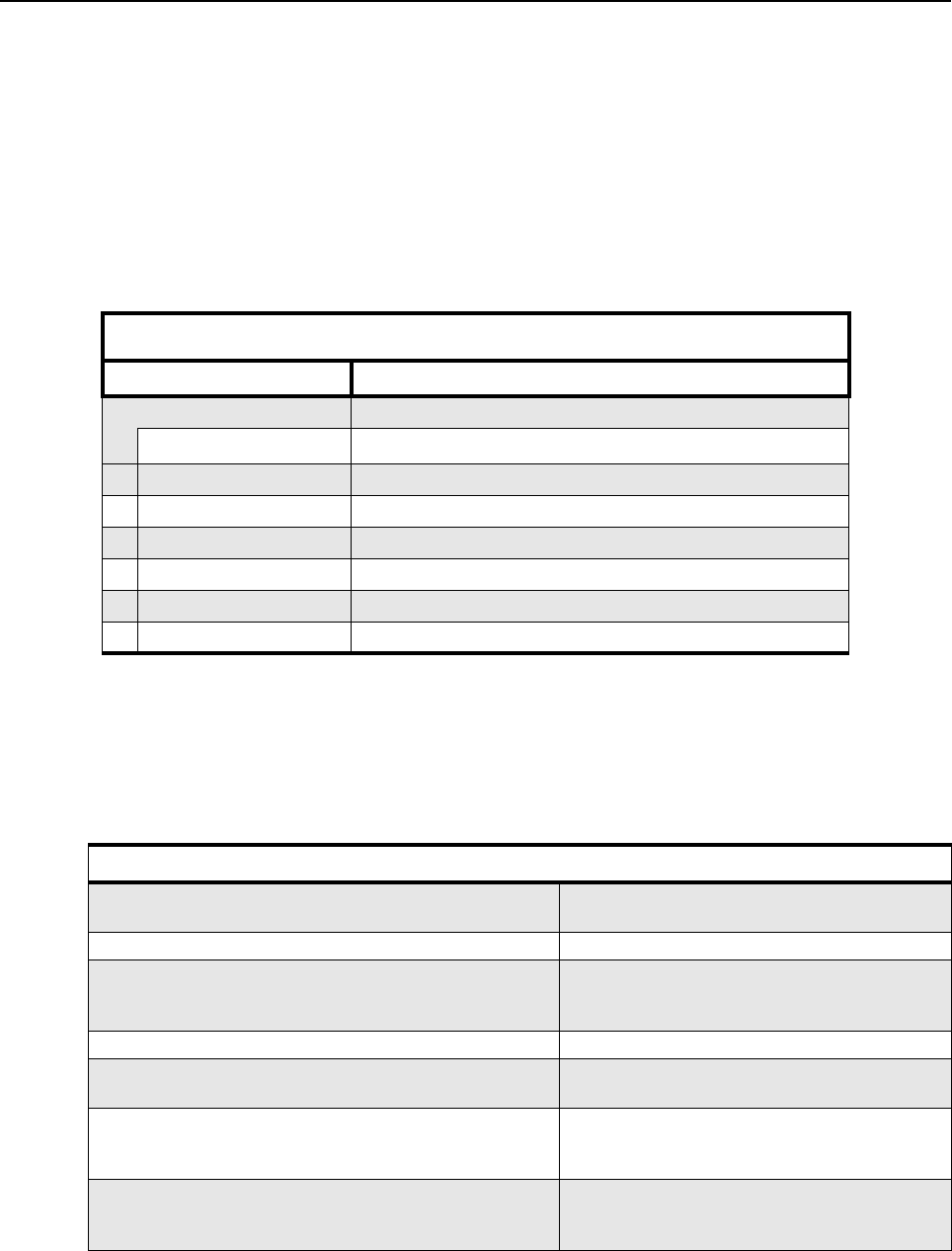
1-1
Section 1
MODEL CHART AND TECHNICAL SPECIFICATIONS
1.0 GM338 Model Chart
2.0 Technical Specifications
Data is specified for +25°C unless otherwise stated.
GM Series, UHF Band 2, 450-520 MHz
Model Description
AZM25SKF9AA5 GM338 450-520 MHz 25-40W (LDMOS)
Item Description
XGCN6114_ GM338 Control Head Direct Mount
X IMUE6019_ Tanapa WM 450-520 MHz 25-40W
XRAE4155_ BNC 470-512 MHz, 1/4 Wave Roof Mount
X RAE4156_ BNC 470-494 MHz, 3.5 Gain Roof Mount
XRAE4157_ BNC 494-512 MHz, 5dB Gain Roof Mount
X 6804112J06 GM338 User Guide
x = Indicates one of each is required.
General Specifications
Channel Capacity
GM338 128
Power Supply 13.2Vdc (10.8 - 15.6Vdc)
Dimensions: H x W x D (mm) Depth excluding knobs GM338
59mm x 179mm x 198mm (25 - 40W)
(add 9mm for Volume Knob)
Weight GM338 1400 g
Sealing: Withstands rain testing per
MIL STD 810 C/D/E and IP54
Shock and Vibration: Protection provided via impact
resistant housing exceeding MIL STD
810-C/D/E
Dust, Salt & Fog: Protection provided via environment
resistant housing exceeding MIL STD
810 C/D/E
1-2 Technical Specifications
*Availability subject to the laws and regulations of individual countries.
Transmitter UHF
*Frequencies - Full Bandsplit UHF 450-520 MHz
Channel Spacing 12.5/20/25 kHz
Frequency Stability
(-30°C to +60°C, +25° Ref.) ±2.0 ppm
Power 25-40W
Modulation Limiting ±2.5 @ 12.5 kHz
±4.0 @ 20 kHz
±5.0 @ 25 kHz
FM Hum & Noise -40 dB @ 12.5kHz
-45 dB @ 20/25kHz
Conducted/Radiated Emission (ETS) -36 dBm <1 GHz
-30 dBm >1 GHz
Adjacent Channel Power -60 dB @ 12.5 kHz
-70 dB @ 25 kHz
Audio Response (300 - 3000 Hz) +1 to -3 dB
Audio Distortion
@1000Hz, 60%
Rated Maximum Deviation <3% typical
Receiver UHF
*Frequencies - Full Bandsplit UHF 450-520 MHz
Channel Spacing 12.5/20/25 kHz
Sensitivity (12 dB SINAD) 0.30 µV (0.22 µV typical)
Intermodulation (ETS) >65 dB
Adjacent Channel Selectivity (ETS) 65 dB @ 12.5 kHz
70 dB @ 20 kHz
75 dB @ 25 kHz
Spurious Rejection (ETS) 70 dB @ 12.5 kHz
75 dB @ 20/25 kHz
Rated Audio 3W Internal
7.5W External
13W External
Audio Distortion @ Rated Audio <3% typical
Hum & Noise -40 dB @ 12.5 kHz
-45 dB @ 20/25 kHz
Audio Response (300 - 3000Hz @ 20/25kHz)
(300 - 2550Hz @12.5kHz) +1 to -3 dB
Conducted Spurious Emission (ETS) -57 dBm <1 GHz
-47 dBm >1 GHz

2-1
Section 2
THEORY OF OPERATION
1.0 Introduction
This Chapter provides a detailed theory of operation for the UHF circuits in the radio. For details of
the theory of operation and troubleshooting for the associated Controller circuits refer to the
Controller Section of this manual.
2.0 UHF (450-520 MHz) Receiver
2.1 Receiver Front-End
The UHF receiver, shown in Figure 2-1, is able to cover the UHF range from 450 to 520 MHz. It
consists of four major blocks: front-end bandpass filters and pre-amplifier, first mixer, high-IF, low-IF
and receiver back-end . Two varactor-tuned bandpass filters perform antenna signal pre-selection.
A cross over quad diode mixer converts the signal to the first IF of 44.85 MHz. Low-side first
injection is used.
Figure 2-1 UHF Receiver Block Diagram
Demodulator
1. Crystal
Filter
Mixer
Varactor
Tuned Filter
RF Amp
Varactor
Tuned Filter
Pin Diode
Antenna
Switch
RF Jack
Control Voltage
from PCIC First LO
from FGU
Recovered Audio
RSSI
Second LO
2. Crystal
Filter
455kHz Filter
(25kHz)
455kHz Filter
(25kHz)
455kHz Filter
(12.5kHz)
455kHz Filter
(12.5kHz)
Switch
Switch
Switch
Switch
Limiter
1. IF Amp
2. IF Amp
Filter Bank Selection
from Synthesizer IC
Harmonic
Filter
BWSELECT

2-2 UHF (450-520 MHz) Receiver
The two 2-pole 44.85 MHz crystal filters in the high-IF section and two pairs of 455 kHz ceramic
filters in the low-IF section provide the required adjacent channel selectivity .The correct pair of
ceramic filters for 12.5 or 25KHz channel spacing is selected via control line BWSELECT. The
second IF at 455 kHz is mixed, amplified, and demodulated in the IF IC. The processing of the
demodulated audio signal is performed by an audio processing IC located in the controller section.
2.2 Front-End Band-Pass Filters & Pre-Amplifier
The received signal from the radio’s antenna connector is first routed through the harmonic filter and
antenna switch, which are part of the RF power amplifier circuits, before being applied to the receiver
pre-selector filter (C5001, C5002, D5001, and related components). The 2-pole pre-selector filter,
tuned by the varactor diodes D5001 and D5002, pre-select the incoming signal (RXIN) from the
antenna switch to reduce spurious effects to the stages that follow. The tuning voltage (FECTRL_1),
ranging from 2 volts to 8 volts, is controlled by pin 20 of PCIC (U5501) in the transmitter section. A
dual hot carrier diode (D5003) limits any inband signal to 0 dBm to prevent damage to the pre-
amplifier.
The RF pre-amplifier is an SMD device (Q5003) with collector base feedback to stabilize gain,
impedance, and intermodulation. The collector current of approximately 11-16 mA is drawn from the
9.3 volt supply via L5003 and R5002. A 3dB pad (R5006,R5007, R5011, and R5008 - R5010)
stabilizes the output impedance and intermodulation performance.
A second 2-pole varactor tuned bandpass filter provides additional filtering of the amplified signal.
Varactor diodes D5004 and D5005 are controlled by the same signal, FECTRL_1, which controls
the pre-selector filter. A following 1 dB pad (R5013 - R5015) stabilizes the output impedance and
intermodulation performance.
2.3 First Mixer and High Intermediate Frequency (IF)
The signal from the front-end is converted to the first IF (44.85 MHz) using cross-over, quad diode
mixer D5051. Its ports are matched for incoming RF signal conversion to the 44.85 MHz IF using low
side injection via matching transformers T5051 and T5052. The injection signal (RXINJ) coming from
the RX VCO buffer (Q5332) is filtered by the lowpass filter consisting of L5053, L5054, and C5053 -
C5055 followed by matching transformer T5052 which has a level of approximately 15dBm.
The mixer IF output signal from transformer T5501, pin 2 is fed to the first two-pole crystal filter
(FL3101). The filter output in turn is matched to IF amplifier Q3101 which is actively biased using
collector-base feedback resistors R3101and R3106 to provide a current drain of approximately 5 mA
drawn from the 5 volt supply. The output impedance of this device is matched to the second two-pole
crystal filter FL3102. The signal is further amplified by a preamplifier Q3102 before going to pin 1 of
IFIC (U3101).
A dual, hot carrier diode (D3101) limits the filter output voltage swing to reduce overdrive effects at
RF input levels above -27 dBm.
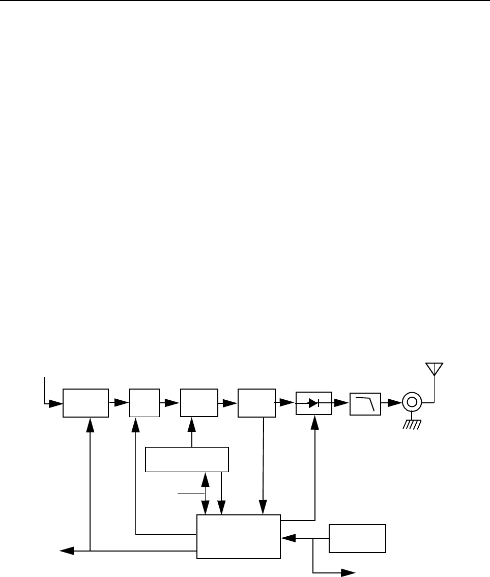
UHF (450-520 MHz) Transmitter Power Amplifier (PA) 40W 2-3
2.4 Low Intermediate Frequency (IF) and Receiver Back End
The 44.85 MHz first IF signal from the second IF amplifier feeds the IF IC (U3101) at pin1. Within the
IF IC the 44.85 MHz high IF signal mixes with the 44.395 MHz second local oscillator to produce a
low IF signal of 455 kHz. The second LO frequency is determined by crystal Y3101. The second IF
signal is amplified and filtered by an external pair of 455 kHz ceramic filters (FL3112 and FL3114) for
20/25 kHz channel spacing, or FL3111 and FL3113/F3115 for 12.5 kHz channel spacing. These
pairs are selectable via BWSELECT. The filtered output from the ceramic filters is applied to the
limiter input pin of the IF IC (pin 14).
The IF IC contains a quadrature detector using a ceramic phase-shift element (Y3102) to provide
audio detection. Internal amplification provides an audio output level of 120 mV rms (at 60%
deviation) from U3103, pin 8 (DISCAUDIO) which is fed to ASFIC_CMP U0221, pin 2 (part of the
controller circuits).
A received signal strength indicator (RSSI) signal is available at U3101, pin 5, which has a dynamic
range of 70 dB. The RSSI signal is interpreted by the µP (U0101, pin 63) and is available at
accessory connector J0501-15.
3.0 UHF (450-520 MHz) Transmitter Power Amplifier (PA) 40W
The radio’s 40W PA is a three stage amplifier used to amplify the output from the VCOBIC to the
radio transmit level. All three stages utilize LDMOS technology. The gain of the first stage (U5401) is
adjustable, controlled by pin 4 of PCIC (U5501). It is followed by an LDMOS stage (Q5421) and
LDMOS final stage (Q5441).
Figure 2-2 UHF Transmitter Block Diagram
Devices U5401, Q5421 and Q5441 are surface mounted. A pressure pad between board and the
radio’s cover provides good thermal contact between the devices and the chassis.
PCIC
Pin Diode
Antenna
Switch RF Jack
Antenna
Harmonic
Filter
Power
Sense
PA-Final
Stage
PA
Driver
From VCO
Controlled
Stage
Vcontrol
Bias 1
Bias 2
To Microprocessor
Temperature
Sense
SPI BUS
ASFIC_CMP
PA
PWR
SET
To Microprocessor
& Bias 3

2-4 UHF (450-520 MHz) Transmitter Power Amplifier (PA) 40W
3.1 First Power Controlled Stage
The first stage (U5401) is a 20dB gain integrated circuit containing two LDMOS FET amplifier
stages. It amplifies the RF signal from the VCO (TXINJ). The output power of stage U5401 is
controlled by a DC voltage applied to pin 1 from Q5473. The control voltage simultaneously varies
the bias of two FET stages within U5401. This biasing point determines the overall gain of U5401
and therefore its output drive level to Q5421, which in turn controls the output power of the PA.
Switch S5440 is a pressure pad with a conductive strip which connects two conductive areas on the
board when the radio's cover is properly screwed to the chassis. When the cover is removed, S5440
opens and cuts the supply voltage to Q5473 thus disabling control voltage to U5401. This prevents
transmitter key up while the devices do not have proper thermal contact to the chassis.
3.2 Power Controlled Driver Stage
The next stage is an LDMOS device (Q5421) providing a gain of 12dB. This device requires a
positive gate bias and a quiescent current flow for proper operation. The bias is set during transmit
mode by U5501-24 and fed to the gate of Q5421 via the resistive network R5480, R5408, R5415
and R5416.
3.3 Final Stage
The final stage is an LDMOS MRF1570 device Q5441. It provides a gain of 11dB. It integrates two
MRF1535 die inside. These two die are being run in parallel. The output of each of the device (die)
inside are combined to constitute the total output power. This device also requires a positive gate
bias and a quiescent current flow for proper operation. The voltage of the line MOSBIAS_2 and
MOSBIAS_3 are set in transmit mode by the ASFIC and fed to the gate of Q5441 via two resistive
network R5631, R5634, R5485, R5486 and R5632, R5635, R5481, R5489. These bias voltages are
tuned in the factory. If the transistor is replaced, the bias voltage must be tuned using the Global
Tuner. Care must be taken not to damage the device by exceeding the maximum allowed bias
voltage. The device’s drain current is drawn directly from the radio’s DC supply voltage input,
PASUPVLTG, via L5421, L5437 and L5436, L5438.
A matching network consisting of C5440-45, C5466-67, C5476-77, C5487, C5491, C5455-56,
C5449-50, C5465, C5468 and striplines transforms the impedance to 50 ohms and feeds the
directional coupler.
3.4 Directional Coupler
The directional coupler is a microstrip printed circuit, which couples a small amount of the forward
power delivered by Q5441. The coupled signal is rectified by D5451. The DC voltage is proportional
to the RF output power and feeds the RFIN port of the PCIC (U5501 pin 1). The PCIC controls the
gain of stage U5401 as necessary to hold this voltage constant, thus ensuring the forward power out
of the radio to be held to a constant value.

UHF (450-520 MHz) Transmitter Power Amplifier (PA) 40W 2-5
3.5 Antenna Switch
The antenna switch consists of two PIN diodes, D5471 and D5472. In the receive mode, both
diodes are off. Signals applied at the antenna jack J5401 are routed, via the harmonic filter, through
network L5472, C5474 and C5475, to the receiver input. In the transmit mode, K9V1 turns on
Q5471 which enables current sink Q5472, set to 96 mA by R5512 and VR5471. This completes a
DC path from PASUPVLTG, through L5437, D5471, L5472, D5472, L5473, R5496 and the current
sink to ground. Both diodes are forward biased into conduction. The transmitter RF from the
directional coupler is routed via D5471 to the harmonic filter and antenna jack. D5472 also
conducts, shunting RF power and preventing it from reaching the receiver port (RXIN). L5472 is
selected to appear as a broadband lambda/4 wave transmission line, making the short circuit
presented by D5472 appear as an open circuit at the junction of D5472 and the receiver path.
3.6 Harmonic Filter
Components L5491-L5493 and L5472, C5448, C5494, C5496 and C5498 form a Butterworth low-
pass filter to attenuate harmonic energy of the transmitter to specifications level. R5491 is used to
drain electrostatic charge that might otherwise build up on the antenna. The harmonic filter also
prevents high level RF signals above the receiver passband from reaching the receiver circuits,
improving spurious response rejection.
3.7 Power Control
The transmitter uses the power control IC (PCIC, U5501) to control the power output of the radio. A
portion of the forward RF power from the transmitter is sampled by the bi-directional coupler and
rectified to provide a dc voltage to the RFIN port of the PCIC (pin 1) that is proportional to the
sampled RF power.
The ASFIC (U0221) has internal digital to analog converters (DACs) which provide a reference
voltage of the control loop to the PCIC via R5483. The reference voltage level is programmable
through the SPI line of the PCIC. This reference voltage is proportional to the desired power setting
of the transmitter, and is factory programmed at several points across the frequency range of the
transmitter to offset frequency response variations of the transmitter’s power detector circuit.
The PCIC provides a DC output voltage at pin 4 (INT) which sets the drain current of the first
(U5401). This adjusts the transmitter power output to the intended value. Variations in forward
transmitter power cause the DC voltage at pin 1 to change, and the PCIC adjusts the control voltage
above or below its nominal value to raise or lower output power.
Capacitors C5502-4, in conjunction with resistors and integrators within the PCIC, control the
transmitter power rise (key-up) and power decay (de-key) characteristic to minimize splatter into
adjacent channels.
U5502 is a temperature-sensing device, which monitors the circuit board temperature in the vicinity
of the transmitter driver and final devices, and provides a DC voltage to the PCIC (TEMP, pin 30)
proportional to temperature. If the DC voltage produced exceeds the set threshold in the PCIC, the
transmitter output power will be reduced so as to decrease the transmitter temperature.

2-6 UHF (450-520 MHz) Frequency Synthesis
4.0 UHF (450-520 MHz) Frequency Synthesis
The synthesizer subsystem shown in Figure 2-3, consists of the reference oscillator (Y5261 or
Y5262), the Low Voltage Fractional-N synthesizer (LVFRAC-N, U5201), and the Voltage Controlled
Oscillator (VCO).
4.1 Reference Oscillator
The reference oscillator (Y5262) contains a temperature compensated crystal oscillator with a
frequency of 16.8 MHz. An Analog-to-Digital (A/D) converter internal to U5201 (LVFRAC-N) and
controlled by the µP via serial interface (SRL) sets the voltage at the warp output of U5201, pin 25 to
set the frequency of the oscillator. The output of the oscillator (Y5262, pin 3) is applied to pin 23
(XTAL1) of U5201 via an RC series combination.
In applications where less frequency stability is required, the oscillator inside U5201 is used along
with external crystal Y5261, varactor diode D5261, C5261, C5262, and R5262. In this case, Y5262,
R5263, C5235 and C5251 are not used. When Y5262 is used, Y5261, D5261, C5261, C5262 and
R5262 are not used, and C5263 is increased to 0.1 uF.
4.2 Fractional-N Synthesizer
The LVFRAC-N synthesizer IC (U5201) consists of a pre-scaler, programmable loop divider, control
divider logic, phase detector, charge pump, A/D converter for low frequency digital modulation,
balanced attenuator used to balance the high frequency analog modulation and low frequency digital
modulation, 13V positive voltage multiplier, serial interface for control, and a super filter for the
regulated 5 volts.
A voltage of 5V applied to the super filter input (U5201, pin 30) supplies an output voltage of 4.5 Vdc
(VSF) at pin 28. It supplies the VCO, VCO modulation bias circuit (via R5322), and synthesizer
charge pump resistor network (R5251, R5252). The synthesizer supply voltage is provided by 5V
regulator, U5211.
To generate a high voltage to supply the phase detector (charge pump) output stage at pin VCP
(U5701-32), a voltage of 13 Vdc is generated by the positive voltage multiplier circuit (D5201,
C5202, and C5203). This voltage multiplier is basically a diode capacitor network driven by two
signals (1.05MHz) 180 degrees out of phase (U5201, pins 14 and 15).
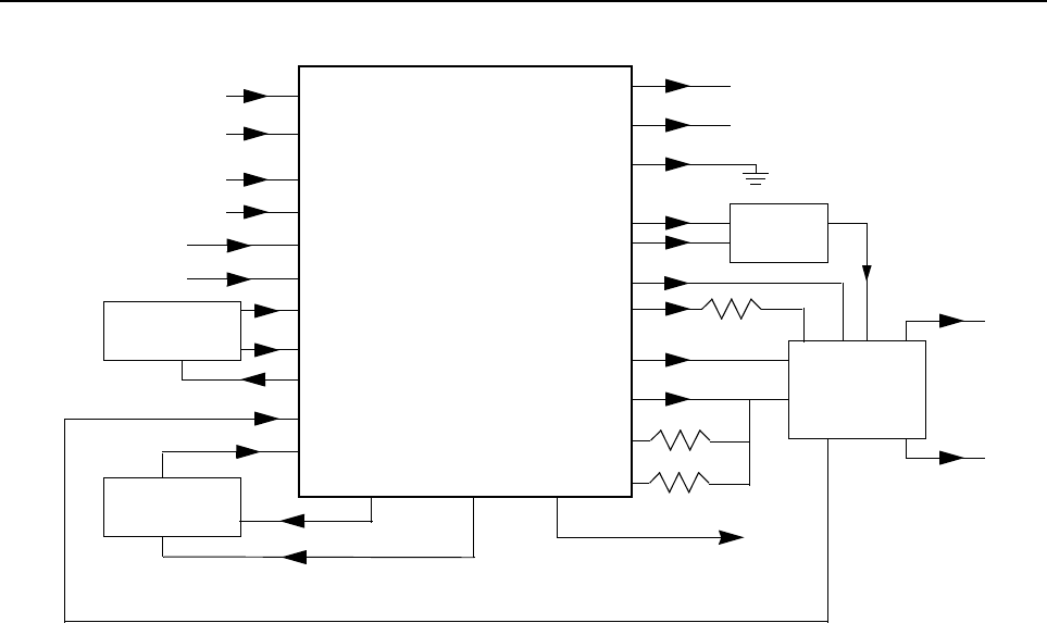
UHF (450-520 MHz) Frequency Synthesis 2-7
Figure 2-3 UHF Synthesizer Block Diagram
Output LOCK (U5201-4) provides information about the lock status of the synthesizer loop. A high
level at this output indicates a stable loop. IC U5201 provides the 16.8 MHz reference frequency at
pin 19.
The serial interface (SRL) is connected to the µP via data line DATA (U5201-7), clock line CLK
(U5201-8), and chip enable line CSX (U5201-9).
DATA
CLK
CEX
MODIN
VCC, DC5V
XTAL1
XTAL2
WARP
PREIN
VCP
REFERENCE
OSCILLATOR
VOLTAGE
MULTIPLIER
DATA (U0101 PIN 100)
CLOCK (U0101 PIN 1)
CSX (U0101 PIN 2)
MOD IN (U0221 PIN 40)
+5V (U4211 PIN 1)
7
8
9
10
13, 30
23
24
25
32
47
VMULT2 VMULT1
BIAS1
SFOUT
AUX3
AUX4
IADAPT
IOUT
GND
FREFOUT
LOCK 4
19
6, 22, 33, 44
43
45
3
2
28
14 15
40
FILTERED 5V
STEERING
LOCK (U0101 PIN 56)
PRESCALER IN
FREF (U0221 PIN 34)
39
BIAS2
41
48
5, 20, 34, 36
+5V (U4211 PIN 1)
AUX1
VDD, DC5V MODOUT
U5201
LOW VOLTAGE
FRACTIONAL-N
SYNTHESIZER
AUX2 1 (NU)
BWSELECT
VCO Bias
TRB
To IF
Section
TX RF INJECTION
(1ST STAGE OF PA)
LO RF INJECTION
VOLTAGE
CONTROLLED
OSCILLATOR
LINE
2-POLE
LOOP
FILTER

2-8 UHF (450-520 MHz) Frequency Synthesis
4.3 Voltage Controlled Oscillator (VCO)
The voltage controlled oscillator (VCO), shown in Figure 2-4, consists of a VCO buffer IC (VCOBIC,
U5301), TX and RX tank circuits, external RX buffer stages, and modulation circuits.
The VCOBIC together with Fractional-N synthesizer (U5201) generates the required frequencies in
both transmit and receive modes. The TRB line (U5301, pin 19) determines which tank circuits and
internal buffers are to be enabled. A high level on TRB enables TX tank and TX output (pin 10), and
a low enables RX tank and RX output (pin 8). A sample of the signal from the enabled output is
routed from U5301, pin 12 (PRESC_OUT), via a low pass filter of U5201, pin 32 (PREIN).
A steering line voltage (VCTRL) between 3.0V and 10.0V at varactor diode CR5311 tunes the full
TX frequency range (TXINJ) from 450 MHz to 520 MHz, and at varactor diodes CR5301, CR5302,
and CR5303 tunes the full RX frequency range (RXINJ) from 405 MHz to 475 MHz. The tank circuits
uses the Hartley configuration for wider bandwidth. For the RX tank circuit, external transistor
Q5301 is used in conjunction with the internal transistor for better side-band noise.
Figure 2-4 UHF VCO Block Diagram
Presc
RX
TX
Matching
Network Low Pass
Filter
Attenuator
Pin8
Pin14
Pin10
(U5201 Pin28)
VCC Buffers
TX RF Injection
U5201 Pin 32
AUX3 (U5201 Pin2)
Prescaler Out
Pin 12Pin 19
Pin 20
TX/RX/BS
Switching Network
U5301
VCOBIC
Rx
Active Bias
Tx
Active Bias
Pin2
Rx-I adjust
Pin1
Tx-I adjust
Pins 9,11,17
Pin18
Vsens
Circuit
Pin15
Pin16
RX VCO
Circuit
TX VCO
Circuit
RX Tank
TX Tank
Pin7
Vcc-Superfilter
Collector/RF in
Pin4
Pin5
Pin6
RX
TX
(U5201 Pin28)
Rx-SW
Tx-SW
Vcc-Logic
(U5201 Pin28)
Steer Line
Voltage
(VCTRL)
Pin13
Pin3
TRB IN
LO RF INJECTION
Q4301
Q4332

UHF (450-520 MHz) Frequency Synthesis 2-9
The external RX buffers (Q5332) are enabled by a high at U5201, pin 3 (AUX4) via transistor switch
Q5333. In TX mode, the modulation signal (VCOMOD) from the LVFRAC-N synthesizer IC (U5201,
pin 41) is applied to the modulation circuits CR5321, R5321, R5322, and C5324. These modulate
the TX VCO frequency via coupling capacitor C5321. Varactor CR5321 is biased for linearity from
the VSF.
4.4 Synthesizer Operation
The synthesizer consists of a low voltage FRAC-N (LVFRACN) IC, reference oscillator (crystal
oscillator with temperature compensation), charge pump circuits, loop filter circuits, and dc supply.
The output signal (PRESC_OUT) of the VCOBIC (U5301, pin12) is fed to of U5201, pin 32 (PREIN)
via a low pass filter (C5229,L5225,and C5226) which attenuates harmonics and provides correct
level to close the synthesizer loop.
The pre-scaler in the synthesizer (U5201) is a dual modulus pre-scaler with selectable divider ratios.
The divider ratio of the pre-scaler is controlled by the loop divider, which in turn receives its inputs via
the SRL. The output of the pre-scaler is applied to the loop divider. The output of the loop divider is
connected to the phase detector, which compares the loop divider´s output signal with the reference
signal.The reference signal is generated by dividing down the signal of the reference oscillator
(Y5261 or Y5262).
The output signal of the phase detector is a pulsed dc signal routed to the charge pump. The charge
pump outputs a current at U5201, pin 43 (IOUT). The loop filter (consisting of R5221-R5223, C5221-
C5225, and L5221) transforms this current into a voltage that is applied to varactor diodes CR5311
for transmit, CR5301, CR5302 and CR5303 for receive and alters the output frequency of the
VCO.The current can be set to a value fixed in the LVFRAC-N IC or to a value determined by the
currents flowing into BIAS 1 (U5201-40) or BIAS 2 (U5201-39). The currents are set by the value of
R5251 or R5252 respectively. The selection of the three different bias sources is done by software
programming.
To reduce synthesizer lock time, when new frequency data has been loaded into the synthesizer, the
magnitude of the loop current is increased by enabling the IADAPT (U5201-45) for a certain software
programmable time (Adapt Mode). The adapt mode timer is started by a low to high transistion of the
CSX line. When the synthesizer is within the lock range, the current is determined only by the
resistors connected to BIAS 1, BIAS 2, or the internal current source. A settled synthesizer loop is
indicated by a high level of signal LOCK (U5201-4) which is routed to one of the µP´s ADCs input
U101-56. From the voltage the µP determines whether LOCK is active.
To modulate the PLL, the two-spot modulation method is utilized via pin 10 (MODIN) on U5201. The
audio signal is applied to both the A/D converter (low frequency path) and the balanced attenuator
(high frequency path). The A/D converter converts the low frequency analog modulating signal into
a digital code which is applied to the loop divider, thereby causing the carrier to deviate. The
balance attenuator is used to adjust the VCO’s deviation sensitivity to high frequency modulating
signals. The output of the balance attenuator is present at the MODOUT port (U5201-41) and
connected to the VCO modulation diode CR5321 via R5321 and C5325.

2-10 UHF (450-520 MHz) Frequency Synthesis
THIS PAGE INTENTIONALLY LEFT BLANK
3-1
Section 3
TROUBLESHOOTING CHARTS
1.0 Troubleshooting Flow Chart for Receiver (Sheet 1 of 2)
Bad SINAD
Bad 20dB Quieting
No Recovered Audio
START
Audio at
pin 8 of
U3101 ?
Check Controller
(in the case of no audio)
OR ELSE go to “B”
Yes
No
Spray or inject 44.85MHz
into XTAL Filter FL3101
Audio heard ?
BYes
No
Check 2nd LO
(44.395MHz) at C3135
LO present ?
B
Yes
Check voltages on
U3101
Biasing OK ?
No
No
A
Yes
Check Q3102 bias
for faults
Replace Q3102
Go to B
Yes
No
Check circuitry
around U3101.
Replace
U3101 if defect
Check circuitry around Y3101.
Replace Y3101 if defect
Voltages
OK?
3-2 Troubleshooting Flow Chart for Receiver
1.1 Troubleshooting Flow Chart for Receiver (Sheet 2 of 2)
IF Signal at
C3101?
No
RF
Signal at
T5051?
RF
Signal at
C5015?
No
No
RF
Signal at
C5025?
No or
Check harmonic filter
L5491-L5493, C5492, J5401
and ant. switch
D5471, D5472, L5472.
Check filter between
C5025 & C5009.
Check tuning voltage
at R5060.
Inject RF into J5401
Is
tuning voltage
OK?
No
Yes
Check RF amp (Q5003)
Stage.
Check filter between
C5015 & T5051.
Yes
Check T5051, T5052,
D5051, R5052, L5008.
Yes
1st LO level
OK?
Locked?
Yes
Check FGU
Yes
Trace IF signal
from C3101 to
Q3101. Check for
bad XTAL filter.
No
Yes IF
signal at Q3102
collector?
Before replacing
U3101, check
U3101 voltages.
Yes
Check for
5VDC
Is 9V3
present?
Check Supply Voltage
circuitry. Check Q0681,
U5211 and U0641.
No
No
No
Check U5501.
Check varactor filter.
No
Yes
Yes
Yes
A
A
B
weak RF
RF
Signal at
C5009?
Troubleshooting Flow Chart for 40W Transmitter 3-3
2.0 Troubleshooting Flow Chart for 40W Transmitter
Q5441 gate (63kohm)
and drain resistances
(15kohm)
Check
No
Yes
Is drive from VCO
>+4dBm?
Is voltage
drop across R5497
between 1V and 0.7V
when Tx power
= 44W?
No
No
Q5421 gate (12kohm)
and drain resistances
(15kohm)
Check
No
PCIC_MOSBIAS_1
Check
No
No
Change
Q5473
START
No power
Is Vctrl
there?
Is Q5473
OK?
Check voltage
n pin 4, U5501
Check voltage
on pin 5, U5501
Check R5422-5
and go back to top
Troubleshoot
ASFIC
Change
PCIC
Check R5409 and
R5473 and go back
to top
Check
MOSBIAS_2/
MOSBIAS_3
Check
ASFIC
Are D5471 &
D5472 OK?
Change
D5471 &
D5472
No
No No
Yes
Yes
Yes
Yes
Yes
Yes Yes
Yes
No
No Check
PCIC
Yes
Change Q5421
Change Q5441
Change U5401
Yes Do visual check
on all components
No
Troubleshoot
VCO
Check voltage
on TP5531
Check if Pressure
Pad closes S5440
Yes
3-4 Troubleshooting Flow Chart for Synthesizer
3.0 Troubleshooting Flow Chart for Synthesizer
5V
at pin 6 of
D5201
Is
information
from µP U0101
correct
?
Is
U5201 Pin 47
at = 13VDC
?
Is
U5301 Pin 19
<40 mVDC in RX &
>4.5 VDC in TX?
(at VCO section)
?
Start
Visual
check of the
Board
OK?
Correct
Problem
Check 5V
Regulator
U5211
+5V
at U5201
Pins
13 & 30
?
Is
16.8MHz
Signal at U5201
Pin 19
?
Check
Y5261 / Y5262 and
associated parts
Are
signals
at Pins 14 &15
of U5201
?
Check
R5201 Check C5381
Is
U5201
Pin 2 >4.5 VDC in
Tx & <40 mVDC
in Rx
?
Replace
U5201
Remove
Shorts
Is
there a short
between Pin 47 and
Pins 14 & 15 of
U5201
?
Replace or
resolder
necessary
components
Is
RF level at
U5201 Pin 32
-12 < x <-25
dBm
?
Are
R5221,R5222,
R5223,C5221,
C5222,& C5223
OK?
Replace
U5201
If C5227
is OK, then see VCO
troubleshooting chart
Are
Waveforms
at Pins 14 & 15
triangular
?
Do
Pins 7,8 & 9
of U5201 toggle
when channel is
changed?
Check programming
lines between
U0101 and U5201
Pins 7,8 & 9
Replace
U5201
Check µP U0101
Troubleshooting
Chart
NO
YES
NO
YES
NO
YES
NO
NO
NO
YES
YES
NO
YES
YES
NO
YES
YES
YES
NO
NO
NO
NO
YES
NO
YES
YES
Check D5201,
C5202, C5203, &
C5206
5V
at U5201
pins 5, 20, 34
& 36
C h e c k 5 V
Regulator
U5211
Is
16.8MHz
signal at
U5201 Pin
23?
Replace
U5201
YES
NO
NO
YES
NO
YES
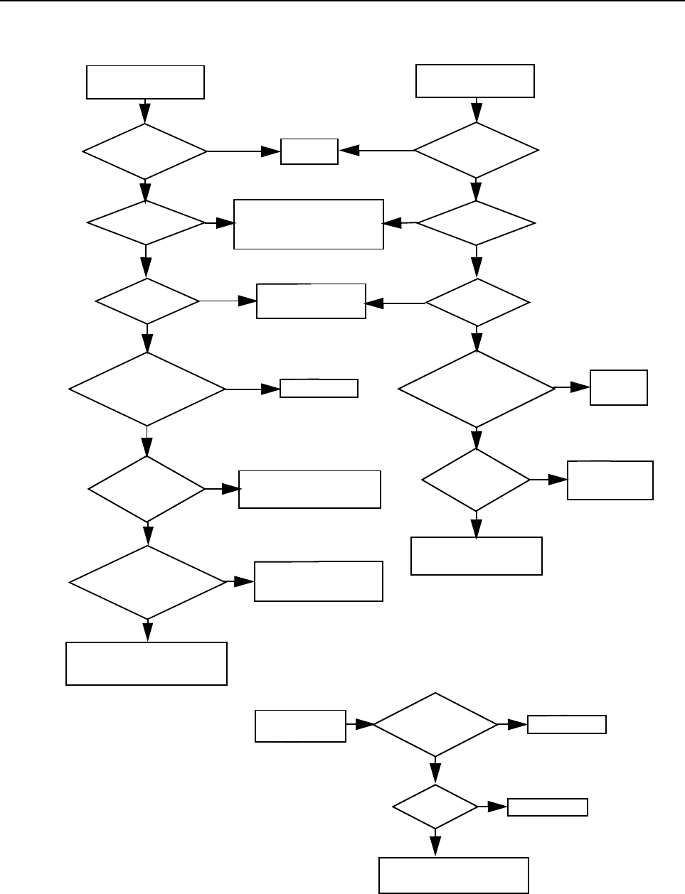
Troubleshooting Flow Chart for VCO 3-5
4.0 Troubleshooting Flow Chart for VCO
Are Q5332
Base at 0.7V
Collector at 4.5V
Emitter at 110mV
Are Q5301
Base at 2.4V
Collector at 4.5V
Emitter at 1.7V
Are Q5311
Base = 1.9V
Collector = 4.5V
Emitter = 1.3V
Low or no RF Signal
at TP5003
Visual check
of board
OK?
35mV DC at
U5301 Pin 19
NO
YES
Replace Q5301
at base of Q5332
NO
NO
NO
NO
YES
YES
YES
YES
Low or no RF Signal
at input to PA
4.8V DC at
U5301 Pin 19
Is RF available
at U5401
YES
YES
YES
YES
NO
NO
NO
NO
NO
Audio =180mVrms
at “-” S
ide of
4.5VDC
at CR5321
If C5321 and R5321 are OK,
then replace CR5321
Replace C5322
Replace C5325
NO
NO
YES
YES
TX VCO
RX VCO
Correct
Problem
Visual check
of board
OK?
Check runner
between U5201 Pin 2
and U5301 Pin 19
Is RF available If all parts from U5301 Pin 8
to Base of Q5332 are OK,
replace U5301
If all parts associated
with the pins are OK,
replace Q5332
If all parts from collector
of Q5332 to TP5003 are
OK, Replace U5301
Power OK but
no modulation
If all parts from U5301 Pin 10
U5401 Pin 16 are OK,
replace U5301
Replace
Q5311
YES
YES
Make sure Synthesizer is
working correctly and runner
between U5201 Pin 28 and
U5301 Pin 14 & 18 are OK
4.5V DC
OK ?
OK? OK?
C5325
at U5301 Pin 14 & 18
4.5V DC
OK ?
at U5301 Pin 14 &18
NO
Pin 16
If R5361 and
L5361 are OK,
replace U5301

3-6 Troubleshooting Flow Chart for VCO
THIS PAGE INTENTIONALLY LEFT BLANK

4-1
Section 4
UHF PCB/SCHEMATICS/PARTS LISTS
1.0 Allocation of Schematics and Circuit Boards
1.1 Controller Circuits
The UHF circuits are contained on the Printed Circuit Board (PCB) which also contains the
Controller circuits. This Chapter shows the schematics for the UHF circuits only, refer to the
Controller section for details of the related Controller circuits . The PCB component layouts and the
Parts Lists in this Chapter show both the Controller and UHF circuit components. The UHF
schematics and the related PCB and parts list are shown in the tables below.
Table 4-1 UHF B2 40W Diagrams and Parts Lists
PCB : 8486250Z02 Main Board Top Side
8486250Z02 Main Board Bottom Side Page 4-3
Page 4-4
SCHEMATICS
Power Amplifier 40W
FRACN
Voltage Controlled Oscillator
Receiver Front End
IF
Page 4-5
Page 4-6
Page 4-7
Page 4-8
Page 4-9
Parts List
8486250Z02 Page 4-10

4-2 Allocation of Schematics and Circuit Boards
THIS PAGE INTENTIONALLY LEFT BLANK
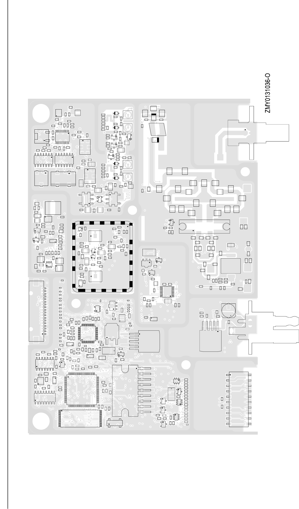
UHF Band 2 25-40W PCB / Schematics / Parts List 4-3
2.0 UHF Band 2 25-40W PCB / Schematics / Parts List
32
17
16 1
U0121
1
76
51
26
U0101
16
1
89
U0251
C0108
C0211
C0212
C0251
C0252
R0103
R0211
R0212
R0251
R0252
R0253
R0257
87
114
U0211
C0256
R0256
R0268
18
1
J0451
Q0110
C0253
C0261
C0262
C0421
R0102
R0110
R0115 R0227
R0261
R0262
R0269
C0441
C0442
C0443
C0445
C0446
C0447
C0448
R0442
R0222
C0131
C0132
R0131
R0132
23
4
Y0131
C0101
C0102
R0105
R0106
R0114
R0170
R0101
C0104
C0106
C0107 R0104
R0108
R0116
C0223
C0224
C0226
C0227
C0231
C0232
C0233
C0234
C0235
C0236
C0237
C0495
R0225
R0228
R0226
C0228
137
25
13
U0221
3
2
1
U0651
C0241
C0242
C0243
C0244
C0245
C0246
R0241
R0242
R0254
R0255
C0221
C0222
C0225
R0220
R0221
R0223
R0224
R0229
C0496
C0681
D0201
Q0681
R0681
R0682
9
U0271
C0651 C0652
D0651
R0651
R0652
1
6
5
U0641
C0482
C0483
C0486
C0487
C0488
C0493
C0494
C0654
C0655
L0481
L0482
C0449
C0470
C0471
C0472
C0473
C0474
C0476
C0477
C0478
C0490
C0502
C0503
C0504
C0505
C0506
C0508
C0509
C0510
C0512
C0542
Q0177
Q0181
Q0185
R0181 R0182
R0185 R0186
R0510
R0535
R0538
R0539
VR0501
VR0503
VR0505
VR0510
C0501
C0511
C0513
C0514
C0515
C0516
C0517
C0518
2011
10
J0501
R0508R0509
C0484
C0601
C0603
C0612
R0533
R0611
R0612
1
6
5
U0611
J0601
C5417
C5419
C5420
C5425
C5426
C5427
C5428
C5429
C5430
C5431
C5432 C5433
C5434
C5435
C5446
C5447
C5453
C5454
C5457
C5458
C5461
C5462
C5481
C5485 C5489 C5490
C5495C5497
C5602
L5474
M3421
R5408
R5415
R5416
R5417
R5418
R5480
3
2
1
45
6
7
8
Q5441
C5478
C5493
C5401
C5403
C5404
C5407
C5410
C5418
C5488
C5505 C5506
L5401
L5403
Q5471
Q5472
R5401
R5402
R5403
R5405
R5504
R5511
R5512
TP5530
1
16
8
9
U5401
VR5471
32
J5401
C5440
C5441
C5442
C5443
C5444
C5445
C5449
C5450
C5455
C5456
C5459
C5465
C5466
C5467
C5468
C5476
C5477
C5487
C5491
C5507
C5521
C5522
L5489
L5490
R5501
R5502 U5502
C5472
C5474
C5475
C5480
C5510
D5471 D5472
L5472
L5473
L5001
L5002
C5210
C5213
C5214
C5215
C5216
C5217
C5221
C5222
C5223
C5224
C5225
C5226
C5227
C5229
C5230
C5231
C5232
C5233
C5234 C5236
C5242
C5243
C5244
C5245
C5246
C5251
C5252
C5253
C5254
C5255
C5289
D5221
L5201
L5221
Q5221
R5211
R5221
R5222
R5223
R5224
R5225
R5227
R5251
R5252
U5211
C3124
C3133
L3124
R3123
R3124
2
Y3102
2
3
456
FL3102
2
3
456
FL3101
3
46
12
T5052
21
54
3
T5051
C5308
C5309
C5317
C5318
C5322
C5323
C5325
C5353
C5355
C5375
L5303
L5305
L5312
L5313
Q5301
Q5311
43
Q5333
R5305
R5311
R5312
R5321
R5346
3
C5331
C5332
C5335
C5337
C5339
C5351
C5352
C5371
C5372
C5373
C5374
C5382
C5383
3
L5304
L5371 R5301
R5302
R5331
R5332
R5333
R5337
R5341
R5343
R5345
SH5301
C5031
C5053
C5054
C5055
D5051
L5053
L5054
L5051
R5051
L5008
C3101
R3148
L3100
C5052
R5015
C5014
C5015
C5016
C5017
C5018
C5019
C5020
C5021
C5022
C5023
C5029
C5030
C5032
C5034
C5065
C5068
D5004
D5005
D5006
L5003
L5004
L5005
L5006
L5009
Q5001
R5005
R5007
R5012
R5013
R5020
R5064
R5066
C5001
C5002
C5003
C5004
C5005
C5006
C5007
C5008
C5009
C5026
C5027
C5033
D5001
D5002
D5003
Q5003
R5001
R5003
R5004
R5021
R5022
C3102
C3103
L3101
R3101
R3106
C3114
C3115
C3131
C3132
C3134
C3135
C3136
C3137
C3143
R3111
R3117
R3130
R3132
R3135
11
1
20
10
U3101
C3139
C3140
C3141
C3142
C3145
C3148
4
32
FL3112
FL3114
R3142
R3144
R3145
87
1
14
U3111
87
1
14
U3115
UHF Band 2 (450-520 MHz) 40W 8486250Z02 Top Side
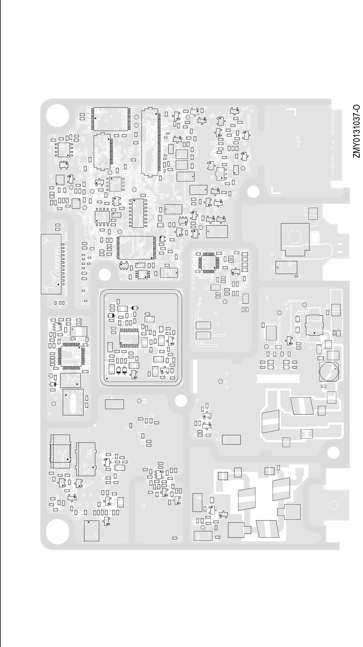
4-4 UHF Band 2 25-40W PCB / Schematics / Parts List
C3144
C3146
C3147
C3151 C3152
43
FL3111
FL3113
43
2
FL3115
Q3141
Q3151
Q3152
R3133
R3134
R3141
R3146
R3147
R3151
R3152
R3153
R3154
C3104
C3110
C3111
C3112
C3113
C3116
C3121
C3122
C3123
D3101
2
L3111
L3112
Q3101
Q3102
R3102
R3104
R3105
R3107
R3108
R3112
R3113
R3114
R3115
R3116 R3118
4
3
2
Y3101
C5024
C5060
C5066
R5019
R5052
R5053
R5054
R5055
R5060
TP5003
C5010
C5011
C5012
C5013
C5028
C5061
C5062
C5064
C5067
C5069
D5007
Q5002
Q5004
R5002
R5016
R5017
R5018
R5061
R5062
R5063
R5068
R5069
R5070
R5071
R5072
C5025
C5448
C5451
C5463
C5469
C5470
C5473
C5492
C5494
C5496
C5498
C5499 D5452
L5491
L5492
L5493
R5455
R5457
R5472R5475
R5491
R5496
TP5531
VR5473
C5422
C5439
L5421
L5437
L5438
C5452
C5464
D5451
D5453
R5409
R5471
R5473
R5474
R5506
R5507
TP5532
C5421
C5424
C5436
C5438
C5483
C5484
C5629
C5630 C5631
C5632
L5402
L5436
L5541
L5543
1
2
3
Q5421
Q5451
R5414
R5440
R5481
R5485
R5486
R5487
R5488
R5489
R5513
R5525
R5630
R5631
R5632
R5634
R5635
S5440
TP5537
TP5538
TP5536
C0499
C0611
E0631
VR0601
C0105
C0121
C0255
R0468
R0543
R0593
14
5
8
U0652
C0122
C0123
22
21 8
7
1
U0122
12
J0401
R0412
R0441
C0205
C0267
R0208
R0265
R0267
R0266
C0201
C0202
C0203 C0204
C0254 C0265
C0266
R0107
R0201
R0202
R0203
R0204
R0205
R0206
R0207
R0408 R0555
TP0102
TP0221
TP0222
U0653
VR0541
1
18
J0552
C0103
R0112
R0113
R0121 TP0103
TP0492
C0111
C0112
D0101
R0111
R0117
R0401
TP0101
TP0104
1
4
58
U0111
C0342
R0342
U0342
R0343R0347
C0422
C0423
C0426
C0427
C0428
C0429
C0430
C0431
F0401
R0407
R0409
R0467
C0304
C0305
C0324
C0325
C0341
C0343
C0344
R0323
R0324
R0341
R0344 R0345
R0346
TP0497
28 15
1
45
8
U0341
C0141
16
1
8
9U0141
C0491
C0492
C0497
C0485
R5495
R5497
C5402
C5405
C5409
C5412
C5413
C5414
C5415
C5416
C5479
C5502
C5503
C5504
L5404
L5411
Q5473
R5412
R5422
R5423
R5424
R5425
R5428
R5431
R5482
R5483
R5484
R5492
R5503
R5514
R5523
TP5533
1
17
9
25
U5501
C0301
C0302
C0303
C0331
C0351
C0352
C0353
C0354
C0641
C0644
C0645
C0662
C0663
C0671
D0301
Q0641
Q0661
Q0662
Q0663
R0331
R0332
R0333
R0335
R0481
R0482 R0641
R0642
R0643
R0662
R0671
R0672
14
1
U0301
U0331
4
58
U0351
C0275
C0621
C0622
C0661
D0621
D0660 D0661
Q0173
R0173
R0174
R0621
R0661
TP0661
VR0621
VR0671
Q0171
C0541
D0179
Q0183
R0171
R0172
R0175
R0176
R0177
R0178
R0179
R0183
R0184
R0511
R0512
R0525
R0529
R0530
R0531
R0537
R0541
R0542
TP0530
VR0504 VR0509
VR0537
C0151
C0271
C0272
C0273
C0274
C0276C0277
C0554
C0558
C0559
C0560
C0575
C0576
C0591
C0592 C0593
D0151
E0271
E0272
1
40
J0551
Q0151
Q0271
R0151
R0152
R0273
R0274
R0275
R0276
R0556
R0591
R0592
TP0151
VR0151
C5201
C5202
C5203
C5204
C5205
C5206
C5207
C5208 C5209
C5211
C5228
C5235
C5241
C5261
C5262
C5263
C5287
C5288 D5201
D5261
L5231
R5201
R5203
R5204
R5206
R5228
R5241
R5261
R5262
R5263
TP5201
TP5202
1
37
25 13
U5201
6
4
1
3
Y5261
2
34
Y5262
C5301
C5302
C5303
C5304
C5305
C5306
C5307
C5311
C5312
C5313
C5314
C5315
C5316
C5321
C5324
C5333
C5334
C5336
C5338
C5354
C5361
C5362
C5363
C5364
C5365
C5381
CR5301
CR5302
CR5303
CR5311
CR5321
L5301
L5302
L5311
L5331
L5332
L5333
L5361
L5362
Q5331
Q5332
R5303
R5304
R5313R5314
R5315
R5322
R5323
R5334
R5335
R5336
R5338
R5339
R5340
R5342
R5344
R5347
R5360
R5361
R5362
R5363
R5381
SH5302
11
120
10
U5301
UHF Band 2 (450-520 MHz) 40W 8486250Z02 Bottom Side
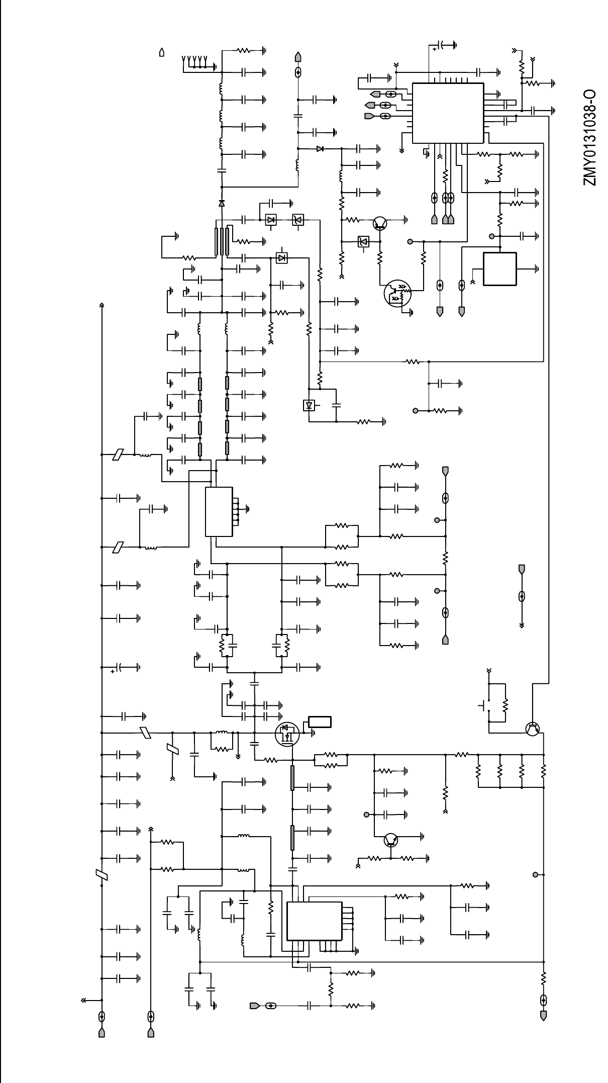
UHF Band 2 25-40W PCB / Schematics / Parts List 4-5
PASUPVLTG
9V3
C5481
3000pF
C5602
.033uF
PASUPVLTG_UHF_PA_1
C5485
30pF
PASUPVLTG
9V3_UHF_PA_1
L5402
57R01
C5421
.033uF
30pF
C5484
NU
NU
C5495
1000pF
C5497
1000pF
C5490
L5541
57R01
C5489 C5436
10uF
NU
L5474
BLM31A02PT
100pF
C5483
9V3
51
R5495
9V3
51
R5497
390nH
L5403
390nH
L5411
C5412
100pF
NU
NU
R5414
R5525
C5409
0.1uF
Load C5457
36pF
C5424
L5543
13.85nH
NU
NU
1
C5453
NU
C5458C5431
27pF
C5454
4.7pF
NU
NU
C5446
R5417
3.9pF
C5434
150pF
C5429
150pF
C5428
C5433
47pF
C5420
12pF
IN2
OUT1
OUT2
GND1
GND2
GND3
GND4
GND5
GND6
IN1
Q5441
NU
NU
R5418 C5430
3.9pF
C5427 C5432
47pF
C5435
12pF
51
R5489
R5481
51
51
R5486 R5485
51
NU
NU
NU C5447 C5419
C5461 39pF
C5462
R5415
51
3
HEATSINK
M3421
1
POS
Q5421
2
R5416
51
C5417
47pF
Load
NU
R5487
2K
R5412
NU
NU
3.7 to 3.9 VDC
R5488
TP5536
20K
R5408
C5426
100pF
.022uF
C5425
Q5451
100pF
C5415 C5416
.022uF
R5401
300
C5410
100pF
R5403
R5402
300
15
100pF
C5401
7
RFOUT2
1VCNTRL
14 VD1 2
VG1 3
VG2
12 GND3
13 GND4
8NC1
9NC2
10 NC3
15 NC4
16 RFIN 6
RFOUT1
U5401
17 EP
11 G2
4GND1
5GND2
30C65
4 to 6 dBm
TXINJ
T5_INJ_UHF_PA_1
NU
C5404
100pF
200
R5405
L5404
C5407
0.1uF
C5403
1.8pF
L5401
11.03nH
NU
NU
C5405
C5402
100pF
C5488
0.1uF
C5418
CNTLVLTG
3.3K
R5514
C5TLVLTG_UHF_PA_1
R5428
1.8K
100pF
C5413
.022uF
C5414
4.5 VDC (44W)
4.4 VDC (28W)
TP5533
PCIC_MOSBIAS_1
R5480
10K
R5424
620
R5422
620
620
R5425
620
R5423
NU
R5431
6.2 VDC (28W)
6.5 VDC (44W)
Q5473
2
NU
R5440
SWITCH
S5440
19V3
PA_PWR_SET_1_UHF_PA_1
PA_PWR_SET
PA_PWR_SET
NU
MOSBIAS_2
R5630
TP5537
BIAS_2_UHF_PA_1
R5634
100K
47K
R5631 100K
R5635
100pF
C5632 R5632
47K
C5630
0.1uF
100pF
C5629
C5631
0.1uF
MOSBIAS_3
BIAS_3_UHF_PA_1
TP5538
NU
C5493 C5478
1000pF
17nH
L5437
57R01
L5421
C5422
100pF
L5436
57R01
C5438
0.1uF
100pF
C5439
17nH
L5438
NU NU
C5476
C5449
3.9pF
3.3pF
C5491
C5466
13pF
C5442
30pF
C5441 C5443
6.8pF
L5489
4.22nH
4.22nH
L5490
NU
NU C5487
3.3pF
C5444
13pF C5477
C5440
30pF C5445
6.8pF C5467
3.3pF
C5450
R5409
100K
9V3
D5453 R5506
10K
NU
C5464 R5474
100K
NU
C5470
100pF
C5507
100pF
C5499
NU
4.3K
R5473 C5452
D5451
NU 100pF
C5459 120
R5457
C5468
3.9pF
C5456
NU
R5472
A+
NU
3.9pF
C5465 C5455
NU
R5471
D5471
C5469
100pF
D5452
VR5473
5.6V
NU
C5463
C5492
100pF
R5513
10K
L5493
17nH 17nH
L5491 17nH
L5492
DUMMY
2J5401-2
J5401-3
3
5
J5401-4
4J5401-5
1J5401-1
C5498
4.7pF 3.3pF
C5496
C5448
9pF
C5494
7pF
11K
R5491
R5_IN_VHF_PA_1
L5472
17nH
C5474
12pF
RXIN
100pF
C5479
9V3
2pF
C5475
NU
C5480
D5472
C5510
30pF
C5472
30pF
Q5472
R5511
51
L5473
43.67nH
C5473
100pF
R5496
82
5.6V
VR5471
Q5471
470
R5512
9.2 VDC PCIC_MOSBIAS_1
T5MPSENSE_UHF_PA
K9V1_UHF_PA_1
TEMPSENSE
K9V1
9V3
TP5530
10K
R5504
CLK
CSX
DATA
0.75 VDC
R5502
68K
TP5532
U5502
GND
3POS 1
2
VOUT
C5522
1000pF
R5501
5.6K
R5482
300K
R5484
20K
9V3
3.9K
R5503
100pF
C5521
31
30
28
25
32
27
29
26
10K
R5492
D5TA_VHF_PA_1
C5K_VHF_PA_1
C5X_VHF_PA_1
9V3
16
V45
V5EXT 17
VAR1 20
VAR2 18
VAR3 24
VG 15
6VL 19
VLIM
10
QX
RFIN
1
21
RS
RSET
23
RX
2T1
TEMP
14
V10
CQX 13
DATA
9
F168
8GND1
GND2
4INT
NA 22
11
Q
ANO
BPOS
CEX
3CI
5CJ
7CL
CLK
12
CQ
U5501
C5502
2200pF
C5504
.01uF
C5505
1uF
2200pF
C5506
2.2 VDC (28W)
3.1 VDC (44W)
100K
R5483
PA_PWR_SET
NU
R5523
470pF
C5503 ALT
R5507
10K
2.2 VDC (28W)
3.11 VDC (44W)
TP5531
0
R5475
NU
NU
R5455 C5451
FECTRL_2
FE_CNTL_2_VHF_PA_1
RESET
FECTRL_1
FE_CNTL_1_VHF_PA_1
R5SET_VHF_PA_1
A+
UHF Band 2 (450-520 MHz) Power Amplifier 40W
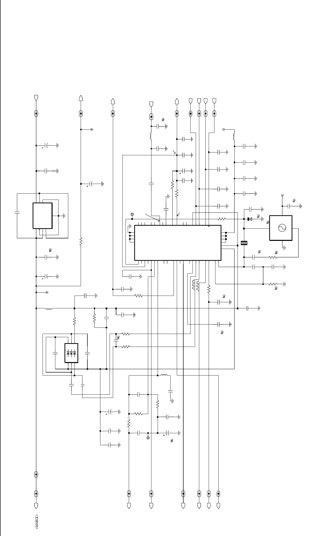
4-6 UHF Band 2 25-40W PCB / Schematics / Parts List
16_8MHz
C5202
.01uF
IN_5V_RF_REG_UHF_FN_1
TRB
MODIN
220
R5241
C5251
0.1uF
TP5202
1
.01uF
C5232
LOCK_UHF_FN_1
C5243
100pF
R5222
510
C5253
4.7uF
o
2.2uF
C5213
C5209
0.1uF
U4506
.01uF
C5231
CLK_UHF_FN_1
L5221
12uH
47K
R5228
1000pF
C5252
150
R5221
R5261
150K
100
R5263
VDDA
CLK
16.8MHz
XTAL
Y5261
1uF
C5223
VCNTL
1
VSF_UHF_FN_1
Y5262
TTS05V
16.8MHz
GND
2
OUT
3
VCC 4
MODIN_UHF_FN_1
2.2uF
C5214
0.1uF
C5254
D 5261
5V_UHF_FN_1
150
R5201
C5288
0.1uF
DATA
100pF
C5227
VDDA_UHF_FN_1
C5246
100pF
C5205
.01uF
1.5pF
C5263
68
R5223
C5235
.01uF
C5255
100pF
C5222
0.1uF
1.2K
R5262
C5245
100pF
C5244
47nH
L5225
100pF
TRB_UHF_FN_1
U4507
16_8MHz_UHF_FN_1 CSX_UHF_FN_1
C5204
0
R5211
100pF
BWSELECT_UHF_FN_1
C5207
100pF
C5228
0.1uF
5V_UHF_FN_2
VSF
C5211
0.1uF
2.4pF
C5226
C5206
10uF
2.2uF
C5210
220pF
C5262
47
R5203
LOCK
C5208
0.1uF
1uF
C5224
510pF
C5225
R5204
R5206
47
33K
C5216
.01uF
LP2951
U5211
VCOBIAS_2
C5212
.018uF
100pF
C5287
100pF
C5201
2pF
C5229
C5230
2.2uF
2.2uF
C5233
0.1uF
C5289
39K
R5251
VCTRL
TP5201
C5242
PRESC
CSX
100pF
L5231
VCOMOD_UHF_FN_1
IN_5V_RF_REG
2.2uH
C5241
100pF
5
A2
4
A3
K1
1
K2
2
K3
3
DATA_UHF_FN_1
6
A1
D5201
C5221
.01uF
.01uF
C5203
R5252
30K
VCTRL_UHF_FN_1
.01uF
C5234
L5201
390nH
62pF
C5261
5V
5V
2.2uF
C5215
VDDA
VDDA
U5201
4.57 VDC
-19 to -17 dBm (Rx)
-17 to -12 dBm (Tx)
4.98 VDC
0 VDC (Rx)
3.09 VDc (Rx)
2.65 VDC (Tx)
4.97 VDC (25KHz Chan. Spacing)
4.97 VDC (Tx)
2.48 VDC
1.76 VDC (Tx)
1.69 VDC (Rx)
0 VDc (12.5KHz Chan. Spacing)
5 VDC (Locked)
0 VDC (Unlocked)
2.5 to 10 Vdc
6.6 VDC
10.87 VDC
12.7 VDC
4.97 VDC
3.03 VDC
3.76 VDC
2.51 VDC
4.95 VDC
0 VDC
2.48 VDC
1.25 VDC
1.97
VDC
5V
VCOMOD
BWSELECT
23 XTAL1
XTAL2
24
21
VBPASS
47 VCP
VMULT1
15
14 VMULT2
12 VMULT3
11 VMULT4
VRO
13
25 WARP
35
PVREF
18
REFSEL
27
SFBASE 26
SFCAP
30
SFIN
28 SFOUT
37 TEST1
38 TEST2
17
NC1
29
NC2
31
NC3
44
PD_GND
PD_VDD
5
PREIN 32
33
PRE_GND
34 PRE_VDD
36 DVDD
19 FREFOUT
45 IADAPT
16 INDMULT
43 IOUT
LOCK
4
10
MODIN
41 MODOUT
20 AVDD
40
BIAS1
39
BIAS2
42
CCOMP
9
CEX 8
CLK
7
DATA
DGND 6
46 ADAPTSW
22
AGND
48 AUX1
1AUX2
2AUX3
3AUX4
INPUT
1OUTPUT
2SENSE 3
SHUTDOWN
65V_TAP
5ERROR 7
FEEDBACK
4
GND
8
ZWG0130364-0
HF Band 2 (450-520 MHz) FRACN

UHF Band 2 25-40W PCB / Schematics / Parts List 4-7
ZMY0130674-O
R5301
5.6K
RXSW
4.2 Vdc (Rx)
0 Vdc (Tx)
R5302
10K
0.22uF
C5371
C5372
100pF
NU
C5305
NU C5306
2pF
L5304
390nH
4.3pF
C5303 C5304
5.6pF
C5302
4.3pF
CR5302
CR5303
220nH
L5302
CR5301
L5301
68nH
68nH
L5311
C5317
100pF
100pF
C5301
NU
VCTRL_UHF_VCO R5315
0
2.5 to 10 Vdc
100pF
C5311 CR5311
C5316
0.1uF
15pF
C5312
VCOMOD
VCOMOD_UHF_VCO 4.7uF
C5325
VCTRL
C5323
1000pF
56K
R5321
C5322
100pF
NU NU
C5321
1pF
R5322
6.8K
CR5321
3pF
C5324 R5323
10K
VSF
NU
4.5 Vdc
P2
2
P3
3
RESONATOR
L5303
P1
1
R5303
30
R5304
150
100pF
C5307
R5311
TXSW 0 Vdc (Rx)
4.5 Vdc (Tx)
7.5K
0.22uF
C5318
L5313
390nH
R5312
7.5K
3pF
C5314
100pF
C5315
R5314
220
Q5311
0 Vdc (Rx)
1.9 Vdc (Tx)
P1
1
P2
2
P3
3
RESONATOR
L5312
C5313
NU R5313
30
C5382
100pF
0.1uF
C5381
TXSW
0 Vdc (Rx)
4.5 Vdc (Tx)
NU
TRB_UHF_VCO
R5381
470 TRB
0 Vdc (Rx)
4.5 Vdc (Tx)
TX_OUT
TX_SWITCH
VCC_BUFFERS 14
VCC_LOGIC 18
RX_IADJ
2RX_OUT
RX_SWITCH
SUPER_FLTR
3
TRB_IN
19
TX_BASE
16
TX_EMITTER
15
TX_IADJ
1
COLL_RFIN
4
FLIP_IN
20
GND_BUFFERS
11 GND_FLAG
9
17 GND_LOGIC
PRESC_OUT
RX_BASE
5
RX_EMITTER
6
U5301
50U54
10
13
8
7
12
4.5 Vdc (Rx)
2.58 Vdc (Tx)
100pF
C5383
39nH
C5365
L5362
3.3pF
RXSW
NU
4.2 Vdc (Rx)
0 Vdc (Tx)
10
R5335
PRESC
PRESC_UHF_VCO NU
NU
R5347
0
R5333
10K R5334
0
C5334
51pF
NU
NU
0.1uF
C5308
L5305
390nH
C5309
100pF R5305
10
VSF VSF_UHF_VC0
VSF
4.5 Vdc
Q5301
2.3 Vdc (Rx)
0 Vdc (Tx)
100pF
C5351
0.1uF
C5352 2.2uF
C5354
2.2uF
C5355
C5361
100pF
0.1uF
C5353
33nH
L5331
R5361
180
390nH
L5361 0.22uF
C5362
270
R5360
C5364
5.6pF
NU
1K
R5363
VSF
C5374
C5363
NU
NU
NU
C5373
L5371
68nH 5.6pF
C5331
4 dBn (Tx)
R5362
10
C5332
0.1uF
C5333
22K
R5332 L5332
15nH R5336
1K
NU NU NU NU
51pF
NU
TXINJ_UHF_VCO
Q5331
R5331
22
TXINJ
NU
R5337
0
NU
5V_UHF_VCO
VCOBIAS_2_UHF_VCO
C5375
10K
R5346
VCOBIAS_2
5V
NU
Q5333
0
R5341
4.7K
47K
47K
10K 4.5 Vdc (Rx)
0 Vdc (Tx)
51pF
C5337
R5342
2.2K L5333
390nH
C5336
.022uF
R5344
10
22
R5339
R5343
1K
220
R5338
100pF
C5335
Q5332
NU
NU
51pF
C5338
220
R5340
NU
R5345 C5339
RXINJ
RXINJ_UHF_VCO
>14 dBn (Rx)
NU
NU
SHIELD
SH5302
1
SHIELD
SH5301
1
GND
UHF Band 2 (450-520 MHz) Voltage Controlled Oscillator

4-8 UHF Band 2 25-40W PCB / Schematics / Parts List
C5055
L5053
C5002
15nH
33pF
16pF
8.2pF
C5031
C5020
Q5002
GND
15nH
L5054
C5024
1000pF
D5002
C5026
1pF
GND_UHF_FE
1000pF
C5008
R5015
100K
R5001
R5017
330K
R5060
3300pF
RXINJ
C5011
C5021
24pF
L5004
IN
NEG
TBD
C5025
D5004
82pF
C5052
150
R5019
R5010
8.2pF
C5032
33
R5008
15nH
L5006
4
C5030
1pF
XFMR
T5051
1
2
3
5
R5022
0
270
R5006
1.5pF
C5017
RXIN_UHF_FE
9V3
C5016
D5001
C5066
TP5003
TBD L5005
IN
NEG
TBD
L5001
IN
NEG
150nH
L5051
L5008
470nH
10K
9V3
2
R5005
T5052
XFMR
4
6
3
1
100K
27pF R5012
C5007
68
R5007
270
TBD
L5002
IN
NEG
R5011
Q5001
FECTRL_1_UHF_FE
1pF
C5029
R5020
10
C5060
R5016
C5023
C5054
16pF
C5009
8.2pF
IF
D5003
0.1uF
C5034
FECTRL_1
C5004
16pF C5006
Q5003
L5009
10
R5021
R5051
15nH
51
20pF
C5003
330
R5002
C5013
3300pF
0
R5052
270nH
R5054
RXIN
L5003
330pF
C5012
C5027
1pF
R5018
R5053
R5003
4.7K
R5013
150
R5009
C5028
100pF
C5015
R5055
9V3_UHF_FE
IF_UHF_FE
C5001
1.5pF
18pF
C5005
100pF
C5014
6.8pF
C5053
R5004
2.7K
C5033
TP5001
0.1uF
RXINJ_UHF_FE
16pF
C5022
TP5002
C5018
33pF
D5051
IO1
1IO2 2
IO3
3
IO4
4
C5019
24pF
330pF
C5010
D5005
GROUND
POS
15pF
POS
POS
POS
3.4 VDC @ 450MHz
4.7 VDC @ 450MHz
6.5 VDC @ 450MHz
0.7 VDC
4.6 VDC
UHF Band 2 (450-520 MHz) Receiver Front End

UHF Band 2 25-40W PCB / Schematics / Parts List 4-9
9186176B01
9180469V04
9180469V03
9180469V06 9180468V06
R3144
2.4K
BWSELECT_VHF_IF_1
9V3_VHF_IF_2
C3113
9.1pF
NU
R3104
100
NU
100
620nH
NU
R3105
R3130
L3100
14
VDD
7
VSS
51
U3111-1
MC74HC4066
13
CNTL
1
2
C3116
L3112
0.1uF
620nH
9V3_VHF_IF_1
10uF
C3133
0.1uF
C3132
.01uF
C3151
OUT 2
C3137
.039uF
CFWC455D
FL3112
GND1
34
GND2
IN
1
620nH
C3121
L3101
0.1uF
R3101
12K
12K
R3147
15pF
DISCAUDIO
C3102
C3152
.01uF
0.1uF
C3139
7
VSS
0.1uF
C3141
U3115-1
MC74HC4066
MC74HC4066
13
CNTL
1
2
14
VDD
DISCAUDIO_VHF_IF_1
620nH
620
L3111
R3108
27pF
C3110
0.1uF
C3147
C3155
9V3
.01uF
NU
Q3155
FL3115
3
GND1GND2
4
1IN 2
OUT
BWSELECT
GND3
45
GND4
3IN 6
OUT
CFWC455F
12R16
FL3102
1
GND1
GND2
2
GND1
12
GND2
4
GND3
GND4
5
IN
3OUT 6
12R16
FL3101
7
C314 2
0.1uF
MC74HC4066
CNTL
6
89
VDD
14
VSS
GND
3
IN
1OUT 2
RSSI
U3111-3 FL3114
CFUCJ455D
4700pF
C3146
27K
GND1
34
GND2
IN
1OUT 2
R3106
OUT
3IN 1
FL3111
CFWC455G
Y3101
12R17
44.395MHz
GND
2
GND1
4
C3131
1pF
NU
0.1uF
C3145
5V_VHF_IF_1
IFIN_VHF_IF_1
IF
330
R3116
10K
R3134
0.1uF
C3144
18pF
C3114
10K
R3155
R3151
VDD
7
VSS
NU
1.2K
U3111-4
MC74HC4066
12
CNTL
14
CNTL
5
4
3VDD
14
VSS
7
U3115-2
MC74HC4066
0.1uF
C3104
C3135
33pF
12
CNTL
11
14
VDD
7
VSS
7
U3115-4
MC74HC4066
MC74HC4066
CNTL
5
4
3VDD
14
VSS
3.3K
U3111-2
R3145
0.1uF
C3140
390
R3115
Q3152
3
22pF
Y3102
455KHz
45B02
C3115
82pF
C3112 C3123
.039uF
R3112
10
0102727B45
0
R3148
0.1uF
C3111
Q3151
27K
R3117
Q3102
8.2K
R3133
Q3101
C3136
30pF
20pF R3102
C3101
33pF
10
C3103
C3134
0.1uF
RSSI_VHF_IF_1
6.8K
R3118
R3111
12K
C3122
.039uF
6.8K
R3107
NU
100
R3114
R3154
5V
10K
10K
R3153
D3101
120pF
C3143
R3152
10K
1.2K
CNTL
6
VDD
14
VSS
7
R3135
U3115-3
MC74HC4066
680
R3146
R3160
0
R3132
15K
FL3113
CS455G2 NU
GND
3
IN
1OUT 2
9V3
5V
5V
9V3
9V3
9V39V3
9V3
5V
9V3
89
10
11 10
OSCIN 4
OSCOUT
3
QUADIN 10
RFIN 1
RFIN_DEC 2
RSSIOUT
5RSSI_FEED 9
VCC
6
IFAMPOUT
16
IFAMP_DEC1 19
IFAMP_DEC2
17
LIMIN 14
LIMOUT
11
LIM_DEC1
13
LIM_DEC2
12
MIXOUT
20
SA616
SA616
AUDIOOUT
8AUDIO_FEED 7
GND 15
IFAMPIN 18
U3101
ZWG0130367-0
UHF Band 2 (450-520 MHz) IF

4-10 UHF Band 2 25-40W PCB / Schematics / Parts List
UHF Band 2 PCB 8486250Z02 Parts List 25-
40W
Circuit
Ref Motorola
Part No. Description
C0101 2113740F51 100pF
C0107 2113741F25 1000pF
C0112 2113743E20 0.1uF
C0121 2113743E20 0.1uF
C0122 2113743E20 0.1uF
C0131 2113740F35 22pF
C0132 2113740F35 22pF
C0141 2113743E20 0.1uF
C0151 2113741F49 10nF
C0201 2311049A57 10uF
C0202 2311049A57 10uF
C0204 2113743E20 0.1uF
C0212 2311049A57 10uF
C0221 2113743E20 0.1uF
C0222 2113743E20 0.1uF
C0223 2113743E20 0.1uF
C0224 2113740F51 100pF
C0225 2113743E20 0.1uF
C0226 2113743E20 0.1uF
C0228 2311049A56 4.7uF
C0231 2113743B29 1uF
C0232 2113743E20 0.1uF
C0234 2113743E20 0.1uF
C0235 2113743E07 0.022uF
C0236 2113743E10 0.033uF
C0241 2113743E20 0.1uF
C0243 2113740F51 100pF
C0244 2113743E20 0.1uF
C0245 2113743E20 0.1uF
C0246 2113741F49 10nF
C0251 2113743E20 0.1uF
C0252 2311049A07 1uF
C0254 2113743E20 0.1uF
C0255 2113743E20 0.1uF
C0256 2113740F51 100pF
C0261 2113743E20 0.1uF
C0262 2113740F49 82pF
C0265 2113743E20 0.1uF
C0267 2113741F49 10nF
C0271 2113741F49 10nF
C0272 2113743E20 0.1uF
C0273 2113741F37 3300pF
C0275 2311049A99 47uF
C0276 2113741F25 1000pF
C0277 2113741F25 1000pF
C0301 2311049A07 1uF
C0302 2113743E20 0.1uF
C0303 2113740F51 100pF
C0304 2113743E20 0.1uF
C0305 2113743E20 0.1uF
C0324 2113743E20 0.1uF
C0331 2113743E20 0.1uF
C0341 2311049A07 1uF
C0342 2113743E20 0.1uF
C0343 2113743E20 0.1uF
C0344 2113743E20 0.1uF
C0351 2113743E20 0.1uF
C0352 2113743E07 0.022uF
C0353 2311049A97 33uF
C0354 2113743E20 0.1uF
C0421 2113743N48 82pF
C0422 2113741F17 470pF
C0423 2113741F17 470pF
C0426 2113743L09 470pF
C0427 2113743L09 470pF
C0428 2113743N48 82pF
C0429 2113743L09 470pF
C0430 2113741F17 470pF
C0431 2113741F17 470pF
C0441 2113743L09 470pF
C0442 2113743L09 470pF
C0445 2113743L09 470pF
C0446 2113743L09 470pF
C0447 2113743L09 470pF
C0448 2113743L09 470pF
C0449 2113743L09 470pF
C0470 2113743L09 470pF
C0471 2113743N48 82pF
C0472 2113743N48 82pF
C0473 2113743N48 82pF
C0474 2113743L09 470pF
C0476 2113743L09 470pF
C0477 2113743L09 470pF
C0478 2113743L09 470pF
C0482 2113743L09 470pF
C0483 2113743L09 470pF
C0484 2113741F17 470pF
C0485 2113743L09 470pF
C0486 2113743L09 470pF
C0487 2113743L09 470pF
C0488 2113743L09 470pF
C0490 2113743L09 470pF
C0491 2113743L09 470pF
C0492 2113743L09 470pF
C0493 2113743L09 470pF
C0494 2113743L09 470pF
C0495 2113743L09 470pF
C0496 2113743L09 470pF
C0497 2113743L09 470pF
C0499 2113743L09 470pF
Circuit
Ref Motorola
Part No. Description
C0501 2113741F49 10nF
C0502 2113741F17 470pF
C0503 2113741F17 470pF
C0504 2113741F17 470pF
C0505 2113741F17 470pF
C0506 2113741F17 470pF
C0508 2113741F17 470pF
C0509 2113741F17 470pF
C0510 2113741F17 470pF
C0511 2113741F17 470pF
C0512 2113741F17 470pF
C0513 2113741F17 470pF
C0514 2113741F17 470pF
C0515 2113741F17 470pF
C0516 2113741F49 10nF
C0517 2113743N48 82pF
C0518 2113741F17 470pF
C0541 2311049A05 0.47uF
C0542 2311049A99 47uF
C0560 2113743L17 1000pF
C0591 2113743E20 0.1uF
C0592 2113743E20 0.1uF
C0593 2113741B69 0.1uF
C0601 2113741F17 470pF
C0603 2380090M24 10uF
C0611 2311049C06 22uF
C0612 2113743E20 0.1uF
C0622 2311049A99 47uF
C0641 2113741F17 470pF
C0644 2311049A97 33uF
C0645 2113743E20 0.1uF
C0652 2311049A97 33uF
C0654 2311049A57 10uF
C0655 2113743E20 0.1uF
C0661 2311049C05 47uF
C0662 2113741F49 10nF
C0663 2113743E20 0.1uF
C0671 2113743E20 0.1uF
C0681 2113743E20 0.1uF
C3101 2113740F34 20pF
C3102 2113740F31 15pF
C3103 2113740F39 33pF
C3104 2113743E20 0.1uF
C3110 2113740F37 27pF
C3111 2113743E20 0.1uF
C3112 2113740F49 82pF
C3114 2113740F33 18pF
C3115 2113740F35 22pF
C3116 2113743E20 0.1uF
C3121 2113743E20 0.1uF
C3122 2113743E11 0.039uF
Circuit
Ref Motorola
Part No. Description
C3123 2113743E11 0.039uF
C3124 2113740L30 33pF
C3132 2113743E20 0.1uF
C3133 2311049A57 10uF
C3134 2113743E20 0.1uF
C3135 2113740L30 33pF
C3136 2113740F35 22pF
C3137 2113743E11 0.039uF
C3139 2113743E20 0.1uF
C3140 2113743E20 0.1uF
C3141 2113743E20 0.1uF
C3142 2113743E20 0.1uF
C3143 2113740F53 120pF
C3144 2113743E20 0.1uF
C3145 2113743E20 0.1uF
C3146 2113741F41 4700pF
C3147 2113743E20 0.1uF
C3151 2113741F49 10nF
C3152 2113741F49 10nF
C5001 2113740F07 1.5pF
C5002 2113740F39 33pF
C5003 2113740F35 22pF
C5004 2113740F32 16pF
C5005 2113740F32 16pF
C5006 2113740F32 16pF
C5007 2113740F32 16pF
C5008 2113741F25 1000pF
C5009 2113740F25 8.2pF
C5010 2113741F13 330pF
C5011 2113741F37 3300pF
C5012 2113741F13 330pF
C5013 2113741F37 3300pF
C5014 2113740F51 100pF
C5015 2113740F51 100pF
C5017 2113740F07 1.5pF
C5018 2113740F39 33pF
C5019 2113740F37 27pF
C5020 2113740F32 16pF
C5021 2113740F33 18pF
C5022 2113740F32 16pF
C5024 2113741F25 1000pF
C5026 2113740F03 1pF
C5027 2113740F03 1pF
C5028 2113741F49 10nF
C5029 2113740F03 1pF
C5030 2113740F03 1pF
C5031 2113740F25 8.2pF
C5032 2113740F25 8.2pF
C5033 2113740F51 100pF
C5034 2113740F51 100pF
C5052 2113740F49 82pF
Circuit
Ref Motorola
Part No. Description

UHF Band 2 25-40W PCB / Schematics / Parts List 4-11
C5053 2113740F23 6.8pF
C5054 2113740F32 16pF
C5061 2113740F63 330pF
C5062 2113743E20 0.1uF
C5064 2113743E20 0.1uF
C5065 2113740F51 100pF
C5067 2113741F37 3300pF
C5068 2113740F51 100pF
C5069 2113741F49 10nF
C5201 2113740F51 100pF
C5202 2113741F49 10nF
C5203 2113741F49 10nF
C5204 2113740F51 100pF
C5205 2113741F49 10nF
C5206 2311049J25 10uF
C5208 2113743E20 0.1uF
C5209 2113743E20 0.1uF
C5210 2104993J02 2.2uF
C5211 2113743E20 0.1uF
C5213 2311049A09 2.2uF
C5214 2311049A09 2.2uF
C5215 2311049A09 2.2uF
C5217 2113741F49 10nF
C5221 2109720D01 0.01uF
C5222 2109720D14 0.1uF
C5224 0882422W23 1uF
C5225 2113741F18 510pF
C5227 2113740F27 10pF
C5230 2104993J02 2.2uF
C5231 2113741F49 10nF
C5232 2113741F49 10nF
C5233 2104993J02 2.2uF
C5234 2113741F49 10nF
C5235 2113741F49 10nF
C5236 2113743E12 0.047uF
C5242 2113740F51 100pF
C5243 2113740F51 100pF
C5244 2113740F51 100pF
C5245 2113740F51 100pF
C5246 2113740F51 100pF
C5251 2113743E20 0.1uF
C5252 2113741F25 1000pF
C5253 2311049A56 4.7uF
C5254 2113743E20 0.1uF
C5255 2113740F51 100pF
C5263 2113743E20 0.1uF
C5287 2113740F51 100pF
C5289 2113743E20 0.1uF
C5301 2113740F51 100pF
C5302 2113740L09 4.3pF
C5303 2113740L09 4.3pF
Circuit
Ref Motorola
Part No. Description
C5304 2113740L12 5.6pF
C5306 2113740L01 2pF
C5307 2113740F51 100pF
C5308 2113743E20 0.1uF
C5309 2113740F51 100pF
C5311 2113740F51 100pF
C5312 2113740F33 18pF
C5314 2113740L01 2pF
C5315 2113740F51 100pF
C5316 2109720D14 0.1uF
C5318 2113743K16 0.22uF
C5321 2113740F03 1pF
C5324 2113740F07 1.5pF
C5325 2311049A56 4.7uF
C5331 2113740L12 5.6pF
C5335 2113740F51 100pF
C5336 2113743E07 0.022uF
C5337 2113740F44 51pF
C5338 2113740F44 51pF
C5351 2113740F51 100pF
C5352 2113743E20 0.1uF
C5353 2113743E20 0.1uF
C5354 2104993J02 2.2uF
C5355 2104993J02 2.2uF
C5361 2113740F51 100pF
C5364 0662057B47 0
C5371 2113743K16 0.22uF
C5381 2113743E20 0.1uF
C5401 2113740F51 100pF
C5404 2113740F51 100pF
C5407 2113743E20 0.1uF
C5409 2113743E20 0.1uF
C5410 2113740F51 100pF
C5412 2113740F51 100pF
C5413 2113740F51 100pF
C5414 2113743E07 0.022uF
C5415 2113740F51 100pF
C5416 2113743E07 0.022uF
C5417 2113740F43 47pF
C5418 2113743E20 0.1uF
C5420 2113740A36 20pF
C5421 2113741A57 0.033uF
C5422 2111078B42 100pF
C5425 2113743E07 0.022uF
C5426 2113740F51 100pF
C5427 2113740A23 6.2pF
C5428 2113740A55 100pF
C5429 2113740A55 100pF
C5431 2113740A39 27pF
C5432 2113740A41 33pF
C5433 2113740A41 33pF
Circuit
Ref Motorola
Part No. Description
C5434 2113740A23 6.2pF
C5435 2113740A36 20pF
C5436 2380090M24 10uF
C5438 2113743E20 0.1uF
C5439 2111078B42 100pF
C5440 2111078B29 33pF
C5441 2111078B29 33pF
C5447 2113740F42 43pF
C5448 2180464E62 9pF
C5449 2111078B03 3.9pF
C5450 2111078B01 3.3pF
C5457 2113740A42 36pF
C5458 2113740A18 4.3pF
C5459 2113740A55 100pF
C5466 2111078B09 6.8pF
C5467 2111078B09 6.8pF
C5469 2113740A55 100pF
C5472 2111078B27 30pF
C5473 2113740F51 100pF
C5474 2113740F18 4.3pF
C5475 2113740F10 2pF
C5478 2113741A21 1000pF
C5479 2113740F51 100pF
C5481 2113741A32 3000pF
C5483 2113740A55 100pF
C5484 2113740F38 30pF
C5485 2113740F38 30pF
C5488 2113740F51 100pF
C5492 2111078B42 100pF
C5494 2180464E60 7pF
C5495 2113741A21 1000pF
C5496 2111078B01 3.3pF
C5497 2113741A21 1000pF
C5498 2111078B01 3.3pF
C5499 2113740F51 100pF
C5502 2113741F33 2200pF
C5503 2113741F17 470pF
C5504 2113741F49 10nF
C5505 2311049A07 1uF
C5506 2113741F33 2200pF
C5507 2113740F51 100pF
C5510 2111078B27 30pF
C5602 2113741A57 0.033uF
C5629 2113740F51 100pF
C5630 2113743E20 0.1uF
C5631 2113743E20 0.1uF
C5632 2113740F51 100pF
CR5301 4805649Q13 DIODE VCTR ISV 228
CR5302 4862824C01 DIODE VARACTOR
CR5303 4862824C01 DIODE VARACTOR
CR5311 4862824C01 DIODE VARACTOR
Circuit
Ref Motorola
Part No. Description
CR5321 4802245J22 DIODE, VARACTOR
D0101 4813825A05 DIODE
D0151 4813833C02 DIODE, DUAL 70V
D0179 4813833C02 DIODE, DUAL 70V
D0301 4802245J47 DIODE, SCHOTTKY
D0621 4813833C02 DIODE, DUAL 70V
D0651 4813833C02 DIODE, DUAL 70V
D0660 4813833C02 DIODE, DUAL 70V
D0661 4813833C02 DIODE, DUAL 70V
D3101 4880154K03 DIODE DUAL SCHOTTKY
D5001 4862824C01 DIODE VARACTOR
D5002 4862824C01 DIODE VARACTOR
D5003 4880154K03 DIODE DUAL SCHOTTKY
D5004 4862824C01 DIODE VARACTOR
D5005 4862824C01 DIODE VARACTOR
D5006 4880142L01 DIODE
D5007 4813833C02 DIODE, DUAL 70V
D5051 4886143B01 DIODE, MIXER
D5201 4802233J09 DIODE, TRIPLE
D5221 4813825A05 DIODE
D5451 4813825A05 DIODE
D5452 4813825A05 DIODE
D5453 4813825A05 DIODE
D5471 4802482J02 DIODE, SMD PIN
D5472 4802482J02 DIODE, SMD PIN
E0271 2484657R01 FERRITE BEAD
E0272 2484657R01 FERRITE BEAD
E0631 2484657R01 FERRITE BEAD
F0401 6580542Z01 FUSE 3A
FL3101 9180112R16 2 POLE 44.85 MHZ CRYSTAL
FILTER
FL3102 9180112R16 2 POLE 44.85 MHZ CRYSTAL
FILTER
FL3111 9180469V03 CERAMIC FILTER, 455KHz
FL3112 9180469V06 CERAMIC FILTER, 455KHz
FL3114 9180468V06 CERAMIC FILTER, 455KHz
FL3115 9180469V04 CERAMIC FILTER, 455KHz
J0401 0902636Y02 FLEX CONNECTOR
J0451 0902636Y01 FLEX CONNECTOR
J0501 0986105B01 ACCESSORY CONNECTOR
J0551 0905505Y04 FLEX CONNECTOR
J0552 0905505Y03 FLEX CONNECTOR
J0601 0986165B01 DC POWER CONNECTOR
J5401 0986166B02 RF CONNECTOR (MINI UHF)
L3101 2462587T25 620nH
L3111 2462587T25 620nH
L3112 2462587T25 620nH
L3124 2462587N68 1uH
L5003 2462587T20 270nH
L5006 2462587V24 15nH
L5008 2462587T23 470nH
Circuit
Ref Motorola
Part No. Description

4-12 UHF Band 2 25-40W PCB / Schematics / Parts List
L5009 2462587V24 15nH
L5051 2462587T17 150nH
L5053 2462587N43 15nH
L5054 2462587N43 15nH
L5201 2462587Q42 390nH
L5221 2462587P25 12uH
L5231 2462587Q20 2.2uH
L5301 2462587T13 68nH
L5302 2462587T19 220nH
L5303 2460593C03 RESONATOR
L5304 2462587T22 390nH
L5305 2462587T22 390nH
L5311 2462587T22 390nH
L5312 2460593C03 RESONATOR
L5313 2462587T22 390nH
L5331 2462587T09 33nH
L5333 2462587T22 390nH
L5361 2462587T22 390nH
L5362 2462587T38 22nH
L5371 2462587T13 68nH
L5401 2460591B04 11.03nH
L5402 2484657R01 FERRITE BEAD
L5403 2462587T22 390nH
L5411 2462587T22 390nH
L5421 2484657R01 FERRITE BEAD
L5436 2484657R01 FERRITE BEAD
L5437 2460592A01 17nH
L5438 2460592A01 17nH
L5472 2460592A01 17nH
L5473 2460591N36 43.67nH
L5489 2460591A01 4.22nH
L5490 2460591A01 4.22nH
L5491 2460592A01 17nH
L5492 2460592A01 17nH
L5493 2460592A01 17nH
L5541 2484657R01 FERRITE BEAD
L5543 2460591A01 4.22nH
M3421 2686201B01 HEAT SPREADER
Q0110 4880048M01 NPN
Q0151 4880048M01 NPN
Q0171 4880048M01 NPN
Q0173 4880052M01 NPN DARLINGTON
Q0177 4880048M01 NPN
Q0181 4880048M01 NPN
Q0183 4880048M01 NPN
Q0185 4880048M01 NPN
Q0271 4880214G02 NPN
Q0641 4880048M01 NPN
Q0661 4805921T02 DUAL NPN/PNP
Q0662 4880214G02 NPN
Q0663 4880048M01 NPN
Circuit
Ref Motorola
Part No. Description
Q0681 4880052M01 NPN DARLINGTON
Q3101 4813827A07 NPN
Q3102 4813827A07 NPN
Q3141 4880214G02 NPN
Q3151 4880048M01 NPN
Q3152 4880048M01 NPN
Q5001 4813827A07 NPN
Q5002 4813824A17 PNP
Q5003 4813827A07 NPN
Q5004 4805921T02 DUAL NPN/PNP
Q5221 4880048M01 NPN
Q5301 4805218N63 DIODE DUAL SCHOTTKY
Q5311 4805218N63 DIODE DUAL SCHOTTKY
Q5332 4813827A07 NPN
Q5333 4802245J50 DUAL NPN/PNP
Q5421 4886212B01 POWER TRANSISTOR -
MRF1518
Q5441 4813828C32 POWER TRANSISTOR -
MRF1570
Q5471 4880048M01 NPN
Q5472 4805128M27 PNP
Q5473 4880214G02 NPN
R0101 0662057A73 10K
R0102 0662057A65 4.7K
R0103 0662057A01 10
R0104 0662057A73 10K
R0106 0662057B47 0
R0108 0662057A57 2.2K
R0111 0662057B47 0
R0113 0662057A73 10K
R0114 0662057A73 10K
R0115 0662057A73 10K
R0117 0662057A63 3.9K
R0121 0662057A97 100K
R0131 0662057B46 10M
R0132 0662057B10 330K
R0151 0662057A82 24K
R0152 0662057A82 24K
R0170 0662057A73 10K
R0171 0662057A65 4.7K
R0172 0662057A73 10K
R0173 0662057A65 4.7K
R0174 0662057A73 10K
R0175 0662057A73 10K
R0176 0662057A84 30K
R0177 0662057A65 4.7K
R0178 0662057A89 47K
R0179 0662057A89 47K
R0181 0662057A65 4.7K
R0182 0662057A89 47K
R0183 0662057A65 4.7K
Circuit
Ref Motorola
Part No. Description
R0184 0662057A89 47K
R0185 0662057A65 4.7K
R0186 0662057A89 47K
R0201 0662057A25 100
R0202 0662057A43 560
R0203 0662057A25 100
R0204 0662057A43 560
R0205 0662057A73 10K
R0206 0662057A73 10K
R0207 0662057A57 2.2K
R0208 0662057A57 2.2K
R0211 0660076E70 7.5K
R0212 0660076E70 7.5K
R0221 0662057A82 24K
R0222 0662057A82 24K
R0223 0662057A84 30K
R0224 0662057A71 8.2K
R0228 0662057B47 0
R0229 0662057A01 10
R0241 0662057A89 47K
R0242 0662057B47 0
R0251 0662057A89 47K
R0252 0662057A91 56K
R0253 0662057A97 100K
R0254 0662057A73 10K
R0255 0662057A73 10K
R0256 0662057A97 100K
R0257 0662057A57 2.2K
R0261 0662057A73 10K
R0262 0662057B08 270K
R0265 0662057A82 24K
R0267 0662057A89 47K
R0268 0662057A73 10K
R0269 0662057A41 470
R0273 0662057A82 24K
R0275 0662057A73 10K
R0276 0662057A77 15K
R0323 0662057A79 18K
R0324 0662057A79 18K
R0331 0662057A73 10K
R0332 0662057A73 10K
R0333 0662057A73 10K
R0335 0662057B02 150K
R0341 0662057A73 10K
R0342 0662057A55 1.8K
R0343 0662057B47 0
R0344 0662057A91 56K
R0345 0662057A66 5.1K
R0346 0662057A89 47K
R0347 0662057A89 47K
R0401 0662057A33 220
Circuit
Ref Motorola
Part No. Description
R0407 0662057M26 10
R0408 0662057A25 100
R0409 0662057M26 10
R0412 0662057B47 0
R0441 0662057B47 0
R0442 0662057A49 1K
R0467 0662057M26 10
R0468 0662057A97 100K
R0481 0662057B47 0
R0482 0662057B47 0
R0508 0662057A41 470
R0509 0662057B47 0
R0510 0662057A65 4.7K
R0511 0662057A97 100K
R0512 0662057A77 15K
R0525 0662057A97 100K
R0529 0662057A89 47K
R0530 0662057A81 22K
R0531 0662057A43 560
R0533 0662057B47 0
R0535 0662057A49 1K
R0537 0662057A33 220
R0538 0662057A33 220
R0539 0662057A65 4.7K
R0541 0662057A83 27K
R0543 0662057A97 100K
R0555 0662057A25 100
R0556 0662057A25 100
R0591 0662057A82 24K
R0592 0662057A01 10
R0593 0662057A97 100K
R0611 0662057A91 56K
R0612 0662057A65 4.7K
R0621 0662057A82 24K
R0641 0662057A73 10K
R0642 0660076E70 7.5K
R0643 0660076E51 1.2K
R0651 0662057A01 10
R0652 0662057A01 10
R0661 0662057A49 1K
R0662 0662057B02 150K
R0671 0662057A84 30K
R0672 0662057A73 10K
R0681 0662057A79 18K
R0682 0662057A93 68K
R3101 0662057A75 12K
R3102 0662057A01 10
R3105 0662057A25 100
R3106 0662057A83 27K
R3107 0662057A69 6.8K
R3108 0662057A44 620
Circuit
Ref Motorola
Part No. Description
UHF Band 2 25-40W PCB / Schematics / Parts List 4-13
* Motorola Depot Servicing only
Reference designators with an asterisk indicate
components which are not field replaceable
because they need to be calibrated with
specialized factory equipment after installation.
Radios in which these parts have been replaced in
the field will be off frequency at temperature
extremes.
R3111 0662057A75 12K
R3112 0662057A01 10
R3113 0662057A37 330
R3115 0662057A39 390
R3116 0662057A37 330
R3117 0662057A83 27K
R3118 0662057A69 6.8K
R3124 0662057A49 1K
R3130 0662057A18 51
R3132 0662057A77 15K
R3133 0662057A71 8.2K
R3134 0662057A73 10K
R3135 0662057A51 1.2K
R3141 0662057A39 390
R3142 0662057A55 1.8K
R3144 0662057A58 2.4K
R3145 0662057A61 3.3K
R3146 0662057A45 680
R3147 0662057A75 12K
R3148 0662057B47 0
R3151 0662057A73 10K
R3152 0662057A73 10K
R3153 0662057A73 10K
R3154 0662057A73 10K
R5001 0662057A97 100K
R5002 0662057A37 330
R5003 0662057A65 4.7K
R5004 0662057A59 2.7K
R5005 0662057A73 10K
R5007 0662057A25 100
R5012 0662057A97 100K
R5016 0662057A61 3.3K
R5018 0662057A61 3.3K
R5020 0662057A01 10
R5021 0662057A01 10
R5022 0662057B47 0
R5051 0662057A18 51
R5052 0662057B47 0
R5060 0662057B10 330K
R5061 0662057A73 10K
R5062 0662057A53 1.5K
R5063 0662057A39 390
R5064 0662057B47 0
R5068 0662057A53 1.5K
R5069 0662057A49 1K
R5070 0662057A39 390
R5071 0662057A73 10K
R5072 0662057A73 10K
R5201 0662057A29 150
R5203 0662057A17 47
R5204 0662057A17 47
Circuit
Ref Motorola
Part No. Description
R5211 0662057B47 0
R5221 0662057A29 150
R5222 0662057A42 510
R5223 0662057A21 68
R5224 0662057A89 47K
R5225 0662057A89 47K
R5228 0662057A89 47K
R5241 0662057A33 220
R5251 0662057A87 39K
R5252 0662057A84 30K
R5261 0662057A89 47K
R5263 0662057A25 100
R5301 0662057A67 5.6K
R5302 0662057A73 10K
R5303 0662057A12 30
R5304 0662057A29 150
R5305 0662057A01 10
R5311 0662057A70 7.5K
R5312 0662057A70 7.5K
R5313 0662057A12 30
R5314 0662057A33 220
R5315 0662057B47 0
R5321 0662057A91 56K
R5322 0662057A69 6.8K
R5323 0662057A97 100K
R5331 0662057A09 22
R5341 0662057B47 0
R5342 0662057A57 2.2K
R5343 0662057A49 1K
R5344 0662057A01 10
R5346 0662057A73 10K
R5347 0662057B47 0
R5361 0662057A31 180
R5362 0662057A01 10
R5363 0662057A49 1K
R5381 0662057A41 470
R5401 0662057A36 300
R5402 0662057A05 15
R5403 0662057A36 300
R5405 0662057A32 200
R5408 0662057A80 20K
R5409 0662057A97 100K
R5412 0662057A56 2K
R5415 0662057A18 51
R5416 0662057A18 51
R5422 0611079A69 620
R5423 0611079A69 620
R5424 0611079A69 620
R5425 0611079A69 620
R5428 0662057A55 1.8K
R5457 0683962T51 120
Circuit
Ref Motorola
Part No. Description
R5473 0662057A64 4.3K
R5474 0662057A97 100K
R5475 0662057B47 0
R5480 0662057A73 10K
R5481 0662057C44 51
R5482 0662057B09 300K
R5483 0662057A97 100K
R5484 0662057A90 51K
R5485 0662057C44 51
R5486 0662057C44 51
R5489 0662057C44 51
R5491 0662057A97 100K
R5492 0662057A73 10K
R5495 0680195M18 51
R5496 0680194M23 82
R5497 0680195M18 51
R5501 0662057A51 1.2K
R5502 0662057B05 200K
R5503 0662057A63 3.9K
R5504 0662057A73 10K
R5506 0662057A73 10K
R5507 0662057A73 10K
R5511 0680194M18 51
R5512 0662057A41 470
R5513 0662057A73 10K
R5514 0662057A61 3.3K
R5631 0662057A89 47K
R5632 0662057A89 47K
R5634 0662057A97 100K
R5635 0662057A97 100K
SH5301 2602641Y02 SHIELD
SH5302 2602641Y02 SHIELD
T5051 2505515V03 TRANSFORMER 4:1
T5052 2508397X02 TRANSFORMER 1:1
U0101 5102226J56 MICROPROCESSOR
U0111 5102463J64 EEPROM
U0121 5186137B01 IC, FLASH ROM
U0122 5185748L01 SRAM
U0141 5113805A30 REMUX
U0211 5183222M49 IC, QUAD OPAMP
U0221 5185130C53 IC, ASFIC
U0251 5184704M60 IC-CMOS ANALOG
U0271 5109699X01 AUDIO PA
U0301 5109152M01 EEPROM ANALOG
U0331 5186204B01 BUFFER / DRIVER
U0341 5113818A01 LINEAR IC OP AMP
U0342 5105750U28 IC CMOS SWITCH
U0351 5102463J40 REGULATOR, 3.3V
U0611 5183308X01 ADJUSTABLE VOLTAGE REG-
ULATOR
Circuit
Ref Motorola
Part No. Description
U0641 5183308X01 ADJUSTABLE VOLTAGE REG-
ULATOR
U0651 5113816A07 REGULATOR, 5V
U0652 5113815A02 UNDERVOLT SENSOR
U3101 5186144B01 IC, IF
U3111 5102463J52 QUAD ANALOG SWITCH
U3115 5102463J52 QUAD ANALOG SWITCH
U5201 5185963A27 IC FRACTN
U5211 5105739X05 IC, VOLTAGE REGULATOR
U5301 5105750U54 IC, VCO
U5401 5185130C65 IC LDMOS DRIVER
U5501 5185765B26 IC POWER CONTROL
U5502 5185963A15 IC TEMPERATURE SENSOR
VR0151 4813830A15 DIODE, 5.6V
VR0501 4805656W09 DIODE, ZENER
VR0503 4805656W09 DIODE, ZENER
VR0504 4813830A40 SOC23 AUTO SDN
VR0505 4805656W09 DIODE, ZENER
VR0509 4813830A40 DIODE, ZENER
VR0510 4813830A40 DIODE, ZENER
VR0537 4813830A15 DIODE, 5.6V
VR0541 4813830A27 DIODE, 14V
VR0601 4813832C77 DIODE
VR0621 4813830A15 DIODE, 5.6V
VR5471 4813830A15 DIODE, 5.6V
VR5473 4813830A15 DIODE, 5.6V
Y0131 4880113R19 CRYSTAL 38.4KHZ
Y3101 4802245J84 3rd OVERTONE XTAL 44.395
MHZ
Y3102 9186145B02 455KHz DISCRIMINATOR
Y5262 4886182B01 TCXO 16.8MHZ
Circuit
Ref Motorola
Part No. Description

4-14 UHF Band 2 25-40W PCB / Schematics / Parts List
THIS PAGE INTENTIONALLY LEFT BLANK

Technical Information Updates
As we continue to make engineering enhancements to our products, the information in our
Service Manuals need to be updated accordingly. If you wish to be informed of these updates,
kindly fill in and fax us your details.
Manual No.: 6804112J18
Kindly complete the Service Manual Feedback Form on the next page to help us ensure that you
receive the most accurate and complete information.
Fax to: 6-04-6124944
The Technical Publications Coordinator,
Media and Communications,
R&D Department,
Motorola Penang.
Your Details
Name/Contact Person:
Company Name:
Address:
Telephone No.:
Fax No.:
Email Address:
How would you like to receive the update notification?
Through: o mail o email o fax

Service Manual Feedback Form
We believe that reports from users provide valuable information for producing quality manuals.
Kindly take a few moments to provide feedback on this manual. Thank you for your cooperation.
1. Please check all the appropriate boxes:
2. How do you rate this particular Service Manual?
o excellent o very good o good o fair o poor
3. Did this Service manual provide you with the information necessary to service and maintain
the specific equipment?
o very much so o generally yes o to some extent o no
4. We would appreciate any corrections or recommendations for improving this manual. Please
include the specific page number(s) of the diagram or procedure in question.
5. General comments/suggestions:
Manual No.: 6804112J18
Fax to: 6-04-6124944
The Technical Publications Coordinator,
Media and Communications,
R&D Department,
Motorola Penang.
Complete
Incomplete
Correct
Incorrect
Clear
Confusing
Size
Adequate
Size
Too Small
Not Covered
in this Manual
Disassembly Pro-
cedures
Alignment
Procedures
Exploded
Views
Schematic
Diagrams
Circuit Board
Details
Electrical Parts
List
Exploded View
Parts List
