Description GM8136 Flash User Guide V1.0
User Manual:
Open the PDF directly: View PDF ![]() .
.
Page Count: 47

GM8136
FLASH
User Guide
Rev.: 1.0
Issue Date: September 2014

REVISION HISTORY
GM8136 Flash User Guide
Date
Rev.
From
To
Sept. 2014
1.0
-
Original
Copyright © 2014 Grain Media, Inc.
All Rights Reserved.
Printed in Taiwan 2014
Grain Media and the Grain Media Logo are trademarks of Grain Media, Inc. in Taiwan and/or other countries.
Other company, product and service names may be trademarks or service marks of others.
All information contained in this document is subject to change without notice. The products described in this document are NOT intended for use in
implantation or other life support application where malfunction may result in injury or death to persons. The information contained in this document
does not affect or change Grain Media’s product specification or warranties. Nothing in this document shall operate as an express or implied license
or indemnity under the intellectual property rights of Grain Media or third parties. All information contained in this document was obtained in specific
environments, and is presented as an illustration. The results obtained in other operating environments may vary.
THE INFORMATION CONTAINED IN THIS DOCUMENT IS PROVIDED ON AN “AS IS” BASIS. In no event will Grain Media be liable for damages
arising directly or indirectly from any use of the information contained in this document.
Grain Media, Inc.
5F, No. 5, Li-Hsin Road III, Hsinchu Science Park, Hsinchu City, Taiwan 300, R.O.C.
Grain Media's home page can be found at:
http://www.grain-media.com

GM8136 Flash User Guide
www.grain-media.com
i
TABLE OF CONTENTS
Chapter 1 Introduction to SPI/NAND ..................................................................................................... 1
1.1 Overview..................................................................................................................... 2
1.2 Jumper Setting ........................................................................................................... 2
1.3 Image Layout of SPI Flash ......................................................................................... 3
1.4 Image Layout of NAND Flash .................................................................................... 5
1.5 Booting Sequence ...................................................................................................... 7
Chapter 2 Building Images ..................................................................................................................... 9
2.1 NSBOOT .................................................................................................................. 10
2.2 U-BOOT.................................................................................................................... 12
2.3 Linux ......................................................................................................................... 14
Chapter 3 Programming Images to SPI/NAND .................................................................................... 19
3.1 PCTOOL ................................................................................................................... 20
3.2 Add and modify MTD partition .................................................................................. 27
3.3 Add New SPI Flash in PCTOOL .............................................................................. 27
3.4 Burn MTD User Area under Linux Environment....................................................... 31
3.5 JFFS2 File System for User Section ........................................................................ 31
Chapter 4 User Section ........................................................................................................................ 33
Chapter 5 Add New Flash Chip ........................................................................................................... 35
Chapter 6 Modify JFFS2 Image ........................................................................................................... 37
Chapter 7 Image Upgrade.................................................................................................................... 39


GM8136 Flash User Guide
www.grain-media.com
iii
LIST OF FIGURES
Figure 1-1. Image Layout of SPI Flash .................................................................................................... 4
Figure 1-2. Image Layout of NAND Flash ............................................................................................... 6
Figure 1-3. Booting Sequence ................................................................................................................. 7
Figure 3-1. NAND Flash Programming by PCTOOL ............................................................................. 27


GM8136 Flash User Guide
www.grain-media.com
2
1.1 Overview
In the recent market, the NOR Flash memories are priced higher than the SDRAM and SPI/NAND Flash
memories. Users are more intended to store the images on a SPI/NAND Flash and execute the main code
on an SDRAM.
The content in the SPI/NAND Flash cannot be read as a memory device. To read the boot image from the
SPI/NAND Flash, an embedded ROM code is responsible for loading the boot loader, nsboot, from the
SPI/NAND Flash into SRAM for execution. SRAM is a readable/writeable memory in MCP100 of GM8136. In
order to support the SPI/NAND Flash boot loader, GM8136 is equipped with an internal SRAM buffer. When
booting, the first page of the SPI/NAND Flash will be read by the embedded ROM code to perform the
validation check. The boot loader body stored in the SPI/NAND Flash memory will be fully loaded into
SRAM for execution. Moreover, in the current design, the image size of nsboot cannot exceed 24K bytes.
Generally, the SPI/NAND boot code will copy the contents of the SPI/NAND Flash to SDRAM. Upon
completing the copy operation, the main program will be executed on SDRAM.
1.2 Jumper Setting
The GM8136 SPI/NAND system mainly has four jumper setting modes: SPI Boot or NAND Boot, SPI
operation mode for SPI or SPI-NAND, SPI Flash 3/4byte type selection, and firmware update mode. For the
detailed information of the jumper settings, please refer to the GM8136 data sheet.
The firmware update mode is for programming an image from PC to the on-board SPI/NAND Flash. In this
mode, the images can be programmed into the SPI/NAND Flash by using the USB interface with PCTOOL.
Please be aware that the jumper setting for the SPI mode or NAND mode must be correctly chosen. There
are two jumpers that need to be correctly configured: Firmware update jumper and SPI/NAND jumper.

GM8136 Flash User Guide
www.grain-media.com
3
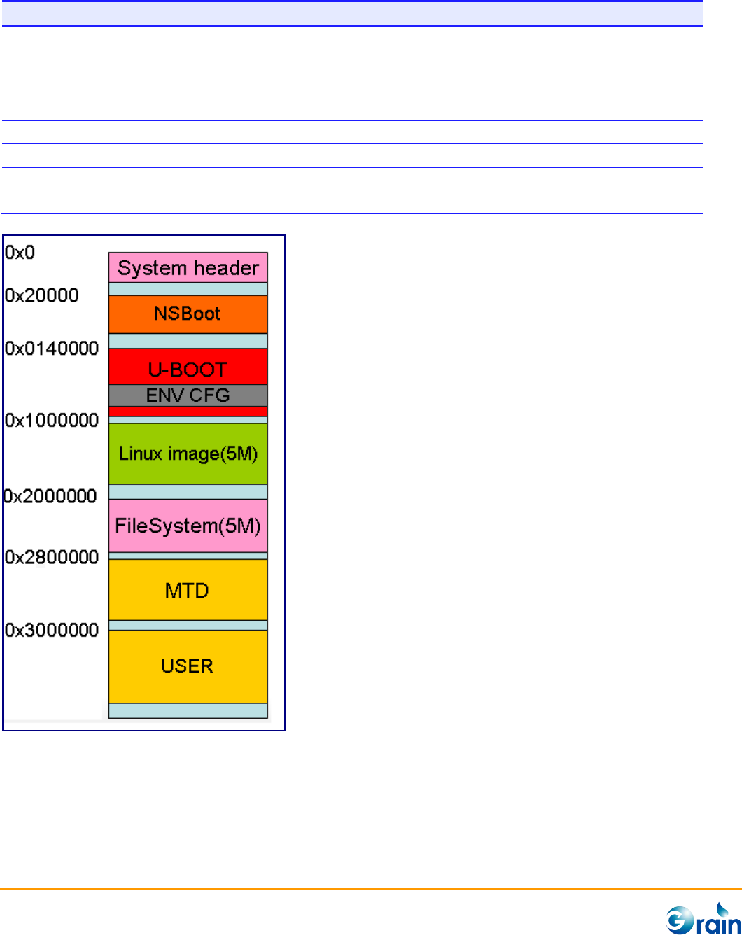
1.3 Image Layout of SPI Flash
The image layout of the SPI Flash is shown in Figure 1-1Figure 1-. The first image executed in the SPI
system is SPI boot, which is located at the second sector of the SPI Flash (The first sector contains a global
system header, which is written by PCTOOL). The purpose is to load the burn-in, U-Boot, or Linux image
into DDR. Currently, the loaded image is U-BOOT. All system initialization tasks, including the DDR
initialization, memory remap, and so on, are done in the boot loader.
An extra image header will be appended with one page size in front of every image. It describes the
information of the associated image, such as the image magic number and the image size. In addition to
the image header, a global system header will also be required in the top position of a Flash. The system
header contains the GM8136 system signature, the image offset of every image, and so on. The image
header contains the checksum, size, and name of an image. Currently, the checksum field is useless. The
system header and image header individually occupy one page and the image body is next to the header.
The structures of the system header and image header are shown in Table 1-1.
Table 1-1. Structures of System Header and Image Header for SPI Flash
Name
Offset (Byte)
Size (Byte)
Description
Signature
0
8
Signature for GM8136, which must be “GM8136”
First image address
8
4
First image offset to be loaded by the SPI boot
First image size
12
4
-
First image reserved
16
4
-
Image 1 address
20
4
Address offset of image 1 specified by PCTOOL
Image 1 size
24
4
Size offset of image 1 specified by PCTOOL
Image 1 name
28
8
Name offset of image 1 specified by PCTOOL
Image 1 reserved
36
4
Unused for image 1
Image N address (N ≤ 10)
40 + (N x 4)
4
Address offset of image N specified by PCTOOL
Image N size
44 + (N x 4)
4
Size offset of image N specified by PCTOOL
Image N name
48 + (N x 4)
8
Name offset of image N specified by PCTOOL
Image N reserved
56 + (N x 4)
4
Unused for image N
pagesz_log2
220
4
Page size in log
For example, ‘11’ means 211 = 2048 bytes.
secsz_log2
224
4
Sector size in log
chipsz_log2
228
4
Chip size in log

GM8136 Flash User Guide
www.grain-media.com
4
Name
Offset (Byte)
Size (Byte)
Description
Clk_div
232
4
Clock divider
reserved
236
16
Unused
last_256
252
4
Magic number
The last two bytes are 0x55 and 0xAA.
Figure 1-1. Image Layout of SPI Flash
Please note that the contents of the SPI Flash can be erased by the block unit or sector unit, where the
block unit is more popular. Users are recommended arranging the locations of all images, except for the
SPI boot in the block alignment (Currently, it is 64K alignment). As mentioned above, the SPI boot is
located in the second sector and it is not aligned with the block boundary. The SPI boot should be updated
every time when users upgrade an image. This image layout is the Grain Media layout. Users not only can

GM8136 Flash User Guide
www.grain-media.com
5
modify the layout address or size to meet the user environment, but also add or delete partition after the
FS_FA6 image.
1.4 Image Layout of NAND Flash
The image layout of the NAND Flash is shown in Figure 1-2. The first image executed for the NAND system
is NAND boot, which is located at the start of NAND Flash. The purpose is to load the burn-in, U-Boot, or
Linux image. Currently, it is the U-BOOT image. All system initialization tasks are done in the boot loader.
One page for the size of the image header will be appended in front of every image body. It describes the
information of the corresponding image, such as the image size. In additional to the image header, a
global system header will also be prepared. The system header contains the GM8136 system signature,
image offset of every image, and so on. The image header contains the checksum, size, and name of an
image. The system header and image header individually occupy one page and the image body is next to
the header. The structures of the SPI-NAND system header and image header are shown in Table 1-2.
Table 1-2. System Header and Image Header of SPI-NAND Flash
Name
Offset (Byte)
Size (Byte)
Description
Signature
0
8
Signature for GM8136, which must be “GM8136”
First image address
8
4
First image offset to be loaded by the SPI boot
First image size
12
4
-
First image reserved
16
4
-
Image 1 address
20
4
Address offset of image 1 specified by PCTOOL
Image 1 size
24
4
Size offset of image 1 specified by PCTOOL
Image 1 name
28
8
Name offset of image 1 specified by PCTOOL
Image 1 reserved
36
4
Unused for image 1
Image N address (N ≤ 10)
40 + (N x 4)
4
Address offset of image N specified by PCTOOL
Image N size
44 + (N x 4)
4
Size offset of image N specified by PCTOOL
Image N name
48 + (N x 4)
8
Name offset of image N specified by PCTOOL
Image N reserved
56 + (N x 4)
4
Unused for image N
nand_numblks
220
4
Number of blocks in a chip
nand_numpgs_blk
224
4
Number of pages in a block
nand_pagesz
228
4
Page size in bytes
nand_sparesz_inpage
232
4
Spare size
GM8136 Flash User Guide
www.grain-media.com
6
Name
Offset (Byte)
Size (Byte)
Description
nand_numce
236
4
Number of CE
Currently; it is always zero.
Nand_clk_div
240
4
This header indicates the clock div for SPI IP.
Nand_ecc_capability
248
4
ECC capability
nand_sparesz_insect
256
4
Spare size per sector to be used by data
Reserved
272
256
Unused
last_511
508
4
Magic number
The last two bytes are 0x55 and 0xAA.
Figure 1-2. Image Layout of NAND Flash
In Figure 1-2, the system header occupies one page and is located in the first block. This image layout is
the Grain Media layout. Users can modify the layout address or size to meet the user environment. Users
GM8136 Flash User Guide
www.grain-media.com
7
can also add or delete partition after the FS_FA6 image. The blue areas are for bad block buffers. The user
image can be bigger than the default image size. (SPI-NAND not has BI table) Please pay attention to the
U-Boot partition, ENV_CFG is inside the U-BOOT partition. When the U-BOOT image is updated, all data in
ENV_CFG will be gone as well.
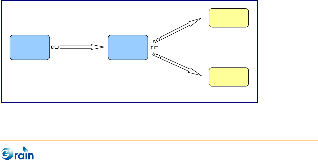
1.5 Booting Sequence
1. When booting, the embedded ROM code will be brought up first and reads the jumper setting to
recognize the accessed Flash type. After the system header in the Flash is read, the Flash will be
checked for valid images. The ROM code checks the signature and 0x55AA of last two bytes in the
system header. The signature must be “GM8136”. If an error occurs, ROMCODE will break the boot
procedure and go to the firmware update mode.
2. Once the system header is verified, the SPI/NAND boot in the next block will be loaded into SRAM and
be executed. For the NAND system, the BI table will also be loaded into SRAM for checking the bad
block. When SPI boot and NAND boot are called “NSBOOT”, it means the NAND boot and SPI boot.
3. NSBOOT reads the system header again to know which one should be executed. Currently, it should
be U-BOOT. NSBOOT then copies the image body to DDR (SDRAM) according to the image size in the
image header of the loaded image.
4. Upon completion of the copy operation, the loaded image will be executed on SDRAM.
The loaded image can be U-BOOT or any customer image.
Linux
U-Boot
(DDR)
(SRAM)
ROMCODE NSBOOT
Figure 1-3. Booting Sequence


GM8136 Flash User Guide
www.grain-media.com
10
2.1 NSBOOT
NSBOOT for GM8136 can be found in the “nsboot” directory. In this directory, users can find the
precompiled image and source archive.
- Unpack
Users can unpack the source archive by applying the following command:
$ tar zxvf nsboot.tar.gz
- Modify
Users can modify Makefile to match the user EVB environment (For the customer solution, users should
select one to perform with different chip IDs which use different NSBOOT definitions, don’t mix them:
The default setting of the PLL3 clock is 540MHz. If users want to set to 594MHz, please add –DPLL3_594.
#=== 8136 ==================================
#CPU 885, default setting
MFLAGS = -DSYSTEM_EVB -DGM8136 -DDDR_1180 -DMODE_3 -DDDR_SZ_8136_2Gbx1 #-DPLL3_594
#CPU 860
#MFLAGS = -DSYSTEM_EVB -DGM8136 -DDDR_1140 -DMODE_5 -DDDR_SZ_8136_2Gbx1
#=== 8136S ==================================
#CPU 860, default setting
#MFLAGS = -DGM8136S -DDDR_1140 -DMODE_3 -DDDR_SZ_8136_1Gbx1
#CPU 885
#MFLAGS = -DGM8136S -DDDR_1180 -DMODE_4 -DDDR_SZ_8136_1Gbx1
#CPU 762, DDR 1016
#MFLAGS = -DGM8136S -DDDR_1000 -DMODE_0 -DDDR_SZ_8136_1Gbx1
#CPU 712
#MFLAGS = -DGM8136S -DDDR_950 -DMODE_7 -DDDR_SZ_8136_1Gbx1
#CPU 590
#MFLAGS = -DGM8136S -DDDR_790 -DMODE_2 -DDDR_SZ_8136_1Gbx1
#=== 8135S ==================================

GM8136 Flash User Guide
www.grain-media.com
11
#CPU 712, default setting
#MFLAGS = -DGM8135S -DDDR_950 -DMODE_4 -DDDR_SZ_8135_512Mbx1
#CPU 590
#MFLAGS = -DGM8135S -DDDR_790 -DMODE_1 -DDDR_SZ_8135_512Mbx1
- Build
Users can apply the “make” command to build an image:
$ make clean;make
- Binaries
Once NSBOOT has been successfully compiled, the following files will be created:
File
Description
nsboot
Compiled ELF image
nsboot.bin
NSBOOT boot converted to a raw binary
The nsboot.bin file is used for programming the NAND Flash.

GM8136 Flash User Guide
www.grain-media.com
12
2.2 U-BOOT
U-BOOT for the GM8136 NAND system can be found in the “u-boot” directory. In this directory, users can
find the precompiled image and source archive.
- Unpack
Users can unpack the source archive by applying the following command (Replace u-boot-2013.01.tar.gz
with the correct file name in the “u-boot” directory if it is not the same):
$ tar xvfz u-boot-2013.01.tar.gz
Users can change to the created “u-boot” directory by applying the following command (Replace
u-boot-2013.01.tar.gz as applicable):
$ cd u-boot-2013.01
- Build SPI system
Before compiling U-BOOT, the SPI configuration of GM8136 must be enabled. Open the GM8136 U-BOOT
configuration file, “include/configs/gm8136.h”, and make sure that the “CONFIG_CMD_SPI” option is
defined and “CONFIG_SPI_NAND_GM” is undefined.
#define CONFIG_CMD_SPI
//#define CONFIG_SPI_NAND_GM
Then, apply the following command to build an image:
$ ./make_8136

GM8136 Flash User Guide
www.grain-media.com
13
- Binaries
Once U-BOOT has been successfully compiled, the following files will be created in the “u-boot” directory:
File
Description
u-boot
Compiled ELF image
u-boot.bin
u-boot converted to a raw binary
u-boot.srec
u-boot.bin converted to the Motorola S-records format
- Build NAND system
Before compiling U-BOOT, the NAND configuration of GM8136 must be enabled. Open the GM8136
U-BOOT configuration file, “include/configs/gm8136.h”. If users want to use the SPI-NAND Flash, please
make sure that the “CONFIG_SPI_NAND_GM” option is defined and “CONFIG_CMD_SPI” is
undefined.
//#define CONFIG_CMD_SPI
#define CONFIG_SPI_NAND_GM
Then, apply the following command to build an image:
$ ./make_8136
- Binaries
Once U-BOOT has been successfully compiled, the following files will be created in the “u-boot” directory:
File
Description
u-boot
Compiled ELF image
u-boot.bin
U-BOOT converted to a raw binary
u-boot.srec
u-boot.bin converted to the Motorola S-records format

GM8136 Flash User Guide
www.grain-media.com
14
2.3 Linux
Linux for GM8136 can be found in the “Embedded_Linux/source” directory. In this directory, users can find
the precompiled image and source archive.
- Unpack
Users can unpack the kernel source and root of the file system archive by applying the following command:
$ tar xvfz arm-linux-3.3.tgz
Users can change to the created Linux kernel source directory by applying the following command:
$ cd linux-3.3-fa
- Build
There is a default Linux kernel configure file for GM8136. Before starting an operation, users must copy the
file from “arch/ arm/configs/GM8136_defconfig” to “.config” in the top directory of the kernel source tree
to build a Linux image.
$ cp arch/arm/configs/GM8136_defconfig .config
Next, apply the following command to configure the kernel:
$ make menuconfig
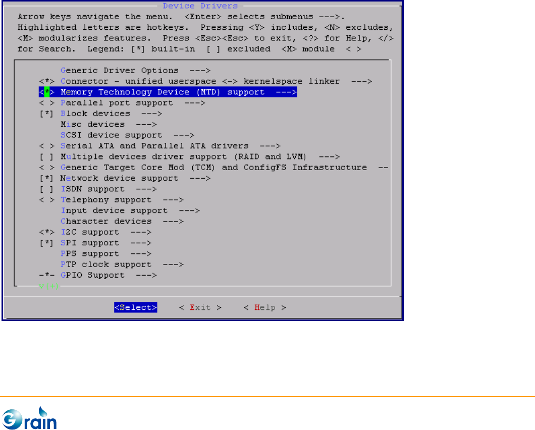
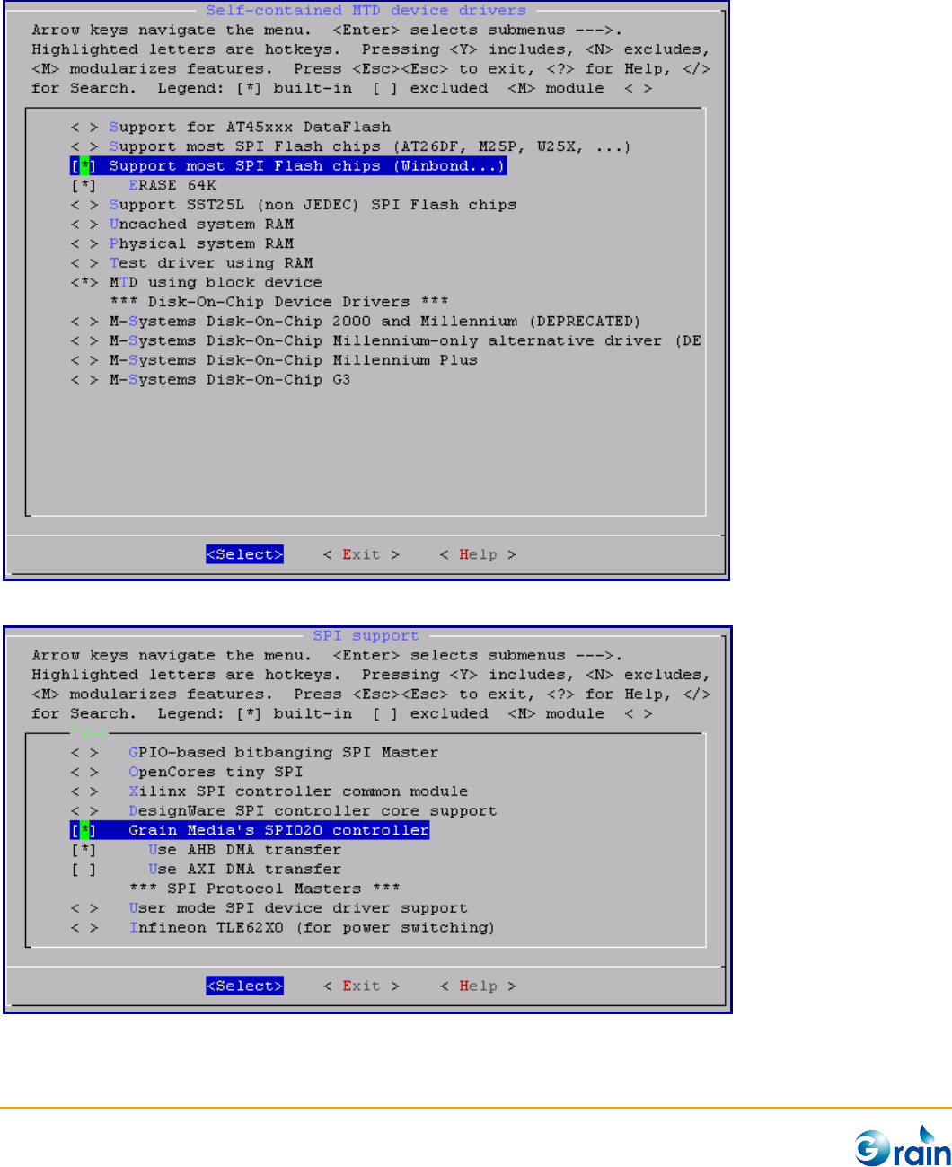
While compiling the kernel, the following items should be selected:
- MTD concatenating support
- MTD partitioning support
- Direct char device access to MTD devices
- Caching block device access to MTD devices
- Size of user Flash partition (KB) (Grain Media only)
- SPI Flash device support
- SPI support
Support most SPI Flash chips (Winbond, ...)
GM8136 Flash User Guide
www.grain-media.com
15
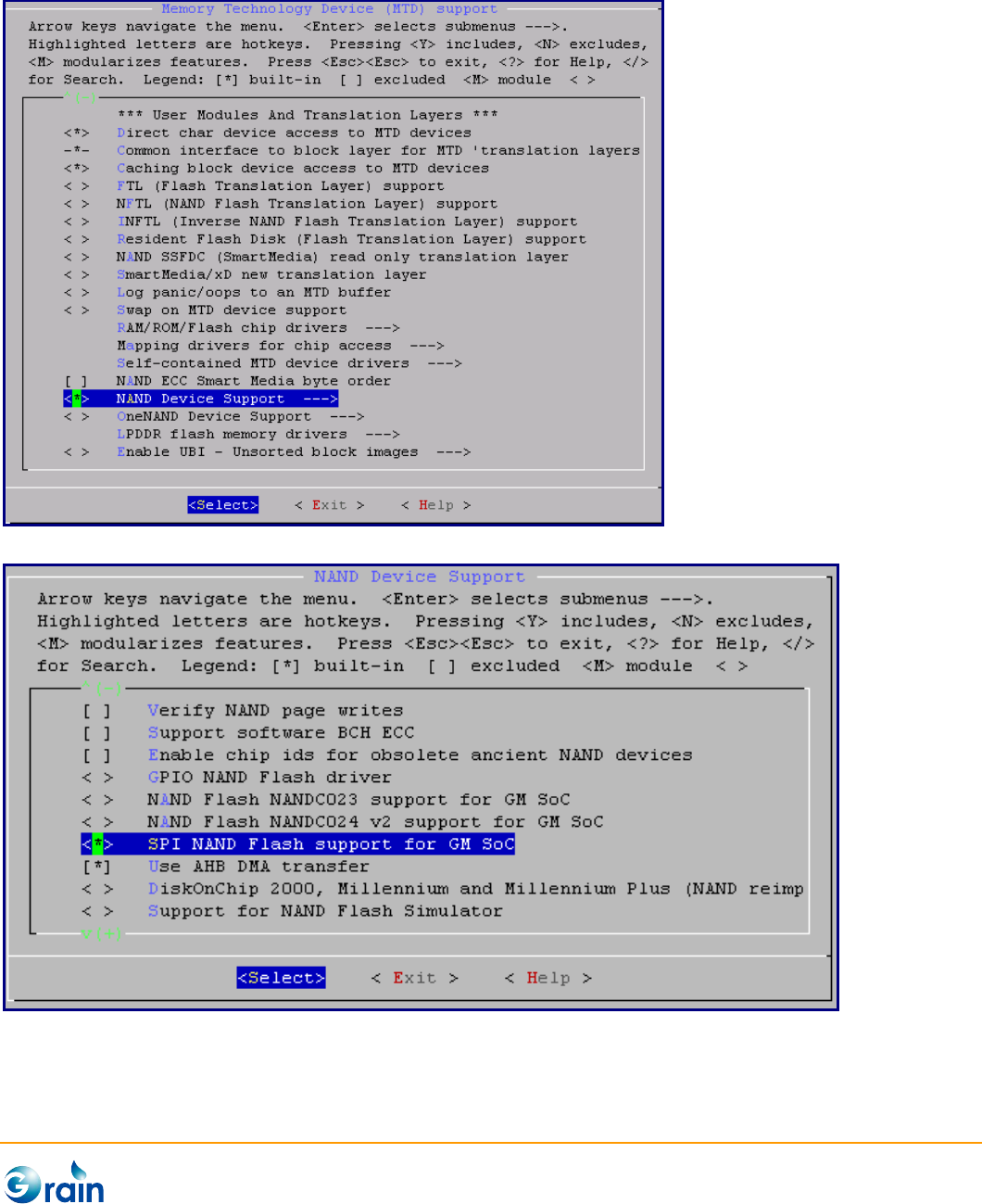
- NAND device support
SPI-NAND Flash support for Grain Media SoC
Use DMA transfer for better CPU performance
For NAND driver debugging verbosity, choose 0
- UBI (Unsorted Block Images): Optional
Miscellaneous file systems:
- Journalling Flash File System v2 (JFFS2) support
- JFFS2 write buffer support
- YAFFS2 file system support: Optional
Auto-select yaffs2 format
- UBIFS file system support
GM8136 Flash User Guide
www.grain-media.com
16
Select SPI Flash:
GM8136 Flash User Guide
www.grain-media.com
17
Select SPI-NAND Flash:
GM8136 Flash User Guide
www.grain-media.com
18
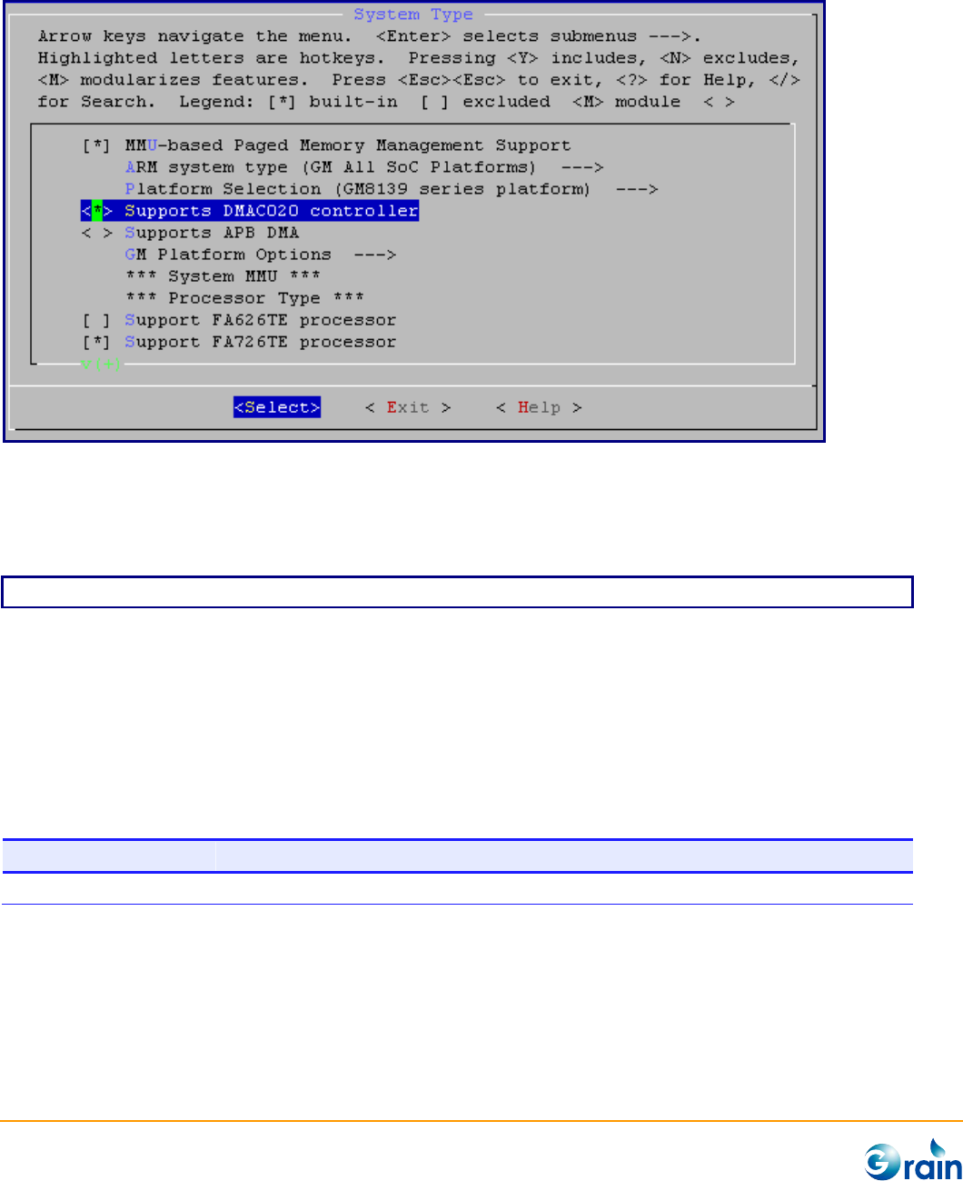
If the driver selects AHB DMA, users must select “Supports DMAC020 controller”:
Configuration is now completed. Next, the kernel and root file system must be updated and compiled.
Please enter the following command:
$ ./build_uImage_8136
- Binaries
After the kernel has been successfully compiled, the image files will be produced and saved in the
“arch/arm/boot” subdirectory. The “bootsImage” image can be loaded onto the NAND Flash of the target
system.
File
Description
bootsImage
Self-decompressed Linux raw binary

GM8136 Flash User Guide
www.grain-media.com
20
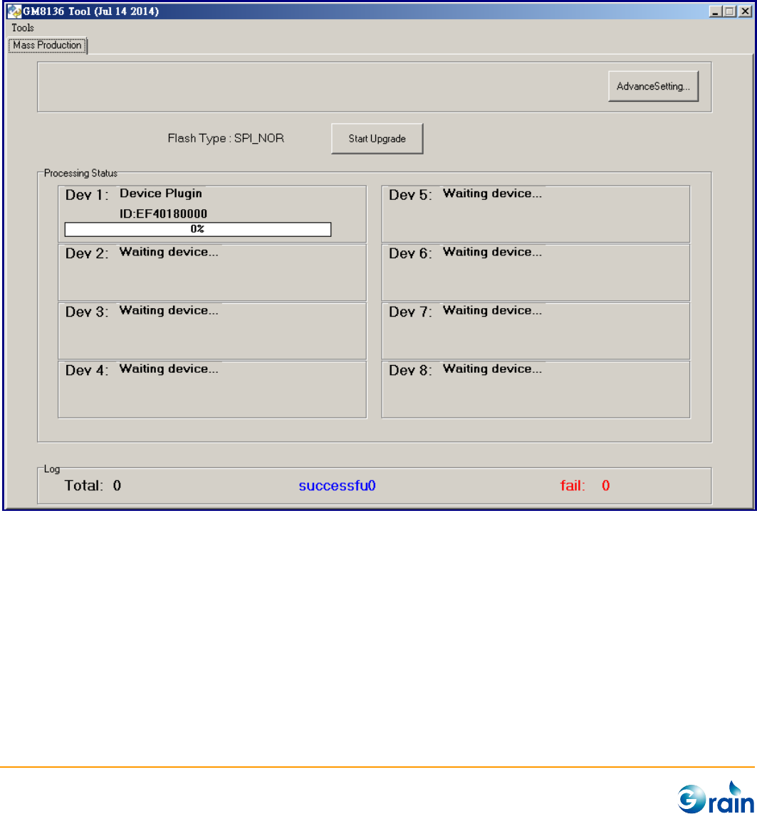
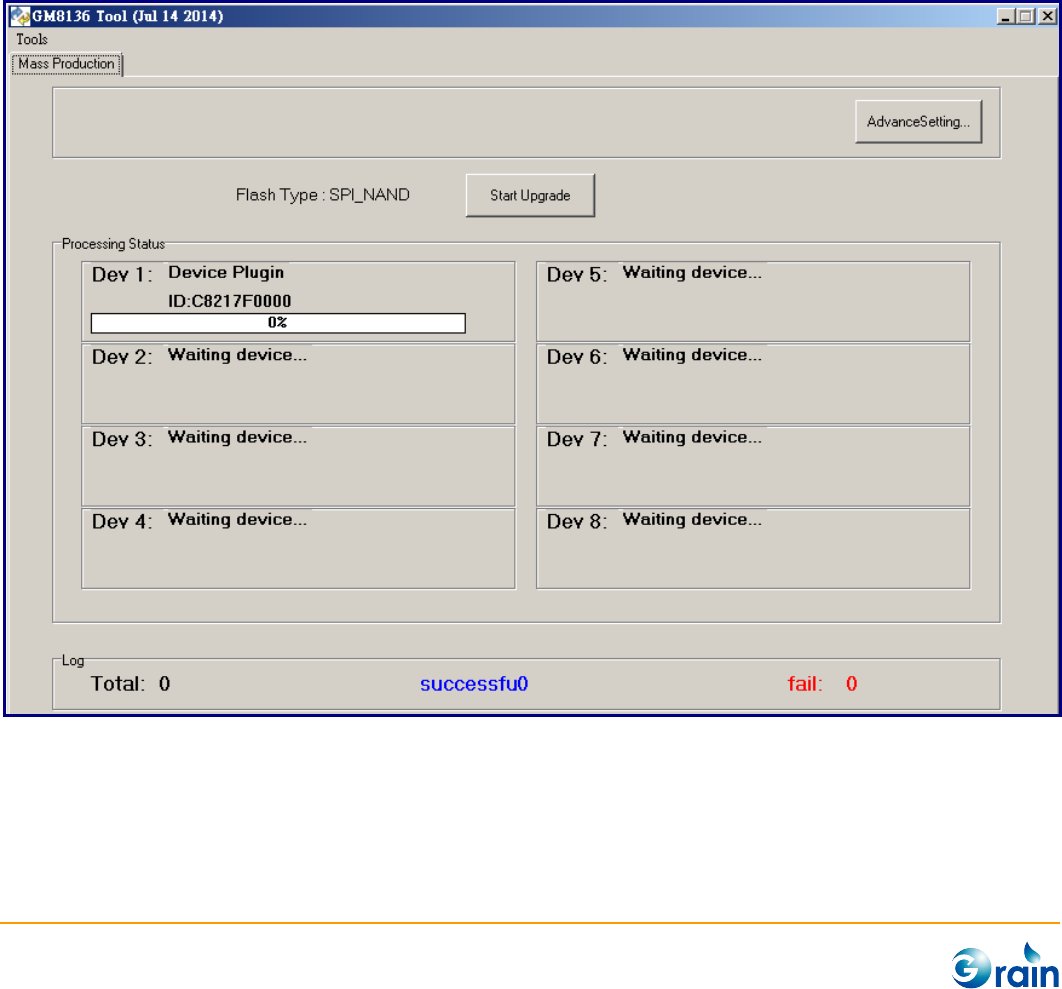
3.1 PCTOOL
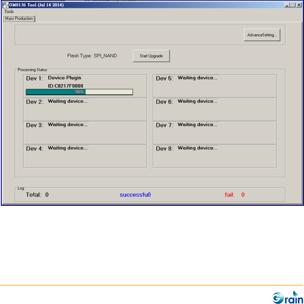
PCTOOL is a utility running on the PC host to program data and target the SPI/NAND Flash while the target
system is in the firmware update mode. The PCTOOL utility is “fusblink8136.exe”. Please power on EVB
and plug in the USB line. After the PCTOOL utility is executed, the following window will be shown on PC.
If the Flash is detected, the ID of a Flash will always be shown, and the “Flash Type” will show the Flash
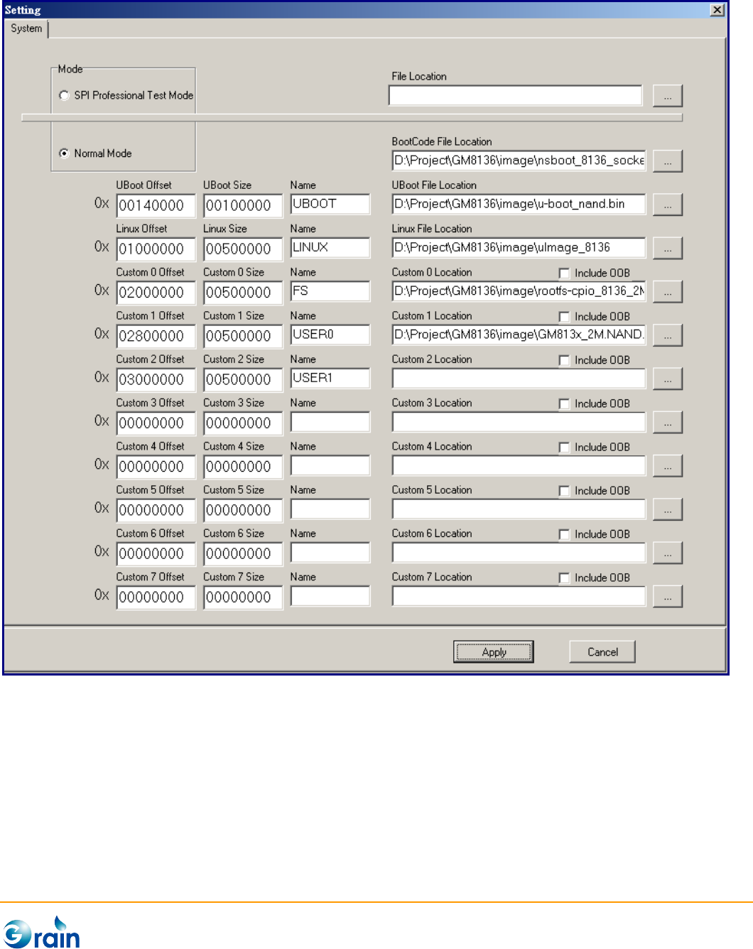
type –SPI-NOR, or SPI-NAND. The required setting must be set via the “AdvancedSetting…” icon. After
pressing the “AdvancedSetting” icon, the window shown on the next page will pop up.

GM8136 Flash User Guide
www.grain-media.com
21

GM8136 Flash User Guide
www.grain-media.com
22
Image assignment:
1. BootCode file: Grain Media has the system board and socket board. The GM8136 system board
(Default) uses 256MB as the DDR size, GM8136S and GM8135S system board uses 128MB or 64MB as
the DDR size.
2. U-BOOT file: U-BOOT depends on the SPI or NAND Flash type, having two images to be selected. Grain
Media selects only one image to meet the Grain Media EVB. The SPI mode image is used by default.
U-BOOT will be mapping to MTD0, and U-BOOT env is also at MTD0, if users update MTD0, U-BOOT env
will be gone. Users must reconstruct the arguments, if necessary. Otherwise, these arguments will go
to the default values.
3. Linux file: Grain Media uses mbootpImage. This image does not include the file system (rootfs).
4. Custom0 file: Grain Media uses the squash file system for the mbootpImage image.
5. Custom1 ~ 5 files: Users can use one for their own.
6. For NAND Flash, PCTOOL has the “Include OOB” icon. If users enable it, it will write OOB (Spare area)
into Flash, and the files inputted by users must include these data. Example: Normal page data is
2048bytes. If users do not enable it, PCTOOL will read 2048bytes from the file and write into Flash. If
users enable it, PCTOOL will read 2112bytes from the file and write into Flash.
When these files and partition setting are assigned, Linux will set the MTD partition depending on the
settings. U-BOOT is MTD0, and so on. The Linux auto-partition message is as follows:
Creating 6 MTD partitions on "wb_spi_flash":
0x000000010000-0x000000060000 : "UBOOT"
0x000000060000-0x000000480000 : "LINUX"
0x000000480000-0x000000600000 : "FS"
0x000000600000-0x000000700000 : "USER0"
0x000000700000-0x000000800000 : "USER1"
0x000000000000-0x000001000000 : "ALL"

GM8136 Flash User Guide
www.grain-media.com
23
Please specify the image offset for every image and note that the offset address should be the erase unit
alignment. The window shown on the next page is the NAND Flash update. If a new SPI Flash comes, users
must specify the related parameters in PCTOOL. The parameters will then be passed to Grain Media
RomCode at the firmware upgrade stage by PCTOOL. Please change the following file,
PCTOOL/flash/cfg_xxx_xxx.txt.
Note 1: Address has the alignment issue. Alignment is recommended depending on the Flash block size.
Note 2: Users should assign the image offset from low address to high address. The image addresses
should not across each other.
Note 3: If users do not want to use the custom fields, please set the offset and size fields as ‘0’ and do not
select file.
Note 4: For the image offset and size, please reserve enough space for future upgrade. If users do not use
USB to upgrade a code, the field arrangement will not be modified by other methods and the
image loading may have errors.
GM8136 Flash User Guide
www.grain-media.com
24
If users use PCTOOL to burn the SPI image and if the system cannot be booted, please check the following:
1. Please check if it is in the SPI mode.
2. Please check if SPI 3-byte/4-byte jump setting is correct.
3. The chip IDs of MXIC and Winbond 256Mb 3 or 4/pure 4-byte addressing modes are the same. If users
use the chip in the 3-byte or 4-byte addressing mode, jump must be set to the 3-byte mode. If users use
the chip in the pure 4-byte addressing mode, jump must be set to the 4-byte mode.
Please note that a system header should be in front of the Flash. The specified offset addresses will be
updated to the system header.
When a NAND Flash is detected, the device ID will be the ID of the NAND Flash.
GM8136 Flash User Guide
www.grain-media.com
25
The window shown above is an example of the NAND Flash.
GM8136 Flash User Guide
www.grain-media.com
26
Every supported Flash has the corresponding configured file located in the PCTOOL/Flash directory. If
users need to add a new Flash, please contact the Grain Media service member for this request. Grain
Media will add the new Flash for users. The next step, users need to select “Default Image”. Users must
choose the “UBoot” item. Once the settings are completed, users should press the “Apply” button; and it
will return to the utility main menu. Please press the “Start Upgrade” icon to begin updating the SPI/NAND
Flash and the message shown below will appear.
GM8136 Flash User Guide
www.grain-media.com
27
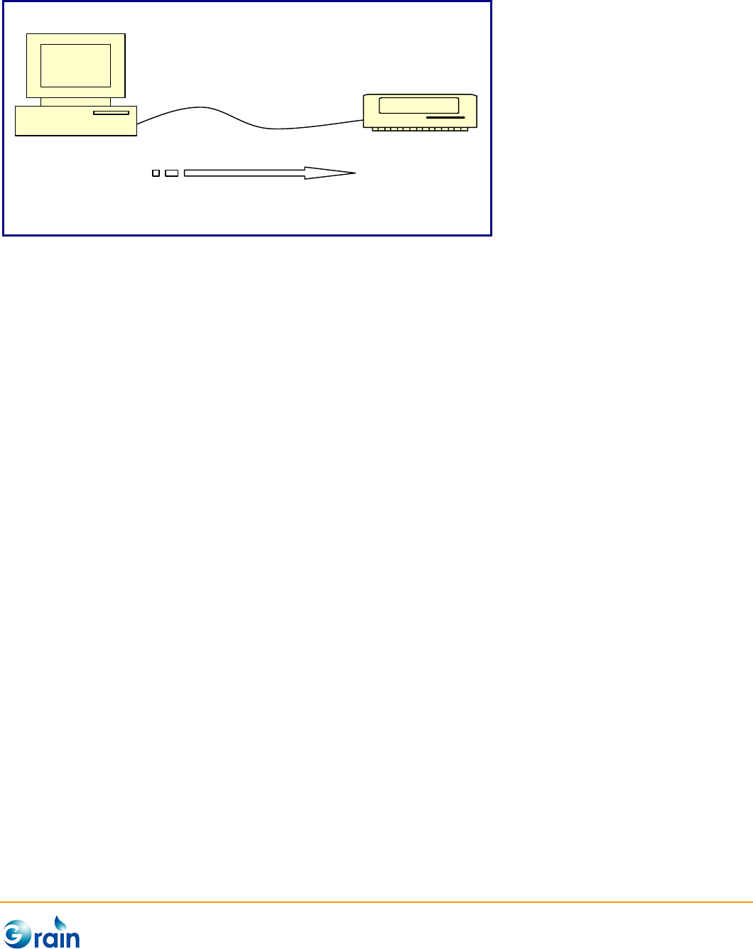
PC
Target
(USB Interface)
Programming Image to Target SPI/NAND Flash
Figure 3-1. NAND Flash Programming by PCTOOL
3.2 Add and modify MTD partition
Driver will auto transfer system header data to MTD partition definition, and PC tool open max fields for
customer to set up them. If users want to add or modify by yourself, please modify driver as follow:
Flash type
(1) SPI NAND
Please modify linux-3.3-fa/drivers/mtd/nand/ftspi020_nand.c
(2) SPI
Please modify linux-3.3-fa/drivers/mtd/devices/spi_flash.c
search "partition_check" string, and set these definition direcly at this API function.
For example:
partitions[0].name = "abc";
partitions[0].offset = 0x140000;
partitions[0].size = 0x200000;
3.3 Add New SPI Flash in PCTOOL
When upgrading the target firmware, PCTOOL needs to pass the related parameters to the NAND Flash,
such as the page size, block size, and so on, to the ROM code embedded in the GM8136 SoC. Therefore,
PCTOOL must be able to identify the target Flash to notify the target board what Flash is used. If users
GM8136 Flash User Guide
www.grain-media.com
28
want to set the NAND Flash, please click the “NAND” icon. If users want to set the SPI Flash, please click
the “SPI” icon.
The steps below show users how to create a new Flash in the database of PCTOOL.
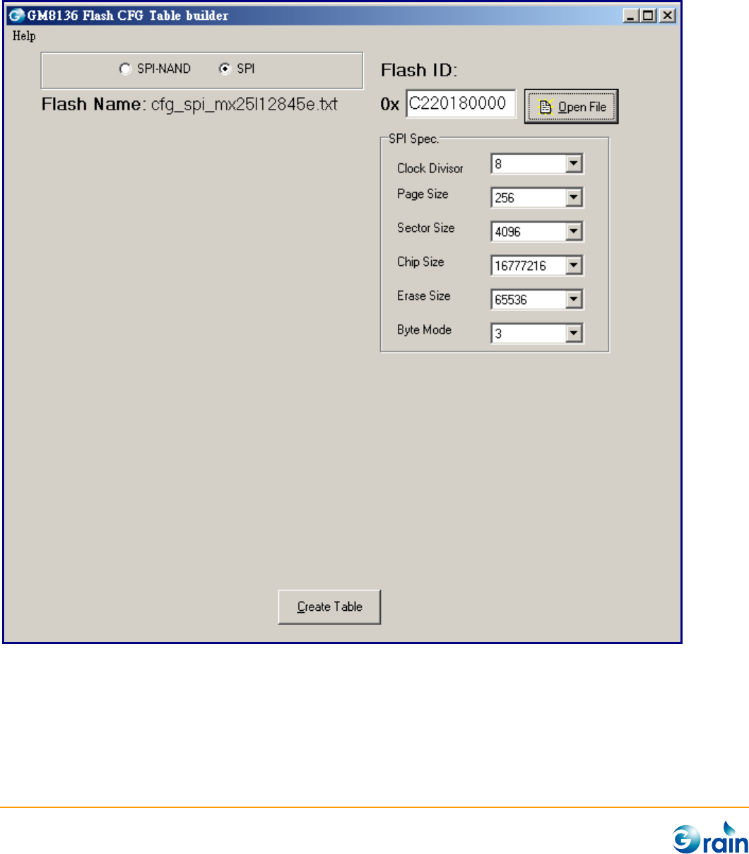
1) Find the executable file, flash/CfgBuilder28.exe
2) Please click the “SPI” icon.
GM8136 Flash User Guide
www.grain-media.com
29
3) “Clock Divisor” is usually set to 8. “Erase Size” is usually set to 64KB.
4) For the Byte Mode, 16MB is usually the 3-byte mode Flash, 32MB is usually the 4-byte mode
Flash.
5) When the user settings are finished, users can click “Create Table” to create the configuration file.
The steps below show users how to create a new Flash in the database of PCTOOL.
1) Find the executable file, flash/CfgBuilder28.exe

GM8136 Flash User Guide
www.grain-media.com
30
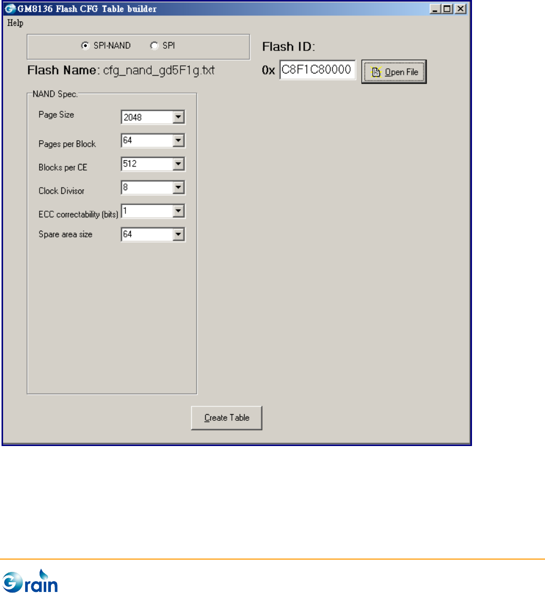
2) Please click the “SPI-NAND” icon.
3) “Clock Divisor” is usually set to 8. “ECC correctability” is usually set to 1 according to the Flash
chip data sheet.
When the user settings are finished, users can click “Create Table” to create the configuration file.

GM8136 Flash User Guide
www.grain-media.com
31
3.4 Burn MTD User Area under Linux Environment
If the Flash type is “SPI Flash”, the following steps can be adopted to run MTD:
1. After making MTD into Flash and ready, users can save the MTD data into file,
cat /dev/mtd1 > mtd.img
2. Use PCTOOL to burn it. The input file is mtd.img.
If the Flash type is “NAND Flash”, the following steps can be adopted to run MTD:
1. After making MTD into Flash and ready, users can save the MTD data into file,
nanddump -p -f mtd.img /dev/mtd0
2. When burning by using PCTOOL, the name of the input file will be mtd.img.
3.5 JFFS2 File System for User Section
Grain Media SDK defines one MTD block for “User Section”, which can be used for the boot script, system
information, AP configure, or setting information.
Creating 5 MTD partitions on "NAND 128MiB 3,3V 8-bit":
0x000000140000-0x000000240000 : "UBOOT"
0x000001000000-0x000001500000 : "LINUX"
0x000002000000-0x000002500000 : "FS"
0x000002800000-0x000002d00000 : "USER0"
0x000003000000-0x000003500000 : "USER1"
The MTD block for “User Section” must be formatted and mounted to the JFFS2 file system.
flash_eraseall /dev/mtd2
mount /dev/mtdblock2 /mnt/mtd/
Users can apply the nanddump command to check whether the MTD OOB data has been successfully
created.
/ # nanddump -p /dev/mtd1
Block size 131072, page size 2048, OOB size 64
Dumping data starting at 0x00000000 and ending at 0x06700000...
0x00000000: ff ff ff ff ff ff ff ff ff ff ff ff ff ff ff ff
0x00000010: ff ff ff ff ff ff ff ff ff ff ff ff ff ff ff ff
0x00000020: ff ff ff ff ff ff ff ff ff ff ff ff ff ff ff ff
…
0x000007e0: ff ff ff ff ff ff ff ff ff ff ff ff ff ff ff ff
0x000007f0: ff ff ff ff ff ff ff ff ff ff ff ff ff ff ff ff
OOB Data: 85 19 03 20 08 00 00 00 ff ff ff ff ff ff ff ff

GM8136 Flash User Guide
www.grain-media.com
32
OOB Data: ff ff ff ff ff ff ff ff ff ff ff ff ff ff ff ff
OOB Data: ff ff ff ff ff ff ff ff ff ff ff ff ff ff ff ff
OOB Data: ff ff ff ff ff ff ff ff ff ff ff ff ff ff ff ff
0x00000800: ff ff ff ff ff ff ff ff ff ff ff ff ff ff ff ff

GM8136 Flash User Guide
www.grain-media.com
33
Chapter 4
User Section
In the MTD partitions, PCTOOL can be used to set the number of MTDs, start address, size, and name of
the MTD partition. MTD can expend up to four user partition areas. Users can decide to burn the selected
images. If the image is empty, Linux will build empty MTD partition. Since the partition is not formatted yet,
mounting the partition will cause some warning messages. As a result, users should format the MTD
partition, read the partition data, and save to one image. Then, PCTOOL should be used to burn the image
into the partition. When Linux is booted, mounting the partition will not show any warning message. If the
MTD partition address and size are already set, the Linux command cannot be used to modify the setting
values. If modifying these settings is required, PCTOOL should be used to burn all setting values again. The
SPI setting values are as follows:

GM8136 Flash User Guide
www.grain-media.com
34

GM8136 Flash User Guide
www.grain-media.com
35
Chapter 5
Add New Flash Chip
(1) If a new SPI chip should be added, users must modify the following files to support this new chip.
U-BOOT
u-boot-2013.01/drivers/mtd/spi/
search eon.c or macronix.c or…to update the user SPI Flash as required
Linux
linux-3.3-fa/drivers/mtd/devices/spi_flash.c
search “common_spi_flash_data” string and update the user SPI Flash as required
(2) If a new SPI-NAND chip should be added, users must modify the following files to support this new
chip.
U-BOOT
u-boot-2013.01/drivers/mtd/nand/mamd_ids.c
search “nand_flash_ids” string and update the user Flash as required

GM8136 Flash User Guide
www.grain-media.com
36
Linux
linux-3.3-fa/drivers/mtd/devices/mtd/nand/nand_ids.c
search “nand_flash_ids” string and update the user Flash as required

GM8136 Flash User Guide
www.grain-media.com
37
Chapter 6
Modify JFFS2 Image
If users want to modify the Grain Media xxx.jffs2.img, users can set the commands as the following to add
or delete a file.
# losetup /dev/loop0 xxx.jffs2.img
# modprobe block2mtd block2mtd=/dev/loop0
# modprobe mtdblock
# mount -t jffs2 -o ro /dev/mtdblock0 mnt

GM8136 Flash User Guide
www.grain-media.com
39
Chapter 7
Image Upgrade
Users can use some methods to upgrade the image.
(1) Use PCTOOL to upgrade the image.
(2) Use U-BOOT to upgrade the image, and users can use the U-BOOT Flash command for image upgrade.
(3) Use Linux to upgrade the image, users can refer to Quick_Start.pdf for the detailed information.
Note: For the NAND Flash, the devices may have blocks that are invalid when they are shipped from the factory, and these blocks
should be avoided. If users want to add new bad blocks, users can use markbad to inform the driver to avoid of using them. The
driver will not take the initiative to mark the bad blocks.
Block 0 contains the bad block message, and each NAND chip is different. Users should not copy the “A”
chip image that includes block 0 to the “B” chip image.
