HD52FA97
User Manual: HD52FA97
Open the PDF directly: View PDF ![]() .
.
Page Count: 284 [warning: Documents this large are best viewed by clicking the View PDF Link!]
- ya463.pdf
- ya463sch.pdf
- HD-52FA97,HD-56FB97,HD-61FB97
- STANDARD CIRCUIT DIAGRAM
- CONTENTS
- USING P.W. BOARD
- SEMICONDUCTOR SHAPES
- WIRING DIAGRAM
- BLOCK DIAGRAM
- CIRCUIT DIAGRAMS
- TUNER PWB CIRCUIT DIAGRAM (1/2)
- TUNER PWB CIRCUIT DIAGRAM (2/2)
- ANALOG PWB CIRCUIT DIAGRAM (1/6)
- ANALOG PWB CIRCUIT DIAGRAM (2/6)
- ANALOG PWB CIRCUIT DIAGRAM (3/6)
- ANALOG PWB CIRCUIT DIAGRAM (4/6)
- ANALOG PWB CIRCUIT DIAGRAM (5/6)
- ANALOG PWB CIRCUIT DIAGRAM (6/6)
- DIGITAL PWB CIRCUIT DIAGRAM (1/15)
- DIGITAL PWB CIRCUIT DIAGRAM (2/15)
- DIGITAL PWB CIRCUIT DIAGRAM (3/15)
- DIGITAL PWB CIRCUIT DIAGRAM (4/15)
- DIGITAL PWB CIRCUIT DIAGRAM (5/15)
- DIGITAL PWB CIRCUIT DIAGRAM (6/15)
- DIGITAL PWB CIRCUIT DIAGRAM (7/15)
- DIGITAL PWB CIRCUIT DIAGRAM (8/15)
- DIGITAL PWB CIRCUIT DIAGRAM(9/15)
- DIGITAL PWB CIRCUIT DIAGRAM (10/15)
- DIGITAL PWB CIRCUIT DIAGRAM (11/15)
- DIGITAL PWB CIRCUIT DIAGRAM (12/15)
- DIGITAL PWB CIRCUIT DIAGRAM (13/15)
- DIGITAL PWB CIRCUIT DIAGRAM(14/15)
- DIGITAL PWB CIRCUIT DIAGRAM (15/15)
- DRIVE PWB CIRCUIT DIAGRAM (1/9)
- DRIVE PWB CIRCUIT DIAGRAM (2/9)
- DRIVE PWB CIRCUIT DIAGRAM (3/9)
- DRIVE PWB CIRCUIT DIAGRAM (4/9)
- DRIVE PWB CIRCUIT DIAGRAM (5/9)
- DRIVE PWB CIRCUIT DIAGRAM (6/9)
- DRIVE PWB CIRCUIT DIAGRAM (7/9)
- DRIVE PWB CIRCUIT DIAGRAM (8/9)
- DRIVE PWB CIRCUIT DIAGRAM (9/9)
- POWER PWB CIRCUIT DIAGRAM (1/3)
- POWER PWB CIRCUIT DIAGRAM (2/3)
- POWER PWB CIRCUIT DIAGRAM (3/3)
- FRONT LED PWB CIRCUIT DIAGRAM [HD-52FA97]
- FRONT LED PWB CIRCUIT DIAGRAM [HD-56FB97, HD-61FB97]
- TEMP PWB CIRCUIT DIAGRAM
- LAMP COVER SW PWB CIRCUIT DIAGRAM
- REMOCON PWB CIRCUIT DIAGRAM
- USB PWB CIRCUIT DIAGRAM
- SIDE CONTROL PWB CIRCUIT DIAGRAM
- PATTERN DIAGRAMS
- VOLTAGE CHARTS
- WAVEFORMS
- ya463ien.pdf
- Important Safety Precautions
- Warnings
- Table of Contents
- Quick Setup
- Onscreen Menus
- Using the Guide
- The Onscreen Menu System
- Auto Tuner Setup
- Channel Summary
- V-Chip
- Set Lock Code
- Language
- Closed Caption
- Auto Shut Off
- XDS ID
- Noise Muting
- Front Panel Lock
- V1 Smart Input
- Video Input Label
- Position Adjustment
- Power Indicator
- Digital-In
- Digital-In1 Audio
- Digital Setup
- Picture Settings
- Color Temperature
- Color Management
- Dynamic Gamma
- Smart Picture
- Digital VNR
- MPEG NR
- Reset
- Sound Settings
- Turn On Volume
- Volume Limit
- Reset
- Set Clock
- On/Off Timer
- Lamp Timer Reset
- Button Functions
- Multi Screen Function
- Power
- Number Buttons - 10Key Pad
- Tune
- Input
- Channel +/–
- Volume +/–
- TheaterPro D6500K
- Return +/TV
- Sound
- Muting
- Video Status
- Natural Cinema
- Sleep Timer
- ML/MTS
- Display
- C.C. (Closed Caption)
- Favorite
- Aspect
- Menu
- OK
- Back
- TV/CATV Slide Switch
- VCR/DVD Slide Switch
- VCR Buttons
- DVD Buttons
- Light
- Digital CH D/A (Digital/Analog)
- Sub Channel
- Guide
- OSD Information
- Lamp Replacement
- Troubleshooting
- Specifications
- Limited Warranty
- To Our Valued Customer
- ya463par.pdf
- USING P.W. BOARD & REMOTE CONTROL UNIT
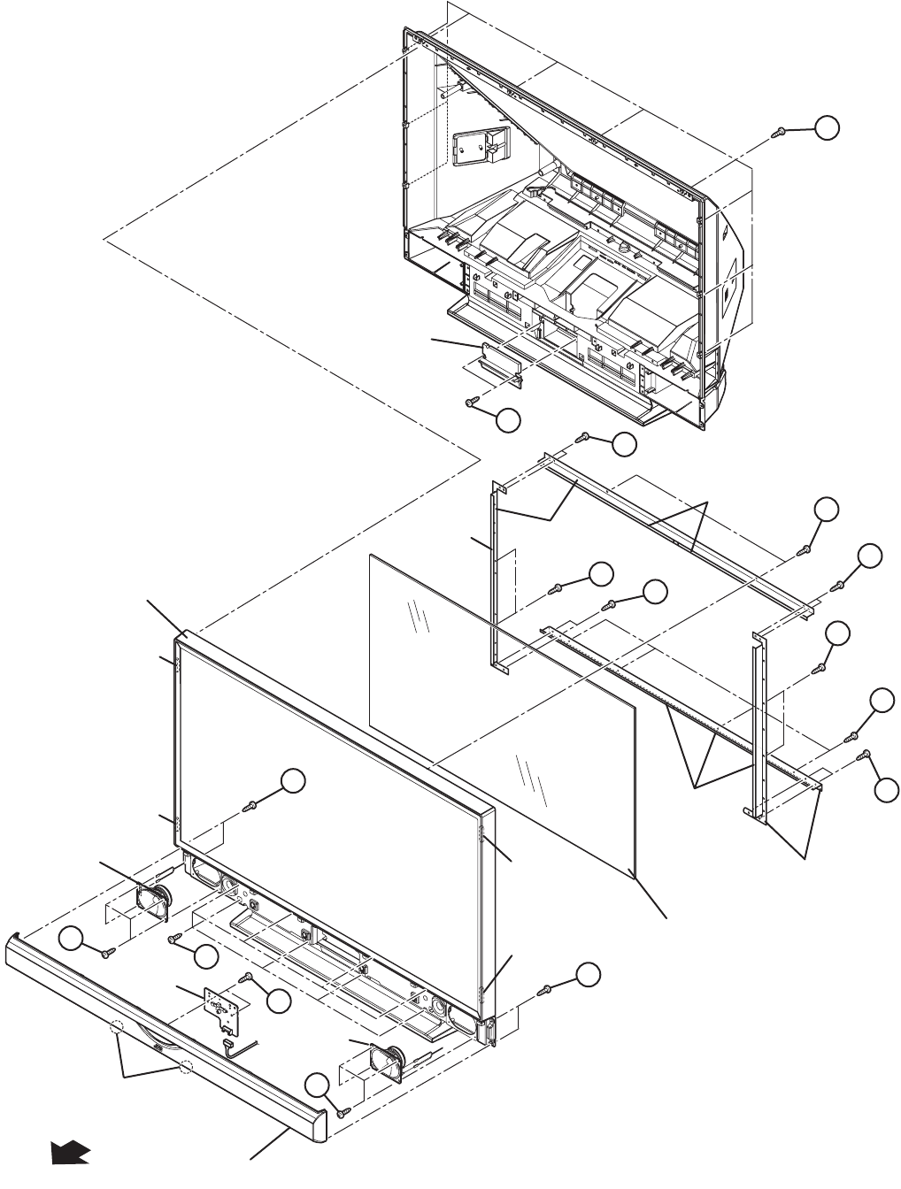
- EXPLODED VIEW PARTS LIST -1 [HD-52FA97]
- EXPLODED VIEW -1 [HD-52FA97]
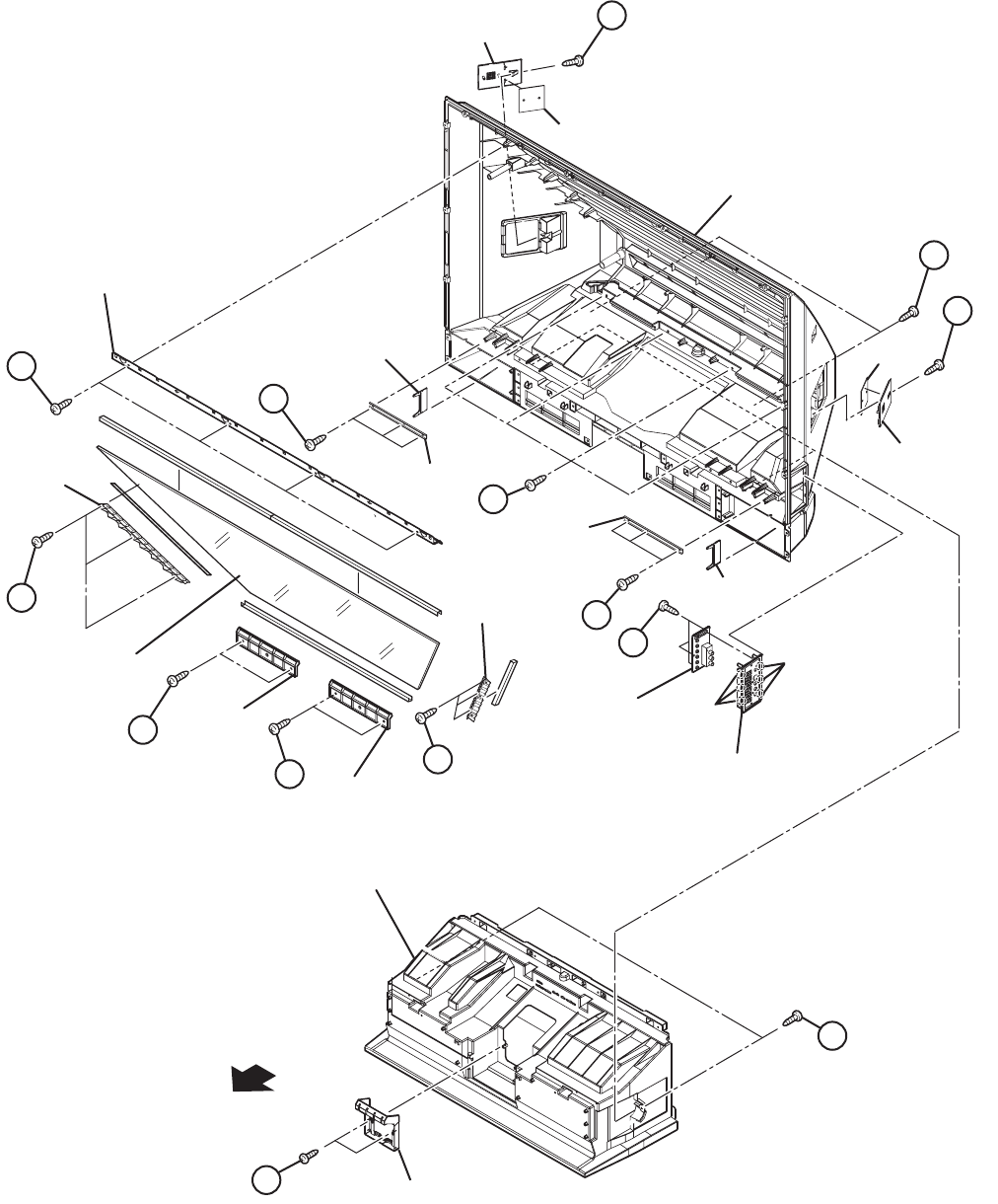
- EXPLODED VIEW PARTS LIST -2 [HD-52FA97]
- EXPLODED VIEW -2 [HD-52FA97]
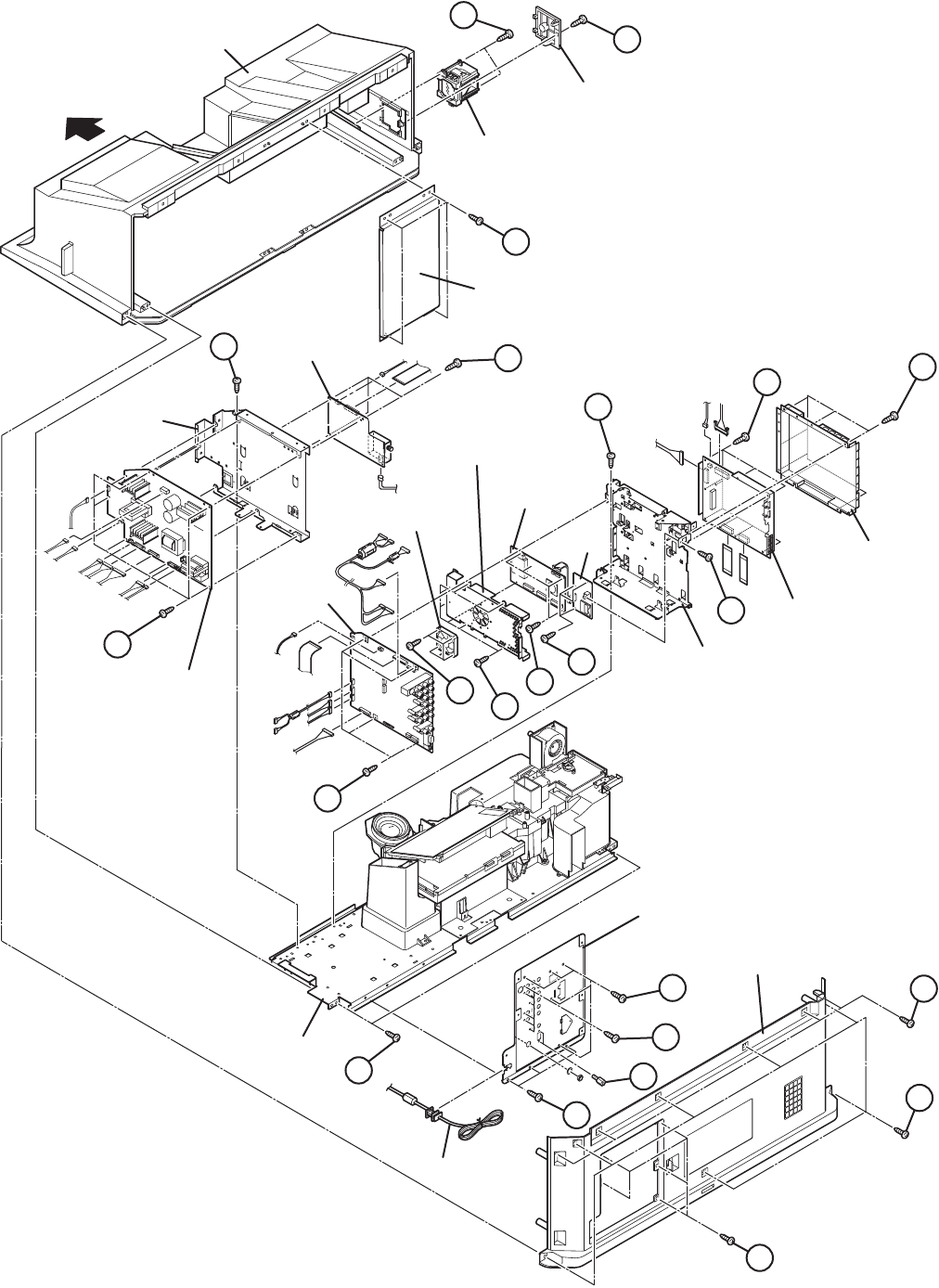
- EXPLODED VIEW PARTS LIST -3 [HD-56FB97, HD-61FB97]
- EXPLODED VIEW -3 [HD-56FB97, HD-61FB97]
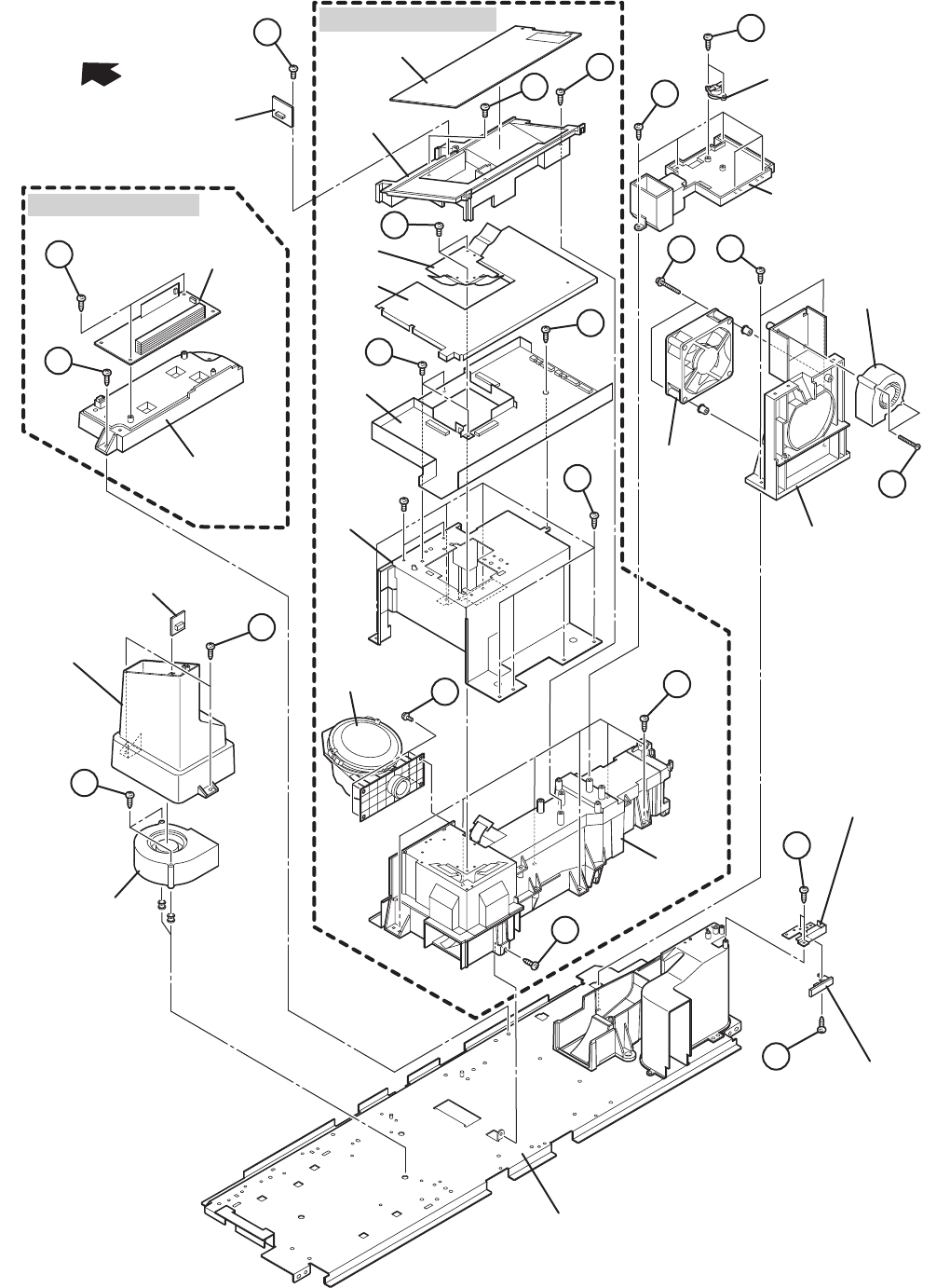
- EXPLODED VIEW PARTS LIST -4 [HD-56FB97, HD-61FB97]
- EXPLODED VIEW -4 [HD-56FB97, HD-61FB97]
- EXPLODED VIEW PARTS LIST -5
- EXPLODED VIEW -5
- EXPLODED VIEW PARTS LIST -6
- EXPLODED VIEW -6
- PRINTED WIRING BOARD PARTS LIST [HD-52FA97]
- ANALOG P.W. BOARD ASS'Y (SRA-1024A-M2)
- DRIVE P.W. BOARD ASS'Y (SRA-3013A-M2)
- REMOCON P.W. BOARD ASS'Y (SRA-8011A-M2)
- TEMP P.W. BOARD ASS'Y (SRA-8211A-M2)
- USB P.W. BOARD ASS'Y (SRA-8521A-M2)
- POWER P.W. BOARD ASS'Y (SRA-9017A-M2)
- DIGITAL P.W. BOARD ASS'Y (SRA0D161A-M2)
- SIDE CONTROL P.W. BOARD ASS'Y (SRA0L013A-M2)
- FRONT LED P.W. BOARD ASS'Y (SRA0L111A-M2)
- LAMP COVER SW P.W. BOARD ASS'Y (SRA0L211A-M2)
- TUNER P.W. BOARD ASS'Y (SRA0R012A-M2)
- ATSC TUNER MODULE P.W. BOARD ASS'Y (SSD-2205A-M2)
- PRINTED WIRING BOARD PARTS LIST [HD-56FB97]
- ANALOG P.W. BOARD ASS'Y (SRA-1024A-M2)
- DRIVE P.W. BOARD ASS'Y (SRA-3013A-M2)
- REMOCON P.W. BOARD ASS'Y (SRA-8011A-M2)
- TEMP P.W. BOARD ASS'Y (SRA-8211A-M2)
- USB P.W. BOARD ASS'Y (SRA-8521A-M2)
- POWER P.W. BOARD ASS'Y (SRA-9017A-M2)
- DIGITAL P.W. BOARD ASS'Y (SRA0D160A-M2)
- SIDE CONTROL P.W. BOARD ASS'Y (SRA0L013A-M2)
- FRONT LED P.W. BOARD ASS'Y (SRA0L113A-M2)
- LAMP COVER SW P.W. BOARD ASS'Y (SRA0L211A-M2)
- TUNER P.W. BOARD ASS'Y (SRA0R012A-M2)
- ATSC TUNER MODULE P.W. BOARD ASS'Y (SSD-2205A-M2)
- PRINTED WIRING BOARD PARTS LIST [HD-61FB97]
- ANALOG P.W. BOARD ASS'Y (SRA-1024A-M2)
- DRIVE P.W. BOARD ASS'Y (SRA-3013A-M2)
- REMOCON P.W. BOARD ASS'Y (SRA-8011A-M2)
- TEMP P.W. BOARD ASS'Y (SRA-8211A-M2)
- USB P.W. BOARD ASS'Y (SRA-8521A-M2)
- POWER P.W. BOARD ASS'Y (SRA-9017A-M2)
- DIGITAL P.W. BOARD ASS'Y (SRA0D159A-M2)
- SIDE CONTROL P.W. BOARD ASS'Y (SRA0L013A-M2)
- FRONT LED P.W. BOARD ASS'Y (SRA0L113A-M2)
- LAMP COVER SW P.W. BOARD ASS'Y (SRA0L211A-M2)
- TUNER P.W. BOARD ASS'Y (SRA0R012A-M2)
- ATSC TUNER MODULE P.W. BOARD ASS'Y (SSD-2205A-M2)
- REMOTE CONTROL UNIT PARTS LIST (RM-C18G-1H)
- PACKING
- PACKING PARTS LIST

SERVICE MANUAL
COPYRIGHT © 2006 Victor Company of Japan, Limited No.YA463
2006/10
D-ILA PROJECTION TELEVISION
YA46320069
HD-52FA97,
HD-56FB97,
HD-61FB97
TABLE OF CONTENTS
1 PRECAUTION. . . . . . . . . . . . . . . . . . . . . . . . . . . . . . . . . . . . . . . . . . . . . . . . . . . . . . . . . . . . . . . . . . . . . . . . . 1-3
2 SPECIFIC SERVICE INSTRUCTIONS . . . . . . . . . . . . . . . . . . . . . . . . . . . . . . . . . . . . . . . . . . . . . . . . . . . . . . 1-7
3 DISASSEMBLY . . . . . . . . . . . . . . . . . . . . . . . . . . . . . . . . . . . . . . . . . . . . . . . . . . . . . . . . . . . . . . . . . . . . . . 1-10
4 ADJUSTMENT . . . . . . . . . . . . . . . . . . . . . . . . . . . . . . . . . . . . . . . . . . . . . . . . . . . . . . . . . . . . . . . . . . . . . . . 1-28
5 TROUBLESHOOTING . . . . . . . . . . . . . . . . . . . . . . . . . . . . . . . . . . . . . . . . . . . . . . . . . . . . . . . . . . . . . . . . . 1-36
BASIC CHASSIS
RA3
1-2 (No.YA463)
SPECIFICATION
Design & specifications are subject to change without notice.
Items Contents
HD-52FA97 HD-56FB97 HD-61FB97
Dimensions ( W × H × D ) 122.9 cm × 91.1 cm × 41.5 cm
(48-1/2" × 35-7/8" × 16-3/8")
129.2 cm × 94.4 cm × 45.0 cm
(50-7/8" × 37-1/8" × 17-3/4")
140.3 cm × 101.6 cm × 48.4 cm
(55-1/4" × 40" × 19")
Mass 39 kg (86 lbs) 41 kg (91 lbs) 45 kg (99 lbs)
TV RF System (Analog
/ Digital)
Analog
Digital
CCIR (M)
ATSC terrestrial / Digital cable
Color System (Analog) NTSC
Stereo System (Analog) BTSC (Multi Channel Sound)
Teletext System (Analog) Closed caption (T1-T4 / CC1-CC4)
TV Receiving Channels
and Frequency
(Analog)
VHF Low
VHF High
UHF
CATV
02ch - 06ch : 54MHz - 88MHz
07ch - 13ch : 174MHz - 216MHz
14ch - 69ch : 470MHz - 806MHz
54MHz - 804MHz
Low Band : 02 - 06
High Band : 07 - 13
Mid Band : 14 - 22
Super Band : 23 - 36
Hyper Band : 37 - 64
Ultra Band : 65 - 94, 100 - 135
Sub Mid Band : 01, 96 - 99
TV / CATV Total Channel 191 Channels
Intermediate
Frequency (Analog)
Video IF
Sound IF
45.75 MHz
41.25 MHz (4.5MHz)
Color Sub Carrier Frequency (Analog) 3.58 MHz
Power Input AC120V, 60Hz
Power Consumption 220W
Projection Source 110W High-pressure mercury lamp
Projection Device D-ILA device (Reflection active matrix type LCD) x 3(R / G /B)
Resolution Total=H:1952 × V:1088 [ Effective =H:1920 × V:1080 ]
Screen Transparent screen (unitized fresnel lens / lenticular lens), aspect ratio 16:9
Screen Size 52" (132 cm) Measured diagonally
H:115.1 cm
×
V:64.8 cm
56" (142cm) Measured diagonally
H:124 cm
×
V:69.8cm
61" (155cm) Measured diagonally
H:135 cm
×
V:76.0cm
Audio Power Output 10W + 10W
Speaker 10 cm round type × 2 (Oblique corn) 8.5cm × 12.5cm oval type × 2 (Oblique corn)
Antenna Terminal (VHF/UHF, ATSC / DIGITAL CABLE IN)
F-type connector, 75Ω unbalanced, coaxial × 1
Video / Audio Input
[INPUT-1/2/3/4]
Component Video
[INPUT-1/2]
1125i / 750p
525p / 525i
S-Video
[INPUT-1]
Video
[INPUT-1/2/4]
Audio
RCA pin jack × 6
Y : 1V (p-p) (Sync signal: 0.35V(p-p), 3-value sync.), 75 Ω
Pb/Pr : ±0.35V(p-p), 75 Ω
Y : 1V (p-p), positive (Negative sync provided), 75 Ω
Pb/Pr : 0.7V(p-p), 75 Ω
Mini-DIN 4 pin × 1
Y: 1V (p-p), positive (Negative sync provided), 75 Ω
C: 0.286V (p-p) (Burst signal), 75 Ω
1V (p-p), positive (Negative sync provided), 75 Ω, RCA pin jack × 3
500mV (rms), high impedance, RCA pin jack × 8
Digital Input Video
Audio
HDMI 2-row 19pin connector × 2
(Digital-input terminal is not compatible with picture signals of personal computer)
Digital: HDMI 2-row 19pin connector × 2
Analog: 500mV(rms) (-4dBs), high impedance, RCA pin jack × 2
PC (RGB) Input D-sub 3-row 15pin × 1
R/G/B : 0.7V (p-p), 75Ω
HD / VD : 2V (p-p) to 5V (p-p), high impedance
< Available signal >
VGA : 640 pixels × 480 pixels (Horizontal : 31.5kHz / Vertical : 60Hz)
XGA : 1024 pixels × 768 pixels (Horizontal : 48.4kHz / Vertical : 60Hz)
Audio Output
Fix
RCA pin jack × 2
500mV(rms) (-4dBs), low impedance (1000Hz when modulated 100%)
Digital Audio Optical Output Digital SPDIF × 1
Remote Control Unit RM-C18G (AA/R6 / UM-3 battery × 2)
(No.YA463)1-3
SECTION 1
PRECAUTION
1.1 SAFETY PRECAUTIONS
(1) The design of this product contains special hardware,
many circuits and components specially for safety
purposes. For continued protection, no changes should be
made to the original design unless authorized in writing by
the manufacturer. Replacement parts must be identical to
those used in the original circuits. Service should be
performed by qualified personnel only.
(2) Alterations of the design or circuitry of the products should
not be made. Any design alterations or additions will void
the manufacturer's warranty and will further relieve the
manufacturer of responsibility for personal injury or
property damage resulting therefrom.
(3) Many electrical and mechanical parts in the products have
special safety-related characteristics. These
characteristics are often not evident from visual inspection
nor can the protection afforded by them necessarily be
obtained by using replacement components rated for
higher voltage, wattage, etc. Replacement parts which
have these special safety characteristics are identified in
the parts list of Service manual. Electrical components
having such features are identified by shading on the
schematics and by ( ) on the parts list in Service
manual. The use of a substitute replacement which does
not have the same safety characteristics as the
recommended replacement part shown in the parts list of
Service manual may cause shock, fire, or other hazards.
(4) Don't short between the LIVE side ground and
ISOLATED (NEUTRAL) side ground or EARTH side
ground when repairing.
Some model's power circuit is partly different in the GND.
The difference of the GND is shown by the LIVE : ( ) side
GND, the ISOLATED (NEUTRAL) : ( ) side GND and
EARTH : ( ) side GND.
Don't short between the LIVE side GND and ISOLATED
(NEUTRAL) side GND or EARTH side GND and never
measure the LIVE side GND and ISOLATED (NEUTRAL)
side GND or EARTH side GND at the same time with a
measuring apparatus (oscilloscope etc.). If above note will
not be kept, a fuse or any parts will be broken.
(5) When service is required, observe the original lead dress.
Extra precaution should be given to assure correct lead
dress in the high voltage circuit area. Where a short circuit
has occurred, those components that indicate evidence of
overheating should be replaced. Always use the
manufacturer's replacement components.
(6) Isolation Check (Safety for Electrical Shock Hazard)
After re-assembling the product, always perform an
isolation check on the exposed metal parts of the cabinet
(antenna terminals, video/audio input and output terminals,
Control knobs, metal cabinet, screw heads, earphone jack,
control shafts, etc.) to be sure the product is safe to operate
without danger of electrical shock.
a) Dielectric Strength Test
The isolation between the AC primary circuit and all metal
parts exposed to the user, particularly any exposed metal
part having a return path to the chassis should withstand a
voltage of 3000V AC (r.m.s.) for a period of one second. (.
. . . Withstand a voltage of 1100V AC (r.m.s.) to an
appliance rated up to 120V, and 3000V AC (r.m.s.) to an
appliance rated 200V or more, for a period of one second.)
This method of test requires a test equipment not generally
found in the service trade.
b) Leakage Current Check
Plug the AC line cord directly into the AC outlet (do not use
a line isolation transformer during this check.). Using a
"Leakage Current Tester", measure the leakage current
from each exposed metal part of the cabinet, particularly
any exposed metal part having a return path to the chassis,
to a known good earth ground (water pipe, etc.). Any
leakage current must not exceed 0.5mA AC (r.m.s.).
However, in tropical area, this must not exceed 0.2mA AC
(r.m.s.).
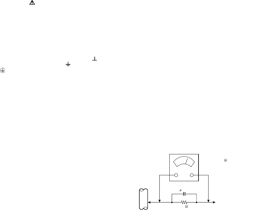
Alternate Check Method
Plug the AC line cord directly into the AC outlet (do not
use a line isolation transformer during this check.). Use
an AC voltmeter having 1000Ω per volt or more
sensitivity in the following manner. Connect a 1500Ω
10W resistor paralleled by a 0.15µF AC-type capacitor
between an exposed metal part and a known good earth
ground (water pipe, etc.). Measure the AC voltage
across the resistor with the AC voltmeter. Move the
resistor connection to each exposed metal part,
particularly any exposed metal part having a return path
to the chassis, and measure the AC voltage across the
resistor. Now, reverse the plug in the AC outlet and
repeat each measurement. Any voltage measured must
not exceed 0.75V AC (r.m.s.). This corresponds to
0.5mA AC (r.m.s.).
However, in tropical area, this must not exceed 0.3V AC
(r.m.s.). This corresponds to 0.2mA AC (r.m.s.).
AC VOLTMETER
(HAVING 1000 /V,
OR MORE SENSITIVITY)
PLACE THIS PROBE
ON EACH EXPOSED
METAL PART
1500 10W
0.15 F AC-TYPE
GOOD EARTH GROUND
1-4 (No.YA463)
1.2 INSTALLATION
1.2.1 HEAT DISSIPATION
If the heat dissipation vent behind this unit is blocked, cooling
efficiency may deteriorate and temperature inside the unit will
rise. The temperature sensor that protects the unit will be
activated when internal temperature exceeds the predetermined
level and power will be turned off automatically.
Therefore, please make sure pay attention not to block the heat
dissipation vent as well as the ventilation outlet behind the unit
and ensure that there is room for ventilation around it.
Do not put foreign objects near the ventilation holes as this
can result in fire or electrical hazards.
Do not block the ventilation holes as this may cause the
internal temperature to rise and possibly result fire.
1.2.2 INSTALLATION REQUIREMENTS
Ensure that the minimal distance is maintained, as specified
fingure, between the unit with and the surrounding walls, as well
as the floor etc.
Install the unit on stable flooring.
Take precautionary measures to prevent the unit from tipping in
order to protect against accidents and earthquakes.
CAUTION FOR INSTALLATION
• Do not tilt the TV towards the left or right, or toward the back.
• Install the TV in a corner on the floor so as to keep cords out
of the way.
• The TV will generate a slight amount of heat during
operation. Ensure that sufficient space is available around
the TV to allow satisfactory cooling.
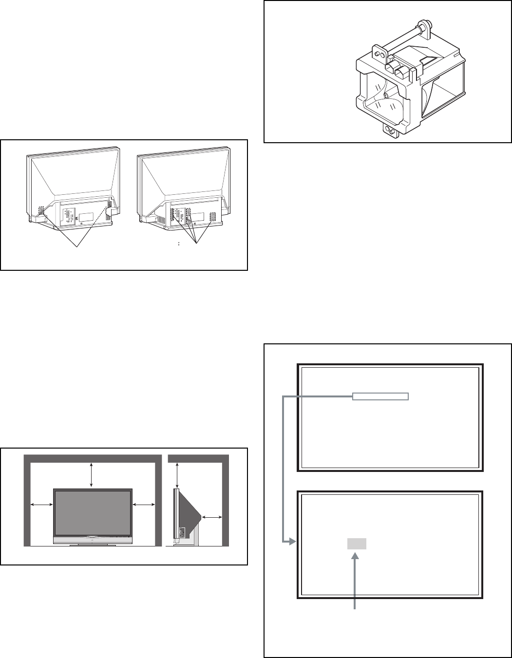
1.3 LAMP UNIT HANDLING CAUTION
1.3.1 PRECAUTION FOR LAMP UNIT
The lamp emits high intensity white, ultraviolet and infrared
light. Do not look directly at the light during service.
Also, do not touch the lamp directly as it presents a burn
hazard.
Handle with extra care. This lamp emits high heat and
contains high-pressure during use.
Do not give any impact as this may cause the broken lamp.
1.3.2 HOW TO CONFIRM LAMP OPERATING TIME
• MAXIMUM COUNT TIME= 65535 hours
(1) Set to "0 minutes" using the [SLEEP TIMER] key.
(2) Press the [VIDEO STATUS] key and [DISPLAY] key
simultaneously, then enter the SERVICE MODE.
(3) When the SERVICE MENU SCREEN is displayed, press
[2] key to enter the SELF CHECK MODE.
(4) The use time of a lamp is displayed on middle of the screen
by the hexadecimal number of 4 figures.
Intake hole Exhaust hole
*Diagram differs from actual appearance.
150 mm
200 mm
150 mm
200 mm
50 mm
LAMP
POWER
VOLUME
INPUT-4
CHANNEL
OPERATE
+
Ð
+
Ð
MENU
VIDEO
L/MONO
R
AUDIO
INPUT
*Diagram differs from actual appearance.
LAMP UNIT : TS-CL110UAA
Lamp operation time (Hexadecimal)
SERVICE MENU SCREEN
SELF CHECK MODE SCREEN (Page 1)
SERVICE MENU
SERVICE MENU
1. ADJUST
1. ADJUST
2. SELF CHECK
2. SELF CHECK
3. I2C STOP
3. I2C STOP
LOB 0 FAN 0
LOB 0 FAN 0
AUD 0
AUD 0
ANA 9 DIG 9
ANA 9 DIG 9
0000 0
0000 0
0
0
CALCULATION EXAMPLE OF LAMP USE TIME
Ex. Display number=12EF
1x163+2x162+Ex16+Fx1=1x4096+2x256+14x16+154847 hours

(No.YA463)1-5
1.3.3 LAMP UNIT REPLACEMENT
(1) The lamp replacement message will appear when need to
change the lamp. After replace the lamp, need to reset the
timer which is built into TV.
(2) Lamp use time can be check at the lamp message MENU.
If lamp use time exceeds 5000 hours, the message of
Fig.1 will be displayed on a screen.
(3) If Fig.1 message appears when turn the TV on, need to
replace the lamp.
(4) Use the lamp timer reset only after replacing the lamp.
NOTE:
• This message will appear every time turn on the TV, when
the lamp needs to be replaced. Press the [OK] key to make
the message disappear, or replace the lamp.
Fig.1
1.3.4 HOW TO REPLACE THE LAMP UNIT
• Refer to the "USERS GUIDE" for a detailed operating
description.
(1) Turn off the TV power.
(2) After the LAMP LED light has stopped blinking, disconnect
the power cord from the AC outlet.
(3) Loosen 1 screw then take out the lamp cover below the left
side of the TV.
(4) Loosen 2 screws then take out the lamp unit.
(5) Install the new lamp unit.
(6) Re-install the lamp cover.
NOTE:
• After installing the new lamp unit, do not forget to reset the
lamp timer.
1.3.5 HOW TO RESET THE LAMP TIMER
• Refer to the "USERS GUIDE" for a detailed operating
description.
(1) Press the [MENU] key to select CLOCK / TIMERS.
(2) Select the <LAMP TIMER RESET> with [] / [] keys.
(3) Enter the <LAMP TIMER RESET> mode, the following
message will appears.
(4) Press the [OK] key while the above message appears on
the screen.
(5) The lamp timer has now been reset, and the following
message will appear.
1.3.6 PRECAUTION FOR REPLACEMENT
• Do not replace the LAMP UNIT immediately after the projector
has been used.
• The temperature of the LAMP UNIT is still high and could
cause a burn.
• Allow a cooling period of 1 hour or more before performing
replacement.
• Before starting LAMP UNIT replacement work, turn off the
MAIN POWER switch, and disconnect the AC power cord plug
from the wall outlet.
• If touched, the lamp glass surface may rupture and burns may
result. Do not touch the glass portion or metal portion. Handle
only plastic handle.
• The replaced old lamp can be discarded in the same manner
as a fluorescent lamp. Check local ordinances and dispose of
the used lamp as prescribed.
PRESS OK TO RESET THE LAMP TIMER
THE LAMP TIMER IS RESET SUCCESSFULLY
LAMP NEEDS TO BE REPLACED.
REFER TO OWNER'S MANUAL FOR
REPLACEMENT INSTRUCTIONS.
AFTER REPLACING THE LAMP,
PLEASE RESET TIMER IN THE TV
MENU.
PRESS OK, IF YOU DO NOT WANT
TO SEE THIS MESSAGE AGAIN.
LAMP REPLACEMENT MESSAGE
1-6 (No.YA463)
1.4 SERVICE PARTS KIT INSTRUCTIONS
Due to the character of this product, these OPTICAL /DRIVE
ASS'Y are prepared.
Please note these OPTICAL/DRIVE ASS'Y when replacing or
ordering the parts.
1.4.1 PART NUMBER AND CONSTRUCTION
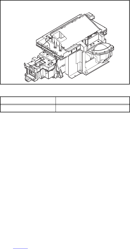
1.4.2 OPTICAL / DRIVE ASS'Y CONSTRUCTION
(1) OPTICAL BLOCK
(Included D-ILA DEVICE, PROJECTION LENS)
(2) OPTICAL BASE
(3) DRIVE PWB ASS'Y
This PWB is mounted with 1 memory IC saved with
adjustment, setting data of the drive circuit.
(4) SHIELD COVER
*The following parts without the kits part.
• REMOTE SENSOR PWB ASS'Y
• LAMP UNIT
• LAMP FAN DUCT
• THERMOSTAT
1.4.3 PRECAUTION FOR USING
(1) In the case of the following defects/problems, replace this
kit (OPTICAL/DRIVE ASS'Y)
a) Picture defect caused by optical system/D-ILA device
related parts.
b) Picture defect caused by drive circuit.
(2) The DRIVE PWB ASS'Y is mounted with a memory IC
[IC3753] saved with adjustment/setting data(GAMMA,
SHADING, etc.) of the drive circuit.
The data of this memory IC is in the optimal state according
to individual D-ILA devices and each section of the
OPTICAL BLOCK.
(3) When replace the DRIVE PWB ASS'Y, take off the 1
memory IC from the original board and replace with new
one. When replace the DRIVE PWB ASS'Y, do same
manner. Replace 1 memory IC.
(4) After the replacement of the OPTICAL BLOCK, projection
lens focus adjustment and drive convergence / projection
adjustment are required.
1.5 SCREEN HANDLING CAUTIONS
1.5.1 SCREEN STORAGE
Store the SCREEN ASS'Y in a standing position in order to avoid
deformation. If the screen is stored horizontally, there is risk of
deforming the screen face.
When necessary to place the SCREEN ASS'Y horizontally,
position the screen side upwards and sure to place spacers
between the screen and resting site (floor or stand etc.) to
prevent the screen from sagging.
1.5.2 SCREEN SURFACE
Since the screen surface is easily scratched or soiled, use ample
care when handling.
1.5.3 PRECAUTIONS FOR CLEANING AND REPLACEMENT
• The SCREEN ASS'Y is made from the lenticular lens and
fresnel lens. The anti static proceeding and the surface of the
lenticular lens. Rubbing the surface with something hard, the
coating may peel off.
• When the screen is dirty, gently wipe it with a soft cloth.
If the screen is very dirty, wipe it down with a cloth dipped in a
diluted kitchen cleaner (neutrality detergent) and thoroughly
wrung-out. Then wipe immediately after with clean, dry cloth.
Never use the organic solvent such as the alcohol or benzine.
• The SCREEN ASS'Y replacement is required if the coating
was peel off. Alkaline detergent or acidity detergent can not be
be used.
• The notched side of the lenticular lens and the fresnel lens are
faced each other.
• Do not rub the screen when cleaning it or replaceing it.
Rubbing the screen may cause of the scratch of the screen by
its notch.
Kit parts number Kit part name
TS-COP14A-SAA OPTICAL / DRIVE ASS'Y
OPTICAL/DRIVE ASS'Y
(No.YA463)1-7
SECTION 2
SPECIFIC SERVICE INSTRUCTIONS
2.1 SYSTEM SETTEING
(1) Set to "0 minutes" using the [SLEEP TIMER] key.
(2) While "0 minutes" is displayed, press the [VIDEO
STATUS] key and [DISPLAY] key simultaneously, then
enter the SERVICE MODE.
(3) When the SERVICE MENU SCREEN is displayed, press
[2] key to enter the self check mode.
(4) Turn off the power by pressing the [POWER] key on the
remote control unit.
2.2 FEATURES
Built in ATSC (Advanced Television Systems Committee)
TUNER
This TV can receive both Digital broadcasting (ATSC) and
Analogue broadcasting.
D.I.S.T. (Digital Image Scaling Technology)
This system uses line interpolation to double the number of
scanning lines and achieve high resolution, flicker-free picture.
SMART CAPTION
Smart caption will appear when you press the MUTING button,
only on channels where the broadcast contains CLOSED
CAPTION information.
VIDEO STATUS
Expression of a favorite screen can be chosen by the VIDEO
STATUS function.
DIGITAL INPUT
Digital-in will display when any picture signal in Digital-in is
displayed.
V-CHIP
Since the V-CHIP is built in, it can choose, view and listen to a
healthy program.
MTS STEREO
The voice multiplex function of the MTS system is built in.
(MTS = Multi channel Television Sound system)
MPEG Noise Reduction
This function effects the block noise removal and mosquito NR
simultaneously.
A.H.S.+
Adds a more spacious surround sound. Music gives basic effect,
and movie for more effect.
NATURAL CINEMA
Watching the movie or animation, press the Natural Cinema to
adjust the out line of the images to make thin more sharp.
VIDEO INPUT LABEL
This function is used to label video input connections for the
onscreen displays.
2.3 MAIN DIFFRENCE LIST
Be sure to carry out the following operation at the end of
the procedure.
SERVICE MENU SCREEN
SELF CHECK MODE SCREEN
SERVICE MENU
SERVICE MENU
1. ADJUST
1. ADJUST
2. SELF CHECK
2. SELF CHECK
3. I2C STOP
3. I2C STOP
LOB 0 FAN 0
LOB 0 FAN 0
AUD 0
AUD 0
ANA 9 DIG 9
ANA 9 DIG 9
0000 0
0000 0
0
0
Item HD-52FA97 HD-56FB97 HD-61FB97
DIGITAL PWB SRA-0D161A-M2 SRA-0D160A-M2 SRA-0D159A-M2
FRONT LED PWB SRA-0L111A-M2 SRA-0L113A-M2 ←
1-8 (No.YA463)
2.4 TECHNICAL INFORMATION
2.4.1 D-ILA DEVICE SPECIFICATION
2.4.2 PROJECTION UNIT
2.4.3 IMAGE LIGHT FLOW
2.4.4 D-ILA DEVICE STRUCTURE
Item Content
Resolution H: 1952 × V:1088
Pixel number about 2123776
Pixel size H : 8.1µm × V :8.1µm
Aspect ratio 16 : 9
Contrast ratio 5000 : 1
Aperture ratio 89% or more
Effective pixel measurement 0.7 inch
R DEVICE
G DEVICE
B DEVICE
Lamp unit
Incident light
Device
BRG
B
BRG
R
Projection
light
G
Mirror
MirrorMirror
FRONT
DEVICE UNIT SECTION (TOP VIEW)
Device
Device
Incident
light
Pixel
FRONT
Incident light
Projection light
Glass
substrate
Transparent
electrode
Reflective pixel
electrode
Back
Plane
Liquid
crystal
Flat film
R / G / B DEVICE (SIDE VIEW)
8.1 m
PIXEL VIEW (FRONT VIEW)
8.1 m

(No.YA463)1-9
2.4.5 MAIN CPU PIN FUNCTION [IC7601 : DIGITAL PWB ASS'Y]
Pin Pin name I/O Function Pin Pin name I/O Function
1 VHOLD1 I Data slice for main screen closed caption 51 NC O Not used
2 HFLT1 I/O LPF for main screen closed caption video input 52 NC O Not used
3 NC O Not used 53 NC O Not used
4 NC O Not used 54 NC O Not used
5 DIGR0 O R [0] for OSD 55 NC O Not used
6 TB1in I AC power for timer clock 56 NC O Not used
7 REMO I Remote control 57 NC O Not used
8 BYTE I Data bus width select [L = 16bit (fixed)] 58 NC O Not used
9 CNVss I CPU programming mode select [Normal = L] 59 NC O Not used
10 DIGG0 O G [0] for OSD 60 NC O Not used
11 DIGB0 O B [0] for OSD 61 NC O Not used
12 RESET I Reset for main CPU [Reset = L] 62 HSYNC I H. sync for OSD
13 Xout O System clock osillation (crystal) : 16MHz 63 NC O Not used
14 Vss - GND 64 VSYNC I V. sync for OSD
15 Xin I System clock osillation (crystal) : 16MHz 65 NC O Not used
16 VccI I 3.3V stand-by power supply 66 NC O Not used
17 OSC1 I Clock for OSD 67 NC O Not used
18 OSC2 O Not used : Clock for OSD 68 NC O Not used
19 INT1 I Not used: AV COMPULINK control 69 NC O Not used
20 INT0 I
Request for sub(chassis) CPU communication (serial data)
70 NC O Not used
21 OUT1 O Ys (blanking) for OSD 71 P2.1 O Not used: Clock for Inter IC (serial) bus control
22 OUT2 O YM (transparence) for OSD 72 P2.0 I/O Not used: Data for Inter IC (serial) bus control
23 NC O Not used 73 NC O Not used
24 NC O Not used 74 NC O Not used
25 NC O Not used 75 NC O Not used
26 NC O Not used 76 NC O Not used
27 CTA2/RTS2 O Not used 77 NC O Not used
28 CLK2 O Not used 78 NC O Not used
29 RxD2 I Digital tuner control 79 NC O Not used
30 TxD2 O Digital tuner control 80 P1.0 O Not used: Function LED lighting
31 SDA2 I/O Not used 81 P0.7 O Not used: Communication LED lighting
32 DIGR1 O R [1] for OSD 82 P0.6 O Test point
33 DIGG1 O G [1] for OSD 83 NC O Not used
34 DIGB1 O B [1] for OSD 84 WAKE O Reset for sub(chassis) CPU
35 TxD0 I Data receive (serial) for external programming 85 CARD_DET I Not used
36 RxD0 O Data transmission (serial) for external programming 86
POWER_SW
I Power switch (mechanical) detection
37 CLK0 I Clock for external programming 87 SDA I/O Data for Inter IC (serial) bus control : memory
38 RTS0 O Busy for external programming [Operation = H] 88 SLC O Clock for Inter IC (serial) bus control : memory
39 P5.7 I Not used 89 DIGR2 O R [2] for OSD
40 P5.6 O Not used 90 DIGG2 O G [2] for OSD
41 HOLD I CPU programming mode select [Normal = H] 91 DIGB2 O B [2] for OSD
42 P5.4 O Not used 92 NC O Not used
43 P5.3 O Not used 93 KEY2 I
Key scan data for front control button (MENU/CH+/CH-) KEY2
44 P5.2 O Not used 94 KEY1 I
Key scan data for front control button (INPUT/VOL+/VOL-) KEY1
45 P5.1 O Not used 95 VHOLD2 I Data slice for sub screen closed caption
46 WR O CPU programming mode select [Normal = L] 96 HLF2 I/O LPF for sub screen closed caption video input
47 P4.7 O
Data transmission for sub(chassis) CPU communication (serial)
97 CVIN2 I Video(Y) for sub screen closed caption
48 P4.6 I
Data receive for sub(chassis) CPU communication (serial)
98 TVSETB I Test terminal [L Fixed]
49 P4.5 I Clock for sub(chassis) CPU communication (serial) 99 VCCE I 5V stand-by power supply
50 P4.4 O Not used 100 CVIN1 I Video(Y) for main screen closed caption
1-10 (No.YA463)
SECTION 3
DISASSEMBLY
3.1 DISASSEMBLY PROCEDURE
CAUTION AT DISASSEMBLY:
•Be sure to perform the SYSTEM SETTEING, at the end of the procedure.
• Make sure that the power cord is disconnected from the outlet.
• Pay special attention not to break or damage the parts.
• When removing each board, remove the connectors as required. Taking notes of the connecting points (connector numbers)
makes service procedure manageable.
• Make sure that there is no bent or stain on the connectors before inserting, and firmly insert the connectors.
• Wait until the LAMP UNIT has cool down is completely.
• While not in repair service, place the chassis back its original position.
3.1.1 FRONT SIDE DISASSEMBLY [HD-52FA97]
3.1.1.1 REMOVING THE SPEAKER GRILL (Fig.1)
(1) Remove the 2 screws [A].
(2) Remove the SPEAKER GRILL by pressing it downward.
3.1.1.2 REMOVING THE FRONT LED PWB (Fig.1)
• Remove the SPEAKER GRILL.
(1) Remove the 1 screw [B].
(2) Remove the FRONT LED PWB.
3.1.1.3 REMOVING THE CENTER COVER (Fig.1)
• Remove the SPEAKER GRILL.
(1) Remove the 2 screws [C].
(2) Remove the CENTER COVER.
3.1.1.4 REMOVING THE FRONT PANEL (Fig.1)
• Remove the SPEAKER GRILL.
(1) Remove the 10 screws [D].
(2) Remove the 12 screws [E].
(3) Remove the FRONT PANEL.
3.1.1.5 REMOVING THE SPEAKER (Fig.1)
• Remove the SPEAKER GRILL.
(1) Remove the 4 screws [F].
(2) Remove the SPEAKER.
(3) Remove the opposite SPEAKER by the same method.
3.1.1.6 REMOVING THE SCREEN BLOCK(Fig.1)
• Remove the SPEAKER GRILL.
• Remove the FRONT PANEL.
(1) Remove the 8 screws [G].
(2) Remove the SCREEN BLOCK.
CAUTION:
• Place the SCREEN BLOCK on a flat table without fail.
• Because of the large size, at least 2 persons are
recommended for removal and reassemble.
• Use care not to scratch the screen during work.
• During assembly, be sure to engage the left and right tabs
with the cabinet mounting positions.
• When supporting the SCREEN BLOCK, avoid grasping the
top of the screen panel, instead grasp the left and right
areas.
• Do not leave the SCREEN BLOCK removed for long time to
prevent soiling from dust.
3.1.1.7 REMOVING THE SCREEN ASS'Y (Fig.1)
• When replacing the SCREEN ASS'Y, confirm each SPACER
is fit on the SCREEN BRACKET without fail.
• Remove the SPEAKER GRILL.
• Remove the FRONT PANEL.
• Remove the SCREEN BLOCK.
(1) Remove the 12 screws [H].
(2) Remove the SCREEN ASS'Y.
NOTE:
• When replacing the SCREEN ASS'Y, confirm each
SPACER is fit on the SCREEN BRACKET without fail.
• Do not touch the front of the SCREEN ASS'Y.
• Do not shock the SCREEN ASS'Y.
• Because of the large size, at least 2 persons are
recommended for removal and reassemble.
(No.YA463)1-11
Fig.1
FRONT
SCREEN BLOCK
SCREEN BRACKET
SCREEN ASS'Y
FRONT BRACKET
SPEAKER
BACK COVER
SPEAKER
CENTER COVER
FRONT PANEL
SPEAKER GRILL
FRONT LED
PWB
SCREEN BLOCK
MAIN BODY
SCREEN BRACKET
SPACER
SPACER
SPACER
SPACER
B
D
F
F
C
E
G
H
H
A
1-12 (No.YA463)
3.1.1.8 REMOVING THE MIRROR (Fig.2)
• Remove the SPEAKER GRILL.
• Remove the FRONT PANEL.
• Remove the SCREEN BLOCK.
(1) Remove the 4 screws [A] attaching the MIRROR HOLDER
of the upper side.
(2) Remove the 6 screws [B] attaching the MIRROR HOLDER
of left and right side.
(3) Raise slightly to disengage of the MIRROR from the bottom
MIRROR HOLDER
(4) Remove the MIRROR.
NOTE :
• Do not touch the front of the MIRROR.
• Do not shock the the MIRROR.
• Because of the large size, at least 2 persons are
recommended for removal and reassemble.
3.1.1.9 REMOVING THE SIDE CONTROL PWB (Fig.2)
• Remove the SPEAKER GRILL.
• Remove the FRONT PANEL.
• Remove the SCREEN BLOCK.
(1) Remove the 2 screws [C].
(2) Remove the SIDE CONTROL BASE.
(3) Remove the 2 screws [D].
(4) Remove the SIDE CONTROL PWB.
3.1.1.10 REMOVING THE SUPPORT HOLDER (Fig.2)
• Remove the SPEAKER GRILL.
• Remove the FRONT PANEL.
• Remove the SCREEN BLOCK.
(1) Remove the 2 screws [E].
(2) Remove the SUPPORT HOLDER.
3.1.1.11 REMOVING THE SHADE COVER (Fig.2)
• Remove the SPEAKER GRILL.
• Remove the FRONT PANEL.
• Remove the SCREEN BLOCK.
(1) Remove the 2 screws [F].
(2) Remove the SHADE COVER.
3.1.1.12 REMOVING THE BACK COVER (Fig.2)
• Remove the SPEAKER GRILL.
• Remove the FRONT PANEL.
• Remove the SCREEN BLOCK.
• Remove the SUPPORT HOLDER.
(1) Remove the 6 screws [G].
(2) Remove the 2 screws [H] from rear side.
(3) Remove the 2 screws [J] attach the SPEAKER BOX.
(4) Remove the BACK COVER with the SPEAKER BOX
CAUTION :
• Because of the large size, at least 2 persons are
recommended for removal and reassemble.
3.1.1.13 REMOVING THE SPEAKER BOX (Fig.2)
• Remove the SPEAKER GRILL.
• Remove the FRONT PANEL.
• Remove the SCREEN BLOCK.
• Remove the SUPPORT HOLDER.
• Remove the BACK COVER with the SPEAKER BOX.
(1) Remove the 1 screw [K].
(2) Remove the SPEAKER BOX.
(3) Remove the opposite SPEAKER BOX by the same method.
3.1.1.14 REMOVING THE FILTER (Fig.2)
(1) Remove the 1 screw [L].
(2) Remove the FILTER COVER with the FILTER.
(3) Remove the FILTER.
(4) Remove the opposite FILTER by the same method.
(No.YA463)1-13
Fig.2
FRONT
MAIN BODY
SUPPORT
HOLDER
SIDE CONTROL
PWB
FILTER COVER
FILTER
SIDE CONTROL
BASE
SPEAKER
BOX
SPEAKER
BOX
MIRROR
MIRROR HOLDER
MIRROR HOLDER
MIRROR
HOLDER
BACK COVER
FILTER
COVER
FILTER
SHADE
COVER
J
J
H
L
L
D
C
E
K
K
F
B
A
B
G
1-14 (No.YA463)
3.1.2 FRONT SIDE DISASSEMBLY [HD-56FB97, HD-61FB97]
3.1.2.1 REMOVING THE SPEAKER GRILL (Fig.3)
(1) Remove the 4 screws [A].
(2) Remove the 2 claws under the SPEAKER GRILL.
(3) Remove the SPEAKER GRILL by pressing it downward.
3.1.2.2 REMOVING THE FRONT LED PWB (Fig.3)
• Remove the SPEAKER GRILL.
(1) Remove the 2 screws [B].
(2) Remove the FRONT LED PWB.
3.1.2.3 REMOVING THE CENTER COVER (Fig.3)
• Remove the SPEAKER GRILL.
(1) Remove the 2 screws [C].
(2) Remove the CENTER COVER.
3.1.2.4 REMOVING THE FRONT PANEL WITH SCREEN
ASS'Y (Fig.3)
• Remove the SPEAKER GRILL.
(1) Remove the 8 screws [D].
(2) Remove the 10 screws [E].
(3) Remove the FRONT PANEL with SCREEN ASS'Y.
CAUTION:
•Place the FRONT PANEL with SCREEN ASS'Y on a flat
table without fail.
•Because of the large size, at least 2 persons are
recommended for removal and reassemble.
•Use care not to scratch the screen during work.
•Do not leave the FRONT PANEL with SCREEN ASS'Y
removed for long time to prevent soiling from dust.
3.1.2.5 REMOVING THE SCREEN ASS'Y (Fig.3)
• Remove the SPEAKER GRILL.
• Remove the FRONT PANEL with SCREEN ASS'Y.
(1) Remove the 10 screws [F].
(2) Remove the 8 screws [G].
(3) Remove the SCREEN BRACKET.
(4) Remove the SCREEN ASS'Y from the FRONT PANEL
NOTE:
• When replacing the SCREEN ASS'Y, confirm each
SPACER is fit on the SCREEN BRACKET and the FRONT
PANEL without fail.
• Do not touch the front of the SCREEN ASS'Y.
• Do not shock the SCREEN ASS'Y.
• Because of the large size, at least 2 persons are
recommended for removal and reassemble.
3.1.2.6 REMOVING THE SPEAKER (Fig.3)
• Remove the SPEAKER GRILL.
• Remove the FRONT PANEL with SCREEN ASS'Y.
(1) Remove the 4 screws [H].
(2) Remove the SPEAKER.
(3) Remove the opposite SPEAKER by the same method.
(No.YA463)1-15
Fig.3
CENTER
COVER
CLAW
FRONT PANEL
SCREEN
ASS'Y
SCREEN
BRACKET
SPEAKER GRILL
SPEAKER
SPEAKER
FRONT LED
PWB
FRONT
SPACER
SPACER
SPACER
SCREEN
BRACKET
G
G
F
G
F
F
F
G
C
E
H
B
D
H
A
A
SPACER
SPACER
SPACER
SPACER
1-16 (No.YA463)
3.1.2.7 REMOVING THE MIRROR (Fig.4)
• Remove the SPEAKER GRILL.
• Remove the FRONT PANEL with the SCREEN ASS'Y.
(1) Remove the 4 screws [A] attaching the MIRROR HOLDER
of the upper side.
(2) Remove the 6 screws [B] attaching the MIRROR HOLDER
of left and right side.
(3) Loosen the 4 screws [C] attaching the MIRROR HOLDER
of bottom side.
(4) Raise slightly to disengage of the MIRROR from the bottom
MIRROR HOLDER.
(5) Remove the MIRROR.
NOTE:
• Do not touch the front of the MIRROR.
• Do not shock the MIRROR.
• Because of the large size, at least 2 persons are recommended
for removal and reassemble.
3.1.2.8 REMOVING THE SIDE CONTROL PWB (Fig.4)
• Remove the SPEAKER GRILL.
• Remove the FRONT PANEL with the SCREEN ASS'Y.
(1) Remove the 3 screws [D].
(2) Remove the SIDE CONTROL PWB from the SIDE CONTROL BASE.
NOTE:
The SIDE CONTROL BASE is taken out by removing 6 claws.
3.1.2.9 REMOVING THE SUPPORT BRACKET (Fig.4)
• Remove the SPEAKER GRILL.
• Remove the FRONT PANEL with the SCREEN ASS'Y.
(1) Remove the 3 screws [E].
(1) Remove the SUPPORT BRACKET.
(2) Remove the opposite SUPPORT BRACKET by the same method.
3.1.2.10 REMOVING THE BACK COVER (Fig.4)
• Remove the SPEAKER GRILL.
• Remove the FRONT PANEL with the SCREEN ASS'Y.
• Remove the SUPPORT BRACKET.
(1) Remove the 2 screws [F] and 2 screws [G] from rear side.
(2) Remove the 4 screws [H].
(3) Remove the BACK COVER.
CAUTION :
Because of the large size, at least 2 persons are recommended
for removal and reassemble.
3.1.2.11 REMOVING THE SHADE COVER (Fig.4)
• Remove the SPEAKER GRILL.
• Remove the FRONT PANEL with the SCREEN ASS'Y.
• Remove the SUPPORT BRACKET.
• Remove the BACK COVER.
(1) Remove the 2 screws [J].
(2) Remove the SHADE COVER.
3.1.2.12 REMOVING THE FILTER (Fig.4)
(1) Remove the 1 screw [K].
(2) Remove the FILTER COVER.
(3) Remove the FILTER from FILTER COVER.
(4) Remove the opposite FILTER by the same method.
(No.YA463)1-17
Fig.4
MAIN BODY
SIDE
CONTROL
PWB
CLAW
CLAW
SIDE
CONTROL
BASE
MIRROR
MIRROR HOLDER
FILTER COVER
FILTER COVER
FILTER
BACK COVER
FILTER
MIRROR
HOLDER
SUPPORT
PLATE
SUPPORT
BRACKET
SUPPORT
BRACKET
SUPPORT
PLATE
MIRROR
HOLDER
SHADE COVER
FRONT
C
MIRROR
HOLDER
MIRROR
HOLDER
C
D
E
H
F
B
A
K
K
G
E
B
J
1-18 (No.YA463)
3.1.3 REAR SIDE DISASSEMBLY
3.1.3.1 REMOVING THE LAMP UNIT (Fig.5)
(1) Remove the 1 screw [A].
(2) Remove the LAMP COVER.
(3) Remove the 2 screws [B]
(4) Pull out the LAMP UNIT.
NOTE :
• Do not leave the LAMP COVER removed for long time to
prevent dirt and dust form covering the lens.
• Make sure that the LAMP COVER is completely installed.
3.1.3.2 REMOVING THE BODY COVER (Fig.5)
(1) Remove the 7 screws [C].
(2) Remove the 4 screws [D]. [only HD-52FA97]
(3) Remove the 5 screws [E].
(4) Remove the BODY COVER.
NOTE :
• Do not leave the BODY COVER removed for long time to
prevent soiling from dust.
3.1.3.3 REMOVING THE MAIN UNIT (Fig.5)
• Remove the LAMP COVER.
• Remove the BODY COVER.
(1) Remove the 4 screws [F]
(2) Remove the BODY BRACKET.
(3) Remove the 2 screws [G]
(4) The MAIN UNIT is pulled out to the back side.
CAUTION :
•Except for confirmation of projection images on the
screen and audio output through the speakers, the
removed MAIN UNIT is still workable in the same state
as if it is still built-in the TV set. Therefore, the MAIN
UNIT can be removed, if necessary, for board diagnosis,
electric testing, etc. apart from confirmation of screen
images and audio output. Do not leave the MAIN UNIT
removed for long time to prevent soiling from dust.
•Because of the large size, at least 2 persons are
recommended for removal and reassemble.
•When carrying the MAIN UNIT, use care not to drop,
shock or shake it.
•Do not stain or damage the projection lens.
•Do not look directly at the light during service.
•Do not touch the lamp directly as it presents a burn
hazard.
NOTE :
• When not performing repair work, attach the cap on the lens
to preventing dust from covering.
• When mounting to the set, make sure the front of the lens is
in contact with the cushion on the set (body) side.
• Make sure that FRONT LED PWB connector is completely
connect to the ANALOG PWB connector.
• When wire clamps are removed during work, use care to
restore them precisely to their original positions.
Performance can be affected if these are not returned to the
original positions.
3.1.3.4 REMOVING THE AV TERMINAL BOARD (Fig.5)
• Remove the LAMP COVER.
• Remove the BODY COVER.
• Remove the BODY BRACKET.
• Remove the MAIN UNIT.
(1) Remove the 3 screws [H], 5 screws [J] and the 7 screws [K].
(2) Remove the 2 hex screws [L].
(3) Remove the nut attaching the ANTENNA TERMINAL.
(4) Remove the AV TERMINAL BOARD.
3.1.3.5 REMOVING THE POWER PWB (Fig.5)
• Remove the LAMP COVER.
• Remove the BODY COVER.
• Remove the BODY BRACKET.
• Remove the MAIN UNIT.
(1) Remove the POWER CORD.
(2) Remove the 7 screws [M].
(3) Remove the POWER PWB.
3.1.3.6 REMOVING THE TUNER PWB (Fig.5)
• Remove the LAMP COVER.
• Remove the BODY COVER.
• Remove the BODY BRACKET.
• Remove the MAIN UNIT.
• Remove the AV TERMINAL BOARD.
(1) Remove the 1 screw [N].
(2) Remove the HANGER BRACKET with TUNER PWB.
(3) Remove the 3 screws [P].
(4) Remove the TUNER PWB.
3.1.3.7 REMOVING THE ANALOG PWB (Fig.5)
• Remove the LAMP COVER.
• Remove the BODY COVER.
• Remove the BODY BRACKET.
• Remove the MAIN UNIT.
• Remove the AV TERMINAL BOARD.
• Remove the POWER PWB and TUNER PWB.
(1) Remove the 4 screws [Q].
(2) Remove the ANALOG PWB.
(No.YA463)1-19
3.1.3.8 REMOVING THE DIGITAL PWB (Fig.5)
• Remove the LAMP COVER.
• Remove the BODY COVER.
• Remove the BODY BRACKET.
• Remove the MAIN UNIT.
• Remove the AV TERMINAL BOARD.
• Remove the POWER PWB and TUNER PWB.
• Remove the ANALOG PWB.
(1) Remove the 1 screw [R].
(2) Remove the DIGITAL PWB BRACKET with DIGITAL PWB
and ATSC TUNER PWB.
(3) Remove the 7 screws [S].
(4) Remove the DIGITAL PWB SHIELD COVER.
(5) Remove the 9 screws [T].
(6) Remove the DIGITAL PWB.
CAUTION :
•Make sure to perform the "SYSTEM SETTEING" , when
DIGITAL PWB is replaced.
•Especially, because the value of F001 (DD) might been
changed, go through next steps to confirm the setting
value with the remote control unit.
(1) Set to "0 minutes" using the [SLEEP TIMER] key.
(2) While "0 minutes" is displayed, press the [VIDEO
STATUS] key and [DISPLAY] key simultaneously,
then enter the SERVICE MODE.
(3) Press [1] key to enter the ADJUSTMENT MODE.
(4) Select < F001 >.
(5) Confirm the value to "000", and set it to "000" when not
"000".
(6) Press [MUTING] key to memorize the data.
(7) Press [BACK] key twice to exit the SERVICE MODE.
3.1.3.9 REMOVING THE ATSC TUNER COOLING FAN (Fig.5)
• Remove the LAMP COVER.
• Remove the BODY COVER.
• Remove the BODY BRACKET.
• Remove the MAIN UNIT.
• Remove the AV TERMINAL BOARD.
• Remove the POWER PWB and TUNER PWB.
• Remove the ANALOG PWB.
(1) Remove the 1 screw [R].
(2) Remove the DIGITAL PWB BRACKET with ATSC TUNER
PWB.
(3) Remove the 4 screws [U].
(4) Remove the ATSC TUNER COOLING FAN.
3.1.3.10 REMOVING THE ATSC TUNER PWB (Fig.5)
• Remove the LAMP COVER.
• Remove the BODY COVER.
• Remove the BODY BRACKET.
• Remove the MAIN UNIT.
• Remove the AV TERMINAL BOARD.
• Remove the POWER PWB and TUNER PWB.
• Remove the ANALOG PWB.
• Remove the ATSC TUNER COOLING FAN.
(1) Remove the 7 screws [V].
(2) Remove the ATSC TUNER SHIELD COVER.
(3) Remove the 4 screws [W].
(4) Remove the ATSC TUNER PWB.
3.1.3.11 REMOVING THE USB PWB (Fig.5)
• Remove the LAMP COVER.
• Remove the BODY COVER.
• Remove the BODY BRACKET.
• Remove the MAIN UNIT.
• Remove the AV TERMINAL BOARD.
• Remove the POWER PWB and TUNER PWB.
• Remove the ANALOG PWB.
• Remove the ATSC TUNER COOLING FAN.
(1) Remove the 7 screws [V].
(2) Remove the ATSC TUNER SHIELD COVER.
(3) Remove the 3 screws [X] and 1 screw [Y].
(4) Remove the USB PWB.
1-20 (No.YA463)
Fig.5
F
E
C
D
G
H
L
K
J
M
N
W
X
Y
S
T
P
R
U
V
Q
B
A
MAIN BODY
FRONT
MAIN UNIT
POWER CORD
POWER PWB
ANALOG PWB
TUNER PWB
ATSC TUNER
MODULE
USB
PWB
AV TERMINAL
BOARD
BODY COVER
DIGITAL PWB
SHIELD COVER
DIGITAL PWB
BRACKET
DIGITAL PWB
BODY BRACKET
LAMP COVER
LAMP UNIT
ATSC TUNER
COOLING FAN
ATSC TUNER
SHIELD COVER
HANGER
BRACKET
(No.YA463)1-21
3.1.3.12 REMOVING THE LAMP COVER SW PWB (Fig.6)
• Remove the LAMP COVER.
• Remove the BODY COVER.
• Remove the BODY BRACKET.
• Remove the MAIN UNIT.
(1) Remove the 2 screws [A].
(2) Remove the LAMP COVER SW BRACKET with LAMP
COVER SW PWB.
(3) Remove the 1 screw [B].
(4) Remove the LAMP COVER SW PWB.
3.1.3.13 REMOVING THE TERMOSTAT (Fig.6)
• Remove the LAMP COVER.
• Remove the BODY COVER.
• Remove the BODY BRACKET.
• Remove the MAIN UNIT.
(1) Remove the 2 screws [C].
(2) Remove the THERMOSTAT.
3.1.3.14 REMOVING THE LAMP FAN DUCT (Fig.6)
• Remove the LAMP COVER.
• Remove the BODY COVER.
• Remove the BODY BRACKET.
• Remove the MAIN UNIT.
• Remove the THERMOSTAT.
(1) Remove the 5 screws [D].
(2) Remove the LAMP FAN DUCT.
3.1.3.15 REMOVING THE LAMP COOLING FAN -1 (Fig.6)
• Remove the LAMP COVER.
• Remove the BODY COVER.
• Remove the BODY BRACKET.
• Remove the MAIN UNIT.
• Remove the LAMP FAN DUCT.
(1) Remove the 2 screws [E].
(2) Remove the COOLING FAN BRACKET by pulling
transversally.
(3) Remove the 2 screws [F].
(4) Remove the LAMP COOLING FAN-1.
3.1.3.16 REMOVING THE LAMP COOLING FAN -2 (Fig.6)
• Remove the LAMP COVER.
• Remove the BODY COVER.
• Remove the BODY BRACKET.
• Remove the MAIN UNIT.
• Remove the LAMP FAN DUCT.
• Remove the COOLING FAN BRACKET.
(1) Remove the 2 screws [G].
(2) Remove the LAMP COOLING FAN -2.
3.1.3.17 REMOVING THE LAMP BALLAST BLOCK (Fig.6)
• Remove the LAMP COVER.
• Remove the BODY COVER.
• Remove the BODY BRACKET.
• Remove the MAIN UNIT.
(1) Remove the 2 screws [H].
(2) Remove the LAMP BALLAST UNIT.
(3) Remove the 1 screw [J].
(4) Remove the LAMP BALLAST BRACKET.
3.1.3.18 REMOVING THE REMOCON PWB(Fig.6)
• Remove the LAMP COVER.
• Remove the BODY COVER.
• Remove the BODY BRACKET.
• Remove the MAIN UNIT.
(1) Remove the 1 screw [L].
(2) Remove the REMOCON PWB.
3.1.3.19 REMOVING THE OPTICAL / DRIVE ASS'Y (Fig.6)
• Remove the LAMP COVER.
• Remove the BODY COVER.
• Remove the BODY BRACKET.
• Remove the MAIN UNIT.
• Remove the LAMP FAN DUCT.
(1) Remove the 7 screws [M], 6 screws [N] and 1 screw [P].
(2) Remove the OPTICAL / DRIVE ASS'Y.
• OPTICAL BLOCK (D-ILA device, PBS, Field lens,
Integrater, Mirror etc.)
• PROJECTION LENS
• Optical base
• DRIVE PWB
• TOP DUCT
• SHIELD COVER
NOTE :
• The OPTICAL / DRIVE ASS'Y contains precision optical
components.
• Handle carefully and avoid imparting strong shock.
• OPTICAL / DRIVE ASS'Y construction
• When not performing repair work, attach the cap on the lens
to preventing dust from covering.
• When mounting to the set, make sure the front of the lens
side is in contact with the cushion on the body side.
• Do not leave the OPTICAL / DRIVE ASS'Y removed for long
time to prevent soiling from dust.
1-22 (No.YA463)
3.1.3.20 REMOVING THE DRIVE PWB (Fig.6)
• Remove the LAMP COVER.
• Remove the BODY COVER.
• Remove the BODY BRACKET.
• Remove the MAIN UNIT.
(1) Slide the TOP DUCT PLATE and remove it.
(2) Remove the 1 screw [Q] and the 1 screw [R].
(3) Remove the TOP DUCT.
(4) Remove the 2 screws [S].
(5) Remove the DEVICE SHIELD.
(6) Remove the SHIELD TOP CASE.
(7) Remove the 3 screws [T] and the 1 screw [U].
(8) Remove the DRIVE PWB.
3.1.3.21 REMOVING THE OPTICAL BLOCK COOLING FAN
(Fig.6)
• Remove the LAMP COVER.
• Remove the BODY COVER.
• Remove the BODY BRACKET.
• Remove the MAIN UNIT.
• Remove the LAMP FAN DUCT.
• Remove the OPTICAL / DRIVE ASS'Y
(1) Remove the 2 screws [V].
(2) Remove the SIROCCO TOP CASE.
(3) Remove the 2 screws [W].
(4) Remove the OPTICAL BLOCK COOLING FAN.
3.1.3.22 REMOVING THE PROJECTION LENS (Fig.6)
• Remove the LAMP COVER.
• Remove the BODY COVER.
• Remove the BODY BRACKET.
• Remove the MAIN UNIT.
(1) Remove the 4 screws [X].
(2) Remove the PROJECTION LENS.
(No.YA463)1-23
Fig.6
H
C
D
E
G
A
B
W
V
F
JT
N
U
M
L
R
Q
P
X
PROJECTION
PROJECTION
LEN
LEN
PROJECTION
LENS
SHIELD
COVER
REMOCON
PWB
OPTICAL / DRIVE ASS'Y
THERMO PWB
UNIT BASE
LAMP BALLAST BLOCK
LAMP
BALLAST
UNIT
LAMP BALLAST
BRACKET
FRONT
SIROCCO TOP
CASE
OPTICAL BLOCK
COOLING FAN
THERMOSTAT
LAMP FAN DUCT
COOLING FAN
BRACKET
LAMP
COOLING
FAN-2
LAMP
COOLING
FAN-1
LAMP COVER SW
PWB
LAMP COVER SW
BRACKET
TOP DUCT PLATE
DRIVE
PWB
SHIELD
TOP
CASE
TOP DUCT
OPTICAL
BLOCK
DEVICE
SHIELD
S
1-24 (No.YA463)
3.2 MEMORY IC REPLACEMENT
• This model uses the memory IC.
• This memory IC stores data for proper operation of the video and drive circuits.
• When replacing, be sure to use an IC containing this (initial value) data.
3.2.1 MEMORY IC TABLE
3.2.2 MEMORY IC REPLACEMENT PROCEDURE
1. Power off
Switch off the power and disconnect the power plug from the AC outlet.
2. Replace the memory IC
Be sure to use the memory IC written with the initial setting values.
3. Power on
Connect the power plug to the AC outlet and switch on the power.
4. Receiving channel setting
Refer to the OPERATING INSTRUCTIONS and set the receive channels (Channels Preset) as described.
5. User setting
Check the user setting items according to the given in page later. Where these do not agree, refer to the OPERATING
INSTRUCTIONS and set the items as described.
6. SERVICE MODE setting
Verify what to set in the SERVICE MODE, and set whatever is necessary (Fig.1). Refer to the SERVICE ADJUSTMENT for setting.
3.2.3 SERVICE MODE SETTING
SERVICE MODE SCREEN
Fig.1
SETTING ITEM
Simbol Number of pins Mounting PWB Main content of data
IC3753 8-pin DRIVE PWB Adjustment and setting data (GAMMA, SHADING, etc.) of
IC3701(DRIVE CPU) are memorized.
IC7201 48-pin DIGITAL PWB Progaram(Video process) of IC6001(System CPU) is memorized.
IC7602 8-pin DIGITAL PWB Setting value of IC7601(MAIN CPU) is memorized.
ADJUSTMENT MODE SCREEN
SERVICE MENU SCREEN
SERVICE MENU
SERVICE MENU
1. ADJUST
1. ADJUST
2. SELF CHECK
2. SELF CHECK
3. I2C STOP
3. I2C STOP
S001 R DRIVE 110
S001 R DRIVE 110
NTSC3 FULL STD LOW
NTSC3 FULL STD LOW
Setting items Settings Item No.
Video system setting Adjust S001 - S009
Audio system setting Adjust T001 - T003
Main CPU system setting Fixed M001 - M224
Drive system setting Fixed F001 - F002
(NOT USED) Fixed D001
(NOT USED) Fixed Z001
(No.YA463)1-25
3.2.4 SETTINGS OF FACTORY SHIPMENT
3.2.4.1 BUTTON OPERATION 3.2.4.2 REMOTE CONTROL DIRECT OPERATION
3.2.4.3 REMOTE CONTROL MENU OPERATION
PICTURE ADJUST
Customers can adjust the picture setting of menu screen as their own
like but the picture standard value during factory shipment is as below.
[NTSC MODE] [HD MODE]
Setting item Setting position
POWER Off
CHANNEL CABLE-02
VOLUME 10
INPUT TV
Setting item Setting position
INPUT TV
CHANNEL CABLE-02
VOLUME 10
MUTING OFF
DISPLAY OFF
ASPECT NTSC, SD PANORAMA
ATSC(525i, 525p) PANORAMA ZOOM
ATSC(750p, 1125i), HD, 1125p
FULL
PC REGULAR
SLEEP TIMER OFF
THEATER PRO OFF
NATURAL CINEMA AUTO
C.C. OFF
MTS STEREO
TWIN
SOURCE
LEFT SIDE CABLE-02
RIGHT SIDE INPUT-1
SOUND A.H.S.+ OFF
A.T.C. ON
SMART SOUND OFF
HYPER BASS OFF
VIDEO STATUS DYNAMIC
Setting item
DYNAMIC
STANDARD
GAME
THEATER
TINT -02 00 00 00
COLOR +08 00 00 00
PICTURE +10 00 -10 00
BRIGHT 00 00 00 00
DETAIL +06 00 00 00
COLOR TEMPERATURE
HIGH LOW HIGH HIGH
COLOR MANAGEMENT
ON ON ON ON
DYNAMIC GAMMA ON ON ON ON
SMART PICTURE OFF ON ON ON
DIGITAL VNR AUTO AUTO AUTO AUTO
MPEG NR OFF OFF OFF OFF
Setting item
DYNAMIC
STANDARD
GAME
THEATER
TINT -02 00 00 00
COLOR +08 00 00 00
PICTURE +13 00 -10 00
BRIGHT -05 00 00 00
DETAIL +12 00 00 00
COLOR TEMPERATURE
HIGH LOW HIGH LOW
COLOR MANAGEMENT
ON ON ON ON
DYNAMIC GAMMA ON ON ON ON
SMART PICTURE OFF ON ON ON
DIGITAL VNR AUTO AUTO AUTO AUTO
MPEG NR OFF OFF OFF OFF

1-26 (No.YA463)
SOUND ADJUST
CLOCK / TIMERS
INITIAL SETUP
Setting item Setting position
BASS 00
TREBLE 00
BALANCE 00
TURN ON VOLUME CURRENT
VOLUME LIMIT 50
Setting item Setting position
ON / OFF TIMER NO
Setting item Setting position
VIDEO-1 MONITOR OUT OFF
TV SPEAKER ON
DIGITAL-IN AUTO
DIGITAL-IN1 AUDIO AUTO
NOISE MUTING ON
FRONT PANEL LOCK OFF
V1 SMART INPUT OFF
VIDEO INPUT LABEL All blank
POSITION ADJUSTMENT Center
POWER INDICATOR HIGH
LANGUAGE ENG.
CLOSED CAPTION OFF
AUTO SHUT OFF OFF
XDS ID ON
AUTO TUNER SETUP Unnecessary to set
V-CHIP OFF
(No.YA463)1-27
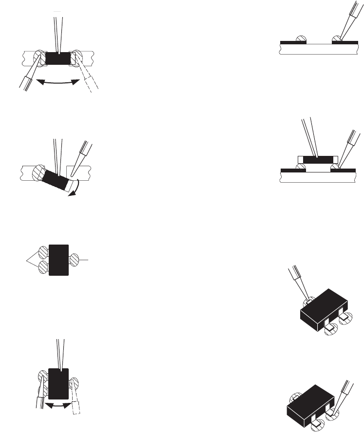
3.3 REPLACEMENT OF CHIP COMPONENT
3.3.1 CAUTIONS
(1) Avoid heating for more than 3 seconds.
(2) Do not rub the electrodes and the resist parts of the pattern.
(3) When removing a chip part, melt the solder adequately.
(4) Do not reuse a chip part after removing it.
3.3.2 SOLDERING IRON
(1) Use a high insulation soldering iron with a thin pointed end of it.
(2) A 30w soldering iron is recommended for easily removing parts.
3.3.3 REPLACEMENT STEPS
1. How to remove Chip parts
[Resistors, capacitors, etc.]
(1) As shown in the figure, push the part with tweezers and
alternately melt the solder at each end.
(2) Shift with the tweezers and remove the chip part.
[Transistors, diodes, variable resistors, etc.]
(1) Apply extra solder to each lead.
(2) As shown in the figure, push the part with tweezers and
alternately melt the solder at each lead. Shift and remove
the chip part.
NOTE :
After removing the part, remove remaining solder from the
pattern.
2. How to install Chip parts
[Resistors, capacitors, etc.]
(1) Apply solder to the pattern as indicated in the figure.
(2) Grasp the chip part with tweezers and place it on the
solder. Then heat and melt the solder at both ends of the
chip part.
[Transistors, diodes, variable resistors, etc.]
(1) Apply solder to the pattern as indicated in the figure.
(2) Grasp the chip part with tweezers and place it on the
solder.
(3) First solder lead A as indicated in the figure.
(4) Then solder leads B and C.
SOLDER SOLDER
A
B
C
A
B
C

1-28 (No.YA463)
SECTION 4
ADJUSTMENT
4.1 ADJUSTMENT PREPARATION
(1) There are 2 ways of adjusting this TV : One is with the
REMOTE CONTROL UNIT and the other is the
conventional method using adjustment parts and
components.
(2) The adjustment using the REMOTE CONTROL UNIT is
made on the basis of the initial setting values. The
setting values which adjust the screen to the optimum
condition can be different from the initial setting
values.
(3) Make sure that connection is correctly made AC to AC
power source.
(4) Turn on the power of the TV and measuring instruments for
warning up for at least 30 minutes before starting
adjustments.
(5) If the receive or input signal is not specified, use the most
appropriate signal for adjustment.
(6) Never touch the parts (such as variable resistors,
transformers and condensers) not shown in the adjustment
items of this service adjustment.
4.2 PRESET SETTING BEFORE ADJUSTMENTS
Unless otherwise specified in the adjustment items, preset the
following functions with the REMOTE CONTROL UNIT.
4.3 MEASURING INSTRUMENT AND FIXTURES
• Oscilloscope
• Signal generator (Pattern generator)
[NTSC / 525i / 525p / 750p / 1125i]
• TV audio multiplex signal generator
• Remote control unit
4.4 ADJUSTMENT ITEMS
FOCUS
• LENS FOCUS adjustment
DRIVE CIRCUIT
• DRIVE CONVERGENCE adjustment
• DRIVE CENTER POSITION adjustment
VIDEO CIRCUIT
• WHITE BALANCE (HIGHLIGHT) adjustment
MTS CIRCUIT
• MTS INPUT LEVEL adjustment
• MTS SEPARATION adjustment
Setting item Settings
VIDEO STATUS STANDARD
Picture adjustments 00
COLOR TEMPERATURE LOW
COLOR MANAGEMENT ON
DYNAMIC GAMMA ON
SMART PICTURE OFF
DIGITAL VNR OFF
MPEG NR OFF
NATURAL CINEMA AUTO
Sound adjustments 00
A.H.S.+ OFF
HYPER BASS OFF
SMART SOUND OFF
ASPECT FULL
(No.YA463)1-29
4.5 BASIC OPERATION OF SERVICE MODE
4.5.1 HOW TO ENTER THE SERVICE MODE
(1) Set to "0 minutes" using the [SLEEP TIMER] key.
(2) While "0 minutes" is displayed, press the [VIDEO
STATUS] key and [DISPLAY] key simultaneously, then
enter the SERVICE MODE (Fig.1)
Fig.1
NOTE:
• Before entering the SERVICE MODE, confirm that the
setting of TV/CATV switch of the REMOTE CONTROL UNIT
is at the "TV" side and the setting of VCR/DVD switch is at
the "VCR" side. If the switches have not been properly set,
you cannot enter the SERVICE MODE.
• When a number key other than the [1] or [9] keys is pressed
in the SERVICE MENU SCREEN, the other relevant screen
may be displayed.
This is not used in the adjustment procedure. Press the
[MENU] key to return to the SERVICE MENU SCREEN.
4.5.2 HOW TO EXIT THE SERVICE MODE
Press the [ BACK ] key to exit the Service mode.
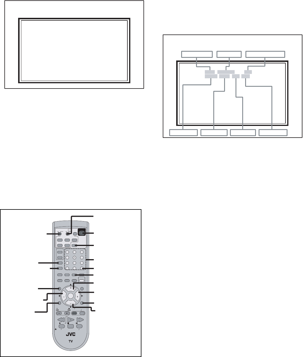
4.5.3 SERVICE MODE SELECT KEY LOCATION
4.5.4 ADJUSTMENT MODE
This mode is used to adjust the VIDEO CIRCUIT and the MTS
CIRCUIT.
4.5.4.1 HOW TO ENTER THE ADJUSTMENT MODE
When the SERVICE MENU SCREEN of SERVICE MODE is
displayed, press [1] key to enter the ADJUSTMENT MODE
(Fig.2).
4.5.4.2 DESCRIPTION OF STATUS DISPLAY OF
ADJUSTMENT MODE
Fig.2
(1) SIGNAL SYSTEM
The signal displayed on the screen is displayed.
(2) SCREEN MODE
State of the SCREEN SIZE or MULTI PICTURE is displayed.
SINGLE SCREEN
MULTI SCREEN
SERVICE MENU SCREEN
SERVICE MENU
SERVICE MENU
1. ADJUST
1. ADJUST
2. SELF CHECK
2. SELF CHECK
3. I2C STOP
3. I2C STOP
INPUT
INDEX
ASPECT
FREEZE SWAP
SELECT
RETURN+/TV
FAVORITE
THEATER
PRO
NATURAL
CINEMA
VIDEO
STATUS
SOUND
TV
CATV VCR DVD
MUTING
MENU BACK
GUIDE
RM-C18G
REW
VCR CHANNEL
PREV NEXT VCR DVD
POWER TV VCR
FFPLAY
REC PAUSE
OPEN CLOSE STILL PAUSE
STOP
CH
CH
VOL VOL
OK
MULTI SCREEN
SPLIT
POWER
SUB
CHANNEL
ML/MTS
SLEEP
DISPLAY
D/A
C.C.
TUNE
1
4
7
2
5
8
0
3
6
9
LIGHT
POWER
VCR/DVD switch
NUMBER
RETURN+
DISPLAY
TV/CATV switch
MENU
SLEEP TIMER
ML/MTS
VIDEO STATUS
MUTING
CHANNEL +
CHANNEL -
VOLUME +
VOLUME - BACK
NTSC3 : 525i (Composite / S-video input)
525I : 525i (Component input)
525P : 525p
1125I6 : 1125i
750P6 : 750p
PCVGA : PC (VGA)
PCXGA : PC (XGA)
PCNG : PC (except VGA/XGA)
H525I : HDMI 525i
H525P : HDMI 525p
H125I6 : HDMI 1125i
H125P6 : HDMI 1125p
H750P6 : HDMI 750p
D525I : ATSC 525i
D525P : ATSC 525p
D125I6 : ATSC 1125i
D750P : ATSC 750p
FULL : FULL
1609 : CINEMA, CINEMA ZOOM
PANO : PANORAMA, PANORAMA ZOOM
REGU : REGULAR, SLIM
M2 : TWIN, FREEZE screen
M12 : INDEX screen
ADJUSTMENT MODE
SIGNAL SYSTEM SCREEN MODE VIDEO STATUS
SETTING VALUE (DATA)SETTING ITEM No. SETTING ITEM
WHITE BALANCE
S001 R DRIVE 110
S001 R DRIVE 110
NTSC3 FULL STD LOW
NTSC3 FULL STD LOW
1-30 (No.YA463)
(3) VIDEO STATUS
(4) WHITE BALANCE
(5) SETTING ITEM NAME
Setting item name are displayed. The setting item numbers to
be displayed are listed below.
(6) SETTING ITEM NO.
Setting item numbers are displayed. For the setting item
names to be displayed, refer to "Initial setting value of
adjustment mode".
(7) SETTING VALUE (DATA)
The SETTING VALUE is displayed.
4.5.4.3 CHANGE AND MEMORY OF SETTING VALUE
SELECTION OF SETTING ITEM
• [CH+] / [CH-] key.
Change the setting items up/ down.
• [SLEEP TIMER] key.
Switches to the next items.
CHANGE OF SETTING VALUE (DATA)
• [VOL+] / [VOL-] key.
Change the setting values up/down.
MEMORY OF SETTING VALUE (DATA)
Changed setting value is memorized by pressing [MUTING]
key.
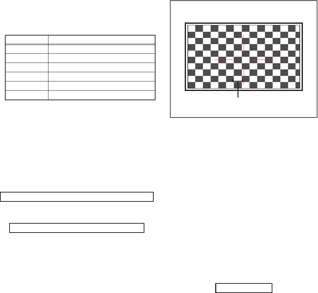
4.5.5 RGB BOX PATTERN MODE
This mode is used to adjust the DRIVE CIRCUIT.
4.5.5.1 HOW TO ENTER THE RGB BOX PATTERN MODE
When the SERVICE MENU SCREEN of SERVICE MODE is
displayed, press [9] key to enter the RGB BOX PATTERN
MODE (Fig3).
4.5.5.2 DESCRIPTION OF STATUS DISPLAY OF RGB BOX
PATTERN MODE
Fig.3
(1) RGB BOX PATTERN
The checkered pattern is displayed. White is a synthesis of
RGB.
(2) ADJUSTMENT COLOR MODE
Presently selected ADJUSTMENT COLOR MODE is
displayed.
SELECTION OF SETTING ITEM
• [CH+] / [CH-] key.
Move the selected RGB BOX PATTERN up/ down pixel by
pixel.
• [VOL+] / [VOL-] key.
Move the selected RGB BOX PATTERN left/ right pixel by
pixel.
• [SLEEP TIMER] key.
Adjusts the data reset.
• [DISPLAY] key.
Adjusts the selected COLOR BOX PATTERN.
• [BACK] key.
Returns to the SERVICE MENU SCREEN from the RGB
BOX PATTERN MODE.
MEMORY OF SETTING VALUE (DATA)
With the RGB BOX PATTERN MODE, the changed date is
written in the MEMORY instantly.
STD : STANDARD
DYN : DYNAMIC
TH : THEATER
GAME : GAME
HIGH : HIGH
LOW : LOW
Item No. Setting item
S001 - S009 Video system setting
T001 - T003 Audio system setting
M001 - M224 Main CPU system setting
F001 - F002 Drive system setting
D001 (NOT USED)
Z001 (NOT USED)
S001... ↔ T001... ↔ M001... ↔ F001... ↔ D001... ↔ Z001...
S001 → T001 → M001... → F001... → D001 → Z001
R → B → RGB
ADJUSTMENT COLOR MODE
RGB
RGB BOX PATTERN MODE
(No.YA463)1-31
4.6 INITIAL SETTING VALUES IN THE SERVICE MODE
• Perform fine-tuning based on the "initial values" using the remote control when in the Service mode.
• The "initial values" serve only as an indication rough standard and therefore the values with which optimal display can be achieved
may be different from the default values. But, don't change the values that are not written in "ADJUSTMENT PROCEDURE". They
are fixed values.
4.6.1 VIDEO SYSTEM SETTING
4.6.2 AUDIO SYSTEM SETTING
4.6.3 MAIN CPU SYSTEM SETTING (Fixed values)
Item No. Item Variable range Setting value
S001 R DRIVE 000 - 255 110
S002 G DRIVE 000 - 255 138
S003 B DRIVE 000 - 255 127
S004 RESREV 000 - 255 000
S005 RESREV 000 - 255 002
S006 RESREV 000 - 255 002
S007 RESREV 000 - 255 002
S008 RESREV 000 - 255 002
S009 RESREV 000 - 255 002
Item No. Item Variable range Setting value
T001 INPLEVEL 000 - 015 007
T002 LOWSEPA 000 - 063 028
T003 HIGHSEPA 000 - 063 018
Item No. Item Variable range Setting value
M001 1E00 00 - FF 00
M002 1E01 00 - FF 00
M003 1E02 00 - FF 0A
M004 1E03 00 - FF 20
M005 1E04 00 - FF 10
M006 1E05 00 - FF 00
M007 1E06 00 - FF 00
M008 1E07 00 - FF 00
M009 1E08 00 - FF 00
M010 1E09 00 - FF 00
M011 1E0A 00 - FF 01
M012 1E0B 00 - FF 00
M013 1E0C 00 - FF 01
M014 1E0D 00 - FF 00
M015 1E0E 00 - FF 00
M016 1E0F 00 - FF 00
M017 1E10 00 - FF 01
M018 1E11 00 - FF 00
M019 1E12 00 - FF 00
M020 1E13 00 - FF 01
M021 1E14 00 - FF 01
M022 1E15 00 - FF 00
M023 1E16 00 - FF 00
M024 1E17 00 - FF 00
M025 1E18 00 - FF 00
M026 1E19 00 - FF 00
M027 1E1A 00 - FF 00
M028 1E1B 00 - FF 00
M029 1E1C 00 - FF 00
M030 1E1D 00 - FF 00
M031 1E1E 00 - FF 00
M032 1E1F 00 - FF 00
M033 1E20 00 - FF 00
M034 1E21 00 - FF 00
M035 1E22 00 - FF 00
M036 1E23 00 - FF 00
M037 1E24 00 - FF 00
M038 1E25 00 - FF 00
M039 1E26 00 - FF 00
M040 1E27 00 - FF 00
M041 1E28 00 - FF 00
M042 1E29 00 - FF 00
M043 1E2A 00 - FF 00
M044 1E2B 00 - FF 00
M045 1E2C 00 - FF 00
M046 1E2D 00 - FF 00
M047 1E2E 00 - FF 00
M048 1E2F 00 - FF 00
M049 1E30 00 - FF 00
M050 1E31 00 - FF 00
M051 1E32 00 - FF 00
M052 1E33 00 - FF 00
M053 1E34 00 - FF 00
M054 1E35 00 - FF 00
M055 1E36 00 - FF 02
M056 1E37 00 - FF 00
M057 1E38 00 - FF 01
M058 1E39 00 - FF 02
M059 1E3A 00 - FF 10
M060 1E3B 00 - FF 83
M061 1E3C 00 - FF 00
M062 1E3D 00 - FF 00
M063 1E3E 00 - FF 00
M064 1E3F 00 - FF 00
M065 1E40 00 - FF 00
M066 1E41 00 - FF 00
M067 1E42 00 - FF 00
M068 1E43 00 - FF 03
M069 1E44 00 - FF 03
M070 1E45 00 - FF 03
M071 1E46 00 - FF 3F
M072 1E47 00 - FF 01
Item No. Item Variable range Setting value

1-32 (No.YA463)
M073 1E48 00 - FF 00
M074 1E49 00 - FF 00
M075 1E4A 00 - FF 00
M076 1E4B 00 - FF 00
M077 1E4C 00 - FF 00
M078 1E4D 00 - FF 00
M079 1E4E 00 - FF 00
M080 1E4F 00 - FF 00
M081 1E50 00 - FF 00
M082 1E51 00 - FF 00
M083 1E52 00 - FF 00
M084 1E53 00 - FF 00
M085 1E54 00 - FF 00
M086 1E55 00 - FF 00
M087 1E56 00 - FF 00
M088 1E57 00 - FF 00
M089 1E58 00 - FF 00
M090 1E59 00 - FF 00
M091 1E5A 00 - FF 00
M092 1E5B 00 - FF 00
M093 1E5C 00 - FF 00
M094 1E5D 00 - FF 00
M095 1E5E 00 - FF 00
M096 1E5F 00 - FF 00
M097 1E60 00 - FF 00
M098 1E61 00 - FF 00
M099 1E62 00 - FF 00
M100 1E63 00 - FF 00
M101 1E64 00 - FF 00
M102 1E65 00 - FF 00
M103 1E66 00 - FF 00
M104 1E67 00 - FF 00
M105 1E68 00 - FF 04
M106 1E69 00 - FF 03
M107 1E6A 00 - FF 02
M108 1E6B 00 - FF 00
M109 1E6C 00 - FF 00
M110 1E6D 00 - FF 00
M111 1E6E 00 - FF 00
M112 1E6F 00 - FF 00
M113 1E70 00 - FF 00
M114 1E71 00 - FF 00
M115 1E72 00 - FF 00
M116 1E73 00 - FF 00
M117 1E74 00 - FF 00
M118 1E75 00 - FF 00
M119 1E76 00 - FF 00
M120 1E77 00 - FF 00
M121 1E78 00 - FF 03
M122 1E79 00 - FF 00
Item No. Item Variable range Setting value
M123 1E7A 00 - FF 00
M124 1E7B 00 - FF 00
M125 1E7C 00 - FF 00
M126 1E7D 00 - FF 00
M127 1E7E 00 - FF 01
M128 1E7F 00 - FF 00
M129 1E80 00 - FF 01
M130 1E81 00 - FF 00
M131 1E82 00 - FF 01
M132 1E83 00 - FF 00
M133 1E84 00 - FF 00
M134 1E85 00 - FF 00
M135 1E86 00 - FF 00
M136 1E87 00 - FF 00
M137 1E88 00 - FF 00
M138 1E89 00 - FF 00
M139 1E8A 00 - FF 00
M140 1E8B 00 - FF 00
M141 1E8C 00 - FF 00
M142 1E8D 00 - FF 00
M143 1E8E 00 - FF 00
M144 1E8F 00 - FF 00
M145 1E90 00 - FF 00
M146 1E91 00 - FF 00
M147 1E92 00 - FF 00
M148 1E93 00 - FF 00
M149 1E94 00 - FF 00
M150 1E95 00 - FF 00
M151 1E96 00 - FF 00
M152 1E97 00 - FF 00
M153 1E98 00 - FF 00
M154 1E99 00 - FF 00
M155 1E9A 00 - FF 01
M156 1E9B 00 - FF 00
M157 1E9C 00 - FF 03
M158 1E9D 00 - FF 00
M159 1E9E 00 - FF 00
M160 1E9F 00 - FF 00
M161 1EA0 00 - FF 00
M162 1EA1 00 - FF 00
M163 1EA2 00 - FF 01
M164 1EA3 00 - FF 00
M165 1EA4 00 - FF 00
M166 1EA5 00 - FF 00
M167 1EA6 00 - FF 00
M168 1EA7 00 - FF 00
M169 1EA8 00 - FF 00
M170 1EA9 00 - FF 00
M171 1EAA 00 - FF 00
M172 1EAB 00 - FF 00
Item No. Item Variable range Setting value
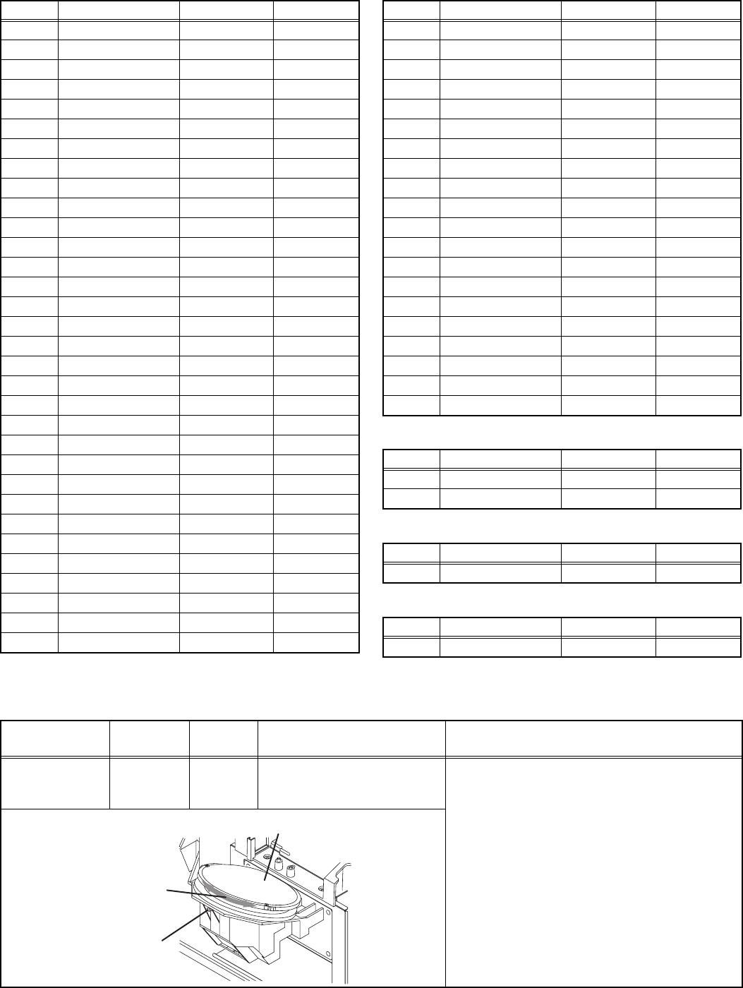
(No.YA463)1-33
4.6.4 DRIVE SYSTEM SETTING (Fixed values)
4.6.5 NOT USED (Fixed values)
4.6.6 NOT USED (Fixed values)
4.7 ADJUSTMENT PROCEDURE
4.7.1 FOCUS
M173 1EAC 00 - FF 0A
M174 1EAD 00 - FF 00
M175 1EAE 00 - FF 00
M176 1EAF 00 - FF 00
M177 1EB0 00 - FF 0A
M178 1EB1 00 - FF 00
M179 1EB2 00 - FF 01
M180 1EB3 00 - FF 00
M181 1EB4 00 - FF 00
M182 1EB5 00 - FF 00
M183 1EB6 00 - FF 00
M184 1EB7 00 - FF 00
M185 1EB8 00 - FF 00
M186 1EB9 00 - FF 00
M187 1EBA 00 - FF 00
M188 1EBB 00 - FF 00
M189 1EBC 00 - FF 00
M190 1EBD 00 - FF 00
M191 1EBE 00 - FF 00
M192 1EBF 00 - FF 00
M193 1EC0 00 - FF 00
M194 1EC1 00 - FF 00
M195 1EC2 00 - FF 01
M196 1EC3 00 - FF 00
M197 1EC4 00 - FF 00
M198 1EC5 00 - FF 00
M199 1EC6 00 - FF 00
M200 1EC7 00 - FF 00
M201 1EC8 00 - FF 00
M202 1EC9 00 - FF 00
M203 1ECA 00 - FF 00
M204 1ECB 00 - FF 00
Item No. Item Variable range Setting value
M205 1ECC 00 - FF 02
M206 1ECD 00 - FF 00
M207 1ECE 00 - FF 00
M208 1ECF 00 - FF 00
M209 1ED0 00 - FF 10
M210 1ED1 00 - FF 00
M211 1ED2 00 - FF 00
M212 1ED3 00 - FF 00
M213 1ED4 00 - FF 00
M214 1ED5 00 - FF 00
M215 1ED6 00 - FF 00
M216 1ED7 00 - FF 00
M217 1ED8 00 - FF 00
M218 1ED9 00 - FF 00
M219 1EDA 00 - FF 00
M220 1EDB 00 - FF 00
M221 1EDC 00 - FF 00
M222 1EDD 00 - FF 00
M223 1EDE 00 - FF 00
M224 1EDF 00 - FF 00
Item No. Item Variable range Setting value
F001 DD 000 - 001 000
F002 RAM REF 000 - 001 000
Item No. Item Variable range Setting value
D001 RESREV 000 - 255 002
Item No. Item Variable range Setting value
Z001 RESREV 000 - 255 002
Item No. Item Variable range Setting value
Item Measuring
instrument Test point Adjustment part Description
LENS FOCUS
Hexagon
wrench
(2.5mm)
FOCUS ring
[PROJECTION LENS]
(1) Remove the SPEAKER GRILL and CENTER
COVER.
(2) Display the MENU screen.
(3) Loosen the focus lock screw.
(4) Adjust the FOCUS ring so that the center
screen may become the best focus.
(5) Fix the focus lock screw by using the Hexagon
wrench.
• On this occasion, hold the FOCUS ring with
your left hand.
(6) Confirm the whole focus of the best screen.
(7) Install the CENTER COVER and SPEAKER
GRILL.
Focus lock
screw
FOCUS ring
Projection lens
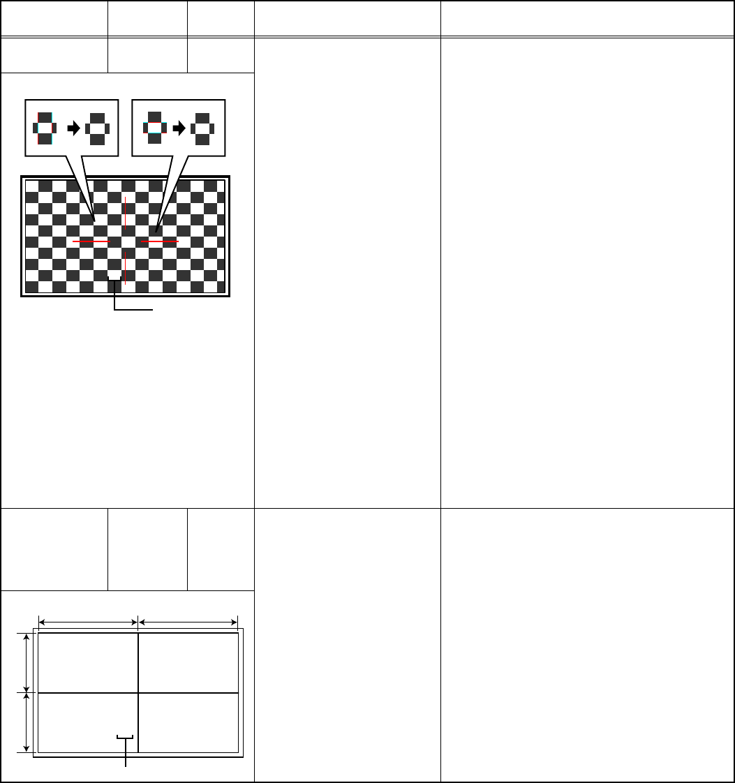
1-34 (No.YA463)
4.7.2 DRIVE CIRCUIT
Item Measuring
instrument Test point Adjustment part Description
DRIVE
CONVERGENCE
Remote
control unit
[9.RGB BOX PATTERN] (1) Set to "0 minutes" using the [SLEEP TIMER]
key.
(2) Press the [VIDEO STATUS] key and
[DISPLAY] key simultaneously, to enter the
SERVICE MODE.
(3) Press the [9] key, to select "RGB BOX
PATTERN MODE" from the SERVICE MODE.
(4) Set the adjustment color mode to "R" to set the
red color adjustment mode.
(5) At Horizontal RGB box pattern, adjust the top
edge position as same or less than 0.5 pixel
hight as green.
(6) At Vertical RGB box pattern, adjust the right
edge position as same or less than 0.5 pixel
hight as green.
(7) Set the adjustment color mode to "B" to set the
blue color adjustment mode.
(8) At Horizontal RGB box pattern, adjust the top
edge position as same or less than 0.5 pixel
hight as green.
(9) At Vertical RGB box pattern, adjust the right
edge position as same or less than 0.5 pixel
hight as green.
(10) Check to see that the cross pattern is white. If
the cross pattern is not white, repeat the step
4. to 9. as abobe.
NOTE:
• Green is fixed. (It can not be removed.)
• With this adjustment mode, the changed data is
written in the MEMORY instantly.
DRIVE CENTER
POSITION
Remote
control unit
Signal
generator
[9.RGB BOX PATTERN] (1) Receive a center cross (or crosshatch) pattern.
(2) Set to "0 minutes" using the [SLEEP TIMER]
key.
(3) Press the [VIDEO STATUS] key and
[DISPLAY] key simultaneously, to enter the
SERVICE MODE.
(4) Press the [9] key, to select "RGB BOX
PATTERN MODE" from the SERVICE MODE.
(5) Set the adjustment color mode to "RGB" to set
the display position adjustment mode.
(6) Adjust the top and the bottom width to make A
and A" even.
(7) Adjust the left and the right width to make B
and B" even.
NOTE:
• With this adjustment mode, the changed data is
written in the MEMORY instantly.
R
Adjustment color
Horizontal RGB box patternVertical RGB box pattern
Adjustment color
A
BB"
A
"
RGB
(B=B")
(A=A")
(No.YA463)1-35
4.7.3 VIDEO CIRCUIT
4.7.4 MTS CIRCUIT
Item Measuring
instrument Test point Adjustment part Description
WHITE
BALANCE
(HIGHLIGHT)
Remote
control unit
Signal
generator
[1.ADJUST]
S001: R DRIVE (Red drive)
S002: G DRIVE (Green drive)
S003: B DRIVE (Blue drive)
(1) Receive a NTSC 75% all white pattern.
(2) Set "VIDEO STATUS" to "STANDARD".
(3) Set "ASPECT" to "FULL".
(4) Select "COLOR TEMPERATURE" to "LOW".
(5) Select "1.ADJUST" from the SERVICE
MODE.
(6) Adjust to keep one of < S001 > (Red drive),
< S002 > (Green drive) or < S003 > (Blue
drive) unchanged, then lower the other two
so that the all-white screen is equally white
throughout.
NOTE:
Set one or more of < S001 >, < S002 >, and
< S003 > to "138".
(7) Check that white balance is properly tracked
from low light to high light. If the white balance
tracking is deviated, adjust to correct it.
(8) Press the [MUTING] key to memoirze the set
value.
Item Measuring
instrument Test point Adjustment part Description
MTS INPUT
LEVEL
Remote
control unit
[1.ADJUST]
T001: INPLEVEL
(1) Receive any broadcast.
(2) Select "1.ADJUST" from the SERVICE
MODE.
(3) Verify that the < T001 > (INPLEVEL) is set at
its initial setting value.
(4) Press the [MUTING] key to memorize the set
value.
MTS
SEPARATION
TV audio
multiplex
signal
generator
Oscilloscope
Remote
control unit
L OUT
R OUT
[1.ADJUST]
T002: LOWSEPA
T003: HIGHSEPA
(1) Input the stereo L signal (300Hz) from the TV
audio multiplex signal generator to the antenna
terminal.
(2) Connect an oscilloscope to L OUT pin of the
AUDIO OUT, and display one cycle portion of
the 300Hz signal.
(3) Change the connection of the oscilloscope to
R OUT pin of the AUDIO OUT, and enlarge the
voltage axis.
(4) Select "1.ADJUST" from the SERVICE
MODE.
(5) Set the initial setting value of the < T002 >
(LOWSEPA).
(6) Adjust the < T002 > so that the stroke element
of the 300Hz signal will become minimum.
(7) Press the [MUTING] key to memorize the set value.
(8) Input the stereo R signal (3kHz) and change
the connection of the oscilloscope to L OUT
pin of the AUDIO OUT.
(9) Similarly adjust < T003 > (HIGHSEPA).
(10) Press the [MUTING] key to memorize the set value.
L-Channel
signal waveform
R-Channel
crosstalk portion
Input the stereo R signal
(3kHz) and change
Minimum
1 cycle
1-36 (No.YA463)
SECTION 5
TROUBLESHOOTING
5.1 SELF CHECK FEATURE
5.1.1 OUTLINE
This unit comes with the "Self check" feature, which checks the
operational state of the circuit and displays/saves it during
failure.Diagnosis is performed when power is turned on, and
information input to the main microcomputer is monitored at all
time.Diagnosis is displayed in 2 ways via screen display and LED
flashes. Failure detection is based on input state of I2C bus and
the various control lines connected to the main microcomputer.
5.1.2 HOW TO ENTER THE SELF CHECK MODE
Before entering the Self check mode, confirm that the setting of
TV/CATV SW of the REMOTE CONTROL UNIT is at the "TV"
side and the setting of VCR/DVD SW is at the "VCR" side. If the
switches have not been properly set, you cannot enter the Self
check mode.
(1) Set to "0 minutes" using the [SLEEP TIMER] key.
(2) While "0 minutes" is displayed, press the [VIDEO STATUS]
key and [DISPLAY] key simultaneously, then enter the
service mode.
(3) Press the [2] key (SELF CHECK) before the service mode
screen disappears.
(4) Self check mode screen is displayed.
(5) Press the [ML/MTS] key to enter Page 2 of the SELF
CHECK MODE.
• When the [RETURN+] key pressed, the first page
change screen.
NOTE:
When a number key other than the [2] key is pressed in
the SERVICE MENU SCREEN, the other relevant
screen may be displayed.
This is not used in the SELF CHECK. Press the [MENU]
key to return to the SERVICE MENU SCREEN.
5.1.3 HOW TO EXIT THE SELF CHECK MODE
TO SAVE FAILURE HISTORY:
Turn off the power by unplugging the AC power cord plug when
in the Self check mode.
TO CLEAR (RESET) FAILURE HISTORY:
Turn off the power by pressing the [POWER] key on the remote
control unit when in the Self check mode.
5.1.4 FAILURE HISTORY
Failure history can be counted up to 9 times for each item. When
the number exceeds 9, display will remain as 9. Failure history
will be stored in the memory unless it has been deleted.
5.1.5 POINTS TO NOTE WHEN USING THE SELF CHECK
FEATURE
In addition to circuit failures (abnormal operation), the following
cases may also be diagnosed as "Abnormal" and displayed and
counted as "NG".
(1) Temporary defective transmissions across circuits due to
pulse interruptions
(2) Misalignment in the on/off timing of power for I2C bus
(VCC) when turning on/off the main power.
Diagnosis may be impeded if a large number of items are
displayed as "NG". As such, start Self check check only after 3
seconds in the case of receivers and 5 seconds in the case of
panels upon turning on the power. If recurrences are expected,
ensure to clear (reset) the failure history and record the new
diagnosis reults.
Fig.1
SERVICE MENU SCREEN
SELF CHECK MODE SCREEN (Page 1)
SELF CHECK MODE SCREEN (Page 2)
Item Failure history
Failure history
Item
TMP 0 L 1 0
TMP 0 L 1 0
L 2 0 DDT 0
L 2 0 DDT 0
FAN 0 L C 0
FAN 0 L C 0
IRS 0
IRS 0
SERVICE MENU
SERVICE MENU
1. ADJUST
1. ADJUST
2. SELF CHECK
2. SELF CHECK
3. I2C STOP
3. I2C STOP
LOB 0 FAN 0
LOB 0 FAN 0
AUD 0
AUD 0
ANA 9 DIG 9
ANA 9 DIG 9
0000 0
0000 0
0
0
(No.YA463)1-37
5.1.6 DETAILS
Self check is performed for the following items:
< Page 1 of screen >
< Page 2 of screen >
Detection item Display Detection content Diagnosis
signal (line) Detection timing
Low bias line short
protection
LOB Detection of the low bias line (2.5V/3.3V/5V/9V/
12V) short.
Q9821, Q9831, Q9841, Q9842, Q9861
[POWER PWB]
LB_PRO Detection starts 3 seconds after
the power is turned on. If error
continues between 1000ms the
power is turned off.
Fan lock FAN Not used ---- ----
Audio AUD Not used ---- ----
Devices on the ANALOG
PWB and the TUNER
PWB
ANA Confirmation of reply of ACK signal which uses
I2C communication.
IC101, IC102, IC601, IC606
[ANALOG PWB]
IC061,TU001 [TUNER PWB]
SDA Detection starts 3 seconds after
the power is turned on. If it checks
whenever I2C communication is
performed and no reply of ACK
signal an error will be counted.
Devices on the DIGITAL PWB
DIG Not used ---- ----
Detection item Display Detection content Diagnosis
signal (line) Detection timing
Temp. sensor TMP Confirmation of the abnormal inner cabinet
temperature. (53°C)
IC2001 [THERMO PWB]
TXD It will count if the serial
communication from a DD
MICOM is always supervised and
an error occurs.
Lamp does not light up L1 Confirm that the lamp dose not light up.
CNBCT1 [DRIVE PWB]
TXD It will count if the serial
communication from a DD
MICOM is always supervised and
an error occurs.
Lamp goes out L2 Confirm that the lamp dose not goes out.
CNBCT1 [DRIVE PWB]
TXD It will count if the serial
communication from a DD
MICOM is always supervised and
an error occurs.
Abnormal DD CPU
circuit
DDT Confirmation of the serial communication error
between DRIVE PWB and DIGITAL PWB.
IC3701 [DRIVE PWB]
TXD It will count if the serial
communication error is error
occurs.
Fan lock FAN Confirmation of the lock signals outputting the
operation(circuit) status of the cooling fan.
IC8005 [DRIVE PWB]
TXD It will count if the serial
communication from a DD
MICOM is always supervised and
an error occurs.
Lamp cover open LC Confirmation of the interlock switch status for the
lamp cover.
S0861 [LAMP COVER SW PWB]
TXD It will count if the serial
communication from a DD
MICOM is always supervised and
an error occurs.
Abnormal of optical iris IRS Not used --- ---

1-38 (No.YA463)
5.1.7 DISPLAY METHOD WHEN RASTER IS NOT AVAILABLE
In a state where a display screen does not appear due to the failure of this unit, the POWER LED (blue) and LAMP/PROGRAM LED
(orange) can be flushing and display a trouble mode.
The factors in case the power is forcibly shut down at the time of failure are memorized and those are displayed.
EXPLANATION ON ACTION
If NG is detected on an item being diagnosed, turn off the power on this unit. As soon as the power goes off, turn on and off POWER
LED and LAMP LED immediately. After the power is shut down, it becomes impossible to turn on the power until the power cable
is either plugged in or unplugged from the AC outlet.
• When the error of [1] occurs, [2], [3], [4], [5], [6] are no longer recognized.
Check item Contents
Classifications
LED flash cycle
POWER LED
(BLUE)
LAMP/
PROGRAM LED
(ORANGE)
Low bias line short
protection
Detection of the low bias line (2.5V/3.3V/5V/9V/12V)
short.
Q9821, Q9831, Q9841, Q9842, Q9861 [POWER PWB]
1 --- 1 sec interval
Fan lock (stop) for
ATSC tuner
Detection of the Fan lock (stop).
CN9FAN [POWER PWB]1 --- 1 sec interval
Lamp cover open Detection of the interlock switch status for the lamp
cover. (H = Abnormal)
S0861 [LAMP COVER SW PWB]
2 0.1 sec interval Simultaneously
Lamp goes out Detection of lamp return (LAMP_RTN) signals output
depending on the status of the lamp supply electric current
monitored constantly within the lamp ballast unit. (H =Off)
CNBCT1 [DRIVE PWB]
5 0.1 sec interval Simultaneously
Lamp does not light up Detection of lamp return (LAMP_RTN) signals output
depending on the status of the lamp supply electric current
monitored constantly within the lamp ballast unit. (H = Off)
CNBCT1 [DRIVE PWB]
5 0.1 sec interval Simultaneously
Fan lock (stop) for
optical system
Detection of LOCK signals outputting the operation
(circuit) status of the cooling fan. (H=Abnormal)
IC8005 [DRIVE PWB]
3 0.5 sec interval Alternately
Abnormal DD CPU
circuit
Detection of serial communication error between MAIN
DRIVE PWB and RECEIVER PWB.
IC3701 [DRIVE PWB]
4 0.5 sec interval Alternately
Abnormal D-ILA
DEVICE temperature
Detection of abnormal inner cabinet temperature. (53°C)
IC2001 [THERMO PWB] 6 0.5 sec interval Alternately

(No.YA463)
ILA Display Category 12, 3-chome, Moriya-cho, Kanagawa-ku, Yokohama-city, Kanagawa-prefecture, 221-8528, Japan
Victor Company of Japan, Limited
VPT
Printed in Japan
COPYRIGHT © 2006 Victor Company of Japan, Limited No.YA463
2006/10
D-ILA PROJECTION TELEVISION
YA46320069
HD-52FA97,
HD-56FB97,
HD-61FB97
BASIC CHASSIS
RA3
SCHEMATIC DIAGRAMS
CD-ROM No.SML200610
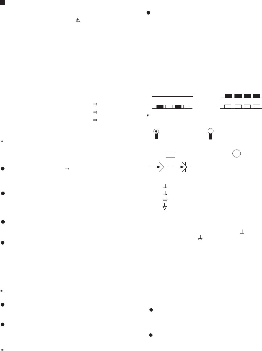
2-1(No.YA463)
5.NOTE FOR REPAIRING SERVICE
This model's power circuit is partly different in the GND. The
difference of the GND is shown by the LIVE : ( ) side GND and the
ISOLATED(NEUTRAL) : ( ) side GND. Therefore, care must be
taken for the following points.
(1)Do not touch the LIVE side GND or the LIVE side GND and the
ISOLATED(NEUTRAL) side GND simultaneously. if the above
caution is not respected, an electric shock may be caused.
Therefore, make sure that the power cord is surely removed from
the receptacle when, for example, the chassis is pulled out.
(2)Do not short between the LIVE side GND and ISOLATED(NEUTRAL)
side GND or never measure with a measuring apparatus measure
with a measuring apparatus ( oscilloscope, etc.) the LIVE side GND
and ISOLATED(NEUTRAL) side GND at the same time.
If the above precaution is not respected, a fuse or any parts will be broken.
Since the circuit diagram is a standard one, the circuit and
circuit constants may be subject to change for improvement
without any notice.
NOTE
Due improvement in performance, some part numbers show
in the circuit diagram may not agree with those indicated in
the part list.
When ordering parts, please use the numbers that appear
in the Parts List.
STANDARD CIRCUIT DIAGRAM
NOTE ON USING CIRCUIT DIAGRAMS
(7)Ground symbol
: LIVE side ground
: ISOLATED(NEUTRAL) side ground
: EARTH ground
: DIGITAL ground
(6)Connecting method
: Connector : Wrapping or soldering
: Receptacle
(5)Test point
: Test point : Only test point display
Respective voltage values are indicated
: B1
: 9V : 5V
: B2 (12V)
(4)Power Supply
Type
MM : Metalized mylar capacitor
PP : Polypropylene capacitor
MPP : Metalized polypropylene capacitor
MF : Metalized film capacitor
TF : Thin film capacitor
BP : Bipolar electrolytic capacitor
TAN : Tantalum capacitor
(3)Coils
No unit
Others
: [µH]
: As specified
No indication : Ceramic capacitor
(2)Capacitors
Capacitance value
1 or higher : [pF]
less than 1 : [µF]
Withstand voltage
No indication : DC50[V]
Others : DC withstand voltage [V]
AC indicated : AC withstand voltage [V]
Electrolytic Capacitors
47/50[Example]: Capacitance value [µF]/withstand voltage[V]
Composition resistor 1/2 [W] is specified as 1/2S or Comp.
Type
No indication : Carbon resistor
OMR : Oxide metal film resistor
MFR : Metal film resistor
MPR : Metal plate resistor
UNFR : Uninflammable resistor
FR : Fusible resistor
4.INDICATIONS ON THE CIRCUIT DIAGRAM
(1)Resistors
Resistance value
No unit : [Ω]
K: [kΩ]
M
Rated allowable power
No indication : 1/16 [W]
Others : As specified
: [MΩ]
3.INDICATION OF PARTS SYMBOL [EXAMPLE]
In the PW board : R209 R209
1.SAFETY
The components identified by the symbol and shading are
critical for safety. For continued safety replace safety ciritical
components only with manufactures recommended parts.
Since the voltage values of signal circuit vary to some extent
according to adjustments, use them as reference values.
2.SPECIFIED VOLTAGE AND WAVEFORM VALUES
The voltage and waveform values have been measured under the
following conditions.
(1)Input signal : Colour bar signal
(2)Setting positions of
each knob/button and
variable resistor
(3)Internal resistance of tester : DC 20kΩ/V
(4)Oscilloscope sweeping time : H 20µs / div
: V 5ms / div
: Othters Sweeping time is
specified
(5)Voltage values : All DC voltage values
: Original setting position
when shipped
HD-52FA97, HD-56FB97, HD-61FB97
CONTENTS
SEMICONDUCTOR SHAPES ......................................................................2-4
WIRING DIAGRAM ........................................................................................2-5
BLOCK DIAGRAM ........................................................................................2-7
CIRCUIT DIAGRAMS
TUNER PWB CIRCUIT DIAGRAM .............................................................................................................. 2-9
ANALOG PWB CIRCUIT DIAGRAM ......................................................................................................... 2-13
DIGITAL PWB CIRCUIT DIAGRAM .......................................................................................................... 2-25
DRIVE PWB CIRCUIT DIAGRAM ............................................................................................................. 2-55
POWER PWB CIRCUIT DIAGRAM .......................................................................................................... 2-73
FRONT LED PWB CIRCUIT DIAGRAM [HD-52FA97] ............................................................................... 2-79
FRONT LED PWB CIRCUIT DIAGRAM [HD-56FB97, HD-61FB97] .......................................................... 2-80
TEMP PWB CIRCUIT DIAGRAM .............................................................................................................. 2-81
LAMP COVER SW PWB CIRCUIT DIAGRAM ......................................................................................... 2-82
REMOCON PWB CIRCUIT DIAGRAM ...................................................................................................... 2-83
USB PWB CIRCUIT DIAGRAM ................................................................................................................ 2-84
SIDE CONTROL PWB CIRCUIT DIAGRAM ............................................................................................. 2-85
PATTERN DIAGRAMS
TUNER PWB PATTERN ............................................................................................................................ 2-87
ANALOG PWB PATTERN ........................................................................................................................ 2-89
DIGITAL PWB PATTERN ......................................................................................................................... 2-93
DRIVE PWB PATTERN ............................................................................................................................. 2-97
POWER PWB PATTERN ........................................................................................................................ 2-101
FRONT LED PWB PATTERN [HD-52FA97] ............................................................................................. 2-105
FRONT LED PWB PATTERN [HD-56FB97, HD-61FB97] ........................................................................ 2-105
TEMP PWB PATTERN ........................................................................................................................... 2-105
LAMP COVER SW PWB PATTERN ....................................................................................................... 2-105
REMOCON PWB PATTERN ................................................................................................................... 2-105
USB PWB PATTERN .............................................................................................................................. 2-106
SIDE CONTROL PWB PATTERN ........................................................................................................... 2-106
VOLTAGE CHARTS ................................................................................ 2-107
WAVEFORMS .......................................................................................... 2-108
(No.YA463)2-2

USING P.W. BOARD
P.W.B ASS’Y name
ANALOG P.W. BOARD
DRIVE P.W. BOARD
REMOCON P.W. BOARD
TEMP P.W. BOARD
USB P.W. BOARD
POWER P.W. BOARD
DIGITAL P.W. BOARD
SIDE CONTROL P.W. BOARD
FRONT LED P.W. BOARD
LAMP COVER SW P.W. BOARD
TUNER P.W. BOARD
SRA-1024A-M2
SRA-3013A-M2
SRA-8011A-M2
SRA-8211A-M2
SRA-8521A-M2
SRA-9017A-M2
SRA0D161A-M2
SRA0L013A-M2
SRA0L111A-M2
SRA0L211A-M2
SRA0R012A-M2
HD-52FA97 HD-61FB97HD-56FB97
SRA0D160A-M2
SRA0L113A-M2
SRA0D159A-M2
2-3(No.YA463)
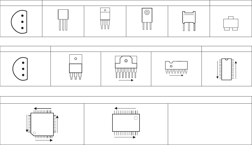
SEMICONDUCTOR SHAPES
(No.YA463)2-4
IC
BOTTOM VIEW FRONT VIEW TOP VIEW
1 N
N
1
OUT
E
IN
IN OUTE
1 N
TOP VIEW
1
N
1
N
CHIP IC
TRANSISTOR
BOTTOM VIEW FRONT VIEW TOP VIEW
CHIP TR
E
C
B
ECB
C
BE
B
(G)
E
(S)
C
(D)
ECB
ECB
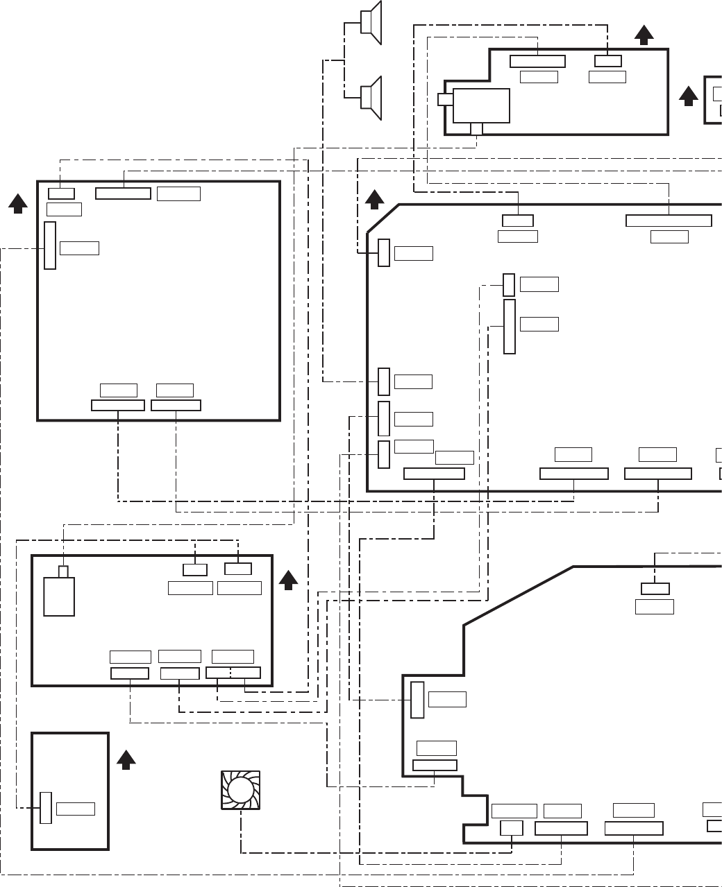
2-5(No.YA463)
POWER PWB
CN9DC CN
9
CN9A3
CN9BL
DIGITAL PWB
CN1DC
CN0LV1
CN011
CN1T2
ANALOG PWB
TUNER PWB
C
RE
M
P
SPEAKER
(L)
SPEAKER
(R)
61
1
112
115
13
CN9A1
1
51
150
CN012
140
15
13
CN0T2
13
CN8DT
18
125
C
CN1T1
125
CN0T1
CN1A3
CN1A2
16
CN1A1
14
115
CN1SP
13
CN1RE
CN012
401
CN011
501112
USB
PWB
ATSC TUNER MODULE
COOLING FAN
TOP
TOP
TOP
TOP
101 1㨪37㨪11
19
3,2
CN5002 CN5001
CN6001
16
ATSC TUNER
MODULE PWB
CN1005 CN1004
TOP
10
CN9UP
1
13
CN1UV
CN1UA
CN0ID
1
5
CN9FAN
41
TOP
WIRING DIAGRAM
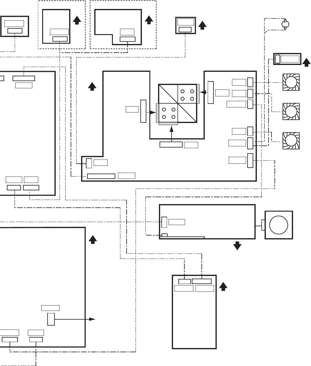
(No.YA463)2-6
B
CN9008
CN08RE
R
EMOCON
PWB
THERMOSTAT
POWER CORD
DRIVE PWB
SIDE
CONTROL
PWB
CNT1
TEMP
PWB
CN82T
CN0806
LAMP COVER
SW PWB
CN101
LAMP BALLAST UNIT
LAMP
COOLING FAN-2
LAMP
COOLING FAN-1
OPTICAL BLOCK
COOLING FAN
CNR1
CNB1
CNG1
CN9A2
CNLV1
CNF2
CNF1
CNSW1
CNDD1
CNF3
CNBCT1
LAMP
B DEVICE
R DEVICE
G DEVICE
CN9PW
12
13
119514 131414
14
41
19
CN08S2
31
CN08S1
12 1
15
31
5
CN1F
1
9(7)
141
CN1S2
CN1S1
13
121
80 1
80
80
1
1
13
TOP
TOP
FRONT
FRONT
TOP
TOP
[HD-56FB97, HD-61FB97]
[HD-52FA97]
TOP
CN9F
17
FRONT LED PWB
TOP
CN07FL
17
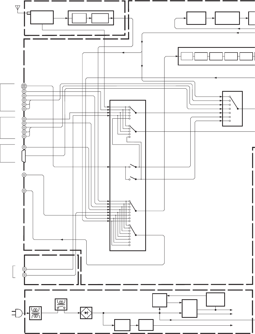
2-7(No.YA463)
TUNER PWB
SIDE CONTROL PWB
Audio_OUT
ANALOG PWB
TU001
U/V TUNER
MTS
DECODE
AUDIO
CONTROL
IC101
VIDEO/AUDIO SELECT
IC061
AUDIO CONTROL
Y1/C1
V1
V2
L1/R1
L3/R3
DVI_L/R
AU_LOUT
AU_ROUT
VARIFIX_L/R
L2/R2
Y1
Y2
Cb1
Cr1
Cb2
Cr2
MAIN_L/R
DTU_L/R
DIN_SL/SR
DTU2_L/R
TV_V1
TV_L/R L/R
VV4
L/R L4/R4
INPUT-4
POWER PWB
T9501
SW
TRANSF
SW
TRANSF
POWER
REG.
5V
REG.
RY9021
D9201
VCC
13.5V
380V
IC9501 PC9501
T9101 IC9101
STB 5V
LF9001
LF9002
LF9003
Y
V
INPUT-1
INPUT-2
INPUT-3
Cb
Cr
DIGITAL-IN(ANALOG) AUDIO L/R
S-VIDEO
L/R
L/R
AUDIO OUT
Y
V
Cb
Cr
L/R
L/R
VOLTAGE
FEEDBACK
DEC_Y
MAIN_VY
MAIN_C
SUB_VY
SUB_C
V1
V2
Y1/C1
V4
L1/R1
TV_L/TV_R
L2/R2
L3/R3
L4/R4
VOL_L
VOL_R
I
D
A
U
IC607
A-D CONVERT
IC610
AUDIO AMP
IC601
A.H.S.+/A.T.C./SMART SOUND/AUDIO CONT
R
A.T.C. VOL. TONE
SMART
SOUND
A.H.S+
PC_R/G/B
PC_HD/VD
PC INPUT
IC102
VIDEO SELECT
V1/Y1/Cb1/Cr1
V2/Y2/Cb2/Cr2
MAIN_VY
MAIN_C
SUB_C
PC_R/G/B
DTU_Y/Cb/Cr
DTU_LIN/RIN
DTU_Y/Cb/Cr
BLOCK DIAGRAM
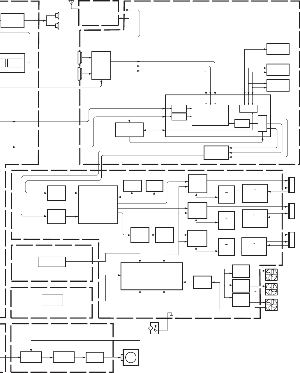
(No.YA463)2-8
SPEAKER(R)
SPEAKER(L)
ATSC TUNER
MODULE PWB
DRIVE PWB
THERMOSTAT
HD-ILA
R DEVICE
OSDR3-5 / OSDG3-5 / OSDB3-5
TA1 / TB1 / TC1 / TD1
TA2 / TB2 / TC2 / TD2
IC3101
R DEVICE
DRIVE
FLASH ROM
MAIN MICOM
IC6501
LVDS DRIVER
IC7201
IC3301
G DEVICE
DRIVE
IC3501
B DEVICE
DRIVE
DDR-SDRAM
IC6101
FLASH ROM
IC7203
HDMI-1
HDMI-2
HDMI
RECEIVE
IC6001
IC7601
CHASSIS MICOM
YMIN / BYMIN / RYMIN
DV1_R0-7
D0-15
D0-15
A0-21
SD_DQ1-32
A0-21
DV1_G0-7
DV1_B0-7
HD-ILA
G DEVICE
HD-ILA
B DEVICE
IC3102
IC3105
IC3302
IC3305
IC3502
IC3505
IC3701
DD CPU
IC3109
IC3111
IC3309
IC3311
IC3509
IC3511
RAM
RAM
RAM
REF. VOLTAGE
REF. VOLTAGE
REF. VOLTAGE
CONTROL
IC8001
FAN
CONTROL
FAN
CONTROL
IC8005
IC8002
IC8003
LAMP COVER SW PWB
S0861
IC2001
SENSOR
TEMP PWB
INTERLOCK SW
CONTROL
CONTROL
IC3001
RECEIVER
IC3005
1PHASE-2PHASE
CONVERT/
OVER DRIVE
IC3002
RECEIVER
IC3007
LVDS
DRIVER
IC3003
SD-RAM
IC3004
SD-RAM
DC-AC
CONVERT IGNITER
DC-DC
CONVERT
LVB0-7
LVG0-7
LVR0-7
DIN_DL/DR
DTU_Y/Cb/Cr
DTU_LIN/RIN
Y/Gout
Cb/Pb/Bout
Cr/Pr/Rout
IC3008
LVDS
RECEIVER
LAMP BALLAST UNIT
LAMP ASS’Y
LAMP
COOLING FAN-1
LAMP
COOLING FAN-2
OPTICAL BLOCK
COOLING FAN
LVDS
LVDS
DIGITAL PWB
IC605
DIGITAL
AUDIO OUT
C
ONTROL
EBASS
BOOST
SUB_VY
SUB_VY
FAN STOP
DETECT
MI_TX
MI_RX
A-D
CONVERT
A-D
CONVERT
YC SEPARATE/
CHROMA DEMOD./
FORMAT CONVERT/
NOISE REDUCT
RGB
PROCESS
OSD
MIX
SUB CPU
QAM_TXD
QAM_RXD
FAN
CONTROL
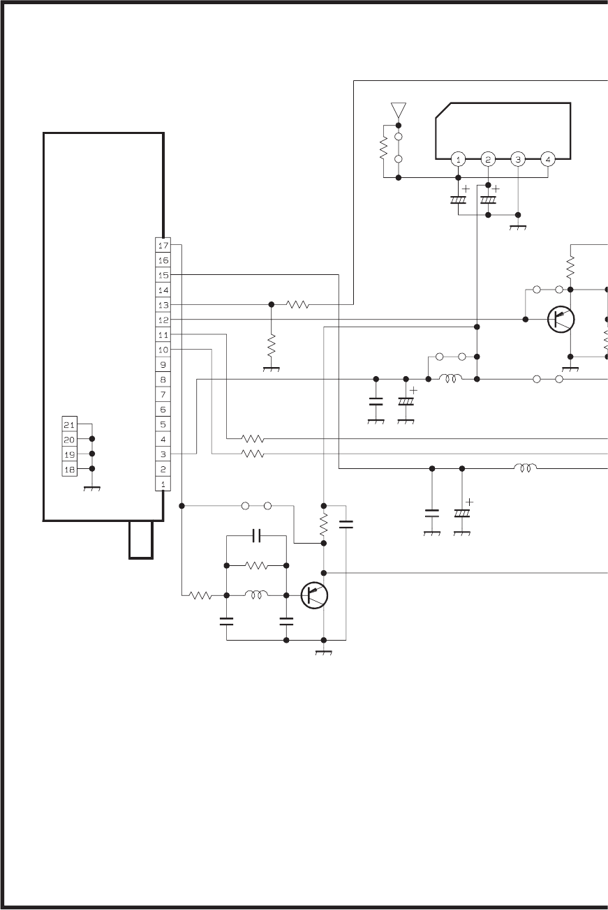
2-9(No.YA463)
R002
Q004
TU001
Y003
R001 Y002
IC001
C001 C002
Y005
Q006
Y006
L004
R007
R008
R006
R028
C016 C017
C014
C015
L002
C013
R004
C007
C006
R005
C010 L003
R029
Y001
R003
2SA812A/5-6/-X
N.C
N.C
N.C
N.C
N.C
N.C
N.C
5V
IF
SCL
SDA
AFT
AUDIO
SIF
30V
VIDEO
QAU0467-001
NRSA63J-0R0X
PQ050RDA1SZ
/16
QETN1CM-107Z /16
QETN1CM-107Z
2SA812A/5-6/-X
NQL953J-120X
CH CH
/16
CH
NQL79GM-100X
/16
QETN1CM-107Z
/50
QETN1HM-106Z
/16
IN
OUT
GND
Cont
QRT029J-6R8
0
OPEN
47k
100 100
OPEN
OPEN
1.2k
330
1k
10k
56p 68p
0.1
12p
100
100
10
.01
100
.1
OPEN
27k
OPEN
GND
9V
GND
GND GND
GND GND
GND
GND
GND
TUNER PWB ASS'Y (1/2)
SRA0R012A-M2
U/V TUNER
CIRCUIT DIAGRAMS
TUNER PWB CIRCUIT DIAGRAM (1/2) SHEET1
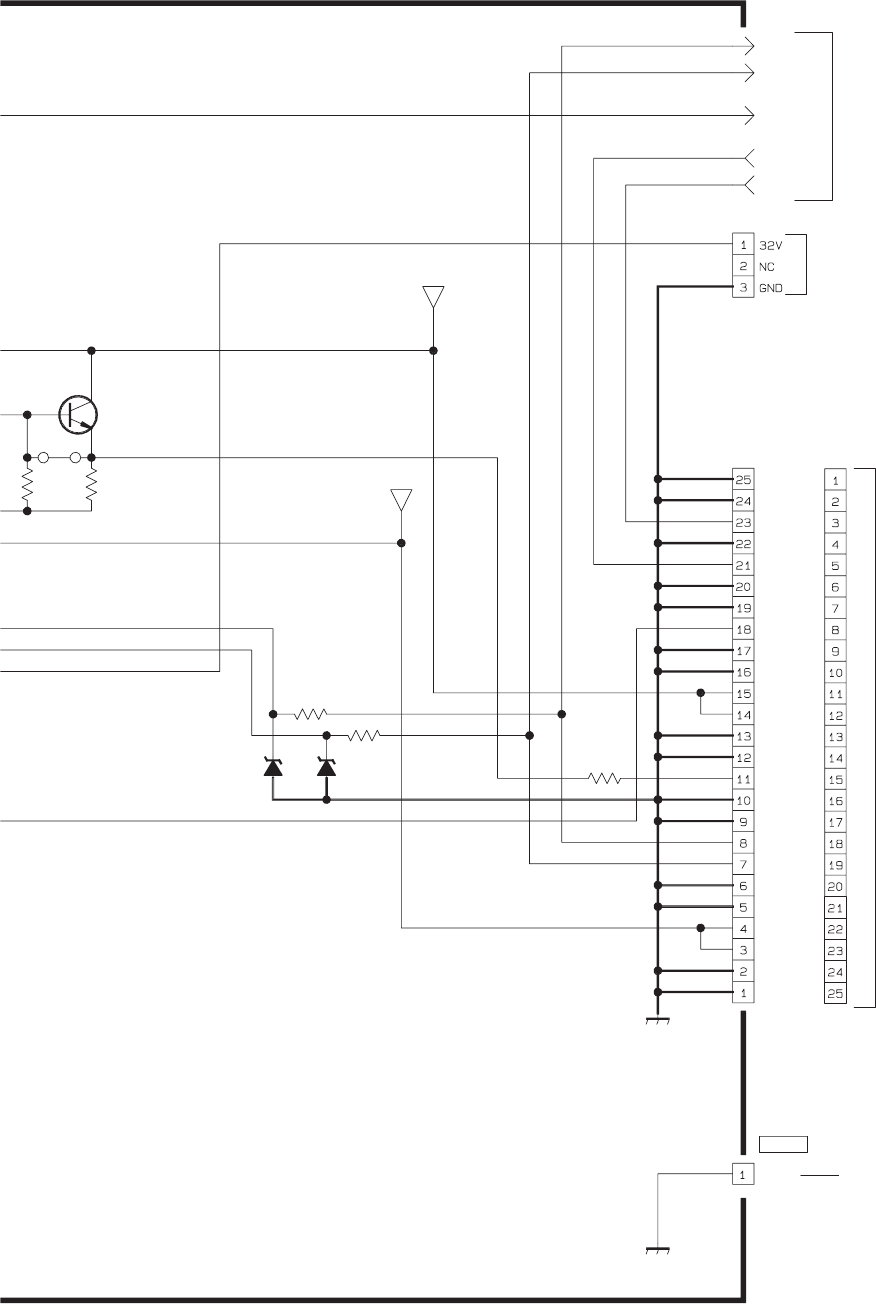
(No.YA463)2-10
c30202001_0214_1/2_0.0
Y004
Q005
CN0G1
0
28
CN0T2
CN0T1
0
29 R030
R014
R013
D002D001
TV_R
TV_L
Audio_out
SCL3A5
SDA3A5
R047
2SC1623A/5-6/-X
0
7Z
GND
QGA2001C1-03
GND
SDA3A5
GND
GND
9V
GND
GND
GND
GND
GND
BS_A5V
BS_A5V
GND
SCL3A5
GND
AFT
GND
9V
GND
GND
TV_V1
GND
TV_L
TV_R
GND
QGF1201C2-25
OPEN
OPEN
0
k
7
k10k
0
0
OPENOPEN 0
GND
9V
GND
BS_A5V
G
ND
SHEET2
ANALOG PWB
ASS'Y(6/6)
CN1T2
(SHEET8)
ANALOG PWB
ASS'Y(1/6)
CN1T1
(SHEET3)
OPEN
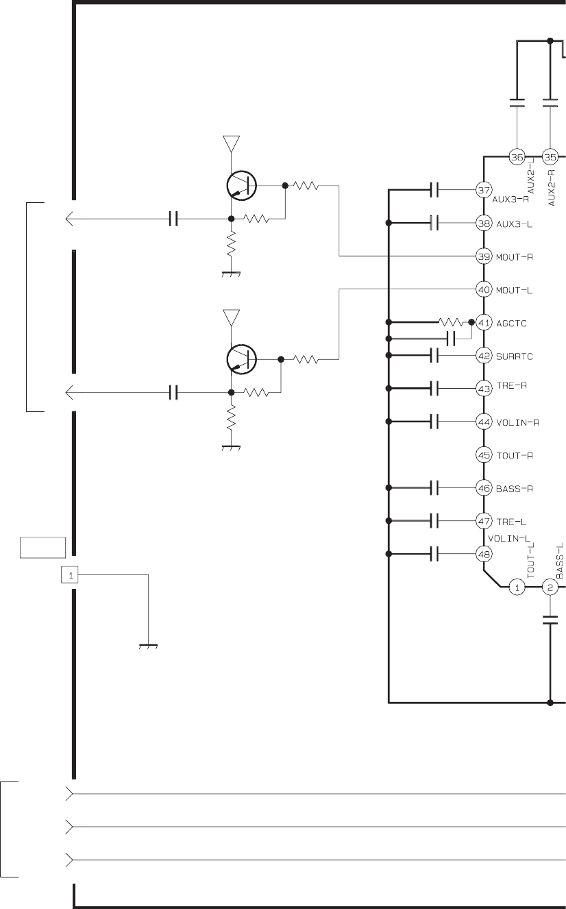
2-11(No.YA463)
SDA3A5
SCL3A5
Audio_out
R072
R074
Q061
Q062
R075
C083
R073 C084
C085
C092
TV_L
TV_R
CN0G2
C091
R076
R077C093
C088
C090
C061
R071
C086
C082
C087
C089
C080
C081
/16
/16
B1
B1
GND /16
B1
/16
/16
/16
/16
/16
0
0
OPEN
OPEN
OPEN
0.1
OPEN 0.1
10/10
2.2/16
OPEN
0.1
0
02.2/16
0.1
0.0047
0.1
2.2M
0.022
0.1
0.0047
0.1
0.1
9V
9V
GND
GND
GND
SHEET1
SHEET1
TUNER PWB CIRCUIT DIAGRAM (2/2) SHEET2
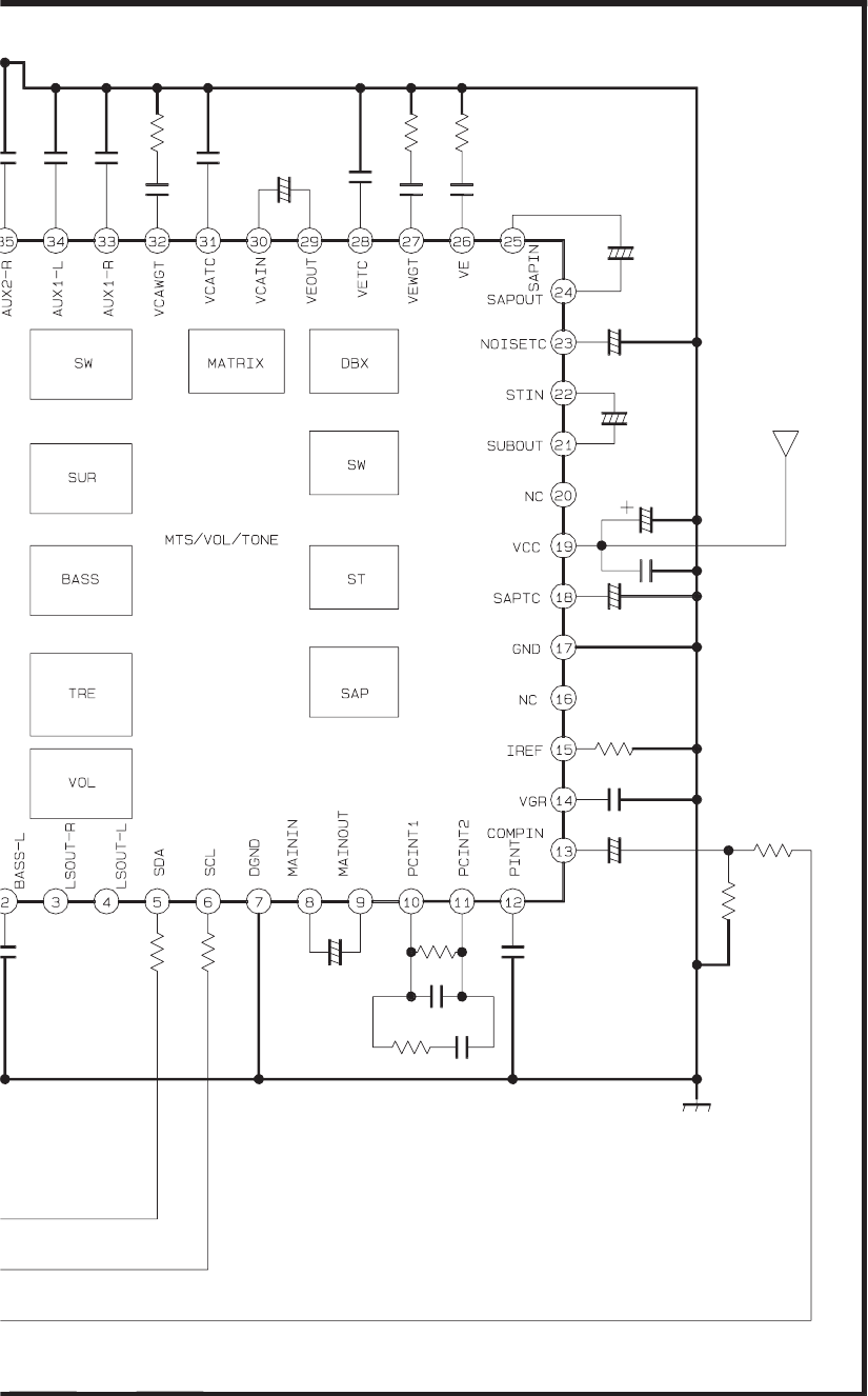
(No.YA463)2-12
c30202002_0214_2/2_0.0
C067
C066
C094
C068
C071
C072
C077
C062
C076
C070
C065
IC061
C064
R064
C063
R067
R070 R069
C069
R068
R066
C073
R065
C075
C078
C079
C080
C074
R063
R062
R061
B1
QENC1HM-475Z
QENC1HM-475Z
QENC1HM-475Z
B1
N
QENC1HM-475Z
B1
QENC1HM-475Z
QENC1HM-475Z
N
QENC1HM-475Z
NCB31CK-105X
CXA2205Q-X
NRSA63D-683X
/16
QETN1CM-476Z
NNN
N
N
NCB31CK-105X
/16
/16
10/10
4.7/50
0.1/16
4.7/50
4.7/50
4.7/50
10/10
4.7/50
4.7/50
4.7/50
1/16
.012100k
.0056
3.9k 3k
47
3.3k
6.8k
.0027
12K
3.3/10
1/16
0.1
0.1
.047
1M
220
220
GND
9V
SDA3A5
SCL3A5
Audio_out
TUNER PWB ASS'Y (2/2)
SRA0R012A-M2
AUDIO CONTROL
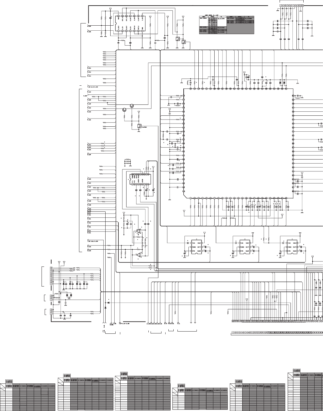
2-13(No.YA463)
R116
V3_VIN
R117
R132
R133
R134
R135
R194
CN1F
R185
Q105
R193
CN1CV1
V3_LIN
V3_RIN
R125
R136
R137
V1_G_Y
V1_B_Cb
Q104
C206
IC104
C148
R124
C150
C151
R123
R126
R196
C149
R127
V2_R_Cr
R128
R129
R197
R277
R138
C214
IC103
C288C287
C144
C146
C147
R292
R287
C285
R285
C145
Q103
R284
C286
IC105
C152
C154
C155
C153
IC282
IC282
CN1S2
R139
R283
R282
C221
C921 C922
CENT_IN
Q101
Q102
R781
R105 R106
C101
C103
R101
R102
R103
R104
DVI_L
DVI_R
IC106
R107
R108
R109
R110
R111
R112
R113
R114
R115
R119
R120
R121
R122
V3_YIN
V3_CIN
V3_S
R278
DIN_PHOTO
R130
R131
R286
A_MU_J
V2_LIN
V2_RIN
R276
TV_LINK
R118
V2_B_Cb
V2_G_Y
V2_VIN
V1_R_Cr
R279
V1_RIN
V1_LIN
V1_VIN
V1_YIN
V1_CIN
V1_S
MON_R
MON_L
MON_V
MON_Y
MON_C
MON_SDC
M_MUTE
AU_ROUT
AU_LOUT
C204
R280
CN011
C201
C202
R296
R295 R297
R957
R298
R958
C291
R967 R968
C118
IC281
IC282
R281
R283
R284
R285
R287
R288
R289
R290
R291
R292
R534
R535
C281
C282
C283
R282
C284
C285
C286
C287
C288
R955
C102
R782
R535R534
C226 C227 C228 C229
C225
R797
R798
C215
C224 C223
C222
C234
C235
C236
C233
C232
C231
C230
D125
D126
R163
R162
R161
C114
C115
C116
IC101
R164
C119
R165
C120
R166
C126
R167
C132
R181
CN1RE
C143
C142
R192
R190
R187
C133
R186
R183
C136
C141
R191
R189
C138
R184
R188
C117
D101 D102
R169 R168
C131
C130
C137
C140
C134
R182
C139
R970
R969
R976
R975
R974
R973
R972
R971
C237
C238
C239
R204
R205
R938
R945
R946
C291
R299
R937
C246
C245
C137
C139
C140
C145
C146
C149
C150
C151
C152
C153
C154
C144
C147
C148
C155
C138
C156
C157
C161
C169
C172
C175
C176
C181
C182
C183
C158
C170
C171
D110
R126
R127
R179
R180
R128
R183
R187
R188
R185
R194
C215
C245
R198
M.PACK
MAIN_POW
LB_PRO5
R199
R200
R201
A_MUTE
TALK
DSP_RST
AC_IN
POW_GOOD
MSP_RST0
C281
IC281
C282
C283
C284
R290 R288
R289R291
BBOUT
SUB_MUTE
R281
L102
L103
C292
C293
R948
R275
R949
C295
C296
R293
R294
A_MU_J
R195
CENT_IN
C199
C200
R140
R141
R143
C112
R144
D110D111
P_OFF_M
D121
D122
D123
D124
R146
R147
R918
R919
R920
C216
C217
C218
C219
C220
C109
R148
R149
C107
R151
C108
R152
R153
C110
R154
R155
C113
C111
R150
C106
R157
R145
R156
R158
R159
C105
C104
R160
R142
C127
R177
C128
C129
R170
R171
R174
R175
R178
R179
R172
R176
R960
R180
R173
SDA3A
SCL3A
C239
C237
C238
LAMP/REC
MECA_SW
ON_TIM
POWERLED
GND
STB3.3V
STB5V
QGA2001C6-09X
N
NN
NNPS
KEY2
KEY1
GND
QGA2001C6-03X
/16
B1
N
QGF0508C2-50W
/16
/16
B1
OLLC10863
-04
OLLC10863
-04
OLLC10863
-04
1SS355W-X
/1
6
O
OLLC11379
1SS355W-X
OLLC10863
OLLC10863
OLLC10863
OLLC11379
OLLC10863
/16 B1
CH CH CH CH
CH
B1
CH CH
B1 B1 B1 B1 B1
1SS355W-X
OLLC10863
-02
OLLC10863
-04
OLLC10494
BD3869AF-X
RC4558D-X
OLLC10863
-02
OLLC10863
-02
MA8056/M/-X
MA8056/M/-X
OLLC10863
-02
/16
/16
FBC_Y_OUT1
CVBS/Y_OUT1
OUT1_VCC5V
C_OUT1
OUT1_GND
CVBS/Y_OUT2
OUT2_VCC5V
FBC_Y_OUT2
C_OUT2
OUT2_GND
CVBS_OUT4
FBC_CVBS_OUT4
CVBS_OUT5
FBC_CVBS_OUT5
R1_OUT
L1_OUT
R2_OUT
L2_OUT
R3_OUT
L3_OUT
AU_O_VCC9V
R10_IN
L10_IN
NC
R9_IN
C3_DC
C_IN3
FBC_CVBS_OUT3
CVBS_OUT3
DRIVER_VCC5V
Y_OUT3
DC_OUT
C_OUT3
DRIVER_GND
CVBS_IN4
CVBS4
Y_IN4
C4_DC
C_IN4
INPUT_GND
CVBS_IN5
VREF
Y_IN5
C5_DC
C_IN5
CVBS5
COMP_Y_IN1
S5
COMP_Y_IN2
ATT_MON_OUT
R2S11004FT
/1
6
/1
6
/16
/16
STB5V
GND
REMO
QGA2001C6-03X
/16
/16
/16
/16
/16
/16
/16
/16
/16
OLLC10494
1SS355W-X
OLLC10494
OLLC11043
BD3869AF-X
RC4558D-X
OLLC11043
1SS355W-X
OLLC10863
-03
OLLC10863
-03
OLLC10863
-03
OLLC10863
-03
OLLC10494
OLLC10863
-04
OLLC10863
-04 OLLC10863 OLLC10863
-02 OLLC10863
-03
OLLC10494OLLC11379 OLLC11043
OLLC10494OLLC11379 OLLC11043
OLLC11379 OLLC11043
1SS355W-X
OLLC11379 OLLC11043
GND
GND
GND
GND
GND
Y
Cb
Cr
HD
VD
L
R
IN2
CHIP
FILTER
GND
VCC
OUT1
OUT2
IN1
SDA
SCL
/16
KEY2
REMOCON
ONTIMER
BS_IR
SCL0
GND
GND
TVLINK
POW_GOOD
AC_IN
LB_PR
LB_POW
MAINPOW
AUDIO_L
B1_POW
CODECRST
[EXT_YS2]
EXT_YS1
DBS_LED1
DBS_LED2
STB3.3V
STB3.3V
A_MUTE
M_MUTE
POW_LED
CARD_INT
MECA_SW
AFT1
EE_CDS
MSP_RST
SDA3A
SCL3A
CARD_DA
DIN_PHOT
TEXT_FR
GND
GND
TXET FB
KEY1
STB_5V
[AUDIO_R}
REC_LED
AGC
CARD_CK
TEXT_FG
SDA0
/16
MA8056/M/-X
MA8056/M/-X
MA8056/M/-X
MA8056/M/-X
/16
/16
/16
/16
/25
L1_IN
R1_IN
P_EXP1
L2_IN
R2_IN
P_EXP2
L3_IN
R3_IN
AU_I_GND
L4_IN
R4_IN
P_EXP3
L5_IN
R5_IN
AU_1/2_VCC
L6_IN
R6_IN
AU_I_VCC9V
L7_IN
R7_IN
P_EXP4
L8_IN
R8_IN
AU_O_GND
L9_IN
FBC_Y_OUT3
Y_IN3
S3
CVBS_IN3
CVBS3
C_IN2
C2_DC
Y_IN2
S2
CVBS_IN2
CVBS2
C_IN
C1_DC
Y_IN1
INPUT_VCC5V
CVBS_IN1
CVBS_IN1_DET
Y_IN1_DET
CVBS_IN6
S4
CVBS_IN7
S1
CVBS1
SCLK
SDATA
/16
/16
/16
OPEN
OPEN
OPEN
OPEN
OPEN
OPEN
OPEN
OPEN
OPEN
0
0
OPEN
OPEN
OPENOPEN
OPEN
OPEN
OPEN
OPEN
OPEN
OPEN
OPEN
OPEN
0.01
OPENOPE
N
OPEN
OPEN
0
OPEN OPEN
OPEN
2.2
OPEN
OPEN
OPEN
OPEN
OPEN
OPEN
OPEN
OPEN
OPEN
OPEN
OPEN
OPEN
OPEN
OPEN
OPEN
OPEN
OPEN
OPEN
OPEN
OPEN
OPEN
0
OPEN
OPEN
OPEN
OPEN
OPEN
0.1
0.1
OPEN
OPEN OPEN
0
OPEN
0
00
OPEN
OPEN
OPEN
0
OPEN
OPEN
OPEN
OPEN
OPEN
OPEN
OPEN
OPEN
OPEN
OPEN
0
OPEN
OPEN
OPEN
OPEN
OPEN
OPEN
OPEN
OPEN
0.01/16
0.01/16
0.01/16
0.01/16
0.01/16
0.1/16
0.01/16
0.01/16
0.01/16
0.01/16
0.01/16
0.01/16
0.01/16
0.01/16
1
0
0
0
OPEN
OPEN
OPEN
0
OPEN
OPEN
OPEN
OPEN
OPEN
OPEN
OPEN
OPEN
0
0
0
OPEN
OPEN
0
0
0
OPEN
0
OPEN
OPEN
OPEN
OPEN
OPEN
OPEN
OPEN
OPEN
OPEN
OPEN
OPEN
OPEN
OPEN
OPEN
OPEN
OPEN
OPEN
OPEN
OPEN
OPEN
0
OPEN
OPEN
OPEN
OPEN
OPEN
OPEN
OPEN
OPEN
OPEN
OPEN
0
0.01/16
0.01/16
0.01/16
0.01/16
OPEN
OPEN
0.01/16
0.1/16
0.01/16
0.01/16
0.01/16
0.01/16
0.01/16
0.01/16
0.01/16
0.01/16
OPEN
2.2
0
180p 100p 100p
10p
10p
0
0
100p 100p
0.01
OPEN
OPEN
OPEN
OPEN
OPEN
OPEN
0
0
0
0
0
0
OPEN
OPEN
OPEN
OPEN
OPEN
OPEN
OPEN 0
0
0
OPEN
OPEN
OPEN
OPEN
OPEN
OPEN
OPEN
OPEN
0
OPEN
OPEN
OPEN
OPEN
OPEN
OPEN
OPEN
0
OPEN
OPEN
4.7k
4.7k
OPEN
OPEN
OPEN
0
OPEN
0.01/16
0.01/16
0.01/16
0.01/16
0.01/16
15k
15k
10k
0.1/16
0.01/16
0.01/16
15k
0.01/16
0.01/16
0.01/16
0.01/16
0.01/16
0.01/16
10k
15k
OPEN
OPEN
6.8k
OPEN
0.1
0.1
220k
1
220
k
1
220
1
220k
1
220k
0.1
0.1
OPEN
OPEN
1
OPEN
0.1
10
OPEN
0
220k
0.1
OPEN OPEN
100 100
0.1
47
100
1
OPEN
100
4.7/16
4.7/16
22/25
100/16
47/16
0.1/16
4.7/16
4.7/16
0
0
0
0
0
0
100
100
15k
15k
10k
10k
15k
4.7k
15k
OPEN
4.7k
0
OPEN
4.7/16
4.7/16
22/25
100/16
47/16
0.1/16
4.7/16
4.7/16
0
0
0
0
0
0
OPEN
OPEN
OPEN
OPEN
OPEN
OPEN
OPEN
OPEN
OPEN
OPEN
OPEN
OPEN
OPEN
OPEN
OPEN
0
OPEN
OPEN
OPEN
OPEN
OPEN
OPEN
OPEN
OPEN
OPEN
OPEN
0
0.01/16
0.01/16
0.01/16
0.01/16
0.01/16
0.1/16
0.01/16
0.01/16
0.01/16
0.01/16
0.01/16
0.01/16
0.01/16
0.01/16
0.01/16
0.01/16
0.01/16
0.01/16
0.01/16
0.022/16
0.01/16
0.01/16
0.01/16
0.01/16
0.01/16
0.01/16
0.01/16
0.01/16
0.1/16
OPEN
0.1/16
OPEN
OPEN
OPEN
OPEN
OPEN
OPEN
OPEN
OPEN
OPEN
0
0
0
0
0
10/10
0
0
OPEN
OPEN
OPEN
OPEN
0
0
100
0
0
68
68
0
0
0
0
0
10/10
0
0
OPEN
OPEN
OPEN
0
0
0
0
0
10/10
0
0
0.1/16
0.1/16
0.1/16
OPEN
OPEN
OPEN
OPEN
OPEN
OPEN
OPEN
OPEN
OPEN
OPEN
OPEN
0
0
0
0
0
10/10
0
0
OPEN
OPEN
OPEN
0
0
0
0
0
10/10
0
0
OPEN
OPEN
OPEN
0
0
0
0
0
10/10
0
0
OPEN
OPEN
OPEN
OPEN
OPEN
OPEN
1/16
OPEN
10/16
100/10
10/16
100/10
10/16
1/16
10/16
100/10
1/16
10/16
1/16
0.1/16
0.1/16
OPEN
0.1/16
OPEN
OPEN
OPEN
OPEN
OPEN
OPEN
OPEN
OPEN
OPEN
OPEN
OPEN
0.1/16
OPEN
0.1/16
OPEN
OPEN
OPEN
OPEN
OPEN
OPEN
OPEN
OPEN
OPEN
OPEN
OPEN
OPEN 10/16OPEN OPEN
0.01/16
0.01/16
0.01/16
0.01/16
0.01/16
0.1/16
0.01/16
0.01/16
0.01/16
0.01/16
0.01/16
0.01/16
0.01/16
0.01/16
0.01
0.01
0.01
0.01
0.01
0.022/16
0.01
0.01
0.01
0.01
0.01
0.01
0.01
0.01
OPEN
OPEN
OPEN
OPEN
OPEN
OPEN
0
0
0
0
0
OPEN 0
OPEN
OPEN
OPEN
OPEN
0
10k
0
0
OPEN
OPEN
OPEN
OPEN
OPEN
OPEN
OPEN OPEN
OPEN 10/10OPEN OPEN
0.1/16 0.10.1/16 0.1/16
OPEN
OPEN
OPEN
OPEN
OPEN
OPEN
OPEN
OPEN
OPEN
OPEN
OPEN
OPEN
OPEN
OPEN
OPEN
OPEN
0.1
0.1
6.8k
6.8k
6.8k
6.8k
OPEN
6.8k
6.8k
OPEN
OPEN
OPEN
OPEN
OPEN
OPEN
OPEN
OPEN
0.1
0
0
0.1
6.8k
47
6.8k
0.1
OPEN
OPEN
33k
4.7
33k
33k
OPEN
OPEN
OPEN
6.8k
33k
1
OPEN
0.1
0.1
0
0
0
0
0
0
OPEN
OPEN
V4_RIN
V4_LIN
V3_D
V1_D
V2_S2
TV_L
TV_R
V1_S2
MON_R
MON_L
MON_V
MON_SDC
MON_Y
V2_RIN
V3_Y
V3_Cb
V3_Cr
V3_SL
V3_VIN
V3_LIN
V3_RIN
V2_LIN
V2_R_Cr
V2_SL
MON_SDC
V2_B_Cb
V2_G_Y
V2_VIN
V2_YS
MON_C
V2_YIN
V2_CIN
V2_SIN
V1_S
V1_G_Y
STB3.3V
V1_B_Cb
V1_R_Cr
V1_YS
V1_RIN
V1_LIN
V1_SL
V1_VIN
V1_YIN
V1_CIN
V3__YIN
AV_SW
BS_A9V
GND
BS_A9V
GND
BS_A9V
GND
V3__S
V3__CIN
V3_S2
MON
STB_5V
GND GND
GND
DTU_LIN
DTU_RIN
TV_LINK
GND
BS_A9V
REMOCON
STB3.3V
BS_A9V
AU_GND
GND
AU_GND
AU_GND
BS_A9V
GND
GND
BS_A5V
BS_A9V GND
GND
AU_GNDAU_GND
BS_A9V
GND
BS_A9V
GND
BS_A9V
GND
GND
BS_A9V
DTU_CIN
CENT_IN
F_CIN
V3_S2
V3__CIN
MON_COUT
DTU_VIN
DTU_YIN
MON_VOUT
MON_YOUT
F_VIN
F_YIN
F_S
BS_A5V
GND
BS_IR
GND
DBS_LED2
DBS_LED1
DIN_PHOTO
GND
AU_GND
GND
GND GND
GND GND
GND
GND
GND
GND
GND
REC_LED
MECA_SW
DIMMER
POW_LED
KEY2
KEY1
BS_A9V
BS_A5V
GND
M.PACK
MON_YOUT
DIMMER
MON_COUT
MON_VOUT
TV_MAIN
CARD_LIN
CARD_RIN
CARD_Cb
REMOCON
MON_Y
MON_C
DIN_L
CARD_Cr
CARD_Y
REC_LED
CARD_HD
CARD_VD
EE_CDS1
DTU2_RIN
MON_V
TALK
TALK
POW_LED
TEXT_R
MECA_SW
KEY2
TEXT_G
TEXT_B
CARD_DA
STB_5V TV_LINK
POW_GOOD
AC_IN
LB_PRO5
MAIN_POW
MSP_RST0
MAIN_POW
LB_PRO5
AC_IN
POW_GOOD
MSP_RST0
BS_IR
KEY1
DBS_LED1
DBS_LED2
V2_YS
V1_YS
LB_POW0
DSP_RST
LB_POW0
DSP_RST
SDA3A
VARI/FIX_R
VARI/FIX_L
DIN_PHOTO
DVI/DIN
DTU_RIN
DVI/DIN
F_LIN
F_RIN
TV_L
TV_R
DTU2_LIN
DTU_LIN
DIN_SL
V1_LIN
V1_RIN
V2_LIN
V2_RIN
V3_LIN
V3_RIN
V4_LIN
V4_RIN
DIN_SR
V1_S
DEC_Y
V1_VIN
V1_YIN
V1_S2
V1_CIN
V2_VIN
V2_SIN
V2_YIN
V2_S2
V2_CIN
V3_VIN
V3__S
V3__YIN
DIN_R
DIN_SL
CARD_CK
CENT_IN
CARD_INT
EE_CDS1
SCL3A5
SDA3A5
SDA0
SCL0
P_OFF_M
DVI_R
DVI_L
SCL3A
SHEET4
SHEET4,5
SHEET4
SHEET7
SHEET4
SHEET4,5
SHEET5
SHEET8
SHEET7
SHEET5
SHEET6
DIGITAL PWB ASS'Y (1/15)
CN011 (SHEET9)
FRONT LED
PWB ASS'Y
CN07FL (SHEET36),
CN9F(SHEET37)
REMOCON
PWB ASS'Y
CN08RE (SHEET40)
SIDE CONTROL
PWB ASS'Y
CN08S2 (SHEET42)
VIDEO/AUDIO SELECT
OPEN
AMP
A
NALOG PWB CIRCUIT DIAGRAM (1/6) SHEET 3
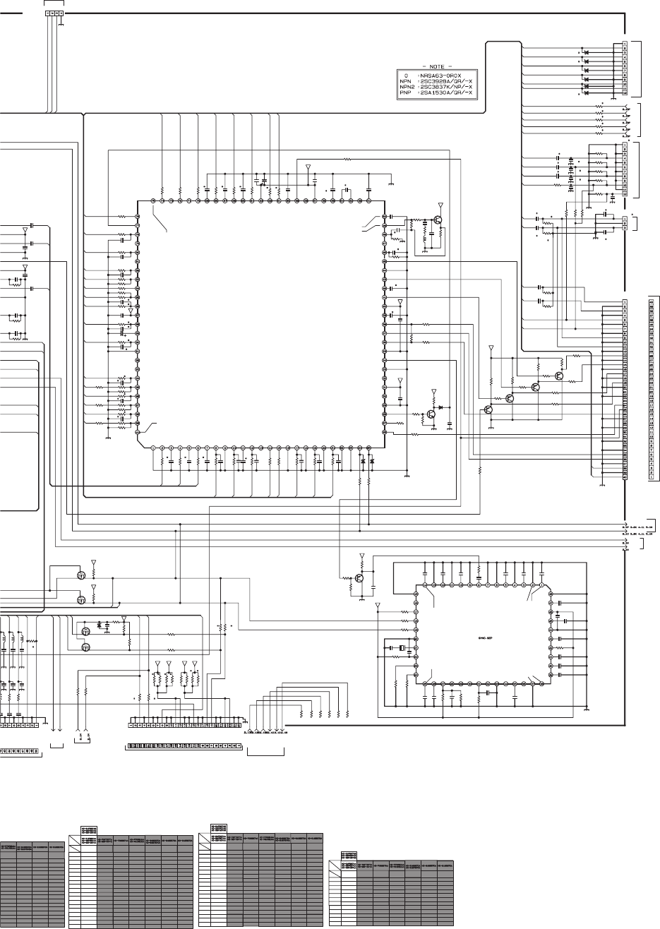
(No.YA463)2-14
ANALOG PWB ASS'Y(1/6)
SRA-1024A-M2
c10508001_0911_1/6_0.0
CN1S1
SCL3A5
SDA3A5
CN012
R257
R951
R253
R952
R249
CN1CV2
PC_R
PC_G
R241
R243
PC_VS
R251
R255
R258
R259
R236
R224
R222
R206
Q107
Q106
R221
R261
R205R204
R227
R226
Q110
R262
R264
R207
R266
R263
R265
R267
Q111
Q112
Q109
R202 R203
CN1UA
R269
R953
R954
C921
PC_HS
PC_B
C922 C923
Q108
R223
R225 D105
C166
C197
C198
R270
R268
C203
C583
C585
C586
C587
C588
C590
C589
X540
C547
C582
IC540
R541
C548
R549
R546
R580
R544
R545
R543
C584
R542
C240
C241
C242
R583
R582
R581
C591
Q540
C243
C244
C118
CN1UV
R956
C207
C208
C209
C210
R584
R585
R586
R587
R593
R594
R592
R591
R590
R589
R588
R299
Q115
Q114
R941
R942
R943
R944
C211
C212
Q113
R598 R599
R597
R595
R596
R947
C213
D106
CN1T1
C234
C235
C236
C194
C195
C196
R272
CN1UV
CN1UA
R153
R248
R252
R256
R584
R585
C111
C112
C191
C192
C193
C194
D131
D132
D133
D134
D135
D136
R905
C195
C196
R271
C207
R154
C208
C125
C124
C240
C121
IC102
R164
C241
C119
R165
C120
R166
C242
C173
C171
C170
C169
C172
R240
R242
R244
R250
R254
C176 C174
C175
R238
R239
R245
R246
R247
R248
R252
R256
C189
C168
C167
C184
C185
C186
C188
C190
C191
C192
C193
C187
C177
C123
C122
R237
C186
C188
C190
R228
R229
R245
R246
R247
MAIN_L
MAIN_R
R590
R591
R588
R589
R592
D131
D132
D136
R158
R159
R170
C197
C198
R933
R934
R931
R932
IC103
IC104
IC105
CARD_CK
CARD_DA
ATT_ON/OFF
C540
SIF_GND
C161
SW2
SW1
R260
TV_SIF
TV_MONO
TV_L1
TV_R1
C541
L102
L103
L104
C292
C293
C294
R948
R949
R950
C542
C295
C543
C296
C544
C297
R273
R274
C545
C546
C580
C549
R548
R540
R547
C581
R959
R931
R933
R935
R937
R932
R934
R936
R938
R945
R946
L101
R235
R234
R233
R232
R963
R231
R962
R230
R229
R209
C156
R210
C157
R211
C158
R212
R213
R216
R217
R218
R966
R964
R228
C183
C182
C181
C178
R965
R214
R961
C159
C160
C162
C163
C164
C165
D103
D104
R219
R220
C180
C179
R215
R208
V4_CIN
V4_YIN
V4_VIN
V4_LIN
V4_RIN
V4_S
GND
GND
GND
GND
GND
GND
QGA1501C5-12W
BS_LOUT
GND
GND
GND
GND
GND
BS_ROUT
BS_YOUT
BS_COUT
DIN_DR
DIN_DL
ML
YMAIN_GND
BYMIN
BYMINGND
RYMIN
SUB_VY
CLPH_Y1V
CLPH_Y2G
FBMIN
NC
CmpHS
CmpVS
GND
MR
GND
GND
GND
GND
GND
GND
GND
GND
YMIN
RYMINGND
QGF0508C2-40W
SSM3K17FU-X
SSM3K17FU-X
U_R
GND
U_L
MA111-X
CH
CH
/16
B1
CH
B1
LINE1-2
SYNC2-IN
DAC1
SDA
SCL
XTAL
VD1-IN
HD1-IN Y3/G3-IN
Cb3/B3-IN
DAC2
Cr3/R3-IN
C-IN
Y-IN
B1
CH
CH
CH
CH
-12X
QGA2001C6
-03X
QGA2001C6 -12X
QGA2001C6
-03X
QGA2001C6
OLLC10863
-04
OLLC11379
OLLC10863
-04
OLLC10863
-04 OLLC10863
/16
OLLC10863
-12X
QGA2001C6
-03X
QGA2001C6
OLLC10863
OLLC10863
OLLC10863
-02
OLLC10863
-02
-12X
QGA2001C6
-03X
QGA2001C6
OLLC10863
-02
GND
CV
U
GND
Y
GND
V
GND
SLOW
GND
C
GND
OLLC10863
-02
B1
B1
B1
B1
CH
CH
QGF1201C2-25
B2
B2
B2
MA8100/M/-X
MA8100/M/-X
MA8100/M/-X
/16
/16
/16
FB_IN1
FB_DET_IN2
Y/G_IN3
COMP/RGB_T3
Cb/Pb/B_IN3
DC1
FB_IN2
COMP/RGB_T4
Cr/Pr/R_IN3
DC2
Y/G_IN4
INPUT_VCC
Cb/Pb/B_IN4
VREF
Cr/Pr/R_IN4
INPUT_GND
FB_IN3
DC3
Y_IN5
DC4
Cb_IN5
DC5
Cr_IN5
DC6 COMP_T5
VD_filter1
Clamp_driver1
Clamp_in1
Sync_slice1
VD_slice1
Y/G_OUT1
Sync2_GND
Cb/Pb/B_OUT1
HD_DET1
Cr/Pr/R_OUT1
OUT_VCC
HD_poldet1
INT_HD_OUT1
INT_VD_OUT1
Clamp_Pulse1_in
OUT_GND
Y/G_OUT2
SUB_GND3
Cb/Pb/B_OUT2
Sync_VCC1
Cr/Pr/R_OUT2
Sync1_GND1
INT_HD_OUT2
INT_VD_OUT2
Clamp_Pulse2_in
R2S11003FT
/16
/16
/16
CH
/16
/16
/16
/16
/16
/16
/16
/16
/16
OLLC11379
OLLC10863
-03OLLC11379
OLLC10494
OLLC10863
-03
-12X
QGA2001C6
-03X
QGA2001C6
OLLC10863
-03
OLLC10863
-03
OLLC10494
OLLC10494
MA8100
/M/-X
MA8100
/M/-X
MA8100
/M/-X
OLLC11043 OLLC11043
OLLC10494
OLLC11043
MM1510XN
-X
MM1510XN
-X
MM1510XN
-X
INT
GND
SDA
SCL
D
G
S
D
G
S
TEXT
_
FR
GND
GND
GND
GND
TXET_FB
MAIN_VY
TEXT_FG
DEC_Y
B1
Cr1/R1-IN
LINE3-1
Cb1/B1-IN
LINE2-1
Y1/G1-IN
LINE1-1
NC
SYNC1-IN
Cb2/B2-IN
Cr2/R2-IN
LINE3-2
LINE2-2
Y2/G2-IN
VD2-IN
HD2-IN
ADDRESS
SYNC-OUT
VD-OUT
HD-OUT
Y-OUT
Cb-OUT
Vf0ADJ
Cr-OUT
NC
SYNC3-IN
D
G
S
D
G
S
NQL79GM-100X
GND
9V
GND
GND
SDA3A5
GND
GND
BS_A5V
BS_A5V
GND
SCL3A5
9V
GND
AFT
GND
TV_L2
TV_R2
GND
GND
GND
TV_V1
GND
GND
GND
GND
SUB_GND1
Y/G_IN6
CL_Y2
Cb/B_IN6
CL_Cb2
Cr/R_IN6
CL_Cr2
G_IN7
MAIN_GND
B_IN7
HD_IN_DET
R_IN7
NC
HD_IN2
VD_IN2
NC
G_IN8
NC
B_IN8
INPUT_GND2
R_IN8
NC
NC
SDATA
SCLK
FB_DET_IN1
Cr/Pr/R_IN2
COMP/RGB_T2
Cb/Pb/B_IN2
COMP/RGB_T1
Y/G_IN2
CL_Y1
R_IN1
CL_Cb1
B_IN1
CL_Cr1
G_IN1
MAIN_VCC2
HD_IN1
VD_IN1
G_IN1_DET
FB_OUT1
FB_OUT2
Sync2_VCC
ATT_MON_OUT
VD_slice2
Clamp_driver2
Clamp_in2
Sync_slice2
VD_filter2
/50
CH
/16
/50
/50
/16
/16
/16
/16
/16
0
82
0
82
0
OPEN
0
0
0
0
OPEN
0
OPEN
22k
OPEN
5.6k
0
2.7k
OPEN
OPEN
PNP2
100
100
5.6k
100
330
330
330
PNP2
PNP2
PNP2
OPEN OPEN
OPEN
82
0
OPENOPENOPEN
NPN
22k
10k
0.01
OPEN
OPEN
OPEN
OPEN
0.1
OPEN
OPEN
OPEN
OPEN
OPEN
OPEN
OPEN
OPEN
OPEN
OPEN
OPEN
OPEN
OPEN
OPEN
OPEN
OPEN
OPEN
OPEN
OPEN
OPEN
OPEN
OPEN
OPEN
OPEN
OPEN
OPEN
OPEN
OPEN
0
0
6.8k
0
0
0
10k
10k
OPEN
6.8k
0
0
0
10k
10k
OPEN
OPEN
OPEN
OPEN
OPEN
2.2/10
2.2/10
2.2/10
2.2/16
6.8k
2.2/16
10p
10p
10p
100p
100p
OPEN
OPEN
OPEN
OPEN
OPEN
OPEN
2.2/10
0
0
0
0
OPEN
OPEN
OPEN
2.2/10
2.2/10
2.2/16
10p
10p
10p
100p
1
100p
6.8k
0
0
0
10k
10k
OPEN
OPEN
OPEN
OPEN
OPEN
2.2/10
6.8k
2.2/16
2.2/10
2.2/10
2.2/16
6.8k
2.2/16
0.1/16
OPEN
0.1/16
OPEN
OPEN
OPEN
OPEN
OPEN
OPEN
OPEN
OPEN
OPEN
OPEN
OPEN
OPEN
OPEN
0.1/16
OPEN
OPEN
0
0
OPEN
OPEN
OPEN
10p
10p
10p
100p
100p
6.8k
0
0
0
10k
10k
OPEN
OPEN
OPEN
OPEN
OPEN
2.2/10
2.2/10
2.2/10
2.2/16
6.8k
2.2/16
0.1/16
OPEN
0.1/16
OPEN
OPEN
OPEN
OPEN
OPEN
OPEN
OPEN
OPEN
OPEN
OPEN
OPEN
OPEN
0
0
OPEN
OPEN
OPEN
OPEN
OPEN OPEN
OPEN
OPEN
220p
82p
NPN
33 470
330
OPEN
OPEN
OPEN
OPEN
OPEN
OPEN
OPEN
OPEN
OPEN
OPEN
OPEN
OPEN
OPEN
0.1/16
270k
OPEN
OPEN
OPEN
OPEN
1
1
1
220k
1
220k
0
1
220k
0
OPEN
10p
OPEN
68p/50
OPEN
OPEN
OPEN
OPEN
OPEN
330p
OPEN
OPEN
10
0.1
0.1
0.1
0.1
0.1
0.1
0.1
0.1
OPEN
OPEN
0
0
0.1/16
0.1/16
0.1/16
OPEN
OPEN
OPEN
OPEN
10p
10p
OPEN
0
0
OPEN
OPEN
OPEN
0
0
OPEN
OPEN
OPEN
0
0
0
0
0
OPEN
OPEN
100p
0
0
0
100p
OPEN
OPEN
OPEN
OPEN
OPEN
OPEN
OPEN
0
0
0
OPEN
0
OPEN
OPEN
0
0
0
0
0
0
0
0
0
0
0
0
OPEN
0
0
0
0
0
0
0
0
0
0
0
OPEN
OPEN
OPEN
OPEN
OPEN
OPEN
0
0
0
0
0
OPEN
6.8k
6.8k
OPEN
OPEN
OPEN
10k
10k
0
0
0
0
0
0000
OPEN
OPEN
OPEN
OPEN
OPEN
OPEN
OPEN
0
0
0
0
0
OPEN
OPEN
OPEN
OPEN
OPEN
OPEN
0.1/16
0.1/16
0.1/16
OPEN
0.1/16
0.1/16
OPEN
OPEN
OPEN
OPEN
OPEN
OPEN
0.1/16
OPEN
0.1/16
OPEN
OPEN
OPEN
OPEN
OPEN
OPEN
OPEN
OPEN
OPEN
OPEN
OPEN
OPEN
OPEN
OPEN
0.1/16
OPEN
OPEN
OPEN
OPEN
OPEN
OPEN
OPEN
OPEN
OPEN
OPEN
OPEN
OPEN
OPEN
OPEN
OPEN
OPEN
OPEN
OPEN
0.1/16
OPEN
OPEN
OPEN
2.2/16
2.2/16
0.1/16
0.1/16
OPEN
OPEN
OPEN
OPEN
OPEN
0
0
OPEN
OPEN
OPEN
6.8k
6.8k
6.8k
6.8k
6.8k
6.8k
6.8k
6.8k
6.8k
6.8k
6.8k
6.8k
OPEN
OPEN
000000 OPEN
OPEN
OPEN
OPEN
OPEN
OPEN
OPEN
OPEN
0.1/16
0.1/16
0.1/16
0.1/16
0.1/16
OPEN
OPEN
OPEN
OPEN
OPEN
OPEN
OPEN
OPEN
OPEN
OPEN
OPEN
OPEN
1/16
OPEN
10/16
100/10
10/16
100/10
10/16
1/16
10/16
100/10
1/16
10/16
1/16
OPEN
10/16
OPEN
OPEN
OPEN
OPEN
OPEN
OPEN
OPEN
OPEN
OPEN
OPEN
10/10
0.1
OPEN
100
OPEN
OPEN
OPEN
OPEN
OPEN
OPEN
OPEN
OPEN
OPEN
OPEN
OPEN
OPEN
OPEN
OPEN
OPEN
OPEN
OPEN
OPEN
OPEN
OPEN
OPEN
OPEN
OPEN
OPEN
OPEN
OPEN
OPEN
OPEN
OPEN
0
0
0
0
OPEN
0
OPEN
0
0
0
OPEN
OPEN
OPEN
OPEN
OPEN
OPEN
OPEN
OPEN
1
OPEN
OPEN
OPEN
0.1
0.1
0.1
0.1
0.1
0.1
OPEN
OPEN
100
100
0.1
47
OPEN
0
DTU_Cb
DTU_LIN
DTU_Cr
AV_SW
F_LIN
DTU_Y
F_CIN
F_RIN
F_YIN
F_VIN
F_S
V1_D
V3_D
V3_SL
DTU_Y
V1_SL
DTU_Cb
V2_SL
DTU_RIN
V1_YS
DTU_Cr
PC__R
PC__B
PC__G
V2_YS
PC__R
V3_Cr
V3_Cb
GND
V3_Y
PC__HS
PC__B
PC__VS
PC__G
DTU_YIN
DTU_CIN
SCL3A
SDA3A5
GND
DIN_R
GND
SCL3A5
DIN_L
V
BS_A9V 9V
BS_A5V
GND GND
GND GND
BS_A5V
SDA3A
VARI/FIX_R
VARI/FIX_L
GND
BS_A5V
BS_A5V
DTU_VIN
GND
GND
CARD_RIN
DIN_SR
CARD_LIN
MAIN_VY
MAIN_C
SUB_C
BS_A5V
MON_L
MON_R
BS_A5V
GND
GND
GND
BS_A5V
GND
GND
BS_A5V
DTU2_RIN
DTU2_LIN
BS_A5V 5V
GND
BS_A5V
GND
BS_A5V
GND
BS_A5V
SYNC1_IN
GND
BS_A5V
BS_A5V
GND GND GND
GND GND GND
GND
GND
GND
GND
GND
GND
BS_A5V
DEC_Y
TV_MAIN
TEXT_G
TEXT_B
TEXT_R
TV_MAIN
TV_R
TV_L
TEXT_B
TEXT_G
CARD_VD
CARD_HD
CARD_Cr
CARD_Cb
CARD_Y
MAIN_C
SUB_C
MAIN_VY
PC__VS
PC__HS
V1_G_Y
V1_B_Cb
V1_R_Cr
V2_G_Y
V2_B_Cb
V2_R_Cr
CARD_CK
CARD_DA
CARD_CK
CARD_INT
CARD_DA
SDA0
SCL0
SHEET7
SHEET5
TUNER PWB ASS'Y (1/2)
CN0T1 (SHEET1)
SHEET5
SHEET5,7,8
SHEET5
SHEET4
ATSC TUNER PWB
ATSC TUNER PWB
SIDE CONTROL
PWB ASS'Y
CN08S1 (SHEET42)
DIGITAL PWB
ASS'Y (4/15)
CN012
(SHEET12)
VIDEO SELECT
OPEN
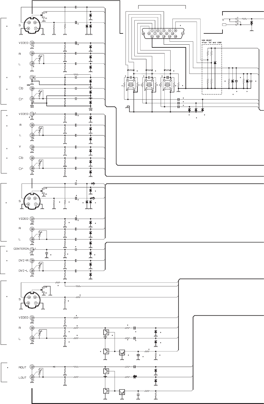
2-15(No.YA463)
C401
C420
J407
J402
J403
C404
J404
C405
C403
R401
R403
R404
R405
C402
D401
R402
D404
D403D402
D406
D405
C406
C407
C408
R407
R408
R409
R406
C453
C415
D407
D409
D408
J405
J406
J409
D451
C418
C419
D452
R417
R419
R420
R418
C417
D416
R416
C416
D419
D418D417
D421
D420
D410
D412
D411
C411
C451
C452
C410
J403
C409
R410
R411
R412
J406
R421
R452
R455
D423
D424
J411
R422
R423
C422
C412
C423
C413
Q451
Q452
R431
R454
C414
R413
C433
R414
R415
R433
R434
D431
D432
D413
R432
J402
R457
D415
C431
C432
D414
R453
J404
R438
R441
R436
Q431
Q432
R440
R443
R439
R444Q433
R442
R437
R435
R458
C463C462C461
C464
C465
C466
Q453
R456
R451
D463
J410
R481
R464 R467R461
R470
D462
D461
R474
R472
R475
R473R471
D465
D466
R476
C469
C468
D464
D481
J401
C421
D422
LC461
LC463
LC462
R469
R468
R466
R465
R463
R462
/10
CB2
/10
CB2
/16
/16
/10
CB2
/10
CB2
/10
CB2
/16
CB1
/10
CB2
/10
CB2
/10
CB2
/16
CB1
/16
CB1
/10
CB2
/16
/10
CB2
/10
CB2
/10
CB2
/10
CB2
RT4N430C-X
RT4N430C-X
/10
CB2
CB1
CB1
CB1
CHCHCH
CB2
CB2
CB2
RT1P440C-X
CH CH
CB2
.01
2.2
2.2
10
75
75
220k
220k
10
*1
75
*1
*1*1
*1
*1
2.2
2.2
2.2
75
75
75
OPEN
1
*1
*1
*1
*1
2.2
2.2
*1
220k
220k *1
*1
*1
*1
*1
2.2
2.2
2.2
2.2
10
75
220k
220k
82k
82k
*1
*1
OPEN
220k
220k
2.2
2.2
2.2
2.2
220
2.2
75
75
75
*1
OPEN
1k
*1
*1
470
39k
470
220
OPEN
0
0
OPENOPEN
OPEN
OPEN
OPEN
OPEN
OPEN
GNDGND
GND
GND
V1_CIN
GND
GND
V1_VIN
V1_LIN
GND
V1_G_Y
GND
V1_YIN
GND
V1_RIN
GND
V1_B_Cb
GND
GND
GND
GND
GND
GND
V1_S
GND GND
V3_CIN
GND
JACK_A
V3_S
GND
V1_R_Cr
V3_YIN
GND
V3_VIN
GND
GND
V3_LIN
GND
V3_RIN
AU_GND
GND
GND GND
GND
GND
GND
GND
GND
GND
V2_LIN
GND
V2_VIN
GND GND
V2_RINGND
GND GND
GND
GND
GND
GND
DVI_R
GND
CENT_IN
AU_LOUT
GND
DVI_L
GND
GND GND
GND
MON_SDC
GND
GND
MON_V
MON_Y
GND
GND
GND
GND
GND
AU_GND
GND
MON_C
MON_L
GND
GND GND
GND GND
M_MUTE
GND
GND
GND
GND
GND
GND
GND
V2_G_Y
V2_B_Cb
GND
V2_R_Cr
AU_ROUT
GND
GND
JACK_A
MON_R
GND
GND
GND
AU_GND
PC_G
GND
GND
GND
GND
PC_HS
PC_B
GND
GND
PC_R
PC_DET
PC_VS
GND
GND
GND GND
A_MU_J
GND
INPUT-1
PC-IN (D-SUB) AV COMPULINK
Υ
INPUT-2
AUDIO
OUT
ATSC OUT
DIGITAL-IN
AUDIO
INPUT-3
A
NALOG PWB CIRCUIT DIAGRAM (2/6) SHEET 4
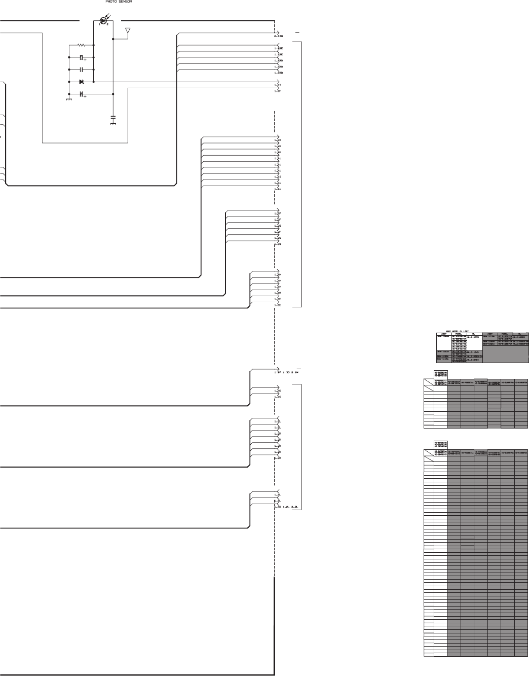
(No.YA463)2-16
ANALOG PWB ASS'Y(2/6)
SRA-1024A-M2
c10508006_0911_6/6_0.0
D492
R491
C491
C492
C493
D491
TV_LINK
V3_S
V3_CIN
V3_YIN
C494
V3_VIN
A_MU_J
PC_VS
PC_HS
C431
V3_LIN
C432
C433
D431
D432
J401
Q431
Q432
Q433
PC_B
PC_G
R431
4
68
PC_R
PC_DET
4
81
DIN_PHOTO
V3_RIN
CENT_IN
V2_RIN
V2_LIN
V2_VIN
V2_R_Cr
V2_B_Cb
V2_G_Y
DVI_R
DVI_L
AU_LOUT
AU_ROUT
MON_SDC
MON_C
MON_Y
MON_V
MON_L
MON_R
M_MUTE
V1_S
V1_CIN
V1_YIN
V1_VIN
V1_LIN
V1_RIN
V1_G_Y
V1_B_Cb
V1_R_Cr
R433
R434
R435
R436
R437
R438
R439
R440
R441
R442
R443
R444
J407
J409
J406
C420
C421
R421
D422
C461
C462
C463
C464
C465
C466
C468
C469
D461
D462
D463
D465
D466
J410
R461
R462
R463
R464
R465
R466
R467
R468
R469
R470
R475
R476
J405
C415
C416
C417
D416
D417
D418
D419
R416
R417
R418
J402
J403
J404
AMS312
/16
/16
/16
MA8033-X
QNN0765
-002
OLLC10494
QNN0349
-004
QNN0764
-002
QNN0349
-004
QNZ0825
-002
OLLC10494
QNZ0825
-002
RT4N430C
-X
RT4N430C
-X
-X
RT1P440C
QNZ0825
-001 QNZ0825
-001
H
QNZ0825
-001
QNN0766
-001
QNZ0825
-002
QNN0766
-002
QNN0766
-001 QNN0766
-001 QNN0766
-001
QNZ0825
-001
QNN0766
-001
QNN0796
-001
QNZ0825
-001
OLLC10863
QNN0794
-001
-001
QNN0795
-001
QNN0794
OLLC10863
QNZ0825
-001
QNN0766
-001
QNN0796
-001
QNZ0825
-001
OLLC10863
-02
QNN0794
-001
-001
QNN0795
OLLC11379
-001
QNN0794
OLLC10863
-02
QNZ0561
-001
QNZ0561
-001 QNZ0561
-001 QNZ0561
-001 QNZ0561
-001
QNZ0825
-001
QNN0766
-001
QNN0796
-001
QNZ0825
-001
OLLC10863
-03
QNN0794
-001
-001
QNN0795
-001
QNN0794
QNN0807
-001
QNN0765
-001
OLLC10863
-03
QNZ0561
-001
OLLC11043
QNZ0825
-001
OLLC11379 OLLC11043
QNN0796
-001
QNZ0825
-001
OLLC10863
-04
OLLC10863
-04
QNN0349
-002
-001
QNN0764
QNN0349
-002
QNN0349
-002
-001
QNN0764
QNN0349
-002
QNN0794
-001
-001
QNN0795
-001
QNN0794
1M
10
0.1
100
1000p/50
2.2/10
220k
*1
0.01
1000p
10/16
10/16
*1
*1
*1
*1
75
75
75
2.2/16
2.2/16
1/16
*1
*1
75
OPEN
OPEN
OPEN
OPEN
OPEN
OPEN
OPEN
OPEN
OPEN
OPEN
OPEN OPEN
OPEN
OPEN
OPEN
OPEN
OPEN OPEN
OPEN
OPEN
OPEN
OPEN
PEN
OPEN
OPEN
OPEN
OPEN
OPEN
75
2.2k
75
2.2k
390
22k
470
OPEN
OPEN
OPEN
OPEN
OPEN
OPEN
OPEN OPEN
OPEN
OPEN
OPEN
OPEN
OPEN OPEN
OPEN
OPEN
OPEN
OPEN
OPEN
OPEN
OPEN
390
22k
470
OPEN
OPEN
OPEN
OPEN
OPEN OPEN
OPEN
OPEN
OPEN
OPEN
1k
OPEN
OPEN
OPEN
39k
OPEN OPEN
OPEN OPEN
OPEN
OPEN
OPEN OPEN OPEN
OPEN
OPEN
OPEN
OPEN
OPEN
OPEN
OPEN
OPEN
OPEN
OPEN
OPEN
OPEN
OPEN
OPEN
OPEN
OPEN
OPEN
OPEN
OPEN
OPEN
OPEN
OPEN
OPEN
OPEN
OPEN
OPEN
0.01
10/16
10/16
*1
*1
*1
*1
75
75
75
OPEN
OPEN
OPEN
OPEN
OPEN
OPEN
OPEN
OPEN
OPEN
OPEN
OPEN
OPEN
OPEN
OPEN
OPEN
OPEN
OPEN
OPEN
OPEN
OPEN
OPEN
OPEN
OPEN
OPEN
OPEN
OPEN
0.01
10/16
10/16
*1
*1
*1
*1
75
75
75
100p100p 100p 100p
100p
100p
2.2/10
2.2/10
2.2/10
100p
100p
100p
100p
2.2/10
100p
100p
2.2/10
2.2/10 2.2/10
2.2/10
100p
2.2/10
100p
100p 100p
100p
100p
2.2/10
2.2/10
2.2/10
100p
100p
*1
*1
*1
*1
*1
*1
*1
*1 *1
*1
*1
*1
*1
*1
*1 *1
*1 *1
*1
*1
100p
100p
100p
2.2/10
2.2/10
2.2/10
100p
100p
*1
*1
*1
*1
*1
OPEN
OPEN
OPEN
OPEN
OPEN
OPEN
OPEN
OPEN
OPEN
OPEN
OPEN
OPEN
OPEN
75
0
75 75
00
75
0
0
75
00
75 75
0
75
75
0
0
75
OPEN
OPEN
OPEN
OPEN
OPEN
0000
0
75
0
0
75
0
75
00
0
75
0
0
0
00
00
0
0
0
0
75
0
0
0
OPEN
OPEN
OPEN
OPEN
OPEN
OPEN
1k
1k
1k 1k
1k 1k
1k
1k
1k
1k
OPEN
OPEN
OPEN
OPEN
OPEN
OPEN
OPEN
OPEN
OPEN
OPEN
OPEN
OPEN
OPEN
OPEN
OPEN
OPEN
OPEN
OPEN
OPEN
OPEN
OPEN
OPEN
OPEN
OPEN
OPEN
OPEN
1000p
2.2/10
220k
*1
OPEN
OPEN
0.01
10/16
10/16
*1
*1
*1
*1
75
75
75
100p
100p
100p
2.2/10
2.2/10
2.2/10
100p
100p
*1
*1
*1
*1
*1
75
0
0
75
0
0
75
0
0
0
1k
1k
OPEN
OPEN
OPEN
0.01
10/16
10/16
OPEN
OPEN
OPEN
*1
*1
*1
OPEN *1
OPEN
OPEN
75
75
OPEN 75
OPEN
OPEN
OPEN
OPEN
0.01
10/16
10/16
*1
*1
*1
*1
75
75
75
GND
BS_A5V
DIN_PHOTO
A_MU_J
_
G
V1_S
V1_CIN
V1_YIN
V1_VIN
V1_LIN
V1_RIN
GND
V1_G_Y
PC_DET
TV_LINK
_
HS
PC_VS
_
B
V1_B_Cb
V1_R_Cr
V3_S
V3_CIN
V3_YIN
_
R
T
V3_VIN
V3_LIN
_
VS
PC_HS
V3_RIN
V2_RIN
V2_LIN
V2_VIN
PC_B
PC_G
V2_R_Cr
PC_R
V2_B_Cb
V2_G_Y
DVI_R
DVI_L
CENT_IN
MON_C
MON_Y
MON_V
MON_L
MON_R
M_MUTE
MON_SDC
AU_LOUT
AU_ROUT
SHEET5
SHEET3
SHEET3
SHEET3,5
N
KΥ
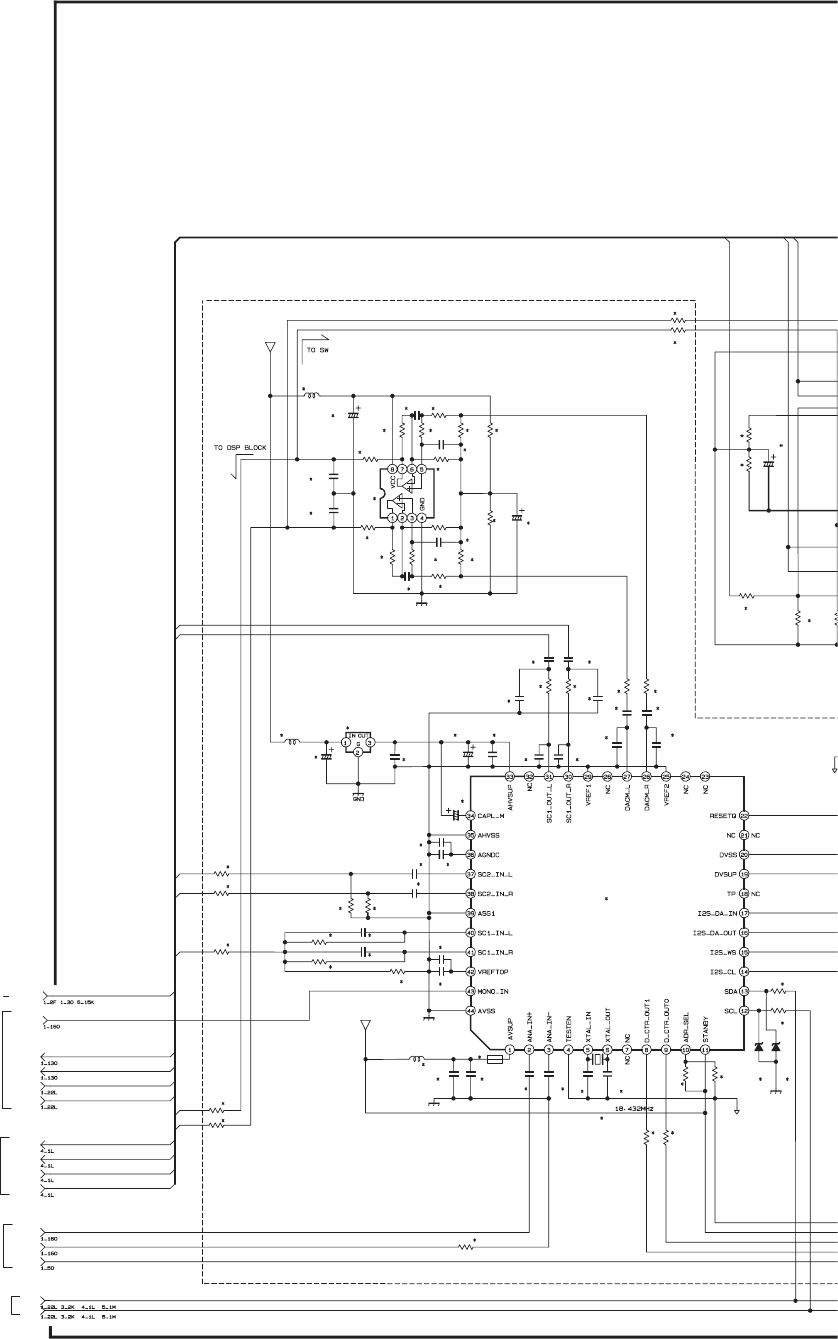
2-17(No.YA463)
ANALOG PWB ASS'Y(3/6)
SRA-1024A-M2
TV_L1
C351
SIF_GND
TV_R1
C352
L332
MSP_RST0
R357
R330
SDA3A5
SCL3A5
MAIN_R
MAIN_L
R329
R339
R342
R347
CENT_IN
R345
R340
C334
R346
R341
C349
DSPIN_L
DSPIN_R
DSPOUT_L
DSPOUT_R
R333
R334
C337
C362
C360
D332D331
C350
IC333
C354
C344 C345
R336
R348
R343
R349
C335
R353 R354
R335
C336
L331
R344
R350
C338
C333
R337
R338
C331
C332
TV_MONO
TV_SIF
R309
R327
R328
R308
R351 R352
C346
C343
K331
C357
C356
C359
C358
C348C347
IC331
X331
C363
C361
C355
C353
C341 C342
R363
R362
L333
R331
R332 R355 R356
R361
C339 C340
IC332
R358
R359
C301
R307 R306
C366
C365
C364
R360
C367
GND
TV_L1
TV_R1
DIG
_
9V
TV_R1
MAIN_R
MAIN_L
GND
TV_L1
GND
LIP_R
5V
MAIN_L
MAIN_R
CENT_IN
DSPIN_R
DSPOUT_L
DSPOUT_R
DIG_GND
GND
CENT_IN
DSPIN_L
LIP_L
DSPIN_R
DSPIN_L
CENT_IN
MAIN_R
MAIN_L
SHEET3,4
SHEET3
SHEET6
SHEET3
SHEET3,7,8
A
NALOG PWB CIRCUIT DIAGRAM (3/6) [MSP/SW BLOCK] SHEET 5
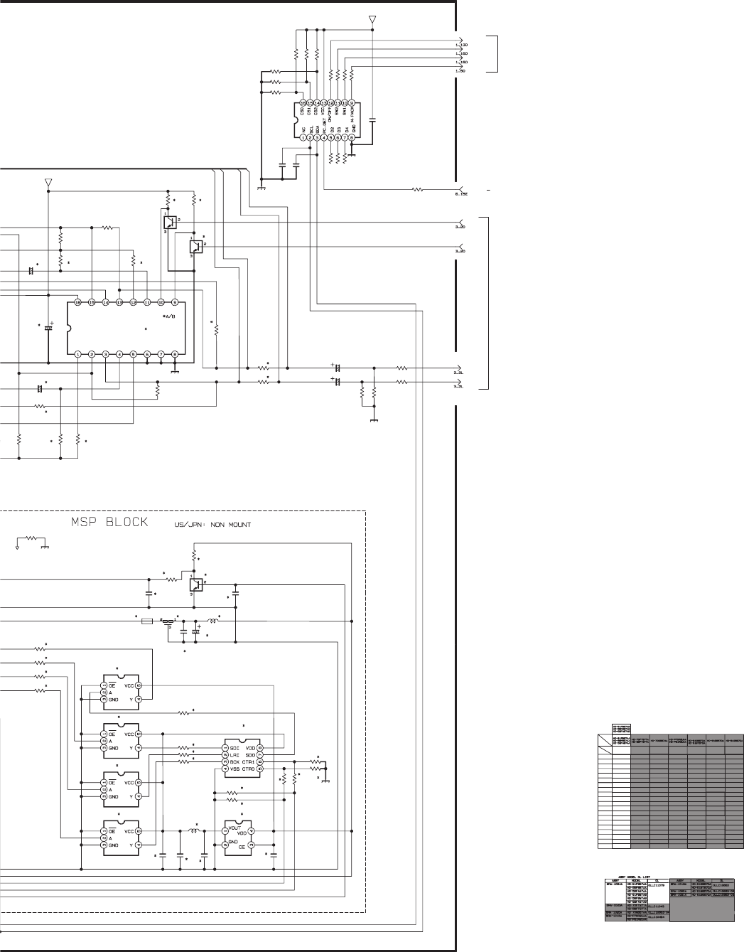
(No.YA463)2-18
c10508002_0911_2/6_0.0
R310
R311
Q301
C304
C303
Q302
R321
R312
ATT_ON/OFF
SW2
R391
R367
R364
C369
Q331
IC354
IC353
IC351
IC352
IC355
R368
IC356
R372
R373
R374
R371
L335
R369
R370
C372
C381
R395
C373
R376
R375
C382
C375
C374
IC301
R320
IC381
R323
R322
PC_DET
VOL_L
VOL_R
3
09
R313
C306
C307 R316 R317
R385
R383
R381
SW1
C305
C383
M.PACK
IC301
R306
R307
R308
R309
R310
R311
R318
R319
R314 R315
R312
R313
R314
R315
C301
C303
C304
C305
K332
Q302
R301
R302
R365
C368
C370
LC331 L334
C371
R379
R380
R324
R302
R301
R325
R324
A_SW1
A_SW2
R377
R387
R378
R394
R392
R388
R389
R390
R393
R384
R386
R382
R325
OLLC10863
CH CH
/25
/25
OLLC10863
-04 OLLC10863
OLLC10494OLLC11043 OLLC10863
-02
OLLC10863 OLLC10863
-03
OLLC10494 OLLC10863
OLLC11379
CD4052
BNS-X
RT1N441C-X
OLLC11043
CD4052
BNS-X
RT1N441C-X
OLLC10863
-04
N
N
B
0Y
2Y
YOUT
3Y
INH
1Y
VEE A
3X
0X
XOUT
1X
2X
VDD
VSS
OPEN
OPEN
OPEN
OPEN
OPEN
OPEN
OPEN
OPEN
OPEN
OPEN
OPEN
OPEN
OPEN
OPEN
0
OPEN
OPEN
OPEN
OPEN
OPEN
OPEN
4.7
4.7
100k 100k
OPEN
OPEN
OPEN
OPEN
OPEN
0
OPEN
OPEN
0
0
OPEN
0
OPEN
OPEN
OPEN
OPEN
OPEN
OPEN
OPEN
OPEN
OPEN
OPEN
OPEN
OPEN
OPEN
OPEN
OPEN
OPEN
OPEN
0
0
0
0
0
0
OPEN
OPEN
OPEN
OPEN
OPEN
OPEN
OPEN
OPEN
OPEN
OPEN
OPEN
OPEN
OPEN
OPEN
OPEN
OPEN
0
0
6.8k
47/16
0
0
OPEN
OPEN
OPEN
OPEN
OPEN
OPEN
OPEN
OPEN
OPEN
OPEN
OPEN
3.3k
3.3k
0
100k
100k
100k
100k
100k
22k
OPEN
OPEN
OPEN
OPEN
OPEN
0
0
0
0
OPEN
OPEN
4.7/16
4.7/16
100/16
OPEN
OPEN
6.8k
47/16
3.3k
3.3k
0
100k
100k
100k
100k
100k
22k
OPEN
OPEN
4.7/16
4.7/16
100/16
OPEN
OPEN
OPEN
OPEN
OPEN
OPEN
OPEN
OPEN
OPEN
OPEN
OPEN
OPEN
OPEN
OPEN
OPEN
OPEN
OPEN
OPEN
0
0
0
0
OPEN
OPEN
OPEN
OPEN
OPEN
OPEN
OPEN
OPEN
OPEN
OPEN
GND
DIG_GND
BS_A5V
A_SW1
GND
A_SW2
GND
GND
9V
GND
GND
DSPIN_L
DSPIN_R
DSPOUT_R
DSPOUT_L
SHEET3
SHEET4
SHEET7
MULTI
PLEXER
2-19(No.YA463)
LC551
R515
IC502
R516
DSPIN_R
DSPIN_L
R529
Q553
C551 C552
R557
R556
R553
R530
R554
C553
C554
R502
R501
C506
C505
C504
C503
IC501
R506
R503
R507
R504
R510
R505
R508
R509 C507
R514
C509
C508
C510
R512
L501
LC552
C501
C502
DSPOUT_R
R555
Q503
IC552
C556C555
C557
DSPOUT_L
C531 C532
SDA3A
SCL3A
R533
R532
R531
C520
C517
C518 C519
C512
Q501
C511
C513
C515
R528
R527
C516
R522
R521 C514
Q502
R519
R520
R518
R517
CO_RST
DSP_RST
D501
D502
R
56
1
R560
R511
R513
C558
C560
C559
C561
R523R524
R525R526
VCOM
AINR
AINL
VSS
VDD
DEM0
DEM1
SDTO SDTI
LRCK
MCLK
SCLK
/PWAD
/PWDA
AOUTL
AOUTR
NN
IN
GND
Nr
VO1
VO2
NN
NN
OPEN
OPEN
OPEN
OPEN
OPEN GND
GND
VCC5 VCC9
DSP9V
GND
DSP9V
GND
DSP9V
GND
VCC1.5
VCC3.3
SHEET5
SHEET3
SHEET7 ADC/
DAC
A
NALOG PWB CIRCUIT DIAGRAM (4/6) [W_DSP BLOCK] SHEET 6
(No.YA463)2-20
ANALOG PWB ASS'Y(4/6)
SRA-1024A-M2
c10508004_0911_4/6_0.0
R921
R922
R923
R925
R924
IC551
R568
R569
R566
R567
R565
R572
C567
C568
C563
C574
C575
C566C565
R928
C572
C571
C573
C562
C564
R571
X551
IC501
IC502
IC551
IC552
D501
D502
Q501
Q502
Q503
R526
R525
R524
R523
R522
R521
R520
R519
R518
R517
R516
R515
R514
R513
R512
R511
R510
R509
R508
R507
R506
R505
R504
R503
R502
R501
Q553
Q552
Q551
R527
R556
R555
R554
R553
R552
R551
R533
R532
R531
R530
R529
R528
R557
R563
R562
R561
R560
R559
R558
R567
R566
R565
R564
R568
R922
R921
R578
R577
R576
R575
R574
R573
R572
R571
R570
R569
R923
R927
R926
R925
R924
C501
C502
C503
C504
C505
C506
C507
C508
C509
C510
C511
C568
C567
C566
C565
C564
C563
C562
C561
C560
C559
C558
C557
C555
C552
C551
C532
C531
C520
C519
C518
C517
C516
C515
C514
C513
C512
C569
R928
X551
L501
C575
C574
C573
C572
C571
R927
R926
R564
R563
R562
R561
R560
R575
R576
R577
R578
R574
R573
C569
R570
VDDP
STANDBY
VDDP
VSS
BCK0
LRCK0
SDI0
SDO0
BCKIA
LRCKIA
VDDM
SAMSTB
VDDT
SDA
SCL
RST
HA17558
AF-X
AK4554
VT-X
JCC5067
PQ2L3152
MS-X
OLLC10494
OLLC10494
MA111-X
MA111-X
2SC3928A/
QR/-X
2SC3928A/
QR/-X
2SC3928A/
QR/-X
2SK3019-X
2SK3019-X
2SC3928A/
QR/-X
OLLC10863
OLLC10863
OLLC10863
-04 OLLC10863
OLLC10494OLLC11043
OLLC10863
-02
OLLC10863
-02
OLLC10863 OLLC10863
-03
OLLC10863
OLLC10863
-03
OLLC11379
NCB31CK
-223X
NCB31CK
-223X
NEHL1AM
-107X
NEHL1CM
-476X
NENA1CM
-475X
NENA1CM
-475X
NENA1CM
-475X
NENA1CM
-475X
NEHL1EM
-475X
NEHL1CM
-106X
NEHL1CM
-106X
NCB30JK
-225X
NEHL0JM
-226X
NCB30JK
-225X
NEHL0JM
-226X
NEHL0JM
-226X
NRSA63J
-222X
NEHL0JM
-226X
NCB31CK
-105X
NEHL0JM
-226X
NRSA02J
-0R0X
NAX0623
-001X
OLLC11379
HA17558
AF-X
AK4554
VT-X
JCC5067
PQ2L3152
MS-X
MA111-X
MA111-X
2SC3928A/
QR/-X
2SC3928A/
QR/-X
2SC3928A/
QR/-X
2SK3019-X
2SK3019-X
2SC3928A/
QR/-X
NRSA63J
-222X
OLLC11043
NCB31CK
-223X
NCB31CK
-223X
NEHL1AM
-107X
NEHL1CM
-476X
NENA1CM
-475X
NENA1CM
-475X
NENA1CM
-475X
NENA1CM
-475X
NEHL1EM
-475X
NEHL1CM
-106X
NEHL1CM
-106X
NCB30JK
-225X
NEHL0JM
-226X
NCB30JK
-225X
NEHL0JM
-226X
NEHL0JM
-226X
NEHL0JM
-226X
NCB31CK
-105X
NEHL0JM
-226X
NRSA02J
-0R0X
NAX0623
-001X
OLLC11043 OLLC10863
-04
OLLC10863
-04
SDI1
BCKIB
LRCKIB
VDD
CKI
VSS
VCOI
VSSP
NIMO
TEST
VSSX
XI
XO
VDDX
CKO
VDD
VSS
OPEN
OPEN
OPEN
OPEN
OPEN
OPEN
OPEN
OPEN
OPEN
OPEN
OPEN
OPEN
OPEN
OPEN
OPEN
OPEN
OPEN
OPEN
OPEN
OPEN
OPEN
OPEN
OPEN
OPEN
OPEN
OPEN
OPEN
OPEN
OPEN
OPEN
OPEN
OPEN
OPEN
OPEN
OPEN
OPEN
OPEN
OPEN
OPEN
OPEN
OPEN
OPEN
OPEN
OPEN
OPEN
OPEN
OPEN
OPEN
OPEN
OPEN
OPEN
OPEN
OPEN
OPEN
OPEN
OPEN
OPEN
OPEN
OPEN
OPEN
OPEN
OPEN
OPEN
OPEN
OPEN
OPEN
OPEN
OPEN
OPEN
OPEN
OPEN
OPEN
OPEN
OPEN
OPEN
OPEN
OPEN
OPEN
OPEN
OPEN
220
220
4.7k
3.3k
3.3k
4.7k
3.3k
1k
1k
3.3k
10k
33k
33k
10k
1k
1k
33k
33k
33k
33k
3.3k
3.3k
1k
OPEN
1k
1k
1k
OPEN
OPEN
OPEN
OPEN
OPEN
OPEN
OPEN
OPEN
OPEN
OPEN
OPEN
OPEN
OPEN
OPEN
OPEN
OPEN
OPEN
OPEN
OPEN
OPEN
OPEN
OPEN
OPEN
OPEN
OPEN
OPEN
OPEN
OPEN
OPEN
OPEN
OPEN
OPEN
OPEN
OPEN
OPEN
OPEN
OPEN
OPEN
OPEN
OPEN
OPEN
OPEN
OPEN
OPEN
OPEN
470
OPEN
OPEN
OPEN
OPEN
OPEN
OPEN
OPEN
OPEN
OPEN
OPEN
OPEN
OPEN
OPEN
OPEN
OPEN
OPEN
OPEN
OPEN
OPEN
OPEN
OPEN
470
100
0
3.3k
10k
10k
100
100
10k
0
0
10k
OPEN
OPEN
OPEN
OPEN
OPEN
OPEN
OPEN
OPEN
OPEN
OPEN
OPEN
OPEN
OPEN
OPEN
10k
OPEN
OPEN
OPEN
OPEN
OPEN
OPEN
OPEN
OPEN
OPEN
OPEN
OPEN
OPEN
OPEN
68k
68k
6.8k
220
220
220
OPEN
OPEN
OPEN
OPEN
OPEN
OPEN
OPEN
OPEN
OPEN
OPEN
OPEN
OPEN
OPEN
OPEN
OPEN
OPEN
OPEN
OPEN
OPEN
OPEN
OPEN
OPEN
OPEN
OPEN
OPEN
OPEN
OPEN
OPEN
OPEN
OPEN
OPEN
OPEN
OPEN
OPEN
OPEN
OPEN
OPEN
OPEN
OPEN
OPEN
OPEN
OPEN
OPEN
OPEN
OPEN
OPEN
OPEN
OPEN
OPEN
OPEN
OPEN
OPEN
OPEN
OPEN
OPEN
OPEN
OPEN
OPEN
OPEN
OPEN
OPEN
OPEN
OPEN
OPEN
OPEN
OPEN
OPEN
OPEN
OPEN
OPEN
OPEN
OPEN
OPEN
OPEN
OPEN
OPEN
OPEN
OPEN
OPEN
OPEN
OPEN
OPEN
OPEN
OPEN
OPEN
OPEN
OPEN
OPEN
OPEN
OPEN
OPEN
OPEN
OPEN
OPEN
OPEN
OPEN
OPEN
OPEN
OPEN
OPEN
OPEN
OPEN
OPEN
OPEN
OPEN
OPEN
OPEN
OPEN
OPEN
OPEN
OPEN
OPEN
OPEN
OPEN
OPEN
OPEN
OPEN
OPEN
OPEN
OPEN
OPEN
OPEN
OPEN
OPEN
OPEN
OPEN
OPEN
OPEN
OPEN
OPEN
OPEN
OPEN
OPEN
OPEN
OPEN
OPEN
220
0
100
100
OPEN
OPEN
OPEN
OPEN
10k
OPEN
OPEN
OPEN
OPEN
OPEN
OPEN
OPEN
OPEN
OPEN
OPEN
OPEN
OPEN
OPEN
OPEN
OPEN
OPEN
OPEN
OPEN
OPEN
OPEN
OPEN
OPEN
OPEN
OPEN
OPEN
10k
100
1M
4.7
10k
0
10k
10k
10k
10k
0
0
OPEN
OPEN
OPEN
OPEN
OPEN
OPEN
OPEN
OPEN
OPEN
OPEN
OPEN
OPEN
OPEN
OPEN
0
OPEN
OPEN
OPEN
OPEN
OPEN
OPEN
OPEN
OPEN
OPEN
OPEN
OPEN
OPEN
OPEN
0
0
0
0
OPEN
OPEN
OPEN
OPEN
OPEN
OPEN
OPEN
OPEN
OPEN
OPEN
OPEN
OPEN
OPEN
OPEN
OPEN
OPEN
OPEN
OPEN
OPEN
OPEN
OPEN
OPEN
OPEN
OPEN
OPEN
OPEN
OPEN
OPEN
OPEN
OPEN
OPEN
OPEN
OPEN
OPEN
OPEN
OPEN
OPEN
OPEN
OPEN
OPEN
OPEN
OPEN
OPEN
OPEN
OPEN
OPEN
OPEN
OPEN
OPEN
OPEN
OPEN
OPEN
OPEN
OPEN
OPEN
OPEN
OPEN
OPEN
OPEN
OPEN
OPEN
OPEN
OPEN
OPEN
OPEN
OPEN
OPEN
OPEN
OPEN
OPEN
OPEN
OPEN
OPEN
OPEN
OPEN
OPEN
OPEN
OPEN
OPEN
OPEN
OPEN
OPEN
OPEN
OPEN
OPEN
OPEN
OPEN
OPEN
OPEN
OPEN
OPEN
OPEN
OPEN
OPEN
OPEN
OPEN
OPEN
OPEN
OPEN
OPEN
OPEN
OPEN
OPEN
OPEN
0.0022
0.0022
0.0082
0.0082
1/50
1/50
1000p
1000p
0.1/16
0.1/16
1000p
1000p
1000p
1000p
0.1/16
0.01
0.01
0.1
0.1
0.01
0.01
OPEN
OPEN
0.01
OPEN
OPEN
OPEN
OPEN
OPEN
OPEN
0.01
0.01
OPEN
OPEN
OPEN
OPEN
OPEN
OPEN
OPEN
OPEN
OPEN
OPEN
OPEN
OPEN
OPEN
OPEN
OPEN
OPEN
OPEN
OPEN
OPEN
OPEN
OPEN
OPEN
OPEN
OPEN
OPEN
OPEN
220
220
4.7k
3.3k
3.3k
4.7k
3.3k
1k
1k
3.3k
10k
33k
33k
10k
1k
1k
33k
33k
33k
33k
3.3k
3.3k
1k
1k
1k
1k
470
470
100
0
3.3k
10k
10k
100
100
10k
0
0
10k
10k
68k
68k
6.8k
220
220
220
220
0
100
100
10k
10k
100
1M
4.7
10k
0
10k
10k
10k
10k
0
0
0
0
0
0
0
0.0022
0.0022
0.0082
0.0082
1/50
1/50
1000p
1000p
0.1/16
0.1/16
1000p
1000p
1000p
1000p
0.1/16
0.01
0.01
0.1
0.1
0.01
0.01
0.01
0.01
0.01
OPEN
OPEN
OPEN
OPEN
OPEN
OPEN
OPEN
OPEN
OPEN
OPEN
OPEN
OPEN
OPEN
OPEN
OPEN
OPEN
OPEN
OPEN
OPEN
OPEN
OPEN
OPEN
OPEN
OPEN
OPEN
OPEN
OPEN
OPEN
OPEN
OPEN
OPEN
OPEN
OPEN
OPEN
OPEN
OPEN
OPEN
OPEN
OPEN
OPEN
OPEN
OPEN
OPEN
OPEN
OPEN
OPEN
OPEN
OPEN
OPEN
OPEN
OPEN
OPEN
OPEN
OPEN
OPEN
OPEN
OPEN
OPEN
OPEN
OPEN
OPEN
OPEN
OPEN
OPEN
OPEN
OPEN
OPEN
OPEN
OPEN
OPEN
OPEN
OPEN
OPEN
OPEN
OPEN
OPEN
OPEN
OPEN
OPEN
OPEN
OPEN
OPEN
OPEN
OPEN
OPEN
OPEN
OPEN
OPEN
OPEN
OPEN
OPEN
OPEN
OPEN
OPEN
OPEN
OPEN
OPEN
OPEN
OPEN
OPEN
OPEN
OPEN
OPEN
OPEN
OPEN
OPEN
OPEN
OPEN
OPEN
OPEN
OPEN
OPEN
OPEN
OPEN
OPEN
OPEN
OPEN
OPEN
OPEN
OPEN
OPEN
OPEN
OPEN
OPEN
OPEN
OPEN
G
ND
GND
GND
2-21(No.YA463)
C631
C616
C617
R649
C632
C634
C614
C636
C635
R653
R646
R651
R652
C615
R620
Q601
R619
R621
IC601
C606 C607R608
L601
R602
C643
IC602
C602
C603
C605
R643
SDA3A5
D603
D602
C601
R629
R630
C727
SCL3A5
D601
C604
R660
C728
R601
R605
R606
R607
R741
R603
R604
A_MUTE
12V
R626
R625
R623
Q602
R624
R622 R627
R628
L602
R659
C654
R650
C664
C665
CN1A1
TALK
R707
I
C
R642
C642
IC609
C640
R668
R667
C652
R666
C644
R634
C621
C731
R635
C622
C730
C678
C677
Q609
C675
C676
R665
R664
R662
C627
C626
R633
R632
R663
R641
R656
D614
R654
K605
C671
C672
CARD_CK
CARD_DA
R688
R689 R690 R691
C746
R692C710
C747
C669
R687
R644
C668
C667
C717
IC606
R708
C641
C637
C623
C624
C625
C628
C629
C630
R610 R611 R612
R636
C633
Q604
R609
C608
IC603
C611
R615
R614
R613
C610
C609
R616
R617
R618 C613C612
R631
Q603
BBOUT
C659
SUB_MUTE
VOL_L
VOL_R
A_MU_J
Q613
R715
R717
C714
R718
D
R716
C715
Q605
Q606
R
C724
CO_RST
A_SW1
A_SW2
P_OFF_M
C666
Q
6
C638
C657
C649
C650
C646
C647
R693
R694
R695
R696
R697
R698
C639
R645
R647C653
C658
C660
C662
C661
C663
R640
R639
C655
R661
C674
C673
IC608
R751
R703
R699
R706
R752
R700
R701
R702
R705
R704
C648
C651
R638
R710
C729
C670
/25
/25
CVB
CA1
SDA
SCL
GND
V+
VREF
CO1TONE_LB
TONE_HB
SUR_FIL2
INB
INA
SUR_FIL1
TONE_HA
TONE_LA
VE1
LP1
AUX
CO2
NJW1182FP1
/50 /25
QETM1EM-477
QQR0621-002Z
PQ20WZ11-X
/25
/25
/50
MA111-X
/25
/25
QETM1EM-477
QQR0621-002Z
/16
CB2
/16
/16
QGA2001C6-06X
REF0V
INL
INR
AVSS
AVDD
RESET
SCL
SDA
M
X
OUT
VDD
NC
VSS
/25
CH
CH
/16
/16
/16
/16
M62320FP-X
/16
CB2
/16
CB2
CB1
MA1
RT1N241
C
RT1P241C-X
/50
/25
N
/16
/16
/16
N
HBSTA
OUT1A
OUT2A
ADDIN1
CSR
CBB
AGCINT
CVA CBH
CA2
CTH
CTL
ADDIN2
OUT2B
OUT1B
HBSTB
LP3 VE3
VE2
LP2
BB1
BB2
BB3
BB4
BBFIXOUT
BBAGCINT
BBAGCOUT
ealaBASS
SENSE
/25
/16
/10
/16
/16
/16
VDD
GND
CE NC
VOUT
/16
/16
CB1
GND
VCC
CB2
CB2
OPEN
4.7
4.7
68k
0.1
0.0082
OPEN
680p
680p
5.6k
100
100
OPEN
0
OPEN
OPEN
OPEN
0.1 4702.2k
0
0.1
33
33
0.01
OPEN
OPEN
OPEN
0.01
OPEN
OPEN
0.1
0.1
470
0
18K
5.6K
47K
2.2k
5.6K
1.8K
OPEN
100
0
OPEN
OPEN
OPEN OPEN
100
.047
33k
1
1
16k
OPEN
OPEN
OPEN
4.7
15k
56k
OPEN
OPEN
OPEN
OPEN
OPEN
OPEN
OPEN
OPEN
3.3k
OPEN
OPEN
OPEN
OPEN
OPEN OPEN OPEN
OPEN
OPENOPEN
OPEN
1
10K
5.6k
1
1
1
OPEN
OPEN
0.18
0.0022
0.018
0.012
0.0022
0.18
47k
0.0082
10/16
OPEN
OPEN
OPEN
OPEN
100k
OPEN
OPEN
2
0.1
10/16
*2
.022
1
1
1
OPEN
0
0
0
OPEN
OPEN
0.1
2.2k
18k.022
OPEN
1
2.2
1
1
OPEN OPEN
10
OPEN
OPEN
100
100
OPEN
100
100
100
100
100
1
1
18k
GND
AU_+VCC
12V
GND
BS_A5V
A_M
U
VCC12V
BBOUT
GND
P_OF
A_M
U
GND
GND2
AU_+VCC
GND
AU_-VCC
5V
BS_A5V
GND
GND
GND
GND
GNDGND
AU
_
P_GND
SHEET3,5,8
SHEET3
SHEET5
SHEET3
SHEET6
SHEET5
POWER PWB
ASS'Y(2/3)
CN9A1
(SHEET34)
SHEET3
A.H.S.+/A.T.C./
SMART SOUND/AUDIO CONTROL
AUDIO
A
NALOG PWB CIRCUIT DIAGRAM (5/6) [AUDIO BLOCK] SHEET 7
(No.YA463)2-22
ANALOG PWB ASS'Y(5/6)
SRA-1024A-M2
c10508003_0911_3/6_0.0
CN1S3
R757
Q751
CN1SP
R758
R744
R742
R759
Q752
R760
R761
R791
R792
R793
R743
R672
C734
C739
C735
C736
R670
R669
C680
C679
D753
C733
R753
R754
C732
L605
L606
D605
D606
IC604
X601
R794
IC751
R771
R796
R795
C738
C737
R671
5
TH601
C757
C756
C755
C761
C753
R762
R764
R765
C759
C754
C752
R768
R769
C760
R770
C751 C758
R767
R756
R755
R705
K601
K602
K603
K604
D610
D751
D607
D608
Q616
Q617
R712
R713
Q615
C670
R773
IC610
R776
R775
R772
R774
R777
C740
C672
C742
C743
D619
R778
C741
R776
R773
R659
R660
R661
R662
R663
R666
R667
IC608
IC604
X601
K605
C738
C737
C736
C735
C733
C716
C732
C731
C730
C678
C677
C676
C675
C671
R671
R668
6
13
R713
R712
D611
D613
D612
D616
R735 R736
D618
C725
C695 C696
D752
C706
C703
R722
7
18
IC607
C689
D615
R725
IC605
C692
R685
C690
C691
R711
R681
R676
R675 R683
C685
C683
R719
C687
R720
C681 R673 R677
C688
C682
C686
C684
R737
Q607
D617
R678
R682
R674
R679
R680 R684
R710
R733
R726R723
R734
R724
R727
C697
C699
Q605
C698
C701
C700
C705
Q606
C702
C707
C704
R729
C708
C709
R728
C729
C722
R731
R730 C711
C712
C723
R732
R738
R740
R739
C
724 C726
Q615
Q616
Q617
Q614
C744
C745
R711
R710
C693
C694
C713
C720
C719
C721
HP_DET
HP_R
HP_GND
HP_L
L
L_GND
R
R_GND
QGA2001C6-04X
/16
/16
CH
CH
CH
CH
NQLC8CM-560X
NQLC8CM-560X
MA111-X
MA111-X
REF0V
INL
INR
AVSS
AVDD
RESET
SCL
SDA
CAP
MXBSOUT
OUTL
OUTR
DVSS
DVDD
OSCO
OSCI
OLLC10863
NQR0499
-002X
NAX0857
-001X
MX3000DS-X
MM3143DN-X
2SC1623A
/5-6/-X
2SA812A
/5-6/-X
2SC1623A
/5-6/-X
N
OLLC11043 OLLC10494OLLC10863
-04 OLLC10863 OLLC10863
-02
OLLC10863 OLLC10863
-03
NQR0499-002X
NQR0499-002X
NQR0499-002X
NQR0499-002X
UDZW20B-X
MA111-X
MA111-X
OLLC10863OLLC11043
NQR0499
-002X
NAX0857
-001X
MX3000DS-X
MM3143DN-X
OLLC11379
2SC1623A
/5-6/-X
2SA812A
/5-6/-X
2SC1623A
/5-6/-X
OLLC10494
NQR0499
-002X
NAX0857
-001X
MX3000DS-X
MM3143DN-X
2SC1623A
/5-6/-X
2SA812A
/5-6/-X
2SC1623A
/5-6/-X
RC4558D-X
/16
/50
/50
UDZW6.2B-X /16
OLLC10863
-04
NQR0499
-002X
NAX0857
-001X
MX3000DS-X
MM3143DN-X
2SC1623A
/5-6/-X
2SA812A
/5-6/-X
2SC1623A
/5-6/-X
/16
NEHL1CM-476X
UDZW20B-X
UDZW20B-X
UDZW20B-X
MA8033-X
MA111-X
LM393DR-X
/50
MA111-X
TDA8928ST/N1
/25
NEHL1EM-226X
QRJ149J-102
/50
/25
NEHL1EM-226X
/50
/50
/50
/50
/50
/50
/50
/50
QETM1HM-226
RT1N241C-X
/50
/50
/50
QETM1EM-477
P
241C-X
QETM1EM-477
/50
/50
QRK129J-5R6
/50
/50
/50
QRK129J-220
QRK129J-5R6 /50
/50
/50
QRK129J-220
/50
CH
CH
NN
N
/25
NCB11EK-105X
/25
NCB11EK-105X
QETM1HM-226
QFVF1HJ-224Z
QFVF1HJ-224Z
QFVF1HJ-224Z
QFVF1HJ-224Z
OPEN
OPEN
33k
1k
0
0
0
33k
OPEN
1k
4.7
4.7
OPEN
OPEN
100p
100p
0
1k
0
0
10k
6.8k
6.8k
0
100
100
1M
2.2/6.3
2.2/6.3
33p
33p
10/16
0.1
1/16
0.015
33p
33p
10/16
0.1
0.47/10
OPEN
1/16
100
100
5.6k
10k
22/6.3
1/16
3.3k
3.3k
OPEN
OPEN
10k
3.3k
3.3k
0
0
0
OPEN
OPEN
OPEN
OPEN
OPEN
OPEN
OPEN
OPEN
OPEN
OPEN
OPEN
OPEN
OPEN
OPEN
OPEN
OPEN
OPEN
10k
OPEN
OPEN
OPEN
OPEN
6.8k
OPEN
OPEN
OPEN
OPEN
OPEN
OPEN
OPEN
OPEN
OPEN
OPEN
OPEN
OPEN
OPEN
OPEN
OPEN
8.2k
8.2k
100
OPEN
6.8k
0
0
0
OPEN
100
OPEN
100
OPEN
OPEN
OPEN
OPEN
OPEN
OPEN
OPEN
100
OPEN
OPEN
OPEN
OPEN
OPEN
OPEN
100
OPEN
OPEN
OPEN
OPEN
0
0
OPEN
OPEN
OPEN
OPEN
OPEN
OPEN
OPEN
OPEN
OPEN
OPEN
OPEN
1M
OPEN
OPEN
OPEN
OPEN
OPEN
OPEN
OPEN
OPEN
OPEN
OPEN
OPEN
OPEN
OPEN
OPEN
OPEN
OPEN
OPEN
OPEN
2.2/6.3
OPEN
OPEN
OPEN
OPEN
OPEN
OPEN
OPEN
OPEN
OPEN
OPEN
OPEN
OPEN
OPEN
OPEN
OPEN
8.2k
8.2k
OPEN 100
1M
2.2/6.3
2.2/6.3
2.2/6.3
33p
33p
33p
10/16
0.1
1/16
0.015
33p
33p
10/16
0.1
33p
10/16
0.47/10
1/16
100
100
5.6k
10k
22/6.3
1/16
2.7k
OPEN
OPEN
OPEN
OPEN
2.7k
10k
3.3k
3.3k
0
100
100
OPEN
1M
2.2/6.3
2.2/6.3
33p
33p
10/16
0.1
1/16
0.015
33p
33p
OPEN
10/16
0.1
0.47/10
1/16
OPEN
OPEN
OPEN
100
100
5.6k
10k
22/6.3
OPEN 1/16
2.7k
8.2k 2.7k
8.2k
100k
100k
8.2k
8.2k
47
1
1
5.6k
47
0.1
1/16
0.015
33p
33p
10/16
0.1
0.47/10
1/16
100
100
5.6k
10k
22/6.3
1/16
3.3k
3.3k
47
P
EN
10k 33k
OPEN
OPEN OPEN
OPEN
OPEN
1k
0
0k
0.1
1k
22
1k
0.1
22
3.9k
1k
100 10k
2200p
3300p
56k
4700p
15k
0.1/16 1.5k 100k
4700p
0.1/16
2200p
3300p
10k
*1
OPEN
100k
3.9k
1.5k
1k
150 10k
15k
1k1k
OPEN
0
39k
0.1
22 0.1
0.1
22
470/25470/25 0.1
0.1
5.6
560p
560p
39k
0.015
22
5.6 560p
560p
0.015
22
2.2k
27k
4.7k
OPEN
*2
10p
10p
1
1
0.22
0.22
0.22
0.22
AU_+VCC
AMP_MUTE
AU_+VCC
GND
P_GND
GND
5V
P_GND
GND
5V
A_MU_J
AU_-VCC
P_OFF_M
A_MUTE
GND2
P_GND
GND
AU_-VCC
AU_-VCC
GND
P_GND
AU_-VCC
GND
P_GND
GNDGND
GND
VCC12V
GND
AU_+VCC
AU_-VCC
GND
AU_-VCC
AU_+VCC
AU_+VCC
P_GND
AU_+VCC
P_GND
AU_+VCC
G
ND
SPEAKER(R)
SPEAKER(L)
OPEN
A
UDIO AMP
DIGITAL AUDIO OUT
A-D
CONVERT
AUDIO AMP
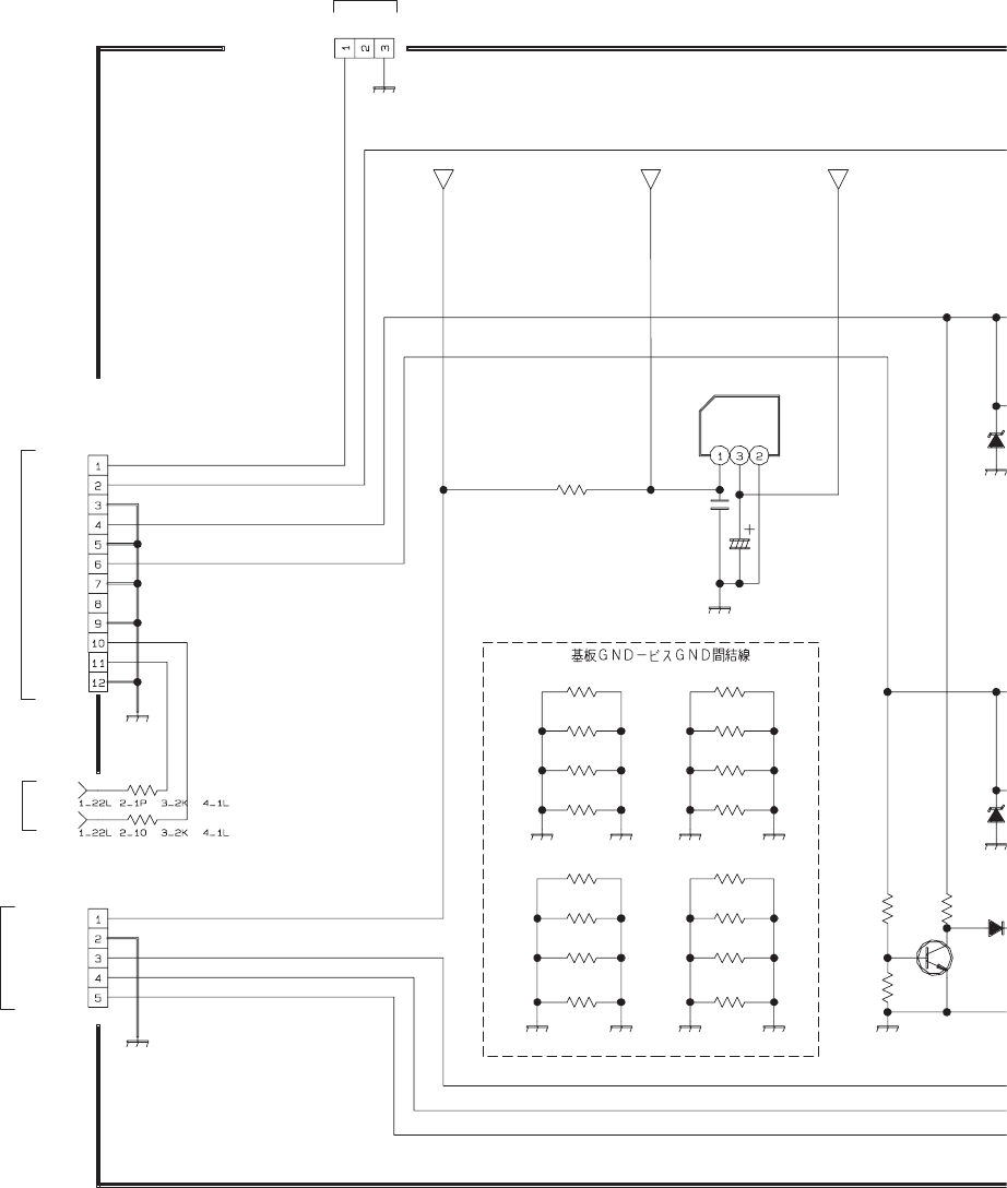
2-23(No.YA463)
IC902
C904
CN1T2
R901 R903
R902
Y905
CN1A2
Q903
Y902
Y903
Y904
D9
C905
CN1A3
R917
Y605
Y609
SCL3A5
SDA3A5
R913
R914
Y601
Y606
Y610
Y602
Y607
Y611
Y603
Y608
Y612
Y604
MM1663DT-X
NCB11AK-106X
QGA2001C6-03X
GND
MAIN_POW
AC_IN
POW_GOOD
STB5V
QGA2001C6-05X
/16
NEHM1CM-476X
GND
GND
GND
GND
GND
12V
9V
5V
NC
SDA3A5
SCL3A5
32V
QGA2001C6-12X
NRSA02J-0R0X
32V
NC
GND
OPEN OPEN
OPEN0
OPEN
0
0
0
O
P
47
0
0
0
OPEN
OPEN
0
0
0
0
0
0
0
0
0
0
GND
STB_5V
GND
GND
STB3.3V
GND_S4
GND_S3
GND_S2
GND_S1
ILA5V
GND
G
N
GND
GND
GND
GND G
N
GND
SHEET3,5,7
POWER PWB
ASS'Y(3/3)
CN9A3
(SHEET35)
TUNER PWB ASS'Y(1/2)
CN0T2 (SHEET1)
POWER PWB
ASS'Y(1/3)
CN9A2
(SHEET33)
A
NALOG PWB CIRCUIT DIAGRAM (6/6) [POWER BLOCK] SHEET 8
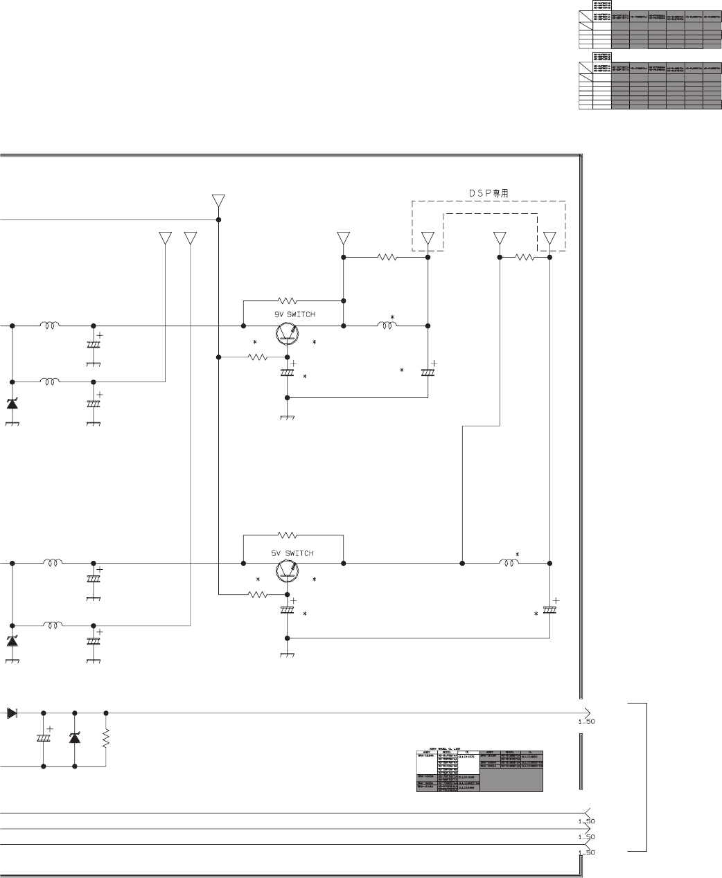
(No.YA463)2-24
ANALOG PWB ASS'Y(6/6)
SRA-1024A-M2
c10508005_0911_5/6_0.0
C919
L902
L905
AC_IN
C911
R904
9
03
R911
D905
D902 C901
LB_PRO5
L906
C920
R912
POW_GOOD
MAIN_POW
C913
L901
Q902
C915
C916
L904
L903
C914 R908
D903
D904
Q901
C912
R907
C919
C920
L905
L906
Q901
Q902
R907
R908
C912
C915
R909
R910
NQL52EM-220X
NEX51CM-335X
OLLC10863
OLLC10863
NEX51CM-335X
NQL52EM-220X
NEX50JM-156X
NQL52EM-220X
NQL52EM-220X
NEX50JM-156X
PTZ11B-X
PTZ6.8B-X
OLLC10863
-02
OLLC10863
-02
OLLC11379
2SC5881
/QR/-X
NRS12BJ
-471W
OLLC10863
-03
OLLC10863
-03
OLLC11379 OLLC10494
2SC5881
/QR/-X
NRS12BJ
-471W
NEX51CM
-335X
OLLC10494
NEX50JM
-156X
NQL52EM
-220X
NQL52EM
-220X
OLLC11043
2SC5881
/QR/-X
NRS12BJ
-471W
OLLC11043
2SC5881
/QR/-X
NRS12BJ
-471W
NEX51CM
-335X
NEX50JM
-156X
NQL52EM
-220X
NQL52EM
-220X
OLLC10863
-04
OLLC11379
-04
OPEN
OPEN
P
EN
OPEN
OPEN
OPEN
OPEN
OPEN OPEN
OPEN
OPEN
OPEN
OPEN
OPEN
OPEN
OPEN
OPEN
OPEN
OPEN
OPEN
OPEN
OPEN
OPEN
OPEN
OPEN
OPEN
OPEN
OPEN
OPEN
OPEN
OPEN
OPEN
OPEN
OPEN
OPEN
OPEN
OPEN
OPEN
OPEN
OPEN
OPEN
OPENOPEN
OPEN
OPEN
OPEN
OPEN
47/16
47/16
47/16
47/16
0
0
OPEN
OPEN
OPEN
OPEN
OPEN
OPEN
OPEN
OPEN
OPEN
OPEN
GND
GND
5V9V
12V
GND
BS_A9V VCC9
GND
VCC5
GND
BS_A5V
GND
GNDGND
SHEET3
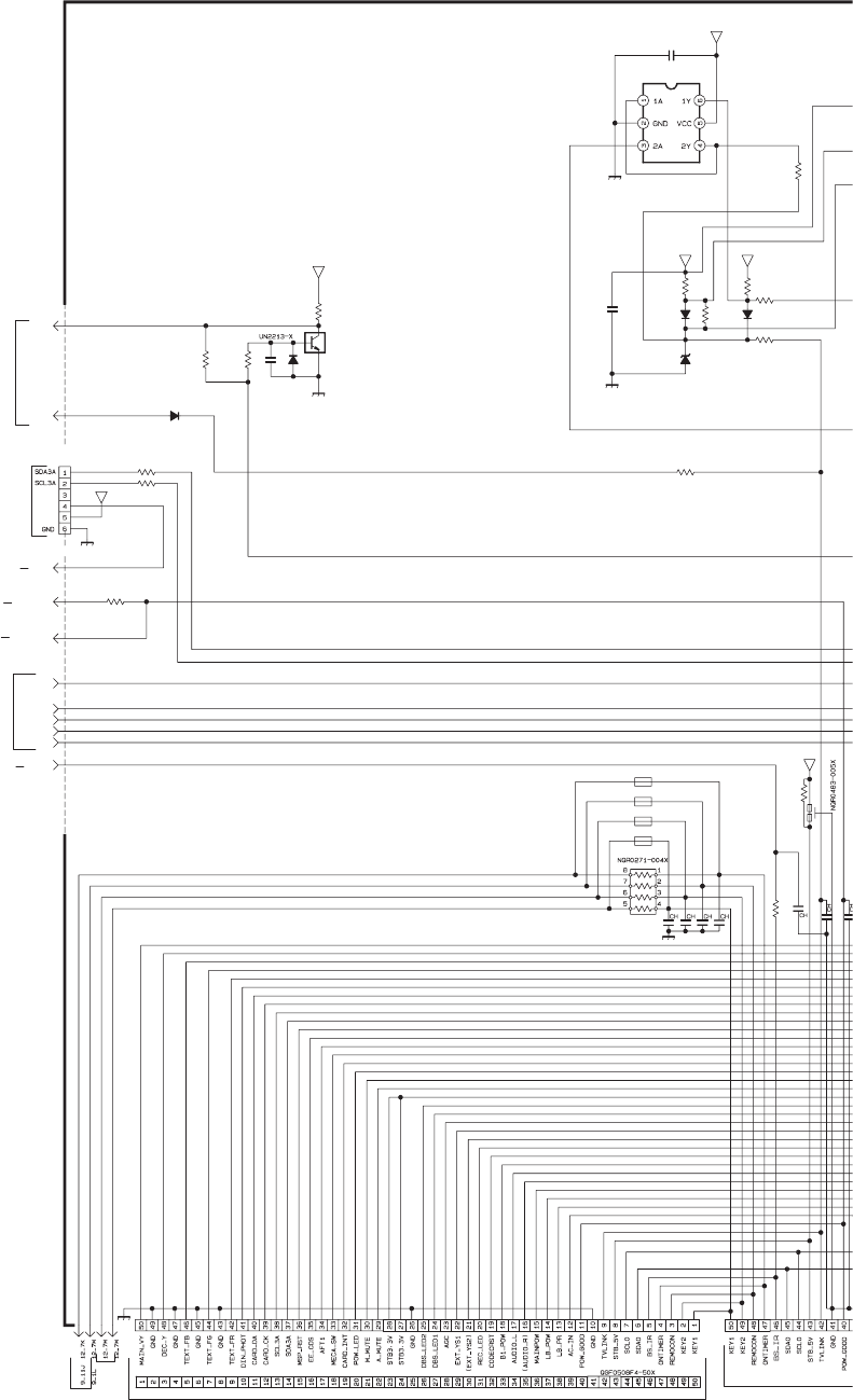
2-25(No.YA463)
DIGITAL PWB ASS'Y(1/15)
SRA0D161A-M2 [HD-52FA97]
SRA0D160A-M2 [HD-56FB97]
SRA0D159A-M2 [HD-61FB97]
R7545
C7502
CN7501
B1_POW
REC_LED
R7504
R7505
D7502C7501
Q7501
Q7
5
IC7502
C7513
R7501
R7502
CODECRST
AUDIO_L
AUDIO_R
R7526
D7509
D7508
R7532
R7530
R7529
TEST0
R7512
CN011
R7533
R7511
RA7503
BS_IR
POW_GOOD
D7501
ACINPOW
TVLINK
R7544
K7506
K7505
K7503
K7502
D7514
POW_GOOD2
R7534
C7511
LC7505
C7505
C7504
R7521
C7514
C7515
C7516
C7517
KEY_1
KEY_2
REMOCON
DIMMER
OPEN
OPEN
100k
10k
*40.1/16
OP
E
OPEN
OPEN
OPEN
OPEN
OPEN
OPEN
OPEN
OPEN
OPEN
OPEN
0
OPEN
OPEN
OPEN
OPEN
OPEN
OPEN
OPEN
OPEN
OPEN
OPEN
OPEN
100
p
10p
OPEN
10p
10p
10p
10p
GND
STB3.3V
VCC3D
STB_5V
STB_5V
STB3.3V
STB3.3V
GND
TEST0
GND
GND
GND
GND
SDA3A_2
SCL3A_2
BS_IR_1
SHEET22
SHEET13
SHEET16,17,19,23
SHEET20,21
SHEET17
SHEET19
SHEET17,20
SHEET20
ANALOG PWB ASS'Y(1/6)
CN011 (SHEET3)
OPEN
DIGITAL PWB CIRCUIT DIAGRAM (1/15) SHEET 9
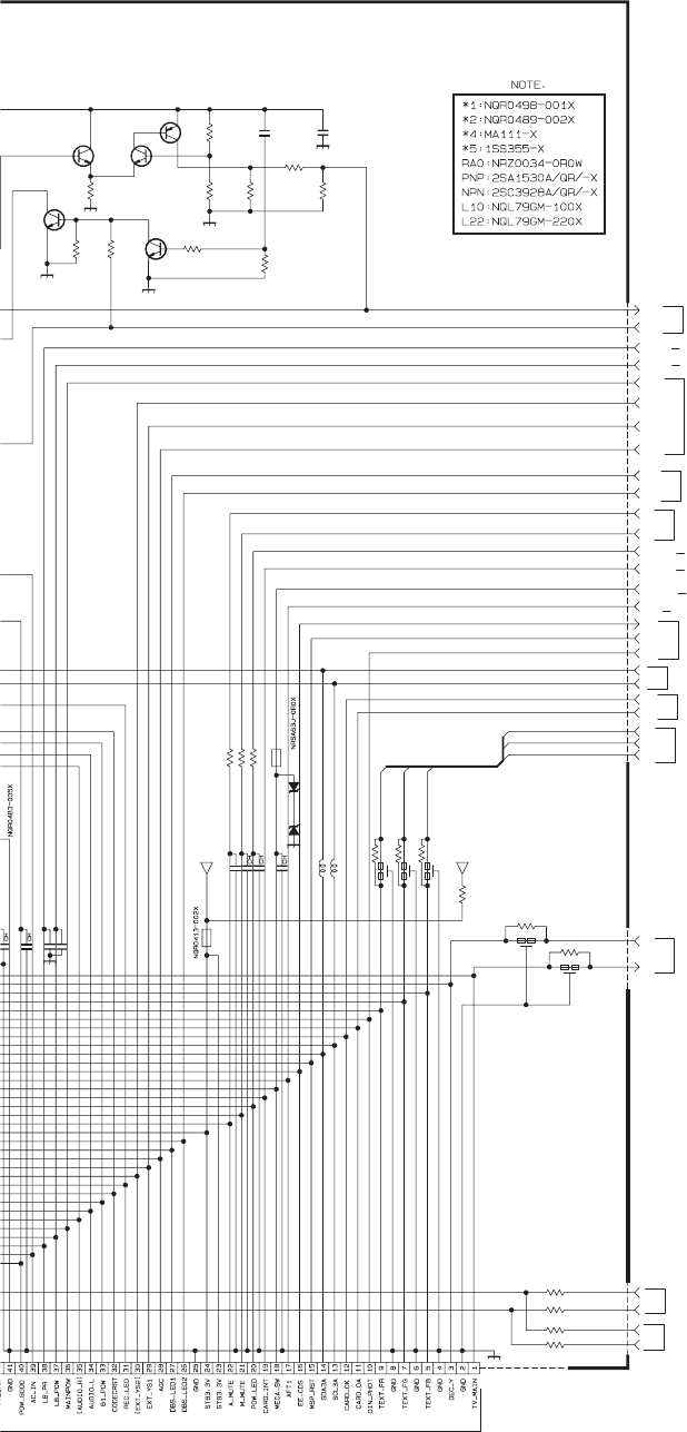
(No.YA463)2-26
c10502011_0808_11/16_0.0
SDA3A
SCL3A
POW_LED
CN001
M_MUTE
A_MUTE
MECA_SW
AFT1
Q7511
MSP_RST
DINPHOT
AGC
EXT_YS1
EXT_YS2
MAIN_POW
LB_POW
EE_CDS1
LB_PRO
TEXT_FR
TEXT_FG
TEXT_FB
Q7514
Q7513
Q7515
CARD_INT
TVLINKOUT
Q7512
DBS_LED1
DBS_LED2
CARD_CK
CARD_DA
DEC_Y
N
TVLINKIN
R7546
R7552
R7553
R7547
LC8801
LC8802
R8886
R8885
SCLM
SDAM
R7548 R7550
R7539
R7551
R7541
R7540
R7542
R7543
SCL1
SDA1
R7555R7554
R7549
C7520 C7521
K7501
C7508
LC7509
LC7508
LC7507
LC7505
C7507
C7506
C7505
C7504
R7523
R7524
R7525
C7510
L7501
L7502
C7518
K7504
C7519
D7513D7512
R7515
R7514
R7513
OPEN
OPEN
OPEN
OPEN
OPEN
OPEN
OPEN
OPEN
OPEN
OPEN
OPEN
OPEN
OPEN
OPEN
OPEN OPEN
OPEN
OPEN
OPEN
OPEN
OPEN
OPEN
OPENOPEN
OPEN
OPEN OPEN
10p
OPEN
OPEN
OPEN
10p
0.01/16
100p
10p
OPEN
OPEN
OPEN
10p
0
0
OPEN
OPEN
OPENOPEN
1k
0
0
TEXT_FR
GND
GND
GND
STB3.3V
GND
STB3.3VA
TV_MAIN
TEXT_FG
TEXT_FB
GND
GND
EXT_YS1
EXT_YS2
AGC
MECA_SW
SDA3A_1
SCL3A_1
A_MUTE
M_MUTE
GND
GND
POW_LED
TEXT_FR
TEXT_FG
TEXT_FB
SHEET23
SHEET17,21
SHEET17
SHEET17,22
SHEET17
SHEET17,20
SHEET12,17,21
SHEET17
SHEET17,22,23
SHEET17
SHEET17
SHEET23
SHEET10
SHEET11,22,23
SHEET22
SHEET10,11,17,18,20
DIGITAL INPUT BLOCK
SHEET13,20,22,23
OPEN
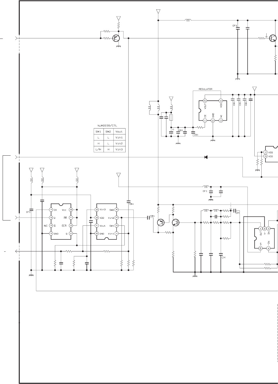
2-27(No.YA463)
DIGITAL PWB ASS'Y(2/15)
SRA0D161A-M2 [HD-52FA97]
SRA0D160A-M2 [HD-56FB97]
SRA0D159A-M2 [HD-61FB97]
C8810
Q8836Q8835
IC8832
R8822
R8801R8802
R8831
C8807
R8803
R88
1
GR_ON
C8809
L8802
L8831
C8866
R8825
IC8801
R8823
D8801
C8865
C8808
C8880
C8831
R8808
GR_RST
R8866
L8847
R8868
R8869
R8824
R8865
R8867 C8867
DEC_Y
L8849
C8868
Q
L8848
R8834
R8832
R8878
C8832
L8801
IC8802
C8811R8884
R8864R8863
R8870
R
C
IC880
3
C8802
IC8841
K8801
R8887
C8873 C8874
C8875
R8889
R8888
L8803
R8890
C8883
R8894
R8893
R8895
Q8837
L8804
L8846
C8871
C8870
C8869
C8879
C8877
C8878
C8876
C9623
C9622
L8866
OPEN
OPENOPEN
OPEN
OPEN
OPENOPEN
OPEN
OPEN
OPEN
OP
E
OPEN
OPEN
OPEN
OPEN
OPEN
OPEN
OPEN
OPEN
OPEN
OPEN
OPEN
OPEN
OPEN
OPEN
OPEN
OPEN
OPEN
OPEN
OPEN
OPEN OPEN
OPEN
OPEN
O
OPEN
OPEN
OPEN
OPEN
OPEN
OPEN
OPEN
OPEN
OPEN
OPENOPEN
OPEN
O
O
OPEN
OPEN
OPEN
OPEN
OPEN
OPEN OPEN
BS_5V
OPEN
OPEN
OPEN
OPEN
OPEN
OPEN
OPEN
OPEN OPEN
OPEN
OPEN
OPEN
OPEN
OPEN
OPEN
OPEN
OPEN
OPEN
OPEN
OPEN
OPEN
OPEN
BS_5VBS_9V
GROUT_6
GROUT_7
GND
BS_5V
GND
GR_3V
GR_3V
TV_MAIN
BS_9V
GND
GND
GND
GND
TV_MAIN_1
GND
BS_9V
GND GROUT_2
GROUT
GROUT_4
GROUT_5
GROUT_1
TV_MAIN_2
TV_MAIN1
GROUT2_1
GROUT_3
SHEET9
SHEET17
SHEET9
DIGITAL PWB CIRCUIT DIAGRAM (2/15) SHEET 10
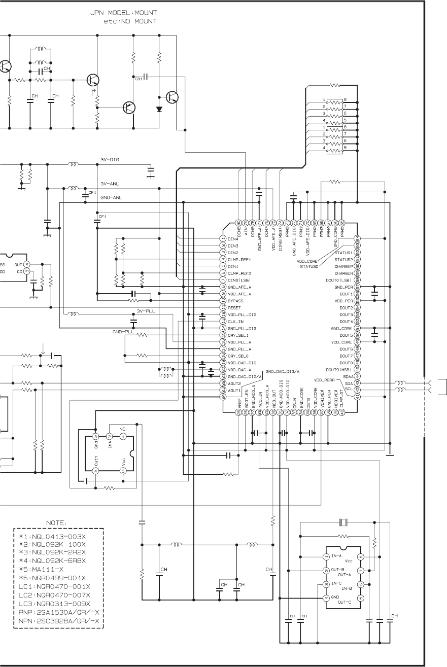
(No.YA463)2-28
c10502015_0808_15/16_0.0
C8836
R8860
R8837
L8845L8844
R8813 R8814
C8838
IC8831
C8860
C8859
C8857
C8837
R8859
R8874
R8875
C8839
SCL3A
SDA3A
R8876
C8856
L8843
R8877
C8806
L8842
R8848
RA8831
R8858
R8840
R8845R8844
Q8833
RA8832
L8834
L8837
X8831
C8862
R8883
R8847
R8861
R8846
Q8831
3
4
C8864
R8853
R8851
C8844
IC8834
C8845
C8858
R8854
C8840
L8841
C8847
C8846
C8872
C8853
R8852
R8871
R8873
Q8832
C8849
C8848
R8872
C8842
C8843
R8849
C8841
R8841
D8831
Q8834
IC8833
C8861
C8863
C8855
R8839
R8850
R8838
R8835
C8834
IC8803
L8832
R8836
C8833
C8835
L8833
C8882
C8881
L8852
L8861
C8850
C8851
C8852
R8892
R8891
OPEN
OPEN
OPEN
OPENOPEN
OPEN OPEN
OPEN
OPEN
OPEN
OPEN
OPEN
OPEN
OPEN
OPEN
OPEN
OPEN
OPEN
OPEN
OPEN
OPEN
OPEN
OPEN
OPEN
OPEN
OPEN
OPEN
OPENOPEN
OPEN OPEN
OPEN
OPEN
OPEN
OPEN
OPEN
OPEN
OPEN
OPEN
OPEN
E
N
OPEN
OPEN
OPEN
OPEN
OPEN
OPEN
OPEN
OPEN
OPEN
OPEN
OPEN
OPEN
OPEN
OPEN
OPEN
OPEN
OPEN
OPEN
OPEN
OPEN
OPEN
OPEN
OPEN
OPEN
OPEN
OPEN
OPEN
OPEN
OPEN
OPEN
OPEN
OPEN
OPEN
OPEN
OPEN
OPEN
OPEN
OPEN
OPEN
OPEN
OPEN
OPEN
OPEN
OPEN
OPEN
OPEN
OPEN
OPEN
OPEN
OPEN
OPEN
OPEN
OPEN
GND
SDA3A_GR
SCL3A_GR
AD8
GND
GND
AD4
AD3
GND
AD2
AD1
AD0
AD2
AD3
AD4
AD1
AD0
AD5
AD6
AD7
3M58_CLK4
_
1
TV_MAIN_4
TV_MAIN_6
3M58_CLK1
GROUT1
GROUT2
20M_NCO3
GND
GROUT2_2
TV_MAIN_5
20M_CLK1
AD8
AD7
AD6
AD5
TV_MAIN_2
TV_MAIN_3
TV_MAIN_7
TV_MAIN_8
GROUT1_1
GROUT2_1
20M_NCO4
3M58_CLK3
20M_NCO1
3M58_CLK2
20M_CLK2
20M_NCO2
SHEET9,11,17,18,20
DIGITAL INPUT BLOCK
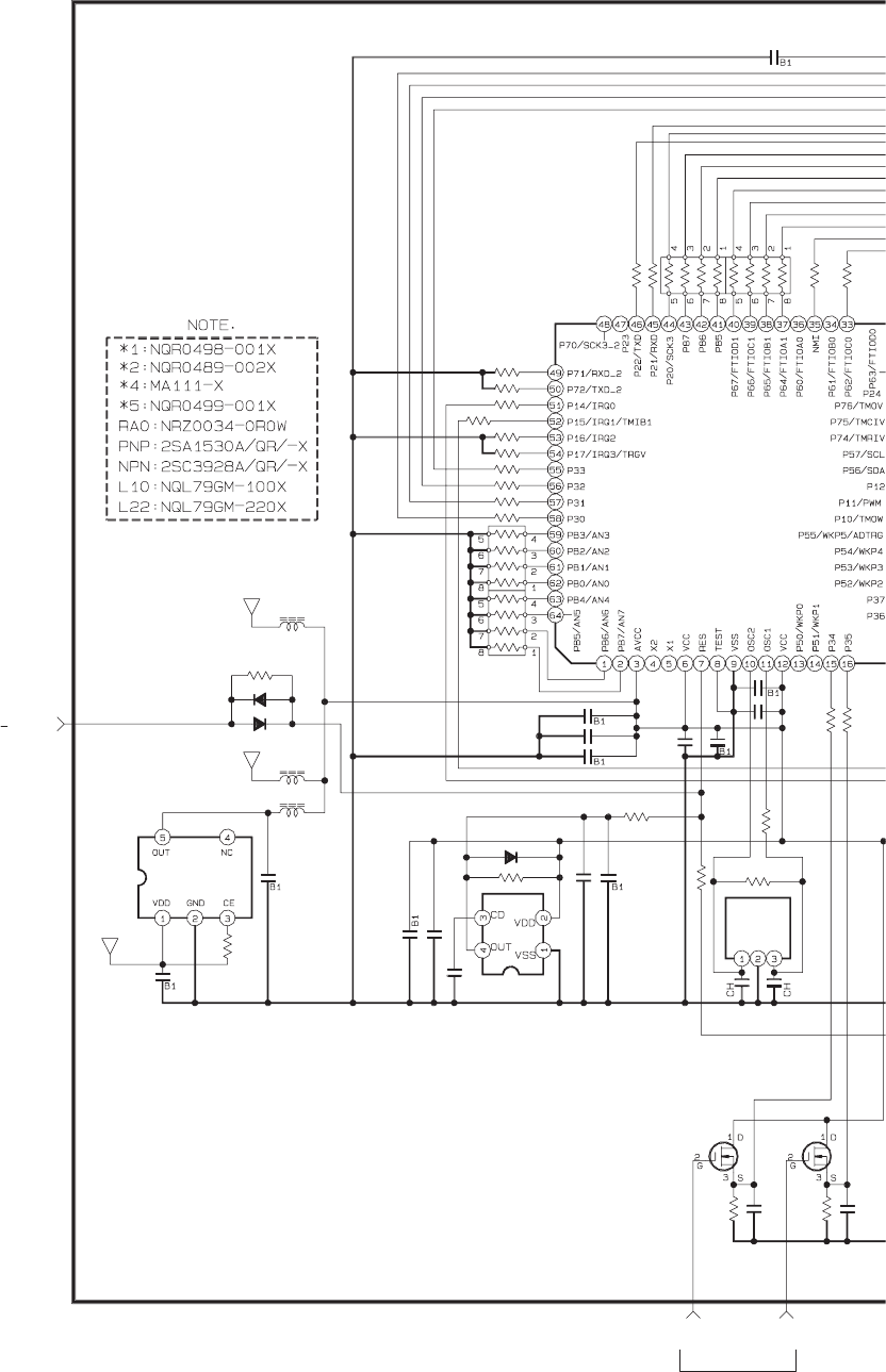
2-29(No.YA463)
DIGITAL PWB ASS'Y(3/15)
SRA0D161A-M2 [HD-52FA97]
SRA0D160A-M2 [HD-56FB97]
SRA0D159A-M2 [HD-61FB97]
C8605
IC8602
R8614
R8615
R8618
R8620
RA8601
R8621
R8622
R8623
RA8602
C8610
C8630
C8604
RA8604
D8604
R8616
R8619
IC8601
R8617
L8603
C8613
R8647
R8625
D8601
C8611 C8612
C8603
D8603
R8624
C8608
C8609
R8630
R8631
L8601
L8602
C8627
C8628
R8648
MI_RESET
Q8603Q8602
C8607
C8629
RA8603
R8628
R8645
X8601
IC8604
C8602
C8601
C8606
R8629
R8626
R8627
HDMI_5V1
HDMI_5V2
R8650
R8651
R8652
R8653
C8631
C8632
OPEN
OPEN
OPEN
OPEN
OPEN
OPEN
OPEN
OPEN
OPEN
OPEN
OPEN
OPEN
OPEN
OPEN
OPEN
OPEN
OPEN
OPEN
OPEN
OPEN
OPEN OPEN
OPEN
OPEN
OPEN
OPEN
OPEN
OPEN
OPEN
OPEN
OPEN
OPEN
OPEN
OPENOPEN
OPEN
OPEN
OPEN
OPEN
OPEN
OPEN
OPEN
OPEN
OPEN
OPEN
OPEN
OPEN
OPEN
OPEN
OPEN
OPEN
CEC_LINE8
STB_5V
STB3.3V
STB3.3MI
SHEET23
DIGITAL INPUT BLOCK
DIGITAL PWB CIRCUIT DIAGRAM (3/15) SHEET 11
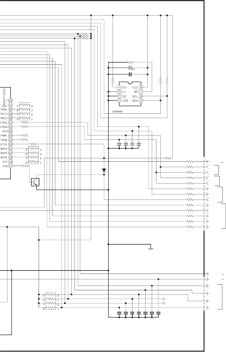
(No.YA463)2-30
c10502014_0808_14/16_0.0
R8601
R8602
R8603
R8604
R8605
R8612
R8609
R8606
R8607
R8608
R8610
R8611
R8613
IC8603
R8639
R8638
RA8605
C8615
D8602
R8636
R8632
RA8607
R8633
TP_C3
Q8601
TP_C2
R8634
R8635
R8637
C8614
R8641
C8620
C8621
C8622
C8623
C8624
C8625
RA8606
R8643
R8642
R8640
C8626
C8616
C8617
R8644
C8618
C8619
R8649
C8632
OPEN
OPEN
OPEN
OPEN
OPEN
OPEN
OPEN
OPEN
OPEN
OPEN
OPEN
OPEN
OPEN
OPEN
OPEN
OPEN
OPEN
OPEN
OPEN
OPEN
OPEN
OPEN
OPEN
OPEN
OPEN
OPEN
OPEN
OPEN
OPEN
OPEN
OPEN
OPEN
OPEN
OPEN
OPEN
OPEN
OPEN
OPEN
OPEN
OPEN
CEC_INT
SCLM
SDAM
SCL3A
SDA3A
SCLHDMI
SDAHDMI
CECIN
DIN_RST
DIN_INT
DIN_HOTP
DINHOTP2
DIN_RWSW
CEC_LINE3
GND
CEC_RST
CEC_NMI
CEC_P85
CEC_LINE5
CEC_LINE4
CEC_TX
CEC_RX
CEC_CLK
CEC_LINE7
CEC_LINE6
SHEET22,23
SHEET9,22,23
SHEET9,10,17,18,20
DIGITAL INPUT BLOCK
DIGITAL INPUT BLOCK
SHEET17,
DIGITAL INPUT BLOCK
SHEET23
SHEET23
SHEET22,23
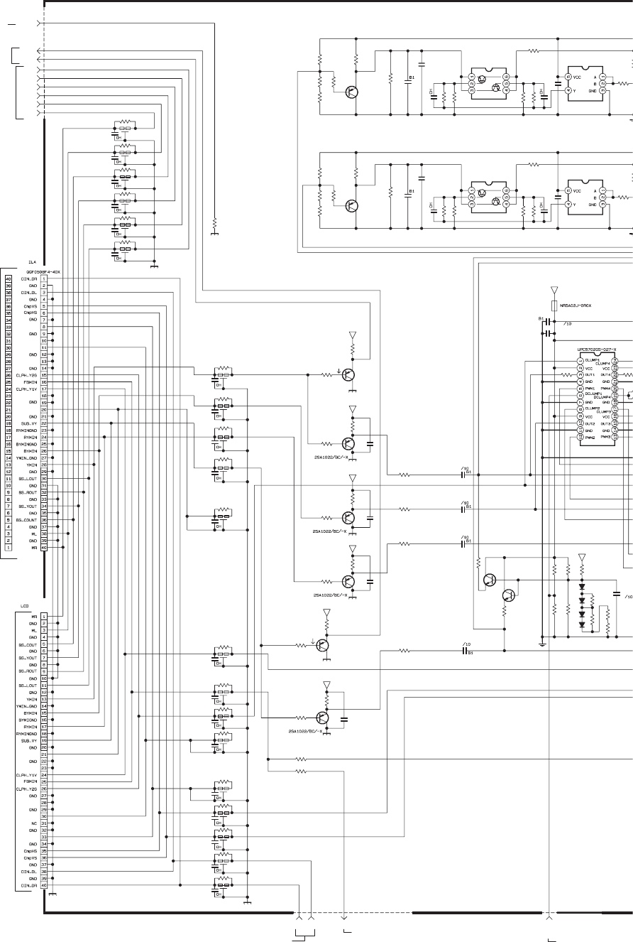
2-31(No.YA463)
R8796
C6250
C6254
C6253
C6252
R6339
Q6201
Q6202
R6280
R6282
R6281
CN012
CN002
R8797
R
R6283
R6338
IC6301
LC6201C6201
R6201
LC6202C6202
R6202
LC6203C6203
R6203
LC6204C6204
R6204
R6206
LC6206C6206
R6318
MAIN_CCD
R6207
LC6207C6207
R6208
LC6208C6208
R6213
R6210
LC6210C6210
LC6209C6209
R6209
LC6212C6212
C6255
K6250
C6251
R6217
R6317
LC6216C6216
LC6215C6215
R6216
IC6250
R6215
LC6214C6214
LC6213C6213
R6214
C6302
MR
ML
BS_COUT
BS_YOUT
BS_ROUT
BS_LOUT
R6223
LC6223C6223
R6224
LC6224C6224
R6225
LC6225C6225
R6226
R
LC6226
C6226
R6221
LC6221C6221
R6222
LC6222C6222
SUB_CCD1
R8798
R8799
R8781
IC6302
Q6301
R6307
R6331
C6307
Q6303
R6320
R6321
R6324
R6323
R6319 C6308
Q6304
R6327
R6330
R6309
R6322
R6308
R6311
R6310
R6306 C6303
Q6302
R6314
R6333R6332
D6301
Q6250
Q6251
C6249
Q6203
Q6204
Q6205
Q6206
R6244
R6211
R6241
R6212
R6238
R6235
R6236
R6239
R6242
R6245
C6239
C6238
C6237
C6236
C6306
ClampSW
R6315
R6313
R6250
R6251
R6341
D6303D6304
R6340
C6311
R6316
R6328
R6326
R6329
R6325
C6310
C6309
R6312
C6305
C6304
R6336
R6337R6335
D6302 R6248
R6249
FBin
0
10
10
10
10
0
PNP
PNP
330
330
100
OPEN
0
100
0
OPEN
OPENOPEN
0
OPENOPEN
0
OPENOPEN
0
OPENOPEN
0
OPEN
OPENOPEN
OPEN
0
OPENOPEN
OPEN
OPENOPEN
OPEN
OPEN
OPEN
OPEN
OPENOPEN
0
OPENOPEN
10
0.1/16
0
OPE
N
OPEN
OPEN
OPENOPEN
0
0
OPENOPEN
OPENOPEN
0
OPEN
0
OPENOPEN
0
OPENOPEN
0
OPENOPEN
0
O
OPENOPEN
OPEN
OPENOPEN
OPEN
OPENOPEN
0
0
OPEN
OPEN
OPEN
OPEN
OPEN
OPEN
OPEN
OPEN
OPEN
OPEN
OPEN
OPEN OPEN
OPEN
OPEN
OPE
N
OPEN
OPEN
OPEN
OPEN
OPEN
OPEN OPEN
OPEN
OPEN
0
0
OPEN
NPN
NPN
1
100
OPEN
100
OPEN
100
100
330
330
330
330
0.1/16
0.1/16
0.1/16
0.1/16
OPEN
OPEN
OPEN
OPEN
0
OPEN
OPEN
OPEN
OPEN
OPEN
OPEN
OPEN
OPEN
OPEN
OPEN
OPEN
OPEN
OPENOPEN
OPEN 47k
33k
BS_5V
BS_ROUT_1
YMIN_4
BYMIN_4
BS_5V
SUB_VY_4
RYMIN_4
BS_5V
MR_1
BS_YOUT_1
GND
GND
BS_LOUT_1
ML_1
BS_COUT_1
YMIN
GND
EXT3DON
BYMIN
GND
BS_5V
SUB_VY_5
RYMIN
SUB_VY_2
YMIN_2
GND
SUB_VY
GND
G
GND
RYMIN_5
YMIN_5
YMIN_1
BYMIN_1
RYMIN_1
BS_5V
BYMIN_5
GND
GND
GND
GND
BS_5V
BS_5V
ADA3V
G
DIN_DL_1
DIN_DR_1
DIN_DR
DIN_DL
SHEET17
SHEET22
SHEET19
DIGITAL
INPUT
BLOCK
SHEET23 SHEET17
ANALOG PWB
ASS'Y(1/6)
CN012
(SHEET3)
OPEN
DIGITAL PWB CIRCUIT DIAGRAM (4/15) SHEET 12
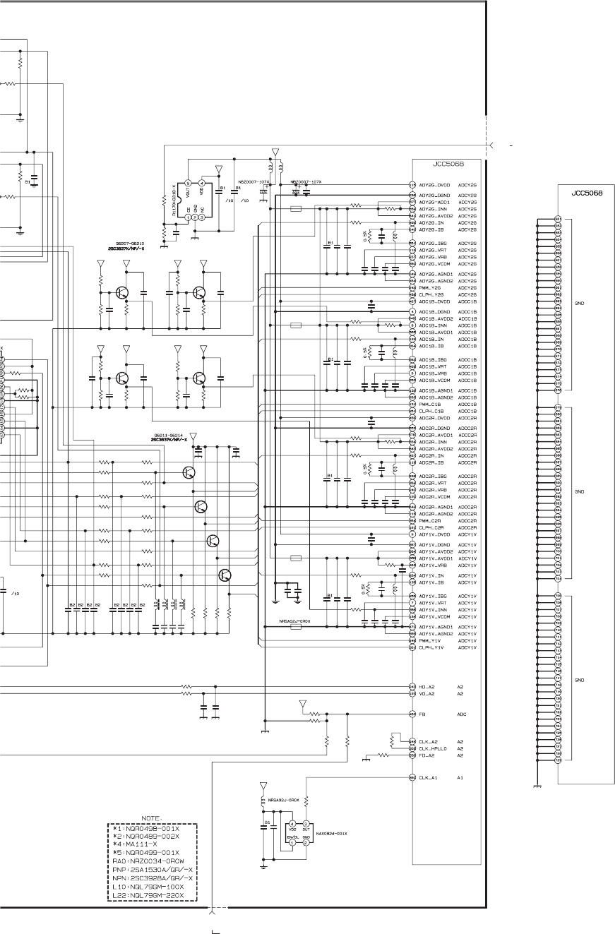
(No.YA463)2-32
DIGITAL PWB ASS'Y(4/15)
SRA0D161A-M2 [HD-52FA97]
SRA0D160A-M2 [HD-56FB97]
SRA0D159A-M2 [HD-61FB97]
c10502001_0808_1/16_0.0
C6295
R6275
R6274
L6266
R6276
C6292
X6250
L6254
C6296 C6297
L6265
C6294
R6279
Q6211
R6318
Q6212
Q6213
Q6214
R6266
R6262
R6258
R6254
R6272
R6273
R6259
R6252
R6264
R6260
R6256
R6253
R6265
R6261
R6257
R6255
R6267
R6263
R6317
C6274
C6275
C6279
C6280
C6281
C6285
C6286
C6289
C6290
C6291
C6268
C6269
C6273
R6292
R6291
C6298
K6268
R6278
K6274
K6272
K6271
R6293
R6290
R6301
R6300
R6303
R6302
IC6001
R6304
C6301
R6305
R6331
R6330
R6333
R6284
R6285
C6235 C6234
C6217 C6218
R6230
R6231
C6230
C6231
R6233
R6232
C6232
C6233
C6249
R6218 R6219
L6257
L6258
L6259
IC6001
C6293
C6247
C6242
C9625
R6286
R6287
L6250
L6251
L6252
L6253
C6264
C6265
C6266
C6267
C6257
C6261
C6258
C6259
C6256
C6262
C6263
C6260
R6288
C6282 C6276
R6269
C6277
C6278
R6270
C6283
C6284
C6288
R6271
C6287
C6270
R6268
C6271
C6272
R6289
C6246
C6241C6245
C6248
C6243
C6244
IC6251
C9626
Q6208
R6234
R6229
R6228
C6205
C6220
C6240
Q6207
R6227
R6220 R6205
C6211
C6219
Q6210
R6277
R6247
C6312
R6337R6335
L6260
R6246
C6299
C6300
Q6209
R6243
R6240
R6237
C6228
C6227
C6229
0
22
*5
0
OPEN
10 10
*5
0
OPEN
220
150
150
150
OPEN
0
4.7k
0
0
0
0
2.2k
10k
2.2k
2.2k
4.7k
4.7k
4.7k
OPEN
0.1/16
OPEN
0.1/16
0.1/16
OPEN
0.1/16
0.1/16
0.1/16
OPEN
0.1/16
0.1/16
OPEN
0.1/16
47k
47K
OPEN
OPEN
*5
*5
*5
OPEN
0
OPEN
0
OPEN
0
OPEN
0.1/16
0
OPEN
OPEN
0
0
0
OPEN OPEN
0.1/16 0.1/16
0
0
OPEN
OPEN
0
0
OPEN
OPEN
1
OPEN OPEN
OPEN
OPEN
OPEN
0.1/16
10/10
1/10
OPEN
390
390
OPEN
OPEN
OPEN
OPEN
OPEN
OPEN
OPEN
OPEN
OPEN
2.2/10
OPEN
OPEN
OPEN
2.2/10
2.2/10
2.2/10
390
0.1/16 0.1/16
2.4k
0.1/16
0.1/16
2.4k
0.1/16
0.1/16
0.1/16
2.4k
OPEN
0.1/16
2.4k
0.1/16
0.1/16
1K
1/10
10/1010/10
1/10
10/10
1/10
OPEN
390
6.8k
3.3k
0.1/16
0.1/16
0.1/16
390
6.8k 3.3k
0.1/16
0.1/16
390
6.8k
OPEN
OPENOPEN
OPEN
3.3k
0.1/16
0.1/16
1k
6.8k
3.3k
0.1/16
0.1/16
0.1/16
ADC2R_IN
BS_5V
ADY1V_IN
ADY2G_IN
ADC1B_IN
SUB_VY_6
YMIN_6
RYMIN_6
BYMIN_6
GND
LB_POW
BS_5V
GND
PWM_C1B
GND
PWM_Y1V
ADA3V
GND
CLPH_Y1V
PWM_Y1V
VCC3D
GND
CLPH_C2R
27M_CLK_A1
27M_CLK_A1_0
VCC3D
ADY2G_IN
GND
PWM_C2R
GND
CLPH_C1B
PWM_C1B
CLPH_Y2G
PWM_Y2G
GND GND
ADC1B_IN
ADY1V_IN
GND
ADC2R_IN
GND
PWM_Y2G
CLPH_Y2G
ADC2R_INN
CLPH_C1B
GND
PWM_C2R
CLPH_C2R
CLPH_Y1V
GND
ADY2G_INN
ADA3V BS_5V
GND
ADC1B_INN
BS_5VADA3V
BS_5V
ADA3V
GND
ADY1V_INN
BS_5VADA3V
GND
FBout
SHEET9,17,21
SHEET23
CHASSIS
MICOM
CHASSIS
MICOM
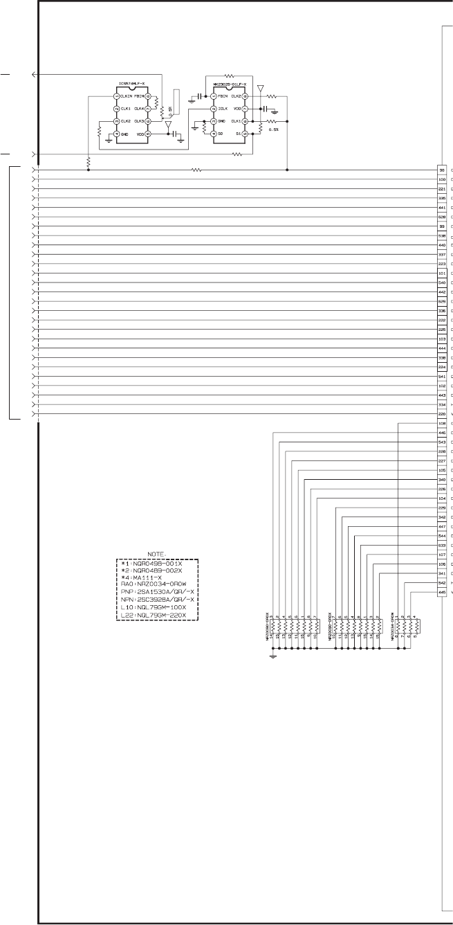
2-33(No.YA463)
DIGITAL PWB ASS'Y(5/15)
SRA0D161A-M2 [HD-52FA97]
SRA0D160A-M2 [HD-56FB97]
SRA0D159A-M2 [HD-61FB97]
IC6004
R6027
R6026
C6004
R6029
CLK_DV1
CLK_DV1R
R6028
C6003
R6033
1080P_ON
IC6003
C6005
R6036
R6035
R6037
R6031
R6032
RA6007
RA6008
RA6009
R6034
OPEN
0
0.1/16
OPEN
0
0.1/16
0
OPEN
OPEN
OPEN
33
0
47
0
DV2_Y6
DV2_Y7
DV2_RB1
DV2_RB2
DV2_RB3
DV2_RB4
DV2_RB5
DV2_RB6
DV2_RB7
DV2_Y0
DV2_Y1
DV2_Y2
DV2_Y3
DV2_Y4
DV2_Y5
CLK_DV1_2
DV1_B0
DV1_B1
DV1_B2
DV1_B3
DV1_B4
DV1_B5
GND
DV1_B6
DV1_R3
DV1_B7
DV1_R0
DV1_R1
DV1_R2
DV1_R4
DV1_R5
DV1_R6
DV1_R7
DV1_Y0
DV1_Y1
DV1_Y2
DV1_Y3
DV1_Y4
DV1_Y5
DV1_Y6
DV1_Y7
CLK_DV1_4
CLK_DV1_3
CLK_DV1_6
GND CLK_DV1_7
VCC3D
GND
GND
VCC3D
GND
CLK_DV1_8
GND
HD_DV1
VD_DV1
CLK_DV1R_5
SHEET21
SHEET19,
DIGITAL INPUT BLOCK
OPEN
DIGITAL PWB CIRCUIT DIAGRAM (5/15) SHEET 13
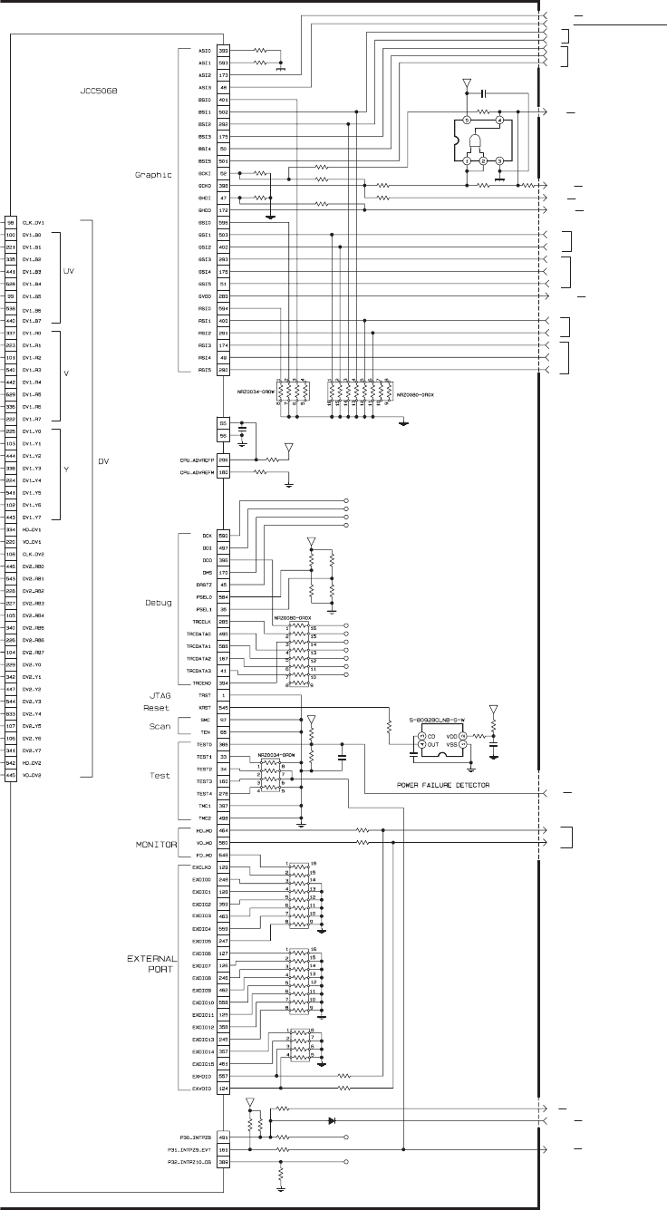
(No.YA463)2-34
c10502002_0808_2/16_0.0
RA6014
RA6013
JW
IC6001
MI_OSDYM
MI_OSDYS
OSDB1
OSDB2
OSDB3
OSDB4
OSDB5
DD_OSDHS
DD_OSDVS
OSDG1
OSDG2
OSDG3
OSDG4
OSDG5
OSDR1
OSDR2
OSDR3
OSDR4
OSDR5
R6005
R6006
TP-DCK
TP-DDI
TP-DDO
TP-DMS
TP-DRSTZ
R6001
R6075
TP-TRCK
TP-TRD0
TP-TRD1
TP-TRD2
TP-TRD3
TP-TREND
R6002
R6003 R6004
RA6010
D6001
MECA_SW
R6014
C6723
R6730
C6724
IC6724
R6732 R6731
VCC3D
TP-JW
1080P_ON
TP-DBINT
R6008
R6009
R6007
R6011
R6073
R6074
R6076
R6012
R6013
RA6001
RA6011
RA6002
R6017
R6018
R6019
R6020
C6001
R6022
R6021
TEXT_HD
TEXT_VD
R6023
RA6012
IC6002
SN74LVC1G08V-X
C6002
R6078
R6077
R6079
R6080
R6025
R6024
C7068
OPEN
OPEN
OPEN
0
OPEN
0
0
0 OPEN
OPEN
0
0.0022
0
0.01/16
00
0
22
OPEN
OPEN
0
0
OPEN
OPEN
OPEN
0
0
0
0
OPEN
OPEN
OPEN
OPEN
OPEN
0.1/16
OPEN
OPEN
OPEN
0
OPEN
OPEN
0.1/16
OSDCK
TEST0
VCC3D
STB3.3V
GND
GND
STB3.3V
GND
GND
GND
GND
VCC3D
GND
GND
GND
GND
VCC3D
GND
OSDCK1
DD_OSDCK
GND
GND
GND
SHEET22,23
SHEET22,23
SHEET23
SHEET22,23
SHEET22,23
SHEET23
SHEET14,22,23
SHEET14,22,23
SHEET9
SHEET23
SHEET23
SHEET18
SHEET18
SHEET18,22,23
SHEET22,23
SHEET23
OPEN
SHEET9,20,22,23
CHASSIS MICOM
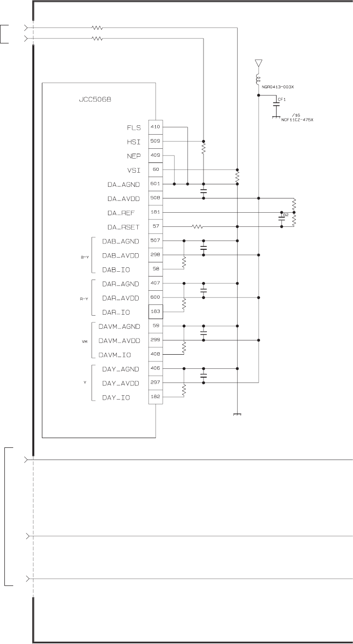
2-35(No.YA463)
IC6001
R6702
LV_VS
LV_HS
LV_AREA
R6703
R6704
R6705
R6706
R6707
R6712
R6713
R6701
C6705
C6708
C6709
C6710
C6711
C6707
L6701
DD_OSDHS
DD_OSDVS
R6714
R6715
C6701
OPEN
OPEN
OPEN
OPEN
OPEN
0
0
0
OPEN
OPEN
OPEN
OPEN
OPEN
OPEN
OPEN
OPEN
OPEN
4.7
VCC3D
GND
GND
SHEET13,22,23
SHEET18,20
CHASSIS MICOM
DIGITAL PWB CIRCUIT DIAGRAM (6/15) SHEET 14
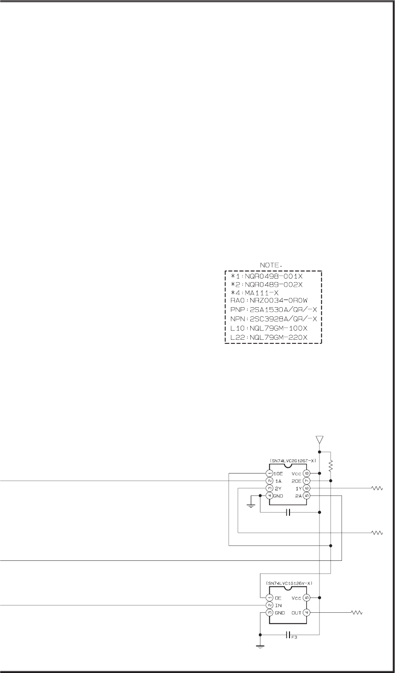
(No.YA463)2-36
DIGITAL PWB ASS'Y(6/15)
SRA0D161A-M2 [HD-52FA97]
SRA0D160A-M2 [HD-56FB97]
SRA0D159A-M2 [HD-61FB97]
c10502005_0808_5/16_0.0
R6726
IC6721
R6725
R6724
C6721
IC6722
C6722
R6727
OPEN
OPEN
OPEN
OPEN
OPEN
OPEN
OPEN
OPEN
VCC3D
GND
GND
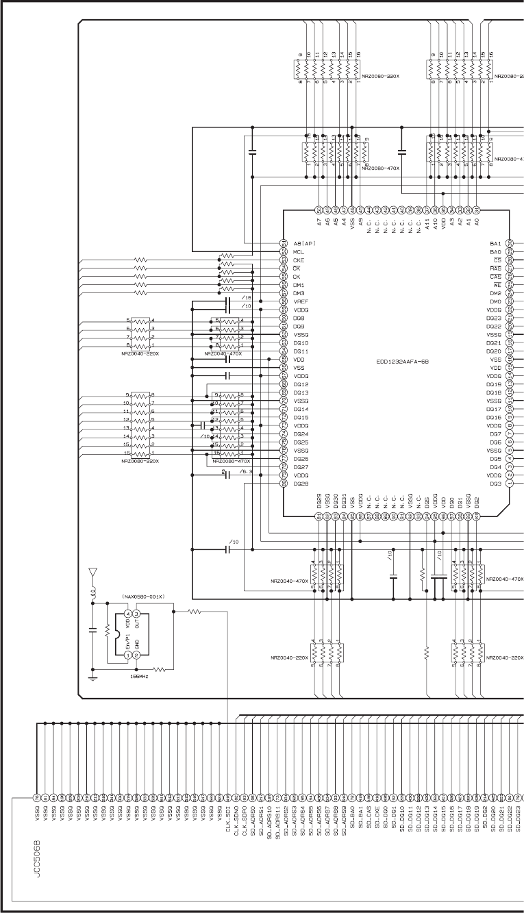
2-37(No.YA463)
RA6109
RA6107RA6108
RA6110
RA6111
RA6102
RA6101
RA6112
RA6103 RA6104
RA6115RA6116
R6128
R6121
C6110
C6114
IC6101
IC6103
C6113
C6115
C6116
C6112
C
C6111
R6129
L6104
C6118
C6117
R6110
R6120
R6119
R6118
R6117
R6109
R6108
R6107
R6106
C6121
C6120
R6130
C6136
C6119
R6111 R6122
IC6001
OPEN
47
OPEN
0.1/16
OPEN
0.47
OPEN
0.47
0.1
0.10.1/16
OPEN
OPEN
0.47
2.2
22
47
47
47
47
22
10
10
22
0.47
OPEN
OPEN
OPEN
0.47
22 47
SD_CKE
CLK_SDNO
CLK_SDPO
VCC3D
SD_DQ1_M
SD_DQ11_M
SD_DQM0_M
SD_DQ2_M
SD_DQ0_M
SD_DQ5
SD_DQ10_M
SD_DQ3_M
SD_DQ5_M
SD_DQ6
SD_DQM1_M
SD_DQ6_M
SD_DQ4_M
SD_DQ7_M
SD_DQ9_M
SD_DQ8_M
GND
CLK_SDPO_M
VT
T
SD_DQ7
SD_DQ4
CLK_SDNO_M
SD_DQ9
SD_DQ8
SD_CKE_M
SD_DQ10
SD_DQ11
SD_DQ2
SD_DQ1
SD_DQ3
SD_DQ0
SD_DQM0
SD_DQM1
SD_DQ17
SD_ADRS8
SD_ADRS11_M
SD_ADRS0
SD_ADRS1
SD_ADRS10
SD_DQ0
SD_ADRS2
SD_ADRS3
SD_ADRS6
SD_ADRS4
SD_ADRS5
SD_ADRS7
SD_ADRS8
SD_ADRS9
SD_DQ1
SD_DQ10
SD_DQ11
SD_GDQS
SD_CAS
SD_DQ12
SD_DQ13
SD_DQ14
SD_DQ15
SD_DQ16
SD_DQ17
SD_BA0
SD_BA1
SD_DQ18
SD_DQ19
SD_DQ2
SD_DQ20
SD_DQ21
SD_DQ22
SD DQ24
SD_DQ23
SD_BA1
SD_BA0
CLK_SDI
CLK_SDPO
CLK_SDNO
SD_CKE
SD_ADRS9_M
SD_ADRS4_M
SD_DQ12 SD_DQ12_M
SD_ADRS11
SD_DQ19_MSD_DQ19 SD_BA1_M
SD_BA0_M
SD_ADRS8_M
CLK_SDI_0
SD_ADRS11
SD_ADRS5_M
SD_ADRS6_M
SD_ADRS7_M
SD_ADRS0_M
SD_ADRS1_M
SD_ADRS2_M
SD_ADRS3_M
SD_ADRS10_M
SD_DQ17_M
SD_DQ18_MSD_DQ18
SD_GDQS_M
SD_DQ15_MSD_DQ15
SD_DQ14_MSD_DQ14
SD_DQ13_MSD_DQ13
SD_DQ16_MSD_DQ16 SD_ADRS0
SD_ADRS1
SD_ADRS2
SD_ADRS3
SD_ADRS10
SD_ADRS9
SD_ADRS4
SD_ADRS5
SD_ADRS6
SD_ADRS7
CHASSIS
MICOM
DDR-SDRAM
DIGITAL PWB CIRCUIT DIAGRAM (7/15) SHEET 15
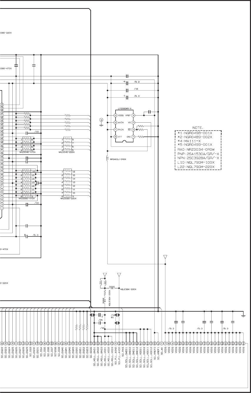
(No.YA463)2-38
DIGITAL PWB ASS'Y(7/15)
SRA0D161A-M2 [HD-52FA97]
SRA0D160A-M2 [HD-56FB97]
SRA0D159A-M2 [HD-61FB97]
c10502003_0808_3/16_0.0
RA6105
RA6106
07
RA6113
RA6114
15
C6126 C6129C6127 C6131C6128
R6127
L6105
IC6102
C6122
C6123
C6124
C6125
C6106
C6103
C6104
C6105
C6107
C6102
C6101
C6109
C6130
C6133
L6101
C6108
L6102
C6134
C6135
IC6102
C6132
R6112 R6101
R6113
R6114
R6115
R6116
R6102
R6103
R6104
R6105
R6143
R6142
R6141
C6139
L6115
R6123
R6124
R6125
R6126
L6103
C6138
2.2 O PENOPEN OPEN2.2
1.5
OPEN
100
0.1
100
0.1/16
OPEN
0.47
OPEN
OPEN
0.47
OPEN
2.2
0.1/16
2.2
0.15
OPEN
10
0.1/16
22
47 22
47
47
47
47
22
22
22
22
OPEN
0
0
0.1/16
*5
OPEN
OPEN
OPEN
OPEN
OPEN
SD_DQ30
SD_DQ31
VCC1.2D VCC_PLL5
SD_RAS
SD_CAS
VCC2.5D
SD_WE
GND
SD_DQ29
SD_DQ28
SD_DQ22_M
SD_DQ21_M
SD_DQ20_M
SD_DQ26_M
SD_DQ27_M
SD_DQ24_M
SD_DQ25_M
SD_DQ23_M
SD_DQ31_M
SD_DQ30_M
SD_DQ29_M
SD_DQ28_M
SD_DQM3_M
VTT0034
GND
SD_DQM2_M
SD_WE_M
SD_CAS_M
SD_RAS_M
SD_DQ27
SD_DQ26
SD_DQ25
SD_DQ24
SD_DQ20
SD_DQ23
SD_DQ22
SD_DQ21
SD_DQM3
SD_DQM2
SD_DQS0
SD_DQS1
SD_RAS
SD_DQS2
SD_DQS3
SD_DQM0
SD
_
DQ22
SD_DQ24
SD_DQ23
SD_DQ25
SD_DQ26
SD_DQ27
SD_WE
SD_DQ28
SD_DQ29
SD_DQ3
SD_DQ30
SD_DQ31
SD_DQ4
SD_DQ5
SD_DQ6
SD_DQ7
SD_DQ8
SD_DQ9
SD_DQM1
SD_DQM2
SD_DQM3
SD_GDQS
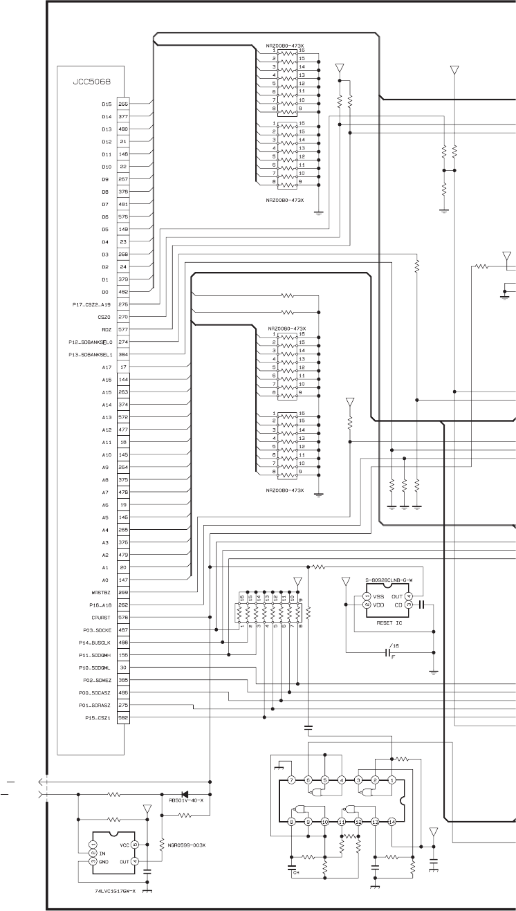
2-39(No.YA463)
CPURST
RA7204
RA7205
RA7202
RA7203
R7223
R7224
C7211
R7203
R7212
R7211
R7208
R7221
R7201 R7202
D7201
POW_GOOD
R7207
C7202
IC7204
RA7201
R7225
IC6001
C7212
R7229
R7234
R7233
R7232
IC7205
C7213
C7214
IC7206
C7216
R7240
R7239
R7238
R7242
R7241
C7217
R7243
R7215
R7216
R7217
R7235
R7237
R7236
47K
47K
47K
47K
47K
47K
1000p
47K
OPEN
0
0
0
47k 47K
100
0.1
OPEN
47K
OPEN
OPEN
OPEN
OPEN
OPEN
OPEN
OPEN
OPEN
0.1/16
10k
OPEN
OPEN
OPEN
OPEN
OPEN
47k
47k
47K
OPEN
OPEN
OPEN
STB3.3V
D15
D14
D13
D12
D11
D10
D9
D8
D7
D6
D5
D4
D3
D2
D1
D0
STB3.3V
GND
STB3.3V
GND
GND
A0
GND
A1
A2
A3
A4
A5
A6
A7
A8
A9
A10
A11
A12
A13
A14
A15
A16
GND
A17
D15
D14
D13
D12
D11
D10
D9
D8
D7
D6
D5
D4
D3
STB3.3V
D2
D1
D0
GND
STB3.3V
A0
A1
A17
A16
BUSCLK
GND
A2
GND
A15
A3
A14
A13
A12
A11
A10
A9
A8
A7
A6
A5
A4
GND
STB3.3V
GND
GND
STB3.3V
GND
STB3.3V
SHEET22,23
SHEET9,17,19,23
CHASSIS
MICOM
DIGITAL PWB CIRCUIT DIAGRAM (8/15) SHEET 16
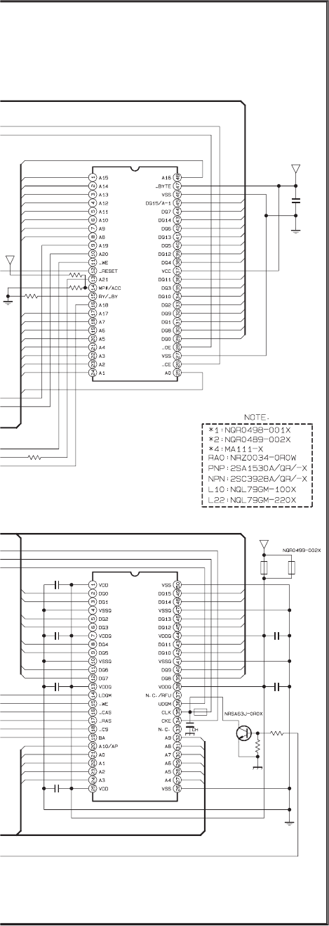
(No.YA463)2-40
DIGITAL PWB ASS'Y(8/15)
SRA0D161A-M2 [HD-52FA97]
SRA0D160A-M2 [HD-56FB97]
SRA0D159A-M2 [HD-61FB97]
c10502008_0808_8/16_0.0
IC7201
R7226
R7214
IC7203
HY57V161610FTP7
R7227
C7203
C7204
C7206
C7207
C7208
C7205
K7201
C7209
R7228
Q7201
R7231
R7230
C7215
K7202
K7211
OPEN
0
OPEN
0.1/16
0.1/16
0.1/16
0.1/16
0.1/16
0.1/16
OPEN
0.1/16
OPEN
OPEN
OPEN
OPEN33p
D15
D7
D14
D6
D13
D5
D12
D4
D11
D3
D10
D2
D9
D1
D8
D0
A15
A14
A13
A12
A11
A10
A9
A8
A17
A7
A6
A5
A4
A3
A2
A1
A0
A16
39VF800A7IEKDG9
39VF800A7IEKDH0
A19
A10
GND
T
B3.3V
A0
A1
A2
A3
A9
A8
A7
A6
A5
A4
D0
D1
D2
D3
D4
D5
D6
D7
D15
D14
D13
D12
D11
D10
D9
STB3.3V
GND
D8
STB3.3V
GND
GND
GND
A20
FLASH ROM
FLASH ROM
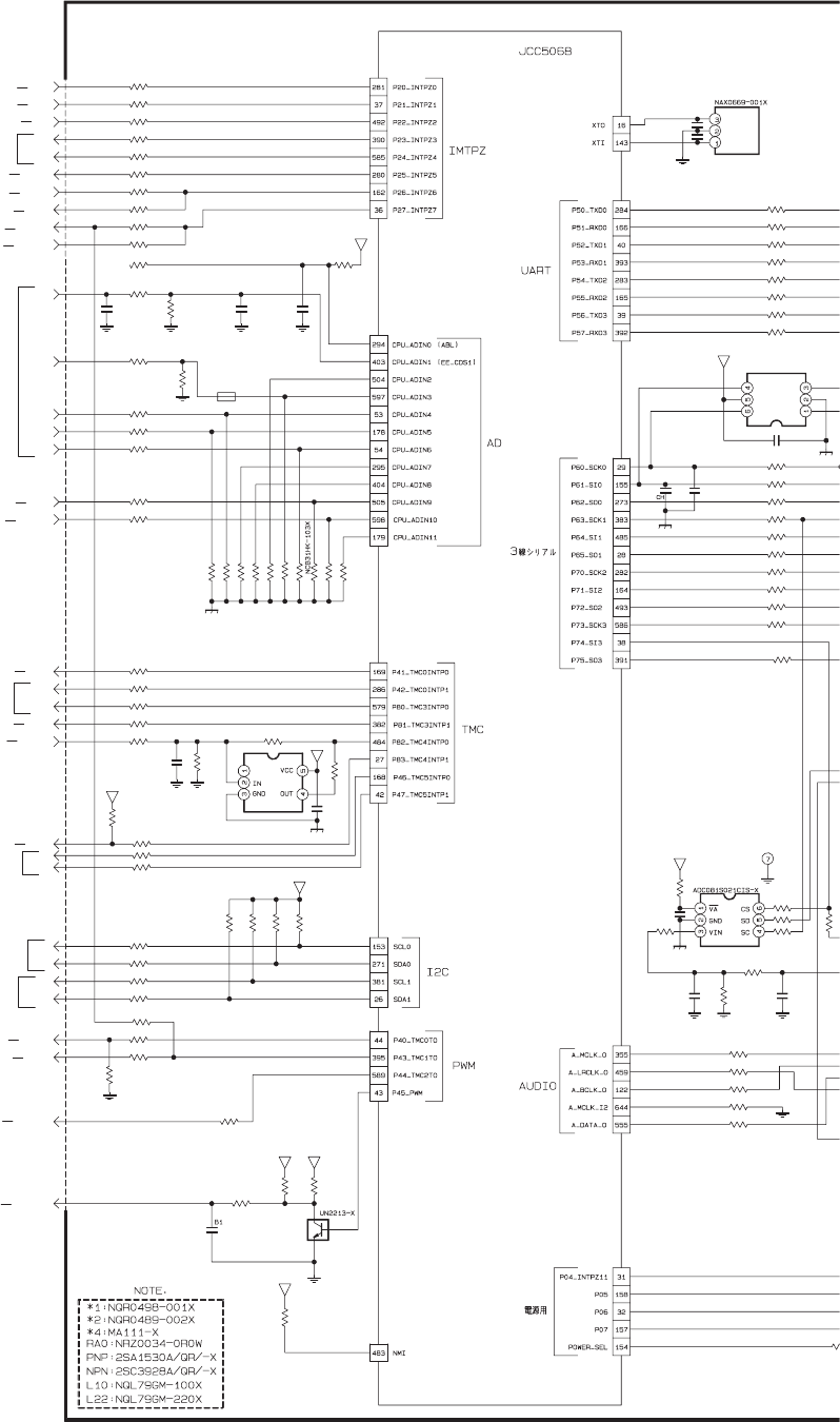
2-41(No.YA463)
R7114
R7115
R7116
R7117
R7118
R7
C7041
C7042
X7001
IC6001
R7103
R7081
R7044
R7043
R7128
R7038
BS_POWEN
R7170
R7033
R7130
IC7039
R7192
DVI_RST
C7040
Q7030
C7075
POW_GOOD
DIN_HOTP
R7030
R7031
R7032
R7034
R7035
R7036
R7045
R7046
R7047
R7052
R7075
R7053
R7056
R7057
R7058
R7055
R7061
R7062
R7063
M_MUTE
A_MUTE
BS_RST
MI_REQ
GR_RST
MSP_RST
CODECRST
MDR_CON
LB_PRO
DINPHOT
EXT_YS2
EXT_YS1
AGC
EE_CDS1
DVI_HOTP
WAKE
DIN_INT
VMUTE
VOUTENB
C7031C7030
R7039
R7040
C7039 R7060
R7059
C7034 C7033
R7041
R7042
K7030
REMOCON
SCL3A
R7086
R7068
R7087
R7088
R7089
SDA3A
CARD_CK
CARD_DA
R7069
R7070
R7071
PWM_DIM
R7072
ANA_DIM
R7188
DBSPWOFF
R7077R7076
C7032
R7078
R7073
R7090
R7091
R7092
R7093
R7094
R7095
R7096
R7097
R7098
R7099
R7084
R7085
C7077
R7100
R7101
R7037
IC7036
DIN_RST
C7074
IC7036
R7177
R7178
R7179R7176
R7175
C7073
C7076
IC7038
R7189
R7197
R
7
GR_ON2
R7193
R7049
R7051
R7184
R7185
R7054
R7067
R7066
R7065
R7064
R7171
R7172
R7173
R7187
R7186
OPEN
OPEN
OPEN
OPEN
OPEN
OPEN
OPEN
0
47K
OPEN
OPEN
0
OPEN
0
0
OPEN
OPEN
0
10/10
OPEN
0
0
150
0
OPEN
OPEN
OPEN
OPEN
0
47k
OPEN
OPEN
0
0
0
0
0
0
0
OPENOPEN
OPEN
0
.001 OPEN
0
OPEN OPEN
22k
OPEN
OPEN
0
0
0
0
0
0
0
0
OPEN
OPEN
330OPEN
OPEN
330
OPEN
0
0
100
100
100
0
OPEN
0
0
0
220
220
OPEN
0
OPEN
OPEN
OPEN
0
0
0
0
0
0.1/16
OPEN
OPEN
OPEN
OPEN
OPEN
0
0
0
OPEN
0
5.6k
5.6k
10K
10K
0
0
0
0
A_MCLK_1
A_LRCLK_1
A_BCLK_1
A_MCLK_I2
A_DATA_1
CLK_7001_3
STB3.3V
CLK_7001_1
GND
GND
GND
STB3.3V
P70_
S
VCC3D
GND
GND
GNDGNDGND
GNDGND
P63_SCK1
STB3.3V
GND
GNDGND GND
GND
P70_SCK2
STB3.3V
GND
GND
VCC3DLCD5V/12V
GND
STB3.3V
GND
P63_
S
STB3.3V
SCL3A_0
SDA3A_0
CARD_CK_0
CARD_DA_0
GND
SHEET19
SHEET19
SHEET19
SHEET9,21
SHEET22,23
SHEET10
SHEET9,20
SHEET19,23
SHEET18
SHEET18
SHEET19
SHEET20
SHEET9,10,11,18,20
DIGITAL INPUT BLOCK
SHEET9
SHEET20
SHEET9
SHEET9,16,19,23
SHEET20
OPEN
SHEET22,23
SHEET11,DIGITAL INPUT BLOCK
SHEET11,DIGITAL INPUT BLOCK
SHEET9
SHEET9
CHASSIS MICOM
DIGITAL PWB CIRCUIT DIAGRAM(9/15) SHEET 17
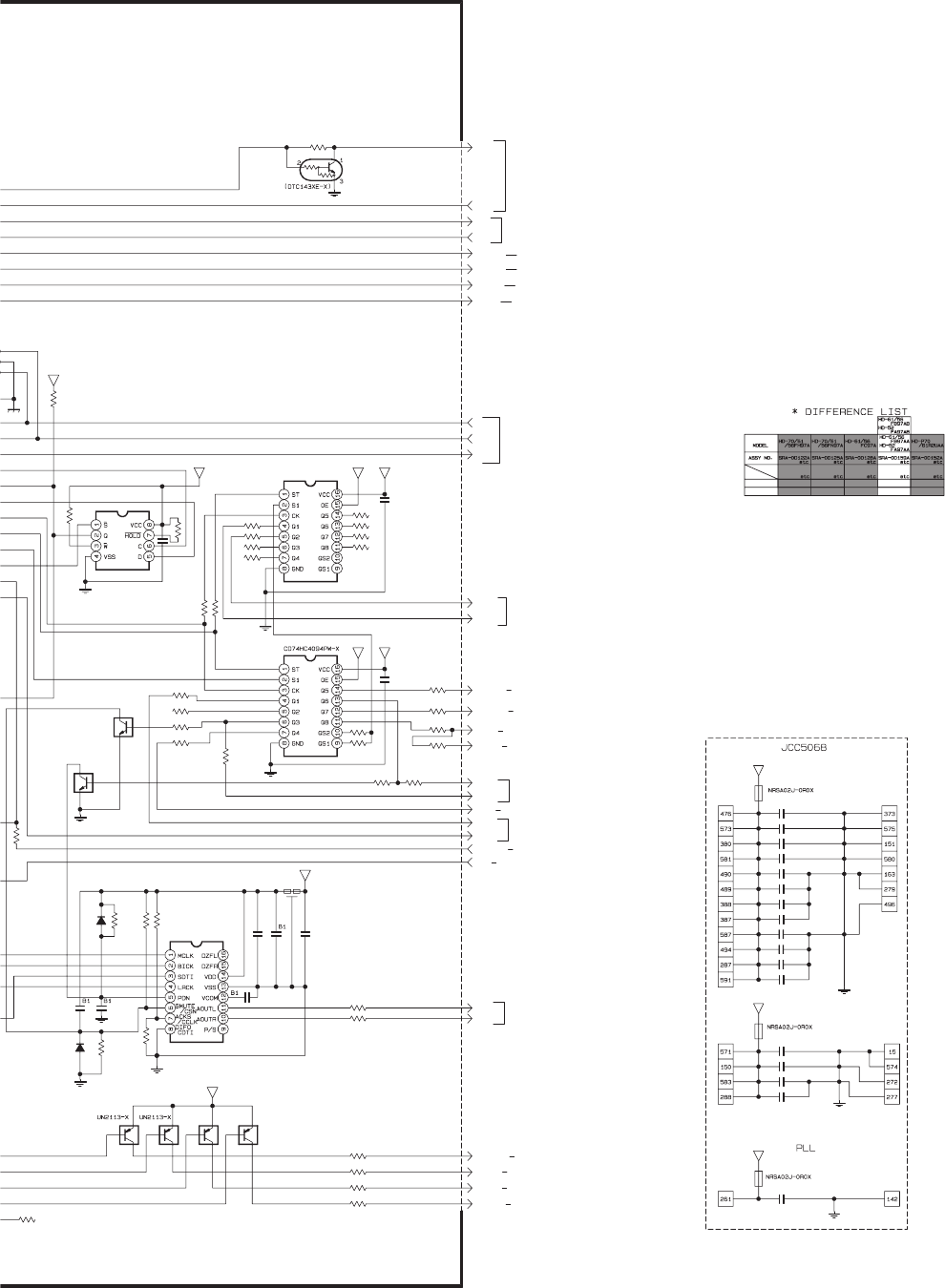
(No.YA463)2-42
DIGITAL PWB ASS'Y(9/15)
SRA0D161A-M2 [HD-52FA97]
SRA0D160A-M2 [HD-56FB97]
SRA0D159A-M2 [HD-61FB97]
c10502009_0808_9/16_0.0
AUDIO_L
AUDIO_R
R7121
IC7034
D7033
C7047
C7046
R7119
R7120
R7122
C7050
K7031
MAIN_POW
R7123
LB_POW
B1_POW
R7124
R7125
Q7035
R7126
DINHOTP2
IC6001
C7051
C7052
C7053
C7054
C7055
C7056
C7057
C7058
C7059
C7060
C7061
C7062
C7063
C7064
C7065
C7066
C7067
K7034
K7032
K7033
GR_ON
PFC_POW
PDP_TX
IC7037
R7131
Q7032 Q7033 Q7034
C7072
R7156
AFT1
R7155R7154
R7157
R7165
R7164
R7163
R7162
R7159
R7158
R7160
R7161
PDP_RX
CARD_INT
POW_LED
REC_LED
DIMMER
R7113
TCCS_RX
TCCS_TX
Q7031
R7195
MI_RX
MI_CK
MI_TX
IC7032
IC7033
C7043
R7104 R7105
DSyncSW1
LCDFRAME
DIN_RWSW
BL_ON
R7110
R7111
R7112
R7106
R7107
R7108
R7109
R7127
C7044
C7045
R7174
Q7037
Q7036
R7183
R7190
R7191
R7196
R7199
GR_ON2
R7198
DBS_FMT2
D7032
C7049
C7048
OPEN
OPEN
OPEN
OPEN
OPEN
OPEN
OPEN
OPEN
OPEN
OPEN
0
0
OPEN
OPEN
OPEN
0.1/16
0.1/16
0.1/16
0.1/16
0.1/16
0.1/16
0.1/16
0.1/16
0.1/16
0.1/16
0.1/16
0.1/16
0.1/16
0.1/16
0.1/16
0.1/16
0.1/16
OPEN
OPEN
OPEN
OPEN
OPEN
OPENOPEN
OPEN
OPEN
OPEN
OPEN
OPEN
OPEN
OPEN
OPEN
OPEN
0
OPEN
OPEN
OPEN
OPEN
OPEN OPEN
0
OPEN
OPEN
0
OPEN
OPEN
OPEN
OPEN
0.1/16
OPEN
47k
OPEN
OPEN
OPEN
OPEN
OPEN
OPEN
OPEN
OPEN
OPEN
OPEN
AUDIO_L_0
GND AUDIO_R_0
GND
A_MCLK_2
BS_5V
A_LRCLK_2
A_BCLK_2
A_DATA_2
STB3.3V
GND
GND
STB1.2V
ClampSW
GND
GND
STB1.2V
STB3.3V GND
VCC3D
GND
VCC3D
EXT3DON
P70_SCK2_1
STB3.3V
GND
STB3.3V
GND
GND
DBS_LED2
DBS_LED1
STB3.3V
P63_SCK1_1
GND
STB3.3V
P70_SCK2_2
C7034
R7042
OLLC11103
-11
OLLC11103
-04
OLLC11103
-07
OLLC11103 OLLC11378
OPEN
OPEN
OPEN OPEN
OPENOPEN
OPEN
OPEN
33k
0.015/16
SHEET22
SHEET22,23
SHEET12
SHEET19
SHEET18,20
SHEET9
SHEET9
SHEET9,20
SHEET9,20
SHEET18
SHEET10
SHEET9,22
SHEET9
SHEET11,
DIGITAL INPUT BLOCK
SHEET18
SHEET19
SHEET9
SHEET9
SHEET21
SHEET9,12,21
SHEET9,22,23
OPEN
CHASSIS MICOM
2-43(No.YA463)
RA6542
RA6502
RA6544
RA6546
RA6541
RA6543
R6569R6568
R6561
RA6503
RA6545
RA6506
R6571
R6503
LV_CK
RA6505
IC6501
RA6504
RA6501
C6513
C6514
R6521
R6522
C6523
C6521
C6524
C6525
C6522
LV_HS
LV_VS
C6515
R6525
R6526
IC6502
R6527
PL_SDA
PL_SCL
PL_SLE
PL_PLE
IC6001
R6528
R6524
R6523
R6575
R6576
R6579
R6577
R6578
IC6505
OSDCK1
R6580
R6590
R6591
R6586
R6589
R6585
R6584
R6587
R6588
C6562
C6563
C6564
R6581
IC6506
OSDCKO
R6582
R6583
R6592
IC6507
R6529
R6530
R6567
R6566
C6571
R6572
R6573
R6595
R6596 C6573
D6503R6597
R659
9
R6506
R6505
R6508
R6501
R6502
R6507
R6510
C6510
C6509C6503
C6501
C6502
C6511
C6512
R6512
R6514
R6513
R6509
R6511
RA0
OPEN0
OPEN
RA0
0
0
RA0
0.1/16
0.1/16
OPEN
OPEN
OPEN
OPEN
OPEN
OPEN
OPEN
0.1/16
OPEN
OPEN
OPEN
OPEN
OPEN
OPEN
OPEN
0
0
OPEN
OPEN
OPEN
OPEN
OPEN
OPEN
OPEN
OPEN
OPEN
OPEN
OPEN
OPEN
OPEN
OPEN
OPEN
OPEN
OPEN
OPEN
OPEN
OPEN
OPEN
OPEN
OPEN
OPEN
OPEN
100p
0
0
OPEN
OPEN OPEN
OPENOPEN
OPE
N
OPEN
1k
0
100
100
OPEN
OPEN
0.1/16
0.1/160.1/16
0.1/16
0.1/16
0.1/16
0.1/16
OPEN
0
OPEN
1k
1k
LV_CK1
520M_0-1
VCC3.3LV
LVB5
LVB6
LVB7
LV_CK2
LVR6
LVR2
LVR3
LVR4
LVR5
LVR0
LVR7
LVG4
LVG3
LVG2
LVG7
LVB0
LVB3
LVB4
LVB5
LVB6
LVB7
LVR1
LVG0
LVG1
LVG6
150M_DDB00
150M_DDB01
150M_LVB0
150M_LVB1
150M_LVB2
150M_LVB3
150M_LVB4
150M_LVB5
150M_LVB6
150M_LVB7
150M_DDG00
150M_DDG01
150M_LVG0
150M_LVG1
150M_LVG2
150M_LVG3
150M_LVG4
150M_LVG5
LVR7
LVR6
LVR5
LVR4
LVR3
LVR2
LVR1
LVR0
LVG7
LVG6
LVG5
LVG4
LVG3
150M_LVG6
150M_LVG7
150M_DDR00
150M_DDR01
150M_LVR0
150M_LVR1
150M_LVR2
150M_LVR3
150M_LVR4
150M_LVR5
150M_LVR6
150M_LVR7
520M_0+1
520M_1-1
520M_1+1
520M_2-1
520M_2+1
520M_CLK
MI_OSDYS
LVG2
LVG1
LVG0
520M_CLK
520M_3-1
LVB0
520M_3+1
LVB1
LVB1
LVB2
LVB2
LVB3
PDP_TX
LVB4
GND
LVG5
PDP_RX
LVB5
LVB6
LVB7
LV_AREA
VCC3.3LV
GND
VCC3D
VCC3D
VCC3D
GND
GND
GND
GND
GND
GND
GND
VCC3.3LV
LCD5V/12V
DDB01
DDB00
DDG01
DDG00
DDR01
DDR00
LVR2
LVR3
LVR4
LVR5
DDR00
DDR01
DDG00
DDG01
LVG0
LVG1
LVG2
LVG3
LVR6
LVR7
LVR0
LVR1
LVG4
LVG5
LVG6
LVG7
DDB00
DDB01
LVB0
LVB1
LVB2
LVB3
LVB4
SHEET20
SHEET14,20
S
H
SHEET17,20
SHEET13,22,23
SHEET21
SHEET13
CHASSIS
MICOM
LVDS DRIVER
DIGITAL PWB CIRCUIT DIAGRAM (10/15) SHEET 18
(No.YA463)2-44
DIGITAL PWB ASS'Y(10/15)
SRA0D161A-M2 [HD-52FA97]
SRA0D160A-M2 [HD-56FB97]
SRA0D159A-M2 [HD-61FB97]
c10502004_0808_4/16_0.0
L6516
C6520
IC6504
R6565
C6561
R6570
L6501
CN000W
R6553R6552R6551
R6562
C6505
C6504
C6508
C6507
C6506
CN0LV1 CN0LV2
CN0LV2
R6554
R6555
CLIP1 CLIP2
R6563 R6564
PSS
ALARM
L6511
L6522
L6512
R6556 R6557
Q6502
R6548
R6549
I2CREADY
L6513
L6514
L6515
L6521
L6523
RA6534 RA6533
R6550
R6536
R6537
L6502
C6531 C6532 C6533
R6534R6533R6532
Q6501
R6539
R6538
R6541 R6531
LC6501
RA6531
CN0LV1
R6558
R6547
LCDFRAME
R6574
R6515
R6516
A
R6544
R6542
RA6532
D6501
R6593
R6594 C6572
D6502
R6598
L6531
R6599
R6535
ANA_DIM
PWM_DIM
BL_ON
R6545
R6546
R6543
RA0
10
OPEN
OPEN
OPEN
OPEN
OPENOPENOPEN
OPEN
0.1/16
0.1/16
0.1/16
0.1/16
0.1/16
OPEN
OPEN
OPEN
OPEN OPEN
RA0
OPEN
RA0
OPEN OPEN
OPEN
OPEN
OPEN
RA0
RA0
RA0
OPEN
OPEN
OPEN OPEN
OPEN
OPEN
OPEN
OPEN
OPEN OPEN OPEN
0OPENOPEN
OPEN
OPEN
OPEN
OPEN OPEN
OPEN
OPEN
OPEN
OPEN
0
OPEN
OPEN
OPEN
OPEN
OPEN
OPEN
OPEN
0.1
OPEN
100k
OPEN
OPEN
OPEN
OPEN
OPEN
520M_0-1
520M_TA1-1
VCC3D
VCC3D
520M_TA1+1
520M_TB1-1
GND
GND
GND
520M_TB1+1
GND
GND
520M_1-2
520M_1+2
GND
520M_0-2
520M_0+2
520M_2-2
520M_2+2
520M_0+1
520M_1-1
520M_1+1
520M_TA1-2
520M_TC1-1
520M_TC1+1
520M_TCLK1-1
520M_TCLK1+1
520M_TD1-1
520M_TD1+1
520M_TE1-1
520M_TE1+1
520M_TA2-1
520M_TA2+1
520M_TB2-1
520M_TB2+1
520M_TC2-1
520M_TC2+1
VCC3D
520M_2-1
520M_2+1
520M_CLK-1 520M_CLK-2
520M_CLK+2520M_CLK+1
520M_3-1
520M_3+1
520M_TA1+2
GND
GND
520M_TB1-2
GND
520M_TB1+2
520M_TC1-2
520M_TC1+2
VCC3D VCC3.3LV
520M_TCLK1-2
520M_TCLK2-1
520M_TCLK1+2
520M_TD1-2
520M_TD1+2
520M_TE1-2
520M_TCLK2+1
GND
GND
520M_TE1+2
520M_TA2-2
520M_TA2+2
520M_TB2-2
520M_TB2+2
520M_TC2-2
520M_TC2+2
520M_TCLK2-2
520M_TCLK2+2
520M_TD2-2
520M_TD2+2
520M_TE2-2
520M_TE2+2
520M_TD2-1
520M_TD2+1
520M_TE2-1
520M_TE2+1
GND
LCD5V/12V
LCD5V/12V
LCD5V/12V
520M_3-2
520M_3+2
SDA3
SCL3A
GND
LCD5V/12V
GND
GND
GND GND
SHEET17
SHEET20
DRIVE PWB ASS'Y(1/9)
CNLV1
(SHEET24)
SHEET9,10,11,17,20,
DIGITAL INPUT BLOCK
OPEN
OPEN
SHEET17
2-45(No.YA463)
BS_LOUT
BS_ROUT
BS_YOUT
D6053
BS_COUT
ML
MR
L6051
C6053
C6052
R6068
C
6
CN0BS
D6052
R6064
R6065
R6066
R6060
D6051
R6059
CN110
R6055
R6057
R6058
C6051
D
DBS_FMT2
R6081
R6061
OPEN
10p
0.1/
1
OPEN
*4
22
22
22
0
OPEN
100
22
22
0.1
0
BSV4
BSV6
BSY
7
BSY
6
BSY
5
BSY
2
BSY
3
BSY
4
BSY
1
BSY
0
BSV
7
BSV
6
BSV
5
BSV
4
BSV
2
BSV
3
BSV
1
BSV
0
BSU
V
BSU
V
BSU
V
BSU
V
BSU
V
BSU
V
BSU
V
GND
GND
GND
GND
VMUTE
VOUTENB
BS_POWEN
BS_TXD
BS_RXD
DBSPWOFF
POW_GOOD
GND
GND
BSU
V
BSD_5V
BS_ODU
BS_RST
BS_IR
GND
BS_BT30
DSyncSW1
BSV7
BSV5
BSUV7
BSUV4
BSUV6
BSUV5
BSV0
BSV1
BSV2
BSV3
BSY0
BSY1
BSY2
BSY3
BSY4
BSY5
BSY6
BSY7
BSUV0
BSUV1
BSUV2
BSUV3
BSCLK
BSHP
BSVP
BS_9V
BSCLK_0
BSVP_0
BSHP_0
SHEET21
SHEET9,16,17,23
SHEET17
SHEET22
SHEET17
SHEET17
SHEET12
SHEET17
SHEET9
SHEET17,23
ATSC TUNER MODULE
DIGITAL PWB CIRCUIT DIAGRAM (11/15) SHEET 19
(No.YA463)2-46
DIGITAL PWB ASS'Y(11/15)
SRA0D161A-M2 [HD-52FA97]
SRA0D160A-M2 [HD-56FB97]
SRA0D159A-M2 [HD-61FB97]
c10502013_0808_13/16_0.0
C6054
C6055
R6072
C6031
IC6012
IC6013
IC6011
0.1/16
0.1/16 0
0.1/16
OPEN
OPEN
OPEN
VD_DV1
HD_DV1
DV1_Y7
VCC3D
GND
GND
BSY7
BSY6
BSY5
BSY2
BSY3
BSY4
BSY1
BSY0
BSV7
BSV6
BSV5
BSV4
BSV2
BSV3
BSV1
BSV0
BSUV7
BSUV6
BSUV5
BSUV4
BSUV3
BSUV2
BSUV1
VD_DV1
CLK_DV1
HD_DV1
BSVP
BSHP
BSCLK
VCC3D
BSUV0
DV1_Y7
DV1_Y6
DV1_Y4
DV1_Y5
DV1_Y3
DV1_Y2
DV1_Y1
DV1_Y0
DV1_R7
DV1_R6
DV1_R5
DV1_R4
DV1_R3
DV1_R2
DV1_R1
DV1_R0
DV1_B7
DV1_B6
DV1_B5
DV1_B4
DV1_B3
DV1_B2
DV1_B1
DV1_B0
GND
DV1_Y6
DV1_Y5
DV1_Y4
DV1_Y3
DV1_Y2
DV1_Y1
DV1_Y0
DV1_R7
DV1_R6
DV1_R5
DV1_R4
DV1_R3
DV1_B0
DV1_B1
DV1_B2
DV1_B3
DV1_B4
DV1_B5
DV1_B6
DV1_B7
DV1_R0
DV1_R1
DV1_R2
CLK_DV1
IC6011
IC6012
IC6013
L6051
C6031
C6053
R6058
R6059
R6060
R6061
C6051
C6052
C6054
C6055
D6052
R6055
R6057
R6064
R6065
R6066
R6068
R6072
CN110
NCJ41CK
-226X-U
SN74CBQ
16211G-X
SN74CBQ
3306AU-X
SN74CBQ
3306AU-X
NRSA02J
-0R0X
NRS181J
-0R0X
NCJ41CK
-226X-U
SN74CBQ
16211G-X
SN74CBQ
3306AU-X
SN74CBQ
3306AU-X
NRSA02J
-0R0X
NRS181J
-0R0X
OLLC11103
-04
OLLC11103
-07
OLLC11103
NCJ41CK
-226X-U
SN74CBQ
16211G-X
SN74CBQ
3306AU-X
SN74CBQ
3306AU-X
NRSA02J
-0R0X
NRS181J
-0R0X
OLLC11378
NRZ0080
-0R0X NRZ0080
-0R0X
NRZ0080
-0R0X
QGB0603L1
-B0 QGB0603L1
-B0
QGB0603L1
-B0
OLLC11103
-11
NCJ41CK
-226X-U
SN74CBQ
16211G-X
SN74CBQ
3306AU-X
SN74CBQ
3306AU-X
NRSA02J
-0R0X
NRS181J
-0R0X
NRZ0080
-0R0X
QGB0603L1
-B0
22
100
0
0
0.1
10p
0.1/16
0.1/16
0.1/16
*4
22
22
22
100
0
0
0.1
10p
0.1/16
0.1/16
0.1/16
*4
22
22
22
100
0
0
0.1
10p
0.1/16
0.1/16
0.1/16
*4
22
22
OPEN
OPEN
OPEN
OPEN
OPEN
OPEN
OPEN
OPEN
OPEN
OPEN
OPEN
OPEN
OPEN
OPEN
OPEN
OPEN
OPEN
OPEN
22 2222 OPEN
22 2222 OPEN
OPEN
000 OPEN
OPEN
22
100
0
0
0.1
10p
0.1/16
0.1/16
0.1/16
*4
22
22
22
22
0
SHEET13,
DIGITAL INPUT BLOCK
BUS SW
ADR LATCH
ADR LATCH
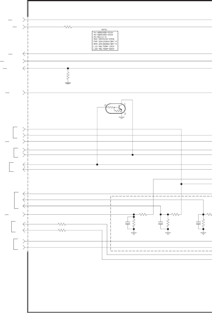
2-47(No.YA463)
DIGITAL PWB ASS'Y(12/15)
SRA0D161A-M2 [HD-52FA97]
SRA0D160A-M2 [HD-56FB97]
SRA0D159A-M2 [HD-61FB97]
REMO
DVI_RST
DVI_HOTP
SCL3A
SDA3A
KEY2
KEY1
LV_AREA
POW_GOOD2
LW_CK
PDP_TX
C6603C6602C6601
R6601
PSS
PDP_RX
MDR_CON
R6604
R6603
R6602
R660
9
R66
1
R6607
R6608
R6605
R6606
MECA_SW
LV_HS
LV_VS
KEY_1
KEY_2
REMOCON
DIMMER
Q7038
0.1/160.1/16
0.1/16
OPEN
OPEN
OPEN
OPEN
100
OP
E
100
OPEN
OPEN
OPEN
OPEN
GND
GND
GNDGND
GND
SHEET9,17
SHEET18
SHEET21
SHEET9,21
SHEET17
SHEET14,18
SHEET17,9
SHEET9
SHEET9,10,11,17,18,
DIGITAL INPUT BLOCK
SHEET17
SHEET22,23
SHEET9,13,22,23
SHEET17,18
SHEET14,18
DIGITAL PWB CIRCUIT DIAGRAM (12/15) [DVI OUT] SHEET 20
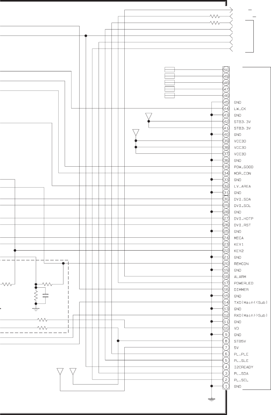
(No.YA463)2-48
c10502012_0808_12/16_0.0
CN0FC
K6605
ALARM
PL_PLE
POW_LED
C6604
K6601
K6602
R6615
R6617
K6603
K6604
PL_SLE
I2CREADY
PL_SDA
PL_SCL
R
6609
R6610
R6611
R6612
R6613
R6614
OPEN
OPEN
OPEN
OPEN
OPEN
OPEN
OPEN
OPEN
OPEN
00
OPEN
1k
OPEN
OPEN
OPEN
GND
BS_5V
VCC3D
STB3.3V
GND
STB_5V
SHEET18
SHEET9,17
SHEET18
OPEN
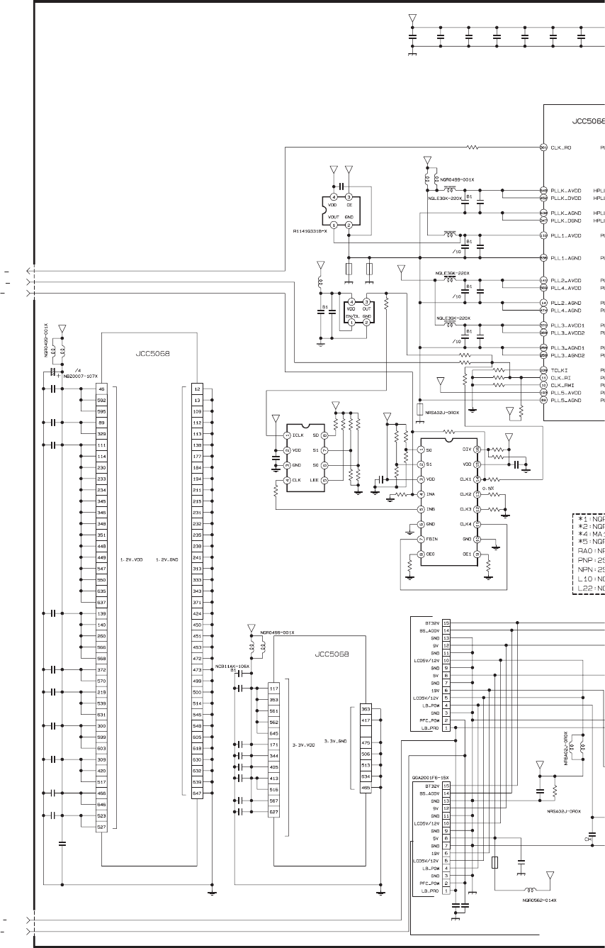
2-49(No.YA463)
DIGITAL PWB ASS'Y(13/15)
SRA0D161A-M2 [HD-52FA97]
SRA0D160A-M2 [HD-56FB97]
SRA0D159A-M2 [HD-61FB97]
L6901
L6902
L6922
C6921 C6922
C6902
R6925
C6903
C6904
C6905
C6906
C6907
C6908
C6909
C6910
C6911
C6913
C6914
C6915
C6916
C6917
C6918
C6919
C6901
IC6001
L6923
L6924
L6925
C6923
C6925
C6927
C6924
C6926
C6928
IC6001
R6921
R6922
R6923
LW_CK
R6924
LV_CK
IC600
1
L6921
IC6901
C9
3
R9306
K6921
C6656
K6922 K6923
IC6904
R6944
R6945
R6946
R6947
R6948
R6949
R6942
R6930
R6943
C6935
C6934
R6953
IC6903
C6933
R6931
R6941
C9644C9643C9642C9641C9640C9639C9638C9637
R6952
C6912
CN0DC
CN1DC
C6929
C9305
C9313 C9314
L9204
K6052 C9209
L6912
L6931
R6926
C6930
L6926
X6901
R6954
R6937
R6939
R6938
R6940
R6933
R6935
R6936
R6932
R6934
L9307
L9306
L6911
C6931
OPEN
OPEN
10/10 0.1/16
0.1/16
OPEN
0.1/16
0.1/16
0.1/16
0.1/16
0.1/16
0.1/16
0.1/16
0.1/16
0.1/16
0.1/16
0.1/16
0.1/16
0.1/16
0.1/16
0.1/16
0.1/16
100
OPEN
10
10
10
0.1/16
0.1/16
0.1/16
0
OPEN
0
0
OPEN
100
p
0.1/16
OPEN
OPEN
OPEN
22
OPEN
OPEN
OPEN
OPEN
OPEN
15
OPEN
OPEN
0
OPEN
OPEN
OPEN
OPEN
OPENOPENOPENOPENOPENOPENOPENOPEN
OPEN
10/10
OPEN
1/10
OPEN
1000p 1000p
*2 1000p/50
OPEN
OPEN
OPEN
OPEN
OPEN
OPEN
OPEN
OPEN
OPEN
OPEN
OPEN
OPEN
OPEN
OPEN
OPEN
OPEN
VCC1.2D
GND GND
VCC3D
VCC_PLL5 CLK_DV1R_4
PFC_POW
VCC1.2D
GND
GND
VCC3D
GND
VCC3D
LB_PRO
LV_CK0
BS_5V
GND
BSD_5V
GND
VCC3D
GND
GNDGND
CLK_DV1R
VCC3D VCC3D
GND
GND GND
GND
GND
CLK_DV1R_2
CLK_DV1R_3
GND
GND
VCC3D
GND
GND
VCC3D
GND
VCC3D
GND
VCC3D
LCD5V/12V
VCC1.2D_2
SHEET18
SHEET20
SHEET13
SHEET9,17
SHEET17
OPEN
POWER P
W
CN9DC (S
H
CHASSIS
MICOM
CHASSIS
MICOM
CHASS
MICO
M
DIGITAL PWB CIRCUIT DIAGRAM (13/15) SHEET 21
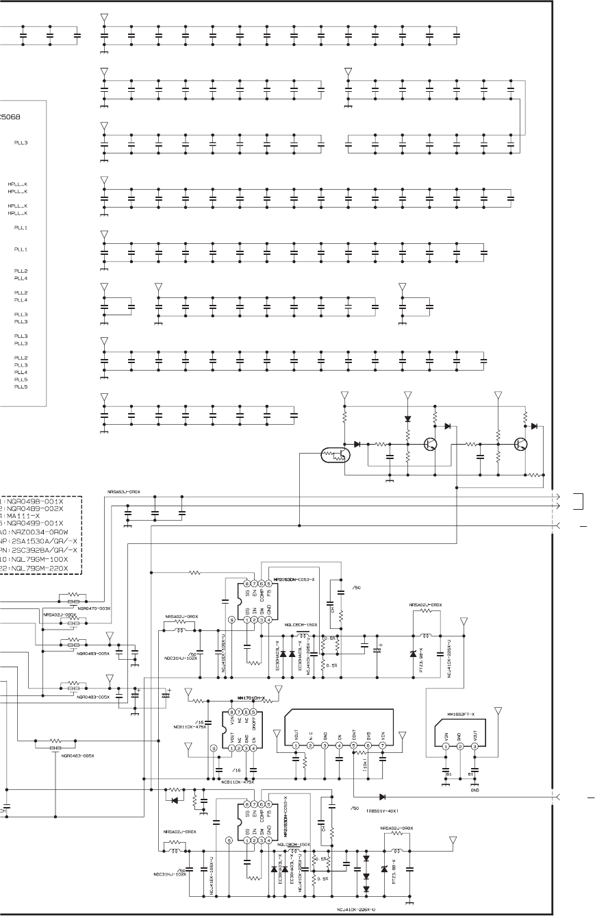
(No.YA463)2-50
c10502010_0808_10/16_0.0
D9208
C9302
C9303
C9103 C9101
IC9001
LC9301
C9304
R9305
R9303
R9302
R9301
LC9302
D9206
LC9303
IC9301
R9001
LC9305
BS_BT30
BS_ODU
R9201
R9002
R9202
R9007
R9207
L9003
L9203
L9202
L9002
R9308
6
001
R9309
C9201
C9001
IC9401
L9001
L9201
R9003
R9004
R9005
R9203 R9204
R9205
R9006
R9206
C9207
C9007
R9008
R9401
C9212
C9210
R9209
C9301
LC9307
R9307
R9208
D9204
C9211
C9401
C9402 C9403
C6637C6636C6635C6634C6633
C9627
C9634C9632 C9633
C9631
C9635
IC9201
C9636
C9629 C9630
C9628
C9645C9644 C9646
C9003
C9203
LB_POW
C6632C6631C6630C6629C6628C6627C6626C6625C6624
C6685C6684C6683C6682C6681C6680C6679C6678C6677
C6670C6669C6668C6667C6666C6665C6664C6663C6662
C6646C6676C6675C6674C6673C6672C6671
C6617 C6618C6616C6615
C6694C6693C6692C6614C6613C6612C6611
C6658C6657
C6655C6654C6653C6652C6651
C6660C6623C6622C6621C6620C6619
C6691C6690C6689C6688C6687C6686
C6699C6698C6697C6696C6695
C6645C6644C6643C6642C6641C6640C6639C6638
C6610
Q9501
R9501
R9502
R9504
D9501
D9502
R9503
C9501
Q9502
R9505 D9503
R9506 R9507
R9508
R9509
Q9503
R9510
D9504
C9502
IC9101
C9208
C9309
C9310
C9311
C9315
C9306 C9307 C9308
C9610
C9607
C9601 C9602 C9603 C9604 C9605 C9606
C9612C9611 C9613 C9614 C9615 C9616 C9617 C9618 C9619 C9620 C9621
C9316
D9401
POW_GOOD2
C9624
D9207
IC9201
C9004C9204
C9202
C9002
C9008
C9010
D9203
D9202
D9201
D9002
C9005
C9205
C9006
C9206
D9001
D9003
C9012
IC9001
IC9301
L9307
R9402
OPEN
4.7
0.01
2.2/16 4.7/16
4.7
OPEN
OPEN
OPEN
OPEN
OPEN
47K
47K
0
OPEN
OPEN
OPEN
OPEN
0
OPEN
1000p
1000p
OPEN
27k 680k
10k
3.0k
OPEN
10k
5.1k
3.3K
0.015
0.01
0
OPEN
OPEN
OPEN
0
100p
OPEN
OPEN
*4
0.047/16
OPEN
OPEN OPEN
0.1/160.1/160.1/160.1/160.1/16
OPEN
OPENOPEN OPEN
OPEN
OPEN OPENOPEN OPEN
OPEN
OPENOPEN OPEN
0.1/25
OPEN
0.1/160.1/160.1/160.1/160.1/160.1/160.1/160.1/160.1/16
0.1/160.1/160.1/160.1/160.1/160.1/160.1/160.1/160.1/16
0.1/160.1/16OPENOPENOPENOPENOPENOPENOPEN
OPEN
OPENOPENOPEN
OPENOPENOPEN
0.1/16 0.1/160.1/160.1/16
0.1/160.1/160.1/160.1/160.1/160.1/160.1/16
0.1/160.1/16
OPEN0.1/16OPENOPEN
OPEN
0.1/160.1/160.1/160.1/160.1/160.1/16
0.1/160.1/160.1/160.1/160.1/160.1/16
0.1/160.1/160.1/160.1/160.1/16
0.1/160.1/160.1/160.1/160.1/160.1/160.1/160.1/16
0.1/16
OPEN
OPEN
OPEN
OPEN
OPEN
OPEN
OPEN OPEN
OPEN OPEN
OPEN OPEN
OPEN
OPEN
OPEN
100k
OPEN
OPEN
22/16
OPEN
OPEN
OPEN
OPEN
OPEN OPEN
OPEN
OPEN
OPEN OPEN OPEN OPEN OPEN OPEN
OPENOPEN OPEN OPEN OPEN OPEN OPEN OPEN OPEN OPEN OPEN
OPEN
OPEN
OPEN
OPEN
0.01/500.01/50
OPEN
12p
12p
OPEN
OPEN
OPEN
STB_5V
BS_9V
BS_5V
STB1.2V
STB3.3V
STB3.3VA STB_5V
BS_5V
GND
GND
STB3.3MI
VCC2.5D
LCD5V/12V
GND
BS_9V
GND
GND
STB3.3V
GND
STB_5V
GND
VCC1.8 VCC1.2D
GND
STB2.5MI
GND
GND GND
VCC2.5D
VCC3D
GND
BS_5V VCC1.2D
VCC3D
GND
GND
GND
GND
POW_GOOD2
GND
VCC3D
VCC1.2D
GND
SHEET19
SHEET9,12,17
SHEET9,20
R
PWB ASS'Y(3/3)
(SHEET35)
A
SSIS
C
OM
2-51(No.YA463)
IC7601
M306V7MG-154FP
D7601
RA7602
X7601
R7643
R761
8
R7604
R7612
R7611
R7606
R7603
C7604
C7605
C7606
C7607
C7609
R7607
R7608
C7602 R7605
C7603
K7601
M
C7608
C7612
IC7602
C7601
C7633
R7609
R7660
R7610
JW
R7651R7650 C7628C7627
RA7601
RA7603
C7617
R7644
CN0C1
AFT1
R7658
TP_IIC
CN0MM
R7617
TCCS_TX
TCCS_RX
R7659
C7614
C7613
R7616
R7602
R7615
R7601
R7619
C7615
R7620
C7616
R7614
R7613
C7611
C7610
IC7603
SN74AHCT1G08V-X
DBS_LED2
DBS_LED1
R7621
SDA1
SCL1
OPEN
RA0
0
0
0
470
1k
1M
0
1000p
220p
2.2
680p
680p
6.8k
1M
0.1/16 470
0.1/16
0.1/16
2.2
1
150p
0
OPEN
0
OPENOPEN OPENOPEN
RA0
RA0
0.1/16
0
10K
56
OPEN
OPEN
0
10k
0
10k
0
0.1/16
1k
0.1/16
0
1k
220p
1000p
OPEN
STB3.3V
OSDG5_0
SUBCCD
MAINCCD1
GND
STB3.3V
GND
SDAM
SCL
GND
GND
OSDB5_0
OSDR5
OSDG5
OSDB5
WAKE
GND
KEY2
KEY1
STB_5V
SUBCCD_1 SUBCCD_2
STB_5V
GND
GND
GND
GND
OSDR5_0
STB3.3V
GND
MAINCCD1_1
GND
GND
GND
STB3.3V
STB3.3V
CEC_INT
CEC_RST
RESET
MECA_SW
DD_OSDCK
MAINCCD1_2
BS_RXD
MI_OSDYS
MI_OSDYM
OSDR3
OSDG3
OSDB3
REMO
BS_TXD
CLK_7601_1
ACINPOW
MI_REQ
TVLINK
CLK_7601_3
SHEET17,23
SHEET9,17 SHEET9
SHEET9,11,23
SHEET17
OPEN
SHEET11,23
OPEN
SHEET13
SHEET11,23
SHEET9,17,23
NOTE : Refer to the part list for the part number of IC7602.
DIGITAL PWB CIRCUIT DIAGRAM(14/15) SHEET 22
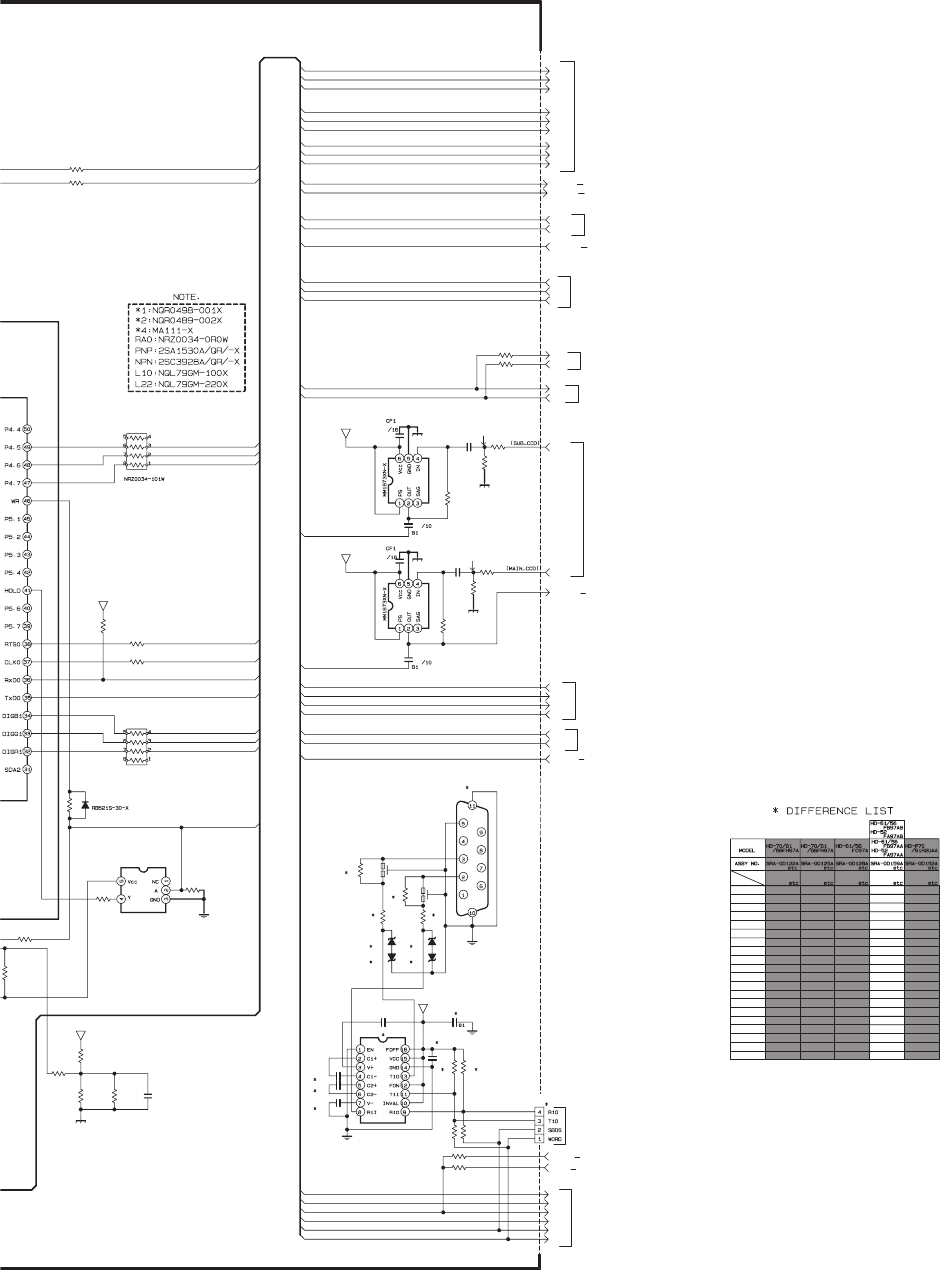
(No.YA463)2-52
DIGITAL PWB ASS'Y(14/15)
SRA0D161A-M2 [HD-52FA97]
SRA0D160A-M2 [HD-56FB97]
SRA0D159A-M2 [HD-61FB97]
c10502006_0808_6/16_0.0
BS_RXD
D7608
C7619
R7618
R7624
C7620
KEY1
KEY2
OSDB5
OSDB4
OSDB3
OSDG5
OSDG4
OSDG3
OSDR5
OSDR4
OSDR3
R7625
EF7601
C7618
REMO
C7621
EF7602
R7636
DD_OSDHS
R7623
R7626
R7627
DD_OSDVS
MAINCCD2
R7631
R7632
DD_OSDCK
MI_OSDYS
IC7604
SN74LVC1G04V-X
R7628
MI_OSDYM
MI_REQ
MI_TX
MI_RX
ACINPOW
TVLINK
R7634
R7635
C7631
BS_TXD
R7637
D7606
MI_SW
CN232SW
C7626
C7622
C7623
IC7607
R7640R7639
C7625
C7624
R7641R7642
D7604
J7601
RA7605
RA7606
MI_CK
CPURST2
CPURST
R7645
R7646
R7647
R7648
R7649
MECA_SW
C7629
R7653
R7652
D7605D7607
R7655
R7654
R7656 R7657 C7630
C7632
PW/CLK
RESET
SBT5
SBD5
WORD
R7662
R7661
QAM_TXD
QAM_RXD
R7620
R7622
IC7605IC7606
IC7603
SN74AHCT1G08V-X
10
0
0
4.7
0
OPEN
4.7
10
OPEN
0
0
0
820
2.2k
33k
820
2.2k
0.22/10
0.1/16
OPENOPEN
RA0
OPEN
0
OPEN
OPEN
10k
OPEN
OPEN
OPEN OPEN OPEN
0.22/10
OPEN
OPEN
1k
0
SBD5
DD_OSDHS
PW/CLK
DD_OSDVS
WORD
DD_OSDVS
MECA_SW
DD_OSDCK
MI_OSDYS
MI_OSDYM
GND
MI_TX
DD_OSDHS
ACINPOW
TVLINK
OSDG4
PW/CLK
OSDR4
OSDB4
SUBCCD
MI_SW
STB3.3V
OSDR5
MI_CK
MI_RX
OSDR4
OSDR3
WORD
RESET
SUB_CCD1
BS_5V
BS_5V
GND
SBD5
MI_SW
OSDG3
OSDG4
OSDG5
OSDB3
OSDB4
OSDB5
REMO
KEY1
KEY2
GND
GND
SBT5
STB3.3V
GND
GND
GND
SUB_CCD1_2
SBT5
BS_RXD
BS_TXD
SUB_CCD1_1
MI_REQ
MI_CK
MI_TX
MI_RX
MAIN_CCD_2
MAIN_CCD
MAINCCD1
GND
BS_5V
GND
MAIN_CCD_1
BS
_
RXD
R7661
R7662
R7636
R7637
R7639
R7640
CN232SW
D7604
C7622
C7623
C7624
C7626
IC7607
J7601
D7605
D7606
D7607
R7652
R7653
C7629
OLLC11103
-04
OLLC11103
-07
OLLC11378OLLC11103 OLLC11103
-11
ICL3221CAZ
-X
QNZ0587
-001
MA8120-X
MA8120-X
MA8120-X
QGA1501F4
-04W
MA8120-X
ICL3221CAZ
-X
QNZ0587
-001
MA8120-X
MA8120-X
MA8120-X
QGA1501F4
-04W
MA8120-X
OPEN
OPEN
OPEN
OPEN
OPEN
OPEN
OPEN
OPEN
OPEN
OPEN
OPEN
OPEN
OPEN
OPEN
OPEN
OPEN
OPEN
OPEN
OPEN
OPEN
OPEN
OPEN
OPEN
OPEN
OPEN
OPEN
OPEN
OPEN
OPEN
OPEN
OPEN
OPEN
OPEN
OPEN
OPEN
OPEN
OPEN
OPEN
OPEN
OPEN
OPEN
OPEN
OPEN
OPEN
OPEN
OPEN
OPEN
OPEN
OPEN
OPEN
OPEN
OPEN
OPEN
OPEN
OPEN
OPEN
OPEN
OPEN
0
0
OPEN
OPEN
OPEN
OPEN
0.1/16
0.1/16
0.1/16
0.1/16
1k
1k
10k
10k
0
0
10/10
0.1/16
0.1/16
0.1/16
0.1/16
1k
1k
10k
10k
0
0
10/10
SHEET13,23
SHEET13,18,23
SHEET13,23
SHEET13,14,23
SHEET13,23
SHEET20,23
SHEET23
SHEET19
SHEET12
SHEET23
SHEET17,23
SHEET9
SHEET9,13,20,23
SHEET23
SHEET23
SHEET16,23
OPEN
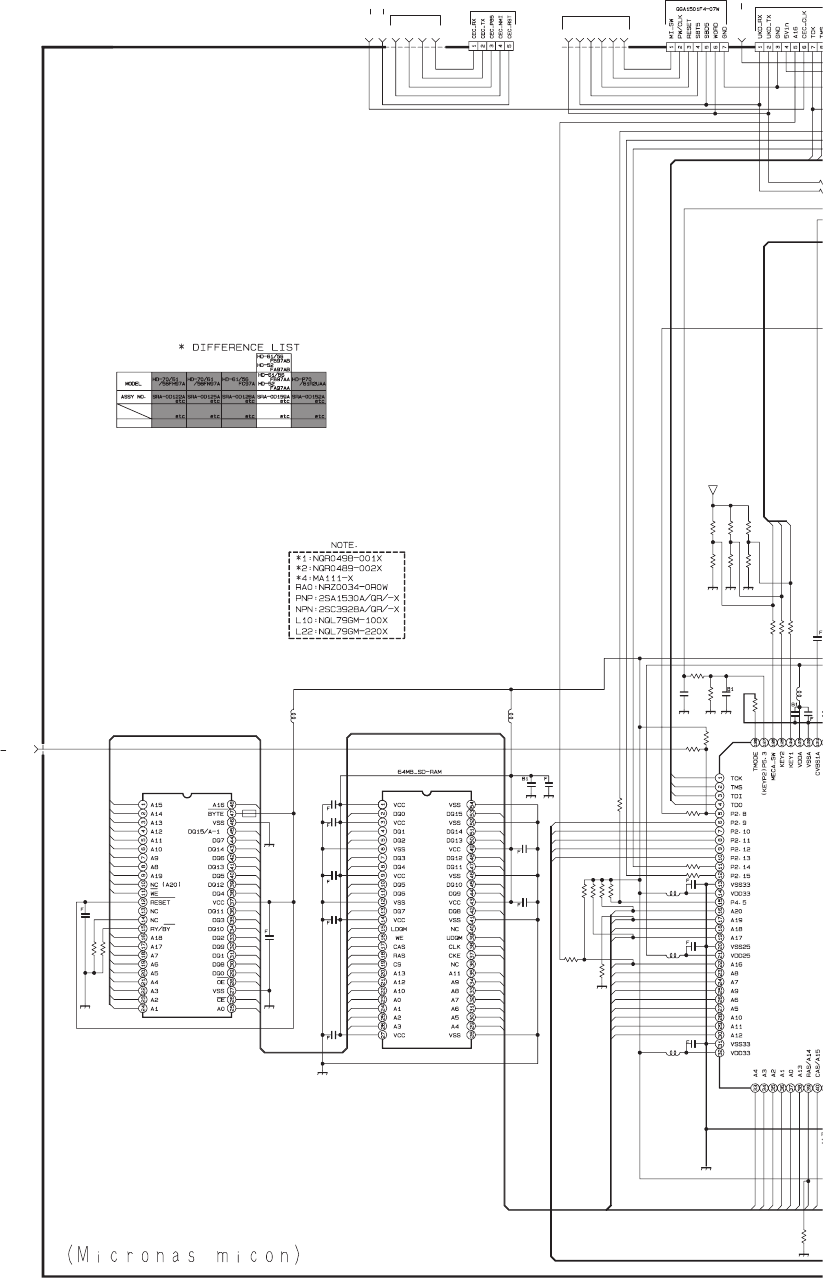
2-53(No.YA463)
DIGITAL PWB ASS'Y(15/15)
SRA0D161A-M2 [HD-52FA97]
SRA0D160A-M2 [HD-56FB97]
SRA0D159A-M2 [HD-61FB97]
IC7303
C7310
C7309
L7315
R7348
IC7302
K7302
C7305
C7306
C7308
C7350
C7307
R7355
L7301
CN0C3
C7311
C7312
C7313
R7317
R7318
R7310
C7302
R7313
L7304
L7303
R7309
L7302
C7304
C7301
C7303
R7361
R7363
CN0C2
R7372
R7371
R7373
C7314
R7303
R7302
C7318
CEC_RST
R7351
R7350
R7349
R7354
R7353
R7352
CEC_CLK
MI_RESET
C7319
C7324
R7314
R7315
R7316
L7305
R7312
R7311
R7305
R7304
C7352
C7351
R7362
R7367
OPEN
OPEN
OPEN
OPEN
OPEN
OPEN
OPEN
OPEN
OPEN
OPEN
OPEN
OPEN
OPEN
OPEN
OPEN
OPEN
OPEN
OPEN
OPEN
OPEN
OPEN
OPEN
OPEN
OPEN
OPEN
OPEN
OPEN
OPEN
OPEN
OPEN
OPEN
OPEN
OPEN
OPEN
OPEN
OPEN
OPEN
10k
10k
10k
OPEN
OPEN
OPEN
OPEN
OPEN
OPEN
OPEN
OPEN
OPEN
OPEN
OPEN
OPEN
OPEN
OPEN
OPEN
OPEN
OPEN
GND
GND
MI_A12
MI_A11
MI_A10
MI_A5
MI_A6
MI_A9
MI_A7
MI_A8
GND
CEC_INT
GND
GNDGNDGND
STB3.3V
OSDB1
OSDB2
OSDB3
OSDB4
OSDB5
MI_D0
MI_D1
MI_D2
MI_D3
MI_D4
MI_D5
MI_D6
MI_D7
LDQM
WR
MI_A15
MI_A14
CSSDRAM
MI_A13
MI_A12
MI_A10
MI_A0
MI_A1
MI_A2
MI_A3
MI_D15
MI_D14
MI_D13
MI_D12
MI_D11
MI_D10
MI_D9
MI_D8
UDQM
CK100
CKE
MI_A11
MI_A9
MI_A8
MI_A7 GND
GND
GND
GND
MI_A6
MI_A19
MI_A18
MI_A17
GND
TCK
TMS
TDI
TDOGNDGND
MI_A4
MI_A5
MI_A15
MI_A14
MI_A13
MI_A12
MI_A11
MI_A10
MI_A9
MI_A8
MI_A19
MI_A20
WR
MI_A18
MI_A17
MI_A7
MI_A6
MI_A5
MI_A4
MI_A3
MI_A2
MI_A1 MI_A0
CSROM
RD
MI_D0
MI_D8
MI_D1
MI_D9
MI_D2
MI_D10
MI_D3
MI_D11
MI_D4
MI_D12
MI_D5
MI_D13
MI_D6
MI_D14
MI_D7
MI_D15
MI_A16
GND
MI_A16
MI_A20
MI_A4
MI_A3
MI_A2
MI_A1
MI_A0
MI_A13
MI_A14
MI A1
5
WORD
KEY1
TCK
TMS
SBD5
MI_SW
PW/CLK
RESET
SBT5
KEY2
MECA_SW
CEC_RX
CEC_TX
CEC_P85
CEC_NMI
CN0ID
OLLC11103
-04
OLLC11103
-07
OLLC11103
QGA1217F1
-05X
OLLC11378 OLLC11103
-11
OPEN OPENOPEN OPEN
SHEET11
SHEET11,22
SHEET11
SHEET22
OPEN
OPEN
OPEN
SHEET11
SHEET11,22
DIGITAL PWB CIRCUIT DIAGRAM (15/15) SHEET 23
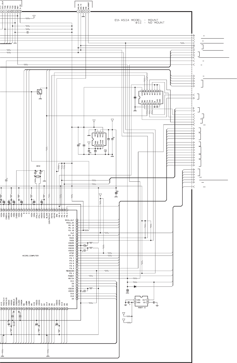
(No.YA463)2-54
c10502007_0808_7/16_0.0
MI_OSDYM
TEXT_HD
C7315
IC7304
C7344
R7343
C7343
C7338
R7342
R7341
R7325
TEXT_VD
CPURST
R7337
R7338
R7356
MI_CK
MI_RX
TEXT_FR
TEXT_FG
MI_OSDYS
TEXT_FB
DD_OSDVS
DD_OSDCK
OSDR1
OSDR2
OSDR3
OSDR4
OSDR5
MI_TX
C7326
OSDG1
OSDG2
R7324
C7327
OSDG4
X7309
REMO
OSDG5
OSDG3
OSDB1
OSDB2
OSDB3
OSDB4
OSDB5
WAKE
R7335
SCLM
MAINCCD2
SDAM
KEY2
KEY1
MECA_SW
TVLINKOUT
MI_REQ
IC7305
R7321
R7319
C7330 C7331
C7335
C7334
C7333
R7320
C7325
R7340
R7334
L7314
L7313
L7312
TVLINKIN
DD_OSDHS
IC7301
AFT1
C7349
R7358
C7348
IC7306
R7359
R7360
R7357
CPURST2
Q7301
R7365
R7366
D7301
POW_GOOD
R7368
R7369
CN0ID
R7347
C7353
IC7305
R7370
CN0MI
R7372
R7371
R7375
R7328
C7318
C7340
C7345
C7346
C7342
L7316
C7341
R7332
R7327
R7333
R7322
R7330
C7319
C7321
C7328
C7329
C7324
L7309
L7308
L7306
C7320
L7307
L7311
L7310
K7308
R7329
C7323
C7322
R7364
R7367
R7323
R7339
R7346
R7374
OPEN
OPEN
OPEN
OPEN
OPEN
OPEN
OPEN
OPEN
OPEN
OPEN
OPEN
OPEN
OPEN
OPEN
OPEN
OPEN
OPEN
OPEN
OPEN
OPEN OPEN
OPEN
OPEN
OPEN
OPEN
OPEN
OPEN
OPEN
OPEN
OPEN
OPEN
OPEN
OPEN
OPEN
OPEN
OPEN
OPEN
OPEN
OPEN
OPEN
OPEN
OPEN
OPEN
OPEN
OPEN
*
OPEN
OPEN
OPEN
OPEN
OPEN
OPEN
OPEN
OPEN
OPEN
OPEN
OPEN
OPEN
OPEN
OPEN
OPEN
OPEN
OPEN
OPEN
OPEN
OPEN
OPEN
OPEN
OPEN
OPEN
OPEN
OPEN
OPEN
OPEN
OPEN
OPEN
OPEN
OPEN
OPEN
OPEN
OPEN
OPEN
OPEN
OPEN
OPEN
OPEN
OPEN
OPEN
OPEN
MI_OSDYM
MI_OSDYS
MI_D11
MI_D3
MI_D4
MI_D10
MI_D12
MI_D2
STB2.5MI
STB3.3MI
SDAM
GND
GND
STB_5V
GND
GND
REMO
OSDG4
OSDG3
OSDG2
OSDG1
GND
OSDR5
OSDR4
OSDR3
OSDR2
OSDR1
OSDG5
STB3.3MI
CPURST2
GND
CPURST2
STB3.3V
MI_CK
TEXT_FB
TEXT_FG
TEXT_FR
WAKE
MECA_SW
KEY1
KEY2
SDAM
SCLM
OSDR1
OSDR2
OSDR3
OSDR4
OSDR5
OSDG1
OSDG2
OSDG3
OSDG4
OSDG5
OSDB1
OSDB2
OSDB3
OSDB4
OSDB5
MI_RX
MI_TX
REMO
WAKE
GND
FBout
FBin
GND
POW_GOOD
POW_GOOD
MI_RX
MI_TX
MI_CK
STB3.3MI
SCLM
GND
GND
STB_5V
GND
GND
BS_RS
QAM_TXD
QAM_RXD
GND
MI
_
A13
MI_A14
MI_A15
CSSDRAM
CKE
CSROM
RD
CK100_0
MI_OSDYS
UDQM
MI_OSDYM
MI_D5
CK100
TEXT_FR
TEXT_FG
TEXT_FB
CLK_7309_2
LDQM
WR
MI_D15
MI_D7
MI_D0
MI_D8
MI_D6
MI_D1
MI_D13
MI_D9
CLK_7309_1
MI_D14
TCK
TMS
CLK_7309_3
TDI
TDO
ATSC TUNER PWB
OPEN
SHEET9
SHEET9
SHEET22
SHEET22
SHEET20,22
SHEET16,22
SHEET13,18,22
SHEET9
SHEET12
SHEET9,11,22
SHEET13,22
SHEET9,13,20,22
SHEET9,17,22
SHEET17,19
SHEET17,22
SHEET13,14,22
SHEET13
SHEET13
SHEET13,22
SHEET13,22
SHEET13
SHEET13,22
SHEET13
SHEET13,22
SHEET17,22
SHEET20,22
SHEET22
SHEET9,16,17,19
SHEET17,22
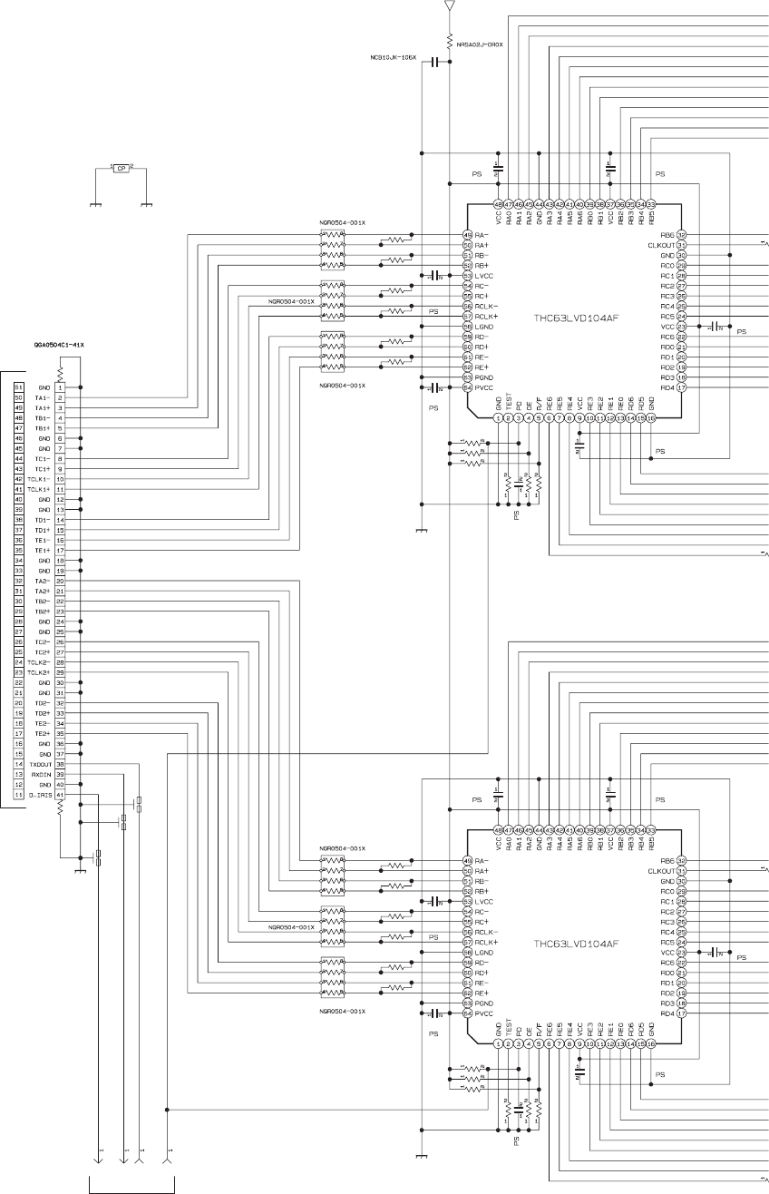
2-55(No.YA463)
DRIVE PWB ASS'Y(1/9)
SRA-3013A-M2
EF3001
R3012
EF3002
C3005
C3003
C3004
C3007
C3008
C3012
C3010
C3011
C3014
C3015
C3013
R3007
R3008
R3009
R3010
R3011
C3006
R3025
EF3003
R3001
R3023
R3024
R3002
R3003
R3004
R3005
R3015
R3013
R3014
IC3001
CNLV1
C3001
IC3002
K3001
K3002
K3003
RB3002
RB3001
R3082
CLIP1
K3004
K3005
K3006
R30
R30
2
R30
2
R3006
R30
2
R3028
D_IRIS
C3009
R3018
LVDSCTL
R3026
C3002
RXD
R3027
R3016
R3017
TXD
*EF5
100
*EF5
0.1
0.1
0.1
0.1
0.1
0.1
0.1
0.1
0.1
0.1
0.1
100
100
100
100
100
0.1
3.3K
*EF2
100
10K
3.3K
100
100
100
100
3.3K
10K
3.3K
GND1
GND1
10/6.3
GND1
VCC3F
0
0
0
OPT
100
100
0.1
100
0
0.1
OPT
0
OPT
RXA1N
RXA1P
RXB1N
RXB1P
RXC1N
RXC1P
RXE1N
RXE1P
RXCLK1N
RXCLK1P
VCC3LV
RXD1N
RXA2N
RXD1P
GND1 GND1
RXA2P
RXB2N
RXB2P
RXC2N
RXC2P
RXCLK2N
RXCLK2P
RXD2N
RXD2P
RXE2N
RXE2P
SHEET30
DIGITAL PWB
ASS'Y(10/15)
CN0LV1
(SHEET18)
RECEIVER
LVDS
RECEIVER
LVDS
DRIVE PWB CIRCUIT DIAGRAM (1/9) [LVDS_INPUT] SHEET 24
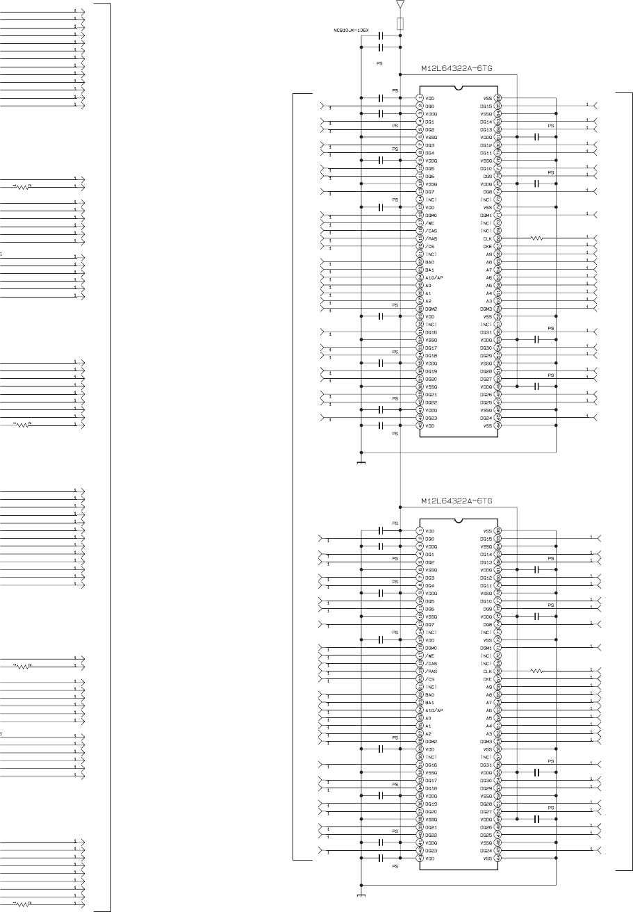
(No.YA463)2-56
c10488004_0808_4/9_0.0
0
4
1
1
MA_DQ15
MA_DQ14
BIN25
CLKIN2
BIN15
CLKIN1
BIN26
BIN16
BIN27
BIN17
MA_DQ13
MA_DQ12
MA_DQ11
IC3003
C3029
C3028
C3027
C3026
C3025
C3024
MA_DQ10
C3016
MA_DQ9
MA_DQ8
MA_DQM1
C3023
C3022
C3021
C3020
C3019
C3018
C3017
IC3004
C3041
C3040
C3039
C3038
C3037
C3036
C3035
C3034
MA_CK
C3033
C3032
C3031
C3030
MA_CKE
MA_A9
R3029
K3012
R3030
MA_A8
BIN18
MA_A7
MA_A6
MA_A5
MA_A4
MA_A3
MA_DQM3
MA_DQ31
BIN19
MA_DQ30
MA_DQ29
MA_DQ28
MA_DQ27
MA_DQ26
MA_DQ25
MA_DQ24
MA_DQ0
MA_DQ1
MA_DQ2
MA_DQ3
MA_DQ4
MA_DQ5
MA_DQ6
MA_DQ7
MA_DQM0
MA_WE
MA_CAS
MA_RAS
MA_CS
MA_BA0
MA_BA1
MA_A10
MA_A0
MA_A1
MA_A2
MA_DQM2
MA_DQ16
MA_DQ17
MA_DQ18
MA_DQ19
MA_DQ20
MA_DQ21
MA_DQ22
MA_DQ23
MB_DQ0
MB_DQ1
MB_DQ2
MB_DQ3
MB_DQ4
MB_DQ5
MB_DQ6
MB_DQ7
MB_DQM0
MB_WE
MB_CAS
MB_RAS
MB_CS
MB_BA0
MB_BA1
MB_A10
MB_A0
MB_A1
MB_A2
MB_DQM2
MB_DQ16
MB_DQ17
BIN28
MB_DQ18
MB_DQ19
MB_DQ20
MB_DQ21
MB_DQ22
MB_DQ23 MB_DQ24
MB_DQ25
MB_DQ26
MB_DQ27
MB_DQ28
MB_DQ29
MB_DQ30
MB_DQ31
MB_DQM3
MB_A3
MB_A4
MB_A5
MB_A6
MB_A7
MB_A8
MB_A9
MB_CKE
MB_CK
MB_DQM1
MB_DQ8
MB_DQ9
MB_DQ10
MB_DQ11
MB_DQ12
MB_DQ13
MB_DQ14
MB_DQ15
HDIN1
VDIN1
DEIN1
RIN12
RIN13
GIN12
GIN13
BIN12
RIN14
RIN15
RIN16
RIN17
RIN18
RIN19
GIN14
GIN15
GIN16
GIN17
GIN18
GIN19
BIN14
NA1
BIN11
BIN10
GIN11
GIN10
RIN11
RIN10
OSDYS1
BIN13
BIN29
HDIN2
VDIN2
DEIN2
RIN22
RIN23
GIN22
GIN23
BIN22
RIN24
RIN25
RIN26
RIN27
RIN28
RIN29
GIN24
GIN25
GIN26
GIN27
GIN28
GIN29
BIN24
NA2
BIN21
BIN20
GIN21
GIN20
RIN21
RIN20
OSDYS2
BIN23
R3019
R3022
R3020
R3021
VCC3F
0.1
0.1
0.1
0.1
0.1
0.1
10/6.3
0.1
0.1
0.1
0.1
0.1
0.1
0.1
GND1
0.1
0.1
0.1
0.1
0.1
0.1
0.1
0.1
0.1
0.1
0.1
0.1
GND1
0
*K1
0
10
10
10
10
MA_CK
MA_DQ24
MB_CK
MA_DQ15
VCC3SD
MA_DQ14
MA_DQ13
MA_DQ12
MA_DQ11
MA_DQ10
MA_DQ9
MA_DQ8
MA_DQM1
MA_A9
MA_CKE
MA_A8
MA_A7
MB_DQ15
MA_A6
MA_A5
MA_A4
MA_A3
MA_DQM3
MA_DQ31
MA_DQ30
MA_DQ29
MA_DQ28
MA_DQ27
MA_DQ26
MA_DQ25
MA_DQ23
MA_DQ22
MA_DQ21
MA_DQ20
MA_DQ19
MA_DQ18
MA_DQ17
MA_DQ16
MA_DQM2
MA_A2
MA_A1
MA_A0
MA_A10
MA_BA1
MA_BA0
MA_CS
MA_RAS
MA_CAS
MA_WE
MB_DQ14
MB_DQ13
MB_DQ12
MB_DQ11
MB_DQ10
MB_DQ9
MB_DQ8
MA_DQM0
MB_DQM1
MB_A9
MB_CKE
MB_A8
MB_A7
MB_A6
MB_A5
MB_A4
MB_A3
MB_DQM3
MB_DQ31
MB_DQ30
MB_DQ29
MB_DQ28
MB_DQ27
MB_DQ26
MB_DQ25
MB_DQ24MB_DQ23
MB_DQ22
MB_DQ21
MB_DQ20
MB_DQ19
MB_DQ18
MB_DQ17
MB_DQ16
MB_DQM2
MB_A2
MB_A1
MB_A0
MB_A10
MB_BA1
MB_BA0
MB_CS
MB_RAS
MB_CAS
MB_WE
MA_DQ7
MA_DQ6
MB_DQM0
MA_DQ5
MB_DQ7
MB_DQ6
MB_DQ5
MB_DQ4
MB_DQ3
MB_DQ2
MB_DQ1
MB_DQ0
MA_DQ4
MA_DQ3
MA_DQ2
MA_DQ1
MA_DQ0
SHEET25
SHEET25
SHEET25
SD-RAM
SD-RAM
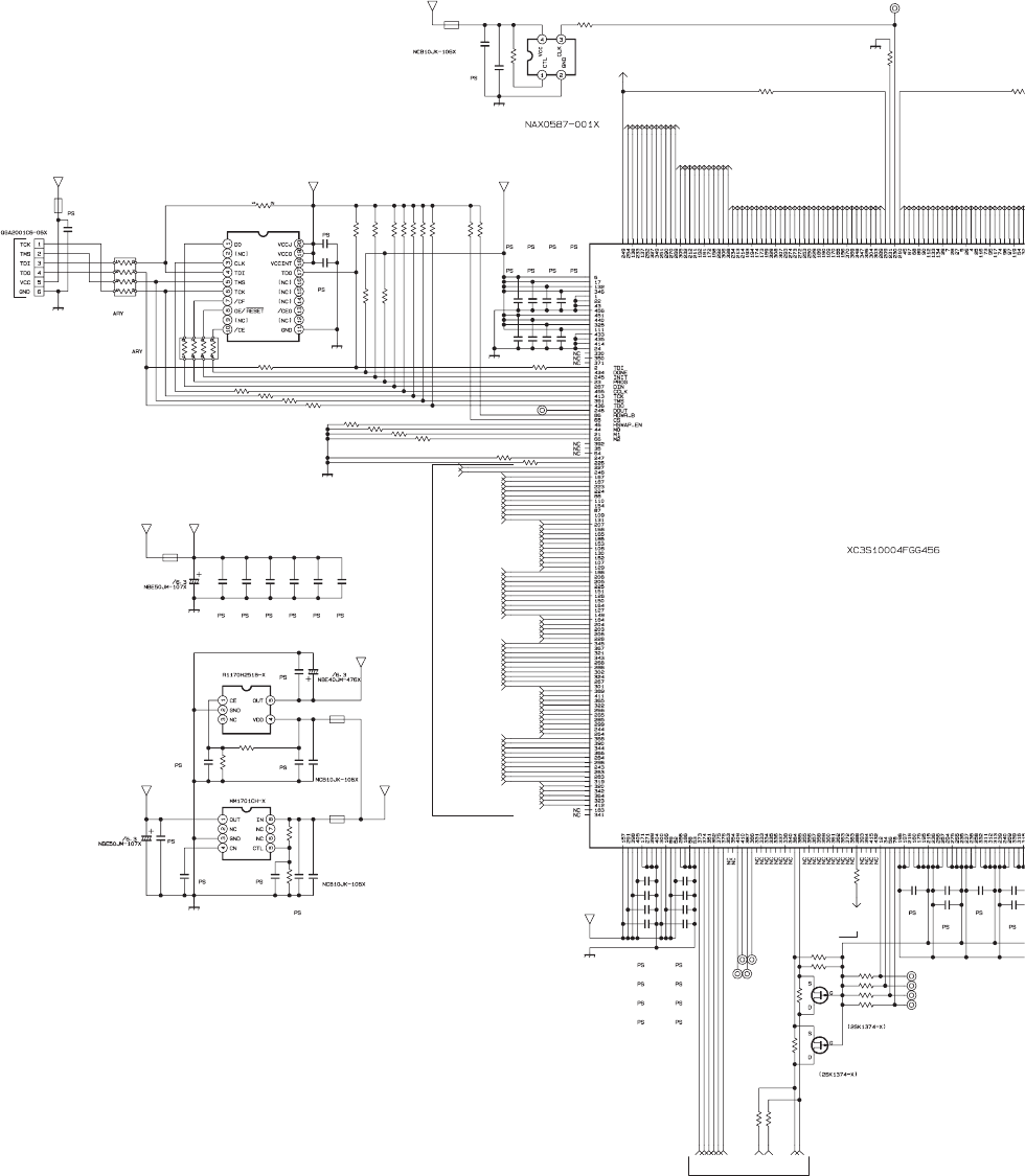
2-57(No.YA463)
DRIVE PWB ASS'Y(2/9)
SRA-3013A-M2
IC3005
R3052
X3001
R3035
R3068 R3069
R3033
R3047 R3048
C3079
CLKIN2
C3048C3047C3046
C3045C3044C3043C3042
R3083
IC3931
IC3930
CA3991
TP3004
TP3005
TP3006
R3089
R3046
Q3001
R3042
R3043
R3041
R3040
Q3002
C3063
C3064
C3065
C3058
R3038
R3039
R3036
CLKIN1
R3037
CA3984
K3951
K3952
TP3001
TP3003
C3049
C3059
C3060
CNJIG2
R3032 R3031
C3061
C3072
R3045
CA3981
C3073
C3075
CA3982
CA3983
C3082
R3051
R3044
TP3002
C3074
RIN10
RIN11
RIN12
RIN13
RIN14
C3080
RIN15
RIN16
RIN17
RIN18
RIN19 GIN10
GIN11
GIN12
GIN13
GIN14
GIN15
GIN16
GIN17
GIN18
GIN19
BIN10
BIN11
BIN12
BIN13
BIN14
BIN15
BIN16
BIN17
BIN18
C3081
IC3006
BIN19
R3049
HDIN1
R3050
VDIN1
C3077
R3067
DEIN1
OSDYS1
NA1
RIN20
RIN21
RIN22
RIN23
RIN24
RIN25
RIN26
RIN27
RIN28
RIN29 GIN20
GIN21
GIN22
GIN23
GIN24
GIN25
GIN26
GIN27
GIN28
GIN29
BIN20
BIN21
BIN22
BIN23
BIN24
BIN25
BIN26
BIN27
BIN28
BIN29 HDIN2
VDIN2
DEIN2
OSDYS2
NA2
R3066R3065
K3014
C3078
CA3988
R3034
CA3986
CA3989
CA3990
K3013
K3950
CA3980
R3986
R3985
R3987
R3988
CA3987
CA3015
C3076
R3064
CA3985
C3062
C3801 C3802 C3803 C3804 C3805
R3070
TP3008
TP3010
TP3009
SCL_F
SDA_F
CTL4
CTL3
CTL2
CTL1
TP3007
CTL6
R3053
R3054
R3055
R3062
R3056
R3057
R3063
R3058
R3059
R3060
SCL_T
SDA_T
R3061
CTL5
CPU_V
MA_DQ0
MA_DQ1
MA_DQ2
MA_DQ3
MA_DQ4
MA_DQ5
MA_DQ6
MA_DQ7
MA_DQ8
MA_DQ9
MA_DQ10
MA_DQ11
MA_DQ12
MA_DQ13
MA_DQ14
MA_DQ15
MA_DQ16
MA_DQ17
MA_DQ18
MA_DQ19
MA_DQ20
MA_DQ21
MA_DQ22
MA_DQ23
MA_DQ24
MA DQ25
MB_DQ0
MB_DQ1
MB_DQ2
MB_DQ3
MB_DQ4
MB_DQ5
MB_DQ6
MB_DQ7
MB_DQ8
MB_DQ9
MB_DQ10
MB_DQ11
MB_DQ12
MB_DQ13
MB_DQ14
MB_DQ15
MB_DQ16
MB_DQ17
MB_DQ18
MB_DQ19
MB_DQ20
MB_DQ21
MB_DQ22
MB_DQ23
MB_DQ24
MB_DQ25
MB_DQ26
MB_DQ27
MB_DQ28
MB_DQ29
MB_DQ30
MB_DQ31 MB_A0
MB_A1
MB_A2
MB_A3
MB_A4
MB_A5
MB_A6
MB_A7
MB_A8
MB_A9
MB_A10 MB_WE
MB_CAS
MB_RAS
MB_CS
MB_BA0
MB_BA1
MB_DQM0
MB_DQM1
MB_DQM2
MB_DQM3
MB_CKE MB_CK
56
0
00
0
056
VCCAUX
0.1
0.10.10.1
0.10.10.10.1
OPT
VCC3F
GND1
10/6.3
OPT
OPT
OPT
OPT
OPT
OPT
OPT
OPT
3.3k
3.3k
OPT
0.1
0.1
0.1
0.1
GND1
3.3k
3.3k
3.3k
3.3k
0.1
*K1
*K1
GND1
OPT
OPT
0.1
0.1
0.1
0
GND1
GND1
0.1
0.1
0
0.1
.01
0.1
47
0.1
GND1
VCC3F
0.1
OPT
10
OPT
0.1
0.1
0.1
VCC3F
56 0
0.1
000
GND1
*K1
VCCAUX
VCC3F
10/6.3
0.1
10
GND1
VCCINT
100
0.1
0.1
DR-VCC3 VCC3F
*K1
GND1
*K1
100
OPT
10k
10k
OPT
0.1
VCC3F
0.1
.01
0
10/6.3
0.1
0.1 0.1 0.1 0.1 0.1
51
OPT
OPT
OPT
OPT
OPT
330
4.7k
4.7k
4.7k
OPT
4.7k
OPT
OPT
OPT
OPT
GND1
GND1
GND1
SHEET24
SHEET30
SHEET
30
SHEET24 SHEET2
4
OPEN
1PHASE-2PHASE
CONVERT/
OVER DRIVE
DRIVE PWB CIRCUIT DIAGRAM (2/9) [FPGA_INPUT] SHEET 25
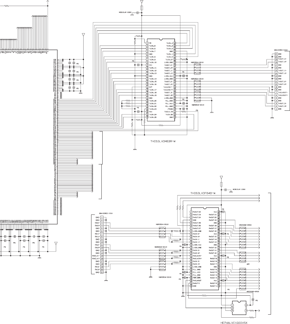
(No.YA463)2-58
c10488005_0808_5/9_0.0
C3050
C3053
C3055
C3057
C3052
CNL1
C3051
C3083
CNL2
C3054
C3056
R3075
C3067
C3066
R3081
R3031
C3097
C3070
C3069C3072
C3073
C3068C3071
C3089
R3097
C3092
R3095
R3092
C3096
C3095
C3094
C3093
C3091
C3090
R3084
R3085
R3086
R3087
R3088
R3090
K3016
R3091
R3093
R3096
R3094
R3074
R3073
BPIXDH0
K3024
K3025
K3026
BPIXDH1
BPIXDH2
BPIXDH3
BPIXDH4
BPIXDH5
BPIXDH6
BPIXDH7
BPIXDH8
BPIXDH9
BPIXCLK
BHSYNC
BVSYNC
BPIXVALID
IC3009 R3098
C3088
C3087
C3084
C3085
R3080
K3015
K3021
K3022
K3023
R3071
R3072
R3076 R3077
C3086
R3079
R3078
BPIXDL0
BPIXDL1
BPIXDL2
BPIXDL3
BPIXDL4
BPIXDL5
BPIXDL6
BPIXDL7
BPIXDL8
BPIXDL9
RPIXDL0
RPIXDL1
RPIXDL2
RPIXDL3
RPIXDL4
RPIXDL5
RPIXDL6
RPIXDL7
RPIXDL8
RPIXDL9
RPIXDH0
RPIXDH1
RPIXDH2
RPIXDH3
RPIXDH4
RPIXDH5
RPIXDH6
RPIXDH7
RPIXDH8
RPIXDH9
RPIXCLK
GPIXDL0
GPIXDL1
GPIXDL2
GPIXDL3
GPIXDL4
GPIXDL5
GPIXDL6
GPIXDL7
GPIXDL8
GPIXDL9
GPIXDH0
GPIXDH1
GPIXDH2
GPIXDH3
GPIXDH4
GPIXDH5
GPIXDH6
GPIXDH7
GPIXDH8
GPIXDH9
GPIXVALID
GPIXCLK
GHSYNC
GVSYNC
RPIXVALID
RHSYNC
RVSYNC
MA
_
DQ19
MA_DQ20
MA_DQ21
MA_DQ22
MA_DQ23
MA_DQ24
MA_DQ25
MA_DQ26
MA_DQ27
MA_DQ28
MA_DQ29
MA_DQ30
MA_DQ31 MA_A0
MA_A1
MA_A2
MA_A3
MA_A4
MA_A5
MA_A6
MA_A7
MA_A8
MA_A9
MA_A10 MA_WE
MA_CAS
MA_RAS
MA_CS
MA_BA0
MA_BA1
MA_DQM0
MA_DQM1
MA_DQM2
MA_DQM3
MA_CKE MA_CK
0.1
.01
.01
.01
0.1
.01
10/6.3
GND1
0.1
0.1
GND1
0
.01
0.1
0
0
GND1
0.1
.01
0.1
GND1
0.1
VCC3F
.01
0.10.1
10/6.3
10
0.1
0
10
ASID3B
0.1
0.1
0.1
0.1
0.1
0.1
100
100
100
100
100
10
*K1
10
10k
0
0
0
0
GND1
OPT
VCC3F
0.1
0.1
0.1
0.1
0
*K1
GND1
GND1
GND1
GND1
0
OPT
OPT
VCCINT
0
0.1
3.3k
0
BOUTCLK
BOUTHD
BOUTVD
BOUTDE
BPIXVALID
BRX2N
BRX0P
BRX1P
BRX3N
BRX3P
GND1
BOUT14
BOUT13
BOUT12
BOUT11
BOUT10
BOUT15
ASID3B_L
BOUT16
BOUT23
BOUT22
BOUT21
BOUT20
BOUT19
BOUT18
BOUT17
BOUT24
BOUT29
BOUT28
BOUT27
BOUT26
BOUT25
GND1
BVSYNC
BHSYNC
BTX0N
BTX0P
BTX1N
BTX1P
BTX2N
BTX2P
BTXCLKN
BTXCLKP
BTX3N
BTX3P
VCC3F_B
BRX1N
BRX0N
BRX2P
BRXCLKN
BRXCLKP
IC3007
IC3008
SHEET27
SHEET26
SHEET28
E
T24
OPEN
OPEN
LVDS
DRIVER
LVDS
DRIVER
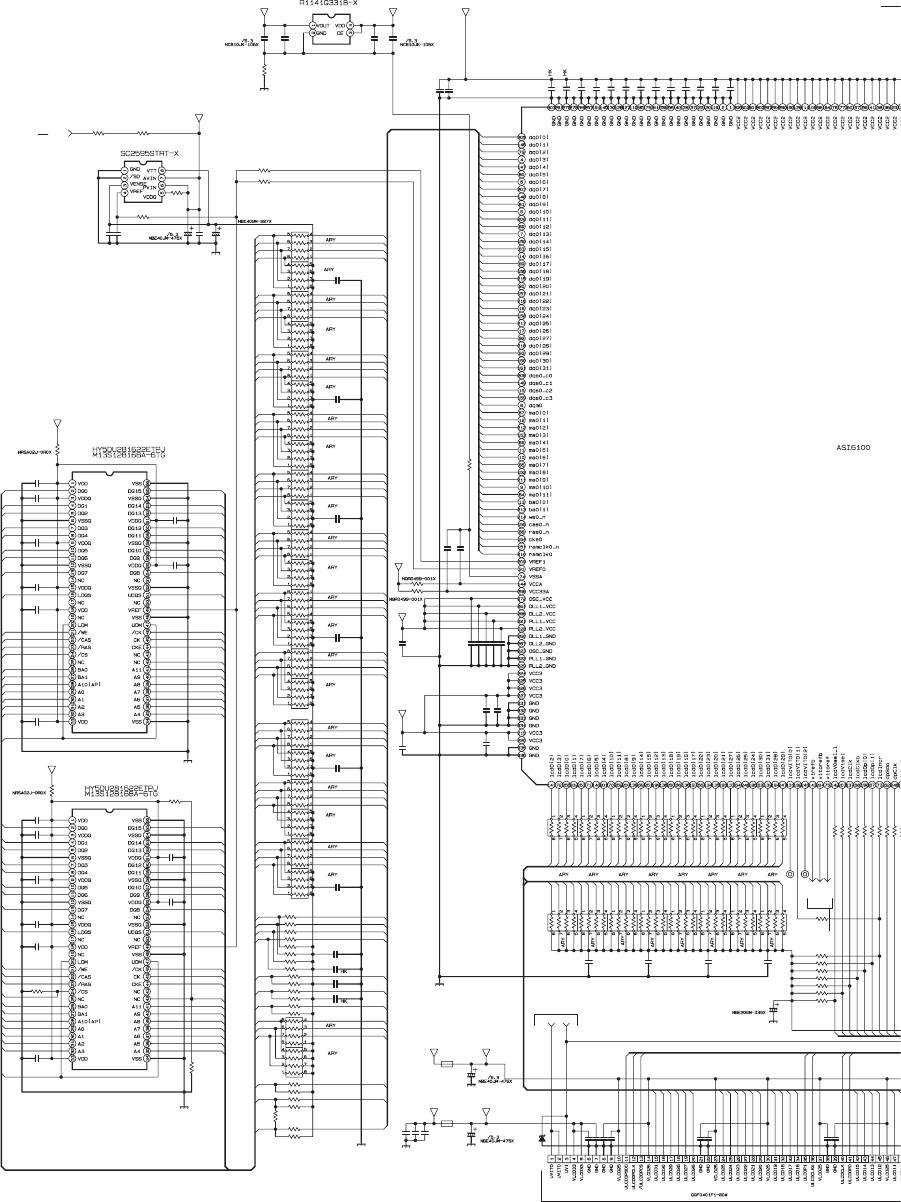
2-59(No.YA463)
C3101
C3109
C3102
C3103
C3104
IC3101
IC3102
C3105
C3106
C3108
C3107
C3110
C3111
C3112
IC3103
C3113
C3114
C3116
C3115
R3101
R3102
R3103
R3122
R3120
R3124
R3851
R3852
R3815
R3816
R3119
R3121
R3123
R3125
R3127
R3128
R3129
R3130
R3131
R3132
R3299
R3227
R3222
R3223
CA3003
CA3004
R3287
C3241
R3134
R3135
R3136
R3137
R3138
R3118
R3139
R3140
R3117
R3116
R3115
R3106
R3113
R3110
R3111
R3108
R3109
R3112
R3107
R3114
R3105
R3104
C3119
C3120
C3121
C3122
R3279
C3123
K3105
C3118
K3107
R3233
C3169
C3117
C3170
C3124
C3125
C3126
C3127
C3171
C3163
R32
3
C3166C3167
C3222C3219
C3162
R3278
R3277
C3248
R3276
R3275
R3205
R3274
R3232
MEM_EN
R3853
R3854
R3855
R3856
R3857
R3858 C3168
C3240
C3239
R3164
R3292
R3163 R3162 R3161 R3157R3158R3159R3160
R3280
R3291
R3290
C3221
C3220
R3289
C3199
C3223 D3101
CNR1
C3128
IC3108
C3238
IC3113
R3288
TP3157
CA3001
TP3155
CA3002
CA3005
CA3006
CA3007
C3145
C3144
C3153
C3152
C3151
C3150
C3149
C3161
C3160
C3158
C3159
C3165
C3135
C3139
C3141
C3143
C3164
C3130
R3172
R3171
R3170
R3169
R3165
R3166
R3167
R3168
R3144
R3154
R3148
R3147
R3143
R3142
R3153
R3141
R3156
R3152
RV1REF
RVITOR_B
RVITOREF
C3203
C3202
C3213
C3214
C3247
C3211
C3212
C3246
MRD2R
0.1
0.1
0.1
0.1
0.1
0.1
0.1
0.1
0.1
0.1
0.1
0.1
0.1
0.1
0.1
0.1
0
OPT
OPT
22
22
22
22
22
22
51
51
51
51
51
22
51
22
51
22
51
0
22
0.1
0.1
OPT
0.1
22
51
22
OPT
100
22
22
OPT
51
22
51
22
51
22
51
22
51
22
51
22
51
22
0.1
0.1
0.1
0.1
51
0.1
*K1
0.1
*K1
0
0.1
220/4
0.1
0.1
0.01
0.1
0.01
0.1
0.1
OP
T
0.10.1
1010
0.1
51
51
33/4
51
51
0
51
0
GND1
ASID3R
22
22
51
51
51
51 0.1
0.1
0.1
51
0
51 51 51 51515151
51
0
0
0.1
0.1
0
GND1
47
47 OPT
0.1
ASIA3R
ASIA3R
GND1
MRD2R
47
ASIA1R
GND1
GND1
OPT
OPT
0.1
OPT
0.1
0.1
0.1
0.1
0.1
0.1
0.1
0.01
0.1
0.1
0.01
0.1
0.1
0.1
0.1
0.1
0.1
0.1
0.1
0.1
0.1
0.1
51
51
51
51
51
51
51
51
OPT
22
22
22
22
22
22
0
0
0
0.1
0.1
0.1
0.1
0.1
0.1
0.1
0.1
RBSO
RDQMA
BS2
RMAA0
RMAA3
RMAA1
RMAA2
MRD2R
RMAA10
RMAA4
RMAA5
RMAA6
RMAA7
RMAA8
RMAA9
RMAA11
RDQA20
RDQA16
RDQA17
RDQA18
RDQA19
RDQA21
RDQA22
RDQA23
RDQA31
RDQA26
RDQA30
RDQA29
RDQA28
RDQA27
RDQA25
RDQA24
RBAA0
RBAA1
R/WEA
R/CASA
R/RASA
R/CSA
R/CKA
RCKA
RCKEA
RDQSA2 RDQSA3
RVREF_MEM_A1
RMAA12
MRD2R
R/CSA
MRD2R_1
GND1
RBS4
RDQMA
RMAA0
RMAA3
RMAA1
RMAA2
RMAA10
RMAA4
RMAA5
RMAA6
RMAA7
RMAA8
RMAA9
RMAA11
RDQA0
RDQA1
RDQA2
RDQA3
RDQA4
RDQA5
RDQA6
RDQA7
RDQA14
RDQA10
RDQA11
RDQA12
RDQA13
RDQA9
RDQA15
RDQA8
RBAA0
RBAA1
R/WEA
R/CASA
R/RASA
ASID2R
R/CKA
RCKA
RCKEA
RDQSA0 RDQSA1
RVREF_MEM_A
RMAA12
RMAA11
RMAA10
RMAA9
RMAA8
RVTTA
RMAA7
RMAA3
RMAA6
RDQSA0
RMAA5
RMAA4
RMAA2
RDQSA-0
RMAA1
RDQSA-1
RMAA0
RDQM-A
RDQSA1
RDQSA3 RDQSA-3
RDQSA2 RDQSA-2
RDQMA
R/CASA
RMAA-11
RMAA-10
RMAA-9
RMAA-8
RMAA-7
RMAA-6
RMAA-5
RMAA-4
RMAA-3
RMAA-2
RMAA-1
RMAA-0
RBAA1
RBAA-1
RBAA-0
R/CAS-A
RBAA0
R/RAS-A
R/WEA
R/WE-A
R/RASA
RCKE-A
RVREF_MEM_A2
RCKEA
R/CKA
RCK-A
R/CK-A
AVCC3
GND1
RCK-A
RCKA
RBS4
R/CK-A
RCKE-A
R/RAS-A
LCD2R
URVITO
RDQA31
RDQA30
RDQA29
RDQA28
RDQA-31
RDQA-30
RDQA-29
RDQA-28
RDQA-23
RDQA27
RDQA-22
RDQA25
RDQA26
RDQA-21
RDQA-20
RDQA24
MRD2R_2
RDQA-24
RDQA-25
RDQA-26
RDQA-27
RDQA-19
RDQA-18
RDQA-17
RDQA-16
GND1
RDQA22
RDQA13
RDQA20
RDQA21
RDQA23
RDQA18
RDQA15
RDQA17
RDQA14
RDQA19
RDQA16
RDQA11
RDQA9
RDQA10
RDQA8
RDQA4
RDQA5
RDQA6
RDQA7
RDQA1
RDQA2
RDQA0
RDQA3
RDQA-15
RDQA-14
RDQA-13
RDQA-12RDQA12
RDQA-11
RDQA-10
RDQA-8
RDQA-9
RDQA-4
RDQA-5
RDQA-6
RDQA-7
RDQA-0
RDQA-1
RDQA-2
RDQA-3
GND1
URV1
R/CAS-A
R/WE-A
RBAA-1
RBAA-0
RMAA-11
RDQA-0
RDQA-1
RDQA-2
RDQA-3
RDQA-4
RDQA-5
GND1
RDQA-6
RDQA-7
RDQA-8
RDQA-9
RDQA-10
RDQA-11
RDQA-12
RDQA-13
RDQA-14
RDQA-15
RDQA-16
RDQA-17
RDQA-18
RDQA-19
MEM_EN
GND1
VLCD2R
RDQA-20
RDQA-21
RDQA-22
RDQA-23
RDQA-24
RDQA-25
RDQA-26
RDQA-27
RDQA-28
RDQA-29
ASIA3R
RDQA-30
VLCD3R
RDQA-31
RDQSA-0
DR-VCC5
RDQSA-1
RDQSA-2
RDQSA-3
RDQM-A
RMAA-0
RMAA-1
RMAA-2
RMAA-3
RMAA-4
RMAA-5
RMAA-6
RMAA-7
RMAA-8
RMAA-9
RMAA-10
RULCD2
RULCD29
RULCD28
RDPSD0
RDPSD0
RDPCLK
RDPCLK
RDPCS
RDPCS
RUOP1
RUOP1
RUCLK1
RUCLK1
RUOP0
RUOP0
RUCLK0
RUCLK0
RV0SEL
RV1SEL
RULCDLNCR
RULCD3
RULCD0
RULCD1
RLCD2
RULCD7
RULCD6
RULCD5
RULCD4
RULCD10
RULCD11
RULCD8
RULCD9
RULCD14
RULCD15
RULCD12
RULCD13
RULCD18
RULCD19
RULCD16
RULCD17
RULCD22
RULCD23
RULCD20
RULCD21
RULCD27
RULCD26
RULCD25
RULCD24
RULCD30
RULCD31
RLCD3
RLCD0
RLCD1
RLCD7
RLCD6
RLCD5
RLCD4
RLCD10
RLCD11
RLCD8
RLCD9
RLCD14
RLCD15
RLCD12
RLCD13
RLCD18
RLCD19
RLCD16
RLCD17
RLCD22
RLCD23
RLCD20
RLCD21
RLCD27
RLCD26
RLCD25
RLCD24
RLCD30
RLCD31
RLCD28
RLCD29
RULCD2
RULCD3
RULCD0
RULCD1
RULCD7
RULCD6
RULCD5
RULCD4
RULCD10
RULCD11
RULCD8
RULCD14
RULCD9
RULCD15
RULCD12
RULCD13
RULCD18
RULCD19
RULCD16
RULCD17
RULCD22
RULCD23
RULCD20
RULCD21
RULCD27
RULCD26
RULCD25
RULCD24
RULCD30
RULCD31
RULCD28
RULCD29
RULCD31
RULCD30
RULCD29
RULCD28
RULCD27
RULCD26
RULCD25
RULCD24
RULCD23
RULCD22
RULCD21
RULCD20
RULCD19
RULCD18
RULCD17
RULCD16
RULCD15
RULCD14
RULCD13
RULCD12
RULCD11
RULCD10
RBSO
SHEET27,28,30
SHEET29
SHEET29
SHEET27,28,30
R D-ILA DE
V
R DEVICE
D
RAM
RAM
DRIVE PWB CIRCUIT DIAGRAM (3/9) [R_DRIVER] SHEET 26
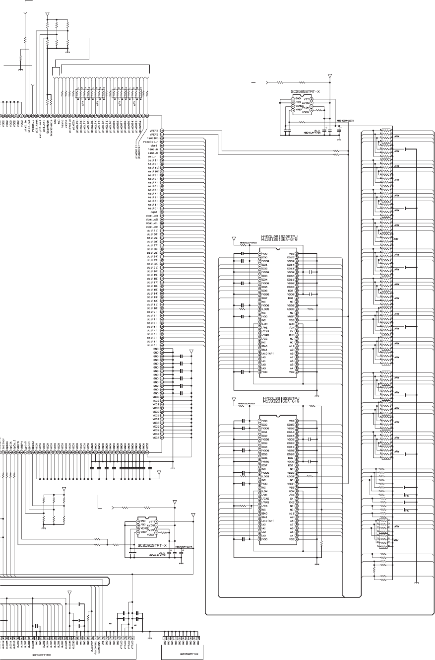
(No.YA463)2-60
DRIVE PWB ASS'Y(3/9)
SRA-3013A-M2
c10488001_0808_1/9_0.0
0
1
IC3104
R3173
C3174
C3175
C3176
C3179
C3178
C3172
C3173
C3177
C3186
C3187
C3181
C3180
C3182
C3183
C3184
C3185
R3175
R3174
IC3105
C3237
C3236
R3229
R3234
R3230
R3235
C3148
C3147
C3154
C3155
C3156
C3157
C3245
C3244
C3243
C3235
R3285
R3298
CNRG1
R3805
R3806
R3807 R3808
R3859
R3860
R3820
R3819
R3194
R3192
R3196
R3191
R3861
R3862
R3193
R3195
R3197
R3199
R3200
R3201
R3202
R3203
R3204
R3863
R3864
R3865
R3866
R3206
R3207
R3208
R3209
R3210
R3190
R3211
R3212
R3189
R3188
R3187
R3178
R3185
R3182
R3183
R3180
R3181
R3184
R3179
R3186
R3177
R3176
C3190
C3191
C3192
C3193
C3194
R3149
C3188
C3195
C3196
C3197
C3198
C3189
R3297
R3145
R3296
LCD_EN
R3150R3146
R3295
R3293
MEM_EN
R3281
R3216
R3217 R3215
R3214
R3294
R3282
C3200
C3201 C3207
C3208
C3209
C3210
C3206
C3205
C3204
CNR1
R3221
R3220
R3218
R3219
C3242
IC3114
R3286
R3284
R3283
C3234
IC3112
R3269
RPIXVALID
RVSYNC
RHSYNC
XCLKR
R3268
R3265
CA3008
RPIXCLK
C3133
C3134
C3136
C3137
C3138
C3140
C3142
C3146
C3129
C3132
C3131
/RESET3V
SDA
R3264
R3270
R3271
R3272
R3273
R3267
R3266
R3263
R3262
RPIXDH8
RPIXDH9
RPIXDH7
RPIXDH6
RPIXDH5
RPIXDH4
RPIXDH3
R3144
R3141
R3156
R3152
RPIXDH2
RPIXDL0
R3151
R3155
RPIXDL1
RPIXDL2
RPIXDL3
RPIXDL4
R3213
RPIXDL5
RPIXDL6
RPIXDL7
RPIXDL8
RPIXDL9
RPIXDH0
RPIXDH1
SCL
GND1
GND1
0
0.1
0.1
0.1
0.1
0.1
0.1
0.1
0.1
0.1
0.1
0.1
0.1
0.1
0.1
0.1
0.1
OPT
OPT
0.1
0.1
GND1
GND1
0
0
OPT
GND1
0
0.1
0.1
0.1
0.1
0.1
0.1
0.1
0.1
0.1
0.1
GND1
0
0
0
0
00
22
22
51
22
22
22
22
51
22
22
51
51
51
22
51
22
51
22
51
51
51
51
51
22
51
22
OPT
100
22
22
OPT
51
22
51
22
51
22
51
22
51
22
51
22
51
22
0.1
0.1
0.1
0.1
0.1
OPT
220/4
0.1
0.01
0.1
0.01
0.1
0
4.7K
GND1
0
4.7KOPT
ASID3R
0
OPT
OPT
MRD2R
OPT
4.7K 4.7K
OPT
ASID3R
OPT
OPT
0.1
0.1 0.01
0.1
0.01
0.1
0.1
0.1
220/4
VTTLCDR
4.7K
OPT
OPT
4.7K
47
0
0
0
LCD2R
47
51
51
51
0.1
0.1
0.1
0.1
0.1
0.1
0.1
0.1
0.1
0.1
0.1
0.1 51
0
51
51
51
51
51
51
51
OPT
0
0
0
4.7k
4.7k
OPT
RBS1
RMAB12
MRD2R
R/CSB
RMAB0
RMAB10
RMAB1
RMAB2
RMAB3 RMAB4
RMAB5
RMAB11
RMAB9
RMAB8
RMAB7
RMAB6
RDQB16
RDQB17
RDQB18
RDQB19
RDQB20
RDQB21
RDQB22
RDQB23 RDQB24
RDQB25
RDQB26
RDQB27
RDQB28
RDQB29
RDQB30
RDQB31
RDQMB
RBAB0
RBAB1
RDQSB2 RDQSB3
RVREF_MEM_B1
RCKEB
RCKB
R/CKB
R/WEB
R/CASB
R/RASB
MRD2R
RMAB0
RMAB10
RMAB1
RMAB2
RMAB3 RMAB4
RMAB5
RMAB11
RMAB9
RMAB8
RMAB7
RMAB6
RDQB0
RDQB1
RDQB2
RDQB3
RDQB4
RDQB5
RDQB6
RDQB7 RDQB8
RDQB9
RDQB10
RDQB11
RDQB12
RDQB13
RDQB14
RDQB15
RDQMB
RBAB0
RBAB1
RDQSB1
RVREF_MEM_B2
RCKEB
RCKB
R/CKB
R/WEB
R/CASB
RMAB12
R/RASB
R/CSB
RBS5
GND1
MRD2R_3
MRD2R_4
GND1
RMAB11
RMAB10
RMAB9
RMAB8
RVTTB
RBS3
RMAB7
RMAB6
RMAB5
RMAB4
RMAB3
RMAB2
RMAB1
RMAB0
RMAB-11
RMAB-10
RMAB-9
RMAB-8
RMAB-7
RMAB-6
RMAB-5
RMAB-4
RMAB-3
RMAB-2
RMAB-1
RMAB-0
RDQSB0 RDQSB-0
RDQSB-1RDQSB1
RDQSB3 RDQSB-3
RDQSB2 RDQSB-2
RDQM-BRDQMB
RBAB1 RBAB-1
RBAB-0RBAB0
R/WEB R /WE-B
R/CASB R /CAS-B
R/RAS-BR/RASB
RCKE-BRCKEB
R/CKB R/CK-B
RCKB RCK-B
RDQB31
RDQB30
RDQB29
RDQB28
RDQB-31
RDQB-30
RDQB-29
RDQB-28
RDQB27
RDQB25
RDQB24
RDQB26
RDQB-24
RDQB-25
RDQB-26
RDQB-27
RDQB-23
RDQB-22
RDQB-21
RDQB-20
RDQB-19
RDQB-18
RDQB-17
RDQB-16
RDQB20
RDQB22
RDQB23
RDQB21
RDQB19
RDQB18
RDQB17
RDQB16
RDQB15
RDQB12
RDQB14
RDQB13
RDQB11
RDQB10
RDQB9
RDQB8
RDQB6
RDQB5
RDQB4
RDQB7
RDQB0
RDQB1
RDQB2
RDQB3
RDQB-15
RDQB-14
RDQB-13
RDQB-12
RDQB-11
RDQB-10
RDQB-8
RDQB-9
RDQB-4
RDQB-5
RDQB-6
RDQB-7
RDQB-0
RDQB-1
RDQB-2
RDQB-3
VLCD3R
ASID1R
MEM_EN
GND1
LCD_EN
ASID2R
RCK-B
R/CK-B
RDQSB0
RCKE-B
R/RAS-B
R/CAS-B
R/WE-B
RBAB-1
RBAB-0
RMAB-11
RMAB-10
RMAB-9
RMAB-8
RMAB-7
RMAB-6
RMAB-5
RMAB-4
RMAB-3
RMAB-2
RMAB-1
RMAB-0
RDQM-B
RDQSB-3
RDQSB-2
RDQSB-1
RDQSB-0
RDQB-31
RDQB-30
RDQB-29
RDQB-28
RDQB-27
RDQB-26
RDQB-25
RDQB-24
RDQB-23
RDQB-22
RDQB-21
RDQB-20
RDQB-19
RDQB-18
RDQB-17
RDQB-16
RDQB-15
RDQB-14
RDQB-13
RDQB-12
RDQB-11
RDQB-10
RDQB-9
RDQB-8
RDQB-7
RDQB-6
RDQB-5
RDQB-4
RDQB-3
RDQB-2
RDQB-1
RDQB-0
XCLKR
RULCDLNCR
RDPSD0
RDPCLK
RDPCS
RV0SEL
RV1SEL
RULCDLNCR
/RESET3V
RULCD12
RULCD11
RULCD10
RULCD9
RULCD8
RULCD7
RULCD6
RULCD5
RULCD4
RULCD3
RULCD2
RULCD1
RULCD0
RBS1
SHEET27,28,30
SHEET25
SHEET27,28,30
SHEET27,28,30
0
SHEET27
DEVICE OPEN
C
E DRIVE
RAM
RAM
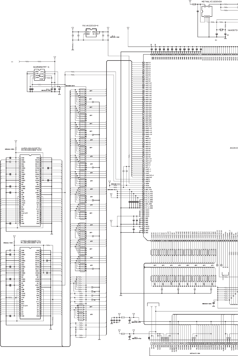
2-61(No.YA463)
C3301
C3309
C3302
C3303
C3304
IC3
IC3302
C3305
C3306
C3308
C3307
C3310
C3311
C3312
IC3303
C3313
C3314
C3316
C3315
R3301
R3302
R3303
R3322
R3320
R3324
R3893
R3894
R3823
R3824
R3319
CA3009
R3321
R3323
R3325
R3327
R3328
R3329
R3330
R3331
R3332
R3499
R3427
R3423
R3422
CA3010
CA3011
CA3012
R3487
C3441
R3334
R3335
R3336
R3337
R3338
R3318
R3339
R3340
R3317
R3316
R3315
R3306
R3313
R3310
R3311
R3308
R3309
R3312
R3307
R3314
R3305
R3304
C3319
C3320
C3321
C3322
R3479
IC3307
C3323
K3305
C3318
K3307
R3433
C3369
C3317
C3370
C3324
C3325
C3326
C3327
C3371
C3363
C3416
C3366
C3417
C3367
R3430
R3431
R3426
C3362
R3478
C3418
R3477
R3429
R3476
R3475
R3474
K3306
X3301
R3424
R3425
MEM_EN
R3895
R3896
R3897
R3898
R3867
R3868 C3368
C3440
C3439
R3364
R3492
R3363 R3362 R3361 R3357R3358R3359R3360
R3480
R3491
R3490
C3448
C3421
C3420
R3489
C3399
C3423 D3301
CNG1
C3328
IC3308
C3438
C3422C3419
IC3313
R3405
R3432
R3488
TP3357
TP3355
C3345
C3344
C3353
C3352
C3351
C3350
C3349
C3361
C3360
C3358
C3359
C3365
C3335
C3339
C3341
C3343
C3364
C3330
R3372
R3371
R3370
R3369
R3365
R3366
R3367
R3368
R3354
R3348
R3347
R3343
R3353
GV1REF
GVITOR_B
GVITOREF
C3403
C3402
C3413
C3414
C3447
C3411
C3412
C3446
0.1
0.1
0.1
0.1
0.1
0.1
0.1
0.1
0.1
0.1
0.1
0.1
0.1
0.1
0.1
0.1
0
OPT
OPT
22
22
22
22
22
22
51
51
0.1
51
51
51
22
51
22
51
22
51
0
22
0.1
0.1
0.1
GND1
OPT
0.1
22
51
22
OPT
100
22
22
OPT
51
22
51
22
51
22
51
22
51
22
51
22
51
22
0.1
0.1
0.1
0.1
51
0.1
*K1
0.1
*K1
0
0.1
220/4
0.1
0.1
0.01
0.1
0.01
0.1
0.1
18p
0.1
18p
0.1
47
47
0
0.1
51
0.1
51
OPT
51
51
51
*K1
0
1M
ASID3G
22
22
51
51
51
51 0.1
0.1
0.1
GND1
51
0
51 51 51 51515151
51
0
0
33/4
0.1
OPT
0
GND1
47
47 OPT
0.1
ASIA3G
GND1
MRD2G
47
ASIA1G
10
GND1
OPT
GND1
33
0
OPT
OPT
OPT
0.1
0.1
0.1
0.01
0.1
0.1
0.01
0.1
0.1
0.1
0.1
0.1
0.1
0.1
0.1
0.1
0.1
0.1
51
51
51
51
51
51
51
51
22
22
10
10
22
0.1
0.1
0.1
0.1
0.1
0.1
0.1
0.1
GBSO
GDQMA
GBS2
GMAA0
GMAA3
GMAA1
GMAA2
MRD2G
GMAA10
GMAA4
GMAA5
GMAA6
GMAA7
GMAA8
GMAA9
GMAA11
GDQA20
GDQA16
GDQA17
GDQA18
GDQA19
GDQA21
GDQA22
GDQA23
GDQA31
GDQA26
GDQA30
GDQA29
GDQA28
GDQA27
GDQA25
GDQA24
GBAA0
GBAA1
G/WEA
G/CASA
G/RASA
G/CSA
G/CKA
GCKA
GCKEA
GDQSA2 GDQSA3
GVREF_MEM_A1
GMAA12
MRD2G
G/CSA
MRD2G_1
GND1
GBS4
GDQMA
GMAA0
GMAA3
GMAA1
GMAA2
GMAA10
GMAA4
GMAA5
GMAA6
GMAA7
GMAA8
GMAA9
GMAA11
GDQA0
GDQA1
GDQA2
GDQA3
GDQA4
GDQA5
GDQA6
GDQA7
GDQA14
GDQA10
GDQA11
GDQA12
GDQA13
GDQA9
GDQA15
GDQA8
GBAA0
GBAA1
G/WEA
G/CASA
G/RASA
ASID2G
G/CKA
GCKA
GCKEA
GDQSA0 GDQSA1
GVREF_MEM_A
GMAA12
GMAA11
GMAA10
GMAA9
GMAA8
GVTTA
GMAA7
GMAA3
GMAA6
GDQSA0
GMAA5
GMAA4
GMAA2
GDQSA-0
GMAA1
GDQSA-1
GMAA0
GDQM-A
GDQSA1
GDQSA3 GDQSA-3
GDQSA2 GDQSA-2
GDQMA
G/CASA
GMAA-11
GMAA-10
GMAA-9
GMAA-8
GMAA-7
GMAA-6
GMAA-5
GMAA-4
GMAA-3
GMAA-2
GMAA-1
GMAA-0
GBAA1 GBAA-1
GBAA-0
G/CAS-A
GBAA0
G/RAS-A
G/WEA G /WE-A
G/RASA
GCKE-A
GVREF_MEM_A2
GCKEA
G/CKA
GCK-A
G/CK-A
AVCC3
ASID1G
GCK-AGCKA
GBS4
G/CK-A
GCKE-A
G/RAS-A
LCD2G
UGVITO
GDQA31
GDQA30
GDQA29
GDQA28
GDQA-31
GDQA-30
GDQA-29
GDQA-28
GDQA-23
GDQA27
GDQA-22
GDQA25
GDQA26
GDQA-21
GDQA-20
GDQA24
MRD2G_2
GDQA-24
GDQA-25
GDQA-26
GDQA-27
GDQA-19
GDQA-18
GDQA-17
GDQA-16
GDQA22
GDQA13
GDQA20
GDQA21
GDQA23
GDQA18
GDQA15
GDQA17
GDQA14
GDQA19
GDQA16
GDQA11
GDQA9
GDQA10
GDQA8
GDQA4
GDQA5
GDQA6
GDQA7
GDQA1
GDQA2
GDQA0
GDQA3
GDQA-15
GDQA-14
GDQA-13
GDQA-12GDQA12
GDQA-11
GDQA-10
GDQA-8
GDQA-9
GDQA-4
GDQA-5
GDQA-6
GDQA-7
GDQA-0
GDQA-1
GDQA-2
GDQA-3
GND1
UGV1
G/CAS-A
G/WE-A
GBAA-1
GBAA-0
GMAA-11
GDQA-0
GDQA-1
GDQA-2
GDQA-3
GDQA-4
GDQA-5
GND1
GDQA-6
GDQA-7
GDQA-8
GDQA-9
GDQA-10
GDQA-11
GDQA-12
GDQA-13
GDQA-14
GDQA-15
GDQA-16
GDQA-17
GDQA-18
GND1
GDQA-19
MEM_EN
GND1
VLCD2G
GDQA-20
GDQA-21
GDQA-22
GDQA-23
GDQA-24
GDQA-25
GDQA-26
GDQA-27
GDQA-28
GDQA-29
ASIA3G
GDQA-30
VLCD3G
GDQA-31
GDQSA-0
DR-VCC5
GDQSA-1
GDQSA-2
GDQSA-3
GDQM-A
GMAA-0
GMAA-1
GMAA-2
GMAA-3
GMAA-4
GMAA-5
GMAA-6
GMAA-7
GMAA-8
GMAA-9
GMAA-10
GULCD2
GULCD29
GULCD28
GDPSD0
GDPCLK
GDPCS
GUOP1
GUCLK1
GUCLK1
GUOP0
GUCLK0
GUCLK0
GV0SEL
GV1SEL
GULCD3
GULCD0
GULCD1
GLCD2
GULCD7
GULCD6
GULCD5
GULCD4
GULCD10
GULCD11
GULCD8
GULCD9
GULCD14
GULCD15
GULCD12
GULCD13
GULCD18
GULCD19
GULCD16
GULCD17
GULCD22
GULCD23
GULCD20
GULCD21
GULCD27
GULCD26
GULCD25
GULCD24
GULCD30
GULCD31
GLCD3
GLCD0
GLCD1
GLCD7
GLCD6
GLCD5
GLCD4
GLCD10
GLCD11
GLCD8
GLCD9
GLCD14
GLCD15
GLCD12
GLCD13
GLCD18
GLCD19
GLCD16
GLCD17
GLCD22
GLCD23
GLCD20
GLCD21
GLCD27
GLCD26
GLCD25
GLCD24
GLCD30
GLCD31
GLCD28
GLCD29
GULCD2
GULCD3
GULCD0
GULCD1
GULCD7
GULCD6
GULCD5
GULCD4
GULCD10
GULCD11
GULCD8
GULCD14
GULCD9
GULCD15
GULCD12
GULCD13
GULCD18
GULCD19
GULCD16
GULCD17
GULCD22
GULCD23
GULCD20
GULCD21
GULCD27
GULCD26
GULCD25
GULCD24
GULCD30
GULCD31
GULCD28
GULCD29
GULCD31
GULCD30
GULCD29
GULCD28
GULCD27
GULCD26
GULCD25
GULCD24
GULCD23
GULCD22
GULCD21
GULCD20
GULCD19
GULCD18
GULCD17
GULCD16
GULCD15
GULCD14
GBSO
SHEET26,28,30
S
H
SHEET29
SHEET29
G D-ILA D
E
G DEVI
C
RAM
RAM
SHEET27
,
DRIVE PWB CIRCUIT DIAGRAM (4/9) [G_DRIVER] SHEET 27
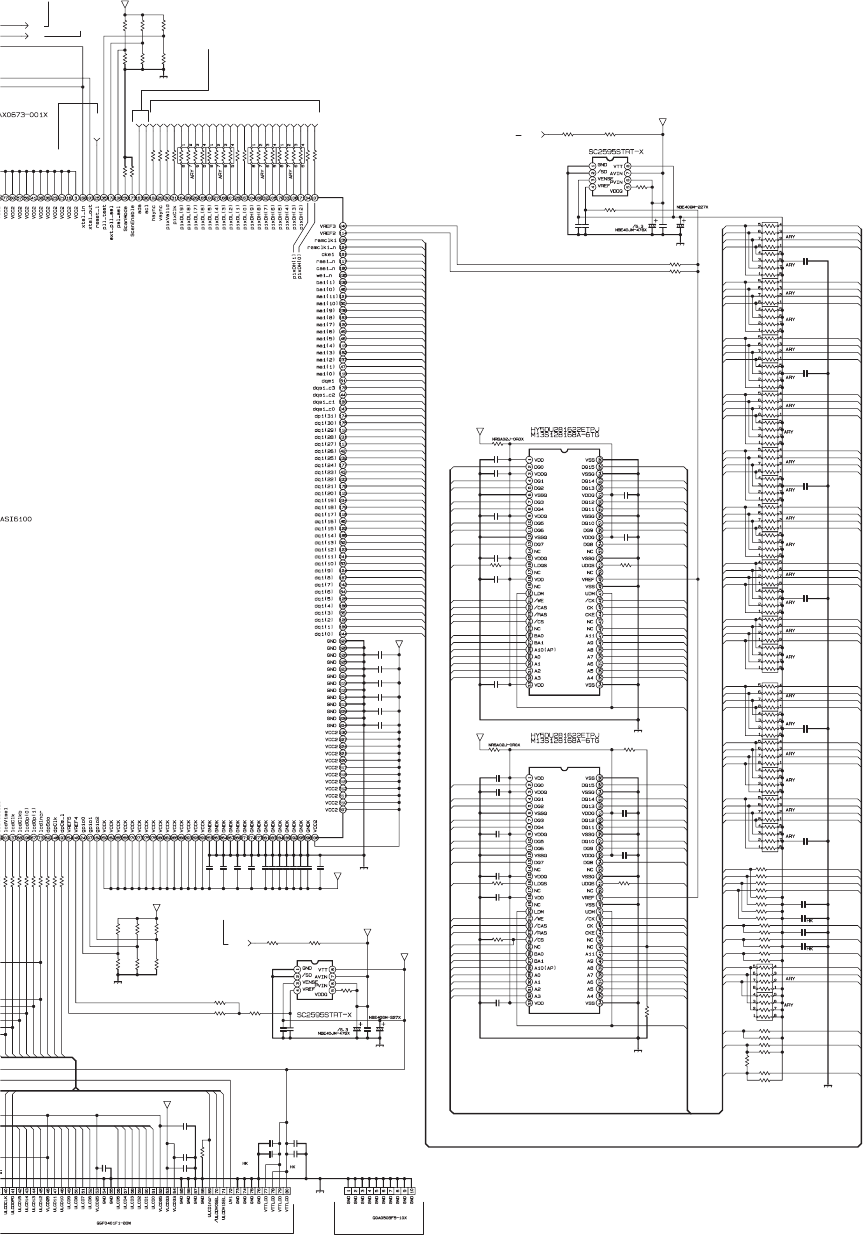
(No.YA463)2-62
DRIVE PWB ASS'Y(4/9)
SRA-3013A-M2
c10488002_0808_2/9_0.0
IC3301
IC3304
R3373
C3374
C3375
C3376
C3379
C3378
C3372
C3373
C3377
C3386
C3387
C3381
C3380
C3382
C3383
C3384
C3385
R3375
R3374
IC3305
C3437
C3436
R3434
6
R3435
C3348
C3347
0
1
C3354
C3355
C3356
C3357
XCLKR
XCLKB
C3445
C3444
C3443
C3435
R3485
R3498
CNGG1
R3801
R3802
R3803 R3804
R3869
R3870
R3828
R3827
R3394
R3392
R3396
R3391
R3871
R3872
R3393
R3395
R3397
R3399
R3400
R3401
R3402
R3403
R3404
R3873
R3874
R3875
R3876
R3406
R3407
R3408
R3409
R3410
R3390
R3411
R3412
R3389
R3388
R3387
R3378
R3385
R3382
R3383
R3380
R3381
R3384
R3379
R3386
R3377
R3376
C3390
C3391
C3392
C3393
C3394
R3349
C3388
C3395
C3396
C3397
C3398
C3389
R3497
R3345
R3496
LCD_EN
R3350R3346
R3495
R3493
MEM_EN
R3481
R3416
R3417 R3415
R3414
R3494
R3482
C3400
C3401 C3407
C3408
C3409
C3410
C3406
C3405
C3404
CNG1
R3421
R3420
R3418
R3419
C3442
IC3314
R3486
R3484
R3483
C3434
IC3312
R3469
GPIXVALID
CA3013
GVSYNC
GHSYNC
R3468
R3465
GPIXCLK
C3333
C3334
C3336
C3337
C3338
C3340
C3342
C3346
C3329
C3332
C3331
/RESET3V
SDA
R3464
R3470
R3471
R3472
R3473
R3467
R3466
R3463
R3462
GPIXDH8
GPIXDH9
GPIXDH7
GPIXDH6
GPIXDH5
GPIXDH4
GPIXDH3
R3344
R3354
R3347
R3343
R3342
R3353
R3341
R3356
R3352
GPIXDH2
GPIXDL0
R3351
R3355
GPIXDL1
GPIXDL2
GPIXDL3
GPIXDL4
C3402
R3413
GPIXDL5
GPIXDL6
GPIXDL7
GPIXDL8
GPIXDL9
GPIXDH0
GPIXDH1
SCL
GND1
GND1
0
0.1
0.1
0.1
0.1
0.1
0.1
0.1
0.1
0.1
0.1
0.1
0.1
0.1
0.1
0.1
0.1
OPT
OPT
0.1
0.1
GND1
GND1
0
0
0.1
0.1
0.1
0.1
0.1
0.1
0.1
0.1
0.1
0.1
GND1
0
0
0
0
00
22
22
51
22
22
22
22
51
22
22
51
51
51
22
51
22
51
22
51
51
51
51
51
22
51
22
OPT
100
22
22
OPT
51
22
51
22
51
22
51
22
51
22
51
22
51
22
0.1
0.1
0.1
0.1
0.1
OPT
220/4
0.1
0.01
0.1
0.01
0.1
0
4.7K
GND1
0
4.7KOPT
ASID3G
0
OPT
OPT
MRD2G
OPT
4.7K 4.7K
OPT
ASID3G
OPT
OPT
0.1
0.1 0.01
0.1
0.01
0.1
0.1
0.1
220/4
VTTLCDG
OPT
4.7K
GND1
OPT
4.7K
47
0
0
0
LCD2G
47
51
0.1
51
51
0.1
0.1
0.1
0.1
0.1
0.1
0.1
0.1
0.1
0.1
0.1 51
51
51
51
51
51
51
51
51
OPT
22
10
10
22
22
0
0
0
4.7k
4.7k
0
.
1
OPT
GBS1
GMAB12
MRD2G
G/CSB
GMAB0
GMAB10
GMAB1
GMAB2
GMAB3 GMAB4
GMAB5
GMAB11
GMAB9
GMAB8
GMAB7
GMAB6
GDQB16
GDQB17
GDQB18
GDQB19
GDQB20
GDQB21
GDQB22
GDQB23 GDQB24
GDQB25
GDQB26
GDQB27
GDQB28
GDQB29
GDQB30
GDQB31
GDQMB
GBAB0
GBAB1
GDQSB2 GDQSB3
GVREF_MEM_B1
GCKEB
GCKB
G/CKBG/WEB
G/CASB
G/RASB
MRD2G
GMAB0
GMAB10
GMAB1
GMAB2
GMAB3 GMAB4
GMAB5
GMAB11
GMAB9
GMAB8
GMAB7
GMAB6
GDQB0
GDQB1
GDQB2
GDQB3
GDQB4
GDQB5
GDQB6
GDQB7 GDQB8
GDQB9
GDQB10
GDQB11
GDQB12
GDQB13
GDQB14
GDQB15
GDQMB
GBAB0
GBAB1
GDQSB1
GVREF_MEM_B2
GCKEB
GCKB
G/CKB
G/WEB
G/CASB
GMAB12
G/RASB
G/CSB
GBS5
GND1
GBS5
MRD2G_3
MRD2G_4
GMAB11
GMAB10
GMAB9
GMAB8
GVTTB
GBS3
GMAB7
GMAB6
GMAB5
GMAB4
GMAB3
GMAB2
GMAB1
GMAB0
GMAB-11
GMAB-10
GMAB-9
GMAB-8
GMAB-7
GMAB-6
GMAB-5
GMAB-4
GMAB-3
GMAB-2
GMAB-1
GMAB-0
GDQSB0 GDQSB-0
GDQSB-1GDQSB1
GDQSB3 GDQSB-3
GDQSB2 GDQSB-2
GDQM-BGDQMB
GBAB1 GBAB-1
GBAB-0GBAB0
G/WEB G /WE-B
G/CASB G/CAS-B
G/RAS-BG/RASB
GCKE-BGCKEB
G/CKB G /CK-B
GCKB GCK-B
GDQB31
GDQB30
GDQB29
GDQB28
GDQB-31
GDQB-30
GDQB-29
GDQB-28
GDQB27
GDQB25
GDQB24
GDQB26
GDQB-24
GDQB-25
GDQB-26
GDQB-27
GDQB-23
GDQB-22
GDQB-21
GDQB-20
GDQB-19
GDQB-18
GDQB-17
GDQB-16
GDQB20
GDQB22
GDQB23
GDQB21
GDQB19
GDQB18
GDQB17
GDQB16
GDQB15
GDQB12
GDQB14
GDQB13
GDQB11
GDQB10
GDQB9
GDQB8
GDQB6
GDQB5
GDQB4
GDQB7
GDQB0
GDQB1
GDQB2
GDQB3
GDQB-15
GDQB-14
GDQB-13
GDQB-12
GDQB-11
GDQB-10
GDQB-8
GDQB-9
GDQB-4
GDQB-5
GDQB-6
GDQB-7
GDQB-0
GDQB-1
GDQB-2
GDQB-3
VLCD3G
ASID1G
GND1
MEM_EN
LCD_EN
ASID2G
GCK-B
G/CK-B
GDQSB0
GCKE-B
G/RAS-B
G/CAS-B
G/WE-B
GBAB-1
GBAB-0
GMAB-11
GMAB-10
GMAB-9
GMAB-8
GMAB-7
GMAB-6
GMAB-5
GMAB-4
GMAB-3
GMAB-2
GMAB-1
GMAB-0
GDQM-B
GDQSB-3
GDQSB-2
GDQSB-1
GDQSB-0
GDQB-31
GDQB-30
GDQB-29
GDQB-28
GDQB-27
GDQB-26
GDQB-25
GDQB-24
GDQB-23
GDQB-22
GDQB-21
GDQB-20
GDQB-19
GDQB-18
GDQB-17
GDQB-16
GDQB-15
GDQB-14
GDQB-13
GDQB-12
GDQB-11
GDQB-10
GDQB-9
GDQB-8
GDQB-7
GDQB-6
GDQB-5
GDQB-4
GDQB-3
GDQB-2
GDQB-1
GDQB-0
GULCDLNCR
GDPSD0
GDPCLK
GDPCS
GUOP1
GUCLK1
GUOP0
GUOP0
GUCLK0
GUCLK0
GV0SEL
GV0SEL
GV1SEL
GV1SEL
GULCDLNCR
/RESET3V
GULCD15
GULCD14
GULCD13
GULCD12
GULCD11
GULCD10
GULCD9
GULCD8
GULCD7
GULCD6
GULCD5
GULCD4
GULCD3
GULCD2
GULCD1
GULCD0
GBS1
SHEET28
SHEET26
SHEET25
SHEET26,28,30
SHEET26,28,30
SHEET26,28,30
A
DEVICE OPEN
EVICE DRIVE
RAM
RAM
T
27,28,30
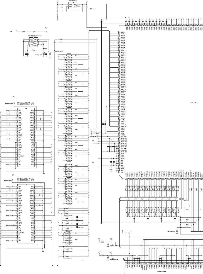
2-63(No.YA463)
C3501
C3509
C3502
C3503
C3504
IC3501
IC3502
C3505
C3506
C3508
C3507
C3510
C3511
C3512
IC3503
C3513
C3514
C3516
C3515
R3501
R3502
R3503
R3522
R3520
R3524
R3877
R3878
R3831
R3832
R3519
CA3014
R3521
R3523
R3525
R3527
R3528
R3529
R3530
R3531
R3532
R3699
R3627
R3623
R3622
R3687
C3641
R3534
R3535
R3536
R3537
R3538
R3518
R3539
R3540
R3517
R3516
R3515
R3506
R3513
R3510
R3511
R3508
R3509
R3512
R3507
R3514
R3505
R3504
C3519
C3520
C3521
C3522
R3679
C3523
K3505
C3518
K3507
R3633
C3569
C3517
C3570
C3524
C3525
C3526
C3527
C3571
C3563
C3566C3567
C3622
C3562
R3678
C3619
R3677
C3648
R3676
R3675
R3605
R3674
R3632
MEM_EN
R3879
R3880
R3881
R3882
R3883
R3884 C3568
C3640
C3639
R3564
R3692
R3563 R3562 R3561 R3557R3558R3559R3560
R3680
R3691
R3690
C3621C3620
R3689
C3599
C3623 D3501
IC3508
CNB1
C3528
C3638
IC3513
R3688
TP3557
TP3555
C3545
C3544
C3553
C3552
C3551
C3550
C3549
C3561
C3560
C3558
C3559
C3565
C3535
C3539
C3541
C3543
C3564
C3530
R3572
R3571
R3570
R3569
R3565
R3566
R3567
R3568
R3544
R3554
R3548
R3547
R3543
R3542
R3553
R3541
R3556
BV1REF
BVITOR_B
BVITOREF
C3603
C3602
C3613
C3614
C3667
C3611
C3612
C3666
0.1
0.1
0.1
0.1
0.1
0.1
0.1
0.1
0.1
0.1
0.1
0.1
0.1
0.1
0.1
0.1
0
OPT
OPT
22
22
22
22
22
22
51
51
0.1
51
51
51
22
51
22
51
22
51
0
22
OPT
0.1
22
51
22
OPT
100
22
22
OPT
51
22
51
22
51
22
51
22
51
22
51
22
51
22
0.1
0.1
0.1
0.1
51
0.1
*K1
0.1
*K1
0
0.1
220/4
0.1
0.1
0.01
0.1
0.01
0.1
0.1
0.10.1
10
0.1
51
OPT
51
33/4
51
51
15
51
0
ASID3B
22
22
51
51
51
51 0.1
0.1
0.1 GND1
51
0
51 51 51 51515151
51
0
0
0.1OPT
0
GND1
47
47 OPT
0.1
ASIA3B
GND1
MRD2B
47
ASIA1B
GND1
GND1
OPT
OPT
OPT
0.1
0.1
0.1
0.01
0.1
0.1
0.01
0.1
0.1
0.1
0.1
0.1
0.1
0.1
0.1
0.1
0.1
0.1
51
51
51
51
51
51
51
51
OPT
22
22
22
22
22
22
0
0
0.1
0.1
0.1
0.1
0.1
0.1
0.1
0.1
GND1
MRD2B_1
GND1
BDQMA
BMAA0
BMAA3
BMAA1
BMAA2
BMAA10
BMAA4
BMAA5
BMAA6
BMAA7
BMAA8
BMAA9
BMAA11
BDQA16
BDQA17
BDQA18
BDQA19
BDQA20
BDQA21
BDQA22
BDQA23
BDQA30
BDQA26
BDQA27
BDQA28
BDQA29
BDQA25
BDQA31
BDQA24
BBAA0
BBAA1
B/WEA
B/CASA
B/RASA
B/CSA
B/CKA
BCKA
BCKEA
BDQSA2 BDQSA3
BMAA12
MRD2B_2
GND1
BDQMA
BMAA0
BMAA3
BMAA1
BMAA2
BMAA10
BMAA4
BMAA5
BMAA6
BMAA7
BMAA8
BMAA9
BMAA11
BDQA0
BDQA1
BDQA2
BDQA3
BDQA4
BDQA5
BDQA6
BDQA7
BDQA14
BDQA10
BDQA11
BDQA12
BDQA13
BDQA9
BDQA15
BDQA8
BBAA0
BBAA1
B/WEA
B/CASA
B/RASA
B/CKA
BCKA
BCKEA
BDQSA0 BDQSA1
GND1
BMAA12
B/CSA
ASID2B
BMAA11
BMAA10
BMAA9
BMAA8
BVTTA
BMAA7
BMAA6
BMAA5
BMAA4
BMAA3
BMAA2
BMAA1
BMAA0
BMAA-11
BMAA-10
BMAA-9
BMAA-8
BMAA-7
BMAA-6
BMAA-5
BMAA-4
BMAA-3
BMAA-2
BMAA-1
BMAA-0
BDQSA0 BDQSA-0
BDQSA-1BDQSA1
BDQSA3 BDQSA-3
BDQSA2 BDQSA-2
BDQM-ABDQMA
BBAA1 BBAA-1
BBAA-0BBAA0
B/WEA B /WE-A
B/CASA B/CAS-A
B/RAS-AB/RASA
BCKE-ABCKEA
B/CKA B/CK-A
BCKA BCK-A
AVCC3 VLCD3B
LCD2B
BDQA31
BDQA30
BDQA29
BDQA28
BDQA-31
BDQA-30
BDQA-29
BDQA-28
BDQA27
BDQA25
BDQA24
BDQA26
BDQA-24
BDQA-25
BDQA-26
BDQA-27
BDQA-23
BDQA-22
BDQA-21
BDQA-20
BDQA-19
BDQA-18
BDQA-17
BDQA-16
BDQA20
BDQA22
BDQA23
BDQA21
BDQA19
BDQA18
BDQA17
BDQA16
BDQA15
BDQA12
BDQA14
BDQA13
BDQA11
BDQA10
BDQA9
BDQA8
BDQA6
BDQA5
BDQA4
BDQA7
BDQA0
BDQA1
BDQA2
BDQA3
BDQA-15
BDQA-14
BDQA-13
BDQA-12
BDQA-11
BDQA-10
BDQA-8
BDQA-9
BDQA-4
BDQA-5
BDQA-6
BDQA-7
BDQA-0
BDQA-1
BDQA-2
BDQA-3
BVREF_MEM_A1
BVREF_MEM_A2
VLCD2B
MRD2B
MRD2B
UBV1
BCK-A
UBVITO
ASIA3B DR-VCC5
BVREF_MEM_A
B/CK-A
BCKE-A
B/RAS-A
B/CAS-A
B/WE-A
BBAA-1
BBAA-0
BMAA-11
BDQA-0
BDQA-1
BDQA-2
BDQA-3
BDQA-4
BDQA-5
BDQA-6
BDQA-7
BDQA-8
BDQA-9
BDQA-10
BDQA-11
BDQA-12
BDQA-13
BDQA-14
BDQA-15
BDQA-16
BDQA-17
BDQA-18
BDQA-19
BDQA-20
BDQA-21
BDQA-22
BDQA-23
BDQA-24
BDQA-25
BDQA-26
BDQA-27
BDQA-28
BDQA-29
BDQA-30
BDQA-31
BDQSA-0
BDQSA-1
BDQSA-2
BDQSA-3
BDQM-A
MEM_EN
BMAA-0
BMAA-1
BMAA-2
BMAA-3
BMAA-4
BMAA-5
BMAA-6
BMAA-7
BMAA-8
BMAA-9
BMAA-10
BBS0
BBS2
BBS4
BBS4
BULCDLNCR
BULCD29
BULCD28
DPSD0B
DPSD0B
DPCLKB
DPCSB
U0PB1
U0PB1
UCLK1B
UCLK1B
U0PB0
U0PB0
BLCD2
BLCD3
BLCD0
BLCD1
BLCD7
BLCD6
BLCD5
BULCD2
UCLK0B
UCLK0B
BLCD4
BV0SEL
BV1SEL
BULCD3
BULCD0
BULCD1
BULCD7
BULCD6
BULCD5
BULCD4
BULCD10
BULCD11
BULCD8
BULCD9
BULCD14
BULCD15
BULCD12
BULCD13
BULCD18
BULCD19
BLCD10
BLCD11
BLCD8
BLCD9
BULCD16
BLCD14
BLCD15
BLCD12
BLCD13
BLCD18
BULCD17
BULCD31
BULCD30
BULCD22
BULCD29
BULCD23
BULCD20
BULCD21
BULCD27
BULCD26
BULCD25
BULCD24
BULCD30
BULCD31
BV1REF
BVITOR_B
BULCD28
BULCD27
BULCD26
BULCD25
BULCD24
BULCD23
BULCD22
BULCD21
BULCD20
BULCD19
BULCD18
BULCD17
BULCD16
BVITOREF
BULCD15
BULCD14
BULCD13
BULCD12
BULCD11
BLCD19
BLCD16
BLCD17
BLCD22
BLCD23
BLCD20
BLCD21
BLCD27
BLCD26
BLCD25
BLCD24
BLCD30
BLCD31
BLCD28
BLCD29
BULCD2
BULCD3
BULCD0
BULCD1
BULCD7
BULCD6
BULCD5
BULCD4
BULCD10
BULCD11
BULCD8
BULCD14
BULCD9
BULCD15
BULCD12
BULCD13
BULCD18
BULCD19
BULCD16
BULCD17
BULCD22
BULCD23
BULCD20
BULCD21
BULCD27
BULCD26
BULCD25
BULCD24
BULCD30
BULCD31
BULCD28
BULCD29
BBS0
SHEET26,27,30
SHEET
2
SHEET29
SHEET29
B D-ILA
D
B DEVICE
RAM
RAM
DRIVE PWB CIRCUIT DIAGRAM (5/9) [B_DRIVER] SHEET 28
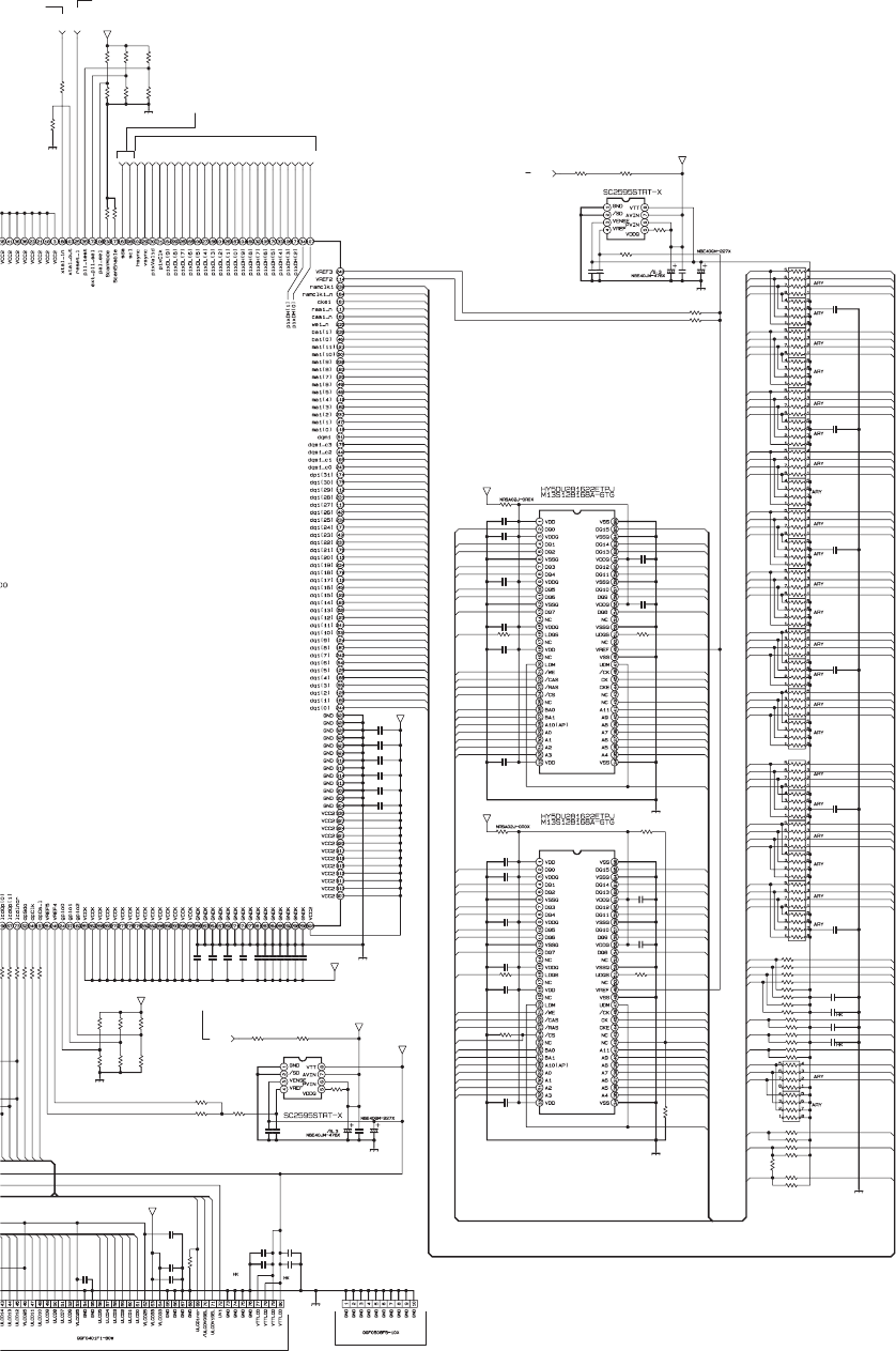
(No.YA463)2-64
DRIVE PWB ASS'Y(5/9)
SRA-3013A-M2
c10488003_0808_3/9_0.0
501
IC3504
R3573
C3574
C3575
C3576
C3579
C3578
C3572
C3573
C3577
C3586
C3587
C3581
C3580
C3582
C3583
C3584
C3585
R3575
R3574
IC3505
C3637
C3636
R3629
R3634
R3630
R3635
C3548
C3547
C3554
C3555
C3556
C3557
C3645
C3644
C3643
C3635
R3685
R3698
CNBG1
R3809
R3810
R3811 R3812
R3885
R3886
R3836
R3835
R3594
R3592
R3596
R3591
R3887
R3888
R3593
R3595
R3597
R3599
R3600
R3601
R3602
R3603
R3604
R3889
R3890
R3891
R3892
R3606
R3607
R3608
R3609
R3610
R3590
R3611
R3612
R3589
R3588
R3587
R3578
R3585
R3582
R3583
R3580
R3581
R3584
R3579
R3586
R3577
R3576
C3590
C3591
C3592
C3593
C3594
R3549
C3588
C3595
C3596
C3597
C3598
C3589
R3697
R3545
R3696
LCD_EN
R3550R3546
R3695
R3693
MEM_EN
R3681
R3616
R3617 R3615
R3614
R3694
R3682
C3600
C3601 C3607
C3608
C3609
C3610
C3606
C3605
C3604
CNB1
R3621
R3620
R3618
R3619
C3642
IC3514
R3686
R3684
R3683
C3634
IC3512
BPIXVALID
BVSYNC
BHSYNC
XCLKB
/RESET3V
BPIXCLK
C3533
C3534
C3536
C3537
C3538
C3540
C3542
C3546
C3529
C3532
C3531
SDA
BPIXDH8
BPIXDH9
BPIXDH7
BPIXDH6
BPIXDH5
BPIXDH4
BPIXDH3
R3544
R3542
R3541
R3556
R3552
BPIXDH2
BPIXDL0
R3551
R3555
BPIXDL1
BPIXDL2
BPIXDL3
BPIXDL4
R3613 BPIXDL5
BPIXDL6
BPIXDL7
BPIXDL8
BPIXDL9
BPIXDH0
BPIXDH1
SCL
GND1
GND1
0
0.1
0.1
0.1
0.1
0.1
0.1
0.1
0.1
0.1
0.1
0.1
0.1
0.1
0.1
0.1
0.1
OPT
OPT
0.1
0.1
GND1
GND1
0
0
OPT
GND1
0
0.1
0.1
0.1
0.1
0.1
0.1
0.1
0.1
0.1
0.1
GND1
0
0
0
0
00
22
22
51
ASID1B
22
22
22
22
51
22
22
51
51
51
22
51
22
51
22
51
51
51
51
51
22
51
22
OPT
100
22
22
OPT
51
22
51
22
51
22
51
22
51
22
51
22
51
22
0.1
0.1
0.1
0.1
0.1
OPT
220/4
0.1
0.01
0.1
0.01
0.1
0
OPT
GND1
0
4.7K4.7K
ASID3B
0
OPT
OPT
MRD2B
OPT
4.7K 4.7K
OPT
ASID3B
OPT
OPT
0.1
0.1 0.01
0.1
0.01
0.1
0.1
0.1
220/4
VTTLCDB
4.7K
OPT
OPT
4.7K
47
0
0
0
LCD2B
47
0.1
0.1
0.1
0.1
0.1
0.1
0.1
0.1
0.1
0.1
0.1
OPT
22
0
0
0
4.7k
4.7k
OPT
MRD2B_3
B/CSB
BMAB0
BMAB10
BMAB1
BMAB2
BMAB3 BMAB4
BMAB5
BMAB11
BMAB9
BMAB8
BMAB7
BMAB6
BDQB16
BDQB17
BDQB18
BDQB19
BDQB20
BDQB21
BDQB22
BDQB23 BDQB24
BDQB25
BDQB26
BDQB27
BDQB28
BDQB29
BDQB30
BDQB31
BDQMB
BBAB0
BBAB1
BDQSB2 BDQSB3
BCKEB
BCKB
B/CKBB/WEB
B/CASB
B/RASB
MRD2B_4
BMAB0
BMAB10
BMAB1
BMAB2
BMAB3 BMAB4
BMAB5
BMAB11
BMAB9
BMAB8
BMAB7
BMAB6
BDQB0
BDQB1
BDQB2
BDQB3
BDQB4
BDQB5
BDQB6
BDQB7 BDQB8
BDQB9
BDQB10
BDQB11
BDQB12
BDQB13
BDQB14
BDQB15
BDQMB
BBAB0
BBAB1
BDQSB1
BCKEB
BCKB
B/CKBB/WEB
B/CASB
BMAB12
B/RASB
BMAB12
B/CSB
MRD2B
ASID1B
ASID2B
VLCD3B
BVREF_MEM_B1
BVREF_MEM_B2
MRD2B
BCK-B
BMAB11
BMAB10
BMAB9
GND1
MEM_EN
BMAB8
LCD_EN
BVTTB
BDQSB0
BMAB7
BMAB6
BMAB5
BMAB4
BMAB3
BMAB2
BMAB1
BMAB0
BMAB-11
BMAB-10
BMAB-9
BMAB-8
BMAB-7
BMAB-6
BMAB-5
BMAB-4
BMAB-3
BMAB-2
BMAB-1
BMAB-0
BDQSB0 BDQSB-0
BDQSB-1BDQSB1
BDQSB3
BDQSB-2
BDQSB-3
BDQSB2
BDQM-BBDQMB
BBAB1 BBAB-1
BBAB-0BBAB0
B/WEB B /WE-B
B/CASB B/CAS-B
B/RAS-BB/RASB
BCKE-BBCKEB
B/CKB B /CK-B
BCKB B CK-B
BDQB31
BDQB30
BDQB29
BDQB28
BDQB-31
BDQB-30
BDQB-29
BDQB-28
BDQB27
BDQB25
BDQB24
BDQB26
BDQB-24
BDQB-25
BDQB-26
BDQB-27
BDQB-23
BDQB-22
BDQB-21
BDQB-20
BDQB-19
BDQB-18
BDQB-17
BDQB-16
BDQB20
BDQB22
BDQB23
BDQB21
BDQB19
BDQB18
BDQB17
BDQB16
BDQB15
BDQB12
BDQB14
BDQB13
BDQB11
BDQB10
BDQB9
BDQB8
BDQB6
BDQB5
BDQB4
BDQB7
BDQB0
BDQB1
BDQB2
BDQB3
BDQB-15
BDQB-14
BDQB-13
BDQB-12
BDQB-11
BDQB-10
BDQB-8
BDQB-9
BDQB-4
BDQB-5
BDQB-6
BDQB-7
BDQB-0
BDQB-1
BDQB-2
BDQB-3
GND1
GND1
B/CK-B
BCKE-B
B/RAS-B
B/CAS-B
B/WE-B
BBAB-1
BBAB-0
BMAB-11
BMAB-10
BMAB-9
BMAB-8
BMAB-7
BMAB-6
BMAB-5
BMAB-4
BMAB-3
BMAB-2
BMAB-1
BMAB-0
BDQM-B
BDQSB-3
BDQSB-2
BDQSB-1
BDQSB-0
BDQB-31
BDQB-30
BDQB-29
BDQB-28
BDQB-27
BDQB-26
BDQB-25
BDQB-24
BDQB-23
BDQB-22
BDQB-21
BDQB-20
BDQB-19
BDQB-18
BDQB-17
BDQB-16
BDQB-15
BDQB-14
BDQB-13
BDQB-12
BDQB-11
BDQB-10
BDQB-9
BDQB-8
BDQB-7
BDQB-6
BDQB-5
BDQB-4
BDQB-3
BDQB-2
BDQB-1
BDQB-0
BBS1
BBS5
BBS3
BBS5
XCLKB
/RESET3V
BULCDLNCR
DPSD0B
DPCLKB
DPCSB
U0PB1
U0PB0
BV0SEL
BV1SEL
BULCDLNCR
BULCD13
BULCD12
BULCD11
BULCD0
BULCD1
BULCD2
BULCD3
BULCD4
BULCD5
BULCD10
BULCD9
BULCD8
BULCD7
BULCD6
BVREF_LCD2
BVREF_LCD1
BBS1
SHEET26,27,30
SHEET26,27,30
E
ET27 SHEET26,27,30
SHEET25
SHEET26,27,30
L
A DEVICE OPEN
I
CE DRIVE
RAM
RAM
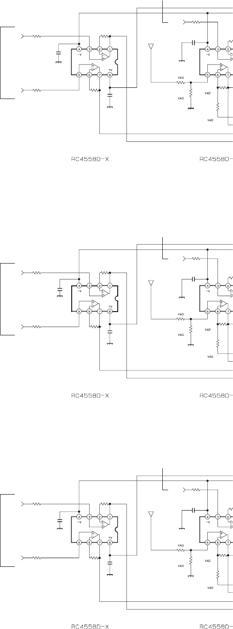
2-65(No.YA463)
DRIVE PWB ASS'Y(6/9)
SRA-3013A-M2
IC3309
IC3509
R3436
R3636
R3438
R3638
R3441
R3641
R3439
R3639
R3437
R3637
C3424
C3624
C3425
C3625
R3
4
R3
6
IC3109
R3236
R3238
R3241
R3239
R3237
C3224
C3225
R3
2
IC3110
R3246
R3247
R3248
R3249
C3226
IC3310
IC3510
RVITOR_B
RVITOREF
RV1REF
R3446
R3646
R3447
R3647
R3448
R3648
R3449
R3649
C3426
C3626
GVITOR_B
BVITOR_B
GVITOREF
BVITOREF
GV1REF
BV1REF
AVCC3
0
0
0
0
0
0
0
0
0
0
0.1
0.1
0.1
0.1
0
0
0
0
0
0
0
0.1
0.1
0
1k
2k
1k
2k
0.1
1k
1k
2k
2k
1k
1k
2k
2k
0.1
0.1
GND1
GND1
GND1
GND1
GND1
GND1
AVCC3
GND1
GND1
GND1
AVCC3
GND1
GND1
GND1
SHEET26
SHEET26
SHEET27
SHEET27
SHEET28
SHEET28
REF. VOLTAGE
REF. VOLTAGE
REF. VOLTAGE
DRIVE PWB CIRCUIT DIAGRAM (6/9) [ITO-V1_DRIVER] SHEET 29
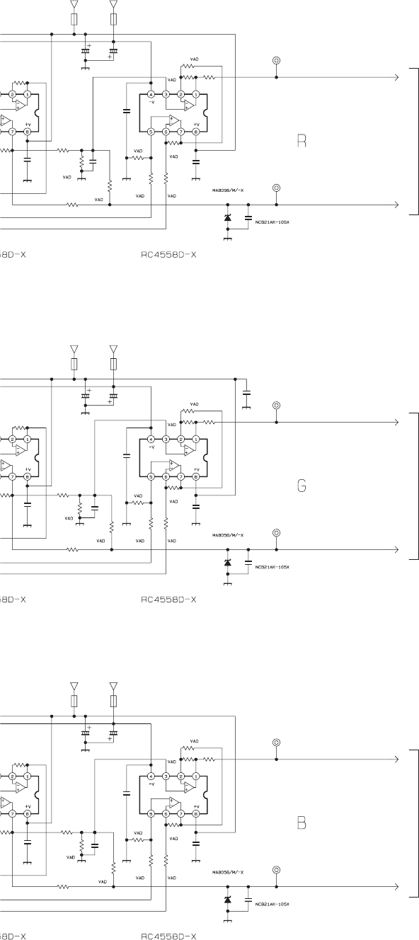
(No.YA463)2-66
c10488007_0808_7/9_0.0
UGV1
UBV1
UGVITO
UBVITO
R3442
R3642
K3491
K3691
IC3311
IC3511
C3428
C3628
C3430
C3630
C3432
C3632
C3429
C3629
R3456
R3656
R3457
R3657
R3455
R3655
R3454
R3654
R3460
R3660
R3459
R3659
URV1
URVITO
R3242
R3461
K3291
IC3111
P8V
C3228
C3230
C3232
N8V
C3229
R3256
R3257
R3255
R3254
R3260
R3259
R3261
TP3102
0
C3227
K3292
R3661
TP3302
TP3502
0
0
R3252
R3253 C3231
C3233
D3102R3258
TP3101
C3427
C3627
K3492
K3692
R3452
R3652
R3453
R3653
C3431
C3631
C3433
C3633
D3302
D3502
R3458
R3658
TP3301
TP3501
R3243
R3443
R3643
CA3021
0
0
*K1
*K1
10/16
10/16
0.1
0.1
0.1
0.1
10/16
10/16
1K
1K
2K
2K
1k
1k
2k
2k
1k
1k
1k
1k
0
0
*K1
10/16
0.1
0.1
10/16
1K
2K
1k
2k
1k
1k
0
OPT
0.1
*K1
0
OPT
OPT
OPT
1k 0.1
1
OPT33
OPT
0.1
0.1
*K1
*K1
OPT
OPT
1k
1k
0.1
0.1
1
1
OPT
OPT
33
33
OPT
OPT
3K
3K
3K
0.1
GND1
GND1
GND1
N8VR
N8VG
GND1
N8VB
N8VP8V
GND1
GND1
GND1
P8VG
GND1
GND1
N8VP8V
GND1
N8V
GND1
P8V
GND1
GND1
GND1
P8VR
GND1
P8VB
GND1
GND1
GND1
GND1
SHEET26
SHEET27
SHEET28
A
GE CONTROL
A
GE CONTROL
A
GE CONTROL
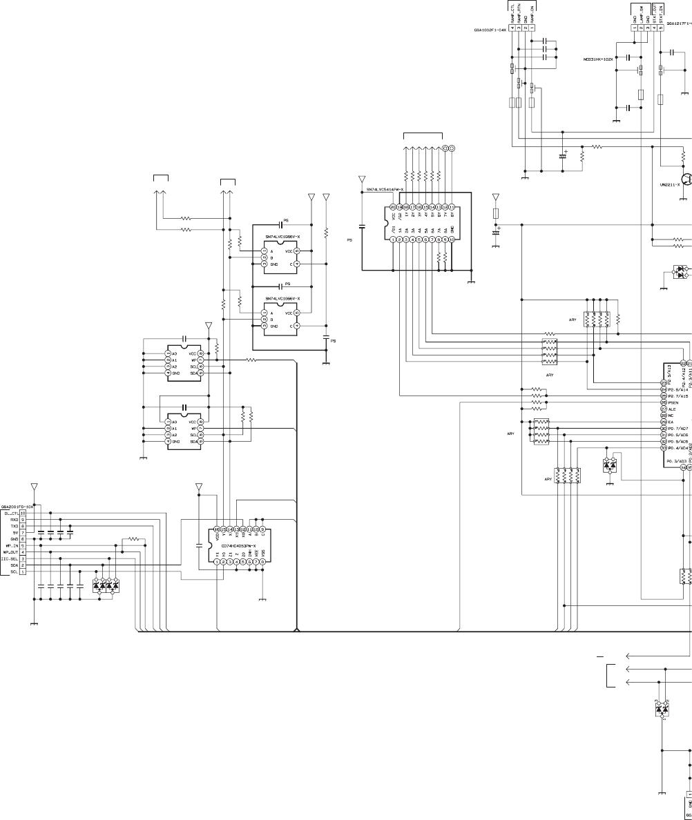
2-67(No.YA463)
I
K3701
C3701
R3732
CN
IC3751
C3754
R3753
D3706
IC3753
IC3752
C3752
C3753
SCL_T
K3711
K3712
CNBCT1
CNJIG1
D3704
D3707
R3733
K3708
/RESET3V
D3751
K3713
D3752
R3715
R3713
R3731
R3714
R3729
R3728
R3712
R3752
R3746
R3747
IC3702
C3706
R3721
R3757
R3755 R3756
R3
7
R3722
R3730
C3707
EF3701
Q3701
R3717
R37
EF3710
EF3709
EF3708
IC3703
R3741
IC3754
C3710
C3709
C3751
C3708
R3745
R3744
R3742
R3743
C3716
C3721
C3722 C3723
C3724 C3725
C3717
C3718 C3719 C3720
C3726
C3727
C3728
K3717
EF3715
C3762
CNSW1
SDA_T
SCL
SDA
TP3704
SDA_F
SCL_F
TP3701
R3718
R3724
CTL5
R3725
CTL6
R3726
R3738
R3727
CTL1
CTL2
CTL3
CTL4
R3739
R3740
DR-STB5V
*K1
47/16
10K
DR-STB5V
0.1
47
*D1
OPT
DR-STB5V
0.1
OPT
*K1
*K1
*D1
*D1
100
*K1
*D1
*K1
*D1
100
100
4.7K
10K
100
10K
10K
3.3K
OPT
OPT
0.1
OPT
0
4.7K 4.7K
82
0
820
100
10/16
*EF2
10K
4.7
*EF5
*EF2
*EF2
10K
0.1
0.1
0.1
GND1
0.1
OPT
OPT
0
0
1000p
OPT
OPT OPT
OPT OPT
OPT
OPT OPT OPT
OPT
OPT
OPT
*K1
*EF5
OPT
0
0
0
0
0
0
0
0
GND1
STB5V
DR-STB5V
GND1
DR-STB5V
DR-STB5V
GND1
DR-STB5V
GND1
WP1_IN
GND1
DR-STB5V
GND1
IIC_SEL1
GND1
GND1
WP2
GND1
SDA0
GND1
DR-VCC3
GND1
DR-VCC5
GND1
GND1
SCL0
WP1_OUT
DL_CTL
TXD_5V
RXD_5V
IIC_SEL1
IIC_SEL2
IIC_SEL2
WP1_IN
WP1_OUT
DL_CTL
WP2
SHEET25
SHEET25
SHEET26,27,28
SHEET25
SHEET26,27,28
OPEN
LAMP
BALLAST UNIT
LAMP COVER SW
PWB ASS'Y
CN0806
(SHEET39) THER
M
T
PW
B
C
(SH
DRIVE PWB CIRCUIT DIAGRAM (7/9) [CONTROLER] SHEET 30
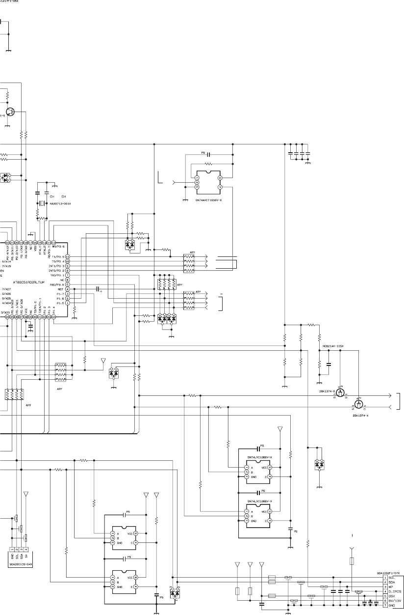
(No.YA463)2-68
DRIVE PWB ASS'Y(7/9)
SRA-3013A-M2
c10488006_0808_6/9_0.0
IC3701
R3736 R3737
C3702
CNT1
CNIR1
R3707
R3734
TXD
RXD
D3701
R3711
IC3755
IC3757
OPEN
OPEN
IC3758
R3704
R3772
C3761
C3760
C3759
R3775
FANCTL
R3702
R3710
C3703
D3704
FAN_LOCK
R3763 R3762
R3735
PON_L
C3704
LVDSCTL
X3701
C3705
FAN_ON
R3709
R3708
R3703
D3702
R3720
R3706
R3759
R3719
R3761
K3704
K3703
K3702
R3723
R3760
D3708
R3758
K3706
MEM_EN
R3701
Q3754
Q3753
R3779
EF3702
7
01
EF3703
R3716
EF3704
CPU_V
R3705
EF3707
EF3706
EF3705
EF3714
LCD_EN
D3703
K3716
EF3713
R3764
C3715 C3714 C3713
C3712 C3711
C3729
R3765
IC3704
R3774
R3773
R3776
R3771
IC3756
R3766
C3758
C3757
C3756
R3769
R3768
R3767
R3770
R3778
7
17
1
5
C3762
S
W1
R3777
C3763
EF3711
C3730
K3705
D3710
D3711
CA3020
D_IRIS
CA3016
CA3017
CA3018
CA3019
DR-STB5V
100 100
0.1
DR-STB5V
100
100
*D1
0
DR-STB5V
100
10K
0.1
0.1
0.1
OPT
100
1M
10/16
*D1
100 OPT
4.7K
3P3P
100
10K
4.7K
*D1
100
10K
4.7K
100
10K
*K1
*K1
*K1
DR-VCC5
820
4.7k
OPT
4.7K
*K1
1K
120
*EF5
*EF5
4.7K
*EF5
4.7K
*EF1
*EF2
*EF2
*EF2
*D1
DR-VCC3
UNP13V
OPT
*EF1
OPT
OPT OPT OPT
OPT OPT
0.1
0
OPT
0
0
DR-VCC5
100
10K
0.1
0.1
0.1
OPT
OPT
0
0
120
OPT
560
1
P8V
*EF2
OPT
*K1
*D1
*D1
0.1
0.1
0.1
0.1
0.1
DR-STB5V
GND1
GND1
GND1
GND1
GND1
GND1
GND1
DR-VCC3
GND1
GND1
GND1
GND1
GND1
DR-VCC5UNP13V
GND1
DR-STB5V
DR-STB5V
GND1
GND1
GND1
GND1
DR-VCC5
P8V
TXD_5V
SDA0
SCL0
RXD_5V
SHEET
25
SHEET24
SHEET24
SHEET31
SHEET26,27,28
SHEET24
SHEET32
E
RMOSTAT
TEMP
P
WB ASS'Y
CN82T
(SHEET38)
OPEN
DD CPU
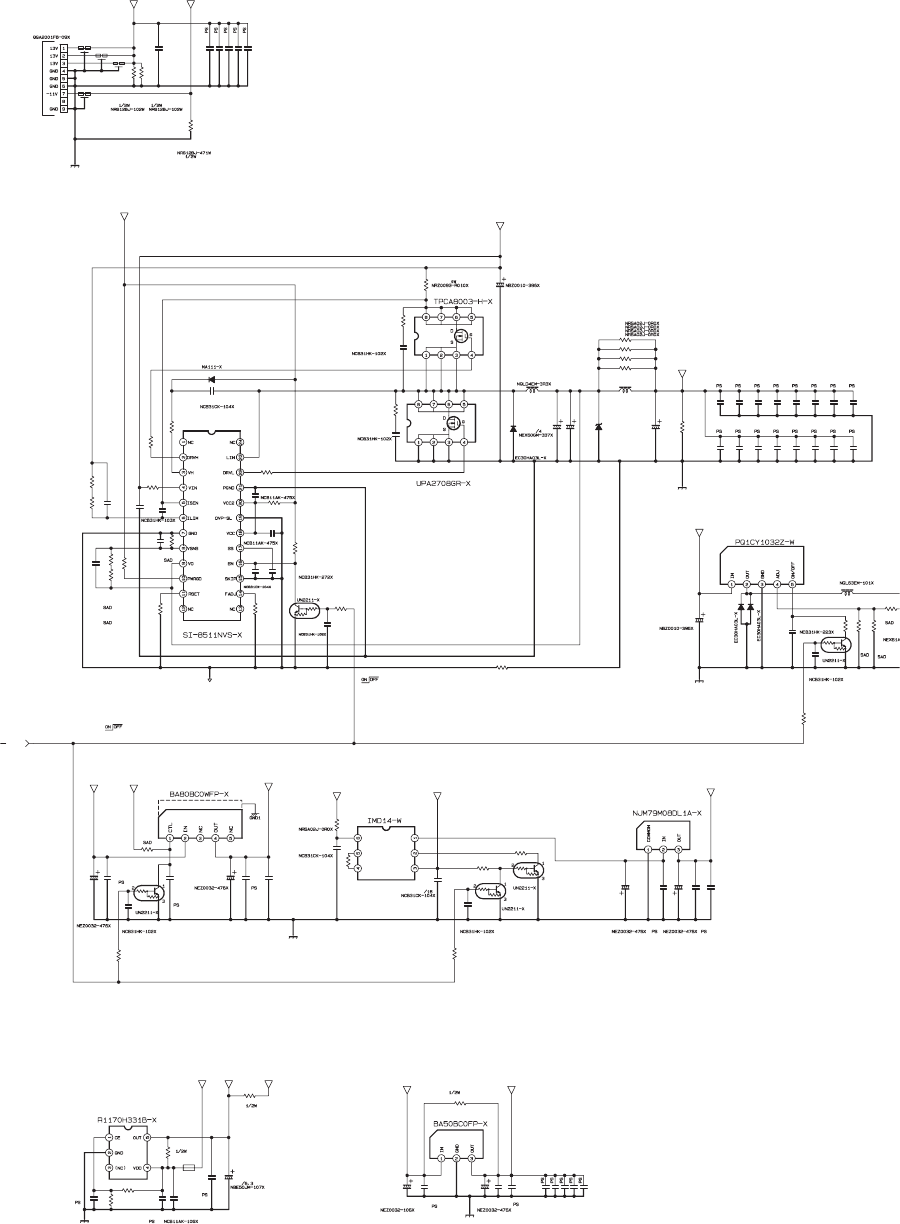
2-69(No.YA463)
DRIVE PWB ASS'Y(8/9)
SRA-3013A-M2
CNDD1
C3937
EF3904
EF3905
EF3906
EF3907
Q3907
C3969
R3973
C3938
C3939
IC3906
R3918
Q3909
R3996
C3974
R3995
IC3901
R3907
R3990
Q3906
Q3905
R3905
R3903
R3991
C3942
C3941
R3904
C3914
C3904
R3906C3905
C3903
C3902
R3920
R3901
C3901
D3901
IC3903
C3951
C3952
Q3910
R3954
PON_L
R3953
C3953 C3954
R3908
C3907
C3955
C3908
R3910
R3997
Q3902
C3906
R3909
R3911
C3910
C3909
IC3905
K3922
C3965 C3966 C3967 C3968
R3912
Q3901
D3902
L3901
C3912
D3903
L3902
R3921
R3916
R3915
C3913
R3917
R3913 C3911
C3960 C3961C3958 C3959
IC3902
C3931 C3932
L3931
R3935
R3933 R3934
R3932
Q3903
R3931
C3933
C3971
C3970
R3970
C3973
R3971
C3972
R3969
R3964
R3981
R3983
R3982
IC3904
C3956
R3914
R3922
R3923
C3915
R3924
C3916
C3829
C3837
C3975
R3919
R3902
C3917
C3824 C3825 C3826 C3827 C3828
C3832 C3833 C3834 C3835 C3836
C3830
C3838
C3831
C3839
CA3022
CA3023
CA3024
CA3025
CA3026
CA3027
CA3028
CA3029
CA3030
CA3031
D3931
D3932
OPT
*EF1
*EF1
*EF1
*EF1
UNP13V UNN11V
10/10
OPT
OPT
OPT
0
GND2
3.3K
0.1/16
1K
DR-STB5V
OPT
0
47K
2.7K
1K
0.001
0.1
2.0K
330
220P
2.2K47P
OPT
0.01
56
1
0.1
UNP13V
GND1
47/16
0.1
1K
4.7K
47/16 0.1
100K
0.1
0.001
0.0027
47K
N8V
GND1
UNN11V
P8V
10K
0.001
1K
18
4.7
4.7
*K1
UNP13V DR-STB5V
10/16 0.1 47/16 0.1
1
GND1
DR-STB5V
OPT
OPT
OPT
0
0
0
OPT
470
0.01 39/16
UNP13V
DR-VCC3
GND1
GND1
47/16 0.147/16 0.1
39/16 0.022
3.3K
1.2K 8.2K
UNP13V
3.3K
1K
0.001
GND1
DR-VCC5
0.1
0.1
OPT
0.1
10K 100
OPT
OPT
1K
470
1K
0.1
DR-STB5V
0
0
10
1000P
10
1000P
0.1
0.1
OPT
3.9
750
0.001
0.1 0.1 0.1 0.1 0.1
0.1 0.1 0.1 0.1 0.1
0.1
0.1
0.1
0.1
0.1
0.1
0.1
0.1
0.1
0.1
0.1
0.1
0.1
0.1
DR-STB5V
GND1
GND1
PON_L
AVCC3
UNP13V UNN11V
DR-VCC3
UNP13V
N8V
GND1
DR-VCC5
GND1
DR-STB5V
GND1GND2
DR-STB5V
GND1
UNP13V
P8V
DR-STB5V
UNN11V
UNP13V
UNP13V
DR-VCC3
SHEET30
POWER PWB
ASS'Y(2/3)
CN9008
(SHEET34)
DRIVE PWB CIRCUIT DIAGRAM (8/9) [POWER_REGULATOR] SHEET 31
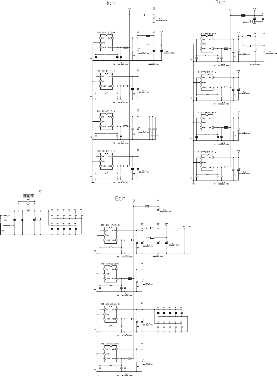
(No.YA463)2-70
c10488008_0808_8/9_0.0
CA3965
CA3964
CA3967
CA3966
CA3969
CA3968
C3813
C3936
C3806 C3807
C3814
CA3904
CA3909
CA3914
CA3925
C3815 C3816 C3817
CA3930
CA3935
C3818
C3819 C3820 C3821 C3840
CA3919 CA3940
R3935
R3934
C3934 D3933
L3932
R3938
R3937
R3936
R3939
CA3946
CA3951
CA3956
CA3961
C3842
C3808 C3809 C3810 C3811
IC3913
K3913
C3812
CA3933
CA3934
CA3936R3946
CA3937
IC3912
K3912
K3908
C3823
CA3928
CA3929
CA3931R3945
CA3932
IC3914
K3914
C3841
CA3938
CA3939
CA3941
R3947
CA3942
IC3911
K3911
CA3922
C3843
CA3923
CA3924
CA3926R3944
CA3927
IC3917
K3920
C3844
CA3954
CA3955
CA3957R3950
CA3958
IC3916
K3919
K3915
C3845
CA3949
CA3950
CA3952
R3949
CA3953
IC3918
K3921
C3822
CA3959
CA3960
CA3962R3951
CA3963
IC3915
K3918
CA3943
CA3944
CA3945
CA3947R3948
CA3948
IC3909
K3906
CA3912
CA3913
CA3915R3942
CA3916
IC3908
K3905
K3901
CA3907
CA3908
CA3910R3941
CA3911
IC3910
K3907
CA3917
CA3918
CA3920R3943
CA3921
IC3907
K3904
CA3901
CA3902
CA3903
CA3905R3940
CA3906
K3902
K3903
K3909
K3910
K3916
K3917
CA3032
CA3033
CA3034
33
33
33
33
33
33
0.1
OPT
0.1 0.1
0.1
10
10
10
10
0.1 0.1 0.1
10
10
0.1
0.1 0.1 0.1 0.1
10 10
3.3K
8.2K
120/10 OPT
OPT
0
0
0
1K
DR-VCC5
10
10
10
10
0.1
0.1 0.1 0.1 0.1
*K1
ASID3G
0.1
0.1
0.1
DR-VCC3
MRD2G
0.1
10K 47
*K1
*K1
0.1
0.1
0.1
ASID2G
0.1
10K 47
*K1
GND1
0.1
0.1
0.1
LCD2G
0.1
10K 47
*K1
47
0.1
0.1
0.1
DVCC1G
0.1
10K 47
GND1
*K1
ASID3B
0.1
0.1
0.1
DR-VCC3
MRD2B
0.1
10K 47
*K1
*K1
0.1
0.1
0.1
ASID2B
0.1
10K 47
*K1
GND1
0.1
0.1
0.1
LCD2B
0.1
10K 47
*K1
47
0.1
0.1
DVCC1B
0.1
10K 47
GND1
*K1
ASID3R
0.1
0.1
DR-VCC3
MRD2R
0.1
10K 47
*K1
*K1
0.1
0.1
ASID2R
0.1
10K 47
*K1
GND1
0.1
0.1
LCD2R
0.1
10K 47
*K1
47
0.1
0.1
DVCC1R
0.1
10K 47
GND1
*K1
*K1
ASID1R ASIA1R
*K1
*K1
ASID1G ASIA1G
*K1
*K1
ASID1B ASIA1B
0.1
0.1
0.1
ASID1R ASIA1R ASID1G
GND1
ASIA1G
ASIA1BASID1B
MRD2G
GND1
DR-VCC3
GND1
ASID3G
MRD2B
GND1
ASID2G
MRD2R
LCD2G
DVCC1G
DR-VCC5
ASID2B
ASID2R
LCD2B
LCD2R
DVCC1B
DVCC1R
DR-VCC3 ASID3B
GND1
DR-VCC3 ASID3R
GND1
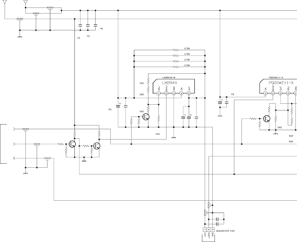
2-71(No.YA463)
EF3912
IC8001
C8001 C8002
R8006
R8003
R8005
C8004 C8005
R8004
Q8001R8001 R8002
R8008
IC8002
C8008 C8009
C8003
R8015
R8010
R8016
R8009
R8014
EF3909
Q8005
R8013
Q8004
Q8002
R8031
R8034
R8011
R8033 R8012
R8036
R8032
R8035
R8007
CNF1
FAN_LOCK
EF3910
EF3911
FANCTL
FAN_ON
EF3901
EF3902
EF3903
EF3913
C8045
C8046
CA3037
CA3036
CA3035
*EF4
47/16 0.1
1K
2.2K
4.7K
GND1
47/16 100P
680
*TR110K 47K
OPT
GND1
10/16 0.1
47/16
680
OPT
2.2K
OPT
4.7K
*EF4
*TR1
OPT
*TR1
OPT
10K
10K
OPT
4.7K OPT
4.7K
22K
22K
OPT
*EF4
GND1
GND1
*EF4
UNP13V
GND1
DR-STB5V
*EF1
OPT
*EF1
*EF1
OPT
OPT
0.1
0.1
0.1
UNP13V
GND1
GND1
DR-STB5V
GND1
GND1
GND1
GND1
SHEET30
OPTICAL BLOCK
COOLING FAN
FAN
CONTROL
FAN
CON
T
DRIVE PWB CIRCUIT DIAGRAM (9/9) [FAN_CONTROL] SHEET 32
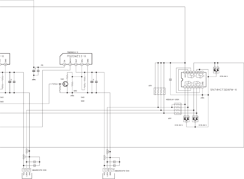
(No.YA463)2-72
DRIVE PWB ASS'Y(9/9)
SRA-3013A-M2
c10488009_0808_9/9_0.0
IC8003
C8018
D8002
C8019
D8003
CNF3
D8001
R8015 R8025
R8026
R8014 R8024
CNF2
C8010 C8020C8011 C8021
R8023
Q8003
R8021
R8022
IC8005
R8042
R8041
C8031
EF3914
EF3915
EF3916
EF3917
C8042
C8041C8043
C8044
GND1
10/16 0.1
680
680
2K
4.7K 2.2K47/16 47/16100P 100P
OPT
OPT GND1
GND1
OPT
OPT
100
10K
10/6.3
*EF4
*EF1
*EF4
*EF1
OPT
OPTOPT
OPT
GND1
GND1
GND1
LAMP COOLING FAN-1 LAMP COOLING FAN-2
FAN
CONTROL
FAN
CONTROL
FAN STOP
DETECT
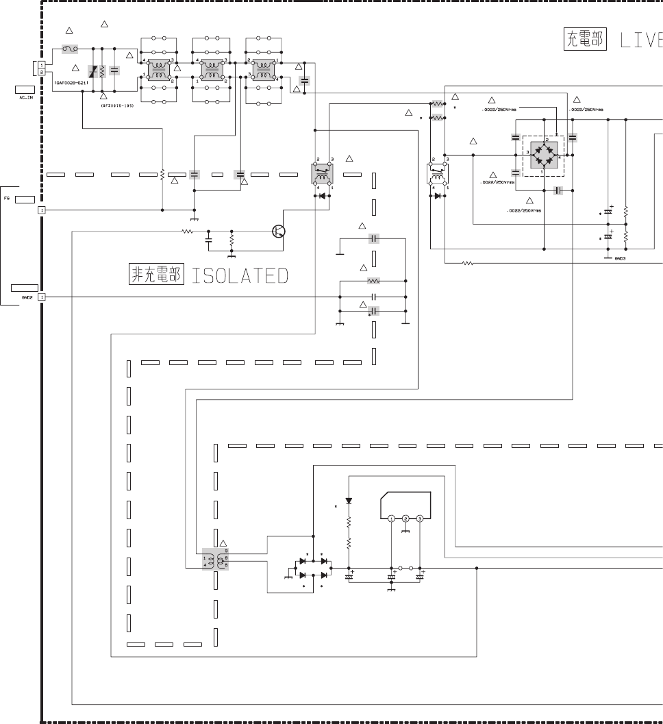
2-73(No.YA463)
POWER PWB ASS'Y(1/3)
SRA-9017A-M2
!
!
!
!
!
!
!
!
!
!!!
!
!
!!
!
!
!
!
!
!
C9205
C9206
D9102
D9021
D9104
R9203
IC9101
D9101
D9103
R9112
D9106
Y9041
Q9021
C9103
T9101
C9101
C9104
R9113
R9022
C9191
R9002
RY9201
D9201
R9201 C9204
C9002
C9203
C9201
C9202
D9202
CN9E1
C9013
C9011
F9001
VA9001
C9001
RY9021
CN9PW
R9001
LF9001
LF9002 LF9003
R9021
R9191
H9211
C9021
C9193
CN9E2
C9192
R9202
Y9011
Y9010
Y9012
Y9013
Y9007
Y9006
Y9008
Y9009
Y9003
Y9002
Y9004
Y9005
R9204R9205
MA111-X
BA50BC0FP-X
QRE121J-330Y
2SC3928A/QR/-X
QEHR1CM-108Z
QQT0520-001
QEHR1CM-108Z
/16
QEHR1CM-107Z
QRE121J-330Y
GBJ6JU
QCZ9078-222
QFZ9072-224
QCZ9078-222
QCZ9078-222
QCZ9078-222
QCZ9079-102
QCZ9079-102
QMF5AD2-6R3-J1
QAF0060-621
/275Vac
QFZ9072-105
QSK0162-001
QGAB801C1-02
QRZ9046-105Z
QQR1542-001
QQR1466-001 QQR1467-001
QRZ9046-685Z
LC32473-001B
QCZ9079-102
QRE121J-124YQRE121J-124Y
OPEN
OPEN
100
47K
OPEN
OPEN
OPEN
OPEN
1
4.7k OPEN
OPEN
OPEN
OPEN
OPEN
OPEN
OPEN
OPEN
OPEN
OPEN
OPEN
OPEN
OPEN
GND1
GND2
GND2
GND2
GND3
GND2
GND2
GND2
POWER CORD
AC120V, 60Hz
OPEN
5V REG.
SW TRANSF
POWER PWB CIRCUIT DIAGRAM (1/3) SHEET 33
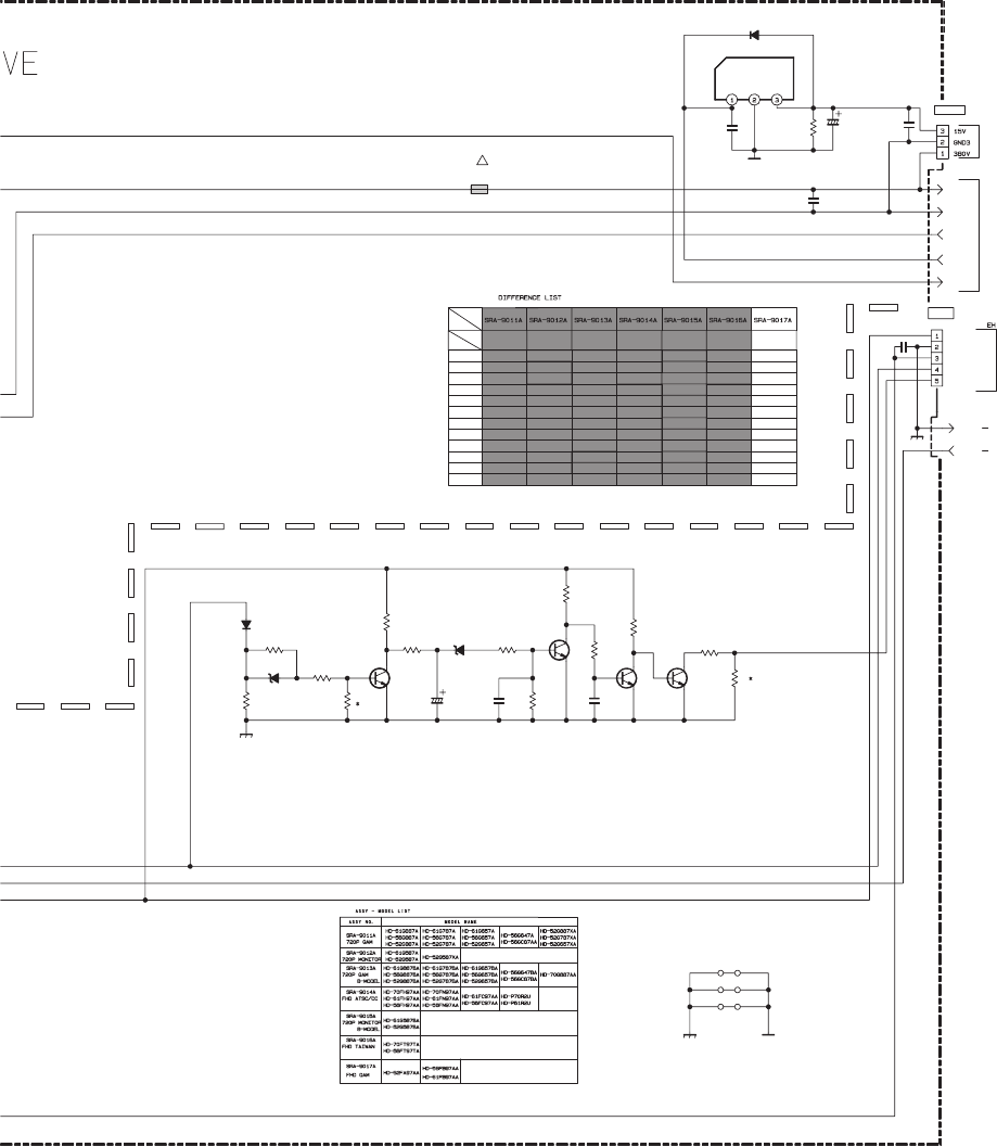
(No.YA463)2-74
c20179001_0912_1/3_0.0
!
C9219
R9293
13.5V
R9292
Q9284Q9283
R9291
R9290
380V
R9289
C9284
R9288
C9283
CN9A2
R9287
D9283
R9286
C9281
IC9301
R9285
R9284
R9283
R9281
R9282
D9281
D9282
D9301
R9201
CP9211
R9202
C9302
C9205
GND2
D9104
C9206
GND3
C9301 CN9BL
D9106
14V
R9284
20V
D9101
R9293
D9102
D9103
Y9053
Y9052
Y9051
C9193
R9301
C9303
C9282
START
Q9282
Q9281
QCZ0122-471
OLLC09898 OLLC09898
-02 OLLC10946 OLLC10257 OLLC10946
-02
2SC3928A/QR/-X2SC3928A/QR/-X
STB5V
GND2
MAIN_POW
AC_IN
POW_GOOD
QGA2001C1-05
OLLC11045
MA8024-X
QEHR1HM-226Z
BAJ5CC0FP-X
MA111-X
MA8047-X
QRF154K
-1R0
SK14-GA-X
QEZ0834
-827
QEZ0834
-827
1N4003SG
-T2
1N4003SG
-T2
1N4003SG
-T2
QRF154K
-2R2
QCZ9079
-222
1N4003SG
-T2
QRF154K
-2R2
1N4003SG
-T2
NDC31HJ
-101X
QEZ0802
-108
QRF154K
-1R0
1K4-T2
QEZ0802
-108
QEZ0834
-827
1K4-T2
QEZ0834
-827
1K4-T2
1K4-T2
NDC31HJ
-101X
1K4-T2
1N4003SG
-T2
1N4003SG
-T2
QMFZ043-5R0Z-J1
1N4003SG
-T2
QRF154K
-2R2
QCZ9079
-222
QRF154K
-1R0 QRF154K
-1R0
1N4003SG
-T2
QRF154K
-2R2
1N4003SG
-T2
/50
NCB31HK-104X
QEZ0569
-827 QEZ0569
-827
NDC31HJ
-101X
QEZ0802
-108
1N4003SG
-T2 1N4003SG
-T2
QEZ0569
-827 QEZ0569
-827
/25
QEHR1EM-107Z QGA7901C1-03
1N4003SG
-T2
QEZ0802
-108
1N4003SG
-T2 1N4003SG
-T2
1N4003SG
-T2 1N4003SG
-T2
1N4003SG
-T2
1N4003SG
-T2
1N4003SG
-T2 1N4003SG
-T2 1N4003SG
-T2
1N4003SG
-T2 1N4003SG
-T2
NDC31HJ
-101X
1N4003SG
-T2
QCZ9079
-102
QCZ9079
-222 QCZ9079
-222
OLLC11380
QCZ9079
-222 QRF154K
-2R2
NRS12BJ-122W
QRF154K
-2R2
QEZ0802
-108
1N4003SG
-T2
QEZ0802
-108
1N4003SG
-T2
1N4003SG
-T2
1N4003SG
-T2
NDC31HJ
-101X
1N4003SG
-T2
QCZ9079
-222
NCF11EZ-105X
NCB31HK-102X
2SC3928A/QR/-X
2SC3928A/QR/-X
0
4.7k
0
47k
OPEN
18k
OPEN
3.9k47
6.8k
4.7k
OPEN
10k
OPEN
47k
OPEN
100k47k
OPEN OPEN
0.1
100
10k 10k 47k
OPEN OPEN
OPEN
OPEN
OPEN
47k
POW_GOOD
GND2
14V
STB5V
AC_IN
GND2 GND4
GND3
380V
20V
GND3
GND2
START
SHEET34
LAMP BALLAST
UNIT
ANALOG PWB
ASS'Y(6/6)
CN1A2
SHEET8
SHEET34
SHEET33,34
2-75(No.YA463)
POWER PWB ASS'Y(2/3)
SRA-9017A-M2
!
!
!
!
GND3
380V
14V
D9504 R9507
D9511
C9510
D9510
IC9501
R9511
R9510
C9506
H9501
R9514
D9505
C9507
K9501
PC95
0
D9507
D9502
R9506
C9503
R9508
R9505
C9501
K9502
R9504
C9512
C9509
C9504
C9505
C9508
R9501
R9512
D9503
R9513
R9502
D9501
D9506
R9503
R9515
D9514
R9516
D9512
C9511
20V
START
R9520
T9
5
FR105SGT-T2 1/2W
MA111-X
D
NC
S/GND
VCC
SS/OLP
FB
OCP/BD
STR-W6754-F5
QRK126J-101X
/50
QEHR1HM-105Z
LC32528-001B
MTZJ33B-T2
/25
NCB31EK-104X
QQR1139-001
PS2581
A
MA111-X
SARS01-T2
/50
NCB31HK-332X
1/2W
QRL039J-220
/630
QFP32JK-332
QQR0621-002Z
QRE121J-394Y
NCB31HK-102X
QEHR1VM-476Z
CH
NCB31HK-152X
QCZ0340-471
QRL039J-104
FR105SGT-T2
QRL039J-333
SARS01-T2
FR105SGT-T2
QRE121J-394Y
QRZ9009-4R7
MTZJ13B-T2
FR105SGT-T2
/50
QEHR1HM-107Z
10
OPEN
OPEN
100
1k
1
3.3k
.1
*
0.0033
1.2K
22
0.0033
390k
OPEN
100k
100
OPEN
380V
GND3
14V
GND3
START
GND3
20V
SHEET33
POWER REG.
VOLT
A
FEED
POWER PWB CIRCUIT DIAGRAM (2/3) SHEET 34
(No.YA463)2-76
c20179002_0912_2/3_0.0
!
!
!
!
!
C9558
D9551
CN9A1
K9551
C9565
C9563
CP9557
D9553
K9555
C9551
C9552
R9556
C9557
C9554
C9601
K9556
K9557
D9554
D9557
C9559
C9562
C9555
C9556
L9553
R9555
K9554
C9561
C9560
PC9501
R9512
D9555
R9603 R9606
R9551
D9552
CN9DU
R9607
R9605
C9603
R9601
R9604
C9602
R9602
R9608
D9601
CN9008
CP9556
CP9555
CP9554
H9553
R9561
R9567
C9573
C9566
R9557
R9568
C9570
T9501
C9568
C9569
GND2
R9562
L9552
D9556
13.5V
R9513
T9501
L9551
R9606
R9608
DCDC13.5
R9562
BT32V
C9557
C9573
L9553
D9553
CNDU
K9552
C9564 R9552
C9571
R9564
R9566
R9563
R9565
R9506
C9559
C9560
C9568
D9554
D9555
D9556
K9556
R9556
R9557
CP9554
C9553
K9553
C9572
HER202G-FL
QGA2501C5-06ZQQR0621-002Z /35
QEHQ1VM-108
CP
ICP-N70-T
QUY153-050Y
QUY153-050Y
FR105SGT-T2
/25
QEHR1EM-477Z
/25
QECQ1EM-188
/25
QECQ1EM-188
QUY153-050Y
S
2581AL1/QW/
OLLC09898
QRX01GJ
-R39 QRX01GJ
-R39
OLLC09898
-02
HER202G-FL
0.5%
/25
NCB31EK-104X
UTCTL431-T
QGA2001C1-09
CP
ICP-N70-T
OLLC10946 OLLC10257
CP
ICP-N50-T
CP
LC32528-001B
NCB31HK-102X
QQS0352
-001 QQS0352
-001
NCB31HK-102X
QQL26AM-3R3Z
QRX01GJ
-R39
QQS0365
-001
QQS0352
-001
QRX01GJ
-5R6
QRX01GJ
-5R6
0.5%
QRX01GJ
-R33
QRX01GJ
-5R6
QQL26AM-3R3Z
0.5% 0.5% 0.5%
QRZ9017
-470
QEHR2AM
-106Z
0.5%
QEHR1HM
-105Z
NCB31HK
-102X
QRL029J
-220
FR105SGT
-T2
MTZJ15B
-T2
QECQ1EM
-188
MTZJ16C
-T2
QUY153
-050Y
QRG01GJ
-152
NCB31HK
-102X
ICP-N50
-T
QQL26AM
-3R3Z
FCH20A10
QQR0621-002Z
/35
QEHQ1VM-108
NCB31HK-102X
QRT039J-R47
QRT039J-R47
FCH20A10
QGA2001C1
-03
FME-220A FCH20A10
OLLC11045
QQS0365
-001
QRX01GJ
-R33
0.5%
0.5%
QRZ9017
-470
QEHR2AM
-106Z
QEHR1HM
-105Z
NCB31HK
-102X
FR105SGT
-T2
MTZJ15B
-T2
MTZJ16C
-T2
QUY153
-050Y
QRG01GJ
-152
ICP-N50
-T
FME-220A
QRZ9017
-120
QEHR2AM
-106Z
QEHR1HM
-105Z
NCB31HK
-102X
FR105SGT
-T2
QRZ9017
-120
QRZ9017
-470
QEHR2AM
-106Z
QEHR1HM
-105Z
NCB31HK
-102X
FR105SGT
-T2
MTZJ15B
-T2
MTZJ16C
-T2
QUY153
-050Y
QRG01GJ
-152
ICP-N50
-T
MTZJ15B
-T2
MTZJ16C
-T2
QUY153
-050Y
QRG01GJ
-152
ICP-N50
-T
QRX01GJ
-R39
OLLC10946
-02
QQS0352
-001
0.5%
FME-220A
QRZ9017
-120
OLLC11380
QQS0365
-001
QRX01GJ
-R33
QRX01GJ
-5R6
0.5%
0.5%
QECQ1EM
-188
FME-220A
QRZ9017
-470
QEHR2AM
-106Z
QEHR1HM
-105Z
NCB31HK
-102X
FR105SGT
-T2
MTZJ15B
-T2
MTZJ16C
-T2
QUY153
-050Y
QRG01GJ
-152
ICP-N50
-T
NCB31HK-102X
OPEN
OPEN
1000
*
OPEN
OPEN
*
*
OPEN
OPEN
*
**
470
1800
1800 OPEN
OPEN
*
*
OPEN
OPEN
2.7k
12k
.1
1k
OPEN
OPEN
1k
*
OPEN
0
OPEN
*
OPEN
*
*
OPEN
12k
OPEN
OPEN
12k
OPEN
OPEN
12k
OPEN
10k
OPEN
OPEN OPEN 18k
OPEN OPEN
OPEN OPEN
OPEN OPEN
330k
OPEN OPEN
1000 OPEN
OPEN
OPEN
OPEN OPEN
OPEN
10k
18k
330k
OPEN
OPEN
OPEN
OPEN
OPEN
OPEN
OPEN
OPEN
OPEN
OPEN
OPEN
OPEN
OPEN
OPEN
OPEN
330k 330k
OPEN
12k
OPEN
OPEN
OPEN
OPEN
OPEN
OPEN
OPEN
OPEN
OPEN
OPEN
OPEN
OPEN
OPEN
OPEN
OPEN
OPEN
10k
18k
OPEN
OPEN
OPEN
OPEN
330k
OPEN
OPEN
GND2
GND2
GND2
GND2
GND2
GND2
GND2
SHEET35
ANALOG PWB
ASS'Y(5/6)
CN1A1
(SHEET7)
SHEET33,35
OPEN
SHEET33
DRIVE PWB
ASS'Y(8/9)
CNDD1
(SHEET31)
VOLTAGE
FEEDBACK
2-77(No.YA463)
D9721
Q9842
R9864
R9845
R9846
R9847
D9842
C9743
IC9721
C9744
R9841
R9842
R9844
Q9841
D9841
Q9861
D9861
D9762
IC9761
H9761
R9866
D9862
D9702
BT32V
R9863
R9865
H9741
C9778
DCDC13.5
C9776
GND2
H9721
R9721
R9722 R9724
R9723
C9724
C9723
C9701
C9702
R9831
R9832
Q9831
D9832
C9831
R9834
R9833
D9831
R9821
R9822
Q9821
R9823
D9821
D9701
IC9701
C9761
R
IC9741
L9741
R9741
R9742 R9744
C9742
D9743
Y9075
R9743
C9745
Y9076
R9701
C9721
D9741
C9741
SK14-GA-X
QECR1AM-128Z
PQ15RW11
2SC3928A/QR/-X
MA111-X
MA111-X
MA111-X
LC31334-003B
LC31334-003B
0.5%
3D
0.5%
3D
0.5%
3D
/16
QEHR1CM-107Z
/50
QEHR1HM-106Z
/16
QEHR1CM-107Z
2SC3928A/QR/-X
/16
CB2
NCB31CK-105X
MA111-X
2SC3928A/QR/-X
MA111-X
SK14-GA-X
PQ120RDA1SZ
PQ1CG2032FZ
QQR1401-001
0.5%
3D
0.5%
3D
0.5%
3D
NCB31EK-104X
MTZJ6.8B-T2
0.5%
3D
/25
QEHR1EM-107Z
/25
QEHR1EM-108Z
1.2k
OPEN
10k
12k
4.7k
OPEN
100k
2.2k OPEN
5.6k
OPEN
100
10
100
4.7k
1.2k
1
10k
8.2k
1.2k
10k
O
33k
3k 15k
0.1 10k
OPEN
47k
100
1000
5V
BT32V
GND2
9V
GND2
12V
GND2
12V
GND2
GND2
GND2
GND2
5V
GND2
GND2
9V
GND2
GND2
GND2
GND2
GND2
GND2
GND2
GND2
GND2
GND2 GND2
GND2 GND2
GND2
GND2
GND2
SHEET34
SHEET33,34
POWER PWB CIRCUIT DIAGRAM (3/3) SHEET 35
(No.YA463)2-78
POWER PWB ASS'Y(3/3)
SRA-9017A-M2
c20179003_0912_3/3_0.0
CN9FAN
R9873
D9801
R9802
L9764
CN9DC
R9775
62
L9761
R9771
R9773
C9852
R9774
R9861
C9773
C9878
C9879
R9862
C9880
C9895
R9877
CN9UP
R9878
IC9761
IC9762
Q9851
R9851
C9772
D9851
R9852
D9852
R9853
R9854
C9851
C9881
C9882
C9883
C9884
C9885
Q9852
Q9853
R9855
C9771
R9898
L9874
H9761
H9762
C9761
C9762
C9763
C9768
C9774
6
C9762
CN9A3
R9899
CN9UP C9770
C9771
C9772
C9773
C9774
C9777
C9778
C9779
C9801
D9762
D9763
D9801
D9841
D9842
L9761
L9764
L9766
Q9841
Q9842
R9771
R9772
R9773
R9776
R9789
R9790
R9801
R9802
R9841
R9842
R9844
R9845
R9846
R9847
C9894
D9763
R9772
C9764
C9763
C9767
R9789
H9762
R9776
IC9762
R9790
R9791
R9792
R9794
C9770
C9777 C9779
C9768
C9876
L9766
C9775
L9876
D9741
C9897
R9775
CN9FAN
Y9071
Y9072
Y9073
Y9074
Y9075
Y9076
Y9073
Y9072
Y9071
Y9074
C9801
R9801
CN9E4
CN9E3
C9877
C9885
L9876
C9897
R9834
D9832
QGA2001C1-15
0.5%
0.5%
/25
NCB31EK-104X
0.5%
/50
NCB31HK-102X
/50
NCB31HK-102X
/50
NCB31HK-102X
/50
NCB31HK-102X
QGA2001C1
-04
OLLC09898 OLLC09898
-02
QGA2001C1
-10
PQ1CG2032
FZ
SI-3011ZF
-F3
2SA1530A/QR/-X
MA8051/M/-X
MA111-X
QEHR1CM-107Z
/50
NCB31HK-102X
/50
NCB31HK-102X
/50
NCB31HK-102X
QGA2001C1
-04
/50
NCB31HK-102X
UN2213-X
UN2213-X
QUY153-050Y
OLLC10946
QGA2001C1
-10
PQ1CG2032
FZ
SI-3011ZF
-F3
OLLC10257
LC31334
-003B
LC31334
-003B
QEHR1EM
-108Z
NCB31EK
-104X
QECR1AM
-128Z
QEHR1CM
-107Z
LC31334
-003B
LC31334
-003B
QEHR1EM
-108Z
NCB31EK
-104X
QGA2001C1-12
QECR1AM
-128Z
QEHR1CM
-107Z
NCB31HK
-102X
NCB31HK
-102X
NCB31HK
-102X
NCB31HK
-102X
NCB31HK
-102X
QEHR1HM
-105Z
NCB31HK
-102X
NCB31HK
-102X
0.5%
0.5%
NCB31HK
-102X
QEHR1CM
-107Z
QEHR1CM
-107Z
QEHR1HM
-106Z
0.5%
NCB31HK
-102X
NCB31HK
-102X
QEHR1HM
-105Z
QEHR1CM
-107Z
QEHR1CM
-107Z
QEHR1HM
-106Z
FMB-G14L
MTZJ3.9B
-T2
MA111-X
/50
NCB31HK-102X
MA111-X
MA111-X
QQR1401
-001
QUY153
-050Y
QUY153
-050Y
2SC3928A
/QR/-X
FSQ05A04
MTZJ3.9B
-T2
MA111-X
MA111-X
MA111-X
QQR1401
-001
2SC3928A
/QR/-X
NRS12BJ
-331W
QUY153
-050Y
QUY153
-050Y
2SC3928A
/QR/-X
QRG01GJ
-470
2SC3928A
/QR/-X
NRS12BJ
-331W
QUY160
-100Y
QUY160
-100Y
QUY160
-100Y
QUY160
-100Y
QUY160
-100Y
QUY160
-100Y
FSQ05A04 FSQ05A04 FMB-G14L FSQ05A04 FMB-G14L FMB-G14L
QRG01GJ
-470
OLLC10946
-02
FAN
GND
LOCK
NC
QUY160
-100Y
QUY160
-100Y
QUY160
-100Y
QUY160
-100Y
QUY160
-100Y
QUY160
-100Y
OLLC11045
/50
NCB31HK-102X
QUY153
-050Y
MA8056
/M/-X
QUY153
-050Y
MA8056
/M/-X
QUY153
-050Y
MA8033-X
NDC31HJ
-470X
QQL26AM
-3R3Z
QEHR1CM
-107Z
MA8033-X
QUY153
-050Y
MA8033-X
QUY153
-050Y
MA8033-X
QGA2001C1
-04
OLLC11380
QGA2001C1
-10
PQ1CG2032
FZ
SI-3011ZF
-F3
LC31334
-003B
LC31334
-003B
QEHR1EM
-108Z
NCB31EK
-104X
QECR1AM
-128Z
QEHR1CM
-107Z
NCB31HK
-102X
NCB31HK
-102X
NCB31HK
-102X
NCB31HK
-102X
NCB31HK
-102X
QEHR1HM
-105Z
QEHR1CM
-107Z
QEHR1CM
-107Z
QEHR1HM
-106Z
FMB-G14L
MTZJ3.9B
-T2
MA111-X
MA111-X
MA111-X
QQR1401
-001
QUY153
-050Y
QUY153
-050Y
2SC3928A
/QR/-X
2SC3928A
/QR/-X
NRS12BJ
-331W
QRG01GJ
-470
QUY160
-100Y
QUY160
-100Y
QUY160
-100Y
QUY160
-100Y
QUY160
-100Y
QUY160
-100Y
FMB-G14L
QUY153
-050Y
MA8033-X
0
0.1
OPEN
1k
1000p
1000p
0
1000p
1000p
0
OPEN
0
OPEN
OPEN
OPEN
10k
4.7k
100k
100
1000p
1000p
1000p
1000
47k
0
OPEN
OPEN
OPEN
OPEN
OPEN
OPEN
OPEN
OPEN
OPEN
OPEN
N
0
OPEN
OPEN
OPEN
OPEN
OPEN
OPEN
OPEN
OPEN
OPEN
OPEN
OPEN
OPEN
OPEN
OPEN
OPEN
OPEN
OPEN
OPEN
OPEN
OPEN
OPEN
OPEN
OPEN
OPEN
1000p
OPEN
OPEN
OPEN
OPEN
OPEN
OPEN
OPEN
OPEN
OPEN
OPEN
OPEN
OPEN
OPEN
5.6k
6.8k
1.8k
4.7k
OPEN
OPEN
OPEN
OPEN
OPEN
OPEN
OPEN
OPEN
OPEN
15k
11k
OPEN
OPEN
OPEN
OPEN
5.6k
6.8k
1.8k
4.7k
OPEN
OPEN
OPEN
2.7k
OPEN
1.2k
10k
1.8k
1.2k
10k
OPEN
OPEN
OPEN
OPEN
OPEN
4.7k OPEN OPEN
15k OPEN
11k OPEN
OPEN
OPEN
OPEN
OPEN
OPEN
OPEN
4.7k OPEN
2.7k
1.2k
10k
1.8k
1.2k
OPEN
OPEN
OPEN
OPEN
OPEN
OPEN
OPEN
OPEN
OPEN
OPEN
OPEN
OPEN
OPEN
OPEN
OPEN
OPEN
OPEN
10k OPEN
OPEN
OPEN
OPEN
OPEN
OPEN
OPEN
OPEN
OPEN
OPEN
OPEN
OPEN
OPEN
OPEN
OPEN
OPEN
OPEN
OPEN
OPEN
OPEN
OPEN
OPEN
OPEN
OPEN
OPEN
OPEN
OPEN
OPEN
OPEN
OPEN
OPEN
OPEN
OPEN
OPEN
OPEN
OPEN
OPEN
OPEN
OPEN
OPEN
OPEN
OPEN
OPEN
OPEN
OPEN
OPEN
OPEN
OPEN
OPEN
OPEN
OPEN
OPEN
OPEN
OPEN
OPEN
OPEN
OPEN
OPEN
OPEN
OPEN
OPEN
OPEN
OPEN
OPEN
OPEN
OPEN
OPEN
OPEN
OPEN
1000p
OPEN
OPEN
OPEN
OPEN
OPEN
OPEN
OPEN
OPEN
OPEN
OPEN
OPEN
OPEN
OPEN
OPEN
OPEN
OPEN
OPEN
OPEN
OPEN
OPEN
OPEN
OPEN
OPEN
OPEN
OPEN
OPEN
OPEN
OPEN
OPEN
OPEN
OPEN
OPEN
OPEN
OPEN
OPEN
OPEN
OPEN
OPEN
OPEN
8.2k
OPEN
OPEN
8.2k
OPEN
OPEN
3.3k 3.3k
OPEN
OPEN
3.3k
OPEN
OPEN
3.3k
5.6k
6.8k
1.8k
4.7k
15k
11k
4.7k
2.7k
1.2k
10k
1.8k
1.2k
10k
OPEN
OPEN
3.3k
BT32V
GND2
GND2
9V
9V
GND2
GND2
GND2
BT32V
12V
9V
GND2
BT32V
2
5V
9V
5V
5V
GND2
GND2
GND2
GND2
GND2
GND2
ANALOG PWB
ASS'Y(6/6)
CN1A3
(SHEET8)
OPEN
DIGITAL PWB
ASS'Y(13/15)
CN1DC
(SHEET21)
ATSC TUNER MODULE
COOLING FAN
ATSC TUNER PWB
OPEN
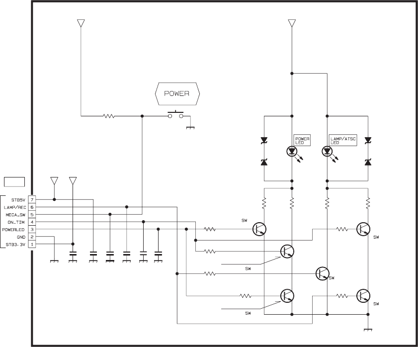
2-79(No.YA463)
FRONT LED PWB ASS'Y
SRA0L111A-M2
c30200001_0214_1/1_0.0
D0706
D0707
R0711
Q0706
Q0707
Q0705
R0716
R0714
R0715R0713
C0701 C0702
D0703
Q0702
R0712
D0704
C0703 C0704 C0705 C0706
Q0704
R0710
CN07FL
R0709
D0705
Q0701
R0708
R0707
R0706
S0701
D0701
MA8068-X
MA8068-X
2SC3928A/QR/-X
2SC3928A/QR/-X
2SC3928A/QR/-X
MA8068-X
2SC3928A/QR/-X
MA8068-X
CH CH CH CH
2SC3928A/QR/-X
QGA2001F2-07V
LE22440
2SC3928A/QR/-X
QSW0619-003Z
SELU5E20C/EF/-T
1.5k 1.5k
33k
33k33k
1000p 1000p
33k
10p 10p 10p 10p
1.8k
33k
33k
10k
100
ON_TIM
POW_LED
STB5V
STB3.3V
GND
ATSC
GND
GND
STB3.3VSTB5V
GND GND GND GND
MECA_SW
GND
GND
ANALOG PWB
ASS'Y(1/6)
CN1F
(SHEET3)
FRONT LED PWB CIRCUIT DIAGRAM [HD-52FA97] SHEET 36
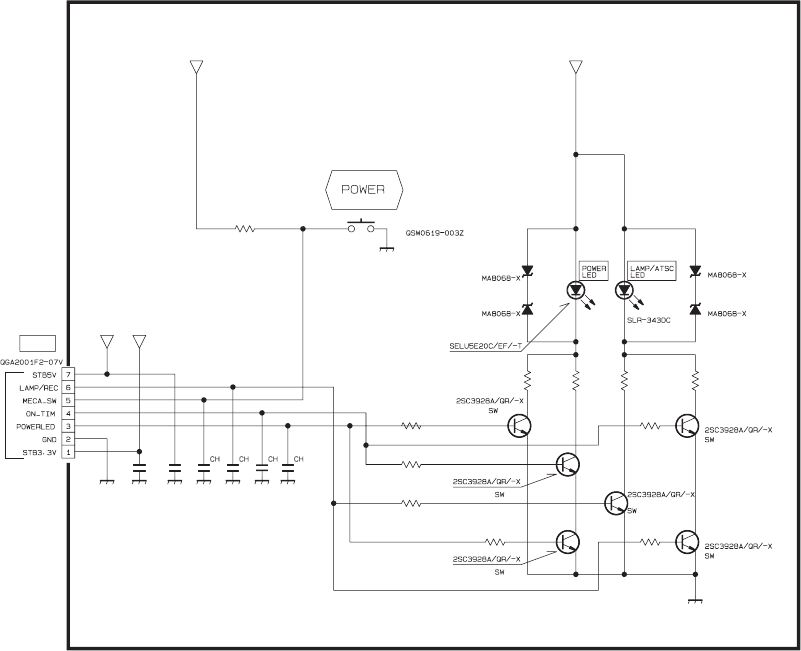
(No.YA463)2-80
FRONT LED PWB ASS'Y
SRA0L113A-M2
c30217001_0712_1/1_0.0
D0906
D0907
R0911
Q0906
Q0907
Q0905
R0916
R0914
R0915R0913
C0901 C0902
D0903
Q0902
R0912
D0904
C0903 C0904 C0905 C0906
Q0904
R0910
CN9F
R0909
D0905
Q0901
R0908
R0907
R0906
D0901
S0901
15k 1.5k
33k
33k33k
1000p 1000p
33k
10p 10p 10p 10p
1.8k
33k
33k
10k
4.7k
ON_TIM
POW_LED
STB5V
STB3.3V
GND
ATSC
GND
GND
STB3.3VSTB5V
GND GND GND GND
MECA_SW
GND
GND
ANALOG
PWB(1/6)
CN1F
(SHEET 3)
FRONT LED PWB CIRCUIT DIAGRAM [HD-56FB97, HD-61FB97] SHEET 37
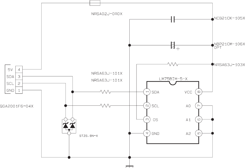
2-81(No.YA463)
TEMP PWB ASS'Y
SRA-8211A-M2
c40078001_0808_1/1_0.0
IC2001
R2003
R2002
R2001
C2001
CN82T
D2001
K2001
C2002
GND1
DRIVE PWB
ASS'Y(7/9)
CN1T
(SHEET30)
SENSOR
TEMP PWB CIRCUIT DIAGRAM SHEET 38
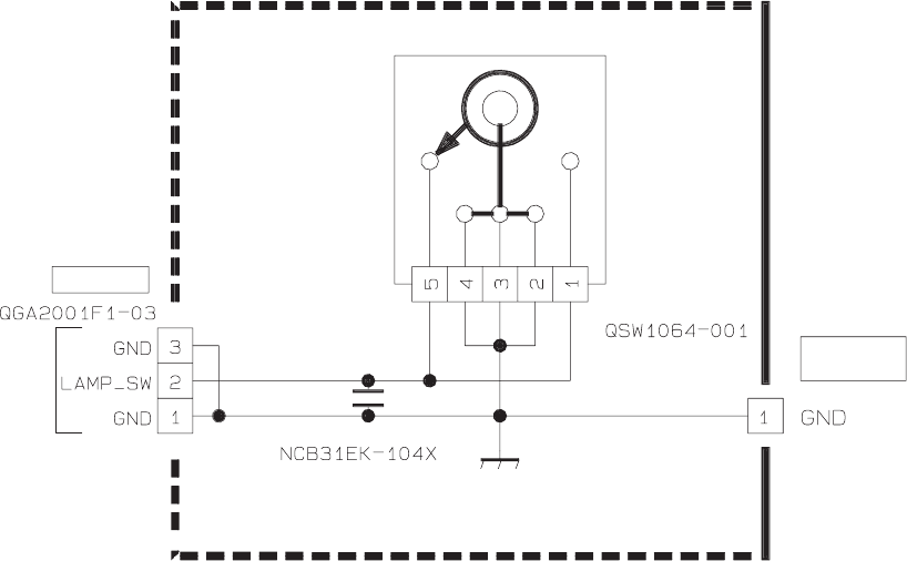
(No.YA463)2-82
LAMP COVER SW PWB ASS'Y
SRA0L211A-M2
c40084001_0808_1/1_0.0
C0861
S0861
CN0806
CN08G3
LAMP_SW
GND
DRIVE PWB
ASS'Y(7/9)
CNSW1
(SHEET30)
INTERLOCK
SW
LAMP COVER SW PWB CIRCUIT DIAGRAM SHEET 39
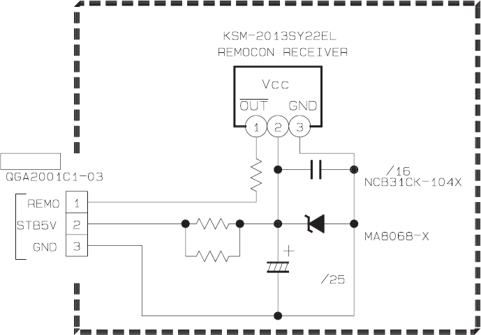
2-83(No.YA463)
REMOCON PWB ASS'Y
SRA-8011A-M2
c40085001_0808_1/1_0.0
CN08RE
IC0821
C0821
D0821
C0822
R0821
R0822
R0823
.1
47
1k
100
100
REMO
GND
STB5V
ANALOG PWB
ASS'Y(1/6)
CN1RE
(SHEET3)
REMOCON PWB CIRCUIT DIAGRAM SHEET 40
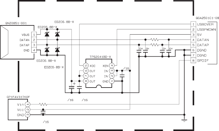
(No.YA463)2-84
USB PWB ASS'Y
SRA-8521A-M2
c40092001_0728_1/1_0.0
J8001
IC8501
C8001C8002C8003
R8501
C8501
IC8001
R8001
D8001
R8002
D8002
D8003
D8004
CN8DT
C8006
C8007
C8005
C8004
27p27p15p
0
.1
33
33
.1100
.1
15p
DGND
ATSC
TUNER
PWB
USB PWB CIRCUIT DIAGRAM SHEET 41
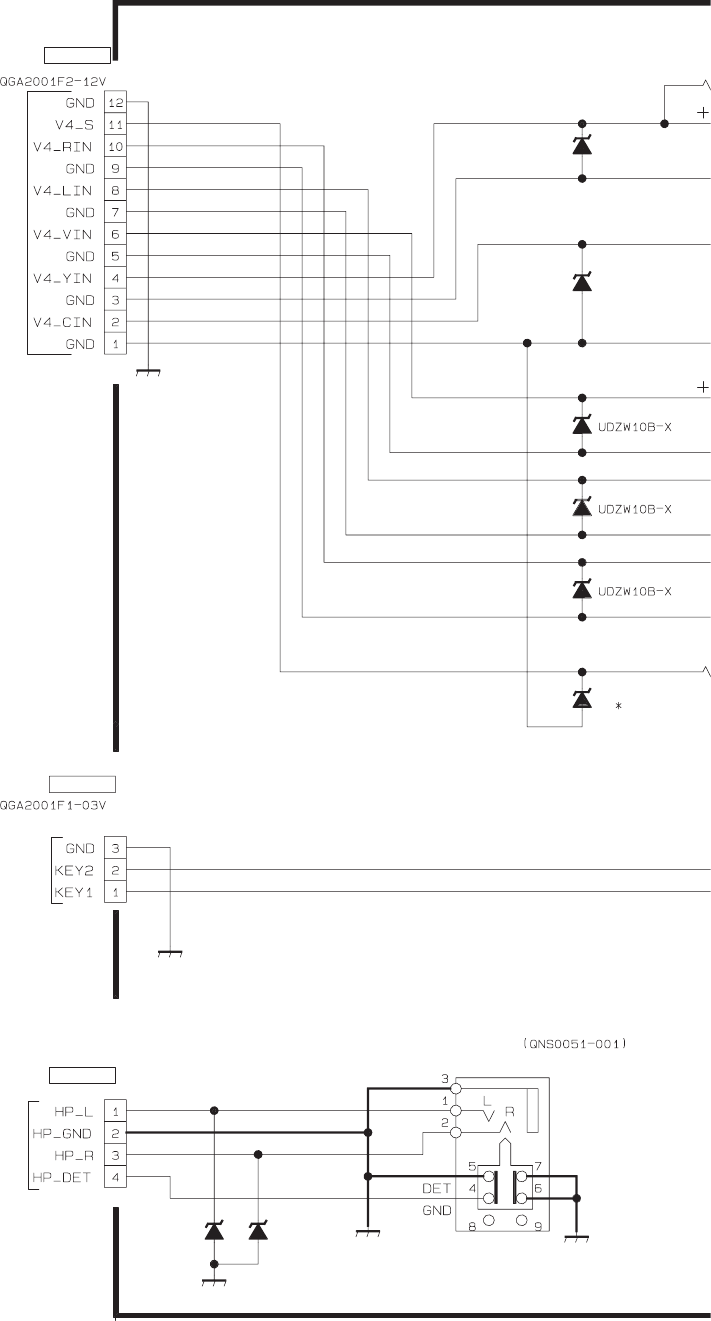
2-85(No.YA463)
SIDE CONTROL PWB AS
SRA0L013A-M2
CN08S1
CN08S2
D0847 D0848
CN08S3
J0831
R
C
D0846
C
0
R
0
C
0
D0842
D0841
D0843
D0844
D0845
OPEN OPEN
OPEN
OPEN
O
P
1
0
OPEN
OPEN
V4_S
V4_RIN
V4_RIN_G
V4_LIN
V4_VIN
V4_YIN
V4_CIN
V4_YCING
GND1
GND1
KEY2
KEY1
HP_GND
HP_GND
HP_L
HP_GND
HP_R
HP_DET
V4_VIN_G
V4_LIN_G
ANALOG PWB ASS'Y(1/6)
CN1S1
(SHEET3)
ANALOG PWB ASS'Y(1/6)
CN1S2
(SHEET3)
OPEN
SIDE CONTROL PWB CIRCUIT DIAGRAM SHEET 42
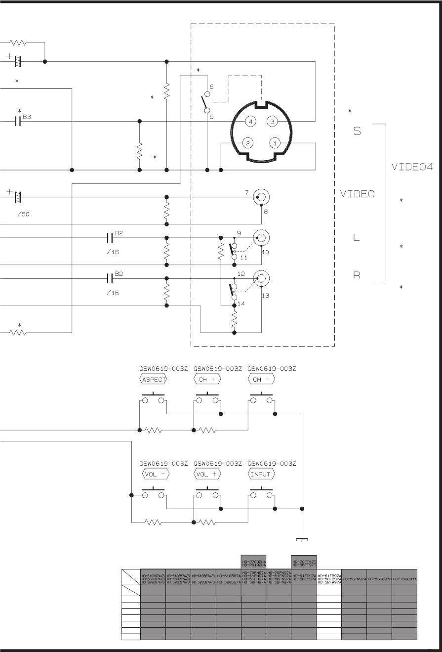
(No.YA463)2-86
SS'Y
c30201001_0922_1/1_0.0
C0844
C0845
S0855
S0853S0851
S0854
S0852
J0841
R0852R0851
R0853
R0848
R0854
S0856
R0849
R0847
J0841
R0842
J0841
R0844
C0842
R0843
R0845
C0841
R0846
R0841
C0843
J0841
J0841
1
1
15k5.6k
5.6k
OPEN
15K
0
75
220k
220k
OPEN
10
GND1
J0841
R0842
R0843
R0847
C0841
C0842
D0846
QNN0787
-001 QNN0787
-001 QNN0787
-001 QNN0787
-001
OLLC09901 OLLC09901 OLLC09901 OLLC09901
-02
OLLC09901
-03
OLLC09901
-03
QNN0787
-001
QNN0787
-001-002
QNN0787 QNN0787
-001
UDZW10B-X UDZW10B-X UDZW10B-X UDZW10B-X
QNN0787
-001
OL-CX3106
OLLC09901
-03
QNN0787
-001 QNN0787
-001
OLLC09901
-04
75
75
33k
10/50
0.01
75
75
33k
10/50
0.01
75
75
33k
10/50
0.01
75
75
33k
10/50
0.01
OPEN
OPEN
OPEN
OPEN
OPEN
OPEN
OPEN
OPEN
OPEN
OPEN
OPEN
OPEN
OPEN
OPEN
OPEN
OPEN
OPEN
OPEN
OPEN
OPEN
OPEN
OPEN
OPEN
OPEN
OPEN
OPEN
OPEN
OPEN
OPEN
OPEN
OPEN
OPEN
OPEN
OPEN
OPEN
OPEN
OPEN
OPEN
OPEN
OPEN
OPEN
OPEN
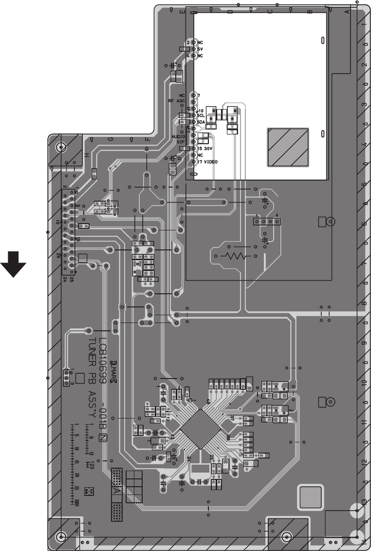
2-87(No.YA463)
C006
C007
C010
C013
C061
C062
C063
C064
C065
C066
C067
C068
C069
C070
C071
C072
C073
C074
C075
C076
C077
C078 C079
C080
C081
C082
C083
C084
C085
C086
C087
C088
C089
C090
C091
C092
C093
C094
D001
D002
IC061
L002
L003
Q004
Q005
Q061
Q062
R001
R002
R004
R005
R013
R014
R028
R029
R030
R047
R061
R062
R063
R064
R065
R066
R067
R068
R069
R070
R071
R072
R073
R074
R075
R076
R077
TU001
Y003
Y004
T1 T2
IC001
C001
W209
W208
W405
W406
W205
W404
W401
W402W403
W201
W204
W407W408
W409
W202
W206
W207
W212
W211
W210
W411
W410
W203
W213
W412
C002
R003
Y002
Y005
W214
W215
W216
W217
W218
W219
W220
W221
Y001
W413
W414
W415
W416
W417
G1 G2
C014
C015
C016C017
L004
Q006
R006
R007
R008Y006
W418
W419
FR
O
N
T
PATTERN DIAGRAMS
TUNER PWB PATTERN [SOLDER SIDE]
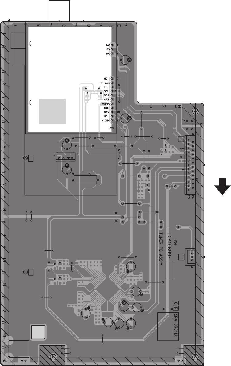
(No.YA463)2-88
C007
C013
C062
C066
C068
C069
C070
C071
C072
C076
TU001
T1 T2
IC001
C001
W209
W208
W405
W406
W205
W404
W401
W402 W403
W201
W204
W407 W408
W409
W202
W206
W207
W212
W211
W210
W411
W410
W203
W213
W412
C002
R003
W214
W215
W216
W217W218
W219
W220
W221
Y001
W413
W414
W415
W416
W417
G1 G2
W418
W419
FR
O
N
T
TUNER PWB PATTERN [PARTS SIDE]
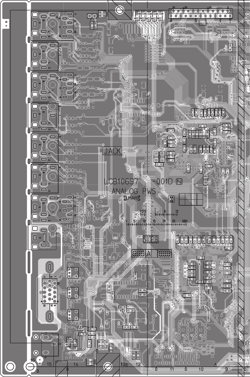
2-89(No.YA463)
LC461
LC462LC463
T1
R534
R535
C104
C105
C107
C109
C110
C111
C112
C113
C114
C115
C116
C117 C122 C123
C127
C128
C129
C131
C132
C133
C134
C136
C137
C138
C140
C142
C156
C157
C158
C159
C160
C162
C163
C164
C165
C167
C168
C177
C178
C181
C182
C183
C184
C185
C186
C187
C188
C190
C191
C192
C193
C199
C200
C201
C202
C203
C492
C584
C291
J401
J402J403 J404
J405 J407
J409 J410
J411
R142
R145
R150
R157
R181
R184
R196
R197
R219
R220
R241
R243
R251
R255
R259
R281
R282
R283
R287
R290
R291R292
C245
C246
R377
R379
R390
R491
Y602
Y603
Y607
Y609
D492
C214
C215
R955
C222
C226
D121
D125
D131
D132
D133
D134
D135
R781
R782
J406
R905
C237
C238
R971
R972
R973
R974
R975
R976
C239
A
NALOG PWB PATTERN [SOLDER SIDE]
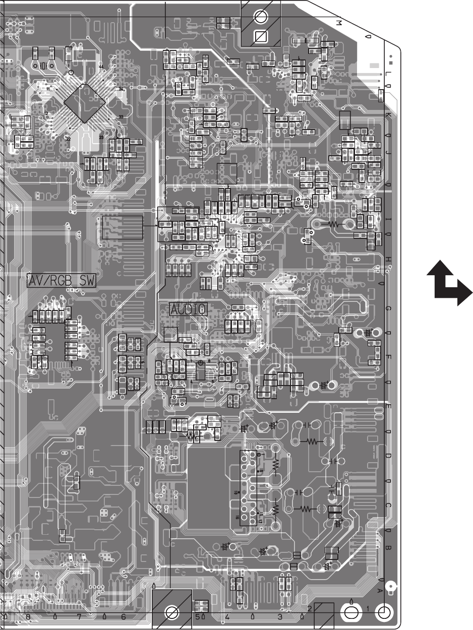
(No.YA463)2-90
IC605
C331
C334
C337
C343
C344
C345
C346
C347
C348
C349
C350
C351
C352
C366
C367
C501
C502
C503
C504
C506
C515C516
C518
C519
C531
C532
C540
C541
C542
C544
C545
C546
C551
C552
C560
C567
C572
C574C575
C580
C581
C583
C584
C585
C586
C587
C588
C590
C601
C604
C605
C606
C607
C609
C610 C611
C613
C621
C622
C623
C624
C625
C626
C627
C628
C629
C630
C631
C632
C633
C634
C635
C636
C638
C639
C640
C641
C643
C746
C647
C648
C649
C650
C651
C652
C653
C654
C747
C660
C661
C662
C663
C664
C665
C667
C668
C669
C679
C680
C699
C700
C702
C705
C713
C717
C753
C755
C759
IC331
K331
L501
L601
L602
R301
R302
R306
R307
R309
R310
R311
R312
R313
R320
R322
R323
R333
R335
R336
R337
R339
R340
R341
R343
R345
R346
R351
R352
R353
R354
R375
R376
R377
R378
R379
R380
R501
R502
R503
R504
R505
R508
R509 R511
R512
R513
R514
R527
R528
R529
R531
R532
R533
R545
R546
R548
R553
R556
R557
R565
R572
R573
R575
R576
R577
R578
R601
R602
R603
R604
R605
R606
R607
R608
R613
R614
R615
R616
R617
R618
R632
R633
R634
R635
R636
R638
R639 R640
R641
R642
R643
R645
R646
R647
R649
R650
R653
R667
R668
R672
R685
R693
R694
R695
R705
R706
R760
R761
R764
R765
R791
R792
R793
R913
R914
X331
Y604
Y611
Y612
Y904
R922
R927
R909
R918
R919
R920
R729
R730
R731
R732
R734
R735
R736
R738
R739
R740
R741
R742
R743
C719
C720
C721
C722
C724
C725
C726
C727
C728
C216
C217
C218
C221
C225
C230
C231
C232
R969R970
R928
R910
R744
C744
IC610
R772
R773
R774
R775
R776
R777
R778
D501
D502
D619
C745
FR
O
N
T
T
OP
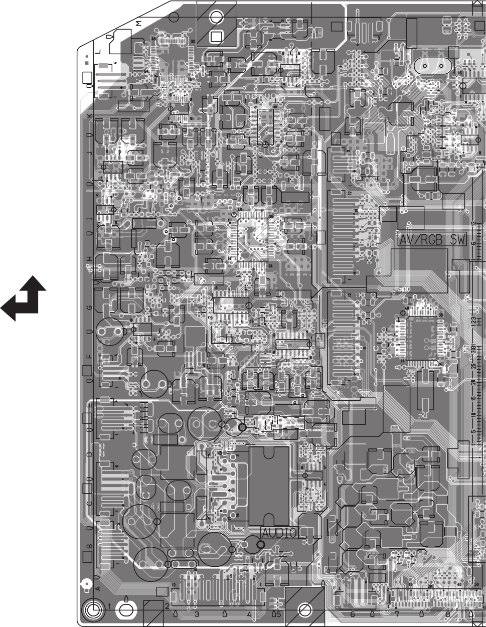
2-91(No.YA463)
IC601
IC540
RE
CV1
T2
A3
A2 S3
T1
A1 SP
UA
CV2
IC605
X551
X540
R584
R585
C207
C208
UV
C118
C119
C120
C121
C124
C125
C126
C729
C161
C194
C195
C196
C197
C198
R710
Q615
C301
C303
C304
C305
C306
C307
C332
C333
C335
C336
C338
C339
C340
C341
C342
C353
C354
C355
C356
C357
C358
C359
C360
C361
C362
C363
C364
C365
C368
C369
C370
C371
C372
C373
C374
C381
C382
C505
C507
C508
C509
C510
C511
C512
C513
C514
C517
C520
C543
C547
C548
C549
C553
C554
C555
C556 C557
C558
C559
C561
C562
C563
C564
C565
C566
C568
C569
C571
C573
C582
C589
C591
C602
C603
C607
C608
C612
C614
C615
C616
C617
C637 C642
C644
C646
C655
C657
C658
C659
C666
C671
C674
C675
L606
C681 C682
C683 C684
C685
C686
C687
C688
C689
C690
C691
C692
C693C694
C695
C696
C697
C698
C699
C700
C701
C702
C703
C704
C705
C706
C707
C708
C709
C710
C711
C712
C713
C714
C715
C716
C751
C752
C753
C754
C755
C756
C757
C758
C760
C761
C901
C904
C905
C911
C912
C913
C914
C915
C916
C919
C920
D103
D104
D331
D332
D601
D602
D603
D605
D606 D607
D608
D610
D611
D612
D613
D614
D615
D751
D752
D753
D902
D903D904
D905
IC301
IC332
IC333
IC351
IC352
IC353
IC354
IC
3
I
C
IC501
IC502
IC551
IC552
IC602
IC603
IC604
IC606
IC751
IC902
K332
K601
K602
K603
K604
C676
C677C678
L331
L332
L333
L334
L335
L601
L602
L605
L901
L902
L903
L904
L905
L906
LC331
LC
551
LC552
Q103
Q106
Q107
Q301
Q302
Q331
Q501
Q502
Q503
Q540
Q553
Q601
Q602
Q603
Q604
Q605
Q606
Q607
Q609
Q613
Q614
Q751
Q752
Q901
Q902
Q903
R164
R165
R166
R167
R195
R198
R199
R200
R201
R202
R203 R204
R205
R206
R207
R208
R209
R210
R211
R212
R213
R214
R215
R216
R217
R218
R268
R269 R270 R271
R272
R273
R274
R275
R308
R314
R315
R316
R317
R318
R319
R321
R327
R328
R329
R330
R331
R332
R334
R338
R342
R344
R347
R348
R349
R350
R355
R356
R357
R358
R359
R360
R361
R362
R363
R364
R365 R367
R368
R369
R370
R371
R372
R373
R374
R381
R383
R385
R395
R506
R507
R510
R515
R516
R519
R520
R530
R540
R541
R542
R543
R544
R547
R549
R554
R555
R560
R561
R562
R563
R564
R566
R567
R568
R569
R570
R571
R574
R580
R581
R582
R583
R609
R610
R611
R612
R616
R619
R620
R621
R622
R623
R624
R625
R626R627
R628
R629R630
R631
R644
R651
R652
R654
R656
R711
R712
R659R660
R661
R662
R663
R664
R665
R666
R669
R670
R671
R673 R674
R675
R676
R677
R678
R679
R680
R681 R682
R683 R684
R685
R687
R688
R689
R690R691
R692
R696
R697
R698
R699
R700
R701
R702
R703
R704
R707
R299
R715
R716
R717 R718
R719
R720
R751
R752
R753
R754
R755
R756
R767
R768
R769
R770
R794
R795
R796
R901
R902
R903
R904
R907
R908
R911
R912
R917
TH601
X331
Y605
Y606
Y610
Y903
X601
R713
Q617
R921
R923
R924
R925
R926
R933
R934
Q616
IC607
D616
D617
D618
R722
R723
R724
R725 R726
R727
R728
R729 R730
R731
R732
R733
R737
C719
C720
C721
C723
C728
R708
C219
C220
R956
C233
C234
C235
C236
D126
C670
R324
R325
K605
IC608
IC609
C730
C734
C737
C739
C731
C732
C733
C735
C736
C738
C672
C673
C240
C241
C242
C243
C244
R959
R
9
C740
C741
C742
C743
FR
O
N
T
TOP
A
NALOG PWB PATTERN [PARTS SIDE]
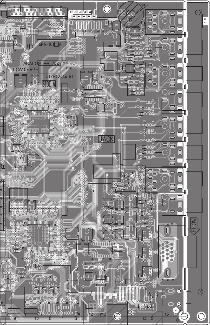
(No.YA463)2-92
LC461 LC462 LC463
IC101
IC102
S1
F
S2
T1
CN011 CN012
R586
R587
C209
C210
C101
C102
C103
C106
C108
C130
C139
C141
C143
C144
C145
C146
C147
C148
C149
C150
C151
C152
C153
C154
C155
C166
C169
C170
C171
C172 C173
C174
C175
C176
C179
C180
C189
C204
C206
C281
C282
C283
C284
C285
C286
C287
C288
C292
C375
C383
C401
C402
C403
C404
C405
C406
C407
C408
C409
C410
C411
C412
C413
C414
C415
C416
C417
C418
C419
C420
C421
C422
C423
C431
C432
C433
C451
C452
C453
C461 C462 C463
C464
C465 C466
C468
C469
C491
C493
C494
C211
C212
D101
D102
D105
D401
D402
D403
D404
D405
D406
D407 D408
D409
D410
D411
D412
D413
D414
D415
D416
D417
D418
D419
D420
D421
D422
D423
D424
D431
D432
D451
D452
D461
D462
D463
D464
D465
D466
D481
D491
C213
IC103
IC104
IC105
IC106
IC281
IC282
IC355
IC356
IC381
J401
J402 J403
J404
J405
J407
J409
J410
J411
Q101
Q102
Q103
Q104
Q105
Q108
Q109
Q110
Q111
Q112
Q431
Q432
Q433
Q451
Q452
Q453
D106
L101
Q113
Q114
R101
R102
R103
R104
R105
R106
R107
R108
R109
R110
R111
R112
R113
R114
R115
R116
R117
R118
R119
R120
R121
R122
R123
R124
R125
R126
R127
R128
R129
R130
R131
R132
R133
R134
R135
R136
R137
R138
R139
R140
R141
R143
R144
R146
R147
R148
R149
R151
R152
R153
R154
R155
R156
R158
R159
R160
R161
R162
R163
R168
R169
R170
R171
R172
R173
R174
R175
R176
R177
R178
R179
R180
R182
R183
R185
R186
R187
R188
R189
R190
R191
R192
R193
R194
R221
R222
R223
R224
R225
R226
R227
R228
R229
R230
R231
R232
R233
R234
R235
R236
R237
R238
R239
R240
R242
R244
R245
R246
R247
R248
R249R250
R252
R253R254
R256
R257R258
R260
R261
R262
R263
R264
R265
R266
R267
R276
R277
R278 R279
R280
R284
R285
R286
R288
R289
R293
R294
R295
R296
R297
R298 R382
R384
R386
R387
R388
R389
R391
R392
R393
R394
R401
R402
R403
R404R405
R406
R407
R408
R409
R410
R411
R412
R413 R414 R415
R416
R417
R418R419
R420
R421
R422
R423
R431
R432
433R
R434
R435
R436 R437
R438
R439
R440
R441
R442
R443
R444
R451
R452
R453
R454
R455
R456
R461
R462
R463
R464
R465
R466
R467
R468
R469
R470
R471
R472
R473
R474
R475
R481
Q115
R595
R596
R597
R598
R599
R941
R797
R798
Y601
Y608
Y902
Y905
R593
R594
D492
R457
R458
R476
R588
R589
R590
R591
R592
R931
R932
R935
R936
R937
R938
R942 R943
R944
R945
R946
R947
C293
C294
C295
C296
C297
C921
C922
C923
D110
D111
L102
L103
L104
R948 R949 R950
R951
R952 R953
R954
C223
C224
C227
C228
C229
D122
D123
D124
D136
J406
R957
R958
R967
R968
R960
R961
R962
R963
R964R965
R966
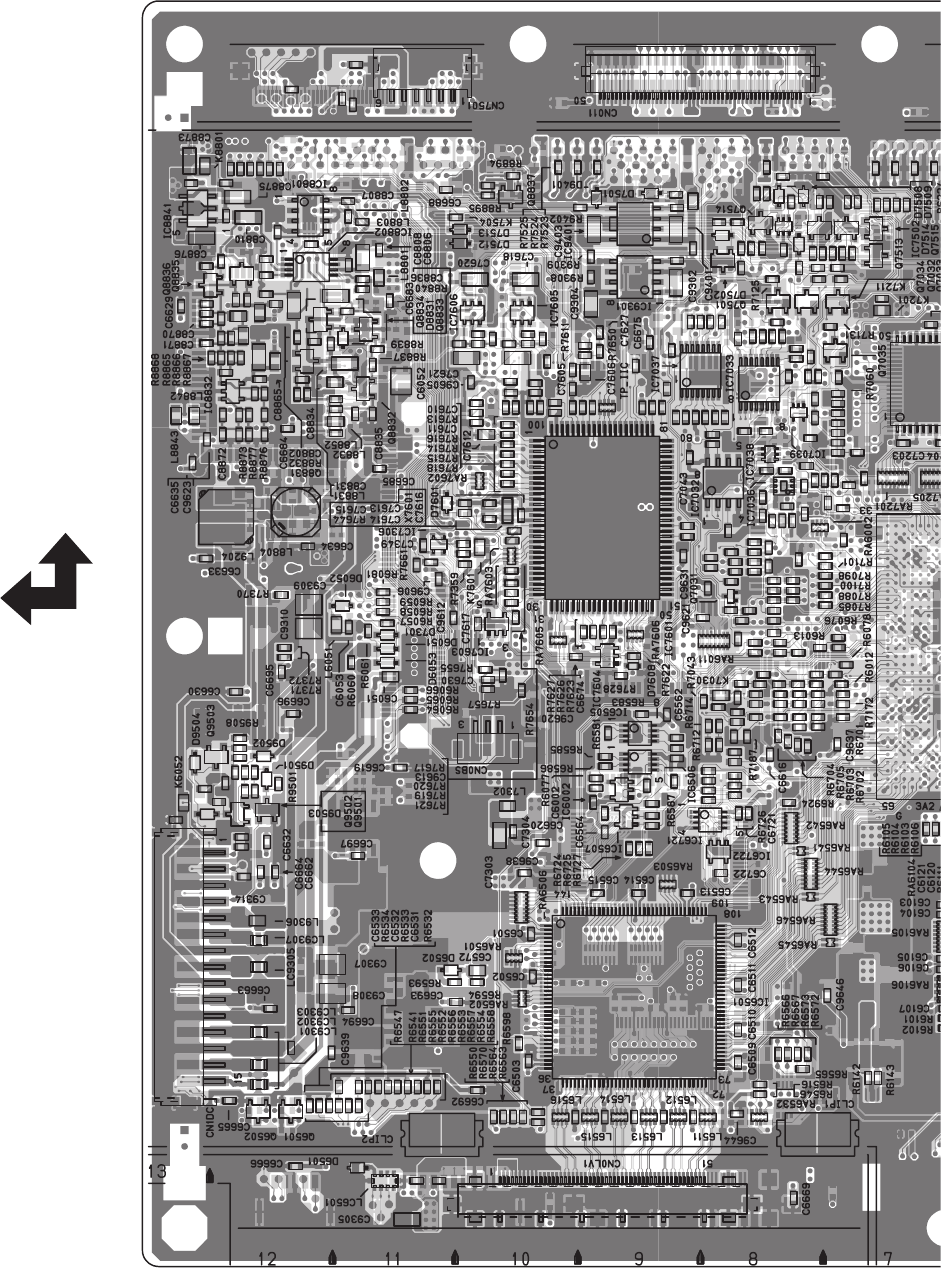
2-93(No.YA463)
CLIP1
CLIP2
C6001
C6051
C
6
C
6
C
6
C
6
C
C6513C6514C6515
C6722
C7030
C7031
C7032
C7033 C7034
C7039
C7203 C
7
C7207
R6593
C7348
C7501
C7502
C7602
C7603
C7608
C7610
C7611
C7612
C7613
C7614
C7615
C7618
C7619
C7620
C7621
C8807
C8810
C8811
C8831
C8832
C8833
C8836
C8866
C8867
C8869
C8870
C8871
C9303
C9402
CN0LV1
CN7501
CN011
D9401 D7508 D7509
D7601
D8831
IC6501
1
36
37
72
73
108
109
144
IC6721
1
4
5
8
IC6722
IC7306
IC7502
IC7601
1
25
26
50
51
75
76
100
IC7603
IC7605IC7606
IC8801
1
4
5
8
IC8802
1
4
5
8
IC9301
1
4.5
5.5
9
IC9401
K7030
K7201
L6511L6512L6513L6514L6515L6516
L7302
L8831
L8832
L8848
LC6501
LC9301
LC9302
LC9303
LC9305
LC9307
Q6501Q6502
Q7032 Q7033Q7034
Q7035
Q7501
Q8835
R6005 R6006
R6012
R6013
R6057
R6058
R6059
R6064
R6065
R6066
R
R
R6503
R6546
R6561
R6562
R6565
R6571
R6574
R6701
R6924
R7030
R7031
R7032
R7033
R7034
R7035
R7036
R7038 R7039 R7040
R7041 R7042
R7044 R7045R7046
R7047
R7049
R7051
R7052
R7053 R7054
R7055
R7056
R7057
R7058
R7059
R7060
R7061
R7062R7063
R7072R7073
R7075
R7084
R7085
R7086
R7087
R7088
R7089 R7090
R7091
R7097
R7098
R7099
R7100
R7101
R7103
R7105
R7107 R7109
R7113
R7123 R7124R7125
R7128
R7130
R7131
R7156
R7157
R7170
R7171 R7172
R7359
R7360
R7505
R7530
R7532
R7606
R7607
R7608
R7613
R7614
R7615
R7616
R7617
R7618
R7619
R7620
R7622
R7624
R7625
R7628
R6594
C7631
R7632
C7632
R7635
R7644
R8781
R8822
R8823
R8824
R8825
R8831
R8834
R8836
R8839
R8840
R8878
RA6002
RA6011
RA6501
RA6503
RA6532
RA7201 RA72
0
RA7601
RA7605
RA7606
IP
4
IP47
IP48IP50
IP51
IP52
IP53
IP54
IP55
IP56
IP57
IP59
IP60IP61
IP63
IP64
IP65 IP66
IP67
IP68
IP69
IP70
IP71
IP72
IP73
IP74
IP75
IP76
IP77IP78
IP79
IP80IP81
IP82
IP83
IP84
IP85
IP86IP87 IP88
IP89
IP90IP93IP94
IP95
IP96
IP97
IP98
IP99
IP100
IP101
IP102
IP103
IP104
IP105
IP106
IP107IP109IP111
IP112
D7514
L9306
IP118
IP119
IP121
IP123
IP124
IP126
IP127
IP129
IP130
IP131
IP133
IP135
IP136
IP137
IP139
IP141
IP143
IP145IP146
IP147IP148IP149IP150IP151
IP263IP264
IP265IP266
IP267IP268IP269
IP270
IP271
IP273
IP274
IP299 IP300
IP301
IP302
IP303
C6571
IP446
R7647R7648
C6619
C6620
C6630
C6633
C6634
C6636
C6663
C6665
C6666
C6667C6668
C6684
C6685
C6688
C6692
C6693
C6694
C6696
C6697
C7628
C8874
C8875
C8876
D9501
D9504
Q9501
Q9503
R6575
R6576
R7651
R8889
R9505
R9506
R9507
R9508
R9509
R9510
R6577
R6578
R6579
IP58
C6563
C7073
IC6505
1
4
5
8
IC6506
1
4
5
8
IC7036
R6073
R6074 R6075
R6580
R6582
R6583
R6584
R6585
R6586
R6588
R6589
R6590
R6592
R7179
R6076
C7074
C7075
C9305
C9307
C9308
C9309
C9310
L8804
C9313
C9314
L8803
R6077
R6078
R6516
R7185
IP447
C9601
IP449
IP451
IP453
IP455
IP457
IP459
C9613
C9615
C9620
C9621
R7655
R7657
C7630
C7076
CN0BS
K7504
Q8837
R8893
R8894
R8895
IP460
C9622
R9402
C9209
R6080
R7659
C7633
C6572
R7370
K7211
L8866
L8852
R7371
R7372
Q7511
Q7514
Q7515
R7374
R7375
R7551
R8607
R8608
R7511
C7077
IC7039
R6081
R7198
R7662
C9638
C9644
C6052
C6053
C6501
C6502
C6503
C6504
C6505
C6506
C6507
C6508
C6509 C6510 C6511 C6512
C6531
C6532
C6533
C6721
C7043
C7044
C7072
C7303
C7304
C7349
C7513
C7604 C7605
C7606
C7607
C7609
C7616
C7617
C8802
C8806
C8808
C8809
C8834
C8835
C8865
C8868
C8872
C9302
C9304
C9401
C9403
D6051
D6052
D6053
D7501
D7502
IC7032
1
4
5
8
IC7033
1
8
9
16
IC7037
1
8
9
16
IC7604
IC8832
K6052
K7601
L6051
L8801
L8802
L8842
L8843
L8846
L8847
L8849
Q7031
Q8831
Q8832 Q8833
Q8834
Q8836
R6060
R6061
R6104
R6105
R6142
R6143 R6221
R6222
R6223
R6224
R6532
R6533
R6534
R6541
R6547
R6550
R6551
R6552
R6553
R6554
R6555
R6556
R6557
R6558
R6563
R6564
R6566
R6567
R6570
R6572
R6573
R6601
R6603
R6613
R6614
R6617
R6702
R6703
R6704
R6705
R6712
R6713
R6714
R6715
R6724
R6725
R6726
R6727
R7043
R7081
R7092
R7093
R7094
R7095
R7096
R7104
R7106
R7108
R7110
R7111
R7112
R7126
R7127
R7154
R7155
R7158
R7159
R7160
R7161
R7162
R7163
R7164
R7165
R7504
R7521
R7523
R7524
R7525
R7526
R7529
R7533
R7539
R7603
R7604
R7605
R7609
R7610
R7611
R7612
R7621
R7623
R7626
R7627
R7631
R7634
R8801
R8802
R8803
R8832R8835
R8837
R8838
R8841
R8863R8864R8865
R8866
R8867
R8868
R8869
R8870
R8871
R8872R8873
R8874
R8875R8876
R8877
R8884
R9308 R9309
R9401
RA6502 RA6506
RA6541
RA6542
RA6543 RA6544
RA6545 RA6546
RA7602
RA7603
X7601
IP7
IP8
IP10
IP11
IP12
IP91
IP92
C6610
C6616
C6629
C6631
C6632
C6635
C6662
C6664
C6669
C6674
C6675
C6680
C6683
C6695
C7627
C8873
C9501
C9502
D9502
D9503
IC8841
K8801
Q9502
R7540
R7541
R7650
R8887
R9501
R9502
R9503R9504
C6562
C6564
IC6507
R6581
R6587
R6591
R7174
R7175
R7176
R7177
R7178
R7542
R7543
CN1DC
C6002
C9306
IC6002
R6079
R7184
R7186
R7187
R7544
C9603
C9605
C9606
C9612
C9614
R7654
R7656
D7301
D7512 D7513
IC7038
R7367
R7658
C9623
R7188
R7189
L9204
D6501
D6502
R6598
R7190
R7191
C7520
C7521
Q7512Q7513
R7545
R7546
R7547
R7548
R7549
R7550
R7552
R7553
R7554
R7555
R7660
R8601
R8611
R7037
R7192R7193
R7197
R7199
R7661
C9631
C9637
C9639
C9646
D7608
F
R
O
N
T
T
OP
DIGITAL PWB PATTERN [SOLDER SIDE]
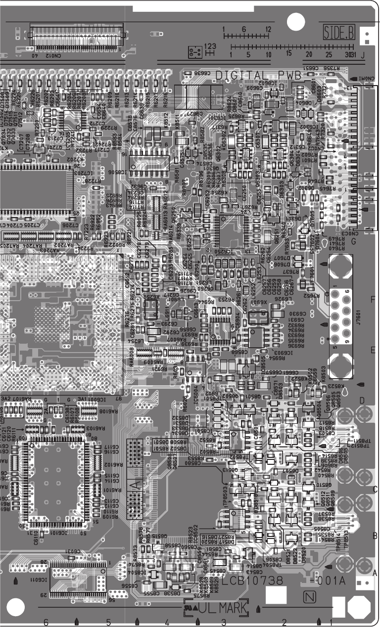
(No.YA463)2-94
C6031
C6103
C6104
C6105
C6106
C6107
C6112
C6113
C6114
C6115
C6116
C6117
C6251
C6292
C6293
C7204 C7205 C7206
C7207 C7208
C8503
C8505
C8543
C8545
C8555
C8556
C8558
C8559
C8560
C8561
C8569
C8570
C8571
C8572
C8573
C8574
C8575
C8577C8579
CN012
D8505D8506
D8507
D8520D8521
D8522
D8535 D8536
IC6101
1
25
26
50
51
75
76
100
IC6250
1
12
13
24
IC8501
1
4
5
8
IC8502
1
4
5
8
IC8505
K6250
K8510
K8511K8512
L6254
L6902
Q8501Q8502
Q8503
Q8504
Q8505Q8506
Q8507Q8508
Q8509
Q8510
Q8511Q8512
Q8515
R6101
R6102
R6109
R6110
R6250
R6251
R6254
R6255
R6258
R6259
R6262
R6263
R6267
R6272
R6273
R6278
R6279
R6925
R7114
R7115
R7116
R7117
R7118
R7320
R7321
R7356
R7601
R7602
R7636
R7643
R7645
R7646
R8501
R8503
R8504
R8507
R8508
R8509 R8510
R8511
R8512R8513
R8514
R8517
R8518
R8520
R8521
R8522
R8526
R8527
R8528 R8529
R8530
R8533R8534
R8535
R8537
R8538
R8539
R8540
R8541
R8542
R8543
R8544
R8552
R8553
R8574
R8575
R8799
RA6007RA6008 RA6009
RA6103RA6104
RA6107 RA6108
RA7202RA7203RA7204RA7205
IP1
IP2
IP3
IP4
IP6
IP13
IP14
IP15
IP16
IP17IP18
IP19
IP20
IP21
IP23
IP24IP26
IP27IP28IP29
IP31
IP32
IP33
IP34
IP35
IP36
IP37
IP38
IP39
IP40
IP41
IP42
IP43
IP44
IP45
IP46
IP47
IP48
IP49IP51
IP161
R6341
D6303
IP461
IP462
IP463
IP464
IP275
IP276
IP277
IP278
IP279
IP280
IP281
IP282
IP283
IP284
IP285
IP286
IP287
IP288
IP289
IP290
C6638 C6651
C6655
C6656
C6657
Q6250
Q6251
R6248
C6234
R6284
C6217
C8580
C8581
D7605
R7652
C9608
C9616
R6218
R6219
R7228
IC7205
1
7
8
14
Q7201
C7212
C7213
C7214
R7229
R7231
R7232
R7234
R7235
R7237
K7202
K8522
IP465
R8606
R8609
R8610
R6926
X6901
C7217
L6926
C6930
C6931
R7242
C9626
C6303
C6304 C6305
C6308
C6309 C6310
C8606
C8621
C8622
C8623
IC8602
R6309
R6311
R6312
R6313 R6315
R6316
R6322
R6324
R6325
R6326 R6328
R6329
R6332 R6333
R6335
R6336
R6337
R6338
R6339
R8624
R8625
C8626
C9627
D8603D8604
C9632
IP466
C6934
C6935
IC6903
1
4
5
8
R6032
R6954
R6931
R6932
R6933
R6934
R6935
R6936
R6939
R6940 R6941
R6943
R6944
R6945
C8583
R6034
R7649
C6108
C6110
C6120
C6121
C6138
C6250
C6252
C6253
C6254 C6255
C6256
C6257
C6258
C6259
C6260
C6262
C6264
C6265
C6266
C6267
C6277
C6278
C6279
C6281
C6912
C7622
C7623
C7624
C8501
C8502
C8504
C8506
C8568
C8576
C8578
CN0MICN0C2
D8501
D8502
D8503
D8516
D8517
D8518
D8531 D8532D8533D8534
EF7601 EF7602
IC7203
1
12.5
13.5
25
26
37.5
38.5
50
IC8504
IC8506
1
8
9
16
J7601
K8502
K8503
K8508
K8509
L6250
L6251
L6252
L6253
L6901
Q8513
Q8514
R6021
R6022
R6103
R6104
R6105
R6106
R6107
R6108
R6111
R6201
R6202
R6203
R6204
R6206
R6207
R6208
R6209
R6210
R6213
R6214
R6215
R6216
R6217
R6223
R6224
R6225
R6226
R6252R6253
R6256
R6260R6261
R6264
R6266
R6270
R6274R6275R6276
R6921
R6922
R6923
R7223
R7224
R7637
R7639
R7640 R7641
R7642
R8502
R8505
R8506
R8523
R8524
R8525
R8573
R8577
R8578
R8580
R8581
R8582
R8583
R8584
R8796
R8797
R8798
IC6004
1
4
5
8
R6031
RA6012RA6013RA6014
RA6101 RA6102
RA6105
RA6106
X6250
D8538
R6340
D6304
CN0C3
R8645
IP291 IP292 IP293 IP294
IP295
IP296IP297IP298
C6612
C6613
C6639
C6640
C6641
C6654
C6659
C6661
C6249
IC6011
1
14
15
28
29
42
43
56
R6249
C6235 R6285
D7604
D7606 D7607
R7653
C9609
R6211
R6212
R7230
R7233R7236
C7215
K8529
K8523
L6912
L6911
K8528
IC6001
1
182.25
183.25
364.5
365.5
546.75
547.75
729
R6024
R6025
R7241
C6302
C6306
C6307
C6311
C6312
C8601
C8602
C8609
C8610
D6301 D6302
D8601
IC6301
IC6302
Q6301
Q6302
Q6303
Q6304
R6306
R6307
R6308
R6310
R6314
R6317
R6318
R6319
R6320
R6321
R6323
R6327
R6330
R6331
R8647
C8630
R8649
C8629
C6004
C6933
C9633
IC6904
1
8
9
16
R6026
R6930
R6937
R6938
R6942
R6946
R6947
R6948
R6949
R6952
2-95(No.YA463)
C6101 C6102
C6109
C6132
C6135
C6201C6202C6203C6204C6206C6207C6208C6209C6210C6212C6213C6214C6215 C6216 C6222C6223C6224C6225C6226
C6246
C6248
C6261
C6263
C6269
C6275
C6282
C6286
C6287
C6288
C6297
C6723
C6904
C6906
C6913
C6915
C6918
C6919
C6925
C6926
C6927
C6928
C7041C7042
C7059 C7060
C
7
C7211
C7325
C7625
C8509C8512
C8513C8517C8518C8519
C8523
C8524
C8525 C8527
C8531
C8532
C8533
C8534
C8535
C8536
C8537
C8538
C8539
C8540
C8541
C8542
C8544
C8546
C8547 C8548
C8549
C8552
C8553 C8554
CN002
R7195
D7032
D7033
D8504
D8519
IC6251
IC7201
1
12
13
24
25
36
37
48
K6274
K6272
K6268
K7031
K7032
K8515
L6102
L6103
L6105
L6266
K6271
L6922
L6923
L6924L6925
Q6201
Q6202
R6017
R6018
R6112
R6113
R6114
R6115
R6116R6117
R6118
R6119
R6120
R6121
R6127
R6128
R6257
R6265
R6268
R6269 R6271
R6732
R7203
R7207
R7208
R7211
R7212
R7214R7215
R7216
R7217
R7221
R7225
R7226
R7227
R7319
R8545
R8546
R8547
R8551
R8554
R8567
R8571
R8572
R8579
RA6111 RA6112
RA6115RA6116
X8501
K6922
K6923
X7001
C6623
C6624
C6625
C6643
C6652
C6653
R6232
R6233
C6230
R7173
C6218
Q6203 Q6204
Q6205
Q6206
Q7036
Q7037
R6238
R7183
R8585
D8537
L6257
L6259
L6931
L6115
R7238
R7239
C7216
C6219
C6220
C6227 C6229
C6240
C6300
C6301
Q6207
Q6208
Q6209
Q6210
R6290
R6293
R6302
R6303
R8515R8516
R8602
R8603
R7243
L6265
C8611
C8612
C8614
C8616
C8617
C8620
C8624
IC8601
1
16
17
32
33
48
49
64
IC8603
1
4
5
8
L8601
Q8601
R8615
R8627
R8628
R8629
R8637
R8638
R8639
R8640
R8641
R8642
R8643
RA8601 RA8602
RA8605 RA8606
C9629
L8603
IC6003
1
4
5
8
R6029
C9640
C9645
C8631
C8632
R8652
R8653
R6035
R6037
C6111
C6118
C6119
C6124C6125
C6126
C6127
C6128
C6129
C6130
C6131
C6133
C6134
C6241
C6242
C6243
C6244
C6245 C6247
C6268
C6270
C6271
C6272
C6273
C6274
C6276
C6280
C6283
C6284
C6285 C6289
C6290
C6291
C6294C6295
C6296
C6298
C6705 C6707
C6724
C6901
C6902
C6903
C6905
C6907
C6908
C6909
C6910
C6911
C6914
C6916
C6917
C6921
C6922
C6923
C6924
C7045
C7046
C7047
C7048
C7049
C7050
C7051
C7052
C7053
C7054
C7055 C7056
C7057 C7058
C7062
C7063
C7064
C7065
C7066
C7067
C7202
C7601
C7626
C8514
C8516
C8520
C8521
C8522
C8526
C8528
C8529
C8530
C8550
C8551
C8557 C8562 C8563
C8564
C8565 C8566 C8567
CN0C1 CN0MM
CN232SW
D7201
D8508D8509
D8510 D8511
D8512D8513
D8514D8515
D8523D8524
D8525 D8526
D8527D8528
D8529D8530
C6205
IC6724
R7196
IC7034
1
8
9
16
IC7204
IC7602
1
4
5
8
IC7607
1
8
9
16
IC8503
1
36.25
37.25
72.5
73.5
108.75
109.75
145
J7601J8501J8502
K6921
K7033
K7034
K8504
K8505
K8506
K8507
L6921
LC6201
LC6202
LC6203
LC6204
LC6206
LC6207
LC6208
LC6209
LC6210
LC6212
LC6213
LC6214
LC6215
LC6216
LC6222
LC6223
LC6224
LC6225
LC6226
Q6211 Q6212Q6213
Q6214
R6122
R6123
R6124
R6125
R6126
R6141
R6280
R6281
R6282
R6283
R6286 R6287R6288
R6289
R6291
R6292
R6730
R6731
R7119
R7120
R7121
R7122
R8548
R8549
R8550
R8555
R8556
R8557
R8558
R8559
R8560
R8561
R8562 R8563
R8564
R8565
R8566
R8568
R8569
R8570
R6953
C6005
RA6109 RA6110
RA6113
RA6114
RA8501
RA8502RA8503
R6033
C6614
C6622
C6626
C6642
C6658
C6660
C6681
R6230
R6231
C6231
C6232
C6233
C8599
R8599
C6054 C6055
IC6012
1
4
5
8
IC6013
1
4
5
8
R6072
C6929
C7629
IC6901
C6236
C6237
C6238
C6239
R6235
R6236
R6239
R6241
R6242
R6244
R6245
C9316
L6258
L6260
K8526
K8527
K8524
R7240
IC7206
C6211 C6228C6299
R6205
R6220
R6227
R6228
R6229
R6234
R6237
R6240
R6243
R6246
R6247
R6277
R6300
R6301
R6304
R6305
R8604
R8605
R8612
R8613
C9625
C8603
C8604
C8605
C8607
C8608
C8613
C8615
C8618
C8619
C8625
D8602
L8602
R8614R8616
R8617
R8618
R8619
R8620
R8621 R8622
R8623
R8626
R8630
R8631
R8632
R8633
R8634
R8635
R8636
R8644
RA8603 RA8604 RA8607
X8601
C9628
IC8604
R8648
C8627
C8628
C6003
R6027
R6028
C9635
C9641
Q8602Q8603
R8650
R8651
C8582
R6036
DIGITAL PWB PATTERN [PARTS SIDE]
(No.YA463)2-96
C6122
C6123
C6136
C6221C6222
2
3
C6520
C6522C6523
C6701
C7040
C7060
C7061
C7301 C7302
C7305C7306C7307C7308C7309
C7310
C7319 C7320 C7321
C7323C7324
C7326 C7327
C7328 C7329
C7330 C7331
C7344
C7346
C7350
C8837
C8838
C8839
C8842 C8843
C8847
C8850 C8851 C8852C8853
C8855
C8862
C8863
C9005
C9008
C9101
C9103
C9205
C9206
C9207
C9208
C9211
C9212
C9301
CN0FC
CN0IDCN0LV2 CN000W
CN001
C8882
C8881
D9001D9002
D9203
D9204
IC7301
1
32
33
64
65
96
97
128
IC7302
1
12
13
24
25
36
37
48
IC7304
1
8
9
16
IC7305
1
4.5
5.5
9
IC8803
IC8831
1
20
21
40
41
60
61
80
IC9001
1
4.5
5.5
9
IC9101
K6603 K6605
0
32
K7302
L6501
L6521L6522L6523
L6701
L7301
L7308
L7309
L7310 L7311
L7312
L7313
L8833
L8834
L8844 L8845
L9001
L9002
L9203
Q7030
R6002
R6004
R6011
R6019
R6020
R6068
R8890R8891
R
6128
R6130
R6505R6506
R6507R6508
R6509R6510
R6511R6512
R6513R6514
R6531
R6537
R6538
R6539
R6542
R6543
R6548
R6549
R6568R6569
R6605
R7076
R7077
R7078
R7201
R7202
R7302
R7303
R7304
R7305
R7309
R7310
R7311
R7312
R7313
R7314
R7315
R7316
R7317
R7318
R7322
R7324 R7325
R7328
R7330
R7334
R7335
R7337
R7338
R7342
R7343
R7347
R7348
R7349
R7350
R7351
R7352
R7353
R7354
R7355
R7357 R7358
R8813
R8814
R8850
R8852
R8853R8854
R9002
R9006
R9007
R9202
R9203
R9204
R9205
R9206
R9207
R9208
R9209
R9301
R9302
R9303
R9305
R9307
RA6001
RA6504 RA6505
RA6531
RA6533
RA6534
RA8831 RA8832
X7309
C7353
L9307
C6618
C6621
C6627
4
3
C6676
C6677 C6678
C6679
C6682
C6686
C6689
C6690
C6698
C6699
C6646
C6139
R8888
C8880
C9203
C9602
C9610
C9618
C9619
C8883
K7502
K7503
K7505
K7506
Q7301
R7363
R7364
R7365
R7366
R7369
C6573
R6595
R6596
R6597
L6531
R6599
R7515
C9630
C9634
C9636
C9643
C9645
C9624
C6124C6125
C6521
C6524
C6525
C6561
C6601
C6602
C6603
C6604
C6705 C6707
C6708
C6709
C6710 C6711
C6902
C6914
C6916
C6917
C7057 C7058
C7066
C7068
C7209
C7311C7312C7313
C7314
C7315
C7318
C7322
C7333C7334C7335
C7338
C7340
C7341
C7342
C7343
C7345
C7504
C7505
C7506
C7507
C7508
C7510
C7511
C8840
C8841
C8844C8845C8846
C8848C8849
C8856
C8857
C8858
C8859
C8860
C8861C8864
C9001
C9002
C9004
C9006
C9007
C9010
C9012
C9201
C9202 C9204
C9210
CN110
CN0DC
D6001
D8801
D9003
D9201 D9202
IC6102
1
4.5
5.5
9
IC6103
IC6502
1
14
15
28
29
42
43
56
IC6504
1
4
5
8
IC7303
1
13.5
14.5
27
28
40.5
41.5
54
IC8833
IC8834
1
4
5
8
IC9201
1
4.5
5.5
9
K6601
K6602
K6604
K7308
K7501
L6101
L6104
L6502
L7303L7304
L7305
L7306
L7307
L7314
L7315
L7316
L7501
L7502
L8837
L8841
L9003
L9201
L9202
LC6221
LC6222
LC6223
LC7505
LC7507
LC7508
LC7509
R6001
R6003
R6007
R6008
R6009
R6014
R6023
R6055
R8892
R6129
R6141
R6501
R6502
R6521
R6522
R6523 R6524
R6525
R6526
R6527 R6528
R6529
R6530
R6535
R6536
R6544
R6545
R6602
R6604
R6606
R6607
R6608
R6609
R6610
R6611
R6612 R6615
R6706
R6707
R7064
R7065
R7066
R7067 R7068
R7069
R7070
R7071
R7323
R7327
R7329
R7332
R7333
R7339
R7340
R7341
R7346
R7501
R7502
R7534
R8808
R8844
R8845
R8846
R8847
R8848
R8849
R8851
R8858R8859
R8860
R8861 R8883
R9001
R9003
R9004
R9005
R9008
R9201
R9306
RA6010
X8831
RA7503
C6611
C6615
C6617
C6628
C6637
C6644
C6645
C6670
C6671
C6672
C6673
C6687
C6691
C7351
C7352
C8877
C8878
C8879
R7361
R7362
R8885
R8886
D9206
D9207 D9208
LC8801
LC8802
C9003
C9311
R6515
C9604
C9607
C9611
C9617
C7514
C7515
C7516
C7517
C7518
C7519
C9315
R7368
D6503
L8861
R7373
Q7038
R7512
R7513
R7514
C9635
C9642
F
R
O
NT
T
OP
2-97(No.YA463)
C3001
C3002
C3003
C3004
C3008
C3009
C3010
C3012 C3013 C3014
C3015
C3016
C3017
C3026C3027
C3042
C3043
C3044
C3045
C3046
C3047
C3048
C3049
C3058
C3059
C3060
C3102
C3107
C3108
C3112
C3114
C3121
C3124
C3127
C3128
C3130
C3137
C3141
C3142
C3143
C3144
C3155
C3156
C3157 C3160
C3161
C3162
C3164
C3165
C3166
C3167
C3168
C3169
C3171
C3173
C3174
C3175
C3178
C3179
C3183
C3184
C3185
C3191
C3192
C3199
C3201 C3203
C3206
C3209
C3210
C3211 C3214
C3226
C3234
C3236
C3240
C3241
C3242
C3244
C3245
EF3001
EF3002
R3018
R3027
R3028
R3046
R3051
R3053
R3058
R3059
R3060
C3302
C3303
C3307
C3308
C3314
C3320
C3327
C3328
C3356
C3357
C3358
C3360
C3361
6
8
C3369
C3370
C3371
C3378
C
C3391
C3399
C3401
C3403
C3406
C3409
C3410
C3411
C3414
R3061
C3416
C3417
C3426
C3427
C3432
C3438
C3439
C3440
C3441
R3077
R3137
R3140
R3174
R3337
R3374
D3101
D3302
R3805
IC3001
IC3002
IC3006
IC3103
IC3105
IC3109
IC3110
IC3111
IC3112
IC3113
IC3303
C
3307
IC3309
IC3310
IC3311
IC3313
K3001 K3002 K3003
K3105
R3432
K3305
R3013
R3014
R3015
R3016
R3017
R3019
R3021
R3022 R3023
R3024
R3025
R3026
R3031 R3032
R3033
R3036
R3037
R3038
R3039
R3040
R3041
R3042
R3043
R3044
R3045
R3047
R3048
R3049
R3050
R3054
R3055
R3056
R3057
R3071
R3072
R3073
R3075
R3076
R3078
R3079
R3080
R3081
EF3702
EF3703
EF3704
R3104R3106
R3113
R3116
R3118
R3125
R3131
R3135
R3154
R3155
R3156
R3157
R3158
R3159
R3160
R3161
R3162
R3163
R3164
R3165
R3166
R3167
R3168
R3169
R3170
R3171
R3172
R3182
R3185
R3189
R3191
R3202
R3204
R3208
R3241
R3242
R3253
R3260
R3261
R3279
R3281
R3282
R3284
R3304
R3306
R3313 R3315
R3316
R3320
R3324
R3325
R3336
R3348
R3354
R3355
R3356
7
R3358
R3359
R3360
R3361
R3362
R3363 R3364
366 R3367 R3368 R3369 R3370 R3371 R3372
R3385
R3424
R3425
R3426
RB3001
R3441
R3442
R3448
R3460
R3461
R3815
R3819
R3820
R3823
R3827
X3301 EF3003
C3227
R3855
R3856
R3897 R3898
C3061
C3062
C3063
C3064
C3065
C3066
C3080
C3081
C3083
C3084
C3085
C3086
C3087
C3088
CA3901
CA3980
CA3981
CA3982
CA3984
CA3985
CA3986
CA3987
CA3988
CA3989
CA3991
IC3114
IC3930
IC3931
K3004 K3005 K3006
R3082
K3012
K3015
K3901
K3950
K3951
K3952
Q3001
Q3002
R3229
R3230
R3287
R3288
R3290
R3291
R3292
R3487
R3488
R3490
R3491
R3492
C3801
C3802
C3803
C3804
C3813
C3824
C3845
RB3002
R3070
R3222
R3083
R3089
CA3005
CA3006
CA3033
CA3004
CA3008
CA3003
CA3015
F
R
O
N
T
DRIVE PWB PATTERN [SOLDER SIDE]
(No.YA463)2-98
C3368
C3373
C3374
C3375
C3378
C3379
C3383
C3384
C3385
C3392
C3414
C3418
C3502
C3503
C3507
C3508
C3514 C3521
C3528
C3541
C3543
C3544
C3555
C3557
C3558
C3560
C3561
C3564
C3568
C3569
C3570
C3571
C3573
C3574
C3575
C3578
C3583
C3584
C3585
C3591
C3592
C3599
C3606
C3608
C3610
C3611
C3613
C3614
C3626
C3633
C3634
C3636
C3637
C3638
C3639
C3640
C3641
C3642
C3644
C3645
R3374
C3706
R3429
C3933
C3954
C3959
C3961
C3966
C3968
C3971
C3972
C3973
R3771
D3301
D3501
D3502
D3702
D3703
D3704
D3707
R3574
D3931
D3932
R3801
R3809
EF3909
IC3009
R3913
IC3305
IC3307
IC3503
IC3505
IC3509
IC3510
IC3511
IC3512
IC3513
R3964
R3970
R3973
IC3902
IC3903
IC3904
IC3905
IC3906
R3434
R3435
K3306
R3632
R3633
R3634
R3635
K3505
Q3903
Q3753
Q3754
EF3701
R3090
R3091
R3092
R3097
R3761
R3763
K3716
R3357
R3358
R
R3365
R3366 R33
6
R3385
R3389
R3391
R3402
R3404
R3430
R3504
R3506
R3518
R3519
R3520
R3524
R3525
R3536
R3555
R3556
R3557 R3558
R3559
R3560
R3561
R3562
R3563
R3564
R3565
R3566
R3567
R3568
R3569
R3570
R3571 R3572
R3584
R3586
R3589
R3591
R3592R3596
R3602
R3604
R3638
R3641 R3642
R3674
R3675
R3676
R3684
R3685
R3702
R3720
R3728
R3732
R3734
R3736
R3737
R3828
R3831
R3835
R3836
R3931
R3932
R3969
R3971
R3777
R3778
R3779
C3763
C3730
R3098
R3881
C3089
C3090C3091
C3092
C3093 C3094
C3095
C3096
C3903
C3904
C3905
C3910
C3915
C3916
C3937
C3938
C3939
C3942
C3974
CA3943
CA3946
CA3948
CA3950
CA3951
CA3952
CA3953
CA3956
CA3958
CA3968
CA3969
D3902
D3903
IC3514
IC3915
IC3916
IC3917
K3016 K3691
K3692
K3708
K3711
K3915
K3916
K3917
K3918
K3919
K3920
K3922
Q3901
Q3905
Q3906
Q3907
Q3909
Q3910
Q8001
R3686
R3693
R3694
R3696
R3697
R3698
R3901
R3902
R3903
R3904
R3905
R3906
R3910
R3912
R3914
R3915
R3916
R3920
R3921
R3923
R3990
R3991
R3996
R8001
R8002
R8003
R8004 R8005
R8006
K3705
IC3702
IC3703
R3741
R3742
R3743
R3744
R3745
R3746 R3747
C3708
C3709
C3710
C3806
C3807
C3808
C3809
C3813
C3814
C3815
C3816
C3817
C3820
C3821
C3822
C3823
C3832
C3833
C3836
C3839
C3843
C3844
C8041
C8042
C3726
C3727
C3728
C3711
C3712
C3713
C3714
C3715
C8043
C8044
IC3704
C3720
C3721
C3722
C3723
C3724
C3725
R3765
C3729
IC3755
IC3756
IC3757
IC3758
R3772
R3773
R3774
R3775
R3776
C3759
C3760
C3761
R3769
R3770
R3766
R3767
R3768
C3756
C3757
C3758
R3622
K3706
D3710
D3711
CA3013
CA3024
CA3025
CA3026
CA3037
CA3016
CA3017
CA3018
CA3019
CA3009
CA3020
CA3027
CA3029
CA3030
CA3031
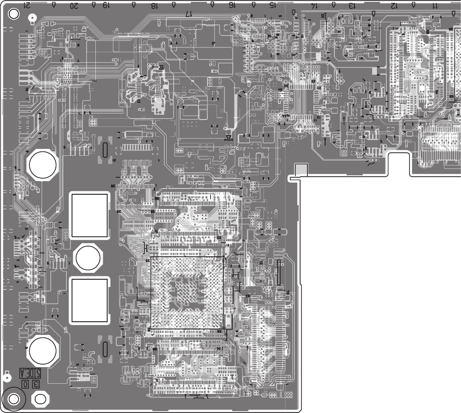
2-99(No.YA463)
C3372
C3386
C3387
C3388
C3390
C3393
C3394
C3404
12
C3413
C3423
C3434
C3436
C3437
C3442
C3501
C3510
C3513
C3517
C3518
C3522
C3523
C3572
C3576
C3577
C3580
C3581
C3582
C3586
C3587
C3588
C3590
C3593
C3594
C3596
C3597
C3604
C3612
C3619
C3622
C3623
C3628
C3629
C3701
C3702
C3703
C3707
C3901
C3931
C3934
C3936
C3951
C3953
C3958
C3960
C3965
C3967
CNDD1
CNJIG1
CNBCT1
CNB1
D3701
R3546
D3706
D3708
R3550
D3933
R3614
R3616
R3618
R3620
EF3901
EF3902
EF3903
EF3904
EF3905
EF3906
EF3907
EF3910
EF3911
R3811
IC3008
R3936
R3937
IC3304
IC3312
IC3501
IC3502
IC3504
IC3508
IC3701
R3938
R8007
R8008
R8009
R8010
K3307
K3507
K3701
L3931
L3932
Q3701
R3084
R3085
R3086
R3087
R3088
R3094R3095 R3096
EF3705
EF3706 EF3707
EF3708
EF3709
EF3710
EF3912
EF3913
EF3914
EF3915
EF3916
EF3917
EF3713
R3351
R3381R3383
R3395
R3397
R3481
R3484
R3505
R3507
R3512
R3541
R3542
R3543
R3544
R3545
R3547
R3548
R3549
R3552
R3553
R3554
R3573
R3576
R3581 R3583
R3590
R3595
R3597
R3600
R3615
R3617
R3619
R3621
R3677
R3678
R3680
R3681
R3701
R3703
R3704
R3706
R3707
R3708
R3709
R3721
R3722
R3723 R3729
R3730
R3731
R3733
R3939
R3981 R3982
R3983
TP3355
TP3357
TP3501
TP3502
TP3701
TP3704
X3701
EF3711
CNIR1
TP3555
R3873
R3885
R3886
R3887
R3889 R3891
C3666
C3667
C3751
C3752
C3902
C3906
C3909
C3911
C3912
C3913
C3914
C3917
C8001
C8002
C8003
C8004
C8005
C8008
C8009
C8010
C8011
C8018
C8019
C8020
C8021
C8031
CA3922
CA3925
CA3927
CA3930
CA3932
CA3933
CA3935
CA3937
CA3940
CA3942
CA3960
CA3961
CA3962
CA3963
CA3966
CA3967
CNBG1
CNL2
CNF1
CNF2
CNF3
D3751
D3752
D3901
D8001
D8002
D8003
IC3314
IC3751
IC3752
IC3753
IC3754
IC3901
IC3911
IC3912
IC3913
IC3914
IC3918
IC8001
IC8002
IC8003
IC8005
K3024
K3026
K3702
K3703
K3704
K3712
K3713
K3908 K3909
K3911
K3912
K3913
K3921
L3901
L3902
Q3902
Q8002
Q8003
Q8004
Q8005
R3486
R3630
R3682
R3687
R3688
R3690
R3691
R3692
R3755
R3756
R3907
R3908
R3909
R3911
R3917
R3918
R3919
R3922
R3945
R3946
R3947
R8011
R8012
R8013
R8015
R8031
R8032
R8036
TP3557
EF3714
R3712
R3713
R3715
C3810
C3811
C3812
C3818
C3819
C3828
C3829
C3830
C3831
C3834
C3835
C3837
C3838
C3841
C3648
C3448
C3716
C8046
C3717
C3975
CNSW1
EF3715
C3762
K3717
R3643
CA3023
CA3035
CA3036
CA3014
CA3010
CA3011
CA3028
DRIVE PWB PATTERN [PARTS SIDE]
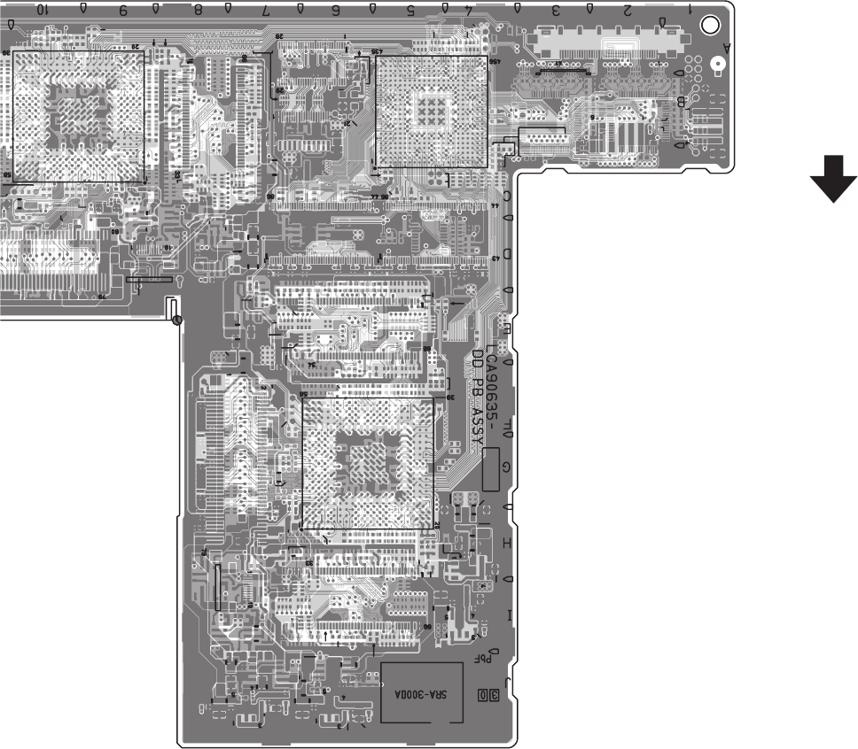
(No.YA463)2-100
C3022
C3023
C3024
C3025
C3029
C3038
C3039
C3040
C3041
C3101
C3115
C3117
C3118
C3122
C3123
C3154
C3172
C3186
C3187
C3188
C3190
C3193
C3194
C3204
C3213
C3219
C3222
C3223
C3228
C3229
C3238
C3239
CNL1
C3301
C3306
C3310
C3311
C3315
C3316
C3317
C3318
C3322
C3323
C3354
C3400
C3402
C3405
C3412
C3419
C3420
C3422
C3428
C3429
R3214
R3216
R3218
R3346
R3350
R3420
CNT1
CNR1
CNG1
IC3003
IC3004
IC3007
IC3101
IC3102
IC3104
IC3108
IC3301
IC3302
IC3308
K3107
R3030
R3034
R3035
R3052
R3062
R3063
R3064
R3065
R3066
R3067
R3068
R3069
R3105 R3107
R3151
R3188
R3190
R3193
R3195
R3197
R3215
R3217
R3219
R3262
R3263
R3266
R3267
R3270
R3271
R3272
R3273
R3305 R3307
R3312
R3342
R3345
R3349
R3351
R3421
R3462
R3463
R3464
R3465
R3466
R3467
R3468
R3469
R3470
R3471
R3472
R3473
R3479
R3480
TP3101
TP3102
TP3301
TP3302
TP3357
TP3155
R3851
R3852
R3854
R3858
R3860
R3893
C3078
C3079
C3082
CA3904
CA3906
CA3907
CA3908
CA3909
CA3911
CA3912
CA3914
CA3916
CA3917
CA3919
CA3921
CA3964
CA3965
CNLV1
CNJIG2
CNRG1
CNGG1
IC3005
IC3907
IC3908
IC3909 IC3910
K3013
K3014
K3021
K3022
K3023
K3291
K3292
K3491
K3492
K3902
K3903
K3904
K3905
K3906
K3907
R3293
R3294
R3296
R3297
R3298
R3941
TP3001
TP3002
TP3003
TP3004
TP3005
TP3006
TP3007
TP3008
TP3009
TP3010
TP3157
X3001
C3805
C3825
C3826
C3827
C3248
R3499
R3243
R3443
CA3021
CA3007
CA3032
CA3034
CA3001
CA3002
CLIP1
FR
O
N
T
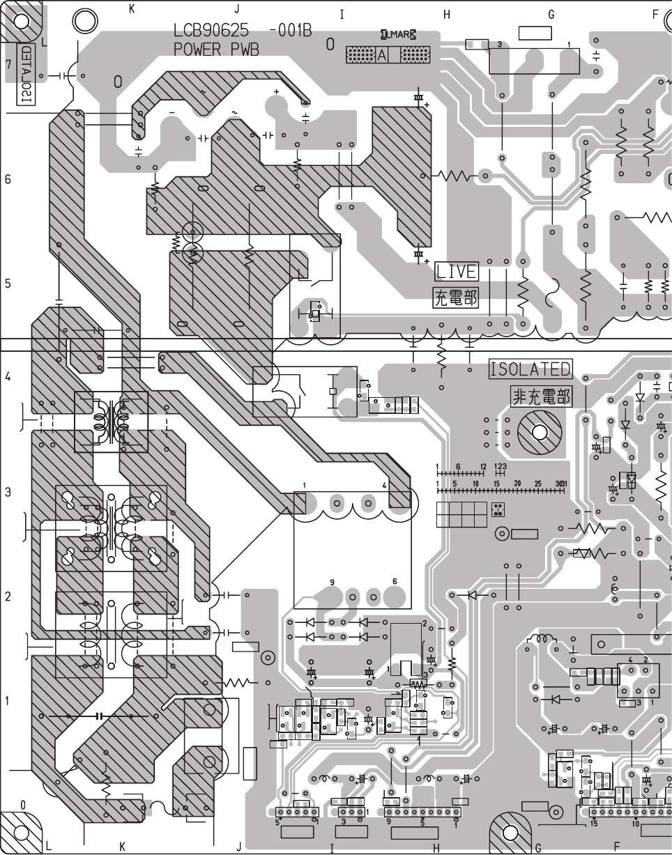
2-101(No.YA463)
H9211
H9741
C9001
C9002
C9011
C9013
C9021
C9101
C9103
C9104
C9191
C9192
C9201
C9202
C9203
C9204
C9205
C9206
C9219
C9281
C9282
C9283
C9284
C9303
C9501
C9557
C9559
C9560
C9561
C9562
C9565
C9566
C9568
C9569
C9572
C9573
C9742
C9743
C9744
C9745 C9831
C9882
C9883
C9884C9885
C9897
CNA2
CNBL
CNDC
CN9008
CNDU
CN9E1
CNPW
CP9211
CP9555
D9021
D9101
D9102
D9103D9104
D9106
D9201
D9202
D9281
D9282
D9283
D9555
D9556
D9557
D9741
D9743
D9831
D9832
F9001
IC9101
IC9741
L9551
L9552
L9553
L9741
LF9001
LF9002
LF9003
Q9021
Q9281
Q9282
Q9283
Q9284
Q9831
R9001
R9002
R9021
R9022
R9112
R9113
R9191
R9201
R9202
R9203
R9204
R9205
R9281
R9282
R9283
R9284
R9285
R9286
R9287
R9288
R9289
R9290
R9291
R9292
R9293
R9501
R9502
R9503
R9504
R9505
R9
5
R9512
R9513
R9520
R9555
R9556
R9557
R9561 R9562
R9567
R9568
R9741
R9742
R9743
R9744
R9831 R9832
R9833
R9834
R9861
R9862
R9878
RY9021
RY9201
T9101
VA9001
Y9002
Y9003
Y9004
Y9005
Y9006
Y9007
Y9008
Y9009
Y9010
Y9011
Y9012
Y9013
Y9041
W9020
W9019
W9006
W9008
W9011
W9010
W9017
W9018
W9002 W9015
W9045
W9021
W9037
CN9E2
W9022
W9053
W9052
W9061
Y9051
W9055
W9065
W9003
CN9E3
W9060
W9034
W9033
Y9052
Y9053
W9027
W9030
W9046
C9193
POWER PWB PATTERN [SOLDER SIDE]
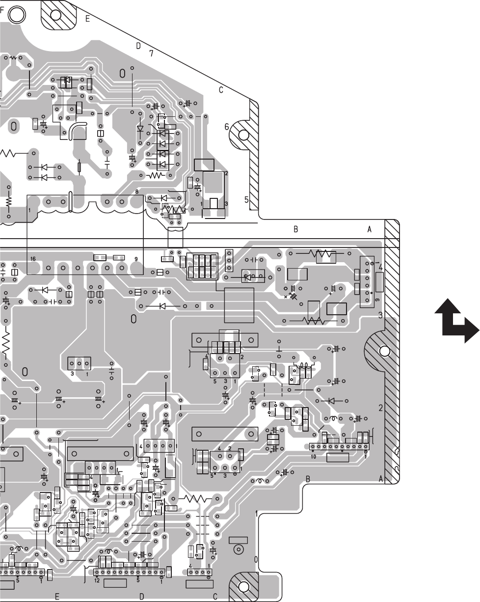
(No.YA463)2-102
H9501
H9553
H9721
H9761
H9762
C9301
C9302
C9503
C9504
C9505
C9506
C9507
C9508
C9509
C9510
C9511
C9512
C9551
C9552
C9553
C9554
C9555
C9556
C9557
C9558
C9559
C9561
C9563
C9564
C9570 C9571
C9601
C9602
C9603
C9701
C9702
C9721
C9723
C9724
C9741
C9761
C9762
C9763
C9764
C9767
C9768
C9770 C9771
C9772
C9773
C9774
C9775
C9776
C9777
C9778
C9779
C9801
C98
51
C9852
C9876
C9877
C9878
C9879
C9880
C9881
C9882
C9894
C9895
CNUP
CNA1
CNA3
N
DC CNFAN
CP9554
CP9556
CP9557
D9301
D9501
D9502 D9503
D9504
D9505
D9506
D9507
D9510
D9511
D9512
D9514
D9551
D9552
D9553
D9554
D9601
D9701
D9702
D9721
D9762
D9763
D9801
D9821
D9841
D9842
D9851 D9852
D9861
D9862
IC9301
IC9501
IC9701
IC9721
IC9761
IC9762
K9501
K9502
K9551
K9552
K9553
K9554
K9555
K9556
K9557
L9761
L9764
L9766
L9874
L9876
PC9501
Q9821
Q9841
Q9842
Q9851
Q9852
Q9853
Q9861
R9301
R9504
R
9505
R9506
R9507
R9508
R9510
R9511
R9512
R9514
R9515
R9516
R9551
R9552
R9556
R9563
R9564
R9565
R9566
R9601
R9602
R9603
R9604
R9605
R9606
R9607
R9608
R9701
R9721
R9722
R9723
R9724
R9771
R9772
R9773
R9774
R9775
R9776
R9789
R9790
R9791
R9792
R9794
R9801
R9802
R9821
R9822
R9823
R9841
R9842
R9844
R9845
R9846
R9847
R9851
R9852 R9853
R9854
R9855
R9863
R9864
R9865
R9866
R9873
R9877
R9898
R9899
T9501
W9031
W9009
W9007
W9014
W9004
W9005
W9001
W9036
W9042
W9013
W9037
W9029
W9051
W9062
W9059
W9064
W9049
W9050
W9026
W9032 W9048
W9066
W9044
W9047
W9056
W9057
W9052
W9012
CN9E4
7
Y9071
Y9072
Y9073
Y9074
Y9075
Y9076
FR
O
NT
TOP
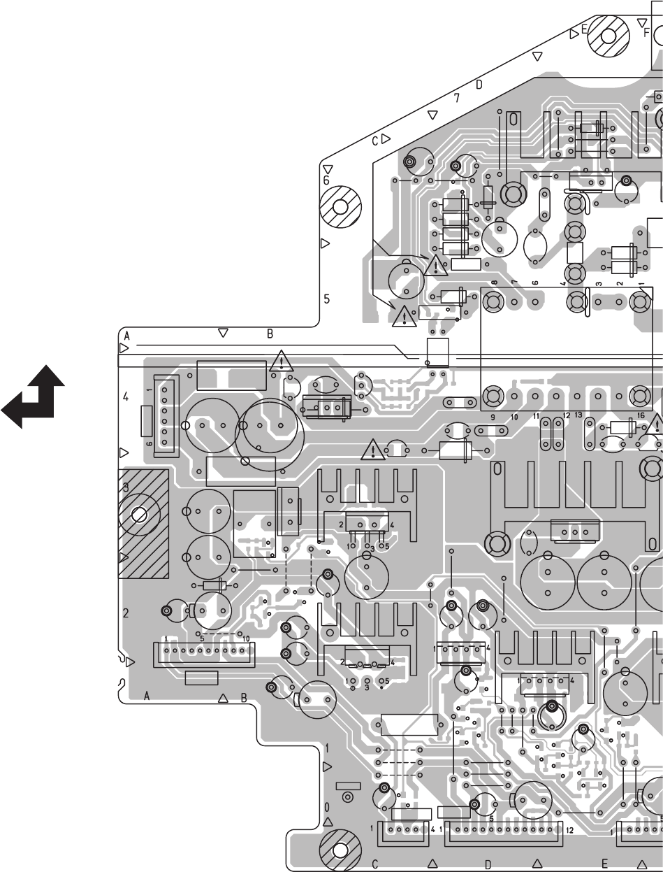
2-103(No.YA463)
H9501
H9553
H9721
H9741
H9761
H9762
CL2
C9301 C9504
C9506
C9508
C9510
C9511
C9551
C9552
C9554
C9555
C9556
C9557
C9558
C9563
C9564
C9701
C9702
C9721
C9723
C9741
C9761
C9763
C9767
C9768
C9775
C9777
C9778
C9779
C9801
C9851
C9894
CNUP
CNA1
CNA3
CNFAN
CP9556
CP9557
D9501
D9502
D9503
D9504
D9505
D9506
D9511
D9512
D9514
D9551
D9552
D9553
D9554
D9601
D9762
D9763
IC9501
IC9701
IC9721
IC9761
IC9762
K9501 K9502
K9551
K9552
K9554
K9555
K9556
K9557
L9761
L9764
L9766
L9874
L987
6
PC9501
R9505
R9506
R9515
R9563
R9566
R9801
T9501
W9031
W9009
W9007
W9014
W9004
W9005
W9001
W9036
W9042
W9013
W9029
W9051
W9062
W9059
W9064
W9049
W9050
W9026
W9032
W9048
W9066
W9044
W9047
W9056
W9057
W9012
CN9E4
Y9071
Y9072
Y9073
Y9074
Y9075
Y9076
FRONT
TOP
POWER PWB PATTERN [PARTS SIDE]
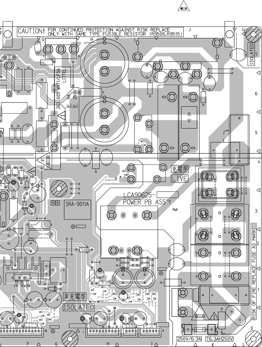
(No.YA463)2-104
H9211
H9741
FC9001 FC9002
CL1
CL2
C9001
C9002
C9011
C9013
C9101
C9103
C9104 C9191
C9192
C9201 C9202
C9203
C9204
C9205 C9206
C9219
C9281
C9501
C9506
C9557
C9559
C9560
C9561
C9562
C9565
C9566
C9741
C9743
C9744
C9897
CNA2
CNBL
CNDC CN9008 CNDU
CN9E1
CNPW
CP9211
CP9554
CP9555
D9101 D9102
D9103 D9104
D9106
D9201
D9555
D9556
D9557
D9741
D9743
F9001
IC9741
K9557
L9551
L9552 L9553
L9741
L9876
LF9001 LF9002
LF9003
R9001
R9002
R9112
R9113
R9191
R9201
R9202
R9203
R9204
R9205
R9501
R9502
R9503
R9504
R9511
R9512
R9513
R9520
R9555
R9556
R9562
RY9021
RY9201
T9101
VA9001
Y9002
Y9003
Y9004
Y9005
Y9006
Y9007
Y9008
Y9009
Y9010
Y9011
Y9012
Y9013
W9020
W9019
W9006
W9008
W9011
W9010
W9017
W9018
W9002
W9015
W9045
W9001
W9021
W9037
CN9E2
W9022
W9057
W9053
W9052
W9061
Y9051
W9055
W9065
W9003
CN9E3
W9060
W9034
W9033
Y9052
Y9053
W9027
W9030
W9046
C9193
CAUTION :
FOR CONTINUED PROTECTION AGAINST FIRE HAZARD,
REPLACE ONLY WITH SAME TYPE AND RATED FUSE(S)
AND ROHM'S MFR'S TYPE CP(S).
T
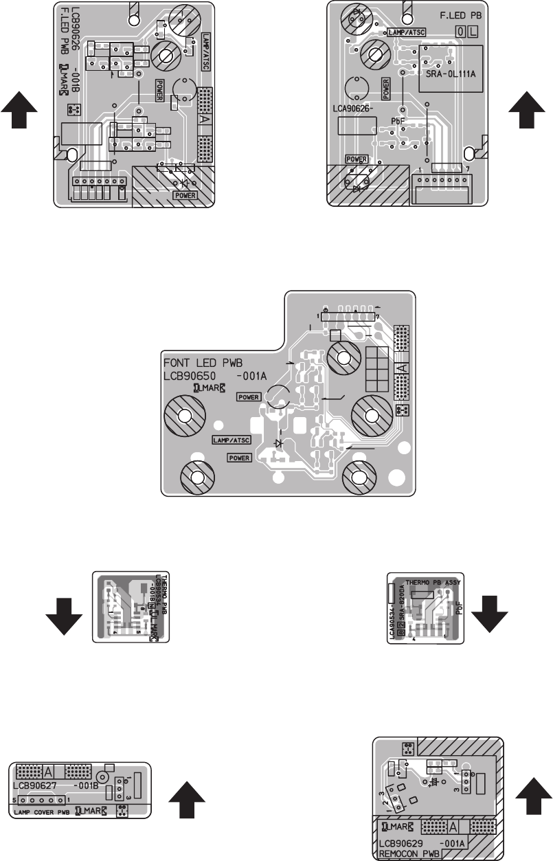
2-105(No.YA463)
C0821
C0822
D0821
IC0821
R0821
R0822
R0823
CNRE
CN0806
C0861
S0861
G3
C2001
C2001
C2002
C2002
D2001
D2001
IC2001
IC2001
K2001
K2001
R2001
R2001
R2002
R2002
R2003
R2003
CN82T
CN82T
CN07FL
D0701
D0705
S0701
C0701
C0702
C0703
C0704
C0705
C0706
D0703
D0704
D0706
D0707
Q0701
Q0702
Q0704
Q0705
Q0706
Q0707
R0706
R0707
R0708
R0709 R0710
R0711
R07
12
R0713
R0714
R0715
R0716
W0601
W0401
CN07FL
D0701
D0705
S0701
W0601
W0401
W0421
C0901
C0902
C0903
C0904
C0905
C0906
F
W0221
D0901
D0903 D0904
D0905
D0906
D0907
Q0901
Q0902
Q0904
Q0905
Q0906
Q0907
R0906
R0907
R0908
R0909
R0910
R0911
R0912
R0913
R0914
R0915
R0916
S0901
W0222
T
OP
T
OP
TOP
TOP
T
OP
T
OP
LAMP COVER SW PWB PATTERN REMOCON PWB PATTERN
TEMP PWB PATTERN [SOLDER SIDE] TEMP PWB PATTERN [PARTS SIDE]
FRONT LED PWB PATTERN [SOLDER SIDE]
[HD-52FA97]
FRONT LED PWB PATTERN
[HD-56FB97, HD-61FB97]
FRONT LED PWB PATTERN [PARTS SIDE]
[HD-52FA97]
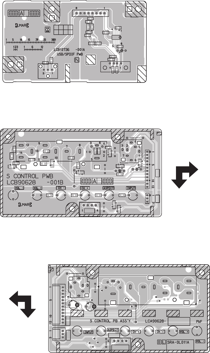
(No.YA463)2-106
R0848
CNS2
R0849
CNS1
CNS3
C0841
C0842
C0843
C0844
C0845
D0841
D0842
D0843
D0844
D0845 D0846
J0831
J0841
R0841
R0842
R0843
R0844
R0845
R0846
R0847
R0851R0852R0853 R0854
W0240
S0851S0852
S0853
S0854 S0855
S0856
W0241
W0242
W0440
W0441
CNS2 CNS1
CNS3
C0841
C0843
J0831
J0841
W0240
S0851 S0852 S0853
S0854
S0855
S0856
W0241
W0242
W0440
W0441
D8001
D8002
D8003
D8004
C8001
C8002
C8003
C8004
C8005
C8006
C8007
C8501
CN8DT
IC8001
IC8501
J8001
R8001
R8002
R8501
W8001
W8002
W8003
F
R
O
NT
T
OP
F
R
O
NT
T
OP
SIDE CONTROL PWB PATTERN [PARTS SIDE]
SIDE CONTROL PWB PATTERN [SOLDER SIDE]
USB PWB PATTERN
2-107(No.YA463)
<
TUNER PWB(1/2)
>
MODE DC (V)
PIN NO.
IC001
1 6.9
2 4.9
3 0
4 6.9
Q004
E 2.8
C 0
B 0
Q005
E 2.2
C 8.7
B 2.8
Q006
E 2.5
C 0
B 2
TU001
1 NC
2 NC
3 4.9
4 NC
5 NC
6 NC
7 NC
8 NC
9 NC
10 4.4
11 4.3
12 0
13 2.8
14 NC
15 31.1
16 NC
17 2.4
<
TUNER PWB(2/2)
>
MODE DC (V)
PIN NO.
IC061
1 NC
2 4
3 NC
4 NC
5 4.9
6 4.9
7 0
8 3.9
9 3.9
10 4
11 3.8
12 3.2
13 4
14 1.2
15 1.3
16 NC
17 0
18 3.2
19 8.9
20 NC
21 4
22 4
23 4
24 3.8
25 4
26 3.9
27 4
28 1.9
29 4
30 4
31 1.8
32 4
33 4
34 4
35 4
36 4
37 4
38 4
39 3.9
40 3.9
41 1.1
42 4
43 4
44 4
45 NC
46 4
47 4
48 4
<
ANALOG PWB(1/6)
>
MODE DC (V)
PIN NO.
MODE DC (V)
PIN NO.
MODE DC (V)
PIN NO.
MODE DC (V)
PIN NO.
IC101
1 4.5
2 4.5
3 0
4 4.5
5 4.5
6 0
7 4.5
8 4.5
9 0
10 4.5
11 4.5
12 0
13 4.5
14 4.5
15 4.5
16 4.5
17 4.5
18 9
19 4.5
20 4.5
21 0
22 4.5
23 4.5
24 0
25 4.5
26 4.5
27 0
28 4.5
29 4.5
30 9
31 0
32 4.5
33 4.5
34 4.5
35 4.5
36 4.5
37 1.4
38 NC
39 1.4
40 NC
41 0
42 2.1
43 1.6
44 5
45 1.9
46 0
47 2
48 5
49 1.9
50 1.6
51 0.1
52 5
53 NC
54 4.9
55 2.5
56 2.1
57 2.5
58 2.1
59 2.1
60 2.5
61 5
62 2.5
63 0.2
64 2.1
65 NC
66 2.5
67 4.9
68 2.5
69 0.2
70 2.1
71 NC
72 2.5
73 4.9
74 2.5
75 0
76 0
77 2.1
78 1.4
79 2.8
80 5
81 2.3
82 0
83 2.8
84 0
85 2.5
86 4.6
87 2.5
88 2.2
89 2.1
90 0
91 2.5
92 2.8
93 2.5
94 0.2
95 2.1
96 NC
97 2.5
98 4.8
99 2.5
100 NC
IC102
1 0
2 2.4
3 2.5
4 2.4
5 2.4
6 2.5
7 2.5
8 2.4
9 0
10 2.4
11 2.2
12 2.4
13 NC
14 0.3
15 0.3
16 0
17 2.4
18 0
19 2.4
20 0
21 2.4
22 0
23 0
24 0.1
25 5
26 0
27 4
28 3.9
29 0
30 NC
31 6.3
32 NC
33 0
34 1.2
35 0
36 3.4
37 4.1
38 3.4
39 1.7
40 6.4
41 1.8
42 2.9
43 1.8
44 0
45 1.3
46 2.8
47 NC
48 2.5
49 3.9
50 6.4
51 4.9
52 NC
53 1.9
54 3
55 2.4
56 NC
57 2.5
58 NC
59 0
60 2.2
61 0
62 0
63 2.5
64 2.5
65 2.5
66 2.5
67 2.5
68 2.4
69 2.5
70 2.4
71 NC
72 2.4
73 NC
74 2.4
75 NC
76 0.6
77 0.1
78 2.4
79 NC
80 2.4
81 NC
82 2.4
83 0.3
84 0.6
85 0.5
86 2.4
87 5
88 2.4
89 2.8
90 2.4
91 0
92 NC
93 NC
94 2.4
95 0
96 2.4
97 0
98 2.4
99 0
100 NC
Q106
S 0.1
D 0.1
G 0
Q107
S 3.2
D 5
G 3.3
Q108
E 0.5
C 0
B 0
Q109
E 2.6
C 0
B 1.9
Q110
E 2.2
C 0
B 1.4
Q111
E 2.2
C 0
B 1.4
Q112
E 1.7
C 0
B 1
Q113
E 0
C 5
B 2.9
<
ANALOG PWB(2/6)
>
MODE DC (V)
PIN NO.
Q451
E 0
C 0
B 2.4
Q452
E 0
C 0
B 2.4
Q453
E 2.4
C 2.5
B 0
<
ANALOG PWB(5/6)
>
MODE DC (V)
PIN NO.
MODE DC (V)
PIN NO.
MODE DC (V)
PIN NO.
IC601
1 6
2 6.1
3 6.1
4 6.1
5 6.1
6 6.1
7 0.7
8 6.1
9 6.1
10 6.1
11 1.1
12 0
13 1
14 6.1
15 0
16 5.2
17 0.1
18 5
19 0
20 12.1
21 5.9
22 0
23 0
24 4.9
25 3.9
26 4.7
27 4.7
28 6.1
29 6.1
30 6.1
31 6.1
32 6.1
33 6.1
34 0
35 0
36 6.1
37 6.1
38 0
39 6.1
40 6.1
41 6.1
42 6.1
43 6.1
44 6
45 6
46 6
47 6.1
48 6.1
IC602
1 14.4
2 2.8
3 12.1
4 2.6
5 0
IC603
1 5.9
2 4.7
3 4.8
4 0
5 6
6 6.1
7 8
8 11.7
IC605
1 -15.4
2 NC
3 -15.4
4 -15.4
5 14.4
6 10.3
7 1.6
8 -15.4
9 -15.4
10 -15.4
11 1.5
12 10.2
13 14.4
14 -14.4
15 -13.7
16 NC
17 -15.3
IC606
1 NC
2 5
3 0.1
4 5
5 4.9
6 0
7 0
8 0
9 4.8
10 4.9
11 0
12 5
13 5
14 0
15 0
16 5
IC607
1 -15.3
2 0
3 0
4 -15.4
5 0
6 0.1
7 -15.3
8 13.6
IC610
1 6.2
2 6.1
3 6.1
4 0
5 6.1
6 6.1
7 6.2
8 12.2
Q603
E 0
C 0
B 0.6
Q604
E 0
C 12.1
B 8
Q605
E 0
C 0
B 4.4
Q606
E 0
C 14.3
B 0
Q607
E -14.4
C -14.3
B -14.3
Q614
E 11.5
C 0
B 11.9
<
ANALOG PWB(6/6)
>
MODE DC (V)
PIN NO.
IC902
1 4.9
2 0
3 3.3
<
DIGITAL PWB(1/15)
>
MODE DC (V)
PIN NO.
Q7501
E 0
C 1
B 2.1
<
DIGITAL PWB(4/15)
>
MODE DC (V)
PIN NO.
MODE DC (V)
PIN NO.
IC6250
1 0
2 5.4
3 1.6
4 0
5 0
6 0
7 0
8 0
9 5.3
10 0.7
11 0
12 3.5
13 0
14 0
15 0
16 5.3
17 0
18 0
19 0
20 2.2
21 0
22 0
23 5.3
24 5.3
IC6251
1 1.6
2 0
3 NC
4 5
5 3.3
Q6201
E 0.5
C 0
B 0.5
Q6202
E 3.3
C 0
B 2.6
Q6203
E 0.5
C 0
B 0.5
Q6204
E 2.9
C 0
B 2.2
Q6205
E 2.9
C 0
B 2.2
Q6206
E 3.3
C 0
B 2.6
Q6207
E 1.3
C 5
B 2
Q6208
E 1.3
C 5
B 2.1
Q6209
E 1.4
C 5
B 2.1
Q6210
E 1.3
C 5
B 2.1
Q6211
E 0.8
C 5
B 1.5
Q6212
E 0
C 5
B 0.07
Q6213
E 0
C 5
B 0.7
Q6214
E 1.5
C 5
B 2.2
Q6250
E 1.5
C 5
B 2
Q6251
E 2.2
C 5
B 2
<
DIGITAL PWB(5/15)
>
MODE DC (V)
PIN NO.
IC6002
1 1.5
2 1.5
3 0
4 2.4
5 3.2
IC6003
1 0.7
2 0
3 0
4 0
5 3.2
6 0.7
7 3.2
8 3.1
IC6004
1 0
2 NC
3 0
4 0
5 3.2
6 0
7 0
8 0
IC6724
1 0
2 3.3
3 0
4 3.3
<
DIGITAL PWB(7/15)
>
MODE DC (V)
PIN NO.
MODE DC (V)
PIN NO.
IC6101
1 1.2
2 2.4
3 0
4 1.2
5 0
6 1.2
7 1.2
8 2.4
9 1.2
10 1.2
11 0
12 1.2
13 1.2
14 0
15 2.4
16 0
17 1.2
18 1.2
19 0
20 0
21 1.2
22 1.2
23 0.6
24 0.6
25 1.7
26 1.7
27 1.8
28 0
29 0.7
30 0.7
31 0.6
32 0.6
33 0.7
34 0.7
35 2.4
36 0
37 0
38 NC
39 NC
40 NC
41 NC
42 NC
43 NC
44 NC
45 0.6
46 0
47 0.7
48 0.7
49 0.7
50 0.7
51 0.6
52 0
53 1.8
54 1.3
55 1.3
56 0.6
57 0.6
58 1.2
59 0
60 1.2
61 0
62 0
63 1.2
64 1.2
65 2.5
66 0
67 2.4
68 1.2
69 1.2
70 0
71 1.2
72 1.2
73 2.4
74 1.2
75 1.2
76 0
77 1.2
78 1.2
79 0
80 1.2
81 1.2
82 0
83 1.2
84 1.2
85 0
86 2.4
87 NC
88 NC
89 NC
90 NC
91 NC
92 0
93 NC
94 1.2
95 2.4
96 2.4
97 1.2
98 1.2
99 0
100 1.2
IC6102
1 0
2 2.6
3 1.3
4 1.3
5 2.6
6 2.6
7 2.6
8 2.6
<
DIGITAL PWB(8/15)
>
MODE DC (V)
PIN NO.
MODE DC (V)
PIN NO.
IC7201
1 0.1
2 0.2
3 0.2
4 0.2
5 0.2
6 0.1
7 0.3
8 0.2
9 0
10 0
11 3.2
12 3.3
13 0
14 0
15 0
16 0
17 0.1
18 0.2
19 0.2
20 0.2
21 0.2
22 0.2
23 0.2
24 0.2
25 0.2
26 3.3
27 0
28 3.3
29 0.2
30 0.2
31 0.2
32 0.2
33 0.2
34 0.2
35 0.2
36 0.2
37 3.2
38 0.1
39 0.2
40 0.2
41 0.1
42 0.2
43 0.2
44 0.2
45 0.1
46 0
47 3.3
48 0.2
IC7203
1 3.2
2 0
3 0.3
4 0
5 0.4
6 0
7 3.3
8 0.2
9 0.4
10 0
11 0.3
12 0
13 3.2
14 2.7
15 3.2
16 3
17 3.2
18 2.6
19 0
20 0.1
21 0.3
22 0.3
23 0.3
24 0.3
25 3.2
26 0
27 0.3
28 0.3
29 0.3
30 0.3
31 0.4
32 0.4
33 NC
34 3.2
35 3
36 2.7
37 NC
38 3.2
39 0.4
40 0.4
41 0
42 0.4
43 0.2
44 3.3
45 0.3
46 0.2
47 0
48 0.3
49 0.2
50 0
IC7204
1 0
2 3.3
3 0
4 3.3
IC7206
1 NC
2 3.3
3 0
4 3.3
5 3.3
<
DIGITAL PWB(9/15)
>
MODE DC (V)
PIN NO.
IC7033
1 0
2 3.2
3 3.2
4 3.2
5 3.2
6 3.2
7 3.2
8 0
9 0
10 3.2
11 0
12 3.2
13 3.2
14 3.3
15 0
16 3.2
IC7036
1 3.3
2 0
3 0
4 0
5 3.3
6 0
Q7030
E 0
C 0
B 0
Q7032
E 3.3
C 3.3
B 0
Q7033
E 3.2
C 3.2
B 0
<
DIGITAL PWB(10/15)
>
MODE DC (V)
PIN NO.
MODE DC (V)
PIN NO.
IC6501
1 0
2 0
3 3.3
4 0
5 0
6 0
7 0.1
8 0.1
9 2.7
10 0
11 0
12 0
13 3.3
14 0
15 2.9
16 0
17 0
18 0
19 0
20 3.3
21 0
22 0
23 NC
24 0
25 0
26 0
27 0
28 0
29 NC
30 3.3
31 0
32 0
33 NC
34 0
35 3.3
36 0
37 0
38 1.3
39 1.3
40 1.3
41 1.3
42 0
43 3.3
44 1.3
45 1.3
46 1.3
47 1.3
48 0
49 3.3
50 1.3
51 1.3
52 1.3
53 1.3
54 0
55 3.3
56 1.3
57 1.3
58 1.3
59 1.3
60 0
61 3.3
62 1.3
63 1.3
64 1.3
65 1.3
66 0
67 3.3
68 1.3
69 1.3
70 1.3
71 1.3
72 0
73 0
74 3.3
75 0
76 0
77 0
78 0.8
79 0.8
80 0.8
81 0.6
82 3.3
83 0
84 0.6
85 0.8
86 0.8
87 1.3
88 0
89 0
90 0.8
91 0.8
92 0.8
93 3.3
94 0
95 0.7
96 0.9
97 0.8
98 0.6
99 0
100 0
101 0.8
102 0.8
103 3.3
104 3.3
105 0
106 0.8
107 0.8
108 0.6
109 NC
110 1.1
111 1
112 0.9
113 3.3
114 0
115 0
116 0
117 0
118 0
119 0
120 0
121 0
122 0
123 0
124 0
125 3.3
126 0
127 0
128 0
129 0
130 0
131 0
132 0
133 0
134 0
135 0
136 0
137 3
138 0
139 0
140 0
141 0
142 0
143 0
144 0
<
DIGITAL PWB(13/15)
>
MODE DC (V)
PIN NO.
IC6901
1 3
2 0
3 3.2
4 5
VOLTAGE CHARTS
(No.YA463)2-108
MODE DC (V)
PIN NO.
IC9001
1 8.6
2 13.3
3 3.5
4 0
5 0.9
6 1.3
7 3.4
8 0.9
IC9101
1 3.3
2 0
3 2.5
IC9201
1 6.5
2 13.3
3 1.3
4 0
5 0.9
6 1.3
7 3.3
8 0.9
IC9301
1 1.2
2 NC
3 0
4 0.3
5 3.2
6 NC
7 NC
8 3.2
<
DIGITAL PWB(14/15)
>
MODE DC (V)
PIN NO.
MODE DC (V)
PIN NO.
IC7601
1 0
2 0
3 NC
4 NC
5 0
6 1
7 2.8
8 0
9 0
10 0
11 0
12 0
13 1.9
14 0
15 1.4
16 3.2
17 1.8
18 NC
19 0
20 3.2
21 0
22 0
23 NC
24 NC
25 NC
26 NC
27 NC
28 NC
29 4.9
30 3.2
31 0
32 0
33 0
34 0
35 0
36 3.2
37 0
38 0
39 NC
40 NC
41 3.2
42 NC
43 NC
44 NC
45 NC
46 0
47 3.2
48 0
49 3.2
50 NC
51 NC
52 NC
53 NC
54 NC
55 NC
56 NC
57 NC
58 NC
59 NC
60 NC
61 NC
62 3.9
63 NC
64 3.2
65 NC
66 NC
67 NC
68 NC
69 NC
70 NC
71 0
72 0
73 NC
74 NC
75 NC
76 NC
77 NC
78 NC
79 NC
80 0
81 0
82 3.2
83 NC
84 3.2
85 NC
86 3.2
87 3.2
88 3.2
89 0
90 0
91 0
92 NC
93 3.2
94 3.2
95 0
96 0.2
97 0
98 0
99 4.9
100 0
IC7602
1 0
2 0
3 0
4 0
5 3.2
6 3.2
7 0
8 3.2
IC7603
1 3.3
2 3.3
3 0
4 5
5 5
IC7604
1 NC
2 0
3 0
4 3.2
5 3.2
IC7605
1 5
2 0
3 NC
4 0
5 0
6 5
IC7606
1 5
2 0
3 NC
4 0
5 0
6 5
<
POWER PWB(1/3)
>
MODE DC (V)
PIN NO.
MODE DC (V)
PIN NO.
IC9101
1 7
2 0
3 5
IC9301
1 17.9
2 0
3 15.2
Q9021
E 0
C 0.1
B 0.7
Q9281
E 1.3
C 0
B 2.3
Q9282
E 0
C 3.7
B 0.2
Q9283
E 0
C 3.8
B 0.2
Q9284
E 0
C 0
B 2.5
<
POWER PWB(2/3)
>
MODE DC (V)
PIN NO.
IC9501
1 385
2 NC
3 0
4 15.7
5 0.1
6 1.1
7 0.8
PC9501
1 11.1
2 10.1
3 13.6
4 1
<
POWER PWB(3/3)
>
MODE DC (V)
PIN NO.
IC9701
1 13.1
2 11.9
3 0
4 2.6
IC9721
1 13.2
2 9.1
3 0
4 2.6
IC9741
1 13.2
2 5.1
3 0
4 1.3
5 6.9
IC9761
1 13.2
2 3.3
3 0
4 1.2
5 6.8
IC9762
1 3.3
2 3.4
3 0
4 2.6
5 1.1
Q9821
E 0
C 0
B 0.6
Q9831
E 0
C 0
B 0.6
Q9841
E 0
C 0
B 0.6
Q9842
E 0
C 0
B 0.7
Q9851
E 13.1
C 6
B 13.1
Q9852
E 0
C 13.1
B 0
Q9853
E 0
C 0
B 3.1
Q9861
E 0
C 0
B 0.6
<FRONT LED PWB>
[HD-52FA97]
MODE DC (V)
PIN NO.
Q0701
E 0.2
C 0.4
B 0.9
Q0702
E 0
C 0
B 0.6
Q0704
E 0
C 4.9
B 0
Q0705
E 0
C 0.2
B 0.7
Q0706
E 4.5
C 4.9
B 3.3
Q0707
E 0
C 4.4
B 0
<FRONT LED PWB>
[HD-56FB97,
HD-61FB97]
MODE DC (V)
PIN NO.
Q0901
E 0.2
C 0.4
B 0.9
Q0902
E 0
C 0
B 0.6
Q0904
E 0
C 4.9
B 0
Q0905
E 0
C 0.2
B 0.7
Q0906
E 4.5
C 4.9
B 3.3
Q0907
E 0
C 4.4
B 0
<TEMP PWB>
MODE DC (V)
PIN NO.
IC2001
1 4.5
2 4.5
3 4
4 0
5 0
6 0
7 0
8 4.9
<REMOCON PWB>
MODE DC (V)
PIN NO.
IC0821
1 2.8
2 4.9
3 0
<USB PWB>
MODE DC (V)
PIN NO.
IC8001
1 0
2 5
3 5
4 3.3
5 3.3
6 5
7 5
8 5
IC8501
1 0.1
2 4.9
3 0
TU001-17
1.8 Vp-p
(H)
IC101-45
6 Vp-p
(H)
IC101-49
6 Vp-p
(H)
IC101-57
1.8 Vp-p
(H)
ANALOG PWB(1/6)
IC7601-13
IC6501-7
6 Vp-p
(0.2ǴU)
IC7601-15
6 Vp-p
IC7601-62
3.5 Vp-p
(H)
IC7601-64
3.5 Vp-p
(V)
DIGITAL PWB(14/15)
DIGITAL PWB(10/15)
(0.2ǴU)
IC102-2
6 Vp-p
(H)
IC102-28
3.0 Vp-p
(H)
(H)
IC102-37
3.4 Vp-p
(V)
(V)
IC102-38
2.5 Vp-p
(H)
IC102-41
0.6 Vp-p
(H)
IC102-43
0.6 Vp-p
(H)
IC102-45
0.8 Vp-p
(H)
3.0 Vp-p
IC6501-8
3.0 Vp-p
TUNER PWB(1/2)
WAVEFORMS

(No.YA463)
ILA Display Category 12, 3-chome, Moriya-cho, Kanagawa-ku, Yokohama-city, Kanagawa-prefecture, 221-8528, Japan
Victor Company of Japan, Limited
VPT
Printed in Japan
Important Note:
In the spaces below, enter the model and serial number of your television (located
at the rear of the television cabinet). Staple your sales receipt or invoice to the
inside cover of this guide. Keep this user’s guide in a convenient place for future
reference. Keep the carton and original packaging for future use.
LCT2170-001A-A
0806TNH-II-IM
Model Number:
Serial Number:
Illustration of HD-56FB97 and RM-C18G
For Models:
HD-52FA97
HD-56FB97
HD-61FB97
Projection Television Users Guide
LCT2170 Eng.indd 1LCT2170 Eng.indd 1 8/4/06 10:26:43 AM8/4/06 10:26:43 AM
2
Important Safety Precautions
WARNING: TO PREVENT FIRE OR SHOCK HAZARDS, DO NOT EXPOSE THIS
APPARATUS TO RAIN OR MOISTURE.
CAUTION: TO INSURE PERSONAL SAFETY, OBSERVE THE FOLLOWING RULES
REGARDING THE USE OF THIS UNIT.
1. Operate only from the power source specified on the unit.
2. Avoid damaging the AC plug and power cord.
3. Avoid Improper installation and never position the unit where good ventilation is unattainable.
4. Do not allow objects or liquid into the cabinet openings.
5. In the event of trouble, unplug the unit and call a service technician. Do not attempt to repair
it yourself or remove the rear cover.
Changes or modifications not approved by JVC could void the warranty.
* When you don’t use this TV set for a long period of time, be sure to disconnect both the
power plug from the AC outlet and antenna for your safety.
* To prevent electric shock do not use this polarized plug with an extension cord, receptacle or
other outlet unless the blades can be fully inserted to prevent blade exposure.
CAUTION: To reduce the risk of electric shock. Do not
remove cover (or back). No user serviceable
parts inside. Refer servicing to qualified service
personnel.
The lightning flash with arrowhead symbol, within an
equilateral triangle is intended to alert the user to the
presence of uninsulated “dangerous voltage” within the
product’s enclosure that may be of sufficient magnitude
to constitute a risk of electric shock to persons.
The exclamation point within an equilateral triangle is
intended to alert the user to the presence of important
operating and maintenance (servicing) instructions in
the literature accompanying the appliance.
RISK OF ELECTRIC SHOCK
DO NOT OPEN
CAUTION
NOTICE (for USA)
This product has a High Intensity Discharge (HID) lamp that
contains a small amount of mercury. It also contains lead in some
components. Disposal of these materials may be regulated in your
community due to environmental considerations. For disposal or
recycling information, please contact your local authorities, or the
Electronics Industries Alliance: http://www.eiae.org
LCT2170 Eng.indd 2LCT2170 Eng.indd 2 8/4/06 10:26:50 AM8/4/06 10:26:50 AM

3
1) Read these instructions.
2) Keep these instructions.
3) Heed all warnings.
4) Follow all instructions.
5) Do not use this apparatus near water.
6) Clean only with dry cloth.
7) Do not block any ventilation openings. Install in accordance with the manufacturer's instructions.
8) Do not install near any heat sources such as radiators, heat registers, stoves, or other apparatus
(including amplifiers) that produce heat.
9) Do not defeat the safety purpose of the polarized or grounding-type plug. A polarized plug has
two blades with one wider than the other. A grounding type plug has two blades and a third
grounding prong. The wide blade or the third prong are provided for your safety. If the provided
plug does not fit into your outlet, consult an electrician for replacement of the obsolete outlet.
10) Protect the power cord from being walked on or pinched particularly at plugs, convenience
receptacles, and the point where they exit from the apparatus.
11) Only use attachments/accessories specified by the manufacturer.
12) Use only with a cart, stand, tripod, bracket, or table specified by the manufacturer, or sold with
the apparatus. When a cart is used, use caution when moving the cart/apparatus combination to
avoid injury from tip-over.
IMPORTANT SAFETY INSTRUCTIONS
• As an “ENERGY STAR®” partner,
JVC has determined that this
product or product model meets the
“ENERGY STAR®” guidelines for energy
efficiency.
LCT2170 Eng.indd 3LCT2170 Eng.indd 3 8/4/06 10:26:51 AM8/4/06 10:26:51 AM
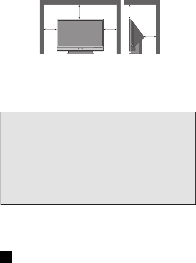
4
13) Unplug this apparatus during lightning storms or when unused for long periods of time.
14) Refer all servicing to qualified service personnel. Servicing is required when the apparatus has
been damaged in any way, such as power-supply cord or plug is damaged, liquid has been
spilled or objects have fallen into the apparatus, the apparatus has been exposed to rain or
moisture, does not operate normally, or has been dropped.
15) Apparatus shall not be exposed to dripping or splashing and no objects filled with liquids, such as
vases, shall be placed on the apparatus.
16) Avoid improper installation and never position the unit where good ventilation is impossible. When
installing this TV, distance recommendations must be maintained between the set and the wall,
as well as inside a tightly enclosed area or piece of furniture. Keep to the minimum distance
guidelines shown for safe operation.
17) Cautions for installation
— Do not tilt the TV towards the left or right, or towards the back.
— Install the TV in a corner on the floor so as to keep cords out of the way.
— The TV will generate a slight amount of heat during operation. Ensure that sufficient space is
available around the TV to allow satisfactory cooling.
18) Make enough room for inserting and removing the power plug. Place the TV as close to the
outlet as possible. The main power supply for this TV is controlled by inserting or removing the
power plug.
150 mm
200 mm
150 mm
200 mm
50 mm
POWER
PUSH
LAMP
VOLUME
INPUT-4
CHANNEL
OPERATE
+
–
+
–
MENU
VIDEO
L/MONO
R
AUDIO
INPUT
FCC Notice:
Note: This equipment has been tested and found to comply with the limits for a Class B
digital device, pursuant to Part 15 of the FCC Rules. These limits are designed to provide
reasonable protection against harmful interference in a residential installation. This
equipment generates, uses and can radiate radio frequency energy and, if not installed
and used in accordance with the instructions, may cause harmful interference to radio
communications. However, there is no guarantee that interference will not occur in a
particular installation. If this equipment does cause harmful interference to radio or television
reception, which can be determined by turning the equipment off and on, the user is
encouraged to try to correct the interference by one or more of the following measures:
– Reorient or relocate the receiving antenna.
– Increase the separation between the equipment and receiver.
– Connect the equipment into an outlet on a circuit different from that to which the receiver is
connected.
– Consult the dealer or an experienced radio/TV technician for help.
LCT2170 Eng.indd 4LCT2170 Eng.indd 4 8/4/06 10:26:51 AM8/4/06 10:26:51 AM

5
Warnings
Caring for the Cabinet
Caring for the Screen
Normally, light dusting with a soft, non-scratching duster will keep your TV clean.
If you wish to wipe down the television, first unplug it. Then wipe gently with a soft cloth, slightly
moistened with water. You can add a few drops of mild liquid detergent to the water to help
remove spots of oily dirt.
• DO NOT allow liquid to enter the TV through the ventilation slots.
• DO NOT use strong or abrasive cleaners on the TV.
• DO NOT spray liquids or cleaners directly on the TV’s surface.
• DO NOT rub or scrub the TV harshly. Wipe the set gently with a soft cloth.
The screen is treated with an electrostatic-proof coating. When it gets dirty, wipe it gently with a
soft cloth. If the screen is very dirty, wipe it down with a cloth dipped in a diluted kitchen cleaner
and thoroughly wrung-out. Then wipe immediately after with a clean, dry cloth.
Do not apply alcohol, organic solvents (like acetone), acidic or alkaline cleansers to the screen.
These will remove the coating layer and cause discolorations.
Do not push or hit the screen. This could cause scratches on the screen surface and image
distortions.
We have an important note for customers who subscribe to basic cable services (do not have
a separate cable box) and plan to use their JVC TV remote control to select channels.
Once you run the Auto Tuner Setup (which detects and programs all the channels your TV is
receiving through the RF input), every channel number available from your cable company
will appear in your television’s Channel Summary and they will all be marked as available for
scanning. Even though every channel is detected and appears as available, you will only be
able to view those that you specifi cally subscribe to from your cable company. This will likely
mean there are blank channels between those channels you wish to scan or “surf”.
We apologize for any inconvenience this may cause but it is important to note that this is
not a malfunction of your television. If you want to sequentially scan those channels you
subscribe to without blank ones in between, you can contact your cable company for their
cable box and remote.
LCT2170 Eng.indd 5LCT2170 Eng.indd 5 8/4/06 10:26:51 AM8/4/06 10:26:51 AM

6
Thank you for purchasing a JVC HDTV-ready projection television which uses the high-quality
HD-ILA projection system. This is one of the highest quality and most technologically advanced
televisions available today. It is recommended that you read this instruction manual before using
your television in order to learn about it’s many features. Cautions related to the safe use of the
device and important information which will help you to be able to use this device for a long time
is in the Appendix. Once again, thank you for purchasing this television and please enjoy using
it.
This television uses a lamp to project the picture onto the screen. Before using this television,
please read the safety cautions and information about this television which are summarized
below.
1. When the power is turned on, the warming up commences
This television uses a lamp to project the picture onto the screen. Once the lamp has warmed
up, you can enjoy the pictures at their full brightness. What happens when the power is turned
on is explained below. Immediately after the power is turned on, since the lamp has not had
time to warm up, the picture is displayed only dimly on the screen. As the lamp warms up, the
picture becomes brighter. It takes approximately one minute for the lamp to warm up to it’s
normal operating temperature. There are 2 LED indicators on the front panel of the television
that can be used as a guide. When the POWER button is pressed, the LAMP LED indicator
blinks in orange for approximately 1 minute at approximately every 2 seconds, and then goes
out.
Note: It is impossible to turn the power off during this period. After 1 or more minutes have
passed, you can turn off the power.
2. Cooling the inside of the television and the lamp
Cooling is also performed while the television is being shut down.
When the POWER button is pressed to turn off the power, the following operations are
performed. When the television is turned off, the picture on the screen disappears. Once the
screen is dark, cooling is performed for approximately 1 minute. When the cooling is being
performed, the LAMP LED indicator on the front panel blinks in orange at approximately every
3 seconds. The television can not be operated while the cooling is being performed.
After the cooling has been performed for 1 minute, the power is turned off. Do not remove
the electrical plug until after the cooling process has completed. If the electrical plug is
removed before the cooling process has completed, the internal circuits and lamp may overheat
leading to the life of the lamp being shortened and the possibility of malfunctions.
Do not block the ventilation holes.
Do not block the ventilation holes while the power is turned on. Do not block the air intake holes
behind the speaker grills.
3. The lamp is a consumable item
Replace the lamp when it has blown or when the picture becomes dark. The lamp is a user
replaceable item. The lamp must be recycled. For a detailed explanation on how to recycle the
lamp, refer to the Appendix and the instructions that are included with the replacement lamp kit.
The life of the lamp changes depending on the atmospheric temperature and altitude in which
the TV is being used.
Warnings
In order to use the television for a long time
LCT2170 Eng.indd 6LCT2170 Eng.indd 6 8/4/06 10:26:52 AM8/4/06 10:26:52 AM

7
4. The television requires a lot of electrical power
It is recommended that the television is connected directly to the wall socket, and not to another
device. When connecting the television to a wall socket that is being used by another device, or
when using an extension cord, be careful not to exceed the electrical capacity of the socket.
Do not turn the power on and off repeatedly in a short amount of time.
It subjects the television and the lamp to stress and may lead to malfunctions and the life of the
lamp being shortened.
5. The screen is made of plastic
Handle the screen very carefully as it can scratch easily. Do not rub, hit or press on it with any
hard objects. When the screen is dirty, gently wipe it with a soft cloth. Refer to the Appendix for
details on how to clean the screen.
6. Caution! Warm air from the air ducts
This unit has an air duct for cooling. The duct will blow warm air while the television is operating.
When placing the television, make sure not to locate it too close to wallpaper. The warm air
could cause the color of the wallpaper to change. Also, take care to keep children and pets
away from the warm air ducts. Long exposure to the warm air from the ducts could cause a
minor burn.
7. Caution! Moving this television
When lifting this television, Do not hold by the screen frame. Holding the screen frame could
cause it to detach, causing the television to fall.
8. Do not replace the lamp immediately after use
The lamp becomes extremely hot during use. If the lamp is touched immediately after use
before it has a chance to cool down, there is a danger of burns. Be careful when handling the
lamp.
9. Do not touch the lamp glass
If the lamp is used when there is dirt from fi ngers on the lamp glass, there is a possibility of the
lamp breaking. Be careful not to touch the lamp glass.
10. ILA element characteristics
Do not project still pictures or pictures that have still segments for a long period of time. The still
parts of the picture may remain on the screen. This is a characteristic of ILA elements and not a
malfunction. The picture will disappear over time.
11. Condensation
When a heater is turned on or the television is moved from a cold place to a hot place, droplets
of water may form on the lamp and screen. This is called condensation. If the television is used
while this condensation is still present, the picture may seem distorted, and the inside of the
screen may become dirty. In this case, wait until the condensation has gone before using the
television.
12. Do not open the rear cabinet of this television
This television has a DIGITAL-IN terminal. Opening up the rear cabinet will violate the copyright
of the program or software shown on the television. Please do not open the rear cabinet.
13. Usable Time
Do not keep the TV on for more than 24 hours consecutively. There is a possibility of the life of
the lamp being shortened.
Warnings
LCT2170 Eng.indd 7LCT2170 Eng.indd 7 8/4/06 10:26:52 AM8/4/06 10:26:52 AM

8
Table of Contents
Important Safety Precautions . . 2
Warnings . . . . . . . . . . . . . . . 5
Quick Setup . . . . . . . . . . . . . . 9
Unpacking your TV . . . . . . . . . . . . 9
TV Models . . . . . . . . . . . . . . . . 10
TV Remote Control . . . . . . . . . . . 12
Getting Started . . . . . . . . . . . . . 13
The Remote Control . . . . . . . . . . 13
Connecting Your Devices . . . . . . . 14
Interactive Plug In Menu . . . . . . . . 24
Programming your remote . . . . . . . 27
Onscreen Menus . . . . . . . . . 31
Using the Guide . . . . . . . . . . . . . 31
Onscreen Menu System . . . . . . . . . 32
Initial Setup . . . . . . . . . . . . . 34
Auto Tuner Setup . . . . . . . . . . . . 34
Channel Summary . . . . . . . . . . . . 35
Channel Label . . . . . . . . . . . . . 36
V-Chip . . . . . . . . . . . . . . . . . . 37
Set Lock Code . . . . . . . . . . . . . 43
Language . . . . . . . . . . . . . . . . 44
Closed Caption . . . . . . . . . . . . . 44
Auto Shut Off . . . . . . . . . . . . . . 47
XDS ID . . . . . . . . . . . . . . . . . 47
Noise Muting . . . . . . . . . . . . . . 47
Front Panel Lock . . . . . . . . . . . . 48
V1 Smart Input . . . . . . . . . . . . 48
Video Input Label . . . . . . . . . . 49
Position Adjustment . . . . . . . . . . . 50
Power Indicator . . . . . . . . . . . . . 50
Digital-In . . . . . . . . . . . . . . . 51
Digital-In1 Audio . . . . . . . . . . . 51
Digital Setup . . . . . . . . . . . . . 52
Antenna Level . . . . . . . . . . . . 52
Digital Sound . . . . . . . . . . . . . . 53
Aspect Ratio . . . . . . . . . . . . . . 53
Software Update . . . . . . . . . . . . 54
Picture Adjust . . . . . . . . . . . . . 55
Picture Settings . . . . . . . . . . . . . 55
Color Temperature . . . . . . . . . . . . 55
Color Management . . . . . . . . . . . . 56
Dynamic Gamma . . . . . . . . . . . . . 56
Smart Picture . . . . . . . . . . . . . . . . 56
Digital VNR . . . . . . . . . . . . . . . . 57
MPEG NR . . . . . . . . . . . . . . . 57
Reset . . . . . . . . . . . . . . . . . . 57
Sound Adjust . . . . . . . . . . . . . 58
Sound Settings . . . . . . . . . . . . . 58
Turn On Volume . . . . . . . . . . . . . 58
Volume Limit . . . . . . . . . . . . . . 58
Reset . . . . . . . . . . . . . . . . . . 58
Clock/Timers . . . . . . . . . . . . . . . . 59
Set Clock . . . . . . . . . . . . . . . . 59
On/Off Timer . . . . . . . . . . . . . . . 60
Lamp Timer Reset . . . . . . . . . . . . . 61
Button Functions . . . . . . . . . . 62
Multi Screen Function . . . . . . . . . . 62
Split . . . . . . . . . . . . . . . . . . 62
Index . . . . . . . . . . . . . . . . . 63
Freeze . . . . . . . . . . . . . . . . . . 63
Swap . . . . . . . . . . . . . . . . . 63
Select . . . . . . . . . . . . . . . . . . 63
Power . . . . . . . . . . . . . . . . . . 64
Number Buttons . . . . . . . . . . . . . 64
Tune . . . . . . . . . . . . . . . 64
Input . . . . . . . . . . . . . . . . . . . 64
Channel +/- . . . . . . . . . . . . . 65
Volume +/- . . . . . . . . . . . . . 65
TheaterPro D6500K . . . . . . . . . . . 65
Return+/TV . . . . . . . . . . . . . . . 65
Sound . . . . . . . . . . . . . . . . . . 66
Muting . . . . . . . . . . . . . . . . . . 66
Video Status . . . . . . . . . . . . . . . 67
Natural Cinema . . . . . . . . . . . . . 67
Sleep Timer . . . . . . . . . . . . . . . 68
ML/MTS . . . . . . . . . . . . . . . . . 68
Display . . . . . . . . . . . . . . . . . 69
C.C. . . . . . . . . . . . . . . . . . . . 69
Favorite . . . . . . . . . . . . . . . . 70
Aspect . . . . . . . . . . . . . . . . . 71
Aspect Ratios . . . . . . . . . . . . . 71
Menu . . . . . . . . . . . . . . . . . . 72
OK . . . . . . . . . . . . . . . . . . . 72
Back . . . . . . . . . . . . . . . . . . . 72
TV/CATV Slide Switch . . . . . . . . . . 73
VCR/DVD Slide Switch . . . . . . . . . 73
VCR Buttons . . . . . . . . . . . . . . . 73
DVD Buttons . . . . . . . . . . . . . . . 73
Light . . . . . . . . . . . . . . . . . . 73
D/A (Digital/Analog) . . . . . . . . . 74
Sub Channel . . . . . . . . . . . . . 74
Guide . . . . . . . . . . . . . . . 74
OSD Information . . . . . . . . . . 75
Lamp Replacement . . . . . . . 76
Troubleshooting . . . . . . . . . . 81
Specifications . . . . . . . . . . 83
Warranty . . . . . . . . . . . . . 84
Authorized Service Center . . . 85
LCT2170 Eng.indd 8LCT2170 Eng.indd 8 8/4/06 10:26:52 AM8/4/06 10:26:52 AM
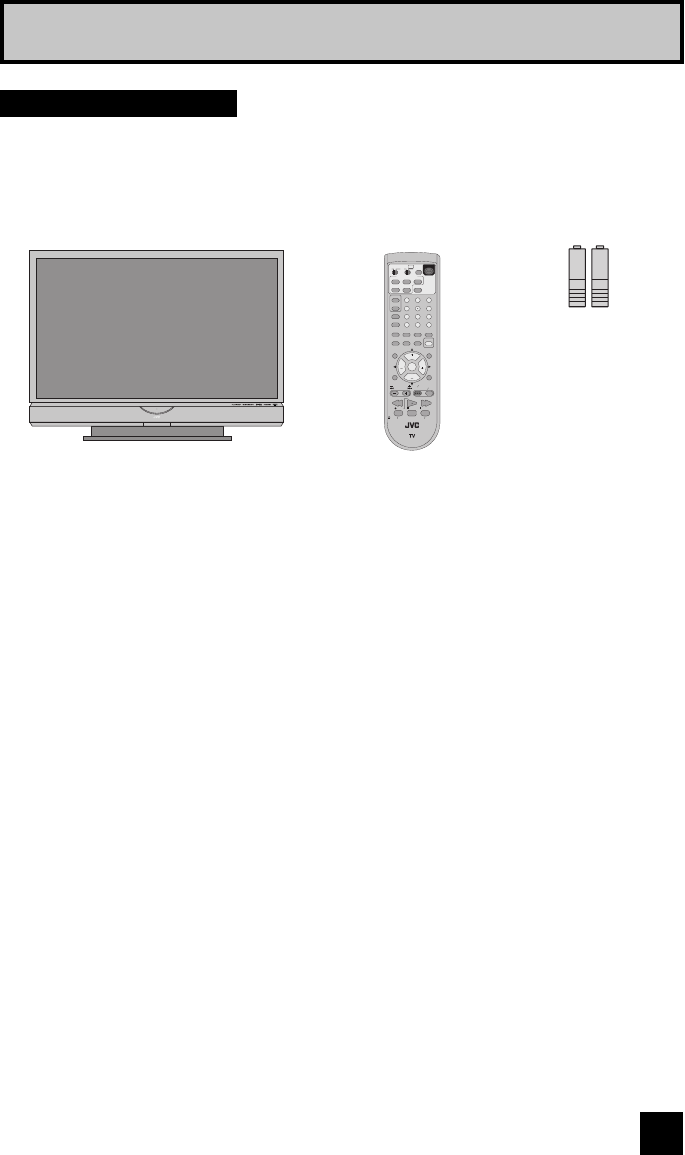
9
AA
Batteries x 2
Television x 1 Remote Control x 1
Note: Your television
and/or remote
control may differ
from the examples
illustrated here.
Quick Setup
Thank you for your purchase of a JVC Color Television. Before you begin setting up your new
television, please check to make sure you have all of the following items. In addition to this
guide, your television box should include:
AA Alkaline
AA Alkaline
POWER
PUSH
LAMP
Unpacking your TV
We recommend that before you start using your new television, you read your entire User’s
Guide so you can learn about your new television’s many great features. If you’re anxious to
start using your television right away, a quick setup guide follows on the next few pages.
INPUT
INDEX
ASPECT
FREEZE SWAP
SELECT
RETURN+/TV
FAVORITE
THEATER
PRO
NATURAL
CINEMA
VIDEO
STATUS
SOUND
TV
CATV VCR DVD
MUTING
MENU BACK
GUIDE
RM-C18G
REW
VCR CHANNEL
PREV NEXT VCR DVD
POWER TV VCR
FFPLAY
REC PAUSE
OPEN CLOSE STILL PAUSE
STOP
CH
CH
VOL VOL
OK
MULTI SCREEN
SPLIT
POWER
SUB
CHANNEL
ML/MTS
SLEEP
DISPLAY
D/A
C.C.
TUNE
1
4
7
2
5
8
0
3
6
9
LIGHT
LCT2170 Eng.indd 9LCT2170 Eng.indd 9 8/4/06 10:26:53 AM8/4/06 10:26:53 AM
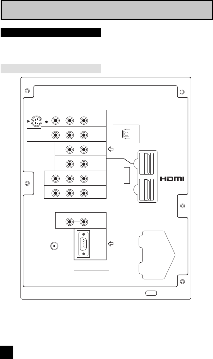
10
75Ω
(VHF/UHF)
OVER
LICENSED UNDER THE
FOLLOWING U.S. PATENTS
6,183,091
6,419,362
SERVICE
ONLY
PC IN
INPUT-1
INPUT-2
INPUT-3
HDMI 1
INPUT-1
INPUT-2
VIDEO
VIDEO
R - AUDIO - L
R - AUDIO - L
R - AUDIO - L
R - AUDIO - L
Y PB PR
Y PB PR
S-VIDEO
DIGITAL-IN
1
2
R L
AUDIO
OUTPUT
INPUT-3
(D-SUB)
PC IN AUDIO
OPTICAL OUT
Digital Auio
Quick Setup
Before you connect your television to another device, please refer to the proper diagrams for
your specific TV and remote. These will help assist you in understanding how to connect your
television to another device, as well as use the remote to set up your television.
Rear Panel Diagram
Notes:
• The terminal labeled "SERVICE ONLY", is exclusively used to update the software version.
• INPUT-3 is for use only with a PC.
TV Models
LCT2170 Eng.indd 10LCT2170 Eng.indd 10 8/4/06 10:26:53 AM8/4/06 10:26:53 AM
11
Quick Setup
Side Panel Diagram
VOLUME
INPUT 4
CHANNEL
OPERATE
+
–
+
–
MENU
VIDEO
L/MONO
R
AUDIO
INPUT
Front Panel Diagram
POWER
LAMP
POWER
LAMP LAMP LED
POWER BUTTON
POWER LED
• For information on the LED, see page 80.
Model: HD-52FA97
POWER
PUSH
LAMP
POWER
LAMP
PUSH
LAMP LED
POWER BUTTON
POWER LED
Models: HD-56FB97, HD-61FB97
LCT2170 Eng.indd 11LCT2170 Eng.indd 11 8/4/06 10:26:53 AM8/4/06 10:26:53 AM
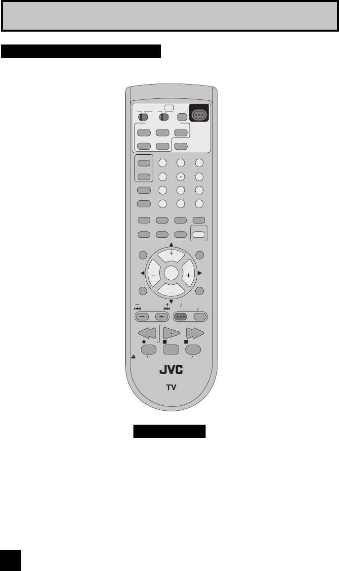
12
Quick Setup
RM-C18G
• For information on remote control buttons, see pages 62 - 74.
• SUB CHANNEL and GUIDE buttons are for digital channels. If your TV is connected to an
ATSC antenna or Digital Cable, you can use these buttons.
Remote Control
INPUT
INDEX
ASPECT
FREEZE SWAP
SELECT
RETURN+/TV
FAVORITE
THEATER
PRO
NATURAL
CINEMA
VIDEO
STATUS
SOUND
TV
CATV VCR DVD
MUTING
MENU BACK
GUIDE
RM-C18G
REW
VCR CHANNEL
PREV NEXT VCR DVD
POWER TV VCR
FFPLAY
REC PAUSE
OPEN CLOSE STILL PAUSE
STOP
CH
CH
VOL VOL
OK
MULTI SCREEN
SPLIT
POWER
SUB
CHANNEL
ML/MTS
SLEEP
DISPLAY
D/A
C.C.
TUNE
1
4
7
2
5
8
0
3
6
9
LIGHT
LCT2170 Eng.indd 12LCT2170 Eng.indd 12 8/4/06 10:26:53 AM8/4/06 10:26:53 AM
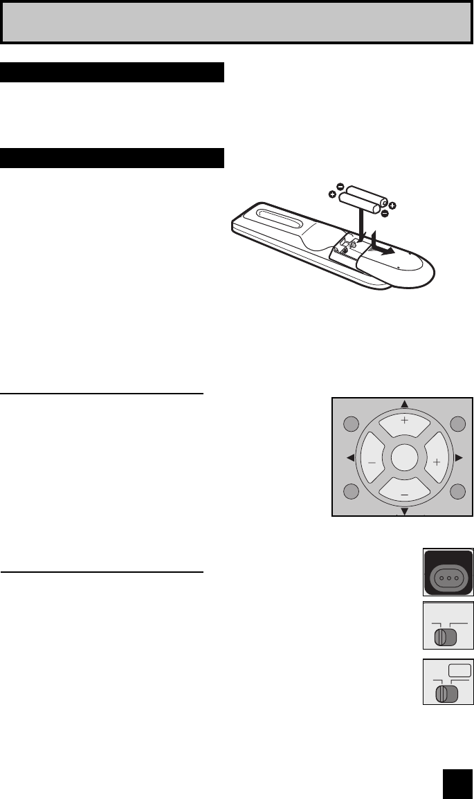
13
These quick setup pages will provide you, in three easy steps, with the basic information you
need to begin using your new television right away. If you have questions, or for more detailed
information on any of these steps, please consult other sections of this manual.
Before you can operate your remote
control, you first need to install the
batteries (included).
Slide the cover on the back of the
remote down towards the bottom of
the remote control. Insert two batteries
(included) carefully noting the “+” and
“–” markings, placing the “–” end in the
unit first. Slide the cover back into place.
When you change the batteries, try to complete the task within three minutes. If you take
longer than three minutes, the remote control codes for your VCR, DVD, and/or cable
box/satellite receiver may have to be reset. See pages 27 - 30.
Quick Setup
Getting Started
Step 1 – The Remote Control
Key Feature Buttons
The four key feature buttons at the center of the remote can be
used for basic operation of the television. The top and bottom
buttons will scan forward and back through the available
channels. To move rapidly through the channels using
JVC’s Hyperscan feature, press and hold CH+ or CH –. The
channels will zip by at a rate of five channels per second. The
right and left buttons will turn the volume up or down. These
buttons are also marked with four arrows and are used with
JVC’s onscreen menu system. To use the onscreen menus,
press the MENU button.
Basic Operation
Turn the television on and off by pressing the POWER button at the top right corner
of the remote. The POWER LED will light blue. If this is the first time you are
turning on the TV, the interactive plug-in menu appears.
• Make sure the TV/CATV switch is set to TV. Move the switch to CATV only if
you need to operate a cable box.
• Slide the VCR/DVD selector switch to VCR to control a VCR. Slide to
DVD to control a DVD player. Please see pages 27 to 30 for instructions on
programming your remote control to operate a cable box, VCR or DVD player.
Note:
• If the lamp replacement message appears when you turn the television ON, see page 77.
MUTING
MENU BACK
GUIDE
VCR CHANNEL C
CH
CH
VOL VOL
OK
T
POWER
VCR DVD
TV
CATV
MUL
LCT2170 Eng.indd 13LCT2170 Eng.indd 13 8/4/06 10:26:53 AM8/4/06 10:26:53 AM
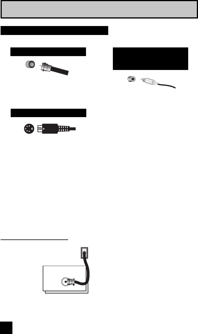
14
Quick Setup
Step 2 – Connecting Your Devices
To make these connections, you will use plugs like the ones illustrated below.
Notes:
• These connections are examples.
• After you are finished connecting your devices, plug the power cord into the nearest power
outlet and turn on the TV.
• If you follow these diagrams and the television does not work properly, contact your local
cable operator.
• To connect a DVD player, see VCR Connection. A DVD player is optional
• If you have a satellite television system, refer to the satellite TV manual.
No VCR Connection
TV Rear Panel
Coaxial Cable (Attachment)
Cable or Antenna
Output
75Ω
(VHF/UHF)
Used to connect an
external antenna or
cable TV system to
your TV.
Used to make video
connections with S-Video
VCRs, Camcorders and
DVD players.
Coaxial Cables
S-Video Cable
Used to connect audio/
video devices like
VCRs, DVD players,
stereo amplifiers, game
consoles, etc.
Component Cables
Composite Cables
Audio Cables
LCT2170 Eng.indd 14LCT2170 Eng.indd 14 8/4/06 10:26:54 AM8/4/06 10:26:54 AM
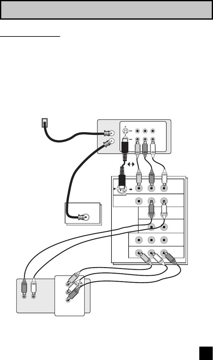
15
Quick Setup
Notes:
• Green, blue and red are the most common colors for DVD cables. Some models may vary
colors. Please consult the user’s manual for your DVD player for more information.
• Be careful not to confuse the red DVD cable with the red audio cable. It is best to complete
one set of connections (DVD or audio output) before starting the other to avoid accidentally
switching the cables.
• You may also connect the DVD player to Input 1.
OVER
INPUT-1
INPUT-2
INPUT-3
HDMI 1
INPUT-1
INPUT-2
VIDEO
VIDEO
R - AUDIO - L
R - AUDIO - L
R - AUDIO - L
R - AUDIO - L
Y P
B
P
R
Y P
B
P
R
S-VIDEO
Cable or Antenna
Output
Coaxial Cable
(Attachment)
Green
Blue
Red
DVD Player (OPTIONAL)
VCR
IN
OUT
V R L
IN
OUT
OR
Y
P
B
P
R
OUT
AUDIO OUT
R L
TV Rear Panel
75Ω
(VHF/UHF)
Diagram #1
VCR Connection
Note:
• If this connection setup does not work for you, try the connection setup on page 16.
LCT2170 Eng.indd 15LCT2170 Eng.indd 15 8/4/06 10:26:54 AM8/4/06 10:26:54 AM
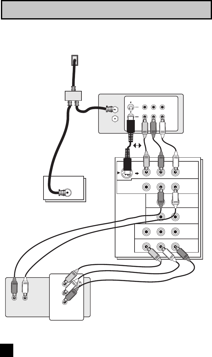
16
Quick Setup
Diagram #2
OVER
INPUT-1
INPUT-2
INPUT-3
HDMI 1
INPUT-1
INPUT-2
VIDEO
VIDEO
R - AUDIO - L
R - AUDIO - L
R - AUDIO - L
R - AUDIO - L
Y PB PR
Y PB PR
S-VIDEO
Cable or Antenna
Output
Two-Way Splitter
Coaxial Cable
(Attachment)
Green
Blue
Red
DVD Player (OPTIONAL)
VCR
TV Rear Panel
OR
IN
OUT
V R L
IN
OUT
Y
PB
PR
OUT
AUDIO OUT
R L
IN
OUT OUT
75Ω
(VHF/UHF)
LCT2170 Eng.indd 16LCT2170 Eng.indd 16 8/4/06 10:26:54 AM8/4/06 10:26:54 AM
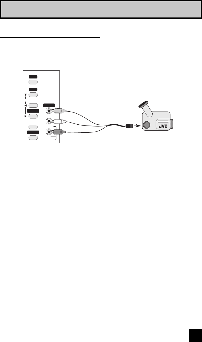
17
Quick Setup
1) Connect a yellow composite cable from the camcorder VIDEO OUT, into the VIDEO IN on
the side of the TV.
2) Connect a white cable from the camcorder LEFT AUDIO OUT, into the LEFT AUDIO IN on
the side of the TV.
3) Connect a red cable from the camcorder RIGHT AUDIO OUT, into the RIGHT AUDIO IN on
the side of the TV.
Note:
• If your camcorder is a mono sound model it will have only one AUDIO OUT. Connect it to the
L/MONO on the side of the TV.
You may connect a camcorder, game console or other equipment to your television by using
the side input jacks (Input 4) located on the side of the television. You can also connect these
using the television’s rear input jacks, using the same instructions.
VOLUME
INPUT 4
CHANNEL
OPERATE
+
–
+
–
MENU
VIDEO
L/MONO
R
AUDIO
INPUT
CAMCORDER
Connecting to a Camcorder
LCT2170 Eng.indd 17LCT2170 Eng.indd 17 8/4/06 10:26:55 AM8/4/06 10:26:55 AM
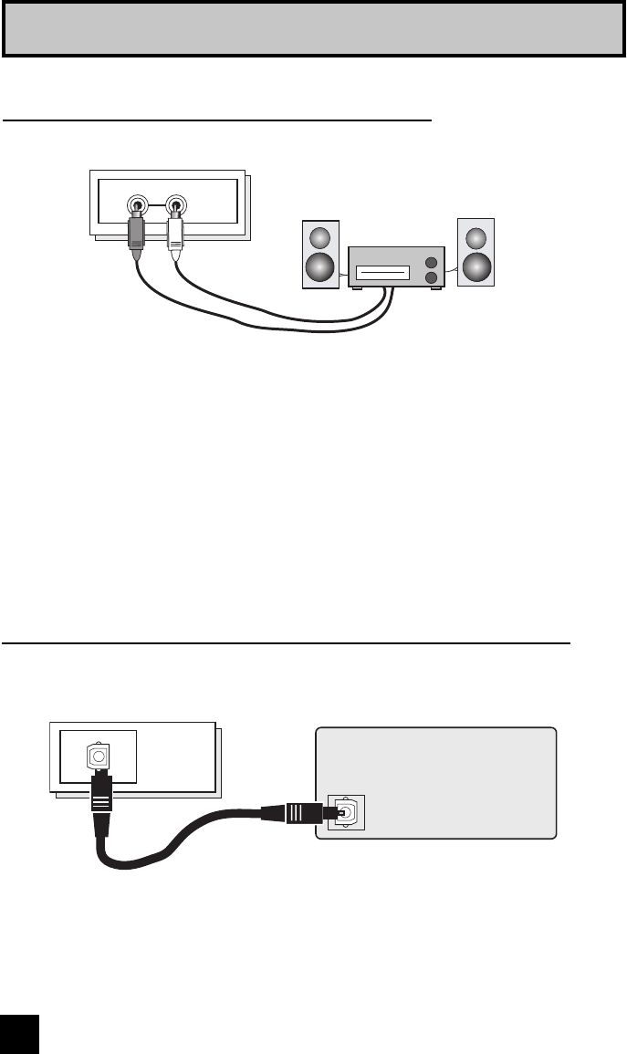
18
Quick Setup
TV Rear Panel
Speaker Speaker
Amplifier
R L
AUDIO
OUTPUT
1) Connect a white cable from the LEFT AUDIO OUTPUT on the back of the TV to the
LEFT AUDIO INPUT on the amplifier.
2) Connect a red cable from the RIGHT AUDIO OUTPUT on the back of the TV to the
RIGHT AUDIO INPUT on the amplifier.
Notes:
• Refer to your amplifier’s manual for more information.
• You can use AUDIO OUTPUT for your home theater system.
• You can not output audio using the AUDIO OUTPUT under the following conditions:
1) When you have digital sound from an HDMI device connected to the HDMI 1 or HDMI 2
connection on the back of your TV. (See page 20).
2) When you have analog sound from a DVI device connected to the AUDIO IN "HDMI 1"
connection. (See page 19).
Connecting to an External Amplifier
Connecting to an amplifier using your optical output
You can connect an amplifier that has an optical digital input terminal by using an optical digital
cable from the optical output. The signal that is output can be PCM or Dolby Digital.
TV Rear Panel Amplifier
OPTICAL OUT
Digital Auio
1) Connect the optical cable from the back of the TV to the back of the amplifier.
Notes:
• This terminal can only output digital audio.
• In order to use the optical output connection, select PCM or Dolby Digital on Digital Sound in
the Digital Setup Menu. See page 53.
• Refer to your owners manual on using your amplifier.
LCT2170 Eng.indd 18LCT2170 Eng.indd 18 8/4/06 10:26:55 AM8/4/06 10:26:55 AM
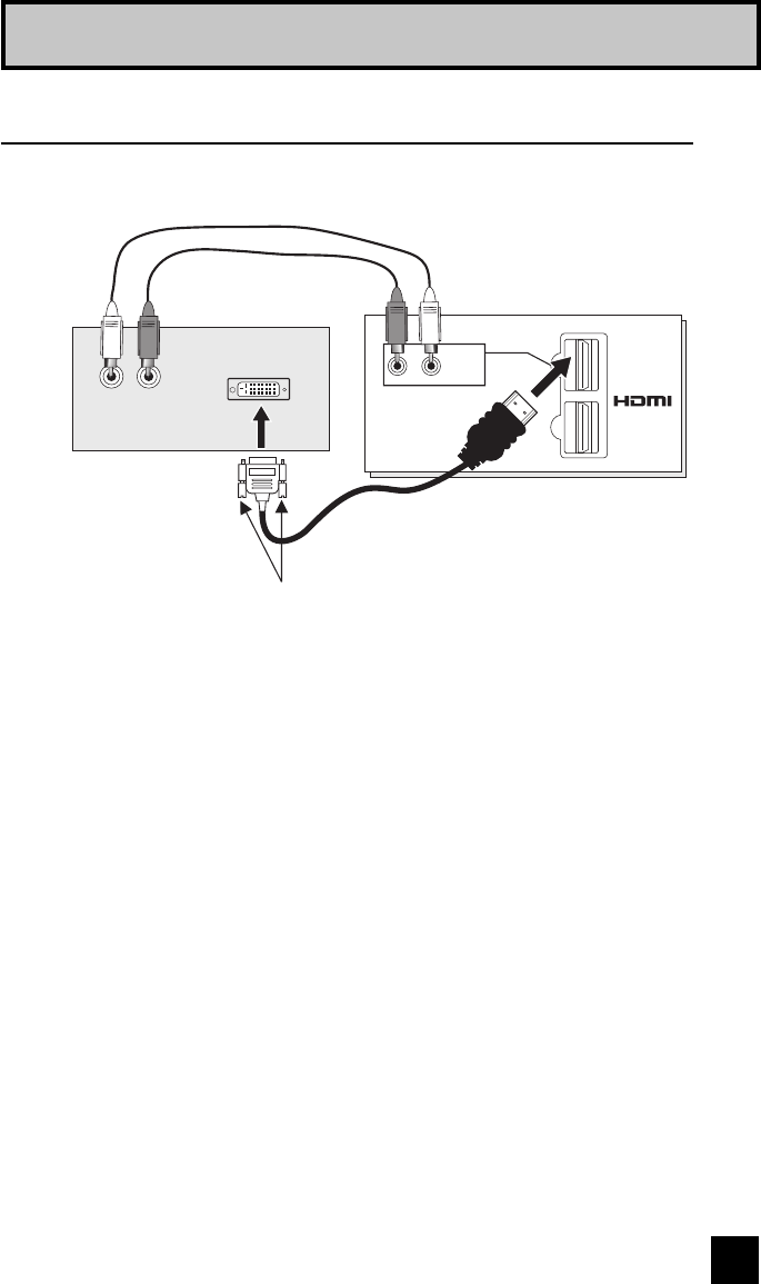
19
Quick Setup
By connecting a Digital TV Receiver, high definition pictures can be displayed on your TV in
their digital form.
DIGITAL-IN
1
2
R - AUDIO - L
HDMI 1
TV Rear Panel
DTV Decoder
HDMI to DVI Cable
After the connections have been made,
tighten the screw to secure the cables.
LR
AUDIO OUT
DIGITAL OUT
Connecting to a Digital TV Receiver
1) Connect the HDMI to DVI Cable from the DIGITAL OUT on the back of your DTV decoder, to
the HDMI1 DIGITAL-IN on the back of your television.
2) Connect a red cable from the "R AUDIO OUT" on the back of your DTV Device, to the
HDMI 1 "R AUDIO" input terminal.
3) Connect a white cable from the "L AUDIO OUT" on the back of your DTV Device, to the
HDMI 1 "L AUDIO" input terminal.
• The digital-in terminal is not compatible with the picture signal of a personal computer.
• Use a HDMI to DVI cable (commercially available) in order to digitally connect the television
with a DTV decoder.
Notes:
• If 480p signals (640x480 or 720x480) are displayed on the screen, the horizontal balance
may be slightly shifted. Access the “DIGITAL-IN” in the initial setup menu to adjust it. (Refer
to page 51.)
• When you do the above connection, set DIGITAL-IN1 AUDIO in the Initial Setup menu to
ANALOG. See "DIGITAL-IN1 AUDIO", page 51.
• The Analog Audio input can only be used with the HDMI 1 input.
• When setting the “DIGITAL AUDIO – ANALOG / DIGITAL” menu setting on the TV, please note
that this setting only effects the HDMI 1 jack and that if you use a DVI to HDMI adapter this
connection must be made to the HDMI 1 along with analog audio cables.
LCT2170 Eng.indd 19LCT2170 Eng.indd 19 8/4/06 10:26:55 AM8/4/06 10:26:55 AM
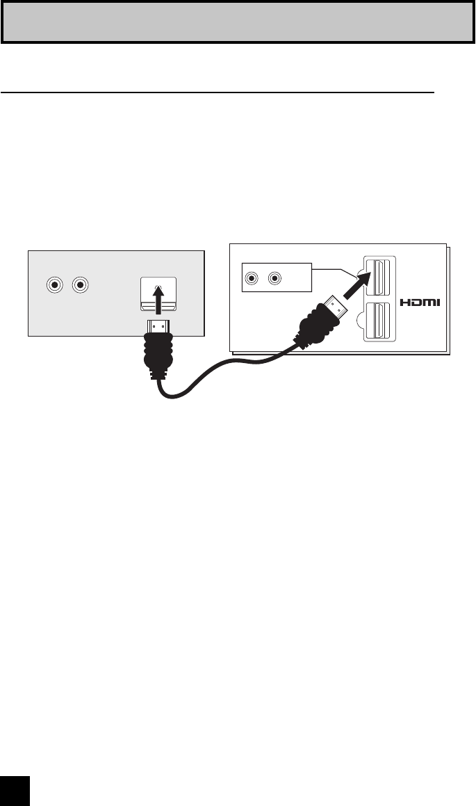
20
By connecting an HDMI compatible device, high definition pictures can be displayed on your
TV in their digital form. Some HDMI devices can include DVD players, D-VHS or any HDMI
compatible devices.
HDMI (High Definition Multimedia Interface) is the first industry supported, uncompressed, all
digital audio/video interface. HDMI provides and interface between any audio/video source,
such as a set-top box, DVD player, A/V receiver or an audio and/or video monitor, such as a
digital television (DTV).
HDMI Compatible Device
TV Rear Panel
HDMI Cable
LR
AUDIO OUT
DIGITAL OUT
DIGITAL-IN
1
2
R - AUDIO - L
HDMI 1
Quick Setup
Connecting to an HDMI Compatible Device
1) Connect the HDMI Cable from the DIGITAL OUT on the back of your DTV or HDMI device, to
the DIGITAL-IN on the back of your television.
Notes:
• When you do the above connection, set DIGITAL-IN1 AUDIO in the Initial Setup menu to
DIGITAL. See "DIGITAL-IN1 AUDIO", page 51.
• Some decoders may not respond depending on the equipment that you have connected
when it is connected to the HDMI.
• If the HDMI output device signal is changed (for example, 480i/60Hz is changed to
480p/60Hz), the screen may turn green and there may be some distortion for a short time
until the signal becomes stable.
• When you have an HDMI device connected to the HDMI 1 connection on the back of
your TV, your TV detects it, and blocks the analog audio signal coming into the "HDMI 1"
jacks. Therefore, you can not hear any analog sound from the other device conected to the
"HDMI 1" jacks, while you are viewing the images from the HDMI device.
LCT2170 Eng.indd 20LCT2170 Eng.indd 20 8/4/06 10:26:55 AM8/4/06 10:26:55 AM
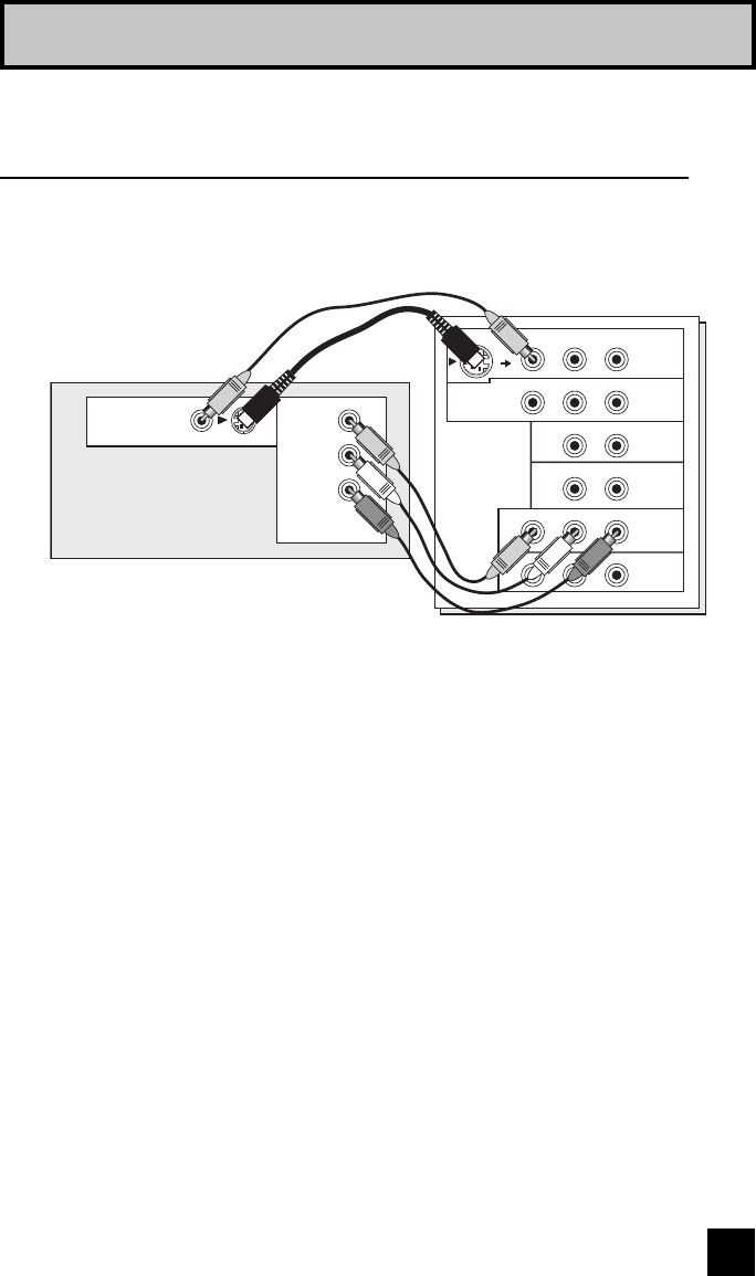
21
Quick Setup
By connecting your AV Receiver to your television's V1 Smart Input, you can watch picture
sources from many different devices, without having to change or use the other input
connections on your TV. This allows you to free up the other input connections so you can
connect more devices to your television.
Connecting to an AV Receiver using your television's
V1 Smart Input
OVER
INPUT-1
INPUT-2
INPUT-3
HDMI 1
INPUT-1
INPUT-2
VIDEO
VIDEO
R - AUDIO - L
R - AUDIO - L
R - AUDIO - L
R - AUDIO - L
Y PB PR
Y PB PR
S-VIDEO
TV Rear Panel
AV Receiver
MONITOR
OUT
MONITOR OUT
Y
PB
PR
1) Connect an S-Video Cable from the AV Receiver's MONITOR OUT, to the S-Video INPUT-1
on the back of your television.
2) Connect a Yellow Composite Cable from the AV Receiver's MONITOR OUT, into the VIDEO
INPUT-1 on the back of your television.
3) Connect a Green Component Cable from the AV Receiver's Y MONITOR OUT, into the Y
VIDEO INPUT-1 on the back of your television.
4) Connect a Blue Component Cable from the AV Receiver's PB MONITOR OUT, into the Pb
VIDEO INPUT-1 on the back of your television.
5) Connect a Red Component Cable from the AV Receiver's PR MONITOR OUT, into the Pr
VIDEO INPUT-1 on the back of your television.
Note:
• Please refer to your AV Receiver instruction manual for more information on connecting your
speakers and other devices like a DVD player.
• Use your AV Receiver's remote to switch to the different devices you have connected.
• Some AV Receivers may not respond when the V1 Smart Input function is turned on.
• If you have video connections for each input device connected to your AV Receiver, you
should not connect them using both S-Video and Composite connection at the same time
when you are using V1 Input as the V1 Smart Input. In this case we recommend using the
S-Video connection.
LCT2170 Eng.indd 21LCT2170 Eng.indd 21 8/4/06 10:26:55 AM8/4/06 10:26:55 AM
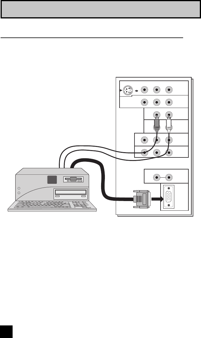
22
Quick Setup
This TV can be used as a computer screen. Use a commercially available D-SUB cable to
connect the TV's PC INPUT terminal to the computer's analog RGB output terminal. If you
want to listen to the sound from the computer, use a commercially available RCA cable to
connect the INPUT-3 audio input terminal to the computer's audio output terminal.
Connecting to the computer
OVER
INPUT-1
INPUT-2
INPUT-3
HDMI 1
INPUT-1
INPUT-2
VIDEO
VIDEO
R - AUDIO - L
R - AUDIO - L
R - AUDIO - L
R - AUDIO - L
Y PB PR
Y PB PR
S-VIDEO
R L
AUDIO
OUTPUT
INPUT-3
(D-SUB)
TV Rear Panel
Notes:
• Refer to your computer manual for a detailed explanation of the connections concerning your
computer.
• Make sure that the connectors are facing the correct way when connecting.
• After connecting, tighten the two screws to fix the connectors in place.
Looking at the images from a computer
After starting the computer, press the INPUT button to choose INPUT-3. You can listen to the
sound when the sound from the computer is connected to the INPUT-3 AUDIO input terminal.
Note:
• When the sound from the computer is connected to INPUT-3 by choosing external input
INPUT-3, the sound from the computer can be listened to, but the images from the computer
cannot be seen.
LCT2170 Eng.indd 22LCT2170 Eng.indd 22 8/4/06 10:26:56 AM8/4/06 10:26:56 AM

23
Quick Setup
Table of signals for each type of computer
Resolution
640 x 480
(VGA)
1024 x 768
(XGA)
Vertical
Frequency
(Hz)
60.0
60.0
Horizontal
Frequency
(kHz)
31.5
48.4
When a picture is not displayed
With some computers, some problems can be solved by changing the settings. Check the
computer's refresh rate and set it to 60Hz. Computers that cannot set the refresh rate to 60
Hz, can not be used with this TV. Refer to the computer's instruction manual.
*Apple Macintosh is a registered trademark of Apple Computer, Inc.
Note:
• If you are inputting a PC signal that is invalid, "Invalid Signal" will appear on the TV screen.
It appears when the input is PC and it is a single screen.
• Only the above formats are supported.
• Even with the above formats at 60 Hz, some problems may be experienced depending on
the quality of the synchronous signal. (Depending on the quality, some pictures may not be
displayed correctly).
• Apple Macintosh* computers are not supported.
LCT2170 Eng.indd 23LCT2170 Eng.indd 23 8/4/06 10:26:56 AM8/4/06 10:26:56 AM
24
When you turn your television on for the first time the interactive plug-in menu will appear. The
plug-in menu helps you to get your TV ready to use by letting you set your preferences for:
• The language in which you want the onscreen menus to appear.
• Setting the TV’s clock to the correct time so your timer functions will work properly. You can
choose “AUTO” or “MANUAL” for setting the clock.
• The auto tuner setup of which channels you wish to receive.
We recommend you complete the interactive plug-in items before you start using your
television.
Notes:
• The interactive plug-in menu setting does not appear if your TV has been turned on before.
In this case use the onscreen menus to perform these settings. See pages 44, 59, 34.
• If you press the Menu button while setting up the interactive plug-in menu, it will skip over it.
Step 3 – The Interactive Plug In Menu
Quick Setup
After the “JVC INTERACTIVE PLUG IN MENU” has been displayed, the TV automatically
switches to the LANGUAGE settings. You can choose to view your onscreen menus in three
languages: ENGLISH, FRANÇAIS (French) or ESPAÑOL (Spanish).
è
To choose a language:
ENGLISH, FRANÇAIS or ESPAÑOL
†
To NEXT (To set clock)
Language
(To be continued...)
LANGUAGE/LANGUE/IDIOMA
ENGLISH
NEXT
SELECT OPERATE EXIT
MENU
LCT2170 Eng.indd 24LCT2170 Eng.indd 24 8/4/06 10:26:56 AM8/4/06 10:26:56 AM
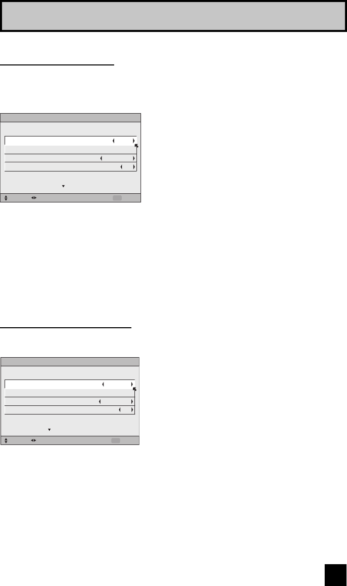
25
To set your clock manually (without using the XDS signal), choose MANUAL. If you choose
AUTO, see auto clock set above.
è
To choose MANUAL
†
To TIME
è
To set the hour
†
To minute
è
To set the minute
†
To TIME ZONE
è
To select your time zone: (Atlantic, Eastern,
Central, Mountain, Pacific, Alaska or
Hawaii)
†
To move to D.S.T. (Daylight Savings Time)
è
To turn D.S.T. ON or OFF
†
To START CLOCK
Manual Clock Set
Note:
• You will have to reset the clock after a power interruption. You must set the clock before
operating any timer functions.
Quick Setup
Before you use any of your TV’s timer functions, you must first set the clock. You may
precisely set your clock using the XDS time signal broadcast by most public analog
broadcasting stations. If you do not have this in your area, you will have to set the clock
manually. See manual clock set below. To set the clock using the XDS signal:
è
To choose AUTO
†
To TIME ZONE
è
To select your time zone: (Atlantic, Eastern,
Central, Mountain, Pacific, Alaska or
Hawaii)
†
To move to D.S.T. (Daylight Savings Time)
è
To turn D.S.T. ON or OFF
†
To NEXT (To Auto Tuner Setup)
Notes:
• D.S.T. can be used when it is set to ON in the SET CLOCK menu.
• Only when the MODE is set to AUTO, the Daylight Savings Time feature automatically
adjusts your TV’s clock for Daylight Savings. The clock will move forward one hour at 2:00
am on the first Sunday in April. The clock will move back one hour at 2:00 am on the last
Sunday in October.
• You will have to reset the clock after a power interruption. You must set the clock before
operating any timer functions.
Auto Clock Set
(To be continued...)
SET CLOCK
SELECT OPERATE EXIT
MENU
TIME
MODE
TIME ZONE
D.S.T.
MANUAL
--
:
--
--
ATLANTIC
ON
START CLOCK
SET CLOCK
NEXT
SELECT OPERATE EXIT
MENU
TIME
--
:
--
--
MODE
TIME ZONE
D.S.T.
AUTO
ATLANTIC
ON
LCT2170 Eng.indd 25LCT2170 Eng.indd 25 8/4/06 10:26:56 AM8/4/06 10:26:56 AM
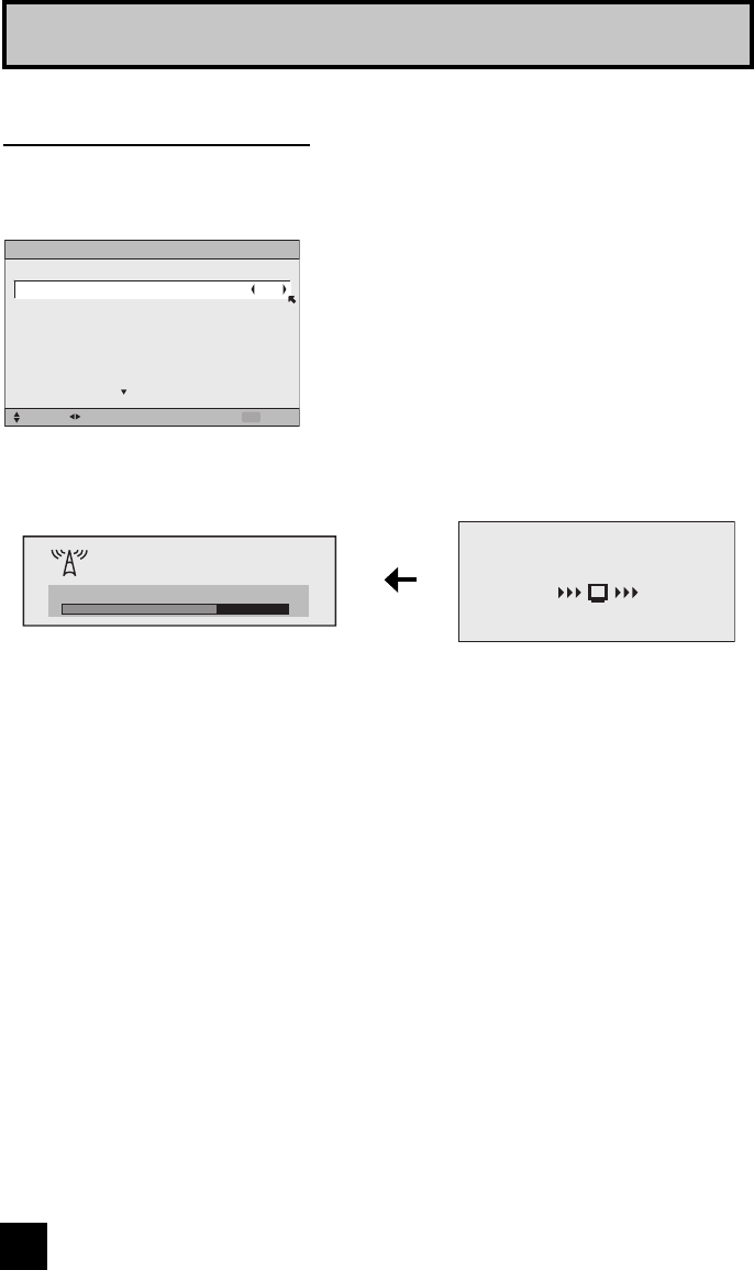
26
Quick Setup
In auto tuner setup, the TV automatically scans through all available channels, memorizing the
active ones and skipping over blank ones or channels with weak signals. This means when you
scan (using the CHANNEL +/– buttons) you will receive only clear, active channels.
è
To choose CABLE or AIR (or SKIP when
you skip Analog Auto Tuner Setup)
†
To START
After Analog Auto Tuner Setup is finished, Digital Auto
Tuner Setup starts.
Auto Tuner Setup
When the setup is finished, "THANK YOU ! SETUP IS NOW COMPLETE" is displayed. Your
quick setup is now complete. You can now begin watching your television, or you can continue
on in this guide for more information on programming your remote control, or using the
JVC onscreen menu system to customize your television viewing experience.
Notes:
• If you want to cancel the Auto Tuner Setup, press the MENU button.
• Noise muting will not work during Auto Tuner Setup.
• If you choose SKIP, it finished without doing the Auto Tuner Setup.
Cable Box and Satellite Users: After your auto tuner setup is complete, you may, (depending
on the type of hookup), have only 1 channel, usually 3 or 4 in the auto tuner memory. This is
normal.
48
NOW
PROGRAMMING !
20
Now Programming...
AUTO TUNER SETUP
SELECT OPERATE EXIT
MENU
AIR TUNER MODE
START
LCT2170 Eng.indd 26LCT2170 Eng.indd 26 8/4/06 10:26:57 AM8/4/06 10:26:57 AM
27
You can program your remote to operate your cable box, satellite receiver, VCR or DVD
player by using the instructions and codes listed below. If the equipment does not respond to
any of the codes listed below or to the code search function, use the remote control supplied
by the manufacturer.
The remote control is programmed with cable box and satellite codes for power on/off,
channel up/down, and 10 key operation.
1) Find the cable box or satellite brand from the list of codes shown below.
2) Slide the 2-way selector switch to “CATV”.
3) Press and hold down the DISPLAY button, then enter the first code number listed with the 10
key pad.
4) Release the DISPLAY button, and confirm the operation of the cable box/satellite receiver.
• If your cable or satellite box does not respond to the first code, try the others listed. If it does
not respond to any code, try the search codes function, on page 30.
Remote Programming
Cable Box or Satellite Codes
ABC
Archer
Cableview
Citizen
Curtis
Diamond
Eagle
Eastern
GC Brand
Gemini
General
Instrument/Jerrold
Hamlin
Hitachi
Macom
Magnavox
Memorex
Movietime
Oak
Paragon
Panasonic
Philips
Pioneer
024
032, 025
051, 032
022, 051
058, 059
024, 032, 025
029
034
032, 051
022, 043
065, 024, 025,
026, 027, 020,
021, 022, 057,
023, 072, 074
040, 041, 042,
045, 058, 064
049, 024
049, 050, 051,
054
033
030
032, 051
039, 037, 048
055, 056, 060,
071, 073
063
028, 029, 030,
052, 053, 031,
069
047, 062
Pulsar 051, 032
Cable Box Codes
Puser
RCA
Realistic
Regal
Regency
Rembrandt
Samsung
Scientific Atlanta
SLMark
Sprucer
Stargate
Telecaption
Teleview
Texscan
Tocom
Toshiba
Unika
Universal
Videoway
Viewstar
032
061, 070
032
058, 064, 040,
041, 042, 045,
068
034
037, 032, 051,
038
051
057, 058, 059
051, 047
051, 056
032, 051
067
047, 051
044
035, 036, 066,
074
050, 048
032, 025
022, 032
052
029, 030
Zenith 063, 046
Zenith/Drake
Satellite
046
Echostar
(Dish Network)
Express VU
G.E.
G.I.
Gradiente
Panasonic
Philips
Primestar
RCA
Proscan
Sony
Star Choice
Toshiba
Uniden
100, 113, 114,
115
100, 113
106
108, 120, 121,
122
112
Hitachi
HNS (Hughes)
104, 111
104
105
102, 103, 116
108
106, 109, 110
106, 109, 110
107
104, 108
101, 104, 117,
118, 119
102, 103
Digital
Satellite
Systems
Codes
Magnavox 102, 103
Cable Box Codes
Quick Setup
LCT2170 Eng.indd 27LCT2170 Eng.indd 27 8/4/06 10:26:57 AM8/4/06 10:26:57 AM
28
The remote control is programmed with VCR codes for power on/off, play, stop, fast-forward,
rewind, pause, record, channel up/down operation.
1) Find the VCR brand from the list of codes shown below.
2) Slide the first 2-way selector switch to “TV” and the other 2-way selector switch to “VCR”.
3) Press and hold down the DISPLAY button, then enter the first code number listed with the 10
key pad.
4) Release the DISPLAY button, and confirm the operation of the VCR.
• If your VCR does not respond to the first code, try the others listed. If it does not respond to
any of the codes, try the search codes function on page 30.
• After you program your remote, some VCR buttons may not work properly. If so, use the
VCR’s remote.
• To record, hold down the REC button on the remote and press PLAY.
VCR Codes
Admiral
Aiwa
Akai
Audio Dynamic
Bell & Howell
Broksonic
Canon
CCE
Citizen
Craig
Curtis Mathes
Daewoo
DBX
Dimensia
Emerson
Fisher
Funai
G.E.
Go Video
Goldstar
Hitachi
Gradiente
Instant Replay
Jensen
035
027, 032, 095
029, 072, 073,
074
003, 005
063, 071
020, 026, 094
023, 025
043
064
063, 029, 064
045, 024, 027,
093
043, 059, 024,
092
003, 004, 005
045, 093
043, 026, 077,
061, 025, 042,
020, 076
063, 066, 067,
065, 071, 091
027, 026, 020,
000
033, 045, 024
037, 051, 049,
050, 089
064
083, 084, 081,
000, 001
023, 045, 058,
093, 027, 081
024, 023
003
JVC
Kenwood
003, 004, 005,
000, 001, 002,
006, 007
003, 004, 064,
005
LXI 027, 064, 058,
065, 066, 063,
067
VCR Codes
Magnavox
Marantz
Marta
Memorex
MGA
Minolta
Mitsubishi
Multitech
NEC
Olympic
Optimus
Orion
Panasonic
Penney
Pentax
Philco
Philips
Pioneer
Proscan
Quasar
Radio Shack
031, 023, 024,
086
003, 004, 005
064
024, 067
038, 040, 047,
048, 041, 042
058, 045, 093
038, 040, 047,
048, 041, 042,
078, 090
047, 027, 062
003, 004, 005,
000
024, 023
028, 021, 035,
064
026, 020
023, 024, 021,
022
024, 058, 045,
063, 003, 004,
005, 093
058, 005, 045,
093
031, 024, 027,
023, 026, 020,
043
031, 023, 024,
086
023
045, 058, 023,
024, 031, 046,
059, 060, 093,
033, 087
021, 022, 023,
024
033, 024, 063,
036, 067, 040,
027
RCA 033, 045, 058,
023, 024, 031,
046, 059, 060,
083, 084, 085,
087, 093, 096
Realistic 024, 063, 036,
067, 040, 027
Codes
Samsung
Samtron
Sansui
Sanyo
Scott
Sears
Sharp
Signature 2000
Sony
Singer
SV 2000
Sylvania
Symphonic
Tashiro
Tatung
Teac
Technics
Teknika
Toshiba
Vector Research
Wards
037, 060, 062,
033, 089
089
003, 026, 020,
052
063, 067, 091,
071
059, 060, 062,
067, 038, 040,
047, 048, 026,
020
063, 064, 065,
066, 058
Shintom 075
035, 036, 080,
088
027, 035
075
028, 029, 030,
053, 054, 055
027
031, 023, 024,
027
027, 081
064
003, 004, 005
003, 004, 027,
005
021, 022, 023,
024
024, 027, 070
059, 046, 079
005
035, 036, 067,
044, 064
Yamaha 063, 003, 004,
005
Zenith 044, 082, 064,
094
Codes
LG 064
Thomson 033, 096
VCR VCR
Quick Setup
LCT2170 Eng.indd 28LCT2170 Eng.indd 28 8/4/06 10:26:57 AM8/4/06 10:26:57 AM
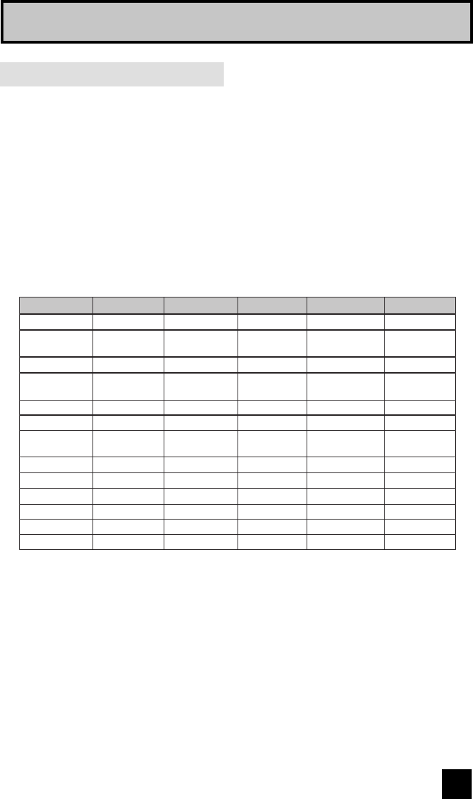
29
The remote control is programmed with DVD codes for power on/off, play, stop, fast-forward,
rewind, previous/next chapter, tray open/close, and still/pause operation.
1) Find the DVD player brand from the list of codes shown below.
2) Slide the first 2-way selector switch to “TV” and the other 2-way selector switch to “DVD”.
3) Press and hold down the DISPLAY button, then enter the first code number listed with the 10
key pad.
4) Release the DISPLAY button, and confirm the operation of the DVD player.
• If your DVD player does not respond to the first code, try the others listed. If it does not
respond to any of the codes, try the search codes function on page 30.
• After you program your remote, some DVD buttons may not work properly. If so, use the
DVD player’s remote.
DVD Codes
CodesDVD Player Codes Codes
Aiwa 043
Apex 040, 054,
055
Denon 020, 037
Hitachi 031
JVC 000
Kenwood 035, 020
Konka 039
Mitsubishi 025
Onkyo 041, 052
Oritron 044
Panasonic 020
Philips 023, 036
Pioneer 022
Raite 033
RCA 021, 026
Sampo 034
Samsung 030
Sharp 028
Silvania 038
Sony 024, 045,
046, 047
Technics 020
Toshiba 023
Wave 042
Yamaha 020, 049
Zenith 027, 032
Vialta 050
Bose 058
Funai 038
Go–Video 032
Harman
Kardon
053
KLH 051
Koss 050
Mintek 057
Next Base 056
Polk Audio 036
SMC 048
Thomson 021
Venturer 051
DVD Player DVD Player
Quick Setup
LCT2170 Eng.indd 29LCT2170 Eng.indd 29 8/4/06 10:26:57 AM8/4/06 10:26:57 AM

30
Cable/Satellite Search Codes Function
1) Slide the first 2-Way Mode Selector switch to CATV.
2) Press the POWER and RETURN+/TV buttons. Hold for at least three seconds and release.
3) Press the POWER button on the remote, and see if the cable or satellite box responds.
4) If there was a response, press RETURN+/TV. The codes are now set. If there was no
response, repeat Step 3. If you repeat Step 3 a total of 80 times without a response, use
the remote control that came with your equipment.
5) Press RETURN+/TV to exit.
VCR/DVD Search Codes Function
1) Slide the first 2-way selector switch to “TV” and the other 2-way selector switch to “VCR” or
“DVD”.
2) Press the VCR or DVD POWER and RETURN+/TV buttons. Hold for at least three seconds
and release.
3) Press the VCR or DVD POWER button, and see if the VCR or DVD responds.
4) If there was a response, press RETURN+/TV. The codes are now set. If there was no
response, repeat Step 3. If you repeat Step 3 a total of 80 times for the VCR (40 times for
the DVD player), and there is no response, use the remote control that came with your
equipment.
5) Press RETURN+/TV to exit.
Search Codes
Quick Setup
LCT2170 Eng.indd 30LCT2170 Eng.indd 30 8/4/06 10:26:58 AM8/4/06 10:26:58 AM
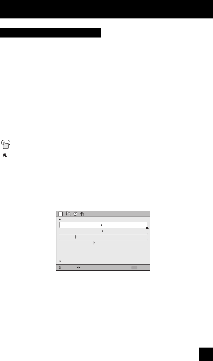
31
To bring up the onscreen menu, press the MENU button on the remote control. The item that
appears in green is the one currently selected. If you use the Menu button on the TV’s side
panel instead of the remote, an additional menu screen showing VIDEO STATUS and ASPECT
will appear between INITIAL SETUP and PICTURE ADJUST. The “interactive plug-in menu” will
appear the first time the TV is plugged in.
Note:
• Menus shown in this book are illustrations, not exact replications of the television’s onscreen
displays.
Certain symbols are used throughout this guide to help you learn about the features of your
new television. The ones you will see most frequently are:
π†
Up and Down arrows mean press the CH+ or CH– buttons. Pressing the CH+ or CH–
buttons let you:
• Move vertically in a main menu screen
• Move through a submenu screen
• Move to the next letter, number, or other choice in a submenu
• Back up to correct an error
• Scan through TV channels (when not in a menu screen)
è
Left and right arrows mean press the VOLUME+ or VOLUME- buttons to move left or right
to:
• Select a highlighted menu item
• Select an item in a submenu
• Select numbers in certain menu options
• Turn the volume up or down (when not in a menu screen)
The “press button” icon means you should press the button named on your remote
control. (Button names appear in SMALL CAPITAL LETTERS.)
The “helping arrow” icon points to the highlighted or selected item in a menu.
Onscreen Menus
Using the Guide
INITIAL SETUP
SELECT OPERATE EXIT
MENU
NEXT PAGE
PREVIOUS
AUTO TUNER SETUP
CHANNEL SUMMARY
V-CHIP
SET LOCK CODE
(4/5)
LCT2170 Eng.indd 31LCT2170 Eng.indd 31 8/4/06 10:26:58 AM8/4/06 10:26:58 AM
32
Your television comes with JVC’s onscreen menu system. The onscreen menus let you make
adjustments to your television’s operation simply and quickly. Examples of the onscreen
menus are shown on the next page. Detailed explanations on using each menu follow later in
this guide. For information about the interactive plug-in Menu, see pages 24 - 26.
Onscreen Menus
The Onscreen Menu System
To open the onscreen menu system, press the MENU button on the remote control. You
navigate within the onscreen menus by using the four directional arrow buttons on the remote
control. (These buttons are also the CH +/– and VOL +/– buttons. Channel and volume functions
will not operate when the onscreen menu is active).
The selected feature and option on a menu screen are highlighted in a different color.
To move to a different feature use the π† arrows to move up or down the list. When you
press the up arrow at the top of the list or the down arrow at the bottom, the next menu screen
will appear. Use the arrows √ ® to select an option from the highlighted feature. Pressing
MENU on the remote control will close the onscreen menu system and return you to normal
television viewing.
Each menu and its features will be discussed in the following pages of this guide.
Notes:
• If you do not press any buttons for about a minute, the onscreen menu will automatically
shut off.
• Button names in this guide are shown in SMALL CAPITAL LETTERS.
• Menus may appear in different sizes onscreen depending on the aspect ratio selected.
• Some menu items may not appear in menu screens when certain aspect ratios or inputs
are selected.
Selected Option
(Green)
Selected Option
(Blue)
The Onscreen Menu System
LANGUAGE
CLOSED CAPTION
ENG. FRAN. ESP.
LCT2170 Eng.indd 32LCT2170 Eng.indd 32 8/4/06 10:26:58 AM8/4/06 10:26:58 AM
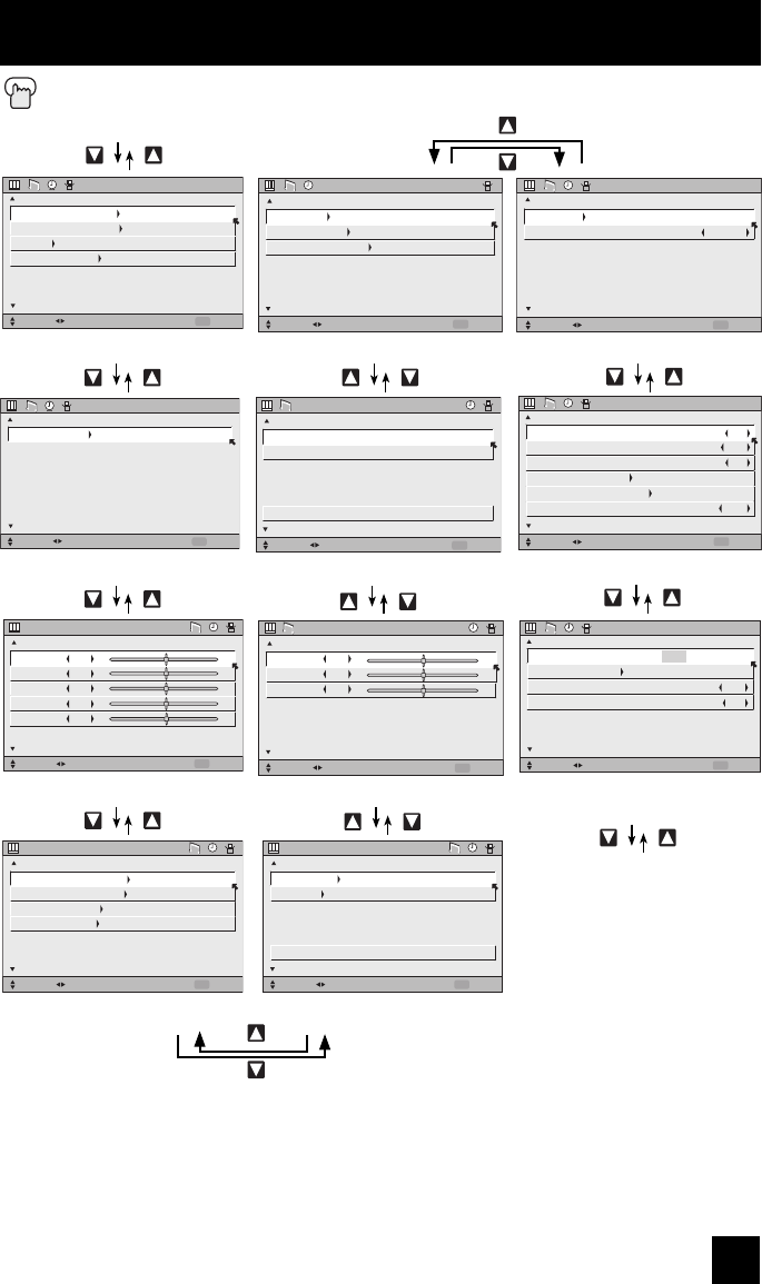
33
Press the MENU button
Onscreen Menus
PICTURE ADJUST
SELECT OPERATE EXIT
MENU
NEXT PAGE
PREVIOUS STANDARD
(1/3)
TINT
COLOR
PICTURE
BRIGHT
DETAIL
00
00
00
00
00
PICTURE ADJUST 01
SELECT OPERATE EXIT
MENU
NEXT PAGE
PREVIOUS STANDARD
PICTURE ADJUST
(2/3)
HIGH
OFF
OFF
ON
COLOR TEMPERATURE
COLOR MANAGEMENT
DYNAMIC GAMMA
SMART PICTURE
PICTURE ADJUST 02
BASS
TREBLE
BALANCE
SOUND ADJUST
SELECT OPERATE EXIT
MENU
NEXT PAGE
PREVIOUS
00
00
00
(1/2)
SOUND ADJUST 01
INITIAL SETUP 04
INITIAL SETUP
SELECT OPERATE EXIT
MENU
NEXT PAGE
PREVIOUS
AUTO TUNER SETUP
CHANNEL SUMMARY
V-CHIP
SET LOCK CODE
(4/5)
CLOCK / TIMERS
SELECT OPERATE EXIT
MENU
NEXT PAGE
PREVIOUS
SET CLOCK
ON / OFF TIMER
LAMP TIMER RESET
CLOCK/TIMERS
INITIAL SETUP
SELECT OPERATE EXIT
MENU
NEXT PAGE
PREVIOUS
ENG. FRAN. ESP.
LANGUAGE
CLOSED CAPTION
AUTO SHUT OFF
XDS ID
OFF
ON
(3/5)
INITIAL SETUP 03
INITIAL SETUP 02
ON
OFF
ON
INITIAL SETUP
SELECT OPERATE EXIT
MENU
NEXT PAGE
PREVIOUS
(2/5)
NOISE MUTING
FRONT PANEL LOCK
V1 SMART INPUT
VIDEO INPUT LABEL
POSITION ADJUSTMENT
POWER INDICATOR OFF
INITIAL SETUP 01
INITIAL SETUP
SELECT OPERATE EXIT
MENU
NEXT PAGE
PREVIOUS
(1/5)
DIGITAL-IN
DIGITAL-IN1 AUDIO
AUTO
DIGITAL
INITIAL SETUP 05
INITIAL SETUP
SELECT OPERATE EXIT
MENU
NEXT PAGE
PREVIOUS
(5/5)
DIGITAL SETUP
Notes:
• The DIGITAL-IN menu can only be displayed when a 480p picture signal is input to the
digital-in terminal and the picture is being displayed on the screen.
• SMART PICTURE menu cannot be displayed when DYNAMIC is selected for Video Status.
• When the Menu button on the TV side panel is pressed, the FRONT PANEL CONTROL menu
between INITIAL SETUP 05 and PICTURE ADJUST 01 will appear.
SELECT OPERATE EXIT
MENU
NEXT PAGE
PREVIOUS STANDARD
PICTURE ADJUST
(3/3)
AUTO
ON
DIGITAL VNR
MPEG NR
RESET
PICTURE ADJUST 03
TURN ON VOLUME
VOLUME LIMIT
RESET
SOUND ADJUST
SELECT OPERATE EXIT
MENU
NEXT PAGE
PREVIOUS
(2/2)
10
40
SOUND ADJUST 02
To INITIAL SETUP 04
To INITIAL SETUP 03
LCT2170 Eng.indd 33LCT2170 Eng.indd 33 8/4/06 10:26:58 AM8/4/06 10:26:58 AM

34
Auto Tuner Setup
The auto tuner setup function is described on page 26 as the interactive plug-in menu. If you
need to run the auto tuner setup again, follow the steps below.
Press the MENU button
π†
To AUTO TUNER SETUP
è
To operate
è
To choose CABLE or AIR
Press the OK button to start
Press the Menu button when finished
Note:
• Digital Auto Tuner Setup will take approximately 14 minutes.
Onscreen Menus
AUTO TUNER SETUP
OPERATE EXIT
MENU
AIR TUNER MODE
PRESS OK TO START
The auto tuner is finished when the message PROGRAMMING OVER! appears onscreen.
LCT2170 Eng.indd 34LCT2170 Eng.indd 34 8/4/06 10:26:59 AM8/4/06 10:26:59 AM
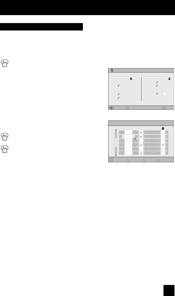
35
Channel Summary
Channel summary allows you to customize the line-up of channels received by your TV.
Regarding analog channels, you can add or delete channels from the line-up or prevent any
unauthorized viewers from watching any or all 191 channels. Regarding digital channels, the
only channels that will appear are the ones that are broadcasting.
Press the MENU button
π†
To CHANNEL SUMMARY
è
To operate
The Channel summary screen will now be displayed with
the channels set to scan marked with an “√”. Regarding
analog channels, you can delete channels from the scan
by removing the “√”. If any channels were missed during
auto tuner setup and you wish to add them, you may by
placing an “√” next to the channel number.
• Digital channels can not be added to the channel
summary if the auto tuner setup did not find them.
π†
è
To the SCAN column
Press the OK button to include or delete from
scan
Press the MENU button when finished
CHANNEL SUMMARY
06
07
08
09
10
CHNO.
SELECT OPERATE EXIT
MENU
01
02
03
04
05
OK
SCAN CHNO. SCANID ID
MTV
A&E
E!
HBO
L
Channel Summary Digital
CH No. Scan
FOX
ABC
CNN
NBC
BOX
NHK
Station Name
D01
D02
D02
D10-1
D10-2
D12345
Select Back
BACK
Exit
MENU
Operate
OK
Analog Channels
Digital Channels
Note:
• The number of a digital channel may change,
depending on the time of some broadcastings. If
this channel existed and now had disappeared, the
lock channel or scanned channel by the channel
summary for that channel will be cancelled.
Onscreen Menus
LCT2170 Eng.indd 35LCT2170 Eng.indd 35 8/4/06 10:27:00 AM8/4/06 10:27:00 AM
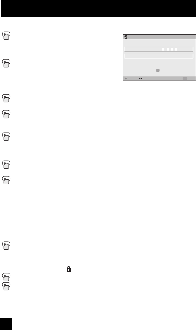
36
How to set the channel label. (This is only for analog broadcasting.)
Press the MENU button
π†
To CHANNEL SUMMARY
è
To operate
π†
To the ID column
Press the OK button to enter
è
To select the character you want
π†
To move to the next space
...continue to follow these directions for all four
spaces
Press the OK button to finish
Your characters are now set
Press the MENU button when finished
If you want to reset the characters you set:
Press the MENU button
π†
To CHANNEL SUMMARY
è
To operate
π†
To the ID column
Press the OK button to enter
π†
To select RESET
Press the OK button to finish
Your characters are now reset
Notes:
• You can use characters for: Alphabet, numbers, marks and spaces.
• It is possible to set the maximum of 40 channel labels.
• If you try to set more than the 40 maximum, the message "MEMORY OVERFLOW" will
appear.
You can block access to a channel by activating the channel lock.
Press the MENU button
π†
To CHANNEL SUMMARY
è
To operate
π†
è
To the Lock Column ( )
Press the ZERO button to lock or unlock that channel
Press the MENU button when finished
ID
PRESS TO FINISH
SELECT OPERATE EXIT
MENU
OK
CHANNEL 09
RESET
Onscreen Menus
LCT2170 Eng.indd 36LCT2170 Eng.indd 36 8/4/06 10:27:00 AM8/4/06 10:27:00 AM
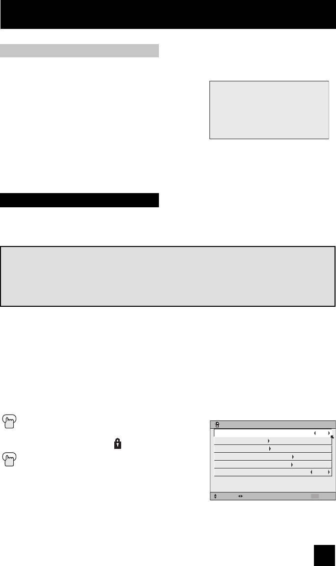
37
When a viewer attempts to watch a guarded channel, the following message appears:
To watch a channel that you have locked, enter the
Lock Code using the 10 key pad.
If the wrong code is entered, the message
“INVALID LOCK CODE!” will flash on the screen.
The channel cannot be accessed until the correct code
is entered.
Notes:
• Once a channel has been unlocked, it will remain unlocked until the television is turned off.
• See also “Set Lock Code”, page 43.
Channel Guard Message
V-Chip
THIS CHANNEL IS LOCKED BY
CHANNEL GUARD.
PLEASE ENTER LOCK CODE BY
10 KEY PAD TO UNLOCK IT.
NO. - - - -
You can customize the V-Chip settings of your television to match your personal tastes. The
V-Chip menu below is the starting point for your V-Chip settings
You can use US V-Chip settings (for programming broadcast from the United States), Canadian
V-Chip settings (for programming broadcast from Canada), and movie ratings. You may use
any or all of the settings (US V-Chip, Canada V-Chip, Movie ratings). Descriptions for setting
each of the three V-Chip formats appear in the next six pages along with descriptions of the
rating categories.
To access the rating categories:
Press the MENU button
π†
To V-CHIP
è
To operate (Lock icon will appear)
Press ZERO to access the V-Chip menu
è
To turn V-Chip ON or OFF (V-Chip must be
turned ON for rating settings to operate)
π†
To move to SET US TV RATINGS,
SET MOVIE RATINGS, or
SET CANADIAN RATINGS (see following
pages for descriptions of each item)
Your TV is equipped with V-Chip technology which enables you to block channels or content
that you feel to be inappropriate for children, based on US and Canada rating guidelines.
V-Chip has no effect on video signals from DVD discs or Camcorder connection.
V-CHIP
SET US TV RATINGS
SET MOVIE RATINGS
SET CANADIAN RATINGS ENG
SET CANADIAN RATINGS FRE
UNRATED
V-CHIP
SELECT OPERATE EXIT
MENU
VIEW
OFF
Note: Some programs, and movies are broadcast without a ratings signal. Even if you set
up V-CHIP ratings limits, these programs will not be blocked. See page 38 for information on
how to block unrated programs.
Note (for Canadian viewers): The V-Chip function is based on specifications designed for
the United States and therefore may not work properly in Canada.
Onscreen Menus
LCT2170 Eng.indd 37LCT2170 Eng.indd 37 8/4/06 10:27:01 AM8/4/06 10:27:01 AM
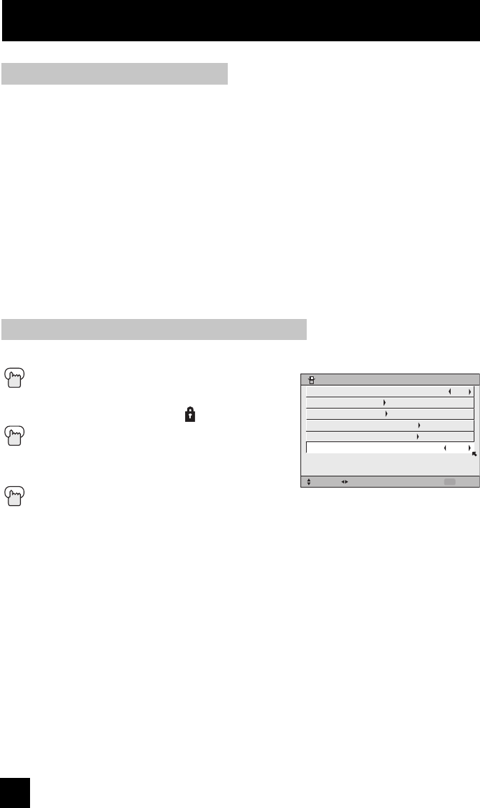
38
You can block programs that are not rated.
Press the MENU button
π†
To V-CHIP
è
To operate (The lock icon appears)
Press ZERO to access V-Chip setup options
π†
To UNRATED
è
To VIEW or BLOCK
Press MENU when done
Directions to Block Unrated Programs
Unrated Programs
Unrated programming refers to any programming which does not contain a rating signal.
Programming on television stations which do not broadcast rating signals will be placed in the
“Unrated Programming” category.
Examples of Unrated programs:
• Emergency Bulletins • Locally Originated Programming
• News • Political Programs
• Public Service Announcements • Religious Programs
• Sports • Weather
• Some Commercials
Note:
• TV programs or movies that do not have rating signals will be blocked if the unrated category
is set to BLOCK.
V-CHIP
SET US TV RATINGS
SET MOVIE RATINGS
SET CANADIAN RATINGS ENG
SET CANADIAN RATINGS FRE
UNRATED
V-CHIP
SELECT OPERATE EXIT
MENU
VIEW
OFF
Onscreen Menus
LCT2170 Eng.indd 38LCT2170 Eng.indd 38 8/4/06 10:27:01 AM8/4/06 10:27:01 AM

39
U.S. PARENTAL RATING SYSTEMS
Programs with the following ratings are appropriate for children.
❒ TV Y is Appropriate for All Children
Programs are created for very young viewers and should be suitable for all ages, including
children ages 2 - 6.
❒ TV Y7 is for Older Children
Most parents would find such programs suitable for children 7 and above. These programs
may contain some mild fantasy violence or comedic violence, which children should be able
to discern from reality.
Programs with the following ratings are designed for the entire audience.
❒ TV G stands for General Audience
Most parents would find these programs suitable for all age groups. They contain little or no
violence, no strong language, and little or no sexual dialog or situations.
❒ TV PG Parental Guidance Suggested
May contain some, but not much, strong language, limited violence, and some suggestive
sexual dialog or situations. It is recommended that parents watch these programs first, or
with their children.
❒ TV 14 Parents Strongly Cautioned
Programs contain some material that may be unsuitable for children under the age of 14
including possible intense violence, sexual situations, strong coarse language, or intensely
suggestive dialog. Parents are cautioned against unattended viewing by children under 14.
❒ TV MA Mature Audiences Only
These programs are specifically for adults and may be unsuitable for anyone under 17
years of age. TV MA programs may have extensive V, S, L, or D.
US V-Chip Ratings
Viewing Guidelines
In addition to the ratings categories explained above, information on specific kinds of content
are also supplied with the V-Chip rating. These types of content may also be blocked. The
content types are:
• V/FV is for VIOLENCE/FANTASY VIOLENCE
• S stands for SEXUAL CONTENT
• L stands for strong LANGUAGE
• D stands for suggestive DIALOG
Onscreen Menus
LCT2170 Eng.indd 39LCT2170 Eng.indd 39 8/4/06 10:27:01 AM8/4/06 10:27:01 AM
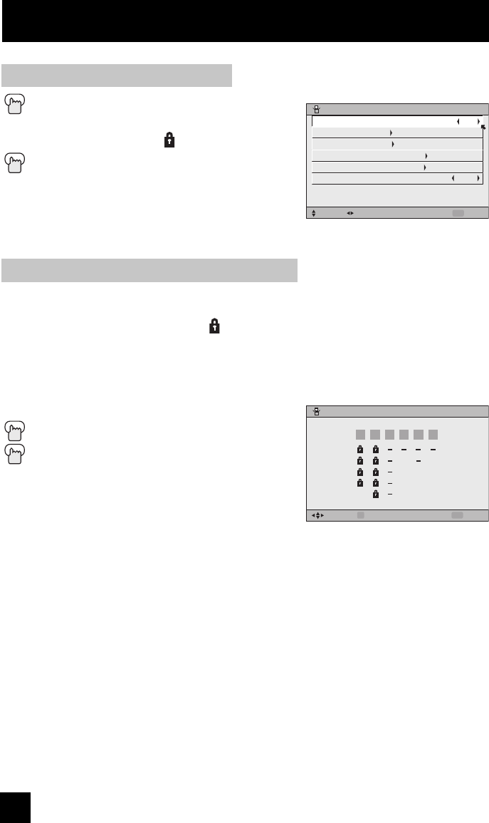
40
Line up the cursor in the column (TV PG, TV G, etc.) with the content row (V/FV, S, etc.) and
press the
π†
or
è
to move the cursor to the correct location. Press OK to turn the locking
feature on or off. An item is locked if the icon appears instead of a “—”.
For example. To block viewing of all TV 14 shows, move the cursor to the top row of that
column and add a lock icon. Once you’ve put a lock on the top row, everything in that column
is automatically locked.
π†
è
To the TV 14 Column
Press the OK button to lock
Press the MENU button when finished
Note:
• If you want to change the setup, move the cursor to
the top column and change the lock icon to “—” by
pressing OK again. You may then select individual
categories to block.
Directions to set US V-Chip Ratings
Press the MENU button
π†
To V-CHIP
è
To operate (lock icon appears)
Press ZERO to access the V-Chip menu
è
To turn V-Chip ON or OFF
π†
To move to SET US TV RATINGS
è
To operate
Setting US V-Chip Ratings
V/FV
S
L
D
SET US TV RATINGS
SELECT OPERATE EXIT
MENU
TV
MA TV
14 TV
PG TV
GTV
Y7 TV
Y
OK
V-CHIP
SET US TV RATINGS
SET MOVIE RATINGS
SET CANADIAN RATINGS ENG
SET CANADIAN RATINGS FRE
UNRATED
V-CHIP
SELECT OPERATE EXIT
MENU
VIEW
OFF
Onscreen Menus
LCT2170 Eng.indd 40LCT2170 Eng.indd 40 8/4/06 10:27:01 AM8/4/06 10:27:01 AM
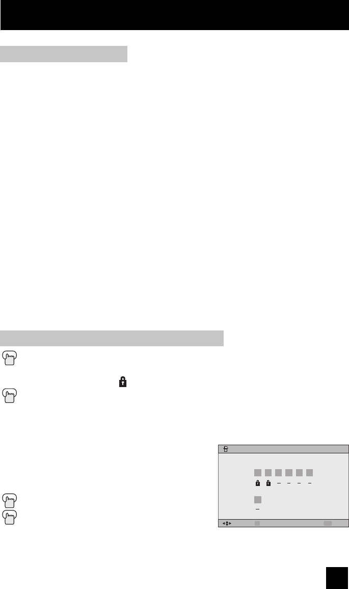
41
❒ NR – Not Rated
This is a film which has no rating. In many cases these films were imported from countries
which do not use the MPAA ratings system. Other NR films may be from amateur producers
who didn’t intend to have their film widely released.
NR (Not Rated) Programming may contain all types of programming including children’s
programming, foreign programs, or adult material.
❒ G – General Audience
In the opinion of the review board, these films contain nothing in the way of sexual content,
violence, or language that would be unsuitable for audiences of any age.
❒ PG – Parental Guidance
Parental Guidance means the movie may contain some contents such as mild violence,
some brief nudity, and strong language. The contents are not deemed intense.
❒ PG-13 – Parents Strongly Cautioned
Parents with children under 13 are cautioned that the content of movies with this rating may
include more explicit sexual, language, and violence content than movies rated PG.
❒ R – Restricted
These films contain material that is explicit in nature and is not recommended for
unsupervised children under the age of 17.
❒ NC-17 – No One Under 17
These movies contain content which most parents would feel is too adult for their children
to view. Content can consist of strong language, nudity, violence, and suggestive or explicit
subject matter.
❒ X – No One under 18
Inappropriate material for anyone under 18.
Movies Ratings
Press the MENU button
π†
To V-CHIP
è
To operate (Lock icon appears)
Press ZERO to access V-Chip setup options
π†
To SET MOVIE RATINGS
è
To enter movies menu
For example: To block viewing of programming rated
NC-17 shows, move the cursor to the NC-17 column and
add a lock icon. Once you've put a lock on the NC-17
column, X column is automatically locked.
π†
è
To the NC-17 Column
Press the OK button to lock
Press the MENU button to finish
• If you want to change the setup, move the cursor to the
column and change the lock icon to “—” by pressing OK again.
Directions to set Movie (MPAA) Ratings
SET MOVIE RATINGS
SELECT OPERATE EXIT
MENU
X
NC
17
R
PG
G
PG
13
NR
OK
Onscreen Menus
LCT2170 Eng.indd 41LCT2170 Eng.indd 41 8/4/06 10:27:02 AM8/4/06 10:27:02 AM
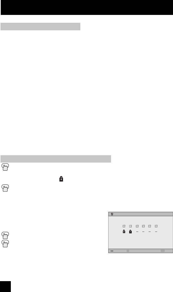
42
Press the MENU button
π†
To V-CHIP
è
To operate (lock icon appears)
Press ZERO to access V-Chip setup options
π†
To SET CANADIAN RATINGS ENG (for English)
è
To enter ratings menu
For example: To block viewing of programming rated 14+ shows, move the cursor to the 14+
column and add a lock icon. Once you've put a lock
on the 14+ column, 18+ column is automatically
locked.
è
To the 14+ Column
Press the OK button to lock
Press the MENU button to finish
Notes:
• If you want to change the setup, move the cursor
to the column and change the lock icon to “—” by pressing OK again.
• For instructions on “SET CANADIAN RATINGS FRE (in French)”, please see page 42 in the
French side of this user’s guide.
Directions to set Canadian V-Chip Ratings
❒ E – Exempt
Exempt programming includes: news, sports, documentaries and other information
programming, talk shows, music videos, and variety programming.
❒ C – Programming Intended for Children
Violence Guidelines: There will be no realistic scenes of violence. Depictions of aggressive
behavior will be infrequent and limited to portrayals that are clearly imaginary, comedic or
unrealistic in nature.
❒ C8+ – Programming Intended for Children 8 and Over
Violence Guidelines: Any realistic depictions of violence will be infrequent, discreet, of low
intensity and will show the consequences of the acts. There will be no offensive language,
nudity or sexual content.
❒ G – General Audience
Programming will contain little violence and will be sensitive to themes which could affect
younger children.
❒ PG – Parental Guidance
Programming intended for a general audience, but which may not be suitable for younger
children. Parents may consider some content not appropriate for children aged 8-13.
❒ 14+ – 14 Years and Older
Parents are strongly cautioned to exercise discretion in permitting viewing by pre-teens and
early teens. Programming may contain mature themes and scenes of intense violence.
❒ 18+ – Adult
Material intended for mature audiences only.
Canadian V-Chip Ratings
14+
18+ PG
GC
C8
SET CANADIAN RATINGS ENG
SELECT OPERATE EXIT
MENU
OK
Onscreen Menus
LCT2170 Eng.indd 42LCT2170 Eng.indd 42 8/4/06 10:27:02 AM8/4/06 10:27:02 AM
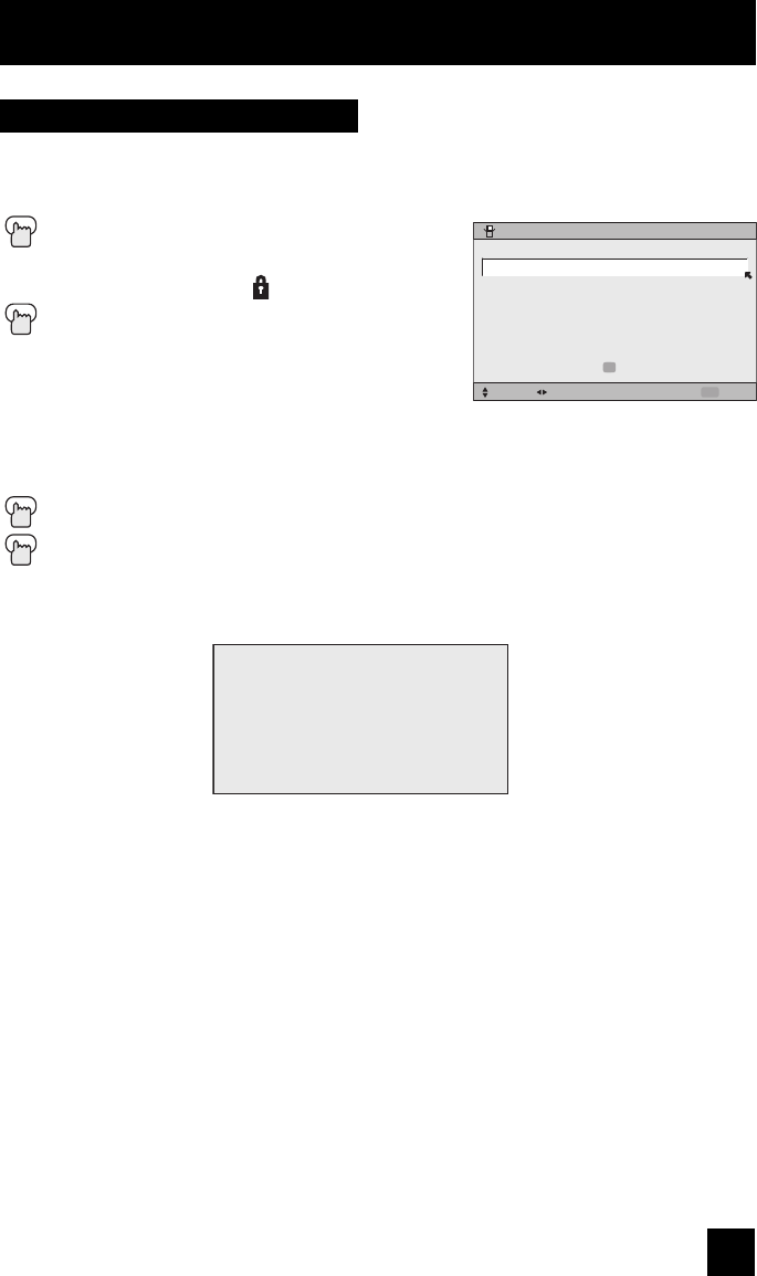
43
Channel guard and V-Chip settings are protected by a four-digit lock code. Your TV comes
preset with a lock code of “0000”. You may change the code to any four-digit number you wish.
To change the lock code, follow the steps below.
Press the MENU button
π†
To SET LOCK CODE
è
To operate (lock icon appears)
Press ZERO to access the lock code
The first digit will be highlighted
è
To select the number
π†
To move to the next digit
Continue to follow these directions for all four numbers
Press the OK button to finish (your lock code is now set)
Press the Menu button when finished
• After a power interruption you must reset the lock code.
• Write your lock code number down and keep it hidden from potential viewers.
• If you forget the lock code, a new code may be set using the steps listed above.
Notes:
When a viewer attempts to watch a blocked channel, this message appears:
The channel will remain blocked until the correct lock code is entered (see above for
information on setting your lock code).
Set Lock Code
LOCK CODE
SET LOCK CODE
SELECT OPERATE EXIT
MENU
PRESS TO FINISH
0000
OK
THIS PROGRAMMING EXCEEDS
YOUR RATING LIMITS.
PLEASE ENTER LOCK CODE BY
10 KEY PAD TO UNLOCK IT.
NO. - - - -
Onscreen Menus
LCT2170 Eng.indd 43LCT2170 Eng.indd 43 8/4/06 10:27:03 AM8/4/06 10:27:03 AM
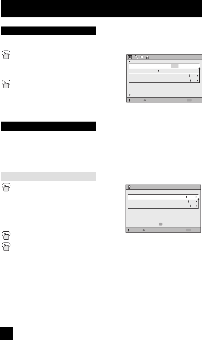
44
The language function is described on page 24 as the interactive plug-in menu. If you need to
choose the language again, follow the steps below.
Press the Menu button
π†
To LANGUAGE
è
To choose a language: ENG. (English),
FRAN. (French) or ESP. (Spanish)
Press the MENU button when finished
Language
INITIAL SETUP
SELECT OPERATE EXIT
MENU
NEXT PAGE
PREVIOUS
ENG. FRAN. ESP.
LANGUAGE
CLOSED CAPTION
AUTO SHUT OFF
XDS ID
OFF
ON
(3/5)
Press the MENU button
π†
To CLOSED CAPTION
è
To enter
π†
To MODE
è
To select CAPTION or TEXT in MODE
π†
To CAPTION or TEXT
è
To select a caption (CC1 to CC4) or text
channel (T1 to T4)
Press the OK button to save
Press the MENU button when finished
Many broadcasts now include an onscreen display of dialog called closed captions. Some
broadcasts may also include displays of additional information in text form. Your television can
access and display this information using the closed caption feature. To activate the closed
caption feature, follow the steps below. There are three methods. When you are watching
analog channels, you can perform Analog Setting of closed caption. When you are watching
digital channels, you can perform Digital Auto Setting or Digital Manual Setting.
Closed Caption
Analog Setting
CLOSED CAPTION
SELECT OPERATE EXIT
MENU
PRESS TO FINISH
OK
TEXTMODE
CAPTION
TEXT
CC1
T1
Onscreen Menus
LCT2170 Eng.indd 44LCT2170 Eng.indd 44 8/4/06 10:27:03 AM8/4/06 10:27:03 AM
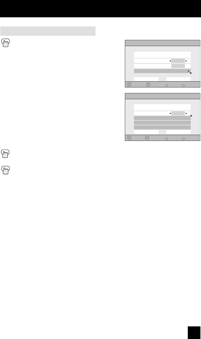
45
Digital Auto Setting
Press the MENU button
π†
To CLOSED CAPTION
è
To enter
π†
To Type
è
To select Auto, Advanced or Basic
Auto: Shows closed caption a priority for
digital channels over analog channels. It is
set automatically.
Advanced: Shows only the digital closed
caption.
Basic: Shows only the analog closed
caption.
π†
To Service
è
To select 1, 2, 3, 4, 5 or 6
π†
To Appearance
è
To enter
è
To select Auto
π†
To Set
Press the OK button to save
The font/type and color are set automatically.
Press the MENU button when finished
Note:
• If you want to cancel the settings, select cancel.
Digital Closed Caption
Preview
Select Back
BACK
Exit
MENU
Operate
Closed Caption Sample
1
Cancel Set
AUTO
Type
Service
Appearance
Digital Closed Caption > Appearance
Preview
Select Back
BACK
Exit
MENU
Closed Caption Sample
Auto
Cancel Set
Appearance Mode
Font
Colors
Opacities
Operate
Onscreen Menus
LCT2170 Eng.indd 45LCT2170 Eng.indd 45 8/4/06 10:27:03 AM8/4/06 10:27:03 AM
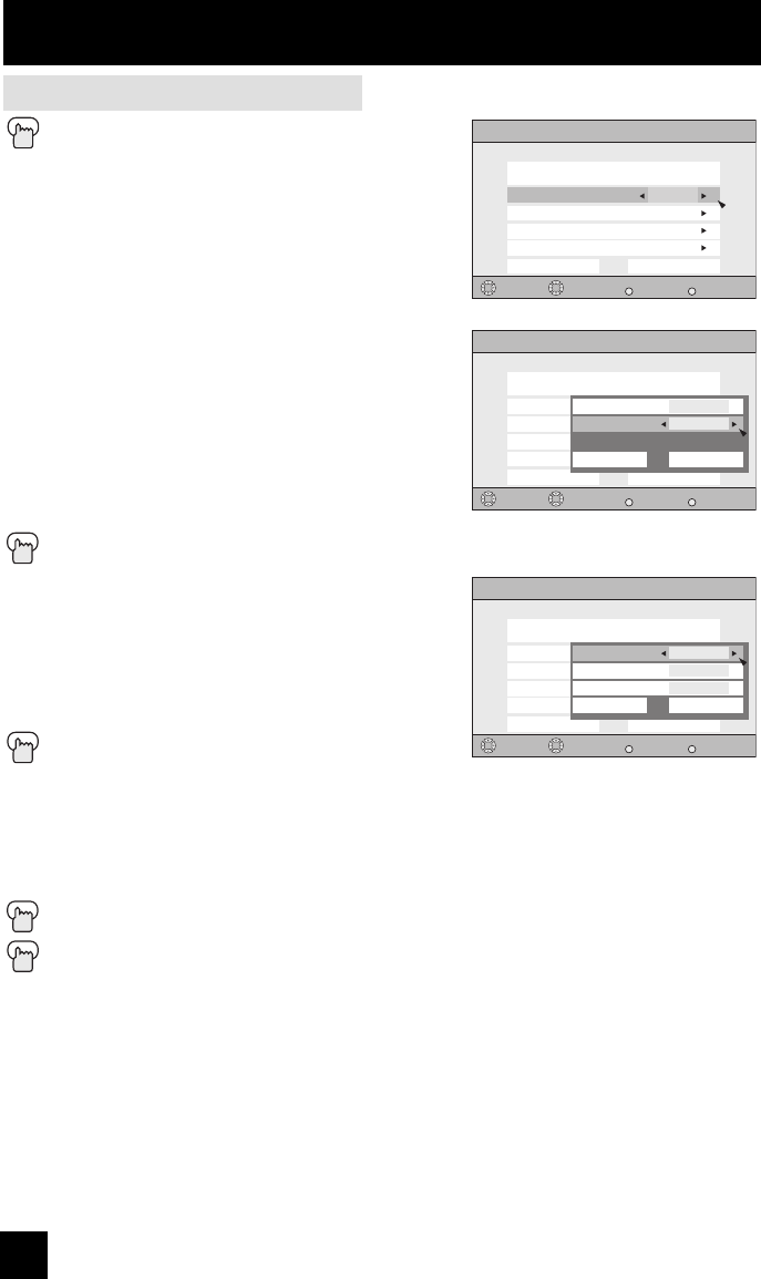
46
• Closed caption subtitles are usually found on closed caption channel CC1. Some programs may
include additional text information which is usually found on text channel T1. The other channels
are available for future use.
• Closed captioning may not work correctly if the signal being received is weak or if you are playing
a video tape.
• Most broadcasts containing closed captioning will display a notice at the start of the program.
• To select the mode, press the C.C. button. See page 69.
• When ZOOM aspects like PANORAMA or CINEMA are selected, Digital Closed Captions may be
cut off or distorted.
Notes:
Press the MENU button
π†
To CLOSED CAPTION
è
To enter
π†
To Type
è
To select Auto, Advanced or Basic
π†
To Service
è
To select 1, 2, 3, 4, 5 or 6
π†
To Appearance
è
To enter
è
To select Manual
π†
To Font
è
To enter
π†
To select Font Size or Font Style
è
To select the setting you like
Font Size: Auto, Standard, Large or Small
Font Style: Auto, Serif Mono, Serif, Sanserif mono,
Sanserif, Casual, Cursive or Small Capital
π†
To Set
Press the OK button to save
π†
To Colors
è
To enter
π†
To select Text, Edge or Background
è
To select the setting you like
Auto, White, Black, Red, Green, Blue,
Yellow, Magenta or Cyan
π†
To Set
Press the OK button to save
π†
To Opacities
è
To enter
π†
To select Text/Edge or Background
è
To select Auto, Transparent, Translucent, Solid
or Flashing
π†
To Set
Press the OK button to save
Press the MENU button when finished
Digital Manual Setting
Digital Closed Caption > Appearance
Preview
Select Back
BACK
Exit
MENU
Closed Caption Sample
Manual
Cancel Set
Appearance Mode
Font
Colors
Opacities
Operate
Digital Closed Caption > Appearance
Preview
Select Back
BACK
Exit
MENU
Closed Caption Sample
Manual
Cancel Set
Appearance Mode
Font
Colors
Opacities
Operate
Cancel Set
Standard
Auto
Font Size
Font Style
Digital Closed Caption > Appearance
Preview
Select Back
BACK
Exit
MENU
Closed Caption Sample
Manual
Cancel Set
Appearance Mode
Font
Colors
Opacities
Operate
Cancel Set
Text
Edge
Background
White
White
Black
All fonts used for digital closed
caption and digital menus are
licensed from Monotype Imaging
Inc.
Onscreen Menus
LCT2170 Eng.indd 46LCT2170 Eng.indd 46 8/4/06 10:27:04 AM8/4/06 10:27:04 AM
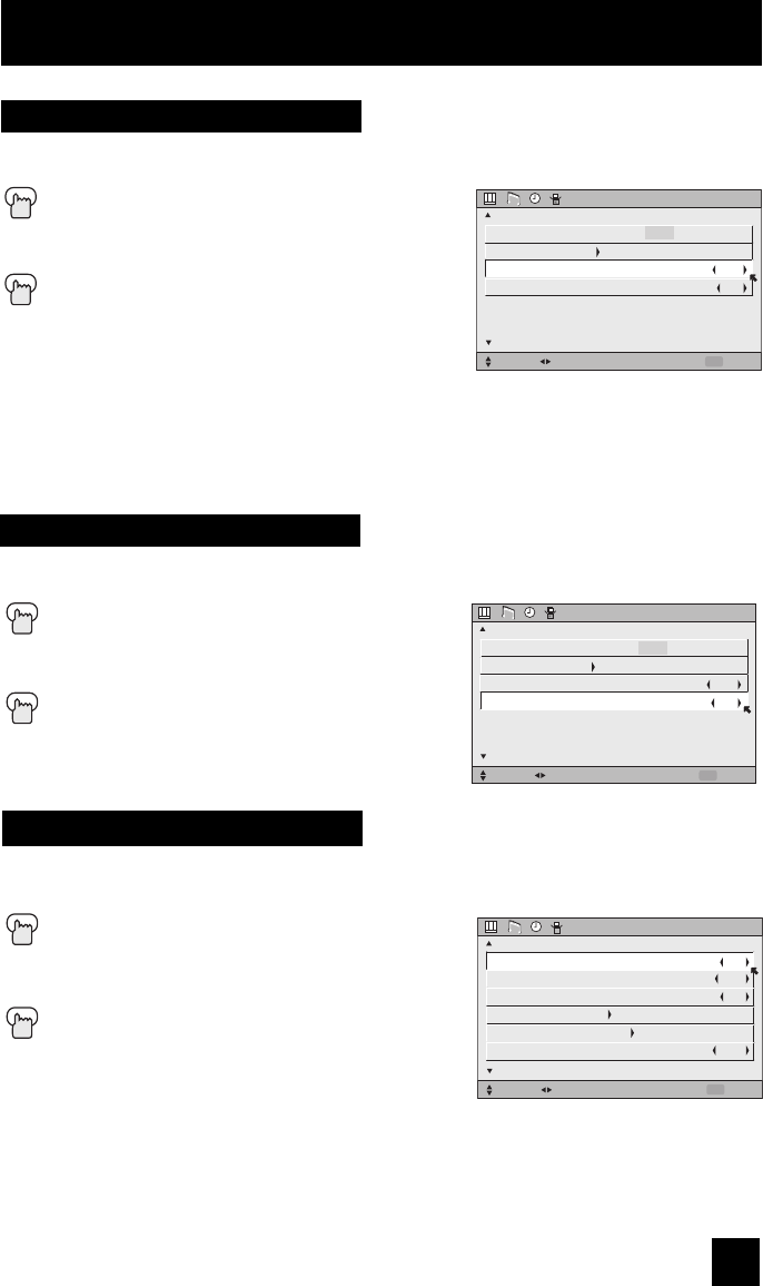
47
This function automatically shuts off your TV when there is no signal from the channel the
TV is on.
Press the MENU button
π†
To AUTO SHUT OFF
è
To turn ON or OFF
Press the MENU button when finished
• If the channel that you have on does not receive a
signal for more than one minute, the blinking text
“NOT RECEIVING A SIGNAL AUTO SHUT OFF
IN 9 MIN.” appears on the screen, and starts the
countdown. If no signal is being received within 10
minutes, the TV shuts itself off.
Auto Shut Off
INITIAL SETUP
SELECT OPERATE EXIT
MENU
NEXT PAGE
PREVIOUS
(3/5)
ENG. FRAN. ESP.
LANGUAGE
CLOSED CAPTION
AUTO SHUT OFF
XDS ID
OFF
ON
XDS ID Display provides a channel’s call letters, the network’s name, and even a program
name. The XDS ID information is provided by the broadcaster.
Press the MENU button
π†
To XDS ID
è
To turn ON or OFF
Press the MENU button when finished
XDS ID
INITIAL SETUP
SELECT OPERATE EXIT
MENU
NEXT PAGE
PREVIOUS
(3/5)
ENG. FRAN. ESP.
LANGUAGE
CLOSED CAPTION
AUTO SHUT OFF
XDS ID
OFF
ON
This feature inserts a blank gray screen over channels which are not broadcasting or are too
weak to be received clearly.
Press the MENU button
π†
To NOISE MUTING
è
To turn noise muting ON or OFF
Press the MENU button when finished
Notes:
• Noise muting will not work during auto tuner setup or
when you operate channel summary.
• Noise muting will not work when the digital TV is displayed.
ON
OFF
ON
INITIAL SETUP
SELECT OPERATE EXIT
MENU
NEXT PAGE
PREVIOUS
(2/5)
NOISE MUTING
FRONT PANEL LOCK
V1 SMART INPUT
VIDEO INPUT LABEL
POSITION ADJUSTMENT
POWER INDICATOR OFF
Noise Muting
Onscreen Menus
LCT2170 Eng.indd 47LCT2170 Eng.indd 47 8/4/06 10:27:04 AM8/4/06 10:27:04 AM
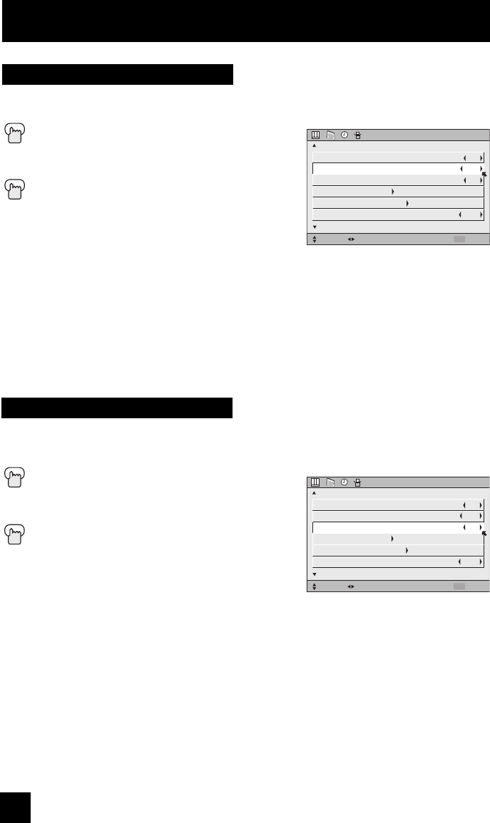
48
This allows you to lock the keys on the side of the TV, so that a child may not accidentally
change your viewing preferences.
Press the MENU button
π†
To FRONT PANEL LOCK
è
To turn ON or OFF
Press the MENU button when finished
Front Panel Lock
You can turn off this feature in the following ways:
• Unplug the power cord, and plug it back in. Do this if
your batteries die, or you lose your remote control.
• Use the remote control.
• Press the MENU button on the side of the TV for more than 3 seconds. In this case, the OSD
for FRONT PANEL LOCK will appear.
Note:
• To turn ON/OFF the TV, press the power button for more than 3 seconds. This feature will
remain ON.
INITIAL SETUP
SELECT OPERATE EXIT
MENU
NEXT PAGE
PREVIOUS
(2/5)
ON
OFF
ON
NOISE MUTING
FRONT PANEL LOCK
V1 SMART INPUT
VIDEO INPUT LABEL
POSITION ADJUSTMENT
POWER INDICATOR OFF
This feature is used if you have connected an AV Receiver to your television. By turning this
feature on, your television can automatically detect the signal source from your components
that are connected to your AV Receiver.
Press the MENU button
π†
To V1 SMART INPUT
è
To turn ON or OFF
Press the MENU button when finished
Notes:
• If you do not have an AV Receiver connected to your
television, turn this feature OFF.
• Some AV Receivers may not work with this function.
V1 Smart Input
INITIAL SETUP
SELECT OPERATE EXIT
MENU
NEXT PAGE
PREVIOUS
(2/5)
ON
OFF
ON
NOISE MUTING
FRONT PANEL LOCK
V1 SMART INPUT
VIDEO INPUT LABEL
POSITION ADJUSTMENT
POWER INDICATOR OFF
Onscreen Menus
LCT2170 Eng.indd 48LCT2170 Eng.indd 48 8/4/06 10:27:05 AM8/4/06 10:27:05 AM
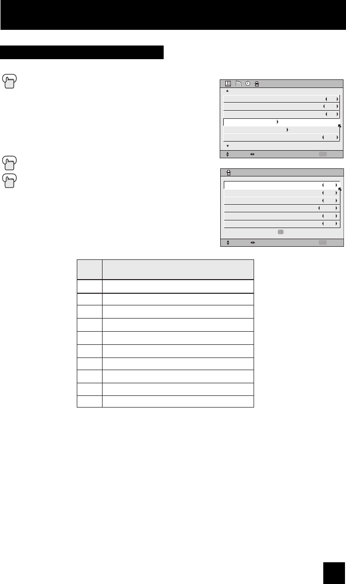
49
This function is used to label video input connections for the onscreen displays.
Press the MENU button
π†
To VIDEO INPUT LABEL
è
To enter
π†
To select the desired video input
è
To select the desired preset input label (see
chart below)
Press the OK button to save
Press the MENU button when finished
Note:
• Though VIDEO-3 is for use only with a PC, you still
can select your desired input label.
INITIAL SETUP
SELECT OPERATE EXIT
MENU
NEXT PAGE
PREVIOUS
(2/5)
ON
OFF
ON
NOISE MUTING
FRONT PANEL LOCK
V1 SMART INPUT
VIDEO INPUT LABEL
POSITION ADJUSTMENT
POWER INDICATOR OFF
Video Input Label
Preset
Labels
VCR
DVD
PVR
DVHS
STB
SAT
AMP
GAME
CAM
DISC
You have a VCR connected to the video input
You have a DVD connected to the video input
You have a Personal Video recorder connected to the video input
You have a Digital VCR connected to the video input
You have a Set-top Box connected to the video input
You have a Satellite Receiver connected to the video input
You have an Amplifier connected to the video input
You have a Video Game connected to the video input
You have a Video Camera connected to the video input
You have a Video Disc player connected to the video input
Select when...
VIDEO INPUT LABEL
SELECT OPERATE EXIT
MENU
PRESS TO FINISH
OK
VCR
DVD
SAT
GAME
STB
DVD
VIDEO-1
VIDEO-2
VIDEO-3
VIDEO-4
DIGITAL-IN1
DIGITAL-IN2
Onscreen Menus
LCT2170 Eng.indd 49LCT2170 Eng.indd 49 8/4/06 10:27:05 AM8/4/06 10:27:05 AM
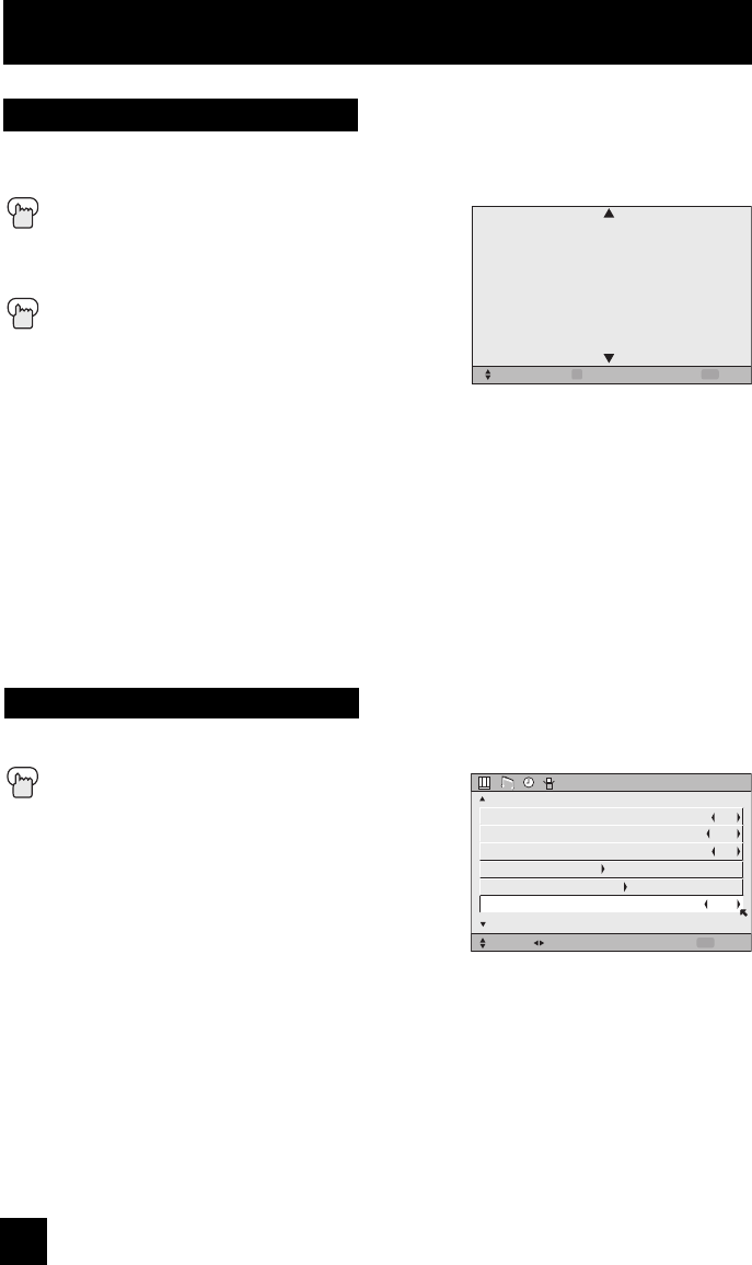
50
Position adjustment allows you to adjust the position of the picture on the screen vertically
when the aspect is set to panorama or cinema.
Press the MENU button
π†
To POSITION ADJUSTMENT
è
To enter
π†
è
To adjust the position
Press the MENU button to finish
Notes:
• To reset the adjustment to the center, press the
OK button.
• When the arrow disappears, while you are adjusting the position, the position is at its
maximum limit.
• If you select REGULAR, SLIM and FULL size with aspect or Multi Screen, position
adjustment option is not seen.
• When you change the screen size, perform the position adjustment again.
• Position adjustment allows you to adjust the screen position vertically and horizontally when
the aspect is set Panorama Zoom or Cinema Zoom for 1080i and 720p signals.
• It is also possible to use Position Adjustment when you are in PC Mode
• When you are receiving a 1080p signal, Position Adjustment can not be selected.
Position Adjustment
OPERATE RESET EXIT
OK MENU
Power indicator allows you to adjust the brightness of the power indicator
Press the MENU button
π†
To POWER INDICATOR
è
To adjust POWER INDICATOR LOW, HIGH
or OFF
Notes :
• When OFF is selected :
The LED disappears if you have a TV signal.
The LED is lit as “LOW” when there is no TV signal.
• When the On Timer turns ON, the LED is lit as
"LOW" when you turn the power off.
• If you set a timer on the TV, the power indicator will light even if the TV is on stand by.
Power Indicator
INITIAL SETUP
SELECT OPERATE EXIT
MENU
NEXT PAGE
PREVIOUS
(2/5)
ON
OFF
ON
NOISE MUTING
FRONT PANEL LOCK
V1 SMART INPUT
VIDEO INPUT LABEL
POSITION ADJUSTMENT
POWER INDICATOR OFF
Onscreen Menus
LCT2170 Eng.indd 50LCT2170 Eng.indd 50 8/4/06 10:27:05 AM8/4/06 10:27:05 AM
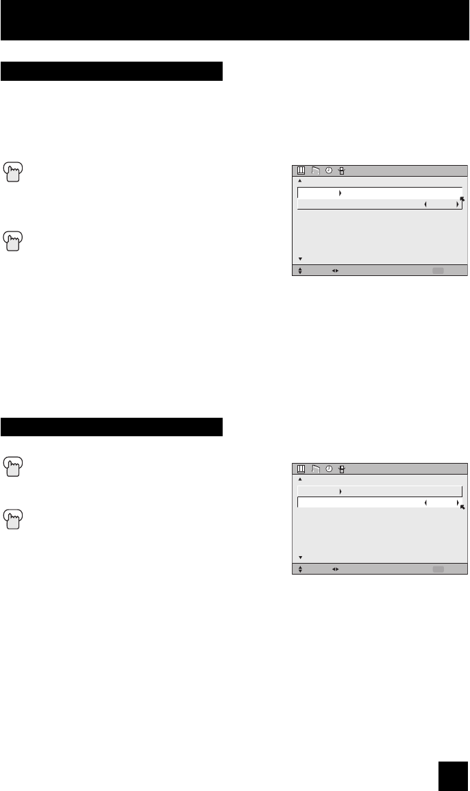
51
This feature is used if you have a DTV or HDMI compatible component connected to your TV.
Press the MENU button
π†
To DIGITAL-IN1 AUDIO
è
To select ANALOG, DIGITAL or AUTO
Press the Menu button when fi nished
Notes:
• If your DTV or HDMI component is capable of digital
audio and video, choose DIGITAL. If your DTV or HDMI
component is capable of analog audio and digital video, choose ANALOG.
• Refer to your DTV or HDMI component’s instruction manual for more information.
• When you select AUTO, the television will select "ANALOG" or "DIGITAL" automatically,
depending on the audio input from the HDMI.
• When you select DIGITAL, select PCM on Digital Sound in the Digital Setup menu. See page
53.
INITIAL SETUP
SELECT OPERATE EXIT
MENU
NEXT PAGE
PREVIOUS
(1/5)
DIGITAL-IN
DIGITAL-IN1 AUDIO
AUTO
DIGITAL
The DIGITAL-IN option can only be displayed in the INITIAL SETUP menu when an HDMI480p
picture signal is being input to the DIGITAL-IN terminal. This option adjusts the position when
an HDMI or DVI 480p picture signal is being displayed on the screen. There are two types of
HDMI480p picture signals: 640x480 and 720x480. If the displayed picture is slightly shifted, the
position can be adjusted by selecting either SIZE1 or SIZE2.
Press the MENU button
π†
To DIGITAL-IN
è
To enter
π†
To select AUTO, SIZE1 or SIZE2
Press the MENU button to finish
Digital-In
Digital-In1 Audio
INITIAL SETUP
SELECT OPERATE EXIT
MENU
NEXT PAGE
PREVIOUS
(1/5)
DIGITAL-IN
DIGITAL-IN1 AUDIO
AUTO
DIGITAL
Notes:
• The DIGITAL-IN menu can only be displayed when a HDMI or DVI 480p picture signal is
input to the Digital-In terminal and the picture is being displayed on the screen.
• You can select AUTO only when the signal is 480p for HDMI. When you select AUTO, the
televison will select "SIZE1" or "SIZE2" automatically.
Onscreen Menus
LCT2170 Eng.indd 51LCT2170 Eng.indd 51 8/4/06 10:27:06 AM8/4/06 10:27:06 AM
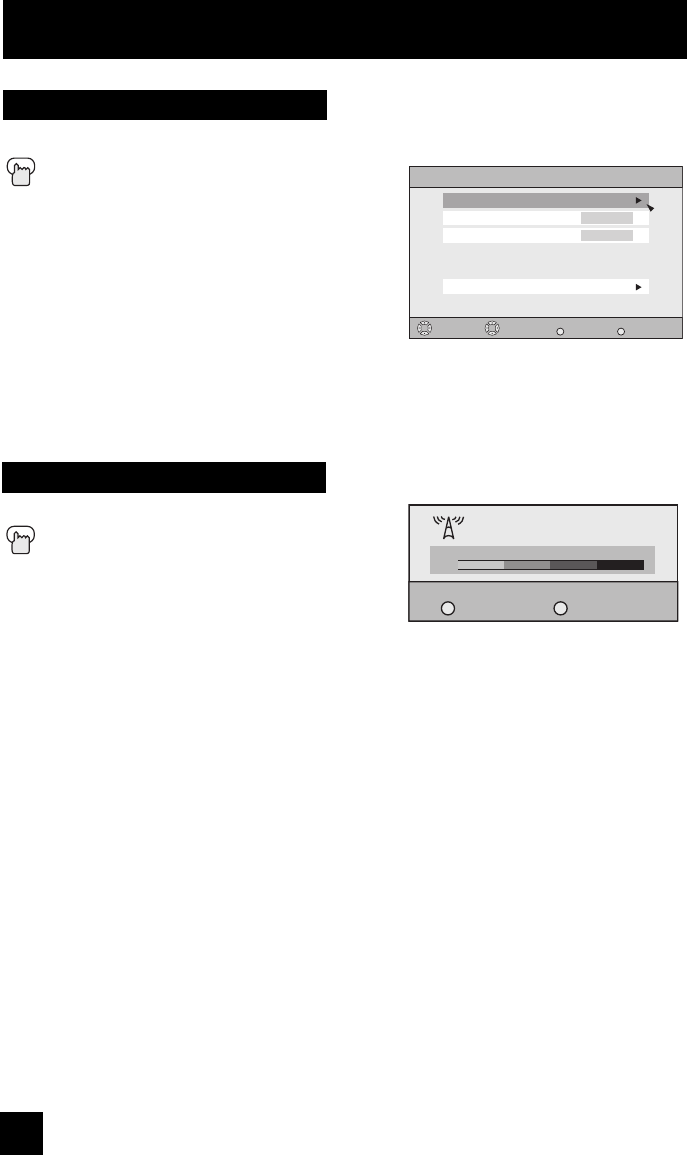
52
Onscreen Menus
Use this function when you are receiving a digital broadcast.
Press the MENU button
π†
To DIGITAL SETUP
è
To enter
The onscreen will appear
Notes:
• Software Update will only appear when the USB
memory is inserted into the USB connector.
• If you are watching an analog channel, you can still
access the digital setup menu at anytime, while you are doing this, the background screen
will turn blank. In this case, the tuner will switch to digital, since you are accessing the digital
setup menu.
Digital Setup
Select Back
BACK Exit
MENU
Operate
PCM
4:3
Antenna Level
Digital Sound
Aspect Ratio
Software Update
Digital Setup
Confirms the present antenna level.
Press the MENU button
π†
To DIGITAL SETUP
è
To enter
π†
To Antenna Level
è
To enter
Note:
• If you are watching an analog channel, antenna level will not appear.
Antenna Level
Back
BACK
Exit
MENU
75
Antenna Level
LCT2170 Eng.indd 52LCT2170 Eng.indd 52 8/4/06 10:27:06 AM8/4/06 10:27:06 AM
53
Onscreen Menus
Aspect Ratio
You can select the aspect mode for ATSC from 4:3 or 16:9.
Press the MENU button
π†
To DIGITAL SETUP
è
To enter
π†
To Aspect Ratio
è
To select 4:3 or 16:9
Press the MENU button when finished
Notes:
• Set the mode to 4:3 or 16:9 before you record a program using the ATSC MONITOR OUT.
• Make sure the mode you choose is the same as the TV’s aspect ratio when the recorded
program is played back, so that you can obtain a good picture quality, free from any unatural
distortions.
Digital Sound
Manufactured under license from Dolby Laboratories. "Dolby", and
the double-D symbol are trademarks of Dolby Laboratories.
You can select the optical digital sound output, either PCM or Dolby Digital when your TV is
connected to an amplifier that has Dolby Digital decoder. If you select Dolby Digital, you can
enjoy listening in 5.1ch sound when watching digital broadcasts.
Press the MENU button
π†
To DIGITAL SETUP
è
To enter
π†
To Digital Sound
è
To select PCM or DOLBY DIGITAL
Press the MENU button when finished
Notes:
• If your amplifier does not have Dolby Digital decoder, select PCM. If you don't select PCM, it
cannot output the sound from the speakers.
• For connecting an amplifier using the optical output, see page 18.
LCT2170 Eng.indd 53LCT2170 Eng.indd 53 8/4/06 10:27:06 AM8/4/06 10:27:06 AM

54
Onscreen Menus
At first, connect the USB memory into the USB connector. This function will appear only when
the USB memory is inserted into the USB connector.
Press the MENU button
π†
To DIGITAL SETUP
è
To enter
π†
To Software Update
è
To enter
π†
Checks the card if it needs an update or not
Press the MENU button when finished
Software Update
LCT2170 Eng.indd 54LCT2170 Eng.indd 54 8/4/06 10:27:07 AM8/4/06 10:27:07 AM
55
Press the MENU button
π†
To TINT, COLOR, PICTURE, BRIGHT or
DETAIL
√ ®
To enter
√ ®
To adjust the setting
π†
To move to the next setting
Press the MENU button when finished
Note:
• There are four video status settings: Dynamic, Standard, Theater and Game. Each video
status setting has a separate memory for HD (1080i/1080p/720p) and SD (480p/480i) video
signal. Each video status can be chosen along with your favorite picture settings (Tint,
Color, Picture, Bright, Detail, etc.) See page 67 for details.
These settings allow you to change and adjust the way the picture appears on your television.
TINT
Tint allows you to adjust the levels of red and green in your TV picture.
COLOR
The color function lets you make all the colors in the TV picture appear either more vivid or
subtle.
PICTURE
Picture allows you to adjust the levels of black and white on the TV screen, giving you a darker
or brighter picture overall.
BRIGHT
You can adjust the overall brightness of the TV picture with the Bright control.
DETAIL
The Detail feature adjusts the level of fine detail displayed in the picture.
Picture Settings
Adjust the Picture Settings
Color Temperature
You can decide how strong or dull the colors appear on the TV screen.
Press the MENU button
π†
To COLOR TEMPERATURE
è
To enter
π†
To set LOW or HIGH
Press the MENU button when finished
TINT +02
PICTURE ADJUST
SELECT OPERATE EXIT
MENU
NEXT PAGE
PREVIOUS STANDARD
(1/3)
TINT
COLOR
PICTURE
BRIGHT
DETAIL
00
00
00
00
00
COLOR TEMPERATURE
LOW
HIGH
Onscreen Menus
LCT2170 Eng.indd 55LCT2170 Eng.indd 55 8/4/06 10:27:07 AM8/4/06 10:27:07 AM
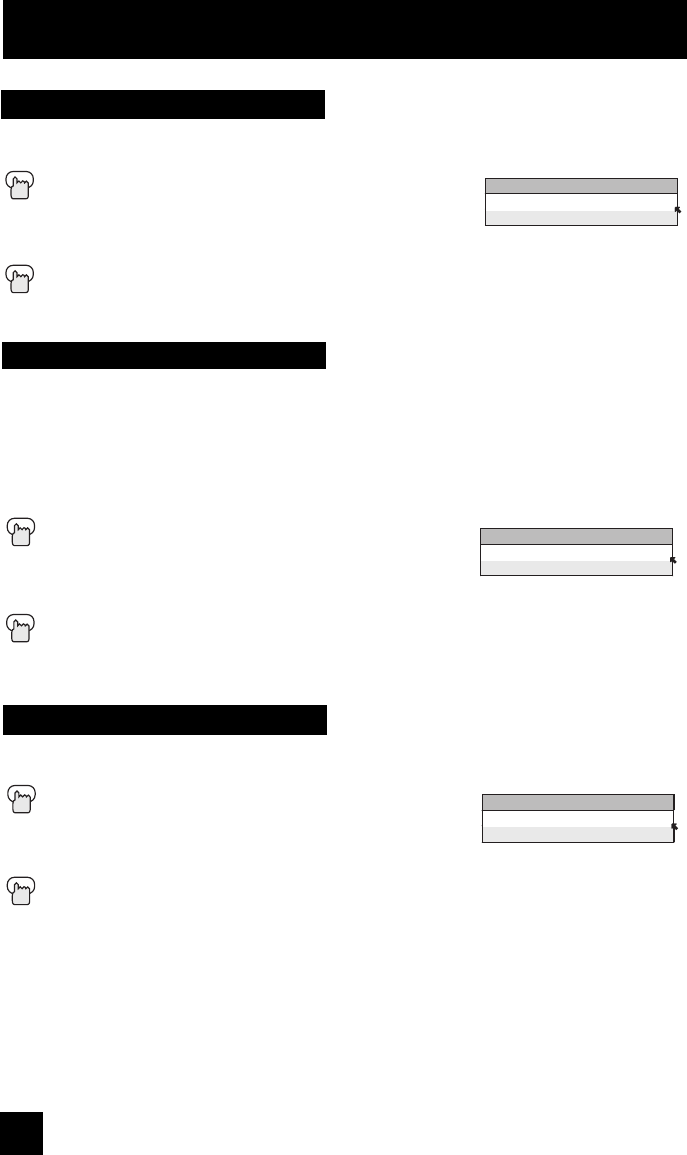
56
Color Management
This TV supports the COLOR MANAGEMENT function to ensure dull colors are compensated
to produce natural hues.
Press the MENU button
π†
To COLOR MANAGEMENT
è
To enter
π†
To select the mode “ON" or "OFF"
Press the MENU button when finished
COLOR MANAGEMENT
ON
OFF
Dynamic Gamma
JVC's Dynamic Gamma Circuitry (DGC) makes it easier to see dark areas when a picture
has many dark areas, and makes it easier to see the bright areas when a picture has many
bright areas. DGC is turned on, DGC analyzes and adjusts the total level of picture brightness
balance, especially in dark areas where the level of grayscale is often lost, turning completely
to black DGC automatically enhances the detail in these dark areas providing a more dynamic
image with fi ner detail, so the optimum picture settings are automatically set for each picture.
Normally use with DGC on.
Press the MENU button
π†
To DYNAMIC GAMMA
è
To enter
π†
To turn ON or OFF
Press the MENU button when finished
DYNAMIC GAMMA
ON
OFF
Smart Picture
Smart Picture detects the APL (Average Picture Level) and adjusts the level of brightness on
the TV screen suitable for what you are watching.
Press the MENU button
π†
To SMART PICTURE
è
To enter
π†
To select the mode "ON" or "OFF"
Press the MENU button when finished
Note:
• When you have "DYNAMIC" selected in the "VIDEO STATUS", Smart Picture is not selected.
SMART PICTURE
ON
OFF
Onscreen Menus
LCT2170 Eng.indd 56LCT2170 Eng.indd 56 8/4/06 10:27:07 AM8/4/06 10:27:07 AM
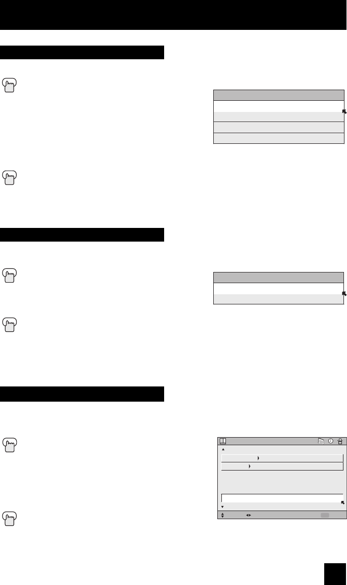
57
This function effects the block noise removal and mosquito NR (Noise Reduction)
simultaneously.
Press the MENU button
π†
To MPEG NR
è
To enter
π†
To select ON or OFF
Press the MENU button when finished
Notes:
• When you are receiving digital channels, block noise removal will have no effect.
• When you are receiving a 1080p signal, MPEG NR can not be selected.
This function can be selected to change the effect of Digital VNR (Video Noise Reduction).
Press the MENU button
π†
To DIGITAL VNR
è
To enter
π†
To select the effect you like.
AUTO: adjusts the effect of VNR automatically.
MIN: adjusts the effect of VNR to minimum.
MAX: adjusts the effect of VNR to Maximum.
OFF: turns the effect of VNR off.
Press the MENU button when finished
Notes:
• If it is in PC, Digital VNR will not be displayed.
• When you are receiving a 1080p signal, Digital VNR can not be selected.
Reset
Reset resets all picture adjustments (tint, color, picture, bright, detail, color temperature, Color
Management, Dynamic Gamma, Smart Picture, Digital VNR and MPEG NR) at once to the
default settings.
Press the MENU button
π†
To RESET
è
To enter
The onscreen menu disappears for a moment,
and then the settings are reset to the default
setting for all the picture adjustments.
Press the MENU button when finished
DIGITAL VNR
AUTO
MIN
MAX
OFF
Digital VNR
MPEG NR
SELECT OPERATE EXIT
MENU
NEXT PAGE
PREVIOUS STANDARD
PICTURE ADJUST
(3/3)
AUTO
ON
DIGITAL VNR
MPEG NR
RESET
MPEG NR
ON
OFF
Onscreen Menus
LCT2170 Eng.indd 57LCT2170 Eng.indd 57 8/4/06 10:27:08 AM8/4/06 10:27:08 AM
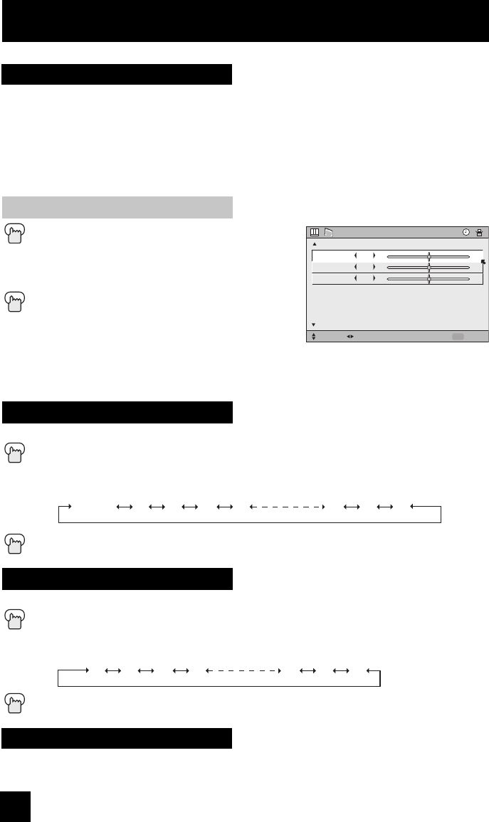
58
These settings allow you to change and adjust the sound on your television.
BASS – You can increase or decrease the level of low-frequency sound in the TV’s audio with
the bass adjustment.
TREBLE – Use treble to adjust the level of high-frequency sound in your TV’s audio.
BALANCE – Adjust the level of sound between the TV’s left and right speakers with the
balance setting.
Press the MENU button
π†
To BASS, TREBLE or BALANCE
√ ®
To adjust the setting
π†
To move to the next setting
Press the MENU button when finished
Note:
• You can reset the sound adjustments (BASS, TREBLE
and BALANCE) you set at once as the default setting
when you select reset.
• You can adjust BALANCE only when A.H.S.+ is off. See page 66.
Sound Settings
Adjust the Sound Settings
BASS
TREBLE
BALANCE
SOUND ADJUST
SELECT OPERATE EXIT
MENU
NEXT PAGE
PREVIOUS
00
00
00
(1/2)
Reset
Reset resets all Sound Adjustments (Bass, Treble, Balance, Turn On Volume and Volume Limit)
at once to the default settings. See page 57 on how to use reset.
Turn On Volume
Volume Limit
Turn On Volume allows you to set the volume level when you turn the TV on.
Press the MENU button
π†
To TURN ON VOLUME
è
To set
Press the MENU button to finish
Current 00 01 02 03 48 49 50
Volume Limit allows you to set the maximum volume level.
Press the MENU button
π†
To VOLUME LIMIT
è
To set the maximum volume level
Press the MENU button to finish
00 01 02 03 48 49 50
Onscreen Menus
LCT2170 Eng.indd 58LCT2170 Eng.indd 58 8/4/06 10:27:08 AM8/4/06 10:27:08 AM
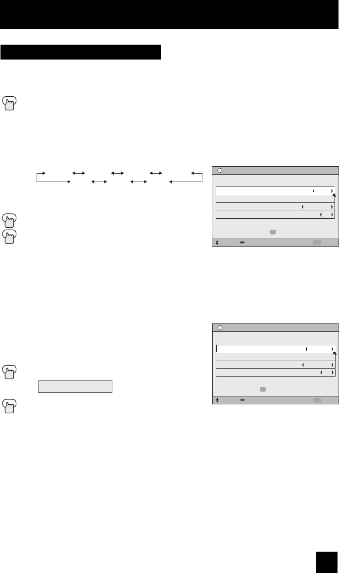
59
Set Clock
The set clock function is described on page 25 as the interactive plug-in menu. You can choose
to set the clock automatically or manually. If you need to set the clock again, follow the steps
below.
Press the MENU button
π†
To SET CLOCK
è
To enter
When you set the clock automatically, choose AUTO by pressing the
√
or
®
arrows.
π†
To TIME ZONE
è
To select your time zone
π†
To D.S.T. (daylight savings time)
è
To turn D.S.T. ON or OFF
Press OK to finish
Press the MENU button when finished
When you set the clock manually, choose MANUAL by
pressing the
√
or
®
arrows.
π†
To move to the hours
è
To set the hours
π†
To move to minutes
è
To set the minutes
π†
To TIME ZONE
è
To select your time zone:
(Atlantic, Eastern, Central, Mountain, Pacific,
Alaska or Hawaii)
π†
To D.S.T. (daylight savings time)
è
To turn D.S.T. ON or OFF
Press OK to start clock
Press the MENU button when finished
SET CLOCK
PRESS TO START CLOCK
SELECT OPERATE EXIT
MENU
OK
TIME
--
:
--
--
MODE
TIME ZONE
D.S.T.
MANUAL
ATLANTIC
ON
SET CLOCK
PRESS TO FINISH
SELECT OPERATE EXIT
MENU
OK
TIME
--
:
--
--
MODE
TIME ZONE
D.S.T.
AUTO
ATLANTIC
ON
THANK YOU !!
ATLANTIC EASTERN CENTRAL MOUNTAIN
HAWAII ALASKA PACIFIC
Notes:
• D.S.T. can be used when it is set to ON in the SET CLOCK menu.
• Only when the MODE set to AUTO, the Daylight Savings Time feature automatically adjusts
your TV’s clock for Daylight Savings. The clock will move forward one hour at 2:00 am on
the first Sunday in April. The clock will move back one hour at 2:00 am on the last Sunday in
October.
• You will have to reset the clock after a power interruption. You must set the clock before
operating any timer functions.
Onscreen Menus
LCT2170 Eng.indd 59LCT2170 Eng.indd 59 8/4/06 10:27:09 AM8/4/06 10:27:09 AM
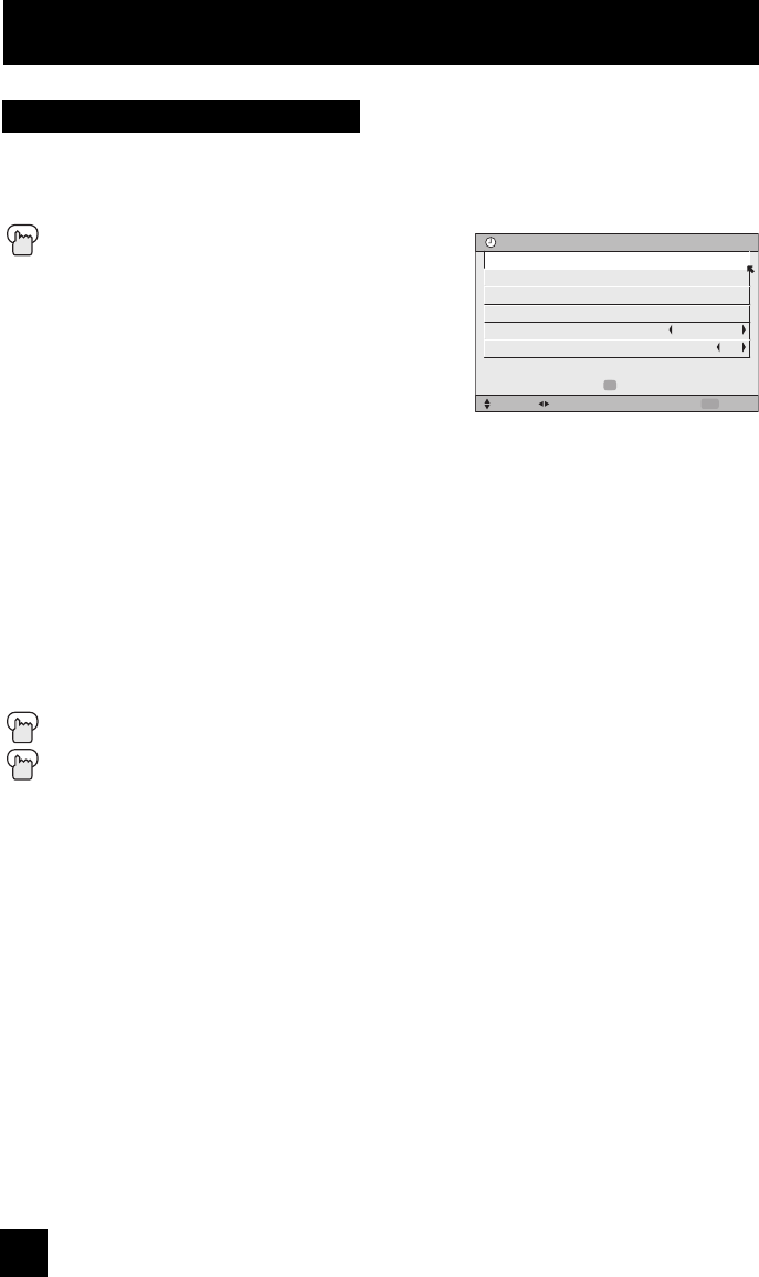
60
The on/off timer lets you program your television to turn itself on or off. You can use it as an
alarm to wake up, to help you remember important programs, or as a decoy when you’re not
home.
Press the MENU button
π†
To ON/OFF TIMER
è
To enter (begins with ON TIME)
è
To set the hour (AM/PM) you want the TV to
turn on
†
To move to minutes
è
To set the minutes
†
To accept ON TIME and move to OFF TIME (the time the TV will turn off). Set the
OFF TIME the same way as ON TIME
†
To accept OFF TIME and move to CHANNEL
è
To select channel
†
To ON VOLUME
è
To set the volume level
†
To move to MODE
è
Choose ONCE or EVERYDAY
†
To ON/OFF TIMER
è
Choose YES to accept the timer setting, choose NO if you don’t wish to accept
Press the OK button to finish
Press the MENU button to exit the menu
• The on/off time cannot be set to locked or guarded channels.
• In order for the on/off timer to work, the clock must be set.
• After a power interruption, the timer settings must be reset.
Notes:
On/Off Timer
ON TIME
OFF TIME
CHANNEL
ON VOLUME
MODE
ON/OFF TIMER
7:00 PM
10:00 PM
03
CURRENT
EVERYDAY
NO
ON/OFF TIMER
SELECT OPERATE EXIT
MENU
PRESS TO FINISH
OK
Onscreen Menus
LCT2170 Eng.indd 60LCT2170 Eng.indd 60 8/4/06 10:27:09 AM8/4/06 10:27:09 AM
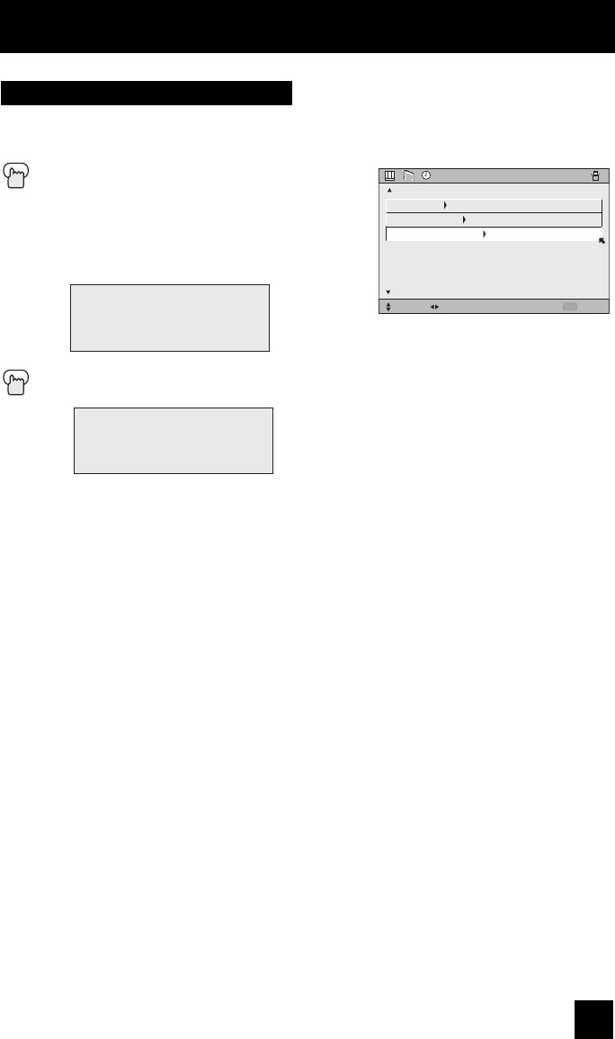
61
The lamp replacement message will appear when you need to change the lamp. After you
replace the lamp, you need to reset the timer which is built into your television.
Press the MENU button
π†
To LAMP TIMER RESET
è
To Enter
The following message will appear.
Press the OK button while the above message appears on the television screen.
The lamp timer has now been reset.
Notes:
• You can use the Lamp Timer Reset only after replacing the lamp.
• See Page 76 for instructions on lamp replacement.
PRESS OK TO RESET THE LAMP
TIMER.
THE LAMP TIMER IS RESET
SUCCESSFULLY.
Lamp Timer Reset
CLOCK / TIMERS
SELECT OPERATE EXIT
MENU
NEXT PAGE
PREVIOUS
SET CLOCK
ON / OFF TIMER
LAMP TIMER RESET
Onscreen Menus
LCT2170 Eng.indd 61LCT2170 Eng.indd 61 8/4/06 10:27:09 AM8/4/06 10:27:09 AM

62
Button Functions
Your television has two kinds of screen: SPLIT (2 channels) and INDEX (12 channels).
Multi Screen Function
Note: After you press any multiscreen buttons, if you press the menu button, only the picture
adjust screen will appear.
Split
Activate the split-screen option by pressing SPLIT on
the remote control. The channel (or input) you were
watching before pressing SPLIT will appear on the
left, the new channel will appear on the right. The
sound will continue to come from the main screen
channel (or input). To turn split-screen off and return
to normal television viewing, press SPLIT again or
press the BACK button.
07
MAIN SCREEN
PICTURE
V-1
SPLIT SCREEN
PICTURE
Notes:
• If the signal that you are watching is coming from the HDMI input, you cannot enter the
SWAP or INDEX mode.
• Main Screen and Split Screen will not display the same channel or input at the same time.
• You can enter the SPLIT mode when the screen is in NORMAL or INDEX mode.
• Split screen will not display digital channels.
• Split-screen functions will not work with locked channels or channels blocked by V-Chip
ratings limits. A gray screen will display instead.
• With split screen, the picture from the component terminal and DIGITAL-IN terminal will
not be displayed.
• The aspect of MAIN CHANNEL PICTURE becomes 16:9 when you input the picture of
480p, 720p and 1080i from the component terminal and DIGITAL-IN terminal.
• After you press the SELECT button, and select SPLIT SCREEN when you press the
OK button, select normal screen. If you don’t operate, the MAIN CHANNEL SCREEN will
be automatically selected about 8 seconds later.
• Aspect does not work in SPLIT mode.
• When it is PC output, Main and Split screen will not be displayed.
• When you are in PC mode, SPLIT, INDEX or FREEZE can not be used.
• When you press the Menu button in SPLIT mode, it appears only as Picture Adjust menu.
• When you are in 1080p mode, SPLIT, INDEX or FREEZE can not be used.
LCT2170 Eng.indd 62LCT2170 Eng.indd 62 8/4/06 10:27:10 AM8/4/06 10:27:10 AM

63
Button Functions
This allows you to quickly look at up to 12 channels at a time so that you can decide which one
to watch.
Notes:
• Only Analog channel input signal will be displayed.
• You can watch the channel added in channel summary. See page 35.
Index
1
5
9
2
6
10
3
7
11
4
8
12
You can exchange the channel (or input) displayed in the split screen window for the main
screen image by pressing the SWAP button.
Note:
• It will only work in SPLIT mode.
Freeze
Swap
With SELECT, you can select the picture (channel) while viewing SPLIT screen. When you
press SELECT button, the channel number on the top will be highlighted. Each press of SELECT
will shift the channel.
Select
Pressing the FREEZE button causes the screen to change to the split-screen display with the still
picture displayed on the right. In order to return to the normal display, press the FREEZE button
once again.
LCT2170 Eng.indd 63LCT2170 Eng.indd 63 8/4/06 10:27:10 AM8/4/06 10:27:10 AM

64
Button Functions
Turns the TV on or off.
Press the POWER button
Note:
• After turning the power on, you can not turn the power off for about one minute.
Power
Use the number buttons on the remote control to move directly to a specific channel. For
example, to move to channel 12:
0 (Zero)
1 (One)
2 (Two)
Number Buttons - 10Key Pad
Tune
Selects the signal input source for the television: VIDEO-1, 2, 3, 4, DIGITAL-IN1 or
DIGITAL-IN2 for video devices like VCRs, DVD players or camcorders.
Press the INPUT button
By every press of the INPUT button, you can change the input mode.
Notes:
• When you return to TV mode, press the RETURN +/TV button or direct 10 key pad or CHANNEL
+/– button.
• You can also access by pressing the INPUT button on the side of the TV instead of the remote
control.
• If you have a PC connected to the TV, select VIDEO-3
Input
Lets you decide the input channel and select it. After you press the number buttons on the
remote, press the TUNE button. For example, to move to channel 12:
1 (One)
2 (Two)
Press the TUNE button
LCT2170 Eng.indd 64LCT2170 Eng.indd 64 8/4/06 10:27:10 AM8/4/06 10:27:10 AM

65
Button Functions
The RETURN+/TV button has three functions:
Return - Returns to the channel viewed just before the channel currently onscreen.
Return+ - Lets you program a specific channel to return to while scanning through the
channels using the CH+ and CH– buttons.
TV - Returns to the TV mode.
Press the RETURN+/TV and hold for three seconds
The channel currently active has been programmed as your return+ channel. Now scan
through the channels using the CHANNEL+/– buttons.
Press the RETURN+/TV
You will return to your programmed channel.
• To cancel your return+ channel, press and hold the RETURN+ button for three seconds. The
message “RETURN CHANNEL CANCELLED!” will appear.
• Return+ works only with the Channel+/– buttons. Pressing any number key will cancel
return+.
Return +/TV
RETURN CHANNEL
PROGRAMMED!
The TheaterPro D6500K color temperature technology function makes sure that the video you
watch is set to the standard color temperature, so that what you see is as true to what the film
to video editors intended it to be.
Press the THEATERPRO button
TheaterPro D6500K
Use these buttons to move up or down all the available channels your TV is able to receive.
Channel +/–
Use these buttons to raise or lower the TV’s volume level. The maximum is the level you set in
Volume Limit. See page 58.
Volume +/–
LCT2170 Eng.indd 65LCT2170 Eng.indd 65 8/4/06 10:27:11 AM8/4/06 10:27:11 AM
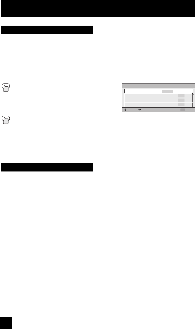
66
By pressing the SOUND button, you can change the A.H.S.+ (Advanced Hyper Surround plus)
mode, A.T.C. (Advanced Tone Correction), SMART SOUND and HYPER BASS on or off.
A.H.S.+ - Adds a more spacious surround sound. Music gives basic effect and movie for more
effect.
A.T.C. - Reproduces distinctive sounds with tone correction.
SMART SOUND - Decreases high sound levels, giving a regulated sound level.
HYPER BASS - Increases bass levels, giving a richer, deeper bass.
Press the SOUND button
π†
To select A.H.S.+, A.T.C., SMART SOUND or
HYPER BASS
è
To choose the setting
Press the MENU when finished
SOUND EFFECT
SELECT OPERATE EXIT
MENU
A.H.S.+
A.T.C.
SMART SOUND
HYPER BASS
MOVIE MUSIC OFF
ON OFF
ON OFF
ON OFF
Notes:
• Smart Sound may become an unnatural effect, depending on the signal source.
• You can adjust BALANCE only when A.H.S.+ is off.
Sound
Button Functions
The MUTING button instantly turns the volume down completely when you press it. Press
MUTING and the volume level will instantly go to zero. To restore the volume to its previous
level, press MUTING again.
Muting
LCT2170 Eng.indd 66LCT2170 Eng.indd 66 8/4/06 10:27:11 AM8/4/06 10:27:11 AM
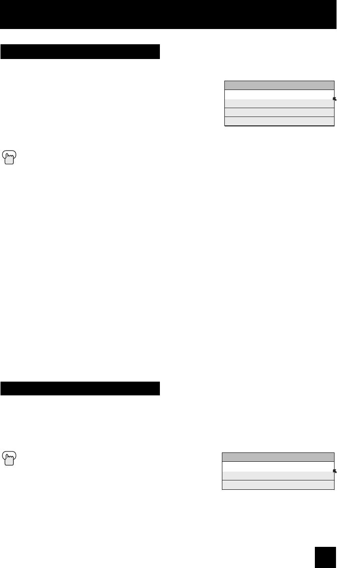
67
Button Functions
The VIDEO STATUS button gives you a choice of four TV picture display settings, including a
display of your own preferences.
Standard - Resets the picture display to the factory settings.
Dynamic - Gives a vivid picture with better contrast when
viewing in a brightly lit room.
Theater - Gives a rich, film-like look to video when viewing in
a dimly lit room.
Game - Used for when you are playing video games connected to your TV.
Press the VIDEO STATUS button
By every press of the VIDEO STATUS button, you change the mode.
Note:
• You can also change the mode by pressing the
π†
buttons.
• Each mode is memorized for each input connected to the TV.
• You can also access the FRONT PANEL CONTROL screen by using the MENU button on
the side of the TV instead of the remote control. It appears between INITIAL SETUP and
PICTURE ADJUST screen, and it has VIDEO STATUS and ASPECT menus. Choose VIDEO
STATUS by pressing MENU
†
on the side panel and choose a mode by using the CHANNEL
+/- buttons (
√
OPERATE
®
).
• There are four video status settings: Dynamic, Standard, Theater and Game. Each video
status setting has a separate memory for HD (1080i/1080p/720p) and SD (480p/480i) video
signal. Each video status can be chosen along with your favorite picture settings (Tint,
Color, Picture, Bright, Detail, etc.)
– When an HD signal is displayed: Your HD settings are recalled for the video status you
are using.
– When an SD signal is displayed: Your SD settings are recalled for the video status you
are using.
– The input you are using (Input-1, Input-2, etc.) does not affect the setting that is recalled,
just the signal type.
– This function considers PC input as an HD signal and PIP and SPLIT screens as an SD
signal.
Video Status
VIDEO STATUS
STANDARD
DYNAMIC
THEATER
GAME
Natural cinema corrects the problem of blurred edges which may occur when viewing a program
originally shot on film (such as motion pictures) or animation. If you notice blurring at the edges
of these programs, press NATURAL CINEMA and set it to AUTO. Natural Cinema helps correct
conversion errors that occur when film, which is shot at 24 frames-per-second, is broadcast at the
television rate of 30 frames-per-second.
Press the NATURAL CINEMA button
Notes:
• When you are receiving a 1080p signal, Natural Cinema
can not be selected.
• The natural cinema mode is automatically set to “AUTO” in the following cases:
- Turning on or off
- Changing the channel or input mode
- Using multi-screen functions
• If you are in PC mode, Natural Cinema can not be used
Natural Cinema
NATURAL CINEMA
AUTO
ON
OFF
LCT2170 Eng.indd 67LCT2170 Eng.indd 67 8/4/06 10:27:11 AM8/4/06 10:27:11 AM
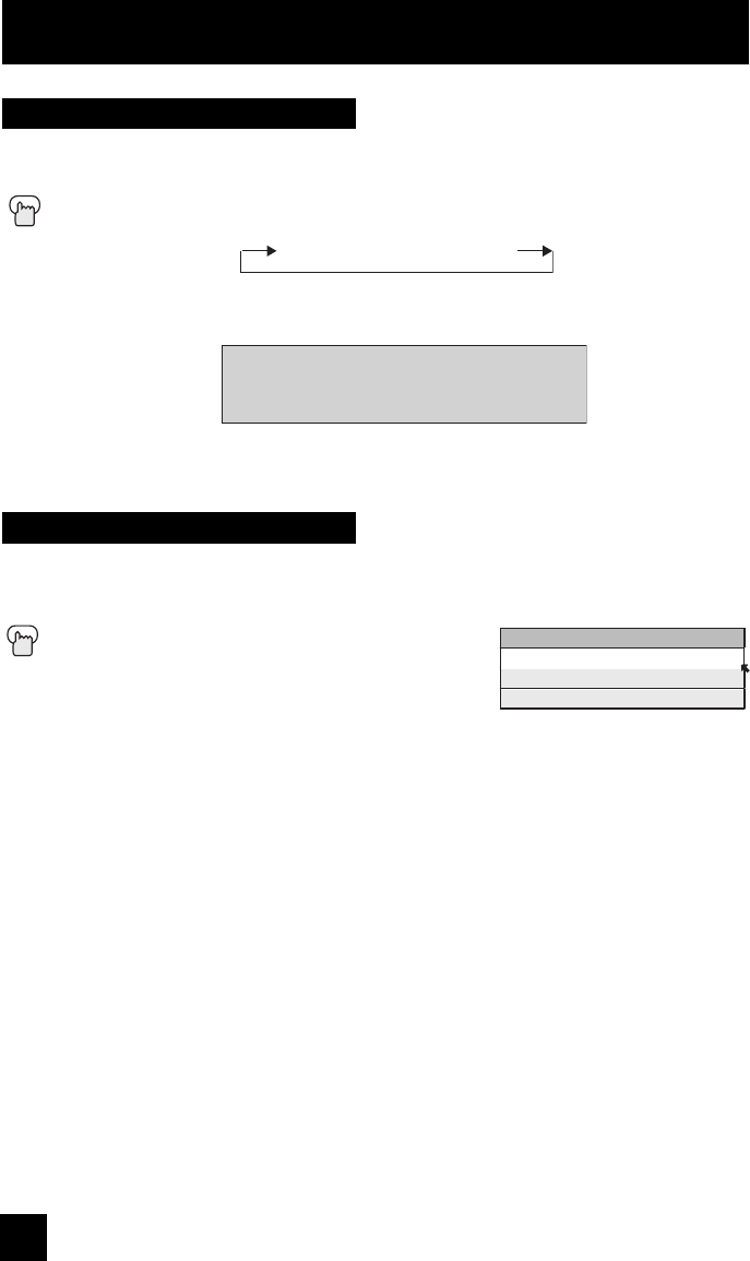
68
Button Functions
The Sleep Timer can turn the TV off for you after you fall asleep. Program it to work in intervals
of 15 minutes, for a total time of up to 180 minutes.
Press the SLEEP button
Sleep Timer Message
60 seconds before the automatic shutoff, this message will appear:
You then have 60 seconds to press the SLEEP button to
delay the shut off for another 15 minutes.
Sleep Timer
GOOD NIGHT!!
PUSH SLEEP TIMER BUTTON
TO EXTEND
0 15 30 45 60 90 120 180
ML/MTS
MTS technology allows several audio signals to be broadcast in analog at once, giving you a
choice in what you wish to hear with a TV program. In addition to mono or stereo sound, an
MTS broadcast may also include a second audio program (SAP).
Press the ML/MTS button
By every press of the ML/MTS button, you change
the mode
Notes:
• When you are receiving a digital broadcast, if there are other languages, you can change the
language by pressing the ML/MTS button.
• Keep the TV in stereo mode to get the best sound quality. The sound will work in stereo
mode even if a certain broadcast is in mono sound only.
• Choose the mono setting to reduce excessive noise on a certain channel or broadcast.
• Selecting SAP will allow you to hear an alternative soundtrack, if one is available.
• MTS unavailable if your television’s Input source is in VIDEO-1, 2, 3, 4, DIGITAL-IN1 or
DIGITAL-IN2 mode, as described on page 64.
• ML/MTS will not work when you are using the Digital-In.
• You can also change the mode by pressing the
π†
buttons.
MTS
STEREO
SAP
MONO
ON AIR
ON AIR
LCT2170 Eng.indd 68LCT2170 Eng.indd 68 8/4/06 10:27:12 AM8/4/06 10:27:12 AM
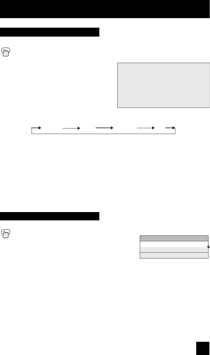
69
Button Functions
The display screen shows the current status of timers, inputs and XDS ID.
Press the DISPLAY button
The screen to the right shows the following
information:
•
The current channel or AV input (Channel 05)
• The current time (12:20 pm)
• Sleep timer status/minutes remaining (The Sleep
Timer is off)
• On/off timer status (Set to turn on everyday at
7:00 PM, off at 10:00 PM)
• Each Press of the DISPLAY button changes the
display mode:
Display - Full screen shown above
Time - Shows the current time only
Channel - Shows the current channel
Off - Turns display off
Notes:
• You may also turn off the display at any step by pressing MENU.
• If the clock, sleep timer or on/off timer are not set, the display screen will show:
“CLOCK NOT SET”, “SLEEP TIMER OFF”, and “ON/OFF TIMER OFF” respectively.
Display
05 KLVX PBS
JAZZ FESTIVAL
NOW
SLEEP TIMER
ON/OFF TIMER
ON TIME
OFF TIME
12:20 PM
OFF
EVERYDAY
7:00 PM
10:00 PM
Display Time Channel Off
C.C. (Closed Caption)
Use the C.C. (Closed Caption) button to select the mode of closed caption.
Press the C.C. button
Notes:
• SMART CAPTION will appear when you press the MUTING
button, only on channels where the broadcast contains
closed captioning.
• When you select ON, it will be the mode selected in the Closed Caption Menu.
• See page 44 when you set the caption/text mode.
• You can also change the mode by pressing the
π†
buttons.
• If you are in PC mode, C.C. can not be used
CLOSED CAPTION
OFF
SMART CAPTION
ON
LCT2170 Eng.indd 69LCT2170 Eng.indd 69 8/4/06 10:27:12 AM8/4/06 10:27:12 AM
70
Button Functions
The Favorite button allows you to select your favorite channels easily. First, you must register
the channels that you like. See how to register below.
Press the FAVORITE button
The favorite channel list will appear.
π†
To select the channel you want to watch
Press the OK button
It will change to the channel you have selected.
Favorite
Press the channel number you want to register
The channel program will change.
Press the FAVORITE button for three seconds
The channel will be registered in the favorite channel list.
Notes:
• Both analog and digital channels can be registered. The digital channels have a "D" in front
of the channel number.
• The maximum number of channels you can register is 24.
• If you have registered the maximum number of channels, and try to register more channels,
the oldest channel you registered will be deleted.
• Sub channels can not be registered.
• The newest channel you registered will appear at the top of the list.
Press the FAVORITE button
The favorite channel list will appear.
π†
To select the channel you want to delete
è
To enter
Press the OK button
The channel was deleted.
Press the FAVORITE button when finished
Note:
• Before pressing the FAVORITE button when you are finished, press the
è
button again, and
you can return to the deleted channel.
FAVORITE
NEXT
101
102
D103
<
D107
8
CBS
FOX
PBS2
>
HBO
ABC
PREVIOUS
Register the favorite channel
Delete the favorite channel
LCT2170 Eng.indd 70LCT2170 Eng.indd 70 8/4/06 10:27:13 AM8/4/06 10:27:13 AM
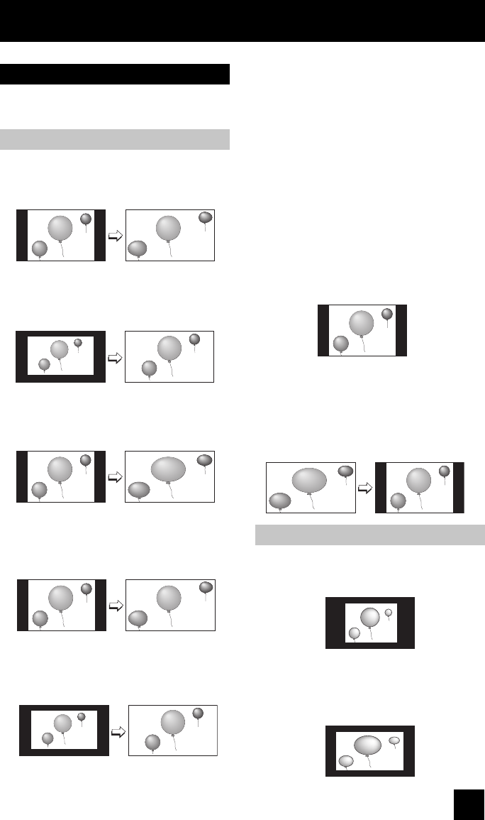
71
Button Functions
This feature will help you adjust the picture you are watching to give you the best possible
picture quality.
Aspect
Aspect Ratios
PANORAMA - With this ratio a normal
4:3 aspect picture is stretched to fit the
dimensions of the 16:9 aspect screen.
CINEMA - This ratio “zooms in” on the
center part of a 4:3 aspect picture, blowing
it up to fill the 16:9 screen.
FULL - This is the ratio to use when
watching 16:9 High-Definition broadcasts.
PANORAMA ZOOM - This ratio stretches
the High-Definition 16:9 aspect image to
eliminate the black side bars.
CINEMA ZOOM - This ratio stretches
the High-Definition 16:9 aspect image to
eliminate the black surrounding bars.
SLIM - This aspect mode shrinks the
screen of 16:9 to 4:3. There are some
programming that is already stretched by
mistake at broadcasting companies, so
this mode corrects it. Black side bars will
appear.
REGULAR - The regular ratio is used
when you want to watch a 4:3 broadcast
or recorded program without modifying the
original picture to fit the dimensions of your
16:9 screen. The 4:3 picture will fill the
screen from top to bottom, while black bars
will appear to fill up the remaining space
along the picture’s sides. The 4:3 picture
will be centered within the boundaries of the
16:9 screen.
Aspect Ratios in PC Mode
REGULAR - This is the original aspect
mode.
FULL - This aspect mode stretches the
image to fit the dimensions of the 16:9
aspect screen.
LCT2170 Eng.indd 71LCT2170 Eng.indd 71 8/4/06 10:27:13 AM8/4/06 10:27:13 AM
72
Button Functions
When you change the aspect ratios, it is different from their broadcast or recorded program.
Aspect Ratios (Continued)
Press the ASPECT button
• By pressing the ASPECT button, you can change the size.
ASPECT
PANORAMA
CINEMA
FULL
REGULAR
ASPECT
PANORAMA ZOOM
CINEMA ZOOM
FULL
Notes:
• You can also choose the size by pressing the
π†
buttons.
• When you change the aspect ratio or signal, reset the picture position to center.
• You can also access the FRONT PANEL CONTROL screen by using the MENU button
on the side of the TV instead of the remote control. It appears between INITIAL SETUP
and PICTURE ADJUST screen, and it has VIDEO STATUS and ASPECT menus. Choose
ASPECT by pressing Menu
†
on the side panel and choose a mode by using the CHANNEL
+/- buttons (
√
OPERATE
®
).
• "SLIM" can only be dispalyed when the signal is ATSC (480i or 480p).
• If the televison receives a 16:9 signal from your HDMI device, the aspect mode will turn to
FULL automatically. If the television receives a 4:3 signal from your HDMI device when you
are in FULL aspect mode, it will return to REGULAR aspect mode. If you change the aspect
mode after the televison changed it to FULL automatically, the televison will change to the
aspect mode you choosed.
• When you are receiving a 1080p signal, you can not change the aspect ratios.
HD (1080i, 720p)
ATSC (1080i, 720p)
SD (480i, 480p)
NTSC, 480i, 480p
The MENU button allows you to access JVC’s onscreen menu system. Press MENU to activate
the onscreen menu system.
• See individual topics like “Sound Adjust” for specific information on using menus.
Menu
Back
OK
This button allows you to go back in the menu to change a selection or correct a mistake.
This button confirms your selection when you are in one of the onscreen menus.
ASPECT
PANORAMA ZOOM
CINEMA ZOOM
FULL
SLIM
ATSC (480i, 480p)
ASPECT
FULL
REGULAR
PC
LCT2170 Eng.indd 72LCT2170 Eng.indd 72 8/4/06 10:27:14 AM8/4/06 10:27:14 AM

73
Button Functions
Use either the television’s own tuner or a cable box to select channels. Set this switch to TV to
operate the television’s built-in tuner. Move the switch to CATV to operate a cable box.
Note:
• See page 25 for information on programming your remote for cable box operation.
You can control a VCR or DVD player with the buttons on the lower part of the remote control.
Move the slide switch to VCR or DVD to operate.
Notes:
• The remote is preset with the code 000 to control JVC-brand VCR’s. For any other
manufacturer’s brand VCR, please see the code chart and instructions on page 26.
• The remote is preset with the code 000 to control JVC-brand DVD players. For any other
manufacturer’s brand DVD player, please see the code chart and instructions on page 27.
TV/CATV Slide Switch
VCR/DVD Slide Switch
You can also use this remote control to operate the basic functions of your DVD player. These
functions include: play, rewind, fast-forward, stop, still/pause, previous/next, tray open/close,
power on and power off.
Move the selector switch to DVD to operate.
• The remote is preset with the code 000 to control JVC-brand DVD players. For any other
manufacturer’s brand DVD player, please see the code chart and instructions on page 27.
You can use this remote control to operate the basic functions of your VCR. These functions
include: play, record, rewind, fast-forward, stop, pause, channel scan, TV/VCR, power on and
power off.
Move the selector switch to VCR to operate.
• The remote is preset with the code 000 to control JVC-brand VCR’s. For any other
manufacturer’s brand VCR, please see the code chart and instructions on page 26.
VCR Buttons
DVD Buttons
Your remote control includes illuminated buttons for key features like CHANNEL +/- and
VOLUME +/-. Press the LIGHT button to turn the illumination on for 5 seconds.
Light
LCT2170 Eng.indd 73LCT2170 Eng.indd 73 8/4/06 10:27:14 AM8/4/06 10:27:14 AM
74
Sub Channel
Digital CH D/A (Digital/Analog)
The D/A button changes the analog and digital channel. Each time you press the D/A button,
you can switch back and forth the analog and digital channels. Digital channels have a "D" in
front of the channel number.
Press the D/A button
For example, to move to channel D23:
Press 2 (Two)
Press 3 (Three)
Press the TUNE button
The main channel sometimes has minor channels (Sub Channels). By using the SUB button,
you can select a sub channel easily.
For example, to move to sub channel 123-45:
Press 1, 2 and 3 in order
Press the SUB button
Press 4 and 5 in order
Press the TUNE button
Note:
• If there are more than 2 major channels, select the digital channel by using the
π†
buttons
and then press the OK button.
Button Functions
You can view the program from the GUIDE.
Notes:
• The GUIDE function will only work when you are receiving digital programming only.
• The GUIDE will not show the correct time and date if you have not performed the set clock
function on your television. See page 59.
Guide
To watch digital channels
LCT2170 Eng.indd 74LCT2170 Eng.indd 74 8/4/06 10:27:14 AM8/4/06 10:27:14 AM

75
OSD Information
This OSD warning appears when the digital channel that you have selected is too weak to
receive or no signal is being detected for that channel.
Weak Signal
Weak Signal
15
Invalid Signal
If you are inputting a PC signal that is invalid, "Invalid Signal" will appear on the TV screen. It
appears when the input is PC and it is a single screen.
If the external input terminal you selected, or were watching is not receiving a signal, "NO
PROGRAM" appears on the television screen. It appears when that external input terminal
is not receiving a signal and you have the Noise Muting function OFF and you have a single
screen. It moves automatically every two seconds to prevent the screen from burn-in.
Note:
• Even if "NO PROGRAM" appears on the screen, your timer functions and auto shut off
functions that you set, are still active.
No Program
LCT2170 Eng.indd 75LCT2170 Eng.indd 75 8/4/06 10:27:15 AM8/4/06 10:27:15 AM

76
Lamp Replacement
Changing the Lamp
WARNING!
It is very important that you NEVER TOUCH THE GLASS SURFACE OF THE NEW
LAMP. Touching the glass surface will deposit oils from your hand onto the lamp
surface. When the lamp heats up to its operating temperature, the oil will cause a
difference in temperature on the lamp surface that will likely cause the lamp to break.
Replace the lamp with part number TS-CL110U only! The television is designed
to work specifically with this lamp. Using a different lamp, or a third-party
manufacturer’s lamp could cause a malfunction and or damage to the television.
This television uses a 110-Watt high-pressure mercury lamp to project images onto the
television screen. When the lamp nears the end of its operating life, you may notice the picture
becoming dark. When the picture begins to darken, or the lamp burns out, it is time to replace
the lamp. The following instructions will tell you how to safely replace the lamp.
WARNING!
Under operating conditions, THE LAMP WILL GET EXTREMELY HOT AND WILL
CAUSE SEVERE BURNS IF TOUCHED.
Before attempting to replace the lamp, make sure the television has completely run
through its cooling cycle. Turn the power off and wait until the LAMP/PROGRAM LED
blinks very slowly and turns off completely. Unplug the TV. If you feel any warmth
as you place your hand near the lamp, DO NOT TOUCH IT. Wait until the lamp has
completely cooled before attempting to replace it. After turning the power off, wait at
least 1 hour or more.
NEVER attempt to replace the lamp with the television plugged into a wall outlet.
Attempting to replace the lamp with the TV plugged in could lead to a severe electrical
shock.
Do not keep the TV on for more than 24 hours consecutively. There is the possibility
of the life of the lamp being shortened.
The life of the lamp changes depending on the atmospheric temperature and altitude
in which the TV is being used.
Please read these instructions fully before attempting to replace the lamp. If you feel
unsure about replacing the lamp yourself, call a service technician.
LCT2170 Eng.indd 76LCT2170 Eng.indd 76 8/4/06 10:27:15 AM8/4/06 10:27:15 AM

77
Lamp Message
If this message appears when you turn the TV
on, you need to replace the lamp. See page 78
on how to replace the lamp.
Note:
• This message will appear every time you
turn on the TV when the lamp needs to be
replaced. Press the OK button to make the
message disappear, or replace the lamp.
LAMP NEEDS TO BE REPLACED.
REFER TO OWNER'S MANUAL FOR
REPLACEMENT INSTRUCTIONS.
AFTER REPLACING THE LAMP,
PLEASE RESET TIMER IN THE TV
MENU.
PRESS OK, IF YOU DO NOT WANT
TO SEE THIS MESSAGE AGAIN.
Replacement Lamp Kit
Before replacing the lamp, you will need to purchase a replacement kit, part number
TS-CL110U. To purchase this kit, consult your dealer or call 1-800-252-5722, or go to www.jvc.
com.
The replacement kit will include the following:
1 High-Pressure Mercury Lamp 1 Instruction Manual
Because the lamp contains a small amount of mercury, it cannot be disposed of with
normal trash.
Lamp Replacement
LCT2170 Eng.indd 77LCT2170 Eng.indd 77 8/4/06 10:27:15 AM8/4/06 10:27:15 AM
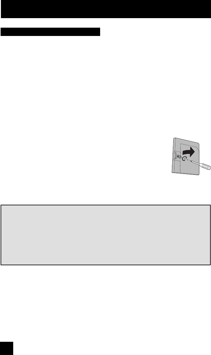
78
How to Replace the Lamp
Please read these instructions fully before attempting to replace the lamp. If you feel
unsure about replacing the lamp yourself, call a service technician. Please observe all
safety warnings.
1) Turn off the television.
Press the POWER button on the remote control or TV front panel. Wait until the picture has
closed and the LAMP LED on the front panel has stopped blinking indicating the lamp cool
down is complete.
Warning: The cool-down process cools the lamp from its operating temperature. This
does not mean that the lamp will now be cool enough to handle safely. We strongly
recommend you wait at least one hour before proceeding.
2) Unplug the television.
Disconnect the power cord from the AC outlet. Make sure that the LAMP LED light has stopped
blinking before you unplug the set. Never attempt to replace the lamp with the television
plugged in.
3) Remove the lamp cover.
The lamp is located behind the lamp cover below the left side of the
television. To access the lamp you will need to remove the lamp cover.
First, remove the screw located on the lamp cover using a Philips head
type screwdriver (cross-head type). Once the screw has been removed,
gently pull the knob towards you and the panel will come away from the
television. Set it aside.
WARNING: DO NOT attempt to remove the assembly until the lamp has fully cooled. If you
feel any heat near the lamp, STOP and wait until the lamp has FULLY COOLED.
NEVER attempt to remove the lamp with the television plugged into an outlet.
DO NOT DROP the used lamp. The inside of the lamp is under pressure. Dropping or other
hard shock could cause the lamp to shatter.
ALWAYS recycle the used lamp. Because the lamp contains a small amount of mercury, it
cannot be thrown away with regular trash. Follow the recycling instructions included with the
Lamp Replacement Kit.
Lamp Replacement
LCT2170 Eng.indd 78LCT2170 Eng.indd 78 8/4/06 10:27:15 AM8/4/06 10:27:15 AM
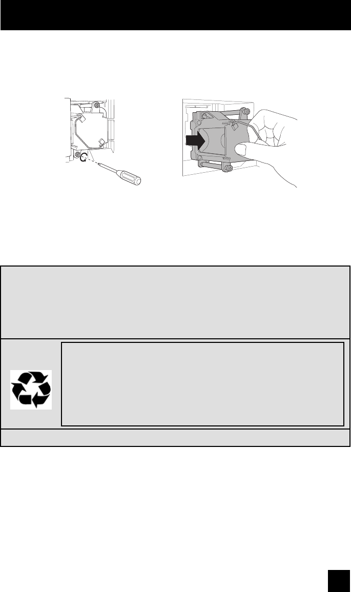
79
WARNING!
Remember it is very important that YOU DO NOT TOUCH THE LAMP SURFACE. Please
read the warnings on page 76 again.
Also, replace the lamp with part number TS-CL110U only! The television is designed
to work specifically with this lamp. Lamps other than TS-CL110U may cause
malfunctions and/or other damage to the television.
To purchase a replacement lamp kit, please call 1-800-252-5722.
NOTICE (for USA)
This product has a High Intensity Discharge (HID) lamp that
contains a small amount of mercury. It also contains lead in some
components. Disposal of these materials may be regulated in your
community due to environmental considerations. For disposal or
recycling information, please contact your local authorities, or the
Electronics Industries Alliance: http://www.eiae.org
5) Install the new lamp unit.
Holding the handle attached to the new lamp unit, slide and push the new lamp straight into the
television and back into the lamp housing area. Do not forget to re-tighten the two screws.
Note: If the lamp does not sit securely in the TV (flat in the lamp housing area), it won’t turn on.
Make sure the lamp sits securely and flat in the housing area.
6) Re-install the lamp cover.
Insert the lamp cover in the right concave and close the lamp cover. Because the lamp cover
has a role to help prevent the danger of an electrical shock, tighten the screw using your
fingers.
Note:
• After installing the new lamp unit, do not forget to reset the lamp timer. See page 61.
4) Remove the lamp unit.
Using a Philips head type screwdriver (cross-head type), loosen the two screws fastening the
lamp unit. When the screws have been loosened, remove the lamp by raising the handle and
gently sliding the unit straight towards you. Place it carefully in the recycling packaging.
Lamp Replacement
LCT2170 Eng.indd 79LCT2170 Eng.indd 79 8/4/06 10:27:16 AM8/4/06 10:27:16 AM

80
Warning LED Messages
While the power is on, and there is a problem with the TV, the TV changes to warning
mode and informs you of the problem using the LED as follows. Then, the power turns off
automatically and performs the cooling for approximately 1 minute.
The LAMP blinks
Condition: It may be a malfunction of the internal electrical circuits.
To correct: Keep the TV off for a while and then turn the power on again. If the TV goes into
warning mode, unplug the TV after the cooling has completed and consult your
dealer.
The POWER LED and LAMP blink alternately
Condition: The inside temperature rises abnormally or the fan may be blocked.
To correct: Keep the TV off for a while and then turn the power on again. If the TV goes into
warning mode, unplug the TV after the cool down as completed and consult your
dealer.
The POWER LED and LAMP blink rapidly simultaneously
Condition: The lamp unit has been installed on a slant and is not flat, or it is not fully inserted
into the lamp housing. Or it may be a lamp malfunction.
To correct: • If this condition occurs soon after replacing the lamp: Reinstall the new lamp unit.
Repeat the lamp installation steps, taking care to observe all warnings. Make
sure the lamp sits FLAT inside the unit when you reinstall it.
• If this condition occurs except for replacing the lamp: Keep the TV off for a while
and then turn the power on again. If the TV goes into warning mode, unplug the
TV after the cool down as completed and consult your dealer.
Lamp Replacement
LCT2170 Eng.indd 80LCT2170 Eng.indd 80 8/4/06 10:27:16 AM8/4/06 10:27:16 AM
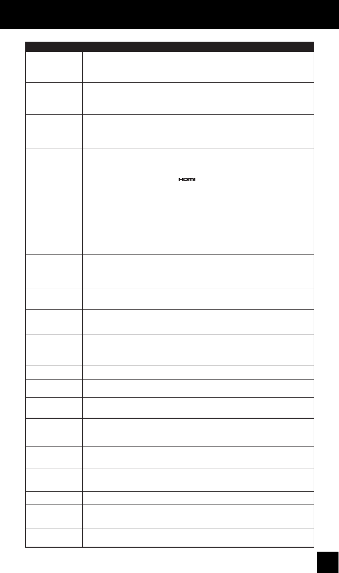
81
Troubleshooting
There is no power
There is no picture
or sound
You cannot select a
certain channel
The power turns off
by itself
The clock is wrong
The color quality
is poor
There are lines
across the picture
The picture is spotted
There are double
pictures (ghosts)
Picture is snowy
(image noise)
Screen is 80% black
Stereo or bilingual
programs can't be
heard
Remote control is not
operating properly or
at all
• See if the power cord became unplugged.
• Check for a blown fuse or circuit breaker or a power outage.
• It is possible the fan is stuck or the inside temperature is rising abnormally.
Consult your dealer.
• Check to see that the batteries are still working and properly installed.
• Make sure the remote has a clear sight path to the TV.
• Check that the TV/CATV switch is in the proper position.
• You may be too far from the TV. You must be within 23 feet (7 meters).
• Make sure the channels have been programmed. See "Channel Summary", page 35.
• Check to see if the channel is locked. See "Channel Summary - Lock" page 36.
• Make sure the set did not become unplugged.
• Perhaps the On/Off Timer is set. See page 60.
• Check to see if the Sleep Timer was set. See page 68.
• The power was interrupted and the clock was not reset. See page 59.
• Tint and Color may be improperly adjusted. See page 55.
• The Video Status mode may be turned to the wrong setting. See page 67.
• There could be interference from another electrical appliance, such as a computer,
another TV or VCR. Move any such appliances further away from the TV.
• There could be interference from a high-wattage appliance, like a hairdryer or vacuum,
operating nearby. Move the antenna away from the appliance or change to a coaxial
cable connection which is less prone to interference.
• A building or passing airplane can reflect the original signal and produce a second,
slightly delayed one. Adjust your antenna position.
• Your antenna may be damaged, disconnected or turned. Check the antenna
connection. If the antenna is damaged, replace it.
• The Closed Caption Text mode is on. Turn it off in the Closed Caption Menu, page 69.
• Make sure the MTS settings are correct. See page 68.
PROBLEMS CHECK
It does not operate
correctly
• This television is operated by a microprocessor. It is possible that external noise or
interference is causing the problem. If the television does not function correctly, remove the
electrical plug from the wall outlet and wait a while before inserting it into the wall outlet
again and operating the television.
The POWER LED
and LAMP LED are
blinking alternately.
• It may be a malfunction that the fan is locked or the temperature has increased.
The POWER LED
and LAMP LED are
blinking rapidly
simultaneously.
• The lamp may not have been installed correctly, or it may be due to a malfunction.
• The lamp door may not be closed correctly.
The LAMP LED
continues blinking
• It may be a malfunction of the internal electrical circuits.
• The antenna could be disconnected.
• The input mode could be set improperly. See page 64.
• The tuner (Auto Tuner Setup) could be set improperly. See page 34.
• The TV station may be having difficulties. Check to see if other stations are working.
• Use the HDMI cable with HDMI logo . See page 20.
• You can not output audio using the AUDIO OUTPUT under the following conditions:
1) When you have digital sound from an HDMI device connected to the HDMI 1 or
HDMI 2 connection on the back of your TV. (See page 20).
2) When you have analog sound from a DVI device connected to the
AUDIO IN "HDMI 1" connection. (See page 19).
• When you have an HDMI device connected to the HDMI 1 connection on the back of your
TV, your TV detects it, and blocks the analog audio signal coming into the "HDMI 1”
jacks. Therefore, you can not hear any analog sound from the other device conected to the
"HDMI 1" jacks, while you are viewing the images from the HDMI device.
(See page 20).
LCT2170 Eng.indd 81LCT2170 Eng.indd 81 8/4/06 10:27:16 AM8/4/06 10:27:16 AM

82
Troubleshooting
The following are not malfunctions.
• The television may make a creaking sound if the temperature of the room or the temperature
inside the television changes. If there is no problem with the screen or sound, then there is no
need to worry.
• The lamp may make a noise when it blows, but this is not dangerous.
• The lamp may make a noise when the power is turned on and a picture is displayed on
the screen. This noise is caused when the mercury inside the lamp is heated, and is not a
malfunction.
• The still parts of a picture may remain on the screen. This is a characteristic of HD-ILA
elements and not a malfunction. The picture will disappear over time.
• The operation of this television is not guaranteed below 0ºC. If the power is turned on while
the temperature is below 0ºC, the picture may be disturbed. Use the television when the
temperature is 0ºC or higher.
• Although the HD-ILA element is manufactured with high-precision technology, please
understand that some pixels may be lost or permanently displayed.
• There is a cooling fan built-in to the television. Please understand that this fan will make some
noise when the television is on and while cooling.
• Although the picture may be temporarily disturbed and noise may be seen on the screen if the
power is turned on immediately after it has been turned off. This is not a malfunction.
PROBLEMS CHECK
Static electricity
You hear occasional
crackling sounds
• It is normal to feel static electricity if you brush or touch the screen.
• It is normal for the TV to make crackling sounds when first turned on or off. Unless
the sound or picture become abnormal, this is fine.
LCT2170 Eng.indd 82LCT2170 Eng.indd 82 8/4/06 10:27:16 AM8/4/06 10:27:16 AM
83
HD-ILA Device ProjectionType
Reception Format
Reception Range
Power Source
Power Consumption
Model
NTSC, BTSC System (Multi-Channel Sound)
ATSC Terrestrial, Digital Cable
AC 120V, 60 Hz
220W
110W High-Pressure Mercury Lamp
Screen Size
Speakers
Audio Output Full Range - 10W + 10W
Antenna Terminal
(VHF/UHF,
ATSC/DIGITAL
CABLE IN)
75 ohms (VHF/UHF)(F-type connector)
Input 1, 2, 3, 4
Terminal
S (Input 1)
Y: 1 Vp-p positive, 75 ohms (negative sync provided)
C: 0.286 Vp-p (burst signal), 75 ohms
Video: 1 Vp-p, 75 ohms (Input 1, 2, 4)
Audio: 500 mVrms (-4dBs) high impedance
Input 1, 2 Terminal
(component terminal)
1080i / 720p / 480p / 480i
Y: 1 Vp-p positive, 75 ohms (negative sync provided)
P
B
/P
R
: 0.7 Vp-p 75 ohms
DIGITAL-IN
(HDMI input terminal)
HDMI Jack x 2
• Personal computer compatibility cannot be guaranteed.
Video: 1080p / 1080i / 720p / 480p / 480i / VGA
Audio: 2ch PCM, 32 / 44.1 / 48 KHz 16 / 20 / 24 bit
Remote control unit x 1 / AA batteries X 2
Dimensions (inch)
W X H X D (cm)
Weight (lbs / kg)
Accessories
Audio Output Jacks FIX : 500mVrms (-4dBs) Low impedance (1000 Hz when modulated 100%)
Projection Source
Optical Output
Digital Audio Digital Out (optical) x 1
PC Input Jack Analog RGB D-SUB (15 pin) x 1
• PC signal is available. Refer to page 23 for details on the signals which
can be input.
56 inch / 142 cm
measured diagonally,
16:9 ratio
50 7/8 x 37 1/8 x 17 3/4
129.2 x 94.4 x 45
91 / 41
HD-52FA97 HD-61FB97HD-56FB97
61 inch / 155 cm
measured diagonally,
16:9 ratio
55 1/4 x 40 x 19
140.3 x 101.6 x 48.4
99 / 45
VHF 2 to 13, UHF 14 to 69 CATV 125 Sub, Mid, Super, Hyper
and Ultra bands (181 channel frequency synthesizer system) at Analog
• Reception of channel A-5 ("95" of the TV set's on-screen cable channel
numbers) is not recommended for your TV set.
VHF 2 to 13, UHF 14 to 69 at ATSC,
CATV 135 Sub, Mid, Super, Hyper and Ultra bands at Digital Cable
(8.5 cm x 12.5 cm) oval x 210 cm round x 2
48 1/2 x 35 7/8 x 16 3/8
122.9 x 91.1 x 41.5
86 / 39
52 inch / 132 cm
measured diagonally,
16:9 ratio
Specifications
Specifications subject to change without notice.
• The open source software is embedded in this product. For more information, please go to:
http://software.jvc.com/opensource/lnx/DP/05_AtscQam/download.html
LCT2170 Eng.indd 83LCT2170 Eng.indd 83 8/4/06 10:27:16 AM8/4/06 10:27:16 AM
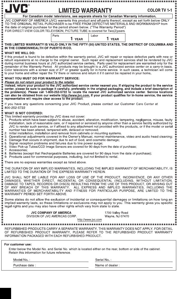
84
LCT2170 Eng.indd 84LCT2170 Eng.indd 84 8/4/06 10:27:17 AM8/4/06 10:27:17 AM

85
LCT2170 Eng.indd 85LCT2170 Eng.indd 85 8/4/06 10:27:17 AM8/4/06 10:27:17 AM

86
Notes
LCT2170 Eng.indd 86LCT2170 Eng.indd 86 8/4/06 10:27:17 AM8/4/06 10:27:17 AM

87
Notes
LCT2170 Eng.indd 87LCT2170 Eng.indd 87 8/4/06 10:27:17 AM8/4/06 10:27:17 AM

JVC COMPANY OF AMERICA
Division of JVC Americas Corp.
1700 Valley Road
Wayne, New Jersey, 07470
JVC CANADA, INC.
21 Finchdene Square
Scarborough, Ontario
Canada, M1X 1A7
LCT2170 Eng.indd 88LCT2170 Eng.indd 88 8/4/06 10:27:17 AM8/4/06 10:27:17 AM
(No.YA463)3-1
PARTS LIST
CAUTION
JThe parts identified by the symbol are important for the safety . Whenever replacing these parts, be sure to use specified ones to secure the
safety.
JThe parts not indicated in this Parts List and those which are filled with lines --- in the Parts No. columns will not be supplied.
JP.W. BOARD Ass'y will not be supplied, but those which are filled with the Parts No. in the Parts No. columns will be supplied.
ABBREVIATIONS OF RESISTORS, CAPACITORS AND TOLERANCES
RESISTORS CAPACITORS
CR Carbon Resistor C CAP. Ceramic Capacitor
FR Fusible Resistor E CAP. Electrolytic Capacitor
PR Plate Resistor M CAP. Mylar Capacitor
VR Variable Resistor CH CAP. Chip Capacitor
HV R High Voltage Resistor HV CAP. High Voltage Capacitor
MF R Metal Film Resistor MF CAP. Metalized Film Capacitor
MG R Metal Glazed Resistor MM CAP. Metalized Mylar Capacitor
MP R Metal Plate Resistor MP CAP. Metalized Polystyrol Capacitor
OM R Metal Oxide Film Resistor PP CAP. Polypropylene Capacitor
CMF R Coating Metal Film Resistor PS CAP. Polystyrol Capacitor
UNF R Non-Flammable Resistor TF CAP. Thin Film Capacitor
CH V R Chip Variable Resistor MPP CAP. Metalized Polypropylene Capacitor
CH MG R Chip Metal Glazed Resistor TAN. CAP. Tantalum Capacitor
COMP. R Composition Resistor CH C CAP. Chip Ceramic Capacitor
LPTC R Linear Positive Temperature Coefficient Resistor BP E CAP. Bi-Polar Electrolytic Capacitor
CH AL E CAP. Chip Aluminum Electrolytic Capacitor
CH AL BP CAP. Chip Aluminum Bi-Polar Capacitor
CH TAN. E CAP. Chip Tantalum Electrolytic Capacitor
CH AL BP E CAP. Chip Tantalum Bi-Polar Electrolytic Capacitor
RESISTORS
FG J KMNRHZ P
±1% ±2% ±5% ±10% ±20% ±30% +30%
-10%
+50%
-10%
+80%
-20%
+100%
-0%
3-2(No.YA463)
CONTENTS
USING P.W. BOARD & REMOTE CONTROL UNIT ................................................................................................... 3-3
EXPLODED VIEW PARTS LIST -1 [HD-52FA97] ...................................................................................................... 3-4
EXPLODED VIEW -1 [HD-52FA97] ............................................................................................................................. 3-5
EXPLODED VIEW PARTS LIST -2 [HD-52FA97] ....................................................................................................... 3-6
EXPLODED VIEW -2 [HD-52FA97] ............................................................................................................................. 3-7
EXPLODED VIEW PARTS LIST -3 [HD-56FB97, HD-61FB97] ................................................................................. 3-8
EXPLODED VIEW -3 [HD-56FB97, HD-61FB97] ....................................................................................................... 3-9
EXPLODED VIEW PARTS LIST -4 [HD-56FB97, HD-61FB97] ............................................................................... 3-10
EXPLODED VIEW -4 [HD-56FB97, HD-61FB97] ..................................................................................................... 3-11
EXPLODED VIEW PARTS LIST -5 ........................................................................................................................... 3-12
EXPLODED VIEW -5 ................................................................................................................................................. 3-13
EXPLODED VIEW PARTS LIST -6 ........................................................................................................................... 3-14
EXPLODED VIEW -6 ................................................................................................................................................. 3-15
PRINTED WIRING BOARD PARTS LIST [HD-52FA97] .......................................................................................... 3-16
ANALOG P.W. BOARD ASS'Y (SRA-1024A-M2) ............................................................................................ 3-16
DRIVE P.W. BOARD ASS'Y (SRA-3013A-M2) ................................................................................................ 3-19
REMOCON P.W. BOARD ASS'Y (SRA-8011A-M2) ........................................................................................3-29
TEMP P.W. BOARD ASS'Y (SRA-8211A-M2) ................................................................................................. 3-29
USB P.W. BOARD ASS'Y (SRA-8521A-M2) ................................................................................................... 3-29
POWER P.W. BOARD ASS'Y (SRA-9017A-M2) ............................................................................................. 3-29
DIGITAL P.W. BOARD ASS'Y (SRA0D161A-M2) ........................................................................................... 3-31
SIDE CONTROL P.W. BOARD ASS'Y (SRA0L013A-M2) ............................................................................... 3-35
FRONT LED P.W. BOARD ASS'Y (SRA0L111A-M2) ..................................................................................... 3-35
LAMP COVER SW P.W. BOARD ASS'Y (SRA0L211A-M2) ........................................................................... 3-35
TUNER P.W. BOARD ASS'Y (SRA0R012A-M2) ............................................................................................. 3-35
ATSC TUNER MODULE P.W. BOARD ASS'Y (SSD-2205A-M2) ................................................................... 3-36
PRINTED WIRING BOARD PARTS LIST [HD-56FB97] .......................................................................................... 3-37
ANALOG P.W. BOARD ASS'Y (SRA-1024A-M2) ............................................................................................ 3-37
DRIVE P.W. BOARD ASS'Y (SRA-3013A-M2) ................................................................................................ 3-37
REMOCON P.W. BOARD ASS'Y (SRA-8011A-M2) ........................................................................................3-37
TEMP P.W. BOARD ASS'Y (SRA-8211A-M2) ................................................................................................. 3-37
USB P.W. BOARD ASS'Y (SRA-8521A-M2) ................................................................................................... 3-37
POWER P.W. BOARD ASS'Y (SRA-9017A-M2) ............................................................................................. 3-37
DIGITAL P.W. BOARD ASS'Y (SRA0D160A-M2) .......................................................................................... 3-37
SIDE CONTROL P.W. BOARD ASS'Y (SRA0L013A-M2) ............................................................................... 3-41
FRONT LED P.W. BOARD ASS'Y (SRA0L113A-M2) ..................................................................................... 3-41
LAMP COVER SW P.W. BOARD ASS'Y (SRA0L211A-M2) ........................................................................... 3-41
TUNER P.W. BOARD ASS'Y (SRA0R012A-M2) ............................................................................................. 3-41
ATSC TUNER MODULE P.W. BOARD ASS'Y (SSD-2205A-M2) ................................................................... 3-41
PRINTED WIRING BOARD PARTS LIST [HD-61FB97] .......................................................................................... 3-42
ANALOG P.W. BOARD ASS'Y (SRA-1024A-M2) ............................................................................................ 3-42
DRIVE P.W. BOARD ASS'Y (SRA-3013A-M2) ................................................................................................ 3-42
REMOCON P.W. BOARD ASS'Y (SRA-8011A-M2) ........................................................................................3-42
TEMP P.W. BOARD ASS'Y (SRA-8211A-M2) ................................................................................................. 3-42
USB P.W. BOARD ASS'Y (SRA-8521A-M2) ................................................................................................... 3-42
POWER P.W. BOARD ASS'Y (SRA-9017A-M2) ............................................................................................. 3-42
DIGITAL P.W. BOARD ASS'Y (SRA0D159A-M2) .......................................................................................... 3-42
SIDE CONTROL P.W. BOARD ASS'Y (SRA0L013A-M2) ............................................................................... 3-46
FRONT LED P.W. BOARD ASS'Y (SRA0L113A-M2) ..................................................................................... 3-46
LAMP COVER SW P.W. BOARD ASS'Y (SRA0L211A-M2) ........................................................................... 3-46
TUNER P.W. BOARD ASS'Y (SRA0R012A-M2) ............................................................................................. 3-46
ATSC TUNER MODULE P.W. BOARD ASS'Y (SSD-2205A-M2) ................................................................... 3-46
REMOTE CONTROL UNIT PARTS LIST (RM-C18G-1H) ........................................................................................ 3-47
PACKING ................................................................................................................................................................... 3-47
PACKING PARTS LIST ............................................................................................................................................. 3-47

(No.YA463)3-3
USING P.W. BOARD & REMOTE CONTROL UNIT
P.W.B ASS'Y name
P.W.B ASS'Y No.
HD-52FA97 HD-56FB97 HD-61FB97
ANALOG P.W.B SRA-1024A-M2 ←←
DRIVE P.W.B SRA-3013A-M2 ←←
REMOCON P.W.B SRA-8011A-M2 ←←
TEMP P.W.B SRA-8211A-M2 ←←
USB P.W.B SRA-8521A-M2 ←←
POWER P.W.B SRA-9017A-M2 ←←
DIGITAL P.W.B SRA0D161A-M2 SRA0D160A-M2 SRA0D159A-M2
SIDE CONTROL P.W.B SRA0L013A-M2 ←←
FRONT LED P.W.B SRA0L111A-M2 SRA0L113A-M2 ←
LAMP COVER SW P.W.B SRA0L211A-M2 ←←
TUNER P.W.B SRA0R012A-M2 ←←
ATSC TUNER MODULE P.W.B SSD-2205A-M2 ←←
REMOTE CONTROL UNIT RM-C18G-1H ←←

3-4(No.YA463)
EXPLODED VIEW PARTS LIST -1 [HD-52FA97]
Ref.No. Part No. Part Name Description Local
1 LC12260-001E-A BACK COVER
2 LC21888-001B-A FILTER COVER (x2)
3 LC33541-001A-A FILTER (x2)
4 QYSBSFG4016MA TAP SCREW M4 x 16mm(x2)
5 QYSBSFG4016MA TAP SCREW M4 x 16mm(x10)
6 QYSBSFG4016MA TAP SCREW M4 x 16mm(x6)
7 QAS0369-002 SPEAKER SP01/SP02(x2)
8 WJJ0487-001A-E E-SI C WIRE C-C SPEAKER (LEFT)
9 WJJ0487-002A-E E-SI C WIRE C-C SPEAKER (RIGHT)
10 QYSBSFG4016MA TAP SCREW M4 x 16mm(x8)
11 WJJ0486-001A-E E-SI C WIRE C-C
12 LC12261-003B-A SPEAKER GRILL
13 LC21877-006A-A FITTING PLATE
14 LC32707-003A-C JVC MARK
15 LC21876-001A-A INDICATE WINDOW
16 LC33145-006A-0K POWER KNOB ASSY
17 LC33148-001B-A LED LENS
18 QYNSS2000P PUSH NUT M2
19 LC12303-001C-A SUPPORT HOLDER
20 LC22201-001A-A SHADE COVER
21 QYSBSFG4016MA TAP SCREW M4 x 16mm(x2)
22 LC21590-001C-A CENTER COVER
23 QYSBSFG4016MA TAP SCREW M4 x 16mm(x2)
24 LC12262-005A-A FRONT PANEL
25 QQR0491-001 FERRITE CORE
201 SRA0L111A-M2 FRONT LED PWB
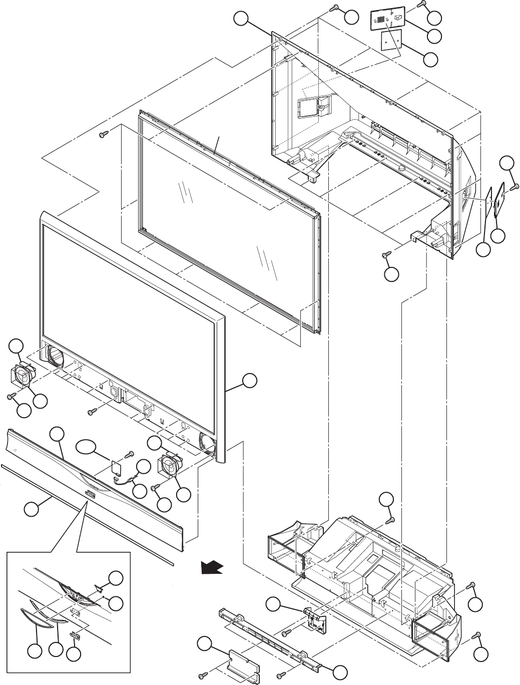
(No.YA463)3-5
EXPLODED VIEW -1 [HD-52FA97]
SCREEN BLOCK
12
10
11
9
23
22
23
20
7
10 7
8
201
5
6
4
2
3
1
2
3
4
21
19
24
14
18
17
16 15
FRONT
23
23
13
25

3-6(No.YA463)
EXPLODED VIEW PARTS LIST -2 [HD-52FA97]
Ref.No. Part No. Part Name Description Local
31 LC33055-003B GLASS MIRROR
32 LC12362-002A-A MIRROR HOLDER TOP
33 LC12371-001A-A MIRROR HOLDER BOTTOM
34 LC21538-001A-A MIRROR HOLDER RIGHT
35 LC21538-002A-A MIRROR HOLDER LEFT
36 LC21931-003A-A SPONGE SPACER (x5)
37 LC33046-003A-A SIDE CONTROL SHEET
38 LC21805-001A-A SIDE CONTROL BASE
39 WJZ0221-001A-E E-HARNESS ASSY SIDE CONTROL S1/S2/S3 - ANALOG
40 LC12305-001A-A SPEAKER BOX LEFT
41 LC12306-001A-A SPEAKER BOX COVER LEFT
42 LC12305-002A-A SPEAKER BOX RIGHT
43 LC12306-002A-A SPEAKER BOX COVER RIGHT
44 LC40506-003A-A TAPPING SCREW (x2)
45 LC40226-005A-H SPACER (x2)
46 QYSBSFG4016MA TAP SCREW (x6)
47 LC12263-001G-A BODY
48 LC12364-001B-A SCREEN HOLDER FRONT TOP/BOTTOM(x2)
49 LC12366-001A-A SCREEN HOLDER FRONT LEFT/RIGHT(x2)
50 LC12365-001B-A SCREEN HOLDER BACK TOP/BOTTOM(x2)
51 LC12367-001A-A SCREEN HOLDER BACK LEFT/RIGHT(x2)
52 52SC-006A-M2 SCREEN ASSY
53 LC21715-020A-A SPONGE SPACER (x4)
54 LC21715-034A-A SPONGE SPACER (x2)
55 QQR0491-001 FERRITE CORE
202 SRA0L013A-M2 SIDE CONTROL PWB
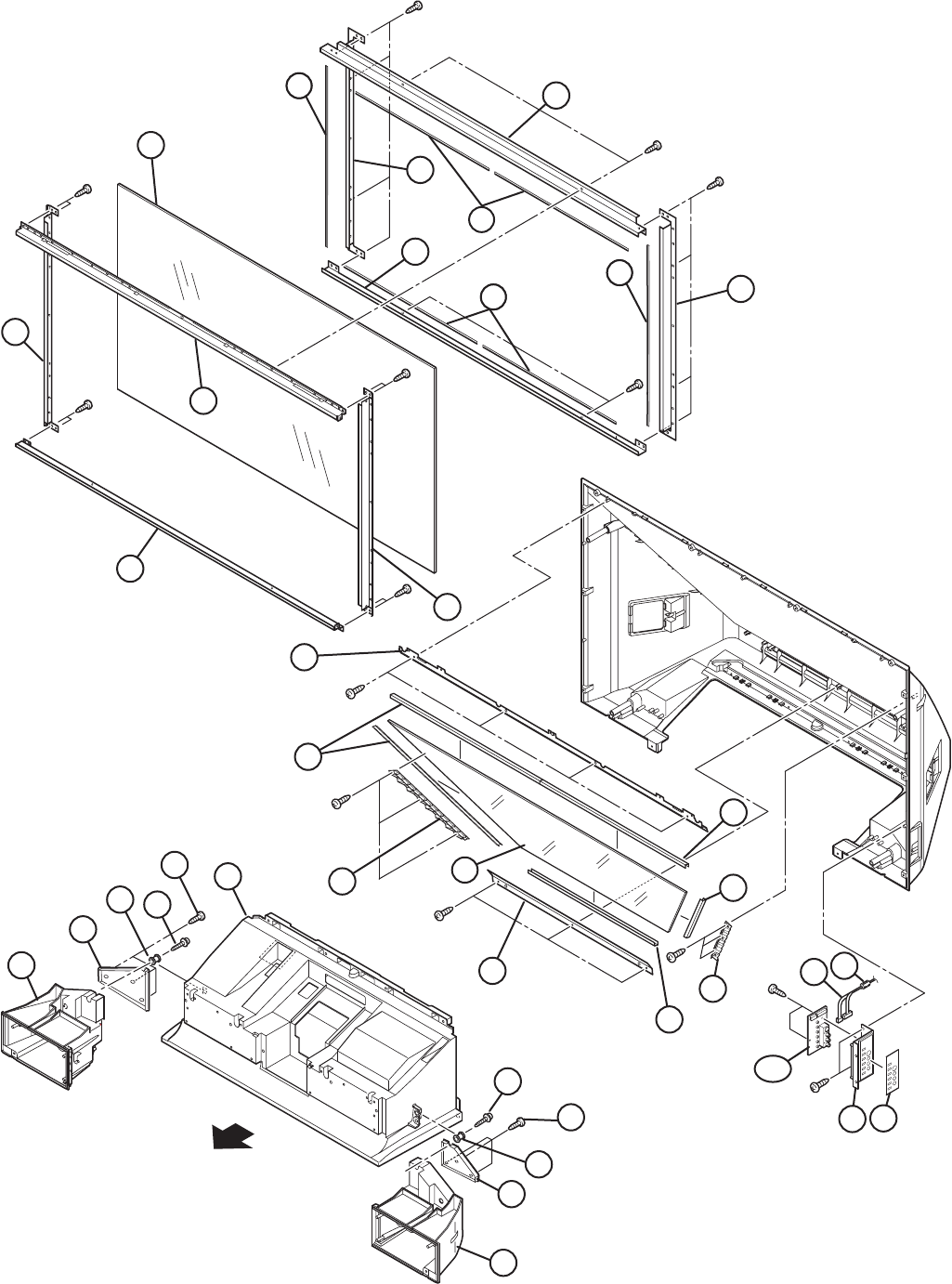
(No.YA463)3-7
EXPLODED VIEW -2 [HD-52FA97]
3
54
53
53
3
54
52
51
50
51
50
48
49
48
42
43
46
45 44
47
35
202
39
38 37
31
36
36
40
41
44
45
46
33
36
34
36
32
49
FRONT
55

3-8(No.YA463)
EXPLODED VIEW PARTS LIST -3 [HD-56FB97, HD-61FB97]
Ref.No. Part No. Part Name Description Local
1 LC12698-004A-A SPEAKER GRILL HD-56FB97
1 LC12746-003A-A SPEAKER GRILL HD-61FB97
2 QYSBSFG4016MA TAP SCREW M4 x 16mm(x4)
3 LC12695-005A-A FRONT PANEL HD-56FB97
3 LC12745-004A-A FRONT PANEL HD-61FB97
4 QAS0437-001 SPEAKER SP01/SP02(x2)
5 QYSBSFG4016MA TAP SCREW M4 x 16mm(x8)
6 WJJ0487-001A-E E-SI C WIRE C-C for SPEAKER
7 WJJ0487-002A-E E-SI C WIRE C-C for SPEAKER
8 WJJ0486-001A-E E-SI C WIRE C-C FRONT LED CN9F - ANALOG
9 LC33535-003A-C JVC MARK
10 LC33460-003A ORNAMENT PLATE
11 LC22099-001B-A POWER KNOB
12 LC22100-001B-A KNOB BASE
13 LC12727-001A-A CENTER COVER
14 QYSBSFG4016MA TAP SCREW M4 x 16mm(x10)
15 56ILASC11AM2 SCREEN ASSY HD-56FB97
15 61SC-012A-M2 SCREEN ASSY HD-61FB97
16 LC12717-001A-A SCREEN HOLDER TOP HD-56FB97
16 LC12751-001A-A SCREEN HOLDER TOP HD-61FB97
17 LC12718-001A-A SCREEN HOLDER BOTTOM HD-56FB97
17 LC12752-001A-A SCREEN HOLDER BOTTOM HD-61FB97
18 LC12716-001A-A SCREEN HOLDER LEFT/RIGHT(x2) HD-56FB97
18 LC12750-001A-A SCREEN HOLDER LEFT/RIGHT(x2) HD-61FB97
19 LC21715-038A-A SPONGE SPACER (x2) HD-56FB97
19 LC21715-033A-A SPONGE SPACER (x2) HD-61FB97
20 LC21715-039A-A SPONGE SPACER (x4) HD-56FB97
20 LC21715-042A-A SPONGE SPACER (x4) HD-61FB97
21 LC33504-001A-A SPEAKER DUCT (x2)
22 QQR0491-001 FERRITE CORE
201 SRA0L113A-M2 FRONT LED PWB
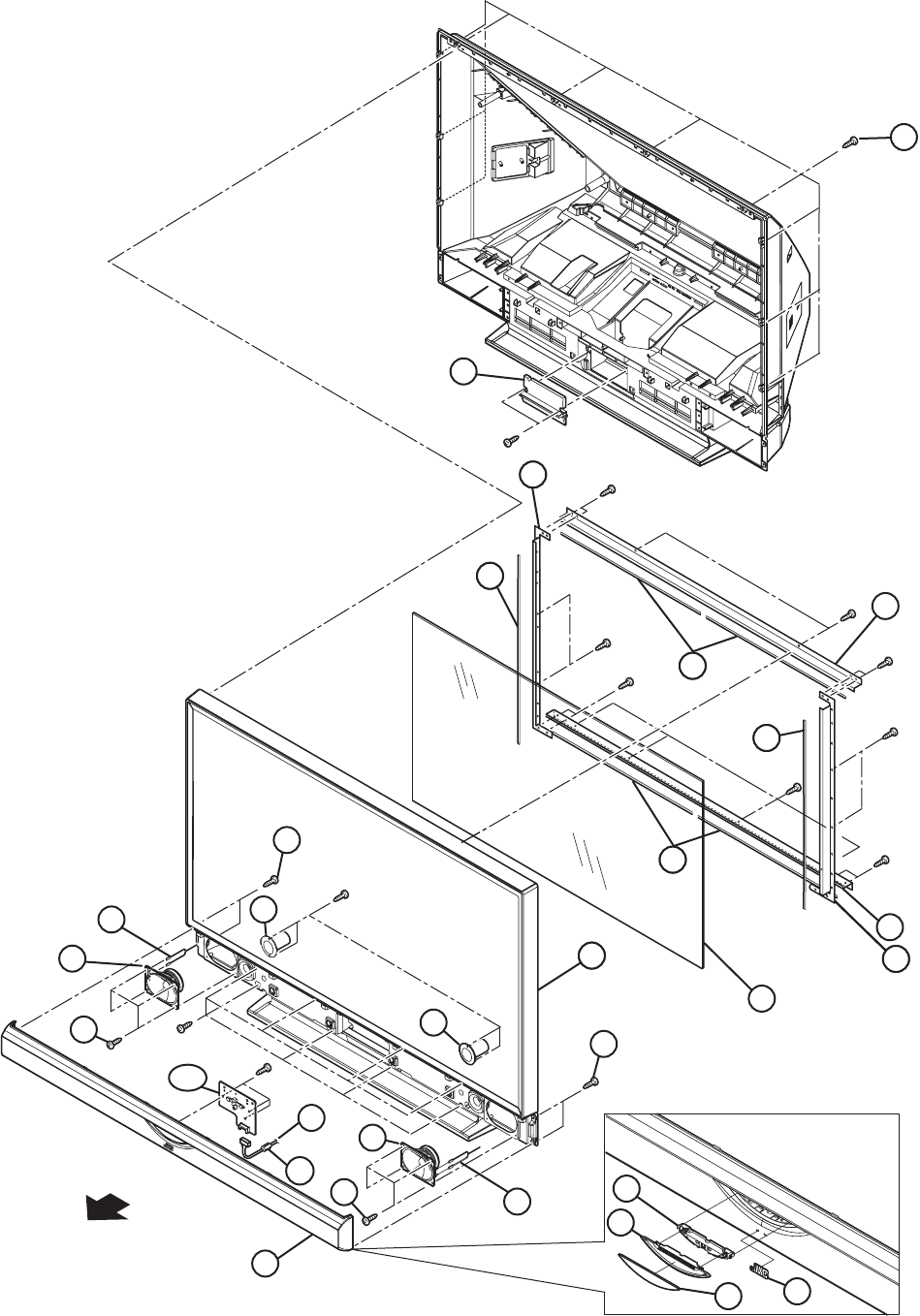
(No.YA463)3-9
EXPLODED VIEW -3 [HD-56FB97, HD-61FB97]
18
18
3
18
18
2
3
7
10 9
1
5
5
201
4
8
2
FRONT
3
19
3
20
3
21
21
4
12
13
11
14
16
17
20
6
15
22
3
19

3-10(No.YA463)
EXPLODED VIEW PARTS LIST -4 [HD-56FB97, HD-61FB97]
Ref.No. Part No. Part Name Description Local
31 LC12696-001B-A BACK COVER HD-56FB97
31 LC12743-001B-A BACK COVER HD-61FB97
32 LC21888-001B-A FILTER COVER (x2)
33 LC33541-001A-A FILTER (x2)
34 QYSBSFG4016MA TAP SCREW M4 x 16mm(x2)
35 LC12713-001A-A MIRROR HOLDER TOP HD-56FB97
35 LC12747-001A-A MIRROR HOLDER TOP HD-61FB97
36 LC33598-008A-A STICK SHEET (x2) HD-56FB97
36 LC33598-010A-A STICK SHEET (x2) HD-61FB97
37 LC33598-006A-A STICK SHEET (x2)
38 LC12715-001A-A MIRROR HOLDER LEFT/RIGHT(x2)
39 LC33507-002A GLASS MIRROR HD-56FB97
39 LC33507-003A GLASS MIRROR HD-61FB97
40 LC33598-008A-A STICK SHEET HD-56FB97
40 LC33598-010A-A STICK SHEET HD-61FB97
41 LC12714-001A-A MIRROR HOLDER BOTTOM(x2)
42 LC12697-001A-A BODY
43 LC22229-001B-A SUPPORT PLATE (x2) HD-56FB97
43 LC22230-001A SUPPORT PLATE (x2) HD-61FB97
44 LC33580-001A-0K SUPPORT BRACKET (x2)
45 WJZ0221-001A-E E-HARNESS ASSY S CONTROL CN08S1/CN08S2 - ANALOG
46 LC33463-001A-A SIDE CONTROL SHEET
47 LC22101-001B-A SIDE CONTROL BASE
48 LC22201-001A-A SHADE COVER
49 QQR0491-001 FERRITE CORE
202 SRA0L013A-M2 SIDE CONTROL PWB
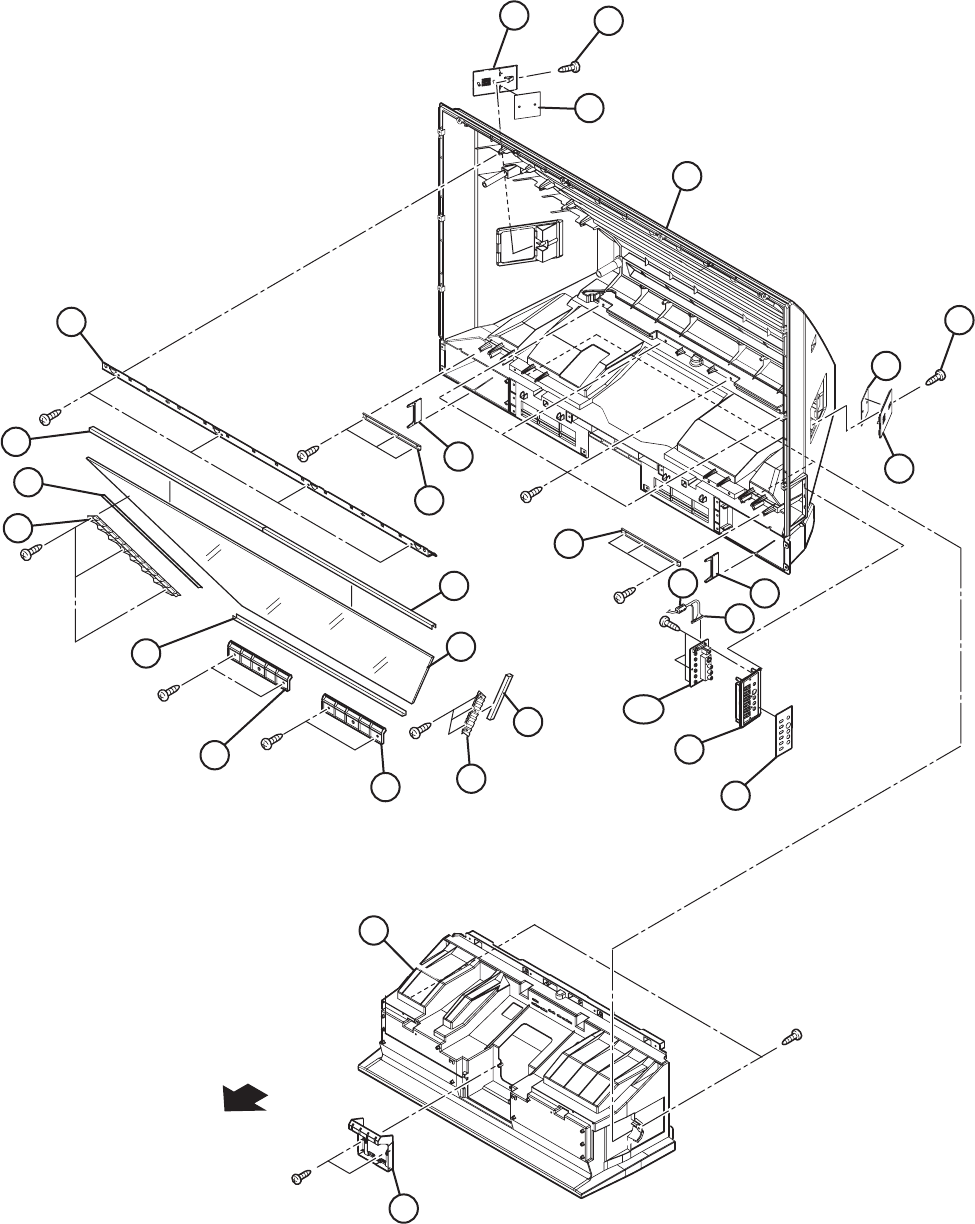
(No.YA463)3-11
EXPLODED VIEW -4 [HD-56FB97, HD-61FB97]
202
47
33
46
32
44
45
43
38
37
36
36
35
34
34
31
32
33
43
44
41
40 39
41
37
38
42
48
FRONT
49

3-12(No.YA463)
EXPLODED VIEW PARTS LIST -5
Ref.No. Part No. Part Name Description Local
71 QYSBSFG4016MA TAP SCREW M4 x 16mm(x11) HD-52FA97
71 QYSBSFG4016MA TAP SCREW M4 x 16mm(x7) HD-56FB97,HD-61FB97
72 QYSBSG4012ZA TAP SCREW M4 x 12mm(x5)
73 LC22113-010A-A AV TERMINAL BOARD
74 QYSBSF3012MA TAP SCREW M3 x 12mm(x7)
75 QYSBSG4012ZA TAP SCREW M4 x 12mm(x3)
76 LC12259-001C-A BODY COVER
77 QNB0036-001 CONN ACCESSORY (x2)
78 QYSBSG3008ZA TAP SCREW M3 x 8mm(x5)
79 CM46798-001 WASHER
80 LC42119-001A NUT
81 QMPD290-200-JC POWER CORD(US/CA) 2m BLACK
82 LC20106-001D-A POWER CORD CLAMP
83 QQR0491-001 FERRITE CORE (x8)
84 QYSBSFG4016MA TAP SCREW M4 x 16mm(x2)
85 LC42077-001A-A ASSY SCREW
86 LC33208-001A-A WARNING SHEET
87 LC12307-001C-A LAMP COVER
88 LC42276-001A-A INSERT NUT
89 TS-CL110UAA LAMP UNIT
90 LC11943-001B-A BODY BRACKET
91 QYSBSFG4016MA TAP SCREW M4 x 16mm(x4)
92 QYSBSGG3008ZA TAP SCREW M3 x 8mm(x7)
93 QUQK12-2514CH-E FFC WIRE TUNER CNT1 - ANALOG CN1T1
95 WJX0035-001A-E E-COAXIAL ASSY TUNER
96 WJZ0222-001A-E E-HARNESS ASSY ANALOG CN1F/CN1S1/CN1S2 - FLONT LED/S CONTROL
97 QJJ015-122012-E SIN CR C-C WIRE ANALOG CN1A3 - POWER CN9A3
98 QJJ015-053010-E SIN CR C-C WIRE ANALOG CN1A2 - POWER CN9A2
99 QJJ061-062211-E SIN CR C-C WIRE ANALOG CN1A1 - POWER CN9A1
100 WJJ0485-003A-E E-SI C WIRE C-C
101 QAR0404-001 COOLING FAN
102 QUQL05-4013AE-E FFC WIRE DIGITAL CN012 - ANALOG CN012
103 QUQL05-5013AE-E FFC WIRE DIGITAL CN011 - ANALOG CN011
104 WJW0051-001A-E E-TWISTED ASSY DIGITAL CN0LV1 - DRIVE CNLV1
105 WJJ0656-001A-E E-SI C WIRE C-C
106 WJJ0729-001A-E E-SI C WIRE C-C
107 WJZ0218-001A-E E-SI C WIRE C-C
108 LC42521-001A-A COVER SHEET
109 QQR0490-001 NOISE FILTER (x2)
110 WJJ0699-001A-E E-SI C WIRE C-C
111 QJJ015-099424-E SIN CR C-C WIRE
112 LC21690-002A-A LAMP DUCT BRACKET
113 LC33206-001A-A FOOT (x4)
203 SRA-9017A-M2 POWER PWB
204 SRA0R012A-M2 TUNER PWB
205 SRA-1024A-M2 ANALOG PWB
206 SSD-2205A-M2 ATSC TUNER MODULE PWB
207 SRA-8521A-M2 USB PWB
208 SRA0D161A-M2 DIGITAL PWB HD-52FA97
208 SRA0D160A-M2 DIGITAL PWB HD-56FB97
208 SRA0D159A-M2 DIGITAL PWB HD-61FB97
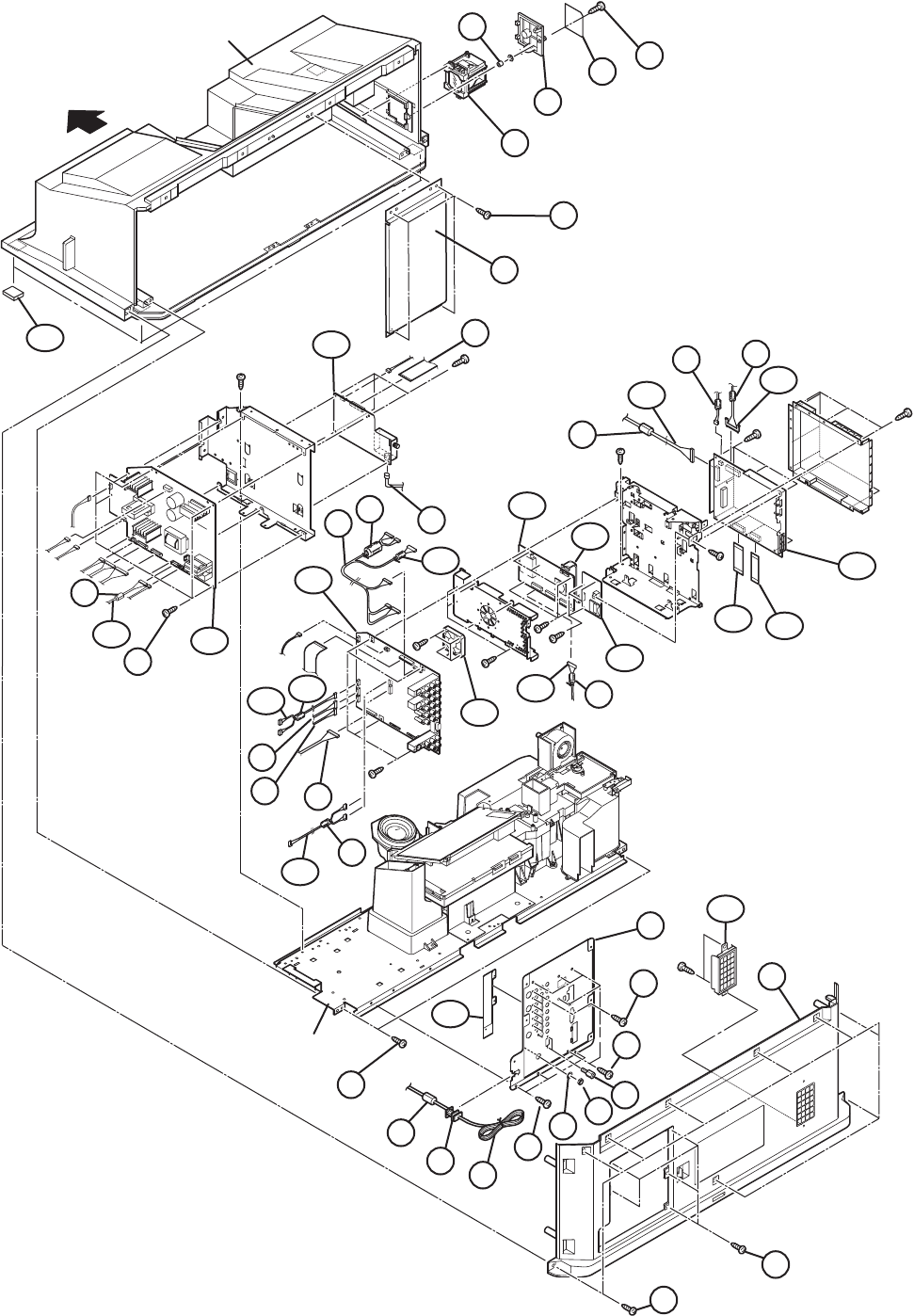
(No.YA463)3-13
EXPLODED VIEW -5
MAIN BODY
MAIN UNIT
FRONT
71
72
75
81
82
83
84
79
77
80
78
73
74 76
90
92
83
91
87
88
86
85
89
93
96 95
100
205
106
207
208
203
204
103 102
104
105
206
101
107
97
98
99
108
83
83
83
109
109 83
110
83
113
111
83
112

3-14(No.YA463)
EXPLODED VIEW PARTS LIST -6
Ref.No. Part No. Part Name Description Local
130 WJJ0708-001B-E E-HARNESS ASSY
131 QQR0490-001 NOISE FILTER (x7)
132 LC12369-001C-A UNIT BASE
133 QAR0368-003 COOLING FAN
134 LC42034-001A-A WELL NUT (x2)
135 LC12355-001B-A SIROCCO CASE T
136 QJJ015-041204-E SIN CR C-C WIRE
137 LC12352-001B-A HOLDER FAN
138 QAR0367-001 COOLING FAN
139 QYSBSFG4035MA TAP SCREW M4 x 35mm(x2)
140 LC42034-001A-A WELL NUT (x2)
141 QAR0354-002 COOLING FAN
142 QYSPSPD4040MA SCREW M4 x 40mm(x2)
143 LC12225-001A-A DUCT PCS
144 QMR0014-001 THERMO PROTECTOR
145 COP14A-SAA OPTICAL/DRIVE ASSY
146 LC12777-002A PJ LENS
147 QJJ015-034213-E SIN CR C-C WIRE
148 LC12353-001C-A BALLAST HOLDER
149 QAL0883-001 POWER UNIT ASSY
150 WJJ0664-001A-E E-SI C WIRE C-C
151 WJJ0652-003A-E E-SI C WIRE C-C
152 QQR0491-001 FERRITE CORE (x2)
209 SRA0L211A-M2 LAMP COVER SW PWB
210 SRA-3013A-M2 DRIVE PWB
212 SRA-8011A-M2 REMOCON PWB
213 SRA-8211A-M2 TEMP PWB
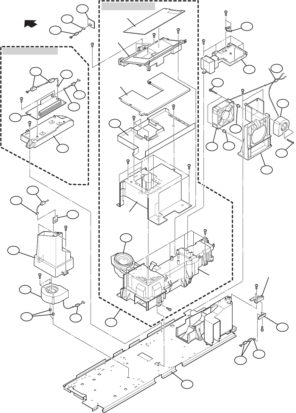
(No.YA463)3-15
EXPLODED VIEW -6
132
133
135
136
131
148
131
213
212
134
149
152
147
131
210
FRONT
SHIELD COVER
OPTICAL / DRIVE ASS'Y
LAMP BALLAST BLOC
LAMP COVER SW
BRACKET
TOP DUCT PLATE
SHIELD
TOP
CASE
TOP DUCT
OPTICAL
BLOCK
130
209
146
145
151
150
131
131
141
137
143
144
138
139
142
140
131
140

3-16(No.YA463)
PRINTED WIRING BOARD PARTS LIST [HD-52FA97]
ANALOG P.W. BOARD ASS'Y (SRA-1024A-M2)
Ref No. Part No. Part Name Description Local
IC101 R2S11004FT IC
IC102 R2S11003FT IC
IC601 NJW1182FP1 IC
IC602 PQ20WZ11-X IC
IC605 TDA8928ST/N1 IC
IC606 M62320FP-X IC
IC607 LM393DR-X IC
IC610 RC4558D-X IC
IC902 MM1663DT-X IC
Q106 SSM3K17FU-X MOS FET
Q107 SSM3K17FU-X MOS FET
Q108 2SC3928A/QR/-X TRANSISTOR
Q109 2SA1022/BC/-X TRANSISTOR
Q110 2SA1022/BC/-X TRANSISTOR
Q111 2SA1022/BC/-X TRANSISTOR
Q112 2SA1022/BC/-X TRANSISTOR
Q113 2SC3928A/QR/-X TRANSISTOR
Q451 UN2226-X DIGI TRANSISTOR
Q452 UN2226-X DIGI TRANSISTOR
Q453 UN2110-X DIGI TRANSISTOR
Q605 UN2212-X DIGI TRANSISTOR
Q606 UN2112-X DIGI TRANSISTOR
Q607 2SC3928A/QR/-X TRANSISTOR
Q614 2SA1530A/QR/-X TRANSISTOR
D105 1SS355W-X DIODE
D110 1SS355W-X DIODE
D121 MA8056/M/-X Z DIODE
D122 MA8056/M/-X Z DIODE
D123 MA8056/M/-X Z DIODE
D124 MA8056/M/-X Z DIODE
D125 MA8056/M/-X Z DIODE
D126 MA8056/M/-X Z DIODE
D133 MA8100/M/-X Z DIODE
D134 MA8100/M/-X Z DIODE
D135 MA8100/M/-X Z DIODE
D401 UDZW10B-X Z DIODE
D402 UDZW10B-X Z DIODE
D403 UDZW10B-X Z DIODE
D404 UDZW10B-X Z DIODE
D405 UDZW10B-X Z DIODE
D406 UDZW10B-X Z DIODE
D407 UDZW10B-X Z DIODE
D408 UDZW10B-X Z DIODE
D409 UDZW10B-X Z DIODE
D410 UDZW10B-X Z DIODE
D411 UDZW10B-X Z DIODE
D412 UDZW10B-X Z DIODE
D413 UDZW10B-X Z DIODE
D414 UDZW10B-X Z DIODE
D415 UDZW10B-X Z DIODE
D420 UDZW10B-X Z DIODE
D421 UDZW10B-X Z DIODE
D423 UDZW10B-X Z DIODE
D424 UDZW10B-X Z DIODE
D451 UDZW10B-X Z DIODE
D452 UDZW10B-X Z DIODE
D461 UDZW10B-X Z DIODE
D462 UDZW10B-X Z DIODE
D463 UDZW10B-X Z DIODE
D465 UDZW10B-X Z DIODE
D466 UDZW10B-X Z DIODE
D491 UDZW3.3B-X Z DIODE
D492 S9648 PHOTO CONDUCTOR
D601 1SS355W-X DIODE
D605 1SS355W-X DIODE
D606 1SS355W-X DIODE
D607 1SS355W-X DIODE
D608 1SS355W-X DIODE
D610 UDZW20B-X Z DIODE
D611 UDZW20B-X Z DIODE
D612 UDZW20B-X Z DIODE
D613 UDZW20B-X Z DIODE
D615 1SS355W-X DIODE
D616 UDZW3.3B-X Z DIODE
D618 1SS355W-X DIODE
D619 UDZW6.2B-X Z DIODE
D903 PTZ11B-X Z DIODE
D904 PTZ6.8B-X Z DIODE
C102 NCB11CK-225X C CAPACITOR 2.2uF 16V K
C103 NCB11CK-225X C CAPACITOR 2.2uF 16V K
C106 NEHL1EM-475X E CAPACITOR 4.7uF 25V M
C107 NCB31CK-104X C CAPACITOR 0.1uF 16V K
C108 NEHL1CM-476X E CAPACITOR 47uF 16V M
C109 NCB31CK-104X C CAPACITOR 0.1uF 16V K
C110 NCB31CK-104X C CAPACITOR 0.1uF 16V K
C115 NCB31CK-104X C CAPACITOR 0.1uF 16V K
C116 NCB31CK-104X C CAPACITOR 0.1uF 16V K
C117 NCB31CK-104X C CAPACITOR 0.1uF 16V K
C118 NCB31CK-105X C CAPACITOR 1uF 16V K
C119 NCB31CK-105X C CAPACITOR 1uF 16V K
C120 NCB31CK-105X C CAPACITOR 1uF 16V K
C121 NCB31CK-105X C CAPACITOR 1uF 16V K
C122 NCB31CK-104X C CAPACITOR 0.1uF 16V K
C123 NCB31CK-104X C CAPACITOR 0.1uF 16V K
C124 NCB31CK-105X C CAPACITOR 1uF 16V K
C125 NCB31CK-105X C CAPACITOR 1uF 16V K
C126 NCB31CK-105X C CAPACITOR 1uF 16V K
C127 NCB31CK-105X C CAPACITOR 1uF 16V K
C128 NCB31CK-104X C CAPACITOR 0.1uF 16V K
C129 NCB31CK-104X C CAPACITOR 0.1uF 16V K
C130 NEHL1CM-476X E CAPACITOR 47uF 16V M
C131 NCB31CK-104X C CAPACITOR 0.1uF 16V K
C132 NCB31CK-105X C CAPACITOR 1uF 16V K
C133 NCB31CK-105X C CAPACITOR 1uF 16V K
C134 NCB31CK-105X C CAPACITOR 1uF 16V K
C136 NCB31CK-104X C CAPACITOR 0.1uF 16V K
C137 NCB31CK-104X C CAPACITOR 0.1uF 16V K
C138 NCB31CK-103X C CAPACITOR 0.01uF 16V K
C140 NCB31CK-104X C CAPACITOR 0.1uF 16V K
C141 NEHL1CM-106X E CAPACITOR 10uF 16V M
C142 NCB31CK-104X C CAPACITOR 0.1uF 16V K
C143 NCB31CK-104X C CAPACITOR 0.1uF 16V K
C156 NCB31CK-103X C CAPACITOR 0.01uF 16V K
C157 NCB31CK-103X C CAPACITOR 0.01uF 16V K
C158 NCB31CK-103X C CAPACITOR 0.01uF 16V K
C159 NCB31HK-104X C CAPACITOR 0.1uF 50V K
C160 NCB31HK-104X C CAPACITOR 0.1uF 50V K
C161 NCB31CK-103X C CAPACITOR 0.01uF 16V K
C162 NCB31HK-104X C CAPACITOR 0.1uF 50V K
C163 NCB31CK-104X C CAPACITOR 0.1uF 16V K
C164 NCB31CK-104X C CAPACITOR 0.1uF 16V K
C165 NCB31CK-104X C CAPACITOR 0.1uF 16V K
C166 NCB31HK-103X C CAPACITOR 0.01uF 50V K
C167 NCB31CK-104X C CAPACITOR 0.1uF 16V K
C168 NCB31CK-104X C CAPACITOR 0.1uF 16V K
C169 NCB31CK-103X C CAPACITOR 0.01uF 16V K
C170 NCB31CK-103X C CAPACITOR 0.01uF 16V K
C171 NCB31CK-103X C CAPACITOR 0.01uF 16V K
C172 NCB31CK-104X C CAPACITOR 0.1uF 16V K
C173 NDC31HJ-680X C CAPACITOR 68pF 50V J
C174 NDC31HJ-331X C CAPACITOR 330pF 50V J
C175 NCB31CK-103X C CAPACITOR 0.01uF 16V K
C176 NCB31CK-103X C CAPACITOR 0.01uF 16V K
C177 NCB31CK-104X C CAPACITOR 0.1uF 16V K
C178 NCB31CK-105X C CAPACITOR 1uF 16V K
C179 NEHL1CM-476X E CAPACITOR 47uF 16V M
C180 NCB31CK-104X C CAPACITOR 0.1uF 16V K
C181 NCB31CK-103X C CAPACITOR 0.01uF 16V K
C182 NCB31CK-103X C CAPACITOR 0.01uF 16V K
C183 NCB31CK-103X C CAPACITOR 0.01uF 16V K
C184 NCB31CK-104X C CAPACITOR 0.1uF 16V K
C185 NCB31CK-104X C CAPACITOR 0.1uF 16V K
C187 NCB31CK-104X C CAPACITOR 0.1uF 16V K
C189 NEHL1CM-106X E CAPACITOR 10uF 16V M
C194 NCB21AK-225X C CAPACITOR 2.2uF 10V K
C195 NCB21AK-225X C CAPACITOR 2.2uF 10V K
C196 NCB21AK-225X C CAPACITOR 2.2uF 10V K
C197 NDC31HJ-101X C CAPACITOR 100pF 50V J
C198 NDC31HJ-101X C CAPACITOR 100pF 50V J
C199 NCB31CK-104X C CAPACITOR 0.1uF 16V K
C200 NCB31CK-104X C CAPACITOR 0.1uF 16V K
C201 NCB31CK-104X C CAPACITOR 0.1uF 16V K
C202 NCB31CK-104X C CAPACITOR 0.1uF 16V K
C203 NCB31CK-104X C CAPACITOR 0.1uF 16V K
C207 NCB11CK-225X C CAPACITOR 2.2uF 16V K
C208 NCB11CK-225X C CAPACITOR 2.2uF 16V K
C211 NDC31HJ-221X C CAPACITOR 220pF 50V J
C212 NDC31HJ-820X C CAPACITOR 82pF 50V J
C221 NCB31HK-103X C CAPACITOR 0.01uF 50V K
C222 NCB31HK-103X C CAPACITOR 0.01uF 50V K
C223 NDC31HJ-101X C CAPACITOR 100pF 50V J
C224 NDC31HJ-101X C CAPACITOR 100pF 50V J
C225 NDC31HJ-100X C CAPACITOR 10pF 50V J
C226 NDC31HJ-181X C CAPACITOR 180pF 50V J
C227 NDC31HJ-101X C CAPACITOR 100pF 50V J
C228 NDC31HJ-101X C CAPACITOR 100pF 50V J
C229 NDC31HJ-100X C CAPACITOR 10pF 50V J
C240 NDC31HJ-100X C CAPACITOR 10pF 50V J
C241 NDC31HJ-100X C CAPACITOR 10pF 50V J
Ref No. Part No. Part Name Description Local

(No.YA463)3-17
C242 NDC31HJ-100X C CAPACITOR 10pF 50V J
C245 NCB31CK-104X C CAPACITOR 0.1uF 16V K
C246 NCB31CK-104X C CAPACITOR 0.1uF 16V K
C291 NCB11AK-106X C CAPACITOR 10uF 10V K
C306 NEHL1EM-475X E CAPACITOR 4.7uF 25V M
C307 NEHL1EM-475X E CAPACITOR 4.7uF 25V M
C401 NCB31HK-103X C CAPACITOR 0.01uF 50V K
C402 NEHL1CM-106X E CAPACITOR 10uF 16V M
C403 NEHL1CM-106X E CAPACITOR 10uF 16V M
C404 NCB21AK-225X C CAPACITOR 2.2uF 10V K
C405 NCB21AK-225X C CAPACITOR 2.2uF 10V K
C406 NCB21AK-225X C CAPACITOR 2.2uF 10V K
C407 NCB21AK-225X C CAPACITOR 2.2uF 10V K
C408 NCB21AK-225X C CAPACITOR 2.2uF 10V K
C409 NEHL1CM-106X E CAPACITOR 10uF 16V M
C410 NCB21AK-225X C CAPACITOR 2.2uF 10V K
C411 NCB21AK-225X C CAPACITOR 2.2uF 10V K
C412 NCB21AK-225X C CAPACITOR 2.2uF 10V K
C413 NCB21AK-225X C CAPACITOR 2.2uF 10V K
C414 NCB21AK-225X C CAPACITOR 2.2uF 10V K
C418 NCB21AK-225X C CAPACITOR 2.2uF 10V K
C419 NCB21AK-225X C CAPACITOR 2.2uF 10V K
C422 NCB21AK-225X C CAPACITOR 2.2uF 10V K
C423 NCB21AK-225X C CAPACITOR 2.2uF 10V K
C451 NCB11CK-225X C CAPACITOR 2.2uF 16V K
C452 NCB11CK-225X C CAPACITOR 2.2uF 16V K
C453 NCB11CK-105X C CAPACITOR 1uF 16V K
C461 NDC31HJ-101X C CAPACITOR 100pF 50V J
C462 NDC31HJ-101X C CAPACITOR 100pF 50V J
C463 NDC31HJ-101X C CAPACITOR 100pF 50V J
C464 NCB21AK-225X C CAPACITOR 2.2uF 10V K
C465 NCB21AK-225X C CAPACITOR 2.2uF 10V K
C466 NCB21AK-225X C CAPACITOR 2.2uF 10V K
C468 NDC31HJ-101X C CAPACITOR 100pF 50V J
C469 NDC31HJ-101X C CAPACITOR 100pF 50V J
C491 NEHL1CM-106X E CAPACITOR 10uF 16V M
C492 NCB31CK-104X C CAPACITOR 0.1uF 16V K
C493 NEHL1CM-107X E CAPACITOR 100uF 16V M
C494 NCB31HK-102X C CAPACITOR 1000pF 50V K
C601 NCB31HK-103X C CAPACITOR 0.01uF 50V K
C602 NEHL1EM-336X E CAPACITOR 33uF 25V M
C603 NEHL1EM-336X E CAPACITOR 33uF 25V M
C604 NCB31EK-104X C CAPACITOR 0.1uF 25V K
C605 NCB31HK-103X C CAPACITOR 0.01uF 50V K
C606 NCB31HK-104X C CAPACITOR 0.1uF 50V K
C607 QETM1EM-477 E CAPACITOR 470uF 25V M
C616 NEHL1EM-475X E CAPACITOR 4.7uF 25V M
C617 NEHL1EM-475X E CAPACITOR 4.7uF 25V M
C623 NCB21CK-184X C CAPACITOR 0.18uF 16V K
C624 NCB31HK-222X C CAPACITOR 2200pF 50V K
C625 NCB31HK-183X C CAPACITOR 0.018uF 50V K
C628 NCB31HK-123X C CAPACITOR 0.012uF 50V K
C629 NCB31HK-222X C CAPACITOR 2200pF 50V K
C630 NCB21CK-184X C CAPACITOR 0.18uF 16V K
C632 NCB31HK-104X C CAPACITOR 0.1uF 50V K
C633 NCB31HK-822X C CAPACITOR 8200pF 50V K
C634 NCB31HK-822X C CAPACITOR 8200pF 50V K
C635 NCB31HK-681X C CAPACITOR 680pF 50V K
C636 NCB31HK-681X C CAPACITOR 680pF 50V K
C638 NCB31EK-223X C CAPACITOR 0.022uF 25V K
C639 NCB31HK-104X C CAPACITOR 0.1uF 50V K
C643 NCB31HK-104X C CAPACITOR 0.1uF 50V K
C644 NEHL1EM-475X E CAPACITOR 4.7uF 25V M
C647 NCB31CK-105X C CAPACITOR 1uF 16V K
C648 NCB31CK-105X C CAPACITOR 1uF 16V K
C649 NCB31CK-105X C CAPACITOR 1uF 16V K
C650 NCB31CK-105X C CAPACITOR 1uF 16V K
C651 NCB31CK-105X C CAPACITOR 1uF 16V K
C653 NCB31EK-223X C CAPACITOR 0.022uF 25V K
C654 NCB31CK-473X C CAPACITOR 0.047uF 16V K
C655 NEHL1CM-106X E CAPACITOR 10uF 16V M
C659 NEHL1CM-106X E CAPACITOR 10uF 16V M
C660 NCB31CK-105X C CAPACITOR 1uF 16V K
C661 NCB31CK-105X C CAPACITOR 1uF 16V K
C662 NCB21AK-225X C CAPACITOR 2.2uF 10V K
C663 NCB31CK-105X C CAPACITOR 1uF 16V K
C664 NCB31CK-105X C CAPACITOR 1uF 16V K
C665 NCB31CK-105X C CAPACITOR 1uF 16V K
C666 NEHL1CM-106X E CAPACITOR 10uF 16V M
C667 NCB31CK-105X C CAPACITOR 1uF 16V K
C668 NCB31CK-105X C CAPACITOR 1uF 16V K
C669 NCB31CK-105X C CAPACITOR 1uF 16V K
C679 NDC31HJ-101X C CAPACITOR 100pF 50V J
C680 NDC31HJ-101X C CAPACITOR 100pF 50V J
C681 NCB31CK-104X C CAPACITOR 0.1uF 16V K
C682 NCB31CK-104X C CAPACITOR 0.1uF 16V K
C683 NCB31HK-332X C CAPACITOR 3300pF 50V K
C684 NCB31HK-332X C CAPACITOR 3300pF 50V K
C685 NCB31HK-222X C CAPACITOR 2200pF 50V K
C686 NCB31HK-222X C CAPACITOR 2200pF 50V K
Ref No. Part No. Part Name Description Local
C687 NCB31HK-472X C CAPACITOR 4700pF 50V K
C688 NCB31HK-472X C CAPACITOR 4700pF 50V K
C689 NCB31HK-104X C CAPACITOR 0.1uF 50V K
C690 NCB31HK-104X C CAPACITOR 0.1uF 50V K
C691 NEHL1EM-226X E CAPACITOR 22uF 25V M
C692 NEHL1EM-226X E CAPACITOR 22uF 25V M
C693 NCB11EK-105X C CAPACITOR 1uF 25V K
C694 NCB11EK-105X C CAPACITOR 1uF 25V K
C697 NCB31HK-104X C CAPACITOR 0.1uF 50V K
C698 NCB31HK-104X C CAPACITOR 0.1uF 50V K
C699 QETM1HM-226 E CAPACITOR 22uF 50V M
C700 QETM1HM-226 E CAPACITOR 22uF 50V M
C701 NCB31HK-104X C CAPACITOR 0.1uF 50V K
C702 QETM1EM-477 E CAPACITOR 470uF 25V M
C704 NCB31HK-104X C CAPACITOR 0.1uF 50V K
C705 QETM1EM-477 E CAPACITOR 470uF 25V M
C707 NCB31HK-104X C CAPACITOR 0.1uF 50V K
C708 NCB31HK-561X C CAPACITOR 560pF 50V K
C709 NCB31HK-561X C CAPACITOR 560pF 50V K
C711 NCB31HK-561X C CAPACITOR 560pF 50V K
C712 NCB31HK-561X C CAPACITOR 560pF 50V K
C713 QFVF1HJ-224Z MF CAPACITOR 0.22uF 50V J
C716 NEHL1CM-476X E CAPACITOR 47uF 16V M
C717 NCB31CK-105X C CAPACITOR 1uF 16V K
C719 QFVF1HJ-224Z MF CAPACITOR 0.22uF 50V J
C720 QFVF1HJ-224Z MF CAPACITOR 0.22uF 50V J
C721 QFVF1HJ-224Z MF CAPACITOR 0.22uF 50V J
C722 NCB31HK-153X C CAPACITOR 0.015uF 50V K
C723 NCB31HK-153X C CAPACITOR 0.015uF 50V K
C724 NCB31HK-104X C CAPACITOR 0.1uF 50V K
C727 NCB31HK-104X C CAPACITOR 0.1uF 50V K
C728 QETM1EM-477 E CAPACITOR 470uF 25V M
C734 NENA1CM-475X BP E CAPACITOR 4.7uF 16V M
C739 NENA1CM-475X BP E CAPACITOR 4.7uF 16V M
C740 NEHL1CM-476X E CAPACITOR 47uF 16V M
C741 NEHL1CM-476X E CAPACITOR 47uF 16V M
C742 NEHL1HM-105X E CAPACITOR 1uF 50V M
C743 NEHL1HM-105X E CAPACITOR 1uF 50V M
C744 NDC31HJ-100X C CAPACITOR 10pF 50V J
C745 NDC31HJ-100X C CAPACITOR 10pF 50V J
C904 NCB11AK-106X C CAPACITOR 10uF 10V K
C905 NEHM1CM-476X E CAPACITOR 47uF 16V M
C911 NEX51CM-335X E CAPACITOR 3.3uF 16V M
C913 NEX51CM-335X E CAPACITOR 3.3uF 16V M
C914 NEX50JM-156X E CAPACITOR 15uF 6.3V M
C916 NEX50JM-156X E CAPACITOR 15uF 6.3V M
R136 NRSA63J-0R0X MG RESISTOR 0
Ω
1/16W J
R137 NRSA63J-0R0X MG RESISTOR 0
Ω
1/16W J
R140 NRSA63J-682X MG RESISTOR 6.8k
Ω
1/16W J
R141 NRSA63J-682X MG RESISTOR 6.8k
Ω
1/16W J
R142 NRSA63J-333X MG RESISTOR 33k
Ω
1/16W J
R143 NRSA63J-682X MG RESISTOR 6.8k
Ω
1/16W J
R144 NRSA63J-682X MG RESISTOR 6.8k
Ω
1/16W J
R145 NRSA63J-333X MG RESISTOR 33k
Ω
1/16W J
R146 NRSA63J-682X MG RESISTOR 6.8k
Ω
1/16W J
R147 NRSA63J-682X MG RESISTOR 6.8k
Ω
1/16W J
R148 NRSA63J-0R0X MG RESISTOR 0
Ω
1/16W J
R149 NRSA63J-0R0X MG RESISTOR 0
Ω
1/16W J
R150 NRSA63J-333X MG RESISTOR 33k
Ω
1/16W J
R151 NRSA63J-682X MG RESISTOR 6.8k
Ω
1/16W J
R152 NRSA63J-682X MG RESISTOR 6.8k
Ω
1/16W J
R153 NRSA63J-682X MG RESISTOR 6.8k
Ω
1/16W J
R154 NRSA63J-682X MG RESISTOR 6.8k
Ω
1/16W J
R157 NRSA63J-333X MG RESISTOR 33k
Ω
1/16W J
R158 NRSA63J-682X MG RESISTOR 6.8k
Ω
1/16W J
R159 NRSA63J-682X MG RESISTOR 6.8k
Ω
1/16W J
R160 NRSA63J-682X MG RESISTOR 6.8k
Ω
1/16W J
R161 NRSA63J-682X MG RESISTOR 6.8k
Ω
1/16W J
R164 NRSA63J-224X MG RESISTOR 220k
Ω
1/16W J
R165 NRSA63J-224X MG RESISTOR 220k
Ω
1/16W J
R166 NRSA63J-224X MG RESISTOR 220k
Ω
1/16W J
R167 NRSA63J-224X MG RESISTOR 220k
Ω
1/16W J
R168 NRSA63J-101X MG RESISTOR 100
Ω
1/16W J
R169 NRSA63J-101X MG RESISTOR 100
Ω
1/16W J
R170 NRSA63J-0R0X MG RESISTOR 0
Ω
1/16W J
R171 NRSA63J-0R0X MG RESISTOR 0
Ω
1/16W J
R172 NRSA63J-0R0X MG RESISTOR 0
Ω
1/16W J
R174 NRSA63J-0R0X MG RESISTOR 0
Ω
1/16W J
R175 NRSA63J-0R0X MG RESISTOR 0
Ω
1/16W J
R176 NRSA63J-0R0X MG RESISTOR 0
Ω
1/16W J
R178 NRSA63J-0R0X MG RESISTOR 0
Ω
1/16W J
R181 NRSA63J-224X MG RESISTOR 220k
Ω
1/16W J
R184 NRSA63J-224X MG RESISTOR 220k
Ω
1/16W J
R189 NRSA63J-0R0X MG RESISTOR 0
Ω
1/16W J
R204 NRSA63J-0R0X MG RESISTOR 0
Ω
1/16W J
R205 NRSA63J-0R0X MG RESISTOR 0
Ω
1/16W J
R206 NRSA63J-562X MG RESISTOR 5.6k
Ω
1/16W J
R207 NRSA63J-562X MG RESISTOR 5.6k
Ω
1/16W J
R208 NRSA63J-0R0X MG RESISTOR 0
Ω
1/16W J
Ref No. Part No. Part Name Description Local

3-18(No.YA463)
R209 NRSA63J-0R0X MG RESISTOR 0
Ω
1/16W J
R210 NRSA63J-0R0X MG RESISTOR 0
Ω
1/16W J
R219 NRSA63J-101X MG RESISTOR 100
Ω
1/16W J
R220 NRSA63J-101X MG RESISTOR 100
Ω
1/16W J
R221 NRSA63J-0R0X MG RESISTOR 0
Ω
1/16W J
R223 NRSA63J-223X MG RESISTOR 22k
Ω
1/16W J
R224 NRSA63J-223X MG RESISTOR 22k
Ω
1/16W J
R225 NRSA63J-103X MG RESISTOR 10k
Ω
1/16W J
R228 NRSA63J-0R0X MG RESISTOR 0
Ω
1/16W J
R229 NRSA63J-0R0X MG RESISTOR 0
Ω
1/16W J
R230 NRSA63J-0R0X MG RESISTOR 0
Ω
1/16W J
R231 NRSA63J-0R0X MG RESISTOR 0
Ω
1/16W J
R232 NRSA63J-0R0X MG RESISTOR 0
Ω
1/16W J
R233 NRSA63J-0R0X MG RESISTOR 0
Ω
1/16W J
R234 NRSA63J-0R0X MG RESISTOR 0
Ω
1/16W J
R235 NRSA63J-0R0X MG RESISTOR 0
Ω
1/16W J
R241 NRSA63J-0R0X MG RESISTOR 0
Ω
1/16W J
R243 NRSA63J-0R0X MG RESISTOR 0
Ω
1/16W J
R245 NRSA63J-0R0X MG RESISTOR 0
Ω
1/16W J
R246 NRSA63J-0R0X MG RESISTOR 0
Ω
1/16W J
R247 NRSA63J-0R0X MG RESISTOR 0
Ω
1/16W J
R248 NRSA63J-0R0X MG RESISTOR 0
Ω
1/16W J
R249 NRSA63J-0R0X MG RESISTOR 0
Ω
1/16W J
R251 NRSA63J-0R0X MG RESISTOR 0
Ω
1/16W J
R252 NRSA63J-0R0X MG RESISTOR 0
Ω
1/16W J
R253 NRSA63J-0R0X MG RESISTOR 0
Ω
1/16W J
R255 NRSA63J-0R0X MG RESISTOR 0
Ω
1/16W J
R256 NRSA63J-0R0X MG RESISTOR 0
Ω
1/16W J
R257 NRSA63J-0R0X MG RESISTOR 0
Ω
1/16W J
R259 NRSA63J-0R0X MG RESISTOR 0
Ω
1/16W J
R260 NRSA63J-101X MG RESISTOR 100
Ω
1/16W J
R261 NRSA63J-272X MG RESISTOR 2.7k
Ω
1/16W J
R262 NRSA63J-101X MG RESISTOR 100
Ω
1/16W J
R263 NRSA63J-331X MG RESISTOR 330
Ω
1/16W J
R264 NRSA63J-101X MG RESISTOR 100
Ω
1/16W J
R265 NRSA63J-331X MG RESISTOR 330
Ω
1/16W J
R266 NRSA63J-101X MG RESISTOR 100
Ω
1/16W J
R267 NRSA63J-331X MG RESISTOR 330
Ω
1/16W J
R282 NRSA63J-0R0X MG RESISTOR 0
Ω
1/16W J
R283 NRSA63J-0R0X MG RESISTOR 0
Ω
1/16W J
R286 NRSA63J-0R0X MG RESISTOR 0
Ω
1/16W J
R299 NRSA63J-0R0X MG RESISTOR 0
Ω
1/16W J
R301 NRSA63J-0R0X MG RESISTOR 0
Ω
1/16W J
R302 NRSA63J-0R0X MG RESISTOR 0
Ω
1/16W J
R316 NRSA63J-104X MG RESISTOR 100k
Ω
1/16W J
R317 NRSA63J-104X MG RESISTOR 100k
Ω
1/16W J
R318 NRSA63J-0R0X MG RESISTOR 0
Ω
1/16W J
R319 NRSA63J-0R0X MG RESISTOR 0
Ω
1/16W J
R324 NRSA63J-0R0X MG RESISTOR 0
Ω
1/16W J
R325 NRSA63J-0R0X MG RESISTOR 0
Ω
1/16W J
R395 NRSA63J-0R0X MG RESISTOR 0
Ω
1/16W J
R401 NRSA63J-750X MG RESISTOR 75
Ω
1/16W J
R402 NRSA63J-750X MG RESISTOR 75
Ω
1/16W J
R403 NRSA63J-750X MG RESISTOR 75
Ω
1/16W J
R404 NRSA63J-224X MG RESISTOR 220k
Ω
1/16W J
R405 NRSA63J-224X MG RESISTOR 220k
Ω
1/16W J
R407 NRSA63J-750X MG RESISTOR 75
Ω
1/16W J
R408 NRSA63J-750X MG RESISTOR 75
Ω
1/16W J
R409 NRSA63J-750X MG RESISTOR 75
Ω
1/16W J
R410 NRSA63J-750X MG RESISTOR 75
Ω
1/16W J
R411 NRSA63J-224X MG RESISTOR 220k
Ω
1/16W J
R412 NRSA63J-224X MG RESISTOR 220k
Ω
1/16W J
R413 NRSA63J-750X MG RESISTOR 75
Ω
1/16W J
R414 NRSA63J-750X MG RESISTOR 75
Ω
1/16W J
R415 NRSA63J-750X MG RESISTOR 75
Ω
1/16W J
R419 NRSA63J-224X MG RESISTOR 220k
Ω
1/16W J
R420 NRSA63J-224X MG RESISTOR 220k
Ω
1/16W J
R422 NRSA63J-224X MG RESISTOR 220k
Ω
1/16W J
R423 NRSA63J-224X MG RESISTOR 220k
Ω
1/16W J
R451 NRSA63J-221X MG RESISTOR 220
Ω
1/16W J
R452 NRSA63J-823X MG RESISTOR 82k
Ω
1/16W J
R453 NRSA63J-471X MG RESISTOR 470
Ω
1/16W J
R454 NRSA63J-221X MG RESISTOR 220
Ω
1/16W J
R455 NRSA63J-823X MG RESISTOR 82k
Ω
1/16W J
R456 NRSA63J-471X MG RESISTOR 470
Ω
1/16W J
R457 NRSA63J-102X MG RESISTOR 1k
Ω
1/16W J
R458 NRSA63J-393X MG RESISTOR 39k
Ω
1/16W J
R461 NRSA63J-750X MG RESISTOR 75
Ω
1/16W J
R462 NRSA63J-0R0X MG RESISTOR 0
Ω
1/16W J
R463 NRSA63J-0R0X MG RESISTOR 0
Ω
1/16W J
R464 NRSA63J-750X MG RESISTOR 75
Ω
1/16W J
R465 NRSA63J-0R0X MG RESISTOR 0
Ω
1/16W J
R466 NRSA63J-0R0X MG RESISTOR 0
Ω
1/16W J
R467 NRSA63J-750X MG RESISTOR 75
Ω
1/16W J
R468 NRSA63J-0R0X MG RESISTOR 0
Ω
1/16W J
R469 NRSA63J-0R0X MG RESISTOR 0
Ω
1/16W J
R470 NRSA63J-0R0X MG RESISTOR 0
Ω
1/16W J
R472 NRSA63J-0R0X MG RESISTOR 0
Ω
1/16W J
R474 NRSA63J-0R0X MG RESISTOR 0
Ω
1/16W J
R475 NRSA63J-102X MG RESISTOR 1k
Ω
1/16W J
Ref No. Part No. Part Name Description Local
R476 NRSA63J-102X MG RESISTOR 1k
Ω
1/16W J
R491 NRSA63J-105X MG RESISTOR 1M
Ω
1/16W J
R584 NRSA63J-103X MG RESISTOR 10k
Ω
1/16W J
R585 NRSA63J-103X MG RESISTOR 10k
Ω
1/16W J
R588 NRSA63J-0R0X MG RESISTOR 0
Ω
1/16W J
R589 NRSA63J-0R0X MG RESISTOR 0
Ω
1/16W J
R590 NRSA63J-0R0X MG RESISTOR 0
Ω
1/16W J
R591 NRSA63J-0R0X MG RESISTOR 0
Ω
1/16W J
R592 NRSA63J-0R0X MG RESISTOR 0
Ω
1/16W J
R593 NRSA63J-0R0X MG RESISTOR 0
Ω
1/16W J
R594 NRSA63J-0R0X MG RESISTOR 0
Ω
1/16W J
R597 NRSA63J-331X MG RESISTOR 330
Ω
1/16W J
R598 NRSA63J-330X MG RESISTOR 33
Ω
1/16W J
R599 NRSA63J-471X MG RESISTOR 470
Ω
1/16W J
R601 NRSA63J-0R0X MG RESISTOR 0
Ω
1/16W J
R602 NRSA63J-0R0X MG RESISTOR 0
Ω
1/16W J
R603 NRSA63J-562X MG RESISTOR 5.6k
Ω
1/16W J
R604 NRSA63J-182X MG RESISTOR 1.8k
Ω
1/16W J
R605 NRSA63J-183X MG RESISTOR 18k
Ω
1/16W J
R606 NRSA63J-562X MG RESISTOR 5.6k
Ω
1/16W J
R607 NRSA63J-473X MG RESISTOR 47k
Ω
1/16W J
R608 NRSA63J-222X MG RESISTOR 2.2k
Ω
1/16W J
R620 NRSA63J-0R0X MG RESISTOR 0
Ω
1/16W J
R623 NRSA63J-0R0X MG RESISTOR 0
Ω
1/16W J
R625 NRSA63J-101X MG RESISTOR 100
Ω
1/16W J
R628 NRSA63J-101X MG RESISTOR 100
Ω
1/16W J
R634 NRSA63J-153X MG RESISTOR 15k
Ω
1/16W J
R635 NRSA63J-563X MG RESISTOR 56k
Ω
1/16W J
R636 NRSA63J-473X MG RESISTOR 47k
Ω
1/16W J
R638 NRSA63J-183X MG RESISTOR 18k
Ω
1/16W J
R641 NRSA63J-332X MG RESISTOR 3.3k
Ω
1/16W J
R642 NRSA63J-163X MG RESISTOR 16k
Ω
1/16W J
R644 NRSA63J-562X MG RESISTOR 5.6k
Ω
1/16W J
R645 NRSA63J-222X MG RESISTOR 2.2k
Ω
1/16W J
R647 NRSA63J-183X MG RESISTOR 18k
Ω
1/16W J
R649 NRSA63J-683X MG RESISTOR 68k
Ω
1/16W J
R650 NRSA63J-333X MG RESISTOR 33k
Ω
1/16W J
R651 NRSA63J-101X MG RESISTOR 100
Ω
1/16W J
R652 NRSA63J-101X MG RESISTOR 100
Ω
1/16W J
R653 NRSA63J-562X MG RESISTOR 5.6k
Ω
1/16W J
R659 NRSA63J-0R0X MG RESISTOR 0
Ω
1/16W J
R660 NRSA63J-0R0X MG RESISTOR 0
Ω
1/16W J
R672 NRSA63J-102X MG RESISTOR 1k
Ω
1/16W J
R673 NRSA63J-152X MG RESISTOR 1.5k
Ω
1/16W J
R674 NRSA63J-152X MG RESISTOR 1.5k
Ω
1/16W J
R675 NRSA63J-101X MG RESISTOR 100
Ω
1/16W J
R676 NRSA63J-102X MG RESISTOR 1k
Ω
1/16W J
R677 NRSA63J-104X MG RESISTOR 100k
Ω
1/16W J
R678 NRSA63J-104X MG RESISTOR 100k
Ω
1/16W J
R679 NRSA63J-102X MG RESISTOR 1k
Ω
1/16W J
R680 NRSA63J-151X MG RESISTOR 150
Ω
1/16W J
R681 NRSA63J-392X MG RESISTOR 3.9k
Ω
1/16W J
R682 NRSA63J-392X MG RESISTOR 3.9k
Ω
1/16W J
R683 NRSA63J-103X MG RESISTOR 10k
Ω
1/16W J
R684 NRSA63J-103X MG RESISTOR 10k
Ω
1/16W J
R685 QRJ149J-102 UNF C RESISTOR 1k
Ω
1/4W J
R687 NRSA63J-103X MG RESISTOR 10k
Ω
1/16W J
R694 NRSA63J-0R0X MG RESISTOR 0
Ω
1/16W J
R695 NRSA63J-0R0X MG RESISTOR 0
Ω
1/16W J
R696 NRSA63J-0R0X MG RESISTOR 0
Ω
1/16W J
R700 NRSA63J-101X MG RESISTOR 100
Ω
1/16W J
R701 NRSA63J-101X MG RESISTOR 100
Ω
1/16W J
R702 NRSA63J-101X MG RESISTOR 100
Ω
1/16W J
R703 NRSA63J-101X MG RESISTOR 100
Ω
1/16W J
R704 NRSA63J-101X MG RESISTOR 100
Ω
1/16W J
R706 NRSA63J-101X MG RESISTOR 100
Ω
1/16W J
R718 NRSA63J-104X MG RESISTOR 100k
Ω
1/16W J
R719 NRSA63J-563X MG RESISTOR 56k
Ω
1/16W J
R720 NRSA63J-153X MG RESISTOR 15k
Ω
1/16W J
R722 NRSA63J-102X MG RESISTOR 1k
Ω
1/16W J
R723 NRSA63J-102X MG RESISTOR 1k
Ω
1/16W J
R724 NRSA63J-0R0X MG RESISTOR 0
Ω
1/16W J
R725 NRSA63J-102X MG RESISTOR 1k
Ω
1/16W J
R726 NRSA63J-102X MG RESISTOR 1k
Ω
1/16W J
R727 NRSA63J-393X MG RESISTOR 39k
Ω
1/16W J
R728 NRSA63J-393X MG RESISTOR 39k
Ω
1/16W J
R729 QRK129J-5R6 UNF C RESISTOR 5.6
Ω
1/2W J
R730 QRK129J-5R6 UNF C RESISTOR 5.6
Ω
1/2W J
R731 QRK129J-220 UNF C RESISTOR 22
Ω
1/2W J
R732 QRK129J-220 UNF C RESISTOR 22
Ω
1/2W J
R733 NRSA63J-153X MG RESISTOR 15k
Ω
1/16W J
R735 NRSA63J-103X MG RESISTOR 10k
Ω
1/16W J
R736 NRSA63J-333X MG RESISTOR 33k
Ω
1/16W J
R737 NRSA63J-103X MG RESISTOR 10k
Ω
1/16W J
R738 NRSA63J-222X MG RESISTOR 2.2k
Ω
1/16W J
R739 NRSA63J-472X MG RESISTOR 4.7k
Ω
1/16W J
R740 NRSA63J-273X MG RESISTOR 27k
Ω
1/16W J
R741 NRSA63J-222X MG RESISTOR 2.2k
Ω
1/16W J
R742 NRSA63J-102X MG RESISTOR 1k
Ω
1/16W J
R743 NRSA63J-333X MG RESISTOR 33k
Ω
1/16W J
Ref No. Part No. Part Name Description Local

(No.YA463)3-19
DRIVE P.W. BOARD ASS'Y (SRA-3013A-M2)
R744 NRSA63J-333X MG RESISTOR 33k
Ω
1/16W J
R751 NRSA63J-101X MG RESISTOR 100
Ω
1/16W J
R771 NRSA63J-102X MG RESISTOR 1k
Ω
1/16W J
R772 NRSA63J-104X MG RESISTOR 100k
Ω
1/16W J
R773 NRSA63J-822X MG RESISTOR 8.2k
Ω
1/16W J
R774 NRSA63J-822X MG RESISTOR 8.2k
Ω
1/16W J
R775 NRSA63J-104X MG RESISTOR 100k
Ω
1/16W J
R776 NRSA63J-822X MG RESISTOR 8.2k
Ω
1/16W J
R777 NRSA63J-822X MG RESISTOR 8.2k
Ω
1/16W J
R778 NRSA63J-562X MG RESISTOR 5.6k
Ω
1/16W J
R781 NRSA63J-0R0X MG RESISTOR 0
Ω
1/16W J
R782 NRSA63J-0R0X MG RESISTOR 0
Ω
1/16W J
R791 NRSA63J-0R0X MG RESISTOR 0
Ω
1/16W J
R792 NRSA63J-0R0X MG RESISTOR 0
Ω
1/16W J
R793 NRSA63J-0R0X MG RESISTOR 0
Ω
1/16W J
R794 NRSA63J-0R0X MG RESISTOR 0
Ω
1/16W J
R795 NRSA63J-0R0X MG RESISTOR 0
Ω
1/16W J
R796 NRSA63J-0R0X MG RESISTOR 0
Ω
1/16W J
R797 NRSA63J-0R0X MG RESISTOR 0
Ω
1/16W J
R798 NRSA63J-0R0X MG RESISTOR 0
Ω
1/16W J
R905 NRSA63J-274X MG RESISTOR 270k
Ω
1/16W J
R909 NRSA63J-0R0X MG RESISTOR 0
Ω
1/16W J
R910 NRSA63J-0R0X MG RESISTOR 0
Ω
1/16W J
R917 NRSA02J-0R0X MG RESISTOR 0
Ω
1/10W J
R931 NRSA63J-0R0X MG RESISTOR 0
Ω
1/16W J
R932 NRSA63J-0R0X MG RESISTOR 0
Ω
1/16W J
R937 NRSA63J-0R0X MG RESISTOR 0
Ω
1/16W J
R938 NRSA63J-0R0X MG RESISTOR 0
Ω
1/16W J
R945 NRSA63J-0R0X MG RESISTOR 0
Ω
1/16W J
R946 NRSA63J-0R0X MG RESISTOR 0
Ω
1/16W J
R951 NRSA63J-820X MG RESISTOR 82
Ω
1/16W J
R952 NRSA63J-820X MG RESISTOR 82
Ω
1/16W J
R953 NRSA63J-820X MG RESISTOR 82
Ω
1/16W J
R954 NRSA63J-0R0X MG RESISTOR 0
Ω
1/16W J
R957 NRSA63J-0R0X MG RESISTOR 0
Ω
1/16W J
R958 NRSA63J-0R0X MG RESISTOR 0
Ω
1/16W J
R967 NRSA63J-0R0X MG RESISTOR 0
Ω
1/16W J
R968 NRSA63J-0R0X MG RESISTOR 0
Ω
1/16W J
R969 NRSA63J-0R0X MG RESISTOR 0
Ω
1/16W J
R971 NRSA63J-680X MG RESISTOR 68
Ω
1/16W J
R972 NRSA63J-680X MG RESISTOR 68
Ω
1/16W J
R973 NRSA63J-0R0X MG RESISTOR 0
Ω
1/16W J
R974 NRSA63J-0R0X MG RESISTOR 0
Ω
1/16W J
R975 NRSA63J-101X MG RESISTOR 100
Ω
1/16W J
R976 NRSA63J-0R0X MG RESISTOR 0
Ω
1/16W J
L101 NQL79GM-100X COIL 10uH M
L601 QQR0621-002Z FERRITE BEADS
L602 QQR0621-002Z FERRITE BEADS
L605 NQLC8CM-560X COIL 56uH M
L606 NQLC8CM-560X COIL 56uH M
L901 NQL52EM-220X COIL 22uH M
L902 NQL52EM-220X COIL 22uH M
L903 NQL52EM-220X COIL 22uH M
L904 NQL52EM-220X COIL 22uH M
CN011 QGF0508C2-50W CONNECTOR FFC/FPC (1-50)
CN012 QGF0508C2-40W CONNECTOR FFC/FPC (1-40)
CN1T1 QGF1201C2-25 CONNECTOR FFC/FPC (1-25)
J401 QNZ0888-001 AV JACK INPUT-1(S/V/L/R)
J402 QNN0794-001 PIN JACK
INPUT-1(COMPONENT)
J403 QNN0795-001 PIN JACK INPUT-2(V/L/R)
J404 QNN0794-001 PIN JACK
INPUT-2(COMPONENT)
J405 QNN0807-001 PIN JACK INPUT-3(L/R)
J406 QNN0796-001 PIN JACK HDMI1(L/R)
J409 QNN0796-001 PIN JACK AUDIO-OUT
J410 QNZ0561-001 D CONNECTOR PC-IN
K601 NQR0499-002X FERRITE BEADS
K602 NQR0499-002X FERRITE BEADS
K603 NQR0499-002X FERRITE BEADS
K604 NQR0499-002X FERRITE BEADS
Ref No. Part No. Part Name Description Local
IC3001 THC63LVD104AF IC
IC3002 THC63LVD104AF IC
IC3003 M12L64322A-6TG IC
IC3004 M12L64322A-6TG IC
IC3005 XC3S10004FGG456 IC
IC3007 THC63LVDM83R-W IC
IC3008 THC63LVDF84B-W IC
IC3009 HD74ALVC1G00VSX IC
IC3101 ASI6100 IC
IC3102 HY5DU281622ETPJ IC
IC3103 HY5DU281622ETPJ IC
Ref No. Part No. Part Name Description Local
IC3104 HY5DU281622ETPJ IC
IC3105 HY5DU281622ETPJ IC
IC3108 R1141Q331B-X IC
IC3109 RC4558D-X IC
IC3110 RC4558D-X IC
IC3111 RC4558D-X IC
IC3112 SC2595STRT-X IC
IC3113 SC2595STRT-X IC
IC3114 SC2595STRT-X IC
IC3301 ASI6100 IC
IC3302 HY5DU281622ETPJ IC
IC3303 HY5DU281622ETPJ IC
IC3304 HY5DU281622ETPJ IC
IC3305 HY5DU281622ETPJ IC
IC3307 HD74ALVC1G00VSX IC
IC3308 R1141Q331B-X IC
IC3309 RC4558D-X IC
IC3310 RC4558D-X IC
IC3311 RC4558D-X IC
IC3312 SC2595STRT-X IC
IC3313 SC2595STRT-X IC
IC3314 SC2595STRT-X IC
IC3501 ASI6100 IC
IC3502 HY5DU281622ETPJ IC
IC3503 HY5DU281622ETPJ IC
IC3504 HY5DU281622ETPJ IC
IC3505 HY5DU281622ETPJ IC
IC3508 R1141Q331B-X IC
IC3509 RC4558D-X IC
IC3510 RC4558D-X IC
IC3511 RC4558D-X IC
IC3512 SC2595STRT-X IC
IC3513 SC2595STRT-X IC
IC3514 SC2595STRT-X IC
IC3701 AT89C51RD2RLTUM IC
IC3702 SN74LVC1G66V-X IC
IC3703 SN74LVC1G66V-X IC
IC3704 SN74AHCT1G08V-X IC
IC3751 CD74HC4053PW-X IC
IC3754 SN74LVC541APW-X IC
IC3755 SN74LVC1G66V-X IC
IC3756 SN74LVC1G66V-X IC
IC3901 SI-8511NVS-X IC
IC3902 PQ1CY1032Z-W IC
IC3903 BA80BC0WFP-X IC
IC3904 NJM79M08DL1A-X IC
IC3905 BA50BC0FP-X IC
IC3906 R1170H331B-X IC
IC3907 R1170H181B-X IC
IC3908 R1170H251B-X IC
IC3909 R1170H251B-X IC
IC3910 R1170H251B-X IC
IC3911 R1170H181B-X IC
IC3912 R1170H251B-X IC
IC3913 R1170H251B-X IC
IC3914 R1170H251B-X IC
IC3915 R1170H181B-X IC
IC3916 R1170H251B-X IC
IC3917 R1170H251B-X IC
IC3918 R1170H251B-X IC
IC3930 R1170H251B-X IC
IC3931 MM1701CH-X IC
IC8001 LM2941S-W IC
IC8002 PQ20WZ11-X IC
IC8003 PQ20WZ11-X IC
IC8005 SN74HCT32APW-X IC
Q3701 UN2211-X TRANSISTOR
Q3753 2SK1374-X MOS FET
Q3754 2SK1374-X MOS FET
Q3901 TPCA8003-H-X POWER MOS FET
Q3902 UN2211-X TRANSISTOR
Q3903 UN2211-X TRANSISTOR
Q3905 UN2211-X TRANSISTOR
Q3906 UN2211-X TRANSISTOR
Q3907 IMD14-W TRANSISTOR
Q3909 UPA2708GR-X POWER MOS FET
Q3910 UN2211-X TRANSISTOR
Q8001 2SC3928A/QR/-X TRANSISTOR
Q8004 2SC3928A/QR/-X TRANSISTOR
Q8005 2SC3928A/QR/-X TRANSISTOR
D3701 STZ6.8N-X Z DIODE
D3702 STZ6.8N-X Z DIODE
D3703 STZ6.8N-X Z DIODE
D3704 STZ6.8N-X Z DIODE
D3706 STZ6.8N-X Z DIODE
D3707 STZ6.8N-X Z DIODE
D3751 STZ6.8N-X Z DIODE
D3752 STZ6.8N-X Z DIODE
Ref No. Part No. Part Name Description Local

3-20(No.YA463)
D3901 MA111-X SI DIODE
D3902 EC30HA03L-X SB DIODE
D3931 EC30HA03L-X SB DIODE
D3932 EC30HA03L-X SB DIODE
D8001 STZ6.8N-X Z DIODE
D8002 STZ6.8N-X Z DIODE
D8003 STZ6.8N-X Z DIODE
C3001 NCB10JK-106X C CAPACITOR 10uF 6.3V K
C3002 NCF31CZ-104X C CAPACITOR 0.1uF 16V Z
C3003 NCF31CZ-104X C CAPACITOR 0.1uF 16V Z
C3004 NCF31CZ-104X C CAPACITOR 0.1uF 16V Z
C3005 NCF31CZ-104X C CAPACITOR 0.1uF 16V Z
C3006 NCF31CZ-104X C CAPACITOR 0.1uF 16V Z
C3007 NCF31CZ-104X C CAPACITOR 0.1uF 16V Z
C3008 NCF31CZ-104X C CAPACITOR 0.1uF 16V Z
C3009 NCF31CZ-104X C CAPACITOR 0.1uF 16V Z
C3010 NCF31CZ-104X C CAPACITOR 0.1uF 16V Z
C3011 NCF31CZ-104X C CAPACITOR 0.1uF 16V Z
C3012 NCF31CZ-104X C CAPACITOR 0.1uF 16V Z
C3013 NCF31CZ-104X C CAPACITOR 0.1uF 16V Z
C3014 NCF31CZ-104X C CAPACITOR 0.1uF 16V Z
C3015 NCF31CZ-104X C CAPACITOR 0.1uF 16V Z
C3016 NCB10JK-106X C CAPACITOR 10uF 6.3V K
C3017 NCF31CZ-104X C CAPACITOR 0.1uF 16V Z
C3018 NCF31CZ-104X C CAPACITOR 0.1uF 16V Z
C3019 NCF31CZ-104X C CAPACITOR 0.1uF 16V Z
C3020 NCF31CZ-104X C CAPACITOR 0.1uF 16V Z
C3021 NCF31CZ-104X C CAPACITOR 0.1uF 16V Z
C3022 NCF31CZ-104X C CAPACITOR 0.1uF 16V Z
C3023 NCF31CZ-104X C CAPACITOR 0.1uF 16V Z
C3024 NCF31CZ-104X C CAPACITOR 0.1uF 16V Z
C3025 NCF31CZ-104X C CAPACITOR 0.1uF 16V Z
C3026 NCF31CZ-104X C CAPACITOR 0.1uF 16V Z
C3027 NCF31CZ-104X C CAPACITOR 0.1uF 16V Z
C3028 NCF31CZ-104X C CAPACITOR 0.1uF 16V Z
C3029 NCF31CZ-104X C CAPACITOR 0.1uF 16V Z
C3030 NCF31CZ-104X C CAPACITOR 0.1uF 16V Z
C3031 NCF31CZ-104X C CAPACITOR 0.1uF 16V Z
C3032 NCF31CZ-104X C CAPACITOR 0.1uF 16V Z
C3033 NCF31CZ-104X C CAPACITOR 0.1uF 16V Z
C3034 NCF31CZ-104X C CAPACITOR 0.1uF 16V Z
C3035 NCF31CZ-104X C CAPACITOR 0.1uF 16V Z
C3036 NCF31CZ-104X C CAPACITOR 0.1uF 16V Z
C3037 NCF31CZ-104X C CAPACITOR 0.1uF 16V Z
C3038 NCF31CZ-104X C CAPACITOR 0.1uF 16V Z
C3039 NCF31CZ-104X C CAPACITOR 0.1uF 16V Z
C3040 NCF31CZ-104X C CAPACITOR 0.1uF 16V Z
C3041 NCF31CZ-104X C CAPACITOR 0.1uF 16V Z
C3042 NCF31CZ-104X C CAPACITOR 0.1uF 16V Z
C3043 NCF31CZ-104X C CAPACITOR 0.1uF 16V Z
C3044 NCF31CZ-104X C CAPACITOR 0.1uF 16V Z
C3045 NCF31CZ-104X C CAPACITOR 0.1uF 16V Z
C3046 NCF31CZ-104X C CAPACITOR 0.1uF 16V Z
C3047 NCF31CZ-104X C CAPACITOR 0.1uF 16V Z
C3048 NCF31CZ-104X C CAPACITOR 0.1uF 16V Z
C3049 NCF31CZ-104X C CAPACITOR 0.1uF 16V Z
C3050 NCF31CZ-104X C CAPACITOR 0.1uF 16V Z
C3051 NCB31HK-103X C CAPACITOR 0.01uF 50V K
C3052 NCF31CZ-104X C CAPACITOR 0.1uF 16V Z
C3053 NCB31HK-103X C CAPACITOR 0.01uF 50V K
C3054 NCF31CZ-104X C CAPACITOR 0.1uF 16V Z
C3055 NCB31HK-103X C CAPACITOR 0.01uF 50V K
C3056 NCF31CZ-104X C CAPACITOR 0.1uF 16V Z
C3057 NCB31HK-103X C CAPACITOR 0.01uF 50V K
C3058 NCF31CZ-104X C CAPACITOR 0.1uF 16V Z
C3059 NCF31CZ-104X C CAPACITOR 0.1uF 16V Z
C3060 NCF31CZ-104X C CAPACITOR 0.1uF 16V Z
C3061 NCF31CZ-104X C CAPACITOR 0.1uF 16V Z
C3062 NCF31CZ-104X C CAPACITOR 0.1uF 16V Z
C3063 NCF31CZ-104X C CAPACITOR 0.1uF 16V Z
C3064 NCF31CZ-104X C CAPACITOR 0.1uF 16V Z
C3065 NCF31CZ-104X C CAPACITOR 0.1uF 16V Z
C3066 NCF31CZ-104X C CAPACITOR 0.1uF 16V Z
C3067 NCB31HK-103X C CAPACITOR 0.01uF 50V K
C3068 NCF31CZ-104X C CAPACITOR 0.1uF 16V Z
C3069 NCF31CZ-104X C CAPACITOR 0.1uF 16V Z
C3070 NCB31HK-103X C CAPACITOR 0.01uF 50V K
C3071 NCF31CZ-104X C CAPACITOR 0.1uF 16V Z
C3072 NCF31CZ-104X C CAPACITOR 0.1uF 16V Z
C3073 NCB31HK-103X C CAPACITOR 0.01uF 50V K
C3074 NCF31CZ-104X C CAPACITOR 0.1uF 16V Z
C3075 NCF31CZ-104X C CAPACITOR 0.1uF 16V Z
C3076 NCB31HK-103X C CAPACITOR 0.01uF 50V K
C3077 NCF31CZ-104X C CAPACITOR 0.1uF 16V Z
C3078 NCB10JK-106X C CAPACITOR 10uF 6.3V K
C3079 NCF31CZ-104X C CAPACITOR 0.1uF 16V Z
C3080 NCF31CZ-104X C CAPACITOR 0.1uF 16V Z
C3081 NCF31CZ-104X C CAPACITOR 0.1uF 16V Z
C3082 NCF31CZ-104X C CAPACITOR 0.1uF 16V Z
Ref No. Part No. Part Name Description Local
C3083 NCB10JK-106X C CAPACITOR 10uF 6.3V K
C3084 NCF31CZ-104X C CAPACITOR 0.1uF 16V Z
C3085 NCF31CZ-104X C CAPACITOR 0.1uF 16V Z
C3086 NCF31CZ-104X C CAPACITOR 0.1uF 16V Z
C3087 NCF31CZ-104X C CAPACITOR 0.1uF 16V Z
C3088 NCF31CZ-104X C CAPACITOR 0.1uF 16V Z
C3089 NCB10JK-106X C CAPACITOR 10uF 6.3V K
C3090 NCF31CZ-104X C CAPACITOR 0.1uF 16V Z
C3091 NCF31CZ-104X C CAPACITOR 0.1uF 16V Z
C3092 NCF31CZ-104X C CAPACITOR 0.1uF 16V Z
C3093 NCF31CZ-104X C CAPACITOR 0.1uF 16V Z
C3094 NCF31CZ-104X C CAPACITOR 0.1uF 16V Z
C3095 NCF31CZ-104X C CAPACITOR 0.1uF 16V Z
C3096 NCF31CZ-104X C CAPACITOR 0.1uF 16V Z
C3097 NCF31CZ-104X C CAPACITOR 0.1uF 16V Z
C3101 NCF31CZ-104X C CAPACITOR 0.1uF 16V Z
C3102 NCF31CZ-104X C CAPACITOR 0.1uF 16V Z
C3103 NCF31CZ-104X C CAPACITOR 0.1uF 16V Z
C3104 NCF31CZ-104X C CAPACITOR 0.1uF 16V Z
C3105 NCF31CZ-104X C CAPACITOR 0.1uF 16V Z
C3106 NCF31CZ-104X C CAPACITOR 0.1uF 16V Z
C3107 NCF31CZ-104X C CAPACITOR 0.1uF 16V Z
C3108 NCF31CZ-104X C CAPACITOR 0.1uF 16V Z
C3109 NCF31CZ-104X C CAPACITOR 0.1uF 16V Z
C3110 NCF31CZ-104X C CAPACITOR 0.1uF 16V Z
C3111 NCF31CZ-104X C CAPACITOR 0.1uF 16V Z
C3112 NCF31CZ-104X C CAPACITOR 0.1uF 16V Z
C3113 NCF31CZ-104X C CAPACITOR 0.1uF 16V Z
C3114 NCF31CZ-104X C CAPACITOR 0.1uF 16V Z
C3115 NCF31CZ-104X C CAPACITOR 0.1uF 16V Z
C3116 NCF31CZ-104X C CAPACITOR 0.1uF 16V Z
C3117 NBE40GM-227X TA E CAPACITOR 220uF 4V M
C3118 NCF31CZ-104X C CAPACITOR 0.1uF 16V Z
C3119 NCF31CZ-104X C CAPACITOR 0.1uF 16V Z
C3120 NCF31CZ-104X C CAPACITOR 0.1uF 16V Z
C3121 NCF31CZ-104X C CAPACITOR 0.1uF 16V Z
C3122 NCF31CZ-104X C CAPACITOR 0.1uF 16V Z
C3123 NCF31CZ-104X C CAPACITOR 0.1uF 16V Z
C3124 NCF31CZ-104X C CAPACITOR 0.1uF 16V Z
C3125 NCB31HK-103X C CAPACITOR 0.01uF 50V K
C3126 NCF31CZ-104X C CAPACITOR 0.1uF 16V Z
C3127 NCB31HK-103X C CAPACITOR 0.01uF 50V K
C3128 NCF31CZ-104X C CAPACITOR 0.1uF 16V Z
C3129 NCF31CZ-104X C CAPACITOR 0.1uF 16V Z
C3130 NCF31CZ-104X C CAPACITOR 0.1uF 16V Z
C3131 NCF31CZ-104X C CAPACITOR 0.1uF 16V Z
C3132 NCF31CZ-104X C CAPACITOR 0.1uF 16V Z
C3133 NCF31CZ-104X C CAPACITOR 0.1uF 16V Z
C3134 NCF31CZ-104X C CAPACITOR 0.1uF 16V Z
C3135 NCF31CZ-104X C CAPACITOR 0.1uF 16V Z
C3136 NCF31CZ-104X C CAPACITOR 0.1uF 16V Z
C3137 NCF31CZ-104X C CAPACITOR 0.1uF 16V Z
C3138 NCF31CZ-104X C CAPACITOR 0.1uF 16V Z
C3139 NCF31CZ-104X C CAPACITOR 0.1uF 16V Z
C3140 NCF31CZ-104X C CAPACITOR 0.1uF 16V Z
C3141 NCF31CZ-104X C CAPACITOR 0.1uF 16V Z
C3142 NCF31CZ-104X C CAPACITOR 0.1uF 16V Z
C3143 NCF31CZ-104X C CAPACITOR 0.1uF 16V Z
C3144 NCF31CZ-104X C CAPACITOR 0.1uF 16V Z
C3145 NCF31CZ-104X C CAPACITOR 0.1uF 16V Z
C3146 NCF31CZ-104X C CAPACITOR 0.1uF 16V Z
C3147 NCF31CZ-104X C CAPACITOR 0.1uF 16V Z
C3148 NCF31CZ-104X C CAPACITOR 0.1uF 16V Z
C3149 NCB31HK-103X C CAPACITOR 0.01uF 50V K
C3150 NCF31CZ-104X C CAPACITOR 0.1uF 16V Z
C3151 NCF31CZ-104X C CAPACITOR 0.1uF 16V Z
C3152 NCB31HK-103X C CAPACITOR 0.01uF 50V K
C3153 NCF31CZ-104X C CAPACITOR 0.1uF 16V Z
C3154 NCF31CZ-104X C CAPACITOR 0.1uF 16V Z
C3155 NCF31CZ-104X C CAPACITOR 0.1uF 16V Z
C3156 NCF31CZ-104X C CAPACITOR 0.1uF 16V Z
C3157 NCF31CZ-104X C CAPACITOR 0.1uF 16V Z
C3158 NCF31CZ-104X C CAPACITOR 0.1uF 16V Z
C3159 NCF31CZ-104X C CAPACITOR 0.1uF 16V Z
C3160 NCF31CZ-104X C CAPACITOR 0.1uF 16V Z
C3161 NCF31CZ-104X C CAPACITOR 0.1uF 16V Z
C3162 NCF31CZ-104X C CAPACITOR 0.1uF 16V Z
C3163 NCF31CZ-104X C CAPACITOR 0.1uF 16V Z
C3164 NCF31CZ-104X C CAPACITOR 0.1uF 16V Z
C3165 NCF31CZ-104X C CAPACITOR 0.1uF 16V Z
C3166 NCF31CZ-104X C CAPACITOR 0.1uF 16V Z
C3167 NCF31CZ-104X C CAPACITOR 0.1uF 16V Z
C3168 NCF31CZ-104X C CAPACITOR 0.1uF 16V Z
C3169 NCF31CZ-104X C CAPACITOR 0.1uF 16V Z
C3170 NCF31CZ-104X C CAPACITOR 0.1uF 16V Z
C3171 NCF31CZ-104X C CAPACITOR 0.1uF 16V Z
C3172 NCF31CZ-104X C CAPACITOR 0.1uF 16V Z
C3173 NCF31CZ-104X C CAPACITOR 0.1uF 16V Z
C3174 NCF31CZ-104X C CAPACITOR 0.1uF 16V Z
C3175 NCF31CZ-104X C CAPACITOR 0.1uF 16V Z
Ref No. Part No. Part Name Description Local

(No.YA463)3-21
C3176 NCF31CZ-104X C CAPACITOR 0.1uF 16V Z
C3177 NCF31CZ-104X C CAPACITOR 0.1uF 16V Z
C3178 NCF31CZ-104X C CAPACITOR 0.1uF 16V Z
C3179 NCF31CZ-104X C CAPACITOR 0.1uF 16V Z
C3180 NCF31CZ-104X C CAPACITOR 0.1uF 16V Z
C3181 NCF31CZ-104X C CAPACITOR 0.1uF 16V Z
C3182 NCF31CZ-104X C CAPACITOR 0.1uF 16V Z
C3183 NCF31CZ-104X C CAPACITOR 0.1uF 16V Z
C3184 NCF31CZ-104X C CAPACITOR 0.1uF 16V Z
C3185 NCF31CZ-104X C CAPACITOR 0.1uF 16V Z
C3186 NCF31CZ-104X C CAPACITOR 0.1uF 16V Z
C3187 NCF31CZ-104X C CAPACITOR 0.1uF 16V Z
C3188 NBE40GM-227X TA E CAPACITOR 220uF 4V M
C3189 NCF31CZ-104X C CAPACITOR 0.1uF 16V Z
C3190 NCF31CZ-104X C CAPACITOR 0.1uF 16V Z
C3191 NCF31CZ-104X C CAPACITOR 0.1uF 16V Z
C3192 NCF31CZ-104X C CAPACITOR 0.1uF 16V Z
C3193 NCF31CZ-104X C CAPACITOR 0.1uF 16V Z
C3194 NCF31CZ-104X C CAPACITOR 0.1uF 16V Z
C3195 NCF31CZ-104X C CAPACITOR 0.1uF 16V Z
C3196 NCB31HK-103X C CAPACITOR 0.01uF 50V K
C3197 NCF31CZ-104X C CAPACITOR 0.1uF 16V Z
C3198 NCB31HK-103X C CAPACITOR 0.01uF 50V K
C3199 NBE40JM-476X TA E CAPACITOR 47uF 6.3V M
C3200 NCF31CZ-104X C CAPACITOR 0.1uF 16V Z
C3201 NCF31CZ-104X C CAPACITOR 0.1uF 16V Z
C3202 NCF31CZ-104X C CAPACITOR 0.1uF 16V Z
C3203 NCF31CZ-104X C CAPACITOR 0.1uF 16V Z
C3204 NBE40GM-227X TA E CAPACITOR 220uF 4V M
C3205 NCF31CZ-104X C CAPACITOR 0.1uF 16V Z
C3206 NCF31CZ-104X C CAPACITOR 0.1uF 16V Z
C3207 NCB31HK-103X C CAPACITOR 0.01uF 50V K
C3208 NCF31CZ-104X C CAPACITOR 0.1uF 16V Z
C3209 NCB31HK-103X C CAPACITOR 0.01uF 50V K
C3210 NCF31CZ-104X C CAPACITOR 0.1uF 16V Z
C3211 NCF31CZ-104X C CAPACITOR 0.1uF 16V Z
C3212 NCF31CZ-104X C CAPACITOR 0.1uF 16V Z
C3213 NCF31CZ-104X C CAPACITOR 0.1uF 16V Z
C3214 NCF31CZ-104X C CAPACITOR 0.1uF 16V Z
C3219 NCB10JK-106X C CAPACITOR 10uF 6.3V K
C3220 NCF31CZ-104X C CAPACITOR 0.1uF 16V Z
C3221 NCF31CZ-104X C CAPACITOR 0.1uF 16V Z
C3222 NCB10JK-106X C CAPACITOR 10uF 6.3V K
C3223 NBE40JM-476X TA E CAPACITOR 47uF 6.3V M
C3224 NCF31CZ-104X C CAPACITOR 0.1uF 16V Z
C3225 NCF31CZ-104X C CAPACITOR 0.1uF 16V Z
C3226 NCF31CZ-104X C CAPACITOR 0.1uF 16V Z
C3227 NCF31CZ-104X C CAPACITOR 0.1uF 16V Z
C3228 NEZ0032-106X E CAPACITOR 10uF
C3229 NEZ0032-106X E CAPACITOR 10uF
C3230 NCF31CZ-104X C CAPACITOR 0.1uF 16V Z
C3231 NCF31CZ-104X C CAPACITOR 0.1uF 16V Z
C3232 NCF31CZ-104X C CAPACITOR 0.1uF 16V Z
C3233 NCB21AK-105X C CAPACITOR 1uF 10V K
C3234 NBE40JM-476X TA E CAPACITOR 47uF 6.3V M
C3235 NCF31CZ-104X C CAPACITOR 0.1uF 16V Z
C3236 NCF31CZ-104X C CAPACITOR 0.1uF 16V Z
C3237 NCF31CZ-104X C CAPACITOR 0.1uF 16V Z
C3238 NBE40JM-476X TA E CAPACITOR 47uF 6.3V M
C3239 NCF31CZ-104X C CAPACITOR 0.1uF 16V Z
C3240 NCF31CZ-104X C CAPACITOR 0.1uF 16V Z
C3241 NCF31CZ-104X C CAPACITOR 0.1uF 16V Z
C3242 NBE40JM-476X TA E CAPACITOR 47uF 6.3V M
C3243 NCF31CZ-104X C CAPACITOR 0.1uF 16V Z
C3244 NCF31CZ-104X C CAPACITOR 0.1uF 16V Z
C3245 NCF31CZ-104X C CAPACITOR 0.1uF 16V Z
C3246 NCF31CZ-104X C CAPACITOR 0.1uF 16V Z
C3247 NCF31CZ-104X C CAPACITOR 0.1uF 16V Z
C3248 NBE20GM-336X TA E CAPACITOR 33uF 4V M
C3301 NCF31CZ-104X C CAPACITOR 0.1uF 16V Z
C3302 NCF31CZ-104X C CAPACITOR 0.1uF 16V Z
C3303 NCF31CZ-104X C CAPACITOR 0.1uF 16V Z
C3304 NCF31CZ-104X C CAPACITOR 0.1uF 16V Z
C3305 NCF31CZ-104X C CAPACITOR 0.1uF 16V Z
C3306 NCF31CZ-104X C CAPACITOR 0.1uF 16V Z
C3307 NCF31CZ-104X C CAPACITOR 0.1uF 16V Z
C3308 NCF31CZ-104X C CAPACITOR 0.1uF 16V Z
C3309 NCF31CZ-104X C CAPACITOR 0.1uF 16V Z
C3310 NCF31CZ-104X C CAPACITOR 0.1uF 16V Z
C3311 NCF31CZ-104X C CAPACITOR 0.1uF 16V Z
C3312 NCF31CZ-104X C CAPACITOR 0.1uF 16V Z
C3313 NCF31CZ-104X C CAPACITOR 0.1uF 16V Z
C3314 NCF31CZ-104X C CAPACITOR 0.1uF 16V Z
C3315 NCF31CZ-104X C CAPACITOR 0.1uF 16V Z
C3316 NCF31CZ-104X C CAPACITOR 0.1uF 16V Z
C3317 NBE40GM-227X TA E CAPACITOR 220uF 4V M
C3318 NCF31CZ-104X C CAPACITOR 0.1uF 16V Z
C3319 NCF31CZ-104X C CAPACITOR 0.1uF 16V Z
C3320 NCF31CZ-104X C CAPACITOR 0.1uF 16V Z
C3321 NCF31CZ-104X C CAPACITOR 0.1uF 16V Z
Ref No. Part No. Part Name Description Local
C3322 NCF31CZ-104X C CAPACITOR 0.1uF 16V Z
C3323 NCF31CZ-104X C CAPACITOR 0.1uF 16V Z
C3324 NCF31CZ-104X C CAPACITOR 0.1uF 16V Z
C3325 NCB31HK-103X C CAPACITOR 0.01uF 50V K
C3326 NCF31CZ-104X C CAPACITOR 0.1uF 16V Z
C3327 NCB31HK-103X C CAPACITOR 0.01uF 50V K
C3328 NCF31CZ-104X C CAPACITOR 0.1uF 16V Z
C3329 NCF31CZ-104X C CAPACITOR 0.1uF 16V Z
C3330 NCF31CZ-104X C CAPACITOR 0.1uF 16V Z
C3331 NCF31CZ-104X C CAPACITOR 0.1uF 16V Z
C3332 NCF31CZ-104X C CAPACITOR 0.1uF 16V Z
C3333 NCF31CZ-104X C CAPACITOR 0.1uF 16V Z
C3334 NCF31CZ-104X C CAPACITOR 0.1uF 16V Z
C3335 NCF31CZ-104X C CAPACITOR 0.1uF 16V Z
C3336 NCF31CZ-104X C CAPACITOR 0.1uF 16V Z
C3337 NCF31CZ-104X C CAPACITOR 0.1uF 16V Z
C3338 NCF31CZ-104X C CAPACITOR 0.1uF 16V Z
C3339 NCF31CZ-104X C CAPACITOR 0.1uF 16V Z
C3340 NCF31CZ-104X C CAPACITOR 0.1uF 16V Z
C3341 NCF31CZ-104X C CAPACITOR 0.1uF 16V Z
C3342 NCF31CZ-104X C CAPACITOR 0.1uF 16V Z
C3343 NCF31CZ-104X C CAPACITOR 0.1uF 16V Z
C3344 NCF31CZ-104X C CAPACITOR 0.1uF 16V Z
C3345 NCF31CZ-104X C CAPACITOR 0.1uF 16V Z
C3346 NCF31CZ-104X C CAPACITOR 0.1uF 16V Z
C3347 NCF31CZ-104X C CAPACITOR 0.1uF 16V Z
C3348 NCF31CZ-104X C CAPACITOR 0.1uF 16V Z
C3349 NCB31HK-103X C CAPACITOR 0.01uF 50V K
C3350 NCF31CZ-104X C CAPACITOR 0.1uF 16V Z
C3351 NCF31CZ-104X C CAPACITOR 0.1uF 16V Z
C3352 NCB31HK-103X C CAPACITOR 0.01uF 50V K
C3353 NCF31CZ-104X C CAPACITOR 0.1uF 16V Z
C3354 NCF31CZ-104X C CAPACITOR 0.1uF 16V Z
C3355 NCF31CZ-104X C CAPACITOR 0.1uF 16V Z
C3356 NCF31CZ-104X C CAPACITOR 0.1uF 16V Z
C3357 NCF31CZ-104X C CAPACITOR 0.1uF 16V Z
C3358 NCF31CZ-104X C CAPACITOR 0.1uF 16V Z
C3359 NCF31CZ-104X C CAPACITOR 0.1uF 16V Z
C3360 NCF31CZ-104X C CAPACITOR 0.1uF 16V Z
C3361 NCF31CZ-104X C CAPACITOR 0.1uF 16V Z
C3362 NCF31CZ-104X C CAPACITOR 0.1uF 16V Z
C3363 NCF31CZ-104X C CAPACITOR 0.1uF 16V Z
C3364 NCF31CZ-104X C CAPACITOR 0.1uF 16V Z
C3365 NCF31CZ-104X C CAPACITOR 0.1uF 16V Z
C3366 NCF31CZ-104X C CAPACITOR 0.1uF 16V Z
C3367 NCF31CZ-104X C CAPACITOR 0.1uF 16V Z
C3368 NCF31CZ-104X C CAPACITOR 0.1uF 16V Z
C3369 NCF31CZ-104X C CAPACITOR 0.1uF 16V Z
C3370 NCF31CZ-104X C CAPACITOR 0.1uF 16V Z
C3371 NCF31CZ-104X C CAPACITOR 0.1uF 16V Z
C3372 NCF31CZ-104X C CAPACITOR 0.1uF 16V Z
C3373 NCF31CZ-104X C CAPACITOR 0.1uF 16V Z
C3374 NCF31CZ-104X C CAPACITOR 0.1uF 16V Z
C3375 NCF31CZ-104X C CAPACITOR 0.1uF 16V Z
C3376 NCF31CZ-104X C CAPACITOR 0.1uF 16V Z
C3377 NCF31CZ-104X C CAPACITOR 0.1uF 16V Z
C3378 NCF31CZ-104X C CAPACITOR 0.1uF 16V Z
C3379 NCF31CZ-104X C CAPACITOR 0.1uF 16V Z
C3380 NCF31CZ-104X C CAPACITOR 0.1uF 16V Z
C3381 NCF31CZ-104X C CAPACITOR 0.1uF 16V Z
C3382 NCF31CZ-104X C CAPACITOR 0.1uF 16V Z
C3383 NCF31CZ-104X C CAPACITOR 0.1uF 16V Z
C3384 NCF31CZ-104X C CAPACITOR 0.1uF 16V Z
C3385 NCF31CZ-104X C CAPACITOR 0.1uF 16V Z
C3386 NCF31CZ-104X C CAPACITOR 0.1uF 16V Z
C3387 NCF31CZ-104X C CAPACITOR 0.1uF 16V Z
C3388 NBE40GM-227X TA E CAPACITOR 220uF 4V M
C3389 NCF31CZ-104X C CAPACITOR 0.1uF 16V Z
C3390 NCF31CZ-104X C CAPACITOR 0.1uF 16V Z
C3391 NCF31CZ-104X C CAPACITOR 0.1uF 16V Z
C3392 NCF31CZ-104X C CAPACITOR 0.1uF 16V Z
C3393 NCF31CZ-104X C CAPACITOR 0.1uF 16V Z
C3394 NCF31CZ-104X C CAPACITOR 0.1uF 16V Z
C3395 NCF31CZ-104X C CAPACITOR 0.1uF 16V Z
C3396 NCB31HK-103X C CAPACITOR 0.01uF 50V K
C3397 NCF31CZ-104X C CAPACITOR 0.1uF 16V Z
C3398 NCB31HK-103X C CAPACITOR 0.01uF 50V K
C3399 NBE40JM-476X TA E CAPACITOR 47uF 6.3V M
C3400 NCF31CZ-104X C CAPACITOR 0.1uF 16V Z
C3401 NCF31CZ-104X C CAPACITOR 0.1uF 16V Z
C3402 NCF31CZ-104X C CAPACITOR 0.1uF 16V Z
C3403 NCF31CZ-104X C CAPACITOR 0.1uF 16V Z
C3404 NBE40GM-227X TA E CAPACITOR 220uF 4V M
C3405 NCF31CZ-104X C CAPACITOR 0.1uF 16V Z
C3406 NCF31CZ-104X C CAPACITOR 0.1uF 16V Z
C3407 NCB31HK-103X C CAPACITOR 0.01uF 50V K
C3408 NCF31CZ-104X C CAPACITOR 0.1uF 16V Z
C3409 NCB31HK-103X C CAPACITOR 0.01uF 50V K
C3410 NCF31CZ-104X C CAPACITOR 0.1uF 16V Z
C3411 NCF31CZ-104X C CAPACITOR 0.1uF 16V Z
Ref No. Part No. Part Name Description Local

3-22(No.YA463)
C3412 NCF31CZ-104X C CAPACITOR 0.1uF 16V Z
C3413 NCF31CZ-104X C CAPACITOR 0.1uF 16V Z
C3414 NCF31CZ-104X C CAPACITOR 0.1uF 16V Z
C3416 NDC31HJ-180X C CAPACITOR 18pF 50V J
C3417 NDC31HJ-180X C CAPACITOR 18pF 50V J
C3418 NCF31CZ-104X C CAPACITOR 0.1uF 16V Z
C3421 NCF31CZ-104X C CAPACITOR 0.1uF 16V Z
C3422 NCB10JK-106X C CAPACITOR 10uF 6.3V K
C3423 NBE40JM-476X TA E CAPACITOR 47uF 6.3V M
C3424 NCF31CZ-104X C CAPACITOR 0.1uF 16V Z
C3425 NCF31CZ-104X C CAPACITOR 0.1uF 16V Z
C3426 NCF31CZ-104X C CAPACITOR 0.1uF 16V Z
C3427 NCF31CZ-104X C CAPACITOR 0.1uF 16V Z
C3428 NEZ0032-106X E CAPACITOR 10uF
C3429 NEZ0032-106X E CAPACITOR 10uF
C3430 NCF31CZ-104X C CAPACITOR 0.1uF 16V Z
C3431 NCF31CZ-104X C CAPACITOR 0.1uF 16V Z
C3432 NCF31CZ-104X C CAPACITOR 0.1uF 16V Z
C3433 NCB21AK-105X C CAPACITOR 1uF 10V K
C3434 NBE40JM-476X TA E CAPACITOR 47uF 6.3V M
C3435 NCF31CZ-104X C CAPACITOR 0.1uF 16V Z
C3436 NCF31CZ-104X C CAPACITOR 0.1uF 16V Z
C3437 NCF31CZ-104X C CAPACITOR 0.1uF 16V Z
C3438 NBE40JM-476X TA E CAPACITOR 47uF 6.3V M
C3439 NCF31CZ-104X C CAPACITOR 0.1uF 16V Z
C3440 NCF31CZ-104X C CAPACITOR 0.1uF 16V Z
C3441 NCF31CZ-104X C CAPACITOR 0.1uF 16V Z
C3442 NBE40JM-476X TA E CAPACITOR 47uF 6.3V M
C3443 NCF31CZ-104X C CAPACITOR 0.1uF 16V Z
C3444 NCF31CZ-104X C CAPACITOR 0.1uF 16V Z
C3445 NCF31CZ-104X C CAPACITOR 0.1uF 16V Z
C3446 NCF31CZ-104X C CAPACITOR 0.1uF 16V Z
C3447 NCF31CZ-104X C CAPACITOR 0.1uF 16V Z
C3448 NBE20GM-336X TA E CAPACITOR 33uF 4V M
C3501 NCF31CZ-104X C CAPACITOR 0.1uF 16V Z
C3502 NCF31CZ-104X C CAPACITOR 0.1uF 16V Z
C3503 NCF31CZ-104X C CAPACITOR 0.1uF 16V Z
C3504 NCF31CZ-104X C CAPACITOR 0.1uF 16V Z
C3505 NCF31CZ-104X C CAPACITOR 0.1uF 16V Z
C3506 NCF31CZ-104X C CAPACITOR 0.1uF 16V Z
C3507 NCF31CZ-104X C CAPACITOR 0.1uF 16V Z
C3508 NCF31CZ-104X C CAPACITOR 0.1uF 16V Z
C3509 NCF31CZ-104X C CAPACITOR 0.1uF 16V Z
C3510 NCF31CZ-104X C CAPACITOR 0.1uF 16V Z
C3511 NCF31CZ-104X C CAPACITOR 0.1uF 16V Z
C3512 NCF31CZ-104X C CAPACITOR 0.1uF 16V Z
C3513 NCF31CZ-104X C CAPACITOR 0.1uF 16V Z
C3514 NCF31CZ-104X C CAPACITOR 0.1uF 16V Z
C3515 NCF31CZ-104X C CAPACITOR 0.1uF 16V Z
C3516 NCF31CZ-104X C CAPACITOR 0.1uF 16V Z
C3517 NBE40GM-227X TA E CAPACITOR 220uF 4V M
C3518 NCF31CZ-104X C CAPACITOR 0.1uF 16V Z
C3519 NCF31CZ-104X C CAPACITOR 0.1uF 16V Z
C3520 NCF31CZ-104X C CAPACITOR 0.1uF 16V Z
C3521 NCF31CZ-104X C CAPACITOR 0.1uF 16V Z
C3522 NCF31CZ-104X C CAPACITOR 0.1uF 16V Z
C3523 NCF31CZ-104X C CAPACITOR 0.1uF 16V Z
C3524 NCF31CZ-104X C CAPACITOR 0.1uF 16V Z
C3525 NCB31HK-103X C CAPACITOR 0.01uF 50V K
C3526 NCF31CZ-104X C CAPACITOR 0.1uF 16V Z
C3527 NCB31HK-103X C CAPACITOR 0.01uF 50V K
C3528 NCF31CZ-104X C CAPACITOR 0.1uF 16V Z
C3529 NCF31CZ-104X C CAPACITOR 0.1uF 16V Z
C3530 NCF31CZ-104X C CAPACITOR 0.1uF 16V Z
C3531 NCF31CZ-104X C CAPACITOR 0.1uF 16V Z
C3532 NCF31CZ-104X C CAPACITOR 0.1uF 16V Z
C3533 NCF31CZ-104X C CAPACITOR 0.1uF 16V Z
C3534 NCF31CZ-104X C CAPACITOR 0.1uF 16V Z
C3535 NCF31CZ-104X C CAPACITOR 0.1uF 16V Z
C3536 NCF31CZ-104X C CAPACITOR 0.1uF 16V Z
C3537 NCF31CZ-104X C CAPACITOR 0.1uF 16V Z
C3538 NCF31CZ-104X C CAPACITOR 0.1uF 16V Z
C3539 NCF31CZ-104X C CAPACITOR 0.1uF 16V Z
C3540 NCF31CZ-104X C CAPACITOR 0.1uF 16V Z
C3541 NCF31CZ-104X C CAPACITOR 0.1uF 16V Z
C3542 NCF31CZ-104X C CAPACITOR 0.1uF 16V Z
C3543 NCF31CZ-104X C CAPACITOR 0.1uF 16V Z
C3544 NCF31CZ-104X C CAPACITOR 0.1uF 16V Z
C3545 NCF31CZ-104X C CAPACITOR 0.1uF 16V Z
C3546 NCF31CZ-104X C CAPACITOR 0.1uF 16V Z
C3547 NCF31CZ-104X C CAPACITOR 0.1uF 16V Z
C3548 NCF31CZ-104X C CAPACITOR 0.1uF 16V Z
C3549 NCB31HK-103X C CAPACITOR 0.01uF 50V K
C3550 NCF31CZ-104X C CAPACITOR 0.1uF 16V Z
C3551 NCF31CZ-104X C CAPACITOR 0.1uF 16V Z
C3552 NCB31HK-103X C CAPACITOR 0.01uF 50V K
C3553 NCF31CZ-104X C CAPACITOR 0.1uF 16V Z
C3554 NCF31CZ-104X C CAPACITOR 0.1uF 16V Z
C3555 NCF31CZ-104X C CAPACITOR 0.1uF 16V Z
C3556 NCF31CZ-104X C CAPACITOR 0.1uF 16V Z
Ref No. Part No. Part Name Description Local
C3557 NCF31CZ-104X C CAPACITOR 0.1uF 16V Z
C3558 NCF31CZ-104X C CAPACITOR 0.1uF 16V Z
C3559 NCF31CZ-104X C CAPACITOR 0.1uF 16V Z
C3560 NCF31CZ-104X C CAPACITOR 0.1uF 16V Z
C3561 NCF31CZ-104X C CAPACITOR 0.1uF 16V Z
C3562 NCF31CZ-104X C CAPACITOR 0.1uF 16V Z
C3563 NCF31CZ-104X C CAPACITOR 0.1uF 16V Z
C3564 NCF31CZ-104X C CAPACITOR 0.1uF 16V Z
C3565 NCF31CZ-104X C CAPACITOR 0.1uF 16V Z
C3566 NCF31CZ-104X C CAPACITOR 0.1uF 16V Z
C3567 NCF31CZ-104X C CAPACITOR 0.1uF 16V Z
C3568 NCF31CZ-104X C CAPACITOR 0.1uF 16V Z
C3569 NCF31CZ-104X C CAPACITOR 0.1uF 16V Z
C3570 NCF31CZ-104X C CAPACITOR 0.1uF 16V Z
C3571 NCF31CZ-104X C CAPACITOR 0.1uF 16V Z
C3572 NCF31CZ-104X C CAPACITOR 0.1uF 16V Z
C3573 NCF31CZ-104X C CAPACITOR 0.1uF 16V Z
C3574 NCF31CZ-104X C CAPACITOR 0.1uF 16V Z
C3575 NCF31CZ-104X C CAPACITOR 0.1uF 16V Z
C3576 NCF31CZ-104X C CAPACITOR 0.1uF 16V Z
C3577 NCF31CZ-104X C CAPACITOR 0.1uF 16V Z
C3578 NCF31CZ-104X C CAPACITOR 0.1uF 16V Z
C3579 NCF31CZ-104X C CAPACITOR 0.1uF 16V Z
C3580 NCF31CZ-104X C CAPACITOR 0.1uF 16V Z
C3581 NCF31CZ-104X C CAPACITOR 0.1uF 16V Z
C3582 NCF31CZ-104X C CAPACITOR 0.1uF 16V Z
C3583 NCF31CZ-104X C CAPACITOR 0.1uF 16V Z
C3584 NCF31CZ-104X C CAPACITOR 0.1uF 16V Z
C3585 NCF31CZ-104X C CAPACITOR 0.1uF 16V Z
C3586 NCF31CZ-104X C CAPACITOR 0.1uF 16V Z
C3587 NCF31CZ-104X C CAPACITOR 0.1uF 16V Z
C3588 NBE40GM-227X TA E CAPACITOR 220uF 4V M
C3589 NCF31CZ-104X C CAPACITOR 0.1uF 16V Z
C3590 NCF31CZ-104X C CAPACITOR 0.1uF 16V Z
C3591 NCF31CZ-104X C CAPACITOR 0.1uF 16V Z
C3592 NCF31CZ-104X C CAPACITOR 0.1uF 16V Z
C3593 NCF31CZ-104X C CAPACITOR 0.1uF 16V Z
C3594 NCF31CZ-104X C CAPACITOR 0.1uF 16V Z
C3595 NCF31CZ-104X C CAPACITOR 0.1uF 16V Z
C3596 NCB31HK-103X C CAPACITOR 0.01uF 50V K
C3597 NCF31CZ-104X C CAPACITOR 0.1uF 16V Z
C3598 NCB31HK-103X C CAPACITOR 0.01uF 50V K
C3599 NBE40JM-476X TA E CAPACITOR 47uF 6.3V M
C3600 NCF31CZ-104X C CAPACITOR 0.1uF 16V Z
C3601 NCF31CZ-104X C CAPACITOR 0.1uF 16V Z
C3602 NCF31CZ-104X C CAPACITOR 0.1uF 16V Z
C3603 NCF31CZ-104X C CAPACITOR 0.1uF 16V Z
C3604 NBE40GM-227X TA E CAPACITOR 220uF 4V M
C3605 NCF31CZ-104X C CAPACITOR 0.1uF 16V Z
C3606 NCF31CZ-104X C CAPACITOR 0.1uF 16V Z
C3607 NCB31HK-103X C CAPACITOR 0.01uF 50V K
C3608 NCF31CZ-104X C CAPACITOR 0.1uF 16V Z
C3609 NCB31HK-103X C CAPACITOR 0.01uF 50V K
C3610 NCF31CZ-104X C CAPACITOR 0.1uF 16V Z
C3611 NCF31CZ-104X C CAPACITOR 0.1uF 16V Z
C3612 NCF31CZ-104X C CAPACITOR 0.1uF 16V Z
C3613 NCF31CZ-104X C CAPACITOR 0.1uF 16V Z
C3614 NCF31CZ-104X C CAPACITOR 0.1uF 16V Z
C3621 NCF31CZ-104X C CAPACITOR 0.1uF 16V Z
C3622 NCB10JK-106X C CAPACITOR 10uF 6.3V K
C3623 NBE40JM-476X TA E CAPACITOR 47uF 6.3V M
C3624 NCF31CZ-104X C CAPACITOR 0.1uF 16V Z
C3625 NCF31CZ-104X C CAPACITOR 0.1uF 16V Z
C3626 NCF31CZ-104X C CAPACITOR 0.1uF 16V Z
C3627 NCF31CZ-104X C CAPACITOR 0.1uF 16V Z
C3628 NEZ0032-106X E CAPACITOR 10uF
C3629 NEZ0032-106X E CAPACITOR 10uF
C3630 NCF31CZ-104X C CAPACITOR 0.1uF 16V Z
C3631 NCF31CZ-104X C CAPACITOR 0.1uF 16V Z
C3632 NCF31CZ-104X C CAPACITOR 0.1uF 16V Z
C3633 NCB21AK-105X C CAPACITOR 1uF 10V K
C3634 NBE40JM-476X TA E CAPACITOR 47uF 6.3V M
C3635 NCF31CZ-104X C CAPACITOR 0.1uF 16V Z
C3636 NCF31CZ-104X C CAPACITOR 0.1uF 16V Z
C3637 NCF31CZ-104X C CAPACITOR 0.1uF 16V Z
C3638 NBE40JM-476X TA E CAPACITOR 47uF 6.3V M
C3639 NCF31CZ-104X C CAPACITOR 0.1uF 16V Z
C3640 NCF31CZ-104X C CAPACITOR 0.1uF 16V Z
C3641 NCF31CZ-104X C CAPACITOR 0.1uF 16V Z
C3642 NBE40JM-476X TA E CAPACITOR 47uF 6.3V M
C3643 NCF31CZ-104X C CAPACITOR 0.1uF 16V Z
C3644 NCF31CZ-104X C CAPACITOR 0.1uF 16V Z
C3645 NCF31CZ-104X C CAPACITOR 0.1uF 16V Z
C3648 NBE20GM-336X TA E CAPACITOR 33uF 4V M
C3666 NCF31CZ-104X C CAPACITOR 0.1uF 16V Z
C3667 NCF31CZ-104X C CAPACITOR 0.1uF 16V Z
C3701 NEZ0032-476X E CAPACITOR 47uF
C3702 NCF31CZ-104X C CAPACITOR 0.1uF 16V Z
C3703 NEZ0032-106X E CAPACITOR 10uF
C3704 NDC31HJ-3R0X C CAPACITOR 3pF 50V J
Ref No. Part No. Part Name Description Local

(No.YA463)3-23
C3705 NDC31HJ-3R0X C CAPACITOR 3pF 50V J
C3706 NCF31CZ-104X C CAPACITOR 0.1uF 16V Z
C3707 NEZ0032-106X E CAPACITOR 10uF
C3708 NCF31CZ-104X C CAPACITOR 0.1uF 16V Z
C3709 NCF31CZ-104X C CAPACITOR 0.1uF 16V Z
C3710 NCF31CZ-104X C CAPACITOR 0.1uF 16V Z
C3716 NCB31HK-102X C CAPACITOR 1000pF 50V K
C3719 NDC31HJ-471X C CAPACITOR 470pF 50V J
C3720 NDC31HJ-471X C CAPACITOR 470pF 50V J
C3729 NCF31CZ-104X C CAPACITOR 0.1uF 16V Z
C3751 NCF31CZ-104X C CAPACITOR 0.1uF 16V Z
C3752 NCF31CZ-104X C CAPACITOR 0.1uF 16V Z
C3754 NCF31CZ-104X C CAPACITOR 0.1uF 16V Z
C3756 NCF31CZ-104X C CAPACITOR 0.1uF 16V Z
C3757 NCF31CZ-104X C CAPACITOR 0.1uF 16V Z
C3758 NCF31CZ-104X C CAPACITOR 0.1uF 16V Z
C3763 NCB21AK-105X C CAPACITOR 1uF 10V K
C3801 NCF31CZ-104X C CAPACITOR 0.1uF 16V Z
C3802 NCF31CZ-104X C CAPACITOR 0.1uF 16V Z
C3803 NCF31CZ-104X C CAPACITOR 0.1uF 16V Z
C3804 NCF31CZ-104X C CAPACITOR 0.1uF 16V Z
C3805 NCF31CZ-104X C CAPACITOR 0.1uF 16V Z
C3806 NCF31CZ-104X C CAPACITOR 0.1uF 16V Z
C3807 NCF31CZ-104X C CAPACITOR 0.1uF 16V Z
C3808 NCF31CZ-104X C CAPACITOR 0.1uF 16V Z
C3809 NCF31CZ-104X C CAPACITOR 0.1uF 16V Z
C3810 NCF31CZ-104X C CAPACITOR 0.1uF 16V Z
C3811 NCF31CZ-104X C CAPACITOR 0.1uF 16V Z
C3812 NCF31CZ-104X C CAPACITOR 0.1uF 16V Z
C3813 NCF31CZ-104X C CAPACITOR 0.1uF 16V Z
C3814 NCF31CZ-104X C CAPACITOR 0.1uF 16V Z
C3815 NCF31CZ-104X C CAPACITOR 0.1uF 16V Z
C3816 NCF31CZ-104X C CAPACITOR 0.1uF 16V Z
C3817 NCF31CZ-104X C CAPACITOR 0.1uF 16V Z
C3818 NCF31CZ-104X C CAPACITOR 0.1uF 16V Z
C3819 NCF31CZ-104X C CAPACITOR 0.1uF 16V Z
C3820 NCF31CZ-104X C CAPACITOR 0.1uF 16V Z
C3821 NCF31CZ-104X C CAPACITOR 0.1uF 16V Z
C3822 NCF31CZ-104X C CAPACITOR 0.1uF 16V Z
C3823 NCF31CZ-104X C CAPACITOR 0.1uF 16V Z
C3824 NCF31CZ-104X C CAPACITOR 0.1uF 16V Z
C3825 NCF31CZ-104X C CAPACITOR 0.1uF 16V Z
C3826 NCF31CZ-104X C CAPACITOR 0.1uF 16V Z
C3827 NCF31CZ-104X C CAPACITOR 0.1uF 16V Z
C3828 NCF31CZ-104X C CAPACITOR 0.1uF 16V Z
C3829 NCF31CZ-104X C CAPACITOR 0.1uF 16V Z
C3830 NCF31CZ-104X C CAPACITOR 0.1uF 16V Z
C3831 NCF31CZ-104X C CAPACITOR 0.1uF 16V Z
C3832 NCF31CZ-104X C CAPACITOR 0.1uF 16V Z
C3833 NCF31CZ-104X C CAPACITOR 0.1uF 16V Z
C3834 NCF31CZ-104X C CAPACITOR 0.1uF 16V Z
C3835 NCF31CZ-104X C CAPACITOR 0.1uF 16V Z
C3836 NCF31CZ-104X C CAPACITOR 0.1uF 16V Z
C3837 NCF31CZ-104X C CAPACITOR 0.1uF 16V Z
C3838 NCF31CZ-104X C CAPACITOR 0.1uF 16V Z
C3839 NCF31CZ-104X C CAPACITOR 0.1uF 16V Z
C3840 NCF31CZ-104X C CAPACITOR 0.1uF 16V Z
C3841 NCF31CZ-104X C CAPACITOR 0.1uF 16V Z
C3842 NCF31CZ-104X C CAPACITOR 0.1uF 16V Z
C3843 NCF31CZ-104X C CAPACITOR 0.1uF 16V Z
C3844 NCF31CZ-104X C CAPACITOR 0.1uF 16V Z
C3845 NCF31CZ-104X C CAPACITOR 0.1uF 16V Z
C3901 NCB31CK-104X C CAPACITOR 0.1uF 16V K
C3902 NCB31HK-103X C CAPACITOR 0.01uF 50V K
C3904 NDC31HJ-221X C CAPACITOR 220pF 50V J
C3905 NDC31HJ-470X C CAPACITOR 47pF 50V J
C3906 NCB31HK-102X C CAPACITOR 1000pF 50V K
C3907 NCB31CK-104X C CAPACITOR 0.1uF 16V K
C3908 NCB31HK-272X C CAPACITOR 2700pF 50V K
C3909 NCB11AK-475X C CAPACITOR 4.7uF 10V K
C3910 NCB11AK-475X C CAPACITOR 4.7uF 10V K
C3911 NBZ0010-396X SP E CAPACITOR 39uF 16V M
C3914 NEX60GM-337X E CAPACITOR 330uF 4V M
C3915 NCB31HK-102X C CAPACITOR 1000pF 50V K
C3916 NCB31HK-102X C CAPACITOR 1000pF 50V K
C3917 NDC31HJ-102X C CAPACITOR 1000pF 50V J
C3931 NBZ0010-396X SP E CAPACITOR 39uF 16V M
C3932 NCB31HK-223X C CAPACITOR 0.022uF 50V K
C3933 NCB31HK-102X C CAPACITOR 1000pF 50V K
C3934 NEX61AM-127X E CAPACITOR 120uF 10V M
C3941 NCB31CK-104X C CAPACITOR 0.1uF 16V K
C3942 NCB31HK-102X C CAPACITOR 1000pF 50V K
C3951 NEZ0032-476X E CAPACITOR 47uF
C3952 NCF31CZ-104X C CAPACITOR 0.1uF 16V Z
C3953 NEZ0032-476X E CAPACITOR 47uF
C3954 NCF31CZ-104X C CAPACITOR 0.1uF 16V Z
C3955 NCB31HK-102X C CAPACITOR 1000pF 50V K
C3956 NCF31CZ-104X C CAPACITOR 0.1uF 16V Z
C3958 NEZ0032-476X E CAPACITOR 47uF
C3959 NCF31CZ-104X C CAPACITOR 0.1uF 16V Z
Ref No. Part No. Part Name Description Local
C3960 NEZ0032-476X E CAPACITOR 47uF
C3961 NCF31CZ-104X C CAPACITOR 0.1uF 16V Z
C3965 NEZ0032-106X E CAPACITOR 10uF
C3966 NCF31CZ-104X C CAPACITOR 0.1uF 16V Z
C3967 NEZ0032-476X E CAPACITOR 47uF
C3968 NCF31CZ-104X C CAPACITOR 0.1uF 16V Z
C3969 NCB11AK-106X C CAPACITOR 10uF 10V K
C3970 NCF31CZ-104X C CAPACITOR 0.1uF 16V Z
C3971 NCF31CZ-104X C CAPACITOR 0.1uF 16V Z
C3972 NBE50JM-107X TA E CAPACITOR 100uF 6.3V M
C3973 NCF31CZ-104X C CAPACITOR 0.1uF 16V Z
C3974 NCB31CK-104X C CAPACITOR 0.1uF 16V K
C8001 NEZ0032-476X E CAPACITOR 47uF
C8002 NCF31CZ-104X C CAPACITOR 0.1uF 16V Z
C8003 NEZ0032-476X E CAPACITOR 47uF
C8004 NEZ0032-476X E CAPACITOR 47uF
C8005 NDC31HJ-101X C CAPACITOR 100pF 50V J
C8008 NEZ0032-106X E CAPACITOR 10uF
C8009 NCF31CZ-104X C CAPACITOR 0.1uF 16V Z
C8010 NEZ0032-476X E CAPACITOR 47uF
C8011 NDC31HJ-101X C CAPACITOR 100pF 50V J
C8018 NEZ0032-106X E CAPACITOR 10uF
C8019 NCF31CZ-104X C CAPACITOR 0.1uF 16V Z
C8020 NEZ0032-476X E CAPACITOR 47uF
C8021 NDC31HJ-101X C CAPACITOR 100pF 50V J
C8031 NCB10JK-106X C CAPACITOR 10uF 6.3V K
CA3001 NCF31CZ-104X C CAPACITOR 0.1uF 16V Z
CA3002 NCF31CZ-104X C CAPACITOR 0.1uF 16V Z
CA3003 NCF31CZ-104X C CAPACITOR 0.1uF 16V Z
CA3004 NCF31CZ-104X C CAPACITOR 0.1uF 16V Z
CA3005 NCF31CZ-104X C CAPACITOR 0.1uF 16V Z
CA3006 NCF31CZ-104X C CAPACITOR 0.1uF 16V Z
CA3007 NCF31CZ-104X C CAPACITOR 0.1uF 16V Z
CA3008 NCF31CZ-104X C CAPACITOR 0.1uF 16V Z
CA3009 NCF31CZ-104X C CAPACITOR 0.1uF 16V Z
CA3010 NCF31CZ-104X C CAPACITOR 0.1uF 16V Z
CA3011 NCF31CZ-104X C CAPACITOR 0.1uF 16V Z
CA3012 NCF31CZ-104X C CAPACITOR 0.1uF 16V Z
CA3013 NCF31CZ-104X C CAPACITOR 0.1uF 16V Z
CA3014 NCF31CZ-104X C CAPACITOR 0.1uF 16V Z
CA3015 NCF31CZ-104X C CAPACITOR 0.1uF 16V Z
CA3016 NCF31CZ-104X C CAPACITOR 0.1uF 16V Z
CA3017 NCF31CZ-104X C CAPACITOR 0.1uF 16V Z
CA3018 NCF31CZ-104X C CAPACITOR 0.1uF 16V Z
CA3019 NCF31CZ-104X C CAPACITOR 0.1uF 16V Z
CA3021 NCF31CZ-104X C CAPACITOR 0.1uF 16V Z
CA3022 NCF31CZ-104X C CAPACITOR 0.1uF 16V Z
CA3023 NCF31CZ-104X C CAPACITOR 0.1uF 16V Z
CA3024 NCF31CZ-104X C CAPACITOR 0.1uF 16V Z
CA3025 NCF31CZ-104X C CAPACITOR 0.1uF 16V Z
CA3026 NCF31CZ-104X C CAPACITOR 0.1uF 16V Z
CA3027 NCF31CZ-104X C CAPACITOR 0.1uF 16V Z
CA3028 NCF31CZ-104X C CAPACITOR 0.1uF 16V Z
CA3029 NCF31CZ-104X C CAPACITOR 0.1uF 16V Z
CA3030 NCF31CZ-104X C CAPACITOR 0.1uF 16V Z
CA3031 NCF31CZ-104X C CAPACITOR 0.1uF 16V Z
CA3032 NCF31CZ-104X C CAPACITOR 0.1uF 16V Z
CA3033 NCF31CZ-104X C CAPACITOR 0.1uF 16V Z
CA3034 NCF31CZ-104X C CAPACITOR 0.1uF 16V Z
CA3035 NCF31CZ-104X C CAPACITOR 0.1uF 16V Z
CA3036 NCF31CZ-104X C CAPACITOR 0.1uF 16V Z
CA3037 NCF31CZ-104X C CAPACITOR 0.1uF 16V Z
CA3901 NBE40JM-476X TA E CAPACITOR 47uF 6.3V M
CA3902 NCF31CZ-104X C CAPACITOR 0.1uF 16V Z
CA3903 NCF31CZ-104X C CAPACITOR 0.1uF 16V Z
CA3904 NCB10JK-106X C CAPACITOR 10uF 6.3V K
CA3905 NCF31CZ-104X C CAPACITOR 0.1uF 16V Z
CA3906 NBE40JM-476X TA E CAPACITOR 47uF 6.3V M
CA3907 NCF31CZ-104X C CAPACITOR 0.1uF 16V Z
CA3908 NCF31CZ-104X C CAPACITOR 0.1uF 16V Z
CA3909 NCB10JK-106X C CAPACITOR 10uF 6.3V K
CA3910 NCF31CZ-104X C CAPACITOR 0.1uF 16V Z
CA3911 NBE40JM-476X TA E CAPACITOR 47uF 6.3V M
CA3912 NCF31CZ-104X C CAPACITOR 0.1uF 16V Z
CA3913 NCF31CZ-104X C CAPACITOR 0.1uF 16V Z
CA3914 NCB10JK-106X C CAPACITOR 10uF 6.3V K
CA3915 NCF31CZ-104X C CAPACITOR 0.1uF 16V Z
CA3916 NBE40JM-476X TA E CAPACITOR 47uF 6.3V M
CA3917 NCF31CZ-104X C CAPACITOR 0.1uF 16V Z
CA3918 NCF31CZ-104X C CAPACITOR 0.1uF 16V Z
CA3919 NCB10JK-106X C CAPACITOR 10uF 6.3V K
CA3920 NCF31CZ-104X C CAPACITOR 0.1uF 16V Z
CA3921 NBE40JM-476X TA E CAPACITOR 47uF 6.3V M
CA3922 NBE40JM-476X TA E CAPACITOR 47uF 6.3V M
CA3923 NCF31CZ-104X C CAPACITOR 0.1uF 16V Z
CA3924 NCF31CZ-104X C CAPACITOR 0.1uF 16V Z
CA3925 NCB10JK-106X C CAPACITOR 10uF 6.3V K
CA3926 NCF31CZ-104X C CAPACITOR 0.1uF 16V Z
CA3927 NBE40JM-476X TA E CAPACITOR 47uF 6.3V M
CA3928 NCF31CZ-104X C CAPACITOR 0.1uF 16V Z
Ref No. Part No. Part Name Description Local

3-24(No.YA463)
CA3929 NCF31CZ-104X C CAPACITOR 0.1uF 16V Z
CA3930 NCB10JK-106X C CAPACITOR 10uF 6.3V K
CA3931 NCF31CZ-104X C CAPACITOR 0.1uF 16V Z
CA3932 NBE40JM-476X TA E CAPACITOR 47uF 6.3V M
CA3933 NCF31CZ-104X C CAPACITOR 0.1uF 16V Z
CA3934 NCF31CZ-104X C CAPACITOR 0.1uF 16V Z
CA3935 NCB10JK-106X C CAPACITOR 10uF 6.3V K
CA3936 NCF31CZ-104X C CAPACITOR 0.1uF 16V Z
CA3937 NBE40JM-476X TA E CAPACITOR 47uF 6.3V M
CA3938 NCF31CZ-104X C CAPACITOR 0.1uF 16V Z
CA3939 NCF31CZ-104X C CAPACITOR 0.1uF 16V Z
CA3940 NCB10JK-106X C CAPACITOR 10uF 6.3V K
CA3941 NCF31CZ-104X C CAPACITOR 0.1uF 16V Z
CA3942 NBE40JM-476X TA E CAPACITOR 47uF 6.3V M
CA3943 NBE40JM-476X TA E CAPACITOR 47uF 6.3V M
CA3944 NCF31CZ-104X C CAPACITOR 0.1uF 16V Z
CA3945 NCF31CZ-104X C CAPACITOR 0.1uF 16V Z
CA3946 NCB10JK-106X C CAPACITOR 10uF 6.3V K
CA3947 NCF31CZ-104X C CAPACITOR 0.1uF 16V Z
CA3948 NBE40JM-476X TA E CAPACITOR 47uF 6.3V M
CA3949 NCF31CZ-104X C CAPACITOR 0.1uF 16V Z
CA3950 NCF31CZ-104X C CAPACITOR 0.1uF 16V Z
CA3951 NCB10JK-106X C CAPACITOR 10uF 6.3V K
CA3952 NCF31CZ-104X C CAPACITOR 0.1uF 16V Z
CA3953 NBE40JM-476X TA E CAPACITOR 47uF 6.3V M
CA3954 NCF31CZ-104X C CAPACITOR 0.1uF 16V Z
CA3955 NCF31CZ-104X C CAPACITOR 0.1uF 16V Z
CA3956 NCB10JK-106X C CAPACITOR 10uF 6.3V K
CA3957 NCF31CZ-104X C CAPACITOR 0.1uF 16V Z
CA3958 NBE40JM-476X TA E CAPACITOR 47uF 6.3V M
CA3959 NCF31CZ-104X C CAPACITOR 0.1uF 16V Z
CA3960 NCF31CZ-104X C CAPACITOR 0.1uF 16V Z
CA3961 NCB10JK-106X C CAPACITOR 10uF 6.3V K
CA3962 NCF31CZ-104X C CAPACITOR 0.1uF 16V Z
CA3963 NBE40JM-476X TA E CAPACITOR 47uF 6.3V M
CA3964 NBE20GM-336X TA E CAPACITOR 33uF 4V M
CA3965 NBE20GM-336X TA E CAPACITOR 33uF 4V M
CA3966 NBE20GM-336X TA E CAPACITOR 33uF 4V M
CA3967 NBE20GM-336X TA E CAPACITOR 33uF 4V M
CA3968 NBE20GM-336X TA E CAPACITOR 33uF 4V M
CA3969 NBE20GM-336X TA E CAPACITOR 33uF 4V M
CA3980 NBE50JM-107X TA E CAPACITOR 100uF 6.3V M
CA3981 NCF31CZ-104X C CAPACITOR 0.1uF 16V Z
CA3982 NBE40JM-476X TA E CAPACITOR 47uF 6.3V M
CA3983 NCF31CZ-104X C CAPACITOR 0.1uF 16V Z
CA3984 NCF31CZ-104X C CAPACITOR 0.1uF 16V Z
CA3985 NCB10JK-106X C CAPACITOR 10uF 6.3V K
CA3986 NBE50JM-107X TA E CAPACITOR 100uF 6.3V M
CA3987 NCF31CZ-104X C CAPACITOR 0.1uF 16V Z
CA3988 NCF31CZ-104X C CAPACITOR 0.1uF 16V Z
CA3989 NCF31CZ-104X C CAPACITOR 0.1uF 16V Z
CA3990 NCF31CZ-104X C CAPACITOR 0.1uF 16V Z
CA3991 NCB10JK-106X C CAPACITOR 10uF 6.3V K
R3001 NRSA63J-101X MG RESISTOR 100
Ω
1/16W J
R3002 NRSA63J-101X MG RESISTOR 100
Ω
1/16W J
R3003 NRSA63J-101X MG RESISTOR 100
Ω
1/16W J
R3004 NRSA63J-101X MG RESISTOR 100
Ω
1/16W J
R3005 NRSA63J-101X MG RESISTOR 100
Ω
1/16W J
R3006 NRSA63J-101X MG RESISTOR 100
Ω
1/16W J
R3007 NRSA63J-101X MG RESISTOR 100
Ω
1/16W J
R3008 NRSA63J-101X MG RESISTOR 100
Ω
1/16W J
R3009 NRSA63J-101X MG RESISTOR 100
Ω
1/16W J
R3010 NRSA63J-101X MG RESISTOR 100
Ω
1/16W J
R3011 NRSA63J-101X MG RESISTOR 100
Ω
1/16W J
R3012 NRSA63J-101X MG RESISTOR 100
Ω
1/16W J
R3013 NRSA63J-103X MG RESISTOR 10k
Ω
1/16W J
R3014 NRSA63J-332X MG RESISTOR 3.3k
Ω
1/16W J
R3015 NRSA63J-332X MG RESISTOR 3.3k
Ω
1/16W J
R3016 NRSA63J-0R0X MG RESISTOR 0
Ω
1/16W J
R3018 NRSA63J-101X MG RESISTOR 100
Ω
1/16W J
R3019 NRSA63J-100X MG RESISTOR 10
Ω
1/16W J
R3020 NRSA63J-100X MG RESISTOR 10
Ω
1/16W J
R3021 NRSA63J-100X MG RESISTOR 10
Ω
1/16W J
R3022 NRSA63J-100X MG RESISTOR 10
Ω
1/16W J
R3023 NRSA63J-103X MG RESISTOR 10k
Ω
1/16W J
R3024 NRSA63J-332X MG RESISTOR 3.3k
Ω
1/16W J
R3025 NRSA63J-332X MG RESISTOR 3.3k
Ω
1/16W J
R3026 NRSA63J-0R0X MG RESISTOR 0
Ω
1/16W J
R3028 NRSA63J-101X MG RESISTOR 100
Ω
1/16W J
R3029 NRSA63J-0R0X MG RESISTOR 0
Ω
1/16W J
R3030 NRSA63J-0R0X MG RESISTOR 0
Ω
1/16W J
R3031 NRSA63J-0R0X MG RESISTOR 0
Ω
1/16W J
R3032 NRSA63J-0R0X MG RESISTOR 0
Ω
1/16W J
R3033 NRSA63J-0R0X MG RESISTOR 0
Ω
1/16W J
R3034 NRSA63J-100X MG RESISTOR 10
Ω
1/16W J
R3035 NRSA63J-0R0X MG RESISTOR 0
Ω
1/16W J
R3036 NRSA63J-332X MG RESISTOR 3.3k
Ω
1/16W J
R3037 NRSA63J-332X MG RESISTOR 3.3k
Ω
1/16W J
R3038 NRSA63J-332X MG RESISTOR 3.3k
Ω
1/16W J
Ref No. Part No. Part Name Description Local
R3039 NRSA63J-332X MG RESISTOR 3.3k
Ω
1/16W J
R3040 NRSA63J-332X MG RESISTOR 3.3k
Ω
1/16W J
R3041 NRSA63J-332X MG RESISTOR 3.3k
Ω
1/16W J
R3044 NRZ0040-100X NET RESISTOR 10
Ω
1/16W J x4
R3045 NRZ0040-0R0X NET RESISTOR 0
Ω
1/16W J x4
R3047 NRSA63J-0R0X MG RESISTOR 0
Ω
1/16W J
R3048 NRSA63J-560X MG RESISTOR 56
Ω
1/16W J
R3049 NRSA63J-560X MG RESISTOR 56
Ω
1/16W J
R3050 NRSA63J-0R0X MG RESISTOR 0
Ω
1/16W J
R3052 NRSA63J-560X MG RESISTOR 56
Ω
1/16W J
R3054 NRSA63J-331X MG RESISTOR 330
Ω
1/16W J
R3055 NRSA63J-472X MG RESISTOR 4.7k
Ω
1/16W J
R3056 NRSA63J-472X MG RESISTOR 4.7k
Ω
1/16W J
R3062 NRSA63J-472X MG RESISTOR 4.7k
Ω
1/16W J
R3063 NRSA63J-472X MG RESISTOR 4.7k
Ω
1/16W J
R3064 NRSA63J-0R0X MG RESISTOR 0
Ω
1/16W J
R3065 NRSA63J-0R0X MG RESISTOR 0
Ω
1/16W J
R3066 NRSA63J-0R0X MG RESISTOR 0
Ω
1/16W J
R3067 NRSA63J-0R0X MG RESISTOR 0
Ω
1/16W J
R3068 NRSA63J-0R0X MG RESISTOR 0
Ω
1/16W J
R3069 NRSA63J-0R0X MG RESISTOR 0
Ω
1/16W J
R3070 NRSA63J-510X MG RESISTOR 51
Ω
1/16W J
R3071 NRSA63J-0R0X MG RESISTOR 0
Ω
1/16W J
R3073 NRSA63J-0R0X MG RESISTOR 0
Ω
1/16W J
R3074 NRSA63J-0R0X MG RESISTOR 0
Ω
1/16W J
R3075 NRSA63J-0R0X MG RESISTOR 0
Ω
1/16W J
R3077 NRSA63J-0R0X MG RESISTOR 0
Ω
1/16W J
R3078 NRSA63J-0R0X MG RESISTOR 0
Ω
1/16W J
R3079 NRSA63J-332X MG RESISTOR 3.3k
Ω
1/16W J
R3080 NRSA63J-0R0X MG RESISTOR 0
Ω
1/16W J
R3081 NRSA63J-0R0X MG RESISTOR 0
Ω
1/16W J
R3082 NRSA02J-0R0X MG RESISTOR 0
Ω
1/10W J
R3084 NRSA63J-101X MG RESISTOR 100
Ω
1/16W J
R3085 NRSA63J-101X MG RESISTOR 100
Ω
1/16W J
R3086 NRSA63J-101X MG RESISTOR 100
Ω
1/16W J
R3087 NRSA63J-101X MG RESISTOR 100
Ω
1/16W J
R3088 NRSA63J-101X MG RESISTOR 100
Ω
1/16W J
R3090 NRSA63J-100X MG RESISTOR 10
Ω
1/16W J
R3091 NRSA63J-100X MG RESISTOR 10
Ω
1/16W J
R3092 NRSA63J-100X MG RESISTOR 10
Ω
1/16W J
R3093 NRSA63J-103X MG RESISTOR 10k
Ω
1/16W J
R3094 NRZ0080-0R0X NET RESISTOR 0
Ω
1/16W J
R3095 NRZ0040-0R0X NET RESISTOR 0
Ω
1/16W J x4
R3096 NRZ0080-0R0X NET RESISTOR 0
Ω
1/16W J
R3097 NRSA63J-100X MG RESISTOR 10
Ω
1/16W J
R3101 NRSA63J-0R0X MG RESISTOR 0
Ω
1/16W J
R3104 NRZ0040-220X NET RESISTOR 22
Ω
1/16W J x4
R3105 NRZ0040-510X NET RESISTOR 51
Ω
1/16W J x4
R3106 NRZ0040-220X NET RESISTOR 22
Ω
1/16W J x4
R3107 NRZ0040-510X NET RESISTOR 51
Ω
1/16W J x4
R3108 NRZ0040-220X NET RESISTOR 22
Ω
1/16W J x4
R3109 NRZ0040-510X NET RESISTOR 51
Ω
1/16W J x4
R3110 NRZ0040-220X NET RESISTOR 22
Ω
1/16W J x4
R3111 NRZ0040-510X NET RESISTOR 51
Ω
1/16W J x4
R3112 NRZ0040-220X NET RESISTOR 22
Ω
1/16W J x4
R3113 NRZ0040-510X NET RESISTOR 51
Ω
1/16W J x4
R3114 NRZ0040-220X NET RESISTOR 22
Ω
1/16W J x4
R3115 NRZ0040-510X NET RESISTOR 51
Ω
1/16W J x4
R3116 NRZ0040-220X NET RESISTOR 22
Ω
1/16W J x4
R3117 NRZ0040-510X NET RESISTOR 51
Ω
1/16W J x4
R3118 NRZ0040-220X NET RESISTOR 22
Ω
1/16W J x4
R3119 NRZ0040-510X NET RESISTOR 51
Ω
1/16W J x4
R3120 NRZ0040-220X NET RESISTOR 22
Ω
1/16W J x4
R3121 NRZ0040-510X NET RESISTOR 51
Ω
1/16W J x4
R3122 NRZ0040-220X NET RESISTOR 22
Ω
1/16W J x4
R3123 NRZ0040-510X NET RESISTOR 51
Ω
1/16W J x4
R3124 NRZ0040-220X NET RESISTOR 22
Ω
1/16W J x4
R3125 NRZ0040-510X NET RESISTOR 51
Ω
1/16W J x4
R3127 NRSA63J-220X MG RESISTOR 22
Ω
1/16W J
R3128 NRSA63J-510X MG RESISTOR 51
Ω
1/16W J
R3129 NRSA63J-220X MG RESISTOR 22
Ω
1/16W J
R3130 NRSA63J-510X MG RESISTOR 51
Ω
1/16W J
R3131 NRSA63J-220X MG RESISTOR 22
Ω
1/16W J
R3132 NRSA63J-510X MG RESISTOR 51
Ω
1/16W J
R3134 NRSA63J-220X MG RESISTOR 22
Ω
1/16W J
R3135 NRSA63J-510X MG RESISTOR 51
Ω
1/16W J
R3136 NRSA63J-220X MG RESISTOR 22
Ω
1/16W J
R3138 NRSA63J-101X MG RESISTOR 100
Ω
1/16W J
R3139 NRSA63J-220X MG RESISTOR 22
Ω
1/16W J
R3141 NRSA63J-0R0X MG RESISTOR 0
Ω
1/16W J
R3142 NRSA63J-220X MG RESISTOR 22
Ω
1/16W J
R3143 NRSA63J-220X MG RESISTOR 22
Ω
1/16W J
R3145 NRSA63J-472X MG RESISTOR 4.7k
Ω
1/16W J
R3147 NRSA63J-220X MG RESISTOR 22
Ω
1/16W J
R3148 NRSA63J-220X MG RESISTOR 22
Ω
1/16W J
R3150 NRSA63J-472X MG RESISTOR 4.7k
Ω
1/16W J
R3151 NRSA63J-472X MG RESISTOR 4.7k
Ω
1/16W J
R3152 NRSA63J-0R0X MG RESISTOR 0
Ω
1/16W J
R3153 NRSA63J-220X MG RESISTOR 22
Ω
1/16W J
R3154 NRSA63J-220X MG RESISTOR 22
Ω
1/16W J
Ref No. Part No. Part Name Description Local

(No.YA463)3-25
R3155 NRSA63J-472X MG RESISTOR 4.7k
Ω
1/16W J
R3156 NRSA63J-0R0X MG RESISTOR 0
Ω
1/16W J
R3157 NRZ0040-510X NET RESISTOR 51
Ω
1/16W J x4
R3158 NRZ0040-510X NET RESISTOR 51
Ω
1/16W J x4
R3159 NRZ0040-510X NET RESISTOR 51
Ω
1/16W J x4
R3160 NRZ0040-510X NET RESISTOR 51
Ω
1/16W J x4
R3161 NRZ0040-510X NET RESISTOR 51
Ω
1/16W J x4
R3162 NRZ0040-510X NET RESISTOR 51
Ω
1/16W J x4
R3163 NRZ0040-510X NET RESISTOR 51
Ω
1/16W J x4
R3164 NRZ0040-510X NET RESISTOR 51
Ω
1/16W J x4
R3165 NRZ0040-510X NET RESISTOR 51
Ω
1/16W J x4
R3166 NRZ0040-510X NET RESISTOR 51
Ω
1/16W J x4
R3167 NRZ0040-510X NET RESISTOR 51
Ω
1/16W J x4
R3168 NRZ0040-510X NET RESISTOR 51
Ω
1/16W J x4
R3169 NRZ0040-510X NET RESISTOR 51
Ω
1/16W J x4
R3170 NRZ0040-510X NET RESISTOR 51
Ω
1/16W J x4
R3171 NRZ0040-510X NET RESISTOR 51
Ω
1/16W J x4
R3172 NRZ0040-510X NET RESISTOR 51
Ω
1/16W J x4
R3173 NRSA63J-0R0X MG RESISTOR 0
Ω
1/16W J
R3176 NRZ0040-220X NET RESISTOR 22
Ω
1/16W J x4
R3177 NRZ0040-510X NET RESISTOR 51
Ω
1/16W J x4
R3178 NRZ0040-220X NET RESISTOR 22
Ω
1/16W J x4
R3179 NRZ0040-510X NET RESISTOR 51
Ω
1/16W J x4
R3180 NRZ0040-220X NET RESISTOR 22
Ω
1/16W J x4
R3181 NRZ0040-510X NET RESISTOR 51
Ω
1/16W J x4
R3182 NRZ0040-220X NET RESISTOR 22
Ω
1/16W J x4
R3183 NRZ0040-510X NET RESISTOR 51
Ω
1/16W J x4
R3184 NRZ0040-220X NET RESISTOR 22
Ω
1/16W J x4
R3185 NRZ0040-510X NET RESISTOR 51
Ω
1/16W J x4
R3186 NRZ0040-220X NET RESISTOR 22
Ω
1/16W J x4
R3187 NRZ0040-510X NET RESISTOR 51
Ω
1/16W J x4
R3188 NRZ0040-220X NET RESISTOR 22
Ω
1/16W J x4
R3189 NRZ0040-510X NET RESISTOR 51
Ω
1/16W J x4
R3190 NRZ0040-220X NET RESISTOR 22
Ω
1/16W J x4
R3191 NRZ0040-510X NET RESISTOR 51
Ω
1/16W J x4
R3192 NRZ0040-220X NET RESISTOR 22
Ω
1/16W J x4
R3193 NRZ0040-510X NET RESISTOR 51
Ω
1/16W J x4
R3194 NRZ0040-220X NET RESISTOR 22
Ω
1/16W J x4
R3195 NRZ0040-510X NET RESISTOR 51
Ω
1/16W J x4
R3196 NRZ0040-220X NET RESISTOR 22
Ω
1/16W J x4
R3197 NRZ0040-510X NET RESISTOR 51
Ω
1/16W J x4
R3199 NRSA63J-220X MG RESISTOR 22
Ω
1/16W J
R3200 NRSA63J-510X MG RESISTOR 51
Ω
1/16W J
R3201 NRSA63J-220X MG RESISTOR 22
Ω
1/16W J
R3202 NRSA63J-510X MG RESISTOR 51
Ω
1/16W J
R3203 NRSA63J-220X MG RESISTOR 22
Ω
1/16W J
R3204 NRSA63J-510X MG RESISTOR 51
Ω
1/16W J
R3205 NRSA63J-0R0X MG RESISTOR 0
Ω
1/16W J
R3206 NRSA63J-220X MG RESISTOR 22
Ω
1/16W J
R3207 NRSA63J-510X MG RESISTOR 51
Ω
1/16W J
R3208 NRSA63J-220X MG RESISTOR 22
Ω
1/16W J
R3210 NRSA63J-101X MG RESISTOR 100
Ω
1/16W J
R3211 NRSA63J-220X MG RESISTOR 22
Ω
1/16W J
R3215 NRSA63J-472X MG RESISTOR 4.7k
Ω
1/16W J
R3217 NRSA63J-472X MG RESISTOR 4.7k
Ω
1/16W J
R3219 NRSA63J-472X MG RESISTOR 4.7k
Ω
1/16W J
R3221 NRSA63J-472X MG RESISTOR 4.7k
Ω
1/16W J
R3222 NQR0499-001X FERRITE BEADS
R3223 NQR0499-001X FERRITE BEADS
R3227 NRSA63J-220X MG RESISTOR 22
Ω
1/16W J
R3229 NRSA63J-0R0X MG RESISTOR 0
Ω
1/16W J
R3232 NRSA02J-0R0X MG RESISTOR 0
Ω
1/10W J
R3233 NRSA02J-0R0X MG RESISTOR 0
Ω
1/10W J
R3234 NRSA02J-0R0X MG RESISTOR 0
Ω
1/10W J
R3235 NRSA02J-0R0X MG RESISTOR 0
Ω
1/10W J
R3236 NRSA63J-0R0X MG RESISTOR 0
Ω
1/16W J
R3237 NRSA63J-0R0X MG RESISTOR 0
Ω
1/16W J
R3238 NRSA63J-0R0X MG RESISTOR 0
Ω
1/16W J
R3239 NRSA63J-0R0X MG RESISTOR 0
Ω
1/16W J
R3241 NRSA63J-0R0X MG RESISTOR 0
Ω
1/16W J
R3242 NRSA63J-0R0X MG RESISTOR 0
Ω
1/16W J
R3243 NRVA63D-302X CMF RESISTOR 3k
Ω
1/16W D
R3246 NRVA63D-102X CMF RESISTOR 1k
Ω
1/16W D
R3247 NRVA63D-202X CMF RESISTOR 2k
Ω
1/16W D
R3248 NRVA63D-102X CMF RESISTOR 1k
Ω
1/16W D
R3249 NRVA63D-202X CMF RESISTOR 2k
Ω
1/16W D
R3253 NRVA63D-102X CMF RESISTOR 1k
Ω
1/16W D
R3254 NRVA63D-202X CMF RESISTOR 2k
Ω
1/16W D
R3255 NRVA63D-102X CMF RESISTOR 1k
Ω
1/16W D
R3256 NRVA63D-102X CMF RESISTOR 1k
Ω
1/16W D
R3257 NRVA63D-202X CMF RESISTOR 2k
Ω
1/16W D
R3258 NRSA63J-330X MG RESISTOR 33
Ω
1/16W J
R3259 NRVA63D-102X CMF RESISTOR 1k
Ω
1/16W D
R3260 NRVA63D-102X CMF RESISTOR 1k
Ω
1/16W D
R3261 NRSA63J-0R0X MG RESISTOR 0
Ω
1/16W J
R3262 NRSA63J-510X MG RESISTOR 51
Ω
1/16W J
R3263 NRSA63J-510X MG RESISTOR 51
Ω
1/16W J
R3264 NRZ0040-510X NET RESISTOR 51
Ω
1/16W J x4
R3265 NRZ0040-510X NET RESISTOR 51
Ω
1/16W J x4
R3266 NRSA63J-510X MG RESISTOR 51
Ω
1/16W J
Ref No. Part No. Part Name Description Local
R3267 NRSA63J-510X MG RESISTOR 51
Ω
1/16W J
R3268 NRZ0040-510X NET RESISTOR 51
Ω
1/16W J x4
R3269 NRZ0040-510X NET RESISTOR 51
Ω
1/16W J x4
R3270 NRSA63J-0R0X MG RESISTOR 0
Ω
1/16W J
R3271 NRSA63J-510X MG RESISTOR 51
Ω
1/16W J
R3272 NRSA63J-510X MG RESISTOR 51
Ω
1/16W J
R3273 NRSA63J-510X MG RESISTOR 51
Ω
1/16W J
R3274 NRSA63J-510X MG RESISTOR 51
Ω
1/16W J
R3275 NRSA63J-510X MG RESISTOR 51
Ω
1/16W J
R3276 NRSA63J-510X MG RESISTOR 51
Ω
1/16W J
R3277 NRSA63J-510X MG RESISTOR 51
Ω
1/16W J
R3278 NRSA63J-510X MG RESISTOR 51
Ω
1/16W J
R3279 NRSA63J-510X MG RESISTOR 51
Ω
1/16W J
R3280 NRSA63J-510X MG RESISTOR 51
Ω
1/16W J
R3283 NRSA63J-0R0X MG RESISTOR 0
Ω
1/16W J
R3284 NRSA63J-0R0X MG RESISTOR 0
Ω
1/16W J
R3285 NRSA63J-0R0X MG RESISTOR 0
Ω
1/16W J
R3286 NRSA63J-0R0X MG RESISTOR 0
Ω
1/16W J
R3289 NRSA63J-0R0X MG RESISTOR 0
Ω
1/16W J
R3290 NRSA63J-0R0X MG RESISTOR 0
Ω
1/16W J
R3291 NRSA63J-0R0X MG RESISTOR 0
Ω
1/16W J
R3292 NRSA63J-0R0X MG RESISTOR 0
Ω
1/16W J
R3295 NRSA63J-0R0X MG RESISTOR 0
Ω
1/16W J
R3296 NRSA63J-0R0X MG RESISTOR 0
Ω
1/16W J
R3297 NRSA63J-0R0X MG RESISTOR 0
Ω
1/16W J
R3298 NRSA63J-0R0X MG RESISTOR 0
Ω
1/16W J
R3299 NRSA63J-0R0X MG RESISTOR 0
Ω
1/16W J
R3301 NRSA63J-0R0X MG RESISTOR 0
Ω
1/16W J
R3304 NRZ0040-220X NET RESISTOR 22
Ω
1/16W J x4
R3305 NRZ0040-510X NET RESISTOR 51
Ω
1/16W J x4
R3306 NRZ0040-220X NET RESISTOR 22
Ω
1/16W J x4
R3307 NRZ0040-510X NET RESISTOR 51
Ω
1/16W J x4
R3308 NRZ0040-220X NET RESISTOR 22
Ω
1/16W J x4
R3309 NRZ0040-510X NET RESISTOR 51
Ω
1/16W J x4
R3310 NRZ0040-220X NET RESISTOR 22
Ω
1/16W J x4
R3311 NRZ0040-510X NET RESISTOR 51
Ω
1/16W J x4
R3312 NRZ0040-220X NET RESISTOR 22
Ω
1/16W J x4
R3313 NRZ0040-510X NET RESISTOR 51
Ω
1/16W J x4
R3314 NRZ0040-220X NET RESISTOR 22
Ω
1/16W J x4
R3315 NRZ0040-510X NET RESISTOR 51
Ω
1/16W J x4
R3316 NRZ0040-220X NET RESISTOR 22
Ω
1/16W J x4
R3317 NRZ0040-510X NET RESISTOR 51
Ω
1/16W J x4
R3318 NRZ0040-220X NET RESISTOR 22
Ω
1/16W J x4
R3319 NRZ0040-510X NET RESISTOR 51
Ω
1/16W J x4
R3320 NRZ0040-220X NET RESISTOR 22
Ω
1/16W J x4
R3321 NRZ0040-510X NET RESISTOR 51
Ω
1/16W J x4
R3322 NRZ0040-220X NET RESISTOR 22
Ω
1/16W J x4
R3323 NRZ0040-510X NET RESISTOR 51
Ω
1/16W J x4
R3324 NRZ0040-220X NET RESISTOR 22
Ω
1/16W J x4
R3325 NRZ0040-510X NET RESISTOR 51
Ω
1/16W J x4
R3327 NRSA63J-220X MG RESISTOR 22
Ω
1/16W J
R3328 NRSA63J-510X MG RESISTOR 51
Ω
1/16W J
R3329 NRSA63J-220X MG RESISTOR 22
Ω
1/16W J
R3330 NRSA63J-510X MG RESISTOR 51
Ω
1/16W J
R3331 NRSA63J-220X MG RESISTOR 22
Ω
1/16W J
R3332 NRSA63J-510X MG RESISTOR 51
Ω
1/16W J
R3334 NRSA63J-220X MG RESISTOR 22
Ω
1/16W J
R3335 NRSA63J-510X MG RESISTOR 51
Ω
1/16W J
R3336 NRSA63J-220X MG RESISTOR 22
Ω
1/16W J
R3338 NRSA63J-101X MG RESISTOR 100
Ω
1/16W J
R3339 NRSA63J-220X MG RESISTOR 22
Ω
1/16W J
R3341 NRSA63J-0R0X MG RESISTOR 0
Ω
1/16W J
R3342 NRSA63J-220X MG RESISTOR 22
Ω
1/16W J
R3343 NRSA63J-100X MG RESISTOR 10
Ω
1/16W J
R3345 NRSA63J-472X MG RESISTOR 4.7k
Ω
1/16W J
R3347 NRSA63J-100X MG RESISTOR 10
Ω
1/16W J
R3348 NRSA63J-220X MG RESISTOR 22
Ω
1/16W J
R3350 NRSA63J-472X MG RESISTOR 4.7k
Ω
1/16W J
R3351 NRSA63J-472X MG RESISTOR 4.7k
Ω
1/16W J
R3352 NRSA63J-0R0X MG RESISTOR 0
Ω
1/16W J
R3353 NRSA63J-220X MG RESISTOR 22
Ω
1/16W J
R3354 NRSA63J-220X MG RESISTOR 22
Ω
1/16W J
R3355 NRSA63J-472X MG RESISTOR 4.7k
Ω
1/16W J
R3356 NRSA63J-0R0X MG RESISTOR 0
Ω
1/16W J
R3357 NRZ0040-510X NET RESISTOR 51
Ω
1/16W J x4
R3358 NRZ0040-510X NET RESISTOR 51
Ω
1/16W J x4
R3359 NRZ0040-510X NET RESISTOR 51
Ω
1/16W J x4
R3360 NRZ0040-510X NET RESISTOR 51
Ω
1/16W J x4
R3361 NRZ0040-510X NET RESISTOR 51
Ω
1/16W J x4
R3362 NRZ0040-510X NET RESISTOR 51
Ω
1/16W J x4
R3363 NRZ0040-510X NET RESISTOR 51
Ω
1/16W J x4
R3364 NRZ0040-510X NET RESISTOR 51
Ω
1/16W J x4
R3365 NRZ0040-510X NET RESISTOR 51
Ω
1/16W J x4
R3366 NRZ0040-510X NET RESISTOR 51
Ω
1/16W J x4
R3367 NRZ0040-510X NET RESISTOR 51
Ω
1/16W J x4
R3368 NRZ0040-510X NET RESISTOR 51
Ω
1/16W J x4
R3369 NRZ0040-510X NET RESISTOR 51
Ω
1/16W J x4
R3370 NRZ0040-510X NET RESISTOR 51
Ω
1/16W J x4
R3371 NRZ0040-510X NET RESISTOR 51
Ω
1/16W J x4
R3372 NRZ0040-510X NET RESISTOR 51
Ω
1/16W J x4
Ref No. Part No. Part Name Description Local

3-26(No.YA463)
R3373 NRSA63J-0R0X MG RESISTOR 0
Ω
1/16W J
R3376 NRZ0040-220X NET RESISTOR 22
Ω
1/16W J x4
R3377 NRZ0040-510X NET RESISTOR 51
Ω
1/16W J x4
R3378 NRZ0040-220X NET RESISTOR 22
Ω
1/16W J x4
R3379 NRZ0040-510X NET RESISTOR 51
Ω
1/16W J x4
R3380 NRZ0040-220X NET RESISTOR 22
Ω
1/16W J x4
R3381 NRZ0040-510X NET RESISTOR 51
Ω
1/16W J x4
R3382 NRZ0040-220X NET RESISTOR 22
Ω
1/16W J x4
R3383 NRZ0040-510X NET RESISTOR 51
Ω
1/16W J x4
R3384 NRZ0040-220X NET RESISTOR 22
Ω
1/16W J x4
R3385 NRZ0040-510X NET RESISTOR 51
Ω
1/16W J x4
R3386 NRZ0040-220X NET RESISTOR 22
Ω
1/16W J x4
R3387 NRZ0040-510X NET RESISTOR 51
Ω
1/16W J x4
R3388 NRZ0040-220X NET RESISTOR 22
Ω
1/16W J x4
R3389 NRZ0040-510X NET RESISTOR 51
Ω
1/16W J x4
R3390 NRZ0040-220X NET RESISTOR 22
Ω
1/16W J x4
R3391 NRZ0040-510X NET RESISTOR 51
Ω
1/16W J x4
R3392 NRZ0040-220X NET RESISTOR 22
Ω
1/16W J x4
R3393 NRZ0040-510X NET RESISTOR 51
Ω
1/16W J x4
R3394 NRZ0040-220X NET RESISTOR 22
Ω
1/16W J x4
R3395 NRZ0040-510X NET RESISTOR 51
Ω
1/16W J x4
R3396 NRZ0040-220X NET RESISTOR 22
Ω
1/16W J x4
R3397 NRZ0040-510X NET RESISTOR 51
Ω
1/16W J x4
R3399 NRSA63J-220X MG RESISTOR 22
Ω
1/16W J
R3400 NRSA63J-510X MG RESISTOR 51
Ω
1/16W J
R3401 NRSA63J-220X MG RESISTOR 22
Ω
1/16W J
R3402 NRSA63J-510X MG RESISTOR 51
Ω
1/16W J
R3403 NRSA63J-220X MG RESISTOR 22
Ω
1/16W J
R3404 NRSA63J-510X MG RESISTOR 51
Ω
1/16W J
R3405 NRSA63J-330X MG RESISTOR 33
Ω
1/16W J
R3406 NRSA63J-220X MG RESISTOR 22
Ω
1/16W J
R3407 NRSA63J-510X MG RESISTOR 51
Ω
1/16W J
R3408 NRSA63J-220X MG RESISTOR 22
Ω
1/16W J
R3410 NRSA63J-101X MG RESISTOR 100
Ω
1/16W J
R3411 NRSA63J-220X MG RESISTOR 22
Ω
1/16W J
R3415 NRSA63J-472X MG RESISTOR 4.7k
Ω
1/16W J
R3417 NRSA63J-472X MG RESISTOR 4.7k
Ω
1/16W J
R3419 NRSA63J-472X MG RESISTOR 4.7k
Ω
1/16W J
R3420 NRSA63J-472X MG RESISTOR 4.7k
Ω
1/16W J
R3422 NQR0499-001X FERRITE BEADS
R3423 NQR0499-001X FERRITE BEADS
R3424 NRSA63J-0R0X MG RESISTOR 0
Ω
1/16W J
R3425 NRSA63J-105X MG RESISTOR 1M
Ω
1/16W J
R3426 NRSA63J-0R0X MG RESISTOR 0
Ω
1/16W J
R3427 NRSA63J-220X MG RESISTOR 22
Ω
1/16W J
R3430 NRSA63J-470X MG RESISTOR 47
Ω
1/16W J
R3431 NRSA63J-470X MG RESISTOR 47
Ω
1/16W J
R3432 NRSA02J-0R0X MG RESISTOR 0
Ω
1/10W J
R3433 NRSA02J-0R0X MG RESISTOR 0
Ω
1/10W J
R3434 NRSA02J-0R0X MG RESISTOR 0
Ω
1/10W J
R3435 NRSA02J-0R0X MG RESISTOR 0
Ω
1/10W J
R3436 NRSA63J-0R0X MG RESISTOR 0
Ω
1/16W J
R3437 NRSA63J-0R0X MG RESISTOR 0
Ω
1/16W J
R3438 NRSA63J-0R0X MG RESISTOR 0
Ω
1/16W J
R3439 NRSA63J-0R0X MG RESISTOR 0
Ω
1/16W J
R3441 NRSA63J-0R0X MG RESISTOR 0
Ω
1/16W J
R3442 NRSA63J-0R0X MG RESISTOR 0
Ω
1/16W J
R3443 NRVA63D-302X CMF RESISTOR 3k
Ω
1/16W D
R3446 NRVA63D-102X CMF RESISTOR 1k
Ω
1/16W D
R3447 NRVA63D-202X CMF RESISTOR 2k
Ω
1/16W D
R3448 NRVA63D-102X CMF RESISTOR 1k
Ω
1/16W D
R3449 NRVA63D-202X CMF RESISTOR 2k
Ω
1/16W D
R3453 NRVA63D-102X CMF RESISTOR 1k
Ω
1/16W D
R3454 NRVA63D-202X CMF RESISTOR 2k
Ω
1/16W D
R3455 NRVA63D-102X CMF RESISTOR 1k
Ω
1/16W D
R3456 NRVA63D-102X CMF RESISTOR 1k
Ω
1/16W D
R3457 NRVA63D-202X CMF RESISTOR 2k
Ω
1/16W D
R3458 NRSA63J-330X MG RESISTOR 33
Ω
1/16W J
R3459 NRVA63D-102X CMF RESISTOR 1k
Ω
1/16W D
R3460 NRVA63D-102X CMF RESISTOR 1k
Ω
1/16W D
R3461 NRSA63J-0R0X MG RESISTOR 0
Ω
1/16W J
R3462 NRSA63J-510X MG RESISTOR 51
Ω
1/16W J
R3463 NRSA63J-510X MG RESISTOR 51
Ω
1/16W J
R3464 NRZ0040-510X NET RESISTOR 51
Ω
1/16W J x4
R3465 NRZ0040-510X NET RESISTOR 51
Ω
1/16W J x4
R3466 NRSA63J-510X MG RESISTOR 51
Ω
1/16W J
R3467 NRSA63J-510X MG RESISTOR 51
Ω
1/16W J
R3468 NRZ0040-510X NET RESISTOR 51
Ω
1/16W J x4
R3469 NRZ0040-510X NET RESISTOR 51
Ω
1/16W J x4
R3470 NRSA63J-510X MG RESISTOR 51
Ω
1/16W J
R3471 NRSA63J-510X MG RESISTOR 51
Ω
1/16W J
R3472 NRSA63J-510X MG RESISTOR 51
Ω
1/16W J
R3473 NRSA63J-510X MG RESISTOR 51
Ω
1/16W J
R3474 NRSA63J-510X MG RESISTOR 51
Ω
1/16W J
R3475 NRSA63J-510X MG RESISTOR 51
Ω
1/16W J
R3476 NRSA63J-510X MG RESISTOR 51
Ω
1/16W J
R3477 NRSA63J-510X MG RESISTOR 51
Ω
1/16W J
R3478 NRSA63J-510X MG RESISTOR 51
Ω
1/16W J
R3479 NRSA63J-510X MG RESISTOR 51
Ω
1/16W J
R3480 NRSA63J-510X MG RESISTOR 51
Ω
1/16W J
Ref No. Part No. Part Name Description Local
R3483 NRSA63J-0R0X MG RESISTOR 0
Ω
1/16W J
R3484 NRSA63J-0R0X MG RESISTOR 0
Ω
1/16W J
R3485 NRSA63J-0R0X MG RESISTOR 0
Ω
1/16W J
R3486 NRSA63J-0R0X MG RESISTOR 0
Ω
1/16W J
R3489 NRSA63J-0R0X MG RESISTOR 0
Ω
1/16W J
R3490 NRSA63J-0R0X MG RESISTOR 0
Ω
1/16W J
R3491 NRSA63J-0R0X MG RESISTOR 0
Ω
1/16W J
R3492 NRSA63J-0R0X MG RESISTOR 0
Ω
1/16W J
R3495 NRSA63J-0R0X MG RESISTOR 0
Ω
1/16W J
R3496 NRSA63J-0R0X MG RESISTOR 0
Ω
1/16W J
R3497 NRSA63J-0R0X MG RESISTOR 0
Ω
1/16W J
R3498 NRSA63J-0R0X MG RESISTOR 0
Ω
1/16W J
R3499 NRSA63J-0R0X MG RESISTOR 0
Ω
1/16W J
R3501 NRSA63J-0R0X MG RESISTOR 0
Ω
1/16W J
R3504 NRZ0040-220X NET RESISTOR 22
Ω
1/16W J x4
R3505 NRZ0040-510X NET RESISTOR 51
Ω
1/16W J x4
R3506 NRZ0040-220X NET RESISTOR 22
Ω
1/16W J x4
R3507 NRZ0040-510X NET RESISTOR 51
Ω
1/16W J x4
R3508 NRZ0040-220X NET RESISTOR 22
Ω
1/16W J x4
R3509 NRZ0040-510X NET RESISTOR 51
Ω
1/16W J x4
R3510 NRZ0040-220X NET RESISTOR 22
Ω
1/16W J x4
R3511 NRZ0040-510X NET RESISTOR 51
Ω
1/16W J x4
R3512 NRZ0040-220X NET RESISTOR 22
Ω
1/16W J x4
R3513 NRZ0040-510X NET RESISTOR 51
Ω
1/16W J x4
R3514 NRZ0040-220X NET RESISTOR 22
Ω
1/16W J x4
R3515 NRZ0040-510X NET RESISTOR 51
Ω
1/16W J x4
R3516 NRZ0040-220X NET RESISTOR 22
Ω
1/16W J x4
R3517 NRZ0040-510X NET RESISTOR 51
Ω
1/16W J x4
R3518 NRZ0040-220X NET RESISTOR 22
Ω
1/16W J x4
R3519 NRZ0040-510X NET RESISTOR 51
Ω
1/16W J x4
R3520 NRZ0040-220X NET RESISTOR 22
Ω
1/16W J x4
R3521 NRZ0040-510X NET RESISTOR 51
Ω
1/16W J x4
R3522 NRZ0040-220X NET RESISTOR 22
Ω
1/16W J x4
R3523 NRZ0040-510X NET RESISTOR 51
Ω
1/16W J x4
R3524 NRZ0040-220X NET RESISTOR 22
Ω
1/16W J x4
R3525 NRZ0040-510X NET RESISTOR 51
Ω
1/16W J x4
R3527 NRSA63J-220X MG RESISTOR 22
Ω
1/16W J
R3528 NRSA63J-510X MG RESISTOR 51
Ω
1/16W J
R3529 NRSA63J-220X MG RESISTOR 22
Ω
1/16W J
R3530 NRSA63J-510X MG RESISTOR 51
Ω
1/16W J
R3531 NRSA63J-220X MG RESISTOR 22
Ω
1/16W J
R3532 NRSA63J-510X MG RESISTOR 51
Ω
1/16W J
R3534 NRSA63J-220X MG RESISTOR 22
Ω
1/16W J
R3535 NRSA63J-510X MG RESISTOR 51
Ω
1/16W J
R3536 NRSA63J-220X MG RESISTOR 22
Ω
1/16W J
R3538 NRSA63J-101X MG RESISTOR 100
Ω
1/16W J
R3539 NRSA63J-220X MG RESISTOR 22
Ω
1/16W J
R3541 NRSA63J-0R0X MG RESISTOR 0
Ω
1/16W J
R3542 NRSA63J-220X MG RESISTOR 22
Ω
1/16W J
R3543 NRSA63J-220X MG RESISTOR 22
Ω
1/16W J
R3546 NRSA63J-472X MG RESISTOR 4.7k
Ω
1/16W J
R3547 NRSA63J-220X MG RESISTOR 22
Ω
1/16W J
R3548 NRSA63J-220X MG RESISTOR 22
Ω
1/16W J
R3550 NRSA63J-472X MG RESISTOR 4.7k
Ω
1/16W J
R3551 NRSA63J-472X MG RESISTOR 4.7k
Ω
1/16W J
R3552 NRSA63J-0R0X MG RESISTOR 0
Ω
1/16W J
R3553 NRSA63J-220X MG RESISTOR 22
Ω
1/16W J
R3554 NRSA63J-220X MG RESISTOR 22
Ω
1/16W J
R3555 NRSA63J-472X MG RESISTOR 4.7k
Ω
1/16W J
R3556 NRSA63J-0R0X MG RESISTOR 0
Ω
1/16W J
R3557 NRZ0040-510X NET RESISTOR 51
Ω
1/16W J x4
R3558 NRZ0040-510X NET RESISTOR 51
Ω
1/16W J x4
R3559 NRZ0040-510X NET RESISTOR 51
Ω
1/16W J x4
R3560 NRZ0040-510X NET RESISTOR 51
Ω
1/16W J x4
R3561 NRZ0040-510X NET RESISTOR 51
Ω
1/16W J x4
R3562 NRZ0040-510X NET RESISTOR 51
Ω
1/16W J x4
R3563 NRZ0040-510X NET RESISTOR 51
Ω
1/16W J x4
R3564 NRZ0040-510X NET RESISTOR 51
Ω
1/16W J x4
R3565 NRZ0040-510X NET RESISTOR 51
Ω
1/16W J x4
R3566 NRZ0040-510X NET RESISTOR 51
Ω
1/16W J x4
R3567 NRZ0040-510X NET RESISTOR 51
Ω
1/16W J x4
R3568 NRZ0040-510X NET RESISTOR 51
Ω
1/16W J x4
R3569 NRZ0040-510X NET RESISTOR 51
Ω
1/16W J x4
R3570 NRZ0040-510X NET RESISTOR 51
Ω
1/16W J x4
R3571 NRZ0040-510X NET RESISTOR 51
Ω
1/16W J x4
R3572 NRZ0040-510X NET RESISTOR 51
Ω
1/16W J x4
R3573 NRSA63J-0R0X MG RESISTOR 0
Ω
1/16W J
R3576 NRZ0040-220X NET RESISTOR 22
Ω
1/16W J x4
R3577 NRZ0040-510X NET RESISTOR 51
Ω
1/16W J x4
R3578 NRZ0040-220X NET RESISTOR 22
Ω
1/16W J x4
R3579 NRZ0040-510X NET RESISTOR 51
Ω
1/16W J x4
R3580 NRZ0040-220X NET RESISTOR 22
Ω
1/16W J x4
R3581 NRZ0040-510X NET RESISTOR 51
Ω
1/16W J x4
R3582 NRZ0040-220X NET RESISTOR 22
Ω
1/16W J x4
R3583 NRZ0040-510X NET RESISTOR 51
Ω
1/16W J x4
R3584 NRZ0040-220X NET RESISTOR 22
Ω
1/16W J x4
R3585 NRZ0040-510X NET RESISTOR 51
Ω
1/16W J x4
R3586 NRZ0040-220X NET RESISTOR 22
Ω
1/16W J x4
R3587 NRZ0040-510X NET RESISTOR 51
Ω
1/16W J x4
R3588 NRZ0040-220X NET RESISTOR 22
Ω
1/16W J x4
Ref No. Part No. Part Name Description Local

(No.YA463)3-27
R3589 NRZ0040-510X NET RESISTOR 51
Ω
1/16W J x4
R3590 NRZ0040-220X NET RESISTOR 22
Ω
1/16W J x4
R3591 NRZ0040-510X NET RESISTOR 51
Ω
1/16W J x4
R3592 NRZ0040-220X NET RESISTOR 22
Ω
1/16W J x4
R3593 NRZ0040-510X NET RESISTOR 51
Ω
1/16W J x4
R3594 NRZ0040-220X NET RESISTOR 22
Ω
1/16W J x4
R3595 NRZ0040-510X NET RESISTOR 51
Ω
1/16W J x4
R3596 NRZ0040-220X NET RESISTOR 22
Ω
1/16W J x4
R3597 NRZ0040-510X NET RESISTOR 51
Ω
1/16W J x4
R3599 NRSA63J-220X MG RESISTOR 22
Ω
1/16W J
R3600 NRSA63J-510X MG RESISTOR 51
Ω
1/16W J
R3601 NRSA63J-220X MG RESISTOR 22
Ω
1/16W J
R3602 NRSA63J-510X MG RESISTOR 51
Ω
1/16W J
R3603 NRSA63J-220X MG RESISTOR 22
Ω
1/16W J
R3604 NRSA63J-510X MG RESISTOR 51
Ω
1/16W J
R3605 NRSA63J-150X MG RESISTOR 15
Ω
1/16W J
R3606 NRSA63J-220X MG RESISTOR 22
Ω
1/16W J
R3607 NRSA63J-510X MG RESISTOR 51
Ω
1/16W J
R3608 NRSA63J-220X MG RESISTOR 22
Ω
1/16W J
R3610 NRSA63J-101X MG RESISTOR 100
Ω
1/16W J
R3611 NRSA63J-220X MG RESISTOR 22
Ω
1/16W J
R3615 NRSA63J-472X MG RESISTOR 4.7k
Ω
1/16W J
R3617 NRSA63J-472X MG RESISTOR 4.7k
Ω
1/16W J
R3619 NRSA63J-472X MG RESISTOR 4.7k
Ω
1/16W J
R3621 NRSA63J-472X MG RESISTOR 4.7k
Ω
1/16W J
R3622 NQR0499-001X FERRITE BEADS
R3623 NQR0499-001X FERRITE BEADS
R3627 NRSA63J-220X MG RESISTOR 22
Ω
1/16W J
R3629 NRSA63J-0R0X MG RESISTOR 0
Ω
1/16W J
R3632 NRSA02J-0R0X MG RESISTOR 0
Ω
1/10W J
R3633 NRSA02J-0R0X MG RESISTOR 0
Ω
1/10W J
R3634 NRSA02J-0R0X MG RESISTOR 0
Ω
1/10W J
R3635 NRSA02J-0R0X MG RESISTOR 0
Ω
1/10W J
R3636 NRSA63J-0R0X MG RESISTOR 0
Ω
1/16W J
R3637 NRSA63J-0R0X MG RESISTOR 0
Ω
1/16W J
R3638 NRSA63J-0R0X MG RESISTOR 0
Ω
1/16W J
R3639 NRSA63J-0R0X MG RESISTOR 0
Ω
1/16W J
R3641 NRSA63J-0R0X MG RESISTOR 0
Ω
1/16W J
R3642 NRSA63J-0R0X MG RESISTOR 0
Ω
1/16W J
R3643 NRVA63D-302X CMF RESISTOR 3k
Ω
1/16W D
R3646 NRVA63D-102X CMF RESISTOR 1k
Ω
1/16W D
R3647 NRVA63D-202X CMF RESISTOR 2k
Ω
1/16W D
R3648 NRVA63D-102X CMF RESISTOR 1k
Ω
1/16W D
R3649 NRVA63D-202X CMF RESISTOR 2k
Ω
1/16W D
R3653 NRVA63D-102X CMF RESISTOR 1k
Ω
1/16W D
R3654 NRVA63D-202X CMF RESISTOR 2k
Ω
1/16W D
R3655 NRVA63D-102X CMF RESISTOR 1k
Ω
1/16W D
R3656 NRVA63D-102X CMF RESISTOR 1k
Ω
1/16W D
R3657 NRVA63D-202X CMF RESISTOR 2k
Ω
1/16W D
R3658 NRSA63J-330X MG RESISTOR 33
Ω
1/16W J
R3659 NRVA63D-102X CMF RESISTOR 1k
Ω
1/16W D
R3660 NRVA63D-102X CMF RESISTOR 1k
Ω
1/16W D
R3661 NRSA63J-0R0X MG RESISTOR 0
Ω
1/16W J
R3674 NRSA63J-510X MG RESISTOR 51
Ω
1/16W J
R3675 NRSA63J-510X MG RESISTOR 51
Ω
1/16W J
R3676 NRSA63J-510X MG RESISTOR 51
Ω
1/16W J
R3677 NRSA63J-510X MG RESISTOR 51
Ω
1/16W J
R3678 NRSA63J-510X MG RESISTOR 51
Ω
1/16W J
R3679 NRSA63J-510X MG RESISTOR 51
Ω
1/16W J
R3680 NRSA63J-510X MG RESISTOR 51
Ω
1/16W J
R3683 NRSA63J-0R0X MG RESISTOR 0
Ω
1/16W J
R3684 NRSA63J-0R0X MG RESISTOR 0
Ω
1/16W J
R3685 NRSA63J-0R0X MG RESISTOR 0
Ω
1/16W J
R3686 NRSA63J-0R0X MG RESISTOR 0
Ω
1/16W J
R3689 NRSA63J-0R0X MG RESISTOR 0
Ω
1/16W J
R3690 NRSA63J-0R0X MG RESISTOR 0
Ω
1/16W J
R3691 NRSA63J-0R0X MG RESISTOR 0
Ω
1/16W J
R3692 NRSA63J-0R0X MG RESISTOR 0
Ω
1/16W J
R3695 NRSA63J-0R0X MG RESISTOR 0
Ω
1/16W J
R3696 NRSA63J-0R0X MG RESISTOR 0
Ω
1/16W J
R3697 NRSA63J-0R0X MG RESISTOR 0
Ω
1/16W J
R3698 NRSA63J-0R0X MG RESISTOR 0
Ω
1/16W J
R3699 NRSA63J-0R0X MG RESISTOR 0
Ω
1/16W J
R3701 NRSA63J-102X MG RESISTOR 1k
Ω
1/16W J
R3702 NRZ0040-101X NET RESISTOR 100
Ω
1/16W J x4
R3703 NRZ0040-472X NET RESISTOR 4.7k
Ω
1/16W J x4
R3704 NRZ0040-101X NET RESISTOR 100
Ω
1/16W J x4
R3705 NRSA63J-472X MG RESISTOR 4.7k
Ω
1/16W J
R3706 NRSA63J-103X MG RESISTOR 10k
Ω
1/16W J
R3707 NRSA63J-101X MG RESISTOR 100
Ω
1/16W J
R3708 NRSA63J-103X MG RESISTOR 10k
Ω
1/16W J
R3709 NRSA63J-101X MG RESISTOR 100
Ω
1/16W J
R3710 NRSA63J-105X MG RESISTOR 1M
Ω
1/16W J
R3711 NRSA63J-0R0X MG RESISTOR 0
Ω
1/16W J
R3712 NRSA63J-103X MG RESISTOR 10k
Ω
1/16W J
R3713 NRSA63J-101X MG RESISTOR 100
Ω
1/16W J
R3714 NRSA63J-103X MG RESISTOR 10k
Ω
1/16W J
R3715 NRSA63J-101X MG RESISTOR 100
Ω
1/16W J
R3716 NRSA63J-472X MG RESISTOR 4.7k
Ω
1/16W J
R3717 NRSA63J-103X MG RESISTOR 10k
Ω
1/16W J
Ref No. Part No. Part Name Description Local
R3718 NRSA63J-0R0X MG RESISTOR 0
Ω
1/16W J
R3719 NRSA63J-101X MG RESISTOR 100
Ω
1/16W J
R3720 NRSA63J-101X MG RESISTOR 100
Ω
1/16W J
R3722 NRSA63J-821X MG RESISTOR 820
Ω
1/16W J
R3723 NRSA63J-821X MG RESISTOR 820
Ω
1/16W J
R3724 NRSA63J-0R0X MG RESISTOR 0
Ω
1/16W J
R3725 NRSA63J-0R0X MG RESISTOR 0
Ω
1/16W J
R3726 NRSA63J-0R0X MG RESISTOR 0
Ω
1/16W J
R3727 NRSA63J-0R0X MG RESISTOR 0
Ω
1/16W J
R3728 NRZ0040-103X NET RESISTOR 10k
Ω
1/16W J x4
R3729 NRZ0040-101X NET RESISTOR 100
Ω
1/16W J x4
R3730 NRSA63J-101X MG RESISTOR 100
Ω
1/16W J
R3731 NRSA63J-472X MG RESISTOR 4.7k
Ω
1/16W J
R3732 NRZ0040-103X NET RESISTOR 10k
Ω
1/16W J x4
R3733 NRZ0040-101X NET RESISTOR 100
Ω
1/16W J x4
R3734 NRZ0040-101X NET RESISTOR 100
Ω
1/16W J x4
R3735 NRZ0040-472X NET RESISTOR 4.7k
Ω
1/16W J x4
R3736 NRSA63J-101X MG RESISTOR 100
Ω
1/16W J
R3737 NRSA63J-101X MG RESISTOR 100
Ω
1/16W J
R3738 NRSA63J-0R0X MG RESISTOR 0
Ω
1/16W J
R3739 NRSA63J-0R0X MG RESISTOR 0
Ω
1/16W J
R3740 NRSA63J-0R0X MG RESISTOR 0
Ω
1/16W J
R3741 NRSA63J-103X MG RESISTOR 10k
Ω
1/16W J
R3742 NRSA63J-0R0X MG RESISTOR 0
Ω
1/16W J
R3743 NRSA63J-0R0X MG RESISTOR 0
Ω
1/16W J
R3752 NRSA63J-332X MG RESISTOR 3.3k
Ω
1/16W J
R3753 NRSA63J-470X MG RESISTOR 47
Ω
1/16W J
R3755 NRSA63J-472X MG RESISTOR 4.7k
Ω
1/16W J
R3756 NRSA63J-472X MG RESISTOR 4.7k
Ω
1/16W J
R3757 NRSA63J-0R0X MG RESISTOR 0
Ω
1/16W J
R3758 NRSA63J-472X MG RESISTOR 4.7k
Ω
1/16W J
R3759 NRSA63J-472X MG RESISTOR 4.7k
Ω
1/16W J
R3760 NRSA63J-472X MG RESISTOR 4.7k
Ω
1/16W J
R3761 NRSA63J-103X MG RESISTOR 10k
Ω
1/16W J
R3763 NRSA63J-101X MG RESISTOR 100
Ω
1/16W J
R3765 NRSA63J-0R0X MG RESISTOR 0
Ω
1/16W J
R3766 NRSA63J-103X MG RESISTOR 10k
Ω
1/16W J
R3767 NRSA63J-0R0X MG RESISTOR 0
Ω
1/16W J
R3770 NRSA63J-0R0X MG RESISTOR 0
Ω
1/16W J
R3777 NRSA63J-561X MG RESISTOR 560
Ω
1/16W J
R3778 NRSA63J-121X MG RESISTOR 120
Ω
1/16W J
R3779 NRSA63J-121X MG RESISTOR 120
Ω
1/16W J
R3801 NRSA63J-0R0X MG RESISTOR 0
Ω
1/16W J
R3802 NRSA63J-0R0X MG RESISTOR 0
Ω
1/16W J
R3803 NRSA63J-0R0X MG RESISTOR 0
Ω
1/16W J
R3804 NRSA63J-0R0X MG RESISTOR 0
Ω
1/16W J
R3805 NRSA63J-0R0X MG RESISTOR 0
Ω
1/16W J
R3806 NRSA63J-0R0X MG RESISTOR 0
Ω
1/16W J
R3807 NRSA63J-0R0X MG RESISTOR 0
Ω
1/16W J
R3808 NRSA63J-0R0X MG RESISTOR 0
Ω
1/16W J
R3809 NRSA63J-0R0X MG RESISTOR 0
Ω
1/16W J
R3810 NRSA63J-0R0X MG RESISTOR 0
Ω
1/16W J
R3811 NRSA63J-0R0X MG RESISTOR 0
Ω
1/16W J
R3812 NRSA63J-0R0X MG RESISTOR 0
Ω
1/16W J
R3815 NRZ0040-220X NET RESISTOR 22
Ω
1/16W J x4
R3816 NRZ0040-510X NET RESISTOR 51
Ω
1/16W J x4
R3819 NRZ0040-220X NET RESISTOR 22
Ω
1/16W J x4
R3820 NRZ0040-510X NET RESISTOR 51
Ω
1/16W J x4
R3823 NRZ0040-220X NET RESISTOR 22
Ω
1/16W J x4
R3824 NRZ0040-510X NET RESISTOR 51
Ω
1/16W J x4
R3827 NRZ0040-220X NET RESISTOR 22
Ω
1/16W J x4
R3828 NRZ0040-510X NET RESISTOR 51
Ω
1/16W J x4
R3831 NRZ0040-220X NET RESISTOR 22
Ω
1/16W J x4
R3832 NRZ0040-510X NET RESISTOR 51
Ω
1/16W J x4
R3835 NRZ0040-220X NET RESISTOR 22
Ω
1/16W J x4
R3836 NRZ0040-510X NET RESISTOR 51
Ω
1/16W J x4
R3851 NRSA63J-220X MG RESISTOR 22
Ω
1/16W J
R3852 NRSA63J-220X MG RESISTOR 22
Ω
1/16W J
R3853 NRSA63J-220X MG RESISTOR 22
Ω
1/16W J
R3854 NRSA63J-220X MG RESISTOR 22
Ω
1/16W J
R3855 NRSA63J-510X MG RESISTOR 51
Ω
1/16W J
R3856 NRSA63J-510X MG RESISTOR 51
Ω
1/16W J
R3857 NRSA63J-510X MG RESISTOR 51
Ω
1/16W J
R3858 NRSA63J-510X MG RESISTOR 51
Ω
1/16W J
R3859 NRSA63J-220X MG RESISTOR 22
Ω
1/16W J
R3860 NRSA63J-220X MG RESISTOR 22
Ω
1/16W J
R3861 NRSA63J-220X MG RESISTOR 22
Ω
1/16W J
R3862 NRSA63J-220X MG RESISTOR 22
Ω
1/16W J
R3863 NRSA63J-510X MG RESISTOR 51
Ω
1/16W J
R3864 NRSA63J-510X MG RESISTOR 51
Ω
1/16W J
R3865 NRSA63J-510X MG RESISTOR 51
Ω
1/16W J
R3866 NRSA63J-510X MG RESISTOR 51
Ω
1/16W J
R3867 NRSA63J-510X MG RESISTOR 51
Ω
1/16W J
R3868 NRSA63J-510X MG RESISTOR 51
Ω
1/16W J
R3869 NRSA63J-220X MG RESISTOR 22
Ω
1/16W J
R3870 NRSA63J-220X MG RESISTOR 22
Ω
1/16W J
R3871 NRSA63J-220X MG RESISTOR 22
Ω
1/16W J
R3872 NRSA63J-220X MG RESISTOR 22
Ω
1/16W J
R3873 NRSA63J-510X MG RESISTOR 51
Ω
1/16W J
R3874 NRSA63J-510X MG RESISTOR 51
Ω
1/16W J
Ref No. Part No. Part Name Description Local

3-28(No.YA463)
R3875 NRSA63J-510X MG RESISTOR 51
Ω
1/16W J
R3876 NRSA63J-510X MG RESISTOR 51
Ω
1/16W J
R3877 NRSA63J-220X MG RESISTOR 22
Ω
1/16W J
R3878 NRSA63J-220X MG RESISTOR 22
Ω
1/16W J
R3879 NRSA63J-220X MG RESISTOR 22
Ω
1/16W J
R3880 NRSA63J-220X MG RESISTOR 22
Ω
1/16W J
R3881 NRSA63J-510X MG RESISTOR 51
Ω
1/16W J
R3882 NRSA63J-510X MG RESISTOR 51
Ω
1/16W J
R3883 NRSA63J-510X MG RESISTOR 51
Ω
1/16W J
R3884 NRSA63J-510X MG RESISTOR 51
Ω
1/16W J
R3885 NRSA63J-220X MG RESISTOR 22
Ω
1/16W J
R3886 NRSA63J-220X MG RESISTOR 22
Ω
1/16W J
R3887 NRSA63J-220X MG RESISTOR 22
Ω
1/16W J
R3888 NRSA63J-220X MG RESISTOR 22
Ω
1/16W J
R3889 NRSA63J-510X MG RESISTOR 51
Ω
1/16W J
R3890 NRSA63J-510X MG RESISTOR 51
Ω
1/16W J
R3891 NRSA63J-510X MG RESISTOR 51
Ω
1/16W J
R3892 NRSA63J-510X MG RESISTOR 51
Ω
1/16W J
R3893 NRSA63J-220X MG RESISTOR 22
Ω
1/16W J
R3894 NRSA63J-220X MG RESISTOR 22
Ω
1/16W J
R3895 NRSA63J-220X MG RESISTOR 22
Ω
1/16W J
R3896 NRSA63J-220X MG RESISTOR 22
Ω
1/16W J
R3897 NRSA63J-510X MG RESISTOR 51
Ω
1/16W J
R3898 NRSA63J-510X MG RESISTOR 51
Ω
1/16W J
R3901 NRSA63J-1R0X MG RESISTOR 1
Ω
1/16W J
R3902 NRSA63J-751X MG RESISTOR 750
Ω
1/16W J
R3903 NRSA63D-272X MG RESISTOR 2.7k
Ω
1/16W D
R3904 NRSA63D-202X MG RESISTOR 2k
Ω
1/16W D
R3905 NRSA63J-473X MG RESISTOR 47k
Ω
1/16W J
R3906 NRSA63D-222X MG RESISTOR 2.2k
Ω
1/16W D
R3908 NRSA63J-104X MG RESISTOR 100k
Ω
1/16W J
R3909 NRSA63J-102X MG RESISTOR 1k
Ω
1/16W J
R3910 NRSA63J-473X MG RESISTOR 47k
Ω
1/16W J
R3911 NRSA63J-180X MG RESISTOR 18
Ω
1/16W J
R3912 NRSA63J-1R0X MG RESISTOR 1
Ω
1/16W J
R3913 NRZ0093-R010X MP RESISTOR 0.01
Ω
R3914 NRSA02J-0R0X MG RESISTOR 0
Ω
1/10W J
R3915 NRSA02J-0R0X MG RESISTOR 0
Ω
1/10W J
R3916 NRSA02J-0R0X MG RESISTOR 0
Ω
1/10W J
R3917 NRSA63J-471X MG RESISTOR 470
Ω
1/16W J
R3918 NRSA63J-0R0X MG RESISTOR 0
Ω
1/16W J
R3919 NRSA63J-3R9X MG RESISTOR 3.9
Ω
1/16W J
R3920 NRSA63J-560X MG RESISTOR 56
Ω
1/16W J
R3921 NRSA02J-0R0X MG RESISTOR 0
Ω
1/10W J
R3922 NRSA63J-0R0X MG RESISTOR 0
Ω
1/16W J
R3923 NRSA63J-100X MG RESISTOR 10
Ω
1/16W J
R3924 NRSA63J-100X MG RESISTOR 10
Ω
1/16W J
R3931 NRSA63J-102X MG RESISTOR 1k
Ω
1/16W J
R3932 NRSA63J-332X MG RESISTOR 3.3k
Ω
1/16W J
R3933 NRSA63D-122X MG RESISTOR 1.2k
Ω
1/16W D
R3934 NRSA63D-822X MG RESISTOR 8.2k
Ω
1/16W D
R3935 NRSA63D-332X MG RESISTOR 3.3k
Ω
1/16W D
R3936 NRSA02J-0R0X MG RESISTOR 0
Ω
1/10W J
R3937 NRSA02J-0R0X MG RESISTOR 0
Ω
1/10W J
R3938 NRSA02J-0R0X MG RESISTOR 0
Ω
1/10W J
R3939 NRSA63J-102X MG RESISTOR 1k
Ω
1/16W J
R3940 NRSA63J-103X MG RESISTOR 10k
Ω
1/16W J
R3941 NRSA63J-103X MG RESISTOR 10k
Ω
1/16W J
R3942 NRSA63J-103X MG RESISTOR 10k
Ω
1/16W J
R3943 NRSA63J-103X MG RESISTOR 10k
Ω
1/16W J
R3944 NRSA63J-103X MG RESISTOR 10k
Ω
1/16W J
R3945 NRSA63J-103X MG RESISTOR 10k
Ω
1/16W J
R3946 NRSA63J-103X MG RESISTOR 10k
Ω
1/16W J
R3947 NRSA63J-103X MG RESISTOR 10k
Ω
1/16W J
R3948 NRSA63J-103X MG RESISTOR 10k
Ω
1/16W J
R3949 NRSA63J-103X MG RESISTOR 10k
Ω
1/16W J
R3950 NRSA63J-103X MG RESISTOR 10k
Ω
1/16W J
R3951 NRSA63J-103X MG RESISTOR 10k
Ω
1/16W J
R3953 NRSA63D-472X MG RESISTOR 4.7k
Ω
1/16W D
R3954 NRSA63J-102X MG RESISTOR 1k
Ω
1/16W J
R3971 NRSA63J-103X MG RESISTOR 10k
Ω
1/16W J
R3981 NRS12BJ-102W MG RESISTOR 1k
Ω
1/2W J
R3982 NRS12BJ-102W MG RESISTOR 1k
Ω
1/2W J
R3983 NRS12BJ-471W MG RESISTOR 470
Ω
1/2W J
R3985 NRSA63J-103X MG RESISTOR 10k
Ω
1/16W J
R3987 NRSA63J-103X MG RESISTOR 10k
Ω
1/16W J
R3990 NRSA02J-0R0X MG RESISTOR 0
Ω
1/10W J
R3991 NRSA63J-102X MG RESISTOR 1k
Ω
1/16W J
R3995 NRSA63J-102X MG RESISTOR 1k
Ω
1/16W J
R3996 NRSA63J-332X MG RESISTOR 3.3k
Ω
1/16W J
R3997 NRSA63J-103X MG RESISTOR 10k
Ω
1/16W J
R8001 NRSA63J-103X MG RESISTOR 10k
Ω
1/16W J
R8002 NRSA63J-473X MG RESISTOR 47k
Ω
1/16W J
R8003 NRSA63D-222X MG RESISTOR 2.2k
Ω
1/16W D
R8004 NRSA63D-681X MG RESISTOR 680
Ω
1/16W D
R8005 NRSA63D-472X MG RESISTOR 4.7k
Ω
1/16W D
R8006 NRSA63D-102X MG RESISTOR 1k
Ω
1/16W D
R8014 NRSA63D-472X MG RESISTOR 4.7k
Ω
1/16W D
R8015 NRSA63D-681X MG RESISTOR 680
Ω
1/16W D
R8016 NRSA63D-222X MG RESISTOR 2.2k
Ω
1/16W D
Ref No. Part No. Part Name Description Local
R8024 NRSA63D-222X MG RESISTOR 2.2k
Ω
1/16W D
R8025 NRSA63D-681X MG RESISTOR 680
Ω
1/16W D
R8026 NRSA63D-202X MG RESISTOR 2k
Ω
1/16W D
R8031 NRSA63J-103X MG RESISTOR 10k
Ω
1/16W J
R8032 NRSA63J-223X MG RESISTOR 22k
Ω
1/16W J
R8033 NRSA63J-472X MG RESISTOR 4.7k
Ω
1/16W J
R8034 NRSA63J-103X MG RESISTOR 10k
Ω
1/16W J
R8035 NRSA63J-223X MG RESISTOR 22k
Ω
1/16W J
R8036 NRSA63J-472X MG RESISTOR 4.7k
Ω
1/16W J
R8041 NRZ0040-103X NET RESISTOR 10k
Ω
1/16W J x4
R8042 NRZ0040-101X NET RESISTOR 100
Ω
1/16W J x4
RB3001 NRSA63J-0R0X MG RESISTOR 0
Ω
1/16W J
RB3002 NRSA63J-0R0X MG RESISTOR 0
Ω
1/16W J
L WJW0031-002A-E E-TWISTED ASSY
L3901 NQLD4EM-3R3X COIL 3.3uH M
L3931 NQL63EM-101X COIL 100uH M
CNB1 QGF0401F1-80W CONNECTOR FFC/FPC (1-80)
CNBG1 QGF0508F5-10X CONNECTOR FFC/FPC (1-10)
CNG1 QGF0401F1-80W CONNECTOR FFC/FPC (1-80)
CNGG1 QGF0508F5-10X CONNECTOR FFC/FPC (1-10)
CNR1 QGF0401F1-80W CONNECTOR FFC/FPC (1-80)
CNRG1 QGF0508F5-10X CONNECTOR FFC/FPC (1-10)
EF3001 NQR0416-002X EMI FILTER 84pF 16V M
EF3002 NQR0416-002X EMI FILTER 84pF 16V M
EF3701 NQR0470-001X EMI FILTER 22pF 50V
EF3702 NQR0416-002X EMI FILTER 84pF 16V M
EF3703 NQR0416-002X EMI FILTER 84pF 16V M
EF3704 NQR0416-002X EMI FILTER 84pF 16V M
EF3708 NQR0470-001X EMI FILTER 22pF 50V
EF3709 NQR0470-001X EMI FILTER 22pF 50V
EF3710 NQR0416-002X EMI FILTER 84pF 16V M
EF3715 NQR0416-002X EMI FILTER 84pF 16V M
EF3901 NQR0483-005X EMI FILTER 100uF 25V Z
EF3903 NQR0483-005X EMI FILTER 100uF 25V Z
EF3904 NQR0483-005X EMI FILTER 100uF 25V Z
EF3905 NQR0483-005X EMI FILTER 100uF 25V Z
EF3906 NQR0483-005X EMI FILTER 100uF 25V Z
EF3907 NQR0483-005X EMI FILTER 100uF 25V Z
EF3909 NQR0470-007X EMI FILTER 2200pF 50V
EF3910 NQR0470-007X EMI FILTER 2200pF 50V
EF3911 NQR0470-007X EMI FILTER 2200pF 50V
EF3912 NQR0470-007X EMI FILTER 2200pF 50V
EF3913 NQR0483-005X EMI FILTER 100uF 25V Z
EF3914 NQR0470-007X EMI FILTER 2200pF 50V
EF3915 NQR0483-005X EMI FILTER 100uF 25V Z
EF3916 NQR0470-007X EMI FILTER 2200pF 50V
EF3917 NQR0483-005X EMI FILTER 100uF 25V Z
K3001 NQR0504-001X EMI FILTER
K3002 NQR0504-001X EMI FILTER
K3003 NQR0504-001X EMI FILTER
K3004 NQR0504-001X EMI FILTER
K3005 NQR0504-001X EMI FILTER
K3006 NQR0504-001X EMI FILTER
K3012 NQR0499-001X FERRITE BEADS
K3013 NQR0499-001X FERRITE BEADS
K3014 NQR0499-001X FERRITE BEADS
K3015 NQR0499-001X FERRITE BEADS
K3016 NQR0499-001X FERRITE BEADS
K3021 NQR0504-001X EMI FILTER
K3022 NQR0504-001X EMI FILTER
K3023 NQR0504-001X EMI FILTER
K3024 NQR0504-001X EMI FILTER
K3025 NQR0504-001X EMI FILTER
K3026 NQR0504-001X EMI FILTER
K3105 NQR0499-001X FERRITE BEADS
K3107 NQR0499-001X FERRITE BEADS
K3291 NQR0499-001X FERRITE BEADS
K3292 NQR0499-001X FERRITE BEADS
K3305 NQR0499-001X FERRITE BEADS
K3306 NQR0499-001X FERRITE BEADS
K3307 NQR0499-001X FERRITE BEADS
K3491 NQR0499-001X FERRITE BEADS
K3492 NQR0499-001X FERRITE BEADS
K3505 NQR0499-001X FERRITE BEADS
K3507 NQR0499-001X FERRITE BEADS
K3691 NQR0499-001X FERRITE BEADS
K3692 NQR0499-001X FERRITE BEADS
K3701 NQR0499-001X FERRITE BEADS
K3708 NQR0499-001X FERRITE BEADS
K3711 NQR0499-001X FERRITE BEADS
K3712 NQR0499-001X FERRITE BEADS
K3713 NQR0499-001X FERRITE BEADS
K3717 NQR0499-001X FERRITE BEADS
K3901 NQR0499-001X FERRITE BEADS
K3902 NQR0499-001X FERRITE BEADS
K3903 NQR0499-001X FERRITE BEADS
K3904 NQR0499-001X FERRITE BEADS
K3905 NQR0499-001X FERRITE BEADS
Ref No. Part No. Part Name Description Local

(No.YA463)3-29
REMOCON P.W. BOARD ASS'Y (SRA-8011A-M2)
TEMP P.W. BOARD ASS'Y (SRA-8211A-M2)
USB P.W. BOARD ASS'Y (SRA-8521A-M2)
POWER P.W. BOARD ASS'Y (SRA-9017A-M2)
K3906 NQR0499-001X FERRITE BEADS
K3907 NQR0499-001X FERRITE BEADS
K3908 NQR0499-001X FERRITE BEADS
K3909 NQR0499-001X FERRITE BEADS
K3910 NQR0499-001X FERRITE BEADS
K3911 NQR0499-001X FERRITE BEADS
K3912 NQR0499-001X FERRITE BEADS
K3913 NQR0499-001X FERRITE BEADS
K3914 NQR0499-001X FERRITE BEADS
K3915 NQR0499-001X FERRITE BEADS
K3916 NQR0499-001X FERRITE BEADS
K3917 NQR0499-001X FERRITE BEADS
K3918 NQR0499-001X FERRITE BEADS
K3919 NQR0499-001X FERRITE BEADS
K3920 NQR0499-001X FERRITE BEADS
K3921 NQR0499-001X FERRITE BEADS
K3922 NQR0499-001X FERRITE BEADS
K3950 NQR0499-001X FERRITE BEADS
K3951 NQR0499-001X FERRITE BEADS
K3952 NQR0499-001X FERRITE BEADS
X3001 NAX0587-001X CXO 54.0000MHz
X3301 NAX0673-001X CRYSTAL 14.31818MHz
X3701 NAX0713-001X CRYSTAL 24.000MHz
Ref No. Part No. Part Name Description Local
IC0821 KSM-2013SY22EL IR DETECT UNIT
D0821 UDZW6.8B-X Z DIODE
C0821 NCB31CK-104X C CAPACITOR 0.1uF 16V K
C0822 QETN1EM-476Z E CAPACITOR 47uF 25V M
R0821 NRSA63J-102X MG RESISTOR 1k
Ω
1/16W J
R0822 NRSA63J-101X MG RESISTOR 100
Ω
1/16W J
R0823 NRSA63J-101X MG RESISTOR 100
Ω
1/16W J
Ref No. Part No. Part Name Description Local
IC2001 LM75BIM-5-X IC
D2001 STZ6.8N-X Z DIODE
C2002 NCB21CK-105X C CAPACITOR 1uF 16V K
R2001 NRSA63J-103X MG RESISTOR 10k
Ω
1/16W J
R2002 NRSA63J-101X MG RESISTOR 100
Ω
1/16W J
R2003 NRSA63J-101X MG RESISTOR 100
Ω
1/16W J
K2001 NRSA02J-0R0X MG RESISTOR 0
Ω
1/10W J
Ref No. Part No. Part Name Description Local
IC8001 TPS2041BD-X IC
IC8501 GP1FAV31TK0F OPT TRANSMITTER
D8001 EDZC6.8B-X Z DIODE
D8002 EDZC6.8B-X Z DIODE
D8003 EDZC6.8B-X Z DIODE
D8004 EDZC6.8B-X Z DIODE
C8001 NDC31HJ-270X C CAPACITOR 27pF 50V J
C8002 NDC31HJ-270X C CAPACITOR 27pF 50V J
C8003 NDC31HJ-150X C CAPACITOR 15pF 50V J
C8004 NDC31HJ-150X C CAPACITOR 15pF 50V J
C8005 NCB31CK-104X C CAPACITOR 0.1uF 16V K
C8006 NCB31CK-104X C CAPACITOR 0.1uF 16V K
C8007 QETN1CM-107Z E CAPACITOR 100uF 16V M
C8501 NCB31CK-104X C CAPACITOR 0.1uF 16V K
R8001 NRSA63J-330X MG RESISTOR 33
Ω
1/16W J
R8002 NRSA63J-330X MG RESISTOR 33
Ω
1/16W J
R8501 NRSA63J-0R0X MG RESISTOR 0
Ω
1/16W J
J8001 QNZ0851-001 USB CONNECTOR
Ref No. Part No. Part Name Description Local
Ref No. Part No. Part Name Description Local
IC9101 BA50BC0FP-X IC
IC9301 BAJ5CC0FP-X IC
IC9501 STR-W6754-F5 SW IC
IC9701 PQ120RDA1SZ IC
IC9721 PQ15RW11 IC
IC9741 PQ1CG2032FZ IC
IC9761 PQ1CG2032FZ IC
IC9762 SI-3011ZF-F3 IC
Q9021 2SC3928A/QR/-X TRANSISTOR
Q9281 2SC3928A/QR/-X TRANSISTOR
Q9282 2SC3928A/QR/-X TRANSISTOR
Q9283 2SC3928A/QR/-X TRANSISTOR
Q9284 2SC3928A/QR/-X TRANSISTOR
Q9821 2SC3928A/QR/-X TRANSISTOR
Q9831 2SC3928A/QR/-X TRANSISTOR
Q9841 2SC3928A/QR/-X TRANSISTOR
Q9842 2SC3928A/QR/-X TRANSISTOR
Q9851 2SA1530A/QR/-X TRANSISTOR
Q9852 UN2213-X DIGI TRANSISTOR
Q9853 UN2213-X DIGI TRANSISTOR
Q9861 2SC3928A/QR/-X TRANSISTOR
D9021 1SS355W-X DIODE
D9101 1N4003SG-T2 SI DIODE
D9102 1N4003SG-T2 SI DIODE
D9103 1N4003SG-T2 SI DIODE
D9104 1N4003SG-T2 SI DIODE
D9106 1N4003SG-T2 SI DIODE
D9201 GBJ6JU BRIDGE DIODE
D9281 1SS355W-X DIODE
D9282 UDZW4.7B-X Z DIODE
D9283 UDZW2.4B-X Z DIODE
D9301 SK14-GA-X SB DIODE
D9501 SARS01-T2 FR DIODE
D9502 SARS01-T2 FR DIODE
D9503 FR105SGT-T2 SI DIODE
D9504 FR105SGT-T2 SI DIODE
D9505 MTZJ33B-T2 Z DIODE
D9506 FR105SGT-T2 SI DIODE
D9507 1SS355W-X DIODE
D9510 1SS355W-X DIODE
D9512 FR105SGT-T2 SI DIODE
D9514 MTZJ13B-T2 Z DIODE
D9551 HER202G-FL SI DIODE
D9552 HER202G-FL SI DIODE
D9553 FME-220A SB DIODE
D9554 FR105SGT-T2 SI DIODE
D9555 MTZJ15B-T2 Z DIODE
D9556 MTZJ16C-T2 Z DIODE
D9557 FR105SGT-T2 SI DIODE
D9601 UTCTL431-T IC
D9701 SK14-GA-X SB DIODE
D9702 1SS355W-X DIODE
D9721 SK14-GA-X SB DIODE
D9741 FMB-G14L SB DIODE
D9743 MTZJ6.8B-T2 Z DIODE
D9762 FMB-G14L SB DIODE
D9763 MTZJ3.9B-T2 Z DIODE
D9801 1SS355W-X DIODE
D9821 1SS355W-X DIODE
D9831 1SS355W-X DIODE
D9832 UDZW3.3B-X Z DIODE
D9841 1SS355W-X DIODE
D9842 1SS355W-X DIODE
D9851 UDZW5.1B-X SB DIODE
D9852 1SS355W-X DIODE
D9861 1SS355W-X DIODE
D9862 1SS355W-X DIODE
C9001 QFZ9072-105 MM CAPACITOR 1uF AC250V K
C9002 QFZ9072-224 MM CAPACITOR 0.22uF AC250V K
C9011 QCZ9079-102 C CAPACITOR 1000pF AC250V M
C9013 QCZ9079-102 C CAPACITOR 1000pF AC250V M
C9101 QEHR1CM-108Z E CAPACITOR 1000uF 16V M
C9103 QEHR1CM-108Z E CAPACITOR 1000uF 16V M
C9104 QEHR1CM-107Z E CAPACITOR 100uF 16V M
C9192 QCZ9079-102 C CAPACITOR 1000pF AC250V M
C9193 QCZ9079-222 C CAPACITOR 2200pF AC250V M
C9201 QCZ9078-222 C CAPACITOR 2200pF AC250V M
C9202 QCZ9078-222 C CAPACITOR 2200pF AC250V M
C9203 QCZ9078-222 C CAPACITOR 2200pF AC250V M
C9204 QCZ9078-222 C CAPACITOR 2200pF AC250V M
C9205 QEZ0802-108 E CAPACITOR 1000uF
C9206 QEZ0802-108 E CAPACITOR 1000uF
C9219 QCZ0122-471 C CAPACITOR 470pF 2kV K
C9281 QEHR1HM-226Z E CAPACITOR 22uF 50V M
C9282 NCB31HK-102X C CAPACITOR 1000pF 50V K

3-30(No.YA463)
C9301 QEHR1EM-107Z E CAPACITOR 100uF 25V M
C9302 NCB31HK-104X C CAPACITOR 0.1uF 50V K
C9303 NCF11EZ-105X C CAPACITOR 1uF 25V Z
C9501 QFP32JK-332 PP CAPACITOR 3300pF 630V K
C9503 NCB31HK-332X C CAPACITOR 3300pF 50V K
C9504 QEHR1VM-476Z E CAPACITOR 47uF 35V M
C9505 NCB31HK-152X C CAPACITOR 1500pF 50V K
C9506 QEHR1HM-105Z E CAPACITOR 1uF 50V M
C9507 NCB31EK-104X C CAPACITOR 0.1uF 25V K
C9508 QCZ0340-471 C CAPACITOR 470pF 2kV K
C9511 QEHR1HM-107Z E CAPACITOR 100uF 50V M
C9512 NCB31HK-102X C CAPACITOR 1000pF 50V K
C9555 QECQ1EM-188 E CAPACITOR 1800uF 25V M
C9556 QECQ1EM-188 E CAPACITOR 1800uF 25V M
C9557 QECQ1EM-188 E CAPACITOR 1800uF 25V M
C9559 QEHR2AM-106Z E CAPACITOR 10uF 100V M
C9560 QEHR1HM-105Z E CAPACITOR 1uF 50V M
C9562 QEHR1EM-477Z E CAPACITOR 470uF 25V M
C9563 QEHQ1VM-108 E CAPACITOR 1000uF 35V M
C9564 QEHQ1VM-108 E CAPACITOR 1000uF 35V M
C9568 NCB31HK-102X C CAPACITOR 1000pF 50V K
C9569 NCB31HK-102X C CAPACITOR 1000pF 50V K
C9570 NCB31HK-102X C CAPACITOR 1000pF 50V K
C9571 NCB31HK-102X C CAPACITOR 1000pF 50V K
C9572 NCB31HK-102X C CAPACITOR 1000pF 50V K
C9603 NCB31EK-104X C CAPACITOR 0.1uF 25V K
C9701 QEHR1HM-106Z E CAPACITOR 10uF 50V M
C9702 QEHR1CM-107Z E CAPACITOR 100uF 16V M
C9721 QEHR1EM-107Z E CAPACITOR 100uF 25V M
C9723 QEHR1CM-107Z E CAPACITOR 100uF 16V M
C9741 QEHR1EM-108Z E CAPACITOR 1000uF 25V M
C9742 NCB31EK-104X C CAPACITOR 0.1uF 25V K
C9743 QECR1AM-128Z E CAPACITOR 1200uF 10V M
C9761 QEHR1EM-108Z E CAPACITOR 1000uF 25V M
C9762 NCB31EK-104X C CAPACITOR 0.1uF 25V K
C9763 QECR1AM-128Z E CAPACITOR 1200uF 10V M
C9768 QEHR1CM-107Z E CAPACITOR 100uF 16V M
C9770 NCB31HK-102X C CAPACITOR 1000pF 50V K
C9771 NCB31HK-102X C CAPACITOR 1000pF 50V K
C9772 NCB31HK-102X C CAPACITOR 1000pF 50V K
C9773 NCB31HK-102X C CAPACITOR 1000pF 50V K
C9774 NCB31HK-102X C CAPACITOR 1000pF 50V K
C9777 QEHR1HM-105Z E CAPACITOR 1uF 50V M
C9778 QEHR1CM-107Z E CAPACITOR 100uF 16V M
C9779 QEHR1CM-107Z E CAPACITOR 100uF 16V M
C9801 QEHR1HM-106Z E CAPACITOR 10uF 50V M
C9831 NCB31CK-105X C CAPACITOR 1uF 16V K
C9851 QEHR1CM-107Z E CAPACITOR 100uF 16V M
C9852 NCB31EK-104X C CAPACITOR 0.1uF 25V K
C9876 NCB31HK-102X C CAPACITOR 1000pF 50V K
C9877 NCB31HK-102X C CAPACITOR 1000pF 50V K
C9878 NCB31HK-102X C CAPACITOR 1000pF 50V K
C9879 NCB31HK-102X C CAPACITOR 1000pF 50V K
C9880 NCB31HK-102X C CAPACITOR 1000pF 50V K
C9881 NCB31HK-102X C CAPACITOR 1000pF 50V K
C9882 NCB31HK-102X C CAPACITOR 1000pF 50V K
C9883 NCB31HK-102X C CAPACITOR 1000pF 50V K
C9884 NCB31HK-102X C CAPACITOR 1000pF 50V K
C9895 NCB31HK-102X C CAPACITOR 1000pF 50V K
R9001 QRZ9046-105Z C RESISTOR 1M
Ω
1/2W K
R9021 NRSA63J-472X MG RESISTOR 4.7k
Ω
1/16W J
R9022 NRSA63J-473X MG RESISTOR 47k
Ω
1/16W J
R9112 QRE121J-330Y C RESISTOR 33
Ω
1/2W J
R9113 QRE121J-330Y C RESISTOR 33
Ω
1/2W J
R9191 QRZ9046-685Z C RESISTOR 6.8M
Ω
1/2W K
R9201 QRF154K-2R2 UNF WW RESISTOR 2.2
Ω
15W K
R9202 QRF154K-2R2 UNF WW RESISTOR 2.2
Ω
15W K
R9204 QRE121J-124Y C RESISTOR 120k
Ω
1/2W J
R9205 QRE121J-124Y C RESISTOR 120k
Ω
1/2W J
R9282 NRSA63J-103X MG RESISTOR 10k
Ω
1/16W J
R9283 NRSA63J-472X MG RESISTOR 4.7k
Ω
1/16W J
R9284 NRSA63J-473X MG RESISTOR 47k
Ω
1/16W J
R9285 NRSA63J-682X MG RESISTOR 6.8k
Ω
1/16W J
R9286 NRSA63J-470X MG RESISTOR 47
Ω
1/16W J
R9287 NRSA63J-392X MG RESISTOR 3.9k
Ω
1/16W J
R9288 NRSA63J-183X MG RESISTOR 18k
Ω
1/16W J
R9289 NRSA63J-473X MG RESISTOR 47k
Ω
1/16W J
R9290 NRSA63J-0R0X MG RESISTOR 0
Ω
1/16W J
R9291 NRSA63J-472X MG RESISTOR 4.7k
Ω
1/16W J
R9292 NRSA63J-0R0X MG RESISTOR 0
Ω
1/16W J
R9293 NDC31HJ-101X C CAPACITOR 100pF 50V J
R9301 NRS12BJ-122W MG RESISTOR 1.2k
Ω
1/2W J
R9501 QRL039J-104 OMF RESISTOR 100k
Ω
3W J
R9502 QRL039J-333 OMF RESISTOR 33k
Ω
3W J
R9503 QRE121J-394Y C RESISTOR 390k
Ω
1/2W J
R9504 QRE121J-394Y C RESISTOR 390k
Ω
1/2W J
R9505 QRL039J-220 OMF RESISTOR 22
Ω
3W J
R9506 QRZ9017-470 FUSI RESISTOR 47
Ω
1/4W J
R9507 NRS12BJ-100W MG RESISTOR 10
Ω
1/2W J
Ref No. Part No. Part Name Description Local
R9508 NRS12BJ-122W MG RESISTOR 1.2k
Ω
1/2W J
R9510 NRSA63J-102X MG RESISTOR 1k
Ω
1/16W J
R9511 QRK126J-101X UNF C RESISTOR 100
Ω
1/2W J
R9512 QRX01GJ-R33 MF RESISTOR 0.33
Ω
1W J
R9513 QRX01GJ-5R6 MF RESISTOR 5.6
Ω
1W J
R9514 NRSA63J-332X MG RESISTOR 3.3k
Ω
1/16W J
R9515 QRZ9009-4R7 FUSI RESISTOR 4.7
Ω
1/2W J
R9516 NRSA63J-104X MG RESISTOR 100k
Ω
1/16W J
R9556 QRG01GJ-152 OMF RESISTOR 1.5k
Ω
1W J
R9557 NRSA63J-334X MG RESISTOR 330k
Ω
1/16W J
R9563 QRT039J-R47 MF RESISTOR 0.47
Ω
3W J
R9566 QRT039J-R47 MF RESISTOR 0.47
Ω
3W J
R9567 NRSA63J-0R0X MG RESISTOR 0
Ω
1/16W J
R9601 NRSA63J-102X MG RESISTOR 1k
Ω
1/16W J
R9602 NRSA63J-102X MG RESISTOR 1k
Ω
1/16W J
R9605 NRSA63J-123X MG RESISTOR 12k
Ω
1/16W J
R9606 NRSA63D-103X MG RESISTOR 10k
Ω
1/16W D
R9607 NRSA63D-272X MG RESISTOR 2.7k
Ω
1/16W D
R9608 NRSA63D-183X MG RESISTOR 18k
Ω
1/16W D
R9701 NRSA63J-473X MG RESISTOR 47k
Ω
1/16W J
R9721 NRSA63J-104X MG RESISTOR 100k
Ω
1/16W J
R9722 NRSA63D-222X MG RESISTOR 2.2k
Ω
1/16W D
R9723 NRSA63D-562X MG RESISTOR 5.6k
Ω
1/16W D
R9741 NRSA63D-333X MG RESISTOR 33k
Ω
1/16W D
R9742 NRSA63D-302X MG RESISTOR 3k
Ω
1/16W D
R9743 NRSA63D-103X MG RESISTOR 10k
Ω
1/16W D
R9744 NRSA63D-153X MG RESISTOR 15k
Ω
1/16W D
R9771 NRSA63D-562X MG RESISTOR 5.6k
Ω
1/16W D
R9772 NRSA63D-682X MG RESISTOR 6.8k
Ω
1/16W D
R9773 NRSA63D-182X MG RESISTOR 1.8k
Ω
1/16W D
R9775 NRS12BJ-331W MG RESISTOR 330
Ω
1/2W J
R9776 NRSA63J-472X MG RESISTOR 4.7k
Ω
1/16W J
R9789 NRSA63D-153X MG RESISTOR 15k
Ω
1/16W D
R9790 NRSA63D-113X MG RESISTOR 11k
Ω
1/16W D
R9801 QRG01GJ-470 OMF RESISTOR 47
Ω
1W J
R9802 NRSA63J-472X MG RESISTOR 4.7k
Ω
1/16W J
R9821 NRSA63J-822X MG RESISTOR 8.2k
Ω
1/16W J
R9822 NRSA63J-122X MG RESISTOR 1.2k
Ω
1/16W J
R9823 NRSA63J-103X MG RESISTOR 10k
Ω
1/16W J
R9831 NRSA63J-472X MG RESISTOR 4.7k
Ω
1/16W J
R9832 NRSA63J-122X MG RESISTOR 1.2k
Ω
1/16W J
R9833 NRSA63J-103X MG RESISTOR 10k
Ω
1/16W J
R9834 NRSA63J-332X MG RESISTOR 3.3k
Ω
1/16W J
R9841 NRSA63J-272X MG RESISTOR 2.7k
Ω
1/16W J
R9842 NRSA63J-122X MG RESISTOR 1.2k
Ω
1/16W J
R9844 NRSA63J-103X MG RESISTOR 10k
Ω
1/16W J
R9845 NRSA63J-182X MG RESISTOR 1.8k
Ω
1/16W J
R9846 NRSA63J-122X MG RESISTOR 1.2k
Ω
1/16W J
R9847 NRSA63J-103X MG RESISTOR 10k
Ω
1/16W J
R9851 NRSA63J-103X MG RESISTOR 10k
Ω
1/16W J
R9852 NRSA63J-472X MG RESISTOR 4.7k
Ω
1/16W J
R9853 NRSA63J-104X MG RESISTOR 100k
Ω
1/16W J
R9854 NRSA63J-101X MG RESISTOR 100
Ω
1/16W J
R9855 NRSA63J-473X MG RESISTOR 47k
Ω
1/16W J
R9861 NRSA63J-102X MG RESISTOR 1k
Ω
1/16W J
R9862 NRSA63J-0R0X MG RESISTOR 0
Ω
1/16W J
R9863 NRSA63J-123X MG RESISTOR 12k
Ω
1/16W J
R9864 NRSA63J-122X MG RESISTOR 1.2k
Ω
1/16W J
R9865 NRSA63J-472X MG RESISTOR 4.7k
Ω
1/16W J
R9866 NRSA63J-103X MG RESISTOR 10k
Ω
1/16W J
R9873 NRSA63J-0R0X MG RESISTOR 0
Ω
1/16W J
R9877 NRSA63J-0R0X MG RESISTOR 0
Ω
1/16W J
R9878 NRSA63J-0R0X MG RESISTOR 0
Ω
1/16W J
R9898 NRSA63J-0R0X MG RESISTOR 0
Ω
1/16W J
R9899 NRSA63J-0R0X MG RESISTOR 0
Ω
1/16W J
L9551 QQL26AM-3R3Z CHOKE COIL 3.3uH M
L9552 QQL26AM-3R3Z CHOKE COIL 3.3uH M
L9741 QQR1401-001 CHOKE COIL
L9761 QQR1401-001 CHOKE COIL
T9101 QQT0520-001 POWER TRANSF
T9501 QQS0365-001 SW TRANSF
CP9211 QMFZ043-5R0Z-J1 FUSE 5A AC250V
CP9554 ICP-N50-T IC PROTECTOR 2.0A
CP9555 ICP-N50-T IC PROTECTOR 2.0A
CP9556 ICP-N70-T IC PROTECTOR 2.5A
CP9557 ICP-N70-T IC PROTECTOR 2.5A
F9001 QMF5AD2-6R3-J1 FUSE 6.3A AC250V
K9501 QQR1139-001 FERRITE BEADS
K9502 QQR0621-002Z FERRITE BEADS
K9551 QQR0621-002Z FERRITE BEADS
K9552 QQR0621-002Z FERRITE BEADS
LF9001 QQR1542-001 LINE FILTER
LF9002 QQR1466-001 LINE FILTER
LF9003 QQR1467-001 LINE FILTER
PC9501 PS2581AL1/QW/ PHOTO COUPLER
RY9021 QSK0162-001 RELAY
VA9001 QAF0060-621 VARISTOR 620V
Ref No. Part No. Part Name Description Local

(No.YA463)3-31
DIGITAL P.W. BOARD ASS'Y (SRA0D161A-M2)
Ref No. Part No. Part Name Description Local
IC6001 JCC5068 IC
IC6002 SN74LVC1G08V-X IC
IC6003 MK2302S-01LF-X IC
IC6004 ICS574MLF-X IC
IC6101 EDD1232AAFA-6B IC
IC6102 LP2996MR-X IC
IC6250 UPC5702GS-027-X IC
IC6251 R1170H331B-X IC
IC6501 THC63LVD1023 IC
IC6724 S-80928CLNB-G-W IC
IC6901 R1141Q331B-X IC
IC7033 CD74HC4094PW-X IC
IC7036 ADC081S021CIS-X IC
IC7201 39VF800A7IEKDG9 IC(MICRO C ROM)
IC7203 HY57V161610FTP7 IC
IC7204 S-80928CLNB-G-W IC
IC7206 74LVC1G17GW-X IC
IC7601 M306V7MG-154FP IC(MCU)
IC7602 ATF16-52FA97 IC (SERVICE)
IC7603 SN74AHCT1G08V-X IC
IC7604 SN74LVC1G04V-X IC
IC7605 MM1673XN-X IC
IC7606 MM1673XN-X IC
IC9001 MP2263DN-C053-X IC
IC9101 MM1662FT-X IC
IC9201 MP2263DN-C053-X IC
IC9301 MM1701CH-X IC
Q6201 2SA1530A/QR/-X TRANSISTOR
Q6202 2SA1530A/QR/-X TRANSISTOR
Q6203 2SA1022/BC/-X TRANSISTOR
Q6204 2SA1022/BC/-X TRANSISTOR
Q6205 2SA1022/BC/-X TRANSISTOR
Q6206 2SA1022/BC/-X TRANSISTOR
Q6207 2SC3837K/NP/-X TRANSISTOR
Q6208 2SC3837K/NP/-X TRANSISTOR
Q6209 2SC3837K/NP/-X TRANSISTOR
Q6210 2SC3837K/NP/-X TRANSISTOR
Q6211 2SC3837K/NP/-X TRANSISTOR
Q6212 2SC3837K/NP/-X TRANSISTOR
Q6213 2SC3837K/NP/-X TRANSISTOR
Q6214 2SC3837K/NP/-X TRANSISTOR
Q6250 2SC3928A/QR/-X TRANSISTOR
Q6251 2SC3928A/QR/-X TRANSISTOR
Q7030 RT1N441C-X TRANSISTOR
Q7032 RT1P441C-X DIGI TRANSISTOR
Q7033 RT1P441C-X DIGI TRANSISTOR
Q7501 RT1N441C-X TRANSISTOR
D7201 RB501V-40-X SB DIODE
D7502 1SS355W-X DIODE
D7608 RB521S-30-X SB DIODE
D9001 EC30HA03L-X SB DIODE
D9002 EC30HA03L-X SB DIODE
D9003 PTZ3.9B-X Z DIODE
D9201 EC30HA03L-X SB DIODE
D9202 EC30HA03L-X SB DIODE
D9203 PTZ3.9B-X Z DIODE
D9204 1SS355W-X DIODE
C6002 NCB31CK-104X C CAPACITOR 0.1uF 16V K
C6003 NCB31CK-104X C CAPACITOR 0.1uF 16V K
C6004 NCB31CK-104X C CAPACITOR 0.1uF 16V K
C6101 NCB30JK-225X C CAPACITOR 2.2uF 6.3V K
C6103 NCB31AK-474X C CAPACITOR 0.47uF 10V K
C6107 NCB31AK-474X C CAPACITOR 0.47uF 10V K
C6109 NCB31CK-104X C CAPACITOR 0.1uF 16V K
C6111 NCB31CK-104X C CAPACITOR 0.1uF 16V K
C6112 NCB31CK-104X C CAPACITOR 0.1uF 16V K
C6113 NCB31AK-474X C CAPACITOR 0.47uF 10V K
C6114 NCB31CK-104X C CAPACITOR 0.1uF 16V K
C6116 NCB31AK-474X C CAPACITOR 0.47uF 10V K
C6117 NCB30JK-225X C CAPACITOR 2.2uF 6.3V K
C6118 NCB31AK-474X C CAPACITOR 0.47uF 10V K
C6119 NCB31AK-474X C CAPACITOR 0.47uF 10V K
C6121 NCB31AK-474X C CAPACITOR 0.47uF 10V K
C6122 NEHL0JM-107X E CAPACITOR 100uF 6.3V M
C6123 NCB31CK-104X C CAPACITOR 0.1uF 16V K
C6124 NEHL0JM-107X E CAPACITOR 100uF 6.3V M
C6125 NCB31CK-104X C CAPACITOR 0.1uF 16V K
C6126 NCB30JK-225X C CAPACITOR 2.2uF 6.3V K
C6128 NCB30JK-225X C CAPACITOR 2.2uF 6.3V K
C6130 NCB30JK-225X C CAPACITOR 2.2uF 6.3V K
C6132 NEHL1EM-226X E CAPACITOR 22uF 25V M
C6133 NCB31CK-154X C CAPACITOR 0.15uF 16V K
C6134 NCB11AK-106X C CAPACITOR 10uF 10V K
C6135 NCB31CK-104X C CAPACITOR 0.1uF 16V K
C6139 NCB31CK-104X C CAPACITOR 0.1uF 16V K
C6205 NCB31CK-104X C CAPACITOR 0.1uF 16V K
C6211 NCB31CK-104X C CAPACITOR 0.1uF 16V K
C6217 NCB31CK-104X C CAPACITOR 0.1uF 16V K
C6218 NCB31CK-104X C CAPACITOR 0.1uF 16V K
C6219 NCB31CK-104X C CAPACITOR 0.1uF 16V K
C6220 NCB31CK-104X C CAPACITOR 0.1uF 16V K
C6227 NCB31CK-104X C CAPACITOR 0.1uF 16V K
C6228 NCB31CK-104X C CAPACITOR 0.1uF 16V K
C6229 NCB31CK-104X C CAPACITOR 0.1uF 16V K
C6236 NCB31CK-104X C CAPACITOR 0.1uF 16V K
C6237 NCB31CK-104X C CAPACITOR 0.1uF 16V K
C6238 NCB31CK-104X C CAPACITOR 0.1uF 16V K
C6239 NCB31CK-104X C CAPACITOR 0.1uF 16V K
C6240 NCB31CK-104X C CAPACITOR 0.1uF 16V K
C6241 NCB11AK-106X C CAPACITOR 10uF 10V K
C6242 NCB31AK-105X C CAPACITOR 1uF 10V K
C6243 NCB11AK-106X C CAPACITOR 10uF 10V K
C6244 NCB31AK-105X C CAPACITOR 1uF 10V K
C6245 NCB11AK-106X C CAPACITOR 10uF 10V K
C6246 NCB31AK-105X C CAPACITOR 1uF 10V K
C6247 NCB11AK-106X C CAPACITOR 10uF 10V K
C6248 NCB31AK-105X C CAPACITOR 1uF 10V K
C6249 NCB31AK-105X C CAPACITOR 1uF 10V K
C6250 NCB11AK-106X C CAPACITOR 10uF 10V K
C6251 NCB31CK-104X C CAPACITOR 0.1uF 16V K
C6252 NCB11AK-106X C CAPACITOR 10uF 10V K
C6253 NCB11AK-106X C CAPACITOR 10uF 10V K
C6254 NCB11AK-106X C CAPACITOR 10uF 10V K
C6255 NCB11AK-106X C CAPACITOR 10uF 10V K
C6260 NCB21AK-225X C CAPACITOR 2.2uF 10V K
C6261 NCB21AK-225X C CAPACITOR 2.2uF 10V K
C6262 NCB21AK-225X C CAPACITOR 2.2uF 10V K
C6263 NCB21AK-225X C CAPACITOR 2.2uF 10V K
C6268 NCB31CK-104X C CAPACITOR 0.1uF 16V K
C6270 NCB31CK-104X C CAPACITOR 0.1uF 16V K
C6271 NCB31CK-104X C CAPACITOR 0.1uF 16V K
C6272 NCB31CK-104X C CAPACITOR 0.1uF 16V K
C6273 NCB31CK-104X C CAPACITOR 0.1uF 16V K
C6274 NCB31CK-104X C CAPACITOR 0.1uF 16V K
C6276 NCB31CK-104X C CAPACITOR 0.1uF 16V K
C6277 NCB31CK-104X C CAPACITOR 0.1uF 16V K
C6278 NCB31CK-104X C CAPACITOR 0.1uF 16V K
C6279 NCB31CK-104X C CAPACITOR 0.1uF 16V K
C6280 NCB31CK-104X C CAPACITOR 0.1uF 16V K
C6282 NCB31CK-104X C CAPACITOR 0.1uF 16V K
C6283 NCB31CK-104X C CAPACITOR 0.1uF 16V K
C6284 NCB31CK-104X C CAPACITOR 0.1uF 16V K
C6285 NCB31CK-104X C CAPACITOR 0.1uF 16V K
C6286 NCB31CK-104X C CAPACITOR 0.1uF 16V K
C6288 NCB31CK-104X C CAPACITOR 0.1uF 16V K
C6289 NCB31CK-104X C CAPACITOR 0.1uF 16V K
C6291 NCB31CK-104X C CAPACITOR 0.1uF 16V K
C6293 NCB31CK-104X C CAPACITOR 0.1uF 16V K
C6294 NBZ0007-107X SP E CAPACITOR 100uF 4V M
C6295 NBZ0007-107X SP E CAPACITOR 100uF 4V M
C6296 NCB11AK-106X C CAPACITOR 10uF 10V K
C6297 NCB11AK-106X C CAPACITOR 10uF 10V K
C6299 NCB31CK-104X C CAPACITOR 0.1uF 16V K
C6300 NCB31CK-104X C CAPACITOR 0.1uF 16V K
C6301 NCB31CK-104X C CAPACITOR 0.1uF 16V K
C6501 NCB31CK-104X C CAPACITOR 0.1uF 16V K
C6502 NCB31CK-104X C CAPACITOR 0.1uF 16V K
C6503 NCB31CK-104X C CAPACITOR 0.1uF 16V K
C6504 NCB31CK-104X C CAPACITOR 0.1uF 16V K
C6505 NCB31CK-104X C CAPACITOR 0.1uF 16V K
C6506 NCB31CK-104X C CAPACITOR 0.1uF 16V K
C6507 NCB31CK-104X C CAPACITOR 0.1uF 16V K
C6508 NCB31CK-104X C CAPACITOR 0.1uF 16V K
C6509 NCB31CK-104X C CAPACITOR 0.1uF 16V K
C6510 NCB31CK-104X C CAPACITOR 0.1uF 16V K
C6511 NCB31CK-104X C CAPACITOR 0.1uF 16V K
C6512 NCB31CK-104X C CAPACITOR 0.1uF 16V K
C6513 NCB31CK-104X C CAPACITOR 0.1uF 16V K
C6514 NCB31CK-104X C CAPACITOR 0.1uF 16V K
C6515 NCB31CK-104X C CAPACITOR 0.1uF 16V K
C6520 NCB11AK-106X C CAPACITOR 10uF 10V K
C6571 NDC31HJ-101X C CAPACITOR 100pF 50V J
C6572 NCB21CK-104X C CAPACITOR 0.1uF 16V K
C6601 NCB31CK-104X C CAPACITOR 0.1uF 16V K
C6602 NCB31CK-104X C CAPACITOR 0.1uF 16V K
C6603 NCB31CK-104X C CAPACITOR 0.1uF 16V K
C6610 NCB31CK-104X C CAPACITOR 0.1uF 16V K
C6611 NCB31CK-104X C CAPACITOR 0.1uF 16V K
C6612 NCB31CK-104X C CAPACITOR 0.1uF 16V K
C6613 NCB31CK-104X C CAPACITOR 0.1uF 16V K
C6614 NCB31CK-104X C CAPACITOR 0.1uF 16V K
C6615 NCB31CK-104X C CAPACITOR 0.1uF 16V K
C6616 NCB31CK-104X C CAPACITOR 0.1uF 16V K
C6617 NCB31CK-104X C CAPACITOR 0.1uF 16V K
C6618 NCB31CK-104X C CAPACITOR 0.1uF 16V K
Ref No. Part No. Part Name Description Local

3-32(No.YA463)
C6619 NCB31CK-104X C CAPACITOR 0.1uF 16V K
C6620 NCB31CK-104X C CAPACITOR 0.1uF 16V K
C6621 NCB31CK-104X C CAPACITOR 0.1uF 16V K
C6622 NCB31CK-104X C CAPACITOR 0.1uF 16V K
C6623 NCB31CK-104X C CAPACITOR 0.1uF 16V K
C6624 NCB31CK-104X C CAPACITOR 0.1uF 16V K
C6625 NCB31CK-104X C CAPACITOR 0.1uF 16V K
C6626 NCB31CK-104X C CAPACITOR 0.1uF 16V K
C6627 NCB31CK-104X C CAPACITOR 0.1uF 16V K
C6628 NCB31CK-104X C CAPACITOR 0.1uF 16V K
C6629 NCB31CK-104X C CAPACITOR 0.1uF 16V K
C6630 NCB31CK-104X C CAPACITOR 0.1uF 16V K
C6631 NCB31CK-104X C CAPACITOR 0.1uF 16V K
C6632 NCB31CK-104X C CAPACITOR 0.1uF 16V K
C6633 NCB31CK-104X C CAPACITOR 0.1uF 16V K
C6634 NCB31CK-104X C CAPACITOR 0.1uF 16V K
C6635 NCB31CK-104X C CAPACITOR 0.1uF 16V K
C6636 NCB31CK-104X C CAPACITOR 0.1uF 16V K
C6637 NCB31CK-104X C CAPACITOR 0.1uF 16V K
C6638 NCB31CK-104X C CAPACITOR 0.1uF 16V K
C6639 NCB31CK-104X C CAPACITOR 0.1uF 16V K
C6640 NCB31CK-104X C CAPACITOR 0.1uF 16V K
C6641 NCB31CK-104X C CAPACITOR 0.1uF 16V K
C6642 NCB31CK-104X C CAPACITOR 0.1uF 16V K
C6643 NCB31CK-104X C CAPACITOR 0.1uF 16V K
C6644 NCB31CK-104X C CAPACITOR 0.1uF 16V K
C6645 NCB31CK-104X C CAPACITOR 0.1uF 16V K
C6654 NCB31CK-104X C CAPACITOR 0.1uF 16V K
C6656 NCB31CK-104X C CAPACITOR 0.1uF 16V K
C6657 NCB31CK-104X C CAPACITOR 0.1uF 16V K
C6658 NCB31CK-104X C CAPACITOR 0.1uF 16V K
C6659 NCB31CK-104X C CAPACITOR 0.1uF 16V K
C6660 NCB31CK-104X C CAPACITOR 0.1uF 16V K
C6661 NCB31CK-104X C CAPACITOR 0.1uF 16V K
C6669 NCB31CK-104X C CAPACITOR 0.1uF 16V K
C6670 NCB31CK-104X C CAPACITOR 0.1uF 16V K
C6677 NCB31CK-104X C CAPACITOR 0.1uF 16V K
C6678 NCB31CK-104X C CAPACITOR 0.1uF 16V K
C6679 NCB31CK-104X C CAPACITOR 0.1uF 16V K
C6680 NCB31CK-104X C CAPACITOR 0.1uF 16V K
C6681 NCB31CK-104X C CAPACITOR 0.1uF 16V K
C6682 NCB31CK-104X C CAPACITOR 0.1uF 16V K
C6683 NCB31CK-104X C CAPACITOR 0.1uF 16V K
C6684 NCB31CK-104X C CAPACITOR 0.1uF 16V K
C6685 NCB31CK-104X C CAPACITOR 0.1uF 16V K
C6686 NCB31CK-104X C CAPACITOR 0.1uF 16V K
C6687 NCB31CK-104X C CAPACITOR 0.1uF 16V K
C6688 NCB31CK-104X C CAPACITOR 0.1uF 16V K
C6689 NCB31CK-104X C CAPACITOR 0.1uF 16V K
C6690 NCB31CK-104X C CAPACITOR 0.1uF 16V K
C6691 NCB31CK-104X C CAPACITOR 0.1uF 16V K
C6692 NCB31CK-104X C CAPACITOR 0.1uF 16V K
C6693 NCB31CK-104X C CAPACITOR 0.1uF 16V K
C6694 NCB31CK-104X C CAPACITOR 0.1uF 16V K
C6695 NCB31CK-104X C CAPACITOR 0.1uF 16V K
C6696 NCB31CK-104X C CAPACITOR 0.1uF 16V K
C6697 NCB31CK-104X C CAPACITOR 0.1uF 16V K
C6698 NCB31CK-104X C CAPACITOR 0.1uF 16V K
C6699 NCB31CK-104X C CAPACITOR 0.1uF 16V K
C6701 NCF11CZ-475X C CAPACITOR 4.7uF 16V Z
C6723 NCB31HK-222X C CAPACITOR 2200pF 50V K
C6724 NCB31CK-103X C CAPACITOR 0.01uF 16V K
C6901 NBZ0007-107X SP E CAPACITOR 100uF 4V M
C6902 NCB31CK-104X C CAPACITOR 0.1uF 16V K
C6903 NCB31CK-104X C CAPACITOR 0.1uF 16V K
C6904 NCB31CK-104X C CAPACITOR 0.1uF 16V K
C6905 NCB31CK-104X C CAPACITOR 0.1uF 16V K
C6906 NCB31CK-104X C CAPACITOR 0.1uF 16V K
C6907 NCB31CK-104X C CAPACITOR 0.1uF 16V K
C6908 NCB31CK-104X C CAPACITOR 0.1uF 16V K
C6909 NCB31CK-104X C CAPACITOR 0.1uF 16V K
C6910 NCB31CK-104X C CAPACITOR 0.1uF 16V K
C6911 NCB31CK-104X C CAPACITOR 0.1uF 16V K
C6912 NCB11AK-106X C CAPACITOR 10uF 10V K
C6913 NCB31CK-104X C CAPACITOR 0.1uF 16V K
C6914 NCB31CK-104X C CAPACITOR 0.1uF 16V K
C6915 NCB31CK-104X C CAPACITOR 0.1uF 16V K
C6916 NCB31CK-104X C CAPACITOR 0.1uF 16V K
C6917 NCB31CK-104X C CAPACITOR 0.1uF 16V K
C6918 NCB31CK-104X C CAPACITOR 0.1uF 16V K
C6919 NCB31CK-104X C CAPACITOR 0.1uF 16V K
C6921 NCB11AK-106X C CAPACITOR 10uF 10V K
C6922 NCB31CK-104X C CAPACITOR 0.1uF 16V K
C6923 NCB11AK-106X C CAPACITOR 10uF 10V K
C6924 NCB31CK-104X C CAPACITOR 0.1uF 16V K
C6925 NCB11AK-106X C CAPACITOR 10uF 10V K
C6926 NCB31CK-104X C CAPACITOR 0.1uF 16V K
C6927 NCB11AK-106X C CAPACITOR 10uF 10V K
C6928 NCB31CK-104X C CAPACITOR 0.1uF 16V K
C6929 NCB31AK-105X C CAPACITOR 1uF 10V K
Ref No. Part No. Part Name Description Local
C7034 NCB31CK-153X C CAPACITOR 0.015uF 16V K
C7039 NCB31HK-102X C CAPACITOR 1000pF 50V K
C7040 NCB11AK-106X C CAPACITOR 10uF 10V K
C7044 NCB31CK-104X C CAPACITOR 0.1uF 16V K
C7051 NCB31CK-104X C CAPACITOR 0.1uF 16V K
C7052 NCB31CK-104X C CAPACITOR 0.1uF 16V K
C7053 NCB31CK-104X C CAPACITOR 0.1uF 16V K
C7054 NCB31CK-104X C CAPACITOR 0.1uF 16V K
C7055 NCB31CK-104X C CAPACITOR 0.1uF 16V K
C7056 NCB31CK-104X C CAPACITOR 0.1uF 16V K
C7057 NCB31CK-104X C CAPACITOR 0.1uF 16V K
C7058 NCB31CK-104X C CAPACITOR 0.1uF 16V K
C7059 NCB31CK-104X C CAPACITOR 0.1uF 16V K
C7060 NCB31CK-104X C CAPACITOR 0.1uF 16V K
C7061 NCB31CK-104X C CAPACITOR 0.1uF 16V K
C7062 NCB31CK-104X C CAPACITOR 0.1uF 16V K
C7063 NCB31CK-104X C CAPACITOR 0.1uF 16V K
C7064 NCB31CK-104X C CAPACITOR 0.1uF 16V K
C7065 NCB31CK-104X C CAPACITOR 0.1uF 16V K
C7066 NCB31CK-104X C CAPACITOR 0.1uF 16V K
C7067 NCB31CK-104X C CAPACITOR 0.1uF 16V K
C7068 NCB31CK-104X C CAPACITOR 0.1uF 16V K
C7073 NCB31CK-104X C CAPACITOR 0.1uF 16V K
C7202 NCB31CK-104X C CAPACITOR 0.1uF 16V K
C7203 NCB31CK-104X C CAPACITOR 0.1uF 16V K
C7204 NCB31CK-104X C CAPACITOR 0.1uF 16V K
C7205 NCB31CK-104X C CAPACITOR 0.1uF 16V K
C7206 NCB31CK-104X C CAPACITOR 0.1uF 16V K
C7207 NCB31CK-104X C CAPACITOR 0.1uF 16V K
C7208 NCB31CK-104X C CAPACITOR 0.1uF 16V K
C7209 NCB31CK-104X C CAPACITOR 0.1uF 16V K
C7211 NCB31HK-102X C CAPACITOR 1000pF 50V K
C7215 NDC31HJ-330X C CAPACITOR 33pF 50V J
C7216 NCB31CK-104X C CAPACITOR 0.1uF 16V K
C7501 NCB31CK-104X C CAPACITOR 0.1uF 16V K
C7504 NDC31HJ-100X C CAPACITOR 10pF 50V J
C7505 NDC31HJ-101X C CAPACITOR 100pF 50V J
C7506 NCB31CK-103X C CAPACITOR 0.01uF 16V K
C7507 NDC31HJ-100X C CAPACITOR 10pF 50V J
C7508 NDC31HJ-100X C CAPACITOR 10pF 50V J
C7510 NDC31HJ-100X C CAPACITOR 10pF 50V J
C7514 NDC31HJ-100X C CAPACITOR 10pF 50V J
C7515 NDC31HJ-100X C CAPACITOR 10pF 50V J
C7516 NDC31HJ-100X C CAPACITOR 10pF 50V J
C7517 NDC31HJ-100X C CAPACITOR 10pF 50V J
C7601 NCB11CK-105X C CAPACITOR 1uF 16V K
C7602 NCB31CK-104X C CAPACITOR 0.1uF 16V K
C7603 NCB31CK-104X C CAPACITOR 0.1uF 16V K
C7604 NCB31HK-102X C CAPACITOR 1000pF 50V K
C7605 NCB31HK-221X C CAPACITOR 220pF 50V K
C7606 NCB21AK-225X C CAPACITOR 2.2uF 10V K
C7607 NCB31HK-681X C CAPACITOR 680pF 50V K
C7608 NCB31CK-104X C CAPACITOR 0.1uF 16V K
C7609 NCB31HK-681X C CAPACITOR 680pF 50V K
C7610 NDC31HJ-102X C CAPACITOR 1000pF 50V J
C7611 NDC31HJ-221X C CAPACITOR 220pF 50V J
C7612 NCB21AK-225X C CAPACITOR 2.2uF 10V K
C7615 NCB31CK-104X C CAPACITOR 0.1uF 16V K
C7616 NCB31CK-104X C CAPACITOR 0.1uF 16V K
C7617 NCB31CK-104X C CAPACITOR 0.1uF 16V K
C7618 NCF11CZ-475X C CAPACITOR 4.7uF 16V Z
C7619 NCB11AK-106X C CAPACITOR 10uF 10V K
C7620 NCF11CZ-475X C CAPACITOR 4.7uF 16V Z
C7621 NCB11AK-106X C CAPACITOR 10uF 10V K
C7625 NCB31CK-104X C CAPACITOR 0.1uF 16V K
C7631 NCB31AK-224X C CAPACITOR 0.22uF 10V K
C7632 NCB31AK-224X C CAPACITOR 0.22uF 10V K
C7633 NDC31HJ-151X C CAPACITOR 150pF 50V J
C9001 NDC31HJ-102X C CAPACITOR 1000pF 50V J
C9002 NCJ41EK-106X-U C CAPACITOR 10mF 25V K
C9003 NCB31EK-104X C CAPACITOR 0.1uF 25V K
C9004 NCB31HK-103X C CAPACITOR 0.01uF 50V K
C9005 NCJ41CK-226X-U C CAPACITOR 22mF 16V K
C9006 NDC31HJ-120X C CAPACITOR 12pF 50V J
C9007 NCB31HK-103X C CAPACITOR 0.01uF 50V K
C9010 NCJ41CK-226X-U C CAPACITOR 22mF 16V K
C9101 NCB11CK-475X C CAPACITOR 4.7uF 16V K
C9103 NCB11CK-225X C CAPACITOR 2.2uF 16V K
C9201 NDC31HJ-102X C CAPACITOR 1000pF 50V J
C9202 NCJ41EK-106X-U C CAPACITOR 10mF 25V K
C9204 NCB31HK-103X C CAPACITOR 0.01uF 50V K
C9205 NCJ41CK-226X-U C CAPACITOR 22mF 16V K
C9206 NDC31HJ-120X C CAPACITOR 12pF 50V J
C9207 NCB31HK-153X C CAPACITOR 0.015uF 50V K
C9208 NCJ41CK-226X-U C CAPACITOR 22mF 16V K
C9209 NCB31HK-102X C CAPACITOR 1000pF 50V K
C9211 NCB31CK-473X C CAPACITOR 0.047uF 16V K
C9301 NDC31HJ-101X C CAPACITOR 100pF 50V J
C9302 NCB11CK-475X C CAPACITOR 4.7uF 16V K
C9303 NCB31HK-103X C CAPACITOR 0.01uF 50V K
Ref No. Part No. Part Name Description Local

(No.YA463)3-33
C9304 NCB11CK-475X C CAPACITOR 4.7uF 16V K
C9306 NRSA63J-0R0X MG RESISTOR 0
Ω
1/16W J
C9313 NCB31HK-102X C CAPACITOR 1000pF 50V K
C9314 NCB31HK-102X C CAPACITOR 1000pF 50V K
R6002 NRSA63J-0R0X MG RESISTOR 0
Ω
1/16W J
R6003 NRSA63J-0R0X MG RESISTOR 0
Ω
1/16W J
R6006 NRSA63J-0R0X MG RESISTOR 0
Ω
1/16W J
R6008 NRSA63J-0R0X MG RESISTOR 0
Ω
1/16W J
R6009 NRSA63J-220X MG RESISTOR 22
Ω
1/16W J
R6014 NRSA63J-0R0X MG RESISTOR 0
Ω
1/16W J
R6017 NRSA63J-0R0X MG RESISTOR 0
Ω
1/16W J
R6018 NRSA63J-0R0X MG RESISTOR 0
Ω
1/16W J
R6019 NRSA63J-0R0X MG RESISTOR 0
Ω
1/16W J
R6020 NRSA63J-0R0X MG RESISTOR 0
Ω
1/16W J
R6026 NRSA63J-0R0X MG RESISTOR 0
Ω
1/16W J
R6028 NRSA63J-0R0X MG RESISTOR 0
Ω
1/16W J
R6031 NRSA63J-0R0X MG RESISTOR 0
Ω
1/16W J
R6032 NRSA63D-470X MG RESISTOR 47
Ω
1/16W D
R6033 NRSA63J-0R0X MG RESISTOR 0
Ω
1/16W J
R6034 NRSA63J-0R0X MG RESISTOR 0
Ω
1/16W J
R6037 NRSA63D-330X MG RESISTOR 33
Ω
1/16W D
R6073 NRSA63J-0R0X MG RESISTOR 0
Ω
1/16W J
R6074 NRSA63J-0R0X MG RESISTOR 0
Ω
1/16W J
R6075 NRSA63J-0R0X MG RESISTOR 0
Ω
1/16W J
R6080 NRSA63J-0R0X MG RESISTOR 0
Ω
1/16W J
R6101 NRSA63J-220X MG RESISTOR 22
Ω
1/16W J
R6102 NRSA63J-220X MG RESISTOR 22
Ω
1/16W J
R6103 NRSA63J-220X MG RESISTOR 22
Ω
1/16W J
R6104 NRSA63J-220X MG RESISTOR 22
Ω
1/16W J
R6105 NRSA63J-220X MG RESISTOR 22
Ω
1/16W J
R6106 NRSA63J-220X MG RESISTOR 22
Ω
1/16W J
R6107 NRSA63J-100X MG RESISTOR 10
Ω
1/16W J
R6108 NRSA63J-100X MG RESISTOR 10
Ω
1/16W J
R6109 NRSA63J-220X MG RESISTOR 22
Ω
1/16W J
R6110 NRSA63J-220X MG RESISTOR 22
Ω
1/16W J
R6111 NRSA63J-220X MG RESISTOR 22
Ω
1/16W J
R6112 NRSA63J-470X MG RESISTOR 47
Ω
1/16W J
R6113 NRSA63J-470X MG RESISTOR 47
Ω
1/16W J
R6114 NRSA63J-470X MG RESISTOR 47
Ω
1/16W J
R6115 NRSA63J-470X MG RESISTOR 47
Ω
1/16W J
R6116 NRSA63J-470X MG RESISTOR 47
Ω
1/16W J
R6117 NRSA63J-470X MG RESISTOR 47
Ω
1/16W J
R6118 NRSA63J-470X MG RESISTOR 47
Ω
1/16W J
R6119 NRSA63J-470X MG RESISTOR 47
Ω
1/16W J
R6120 NRSA63J-470X MG RESISTOR 47
Ω
1/16W J
R6121 NRSA63J-470X MG RESISTOR 47
Ω
1/16W J
R6122 NRSA63J-470X MG RESISTOR 47
Ω
1/16W J
R6127 NRSA63J-1R5X MG RESISTOR 1.5
Ω
1/16W J
R6141 NRSA63J-0R0X MG RESISTOR 0
Ω
1/16W J
R6142 NRSA63J-0R0X MG RESISTOR 0
Ω
1/16W J
R6201 NRSA63J-0R0X MG RESISTOR 0
Ω
1/16W J
R6202 NRSA63J-0R0X MG RESISTOR 0
Ω
1/16W J
R6203 NRSA63J-0R0X MG RESISTOR 0
Ω
1/16W J
R6204 NRSA63J-0R0X MG RESISTOR 0
Ω
1/16W J
R6205 NRSA63J-332X MG RESISTOR 3.3k
Ω
1/16W J
R6207 NRSA63J-0R0X MG RESISTOR 0
Ω
1/16W J
R6209 NRSA63J-0R0X MG RESISTOR 0
Ω
1/16W J
R6214 NRSA63J-0R0X MG RESISTOR 0
Ω
1/16W J
R6215 NRSA63J-0R0X MG RESISTOR 0
Ω
1/16W J
R6216 NRSA63J-0R0X MG RESISTOR 0
Ω
1/16W J
R6217 NRSA63J-0R0X MG RESISTOR 0
Ω
1/16W J
R6220 NRSA63J-682X MG RESISTOR 6.8k
Ω
1/16W J
R6223 NRSA63J-0R0X MG RESISTOR 0
Ω
1/16W J
R6224 NRSA63J-0R0X MG RESISTOR 0
Ω
1/16W J
R6225 NRSA63J-0R0X MG RESISTOR 0
Ω
1/16W J
R6226 NRSA63J-0R0X MG RESISTOR 0
Ω
1/16W J
R6227 NRSA63J-391X MG RESISTOR 390
Ω
1/16W J
R6228 NRSA63J-332X MG RESISTOR 3.3k
Ω
1/16W J
R6229 NRSA63J-682X MG RESISTOR 6.8k
Ω
1/16W J
R6230 NRSA63J-0R0X MG RESISTOR 0
Ω
1/16W J
R6231 NRSA63J-0R0X MG RESISTOR 0
Ω
1/16W J
R6232 NRSA63J-0R0X MG RESISTOR 0
Ω
1/16W J
R6233 NRSA63J-0R0X MG RESISTOR 0
Ω
1/16W J
R6234 NRSA63J-391X MG RESISTOR 390
Ω
1/16W J
R6235 NRSA63J-101X MG RESISTOR 100
Ω
1/16W J
R6236 NRSA63J-331X MG RESISTOR 330
Ω
1/16W J
R6237 NRSA63J-332X MG RESISTOR 3.3k
Ω
1/16W J
R6238 NRSA63J-101X MG RESISTOR 100
Ω
1/16W J
R6239 NRSA63J-331X MG RESISTOR 330
Ω
1/16W J
R6240 NRSA63J-682X MG RESISTOR 6.8k
Ω
1/16W J
R6241 NRSA63J-101X MG RESISTOR 100
Ω
1/16W J
R6242 NRSA63J-331X MG RESISTOR 330
Ω
1/16W J
R6243 NRSA63J-102X MG RESISTOR 1k
Ω
1/16W J
R6244 NRSA63J-101X MG RESISTOR 100
Ω
1/16W J
R6245 NRSA63J-331X MG RESISTOR 330
Ω
1/16W J
R6246 NRSA63J-332X MG RESISTOR 3.3k
Ω
1/16W J
R6247 NRSA63J-682X MG RESISTOR 6.8k
Ω
1/16W J
R6248 NRSA63J-473X MG RESISTOR 47k
Ω
1/16W J
R6249 NRSA63J-333X MG RESISTOR 33k
Ω
1/16W J
Ref No. Part No. Part Name Description Local
R6251 NRSA63J-0R0X MG RESISTOR 0
Ω
1/16W J
R6252 NRSA63J-0R0X MG RESISTOR 0
Ω
1/16W J
R6253 NRSA63J-222X MG RESISTOR 2.2k
Ω
1/16W J
R6254 NRSA63J-151X MG RESISTOR 150
Ω
1/16W J
R6255 NRSA63J-472X MG RESISTOR 4.7k
Ω
1/16W J
R6256 NRSA63J-0R0X MG RESISTOR 0
Ω
1/16W J
R6257 NRSA63J-222X MG RESISTOR 2.2k
Ω
1/16W J
R6258 NRSA63J-151X MG RESISTOR 150
Ω
1/16W J
R6259 NRSA63J-472X MG RESISTOR 4.7k
Ω
1/16W J
R6260 NRSA63J-0R0X MG RESISTOR 0
Ω
1/16W J
R6261 NRSA63J-222X MG RESISTOR 2.2k
Ω
1/16W J
R6262 NRSA63J-151X MG RESISTOR 150
Ω
1/16W J
R6263 NRSA63J-472X MG RESISTOR 4.7k
Ω
1/16W J
R6264 NRSA63J-0R0X MG RESISTOR 0
Ω
1/16W J
R6265 NRSA63J-103X MG RESISTOR 10k
Ω
1/16W J
R6266 NRSA63J-221X MG RESISTOR 220
Ω
1/16W J
R6267 NRSA63J-472X MG RESISTOR 4.7k
Ω
1/16W J
R6268 NRSA63D-242X MG RESISTOR 2.4k
Ω
1/16W D
R6269 NRSA63D-242X MG RESISTOR 2.4k
Ω
1/16W D
R6270 NRSA63D-242X MG RESISTOR 2.4k
Ω
1/16W D
R6271 NRSA63D-242X MG RESISTOR 2.4k
Ω
1/16W D
R6273 NRSA63J-0R0X MG RESISTOR 0
Ω
1/16W J
R6274 NRSA63J-220X MG RESISTOR 22
Ω
1/16W J
R6275 NRSA63J-0R0X MG RESISTOR 0
Ω
1/16W J
R6276 NRSA63J-0R0X MG RESISTOR 0
Ω
1/16W J
R6277 NRSA63J-391X MG RESISTOR 390
Ω
1/16W J
R6279 NRSA63J-0R0X MG RESISTOR 0
Ω
1/16W J
R6280 NRSA63J-331X MG RESISTOR 330
Ω
1/16W J
R6281 NRSA63J-101X MG RESISTOR 100
Ω
1/16W J
R6282 NRSA63J-331X MG RESISTOR 330
Ω
1/16W J
R6283 NRSA63J-101X MG RESISTOR 100
Ω
1/16W J
R6284 NRSA63J-0R0X MG RESISTOR 0
Ω
1/16W J
R6285 NRSA63J-0R0X MG RESISTOR 0
Ω
1/16W J
R6286 NRSA63J-391X MG RESISTOR 390
Ω
1/16W J
R6287 NRSA63J-391X MG RESISTOR 390
Ω
1/16W J
R6288 NRSA63J-391X MG RESISTOR 390
Ω
1/16W J
R6289 NRSA63J-102X MG RESISTOR 1k
Ω
1/16W J
R6290 NRSA63J-0R0X MG RESISTOR 0
Ω
1/16W J
R6291 NRSA63J-473X MG RESISTOR 47k
Ω
1/16W J
R6292 NRSA63J-473X MG RESISTOR 47k
Ω
1/16W J
R6300 NRSA63J-0R0X MG RESISTOR 0
Ω
1/16W J
R6302 NRSA63J-0R0X MG RESISTOR 0
Ω
1/16W J
R6305 NRSA63J-0R0X MG RESISTOR 0
Ω
1/16W J
R6332 NRSA63J-0R0X MG RESISTOR 0
Ω
1/16W J
R6333 NRSA63J-0R0X MG RESISTOR 0
Ω
1/16W J
R6338 NRSA63J-0R0X MG RESISTOR 0
Ω
1/16W J
R6339 NRSA63J-0R0X MG RESISTOR 0
Ω
1/16W J
R6501 NRSA63J-101X MG RESISTOR 100
Ω
1/16W J
R6502 NRSA63J-101X MG RESISTOR 100
Ω
1/16W J
R6503 NRSA63J-0R0X MG RESISTOR 0
Ω
1/16W J
R6505 NRSA63J-102X MG RESISTOR 1k
Ω
1/16W J
R6508 NRSA63J-0R0X MG RESISTOR 0
Ω
1/16W J
R6509 NRSA63J-102X MG RESISTOR 1k
Ω
1/16W J
R6511 NRSA63J-102X MG RESISTOR 1k
Ω
1/16W J
R6514 NRSA63J-0R0X MG RESISTOR 0
Ω
1/16W J
R6534 NRSA63J-0R0X MG RESISTOR 0
Ω
1/16W J
R6568 NRSA63J-0R0X MG RESISTOR 0
Ω
1/16W J
R6571 NRSA63J-0R0X MG RESISTOR 0
Ω
1/16W J
R6572 NRSA63J-0R0X MG RESISTOR 0
Ω
1/16W J
R6573 NRSA63J-0R0X MG RESISTOR 0
Ω
1/16W J
R6574 NRSA63J-0R0X MG RESISTOR 0
Ω
1/16W J
R6575 NRSA63J-0R0X MG RESISTOR 0
Ω
1/16W J
R6576 NRSA63J-0R0X MG RESISTOR 0
Ω
1/16W J
R6598 NRSA63J-104X MG RESISTOR 100k
Ω
1/16W J
R6607 NRSA63J-101X MG RESISTOR 100
Ω
1/16W J
R6609 NRSA63J-101X MG RESISTOR 100
Ω
1/16W J
R6611 NRSA63J-102X MG RESISTOR 1k
Ω
1/16W J
R6707 NRSA63J-0R0X MG RESISTOR 0
Ω
1/16W J
R6712 NRSA63J-0R0X MG RESISTOR 0
Ω
1/16W J
R6713 NRSA63J-0R0X MG RESISTOR 0
Ω
1/16W J
R6730 NRSA63J-0R0X MG RESISTOR 0
Ω
1/16W J
R6731 NRSA63J-0R0X MG RESISTOR 0
Ω
1/16W J
R6732 NRSA63J-0R0X MG RESISTOR 0
Ω
1/16W J
R6921 NRSA63J-0R0X MG RESISTOR 0
Ω
1/16W J
R6923 NRSA63J-0R0X MG RESISTOR 0
Ω
1/16W J
R6924 NRSA63J-0R0X MG RESISTOR 0
Ω
1/16W J
R6943 NRSA63J-150X MG RESISTOR 15
Ω
1/16W J
R6946 NRSA63D-220X MG RESISTOR 22
Ω
1/16W D
R6953 NRSA63J-0R0X MG RESISTOR 0
Ω
1/16W J
R7030 NRSA63J-0R0X MG RESISTOR 0
Ω
1/16W J
R7031 NRSA63J-0R0X MG RESISTOR 0
Ω
1/16W J
R7032 NRSA63J-151X MG RESISTOR 150
Ω
1/16W J
R7033 NRSA63J-0R0X MG RESISTOR 0
Ω
1/16W J
R7034 NRSA63J-0R0X MG RESISTOR 0
Ω
1/16W J
R7040 NRSA63J-0R0X MG RESISTOR 0
Ω
1/16W J
R7041 NRSA63J-223X MG RESISTOR 22k
Ω
1/16W J
R7042 NRSA63J-333X MG RESISTOR 33k
Ω
1/16W J
R7047 NRSA63J-0R0X MG RESISTOR 0
Ω
1/16W J
R7049 NRSA63J-0R0X MG RESISTOR 0
Ω
1/16W J
R7051 NRSA63J-0R0X MG RESISTOR 0
Ω
1/16W J
Ref No. Part No. Part Name Description Local

3-34(No.YA463)
R7052 NRSA63J-473X MG RESISTOR 47k
Ω
1/16W J
R7054 NRSA63J-0R0X MG RESISTOR 0
Ω
1/16W J
R7055 NRSA63J-0R0X MG RESISTOR 0
Ω
1/16W J
R7056 NRSA63J-0R0X MG RESISTOR 0
Ω
1/16W J
R7057 NRSA63J-0R0X MG RESISTOR 0
Ω
1/16W J
R7058 NRSA63J-0R0X MG RESISTOR 0
Ω
1/16W J
R7059 NRSA63J-0R0X MG RESISTOR 0
Ω
1/16W J
R7061 NRSA63J-0R0X MG RESISTOR 0
Ω
1/16W J
R7062 NRSA63J-0R0X MG RESISTOR 0
Ω
1/16W J
R7063 NRSA63J-0R0X MG RESISTOR 0
Ω
1/16W J
R7064 NRSA63J-103X MG RESISTOR 10k
Ω
1/16W J
R7065 NRSA63J-103X MG RESISTOR 10k
Ω
1/16W J
R7066 NRSA63J-562X MG RESISTOR 5.6k
Ω
1/16W J
R7067 NRSA63J-562X MG RESISTOR 5.6k
Ω
1/16W J
R7068 NRSA63J-0R0X MG RESISTOR 0
Ω
1/16W J
R7069 NRSA63J-0R0X MG RESISTOR 0
Ω
1/16W J
R7070 NRSA63J-0R0X MG RESISTOR 0
Ω
1/16W J
R7071 NRSA63J-0R0X MG RESISTOR 0
Ω
1/16W J
R7077 NRSA63J-331X MG RESISTOR 330
Ω
1/16W J
R7078 NRSA63J-331X MG RESISTOR 330
Ω
1/16W J
R7081 NRSA63J-473X MG RESISTOR 47k
Ω
1/16W J
R7084 NRSA63J-221X MG RESISTOR 220
Ω
1/16W J
R7085 NRSA63J-221X MG RESISTOR 220
Ω
1/16W J
R7086 NRSA63J-0R0X MG RESISTOR 0
Ω
1/16W J
R7087 NRSA63J-0R0X MG RESISTOR 0
Ω
1/16W J
R7088 NRSA63J-0R0X MG RESISTOR 0
Ω
1/16W J
R7089 NRSA63J-0R0X MG RESISTOR 0
Ω
1/16W J
R7090 NRSA63J-0R0X MG RESISTOR 0
Ω
1/16W J
R7091 NRSA63J-0R0X MG RESISTOR 0
Ω
1/16W J
R7092 NRSA63J-101X MG RESISTOR 100
Ω
1/16W J
R7093 NRSA63J-101X MG RESISTOR 100
Ω
1/16W J
R7094 NRSA63J-101X MG RESISTOR 100
Ω
1/16W J
R7095 NRSA63J-0R0X MG RESISTOR 0
Ω
1/16W J
R7097 NRSA63J-0R0X MG RESISTOR 0
Ω
1/16W J
R7098 NRSA63J-0R0X MG RESISTOR 0
Ω
1/16W J
R7099 NRSA63J-0R0X MG RESISTOR 0
Ω
1/16W J
R7100 NRSA63J-0R0X MG RESISTOR 0
Ω
1/16W J
R7103 NRSA63J-0R0X MG RESISTOR 0
Ω
1/16W J
R7106 NRSA63J-0R0X MG RESISTOR 0
Ω
1/16W J
R7110 NRSA63J-0R0X MG RESISTOR 0
Ω
1/16W J
R7113 NRSA63J-0R0X MG RESISTOR 0
Ω
1/16W J
R7123 NRSA63J-0R0X MG RESISTOR 0
Ω
1/16W J
R7124 NRSA63J-0R0X MG RESISTOR 0
Ω
1/16W J
R7128 NRSA63J-0R0X MG RESISTOR 0
Ω
1/16W J
R7170 NRSA63J-0R0X MG RESISTOR 0
Ω
1/16W J
R7171 NRSA63J-0R0X MG RESISTOR 0
Ω
1/16W J
R7172 NRSA63J-0R0X MG RESISTOR 0
Ω
1/16W J
R7173 NRSA63J-0R0X MG RESISTOR 0
Ω
1/16W J
R7174 NRSA63J-473X MG RESISTOR 47k
Ω
1/16W J
R7175 NRSA63J-0R0X MG RESISTOR 0
Ω
1/16W J
R7176 NRSA63J-0R0X MG RESISTOR 0
Ω
1/16W J
R7177 NRSA63J-0R0X MG RESISTOR 0
Ω
1/16W J
R7178 NRSA63J-0R0X MG RESISTOR 0
Ω
1/16W J
R7179 NRSA63J-0R0X MG RESISTOR 0
Ω
1/16W J
R7184 NRSA63J-0R0X MG RESISTOR 0
Ω
1/16W J
R7186 NCB31HK-103X C CAPACITOR 0.01uF 50V K
R7187 NRSA63J-0R0X MG RESISTOR 0
Ω
1/16W J
R7192 NRSA63J-0R0X MG RESISTOR 0
Ω
1/16W J
R7201 NRSA63J-473X MG RESISTOR 47k
Ω
1/16W J
R7202 NRSA63J-473X MG RESISTOR 47k
Ω
1/16W J
R7203 NRSA63J-473X MG RESISTOR 47k
Ω
1/16W J
R7207 NRSA63J-101X MG RESISTOR 100
Ω
1/16W J
R7208 NRSA63J-0R0X MG RESISTOR 0
Ω
1/16W J
R7211 NRSA63J-0R0X MG RESISTOR 0
Ω
1/16W J
R7214 NRSA63J-0R0X MG RESISTOR 0
Ω
1/16W J
R7215 NRSA63J-473X MG RESISTOR 47k
Ω
1/16W J
R7216 NRSA63J-473X MG RESISTOR 47k
Ω
1/16W J
R7217 NRSA63J-473X MG RESISTOR 47k
Ω
1/16W J
R7221 NRSA63J-0R0X MG RESISTOR 0
Ω
1/16W J
R7223 NRSA63J-473X MG RESISTOR 47k
Ω
1/16W J
R7224 NRSA63J-473X MG RESISTOR 47k
Ω
1/16W J
R7225 NRSA63J-473X MG RESISTOR 47k
Ω
1/16W J
R7239 NRSA63J-103X MG RESISTOR 10k
Ω
1/16W J
R7240 NQR0599-003X FERRITE BEADS
R7349 NRSA63J-103X MG RESISTOR 10k
Ω
1/16W J
R7350 NRSA63J-103X MG RESISTOR 10k
Ω
1/16W J
R7351 NRSA63J-103X MG RESISTOR 10k
Ω
1/16W J
R7504 NRSA63J-104X MG RESISTOR 100k
Ω
1/16W J
R7505 NRSA63J-103X MG RESISTOR 10k
Ω
1/16W J
R7512 NRSA63J-0R0X MG RESISTOR 0
Ω
1/16W J
R7513 NRSA63J-0R0X MG RESISTOR 0
Ω
1/16W J
R7514 NRSA63J-0R0X MG RESISTOR 0
Ω
1/16W J
R7515 NRSA63J-102X MG RESISTOR 1k
Ω
1/16W J
R7601 NRSA63J-103X MG RESISTOR 10k
Ω
1/16W J
R7602 NRSA63J-103X MG RESISTOR 10k
Ω
1/16W J
R7603 NRSA63J-0R0X MG RESISTOR 0
Ω
1/16W J
R7604 NRSA63J-0R0X MG RESISTOR 0
Ω
1/16W J
R7605 NRSA63J-471X MG RESISTOR 470
Ω
1/16W J
R7606 NRSA63J-105X MG RESISTOR 1M
Ω
1/16W J
R7607 NRSA63J-682X MG RESISTOR 6.8k
Ω
1/16W J
Ref No. Part No. Part Name Description Local
R7608 NRSA63J-105X MG RESISTOR 1M
Ω
1/16W J
R7609 NRSA63J-0R0X MG RESISTOR 0
Ω
1/16W J
R7610 NRSA63J-0R0X MG RESISTOR 0
Ω
1/16W J
R7611 NRSA63J-102X MG RESISTOR 1k
Ω
1/16W J
R7612 NRSA63J-471X MG RESISTOR 470
Ω
1/16W J
R7613 NRSA63J-102X MG RESISTOR 1k
Ω
1/16W J
R7614 NRSA63J-0R0X MG RESISTOR 0
Ω
1/16W J
R7615 NRSA63J-0R0X MG RESISTOR 0
Ω
1/16W J
R7616 NRSA63J-0R0X MG RESISTOR 0
Ω
1/16W J
R7618 NRSA63J-0R0X MG RESISTOR 0
Ω
1/16W J
R7619 NRSA63J-0R0X MG RESISTOR 0
Ω
1/16W J
R7620 NRSA63J-102X MG RESISTOR 1k
Ω
1/16W J
R7622 NRSA63J-0R0X MG RESISTOR 0
Ω
1/16W J
R7623 NRSA63J-0R0X MG RESISTOR 0
Ω
1/16W J
R7624 NRSA63J-0R0X MG RESISTOR 0
Ω
1/16W J
R7625 NRSA63J-0R0X MG RESISTOR 0
Ω
1/16W J
R7626 NRSA63J-0R0X MG RESISTOR 0
Ω
1/16W J
R7627 NRSA63J-0R0X MG RESISTOR 0
Ω
1/16W J
R7628 NRSA63J-333X MG RESISTOR 33k
Ω
1/16W J
R7631 NRSA63J-821X MG RESISTOR 820
Ω
1/16W J
R7632 NRSA63J-222X MG RESISTOR 2.2k
Ω
1/16W J
R7634 NRSA63J-821X MG RESISTOR 820
Ω
1/16W J
R7635 NRSA63J-222X MG RESISTOR 2.2k
Ω
1/16W J
R7643 NRSA63J-0R0X MG RESISTOR 0
Ω
1/16W J
R7644 NRSA63J-0R0X MG RESISTOR 0
Ω
1/16W J
R7646 NRSA63J-0R0X MG RESISTOR 0
Ω
1/16W J
R7649 NRSA63J-103X MG RESISTOR 10k
Ω
1/16W J
R7658 NRSA63J-103X MG RESISTOR 10k
Ω
1/16W J
R7659 NRSA63J-560X MG RESISTOR 56
Ω
1/16W J
R7661 NRSA63J-0R0X MG RESISTOR 0
Ω
1/16W J
R7662 NRSA63J-0R0X MG RESISTOR 0
Ω
1/16W J
R8796 NRSA63J-0R0X MG RESISTOR 0
Ω
1/16W J
R8797 NRSA63J-0R0X MG RESISTOR 0
Ω
1/16W J
R8798 NRSA63J-0R0X MG RESISTOR 0
Ω
1/16W J
R8799 NRSA63J-0R0X MG RESISTOR 0
Ω
1/16W J
R9001 NRSA63J-473X MG RESISTOR 47k
Ω
1/16W J
R9002 NRSA02J-0R0X MG RESISTOR 0
Ω
1/10W J
R9003 NRSA63D-273X MG RESISTOR 27k
Ω
1/16W D
R9004 NRSA63J-684X MG RESISTOR 680k
Ω
1/16W J
R9005 NRSA63D-103X MG RESISTOR 10k
Ω
1/16W D
R9006 NRSA63J-512X MG RESISTOR 5.1k
Ω
1/16W J
R9007 NRSA02J-0R0X MG RESISTOR 0
Ω
1/10W J
R9008 NRSA63J-0R0X MG RESISTOR 0
Ω
1/16W J
R9201 NRSA63J-473X MG RESISTOR 47k
Ω
1/16W J
R9202 NRSA02J-0R0X MG RESISTOR 0
Ω
1/10W J
R9203 NRSA63D-302X MG RESISTOR 3k
Ω
1/16W D
R9205 NRSA63D-103X MG RESISTOR 10k
Ω
1/16W D
R9206 NRSA63J-332X MG RESISTOR 3.3k
Ω
1/16W J
R9207 NRSA02J-0R0X MG RESISTOR 0
Ω
1/10W J
R9209 NRSA63J-0R0X MG RESISTOR 0
Ω
1/16W J
R9302 NRSA02J-0R0X MG RESISTOR 0
Ω
1/10W J
R9306 NRSA02J-0R0X MG RESISTOR 0
Ω
1/10W J
R9308 NRSA63J-0R0X MG RESISTOR 0
Ω
1/16W J
R9510 NRSA63J-104X MG RESISTOR 100k
Ω
1/16W J
RA6001 NRZ0080-0R0X NET RESISTOR 0
Ω
1/16W J
RA6002 NRZ0034-0R0W NET RESISTOR 0
Ω
1/32W J x4
RA6007 NRZ0080-0R0X NET RESISTOR 0
Ω
1/16W J
RA6008 NRZ0080-0R0X NET RESISTOR 0
Ω
1/16W J
RA6009 NRZ0034-0R0W NET RESISTOR 0
Ω
1/32W J x4
RA6010 NRZ0034-0R0W NET RESISTOR 0
Ω
1/32W J x4
RA6011 NRZ0080-0R0X NET RESISTOR 0
Ω
1/16W J
RA6101 NRZ0040-220X NET RESISTOR 22
Ω
1/16W J x4
RA6102 NRZ0080-220X NET RESISTOR 22
Ω
1/16W J
RA6103 NRZ0040-220X NET RESISTOR 22
Ω
1/16W J x4
RA6104 NRZ0040-220X NET RESISTOR 22
Ω
1/16W J x4
RA6105 NRZ0080-220X NET RESISTOR 22
Ω
1/16W J
RA6106 NRZ0040-220X NET RESISTOR 22
Ω
1/16W J x4
RA6107 NRZ0080-220X NET RESISTOR 22
Ω
1/16W J
RA6108 NRZ0080-220X NET RESISTOR 22
Ω
1/16W J
RA6109 NRZ0040-470X NET RESISTOR 47
Ω
1/16W J x4
RA6110 NRZ0080-470X NET RESISTOR 47
Ω
1/16W J
RA6111 NRZ0040-470X NET RESISTOR 47
Ω
1/16W J x4
RA6112 NRZ0040-470X NET RESISTOR 47
Ω
1/16W J x4
RA6113 NRZ0080-470X NET RESISTOR 47
Ω
1/16W J
RA6114 NRZ0040-470X NET RESISTOR 47
Ω
1/16W J x4
RA6115 NRZ0080-470X NET RESISTOR 47
Ω
1/16W J
RA6116 NRZ0080-470X NET RESISTOR 47
Ω
1/16W J
RA6501 NRZ0034-0R0W NET RESISTOR 0
Ω
1/32W J x4
RA6502 NRZ0034-0R0W NET RESISTOR 0
Ω
1/32W J x4
RA6503 NRZ0034-0R0W NET RESISTOR 0
Ω
1/32W J x4
RA6504 NRZ0080-0R0X NET RESISTOR 0
Ω
1/16W J
RA6505 NRZ0080-0R0X NET RESISTOR 0
Ω
1/16W J
RA6506 NRZ0080-0R0X NET RESISTOR 0
Ω
1/16W J
RA6541 NRZ0033-0R0W NET RESISTOR 0
Ω
RA6542 NRZ0080-0R0X NET RESISTOR 0
Ω
1/16W J
RA6543 NRZ0033-0R0W NET RESISTOR 0
Ω
RA6544 NRZ0080-0R0X NET RESISTOR 0
Ω
1/16W J
RA6545 NRZ0033-0R0W NET RESISTOR 0
Ω
RA6546 NRZ0080-0R0X NET RESISTOR 0
Ω
1/16W J
RA7202 NRZ0080-473X NET RESISTOR 47k
Ω
Ref No. Part No. Part Name Description Local

(No.YA463)3-35
SIDE CONTROL P.W. BOARD ASS'Y (SRA0L013A-M2)
FRONT LED P.W. BOARD ASS'Y (SRA0L111A-M2)
LAMP COVER SW P.W. BOARD ASS'Y (SRA0L211A-M2)
TUNER P.W. BOARD ASS'Y (SRA0R012A-M2)
RA7203 NRZ0080-473X NET RESISTOR 47k
Ω
RA7204 NRZ0080-473X NET RESISTOR 47k
Ω
RA7205 NRZ0080-473X NET RESISTOR 47k
Ω
RA7503 NQR0271-004X EMI FILTER
RA7601 NRZ0034-0R0W NET RESISTOR 0
Ω
1/32W J x4
RA7602 NRZ0034-0R0W NET RESISTOR 0
Ω
1/32W J x4
RA7603 NRZ0034-0R0W NET RESISTOR 0
Ω
1/32W J x4
RA7605 NRZ0034-0R0W NET RESISTOR 0
Ω
1/32W J x4
RA7606 NRZ0034-101W NET RESISTOR 100
Ω
1/32W J x4
L6101 NRSA02J-0R0X MG RESISTOR 0
Ω
1/10W J
L6102 NQLE3GK-220X COIL 22uH K
L6103 NQLE3GK-220X COIL 22uH K
L6115 NQR0499-001X FERRITE BEADS
L6254 NRSA02J-0R0X MG RESISTOR 0
Ω
1/10W J
L6265 NQR0499-001X FERRITE BEADS
L6266 NQR0499-001X FERRITE BEADS
L6511 NRZ0034-0R0W NET RESISTOR 0
Ω
1/32W J x4
L6512 NRZ0034-0R0W NET RESISTOR 0
Ω
1/32W J x4
L6513 NRZ0034-0R0W NET RESISTOR 0
Ω
1/32W J x4
L6514 NRZ0034-0R0W NET RESISTOR 0
Ω
1/32W J x4
L6515 NRZ0034-0R0W NET RESISTOR 0
Ω
1/32W J x4
L6516 NRZ0034-0R0W NET RESISTOR 0
Ω
1/32W J x4
L6531 NQR0199-007X FERRITE BEADS
L6701 NQR0413-003X FERRITE BEADS
L6911 NQR0499-001X FERRITE BEADS
L6912 NQR0499-001X FERRITE BEADS
L6922 NQLE3GK-220X COIL 22uH K
L6924 NQLE3GK-220X COIL 22uH K
L6925 NQLE3GK-220X COIL 22uH K
L6931 NQR0499-001X FERRITE BEADS
L7501 NRSA63J-0R0X MG RESISTOR 0
Ω
1/16W J
L7502 NRSA63J-0R0X MG RESISTOR 0
Ω
1/16W J
L9001 NQLC8CM-150X COIL 15uH M
L9201 NQLC8CM-150X COIL 15uH M
L9204 NQR0562-014X CHOKE COIL
L9306 NRSA02J-0R0X MG RESISTOR 0
Ω
1/10W J
CN011 QGF0508F4-50X CONNECTOR FFC/FPC (1-50)
CN012 QGF0508F4-40X CONNECTOR FFC/FPC (1-40)
J8501 NNZ0117-001 CONNECTOR DIGITAL IN-2
J8502 NNZ0117-001 CONNECTOR DIGITAL IN-1
K6052 NQR0489-002X FERRITE BEADS
K6250 NRSA02J-0R0X MG RESISTOR 0
Ω
1/10W J
K6268 NRSA02J-0R0X MG RESISTOR 0
Ω
1/10W J
K6271 NQR0499-001X FERRITE BEADS
K6272 NQR0499-001X FERRITE BEADS
K6274 NQR0499-001X FERRITE BEADS
K6921 NRSA02J-0R0X MG RESISTOR 0
Ω
1/10W J
K7032 NRSA02J-0R0X MG RESISTOR 0
Ω
1/10W J
K7033 NRSA02J-0R0X MG RESISTOR 0
Ω
1/10W J
K7034 NRSA02J-0R0X MG RESISTOR 0
Ω
1/10W J
K7202 NRSA63J-0R0X MG RESISTOR 0
Ω
1/16W J
K7211 NQR0499-002X FERRITE BEADS
K7501 NQR0413-002X FERRITE BEADS
K7504 NRSA63J-0R0X MG RESISTOR 0
Ω
1/16W J
K7601 NRSA02J-0R0X MG RESISTOR 0
Ω
1/10W J
LC7505 NQR0483-005X EMI FILTER 100uF 25V Z
LC9301 NQR0470-003X EMI FILTER 100pF 50V
LC9303 NQR0483-005X EMI FILTER 100uF 25V Z
LC9305 NQR0483-005X EMI FILTER 100uF 25V Z
LC9307 NQR0483-005X EMI FILTER 100uF 25V Z
X6250 NAX0580-001X CXO 27.0000MHz
X7001 NAX0669-001X C RESONATOR 6.000MHz
X7601 NAX0613-001X C RESONATOR 16.000MHz
Ref No. Part No. Part Name Description Local
D0843 UDZW10B-X Z DIODE
D0844 UDZW10B-X Z DIODE
D0845 UDZW10B-X Z DIODE
C0843 QETN1HM-106Z E CAPACITOR 10uF 50V M
C0844 NCB21CK-105X C CAPACITOR 1uF 16V K
C0845 NCB21CK-105X C CAPACITOR 1uF 16V K
R0844 NRSA63J-750X MG RESISTOR 75
Ω
1/16W J
R0845 NRSA63J-224X MG RESISTOR 220k
Ω
1/16W J
R0846 NRSA63J-224X MG RESISTOR 220k
Ω
1/16W J
R0849 NRSA63J-0R0X MG RESISTOR 0
Ω
1/16W J
R0851 NRSA63J-562X MG RESISTOR 5.6k
Ω
1/16W J
R0852 NRSA63J-153X MG RESISTOR 15k
Ω
1/16W J
R0853 NRSA63J-562X MG RESISTOR 5.6k
Ω
1/16W J
R0854 NRSA63J-153X MG RESISTOR 15k
Ω
1/16W J
Ref No. Part No. Part Name Description Local
J0841 QNN0787-001 PIN JACK INPUT-4(V/L/R)
S0851 QSW0619-003Z PUSH SWITCH MENU
S0852 QSW0619-003Z PUSH SWITCH CH+
S0853 QSW0619-003Z PUSH SWITCH CH-
S0854 QSW0619-003Z PUSH SWITCH VOL-
S0855 QSW0619-003Z PUSH SWITCH VOL+
S0856 QSW0619-003Z PUSH SWITCH INPUT
Ref No. Part No. Part Name Description Local
Q0701 2SC3928A/QR/-X TRANSISTOR
Q0702 2SC3928A/QR/-X TRANSISTOR
Q0704 2SC3928A/QR/-X TRANSISTOR
Q0705 2SC3928A/QR/-X TRANSISTOR
Q0706 2SC3928A/QR/-X TRANSISTOR
Q0707 2SC3928A/QR/-X TRANSISTOR
D0701 SELU5E20C/EF/-T LED POWER
D0703 MA8068-X Z DIODE
D0704 MA8068-X Z DIODE
D0705 LE22440 LED LAMP
D0706 MA8068-X Z DIODE
D0707 MA8068-X Z DIODE
C0701 NCB31HK-102X C CAPACITOR 1000pF 50V K
C0702 NCB31HK-102X C CAPACITOR 1000pF 50V K
C0703 NDC31HJ-100X C CAPACITOR 10pF 50V J
C0704 NDC31HJ-100X C CAPACITOR 10pF 50V J
C0705 NDC31HJ-100X C CAPACITOR 10pF 50V J
C0706 NDC31HJ-100X C CAPACITOR 10pF 50V J
R0706 NRSA63J-101X MG RESISTOR 100
Ω
1/16W J
R0707 NRSA63J-103X MG RESISTOR 10k
Ω
1/16W J
R0708 NRSA63J-333X MG RESISTOR 33k
Ω
1/16W J
R0709 NRSA63J-333X MG RESISTOR 33k
Ω
1/16W J
R0710 NRSA63J-182X MG RESISTOR 1.8k
Ω
1/16W J
R0711 NRSA63J-152X MG RESISTOR 1.5k
Ω
1/16W J
R0712 NRSA63J-333X MG RESISTOR 33k
Ω
1/16W J
R0713 NRSA63J-333X MG RESISTOR 33k
Ω
1/16W J
R0714 NRSA63J-333X MG RESISTOR 33k
Ω
1/16W J
R0715 NRSA63J-333X MG RESISTOR 33k
Ω
1/16W J
R0716 NRSA63J-152X MG RESISTOR 1.5k
Ω
1/16W J
S0701 QSW0619-003Z PUSH SWITCH POWER
Ref No. Part No. Part Name Description Local
C0861 NCB31EK-104X C CAPACITOR 0.1uF 25V K
CN08G3 QUB130-32EMZ4-E SIN TWIST WIRE
S0861 QSW1064-001 DETECT SWITCH LAMP COVER SW
Ref No. Part No. Part Name Description Local
IC001 PQ050RDA1SZ IC
IC061 CXA2205Q-X IC
Q004 2SA1530A/QR/-X TRANSISTOR
Q005 2SC3928A/QR/-X TRANSISTOR
Q006 2SA1530A/QR/-X TRANSISTOR
C001 QETN1CM-107Z E CAPACITOR 100uF 16V M
C002 QETN1CM-107Z E CAPACITOR 100uF 16V M
C006 NCB31HK-103X C CAPACITOR 0.01uF 50V K
C007 QETN1HM-106Z E CAPACITOR 10uF 50V M
C010 NCB31CK-104X C CAPACITOR 0.1uF 16V K
C013 QETN1CM-107Z E CAPACITOR 100uF 16V M
C014 NCB31CK-104X C CAPACITOR 0.1uF 16V K
C015 NDC31HJ-120X C CAPACITOR 12pF 50V J
C016 NDC31HJ-560X C CAPACITOR 56pF 50V J
C017 NDC31HJ-680X C CAPACITOR 68pF 50V J
C061 NCB31CK-104X C CAPACITOR 0.1uF 16V K
C062 QENC1HM-475Z BP E CAPACITOR 4.7uF 50V M
C063 NCB31HK-562X C CAPACITOR 5600pF 50V K
C064 NCB31HK-123X C CAPACITOR 0.012uF 50V K
Ref No. Part No. Part Name Description Local

3-36(No.YA463)
ATSC TUNER MODULE P.W. BOARD ASS'Y
(SSD-2205A-M2)
C065 NCB31CK-105X C CAPACITOR 1uF 16V K
C066 QENC1HM-475Z BP E CAPACITOR 4.7uF 50V M
C067 NCB11AK-106X C CAPACITOR 10uF 10V K
C068 QENC1HM-475Z BP E CAPACITOR 4.7uF 50V M
C069 QETN1CM-476Z E CAPACITOR 47uF 16V M
C070 QENC1HM-475Z BP E CAPACITOR 4.7uF 50V M
C071 QENC1HM-475Z BP E CAPACITOR 4.7uF 50V M
C072 QENC1HM-475Z BP E CAPACITOR 4.7uF 50V M
C073 NCB31HK-272X C CAPACITOR 2700pF 50V K
C074 NCB31HK-473X C CAPACITOR 0.047uF 50V K
C075 NCB11AK-335X C CAPACITOR 3.3uF 10V K
C076 QENC1HM-475Z BP E CAPACITOR 4.7uF 50V M
C077 NCB11AK-106X C CAPACITOR 10uF 10V K
C078 NCB31CK-105X C CAPACITOR 1uF 16V K
C079 NCB31CK-104X C CAPACITOR 0.1uF 16V K
C080 NCB31CK-104X C CAPACITOR 0.1uF 16V K
C081 NCB31CK-104X C CAPACITOR 0.1uF 16V K
C082 NCB31CK-104X C CAPACITOR 0.1uF 16V K
C083 NCB31CK-104X C CAPACITOR 0.1uF 16V K
C084 NCB31CK-104X C CAPACITOR 0.1uF 16V K
C085 NCB11AK-106X C CAPACITOR 10uF 10V K
C086 NCB31HK-223X C CAPACITOR 0.022uF 50V K
C087 NCB31HK-472X C CAPACITOR 4700pF 50V K
C088 NCB31CK-104X C CAPACITOR 0.1uF 16V K
C089 NCB31CK-104X C CAPACITOR 0.1uF 16V K
C090 NCB31HK-472X C CAPACITOR 4700pF 50V K
C091 NCB31CK-104X C CAPACITOR 0.1uF 16V K
C092 NCB11CK-225X C CAPACITOR 2.2uF 16V K
C093 NCB11CK-225X C CAPACITOR 2.2uF 16V K
C094 NCB31CK-104X C CAPACITOR 0.1uF 16V K
R001 NRSA63J-473X MG RESISTOR 47k
Ω
1/16W J
R002 NRSA63J-0R0X MG RESISTOR 0
Ω
1/16W J
R003 QRT029J-6R8 MF RESISTOR 6.8
Ω
2W J
R004 NRSA63J-101X MG RESISTOR 100
Ω
1/16W J
R005 NRSA63J-101X MG RESISTOR 100
Ω
1/16W J
R006 NRSA63J-102X MG RESISTOR 1k
Ω
1/16W J
R007 NRSA63J-122X MG RESISTOR 1.2k
Ω
1/16W J
R008 NRSA63J-331X MG RESISTOR 330
Ω
1/16W J
R013 NRSA63J-0R0X MG RESISTOR 0
Ω
1/16W J
R014 NRSA63J-0R0X MG RESISTOR 0
Ω
1/16W J
R028 NRSA63J-103X MG RESISTOR 10k
Ω
1/16W J
R029 NRSA63J-273X MG RESISTOR 27k
Ω
1/16W J
R030 NRSA63J-103X MG RESISTOR 10k
Ω
1/16W J
R047 NRSA63J-0R0X MG RESISTOR 0
Ω
1/16W J
R061 NRSA63J-221X MG RESISTOR 220
Ω
1/16W J
R062 NRSA63J-221X MG RESISTOR 220
Ω
1/16W J
R063 NRSA63J-105X MG RESISTOR 1M
Ω
1/16W J
R064 NRSA63J-104X MG RESISTOR 100k
Ω
1/16W J
R065 NRSA63J-123X MG RESISTOR 12k
Ω
1/16W J
R066 NRSA63J-682X MG RESISTOR 6.8k
Ω
1/16W J
R067 NRSA63D-683X MG RESISTOR 68k
Ω
1/16W D
R068 NRSA63J-332X MG RESISTOR 3.3k
Ω
1/16W J
R069 NRSA63J-302X MG RESISTOR 3k
Ω
1/16W J
R070 NRSA63J-392X MG RESISTOR 3.9k
Ω
1/16W J
R071 NRSA63J-225X MG RESISTOR 2.2M
Ω
1/16W J
R072 NRSA63J-0R0X MG RESISTOR 0
Ω
1/16W J
R074 NRSA63J-0R0X MG RESISTOR 0
Ω
1/16W J
R076 NRSA63J-0R0X MG RESISTOR 0
Ω
1/16W J
R077 NRSA63J-0R0X MG RESISTOR 0
Ω
1/16W J
L002 NQLE3GK-100X COIL 10uH K
L004 NQL953J-120X COIL 12uH J
CN0T1 QGF1201C2-25 CONNECTOR FFC/FPC (1-25)
CN0T2 WJK0235-001A-E E-SI C WIRE C-B
TU001 QAU0467-001 TUNER
Ref No. Part No. Part Name Description Local
MD001 SSD-2205A-M2 ATSC TUNER MODULE PWB
Ref No. Part No. Part Name Description Local

(No.YA463)3-37
PRINTED WIRING BOARD PARTS LIST [HD-56FB97]
ANALOG P.W. BOARD ASS'Y (SRA-1024A-M2)
REFER TO PARTS LIST IN PAGE 3-16 FOR THIS P.W. BOARD.
DRIVE P.W. BOARD ASS'Y (SRA-3013A-M2)
REFER TO PARTS LIST IN PAGE 3-19 FOR THIS P.W. BOARD.
REMOCON P.W. BOARD ASS'Y (SRA-8011A-M2)
REFER TO PARTS LIST IN PAGE 3-29 FOR THIS P.W. BOARD.
TEMP P.W. BOARD ASS'Y (SRA-8211A-M2)
REFER TO PARTS LIST IN PAGE 3-29 FOR THIS P.W. BOARD.
USB P.W. BOARD ASS'Y (SRA-8521A-M2)
REFER TO PARTS LIST IN PAGE 3-29 FOR THIS P.W. BOARD.
POWER P.W. BOARD ASS'Y (SRA-9017A-M2)
REFER TO PARTS LIST IN PAGE 3-29 FOR THIS P.W. BOARD.
DIGITAL P.W. BOARD ASS'Y (SRA0D160A-M2)
Ref No. Part No. Part Name Description Local
SRA0D160A-M2 DIGITAL BOARD ASSY
IC6001 JCC5068 IC
IC6002 SN74LVC1G08V-X IC
IC6003 MK2302S-01LF-X IC
IC6004 ICS574MLF-X IC
IC6101 EDD1232AAFA-6B IC
IC6102 LP2996MR-X IC
IC6250 UPC5702GS-027-X IC
IC6251 R1170H331B-X IC
IC6501 THC63LVD1023 IC
IC6724 S-80928CLNB-G-W IC
IC6901 R1141Q331B-X IC
IC7033 CD74HC4094PW-X IC
IC7036 ADC081S021CIS-X IC
IC7201 39VF800A7IEKDH0 IC(MICRO C ROM)
IC7203 HY57V161610FTP7 IC
IC7204 S-80928CLNB-G-W IC
IC7206 74LVC1G17GW-X IC
IC7601 M306V7MG-154FP IC(MCU)
IC7602 ATF16-52FA97 IC (SERVICE)
IC7603 SN74AHCT1G08V-X IC
IC7604 SN74LVC1G04V-X IC
IC7605 MM1673XN-X IC
IC7606 MM1673XN-X IC
IC9001 MP2263DN-C053-X IC
IC9101 MM1662FT-X IC
IC9201 MP2263DN-C053-X IC
IC9301 MM1701CH-X IC
Q6201 2SA1530A/QR/-X TRANSISTOR
Q6202 2SA1530A/QR/-X TRANSISTOR
Q6203 2SA1022/BC/-X TRANSISTOR
Q6204 2SA1022/BC/-X TRANSISTOR
Q6205 2SA1022/BC/-X TRANSISTOR
Q6206 2SA1022/BC/-X TRANSISTOR
Q6207 2SC3837K/NP/-X TRANSISTOR
Q6208 2SC3837K/NP/-X TRANSISTOR
Q6209 2SC3837K/NP/-X TRANSISTOR
Q6210 2SC3837K/NP/-X TRANSISTOR
Q6211 2SC3837K/NP/-X TRANSISTOR
Q6212 2SC3837K/NP/-X TRANSISTOR
Q6213 2SC3837K/NP/-X TRANSISTOR
Q6214 2SC3837K/NP/-X TRANSISTOR
Q6250 2SC3928A/QR/-X TRANSISTOR
Q6251 2SC3928A/QR/-X TRANSISTOR
Q7030 RT1N441C-X TRANSISTOR
Q7032 RT1P441C-X DIGI TRANSISTOR
Q7033 RT1P441C-X DIGI TRANSISTOR
Q7501 RT1N441C-X TRANSISTOR
D7201 RB501V-40-X SB DIODE
D7502 1SS355W-X DIODE
D7608 RB521S-30-X SB DIODE
D9001 EC30HA03L-X SB DIODE
D9002 EC30HA03L-X SB DIODE
D9003 PTZ3.9B-X Z DIODE
D9201 EC30HA03L-X SB DIODE
D9202 EC30HA03L-X SB DIODE
D9203 PTZ3.9B-X Z DIODE
D9204 1SS355W-X DIODE
C6002 NCB31CK-104X C CAPACITOR 0.1uF 16V K
C6003 NCB31CK-104X C CAPACITOR 0.1uF 16V K
C6004 NCB31CK-104X C CAPACITOR 0.1uF 16V K
C6101 NCB30JK-225X C CAPACITOR 2.2uF 6.3V K
C6103 NCB31AK-474X C CAPACITOR 0.47uF 10V K
C6107 NCB31AK-474X C CAPACITOR 0.47uF 10V K
C6109 NCB31CK-104X C CAPACITOR 0.1uF 16V K
C6111 NCB31CK-104X C CAPACITOR 0.1uF 16V K
C6112 NCB31CK-104X C CAPACITOR 0.1uF 16V K
C6113 NCB31AK-474X C CAPACITOR 0.47uF 10V K
C6114 NCB31CK-104X C CAPACITOR 0.1uF 16V K
C6116 NCB31AK-474X C CAPACITOR 0.47uF 10V K
C6117 NCB30JK-225X C CAPACITOR 2.2uF 6.3V K
C6118 NCB31AK-474X C CAPACITOR 0.47uF 10V K
C6119 NCB31AK-474X C CAPACITOR 0.47uF 10V K
C6121 NCB31AK-474X C CAPACITOR 0.47uF 10V K
C6122 NEHL0JM-107X E CAPACITOR 100uF 6.3V M
C6123 NCB31CK-104X C CAPACITOR 0.1uF 16V K
C6124 NEHL0JM-107X E CAPACITOR 100uF 6.3V M
C6125 NCB31CK-104X C CAPACITOR 0.1uF 16V K
C6126 NCB30JK-225X C CAPACITOR 2.2uF 6.3V K
C6128 NCB30JK-225X C CAPACITOR 2.2uF 6.3V K
C6130 NCB30JK-225X C CAPACITOR 2.2uF 6.3V K
C6132 NEHL1EM-226X E CAPACITOR 22uF 25V M
C6133 NCB31CK-154X C CAPACITOR 0.15uF 16V K
C6134 NCB11AK-106X C CAPACITOR 10uF 10V K
C6135 NCB31CK-104X C CAPACITOR 0.1uF 16V K
C6139 NCB31CK-104X C CAPACITOR 0.1uF 16V K
C6205 NCB31CK-104X C CAPACITOR 0.1uF 16V K
C6211 NCB31CK-104X C CAPACITOR 0.1uF 16V K
C6217 NCB31CK-104X C CAPACITOR 0.1uF 16V K
C6218 NCB31CK-104X C CAPACITOR 0.1uF 16V K
C6219 NCB31CK-104X C CAPACITOR 0.1uF 16V K
C6220 NCB31CK-104X C CAPACITOR 0.1uF 16V K
C6227 NCB31CK-104X C CAPACITOR 0.1uF 16V K
C6228 NCB31CK-104X C CAPACITOR 0.1uF 16V K
C6229 NCB31CK-104X C CAPACITOR 0.1uF 16V K
C6236 NCB31CK-104X C CAPACITOR 0.1uF 16V K
C6237 NCB31CK-104X C CAPACITOR 0.1uF 16V K
C6238 NCB31CK-104X C CAPACITOR 0.1uF 16V K
C6239 NCB31CK-104X C CAPACITOR 0.1uF 16V K
C6240 NCB31CK-104X C CAPACITOR 0.1uF 16V K
C6241 NCB11AK-106X C CAPACITOR 10uF 10V K
C6242 NCB31AK-105X C CAPACITOR 1uF 10V K
C6243 NCB11AK-106X C CAPACITOR 10uF 10V K
C6244 NCB31AK-105X C CAPACITOR 1uF 10V K
C6245 NCB11AK-106X C CAPACITOR 10uF 10V K
C6246 NCB31AK-105X C CAPACITOR 1uF 10V K
C6247 NCB11AK-106X C CAPACITOR 10uF 10V K
C6248 NCB31AK-105X C CAPACITOR 1uF 10V K
C6249 NCB31AK-105X C CAPACITOR 1uF 10V K
C6250 NCB11AK-106X C CAPACITOR 10uF 10V K
C6251 NCB31CK-104X C CAPACITOR 0.1uF 16V K
C6252 NCB11AK-106X C CAPACITOR 10uF 10V K
C6253 NCB11AK-106X C CAPACITOR 10uF 10V K
C6254 NCB11AK-106X C CAPACITOR 10uF 10V K
C6255 NCB11AK-106X C CAPACITOR 10uF 10V K
C6260 NCB21AK-225X C CAPACITOR 2.2uF 10V K
C6261 NCB21AK-225X C CAPACITOR 2.2uF 10V K
C6262 NCB21AK-225X C CAPACITOR 2.2uF 10V K
C6263 NCB21AK-225X C CAPACITOR 2.2uF 10V K
C6268 NCB31CK-104X C CAPACITOR 0.1uF 16V K
C6270 NCB31CK-104X C CAPACITOR 0.1uF 16V K
C6271 NCB31CK-104X C CAPACITOR 0.1uF 16V K
C6272 NCB31CK-104X C CAPACITOR 0.1uF 16V K
C6273 NCB31CK-104X C CAPACITOR 0.1uF 16V K
C6274 NCB31CK-104X C CAPACITOR 0.1uF 16V K
C6276 NCB31CK-104X C CAPACITOR 0.1uF 16V K
C6277 NCB31CK-104X C CAPACITOR 0.1uF 16V K
C6278 NCB31CK-104X C CAPACITOR 0.1uF 16V K
C6279 NCB31CK-104X C CAPACITOR 0.1uF 16V K
C6280 NCB31CK-104X C CAPACITOR 0.1uF 16V K
Ref No. Part No. Part Name Description Local

3-38(No.YA463)
C6282 NCB31CK-104X C CAPACITOR 0.1uF 16V K
C6283 NCB31CK-104X C CAPACITOR 0.1uF 16V K
C6284 NCB31CK-104X C CAPACITOR 0.1uF 16V K
C6285 NCB31CK-104X C CAPACITOR 0.1uF 16V K
C6286 NCB31CK-104X C CAPACITOR 0.1uF 16V K
C6288 NCB31CK-104X C CAPACITOR 0.1uF 16V K
C6289 NCB31CK-104X C CAPACITOR 0.1uF 16V K
C6291 NCB31CK-104X C CAPACITOR 0.1uF 16V K
C6293 NCB31CK-104X C CAPACITOR 0.1uF 16V K
C6294 NBZ0007-107X SP E CAPACITOR 100uF 4V M
C6295 NBZ0007-107X SP E CAPACITOR 100uF 4V M
C6296 NCB11AK-106X C CAPACITOR 10uF 10V K
C6297 NCB11AK-106X C CAPACITOR 10uF 10V K
C6299 NCB31CK-104X C CAPACITOR 0.1uF 16V K
C6300 NCB31CK-104X C CAPACITOR 0.1uF 16V K
C6301 NCB31CK-104X C CAPACITOR 0.1uF 16V K
C6501 NCB31CK-104X C CAPACITOR 0.1uF 16V K
C6502 NCB31CK-104X C CAPACITOR 0.1uF 16V K
C6503 NCB31CK-104X C CAPACITOR 0.1uF 16V K
C6504 NCB31CK-104X C CAPACITOR 0.1uF 16V K
C6505 NCB31CK-104X C CAPACITOR 0.1uF 16V K
C6506 NCB31CK-104X C CAPACITOR 0.1uF 16V K
C6507 NCB31CK-104X C CAPACITOR 0.1uF 16V K
C6508 NCB31CK-104X C CAPACITOR 0.1uF 16V K
C6509 NCB31CK-104X C CAPACITOR 0.1uF 16V K
C6510 NCB31CK-104X C CAPACITOR 0.1uF 16V K
C6511 NCB31CK-104X C CAPACITOR 0.1uF 16V K
C6512 NCB31CK-104X C CAPACITOR 0.1uF 16V K
C6513 NCB31CK-104X C CAPACITOR 0.1uF 16V K
C6514 NCB31CK-104X C CAPACITOR 0.1uF 16V K
C6515 NCB31CK-104X C CAPACITOR 0.1uF 16V K
C6520 NCB11AK-106X C CAPACITOR 10uF 10V K
C6571 NDC31HJ-101X C CAPACITOR 100pF 50V J
C6572 NCB21CK-104X C CAPACITOR 0.1uF 16V K
C6601 NCB31CK-104X C CAPACITOR 0.1uF 16V K
C6602 NCB31CK-104X C CAPACITOR 0.1uF 16V K
C6603 NCB31CK-104X C CAPACITOR 0.1uF 16V K
C6610 NCB31CK-104X C CAPACITOR 0.1uF 16V K
C6611 NCB31CK-104X C CAPACITOR 0.1uF 16V K
C6612 NCB31CK-104X C CAPACITOR 0.1uF 16V K
C6613 NCB31CK-104X C CAPACITOR 0.1uF 16V K
C6614 NCB31CK-104X C CAPACITOR 0.1uF 16V K
C6615 NCB31CK-104X C CAPACITOR 0.1uF 16V K
C6616 NCB31CK-104X C CAPACITOR 0.1uF 16V K
C6617 NCB31CK-104X C CAPACITOR 0.1uF 16V K
C6618 NCB31CK-104X C CAPACITOR 0.1uF 16V K
C6619 NCB31CK-104X C CAPACITOR 0.1uF 16V K
C6620 NCB31CK-104X C CAPACITOR 0.1uF 16V K
C6621 NCB31CK-104X C CAPACITOR 0.1uF 16V K
C6622 NCB31CK-104X C CAPACITOR 0.1uF 16V K
C6623 NCB31CK-104X C CAPACITOR 0.1uF 16V K
C6624 NCB31CK-104X C CAPACITOR 0.1uF 16V K
C6625 NCB31CK-104X C CAPACITOR 0.1uF 16V K
C6626 NCB31CK-104X C CAPACITOR 0.1uF 16V K
C6627 NCB31CK-104X C CAPACITOR 0.1uF 16V K
C6628 NCB31CK-104X C CAPACITOR 0.1uF 16V K
C6629 NCB31CK-104X C CAPACITOR 0.1uF 16V K
C6630 NCB31CK-104X C CAPACITOR 0.1uF 16V K
C6631 NCB31CK-104X C CAPACITOR 0.1uF 16V K
C6632 NCB31CK-104X C CAPACITOR 0.1uF 16V K
C6633 NCB31CK-104X C CAPACITOR 0.1uF 16V K
C6634 NCB31CK-104X C CAPACITOR 0.1uF 16V K
C6635 NCB31CK-104X C CAPACITOR 0.1uF 16V K
C6636 NCB31CK-104X C CAPACITOR 0.1uF 16V K
C6637 NCB31CK-104X C CAPACITOR 0.1uF 16V K
C6638 NCB31CK-104X C CAPACITOR 0.1uF 16V K
C6639 NCB31CK-104X C CAPACITOR 0.1uF 16V K
C6640 NCB31CK-104X C CAPACITOR 0.1uF 16V K
C6641 NCB31CK-104X C CAPACITOR 0.1uF 16V K
C6642 NCB31CK-104X C CAPACITOR 0.1uF 16V K
C6643 NCB31CK-104X C CAPACITOR 0.1uF 16V K
C6644 NCB31CK-104X C CAPACITOR 0.1uF 16V K
C6645 NCB31CK-104X C CAPACITOR 0.1uF 16V K
C6654 NCB31CK-104X C CAPACITOR 0.1uF 16V K
C6656 NCB31CK-104X C CAPACITOR 0.1uF 16V K
C6657 NCB31CK-104X C CAPACITOR 0.1uF 16V K
C6658 NCB31CK-104X C CAPACITOR 0.1uF 16V K
C6659 NCB31CK-104X C CAPACITOR 0.1uF 16V K
C6660 NCB31CK-104X C CAPACITOR 0.1uF 16V K
C6661 NCB31CK-104X C CAPACITOR 0.1uF 16V K
C6669 NCB31CK-104X C CAPACITOR 0.1uF 16V K
C6670 NCB31CK-104X C CAPACITOR 0.1uF 16V K
C6677 NCB31CK-104X C CAPACITOR 0.1uF 16V K
C6678 NCB31CK-104X C CAPACITOR 0.1uF 16V K
C6679 NCB31CK-104X C CAPACITOR 0.1uF 16V K
C6680 NCB31CK-104X C CAPACITOR 0.1uF 16V K
C6681 NCB31CK-104X C CAPACITOR 0.1uF 16V K
C6682 NCB31CK-104X C CAPACITOR 0.1uF 16V K
C6683 NCB31CK-104X C CAPACITOR 0.1uF 16V K
C6684 NCB31CK-104X C CAPACITOR 0.1uF 16V K
Ref No. Part No. Part Name Description Local
C6685 NCB31CK-104X C CAPACITOR 0.1uF 16V K
C6686 NCB31CK-104X C CAPACITOR 0.1uF 16V K
C6687 NCB31CK-104X C CAPACITOR 0.1uF 16V K
C6688 NCB31CK-104X C CAPACITOR 0.1uF 16V K
C6689 NCB31CK-104X C CAPACITOR 0.1uF 16V K
C6690 NCB31CK-104X C CAPACITOR 0.1uF 16V K
C6691 NCB31CK-104X C CAPACITOR 0.1uF 16V K
C6692 NCB31CK-104X C CAPACITOR 0.1uF 16V K
C6693 NCB31CK-104X C CAPACITOR 0.1uF 16V K
C6694 NCB31CK-104X C CAPACITOR 0.1uF 16V K
C6695 NCB31CK-104X C CAPACITOR 0.1uF 16V K
C6696 NCB31CK-104X C CAPACITOR 0.1uF 16V K
C6697 NCB31CK-104X C CAPACITOR 0.1uF 16V K
C6698 NCB31CK-104X C CAPACITOR 0.1uF 16V K
C6699 NCB31CK-104X C CAPACITOR 0.1uF 16V K
C6701 NCF11CZ-475X C CAPACITOR 4.7uF 16V Z
C6723 NCB31HK-222X C CAPACITOR 2200pF 50V K
C6724 NCB31CK-103X C CAPACITOR 0.01uF 16V K
C6901 NBZ0007-107X SP E CAPACITOR 100uF 4V M
C6902 NCB31CK-104X C CAPACITOR 0.1uF 16V K
C6903 NCB31CK-104X C CAPACITOR 0.1uF 16V K
C6904 NCB31CK-104X C CAPACITOR 0.1uF 16V K
C6905 NCB31CK-104X C CAPACITOR 0.1uF 16V K
C6906 NCB31CK-104X C CAPACITOR 0.1uF 16V K
C6907 NCB31CK-104X C CAPACITOR 0.1uF 16V K
C6908 NCB31CK-104X C CAPACITOR 0.1uF 16V K
C6909 NCB31CK-104X C CAPACITOR 0.1uF 16V K
C6910 NCB31CK-104X C CAPACITOR 0.1uF 16V K
C6911 NCB31CK-104X C CAPACITOR 0.1uF 16V K
C6912 NCB11AK-106X C CAPACITOR 10uF 10V K
C6913 NCB31CK-104X C CAPACITOR 0.1uF 16V K
C6914 NCB31CK-104X C CAPACITOR 0.1uF 16V K
C6915 NCB31CK-104X C CAPACITOR 0.1uF 16V K
C6916 NCB31CK-104X C CAPACITOR 0.1uF 16V K
C6917 NCB31CK-104X C CAPACITOR 0.1uF 16V K
C6918 NCB31CK-104X C CAPACITOR 0.1uF 16V K
C6919 NCB31CK-104X C CAPACITOR 0.1uF 16V K
C6921 NCB11AK-106X C CAPACITOR 10uF 10V K
C6922 NCB31CK-104X C CAPACITOR 0.1uF 16V K
C6923 NCB11AK-106X C CAPACITOR 10uF 10V K
C6924 NCB31CK-104X C CAPACITOR 0.1uF 16V K
C6925 NCB11AK-106X C CAPACITOR 10uF 10V K
C6926 NCB31CK-104X C CAPACITOR 0.1uF 16V K
C6927 NCB11AK-106X C CAPACITOR 10uF 10V K
C6928 NCB31CK-104X C CAPACITOR 0.1uF 16V K
C6929 NCB31AK-105X C CAPACITOR 1uF 10V K
C7034 NCB31CK-153X C CAPACITOR 0.015uF 16V K
C7039 NCB31HK-102X C CAPACITOR 1000pF 50V K
C7040 NCB11AK-106X C CAPACITOR 10uF 10V K
C7044 NCB31CK-104X C CAPACITOR 0.1uF 16V K
C7051 NCB31CK-104X C CAPACITOR 0.1uF 16V K
C7052 NCB31CK-104X C CAPACITOR 0.1uF 16V K
C7053 NCB31CK-104X C CAPACITOR 0.1uF 16V K
C7054 NCB31CK-104X C CAPACITOR 0.1uF 16V K
C7055 NCB31CK-104X C CAPACITOR 0.1uF 16V K
C7056 NCB31CK-104X C CAPACITOR 0.1uF 16V K
C7057 NCB31CK-104X C CAPACITOR 0.1uF 16V K
C7058 NCB31CK-104X C CAPACITOR 0.1uF 16V K
C7059 NCB31CK-104X C CAPACITOR 0.1uF 16V K
C7060 NCB31CK-104X C CAPACITOR 0.1uF 16V K
C7061 NCB31CK-104X C CAPACITOR 0.1uF 16V K
C7062 NCB31CK-104X C CAPACITOR 0.1uF 16V K
C7063 NCB31CK-104X C CAPACITOR 0.1uF 16V K
C7064 NCB31CK-104X C CAPACITOR 0.1uF 16V K
C7065 NCB31CK-104X C CAPACITOR 0.1uF 16V K
C7066 NCB31CK-104X C CAPACITOR 0.1uF 16V K
C7067 NCB31CK-104X C CAPACITOR 0.1uF 16V K
C7068 NCB31CK-104X C CAPACITOR 0.1uF 16V K
C7073 NCB31CK-104X C CAPACITOR 0.1uF 16V K
C7202 NCB31CK-104X C CAPACITOR 0.1uF 16V K
C7203 NCB31CK-104X C CAPACITOR 0.1uF 16V K
C7204 NCB31CK-104X C CAPACITOR 0.1uF 16V K
C7205 NCB31CK-104X C CAPACITOR 0.1uF 16V K
C7206 NCB31CK-104X C CAPACITOR 0.1uF 16V K
C7207 NCB31CK-104X C CAPACITOR 0.1uF 16V K
C7208 NCB31CK-104X C CAPACITOR 0.1uF 16V K
C7209 NCB31CK-104X C CAPACITOR 0.1uF 16V K
C7211 NCB31HK-102X C CAPACITOR 1000pF 50V K
C7215 NDC31HJ-330X C CAPACITOR 33pF 50V J
C7216 NCB31CK-104X C CAPACITOR 0.1uF 16V K
C7501 NCB31CK-104X C CAPACITOR 0.1uF 16V K
C7504 NDC31HJ-100X C CAPACITOR 10pF 50V J
C7505 NDC31HJ-101X C CAPACITOR 100pF 50V J
C7506 NCB31CK-103X C CAPACITOR 0.01uF 16V K
C7507 NDC31HJ-100X C CAPACITOR 10pF 50V J
C7508 NDC31HJ-100X C CAPACITOR 10pF 50V J
C7510 NDC31HJ-100X C CAPACITOR 10pF 50V J
C7514 NDC31HJ-100X C CAPACITOR 10pF 50V J
C7515 NDC31HJ-100X C CAPACITOR 10pF 50V J
C7516 NDC31HJ-100X C CAPACITOR 10pF 50V J
Ref No. Part No. Part Name Description Local

(No.YA463)3-39
C7517 NDC31HJ-100X C CAPACITOR 10pF 50V J
C7601 NCB11CK-105X C CAPACITOR 1uF 16V K
C7602 NCB31CK-104X C CAPACITOR 0.1uF 16V K
C7603 NCB31CK-104X C CAPACITOR 0.1uF 16V K
C7604 NCB31HK-102X C CAPACITOR 1000pF 50V K
C7605 NCB31HK-221X C CAPACITOR 220pF 50V K
C7606 NCB21AK-225X C CAPACITOR 2.2uF 10V K
C7607 NCB31HK-681X C CAPACITOR 680pF 50V K
C7608 NCB31CK-104X C CAPACITOR 0.1uF 16V K
C7609 NCB31HK-681X C CAPACITOR 680pF 50V K
C7610 NDC31HJ-102X C CAPACITOR 1000pF 50V J
C7611 NDC31HJ-221X C CAPACITOR 220pF 50V J
C7612 NCB21AK-225X C CAPACITOR 2.2uF 10V K
C7615 NCB31CK-104X C CAPACITOR 0.1uF 16V K
C7616 NCB31CK-104X C CAPACITOR 0.1uF 16V K
C7617 NCB31CK-104X C CAPACITOR 0.1uF 16V K
C7618 NCF11CZ-475X C CAPACITOR 4.7uF 16V Z
C7619 NCB11AK-106X C CAPACITOR 10uF 10V K
C7620 NCF11CZ-475X C CAPACITOR 4.7uF 16V Z
C7621 NCB11AK-106X C CAPACITOR 10uF 10V K
C7625 NCB31CK-104X C CAPACITOR 0.1uF 16V K
C7631 NCB31AK-224X C CAPACITOR 0.22uF 10V K
C7632 NCB31AK-224X C CAPACITOR 0.22uF 10V K
C7633 NDC31HJ-151X C CAPACITOR 150pF 50V J
C9001 NDC31HJ-102X C CAPACITOR 1000pF 50V J
C9002 NCJ41EK-106X-U C CAPACITOR 10mF 25V K
C9003 NCB31EK-104X C CAPACITOR 0.1uF 25V K
C9004 NCB31HK-103X C CAPACITOR 0.01uF 50V K
C9005 NCJ41CK-226X-U C CAPACITOR 22mF 16V K
C9006 NDC31HJ-120X C CAPACITOR 12pF 50V J
C9007 NCB31HK-103X C CAPACITOR 0.01uF 50V K
C9010 NCJ41CK-226X-U C CAPACITOR 22mF 16V K
C9101 NCB11CK-475X C CAPACITOR 4.7uF 16V K
C9103 NCB11CK-225X C CAPACITOR 2.2uF 16V K
C9201 NDC31HJ-102X C CAPACITOR 1000pF 50V J
C9202 NCJ41EK-106X-U C CAPACITOR 10mF 25V K
C9204 NCB31HK-103X C CAPACITOR 0.01uF 50V K
C9205 NCJ41CK-226X-U C CAPACITOR 22mF 16V K
C9206 NDC31HJ-120X C CAPACITOR 12pF 50V J
C9207 NCB31HK-153X C CAPACITOR 0.015uF 50V K
C9208 NCJ41CK-226X-U C CAPACITOR 22mF 16V K
C9209 NCB31HK-102X C CAPACITOR 1000pF 50V K
C9211 NCB31CK-473X C CAPACITOR 0.047uF 16V K
C9301 NDC31HJ-101X C CAPACITOR 100pF 50V J
C9302 NCB11CK-475X C CAPACITOR 4.7uF 16V K
C9303 NCB31HK-103X C CAPACITOR 0.01uF 50V K
C9304 NCB11CK-475X C CAPACITOR 4.7uF 16V K
C9306 NRSA63J-0R0X MG RESISTOR 0
Ω
1/16W J
C9313 NCB31HK-102X C CAPACITOR 1000pF 50V K
C9314 NCB31HK-102X C CAPACITOR 1000pF 50V K
R6002 NRSA63J-0R0X MG RESISTOR 0
Ω
1/16W J
R6003 NRSA63J-0R0X MG RESISTOR 0
Ω
1/16W J
R6006 NRSA63J-0R0X MG RESISTOR 0
Ω
1/16W J
R6008 NRSA63J-0R0X MG RESISTOR 0
Ω
1/16W J
R6009 NRSA63J-220X MG RESISTOR 22
Ω
1/16W J
R6014 NRSA63J-0R0X MG RESISTOR 0
Ω
1/16W J
R6017 NRSA63J-0R0X MG RESISTOR 0
Ω
1/16W J
R6018 NRSA63J-0R0X MG RESISTOR 0
Ω
1/16W J
R6019 NRSA63J-0R0X MG RESISTOR 0
Ω
1/16W J
R6020 NRSA63J-0R0X MG RESISTOR 0
Ω
1/16W J
R6026 NRSA63J-0R0X MG RESISTOR 0
Ω
1/16W J
R6028 NRSA63J-0R0X MG RESISTOR 0
Ω
1/16W J
R6031 NRSA63J-0R0X MG RESISTOR 0
Ω
1/16W J
R6032 NRSA63D-470X MG RESISTOR 47
Ω
1/16W D
R6033 NRSA63J-0R0X MG RESISTOR 0
Ω
1/16W J
R6034 NRSA63J-0R0X MG RESISTOR 0
Ω
1/16W J
R6037 NRSA63D-330X MG RESISTOR 33
Ω
1/16W D
R6073 NRSA63J-0R0X MG RESISTOR 0
Ω
1/16W J
R6074 NRSA63J-0R0X MG RESISTOR 0
Ω
1/16W J
R6075 NRSA63J-0R0X MG RESISTOR 0
Ω
1/16W J
R6080 NRSA63J-0R0X MG RESISTOR 0
Ω
1/16W J
R6101 NRSA63J-220X MG RESISTOR 22
Ω
1/16W J
R6102 NRSA63J-220X MG RESISTOR 22
Ω
1/16W J
R6103 NRSA63J-220X MG RESISTOR 22
Ω
1/16W J
R6104 NRSA63J-220X MG RESISTOR 22
Ω
1/16W J
R6105 NRSA63J-220X MG RESISTOR 22
Ω
1/16W J
R6106 NRSA63J-220X MG RESISTOR 22
Ω
1/16W J
R6107 NRSA63J-100X MG RESISTOR 10
Ω
1/16W J
R6108 NRSA63J-100X MG RESISTOR 10
Ω
1/16W J
R6109 NRSA63J-220X MG RESISTOR 22
Ω
1/16W J
R6110 NRSA63J-220X MG RESISTOR 22
Ω
1/16W J
R6111 NRSA63J-220X MG RESISTOR 22
Ω
1/16W J
R6112 NRSA63J-470X MG RESISTOR 47
Ω
1/16W J
R6113 NRSA63J-470X MG RESISTOR 47
Ω
1/16W J
R6114 NRSA63J-470X MG RESISTOR 47
Ω
1/16W J
R6115 NRSA63J-470X MG RESISTOR 47
Ω
1/16W J
R6116 NRSA63J-470X MG RESISTOR 47
Ω
1/16W J
R6117 NRSA63J-470X MG RESISTOR 47
Ω
1/16W J
R6118 NRSA63J-470X MG RESISTOR 47
Ω
1/16W J
Ref No. Part No. Part Name Description Local
R6119 NRSA63J-470X MG RESISTOR 47
Ω
1/16W J
R6120 NRSA63J-470X MG RESISTOR 47
Ω
1/16W J
R6121 NRSA63J-470X MG RESISTOR 47
Ω
1/16W J
R6122 NRSA63J-470X MG RESISTOR 47
Ω
1/16W J
R6127 NRSA63J-1R5X MG RESISTOR 1.5
Ω
1/16W J
R6141 NRSA63J-0R0X MG RESISTOR 0
Ω
1/16W J
R6142 NRSA63J-0R0X MG RESISTOR 0
Ω
1/16W J
R6201 NRSA63J-0R0X MG RESISTOR 0
Ω
1/16W J
R6202 NRSA63J-0R0X MG RESISTOR 0
Ω
1/16W J
R6203 NRSA63J-0R0X MG RESISTOR 0
Ω
1/16W J
R6204 NRSA63J-0R0X MG RESISTOR 0
Ω
1/16W J
R6205 NRSA63J-332X MG RESISTOR 3.3k
Ω
1/16W J
R6207 NRSA63J-0R0X MG RESISTOR 0
Ω
1/16W J
R6209 NRSA63J-0R0X MG RESISTOR 0
Ω
1/16W J
R6214 NRSA63J-0R0X MG RESISTOR 0
Ω
1/16W J
R6215 NRSA63J-0R0X MG RESISTOR 0
Ω
1/16W J
R6216 NRSA63J-0R0X MG RESISTOR 0
Ω
1/16W J
R6217 NRSA63J-0R0X MG RESISTOR 0
Ω
1/16W J
R6220 NRSA63J-682X MG RESISTOR 6.8k
Ω
1/16W J
R6223 NRSA63J-0R0X MG RESISTOR 0
Ω
1/16W J
R6224 NRSA63J-0R0X MG RESISTOR 0
Ω
1/16W J
R6225 NRSA63J-0R0X MG RESISTOR 0
Ω
1/16W J
R6226 NRSA63J-0R0X MG RESISTOR 0
Ω
1/16W J
R6227 NRSA63J-391X MG RESISTOR 390
Ω
1/16W J
R6228 NRSA63J-332X MG RESISTOR 3.3k
Ω
1/16W J
R6229 NRSA63J-682X MG RESISTOR 6.8k
Ω
1/16W J
R6230 NRSA63J-0R0X MG RESISTOR 0
Ω
1/16W J
R6231 NRSA63J-0R0X MG RESISTOR 0
Ω
1/16W J
R6232 NRSA63J-0R0X MG RESISTOR 0
Ω
1/16W J
R6233 NRSA63J-0R0X MG RESISTOR 0
Ω
1/16W J
R6234 NRSA63J-391X MG RESISTOR 390
Ω
1/16W J
R6235 NRSA63J-101X MG RESISTOR 100
Ω
1/16W J
R6236 NRSA63J-331X MG RESISTOR 330
Ω
1/16W J
R6237 NRSA63J-332X MG RESISTOR 3.3k
Ω
1/16W J
R6238 NRSA63J-101X MG RESISTOR 100
Ω
1/16W J
R6239 NRSA63J-331X MG RESISTOR 330
Ω
1/16W J
R6240 NRSA63J-682X MG RESISTOR 6.8k
Ω
1/16W J
R6241 NRSA63J-101X MG RESISTOR 100
Ω
1/16W J
R6242 NRSA63J-331X MG RESISTOR 330
Ω
1/16W J
R6243 NRSA63J-102X MG RESISTOR 1k
Ω
1/16W J
R6244 NRSA63J-101X MG RESISTOR 100
Ω
1/16W J
R6245 NRSA63J-331X MG RESISTOR 330
Ω
1/16W J
R6246 NRSA63J-332X MG RESISTOR 3.3k
Ω
1/16W J
R6247 NRSA63J-682X MG RESISTOR 6.8k
Ω
1/16W J
R6248 NRSA63J-473X MG RESISTOR 47k
Ω
1/16W J
R6249 NRSA63J-333X MG RESISTOR 33k
Ω
1/16W J
R6251 NRSA63J-0R0X MG RESISTOR 0
Ω
1/16W J
R6252 NRSA63J-0R0X MG RESISTOR 0
Ω
1/16W J
R6253 NRSA63J-222X MG RESISTOR 2.2k
Ω
1/16W J
R6254 NRSA63J-151X MG RESISTOR 150
Ω
1/16W J
R6255 NRSA63J-472X MG RESISTOR 4.7k
Ω
1/16W J
R6256 NRSA63J-0R0X MG RESISTOR 0
Ω
1/16W J
R6257 NRSA63J-222X MG RESISTOR 2.2k
Ω
1/16W J
R6258 NRSA63J-151X MG RESISTOR 150
Ω
1/16W J
R6259 NRSA63J-472X MG RESISTOR 4.7k
Ω
1/16W J
R6260 NRSA63J-0R0X MG RESISTOR 0
Ω
1/16W J
R6261 NRSA63J-222X MG RESISTOR 2.2k
Ω
1/16W J
R6262 NRSA63J-151X MG RESISTOR 150
Ω
1/16W J
R6263 NRSA63J-472X MG RESISTOR 4.7k
Ω
1/16W J
R6264 NRSA63J-0R0X MG RESISTOR 0
Ω
1/16W J
R6265 NRSA63J-103X MG RESISTOR 10k
Ω
1/16W J
R6266 NRSA63J-221X MG RESISTOR 220
Ω
1/16W J
R6267 NRSA63J-472X MG RESISTOR 4.7k
Ω
1/16W J
R6268 NRSA63D-242X MG RESISTOR 2.4k
Ω
1/16W D
R6269 NRSA63D-242X MG RESISTOR 2.4k
Ω
1/16W D
R6270 NRSA63D-242X MG RESISTOR 2.4k
Ω
1/16W D
R6271 NRSA63D-242X MG RESISTOR 2.4k
Ω
1/16W D
R6273 NRSA63J-0R0X MG RESISTOR 0
Ω
1/16W J
R6274 NRSA63J-220X MG RESISTOR 22
Ω
1/16W J
R6275 NRSA63J-0R0X MG RESISTOR 0
Ω
1/16W J
R6276 NRSA63J-0R0X MG RESISTOR 0
Ω
1/16W J
R6277 NRSA63J-391X MG RESISTOR 390
Ω
1/16W J
R6279 NRSA63J-0R0X MG RESISTOR 0
Ω
1/16W J
R6280 NRSA63J-331X MG RESISTOR 330
Ω
1/16W J
R6281 NRSA63J-101X MG RESISTOR 100
Ω
1/16W J
R6282 NRSA63J-331X MG RESISTOR 330
Ω
1/16W J
R6283 NRSA63J-101X MG RESISTOR 100
Ω
1/16W J
R6284 NRSA63J-0R0X MG RESISTOR 0
Ω
1/16W J
R6285 NRSA63J-0R0X MG RESISTOR 0
Ω
1/16W J
R6286 NRSA63J-391X MG RESISTOR 390
Ω
1/16W J
R6287 NRSA63J-391X MG RESISTOR 390
Ω
1/16W J
R6288 NRSA63J-391X MG RESISTOR 390
Ω
1/16W J
R6289 NRSA63J-102X MG RESISTOR 1k
Ω
1/16W J
R6290 NRSA63J-0R0X MG RESISTOR 0
Ω
1/16W J
R6291 NRSA63J-473X MG RESISTOR 47k
Ω
1/16W J
R6292 NRSA63J-473X MG RESISTOR 47k
Ω
1/16W J
R6300 NRSA63J-0R0X MG RESISTOR 0
Ω
1/16W J
R6302 NRSA63J-0R0X MG RESISTOR 0
Ω
1/16W J
R6305 NRSA63J-0R0X MG RESISTOR 0
Ω
1/16W J
R6332 NRSA63J-0R0X MG RESISTOR 0
Ω
1/16W J
Ref No. Part No. Part Name Description Local

3-40(No.YA463)
R6333 NRSA63J-0R0X MG RESISTOR 0
Ω
1/16W J
R6338 NRSA63J-0R0X MG RESISTOR 0
Ω
1/16W J
R6339 NRSA63J-0R0X MG RESISTOR 0
Ω
1/16W J
R6501 NRSA63J-101X MG RESISTOR 100
Ω
1/16W J
R6502 NRSA63J-101X MG RESISTOR 100
Ω
1/16W J
R6503 NRSA63J-0R0X MG RESISTOR 0
Ω
1/16W J
R6505 NRSA63J-102X MG RESISTOR 1k
Ω
1/16W J
R6508 NRSA63J-0R0X MG RESISTOR 0
Ω
1/16W J
R6509 NRSA63J-102X MG RESISTOR 1k
Ω
1/16W J
R6511 NRSA63J-102X MG RESISTOR 1k
Ω
1/16W J
R6514 NRSA63J-0R0X MG RESISTOR 0
Ω
1/16W J
R6534 NRSA63J-0R0X MG RESISTOR 0
Ω
1/16W J
R6568 NRSA63J-0R0X MG RESISTOR 0
Ω
1/16W J
R6571 NRSA63J-0R0X MG RESISTOR 0
Ω
1/16W J
R6572 NRSA63J-0R0X MG RESISTOR 0
Ω
1/16W J
R6573 NRSA63J-0R0X MG RESISTOR 0
Ω
1/16W J
R6574 NRSA63J-0R0X MG RESISTOR 0
Ω
1/16W J
R6575 NRSA63J-0R0X MG RESISTOR 0
Ω
1/16W J
R6576 NRSA63J-0R0X MG RESISTOR 0
Ω
1/16W J
R6598 NRSA63J-104X MG RESISTOR 100k
Ω
1/16W J
R6607 NRSA63J-101X MG RESISTOR 100
Ω
1/16W J
R6609 NRSA63J-101X MG RESISTOR 100
Ω
1/16W J
R6611 NRSA63J-102X MG RESISTOR 1k
Ω
1/16W J
R6707 NRSA63J-0R0X MG RESISTOR 0
Ω
1/16W J
R6712 NRSA63J-0R0X MG RESISTOR 0
Ω
1/16W J
R6713 NRSA63J-0R0X MG RESISTOR 0
Ω
1/16W J
R6730 NRSA63J-0R0X MG RESISTOR 0
Ω
1/16W J
R6731 NRSA63J-0R0X MG RESISTOR 0
Ω
1/16W J
R6732 NRSA63J-0R0X MG RESISTOR 0
Ω
1/16W J
R6921 NRSA63J-0R0X MG RESISTOR 0
Ω
1/16W J
R6923 NRSA63J-0R0X MG RESISTOR 0
Ω
1/16W J
R6924 NRSA63J-0R0X MG RESISTOR 0
Ω
1/16W J
R6943 NRSA63J-150X MG RESISTOR 15
Ω
1/16W J
R6946 NRSA63D-220X MG RESISTOR 22
Ω
1/16W D
R6953 NRSA63J-0R0X MG RESISTOR 0
Ω
1/16W J
R7030 NRSA63J-0R0X MG RESISTOR 0
Ω
1/16W J
R7031 NRSA63J-0R0X MG RESISTOR 0
Ω
1/16W J
R7032 NRSA63J-151X MG RESISTOR 150
Ω
1/16W J
R7033 NRSA63J-0R0X MG RESISTOR 0
Ω
1/16W J
R7034 NRSA63J-0R0X MG RESISTOR 0
Ω
1/16W J
R7040 NRSA63J-0R0X MG RESISTOR 0
Ω
1/16W J
R7041 NRSA63J-223X MG RESISTOR 22k
Ω
1/16W J
R7042 NRSA63J-333X MG RESISTOR 33k
Ω
1/16W J
R7047 NRSA63J-0R0X MG RESISTOR 0
Ω
1/16W J
R7049 NRSA63J-0R0X MG RESISTOR 0
Ω
1/16W J
R7051 NRSA63J-0R0X MG RESISTOR 0
Ω
1/16W J
R7052 NRSA63J-473X MG RESISTOR 47k
Ω
1/16W J
R7054 NRSA63J-0R0X MG RESISTOR 0
Ω
1/16W J
R7055 NRSA63J-0R0X MG RESISTOR 0
Ω
1/16W J
R7056 NRSA63J-0R0X MG RESISTOR 0
Ω
1/16W J
R7057 NRSA63J-0R0X MG RESISTOR 0
Ω
1/16W J
R7058 NRSA63J-0R0X MG RESISTOR 0
Ω
1/16W J
R7059 NRSA63J-0R0X MG RESISTOR 0
Ω
1/16W J
R7061 NRSA63J-0R0X MG RESISTOR 0
Ω
1/16W J
R7062 NRSA63J-0R0X MG RESISTOR 0
Ω
1/16W J
R7063 NRSA63J-0R0X MG RESISTOR 0
Ω
1/16W J
R7064 NRSA63J-103X MG RESISTOR 10k
Ω
1/16W J
R7065 NRSA63J-103X MG RESISTOR 10k
Ω
1/16W J
R7066 NRSA63J-562X MG RESISTOR 5.6k
Ω
1/16W J
R7067 NRSA63J-562X MG RESISTOR 5.6k
Ω
1/16W J
R7068 NRSA63J-0R0X MG RESISTOR 0
Ω
1/16W J
R7069 NRSA63J-0R0X MG RESISTOR 0
Ω
1/16W J
R7070 NRSA63J-0R0X MG RESISTOR 0
Ω
1/16W J
R7071 NRSA63J-0R0X MG RESISTOR 0
Ω
1/16W J
R7077 NRSA63J-331X MG RESISTOR 330
Ω
1/16W J
R7078 NRSA63J-331X MG RESISTOR 330
Ω
1/16W J
R7081 NRSA63J-473X MG RESISTOR 47k
Ω
1/16W J
R7084 NRSA63J-221X MG RESISTOR 220
Ω
1/16W J
R7085 NRSA63J-221X MG RESISTOR 220
Ω
1/16W J
R7086 NRSA63J-0R0X MG RESISTOR 0
Ω
1/16W J
R7087 NRSA63J-0R0X MG RESISTOR 0
Ω
1/16W J
R7088 NRSA63J-0R0X MG RESISTOR 0
Ω
1/16W J
R7089 NRSA63J-0R0X MG RESISTOR 0
Ω
1/16W J
R7090 NRSA63J-0R0X MG RESISTOR 0
Ω
1/16W J
R7091 NRSA63J-0R0X MG RESISTOR 0
Ω
1/16W J
R7092 NRSA63J-101X MG RESISTOR 100
Ω
1/16W J
R7093 NRSA63J-101X MG RESISTOR 100
Ω
1/16W J
R7094 NRSA63J-101X MG RESISTOR 100
Ω
1/16W J
R7095 NRSA63J-0R0X MG RESISTOR 0
Ω
1/16W J
R7097 NRSA63J-0R0X MG RESISTOR 0
Ω
1/16W J
R7098 NRSA63J-0R0X MG RESISTOR 0
Ω
1/16W J
R7099 NRSA63J-0R0X MG RESISTOR 0
Ω
1/16W J
R7100 NRSA63J-0R0X MG RESISTOR 0
Ω
1/16W J
R7103 NRSA63J-0R0X MG RESISTOR 0
Ω
1/16W J
R7106 NRSA63J-0R0X MG RESISTOR 0
Ω
1/16W J
R7110 NRSA63J-0R0X MG RESISTOR 0
Ω
1/16W J
R7113 NRSA63J-0R0X MG RESISTOR 0
Ω
1/16W J
R7123 NRSA63J-0R0X MG RESISTOR 0
Ω
1/16W J
R7124 NRSA63J-0R0X MG RESISTOR 0
Ω
1/16W J
R7128 NRSA63J-0R0X MG RESISTOR 0
Ω
1/16W J
Ref No. Part No. Part Name Description Local
R7170 NRSA63J-0R0X MG RESISTOR 0
Ω
1/16W J
R7171 NRSA63J-0R0X MG RESISTOR 0
Ω
1/16W J
R7172 NRSA63J-0R0X MG RESISTOR 0
Ω
1/16W J
R7173 NRSA63J-0R0X MG RESISTOR 0
Ω
1/16W J
R7174 NRSA63J-473X MG RESISTOR 47k
Ω
1/16W J
R7175 NRSA63J-0R0X MG RESISTOR 0
Ω
1/16W J
R7176 NRSA63J-0R0X MG RESISTOR 0
Ω
1/16W J
R7177 NRSA63J-0R0X MG RESISTOR 0
Ω
1/16W J
R7178 NRSA63J-0R0X MG RESISTOR 0
Ω
1/16W J
R7179 NRSA63J-0R0X MG RESISTOR 0
Ω
1/16W J
R7184 NRSA63J-0R0X MG RESISTOR 0
Ω
1/16W J
R7186 NCB31HK-103X C CAPACITOR 0.01uF 50V K
R7187 NRSA63J-0R0X MG RESISTOR 0
Ω
1/16W J
R7192 NRSA63J-0R0X MG RESISTOR 0
Ω
1/16W J
R7201 NRSA63J-473X MG RESISTOR 47k
Ω
1/16W J
R7202 NRSA63J-473X MG RESISTOR 47k
Ω
1/16W J
R7203 NRSA63J-473X MG RESISTOR 47k
Ω
1/16W J
R7207 NRSA63J-101X MG RESISTOR 100
Ω
1/16W J
R7208 NRSA63J-0R0X MG RESISTOR 0
Ω
1/16W J
R7211 NRSA63J-0R0X MG RESISTOR 0
Ω
1/16W J
R7214 NRSA63J-0R0X MG RESISTOR 0
Ω
1/16W J
R7215 NRSA63J-473X MG RESISTOR 47k
Ω
1/16W J
R7216 NRSA63J-473X MG RESISTOR 47k
Ω
1/16W J
R7217 NRSA63J-473X MG RESISTOR 47k
Ω
1/16W J
R7221 NRSA63J-0R0X MG RESISTOR 0
Ω
1/16W J
R7223 NRSA63J-473X MG RESISTOR 47k
Ω
1/16W J
R7224 NRSA63J-473X MG RESISTOR 47k
Ω
1/16W J
R7225 NRSA63J-473X MG RESISTOR 47k
Ω
1/16W J
R7239 NRSA63J-103X MG RESISTOR 10k
Ω
1/16W J
R7240 NQR0599-003X FERRITE BEADS
R7349 NRSA63J-103X MG RESISTOR 10k
Ω
1/16W J
R7350 NRSA63J-103X MG RESISTOR 10k
Ω
1/16W J
R7351 NRSA63J-103X MG RESISTOR 10k
Ω
1/16W J
R7504 NRSA63J-104X MG RESISTOR 100k
Ω
1/16W J
R7505 NRSA63J-103X MG RESISTOR 10k
Ω
1/16W J
R7512 NRSA63J-0R0X MG RESISTOR 0
Ω
1/16W J
R7513 NRSA63J-0R0X MG RESISTOR 0
Ω
1/16W J
R7514 NRSA63J-0R0X MG RESISTOR 0
Ω
1/16W J
R7515 NRSA63J-102X MG RESISTOR 1k
Ω
1/16W J
R7601 NRSA63J-103X MG RESISTOR 10k
Ω
1/16W J
R7602 NRSA63J-103X MG RESISTOR 10k
Ω
1/16W J
R7603 NRSA63J-0R0X MG RESISTOR 0
Ω
1/16W J
R7604 NRSA63J-0R0X MG RESISTOR 0
Ω
1/16W J
R7605 NRSA63J-471X MG RESISTOR 470
Ω
1/16W J
R7606 NRSA63J-105X MG RESISTOR 1M
Ω
1/16W J
R7607 NRSA63J-682X MG RESISTOR 6.8k
Ω
1/16W J
R7608 NRSA63J-105X MG RESISTOR 1M
Ω
1/16W J
R7609 NRSA63J-0R0X MG RESISTOR 0
Ω
1/16W J
R7610 NRSA63J-0R0X MG RESISTOR 0
Ω
1/16W J
R7611 NRSA63J-102X MG RESISTOR 1k
Ω
1/16W J
R7612 NRSA63J-471X MG RESISTOR 470
Ω
1/16W J
R7613 NRSA63J-102X MG RESISTOR 1k
Ω
1/16W J
R7614 NRSA63J-0R0X MG RESISTOR 0
Ω
1/16W J
R7615 NRSA63J-0R0X MG RESISTOR 0
Ω
1/16W J
R7616 NRSA63J-0R0X MG RESISTOR 0
Ω
1/16W J
R7618 NRSA63J-0R0X MG RESISTOR 0
Ω
1/16W J
R7619 NRSA63J-0R0X MG RESISTOR 0
Ω
1/16W J
R7620 NRSA63J-102X MG RESISTOR 1k
Ω
1/16W J
R7622 NRSA63J-0R0X MG RESISTOR 0
Ω
1/16W J
R7623 NRSA63J-0R0X MG RESISTOR 0
Ω
1/16W J
R7624 NRSA63J-0R0X MG RESISTOR 0
Ω
1/16W J
R7625 NRSA63J-0R0X MG RESISTOR 0
Ω
1/16W J
R7626 NRSA63J-0R0X MG RESISTOR 0
Ω
1/16W J
R7627 NRSA63J-0R0X MG RESISTOR 0
Ω
1/16W J
R7628 NRSA63J-333X MG RESISTOR 33k
Ω
1/16W J
R7631 NRSA63J-821X MG RESISTOR 820
Ω
1/16W J
R7632 NRSA63J-222X MG RESISTOR 2.2k
Ω
1/16W J
R7634 NRSA63J-821X MG RESISTOR 820
Ω
1/16W J
R7635 NRSA63J-222X MG RESISTOR 2.2k
Ω
1/16W J
R7643 NRSA63J-0R0X MG RESISTOR 0
Ω
1/16W J
R7644 NRSA63J-0R0X MG RESISTOR 0
Ω
1/16W J
R7646 NRSA63J-0R0X MG RESISTOR 0
Ω
1/16W J
R7649 NRSA63J-103X MG RESISTOR 10k
Ω
1/16W J
R7658 NRSA63J-103X MG RESISTOR 10k
Ω
1/16W J
R7659 NRSA63J-560X MG RESISTOR 56
Ω
1/16W J
R7661 NRSA63J-0R0X MG RESISTOR 0
Ω
1/16W J
R7662 NRSA63J-0R0X MG RESISTOR 0
Ω
1/16W J
R8796 NRSA63J-0R0X MG RESISTOR 0
Ω
1/16W J
R8797 NRSA63J-0R0X MG RESISTOR 0
Ω
1/16W J
R8798 NRSA63J-0R0X MG RESISTOR 0
Ω
1/16W J
R8799 NRSA63J-0R0X MG RESISTOR 0
Ω
1/16W J
R9001 NRSA63J-473X MG RESISTOR 47k
Ω
1/16W J
R9002 NRSA02J-0R0X MG RESISTOR 0
Ω
1/10W J
R9003 NRSA63D-273X MG RESISTOR 27k
Ω
1/16W D
R9004 NRSA63J-684X MG RESISTOR 680k
Ω
1/16W J
R9005 NRSA63D-103X MG RESISTOR 10k
Ω
1/16W D
R9006 NRSA63J-512X MG RESISTOR 5.1k
Ω
1/16W J
R9007 NRSA02J-0R0X MG RESISTOR 0
Ω
1/10W J
R9008 NRSA63J-0R0X MG RESISTOR 0
Ω
1/16W J
R9201 NRSA63J-473X MG RESISTOR 47k
Ω
1/16W J
Ref No. Part No. Part Name Description Local

(No.YA463)3-41
SIDE CONTROL P.W. BOARD ASS'Y (SRA0L013A-M2)
REFER TO PARTS LIST IN PAGE 3-35 FOR THIS P.W. BOARD.
FRONT LED P.W. BOARD ASS'Y (SRA0L113A-M2)
LAMP COVER SW P.W. BOARD ASS'Y (SRA0L211A-M2)
REFER TO PARTS LIST IN PAGE 3-35 FOR THIS P.W. BOARD.
TUNER P.W. BOARD ASS'Y (SRA0R012A-M2)
REFER TO PARTS LIST IN PAGE 3-35 FOR THIS P.W. BOARD.
ATSC TUNER MODULE P.W. BOARD ASS'Y
(SSD-2205A-M2)
REFER TO PARTS LIST IN PAGE 3-36 FOR THIS P.W. BOARD.
R9202 NRSA02J-0R0X MG RESISTOR 0
Ω
1/10W J
R9203 NRSA63D-302X MG RESISTOR 3k
Ω
1/16W D
R9205 NRSA63D-103X MG RESISTOR 10k
Ω
1/16W D
R9206 NRSA63J-332X MG RESISTOR 3.3k
Ω
1/16W J
R9207 NRSA02J-0R0X MG RESISTOR 0
Ω
1/10W J
R9209 NRSA63J-0R0X MG RESISTOR 0
Ω
1/16W J
R9302 NRSA02J-0R0X MG RESISTOR 0
Ω
1/10W J
R9306 NRSA02J-0R0X MG RESISTOR 0
Ω
1/10W J
R9308 NRSA63J-0R0X MG RESISTOR 0
Ω
1/16W J
R9510 NRSA63J-104X MG RESISTOR 100k
Ω
1/16W J
RA6001 NRZ0080-0R0X NET RESISTOR 0
Ω
1/16W J
RA6002 NRZ0034-0R0W NET RESISTOR 0
Ω
1/32W J x4
RA6007 NRZ0080-0R0X NET RESISTOR 0
Ω
1/16W J
RA6008 NRZ0080-0R0X NET RESISTOR 0
Ω
1/16W J
RA6009 NRZ0034-0R0W NET RESISTOR 0
Ω
1/32W J x4
RA6010 NRZ0034-0R0W NET RESISTOR 0
Ω
1/32W J x4
RA6011 NRZ0080-0R0X NET RESISTOR 0
Ω
1/16W J
RA6101 NRZ0040-220X NET RESISTOR 22
Ω
1/16W J x4
RA6102 NRZ0080-220X NET RESISTOR 22
Ω
1/16W J
RA6103 NRZ0040-220X NET RESISTOR 22
Ω
1/16W J x4
RA6104 NRZ0040-220X NET RESISTOR 22
Ω
1/16W J x4
RA6105 NRZ0080-220X NET RESISTOR 22
Ω
1/16W J
RA6106 NRZ0040-220X NET RESISTOR 22
Ω
1/16W J x4
RA6107 NRZ0080-220X NET RESISTOR 22
Ω
1/16W J
RA6108 NRZ0080-220X NET RESISTOR 22
Ω
1/16W J
RA6109 NRZ0040-470X NET RESISTOR 47
Ω
1/16W J x4
RA6110 NRZ0080-470X NET RESISTOR 47
Ω
1/16W J
RA6111 NRZ0040-470X NET RESISTOR 47
Ω
1/16W J x4
RA6112 NRZ0040-470X NET RESISTOR 47
Ω
1/16W J x4
RA6113 NRZ0080-470X NET RESISTOR 47
Ω
1/16W J
RA6114 NRZ0040-470X NET RESISTOR 47
Ω
1/16W J x4
RA6115 NRZ0080-470X NET RESISTOR 47
Ω
1/16W J
RA6116 NRZ0080-470X NET RESISTOR 47
Ω
1/16W J
RA6501 NRZ0034-0R0W NET RESISTOR 0
Ω
1/32W J x4
RA6502 NRZ0034-0R0W NET RESISTOR 0
Ω
1/32W J x4
RA6503 NRZ0034-0R0W NET RESISTOR 0
Ω
1/32W J x4
RA6504 NRZ0080-0R0X NET RESISTOR 0
Ω
1/16W J
RA6505 NRZ0080-0R0X NET RESISTOR 0
Ω
1/16W J
RA6506 NRZ0080-0R0X NET RESISTOR 0
Ω
1/16W J
RA6541 NRZ0033-0R0W NET RESISTOR 0
Ω
RA6542 NRZ0080-0R0X NET RESISTOR 0
Ω
1/16W J
RA6543 NRZ0033-0R0W NET RESISTOR 0
Ω
RA6544 NRZ0080-0R0X NET RESISTOR 0
Ω
1/16W J
RA6545 NRZ0033-0R0W NET RESISTOR 0
Ω
RA6546 NRZ0080-0R0X NET RESISTOR 0
Ω
1/16W J
RA7202 NRZ0080-473X NET RESISTOR 47k
Ω
RA7203 NRZ0080-473X NET RESISTOR 47k
Ω
RA7204 NRZ0080-473X NET RESISTOR 47k
Ω
RA7205 NRZ0080-473X NET RESISTOR 47k
Ω
RA7503 NQR0271-004X EMI FILTER
RA7601 NRZ0034-0R0W NET RESISTOR 0
Ω
1/32W J x4
RA7602 NRZ0034-0R0W NET RESISTOR 0
Ω
1/32W J x4
RA7603 NRZ0034-0R0W NET RESISTOR 0
Ω
1/32W J x4
RA7605 NRZ0034-0R0W NET RESISTOR 0
Ω
1/32W J x4
RA7606 NRZ0034-101W NET RESISTOR 100
Ω
1/32W J x4
L6101 NRSA02J-0R0X MG RESISTOR 0
Ω
1/10W J
L6102 NQLE3GK-220X COIL 22uH K
L6103 NQLE3GK-220X COIL 22uH K
L6115 NQR0499-001X FERRITE BEADS
L6254 NRSA02J-0R0X MG RESISTOR 0
Ω
1/10W J
L6265 NQR0499-001X FERRITE BEADS
L6266 NQR0499-001X FERRITE BEADS
L6511 NRZ0034-0R0W NET RESISTOR 0
Ω
1/32W J x4
L6512 NRZ0034-0R0W NET RESISTOR 0
Ω
1/32W J x4
L6513 NRZ0034-0R0W NET RESISTOR 0
Ω
1/32W J x4
L6514 NRZ0034-0R0W NET RESISTOR 0
Ω
1/32W J x4
L6515 NRZ0034-0R0W NET RESISTOR 0
Ω
1/32W J x4
L6516 NRZ0034-0R0W NET RESISTOR 0
Ω
1/32W J x4
L6531 NQR0199-007X FERRITE BEADS
L6701 NQR0413-003X FERRITE BEADS
L6911 NQR0499-001X FERRITE BEADS
L6912 NQR0499-001X FERRITE BEADS
L6922 NQLE3GK-220X COIL 22uH K
L6924 NQLE3GK-220X COIL 22uH K
L6925 NQLE3GK-220X COIL 22uH K
L6931 NQR0499-001X FERRITE BEADS
L7501 NRSA63J-0R0X MG RESISTOR 0
Ω
1/16W J
L7502 NRSA63J-0R0X MG RESISTOR 0
Ω
1/16W J
L9001 NQLC8CM-150X COIL 15uH M
L9201 NQLC8CM-150X COIL 15uH M
L9204 NQR0562-014X CHOKE COIL
L9306 NRSA02J-0R0X MG RESISTOR 0
Ω
1/10W J
CN011 QGF0508F4-50X CONNECTOR FFC/FPC (1-50)
CN012 QGF0508F4-40X CONNECTOR FFC/FPC (1-40)
J8501 NNZ0117-001 CONNECTOR DIGITAL IN-2
J8502 NNZ0117-001 CONNECTOR DIGITAL IN-1
K6052 NQR0489-002X FERRITE BEADS
K6250 NRSA02J-0R0X MG RESISTOR 0
Ω
1/10W J
Ref No. Part No. Part Name Description Local
K6268 NRSA02J-0R0X MG RESISTOR 0
Ω
1/10W J
K6271 NQR0499-001X FERRITE BEADS
K6272 NQR0499-001X FERRITE BEADS
K6274 NQR0499-001X FERRITE BEADS
K6921 NRSA02J-0R0X MG RESISTOR 0
Ω
1/10W J
K7032 NRSA02J-0R0X MG RESISTOR 0
Ω
1/10W J
K7033 NRSA02J-0R0X MG RESISTOR 0
Ω
1/10W J
K7034 NRSA02J-0R0X MG RESISTOR 0
Ω
1/10W J
K7202 NRSA63J-0R0X MG RESISTOR 0
Ω
1/16W J
K7211 NQR0499-002X FERRITE BEADS
K7501 NQR0413-002X FERRITE BEADS
K7504 NRSA63J-0R0X MG RESISTOR 0
Ω
1/16W J
K7601 NRSA02J-0R0X MG RESISTOR 0
Ω
1/10W J
LC7505 NQR0483-005X EMI FILTER 100uF 25V Z
LC9301 NQR0470-003X EMI FILTER 100pF 50V
LC9303 NQR0483-005X EMI FILTER 100uF 25V Z
LC9305 NQR0483-005X EMI FILTER 100uF 25V Z
LC9307 NQR0483-005X EMI FILTER 100uF 25V Z
X6250 NAX0580-001X CXO 27.0000MHz
X7001 NAX0669-001X C RESONATOR 6.000MHz
X7601 NAX0613-001X C RESONATOR 16.000MHz
Ref No. Part No. Part Name Description Local
Q0901 2SC3928A/QR/-X TRANSISTOR
Q0902 2SC3928A/QR/-X TRANSISTOR
Q0904 2SC3928A/QR/-X TRANSISTOR
Q0905 2SC3928A/QR/-X TRANSISTOR
Q0906 2SC3928A/QR/-X TRANSISTOR
Q0907 2SC3928A/QR/-X TRANSISTOR
D0901 SELU5E20C/EF/-T LED POWER
D0903 MA8068-X Z DIODE
D0904 MA8068-X Z DIODE
D0905 SLR-343DC LED LAMP
D0906 MA8068-X Z DIODE
D0907 MA8068-X Z DIODE
C0901 NCB31HK-102X C CAPACITOR 1000pF 50V K
C0902 NCB31HK-102X C CAPACITOR 1000pF 50V K
C0903 NDC31HJ-100X C CAPACITOR 10pF 50V J
C0904 NDC31HJ-100X C CAPACITOR 10pF 50V J
C0905 NDC31HJ-100X C CAPACITOR 10pF 50V J
C0906 NDC31HJ-100X C CAPACITOR 10pF 50V J
R0906 NRSA63J-472X MG RESISTOR 4.7k
Ω
1/16W J
R0907 NRSA63J-103X MG RESISTOR 10k
Ω
1/16W J
R0908 NRSA63J-333X MG RESISTOR 33k
Ω
1/16W J
R0909 NRSA63J-333X MG RESISTOR 33k
Ω
1/16W J
R0910 NRSA63J-182X MG RESISTOR 1.8k
Ω
1/16W J
R0911 NRSA63J-153X MG RESISTOR 15k
Ω
1/16W J
R0912 NRSA63J-333X MG RESISTOR 33k
Ω
1/16W J
R0913 NRSA63J-333X MG RESISTOR 33k
Ω
1/16W J
R0914 NRSA63J-333X MG RESISTOR 33k
Ω
1/16W J
R0915 NRSA63J-333X MG RESISTOR 33k
Ω
1/16W J
R0916 NRSA63J-152X MG RESISTOR 1.5k
Ω
1/16W J
S0901 QSW0619-003Z PUSH SWITCH POWER
Ref No. Part No. Part Name Description Local

3-42(No.YA463)
PRINTED WIRING BOARD PARTS LIST [HD-61FB97]
ANALOG P.W. BOARD ASS'Y (SRA-1024A-M2)
REFER TO PARTS LIST IN PAGE 3-16 FOR THIS P.W. BOARD.
DRIVE P.W. BOARD ASS'Y (SRA-3013A-M2)
REFER TO PARTS LIST IN PAGE 3-19 FOR THIS P.W. BOARD.
REMOCON P.W. BOARD ASS'Y (SRA-8011A-M2)
REFER TO PARTS LIST IN PAGE 3-29 FOR THIS P.W. BOARD.
TEMP P.W. BOARD ASS'Y (SRA-8211A-M2)
REFER TO PARTS LIST IN PAGE 3-29 FOR THIS P.W. BOARD.
USB P.W. BOARD ASS'Y (SRA-8521A-M2)
REFER TO PARTS LIST IN PAGE 3-29 FOR THIS P.W. BOARD.
POWER P.W. BOARD ASS'Y (SRA-9017A-M2)
REFER TO PARTS LIST IN PAGE 3-29 FOR THIS P.W. BOARD.
DIGITAL P.W. BOARD ASS'Y (SRA0D159A-M2)
Ref No. Part No. Part Name Description Local
IC6001 JCC5068 IC
IC6002 SN74LVC1G08V-X IC
IC6003 MK2302S-01LF-X IC
IC6004 ICS574MLF-X IC
IC6101 EDD1232AAFA-6B IC
IC6102 LP2996MR-X IC
IC6250 UPC5702GS-027-X IC
IC6251 R1170H331B-X IC
IC6501 THC63LVD1023 IC
IC6724 S-80928CLNB-G-W IC
IC6901 R1141Q331B-X IC
IC7033 CD74HC4094PW-X IC
IC7036 ADC081S021CIS-X IC
IC7201 39VF800A7IEKDH0 IC(MICRO C ROM)
IC7203 HY57V161610FTP7 IC
IC7204 S-80928CLNB-G-W IC
IC7206 74LVC1G17GW-X IC
IC7601 M306V7MG-154FP IC(MCU)
IC7602 ATF16-52FA97 IC (SERVICE)
IC7603 SN74AHCT1G08V-X IC
IC7604 SN74LVC1G04V-X IC
IC7605 MM1673XN-X IC
IC7606 MM1673XN-X IC
IC9001 MP2263DN-C053-X IC
IC9101 MM1662FT-X IC
IC9201 MP2263DN-C053-X IC
IC9301 MM1701CH-X IC
Q6201 2SA1530A/QR/-X TRANSISTOR
Q6202 2SA1530A/QR/-X TRANSISTOR
Q6203 2SA1022/BC/-X TRANSISTOR
Q6204 2SA1022/BC/-X TRANSISTOR
Q6205 2SA1022/BC/-X TRANSISTOR
Q6206 2SA1022/BC/-X TRANSISTOR
Q6207 2SC3837K/NP/-X TRANSISTOR
Q6208 2SC3837K/NP/-X TRANSISTOR
Q6209 2SC3837K/NP/-X TRANSISTOR
Q6210 2SC3837K/NP/-X TRANSISTOR
Q6211 2SC3837K/NP/-X TRANSISTOR
Q6212 2SC3837K/NP/-X TRANSISTOR
Q6213 2SC3837K/NP/-X TRANSISTOR
Q6214 2SC3837K/NP/-X TRANSISTOR
Q6250 2SC3928A/QR/-X TRANSISTOR
Q6251 2SC3928A/QR/-X TRANSISTOR
Q7030 RT1N441C-X TRANSISTOR
Q7032 RT1P441C-X DIGI TRANSISTOR
Q7033 RT1P441C-X DIGI TRANSISTOR
Q7501 RT1N441C-X TRANSISTOR
D7201 RB501V-40-X SB DIODE
D7502 1SS355W-X DIODE
D7608 RB521S-30-X SB DIODE
D9001 EC30HA03L-X SB DIODE
D9002 EC30HA03L-X SB DIODE
D9003 PTZ3.9B-X Z DIODE
D9201 EC30HA03L-X SB DIODE
D9202 EC30HA03L-X SB DIODE
D9203 PTZ3.9B-X Z DIODE
D9204 1SS355W-X DIODE
C6002 NCB31CK-104X C CAPACITOR 0.1uF 16V K
C6003 NCB31CK-104X C CAPACITOR 0.1uF 16V K
C6004 NCB31CK-104X C CAPACITOR 0.1uF 16V K
C6101 NCB30JK-225X C CAPACITOR 2.2uF 6.3V K
C6103 NCB31AK-474X C CAPACITOR 0.47uF 10V K
C6107 NCB31AK-474X C CAPACITOR 0.47uF 10V K
C6109 NCB31CK-104X C CAPACITOR 0.1uF 16V K
C6111 NCB31CK-104X C CAPACITOR 0.1uF 16V K
C6112 NCB31CK-104X C CAPACITOR 0.1uF 16V K
C6113 NCB31AK-474X C CAPACITOR 0.47uF 10V K
C6114 NCB31CK-104X C CAPACITOR 0.1uF 16V K
C6116 NCB31AK-474X C CAPACITOR 0.47uF 10V K
C6117 NCB30JK-225X C CAPACITOR 2.2uF 6.3V K
C6118 NCB31AK-474X C CAPACITOR 0.47uF 10V K
C6119 NCB31AK-474X C CAPACITOR 0.47uF 10V K
C6121 NCB31AK-474X C CAPACITOR 0.47uF 10V K
C6122 NEHL0JM-107X E CAPACITOR 100uF 6.3V M
C6123 NCB31CK-104X C CAPACITOR 0.1uF 16V K
C6124 NEHL0JM-107X E CAPACITOR 100uF 6.3V M
C6125 NCB31CK-104X C CAPACITOR 0.1uF 16V K
C6126 NCB30JK-225X C CAPACITOR 2.2uF 6.3V K
C6128 NCB30JK-225X C CAPACITOR 2.2uF 6.3V K
C6130 NCB30JK-225X C CAPACITOR 2.2uF 6.3V K
C6132 NEHL1EM-226X E CAPACITOR 22uF 25V M
C6133 NCB31CK-154X C CAPACITOR 0.15uF 16V K
C6134 NCB11AK-106X C CAPACITOR 10uF 10V K
C6135 NCB31CK-104X C CAPACITOR 0.1uF 16V K
C6139 NCB31CK-104X C CAPACITOR 0.1uF 16V K
C6205 NCB31CK-104X C CAPACITOR 0.1uF 16V K
C6211 NCB31CK-104X C CAPACITOR 0.1uF 16V K
C6217 NCB31CK-104X C CAPACITOR 0.1uF 16V K
C6218 NCB31CK-104X C CAPACITOR 0.1uF 16V K
C6219 NCB31CK-104X C CAPACITOR 0.1uF 16V K
C6220 NCB31CK-104X C CAPACITOR 0.1uF 16V K
C6227 NCB31CK-104X C CAPACITOR 0.1uF 16V K
C6228 NCB31CK-104X C CAPACITOR 0.1uF 16V K
C6229 NCB31CK-104X C CAPACITOR 0.1uF 16V K
C6236 NCB31CK-104X C CAPACITOR 0.1uF 16V K
C6237 NCB31CK-104X C CAPACITOR 0.1uF 16V K
C6238 NCB31CK-104X C CAPACITOR 0.1uF 16V K
C6239 NCB31CK-104X C CAPACITOR 0.1uF 16V K
C6240 NCB31CK-104X C CAPACITOR 0.1uF 16V K
C6241 NCB11AK-106X C CAPACITOR 10uF 10V K
C6242 NCB31AK-105X C CAPACITOR 1uF 10V K
C6243 NCB11AK-106X C CAPACITOR 10uF 10V K
C6244 NCB31AK-105X C CAPACITOR 1uF 10V K
C6245 NCB11AK-106X C CAPACITOR 10uF 10V K
C6246 NCB31AK-105X C CAPACITOR 1uF 10V K
C6247 NCB11AK-106X C CAPACITOR 10uF 10V K
C6248 NCB31AK-105X C CAPACITOR 1uF 10V K
C6249 NCB31AK-105X C CAPACITOR 1uF 10V K
C6250 NCB11AK-106X C CAPACITOR 10uF 10V K
C6251 NCB31CK-104X C CAPACITOR 0.1uF 16V K
C6252 NCB11AK-106X C CAPACITOR 10uF 10V K
C6253 NCB11AK-106X C CAPACITOR 10uF 10V K
C6254 NCB11AK-106X C CAPACITOR 10uF 10V K
C6255 NCB11AK-106X C CAPACITOR 10uF 10V K
C6260 NCB21AK-225X C CAPACITOR 2.2uF 10V K
C6261 NCB21AK-225X C CAPACITOR 2.2uF 10V K
C6262 NCB21AK-225X C CAPACITOR 2.2uF 10V K
C6263 NCB21AK-225X C CAPACITOR 2.2uF 10V K
C6268 NCB31CK-104X C CAPACITOR 0.1uF 16V K
C6270 NCB31CK-104X C CAPACITOR 0.1uF 16V K
C6271 NCB31CK-104X C CAPACITOR 0.1uF 16V K
C6272 NCB31CK-104X C CAPACITOR 0.1uF 16V K
C6273 NCB31CK-104X C CAPACITOR 0.1uF 16V K
C6274 NCB31CK-104X C CAPACITOR 0.1uF 16V K
C6276 NCB31CK-104X C CAPACITOR 0.1uF 16V K
C6277 NCB31CK-104X C CAPACITOR 0.1uF 16V K
C6278 NCB31CK-104X C CAPACITOR 0.1uF 16V K
C6279 NCB31CK-104X C CAPACITOR 0.1uF 16V K
C6280 NCB31CK-104X C CAPACITOR 0.1uF 16V K
C6282 NCB31CK-104X C CAPACITOR 0.1uF 16V K
C6283 NCB31CK-104X C CAPACITOR 0.1uF 16V K
C6284 NCB31CK-104X C CAPACITOR 0.1uF 16V K
Ref No. Part No. Part Name Description Local

(No.YA463)3-43
C6285 NCB31CK-104X C CAPACITOR 0.1uF 16V K
C6286 NCB31CK-104X C CAPACITOR 0.1uF 16V K
C6288 NCB31CK-104X C CAPACITOR 0.1uF 16V K
C6289 NCB31CK-104X C CAPACITOR 0.1uF 16V K
C6291 NCB31CK-104X C CAPACITOR 0.1uF 16V K
C6293 NCB31CK-104X C CAPACITOR 0.1uF 16V K
C6294 NBZ0007-107X SP E CAPACITOR 100uF 4V M
C6295 NBZ0007-107X SP E CAPACITOR 100uF 4V M
C6296 NCB11AK-106X C CAPACITOR 10uF 10V K
C6297 NCB11AK-106X C CAPACITOR 10uF 10V K
C6299 NCB31CK-104X C CAPACITOR 0.1uF 16V K
C6300 NCB31CK-104X C CAPACITOR 0.1uF 16V K
C6301 NCB31CK-104X C CAPACITOR 0.1uF 16V K
C6501 NCB31CK-104X C CAPACITOR 0.1uF 16V K
C6502 NCB31CK-104X C CAPACITOR 0.1uF 16V K
C6503 NCB31CK-104X C CAPACITOR 0.1uF 16V K
C6504 NCB31CK-104X C CAPACITOR 0.1uF 16V K
C6505 NCB31CK-104X C CAPACITOR 0.1uF 16V K
C6506 NCB31CK-104X C CAPACITOR 0.1uF 16V K
C6507 NCB31CK-104X C CAPACITOR 0.1uF 16V K
C6508 NCB31CK-104X C CAPACITOR 0.1uF 16V K
C6509 NCB31CK-104X C CAPACITOR 0.1uF 16V K
C6510 NCB31CK-104X C CAPACITOR 0.1uF 16V K
C6511 NCB31CK-104X C CAPACITOR 0.1uF 16V K
C6512 NCB31CK-104X C CAPACITOR 0.1uF 16V K
C6513 NCB31CK-104X C CAPACITOR 0.1uF 16V K
C6514 NCB31CK-104X C CAPACITOR 0.1uF 16V K
C6515 NCB31CK-104X C CAPACITOR 0.1uF 16V K
C6520 NCB11AK-106X C CAPACITOR 10uF 10V K
C6571 NDC31HJ-101X C CAPACITOR 100pF 50V J
C6572 NCB21CK-104X C CAPACITOR 0.1uF 16V K
C6601 NCB31CK-104X C CAPACITOR 0.1uF 16V K
C6602 NCB31CK-104X C CAPACITOR 0.1uF 16V K
C6603 NCB31CK-104X C CAPACITOR 0.1uF 16V K
C6610 NCB31CK-104X C CAPACITOR 0.1uF 16V K
C6611 NCB31CK-104X C CAPACITOR 0.1uF 16V K
C6612 NCB31CK-104X C CAPACITOR 0.1uF 16V K
C6613 NCB31CK-104X C CAPACITOR 0.1uF 16V K
C6614 NCB31CK-104X C CAPACITOR 0.1uF 16V K
C6615 NCB31CK-104X C CAPACITOR 0.1uF 16V K
C6616 NCB31CK-104X C CAPACITOR 0.1uF 16V K
C6617 NCB31CK-104X C CAPACITOR 0.1uF 16V K
C6618 NCB31CK-104X C CAPACITOR 0.1uF 16V K
C6619 NCB31CK-104X C CAPACITOR 0.1uF 16V K
C6620 NCB31CK-104X C CAPACITOR 0.1uF 16V K
C6621 NCB31CK-104X C CAPACITOR 0.1uF 16V K
C6622 NCB31CK-104X C CAPACITOR 0.1uF 16V K
C6623 NCB31CK-104X C CAPACITOR 0.1uF 16V K
C6624 NCB31CK-104X C CAPACITOR 0.1uF 16V K
C6625 NCB31CK-104X C CAPACITOR 0.1uF 16V K
C6626 NCB31CK-104X C CAPACITOR 0.1uF 16V K
C6627 NCB31CK-104X C CAPACITOR 0.1uF 16V K
C6628 NCB31CK-104X C CAPACITOR 0.1uF 16V K
C6629 NCB31CK-104X C CAPACITOR 0.1uF 16V K
C6630 NCB31CK-104X C CAPACITOR 0.1uF 16V K
C6631 NCB31CK-104X C CAPACITOR 0.1uF 16V K
C6632 NCB31CK-104X C CAPACITOR 0.1uF 16V K
C6633 NCB31CK-104X C CAPACITOR 0.1uF 16V K
C6634 NCB31CK-104X C CAPACITOR 0.1uF 16V K
C6635 NCB31CK-104X C CAPACITOR 0.1uF 16V K
C6636 NCB31CK-104X C CAPACITOR 0.1uF 16V K
C6637 NCB31CK-104X C CAPACITOR 0.1uF 16V K
C6638 NCB31CK-104X C CAPACITOR 0.1uF 16V K
C6639 NCB31CK-104X C CAPACITOR 0.1uF 16V K
C6640 NCB31CK-104X C CAPACITOR 0.1uF 16V K
C6641 NCB31CK-104X C CAPACITOR 0.1uF 16V K
C6642 NCB31CK-104X C CAPACITOR 0.1uF 16V K
C6643 NCB31CK-104X C CAPACITOR 0.1uF 16V K
C6644 NCB31CK-104X C CAPACITOR 0.1uF 16V K
C6645 NCB31CK-104X C CAPACITOR 0.1uF 16V K
C6654 NCB31CK-104X C CAPACITOR 0.1uF 16V K
C6656 NCB31CK-104X C CAPACITOR 0.1uF 16V K
C6657 NCB31CK-104X C CAPACITOR 0.1uF 16V K
C6658 NCB31CK-104X C CAPACITOR 0.1uF 16V K
C6659 NCB31CK-104X C CAPACITOR 0.1uF 16V K
C6660 NCB31CK-104X C CAPACITOR 0.1uF 16V K
C6661 NCB31CK-104X C CAPACITOR 0.1uF 16V K
C6669 NCB31CK-104X C CAPACITOR 0.1uF 16V K
C6670 NCB31CK-104X C CAPACITOR 0.1uF 16V K
C6677 NCB31CK-104X C CAPACITOR 0.1uF 16V K
C6678 NCB31CK-104X C CAPACITOR 0.1uF 16V K
C6679 NCB31CK-104X C CAPACITOR 0.1uF 16V K
C6680 NCB31CK-104X C CAPACITOR 0.1uF 16V K
C6681 NCB31CK-104X C CAPACITOR 0.1uF 16V K
C6682 NCB31CK-104X C CAPACITOR 0.1uF 16V K
C6683 NCB31CK-104X C CAPACITOR 0.1uF 16V K
C6684 NCB31CK-104X C CAPACITOR 0.1uF 16V K
C6685 NCB31CK-104X C CAPACITOR 0.1uF 16V K
C6686 NCB31CK-104X C CAPACITOR 0.1uF 16V K
C6687 NCB31CK-104X C CAPACITOR 0.1uF 16V K
Ref No. Part No. Part Name Description Local
C6688 NCB31CK-104X C CAPACITOR 0.1uF 16V K
C6689 NCB31CK-104X C CAPACITOR 0.1uF 16V K
C6690 NCB31CK-104X C CAPACITOR 0.1uF 16V K
C6691 NCB31CK-104X C CAPACITOR 0.1uF 16V K
C6692 NCB31CK-104X C CAPACITOR 0.1uF 16V K
C6693 NCB31CK-104X C CAPACITOR 0.1uF 16V K
C6694 NCB31CK-104X C CAPACITOR 0.1uF 16V K
C6695 NCB31CK-104X C CAPACITOR 0.1uF 16V K
C6696 NCB31CK-104X C CAPACITOR 0.1uF 16V K
C6697 NCB31CK-104X C CAPACITOR 0.1uF 16V K
C6698 NCB31CK-104X C CAPACITOR 0.1uF 16V K
C6699 NCB31CK-104X C CAPACITOR 0.1uF 16V K
C6701 NCF11CZ-475X C CAPACITOR 4.7uF 16V Z
C6723 NCB31HK-222X C CAPACITOR 2200pF 50V K
C6724 NCB31CK-103X C CAPACITOR 0.01uF 16V K
C6901 NBZ0007-107X SP E CAPACITOR 100uF 4V M
C6902 NCB31CK-104X C CAPACITOR 0.1uF 16V K
C6903 NCB31CK-104X C CAPACITOR 0.1uF 16V K
C6904 NCB31CK-104X C CAPACITOR 0.1uF 16V K
C6905 NCB31CK-104X C CAPACITOR 0.1uF 16V K
C6906 NCB31CK-104X C CAPACITOR 0.1uF 16V K
C6907 NCB31CK-104X C CAPACITOR 0.1uF 16V K
C6908 NCB31CK-104X C CAPACITOR 0.1uF 16V K
C6909 NCB31CK-104X C CAPACITOR 0.1uF 16V K
C6910 NCB31CK-104X C CAPACITOR 0.1uF 16V K
C6911 NCB31CK-104X C CAPACITOR 0.1uF 16V K
C6912 NCB11AK-106X C CAPACITOR 10uF 10V K
C6913 NCB31CK-104X C CAPACITOR 0.1uF 16V K
C6914 NCB31CK-104X C CAPACITOR 0.1uF 16V K
C6915 NCB31CK-104X C CAPACITOR 0.1uF 16V K
C6916 NCB31CK-104X C CAPACITOR 0.1uF 16V K
C6917 NCB31CK-104X C CAPACITOR 0.1uF 16V K
C6918 NCB31CK-104X C CAPACITOR 0.1uF 16V K
C6919 NCB31CK-104X C CAPACITOR 0.1uF 16V K
C6921 NCB11AK-106X C CAPACITOR 10uF 10V K
C6922 NCB31CK-104X C CAPACITOR 0.1uF 16V K
C6923 NCB11AK-106X C CAPACITOR 10uF 10V K
C6924 NCB31CK-104X C CAPACITOR 0.1uF 16V K
C6925 NCB11AK-106X C CAPACITOR 10uF 10V K
C6926 NCB31CK-104X C CAPACITOR 0.1uF 16V K
C6927 NCB11AK-106X C CAPACITOR 10uF 10V K
C6928 NCB31CK-104X C CAPACITOR 0.1uF 16V K
C6929 NCB31AK-105X C CAPACITOR 1uF 10V K
C7034 NCB31CK-153X C CAPACITOR 0.015uF 16V K
C7039 NCB31HK-102X C CAPACITOR 1000pF 50V K
C7040 NCB11AK-106X C CAPACITOR 10uF 10V K
C7044 NCB31CK-104X C CAPACITOR 0.1uF 16V K
C7051 NCB31CK-104X C CAPACITOR 0.1uF 16V K
C7052 NCB31CK-104X C CAPACITOR 0.1uF 16V K
C7053 NCB31CK-104X C CAPACITOR 0.1uF 16V K
C7054 NCB31CK-104X C CAPACITOR 0.1uF 16V K
C7055 NCB31CK-104X C CAPACITOR 0.1uF 16V K
C7056 NCB31CK-104X C CAPACITOR 0.1uF 16V K
C7057 NCB31CK-104X C CAPACITOR 0.1uF 16V K
C7058 NCB31CK-104X C CAPACITOR 0.1uF 16V K
C7059 NCB31CK-104X C CAPACITOR 0.1uF 16V K
C7060 NCB31CK-104X C CAPACITOR 0.1uF 16V K
C7061 NCB31CK-104X C CAPACITOR 0.1uF 16V K
C7062 NCB31CK-104X C CAPACITOR 0.1uF 16V K
C7063 NCB31CK-104X C CAPACITOR 0.1uF 16V K
C7064 NCB31CK-104X C CAPACITOR 0.1uF 16V K
C7065 NCB31CK-104X C CAPACITOR 0.1uF 16V K
C7066 NCB31CK-104X C CAPACITOR 0.1uF 16V K
C7067 NCB31CK-104X C CAPACITOR 0.1uF 16V K
C7068 NCB31CK-104X C CAPACITOR 0.1uF 16V K
C7073 NCB31CK-104X C CAPACITOR 0.1uF 16V K
C7202 NCB31CK-104X C CAPACITOR 0.1uF 16V K
C7203 NCB31CK-104X C CAPACITOR 0.1uF 16V K
C7204 NCB31CK-104X C CAPACITOR 0.1uF 16V K
C7205 NCB31CK-104X C CAPACITOR 0.1uF 16V K
C7206 NCB31CK-104X C CAPACITOR 0.1uF 16V K
C7207 NCB31CK-104X C CAPACITOR 0.1uF 16V K
C7208 NCB31CK-104X C CAPACITOR 0.1uF 16V K
C7209 NCB31CK-104X C CAPACITOR 0.1uF 16V K
C7211 NCB31HK-102X C CAPACITOR 1000pF 50V K
C7215 NDC31HJ-330X C CAPACITOR 33pF 50V J
C7216 NCB31CK-104X C CAPACITOR 0.1uF 16V K
C7501 NCB31CK-104X C CAPACITOR 0.1uF 16V K
C7504 NDC31HJ-100X C CAPACITOR 10pF 50V J
C7505 NDC31HJ-101X C CAPACITOR 100pF 50V J
C7506 NCB31CK-103X C CAPACITOR 0.01uF 16V K
C7507 NDC31HJ-100X C CAPACITOR 10pF 50V J
C7508 NDC31HJ-100X C CAPACITOR 10pF 50V J
C7510 NDC31HJ-100X C CAPACITOR 10pF 50V J
C7514 NDC31HJ-100X C CAPACITOR 10pF 50V J
C7515 NDC31HJ-100X C CAPACITOR 10pF 50V J
C7516 NDC31HJ-100X C CAPACITOR 10pF 50V J
C7517 NDC31HJ-100X C CAPACITOR 10pF 50V J
C7601 NCB11CK-105X C CAPACITOR 1uF 16V K
C7602 NCB31CK-104X C CAPACITOR 0.1uF 16V K
Ref No. Part No. Part Name Description Local

3-44(No.YA463)
C7603 NCB31CK-104X C CAPACITOR 0.1uF 16V K
C7604 NCB31HK-102X C CAPACITOR 1000pF 50V K
C7605 NCB31HK-221X C CAPACITOR 220pF 50V K
C7606 NCB21AK-225X C CAPACITOR 2.2uF 10V K
C7607 NCB31HK-681X C CAPACITOR 680pF 50V K
C7608 NCB31CK-104X C CAPACITOR 0.1uF 16V K
C7609 NCB31HK-681X C CAPACITOR 680pF 50V K
C7610 NDC31HJ-102X C CAPACITOR 1000pF 50V J
C7611 NDC31HJ-221X C CAPACITOR 220pF 50V J
C7612 NCB21AK-225X C CAPACITOR 2.2uF 10V K
C7615 NCB31CK-104X C CAPACITOR 0.1uF 16V K
C7616 NCB31CK-104X C CAPACITOR 0.1uF 16V K
C7617 NCB31CK-104X C CAPACITOR 0.1uF 16V K
C7618 NCF11CZ-475X C CAPACITOR 4.7uF 16V Z
C7619 NCB11AK-106X C CAPACITOR 10uF 10V K
C7620 NCF11CZ-475X C CAPACITOR 4.7uF 16V Z
C7621 NCB11AK-106X C CAPACITOR 10uF 10V K
C7625 NCB31CK-104X C CAPACITOR 0.1uF 16V K
C7631 NCB31AK-224X C CAPACITOR 0.22uF 10V K
C7632 NCB31AK-224X C CAPACITOR 0.22uF 10V K
C7633 NDC31HJ-151X C CAPACITOR 150pF 50V J
C9001 NDC31HJ-102X C CAPACITOR 1000pF 50V J
C9002 NCJ41EK-106X-U C CAPACITOR 10mF 25V K
C9003 NCB31EK-104X C CAPACITOR 0.1uF 25V K
C9004 NCB31HK-103X C CAPACITOR 0.01uF 50V K
C9005 NCJ41CK-226X-U C CAPACITOR 22mF 16V K
C9006 NDC31HJ-120X C CAPACITOR 12pF 50V J
C9007 NCB31HK-103X C CAPACITOR 0.01uF 50V K
C9010 NCJ41CK-226X-U C CAPACITOR 22mF 16V K
C9101 NCB11CK-475X C CAPACITOR 4.7uF 16V K
C9103 NCB11CK-225X C CAPACITOR 2.2uF 16V K
C9201 NDC31HJ-102X C CAPACITOR 1000pF 50V J
C9202 NCJ41EK-106X-U C CAPACITOR 10mF 25V K
C9204 NCB31HK-103X C CAPACITOR 0.01uF 50V K
C9205 NCJ41CK-226X-U C CAPACITOR 22mF 16V K
C9206 NDC31HJ-120X C CAPACITOR 12pF 50V J
C9207 NCB31HK-153X C CAPACITOR 0.015uF 50V K
C9208 NCJ41CK-226X-U C CAPACITOR 22mF 16V K
C9209 NCB31HK-102X C CAPACITOR 1000pF 50V K
C9211 NCB31CK-473X C CAPACITOR 0.047uF 16V K
C9301 NDC31HJ-101X C CAPACITOR 100pF 50V J
C9302 NCB11CK-475X C CAPACITOR 4.7uF 16V K
C9303 NCB31HK-103X C CAPACITOR 0.01uF 50V K
C9304 NCB11CK-475X C CAPACITOR 4.7uF 16V K
C9306 NRSA63J-0R0X MG RESISTOR 0
Ω
1/16W J
C9313 NCB31HK-102X C CAPACITOR 1000pF 50V K
C9314 NCB31HK-102X C CAPACITOR 1000pF 50V K
R6002 NRSA63J-0R0X MG RESISTOR 0
Ω
1/16W J
R6003 NRSA63J-0R0X MG RESISTOR 0
Ω
1/16W J
R6006 NRSA63J-0R0X MG RESISTOR 0
Ω
1/16W J
R6008 NRSA63J-0R0X MG RESISTOR 0
Ω
1/16W J
R6009 NRSA63J-220X MG RESISTOR 22
Ω
1/16W J
R6014 NRSA63J-0R0X MG RESISTOR 0
Ω
1/16W J
R6017 NRSA63J-0R0X MG RESISTOR 0
Ω
1/16W J
R6018 NRSA63J-0R0X MG RESISTOR 0
Ω
1/16W J
R6019 NRSA63J-0R0X MG RESISTOR 0
Ω
1/16W J
R6020 NRSA63J-0R0X MG RESISTOR 0
Ω
1/16W J
R6026 NRSA63J-0R0X MG RESISTOR 0
Ω
1/16W J
R6028 NRSA63J-0R0X MG RESISTOR 0
Ω
1/16W J
R6031 NRSA63J-0R0X MG RESISTOR 0
Ω
1/16W J
R6032 NRSA63D-470X MG RESISTOR 47
Ω
1/16W D
R6033 NRSA63J-0R0X MG RESISTOR 0
Ω
1/16W J
R6034 NRSA63J-0R0X MG RESISTOR 0
Ω
1/16W J
R6037 NRSA63D-330X MG RESISTOR 33
Ω
1/16W D
R6073 NRSA63J-0R0X MG RESISTOR 0
Ω
1/16W J
R6074 NRSA63J-0R0X MG RESISTOR 0
Ω
1/16W J
R6075 NRSA63J-0R0X MG RESISTOR 0
Ω
1/16W J
R6080 NRSA63J-0R0X MG RESISTOR 0
Ω
1/16W J
R6101 NRSA63J-220X MG RESISTOR 22
Ω
1/16W J
R6102 NRSA63J-220X MG RESISTOR 22
Ω
1/16W J
R6103 NRSA63J-220X MG RESISTOR 22
Ω
1/16W J
R6104 NRSA63J-220X MG RESISTOR 22
Ω
1/16W J
R6105 NRSA63J-220X MG RESISTOR 22
Ω
1/16W J
R6106 NRSA63J-220X MG RESISTOR 22
Ω
1/16W J
R6107 NRSA63J-100X MG RESISTOR 10
Ω
1/16W J
R6108 NRSA63J-100X MG RESISTOR 10
Ω
1/16W J
R6109 NRSA63J-220X MG RESISTOR 22
Ω
1/16W J
R6110 NRSA63J-220X MG RESISTOR 22
Ω
1/16W J
R6111 NRSA63J-220X MG RESISTOR 22
Ω
1/16W J
R6112 NRSA63J-470X MG RESISTOR 47
Ω
1/16W J
R6113 NRSA63J-470X MG RESISTOR 47
Ω
1/16W J
R6114 NRSA63J-470X MG RESISTOR 47
Ω
1/16W J
R6115 NRSA63J-470X MG RESISTOR 47
Ω
1/16W J
R6116 NRSA63J-470X MG RESISTOR 47
Ω
1/16W J
R6117 NRSA63J-470X MG RESISTOR 47
Ω
1/16W J
R6118 NRSA63J-470X MG RESISTOR 47
Ω
1/16W J
R6119 NRSA63J-470X MG RESISTOR 47
Ω
1/16W J
R6120 NRSA63J-470X MG RESISTOR 47
Ω
1/16W J
R6121 NRSA63J-470X MG RESISTOR 47
Ω
1/16W J
Ref No. Part No. Part Name Description Local
R6122 NRSA63J-470X MG RESISTOR 47
Ω
1/16W J
R6127 NRSA63J-1R5X MG RESISTOR 1.5
Ω
1/16W J
R6141 NRSA63J-0R0X MG RESISTOR 0
Ω
1/16W J
R6142 NRSA63J-0R0X MG RESISTOR 0
Ω
1/16W J
R6201 NRSA63J-0R0X MG RESISTOR 0
Ω
1/16W J
R6202 NRSA63J-0R0X MG RESISTOR 0
Ω
1/16W J
R6203 NRSA63J-0R0X MG RESISTOR 0
Ω
1/16W J
R6204 NRSA63J-0R0X MG RESISTOR 0
Ω
1/16W J
R6205 NRSA63J-332X MG RESISTOR 3.3k
Ω
1/16W J
R6207 NRSA63J-0R0X MG RESISTOR 0
Ω
1/16W J
R6209 NRSA63J-0R0X MG RESISTOR 0
Ω
1/16W J
R6214 NRSA63J-0R0X MG RESISTOR 0
Ω
1/16W J
R6215 NRSA63J-0R0X MG RESISTOR 0
Ω
1/16W J
R6216 NRSA63J-0R0X MG RESISTOR 0
Ω
1/16W J
R6217 NRSA63J-0R0X MG RESISTOR 0
Ω
1/16W J
R6220 NRSA63J-682X MG RESISTOR 6.8k
Ω
1/16W J
R6223 NRSA63J-0R0X MG RESISTOR 0
Ω
1/16W J
R6224 NRSA63J-0R0X MG RESISTOR 0
Ω
1/16W J
R6225 NRSA63J-0R0X MG RESISTOR 0
Ω
1/16W J
R6226 NRSA63J-0R0X MG RESISTOR 0
Ω
1/16W J
R6227 NRSA63J-391X MG RESISTOR 390
Ω
1/16W J
R6228 NRSA63J-332X MG RESISTOR 3.3k
Ω
1/16W J
R6229 NRSA63J-682X MG RESISTOR 6.8k
Ω
1/16W J
R6230 NRSA63J-0R0X MG RESISTOR 0
Ω
1/16W J
R6231 NRSA63J-0R0X MG RESISTOR 0
Ω
1/16W J
R6232 NRSA63J-0R0X MG RESISTOR 0
Ω
1/16W J
R6233 NRSA63J-0R0X MG RESISTOR 0
Ω
1/16W J
R6234 NRSA63J-391X MG RESISTOR 390
Ω
1/16W J
R6235 NRSA63J-101X MG RESISTOR 100
Ω
1/16W J
R6236 NRSA63J-331X MG RESISTOR 330
Ω
1/16W J
R6237 NRSA63J-332X MG RESISTOR 3.3k
Ω
1/16W J
R6238 NRSA63J-101X MG RESISTOR 100
Ω
1/16W J
R6239 NRSA63J-331X MG RESISTOR 330
Ω
1/16W J
R6240 NRSA63J-682X MG RESISTOR 6.8k
Ω
1/16W J
R6241 NRSA63J-101X MG RESISTOR 100
Ω
1/16W J
R6242 NRSA63J-331X MG RESISTOR 330
Ω
1/16W J
R6243 NRSA63J-102X MG RESISTOR 1k
Ω
1/16W J
R6244 NRSA63J-101X MG RESISTOR 100
Ω
1/16W J
R6245 NRSA63J-331X MG RESISTOR 330
Ω
1/16W J
R6246 NRSA63J-332X MG RESISTOR 3.3k
Ω
1/16W J
R6247 NRSA63J-682X MG RESISTOR 6.8k
Ω
1/16W J
R6248 NRSA63J-473X MG RESISTOR 47k
Ω
1/16W J
R6249 NRSA63J-333X MG RESISTOR 33k
Ω
1/16W J
R6251 NRSA63J-0R0X MG RESISTOR 0
Ω
1/16W J
R6252 NRSA63J-0R0X MG RESISTOR 0
Ω
1/16W J
R6253 NRSA63J-222X MG RESISTOR 2.2k
Ω
1/16W J
R6254 NRSA63J-151X MG RESISTOR 150
Ω
1/16W J
R6255 NRSA63J-472X MG RESISTOR 4.7k
Ω
1/16W J
R6256 NRSA63J-0R0X MG RESISTOR 0
Ω
1/16W J
R6257 NRSA63J-222X MG RESISTOR 2.2k
Ω
1/16W J
R6258 NRSA63J-151X MG RESISTOR 150
Ω
1/16W J
R6259 NRSA63J-472X MG RESISTOR 4.7k
Ω
1/16W J
R6260 NRSA63J-0R0X MG RESISTOR 0
Ω
1/16W J
R6261 NRSA63J-222X MG RESISTOR 2.2k
Ω
1/16W J
R6262 NRSA63J-151X MG RESISTOR 150
Ω
1/16W J
R6263 NRSA63J-472X MG RESISTOR 4.7k
Ω
1/16W J
R6264 NRSA63J-0R0X MG RESISTOR 0
Ω
1/16W J
R6265 NRSA63J-103X MG RESISTOR 10k
Ω
1/16W J
R6266 NRSA63J-221X MG RESISTOR 220
Ω
1/16W J
R6267 NRSA63J-472X MG RESISTOR 4.7k
Ω
1/16W J
R6268 NRSA63D-242X MG RESISTOR 2.4k
Ω
1/16W D
R6269 NRSA63D-242X MG RESISTOR 2.4k
Ω
1/16W D
R6270 NRSA63D-242X MG RESISTOR 2.4k
Ω
1/16W D
R6271 NRSA63D-242X MG RESISTOR 2.4k
Ω
1/16W D
R6273 NRSA63J-0R0X MG RESISTOR 0
Ω
1/16W J
R6274 NRSA63J-220X MG RESISTOR 22
Ω
1/16W J
R6275 NRSA63J-0R0X MG RESISTOR 0
Ω
1/16W J
R6276 NRSA63J-0R0X MG RESISTOR 0
Ω
1/16W J
R6277 NRSA63J-391X MG RESISTOR 390
Ω
1/16W J
R6279 NRSA63J-0R0X MG RESISTOR 0
Ω
1/16W J
R6280 NRSA63J-331X MG RESISTOR 330
Ω
1/16W J
R6281 NRSA63J-101X MG RESISTOR 100
Ω
1/16W J
R6282 NRSA63J-331X MG RESISTOR 330
Ω
1/16W J
R6283 NRSA63J-101X MG RESISTOR 100
Ω
1/16W J
R6284 NRSA63J-0R0X MG RESISTOR 0
Ω
1/16W J
R6285 NRSA63J-0R0X MG RESISTOR 0
Ω
1/16W J
R6286 NRSA63J-391X MG RESISTOR 390
Ω
1/16W J
R6287 NRSA63J-391X MG RESISTOR 390
Ω
1/16W J
R6288 NRSA63J-391X MG RESISTOR 390
Ω
1/16W J
R6289 NRSA63J-102X MG RESISTOR 1k
Ω
1/16W J
R6290 NRSA63J-0R0X MG RESISTOR 0
Ω
1/16W J
R6291 NRSA63J-473X MG RESISTOR 47k
Ω
1/16W J
R6292 NRSA63J-473X MG RESISTOR 47k
Ω
1/16W J
R6300 NRSA63J-0R0X MG RESISTOR 0
Ω
1/16W J
R6302 NRSA63J-0R0X MG RESISTOR 0
Ω
1/16W J
R6305 NRSA63J-0R0X MG RESISTOR 0
Ω
1/16W J
R6332 NRSA63J-0R0X MG RESISTOR 0
Ω
1/16W J
R6333 NRSA63J-0R0X MG RESISTOR 0
Ω
1/16W J
R6338 NRSA63J-0R0X MG RESISTOR 0
Ω
1/16W J
R6339 NRSA63J-0R0X MG RESISTOR 0
Ω
1/16W J
Ref No. Part No. Part Name Description Local

(No.YA463)3-45
R6501 NRSA63J-101X MG RESISTOR 100
Ω
1/16W J
R6502 NRSA63J-101X MG RESISTOR 100
Ω
1/16W J
R6503 NRSA63J-0R0X MG RESISTOR 0
Ω
1/16W J
R6505 NRSA63J-102X MG RESISTOR 1k
Ω
1/16W J
R6508 NRSA63J-0R0X MG RESISTOR 0
Ω
1/16W J
R6509 NRSA63J-102X MG RESISTOR 1k
Ω
1/16W J
R6511 NRSA63J-102X MG RESISTOR 1k
Ω
1/16W J
R6514 NRSA63J-0R0X MG RESISTOR 0
Ω
1/16W J
R6534 NRSA63J-0R0X MG RESISTOR 0
Ω
1/16W J
R6568 NRSA63J-0R0X MG RESISTOR 0
Ω
1/16W J
R6571 NRSA63J-0R0X MG RESISTOR 0
Ω
1/16W J
R6572 NRSA63J-0R0X MG RESISTOR 0
Ω
1/16W J
R6573 NRSA63J-0R0X MG RESISTOR 0
Ω
1/16W J
R6574 NRSA63J-0R0X MG RESISTOR 0
Ω
1/16W J
R6575 NRSA63J-0R0X MG RESISTOR 0
Ω
1/16W J
R6576 NRSA63J-0R0X MG RESISTOR 0
Ω
1/16W J
R6598 NRSA63J-104X MG RESISTOR 100k
Ω
1/16W J
R6607 NRSA63J-101X MG RESISTOR 100
Ω
1/16W J
R6609 NRSA63J-101X MG RESISTOR 100
Ω
1/16W J
R6611 NRSA63J-102X MG RESISTOR 1k
Ω
1/16W J
R6707 NRSA63J-0R0X MG RESISTOR 0
Ω
1/16W J
R6712 NRSA63J-0R0X MG RESISTOR 0
Ω
1/16W J
R6713 NRSA63J-0R0X MG RESISTOR 0
Ω
1/16W J
R6730 NRSA63J-0R0X MG RESISTOR 0
Ω
1/16W J
R6731 NRSA63J-0R0X MG RESISTOR 0
Ω
1/16W J
R6732 NRSA63J-0R0X MG RESISTOR 0
Ω
1/16W J
R6921 NRSA63J-0R0X MG RESISTOR 0
Ω
1/16W J
R6923 NRSA63J-0R0X MG RESISTOR 0
Ω
1/16W J
R6924 NRSA63J-0R0X MG RESISTOR 0
Ω
1/16W J
R6943 NRSA63J-150X MG RESISTOR 15
Ω
1/16W J
R6946 NRSA63D-220X MG RESISTOR 22
Ω
1/16W D
R6953 NRSA63J-0R0X MG RESISTOR 0
Ω
1/16W J
R7030 NRSA63J-0R0X MG RESISTOR 0
Ω
1/16W J
R7031 NRSA63J-0R0X MG RESISTOR 0
Ω
1/16W J
R7032 NRSA63J-151X MG RESISTOR 150
Ω
1/16W J
R7033 NRSA63J-0R0X MG RESISTOR 0
Ω
1/16W J
R7034 NRSA63J-0R0X MG RESISTOR 0
Ω
1/16W J
R7040 NRSA63J-0R0X MG RESISTOR 0
Ω
1/16W J
R7041 NRSA63J-223X MG RESISTOR 22k
Ω
1/16W J
R7042 NRSA63J-333X MG RESISTOR 33k
Ω
1/16W J
R7047 NRSA63J-0R0X MG RESISTOR 0
Ω
1/16W J
R7049 NRSA63J-0R0X MG RESISTOR 0
Ω
1/16W J
R7051 NRSA63J-0R0X MG RESISTOR 0
Ω
1/16W J
R7052 NRSA63J-473X MG RESISTOR 47k
Ω
1/16W J
R7054 NRSA63J-0R0X MG RESISTOR 0
Ω
1/16W J
R7055 NRSA63J-0R0X MG RESISTOR 0
Ω
1/16W J
R7056 NRSA63J-0R0X MG RESISTOR 0
Ω
1/16W J
R7057 NRSA63J-0R0X MG RESISTOR 0
Ω
1/16W J
R7058 NRSA63J-0R0X MG RESISTOR 0
Ω
1/16W J
R7059 NRSA63J-0R0X MG RESISTOR 0
Ω
1/16W J
R7061 NRSA63J-0R0X MG RESISTOR 0
Ω
1/16W J
R7062 NRSA63J-0R0X MG RESISTOR 0
Ω
1/16W J
R7063 NRSA63J-0R0X MG RESISTOR 0
Ω
1/16W J
R7064 NRSA63J-103X MG RESISTOR 10k
Ω
1/16W J
R7065 NRSA63J-103X MG RESISTOR 10k
Ω
1/16W J
R7066 NRSA63J-562X MG RESISTOR 5.6k
Ω
1/16W J
R7067 NRSA63J-562X MG RESISTOR 5.6k
Ω
1/16W J
R7068 NRSA63J-0R0X MG RESISTOR 0
Ω
1/16W J
R7069 NRSA63J-0R0X MG RESISTOR 0
Ω
1/16W J
R7070 NRSA63J-0R0X MG RESISTOR 0
Ω
1/16W J
R7071 NRSA63J-0R0X MG RESISTOR 0
Ω
1/16W J
R7077 NRSA63J-331X MG RESISTOR 330
Ω
1/16W J
R7078 NRSA63J-331X MG RESISTOR 330
Ω
1/16W J
R7081 NRSA63J-473X MG RESISTOR 47k
Ω
1/16W J
R7084 NRSA63J-221X MG RESISTOR 220
Ω
1/16W J
R7085 NRSA63J-221X MG RESISTOR 220
Ω
1/16W J
R7086 NRSA63J-0R0X MG RESISTOR 0
Ω
1/16W J
R7087 NRSA63J-0R0X MG RESISTOR 0
Ω
1/16W J
R7088 NRSA63J-0R0X MG RESISTOR 0
Ω
1/16W J
R7089 NRSA63J-0R0X MG RESISTOR 0
Ω
1/16W J
R7090 NRSA63J-0R0X MG RESISTOR 0
Ω
1/16W J
R7091 NRSA63J-0R0X MG RESISTOR 0
Ω
1/16W J
R7092 NRSA63J-101X MG RESISTOR 100
Ω
1/16W J
R7093 NRSA63J-101X MG RESISTOR 100
Ω
1/16W J
R7094 NRSA63J-101X MG RESISTOR 100
Ω
1/16W J
R7095 NRSA63J-0R0X MG RESISTOR 0
Ω
1/16W J
R7097 NRSA63J-0R0X MG RESISTOR 0
Ω
1/16W J
R7098 NRSA63J-0R0X MG RESISTOR 0
Ω
1/16W J
R7099 NRSA63J-0R0X MG RESISTOR 0
Ω
1/16W J
R7100 NRSA63J-0R0X MG RESISTOR 0
Ω
1/16W J
R7103 NRSA63J-0R0X MG RESISTOR 0
Ω
1/16W J
R7106 NRSA63J-0R0X MG RESISTOR 0
Ω
1/16W J
R7110 NRSA63J-0R0X MG RESISTOR 0
Ω
1/16W J
R7113 NRSA63J-0R0X MG RESISTOR 0
Ω
1/16W J
R7123 NRSA63J-0R0X MG RESISTOR 0
Ω
1/16W J
R7124 NRSA63J-0R0X MG RESISTOR 0
Ω
1/16W J
R7128 NRSA63J-0R0X MG RESISTOR 0
Ω
1/16W J
R7170 NRSA63J-0R0X MG RESISTOR 0
Ω
1/16W J
R7171 NRSA63J-0R0X MG RESISTOR 0
Ω
1/16W J
R7172 NRSA63J-0R0X MG RESISTOR 0
Ω
1/16W J
Ref No. Part No. Part Name Description Local
R7173 NRSA63J-0R0X MG RESISTOR 0
Ω
1/16W J
R7174 NRSA63J-473X MG RESISTOR 47k
Ω
1/16W J
R7175 NRSA63J-0R0X MG RESISTOR 0
Ω
1/16W J
R7176 NRSA63J-0R0X MG RESISTOR 0
Ω
1/16W J
R7177 NRSA63J-0R0X MG RESISTOR 0
Ω
1/16W J
R7178 NRSA63J-0R0X MG RESISTOR 0
Ω
1/16W J
R7179 NRSA63J-0R0X MG RESISTOR 0
Ω
1/16W J
R7184 NRSA63J-0R0X MG RESISTOR 0
Ω
1/16W J
R7186 NCB31HK-103X C CAPACITOR 0.01uF 50V K
R7187 NRSA63J-0R0X MG RESISTOR 0
Ω
1/16W J
R7192 NRSA63J-0R0X MG RESISTOR 0
Ω
1/16W J
R7201 NRSA63J-473X MG RESISTOR 47k
Ω
1/16W J
R7202 NRSA63J-473X MG RESISTOR 47k
Ω
1/16W J
R7203 NRSA63J-473X MG RESISTOR 47k
Ω
1/16W J
R7207 NRSA63J-101X MG RESISTOR 100
Ω
1/16W J
R7208 NRSA63J-0R0X MG RESISTOR 0
Ω
1/16W J
R7211 NRSA63J-0R0X MG RESISTOR 0
Ω
1/16W J
R7214 NRSA63J-0R0X MG RESISTOR 0
Ω
1/16W J
R7215 NRSA63J-473X MG RESISTOR 47k
Ω
1/16W J
R7216 NRSA63J-473X MG RESISTOR 47k
Ω
1/16W J
R7217 NRSA63J-473X MG RESISTOR 47k
Ω
1/16W J
R7221 NRSA63J-0R0X MG RESISTOR 0
Ω
1/16W J
R7223 NRSA63J-473X MG RESISTOR 47k
Ω
1/16W J
R7224 NRSA63J-473X MG RESISTOR 47k
Ω
1/16W J
R7225 NRSA63J-473X MG RESISTOR 47k
Ω
1/16W J
R7239 NRSA63J-103X MG RESISTOR 10k
Ω
1/16W J
R7240 NQR0599-003X FERRITE BEADS
R7349 NRSA63J-103X MG RESISTOR 10k
Ω
1/16W J
R7350 NRSA63J-103X MG RESISTOR 10k
Ω
1/16W J
R7351 NRSA63J-103X MG RESISTOR 10k
Ω
1/16W J
R7504 NRSA63J-104X MG RESISTOR 100k
Ω
1/16W J
R7505 NRSA63J-103X MG RESISTOR 10k
Ω
1/16W J
R7512 NRSA63J-0R0X MG RESISTOR 0
Ω
1/16W J
R7513 NRSA63J-0R0X MG RESISTOR 0
Ω
1/16W J
R7514 NRSA63J-0R0X MG RESISTOR 0
Ω
1/16W J
R7515 NRSA63J-102X MG RESISTOR 1k
Ω
1/16W J
R7601 NRSA63J-103X MG RESISTOR 10k
Ω
1/16W J
R7602 NRSA63J-103X MG RESISTOR 10k
Ω
1/16W J
R7603 NRSA63J-0R0X MG RESISTOR 0
Ω
1/16W J
R7604 NRSA63J-0R0X MG RESISTOR 0
Ω
1/16W J
R7605 NRSA63J-471X MG RESISTOR 470
Ω
1/16W J
R7606 NRSA63J-105X MG RESISTOR 1M
Ω
1/16W J
R7607 NRSA63J-682X MG RESISTOR 6.8k
Ω
1/16W J
R7608 NRSA63J-105X MG RESISTOR 1M
Ω
1/16W J
R7609 NRSA63J-0R0X MG RESISTOR 0
Ω
1/16W J
R7610 NRSA63J-0R0X MG RESISTOR 0
Ω
1/16W J
R7611 NRSA63J-102X MG RESISTOR 1k
Ω
1/16W J
R7612 NRSA63J-471X MG RESISTOR 470
Ω
1/16W J
R7613 NRSA63J-102X MG RESISTOR 1k
Ω
1/16W J
R7614 NRSA63J-0R0X MG RESISTOR 0
Ω
1/16W J
R7615 NRSA63J-0R0X MG RESISTOR 0
Ω
1/16W J
R7616 NRSA63J-0R0X MG RESISTOR 0
Ω
1/16W J
R7618 NRSA63J-0R0X MG RESISTOR 0
Ω
1/16W J
R7619 NRSA63J-0R0X MG RESISTOR 0
Ω
1/16W J
R7620 NRSA63J-102X MG RESISTOR 1k
Ω
1/16W J
R7622 NRSA63J-0R0X MG RESISTOR 0
Ω
1/16W J
R7623 NRSA63J-0R0X MG RESISTOR 0
Ω
1/16W J
R7624 NRSA63J-0R0X MG RESISTOR 0
Ω
1/16W J
R7625 NRSA63J-0R0X MG RESISTOR 0
Ω
1/16W J
R7626 NRSA63J-0R0X MG RESISTOR 0
Ω
1/16W J
R7627 NRSA63J-0R0X MG RESISTOR 0
Ω
1/16W J
R7628 NRSA63J-333X MG RESISTOR 33k
Ω
1/16W J
R7631 NRSA63J-821X MG RESISTOR 820
Ω
1/16W J
R7632 NRSA63J-222X MG RESISTOR 2.2k
Ω
1/16W J
R7634 NRSA63J-821X MG RESISTOR 820
Ω
1/16W J
R7635 NRSA63J-222X MG RESISTOR 2.2k
Ω
1/16W J
R7643 NRSA63J-0R0X MG RESISTOR 0
Ω
1/16W J
R7644 NRSA63J-0R0X MG RESISTOR 0
Ω
1/16W J
R7646 NRSA63J-0R0X MG RESISTOR 0
Ω
1/16W J
R7649 NRSA63J-103X MG RESISTOR 10k
Ω
1/16W J
R7658 NRSA63J-103X MG RESISTOR 10k
Ω
1/16W J
R7659 NRSA63J-560X MG RESISTOR 56
Ω
1/16W J
R7661 NRSA63J-0R0X MG RESISTOR 0
Ω
1/16W J
R7662 NRSA63J-0R0X MG RESISTOR 0
Ω
1/16W J
R8796 NRSA63J-0R0X MG RESISTOR 0
Ω
1/16W J
R8797 NRSA63J-0R0X MG RESISTOR 0
Ω
1/16W J
R8798 NRSA63J-0R0X MG RESISTOR 0
Ω
1/16W J
R8799 NRSA63J-0R0X MG RESISTOR 0
Ω
1/16W J
R9001 NRSA63J-473X MG RESISTOR 47k
Ω
1/16W J
R9002 NRSA02J-0R0X MG RESISTOR 0
Ω
1/10W J
R9003 NRSA63D-273X MG RESISTOR 27k
Ω
1/16W D
R9004 NRSA63J-684X MG RESISTOR 680k
Ω
1/16W J
R9005 NRSA63D-103X MG RESISTOR 10k
Ω
1/16W D
R9006 NRSA63J-512X MG RESISTOR 5.1k
Ω
1/16W J
R9007 NRSA02J-0R0X MG RESISTOR 0
Ω
1/10W J
R9008 NRSA63J-0R0X MG RESISTOR 0
Ω
1/16W J
R9201 NRSA63J-473X MG RESISTOR 47k
Ω
1/16W J
R9202 NRSA02J-0R0X MG RESISTOR 0
Ω
1/10W J
R9203 NRSA63D-302X MG RESISTOR 3k
Ω
1/16W D
R9205 NRSA63D-103X MG RESISTOR 10k
Ω
1/16W D
Ref No. Part No. Part Name Description Local

3-46(No.YA463)
SIDE CONTROL P.W. BOARD ASS'Y (SRA0L013A-M2)
REFER TO PARTS LIST IN PAGE 3-35 FOR THIS P.W. BOARD.
FRONT LED P.W. BOARD ASS'Y (SRA0L113A-M2)
REFER TO PARTS LIST IN PAGE 3-41 FOR THIS P.W. BOARD.
LAMP COVER SW P.W. BOARD ASS'Y (SRA0L211A-M2)
REFER TO PARTS LIST IN PAGE 3-35 FOR THIS P.W. BOARD.
TUNER P.W. BOARD ASS'Y (SRA0R012A-M2)
REFER TO PARTS LIST IN PAGE 3-35 FOR THIS P.W. BOARD.
ATSC TUNER MODULE P.W. BOARD ASS'Y
(SSD-2205A-M2)
REFER TO PARTS LIST IN PAGE 3-36 FOR THIS P.W. BOARD.
R9206 NRSA63J-332X MG RESISTOR 3.3k
Ω
1/16W J
R9207 NRSA02J-0R0X MG RESISTOR 0
Ω
1/10W J
R9209 NRSA63J-0R0X MG RESISTOR 0
Ω
1/16W J
R9302 NRSA02J-0R0X MG RESISTOR 0
Ω
1/10W J
R9306 NRSA02J-0R0X MG RESISTOR 0
Ω
1/10W J
R9308 NRSA63J-0R0X MG RESISTOR 0
Ω
1/16W J
R9510 NRSA63J-104X MG RESISTOR 100k
Ω
1/16W J
RA6001 NRZ0080-0R0X NET RESISTOR 0
Ω
1/16W J
RA6002 NRZ0034-0R0W NET RESISTOR 0
Ω
1/32W J x4
RA6007 NRZ0080-0R0X NET RESISTOR 0
Ω
1/16W J
RA6008 NRZ0080-0R0X NET RESISTOR 0
Ω
1/16W J
RA6009 NRZ0034-0R0W NET RESISTOR 0
Ω
1/32W J x4
RA6010 NRZ0034-0R0W NET RESISTOR 0
Ω
1/32W J x4
RA6011 NRZ0080-0R0X NET RESISTOR 0
Ω
1/16W J
RA6101 NRZ0040-220X NET RESISTOR 22
Ω
1/16W J x4
RA6102 NRZ0080-220X NET RESISTOR 22
Ω
1/16W J
RA6103 NRZ0040-220X NET RESISTOR 22
Ω
1/16W J x4
RA6104 NRZ0040-220X NET RESISTOR 22
Ω
1/16W J x4
RA6105 NRZ0080-220X NET RESISTOR 22
Ω
1/16W J
RA6106 NRZ0040-220X NET RESISTOR 22
Ω
1/16W J x4
RA6107 NRZ0080-220X NET RESISTOR 22
Ω
1/16W J
RA6108 NRZ0080-220X NET RESISTOR 22
Ω
1/16W J
RA6109 NRZ0040-470X NET RESISTOR 47
Ω
1/16W J x4
RA6110 NRZ0080-470X NET RESISTOR 47
Ω
1/16W J
RA6111 NRZ0040-470X NET RESISTOR 47
Ω
1/16W J x4
RA6112 NRZ0040-470X NET RESISTOR 47
Ω
1/16W J x4
RA6113 NRZ0080-470X NET RESISTOR 47
Ω
1/16W J
RA6114 NRZ0040-470X NET RESISTOR 47
Ω
1/16W J x4
RA6115 NRZ0080-470X NET RESISTOR 47
Ω
1/16W J
RA6116 NRZ0080-470X NET RESISTOR 47
Ω
1/16W J
RA6501 NRZ0034-0R0W NET RESISTOR 0
Ω
1/32W J x4
RA6502 NRZ0034-0R0W NET RESISTOR 0
Ω
1/32W J x4
RA6503 NRZ0034-0R0W NET RESISTOR 0
Ω
1/32W J x4
RA6504 NRZ0080-0R0X NET RESISTOR 0
Ω
1/16W J
RA6505 NRZ0080-0R0X NET RESISTOR 0
Ω
1/16W J
RA6506 NRZ0080-0R0X NET RESISTOR 0
Ω
1/16W J
RA6541 NRZ0033-0R0W NET RESISTOR 0
Ω
RA6542 NRZ0080-0R0X NET RESISTOR 0
Ω
1/16W J
RA6543 NRZ0033-0R0W NET RESISTOR 0
Ω
RA6544 NRZ0080-0R0X NET RESISTOR 0
Ω
1/16W J
RA6545 NRZ0033-0R0W NET RESISTOR 0
Ω
RA6546 NRZ0080-0R0X NET RESISTOR 0
Ω
1/16W J
RA7202 NRZ0080-473X NET RESISTOR 47k
Ω
RA7203 NRZ0080-473X NET RESISTOR 47k
Ω
RA7204 NRZ0080-473X NET RESISTOR 47k
Ω
RA7205 NRZ0080-473X NET RESISTOR 47k
Ω
RA7503 NQR0271-004X EMI FILTER
RA7601 NRZ0034-0R0W NET RESISTOR 0
Ω
1/32W J x4
RA7602 NRZ0034-0R0W NET RESISTOR 0
Ω
1/32W J x4
RA7603 NRZ0034-0R0W NET RESISTOR 0
Ω
1/32W J x4
RA7605 NRZ0034-0R0W NET RESISTOR 0
Ω
1/32W J x4
RA7606 NRZ0034-101W NET RESISTOR 100
Ω
1/32W J x4
L6101 NRSA02J-0R0X MG RESISTOR 0
Ω
1/10W J
L6102 NQLE3GK-220X COIL 22uH K
L6103 NQLE3GK-220X COIL 22uH K
L6115 NQR0499-001X FERRITE BEADS
L6254 NRSA02J-0R0X MG RESISTOR 0
Ω
1/10W J
L6265 NQR0499-001X FERRITE BEADS
L6266 NQR0499-001X FERRITE BEADS
L6511 NRZ0034-0R0W NET RESISTOR 0
Ω
1/32W J x4
L6512 NRZ0034-0R0W NET RESISTOR 0
Ω
1/32W J x4
L6513 NRZ0034-0R0W NET RESISTOR 0
Ω
1/32W J x4
L6514 NRZ0034-0R0W NET RESISTOR 0
Ω
1/32W J x4
L6515 NRZ0034-0R0W NET RESISTOR 0
Ω
1/32W J x4
L6516 NRZ0034-0R0W NET RESISTOR 0
Ω
1/32W J x4
L6531 NQR0199-007X FERRITE BEADS
L6701 NQR0413-003X FERRITE BEADS
L6911 NQR0499-001X FERRITE BEADS
L6912 NQR0499-001X FERRITE BEADS
L6922 NQLE3GK-220X COIL 22uH K
L6924 NQLE3GK-220X COIL 22uH K
L6925 NQLE3GK-220X COIL 22uH K
L6931 NQR0499-001X FERRITE BEADS
L7501 NRSA63J-0R0X MG RESISTOR 0
Ω
1/16W J
L7502 NRSA63J-0R0X MG RESISTOR 0
Ω
1/16W J
L9001 NQLC8CM-150X COIL 15uH M
L9201 NQLC8CM-150X COIL 15uH M
L9204 NQR0562-014X CHOKE COIL
L9306 NRSA02J-0R0X MG RESISTOR 0
Ω
1/10W J
CN011 QGF0508F4-50X CONNECTOR FFC/FPC (1-50)
CN012 QGF0508F4-40X CONNECTOR FFC/FPC (1-40)
J8501 NNZ0117-001 CONNECTOR DIGITAL IN-2
J8502 NNZ0117-001 CONNECTOR DIGITAL IN-1
K6052 NQR0489-002X FERRITE BEADS
K6250 NRSA02J-0R0X MG RESISTOR 0
Ω
1/10W J
K6268 NRSA02J-0R0X MG RESISTOR 0
Ω
1/10W J
K6271 NQR0499-001X FERRITE BEADS
K6272 NQR0499-001X FERRITE BEADS
Ref No. Part No. Part Name Description Local
K6274 NQR0499-001X FERRITE BEADS
K6921 NRSA02J-0R0X MG RESISTOR 0
Ω
1/10W J
K7032 NRSA02J-0R0X MG RESISTOR 0
Ω
1/10W J
K7033 NRSA02J-0R0X MG RESISTOR 0
Ω
1/10W J
K7034 NRSA02J-0R0X MG RESISTOR 0
Ω
1/10W J
K7202 NRSA63J-0R0X MG RESISTOR 0
Ω
1/16W J
K7211 NQR0499-002X FERRITE BEADS
K7501 NQR0413-002X FERRITE BEADS
K7504 NRSA63J-0R0X MG RESISTOR 0
Ω
1/16W J
K7601 NRSA02J-0R0X MG RESISTOR 0
Ω
1/10W J
LC7505 NQR0483-005X EMI FILTER 100uF 25V Z
LC9301 NQR0470-003X EMI FILTER 100pF 50V
LC9303 NQR0483-005X EMI FILTER 100uF 25V Z
LC9305 NQR0483-005X EMI FILTER 100uF 25V Z
LC9307 NQR0483-005X EMI FILTER 100uF 25V Z
X6250 NAX0580-001X CXO 27.0000MHz
X7001 NAX0669-001X C RESONATOR 6.000MHz
X7601 NAX0613-001X C RESONATOR 16.000MHz
Ref No. Part No. Part Name Description Local
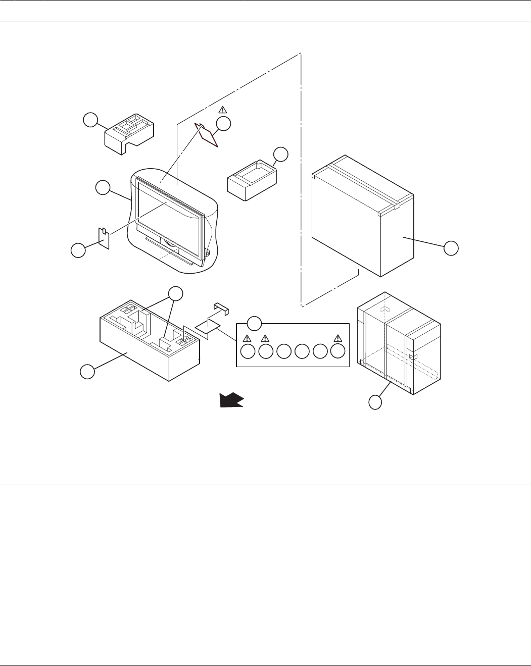
(No.YA463)3-47
REMOTE CONTROL UNIT PARTS LIST (RM-C18G-1H)
PACKING
PACKING PARTS LIST
Ref.No. Part No. Part Name Description Local
UR77EC1403A BATTERY COVER
Ref.No. Part No. Part Name Description Local
1 LC12022-012A-A PACKING CASE HD-52FA97
1 LC12428-009A-A PACKING CASE HD-56FB97
1 LC12022-013A-A PACKING CASE HD-61FB97
2 LC12767-001A-A PACKING TRAY HD-52FA97
2 LC12726-001A-A PACKING TRAY HD-56FB97
2 LC12757-001A-A PACKING TRAY HD-61FB97
3 LC22193-001A-A SUPPORT TRAY HD-52FA97
3 LC22203-001A-A SUPPORT TRAY HD-56FB97
3 LC22205-001A-A SUPPORT TRAY HD-61FB97
4 LC12770-001C-A CUSHION ASSY 4pcs in 1set HD-52FA97
4 LC12723-001A-A CUSHION ASSY 4pcs in 1set HD-56FB97
4 LC12754-001A-A CUSHION ASSY 4pcs in 1set HD-61FB97
5 LC22040-001A-A POLY BAG
6 LCT1910-001A-A INST BOOK English
7 LCT1721-001A-A INST SHEET English/French
8 QPA02503505P POLY BAG 25cm x 35cm
9 LCT2170-001A-A INST BOOK English
10 LCT2171-001A-A INST BOOK French
11 ------------ BATTERY R6P/AA(x2)
12 RM-C18G-1H REMOTE CONTROL UNIT
13 BT-51041-1A REGI. CARD
14 LCT1728-001B-A INST SHEET English/French
FRONT
1
4
4
4
7
5
6
3
8
9 10 11 13
12
2
14
