8457 HP 8558 Spectrum Analyzer User Manual
User Manual: HP 8558 Spectrum Analyzer User Manual
Open the PDF directly: View PDF ![]() .
.
Page Count: 343 [warning: Documents this large are best viewed by clicking the View PDF Link!]
- TOC
- SECTIONS
- FIGURES
- FIGURE 1-1
- FIGURE 1-2
- FIGURE 1-3
- FIGURE 2-1
- FIGURE 3-1
- FIGURE 3-2
- FIGURE 4-1
- FIGURE 4-2
- FIGURE 4-3
- FIGURE 4-4
- FIGURE 4-5
- FIGURE 4-6
- FIGURE 4-7
- FIGURE 4-8
- FIGURE 4-9
- FIGURE 4-10
- FIGURE 4-11
- FIGURE 4-12
- FIGURE 4-13
- FIGURE 4-14
- FIGURE 4-15
- FIGURE 4-16
- FIGURE 4-17
- FIGURE 4-18
- FIGURE 4-19
- FIGURE 4-20
- FIGURE 4-21
- FIGURE 5-1
- FIGURE 5-2
- FIGURE 5-3
- FIGURE 5-4
- FIGURE 5-5
- FIGURE 5-6
- FIGURE 5-7
- FIGURE 5-8
- FIGURE 5-9
- FIGURE 5-10
- FIGURE 5-11
- FIGURE 5-12
- FIGURE 5-13
- FIGURE 5-14
- FIGURE 5-15
- FIGURE 5-16
- FIGURE 6-1
- FIGURE 6-2
- FIGURE 6-3
- FIGURE 7-1
- FIGURE 7-2
- FIGURE 7-3
- FIGURE 7-4
- FIGURE 7-5
- FIGURE 7-6
- FIGURE 7-7
- FIGURE 7-8
- FIGURE 7-9
- FIGURE 7-10
- FIGURE 8-1
- FIGURE 8-2
- FIGURE 8-3
- FIGURE 8-4
- FIGURE 8-5
- FIGURE 8-6
- FIGURE 8-7
- FIGURE 8-8
- FIGURE 8-9
- FIGURE 8-10
- FIGURE 8-11
- FIGURE 8-12
- FIGURE 8-13
- FIGURE 8-14
- FIGURE 8-15
- FIGURE 8-16
- FIGURE 8-17
- FIGURE 8-18
- FIGURE 8-19
- FIGURE 8-20
- FIGURE 8-21
- FIGURE 8-22
- FIGURE 8-23
- FIGURE 8-24
- FIGURE 8-25
- FIGURE 8-26
- FIGURE 8-27
- FIGURE 8-28
- FIGURE 8-29
- FIGURE 8-30
- FIGURE 8-31
- FIGURE 8-32
- FIGURE 8-33
- FIGURE 8-34
- FIGURE 8-35
- FIGURE 8-36
- FIGURE 8-37
- FIGURE 8-38
- FIGURE 8-39
- FIGURE 8-40
- FIGURE 8-41
- FIGURE 8-42
- FIGURE 8-43
- FIGURE 8-44
- FIGURE 8-45
- FIGURE 8-46
- FIGURE 8-47
- FIGURE 8-48
- FIGURE 8-49
- FIGURE 8-50
- FIGURE 8-49
- FIGURE 8-50
- FIGURE 8-51
- FIGURE 8-52
- FIGURE 8-53
- TABLES
- TABLE 1-1
- TABLE 1-2
- TABLE 1-3
- TABLE 1-4
- TABLE 2-1
- TABLE 2-2
- TABLE 4-1
- TABLE 4-2
- TABLE 4-3
- TABLE 4-4
- TABLE 4-5
- TABLE 4-6
- TABLE 4-7
- TABLE 4-8
- TABLE 4-9
- TABLE 4-10
- TABLE 4-11
- TABLE 4-12
- TABLE 4-13
- TABLE 4-14
- TABLE 4-15
- TABLE 5-1
- TABLE 5-2
- TABLE 5-3
- TABLE 5-4
- TABLE 5-5
- TABLE 5-6
- TABLE 5-7
- TABLE 5-8
- TABLE 5-9
- TABLE 5-10
- TABLE 6-1
- TABLE 6-2
- TABLE 6-3
- TABLE 7-1
- TABLE 7-2
- TABLE 7-3
- TABLE 7-4
- TABLE 7-5
- TABLE 7-6
- TABLE 7-7
- TABLE 8-1
- TABLE 8-2
- TABLE 8-3
- APPENDICES
- PAGES
- PAGE 0-1
- PAGE 1-0
- PAGE 1-2
- PAGE 1-3
- PAGE 1-6
- PAGE 1-8
- PAGE 1-10
- PAGE 1-12
- PAGE 1-14
- PAGE 2-1
- PAGE 2-3
- PAGE 2-4
- PAGE 3-7
- PAGE 4-1
- PAGE 4-2
- PAGE 4-3
- PAGE 4-5
- PAGE 4-7
- PAGE 4-9
- PAGE 4-10
- PAGE 4-11
- PAGE 4-13
- PAGE 4-14
- PAGE 4-15
- PAGE 4-17
- PAGE 4-19
- PAGE 4-20
- PAGE 4-21
- PAGE 4-25
- PAGE 4-27
- PAGE 4-28
- PAGE 4-29
- PAGE 4-32
- PAGE 4-33
- PAGE 4-34
- PAGE 4-36
- PAGE 4-37
- PAGE 4-41
- PAGE 4-43
- PAGE 4-45
- PAGE 4-46
- PAGE 4-48
- PAGE 4-50
- PAGE 4-51
- PAGE 4-52
- PAGE 4-55
- PAGE 4-57
- PAGE 4-58
- PAGE 4-59
- PAGE 4-61
- PAGE 4-63
- PAGE 5-1
- PAGE 5-2
- PAGE 5-3
- PAGE 5-6
- PAGE 5-7
- PAGE 5-8
- PAGE 5-11
- PAGE 5-12
- PAGE 5-13
- PAGE 5-14
- PAGE 5-15
- PAGE 5-17
- PAGE 5-18
- PAGE 5-21
- PAGE 5-23
- PAGE 5-25
- PAGE 5-27
- PAGE 5-28
- PAGE 5-29
- PAGE 5-33
- PAGE 5-35
- PAGE 5-37
- PAGE 5-39
- PAGE 5-40
- PAGE 5-41
- PAGE 5-42
- PAGE 5-43
- PAGE 5-45
- PAGE 5-47
- PAGE 5-48
- PAGE 5-49
- PAGE 5-51
- PAGE 5-53
- PAGE 6-1
- PAGE 6-2
- PAGE 6-4
- PAGE 6-5
- PAGE 6-12
- PAGE 6-13
- PAGE 6-14
- PAGE 6-18
- PAGE 6-19
- PAGE 6-21
- PAGE 6-24
- PAGE 6-26
- PAGE 6-28
- PAGE 6-29
- PAGE 6-31
- PAGE 6-33
- PAGE 7-1
- PAGE 7-2
- PAGE 7-6
- PAGE 7-7
- PAGE 7-8
- PAGE 7-11
- PAGE 7-14
- PAGE 7-15
- PAGE 7-17
- PAGE 7-18
- PAGE 7-19
- PAGE 7-20
- PAGE 7-24
- PAGE 7-25
- PAGE 7-26
- PAGE 7-27
- PAGE 7-28
- PAGE 7-29
- PAGE 7-30
- PAGE 8-1
- PAGE 8-2
- PAGE 8-4
- PAGE 8-5
- PAGE 8-9
- PAGE 8-11
- PAGE 8-13
- PAGE 8-15
- PAGE 8-18
- PAGE 8-20
- PAGE 8-21
- PAGE 8-22
- PAGE 8-23
- PAGE 8-24
- PAGE 8-26
- PAGE 8-27
- PAGE 8-28
- PAGE 8-31
- PAGE 8-32
- PAGE 8-33
- PAGE 8-35
- PAGE 8-36
- PAGE 8-42
- PAGE 8-43
- PAGE 8-44
- PAGE 8-46
- PAGE 8-52
- PAGE 8-53
- PAGE 8-56
- PAGE 8-59
- PAGE 8-60
- PAGE 8-61
- PAGE 8-62
- PAGE 8-65
- PAGE 8-66
- PAGE 8-68
- PAGE 8-69
- PAGE 8-72
- PAGE 8-74
- PAGE 8-75
- PAGE 8-76
- PAGE 8-78
- PAGE 8-79
- PAGE 8-81
- PAGE 8-84
- PAGE 8-85
- PAGE 8-91
- PAGE 8-92
- PAGE 8-94
- PAGE 8-95
- PAGE 8-97
- PAGE 8-102
- PAGE 8-103
- PAGE 8-107
- PAGE A-1
- PAGE B-1
- PAGE D-1
TM 11-6625-3061-14
A
TM 11-6625-3061-14
SAFETY CONSIDERATIONS
Safety Symbols
The following safety symbols are used throughout this manual and in the instrument. Familiarize yourself with each of
the symbols and its meaning before operating this instrument.
Instruction manual symbol: the apparatus
will be marked with this symbol when it is
necessary for the user to refer to the
instruction manual in order to protect the
apparatus against damage.
Indicates dangerous voltages.
The CAUTION sign denotes a hazard. It
calls attention to an operation procedure,
practice, or the like, which, if not correctly
performed or adhered to, could result in
damage to or destruction of part or all of
the equipment. Do not proceed beyond a
CAUTION sign until the indicated conditions
are fully understood and met.
The WARNING sign denotes a hazard. It
calls attention to a procedure, practice, or
the like, which, if not correctly performed or
adhered to, could result in injury or loss of
life. Do not proceed beyond a WARNING
sign until the indicated conditions are fully
understood and met.
Operation
BEFORE THIS INSTRUMENT IS
SWITCHED ON, the oscilloscope
mainframe protective earth terminal must
be connected through the protective
conductor of the ac power cable to a socket
outlet provided with protective earth contact.
Failure to ground the instrument can result
in personal injury.
The 8558B Spectrum Analyzer should not
be operated without protective covers (out
of the mainframe). Adjustments,
performance tests, and service procedures
which require operation of the 8558B out of
the mainframe should be performed only by
trained service personnel.
CAUTION
BEFORE THIS INSTRUMENT IS
SWITCHED ON, make sure that the
oscilloscope mainframe is set to the voltage
of the ac power source. Failure to set the
ac power input to the correct voltage could
cause damage to the instrument when the
ac power cable is plugged in.
Service and Adjustments
There are voltages at many points in the
instrument which can, if contacted, cause
personal injury. Be extremely careful.
Service and adjustments should be
performed only by trained service
personnel.
Any interruption of the protective
(grounding) conductor, inside or outside the
instrument, or disconnection of the
protective earth terminal may cause
personal injury.
WARNING
WARNING
WARNING
WARNING WARNING
CAUTION
B

TM 11-6625-3061-14
This manual contains copyright material reproduced by permission of the Hewlett-Packard Company, Valley Forge, PA
19482.
TM 11-6625-3061-14
Technical Manual ) HEADQUARTERS
)DEPARTMENT OF THE ARMY
No. 11-6625-3061-14) Washington, DC, 1 January 1986
OPERATOR'S ORGANIZATIONAL AND
DIRECT SUPPORT, AND GENERAL SUPPORT
MAINTENANCE MANUAL
SPECTRUM ANALYZER HEWLETT-PACKARD MODEL 8558B
(Includes Option 001 and Option 002)
SERIAL NUMBERS
This manual applies directly to instruments with serial numbers
prefixed 2147A.
With modifications described in Section VII, this manual also
applies to instruments with the serial prefixes 1914A through
2145A.
For additional important information about serial numbers, see
INSTRUMENTS COVERED BY MANUAL in Section I.
REPORTING ERRORS AND RECOMMENDING IMPROVEMENTS
You can help improve this manual. If you find any mistakes or if you know of a
way to improve the procedures, please let us know. Mail your letter, DA Form
2028 (Recommended Changes to Publications and Blank Forms), or DA Form
2028-2 located in the back of this manual direct to Commander, US Army
Communications-Electronics Command and Fort Monmouth, ATTN: AMSEL-
ME-MP, Fort Monmouth, NJ 07703-5007.
In either case, a reply will be furnished direct to you.
i
TM 11-6625-3061-14
TABLE OF CONTENTS
Section Page
0INTRODUCTION
0-1 Scope...................................................................................................................... 0-1
0-2 Consolidated Index of Army Publications and Blank Forms ..................................... 0-1
0-3 Maintenance Forms, Records, and Reports ............................................................. 0-1
0-4 Reporting Equipment Improvement Recommendations (EIR).................................. 0-1
0-5 Administrative Storage ............................................................................................ 0-1
0-6 Destruction of Army Electronics Materiel ................................................................. 0-1
ii
TM 11-6625-3061-14
CONTENTS
Section Page Section Page
I GENERAL INFORMATION..................................1-1 IV PERFORMANCE TESTS................................4-1
1-1. Introduction..........................................1-1 4-1. Introduction ........................................4-1
1-3. Description...........................................1-1 4-3. Instruments Tested.............................4-1
1-6. Manual Organization............................1-1 4-5. Equipment Required...........................4-1
1-10. Specifications.......................................1-2 4-7. Test Record........................................4-1
1-12. Safety Considerations ..........................1-2 4-9. Calibration Cycle ................................4-1
1-14. Instruments Covered by Manual...........1-2 4-11. Frequency Span Accuracy..................4-2
1-15. Serial Numbers ....................................1-2 4-12. Tuning Accuracy.................................4-7
1-17. Manual Changes Supplement ..............1-2 4-13. Residual FM.......................................4-10
1-20. Manual Backdating Changes................1-2 4-14. Noise Sidebands ................................4-13
1-23. Options ................................................1-9 4-15. Resolution Bandwidth
1-24. Option 001 ...........................................1-9 Accuracy......................................4-15
1-26. Option 002 ...........................................1-9 4-16. Resolution Bandwidth
1-28. Option 910 ...........................................1-9 Selectivity ....................................4-20
1-30. Accessories Supplied ...........................1-9 4-17. Average Noise Level ..........................4-25
1-32. Termination..........................................1-9 4-18. Spurious Responses...........................4-27
1-34. Cable Adapter......................................1-9 4-19. Residual Responses ...........................4-34
1-36. Side Stop Kit........................................1-9 4-20. Frequency Response..........................4-37
1-38. Graticule Overlays ...............................1-9 4-21. Bandwidth Switching
1-39. Equipment Required But ..................... (Amplitude Variation)....................4-41
Not Supplied..................................1-10 4-22. Input Attenuator Accuracy ..................4-43
1-40. Display Mainframe ...............................1-10 4-23. Reference Level Accuracy..................4-46
1-43. Extender Cable Assembly ....................1-10 4-24. Display Fidelity...................................4-51
1-45. Measurement Accessories ...................1-10 4-25. Calibrator Accuracy............................4-55
1-46. AC Probe .............................................1-10
1-48. Modification Kit ................................... VADJUSTMENTS .............................................5-1
(Option 807 Connections) ..............1-10 5-1. Introduction ........................................5-1
1-50. Oscilloscope Camera ...........................1-10 5-4. Equipment Required...........................5-1
1-52. Service Accessories.............................1-10 5-7. Adjustment Tools .........................5-1
1-54. Recommended Test Equipment ...........1-11 5-9. Extender Cable Installation...........5-1
...................................................... 5-13. Related Adjustments ..........................5-1
II INSTALLATION...................................................2-1 5-15. Factory-Selected Components............5-2
2-1. Introduction..........................................2-1 5-17. Second Converter LO and
2-3. Initial Inspection ...................................2-1 Bandpass Adjustments.................5-12
2-5. Preparation for Use..............................2-1 5-18. Third Converter LO and
2-6. Installation............................................2-1 CAL OUTPUT Adjustment............5-15
2-9. Side Stop Kit........................................2-1 5-19. Slope Adjustment ...............................5-18
2-13. Graticule Overlays ...............................2-2 5-20. Second IF Bandpass Amplifier and
2-15. Mainframe Interconnections .................2-2 Bandpass Filter Adjustment..........5-21
2-17. Operating Environment ........................2-2 5-21. Crystal and LC Bandwidth
2-21. Modifications........................................2-2 Filter Adjustments ........................5-23
2-23. Storage and Shipment..........................2-3 5-22. 3-dB Bandwidth Adjustment................5-29
2-24. Environment ........................................2-3 5-23. Step Gain Assembly RF
2-26. Packaging............................................2-3 Gain Adjustment ..........................5-33
...................................................... 5-24. Step Amplifier Gain
III OPERATION ......................................................3-1 Adjustments .................................5-35
3-1. Introduction..........................................3-1 5-25. +19.5V Adjustment.............................5-39
3-3. Controls, Indicators, and Connectors....3-1 5-26. Log Amplifier Log and
3-5. Control Grouping..................................3-1 Linear Adjustment ........................5-40
3-13. Variable Persistence and ..................... 5-27. Sweep Time Per Division
Storage Functions..........................3-2 Adjustment...................................5-45
3-15. Persistence and Intensity .....................3-2 5-28. Frequency Control and
3-19. Photographic Techniques.....................3-2 DPM Adjustments ........................5-48
Operating Precautions..........................3-2 5-29. 1-dB Offset Adjustment ......................5-51
iii
TM 11-6625-3061-14
CONTENTS
Section Page Section Page
VI REPLACEABLE PARTS......................................6-1 8-5. Schematic Symbols, Terminology,
6-1. Introduction..........................................6-1 and Voltage Levels.......................8-1
6-3. Replaceable Parts List .........................6-1 8-7. Test Equipment..................................8-1
6-6. Ordering Information............................6-1 8-9. Troubleshooting..................................8-1
...................................................... 8-10. General........................................8-1
VII MANUAL BACKDATING CHANGES ...................7-1 8-13. Troubleshooting Hints...................8-1
7-1. Introduction..........................................7-1 8-18. General Principles of Operation..........8-4
7-5. Manual Change.................................... Front Switch Assembly A2,
Instructions ....................................7-2 Disassembly and Repair...............8-107
VII SERVICE ......................................................8-1 NOTE
8-1. Introduction..........................................8-1 Schematic, block and component location
8-3. Service Information Index ....................8-1 diagrams are listed under ILLUSTRATIONS.
LIST OF ILLUSTRATIONS
Figure Page Figure Page
1-1. HP Model 8558B Spectrum Analyzer 5-2. Special Adapter Used in Second Converter
with Accessories Supplied........................... 1-0 LO and Bandpass Test Setup................5-14
1-2. Typical Serial Number Label............................ 1-2 5-3. Third Converter LO and CAL OUTPUT
1-3. Service Accessories .......................................1-12 Adjustment Test Setup..........................5-17
2-1. Location of Side Stops..................................... 2-3 5-4. Slope Adjustment Test Setup.....................5-21
3-1. HP 8558B Installed in HP 182T 5-5. Second IF Bandpass Amplifier and Bandpass
Display Mainframe...................................... 3-5 Filter Adjustment Test Setup.................5-25
3-2. Rear Panel Controls and Connectors............... 3-7 5-6. Crystal and LC Bandwidth Filter
4-1. Frequency Span Accuracy Test Setup ............. 4-3 Adjustment Test Setup..........................5-27
4-2. Frequency Span Accuracy Measurement for 5-7. Crystal Short Configuration........................5-28
Ninth Spectral Line...................................... 4-5 5-8. Adjusting Crystal Symmetry and
4-3. Frequency Span Accuracy Measurement for Crystal Centering ..................................5-29
Seventeenth Spectral Line.......................... 4-5 5-9. 3- dB Bandwidth Adjustment Test Setup..........5-33
4-4. Tuning Accuracy Test Setup............................ 4-9 5-10. Step Gain Assembly RF Gain
4-5. Residual FM Test Setup .................................4-13 Adjustment Test Setup..........................5-37
4-6. Example of Residual FM ................................4-14 5-11. Step Amplifier Gain Adjustment
4-7. Noise Sideband Test Setup ............................4-17 Test Setup ............................................5-39
4-8. Resolution Bandwidth Accuracy Test Setup, 5-12. +19.5V Adjustment Test Setup ..................5-43
3 MHz to 100 kHz ......................................4-19 5-13. Log Amplifier and Linear Adjustment
4-9. Resolution Bandwidth Accuracy Test Setup, Test Setup ............................................5-45
1 kHz to 30 kHz .........................................4-21 5-14. Sweep Time Per Division Adjustment
4-10. Resolution Bandwidth Selectivity Test Setup, Test Setup ............................................5-51
1 kHz to 30 kHz .........................................4-25 5-15. Frequency Control and DPM Adjustments
4-11. Resolution Bandwidth Selectivity Test Setup, Test Setup ............................................5-55
100 kHz to 3 MHz ......................................4-28 5-16. l-dB Offset Adjustment Test Setup.............5-59
4-12. Average Noise Level Measurement ................4-32 6-1. Cable Assembly W1 (08558-60038 or
4-13. Harmonic Distortion Test Setup ......................4-33 08558-60031) Replaceable Parts ..........6-29
4-14. Intermodulation Distortion Test Setup.............4-36 6-2. Mechanical Chassis Parts..........................6-31
4-15. Intermodulation Distortion Products ................4-37 6-3. Front Switch Assembly ..............................6-33
4-16. Residual Responses Test Setup .....................4-41 7-1. Mechanical Chassis Parts (CHANGE A) ......7-8
4-17. Frequency Response Test Setup ....................4-45 7-2. Front Panel Assembly (CHANGE A)..........7-11
4-18. Input Attenuator Accuracy Test Setup.............4-51 7-3. Front Switch Assembly A2,
4-19. Reference Level Accuracy Test Setup............4-55 Schematic (CHANGE A) .......................7-13
4-20. Amplitude Log Display Accuracy Test Setup...4-61 7-4. Log Amplifier Log and Linear Adjustment
4-21. Calibrator Accuracy Test Setup ......................4-65 Test Setup (CHANGE B).......................7-15
5-1. Second Converter LO and 7-5. A14 Log Amplifier, Component and Test
Bandpass Adjustment Test Setup...............5-13 Point Locations (CHANGE B)................7-24
iv
TM 11-6625-3061-14
LIST OF ILLUSTRATIONS
Figure Page Figure Page
7-6. A14 Log Amplifier Assembly Schematic 8-21. Simplified Schematic of Sweep Generator
(CHANGE B)..............................................7-25 in AUTO Mode......................................8-46
7-7. A9 Third Converter and A10 Second IF, 8-22. A8 Sweep Generator Assembly,
Component Locations (CHANGE C)...........7-27 Component and Test Point Locations....8-52
7-8. P/O A9 Third Converter and A10 Second IF, 8-23. A8 Sweep Generator, Schematic...............8-53
Schematic Diagram (CHANGE C)..............7-28 8-24. Bandpass Amplifier Tank Circuit,
7-9. A9 Third Converter and A10 Second IF, Simplified Schematic ............................8-59
Component Locations (CHANGE F)...........7-29 8-25. A9 Third Converter Assembly, and
7-10. P/O A9 Third Converter and A10 Second IF, A10 Second IF Assembly, Component
Schematic Diagram (CHANGE F)..............7-30 Locations ..............................................8-60
8-1. Symbols Used in Schematics and 8-26. A9 Third Converter and A10 Second IF,
Block Diagrams........................................... 8-5 Schematic.............................................8-61
8-2. Conditions for Schematic Diagram 8-27. Crystal Pole, Simplified Schematic ............8-65
Measurements ............................................ 8-9 8-28. LC Pole, Simplified Schematic ..................8-66
8-3. CRT Displays for Residual FM 8-29. A11 Bandwidth Filter No. 1 Assembly,
Troubleshooting .........................................8-13 Component and Test Point Locations....8-68
8-4. Baseline Step Caused by Failure of A7Q18 ....8-13 8-30. A11 Bandwidth Filter No. 1, Schematic.....8-69
8-5. Simplified Block Diagram ...............................8-15 8-31. Equivalent Circuit for
8-6. Troubleshooting Block Diagram......................8-17 Step Gain Amplifiers.............................8-72
8-7. A1A2U1 Clock ................................................8-20 8-32. A12 Step Gain Assembly, Component and
8-8. Integrator and EOC Waveforms for FRE- Test Point Locations..............................8-74
QUENCY MHz Display of 1296 MHz..........8-20 8-33. A12 Step Gain, Schematic.........................8-75
8-9. A1A2U1 Outputs for FREQUENCY MHz 8-34. A13 Bandwidth Filter No. 2 Assembly,
Display of 1296 MHz..................................8-21 Component and Test Point Locations....8-78
8-10. A1A2 DPM Driver Component Locations ........8-22 8-35. A13 Bandwidth Filter No. 2, Schematic.....8-79
8-11. A1A2 DPM Driver (and DPM Display), 8-36. Simplified Log Amplifier Stage...................8-81
Schematic..................................................8-23 8-37. A14 Log Amplifier Assembly,
8-12. Front Switch Board Assembly A2A1, Component Locations ...........................8-84
Component Locations ................................8-26 8-38. A14 Log Amplifier Assembly, Schematic ...8-85
8-13. A2 Front Switch, Schematic Diagram .............8-27 8-39. Simplified Vertical Driver Circuit................8-91
8-14. A3 Input Attenuator.........................................8-31 8-40. Simplified Blanking Circuit.........................8-92
8-15. A6 YIG Oscillator............................................8-31 8-41. A15 Vertical Driver and Blanking Assembly,
8-16. A4 First Converter, Component Component and Test Point Locations....8-94
Locations ...................................................8-32 8-42. A15 Vertical Driver and Blanking,
8-17. A5 Second Converter Assembly, Schematic.............................................8-95
Component Locations ................................8-33 8-43. A16 Motherboard Assembly, Components
8-18. A3 Input Attenuator, A4 First Converter, and Test Point Locations.......................8-97
A5 Second Converter, and A6 YIG 8-44. A16 Motherboard, Schematic Diagram ......8-97
Oscillator, Schematic.................................8-35 8-45. A17 Inverter Assembly, Component
8-19. A7 Frequency Control Assembly, Locations ............................................8-102
Component and Test Point Locations.........8-42 8-46. A17 Inverter, Schematic ..........................8-103
8-20. A7 Frequency Control, Schematic ..................8-43 8-47. Locations of Major Assemblies ................8-105
LIST OF TABLES
Table Page Table Page
1-1. HP Model 8558B Specifications....................... 1-3 1-4. Recommended Test Equipment.................1-14
1-2. Model 8558B/180-Series 2-1. Side Stop Kit (08558-60131)........................2-1
Supplemental Characteristics...................... 1-6 2-2. HP Model 8558B Mainframe
1-3. Parts Included in Modification Interconnections......................................2-4
Kit 00180-69503.........................................1-10 4-1. Performance Tests ......................................4-1
V
TM 11-6625-3061-14
LIST OF TABLES
Table Page Table Page
4-2. Narrow Span Width Error Measurement .......... 4-7 5-4. Related Adjustments..................................5-11
4-3. Tuning Accuracy Measurement.......................4-11 5-5. REF LEVEL FINE Control Check...............5-41
4-4. Resolution Bandwidth Selectivity ....................4-29 5-6. REFERENCE LEVEL Control Check .........5-42
4-5. Frequency Response, 5 MHz to 1500 MHz. ...4-48 5-7. Log Fidelity Check.....................................5-47
4-6. Frequency Response, 100 kHz to 5 MHz ........4-48 5-8. Linear Gain Adjustments............................5-48
4-7. Amplitude Accuracy, Switching Between .............. 5-9. Log Gain Adjustment Limits.......................5-48
Bandwidths ................................................4-50 5-10. Log Amplifier Output Limits .......................5-49
4-8. Input Attenuator Accuracy...............................4-52 6-1. Reference Designations and Abbreviations..6-2
4-9. IF Gain Accuracy in LOG Mode......................4-57 6-2. Manufacturers Code List..............................6-4
4-10. IF Gain Accuracy in Linear Mode....................4-58 6-3. Replaceable Parts .......................................6-5
4-11. Conversion Table, Deviation in............................. 7-1. Manual Change Requirement by
Linear Mode...............................................4-58 Serial Number.........................................7-1
4-12. Vernier Accuracy ............................................4-59 7-2. Replaceable Parts (CHANGE A)..................7-6
4-13. Amplitude Log Display Accuracy.....................4-63 7-3. Replaceable Parts (CHANGE A)..................7-7
4-14. Sample Computations of Amplitude...................... 7-4. Linear Gain Adjustment Limits...................7-17
Log Display Accuracy.................................4-63 7-5. Log Fidelity Check.....................................7-18
4-15. Performance Test Record...............................4-69 7-6. Log Gain Adjustment Limits.......................7-19
5-1. Adjustable Components................................... 5-3 7-7. Replaceable Parts (CHANGE B)................7-20
5-2. Factory Selected Components in .......................... 8-1. Service Information .....................................8-2
Alpha-Numeric Order.................................. 5-7 8-2. Residual FM Troubleshooting
5-3. HP Part Numbers of Standard Value .................... Procedure .............................................8-11
Replacement Components.......................... 5-8 8-3. Truth Table for A2DSI Display ...................8-20
APPENDICES
APPENDIX
A. REFERENCES .......................................................................A-1
B. COMPONENTS OF END ITEM LIST...................................... B-1
C. ADDITIONAL AUTHORIZATION LIST(Not Applicable)
D. MAINTENANCE ALLOCATION...............................................D-1
E. EXPENDABLE SUPPLIES AND MATERIAL LIST(Not Applicable)
vi

TM 11-6625-3061-14
SECTION 0.
INTRODUCTION
0-1. SCOPE
This manual describes Spectrum Analyzer, Hewlett-Packard Model 8558B and provides instructions for operation and
maintenance.
0-2. CONSOLIDATED INDEX OF ARMY PUBLICATIONS AND BLANK FORMS
Refer to the latest issue of DA Pam 310-1 to determine whether there are new editions, changes or additional
publications pertaining to the equipment.
0-3. MAINTENANCE FORMS, RECORDS, AND REPORTS
a.Reports of Maintenance and Unsatisfactory Equipment. Department of the Army forms and procedures used for
equipment maintenance will be those prescribed by DA Pam 738-750, as contained in Maintenance Management
Update.
b.Report of Packaging and Handling Deficiencies. Fill out and forward SF 364 (Report of Discrepancy (ROD)) as
prescribed in AR 735-11-2/DLAR 4140.55/ NAVMATINST 4355.73A/AFR 400-54/MCO 4430.3F.
c.Discrepancy in Shipment Report (DISREP)(SF 361). Fill out and forward Discrepancy in Shipment Report
(DISREP)(SF 361) as prescribed in AR 55-38/ NAVSUPINST 4610.33C/AFR 75-18/MCO P4610.19D/DLAR 4500.15.
0-4. REPORTING EQUIPMENT IMPROVEMENT RECOMMENDATIONS (EIR)
If your equipment needs improvement, let us know. Send us an EIR. You, the user, are the only one who can tell us
what you don't like about your equipment. Let us know why you don't like the design. Put it on an SF 368 (Quality
Deficiency Report). Mail it to Commander, US Army Communications-Electronics Command and Fort Monmouth,
ATTN: AMSEL-ME-MP, Fort Monmouth, NJ 07703-5007. We'll send you a reply.
0-5. ADMINISTRATIVE STORAGE
Administrative storage of equipment issued to and used by Army activities will have preventive maintenance performed
in accordance with the PMCS charts before storing. When removing the equipment from administrative storage the
PMCS should be performed to assure operational readiness. Disassembly and repacking of equipment for shipment or
limited storage is covered in paragraph 2-23.
0-6. DESTRUCTION OF ARMY ELECTRONICS MATERIEL
Destruction of Army electronics materiel to prevent enemy use shall be in accordance with TM 750-244-2.
0-1
TM 11-6625-3061-14
Model 8558B
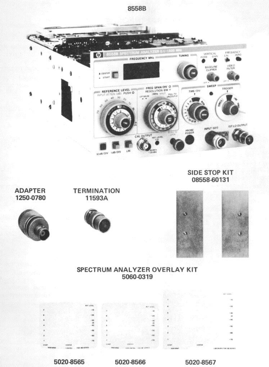
Figure 1-1. HP Model 8558B Spectrum Analyzer with Accessories Supplied
1-0
TM 11-6625-3061-14
Model 8558B
SECTION I.
GENERAL INFORMATION
1-1. INTRODUCTION
1-2. This Operation and Service manual contains
information required to install, operate, test, adjust, and
service the Hewlett-Packard Model 8558B Spectrum
Analyzer. Figure 1-1 shows the standard instrument and
accessories supplied. This section covers instrument
identification, description, options, accessories,
specifications, and other basic information.
1-3. DESCRIPTION
1-4. The HP 8558B displays the amplitude and
frequency of each component of an input signal on a
CRT. This display gives quantitative information often
not available from a conventional oscilloscope. The HP
8558B is capable of measuring signals from -117 dBm
to +30 dBm over a frequency range of 100 kHz to 1500
MHz.
001: 110 dBm to + 30 dBm
002: 63 dBmV to + 80 dBmV
1-5. The complete measuring system includes the HP
8558B Spectrum Analyzer plugged into a compatible
Hewlett-Packard display mainframe.
1-6. MANUAL ORGANIZATION
1-7. This manual is divided into eight sections as
follows:
SECTION I, GENERAL INFORMATION, contains the
instrument description and specifications, explains
accessories and options, and lists recommended test
equipment.
SECTION II, INSTALLATION AND OPERATION
VERIFICATION, contains information concerning initial
mechanical inspection, preparation for use, operating
environment, packaging and shipping, and operation
verification.
SECTION III, OPERATION, contains detailed
instructions for operation of the instrument.
SECTION IV, PERFORMANCE TESTS, contains the
necessary tests to verify that the electrical operation of
the instrument is in accordance with published
specifications.
SECTION V, ADJUSTMENTS, contains the necessary
adjustment procedures to properly adjust the instrument
after repair.
SECTION VI, REPLACEABLE PARTS, contains the
information necessary to order parts and/or assemblies
for the instrument.
SECTION VII, MANUAL BACKDATING CHANGES,
contains backdating information to make this manual
compatible with earlier equipment configurations.
SECTION VIII, SERVICE, contains schematic diagrams,
block diagrams, component location illustrations, circuit
descriptions, and troubleshooting information to aid in
repair of the instrument.
1-8. On the title page of this manual, below the manual
part number, is a microfiche part number. This number
may be used to order 4-by 6-inch microfilm
transparencies of the manual. Each microfiche contains
up to 60 photo-duplicates of the manual pages. The
microfiche package also includes the latest Manual
Changes supplement.
1-9. Where text changes are required to reflect Options
001 and 002, these changes are shown in bold type
immediately following applicable text. Notes are also
included in tables and illustrations where users of
Options 001 and 002 need to be informed of differences
from the standard instrument. Users of the standard
instrument should ignore references to Options 001 and
002.
1-1
Model 8558B TM 11-6625-3061-14
1-10. SPECIFICATIONS
1-11. Instrument specifications are listed in Table 1-1.
These specifications are the performance standards or
limits against which the instrument is tested. Table 1-2
lists supplemental characteristics. Supplemental
characteristics are not specifications but are typical
characteristics included as additional information for the
user.
NOTE
To ensure that the HP Model 8558B
meets the specifications listed in
Table 1-1, performance tests (Section
IV) should be performed every six
months.
1-12. SAFETY CONSIDERATIONS
1-13. Before operating this instrument, you should
familiarize yourself with the safety markings on the
instrument and safety instructions in this manual. This
instrument has been manufactured and tested according
to international safety standards. However, to ensure
safe operation of the instrument and personal safety of
the user and service personnel, the cautions and
warnings in this manual must be followed. Refer to the
Safety Considerations at the front of the manual. Refer
also to individual sections of this manual for detailed
safety notation concerning the use of the instrument as
described in those individual sections.
1-14. INSTRUMENTS COVERED BY MANUAL
1-15. Serial Numbers
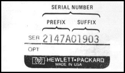
1-16. Attached to the rear of your instrument is a mylar
serial number label. The serial number is in two parts.
The first four digits and letter are the serial number
prefix; the last five digits are the suffix (see Figure 1-2).
The prefix is the same for all identical instruments; it
changes only when a change is made to the instrument.
The suffix, however, is assigned sequentially and is
different for each instrument. The contents of this
manual apply to instruments with the serial number
prefix(es) listed under SERIAL NUMBERS on the title
page.
Figure 1-2. Typical Serial Number Label
1-17. Manual Changes Supplement
1-18. An instrument manufactured after the printing of
this manual might have a serial number prefix that is not
listed on the title page. This unlisted serial number
prefix indicates that the instrument is different from
those described in this manual. The manual for this
newer instrument is accompanied by a yellow Manual
Changes supplement. This supplement contains
change information that explains how to adapt the
manual to the newer instrument.
1-19. In addition to change information, the supplement
may contain information for correcting errors in the
manual. To keep this manual as current and accurate
as possible, Hewlett-Packard recommends that you
periodically request the latest Manual Changes
supplement. The supplement carries a manual
identification block that includes the model number, print
date of the manual, and manual part number.
Complimentary copies of the supplement are available
from Hewlett-Packard. Addresses of Hewlett-Packard
offices are located at the back of this manual.
1-20. Manual Backdating Changes
1-21. Instruments manufactured before the printing of
this manual have been assigned serial number prefixes
other than those for which this manual was written
directly. Manual backdating information is provided in
Section VII to adapt this manual to earlier serial number
prefixes. For instruments with serial number prefixes
1829A and earlier, refer to the HP 8558B Operating and
Service Manual dated October 1977, HP part number
08558-90043, and to the Manual Changes supplement
supplied with that manual.
1-2
Model 8558B TM 11-6625-3061-14
Table 1-1. HP Model 8558B Specifications (1 of 3)
FREQUENCY SPECIFICATIONS
FREQUENCY RANGE
100 kHz to 1500 MHz
FREQUENCY SPANS
Per Division (MHz/Div, kHz/Div)
14 frequency scale calibrations in 1-2-5 sequence
from 5 kHz/div to 100 MHz/div. Start or center
frequency is set with the TUNING control and
indicated by the FREQUENCY MHz readout.
Zero Span (0)
Analyzer functions as a manually tuned receiver, at
the frequency indicated by the FREQUENCY MHz
readout, for time-domain display of signal modulation.
FREQUENCY ACCURACY
Tuning Accuracy
Frequency MHz readout (start or center frequency),
after zeroing on the LO feedthrough and operating the
FREQUENCY CAL control, +10°C to +40°C: 0-195
MHz: ±(1 MHz+20% of frequency span per division)
195-1500 MHz: ±(5 MHz + 20% of frequency span per
division)
Frequency Readout Resolution
0-195 MHz: 100 kHz
195-1500 MHz: 1 MHz
Frequency Span Accuracy
± 5% of displayed frequency separation
SPECTRAL RESOLUTION AND STABILITY
Resolution Bandwidths
Eight selectable resolution (3-dB) bandwidths in 1-3
sequence from 1 kHz to 3 MHz. Bandwidth may be
selected independently or coupled with frequency
span. Optimum ratio of frequency span to resolution
bandwidth is indicated by alignment of markers ( > < )
on the two controls.
Resolution Bandwidth Accuracy:
Individual resolution bandwidth 3-dB points:
±20% (+10°C to +40°C)
Selectivity:
60-dB: 3-dB resolution bandwidth ratio: <15:1
Stability
Residual FM:
<1 kHz p-p in 0.1 second
Noise Sidebands:
>65 dB down, >50 kHz from center of CW signal
with 1 kHz resolution bandwidth and full video
filtering.
Video Filter
Post-detection low-pass filter averages displayed
noise for a smooth trace. The MAX (detent)
position selects a video filter bandwidth of
approximately 1.5 Hz for noise level
measurement.
AMPLITUDE SPECIFICATIONS
AMPLITUDE RANGE
-117 dBm to +30 dBm
001: - 110 dBm to +30 dBm
002: -63 dBm V to +80 dBm V
Maximum Input (Damage) Levels
Total Power:
+30 dBm (1W, 7.1 Vrms)
001: +30 dBm (1W, 8.7 Vrms)
002: +80 dBm V (1.3W, 10 Vrms)
dc or ac (<100 Hz):
± 50V
Peak Pulse Power:
+50 dBm (100W, <10 æsec pulse width, 0.01%
duty cycle) with input attenuation >20 dB
002: + 100 dBm V (130W)
Average Noise Level
The displayed average noise level determines
sensitivity (minimum discernible signal). Signals
at this input level peak approximately 3 dB above
the displayed noise.
Maximum average noise level with 10 kHz
resolution bandwidth, 0 dB input attenuation, and
maximum (MAX) video filtering:
<-107 dBm (1-1500 MHz)
001: <-100 dBm (1-1500 MHz)
002: <-53 dBmV (1-1500 MHz)
Calibrated Display Range
Log (from Reference Level):
70 dB with 10 dB/DIV Amplitude Scale
8 dB with 1 dB/DIV Amplitude Scale
Linear:
8 divisions with LIN Amplitude Scale
AMPLITUDE ACCURACY
With AUTO sweep time selected, amplitude accuracy
is determined by one or more of the following factors,
depending on the measurement technique.
Calibrator Output
-30 dBm +1 dB (into 50Ω)
280 MHz ± 300 kHz
001: -30 dBm + 1 dB (into 75Ω)
002: +20 dBm V + 1 dB (into 75Ω)
1-3
Model 8558B TM 11-6625-3061-14
Table 1-1. HP Model 8558B Specifications (2 of 3)
Reference Level
10-dB steps and a 12-dB vernier for calibrated
Reference Level adjustment from -112 dBm to +60
dBm.
(002: -62 dBm V to + 1 10 dBm V) 1
Step Accuracy:
Steps referenced with 0 dB input attenuation.
-10 dBm to -80 dBm: ± 0.5 dB
-10 dBm to -100 dBm: ±1.0 dB
Vernier Accuracy
±0.5 dB
Frequency Response
Frequency response includes input attenuator, limiter,
and mixer flatness:
6<±1.0 dB with 10 dB input attenuation
Input Attenuator
0 dB to 70 dB of input attenuation selectable in 10-dB
steps
Step Accuracy:
0 dB to 70 dB: <±0.5 dB per 10-dB step
Maximum Cumulative Error:
0 dB to 70 dB: <±1.0 dB
Bandwidth Switching (Amplitude Variation)
Bandwidths 3 MHz to 300 kHz: <±0.5 dB
Bandwidths 3 MHz to 1 kHz: <±1.0 dB2
Display Fidelity
CRT linearity and log or linear fidelity affect amplitude
accuracy at levels other than Reference Level.
Log Incremental Accuracy:
±0.1 dB per dB from Reference Level
Log Maximum Cumulative Error:
<±1.5 dB over entire 70-dB range
Linear Accuracy:
±3% of Reference Level
SPURIOUS RESPONSES
Second Harmonic Distortion:
>70 dB3 below a -40 dBm input signal with 0 dB input
attenuation.
001: -35 dBm input signal
002: + 15 dBm V input signal
Third Order Intermodulation Distortion:
>70 dB3 below two -30 dBm input signals, separated
by >50 kHz, with 0 dB input attenuation.
001: two -25 dBm input signals
002: two +25 dBm V input signals
Image and Multiple Responses:
>70 dB3 below a -40 dBm input level with 0dB input
attenuation.
001: -35 dBm input level
002: + 15 dBm V input level
RESIDUAL RESPONSES
<-100 dBm (1-1500 MHz) with 0 dB input attenuation
and no signal present at input.
001: <-95 dBm (1--1500 MHz)
002: <-50 dBm V (1- 1500 MHz)
SWEEP SPECIFICATIONS
SWEEP TIME
Automatic (AUTO):
Sweep time adjusted automatically to maintain
absolute amplitude calibration for any combination
of frequency span, resolution bandwidth, and video
filter bandwidth.
Calibrated Sweep Times (sec/Div, mSec/Div):
16 selectable sweep times in 1-2-5 sequence from
0.1 msec/div to 10 sec/div, provided primarily for
time-domain calibration in zero span (0).
GENERAL SPECIFICATIONS
TEMPERATURE RANGE
Operating: 0°C to +55°C
Storage: -40°C to +75°C.
HUMIDITY RANGE
Type-tested from 50% to 95% relative humidity (-
<+40°C) per requirements of MIL-STD-810C, Method
507.1, Procedure IV.
EMI
Conducted and radiated interference is in compliance
with MIL-STD 461A, Methods CE03 and RE02, CISPR
Publication 11 (1975) and Messempfaenger
Postverfuegung 526/527/79 (Kennzeichnung Mit F-
Nummer/Funkschutzzeichen).
1 Input level not to exceed +30 dBm (002: +80 dBm V) damage level.
2 100 kHz bandwidth limited to < 80% relative humidity. Amplitude variation is < +2.5 at 95% relative humidity, +40°C.
3 > 60 dB for 100 kHz to 5 MHz input signals. k,
1-4
Model 8558B TM 11-6625-3061-14
Table 1-1. HP Model 8558B Specifications (3 of 3)
POWER REQUIREMENTS
HP Model 182T/180TR Display with HP Model
8558B Spectrum Analyzer:
48440 Hz, 115 or 230 volts (±10%), 200VA maxi-
mum, convection cooled.
HP Model 181T/181TR Display with HP Model
8558B Spectrum Analyzer:
48440 Hz, 115 or 230 volts (±10%), 225 VA maxi-
mum, convection cooled.
WEIGHT
HP Model 8558B Spectrum Analyzer:
Net: 5.5 kg (12 lbs)
Shipping: 10.5 kg (23 lbs)
HP Model 182T Display:
Net: 12.5 kg (27 lbs)
Shipping: 16.5 kg (36 lbs)
HP Model 181T Display:
Net: 11.0 kg (24 lbs)
Shipping: 15.5 kg (34 lbs)
HP Model 181TR Display:
Net: 12.0 kg (26 lbs)
Shipping: 17.5 kg (38 lbs)
HP Model 180TR Display:
Net: 12.0 kg (26 lbs)
Shipping: 17.5 kg (38 lbs)
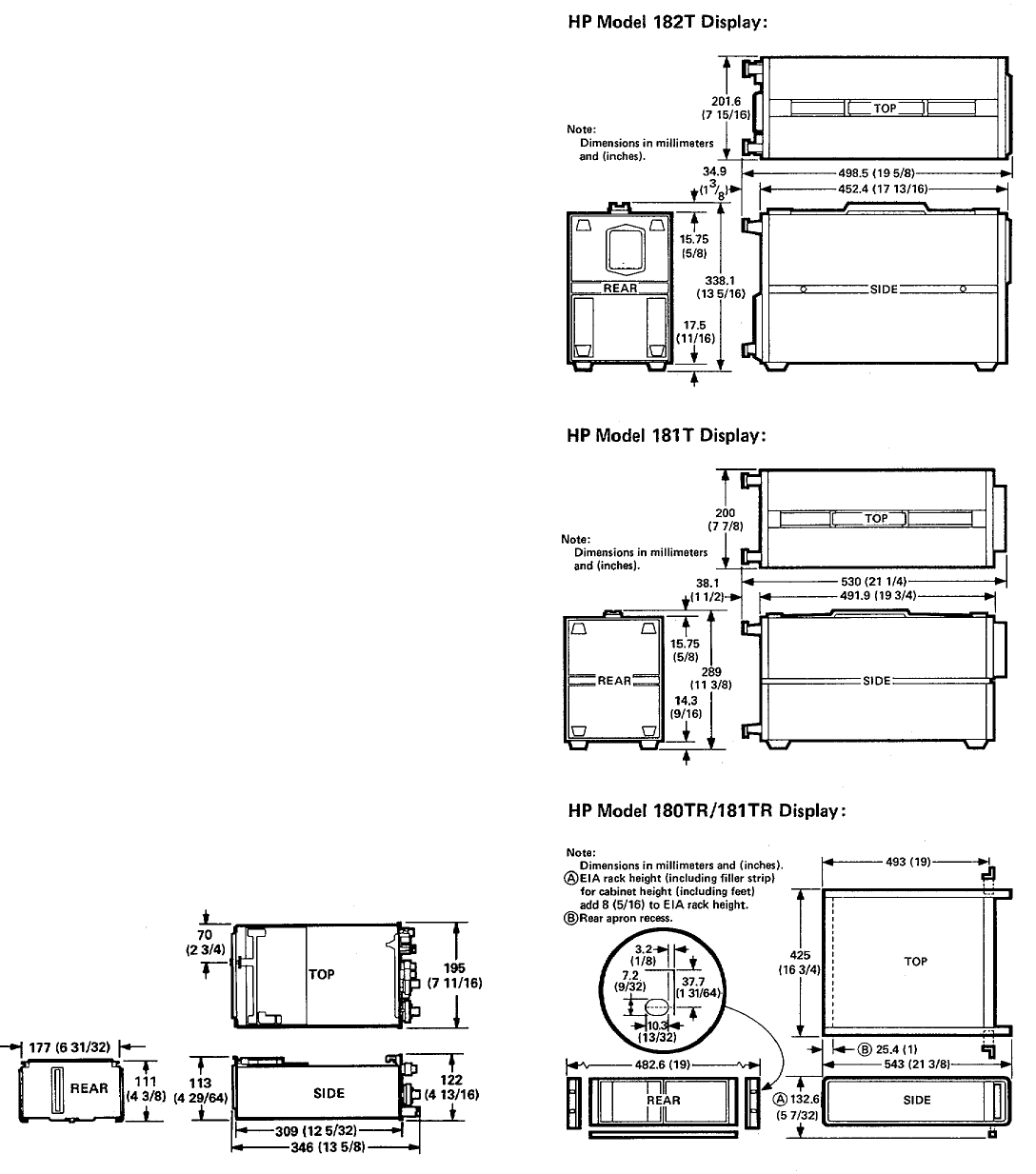
DIMENSIONS
HP Model 8558B Spectrum Analyzer:
1-5
Model 8558B TM 11-6625-3061-14
Table 1-2. Model 8558B/180-Series Supplemental Characteristics (1 of 3)
SUPPLEMENTAL CHARACTERISTICS
NOTE:
Values in this table are not specifications. They are typical characteristics included for user information.
FREQUENCY CHARACTERISTICS
FREQUENCY ACCURACY
FREQUENCY ZERO
Adjusts digital FREQUENCY MHz readout. FRE-
QUENCY ZERO control may be used to calibrate
the frequency readout on a known signal or on the
LO feedthrough.
FREQUENCY CAL
Removes tuning hysteresis from first LO (YIG
oscillator). FREQUENCY CAL button should be
pressed to maintain FREQUENCY MHz readout
accuracy whenever TUNING is changed by more
than 50 MHz.
FREQUENCY RANGE
OUT-OF-RANGE BLANKING
The CRT trace is automatically blanked whenever
the spectrum analyzer is swept or tuned beyond its
frequency range (approximately -50 MHz and 1600
MHz).
SPECTRAL RESOLUTION AND STABILITY
FREQUENCY DRIFT
At fixed start/center frequency, after 2-hour warmup:
<50 kHz in 10 minutes.
With temperature changes: <200 kHz/°C
RESOLUTION BANDWIDTH SHAPE
Approximately gaussian (synchronously-tuned,
4-pole filter).
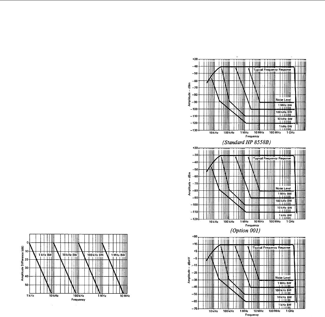
SPECTRAL RESOLUTION
The following graph shows typical spectrum
analyzer resolution for different resolution
bandwidths.
Signal Resolution vs. Frequency Separation
AMPLITUDE CHARACTERISTICS
AMPLITUDE RANGE AND ACCURACY
DYNAMIC RANGE
Maximum power ratio of two signals simultaneously
present at the input that may be measured within the
limits of specified accuracy, sensitivity, and distortion
(i.e. spurious responses): >70 dB
FREQUENCY RESPONSE AND AVERAGE
NOISE LEVEL
The following graphs show typical frequency response
and average noise level versus frequency.
(Option 002)
Average Noise Level and Frequency Response
1-6
Model 8558B TM 11-6625-3061-14
Table 1-2. Model 8558B/180-Series Supplemental Characteristics (2 of 3)
SUPPLEMENTAL CHARACTERISTICS
NOTE:
Values in this table are not specifications. They are typical characteristics included for user information.
GAIN COMPRESSION
Gain compression is typically less than 1 dB for a -
10 dBm input level with 0 dB input attenuation.
001: -5 dBm input level
002: +45 dBmV input level
AMPLITUDE SCALE SWITCHING
Reference Level variation is typically less than
±1 dB for any change in Amplitude Scale.
SPURIOUS RESPONSES
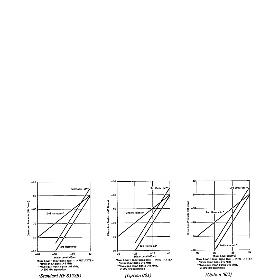
SECOND HARMONIC AND THIRD ORDER
INTERMODULATION DISTORTION
The graphs below illustrate typical second harmonic
and third order intermodulation distortion.
SWEEP CHARACTERISTICS
SWEEP TIME
CALIBRATED SWEEP TIME ACCURACY
(Sec/DIV, mSec/DIV)
Sweep times are typically ±10% of indicated value.
MANUAL
Spectrum analyzer may be swept manually, in either
direction, with front panel control.
SWEEP TRIGGER
FREE RUN
End of each sweep triggers new sweep.
LINE
Sweep triggered at ac line frequency.
VIDEO
Sweep triggered on post-detection video waveform.
One-half major division of vertical deflection
required to trigger sweep.
SINGLE
Single sweep started or reset by turning SWEEP
TRIGGER clockwise momentarily.
FRONT PANEL INPUT AND OUTPUT
CHARACTERISTICS
SIGNAL INPUT
INPUT IMPEDANCE
50 ohms nominal; Precision Type N female
connector.
001 and 002: 75 ohms nominal; 75-ohm BNC female
connector.
INPUT SWR
<1.5 SWR with >10 dB input attenuation
001 and 002: <1.5 SWR
Distortion vs. Mixer Level
1-7

Model 8558B TM 11-6625-3061-14
Table 1-2. Model 8558B/180-Series Supplemental Characteristics (3 of 3)
SUPPLEMENTAL CHARACTERISTICS
NOTE:
Values in this table are not specifications. They are typical characteristics included for user information.
CAL OUTPUT
-30 dBm at 280 MHz with second through fourth
harmonics greater than -70 dBm (into 50 ohms).
001:-30 dBm at 280 MHz (into 75 ohms)
002: +20 dBm V at 280 MHz (into 75 ohms)
1ST LO OUTPUT
+10 dBm nominal into 50 ohms, 2.05-3.55 GHz.
Terminate with a 50-ohm load when not in use.
PROBE POWER
+15V, -12.6V, and GND (150 mA maximum) for use
with HP High-Impedance Probes (i.e. HP 1120A,
1121A, 1123A, 1124A). The HP 1121A is
recommended for its low noise characteristics.1'
REAR PANEL OUTPUT CHARACTERISTICS2
VERTICAL, PENLIFT/BLANKING, AND HORIZONTAL
OUTPUTS (AUX A, B, D)
These outputs are compatible with and may be used
to drive HP X-Y Recorders (using positive pencoils
or TTL penlift input) and CRT monitors.
1See Section II for details regarding use with 001 and
002 75ohm inputs.
2Rear panel outputs refer to 180T-series display
mainframes and other 180-series mainframes with
Option 807 installed. Horizontal, vertical, and blanking
outputs, attenuated and shifted in dc level, are available
on other 180-series mainframes at the MAIN SWEEP,
MAIN GATE, and DELAYED GATE outputs,
respectively. DO NOT connect an X-Y recorder to the
DELAYED GATE OUTPUT, or damage will result.
AUX A VERTICAL OUTPUT
BNC output provides detected video signal from a
50-ohm output impedance. Typical 0-800 mV range
corresponds to full 8-division CRT vertical
deflection.
AUX B PENLI FT/BLANKING OUTPUT
BNC output provides a +15V penlift/blanking signal
from a 10K-ohm output impedance when CRT trace
is blanked. Otherwise, output is low at OV (low
impedance, 150 mA max.) for an unblanked trace.
AUX C 21.4 MHz IF OUTPUT
BNC output provides 21.4 MHz IF signal (linearly
related to spectrum analyzer RF input) from a 50-
ohm output impedance. Output bandwidth
controlled by spectrum analyzer RESOLUTION BW
setting; output amplitude controlled by INPUT
ATTEN, REFERENCE LEVEL FINE, and first six
REFERENCE LEVEL positions (i.e. -10 through -60
dBm with 0 dB input attenuation). Output level is
approximately -10 dBm into 50 ohms with a signal
displayed at Reference Level.
002: (i.e. +40 to -10 dBmV with 0 dB input
attenuation).
AUX D HORIZONTAL OUTPUT
BNC output provides horizontal sweep voltage from
a 5K-ohm output impedance. -5V to +5V range
corresponds to full 10-division CRT horizontal
deflection.
1-8

Model 8558B TM 11-6625-3061-14
1-22. This information should not be confused with
information contained in the yellow Manual Changes
supplement, which is intended to adapt this manual to
instrument changes that are accomplished after its
printing.
1-23. OPTIONS
CAUTION
The two 75-ohm BNC connectors on
Option 001 and Option 002
instruments are not compatible with
50ohm BNC connectors. Direct use
of 50-ohm BNC connectors with
these instruments might damage the
INPUT and CAL OUTPUT connectors.
1-24. Option 001
1-25. Option 001 provides direct-measurement
capability in a 75-ohm system. The BNC input and
calibration-output connectors have 75 Ω impedance
(nominal). Option 001 is calibrated in dBm, providing a
measurement range from -110 dBm to +30 dBm.
Throughout the manual, differences between the
standard instrument and Option 001 are given in
boldface type following applicable text references and
as necessary in tables and illustrations.
1-26. Option 002
1-27. Option 002 provides direct-measurement
capability in a 75-ohm system. The BNC input and
calibration-output connectors have 75Q impedance
(nominal). Option 002 is calibrated in dBmV, providing
a measurement range from -63 dBmV to + 80 dBmV.
Throughout the manual, differences between the
standard instrument and Option 002 are given in
boldface type following applicable text references and
as necessary in tables and illustrations.
1-28. Option 910
1-29. One additional Operation and Service manual is
provided for each Option 910 ordered. To obtain
additional manuals after initial shipment, order by the
manual part number, which appears on the title page
and on the back cover.
1-30. ACCESSORIES SUPPLIED
1-31. The following accessories, supplied with the
instrument, are shown in Figure 1-1:
•BNC termination
•Cable adapter
•Side stop kit
•Graticule overlays
1-32. Termination
1-33. A BNC, 50-ohm termination, HP Model 11593A,
is supplied for the front-panel 1ST LO OUTPUT.
1-34. Cable Adapter
1-35. A Type N male to BNC female adapter, HP part
number 1250-0780, is supplied with the standard
instrument for the use of lightweight cables with BNC
connectors.
1-36. Side Stop Kit
1-37. A side stop kit, HP part number 08558-60131, is
supplied to prevent the spectrum analyzer from sliding
out of the mainframe. When the side stops are
installed, the plug-in cannot be removed from the
mainframe. Refer to Section II for installation or
removal of the side stops.
1-38. Graticule Overlays
Three graticule overlays provide the operator with
reference-level labels for the CRT. HP Part Number
5020-8565 is the overlay for 180-series display
mainframes. HP Part Number 5020-8566 is the overlay
for 181-series display mainframes. HP Part Number
5020-8567 is the overlay for 182- series display
mainframes. For proper installation of the graticule
overlay, refer to Section II.
1-9

Model 8558B TM 11-6625-3061-14
1-39. EQUIPMENT REQUIRED BUT NOT
SUPPLIED
1-40. Display Mainframe
1-41. A 180T-series display mainframe (180TR, 181T,
181TR, or 182T) is recommended for use with the HP
Model 8558B. In the 180T-series mainframe, the rear-
panel auxiliary output connectors (AUX A, AUX B, AUX
C, and AUX D) provide, respectively, Vertical Output,
Pen Lift Output, 21.4 MHz IF Output, and Horizontal
Output.
1-42. A standard 180-series Display mainframe
(180A/AR, 180C/D, 181A/AR, 182A/C, or 184A/B)
provides only horizontal, vertical, and blanking rear
panel outputs. Furthermore, these outputs are
attenuated and shifted in dc level. Unbuffered rear
panel outputs (similar to the 180T-series) are provided
only if Option 807 is installed.
1-43. Extender Cable Assembly
1-44. An Extender Cable Assembly (Figure 1-3), HP
Part Number 5060-0303, allows operation of the HP
8558B outside the display mainframe. This provides
access to the HP 8558B for necessary adjustments and
some performance tests. This cable is also useful for
troubleshooting.
1-45. MEASUREMENT ACCESSORIES
1-46. AC Probe
1-47. The HP Model 8558B Spectrum Analyzer has a
front-panel PROBE POWER connector for the use of
high-impedance active probes such as the HP 1120A,
HP 1121A, HP 1123A, and HP 1124A. High-impedance
probes permit testing of high-frequency circuits without
significant loading effects. The low-noise, AC-coupled
HP 1121A is preferred for use with the HP 8558B.
CAUTION
The 75-ohm BNC input connector on
ANT Option 001 and 002 instruments
is not compatible with 50-ohm BNC
connectors. Direct connection of an
AC probe might damage the input
connector.
001 and 002: The AC probes have a 50-ohm output
impedance. Use of a probe with the 75-ohm Option 001
or 002 without proper impedance matching causes a +
1.58 dB error in displayed signal levels.
1-48. Modification Kit (Option 807 Connections)
1-49. A modification kit, HP part number 00180-69503,
provides the materials and information necessary to
install unbuffered rear panel connections (formerly
included in Option 807) in the following display
mainframes: 180A/AR, 180C/D, 181A/AR, 182A/C, and
184A/B. Refer to Table 1-3 for a description of parts
included in the modification kit.
1-50. Oscilloscope Camera
1-51. The HP Model 197B, Option 002, General
Purpose Camera can be used with 180- and 181-series
display mainframes to make a permanent record of
measurements. The HP 10367A adapter allows the
camera to be used with 182-series mainframes.
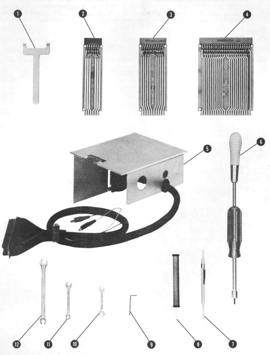
1-52. SERVICE ACCESSORIES
1-53. Service accessories are shown in Figure 1-3.
Table 1-3. Parts Included in Modification Kit 00180-69503
Quantity Description HP Part Number
1Output Amplifier Assembly (Auxiliary Output
Board) 00180-66551
1Label 7120-3116
23/4 inch pieces of shrink tubing 0890-0720
1Service Note 180A/AR-10, 180C/D-2, 181A/AR8
182A/C-1, or 184/B-1 (modification is
similar for all instruments listed)
1-10
Model 8558B TM 11-6625-3061-14
1-54. RECOMMENDED TEST EQUIPMENT
1-55. Equipment required for operation verification,
performance tests, adjustments, and
troubleshooting of the HP Model 8558B is listed in Table
1-4. Other equipment may be substituted if it meets or
exceeds the critical specifications listed in the table.
1-11
Model 8558B TM 11-6625-3061-14
Figure 1-3. Service Accessories (1 of 2)
1-12

Model 8558B TM 11-6625-3061-14
Item Description CD HP Part Number
(1) Board Puller, 2 prongs to lift PC boards 103950-4001
(2) Extender Board, 6 pin, 12 contacts 208559-60042
(3) Extender Board, 10 pin, 20 contacts 285680-60028
(4) Extender Board, 22 pin, 44 contacts 808565-60107
(5) Extender Cable Assembly, for plug-in operation out of
display mainframe 95060-0303
(6) Tuning Tool, modified 5/16 inch nut driver with
modified No. 10 Allen driver 608555-60107
(7) Alignment tool, metal tip in plastic 78710-0630
(8) Alignment tool, non-metallic 48710-0033
(9) Wrench, No. 2 Bristol 08710-0055
(10) Wrench, 15/64 inch, combination 88710-0946
(11) Wrench, 1/4 inch, open end 28720-0014
(12) Wrench, 5/16 inch, slotted box end/open end 908555-20097
Figure 1-3. Service Accessories (2 of 2)
1-13

Model 8558B TM 11-6625-3061-14
Table 1-4. Recommended Test Equipment (1 of 4)
Recommended
Equipment Critical Specifications Model Use*
Display Mainframe HP 180T Series with variable persistence HP 181T/TR P, A, T
Oscilloscope Time Base: 1 ms/cm to 10 ms/cm HP 1741A A, T
Vertical Sensitivity: 1 mV/cm to 20 V/cm
Frequency Counter Frequency Range: 150 MHz to 1.5 GHz HP 5342A P, A, T
Sensitivity: -30 dBm
Timer/Counter Time base: 10 us HP 5308A A, T
Digital Voltmeter Accuracy: ±(.05% Rdg ± digit) HP 3455A P, A, T
Power Meter Power Range: -20 dBm to +10 dBm HP 435A/B P, A, T
Power Sensor Frequency Range: 100 kHz to 1.5 GHz HP 8482A P, A, T
Maximum SWR: 1.1,0.1 to 1 GHz
Amplifier Frequency Range: 200 MHz to 300 MHz HP 8447D P, A, T
Gain: > 20 dB
Impedance: 50 Ω
Signal Generator Frequency Range: 4 MHz to 305 MHz HP 8640B P, A, T
(2 required) Drift: Less than 50 ppm (or 5 Hz,
whichever is greater)
Harmonic Distortion: > 30 dB below
fundamental
Noise Sidebands: > 80 dB down, 50 kHz
away, 1 kHz BW
Tracking Generator Frequency Range: 5 MHz to 1500 MHz HP 8444A Opt. 059 P, T
Sweep Oscillator Manual Sweep HP 8350A A
RF Plug-In Frequency Range: 10 MHz to 1.5 GHz HP 83522A A
Flatness (external leveling): < ±0.1 dB
Spectrum Analyzer Frequency Range: 10 MHz to 1.5 GHz HP 141T/8552B/ T
8555A
Comb Generator Accuracy: 0.01% HP 8406A P, A, T
Function Generator Frequency Range: 5 kHz to 5 MHz HP 3310A P, T
Crystal Detector Frequency Range: 10 MHz to 1.5 GHz HP 423B A, T
Frequency Response: ± 0.2 dB/octave
to 2 GHz; ±0.5 dB overall
*P = Performance Test; A = Adjustment; T = Troubleshooting
1-14

Model 8558B TM 11-6625-3061-14
Table 1-4. Recommended Test Equipment (2 of 4)
Recommended
Equipment Critical Specifications Model Use*
300 MHz LPF Rejection: > 50 dB for signals above Telonic P, A, T
300 MHz TPL 3004AB
Power Splitter Frequency Range: 100 kHz to 1.5 GHz HP 11667A P, A
Input SWR: <, 1.15
10 dB Attenuator Frequency Range: 100 kHz to 1.5 GHz HP 8491A Opt. 010 P, A
(2 required) Accuracy: ±0.5 dB
Step Attenuator Frequency Range: 20 MHz to 305 MHz HP 355C Opt. H80 P, A, T
Attenuation: 12 dB in l-dB steps
calibrated at 30 MHz by a standards lab
Accuracy: ±0.25 dB
Step Attenuator Frequency Range: 20 MHz to 305 MHz HP 355D Opt. H82 P, A, T
Attenuation: 80 dB in 10-dB steps
calibrated at 30 MHz and 280 MHz
by a standards lab
Accuracy: ±0.01 dB ±0.02/10 dB step
at calibrated frequencies
Termination Impedance: 50Ω HP 908A/11593A P, A
Type N Cable 50Ω coaxial cable with Type N (m) HP 11500A P, A
connectors on both ends
BNC Cable, 20 cm (9 in) 50Ω coaxial cable with BNC (m) HP 10502A P, A, T
connectors on both ends
BNC Cable, 120 cm 50Ω coaxial cable with BNC (m) HP 10503A P, A, T
(48 in) (2 required) connectors on both ends
Cable BNC to Banana Plug HP 11001A P
Cable SMC (f) to BNC (m) HP 11592-60001 A, T
Cable Banana Plug to Alligator Clips HP 11102A A
Adapter Banana plugs to BNC (f) HP 10111 A P, T
Adapter N (m) to BNC (f) (3 required) HP 1250-0780 P, A
Adapter SMC (m) to BNC (m) HP 1250-0831 P
Adapter BNC (f) to BNC (f) HP 1250-0080 P
Adapter BNC Tee HP 1250-0781 A
*P = Performance Test; A = Adjustment; T = Troubleshooting
1-15

Model 8558B TM 11-6625-3061-14
Table 1-4. Recommended Test Equipment (3 of 4)
Recommended
Equipment Critical Specifications Model Use*
Adapter N (m) to N (m) HP 1250-1475 P
Adapter BNC (m) to BNC (m) HP 1250-0216 P
Adapter N (f) to BNC (m) HP 1250-0077 P
Adapter SMC (m) to SMC (m) HP 1250-0827 A, T
Adapter Type N (m) to SMC (m) HP 1250-1023 A, T
Adapter BNC (f) to Alligator Clips HP 8120-1292 A, T
Adapter SMC (f) to SMC (f) HP 1250-1113 A, T
Adapter Type N (m) to SMA (f) HP 1250-1250 P, A
Adapter BNC (f) to SMA (m) HP 1250-1200 P
Adapter SMA (f) to SMA (f) HP 1250-1158 P
Extender Board 6 pin, 12 contacts with 51.1 Ω resistor HP 08505-60109 A, T
from pin 1 to pin 5 HP 0757-0394
NOTE
The following equipment is required
for Option 001 and Option 002.
Termination Impedance: 75 Ω HP 11652-60010 P
Power Sensor Frequency Range: 10 MHz to 2 GHz HP 8483A T
Maximum SWR: 1.18, 10 MHz to 2 GHz
Adapter 75Ω BNC (m) to 75Ω Type N (f) HP 1250-1534 T
Minimum Loss Adapter 75Ω BNC (f) to 50Ω SMA (m) HP 08558-60031 P, A, T
5.72 dB attenuation
Adapter BNC (f) to SMA (m) HP 1250-1200 T
Adapter SMA (f) to SMA (f) HP 1250-1158 P, T
*P = Performance Test; A = Adjustment; T = Troubleshooting
1-16

Model 8558B TM 11-6625-3061-14
Table 1-4. Recommended Test Equipment (4 of 4)
Recommended
Equipment Critical Specifications Model Use*
Adapter N (f) to N (f) HP 1250-0777 A, T
Cable BNC, 30 cm (12 in), 75Ω HP 11652-60012 P, A, T
Cable BNC, 60 cm (24 in), 75ΩHP 11652-60013 P, A, T
Cable BNC, 90 cm (37 in), 75ΩHP 11652-60014 P, A, T
Adapter BNC (m) to BNC (m) HP 1250-1288 P, A, T
Adapter Type N (m) to SMA (f) HP 1250-1250 P, A, T
*P = Performance Test; A = Adjustment; T = Troubleshooting
1-17/1-18

Model 8558B TM 11-6625-3061-14
SECTION II.
INSTALLATION
2-1. INTRODUCTION
2-2.This section includes information on initial
inspection, preparation for use, and storage and
shipping requirements for the HP Model 8558B.
2-3. INITIAL INSPECTION
2-4.Inspect the shipping container for damage. If the
shipping container or cushioning material is damaged, it
should be kept until the contents of the shipment have
been checked for completeness and the instrument has
been checked mechanically and electrically. The
contents of the shipment should be as shown in Figure
1-1. The electrical performance is checked with the
procedures in Section IV. If the contents are
incomplete, if there is mechanical damage or defect, or
if the instrument does not pass the Performance Test
procedures, notify the nearest Hewlett-Packard office. If
the shipping container is damaged, or if the cushioning
material shows signs of stress, notify the carrier as well
as the Hewlett-Packard office. Keep the shipping
materials for inspection by the carrier. The Hewlett-
Packard office will arrange for repair or replacement
without waiting for a claim settlement.
2-5. PREPARATION FOR USE
2-6. Installation
2-7.When properly installed, the spectrum analyzer
obtains all necessary power from the display mainframe.
The rear panel connector provides the interface.
CAUTION
BEFORE SWITCHING ON THIS
INSTRUMENT, make sure it is
adapted to the voltage of the ac
power source to be used and the
proper fuse is installed. Failure to
set the ac power input of the
instrument
for the correct voltage level could
cause damage to the instrument
when plugged in. Refer to the
display mainframe Operation and
Service Manual for line voltage and
fuse selection.
2-8.To install the spectrum analyzer in the mainframe:
1.Set display mainframe LINE switch to OFF.
2.Pull out lock knob and slide plug-in toward rear of
compartment until it is seated firmly in place.
3.Push in lock knob to secure spectrum analyzer in
mainframe.
2-9. Side Stop Kit
2-10.Installation of a Side Stop Kit, HP part number
08558-60131, prevents the removal of the analyzer from
the 180-series mainframe without the use of hand tools.
This kit contains two side stops, mounting hardware,
label, and installation instructions. (Refer to Table 2-1
for part numbers of individual items.)
Table 2-1. Side Stop Kit (08558-60131)
HP Part C
Quantity Description Number D
2 SIDE STOP 08558-00094 7
4 MACHINE SCREW, 2200-0168 9
440 .438-IN-LG
82 DEG FLATHEAD
1 LABEL, FRONT-PANEL 7120-8131 7
1 LABEL, INSTRUCTIONS 7120-8215 8
2-1
Model 8558B TM 11-6625-3061-14
2-11. To install side stops:
WARNING
Before removing covers from the
display mainframe, disconnect line
power by removing the ac power
cord.
1. Remove side covers from bottom section of
mainframe. (Remove only right side cover if
mainframe is a rack-mounted model.)
2. Use flathead machine screws to install side stops as
shown in Figure 2-1.0
3. Reinstall side covers on mainframe.
4. Place caution label on front panel of spectrum
analyzer (upper right-hand corner) to indicate that
plug-in is secured with side stops.
2-12. To remove side stops:
WARNING
Before removing covers from the
display mainframe, disconnect line
power by removing the ac power
cord.
1. Remove side covers from bottom section of
mainframe. (Remove only right side cover if
mainframe is a rack-mounted model.)
2. Remove side stops. (See Figure 2-1.)
3. Reinstall side covers on display mainframe.
2-13. Graticule Overlays
2-14. To install a graticule overlay:
1. Select proper overlay. HP part number 5020-8565
is for 180TR display mainframes, HP part number
5020-8566, for 181T/TR display mainframes, and
HP part number 5020-8567, for 182T display
mainframes.
2. For 180TR and 181T/TR mainframes, remove
CRT bezel and metallic-mesh contrast filter. Insert
proper overlay and replace contrast filter and CRT
bezel.
3. For 182T mainframes, grasp top portion of CRT
bezel and pull straight up. Remove metallic-mesh
contrast filter and insert proper overlay and contrast
filter. (Either the metallic-mesh contrast filter or a
light blue contrast filter may be used.)
4. Slide bezel back into place to retain overlay and
filter.
2-15. Mainframe Interconnections
2-16. When the HP 8558B is properly installed in the
display mainframe, the interconnections are as listed in
Table 2-2.
2-17. Operating Environment
2-18. Temperature. The instrument may be operated
in temperatures from 0°C to + 55oC.
2-19. Humidity. The instrument may be operated in
environments with relative humidity from 5 percent to 95
percent, 0°C to +40oC. The recommended long-term
operating environment is 5 percent to 80 percent
relative humidity. The instrument should also be
protected from abrupt temperature changes that cause
internal condensation.
2-20. Altitude. The instrument may be operated in
altitudes up to 4572 meters (15,000 feet).
2-21. Modifications
2-22. A Modification Kit, HP part number 00180-69503,
provides materials and information necessary to add
Option 807 rear-panel connections to the standard HP
180-series display. Refer to Table 1-3 in Section I.
Option 807 is factory-installed in 180T, 181T, 181TR,
and 182T mainframes. The modification kit is required
for use with other mainframes if all four rear-panel
outputs are needed.
2-2
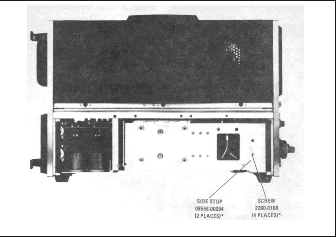
Model 8558B TM 11-6625-3061-14
* Only one side stop and two screws are used for rackmount models.
Figure 2-1. Location of Side Stops
2-23. STORAGE AND SHIPMENT
2-24. Environment
2-25. The instrument may be stored or shipped in
environments within the following limits:
Temperature: -40°Cto +75°C
Humidity: 5% to95o (0°Cto +400C)
Altitude: Up to 15240 meters (50,000 feet)
The instrument should also be protected from
temperature extremes which cause condensation within
the instrument.
2-26. Packaging
2-27. Original Packaging. Containers and materials
identical to those used in factory packaging are
available through Hewlett-Packard offices. If the
instrument is being returned to Hewlett-Packard for
servicing, attach a tag indicating the type of service
required, return address, model number, and full serial
number. A supply of these tags is provided at the end
of this section. Mark the container FRAGILE to assure
careful handling. In any correspondence, refer to the
instrument by model number and full serial number.
2-3

Model 8558B TM 11-6625-3061-14
Table 2-2. HP Model 8558B Mainframe Interconnections
Pin on P1 Signal or Voltage Pin on P1 Signal or Voltage
1CRT HORIZ (adjusted horizontal 17 BLANKING
signal) 18 NC
2GROUND from mainframe 19 GROUND from mainframe
(jumpered to pin 8) (jumpered in pin 24)
3NC 20 AUTO SWP
4L NORM 21 BEAM FINDER
5YNORM 22 NC
6NC 23 NC
7SING SWP 24 GROUND from mainframe
8GROUND from mainframe (jumpered to pin 19)
(jumpered to pin 2) 25 NC
9MAN SWP 26 NC
10 NC 27 NC
11 AUX D Horizontal Output 28 -12.6 VDC from mainframe
(to mainframe rear panel) 29 +15 VDC from mainframe
12 AUX C 21.4 MHz IF Output 30 +100 VDC from mainframe
(to mainframe rear panel) 31 30V p-p from mainframe
13 AUX B Penlift/Blanking Output (for LINE TRIGGER)
(to mainframe rear panel) 32 NC
14 AUX A Vertical Output W10P3 +VERT (top contact,
(to mainframe rear panel) (2 contacts) yellow wire)
15 GROUND -VERT (bottom contact,
16 NC orange wire)
2-28. Other Packaging. The following general
instructions should be used for repackaging with
commercially available materials:
1. Wrap instrument in heavy paper or plastic. If
shipment is to a Hewlett-Packard office or service
center, attach a tag indicating type of service
required, return address, model number, and full
serial number. A supply of these tags is provided at
end of this section.
2. Use a strong shipping container. A double-wall
carton made of 350-pound test material is adequate.
3. Use enough shock-absorbing material (3- to 4-inch
layer) around all sides of the instrument to provide
firm cushion and prevent movement inside
container. Protect control panel with cardboard.
4. Seal shipping container securely.
5. Mark shipping container FRAGILE to assure careful
handling.
2-4
Model 8558B TM 11-6625-3061-14
SECTION III.
OPERATION
3-1. INTRODUCTION
3-2.This section provides operating information for the
Model 8558B Spectrum Analyzer. It also provides a
brief description of display mainframe controls. For a
detailed description of the display mainframe, refer to its
manual.
3-3. CONTROLS, INDICATORS, AND CONNECTORS
3-4.The spectrum analyzer is used with one of the
180-series display mainframes. The 180T-series display
mainframes, or the 180-series mainframes with Option
807, have the correct rear-panel connections for
spectrum analyzer horizontal, vertical, penlift, and IF
outputs. Figure 3-1 shows the front-panel features of
the HP 8558B Spectrum Analyzer and the display
mainframe. Figure 3-2 shows the rear-panel features of
the HP 8558B. The rear panels of all 180T-series
mainframes, and 180-series mainframes with Option
807, are basically the same.
3-5. Control Grouping
3-6.The spectrum analyzer and display mainframe
front-panel controls fall into three general groups: those
that deal with the display, those that deal with
frequency, and those that deal with amplitude.
3-7. Display. The display group consists of:
SWEEP TIME/DIV
SWEEP TRIGGER
VERTICAL POSN
VERTICAL GAIN
MAN SWEEP
HORIZ GAIN (rear panel of 8558B)
VIDEO FILTER
BASELINE CLIPPER
HORIZONTAL POSITION
INTENSITY
FOCUS
TRACE ALIGN
ASTIG
3-8.The display group enables the operator to
calibrate the display and to select a variety of scan and
display conditions. The controls are explained in
Figures 3-1 and 3-2. However, when the SWEEP
TIME/DIV control is placed in the AUTO position, sweep
time is controlled by the RESOLUTION BW, FREQ
SPAN/DIV, and VIDEO FILTER controls.
3-9. Frequency. The frequency group consists of:
TUNING
RESOLUTION BW
FREQ SPAN/DIV
3-10.The frequency group enables the operator to
control how the spectrum analyzer displays the
frequency domain. The RESOLUTION BW and FREQ
SPAN/DIV controls when pushed in are coupled
together, and moving either control moves the other.
When the SWEEP TIME/DIV control is in the AUTO
position varying the RESOLUTION BW or the FREQ
SPAN/DIV (coupled or uncoupled) will change the
sweep time to maintain calibration. With the two
controls coupled together in the OPTIMUM position,
RESOLUTION BW's of 3 MHz to 1 kHz will be
automatically selected as the FREQ SPAN/DIV is
narrowed from 100 MHz to 0. TUNING controls coarse
and fine (coarse is larger knob) set the center frequency
of the displayed spectrum. RESOLUTION BW control
determines the resolution of the signals on the CRT.
3-11. Amplitude. The amplitude group consists of:
REFERENCE LEVEL
INPUT ATTEN
REF LEVEL FINE
REF LEVEL CAL
10 dB/DIV - 1 dB/DIV - LIN (Amplitude
Scale)
3-12.The amplitude group enables the operator to
measure signal amplitude in units of either voltage or
dBm.
3-1
Model 8558B TM 11-6625-3061-14
3-13. Variable Persistence and Storage Functions
3-14. With the 181T/TR Display Mainframe, the
operator can set trace persistence for a bright, steady
trace that does not flicker, even on the slow sweeps
required for narrow band analysis. The variable
persistence also permits the display of low repetition
rate pulses without flickering; and using the longest
persistence, intermittent signals can be captured and
displayed. The storage capability allows side-by-side
comparison of changing signals.
3-15. Persistence and Intensity
CAUTION
Excessive INTENSITY may damage
the CRT storage mesh.
3-16. These controls determine the appearance of the
CRT trace. Specifically, PERSISTENCE controls the
rate at which a signal is erased and INTENSITY controls
the trace brightness as the signal is written. With a
given PERSISTENCE setting, the actual time of trace
visibility can be increased by greater INTENSITY.
Since the PERSISTENCE control sets the rate of trace
erasure, a brighter trace requires more time to be
erased. Conversely, a display of low intensity
disappears more rapidly. The same principle applies to
a stored display of high or low intensity.
3-17. Storage. These controls select the storage
mode in which the CRT functions. In ERASE mode,
STORE, WRITE, and MAX WRITE are disconnected
and all written signals are removed from the CRT. The
STORE selector disconnects the WRITE, MAX WRITE,
and ERASE functions and implements signal retention
at reduced intensity. In the STORE mode,
PERSISTENCE and INTENSITY have no function.
3-18. Writing Speed. In the MAX WRITE mode, the
CRT storage surface is primed to allow much faster
writing on the storage surface. Since the erasing rate is
decreased, the entire screen becomes illuminated more
rapidly and the display is obscured. The effective
persistence and storage times are thus considerably
reduced. For this reason, MAX WRITE is not normally
used with a spectrum analyzer plug-in.
3-19. Photographic Techniques
3-20. The HP Model 197A Oscilloscope Camera
attaches directly to the spectrum analyzer's CRT bezel
without adapters. Flood guns in the CRT provide
background lighting of the display. When photography
of stored traces (181T/TR) is required, a double
exposure is needed. (Flood guns are turned off when
STORE is pressed.) See Application Note AN 150-5 for
full details.
OPERATING PRECAUTIONS
The spectrum analyzer is a sensitive measuring
instrument. To avoid damage to the instrument, do not
exceed the following Absolute Maximum Inputs:
Total Power: + 30 dBm (1W, 7.1 Vrms)
Option 001: + 30dBm(1W, 8.7 Vrms)
Option 002: +80dBmV(1.3W, 9.9 Vrms)
dc or ac (< 100 Hz): ±50V
Peak Pulse Power:
+ 50 dB, (100W, < 10 µs pulse width,
0.01% duty cycle) with ò20 dB INPUT ATTEN
Option 002: + 100 dBmV (130W), <10 µs
Overloading the input with too much power, peak
voltages, or dc voltages will damage the input circuit
and require expensive repairs.
CAUTION
While the analyzer's reference level
may be set for power levels up to +60
dBm, the total input power must not
exceed the absolute maximum limits
listed.
FRONT PANEL ADJUSTMENT PROCEDURE
Whenever an HP 8558B Spectrum Analyzer plug-in is
reinstalled in a different mainframe, the spectrum
3-2

Model 8558B TM 11-6625-3061-14
analyzer should be calibrated to ensure proper
correlation between plug-in and display. It is good
practice to execute this adjustment procedure
periodically (recommended daily) to correct for changes
in calibration which may occur over a period of time.
These adjustments are also an excellent way for the
new user to become acquainted with the spectrum
analyzer. For reference, a front panel view appears in
Figure 3-1.
If an HP 181 Variable Persistence Display is being used,
begin by setting the PERSISTENCE maximum
counterclockwise and pushing in the WRITE button.
Make the following spectrum analyzer settings.
Function Setting
INPUT ATTEN 10 dB
(push knob to engage)
REFERENCE LEVEL 0 dBm
002: +50 dBmV
REF LEVEL FINE 0
Amplitude Scale LIN
FREQ SPAN/DIV 10 MHz
(uncoupled)
RESOLUTION BW 1 MHz
(uncoupled)
SWEEP TIME/DIV AUTO
SWEEP TRIGGER FREE RUN
START - CENTER CENTER
TUNING > 60 MHz
BASELINE CLIPPER OFF
VIDEO FILTER OFF
180-series mainframes:
DISPLAY INT (out)
MAGNIFIER X1 (out)
SCALE (180TR, 182T) OFF
PERSISTENCE (181T/TR) MIN (ccw)
Display Mode (181T/TR) WRITE
DISPLAY ADJUSTMENTS
1. With an adjustment tool, adjust VERTICAL POSN to
place the CRT trace on a horizontal graticule line
near center of CRT.
2. Reduce the INTENSITY and set the SWEEP
TIME/DIV control to MAN. Adjust the MAN SWEEP
knob to bring dot to center of CRT.
CAUTION
Leaving a dot on the CRT for
prolonged periods at high intensity
may burn the phosphor.
3. Adjust the FOCUS and ASTIG controls for the
smallest round dot possible.
4. Reset the SWEEL TIME/DIV control to AUTO and
increase the INTENSITY for an optimum CRT trace.
Center the trace horizontally with the HORIZONTAL
POSITION control. If the horizontal deflection is not
exactly 10 divisions, adjust the HORIZ GAIN control
(located on the spectrum analyzer rear panel) for a
10 division (wide) horizontal deflection.
NOTE
The analyzer must be removed from
the mainframe to adjust the HORIZ
GAIN control.
5. Adjust the TRACE ALIGN so that the CRT trace is
parallel with the horizontal graticule lines.
6. Adjust the VERTICAL POSN until the trace aligns
with the bottom graticule line.
FREQUENCY ADJUSTMENTS
7. Center the LO feedthrough - the 'signal' at 0 MHz -
on the CRT with the TUNING control, pressing the
FREQUENCY CAL pushbutton two or three times to
remove tuning hysteresis in the first LO (YIG
oscillator).
8. Narrow the FREQ SPAN/DIV to 200 kHz and press
the FREQUENCY CAL pushbutton once more.
Adjust the REF LEVEL FINE control as necessary to
position the signal peak near the top CRT graticule
line.
9. Re-center the LO feedthrough, if necessary, and
adjust FREQUENCY ZERO to calibrate the
FREQUENCY MHz readout at 00.0 MHz.
3-3
Model 8558B TM 11-6625-3061-14
AMPLITUDE ADJUSTMENTS
10. Set the FREQ SPAN/DIV control to 1 MHz and the
REF LEVEL FINE control to 0. Adjust the TUNING
control for a FREQUENCY MHz readout of
approximately 280 MHz.
11. Press the 10 dB/DIV Amplitude Scale pushbutton,
and set the REFERENCE LEVEL control to - 20
dBm (+ 30 dBmV for Option 002).
CAUTION
The HP 8558B Options 001 and 002
feature 75-ohm (female) INPUT and
CAL OUTPUT connectors. Standard
50-ohm BNC cables and adapters
should not be used with these
connectors since damage might
result.
12. Connect the 280 MHz CAL OUTPUT to the
spectrum analyzer input and center the signal on
the CRT with the TUNING control, pressing the
FREQUENCY CAL pushbutton two or three times.
The FREQUENCY MHz readout will indicate 280
MHz + 5 MHz.
13. Press the LIN Amplitude Scale pushbutton. Adjust
the REF LEVEL FINE control to place the signal
peak at the top CRT graticule line.
14. Press the 10 dB/DIV Amplitude Scale pushbutton.
Adjust VERTICAL GAIN to place the signal peak at
the top CRT graticule line.
15. Repeat steps 12 and 13 until the signal peak
remains at the top CRT graticule line when the
Amplitude Scale is alternated between 10 dB/DIV
and LIN.
16. Set the REF LEVEL FINE control to 0 and the
REFERENCE LEVEL control to -30 dBm (+ 20
dBmV for Option 002).
17. Press the LIN Amplitude Scale pushbutton and
adjust REF LEVEL CAL to place the signal peak at
the top CRT graticule line.
Once the Front Panel Adjustment Procedure is
completed, the spectrum analyzer is calibrated for
absolute amplitude and frequency measurements.
During normal operation, the FREQUENCY CAL
pushbutton should be pressed whenever the tuning is
changed by more than 50 MHz. This removes tuning
hysteresis and ensures maximum frequency accuracy.
3-4
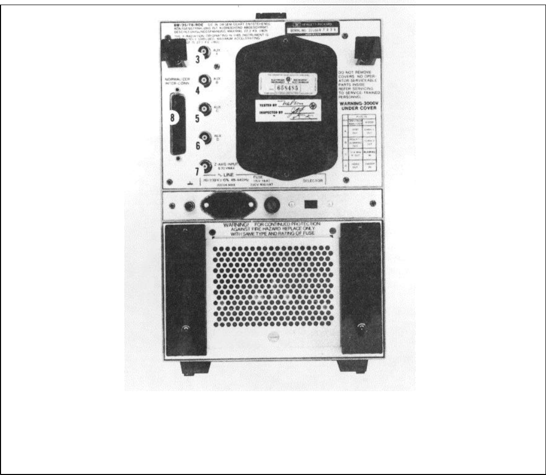
Model 8558B TM 11-6625-3061-14
Figure 3-2. Rear Panel Controls and Connectors (2 of 2)
3-7/3-8 (blank)

Model 8558B TM 11-6625-3061-14
SECTION IV.
PERFORMANCE TESTS
4-1. INTRODUCTION
4-2.The procedures in this section test the electrical
performance of the instrument against the specifications
in Section I. The performance tests included in this
section are listed in Table 4-1. Most of the tests can be
performed without access to the interior of the
instrument. If a test measurement is marginal, perform
the appropriate adjustment procedures in Section V.
Table 4-1. Performance Tests
Paragraph Test
4-11 Frequency Span Accuracy
4-12 Tuning Accuracy
4-13 Residual FM
4-14 Noise Sidebands
4-15 Resolution Bandwidth Accuracy
4-16 Resolution Bandwidth Selectivity
4-17 Average Noise Level
4-18 Spurious Responses
4-19 Residual Responses
4-20 Frequency Response
4-21 Bandwidth Switching (Amplitude
Variation)
4-22 Input Attenuator Accuracy
4-23 Reference Level Accuracy
4-24 Display Fidelity
4-25 Calibrator Accuracy
4-3. INSTRUMENTS TESTED
4-4.Since a 180-series Display mainframe is required
for operation of the HP Model 8558B Spectrum Analyzer
plug-in, the specifications listed in Table 1-1 apply when
both instruments are functioning together.
Consequently, the performance tests in this section
verify the proper operation of both the HP 8558B and
the 180-series Display mainframe.
4-5. EQUIPMENT REQUIRED
4-6.The equipment required for the performance tests
is listed under Recommended Test Equipment in
Section I. Any equipment that satisfies the critical
specifications given in the table may be substituted for
the recommended model.
4-7. TEST RECORD
4-8.Results of the performance tests may be tabulated
in the Performance Test Record at the end of this
section. The test record lists test specifications and
acceptable limits.
4-9. CALIBRATION CYCLE
4-10.This instrument requires periodic calibration.
Calibration should be verified every six months by
means of the performance tests.
4-1
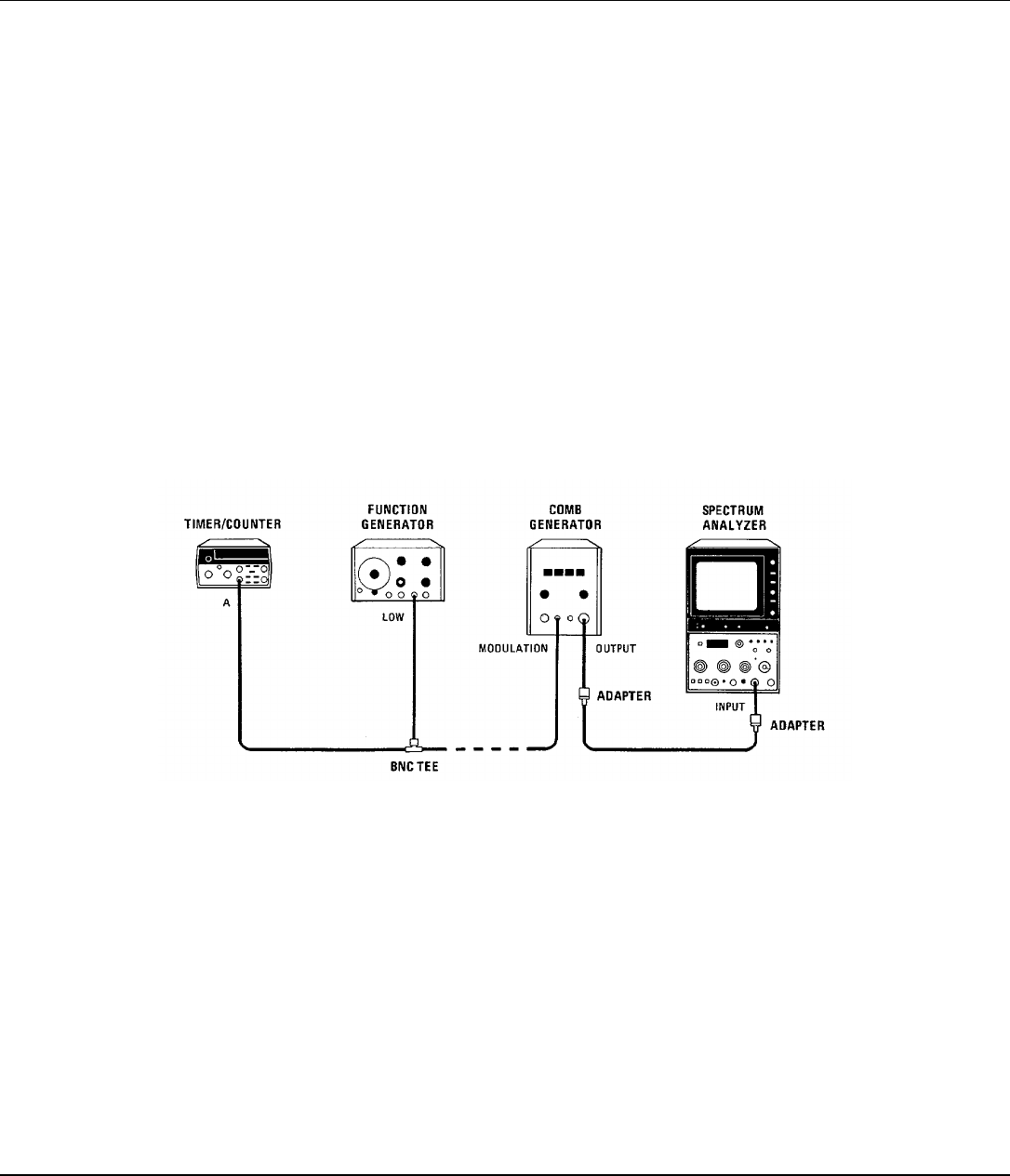
Model 8558B TM 11-6625-3061-14
PERFORMANCE TESTS
NOTE
Perform the Front Panel Adjustment Procedure in Section III before proceeding
with the performance tests. Allow at least 30 minutes warmup time.
4-11. FREQUENCY SPAN ACCURACY
SPECIFICATION
Fourteen calibrated spans from 100 MHz/div to 5 kHz/div in a 1, 2, 5 sequence. Frequency error between any two points
on the display is less than - 5 % of the indicated frequency separation.
DESCRIPTION
Wide span widths are checked by using the 100-, 10-, and 1-MHz outputs from a comb generator. Narrow span widths
are checked by using the output from a comb generator modulated by a function generator. Since the comb generator
produces frequency components separated by a precisely determined frequency interval, the resultant spectral lines
displayed on the CRT are evenly spaced when no span error exists in the instrument. Thus, span error is the cumulative
variance of distance among the spectral line intervals displayed across the CRT. The amount of span error is
determined by comparing the distance of the first nine graticule divisions to the display distance of the corresponding
spectral line intervals.
Figure 4-1. Frequency Span Accuracy Test Setup
EQUIPMENT
Comb Generator.................................................................................................... HP 8406A
Timer/Counter ....................................................................................................... HP 5308A
Function Generator ............................................................................................... HP 3310A
BNC Cable, 120 cm (48 in)................................................................................. HP 10503A
Adapter, Type N (m) to BNC (f) (2 required) .................................................... HP 1250-0780
BNC Tee ......................................................................................................... HP 1250-0781
Additional Equipment, Options 001 and 002:
Minimum Loss Adapter, 75Ω to 50Ω............................................................. HP 08558-60031
Adapter, BNC (m) to BNC (m), 75Ω.................................................................. HP 1250-1288
Adapter, SMA (f) to SMA (f).............................................................................. HP 1250-1158
Adapter, BNC (f) to SMA (m)............................................................................ HP 1250-1200
4-2

Model 8558B TM 11-6625-3061-14
PERFORMANCE TESTS
4-11. FREQUENCY SPAN ACCURACY(Cont'd)
PROCEDURE
1. Set equipment controls as follows:
Spectrum Analyzer:
START-CENTER..................................................................................................... CENTER
TUNING .................................................................................................................. 800 MHz
FREQ SPAN/DIV .................................................................................................... 100 MHz
RESOLUTION BW............................................................... OPTIMUM, coupled (pushed in)
INPUT ATTEN............................................................................................................... 0 dB
REFERENCE LEVEL ............................................................................................... -20 dBm
002: + 30 dBmV
Amplitude Scale .................................................................................................... 10 dB/DIV
SWEEP TIME/DIV ...................................................................................................... AUTO
SWEEP TRIGGER............................................................................................... FREE RUN
BASELINE CLIPPER..................................................................................................... OFF
VIDEO FILTER.............................................................................................................. OFF
Comb Generator:
COMB FREQUENCY- MHz........................................................................................ 100 MC
INTERPOLATION AMPLITUDE- 1 MHz......................................................................... OFF
OUTPUT AMPLITUDE ............................................................................................10 o'clock
Function Generator:
FUNCTION ................................................................................................................... SINE
RANGE .......................................................................................................................... 10K
Frequency ................................................................................................................ 200 kHz
DC OFFSET LEVEL............................................................................................................ 0
2. Connect equipment as shown in Figure 4-1 but do not connect function generator to comb generator.
3. Adjust spectrum analyzer TUNING control to position one spectral line (from comb generator) at first graticule line
(left-hand edge of display). Measure error between ninth spectral line and ninth graticule line as shown in Figure 4-2.
Error should be no greater than - 0.4 division.
__________ div
4. Set FREQ SPAN/DIV to 50 MHz. Adjust TUNING control to position one spectral line at first graticule line. Measure
error between fifth spectral line and ninth graticule line. Error should be no greater than i 0.4 division.
__________ div
4-3
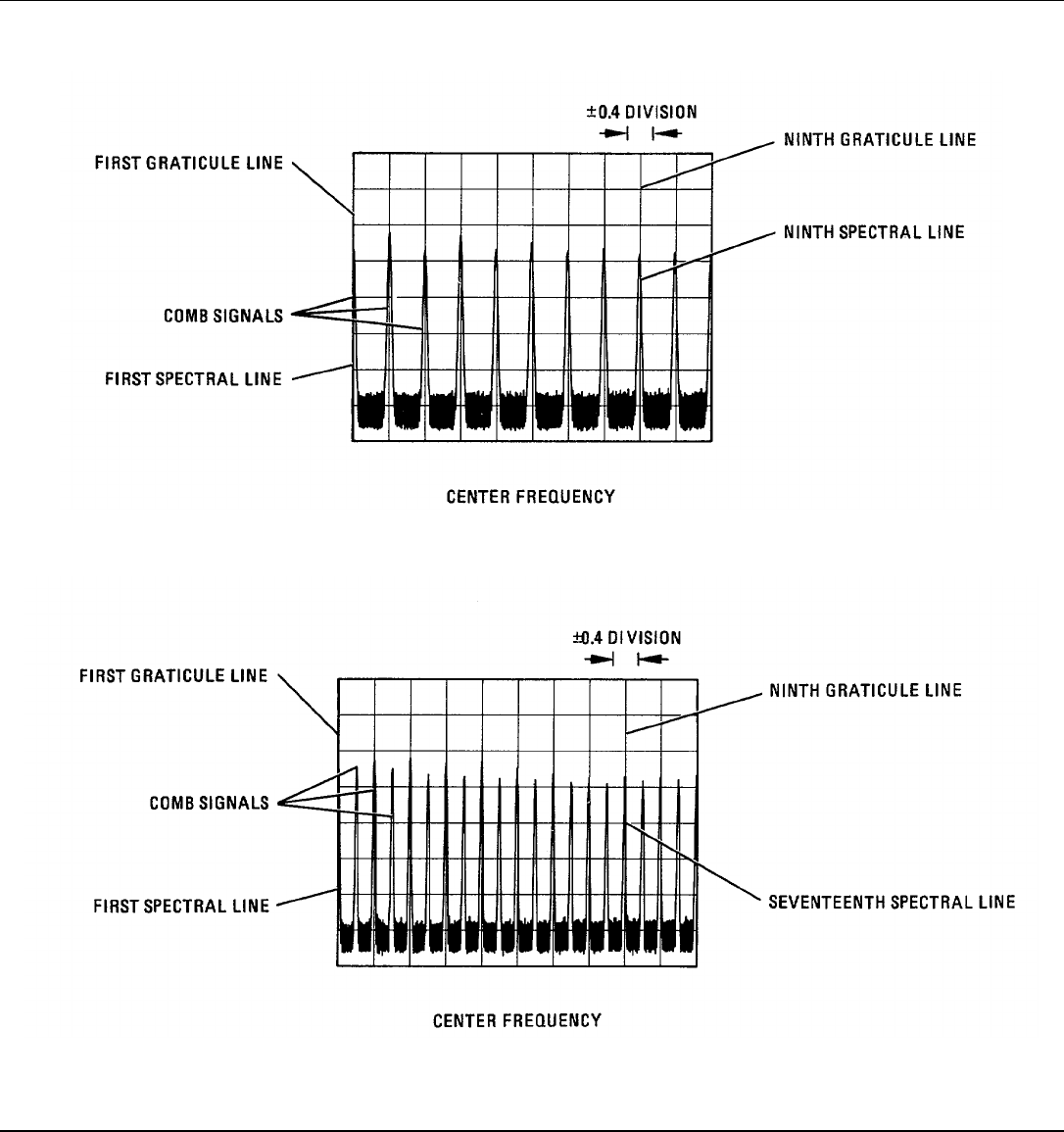
Model 8558B TM 11-6625-3061-14
PERFORMANCE TESTS
4-11. FREQUENCY SPAN ACCURACY(Cont'd)
Figure 4-2. Frequency Span Accuracy Measurement for Ninth Spectral Line
Figure 4-3. Frequency Span Accuracy Measurement for Seventeenth Spectral Line
4-4

Model 8558B TM 11-6625-3061-14
PERFORMANCE TESTS
4-11. FREQUENCY SPAN ACCURACY(Cont'd)
5. Set comb generator COMB FREQUENCY-MHz for 10-MHz comb. Set spectrum analyzer FREQ SPAN/DIV to 20
MHz. Adjust TUNING control to position one spectral line at first graticule line. Measure error between 17th
spectral line and ninth graticule line as shown in Figure 4-3. Error should be no greater than ± 0.4 division.
__________ div
6. Set FREQ SPAN/DIV to 10 MHz. Adjust TUNING control to position one spectral line at first graticule line.
Measure error between ninth spectral line and ninth graticule line. Error should be no greater than ± 0.4 division.
__________ div
7. Set FREQ SPAN/DIV to 5 MHz. Adjust TUNING control to position one spectral line at first graticule line. Measure
error between fifth spectral line and ninth graticule line. Error should be no greater than ± 0.4 division.
__________ div
8. Set comb generator COMB FREQUENCY-MHz for 1-MHz comb. Set spectrum analyzer FREQ SPAN/DIV to 2
MHz. Adjust TUNING control to position one spectral line at first graticule line. Measure error between 17th
spectral line and ninth graticule line. Error should be no greater than ± 0.4 division.
__________ div
9. Set FREQ SPAN/DIV to 1 MHz. Adjust TUNING control to position one spectral line at first graticule line. Measure
error between ninth spectral line and ninth graticule line. Error should be no greater than ± 0.4 division.
__________ div
10. Set FREQ SPAN/DIV to 500 kHz. Adjust TUNING control to position one spectral line at first graticule line.
Measure error between fifth spectral line and ninth graticule line. Error should be no greater than ± 0.4 division.
__________ div
11. Set comb generator COMB FREQUENCY-MHz for 10-MHz comb. Adjust spectrum analyzer TUNING to position
a spectral line at center graticule line. Turn on comb generator INTERPOLATION AMPLITUDE- 1 MHz.
12. Set function generator frequency to 200 kHz (±0.5%) using frequency counter. Connect function generator output to
comb generator MODULATION input. Set function generator OUTPUT LEVEL for a clean 200-kHz comb on the
spectrum analyzer display.
4-5

Model 8558B TM 11-6625-3061-14
PERFORMANCE TESTS
4-11. FREQUENCY SPAN ACCURACY (Cont'd)
NOTE
To obtain a clean comb on the spectrum analyzer display, use the LOW or HIGH
output of the function generator as necessary. Readjust the function generator
OUTPUT LEVEL and the comb generator INTERPOLATION AMPLITUDE - 1 MHz as
necessary.
13.Set spectrum analyzer FREQ SPAN/DIV to 200 kHz. Adjust TUNING control to position one spectral line at first
graticule line. Measure error between ninth spectral line and ninth graticule line. Error should be no greater than 4
0.4 division.
__________ div
14. Using procedure of NOTE in step 12, vary spectrum analyzer FREQ SPAN/DIV and Function Generator Output
Frequency in accordance with Table 4-2. Adjust spectrum analyzer TUNING control to position one spectral line at
first graticule line. Measure span error between ninth spectral line and ninth graticule line.
Table 4-2. Narrow Span Width Error Measurement
Spectrum Analyzer Function Generator Allowable Error
FREQ SPAN/DIV RESOLUTION BW Output Frequency* (Max.)
100 kHz OPTIMUM 100 kHz +0.4 Division
50 kHz OPTIMUM 50 kHz +0.4 Division
20 kHz OPTIMUM 20 kHz +0.4 Division
10 kHz OPTIMUM 10 kHz +0.4 Division
5 kHz OPTIMUM 5 kHz +0.4 Division
*Check function generator output frequency using a frequency counter. Frequency readout should be within +0.5%
of desired audio frequency.
4-6

Model 8558B TM 11-6625-3061-14
PERFORMANCE TESTS
4-12. TUNING ACCURACY
SPECIFICATION
0 to 195 MHz: ±(1 MHz ±20% of FREQ SPAN/DIV setting), 10°C to 40°C
195 to 1500 MHz: ±(5 MHz ±20% of FREQ SPAN/DIV setting), 10°C to 40°C.
DESCRIPTION
A comb generator is used to provide 1-, 10-, or 100-MHz frequency components that produce spectral lines on the CRT
at 1-, 10-, or 100-MHz intervals, respectively. The spectrum analyzer TUNING control is adjusted until the desired test
frequency is shown on the FREQUENCY MHz readout of the Digital Panel Meter. The FREQUENCY CAL switch is
pressed and the amount of readout (or tuning) error is found by measuring the distance of the spectral line offset from the
center graticule line.
Figure 4-4. Tuning Accuracy Test Setup
EQUIPMENT
Comb Generator....................................................................................................HP 8406A
BNC Cable, 120 cm (48 in)...................................................................................HP 10503A
Adapter, Type N (m) to BNC (f) (2 required)....................................................HP 1250-0780
Additional Equipment, Options 001 and 002:
Minimum Loss Adapter, 75Ω to 50Ω...........................................................HP 08558-60031
Adapter, BNC (m) to BNC (m), 75Ω.................................................................HP 1250-1288
Adapter, SMA (f) to SMA (f).............................................................................HP 1250-1158
Adapter, BNC (f) to SMA (m)...........................................................................HP 1250-1200
4-7

Model 8558B TM 11-6625-3061-14
PERFORMANCE TESTS
4-12. TUNING ACCURACY (Cont'd)
PROCEDURE
1. Set spectrum analyzer controls as follows:
START-CENTER..................................................................................................... CENTER
FREQ SPAN/DIV ..................................................................................................... 200 kHz
RESOLUTION BW................................................................................................ OPTIMUM
INPUT ATTEN............................................................................................................... 0 dB
REFERENCE LEVEL .............................................................................................. - 20 dBm
002: +30dBmV
Amplitude Scale .................................................................................................... 10 dB/DIV
SWEEP TIME/DIV ...................................................................................................... AUTO
SWEEP TRIGGER............................................................................................... FREE RUN
BASELINE CLIPPER...................................................................................................... OFF
VIDEO FILTER............................................................................................................... OFF
2. Adjust spectrum analyzer TUNING control to position LO feedthrough signal at center graticule line of display.
Press FREQUENCY CAL switch and reposition LO feedthrough signal at center graticule line, as required. Adjust
FREQ ZERO control for zero indication on FREQUENCY MHz readout. LO feedthrough signal should still be
positioned at center graticule line of display.
3. Connect equipment as shown in Figure 4-4.
4.Set comb generator controls as follows:
COMB FREQUENCY - MHz....................................................................................... 10 MC
INTERPOLATION AMPLITUDE- 1 MHz......................................................................... OFF
OUTPUT AMPLITUDE .......................................................................................... 10 o'clock
5. Adjust spectrum analyzer TUNING control until FREQUENCY MHz readout indicates 10.0 MHz. Press
FREQUENCY CAL switch. Comb generator spectral line, displayed on CRT, should be within 5.2 divisions ( - 1.04
MHz) of center graticule line.
__________ div
NOTE
If the spectral line is off screen, set FREQ SPANIDIV to 500 kHz and check that the
spectral line is within 2.2 divisions of the center graticule line.
6. Using procedure of step 5, adjust spectrum analyzer and comb generator controls as shown in Table 4-3 to measure
TUNING accuracy. After tuning to each FREQUENCY MHz readout, press FREQUENCY CAL switch before
measuring TUNING accuracy.
4-8

Model 8558B TM 11-6625-3061-14
PERFORMANCE TESTS
4-12. TUNING ACCURACY (Cont'd)
Table 4-3. Tuning Accuracy Measurement
Spectrum Analyzer Comb Generator Specification
FREQUENCY COMB (Spectral line limits referenced
MHz FREQ FREQUENCY-MC to center graticule line)
Readout SPAN/DIV. Setting (Divisions)
(MHz) Setting (MHz) Min. Max.
20.0 200 kHz 10 -5.2 +5.2
40.0 200 kHz 10 -5.2 +5.2
60.0 200 kHz 10 -5.2 +5.2
80.0 200 kHz 10 -5.2 +5.2
100.0 200 kHz 10 -5.2 +5.2
120.0 200 kHz 10 -5.2 +5.2
140.0 200 kHz 10 -5.2 +5.2
160.0 200 kHz 10 -5.2 +5.2
180.0 200 kHz 10 -5.2 +5.2
200 1 MHz 100 -5.2 +5.2
400 1 MHz 100 -5.2 +5.2
600 1 MHz 100 -5.2 +5.2
800 1 MHz 100 -5.2 +5.2
1000 1 MHz 100 -5.2 +5.2
1200 1 MHz 100 -5.2+5.2
1400 1 MHz 100 -5.2 +5.2
1500 1 MHz 100 -5.2 +5.2
4-9
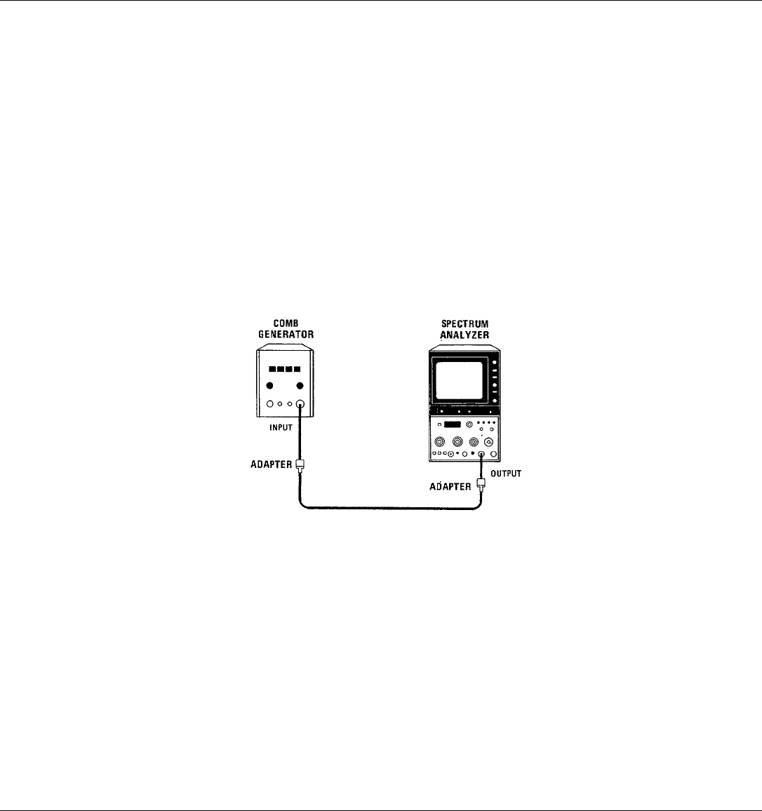
Model 8558B TM 11-6625-3061-14
PERFORMANCE TESTS
4-13. RESIDUAL FM
SPECIFICATION
Less than 1 kHz peak-to-peak for time < 0.1 second
FM DESCRIPTION
This test measures the inherent short-term instability (residual FM) of the LO system in the spectrum analyzer. A stable
signal applied to the input of the spectrum analyzer is slope-detected on the linear portion of the 10 kHz bandwidth filter
in zero span (fixed-tuned receiver). (See Figure 4-6a.) Instability in the LO system in transferred to the IF signal in the
mixing process. As the IF signal moves in relation to the center of the IF filter, the attenuation of the signal changes in
accordance with the skirt characteristics of the filter. If the signal stays on the linear portion of the IF filter skirt, the
amplitude of the IF signal applied to the final detector (and thus the level on the display) is linearly related to the
frequency of the IF signal. (See Figure 4-6b). Therefore, any variations in level seen on the display are linearly related
to variations in LO frequency.
Figure 4-5. Residual FM Test Setup
EQUIPMENT
Comb Generator.................................................................................................... HP 8406A
BNC Cable, 120 cm (48 in)................................................................................... HP 10503A
Adapter, Type N (m) to BNC (f) (2 required) .................................................... HP 1250-0780
Additional Equipment, Options 001 and 002:
Minimum Loss Adapter, 75Ω to 50Ω........................................................... HP 08558-60031
Adapter, BNC (m) to BNC (m), 75Ω................................................................. HP 1250-1288
Adapter, SMA (f) to SMA (f)............................................................................. HP 1250-1158
Adapter, BNC (f) to SMA (m)........................................................................... HP 1250-1200
4-10
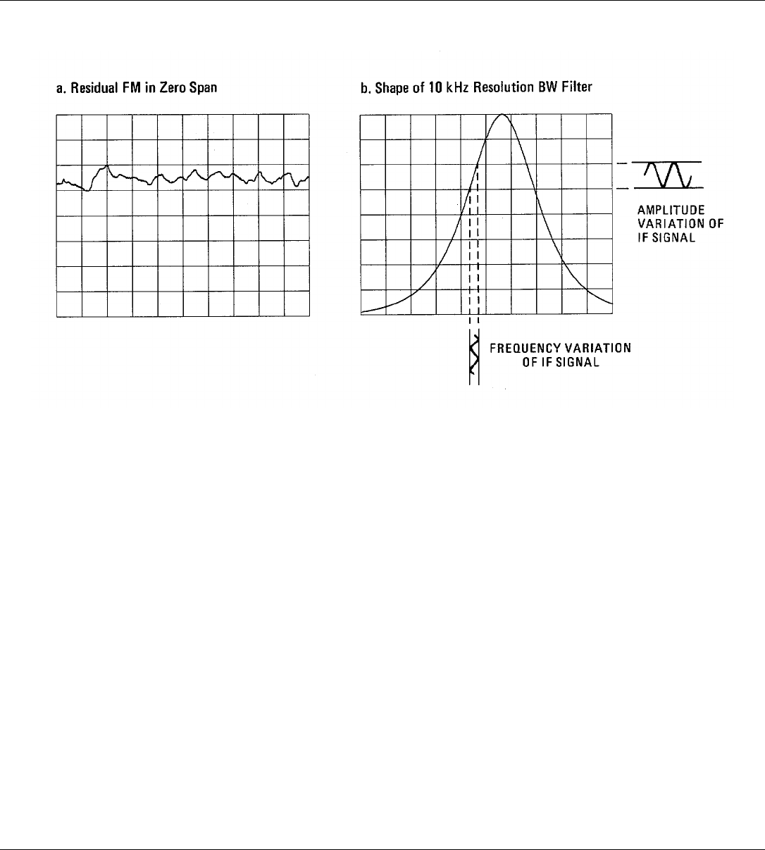
Model 8558B TM 11-6625-3061-14
PERFORMANCE TESTS
4-13. RESIDUAL FM (Cont'd)
Figure 4-6. Example of Residual FM
PROCEDURE
1. Set spectrum analyzer and comb generator controls as follows:
Spectrum Analyzer:
START-CENTER..................................................................................................... CENTER
FREQUENCY SPAN/DIV ......................................................................................... 100 kHz
RESOLUTION BW...................................................................................................... 10kHz
INPUT ATTEN............................................................................................................... 0 dB
REFERENCE LEVEL .............................................................................................. - 20 dBm
002: +30dBmV
Amplitude Scale ............................................................................................................. LIN
SWEEP TIME/DIV ...................................................................................................... AUTO
SWEEP TRIGGER............................................................................................... FREE RUN
BASELINE CLIPPER...................................................................................................... OFF
VIDEO FILTER............................................................................................................... OFF
Comb Generator:
COMB FREQUENCY - MHz....................................................................................... 100 MC
INTERPOLATION AMPLITUDE- 1 MHz......................................................................... OFF
OUTPUT AMPLITUDE .................................................................................. Fully clockwise
4-11

Model 8558B TM 11-6625-3061-14
PERFORMANCE TESTS
4-13. RESIDUAL FM (Cont'd)
2. Connect OUTPUT of comb generator to spectrum analyzer INPUT connector as shown in Figure 4-5.
NOTE
The HP 8558B is sensitive to vibration. Be sure the instrument is in a vibration-
free environment.
3. Adjust spectrum analyzer TUNING control to display 500-MHz signal produced by comb generator. Adjust
REFERENCE LEVEL and REF LEVEL FINE controls to position peak of signal at top graticule line.
4. Keep 500-MHz signal centered on CRT while reducing FREQ SPAN/DIV to zero.
5. Set RESOLUTION BW to 10 kHz and SWEEP TIME/DIV to .1 SEC.
6. Slightly readjust fine TUNING control of spectrum analyzer until trace appears between fourth and seventh graticule
lines. Peak-to-peak variation of trace should not exceed one major vertical division for each major horizontal
division. (See Figure 4-6a.)
__________ div
4-12
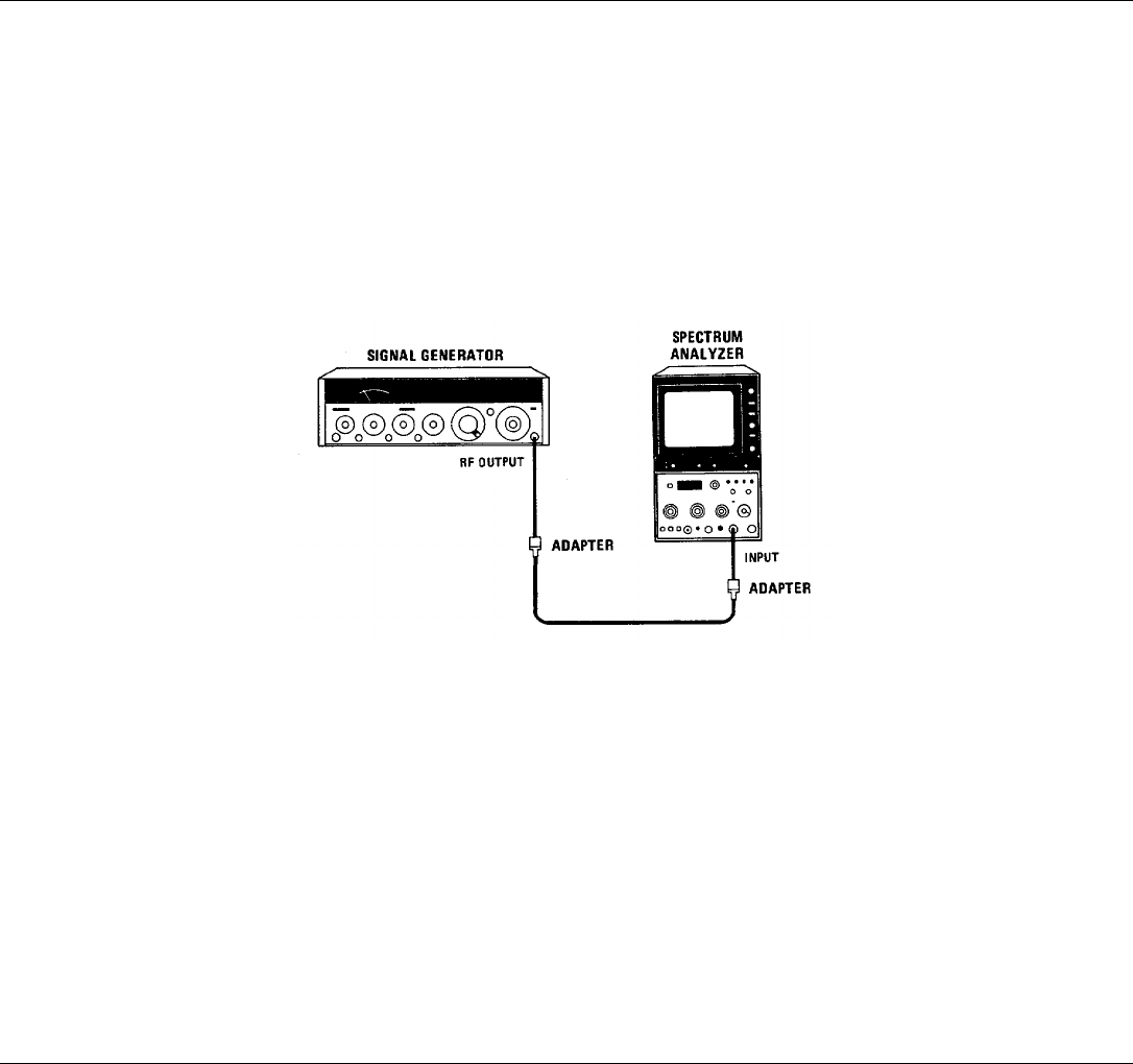
Model 8558B TM 11-6625-3061-14
PERFORMANCE TESTS
4-14. NOISE SIDEBANDS
SPECIFICATION
More than 65 dB below CW signal, 50 kHz or more away from signal with a 1-kHz resolution bandwidth and full video
filtering.
DESCRIPTION
A stable 400-MHz CW signal is applied at a - 20 dBm level to the spectrum analyzer and is displayed on the CRT. The
test is designed to measure the amplitude of noise-associated sidebands and unwanted responses.
Figure 4-7. Noise Sideband Test Setup
EQUIPMENT
Signal Generator ................................................................................................... HP 8640B
BNC Cable, 120 cm (48 in)................................................................................... HP 10503A
Adapter, Type N (m) to BNC (f) (2 required) .................................................... HP 1250-0780
Additional Equipment, Options 001 and 002:
Minimum Loss Adapter, 75Ω to 50Ω........................................................... HP 08558-60031
Adapter, BNC (m) to BNC (m), 75Ω................................................................. HP 1250-1288
Adapter, SMA (f) to SMA (f)............................................................................. HP 1250-1158
Adapter, BNC (f) to SMA (m)........................................................................... HP 1250-1200
4-13

Model 8558B TM 11-6625-3061-14
PERFORMANCE TESTS
4-14. NOISE SIDEBANDS(Cont'd)
PROCEDURE
1. Set equipment controls as follows:
Spectrum Analyzer:
START-CENTER..................................................................................................... CENTER
TUNING ................................................................................................................... 400MHz
FREQUENCY SPAN/DIV ......................................................................................... 1 MHz
RESOLUTION BW..................................................................................................... 30 KHz
INPUT ATTEN............................................................................................................ 10 dB
REFERENCE LEVEL .............................................................................................. - 20 dBm
002: +30dBmV
Amplitude Scale ......................................................................................................10 dB/DIV
SWEEP TIME/DIV ...................................................................................................... AUTO
SWEEP TRIGGER............................................................................................... FREE RUN
BASELINE CLIPPER...................................................................................................... OFF
VIDEO FILTER............................................................................................................... OFF
Signal Generator
FREQUENCY.......................................................................................................... 400 MHz
RF OUTPUT ........................................................................................................... - 20 dBm
RF.................................................................................................................................. ON
AM ................................................................................................................................. OFF
FM ................................................................................................................................. OFF
2. Connect equipment as shown in Figure 4-7.
3. Adjust TUNING control to locate 400-MHz signal on CRT.
4. Adjust REFERENCE LEVEL and REF LEVEL FINE controls to position peak of 400-MHz signal at top graticule line.
5. Decrease FREQ SPAN/DIV to 20 kHz and RESOLUTION BW to 1 kHz. Adjust TUNING to keep signal centered.
6. Position signal at center of display. Turn VIDEO FILTER control fully clockwise (not in detent). Measure noise
sidebands existing more than 2.5 division (50 kHz) from 400-MHz signal. Noise sidebands should be greater than
65 dB (6.5 divisions) down from top graticule line.
_________ div down
4-14
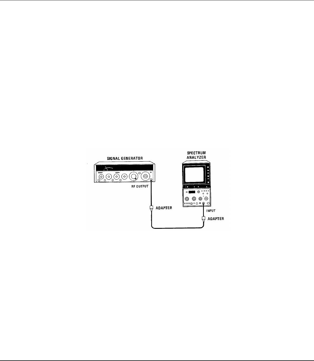
Model 8558B TM 11-6625-3061-14
PERFORMANCE TESTS
4-15. RESOLUTION BANDWIDTH ACCURACY
SPECIFICATION
Individual resolution bandwidth 3-dB points calibrated to 20%o (10°C to 400C)
DESCRIPTION
Resolution bandwidth accuracy is measured in the linear mode to eliminate log amplifier errors. Since signal level at the
3-dB points (half-power points) is related to peak signal level by a voltage ratio of 0.707:1.0, a peak level of 7.1 vertical
divisions on the spectrum analyzer display gives a half-power level of 5 vertical divisions:
0.707 (voltage ratio) = X div/7.1 div
X div = (7.1)(0.707)
≈ 5 div
In the 30-, 10-, and 1-kHz bandwidths, a 301.4-MHz signal (second IF) is injected into A9 Third Converter Assembly to
provide the stability required for measurement of narrow resolution bandwidths.
Figure 4-8. Resolution Bandwidth Accuracy Test Setup, 3 MHz to 100 kHz
EQUIPMENT
Signal Generator ................................................................................................... HP 8640B
Extender Cable Assembly ............................................................................... HP 5060-0303
Adapter, SMC (m) to BNC (m)......................................................................... HP 1250-0831
Adapter, BNC (f) to BNC (f)............................................................................. HP 1250-0080
Adapter, Type N (m) to BNC (f) (2 required) .................................................... HP 1250-0780
BNC Cable, 120 cm (48 in)................................................................................... HP 10503A
Additional Equipment, Options 001 and 002:
Minimum Loss Adapter, 75Ω to 50Ω........................................................... HP 08558-60031
Adapter, BNC (m) to BNC (m), 75Ω................................................................. HP 1250-1288
Adapter, SMA (f) to SMA (f)............................................................................. HP 1250-1158
Adapter, BNC (f) to SMA (m)........................................................................... HP 1250-1200
4-15

Model 8558B TM 11-6625-3061-14
PERFORMANCE TESTS
4-15. RESOLUTION BANDWIDTH ACCURACY(Cont'd) ,
PROCEDURE
WARNING
This test must be performed with power supplied to the instrument and with
protective covers removed. The test should be performed only by service-trained
personnel who are aware of the hazards involved.
1. Set equipment controls as follows:
Spectrum Analyzer:
START-CENTER..................................................................................................... CENTER
TUNING ................................................................................................................... 10 MHz
FREQUENCY SPAN/DIV .................................................................................................... 0
RESOLUTION BW...................................................................................................... 3 MHz
INPUT ATTEN............................................................................................................. 20 dB
REFERENCE LEVEL ................................................................................................. 0 dBm
002: +30dBmV
Amplitude Scale ............................................................................................................... LIN
SWEEP TIME/DIV .....................................................................................................5 mSEC
SWEEP TRIGGER............................................................................................... FREE RUN
BASELINE CLIPPER...................................................................................................... OFF
VIDEO FILTER............................................................................................................... OFF
Signal Generator
COUNTER MODE................................................................................... INT, EXPAND X10
AM ................................................................................................................................ OFF
FM ................................................................................................................................ OFF
FREQUENCY TUNE .................................................................................................. 10 MHz
RF.................................................................................................................................... ON
OUTPUT LEVEL ........................................................................................................ 0 dBm
2. Connect equipment as shown in Figure 4-8.
3. Adjust spectrum analyzer TUNING control to locate peak of 10-MHz signal on CRT. Reduce signal generator output
if necessary.
4. Adjust signal generator OUTPUT LEVEL to position trace at 7.1 divisions above graticule baseline.
5. Tune signal generator frequency until trace drops to 5 divisions above graticule baseline. Record signal generator
frequency.
__________ MHz
4-16
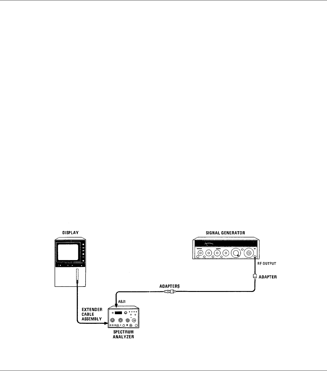
Model 8558B TM 11-6625-3061-14
PERFORMANCE TESTS
4-15. RESOLUTION BANDWIDTH ACCURACY(Cont'd)
6. Tune signal generator frequency in direction opposite to that of step 5 until trace peaks (7.1 divisions above
graticule baseline) and then drops to 5 divisions above graticule baseline. Record signal generator frequency.
__________ MHz
7. Calculate and record resolution bandwidth at 3-dB points (difference between frequencies recorded in steps 5 and
6).
Min. Actual Max.
2.40 MHz ________________3.60 MHz
8. Set RESOLUTION BW to 1 MHz, leaving FREQ SPAN/DIV set to 0. Set signal generator to 10 MHz and repeat
steps 3 through 7.
Min. Actual Max.
800 kHz _________________1200 kHz
9. Set RESOLUTION BW to 300 kHz, leaving FREQ SPAN/DIV set to 0. Set signal generator to 10 MHz and repeat
steps 3 through 7.
Min. Actual Max.
240 kHz _________________360 kHz
10. Set RESOLUTION BW to 100 kHz, leaving FREQ SPAN/DIV set to 0. Set signal generator to 10 MHz and repeat
steps 3 through 7.
Min. Actual Max.
80 kHz __________________120 kHz
Figure 4-9. Resolution Bandwidth Accuracy Test Setup, 1 kHz to 30 kHz
4-17

Model 8558B TM 11-6625-3061-14
PERFORMANCE TESTS
4-15. RESOLUTION BANDWIDTH ACCURACY(Cont'd)
WARNING
In the following procedure, the plug-in must be removed from the display
mainframe and connected through the extender cable assembly. Be very careful;
the energy at some points in the instrument might, if contacted, cause personal
injury. This test should be performed only by a skilled person who knows the
hazard involved.
11. Set signal generator OUTPUT LEVEL to approximately -12 dBm and tune frequency to 301.4 MHz. Set COUNTER
MODE to EXPAND X100.
12. Set spectrum analyzer INPUT ATTEN to 0 dB and REFERENCE LEVEL to -10 dBm. Set RESOLUTION BW to 30
kHz. Leave FREQ SPAN/DIV set to 0.
002: REFERENCE LEVEL, + 40 dBmV.
13. Connect equipment as shown in Figure 4-9. Remove W7P1 from A10OJ2. Connect signal generator through
adapters to W7P1.
14. Adjust signal generator frequency until spectrum analyzer trace is at peak. Set signal generator OUTPUT LEVEL to
position trace at 7.1 divisions above graticule baseline.
15. Tune signal generator frequency until trace drops to 5 divisions above graticule baseline. Record signal generator
frequency.
__________ MHz
16. Tune signal generator frequency in direction opposite to that of step 15 until trace peaks and then drops to 5
divisions above graticule baseline. Record signal generator frequency.
__________ MHz
17. Calculate and record resolution bandwidth at 3-dB points (difference between frequencies recorded in steps 15 and
16).
Min. Actual Max.
24 kHz __________________36 kHz
18. Set RESOLUTION BW to 10 kHz, leaving FREQ SPAN/DIV set to 0. Repeat steps 14 through 17.
Min. Actual Max.
8 kHz ___________________12 kHz
4-18

Model 8558B TM 11-6625-3061-14
PERFORMANCE TESTS
4-15. RESOLUTION BANDWIDTH ACCURACY(Cont'd) ,
19. Set RESOLUTION BW to 3 kHz, leaving FREQ SPAN/DIV set to 0. Repeat steps 14 through 17.
Min. Actual Max.
2.4 kHz__________________3.6 kHz
20. Set RESOLUTION BW to 1 kHz, leaving FREQ SPAN/DIV set to 0. Repeat steps 14 through 17.
Min. Actual Max.
0.8 kHz__________________1.2 kHz
21. Reconnect W7P1 to A10J2 unless continuing on with next performance test.
4-19
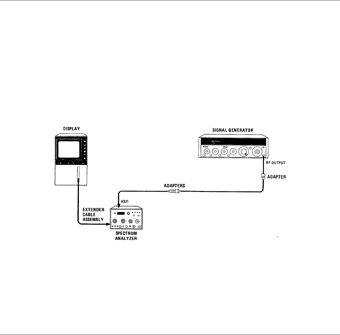
Model 8558B TM 11-6625-3061-14
PERFORMANCE TESTS
4-16. RESOLUTION BANDWIDTH SELECTIVITY '
SPECIFICATION
60-dB:3-dB resolution bandwidth ratio < 15:1.
DESCRIPTION
The 60-dB bandwidth is measured for all resolution bandwidths. The 60- to 3-dB resolution bandwidth ratio (shape
factor) is then computed for each bandwidth by dividing the 3-dB value (from the Resolution Bandwidth Accuracy test)
into the 60-dB value.
In the 30-, 10-, and 1-kHz bandwidths, a 301.4-MHz signal (second IF) is injected into A9 Third Converter assembly to
provide the stability required for the measurement of narrow resolution bandwidths.
Figure 4-10. Resolution Bandwidth Selectivity Test Setup, 1 kHz to 30 kHz
WARNING
In the following procedure, the plug-in must be removed from the display
mainframe and connected through the extender cable assembly. Be very careful;
the energy at some points in the instrument might, if contacted, cause personal
injury. This test should be performed only by a skilled person who knows the
hazard involved.
4-20

Model 8558B TM 11-6625-3061-14
PERFORMANCE TESTS
4-16. RESOLUTION BANDWIDTH SELECTIVITY(Cont'd)
EQUIPMENT
Signal Generator ..........................................................................................................................HP 8640B
Extender Cable Assembly...................................................................................................... HP 5060-0303
Adapter, SMC (m) to BNC (m)............................................................................................... HP 1250-0831
Adapter, BNC (f) to BNC (f) ................................................................................................... HP 1250-0080
Adapter, Type N (m) to BNC (f) (2 required) .......................................................................... HP 1250-0780
BNC Cable, 120 cm (48 in)......................................................................................................... HP 10503A
Additional Equipment, Options 001 and 002:
Minimum Loss Adapter, 75Ω to 50Ω...................................................................................HP 08558-60031
Adapter, BNC (m) to BNC (m), 75Ω....................................................................................... HP 1250-1288
Adapter, SMA (f) to SMA (f)................................................................................................... HP 1250-1158
Adapter, BNC (f) to SMA (m) ................................................................................................. HP 1250-1200
PROCEDURE
1. Set equipment controls as follows:
Spectrum Analyzer
START-CENTER........................................................................................................................... CENTER
TUNING ...........................................................................................................................................50 MHz
FREQ SPAN/DIV........................................................................................................................................0
RESOLUTION BW ..............................................................................................................................1 kHz
INPUT ATTEN.......................................................................................................................................0 dB
REFERENCE LEVEL.......................................................................................................................-10 dBm
002: + 40 dBm V
Amplitude Scale ...........................................................................................................................10 dB/DIV
SWEEP TIME/DIV...........................................................................................................................5 mSEC
SWEEP TRIGGER.....................................................................................................................FREE RUN
BASELINE CLIPPER.............................................................................................................................OFF
VIDEO FILTER......................................................................................................................................OFF
Signal Generator
COUNTER MODE ...........................................................................................................INT, EXPAND X10
AM.........................................................................................................................................................OFF
FM.........................................................................................................................................................OFF
FREQUENCY TUNE ...................................................................................................................301.4 MHz
RF ...........................................................................................................................................................ON
OUTPUT LEVEL..............................................................................................................................-20 dBm
2. Connect equipment as shown in Figure 4-10. Remove W7P1 from A10J2. Connect signal generator through
adapters to W7P1.
3. Adjust signal generator frequency until spectrum analyzer trace is at peak. Set signal generator OUTPUT LEVEL to
position trace at top graticule line.
4-21

Model 8558B TM 11-6625-3061-14
PERFORMANCE TESTS
4-16. RESOLUTION BANDWIDTH SELECTIVITY(Cont'd)
4. Tune signal generator until trace drops to 2 divisions above graticule baseline. Record signal generator frequency.
MHz
5. Tune signal generator in direction opposite to that of step 4 until trace peaks and then drops to 2 divisions above
graticule baseline. Record signal generator frequency.
MHz
6. Calculate and record resolution bandwidth at 60-dB points (difference between frequencies recorded in steps 4 and
5).
kHz
7Set RESOLUTION BW to 3 kHz, leaving FREQ SPAN/DIV set to 0. Repeat steps 3 through 6.
kHz
8. Set RESOLUTION BW to 10 kHz, leaving FREQ SPAN/DIV set to 0. Repeat steps 3 through 6.
kHz
9. Set spectrum analyzer RESOLUTION BW to 30 kHz, leaving FREQ SPAN/DIV set to 0. Repeat steps 3 through 6.
kHz
10. Reconnect W7P1 to A10J2. Set display LINE power to OFF and remove extender cable assembly. Install plug-in in
mainframe and set LINE power to ON.
11. Set signal generator OUTPUT LEVEL to 0 dBm.
12. Set spectrum analyzer INPUT ATTEN to 20 dB and REFERENCE LEVEL to 0 dBm. Set RESOLUTION BW to 100
kHz, leaving FREQ SPAN/DIV set to 0.
002: REFERENCE LEVEL, +50 dBmV.
13. Connect equipment as shown in Figure 4-11.
14. Set signal generator frequency to 50 MHz. Adjust spectrum analyzer TUNING to locate peak of 50-MHz signal on
CRT.
15. Adjust signal generator OUTPUT LEVEL to position trace at top graticule line.
4-22
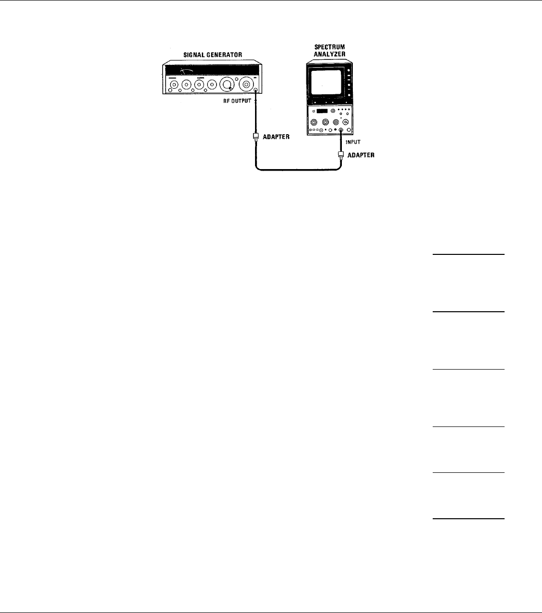
Model 8558B TM 11-6625-3061-14
PERFORMANCE TESTS
4-16. RESOLUTION BANDWIDTH SELECTIVITY (Cont'd)
Figure 4-11. Resolution Bandwidth Selectivity Test Setup, 100 kHz to 3 MHz
16. Tune signal generator frequency until trace drops to 2 divisions above graticule baseline. Record signal generator
frequency.
MHz
17. Tune signal generator frequency in direction opposite to that of step 16 until trace peaks and then drops to 2 divisions
above graticule baseline. Record signal generator frequency.
MHz
18. Calculate and record resolution bandwidth at 60-dB points (difference between frequencies recorded in steps 16 and
17).
kHz
19. Set spectrum analyzer RESOLUTION BW to 300 kHz, leaving FREQ SPAN/DIV set to 0. Repeat steps 14 through
18.
kHz
20. Set RESOLUTION BW to 1 MHz, leaving FREQ SPAN/DIV set to 0. Repeat steps 14 through 18.
MHz
21. Set RESOLUTION BW to 3 MHz, leaving FREQ SPAN/DIV set to 0. Repeat steps 14 through 18.
MHz
22. In Table 4-4, record 3-dB bandwidths computed in Resolution Bandwidth Accuracy test.
23. In Table 4-4, record 60-dB bandwidths recorded in this procedure.
24. For each resolution bandwidth, divide 60-dB bandwidth by 3-dB bandwidth to obtain Resolution Bandwidth Ratio.
Each ratio should be less than 15:1.
4-23

Model 8558B TM 11-6625-3061-14
PERFORMANCE TESTS
4-16. RESOLUTION BANDWIDTH SELECTIVITY (Cont'd)
Table 4-4. Resolution Bandwidth Selectivity
RESOLUTION
BW Setting MEASURED
3 db BW MEASURED
60 db BW
Resolution Bandwidth
Ration (60 db BW):
(3 dB BW)
3 MHz
1 MHz
300 kHz
100 kHz
30 kHz
10 kHz
3 kHz
1 kHz
4-24

Model 8558B TM 11-6625-3061-14
PERFORMANCE TESTS
4-17. AVERAGE NOISE LEVEL
SPECIFICATION
Less than - 107 dBm with a 10-kHz resolution bandwidth (0 dB input attenuation), 1 MHz to 1500 MHz.
001: Less than - 100dBm
002: Less than - 53 dBm V
DESCRIPTION
The average noise level is checked by observing the average noise power level displayed on the CRT when no input
signal is applied to the instrument. The test is performed with a 10-kHz resolution bandwidth.
PROCEDURE
1. Set spectrum analyzer controls as follows:
START-CENTER.....................................................................................................................................CENTER
TUNING .................................................................................................................................................. 500 MHz
FREQ SPAN/DIV..................................................................................................................................... 100 MHz
RESOLUTION BW ..................................................................................................................................... 10 kHz
INPUT ATTEN.................................................................................................................................................0dB
REFERENCE LEVEL ..............................................................................................................................- 60 dBm
002:-10 dBm V
Amplitude Scale .................................................................................................................................... 10 dB/DIV
SWEEP TIME/DIV.................................................................................................................................. 10 mSEC
SWEEP TRIGGER.............................................................................................................................. FREE RUN
BASELINE CLIPPER.......................................................................................................................................OFF
VIDEO FILTER.......................................................................................................................................12 o'clock
2. Adjust TUNING until LO feedthrough is not on screen. Set VIDEO FILTER to MAX (not in detent) and observe CRT
display of noise level from 1 MHz to 1000 MHz. Noise level, as shown in Figure 4-12, should be less than - 107.
001: Change '- 107 dBm' to '- 100 dBm' throughout procedure and in Figure 4-12.
002: Change '- 107 dBm' to '- 53 dBmV' throughout procedure and in Figure 4-12.
< - 107 dBm
3. Set START-CENTER switch to START. Observe average noise level from 500 MHz to 1500 MHz. Noise level
should be less than - 107 dBm.
< - 107 dBm
4-25
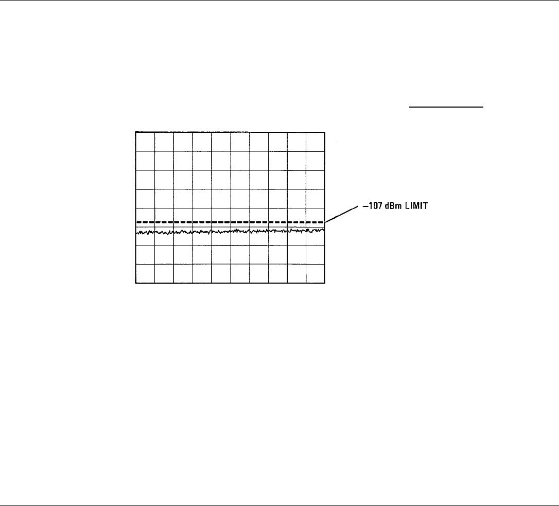
Model 8558B TM 11-6625-3061-14
PERFORMANCE TESTS
4-17. AVERAGE NOISE LEVEL(Cont'd)
4. Set START-CENTER switch to CENTER and FREQ SPAN/DIV to 1 MHz. Adjust TUNING for a FREQUENCY MHz
readout of 6 MHz and momentarily press FREQUENCY CAL switch.
5. Observe average noise level from I MHz to 11 MHz. Noise level should be less than - 107 dBm.
< - 107 dBm
Figure 4-12. Average Noise Level Measurement
4-26
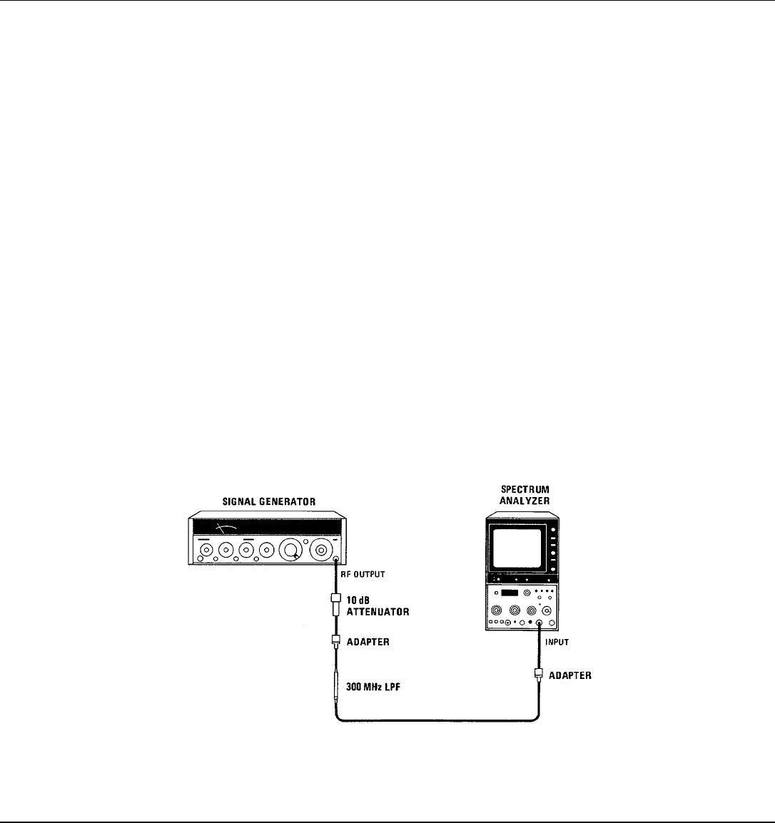
Model 8558B TM 11-6625-3061-14
PERFORMANCE TESTS
4-18. SPURIOUS RESPONSES
SPECIFICATION
Image and multiple responses and second harmonic distortion products are > 70 dB* below a - 40 dBm in-put signal with
0 dB input attenuation.
001: - 35 dBm input signal
002: + 15dBmV input signal
Third order intermodulation distortion products are >70 dB* below two -30 dBm input signals, separated by ≥ 50 kHz, with
0 dB input attenuation.
001: two - 25 dBm input signals
002: two + 25 dBm V input signals
* > 60 dB for 100 kHz to 5 MHz input signals.
DESCRIPTION:
A signal source with a lowpass filter is used to measure harmonic distortion. The LPF is required to ensure that the
signals displayed on the CRT are due to harmonic distortion in the spectrum analyzer rather than to the harmonic content
of the signal generator.
In measuring spurious responses due to image frequencies, out-of-band responses, and intermodulation distortion,
signals from two separate sources are applied to the spectrum analyzer.
Figure 4-13. Harmonic Distortion Test Setup
4-27

Model 8558B TM 11-6625-3061-14
PERFORMANCE TESTS
4-18. SPURIOUS RESPONSES (Cont'd)
EQUIPMENT
Signal Generator (2 required) .......................................................................................................HP 8640B
10 dB Attenuator (2 required).........................................................................................HP 8491A Opt. 010
300 MHz LPF...............................................................................................................Telonic TLP 300-4AB
BNC Tee................................................................................................................................ HP 1250-0781
Adapter, Type N (m) to BNC (f) (3 required) .......................................................................... HP 1250-0780
BNC Cable, 120 cm (48 in) (2 required)...................................................................................... HP 10503A
Additional Equipment, Options 001 and 002:
Minimum Loss Adapter, 75Ω to 50Ω...................................................................................HP 08558-60031
Adapter, BNC(m) to BNC(m), 75Ω......................................................................................... HP 1250-1288
Adapter, SMA (f) to SMA (f)................................................................................................... HP 1250-1158
Adapter, BNC (f) to SMA (m) ................................................................................................. HP 1250-1200
PROCEDURE
Harmonic Distortion
1. Set spectrum analyzer controls as follows:
START-CENTER........................................................................................................................... CENTER
TUNING .........................................................................................................................................280 MHz
FREQ SPAN/DIV.............................................................................................................................500 kHz
RESOLUTION BW ............................................................................................................................30 kHz
INPUT ATTEN.......................................................................................................................................0 dB
REFERENCE LEVEL.......................................................................................................................-40 dBm
001: -30 dBm
002: + 20 dBm V
REF LEVEL FINE.......................................................................................................................................0
001: -5
002: -5
Amplitude Scale ...........................................................................................................................10 dB/DIV
SWEEP TIME/DIV..............................................................................................................................AUTO
SWEEP TRIGGER.....................................................................................................................FREE RUN
BASELINE CLIPPER.............................................................................................................................OFF
VIDEO FILTER............................................................................................................................. 12 o'clock
2. Set signal generator frequency to 280 MHz and OUTPUT LEVEL to - 30 dBm.
3. Connect equipment as shown in Figure 4-13.
4. Momentarily press FREQUENCY CAL switch. Tune signal generator to center signal on spectrum analyzer display.
4-28

Model 8558B TM 11-6625-3061-14
PERFORMANCE TESTS
4-18. SPURIOUS RESPONSES (Cont'd)
5. Adjust signal generator OUTPUT LEVEL for -40 dBm displayed at top graticule line of spectrum analyzer CRT.
001: -35 dBm
002: + 15 dBm V
6. Increase signal generator OUTPUT LEVEL by 20 dB.
7. Set spectrum analyzer TUNING to approximately 560 MHz and identify second harmonic.
8. Center signal on spectrum analyzer display and reduce signal generator OUTPUT LEVEL by 20 dB.
9. Set spectrum analyzer RESOLUTION BW to 3 kHz. Harmonics should be more than 70 dB below input signal
(below first graticule line from bottom).
2nd Harmonic: dB
3rd Harmonic: dB
10. Set RESOLUTION BW to 30 kHz. Increase signal generator OUTPUT LEVEL by 20 dB.
11. Set spectrum analyzer TUNING to approximately 840 MHz and identify third harmonic.
12. Repeat steps 8 and 9.
Intermodulation Distortion
13. Set spectrum analyzer controls as follows:
START-CENTER........................................................................................................................... CENTER
TUNING ...........................................................................................................................................30 MHz
FREQ SPAN/DIV.............................................................................................................................500 kHz
RESOLUTION BW ............................................................................................................................30 kHz
INPUT ATTEN.......................................................................................................................................0 dB
REFERENCE LEVEL......................................................................................................................- 30 dBm
001: -20dBm
002: +30dBm V
REF LEVEL FINE.......................................................................................................................................0
001: -5
002: -5
Amplitude Scale ...........................................................................................................................10 dB/DIV
SWEEP TIME/DIV..............................................................................................................................AUTO
SWEEP TRIGGER.....................................................................................................................FREE RUN
BASELINE CLIPPER.............................................................................................................................OFF
VIDEO FILTER............................................................................................................................. 12 o'clock
4-29
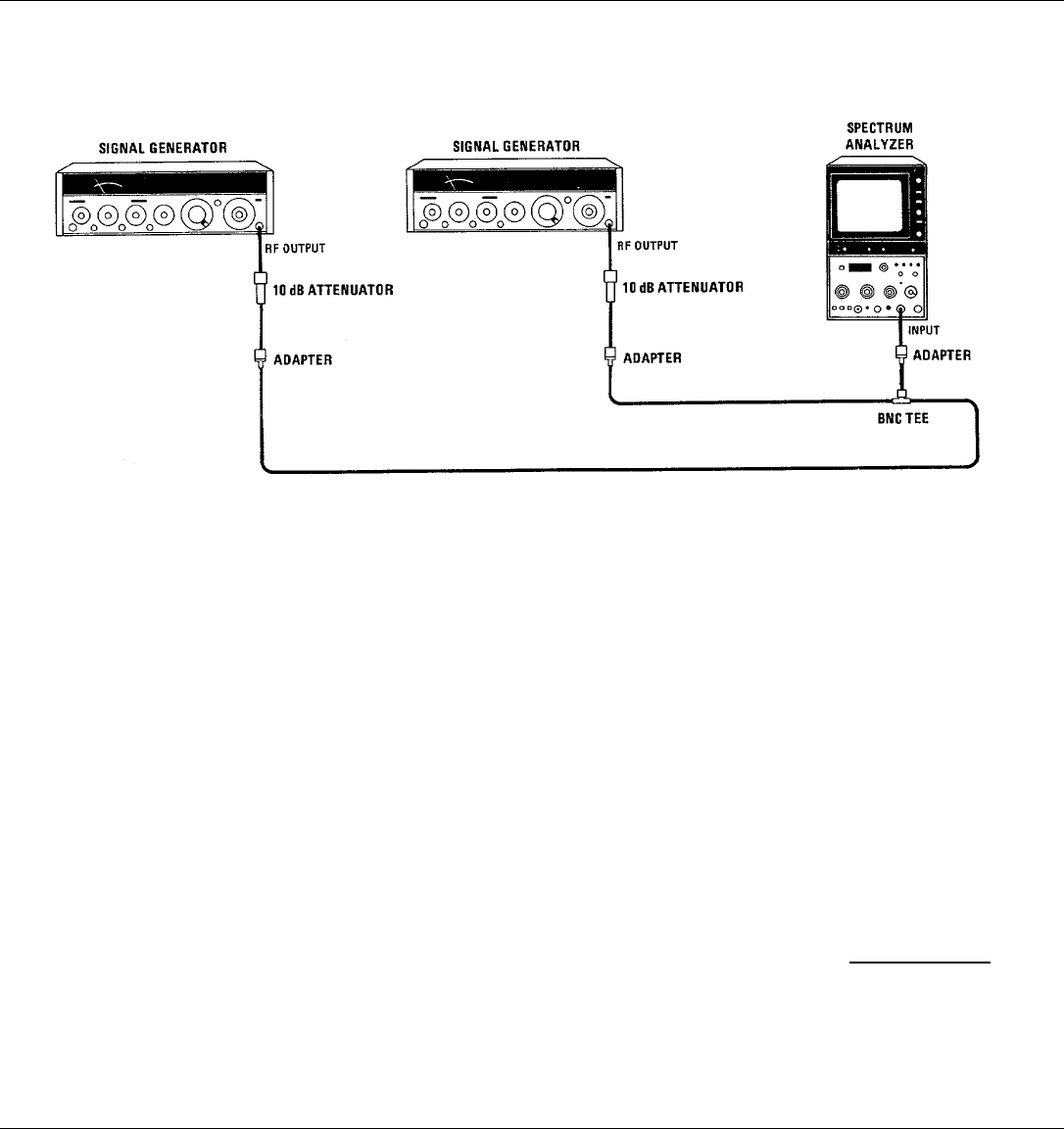
Model 8558B TM 11-6625-3061-14
PERFORMANCE TESTS
4-18. SPURIOUS RESPONSES(Cont'd)
14. Connect equipment as shown in Figure 4-14.
Figure 4-14. Intermodulation Distortion Test Setup
15. Set both signal generators for approximately 30 MHz output at - 24 dBm.
16. Momentarily press FREQUENCY CAL switch. Tune signal generators until signals are 2 divisions apart and centered
on display.
17. Adjust OUTPUT LEVEL controls of both signal generators for - 30 dBm displayed on spectrum analyzer.
001: -25 dBm
002: + 25 dBm V
18. Reduce spectrum analyzer RESOLUTION BW to 3 kHz and check for third order intermodulation distortion products
at approximately 3 divisions to either side of center graticule line (see NOTE below). They should be more than 70
dB below input signals (-100 dBm on spectrum analyzer display). (See Figure 4-15.)
001: - 95 dBm on spectrum analyzer display
002: - 50 dBmV on spectrum analyzer display
dB
NOTE
If the intermodulation distortion product cannot be located, increase output levels of both signal
generators by 10 dB. Be sure to return the OUTPUT LEVEL of each signal generator to its
previous setting before making the actual measurement.
4-30
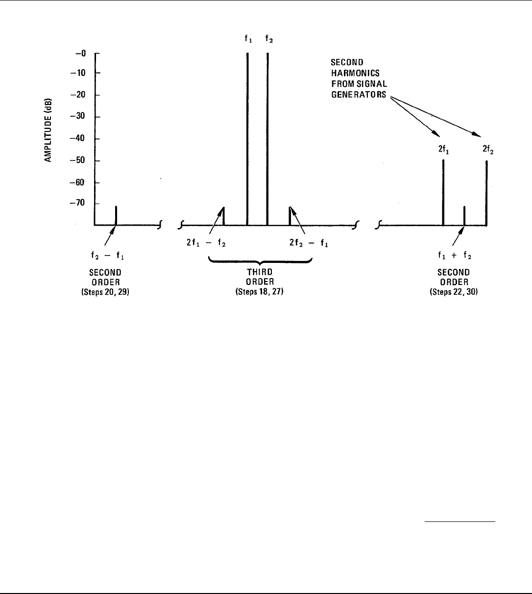
Model 8558B TM 11-6625-3061-14
PERFORMANCE TESTS
4-18. SPURIOUS RESPONSES(Cont'd)
Figure 4-15. Intermodulation Distortion Products
19. Set INPUT ATTEN to 0 dB, REFERENCE LEVEL to -40 dBm, and RESOLUTION BW to 30 kHz. Adjust OUTPUT
LEVEL of each signal generator to - 43 dBm as displayed on CRT.
001: REFERENCE LEVEL - 35 dBm; output level of - 38 dBm displayed on CRT
002: REFERENCE LEVEL + 15 dBmV; output level of + 12 dBmV displayed on CRT
20. Set spectrum analyzer TUNING to 1 MHz and momentarily press FREQUENCY CAL switch. Set RESOLUTION BW
to 3 kHz and adjust VIDEO FILTER as necessary for more than 70 dB display range. Check for second order
intermodulation distortion product (f2 fl) near center of display (see NOTE below). Second order intermodulation
distortion product should be more than 60 dB below the total applied signal (- 100 dBm on spectrum analyzer
display). (See Figure 4-15.)
001: - 95 dBm on spectrum analyzer display
002: - 45 dBmV on spectrum analyzer display
dB
NOTE
If the intermodulation distortion product cannot be located, increase output levels of both signal
generators by 10 dB. Be sure to return the OUTPUT LEVEL of each signal generator to its
previous setting before making the actual measurement.
4-31

Model 8558B TM 11-6625-3061-14
PERFORMANCE TESTS
4-18. SPURIOUS RESPONSES (Cont'd)
21. Set spectrum analyzer TUNING to 60 MHz and RESOLUTION BW to 30 kHz. Momentarily press FREQUENCY
CAL switch.
22. Check for second order intermodulation distortion product (f1 + f2) between 2f1 and 2f2 signals (see NOTE below).
Set RESOLUTION BW to 3 kHz and adjust VIDEO FILTER as necessary for more than 70 dB display range.
Second order intermodulation distortion product should be more than 70 dB below total applied signal (- 110 dBm on
spectrum analyzer display). (See Figure 4-15.)
001: - 105 dBm on spectrum analyzer display
002: - 60 dBm V on spectrum analyzer display
dB
NOTE
If the intermodulation distortion product cannot be located, increase output levels of both signal
generators by 10 dB. Be sure to return the OUTPUT LEVEL of each signal generator to its
previous setting before making the actual measurement.
23. Set spectrum analyzer controls as follows:
START-CENTER........................................................................................................................... CENTER
TUNING .............................................................................................................................................4 MHz
FREQ SPAN/DIV.............................................................................................................................500 kHz
RESOLUTION BW ............................................................................................................................30 kHz
INPUT ATTEN.......................................................................................................................................0 dB
REFERENCE LEVEL......................................................................................................................- 30 dBm
001: - 20 dBm
002: +30dBmV
REF LEVEL FINE.......................................................................................................................................0
001: -5
002: -5
Amplitude Scale ...........................................................................................................................10 dB/DIV
SWEEP TIME/DIV..............................................................................................................................AUTO
SWEEP TRIGGER.....................................................................................................................FREE RUN
BASELINE CLIPPER.............................................................................................................................OFF
VIDEO FILTER............................................................................................................................. 12 o'clock
24. Set both signal generators for approximately 4 MHz at - 24 dBm.
25. Momentarily press FREQUENCY CAL switch. Tune signal generators until signals are 2 divisions apart and centered
on display.
26. Adjust OUTPUT LEVEL of each signal generator for - 30 dBm as displayed on CRT.
001: - 25 dBm
002: + 25 dBm V
4-32

Model 8558B TM 11-6625-3061-14
PERFORMANCE TESTS
4-18. SPURIOUS RESPONSES(Cont'd)
27. Check for third order intermodulation distortion products at approximately 3 divisions from either side of center
graticule line. Third order intermodulation distortion products should be more than 60 dB below input signals (- 90
dBm on spectrum analyzer display).
001: - 85 dBm on spectrum analyzer display
002: - 35 dBm V on spectrum analyzer display
dB
NOTE
If signal generators other than HP 8640's are used, intermodulation distortion might be in the
generators themselves because of crosstalk between the two sources.
28. Set INPUT ATTEN to 0 dB and REFERENCE LEVEL to -40 dBm. Adjust OUTPUT LEVEL of each signal generator
for - 43 dBm as displayed on CRT.
001: REFERENCE LEVEL, - 35 dBm; output level of - 38 dBm displayed on CRT
002: REFERENCE LEVEL, + 15 dBmV; + 12 dBmV as displayed on CRT
29. Set spectrum analyzer TUNING to 1 MHz and momentarily press FREQUENCY CAL switch. Set RESOLUTION BW
to 3 kHz and adjust VIDEO FILTER as necessary for more than 70 dB display range. Check for second order
intermodulation distortion product (f2 - f1) near center of display (see NOTE below). Second order intermodulation
distortion product should be more than 60 dB below total applied signal (-100 dBm on spectrum analyzer display).
(See Figure 4-15.)
001: - 95 dBm on spectrum analyzer display
002: - 45 dBm V on spectrum analyzer display
dB
NOTE
If the intermodulation distortion product cannot be located, increase output levels of both signal
generators by 10 dB. Be sure to return the OUTPUT LEVEL of each signal generator to its
previous setting before making the actual measurement.
30. Set spectrum analyzer TUNING to 8 MHz and check for second order intermodulation distortion product (f1 + f2)
between 2f1 and 2f2 signals. (See figure 4-15.) Second order intermodulation distortion product should be more than
60 dB below total applied signal (- 100 dBm on spectrum analyzer display). (See NOTE above.)
001: - 95 dBm on spectrum analyzer display
002: - 45 dBmV on spectrum analyzer display
dB
4-33
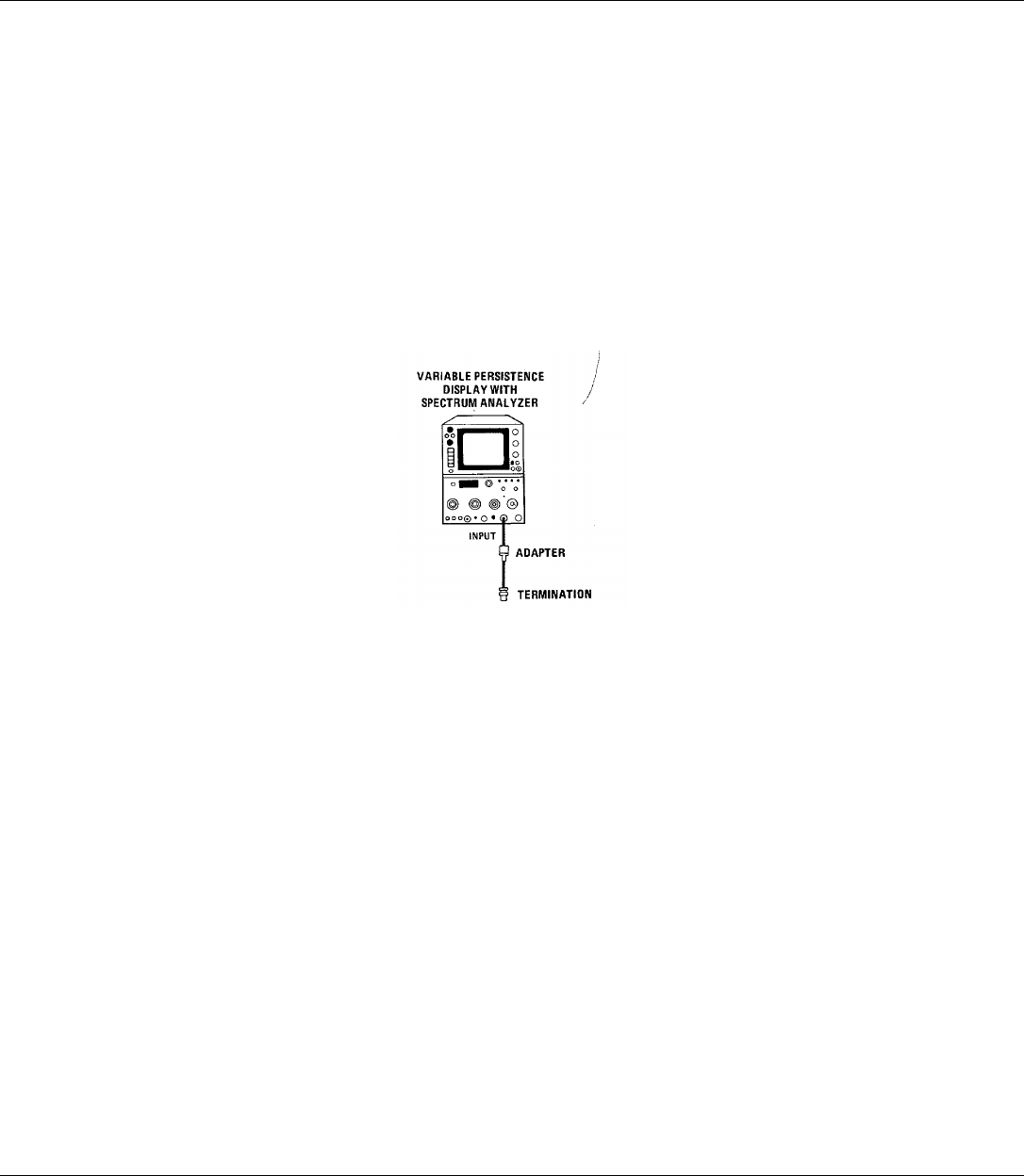
Model 8558B TM 11-6625-3061-14
PERFORMANCE TESTS
4-19. RESIDUAL RESPONSES
SPECIFICATION
< - 100 dBm (1-1500 MHz) with 0 dB input attenuation and no signal present at input.
001: < - 95 dBm
002: < - 50 dBmV
DESCRIPTION
The spectrum analyzer is tested for residual responses with no signal applied to the INPUT 509 connector. The input
attenuation is set to 0 dB.
001 and 002: INPUT 75Ω
Figure 4-16. Residual Responses Test Setup
EQUIPMENT
Variable Persistence/Storage Display ............................................................................................. HP 181T
50-Ohm Termination................................................................................................................... HP 11593A
001 and 002: 75-Ohm Termination, HP 11652-60010
PROCEDURE
1. Set spectrum analyzer controls as follows:
START-CENTER........................................................................................................................... CENTER
TUNING .........................................................................................................................................500 MHz
FREQ SPAN/DIV............................................................................................................................100 MHz
RESOLUTION BW .............................................................................................................................1 MHz
INPUT ATTEN.......................................................................................................................................0 dB
REFERENCE LEVEL......................................................................................................................- 60 dBm
002: - 10 dBm V
Amplitude Scale ...........................................................................................................................10 dB/DIV
SWEEP TIME/DIV..............................................................................................................................AUTO
SWEEP TRIGGER.....................................................................................................................FREE RUN
VIDEO FILTER...............................................................................................Fully clockwise (not in detent)
4-34

Model 8558B TM 11-6625-3061-14
PERFORMANCE TESTS
4-19. RESIDUAL RESPONSES (Cont'd)
2. Terminate INPUT 501 connector with 50-ohm coaxial termination (see Figure 4-16).
001 and 002: 75Ω; 75-ohm
3. With variable persistence display in NORM mode, set LO feedthrough to far left vertical graticule line. Set
BASELINE CLIPPER to 3 o'clock.
4. Set HP 181T to WRITE mode. Set PERSISTENCE control to MAX and INTENSITY control to approximately 12
o'clock.
5. Set spectrum analyzer SWEEP TRIGGER to SINGLE sweep mode and RESOLUTION BW to 30 kHz. Momentarily
press ERASE pushbutton.
NOTE
When the ERASE pushbutton is pressed, the spectrum analyzer sweep might be triggered. To
stop the sweep, turn SWEEP TRIGGER control clockwise.
6. Turn SWEEP TRIGGER control clockwise to initiate sweep.
7. Slowly turn BASELINE CLIPPER control until peaks of trace begin to appear on display. It might be necessary to
increase baseline clipping slightly near end of sweep to reduce blooming.
8. Trigger sweep at least one more time and check for residual responses from 1 to 1000 MHz. Record frequency at
which residual response of greatest amplitude appears. MHz
9. Set display to NORM mode. Set spectrum analyzer BASELINE CLIPPER fully counterclockwise and SWEEP
TRIGGER to FREE RUN.
10. Set FREQ SPAN/DIV to 20 kHz and TUNING to center frequency of residual recorded in step 8.
11. Narrow FREQ SPAN/DIV and RESOLUTION BW, using TUNING control to keep signal centered. Use SWEEP
TIME/DIV control to reduce sweep speed until signal level does not rise when sweep speed is further reduced.
Residual response must be less than - 100 dBm.
dBm
001: < - 95 dBm
002: < - 50 dBmV
12. Repeat steps 1 through 5.
13. Set START-CENTER switch to START and repeat steps 6 and 7.
4-35

Model 8558B TM 11-6625-3061-14
PERFORMANCE TESTS
4-19. RESIDUAL RESPONSES(Cont'd)
14. Trigger sweep at least one more time and check for residual responses from 500 MHz to 1500 MHz. Record
frequency at which residual response of greatest amplitude appears.
MHz
15. Repeat step 9.
16. Set spectrum analyzer FREQ SPAN/DIV to 20 kHz and TUNING to center frequency of residual recorded in step 14.
17. Narrow FREQ SPAN/DIV and RESOLUTION BW, using TUNING control to keep signal centered. Use SWEEP
TIME/DIV control to reduce sweep speed until signal level does not rise when sweep speed is further reduced.
Residual response must be less than - 100 dBm.
dBm
001: < - 95 dBm
002: < - 50 dBm V
4-36
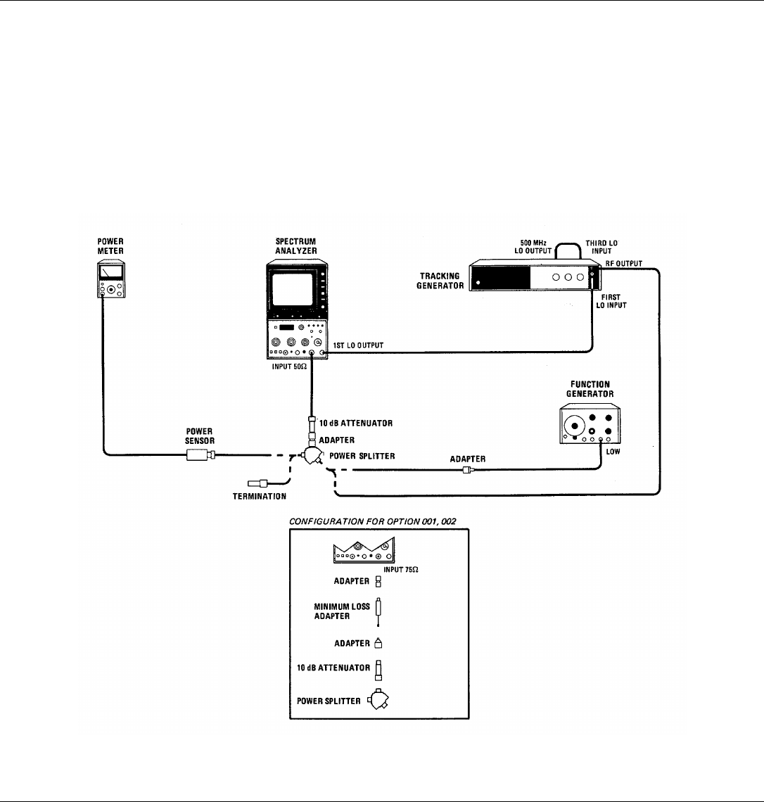
Model 8558B TM 11-6625-3061-14
PERFORMANCE TESTS
4-20. FREQUENCY RESPONSE
SPECIFICATION
≤ ± 1.0 dB with 10 dB input attenuation
DESCRIPTION
Signals from 0.1 to 1500 MHz are applied to the input of the spectrum analyzer. The amplitude of each signal is adjusted
to a reference set on the analyzer display. The power level, measured with a power meter, determines the frequency
response of the spectrum analyzer.
Figure 4-17. Frequency Response Test Setup
4-37

Model 8558B TM 11-6625-3061-14
PERFORMANCE TESTS
4-20. FREQUENCY RESPONSE(Cont'd)
EQUIPMENT
Tracking Generator........................................................................................................HP 8444A Opt. 059
Power Meter ...................................................................................................................................HP 435B
Power Sensor ...............................................................................................................................HP 8482A
Function Generator.......................................................................................................................HP 3310A
Power Splitter .............................................................................................................................HP 11667A
BNC Cable, 20 cm (9 in)............................................................................................................. HP 10502A
BNC Cable, 120 cm (48 in)......................................................................................................... HP 10503A
Type N cable, 180 cm (72 in)...................................................................................................... HP 11500A
10 dB Attenuator............................................................................................................HP 8491B Opt. 010
Adapter, Type N (m) to Type N (m)........................................................................................ HP 1250-1475
Adapter, Type N (m) to BNC (f) ............................................................................................. HP 1250-0780
Additional Equipment, Options 001 and 002:
Adapter, BNC (m) to BNC (m), 75Ω....................................................................................... HP 1250-1288
Adapter, Type N (m) to SMA (f), 50Ω..................................................................................... HP 1250-1250
Minimum Loss Adapter, 75Ω to 50Ω...................................................................................HP 08558-60031
PROCEDURE
1. Set controls as follows:
Spectrum Analyzer:
START- CENTER.......................................................................................................................... CENTER
TUNING .....................................................................................................................................................0
FREQ SPAN/DIV........................................................................................................................................0
RESOLUTION BW ..........................................................................................................................100 kHz
INPUT ATTEN.....................................................................................................................................10 dB
REFERENCE LEVEL.......................................................................................................................-10 dBm
002: + 40 dBmV
Amplitude Scale ...........................................................................................................................10 dB/DIV
SWEEP TIME/DIV..............................................................................................................................AUTO
SWEEP TRIGGER.....................................................................................................................FREE RUN
BASELINE CLIPPER.............................................................................................................................OFF
VIDEO FILTER......................................................................................................................................OFF
2. Adjust spectrum analyzer TUNING to peak LO feedthrough signal on display. Press FREQUENCY CAL and readjust
TUNING for peak. Repeat. Adjust TUNING for peak and adjust FREQUENCY ZERO for a FREQUENCY MHz
reading of 00.0.
3. Adjust TUNING for a FREQUENCY MHz reading of 5.0 MHz. Press FREQUENCY CAL. Set up equipment as
shown in Figure 4-17. Connect the tracking generator 500 MHz LO OUTPUT to the THIRD LO INPUT (rear panel).
4. Set spectrum analyzer Amplitude Scale to 1 dB/DIV and adjust REF LEVEL FINE to bring the trace on the display.
Peak the trace using tracking generator TRACK ADJ.
4-38

Model 8558B TM 11-6625-3061-14
PERFORMANCE TESTS
4-20. FREQUENCY RESPONSE(Cont'd)
5. Set power meter CAL FACTOR according to chart on power probe (5 MHz). Set RANGE to - 10 dBm.
6. Adjust tracking generator LEVEL to set a reference of - 12 dBm on the power meter.
7. Adjust spectrum analyzer REF LEVEL FINE to position trace to fourth graticule line.
8. For each setting in Table 4-5:
a. Adjust spectrum analyzer TUNING and press FREQUENCY CAL.
b. Set power meter CAL FACTOR.
c. Adjust tracking generator TRACK ADJ to peak signal on display and adjust LEVEL to place signal on reference
graticule.
d. Record Power Meter Reading.
9. Disconnect Type N cable from power splitter. Connect function generator LOW output to power splitter.
10. Set controls as follows:
Spectrum Analyzer
FREQ SPAN/DIV...............................................................................................................................50 kHz
RESOLUTION BW ............................................................................................................................10 kHz
Amplitude Scale ...........................................................................................................................10 dB/DIV
Function Generator:
RANGE ...........................................................................................................................................100 kHz
Frequency ..........................................................................................................................................5 MHz
FUNCTION...........................................................................................................................................SINE
DC OFFSET...............................................................................................................................................0
11. Set power meter CAL FACTOR according to chart on power sensor (5 MHz). Adjust spectrum analyzer TUNING to
center 5 MHz signal on display. Set amplitude scale to 1 dB/DIV.
12. Adjust function generator OUTPUT LEVEL to - 12 dB on power meter.
13. Adjust REF LEVEL FINE to bring the peak of the 5 MHz signal to fourth graticule from bottom.
14. For each frequency in Table 4-6, set function generator frequency and tune spectrum analyzer to bring signal to
center screen. Adjust function generator OUTPUT LEVEL to bring signal peak to reference graticule on the display.
Set the power meter CAL FACTOR and record the power indicated by the power meter.
15. Find the overall maximum power reading from both Table 4-5 and Table 4-6.
dBm
4-39

Model 8558B TM 11-6625-3061-14
PERFORMANCE TESTS
4-20. FREQUENCY RESPONSE (Cont'd)
16. Find the overall minimum power reading from both Table 4-5 and Table 4-6.
dBm
17. The difference between the overall maximum power in step 15 and the overall minimum power in step 16 should be
less than 2 dB.
dB
Table 4-5. Frequency Response, 5 lMHz to 1500 MHz
Spectrum Analyzer TUNING
(MHz) Power Meter Reading
(dBm)
5
100
200
300
400
500
600
700
800
900
1000
1100
1200
1300
1400
1500
-12(Ref.)
Table 4-6. Frequency Response, 100 kHz to 5 MHz
Spectrum Analyzer/Function Generator
Frequency Power Meter Reading
(dBm)
5 MHz
3 MHz
1 MHz
500 kHz
100 kHz
-12 (Ref.)
4-40

Model 8558B TM 11-6625-3061-14
PERFORMANCE TESTS
4-21. BANDWIDTH SWITCHING (AMPLITUDE VARIATION)
SPECIFICATION
3 MHz to 300 kHz: ≤ ± 0.5 dB
3 MHz to I kHz: ≤ ±1.0 dB (100 kHz bandwidth limited to < 80o R.H.)
DESCRIPTION
The spectrum analyzer 280 MHz CAL OUTPUT signal is applied to the INPUT connector and displayed on the CRT. The
peak of the displayed 280 MHz signal is centered on the CRT and adjusted for a vertical deflection of seven divisions.
The amplitude variation of the 280 MHz signal is measured for each RESOLUTION BW control setting. The overall
variation between RESOLUTION BW settings of 3 MHz to 300 kHz should be equal to or less than 1 dB (± 0.5 dB). The
overall variation between RESOLUTION BW settings of the 3 MHz to 1 kHz should be equal to or less than 2 dB (±1.0
dB).
EQUIPMENT
BNC Cable, 20 cm (9 in)............................................................................................................. HP 10502A
Adapter, Type N (m) to BNC (f) ............................................................................................. HP 1250-0780
Additional Equipment, Options 001 and 002:
Minimum Loss Adapter, 75Ω to 50Ω....................................................................................HP08558-60031
Adapter, BNC(m) to BNC(m), 75Ω......................................................................................... HP 1250-1288
Adapter, SMA (f) to SMA (f)................................................................................................... HP 1250-1158
Adapter, BNC (f) to SMA (m) ................................................................................................. HP 1250-1200
PROCEDURE
1. Set spectrum analyzer controls as follows:
START- CENTER.......................................................................................................................... CENTER
TUNING .........................................................................................................................................280 MHz
FREQ SPAN/DIV................................................................................................................................1 MHz
RESOLUTION BW .............................................................................................................................3 MHz
INPUT ATTEN.......................................................................................................................................0 dB
REFERENCE LEVEL.......................................................................................................................-20 dBm
002: + 30 dBm
REF LEVEL FINE....................................................................................................................................-10
Amplitude Scale .............................................................................................................................1 dB/DIV
SWEEP TIME/DIV..............................................................................................................................AUTO
SWEEP TRIGGER.....................................................................................................................FREE RUN
BASELINE CLIPPER.............................................................................................................................OFF
VIDEO FILTER......................................................................................................................................OFF
2. Connect spectrum analyzer CAL OUTPUT signal to INPUT 50Ω connector.
001 and 002: 75Ω
4-41
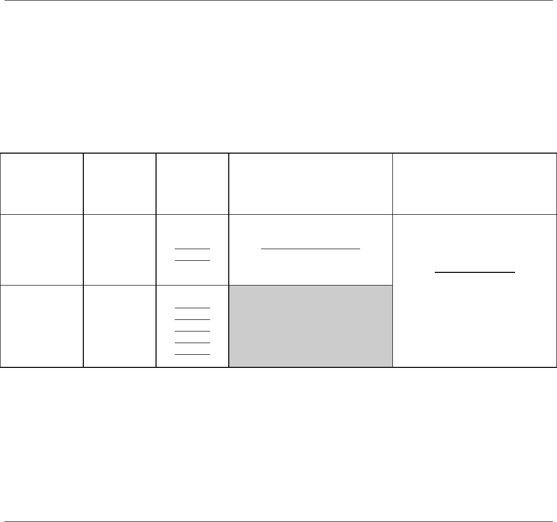
Model 8558B TM 11-6625-3061-14
PERFORMANCE TESTS
4-21. BANDWIDTH SWITCHING (AMPLITUDE VARIATION) (Cont'd)
3. Set TUNING control, as required, to center 280 MHz signal on CRT.
4. Set REF LEVEL FINE control to position peak of 280 MHz signal seven divisions above graticule baseline.
5. Vary the RESOLUTION BW and FREQ SPAN/DIV controls in accordance with Table 4-7. Record the change in
amplitude for each RESOLUTION BW setting. Changes in amplitude above reference level set in step 4 are positive
(+). Changes below reference level are negative (-).
Table 4-7. Amplitude Accuracy, Switching Between Bandwidths
RESOLUTION
BW
Setting
FREQ
SPAN/DIV
Setting
Change in
Amplitude
(dB)
Overall Variation Between
3 MHz and 300 kHz
RESOLUTION BW Settings (dB)
Overall Variation
Between 3 MHZ and
1 HZ RESOLUTION
BW Settings (dB)
3 MHz
1 MHz
300 kHz
1 MHz
500 kHz
100 KH
0 (Ref)
100 kHz
30 kHz
10 kHz
3 kHz
1 kHz
50 kHz
10 KHz
5 kHz
5 kHz
5 kHz
6. To find the overall variation in Table 4-7, algebraically subtract the greatest negative change in amplitude from the
greatest positive change in amplitude. If all changes in amplitude are of the same sign, the overall variation is the
largest positive or largest negative change in amplitude. The overall variation between 3 MHz and 300 kHz
RESOLUTION BW settings should be ≤ 1.0 dB (± 5.0 dB). The overall variation between 3 MHz and 1 kHz
RESOLUTION BW settings should be ≤2.0 dB ( ±1.0 dB).
4-42
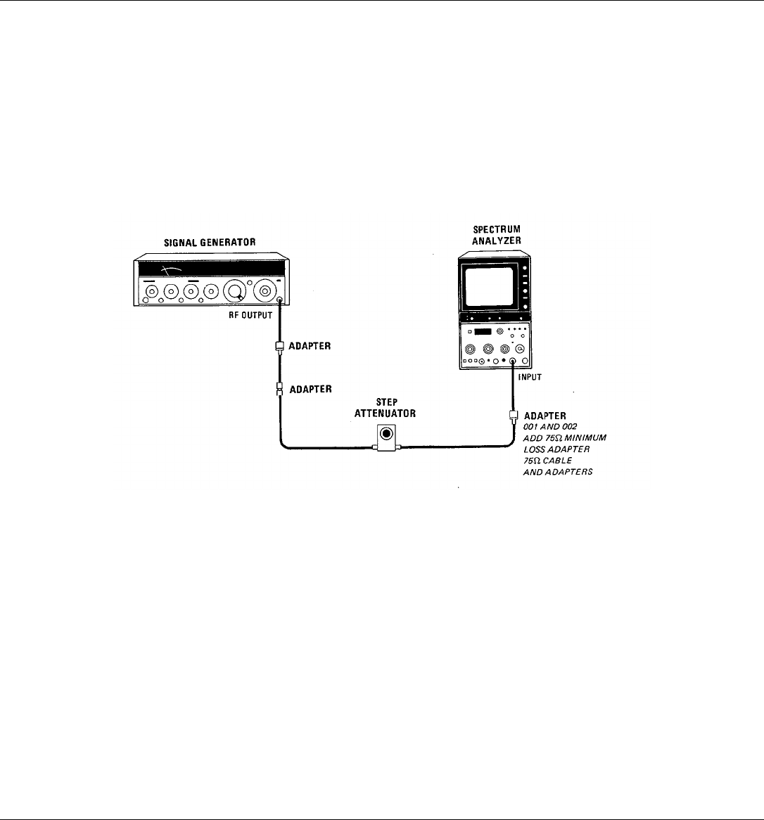
Model 8558B TM 11-6625-3061-14
PERFORMANCE TESTS
4-22. INPUT ATTENUATOR ACCURACY
SPECIFICATION
Accuracy ±0.5 dB for each 10 dB step but not more than ±1.0 dB over full 70 dB range.
DESCRIPTION
The input attenuator accuracy is tested over its full 70 dB range using an RF substitution method. A step attenuator that
has been calibrated by a Standards Laboratory at 30 MHz is used for substitution. The known error of the calibrated
attenuator is taken into account when computing the 8558B input attenuator accuracy.
Figure 4-18. Input Attenuator Accuracy Test Setup
EQUIPMENT
Signal Generator ..........................................................................................................................HP 8640B
Step Attenuator................................................................................................................HP 355D Opt. H82
Adapter, Type N (m) to BNC (f) (2 required) .......................................................................... HP 1250-0780
Adapter, BNC (m) to BNC (m) ............................................................................................... HP 1250-0216
BNC Cable, 120 cm (48 in)......................................................................................................... HP 10503A
Additional Equipment, Options 001 and 002:
Minimum Loss Adapter, 75Ω to 50Ω...................................................................................HP 08558-60031
Adapter, BNC (m) to BNC (m)................................................................................................ HP 1250-0216
Adapter, BNC (f) to SMA (m) ................................................................................................. HP 1250-1200
Adapter, SMA (f) to SMA (f)................................................................................................... HP 1250-1158
BNC Cable, 30cm (12 in), 75Ω............................................................................................HP 11652-60012
4-43

Model 8558B TM 11-6625-3061-14
PERFORMANCE TESTS
4-22 INPUT ATTENUATOR ACCURACY(Cont'd)
PROCEDURE
1. Set controls as follows:
Spectrum Analyzer
START - CENTER......................................................................................................................... CENTER
TUNING ...........................................................................................................................................30 MHz
FREQ SPAN/DIV.............................................................................................................................200 kHz
RESOLUTION BW ............................................................................................................................30 kHz
INPUT ATTEN.....................................................................................................................................70 dB
REFERENCE LEVEL..........................................................................................................................0 dBm
001 -10dBm
002: +40dBmV
Amplitude Scale .............................................................................................................................1 dB/DIV
SWEEP TIME/DIV..............................................................................................................................AUTO
SWEEP TRIGGER.....................................................................................................................FREE RUN
BASELINE CLIPPER.............................................................................................................................OFF
VIDEO FILTER............................................................................................................................... 2 o'clock
Signal Generator
COUNTER MODE .................................................................................................................................. INT
AM.........................................................................................................................................................OFF
FM.........................................................................................................................................................OFF
FREQUENCY TUNE .....................................................................................................................30.0 MHz
OUTPUT LEVEL.................................................................................................................................0 dBm
RF ...........................................................................................................................................................ON
2. Connect equipment as shown in Figure 4-18 with step attenuator set at 0 dB. Locate signal on CRT and adjust signal
generator OUTPUT LEVEL until signal peak is 6 divisions above graticule baseline.
3. Set HP 8558B INPUT ATTEN control and step attenuator to settings indicated in Table 4-8. Record deviation from
sixth division reference set in step 2 for each setting.
Table 4-8. Input Attenuator Accuracy
INPUT ATTEN
Setting (dBm) Step Attenuator
Setting (db) Deviation from 6th
Division (db) Step Attenuator Error
(Calibration) Corrected Deviation
(db)
70
60
50
40
30
20
10
0
0
10
20
30
40
50
60
70
0 (Ref.)
Ref.
0 (Ref.)
*Attenuations > dial settings are positive (+). Attenuations < dial settings are negative (-). For example, 9.99 dB
calibration for a 10 dB attenuator setting represents an error of -0.01 dB.
4-44

Model 8558B TM 11-6625-3061-14
PERFORMANCE TESTS
4-22. INPUT ATTENUATOR ACCURACY(Cont'd)
4. To compute Corrected Deviation, add Step Attenuator Error to Deviation from 6th Division for each setting.
Corrected Deviation should not differ more than 0.5 dB between any two adjacent settings of input attenuator.
Error Between Adjacent Settings
5. Record maximum positive and maximum negative Corrected Deviation values. Difference between these two
values (total deviation) should not exceed 2.0 dB (± 1.0 dB).
dB Maximum Positive Corrected Deviation
dB Maximum Negative Corrected Deviation
dB Total Corrected Deviation
4-45
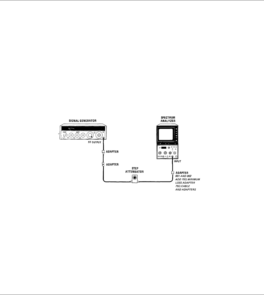
Model 8558B TM 11-6625-3061-14
PERFORMANCE TESTS
4-23. REFERENCE LEVEL ACCURACY
SPECIFICATION
Step Accuracy:
Steps referenced with 0 dB input attenuation
-10 dBm to - 80 dBm: ± 0.5 dB
-10 dBm to - 100 dBm: ± 1.0 dB
Vernier Accuracy:
± 0.5 dB
DESCRIPTION
The reference level accuracy is tested over the range of - 10 dBm to - 100 dBm by checking the IF gain steps in 1
dB/DIV (Log) and in LIN. The resulting maximum deviation in each case must be less than 1.0 dB (± 0.5 dB) from - 10
dBm to - 80 dBm and less than 2.0 dB (+ 1.0 dB) from - 10 dBm to - 100 dBm.
002: Change range to + 40 dBm V to - 50 dBm V.
Figure 4-19. Reference Level Accuracy Test Setup
EQUIPMENT
Signal Generator ..........................................................................................................................HP 8640B
1 dB Step Attenuator ......................................................................................................HP 355C Opt. H80
10 dB Step Attenuator.....................................................................................................HP 355D Opt. H82
Adapter (2 required)............................................................................................................... HP 1250-0780
BNC Cable, 20 cm (9 in)............................................................................................................. HP 10502A
BNC Cable, 120 cm (48 in)......................................................................................................... HP 10503A
Additional Equipment, Options 001 and 002:
Minimum Loss Adapter, 75Ω to 50Ω...................................................................................HP 08558-60031
Adapter, BNC (m) to BNC (m), 75Ω....................................................................................... HP 1250-1288
Adapter, SMA (f) to SMA (f)................................................................................................... HP 1250-1158
Adapter, BNC (f) to SMA (m) ................................................................................................. HP 1250-1200
4-46

Model 8558B TM 11-6625-3061-14
PERFORMANCE TESTS
4-23. REFERENCE LEVEL ACCURACY (Cont'd)
PROCEDURE
Step Accuracy in Log Mode
1. Set controls as follows:
Spectrum Analyzer
START - CENTER......................................................................................................................... CENTER
TUNING ...........................................................................................................................................30 MHz
FREQ SPAN/DIV.................................................................................................................................5 kHz
RESOLUTION BW ..............................................................................................................................3 kHz
INPUT ATTEN.......................................................................................................................................0 dB
REFERENCE LEVEL dBm ..............................................................................................................-10 dBm
002: +40dBmV
Amplitude Scale .............................................................................................................................1 dB/DIV
SWEEP TIME/DIV..............................................................................................................................AUTO
SWEEP TRIGGER.....................................................................................................................FREE RUN
BASELINE CLIPPER.............................................................................................................................OFF
VIDEO FILTER............................................................................................................................... 2 o'clock
Signal Generator
COUNTER MODE .................................................................................................................................. INT
AM.........................................................................................................................................................OFF
FM.........................................................................................................................................................OFF
FREQUENCY TUNE ........................................................................................................................30 MHz
OUTPUT LEVEL..............................................................................................................................-10 dBm
2. Connect equipment in Figure 4-19 with step attenuator set at 0 dB. Locate signal on CRT.
NOTE
If signal is difficult to locate, press RESOLUTION BW control to couple with FREQ SPANIDIV
control and turn the coupled controls clockwise until signal appears on display. Momentarily
depress FREQ CAL switch and center the signal, using TUNING control. Return controls to
positions called out in step 1, adjusting TUNING control as necessary to keep signal centered.
3. Adjust signal generator OUTPUT LEVEL until trace is 6 divisions above graticule baseline. Set the 8558B
REFERENCE LEVEL control and step attenuator to settings indicated in Table 4-9. Record the Deviation from the
6th Division (reference set in step 2) for each setting.
4. To compute the Corrected Deviation, add the Step Attenuator Error to the Deviation from 6th Division for each
setting. The difference between the maximum positive and the maximum negative Corrected Deviation values
from -10 dBm to -80 dBm should not exceed 1.0 dB. The difference between the maximum positive and the
maximum negative Corrected Deviation values from - 10 dBm to - 100 dBm should not exceed 2.0 dB.
- 10 dBm to - 80 dBm dB
- 10 dBm to - 100 dBm dB
002: Change ranges to +40 dBm V to -30 dBm V and +40 dBm V to -50d BmV
4-47
Model 8558B TM 11-6625-3061-14
PERFORMANCE TESTS
4-23. REFERENCE LEVEL ACCURACY (Cont'd)
Table 4-9. IF Gain Accuracy in LOG Mode
REFERENCE
LEVEL Setting
(dBm)
Step Attenuator
Setting
(db)
Deviation from
6th Division
(db)
Step Attenuator
Error (Calibration)*
(dB)
Corrected
Deviation
(db)
-10
-20
-30
-40
-50
-60
-70
-80
-90
-100
0
10
20
30
40
50
60
70
80
90
0 (Ref.)
Ref.
0 (Ref.)
002: REFERENCE LEVEL (dBm V) from top to bottom: 40, 30, 20, 10, 0, -10, -20, -30, -40, -50.
*Attenuations > dial settings are positive (+). Attenuations < dial settings are negative (-). For example, 9.99 dB
calibration for a 10 dB attenuator setting represents an error of -0.01 dB.
Step Accuracy in Linear Mode
5. Set the spectrum analyzer Amplitude Scale switch to LIN. Set REFERENCE LEVEL control to - 10 dBm and set step
ttenuator to 0 dB. Readjust signal generator OUTPUT LEVEL until trace is 6 divisions above graticule baseline.
6. Set the 8558B REFERENCE LEVEL control and step attenuator to settings indicated in Table 4-10. Record the
Deviation from the 6th Division in Linear Mode (reference set in step 5) for each setting.
7. Using Table 4-11, convert Deviation from 6th Division in Linear Mode to deviation in dB for each setting. Record dB
values in Table 4-10.
8. To compute the Corrected Deviation, add the Step Attenuator Error to the Deviation from the 6th Division in dB. The
difference between the maximum positive and the maximum negative Corrected Deviation values from - 10 dBm to -
80 dBm should not exceed 1.0 dB. The difference between the maximum positive and the maximum negative
Corrected Deviation values from - 10 dBm to - 100 dBm should not exceed 2.0 dB.
002: Change ranges to + 40 dBm V to -30 dBm V and +40 dBm V to -50 dBm V.
- 10 dBm to - 80 dBm dB
- 10 dBm to - 100 dBm _ dB
4-48
Model 8558B TM 11-6625-3061-14
PERFORMANCE TESTS
4-23. REFERENCE LEVEL ACCURACY(Cont'd)
Table 4-10. IF Gain Accuracy in Linear Mode
REFERENCE
LEVEL
Setting (dBm)
Step Attenuator
Setting
(db)
Deviation from
6th Division in
Linear Mode (div.)
Deviation from
6th Division
in db*
Step Attenuator
Error (Calibra-
tion)** (dB)
Corrected
Deviation
(dB)
-10
-20
-30
-40
-50
-60
-70
-80
-90
-100
0
10
20
30
40
50
60
70
80
90
0 (Ref.)
0 (Ref.)
Ref.
0 (Ref.)
002: REFERENCE LEVEL (dBmV) from top to bottom: 40, 30, 20, 10, 0, -10, -20, -30, -40, -50.
*Use Table 4-11 to convert deviation in linear mode to deviation in dB.
**Attenuations > dial settings are positive (+). Attenuations < dial settings are negative (-).
Table 4-11. Conversion Table, Deviation in Linear Mode
POSTIVE DEVIATIONS (Above 6th division
from graticule baseline) NEGATIVE DEVIATIONS (Below 6 th division
from graticule baseline)
Liner (Divisions)I dB Linear (Divisions) dB
0
+.1
+.2
+.3
+.4
+.5
+.6
+.7
+.8
+.9
+1.0
+1.1
+1.2
+1.3
+1.4
+1.5
0
+0.14
+0.28
+0.42
+0.56
+0.70
+0.82
+0.96
+1.09
+1.21
+1.34
+1.46
+1.58
+1.70
+1.82
+1.94
0
-.1
-.2
-.3
-.4
-.5
-.6
-.7
-.8
-.9
-1.0
-1.1
-1.2
0
-0.15
-0.29
-0.45
-0.60
-0.76
-0.92
-1.08
-1.24
-1.41
-1.58
-1.76
-1.94
4-49
Model 8558B TM 11-6625-3061-14
PERFORMANCE TESTS
4-23. REFERENCE LEVEL ACCURACY(Cont'd)
Vernier Accuracy
9. Replace 10 dB step attenuator with 1 dB step attenuator. Set spectrum analyzer as follows:
REFERENCE LEVEL......................................................................................................................- 10 dBm
REFERENCE LEVEL FINE.........................................................................................................................0
Amplitude Scale ................................................................................................................................dB/DIV
FREQ SPAN/DIV...............................................................................................................................50 kHz
RESOLUTION BW ..........................................................................................................................300 kHz
10. Center the signal on the CRT and adjust signal generator OUTPUT LEVEL until trace is 6 divisions above graticule
baseline. Set step attenuator and spectrum analyzer REFERENCE LEVEL FINE to settings indicated in Table 4-12.
Record Deviation from 6th Division for each setting.
11. To compute Corrected Deviation, add Step Attenuator Error to Deviation from 6th Division for each setting.
Corrected Deviation should not exceed + 0.5 dB or -0.5 dB for each setting.
Table 4-12. Vernier Accuracy
Step Attenuator
Setting
(dB)
REFERENCE
LEVEL FINE
Setting
Deviation From
6th Division
(dB)
Step Attenuator
Error (Calibration)*
(dB)
Corrected
Deviation
(dB)
0
1
2
3
4
5
6
7
8
9
10
11
12
0
-1
-2
-3
-4
-5
-6
-7
-8
-9
-10
-11
-12
0 (Ref.)
Ref.
0 (Ref.)
* Attenuations > dial settings are positive (+). Attenuations < dial settings are negative (-).
4-50
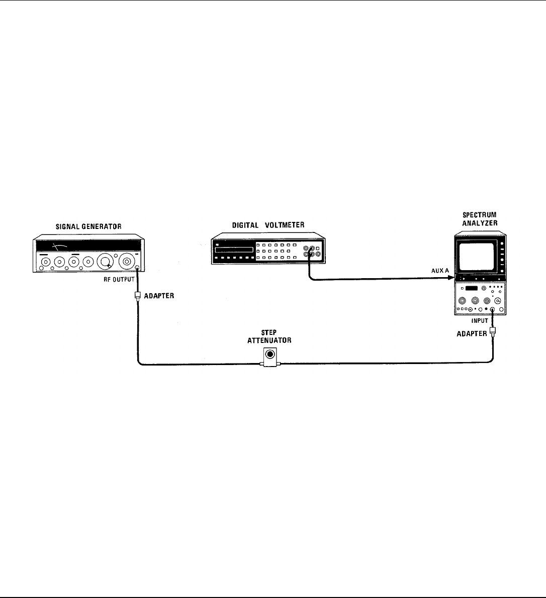
Model 8558B TM 11-6625-3061-14
PERFORMANCE TESTS
4-24. DISPLAY FIDELITY
SPECIFICATION
Log Incremental Accuracy:
± 0.1 dB per dB from Reference Level
Log Maximum Cumulative Error:
< ± 1.5 dB over entire 70-dB range
Linear Accuracy:
± 3% of Reference Level
DESCRIPTION
The amplitude log display amplifier is tested by connecting a DVM to the rear panel AUX A connector (vertical output) of
the mainframe. The widest analyzer bandwidth possible is selected so the signal appears as a straight horizontal line on
the CRT display. The DVM is used to provide good resolution when checking for ±1 dB per 10 dB step (0.1 dB/dB).
Figure 4-20. Amplitude Log Display Accuracy Test Setup
EQUIPMENT
Signal Generator ............................................................................................................................. HP 8640B
Digital Voltmeter.............................................................................................................................. HP 3455A
10 dB Step Attenuator ....................................................................................................... HP 355D Opt. H82
Adapter, Type N (m) to BNC (f) (2 required) ..............................................................................HP 1250-0780
Cable, BNC to Banana Plug ...........................................................................................................HP 11001A
Additional Equipment, Options 001 and 002:
Minimum Loss Adapter, 75Ω to 50Ω...................................................................................... HP 08558-60031
Adapter, BNC (m) to BNC (m), 75Ω...........................................................................................HP 1250-1288
Adapter, SMA (f) to SMA (f).......................................................................................................HP 1250-1158
Adapter, BNC (f) to SMA (m).....................................................................................................HP 1250-1200
4-51

Model 8558B TM 11-6625-3061-14
PERFORMANCE TESTS
4-24. DISPLAY FIDELITY (Cont'd)
PROCEDURE
Log Display Accuracy
1. Set controls as follows:
Spectrum Analyzer
START - CENTER.............................................................................................................................CENTER
TUNING .............................................................................................................................................. 30 MHz
FREQ SPAN/DIV ................................................................................................................................500 kHz
RESOLUTION BW..............................................................................................................................300 kHz
INPUT ATTEN........................................................................................................................................ 10 dB
REFERENCE LEVEL ............................................................................................................................ 0 dBm
002: + dBm V
REF LEVEL FINE.......................................................................................................................................... 0
Amplitude Scale .............................................................................................................................. 10 dB/DIV
SWEEP TIME/DIV .................................................................................................................................AUTO
SWEEP TRIGGER........................................................................................................................ FREE RUN
BASELINE CLIPPER................................................................................................................................ OFF
VIDEO FILTER......................................................................................................................................... OFF
Digital Voltmeter
RANGE ......................................................................................................................................................100
FUNCTION ...........................................................................................................................................V (DC)
AUTO CAL.............................................................................................................................................AUTO
TRIGGER.......................................................................................................................................INTERNAL
MATH....................................................................................................................................................... OFF
Signal Generator
FREQUENCY...................................................................................................................................... 30 MHz
COUNTERMODE.......................................................................................................................................INT
OUTPUT LEVEL ................................................................................................................................... 0 dBm
AM ........................................................................................................................................................... OFF
FM ........................................................................................................................................................... OFF
2. With no signal at INPUT, measure and record the vertical output (AUX A) offset of the spectrum analyzer.
_______ mV
3. Connect equipment as shown in Figure 4 20. Tune signal generator to 30 MHz and set power output for
approximately 0 dBm. Set step attenuator to 0 dB.
4. Set spectrum analyzer Amplitude Scale to 10 dB/DIV and adjust TUNING control to center the signal on CRT
display.
5. Set the FREQ SPAN/DIV control to zero (0) and RESOLUTION BW control to 100 kHz. Tune the signal
generator frequency for maximum reading on DVM.
4-52
Model 8558B TM 11-6625-3061-14
PERFORMANCE TESTS
4-24. DISPLAY FIDELITY(Cont'd)
6. Set the signal generator OUTPUT LEVEL so the DVM reads + 800 mV plus the offset (step 2) ± 0.5 mV. The
trace should be approximately at the top graticule line.
Table 4-13. Amplitude Log Display Accuracy
AUX A Theoretical Difference
Attenuator DVM Corrected AUX A Reading Subtracted Between
Setting Reading DMV Theoretical From Corrected Adjacent
(dB) (mV) Reading* Reading DMV Reading Readings
(mV) (mV) (mV) (mV)
0+800 (Ref.) +800 0
10 - - +700 - -
20 - - +600 - -
30 - - +500 - -
40 - - +400 - -
50 - - +300 - -
60 - - +200 - -
70 - - +100 - -
*DVM Reading minus offset recorded in step 2.
Example (+ 5 mV offset):
Table 4-14. Sample Computations of Amplitude Log Display Accuracy
AUX A Theoretical Difference
Attenuator DVM Corrected AUX A Reading Subtracted Between
Setting Reading DMV Theoretical From Corrected Adjacent
(dB) (mV) Reading* Reading DMV Reading Readings
(mV) (mV) (mV) (mV)
0+805 +800 +800 0
10 +811 +703 +700 +3 -3
20 +599 +594 +600 -6 +9
30 +497 +492 +500 -8 +2
40 +406 +401 +400 +1 -9
*DVM Reading minus offset recorded in step 2.
7. Record the DVM Reading for each 10 dB step of the step attenuator, up to 70 dB, in Table 4-13.
8. Having recorded the DVM readings for all of the attenuator settings from 0 to 70 dB, subtract the AUX A
Theoretical Reading from the Corrected DVM Reading (DVM reading minus offset) in each case and record
results in Table 4-13. Theoretical Reading Subtracted From Corrected DVM Reading should not exceed ± 15
mV (± 1.5 dB).
4-53

Model 8558B TM 11-6625-3061-14
PERFORMANCE TESTS
4.24. DISPLAY FIDELITY (Cont'd)
9. Subtract each converted reading (AUX A Theoretical Reading Subtracted From Corrected DVM Reading) from
the previous converted reading. This subtraction must be performed algebraically. Record results in Table 4-13
(see Example).
10. The difference between adjacent readings (Table 4-13) should not exceed 10 mV (4 0.1 dB/dB).
Linear Display Accuracy
11. Replace 10 dB step attenuator with 1 dB step attenuator. Set step attenuator to 0 dB.
12. Set spectrum analyzer Amplitude Scale to LIN and RESOLUTION BW control to 1 MHz.
13. Peak the signal on the CRT display using the TUNING control. Set the signal generator OUTPUT LEVEL to
place the trace at the top graticule line.
14. Set the step attenuator to 6 dB. Trace should be at 4th division above graticule baseline (center horizontal
graticule line) 1.2 minor divisions.
_______ div
15. Set the step attenuator to 12 dB. Trace should be at 2nd division above graticule baseline 1.2 minor divisions.
_______ div
4-54
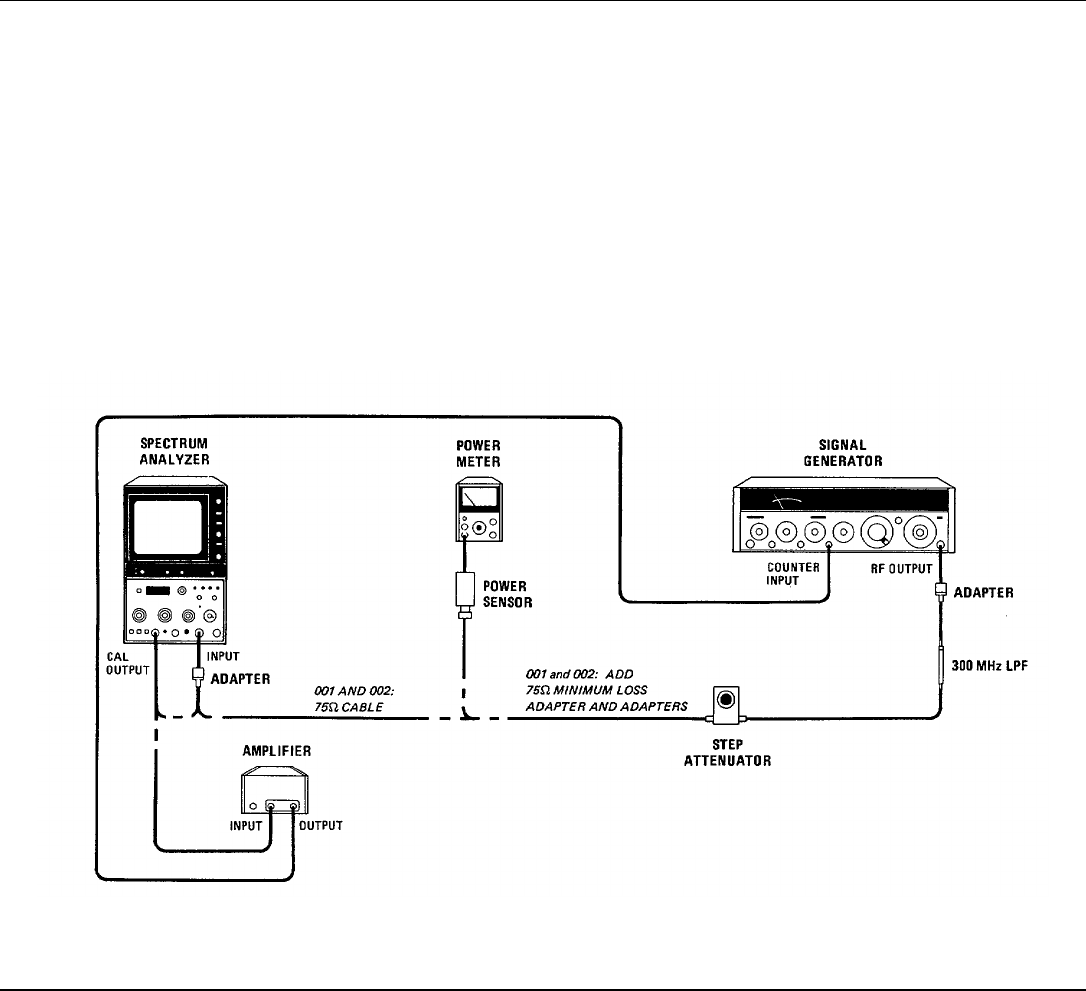
Model 8558B TM 11-6625-3061-14
PERFORMANCE TESTS
4-25. CALIBRATOR ACCURACY
SPECIFICATION
Amplitude: -30 dBm ± 1 dB.
002: +20dBmV ± 1 dB.
Frequency: 280 MHz ±300 MHz.
DESCRIPTION
The amplitude accuracy and frequency accuracy of the CAL OUTPUT signal are checked for -30 dBm ± 1 dB and 280
MHz ± 300 kHz, respectively.
002: +20dBmV ±1 dB.
Figure 4-21. Calibrator Accuracy Test Setup
4-55

Model 8558B TM 11-6625-3061-14
PERFORMANCE TESTS
4-25. CALIBRATOR ACCURACY (Cont'd)
EQUIPMENT
Amplifier.......................................................................................................................................... HP 8447D
Signal Generator ............................................................................................................................. HP 8640B
10 dB Step Attenuator (Calibrated at 280 MHz) ................................................................. HP 355D Opt. H82
Power Meter...................................................................................................................................... HP 435B
300 MHz LPF ............................................................................................................. TELONIC TLP 300-4AB
Power Sensor.................................................................................................................................. HP 8482A
Adapter, Type N (m) to BNC (f) (2 required) ..............................................................................HP 1250-6780
Adapter, Type N (f) to BNC (m) .................................................................................................HP 1250-0077
BNC Cable, 120 cm (48 in) (2 required)..........................................................................................HP 10503A
Additional Equipment for Options 001 and 002:
Power Sensor, 750.......................................................................................................................... HP 8483A
Adapter, GR Type 874 to BNC (m), 75Ω.................................................................. General Radio 0874-9754
Adapter, GR Type 874 to N (f), 75Ω........................................................................ General Radio 0874-9751
Minimum Loss Adapter, 75Q to 50Ω...................................................................................... HP 08558-60031
Adapter, BNC (m) to BNC (m) ...................................................................................................HP 1250-0216
Adapter, SMA (f) to SMA (f).......................................................................................................HP 1250-1158
Adapter, BNC(f) to SMA (m)......................................................................................................HP 1250-1200
BNC Cable 30 cm (12 in), 75Ω.............................................................................................. HP 11652-60012
PROCEDURE
1. Set spectrum analyzer controls as follows:
START - CENTER.............................................................................................................................CENTER
TUNING ............................................................................................................................................ 280 MHz
FREQ SPAN/DIV .................................................................................................................................. 1 MHz
RESOLUTION BW................................................................................................................................ 1 MHz
INPUT ATTEN........................................................................................................................................ 10 dB
REFERENCE LEVEL ......................................................................................................................... -20 dBm
002: +30dBmV
Amplitude Scale .............................................................................................................................. 10 dB/DIV
SWEEP TIME/DIV .................................................................................................................................AUTO
SWEEP TRIGGER........................................................................................................................ FREE RUN
BASELINE CLIPPER................................................................................................................................ OFF
2. Set signal generator COUNTER MODE to EXT, 0-550, and EXPAND-X10. Connect spectrum analyzer CAL
OUTPUT to signal generator COUNTER INPUT connector through amplifier. Frequency counter should indicate
280 MHz ± 300 kHz.
__________ MHz
3. Set signal generator COUNTER MODE to INT and tune frequency to 280 MHz. Connect output of signal
generator to calibrated step attenuator through 300 MHz low pass filter. Set signal generator OUTPUT LEVEL to
0 dBm.
4-56

Model 8558B TM 11-6625-3061-14
PERFORMANCE TESTS
4-25. CALIBRATOR ACCURACY(Cont'd)
4. Set step attenuator to 10 dB and connect power sensor and power meter to attenuator as shown in Figure 4-21.
5. Set signal generator OUTPUT LEVEL power for a 10 dBm reading on power meter. Leave signal generator set
at this level.
6. Set step attenuator to 30 dB and connect output of step attenuator to spectrum analyzer INPUT connector.
7. Set spectrum analyzer TUNING control to center signal on CRT display. Peak amplitude of reference signal
should be one division down from top graticule line.
8. Set Amplitude Scale switch to I dB/DIV and adjust REF LEVEL FINE control so peak amplitude of reference
signal is one division down from top graticule line.
9. Disconnect reference signal and connect spectrum analyzer CAL OUTPUT to the INPUT connector. Signal peak
amplitude should be one division down from top graticule line ±1 division.
- 31 dBm _______ 29 dBm
PROCEDURE FOR OPTIONS 001 and 002:
1. Set spectrum analyzer controls as indicated above.
2. Connect CAL OUTPUT to 8640B counter input connector through amplifier. Frequency counter should indicate
280 MHz ±300 kHz. (Use EXPAND X10 COUNTER MODE, EXT 0-550.)
3. Set signal generator frequency to 280 MHz. Connect output of signal generator to calibrated step attenuator and
75-ohm minimum loss adapter (approximately 5.7 dB attenuation). Set signal generator OUTPUT LEVEL to 5
dBm.
4. Set the step attenuator to 0 dB. Connect minimum loss adapter through power sensor to power meter.
5. Set signal generator OUTPUT LEVEL for a 10 dBm (Option 001) or -8.75 dBm (Option 002) reading on power
meter. Leave the signal generator set at this level.
6. Set step attenuator to 20 dB and connect -30 dBm (+20 dBm V) reference signal from signal generator through
step attenuator, minimum loss adapter, and 75 ohm cable to HP 8558B INPUT 75Ω connector.
7. With Amplitude Scale switch set to 10 dB/DIV, adjust TUNING control to center signal on CRT display. Peak
amplitude of reference signal should be one division down from the top graticule line.
4-57

Model 8558B TM 11-6625-3061-14
PERFORMANCE TESTS
4-25. CALIBRATOR ACCURACY (Cont'd)
8. Set Amplitude Scale switch to 1 dB/DIV and adjust REF LEVEL FINE control so peak amplitude of reference
signal is on seventh graticule line (one division down from top).
9. Disconnect the reference signal and connect HP 8558B CAL OUTPUT through 75-ohm cable to INPUT 75g
connector. Signal peak amplitude should be one division down from top, plus or minus one division.
001: -31 dBm _______ 29 dBm
002: + 19 dBm V ______21 dBm V
4-58

Model 8558B TM 11-6625-3061-14
Table 4-15. Performance Test Record (1 of 4)
Hewlett-Packard Company Tested by:__________
Model 8558B
Spectrum Analyzer 0.1-1500 MHz
Serial No._________________ Date:______________
Paragraph Results
Number Test Description Min. Actual Max.
4-11 Frequency Span Accuracy
3.100 MHz FREQ SPAN/DIV -0.4 div - +0.4 div
4.50 MHz FREQ SPAN/DIV -0.4 div - +0.4 div
5.20 MHz FREQ SPAN/DIV .-0.4 div - +0.4 div
6.10 MHz FREQ SPAN/DIV -0.4 div - +0.4 div
7.5 MHz FREQ SPAN/DIV -0.4 div - +0.4 div
8.2 MHz FREQ SPAN/DIV -0.4 div - +0.4 div
9.1 MHz FREQ SPAN/DIV -0.4 div - +0.4 div
10.500 kHz FREQ SPAN/DIV -0.4 div - +0.4 div
13.200 kHz FREQ SPAN/DIV -0.4 div - +0.4 div
14.100 kHz FREQ SPAN/DIV -0.4 div - +0.4 div
50 kHz FREQ SPAN/DIV -0.4 div - +0.4 div
20 kHz FREQ SPAN/DIV -0.4 div - +0.4 div
10 kHz FREQ SPAN/DIV -0.4 div - +0.4 div
5 kHz FREQ SPAN/DIV -0.4 div - +0.4 div
4-12 TUNING Accuracy
5.10.0 MHz -5.2 div - +5.2 div
(8.96 MHz) (11.04 MHz)
6.20.0MHz -5.2 div - +5.2 div
(18.96 MHz) (21.04 MHz)
40.0 MHz -5.2 div - +5.2 div
(38.96 MHz) (41.04 MHz)
60.0 MHz -5.2 div - +5.2 div
(58.96 MHz) (61.04 MHz)
80.0 MHz -5.2 div - +5.2 div
(78.96 MHz) (81.04 MHz)
100.0 MHz -5.2 div - +5.2 div
(96.96 MHz) (101.04 MHz)
120.0 MHz -5.2 div - +5.2 div
(118.96 MHz) (121.04 MHz)
140.0 MHz -5.2 div - +5.2 div
(138.96 MHz) (141.04 MHz)
160.0 MHz -5.2 div - +5.2 div
(158.96 MHz) (161.04 MHz)
180.0 MHz -5.2 div - +5.2 div
(178.96 MHz) (181.04 MHz)
200 MHz -5.2 div - +5.2 div
(194.8 MHz) (205.2 MHz)
4-59

Model 8558B TM 11-6625-3061-14
Table 4-15. Performance Test Record (2 of 4)
Paragraph Results
Number Test Description Min. Actual Max.
4-12 TUNING Accuracy (Cont'd)
400 MHz -5.2 div - +5.2 div
(394.8 MHz) (405.2 MHz)
600 MHz -5.2 div - +5.2 div
(594.8 MHz) (605.2 MHz)
800 MHz -5.2 div - +5.2 div
(794.8 MHz) (805.2 MHz)
1000 MHz -5.2 div - +5.2 div
(994.8 MHz) (1005.2 MHz)
1200 MHz -5.2 div - +5.2 div
(1194.8 MHz) (1205.2 MHz)
1400 MHz -5.2 div - +5.2 div
(1394.8 MHz) (1405.2 MHz)
1500 MHz -5.2 div - +5.2 div
(1494.8 MHz) (1505.2 MHz)
4-13 Residual FM
6.Peak-to-Peak Variation of Trace - 1.0 div
(1 kHz/0.1 sec)
4-14 Noise Sidebands
6.Noise Sidebands - 6.5 div down
(-65 dB)
4-15 Resolution Bandwidth Accuracy
7.3 MHz Resolution BW 2.40 MHz - 3.60 MHz
8.1 MHz Resolution BW 800 kHz - 1.20 MHz
9.300 kHz Resolution BW 240 kHz - 360 kHz
10.100 kHz Resolution BW 80 kHz - 120 kHz
17.30 kHz Resolution BW 24 kHz - 36 kHz
18.10 kHz Resolution BW 8 kHz - 12 kHz
19.3 kHz Resolution BW 2.4 kHz - 3.6 kHz
20.1 kHz Resolution BW 0.8 kHz - 1.2 kHz
4-16 Resolution Bandwidth Selectivity
24.3 MHz Resolution BW Selectivity - 15:1
1 MHz Resolution BW Selectivity - 15:1
300 kHz Resolution BW Selectivity - 15:1
100 kHz Resolution BW Selectivity - 15:1
30 kHz Resolution BW Selectivity - 15:1
10 kHz Resolution BW Selectivity - 15:1
3 kHz Resolution BW Selectivity - 15:1
1 kHz Resolution BW Selectivity - 15:1
4-60

Model 8558B TM 11-6625-3061-14
Table 4-15. Performance Test Record (3 of 4)
Paragraph Results
Number Test Description Min. Actual Max.
4-17 Average Noise Level
2 Average Noise Level 1 MHz to 1000 MHz - -107 dBm
3 Average Noise Level 500 MHz to 1500 MHz - -107 dBm
5 Average Noise Level 1 MHz to 11 MHz - -107 dBm
001: Max. is -100 dBm
002: Max. is -53 dBm V
4-18 Spurious Responses
9.Harmonic Distortion
2nd Harmonic -70 dB -
3rd Harmonic -70 dB -
18.Third Order Intermodulation Distortion,
30 MHz input signals -70 dB -
20.Second Order Intermodulation Distortion,
30 MHz input signals (f1 + f2) -70 dB -
22.Second Order Intermodulation Distortion,
30 MHz input signals (f1 + f2) -70 dB -
27.Third Order Intermodulation Distortion,
4 MHz input signals -60 dB -
29.Second Order Intermodulation Distortion,
4 MHz input signals (f1 + f2) -60 dB -
30.Second Order Intermodulation Distortion,
4 MHz input signals (f1 + f2) -60 dB -
4-19 Residual Responses
11.Residual Responses 1 MHz to 1000 MHz - -100 dBm
17.Residual Responses 500 MHz to 1500 MHz - -100 dBm
001: Max. is <-95 dBm
002: Max. is <-45 dBm V
4-20 Frequency Response
17.Frequency Response - 2.0 dB
4-21 Bandwidth Switching (Amplitude Variation)
6.3 MHz to 300 kHz (overall variation) -0.5 dB - +0.5 dB
3 MHz to 1 kHz (overall variation) -1.0 dB - +1.0 dB
4-22 Input Attenuator Accuracy
4.Error Between Adjacent Settings - ±0.5 dB
(1.0 dB)
5.Error Over Full 70 dB Range - ±1.0 dB
(2.0 dB)
4-61

Model 8558B TM 11-6625-3061-14
Table 4-15. Performance Test Record (4 of 4)
Paragraph Results
Number Test Description Min. Actual Max.
4-23 Reference Level Accuracy
4.Step Accuracy in Log
-10 dBm to -80 dBm ±0.5 dB
(1.0 dB)
-10 dBm to -100 dBm ±1.0 dB
(2.0 dB)
002:+40 dBm V to -30 dBm V
+40 dBm V to -50 dBm V
8.Step Accuracy in LIN
-10 dBm to 80 dBm ±0.5 dB
(1.0 dB)
-10 dBm to -100 dBm ±1.0 dB
(2.0 dB)
002: +40 dBm V to -30 dBm V
+40 dBm V to -50 dBm V
11.Vernier Accuracy
REF LEVEL FINE:
-1 -0.5 dB +0.5 dB
-2 -0.5 dB +0.5 dB
-3 -0.5 dB +0.5 dB
-4 -0.5 dB +0.5 dB
-5 -0.5 dB +0.5 dB
-6 -0.5 dB +0.5 dB
-7 -0.5 dB +0.5 dB
-8 -0.5 dB +0.5 dB
-9 -0.5 dB +0.5 dB
-10 -0.5 dB +0.5 dB
-11 -0.5 dB +0.5 dB
-12 -0.5 dB +0.5 dB
4-24 Display Fidelity
Log Display Accuracy
8.Maximum Error Over Full 70 dB Display Range ±1.5 dB
(±15 mV)
10.Error Between Adjacent Readings ±1.0 dB
(±10 mV)
Linear Display Accuracy
14.Error at 4th division 3.76 div 4.24 div
15.Error at 2nd division 1.76 div 2.24 div
4-25 Calibrator Accuracy
2.CAL OUTPUT Frequency 279.7 MHz 280.3 MHz
9.CAL OUTPUT Amplitude -31 dBm -29 dBm
002: Min. is + 19 dBm V, Max. is +21 dBm V
4-62
TM 11-1247-B
THIS PAGE MISSING NOT AVAILABLE FOR DIGITIZATION.
PAGES
4-63 through 4-69
Model 8558B TM 11-6625-3061-14
SECTION V.
ADJUSTMENTS
5-1. INTRODUCTION
5-2. The adjustments in this section are required to
optimize spectrum analyzer performance after repair.
Table 5-1 lists adjustable components by adjustment
name, reference designation, adjustment paragraph,
and description.
5-3. Data taken during adjustment should be
recorded in the spaces provided. Comparison of initial
data with data taken during periodic adjustments is
useful for preventive maintenance and troubleshooting.
WARNING
The adjustments in this section
require the spectrum analyzer to be
removed from the display mainframe
and connected through an extender
cable assembly. Be very careful; the
energy at some points in the
instrument might, if contacted, cause
personal injury. The adjustments in
this section should be performed
only by a skilled person who knows
the hazard involved.
NOTE
Before performing any adjustments,
allow 1 hour warmup time.
5-4. EQUIPMENT REQUIRED
5-5. The table of Recommended Test Equipment in
Section I lists the test equipment and test accessories
required in the adjustment procedures. In addition, the
table lists the required minimum specifications and
suggested manufacturers' model numbers.
5-6. Required service accessories, with part
numbers, are illustrated in Section I.
5-7. Adjustment Tools
5-8. For adjustments requiring a non-metallic tuning
tool, use fiber tuning tool, HP Part Number 8170-0033.
Never try to force an adjustment control in the analyzer.
This is especially critical when tuning slug-tuned
inductors and variable capacitors.
5-9. Extender Cable Installation
WARNING
Disconnect mainframe line cord
before installing extender cable
assembly.
5-10. Pull out the lock knob and slide the spectrum
analyzer out of the display mainframe. If side stops are
installed, refer to Section II for removal.
5-11. Carefully slide the extender cable assembly,
HP part number 5060-0303, into the display mainframe,
aligning the metal guide plate with the slotted side rails
of the mainframe. Firmly seat the extender cable
assembly to ensure good contact.
5-12. Connect the opposite end of the cable to the
spectrum analyzer. The plug is keyed so it will go on
correctly and will not make contact upside down.
Remove the orange and the yellow leads from pins 3
and 4 on the A15 board at the rear of the spectrum
analyzer. Connect the corresponding leads from the
extender cable assembly to these pins by means of the
insulated alligator clips.
5-13. RELATED ADJUSTMENTS
5-14. These adjustments should be performed
whenever troubleshooting information in Section VIII
indicates that an adjustable circuit is not operating
properly. Perform the adjustments after repair or
replacement of the circuit. The troubleshooting
procedures and Table 5-1 specify the required
adjustments.
5-1
Model 8558B TM 11-6625-3061-14
5-15. FACTORY-SELECTED COMPONENTS
5-16. Table 5-2 provides a list of factory-selected
components by reference designation, selection
procedure paragraph number, range of values, and
basis
of selection. Factory-selected components are
designated by an asterisk (*) on the schematic diagrams
in Section VIII and in the table of Replaceable Parts,
Section VI. Part numbers for standard-value
components can be found in Table 5-3.
5-2

Model 8558B TM 11-6625-3061-14
Table 5-1. Adjustable Components (1 of 4)
Adjustment Reference Adjustment
Name Designator Paragraph Description
REF A1A2R3 5-28 Adjusts DPM reference voltage and adjusts frequency
for correct FREQUENCY MHz readout at 1500 MHz.
2nd MIXER MATCH A5L2 5-17 Adjust for optimum match between second converter
output and second IF input.
Z1, Z2, Z3 A5Z1 A5Z3 5-17 Adjust the bandpass of the 2050 MHz bandpass filter.
2nd LO FREQUENCY A5Z4 5-17 Adjusts second LO frequency to 1748.60 MHz.
3.55 GHZ A7R1 5-28 Coarse adjustment of YIG upper frequency limit, 3.55
GHz.
3.55 FINE A7R2 5-28 Fine adjustment of YIG upper frequency limit, 3.55
GHz.
2.0 GHZ A7R3 5-28 Adjusts YIG lower frequency limit, 2.05 GHz
REF V A7R4 5-28 Adjusts reference voltage to 6.0 volts and is fine
adjustment of YIG lower frequency limit, 2.05 GHz.
+14.5V A7R5 5-28 Adjusts 14.5 volt supply to +14.5 volts.
FM A7R6 5-28 Adjusts frequency span accuracy for frequency spans
<1 MHz per division.
GAIN A7R7 5-28 Adjusts frequency for correct DPM frequency readout
at 190.0 MHz.
RNG A7R8 5-28 Adjusts frequency control circuit for proper DPM
ranging.
OFS A7R72 5-28 Adjusts frequency for correct FREQUENCY MHZ
readout at 200 MHz.
2 ms A8R13 5-27 Adjusts sweep ramp to calibrate 2 ms per division
sweep time.
1 ms A8R10 5-27 Adjusts sweep ramp to calibrate 1 ms per division
sweep time.
+10V A8R7 5-27 Adjusts +10 volt supply. This adjustment must be
performed while spectrum analyzer is still cold, during
first five minutes after turn on.
XTL A8R72 5-21 Adjusts IF bandwidth between 3 dB points for
5-22 RESOLUTION BW setting of 3 kHz.
LC A8R85 5-21 Adjusts IF bandwidth between 3 dB points for
RESOLUTION BW setting of 1 MHz.
LO FREQ A9L4 5-18 Adjusts third converter 280 MHz crystal-controlled LO
for maximum output.
5-3

Model 8558B TM 11-6625-3061-14
Table 5-1. Adjustable Components (2 of 4)
Adjustment Reference Adjustment
Name Designator Paragraph Description
SLOPE COMP A9R1 5-19 Compensates for frequency response of input mixer,
allowing flatness of less than 2 dB.
3rd LO PWR A9R5 5-18 Adjusts CAL OUTPUT signal for -30 dBm power level.
002: +20 dBm V.
C 1, C2, C3 A10C1 A10C3 5-20 Adjust the bandpass of the Second IF assembly
Bandpass Filter (301.4 MHz).
2nd IF TUNING A10L2 5-20 Peaks second IF bandpass amplifier. Has very little
effect on signal.
SYM A11C15 5-21 Adjust symmetry of first stage of crystal bandwidth
filter.
LC CTR A11C23 5-21 Adjusts centering of first stage of LC bandwidth filter.
CTR A11C25 5-21 Adjusts centering of first stage of crystal bandwidth
filter.
SYM A11C38 5-21 Adjusts symmetry of second stage of crystal
bandwidth filter.
LC CTR A11C45 5-21 Adjusts centering of second stage of LC bandwidth
filter.
CTR A11C54 5-21 Adjusts centering of second stage of crystal bandwidth
filter.
C73 A11C73 5-21 Compensates for capacitance of CR3.
C74 A11C74 5-21 Compensates for capacitance of CR11.
LC A11R26 5-21 Adjusts feedback in LC circuit of bandpass filter.
XTL A11R31 5-21 Adjusts feedback in crystal circuit of bandpass filter.
40 dB A12R1 5-24 Adjust 40 dB step gain.
10 dB A12R3 5-24 Adjusts 10 dB step gain.
GAIN A12R4 5-23 Adjusts overall gain of Step Gain assembly.
0 dB A12R5 5-24 Adjusts to calibrate 0 dB position of REF LEVEL FINE
control.
5-4

Model 8558B TM 11-6625-3061-14
Table 5-1. Adjustable Components (3 of 4)
Adjustment Reference Adjustment
Name Designator Paragraph Description
-12 dB A12R6 5-24 Adjusts to calibrate -12 dB position of REF LEVEL
FINE control.
+19.5V A12R7 5-25 Adjusts +19.5 volt supply.
SYM A13C15 5-21 Adjusts symmetry of first stage of crystal bandwidth
filter.
LC CTR A13C23 5-21 Adjusts centering of first stage of LC bandwidth filter.
CTR A13C25 5-21 Adjusts centering of first stage of crystal bandwidth
filter.
SYM A13C38 5-21 Adjusts symmetry of second stage of crystal
bandwidth filter.
LC CTR A13C45 5-21 Adjusts centering of second stage of LC bandwidth
filter.
CTR A13C54 5-21 Adjusts centering of second stage of crystal bandwidth
filter.
C73 A13C73 5-21 Compensate for capacitance of CR3.
C74 A13C74 5-21 Compensates for capacitance of CR11 .
LC A13R26 5-21 Adjusts feedback in LC circuit of bandpass filter.
XTL A13R31 5-21 Adjusts feedback in crystal circuit of bandpass filter.
OFFSET A14R10 5-26 Adjusts -8V temperature compensated supply.
TC A14R21 Adjusts gain of +1V supply to provide temperature
compensation for log mode temperature controlled
variable gain amplifier. (Factory adjustable only.)
SLOPE A14R23 5-26 Adjusts gain of log mode temperature controlled gain
amplifier.
G6 A14R27 5-26 Adjusts combined gain of 2nd and 3rd stages in linear
mode.
G5 A14R30 5-26 Adjusts gain of 4th stage in linear mode.
G4 A14R33 5-26 Adjusts gain of 5th stage in linear mode.
5-5

Model 8558B TM 11-6625-3061-14
Table 5-1. Adjustable Components (4 of 4)
Adjustment Reference Adjustment
Name Designator Paragraph Description
LIN A14R34 5-26 Adjusts combined gain of 6th and 7th stages in linear
mode.
-10 dB A14R39 5-26 Adjusts shape of log fidelity curve at -10 dB.
-30 dB A14R69 5-26 Adjusts shape of log fidelity curve at -30 dB.
1 VT A14R88 Adjusts voltage at A14TP1 for approximately +1V.
(Factory adjustable only.)
LOG GAIN A14R121 5-26 Adjusts dc offset circuitry at output of A14 Log
Amplifier Assembly for 10 dB steps in log mode.
1 dB OFFSET A15R1 5-29 Adjusts for equal amplitude displayed at full screen in
10 dB/DIV and 1 dB/DIV for a given input.
5-6

Model 8558B TM 11-6625-3061-14
Table 5-2. Factory Selected Components in Alpha-Numerical Order
Selection
Reference Procedure
Designator Paragraph Basis of Selection
Number
A8R30 Selected to set start of sweep ramp to -5.OOOV ±30 mV.
A8R35 Selected to set high end of sweep ramp to +5V.
A8R74 Selected to optimize 1 kHz bandwidth.
A8R76 Selected to optimize 3 kHz bandwidth.
A8R78 5-22 Selected to optimize 10 kHz bandwidth.
A9R89 5-22 Selected to optimize 300 kHz bandwidth.
A8R92 Selected to optimize 1 MHz bandwidth.
A8R95 5-22 Selected to optimize 3 MHz bandwidth.
A8R105 Selected for OV at A8TP8 with START CENTER switch in START, 100 MHz/DIV,
single scan mode (no sweep).
A8R125 Selected for optimum automatic sweep time with VIDEO FILTER on (but not in
detent).
A9R4 5-18 Selected for proper Third Converter LO power.
A9R9 Selected for proper CAL OUTPUT power.
A9R12 Selected for proper gain of Third Converter.
A9R14 Selected for proper REF LEVEL CAL range.
A11C20 Selected to shift adjustment range of A11C23.
A11C44 Selected to shift adjustment range of A11C45.
A11R23 5-22 Selected to give correct IF bandwidth for RESOLUTION BW of 30 kHz.
A11R43 5-22 Selected to give correct IF bandwidth for RESOLUTION BW of 100 kHz.
A11R48 5-22 Selected to give correct IF bandwidth for RESOLUTION BW of 30 kHz.
A11R56 Selected to equalize feedback between LC stages (not field selectable).
A13C20 Selected to shift adjustment range of A13C23.
A13C44 Selected to shift adjustment range of A13C45.
A13R19 5-22 Selected to give correct IF bandwidth for RESOLUTION BW of 100 kHz.
A13R23 5-22 Selected to give correct IF bandwidth for RESOLUTION BW of 30 kHz.
A13R43 5-22 Selected to give correct IF bandwidth for RESOLUTION BW of 100 kHz.
A13R48 5-22 Selected to give correct IF bandwidth for RESOLUTION BW of 30 kHz.
A13R56 Selected to equalize feedback between LC stages (not field selectable).
A14R93 Selected to shift adjustment range of A14R34.
A14R101 Selected to shift adjustment range of A14R34.
A14R107 Selected to shift adjustment range of A14R23.
A15R26 Selected to provide increased range adjustment for 1 dB offset circuit.
A17R1 Selected for proper voltage offset of A17Q1 and A17Q2 to ensure initial turn-on of
oscillator.
5-7
Model 8558B TM 11-6625-3061-14
Table 5-3. HP Part Numbers of Standard Value Replacement Components (1 of 3)
CAPACITORS
Value CValue C
(pF) HP Part Number D(pF) HP Part Number D
1.0 0160-2236 8 27 0160-2306 3
1.2 0160-2237 9 30 0160-2199 2
1.5 0150-0091 8 33 0160-2150 5
1.8 0160-2239 1 36 0160-2308 5
2.0 0160-2240 443 0160-2200 6
2.2 0160-2241 5 47 0160-2307 4
2.4 0160-2242 6 51 0160-2201 7
2.7 0160-2243 7 56 0140-0191 8
3.0 0160-2244 8 62 0140-0205 5
3.3 0150-0059 868 0140-0192 9
3.6 0160-2246 0 75 0160-2202 8
3.9 0160-2247 1 82 0140-0193 0
4.3 0160-2248 2 91 0160-2203 9
4.7 0160-2249 3 100 0160-2204 0
5.1 0160-2250 6 110 0140-0194 1
120 0160-2205 1
5.6 0160-2251 7 130 0140-0195 2
6.2 0160-2252 8 150 0140-0196 3
6.8 0160-2253 9 160 0160-2206 2
7.5 0160-2254 0
8.2 0160-2255 1 180 0140-0197 4
200 0140-0198 5
9.1 OloO-2256 2 220 0160-0134 1
10.0 0160-2257 3 240 0140-0199 6
11.0 0160-2258 4
12.0 0160-2259 5
13.0 0160-2260 8 330 0160-2208 4
360 0160-2209 5
15.0 0160-2261 9 390 0140-0200 0
16.0 0160-2262 0 430 0160-0939 4
18.0 0160-2263 1
20.0 0160-2264 2 470 0160-3533 0
22.0 0160-2265 3 510 0160-3534 1
560 0160-3535 2
24.0 0160-2266 4 620 0160-3536 3
680 0160-3537 4
RANGE: 1 to 24 pF
TYPE: Tubular
TOLERANCE:
1 to 9.1 pF = ±.25 pF
10 to 24 pF = ±5%
RANGE: 27 to 680 pF
TYPE: Dipped Mica
TOLERANCE: ±5%
5-8
Model 8558B TM 11-6625-3061-14
Table 5-3. HP Part Numbers of Standard Value Replacement Components (2 of 3)
RESISTORS
RANGE: 10 to 464 K Ohms
TYPE: Fixed-Film
WATTAGE: .125 at 125° C
TOLERANCE: ±1.0%
Value CValue CValue C
(Ω)HP Part Number D(Ω)HP Part Number D(Ω)HP Part Number D
10.0 0757-0346 2 464 0698-0082 721.5K 0757-0199 3
11.0 0757-0378 0 511 0757-0416 723.7K 0698-3158 4
12.1 0757-0379 1 562 0757-0417 826.1K 0698-3159 5
13.3 0698-3427 0 619 0757-0418 928.7K 0698-3449 6
14.7 0698-3428 1 681 0757-0419 031.6K 0698-3160 8
16.2 0757-0382 6 750 0757-0420 334.8K 0757-0123 3
17.8 0757-0294 9 825 0757-0421 438.3K 0698-3161 9
19.6 0698-3429 2 909 0757-0422 542.2K 0698-3450 9
21.5 0698-3430 51.0K 0757-0280 346.4K 0698-3162 0
23.7 0698-3431 61.1K 0757-0424 751.1K 0757-0458 7
26.1 0698-3432 71.21K 0757-0274 556.2K 0757-0459 8
28.7 0698-3433 81.33K 0757-0317 761.9K 0757-0460 1
31.6 0757-0180 21.47K 0757-1094 968.1K 0757-0461 2
34.8 0698-3434 91.62K 0757-0428 175.0K 0757-0462 3
38.3 0698-3435 01.78K 0757-0278 982.5K 0757-0463 4
42.2 0757-0316 61.96K 0698-0083 890.9K 0757-0464 5
46.4 0698-4037 02.15K 0698-0084 9100K 0757-0465 6
51.1 0757-0394 02.37K 0698-3150 6110K 0757-0466 7
56.2 0757-0395 12.61K 0698-0085 0121K 0757-0467 8
61.9 0757-0276 72.87K 0698-3151 7133K 0698-3451 0
68.1 0757-0397 33.16K 0757-0279 0147K 0698-3452 1
75.0 0757-0398 43.48K 0698-3152 8162K 0757-0470 3
82.5 0757-0399 53.83K 0698-3153 9178K 0698-3243 8
90.9 0757-0400 94.22K 0698-3154 0196K 0698-3453 2
100 0757-0401 04.64K 0698-3155 1215K 0698-3454 3
110 0757-0402 15.11K 0757-0438 3237K 0698-3266 5
121 0757-0403 25.62K 0757-0200 7261K 0698-3455 4
133 0698-3437 26.19K 0757-0290 5287K 0698-3456 5
147 0698-3438 36.81K 0757-0439 4316K 0698-3457 6
162 0757-0405 47.50K 0757-0440 7348K 0698-3458 7
178 0698-3439 48.25K 0757-0441 8383K 0698-3459 8
196 0698-3440 79.09K 0757-0288 1422K 0698-3460 1
215 0698-3441 810.0K 0757-0442 9464K 0698-3260 9
237 0698-3442 911.0K 0757-0443 o
261 0698-3132 412.1K 0757-0444 1
287 0698-3443 013.3K 0757-0289 2
316 0698-3444 114.7K 0698-3156 2
348 0698-3445 216.2K 0757-0447 4
383 0698-3446 317.8K 0698-3136 8
422 0698-3447 419.6K 0698-3157 3
5-9
Model 8558B TM 11-6625-3061-14
Table 5-3. HP Part Numbers of Standard Value Replacement Components (3 of 3)
RESISTORS
RANGE: 10 to 1.47M Ohms
TYPE: Fixed-Film
WATTAGE: .5 at 125°C
TOLERANCE: ±1%
Value HP Part CValue HP Part CValue HP Part CValue HP Part C
(Ω)Number D(Ω)Number D(Ω)Number D(Ω)Number D
10.0 0757-0984 4 215 0698-3401 04.64K 0698-3348 4110K 0757-0859 2
11.0 0575-0985 5 237 0698-3102 85.11K 0757-0833 2121K 0757-0860 5
12.1 0757-0986 6 261 0757-1090 55.62K 0757-0834 3133K 0757-0310 0
13.3 0757-0001 6 287 0757-1092 76.19K 0757-0196 0147K 0698-3175 5
14.7 0698-3388 2 316 0698-3402 16.81K 0757-0835 4162K 0757-0130 2
16.2 0757-0989 9 348 0698-3403 27.50K 0757-0836 5178K 0757-0129 9
17.8 0698-3389 3 383 0698-3404 38.25K 0757-0837 6196K 0757-0063 0
19.6 0698-3390 6 422 0698-3405 49.09K 0757-0838 7215K 0757-0127 7
21.5 0698-3391 7 464 0698-0090 710.0K 0757-0839 8237K 0698-3424 7
23.7 0698-3392 8 511 0757-0814 912.1K 0757-0841 2261K 0757-0064 1
26.1 0757-0003 8 562 0757-0815 013.3K 0698-3413 4287K 0757-0154 0
28.7 0698-3393 9 619 0757-0158 414.7K 0698-3414 5316K 0698-3425 8
31.6 0698-3394 0 681 0757-0816 116.2K 0757-0844 5348K 0757-0195 9
34.8 0698-3395 1 750 0757-0817 217.8K 0698-0025 8383K 0757-0133 5
38.3 0698-3396 2 825 0757-0818 319.6K 0698-3415 6422K 0757-0134 6
42.2 0698-3397 3 909 0757-0819 421.5K 0698-3416 7 464K 0698-3426 9
46.4 0698-3398 41.00K 0757-0159 523.7K 0698-3417 851IK 0757-0135 7
51.1 0757-1000 71.10K 0757-0820 726.1K 0698-3418 9562K 0757-0868 3
56.2 0757-1001 81.21K 0757-0821 828.7K 0698-3103 9619K 0757-0136 8
61.9 0757-1002 91.33K 0698-3406 531.6K 0698-3419 0681K 0757-0869 4
68.1 0757-0794 41.47K 0757-1078 934.8K 0698-3420 3750K 0757-0137 9
75.0 0757-0795 51.62K 0757-0873 038.3K 0698-3421 4825K 0757-0870 7
82.5 0757-0796 61.78K 0698-0089 442.2K 0698-3422 5909K 0757-0138 0
90.0 0757-0797 71.96K 0698-3407 646.4K 0698-3423 61M 0757-0059 4
100 0757-0198 22.15K 0698-3408 751.1K 0757-0853 61.M 0757-0139 1
110 0757-0798 82.37K 0698-3409 856.2K 0757-0854 71.21M 0757-0871 8
121 0757-0799 92.61K 0698-0024 761.9K 0757-0309 71.33M 0757-0194 8
133 0698-3399 52.87K 0698-3101 768.1K 0757-0855 81.47M 0698-3464 5
147 0698-3400 93.16K 0698-3410 175.0K 0757-0856 9
162 0757-0802 53.48K 0698-3411 282.5K 0757-0857 0
178 0698-3334 83.83K 0698-3412 390.9K 0757-0858 1
196 0757-1060 94.22K 0698-3346 2100K 0757-0367 7
5-10

Model 8558B TM 11-6625-3061-14
Table 5-4. Related Adjustments
Assembly Charged Paragraph
or Repaired Perform the Following Related Adjustments Number
A1 Digital Panel Meter A1A2R3 5-28
A2 Front Switch A12RS, A12R6 5-24
A3 Input Attenuator No related adjustments
A4 First Converter A9R1 5-19
AS Second Converter A5Z1, A5Z2, A5Z3, A5Z4, A5L2 5-17
A6 YIG Oscillator A1A2R3, A7R1, A7R2, A7R3, A7R4, A7R6, A7R7, 5-28
A7R8, A7R72
A7 Frequency Control A5Z4 5-17
A1A2R3, A7R1, A7R2, A7R3, A7R4, A7R5, A7R6, 5-28
A7R7, A7R72
A8 Sweep Generator A8R2, A8R10, A8R13, A8R72, A8R85 5-22, 5-27
A9 Third Converter A9L4, A9R5, A9R1 5-18, 5-19
A10 Second IF A10C1, A10C2, A10C3, A10L2 5-20
A11, Bandwidth Filters A11C15, A11C23, A11C25, A11C38, A11C45, A11C54, A11C73, 5-21,5-22
A13* A11C74, A13C15, A13C23, A13C25, A13C38, A13C45, A13C54,
A13C73, A13C74, A8R72, A8R85
A12 Step Gain A12R1, A12R2, A12R3, A12R4, A12R5, A12R6, A12R7 5-23 - 5-25
A14 Log Amplifier A14R23, A14R27, A14R30, A14R33, A14R34, A14R39, 5-26
A14R69, A14R121 5-29
A15 Vertical Driver A15R1 5-29
and Blanking
A16 Motherboard No related adjustments
A17 Inverter No related adjustments
*A11 and A13 bandwidth filter assemblies contain a matched set of crystals. These two assemblies must be treated as a
matched pair when replacement is necessary.
5-11
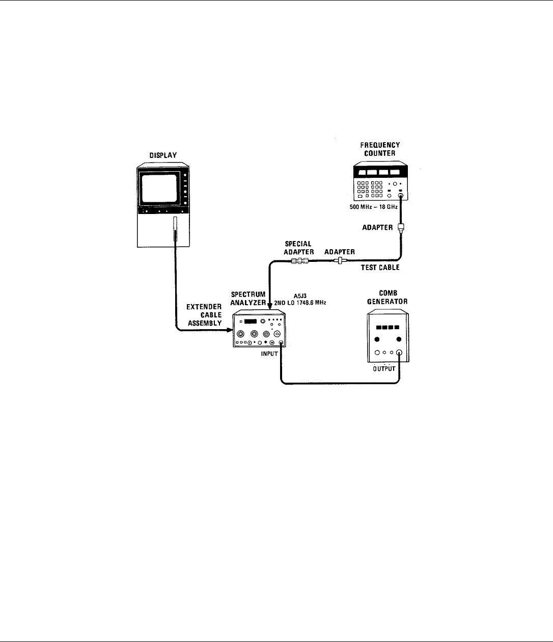
Model 8558B TM 11-6625-3061-14
ADJUSTMENTS
5-17. SECOND CONVERTER LO AND BANDPASS ADJUSTMENTS
REFERENCE
A5 Schematic
DESCRIPTION
The second converter is adjusted for 1748.60 MHz and the bandpass filter is adjusted for a 2050 MHz Bandpass.
Figure 5-1. Second Converter LO and Bandpass Adjustment Test Setup
EQUIPMENT
Frequency Counter.................................................................................................................... HP 5342A
Comb Generator ....................................................................................................................... HP 8406A
Test Cable, SMC (f) to BNC (m)...................................................................................... HP 11592-60001
Adapter, SMC (m) to SMC (m)............................................................................................HP 1250-0827
Adapter, Type N (m) to BNC (f)...........................................................................................HP 1250-0780
Special Adapter.................................................................................................................. See Figure 5-2
BNC Cable 120 cm (48 in) .......................................................................................................HP 10503A
Extender Cable Assembly ...................................................................................................HP 5060-0303
Additional Equipment, Options 001 and 002:
Minimum Loss Adapter, 75Ω to 50Ω................................................................................ HP 08558-60031
Adapter, BNC (m) to BNC (m), 75Ω....................................................................................HP 1250-1288
Adapter, SMA (f) to SMA (f) ................................................................................................HP 1250-1158
Adapter, BNC(f) to SMA (m)................................................................................................HP 1250-1200
5-12
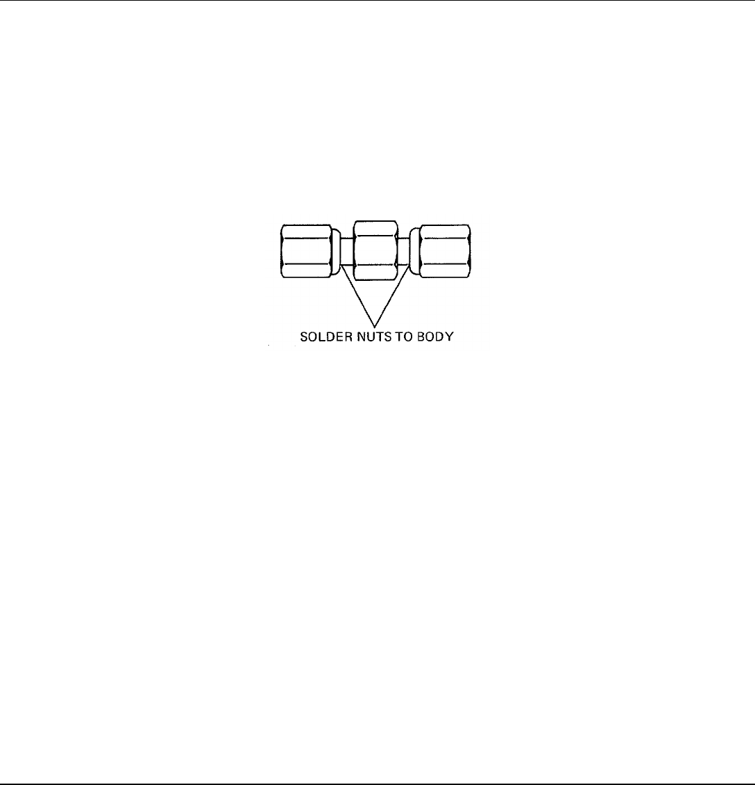
Model 8558B TM 11-6625-3061-14
ADJUSTMENTS
5-17. SECOND CONVERTER LO AND BANDPASS ADJUSTMENTS (Cont'd)
NOTE
The special adapter in Figure 5-1 is made from a SMC (f) to SMC (f) adapter, HP Part No. 1250-
1113. The nuts must be soldered to the body of the subminiature RF adapter so they will both
turn with the body. Be sure to space the nuts properly before soldering (see Figure 5-2).
MAXIMUM SPACE
⇐(PULL NUT TO END⇒
OF BODY, BOTH SIDES)
Figure 5-2. Special Adapter Used in Second Converter LO and Bandpass Test Setup
PROCEDURE
1. Set equipment as follows:
Spectrum Analyzer
START - CENTER ......................................................................................................................CENTER
TUNING...................................................................................................................................... 300 MHz
FREQ SPAN/DIV ........................................................................................................................ 100 MHz
RESOLUTION BW......................................................................................................... 1 MHz (optimum)
INPUT ATTEN ................................................................................................................................... 0 dB
REFERENCE LEVEL...................................................................................................................-30 dBm
002: +20dBmV
Amplitude Scale........................................................................................................................ 10 dB/DIV
SWEEP TIME/DIV ...........................................................................................................................AUTO
SWEEP TRIGGER ................................................................................................................. FREE RUN
Frequency Counter
10 Hz-500 MHz/500 MHz- 18 GHz ................................................................................ 500 MHz- 18 GHz
SAMPLE RATE........................................................................................................ Full counterclockwise
Comb Generator
COMB FREQUENCY..................................................................................................................... 100MC
INTERPOLATION AMPLITUDE......................................................................................................... OFF
5-13

Model 8558B TM 11-6625-3061-14
ADJUSTMENTS
5-17. SECOND CONVERTER LO AND BANDPASS ADJUSTMENTS (Cont'd)
2. Connect equipment as shown in Figure 5-1 and switch display mainframe power ON. Connect counter to A5J3
at the top of A5 Converter Assembly. Connect comb generator to HP 8558B INPUT.
3. Adjust second LO FREQUENCY adjustment A5Z4 for 1748.60 40.2 MHz. Use Allen wrench through center of
drilled-out 5/16-inch nut driver to enable nut to be tightened without shifting frequency.
4. Set comb generator for 100 MHz comb.
5. Center a 100 MHz comb tooth using 8558B TUNING control. Turn FREQ SPAN/DIV control to 2 MHz and
uncoupled RESOLUTION BW control to 300 kHz, keeping comb tooth centered on display.
6. Loosen lock nut on A5Z1 and A5Z2. Carefully turn tuning screws clockwise until they bottom on cavity.
7. Turn A5Z1 and A5Z2 one turn counterclockwise and lightly tighten lock nuts.
8. Loosen lock nut on A5Z3, and adjust A5Z3 for peak signal on display. Make final adjustment with Amplitude
Scale switch in LIN position. It might be necessary to increase gain to see signal in linear mode. Leave in LIN
position.
9. Adjust A5Z1 for peak signal on display. Reduce REFERENCE LEVEL as necessary to keep signal on display.
Repeat A5Z1 and A5Z3 adjustments for maximum signal on display.
10. Adjust A5Z2 for maximum signal on display. Reduce REFERENCE LEVEL as necessary to keep signal on
display.
11. Carefully tighten lock nuts on A5Z1, A5Z2, and A5Z3 so that signal does not change on display.
12. Adjust A5L2 2nd MIXER MATCH adjustment for maximum signal.
13. Check second LO frequency. If frequency error is greater than 4i0.5 MHz, repeat step 3.
5-14
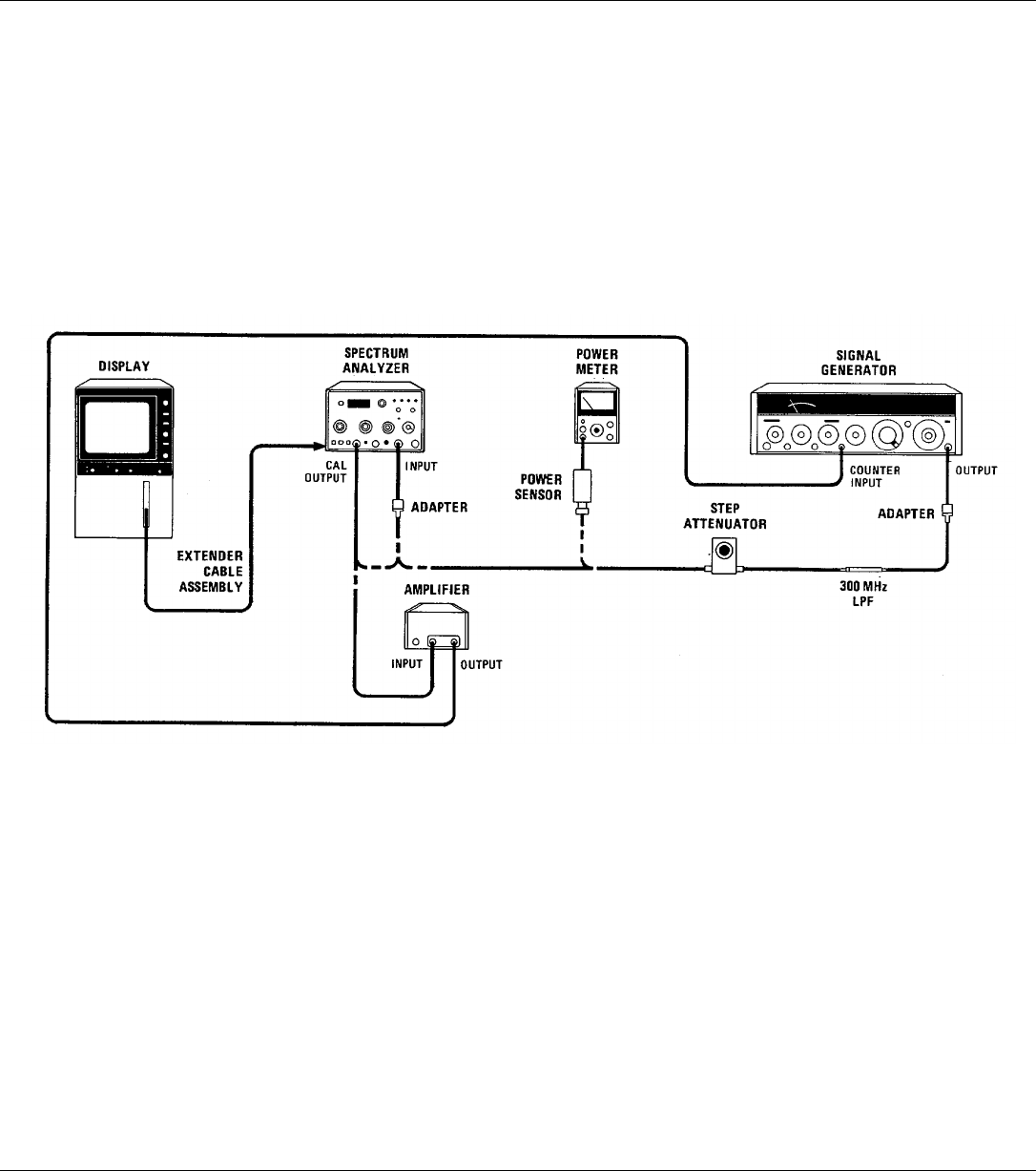
Model 8558B TM 11-6625-3061-14
ADJUSTMENTS
5-18. THIRD CONVERTER LO AND CAL OUTPUT ADJUSTMENT
REFERENCE
A9 Schematic
DESCRIPTION
The third converter LO frequency is adjusted for maximum output, and power is adjusted for -30 dBm ±1.0 dB CAL
OUTPUT. The third LO frequency is checked for 280 MHz ±300 kHz.
002: +20 dBmV ±1.0dB
Figure 5-3. Third Converter LO and CAL OUTPUT Adjustment Test Setup
EQUIPMENT Amplifier ................................................................................................................................... HP 8447A
Power Meter................................................................................................................................ HP 435B
Power Sensor............................................................................................................................ HP 8482A
Signal Generator....................................................................................................................... HP 8640B
10 dB Step Attenuator (calibrated at 280 MHz)........................................................... HP 355D, Opt. H82
300 MHz LPF...........................................................................................................Telonic TLP 300-4AB
Adapter, Type N (m) to BNC (f) (2 required)........................................................................HP 1250-0780
Additional Equipment, Options 001 and 002:
Power Sensor, 75Ω, HP 8483A
Minimum Loss Adapter, 75Ω to 50Ω................................................................................ HP 08558-60031
Adapter, BNC(m) to BNC(m), 75Ω......................................................................................HP 1250-1288
BNC Cable, 30 cm (12 in), 75Ω....................................................................................... HP 11652-60012
5-15

Model 8558B TM 11-6625-3061-14
ADJUSTMENTS
5-18. THIRD CONVERTER LO AND CAL OUTPUT ADJUSTMENT (Cont'd)
PROCEDURE
1. Set equipment as follows:
START- CENTER .......................................................................................................................CENTER
TUNING...................................................................................................................................... 280 MHz
FREQ SPAN/DIV ..........................................................................................................................500 kHz
RESOLUTION BW.......................................................................................................................... 1 MHz
INPUT ATTEN ................................................................................................................................. 10 dB
REFERENCE LEVEL dBm................................................................................................................... -20
002: + 30 dBm V
Amplitude Scale...................................................................................................................................LIN
SWEEP TIME/DIV ...........................................................................................................................AUTO
Extender Cable Assembly ...................................................................................................HP 5060-0303
Signal Generator:
OUTPUT LEVEL........................................................................................................................ + 10 dBm
FREQUENCY ............................................................................................................................. 280 MHz
AM .................................................................................................................................................... OFF
FM .................................................................................................................................................... OFF
RF ......................................................................................................................................................ON
COUNTER MODE................................................................................................................................INT
2. Connect equipment as shown in Figure 5-3. Connect CAL OUTPUT to INPUT 50( connector.
001 and 002: 75Ω
3. Center the 280 MHz signal on the display.
4. Adjust A9L4 third converter LO FREQ adjustment for maximum signal amplitude.
5. Tune signal generator to frequency of third converter LO (280 MHz ±300 kHz).
6. Connect signal generator through 300 MHz LPF to calibrated step attenuator. Set step attenuator to 10 dB.
7. Connect power sensor and power meter to step attenuator as shown in Figure 5-3.
8. Set signal generator OUTPUT LEVEL for a 0 dBm full scale reading on power meter. Leave signal generator set
at this level.
001: +5.7 dBm
002: + 7.0
9. Set step attenuator to 40 dB and connect the reference signal set in step 8 (from signal generator through step
attenuator) to the 8558B INPUT 50Ω connector.
001 and 002: INPUT 75Ω connector using Minimum Loss Adapter and 75Ω BNC Cable.
5-16

Model 8558B TM 11-6625-3061-14
ADJUSTMENTS
5-18. THIRD CONVERTER LO AND CAL OUTPUT ADJUSTMENT (Cont'd)
10. Set signal from signal generator to a convenient reference level on display with REFERENCE LEVEL and REF
LEVEL FINE controls.
11. Disconnect signal generator and connect spectrum analyzer CAL OUTPUT to the INPUT 500 connector.
001 and 002: 75Ω
12. Adjust A9R5 3RD LO PWR adjustment, accessible from bottom of analyzer through motherboard, to the
reference set in step 10. (If range is insufficient on A9R5, change value of factory-selected resistor A9R4*.)
13. Connect CAL OUTPUT to amplifier input and connect amplifier output to COUNTER INPUT of 8640B. Set HP
8640B COUNTER MODE to EXT EXPAND X10. The third LO frequency should read 280 MHz ±300 kHz.
5-17
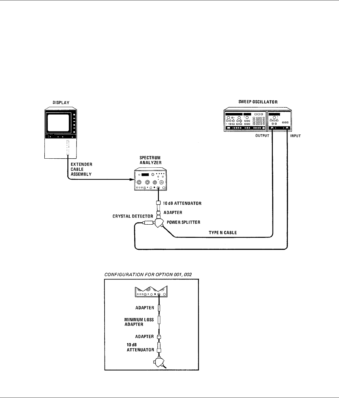
Model 8558B TM 11-6625-3061-14
ADJUSTMENTS
5-19. SLOPE ADJUSTMENT
REFERENCE
A9 Schematic
DESCRIPTION
An externally leveled signal is applied to the INPUT of the spectrum analyzer. The signal is adjusted across the
frequency range of the spectrum analyzer. A9R1 SLOPE COMP is adjusted for best flatness, compensating for first
converter conversion loss over frequency.
Figure 5-4. Slope Adjustment Test Setup
5-18

Model 8558B TM 11-6625-3061-14
ADJUSTMENTS
5-19. SLOPE ADJUSTMENT (Cont'd)
EQUIPMENT
Sweep Oscillator*...................................................................................................................... HP 8350A
RF Plug-In* ..............................................................................................................................HP 83522A
Power Splitter...........................................................................................................................HP 11667A
Crystal Detector .......................................................................................................................... HP 423B
10-dB Attenuator........................................................................................................HP 8491B Opt. 010
Adapter, Type N (m) to Type N (m).....................................................................................HP 1250-1475
BNC Cable, 120 cm (48 in) ......................................................................................................HP 10503A
Type N Cable...........................................................................................................................HP 11500A
Extender Cable Assembly ...................................................................................................HP 5060-0303
*8620C/86222A may be substituted
Additional Equipment, Options 001 and 002:
Minimum Loss Adapter, 752 to 50Ω................................................................................ HP 08558-60031
Adapter, BNC(m) to BNC (m), 75Ω.....................................................................................HP 1250-1288
Adapter, Type N (m) to SMA (f)...........................................................................................HP 1250-1250
PROCEDURE
1. Set equipment as follows:
Spectrum Analyzer
START - CENTER ......................................................................................................................CENTER
TUNING...................................................................................................................................... 500 MHz
FREQ SPAN/DIV ........................................................................................................................ 100 MHz
RESOLUTION BW.......................................................................................................................... 1 MHz
INPUT ATTEN ................................................................................................................................. 10 dB
REFERENCE LEVEL...................................................................................................................-10 dBm
002: +40dBmV
REF LEVEL FINE ................................................................................................................................... 0
Amplitude Scale.......................................................................................................................... 1 dB/DIV
SWEEP TIME/DIV ...........................................................................................................................AUTO
BASELINE CLIPPER ......................................................................................................................... OFF
VIDEO FILTER .................................................................................................................................. OFF
Sweep Oscillator
START.......................................................................................................................................... 10 MHz
STOP........................................................................................................................................... 1.5 GHz
SWEEP .............................................................................................................................................MAN
POWER LEVEL.............................................................................................................................. 0 dBm
ALC MODE.........................................................................................................................................EXT
FREQUENCY/TIME.................................................................................................................... 500 MHz
2. Connect equipment as shown in Figure 5-4.
5-19

Model 8558B TM 11-6625-3061-14
ADJUSTMENTS
5-19. SLOPE ADJUSTMENT (Cont'd)
3. Adjust spectrum analyzer REF LEVEL FINE to bring signal peak on display.
4. Set spectrum analyzer START - CENTER to CENTER. Manually tune sweep oscillator for output frequencies
from 10 MHz to 1.0 GHz. Set spectrum analyzer START - CENTER to START. Manually tune sweep oscillator
for output frequencies from 1.0 GHz to 1.5 GHz.
5. Using procedure of step 4, locate highest displayed amplitude. Adjust spectrum analyzer REF LEVEL FINE to
bring highest displayed amplitude to fifth CRT graticule line from bottom.
6. Using procedure of step 4, locate lowest displayed amplitude.
7. Adjust spectrum analyzer A9R1 SLOPE COMP for minimum difference between highest and lowest displayed
amplitudes.
8. Repeat steps 5, 6, and 7 until no further adjustment is necessary.
9. With highest displayed amplitude set to fifth graticule line from bottom lowest displayed amplitude should be at
or above third graticule line from bottom.
5-20
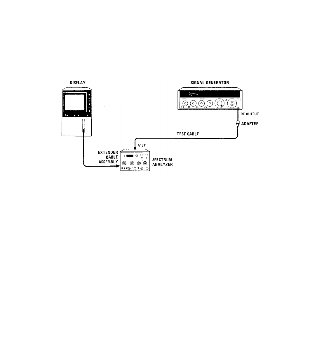
Model 8558B TM 11-6625-3061-14
ADJUSTMENTS
5-20. SECOND IF BANDPASS AMPLIFIER AND BANDPASS FILTER ADJUSTMENT
REFERENCE
A10 Schematic
DESCRIPTION
Tune bandpass amplifier output and bandpass filter.
Figure 5-5. Second IF Bandpass Amplifier and Bandpass Filter Adjustment Test Setup
EQUIPMENT
Signal Generator....................................................................................................................... HP 8640B
Adapter, Type N (m) to BNC (f)...........................................................................................HP 1250-0780
Test Cable, SMC (f) to BNC (m)...................................................................................... HP 11592-60001
Extender Cable Assembly ...................................................................................................HP 5060-0303
PROCEDURE
1. Set spectrum analyzer controls as follows:
FREQ SPAN/DIV ........................................................................................................................ 100 MHz
RESOLUTION................................................................................................................................. 1 MHz
INPUT ATTEN ................................................................................................................................... 0 dB
REFERENCE LEVEL..................................................................................................................- 10 dBm
002: +40 dBmV
Amplitude Scale........................................................................................................................ 10 dB/DIV
SWEEP TIME/DIV ...........................................................................................................................AUTO
SWEEP TRIGGER ................................................................................................................. FREE RUN
2. Set signal generator frequency to 301.4 MHz and set output level to approximately - 35 dBm.
5-21

Model 8558B TM 11-6625-3061-14
ADJUSTMENTS
5-20. SECOND IF BANDPASS AMPLIFIER AND BANDPASS FILTER ADJUSTMENT (Cont'd)
NOTE
If 8640B is not used, adjust the signal generator for maximum signal on the display in step 3.
3. Remove W6P2 from Second IF A10J1. Connect signal generator through test cable to A10J1 as shown in
Figure 5-5.
4. Adjust bandpass filter capacitors A10C1, A10C2, and A10C3 on Second IF Assembly fully counterclockwise.
Adjust REFERENCE LEVEL if necessary for an on-screen display.
5. Adjust A10C1 for maximum signal amplitude. Make final adjustment with Amplitude Scale switch in LIN position.
Leave switch in LIN position. Use REFERENCE LEVEL and REF LEVEL FINE controls to keep signal on top
half of display.
6. Adjust A10C3 for maximum signal amplitude. There may be a double peak; tune past first peak to second peak.
Signal on display will peak and fall off slightly and then peak again.
7. Repeat steps 5 and 6 adjusting A10C1 and A10C3 for maximum amplitude.
8. Adjust A10C2 for maximum signal amplitude. There may be a double peak; tune to second peak. Reduce input
signal level to keep signal on display.
NOTE
The following adjustment of A10L2 has very little effect on the signal or performance of the
spectrum analyzer. A10L2 need not be adjusted because the position of the core is not critical.
9. Adjust A10L2 2ND IF TUNING adjustment for maximum signal amplitude. L2 is adjusted through motherboard
on bottom of analyzer. Reconnect W6P2 to A10J1.
5-22
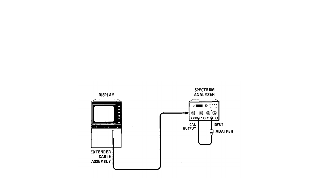
Model 8558B TM 11-6625-3061-14
ADJUSTMENTS
5-21. CRYSTAL AND LC BANDWIDTH FILTER ADJUSTMENTS
REFERENCE
A8, A11, and A13 Schematics
DESCRIPTION
The crystal and LC bandwidth filter circuits are adjusted for symmetry, center, and peak. Three-dB bandwidths are
adjusted on the Sweep Generator Assembly A8 (paragraph 5-22).
Figure 5-6. Crystal and LC Bandwidth Filter Adjustment Test Setup
EQUIPMENT
Adapter, Type N (m) to BNC (f)...........................................................................................HP 1250-0780
BNC Cable, 20 cm (9 in) ..........................................................................................................HP 10502A
Crystal Short (3 Required)................................................................................................. See Figure 5-7.
Extender Cable Assembly ...................................................................................................HP 5060-0303
Additional Equipment, Options 001 and 002:
BNC Cable, 30 cm (12 in), 75Ω................................................................................. HP 11652-60012
NOTE
A crystal short consists of a .01 µF capacitor (HP Part No. 0160-0161) and a 90.9 ohm resistor (HP
Part No. 0757-0400) connected in series. Two square-terminal connectors (HP Part No. 0362-
0265) are used to connect the crystal short across the test points.
5-23
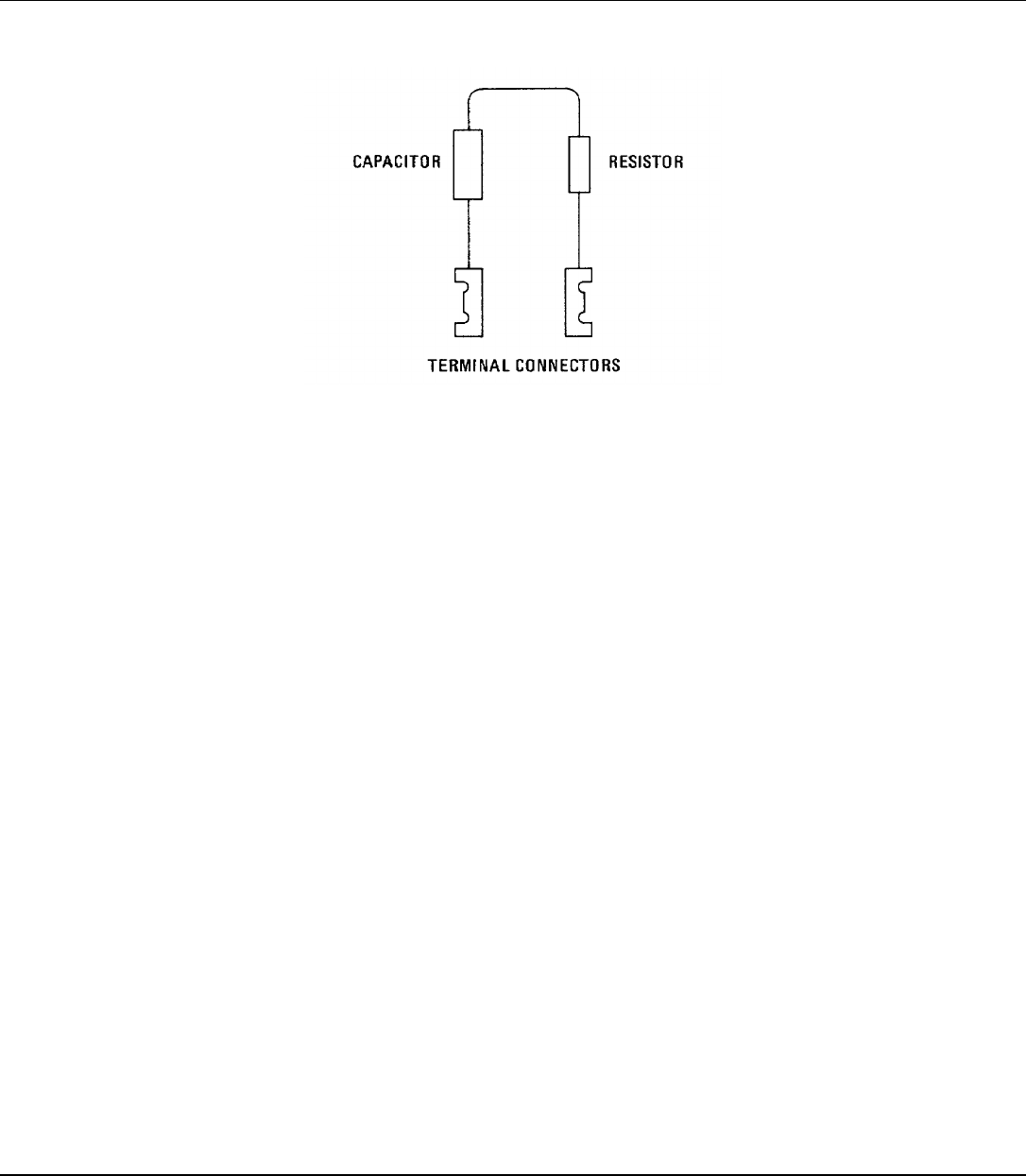
Model 8558B TM 11-6625-3061-14
ADJUSTMENTS
5-21. CRYSTAL AND LC BANDWIDTH FILTER ADJUSTMENTS (Cont'd)
Figure 5-7. Crystal Short Configuration
PROCEDURE
NOTE
Allow 30 minutes warmup time before performing adjustments.
1. Set spectrum analyzer controls as follows:
START- CENTER .......................................................................................................................CENTER
TUNING...................................................................................................................................... 280 MHz
FREQ SPAN/DIV ............................................................................................................................. 5 kHz
RESOLUTION BW........................................................................................................................... 1 kHz
INPUT ATTEN ................................................................................................................................... 0 dB
REFERENCE LEVEL...................................................................................................................-20 dBm
002: + 30 dBmV
Amplitude Scale...................................................................................................................................LIN
SWEEP TIME/DIV ..................................................................................................................... 10 mSEC
SWEEP TRIGGER ................................................................................................................. FREE RUN
Crystal Alignment
2. Connect equipment as shown in Figure 5-6.
NOTE
If A8 Sweep Generator has been replaced or adjusted, perform steps 3 through 9. If not, proceed
to step 10.
3. Set FREQ SPAN/DIV to 500 kHz and RESOLUTION BW to 1 MHz.
4. Center the signal with TUNING control. Using REF LEVEL FINE control, place signal at 7.1 divisions (0.9
division from top graticule line).
5-24
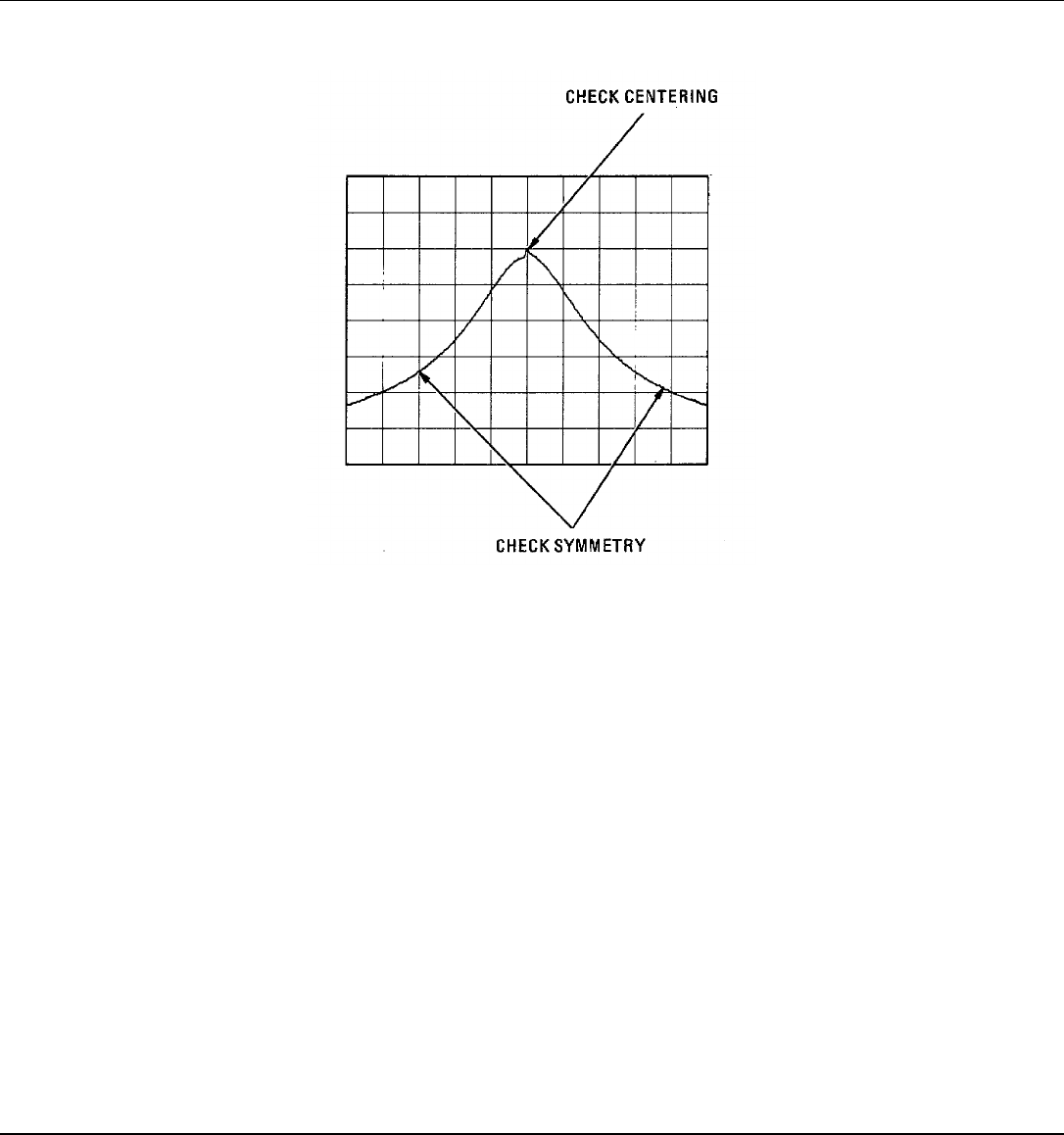
Model 8558B TM 11-6625-3061-14
ADJUSTMENTS
5-21. CRYSTAL AND LC BANDWIDTH FILTER ADJUSTMENTS (Cont'd)
Figure 5-8. Adjusting Crystal Symmetry and Crystal Centering
5. Adjust A8R85 LC until signal is two divisions wide at the fifth graticule line (1 MH4z. wide at; 3-dB points).
6. Set FREQ SPAN/DIV to 5 kHz and RESOLUTION BW to 10 kHz.
7. Using REF LEVEL FINE control, place signal at 7.1 divisions.
8. Adjust A8R72 XTL until signal is two divisions wide- at the fifth graticule line (10 kHz wide at 3-dB points).
9. Set FREQ SPAN/DIV to 5 kHz and RESOLUTION BW to 1 kHz.
10. Center signal with TUNING control. (It might be necessary to increase FREQ SPAN/DIV temporarily to find the
signal.) Set REF LEVEL FINE control to place signal at sixth graticule line.
11. Set FREQ SPAN/DIV to 20 kHz and RESOLUTION BW to 30 kHz.
NOTE
A non-metallic tuning tool is required for adjustments on the Al1 and A13 bandwidth filter
assemblies.
12. Connect crystal shorts (through cover access holes) across A13TP1/TP2, A11TP1/TP2, and A11TP4/TP5.
5-25

Model 8558B TM 11-6625-3061-14
ADJUSTMENTS
5-21. CRYSTAL AND LC BANDWIDTH FILTER ADJUSTMENTS (Co nt'd)
NOTE
Keep crystal spike centered during adjustments. The SYM and CTR adjustments for each crystal
interact.
13. Adjust front-panel TUNING control to center bandpass spike (Figure 5-8) on the CRT display.
14. Adjust A13C38 SYM and A13C54 CTR for a centered and symmetrical bandpass as shown in Figure 5-8. Adjust
A13C54 CTR for minimum signal amplitude.
15. Remove crystal short from A13TP1/TP2 and connect it across A13TP4/TP5.
16. Adjust A13C15 SYM and A13C25 CTR for a centered and symmetrical bandpass. Adjust A13C25 CTR for
minimum signal amplitude.
17. Remove crystal short from A11TP4/TP5 and connect it across A13TP1/TP2.
18. Adjust A11C38 SYM and A11C54 CTR for a centered and symmetrical bandpass. Adjust A11C54 CTR for
minimum signal amplitude.
19. Remove crystal short from A11TP1/TP2 and connect it across A11TP4/TP5.
20. Adjust A11C15 SYM and A11C25 CTR for a centered and symmetrical bandpass. Adjust A11C25 CTR for
minimum signal amplitude.
21. Remove the crystal shorts.
LC Alignment
22. Perform preliminary LC filter adjustments as follows:
a. Install A13 on extender board. Set RESOLUTION BW control to 100 kHz.
b. Short to ground the following test points: A13TP6, A11TP3, and A11TP6. Jumper A8TP1 to A8TP2.
c. Adjust A13C73 for minimum signal amplitude.
d. Disconnect short from A13TP6 and short to ground A13TP3.
e. Adjust A13C74 for minimum signal amplitude.
f. Reinstall A13 and install A11 on extender board.
g. Disconnect short from A11TP3 and short to ground A13TP6.
h.Adjust A11C73 for minimum signal amplitude.
i. Disconnect short from A11TP6 and short to ground A11TP3.
5-26

Model 8558B TM 11-6625-3061-14
ADJUSTMENTS
5-21. CRYSTAL AND LC BANDWIDTH FILTER ADJUSTMENTS (Cont'd)
j. Adjust A11C74 for minimum signal amplitude.
k. Disconnect shorts from test points and reinstall A11. Replace covers on A11 and A13 assemblies. Remove
jumper from A8TP1/A8TP2.
NOTE
When A11 and A13 BW Filter Assemblies are installed with covers in place, midget copper
alligator clips (HP Part No. 1400-0483) can be used to short test points to the cover.
23. Carefully center signal on CRT in 30 kHz RESOLUTION BW; then switch RESOLUTION BW to 100 kHz. Note
where signal intersects the center vertical graticule line.
24. Adjust A13C45 LC CTR for maximum signal amplitude where the signal intersects the center vertical graticule
line.
25. Switch RESOLUTION BW to 30 kHz and center signal; then switch to 100 kHz. Note where signal intersects the
center vertical graticule line.
26. Adjust A13C23 LC CTR for maximum signal amplitude where the signal intersects the center vertical graticule
line.
27. Switch RESOLUTION BW to 30 KHz and center signal; then switch to 100 kHz. Note where signal intersects the
center vertical graticule line.
28. Adjust A11C45 LC CTR for maximum signal amplitude where the signal intersects the center vertical graticule
line.
29. Switch RESOLUTION BW to 30 kHz and center signal; then switch to 100 kHz. Note where signal intersects the
center vertical graticule line.
30. Adjust A11C23 LC CTR for maximum signal amplitude where the signal intersects the center vertical graticule
line.
31. Switch RESOLUTION BW between 100 kHz and 30 kHz to be sure the signal is centered at both bandwidth
settings.
32. Set FREQ SPAN/DIV to 5 kHz and RESOLUTION BW to 1 kHz. Center signal with TUNING control.
Bandwidth Amplitude
33. Set A11R31 XTL and A13R31 XTL fully counterclockwise.
34. Set Amplitude Scale switch to 1 dB/DIV.
35. Jumper A8TP1 to A8TP2. Short A11TP3, A11TP6, A13TP3, and A13TP6 to ground.
5-27

Model 8558B TM 11-6625-3061-14
ADJUSTMENTS
5-21. CRYSTAL AND LC BANDWIDTH FILTER ADJUSTMENTS (Cont'd)
36. Set RESOLUTION BW to 1 MHz and FREQ SPAN/DIV to 50 kHz.
37. Adjust fine TUNING and REF LEVEL FINE for a centered signal at 7 divisions.
38. Remove shorts from A13TP3 and A13TP6 and center signal with fine TUNING control. Adjust A13R26 LC for a
signal amplitude of 7 divisions.
39. Remove shorts from Al1TP3 and Al1TP6. Adjust A11R26 LC for a signal amplitude of 7 divisions.
40. Repeat steps 35 through 39 until no further adjustment is necessary.
41. Set RESOLUTION BW to 1 kHz and FREQ SPAN/DIV to 5 kHz. Center signal with fine TUNING control. Adjust
A11 R31 XTL and Al3R31 XTL equally for a signal amplitude of 7 divisions.
NOTE
Each potentiometer should be adjusted to accomplish half the necessary increase in signal
amplitude.
42. Remove jumper from A8TP1 and A8TP2.
43. Set FREQ SPAN/DIV to 100 MHz and RESOLUTION BW to 3 MHz and push in to couple the two controls.
44. Turn coupled controls to set FREQ SPAN/DIV to 50 MHz and RESOLUTION BW to 1 MHz. Center signal with
TUNING control. Adjust REF LEVEL FINE for a signal amplitude of 7 divisions.
45. With controls coupled, step down RESOLUTION BW from 1 MHz to 300 kHz. Variation in signal amplitude
should be less than ±0.4 dB.
46. Step down RESOLUTION BW from 100 kHz to 1 kHz. Variation of signal amplitude should be less than ±0.5 dB.
47. Repeat steps 35 through 46 until variation in signal amplitude is within limits.
5-28
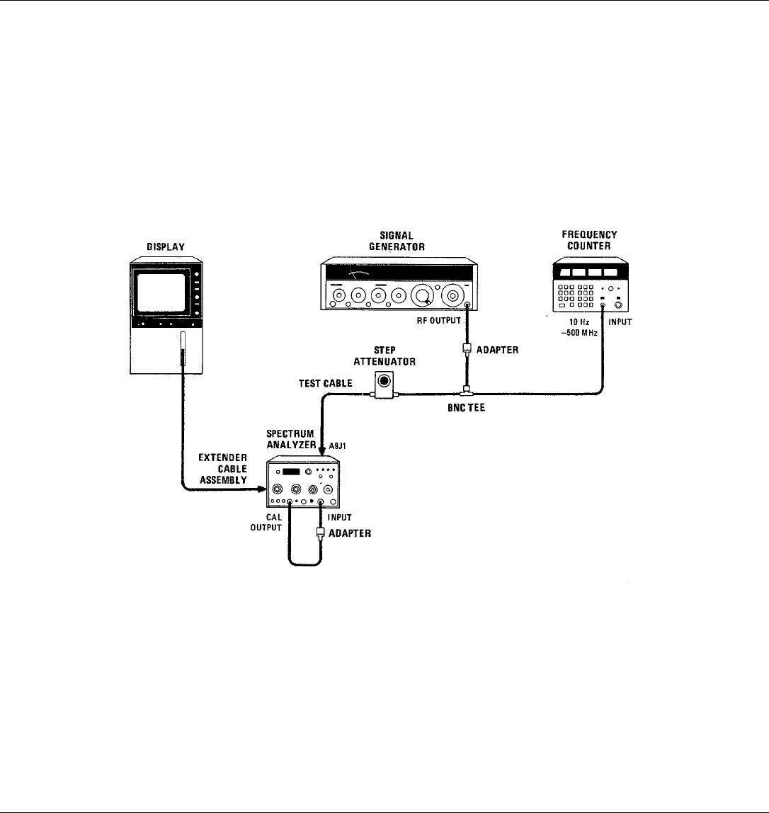
Model 8558B TM 11-6625-3061-14
ADJUSTMENTS
5-22. 3-dB BANDWIDTH ADJUSTMENT
REFERENCE
A8 Schematic
DESCRIPTION
The 3-dB bandwidths for the 3 MHz, 1 MHz and 300 kHz RESOLUTION BW settings are adjusted using the CAL
OUTPUT as the signal source. The 3-dB bandwidths for the 10 kHz, 3 kHz, and 1 kHz RESOLUTION BW settings are
adjusted by injecting a stable 301.4 MHz signal into the third converter of the spectrum analyzer.
Figure 5-9. 3-dB Bandwidth Adjustment Test Setup
EQUIPMENT
Signal Generator....................................................................................................................... HP 8640B
Frequency Counter.................................................................................................................... HP 5343A
10 dB Step Attenuator................................................................................................................. HP 355D
BNC Cable, 20 cm (9 in) ..........................................................................................................HP 10502A
Adapter, Type N (m) to BNC (f) (3 requird)..........................................................................HP 1250-0780
BNC Tee.............................................................................................................................HP 1250-0781
Test Cable, SMC (f) to BNC (m)...................................................................................... HP 11592-60001
Extender Cable Assembly ...................................................................................................HP 5060-0303
5-29

Model 8558B TM 11-6625-3061-14
ADJUSTMENTS
5-22. 3-dB BANDWIDTH ADJUSTMENT (Cont'd)
PROCEDURE
1. Set spectrum analyzer controls as follows:
START - CENTER ......................................................................................................................CENTER
TUNING...................................................................................................................................... 280 MHz
FREQ SPAN/DIV ..........................................................................................................................200 kHz
RESOLUTION BW.......................................................................................................................... 1 MHz
INPUT ATTEN ................................................................................................................................... 0 dB
REFERENCE LEVEL...................................................................................................................-20 dBm
Amplitude Scale...................................................................................................................................LIN
SWEEP TIME/DIV ....................................................................................................................... 1 mSEC
SWEEP TRIGGER ................................................................................................................. FREE RUN
VIDEO FILTER .................................................................................................................................. OFF
2. Connect equipment as shown in Figure 5-9 except for signal input to A9J1. Connect CAL OUTPUT to spectrum
analyzer INPUT 50(.
3. Set signal level of 7.1 divisions on display with REF LEVEL FINE control. (Signal should be 0.9 division from top
graticule line.)
4. Set RESOLUTION BW to 1 MHz and FREQ SPAN/DIV to 200 kHz. Adjust A8R85 LC to set bandwidth of 5
divisions at the fifth graticule line.
5. Set RESOLUTION BW to 3 MHz and FREQ SPAN/DIV to 500 kHz. The bandwidth at the fifth graticule line
should be between 5.4 and 6.6 divisions.
NOTE
A8R85 LC may be further adjusted to bring the 3 MHz and 300 kHz bandwidths within limits;
however, the final measurement of the 1 MHz bandwidth must be between 4.5 and 5.5 divisions at
the fifth graticule line. (If the 3 MHz bandwidth cannot be brought within limits by adjustment of
A8R85 LC, change the value of factory-selected resistor A8R95*.)
6. Set RESOLUTION BW to 300 kHz and FREQ SPAN/DIV to 50 kHz. The bandwidth should be between 5.4 and
6.6 divisions at the fifth graticule line. (If the bandwidth cannot be adjusted within the specified limits, change the
value of factory-selected resistor A8R89*.)
7. Set RESOLUTION BW to 100 kHz and FREQ SPAN/DIV to 20 kHz. The bandwidth should be between 4.3 and
5.7 divisions at the fifth graticule line.
NOTE
If the 100 kHz bandwidth is not within the specified limits, change the values of factory-selected
resistors A13R19*, A13R43*, and A11R43*. If the bandwidth is too wide, increase the value of the
resistors; if the bandwidth is too narrow, decrease the value of the resistors. The three factory-
selected resistors need not be of equal value, but each must be within one standard value of the
others.
5-30

Model 8558B TM 11-6625-3061-14
ADJUSTMENTS
5-22. 3-dB BANDWIDTH ADJUSTMENT (Cont'd )
8. Set RESOLUTION BW to 30 kHz and FREQ SPAN/DIV to 5 kHz. The bandwidth should be between 5.2 and 6.8
divisions at the fifth graticule line.
NOTE
If the 30 kHz bandwidth is not within the specified limits, change the values of factory-selected
resistors A11R23*, A11R48*, A13R23*, and A13R48*. If the bandwidth is too wide, decrease the
value of the factory selected resistors; if the bandwidth is too narrow, increase the value of the
resistors. The four factory-selected resistors need not be of equal value, but each must be within
one standard value of the others.
9. Connect signal generator through the BNC Tee connector to the step attenuator and to the frequency counter as
shown in Figure 5-9. Set the signal generator to approximately 0 dBm and the step attenuator to 30 dB. Set
COUNTER MODE to EXPAND X100.
10. Remove W7P2 from Third Converter A9J1. Connect step attenuator through test cable to A9J1.
11. Set HP 8558B RESOLUTION BW to 1 MHz. Tune signal generator to peak signal on CRT display (near 301.4
MHz). Adjust the output level of signal generator to place the signal at 7.1 divisions.
12. Set RESOLUTION BW to 3 kHz. Tune signal generator to peak signal on CRT display.
13. Adjust REF LEVEL FINE to place signal at 7.1 divisions.
14. Note the counter frequency and tune the signal generator 1500 Hz below the center frequency noted. Record the
new counter frequency.
15. Adjust A8R72 XTL to bring signal level to the fifth graticule line (three divisions from the top graticule line).
16. Increase signal generator frequency until signal on CRT display peaks and then decreases to the fifth graticule
line. Record counter frequency.
17. Compare new frequency with frequency recorded in step 14. The difference between the two frequencies should
be 2800 to 3200 Hz. If the bandwidth is not within limits, repeat steps 12 through 17, slightly readjusting A8R72
XTL, until the specified limits are achieved.
18. Set RESOLUTION BW to 10 kHz. Tune signal generator to peak signal on CRT display.
19. Adjust REF LEVEL FINE to place signal at 7.1 divisions.
20. Note the counter frequency and tune the signal generator 5 kHz below the center frequency noted. Record the
new counter frequency.
21. Increase the signal generator frequency until the signal on the CRT display peaks and then decreases to the fifth
graticule line. Record counter frequency.
22. Compare new frequency with frequency recorded in step 20. The difference between the two frequencies should
be 9.000 kHz to 11.000 kHz.
5-31

Model 8558B TM 11-6625-3061-14
ADJUSTMENTS
5-22. 3-dB BANDWIDTH ADJUSTMENT (Cont'd)
NOTE
A8R72 XTL may be further adjusted to bring the 10 kHz and 1 kHz bandwidths within limits;
however, the final measurement of the 3 kHz bandwidth must be between 2700 Hz and 3300 Hz.
(If the 10 kHz bandwidth cannot be brought within limits by adjustment of A8R72 XTL, change
the value of factory-selected resistor A8R78*.)
23. Set RESOLUTION BW to 1 kHz. Tune signal generator to peak signal on CRT display.
24. Adjust REF LEVEL FINE to place signal at 7.1 divisions.
25. Note the counter frequency. Increase signal generator frequency until signal on CRT display peaks and then
decreases to the fifth graticule line. Record new counter frequency.
26. Compare new frequency with frequency originally noted in step 25. The difference between the two frequencies
should be 450 Hz to 550 Hz.
27. Reconnect W7P2 to A9J1.
5-32
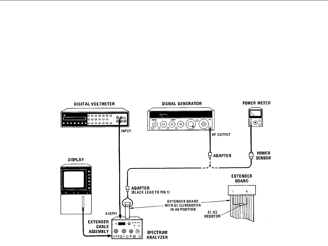
Model 8558B TM 11-6625-3061-14
ADJUSTMENTS
5-23. STEP GAIN ASSEMBLY RF GAIN ADJUSTMENT
REFERENCE
A12 Schematic
DESCRIPTION
The RF gain (sensitivity) of the Step Gain assembly is adjusted by injecting a 21.4 MHz signal at A16XA9. The Third
Converter Assembly A9 is removed and replaced with a special extender board for applying the 21.4 MHz signal from the
signal generator.
Figure 5-10. Step Gain Assembly RF Gain Adjustment Test Setup
EQUIPMENT
Signal Generator....................................................................................................................... HP 8640B
Digital Voltmeter ....................................................................................................................... HP 3455A
Power Meter................................................................................................................................ HP 435B
Power Sensor............................................................................................................................ HP 8482A
Adapter, BNC (f) to alligator clips ........................................................................................HP 8120-1292
Special Extender Board with 51.1-ohm resistor ..............................................HP 08505-60109/0757-0394
BNC Cable, 120 cm (48 in) ......................................................................................................HP 10503A
Extender Cable Assembly ...................................................................................................HP 5060-0303
NOTE
To make special extender board, solder 51.1 ohm resistor from pin 1 to pin 5 of standard
extender board, HP Part No. 5060-0257. Leave resistor leads long for easy connection of clip
leads.
5-33

Model 8558B TM 11-6625-3061-14
ADJUSTMENTS
5-23. STEP GAIN ASSEMBLY RF GAIN ADJUSTMENT (Cont'd)
PROCEDURE
1. Set equipment as follows:
Spectrum Analyzer
FREQ SPAN/DIV ............................................................................................................................ 1 MHz
RESOLUTION BW.......................................................................................................................... 1 MHz
INPUT ATTEN ................................................................................................................................. 10 dB
REFERENCE LEVEL...................................................................................................................... 0 dBm
002: + 50 dBmV
REF LEVEL FINE ................................................................................................................................... 0
Amplitude Scale...................................................................................................................................LIN
SWEEP TIME/DIV ...........................................................................................................................AUTO
SWEEP TRIGGER ................................................................................................................. FREE RUN
VIDEO FILTER .................................................................................................................................. OFF
Digital Voltmeter
RANGE............................................................................................................................................AUTO
FUNCTION ..................................................................................................................................DC Volts
TRIGGER ................................................................................................................................INTERNAL
MATH ................................................................................................................................................ OFF
AUTO CAL.:.........................................................................................................................................ON
2. Connect equipment as shown in Figure 5-10.
3. Set signal generator frequency to 21.4 MHz. Set OUTPUT LEVEL for approximately - 5 dBm.
4. Connect output of signal generator across 51.1 ohm resistor on special board using BNC to clip-lead adapter.
The red lead (center conductor) should be connected to pin 5 of extender board.
5. Set signal generator frequency for peak amplitude on CRT display. Connect output of signal generator to power
meter through power sensor and set OUTPUT LEVEL to - 1 dBm. Reconnect signal generator output to clip-lead
adapter.
001: -5 dBm
002: - 6 dBm
6. Adjust A12R4 GAIN adjustment for signal one division from top graticule line. DVM should indicate + 700 mV
±30 mV. Remove special extender board and replace Third Converter Assembly A9.
NOTE
Front panel VERTICAL GAIN and VERTICAL POSN control settings can affect the voltage
measured at A15TP1. Vertical calibration should be checked after adjusting A12R4 for 700 mV.
(Refer to Operator's Check, Section III).
5-34
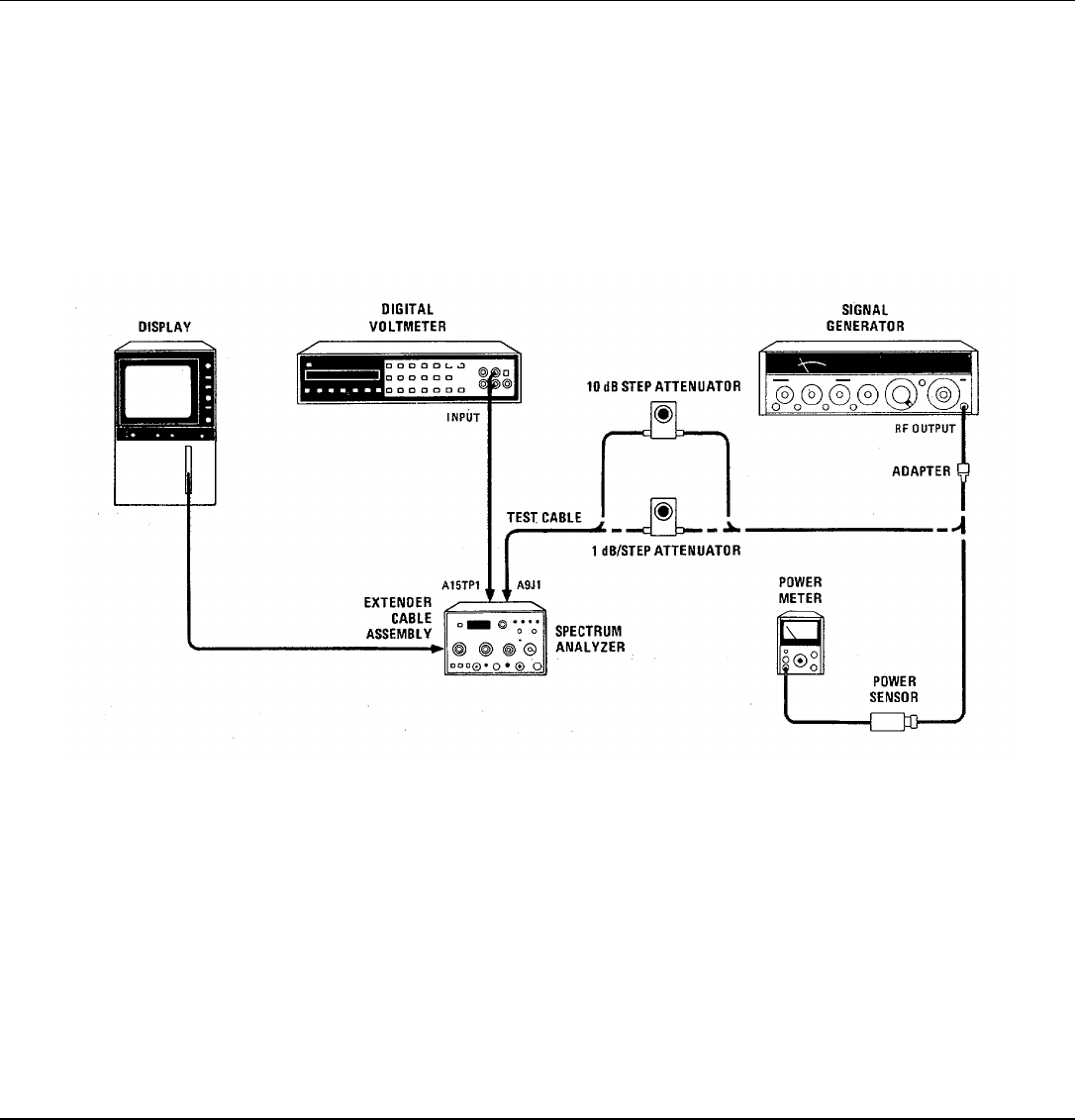
Model 8558B TM 11-6625-3061-14
ADJUSTMENTS
5-24. STEP AMPLIFIER GAIN ADJUSTMENTS
REFERENCE
A12 Schematic
DESCRIPTION
REF LEVEL FINE, 0 dB, and -12 dB adjustments are properly set and step gains of 10 dB, 20 dB, and 40 dB are
adjusted.
Figure 5-11. Step Amplifier Gain Adjustment Test Setup
EQUIPMENT
Signal Generator....................................................................................................................... HP 8640B
1-dB Step Attenuator................................................................................................... HP 355C Opt. H80
10-dB Step Attenuator................................................................................................. HP 355D Opt. H82
Digital Voltmeter ....................................................................................................................... HP 3455A
Power Meter................................................................................................................................ HP 435B
Power Sensor............................................................................................................................ HP 8482A
Adapter, Type N (m) to BNC (f)...........................................................................................HP 1250-0780
Test Cable, SMC (f) to BNC (m)...................................................................................... HP 11592-60001
Adapter, SMC (m) to SMC (m)............................................................................................HP 1250-0827
Extender Cable Assembly ...................................................................................................HP 5060-0303
5-35

Model 8558B TM 11-6625-3061-14
ADJUSTMENTS
5-24. STEP AMPLIFIER GAIN ADJUSTMENTS (Cont'd)
PROCEDURE
1. Set equipment as follows:
TUNING...................................................................................................................................... 280 MHz
FREQ SPAN/DIV ............................................................................................................................ 1 MHz
RESOLUTION BW.......................................................................................................................... 1 MHz
INPUT ATTEN ................................................................................................................................. 10 dB
REFERENCE LEVEL...................................................................................................................... 0 dBm
002: + 50 dBm V
Amplitude Scale.......................................................................................................................... 1 dB/DIV
SWEEP TIME/DIV ...........................................................................................................................AUTO
SWEEP TRIGGER ................................................................................................................. FREE RUN
VIDEO FILTER .................................................................................................................................. OFF
2. Connect equipment as shown in Figure 5-11. Connect signal generator tuned to 301.4 MHz with approximately -
13 dBm output to one side of a 1 dB/step attenuator. Connect attenuator output to A9J1 through test cable.
Tune signal generator frequency for peak amplitude on display.
3. Set step attenuator to 12 dB and REF LEVEL FINE to - 12. Set signal generator level for a signal one division
down from top graticule line.
4. Adjust A12R6 - 12 dB until signal stops rising on display, then adjust A12R6 counterclockwise until signal drops
approximately one third to one half of a division.
5. Set signal generator level so signal is one division down from top graticule line on display.
6. Set step attenuator to 0 dB and REF LEVEL FINE to 0.
7. Adjust A12R5 0 dB adjustment for a signal level one division from top graticule line.
8. Set step attenuator to 12 dB and REF LEVEL FINE to -12. Signal level on display should be ±0.1 division from
the reference one division down from top graticule line. If signal level is out of limits, repeat steps 3 through 8
until the signal level is within limits.
9. Check REF LEVEL FINE control from 0 to - 12 dBm, as shown in Table 5-5. Verify correct operation on display,
or measure voltage at A15TP1 with digital voltmeter.
NOTE
Be sure all covers in the IF section are secured by at least six screws before proceeding. If
covers are left off or not secured by at least six screws, leakage between assemblies may occur.
This leakage causes erroneous adjustment.
10. Replace 1 dB/step attenuator with 10 dB/step attenuator set to 0 dB. Set REF LEVEL FINE control to 0.
5-36
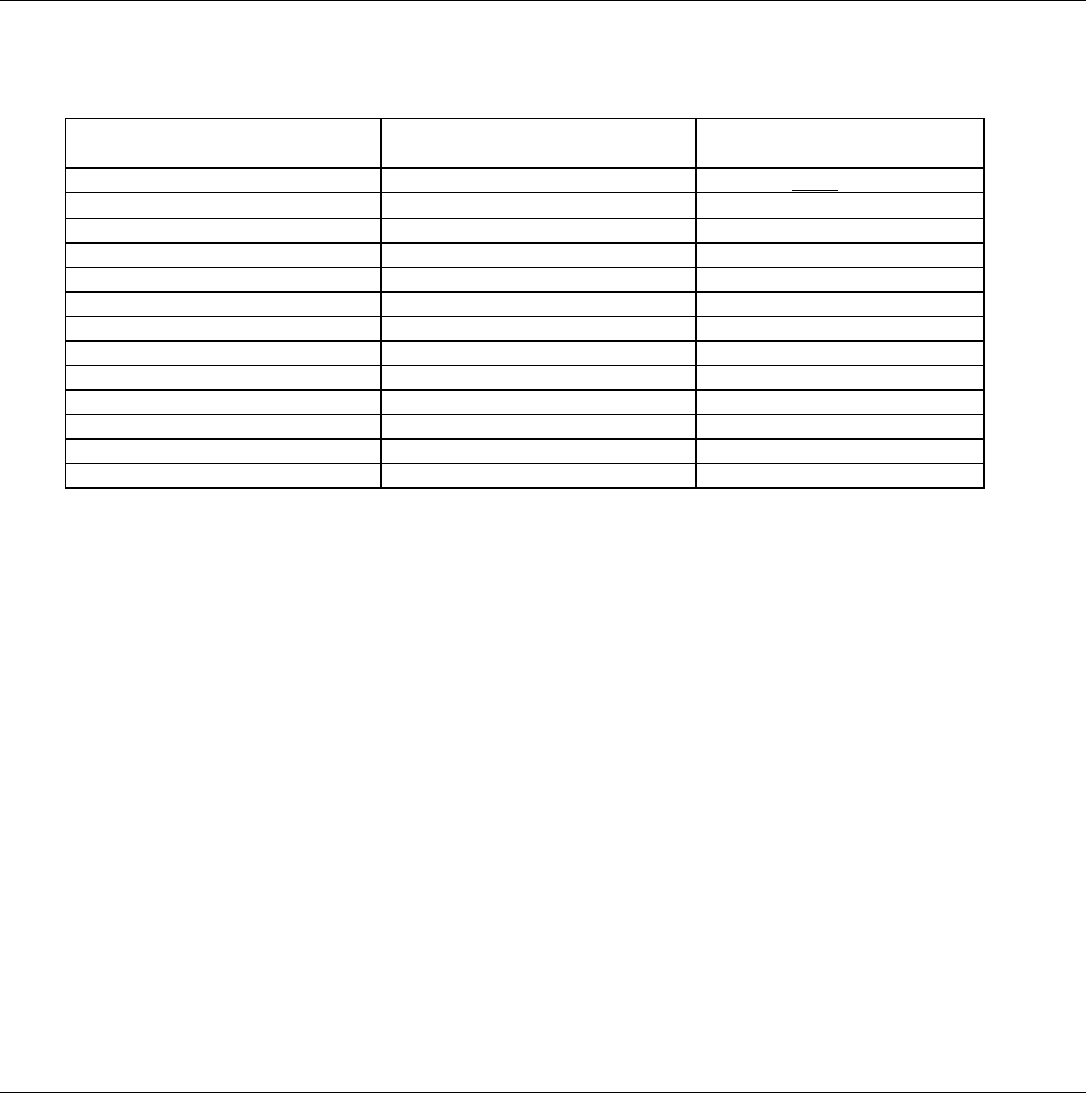
Model 8558B TM 11-6625-3061-14
ADJUSTMENTS
5-24. STEP AMPLIFIER GAIN ADJUSTMENTS (Cont'd)
Table 5-5. REF LEVEL FINE Control Check
REF LEVEL
FINE Setting Step Attenuator
Setting (dB Deviation From
Reference
0 0 Ref. mV (Ref.)
-1 1±0.3 Div ±30 mV
-2 2±0.3 Div ±30 mV
-3 3±0.3 Div ±30 mV
-4 4±0.3 Div ±30 mV
-5 5±0.3 Div ±30 mV
-6 6±0.3 Div ±30 mV
-7 7±0.3 Div ±30 mV
-8 8±0.3 Div ±30 mV
-9 9±0.3 Div ±30 mV
-10 10 ±0.3 Div ±30 mV
-11 11 ±0.3 Div ±30 mV
-12 12 ±0.3 Div ±30 mV
11. Connect power sensor and power meter to attenuator output and adjust signal generator output level for a power
meter reading of - 13 dBm. Connect test cable from attenuator to A9J1.
12. Tune signal generator frequency for peak amplitude on the display (near 301.4 MHz).
13. Set step attenuator to 10 dB and REFERENCE LEVEL to - 10 dBm.
002: +40dBmV
14. Adjust A12R3 10 dB adjustment for signal level one division from top graticule line.
15. Set step attenuator to 20 dB and REFERENCE LEVEL to - 20 dBm.
002: + 30 dBmV
16. Adjust A12R2 20 dB adjustment for signal level one division from top graticule line.
17. Set attenuator to 40 dB and REFERENCE LEVEL to - 40 dBm.
002: +10dBmV
NOTE
Some video filtering might help reduce noise. Set VIDEO FILTER control so noise is reduced,
but the signal amplitude remains unchanged.
18. Adjust A12R1 40 dB adjustment for signal level one division from top graticule line.
5-37
Model 8558B TM 11-6625-3061-14
ADJUSTMENTS
5-24. STEP AMPLIFIER GAIN ADJUSTMENTS (Cont' d)
19. Check REFERENCE LEVEL control from 0 to - 50 dBm as shown in Table 5-6.
002: + 50 dBmV to 0 dBm V. REFERENCE LEVEL dBmV settings in Table 5-6 are, from top to bottom, + 50,
+ 40, + 30, + 20, + 10, 0.
20. Reconnect W7P2 to A9JI.
Table 5-6. REFERENCE LEVEL Control Check
REFERENCE LEVEL
(dBm) Attenuator
(dB) Deviation From
Reference
0 0 Reference
-10 10 ±0.2 Div ±20 mV
-20 20 ±0.2 Div ±20 mV
-30 30 ±0.2 Div ±20 mV
-40 40 ±0.2 Div ±20 mV
-50 50 ±0.2 Div ±20 mV
5-38
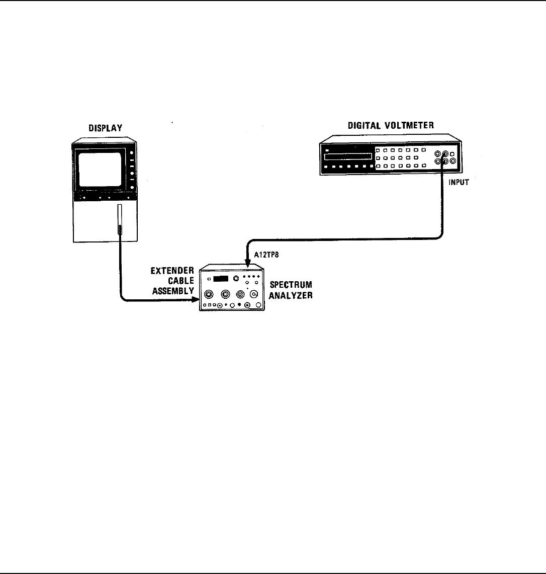
Model 8558B TM 11-6625-3061-14
ADJUSTMENTS
5-25. + 19.5V ADJUSTMENT
REFERENCE
A12 Schematic
DESCRIPTION
+ 19.5V for YIG Oscillator is adjusted.
Figure 5-12. +19.5VAdjustment Test Setup
EQUIPMENT
Digital Voltmeter........................................................................................................................... HP 3455A
Cable, Banana Plug to Alligator Clip........................................................................................... HP 11102A
Extender Cable Assembly ......................................................................................................HP 5060-0303
PROCEDURE
1. Set Digital Voltmeter as follows:
RANGE .............................................................................................................................................. AUTO
FUCTION............................................................................................................................................... dcV
AUTO CAL ..............................................................................................................................................ON
TRIGGER....................................................................................................................................INTERNAL
2. Connect equipment as shown in Figure 5-12. Connect digital voltmeter to A12TP8 (left side of A12R7 + 19.5V
adjustment).
3. Adjust A12R7 + 19.5V adjustment for + 19.5 ± 0.1 V.
5-39
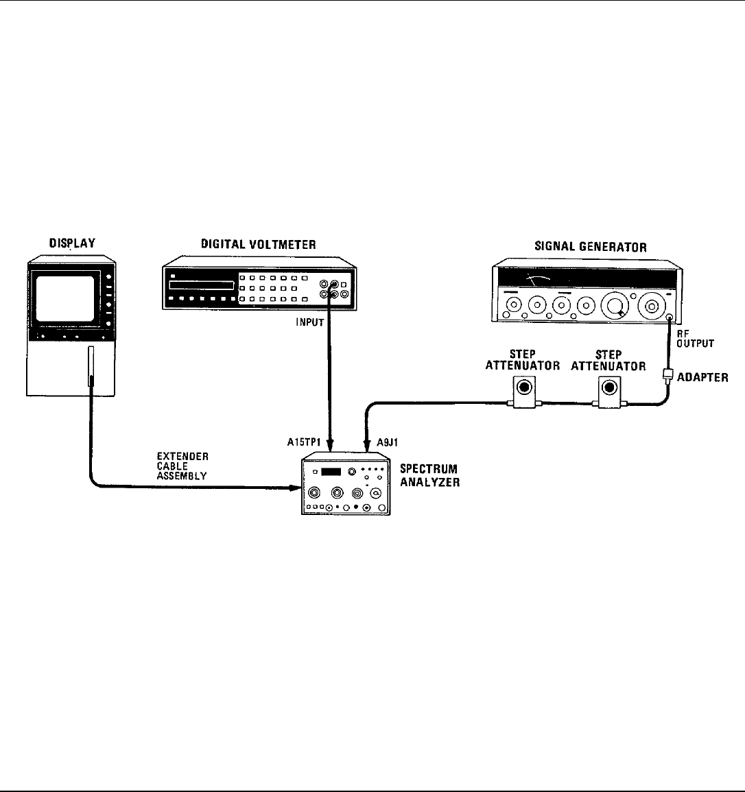
Model 8558B TM 11-6625-3061-14
ADJUSTMENTS
5-26. LOG AMPLIFIER LOG AND LINEAR ADJUSTMENT
REFERENCE:
A9, A12, A14, and A15 Schematics
DESCRIPTION
Step attenuators are used to change, in calibrated steps, the input signal level of the spectrum analyzer. The output of
Vertical Driver and Blanking Assembly A15 is monitored, and adjustments are performed to calibrate Log Amplifier
Assembly A14.
Figure 5-13. Log Amplifier and Linear Adjustment Test Setup
EQUIPMENT
Signal Generator .......................................................................................................................... HP 8640B
Digital Voltmeter........................................................................................................................... HP 3455A
10-dB Step Attenuator ...................................................................................................HP 355D, Opt. H82
1-dB Step Attenuator.....................................................................................................HP 355C, Opt. H80
Adapter, Type N (m) to SMC (m)............................................................................................HP 1250-1023
Adapter, Type N (m) to BNC (f) (2 required) ...........................................................................HP 1250-0780
BNC Cable, 20 cm (9 in)............................................................................................................. HP 18502A
BNC Cable, 120 cm (48 in)......................................................................................................... HP 18503A
Cable Assembly, Banana Plug to Alligator Clip........................................................................... HP 11102A
Test Cable, SMC (f) to BNC (m).........................................................................................HP 11592-60001
Extender Cable Assembly ......................................................................................................HP 5060-0303
5-40

Model 8558B TM 11-6625-3061-14
ADJUSTMENTS
5-26. LOG AMPLIFIER LOG AND LINEAR ADJUSTMENT (Cont'd)
PROCEDURE
1. Set equipment as follows:
Spectrum Analyzer
FREQ SPAN/DIV .............................................................................................................................. 0
RESOLUTION BW................................................................................................................. 300 kHz
INPUT ATTEN ...........................................................................................................................10 dB
REFERENCE LEVEL.............................................................................................................-50 dBm
002: 0 dBmV
Amplitude Scale.............................................................................................................................LIN
SWEEP TIME/DIV .................................................................................................................... AUTO
SWEEP TRIGGER ........................................................................................................... FREE RUN
Digital Voltmeter
RANGE........................................................................................................................................... 10
FUNCTION ...................................................................................................................................dcV
TRIGGER ..........................................................................................................................INTERNAL
MATH ..........................................................................................................................................OFF
AUTO CAL.....................................................................................................................................ON
2. Connect equipment as shown in Figure 5-13. Set 1-dB step attenuator to 10 dB. Set signal generator frequency
to 301.4 MHz and OUTPUT LEVEL to -13 dBm. Remove W7 from A9J1. Connect signal generator output
through step attenuators and test cable to A9J 1.
NOTE
The HP 355C 10 dB attenuation is included to compensate for the 10 dB of gain on Step Gain
Assembly A12 the TEST-NORM switch is in TEST.
3. Set the TEST-NORM switch on Step Gain Assembly A12 to the TEST position. Tune signal generator frequency
for maximum signal amplitude on display with 10 dB step attenuator set to 0 dB. (It may be necessary to reduce
signal generator OUTPUT LEVEL slightly.)
4. Disconnect signal generator output from step attenuator. Measure offset at A15TP and record.
mV
5. Connect signal generator to step attenuator and adjust signal generator FINE TUNE control to peak signal on
CRT display.
6. Adjust spectrum analyzer REF LEVEL CAL and signal generator OUTPUT LEVEL for DVM reading (± 1 mV) of
800 mV plus offset recorded in step 4, as measured at A15TP1.
7. Set Amplitude Scale to 10 dB/DIV.
8. Set 10-dB step attenuator to 0 dB and adjust A14R23 SLOPE for DVM reading (I 1 mV) of 800 mV plus offset
recorded in step 4, as measured at A15TP1.
5-41

Model 8558B TM 11-6625-3061-14
ADJUSTMENTS
5-26. LOG AMPLIFIER LOG AND LINEAR ADJUSTMENT (Cont'd)
9. Set 10-dB step attenuator to 60 dB and adjust A14R10 OFFSET for DVM reading (± 1 mV) of 200 mV plus offset
recorded in step 4, as measured at A15TP1.
10. Repeat steps 8 and 9 until no further adjustment is necessary.
11. Set 10-dB step attenuator to 30 dB and adjust A14R23 SLOPE for DVM reading (± 1 mV) of 500 mV plus offset
recorded in step 4, as measured at A15TP1.
12. Set 10-dB step attenuator to 0 dB and adjust A14R69 - 30 dB for DVM (± 1 mV) of 800 mV plus offset recorded
in step 4, as measured at A15TP1.
13. Repeat steps 11 and 12 until no further adjustment is necessary.
14. Set 10-dB step attenuator to 10 dB and adjust A14R23 SLOPE for DVM reading (± 1 mV) of 700 mV plus offset
recorded in step 4, as measured at A15TP1.
15. Set 10-dB step attenuator to O dB and adjust A14R39 - 10 dB for DVM reading (± 1 mV) of 800 mV plus offset
recorded in step 4, as measured at A15TP1.
16. Repeat steps 14 and 15 until no further adjustment is necessary.
17. Repeat steps 8 through 16 until limits in Table 5-7 are met.
Table 5- 7. Log Fidelity Check
Step Attenuator Setting (dB) DVM Reading*
0Ref: 800 ±1 mV
10 700 ±3 mV
20 600 ±4 mV
30 500 ±4 mV
40 400 ±5 mV
50 300 ±6 mV
60 200 ±7 mV
70 100 ±8 mV
*Plus offset
Linear Output and Linear Step Gain
18. Set spectrum analyzer controls as follows:
REFERENCE LEVEL............................................................................................................- 50 dBm
002: 0 dBmV
Amplitude Scale.............................................................................................................................LIN
5-42

Model 8558B TM 11-6625-3061-14
ADJUSTMENTS
5-26. LOG AMPLIFIER LOG AND LINEAR ADJUSTMENT (Cont'd)
19. Set 10-dB step attenuator to O dB and adjust A14R34 LIN for DVM reading (±1 mV) of 800 mV plus offset
recorded in step 4, as measured at A15TP1.
20. Make adjustments indicated in Table 5-8 .
Table 5-8. Linear Gain Adjustments
Adjustment Step Attenuator Reference Level DVM Reading*
A14R34 0-50 dBm Ref: 800 ± 1 mV
A14R33 10 -60 dBm 800 ± 5 mV
A14R30 20 -70 dBm 800 ± 5 mV
A14R27 30 -80 dBm 800 ± 5 mV
No Adjustment 40 -90 dBm 800 ± 10 mV
*Plus offset
Log Gain
21. Set spectrum analyzer control as follows:
REFERENCE LEVEL............................................................................................................- 50 dBm
002: 0 dBmV
Amplitude Scale.................................................................................................................... 1 dB/DIV
22. Set 10-dB step attenuator to 0 dB. Adjust signal generator for DVM reading (± 1 mV) of 800 mV plus offset
recorded in step 4, as measured at A15TP1.
23. Set 10-dB step attenuator to 40 dB. Set REF LEVEL dBm to -90 and adjust A14R121 LOG GAIN for DVM
reading (± 3 mV) of 800 mV plus offset recorded in step 4, as measured at A15TP1.
002: - 40 dBmV
24. Check log gain steps according to Table 5-9.
Table 5-9. Log Gain Adjustment Limits
Step Attenuator Reference Level DVM Reading*
0-50 dBm Ref: 800 +1 mV
10 -60 dBm 800 +30 mV
20 -70 dBm 800 +30 mV
30 -80 dBm 800 +30 mV
40 -90 dBm 800 +30 mV
*Plus offset
5-43

Model 8558B TM 11-6625-3061-14
ADJUSTMENTS
5-26. LOG AMPLIFIER LOG AND LINEAR ADJUSTMENT (Cont'd)
Error Check (1 dB/DIV)
25. Set spectrum analyzer controls as follows:
REFERENCE LEVEL............................................................................................................- 50 dBm
002: 0dBmV
Amplitude Scale...........................................................................................................................1 dB
26. Set both step attenuators to 0 dB. Reduce signal generator OUTPUT LEVEL until signal appears at top of
display. Adjust signal generator FINE TUNE to peak trace on display and adjust OUTPUT LEVEL for DVM
reading (± 1 mV) of 800 mV plus offset recorded in step 4, as measured at A 5TP 1. Increase attenuation in 1-
dB steps and take DVM readings to check log amplifier output. (Refer to Table 5-10.)
27. Return A12S1 TEST-NORM switch to NORM. Remove test cable and reconnect W7 to A9J1.
Table 5-10. Log Amplifier Output Limits
Step Attenuator DVM Reading*
1700 ± 10 mV
2600 ± 20 mV
3500 ± 30 mV
4400 ± 30 mV
5300 ± 30 mV
6200 ± 30 mV
7100 ± 30 mV
*Plus offset
5-44
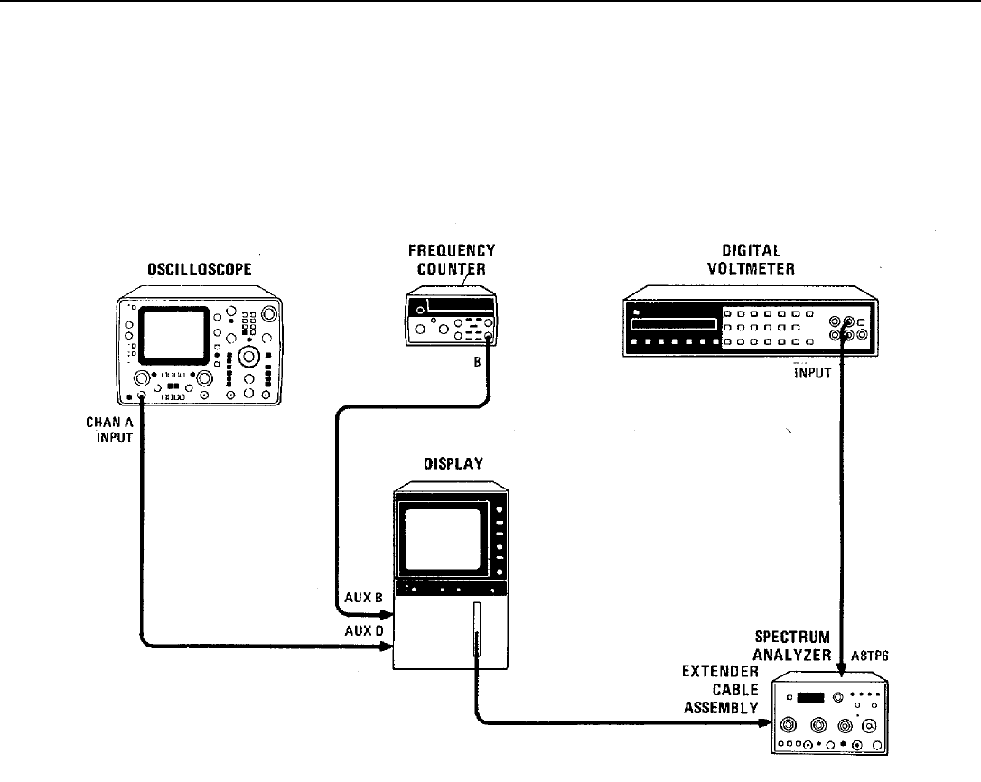
Model 8558B TM 11-6625-3061-14
ADJUSTMENTS
5-27. SWEEP TIME PER DIVISION ADJUSTMENT
REFERENCE
A8 Schematic
DESCRIPTION
Sweep time per division is adjusted for proper sweep time and 'dead time.'
Figure 5-14. Sweep Time Per Division Adjustment Test Setup
EQUIPMENT
Oscilloscope........................................................................................................................ HP 1741A
Digital Voltmeter ................................................................................................................. HP 3455A
Timer/Counter..................................................................................................................... HP 5308A
BNC Cable, 120 cm (48 in) ............................................................................................... HP 18503A
Cable, Banana Plug to Alligator Clips 150 cm (60 in) ........................................................ HP 11002A
Extender Cable Assembly .............................................................................................HP 5060-0303
5-45

Model 8558B TM 11-6625-3061-14
ADJUSTMENTS
5-27. SWEEP TIME PER DIVISION ADJUSTMENT (Cont'd)
PROCEDURE
1. Set equipment as follows:
Oscilloscope
DISPLAY...........................................................................................................................................A
TRIGGER .........................................................................................................................................A
CHAN A .........................................................................................................................2 VOLTS/DIV
AC-GND-DC ..................................................................................................................................DC
WRITE...........................................................................................................................................ON
TIME/DIV...............................................................................................................................2 mSEC
MAG X5 .......................................................................................................................................OFF
EXT TRIGGER.............................................................................................................................. INT
MODE........................................................................................................................................ MAIN
Digital Voltmeter
RANGE..................................................................................................................................... AUTO
FUNCTION ...................................................................................................................................dcV
AUTO CAL.....................................................................................................................................ON
TRIGGER ..........................................................................................................................INTERNAL
MATH ..........................................................................................................................................OFF
TIMER/COUNTER
TIME BASE.................................................................................................................................10 µs
FUNCTION ...............................................................................................................................PER B
2. Connect equipment as shown in Figure 5-14. Connect oscilloscope to AUX D, HORIZONTAL OUT- PUT, rear of
display mainframe, or to A8TP5 of HP 8558B. Connect digital voltmeter to A8TP6 (located to the left and below
A8TP4.)
3. Adjust A8R7 + 10lOV adjustment for 1OV 40.02 V.
NOTE
The + 10V must be adjusted while analyzer is still cold, during first five minutes after turn-on. If
instrument has been operating, turn off mainframe and remove A8 Sweep Generator assembly.
Let A8 assembly cool on bench for 15 minutes. Replace A8 and proceed with adjustment of
A8R7 during the first five minutes after turn on.
4. Set spectrum analyzer controls as follows:
SWEEP TIME/DIV ...................................................................................................................... 1 ms
SWEEP TRIGGER ........................................................................................................... FREE RUN
5. Check oscilloscope trace for approximately a - 5V to + 5V ramp.
5-46

Model 8558B TM 11-6625-3061-14
ADJUSTMENTS
5-27. SWEEP TIME PER DIVISION ADJUSTMENT (Cont'd)
6. Adjust A8R10 1 ms adjustment for a 10 ms ramp time. Measure dead time of ramp.
MIN. ACTUAL MAX.
0.25 ms 0.40 ms
7. Set spectrum analyzer SWEEP TIME/DIV to 2 mSEC. Adjust A8R13 2 ms adjustment for a 20 ms ramp time.
Measure dead time of ramp.
MIN. ACTUAL MAX.
6.0 ms 9.0 ms
8. Set SWEEP TIME/DIV to 1 mSEC. Frequency counter should read sweep time plus dead time (10 ms + dead
time 40.05 ms). Adjust A8R10 if necessary to obtain an indication of 10 ms + dead time ± 0.05 ms.
9. Set SWEEP TIME/DIV to 2 mSEC. Frequency counter should read sweep time plus dead time (20 ms + dead
time -0.10 ms). Adjust A8R13 if necessary to obtain an indication of 20 ms + dead time ± 0.10 ms.
10. Repeat steps 8 and 9 until the sweep time plus dead time (dt) for the 1 ms and 2 ms sweeps are within limits.
MIN ACTUAL MAX.
10 ms + dt - 0.05 ms 10 ms + dt + 0.05 ms
20ms + dt- 0.10ms 20ms + dt + 0.10ms
5-47
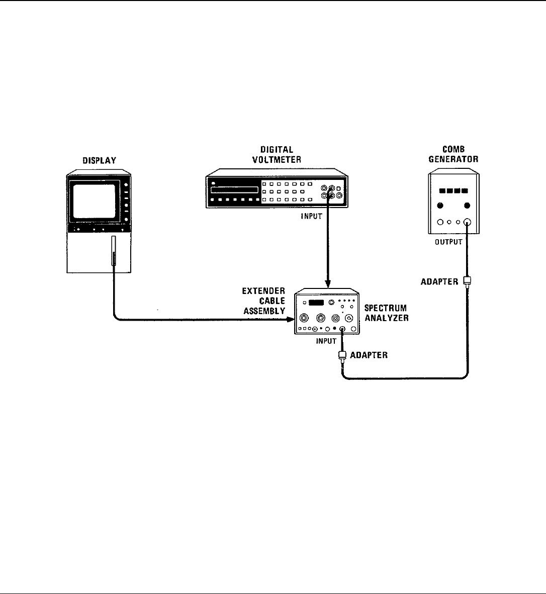
Model 8558B TM 11-6625-3061-14
ADJUSTMENTS
5-28. FREQUENCY CONTROL AND DPM ADJUSTMENTS
REFERENCE
A1 and A7 Schematics
DESCRIPTION
The + 14.5V and REF V voltages are adjusted and the - 10.0V voltage is checked. The frequency limits and linearity of
the YIG oscillator are set. The FREQUENCY MHz readout is adjusted for proper voltage calibration and for correct
ranging.
Figure 5-15. Frequency Control and DPM Adjustments Test Setup
EQUIPMENT Digital Voltmeter ................................................................................................................. HP 3455A
Comb Generator ................................................................................................................. HP 8406A
Adapter, Type N (m) to BNC (f) (2 required)..................................................................HP 1250-0780
BNC Cable, 120 cm (48 in) ............................................................................................... HP 18503A
Cable, Banana Plug to Alligator Clips 150 cm (60 in) ........................................................ HP 11002A
Extender Cable Assembly .............................................................................................HP 5060-0303
Additional Equipment, Options 001 and 002:
Minimum Loss Adapter, 75Ω to 50Ω..........................................................................HP 08558-60031
Adapter, BNC (m) to BNC (m), 75Ω..............................................................................HP 1250-1288
Adapter, SMA (f) to SMA (f) ..........................................................................................HP 1250-1158
Adapter, BNC (f) to SMA (m).........................................................................................HP 1250-1200
5-48

Model 8558B TM 11-6625-3061-14
ADJUSTMENTS
5-28. FREQUENCY CONTROL AND DPM ADJUSTMENTS (Cont'd)
PROCEDURE
Voltage Adjustments
1. Connect equipment as shown in Figure 5-15. Connect digital voltmeter to A7TP7 (located between A7R4 REF V
and A7R5 + 14.5V adjustments).
2. Adjust A7R5 + 14.5V potentiometer for + 14.50 ± 0.02 V.
3. Connect digital voltmeter to A7TP8 (located to the right of A7R5 + 14.5V adjustment) and check for -10.0 ± 0.2
V.
4. Connect digital voltmeter to A7TP6 and adjust A7R4 REF V potentiometer for + 6.00 ± 0.01 V.
YIG Oscillator Adjustment
NOTE
Check HORIZ GAIN and HORIZ POSN adjustments and perform voltage adjustments before
continuing with the following procedure.
5. Set spectrum analyzer controls as follows:
START - CENTER ................................................................................................................CENTER
FREQ SPAN/DIV ......................................................................................................................5 MHz
RESOLUTION BW................................................................................................................. 100 kHz
INPUT ATTEN ................................................................................................................................dB
REFERENCE LEVEL.............................................................................................................-10 dBm
002: +40dBmV
Amplitude Scale.................................................................................................................. 10 dB/DIV
SWEEP TIME/DIV .................................................................................................................... AUTO
SWEEP TRIGGER ........................................................................................................... FREE RUN
6. Turn FREQUENCY ZERO control fully counterclockwise.
7. Adjust TUNING for FREQUENCY MHz readout of approximately - 16.0.
NOTE
Press FREQUENCY CAL button to remove YIG oscillator hysteresis whenever the TUNING
control is adjusted.
8. Adjust A7R3 2.0 GHZ to center LO feedthrough (within one division) on CRT.
NOTE
Disconnect comb generator whenever it is necessary to center the LO feedthrough.
5-49

Model 8558B TM 11-6625-3061-14
ADJUSTMENTS
5-28. FREQUENCY CONTROL AND DPM ADJUSTMENTS (Cont'd)
9. Couple FREQ SPAN/DIV and RESOLUTION BW controls. Set FREQ SPAN/DIV to 100 MHz/DIV. Set comb
generator frequency to 100 MHz. Adjust TUNING to approximately 500 MHz for full-screen display of comb
teeth.
10. Adjust TUNING, A7R1 3.55 GHZ, and A7R2 3.55 FINE to align comb teeth on vertical graticule lines (one tooth
per division).
11. Repeat steps 7 and 8. (A7R1 3.55 GHZ adjustment has a slight effect on A7R3 2.0 GHZ adjustment.)
12. Set FREQ SPAN/DIV to 1 MHz and comb generator frequency to 1 MHz.
13. Adjust TUNING to approximately 750 MHz. Adjust A7R6 FM to align comb teeth on vertical graticule lines (one
tooth per division).
Digital Panel Meter Adjustment
14. Set FREQ SPAN/DIV to 500 kHz.
15. Center LO feedthrough. Press FREQUENCY CAL button and re-center LO feedthrough.
16. Adjust FREQUENCY ZERO control for FREQUENCY MHz readout of 00.0.
17. Set comb generator frequency to 100 MHz. Adjust TUNING to center 1500-MHz tooth (15th tooth from LO
feedthrough). Press FREQUENCY CAL button and re-center comb tooth. Adjust A1A2R3 REF for
FREQUENCY MHz readout of 1500 + 1.
18. Adjust A7R8 RNG fully clockwise. Set comb generator frequency to 10 MHz. Adjust TUNING to center 190-MHz
comb tooth (19th tooth from LO feedthrough). Adjust A7R7 GAIN for FREQUENCY MHz readout of 190.0.
NOTE
Press FREQUENCY CAL frequently while counting the comb teeth to avoid miscounting.
19. Adjust TUNING for FREQUENCY MHz readout of 198.5. Slowly adjust A7R8 RNG counterclockwise until
range switches (no decimal on FREQUENCY MHz display).
20. Center LO feedthrough. Press FREQUENCY CAL button and re-center LO feedthrough. Set comb generator
frequency to 100 MHz. Adjust TUNING to center 200-MHz comb tooth (second tooth from LO feedthrough).
Press FREQUENCY CAL button and re-center comb tooth. Adjust A7R72 OFS for FREQUENCY MHz readout
of 200.
21. Repeat steps 15 through 21 until 190.0 MHz, 200 MHz, and 1500 MHz readouts on FREQUENCY MHz display
are calibrated.
5-50
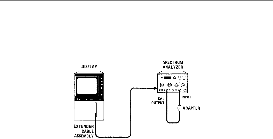
Model 8558B TM 11-6625-3061-14
ADJUSTMENTS
5-29. 1 dB OFFSET ADJUSTMENT
REFERENCE
A15 Schematic
DESCRIPTION
Reference is set in 10 dB/DIV and 1 dB offset is adjusted in 1 dB/DIV for the same full display reference in 10 dB/DIV.
Figure 5-16. 1-dB Offset Adjustment Test Setup
EQUIPMENT
BNC Cable, 120 cm (9 in) ................................................................................................. HP 18502A
Adapter, Type N (m) to BNC (f).....................................................................................HP 1250-0780
Extender Cable Assembly .............................................................................................HP 5060-0303
Additional Equipment, Options 001 and 002:
BNC Cable, 30 cm (12 in)..........................................................................................HP 11652-60012
PROCEDURE
1. Set Spectrum Analyzer controls as follows:
START - CENTER ................................................................................................................CENTER
TUNING................................................................................................................................ 280 MHz
FREQ SPAN/DIV ......................................................................................................................1 MHz
RESOLUTION BW....................................................................................................................1 MHz
INPUT ATTEN ...........................................................................................................................10 dB
REFERENCE LEVEL.............................................................................................................-20 dBm
002: +30dBmV
REF LEVEL FINE ..................................................................................................Approximately - 10
Amplitude Scale.............................................................................................................................LIN
SWEEP TIME/DIV .................................................................................................................... AUTO
SWEEP TRIGGER ........................................................................................................... FREE RUN
5-51

Model 8558B TM 11-6625-3061-14
ADJUSTMENTS
5-29. 1-dB OFFSET ADJUSTMENT (Cont'd)
2. Connect equipment as shown in Figure 5-16.
3. Set Amplitude Scale switch to LIN. Set TUNING control to center the trace on the display. Set REF LEVEL
FINE for a full-screen trace (signal at top graticule line).
4. Set Amplitude Scale switch to 10 dB/DIV. Adjust VERTICAL GAIN if necessary for full screen trace.
5. Repeat steps 3 and 4 until the trace is full screen in both LIN and 10 dB/DIV.
NOTE
1 dB/DIV will read approximately 0.5 dB (0.5 division) low when using extender cable assembly.
Adjusting A15Ri 1 dB OFFSET for a trace 0.5 division down from top graticule line should place
signal at top graticule line when 8558B is properly installed in 180-series mainframe.
6. Amplitude Scale switch to 1 dB/DIV. Adjust A15R1 1 dB OFFSET for a trace 0.5 division down from top
graticule line.
5-52
TM 11-1247-B
THIS PAGE MISSING NOT AVAILABLE FOR DIGITIZATION.
PAGES
5-53 through 5-59
Model 8558B TM 11-6625-3061-14
SECTION VI.
REPLACEABLE PARTS
6-1. INTRODUCTION
6-2.This section contains information for ordering
replacement parts. Table 6-1 includes a list of reference
designations and a list of abbreviations used in the parts
list. Table 6-2 lists names and addresses that
correspond to the manufacturer code numbers in the
parts list. Table 6-3 lists all replaceable parts in alpha-
numerical order by reference designation.
6-3. REPLACEABLE PARTS LIST
6-4. Table 6-3, the list of replaceable parts, is organized
as follows:
1.Electrical assemblies and their components in
alpha-numerical order by reference designation
2.Miscellaneous parts, with appropriate electrical
assembly
3.Chassis-mounted electrical parts, in
alphanumerical order by reference designation
4. Mechanical chassis parts, at end of
parts list
6-5.The following information is listed for each part:
1.The Hewlett-Packard part number
2.The part number check digit (CD)
3.The total quantity (Qty) in the instrument. This
quantity is given only once, at the first
appearance of the part in the list.
4.The description of the part
5.A five-digit code indicating a typical
manufacturer of the part
6.The manufacturer's part number
6-6. ORDERING INFORMATION
6-7.To order a part listed in the replaceable parts
table, quote the Hewlett-Packard part number (with
check digit), indicate the quantity required, and address
the order to the nearest Hewlett-Packard office. The
check digit will ensure accurate and timely processing of
your order.
6-8.To order a part that is not listed in the
replaceable parts table, include the instrument model
number, instrument serial number, the description and
function of the part, and the number of parts required.
Address the order to the nearest Hewlett-Packard office.
6-1
Model 8558B TM 11-6625-3061-14
Table 6-1. Reference Designations and Abbreviations (1 of 3)
REFERENCE DESIGNATIONS
A........................................Assembly F...............................................Fuse RT .............................. Thermistor
AT......... Attenuator, Isolator, Limiter, FL .............................................Filter S........................................Switch
Termination H........................................Hardware T............................... Transformer
B......................................Fan, Motor HY .....................................Circulator TB........................ Terminal Board
BT..........................................Battery J..... Electrical Connector (Stationary TC .........................Thermocouple
C........................................Capacitor Portion), Jack TP................................ Test Point
CP ....................................... Coupler K..............................................Relay U....Integrated Circuit, Microcircuit
CR ........Diode, Diode Thyristor, Step L.................................. Coil, Inductor V............................ Electron Tube
Recovery Diode (SCR), Varactor M.............................................Meter VR ....... Breakdown Diode(Zener),
DC ......................Directional Coupler MP....Miscellaneous Mechanical Part Voltage Regulator
DL.................................... Delay Line P........Electrical Connector (Movable W.Cable, Transmission Path, wire
DS .............Annunciator, Lamp, Light Portion), Plug X........................................Socket
Emitting Diode (LED), Signaling Q ............ Silicon Controlled Rectifier Y.........Crystal Unit (Piezoelectric,
Device (Audible or Visible (SCR), Transistor, Triode Thyristor Quartz)
E..........Miscellaneous Electrical Part R.......................................... Resistor Z.......Tuned Cavity, Tuned Circuit
ABBREVIATIONS
ADG
A.................Across Flats, Acrylic, Air D................. Deep, Depletion, Depth, GEN .............. General, Generator
(Dry Method), Ampere Diameter, Direct Current GND .................................Ground
ADJ..................... Adjust, Adjustment DA ....................................Darlington GP......... General Purpose, Group
ANSI ....................American National DAP-GL .........Diallyl Phthalate Glass
Standards Institute (formerly DBL .......................................Double
USASI-ASA) DCDR ..................................Decoder H
ASSY.................................Assembly DEG...................................... Degree
AWG................American Wire Gage D-HOLE....................D-Shaped Hole H...............Henry, Hermaphrodite,
DIA .................................... Diameter High, Hole Diameter, Hot, Hub
DIP ................. Dual In-Line Package Inside Diameter, Hydrogen
BDIP-SLDR........................ Dip Solder HDW........................... Hardware .
D-MODE.................. Depletion Mode HEX........Hexadecimal, Hexagon,
BCD...............Binary Coded Decimal DO.......... Package Type Designation Hexagonal
BD ............... Deep, Depth, Diametric DP ............... Deep, Depth, Diametric HLCL .................................Helical
BE-CU ...................Beryllium Copper Pitch, Dip HP .....Hewlett-Packard Company,
BNC.....................Type of Connector DP3TMINTR ........Double Pole Three High Pass, Horsepower
BRG..........................Bearing, Boring Throw, Miniature
BRS .........................................Brass DPDTMINTR......Double Pole Double I
BSC ......................................... Basic Throw, Miniature
BTN ........................................Button DWL ....................................... Dowel IC......................Collector Current,
CEIntegrated Circuit
ID...Identification, Inside Diameter
E-R ........................................E-Ring IF.......................Forward Current,
C............... Capacitance, Capacitore, EXT .................Extended, Extension, Intermediate Frequency
Center Tapped, Centistoke, External, Extinguish IN.............................. Inch, indium
Cermet, Circular Mil Foot, Closed
Cup, Cold, Compression FINCL .............................. Including
CCP.......Carbon Composition Plastic INT ......Integral, Intensity, Internal
CD ..........................Cadmium, Card, F............ Fahrenheit, Farad, Female, INTL ........... Internal, International
Cold-Drawn, Cord Film (Resistor), Fixed, Flange,
CER.....................................Ceramic Flint, Fluorine, Frequency
CHAM................................. Chamfer FC.......... Carbon Film / Composition,
CHAR .............................. Character, Edge of Cutoff Frequency, Face J
Characteristic, Charcoal FDTHRU.....................Feed Through J-FET .......... Junction Field Effect
CMOS............ Complementary Metal FEM......................................Female Transistor
Oxide Semiconductor FIL-HD......................... Fillister Head JFET............ Junction Field Effect
CNDCT ...... Conducting, Conductive, FL ...........................Flash, Flat, Fluid Transistor
Conductivity, Conductor FLAT-PT............................Flat Point
CONT .............. Contact, Continuous,FR.............................................Front
Control, Controller FREQ .............................. Frequency K
CONV ............................... Converter FT................Current Gain Bandwidth
CPRSN ........................ Compression Product (Transition Frequency); K...... Kelvin, Key, Kilo, Potassium
CUP-PT ............................ Cup Point Feet, Foot KNRLD ............................ Knurled
CW ..... Clockwise, Continuous Wave FXD .........................................Fixed KVDC ...... Kilovolts Direct Current
6-2
Model 8558B TM 11-6625-3061-14
Table 6-1. Reference Designations and Abbreviations (2 of 3)
LPAN-HD............................ Pan Head T
PAR...........................Parallel, Parity
LED................... Light Emitting Diode PB............ Lead (Metal), Push Button T........... Tab Width, Taper, Teeth,
LG................................ Length, Long PC ....................Picocoulomb, Piece, Temperature, Tera, Tesla,
LIN.....Linear, Linear Taper, Linearity Printed Circuit .............................. Thermoplastic (Insulation),
LK.....................................Link, Lock PCB................. Printed Circuit Board Thickness, Time, Timed, Tooth,
LKG ...................... Leakage, Locking P-CHAN........................... P-Channel Turns Ratio, Typical
LOGO ................................ Logotype PD .................. Pad, Palladium, Pitch TA............. Ambient Temperature,
LUM...................................Luminous Diameter, Power Dissipation Tantalum
PF............... Picofarad; Pipe, Female TC ......................... Thermoplastic
MConnection; Power Factor THD................. Thread, Threaded
PKG.................................... Package THK.....................................Thick
M.......... Male, Maximum, Mega, Mil, PLSTC................................... Plastic TO .....Package Type Designation,
Milli, Mode, Momentary, PNL .........................................Panel Troy Ounce
Mounting Hole Centers, Mounting ..................................................PNP Positive Negative..................TPG
Tapping
Hole Diameter Positive (Transistor) TR-HD ....................... Truss Head
MA..................................Milliampere POLYC ...................... Polycarbonate TRMR.............................Trimmer
MACH................................Machined POLYE............................... Polyester TRN........................... Turn, Turns
MAX.................................. Maximum POT............................Potentiometer TRSN................................Torsion
MC..................... Hot Molded Carbon POZI........................Pozidriv Recess
Composition, Megacycle, PREC................................. Precision U
Microcircuit, Molded Carbon PRP.........................Purple, Purpose
Composition PSTN...................................... Piston UCD........................ Microcandela
MET.......................... Metal, Metallic, PT..................... Part, Pint, Platinum, UF ...............................Microfarad
Metallized, Metallurgical Point, Pulse Time UH..............................Microhenry
MHZ................................. Megahertz PW ..Power Wirewound, Pulse Width UL............Microliter, Underwriters'
MIT ...........................................Miter Laboratories, Inc.
MLD.............................Mold, Molded UNHDND .................. Unhardened
MM ................... Magnetized Material Q
(Restricted Articles Code); Q ...............................Figure of Merit V
Millimeter
MOM............................... Momentary V........Vanadium, Variable, Violet,
MTG .................................. Mounting Volt, Voltage
MTLC....................................Metallic RVAC......................Vacuum; Volts,
MUW .............................. Music Wire Alternating Current
MW...................................... Milliwatt R................ Range, Red, Resistance, VAC/DC......Volts, Alternating and
Resistor, Right, Ring, Rosin, Direct Current
Rubber-Resin, Run Torque VAR................................ Variable
NREF ..................................Reference VDC..............Volts, Direct Current
RES.Research, Resistance, Resistor
N..................Fan Out, Intrinsic Stand RF.......................... Radio Frequency W
Off Ratio, Nano, Nanosecond, RGD .........................................Rigid
Nitrogen, None RND........................................Round W.............. Watt, Wattage, White,
N-CHAN...........................N-Channel RR ............................................ Rear Wide, Width, Wire
NH ...................................Nanohenry RVT ............................Rivet, Riveted
NMH ............Nanometer Nonmetallic SW/CP....Wire / Conductive Plastic
NO..............Normally Open, Number W/SW........................With Switch
NOM ....................................Nominal WW ..........................Wire Wound
NPN...................... Negative Positive
Negative (Transistor) SAWR.......... Surface Acoustic Wave X
NS Nanosecond, Non-Shorting, Nose Resonator
NUM ..................Numeric, Numerical SEG....................................Segment X...... By (Used With Dimensions),
NYL......................Nylon (Polyamide) SGL ........................................Single Reactance
SI.......................Silicon, Square Inch XSTR............................Transistor
OSL................................... Slide, Slow
SLT......................Slate, Slot, Slotted Y
OA .......................... Other Restricted SMA................Subminiature, A Type
Articles, Group A (Restricted (Threaded Connector) YIG.................Yttrium-ron-Garnet
Articles Code); Over-All SMC ...............Subminiature, C Type
OD......Olive Drab, Outside Diameter (Threaded Connector) Z
OP AMP...........Operational Amplifier SPCG .................................. Spacing
OPT........... Optical, Option, Optional SPDTSUBMIN ....Single Pole Double ZNR.................................... Zener
Throw, Subminiature
PSPST.........Single Pole Single Throw
SQ .........................................Square
PA...................... Picoampere, Power SST ...........................Stainless Steel
Amplifier, Pressure Angle, STL...........................................Steel
Protactinium SZ..............................................Size
6-3

Model 8558B TM 11-6625-3061-14
Table 6-1. Reference Designations and Abbreviations (3 of 3)
MULTIPLIERS
Abbreviation Prefix Multiple
Ttera 1012
Ggiga 10 9
Mmega 106
kkilo 103
da deka 10
ddeci 10-1
ccenti 10-2
mmilli 10-3
,U micro 10-6
n nano 10-9
ppico 10-12
f femto 10-15
aatto 10-18
Table 6-2. Manufacturers Code List
Mfr.
No. Manufacturer Name Address Zip Codes
00000 ANY SATISFACTORY SUPPLIER
01121 ALLEN-BRADLEY CO MILWAUKEE, WI 53204
01295 TEXAS INSTR INC SEMICOND CMPNT DIV DALLAS, TX 75222
02111 SPECTROL ELECTRONICS CORP CITY OF IND, CA 91745
02660 BUNKER RAMO CORP AMPHENOL CONN DIV BROADVILLE, IL 60153
03888 K D I PYROFILM CORP WHIPPANY, NJ 07981
04713 MOTOROLA SEMICONDUCTOR PRODUCTS PHOENIX, AZ 85008
06665 PRECISION MONOLITHICS INC SANTA CLARA, CA 95050
11236 CTS OF BERNE INC BERNE, IN 46711
13606 SPRAGUE ELECT CO SEMICONDUCTOR DIV CONCORD, NH 03301
18736 VOLTRONICS CORP HANOVER, NJ 07936
19701 MEPCO/ELECTRA CORP MINERAL WELLS; TX 76067
24046 TRANSITRON ELECTRONIC CORP WAKEFIELD, MA 01880
24546 CORNING GLASS WORKS (BRADFORD) BRADFORD, PA 16701
28480 HEWLETT-PACKARD CO CORPORATE HQ PALO ALTO, CA 94304
3L585 RCA CORP SOLID STATE DIV SOMERVILLE, NJ
30983 MEPCO/ELECTRIC CORP SAN DIEGO, CA 92121
33095 SPECTRUM CONTROL INC FAIRVIEW, PA 16415
52763 STETTNER-TRUSH INC CAZENOVIA, NY 13035
56289 SPRAGUE ELECTRIC CO NORTH ADAMS, MA 01247
71041 BOSTON GEAR WKS DIV OF NA ROCKWELL QUINCY, MA 02171
72136 ELECTRO MOTIVE CORP FLORENCE, SC 06226
72982 ERIE TECHNOLOGICAL PRODUCTS INC ERIE, PA 16512
74970 JOHNSON E F CO WASECA, MN 56093
78707 TEK BEARING CO INC NEW YORK, NY 10013
9N171 UNITRODE COMPUTER PRODUCTS CORP METHUEN, MA
92830 ASSOCIATED SPRING CORP BRISTOL, CT 06010
6-4

Model 8558B TM 11-6625-3061-14
Table 6-3. Replaceable Parts
Reference HP Part CMfr.
Designation Number DQty Description Code Mfr Part Number
A1 DIGITAL PANEL METER ASSEMBLY
A1A1 NOT ASSIGNED
A1A2 08558-60125 1 1 DPM DRIVER ASSEMBLY 28480 08558-60125
NOTE
SEE A2 FOR DPM DISPLAY
A1A2C1 THRU 2
A1A2C3 NOT ASSIGNED
A1A2C4 0180-0197 8 18 CAPACITOR-FXD 2,2UF+-10X 20VDC TA 56289 150D225X9020A2
A1A2C5 THRU
A1A2C9 NOT ASSIGNED
A1A2C10 0160-4084 8 11 CAPACITOR-FXD .UF +-20% 50VDC CER 28480 0160-4084
A1A2C11 0160-4084 8CAPACITOR-FXD .1UF +-20% 50VDC CER 28480 0160-4084
A1A2CI2 0180-0197 8CAPACITOR-FXD 2.2UF+-10% 20VDC TA 56289 150D225X9020A2
A1A2C13 NOT ASSIGNED
A1A2C14 0160-0168 1 1 CAPACITOR-FXD .1UF +-10% 200VODC POLYE 28480 0160-0168
A1A2C15 0180-2207 5 1 CAPACITOR-FXD 100UF +-10% 10VDC TA 56289 150D107X9010R2
A1A2C16 0160-4084 8CAPACITOR-FXD , 1UF +-20X 50VDC CER 28480 0160-4084
A1A2CR1 NOT ASSIGNED
A1A2CR2 1901-0040 1 29 DIODE-SWITCHING 30V 50MA 2NS DO-35 28480 1901-0040
A1A2CR3 1901-0050 3 27 DIODE-SWITCHING 80V 200MA 2NS DO-35 28480 1901-0050
A1A2J1 1200-0508 0 1 SOCKET-IC 14-CONT DIP-SLDR 28480 1200-0508
A1A2L1 9100-1644 3 1 INDUCTOR RF-CH-MLD 330UH 5% .2DX.45L.G 28480 9100-1644
A1A2Q1 NOT ASSIGNED
A1A2Q2 NOT ASSIGNED
A1A2Q3 1854-0404 0 35 TRANSISTOR NPN SI TO-18 PD=360MW 28480 1854-0404
A1A2Q4 1854-0404 0TRANSISTOR NPN SI TO-18 PD=360MW 28480 1854-0404
A1A2R1 0757-0465 6 27 RESISTOR 100K 1% .125W F TC=0+-100 24546 C4-1/8-TO-1003-F
A1A2R2 0757-0420 3 7 RESISTOR 750 1% .125W F TC=0+-100 24546 C4-1/8-TO-751-F
A1A2R3 2100-1702 7 1 RESISTOR-TRMR 100 10% WW SIDE-ADJ 20-TRN 02660 3810P-101
A1A2R4 0698-3446 3 3 RESISTOR 383 1% .125W F TC=0+-100 24546 C4-1/8-TO-383R-.F
A1A2R5 0757-0442 9RESISTOR 10K 1X .125W F TC=0+-100 24546 C4-1/8-TO-1002-F
A1A2R6 0698-3260 9 5 RESISTOR 464K 1% .125W F TC=0+-1OO 28480 0698-3260
A1A2R7 0698-3457 6RESISTOR 316K 1% .125W F TC=0+-100 28480 0698-3457
A1A2R8 0698-3439 4 1 RESISTOR 178 1% .125W F TC=0+-100 24546 C4-1/8-TO-178R-F
A1A2R9 0757-0442 9RESISTOR 10OK 1%X 125W F TC=0+-100 24546 C4-1/8-TO-1002-F
A1A2R10 0757-0416 7RESISTOR 511 1% .125W F TC=0+-100 24546 C4-1/8-TO-511R-F
A1A2R11 0757-0442 9RESISTOR 10K 1% .125W F TC=0+-100 24546 C4-1/8-TO-1002-F
A1A2R12 0757-0458 7RESISTOR 51.1K 1% .125W F TC=0+-O00 24546 C4-1/B-TO-5112-F
A1A2R13 0757-0458 7RESISTOR 51.1K 1X .125W F TC=0+-100 24546 C4-1/8-TO-5112-F
A1A2R14 0757-0317 7 6 RESISTOR 1.33K 1% .125W F TC=0+-100 24546 C4--1/8-TO-1331-F
A1A2TP1 0360-0535 0 13 TERMINAL TEST POINT PCB 00000 ORDER BY DESCRIPTION
A1A2TP2 0360-0535 0TERMINAL TEST POINT PCB 00000 ORDER BY DESCRIPTION
A1A2TP3 0360-0535 0TERMINAL TEST POINT PCB 00000 ORDER BY DESCRIPTION
A1A2U1 1826-0431 4 1 IC CONV 24-DIP- C PKG 04713 MC14433L
A1A2U2 1858-0047 5 1 TRANSISTOR ARRAY 16-PIN PLSTC DIP 13606 ULN-2003A
A1A2U3 1820-1413 2 1 IC DCDR CMOS BCD-TO-7-SEG 4-TO-7-LINE 3L585 CD45118E
A1A2U4 1810-0346 7 tNETWORK-RES 16-DIP080.0 OHM X S 11236 761-3-RI80
A1A2VR1 NOT ASSIGNED
A1A2VR2 1902-0064 1 2 DIODE-ZNR 7.5V 5% DO-35 PD=,4W TC=+.05X 28480 1902-0064
A2 08558-60100 2 1 FRONT SWITCH ASSEMBLY 28480 0855860100
(ELECTRICAL PARTS)
NOTE
SEE FIGURE 6-3 FOR COMPLETE IDENT-
IFICATION OF FRONT SW. ASSY PARTS.
A2R1 2100-3593 8 1 RESISTOR-VAR PREC W/CP 10-TRN 5K 10% 28480 2100-3593
(COARSE TUNE)
A2R2 2100-.3452 8 1 RESISTOR-VAR PREC W/CP 10-.TRN 10K 10% 28480 2100-3452
(FINE TINE)
A2R3 2100-3066 0 1 RESISTOR-VAR PREC WW 10-TRN 5K 5% 28480 2100-3066
(FREQ. ZERO)
A2R4 2100-0542 1 1 RESISTOR-VAR CONTROL WW 10K 5% LIN 28480 2100-0542
(RF LVL FINE)
A2R5 2100-3973 8 3 RESISTOR-VARIABLE W/SW 50K +-20%; 10CW 28480 2100-3973
(VIDEO FILTER)
A2R6 2100-3973 8RESISTOR-VARIABLE W/SW 50K +-20%; 10CW 28480 2100-3973
(VIDEO FILTER)
A2S1 3101-0044 1 1 SWITCH-PB SPST-NO MOM .5A 115VAC RED-BTN 28480 3101-0044
(FREQ. CAL)
A2S2 2100-3973 8RESISTOR-VARIABLE W/SW 50K +-20%; 10CW 28480 2100-3973
P/O A2RS/R6/52(MAX VIDEO FILTER)
See introduction to this section for ordering information
*Indicates factory selected value
6-5

Model 8558B TM 11-6625-3061-14
Table 6-3. Replaceable Parts
Reference HP Part CMfr.
Designation Number DQty Description Code Mfr Part Number
A2A1 08558-60160 4 1 SWITCH BOARD ASSEMBLY 28480 08558-60160
A2A1CR1 1901-0025 2 1 DIODE-GEN PRP 1OOV 200MA DO-7 28480 1901-0025
A2A1CR2 1902-0064 1DIODE-ZNR 7.5V 5% 0DO-35 PD=.4W TC=+.05% 20480 1902-0064
A2A1DS1 1990-0619 7 8 DISPLAY-NUM-SEG 1-CHAR .3-H 20480 1990-0619
A2A1DS2 1990-0619 7DISPLAY-.NUM-SEG 1-CHAR .3--H 28480 1990-0619
A2A1DS3 1990-0619 7DISPLAY-NUM-SEG 1-CHAR .3-H 28480 1990-0619
A2A1DS4 1990-0619 7DISPLAY-NUM-SEG 1-CHAR .3-H 28480 1990-0619
A2A1D55 1990-0485 5 2 LED-LAMP LUM-INT=8OOUCD IF=3OMA-MAX 28480 1990-0485
A2A1R1 0757-0447 4 6 RESISTOR 16.2K 1% .125W F TC=0+-100 24546 C4-1/8-TO-1622-F
A2A1R2 2100-3340 3 1 RESISTOR-VAR CONTROL CCP 1K 20% LIN 28480 2100-3340
A2A1R3 2100-2681 3 1 RESISTOR-TRMR 5K 10% CCP TOP-ADJ I-TRN 28480 2100-2681
A21AR4 2100-3332 3 0 RESISTOR-TRMR o10K 20% CC TOP-ADS 1-TRN 28480 2100-3332
A2A1R5 0757-0444 1 17 RESISTOR 12.1K 1% .125W F TC=0+-100 24546 C4-1/8-TO-1212-F
A2A1R6 2100-1412 6 1 RESISTOR-TRMR 500 20% CCP TOP-ADJ 1-TRN 28480 2100-1412
A2A1R7 2100-3331 2 1 RESISTOR-TRMR 10K 20% MC TOP-ADJ 1-TRN 28480 2100-3331
A2A1R8 0757-0317 7RESISTOR 1.33K 1% .125W F TC=0+-100 24546 C4-1/8-TO-1331-F
A2A1S1 (REF LEVEL DOM) SEE FIGURE 6-3.
A2A1S2 3101-2213 0 1 SWITCH-PB DPDT(AMPLITUDE SCALE) 28480 3101-2213
A2A1S3 (SWEEP TIME/DIV) SEE FIGURE 6-3.
A2A1S4 (SWEEP TRIGGER) SEE FIGURE 6-3.
A2A1S5 (RESOLUTION BW) SEE FIGURE 6-3.
A2A1S6 (FREQ SPAN/DIV) SEE FIGURE 6-3.
A2A1S7 3101-2124 2 1 SWITCH-PB DPDT (START/CENTER) 28480 3101-2124
A21AW1 018558-60168 2 1 RIBBON CABLE ASSY-DPM 28480 08558-60168
A2A1W2 08558-60037 4 1 RIBBON CABLE ASSY-INTERCONNECT 28480 08558-60037
A2A1XDS1 1990-0619 7DISPLAY-NUM-SEG 1-CHAR .3-H 28480 1990-0819
A2A1XDS2 1990-0619 7DISPLAY-NUM-SEG I-CHAR .3-H 28480 1990-0619
A2A1XDS3 1990-0619 7DISPLAY-HUM-SEC i-CHAR .3--H 28480 1990-0619
A2A1XDS4 1990-0619 7DISPLAY-NUM-SEG 1-CHAR .3-H 28480 1990-0619
A2A1XDS5 1990-0485 5LED-LAMP LUM-INT=800UCD IF=30MA-MAX 28480 1990-0485
A3 5086-7363 9 1 INPUT ATTENUATOR 28480 5086-7363
08495-60004 9RESTORED 08558-60003,EXCHANGE REQUIRED 28480 08495-60004
A4 08558-60004 5 1 FIRST CONVERTER 28480 08558-60004
A4J1 1250-1020 8 4 CONNECTOR-RF SMA FEM SGL-HOLE-RR 50-OHM 28480 1250-1020
A4J2 1250-1020 8CONNECTOR-RF SMA FEM SGL-HOLE-RR 50-OHM 28480 1250-1020
A4J3 1250--1020 8CONNECTOR-RF SMA FEN SGL-HOLE-RR 50-OHM 28480 1250-1020
A4J4 1250-1020 8CONNECTOR-RF SMA FEM SGL-'HOLE-RR 50-OHM 28480 1250-1020
A4MP1 0E8558-00052 7 1 GASKET, FIRST CONVERTER 28480 08558-00052
A4HP2 08558--20042 7 1 COVER, FIRST CONVERTER 28480 08558-20042
A4MP3 08558-20043 8 1 MOUNT, FIRST CONVERTER 28480 08558-20043
A4R0 0698-7212 9 3 RESISTOR 100 1% .05W F TC=0+-100 24546 C3-1/8-TO-100R-F
A4R2 0698-7221 0 1 RESISTOR 237 1% .05W F TC=0+-100 24546 C3-1/8-TO-237R-F
64R3 0698-7216 3 2 RESISTOR 147 1% .05W F TC=0+-100 24546 C3-1/8-TO-147R-F
64R4 0698-7202 7 0 RESISTOR 38.3 1% .05W F TC=0+-100 24546 C3-1/8-TO-30R3-F
A4R5 0698-7216 3RESISTOR 147 1% .85W F TC=0+-100 24546 C3-1/8-TO-147R-F
A4U1 08550-60152 4 1 FIRST MIXER DIODE ASSEMBLY 28480 08558-60152
A5 08558-60097 6 1 SECOND-CONVERTER 28480 0855800097
A5C1 0160-3036 8 2 CAPACITOR-FDTHRU 5000PF +80 -20% 200V 28480 0160-3036
A5C2 0160-3036 8CAPACITOR-FDTHRU 5000PF 0SO -20% 200V 28480 0160-3036
A5C3 0160-4959 6 1 CAPACITOR-FDTHRU 10PF 5% 200V CER 33095 54-713-002-XSE-100J
A5C4 0140-0075 7 1 CAPACITOR-FDTHRU 22PF 10% 500V MICA 72982 666-053-0160-220K
A5CR1 1901-0950 2 1 DIODE-SM SIG SCHOTTKY 28410 1901-0950
A5J1 1250-1157 2 1 CONNECTOR-RF SMA FEM THD-HOLE 50-OlIM 28480 1250-1157
A5J2 1250-1435 9 1 CONN: RF: 500 OHM: SMC 28480 1250-1435
A5J3 1250-0829 3 1 CONNECTOR-RF SMC M SGL-HOLE-FR 50-OHM 28480 1250-0829
A5L1 9100-2255 4 6 INDUCTOR RF-CH-MLD 47ONH 10% .185DX.26LC 28480 9100-2255
A5L2 08558-80009 2 1 COIL, SECOND CONVERTER 28480 08558-80009
A5L3 08550-00034 5 1 COUPLING LOOP, INPUT 28400 08558-00034
A5L4 08558-00033 4 2 COUPLING LOOP, FILTER 28480 08558-00033
A5L5 08558-00033 4COUPLING LOOP, FILTER 28480 08558-00033
A5MP1 08558-20122 4 1 OSCILLATOR HOUSING/SECOND CONV. COVER 28480 08558-20122
MATCHED> TO ASFMP2NOT SEPARATELY REPLA
A5MP2 08558-20121 3 1 CAVITY BLOCK, SECOND CONVERTER 28480 08558-20121
MATCHED TO A5MP1;NOT SEPARATELY REPLACE
A5MP3 NOT ASSIGNED
See introduction to this section for ordering information
*Indicates factory selected value
6-6

Model 8558B TM 11-6625-3061-14
Table 6-3. Replaceable Parts
Reference HP Part CMfr.
Designation Number DQty Description Code Mfr Part Number
A5MP4 08558-20074 5 1 INSULATOR, COUPLING POST 28480 08558-20074
A5MP5' 085513-00032 3 1 MOUNTING, MIXER DIODE 28480 08558-00032
A5MP6 08558-20120 2 1 COVER, OSCILLATOR 20480 08558-20120
A5MP7 THRU
A5MP10 3030-0397 6 4 SCREW-SET 10-32 1-IN-LG FLAT-PT BRS 00000 ORDER BY DESCRIPTION
A5MP11 0380-0573 8 1 STANDOFF-HEX .625-IN-LG 10-32THD 00000 ORDER BY DESCRIPTION
A5MP12THRU
A5MP17 0516-0041 4 6 SCREW-MACH 0-80 .125-IN-LG FIL-HD-SLT 00000 ORDER BY DESCRIPTION
A5MP18 2200-0151 0 1 SCREW-MACH 4-40 ,75-IN-LG PAN-ND-POZI 00000 ORDER BY DESCRIPTION
A5MP19THRU
A5MP22 2740-0001 3 4 NUT-HEX-DBL-CHAM 10-32-THD .109-IN-THK 00000 ORDER BY DESCRIPTION
A5MP23 08565-20068 6 1 CAPACITOR, INNER ELEMENT 28480 08565-20068
A5MP24 08565-20069 7 1 CAPACITOR, OUTER ELEMENT 28480 08565-20069
ASMP25 08565-20092 6 1 CAPACITOR, DIELECTRIC 28480 08565-20092
A5R1 0757-0346 2 30 RESISTOR 10 1% .125W F TC=0+-100 24546 C4-1/8-TR-10R0-F
A5A1 08558-60028 3 1 SECOND CONVERTER OSCILLATOR 28480 08558-60028
A5A1Q1 5086-4218 7 2 TRANSISTOR, NPN, MICROWAVE 28480 5086-4218
A5A1R1 0683-4705 8 1 RESISTOR 47 5% .25W FC TC=-400/+500 01121 CB4705
A5A1R2 0683-2715 6 1 RESISTOR 270 5% .25W FC TC=-400/+600 01121 C82715
A6 5086-7080 7 1 OSCILLATOR, YIG (DOES NOT INCL MTG. HDW} 28480 5086-7080
A6MP1 08558-00008 3 2 YIG BRACKET 28480 08558-00008
A6MP2 08558-00008 3YIG BRACKET 28480 08558-00008
A6MP3 08558-00076 5 1 STRAP, YIG OSCILLATOR 28480 08558-00076
A6MP4 08558-20118 8 1 STANDOFF, NOTCHED 28460 08558-20118
A6MP5 THRU
A6MP7 686558-20119 9 3 STANDOFF, PLAIN 28480 08558-20119
A7 08558-60126 2 1 FREQUENCY CONTROL 28480 08558R0126
A7C1 0180-1746 5 2 CAPACITOR-FXD 15lF+-10% 20VDC TA 56289 150D156X9020812
A7C2 0180-1746 5CAPACITOR-FXD 15UF+--10% 20VDC TA 56289 150D156X902082
A7C3 0160-3466 8 3 CAPACITOR-FXD 100PF +-10% 1KVDC CER28480 0160-3466
A7C4 0180-0197 8CAPACITOR--FXD 2,216F+-10% 2OVDC TA 56289 150D225X9020A2
A7C5 0160-3094 8 4 CAPACITOR-FXD 1UF +-10% 10VDC CER 28480 0160-3094
A7C6 0160-3457 7 4 CAPACITOR-FXD 200RPF +-10% 250VDC CER 28480 0160-3457
A7C7 0160-3094 8CAPACITOR-FXD 1UF +-10% 1IRVDC CER 28480 0160-3094
A7C8 0180-0197 8CAPACITOR-FXD 2,21UF+-1O% 2OVDC TA 56289 1500225X9020A2
A7C9 0180-1745 4 1 CAPACITOR-FXD 1,SUF+-10% 20VDC TA 56289 150D155X9020A2
A7C10 0160-3466 8CAPACITOR-FXD 100PF +-10% 1KVDC CER 28480 0160-3466
A7C11 0160-2055 9 98 CAPACITOR-FXD .01UF +80-20% 10VDC CER 20480 0160-2055
A7C12 0160-2055 9CAPACITOR-FXD ,.01UF +80-20% 10VDC CER 26480 0160-2055
A7C13 0180-1714 7 3 CAPACITOR-FXD 330UF+-10% 6VDC TA 56289 150D337X9006S2
A7C14 0180-1714 7CAPACITOR-FXD 330UF+-10% 6VDC TA 56289 156B337X9006S2
A7CR1 1901-0040 1DIODE-SWITCHING 30V SOMA 2NS 0D-35 28480 1901-0040
A7CR2 1901-0535 9 12 DIODE-SM SIC SCHOTTKY 28480 1901-0535
A7CR3 1901-0040 1DIODE-SWITCHING 30V 50MA 2NS D0-35 28480 1901-0040
A7CR4 1901-0040 1DIODE-SWITCHING 30V 50MA 2NS D0-35 28480 1901-0040
A7CR5 1901-0050 3DIODE-SWITCHING 80V 200MA 2NS D0-35 28480 1901-0050
A7CR6 1901-0050 3DIODE-SWITCHING 80V 2ODMA 2NS D0-35 28480 1901-0050
A7CR7 1901-0050 3DIODE-SWITCHING 8OV I00MA 2NS D0-35 28480 1901-0050
A7CR8 NOT ASSIGNED
A7CR9 1901--0040 1DIODE-SWITCHING 30V 50MA 2NS D0-35 28480 1901-0040
A7L1 08558-80011 6 2 COIL, 100 UH 26480 08558-80011
A7L2 08558-80011 6COIL, 100 UH 28460 08558-80011
A7MP1 1205-0002 9 3 HEAT SINK TO-5/TO-39-CS 28480 1205-0002
A7MP2 1205-0002 9HEAT SINK TO-5/TO-39-CS 28480 1205-0002
A7MP3 1205-0002 9HEAT SINK TO-5/TO-39-CS 28480 1205-0002
A7MP4 08558-00007 2 1 HEAT SINK, YIG DRIVE 28430 08558-00007
A7MP5 THRU
A7MP8 0520-0129 8 4 SCREW-MACH 2-56 .312-IN-LG PAN-HD-POZI 00000 ORDER BY DESCRIPTION
A7MP9 THRU
A7MP12 0610-0001 6 4 NUT-HEX-DBL-CHAM 2-56-THD .062-IN-THK 00000 ORDER BY DESCRIPTION
A7MP13THRU
A7MP16 2190-0014 1 4 WASHER-LK INTL T NO. 2 .089-IN-ID 20480 2190-0014
A7Q1 1854-0039 7 6 TRANSISTOR NPN 2N30536 SI TO-39 PD=1W 3L585 2N3053S
A7Q2 1853-0451 5 3 TRANSISTOR PNP 2N3799 SI TO-18 PD=360MW 01295 2N3799
A7Q3 1854-0023 9 2 TRANSISTOR NPN SI TO-8IS PD=360MW 28486 1854-0023
A7Q4 1855-0417 7 4 TRANSISTOR J-.FET N--CHAN D-MODE TO-18 SI 26480 1855-0417
A7Q5 1854-0039 7TRANSISTOR NPN 2N3053S SI TO-39 PD=1W 3L585 2N3053S
A7Q6 1854-0023 9TRANSISTOR NPN SI TO-18 PD=360MW 28480 1854-0023
A7Q7 1854-0475 5 3 TRANSISTOR-DUAL NPN PD=750MW 28480 1854-0475
A7Q8 1853-0012 4 1 TRANSISTOR PNP 2N2904A SI TO-39 PD=600MW 01295 2N2904A
A7Q9 1854-0882 8 4 TRANSISTOR NPN PD=300MW FT=20OMHZ 28480 1854-0882
A7Q10 1853-0007 7 26 TRANSISTOR PNP 2N3251 SI TO-18 PD=360MW 04713 2N3251
See introduction to this section for ordering information
*Indicates factory selected value
6-7

Model 8558B TM 11-6625-3061-14
Table 6-3. Replaceable Parts
Reference HP Part CMfr.
Designation Number DQty Description Code Mfr Part Number
A7Q11 1854-0882 8TRANSISTOR NPN PD=30OMNW FT=200MHZ 20480 1854-0882
A7Q12 1854-0039 7TRANSISTOR NPN 2N30535 SI TO-39 PD=1W 3L585 2N3053S
A7Q13 1853-0007 7TRANSISTOR PNP 2N3251 SI TO-18 PD=360MW 04713 2N3251
47Q14 1853-0007 7TRANSISTOR PNP 2N3251 SI TO-18 PD=360MW 04713 2N3251
A7Q15 1855-0062 8 5 TRANSISTOR J-FET N-CHAN D-MODE SI 28480 1855-0062
A7Q16 1855-0062 8TRANSISTOR J-FET N-CHAN D-MODE SI 20480 1855-0062
A7Q17 1854-0404 0TRANSISTOR NPN SI TO-18 PD=360NMW 28480 1854-0404
A7Q18 1853-0007 7TRANSISTOR PNP 2N3251 SI TO-18 PD=360MW 04713 2N3251
A7Q19 1855-0420 2 1 TRANSISTOR J-FET 2N4391 N-CHAN D-MODE 01295 2N4391
A7Q20 1855-0062 8TRANSISTOR J-FET N-CHAN D-MODE SI 28480 1855-0062
A7Q21 1B54-0404 0TRANSISTOR NPN SI TO-18 PD=360MW 28480 1854-0404
A7Q22 1854-0404 0TRANSISTOR NPN SI TO-18 PD=360HW 28480 1854-0404
A7Q23 1854-0404 0TRANSISTOR NPN SI TO-18 PD=360MW 28480 1854-0404
A7Q24 1855-0062 5TRANSISTOR J-FET N-CHAN D-MODE SI 28480 1855-0062
A7Q25 1854-0404 0TRANSISTOR NPN SI TO-18 PD=360hW 28480 1854-0404
A7R1 2100-1754 9 2 RESISTOR-TRMR 50 5% WW SIDE-ADJ 1-TRN 28480 2100-1754
A7R2 2100-1760 7 1 RESISTOR-TRMR 5K 5% WW SIDE-ADJ 1-TRN 28480 2100-1760
A7R3 2100-1754 9RESISTOR-TRMR 50 5% WW SIDE-ADS 1-TRN 28480 2100-1754
A7R4 2100-1757 2 4 RESISTOR-TRMR 500 5% WW SIDE-ADJ 1-TRN 28480 2100-1757
A7R5 2100-1757 2RESISTOR-TRMR 500 5% WW SIDE-ADJ 1-TRN 28480 2100-1757
A7R6 2100-1756 1 1 RESISTOR-TRMR 200 5% WW SIDE-ADJ I-TRN 28480 2100-1756
A7R7 2100-3123 0 4 RESISTOR-TRMR 500 10% C SIDE-ADJ 17--TRN 02111 43P501
A7R8 2100-3123 0RESISTOR-TRMR 500 10% C SIDE-ADJ 17-TRN 02111 43P501
A7R9 0698-3458 7 6 RESISTOR 348K 1% .125W F TC=0+-100 28480 0698-3450
A7R10 0757-0317 7RESISTOR 1.33K 1% .125W F TC=0+-100 24546 C4-1/8-TO-1331-F
A7R11 0757-0465 6RESISTOR 10OK 1% .125W F TC=0+-100 24546 C4-1/8-TO-1003-F
A7R12 0683-1555 0 6 RESISTOR 1.5N 5% .25W FC TC=.-900/+1100 01121 CS1555
A7R13 0757-0280 3 23 RESISTOR 1K 1% .125W F TC=0+-100 24546 C4-1/8-TO-1001-F
A7R14 0757-0465 6RESISTOR 100K 1% .125W F TC=0+-100 24546 C4-1/8-TO-1003--F
A7R15 0757-0465 6RESISTOR 100K 1% .125W F TC=0+-100 24546 C4-1/8-TO-1003-F
A7R16 0757-0424 7RESISTOR 1.1K 1% .125W F TC= 0+-100 24546 C4-1/8-TO-1101.-F
A7R17 0757-0274 5RESISTOR 1.21K 1% .125W F TC=0+-100 24546 C4-1/8-TO-1211-F
A7R18 069B-3151 7RESISTOR 2.87K 1% .125W F TC=0+-100 24546 C4-1/8-TO-2871-F
A7R19 0683-1555 0RESISTOR 1.50 5% .25W FC TC=-900/+1100 01121 C81555
A7R20 0757-0438 3RESISTOR 5.111K 1% .125W F TC=0+-100 24546 C4-1/8-TO-5111-F
A7R21 0698-3458 7RESISTOR 348K 1% .125W F T 0=D+-100 28480 0698-3450
A7R22 0757-0465 6RESISTOR 100K 1% .125W F TC=0+-100 24546 C4-1/8-TO-1003-F
A7R23 0683-1555 0RESISTOR 1.5M 5% .25W FC TC=-900/+1100 01121 C155
A7R24 0698-3458 7RESISTOR 348K 1% .125W F TC=0+-100 28480 0698-5458
A7R25 0757-0465 6RESISTOR 100K 1% .125W F TC=+-100 24546 C4-1/8-TO-1003-F
47R26 0757-0438 3RESISTOR 5.11K 1% .125W F TC=0+-10 24546 C4-1/8-TO-5111-F
A7R27 0698-0083 8 6 RESISTOR 1.96K 1% .125W F TC= 0+-100 24546 C4-1/8-TO-1961-F
A7R28 0698-3153 9RESISTOR 3.83K 1% ,125W F TC=0+-100 24546 C4-1/8-TO-3831-F
A7R29 0698-3151 7RESISTOR 2.87K 1% ,125W F TC=0+-100 24546 C4--1/8-TO-2871-F
A7R30 06B3-1555 0RESISTOR 1.5N 5% .25W FC 'TC=-900/+1100 01121 CB1555
A7R31 0683-1555 0RESISTOR 1.5M 5% .25W FC TC=-900/+1100 01121 C81555
A7R32 0757-0280 3RESISTOR 1K 1% .125W F TC=2+-100 24546 C4-1/S-TO-1001 -F
A7R33 0698-3153 9RESISTOR 3.83K 1% .125W F TC=2+-100 24546 C4-.1/8-TO-3831-F
A7R34 0757-0290 5 11 RESISTOR 6.19K 1% .125W F TC=0+-100 19701 MF4CI/8-TO-6191 -F
A7R35 0698-3154 0 2 RESISTOR 4.22K 1% .125W F TC=0+ -100 24546 C4-1/8-TO-4221-F
A7R36 0698-3458 7RESISTOR 348K 1% .125W F TC=D+-100 28480 0698-3458
A7R37 0698-3156 2RESISTOR 14.7K 1% .125W F TC=0+-100 24546 C4-1/8-TO-1472-F
A7R38 0698-3453 2 1 RESISTOR 196K 1% .125W F TC=0+-100 24546 C4-1/8-10-1963-F
A7R39 0757-0401 0 19 RESISTOR 100 1% .125W F TC=2+-100 24546 C4-1/S-TO-101-F
A7R40 0698-3458 7RESISTOR 348K 1% .125W F TC= 0+-100 28480 06?98-2458
A7R41 0757-0470 3 2 RESISTOR 162K 1% .125W F TC=0+-100 24546 C4-1/8-TO-1623.-F
A7R42 0698-3160 8 4 RESISTOR 31.6K 1% .125W F TC=0+-100 24546 C4--1/8-TO-3162-F
A7R43 0757-0470 3RESISTOR 162K 1% .125W F TC=0+-1 00 24546 C4- 1/8--1T623--F
A7R44 0757-0401 0RESISTOR 100 1% .125W F TC=0+-800 24546 84-1/8-TO-101 F
A7R45 0757-0401 0RESISTOR 100 1% .125W F TC=0+-100 24546 C4-1/8-TO-101-F
A7R46 0757-0290 5RESISTOR 6.19K 1% .125W F TC=0+-100 19701 1/8-0-191-F
A7R47 0757-0199 3RESISTOR 21.5K 1% 125W F TC=0+-100 24546 C42/8-1-1--F
A7R48 0698-3151 7RESISTOR 2.B7K 1% .125W F TC=0+-100 24546 C4-01/8-0-2871-F
A7R49 0698-6271 8 1 RESISTOR 3K .1% .125W F TC=0+-50 28480 0698-6271
A7R50 0698-6315 1 1 RESISTOR 503.1 .12X .125W F TC=0+-100 03888 PME55-1/8-TO-503R1-C
A7R51 0683-1555 0RESISTOR 1.5M 5% .25W FC TC=-800/+1100 01121 C81555
A7R52 0698-7799 7 1 RESISTOR 2K .25% .125W F TC=0+-100 19701 NF4C1/8-10-2001-C
A7R53 0698-8323 5 1 RESISTOR 2.76K .25% ,125W F TC=0+-50 19701 MF4C1/8-T2-2761-C
A7R54 0698-3458 7RESISTOR 348K 1% .125W F TC= 0-1100 28480 0698-345 8
A7R55 0698-3438 3 3 RESISTOR 147 1% .125W F TC=0+-100 84546 C4-1/8-TO-147R-F
A7R56 0698-3162 0 5 RESISTOR 46.4K 1% .12 5W F -TC=0+-10 24546 C4-1/8-TO-4642-F
A7R57 0757-0317 7RESISTOR 1.33K 1% .125W F TC=0+-100 24546 C4-1/8-TO-1331-F
A7R58 0757-0290 5RESISTOR 6.19K 1% .15W F TC=0+-100 19701 MF4C1/8-TO-6191-F
A7R59 0757-0279 0 22 RESISTOR 3.16K 1% .125W F TC=0+-100 24546 C4-1/8-TO-3161-F
A7R60 0698-3153 9RESISTOR 3.83K 1% .125W F TC=0+-100 24546 C4-1/8-TO-3831-F
See introduction to this section for ordering information
*Indicates factory selected value
6-8

Model 8558B TM 11-6625-3061-14
Table 6-3. Replaceable Parts
Reference HP Part CMfr.
Designation Number DQty Description Code Mfr Part Number
A7R61 0757-0401 0RESISTOR 100 1% .125W F TC=0+-100 24546 C4-1/8-TO-101-F
A7R62 0757-0416 7RESISTOR 511 1% .125W F TC=0+-00 24546 C4-1/8-TO-511R-F
A7R63 0757-0199 3RESISTOR 21.5K 1% .125W F TC=0+-1Dno 24546 C4-1/8-T0-2152-F
A7R64 0690-3450 9 4 RESISTOR 41.2K 1% .125W F TC=0+-100 24546 C4-1/8-TO-4222-F
A7R65 0757-0441 8 1 RESISTOR 8.25K 1% .125W F TC=0+-100 24546 C4-1/8-TO-8251-F
A7R66 0811-3247 4 1 RESISTOR 150 1% 7.5W PW TC=0+-20 21480 0811-3247
A7R67 0683-1065 7 2 RESISTOR 10N 5% .25W CC TC=-900/+1100 01121 C01065
A7R68 0698-3156 2RESISTOR 14.7K 1% .125W F TC=0+-100 24546 C4-1/8-TO-1472-F
A7R69 0757-0199 3RESISTOR 21.5K 1% .125W F TC=0+-100 24546 C4-1/8-TO-2152-F
A7R70 0757-0401 0RESISTOR 100 1% .125W F TC=0+-100 24546 C4-1/8-TO-101-F
A7R71 0811-3246 3 1 RESISTOR 110 1% 7.5W PW TC=0+-20 28480 0811-3246
A7R72 2100-3094 4 1 RESISTOR-TRMR 100K 10% C SIDE-ADJ 17-TEN 02111 43P104
A7R73 0757-0462 3 1 RESISTOR 75K 1% .125W F TC=0+-100 24546 C41/8-TO-7502-F
A7R74 0757-0459 8RESISTOR 56.2K 1% .125W F TC=0+-100 24546 C4-1/8-TO-5622--F
A7R75 0698-3428 1 1 RESISTOR 14.7 1% .125W F TC=0+-100 0388 PME55-1/8-TO-14R7-F
A7R76 0757-0199 3RESISTOR 21.5K 1% .125W F TC=0+-100 24546 C4-1/8-TO-2152-F
A7R77 0698-3132 4 2 RESISTOR 261 1% .125W F TC=0+-100 24546 C4-1/8-TO-2610-F
A7R78 0683-1065 7RESISTOR 10M 5% .25W CC TC=-900/+1100 01121 CB1065
A7R79 0757-0422 5 1 RESISTOR 909 1% .125W F TC=0+-100 24546 C4-1/8-TO-909R-F
A7TP1 THRU
A7TP19** 1251-0600 0 60 CONNECTOR-SGL CONT PIN 1.14-MM-BSC-SZ SQ 20480 1251-0600
A7U1 1826-0261 8 2 IC OP AMP LOW-NOISE TO-99 PKG 28480 1826-0261
A7U2THRU
A7U4 1826-0229 8 3 IC OP AMP LOW-DRIFT TO-99 PKG 06665 OP-05CJ
A7U5 1858-0032 8 2 TRANSISTOR ARRAY 14-PIN PLSTC DIP 3L585 CA3146E
A7U6 1826-0092 3 5 IC OP AMP GP DUAL TO-99 PKG 28480 1826-0092
A7VR1 1902-0033 4 3 DIODE--ZNR IN823 6.2V 5% 0DO-7 PD=.4W 24046 1N823
A7VR2 1902-0680 7 1 DIODE-ZNR 1N827 6.2V 5% D00-7 PD=.4W 24046 1N827
A7VR3 1902-0202 9 2 DIODE-ZNR 15V 5% PD=1W IR=5UA 28480 1902-0202
A8 08558-60123 9 1 SWEEP GENERATOR 28480 0855860123
A8C1 0180-0197 8CAPACITOR-FXD 2.2LIF+-10% 20VDC TA 56289 150D225X9020A2
A8C2 0160-3456 6 12 CAPACITOR-FXD 1000PF +-10% 1KVDC CER 28480 0160-3456
A8C3 0160-3402 2 1 CAPACITOR-FXD 1IF +-5% 50VDC MET-POLYC 28480 0160-3402
A8C4 0160-3009 5 1 CAPACITOR-FXD 982PF +-1% 1 100VDC MICA 28480 0160-3009
A8C5 0180-0197 0CAPACITOR-FXD 2.21JF+-10% 20VDC TA 56289 1500225X9020A2
A8C6 0160-3094 8CAPACITOR-FXD .1UF +-10% 100VDC CER 28480 0160-3094
A8C7 0160-3456 6CAPACITOR-FXD 100PF +-10% 1KVDC CER 28480 0160-3456
A8C8 0160-3466 8CAPACITOR-FXD 100PF +-10% 1KVDC CER 28480 0160-3466
A8C9 0160-2257 3 1 CAPACITOR-FXD 10PF +-5% 50FVDC CER 0+-60 28480 0160-2257
A8C10 0160-2150 5 1 CAPACITOR-FXD 33PF +-5% 300VDC MICA 28480 0160-2150
A8C11 0180-0197 8CAPACITOR-FXD 2.21WF+-10% 20VDC TA 56289 150D225X9020A2
A8C12 0140-0192 9 1 CAPACITOR-FXD 68PF +-5% 30OVDC MICA 72136 DM15E68OJO300WVICR
A8C13 0180-0197 8CAPACITOR--FXD 2,21UF+-10% 20VDC TA 56289 150D225X9020A2
A8C14 0160-4297 5 2 CAPACITOR-FXD .022UF +80-20% 100VDC CER 56289 C023F101H223ZS22-CDH
A8C15 0160-3456 6CAPACITOR-FXD 100PF +-10% 1KVDC CER 28480 0160-3456
A8C16 0160-3094 5CAPACITOR-FXD 1UF +-10% 100VDC CER 24800 0160-3094
A8C17 0160-3449 7 1 CAPACITOR-FXD 200OPF +-10% 250VDC CER 28480 0160-3449
A8C18 0160-4297 5CAPACITOR-FXD .022UF +80-20% 100VDC CER 56289 C023F101H223ZS22-CDH
A8C19 0180-2205 3 1 CAPACITOR-FXD 33UF+-10% 35VDC TA 56289 150D334X9035A2
A8C20 0180-1743 2 1 CAPACITOR-FXD .1UF+-10% 35VDC TA 56289 150D104X9035A2
A8C21 0160-0163 6 1 CAPACITOR-FXD ,033UF +-10% 20OVDC POLYE 28480 0160-0163
A8C22 0160-2055 9CAPACITOR-FXD O01UF +80-20% 100VDC CER 28480 0160--2055
A8C23 0160-0155 6 1 CAPACITOR-FXD 3300PF +-10% 200VDC POLYE 21480 0160-0155
A8C24 0160-0153 4 1 CAPACITOR-FXD 1000PF +-10% 20OVDC POLYE 28480 0160-0153
A8C25 0160-0134 1 1 CAPACITOR-FXD 220PF +-5% 300VDC MICA 28480 0160-0134
A8C26 0180-0197 0CAPACITOR-FXD 2.2UF+-10% 20VDC TA 56289 1500225X902A2
A8C27 0170-0066 9 1 CAPACITOR-FXD .027UF +-10% 20OVDC POLYE 28480 0170-0066
A8CR1 1901-0040 1DIODE-SWITCHING 30V 50NA 2NS D0-35 28480 1901-0040
A8CR2 1901-0040 1DIODE-SWITCHING 30V 50NA 2NS D0-35 28480 1901-0040
A8CR3 1901-0040 1DIODE-SWITCHING 30V 50MA 2NS D0-35 28480 1901-0040
A8CR4 1901-0040 1DIODE-SWITCHING 30V 50MA 2NS D0-35 28480 1901-0040
A8CR5 1901-0376 6 2 DIODE-GEN PRP 35V 50MA D00-35 28480 1901-0376
A8CR6 1901-0040 1DIODE-SWITCHING 30V 50MA 2NS D0-35 28480 1901-0040
A8CR7 1901-0040 1DIODE-SWITCHING 30V 50MA 2NS D00-35 28480 1901-0040
A8CR8 1901-0040 1DIODE--SWITCHING 30V 50MA 2NS D00-35 28480 1901-0040
A8CR9 1901-0040 1DIODE-SWITCHING 30V 50MA 2NS D00-35 28480 1901-0040
A8CR10 1901-0040 1DIODE-SWITCHING 30V 50MA 2NS D00-35 28480 1901-0040
A8CR11 1901-0040 1DIODE-SWITCHING 30V SOMA 2NS D00-35 28480 1901-0040
A8CR12 1901-0050 3DIODE-SWITCHING 80V 200MA 2NS D00-35 28480 1901-0050
A8CR13 1901-0050 3DIODE-SWITCHING 80V 200MA 2NS D00-35 28480 1901-0050
A8CR14 1901-0050 3DIODE-SWITCHING 80V 200MA 2NS 00-35 28480 1901-0050
A8CR15 1901-0050 3DIODE-SWITCHING 80V 200MA 2NS 00-35 28480 1901-0050
See introduction to this section for ordering information **A7TP11 IS GND;A7TP12 NOT ASSIGNED.
*Indicates factory selected value
6-9

Model 8558B TM 11-6625-3061-14
Table 6-3. Replaceable Parts
Reference HP Part CMfr.
Designation Number DQty Description Code Mfr Part Number
A8CR16 1901-0050 3DIODE-SWITCHING 80V 200MA 2NS DO-35 28480 1901-0 050
A8CR17 1901-0050 3DIODE-SWITCHING 80V 200MA 2HS DO-35 28480 1901-0050
A8CR18 1901-0050 3DIODE-SWITCHING 80V 200MA 2NS DO-35 28480 1901-0050
A8CR19 1901-0050 3DIODE-SWITCHING 80V 200MA INS DO-35 28480 1901-0050
A8CR20 1901-0050 3DIODE-SWITCHING 80V 200MA 2NS DO-35 28480 1901-0050
A8CR21 1901-0050 3DIODE-SWITCHING 80V 200MA 2NS DO-35 28480 1901-0050
A8CR22 1901-0050 3DIODE-SWITCHING 80V 200MA 2NS 00-35 28480 1901-0050
A8CR23 1901-0040 1DIODE-SWITCHING 30V 50MA 2NS DO-35 28480 1901-0040
A8CR24 1901-0050 3 DIODE-SWITCHING 80V 200MA 2NS DO-35 28480 1901-0050
A8CR25 1901-0040 1DIODE-SWITCHING 30V 50MA 2NS DO-35 28480 1901-0040
A8MP1 1205-0202 1 1 THERMAL LINK DUAL TO-18-CS 28480 1205-0202
A8MP2 0380-0198 3 1 STANDOFF-RVT-ON .312-IN-LG 6-32THD 00000 ORDER BY DESCRIPTION
A8MP3 2360-0055 1 1 SCREW-MACH 6-32 .188-IN-LG BDG-HD-SLT 00000 ORDER BY DESCRIPTION
A8Q1 1854-0071 7 16 TRANSISTOR NPN SI PD=3OOMW FT=200MNHZ 28480 1854-0071
A8Q2 1855-00B2 2 7 TRANSISTOR J-FET P-CHAN D-.MODE SI 28480 1855-0082
A8Q3 1855-0082 2 TRANSISTOR J-FET P-CHAN D-MODE SI 28480 1855-0082
A8Q4 1853-0007 7TRANSISTOR PNP 2N31251 SI T0-18 PD :360NW 04713 2N3251
A8Q5 1853-0020 4 5 TRANSISTOR PNP SI PD=300MW FT=15SNHZ 28480 1853-0020
A8Q6 1854-0071 7TRANSISTOR NPN SI PD=3OOnW FT=200NHZ 28480 1854-0071
A8Q7 1853-0007 7TRANSISTOR PNP 2N3251 SI TO-18 PD=360NW 04713 2N3251
A8Q8 1854-0071 7TRANSISTOR NPN SI PD=30OMW FT=200NHZ 28480 1854-0071
A8Q9 1854-0071 7TRANSISTOR NPN SI PD=3SSNW FT=201HZ 28480 1854-0071
A8Q10 1854-0404 0TRANSISTOR NPN SI TO-18 PD=360MW 28480 1854-0404
A8Q11 1855-0417 7TRANSISTOR J-FET N-CHAN D0MODE TO-18 SI 28480 1855-0417
A8Q12 1853-0020 4TRANSISTOR PNP SI PD=30OMW FT=150MIIZ 28480 1853-0020
A8Q13 1854-0404 0TRANSISTOR NPN SI TO-18 PD=360MW 28480 1854-0404
A8Q14 1854-0404 0TRANSISTOR NPN SI TO-18 PD=360MW 28480 1854-0404
A8Q15 1854-0404 0TRANSISTOR NPN SI TO-18 PD=360MW 28480 1854-0404
A8Q16 1854-0019 3 20 TRANSISTOR NPN SI TO-18 PD=360MW 28480 1854-0019
A8Q17 1854-0404 0TRANSISTOR NPN SI TO-18 PS=360MW 28480 1854-0404
A8Q18 1854-0019 3TRANSISTOR NPN SI TO-18 PD=360NW 28480 1854-0019
A8Q19 1854-0404 0TRANSISTOR NPN SI TO-18 PS=360MW 28480 1854-0404
A8Q20 1854-0404 0TRANSISTOR NPN SI TO-18 PD=36ONW 28480 1854-0404
A8Q21 1854-0404 0TRANSISTOR NPN SI TO-B18 PD=360MW 28480 1854-0404
A8Q22 1854-0404 0TRANSISTOR NPN SI TO-18 PD=360MW 28480 1854-0404
A8Q23 1854-0404 0TRANSISTOR NPN SI TO-18 PD=360MW 28480 1854-0404
A8Q24 1854-0019 3TRANSISTOR NPN SI TO-S18 PD=360MW 28480 1854-0019
A8Q25 1855-0002 2 TRANSISTOR J-FET P-CHAN D-MODE SI 28480 1855-0082
A8Q26 1855-0082 2TRANSISTOR J-FET P--CHAN D-MODE SI 28480 1855-0002
A8Q27 1855-0082 2TRANSISTOR J-FET P-CHAN D-MODE SI 28480 1855-0082
A8Q28 1855-0082 2TRANSISTOR J-FET P--CHAN D-MODE SI 28480 1855-0082
A8Q29 1855-0062 8TRANSISTOR J-FET N-CHAN D-MODE SI 28480 1855-0062
A8Q30 1855-0082 2TRANSISTOR J-FET P-CHAN D-MODE SI 28480 1855-0082
A8Q31 1854-0071 7TRANSISTOR NPN SI PD=300MW FT=200MHZ 28480 1854-0071
A8Q32 1854-0071 7TRANSISTOR NPN SI PD=300MW FT=20MHZ 28480 1854-0071
A8Q33 1854-0071 7TRANSISTOR NPN SI PD=300MW FT=200MHZ 28480 1854-0071
A8Q34 1854-0071 7TRANSISTOR NPN SI PD=300MW FT=200MHZ 28480 1854-0071
A8Q35 1854-0071 7TRANSISTOR NPN SI PD=300MW FT=200MHZ 28480 1854-0071
A8Q36 1854-0071 7TRANSISTOR NPN SI PD=300MW FT=200MHZ 28480 1854-0071
A8Q37 1853-0020 4TRANSISTOR PNP SI PD=300MW FT=15MHZ 28480 1853-0020
A8Q38 1854-0071 7TRANSISTOR NPN SI PD=300MW FT=200MHZ 28480 1854-0071
A8Q39 1854-0071 7TRANSISTOR NPN ST PD=300MW FT=200MHZ 28480 1854-0071
A8Q40 1854-0071 7TRANSISTOR NPN SI PD=300MW FT=200MHZ 28480 1854-0071
A8Q41 1854-0404 0TRANSISTOR NPN SI TO-18 PD=360MW 28480 1854-0404
A8Q42 1854-0404 0TRANSISTOR NPN SI TO-18 PD=360MW 28480 1854-0404
A8Q43 1854-0019 3TRANSISTOR NPN SI TO-18 PD=360MW 28480 1854-0019
A8Q44 1854-0404 0TRANSISTOR NPN SI TO-18 PD=360MW 28480 1854-0404
A8Q45 1854-0019 3TRANSISTOR NPN SI TO-18 PD=360MW 28480 1854-0019
A8Q46 1854-0404 0TRANSISTOR NPN SI TO-18 PD=3&0MW 28480 1854-0404
A8Q47 1854-0019 3TRANSISTOR NPN SI TO-18 PD=3&0MW 28480 1854-0019
A8Q48 1854-0404 0TRANSISTOR NPN SI TO-18 PD=360MW 28480 1854-0404
A8Q49 1854-0404 0TRANSISTOR NPN SI TO--IS PD=360MW 28480 1854-0404
A8Q50 1853-0020 4TRANSISTOR PNP SI, PD=300MW FT=150MHZ 28480 1353-0020(
A8Q51 1854-0071 7TRANSISTOR NPN SI PD=300MW FT=20 0MHZ 28480 1854-0071
A8Q52 1855-0417 7TRANSISTOR J--FET N-CHAN D-MODE TO-18 SI 28480 1855-0417
A8Q53 1854-0071 7TRANSISTOR NPN SI PD=300MW FT=20PNDZ 28480 1854-0071
A8Q54 1853-0020 4TRANSISTOR PNP SI PD=300MW FT=150MHZ 28480 1853-0020
A8Q55 1854-0071 7TRANSISTOR NPN SI PD=300MW FT=200MHZ 28480 1854-0071
A8R1 0698-3450 9RESISTOR 42.2K 1% .125W F TC=0+-100 24546 C4-1/8-TO-4222-F
A8R2 2100-3154 7 1 RESISTOR-TRMR 1K 10% C SIDE-ADJ 17-TRN 02111 43P102
A8R3 0757-0279 0RESISTOR 3.16K 1% .125W F TC=0+-100 24546 C4-1/8-TO-3161-F
A8R4 0757-0419 0 6 RESISTOR 681 1% .125W F TC=0+-100 24546 C4-1/8-TO-681R-F
A8R5 0757-0459 8RESISTOR 56.2K 1% .125W F TC=0+-100 24546 C4-1/8-TO-5622-F
A8R6 0698-3152 8 2 RESISTOR 3.48K 1% .125W F TC=0+-100 24546 C4-1/8-TO-3481-F
A8R7 0757-0442 9RESISTOR 10K 1% .125W F TC=0+-100 24546 C4-1/8-TO-1002-F
A8R8 0757-0442 9RESISTOR 10K 1% .125W F TC=0+-100 24546 C4-1/8-TO-1002-F
A8R9 0757-0444 1RESISTOR 11.1K 17 .125W F TC=0+-100 24546 C4-1/8-TO-1212-F
A8R10 2100-3109 2 1 RESISTOR-TRMR 2K 10% C SIDE-ADJ 17--TRN 02111 43P202
See introduction to this section for ordering information
*Indicates factory selected value
6-10

Model 8558B TM 11-6625-3061-14
Table 6-3. Replaceable Parts
Reference HP Part CMfr.
Designation Number DQty Description Code Mfr Part Number
A8R11 0698-3457 6RESISTOR 316K 1% .125W F TC=0+-100 28480 0698-3457
A8R12 0698-3442 9 7 RESISTOR 237 1% .125W F TC=0+-100 24546 C4-1/8-TO-237R-F
A8R13 2100-3052 4 3 RESISTOR-TRMR 50 10% C SIDE-ADJ 17-TRN 02111 43P500
A8R14 0698-3446 3RESISTOR 383 1% .125W F TC=0+-100 24546 C4-1/8-TO-383R-F
A8R15 0757-0424 7RESISTOR 1.1K 1% .125W - TC=0+-100 24546 C4-1/8-TO-1101-F
A8R16 0698-7412 1 3 RESISTOR 13.3K .25% .125W F TC=0+-100 19701 MF4C1/8 -TO-1332-C
A8R17 0757-0442 9RESISTOR 10K 1% .125W F TC=0+-100 24546 C4-1/8-TO-1002-F
A8R18 0757-0458 7RESISTOR -51.1K 1% .125W F TC=0+-100 24546 C4-1/8-TO-5112-F
A8R19 0757-0465 6RESISTOR 100K 1% .125W F TC=0+-100 24546 C4-1/8-TO-1003-F
A8R20 0757-0465 6RESISTOR 100K 1% .125W F TC=0+-100 24546 C4-1/8-TO-1003-F
A8R21 0757-0279 0RESISTOR 3.16K 1% .125W F TC=0+-100 24546 C4-1/8-TO-3161-F
A8R22 0757-0280 3RESISTOR 1K 1% 125W F TC=0+-100 24546 C4-1/8-TO-1001-F
A8R23 0698-3444 1 17 RESISTOR 316 1% .125W F TC=0+-100 24546 C4-1/8-T0-316R-F
A8R24 0698-7794 2 8 RESISTOR 10K .25% .125W F TC=0+-100 19701 MF4C1/8-TO-1002-C
A8R25 0698-0416 7 1 RESISTOR 44K .25% .125W F TC=0+-50 19701 MF4C1/8-TO-4402-C
A8R26 0698-7794 2RESISTOR 10K .25% .125W F TC=:0-100 19701 MF4C1/8-TO-1002-C
A8R27 0683-3355 2 3 RESISTOR 3.3M 5%., .125W F TC=-900/+1100 01121 CB3355
A8R28 0683-3355 2RESISTOR 3.3M 5% .25W F TC=-900/+1100 01121 CB3355
A8R29 0698-7794 2RESISTOR 10K .25% .125W F TC=+100 19701 MF4C1/8-TO-1002-C
A8R30* 0698-7798 6 1 RESISTOR 5.25K .25% .125W F TC=0+-100 19701 MF4C1/8-TO-5251-C
A8R31 0757-0442 9RESISTOR 10K 1% .125W F TC=0+-100 24546 C4-1/8 TO-1002-F
A8R32 0698-3160 8RESISTOR 31.6K 1% .125W F TC=0+-100 24546 C4-1/8-TO-3162-F
A8R33 0698-3260 9RESISTOR 464k 1% .125W F TC=:+-100 28480 0698-3260
A8R34 0698-3160 8RESISTOR 31.6K 1% .125W F TC=0+-100 24546 C4-1/8-TO-3162-F
A8R35* 0757-0400 9RESISTOR 90.9 1% .125W F TC=0+-100 24546 C4-1/8-TO -90R9-F
A8R36 0757-0401 0RESISTOR 100 1% .125W F TC:TC=0+-100 24546 C4-1/8-TO-101-F
A8R37 0683-6845 1 1 RESISTOR 680K 5% .25W F TC=-800/+900 01121 CB6845
A8R38 3498-3457 6RESISTOR 316K 1% . 125W F TC=0+-100 28480 0698-3457
A8R39 0757-0442 9RESISTOR 10K 1% .125W F TC=0+-100 24546 C4-1/8-TO-1002-F
A8R40 0698-3451 0 2 RESISTOR 133K 1% .125W F TC=0+-100 24546 C4-1/8-TO-1333-F
A8R41 0757-0459 8RESISTOR 56.2K 1% .125W F TC=0+-100 24546 C4-1/8-TO-5622-F
A8R42 0698-7421 2 3 RESISTOR 40K .25% .125W F TC=0+-100 19701 MF4C1/8-TO-4002-C
A8R43 0698-3194 8 4 RESISTOR 20K .25% ,125W F TC=0+-50 03888 PME55-1/8-T2-2002-C
A8R44 0698-7794 2RESISTOR 10K .25% .125W F TC=0+-100 19701 MF4C1/8-TO-1002-C
A8R45 0698-3156 2RESISTOR 14.7K 1% .125W F TC=+-100 24546 C4-1/8-TO-1472-F
A8R46 0757-0199 3RESISTOR 21.5K 1% .125W F TC=0+-100 24546 C4-1/8-TO-2152-F
A8R47 0757-0346 2RESISTOR 10 1% .125W F TC=0·1-100 24546 C4-1/8-TO-10R0-F
A8R48 0757-0465 6RESISTOR 100K 1% .125W F TC:0+-100 24546 C4-1/8-TO-1003-F
A8R49 0757-0464 5 3 RESISTOR 90.9K 1% .125W F TC=0+ -100 24546 C4-1/8-TO-9092-F
AR850 0757-0442 9RESISTOR 10K 1% .125W F TC-TC=0+-100 24546 C4-1/8-TO-1002-F
A8R51 0757-0279 0RESISTOR 3.16K 1% .125W E TC=D+-100 24546 C4-1/8-TO-3161-F
A8R52 0757-0439 4 4 RESISTOR 6.81K 1% .125W F TC=0+-100 24546 C4-1/8-TO-6811-F
A8R53 0757-0460 1RESISTOR 61.9K 1% .125W F TC=0+-100 24546 C4-1/8-TO-6192-F
A8R54 0757-0442 9RESISTOR 10K 1% .125W F TC=0+-100 24546 C4-1/8-TO-1002-F
A8R55 0757-0442 9RESISTOR 10K 1% .125W F TC=0+-100 24546 C4-1/8-TO-1002-F
A8R56 0757-0465 6RESISTOR 100K 1% .125W F TC=0+ -100 24546 C4-1/8-TO-1003-F
A8R57 0757-0439 4RESISTOR 6.81K 1% .125W F TC=0+-100 24546 C4-1/8-TO-6811-F
A8R58 0757-0465 6RESISTOR 100K 1% ,125W F TC=0+ -100 24546 C4-1/8-TO-1003-F
A8R59 0757-0279 0RESISTOR 3.16K 1% .125W F TC=0+-100 24546 C4-1/8-TO-3161-F
A8R60 0698-3160 8RESISTOR 31.6K 1% ,125W F TC=0+-100 24546 C4-1/8-TO-3162-F
A8R61 0757-0465 6RESISTOR 100K 1% .125W F TC=0+-100 24546 C4-1/8-TO-1003-F
A8R62 0757-0465 6RESISTOR 100K 1% .125W F TC=0+-100 24546 C4-1/8-TO-1003-F
A8R63 0757-0346 2RESISTOR 10 1% .125W F TC=0+-100 24546 C4-1/8-TO-10R0-F
A8R64 0757-0199 3RESISTOR 21.5K 1% ,125W F TC=0+-100 24546 C4-1/8-TO-2152-F
A8R65 0757-0199 3RESISTOR 21.5K 1% .125W F TC=0+-100 24546 C4-1/8-TO-2152-F
A8R66 0757-0199 3RESISTOR 21 .5K 1% .125W F TC=0+-10S 24546 C4-1/8-TO-2152-F
A8R67 0757-0199 3RESISTOR 21.5K 17 .125W F TC=04-100 24546 C4-1/8-TO-2152-F
A8R68 0698-7412 1RESISTOR 3.3K 25% .125W F TC=0+-100 19701 MF4C1/8-TO-1332-C
A8R69 0757-1094 9 4 RESISTOR 1.47K 17 .125W F TC=0+-10 24546 C4-1/8-TO-1471-F
A8R70 0757-0199 3RESISTOR 21.5K 1% .125W F TC=0+-100 24546 C4-1/8-TO-2152-F
A8R71 0757-0199 3RESISTOR 21.5K 1-. 125W F TC=D+-100 24546 C4-1/8-TO-2152-F
A8R72 2100-2850 8 2 RESISTOR-TRMR 10K 10% WW SIDE-ADJ 20-TRN 02660 3810P-103
A8R73 0757-0199 3RESISTOR 21.5K 1% .125W F TC=+-100 24546 C4-1/8-TO-2152-F
A8R74* 0698-3151 7 8 RESISTOR 2.87K 1% .125W F TC=0+-10 0 24546 C4-1/8-TO-2071-F
A8R75 0757-0199 3RESISTOR 21.5K 1% .125W F TC=0+-100 24546 C4-1/8-TO-2152-F
A8R76 0757-0442 9 47 RESISTOR 10K 1% .125W F TC=0+-100 24546 C4-1/8-TO-1002-F
A8R77 0757-0199 3RESISTOR 21.5K 1% .125W F TC=0+-100 24546 C4-1/8-TO-2152-F
A8R78* 0757-0458 7 6 RESISTOR 51.1K 1% ,125W F TC:0+-100 24546 C4-1/8-TO-5112-F
A8R79 0757-0199 3RESISTOR 21.5K 1% , 125W F TC=0+-100 24546 C4-1/8-TO-2152-F
A8R80 0757-0199 3RESISTOR 21.5K 1% .1 -5W F TC=0+-100 24546 C4-1/8-TO-2152-F
A8R81 0757-0199 3RESISTOR 21.5K 1% .125W F TC=0+-101 24546 C4-1/8-TO-2152-F
A8R82 0698-0085 0 2 RESISTOR 2.61K 1% .125W F TC=0+-100 24546 C4-1/8-TO-2611-F
A8R83 0698-3260 9RESISTOR 464K 1% .125W F TC=0+-100 28480 0698-3260
A8R84 0757-0444 1RESISTOR 12.1K 1% .125W F TC=0+-100 24546 C4-1/8-TO-1212-F
A8R85 2100-2850 8RESISTOR-TRMR 10K 10% WW SIDE-ADJ 20-TRN 02660 3810P-103
See introduction to this section for ordering information
*Indicates factory selected value
6-11

Model 8558B TM 11-6625-3061-14
Table 6-3. Replaceable Parts
Reference HP Part CMfr.
Designation Number DQty DescriptionCode Mfr Part Number
A8R86 0698-7794 2RESISTOR 10K .25% .125W F TC=0+-1O0 19701 MF4C1/8-TO-1002-C
A8R87 0757-0199 3RESISTOR 21.5K 1% .125W F TC=0+-100 24546 C4-1/8-TO-2152-F
A8R88 0757-0199 3RESISTOR 21.5K 1% .125W F TC=0+-100 24546 C4-1/8-TO-2152-F
A8R89* 0757-0460 1 3 RESISTOR 61.9K 1% .125W F TC=0+-100 24546 C4-1/8-TO-6192-F
A8R90 0698-7421 2RESISTOR 40K .25% .125W F TC=0+-100 19701 MF4C1/8-TO-4002-C
A8R91 0757-0199 3RESISTOR 21.5K 1% .125W F TC=0+-100 24546 C4-1/8-TO-2152-F
A8R92 0757-0289 2 7 RESISTOR 13.3K 1% .125W F TC=0+-100 19701 MF4C1/8-TO-1332-F
A8R93 0698-3194 0RESISTOR 20K .25% .125W F TC=0+-50 03888 PME55-1/8-T2-2002-C
A8R94 0757-0199 3RESISTOR 21.5K 1% ,125W F TC=0+ -100 24546 C4-1/8-TO-2152-F
A8R95* 0698-3153 9 10 RESISTOR 3.83K 1% .125W F TC=0+-100 24546 C4-1/8-TO-3831-F
A8R96 0698-7412 1RESISTOR 13.3K .25% ,125W F TC=0+-100 19701 MF4C1/8-TO-1332-C
A8R97 0757-0199 3RESISTOR 21.5K 1% .125W F TC=0+-100 24546 C4-1/8-TO-2152-F
A8R98 0757-0442 9RESISTOR 10K 1% .125W F TC=0+-100 24546 C4-1/8-TO-1002-F
A8RR99 0757-0199 3RESISTOR 21.5K 1% .125W F TC=0+-100 24546 C4-1/8-TO-2152-F
A8R100 0757-0465 6RESISTOR 100K 1% .125W F TC=0+-100 24546 C4-1/8-TO-1003-PF
A8R101 0698-7794 2RESISTOR 10K .25% ,125W F TC=0+-100 19701 MF4C1/8-TO-1002-C
A8R102 0757-0459 8RESISTOR 56.2K 1% .125W F TC=0+-100 24546 C4-1/8-TO-5622-F
A8R103 0757-0442 9RESISTOR 10K 1% .125W F TC=0+-100 24546 C4-1/8-TO-1002-F
A8R104 0698-3154 0RESISTOR 4.22K 1% ,125W F TC=0+-100 24546 C4-1/8-TO-4221-F
A8R105* 0698-3457 6 5 RESISTOR 316K 1% .125W F TC=0+-100 28480 0698-3457
A8R106 0757-0440 7 10 RESISTOR 7.5K 1% .125W F TC=0+-100 24546 C4-1/B-TO-7501-F
A8R107 0757-0442 9RESISTOR 10K 1% .125W F TC=0+-100 24546 C4-1/8-TO-1002-F
A8R108 0757-0442 9RESISTOR 10K 1% .125W F TC=0+-100 24546 C4-1/8-TO-1002-F
A8R109 0757-0442 9RESISTOR 10K 1% .125W F TC=0+-100 24546 C4-1/8-TO-1002-F
A8R110 0698-3451 0RESISTOR 133K 1% 3 125W F TC=0+-100 24546 C4-1/8-TO-1333-F
A8R111 0757-0442 9RESISTOR 10K 1% .125W F TC=0+-100 24546 C4-1/8-TO-1002-F
A8R112 0757-0442 9RESISTOR 10K 1% .125W F TC=0+-100 24546 C4-1/8-TO-1002-F
A8R113 0698-7794 2RESISTOR 10K .25% .125W F TC=0+-100 19701 MF4C1/8-TO-1002-C
A8R114 0757-0459 BRESISTOR 56.2K 1% .125W F TC=0+-100 24546 C4-1/8-TO-5622--F
A8R115 0757-0442 9RESISTOR 10K 1% .125W F TC=0+-100 24546 C4-1/8-TO-1002-F
A8R116 0757-0442 9RESISTOR 10K 1% .125W F TC=0+-100 24546 C4-1/8-TO-1002-F
A8R117 0698-3238 1 1 RESISTOR 2.5K .25% .125W F TC=0+-50 28480 0698-3238
A8R118 0757-0465 6RESISTOR 100K 1% .125W F TC=0+-100 24546 C4-1/8-TO-1003-F
A8R119 0698-7794 2RESISTOR 10K .25% .125W F TC=0+-100 19701 MF4C1/8-TO-1002-C
A8R120 0698-7086 5 1 RESISTOR 1.02K .25% -125W F TC=0+-100 28480 0690-7086
A8R121 0698-8322 4RESISTOR 111 .2% .125W F TC=0+-100 19701 MF4C1/8-TO-111R-C
A8R122 0683-1055 5 3 RESISTOR 1M 5% .25W FC TC=0+-800/+900 01121 CB1055
A8R123 0683-1055 5RESISTOR 1M 5% .25W FC TC=0+-800/+900 01121 CB1055
A8R124 0757-0465 6RESISTOR 100K 1% .125W F TC=0+-100 24546 C4-1/8-TO-1003-F
A8R125 0757-0461 2 1 RESISTOR 68.1K 1% .125W F TC=0+-100 24546 C4-1/8-TO-6812-F
A8R126 0757-0442 9RESISTOR 10K 1% .125W F TC=0+-100 24546 C4-1/8-TO-1002-F
A8R127 0698-7421 2RESISTOR 40K .25% .125W F TC=0+-100 19701 MF4C1/8-TO-4002-C
A8R128 0757-0442 9RESISTOR 10K 1% .125W F TC=0+-100 24546 C4-1/8-TO-1002-F
A8R129 0698-3194 8RESISTOR 20K .25% .125W F TC=0+-50 03888 PME55-1/8-T2-2002-C
A8R130 0683-3355 2RESISTOR 3.3M 5% .25W FC TC=0+-900/+1100 01121 CB3355
A8R131 0757-0442 9RESISTOR 10K 1% .125W F TC=0+-100 24546 C4-1/8-TO-1002-F
A8R132 0698-3194 8RESISTOR 20K .25% .125W F rC=0+-50 03888 PME55-1/8-T2-2002-C
A8TP1 THRU
A8TP9 1251-0600 0CONNECTOR-SGL CONT PIN 1.14-MM-BSC-S7 SQ 28480 1251-0600
A8U1 1820-0223 0 1 IC OP AMP GP TD-99 PKG 3L585 CA301AT
A8U2 1826-0092 3IC OP AMP GP DUAL TO-99 PKG 28480 1826-0092
A8U3 1826-0261 8IC OP AMP LOW-NOISE TO-99 PKG 28480 1826-0261
A8VR1 1902-0025 4 2 DIODE-ZNR 10V 5% DO-35 PD=4W TC=.06% 28480 1902-0025
A8VR2 1902-3139 7 1 DIODE-ZNR 8.25V 5% DO-35 PD=.4W 28480 1902-3139
A8VR3 1902-0049 2IDIODE-ZNR 6.19V 5% DO-35 PD=.4W 28480 1902-0049
A9 08558-60154 6 1 THIRD CONVERTER 28480 08558-60154
A9 08558-60155 7 1 THIRD CONVERTER, OPTION 001/002 28480 08558-60155
A9C1 0160-3878 6 12 CAPACITOR-FXD 1000PF +-20% 10IVOC CER 28480 0160-3878
A9C2 0160-3878 6CAPACITOR-FXD 1000PF +-20% 1009VDC CER 28480 0160-3878
A9C3 0160-3878 6CAPACITOR-FXD 1000PF +-20% 100VDC CER 28480 0160-3878
A9C4 0160-2249 3 1 CAPACITOR-FXD 4.7PF +-.25PF 500VDC CER 28480 0160-2249
A9C5 0160-2264 2 1 CAPACITOR-FXD 20PF +-5% 500VDC CER 0+-30 28480 0160-2264
A9C6 0160-3878 6CAPACITOR-FXD 1000PF +-20% 100VDC CER 28480 0160-3878
A9C7 0160-3878 6CAPACITOR-FXD 1000PF +-20% 100VDC CER 28480 0160-3878
A9C8 0160-3878 6CAPACITOR-FXD 1000PF +-20% 100VDC CER 28480 0160-3878
A9C9 0160-3878 6CAPACITOR-FXD 1000PF +-20% 100VDC CER 28480 0160-3878
A9C10 0160-2207 3 5 CAPACITOR-FXD 300PF +-5% 300VDC MICA 28480 0160-2207
A9C11 0140-0195 2 2 CAPACITOR-FXD 130PF +-5% 300VDC MICA 72136 DM15F131J0300WV1CR
A9C12 0140-0198 5 1 CAPACITOR-FXD 200PF +-5% 300VDC MICA 72136 DM15F201J0300WV1CR
A9C13 0180-0197 3CAPACITOR--FXD 2.2UF+-10% 20VDC TA 56289 150D225X9020A2
A9C14 0180-0197 8CAPACITOR-FXD 2.2U2F+-10% 20VDC TA 56289 150D225X9020A2
A9C15 0160-3878 6CAPACITOR-FXD 100PF +-20% 100VDC CER 28480 0160-3878
See introduction to this section for ordering information
*Indicates factory selected value
6-12

Model 8558B TM 11-6625-3061-14
Table 6-3. Replaceable Parts
Reference HP Part CMfr.
Designation Number DQty Description Code Mfr Part Number
A9C16 0160-3456 6CAPACITOR-FXD 1000PF +-10% 1KVDC CER 28480 0160-3456
A9C17 0160-3879 7 10 CAPACITOR-FXD .01UF +-20% 100VDC CER 28480 0160-3879
A9C18 0160-3879 7CAPACITOR-FXD .01UF +-20% 100VDC CER 28480 0160-3879
A9C19 0160-3879 7CAPACITOR-FXD .01UF +-20% 100VDC CER 28480 0160-3879
A9C20 0160-3879 7CAPACITOR-FXD .01UF +-20% 100VDC CER 28480 0160-3879
A9CR1 1901-0040 1DIODE-SWITCHING 30V 50MA 2NS DO-35 28480 1901-0040
A9CR2 1901-0040 1DIODE-SWITCHING 30V 50MA 2NS DO-35 28480 1901-0040
A9CR3 1901-1070 9 23 DIODE-PIN 110V 28480 1901-1070
A9CR4 1901-1070 9DIODE-PIN 110V 28480 1901-1070
A9CR5 1901-0040 1DIODE-SWITCHING 30V 50MA 2NS DO-35 28480 1901-0040
A9CR6 1901-0040 1DIODE-SWITCHING 30V 50MA 2NS DO-35 28480 1901-0040
A9CR7 1901-0070 7 2 DIODE-PWR RECT 600V 750MA DO-29 28480 1901-0070
A9CR8 1901-0070 7DIODE-PWR RECT 600V 750MA DO-29 28480 1901-0070
A9E1 9170-0029 3 21 CORE-SHIELDING BEAD 28480 9170-0029
A9E2 1200-0173 5 3 INSULATOR-XSTR DAP-GL 28480 1200-0173
A9E3 1200-0173 5INSULATOR-XSTR DAP-GL 28400 1200-0173
A9J1 1250-0830 6 4 CONNECTOR-RF SMC M SGL-HOLE-FR 50-OHM 28480 1250-0830
A9J2 1250-0830 6CONNECTOR-RE SMC M SGL-HOLE-FR 50-OHM 28480 1250-0830
A9L1 9100-2255 4INDUCTOR RF-CH-MLD 470NH 10% .105DX.26LG 28480 9100-2255
A9L2 9100-2255 4INDUCTOR RF-CH-MLD 470NH 10% .105DX.26LG 28480 9100-2255
A9L3 08558-80002 5 1 COIL, NEUTRALIZING 28480 08558-80002
A9L4 08558-80012 7 1 COIL., FREQUENCY ADJUST 28480 08558-80012
A9L5 9100-2255 4INDUCTOR RF-CH-MLD 470NH 10% .105DX.26LG 28480 9100-2255
A9L6 9100-2250 9 1 INDUCTOR RF-CH-MLD 180NH 10% .105DX.26LG 28480 9100-2250
A9L7 9100-2255 4INDUCTOR RF-CH-MLD 470NH 10% .105DX.26LG 28480 9100-2255
A9L8 9100-2255 4INDUCTOR RF-CH-MLD 470NH 10% .105DX.26LG 28480 9100-2255
A9L9 9100-2249 6 2 INDUCTOR RF-CH-MLD 150NH 10% .105DX.26LG 28480 9100-2249
A9L10 9100-2249 6INDUCTOR RF-CH-MLD 150NH 10% .105DX.26LG 28480 9100-2249
A9L11 9100-2276 9 1 INDUCTOR RF-CH-MLD 100UH 10% .185Dx.26L.G 28480 9100-2276
A9L12 9140-0178 0 4 INDUCTOR RF-CH-MLD 12UH 10% .166DX.385LG 28480 9140-0178
A9L13 9140-0178 0INDUCTOR RF-CH-MLD 12UH 10%.166DX.385LG 28480 9140-0178
A9L14 9140-0143 9 1 INDUCTOR RF-CH-MLD 3.3UH 10% .105DX,26LG 28480 9140-0143
A9L15 9100-1623 8 2 INDUCTOR RF-CH-MLD 27UH 5% .166DX,38SLG 28480 9100-1623
A9L16 9100-1623 8INDUCTOR RF-CH-MLD 27UH 5% .166DX.385L.G 28480 9100-1623
A9MP1 08558-00014 1 1 COVER, THIRD CONVERTER 28480 08558-00014
A9MP2 08558-00079 8 1 RF SHIELD, MIXER 28480 08558-00079
A91Q 1854-0345 8 6 TRANSISTOR NPN 2N5179 SI T0-72 PD=200MW 04713 2N5179
A9Q2 1854-0247 9 2 TRANSISTOR NPN SI TO-39 PD=1W FT=800MHZ 28480 1854-0247
A9Q3 1854-0247 9TRANSISTOR NPN SI TO-39 PD=1W FT=800MHZ 28480 1854-0247
A9Q4 1854-0019 3TRANSISTOR NPN SI TO-18 PD=360MW 28480 1854-0019
A9Q5 1854-0404 0TRANSISTOR NPN SI TO-18 PD=360MW 28480 1854-0404
A9R1 2100-2522 1 4 RESISTOR-TRMR 10K 10% C SIDE-ADJ 1-TRN 30983 ET50X103
A9R2 0757-0280 3RESISTOR 1K 1% .125W F TC=O+-100 24546 C4-1/8-TO-001-F
A9R3 0757-0346 2RESISTOR 10 1% .125W F TC=0+-100 24546 C4-1/8-TO-10R0-F
A9R4* 0757-0424 7 8 RESISTOR 1.1K 1% .125W F TC=0+-100 24546 C4-1/8-TO-1101-F
A9R5 2100-3123 0RESISTOR-TRMR 500 10% C SIDE-ADJ 17-TRN 02111 43P501
A9R6 0757-0346 2RESISTOR 10 1X .125W F TC=0+-100 24546 C4-1/8-TO-10R0-F
A9R7 0757-0346 2RESISTOR 10 1% .125W F TC=0+-100 24546 C4-1/8-TO-10R0-F
A9R8 0757-0799 9 1 RESISTOR 121 1x .5W F TC=0+-100 28480 0757-0799
A9R9* 0757-0274 5 8 RESISTOR 1.21K 1% .125W F TC=0+-100 24546 C4-1/8-TO-1211-F
A9R10 0698-7188 8 1 RESISTOR 10 1% .5OW F TC=0+-100 24546 C3-1/8-TO-10R-F
A9R10 0698-7196 8 1 RESISTOR 21.5 1% .05W F TC=0+-100 24546 C3-1/8-TO-21R5-F
(OPTION 001/002)
A9R10 0698-7203 8 1 RESISTOR 42.2 1% .05W F TC=0+-100 24546 C3-1/8-TO-42R2-F
A9R11 0698-7206 1 1 RESISTOR 56.2 1% .05W F TC=0+-100 24546 C3-1/8-TO-56R2-F
(OPTION 001/002)
A9R12* 0757-0416 7RESISTOR 511 1% .125W F TC=1+-100 24546 C4-1/8-TO-511R-F
A9R12* 0757-0416 7 12 RESISTOR 511 1% .125W F TC=0+-100 24546 C4-1/8-TO-511R-F
(OPTION 001/002)
A9R13 0698-3450 9RESISTOR 42.2K 1% .125W F TC=0+-100 24546 C4-1/8-TO-4222-F
A9R14* 0757-0463 4 1 RESISTOR 02.5K 1X .125W F TC=0+-100 24546 C4-1/8-TO-0252-F
A9R15 0698-3438 3RESISTOR 147 1% .125W F TC=0+-100 24546 C4-1/8-TO-147R-F
A9R16 0683-0475 1 2 RESISTOR 4.7 5% .25W FC TC=-400/+500 01121 CB47G5
A9R17 0757-0464 5RESISTOR 90,9K 1% .125W F TC=0+-100 24546 C4-1/8-TO-9092-F
A9R18 0698-3150 6 5 RESISTOR 2,37K 1% .125W F TC=0+-100 24546 C4-1/8-TO-2371-F
A9R19 0698-3156 2RESISTOR 14.7K 1Z .125W F TC=0+-100 24546 C4-1/8-TO-1472-F
A9R20 0757-0418 9 4 RESISTOR 619 1% .125W F TC=0+-100 24546 C4-1/8-TO-619R-F
A9R21 0698-3159 5 0 RESISTOR 26.1K 1% .125W F TC=0+-100 24546 C4-1/8-TO-2612-F
A9R22 0757-0317 7RESISTOR 1.33K-1% ,125W F TC=0+-100 24546 C4-1/8-TO-1331-F
A9R23 0698-3447 4 0 RESISTOR 422 1% ,125W F T=0+-100 24546 C4-1/8-TO-422R-F
A9R24 0757-0280 3RESISTOR 1K 1% .125W F TC=0+-100 24546 C4-1/8-TO-1001-F
A9R25 0757-0418 9RESISTOR 619 1% .125W F TC=0+-100 24546 C4-1/8-TO-619R-F
See introduction to this section for ordering information
*Indicates factory selected value
6-13

Model 8558B TM 11-6625-3061-14
Table 6-3. Replaceable Parts
Reference HP Part CMfr.
Designation Number DQty Description Code Mfr Part Number
A9U1 0955-0076 5 1 MIXER, D0UBLE BALANCED 28480 0955-0076
A9VR1 1902-3104 6 1 DI0DE-ZNR 5.62V 5% DO-35 PD=.4W 28480 1902-3104
A9VR2 1902-0025 4DI0DE-ZNR 10V 5% DO-35 PD=.4W TC=+.06% 28480 1902-0025
A9Z1 1GA1-8001 3 1 SURFACE ACOUSTICAL. WAVE RESONATOR 28480 1GA1-8001
(SAWR)
A10 08558-60010 3 1 SECOND IF28480 08558-60010
A10C1 0121-0457 9 3 CAPACITOR-V TRMR-PSTN 8-8.5PF 750V 18736 TP9
A10C2 0121-0457 9CAPACITOR-V TRMR-PSTN .8-8.5PF 750V 18736 TP9
A10C3 0121-0457 9CAPACITOR-V TRMR-PSTN .8-8.5PF 750V 18736 TP9
A10C4 0160-3878 6CAPACITOR-FXD 1D00PF +-20% 100VDC CER 28480 0160-3878
A10C5 0160-3878 6CAPACITOR-FXD 1000PF +-20% 100VDC CER 28480 0160-3878
A10C6 0160-3877 5 1 CAPACITOR-FXD 100PF +-20% 200VDC CER 28480 0160-3877
A10C7 0160-3878 6CAPACITOR-FXD 100PF +-20% 100VDC CER 28480 0160-3878
A10C8 0160-2236 8 3 CAPACITOR-FXD 1PF +-.25PF 500VDC CER 28480 0160-2236
A10C9 0160-2250 6 9 CAPACITOR-FXD 5.1PF +-.25PF 500 VDC CER 28480 0160-2250
A10C10 0160-3878 6CAPACITOR-FXD 1000PF +-.20% 100VDC CER 28480 0160-3878
A10C11 0160-2250 6CAPACITOR-FXD 5.1PF +-.25PF 500 VDC CER 28480 0160-2250
A10C12 0160-2250 6CAPACITOR-FXD 5.1PF +-.25PF 500VDC CER 28480 0160-2250
A10C13 0160-2252 8 1 CAPACITOR-FXD 6.2PF +-.25PF 500VDC CER 28480 0160-2252
A10C14 0160-2250 6CAPACITOR-FXD 5.1PF +-.25PF 500VDC CER 28480 0160-2250
A10C15 0160-2250 6CAPACITOR-FXD 5.1PF +-.25PF 500VDC CER 28480 0160-2250
A10J1 1250-0830 6CONNECTOR-RF SMC M SGL-H0LE-FR 50-OHM 28480 1250-0830
A10J2 1250-0830 6CONNECTOR-RF SMC M SGL-H0LE-FR 50-OHM 28480 1250-0830
A10L1 9100-2247 4 2 INDUCTOR RF-CH-MLD 100NH 10% .105DX.26LG 28480 9100-2247
A10L2 08558-80005 8 1 COIL, PAR TANK 28480 08558-80005
A10L3 08558-80003 6 3 COIL, BANDPASS FILTER 28480 08558-80003
A10L4 08558-80003 6COIL, BANDPASS FILTER 28480 08558-80003
A10L5 08558-80003 6COIL, BANDPASS FILTER 28480 08558-80003
A10MP1 08558-00015 2 1 C0VER, SECOND I. F 28480 08558-00015
A10MP2 1200-0172 4 1 INSULATOR-XSTR DAP-GL 28480 1200-0172
A10Q1 1853-0007 7TRANSISTOR PNP 2N3251 SI TO-18 PD=360MW 04713 2N3251
A10Q2 5086-4218 7TRANSISTOR, NPN MICROWAVE 28480 5086-4218
A10R1 0757-0442 9RESISTOR 10K 1% .125W F TC:=0+-100 24546 C4-1/8-T0-1002-F
A10R2 0698-3136 8 3 RESISTOR 17.8K 1% .125W F TC=0+-100 24546 C4-1/8-T0-1782-F
A10R3 0757-0438 3RESISTOR 5.11K 1% .125W F TC=0+-100 24546 C4-1/8-T0-5111-F
A10R4 0698-3442 9RESISTOR 237 1% .125W F TC=0+-100 24546 C4--1/8-T0-237R-F
A10R5 0757-0280 3RESISTOR 1K 1% .125W F TC=00+-100 24546 C4-1/8-T0-1001-F
A11 08558-60128 4 1 BANDWIDTH FILTER NO. 1 28480 08558-60128
A11C1 0160-2055 9CAPACITOR-FXD ,01UF +80-20% 100VDC CE0R 28480 0160-2055
A11C2 0160-0127 2 2 CAPACITOR-FXD 11JF -20% 2SVDC CER 28480 0160-0127
A11C3 0160-2236 8CAPACITOR-FXD 1PF +-.2PF 5S00VDC CER 28480 0160-2236
A11C4 0160-2055 9CAPACITOR-FXD .016F +80-20% 1100VDC CER 28480 0160-2055
A11C5 0160-2055 9CAPACITOR-7FXD .0UF +00-20 1001VDC CER 28480 0160-2055
A11C6 0160-2055 9CAPACITOR-FXD .01UF +80-20% 100VDC CER 28480 0160-2055
A11C7 0160-2055 9CAPACITOR-FXD .01UF +80-20% 100VDC CER 28480 0160-2055
A11C8 0160-2207 3CAPACITOR-FXD 500PF 1-5% 300VDC MICA 28480 0160-2207
A11C9 0160-2055 9CAPACITOR-FXD 01UF +80-20% 10VD0C CER 28480 0160-2055
A11C10 0160-2055 9CAPACITOR --FXD .01UF +80--207 10lVDC CER 28480 0160-2055
A11C1 0160-2055 9CAPACITOR-FXD .01UF +80-20% 100VDC CER 28480 0160-2055
A11C12 0160-2055 9CAPACITOR-FXD .01UF +80-20% 100VDC CER 28480 0160-2055
A11C13 0160-3456 6CAPACITOR-FXD 1000PF +-10%x 1KVDC CER 28480 0160-3456
A11C14 0160-2250 6CAPACITOR-FXD 5.1PF +-.25'SPF 500VDC CER 28480 0160-2250
A11C15 0121-0059 7 4 CAPACITOR-V TRMR-CER 2-8PF 350V PC-MTG 52763 304324 2/8PF NPO
A11C16 NOT ASSIGNED
A11C17 0160-2055 9CAPACITOR-FXD .01UF +80-.20 100VDC CER 28480 0160-2055
A11C18 0160-2055 9CAPACITOR-FXD .01UF +0--20% 1D0VDC 10 ER 28480 0160-2055
A11C19 0160-2055 9CAPACITOR-FXD .01UF +80-20X 100VDC CER 28480 0160-2055
A11C20* 0140-0194 1 5 CAPACITOR-FXD 110PF +-5% 300VDC MICA 72136 DM15F111J0300D0WV1CR
A11C21 0160-3431 7 4 CAPACITOR-FXD 6.8 .+-.5PF 500VDC 28480 0160-3431
A11C22 0160-4084 8CAPACITOR-FXD .1UF +-20% 50VDC 28480 0160-4084
A11C23 0121-0036 0 4 CAPACITOR-V TRMR-CER 5.5-18PF 350V 52763 304324 5.5/18PF NPO
A11C24 NOT ASSIGNED
A11C25 0121-0446 6 4 CAPACITOR-V TRMR-CER 4.5-20PF 160V 28480 0121-0446
A11C26 0160-2055 9CAPACITOR FXD 01UF +80-20% 100VDC CER 28480 0160-2055
A11C27 0160-2055 9CAPACITOR-FXD 01UF +80-20% 10UVDC CER 28480 0160-2055
A11C28 0160-2055 9CAPACITOR-FXD .01UF +10-20% 10VDC CER 28400 0160-2055
A11C29 0160-3456 6CAPACITOR-FXD 1000PF +-10% 1KVDC CER 28480 0160-3456
A11C30 0160-2055 9CAPACITOR-FXD .01UF R80-20% 100VDC CER 28400 0160-2055
A11C31 0160-3456 6CAPACITOR-FXD 1000PF +-10% 1KVDC CER 28480 0160-3456
A11C32 0160-4084 8CAPACITOR-FXD .1UF +-20% 50VDC CER 28480 0160-4084
A11C33 0160-2207 3CAPACITOR-FXD 300PF +-5% 300VDC MICA 28480 0160-2207
A11C34 0160-2055 9CAPACITOR-FXD .01UF +80-20% - 100VDC CER 28480 0160-2055
A11C35 0160-2055 9CAPACITOR-FXD .01UF +80-20% x100VDC CER 28480 0160-2055
See introduction to this section for ordering information
*Indicates factory selected value
6-14

Model 8558B TM 11-6625-3061-14
Table 6-3. Replaceable Parts
Reference HP Part CMfr.
Designation Number DQty Description Code Mfr Part Number
A11C36 0160-2055 9CAPACITOR-FXD .01UF +80-20% 100VDC CER 28480 0160-2055
A11C37 0160-2250 6CAPACITOR-FXD 5.1PF +-.25PF 500VDC CER 28480 0160-2250
A11C38 0121-0059 7CAPACITOR-V TRMR-CER 2-8PF 350V PC-MTG 52763 304324 2/8PF NPO
A11C39 NOT ASSIGNED
A11C40 0160-2055 9CAPACITOR-FXD .01UF +80-20% 100VDC CER 28480 0160-2055
A11C41 0160-3456 6CAPACITOR-FXD 1000PF +-10% 1KVDC: CER 28480 0160-3456
A11C42 0160-2055 9CAPACITOR-FXD .01F +80-20% 100VDC CER 28480 0160-2055
A11C43 0160-3431 7CAPACITOR-FXD 6.8PF +-5PF 500VDC CER 28480 0160-3431
A11C44 0140-0194 1CAPACITOR-FXD 110PF +-5% 300VDC CER 72136 DM15F111J0300WV1CR
A11C45 0121-0036 0CAPACITOR-V TRMR-CER 5.5-18PF 350V 52763 304324 5.5/18PF NPO
A11C46 0160-4084 8CAPACITOR-FXD .1UF4-20% 50VDC CER 28480 0160-4084
A11C47 0160-2055 9CAPACITOR-FXD .01UF +80-20 100VDC CER 28480 0160-2055
A11C48 0160-2055 9CAPACITOR--FXD .01UF +80-20% 100VDC CER 284B0 0160-2055
A11C49 0160-2055 9CAPACITOR-FXD .01UF +80-20% 100VDC CER 28480 0160-2055
A11C50 0160-2055 9CAPACITOR-FXD .01UF +80-20% 100VDC CER 28480 0160-2055
A11C51 0160-2055 9 CAPACITOR-FXD .01UF +80-20% 100VDC CER 28480 0160-2055
A11C52 0160-2055 9CAPACITOR--FXD .01UF +80-2.0% 100VDC CER 28480 0160-2055
A11C53 0160-2055 9CAPACITOR-FXD .01UF +80-20% 100VDC CER 28480 0160-2055
A11C54 0121-0446 6CAPACITOR-V TRMR-CER 4.5-20PF 160V 28480 0121-0446(
A11C55 0160-2055 9CAPACITOR-FXD .01UF +80-20% 100VDC CER 28480 0160-2055
A11C56THRU
A11C59 NOT ASSIGNED
A11C60 0160-2055 9CAPACITOR--FXD .01UF +80-20% 10VDC CER 28480 0160-2055
A11C61 0160-2055 9CAPACITOR-FXD .01UF +80-20% 100VDC CER 28480 0160-2055
A11C62 0160-2055 9CAPACITOR-FXD .01UF +80-20% 100VDC CER 28480 0160-2055
A11C63 0160-2055 9CAPACITOR-FXD .01UF +80-20% 100VDC CER 28480 0160-2055
A11C64 0160-2208 4 1 CAPACITOR-FXD 330PF +-5% 300VDC MICA 28480 0160-2208
A11C65 0160-2055 9CAPACITOR-FXD .01UF +80-20% 100VDC CER 28480 0160-2055
A11C66 0160-2055 9CAPACITOR-FXD .01UF +50-20% 100VDC CER 28480 0160-2055
A11C67 0160-2055 9CAPACITOR-FXD .01UF +80-20% 100VDC CER 28480 0160-2055
A11C68THRU
A11C72 NOT ASSIGNED
A11C73 0121-0452 4 4 CAPACITOR-V TRMR-AIR 1.3-5.4PF 175V 74970 187-0103-028
A11C74 0121-0452 4CAPACITOR-V TRMR-AIR 1.3-5.4PF 175V 74970 187-0103-028
A11CR1 1901-0047 8 13 DIODE-SWITCHING 20V 75MA 10NS 28480 1901-0047
A11CR2 1901-0047 8DIODE-SWITCHING 20V 75MA 10NS 28480 1901-0047
A11CR3 1901-1070 9DIODE-PIN 110V 28480 1901-1070
A11CR4 1901-1070 9DIODE-PIN 110V 28480 1901-1070
A11CR5 1901-1070 9DIODE-PIN 110V 28480 1901-1070
A11CR6 1901-0535 9DIODE-SM SIG SCHOTTKY 28480 1901-0535
A11CR7 NOT ASSIGNED
A11CR8 1901-0535 9DIODE-SM SIG SCHOTTKY 28480 1901-0535
A11CR9 1901-0047 8DIODE-SWITCHING 20V 75MA 10NS 28480 1901-0047
A11CR10 1901-0047 8DIODE-SWITCHING 20V 75MA 10NS 28480 1901-0047
A11CR11 1901-1070 9DIODE--PIN 110V 28480 1901-1070
A11CR12 1901-1070 9DIODE-PIN 110V 28480 1901-1070
A11CR13 1901-0047 8DIODE-SWITCHING 20V 75MA 10NS 28480 1901-0047
A11CR14 1901-0535 9DIODE-SM SIG SCHOTTKY 28480 1901-0535
A11CR15 1901-0535 9DIODE.-SM SIG SCHOTTKY 28480 1901-0535
A11CR16 1901-0047 8 DIODE-SWITCHING 20V 75HA 10NS 28480 1901-0047
A11CR17 1901-0535 9DIODE-SM SIG SCHOTTKY 28480 1901-0535
A11E1 THRU
A11E8 9170-0029 3CORE-SHIELDING BEAD 28480 9170-0029
A11L1 9140-0112 2 3 INDUCTOR RF-CH-MLD 4.7UH 10% 28480 9140-0112
A11L2 9100-1641 0 4 INDUCTOR RF-CH-MLD 240UH 5% .166DX,385LG 28480 9100-1641
A11L3 9140-0114 4 7 INDUCTOR RF-CH-MLD 10UH 10% .166DX.385LG 28480 9140-0114
A11L4 9100-1624 9 6 INDUCTOR RF-CH-MLD 30UH 5% 166DX.385LG 28480 9100-1624
A11L5 9140-0179 1 14 INDUCTOR RF-CH-MLD 22UH 10% .166DX .385LG 28480 9140-0179
A11L6 9100-3854 1 4 INDUCTOR 400NH 10% .3DX1 .016LG Q =150 28480 9100-3854
A11L7 9140-0098 3 4 INDUCTOR RF-CH-MLD 2.2UH 10 28480 9140-0098
A11L8 9140-0178 0INDUCTOR RF-CH-MLD 12UH 10% .166DX.385LG 28480 9140-0178
A11L9 9100-1641 0INDUCTOR RF-CH-MLD 240UH 5% .166DX.385LG 28480 9100-1641
A11L10 9140-0114 4INDUCTOR RF-CH-MLD 10UH 10% .166DX .385LG 28480 9140-0114
A11L11 9100-1624 9INDUCTOR RF-CH-MLD 30UH 5% .166DX. 385LG 28480 9100-1624
A11L12 9140-0179 1INDUCTOR RF-CH-MLD 22UH 10% .166DX.385LG 28480 9140-0179
A11L13 9140-0098 3INDUCTOR RF-CH-MLD 2,2UH 10% 28480 9140-0098
A11L14 9100-1620 5 2 INDUCTOR RF-CH-MLD 15UH 10% .166DX385LG 28480 9100-1620
A11L15 9100-3854 1INDUCTOR 400NH 10% .3DX1, .016LG Q=150 28480 9100-3854
A11L16 9140-0144 0 3 INDUCTOR RF-CH-MLD 4.7UH 10% .185 DX.26LG 28480 9140-0144
A11L17 9100-1624 9INDUCTOR RF-CH-MLD 30UH 5% .1,6DX.385LG 28480 9100-1624
A11MP1 08565-00024 2 2 BAFFLE, INDUCTOR 28480 08565-00024
A11Q1 1854-0345 8 1 TRANSISTOR NPN 2N5179 SI TO-72 PD=200MW 04713 2N5179
A11Q2 1854-0404 0TRANSISTOR NPN SI TO-18 PD=360MW 28480 1854-0404
A11Q3 1853-0007 7TRANSISTOR PNP 2N3251 SI TO-18 PD=360MW 04713 2N3251
A11Q4 1853-0007 7TRANSISTOR PNP 2N3251 SI TO-18 PD:=360MW 04713 2N3251
A11Q5 1855-0267 5 4 TRANSISTOR J-FET N-CHAN 0-MODE TO-92 SI 28480 1855--0267
See introduction to this section for ordering information
*Indicates factory selected value
6-15

Model 8558B TM 11-6625-3061-14
Table 6-3. Replaceable Parts
Reference HP Part CMfr.
Designation Number DQty Description Code Mfr Part Number
A11Q6 1853-0007 7TRANSISTOR PNP 2N3251 SI TO-18 PD=360MW 04713 2N3251
A11Q7 1854-0404 0TRANSISTOR NPN SI TO-18 PD=360MW 28480 1854-0404
A1RQ8 1853-0007 7TRANSISTOR PNP 2N3251 SI TO-18 PD=360MW 04713 2N3251
A11Q9 1855-0267 5TRANSISTOR J-FET N-CHAN D-M0DE TO-92 SI 28480 1855-0267
A11Q10 1853-0007 7TRANSISTOR PNP 2N3251 SI TO-18 PD=360MW 04713 2N3251
A11R1 0757-0444 1RESISTOR 12.1K 1% .125W F TC=0-100 24546 C4-1/8-TO-1212-F
A11R2 0698-3156 2RESISTOR 14.7K 1% .125W F TC=0+-100 24546 C4-1/8-TO-1472-F
A11R3 0757-0402 1 6 RESISTOR 110 1% .125W F TC=0+-100 24546 C4-1/8-TO-111-F
A11R4 NOT ASSIGNED
A11R5 0757-0405 4 2 RESISTOR 162 1% .125W F TC=0+-100 24546 C4-1/8-TO-162R-F
A11R6 0698-3431 6 2 RESISTOR 23.7 1% .125W F TC=+-100 03888 PME55-1/8-TO-23R7-F
A11R7 0698-8822 9 1 RESISTOR 6.81 1% .1251W F TC=0+-100 28480 0698-8822
A11R8 0757-0401 0RESISTOR 100 1% .125W F TC=0+-100 24546 C4-1/8-TO-101-F
A11R9 0757-0439 4RESISTOR 6.81K 1% .125W F TC=0+-100 24546 C4-1/8-TO-6811-F
A11R10 0757-1094 9RESISTOR 1.47K 1% .125W F TC=0+-100 24546 C4-1/8-TR-1471-F
A11R11 0757-0440 7RESISTOR 7.5K 1% .125W F TC=0+-100 24546 C4-1/8-TO-7501-F
A11R12 0757-0447 4RESISTOR 16.2K 1% .125W F TC=0+-100 24546 C4-1/8-'TO-1622-F
A11R13 0698-0082 7 1 RESISTOR 464 1% .125W F TC=0+-100 24546 C4-1/8-TO-4640-F
A11R14 0757-0346 2RESISTOR 10 1% .125W F TC=0+-100 24546 C4-1/8-TO-10R0-F
A11R15 0698-3440 7 9 RESISTOR 196 1% .125W F TC=0+-100 24546 C4-1/8-TO-196R-F
A11R16 0757-0419 0RESISTOR 681 1% .125W F 1C=D+-100 24546 C4-1/8-TO-681R-F
A11R17 0698-3442 9RESISTOR 237 1% .125W F TC=0+-100 24546 C4-1/8-TO-237R-F
A11R18 0757-0279 0RESISTOR 3.16K 1% ,125W F TC=0+-100 24546 C4-1/8-TO-3161--F
A11R19 0757-0279 0RESISTOR 3.16K 1% .125W F TC=0+-100 24546 C4-1/8-TO-3161-F
A11R20 0757-0442 9RESISTOR 10K 1% .125W F TC=D+-100 24546 C4-1/8-TO-1002-F
A11R21 0757-0442 9RESISTOR 11K 1% .125W F TC=0+-100 24546 C4-1/8-TO-1002-F
A11R22 0757-0442 9RESISTOR 10K 1% .125W F TC=0+-100 24546 C4-1/8-TO-1002-F
A11R23* 0757-0289 2 14 RESISTOR 13.3K 1%.125W F TC=0+-100 19701 MS4C1/8-TO-1332F
A11R24 0757-0465 6RESISTOR 100K 1% .125W F TC=0+-100 24546 C4-1/8-TO-1003-F
A11R25 0757-0465 6RESISTOR 100K 1% .125W F TC=0+-100 24546 C4-1/8-TO-1003-F
A11R26 2100-3163 8 2 RESISTOR-TRMR 1M 20% C SIDE-.ADJ 17-TRN 02111 43P105
A11R27 0757-0444 1RESISTOR 12.1K 1% .125W F TC=0+-1R0 24546 C4-1/8-TO-1212-F
A11R28 0757-0290 5RESISTOR 6.19K 1% .125W F TC=0+-100 19701 MF4C1/8-TO-6191-F
A11R29 0757-1094 9RESISTOR 1.47K 1% .125W F TC=0+-100 24546 C4-1/8-TO-1471-F
A11R30 0757-0402 1RESISTOR 110 1% .125W F TC=0 +-100 24546 C4-1/8-TO-111-F
A11R31 2100-3052 4RESISTOR-TRMR 50 10% C SIDE--ADJ 17-TRN 02111 43P500
A11R32 NOT ASSIGNED
A11R33 0757-0442 9RESISTOR 11K 1% .125W F TC=0+-100 24546 C4-1/8-TO-1002-F
A11R34 0757-0199 3RESISTOR 21.5K 1X .125W F TC=0+-100 24546 C4-1/8-TO-2152-F
A11R35 0757-0288 1 5 RESISTOR 9.09K 1% .125W F TC=0+-100 19701 MF4C1/8-TO-9091-F
A11R36 0698-0083 0RESIST1)R 1.96K 1% .125W F TC=0+-100 24546 C4-1/8-TO-1961-F
A11R37 0757-0416 7RESISTOR 511 1% .125W F TC=0+-100 24546 C4-1/8-TO-511R-F
A11R38 0698-3441 8 3 RESISTOR 215 1% .125W F TC=0+-100 24546 C4-1/8-TO-215R-F
A11R39 0757-0419 0RESISTOR 681 1% .125W F TC=0+-100 24546 C4-1/8-TO-681R-F
A11R40 0698-3442 9RESISTOR 237 1% .125W F TC=0+-100 24546 C4-1/8-TO-237R-F
A11R41 0757-0279 0RESIST 0R 3.16K 1% .125W F TC=0+-100 24546 C4-1/8-TO-3161-F
A11R42 0757-0442 9RESISTOR 10K 1% .125W F TC=0+-100 24546 C4. 1/8-TO-1002-F
A11R43* 0757-0200 7 4 RESISTOR 5.62K 1% .125W F TC=0+-100 24546 C4-1/8-TO-5621-F
A11R44 0757-0442 9RESISTOR 10K 1% .125W F TC=0+-100 24546 C4-1/8-TO-1002-F
A11R45 0757-0401 0RESISTOR 100 1% .125W F TC=0+-100 24546 C4-1 /8-TO-101-F
A11R46 0757-0401 0RESISTOR 100 1% .125W F TC=0+-100 24546 C4-1/8-TO-101-F
A11R47 0757-0346 2RESISTOR 10 1% .125W F TC=0+-100 24546 C4-1/8-TO-10R0-F
A11R48* 0698-3156 2RESISTOR 14.7K 1% .125W F TC=0+-100 24546 C4-1/8-TO-1472-F
A11R49 0757-0444 1RESISTOR 12.1K 1% .125W F TC=0+-110 24546 C4-1/8TO-1212-F
A11R50 NOT ASSIGNED
A11R51 0757-0346 2RESISTOR 10 1% .125W F TC=0+-100 24546 C4-1/8 -TO-10R0-F
A11R52 0757-0290 5RESISTOR 6.19K 1% .125W F TC=0+-100 19701 MF4C1/8STD-6191-F
A11R53 0698-3440 7RESISTOR 196 1% .125W F TC=0+-110 24546 C4-1/8-TO-196R-F
A11R54 0757-0416 7RESISTOR 511 1% .125W F TC=0+-100 24546 C4-1/8-TO-511R--F
A11R55 0757-0442 9RESISTOR 10K 1% .125W F TC=0+-10 24546 C4-1/8-TO-1002-F
A11R56* 0757-0424 7RESISTOR 1.1K 1% .125W F TC=0+-100 24546 C4-1/8-TO-1101-F
A11R57 0757-0180 2 6 RESISTOR 31.6 1x .125W F TC=0+-100 28480 0757-0180
A11R58 0698-3152 8RESISTOR 3.48K 1% .125W F TC=0+-100 24546 C4-1/8-TO-3481-F
A11R59 0757-0180 2RESISTOR 31.6 1% .125W F TC=0+-100 28480 0757-0180
A11R60 0698-3153 9RESISTOR 3.83K 1% .125W F TC=0+-100 24546 C4-1/8-TO-3831-F
A11TP1 0360-1788 7 8 CONNECTOR-SGL CONT PIN .045-IN-BSC-SZ SQ 28480 0360-1788
A11TP2 0360-1788 7CONNECTOR-SGL CONT PIN .045-IN-BSC-SZ SQ 28480 0360-1788
A11TP3 1251-0600 0CONNECTOR-SGL CONT PIN 1.14-MM-BSC-SZ S0 28480 1251-0600
A11TP4 0360-1788 7CONNECTOR-SGL CONT PIN .045-IN-BSC-SZ SQ 28480 0360-1788
A11TP5 0360-1788 7CONNECTOR-SGL CONT PIN .045-IN-BSC-SZ S 28480 0360-1788
A11TP6 1251-0600 0CONNECTOR-SGL- CONT PIN 1.14-MM-BSC-SZ SQ 28480 1251-0600
A11TP7 NOT ASSIGNED
A11TP8 1251-0600 0C10NNECTOR-SGL CONT PIN 1.14-MM-BSC-SZ SQ 28480 1251-0600
A11TP9 1251-0600 0CONNECTOR-SGL CONT PIN 1.14-MM-BSC-SZ SQ 28480 1251-0600
A11TP10 1251-0600 0CONNECTOR-SGL CONT PIN 1.14-MM-BSC-SZ SQ 28480 1251-0600
See introduction to this section for ordering information
*Indicates factory selected value
6-16

Model 8558B TM 11-6625-3061-14
Table 6-3. Replaceable Parts
Reference HP Part CMfr.
Designation Number DQty Description Code Mfr Part Number
A11TP1 1251-0600 0CONNECTOR-SGL CONT PIN 1,14-MM-BSC-SZ SQ 28480 1251-0600
A11VR1 1902-0048 1 2 DIODE-ZNR 6.81V 5% DO-35 PD=.4W 28480 1902-0048
A11Y1/2 0410-0450 5 2 CRYSTAL, 21.4 MHZ (MATCHED SET OF FOUR; 28480 0410-0450
INCLUDES A11Y1, A11Y2, A13Y1, & A13Y2)
A12 08558-60012 5 1 STEP GAIN 28480 08558-60012
A12 08558-60073 8STEP GAIN, OPTION 001/002 28480 08558-60073
A12C1 0160-2055 9CAPACITOR-FXD .01UF +80-20% 100VDC CER 28480 0160-2055
A12C2 0160-2055 9CAPACITOR-FXD .01UF +80-20% 100VDC CER 28480 0160-2055
A12C3 0160-2055 9CAPACITOR-FXD .01UF +80-20% 100VDC CER 28480 0160-2055
A12C4 0160-2055 9CAPACITOR-FXD .01UF +80-20% 100VDC CER 28480 0160-2055
A12C5 0160-2055 9CAPACITOR-FXD .01UF +80-20% 100VDC CER 28480 0160-2055
A12C6 0160-2055 9CAPACITOR-FXD .01UF +80-20% 100VDC CER 28480 0160-2055
A12C7 0160-2055 9CAPACITOR-FXD .01UF +80-20% 100VDC CER 28480 0160-2055
A12C8 0160-2055 9CAPACITOR-FXD .01UF +80-20% 100VDC CER 28480 0160-2055
A12C9 0160-2055 9CAPACITOR-FXD .01UF +80-20% 100VDC CER 28480 0160-2055
A12C10 0160-2055 9CAPACITOR-FXD .01UF +80-20% 100VDC CER 28480 0160-2055
A12C11 0160-2055 9CAPACITOR-FXD .01UF +80-20% 100VDC CER 28480 0160-2055
A12C12 0160-2055 3 2 CAPACITOR-FXD 1UF+-10% 35VDC TA 56289 150D105X9035A2
A12C13 0160-2055 9CAPACITOR-FXD .01UF +80-20% 100VDC CER 28480 0160-2055
A12C14 0160-2055 9CAPACITOR-FXD .01UF +80-20% 100VDC CER 28480 0160-2055
A12C15 0160-2055 9CAPACITOR-FXD .01UF +80-20% 100VDC CER 28480 0160-2055
A12C16 0160-2055 9CAPACITOR-FXD 2000PF +-10% 250VDC CER 28480 0160-3457
A12C17 0160-2055 9CAPACITOR-FXD .01UF +80-20% 100VDC CER 28480 0160-2055
A12C18 0160-2055 9CAPACITOR-FXD .01UF +80-20% 100VDC CER 28480 0160-2055
A12C19 0160-2055 9CAPACITOR-FXD 2000PF +-10% 250VDC CER 28480 0160-3457
A12C20 0160-2055 9CAPACITOR-FXD .01UF +80-20% 100VDC CER 28480 0160-2055
A12C21 0160-2055 9CAPACITOR-FXD 01UF +80-20% 100VDC CER 28480 0160-2055
A12C22 0160-2055 9CAPACITOR-FXD 2000PF +-10% 250VDC CER 28480 0160-3457
A12C23 0160-2055 9CAPACITOR-FXD 01UF +80-20% 100VDC CER 28480 0160-2055
A12C24 0160-2199 2 1 CAPACITOR-FXD 30PF +-5% 300VDC MICA 28480 0160-2199
A12C25 0160-2307 4 1 CAPACITOR-FXD 47PF +-5% 300VDC MICA 28480 0160-2307
A12C26 0140-0194 1CAPACITOR-FXD 110PF +-5% 300VDC MICA 72136 DM15F111J0300WV1CR
A12C27 0180-0291 3CAPACITOR-FXD 1UF+-10% 35VDC TA 56209 150D105X9035A2
A12CR1 1901-0050 3DIODE-SWITCHING 80V 200MA 2NS DO-35 28480 1901-0050
A12CR2 1901-0050 3DIODE-SWITCHING 80V 200MA 2NS DO-35 28480 1901-0050
A12CR3 1901-1070 9DIODE-PIN 110V 28480 1901-1070
A12CR4 1901-1070 9DIODE-PIN 110V 28480 1901-1070
A12CR5 1901-1070 9DIODE-PIN 110V 28480 1901-1070
A12CR6 1901-1070 9DIODE-PIN 110V 28480 1901-1070
A12E1 9170-0029 3CORE-SHIELDING BEAD 28480 9170-0029
A12E2 9170-0029 3CORE-SHIELDING BEAD 28480 9170-0029
A12E3 9170-0029 3CORE-SHIELDING BEAD 28480 9170-0029
A12L1 9140-0179 1INDUCTOR RF-CH-MLD 22UH 10% .166DX.385LG 28480 9140-0179
A12L2 9140-0179 1INDUCTOR RF-CH-MLD 22UH 10% .166DX.385LG 28480 9140-0179
A12L3 9140-0179 1INDUCTOR RF-CH-MLD 22UH 10% .166DX.385LG 28480 9140-0179
A12L4 9140-0179 1INDUCTOR RF-CH-MLD 22UH 10% .166DX.385LG 28480 9140-0179
A12L5 9140-0179 1INDUCTOR RF-CH-MLD 22UH 10% .166DX.385LG 28480 9140-0179
A12L6 9140-0179 1INDUCTOR RF-CH-MLD 22UH 10% .166DX.385LG 28480 9140-0179
A12L7 9140-0179 1INDUCTOR RF-CH-MLD 22UH 10% .166DX.385LG 28480 9140-0179
A12L8 9140-0179 1INDUCTOR RF-CH-MLD 22UH 10% .166DX.385LG 28480 9140-0179
A12L9 9100-2260 1INDUCTOR RF-CH-MLD 1.8UH 10% .105DX.26LG 28480 9100-2260
A12L10 9140-0158 6 5 INDUCTOR RF-CH-MLD 1UH 10% .105DX.26LG 28480 9140-0158
A12L11 9100-2552 4 4 INDUCTOR RF-CH-MLD 15UH 10% .161DX.385LG 28480 9100-2552
A12Q1 1853-0007 7TRANSISTOR PNP 2N3251 SI TO-18 PD=360MW 04713 2N3251
A12Q2 1854-0345 8TRANSISTOR NPN 2N5179 SI TO-72 PD=200MW 04713 2N5179
A12Q3 1853-0007 7TRANSISTOR PNP 2N3251 SI TO-18 PD=360MW 04713 2N3251
A12Q4 1854-0345 8TRANSISTOR NPN 2N5179 SI TO-72 PD=200MW 04713 2N5179
A12Q5 1853-0007 7TRANSISTOR PNP 2N3251 SI TO-18 PD=360MW 04713 2N3251
A12Q6 1854-0345 8TRANSISTOR NPN 2N5179 SI TO-72 PD=200MW 04713 2N5179
A12Q7 1853-0007 7TRANSISTOR PNP 2N3251 SI TO-18 PD=360MW 04713 2N3251
A12Q8 1853-0007 7TRANSISTOR PNP 2N3251 SI TO-18 PD=360MW 04713 2N3251
A12Q9 1853-0007 7TRANSISTOR PNP 2N3251 SI TO-18 PD=360MW 04713 2N3251
A12Q10 1854-0882 8TRANSISTOR NPN PD=300MW FT=200MHZ 28480 1854-0882
A12Q11 1854-0882 8TRANSISTOR NPN PD=300MW FT=200MHZ 28480 1854-0882
A12Q12 1853-0007 7TRANSISTOR PNP 2N3251 SI TO-18 PD=360MW 04713 2N3251
A12Q13 1853-0213 7 1 TRANSISTOR PNP 2N4236 SI TO-5 PD=1W 04713 2N4236
A12R1 2100-3103 6 3 RESISTOR-TRMR 10K 10% C SIDE-ADJ 17-TRN 02111 43P103
A12R2 2100-3103 6RESISTOR-TRMR 10K 10% C SIDE-ADJ 17-TRN 02111 43P103
A12R3 2100-3054 6 1 RESISTOR-TRMR 50K 10% C SIDE-ADJ 17-TRN 02111 43P503
A12R4 2100-3061 5 1 RESISTOR-TRMR 500K 10% C SIDE-ADJ 17-TRN 02111 43P504
A12R5 2100-3103 6RESISTOR-TRMR 10K 10% C SIDE-ADJ 17-TRN 02111 43P103
See introduction to this section for ordering information
*Indicates factory selected value
6-17

Model 8558B TM 11-6625-3061-14
Table 6-3. Replaceable Parts
Reference HP Part CMfr.
Designation Number DQty Description Code Mfr Part Number
A12R6 2100-3056 8 1 RESISTOR-TRMR 5K 10% C SIDE-ADJ 17-TRN 02111 43P502
A12R7 2100-1757 2RESISTOR-TRMR 500 5% WW SIDE-ADJ 1-TRN 28480 2100-1757
A12R8 0757-0288 1RESISTOR 9.09K 17 .125W F TC=0+-100 19701 MF4C1/8-TO-9091-F
A12R9 0698-3457 6RESISTOR 316K 1% .125W F TC=0+-100 213480 0698-3457
A12R10 0757-0346 2RESISTOR 10 1% .125W F TC=0+-100 24546 C4-1/8-TO-10R0-F
A12R11 0757-0279 0RESISTOR 3.16K 1% .125W F TC=0+-100 24546 C4-1/8-TO-3161-F
A12812 0698-3444 1RESISTOR 316 1% .125W F TC=0+-100 24546 C4-1/8-TO-316R-F
A12R13 0757-0208 1RESISTOR 9.09K 1% .125W F TC=0+-100 19701 MF4C1/8-TO-9091-F
A12R14 0757-0395 1 5 RESISTOR 56.2 1% .125W F TC=0+-100 24546 C4-1/8-TO-56R2-F
A12R15 0757-0346 2RESISTOR 10 1% .125W F TC=0+-100 24546 C4-1/8-TO-10R0-F
A12R16 0757-0346 2RESISTOR 10 1% .125W F TC=0+-100 24546 C4-1/8-TO-10R0-F
A12R17 0757-0290 5RESISTOR 6.19K 1% .125W F TC=0+-100 19701 MF4C1/8-TO-6191-F
A12R18 0757-0346 2RESISTOR 10 1% .125W F TC=0+-100 24546 C4-1/8-TO-10R0-F
A12R19 0757-0290 5RESISTOR 6.19K 1% .125W F TC=0+-100 19701 MF4C1/8-TO-6191-F
A12R20 0757-0279 0RESISTOR 3.16K 1x .125W F TC=0+-100 24546 C4-1/8-TO-3161-F
A12R21 0698-3162 0RESISTOR 46.4K 11 .125W F TC=0+-100 24546 C4-1/8-TO-4642-F
A12R22 0757-0279 0RESISTOR 3.16K 1% .125W F TC=0+-100 24546 C4--1/8-TO-3161-F
A12R23 0698-3444 1RESISTOR 316 1% .125W F TC=0+-100 24546 C4-1/8-TO-316R-F
A12824 0757-0395 1RESISTOR 56.2 17 .125W F TC=0+-100 24546 C4-1/8-TO-56R2-F
A12R25 0757-0280 3RESISTOR 1K 11 .125W F TC=0+-108 24546 C4-1/8-TO-1001-F
A12R26 0757-0417 8 2 RESISTOR 562 1% .125W F TC=0+-100 24546 C4-1/8-TO-562R-F
A12R26 0757-0419 0RESISTOR 681 1% .125W F TC=0+-100 24546 C4-1/8-TO-681R-F
(OPTION 001/002)
A12827 0757-0280 3RESISTOR 1K 1% .125W F TC=0+-100 24546 C4-1/8-TO-1001-F
A12R28 0757-0279 0RESISTOR 3.16K 1% .125W F C=0+-100 24546 C4-1/8-TO-3161-F
A12R29 0690-3444 1RESISTOR 316 1% .125W F TC=0+-100 24546 C4-1/8-TO-316R-F
A12R30 0757-0395 1RESISTOR 56.2 1% .125W F TC=0+-100 24546 C4-1/8-TO-56R2-F
A12R31 0757-0280 3RESISTOR 1K 1% .125W F TC=0+-100 24546 C4-1/8-TO-1001-F
A12R32 0757-0420 3RESISTOR 750 1% .125W F TC=0+-100 24546 C4-1/8-TO-751-F
A12R33 0757-0280 3RESISTOR 1K 1% .125W F TC=0+-100 24546 C4-1/8-TO-1001-F
A12R34 0757-0279 0RESISTOR 3.16K 1% .125W F TC=0+-100 24546 C4-1/8-TO-3161-F
A12R35 0698-3444 1RESISTOR 316 1X .125W F TC=0+-100 24546 C4-1/8-TO-316R-F
A12R36 0757-0395 1RESISTOR 56.2 1% .125W F TC=0+-100 24546 C4-1/8-TO-56R2-F
A12R37 0757-0280 3RESISTOR 1K 1% .125W F TC=0+-100 24546 C4-1/8-TO-1001-F
A12R38 0757-0420 3RESISTOR 750 1% .125W F TC=0+-100 24546 C4-1/8-TO-751-F
A12R39 0757-0280 3RESISTOR 1K 1% .125W F TC=0+-100 24546 C4-1/8-TO-1001-F
A12R40 0698-3440 7RESISTOR 196 1% .125W F TC=0+-100 24546 C4-1/8-TO-196R-F
A12R41 0757-0274 5RESISTOR 1.21K 1% .125W F TC=0+-100 24546 C4-1/8-TO-1211-F
A12R42 0757-0274 5RESISTOR 1.21K 1% .125W F TC=0+-100 24546 C4-1/8-TO-1211-F
A12R43 0698-3151 7RESISTOR 2.87K 1% .125W F TC=0+-100 24546 C4-1/8-TO-2071-F
A12R44 0698-3151 7RESISTOR 2.87K 1% .125W F TC=0+-100 24546 C4-1/8-TO-2871-F
A12R45 0757-0290 5RESISTOR 6.19K 1% .125W F TC=0+-100 19701 MF4C1/8-TO-6191-F
A12R46 0698-3151 7RESISTOR 2.87K 1% .125W F TC=0+-100 24546 C4-1/8-TO-2871-F
A12R47 0698-3162 0RESISTOR 46.4K 1% .125W F TC=0+-100 24546 C4-1/8-TO-4642-F
A12R48 0698-3162 0RESISTOR 46.4K 1% .125W F TC=0+-100 24546 C4-1/8-TO-4642-F
A12R49 0698-3162 0RESISTOR 46.4K 1% ,125W F TC=0+-100 24546 C4-1/8-TO-4642-F
A12S1 3101-0973 5 1 SWITCH-SL DPDT MINTR .5A 125VAC/DC PC 28480 3101-0973
A12TP1 THRU
A12TP9 1251-0600 0CONNECTOR-SGL CONT PIN 1.14-MM-BSC-SZ SQ 28480 1251-0600
A12VR1 1902-0033 4DIODE-ZNR 1N823 6.2V 5% DO-7 PD=.4W 24046 1N823
A13 08558-60129 5 1 BANDWIDTH FILTER NO. 2 28480 08558-60129
A13C1 0160-2055 9CAPACITOR-FXD .01UF +80-20% 100VDC CER 28480 0160-2055
A13C2 0160-0127 2CAPACITOR-FXD 1UF +-20% 25VDC CER 28480 0160-0127
A13C3 0160-2236 8CAPACITOR-FXD 1PF +-.25PF 500VDC CER 28480 0160-2236
A13C4 0160-2055 9CAPACITOR-FXD .01UF +80-20% 100VDC CER 28480 0160-2055
A13C5 0160-2055 9CAPACITOR-FXD .01UF +80-20% 100VDC CER 28480 0160-2055
A13C6 0160-2055 9CAPACITOR-FXD .01UF +80-20% 100VDC CER 28480 0160-2055
A13C7 0160-2055 9CAPACITOR-FXD .01UF +80-20% 100VDC CER 28480 0160-2055
A13C8 0160-2207 3CAPACITOR-FXD 300PF +-5% 300VDC MICA 28480 0160-2207
A13C9 0160-2055 9CAPACITOR-FXD .01UF +80-20% 100VDC CER 28480 0160-2055
A13C10 0160-2055 9CAPACITOR-FXD .01UF +80-20% 100VDC CER 28480 0160-2055
A13C11 0160-2055 9 CAPACITOR-FXD .01UF +80-20% 100VDC CER 28480 0160-2055
A13C12 0160-2055 9CAPACITOR-FXD .01UF +80-20% 100VDC CER 28480 0160-2055
A13C13 0160-3456 6CAPACITOR-FXD 1000PF +-10% 1KVDC CER 28480 0160-3456
A13C14 0160-2250 6CAPACITOR-FXD 5.1PF +-.25PF 500VDC CER 28480 0160-2250
A13C15 0121-0059 7CAPACITOR-V TRMR-CER 2-8PF 350V PC-MTG 52763 304324 2/8PF NPO
A13C16 NOT ASSIGNED
A13C17 0160-2055 9CAPACITOR-FXD .01UF +80-20% 100VDC CER 28480 0160-2055
A13C18 0160-2055 9CAPACITOR-FXD .01UF +80-20% 100VDC CER 28480 0160-2055
A13C19 0160-2055 9CAPACITOR-FXD .01UF +80-20% 100VDC CER 28480 0160-2055
A13C20* 0140-0194 1CAPACITOR-FXD 110PF +-5% 300VDC MICA 72136 DM15F111J0300WV1CR
See introduction to this section for ordering information
*Indicates factory selected value
6-18

Model 8558B TM 11-6625-3061-14
Table 6-3. Replaceable Parts
Reference HP Part CMfr.
Designation Number DQty Description Code Mfr Part Number
A13C21 0160-3431 7CAPACITOR-FXD 6.8PF +-.5PF 500VDC CER 28480 0160-3431
A13C22 0160-4084 8CAPACITOR-FXD .1UF +-20% 50VDC CER 28480 0160-4084
A13C23 0121-0036 0CAPACITOR-V TRMR-CER 5.5-18PF 350V 52763 304324 5.5/18PF NPO
A13C24 NOT ASSIGNED
A13C25 0121-0446 6CAPACITOR-V TRMR-CER 4.5-20PF 160V 28480 0121-0446
A13C26 0160-2055 9CAPACITOR-FXD .01UF +80-20x 100VDC CER 28480 0160--2055
A13C27 0160-2055 9CAPACITOR-FXD .01UF +80-20% 100VDC CER 28480 0160-2055
A13C28 0160-2055 9CAPACITOR-FXD .01UF +80-20% 100VDC CER 28480 0160-2055
A13C29 0160-3456 6CAPACITOR-FXD 1000PF +-10% 1KVDC CER 28480 0160-3456
A13C30 0160-2055 9CAPACITOR-FXD .01UF +80-20% 100VDC CER 28480 0160-2055
A13C31 0160-3456 6CAPACITOR-FXD 1000PF +-10% 1KVDC CER 28480 0160-3456
A13C32 0160-4084 8CAPACITOR-FXD .1UF +-20% 50VDC CER 28480 0160-4084
A13C33 0160-2207 3CAPACITOR-FXD 300PF +-5% 300VDC MICA 28480 0160-2207
A13C34 0160-2055 9CAPACITOR-FXD .01UF +80-20% 100VDC CER 28480 0160-2055
A13C35 0160-2055 9CAPACITOR-FXD .01UF +80-20% 100VDC CER 28480 0160-2055
A13C36 0160-2055 9CAPACITOR-FXD .01UF +80-20% 100VDC CER 20480 0160-2055
A13C37 0160-2250 6CAPACITOR-FXD 5.1PF +-.25PF 500VDC CER 28480 0160-2250
A13C38 0121-0059 7CAPACITOR-V TRMR-CER 2-8PF 350V PC-MTG 52763 304324 2/8PF NPO
A13C39 NOT ASSIGNED
A13C40 0160-2055 9CAPACITOR-FXD .01UF +80-20% 100VDC CER 28480 0160-2055
A13C41 0160-3456 6CAPACITOR-FXD 1000PF +.-10% 1KVDC CER 28480 0160-3456
A13C42 0160-2055 9CAPACITOR-FXD .01UF +80-20% 100VDC CER 20480 0160-2055
A13C43 0160-3431 7CAPACITOR-FXD 6.8PF +-.5PF 500VDC CER 28480 0160-3431
A13C44* 0140-0194 1CAPACITOR-FXD 110PF +-5% 300VDC MICA 72136 DM15F111J0300WV1CR
A13C45 0121-0036 0CAPACITOR-V TRMR-CER 5.5-18PF 350V 52763 304324 5.5/18PF NPO
A13C46 0160-4084 8CAPACITOR-FXD .1UF +-20% 50VDC CER 28480 0160-4084
A13C47 0160-2055 9CAPACITOR--FXD .01UF +80-20% 100VDC CER 28480 0160-2055
A13C48 0160-2055 9CAPACITOR-FXD .01UF +80-20% 100VDC CER 28480 0160-20550
A13C49 0160-2055 9CAPACITOR-FXD .01UF +80-20% 100VDC CER 28480 0160-2055
A13C50 0160-2055 9CAPACITOR-FXD .01UF+80-20% 100VDC CER 28480 0160-2055
A13C51 0160-2055 9CAPACITOR-FXD .01UF +80-20% 100VDC CER 28480 0160-2055
A13C52 0160-2055 9CAPACITOR-FXD .01UF +80-20% 100VDC CER 28480 0160-2055
A13C53 0160-2055 9CAPACITOR-FXD .01UF +80-20% 100VDC CER 28480 0160-2055
A13C54 0121-0446 6CAPACITOR-V TRMR-CER 4.5-20PF 160V 28480 0121-0446
A13C55 0160-2055 9CAPACITOR-FXD .01UF +80-20% 100VDC CER 28480 0160-2055
A13C56 THRU
A13C59 NOT ASSIGNED
A13C60 0160-2055 9CAPACITOR-FXD .01UF +80-20% 100VDC CER 28480 0160-2055
A13C61 0160-2055 9CAPACITOR-FXD .01UF +80-20% 100VDC CER 28480 0160-2055
A13C62 0160-2055 9CAPACITOR-FXD .01UF +80-20% 100VDC CER 28480 0160-2055
A13C63 0160-2055 9CAPACITOR-FXD .01UF +80-20% 100VDC CER 28480 0160-2055
A13C64 0160-2055 9CAPACITOR-FXD .01UF +80-20% 100VDC CER 28480 0160-2055
A13C65 0160-2055 9CAPACITOR-FXD .01UF +80-20% 100VDC CER 28480 0160-2055
A13C66 0160-2055 9CAPACITOR-FXD .01UF +80-20% 100VDC CER 28480 0160-2055
A13C67 0160-2055 9CAPACITOR-FXD .01UF +80-20% 100VDC CER 28480 0160-2055
A13C68 THRU
A13C72 NOT ASSIGNED
A13C73 0121-0452 4CAPACITOR-V TRMR-AIR 1.3-5.4PF 175V 74970 187-0103-028
A13C74 0121-0452 4CAPACITOR-V TRMR-AIR 1.3-5.4PF 175V 74970 187-0103-028
A13CR1 1901-0047 8DIODE-SWITCHING 20V 75MA 10NS 28480 1901-0047
A13CR2 1901-0047 8DIODE-SWITCHING 20V 75MA 10NS 28480 1901-0047
A13CR3 1901-1070 9DIODE-PIN 110V 28480 1901-1070
A13CR4 1901-1070 9DIODE-PIN 110V 28480 1901-1070
A13CR5 1901-1070 9DIODE-PIN 112V 28480 1901-1070
A13CR6 1901-0535 9DIODE-SM SIG SCHOTTKY 28480 1901-0535
A13CR7 NOT ASSIGNED
A13CR8 1901-0535 9DIODE-SM SIG SCHOTTKY 28480 1901-0535
A13CR9 1901-0047 8DIODE-SWITCHING 20V 75MA 10NS 28480 1901-0047
A13CR10 1901-0047 8DIODE-SWITCHING 20V 75MA 10NS 28480 1901-0047
A13CR11 1901-1070 9DIODE-PIN 110V 28480 1901-1070
A13CR12 1901-1070 9DIODE-PIN 110V 28480 1901-1070
A13CR13 1901-0047 8DIODE-SWITCHING 20V 75MA-10NS 28480 1901-0047
A13CR14 1901-0535 9DIODE-SM SIG SCHOTTKY 28480 1901-0535
A13CR15 1901-0535 9DIODE-SM SIG SCHOTTKY 28480 1901-0535
A13CR16 1901-0047 8DIODE-SWITCHING 20V 75MA 10NS 28480 1901-0047
A13CR17 1901-0535 9DIODE-SM SIG SCHOTTKY 28480 1901-0535
A13CR18 1901-0047 8DIODE-SWITCHING 20V 75MA 10NS 28480 1901-0047
A13E1 9170-0029 3CORE-SHIELDING BEAD 28480 9170-0029
A13E2 9170-0029 3CORE-SHIELDING BEAD 28480 9170-0029
A13E3 9170-0029 3CORE-SHIELDING BEAD 28480 9170-0029
A13E4 9170-0029 3CORE-SHIELDING BEAD 28480 9170-0029
A13E5 9170-0029 3CORE-SHIELDING BEAD 28480 9170-0029
A13E6 9170-0029 3CORE-SHIELDING BEAD 28480 9170-0029
A13E7 9170-0029 3CORE-SHIELDING BEAD 28480 9170-0029
A13E8 9170-0029 3CORE-SHIELDING BEAD 28480 9170-0029
See introduction to this section for ordering information
*Indicates factory selected value
6-19

Model 8558B TM 11-6625-3061-14
Table 6-3. Replaceable Parts
Reference HP Part CMfr.
Designation Number DQty Description Code Mfr Part Number
A13L1 9140-0112 2INDUCTOR RF-CH-MLD 4.7UH 10% 28480 9140-0112
A13L2 9100-1641 0INDUCTOR RF-CH-MLD 240UH 5% .166DX.385LG 28480 9100-1641
A13L3 9140-0114 4INDUCTOR RF-CH-MLD 10UH 10% .166DX.385LG 28480 9140-0114
A13L4 9100-1624 9INDUCTOR RF-CH-MLD 30UH 5% .166DX.385LG 28480 9100-1624
A13L5 9140-0179 1INDUCTOR RF-CH-MLD 22UH 10% .166DX.385LG 28480 9140-0179
A13L6 9100-3854 1INDUCTOR 400NH 10% .3DX1.016LG Q=150 28480 9100-3854
A13L7 9140-0098 3INDUCTOR RF-CH-MLD 2.2UH 10% 28480 9140-0098
A13L8 9140-0178 0INDUCTOR RF-CH-MLD 12UH 10% .166DX.385LG 28480 9140-0178
A13L9 9100-1641 0INDUCTOR RF-CH-MLD 240UH 5% .166DX.305LG 28480 9100-1641
A13L10 9140-0114 4INDUCTOR RF-CH-MLD 10UH 10% .166DX.38SLG 28480 9140-0114
A13L11 9100-1624 9INDUCTOR RF-CH-MLD 30UH 5% .166DX.385LG 28480 9100-1624
A13L12 9140-0179 1INDUCTOR RF-CH-MLD 22UH 10% .166DX.385LG 28480 9140-0179
A13L13 9140-0098 3INDUCTOR RF-CH-MLD 2.2UH 10% 28480 9140-0098
A13L14 9100-1620 5INDUCTOR RF-CH-MLD 15UH 10% .166DX.385LG 28480 9100-1620
A13L15 9100-3854 1INDUCTOR 400NH 10% ,3DX1.016LG Q=150 28480 9100-3854
A13L16 9140-0144 0INDUCTOR RF-CH-MLD 4.7UH 10% ,105DX.26LG 28480 9140-0144
A13L17 9100-1624 9INDUCTOR RF-CH-MLD 30UH 5% .166DX.385LG 28480 9100-1624
A13MP1 08565-00024 2BAFFLE, INDUCTOR 28480 08565-00024
A13Q1 1854-0345 8TRANSISTOR NPN 2N5179 SI TO-72 PD=200MW 04713 2N5179
A15Q2 1854-0404 0TRANSISTOR NPN SI TO-18 PD=360NW 28480 1854-0404
A13Q3 1853-0007 7TRANSISTOR PNP 2N3251 SI TO-18 PD=360MW 04713 2N3251
A13Q4 1053-0007 7TRANSISTOR PNP 2N3251 SI TO-18 PD=360MW 04713 2N5251
A13Q5 1855-0267 5TRANSISTOR J-FET N-CHAN D-MODE TO-92 SI 28480 1855-0267
A13Q6 1853-0007 7TRANSISTOR PNP 2N3251 SI TO-18 PD=360MW 04713 2N3251
A13Q7 1854-0404 0TRANSISTOR NPN SI TO-18 PD=360MW 28480 1854-0404
A13Q8 1853-0007 7TRANSISTOR PNP 2N3251 SI TO-18 PD=360MW 04713 2N3251
A13Q9 1855-0267 5TRANSISTOR J-FET N-CHAN D-MODE TO-92 SI 20480 1855-0267
A13Q10 1853-0007 7TRANSISTOR PNP 2N5251 SI TO-18 PD=360MW 04713 2N3251
A13R1 0757-0447 4RESISTOR 16.2K 1% .125W F TC=0+-100 24546 C4-1/8-TO-1622-F
A13R2 0698-3157 3 1 RESISTOR 19.6K 1% .125W F TC=0+-100 24546 C4-1/8-TO-1962-F
A13R3 0757-0402 1RESISTOR 110 1X .125W F TC=0+-100 24546 C4-1/8-TO-111-F
A13R4 NOT ASSIGNED
A13R5 0757-0405 4RESISTOR 162 1% .125W F TC=0+-100 24546 C4-1/8-TO-162R-F
A13R6 0698-3431 6RESISTOR 23,7 1% .125W F TC=0+-100 03888 PME55-1/8-TO-23R7-F
A13R7 0698-3427 0 1 RESISTOR 13.3 1% .125W F TC=0+-100 03888 PME55-1/8-TO-13R3-F
A13R8 0757-0402 1RESISTOR 110 1% .125W F TC=0+-100 24546 C4-1/8-TO-111-F
A13R9 0757-0288 1RESISTOR 9.09K 1% .125W F TC=0+-100 19701 MF4C1/8-TO-9091-F
A13R10 0698-0083 8 RESISTOR 1.96K 1% .125W F TC=0+-100 24546 C4-2/8-TO-1961-F
A13011 0757-0442 9RESISTOR 10K 1% .125W F TC=0+-100 24546 C4-1/8-TO-1002-F
A13R12 0757-0199 3RESISTOR 21.5K 1% .125W F TC=0+-100 24546 C4-1/8-TO-2152-F
A13R13 0757-0416 7RESISTOR 511 1% .125W F TC=0+-100 24546 C4-1/8-TO-511R-F
A13R14 0757-0346 2RESISTOR 10 1% .125W F TC=0+-100 24546 C4-1/8-TO-10R0-F
A13R15 0698-3441 8RESISTOR 215 1% .125W F TC=0+-100 24546 C4-1/8-TO-215R-F
A13R16 0757-0419 0RESISTOR 681 1% .125W F TC=0+-100 24546 C4-1/8-TO-681R-F
A13R17 0698-3442 9RESISTOR 237 1% .125W F TC=0+-100 24546 C4-1/8-TO-237R-F
A13R18 0757-0279 0RESISTOR 3.16K 1% .125W F TC=0+-100 24546 C4-1/8-TO-3161-F
A13019* 0757-0200 7RESISTOR 5.62K 1% .125W F TC=0+-100 24546 C4-1/8-TO-5621-F
A13R20 0757-0442 9RESISTOR 10K 1% .125W F TC=0+-100 24546 C4-1/8-TO-1002-F
A13R21 0757-0442 9RESISTOR 10K 1% .125W F TC=0+-100 24546 C4-1/8-TO-1002-F
A13R22 0757-0442 9RESISTOR 10K 1% .125W F TC=0+-100 24546 C4-1/8-TO-1002-F
A13R23* 0698-3156 2RESISTOR 14.7K 1% .125W F TC=0+-100 24546 C4-1/8-TO-1472-F
A13R24 0757-0465 6RESISTOR 100K 1% .125W F TC=0+-100 24546 C4-1/8-TO-1003-F
A13R25 0757-0465 6RESISTOR 100K 1% .125W F TC=0+-100 24546 C4-1/8-TO-1003-F
A13R26 2100-3163 8RESISTOR-TRMR 1M 20% C SIDE-ADJ 17-TRN 02111 43P105
A13R27 0757-0444 1RESISTOR 12.1K 1% .125W F TC=0+-100 24546 C4-1/8-TO-1212-F
A13R28 0757-0290 5RESISTOR 6.19K 1% .125W F TC=0+-100 19701 MF4C1/8-T0-6191-F
A13R29 0757-1094 9RESISTOR 1.47K 1% .125W F TC=0+-100 24546 C4-1/8-TO-1471-F
A13R30 0757-0402 1RESISTOR 110 1% .125W F TC=0+-100 24546 C4-1/8-TO-111-F
A13R31 2100-3052 4RESISTOR-TRMR 50 10% C SIDE-ADJ 17-TRN 02111 4AF500
A13R32 NOT ASSIGNED
A13R33 0757-0442 9RESISTOR 10K 1% .125W F TC=0+-100 24546 C4-11/-TO-1002-F
A13R34 0757-0199 3RESISTOR 21.5K 1% .125W F TC=0+-100 24546 C4-1/8-TO-2152-F
A13R35 0757-0288 1RESISTOR 9.09K 1% .125W F TC=0+-100 19701 MF4C1/8-TO-9091-F
A13R36 0698-0083 8RESISTOR 1.96K 1% .125W F TC=0+-100 24546 C4-1/8-TO-1961-F
A13R37 0757-0416 7RESISTOR 511 1% .125W F TC=0+-100 24546 C4-1/8-TO-511R-F
A13R38 0698-3441 8RESISTOR 215 1% .125W F TC=0+-100 24546 C4-1/8-TO-215R-F
A13R39 0757-0419 0RESISTOR 681 1% .125W F TC=0+-100 24546 C4-1/8-TO-681R-F
A13R40 0698-3442 9RESISTOR 237 1% .125W F TC=0+-100 24546 C4-1/8-TO-237R-F
A13R41 0757-0279 0RESISTOR 3.16K 1% .125W F TC=0+-100 24546 C4-1/8-TO-3161-F
A13R42 0757-0442 9RESISTOR 10K 1% .125W F TC=0+-100 24546 C4-1/8-TO-1002-F
A13043* 0757-0438 3 4 RESISTOR 5.11K 1% .125W F TC=0+-100 24546 C4-1/8-TO-5111-F
A13R44 0757-0442 9RESISTOR 10K 1% .125W F TC=0+-100 24546 C4-1/8-TO-1002-F
A13R45 0757-0401 0RESISTOR 100 1% .125W F TC=0+-100 24546 C4-1/8-TO-101 F
See introduction to this section for ordering information
*Indicates factory selected value
6-20

Model 8558B TM 11-6625-3061-14
Table 6-3. Replaceable Parts
Reference HP Part CMfr.
Designation Number DQty Description Code Mfr Part Number
A13R46 0757-0401 0RESISTOR 100 1% .125W F TC=0+-100 24546 C4-1/8-TO-101-F
A13R47 0757-0346 2RESISTOR 10 1% .125W F TC=0+-100 24546 C4-1/8-TO-10R0-F
A13R48* 0698-3156 2RESISTOR 14.7K 1% .125W F TC=0+-100 24546 C4-1/8-TO-1472-F
A13R49 0757-0444 1RESISTOR 12.1K 1% .125W F TC=0+-100 24546 C4-1/8-TO-1212-F
A13R50 NOT ASSIGNED
A13R51 0757-0346 2RESISTOR 10 1% .125W F TC=0+-100 24546 C4-1/8-TO-10R0-F
A13R52 0757-0290 5RESISTOR 6.19K 1% .125W F TC=0+-100 19701 MF4C1/8-TO-6191-F
A13R53 0698-3440 7RESISTOR 196 1% .125W F TC=0+-100 24546 C4-1/8-TO-196R-F
A13R54 0757-0416 7RESISTOR 511 1% .125W F TC=0+-100 24546 C4-1/8-TO-511R-F
A13R55 0757-0442 9RESISTOR 10K 1% .125W F TC=0+-100 24546 C4-1/8-TO-1002-F
A13R56* 0757-0274 5RESISTOR 1.21K 1% .125W F TC=0+-100 24546 C4-1/8-TO-1211-F
A13R57 0757-0180 2RESISTOR 31.6 1% .125W F TC=.+-100 24546 0757-0180
A13R58 0698-3153 9RESISTOR 3.83K 1% .125W F TC=0+-100 24546 C4-1/8-TO-3831-F
A13R59 0757-0180 2RESISTOR 31.6 1% .125W F TC=0+-100 28480 0757-0180
A13R60 0698-3153 9RESISTOR 3.83K 1%X .125W F TC=0+-100 24546 C4-1/8-TO-3831-F
A13TP1 0360-1788 7CONNECTOR-SGL CONT PIN .045-IN-BSC-SZ SQ 28480 0360-1788
A13TP2 0360-1788 7CONNECTOR-SGL CONT PIN .045-IN-BSC-SZ SQ 28480 0360-1788
A13TP3 1251-0600 0CONNECTOR-SGL CONT PIN 1.14-MM-BSC-SZ SQ 28480 1251-0600
A13TP4 0360-1788 7CONNECTOR-SGL CONT PIN .045-IN-BSC-SZ SQ 28480 0360-1788
A13TP5 0360-1788 7CONNECTOR-SGL CONT PIN .045-IN-BSC-SZ SQ 28480 0360-1788
A13TP6 1251-0600 0CONNECTOR-SGL CONT PIN 1.14-MM-BSC-SZ SQ 28480 1251-0600
A13TP7 NOT ASSIGNED
A13TP8 1251-0600 0CONNECTOR-SGL CONT PIN 1.14-MM-BSC-SZ SQ 28480 1251-0600
A13TP9 1251-0600 0CONNECTOR-SGL CONT PIN 1.14-MM-BSC-SZ SQ 28480 1251-0600
A13TP10 1251-0600 0CONNECTOR-SGL CONT PIN 1.14-MM-BSC-SZ SQ 28480 1251-0600
A13TP11 1251-0600 0CONNECTOR-SGL CONT PIN 1.14-MM-BSC-SZ SQ 28480 1251-0600
A13VR1 1902-0048 1DIODE-ZNR 6.81V 5%X DO-35 PD=.4W 28480 1902-0048
A13Y1/2 0410-0450 5CRYSTAL, 21.4 MHZ 28480 0410-0450
(MATCHED SET OF 4;INCL.A13Y1,A13Y2,A11Y1
AND A11Y2)
A14 5061-5411 2 1 LOG AMPLIFIER ASSEMBLY 28480 5061-5411
A14C1 0160-4554 7 65 CAPACITOR-FXD .01UF +-20% 50VDC CER 28480 0160-4554
A14C2 0180-0197 8CAPACITOR-FXD 2.2UF+-10% 20VDC TA 56289 150D225X9020A2
A14C3 0160-4554 7CAPACITOR-FXD .01UF +-20% 50VDC CER 28480 0160-4554
A14C4 0160-4554 7CAPACITOR-FXD .1UF +-20% 50VDC CER 28480 0160-4554
A14C5 0160-4554 7CAPACITOR-FXD .1UF +-20% 50VDC CER 28480 0160-4554
A14C6 0160-4554 7CAPACITOR-FXD .01UF +-20% 50VDC CER 28480 0160-4554
A14C7 0160-3879 7CAPACITOR-FXD .01UF +-20% 100VDC CER 28480 0160-3879
A14C8 0160-4554 7CAPACITOR-FXD .01UF +-20% 50VDC CER 28480 0160-4554
A14C9 0160-4554 7CAPACITOR-FXD .01UF +-20% 50VDC CER 28480 0160-4554
A14C10 0160-4554 7CAPACITOR-FXD .01UF +-20% 50VDC CER 28480 0160-4554
A14C11 0160-4554 7CAPACITOR-FXD .01UF +-20% 50VDC CER 28480 0160-4554
A14C12 0160-4554 7CAPACITOR-FXD .01UF +-20% 50VDC CER 28480 0160-4554
A14C13 NOT ASSIGNED
A14C14 THRU
A14C34 0160-4554 7CAPACITOR-FXD .01UF +-20% 50VDC CER 28480 0160-4554
A14C35 NOT ASSIGNED
A14C36 THRU
A14C69 0160-4554 7CAPACITOR-FXD .01UF +-20% 50VDC CER 28480 0160-4554
A14C70 0160-4519 4 1CAPACITOR-FXD 9.1PF +-.5PF 200VDC CER 28480 0160-4519
A14C71 0140-0195 2CAPACITOR-FXD 130PF +-5% 300VDC MICA 72136 DM15F131J0300WV1CR
A14C72 0160-4386 3 1 CAPACITOR-FXD 33PF +-5% 200VDC CER 0+-30 28480 0160-4386
A14C73 0160-3872 0 1 CAPACITOR-FXD 2.2PF +-.25PF 200VDC CER 28480 0160-3872
A14C74 0160-4554 7CAPACITOR-FXD .01UF +-20% 50VDC CER 28480 0160-4554
A14C75 0160-4554 7CAPACITOR-FXD .01UF +-20% 50VDC CER 28480 0160-4554
A14C76 0160-4554 7 CAPACITOR-FXD .01UF +-20% 50VDC CER 28480 0160-4554
A14C77 0160-4554 7CAPACITOR-FXD .01UF +-20% 50VDC CER 28480 0160-4554
A14CR1 1910-0016 0 1DIODE-GE 60V 60MA 1US DO-7 28480 1910-0016
A14CR2 1901-0050 3DIODE-SWITCHING 80V 200MA 2NS DO-35 28480 1901-0050
A14CR3 NOT ASSIGNED
A14CR4 1901-0050 3DIODE-SWITCHING 80V 200MA 2NS DO-35 28480 1901-0050
A14CR5 NOT ASSIGNED
A14CR6 1901-1085 6 16 DIODE-SM SIG SCHOTTKY 28480 1901-1085
A14CR7 1901-1085 6DIODE-SM SIG SCHOTTKY 28480 1901-1085
A14CR8 1901-1085 6DIODE-SM SIG SCHOTTKY 28400 1901-1065
A14CR9 1901-1085 6DIODE-SM SIG SCHOTTKY 28480 1901-1085
A14CR10 1901-1085 6DIODE-SM SIG SCHOTTKY 28480 1901-1085
A14CR11 1901-1085 6DIODE-SM SIG SCHOTTKY 28480 1901-1085
A14CR12 1901-1070 9DIODE-PIN 110V 28480 1901-1070
A14CR13 1901-1085 6DIODE-SM SIG SCHOTTKY 28480 1901-1085
A14CR14 1901-1085 6 1DIODE-SM SIG SCHOTTKY 28480 1901-1085
A14CR15 1901-1070 9DIODE-PIN 110V 28480 1901-1070
See introduction to this section for ordering information
*Indicates factory selected value
6-21

Model 8558B TM 11-6625-3061-14
Table 6-3. Replaceable Parts
Reference HP Part CMfr.
Designation Number DQty Description Code Mfr Part Number
A14CR16 1901-1070 9DIODE-PIN 110V 28480 1901-1070
A14CR17 1901-1085 6DIODE-SM SIG SCHOTTKY 28480 1901-1005
A14CR18 1901-1085 6DIODE-SM SIG SCHOTTKY 28480 1901-1085
A14CR19 1901-1070 9DIODE-PIN 110V 28480 1901-1070
A14CR20 1901-1085 6DIODE-SM SIG SCHOTTKY 28480 1901-1085
A14CR21 1901-1085 6DIODE-SM SIG SCHOTTKY 28400 1901-1085
A14CR22 1901-0040 1DIODE-SWITCHING 30V 50MA 2NS DO-35 28480 1901-0040
A14CR23 1901-1085 6DIODE-SM SIG SCHOTTKY 28480 1901-1005
A14CR24 1901-1005 6DIODE-SM SIG SCHOTTKY 28480 1901-1085
A14CR25 1901-1070 9DIODE-PIN 110V 28480 1901-1070
A14CR26 1901-1085 6DIODE-SM SIG SCHOTTKY 28480 1901-1085
A14CR27 1901-1085 6DIODE-SM SIG SCHOTTKY 28480 1901-1085
A14CR28 1901-1070 9DIODE-PIN 110V 28480 1901-1070
A14CR29 1901-1070 9DIODE-PIN 110V 28400 1901-1070
A14CR30 1901-1005 6DIODE-SM SIG SCHOTTKY 28480 1901-1085
A14CR31 1901-0050 3DIODE-SWITCHING 80V 200MA 2NS DO-35 28480 1901-0050
A14CR32 1901-0050 3DIODE-SWITCHING 80V 200MA 2NS DO-35 28480 1901-0050
A14CR33 1901-0050 3DIODE-SWITCHING 80V 200MA 2NS DO-35 28480 1901-0050
A14E1 9170-0029 3CORE-SHIELDING BEAD 28480 9170-0029
A14L1 9100-1618 1 2 INDUCTOR RF-CH-MLD 5.6UH 10% 28480 9100-1618
A14L2 9140-0144 0INDUCTOR RF-CH-MLD 4.7UH 10% .105DX.26LG 28480 9140-0144
A14L3 9140-0105 3 2 INDUCTOR RF-CH-MLD 8.2UH 10% 28480 9140-0105
A14L4 9100-1619 2 2 INDUCTOR RF-CH-MLD 6.8UH 10% 28480 9100-1619
A14L5 9100-1619 2INDUCTOR RF-CH-MLD 6.8UH 10% 28480 9100-1619
A14L6 9140-0114 4INDUCTOR RF-CH-MLD 10UH 10% .166DX.385LG 28480 9140-0114
A14L7 9140--0114 4INDUCTOR RF-CH-MLD 10UH 10% .166DX.385LG 28480 9140-0114
A14L8 9140-0114 4INDUCTOR RF-CH-MLD 10UH 10% .166DX.385LG 28480 9140-0114
A14L9 9140-0112 2INDUCTOR RF-CH-MLD 4.7UH 10% 28480 9140-0112
A14L10 9140-0105 3INDUCTOR RF-CH-MLD 8.2UH 10% 28480 9140-0105
A14L11 9100-1627 2 1 INDUCTOR RF-CH-MLD 39UH 5% .166DX.385LG 28480 9100-1627
A14L12 9100-1629 4 1 INDUCTOR RF-CH-MLD 47UH 5% .166DX.385LG 28480 9100-1629
A14L13 9100-1622 7 1 INDUCTOR RF-CH-MLD 24UH 5% .166DX.385LG 28480 9100-1622
A14L14 9100-2257 6 1 INDUCTOR RF-CH-MLD 820NH 10%X ,105DX.26LG 28480 9100-2257
A14Q1 1854-0637 1 1 TRANSISTOR NPN 2N2219A SI TO-5 PD=800MW 01295 2N2219A
A14Q2 1853-0281 9 3 TRANSISTOR PNP 2N2907A SI TO-18 PD=400MW 04713 2N2907A
A14Q3 1853-0281 9TRANSISTOR PNP 2N2907A SI TO-18 PD=400MW 04713 2N2907A
A14Q4 1053-0015 7 4 TRANSISTOR PNP SI PD=200MW FT=500MHZ 28480 1853-0015
A14Q5 1053-0015 7TRANSISTOR PNP SI PD=200MW FT=500MHZ 28480 1853-0015
A14Q6 1853-0007 7TRANSISTOR PNP 2N3251 SI T0-18 PD=360MW 04713 2N3251
A14Q7 1854-0019 3TRANSISTOR NPN SI TO-18 PD=360MW 28480 1854-0019
A14Q8 1853-0015 7TRANSISTOR PNP SI PD=200MW FT=500MHZ 28480 1853-0015
A14Q9 1854-0019 1TRANSISTOR NPN SI TO-18 PD=360MW 28480 1854-0019
A14Q10 1853-0015 7 1TRANSISTOR PNP SI PD=200MW FT=500MHZ 28480 1853-0015
A14Q11 1854-0019 3TRANSISTOR NPN SI TO-18 PD=360MW 28480 1854-0019
A14912 1053-0015 7TRANSTSTOR PNP SI PD=200MW FT=500MHZ 28480 1853-0015
A14Q13 1854-0019 3TRANSISTOR NPN SI TO-18 PD=360MW 28480 1854-0019
A14Q14 1854-0019 3TRANSISTOR NPN SI TO-18 PD=360MW 28480 1854-0019
A14Q15 1854-0019 3TRANSISTOR NPN SI TO-18 PD=360MW 28480 1854-0019
A14Q16 1854-0019 3TRANSISTOR NPN SI TO-18 PD=360MW 28480 1854-0019
A14Q17 1854-0019 3TRANSISTOR NPN SI TO-18 PD=360MW 28480 1854-0019
A14Q18 1854-0019 3TRANSISTOR NPN SI TO-18 PD=360MW 28480 1854-0019
A14Q19 1854-0019 3TRANSISTOR NPN SI TO-18 PD=360MW 28480 1854-0019
A14Q20 1854-0019 3TRANSISTOR NPN SI TO-18 PD=360MW 28480 1854-0019
A14Q21 1854-0475 5TRANSISTOR-DUAL NPN PD=750MW 28480 1854-0475
A14Q22 1854-0404 0TRANSISTOR NPN SI TO -18 PD=360MW 28480 1854-0404
A14Q23 1853-0181 9TRANSISTOR PNP 2N2907A SI TO-18 PD=400MW 04713 2N2907A
A14Q24 1854-0404 0TRANSISTOR NPN SI TO-18 PD=360MW 28480 1854-0404
A14Q25 1854-0019 3TRANSISTOR NPN SI TO-18 PD=360MW 28480 1854-0019
A14R1 0757-0117 7RESISTOR 1.33K 1% .125W F TC=0+-100 24546 C4-1/8-TO-1331-F
A14R2 0757-0280 3RESISTOR 1K 1% ,125W F TC=0+-100 24546 C4-1/8-TO-1001-F
A14R3 0698-0084 9 2 RESISTOR 2.15K 1% .125W F TC=0+-100 24546 C4-1/8-TO-2151-F
A14R4 0698-1430 5 1 RESISTOR 21.5 1% .125W F TC=0+-100 03888 PME55-1/8-TO-21R5-F
A14R5 0757-0443 0 1 RESISTOR 11K 1% .125W F TC=0+-100 24546 C4-1/8-TO-1102-F
A14R6 0757-0442 9RESISTOR 10K 1% .125W F TC=0+-100 24546 C4-1/8-TO-1002-F
A14R7 0757-0465 6RESISTOR 100K 1% .125W F TC=0+-100 24546 C4-1/8-TO-1003--F
A14R8 0757-0442 9RESISTOR 10K 1% .125W F TC=0+-100 24546 C4-1/8-TO-1002-F
A14R9 0698-3450 9RESISTOR 42.2K 1% .125W F TC=0+-100 24546 C4-1/8-TO-4222-F
A14R10 2100-2633 5 2 RESISTOR-TRMR 1K 10% C SIDE-ADJ 1-TRN 30983 ET50X102
A14R11 0698-3155 1 4RESISTOR 4.64K 1% .125W F TC=0+--100 24546 C4-1/8-TO-4641-F
A14R12 0757-0458 7RESISTOR 51.1K 1% .125W F TC=0+-100 24546 C4-1/8-TO-5112-F
A14R13 0757-0401 0RESISTOR 100 1% .125W F TC=0+-100 24546 C4-1/8-TO-101-F
A14R14 0757-0460 1RESISTOR 61,9K 1% .125W F TC=0+-100 24546 C4-1/8-TO-6192-F
A14R15 0757-0458 7RESISTOR 51.1K 1% .125W F TC=0+-100 24546 C4-1/8-TO-5112-F
See introduction to this section for ordering information
*Indicates factory selected value
6-22

Model 8558B TM 11-6625-3061-14
Table 6-3. Replaceable Parts
Reference HP Part CMfr.
Designation Number DQty Description Code Mfr Part Number
A14R16 0757-0180 2RESISTOR 31.6 1% .125W F TC=0+-100 28480 0757-0180
A14R17 0757-0464 5RESISTOR 90.9K 1% .125W F TC=0+-100 24546 C4-1/8-TO-9092-F
A14R18 0698-3136 8RESISTOR 17.8K 1% .125W F TC=0+-100 24546 C4-1/8-TO-1782-F
A14R19 0757-0123 3 1RESISTOR 34.8K 1% .125W F TC=0+-100 28480 0757-0123
A14R20 0698-0003 8RESISTOR 1.96K 1% .125W F TC=0+-100 24546 C4-1/8-TO-1961-F
A14R21 2100-2489 9 2 RESISTOR-TRMR 5K 10% C SIDE-ADJ 1-TRN 30983 ET50X502
A14R22 0698-3452 1 1 RESISTOR 147K 1% .125W F TO=0+-100 24546 C4-1/8-TO-1473-F
A14R23 2100-2514 1 1 RESISTOR-TRMR 20K 10% C SIDE-ADJ 1-TRN 30983 ET50W203
A14R24 0757-0274 5RESISTOR 1.21K 1% .125W F TC=0+-100 24546 C4-1/8-TO-1211-F
A14R25 0757-0274 5RESISTOR 1.21K 1% ,125W F TC=0+-100 24546 C4-1/8-TO-1211-F
A14R26 0757-0274 5RESISTOR 1.21K 1% .125W F TC=0+-100 24546 C4-1/8-TO-1211-F
A14R27 2100-2489 9RESISTOR-TRMR 5K 10% C SIDE-ADJ 1-TRN 30983 ET50X502
A14R28 0757-0346 2RESISTOR 10 1% .125W F TC=0+-100 24546 C4-1/8-TO-10R0-F
A14R29 0757-0346 2RESISTOR 10 1% .125W F TC=0+-100 24546 C4-1/8-TO-10R0-F
A14R30 2100-2522 1RESISTOR-TRMR 10K 10% C SIDE-ADJ 1-TRN 30983 ET50X103
A14R31 0757-0346 2RESISTOR 10 1% .125W F TC=0+-100 24546 C4-1/8-TO-10R0-F
A14R32 0757-0346 2RESISTOR 10 1% .125W F TC=0+-*100 24546 C4-1/8-TO-10R0-F
A14R33 2100-2522 1RESISTOR-TRMR 10K 10% C SIDE-ADJ 1-TRN 30983 ET50X103
A14R34 2100-2521 0 1RESISTOR-TRMR 2K 10% C SIDE-ADJ 1-TRN 30983 ET50X202
A14R35 0757-0346 2RESISTOR 10 1% .125W F TC=0+-100 24546 C4-1/8-TO-10R0-F
A14R36 0757-0346 2RESISTOR 10 1% .125W F TC=0+-100 24546 C4-1/8-TO-10R0-F
A14R37 0757-0442 9RESISTOR 10K 1% .125W F TC=0+-100 24546 C4-1/8-TO-1002-F
A14R38 0698-3151 7RESISTOR 2.87K 1% .125W F TC=0+-100 24546 C4-1/8-TO-2871-F
A14R39 2100-2520 9 1RESISTOR-TRMR 50 20% C SIDE-ADJ 1-TRN 30983 ET50X500
A14R40 0757-0442 9RESISTOR 10K 1% .125W F TC=0+-100 24546 C4-1/8-TO-1002-F
A14R41 0757-0290 5RESISTOR 6.19K 1% .125W F TC=0+-100 19701 MF4C1/8-TO-6191-F
A14R42 0757-0200 7RESISTOR 5.62K 1% .125W F TC=0+-100 24546 C4-1/8-TO-5621-F
A14R43 0757-0447 4RESISTOR 16.2K 1% .125W F TC=0+-100 24546 C4-1/8-TO-1622-F
A14R44 0757-0420 3RESISTOR 750 1% .125W F TC=0+-100 24546 C4-1/8-TO-751-F
A14R45 0698-3444 1RESISTOR 316 1% .125W F TC=0+-100 24546 C4-1/8-TO-316R-F
A14R46 0698-3156 2RESISTOR 14.7K 1% .125W F TC=0+-100 24546 C4-1/8-TO-1472-F
A14R47 0757-0346 2RESISTOR 10 1% .125W F TC=0+-100 24546 C4-1/8-TO-10R0-F
A14R48 0698-3150 6RESISTOR 2.371K 1% .125W F TC=0+-100 24546 C4-1/8-TO-2371-F
A14R49 0698-3132 4RESISTOR 261 1% ,125W F TC=0+-100 24546 C4-1/8-TO-2610-F
A14R50 0757-0279 0RESISTOR 3.16K 1% .125W F TC=0 +-100 24546 C4-1/8-TO-3161-F
A14R51 0757-0346 2RESISTOR 10 1% .125W F TC=0+-100 24546 C4-1/8-TO-10R0-F
A14R52 0698-3444 1RESISTOR 316 1% .125W F TC=0+-100 24546 C4-1/8-TO-316R-F
A14R53 0757-0444 1RESISTOR 12.1K 1% .125W F TC=0+-100 24546 C4-1/8-TO-1212-F
A14R54 0757-0444 1RESISTOR 12.1K 1% .125W F TC=0+-100 24546 C4-1/8-TO-1212-F
A14R55 0757-0440 7RESISTOR 7.5K 1% .125W F TC=0+-100 24546 C4-1/8-TO-7501-F
A14R56 0757-0401 0RESISTOR 100 1% .125W F TC=0+-100 24546 C4-1/8-TO-101-F
A14R57 0757-0280 3RESISTOR 1K 1% .125W F TC=0+-100 24546 C4-1/8-TO-1001-F
A14R58 0757-0346 2RESISTOR 10 1% .125W F TC=0+-100 24546 C4-1/8-TO-10R0-F
A14R59 0698-3150 6RESISTOR 2.37K 1% .125W F TC=0+-100 24546 C4-1/8-TO-2371-F
A14R60 0698-3444 1RESISTOR 316 1% .125W F TC=0+-100 24546 C4-1/8-TO-316R-F
A14R61 0757-0200 3RESISTOR 1K 1% .125W F TC=0+-100 24546 C4-1/8-TO-1001-F
A14R62 0757-0444 1RESISTOR 12.1K 1% .125W F TC=0+-100 24546 C4-1/8-TO-1212-F
A14R63 0757-0444 1RESISTOR 12.1K 1% .125W F TC=0+-100 24546 C4-1/8-TO-1212-F
A14R64 0757-0440 7RESISTOR 7.5K 1% .125W F TC=0+-100 24546 C4-1/8-TO-7501-F
A14R65 0757-0401 0RESISTOR 100 1% .125W F TC=0+-100 24546 C4-1/8-TO-101-F
A14R66 0757-0280 3RESISTOR 1K 1% .125W F TC=0+-100 24546 C4-1/8-TO-1001-F
A14R67 0757-0346 2RESISTOR 10 1% .125W F TC=0+-100 24546 C4-1/8-TO-10R0-F
A14R68 0698-8958 2 1 RESISTOR 511K 1% .125W F TC=0+-100 28480 0698-0958
A14R69 2100-2692 6 1 RESISTOR-TRMR 1M 20% C SIDE-ADJ 1-TRN 30983 ET5X105
A14R70 0698-3444 1RESISTOR 316 1% .125W F TC=0+-100 24546 C4-1/8-TO-316R-F
A14R71 0757-0279 0RESISTOR 3.16K 1% .125W F TC=0+-100 24546 C4-1/8-TO-3161-F
A14R72 0707-0444 1RESISTOR 12.1K 1% .125W F TC-=0+-100 24546 C4-1/8-TO-1212-F
A14R73 0757-0444 1RESISTOR 12.1K 1% .125W F TC=0+-100 24546 C4-1/8-TO-1212-F
A14R74 0757-0440 7RESISTOR 7.5K 1% .125W F TC=0+-100 24546 C4-1/8-TO-7501-F
A14R75 0757-0401 0RESISTOR 100 1% .125W F TC=0+-100 24546 C4-1/8-TO-101-F
A14R76 0757-0280 3RESISTOR 1K 1% .125W F TC=0+-100 24546 C4-1/8-TO-101-F
A14R77 0757-0346 2RESISTOR 10 1% .125W F TC=0+-100 24546 C4-1/8-TO-10R0-F
A14R78 0698-3150 6RESISTOR 2.37K 1% .125W F TC=0+-100 24546 C4-1/8-TO-2371-F
A14R79 0690-3444 1RESISTOR 316 1% .125W F TC=0+-100 24546 C4-1/8-TO-316R-F
A14R80 0757-0289 2RESISTOR 13.3K 1% .125W F TC=0+-100 19701 MF4C1/8-TO-1332-F
A14R81 0757-0289 2RESISTOR 13.3K 1% .125W F TC=0+-100 19701 MF4C1/8-TO-1332-F
A14R82 0757-0440 7RESISTOR 7.5K 1% .125W F TC=0+-100 24546 C4-1/8-TO-7501-F
A14R83 0757-0401 0RESISTOR 100 1% .125W F TC=0+-100 24546 C4-1/8-TO-101-F
A14R84 0757-0280 3RESISTOR 1K 1% .125W F TC=0+-100 24546 C4-1/8-TO-1001-F
A14R85 0757-0279 0RESISTOR 3.16K 1% .125W F TC=0+-100 24546 C4-1/8-TO-3161-F
A14R86 0757-0346 2RESISTOR 10 1% .125W F TC=0+-100 24546 C4-1/8-TO-10R0-F
A14R87 0698-3444 1RESISTOR 316 1% .125W F TC=0+-100 24546 C4-1/8-TO-316R-F
A14R88 2100-2522 1RESISTOR-TRMR 10K 10% C SIDE-ADJ 1-TRN 30983 ET50X103
A14R89 0757-0440 7RESISTOR 7.5K 1% .125W F TC=0+-100 24546 C4-1/8-TO-7501-F
A14R90 0757-0403 2 2RESISTOR 121 1% .125W F TC=0+-100 24546 C4-1/8-TO-121R-F
See introduction to this section for ordering information
*Indicates factory selected value
6-23

Model 8558B TM 11-6625-3061-14
Table 6-3. Replaceable Parts
Reference HP Part CMfr.
Designation Number DQty Description Code Mfr Part Number
A14R91 0757-0289 2RESISTOR 13.3K 1% .125W F TC=0+-100 19701 MF4C1/8-TO-1332-F
A14R92 0757-0289 2RESISTOR 13.3K 1% .125W F TC=0+-100 19701 MF4C1/8-TO-1332-F
A14R93* 0698-3153 9RESISTOR 3.83K 1% .125W F TC=0+-100 24546 C4-1/8-TO-3831-F
A14R94 0698-3150 6RESISTOR 2.37K 1% .125W F TC=0+-100 24546 C4-1/8-TO-2371-F
A14R95 0757-0346 2RESISTOR 10 1% .125W F TC=0+-100 24546 C4-1/8-TO-10R0-F
A14R96 0698-3444 1RESISTOR 316 1% .125W F TC=0+-100 24546 C4-1/8-TO-316R-F
A14R97 0757-0289 2RESISTOR 13.3K 1% .125W F TC=0+-100 19701 MF4C1/8-TO-1332-F
A14R98 0757-0289 2RESISTOR 13.3K 1% .125W F TC=0+-100 19701 MF4C1/8-TO-1332-F
A14R99 0757-0440 7RESISTOR 7.5K 1% .125W F TC=0+-100 24546 C4-1/8-TO-7501-F
A14R100 0757-0403 2RESISTOR 121 1% .125W F TC=0+-100 24546 C4-1/8-TO-121R-F
A14R101* 0698-3153 9RESISTOR 3.83K 1% .125W F TC=0+-100 24546 C4-1/8-TO-3831-F
A14R102 0757-0346 2RESISTOR 10 1% .125W F TC=0+-100 24546 C4-1/8-TO-10R0-F
A14R103 0757-0401 0RESISTOR 100 1% .125W F TC=0+-100 24546 C4-1/8-TO-101-F
A14R104 0757-0401 0RESISTOR 100 1% .125W F TC-0+-100 24546 C4-1/8-TO-101-F
A14R105 0698-3444 1RESISTOR 316 1% .125W F TC=0+-100 24546 C4-1/8-TO-316R-F
A14R106 0757-0417 8RESISTOR 562 1% .125W F TC=0+-100 24546 C4-1/8-TO-562R-F
A14R107* 0757-0199 3 33 RESISTOR 21.5K 1% .125W F TC=0+-100 24546 C4-1/8-TO-2152-F
A14R108 0698-3434 9 1 RESISTOR 34.8 1% .125W F TC=0+-100 24546 C4-1/8-TO-34R8-F
A14R109 0757-0400 9RESISTOR 90.9 1% .125W F TC=0+-100 24546 C4-1/8-TO-90R9-F
A14R110 0757-0418 9RESISTOR 619 1% .125W F TC=0+-100 24546 C4-1/8-TO-619R-F
A14R111 0698-3440 7RESISTOR 196 1% .125W F TC=0+-100 24546 C4-1/8-TO-196R-F
A14R112 0757-0280 3RESISTOR 1K 1% .125W F TC=0+-100 24546 C4-1/8-TO-1001-F
A14R113 0757-0280 3RESISTOR 1K 1% .125W F TC=0+-100 24546 C4-1/8-TO-1001-F
A14R114 0698-3136 8RESISTOR 17.8K 1% .125W F TC=0+-100 24546 C4-1/8-TO-1782-F
A14R115 0757-0401 0RESISTOR 100 1% .125W F TC=0+-100 24546 C4-1/8-TO-101-F
A14R116 0757-0418 9RESISTOR 619 1% .125W F TC=0+-100 24546 C4-1/8-TO-619R-F
A14R117 0757-0440 7RESISTOR 7.5K 1% .125W F TC=0+- 100 24546 C4-1/8-TO-7501-F
A14R118 0698-0085 0RESISTOR 2.61K 1% .125W F TC=0+-100 24546 C4-1/8-TO-2611-F
A14R119 0698-3438 3RESISTOR 147 1% .125W F TC=0+-100 24546 C4-1/8-TO-147R-F
A14R120 0757-0439 4RESISTOR 6.81K 1% .125W F TC=0+-100 24546 C4-1/8-TO-6811-F
A14R121 2100-2633 5RESISTOR-TRMR 1K 10% C SIDE-ADJ 1-TRN 30983 ET50X102
A14R122 0757-0420 3RESISTOR 750 1% .125W F TC=0+-100 24546 C4-1/8-TO-751-F
A14R123 0757-0440 7RESISTOR 7.5K 1% .125W F TC=0+-100 24546 C4-1/8-TO-7501-F
A14R124 0757-0447 4RESISTOR 16.2K 1% .125W F TC=0+-100 24546 C4-1/8-TO-1622-F
A14R125 0757-0447 4RESISTOR 16.2K 1% .125W F TC=0+-100 24546 C4-1/8-TO-1622-F
A14R126 0757-0465 6RESISTOR 100K 1% .125W F TC=0+-100 24546 C4-1/8-TO-1003-F
A14R127 0757-0465 6RESISTOR 100K 1% .125W F TC=0+-100 24546 C4-1/8-TO-1003-F
A14R128 0757-0465 6RESISTOR 100K 1% .125W F TC=0+-100 24546 C4-1/8-TO-1003-F
A14R129 0698-0083 8RESISTOR 1.96K 1% .125W F TC=0+-100 24546 C4-1/8-TO-1961-F
A14R130 0757-0279 0RESISTOR 3.16K 1% .125W F TC=0+-100 24546 C4-1/8-TO-3161-F
A14R131 0757-0402 1RESISTOR 110 1% .125W F TC=0+-100 24546 C4-1/8-TO-111-F
A14R132 0757-1438 5 1RESISTOR-5.11K 1% .125W F TC=0+-100 28480 0757-1438
A14R133 0698-7212 9RESISTOR 100 1% .05W F TC=0+-100 24546 C3-1/8-TO-101R-F
A14R134 0698-7212 9RESISTOR 100 1% .05W F TC=0+-100 24546 C3-1/8-TO-100R-F
A14TP1 0360-0535 0TERMINAL TEST POINT PCB 00000 ORDER BY DESCRIPTION
A14TP2 0360-0535 0TERMINAL TEST POINT PCB 00000 ORDER BY DESCRIPTION
A14TP3 0360-0535 0TERMINAL TEST POINT PCB 00000 ORDER BY DESCRIPTION
A14TP4 0360-0535 0TERMINAL TEST POINT PCB 00000 ORDER BY DESCRIPTION
A14TP5 0360-0535 0TERMINAL TEST POINT PCB 00000 ORDER BY DESCRIPTION
A14TP6 0360-0535 0 TERMINAL TEST POINT PCB 00000 ORDER BY DESCRIPTION
A14TP7 0360-0535 0TERMINAL TEST POINT PCB 00000 ORDER BY DESCRIPTION
A14TP8 0360-0535 0TERMINAL TEST POINT PCB 00000 ORDER BY DESCRIPTION
A14TP9 0360-0535 0TERMINAL TEST POINT PCB 00000 ORDER BY DESCRIPTION
A14TP10 0360-0535 0TERMINAL TEST POINT PCB 00000 ORDER BY DESCRIPTION
A14U1 1826-0092 3IC OP AMP GP DUAL TO-99 PKG 28480 1826-0092
A14U2 1826-0092 3IC OP AMP GP DUAL TO-99 PKG 28480 1826-0092
A14VR1 1902-0901 5 1 DIODE-ZNR 5.4V 1% DO-35 PD=.4W TC=+.046% 28480 1902-0901
A15 08558-60015 8 1 VERTICAL DRIVE AND BLANKING 28480 08558-00015
A15C1 0180-0197 8CAPACITOR-FXD 2.2UF+-10% 20VDC TA 56289 150D225X9020A2
A15C2 0180-0197 8CAPACITOR-FXD 2.2UF+-10% 20VDC TA 56289 150D225X9020A2
A15C3 0180-0197 8CAPACITOR-FXD 2.2UF+-10% 20VDC TA 56289 150D225X9020A2
A15C4 0160-2055 9CAPACITOR-FXD .01UF +80-20% 100VDC CER 28480 0160-2055
A15C5 0180-0197 8CAPACITOR-FXD 2.2UF+-10% 20VDC TA 56289 150D225X9020A2
A15C6 0160-2055 9CAPACITOR-FXD .01UF +80-20% 100VDC CER 28400 0160-2055
A15CR1 1901-0040 1DIODE-SWITCHING 30V 50MA 2NS DO-35 28480 1901-0040
A15CR2 1901-0040 1DIODE-SWITCHING 30V 50MA 2NS DO-35 28400 1901-0040
A15CR3 1901-0040 1DIODE-SWITCHING 30V 50MA 2NS DO-35 28480 1901-0040
A15CR4 1901-0535 9DIODE-SM SIG SCHOTTKY 28450 1901-0535
A15CR5 1901-0040 1DIODE-SWITCHING 30V 50MA 2NS DO-35 28480 1901-0040
A15CR6 1901-0040 1DIODE-SWITCHING 30V 50MA 2NS DO-35 28480 1901-0040
A15CR7 1901-0040 1DIODE-SWITCHING 30V 50MA 2NS DO-35 28480 1901-0040
A15CR8 1901-0040 1DIODE-SWITCHING 30V 50MA 2NS DO-35 28480 1901-0040
A15CR9 1901-0050 3DIODE-SWITCHING 80V 200MA 2NS DO-35 28480 1901-0050
A15CR10 1901-0050 3DIODE-SWITCHING 80V 200MA 2NS DO-35 28480 1901-0050
See introduction to this section for ordering information
*Indicates factory selected value
6-24

Model 8558B TM 11-6625-3061-14
Table 6-3. Replaceable Parts
Reference HP Part CMfr.
Designation Number DQty Description Code Mfr Part Number
A15CR11 1901-0050 3DIODE-SWITCHING 80V 200MA 2NS DO-35 28480 1901-0050
A15CR12 1901-0518 8 1DIODE-SM SIG SCHOTTKY 28480 1901-0518
A15L1 9140-0179 1INDUCTOR RF-CH-MLD 22UH 10% .166DX.385LG 28480 9140-0179
A15L2 9140-0179 IINDUCTOR RF-CH-MLD 22UH 10% .166DX.385LG 28480 9140-0179
A15MP1 1200-0173 5INSULATOR-XSTR DAP-GL 28480 1200-0173
A15Q1 1853-0007 7TRANSISTOR PNP 2N3251 SI TO-18 PD=360MW 04713 2N3251
A15Q2 1854-0234 4 4TRANSISTOR NPN 2N3440 SI TO-5 PD=1W 3L585 2N3440
A19Q3 1854-0234 4TRANSISTOR NPN 2N3440 SI TO-5 PD=1W 3L585 2N3440
A15Q4 1854-0009 1 1TRANSISTOR NPN SI PD=300MW FT=600MHZ 04713 2N709
A15Q5 1854-0404 0TRANSISTOR NPN SI TO-18 PD=360MW 28480 1854-0404
A15Q6 1854-0234 4TRANSISTOR NPN 2N3440 SI TO-5 PD=1W 3L585 2N3440
A15Q7 1854-0234 4TRANSISTOR NPN 2N3440 SI TO-5 PD=1W 3L585 2N3440
A15Q8 1853-8007 7TRANSISTOR PNP 2N3251 SI TO-18 PD=360MW 04713 2N3251
A15Q9 1854-0019 3TRANSISTOR NPN SI TO-18 PD=360MW 28480 1854-0019
A15Q10 1854-0039 7TRANSISTOR NPN 2N3053S SI TO-39 PD=1W 3L585 2N30535
A15Q11 1853-0451 5TRANSISTOR PNP 2N3799 SI TO-18 PD=360MW 01295 2N3799
A15Q12 1853-0451 5TRANSISTOR PNP 2N3799 SI TO-18 PD=360MW 01295 2N3799
A15Q13 1854-0404 0TRANSISTOR NPN SI TO-18 PD=360MW 28480 1854-0404
A15Q14 1854-0475 5TRANSISTOR-DUAL NPN PD=750MW 28480 1854-0475
A15Q15 1854-0404 0TRANSISTOR NPN SI TO-18 PD=360MW 28480 1854-0404
A15Q16 1853-0007 7TRANSISTOR PNP 2N3251 SI TO-18 PD=360MW 04713 2N3251
A15Q17 1855-0049 1 1TRANSISTOR-JFET DUAL N-CHAN D-MODE SI 28480 1855-0049
A15Q18 1854-0404 0TRANSISTOR NPN SI TO-18 PD=360MW 28480 1854-0404
A15Q19 1855-0417 7TRANSISTOR J-FET N-CHAN D-MODE TO-18 SI 28480 1855--0417
A15Q20 1854-0404 0TRANSISTOR NPN SI TO-18 PD=360MW 28480 1854-0404
A15Q21 1855-0020 8 1TRANSISTOR J-FET N-CHAN D-MODE TO-18 SI 28480 1855-0020
A15R1 2100-3123 0RESISTOR-TRMR 500 10% C SIDE-ADJ 17-TRN 02111 43P501
A15R2 0757-0199 3RESISTOR 21.5K 1% .125W F TC=0+-100 24546 C4-1/8-TO-2152-F
A15R3 0757-0420 3RESISTOR 750 1% .125W F TC=0+-100 24546 C4-1/8-TO-751-F
A15R4 0757-0280 3RESISTOR 1K 1% .125W F TC=0+-100 24546 C4-1/8-TO-1001-F
A15R5 0757-0279 0RESISTOR 3.16K 1% .125W F TC=0+-100 24546 C4-1/8-TO-3161-F
A15R6 0698-3156 2RESISTOR 14.7K 1% .125W F TC=0+-100 24546 C4-1/8-TO-1472-F
A15R7 0757-0444 1RESISTOR 12.1K 1% .125W F TC=0+-100 24546 C4-1/8-TO-1212-F
A15R8 0757-0424 7RESISTOR 1.1K 1% .125W F TC=0+-100 24546 C4-1/8-TO-1101-F
A15R9 0698-3156 2RESISTOR 14.7K 1% .125W F TC=0+-100 24546 C4-1/8-TO-1472-F
A15R10 8757-0199 3RESISTOR 21.5K 1% .125W F TC=0+-100 24546 C4-1/8-TO-2152-F
A15R11 0698-3155 1RESISTOR 4.64K 1% .125W F TC=0+-100 24546 C4-1/8-TO-4641-F
A15R12 0757-0416 7RESISTOR 511 1% .125W F TC=0+-100 24546 C4-1/8-TO-511R-F
A15R13 0683-0475 1RESISTOR 4.7 5% .25W FC TC=-400/+500 01121 CB47G5
A15R14 0757-0424 7RESISTOR 1.1K 1% .125W F TC=0+-100 24546 C4-1/8-TO-1101-F
A15R15 0757-0199 3RESISTOR 21.5K 1% .125W F TC=0+-100 24546 C4-1/8-TO-2152-F
A15R16 0757-0199 3RESISTOR 21.5K 1% .125W F TC=0+-100 24546 C4-1/8-TO-2152-F
A15R17 0757-0280 3RESISTOR 1K 1% .125W F TC=0+-100 24546 C4-1/8-TO-1001-F
A15R18 0698-3155 1RESISTOR 4.64K 1% .125W F TC=0+-100 24546 C4-1/8-TO-4641-F
A15R19 0698-0084 9RESISTOR 2,15K 1% .125W F TC=0+-100 24546 C4-1/8-TO-2151-F
A15R20 0757-0416 7RESISTOR 511 1% .125W F TC=0+-10O 24546 C4-1/8-TO-511R-F
A15R21 0683-1055 5RESISTOR 1M 5% .25W FC TC=-800/+900 01121 CB1055
A15R22 0757-0442 9RESISTOR 10K 1% .125W F TC=0+-100 24546 C4-1/8-TO-1002-F
A15R23 0757-0465 6RESISTOR 100K 1% .125W F TC=0+-100 24546 C4-1/8-TO-1003-F
A15R24 0757-0442 9RESISTOR 10K 1% .125W F TC=0+-100 24546 C4-1/8-TO-1002-F
A15R25 0757-0199 3RESISTOR 21.5K 1% .125W F TC=0+-100 24546 C4-1/8-TO-2152-F
A15R26* 0698-3153 9RESISTOR 3.83K 1% .125WF TC=0+-100 24546 C4-1/8-TO-3831-F
A15R27 0698-3440 7RESISTOR 196 1% .125W F TC=0+-100 24546 C4-1/8-TO-196R-F
A15R28 0698-3440 7RESISTOR 196 1% .125W F TC=0+-100 24546 C4-1/8-TO-196R-F
A15R29 0757-0279 0RESISTOR 3.16K 1% .125W F TC=0+-100 24546 C4-1/8-TO-3161-F
A15R30 0698-3156 2RESISTOR 14.7K 1% .125W F TC=0+-100 24546 C4-1/8-TO-1472-F
A15R31 0757-0444 1RESISTOR 12.1K 1% .125W F TC=0+-100 24546 C4-1/8-TO-1212-F
A15R32 0698-3444 1RESISTOR 316 1% .125W F TC=0+-100 24546 C4-1/8-TO-316R-F
A15R33 0757-0424 7RESISTOR 1,1K 1% .125W F TC=0+-100 24546 C4-1/8-TO-1101-F
A15R34 0698-3156 2RESISTOR 14.7K 1% .125W F TC=0+-100 24546 C4-1/8-TO-1472-F
A15R35 0757-0279 0RESISTOR 3.16K 1% .125W F TC=0+-100 24546 C4-1/8-TO-3161-F
A15R36 0757-0200 7RESISTOR 5.62K 1% .125W F T=0+-100 24546 C4-1/8-TO-5621-F
A15R37 0757-0465 6RESISTOR 100K 1% .125W F TC=0+-100 24546 C4-1/8-TO-1013-F
A15R38 0757-0199 3RESISTOR 21.5K 1% 125W F TC=0+-100 24546 C4-1/8-TO-2152-F
A15R39 0698-3444 1RESISTOR 316 1% .125W F TC=0+-100 24546 C4-1/8-TO-316R-F
A15R40 0757-0394 0 1RESISTOR 51.1 1% .125W F TC=0+-100 24546 C4-1/8-TO-51R1-F
A15R41 0698-3155 1RESISTOR 4.64K 1% .125W F TC=0+-100 24546 C4-1/8-TO-4641-F
A15R42 0757-0416 7RESISTOR 511 1% .125W F TC=0+-100 24546 C4-1/8-TO-511R-F
A15R43 0757-0442 9RESISTOR 10K 1% .125W FTC=0+-100 24546 C4-1/8-TO-1002-F
A15R44 0698-3444 1RESISTOR 316 1% .125W F TC=0+-100 24546 C4-1/8-TO-316R-F
A15R45 0757-0837 6 2 RESISTOR 8.25K 1% .5W F TC=0+-100 28480 0757-0837
A15R46 0757-0844 5 2 RESISTOR 16.2K 1% .5W F TC=0+-100 28480 0757-0844
A15R47 0698-3440 7RESISTOR 196 1% .125W F TC=0+-100 24546 C4-1/8-TO-196R-F
A15R48 0757-0420 3RESISTOR 750 1% .125W F TC=0+-100 24546 C4-1/8-TO-751-F
A15R49 0757-0844 5RESISTOR 16.2K 1% .5W F TC=0+-100 28480 0757-0844
A15R50 0698-3440 7RESISTOR 196 1% .125W F TC=0+-100 24546 C4-1/8-TO-196R-F
See introduction to this section for ordering information
*Indicates factory selected value
6-25

Model 8558B TM 11-6625-3061-14
Table 6-3. Replaceable Parts
Reference HP Part CMfr.
Designation Number DQty Description Code Mfr Part Number
A15R51 0757-0837 6RESISTOR 8.25K 1% .5W F TC=0+-100 28480 0757-0837
A15R52 0698-3444 1RESISTOR 316 1% .125W F TC=0+-100 24546 C4-1/8-TO-316R-F
A15R53 0698-3260 9RESISTOR 464K 1% .125W F TC=0+-100 28480 0698-3260
A15R54 0698-3446 3RESISTOR 383 1% .125W F TC=0+-100 24546 C4-1/8-TO-383R-F
A15R55 0757-0280 3RESISTOR 1K 1% .125W F TC=0+-100 24546 C4-1/8-TO-1001-F
A15R56 0698-7284 5 1 RESISTOR 100K 1% .125W F TC=0+-100 24546 C3-1/8-TO-1003-F
A15V1 1826-0092 3IC OF AMP GP DUAL TO-99 PKG 28480 11326-0092
A15V2 1E58-0032 8TRANSISTOR ARRAY 14-PIN PLSTC DIP 3L585 CA3146E
A15VR1 1902-0033 4DIODE-ZNR 1N823 6.2V 5% DO-7 PD=.4W 24046 1N823
A15VR2 1902-0202 9DIODE-ZNR 15V 5% PD=1W 1R=5UA 28480 1902-0202
A15VR3 1902-0556 6 1DIODE-ZNR 20V 5% PD=1W 1R=5UA 28480 1902-0556
A15TP1 THRU
A15TP8 1251-0600 0CONNECTOR-SGL CONT PIN 1.14-MM-BSC-SZ SQ 28480 1251-0600
A16 08558-65159 1 1MOTHERBOARD (INCL W12, W13 & P1) 28480 08558-65159
A16C1 0160-3879 7CAPACITOR-FXD .01UF +-20 100VDC CER 28480 0160-3879
A16C2 0160-3879 7CAPACITOR-FXD .01UF +-20 100VDC CE.R 2B480 0160-3879
A16C3 0160-3879 7CAPACITOR-FXD .01UF +-20 100VDC CER 28480 0160-3879
A16C4 0160-3879 7CAPACITOR-FXD .01UF +-20 100VDC CER 28480 0160-3879
A16C5 0180-0197 8CAPACITOR-FXD 2.2UF+-10% 20VDC TA 56289 150D225X9020A2
A16C6 0180-0197 8CAPACITOR-FXD 2.2UF+-10% 20VDC TA 56289 150D225X9020A2
A16C7 0160-3879 7CAPACITOR-FXD .01UF +-20% 100VDC CER 28480 0160-3879
A16C8 THRU
A16C14 0160-2055 CAPACITOR-FXD .01UF +80-20% 100VDC CER 28480 0160-2055
A16CR1 1901-0033 DIODE-GEN PRP 180V 200MA DO-7 28480 1901-0033
A16CR2 1901-0376 DIODE-GEN PRP 35V 50MA DO-35 28480 1901-0376
A16CR3 1901-0050 DIODE-SWITCHING 80V 200MA 2NS DO-35 28480 1901-0050
A16L1 9140-0158 6INDUCTOR RF-CH-MLD 1UH 10 .105DX.26LG 28480 9140-0158
A16L2 9140-0158 6INDUCTOR RF-CH-MLD 1UH 10 .105DX.26LG 28480 9140-0158
A16L3 9140-0158 6INDUCTOR RF-CH-MLD 1UH 10 .105DX.26LG 28480 9140-0158
A16L4 9140-0158 6INDUCTOR RF-CH-MLD 1UH 10 .105DX.26LG 28480 9140-0158
A16L5 9100-2247 4INDUCTOR RF-CH-MLD 100NH 10% .105DX.26LG 28480 9100-2247
A16MP1 08558-20159 7BOARD-MOTHER 28480 08558-20159
A16MP2 0380-0843 5 1 STANDOFF-RVT-ON .125-IN-LG 4-40THD 00000 ORDER BY DESCRIPTION
A16R1 0757-0424 7RESISTOR 1.1K 1% .125W F TC=0+-100 24546 C4-1/8-TO-1101-F
A16R2 0757-0465 6RESISTOR 100K 1% .125W F TC=0+-100 24546 C4-1/8-TO-1003-F
A16R3 0698-5360 2 1RESISTOR 3.74K .25% .125W F TC=0+-50 28480 0698-5368
A16R4 2100-1757 2RESISTOR-TRMR 500 5% WW SIDE-ADJ 1-TRN 28480 2100-1757
A16R5 0757-0444 1RESISTOR 12.1K 17 .125W F TC=0+-100 24546 C4-1/8-TO-1212--F
A16R6 0698-3442 9RESISTOR 237 1% .125W F TC=0+-100 24546 C4-1/8-TO-237R-F
A16R7 0757-0395 1RESISTOR 56.2 1% .125W F TC= 0+-100 24546 C4-1/8-TO-56R2-F
A16R8 0698-3260 9RESISTOR 464K 1% .125W F TC=0+-100 28480 0698-3260
A16TP1 1251-0600 0CONNECTOR-SGL CONT PIN 1.14-MM-BSC-SZ SQ 28480 1251-0600
A16TP2 1251-0600 0CONNECTOR-SGL CONT PIN 1.14-MM-BSC-SZ SQ 28480 1251-0600
A16VR1 1902-0625 0 1 DIODE-ZNR 1N829 6.2V 5% DO-7 PD=.25W 04713 1N829
A16VR2 1902-0631 0 1 DIODE-ZNR 1N5351B 6.2V 5% DO-7 PD=.25W 04713 1N5351B
A16VR3 1902-0632 0 1 DIODE-ZNR 1N5354B 6.2V 5% DO-7 PD=.25W 04713 1N5354B
A16VR4 1902-3182 0 1 DIODE-ZNR 1N829 12.1V 5% DO-7 PD=.25W 04713 1902-3182
A16W1 08558-60169 3 1 CABLE ASSY-.REAR PANEL INTERCONNECT 28480 08558-60169
A16W2 08558-60044 3 1 CABLE ASSY-YIG DRIVER 28480 08558-60044
A16W3 08558-60080 7 1 CABLE ASSY-SECOND CONVERTER 28480 08558-60080
A16W4 08558-60081 8 1 CABLE ASSY-DPM DRIVER 28480 08558-60081
A16XA1 THRU
A16XA6 NOT ASSIGNED
A16XA7 1251-1365 6 6CONNECTOR-PC EDGE 22-CONT/ROW 2-ROWS 28480 1251-1365
A16XA8 1251-1365 6CONNECTOR-PC EDGE 22-CONT/ROW 2-ROWS 28480 1251-1365
A16XA9 1251-0472 4 2CONNECTOR-PC EDGE 6-CONT/ROW 2-ROWS 28480 1251-0472
A16XA10 1251-0472 4CONNECTOR-PC EDGE 6-CONT/ROW 2-ROWS 28480 1251-0472
A16XA11 1251-1365 6CONNECTOR-PC EDGE 22-CONT/ROW 2-ROWS 28480 1251-1365
A16XA12 1251-1365 6CONNECTOR-PC EDGE 22-CONT/ROW 2-ROWS 28480 1251-1365
A16XA13 1251-1365 6CONNECTOR-PC EDGE 22-CONT/ROW 2-ROWS 28480 1251-1365
A16XA14 1251-1365 6CONNECTOR-PC EDGE 22-CONT/ROW 2-ROWS 28480 1251-1365
A16XA15 1251-2034 8 1 CONNECTOR-PC EDGE 10-CONT/ROW 2-ROWS 28480 1251-2034
A17 08558-60035 2 1 INVERTER 28480 08558-60035
A17C1 11100-0228 6 1 CAPACITOR-FXD 22.UF+-10% 15VDC TA 56289 150D226X9015B2
A17C2 0180-1747 6 1 CAPACITOR-FXD 150UF+-20% 15VDC TA 56289 150D157X0015
A17C3 0160-0128 3 2 CAPACITOR-FXD 2.2UF +-20% 50VDC CER 28480 0160-0128
A17C4 0180-0229 7 1 CAPACITOR-FXD 33UF+-10% 10VDC TA 56289 150D336X9010B2
A17C5 0160-0128 3CAPACITOR-FXD 2.2UF +-20% 50VDC CER 28480 0160-0128
See introduction to this section for ordering information ,
*Indicates factory selected value
6-26

Model 8558B TM 11-6625-3061-14
Table 6-3. Replaceable Parts
Reference HP Part CMfr.
Designation Number DQty Description Code Mfr Part Number
A17C6 0180-1714 7CAPACITOR-FXD 330UF+-10% 6VDC TA 56289 150D337X9006S2
A17CR1 1901-0620 3 8 DIODE-SWITCHING 60V 400MA DO-35 9N171 NDP250
A17CR2 1901-0620 3DIODE-SWITCHING 60V 400MA DO-35 9N171 NDP250
A17CR3 1901--0620 3DIODE-SWITCHING 60V 400MA DO-35 9N171 NDP250
A17CR4 1901-0620 3DIODE-SWITCHING 60V 400MA DO-35 9N171 NDP250
A17CR5 1901-0620 3DIODE-SWITCHING 60V 400MA DO-35 9N171 NDP250
A17CR6 1901-0620 3DIODE-SWITCHING 60V 400MA DO-35 9N171 NDP250
A17CR7 1901-0620 3DIODE-SWITCHING 60V 400MA DO-35 9N171 NDP250
A17CR8 1901-0620 3DIODE-SWITCHING 60V 400MA DO-35 9N171 NDP250
A17L1 9100-2552 4INDUCTOR RF-CH-MLD 15UH 10% .161DX .385LG 28480 9100-2552
A17L2 08558-80010 5 1COIL, FILTER, ORANGE, 500 UH 28480 08550-80010
A17L3 9100-1618 1INDUCTOR RF-CH-MLD 5.6UH 10% 28480 9100-1618
A17L4 9100-2552 4INDUCTOR RF-CH-MLD 15UH 10% .161DX.385LG 28480 9100-2552
A17L5 9100-2552 4INDUCTOR RF-CH-MLD 15UH 10% .161DX.385LG 28480 9100-2552
A17L6 9140-0096 1 1 INDUCTOR RF-CH-MLD 1UH 10% .166DX.385LG 28480 9140-0096
A17L7 08558-80007 0 2 COIL, FILTER, GREEN, 150 UH 28480 08558-80007
A17L8 08558-80007 0COIL, FILTER, GREEN, 150 UH 28480 08558-80007
A17NP1 7100-0529 9 1 COVER 28480 7100-0529
A17MP2 7100-0530 2 1 CAN 28480 7100-0530
A17MP3 08558-00049 2 1 INSULATOR, INVERTER 28480 0855EI-00049
A17Q1 1854-0039 7TRANSISTOR NPN 2N3053S SI TO-39 PD=1W 3L585 2N3053S
A17Q2 1854-0039 7TRANSISTOR NPN 2N3053S SI TO-39 PD=1W 3L585 2N3053S
A17R1* 0757-0459 8 6 RESISTOR 56.2K 1% .125W F TC=0+-100 24546 C4-1/8-TO-5622-F
A17R2 0757-0180 2RESISTOR 31.6 1% .125W F TC=0+-100 28480 0757-0100
A17T1 08558-80006 9 1 TRANSFORMER, INVERTER 28480 08558-80006
A17VR1 1902-0551 1 1 DIODE-ZNR 6.2V 5% PD=1W 1R=10UA 28480 1902-0551
See introduction to this section for ordering information
*Indicates factory selected value
6-27

Model 8558B TM 11-6625-3061-14
Table 6-3. Replaceable Parts
Reference HP Part CMfr.
Designation Number DQty Description Code Mfr Part Number
ACCESSORIES SUPPLIED
11593A 7 1 TERMINATION-50 OHM 28480 11593A
1250-0780 5 1 ADAPTER, TYPE N MALE TO BNC FEMAL.E 28480 1250-0780
5020-8565 7 1 CRT-OVERLAY, 180-SERIES DISPLAYS 28480 5020-8565
5020-8566 0 1 CRT-OVERLAY, 181-SERIES DISPLAYS 28480 5020-8566
5020-8567 9 1 CRT-OVERLAY, 182-SERIES DISPLAYS 28480 5020-8567
08558-60131 9 1 SIDE STOP KIT 28480 08558-60131
ELECTRICAL CHASSIS PARTS
V1 5086-7282 1 1 LIMITER, RF INPUT,THRESH=1MW; MAX 10W,2WDC 28480 5086-7282
W1 08558-60031 8 1 CABLE ASSY-750 OHM INPUT(OPT.001,002) 28480 08558-60031
W1 08558-60038 5 1 CABLE ASSY-50 OHM INPUT(STD. SEE FIG.6-1) 28480 08558-60038
W2 NOT ASSIGNED
W3 08558-20071 2 1 CABLE ASSY-1ST LO OUTPUT 28480 08558-20071
W4 08558-20090 5 1 CABLE ASSY-YIG OSC TO FIRST CONVERTER 28480 08558-20090
W5 08558-20073 4 1 CABLE ASSY-FIRST CONVERTER TO SECOND CON 28480 08558-20073
W6 08558-60047 6 1 CABLE ASSY-SECOND CONVERTER TO SECOND IF 28480 08558-60047
W7 08558-60048 7 1 CABLE ASSY-SECOND IF TO THIRD CONVERTER 28480 08558-60048
W8 08558-60046 5 1 CABLE ASSY-50-OHM CAL OUTPUT (STD) 28480 08558-60046
W8 08558-60074 9 1 CABLE ASSY-75-OHM CAL OUTPUT(OPT.001/002 28480 08558-60074
W9 NOT ASSIGNED
W10 08557-60045 3 1 CABLE ASSY-VERT. OUTPUT(ON TOP GUIDE RAIL 28480 08557-60045
W11 NOT ASSIGNED
W12 NOT ASSIGNED
W13 NOT ASSIGNED
W14 08558-20117 7 1 CABLE ASSY-ATTEN TO LIMITER 28480 08558-20117
W15 08558-20116 6 1 CABLE ASSY-LIMITER TO FIRST CONVERTER 28480 08558-20116
W16 08558-60170 6 1 CABLE ASSY- PROBE POWER 28480 08558-60170
See introduction to this section for ordering information
*Indicates factory selected value
6-28
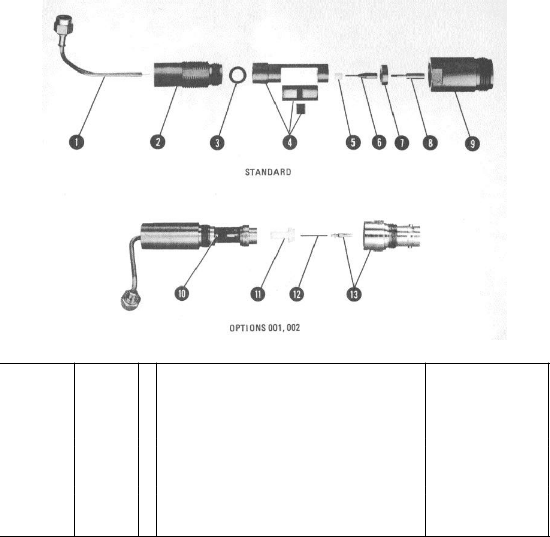
Model 8558B TM 11-6625-3061-14
Reference HP Part CMfr.
Designation Number DQty Description Code Mfr Part Number
108558-20080 3 1 Assy: Cable (Includes W1P1) 28480 08558-20080
208558-20079 0 1 Shell: Type-N Capacitor 28480 08558-20079
33050-0253 5 1 Washer: Spring 28480 3050-0253
408558-60127 3 1 Blocking Capacitor Assy 28480 08558-60127
508558-20077 8 1 Dielectric 28280 08558-20077
608558-20076 7 1 Conductor: Inner Type-N 28480 08558-20076
75040-0306 0 1 Capacitor Insulator 28480 5040-0306
81250-0915 8 1 Contact: RF Connector 02660 131-149
91250-0914 7 1 Body: RF Connector 02660 131-150
10 0160-3344 1 1 Capacitor: 0.12æF 50 Vdc 28480 0160-3344
11 08558-20101 9 1 Dielectric 28480 08558-20101
12 24 AWG Wire
13 1250-0505 2 1 RF Connector: 75 ohm 28480 1250-0505
(separate white teflon
dielectric supplied with
connector and pin is not used)
Figure 6-1. Cable Assembly W1 (08558-60038 or 08558-60031) Replaceable Parts
6-29/6-30(blank)
TM 11-1247-B
THIS PAGE MISSING NOT AVAILABLE FOR DIGITIZATION.
PAGES
6-31 through 6-33

Model 8558B TM 11-6625-3061-14
SECTION VII.
MANUAL BACKDATING CHANGES
7-1. INTRODUCTION
7-2. This section contains information for adapting this
manual to earlier 8558B Spectrum Analyzers. If the
serial number prefix of your spectrum analyzer appears
on the title page of this manual, the contents of the
manual are directly applicable to your instrument. If,
however, your spectrum analyzer has a lower serial
number prefix than what is shown on the title page, you
must adapt this manual to your instrument by changing
it as indicated in this section.
7-3. To adapt this manual to your instrument, refer to
Table 7-1 and make all the manual changes listed
opposite your instrument serial number. Make the
changes in the sequence in which they are given.
7-4. If your instrument serial number is not listed on the
title page of this manual, or in Table 7-1 below, it may
be documented in a yellow MANUAL CHANGES
supplement. For additional important information about
serial number coverage, refer to INSTRUMENTS
COVERED BY MANUAL in Section I.
NOTE
In instruments with serial numbers
listed in Table 7-1, some parts have
part numbers that are different from
those listed in the Replaceable Parts
list (Table 6-3) of this manual. Unless
otherwise indicated by the ‘change'
instructions in this section, however,
the listed parts are the recommended
replacement parts.
Table 7-1. Manual Change Requirements by Serial Number
Serial Number, Prefix or Complete Number Make Manual Changes:
2145A A
2142A A, B
2118A A,B,C
2024A06643 thru -06691, and 2024A06731 to, but A, B, C, D
not including, prefix 2118A
2024A prefix with suffixes thru 06642 A, B, C, D, E
1926A prefixes and 1914A with suffixes 04747,04918, A, B, C, D, E, F
04993,05158,05160, 05172, 05228,05229,05252,
05281,05297, 05300, thru 05307,05311,05312,
05313,05316,05318,05320
1914A with suffixes other than those listed above A, B, C, D, E, F, G
7-1

Model 8558B TM 11-6625-3061-14
7-5. MANUAL CHANGE INSTRUCTIONS
CHANGE A
Page 6-5, Table 6-3:
Insert Table 7-2 (CHANGE A), A1 Digital Panel Meter parts list, of this section so it precedes the A1A2 list.
Page 6-28, Table 6-3:
Substitute Table 7-3 (CHANGE A) of this section for list of Accessories and Chassis Parts shown in Table 6-3.
Page 6-31, Figure 6-2, Mechanical Chassis Parts:
Substitute Figure 7-1 (CHANGE A) of this section for Figure 6-2.
Page 6-33, Figure 6-3, Front Panel Assembly:
Substitute Figure 7-2 (CHANGE A) in this section for Figure 6-3.
Page 8-26, Figure 8-12, Front Switch Board Assembly A2A1 Component Locations:
Delete Figure 8-12.
Page 8-27, Figure 8-13, Front Switch Assembly A2 Schematic Diagram:
Substitute Figure 7-3 of this section for Figure 8-13.
General:
Change all references to front-panel control INPUT ATTEN (dB) to read 'OPTIMUM INPUT.' In Section III and in
the operation booklet, 8558B Spectrum Analyzer Operation, change front panel PUSH TO LOCK to LOCK (rotate
clockwise to lock 8558B into mainframe).
Change description of OPTIMUM INPUT (changed from INPUT ATTEN) control function to read: 'The optimum
and maximum input level selected is designated by the pointer behind the control. Push in control knob and turn
it to select the required input level range.
Use table below to translate input attenuation levels given in manual to optimum input levels.
INPUT OPTIMUM OPTION OPTION
ATTEN (dB) INPUT 001 002
0-40 dBm -35 dBm 15 dBmV
10 -30 dBm -25 dBm 25 dBmV
20 -20 dBm -15 dBm 35 dBmV
30 -10 dBm -5 dBm 45 dBmV
40 0 dBm 5 dBm 55 dBmV
50 10 dBm 15 dBm 65 dBmV
60 20 dBm 25 dBm 75 dBmV
70 30 dBm 30 dBm 80 dBmV
CHANGE B
Page 5-6,Table 5-1:
Add adjustment LOG GAIN, A14R1, paragraph 7-6, adjusts dc offset circuitry at output of Log Amplifier for 10 dB
steps in Log mode.
Add adjustment LOG/LIN, A14R2, paragraph 7-6, adjusts for Log-to-linear full-screen display translations.
Add adjustment LIN GAIN, A14R3, paragraph 7-6, adjusts Log Amplifier for 10 dB gain steps in Linear mode.
Affects adjustment of LOG/LIN.
7-2
Model 8558B TM 11-6625-3061-14
7-5. MANUAL CHANGE INSTRUCTIONS (Cont'd)
CHANGE B (Cont'd)
Page 5-45, Paragraph 5-26, Figure 5-13:
Substitute paragraph 7-6, LOG AMPLIFIER LOG AND LINEAR ADJUSTMENT (CHANGE
B) in this section for paragraph 5-26, and Figure 7-4 (CHANGE B) for Figure 5-13.
Pages 6-21 through 6-24, Table 6-3:
Replace entire A14 Replaceable Parts list (A14 through A14VR1) with Table 7-7 (CHANGE B)
of this section.
Page 6-31, Figure 6-2, Mechanical Chassis Parts:
Change item 30 to HP Part Number 08558-00086, Check Digit 7.
Page 8-84, Figure 8-37, A14 Log Amplifier Component and Test Point Locations:
Replace Figure 8-37 with Figure 7-5 (CHANGE B) of this section.
Pages 8-85/8-86 and 8-87/8-88, Figure 8-38, A14 Log Amplifier Schematic:
Replace Figure 8-38 with Figure 7-6 (2 sheets) (CHANGE B) of this section.
CHANGE C
Page 1-3,Table 1-1:
Under Calibrator Output, change '±300 kHz' to '±50 kHz.'
Page 1-8, Table 1-2:
Under Cal Output, change text to read as follows:
'-30 dBm, 280 MHz with 2nd through 5th harmonics greater than -60 dBm.
002: + 20 dBm V, 280 MHz with 2nd through 5th harmonics greater than - 10 dBm V.'
Page 6-12, Table 6-3:
Change A9C5 to HP Part Number 0150-2251, Check Digit 6, Qty 1, CAPACITOR-FXD 5.6PF
± .25PF.
Delete A9C20
Page 6-14, Table 6-3:
Add A9Y1, HP Part Number 0410-0447, Check Digit 0, Qty 1, CRYSTAL-QUARTZ
FREQ = 280 MHz 11th OVERTONE.
Delete A9Z 1.
Page 8-60, Figure 8-25:
Replace Figure 8-25 with Figure 7-7 (CHANGE C) of this section.
Page 8-61, Figure 8-26:
Replace function block A with function block A shown in Figure 7-8 (CHANGE C) of this section.
CHANGED
Page 6-14, Table 6-3:
Change A11C14 to HP Part Number 0160-2253, Check Digit 9, Qty 1, CAPACITOR-FXD
6.8PF ± .25PF 500VDC CER, 28480, 0160-2253.
Change A11C37 to HP Part Number 0160-2252, Check Digit 8, Qty 1, CAPACITOR-FXD
6.2PF ± .25PF 500VDC CER, 28480, 0160-2252.
7-3
Model 8558B TM 11-6625-3061-14
7-5. MANUAL CHANGE INSTRUCTIONS (Cont'd)
CHANGE D (Cont'd)
Pages 6-18, and 6-19, Table 6-3:
Change A13C14 to HP Part Number 0160-2253, Check Digit 9, Qty 1, CAPACITOR- FXD 6.8PF ± .25PF
500VDC CER, 28480, 0160-2253.
Change A13C37 to HP Part Number 0160-2252, Check Digit 8, Qty 1, CAPACITOR-FXD 6.2PF ±.25PF 500VDC
CER, 28480, 0160-2252.
Page 8-69, Figure 8-30, A11 Bandwidth Filter No. 1 Schematic:
Change value of C14 to 6.8PF, and value of C37 to 6.2PF.
Page 8-79, Figure 8-35, A13 Bandwidth Filter No. 2 Schematic:
Change value of C14 to 6.8PF, and value of C37 to 6.2PF.
CHANGE E
Page 6-26, Table 6-3:
Delete A16C9 and A16C10.
Page 8-97, Figure 8-44:
Delete C9 and C10.
CHANGE F
Page 5-7,Table 5-2:
Change A9R14 to A9R25.
Pages 6-12 and 6-13, Table 6-3:
Delete A9C17, A9C18, A9C19, A9CR7, A9L15, and A9L16.
Change A9R12* (standard instrument) to HP Part Number 0698-3132, Check Digit 4, Qty 1, RESISTOR 261 1%
.125W F TC=0 ± 100, 24546, C4-1/8-TO-2610-F.
Change A9R14* to A9R14, HP Part Number 0757-0462, Check Digit 3, Qty 1, RESISTOR 75K 1% .125W F TC
= 0 ± 100, 24546, C4-1/8-TO-7502-F.
Change A9R25 to A9R25*.
Page 8-60, Figure 8-25:
Replace Figure 8-25 with Figure 7-9 of this section.
Pages 8-57, and 8-58:
Replace circuit descriptions for 21.4 MHz Amplifier (E) and PIN Driver (F) with the circuit descriptions provided
below.
21.4 MHz Amplifier E
The 21.4 MHz Amplifier consists of A9Q3 in a common-emitter configuration and A9Q4 as an emitter follower.
Transistor A9Q3 employs resistor A9R12 and zener diode A9VR2 to furnish base bias and negative feedback for
gain control and stabilization. Resistor A9R12 is factory selected to provide the proper gain of the third converter
assembly. Capacitor A9C14 is connected across A9VR2 to reduce zener noise. The output of the 21.4 MHz
Amplifier looks into a voltage-controlled attenuator consisting of two PIN diodes, A9CR3 and CR4, resistor
A9R25, and the input impedance of the A11 Bandwidth Filter No. 1.
7-4
Model 8558B TM 11-6625-3061-14
7-5. MANUAL CHANGE INSTRUCTIONS (Cont'd)
CHANGE F (Cont'd)
PIN Driver (F)
The PIN diode resistance of A9CR3 and CR4 is controlled by the PIN driver A9Q5 and its associated circuitry.
The base of A9Q5 is the summing point for the frequency analog voltage from the A7 Frequency Control and a
dc level set by the front-panel REF LEVEL CAL screwdriver adjustment A2R3. Setting the dc level by adjusting
A2R3 calibrates the 8558B display at a given frequency, usually performed at 280 MHz. The frequency analog
voltage is a dc level varying from + 0.6 volts to + 6.7 volts as a function of frequency. This frequency analog
voltage at the base of A9Q5 compensates for input mixer response. SLOPE COMP adjustment A9R1 sets the
amount of compensation required for a flat frequency response. The total current through the PIN diodes A9CR3
and CR4 is shaped by the emitter network of A9Q5. This network provides a change in current through the PIN
diodes to cause a change of PIN diode resistance. The change in resistance is required to provide the proper log
curve within an 8 dB range for the voltage-controlled attenuator.
Page 8-61, Figure 8-26:
Replace function block E and F with function blocks E and F shown in Figure 7-10 (CHANGE F).
CHANGE G
Page 7-11, Figure 7-2:
Change item 53 HP Part Number to 08558-20052, Check Digit 9.
Change item 57 on HP Part Number 08552-20053, Check Digit 0.
7-5

Model 8558B TM 11-6625-3061-14
Table 7-2. Replaceable Parts (CHANGE A)
Reference HP Part CMfr.
Designation Number DQty Description Code Mfr Part Number
A1 DIGITAL PANEL METER ASSEMBLY
A1MP1 08558-00090 3 1 BRACKET, LEFT-HAND 28480 08558-00090
A1MP2 08558-00091 4 1 BRACKET, RIGHT-HAND 28480 08558-00090
A1MP3 08558-20130 4 2 DPM DISPLAY MOUNT 28480 08558-20130
A1MP4 08558-20130 4DPM DISPLAY MOUNT 28480 08558-20130
A1MP5 2200-0107 6 4 SCREW-MACH 4-40.375-IN-LG PAN-HD-POZI 28480 2200-0107
A1MP6 2200.0107 6SCREW-MACH 4-40.375-IN-LG PAN-HD-POZI 28480 2200-0107
A1MP7 2200-0107 6SCREW-MACH 4-40.375-IN-LG PAN-HD-POZI 28480 2200-0107
A1IMP8 2200-0107 6SCREW-MACH 4-40.375-IN-LG PAN-HD-POZI 28480 2200-0107
A1MP9 THRU 1
A1MP16 0520-0174 3 8SCREW-MACH 2-56 .25-IN-LG PAN-HD-POZI 28480 0520-0174
A1MP17 THRU
A1MP20 0610-0001 6 4 NUT-HEX-DBL-CHAM 2-56-THD.062-IN-THK 28480 0610-0001
A1MP21 THRU
A1MP24 2190-0890 1 4 WASHER-LK MTCL NO. 2.088-IN-ID 28480 2190-0890
A1MP25 THRU
A1MP28 3050-0098 6 4 WASHER-FL MTLC NO. 2.094-IN-ID 28480 3050-0098
A1A1 08558-60124 0 1 DPM DISPLAY 28480 08558-60124
A1A1DS1 1990-0619 7 4 DISPLAY-NUM-SEG 1-CHAR .3-H 28480 5082-7613
A1A1DS2 1990-0619 7DISPLAY-NUM-SEG 1-CHAR .3-H 28480 5082-7613
A1A1DS3 1990-0619 7DISPLAY-NUM-SEG 1-CHAR .3-H 28480 5082-7613
A1A1DS4 1990-0619 7DISPLAY-NUM-SEG 1-CHAR .3-H 28480 5082-7613
A1A1W1 08558-60130 8 1 CABLE ASSY RIBBON, DPM 28480 08558-60130
A1A1XDS1 1200-0693 4 4 SOCKET-IC 10-CONT DIP DIP-SLDR 51167 10-513-11
A1A1XDS2 1200-0693 4SOCKET-IC 10-CONT DIP DIP-SLDR 51167 10-513-11
A1A1XDS3 1200-0693 4SOCKET-IC 10-CONT DIP DIP-SLDR 51167 10-513-11
A1A1XDS4 1200-0693 4SOCKET-IC 10-CONT DIP DIP-SLDR 51167 10-513-11
7-6

Model 8558B TM 11-6625-3061-14
Table 7-3. Replaceable Parts (CHANGE A)
Reference HP Part CMfr.
Designation Number DQty Description Code Mfr Part Number
ACCESSORIES SUPPLIED
AT1 11593A 7 1 TERMINATION, 50 OHM 28480 11593A
1250-0780 5 1 ADAPTER, TYPE N MALE TO BNC FEMALE 28480 1250-0780
5020-8565 7 1 OVERLAY, 180 SERIES SCOPES 28480 5020-8565
5020-8566 8 1 OVERLAY, 181 SERIES SCOPES 28480 5020-8565
5020-8567 9 1 OVERLAY, 182 SERIES SCOPES 28480 5020-8567
08558-60131 9 1 KIT, SIDE STOP 28480 08558-60131
CHASSIS PARTS
P1 08558-60117 1 1 REAR-PANEL INTERCONNECT (PREWIRED) 28480 08558-60117
R1 2100-3593 8 1 RESISTOR-VAR PREC W/CP 10-TRN 5K 10% 28480 2100-3593
R2 2100-3452 8 1 RESISTOR-VAR PREC W/CP 10-TRN 10K 10% 28480 2100-3452
R3 2100-3066 0 1 RESISTOR-VAR PREC WW 10-TRN 5K 5% 28480 2100-3066
R4 2100-0542 1 1 RESISTOR-VAR CONTROL WW 10K 5% LIN 28480 2100-0542
R5 2100-3317 4 2 RESISTOR-VARIABLE W/SW 50K +-20% 10CW 28480 2100-3317
R6 2100-3317 4RESISTOR-VARIABLE W/SW 50K +-20% 10CW 28480 2100-3317
S1 3101.0044 1 1 SWITCH-PB SPST-NO MOM .5A 115VAC RED-BTN 28480 3101-0044
U1 5086-7282 1 1 LIMITER, RF INPUT 28480 5086-7282
W1 08558-60038 5 1 CABLE ASSY, INPUT, RF(SEE FIG. 6-1) 28480 08558-60038
W1 08558-60031 8 1 CABLE ASSY, INPUT, RF (OPT. 001/002) 28480 08558-60031
W2 NOT ASSIGNED
W3 08558-20071 2 1 CABLE ASSY, OUTPUT, L.O. 28480 08558-20071
W4 08558-20090 5 1 CABLE ASSY, INPUT, 1ST L.O. 28480 08558-20090
W5 08558-20073 4 1 CABLE ASSY, OUTPUT, 1ST I.F. 28480 08558-20073
W6 08558-20047 6 1 CABLE ASSY, INPUT, 2ND I.F. 28480 08558-60047
W7 08558-20048 7 1 CABLE ASSY, OUTPUT, 2ND I.F. 28480 08558-60048
W8 08558-20046 5 1 CABLE ASSY, CAL OUTPUT 28480 08558-60046
W8 08558-20074 9 1 CABLE ASSY, CAL OUTPUT (OPT. 001/002) 28480 08558-60074
W9 08558-60037 4 1 CABLE ASSY, INTERCONNECT 28480 08558-60037
W10 08558-60043 2 1 CABLE ASSY, OUTPUT, VERTICAL 28480 08558-60043
W11 NOT ASSIGNED
W12 08558-60044 3 1 CABLE ASSY, YIG DRIVER 28480 08558-60044
W13 08558-60080 7 1 CABLE ASSY, SECOND CONVERTER 28480 08558-60080
W14 08558-20117 7 1 CABLE ASSY, ATTENUATOR TO LIMITER 28480 08558-20117
W15 08558-20116 6 1 CABLE ASSY, LIMITER TO FIRST CONVERTER 28480 08558-20116
See introduction to this section for ordering information
*Indicates factory selected value
7-7

Model 8558B TM 11-6625-3061-14
Reference HP Part CMfr.
Designation Number DQty Description Code Mfr Part Number
MECHANICAL CHASSIS PARTS
108558-00002 7 1 PANEL, FRONT, SUP 28480 08558-00002
208558-00004 9 1 GUSSET, LEFT 28480 08558-00004
308558-00005 0 1 GUSSET, RIGHT 28480 08558-00005
408558-00003 8 1 PANEL, REAR 28480 08558-00003
508558-20039 2 1 GUIDE RAIL, LEFT 28480 08558-20039
608558-20040 5 1 GUIDE RAIL, RIGHT 28480 08558-20040
708558-20037 0 1 EXTRUSION, END PLATE ENCLOSURE 28480 08558-20037
808558-20036 9 1 EXTRUSION, CIRCUIT ENCLOSURE, TAPPED (4) 28480 08558-20036
908558-20051 7 2 EXTRUSION, CIRCUIT ENCLOSURE 28480 08558-20051
10 08558-20038 1 1 EXTRUSION, ENCLOSURE DIVIDER 28480 08558-20038
11 08558-40015 6 1 HOUSlNG, LATCH (FOR INSTRUMENTS WITH 28480 08558-40015
SERIAL PREFIX 13344 & BELOW, SEE
SECTION VII
12 08558-20092 7 1 SHIFT, LATCH 28480 08558-20092
13 08558-20030 1 1 INSULATOR, BOTTOM GUIDE RAIL 28480 08558-00030
14 08558-20041 6 1 GUIDE RAIL, BOTTOM 28480 08558-20041
15 08558-20027 8 1 BOARD, VERTICAL OUTPUT CONNECTOR 28480 08558-20027
16 0624-0203 9 8 SCREW-TPG 4-40 .375-IN-LG 82 DEG 28480 0624-0203
17 2200-0055 3 1 SCREW-MACH 4-40 .125-IN-LG 82 DEG 28480 2200-0055
18 2200-0104 3 17 SCREW-MACH 4-40 .25-IN-LG 82 DEG 28480 2200-0104
19 2360-0210 0 4 SCREW-MACH 6-32 .625-IN-LG 82 DEG 28280 2360-0210
20 0624-0268 6 40 SCREW-TPG 4-24 .375-IN-LG PAN-HD-POZI 28480 0624-0268
21 0624-0206 2 1 SCREW-TPG 6-32 .25.-IN-LG PAN-HD-POZI STL 28480 0624-0206
22 2200-0103 2 4 SCREW-MACH 4-40 .25-IN-LG PAN-HD-POZI 28480 2200-0103
23 2360-0115 4 1 SCREW-MACH 6-32 .31 2-IN-LG PAN-HD-POZI 28480 2360-0115
24 2200-0170 3 2 SCREW-MACH 4-40 .625.-IN-LG 82 DEG 28480 2200-0170
25 0380-0006 2 2 SPACER-RND .375-IN-LG .18-IN-ID 28480 0380-0006
26 2260-0003 7 2 NUT.HEX-PLSTC LKG 4-40-THD .141-IN.-THK 28480 2260-0003
27 2200-0107 2SCREW-MACH 4-40 .375IN-LG PAN-HD-POZI 28480 2200-0107
28 2200-0164 5 7 SCREW-MACH 4-40 .188-IN.LG UNCT 82 DEG 28480 2200-0164
29 2200-0168 9 3 SCREW-MACH 4-40 .438-IN-LG 82 DEG 28480 2200-0168
30 08558-00086 7 1 COVER, LOG AMPLIFIER28480 08558-00086
31 08558-00089 0 2 COVER, BANDWIDTH FILTER NO. 1 28480 08558-00089
32 08558-00088 9 1 COVER, STEP GAIN 28480 08558-00088
33 08558-00087 8 1 COVER, BANDWIDTH FILTER NO. 2 28480 08558-00087
34 08565-20096 0 1 EXTRUSION, CIRCUIT ENCLOSURE,TAPPED (8) 28480 08565-20096
35 08565-20093 7 1 EXTRUSION, CIRCUIT ENCLOSURE,TAPPED (4) 28480 08565-20093
Figure 7-1. Mechanical Chassis Parts (1 of 2) (CHANGE A)
7-8
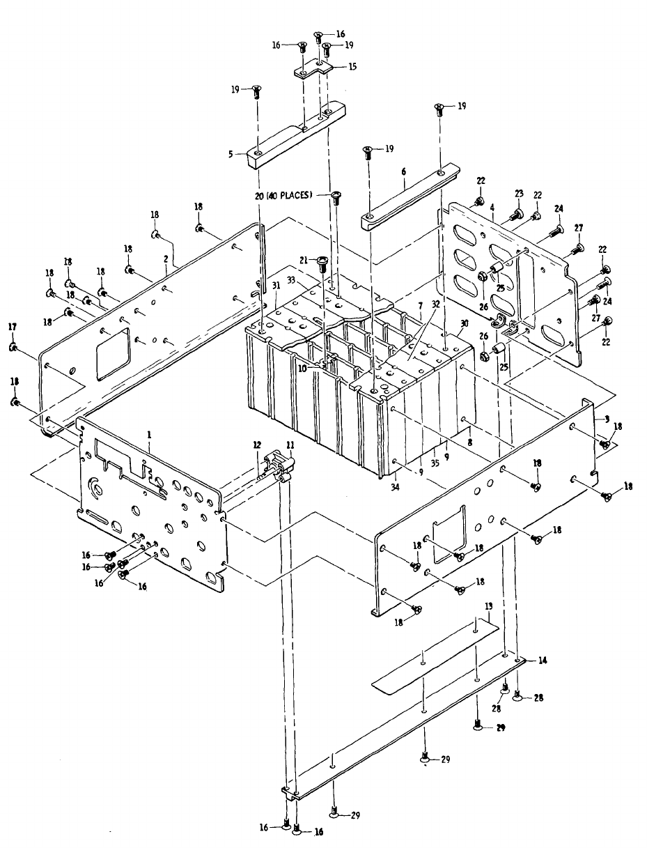
Model 8558B TM 11-6625-3061-14
Figure 7-1. Mechanical Chassis Parts (2 of 2) (CHANGE A)
7-9

Model 8558B TM 11-6625-3061-14
Reference HP Part CMfr.
Designation Number DQty Description Code Mfr Part Number
FRONT PANEL ASSEMBLY
108558-00036 7 1 KNOB,REF LEVEL FINE 28480 08558-00036
23030-0007 5 33 SCREW-SET 4-40 .125-IN-LG SMALL CUP-PT 28480 3030-0007
30510-0089 8 1 RETAINER-RING BSC EXT .188-IN-DIA BE-CU 28480 0510-0089
408558-00017 4 1 DISC, INDEX 28480 08558-00017
408558-00055 0 1 DISC, INDEX (OPTION 002) 28480 08558-00055
53050-0032 8 1 WASHER-FL MTLC NO. 8 .189-IN-ID 28480 3050-0032
608558-60050 1 1 KNOB, REF LEVEL 28480 08558-60050
608558-60072 7 1 KNOB, REF LEVEL (OPTION 002) 28480 08558-60072
73030-0022 4 10 SCREW-SET 6-32 .125-IN-LG SMALL CUP-PT 28480 3030-0022
808558-00043 9 1 NUT 28480 08558-00043
908558-00018 5 1 POINTER, ATTENUATOR 28480 08558-00018
10 08558-00038 9 1 KNOB, DIAL, RESOLUTION 28480 08558-00038
11 08558-60051 2 1 KNOB, FREQUENCY 28480 08558-60051
12 00180-67402 9 1 KNOB, FINE TUNING 28480 00180-67402
13 08558-00043 6 1 KNOB, COARSE TUNING 28480 08558-00043
14 08558-40003 2 1 WINDOW, DBM 28480 08558-40003
15 2950-0043 8 9 NUT-HEX-DBL-CHAM 3/8-32-THD .094-IN-THK 28480 2950-0043
16 2190-0016 3 13 WASHER-LK INTL T 3/8 IN .377-IN-ID 28480 2190-0016
17 1410-0721 4 1 BUSHING PNL .265-ID .47-LG 3/8-32-THD 28480 1410-0721
18 08558-40001 0 1 SLIDER, REF LEVEL 28480 08558-40001
19 2200-0781 2 3 SCREW-MACH 4-40 2.75-IN-LG PAN-HD-POZI 28480 2200-0781
20 08558-00019 6 3 DETENT, ATTENUATOR 28480 08558-00019
21 0380-0411 3 14 SPACER-RND .5-IN-LG .114-IN-ID 28480 0380-0411
22 08558-20047 2 4 BUSHING, PANEL 28480 08558-20047
23 08558-20051 8 1 SHAFT, REF LEVEL 28480 08558-20051
24 1410-0006 8 6 BALL-BRG TYPE .1875-DIA GRADE-50 SST 28480 1410-0006
25 1460-0578 4 5 SPRING-CPRSN .18-IN-OD .312-IN-DA-LG MUW 28480 1460-0578
26 08559-60060 4 6 HUB ASSEMBLY 28480 08559-60060
27 1480-0367 1 1 PIN-DWL ANSI-UNHDND/GND .0625-IN-DIA 28480 1480-0367
28 1480-0059 8 10 PIN-ROLL .062-IN-DIA .25-IN-LG STL 28480 1480-0059
29 08558-40011 1 1 ROTOR, ATTENUATOR DRIVE 28480 08558-40011
30 08558-40008 1 1 GEAR, 45 TEETH 28480 08558-40008
31 0510-0015 2 2 RETAINER-RING E-R EXT .125-IN-DIA STL 28480 0510-0015
32 08558-60046 2 2 CABLE, CAL OUTPUT 28480 08558-60046
32 08558-60074 CABLE, CAL OUTPUT, 75 OHM (OPT. 001/002) 28480 08558-60074
33 2200-0509 1 1 SCREW-MACH 4-40 1.625-IN-LG PAN-HD-POZI 28480 2200-0509
34 2200-0125 1 1 SCREW-MACH 4-40 1.5-IN-LG PAN-HD-POZI 28480 2200-0125
35 08558-00024 2 2 DETENT, SWEEP TIME 28480 08558-00024
36 08558-20050 1 1 SHAFT, SWEEP WIDTH 28480 08558-20050
37 08558-20066 1 1 ROTOR, FREQUENCY SPAN 28480 08558-20066
38 08558-20089 2 1 BUSHING, SLOTTED 28480 08558-20089
39 1460-1376 2 1 SPRING-TRSN MUW 28480 1460-1376
40 08558-20088 1 1 GEAR, 20 TEETH 28480 08558-20088
41 0520-0139 0 2 SCREW-MACH 2-56 .875-IN-LG PAN-HD-POZI 28480 0520-0139
42 0380-0487 3 2 SPACER-RND .625-IN-LG .086-IN-ID 28480 0380-0487
43 NOT ASSIGNED 28480
44 0610-0002 7 2 NUT, HEX-BL-CHAM 2-56-THD .062-IN-LG 28480 0610-0002
45 08558-20002 9 1 BOARD, FRONT SWITCH 28480 08558-20002
46 08558-40005 4 3 ROTOR, DOUBLE CONTACT 28480 08558-40005
47 3050-0017 9 3 WASHER-FL MTLC ¼ IN .26-IN-ID 28480 3050-0017
48 1460-0532 0 1 SPRING-CPRSN .54-IN-OD .45-IN-DA-LG MUW 28480 1460-0532
49 2200-0165 6 4 SCREW-MACH 4-40 .25-IN-LG 82 DEG 28480 2200-0165
50 08558-00020 9 1 DETENT, IF GAIN 28480 08558-00020
51 08558-20061 0 1 LOCKOUT, ROTATING 28480 08558-20061
52 08558-20062 1 1 LOCKOUT, FIXED 28480 08558-20062
53 08558-20052 9 1 SHAFT, FIXED 28480 08558-20052
54 2260-0002 6 18 NUT-HEX-DBL-CHAM 4-40-THD .062-IN-THK 28480 2260-0002
55 0380-0413 5 3 SPACER-RND 1.25-IN-LG .114-IN-ID 28480 0380-0413
56 08558-00022 1 1 CRANK, SLOTTED 28480 08558-00022
57 08558-20053 0 1 SHAFT, REF LEVEL FINE 28480 08558-20053
58 1490-0841 7 1 COUPLER-RGD .375-LG BRS 28480 1490-0841
59 2950-0006 3 4 NUT-HEX-DBL-CHAM ¼-32-THD .094-IN-THK 28480 2950-0006
60 2190-0027 6 6 WASHER-LK INTL T ¼ IN .256-IN-ID 28480 2190-0027
61 08558-00021 0 1 PLATE, LEVEL POT 28480 08558-00021
62 2190-0019 6WASHER-LK HLCL NO. 4 .115-IN-ID 28480 2190-0019
63 08558-20054 1 1 SHAFT, ATTENUATOR DRIVE 28480 08558-20054
64 1430-0036 6 2 GEAR-MIT 16-T 32-DP 20-DEG PA BRS 28480 G462Y (MOD)
65 NOT ASSIGNED 28480
66 08558-00081 2 1 BRACKET, ATTENUATOR 28480 08558-00081
67 3050-0105 6 4 WASHER-FL MTLC NO. 4 .125-IN-ID 28480 3050-0105
68 NOT ASSIGNED 28480
69 08558-20030 3 1 BOARD, REAR SWITCH 28480 08558-20030
70 2200-0143 0 2 SCREW-MACH 4-40 .375-IN-LG PAN-HD-POZI 28480 2200-0143
71 08558-40004 3 1 ROTOR, SINGLE CONTACT 28480 08558-40004
72 08558-00025 4 1 DETENT, BANDWIDTH 28480 08558-00025
Figure 7-2. Front Panel Assembly (1 of 3) (CHANGE A)
7-10
TM 11-1247-B
THIS PAGE MISSING NOT AVAILABLE FOR DIGITIZATION.
PAGES
7-11 through 7-14
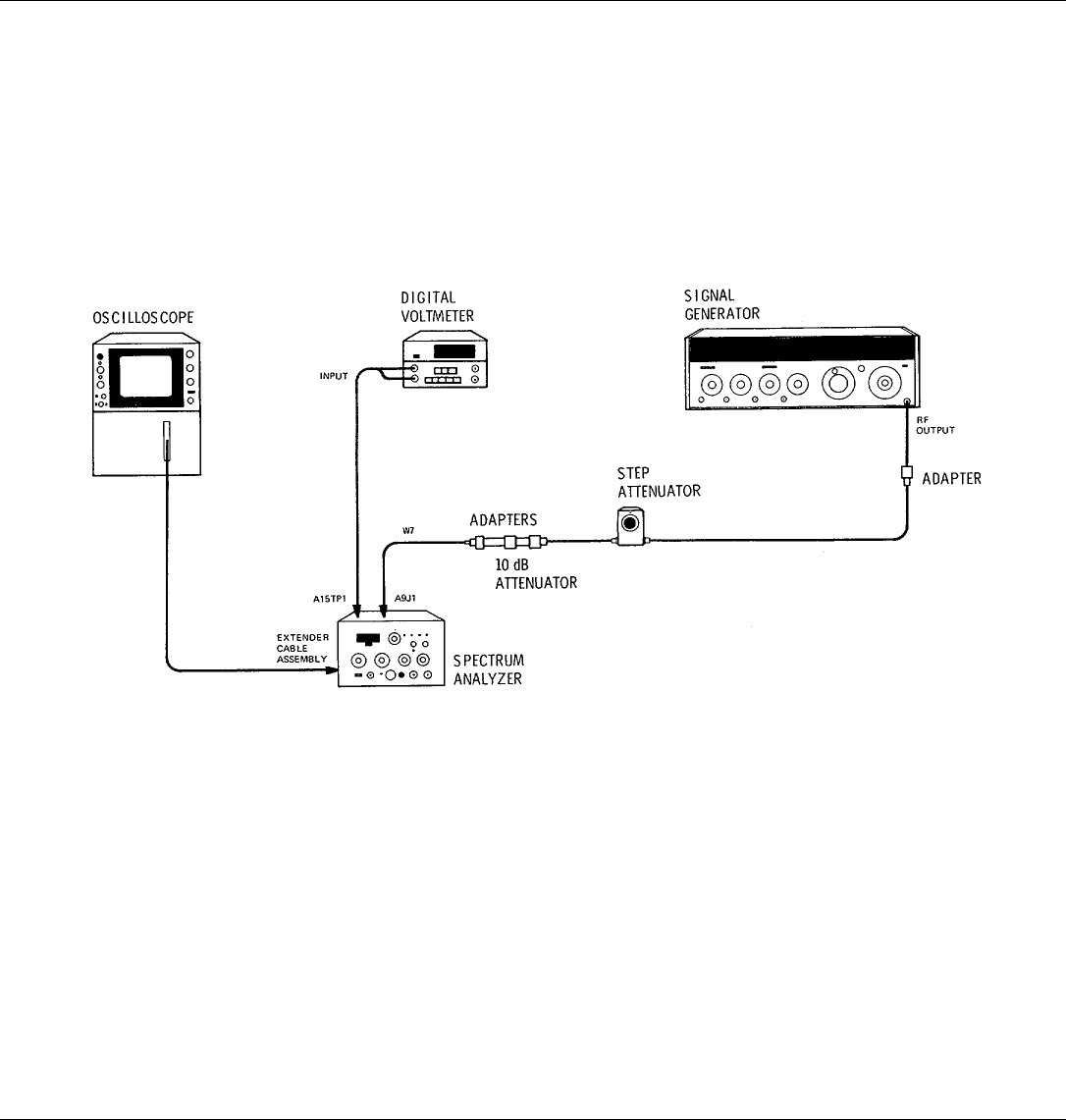
Model 8558B TM 11-6625-3061-14
ADJUSTMENTS
7-6. LOG AMPLIFIER LOG AND LINEAR ADJUSTMENT (CHANGE B)
REFERENCE
A14 and A15 Schematics
DESCRIPTION
10 dB/DIV and LIN are adjusted for correct steps and full-screen display translations.
Figure 7-4. Log Amplifier Log and Linear Adjustment Test Setup (CHANGE B)
EQUIPMENT
Signal Generator.......................................................................................................................HP 8640B
Digital Voltmeter.........................................................................................................HP 34740A/34702A
10 dB Attenuator....................................................................................................HP 8491A, Option 010
Step Attenuator (10 dB/step).......................................................................................................HP 355D
Adapter, Type N Male on one end,
BNC Female on other end (2 required)..........................................................................HP 1250-0780
Adapter, Type N Female on both ends................................................................................HP 1250-0777
Adapter, Type N Male on one end,
SMC Male on other end................................................................................................HP 1250-1023
7-15

Model 8558B TM 11-6625-3061-14
ADJUSTMENTS
7-6. LOG AMPLIFIER LOG AND LINEAR ADJUSTMENT (CHANGE B) (Cont'd)
PROCEDURE
1. Set spectrum analyzer controls as follows:
FREQ SPAN/DIV ............................................................................................................................1 MHz
RESOLUTION BW .......................................................................................................................300 kHz
OPTIMUM INPUT .......................................................................................................................- 30 dBm
001: - 25 dBm
002: + 25 dBm V
REFERENCE LEVEL dBm..................................................................................................................- 50
002: 0 dBm V
10 dB/DIV - 1 dB/DIV - LIN...................................................................................................................LIN
SWEEP TIME/DIV ..........................................................................................................................AUTO
SWEEP TRIGGER..................................................................................................................FREE RUN
2. Connect equipment as shown in Figure 7-4. Set signal generator frequency to 301.4 MHz and output level to - 13
dBm. Remove W7P1 from Second IF assembly A10J2. Connect signal generator output through step attenuator, 0
dB attenuator, and adapters to W7P1.
NOTE
The 10 dB attenuator is included to compensate for the 10 dB of gain on A12 Step
Gain assembly when the TEST-NORM switch is in TEST.
3. Set the TEST-NORM switch on A12 Step Gain assembly to the TEST position. Tune signal generator frequency for
maximum signal amplitude on oscilloscope display with step attenuator set at 0 dB.
4. Set output level of signal generator for a digital voltmeter reading of 700 mV, with step attenuator set at 0 dB and
REFERENCE LEVEL control set to - 50 dBm.
002: 0 dBm V
5. Set 8558B REFERENCE LEVEL to - 80 dBm and set step attenuator to 30 dB. Observe digital voltmeter reading.
002: - 30 dBm V
6. Adjust A14R3 LIN GAIN for a digital voltmeter reading of 700 mV.
7. Repeat steps 4, 5, and 6 until the DVM reading in step 5 is 700 +2 . mV.
8. Set 8558B REFERENCE LEVEL to -50 dBm and set step attenuator to 0 dB. Change REFERENCE LEVEL and step
attenuator settings as shown in Table 7-4. If Deviation From Reference is not within the given limits, readjust
A14R3.
002: Set REFERENCE LEVEL dBm V to 0 and set attenuator to 0 dB. REFERENCE
LEVEL (dBmV) settings in Table 5-7 top to bottom are, 0, -10, -20, -30, -40.
7-16

Model 8558B TM 11-6625-3061-14
ADJUSTMENTS
7-6. LOG AMPLIFIER LOG AND LINEAR ADJUSTMENT (CHANGE B) (Cont'd)
Table 7-4. Linear Gain Adjustment Limits
Reference Level Step Attenuator Deviation From
(dBm) Setting (dB) Reference
-50 0Reference
-60 10 ±0.2 DIV ±20 mV
-70 20 ±0.2 DIV ±20 mV
-80 30 ±0.2 DIV ±20 mV
-90 40 ±0.3 DIV ±30 mV
9. Set 8558B REFERENCE LEVEL to 0 dBm and disconnect signal generator from step attenuator. Record offset
reading (DVM). The offset should be less than + 30 mV.
002: REFERENCE LEVEL, +50 dBm V
10. Reconnect signal generator as shown in Figure 7-3. Set 10 dB/DIV - 1 dB/DIV - LIN switch to 10 dB/DIV and set step
attenuator to 40 dB.
11. Set output level of signal generator for a digital voltmeter reading of 400 mV plus offset recorded in step 9 (algebraic
sum). (Example: If offset is - 23 mV, set output level of signal generator for a DVM reading of 377 mV.)
12. Set step attenuator to 0 dB. Digital voltmeter should indicate 800 mV, plus offset (algebraic sum) ±1 mV. If DVM
reading is not within limits, adjust A14R2 LOG/LIN adjustment for a digital voltmeter reading of 800 mV, plus offset
minus 50 percent of overshoot. Example: If DVM indicates 767 mV and should be indicating 777 mV (-10 mV
overshoot), adjust A14R2 for a DVM reading of 777 mV minus - 5 mV, or 782 mV.
13. Repeat steps 10, 11, and 12 until the digital voltmeter indicates 800 mV plus offset ±1 mV with no further adjustment
of A14R2 in step 12.
14. Set the step attenuator to the positions shown in Table 7-5 and record DVM reading for each setting. Correct the
DVM readings by algebraically adding the offset (recorded in step 9).
15. Readjust A14R2 if necessary to meet the limits in Table 7-5.
16. Set step attenuator to 0 dB and set output level of signal generator for a digital voltmeter reading of 800 mV plus
offset (recorded in step 9) ±1 mV.
17. Set 10 dB/DIV - 1 dB/DIV - LIN switch to LIN. The digital voltmeter should indicate the reading set in step 16 ±25
mV. If it does, go to step 19. If it does not, or if log fidelity is not within limits, go to step 18 and select A14R16*.
7-17

Model 8558B TM 11-6625-3061-14
ADJUSTMENTS
7-6. LOG AMPLIFIER LOG AND LINEAR ADJUSTMENT (CHANGE B) (Cont'd)
Table 7-5. Log Fidelity Check
DVM Reading Corrected For Offset
Step Attenuator DVM Reading
Setting (dB) (mV) Min. (mV) Actual (mV) Max. (mV)
0 _______________ 799 _______________ 801
10 _______________ 697 _______________ 703
20 _______________ 596 _______________ 604
30 _______________ 496 _______________ 504
40 _______________ 395 _______________ 405
50 _______________ 294 _______________ 306
60 _______________ 193 _______________ 207
70 _______________ 92 _______________ 108
18. Select A14R16* to obtain an output in step 17 within ±25 mV of the reading set in step 16. Decreasing A14R16* 10
percent will increase the DVM reading approximately 30 mV in step 17.
NOTE
Log fidelity must be considered when selecting A14R16*. That is, if the DVM
READING CORRECTED FOR OFFSET in Table 7-5 is greater than 100 mV for a
STEP ATTENUATOR SETTING of 70 dB, A14R16* should be selected for a DVM
reading greater than the reading set in step 16. If the READING CORRECTED FOR
OFFSET is less than 100 mV, A14R16* should be selected for DVM reading less
than the reading set in step 16.
19. Set output level of signal generator for a digital voltmeter reading of 800 mV plus offset (algebraic sum) ±m 1 V.
20. Set 8558B 10 dB/DIV - 1 dB/DIV - LIN switch to 10 dB/DIV and adjust A14R2 LOG/LIN adjustment for a digital
voltmeter reading of 800 mV plus offset.
21. Repeat step 14 to recheck the log fidelity.
22. Set the 8558B REFERENCE LEVEL dBm control to -50. Set the 10 dB/DIV - 1 dB/DIV - LIN switch to 1 dB/DIV.
002: 0 dBm V
23. Set the step attenuator to 0 dB and set output level of signal generator for a digital voltmeter reading of 700 mV (do
not include offset).
24. Set the 8558B REFERENCE LEVEL dBm control to -90 and the step attenuator to 40 dB. Adjust A14RI LOG GAIN
adjustment for a digital voltmeter reading of 700 mV.
002: - 40 dBm V
7-18

Model 8558B TM 11-6625-3061-14
ADJUSTMENTS
7-6. LOG AMPLIFIER LOG AND LINEAR ADJUSTMENT (CHANGE B) (Cont'd)
25.Change REFERENCE LEVEL and step attenuator settings as shown in Table 7-6. Deviation From Reference should
not exceed the given limits.
002: REFERENCE LEVEL (dBmV) settings, top to bottom are, 0, -10, -20, -30, -40.
26.Return the TEST-NORM switch on A12 assembly to the NORM position.
Table 7-6. Log Gain Adjustment Limits
Reference Level Step Attenuator Deviation From
(dBm) Setting (dB) Reference
-50 0 Reference
-60 10 ±0.3 DIV ±30 mV
-70 20 ±0.3 DIV ±30 mV
-80 30 ±0.3 DIV ±30 mV
-90 40 ±0.3 DIV ±30 mV
7-19

Table 7-7. Replaceable Parts (1 of 4) (CHANGE B)
Reference HP Part CMfr.
Designation Number DQty Description Code Mfr Part Number
A14 08565-60111 4 1 LOG AMPLIFIER 28480 08565-60111
A14C1 0160-2055 9 59 CAPACITOR-FXD .01UF +80-20% 100VDC CER 28480 0160-2055
A14C2 0160-3459 9 7 CAPACITOR-FXD .02UF +-20% 100VDC CER 28480 0160-3459
A14C3 0160-3459 9CAPACITOR-FXD .02UF +-20% 100VDC CER 28480 0160-3459
A14C4 0160-3459 9CAPACITOR-FXD .02UF +-20% 100VDC CER 28480 0160-3459
A14C5 0160-3459 9CAPACITOR-FXD .02UF +-20% 100VDC CER 28480 0160-3459
A14C6 0160-2055 9CAPACITOR-FXD .01UF +80-20% 100VDC CER 28480 0160-2055
A14C7 0160-3459 9CAPACITOR-FXD .02UF +-20% 100VDC CER 28480 0160-3459
A14C8 0160-3459 9CAPACITOR-FXD .02UF +-20% 100VDC CER 28480 0160-3459
A14C9 0160-2055 9CAPACITOR-FXD .01UF +80-20% 100VDC CER 28480 0160-2055
A14C10 0160-2055 9CAPACITOR-FXD .01UF +80-20% 100VDC CER 28480 0160-2055
A14C11 0160-2055 9CAPACITOR-FXD .01UF +80-20% 100VDC CER 28480 0160-2055
A14C12 0160-2055 9CAPACITOR-FXD .01UF +80-20% 100VDC CER 28480 0160-2055
A14C13 0160-2055 9CAPACITOR-FXD .01UF +80-20% 100VDC CER 28480 0160-2055
A14C14 0160-2055 9CAPACITOR-FXD .01UF +80-20% 100VDC CER 28480 0160-2055
A14C15 0160-2055 9CAPACITOR-FXD .01UF +80-20% 100VDC CER 28480 0160-2055
A14C16 0160-2055 9CAPACITOR-FXD .01UF +80-20% 100VDC CER 28480 0160-2055
A14C17 0160-2055 9CAPACITOR-FXD .01UF +80-20% 100VDC CER 28480 0160-2055
A14C18* 0160-2234 6 1 CAPACITOR-FXD .51PF +-.25PF 500VDC CER 28480 0160-2055
A14C19 0160-2055 9CAPACITOR-FXD .01UF +80-20% 100VDC CER 28480 0160-2055
A14C20 0160-2236 8CAPACITOR-FXD 1PF +-25PF 500VDC CER 28480 0160-2236
A14C21 0160-2055 9CAPACITOR-FXD .01UF +80-20% 100VDC CER 28480 0160-2055
A14C22 0160-2055 9CAPACITOR-FXD .01UF +80-20% 100VDC CER 28480 0160-2055
A14C23 0160-2055 9CAPACITOR-FXD .01UF +80-20% 100VDC CER 28480 0160-2055
A14C24 0160-2055 9CAPACITOR-FXD .01UF +80-20% 100VDC CER 28480 0160-2055
A14C25 0160-2055 9CAPACITOR-FXD .01UF +80-20% 100VDC CER 28480 0160-2055
A14C26 0160-2055 9CAPACITOR-FXD .01UF +80-20% 100VDC CER 28480 0160-2055
A14C27 0160-2055 9CAPACITOR-FXD .01UF +80-20% 100VDC CER 28480 0160-2055
A14C28 0160-0228 6 1 CAPACITOR-FXD 22UF +-10% 15VDC TA 28480 150D226X901582
A14C29 0160-2055 9CAPACITOR-FXD .01UF +80-20% 100VDC CER 28480 0160-2055
A14C30* 0160-2236 8 5 CAPACITOR-FXD 1PF +-25PF 500VDC CER 28480 0160-2236
A14C31 0160-2055 9CAPACITOR-FXD .01UF +80-20% 100VDC CER 28480 0160-2055
A14C32 0160-2055 9CAPACITOR-FXD .01UF +80-20% 100VDC CER 28480 0160-2055
A14C33 0160-2055 9CAPACITOR-FXD .01UF +80-20% 100VDC CER 28480 0160-2055
A14C34 0160-2055 9CAPACITOR-FXD .01UF +80-20% 100VDC CER 28480 0160-2055
A14C35 0160-2055 9CAPACITOR-FXD .01UF +80-20% 100VDC CER 28480 0160-2055
A14C36 0160-2055 9CAPACITOR-FXD .01UF +80-20% 100VDC CER 28480 0160-2055
A14C37 0160-2055 9CAPACITOR-FXD .01UF +80-20% 100VDC CER 28480 0160-2055
A14C38 0160-2055 9CAPACITOR-FXD .01UF +80-20% 100VDC CER 28480 0160-2055
A14C39 0160-2055 9CAPACITOR-FXD .01UF +80-20% 100VDC CER 28480 0160-2055
A14C40* 0160-2236 8CAPACITOR-FXD 1PF +-25PF 500VDC CER 28480 0160-2236
A14C41 0160-2055 9CAPACITOR-FXD .01UF +80-20% 100VDC CER 28480 0160-2055
A14C42 0160-2055 9CAPACITOR-FXD .01UF +80-20% 100VDC CER 28480 0160-2055
A14C43 0160-2055 9CAPACITOR-FXD .01UF +80-20% 100VDC CER 28480 0160-2055
A14C44 0160-2055 9CAPACITOR-FXD .01UF +80-20% 100VDC CER 28480 0160-2055
A14C45 NOT ASSIGNED
A14C46 0160-2055 9CAPACITOR-FXD .01UF +80-20% 100VDC CER 28480 0160-2055
A14C47 0160-2055 9CAPACITOR-FXD .01UF +80-20% 100VDC CER 28480 0160-2055
A14C48 0160-2055 9CAPACITOR-FXD .01UF +80-20% 100VDC CER 28480 0160-2055
A14C49 0160-2055 9CAPACITOR-FXD .01UF +80-20% 100VDC CER 28480 0160-2055
A14C50 0160-2055 9CAPACITOR-FXD .01UF +80-20% 100VDC CER 28480 0160-2055
A14C51 0160-3459 9CAPACITOR-FXD .02UF +-20% 100VDC CER 28480 0160-3459
A14C52* 0160-2236 8CAPACITOR-FXD 1PF +-25PF 500VDC CER 28480 0160-2236
A14C53 0160-2055 9CAPACITOR-FXD .01UF +80-20% 100VDC CER 28480 0160-2055
A14C54 0160-2055 9CAPACITOR-FXD .01UF +80-20% 100VDC CER 28480 0160-2055
A14C55 0160-2055 9CAPACITOR-FXD .01UF +80-20% 100VDC CER 28480 0160-2055
A14C56 0160-2055 9CAPACITOR-FXD .01UF +80-20% 100VDC CER 28480 0160-2055
A14C57* 0160-2256 2CAPACITOR-FXD 9.1PF +-.2PF 500VDC CER 28480 0160-2256
A14C58 0160-2055 9CAPACITOR-FXD .01UF +80-20% 100VDC CER 28480 0160-2055
A14C59 0160-2055 9CAPACITOR-FXD .01UF +80-20% 100VDC CER 28480 0160-2055
A14C60 0160-2055 9 CAPACITOR-FXD .01UF +80-20% 100VDC CER 28480 0160-2055
A14C61 0160-2055 9CAPACITOR-FXD .01UF +80-20% 100VDC CER 28480 0160-2055
A14C62 0160-0195 2 1 CAPACITOR-FXD 130PF +-5% 300VDC MICA 28480 DM15F131J0300WV1CR
A14C63 0160-2055 9CAPACITOR-FXD .01UF +80-20% 100VDC CER 28480 0160-2055
A14C64 0160-2308 5 1 CAPACITOR-FXD 36PF +-5% 500VDC MICA 28480 0160-2308
A14C65 0160-2240 4 1 CAPACITOR-FXD 2PF +-.25PF 500VDC CER 28480 0160-2240
A14C66 0160-2055 9CAPACITOR-FXD .01UF +80-20% 100VDC CER 28480 0160-2055
A14C67 0160-2236 8CAPACITOR-FXD 1PF +0-.25PF 500VDC CER 28480 0160-2236
A14C68 0160-2055 9CAPACITOR-FXD .01UF +80-20% 100VDC CER 28480 0160-2055
A14C69 0160-2055 9CAPACITOR-FXD .01UF +80-20% 100VDC CER 28480 0160-2055
A14C70 0160-2055 9CAPACITOR-FXD .01UF +80-20% 100VDC CER 28480 0160-2055
See introduction to this section for ordering information
*Indicates factory selected value
7-20

Model 8558B TM 11-6625-3061-14
Table 7-7. Replaceable Parts (2 of 4) (CHANGE B)
Reference HP Part CMfr.
Designation Number DQty Description Code Mfr Part Number
A14C71 0160-2055 9CAPACITOR-FXD .01UF +80-20% 100VDC CER 28480 0160-2055
A14C72 0160-2055 9CAPACITOR-FXD .01UF +80-20, 100VDC CER 28480 0160-2055
A14C73 0160-2055 9CAPACITOR-FXD .01UF +80-20 100VDC CER 28080 0160-2055
A14C74 0180-2206 4 1 CAPACITOR-FXD 60UF+ -10% 6VDC TA 56289 150D606X9006B2
A14C75 0160-2055 9CAPACITOR-FXD .01UF +80-20% 100VDC CER 28480 0160-2055
A14C76 0160-2055 9CAPACITOR-FXD .01UF +80-20% 100VDC CER 28480 0160-2055
A14C77 0160-2055 9CAPACITOR-FXD .01UF +80-20% 100VDC CE 28480 0160-2055
A14C78 0180-0197 8 5 CAPACITOR-FXD 2.2UF+ -10% 20VDC TA 56280 150D225X9020A2
A14CR1 1901-0040 1 17 DIODE-SWITCHING 30V 50MA 2NS DO-35 28480 1901-0040
A14CR2 1901-0040 1DIODE-SWITCHING 30V 50MA 2NS DO-35 28480 1901-0040
A14CR3 1901-1085 6 17 DIODE-SCHOTTKY 28480 1901-1085
A14CR4 1901-1085 6DIODE-SCHOTTKY 28480 1901-1085
A14CR5 1901-0040 1DIODE-SWITCHING 30V 50MA 2NS DO-35 28480 1901-0040
A14CR6 1901-0040 1DIODE-SWITCHING 30V 50MA 2NS DO-35 284080 1901-0040
A14CR7 1901-0040 1DIODE-SWITCHING 30V 50MA 2NS DO-35 28480 1901-0040
A14CR8 1901-1085 6DIODE-SCHOTTKY 28480 1901-1085
A14CR9 1901-1085 6DIODE-SCHOTTKY 28480 1901-1085
A14CR10 1901-1085 6DIODE-SCHOTTKY 28480 1901-1085
A14CR11 1901-1085 6DIODE-SCHOTTKY 28480 1901-1085
A14CR12 1901-1085 6DIODE-SCHOTTKY 28480 1901-1085
A14CR13 1901-1085 6DIODE-SCHOTTKY 28480 1901-1085
A14CR14 1901-0040 8 3 DIODE-SWITCHING 20V 75MA 10NS 28480 1901-0047
A14CR15 1901-1085 6DIODE-SCHOTTKY 28480 1901-1085
A14CR16 1901-1070 9 2 DIODE-PIN 110V 28480 1901-1010
A14CR17 1901-1085 6DIODE-SCHOTTKY 28480 1901-1085
A14CR18 1901-1070 9DIODE-PIN 110V 28480 1901-1070
A14CR19 1901-0040 1DIODE-SWITCHING 30V 50MA 2NS D0-35 28480 1901-0040
A14CR20 1901-1085 6DIODE-SCHOTTKY 28480 1901-1085
A14CR21 1901-1085 6DIODE-SCHOTTKY 28480 1901-1085
A14CR22 1901-1085 6DIODE-SCHOTTKY 28480 1901-1085
A14CR23 1901-1085 6DIODE-SCHOTTKY 28480 1901-1085
A14CR24 1901-0040 1DIODE-SWITCHING 30V 50MA 2NS DO-35 28480 1901-0040
A14CR25 1901-1085 6DIODE-SCHOTTKY 28480 1901-1085
A14CR26 1901-0047 8DIODE-SWITCHING 20V 75MA 10NS 28480 1901-0047
A14CR27 1901-1085 6DIODE-SCHOTTKY 28480 1901-1085
A14CR28 1901-1085 6DIODE-SCHOTTKY 28480 1901-1085
A14CR29 1901-0047 8DIODE-SWITCHING 20V 75MA 10NS 28480 1901-0047
A14CR30 1901-0040 1DIODE-SWITCHING 30V 50MA 2NS DO-35 28480 1901-0040
A14CR31 1901-0040 1DIODE-SWITCHING 30V 50MA 2NS D0-35 28480 1901-0040
A14CR32 1901-0040 1DIODE-SWITCHING 30V 50MA 2NS DO-35 28480 1901-0040
A14E1 9170-0029 3 1 CORE-SHIELDING READ 28480 9170-0029
A14L1 9100-1622 7 2 COIL-MLD 24AUH 5% Q=60 .155DX .375L-NOM 28480 9100-1622
A14L2 9100-0105 3 1 COIL-MLD 8.2UH 10% Q=50 .155DX .375LG-NOM 28480 9100-0105
A14L3 9100-1619 2 7 COIL-MLD 6.8UH 10% Q=50 .155DX .375LG-NOM 28480 9100-1619
A14L4 9100-1619 2COIL-MLD 6.8UH 10% Q=50 .155DX .375LG-NOM 28480 9100-1619
A14L5 9100- 2COIL-MLD 6.8UH 10% Q=50 .155DX .375LG-NOM 28480 9100-1619
A14L6 9100-1619 2COIL-MLD 6.8UH 10% Q=50 .155DX .375LG-NOM 28480 9100-1619
A14L7 9100-1619 2COIL-MLD 6.8UH 10% Q=50 .155DX .375LG-NOM 28480 9100-1619
A14L8 9100-1619 2COIL-MLD 6.8UH 10% Q=50 .155DX .375LG-NOM 28480 9100-1619
A14L9 9100-1627 2 1 COIL-MLD 39UH 5% Q=60 .155DX.375LG-NOM 28480 9100-1627
A14L10 9100-1629 4 1 COIL-MLD 47UH 5% Q=55 .155DX.375LG-NOM 28480 9100-1629
A14L11 9100-1622 7COIL-MLD 24UH 5% Q=60 .155DX .375LG-NOM 28480 9100-1622
A14L12 9100-1619 2COIL-MLD 6.8UH 10% Q=50 .155DX .375LG-NOM 28480 9100-1619
A14L13 9140-0145 1 1 COIL-MLD 8.2UH 10% Q=60 .095DX .25LG-NOM 28480 9140-0145
A14L14 9100-2269 0 0 COIL-MLD 27UH 10% Q=45 .095DX .25LG-NOM 28480 9100-2269
A14Q1 1854-0071 7 3 TRANSISTOR NPN SI PD=300mw FT=20OMHZ 28480 1854-0071
A14Q2 1854-0019 3 15 TRANSISTOR NPN SI TO-18 PD=360mw 28480 1854-0019
A14Q3 1854-0019 3TRANSISTOR NPN SI TO-18 PD=360mw 28480 1854-0019
A14Q4 1854-0019 3TRANSISTOR NPN SI TO-18 PD=360mw 28480 1854-0019
A14Q5 1854-0019 3TRANSISTOR NPN SI TO-18 PD=360mw 28480 1854-0019
A14Q6 1854-0019 3TRANSISTOR NPN SI TO-18 PD=360mw 28480 1854-0019
A14Q7 1854-0019 3TRANSISTOR NPN SI TO-18 PD=360mw 28480 1854-0019
A14Q8 1854-0019 3TRANSISTOR NPN SI TO-18 PD=360mw 28480 1854-0019
A14Q9 1854-0019 3TRANSISTOR NPN SI TO-18 PD=360mw 28480 1854-0019
A14Q10 1854-0019 3TRANSISTOR NPN SI TO-18 PD=360mw 28480 1854-0019
A14Q11 1854-0019 3TRANSISTOR NPN SI TO-18 PD=360mw 28480 1854-0019
A14Q12 1854-0019 3TRANSISTOR NPN SI TO-18 PD=360mw 28480 1854-0019
A14Q13 1854-0019 3TRANSISTOR NPN SI TO-18 PD=360mw 28480 1854-0019
A14Q14 1854-0019 3TRANSISTOR NPN SI TO-18 PD=360mw 28480 1854-0019
A14Q15 1854-0019 3TRANSISTOR NPN SI TO-18 PD=360mw 28480 1854-0019
A14Q16 1853-0020 4 2 TRANSISTOR PNP SI PD=300mw FT=150MHZ 28480 1853-0020
A14Q17 1853-0007 7 4 TRANSISTOR PNP 2N3251 SI TO=18 PD=360mw 04713 2N3251
A14Q18 1853-0345 8 1 TRANSISTOR NPN 2N5179 SI T0=72 PD=I200mw 04713 2N5179
A14Q19 1853-0015 7 1 TRANSISTOR PNP SI PD=200mw FT=500MHZ 28480 1853-0015
A14Q20 1854-0475 5 2 TRANSISTOR-DUAL NPN PD=750mw 28480 185-0475
See introduction to this section for ordering information
* Indicates factory selected value
7-21

Model 8558B TM 11-6625-3061-14
Table 7-7. Replaceable Parts (3 of 4) (CHANGE B)
Reference HP Part CMfr.
Designation Number DQty Description Code Mfr Part Number
A14Q21 1854-0404 0 6 TRANSISTOR NPN SI TO=18 PD=360MW 28480 1854-0404
A14Q22 1853-0020 4TRANSISTOR PNP SI PD=300mw FT=150MHZ 28480 1854-0020
A14Q23 1854-0071 7TRANSISTOR NPN SI PD=300mw FT=200MHZ 28480 1854-0071
A14Q24 1854-0071 7TRANSISTOR NPN SI PD=300mw FT=200MHZ 28480 1854-0071
A14Q25 1854-0039 7 2 TRANSISTOR NPN 2N30538 SI TO=39 PD=1w 01928 2N30538
A14R1 2100-3109 2 2 RESISTOR-TRMR 2K 10% C SIDE-ADJ 17-TRN 02111 43P202
A14R2 2100-3161 6 1 RESISTOR-TRMR 20K 10% C SIDE-ADJ 17-TRN 02111 43P203
A14R3 2100-3109 2RESISTOR-TRMR 2K 10% C SIDE-ADJ 17-TRN 02111 43P202
A14R4 0757-0442 9 9 RESISTOR 10K 1% .125W F TC=0+-100 24546 C4-1/8-TO-1002-F
A14R5 0757-0279 0RESISTOR 3.16K 1% .125W F TC=0+-100 24546 C4-1/8-TO-3161-F
A14R6* 0757-0346 2 20 RESISTOR 10 1% .125W F TC=0+-100 24546 C4-1/8-TO-1080-F
A14R7 0757-0442 9RESISTOR 10K 1% .125W F TC=0+-100 24546 C4-1/8-TO-1002-F
A14R8* 0757-0280 3 9 RESISTOR 1K 1% .125W F TC=0+-100 24546 C4-1/8-TO-1001-F
A14R9 0757-0430 4 9 RESISTOR 6.81K 1% .125W F TC=0+-100 24546 C4-1/8-TO-6811-F
A14R10 0757-0465 6 4 RESISTOR 100K 1% .125W F TC=0+-100 24546 C4-1/8-TO-1003-F
A14R11 0757-0440 7 2 RESISTOR 7.5K 1% .125W F TC=0+-100 24546 C4-1/8-TO-7501-F
A14R12 0698-3157 3 2 RESISTOR 19.6K 1% .125W F TC=0+-100 24546 C4-1/8-TO-1962-F
A14R13 0698-3444 1 12 RESISTOR 316 1% .125W F TC=0+-100 24546 C4-1/8-TO-316R-F
A14R14 0757-0420 3 3 RESISTOR 750 1% .125W F TC=0+-100 24546 C4-1/8-TO-751-F
A14R15 0698-3136 8 1 RESISTOR 17.8K 1% .125W F TC=0+-100 24546 C4-1/8-TO-1782-F
A14R16* 0698-3443 0 1 RESISTOR 287 1% .125W F TC=0+-100 24546 C4-1/8-TO-287R-F
A14R17 0698-3156 2 5 RESISTOR 14.7K 1% .125W F TC=0+-100 24546 C4-1/8-TO-1472-F
A14R18 NOT ASSIGNED
A14R19 0698-0085 0 2 RESISTOR 2.61K 1% .125W F TC=0+-100 24546 C4-1/8-TO-2611-F
A14R20 0757-0279 0RESISTOR 13.6K 1% .125W F TC=0+-100 24546 C4-1/8-TO-3161-F
A14R21 0757-0289 2 12 RESISTOR 13.3K 1% .125W F TC=0+-100 19701 MF4C1/8-TO-1332-F
A14R22 0757-0346 2RESISTOR 10 1% .125W F TC=0+-100 24546 C4-1/8-TO-10R0-F
A14R23 0698-3444 1RESISTOR 316 1% .125W F TC=0+-100 24546 C4-1/8-TO-316R-F
A14R24 0757-0279 0RESISTOR 3.16K 1% .125W F TC=0+-100 24546 C4-1/8-TO-3161-F
A14R25 0698-3152 1RESISTOR 316 1% .125W F TC=0+-100 24546 C4-1/8-TO-316R-F
A14R26 0757-0290 5RESISTOR 16.9K 1% .125W F TC=0+-100 19701 MF4C1/8-TO-6191-F
A14R27 0757-0346 2RESISTOR 10 1% .125W F TC=0+-100 24546 C4-1/8-TO-10R0-F
A14R28 0698-3449 6 1 RESISTOR 28.7K 1% .125W F TC=0+-100 24546 C4-1/8-TO-2872-F
A14R29 0757-0199 3 7 RESISTOR 21.5K 1% .125W F TC=0+-100 24546 C4-1/8-TO-2152-F
A14R30 0698-3152 8 2 RESISTOR 3.48K 1% .125W F TC=0+-100 24546 C4-1/8-TO-3481-F
A14R31 0757-0279 0RESISTOR 3.16K 1% .125W F TC=0+-100 24546 C4-1/8-TO-3161-F
A14R32 0757-0289 2RESISTOR 13.3K 1% .125W F TC=0+-100 19701 MF4C1/8-TO-1332-F
A14R33 0757-0289 2RESISTOR 13.3K 1% .125W F TC=0+-100 19701 MF4C1/8-TO-1332-F
A14R34 0698-3154 1RESISTOR 316 1% .125W F TC=0+-100 24546 C4-1/8-TO-316R-F
A14R35* 0757-0346 2RESISTOR 10 1% .125W F TC=0+-100 24546 C4-1/8-TO-10R0-F
A14R36 0698-3438 3 2 RESISTOR 147 1% .125W F TC=0+-100 24546 C4-1/8-TO-147R-F
A14R37 0757-0439 4RESISTOR 6.81K 1% .125W F TC=0+-100 24546 C4-1/8-TO-6811-F
A14R38 0757-0279 0RESISTOR 3.16K 1% .125W F TC=0+-100 24546 C4-1/8-TO-3161-F
A14R39 0698-3154 0 1 RESISTOR 4.22K 1% .125W F TC=0+-100 24546 C4-1/8-TO-4221-F
A14R40 0757-0280 3RESISTOR 1K 1% .125W F TC=0+-100 24546 C4-1/8-TO-1001-F
A14R41 0757-0346 2RESISTOR 10 1% .125W F TC=0+-100 24546 C4-1/8-TO-10R0-F
A14R42 0757-0346 2RESISTOR 10 1% .125W F TC=0+-100 24546 C4-1/8-TO-10R0-F
A14R43 0757-0289 2RESISTOR 13.3K 1% .125W F TC=0+-100 19701 MF4C1/8-TO-1332-F
A14R44 NOT ASSIGNED
A14R45 0757-0439 4RESISTOR 6.81K 1% .125W F TC=0+-100 24546 C4-1/8-TO-6811-F
A14R46* 0698-0083 8 2 RESISTOR 1.96K 1% .125W F TC=0+-100 24546 C4-1/8-TO-1961-F
A14R47 0757-0279 0RESISTOR 3.16K 1% .125W F TC=0+-100 24546 C4-1/8-TO-3161-F
A14R48 0757-0289 2RESISTOR 13.3K 1% .125W F TC=0+-100 19701 MF4C1/8-TO-1332-F
A14R49 0757-0416 7 5 RESISTOR 511 1% .125W F TC=0+-100 24546 C4-1/8-TO-511R-F
A14R50 0698-3444 1RESISTOR 316 1% .125W F TC=0+-100 24546 C4-1/8-TO-316R-F
A14R51* 0757-0346 2RESISTOR 10 1% .125W F TC=0+-100 24546 C4-1/8-TO-10R0-F
A14R52 0757-0465 6RESISTOR 100K 1% .125W F TC=0+-100 24546 C4-1/8-TO-1003-F
A14R53 0698-0083 8RESISTOR 1.96K 1% .125W F TC=0+-100 24546 C4-1/8-TO-1961-F
A14R54 0757-0280 3RESISTOR 1K 1% .125W F TC=0+-100 24546 C4-1/8-TO-1001-F
A14R55 0698-3151 7RESISTOR 2.87K 1% .125W F TC=0+-100 24546 C4-1/8-TO-2871-F
A14R56 0757-0458 7RESISTOR 51.1K 1% .125W F TC=0+-100 24546 C4-1/8-TO-5112-F
A14R57 0757-0346 2RESISTOR 10.1K 1% .125W F TC=0+-100 24546 C4-1/8-TO-10R0-F
A14R58 0757-0289 2RESISTOR 13.3K 1% .125W F TC=0+-100 19701 MF4C1/8-TO-1332-F
A14R59 0757-0442 9RESISTOR 10K 1% .125W F TC=0+-100 24546 C4-1/8-TO-1002-F
A14R60 0698-3157 3RESISTOR 19.6K 1% .125W F TC=0+-100 24546 C4-1/8-TO-1962-F
A14R61 0757-0442 9 RESISTOR 10K 1% .125W F TC=0+-100 24546 C4-1/8-TO-1002-F
A14R62 0698-3152 8RESISTOR 3.48K 1% .125W F TC=0+-100 24546 C4-1/8-TO-3481-F
A14R63 0698-3159 5 1 RESISTOR 2.61K 1% .125W F TC=0+-100 24546 C4-1/8-TO-2612-F
A14R64* 0757-0279 0 14 RESISTOR 3.16K 1% .125W F TC=0+-100 24546 C4-1/8-TO-3161-F
A14R65 0757-0290 5RESISTOR 6.19K 1% .125W F TC=0+-100 19701 MF4C1/8-TO-6191-F
A14R66 0757-0439 4RESISTOR 6.81K 1% .125W F TC=0+-100 24546 C4-1/8-TO-6811-F
A14R67 0757-0279 0RESISTOR 3.16K 1% .125W F TC=0+-100 24546 C4-1/8-TO-3161-F
A14R68 0757-0289 2RESISTOR 13.3K 1% .125W F TC=0+-100 19701 MF4C1/8-TO-1332-F
A14R69 0757-0440 7RESISTOR 7.5K 1% .125W F TC=0+-100 24546 C4-1/8-TO-7501-F
A14R70 0757-0463 4 1 RESISTOR 82.5K 1% .125W F TC=0+-100 24546 C4-1/8-TO-8252-F
See introduction to this section for ordering information
*Indicates factory selected value
7-22

Model 8558B TM 11-6625-3061-14
Table 7-7. Replaceable Parts (4 of 4) (CHANGE B)
Reference HP Part CMfr.
Designation Number DQty Description Code Mfr Part Number
A14R71 0698-3444 1RESISTOR 316 1% .125W F TC=0+-100 24546 C4-1/8-TO-316R-F
A14R72 0757-0290 5RESISTOR 6.19K 1% .125W F TC=0+-100 19701 MF4C1/8-TO-6191-F
A14R73* 0757-0346 5RESISTOR 10 1% .125W F TC=0+-100 19701 C4-1/8-TO-10R0-F
A14R74* 0698-3151 1RESISTOR 2.87K 1% .125W F TC=0+-100 24546 C4-1/8-TO-2871-F
A14R75 0757-0442 5RESISTOR 10K 1% .125W F TC=0+-100 19701 C4-1/8-TO-1002-F
A14R76 0757-0289 5RESISTOR 13.3K 1% .125W F TC=0+-100 19701 MF4C1/8-TO-1332-F
A14R77 0757-0280 1RESISTOR 1K 1% .125W F TC=0+-100 24546 C4-1/8-TO-1001-F
A14R78 0757-0346 1RESISTOR 10 1% .125W F TC=0+-100 24546 C4-1/8-TO-10R0-F
A14R79 0757-0346 1RESISTOR 10 1% .125W F TC=0+-100 24546 C4-1/8-TO-10R0-F
A14R80 0757-0439 1RESISTOR 6.81K 1% .125W F TC=0+-100 24546 C4-1/8-TO-6811-F
A14R81 0757-0403 1RESISTOR 121 1% .125W F TC=0+-100 24546 C4-1/8-TO-121R-F
A14R82* 0757-0290 5RESISTOR 6.19K 1% .125W F TC=0+-100 19701 MF4C1/8-TO-6191-F
A14R83 0757-0418 1RESISTOR 619 1% .125W F TC=0+-100 24546 C4-1/8-TO-619R-F
A14R84 0757-0402 1RESISTOR 110 1% .125W F TC=0+-100 24546 C4-1/8-TO-111-F
A14R85 0757-0279 1RESISTOR 3.16 1% .125W F TC=0+-100 24546 C4-1/8-TO-3161-F
A14R86 NOT ASSIGNED
A14R87 0757-0289 5RESISTOR 13.3K 1% .125W F TC=0+-100 19701 MF4C1/8-TO-1332-F
A14R88 0757-0416 1RESISTOR 511 1% .125W F TC=0+-100 24546 C4-1/8-TO-511R-F
A14R89 0757-0346 1RESISTOR 10 1% .125W F TC=0+-100 24546 C4-1/8-TO-10R0-F
A14R90 0698-3444 1RESISTOR 316 1% .125W F TC=0+-100 24546 C4-1/8-TO-316R-F
A14R91 0757-0439 1RESISTOR 6.81K 1% .125W F TC=0+-100 24546 C4-1/8-TO-6811-F
A14R92 0757-0346 1RESISTOR 10 1% .125W F TC=0+-100 24546 C4-1/8-TO-10R0-F
A14R93 0757-0438 1RESISTOR 5.11K 1% .125W F TC=0+-100 24546 C4-1/8-TO-5111-F
A14R94 0757-0346 1RESISTOR 10 1% .125W F TC=0+-100 24546 C4-1/8-TO-10R0-F
A14R95 0757-0289 5RESISTOR 13.3K 1% .125W F TC=0+-100 19701 MF4C1/8-TO-1332-F
A14R96 0757-0280 1RESISTOR 1K1% .125W F TC=0+-100 24546 C4-1/8-TO-1001-F
A14R97 0757-0346 1RESISTOR 10 1% .125W F TC=0+-100 24546 C4-1/8-TO-10R0-F
A14R98 0757-0346 1RESISTOR 10 1% .125W F TC=0+-100 24546 C4-1/8-TO-10R0-F
A14R99 0757-0346 1RESISTOR 10 1% .125W F TC=0+-100 24546 C4-1/8-TO-10R0-F
A14R100 0757-0346 1RESISTOR 10 1% .125W F TC=0+-100 24546 C4-1/8-TO-10R0-F
A14R101 0757-0439 1RESISTOR 6.81K 1% .125W F TC=0+-100 24546 C4-1/8-TO-6811-F
A14R102* 0757-0290 5RESISTOR 6.19K 1% .125W F TC=0+-100 19701 MF4C1/8-TO-6191-F
A14R103 0757-0405 1RESISTOR 162 1% .125W F TC=0+-100 24546 C4-1/8-TO-162R-F
A14R104 0757-0279 1RESISTOR 3.16K 1% .125W F TC=0+-100 24546 C4-1/8-TO-3161-F
A14R105 0757-0280 1RESISTOR 1K 1% .125W F TC=0+-100 24546 C4-1/8-TO-1001-F
A14R106 0757-0289 5RESISTOR 13.3K 1% .125W F TC=0+-100 19701 MF4C1/8-TO-1332-F
A14R107 0757-0288 5RESISTOR 9.09K 1% .125W F TC=0+-100 19701 MF4C1/8-TO-9091-F
A14R108 0698-3444 1RESISTOR 316 1% .125W F TC=0+-100 24546 C4-1/8-TO-316R-F
A14R109 0757-0439 1RESISTOR 6.81K 1% .125W F TC=0+-100 24546 C4-1/8-TO-6811-F
A14R110 0757-0346 1RESISTOR 10 1% .125W F TC=0+-100 24546 C4-1/8-TO-10R0-F
A14R111 0698-3158 1RESISTOR 23.7K 1% .125W F TC=0+-100 24546 C4-1/8-TO-2372-F
A14R112 0698-3160 1RESISTOR 31.6K 1% .125W F TC=0+-100 24546 C4-1/8-TO-3162-F
A14R113 0698-3160 1RESISTOR 31.6K 1% .125W F TC=0+-100 24546 C4-1/8-TO-3162-F
A14R114 0698-3160 1RESISTOR 31.6K 1% .125W F TC=0+-100 24546 C4-1/8-TO-3162-F
A14R115 0757-0346 1RESISTOR 10 1% .125W F TC=0+-100 24546 C4-1/8-TO-10R0-F
A14R116 0757-0289 5RESISTOR 13.3K 1% .125W F TC=0+-100 19701 MF4C1/8-TO-1332-F
A14R117 0698-0085 1RESISTOR 2.61K 1% .125W F TC=0+-100 24546 C4-1/8-TO-2611-F
A14R118 0757-0439 1RESISTOR 6.81K 1% .125W F TC=0+-100 24546 C4-1/8-TO-6811-F
A14R119* 0757-0290 5RESISTOR 6.19K 1% .125W F TC=0+-100 19701 MF4C1/8-TO-6191-F
A14R120 0757-0279 1RESISTOR 3.16K 1% .125W F TC=0+-100 24546 C4-1/8-TO-3161-F
A14R121 0698-0348 1RESISTOR 147 1% .125W F TC=0+-100 24546 C4-1/8-TO-147R-F
A14R122 0757-0447 1RESISTOR 16.2K 1% .125W F TC=0+-100 24546 C4-1/8-TO-1622-F
A14R123 0757-0447 1RESISTOR 16.2K 1% .125W F TC=0+-100 24546 C4-1/8-TO-1622-F
A14R124 0757-0441 1RESISTOR 8.25K 1% .125W F TC=0+-100 24546 C4-1/8-TO-8251-F
A14R125 0698-3260 9 2 RESISTOR 464K 1% .125W F TC=0+-100 28480 0698-3260
A14R126 0757-0442 1RESISTOR 10K 1% .125W F TC=0+-100 24546 C4-1/8-TO-1002-F
A14R127 0757-0421 1RESISTOR 825 1% .125W F TC=0+-100 24546 C4-1/8-TO-825R-F
A14R128 0757-0290 5RESISTOR 6.19K 1% .125W F TC=0+-100 19701 MF4C1/8-TO-6191-F
A14R129 0757-0290 5RESISTOR 6.19K 1% .125W F TC=0+-100 19701 MF4C1/8-TO-6191-F
A14R130* 0757-0467 1RESISTOR 121K 1% .125W F TC=0+-100 24546 C4-1/8-TO-1213-F
A14U1 1826-0092 3 2 OP AMP GP DUAL TO-99 28480 1826-0092
A14VR1 1902-0041 4 1 DIODE-ZNR 5.11V 5% DO-7 PD=.4W TC=-.009% 28480 1902-0041
A14VR2 1902-0048 1 1 DIODE-ZNR 6.81V 5% DO-7 PD=4W TC=+.043% 28480 1902-0048
A14VR3 1902-0579 3 1 DIODE-ZNR 5.11V 5% DO-15 PD=1W TC=-.009% 28480 1902-0579
See introduction to this section for ordering information
*Indicates factory selected value
7-23
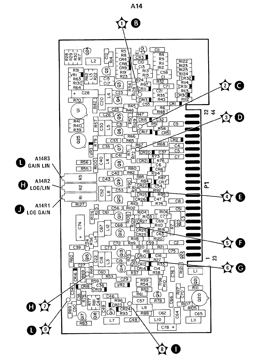
Model 8558B TM 11-6625-3061-14
Figure 7-5. A14 Log Amplifier, Component and Test Point Locations (CHANGE B)
7-24
TM 11-1247-B
THIS PAGE MISSING NOT AVAILABLE FOR DIGITIZATION.
PAGES
7-25 through 7-26
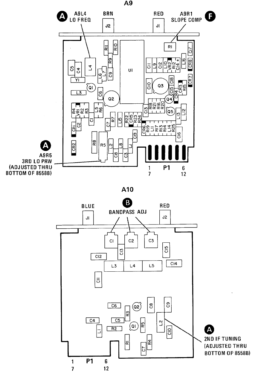
Model 8558B TM 11-6625-3061-14
Figure 7-7. A9 Third Converter and A10 Second IF, Component Locations (CHANGE C)
7-27
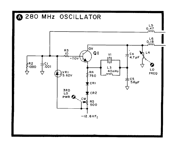
Model 8558B TM 11-6625-3061-14
Figure 7-8. P/O A9 Third Converter and A10 Second IF Schematic Diagram (CHANGE C)
7-28
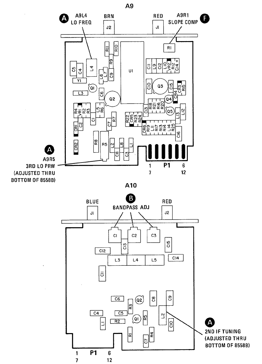
Model 8558B TM 11-6625-3061-14
Figure 7-9. A9 Third Converter and A10 Second IF, Component Locations (CHANGE F)
7-29
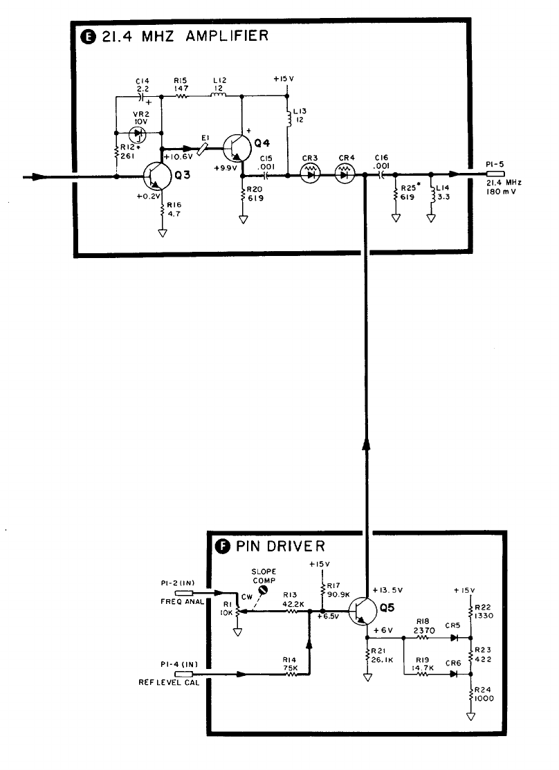
Model 8558B TM 11-6625-3061-14
Figure 7-10. P/O A9 Third Converter and A10 Second IF Schematic Diagram (CHANGE F)
7-30
Model 8558B TM 11-6625-3061-14
SECTION VIII.
SERVICE
8-1. INTRODUCTION
8-2. This section provides instructions for
troubleshooting and repairing the HP Model 8558B
Spectrum Analyzer. It includes general servicing hints
and information, block diagrams of the instrument,
circuit descriptions, parts identification illustrations, and
schematic diagrams.
WARNING
To troubleshoot and repair this
instrument, you must remove it from
the display mainframe and reconnect it
to the mainframe through an extender
cable. Operating the spectrum
analyzer outside the mainframe in this
manner exposes high voltage points in
the instrument which might, if
contacted, cause personal injury.
Maintenance and repair of this
instrument should, therefore, be
performed only by a skilled person
who knows the hazards involved.
8-3. SERVICE INFORMATION INDEX
8-4. Table 8-1 lists specific kinds of information about
the spectrum analyzer main assemblies, and indicates
where the information is located. The service
information for each assembly normally includes a
description of the assembly circuits, a diagram showing
the locations of the assembly components, and a
schematic of the assembly circuits. These packages of
assembly information are arranged in assembly number
order with the circuit descriptions and component
locations diagram preceding the assembly schematic.
The assembly numbers are printed in large, bold-faced,
alpha-numeric characters (e.g., A4) in the lower right-
hand corner of each schematic diagram.
8-5. SCHEMATIC SYMBOLS, TERMINOLOGY, AND
VOLTAGE LEVELS
8-6. Symbols and terminology used on the schematic
diagrams are explained in Figure 8-1.
Test conditions for the signal and dc voltage levels
shown on the block and schematic diagrams are
provided in Figure 8-2.
8-7. TEST EQUIPMENT
8-8. Test instruments and accessories used to maintain
the spectrum analyzer are listed in Table 1-4. If the
listed instrument is not available, another instrument
that meets the required minimums specifications may
be substituted.
8-9. TROUBLESHOOTING
8-10. General
8-11. Troubleshooting to the assembly level is
accomplished by referring to the overall and
troubleshooting block diagrams, and by checking for the
voltages given for the various system test points. Once
the problem is isolated to a particular assembly, the
circuit description and schematic diagram for the
suspect assembly are used to locate the faulty
component.
8-12. Before pursuing any troubleshooting in the
spectrum analyzer, you should first make sure the
problem is not in the display mainframe, or is not
caused by a faulty connection between the spectrum
analyzer and the display mainframe.
8-13. Troubleshooting Hints
NOTE
When a part is replaced, an
adjustment of the affected circuitry is
usually required. For adjustment
procedures, refer to Section V.
8-14. Residual FM. The troubleshooting procedure
provided in Table 8-2 can usually isolate the cause of
residual FM to a particular circuit or circuit component.
Figure 8-3 shows how certain components affect FM in
these procedures. Note that the zener diode causes
peaks which are sharp and extreme compared to the IC
peaks. A leaky
8-1

Model 8558B TM 11-6625-3061-14
Table 8-1. Service Information Index (1 of 2)
Subject Location
General Troubleshooting Paragraph 8-10
Troubleshooting Hints
Residual FM Paragraph 8-14
Sideband Noise Paragraph 8-15
Spurious Responses Paragraph 8-16
Baseline Step Paragraph 8-17
Troubleshooting Block Diagram Figure 8-6
General Principles of Operation Paragraph 8-18
Simplified Block Diagram Figure 8-5
DPM Driver Assembly A1A2
Schematic (includes display) Figure 8-11
Component Locations Figure 8-10
Circuit Description Precedes Figure 8-1
Front Switch Assembly A2
Schematic Figure 8-13
Board Assembly A2A1 Component Locations Figure 8-12
Disassembly and Repair Procedures Follows Figure 8-47
Input Attenuator Assembly A3 Figure 8-14
Schematic Figure 8-18
Description Precedes Figure 8-18
First Converter Assembly A4
Schematic Figure 8-18
Component Locations Figure 8-16
Circuit Description Precedes Figure 8-18
Second Converter Assembly A5
Schematic Figure 8-18
Component Locations Figure 8-17
Circuit Description Precedes Figure 8-18
Frequency Control Assembly A7
Schematic Figure 8-20
Component Locations Figure 8-19
Circuit Description Precedes Figure 8-20
Sweep Generator Assembly A8
Schematic Figure 8-23
Component Locations Figure 8-22
Circuit Description Precedes Figure 8-23
Third Converter Assembly A9
Schematic Figure 8-26
Component Locations Figure 8-25
Circuit Description Precedes Figure 8-26
8-2

Model 8558B TM 11-6625-3061-14
Table 8-1. Service Information Index (2 of 2)
Subject Location
Second IF Assembly A10
Schematic Figure 8-26
Component Locations Figure 8-25
Circuit Description Follows Figure 8-23
Bandwidth Filter No. 1 Assembly A11
Schematic Figure 8-30
Component Locations Figure 8-29
Circuit Description Precedes Figure 8-30
Step Gain Assembly A12
Schematic Figure 8-33
Component Locations Figure 8-32
Circuit Description Precedes Figure 8-33
Bandwidth Filter No. 2 Assembly A13
Schematic Figure 8-35
Component Locations Figure 8-34
Circuit Description Precedes Figure 8-35
Log Amplifier Assembly A14
Schematic Figure 8-38
Component Locations Figure 8-37
Circuit Description Precedes Figure 8-38
Vertical Driver and Blanking Assembly A15
Schematic Figure 8-42
Component Locations Figure 8-41
Circuit Description Precedes Figure 8-42
Motherboard Assembly A16
Schematic Figure 8-44
Component Locations Figure 8-43
Inverter Assembly A17
Schematic Figure 8-46
Component Locations Figure 8-45
Circuit Description Precedes Figure 8-46
Major Assemblies, Location of Figure 8-47
8-3
Model 8558B TM 11-6625-3061-14
electrolytic capacitor (not shown) usually causes the
displayed signal to step down and remain at the same
level for several divisions before stepping up to a new
level.
8-15. Sideband Noise. Sideband noise is usually
caused by YIG Oscillator Assembly A6.
8-16. Spurious Responses. Spurious responses are
usually caused by loose RF connections. Check all the
RF connections.
8-17. Baseline Step. If the left side of the baseline lifts
to the signal peak level, the trouble is A7Q17; a lift of
the right side of the baseline is caused by A7Q18 (see
Figure 8-4).
8-18. GENERAL PRINCIPLES OF OPERATION
8-19. A simplified block diagram of the HP 8558B
Spectrum Analyzer is shown in Figure 8-5. The HP
8558B is basically a superheterodyne receiver with a
YIG (Yttrium-Iron-Garnet) tuned oscillator for the first
LO (local oscillator). The first LO is the only LO that is
swept. The sweep width is determined by the sweep
attenuator (part of A8) which attenuates the ramp
driving the LO. This ramp is produced by the sweep
generator on A8. The ramp also drives the horizontal
sweep of
the CRT, and is available at a rear panel BNC connector
to synchronize other instruments, such as X-Y recorders,
with the analyzer.
8-20. The RF input to the spectrum analyzer passes
through an attenuator network on assembly A3 which is
controlled by the front panel INPUT ATTEN dB control.
This control is used to set the input signal level as
required for a wide dynamic range. From the
attenuator, the signal goes to first converter assembly
A4. Here it is mixed with a 2050 to 3550 MHz output
from YIG oscillator assembly A6. The lower sideband,
2050 MHz, of the resulting signal is passed by a 2050
MHz IF amplifier immediately following the first
converter circuit. It then enters second converter
assembly A5 where it is mixed with a fixed 1748.6 MHz
signal from a fixed-cavity local oscillator. This produces
a 301.4 MHz IF signal which is amplified and fed to third
converter assembly A9. This time, the signal is mixed
with a 280 MHz signal from a SAWR (surface acoustic
wave resonator) oscillator, resulting in a 21.4 MHz IF
signal. The final 21.4 MHz signal is amplified and
detected, then filtered by low pass video filter A2 before
it is applied to the vertical deflection amplifier of the
CRT. The vertical deflection seen on the CRT
corresponds to the RF input signal amplitude. The 280
MHz signal from the SAWR oscillator is fed out of the
front panel for use as a -30 dBm calibration reference.
8-21. Circuit descriptions for each assembly precede
the assembly schematic diagram.
8-4
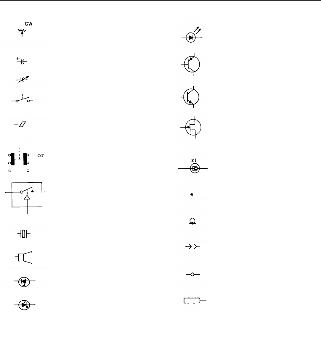
8-5
Model 8558B TM 11-6625-3061-14
SYMBOLS USED IN SCHEMATICS AND BLOCK DIAGRAMS
BASIC COMPONENT SYMBOLS
Variable Resistor: Clockwise
rotation of shaft moves wiper Light-emitting diode
towards end of resistor mark-
ed CW.
Transistor, PNP
Electrolytic capacitor
Variable capacitor Transistor, NPN
Slide, toggle, or rocker
switch
MOS-FET, N-Channel
Ferrite bead (prevents high
frequency parasitic
oscillations)
Pushbutton switch Surface Acoustic Wave
Resonator (SAWR)
Relay Indicates a factory-select
component
Indicates shielding conductor
for cables
Crystal Indicates a plug-in
connection
Speaker
Indicates a soldered or
mechanical connection
Breakdown (zener) diode
Indicates a single pin of a
Schottky diode PC board edge connector
Figure 8-1. Symbols Used in Schematics and Block Diagrams (1 of 4)
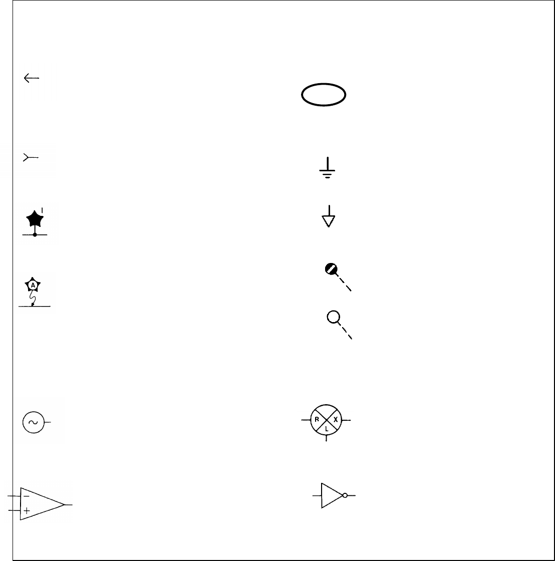
Model 8558B TM 11-6625-3061-14
SYMBOLS USED IN SCHEMATICS AND BLOCK DIAGRAMS
BASIC COMPONENT SYMBOLS
Connection symbol Indicates wire or cable color
indicating a Jack (except for code. Color code same as
PC board edge connectors) resistor color code. First
number indicates base color,
second and third numbers
indicate colored stripes.
Connection symbol
indicating a Plug (except for
PC board edge connectors) Earth ground
Instrument chassis ground.
Test Point: Terminal May be accompanied by a
provided for test probe. number or letter to specify a
particular ground.
Measurement Point: Used to Screwdriver adjustment
indicate a convenient point
for measurement. No
terminal provided for test
probe. Front-panel control
COMMONLY USED ASSEMBLY AND CIRCUIT SYMBOLS
Oscillator Mixer
Operational amplifier Inverter, buffer
Figure 8-1. Symbols Used in Schematics and Block Diagrams (2 of 4)
8-6
946
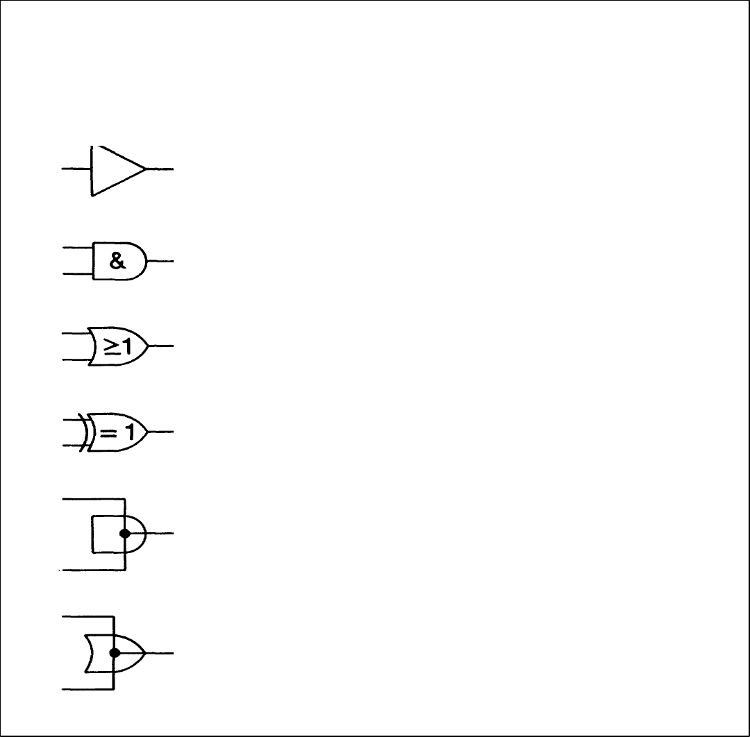
Model 8558B TM 11-6625-3061-14
SYMBOLS USED IN SCHEMATIC AND BLOCK DIAGRAMS
BASIC LOGIC SYMBOLS
Distinctive-Shape Symbols
AMPLIFIER/BUFFER Output is active when input is active.
AND FUNCTION Output is active only when all inputs are
active.
OR FUNCTION Output is active when one or more in-
puts are active.
EXCLUSIVE-OR Output is active when only one input is
FUNCTION active.
WIRED AND Two or more elements are joined
FUNCTION together to achieve the effect of an AND
function.
WIRED OR Two or more elements are joined
FUNCTION together to achieve the effect of an OR
function.
Figure 8-1. Symbols Used in Schematics and Block Diagrams (3 of 4)
8-7
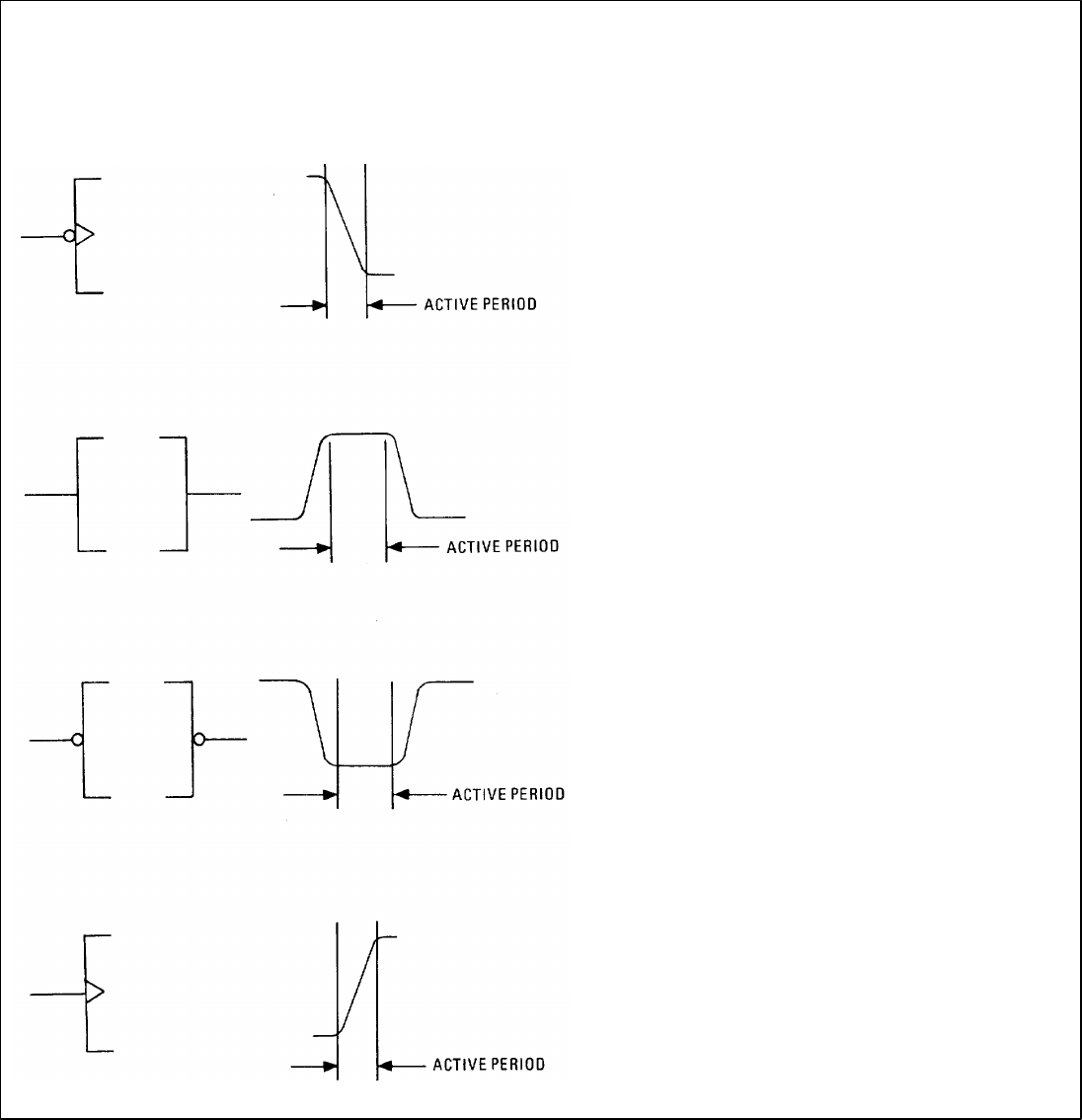
Model 8558B TM 11-6625-3061-14
SYMBOLS USED IN SCHEMATIC AND BLOCK DIAGRAMS
BASIC LOGIC SYMBOLS
Indicator Symbols (positive logic assumed)
Input is active only on the negative-
going transition.
ACTIVE-HIGH inputs and outputs are
indicated by the absence of the negation
symbol, O.
ACTIVE-LOW inputs and outputs are in-
dicated by the presence of the negation
symbol, O.
EDGE-TRIGGERED (dynamic) inputs
are indicated by the presence of the
dynamic input symbol.
Input is active only on the positive-going
transition.
Figure 8-1. Symbols Used in Schematics and Block Diagrams (4 of 4)
8-8
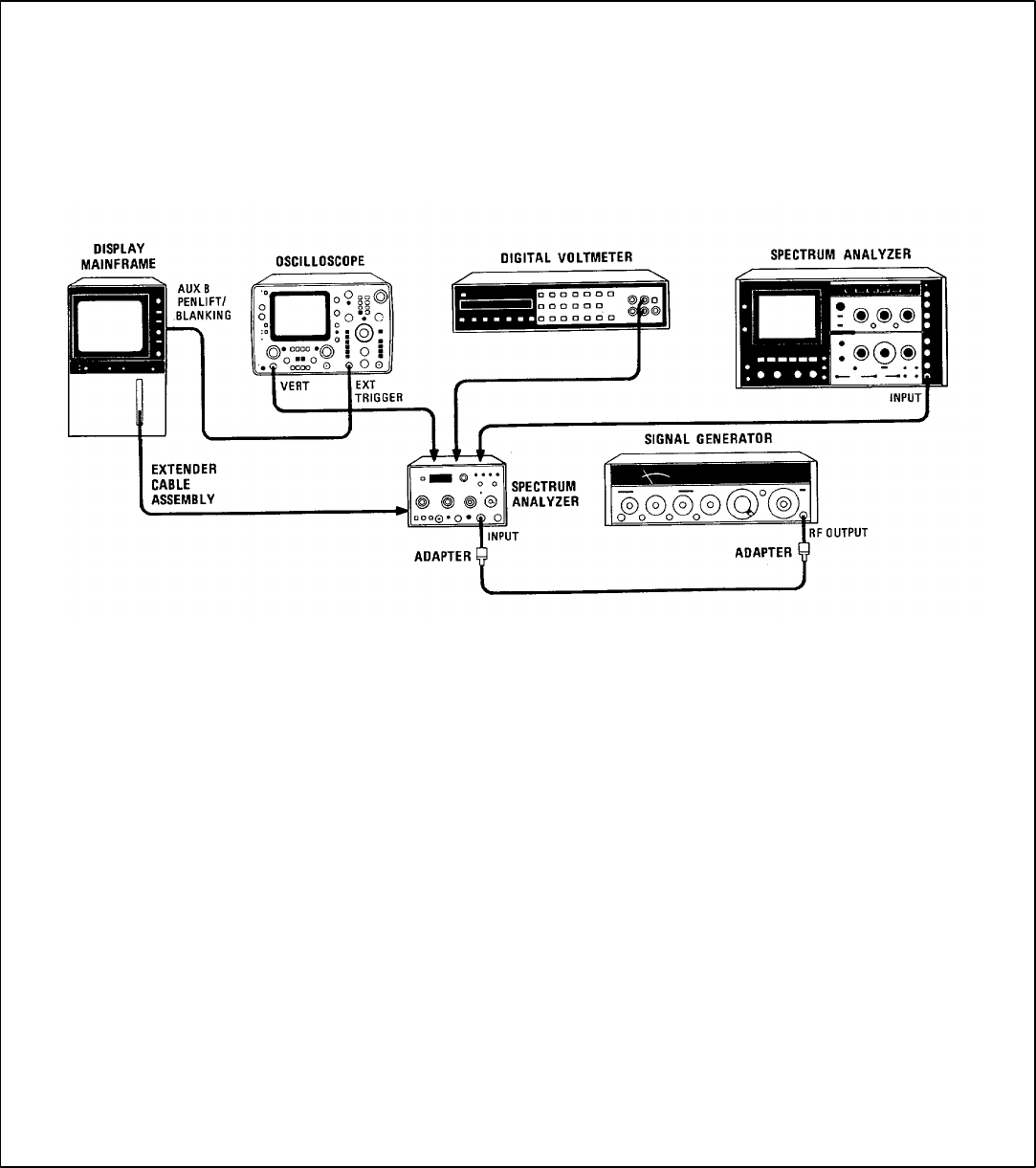
Model 8558B TM 11-6625-3061-14
Nominal power levels, voltages, and waveforms shown on schematic diagrams were measured using
the test setup shown below. Note that signal characteristics shown on schematic diagrams are provided
as a troubleshooting aid only. They should not be used for making instrument adjustments.
EQUIPMENT: Oscilloscope(with 10:1 probe) .......................................................................................HP 1741A
Spectrum Analyzer....................................................................................HP 141T/8552B/8555A
Digital Voltmeter ...........................................................................................................HP 3455A
Signal Generator...........................................................................................................HP 8640B
Extender Cable Assembly......................................................................................HP 5060-0303
Adapter, Type N to BNC (2 required)...................................................................... HP 1250-0780
Figure 8-2. Conditions for Schematic Diagram Measurements (1 of 2)
8-9

Model 8558B TM 11-6625-3061-14
PROCEDURE:
1. Set HP 8558B Spectrum Analyzer controls as follows:
START-CENTER ...........................................................................................................CENTER
TUNING..........................................................................................................................280 MHz
FREQ SPAN/DIV................................................................................................................1 MHz
RESOLUTION BW...........................................................................................................300 kHz
INPUT ATTEN .......................................................................................................................0 dB
REFERENCE LEVEL.......................................................................................................-10 dBm
Option 002: +40 dBm V
REFERENCE LEVEL FINE.........................................................................................................0
Amplitude Scale............................................................................................................10 dB/DIV
SWEEP TIME/DIV..............................................................................................................AUTO
SWEEP TRIGGER .....................................................................................................FREE RUN
VIDEO FILTER......................................................................................................................OFF
BASELINE CLIPPER.............................................................................................................OFF
BL CLIP .................................................................................................................................OFF
2. Connect equipment as shown. Set signal genera tor for a 280 MHz, -10 dBm output signal. Center the signal on
the display.
3. Using board extenders when necessary, check voltages and waveforms indicated on schematic diagrams.
Trigger oscilloscope on negative transition of AUX B PENLIFT/BLANKING signal from rear of display mainframe.
4. To measure RF power levels, set RESOLUTION BW control to 3 MHz and FREQ SPAN/DIV to 0 (zero span).
The first LO is not swept in zero span, allowing signal levels to be checked with a second spectrum analyzer (use
adapter cables as necessary). DO NOT use a power meter (harmonics and LO signals will contribute to give
erroneous levels).
Figure 8-2. Conditions for Schematic Diagram Measurements (2 of 2)
8-10

Model 8558B TM 11-6625-3061-14
Table 8-2. Residual FM Troubleshooting Procedure (1 of 2)
Troubleshooting Step Probable FM Source
1. Set 8558B controls as follows:
INPUT ATTEN......................................0 dB
REF LEVEL............................................-20
(Option 002: +30 dBm V)
FREQ SPAN/DIV...............................2 MHz
RESOLUTION BW ............................1 MHz
SWEEP TIME/DIV.............................AUTO
SWEEP TRIGGER....................FREE RUN
AMPLITUDE SCALE..............................LIN
VIDEO FILTER.....................................OFF
2. Tune LO feedthrough to the left edge of CRT display Main Coil Filter A7Q4 and
and make sure a double lobe (Figure 8-3d) does not associated circuitry.
occur.
3. Connect CAL OUTPUT to spectrum analyzer input.
Center 280 MHz signal on CRT and adjust REF
LEVEL FINE for a top-of-screen signal.
4. Step FREQ SPAN/DIV from 2 MHz to 1 MHz. Main Coil Filter A7Q4 and
Frequency shift should be less than one major division. associated circuitry.
5. Use FREQUENCY CAL pushbutton to remove YIG Calibrate single shot A7Q21-23. Proceed
hysteresis, then center 280 MHz signal on CRT. to step 11.
Repeated operations should shift signal less than one
major division.
6. Second LO frequency should be stable and not vary ASCR1 or A5Q1
more than 200 kHz (check at A5J3).
7. Check the voltages at A7TP6 and A7TP7 for correct
level and stability.
A7TP6 ≈ +6V A7VR2
A7TP7 ≈ +14.5V A7VR1
8. Select a 10 kHz RESOLUTION BW and tune the
spectrum analyzer so the 280 MHz signal skirt crosses
the center frequency graticule line between the fourth
and seventh horizontal graticule lines. Switch to zero (0)
span and select a .1 SEC/DIV sweep time. Peak-to-peak
variations of the trace should not exceed one major
vertical division for each major horizontal division.
9. Try FM check (step 8) with TUNING potentiometer TUNING potentiometer
in several different positions. (Tune slightly off
frequency with COARSE TUNING control and
adjust FINE TUNING control for proper display.)
8-11

Model 8558B TM 11-6625-3061-14
Table 8-2. Residual FM Troubleshooting Procedure (2 of 2)
Troubleshooting Step Probable FM Source
10. Disconnect one end of A7C13 and repeat step 8. A7C13 or A7C14
Reconnect A7C13, disconnect one end of A7C4,
and again repeat step 8.
11. Remove A7CR2 and A7Q22. If FM is still present, Calibrate single shot circuit
remove A7Q21 and A7Q23. on Frequency Control Assy A7.
12. Remove A7R55 and repeat step 8. YIG FM coil driver circuit on
Frequency Control Assy A7.
Probably A7U1.
13. Disconnect one end of A7VR3 or A7CR9 and A7VR3 or A7CR9
repeat step 8.
14. Ground A7TP1 and repeat step 8. YIG main coil gate on Frequency
Control Assy A7.
15. If residual FM is still present, the problem is in the YIG main coil drivers on Frequency Control Assembly A7.
Refer to the Frequency Control Assembly schematic diagram for further troubleshooting.
8-12
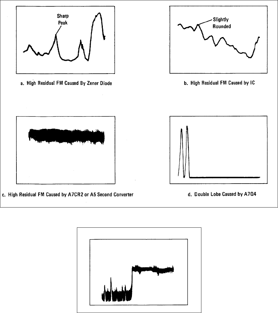
Model 8558B TM 11-6625-3061-14
Figure 8-3. CRT Displays for Residual FM Troubleshooting
Figure 8-4. Baseline Step Caused by Failure of A7Q18
8-13/8-14 (blank)
TM 11-1247-B
THIS PAGE MISSING NOT AVAILABLE FOR DIGITIZATION.
PAGES
8-15 through 8-18
Model 8558B TM 11-6625-3061-14
A1A2 DPM DRIVER ASSEMBLY CIRCUIT DESCRIPTION
The DPM circuit is a dc voltmeter that measures a tuning voltage from Frequency Control Assembly A7, and converts it
to a front-panel frequency readout.
The DPM Driver is divided into three parts:
1. The Analog-to-Digital Converter.
2. The Segment Driver.
3. The Digit Driver.
Analog-to-Digital Converter
The Analog-to-Digital converter comprises an MOS LSI device, A1A2U1, and associated circuitry. A1A2U1 compares the
input voltage (MTR V) on pin 3 with a reference voltage (V REF) on pin 2 and outputs the measured voltage in a binary-
coded decimal (BCD) format. The BCD data is multiplexed out of A1A2U1, one decimal digit (four bits) at a time on pins
20 through 23. DS1 through DS4 (pins 16 through 19) are the enable lines for A2DS1 (MSD) through A2DS4 (LSD).
A1A2R2, A1A2R3, and A1A2R4 form an adjustable voltage divider which divides the 6.2 volts from A16VRI down to
approximately 2.0V for the reference voltage (V REF) at pin 2 of A1A2U1.
Segment Drive
AIA2U3 converts the BCD data to seven-segment data for the displays and provides a test function which lights all the
segments of all the displays when pin 3 (TP2) is jumpered to ground. A1A2Q3 switches the decimal point LED on for
frequencies below 198.6 MHz. (The voltage, MTR V, is multiplied by 10 on the Frequency Control Assembly.) A1A2Q4
allows the 'g' segment line of A2DS1 to go high when the input voltage (MTR V) is less than zero. This causes a minus
sign (-) to be displayed.
Digit Driver
The digits are enabled one at a time, sequentially through digit driver A1A2U2. Each digit display is in turn enabled for
300 microseconds until a 250 millisecond period has passed. This is the length of time A1A2U1 requires to make a new
voltage measurement. After 250 milliseconds, the new data is put out on pins 20 through 23 of A1A2U1 and the cycle
repeats. (See Figures 8-8 and 8-9.)
Display
The digit displays, A2DS1 through A2DS4, are of the common-cathode type. When the digit enable line (cathode) is low
and a segment line is high, that segment is turned on. Although only one digit display is enabled at a time, the enable
rate is fast enough to prevent visible display flicker.
Troubleshooting
To check the digit displays, jumper A1A2TP2 (LT) to ground. All segments of all four numeric displays (A2DS1 through
A2DS4) should light. To troubleshoot DPM Driver A1A2, check for proper clock and outputs at A1A2U1 (see Figures 8-7,
8-8, and 8-9 and Table 8-3).
8-19
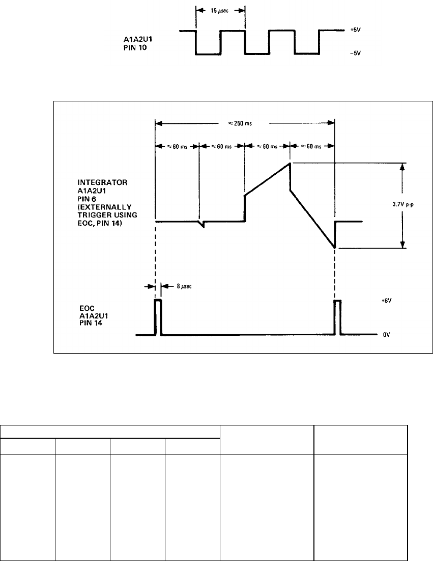
Model 8558B TM 11-6625-3061-14
Figure 8-7. A1A2U1 Clock
Figure 8-8. Integrator and EOC Waveforms for FREQUENCY MHz Display of 1296 MHz
Table 8-3. Truth Table for A2DS1 Display
A1A2U1 Data Output Decimal A1A1DS1
Y3Y2Y1Y0Equivalent Display
0000 0 -1
0011 3 -1
0 1 0 0 4 1
0 1 1 1 7 1
1 0 1 0 10 -
1 0 1 1 11 -
1 1 1 0 14 Blank
1 1 1 1 15 Blank
8-20
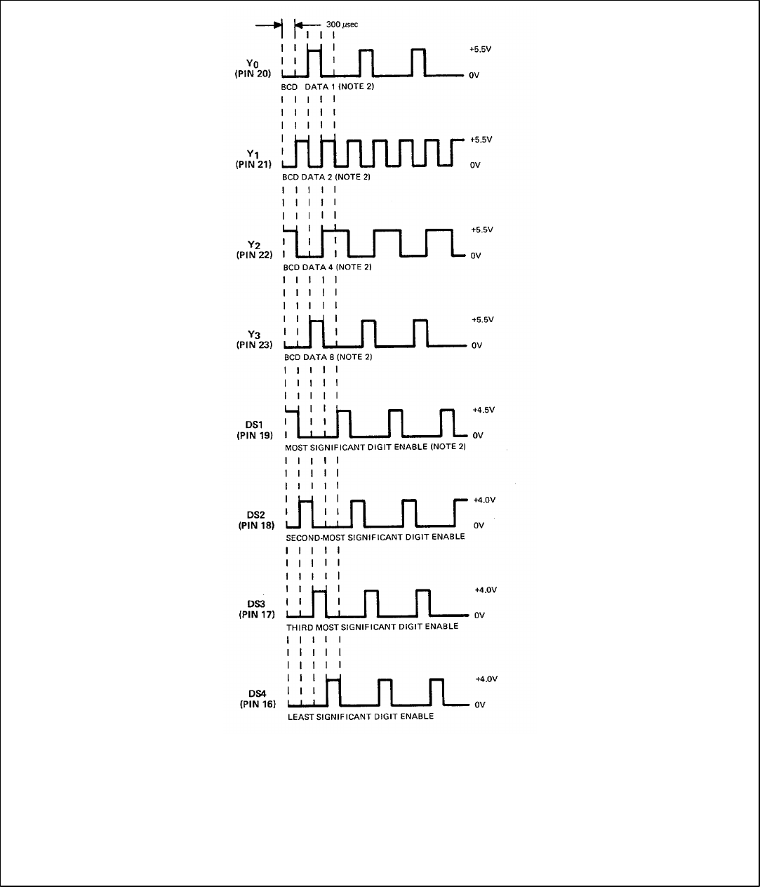
Model 8558B TM 11-6625-3061-14
NOTES
1. TRIGGER OSCILLOSCOPE EXTERNALLY USING EOC {(END OF
CONVERSION), A1A2U1 PIN 14.
2. DURING THE TIME INTERVA L THAT DS1 LINE IS HIGH,THE DATA ON
PINS 20 THROUGH 23 IS NOT STANDARD BCD CODE. SEE TABLE 8-2.
Figure 8-9. A1A2U1 Outputs for FREQUENCY MHz Display of 1296 MHz
8-21
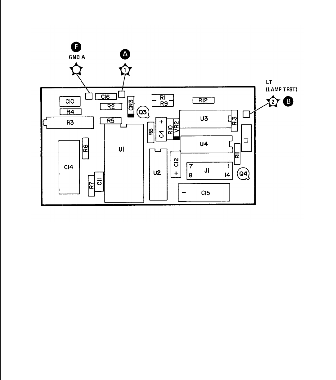
Model 8558B TM 11-6625-3061-14
A1A2
Figure 8-10. A1A2 DPM Driver Component Locations
8-22
TM 11-1247-B
THIS PAGE MISSING NOT AVAILABLE FOR DIGITIZATION.
PAGES
8-23 through 8-24
Model 8558B TM 11-6625-3061-14
A2 FRONT SWITCH ASSEMBLY CIRCUIT DESCRIPTION
Functions of the switches and potentiometers on Front Switch Assembly A2 and Front Switch Board Assembly A2A1 are
covered in the circuit descriptions for the electronic assemblies they control. Disassembly and repair procedures for the
Front Switch Assembly are at the back of this section (following Figure 8-47).
8-25
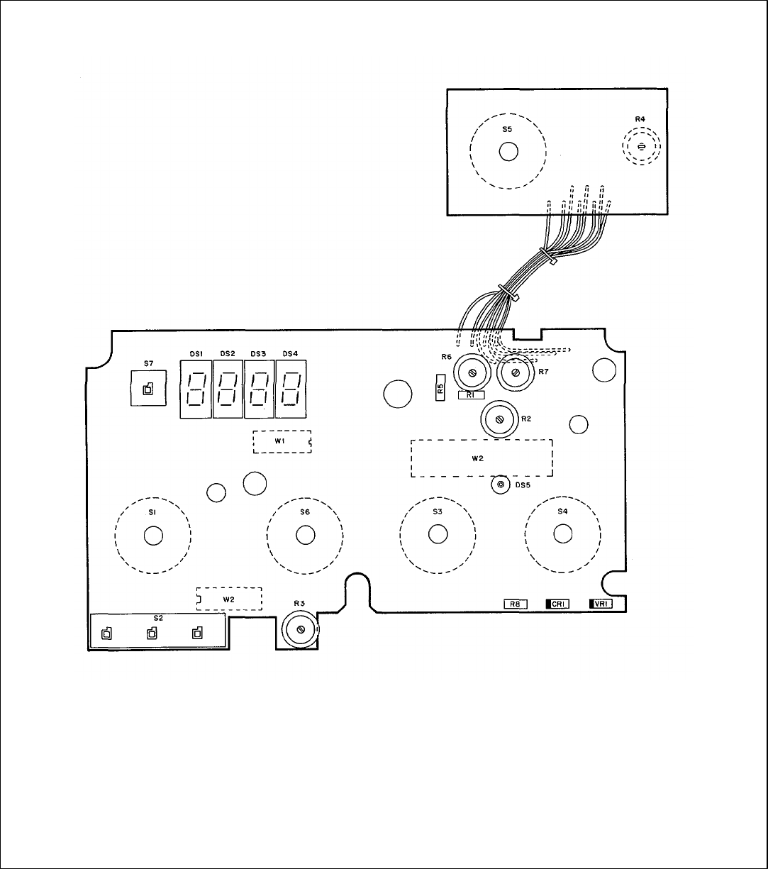
Model 8558B TM 11-6625-3061-14
A2A1
Figure 8-12. Front Switch Board Assembly A2A1, Component Locations
8-26
TM 11-1247-B
THIS PAGE MISSING NOT AVAILABLE FOR DIGITIZATION.
PAGES
8-27 through 8-28
Model 8558B TM 11-6625-3061-14
A3, U1, A4, A5, A6 CIRCUIT DESCIPTIONS
A3 Input Attenuator Circuit Description
The 8558B input attenuator (Figure 8-14) is a 50-ohm, precision, coaxial step attenuator. Attenuation in 10 dB steps
from 0 dB to 70 dB is accomplished by switching the signal path through one or more of the three resistive pads in a
predetermined sequence. (Note that the input attenuator is not field repairable.)
U1, RF Input Limiter Circuit Description
The RF input limiter contains Schottky diodes which clamp the input signal voltage, protecting the mixer diodes in the
First Converter Assembly A4. The typical limiting threshold is 1 mW (0 dBm). The limiter is not field serviceable.
A4 First Converter Circuit Description
The RF signal input (0.1 1500 MHz) passes through a 1550 MHz low pass filter to the mixer diode assembly, U1. The
output impedance of this low-pass filter seen from the mixer is effectively a short circuit at 2050 MHz, reflecting any IF
power back to the mixer. The first LO input from YIG Oscillator Assembly A6 passes through a 3 dB power splitter
consisting of two resistors, R1 and R2, and etched transmission lines. One of the power splitter outputs provides the
front panel LO OUTPUT; the other output is through a balun (short piece of semi-rigid coaxial transmission line) to
provide drive voltage to the mixer diodes. The LO signal is coupled to one mixer diode through the balun shield and to
the other mixer diode through the balun center conductor. This arrangement splits the LO signal voltage evenly between
the two mixer diodes. The 2050 MHz output signal from the mixer (first IF) is split-line coupled to a 6 dB 'pi' resistive
matching pad (R3, R4, and R5). A small block of polyiron is placed over the split-output line. The polyiron helps balance
the mixer and absorbs harmonics of the mixing signals. A 5000 MHz low-pass filter etched on the A4 printed circuit
board provides additional filtering to the 2050 MHz IF signal after the 6 dB pad. The signal is then coupled to Second
Converter Assembly A5 through a semi-rigid coaxial cable.
A5 Second Converter Circuit Description
The IF signal from the First Converter is coupled into the Second Converter bandpass filter through coupling loop L3.
The bandpass filter consists of three circular, slug-tuned cavity resonators operating as less than a quarter wavelength
inductive transmission lines. The cavities provide high 'Q' for good selectivity at 2050 MHz. Coupling loops L4 and L5
provide coupling between the cavities. The 2050 MHz signal is loop coupled to the cathode end of second mixer diode
CR1. The second LO signal is loop coupled to the anode end of CR1. The second local oscillator is a Colpitts type
circuit operating at 1748.6 MHz. The capacitive 'fingers' etched on the A5A1 printed circuit board and the internal
transistor capacitances of A5A1Ql provide the positive feedback necessary to sustain oscillation. The oscillator tank
circuit is a slug-tuned cavity, Z4. The signal from the second LO is coupled into cavity Z4 by a 4 - 40 machine screw
extending down into the cavity. The second LO output is also available at test jack A5J3. The 1748.6 MHz local
oscillator provides the drive for mixer diode CR1. The difference frequency between the first IF, 2050 MHz, and the
second LO frequency, 1748.6 MHz, is 301.4 MHz. This 301.4 MHz signal is coupled through the matching filter to the
A10 Second IF. The matching filter is a passive network designed to match the relatively high impedance of the second
mixer, about 200 ohms, to the low input impedance of the second IF, about 50 ohms. The match may be optimized by
adjusting A5L2, 2nd MIXER MATCH adjustment.
A6 YIG Oscillator Circuit Description
The YIG Oscillator is a transistorized thin-film microcircuit. It uses an yttrium-iron-garnet (YIG) sphere as the frequency
determining structure. The YIG sphere is a ferromagnetic material whose resonant frequency is directly proportional to
the applied magnetic field. The sphere is placed in the gap of an electromagnet to provide a magnetic tuning structure
whose field (and thereby the oscillator's frequency) is linearly proportional to the drive current from Frequency Control
Assembly A7.
8-29
Model 8558B TM 11-6625-3061-14
The main coil is used for wide range sweeping and tuning with the coil current varying from approximately 50 to 8 mA.
The FM coil is used only for narrow spans (1 MHz/DIV and less) with the coil current varying from approximately - 25 mA
to + 25 mA.
The YIG Oscillator Assembly consists of three parts: a sealed magnet assembly which encloses the YIG sphere and
oscillator; a bias board which uses discrete components to establish oscillator/amplifier bias and to protect against supply
noise and voltage overloads; and a mu-metal magnetic shielding can.
8-30
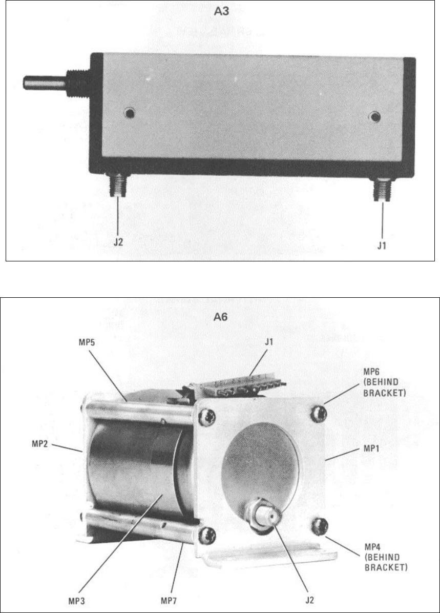
Model 8558B TM 11-6625-3061-14
Figure 8-14. A3 Input Attenuator
Figure 8-15. A 6 YIG Oscillator
8-31
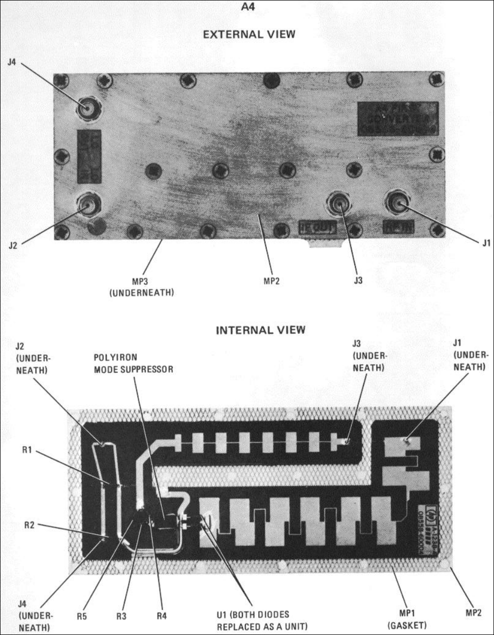
Model 8558B TM 11-6625-3061-14
Figure 8-16. A4 First Converter, Component Locations
8-32
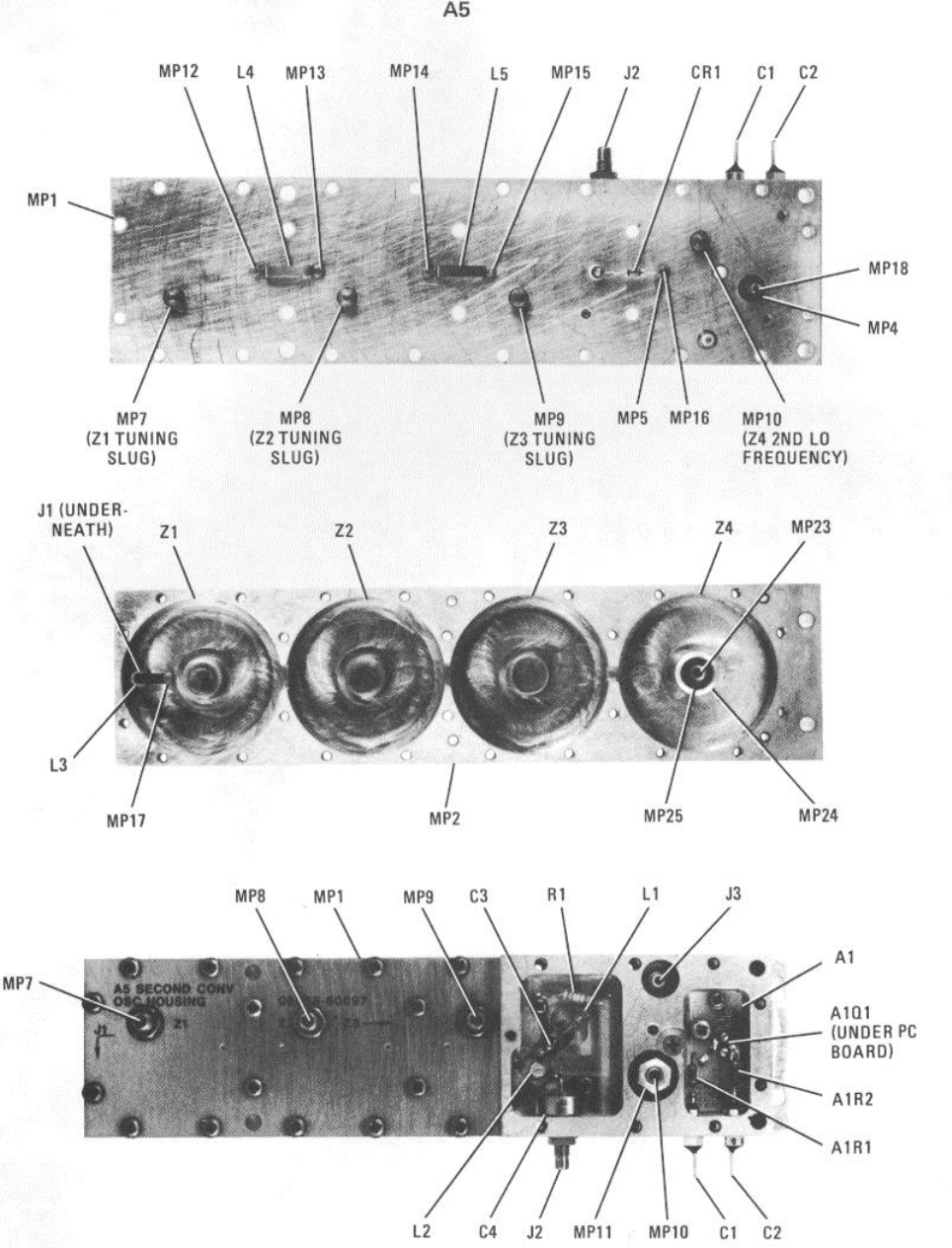
Model 8558B TM 11-6625-3061-14
Figure 8-17. A5 Second Converter Assembly, Component Locations
8-33/8-34(blank)
TM 11-1247-B
THIS PAGE MISSING NOT AVAILABLE FOR DIGITIZATION.
PAGES
8-35 through 8-36
Model 8558B TM 11-6625-3061-14
A7 FREQUENCY CONTROL CIRCUIT DESCRIPTION
General Description
Frequency Control Assembly A7 contains the circuitry to drive and control YIG Oscillator Assembly A6. The frequency is
controlled by the sum of the sweep and tune voltages. The tune voltage is generated by the center frequency coarse and
fine TUNING controls. The tune voltage is measured by the digital panel meter (DPM) voltmeter to provide the center-
frequency digital readout. The sweep voltage, controlled by the FREQ SPAN/DIV switch, is generated in Sweep
Generator Assembly A8. The YIG Oscillator has two driving coils: the main tuning coil and the FM coil. The tune
voltage is applied to the main tuning coil driver. The sweep voltage is either summed with the tune voltage and applied
to the main tuning coil driver or, in narrow frequency spans, it is applied to the FM coil driver. Gating circuits determine
whether the sweep voltage is applied to the main or FM coil. The Frequency Control Assembly also contains separate
low-noise voltage regulators to bias the YIG Oscillator and the 1748.6 MHz second local oscillator.
YIG Main Coil Fixed Driver
The YIG Main Coil Fixed Driver consists of differential amplifier A7Q7, a Darlington pair current source, A7Q5 and Q6,
and a + 6V reference voltage from A7VR2 and R4. The fixed driver is used to tune the YIG oscillator to the minimum
frequency of 2050 MHz.
The + 6V reference voltage is one input to A7Q7 and the other input, measured at TP3, is negative feedback that senses
the voltage across A7R3 and R71. The operation of the fixed coil driver maintains a constant +6.OV across A7R3 and
R71. A11 current through R3/R71 comes from the YIG main coil through Darlington current source A7Q5 and Q6. A7R3
is the 2.05 GHz lower frequency adjustment and sets the emitter current of A7Q5 and Q6. The current source provides
the fixed current to determine the zero CENTER FREQUENCY point set by A7R3.
YIG Main Coil Swept Driver
The YIG Main Coil Swept Driver consists of a swept driver, A7U4, and a Darlington pair current source, A7Q1 and Q3.
The swept driver tunes the YIG oscillator over the frequency range of 2050 MHz to 3550 MHz. The inputs to A7U4 are
the Coarse and Fine TUNING voltage from the Tune Summing Amplifier, and the attenuated sweep ramp from the
Sweep Buffer. The output from A7U3 is the attenuated sweep only when 2 MHz/DIV or wider frequency spans have
been selected. In narrower frequency spans, only the sum of the TUNING voltages is applied to the main coil swept
driver. The attenuated sweep and TUNING voltages are summed across A7R49 and R52 and then applied to the
noninverting input of A7U4. Diode A7CR3 prevents the input of the swept driver from going negative and driving it into
cutoff. A7U4 drives the current source which converts the voltage at the emitter of Q1 into current to drive the YIG main
tuning coil.
The current from A7Q1/Q3 is summed with the current from the fixed driver current source, A7Q5/Q6, to increase the
main coil current synchronously with the TUNING and sweep voltages. The YIG upper frequency 3.55 GHz is set by
A7R1 (coarse adjust) and A7R2 (fine adjust). The emitter of A7Q1 is connected to the inverting input of A7U4 to provide
a voltage proportional to the collector current of Q1/Q3 to be used as negative feedback.
Frequency AnA10g Output for Blanking. The emitter of A7Q1 also drives the base of A7Q2. A7Q2 is an emitter follower
that provides the frequency anA10g output voltage to Third Converter Assembly A3 and to the Sweep Ramp High/Low
Limit Comparator (A15U1) of Vertical Driver and Blanking Assembly A15. (See A15 Schematic.)
8-37
Model 8558B TM 11-6625-3061-14
Coarse and Fine TUNING. The Coarse and Fine tuning voltages from control potentiometers A2R1 and A2R2 (shown
on A2 schematic) are applied to the noninverting and inverting inputs respectively of A7U2. A7U2 sums these voltages
and applies the voltage sum to the junction of A7R52 and R53. It is in turn summed with the attenuated sweep signal
from the output of the sweep buffer A7U3 if 2 MHz/DIV or wider frequency spans have been selected. In narrower
frequency spans, the input of buffer A7U3 is grounded so only the summed tuning voltages are applied to A7U4.
YIG FM Coil Driver
The FM Coil Driver consists of A7U1, Q17, Q18, and FM adjust R6. Selecting 1 MHz/DIV and narrower frequency spans
enables the YIG FM Coil Gate, allowing the attenuated sweep to be applied to the YIG FM Coil Driver. (A7Q15 is on and
Q16 is off.) A7U1 converts the sweep ramp voltage into current to drive the YIG FM coil. Transistors A7Q17/Q18 are
biased at cutoff and provide additional current drive. The FM adjust, A7R6, sets the maximum FM coil current.
YIG Main and FM Coil Gates
The YIG Coil Gates determine which YIG coil is used to control the YIG oscillator frequency. The YIG Coil Gates are
selected by the Scan Select which is controlled by FREQ SPAN/DIV control A2S6.
YIG Main Coil Gate. When 2 MHz/DIV and wider frequency spans are selected, the base of transistor A7U5C is
returned to 12.6V through A7R11 and A8R131. A7U5C is turned off and the collector rises to about 5V while the emitter
drops to near 12.6V. The collector of A7U5C turns on U5E and U5D, and these two transistors then turn off FETs Q15
and Q24 respectively. The emitter of A7U5C turns off U5A and U5B, which then turn on FETs Q16 and Q20. With
A7Q20 conducting and A7Q24 open, the attenuated sweep is applied to sweep buffer A7U3 and YIG main coil swept
driver A7U4 to control the YIG oscillator frequency. FET A7Q15 is turned off preventing the attenuated sweep input from
reaching the ./ YIG FM Coil Driver, and A7Q16 is turned on, grounding the input to the YIG FM coil driver.
YIG FM Coil Gate. The selection of 1 MHz/Div and narrower frequency spans with FREQ SPAN/DIV control A2S6
applies + 15V to the input of A7USC. The + 15V turns U5C on; FETs Q20 and Q16 are turned off, and FETs Q24 and
Q15 are turned on. This enables the YIG FM coil gate, allowing the sweep signal to be applied to the YIG FM Coil
Driver. A7Q20 prevents the Attenuated Sweep input from reaching the sweep buffer A7U3 and A7Q24 grounds the input
of A7U3. However, the tuning voltage from the tune summing amplifier is still applied to the YIG main coil swept driver.
Main Coil Filter
When the narrower frequency spans are selected, the + 15V from FREQ SPAN/DIV switch A2S6 is also applied to A7Q4
in the main coil filter. The main coil filter consists of FET switch A7Q4, R75, and C13/C14. The filter provides noise
filtering in the 1 MHz and narrower frequency spans. With the FET switch closed, the filter is connected in parallel with
the YIG main tuning coil.
Meter Ranging
The DPM is a digital voltmeter which measures the TUNING voltage at the output of the tune summing amplifier. The
output of the tune summing amplifier, approximately 0 to -10V, is divided down to 0 to 1.5V at pins 2 and 5 of A7U6 by
A7R53 and R50. This provides a 1 mV/MHz voltage to the DPM. The FREQ ZERO adjust R3 (shown on A2 schematic),
A7R43, and A7R54 enable this voltage to be offset 4 15 mV to zero the DPM. The FREQ ZERO adjustment
compensates for the changes in the frequency of the YIG oscillator caused by temperature drift.
8-38
Model 8558B TM 11-6625-3061-14
A7U6A functions as a comparator and A7U6B as a switchable Xl/X10 gain stage. When the instrument is tuned to a
frequency below 198.4 MHz, the voltage at A7U6 pin 2 is less than 198 mV. Since the voltage at A7U6 pin 3 is adjusted
to be approximately 198 mV, the output at A7U6 pin 1 is positive. This turns on Q19, causing A7U6B to have a gain of
approximately 10 and results in an output voltage at pin 7 of 10 mV/MHz.
When the instrument is tuned above 198.4 MHz, A7U6A pin 1 goes low, turning Q19 off, causing A7U6B to have a gain
of 1. This results in an output voltage at pin 7 of 1 mV/MHz. The output of A7U6A pin 1 is also used to turn A7Q25 off to
turn off the decimal point. The positive feedback from the emitter of A7Q25 to A7U6A pin 3 provides hysteresis for rapid
switching of the X1/X10 crossover point. A7CR6 and CR7 provide proper biasing for FET Q19. OFS adjustment A7R72
compensates for input offset of A7U6B.
+ 14.5V Regulator The + 14.5V Regulator consists of series regulator A7Q8, driver Q10, and reference amplifier Q9 and
Q11. The +6.2V developed across zener diode A7VRI provides the base reference for A7Q9. This is compared to the
voltage at the base of A7Q11 1 which senses the + 14.5V output across voltage divider A7R28, R29, and the + 14.5V
adjust R5. Should the output voltage increase, A7Q11 conducts more, decreasing the conduction of A7Q9 and driving
the base of Q10 more positive. This decreases the drive current to A7Q8 and causes the output voltage to drop (return
to + 14.5V). A7C4 provides stability compensation and some additional noise filtering at the output.
The + 14.5V supply is used for the positive supply on A7U2, U3, U4, and Q7. It is also used on Sweep Generator
Assembly A8 as the voltage reference that sets the 5V to + 5V ramp amplitude. The + 14.5V is also applied to Second
Converter A5 as the positive supply for the 1748.6 MHz second local oscillator.
+ 6.00V Reference Voltage Regulator
The + 14.5V at A7R32 and the +6.2V dropped across A7VR2, develop the +6.00V reference voltage. A7R4 REF V
adjusts the voltage at TP6 to + 6.00V.
-10V Regulator
The regulated + 14.5V provides a reference voltage for voltage divider A7R34 and R35 for the -10V regulator. The -10V
regulator consists of series regulator A7Q12 and reference amplifier A7Q13 and Q14. Should the -10V tend to become
more positive (less negative), A7Q13 decreases its conduction and turns A7Q14 on harder. A7Q14 then increases the
conduction of A7Q12, dropping the output voltage back to -10V.
The -10V supply is used for the negative supply on A7U2, U3, U4, and Q7. It is also used as the negative supply for the
A6 YIG Oscillator and the second local oscillator in A5.
Calibrate Single Shot
The calibrate single shot circuit consists of A7Q23, Q22, and Q21. The circuit is activated when the front panel FREQ
CAL button is pressed. With the FREQ CAL switch A2S1 (shown on A2 schematic) closed, the YIG Oscillator is tuned to
its lowest frequency. Releasing the FREQ CAL button returns the YIG Oscillator to the previous operating frequency.
Pressing the FREQ CAL button shorts the + 6V line to ground, discharging A7C8 and turning A7Q23 off. The emitter of
A7Q22 is grounded, turning it on, and its collector goes low, turning off FET switch A7Q4. The main coil filter is now
disabled and the charge held on A7C13/C14 remains the same during the calibration sequence. The charge voltage
represents the previous operating frequency. The ground on the + 6V line is applied to the base of A7Q7, disabling the
YIG main coil fixed driver. When the + 6.OV line is grounded, the output of the coarse TUNING control is grounded; the
YIG main coil swept driver is disabled by the output from A7U2. With both YIG main coil drivers disabled, the magnetic
current is removed and the magnet hysteresis is cancelled.
8-39
Model 8558B TM 11-6625-3061-14
When the FREQ CAL button is released, the +6.0V reference line jumps to approximately + 1V. The charge on capacitor
A7C8 turns on A7Q23 which then turns on Q21. A7C8, Q21, and Q23 form a Miller Integrator and the +6.0V reference
line slowly charges to +6.0V. This takes about 0.3 second and prevents the introduction of transients into the main coil.
However, as long as the + 6.0V reference line is charging; the conduction of A7Q23 keeps FET switch A7Q4 off, still
disabling the main coil filter. The charge on A7C13/C14 has no path for discharge and remains the same. This allows
the YIG Oscillator to return to the previous frequency faster since A7C13 and C14 do not have to be recharged.
8-40
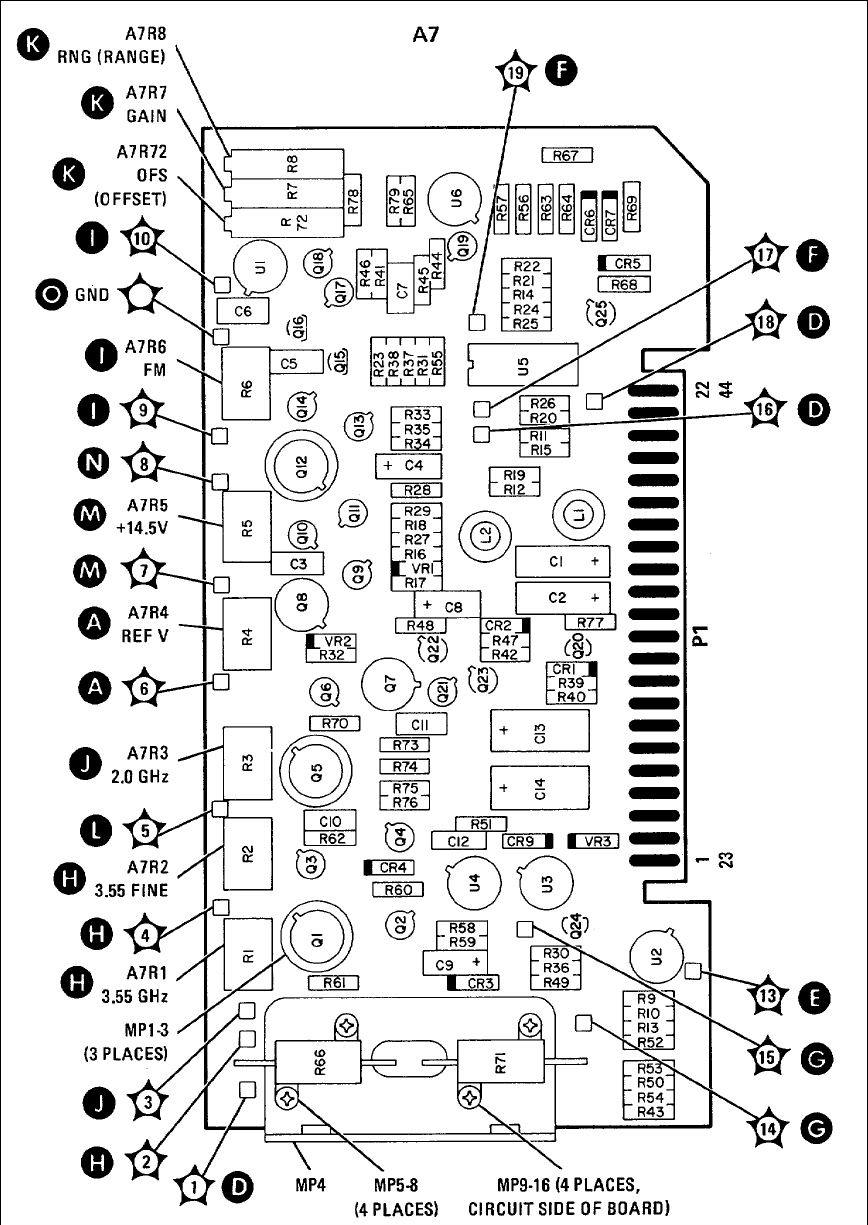
Model 8558B TM 11-6625-3061-14
Figure 8-19. A7 Frequency Control Assembly, Component and Test Point Locations
8-42
TM 11-1247-B
THIS PAGE MISSING NOT AVAILABLE FOR DIGITIZATION.
PAGES
8-43 through 8-44
Model 8558B TM 11-6625-3061-14
A8 SWEEP GENERATOR CIRCUIT DESCRIPTION
General Description
The Sweep Generator Assembly generates a -5 volt to + 5 volt linear sweep voltage. The sweep voltage controls the
frequency of YIG oscillator Assembly A6, and also controls the horizontal deflection of the CRT beam. The SWEEP
TIME/DIV control varies from 0.1 mSEC/DIV to 10 SEC/DIV so the full scan sweep time varies from 1 ms to 100 sec.
The sweep may be synchronized with either the video input or the line voltage. Manual and free run modes are also
provided. A single sweep may be started or stopped with the front panel TRIGGER switch. A retrace voltage is
generated and applied to Vertical Driver and Blanking Assembly A15.
Sheet 2 of the A8 schematic (Figure 8-23) shows the resolution bandwidth control circuit, the video filter, the sweep
attenuator circuit, and the + V sweep offset circuit. The resolution bandwidth control circuit has three purposes. First it
provides the bandwidth filter control current to the PIN diodes on Bandwidth Filter Assemblies A11 and A13. Second, it
provides current to the sweep generator current source (AST line) to control the AUTO sweep time circuit as a function of
resolution bandwidth. Third, it switches in the proper capacitor for the RC lowpass video filter to provide video filtering as
a constant percentage of resolution bandwidth. The sweep attenuator circuit attenuates the sweep ramp to Frequency
Control Assembly A7 in proportion to the FREQ SPAN/DIV selected. It also provides a current to the sweep generator
current source (AST line) to control the automatic sweep time circuit as a function of frequency span per division. The +
V sweep offset circuit offsets the ramp voltage by 5 volts so the ramp voltage, when START frequency is selected, is
from 0V to + 10V instead of 5V to + 5V.
Sweep Generator Circuit
The sweep ramp is generated in the following cycle. (See Figure 8-21.)
When transistor Q10 turns on, the sweep ramp is initiated. At the beginning of the sweep cycle, the voltage at TP3 is -4V
and dead-time capacitor C15 is charging toward + 15V through R33. When the anode voltage on CR11 reaches + 1 .5V,
Q10 turns on and the TP5 voltage becomes + 3V.
Pin 2 of U1 is at -5V and comparator U1 toggles to its positive supply voltage of + 14.5V. CR5 is now reverse biased.
The current source can begin charging timing capacitors C3 and C4 positively, forming the positive slope of the sweep
ramp.
As the sweep ramp level approaches + 5V at TP8, the U1 feedback circuit takes control, holding pin 2 of U1 at 2.68V and
temporarily bringing pin 6 out of saturation. The anode voltage of zener diode VR1 equals the voltage at pin 6 minus
10V:
EVR1 = Epin6 - 10V
8-45
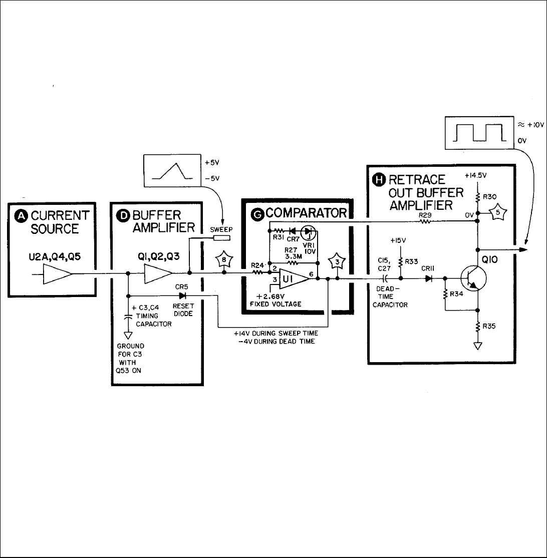
Model 8558B TM 11-6625-3061-14
Figure 8-21. Simplified Schematic of Sweep Generator in AUTO Mode
8-46
Model 8558B TM 11-6625-3061-14
As the voltage at U1 pin 6 (TP3) decreases, the anode voltage of VR1 decreases. At some time (when the level of the
sweep ramp at TP8 is + 5V), the anode voltage of VR1 will no longer forward bias CR7, and the zener feedback loop
opens. At this point, the 3.3 megaohm feedback loop becomes active and U1 saturates again. The comparator toggles,
this time toward the negative operational amplifier supply, and 4V appears at TP3.
The -4V at T3 forward biases CR5. Timing capacitors C3 and C4 discharge through CR5, forming the negative slope of
the sweep ramp. Dead-time capacitor C15 discharges.
The endpoints of the sweep ramp at TP8, 5V and + 5V, are controlled by the voltage divider R21, R24, R29, and R30 or
R35, and by U1 and its feedback loops. U1 controls the ramp voltage as it maintains 2.68V at pin 2.
At the end of the ramp, when CR5 is forward biased, and the comparator output (pin 6 of U1) is approaching its negative
supply, U1 uses Q1 and Q3 to maintain 2.68V at pin 2. Q10 is off, and the voltage divider R21, R24, R29, and R30
produces -5V at TP8.
At the beginning of the ramp, when CR5 is reverse biased, and the comparator output is approaching its positive supply,
U1 again maintains 2.68V at pin 2. This time, Q10 is on, and voltage divider R21, R24, R29, and R35 produces + 5V at
TP8.
Fast/Slow Sweep Time Operation. The ST6 control line from Front Switch Assembly A2A1, selects timing and dead-
time capacitors C3, C4, C5, and C27, to control fast and slow sweep times. If the same amount of charging current is
supplied to a larger capacitor, it charges at a slower rate.
Timing capacitors C3 and C4 are used to provide fast and slow sweep operation. When a fast sweep time (ms/div) is
selected at TIME/DIV switch A2A1S3, the ST6 (FAST SWEEP) control line is grounded, turning off Q55 and Q53. With
Q53 off, C3 and C4 are in series and the timing capacitor becomes C4. With Q55 off, the + 15V at R57 back biases CR9
and CR6, so C27 is switched out of the dead-time circuit. the dead-time (about 0.4 ms) is set by C15. In sweep times
greater than 1 ms/div (or in AUTO sweep times), the ST6 (FAST SWEEP) control line is open, Q55 and Q53 are both on.
With Q53 on, a ground is provided for C3 and it becomes the timing capacitor. CR6 and CR9 are on because of the
conduction of Q55. C15 and C27 are in parallel, so the longer dead-time (about 7.5 ms) is set by C27.
When selecting FREE RUN mode (A2A1S4), + 15 volts is routed to the voltage divider, R59 and R60, via the TRIG
control line. CR10 is reversed biased.
FREE RUN TRIGGER Operation. The circuit free runs and QI0 conducts when U1 switches on and off at a time
determined by the RC time constants.
VIDEO TRIGGER OPERATION. When the video mode is selected (VIDEO position on A2A1S4 switch), CR10 is
forward biased by R59, and Q10 is off. The sweep ramp is generated by turning on Q10 with a negative pulse from the
pulse shaper circuitry. The negative pulse is applied to the emitter of Q10.
8-47
Model 8558B TM 11-6625-3061-14
The pulse shape consists of a Schmitt trigger (Q39 and Q40), a differentiator (C12 and R55), and an emitter follower
(Q12). The Schmitt trigger produces a pulse which exists as long as the video trigger information on the SYNC line is
above a certain dc level. When the TRIGGER switch is in VIDEO position, video information from Vertical Driver and
Blanking Assembly A15 is routed through the switch to the base of Q40. Q40 is normally off and Q39 is conducting.
During the positive portion of the SYNC signal, Q40 turns on, turning Q39 off. C7 accelerates the Q39 switching. When
Q40 switches on, the negative change at the collector is differentiated by C12 and R55, and coupled through Q12 to the
Q10 emitter. The negative pulse turns on Q10. CR8, R32, and VR1 keep Q10 on while the ramp is being generated.
After the ramp is completed, the circuit returns to its dead-time state and another trigger is required to generate another
sweep. Trigger pulses from Q40, which may occur during the sweep, have no effect since Q10 is already on.
LINE TRIG Operation The sweep may be synchronized with the ac line voltage in the same manner as described in
VIDEO operation. With TRIGGER switch A2A1S4 in LINE position, the ac line from the mainframe power transformer is
connected to the Schmitt trigger (Q40 and Q39) input. A16R2 and A16C2 on the motherboard attenuate the ac line
signal to approximately 2 volts p-p and filter any line spikes.
SINGLE Sweep Trigger and Abort. Q10 is initially held off by R59 and CR10. Q9 is on, and voltage divider R37 and
R38 charges C16 to +2.8V. When the trigger switch A2A1R4 is set to SINGLE sweep (spring-loaded position), + 15V is
applied to R62 turning on Q11. This shorts the positive end of C16 to ground and produces a negative pulse at the
emitter of Q10. This turns Q10 on starting a sweep.
During the generation of a sweep, Q9 is off and the voltage divider R37 and R38 charges C16 to 4V. The sweep may be
aborted (reset to 5V) by pressing the SINGLE switch to the spring-loaded position. This switches on Q11. The negative
end of C16 is shorted to ground, a positive pulse is generated at the emitter of Q10, and Q10 is turned off aborting the
sweep.
MANUAL Sweep Control
Manual control of the sweep is obtained with the TIME/DIV switch A2A1S3 in MAN position. A ground is applied to the
base of Q38 and Q37 by the ST7 line from A2A1S3 in all sweep modes except manual; the ground holds Q38 and Q37
off. With A2A1S3 in MAN position, Q38 and Q37 are turned on. Q37 turns Q10 on and keeps it on. CR5 is on and the
feedback loop to the timing capacitor is closed. Turning the MANUAL SWEEP control A2A1R4 changes the voltage at
the collector of Q38 which changes the input current at U1 pin 2. Since the feedback current through R29 is constant,
any change in manual sweep current must be compensated by a change in the current through R24, thereby varying the
ramp output voltage.
Current Source
Current for the generation of the sweep is provided by the current source circuit. The temperature dependent power
supply provides a nominal + 10V; Q6 is the temperature sensing element (diode). The following switches control current
to operational amplifier U2A pin 2: RESOLUTION BW switch A2A1S5, FREQ SPAN/DIV switch A2A1S6, VIDEO FILTER
potentiometer A2R5, and TIME/DIV switch A2A1S3. In the AUTO sweep time mode, the sweep time is controlled by the
RESOLUTION BW, FREQ SPAN/DIV, and VIDEO FILTER which set the currents to U2A. These currents are summed
by U2A to produce a voltage proportional to the log of the sweep time. Q4 is the current driver and converts voltage
variations into current variations proportional to sweep time. The current is applied to the timing capacitors C3 and C4,
in the buffer amplifier circuit.
8-48
Model 8558B TM 11-6625-3061-14
Q7 provides temperature compensation for Q4. Q8 is a constant-current regulator for Q7. In AUTO, the sweep time is
limited to 1 ms and longer because current is limited to 1 mA by Q5/R15.
In the calibrated sweep time/division mode, the gate of Q52 is grounded. This turns Q52 off and disconnects the
currents proportional to RESOLUTION BW, FREQ SPAN/DIV, and VIDEO FILTER. Calibrated sweep times are now
produced by the currents fed to U2A through R40 through R44. Those resistors are grounded in various combinations by
SWEEP TIME/DIV switch A2A1S3 resistor network. (See A2 Schematic.)
XTAL Resolution Bandwidth Control
When a XTAL bandwidth is selected (30 kHz, 10 kHz, 3 kHz, 1 kHz), control line BW5 is released from + 15V on the front
panel and is pulled to -.5V by Q13. This has four effects.
1. On the Bandwidth Filter boards CR2 and CR13 are turned off and Q3, Q6, CR8 and CR15 are turned on,
allowing the XTAL filters to operate.
2. Q21 is turned off allowing BW7 to be pulled up to more than + -10V by CR18 and R82. This turns off the LC
filter sections on the Bandwidth Filter boards.
3. Q14 is turned off allowing the voltage on BW6 to be controlled by the current through A8Q 19.
4. Q22 is turned off having an effect on sweep time which is discussed in detail later.
The current through Q19 is a function of the states (off or on) of Q15, Q17, Q42, the values of factory select resistors
R74, R76, and R78, and the setting of. R72 XTL (3 kHz adjustment). The off/on states of Q15, Q17, and Q42 are
controlled by BW1, BW2, and BW3 which are controlled by the front panel RESOLUTION BW switch and are at either +
15V or some negative voltage. The amount of current through Q19 controls the bandwidths of the XTAL filter sections
on the Bandwidth Filter boards.
LC Resolution Bandwidth Control
When an LC bandwidth is selected, (3 MHz, 1 MHz, 300 kHz, 100 kHz), control line BW5 is pulled to + 15V at the front
panel. This has four effects.
1. On the Bandwidth Filter boards: Q3, Q6, CR8, and CR15 are turned off and CR2 and CR13 are turned on, thus
blocking any signal from passing through the XTAL filer sections.
2. Q14 is turned on, pulling BW6 to -4V, which further defeats any possible action of the XTAL filter sections.
3. Q21 is turned on, allowing the voltage on BW7 to be controlled by the current through Q20.
8-49
Model 8558B TM 11-6625-3061-14
The current through Q20 is a function of the states (off or on) of Q23, Q44, Q49, the values of factory select resistors
R89, R92, and R95, and the setting of R85 LC (1 MHz adjustment). The off/on states of Q23, Q44, Q49 are controlled by
BW2, BW3, and BW4 which are controlled by the front panel bandwidth switch and are either at + 15V or some negative
voltage. The amount of current through Q20 controls the bandwidths of the LC filter sections on the Bandwidth Filter
boards.
4. Q22 is turned on having an effect on AUTO sweep time which is discussed later.
Video Filter
The video filter is composed of front panel control A2R6, switch A2S2, and 8 capacitors on Sweep Generator A8. The
amount of filtering is controlled by the Resolution Bandwidth setting through Q16, Q18, Q43, Q41, Q46, Q24, and Q45.
These transistors switch in and out various combinations of filter capacitors to provide more video filtering when the
resolution bandwidth is decreased. In LC mode, BW6 is low holding Q15, Q17, Q42, Q41 off and keeping C19, C20, C21
and C22 out of the circuit.
Switch A2S2 applies maximum video filtering for noise measure mode by switching in C26 through Q47.
Sweep Attenuator
The sweep attenuator circuit changes the amplitude of the sweep voltage applied to the Frequency Control A7 as a
function of the FREQ SPAN/DIV selected. The attenuator attenuates the -5V to +5V ramp routed through XA8 pin 39 in
a divide by 1, 2, 5, and 10 sequence from a divide-by-1 to a divide-by-200. The circuit also generates an auto-sweep
control current used to control the AUTO sweep time circuit as a function of the frequency span.
The sweep attenuator has two voltage dividers buffered by the unity gain voltage follower U3. The divider at the input of
U3 provides either a divide-by-two or a divide-by-five; the divider at the output of the U3 provides a divide-by-one, a
divide-by-ten, and a divide-by-one hundred.
Assuming that FS3 (divide-by-two) is selected, + 15V turns on Q31 and Q32 grounds a 10K ohm resistor R113. The -5V
to +5V ramp is divided across the input resistor R101 (10K ohms) and R113 (10K ohms). The ramp is now divided in
half and applied to sweep buffer U3 pin 3. The dividers at the output of U3 (controlled by FS4 and FS5) have reversed
control logic; they are normally connected to + 15V by A2A1S5 and open when selected. Q50 is a gate to drive Q30.
When FS4 and FS5 are connected to + 15V, Q50 is off and Q30 is on, connecting the divide-by-one divider at the output
of U3. If either FS4 or FS5 is open, Q30 is off and Q28 or Q26 is on, providing either a divide-by-10 or divide-by-100.
AUTO sweep control current is applied to Q52 as a function of frequency span by Q35, Q31, Q33, Q27, and Q25 and the
appropriate resistors. For narrow spans (1 MHz/DIV or less), when the YIG FM coil is swept, FS6 is connected to + 15V
by A2A1S5. Q29 is on and the additional current in the AUTO sweep control is used to reduce the sweep time.
8-50
Model 8558B TM 11-6625-3061-14
+ V Sweep Offset
Normally, START-CENTER switch A2A1S7 is in the CENTER position. The + 15V back biases Q54 and holds it off.
Switching to START allows Q54 to conduct and adds 0.5 mA of current through R67 to offset the sweep ramp. When
START frequency is used, the ramp excursion is from 0V to a positive voltage.
8-51
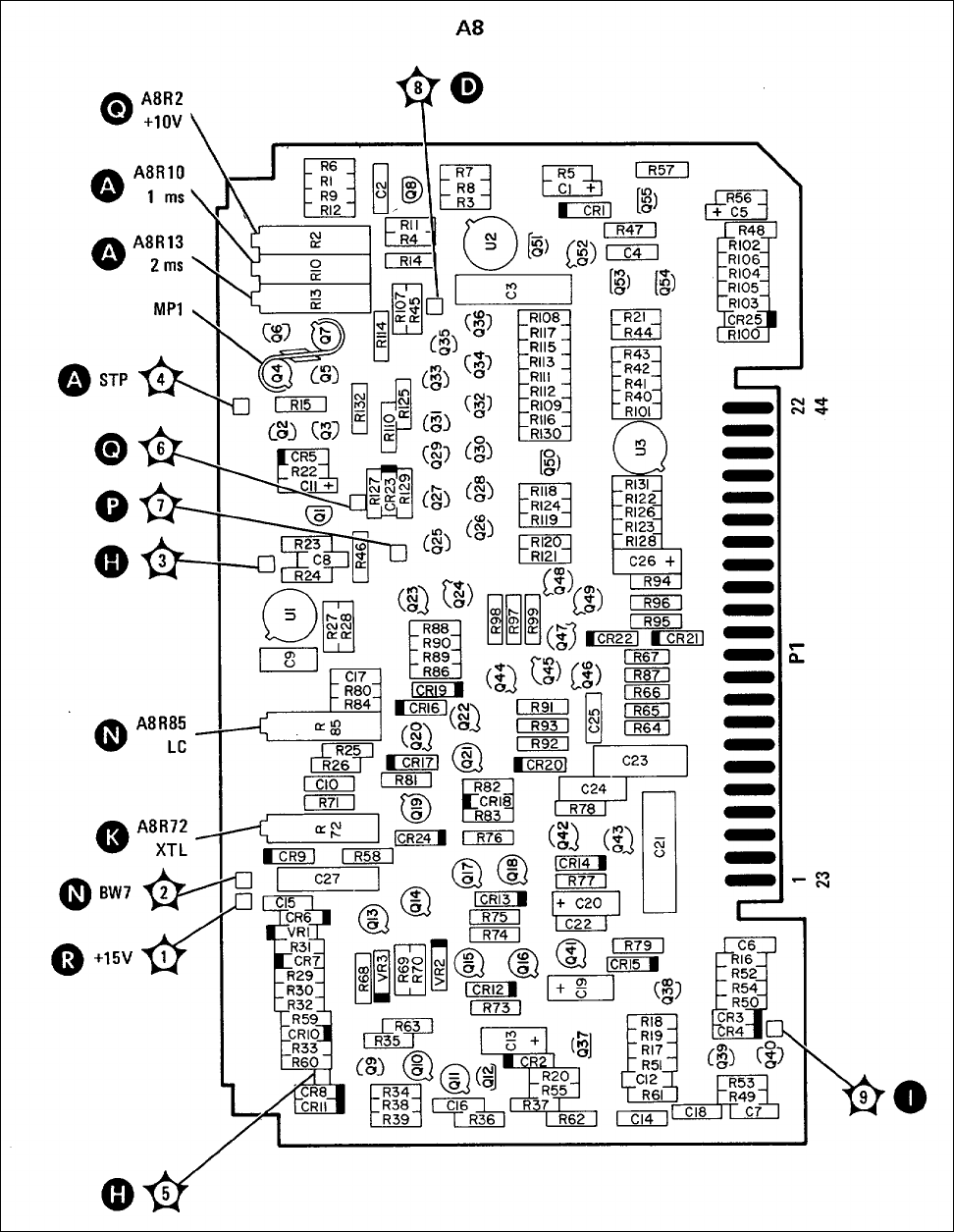
Model 8558B TM 11-6625-3061-14
Figure 8-22. A8 Sweep Generator Assembly, Component and Test Point Locations
8-52
TM 11-1247-B
THIS PAGE MISSING NOT AVAILABLE FOR DIGITIZATION.
PAGES
8-53 through 8-56
Model 8558B TM 11-6625-3061-14
A9 THIRD CONVERTER CIRCUIT DESCRIPTION
General Description
The Third Converter Assembly contains of a 280 MHz oscillator followed by a buffer amplifier, a balanced mixer, a
matching filter, a 21.4 MHz amplifier,, and a PIN attenuator. The 301.4 MHz second IF signal from A10 is mixed with the
280 MHz oscillator (third LO) in balanced mixer A9U1. The output from the mixer is the difference frequency, 21.4 MHz,
which is applied to the matching filter. This is a 21.4 MHz bandpass filter which also acts as an inter-stage impedance
matching device. The signal is then amplified by the 21.4 MHz amplifier and coupled to a divider network consisting of
two PIN diodes A9CR3 and CR4, resistor R25, and the input impedance of the Bandwidth Filter No. 1 Assembly A11.
PIN driver A9Q5 changes the bias of the PIN diodes as a function of frequency, compensating for input mixer frequency
response. The 21.4 MHz third IF output signal is coupled to the input of Bandwidth Filter No. 1. The 280 MHz Oscillator
also provides the front panel CAL OUTPUT 280 MHz -30 dBm signal. It is sometimes necessary to select a different
value for R9 to provide the 30 dBm CAL OUTPUT level while maintaining the proper input level to the balanced mixer.
280 MHz Oscillator (Third LO)
The third local oscillator is a modified Colpitts circuit with a 280 MHz surface acoustic wave resonator (SAWR) A9Z1 in
the positive feedback path to provide increased frequency stability. Inductor A9L3, across the SAWR, tunes out the
SAWR shunt capacitance. The oscillator tuned circuit consists of capacitors A9C4, C5, and inductors L4 and L6. This
tuned circuit ensures that the oscillator oscillates only on the proper overtone of the SAWR. A1though A9L4 is called the
LO FREQ adjustment, it is used to adjust for maximum LO output power and has only a slight effect on the output
frequency. Inductor A9L5 provides a dc path for base bias of buffer amplifier A9Q2. Diodes A9CRI and CR2 provide
temperature compensation for the 280 MHz oscillator and indirectly stabilize the CAL OUTPUT level. Power is taken out
of the oscillator through L6, which transforms the output to approximately 50 ohms at a level of 0 dBm. The output level
of the circuit is controlled by 3RD LO PWR adjustment A9RS, which sets the emitter current of A9Q1 and allows
adjustment f6r a 30 dBm 280 MHz front-panel CAL OUTPUT level. It is sometimes necessary to select a different value
for A9R4 to provide the proper third LO output level. Buffer amplifier A9Q2 provides isolation for the 280 MHz oscillator
and provides about 10 dB of power gain to the L port of balanced mixer U1. The buffer amplifier also provides the
proper output level to the front-panel CAL OUTPUT (by selecting A9R9) for a given balanced mixer input.
Balanced Mixer (Third Mixer)
The third LO 280 MHz input to the L port of the balanced mixer is approximately + 10 dBm. The level of the second IF
301.4 MHz input to the X port of the mixer is about 12 dBm or less. The third mixer output (Port R) is the 21.4 MHz
difference frequency produced by heterodyning the 301.4 MHz IF and the 280 MHz LO. The third mixer has a
conversion loss of about 7 dB.
Matching Filter
The output of the balanced mixer is applied to the matching filter which consists of A9L9, C10, C11, C12, and L10. The
matching filter is a 21.4 MHz bandpass filter which also serves as an impedance matching network. The circuit raises
the low input impedance of the 21.4 MHz amplifier (about 10 ohms) to match the higher output impedance of the
balanced mixer (about 50 ohms).
21.4 MHz Amplifier
The 21.4 MHz amplifier consists of A9Q3 in a common-emitter configuration and A9Q4 as an emitter follower. Transistor
A9Q3 employs resistor A9R12 and zener diode A9VR2 to furnish base bias and negative feedback for gain control and
stabilization. Resistor A9R12 is factory selected to provide the
8-57
Model 8558B TM 11-6625-3061-14
proper gain of the Third Converter Assembly. Capacitor A9C14 is connected across A9VR2 to reduce zener noise. The
output of the 21.4 MHz amplifier looks into a voltage-controlled attenuator consisting of two PIN diodes, A9CR3 and
CR4, resistor A9R25, and the input impedance of the Bandwidth Filter No. 1 Assembly A11.
PIN Driver
The PIN diode resistance of A9CR3 and CR4 is controlled by the PIN driver A9Q5 and its associated circuitry. The base
of A9Q5 is the summing point for the frequency anA10g voltage from the Frequency Control Assembly A7 and a dc level
set by front-panel REF LEVEL CAL screwdriver adjustment A2R3. Setting the dc level by adjusting A2R3 calibrates the
8558B display at a given frequency, usually performed at 280 MHz. The frequency analog voltage is a dc level varying
from + 0.6 volts to + 6.7 volts as a function of frequency. This frequency anA10g voltage at the base of A9Q5
compensates for input mixer response. SLOPE COMP adjustment A9R1 sets the amount of compensation required for a
flat frequency response. The total current through the PIN diodes A9CR3 and CR4 is shaped by the emitter network of
A9Q5. This network provides a change in current through the PIN diodes to cause a change of PIN diode resistance.
The change in resistance is required to provide the proper log curve within an 8 dB range for the voltage-controlled
attenuator.
8-58
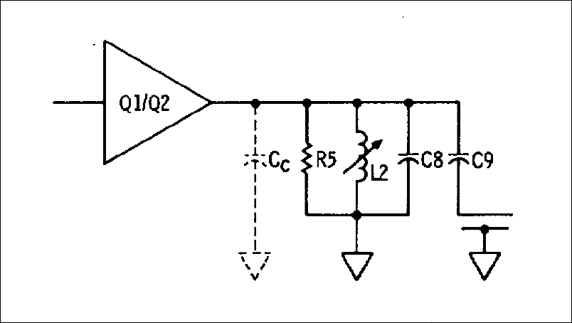
Model 8558B TM 11-6625-3061-14
A10 SECOND IF CIRCUIT DESCRIPTION
General Description
The Second IF Assembly contains a bandpass amplifier which provides a gain of approximately 16 dB at 301.4 MHz. It
also contains a bandpass filter which provides further rejection of unwanted signals. The bandpass filter has a 3 dB loss,
giving the Second IF Assembly a net gain of approximately 13 dB at 301.4 MHz. The 301.4 MHz IF output signal is
coupled to Third Converter Assembly A9 by cable W7. This signal is the input to the X port of the balanced mixer on the
Third Converter Assembly.
Bandpass Amplifier
The bandpass amplifier consists of A10Q2 in a common-emitter configuration, and A10Q1 connected to control the base
drive and bias current of A10Q2. Capacitors A10C4, C5, C7, and C10 serve as decoupling for high frequencies. The
gain of the bandpass amplifier is set by the high frequency characteristics of A10Q2, R5, and the small amount of
inductance on the emitter connection of Q2. The emitter inductance is used to establish a 50 ohm input impedance and
to help stabilize the current gain of A10Q2. Resistor A10R5 in parallel with the output resistance of A10Q2 establishes
an output impedance of about 500 ohms. Components A10L2, C8, C9 and the collector capacitance (Cc) of Q2 form the
collector tank circuit (see Figure 8-24). This tank circuit determines the center frequency of the bandpass amplifier and
transforms the 500 ohm output impedance at the collector of A10Q1 down to 50 ohms. The output of the bandpass
amplifier flows from A10C9 through a 50 ohm microstrip transmission line (etched on the printed circuit board) to the
bandpass filter. The bandpass amplifier has a gain of about 16 dB from the base of A10Q2 to the 50 ohm output of
A10C9.
Bandpass Filter
The output of the bandpass amplifier passes through a 301.4 MHz bandpass filter. The bandpass filter is made up of
A10L3, L4, L5, C11, C12, C13, C14, C15 and adjustable piston-type capacitors A10C1, C2, and C3. Capacitors A10C11
and C15 are used to transform the bandpass filter input and output impedance to 50 ohms. Inductors A10L3, L4, and L5
are wound on a common coil form which provides mutual inductance coupling between filter sections. The bandpass
filter has an insertion loss of approximately 3 dB and 3 dB bandwidth of about 12 MHz.
Figure 8-24. Bandpass Amplifier Tank Circuit, Simplified Schematic
8-59
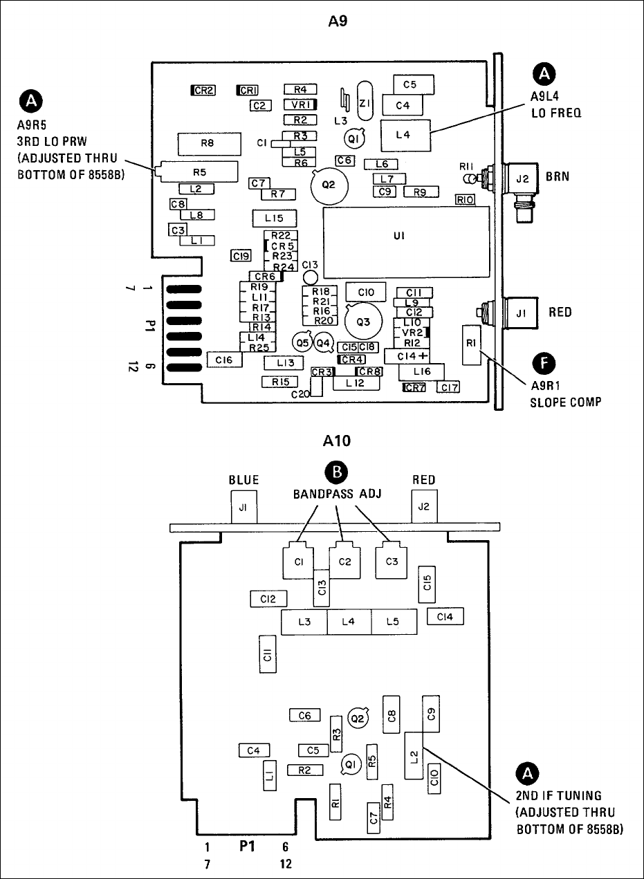
Model 8558B TM 11-6625-3061-14
Figure 8-25. A9 Third Converter Assembly, and A10 Second IF Assembly, Component Locations
8-60
TM 11-1247-B
THIS PAGE MISSING NOT AVAILABLE FOR DIGITIZATION.
PAGES
8-61 through 8-62
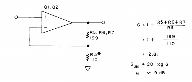
Model 8558B TM11-6625-3061-14
A11 BANDWIDTH FILTER NO. 1 CIRCUIT DESCRIPTION
General Description
Bandwidth Filter No. 1 operates at 21.4 MHz and is variable in bandwidth from 3 MHz to 1 kHz. The front-panel
RESOLUTION BW switch is used to select one of eight available bandwidth settings (3 MHz, 1 MHz, 300 kHz, 100 kHz,
30 kHz, 10 kHz, 3 kHz, or 1 kHz).
The narrower bandwidths (1 kHz through 30 kHz) are obtained from four synchronously tuned crystal filters; the four
wider bandwidths (100 kHz through 3 MHz), from four synchronously tuned LC tank circuits. The four stages of
bandwidth filters are on two similar printed-circuit boards, Bandwidth Filter No. 1 (A11) and Bandwidth Filter No. 2
(A13). Two LC tank circuits and two crystal filters are on each board. The four crystals in the two bandwidth assemblies
(A11Y1, A11Y2, A13Y1, and A13Y2) are a factory-selected matched set. If replacement of a Bandwidth Filter assembly
is necessary, the new board is shipped with two crystals installed. The other two crystals (which must be used to replace
the existing two crystals in the good Bandwidth Filter assembly) are packaged separately and shipped with the new
Bandwidth Filter board. In addition to the filter stages, each Bandwidth Filter provides 10 dB of gain in both LC and
crystal filter operation. (There is some gain in the "unity" gain buffer amplifiers.)
10 dB Input Buffer Amplifier
The 10 dB input buffer amplifier functions as a non-inverting operational amplifier.
In the crystal mode (bandwidths <30 kHz), the amplifier includes Q3. The biasing of the amplifier is independent of its ac
(21.4 MHz) operation but is very critical for its proper functioning. If a malfunction occurs, the dc bias should be checked
first.
In the LC mode (the four wider bandwidths), the BW5 line goes to + 14.8V and turns off current source Q3. The current
supplied by Q3 in the crystal mode is then supplied through CR1 and R13 from the BW5 line.
Unity Gain Buffer Amplifier
The unity gain buffer amplifier is the same as the 10 dB input buffer amplifier, except that it has a FET input (Q5) and is
connected for unity gain. The input is selected by the BW5 line from CR9 in the LC mode, or from CR8 in the crystal
mode.
In the crystal mode, the current through Q5 is determined by the difference between the current sourced by Q6 and that
sunk by Q7: about 4 mA. A significant deviation from this current should be reflected by the gate-to-source voltage of
Q5. The source should be at least 0.2V more positive than the gate, but not more than 1.5V more positive. If the
difference is less than 0.2V, the FET current is too high; if the difference is greater than 1.5V, the FET current is too low.
In either case the FET could also be defective. To determine
8-63
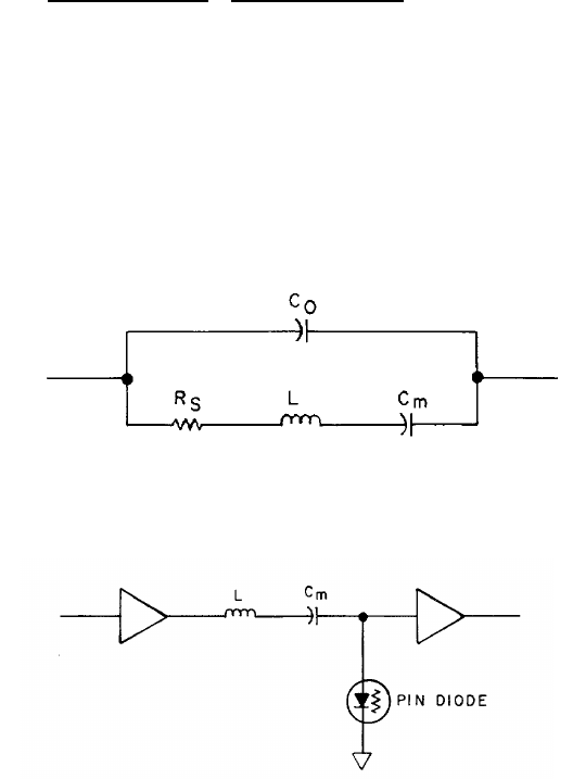
Model 8558B TM11-6625-3061-14
precisely the current through Q5, the difference between the current through R38 and that through R60 should be
subtracted from the current through R30. If the results are inconsistent, check the above mentioned resistors.
In LC mode of operation, current is supplied through R37 and CR19 from the BW5 line instead of through Q6. The
difference between the current through R37 and that through R30 yields the FET current.
Output Buffer Amplifier The output buffer amplifier is a complementary pair of transistors in which Q9 acts as a source
follower boosted by Q10. The current through FET Q9 is set by R53:
Vbe (Q10) .7V
IFET = ÷ ÷3 mA
196Ω196Ω
The total current through Q9 and Q10 is set by R54. The input is selected by the BW5 line from either CR16 in the LC
mode or CR15 in the crystal mode.
Crystal Filtering Circuits
The bandwidths 1 kHz, 3 kHz, 10 kHz, and 30 kHz are obtained by crystal filtering. The crystals are used in series
resonant mode and can be modeled as a series resonant circuit with a parallel capacitance:
The parallel capacitance (Co) and series resistance (Rs) are not desired and are compensated for in the circuit, resulting
in this simplified schematic of a single pole of crystal filtering:
PIN diode CR4 functions as a variable resistor at 21.4 MHz. As the resistance is lowered by increasing the current in the
BW6 line, the bandshape becomes narrower. The bandwidth of one pole widens to approximately 70 kHz when the PIN
is turned off completely at the 30 kHz BW setting. (For a four-pole filter, the bandwidth of each pole is about 2.3 times
the bandwidth of all four poles taken together. The bandwidth of two poles is about 1.5 times the bandwidth of all four
poles taken together).
A simplified schematic of a crystal pole, including compensation for Rx and Co in the crystal and input capacitance of the
buffer amplifier, is shown in Figure 8-27.
8-64
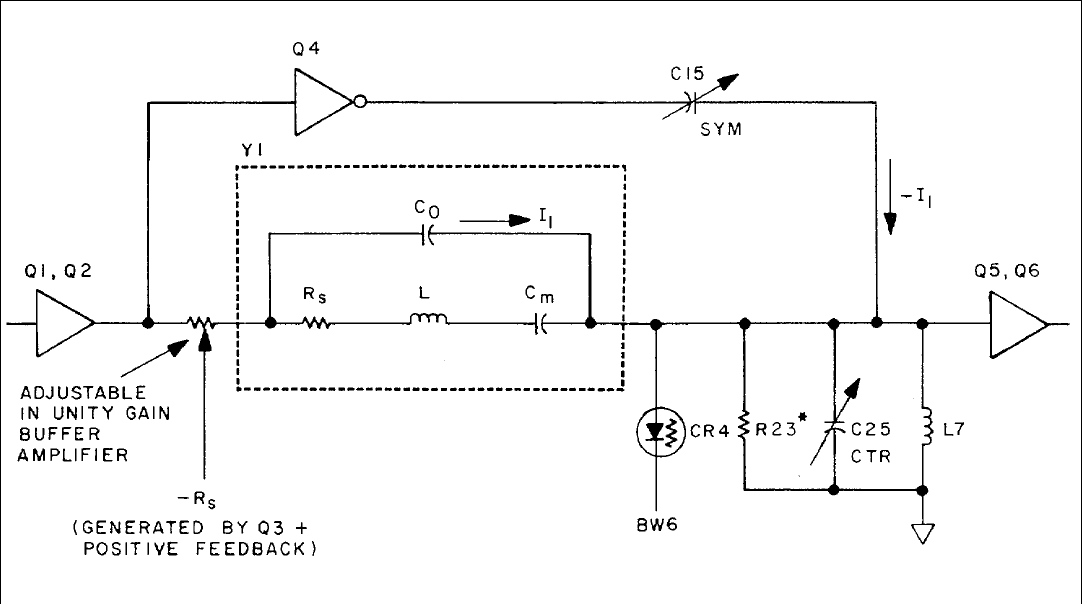
Model 8558B TM11-6625-3061-14
Figure 8-27. Crystal Pole, Simplified Schematic
The SYM adjustment, C15, compensates for Co by producing a current (-11) that is equal to the current (11) through Co
of the crystal but opposite in phase. These currents cancel and nullify the effect of Co. The positive feedback from the
collector of Q3 generates a negative output resistance that cancels Rs of the crystal. This is approximated by resistor R6
in the 10 dB input buffer amplifier and by potentiometer R31 in the unity gain buffer amplifier.
The input capacitance of the buffer amplifier, the printed circuit board capacitance, the PIN capacitance, and the
centering (CTR) capacitor C25 are in parallel resonance with L7. These components have negligible effect on the band
shape and as long as C25 has sufficient range to 'dip' the bandshape, they can be ignored in analyzing the remainder of
the circuit.
PIN diode CR4 controls bandwidths from 1 kHz to 10 kHz. For the 30 kHz bandwidth, CR4 is back biased, and R23 sets
the bandwidth. If the 30 kHz bandwidth is much too narrow, even with CR4 back biased, the circuit may be loaded by a
bad buffer amplifier (Q5, Q7) or inverting amplifier (Q4). If the bandwidth is only slightly narrow, it may be widened by
padding R23. If the narrowest bandwidths (1 kHz or 3 kHz) have too little gain, and it cannot be increased enough by
R31, either the crystals have too high a series resistance (defective crystal); or the output resistance is not negative
enough (defective buffer amplifier or Q3).
Almost any defect in the Bandwidth Filter boards will result in a faulty dc bias condition in one of the three buffer
amplifiers on each board. The dc bias of each stage is less straightforward than ac (21.4 MHz) operation and should be
checked carefully.
8-65
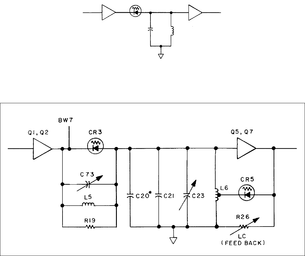
Model 8558B TM11-6625-3061-14
LC Filtering Circuits
The two LC filtering circuits are used for the wider bandwidths (100 kHz through 3 MHz). They are similar in function; the
first LC pole circuit is described. A schematic of the simplified equivalent circuit is shown below:
The LC filter uses a metallized inductor L6 in parallel with three capacitors: C23 (LC CTR) for centering, C21 for
temperature compensation, and C20*. The parallel circuit is driven through PIN diode CR3, which functions as a variable
resistor. The BW7 line sets the current through CR3. Higher resistance results in narrower bandwidth. A simplified
schematic of the first LC pole circuit is shown in Figure 8-28.
Figure 8-28. LC Pole, Simplified Schematic
8-66
Model 8558B TM11-6625-3061-14
C73 and L5 tune out the capacitance of CR3. R19 sets the 100 kHz bandwidth when CR3 is back biased (i.e., highest
resistance). CR5 is controlled by the LC FEEDBACK pot R26 and compensates for losses in the parallel resonant circuit.
(In the second LC pole circuit, fixed resistor R56* replaces CR5.) Low gain in one of the poles in the 100 kHz bandwidth
is caused by:
1. The pole being centered at some frequency other than 21.4 MHz (a defective metallized inductor is most
common).
2. The Q of the pole being too low (not a common failure).
3. Insufficient feedback from the buffer amplifier.
4. Defective buffer amplifier is loading the circuit.
If the 100 kHz bandwidth amplitude is correct, but that of the 300 kHz bandwidth is too low, either C73 or C74 might not
be properly adjusted. If the 300 kHz amplitude is too high, the four LC poles are not tuned close enough to the same
frequency. In either case, refer to Section V, Adjustments.
8-67
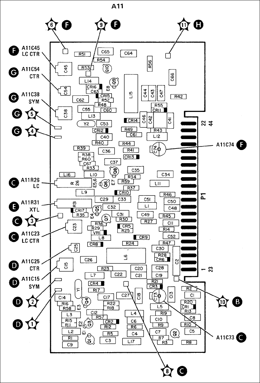
Model 8558B TM11-6625-3061-14
Figure 8-29. A11 Bandwidth Filter No. 1 Assembly, Component and Test Point Locations
8-68
TM 11-1247-B
THIS PAGE MISSING NOT AVAILABLE FOR DIGITIZATION.
PAGES
8-69
Model 8558B TM 11-6625-3061-14
A12 STEP GAIN CIRCUIT DESCRIPTION
General Description
The Step Gain Assembly contains three amplifier stages to provide a 0 to 50 dB amplification of the 21.4 MHz third IF
signal. The amplifier stages are selected by front panel REF LEVEL dBm switch A2S1. At the output of the final
amplifier is a two-section bandpass filter. In conjunction with the front panel REF LEVEL FINE control, the step gain
assembly also contains the circuitry for the 0 to 12 dB fine control for the reference level. A TEST/NORM switch is
available; in TEST position, tests are made at a low gain level.
0 - 12 dB Control
A minimum current flow through PIN diode A12CR3 (maximum allowable diode resistance) is established by the 12 dB
potentiometer, A12R6, so the diode is never completely cutoff. Adjustment of A12R6 sets the 0.3 dB point and is
adjusted with the REF LEVEL FINE control fully clockwise (-12 position).
The maximum current flow through the PIN diode is set by the 0 dB potentiometer, A12R5. A12R5 is adjusted to the
12.3 dB attenuation point with the REF LEVEL FINE control fully counterclockwise (0 position).
Transistors A12Q8 and A12Q9 are identical current sources. The maximum current is set by 0 dB adjustment A12R5 in
the common base circuit. Diode A12CR1 provides temperature compensation for the transistors.
A12Q8 provides current for a bias voltage applied to the anode of the PIN diode. The voltage source consists of A12R6,
A12R17, and A12CR2. Diode A12CR2 provides temperature compensation for the PIN diode. Inductance A12L5
isolates the current source from the RF signal.
A12Q9 provides current for a variable voltage source at the cathode of PIN diode A12CR3. A resistance is formed by
REF LEVEL FINE control R4 (shown on A2 schematic) and fixed resistor A12R9. The fixed 316K ohm resistor is used to
shape the value of potentiometer R4 to match the PIN diode resistance changes. The REF LEVEL FINE control varies
the voltage at the cathode of PIN diode A12CR3 and thus varies diode current flow. Regulating the current flow through
the PIN diode controls the amount of signal attenuation. For example, if PIN diode current flow is increased, more RF
signal is shunted or bypassed to ground. A12C12 provides the RF ground and also isolates from ground the variable dc
from the REF LEVEL FINE control. When the REF LEVEL FINE control is fully clockwise, the PIN diode is at minimum
conduction, and maximum signal is applied to the base of A12Q7. Conversely, when the REF LEVEL FINE control is
fully counterclockwise, the PIN diode is at maximum conduction and minimum signal is applied to A12Q7.
Step Gain Amplifiers
Buffer amplifier A12Q7 operates in an emitter-follower configuration and provides isolation between the 0 12 dB control
and the 10 dB amplifier.
The three step gain amplifiers can be considered as operational amplifiers. An equivalent circuit for the three stages is
shown in Figure 8-31. The gain for each amplifier is Av = Rf/Ri. The feedback resistance (Rf) for the 10 dB amplifier is
A12R26, 562 ohms; and for the 20 dB amplifiers it is A12R32 and A12R38, 750 ohms. The input resistance Ri is a
combination of a fixed series resistance (56.2 ohms) and the controlled resistance of the PIN diodes. The resistance of
the PIN diodes is approximatey 10 to 1000 ohms and increases as the forward bias current is decreased from 100 mA to
1 µA. Ri is approximately 260 ohms for the 10 dB amplifier and approximately 83 ohms for the 20 dB amplifiers.
8-71
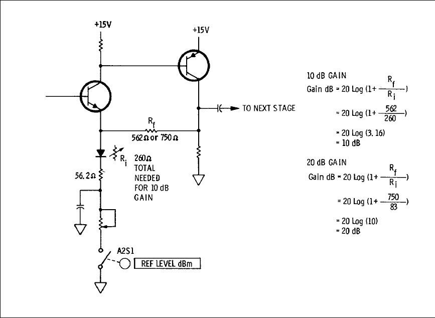
Model 8558B TM11-6625-3061-14
Selection of the correct combination of step gain amplifiers is accomplished with front panel REF LEVEL dBm switch
A2S 1. Rotating the switch grounds the emitter circuit of the selected amplifier(s) allowing current to flow through the PIN
diode(s). The possible switch combinations allow the gain to vary from unity (all switches open) to 50 dB maximum gain
with all three emitter circuits grounded.
A TEST/NORM switch, A12S1, is included in the emitter paths of the 20 dB step gain amplifiers. In the TEST position,
the switch defeats the two 20 dB amplifier stages, providing a fixed 10 dB of gain for use when making LOG amplifier
adjustments.
Bandpass Filter
The output of the step-gain amplifiers is coupled through a two-section bandpass filter. The bandpass filter consists of
A12L9, A12L10, A12C24, and A12C25 and provides rejection of signals outside the region of 21.4 MHz.
+ 19.5V Regulator
The + 19.5V regulator consists of series regulator A12Q13, driver A12Q12, and reference amplifier A12Q10 and Q11.
Zener diode A12VR1 provides a +6.2V reference for the base of Q11. Q10 senses the + 19.5V output across resistors
A12R45, R46, and R7, the + 19.5V adjustment. Should the output voltage start to drop below + 19.5V, Q10 will start to
turn off. This will turn on Q11 which turns on Q12 and Q13, raising the output back to + 19.5V. L11 and C27 filter the +
19.5V output. C26 between the collector and emitter of Q 12 is used to stabilize the feedback gain at high frequencies.
Figure 8-31. Equivalent Circuit for Step Gain Amplifiers
8-72
8-73
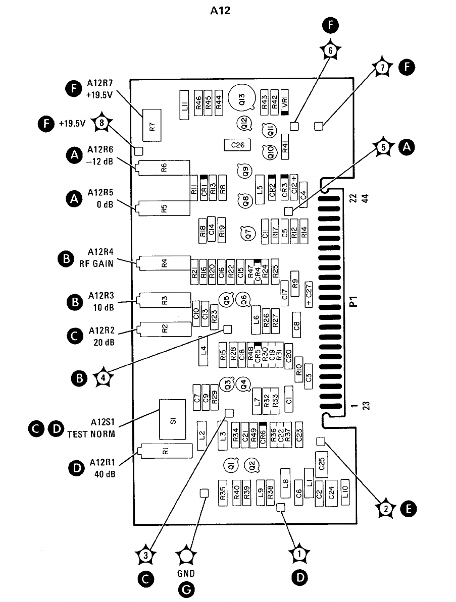
Model 8558B TM 11-6625-3061-14
Figure 8-32. A12 Step Gain Assembly, Component and Test Point Locations
8-74
TM 11-1247-B
THIS PAGE MISSING NOT AVAILABLE FOR DIGITIZATION.
PAGES
8-75 through 8-76
Model 8558B TM 11-6625-3061-14
A13 BANDWIDTH FILTER NO. 2 CIRCUIT DESCRIPTION
The Bandwidth Filter No. 2 Assembly is very similar to the Bandwidth Filter No. 1 Assembly A11, and corresponding
components have the same reference designators. The differences between the two board assemblies are as follows:
1. A13 has a limiting diode, CR18, connected between the input (P1-23) and ground; A11 does not.
2. The values of some resistors and capacitors in A13 are different from their counterparts in A11.
3. A13 has about 0.5 dB less gain than A11.
8-77
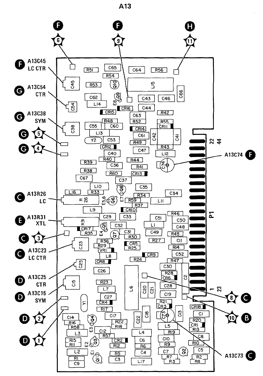
Model 8558B TM 11-6625-3061-14
Figure 8-34. A13 Bandwidth Filter No. 2 Assembly, Component and Test Point Locations
8-78
TM 11-1247-B
THIS PAGE MISSING NOT AVAILABLE FOR DIGITIZATION.
PAGES
8-79 through 8-80
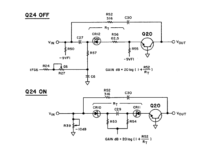
Model 8558B TM 11-6625-3061-14
A14 LOG AMPLIFIER ASSEMBLY, CIRCUIT DESCRIPTION
General Description
The Log Amplifier Assembly provides the ability to display signals in either a linear mode or 70 dB LOG mode. It also
operates with the Step Gain Assembly A12 to provide the last 40 dB of step gain amplification of the 21.4 MHz IF signal.
The Log Amplifier Assembly has seven amplifier stages, with each stage capable of providing both linear and logarithmic
amplification. Following the amplifier stages, the amplified IF signal is detected to produce the vertical signal for the
display. An offset circuit, following the detector, is used-in the log mode to offset the vertical output in steps equivalent to
40 dB of IF gain.
Log Mode of Operation
The seven amplifier stages limit the gain in sequence to provide 70 dB of log amplification. Each stage consists of an
emitter follower used as a voltage source to drive a common-base amplifier whose gain decreases with increasing signal
level.
Log Amplifier Gain. The operation of the second stage is described. In the log mode of operation, Q24 (Gain Control
Lines circuit) is on, forward biasing the log diodes, CR10 and CR11, which are Schottky diodes with a forward bias
voltage of approximately 0.4V. The gain of the amplifier is set by the ratio of R52 to the total resistance RT between the
emitters of Q13 and Q8. An example of gain computation is shown in Figure 8-36 RT is at a minimum (approximately
150 ohms) for small signals when the ac signal current in log diodes CR10 and CR11 is small compared to their dc bias
current. As the ac signal level is increased, the ac signal current increases to the level of the dc bias current and RT
increases because of current limiting in the diodes.
The initial (maximum) gain of the stage (approximately 10 dB) is set by the dc bias current through the log diodes. The
bias current is controlled by the temperature variable -8VT supply at the emitter of Q24. The final (minimum) gain of the
stage (0 dB) is set by the circuit configuration (RT becomes very large) and can be set further by the adjustment of R39 -
10 dB.
Figure 8-36. Simplified Log Amplifier Stage
8-81
Model 8558B TM 11-6625-3061-14
Linear Mode of Operation
Linear Gain. In the linear mode, the limiting action of the log diodes is removed from the seven amplifier stages. The
operation of the second stage is described. Q24 is turned off, and the dc bias current through log diodes CR10 and
CR11 is zero. With zero dc bias current the total resistance, RT, is maximum and the stage gain is approximately unity
(0 dB). (See Figure 8-26.)
In the sixth and seventh stages, an alternate signal path is used to set the gain at about 5 dB per stage. The purpose of
this fixed gain is to scale properly between the log and linear modes. These stages are activated by the -8VT from the
AMPLITUDE SCALE switch through R34 (LIN), R93, and R101, and finally through the cathodes of CR25 and CR28.
The combined gain of the two stages is adjusted with R34 (LIN), which controls the dc bias current in the PIN diodes.
Step Gain Operation
The Log Amplifier Board Assembly provides 40 dB of step gain in 10 dB steps. This gain, combined with 50 dB of step
gain from Step Gain Assembly A12, will produce up to 90 dB of total step gain. The amount of step gain is selected by
the front panel REFERENCE LEVEL switch (A2A1S1). The control lines from A2AiS1, IFG4, IFG5, and IFG6, control the
step gain on the Log Amplifier Board Assembly.
Step Gain When in Log Mode. When in log mode, control lines IFG4, IFG5, and IFG6 route + 15V to the Log Offset
circuit through R24, R25, and R26. This forward biases diodes CR32, CR33, and CR31. The Log Offset circuit provide
10, 20, 30, or 40 dB of step gain, depending on the state of the control lines. (See Log Offset circuit description.)
Step Gain When in Linear Mode. In linear mode, amplifier stages 2, 3, 4, and 5, are used to provide 40 dB of step gain
in 10 dB steps. In linear mode, the LOG/LIN line is at -8VT, Q24 is off, and the log diodes are normally off. Each
amplifier stage has unity gain (0 dB). The control lines, IFG4, IFG5, and IFG6 are used to forward bias the log diodes,
thus changing the gain of the amplifier stages from 0 dB to 10 dB. The state of the control lines determine which of
stages 2, 3, 4, or 5 has a gain of 10 dB.
For example, with INPUT ATTEN at 0 dB and REFERENCE LEVEL dBm at -60, -8VT is routed through A2A1S2 and
A2A1S1 to the IFG4 control line to forward bias CR22. The fifth amplifier stage gain changes from 0 dB to 10 dB,
providing 10 dB of step gain.
Resistors R33, R30, and R27 may be adjusted to set the step gains of stages 5, 4, and 3 and 2, respectively.
Log Mode Temperature Controlled Variable Gain Amplifier
LOG/LIN Relationship. In linear mode, when approximately 700 mVrms (+ 10 dBm) is applied to the input of the log
amplifier, the voltage at the output of stage 7 (TP5) is about 1.5 Vrms. With the same input signal in log mode, the
output at TP5 is about 2.0 Vrms. To maintain equal relationship with maximum input signal (trace at the top of the
display) the output in log mode must be attenuated. This attenuation is achieved through the use of variable gain
amplifier Q7, whose gain is determined by the ratio of its collector load to its emitter load.
Variable Gain Amplifier. In linear mode, the LOG/LIN control line is at -8VT. This forward biases CR4 and causes the
output of U2B (TP1) to go to approximately + 15V. CR29 is reverse biased, and the gain of the variable gain amplifier is
R104/R105 (100/316), or approximately 0.3. In log mode, the LOG/LIN control line is at + 15V, which reverse biases
CR4. The output of U2B is now approximately + 0.45V. CR29 is forward biased and has an ac resistance of about 100
ohms, which is in parallel with the 100-ohm R104, so the collector load of Q7 is 50 ohms. The gain is 50/316, or 0.15.
This gain depends upon the resistance of CR29, which is set by SLOPE adjustment R23.
8-82
Model 8558B TM 11-6625-3061-14
Detector and Buffer Amplifier
The signal output of Q7 is applied to the base of Q6, which converts voltage variations into current variations. Q5 is the
current driver for the detector. Q4, a half-wave rectifier, is biased just below cutoff by CR1. When the input signal is
positive, Q4 is in conduction but is cut off during the negative transistion. The detector output is routed to a low-pass filter
and a X2 buffer amplifier, Q21 and Q22, to provide the video output.
Log Offset
The last 40 dB of log step gain is produced in this circuit. When this gain is used, there is already a full 50 dB of gain in
the Step Gain Assembly, so the noise of the analyzer is amplified into the log range of the Log Amplifier Assembly. This
makes further amplificiation unnecessary since any signal below the log range of the Log Amplifer Assembly would be
buried in the noise. The output of the detector can then be offset in 100-mV steps corresponding to 10 dB of IF
amplification. This offset is provided by Q23 operating as a stepped current source into R115. With the AMPLITUDE
SCALE switch in one of the LOG/DIV positions, + 15V is routed throuh the closed contacts of the REFERENCE LEVEL
dBm switch to the IF gain control lines IFG4, IFG5, and IFG6. With an IF gain control line connected to + 15V, a log-shift
diode (CR31, CR32, or CR33) is forward biased, and this bias current, determined by R123, R124, or R125, flows into the
emitter of current source Q23. IFG4 and IFG5 each provides 10 dB (100 mV) of log offset gain and IFG6 provides 20 dB
(200 mV). The LOG GAIN adjustment R121 sets the operating point of Q23 for 100-mV steps.
Temperature Compensation Power Supply
Temperature compensation is provided for the - 8VT and + 1V regulators. CR2 and CR4 operate as the temperature-
sensing element. Temperature variations cause diode voltage changes that are amplified by U1A for the - 8VT supply
and by U2B for the + 1V supply. The - 8VT supply provides bias current for the Schottky diodes in the LOG mode. In
the linear mode, the - 8VT supply provides bias current for CR12, CR15, CR19, CR22, CR25, and CR28. The + 1V
supply provides bias current for CR29.
+11 V Regulated Power Supply
A precise 5.4V reference voltage VR1 is provided for the + 11V Regulator. This reference voltage is applied to the
positive input of U1B. R5 and R6 set the gain of U1B to 2.1. The output at TP2 is 2.1 x 5.4, or 11.3V. Q1 acts as an
emitter follower and provides the current drive for the + 11 V supply.
8-83
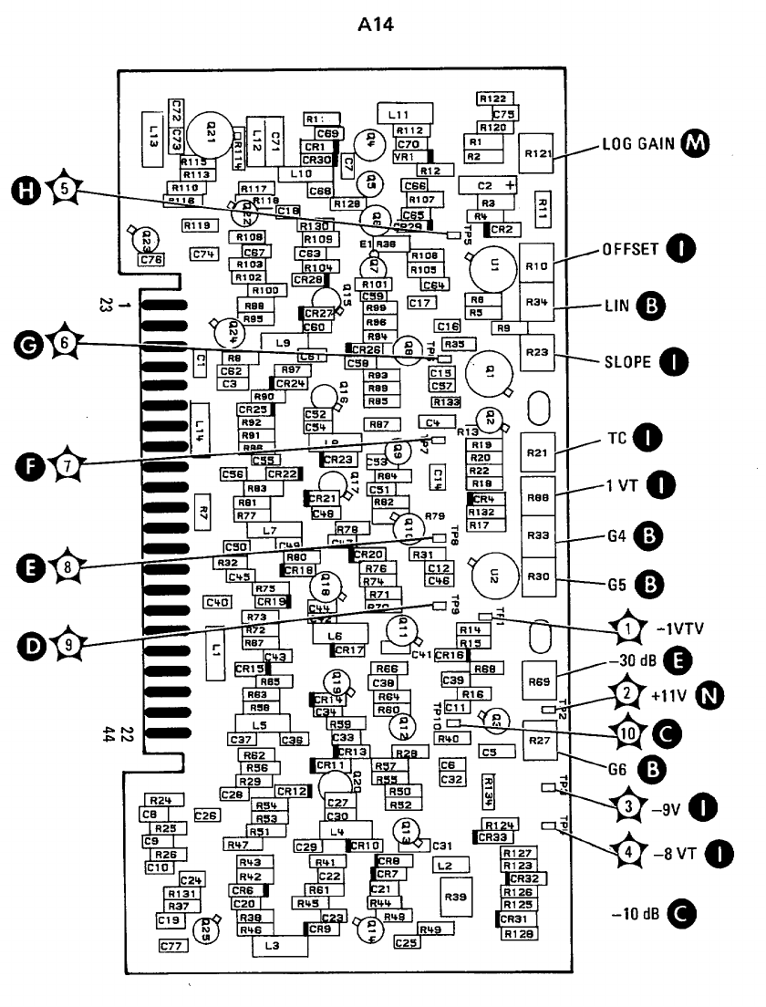
Model 8558B TM 11-6625-3061-14
Figure 8-37. A14 Log Amplifier Assembly, Component Locations
8-84
TM 11-1247-B
THIS PAGE MISSING NOT AVAILABLE FOR DIGITIZATION.
PAGES
8-85 through 8-88
Model 8558B TM 11-6625-3061-14
A15 VERTICAL DRIVER AND BLANKING CIRCUIT DESCRIPTION
General Description
The Vertical Driver and Blanking Assembly provides a preamplifier circuit to amplify the detected and filtered video from
the log amplifier. The video signal needed to trigger the sweep generator in INT mode is picked off at the preamplifier.
A vertical driver (differential amplifier) converts the signal to drive the vertical deflection plates (push-pull output).
The blanking and pen lift drive signals are also generated on assembly A15.
Preamplifier
The detected and filtered video input (0V to 0.8V) from the Log Amplifier Assembly A14 is applied to the gate of
A15Q17A. A15Q17, Q11, Q12, and Q18 make up a differential amplifier. The gate of Q17A is the noninverting input
and the gate of Q17B is the inverting input. The output at the emitter of A15Q18 is feedback applied to the gate of Q17B
through voltage divider A15R11, R12, and R13. The voltage gain of the preamplifier is 1 + R11/R12 + R13 = 10. With
an input voltage range of 0V to 0.8V, the maximum signal measured at the output of A15Q18 (TP5) would be 8V. (This
signal coupled through A15R17 is the trigger voltage for INT mode.) A buffer amplifier consisting of A15U2A, U2B, and
Q20 provides isolation between the preamplifier and vertical driver. A15U2D and Q13 are current sources to bias the
differential amplifier.
The vertical deflection sensitivity of the following vertical driver is 0.8V for full-scale deflection. Since a maximum
possible signal of 8V is available from the preamplifier, to obtain the correct signal amplitude, a divide-by-10 and an
offset circuit are used.
10 dB/DIV and LIN. The preamplifier output is divided by 10 when LOG/LIN switch A2S2 is in either LIN or 10 dB/DIV.
With LIN or 10 dB/DIV selected, + 15V is applied to the Expand line, back biasing A15CR1, and turning A15Q19 on.
Also A15CR2 is on and CR3 is back biased. With A15Q19 on, a voltage divider consisting of A15R18, R20, and Q19
divides the preamplifier output by 10.
1 dB/DIV. With 1 dB/DIV selected, the Expand line is open and A15Q19 is held off by A15CR1 and R22. The divide-by-
10 circuit is disabled and the full 8-volt preamp voltage is available. Since only the 0.8V peak can be displayed, the
signal to the buffer amplifier is offset by -7.2 volts as follows: A current source A15U2C is on, drawing current through
A15CR3 and R18. The voltage drop across R18 is set for 7.2V, so the 8V input is shifted -7.2V below ground. When the
signal goes below ground (OV), A15CR4 conducts and clamps the signal at -0.6V. The 1 dB OFFSET adjustment,
A15R1, sets the current for the correct voltage shift.
-5.5V Temperature Compensated Supply
The -5.5V temperature-compensated supply controls four current sources: A15U2D, Q13, U2C, and Q15. The
temperature-sensing element, A15U2E (connected as a diode), tracks the base-emitter temperature changes of the
current-source transistors.
Vertical Driver
The vertical driver-is a differential amplifier that consists of A15Q2, Q3, Q6, Q7, and Q14 with Q15 as the current source.
(See Figure 8-39.) The 0V to 0.8V vertical signal from the output of the preamplifier is converted to a push-pull signal to
drive the CRT vertical deflection plates. A15Q14 is a dual transistor used as the input stage to the Vertical Driver circuit.
The reference input level at the base of A15Q14A is set by the VERT POSN control, A2R6. The gain of the vertical
driver is set by the voltage divider consisting of A15R34, R42, and VERT GAIN control A2R7. The transistor pairs
A15Q2/Q6 and A15Q3/Q7 are current-to-voltage amplifiers and are driven by the current from the collectors of A15Q14A
and B respectively. Diodes A15CR5 through CR8 protect the bases of A15Q2, Q3, Q6, and Q7 to prevent them from
8-89
Model 8558B TM 11-6625-3061-14
being driven more negative than approximately 0.6V (the voltage drop across a diode). The resistors A15R44 and R52
decouple the capacitive load of the CRT plates from the emitters of A15Q2 and Q3, preventing overshoot and ringing in
the vertical driver. A15Q21, CR11, and CR12 provide vertical driver input switching for normalizer compatibility. When
the normalizer is not connected, pull-up resistor A15R56 places the cathode of A15CR11 at + 15V, preventing CR11
from conducting. A15Q21 is turned on so the input to the vertical driver is from the output of the preamplifier. When the
normalizer is connected and in the BYPASS mode, the L NORM line at A15J3 is high (+ 12V) preventing A15CR11 from
conducting. When the normalizer is operating, the L NORM line is pulled low (- 12V) causing A15CR11 to conduct.
A15Q21 is turned off by the negative voltage at the gate, switching the vertical driver input to the normalizer output (Y
NORM).
Blanking OR
Normally A15Q4 is off placing a low at the base of A15Q9 and turning it on. A15Q4 requires a positive voltage or about
1 mA to turn on and cut Q9 off. A high into the OR circuit provides a high blanking output (0V) to the mainframe. There
are four conditions that cause blanking of the sweep. (See Figure 8-40.) When the normalizer is not connected, pull-up
resistor A15R56 places the cathode of A15CR12 at + 15V, preventing CR12 from conducting. When the normalizer is
connected and in the bypass mode, the L NORM line at A15J3 is high (+12V) keeping A15CR12 from conducting. When
the normalizer is operating, the L NORM line is pulled low (-12V) causing A15CR12 to conduct. With A15CR12
conducting, the output of the blanking OR is held at a negative voltage level, inhibiting blanking from the 8558B.
Vertical/Baseline Comparator
The vertical/baseline comparator circuit consists of A15Q16 and Q8. The baseline clipping reference voltage is set by
front panel BASELINE CLIPPER control A2R2 which varies the base voltage of A15Q16. The vertical preamplifier output
signal is applied to the base of A15Q8. The signal voltage at the base of A15Q8 is compared to the dc reference on
Q16. When the signal voltage becomes more negative than the reference, Q8 turns on and the high input to its base
turns A15Q4 on, blanking the display.
Sweep Ramp High/Low Limit Comparator
Operational amplifier A15Q1A and Q1B is connected to form a comparator circuit. A voltage divider made up of A15R6,
R7, and R8 establishes a high and low voltage reference at UIA pin 2 and U1B pin 5. The switching limits are
approximately + 0.6V at U1B pin 5 (low frequency blanking) and +6.8V at U1A pin 2 (high frequency blanking). The
signal to the other inputs of the comparator is the frequency analog voltage from the YIG main coil swept driver. The
frequency analog input voltage is proportional to the instantaneous frequency to which the analyzer is tuned and sweeps
from 0.7V to 6.7V as the analyzer tunes from 0 to 1500 MHz. If the YIG tuning voltage at U1B pin 6 goes below 0.6V,
the output of U1B rises to about + 14V. This turns on A15Q4 and blanks the display. If the YIG tuning voltage at U1A
pin 2 rises above 6.8V, the output of U1A rises to about + 14V turning on A15Q4. Blanking of the display occurs
whenever the analyzer is swept below about - 30 MHz or above about 1600 MHz.
Pen Lift Driver
The display is blanked during retrace and the dead time of the sweep voltage. The Retrace Blanking input from A8Q9 in
the sweep generator circuit is applied to the emitter of buffer amplifier A15Q1. When the sweep ramp is turned off (dead
time), the Retrace Blanking signal rises to + 10V. The + 10V connected to the base of A15Q4 produces the blanking
output. The same + 10V Retrace Blanking input is applied to the base of A15Q5, turning Q5 on and Q10 off. The
collector of A15Q10 then rises to + 15V. A15Q10 provides a signal that can be used to drive the Pen Lift input on an X-Y
recorder. This signal causes the pen to lift during the analyzer sweep retrace and dead time. Breakdown diodes A15VR2
and VR3 suppress the high positive and negative voltage transients that some X-Y recorder pen lift coils can generate.
8-90
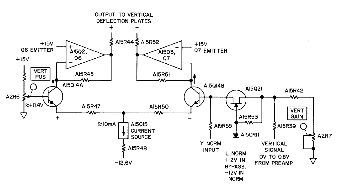
Model 8558B TM 11-6625-3061-14
Figure 8-39. Simplified Vertical Driver Circuit
8-91
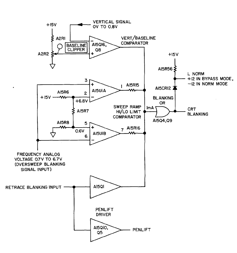
Model 8558B TM 11-6625-3061-14
Figure 8-40. Simplified Blanking Circuit
8-92
8-93
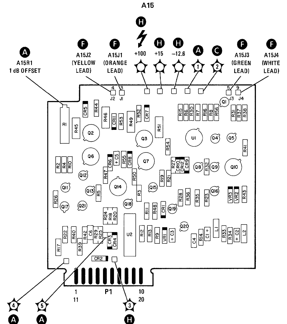
Model 8558B TM 11-6625-3061-14
Figure 8-41. A15 Vertical Driver and Blanking Assembly, Component and Test Point Locations
8-94
TM 11-1247-B
THIS PAGE MISSING NOT AVAILABLE FOR DIGITIZATION.
PAGES
8-95 through 8-100
Model 8558B TM 11-6625-3061-14
A17 INVERTER CIRCUIT DESCRIPTION
+5V Power Supply
Inverter Assembly A17 is a single transformer inverter with A17Q1 and Q2 operating as a 22 kHz squarewave oscillator.
Diodes A17CR1 and CR2 prevent the transistors from base-emitter reverse breakdown. Positive feedback to sustain the
oscillation is taken from the transistor base tickler winding of T1. A17R1* provides current to the base of Q2 to start
oscillations when the -12.6V supply is first turned on. The voltage at the collectors of A17Q1 and Q2 is a -12V to +12V
square wave. Diodes A17CR5, CR6, CR7, and CR8 are connected as a full-wave rectifier, receiving ac power from 6V
taps on either side of the grounded center tap. The rectified dc is filtered by A17L6, L7, L8, C5, and C6. The filtered
output voltage is +5V and powers DPM Driver Assembly A1A2. A17VR1, a 6.19V zener, provides protection for the DPM
Driver in case of excessive or reverse voltage.
+20.5V Power Supply
The oscillating current between the collectors of A17Q1 and Q2 through the primary winding of T1 induces a voltage in
the secondary of T1. Diodes CR3 and CR4 full-wave rectify this voltage, which is then filtered by A17L3, L4, L5, C3, and
C4. The dc output voltage, approximately +5.5V, is added to the +15V supply to obtain a + 20.5V supply
8-101
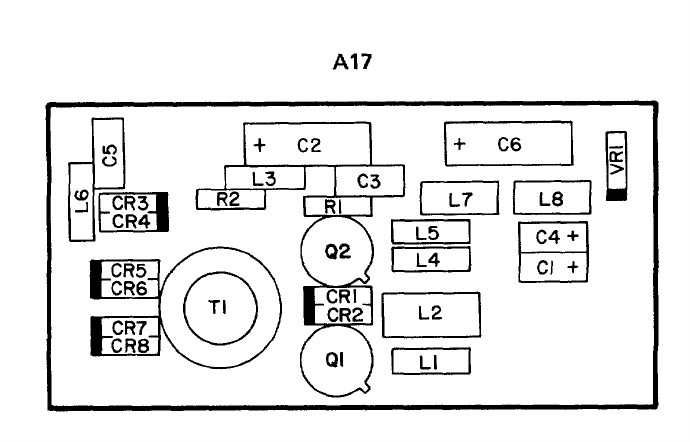
Model 8558B TM 11-6625-3061-14
Figure 8-45. A17 Inverter Assembly, Component Locations
8-102
TM 11-1247-B
THIS PAGE MISSING NOT AVAILABLE FOR DIGITIZATION.
PAGES
8-103 through 8-106

Model 8558B TM 11-6625-3061-14
FRONT SWITCH ASSEMBLY A2 DISASSEMBLY AND REPAIR
Tools and Materials Required
Description HP Part Number Check Digit
No. 2 Spline (Bristol) Wrench 8710-0055 0
Long No.4 Hex (Allen) Wrench 5020-0288 5
Long No. 6 Hex (Allen) Wrench 5020-0289 6
13/64-inch Open-end Wrench 8710-0946 8
5/16-inch Open-end Wrench 8720-0015 3
3/8-inch Open-end Wrench 8720-0016 4
1/2-inch Open-end Wrench 8720-0025 5
5/8-inch Open-end Wrench 8720-0010 8
1/4-inch Nut Driver 8720-0002 8
5/16-inch Nut Driver 8720-0003 9
3/8-inch Nut Driver 8720-0005 1
1/2-inch Nut Driver (end covered with heatshrink tubing) 8720-0007 3
9/16-inch Nut Driver (drilled out, end covered with
heatshrink tubing) 8720-0008 4
Pozi-driv Screwdriver 8710-0899 0
Long-nose Pliers 8710-0030 1
Wire Cutters 87100012 9
Instrument Grease 6040-0584 7
Tiewraps 1400-0249 0
Small Brush (for Grease Application) 8520-0015 9
Isoproply Alcohol/Distilled Water Mixture
(50%-50%, for use as cleaning solvent)
REMOVAL OF FRONT SWITCH ASSEMBLY FROM HP 8558B CHASSIS
1. Turn HP 8558B upside down on a flat work surface.
NOTE
Numbers in parentheses match the numerical callouts on Figure 6-3, Front Switch
Assembly (exploded view), in Section VI. Unless otherwise indicated, all other
illustrations referenced in these procedures follow the last procedural step.
2. Use a 9/16-inch nut driver (drilled out, if necessary, to fit over front panel BNC connectors, and covered with
heatshrink tubing or tape to avoid scratching enameled front panel) to remove two dress nuts holding 1 ST LO
OUTPUT and CAL OUTPUT connectors to front panel.
3. Use a 5/16-inch open-end wrench to carefully disconnect semi-rigid Cable W14 from RF Input Limiter U1 (cable
connects Limiter to Input Attenuator A3).
4. Cut plastic tiewrap holding brown CAL OUTPUT Cable W8 to Front Switch Standoff (69).
5. Disconnect 50-conductor Ribbon Cable A2A1W3 (53) from Motherboard Assembly A16.
8-107
Model 8558B TM 11-6625-3061-14
6. Turn HP 8558B right-side up, with front panel facing you.
7. Disconnect 14-conductor Ribbon Cable A2AlWl (52) from DPM Driver Assembly A1A2. Fold cable up away from
board.
8. Remove the four Screws (19) attaching DPM Driver Assembly A1A2 to DPM Mounting Brackets (20, 21).
9. Disconnect four wires (0, 916, 918, 923) from upper right corner of Front Switch Board Assembly A2A1 (next to
FREQUENCY ZERO potentiometer).
10. Remove the four screws attaching Front Switch Diecast (1) to left and right side gussets. Remove Front Switch
Assembly A2, with Front Panel and RF Input Attenuator A3, from HP 8558B chassis and set chassis to one side.
DISASSEMBLY OF FRONT SWITCH ASSEMBLY
NOTE
It is not necessary to remove front panel, all connectors, and all knobs to service
Front Switch Board Assembly A2A1 (steps 11-24).
11. Remove the following front panel knobs using a no. 4 hex (Allen) wrench: FINE TUNE, COARSE TUNE,
RESOLUTION BW, FREQ SPAN/DIV, REF LEVEL FINE, and REFERENCE LEVEL (including Index Disc,
Retaining Clip, Nylon Spacer Washer(s), Conical Spring, and Input Attenuator pointer).
12. Remove VIDEO FILTER and BASELINE CLIPPER knobs using a no. 2 spline (Bristol) wrench.
13. Remove dress nut on FREQUENCY CAL pushbutton using a 13/64-inch open-end wrench.
14. Remove front panel hex nut and lockwasher on Coarse Tune Bushing (42) using a 1/2-inch nut driver (covered
with heatshrink tubing or tape to avoid scratching enameled front panel).
15. Remove Retaining Clip (25) from RESOLUTION BW Shaft (61).
16. Place Front Switch Assembly on flat working surface with remaining knobs face-down and lock mechanism
facing you. Prop sides of switch assembly to allow knobs and shafts to clear working surface (be careful not to
scratch front panel enamel).
17. Loosen hex nut attaching RF Input Cable Assembly W1 to Front Switch Assembly using a 5/8-inch open-end
wrench (Options 001 and 002: Loosen front panel dress nut with special 9/16-inch nut driver). Carefully
disconnect input cable assembly from RF Input Attenuator A3 using a 5/16-inch open-end wrench. Remove input
cable assembly from Front Switch Assembly.
18. Remove Screw (19) and Washer (56) attaching Attenuator Bracket (55) to Front Switch Diecast (1). Remove RF
Input Attenuator A3 from Front Switch Assembly.
19. Disassembly of REFERENCE LEVEL Switch:
a. Cut tiewrap holding REF LEVEL FINE wires to Standoff (69).
b. Remove the three Screws (54) attaching Ref Level Fine Pot Plate (75) to Standoffs (69).
c. Remove Index Disc Locator and Ref Level Fine Assembly (35, 36, and 71 through 76) from Front Switch
Assembly (set to one side, without detaching wires).
8-108
Model 8558B TM 11-6625-3061-14
d. Remove three Standoffs (69) used to support Ref Level Fine Pot Plate (75). Use a no. 6 hex wrench to loosen
the two set screws on Miter Gear (57) attached to Attenuator Shaft Assembly (17); then remove Miter Gear from
shaft.
e. Use a no. 4 hex wrench to loosen Rotating Lockout (70) attached to Ref Level Shaft (6), and remove lockout
from shaft. Remove Ref Level Detent (68) from Front Switch Assembly. Be careful to keep Ball Bearing (10)
and Spring (11) with Ref Level Rotor (67).
f. Remove the three Studs (59) used to support Ref Level Detent (68).
g. Use a no. 4 hex wrench to loosen the two set screws on front Anticrush Drive Hub Assembly (7) (between Front
Switch Board A2A1 and Front Switch Diecast (1) on Ref Level Shaft (6); accessible from side of Front Switch
Assembly). Remove Ref Level Rotor (67) and Ref Level Shaft (6) with rear Anticrush Drive Hub Assembly (7)
still attached.
NOTE
Rear Anticrush Drive Hub Assembly (7) on Ref Level Shaft (6) is preset at 9.525
mm (03 in.) from end of shaft (see Figure 848A). Do not remove drive hub unless
necessary for repair.
20. Disassembly of RESOLUTION BW Switch.
a. Use a 1/4-inch Nut Driver to remove two Hex Nuts (22) attaching Bandwidth Switch Board (66) to Front Switch
Assembly, and set board to one side (without detaching wires).
b. Remove Rotor Spacer (64) and Bandwidth Rotor (63). Be careful to keep Ball Bearings (10) and Springs (62)
with rotor.
c. Remove Bandwidth Shaft (61), with rear Drive Hub (14) still attached, from Front Switch Assembly.
NOTE
Rear Drive Hub (14) on Bandwidth Shaft (61) is preset flush with collar on shaft
(see Figure 848B). Do not remove drive hub unless necessary for repair.
d. Use a no. 4 hex wrench to loosen the two screws on Coupling Hub (60) attached to Frequency Span Shaft (9),
and remove hub from shaft.
e. Remove the two Studs (59) used to support Bandwidth Switch Board (66). Remove Bandwidth Detent (58) from
Front Switch Assembly.
21. Disconnect Probe Power wires (0, 92, 97) from Front Switch Board Assembly A2A1.
22. Remove Screw (23) and Spacer (24) attaching Front Switch Board Assembly A2A1 to Front Switch Diecast (1)
above DPM Display.
23. Remove the three remaining Screws (54, not shown in Figure 6-3) attaching Front Switch Board Assembly A2A1
to Front Switch Diecast (1).
24. Twist the left side of Front Switch Board Assembly A2Al down approximately 1/8-inch to provide clearance from
Front Switch Diecast support arm (upper left corner). Lift Front Switch Board Assembly A2A1 from Front Switch
Diecast (1) and set aside.
8-109

Model 8558B TM 11-6625-3061-14
25. Removal of Rotor Assemblies:
a. Remove Attenuator Drive Rotor (8), front Anticrush Drive Hub Assembly (7), and Attenuator Shaft Assembly (17)
from Front Switch Diecast (1), and set these parts aside.
b. Remove Frequency Span Rotor (13) with associated parts (9-12, 14-16) from Front Switch Diecast (1), and set
aside. Be careful to keep Ball Bearings (10) and Springs (11) with Frequency Span Rotor (13).
NOTE
Drive Hub (14) on Frequency Span Shaft (9) is preset at 12.954 mm (0.510 in.) from
end of shaft (see Figure 848C). Do not remove drive hub from shaft unless
necessary for repair.
c. Remove SWEEP TRIGGER, MANUAL SWEEP, and SWEEP TIME/DIV knobs using a no. 4 hex wrench.
d. Remove both remaining rotor assemblies from Front Switch Diecast (1), and set aside. Be careful to keep Ball
Bearings (10) and Springs (27) with their respective rotors.
26. Use a no. 4 hex wrench to loosen the two set screws in Lock Knob. Remove Lock Knob.
27. Use a 5/16-inch nut driver to remove the two nuts attaching front panel to Front Switch Diecast (1). Remove
front panel from Front Switch Diecast.
28. Disassembly of Lock:
a. Press Locking Link (5) into Front Switch Diecast (1) to release pressure on Dowel Pin (4). Remove Dowel Pin
through cutout in Front Switch Diecast. (Individual parts are identified in Figure 8-50.)
b. Remove Locking Link (5), Locking Shaft (3), and Lock Spring (2) from Front Switch Diecast.
CLEANING AND INSPECTION OF FRONT SWITCH ASSEMBLY
1. All switch contacts must be totally clean and grease-free for proper operation. Use a 50-50 mixture of isopropyl
alcohol and distilled water to thoroughly clean switch rotor contacts and Front Switch Board Assembly A2A1.
Avoid touching contacts with fingers.
2. Inspect for bent or damaged shafts, worn or broken contacts, weak or broken springs, rough feeling
potentiometers, cracked castings, and damaged PC boards. Check for signs of corrosion or rust. Replace any
suspect parts.
3. A special Instrument Grease, (see list of Tools and Materials at beginning of these procedures) is recommended
exclusively for use during switch reassembly. Lubrication is essential for proper operation of switches and lock.
A small brush is recommended for applying the Instrument Grease.
CAUTION
Misapplied grease might cause intermittent switch connections. Utmost care
must be taken during reassembly to avoid excessive application of grease and
contamination of switch contacts. Avoid getting grease on fingers.
8-110

Model 8558B TM 11-6625-3061-14
ASSEMBLY OF FRONT SWITCH ASSEMBLY
1. Assembly of Lock:
a. Lightly grease Locking Shaft (3) and insert into Front Switch Diecast (1). Lightly grease bearing surfaces of
Locking Link (5).
b. Insert Lock Spring (2) into Front Switch Diecast (1). Press Locking Link (5) fully into Front Switch Diecast and
insert Dowel Pin (4) through access cutout (left side of lock boss) to hold lock mechanism in place. Check for
correct lock operation.
CAUTION
Pressed-in mounting studs on front panel will break if overtightened.
2. Use a 5/16-inch nut driver and two hex nuts to carefully install front panel (with pushbutton bezels and DPM
window installed) on Front Switch Diecast (1).
3. Use a no. 4 hex (Allen) wrench to install lock knob on Locking Shaft (3). Base of Lock Knob should clear front
panel when Locking Shaft is pushed in.
4. Installation of Rotor Assemblies:
a. Lightly grease all switch rotor detent holes on back of Front Switch Diecast (1).
b. Place Front Switch Assembly on flat working surface with front panel face-down and lock mechanism facing you.
Prop sides of switch assembly to provide clearance for knobs and shafts during assembly (be careful not to
scratch front panel enamel).
c. Inspect SWEEP TRIGGER rotor assembly (10, 12, 27-31). Stop Arm (30) and Horseshoe Spring (31) are held in
position by Push-on Retainer (29) and should move smoothly without binding (see Figure 849A). Roll Pins (12)
should be positioned in hole 7 and hole 18 on SWEEP TRIGGER Rotor (28). Check that Spring (27) and Ball
Bearing (10) are in position.
d. Lightly grease long side of SWEEP TRIGGER Shaft (28) and insert SWEEP TRIGGER rotor assembly into left-
most bushing in Front Switch Diecast (1). Position rotor so that Ball Bearing (10) aligns with stop boss on left
side of Front Switch Diecast (see Figure 8-51).
e. Inspect SWEEP TIME/DIV rotor assembly (10, 25-28), Figure 8-49B. MANUAL SWEEP Shaft (26) should be
lightly greased and should turn freely inside SWEEP TIME/DIV Shaft (28). Check that Spring (27) and Ball
Bearing (10) are in position. Note that there are no roll pins inserted in the SWEEP TIME/DIV Rotor (28).
f. Lightly grease long side of SWEEP TIME/DIV Shaft (28) and insert SWEEP TIME/DIV rotor assembly into next
bushing in Front Switch Diecast (1) (see Figure 8-51).
g. Inspect FREQ SPAN/DIV rotor assembly (9-16). If Drive Hub (14) has been loosened or removed from
Frequency Span Shaft (9), refer to Figure 8-49C for correct dimensions for adjustment. Roll Pins (12) should be
positioned in hole 1 and hole 16 on Frequency Span Rotor (13), as shown in Figure 849C. Slotted Bushing (15),
Hairpin Spring (16), and Frequency Span Shaft must be lightly greased where they contact each other for proper
operation of push-pull mechanism. Check that Springs (11), Ball Bearings (10), Slotted Bushing, and Hairpin
Spring are in correct position.
8-111
Model 8558B TM 11-6625-3061-14
h.Lightly grease long side of Frequency Span Shaft (9) and insert FREQ SPAN/DIV rotor assembly (9-16) into next
bushing in Front Switch Diecast (I). Position FREQ SPAN/DIV rotor assembly so that stop boss on Front Switch
Diecast does not fall within small span between Roll Pins (12), as shown in Figure 8-51.
i.Inspect Attenuator Drive Rotor (8). Roll Pins (12) should be positioned in hole 1 and hole 9, as shown in Figure
8-49D.
j.Inspect front Anticrush Drive Hub Assembly (7). Note that pin is offset to one side of drive hub; place drive hub
over right-most bushing in Front Switch Diecast (1) with this side down (i.e., pin as close as possible to Front
Switch Diecast) for proper switch operation.
NOTE
Correct side of front Anticrush Drive Hub (7) must be oriented towards Front
Switch Diecast (1) for proper operation of Front Switch Assembly.
k.Set Attenuator Drive Rotor (8) over Anticrush Drive Hub (7) with Attenuator Drive Rotor gear facing up. Long pin
on Attenuator Drive Rotor should protrude through curved slot in diecast.
l.Lightly grease gear end of Attenuator Shaft Assembly (17) and insert into Front Switch Diecast (1) as shown in
Figure 8-51 Place metal Washer (18) on shaft.
m.Clean contact fingers on all rotors using lint-free cloth and isopropyl alcohol/distilled water mixture. All rotors
should be in proper position as shown in Figure 8-51
5. Installation of Front Switch Board Assembly A2A1:
a.Inspect Front Switch Board Assembly. Check switch traces for dirt, grease, or wear. Check interconnect wires,
solder joints, pushbutton switches, and ribbon cables (52, 53).
b.Clean switch traces using lint-free cloth and isopropyl alcohol/distilled water mixture. No residue should be
visible on traces.
c.Use a 1/4-inch nut driver to tighten Hex Nuts (22) and Screws (19) fastening DPM Mounting Brackets (20, 21) to
Front Switch Board Assembly.
d.Use a 3/8-inch open-end wrench to tighten Hex Nut (36) and Lockwasher (35) attaching FREQUENCY ZERO
Potentiometer (37) to Front Switch Board Assembly. Use a no. 2 spline (Bristol) wrench to install FREQUENCY
ZERO Knob (34).
e.Use a 3/8-inch open-end wrench to tighten Hex Nut (36) and Lockwasher (35) attaching VIDEO FILTER
Potentiometer (39) and metal Washer (38) to Front Switch Board Assembly.
f.Use a 1/2-inch open-end wrench to tighten inner Hex Nut (32) and Washer (33) attaching Dual Tune Pot
assembly (25, 32, 33, 40-51, 77) to Front Switch Board Assembly. Note that Roll Pin (12) aligns with hole in
switch board to locate Dual Pot Bracket (45); Washer (33) between bracket and switch board is critical to proper
switch operation. See Figure 8-52 for front view of assembled switch board.
g.Check Dual Tune Pot assembly for smooth operation and proper gear meshing; disassemble and lightly grease
shafts if necessary. Install second Hex Nut (32) mid-way onto Coarse Tune Shaft Bushing (42).
h.Set Front Switch Board Assembly into place on partially-assembled Front Switch Assembly and use a Stud (59)
on right-most side of switch assembly to loosely fasten switch board to Front Switch Diecast (1).
8-112

Model 8558B TM 11-6625-3061-14
i.With one Stud (59) in place but not tight, twist left side of Front Switch Board Assembly up approximately 1/8-
inch to fasten switch board under Front Switch Diecast support arm (upper left corner) and align switch shafts.
j.Loosely install the three remaining Screws (54, not shown in Figure 6-3) used to fasten Front Switch Board
Assembly to Front Switch Diecast (1).
k.Use a no. 4 hex wrench to temporarily install SWEEP TRIGGER, SWEEP TIME/DIV, MANUAL SWEEP, and
FREQ SPAN/DIV knobs. Insert FREQUENCY CAL pushbutton through front panel and fasten with dress nut.
Use a 13/64-inch open-end wrench to tighten nut to front panel.
CAUTION
Do not overtighten screws and studs into Front Switch Diecast (1).
l.Tighten Stud (59) and left-most Screw (54) attaching Front Switch Board Assembly to Front Switch Diecast (1).
Check all switch rotors for smooth, free switch action. Readjust position of Front Switch Board Assembly as
necessary for proper switch action.
m.Install Screw (23) and Spacer (24) used to attach Front Switch Board Assembly to Front Switch Diecast (1)
above DPM Display.
n.Tighten the two remaining Screws (54) attaching Front Switch Board Assembly to Front Switch Diecast (1).
o.Recheck all switch rotors for smooth, free switch action and readjust Front Switch Assembly as necessary.
p.Connect PROBE POWER wires (0, 92, 97) to respective pins on Front Switch Board Assembly.
6. Assembly of RESOLUTION BW Switch:
a.Place Coupler Hub (60) on Frequency Span Shaft (9) with pin facing up (away from Front Switch Assembly). Do
not tighten Coupler Hub at this time.
b.Center Bandwidth Detent (58) over Coupler Hub (60) with stop tab towards top of Front Switch Assembly, and
fasten to Front Switch Assembly using two Studs (59).
c.If Drive Hub (14) has been removed or loosened from Bandwidth Shaft (61), refer to Figure 8-48B for proper
adjustment. Lightly grease narrow end of Bandwidth Shaft (61) and detent holes on Bandwidth Detent (58).
Insert Bandwidth Shaft (61) through Frequency Span Shaft (9).
d.Inspect RESOLUTION BW Rotor (63). Roll Pins (12) should be positioned in hole 1 and hole 18 as shown in
Figure 8-49E. Check that Springs (62) and Ball Bearings (10) are in position.
e.Place RESOLUTION BW Rotor (63) onto Bandwidth Shaft (61). Position RESOLUTION BW Rotor assembly so
that stop tab does not fall within small span between Roll Pins (12).
f.Place Rotor Spacer (64) onto RESOLUTION BW Rotor (63).
g.Clean contract fingers on RESOLUTION BW Rotor and switch traces on Bandwidth Switch Board (66) using lint-
free cloth and isopropyl alcohol/distilled water mixture.
h.Use a 1/4-inch nut driver to fasten Bandwidth Switch Board (66) to Front Switch Assembly with two Hex Nuts
(22). End of Bandwidth Shaft (61) must not bind against hole in board. Align MANUAL SWEEP Shaft (26) with
MANUAL SWEEP Potentiometer (65) by turning MANUAL SWEEP knob clockwise until shaft engages with
MANUAL SWEEP Potentiometer.
8-113

Model 8558B TM 11-6625-3061-14
NOTE
Depth of MANUAL SWEEP Shaft (26) can be adjusted if necessary by carefully tapping
SWEEPTIME/DIV Shaft (28) farther into the white plastic rotor.
i. Turn Front Switch Assembly over and remove FREQ SPAN/DIV knob using a no. 4 hex wrench.
j. Install Retainer Clip (25) on Bandwidth Shaft (61).
k. Use a no. 4 hex wrench to temporarily install FREQ SPAN/DIV and RESOLUTION BW knobs.
l. Pull and turn FREQ SPAN/DIV Knob until a set screw is visible on Coupling Hub (60). Push FREQ SPAN/DIV
knob in and out to align pin on Coupling Hub with slots in Bandwidth Rotor (63). With FREQ SPAN/DIV knob
pushed in and Coupling Hub flush against Bandwidth Rotor (pin aligned), tighten set screw using a no. 4 hex
wrench. Turn FREQ SPAN/DIV knob until second set screw is visible, and tighten second set screw.
m. Push FREQ SPAN/DIV knob in and out while observing Bandwidth Rotor (63). Bandwidth Rotor will not move if
Coupling Hub (60) is properly aligned. Readjust Coupling Hub as necessary for proper operation.
7. Assembly of REFERENCE LEVEL Switch:
a. Install remaining two Studs (59) on Front Switch Assembly. Check that all screws and studs have been
tightened.
b. If rear Anticrush Drive Hub Assembly (7) has been loosened or removed from Ref Level Shaft (6), refer to Figure
8-48A for correct dimensions for adjustment.
c. Inspect Ref Level Rotor (67). Roll Pins (12) should be positioned in hole 1 and hole 9, as shown in Figure 849F.
Check that Spring (11) and Ball Bearing (10) are in position. Insert Ref Level Shaft (6) through Ref Level Rotor
so that rear Anticrush Drive Hub (7) seats properly into rotor.
d. Lightly grease long end of Ref Level Shaft (6) and insert through Front Switch Board Assembly A2Al, Attenuator
Drive Rotor (8), front Anticrush Drive Hub (7), and bushing in Front Switch Diecast (1).
e. Lightly grease detent holes on flat side of Ref Level Detent (68). Mount detent on three Studs (59) and fasten
tightly with three Standoffs (69).
CAUTION
Hollow Ref Level Shaft (6) might be damaged if set screws in Rotating Lockout
(70) are tightened excessively.
f. Place Rotating Lockout (70) on Ref Level Shaft (6) with teeth flat against Ref Level Detent (68). Lockout teeth
should be aligned to miss pin on Ref Level Detent when Ref Level Shaft is pushed in (switch in any detent
position). With Ref Level Shaft fully extended from front panel, use a no. 4 hex wrench to tighten Rotating
Lockout.
g. Push Ref Level Shaft (6) in and out and check for smooth mechanical feel and proper Rotating Lockout (70)
alignment. Rotating Lockout should not bind against Ref Level Detent (68) and should allow Ref Level Shaft to
turn smoothly between detent positions. Adjust Rotating Lockout as necessary for proper operation.
8-114
Model 8558B TM 11-6625-3061-14
h. Use a no. 4 hex wrench to lightly tighten one set screw in front Anticrush Drive Hub (7) visible between
Attenuator Drive Rotor (8) and Front Switch Diecast (1).
i. Turn Attenuator Drive Rotor (8) so that long pin (for Input Attenuator pointer) is at bottom of Front Switch Diecast
(1). Hold Attenuator Drive Rotor in position and push in on Ref Level Shaft (6) to align front Anticrush Drive Hub
(7).
j. Push Ref Level Shaft (6) in and out while observing Ref Level Rotor (67) and Attenuator Drive Rotor (8). Rotors
will not move when front Anticrush Drive Hub (7) is properly adjusted.
k. Use a no. 4 hex wrench to firmly tighten both set screws in front Anticrush Drive Hub (7). Recheck Ref Level
Shaft (6) as in step j, and readjust front Anticrush Drive Hub as necessary.
l. Slip Miter Gear (57) over Attenuator Shaft Assembly (17). Do not tighten at this time.
m. Inspect Ref Level Fine Assembly (35, 36, 72-76). Ref Level Fine Shaft (72) should turn smoothly. Check Ref
Level Fine Potentiometer (76) and connecting wires for good electrical connections. Lightly grease Ref Level
Fine Shaft and hollow Index Disc Locator (71) shaft.
n. Install Index Disc Locator (71) on Front Switch Assembly. Hole in locator bar rides over left-most Standoff (69)
used to support Ref Leve Fine Pot Plate (75). Install Ref Level Fine Assembly (35, 36, 72-76) on Front Switch
Assembly with three Screws (54). Connecting wires should be routed as shown in Figure 8-53. Ref Level Fine
Shaft (72) should turn smoothly without binding over its full rotation. Adjust position of Ref Level Fine Pot Plate
as necessary.
o. Use a new tiewrap to attach Ref Level Fine connecting wires to Standoff (69) as shown in Figure 8-53.
8. Installation of RF Input Attenuator A3:
a. Mount RF Input Attenuator to Attenuator Bracket (55) using two Screws (53). Check all eight attenuator positions
by hand for proper detent action and smooth operation. Leave attenuator in full counter-clockwise position.
b. Slide Miter Gear (57) to end of Attenuator Shaft Assembly (17) against Ref Level Fine Pot Plate (75). Set
Attenuator Assembly in place on Front Switch Assembly, with notch in Attenuator Bracket (55) lightly greased
and aligned with Attenuator Shaft Assembly. Use Washer (56) and Screw (19) to fasten Attenuator Bracket to
lower left corner of Front Switch Diecast (1). (Do not tighten Miter Gear at this time.)
c. Insert RF Input Cable Assembly W1 through front panel and loosely attach with hex nut. Carefully connect cable
assembly to RF Input Attenuator using a 5/16-inch open-end wrench. Tighten cable assembly to front panel
using a 5/8-inch open-end wrench (Options 001 and 002: use special 9/16-inch nut driver to tighten front panel
dress nut).
NOTE
Front-panel control knobs and their attaching parts are identified in Figure 6-2.
Numbers in parentheses match numerical callouts on Figure 6-3.
9. Installation of Knobs:
a. Turn SWEEP TRIGGER Shaft (28) fully clockwise (as seen from front of Front Switch Assembly) to
spring4oaded SINGLE position and release. Use a no. 4 hex wrench to install SWEEP TRIGGER knob with
SINGLE line aligned with painted arrow on front panel. Check for proper switch operation and alignment.
8-115
Model 8558B TM 11-6625-3061-14
b. Turn SWEEP TIME/DIV Shaft (28) to align Ball Bearing (10) on SWEEP TIME/DIV Rotor with left-most edge of
stop boss on Front Switch Diecast (1). This positions SWEEP TIME/DIV Rotor with Ball Bearing slightly right of
12 o'clock position (as seen from front of Front Panel Assembly). Use a no. 4 hex wrench to lightly tighten
SWEEP TIME/DIV knob onto SWEEP TIME/DIV Shaft with approximate center of green AUTO position aligned
with painted arrow on front panel. Turn SWEEP TIME/DIV knob to any calibrated sweep time position and align
knob markings exactly with painted arrow on front panel. Tighten SWEEP TIME/DIV knob and check for proper
switch operation and alignment.
c. Uncouple RESOLUTION BW Shaft (61) from FREQ SPAN/DIV Shaft (9) by pulling both shafts out. Turn each
shaft fully clockwise. Use a no. 4 hex wrench to install FREQ SPAN/DIV knob with 100 MHz indicated, checking
that the plastic indicator guide on back of knob does not completely bottom into hole in Front Switch Diecast (1).
Install RESOLUTION BW Knob with 3 MHz indicated. Check for proper operation and alignment of both
switches. Push-pull action should be smooth and positive.
d. Set nylon shim washer(s) and Index Disc (see Figure 6-2) in place on REFERENCE LEVEL knob to check for
proper shim width. Nylon washers should shim Index Disc slightly away from labelled ring on REFERENCE
LEVEL knob to prevent rubbing against painted numbers. Add or remove shim washers as necessary to provide
slight clearance.
e. Turn Attenuator Drive Rotor (8) fully counter-clockwise so that Input Attenuator Pointer guide pin (P/O 8) is at
bottom of front panel. Turn Ref Level Shaft (6) fully clockwise. Place plastic Input Attenuator Pointer over guide
pin (pointer should indicate 70 dB). Place large end of conical spring against Input Attenuator Pointer and slide
REFERENCE LEVEL knob, nylon washer(s), and Index Disc (from step d) onto Ref Level Shaft, securing with
retainer clip.
f. Use a no. 6 hex wrench to adjust Miter Gears (57) for alignment of Input Attenuator Pointer with 70 dB front
panel label and proper gear mesh (Input Attenuator A3 still in full counter-clockwise position).
g. Turn REFERENCE LEVEL knob to indicate level of CAL OUTPUT signal (i.e., -30 dB; Option 002: +20 dBm V)
and tighten knob securely with a no. 4 hex wrench. Check for proper operation and alignment of REFERENCE
LEVEL and INPUT ATTEN controls, and readjust knob, gears, and Rotating Lockout (70) as necessary.
Reference Level should range from -10 dBm to -100 dBm with 0 dB INPUT ATTEN selected (Option 002: +40
dBm V to -50 dBm).
h. Turn REF LEVEL FINE Shaft (72) fully counter-clockwise and use a no. 4 hex wrench to install REF LEVEL
FINE knob with 0 dB indicated. Check for proper operation and alignment and readjust knob as necessary.
i. Turn BASELINE CLIPPER Shaft and VIDEO FILTER Shaft (39) fully counter-clockwise and use a no. 2 spline
wrench to install BASELINE CLIPPER and VIDEO FILTER knobs in OFF position. Check for proper operation
and alignment and readjust as necessary.
j. Loosely tighten second Hex Nut (32) on Coarse Tune Bushing (42) against Front Switch Diecast (1). Install front
panel nut and washer on Coarse Tune Bushing and tighten with special 1/2-inch nut driver.
k. Use a no. 4 hex wrench to install COARSE TUNE and FINE TUNE knobs. Base of COARSE TUNE knob should
clear front panel. Check for proper operation of TUNING control.
8-116
Model 8558B TM 11-6625-3061-14
INSTALLATION OF FRONT SWITCH ASSEMBLY INTO HP 8558B CHASSIS
10. Set Front Switch Assembly into place in chassis, being careful not to bend semi-rigid cables or pinch wires or
ribbon cables. Attach Front Switch Diecast (1) to left and right side gussets with four screws.
11. Connect four wires (0, 916, 918, 923) to correspondingly4abelled pins in upper right corner of Front Switch Board
A2A1.
12. Attach DPM Driver Assembly A1A2 to DPM Mounting Brackets (20, 21) with four Screws (19).
13. Connect 14-conductor Ribbon Cable A2A1W1 (52) to DPM Driver Assembly A1A2.
14. Connect 50-conductor Ribbon Cable A2A1 W2 (53) to Motherboard Assembly A16.
15. Use a 5/16-inch open-end wrench to carefully connect Semi-rigid Cable W14 to RF Input Limiter U1.
16. Use special 9/16-inch nut driver to install CAL OUTPUT and 1ST LO OUTPUT connectors to front panel with two
dress nuts.
17. Attach brown CAL OUTPUT Cable W8 to Front Switch Standoff (69) with tiewrap.
18. Slide HP 8558B into display mainframe, turn instrument ON, and verify proper operation of all controls.
8-117
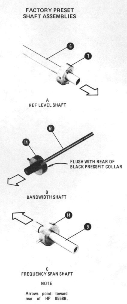
Model 8558B TM 11-6625-3061-14
Figure 8-48. Shaft Assemblies
8-118
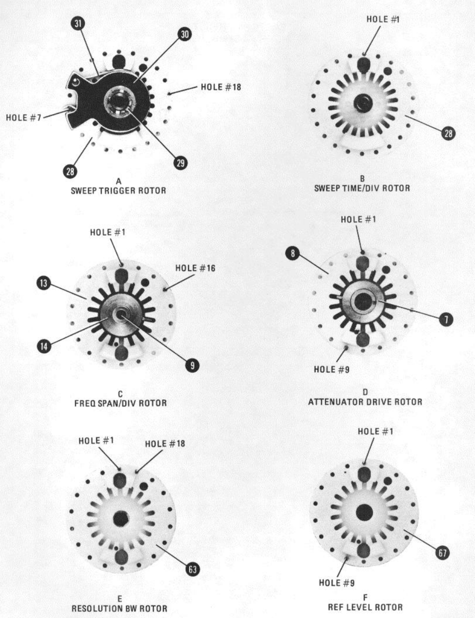
Model 8558B TM 11-6625-3061-14
Figure 8-49. Rotor Assemblies
8-119
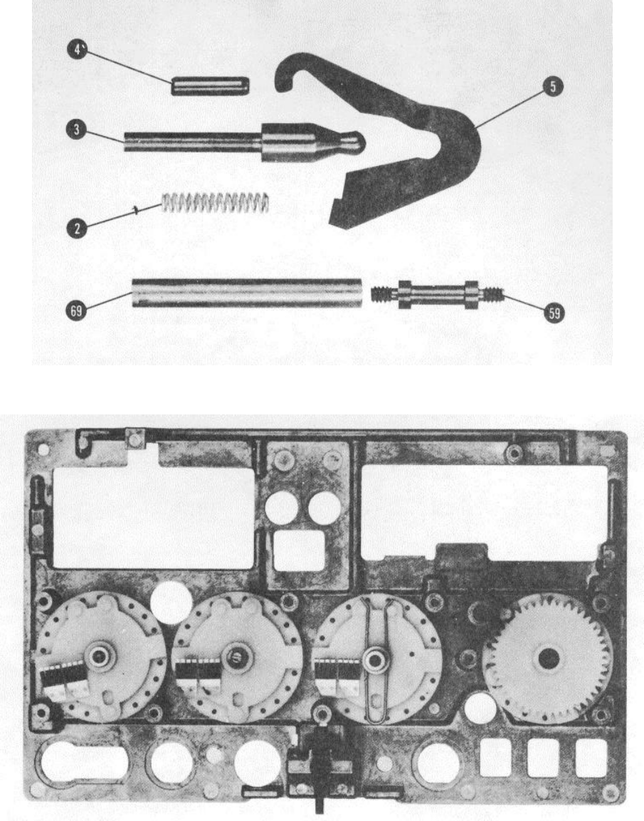
Model 8558B TM 11-6625-3061-14
Figure 8-50. Machined Parts
Figure 8-51. Proper Positioning of Rotors on Front Switch Diecast
8-120
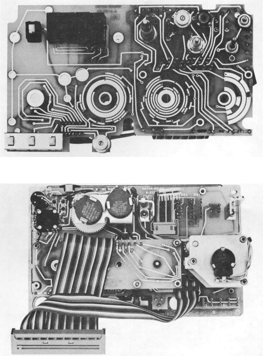
Model 8558B TM 11-6625-3061-14
Figure 8-52. Front View of Switchboard Assembly A2A1
Figure 8-53. Rear View of Front Switch Assembly A2
8-121/8-122(blank)
TM 11-6625-3061-14
APPENDIX A
REFERENCES
DA Pam 310-1 Consolidated Index of Army Publications and Blank Forms.
DA Pam 738-750 The Army Maintenance Management System (TAMMS).
TM 750-244-2 Procedures for Destruction of Electronics Materiel to Prevent Enemy Use (Electronics
Command).
TM 11-6625-3061-24P Organizational, Direct Support, and General Support Maintenance, Repair Parts and Special
Tools List, and Maintenance Allocation Chart for Spectrum Analyzer Hewlett-Packard Model
8558B
A-1/(A-2 blank)

TM 11-6625-3061-14
APPENDIX B
COMPONENTS OF END ITEM LIST
Section I. INTRODUCTION
B-1. Scope
The appendix lists integral components of and basic issue items for Spectrum Analyzer, HP Model 8558B to help you
inventory items required for safe and efficient operation.
B-2. General
This Components of End Item List is divided into the-following sections:
a.Section II. Integral Components of the End Item. These items, when assembled, comprise the Spectrum
Analyzer, HP Model 8558B and must accompany it whenever it is transferred or turned in. The illustrations referenced
will help you in identify these items.
b.Section III. Basic Issue Items. Not applicable.
B-3. Explanation of Columns
a.Illustration. This column is divided as follows:
(1)Figure number. Indicates the figure number of the illustration on which item is shown.
(2)Item number. The number used to identify item called out in the illustration.
b.National Stock Number. Indicates the National Stock Number assigned to the item and which will be used for
requisitioning.
c. Description. Indicated the Federal item name and, if required, a minimum description to identify the item. The
part number indicated the primary number used by the manufacturer, which controls the design and characteristics of the
item by means of its engineering drawings, specifications, standards, and inspection requirements to identify an item or
range of items. Following the part number, the Federal Supply Code for Manufacturers (FSCM) is shown in parentheses.
d.Location. The physical location of each item listed is given in the column. The lists are designed to inventory all
items in one
B-1

TM 11-6625-3061-14
area of the major item before moving in to an adjacent area.
e.Usable on Code. Not applicable.
f.Quantity Required (Qty Reqd). This column lists the quantity of each item required for a complete major item.
g.Quantity. This column is left blank for use during the inventory. Under the Rcvd column, list the quantity you
actually receive on your major item. The Date columns are for your use when you inventory the major item.
B-2

TM 11-6625-3061-14
Section II. INTEGRAL COMPONENTS OF END ITEM
(1) (2) (3) (4) (5) (6) (7)
ILLUSTRATION QUANTITY
(A) (B) NATIONAL DESCRIPTION USUABLE
FIG.ITEM STOCK ON QTY
NO. NO. NUMBER PART NUMBER CAGE LOCATION CODE REQD RCVDDATE
SPECTRUM ANALYZER,
HP MODEL 8558B 28480
B-3

TM 11-6625-3061-14
APPENDIX D
MAINTENANCE ALLOCATION
Section I. INTRODUCTION
D-1. General
This appendix provides a summary of the maintenance operations for Spectrum Analyzer, HP Model 8558B. It
authorizes categories of maintenance for specific maintenance function on repairable items and components and the
tools and equipment required to perform each function. This appendix may be used as an aid in planning maintenance
operations.
D-2. Maintenance Function
Maintenance functions will be limited to and defined as follows:
a.Inspect. To determine the serviceability of an item by comparing its physical, mechanical, and/or electrical
characteristics with established standards through examination.
b.Test. To verify serviceability and to detect incipient failure by measuring the mechanical or electrical
characteristics of an item and comparing those characteristics with prescribed standards.
c.Service. Operations required periodically to keep an item in proper operating condition; ie., to clean
(decontaminate), to preserve, to drain, to paint, or to replenish fuel, lubricants, hydraulic fluids, or compressed air
supplies.
d.Adjust. To maintain, within prescribed limits, by bringing into proper or exact position, or setting the operating
characteristics to specified parameters.
e.Aline. To adjust specified variable elements of an item to bring about optimum or desired performance.
f.Calibrate. To determine and cause corrections to be made or to be adjusted in instruments or test measuring
and diagnostics equip-
D-1

TM 11-6625-3061-14
ments use in precision measurement. Consists of comparison of two instruments, one in which is a certified standard of
known accuracy of the instrument being compared.
g.Install. The act of emplacing, seating, or fixing into position an item, part, module (component or assembly) in a
manner to allow the proper functioning of the equipment or system.
h.Replace. The act of substituting a serviceable like type part, subassembly, or module (component or assembly)
for an unserviceable counterpart.
i. Repair. The application of maintenance services (inspect, test, service, adjust, aline, calibrate, replace) or other
maintenance actions (welding, grinding, riveting, staightening, facing, remachining, or resurfacing) to restore
serviceability to an item by correcting specific damage, fault, malfunction, or failure in a part, subassembly, module
(component or assembly), end item, or system. This function does not include the trial and error replacement of running
spare type items such as fuses, lamps, or electron tubes.
j. Overhaul. That maintenance effort (service/action) necessary to restore an item to a completely
serviceable/operational condition as prescribed by maintenance standards (.i..e., DMWR) in appropriate technical
publications. Overhaul is normally the highest degree of maintenance performed by the Army. Overhaul does not
normally return an item to like new condition.
k.Rebuild. Consists of those services/actions necessary for the restoration of unserviceable equipment to a like
new condition in accordance with original manufacturing standards. Rebuild is the highest degree of materiel
maintenance applied to Army equipment.
The rebuild operation includes the act of returning to zero those age measurements (hours, miles, etc.) considered in
classifying Army equipments/components.
D-3. Column Entries
a.Column 1, Group Number. Column 1 lists group numbers, the purpose of which is to indentify components,
assemblies, subassemblies,
D-2

TM 11-6625-3061-14
and modules with the next higher assembly.
b.Column 2, Component/Assembly. Column 2 contains the noun names of components, assemblies,
subassemblies, and modules for which maintenance is authorized,
c.Column 3, Maintenance Functions. Column 3 lists the functions to be performed on the item listed column 2.
When items are listed without maintenance functions, it is solely for purpose of having the group numbers in the MAC
and RPSTL coincide.
d.Column 4, Maintenance Category. Column 4 specifies, by the listing of a "work time" figure in the appropriate
subcolumn(s), the lowest level of maintenance authorized to perform the function listed in column 3. This figure
represents the active time required to perform that maintenance function at the indicated category of maintenance. If the
number or complexity of the tasks within the listed maintenance function vary at different maintenance categories,
appropriate "work time" figures will be shown for each category. The number of task-hours specified by the "work time"
figure represents the average time required to restore an item (assembly, subassembly, components, module, end item
or system) to a serviceable condition under typical field operating conditions. This time includes preparation time,
troubleshooting time, and quality assurance/quality control time in addition to the time required to perform the specific
tasks indentified for the maintenance function authorized in the maintenance allocation chart. Subcolumns of column 4
are as follows:
C - Operator/Crew
O - Organizational
F - Direct Support
H - General Support
D - Depot
e.Columns 5, Tools and Equipment. Column 5 specifies by code, those common tools sets (not individual tools)
and special tools, test, and support equipment required to perform the designated function.
f.Column 6, Remarks. Column 6 contains as alphabetic code which leads to the remark in section IV, Remarks,
which is pertinent
D-3

TM 11-6625-3061-14
to the item opposite the particular code.
D-4. Tool and Test Equipment Requirements (Sec III)
a.Tool and Test Equipment Reference Code. The numbers in this column coincide with the numbers used in the
tools and equipment column of the MAC. The numbers indicate the applicable tool or test equipment for the
maintenance functions.
b.Maintenance Category. The codes in this column indicate the maintenance category allocated the tool or test
equipment.
c.Nomenclature. This column lists the noun name and nomenclature of the tools and test functions.
d.National/NATO Stock Number. This column lists the National/NATO Stock Number of the specific tool or test
equipment.
e.Tool number. This column lists the manufacturer's part number of the tool followed by the Federal Supply Code
for manufacturers (5 digit) in parentheses.
D-5. Remarks (Sec IV)
a.Reference Code. This code refers to the appropriate item in section II, column 6.
b.Remarks. This column provides the required explanatory information necessary to clarify items appearing in
section II.
D-4
TM 11-6625-3061-14
SECTION II MAINTENANCE ALLOCATION CHART
FOR
SPECTRUM ANALYZER HP8558B
(1) (2) (3) (4) (5) (6)
GROUP MAINTENANCE MAINTENANCE LEVEL TOOLS AND
NUMBER COMPONENT ASSEMBLY FUNCTION COFH D EQUIPMENT REMARKS
00 SPECTRUM ANALYZER Inspect 0.1
HP8558B Test 3.0 1-20 B
MTBF= 10,000 Hrs Test 3.0
Adjust 0.3 6A
Calibrate 9.2 1,3-25 B
Replace 0.1
Repair 10. 1,2,6- B,C,E
20,22- D
30
Repair 10.
01 FRONT SWITCH ASSY Inspect 0.1
08558-60100 Test 1.0
A2 Replace 0.3 6
Repair 4.0
0101 SWITCH BOARD ASSY Inspect 0.1
08558-60160 Test 1.0
A2A1 Replace 03 6
Repair 4.0
02 FIRST CONVERTER Inspect 0.1
08558-60004 Test 1.0
A4 Replace 0.3 6
Repair 4.0
03 SECOND CONVERTER Inspect 0.1
08558-60097 Test 1.0
AS Replace 0.3 6
Repair 4.0
04 THIRD CONVERTER Inspect 0.1
08558-60154 Test 1.0
A9 Replace 0.3 6
Repair 4.0
05 BW FILTER NO. 1 Inspect 0.1
08559-60058 Test 1.0
All Replace 0.3 6
Repair 4.0
06 BW FILTER NO. 2 Inspect 0.1
08558-6019 Test 1.0
A13 Replace 0.3 6
Repair 4.0
07 LOG AMPLIFIER ASSY Inspect 0.1
5061-5411 Test 1.0 6
A14 Replace 0.3 6
Repair 4.0
08 MOTHERBOARD ASSY Inspect 0.1
08558-65159 Test 2.0 6
A16 Replace 0.5 6
Repair 4.0
DRSEL-MA Form 6031,(1 Jul 76) HISA-FM 2314-79
D-5

TM 11-6625-3061-14
SECTION III. TOOL AND TEST EQUIPMENT REQUIREMENTS
FOR
SPECTRUM ANALYZER HP8558B
TOOL OR TESTMAINTENANCE NATIONAL/NATO TOOL
EQUIPMENT CATEGORY NOMENCLATURE STOCK NUMBER NUMBER
REF CODE
1 H TRACKING GENERATOR HP8444A 6625-00-185-4802
2 H FUNCTION GENERATOR HP3310A 6625-01-028-4989
3 H POWER SPLITTER HP11667A 6625-01-017-2713
4 H 10 dB ATTENUATOR HP8491A 5985-00-128-0195
5 H 50 ohm TERMINATOR HP908A
6 F,H TOOL KIT, ELEC EQUIP TK-105/G 5180-00-610-8177
7 H TUNING TOOL 08555-60107
8 H ALINEMENT TOOL, MET TIP 8710-0630 5120-01-080-7650
9 H ALINEMENT TOOL, PLASTIC 8710-0033 1005-00-634-8012
10 H DISPLAY MAINFRAME HP181T
11 H FREQUENCY COUNTER HP5342A 6625-01-103-2958
12 H DIGITAL VOLTMETER HP3455A 6625-01-874-1000
13 H POWER METER HP435A 6625-00-449-9167
14 H POWER SENSOR HP8482A
15 H AMPLIFIER HP8447D 6625-01-065-0305
16 H SIGNAL GENERATOR HP8460 6625-00-318-6304
17 H COMB GENERATOR HP8406A 6625-00-937-3525
18 H 300 MHz LP FILTER TPL300-4AB
19 H STEP ATTENUATOR HP355C 5985-00-525-5074
20 H STEP ATTENUATOR HP355D 5985-00-957-1860
21 H SWEEP OSCILLATOR HP8350A
22 H RF PLUGIN HP83522A
23 H TIME COUNTER HP5308A 6625-01-022-6231
24 H OSCILLOSCOPE HP1741A 6625-01-058-0139
25 H CRYSTAL DETECTOR HP423B 6625-01-035-0626
26 H SPECTRUM ANALYZER HP141T 6625-00-424-4370
27 H BOARD PULLER 03950-4001
28 H EXTENDER BOARD, 6 PIN 08559-60042
29 H EXTENDER BOARD, 10 PIN 85680-60028 6625-01-137-2674
30 H EXTENDER BOARD, 22 PIN 08565-60107
31 H EXTENDER CABLE ASSY 5060-0303 5995-01-036-2960
D-6

TM 11-6625-3061-14
SECTION IV. REMARKS
SPECTRUM ANALYZER HP8558B
REFERENCE REMARKS
CODE
AAdjustments made when combining units with other subassemblies in display frame.
BTest, repair, and calibrate by USATSG at general support.
CSubassemblies A3, A6, A7, A8, A10, A12, A15, A17 and W1 through W6 are throw-aways.
DRepair consists of replacement of subassemblies and mainframe components as required.
EA1is not a replaceable subassembly and has no part number.
D-7/(D-8 blank
By Order of the Secretary of the Army:
JOHN A. WICKHAM JR.
General, United States Army
Official: Chief of Staff
MILDRED E. HEDBERG
Brigadier General, United States Army
The Adjutant General
Distribution:
To be distributed in accordance with special list.
*U.S. GOVERNMENT PRINTING OFFICE: 1986-612-069
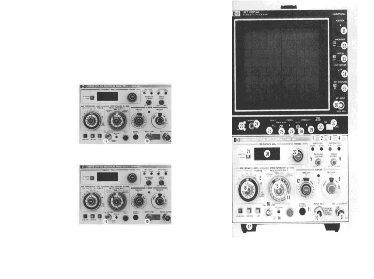
Model 8558B TM 11-6625-3061-14
FRONT PANEL FEATURES
1. VERTICAL POSN: Adjusts vertical
position of CRT trace.
2. VERTICAL GAIN: Adjusts deflection
circuit gain for amplitude scale calibration
of CRT display.
3. FREQUENCY CAL: Removes tuning
hysteresis from first LO (YIG oscillator).
Should be pressed before calibration and
whenever TUNING (22) is changed by
more than 50 MHz.
4. FREQUENCY ZERO: Adjusts
FREQUENCY MHz (20) readout for
calibration on LO feedthrough.
5. BASELINE CLIPPER: Blanks variable
lower portion of CRT display. Prevents
CRT blooming with a variable persistence
storage display mainframe (i.e.
181T/TR).
6. VIDEO FILTER: Post-detection low-pass
filter smooths CRT trace by averaging
random noise. Filter bandwidth scaled by
resolution bandwidth (15) setting. MAX
(detent) position selects 1.5 Hz bandwidth
for maximum noise averaging and noise
level measurements. MAX VIDEO
FILTER should not be used for CW signal
analysis.
7. SWEEP Indicator: Remains lit during
each sweep.
8. SWEEP TRIGGER: Selects sweep trigger
mode.
VIDEO: Sweep triggered on internal
post-detection video waveform. One-
half major division of vertical deflection
(noise, AM signal, etc.) required to
trigger sweep. Normally used with 0
(zero) frequency span for time-domain
analysis.
LINE: Sweep triggered at ac line
frequency.
FREE RUN: End of each sweep triggers
new sweep.
SINGLE: Single sweep triggered or
reset by turning SWEEP TRIGGER
clockwise momentarily.
9. 1st LO OUTPUT: 50-ohm BNC output
provides 2.05-3.55 GHz first LO signal at
approximately + 10 dBm. Terminate with
50ohm load when not in use.
10. INPUT 50f: Precision type N (female)
signal input connector with 50-ohm input
impedance.
Options 001 and 002: INPUT 75f- 75-ohm
BNC (female) signal input connector.
CAUTION
50-ohm BNC connectors might
cause damage if used directly with
Option 001 and 002 75-ohm BNC
INPUT and CAL OUTPUT
connectors.
11. SWEEP TIME/DIV: Selects time required
to sweep one major horizontal division on
CRT.
AUTO: Automatically selects fastest
allowable sweep time as a function of
FREQ SPAN/DIV (13), RESOLUTION
BW (15), and VIDEO FILTER (6)
settings to maintain display amplitude
calibration. AUTO operation retained
with FREQ SPAN/DIV and
RESOLUTION BW controls uncoupled.
TIME/DIV: Selects calibrated sweep
time; used primarily with 0 (Zero)
frequency span for time-domain
analysis of modulation waveforms.
Display amplitude calibration not
automatically guaranteed for other
frequency spans.
MAN: Enables manual frequency scan
using MAN SWEEP knob.
12. PROBE POWER: Provides power for
high-impedance active probes such as the
HP 1121A. (See Section I of HP 8558B
Operation and Service Manual for details
regarding use with Options 001 and 002.)
13. FREQ SPAN/DIV: Selects CRT horizontal
axis frequency calibration.
MHz/DIV
kHz/DIV: Selects desired frequency
span. Alignment of OPTIMUM
markings (><) selects optimum
resolution bandwidth (15).
0 (Zero Span): Spectrum analyzer
operates as a manually-tuned receiver,
at frequency indicated by FREQUENCY
MHz readout, for time-domain display of
signal modulation. 16 calibrated sweep
times selectable with SWEEP TIME/DIV
control (11).
14. REF LEVEL CAL: Adjusts spectrum
analyzer RF gain to calibrate top CRT
graticule line for absolute amplitude
measurements.
15. RESOLUTION BW: Selects spectrum
analyzer 3-dB bandwidth. Alignment of
OPTIMUM markings ( > < ) automatically
selects optimum resolution bandwidth for
any frequency span. Control pushed in to
couple mechanically with FREQ
SPAN/DIV.
16. CAL OUTPUT: BNC output provides 280
MHz, -30 dBm calibration signal from 50f
output impedance.
Option 001: 280 MHz, -30 dBm calibration
signal from 759 output impedance.
Option 002: 280 MHz, + 20 dBmV
calibration signal from 752 output
impedance.
CAUTION
50-ohm BNC connectors might
cause damage if used directly with
Option 001 and 002 75-ohm BNC
INPUT and CAL OUTPUT
connectors.
17. 10 dB/DIV - dB/DIV - LIN (Amplitude
Scale): Selects CRT vertical axis
amplitude calibration (logarithmic or linear
scale). Reference Level remains constant
at top CRT graticule line.
18. REFERENCE LEVEL: Adjusts' power
level (in dBm or dBmV) represented |by
top CRT graticule line. Large outer knob
provides adjustment in calibrated 10-dB
steps; FINE vernier provides 12 dB of
continuous adjustment.
19. INPUT ATTEN: Selects desired RF input
attenuation, indicated by blue numbers
(push and turn).
20. FREQUENCY MHz: Displays spectrum
analyzer start or center frequency.
Automatically ranges at approximately
195 MHz for increased resolution at lower
frequencies.
21. START-CENTER: Selects mode of
FREQUENCY MHz (20) readout.
22. TUNING: Adjusts spectrum analyzer start
or center frequency. Coarse tuning is
provided by large knob; smaller knob
provides FINE tuning.
180-Series Display Mainframes
23. CALIBRATOR (180TR, 182T): Provides 1
kHz square wave at two amplitudes: 250
mV and 10V p-p (not used with spectrum
analyzer).
24. Ground Connection (180TR, 182T):
Provides chassis ground connection point.
25. SCALE (180TR, 182T): Adjusts CRT
graticule illumination.
26. TRACE ALIGN: Adjusts CRT trace
alignment with horizontal graticule lines.
27. FOCUS: Adjusts CRT trace sharpness.
28. ASTIG: Adjusts CRT spot shape.
29. INTENSITY: Adjusts CRT trace intensity.
30. FIND BEAM: Intensifies trace and forces
on-screen display (normally not used with
spectrum analyzer).
31. HORIZONTAL POSITION: Single knob
provides coarse and fine horizontal
adjustment of CRT trace.
32. MAGNIFIER: Selects horizontal
deflection factor (normally left in X1 position).
33. DISPLAY: Selects CRT sweep source
(normally left in INT position).
34. EXT VERNIER: Provides continuous
deflection factor adjustment for external CRT
sweep signals. In CAL detent position,
deflection factor is selected by MAGNIFIER
(32) control (normally not used with spectrum
analyzer).
35. EXT COUPLING: Selects EXT INPUT
(36) ac or dc coupling (normally not used with
spectrum analyzer).
36. EXT INPUT: BNC input for external CRT
sweep signal (normally not used with
spectrum analyzer).
NOTE
HORIZONTAL EXT INPUT does not
sweep the spectrum analyzer first
LO. Analyzer should be set to 0
(zero) FREQ SPANIDIV, AUTO
TIMEIDIV, and SINGLE SWEEP
TRIGGER- when operated with an
external horizontal input.
37. Switch with indicator light for turning
power ON and OFF.
NOTE
See Appendix A for details
regarding HP 181TITR Variable
Persistence Storage Display
Mainframes.
HP 8558B Front Panel, Option 001
HP 8558B Front Panel, Option 002
Figure 3-1. HP 8558B Installed in HP 182T Display Mainframe
3-5
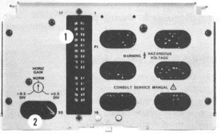
Model 8558B TM 11-6625-3061-14
REAR PANEL FEATURES
1. P1 Connector: Connects spectrum analyzer plug-in to display mainframe.
2. HORIZ GAIN: Allows ± 1/2 major division of horizontal gain adjustment to
calibrate spectrum analyzer plug-in with display mainframe.
3. AUX A Vertical Output: BNC output provides detected video signal from a
50-ohm output impedance. Typical 0-800 mV range corresponds to full
8-division display deflection.
4. AUX B PENLIFT/BLANKING OUTPUT: BNC output provides a + 15V
penlift/blanking signal from a 10K-ohm output impedance when CRT trace
is blanked. Otherwise, output is low at 0V (low impedance, 150 mA max.)
for an unblanked trace.
5. AUX C 21.4 MHz IF OUTPUT: BNC output provides 21.4 MHz IF signal
(linearly related to spectrum analyzer RF input) from a 50-ohm
output impedance. Output bandwidth controlled by spectrum analyzer
RESOLUTION BW setting; output amplitude controlled by INPUT ATTEN,
REFERENCE LEVEL FINE, and first six REFERENCE LEVEL positions
(i.e., with 0 dB input attenuation, - 10 through -60 dBm; for Option 002, +
40 through - 10 dBmV).
6. AUX D Horizontal Output: BNC output provides horizontal sweep voltage
from a 5Kohm output impedance. -5V to + 5V range corresponds to full
10-division display deflection.
7. Z-Axis Input: BNC input with a 5K-ohm impedance allows external
modulation of CRT trace intensity. Approximately + 2V blanks normal-
intensity trace; negative voltage increases trace intensity. Maximum
input voltage ± 20 Vdc.
8. NORMALIZER INTER-CONN (180TR/182T): Provides connections for HP
8750A Storage Normalizer.
Figure 3-2. Rear Panel Controls and Connectors (1 of 2)
3-6
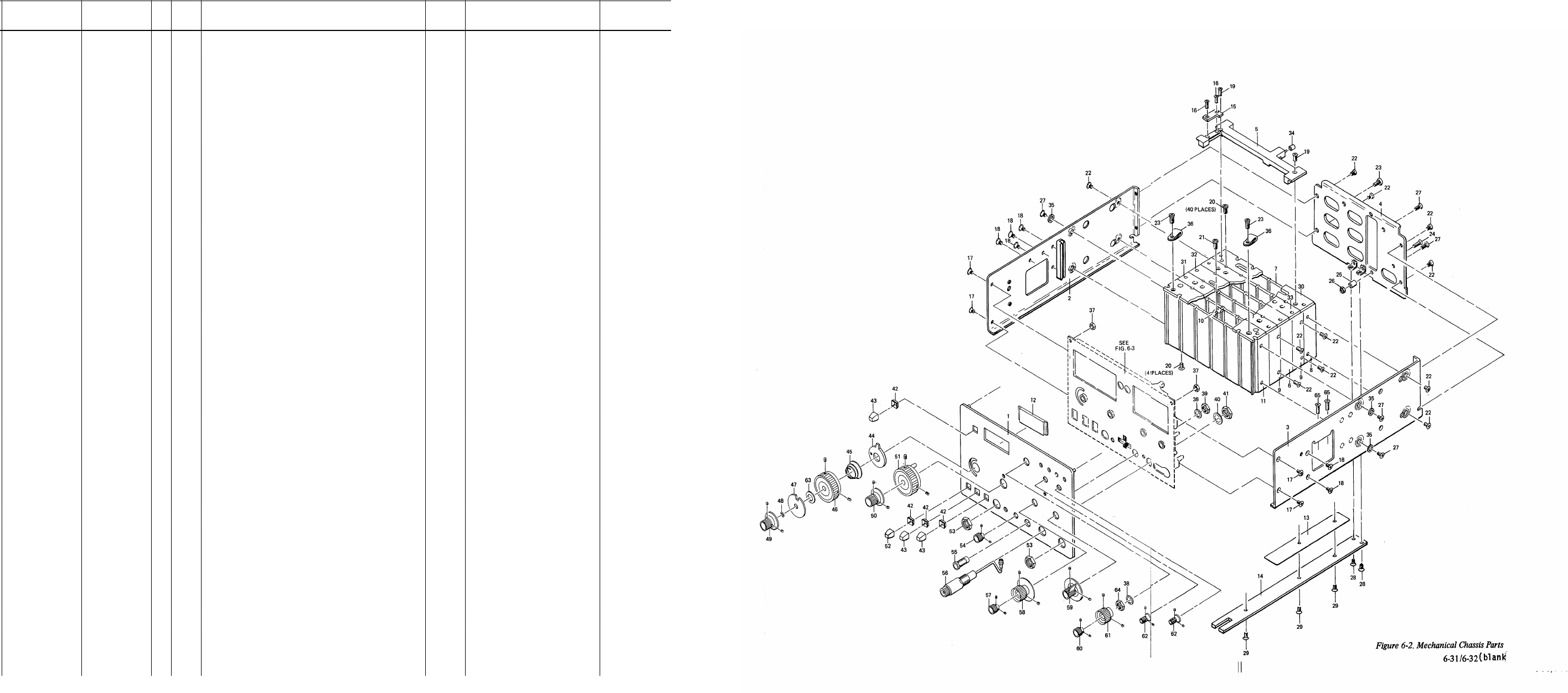
Model 8558B TM 11-6625-3061-14
Reference HP Part CMfr.
Designation Number DQty Description Code Mfr Part Number
MECHANICAL CHASSIS PARTS
NOTE
COMPLETE FRONT PANEL ASSEMBLIES (LISTED
BELOW) INCLUDE A2 FRONT SWITCH ASSY,
PANEL, ALL KNOBS, & PROBE POWER INPUT, CAL
OUTPUT, AND LO OUTPUT CABLES
08558-60161 5 1 FRONT PANEL ASSY (STD.) 28480 08558-60161
08558-60164 8 FRONT PANEL ASSY (OPT. 001) 28480 08558-60164
08558-60165 9 1 FRONT PANEL ASSY (OPT. 002) 28480 08558-60165
1 08558-00114 2 1 PANEL-FRONT (STD.) 28480 08558-00114
1 08558-00121 1 1 PANEL-FRONT (OPT.001) 28480 08558-00121
1 08558-00122 2 1 PANEL-FRONT (OPT.002) 28480 08558-00122
2 08558-00116 4 1 SIDE GUSSET (LEFT) 28480 08558-00116
3 08558-00115 3 1 SIDE GUSSET (RIGHT) 28480 08558-00115
4 08558-00003 8 1 PANEL (REAR) 28480 08558-00003
5 5061-5426 9 1 GUIDE RAIL (TOP) 28480 5061-5426
6 08565-20093 7 4 EXTRUSION, CIRCUIT ENCLOSURE, TAPPED 28480 08565-20093
7 08558-20037 0 1 EXTRUSION, END PLATE ENCLOSURE 28480 08558-20037
8 08558-20036 9 4 EXTRUSION, CIRCUIT ENCLOSURE, TAPPED 28480 08558-20036
9 08565-20051 7 1 EXTRUSION, CIRCUIT ENCLOSURE 28480 08565-20051
10 08558-20038 1 1 EXTRUSION, ENCLOSURE DIVIDER 28480 08558-20038
11 08565-20096 0 8 EXTRUSION, CIRCUIT ENCLOSURE, TAPPED 28480 08565-20096
12 5021-3229 2 1 WINDOW, FREQ. DISPLAY (GLUED TO 1) 28480 5021-3229
13 08558-00030 1 1 INSULATOR-GUIDE RAIL (BOTTOM) 28480 08558-00030
14 08558-20164 4 1 GUIDE RAIL (BOTTOM) 28480 08558-20164
15 08557-60045 3 1 CABLE ASSY (W10) VERTICAL OUTPUT 28480 08557-60045
16 2200-0165 6 2 SCREW-MACH 4-40 .25-IN-LG 82 DEG 28480 2200-0165
17 2360-0194 9 4 SCREW-MACH 6-32 .312-IN-LG 100 DEG 28480 2360-0194
18 2200-0104 3 6 SCREW-MACH 4-40 .25-IN-LG 82 DEG 28480 2200-0104
19 2360-0201 9 2 SCREW-MACH 6-32 .5-IN-LG PAN-HD-POZI 28480 2360-0201
20 0624-0099 1 81 SCREW-TPG 4-40 .375-IN-LG PAN-HD-POZI 28480 0624-0099
21 0624-0206 2 1 SCREW-TPG 6-32 .25-IN-LG PAN-HD-POZI 28480 0624-0206
22 2200-0103 2 12 SCREW-MACH 440 .25-IN-LG PAN-HD-POZI 28480 2200-0103
23 2360-0115 4 3 SCREW-MACH 6-32 .312-IN-LG PAN-HD-POZI 28480 2360-0115
24 2200-0170 3 1 SCREW-MACH 440 .625-IN-LG 82 DEG 28480 2200-0170
25 0380-0005 1 1 SPACER-RND .312 IN-LG .18-IN-ID 28480 0380-0005
26 2260-0003 7 1 NUT-HEX-PLSTC LKG 4-40-THD .141-IN-THK 28480 2260-0003
27 2200-0105 4 6 SCREW-MACH 4-40 .312-IN-LG PAN-HD-POZI 28480 2200-0105
28 2200-0164 5 2 SCREW-MACH 4-40 .188-IN-LG UNCT 82 DEG 28480 2200-0164
29 2200-0168 9 3 SCREW-MACH 4-40 .438-IN-LG 82 DEG 28480 2200-0168
30 08558-00108 4 1 COVER-LOG AMPLIFIER 28480 08558-00108
31 08558-00089 0 1 COVER-BANDWIDTH FILTER NO. 1 28480 08558-00089
32 08558-00088 9 1 COVER-STEP GAIN 28480 08558-00088
33 08558-00087 8 1 COVER-BANDWIDTH FILTER NO. 2 28480 08558-00087
34 0380-0005 1 1 SPACER-RND .312 IN-LG .18-IN-ID 28480 0380-0005
35 3050-0105 6 4 WASHER-FL MTLC NO. 4 .125-IN-ID 28480 3050-0105
36 1400-0082 9 2 CLAMP-CABLE .125-iDIA .375-WD NYL 28480 1400-0082
37 2420-0001 5 2 NUT-HEX-W/LKWR 6-32-THD .109-IN-THK 28480 2420-0001
38 2190-0016 3 2 WASHER-LK INTL T 3/8 IN .377-IN-ID 28480 2190-0016
39 2950-0043 8 1 NUT-HEX-DBL-CHAM 3/8-32-THD .094-IN-THK 28480 2950-0043
40 2190-0068 5 1 WASHER-LK INTL T 1/2 IN .505-IN-ID 28480 2190-0068
41 2950-0054 1 1 NUT-HEX-DBL-CHAM 1/2-28-THD .125-IN-THK 28480 2950-0054
42 0370-0606 7 4 BEZEL-PB .330-IN-SQ;JADE GRAY 28480 0370-0606
43 5040-8817 4 3 PUSHBUTTON- SQUARE; JADE GRAY 28480 5040-8817
44 08565-40011 1 1 POINTER-INPUT ATTENUATOR 28480 08565-40011
45 1460-0532 0 1 SPRING-CONICAL 28480 1460-0532
46 08558-60166 0 1 KNOB ASSY-REFERENCE LEVEL (OPT. 002) 28480 08558-60166
46 08558-60167 1 1 KNOB ASSY-REFERENCE LEVEL (STD. OPT. 001) 28480 08558-60167
47 08558-00123 3 1 INDEX DISK (OPT. 002) REFERENCE LEVEL 28480 08558-00123
47 08565-00043 5 1 INDEX DISK (STD. OPT. 001) REFERENCE LEVEL 28480 08565-00043
48 0510-0089 8 1 RETAINER-RING BSC EXT .188-IN-DIA BE-CU 28480 0510-0089
49 08565-60047 5 1 KNOB ASSY, REF. LEVEL (FINE) 28480 08565-60047
50 08558-20161 1 1 KNOB ASSY, RESOLUTION BW 28480 08558-20161
51 08558-20162 2 1 KNOB ASSY, FREQ. SPAN/DIV 28480 08558-20162
52 5040-8819 6 1 PUSHBUTTON-SQUARE, WILLOW GREEN 28480 5040-8819
53 0590-1251 6 2 NUT-SPCLY 15/32-32-THD .1-IN-THK .562-WD 28480 0590-1251
54 0370-1121 3 1 KNOB-LOCK 28480 0370-1121
55 08558-60170 6 1 CABLE ASSY-PROBE POWER (W16) 28480 08558-60170
56 08558-60031 8 1 CABLE ASSY-75 OHM INPUT (W1) OPT. 001, 002 28480 08558-60031
56 08558-60038 5 1 CABLE ASSY-50 OHM INPUT (W1) STD. SEE FIG 6-1 28480 08558-60038
57 0370-3021 6 1 KNOB ASSY-MANUAL SWEEP 28480 0370-3021
58 08558-20163 3 1 KNOB ASSY-SWEEP TIME/DIV 28480 08558-20163
59 08559-20050 8 1 KNOB ASSY-SWEEP TRIGGER 28480 08559-20050
60 0370-3006 7 1 KNOB ASSY-FINE TUNE 28480 0370-3006
61 0370-3004 5 1 KNOB ASSY-COARSE TUNE 28480 0370-3004
62 08565-60170 5 2 KNOB-BASELINE CLIP/VIDEO FILTER 28480 08565-60170
63* 2190-0390 6 1 WASHER-FL NM 1/4 IN .26-IN-ID .562-IN-OD 28480 2190-0390
64 2950-0001 8 1 NUT-HEX-DBL-CHAM 3/8-32-THD .094-IN-THK 28480 2950-0001
65 2200-0119 0 2 SCREW-MACH 440 1-IN-LG PAN-HD-POZI 28480 2200-0119
66* 3050-0929 2 1 WASHER-FL NM 1/4 IN .26-IN-ID .562-IN-OD 28480 3050-0929
(SHIM WASHER, NOT SHOWN, USED WITH 63 FOR
PROPER SPACING BETWEEN 46 AND 47.)
7-2. Front Panel Assembly (2 of 3) (CHANGE A)
Figure 6-2. Mechanical Chassis Parts
6-31/6-32 (blank)
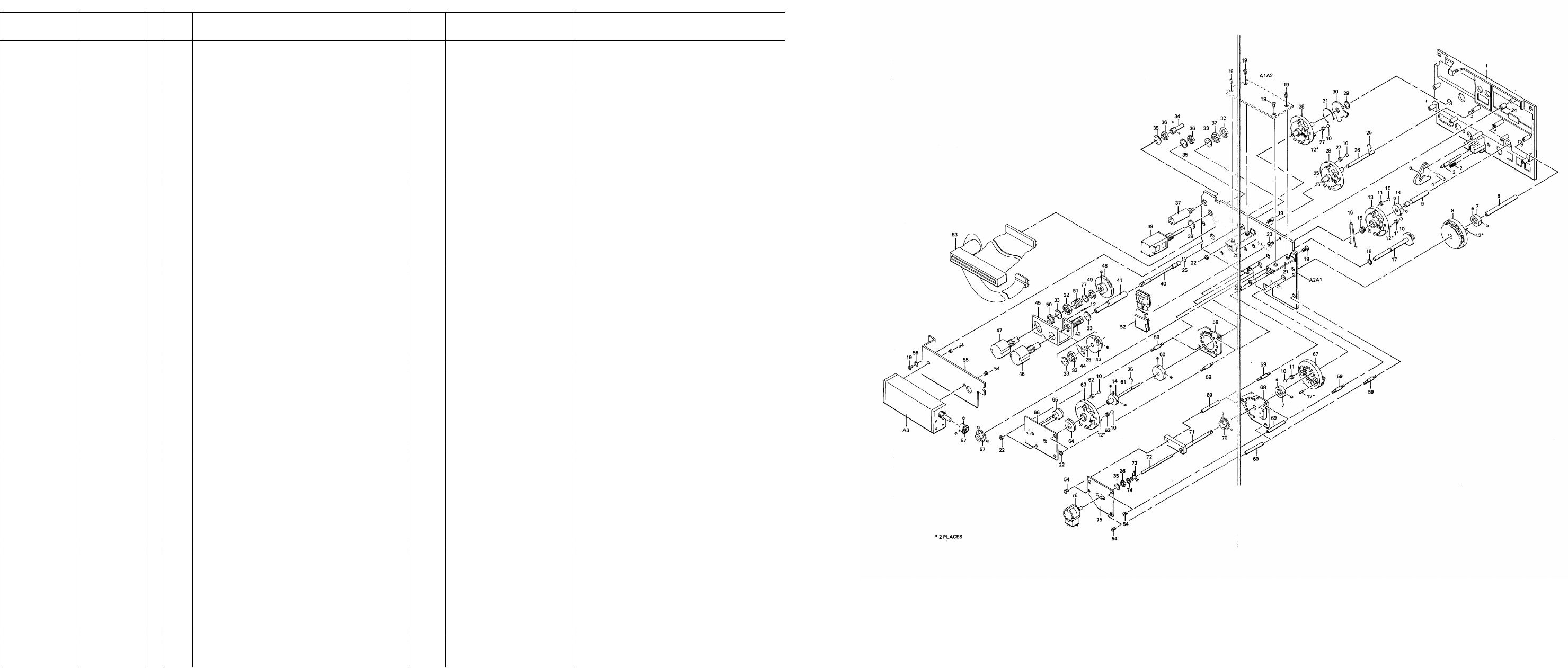
Model 8558B TM 11-6625-3061-14
Reference HP Part CMfr.
Designation Number DQty Description Code Mfr Part Number
A2 08558-60100 2 1 FRONT SWITCH ASSEMBLY (MECH PARTS) 28480 08558-60100
NOTE
SEE A2 FRONT SWITCH ASSY LISTING FOR
ELECTRICAL PARTS; SEE FIG 6-2 FOR FRONT
PANEL PARTS
1 5021-3213 4 1 DIECAST-FRONT SWITCH 28480 5021-3213
2 1460-0012 1 1 SPRING-CPRSN .135-IN-OD .688-IN-OA-LG 28480 1460-0012
3 5021-3227 0 1 SHAFT-LOCKING 28480 5021-3227
4 1480-0017 8 1 PIN-DOWEL .125 OD 28480 1480-0017
5 5001-5818 7 1 LINK-LOCKING 28480 5001-5818
6 5021-3218 9 1 SHAFT-REF LEVEL 28480 5021-3218
7 08559-60060 4 2 HUB ASSEMBLY-DRIVE, ANTI-CRUSH 28480 08559-60060
8 08558-60098 7 1 ROTOR-ATTENUATOR DRIVE 28480 08558-60098
9 5021-3224 7 1 SHAFT-FREQUENCY SPAN 28480 5021-3224
10 1410-0006 8 7 BALL-BRG TYPE .1875-DIA GRADE-50 SST 78707 GRADE 50
11 1460-0623 0 3 SPRING-COMPRESSION .18-IN-OD .312-IN-OA-L 28480 1460-0623
12 1480-0059 8 11 PIN-ROLL 28480 1480-0059
13 08558-20066 5 1 ROTOR-FREQUENCY SPAN 28480 08558-20066
14 08558-20059 6 2 HUB-DRIVE 28480 08558-20059
15 08558-20089 2 1 BUSHING-SLOTTED 28480 08558-20089
16 1460-1376 2 1 SPRING-HAIRPIN 28480 1460-1376
17 5061-5424 7 1 SHAFT ASSEMBLY-ATTENUATOR 28480 5061-54240
18 3050-0032 8 1 WASHER-FL MTLC NO. 8 .189-IN-ID 28480 3050-0032
19 2200-0105 4 7 SCREW-MACH 4-40 .312-IN-LG PAN-HD-POZI 28480 2200-0105
20 5001-5813 2 1 BRACKET-LEFT DPM MOUNTING 28480 5001-5813
21 5001-5814 3 1 BRACKET-RIGHT DPM MOUNTING 28480 5001-5814
22 2260-0009 3 4 NUT-HEX-W/LKWR 4-40-THD .094-IN-THK 28480 2260-0009
23 2200-0111 2 1 SCREW-MACH 4-40.5-IN-LG PAN-HD-POZI 28480 2200-0111
24 0380-0034 6 1 SPACER-RND .312-IN-LG .116-IN-ID 28480 0380-0034
25 0510-0015 0 5 RETAINER-RING E-R EXT.125-IN-DIA STL 28480 0510-0015
26 5021-3226 9 1 SHAFT-MANUAL SWEEP 28480 5021-3226
27 1460-0578 4 2 SPRING-COMPRESSION 28480 1460-0578
28 5061-5425 8 2 ROTOR/SHAFT ASSEMBLY, DOUBLE CONTACT 28480 5061-5425
29 0510-0027 4 1 RETAINER-PUSH ON 28480 0510-0027
30 08558-00053 8 1 STOP ARM 28480 08558-00053
31 1460-0537 5 1 SPRING-HORSESHOE 28480 1460-0537
32 2950-0001 8 4 NUT-HEX-DBL-CHAM 3/8-32-THD .094-IN-THK 28480 2950-0001
33 2190-0016 3 4 WASHER-LK INTL T 3/8 IN .377-IN-ID 28480 2190-0016
34 08558-40007 6 1 KNOB-FREQ. ZERO 28480 08558-40007
35 2190-0067 4 3 WASHER-LK INTL T 1/4 IN .256-IN-ID 28480 2190-0067
36 2950-0006 3 3 NUT-HEX-DBL-CHAM 1/4-32-THD .094-IN-THK 28480 2950-0006
37 2100-3066 0 1 RESISTOR-VAR 5K 5% PREC WW (A2R3) FREQ. 28480 2100-3066
38 3050-0028 2 1 WASHER-FL MTLC NO. 12 .25-IN-ID 28480 3050-0028
39 2100-3973 8 1 RESISTOR-VAR 50K 20% 5W(VIDEO FILTER) 28480 2100-3973
40 08558-20114 4 1 SHAFT-FINE TUNE 28480 08558-20114
41 08558-20113 3 1 SHAFT-COARSE TUNE 28480 08558-20113
42 08559-20040 6 1 BUSHING-COARSE TUNE SHAFT 28480 08559-20040
43 1430-0568 9 1 GEAR-SPUR, 40T 28480 1430-0568
44 1460-1542 4 1 SPRING-UNIVERSAL COUPLER 28480 1460-1542
45 5001-5825 6 1 BRACKET-DUAL POT 28480 5001-5825
46 2100-3452 8 1 RESISTOR-VAR PREC W/CP 10-TRN 10K 10% 28480 2100-3452
47 2100-3593 8 1 RESISTOR-VAR PREC W/CP 10-TRN 5K 10% 28480 2100-3593
48 1430-0567 8 1 GEAR-SPUR, 60T 28480 1430-0567
49 2190-0390 6 1 WASHER-FL NM 1/4 IN .26-IN-ID .562-IN-OD 28480 2190-0390
50 3050-0086 2 1 WASHER-FL MTLC 3/8 IN .406-IN-ID 28480 3050-0086
51 1460-0019 8 1 SPRING-COMPRESSION 28480 1460-0019
52 08558-60168 2 1 CABLE ASSY, DPM RIBBON (A2A1W1) (P/O A2A1) 28480 08558-60168
53 08558-60171 7 1 CABLE ASSY, INT RIBBON (A2A1W2) (P/O A2A1) 28480 08558-60171
54 2200-0103 2 8 SCREW-MACH 4-40 .25-IN-LG PAN-HD-POZI 28480 2200-0103
55 5001-5817 6 1 BRACKET-ATTENUATOR 28480 5001-5817
56 3050-0105 6 1 WASHER-FL MTLC NO. 4 .125-IN-ID 28480 3050-0105
57 1430-0036 6 2 GEAR-MIT 16-T 32-DP 20-DG PA BRS 71041 G462Y(MOD)
58 5001-5816 5 I DETENT-BANDWIDTH 28480 5001-5816
59 5021-3220 3 5 STUD-.500-IN-LG, 4-40 THD 28480 5021-3220
60 08558-20058 5 1 HUB-COUPLING 28480 08558-20058
61 5021-3225 8 1 SHAFT-BANDWIDTH 28480 5021-3225
62 1460-1860 9 2 SPRING-CPRSN .18-IN-OD 92830 C0180-014-0310-S
63 08558-40004 3 1 ROTOR-SINGLE CONTACT 28480 08558-40004
64 08558-20139 3 1 SPACER-ROTOR 28480 08558-20139
65 2100-3332 3 1 RESISTOR-TRMR 10K 20% CC 1-TRN(A2A1R4) 28480 2100-3332
66 08558-20030 3 1 BOARD-BANDWIDTH SWITCH (P/O A2A1) 28480 08558-20030
67 08558-40005 4 1 ROTOR-DOUBLE CONTACT 28480 08558-40005
68 5061-5423 6 1 DETENT-REF. LEVEL 28480 5061-5423
69 5021-3221 4 3 STANDOFF-1 .438-1N-LG 4-40 THD 28480 5021-3221
70 08558-20061 0 1 LOCKOUT-ROTATING 28480 08558-20061
71 5061-5422 5 1 LOCATOR-INDEX DISC 28480 5061-5422
72 5021-3217 8 1 SHAFT-REF. LEVEL (FINE) 28480 5021-3217
73 1490-0841 7 1 COUPLING-RGD .375-LG BRS 28480 1490-0841
74 3050-0080 6 1 WASHER-FL NM NO. 5 .13-IN-ID .25-IN-OD 28480 3050-0080
75 08558-00021 0 1 PLATE-REF. LEVEL, FINE POT 28480 08558-00021
76 2100-0542 1 1 RESISTOR-VAR CONTROL WW 10K 5% LIN 28480 2100-0542
77 3050-0017 9 1 WASHER-FL MTLC .25-IN-ID 28480 3050-0017
Figure 6-3. Front Switch Assembly
6-33/6-34 (blank)
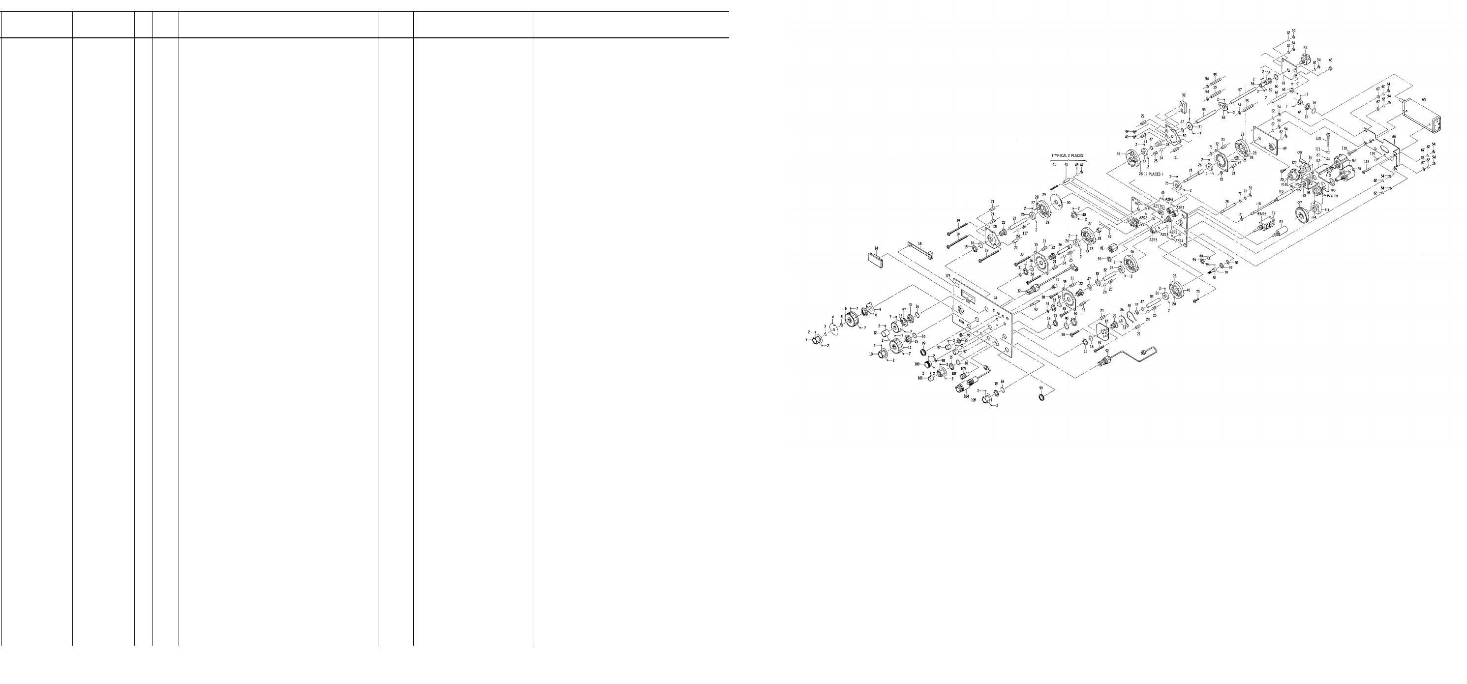
Model 8558B TM 11-6625-3061-14
Reference HP Part CMfr.
Designation Number DQty Description Code Mfr Part Number
73 2260-0001 5 2 NUT-HEX-DBL-CHAM 4-40 28480 2260-0001
74 08558-20056 3 1 SHAFT, BANDWIDTH 28480 08558-20056
75 08558-20058 5 1 HUB, COUPLING 28480 08558-20058
76 2190-0102 8 1 WASHER-LK INTL T-15/32 IN .472-IN-ID 28480 2190-0102
77 3050-0124 9 2 WASHER-FL MTLC NO. 5 .13-IN-ID 28480 3050-0124
78 08558-20055 2 1 SHAFT, MANUAL SWEEP 28480 08558-20055
79 3030-0332 9 2 SCREW-SET 2-56 .094-IN-LG CUP-PT SST 28480 3030-0332
80 08558-40007 6 1 KNOB, KNURLED 28480 08558-40007
81 2950-0142 8 1 NUT-HEX-DBL-CHAM 3/8-32-THD .635-IN-THX 28480 2950-0142
82 08558-20049 4 1 SHAFT, SWEEP TIME 28480 08558-20049
83 2200-0151 6 1 WASHER-FL NM ¼ IN .26-IN-ID .562-IN-OD 28480 2190-0390
84 08558-20048 3 1 SHAFT, SWEEP TRIGGER 28480 08558-20048
85 1460-0537 5 1 SPRING-TRSN MUW CD 28480 1460-0537
86 08558-00053 8 1 STOP ARM 28480 08558-00053
87 08558-00026 5 1 DETENT, SWEEP TRIGGER 28480 08558-00026
88 2200-0151 0 4 SCREW-MACH 4-40 .75-IN-LG PAN-HD-POZI 28480 2200-0151
89 2950-0054 1 1 NUT-HEX-DBL-CHAM ½-28-THD .125-IN-THX 28480 2950-0054
90 2190-0068 5 1 WASHER-LK INTL T ½ IN .505-IN-ID 28480 2190-0068
91 2200-0155 4 1 SCRE-MACH 4-40 1-IN1LG PAN-HD-POZI 28480 2200-0155
92 08558-20071 2 2 CABLE, LO OUTPUT 28480 08558-20071
93 08558-20092 7 1 SHAFT, LATCH 28480 08558-20092
94 08558-00082 3 1 PANEL, FRONT (SEE FIG. 6-2 FOR SUB-PANEL) 28480 08558-00082
94 08558-00083 4 1 PANEL, FRONT (OPTION 001) 28480 08558-00083
94 08558-00084 5 1 PANEL, FRONT (OPTION 002) 28480 08558-00084
95 2950-0072 3 1 NUT-HEX-DBL-CHAM ¼-32-THD .062-IN-THK 28480 2950-0072
96 3101-0044 1 2 SWITCH-PB SPST-NO MOM .5A 115VAC RED-BTN 28480 3101-0044
97 00183-67407 7 2 KNOB 28480 00183-67407
98 0510-0045 6 1 RETAINER-RING F-R EXT .188-IN-DIA STL 28480 0510-0045
99 0590-0012 5 2 NUT-KNRLD-R 15/32-32-THD .062-IN-THK 28480 0590-0012
100 08558-20093 8 1 KNOB, LATCH 28480 08558-20093
101 08558-00045 8 1 KNOB, MANUAL SWEEP 28480 08558-00045
102 08558-00044 7 1 KNOB, SWEEP TIME 28480 08558-00044
103 5060-0467 6 1 CONNECTOR, MALE, PROBE POWER 28480 5060-0467
104 08558-60038 5 1 CABLE ASSY, INPUT, RF 28480 08558-60038
104 08558-60031 8 1 CABLE ASSY, 75 OHM INPUT, RF 28480 08558-60031
105 08558-00107 3 1 KNOB, TRIGGER SWITCH 28480 08558-00107
106 0380-0063 1 1 SPACER-RND .125-IN-LG .129-IN-ID 28480 0380-0063
107 1430-0567 8 1 GEAR, SPUR, 60 T 28480 1430-0567
108 1430-0568 9 1 GEAR, SPUR, 40 T 28480 1430-0568
109 1460-1542 4 1 SPRING, UNIVERSAL COUPLER 28480 1460-1542
110 3050-0086 2 2 WASHER-FL MTLC 3/8 IN .406-IN-ID 28480 3050-0086
111 08558-00069 6 1 SPRING 28480 08558-00069
112 08558-00070 9 1 BRACKET, DUAL POT 28480 08558-00070
113 08558-20111 1 1 BUSHING, COARSE TUNE SHAFT 28480 08558-20111
114 08558-20112 2 1 WASHER, THRUSH 28480 08558-20112
115 08558-20113 3 1 SHAFT, COARSE TUNE 28480 08558-20113
116 08558-20114 4 1 SHAFT, FINE TUNE 28480 08558-20114
117 1460-0623 0 1 SPRING-CPRSN .18-INOD .312-IN-OA-LG MUW 28480 1460-0623
118 2200-0165 6SCREW-MACH 4-40 .25-IN-LG 82 DEG 28480 2200-0165
119 6960-0016 0 1 PLUG-HOLE TR-HD FOR .125-D-HOLE NYL 28480 6960-0016
120 2200-0121 4 1 SCREW-MACH 4-40 1.1258-IN-LG PAN-HD-POZI 28480 2200-0121
121 2190-0004 9 1 WASHER-LK INTL T NO. 6 .115-IN-ID 28480 2190-0004
122 2950-0001 8 1 NUT-HEX-DBL-CHAM 3/8-32-THD .094-IN-THK 28480 2950-0001
123 7120-7136 0 1 LABEL, HP LOGO 28480 7120-7136
Figure 7-2. Front Panel Assembly (2 of 3) (CHANGE A)
Figure 7-2. Front Panel Assembly (3 of 3) (CHANGE A)
7-11/7-12 (blank)

Model 8558B TM 11-6625-3061-14
Figure 7-3. Front Switch Assembly A2, Schematic (CHANGE A)
7-13/7-14 (blank)

Model 8558B TM 11-6625-3061-14
Figure 7-6. A14 Log Amplifier Assembly Schematic (CHANGE B)
7-25/7-26 (blank)
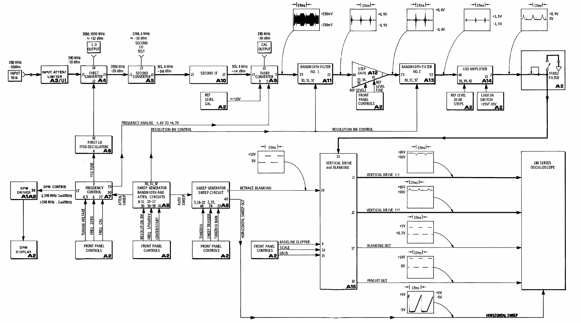
TM 11-6625-3061-14
Figure 8-5. Simplified Block Diagram
8-15/8-16 (blank)
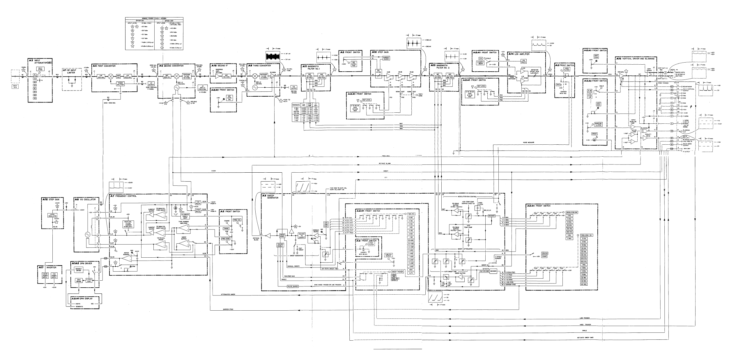
TM 11-6625-3061-14
Figure 8-6. Troubleshooting Block Diagram
8-17/8-18 (blank)
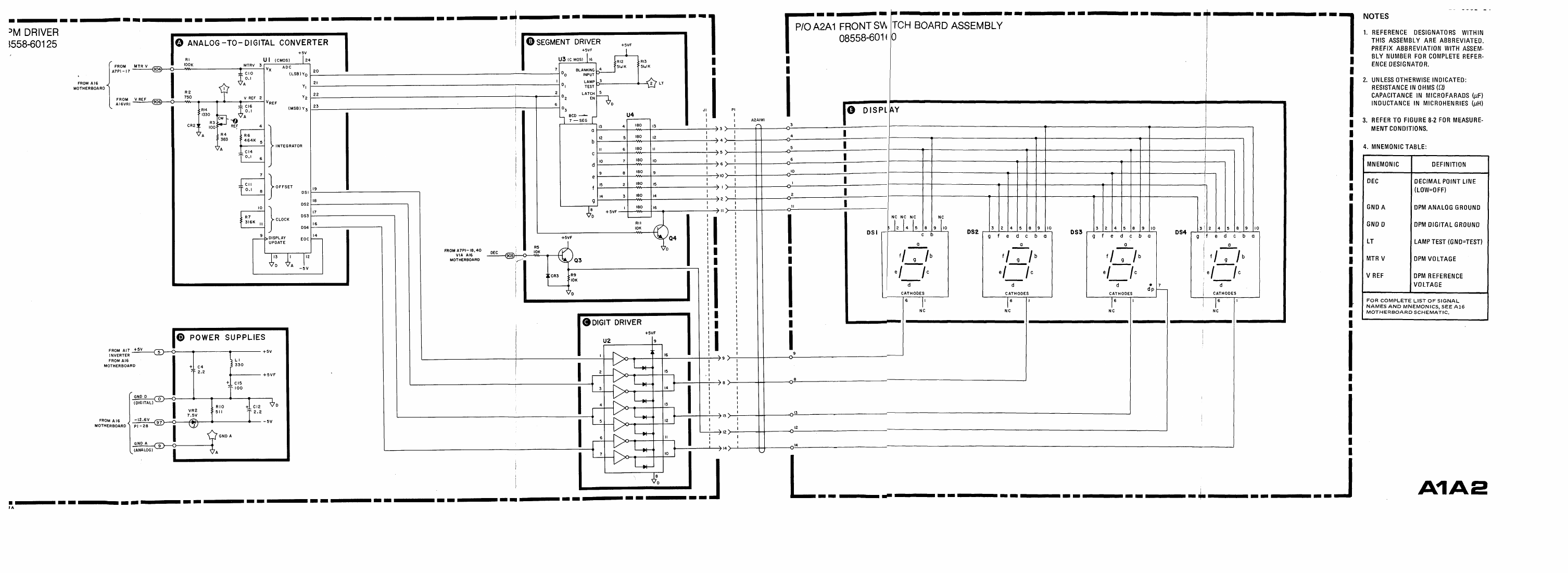
TM 11-6625-3061-14
Figure 8-11. A1A2 DPM Driver (and DPM Display), Schematic
8-23/8-24

TM 11-6625-3061-14
Figure 8-13. A2 Front Switch, Schematic Diagram
8-27/8-28 (blank)

TM 11-6625-3061-14
Figure 8-18. A3 Input Attenuator, A4 First Converter, A5 Second Converter and A6 YIG Oscillator, Schematic
8-35/8-36 (blank)

TM 11-6625-3061-14
Figure 8-20. A7 Frequency Control, Schematic
8-43/8-44 (blank)

TM 11-6625-3061-14
Figure 8-23. A8 Sweep Generator, Schematic (1 of 2)
8-53/8-54 (blank)

TM 11-6625-3061-14
Figure 8-23. A8 Sweep Generator, Schematic (2 of 2)
8-55/8-56 (blank)

TM 11-6625-3061-14
Figure 8-26. A9 Third Converter and A10 Second IF, Schematic
8-61/8-62 (blank)
TM 11-6625-3061-14

Figure 8-30. A11 Bandwidth Filter No. 1, Schematic
8-69/8-70 (blank)
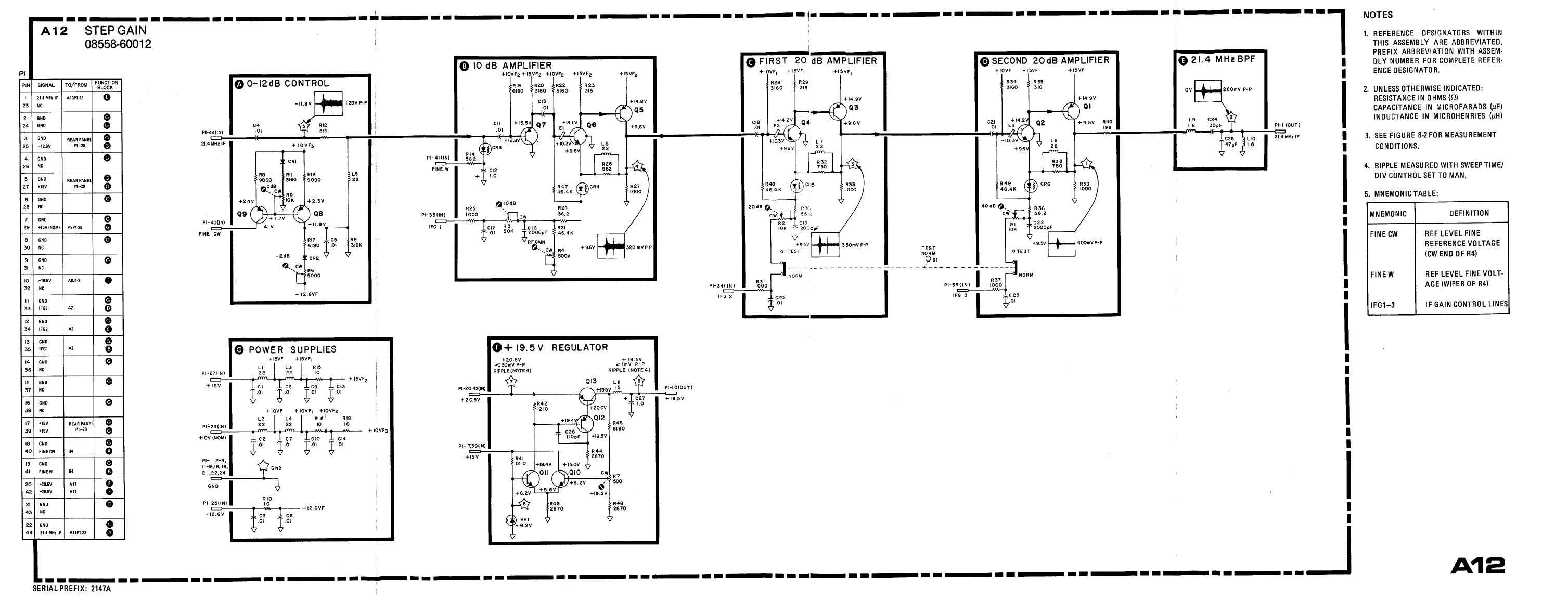
TM 11-6625-3061-14
Figure 8-33. A12 Step Gain, Schematic
8-75/8-76 (blank)
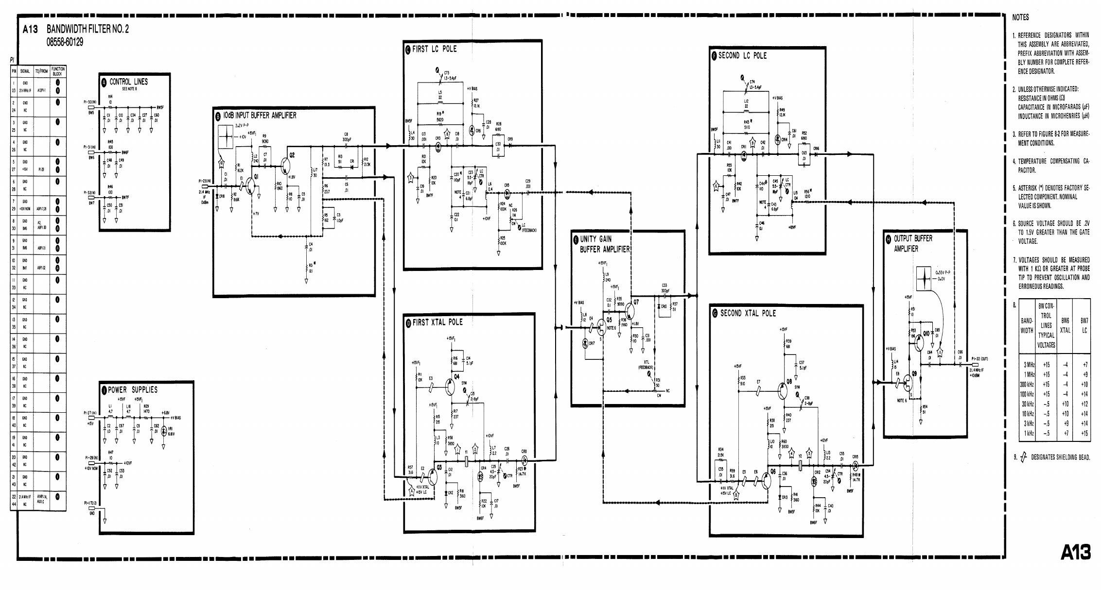
TM 11-6625-3061-14
Figure 8-35. A13 Bandwidth Filter No. 2, Schematic
8-79/8-80 (blank)
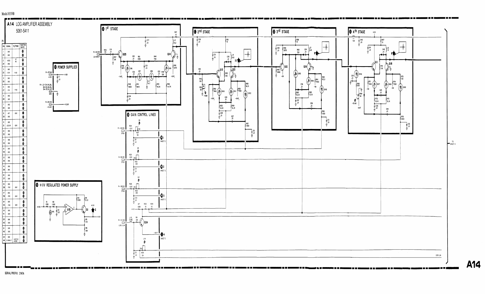
TM 11-6625-3061-14
SERIAL PREFIX: 2147A Figure 8-38. A14 Log Amplifier Assembly, Schematic (1 of 2)
8-85/8-86 (blank)
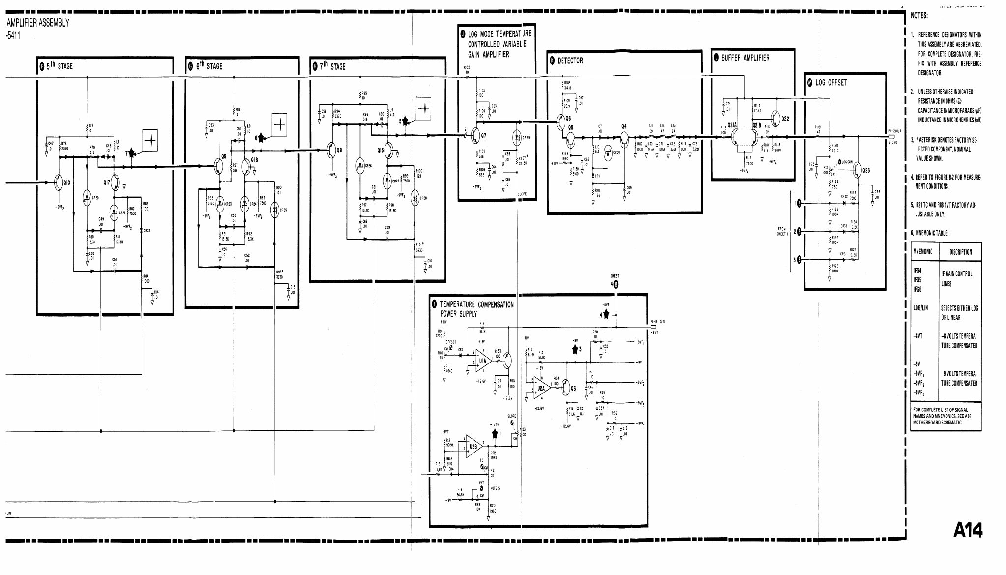
TM 11-6625-3061-14
Figure 8-38. A14 Log Amplifier Assembly, Schematic (2 of 2)
8-87/8-88 (blank)
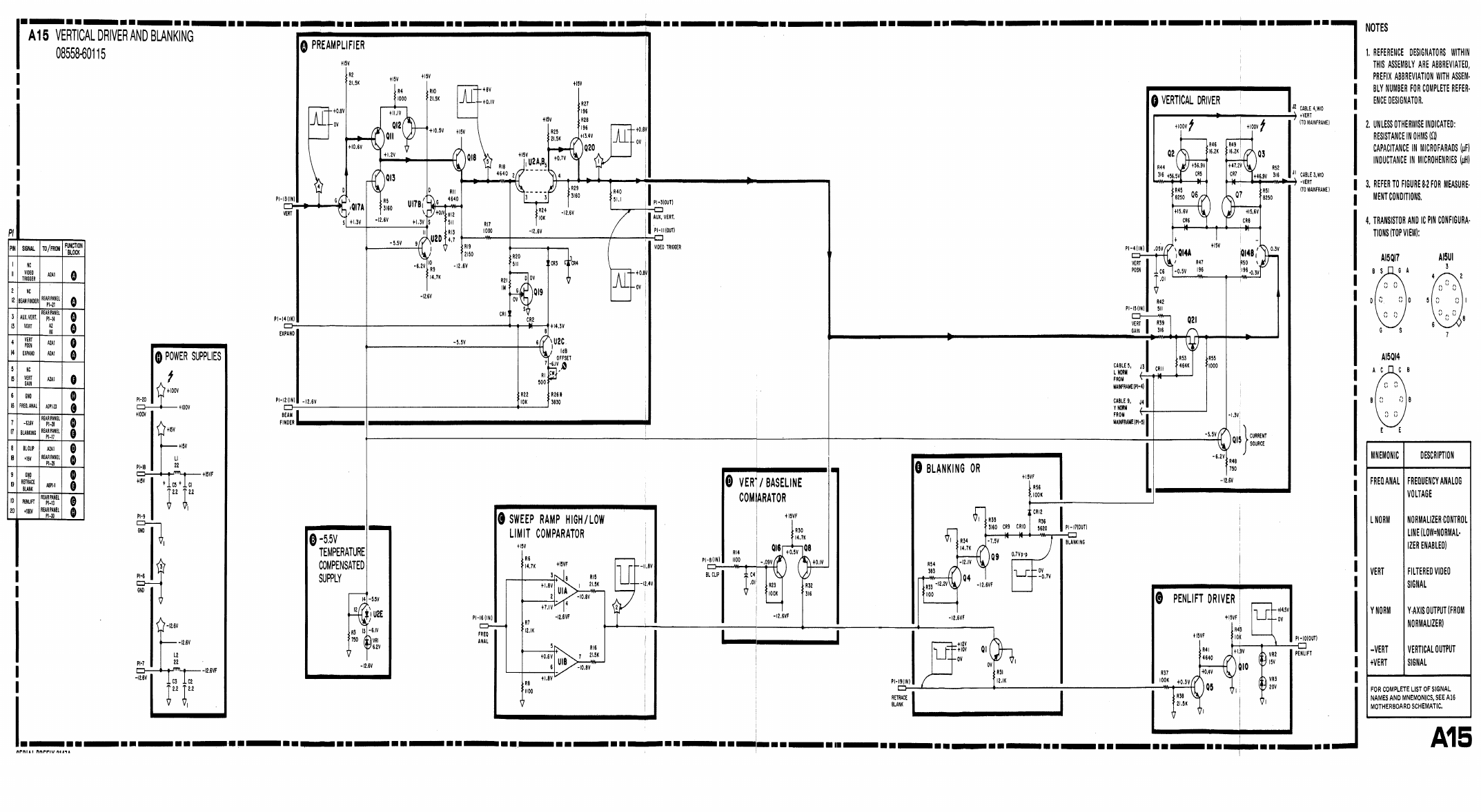
TM 11-6625-3061-14
Figure 8-42. A15 Vertical driver and Blanking, Schematic
8-95/8-96 (blank)
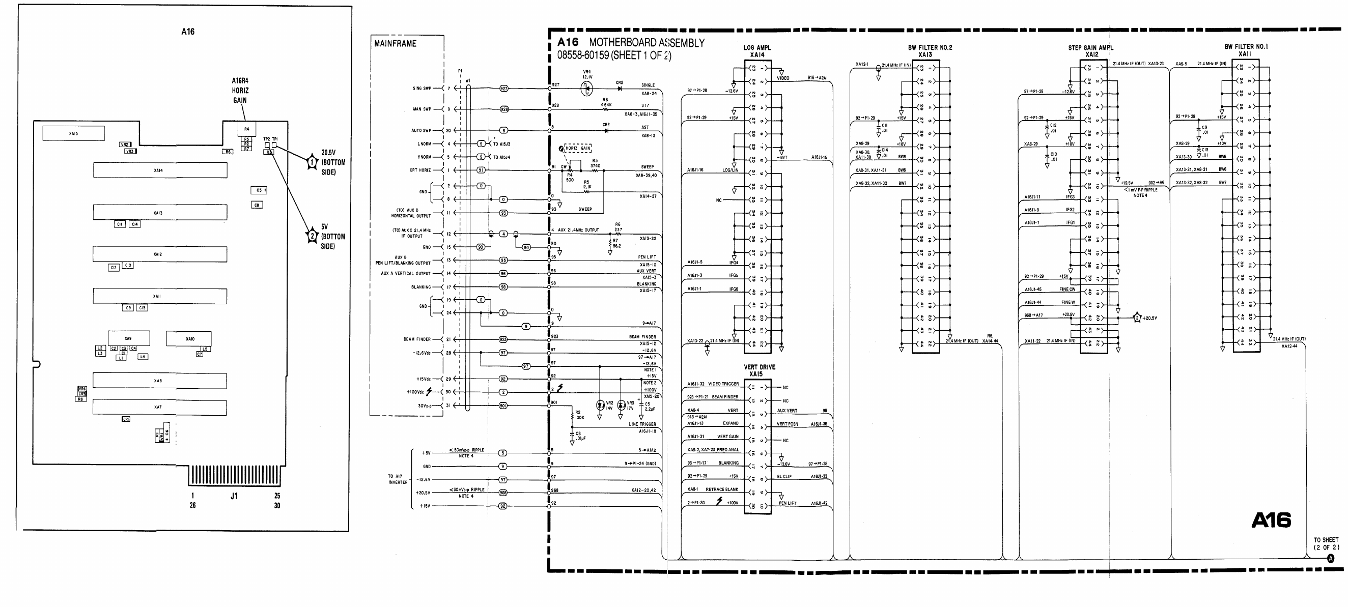
TM 11-6625-3061-14
Figure 8-43. A16 Motherboard Assembly, Components and Test Point Locations Figure 8-44. A16 Motherboard, Schematic Diagram (1 of 2)
8-97/8-98
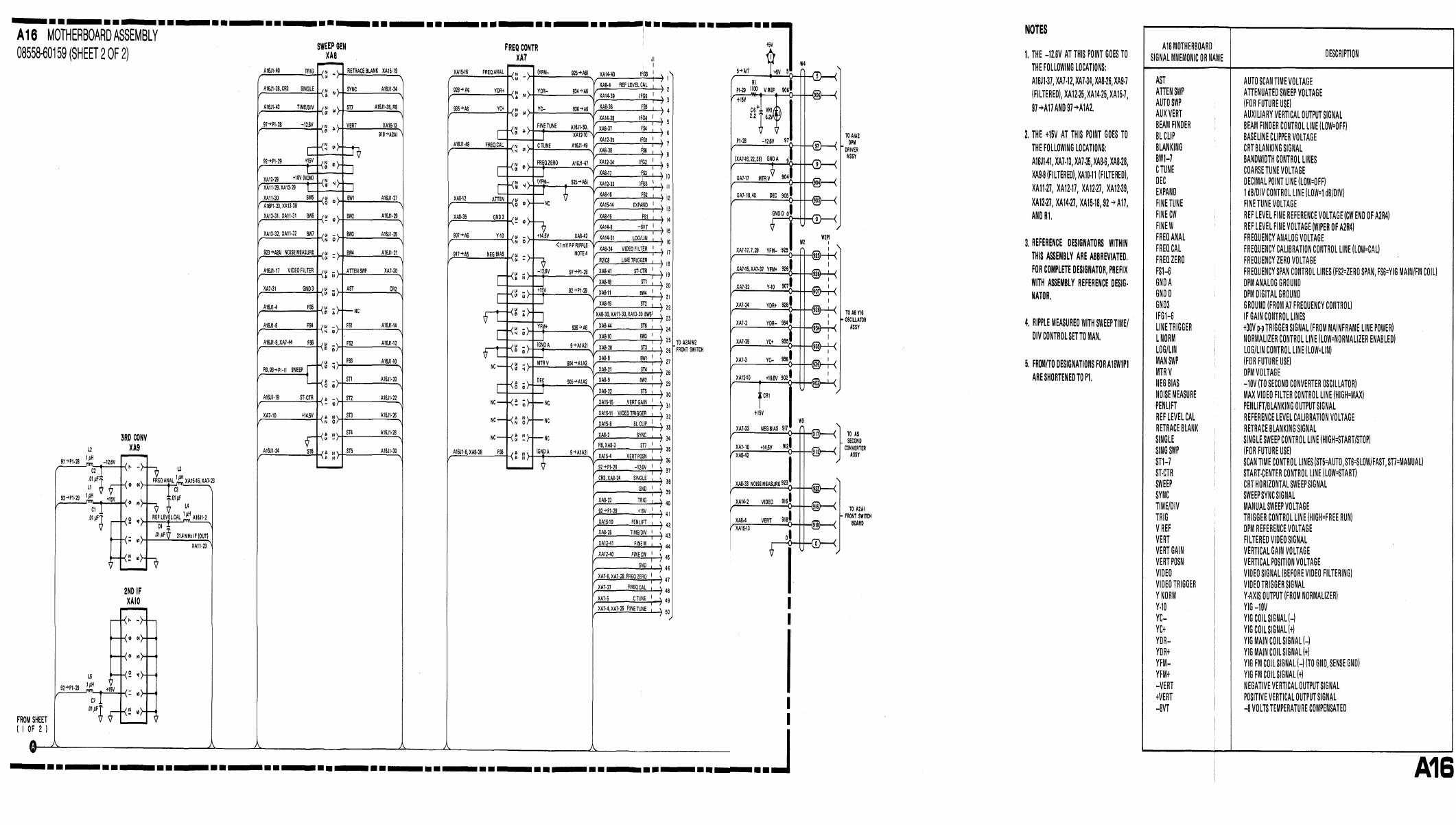
TM 11-6625-3061-14
Figure 8-44. A16 Motherboard, Schematic Diagram (2 of 2)
8-99/8-100 (blank)
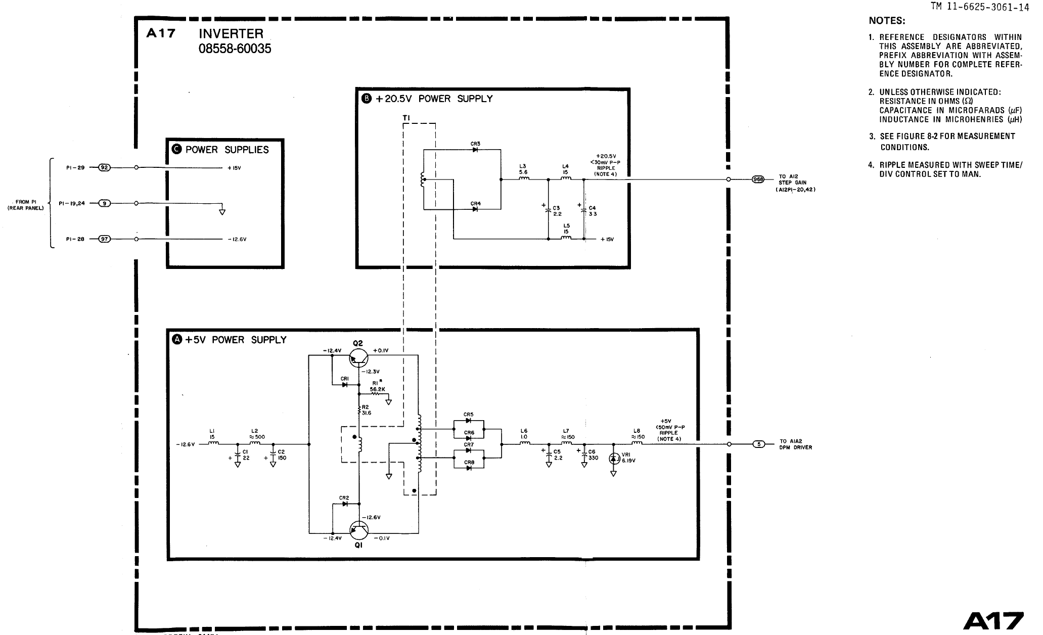
TM 11-6625-3061-14
Figure 8-46. A17 Inverter. Schematic
8-103/8-104 (blank)
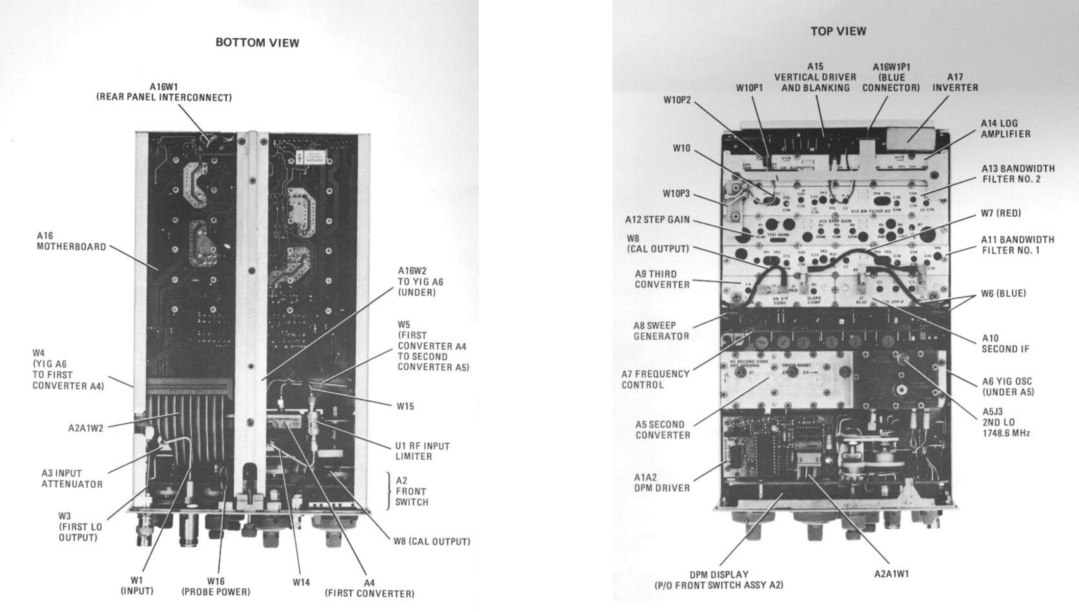
TM 11-6625-3061-14
Figure 8-47. Location of Major Assemblies
8-105/8-106 (blank)
PIN: 059359-000
