HP 8660B Signal Generator Mil TM 1979 WW
User Manual: HP-8660B-Signal-Generator-Mil-TM-1979-WW HP
Open the PDF directly: View PDF ![]() .
.
Page Count: 431 [warning: Documents this large are best viewed by clicking the View PDF Link!]
- TOC
- LIST OF ILLUSTRATIONS
- LIST OF TABLES
- WARNING
- SECTIONS
- PAGES
- PAGE 0-1
- PAGE 1-0
- PAGE 1-1
- PAGE 1-2
- PAGE 1-3
- PAGE 1-4
- PAGE 1-5
- PAGE 2-1
- PAGE 2-2
- PAGE 2-3
- PAGE 3-1
- PAGE 3-2
- PAGE 3-4
- PAGE 3-5
- PAGE 3-9
- PAGE 3-10
- PAGE 3-11
- PAGE 3-14
- PAGE 3-15
- PAGE 3-16
- PAGE 3-17
- PAGE 3-18
- PAGE 3-19
- PAGE 4-1
- PAGE 4-2
- PAGE 4-3
- PAGE 4-4
- PAGE 4-5
- PAGE 4-6
- PAGE 4-7
- PAGE 4-8
- PAGE 5-1
- PAGE 5-2
- PAGE 5-3
- PAGE 5-4
- PAGE 5-5
- PAGE 5-6
- PAGE 5-7
- PAGE 5-8
- PAGE 5-9
- PAGE 5-10
- PAGE 5-12
- PAGE 5-13
- PAGE 5-14
- PAGE 5-15
- PAGE 5-16
- PAGE 5-18
- PAGE 5-19
- PAGE 5-20
- PAGE 5-21
- PAGE 5-22
- PAGE 5-23
- PAGE 5-24
- PAGE 5-25
- PAGE 5-27
- PAGE 5-28
- PAGE 6-1
- PAGE 6-2
- PAGE 6-3
- PAGE 6-7
- PAGE 6-54
- PAGE 6-55
- PAGE 7-1
- PAGE 7-2
- PAGE 7-4
- PAGE 7-8
- PAGE 7-9
- PAGE 7-11
- PAGE 7-13
- PAGE 7-14
- PAGE 8-0
- PAGE 8-1
- PAGE 8-3
- PAGE 8-4
- PAGE 8-5
- PAGE 8-6
- PAGE 8-7
- PAGE 8-8
- PAGE 8-9
- PAGE 8-11
- PAGE 8-22
- PAGE 8-23
- PAGE 8-24
- PAGE 8-25
- PAGE 8-26
- PAGE 8-28
- PAGE 8-33
- PAGE 8-36
- PAGE 8-37
- PAGE 8-38
- PAGE 8-39
- PAGE 8-40
- PAGE 8-41
- PAGE 8-42
- PAGE 8-43
- PAGE 8-44
- PAGE 8-46
- PAGE 8-48
- PAGE 8-49
- PAGE 8-50
- PAGE 8-54
- PAGE 8-55
- PAGE 8-56
- PAGE 8-63
- PAGE 8-64
- PAGE 8-65
- PAGE 8-66
- PAGE 8-69
- PAGE 8-71
- PAGE 8-74
- PAGE 8-73
- PAGE 8-75
- PAGE 8-78
- PAGE 8-77
- PAGE 8-79
- PAGE 8-81
- PAGE 8-82
- PAGE 8-83
- PAGE 8-85
- PAGE 8-87
- PAGE 8-88
- PAGE 8-89
- PAGE 8-91
- PAGE 8-92
- PAGE 8-93
- PAGE 8-95
- PAGE 8-97
- PAGE 8-99
- PAGE 8-100
- PAGE 8-101
- PAGE 8-103
- PAGE 8-105
- PAGE 8-107
- PAGE 8-109
- PAGE 8-110
- PAGE 8-111
- PAGE 8-113
- PAGE 8-115
- PAGE 8-116
- PAGE 8-117
- PAGE 8-119
- PAGE 8-121
- PAGE 8-123
- PAGE 8-125
- PAGE 8-127
- PAGE 8-129
- PAGE 8-131
- PAGE 8-133
- PAGE 8-135
- PAGE 8-137
- PAGE 8-139
- PAGE 8-140
- PAGE 8-141
- PAGE 8-143
- PAGE 8-145
- PAGE 8-146
- PAGE 8-147
- PAGE 8-149
- PAGE 8-151
- PAGE 8-152
- PAGE 8-153
- PAGE 8-154
- PAGE 8-155
- PAGE 8-156
- PAGE A-1
- PAGE B-1
- PAGE C-1
- PAGE D-1
- FIGURES
- FIGURE 1-1
- FIGURE 2-1
- FIGURE 2-2
- FIGURE 2-3
- FIGURE 3-1
- FIGURE 3-2
- FIGURE 3-3
- FIGURE 4-1
- FIGURE 4-2
- FIGURE 4-3
- FIGURE 4-4
- FIGURE 4-5
- FIGURE 5-1
- FIGURE 5-2
- FIGURE 5-3
- FIGURE 5-4
- FIGURE 5-5
- FIGURE 5-6
- FIGURE 5-7
- FIGURE 5-8
- FIGURE 5-9
- FIGURE 5-10
- FIGURE 5-11
- FIGURE 5-12
- FIGURE 5-13
- FIGURE 5-14
- FIGURE 5-15
- FIGURE 5-16
- FIGURE 5-17
- FIGURE 6-1
- FIGURE 6-2
- FIGURE 7-1
- FIGURE 7-2
- FIGURE 7-3
- FIGURE 7-4
- FIGURE 8-16
- FIGURE 8-95
- FIGURE 8-1
- FIGURE 8-2
- FIGURE 8-3
- FIGURE 8-4
- FIGURE 8-5
- FIGURE 8-6
- FIGURE 8-7
- FIGURE 8-8
- FIGURE 8-9
- FIGURE 8-10
- FIGURE 8-11
- FIGURE 8-12
- FIGURE 8-14
- FIGURE 8-13
- FIGURE 8-15
- FIGURE 8-17
- FIGURE 8-18
- FIGURE 8-19
- FIGURE 8-20
- FIGURE 8-21
- FIGURE 8-24
- FIGURE 8-22
- FIGURE 8-23
- FIGURE 8-26
- FIGURE 8-25
- FIGURE 8-27
- FIGURE 8-28
- FIGURE 8-29
- FIGURE 8-30
- FIGURE 8-31
- FIGURE 8-32
- FIGURE 8-33
- FIGURE 8-34
- FIGURE 8-35
- FIGURE 8-36
- FIGURE 8-37
- FIGURE 8-38
- FIGURE 8-39
- FIGURE 8-40
- FIGURE 8-41
- FIGURE 8-42
- FIGURE 8-43
- FIGURE 8-44
- FIGURE 8-45
- FIGURE 8-46
- FIGURE 8-47
- FIGURE 8-48
- FIGURE 8-49
- FIGURE 8-50
- FIGURE 8-51
- FIGURE 8-52
- FIGURE 8-53
- FIGURE 8-54
- FIGURE 8-55
- FIGURE 8-56
- FIGURE 8-57
- FIGURE 8-58
- FIGURE 8-59
- FIGURE 8-60
- FIGURE 8-61
- FIGURE 8-62
- FIGURE 8-63
- FIGURE 8-64
- FIGURE 8-65
- FIGURE 8-66
- FIGURE 8-67
- FIGURE 8-68
- FIGURE 8-69
- FIGURE 8-70
- FIGURE 8-71
- FIGURE 8-72
- FIGURE 8-74
- FIGURE 8-75
- FIGURE 8-76
- FIGURE 8-77
- FIGURE 8-78
- FIGURE 8-79
- FIGURE 8-80
- FIGURE 8-81
- FIGURE 8-82
- FIGURE 8-83
- FIGURE 8-84
- FIGURE 8-85
- FIGURE 8-86
- FIGURE 8-87
- FIGURE 8-88
- FIGURE 8-89
- FIGURE 8-90
- FIGURE 8-91
- FIGURE 8-92
- FIGURE 8-93
- FIGURE 8-94
- FIGURE 8-96
- FIGURE 8-97
- FIGURE 8-99
- FIGURE 8-98
- FIGURE 8-100
- FIGURE 8-102
- FIGURE 8-101
- FIGURE 8-103
- FIGURE 8-104
- FIGURE 8-105
- FIGURE 8-106
- FIGURE 8-107
- FIGURE 8-109
- FIGURE 8-110
- FIGURE 8-108
- FIGURE 8-111
- FIGURE 8-112
- FIGURE 8-113
- FIGURE 8-114
- FIGURE 8-115
- FIGURE 8-116
- FIGURE 8-117
- PARAGRAPHS
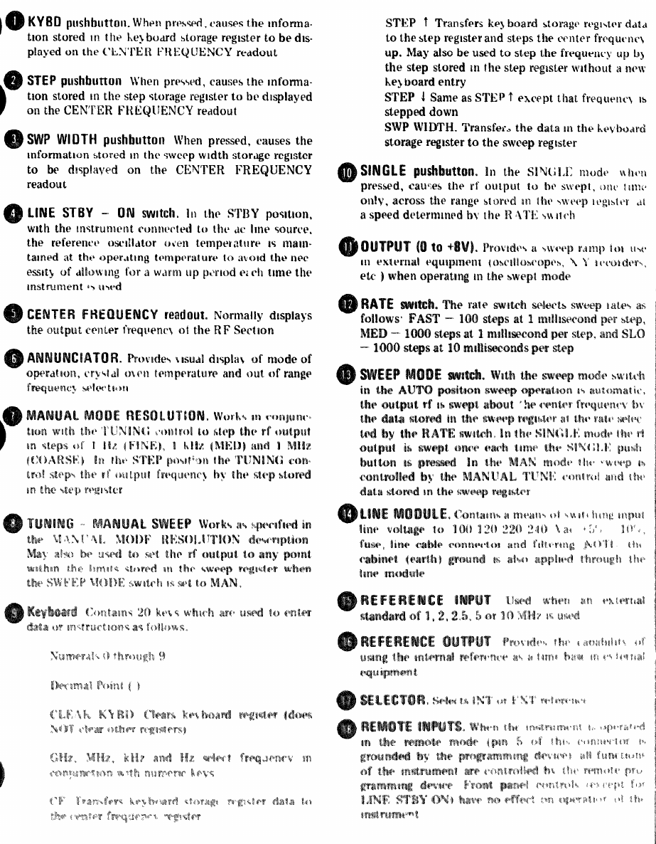
- PARA 1-1
- PARA 1-6
- PARA 1-8
- PARA 1-13
- PARA 1-22
- PARA 1-28
- PARA 1-30
- PARA 1-32
- PARA 1-34
- PARA 1-36
- PARA 1-38
- PARA 2-1
- PARA 2-3
- PARA 2-6
- PARA 2-7
- PARA 2-9
- PARA 2-12
- PARA 2-14
- PARA 2-16
- PARA 2-19
- PARA 2-21
- PARA 2-23
- PARA 2-24
- PARA 2-26
- PARA 3-1
- PARA 3-4
- PARA 3-6
- PARA 3-8
- PARA 3-20
- PARA 3-22
- PARA 3-23
- PARA 3-32
- PARA 3-39
- PARA 3-41
- PARA 3-46
- PARA 3-49
- PARA 3-53
- PARA 3-59
- PARA 3-63
- PARA 3-66
- PARA 4-1
- PARA 4-3
- PARA 4-5
- PARA 4-7
- PARA 4-8
- PARA 4-9
- PARA 4-10
- PARA 4-11
- PARA 5-1
- PARA 5-4
- PARA 5-7
- PARA 5-9
- PARA 5-13
- PARA 5-16
- PARA 5-18
- PARA 5-20
- PARA 5-26
- PARA 5-27
- PARA 5-28
- PARA 5-29
- PARA 5-30
- PARA 5-31
- PARA 5-32
- PARA 5-33
- PARA 5-34
- PARA 6-1
- PARA 6-3
- PARA 6-5
- PARA 6-7
- PARA 6-11
- PARA 6-16
- PARA 7-1
- PARA 7-3
- PARA 7-6
- PARA 7-7
- PARA 7-8
- PARA 7-10
- PARA 8-1
- PARA 8-3
- PARA 8-26
- PARA 8-28
- PARA 8-34
- PARA 8-46
- PARA 8-49
- PARA 8-74
- PARA 8-80
- PARA 8-86
- PARA 8-88
- TABLES
- TABLE 1-1
- TABLE 1-2
- TABLE 1-3
- TABLE 3-1
- TABLE 3-2
- TABLE 3-3
- TABLE 3-4
- TABLE 3-5
- TABLE 3-6
- TABLE 3-7
- TABLE 3-8
- TABLE 4-1
- TABLE 5-1
- TABLE 5-2
- TABLE 5-3
- TABLE 5-4
- TABLE 5-5
- TABLE 5-6
- TABLE 5-7
- TABLE 5-8
- TABLE 5-9
- TABLE 5-10
- TABLE 5-11
- TABLE 5-12
- TABLE 6-1
- TABLE 6-2
- TABLE 6-3
- TABLE 6-4
- TABLE 6-5
- TABLE 7-1
- TABLE 7-2
- TABLE 8-1
- TABLE 8-2
- TABLE 8-3
- TABLE 8-4
- TABLE 8-6
- TABLE 8-7
- TABLE 8-8
- TABLE 8-9
- TABLE 8-10
- TABLE 8-11
- TABLE 8-12
- TABLE 8-13
- TABLE 8-14
- TABLE 8-15
- TABLE 8-16
- TABLE 8-17
- TABLE 8-18
- TABLE 8-19
- TABLE 8-20
- TABLE 8-21
- TABLE 8-26
- TABLE 8-22
- TABLE 8-23
- TABLE 8-24
- TABLE 8-25
- TABLE 8-27
- TABLE 8-28
- TABLE 8-29
- TABLE 8-30
- TABLE 8-31
- TABLE 8-33
- TABLE 8-34
- TABLE 8-36
- TABLE 8-37
- TABLE 8-35
- TABLE 8-38
- APPENDICIES

TECHNICAL MANUAL
NO 11-625-2837-14&P)
TM 11-6625-2837-14&P
i
TM 11-6625-2837-14&P
CONTENTS
Section Page
0.
INTRODUCTION.
......................0
-1
I.
GENERAL INFORMATION
1-1. Introduction
1-6. Specifications
1-8.
Instruments Covered By Manual
1-13. Description
1-22. Options
1-28. Equipment Required
But Not Supplied
1-30. Equipment Available
1-32. Accessories Supplied
1-34. Deleted
1-36. Test Equipment
and
Accessories
1-38. Electrical Protection
II.
INSTALLATION
2-1.
Introduction
2-3. Initial Inspection
2-6. Preparation For Use
2-7.
Power Requirements
2-9.
Line Voltage Selection
2-12.
Power Cable
2-14.
Mating Connectors
2-16.
Operating Environment
2-19.
Bench Operation
2-21.
Rack Mounting
2-23. Storage and Shipment
2-24.
Environment
2-26.
Packaging
III. OPERATION
3-1. Introduction
3-4. Panel Features
3-6. Operating Principles
3-8.
Local Operation
3-20. Operator’s Maintenance
3-22.
Remote Operation
3-23.
BCD Remote Operation
3-32.
Programming Sequence
3-39. GPI Bus Remote Operation
3-41.
GPI Bus Description
3-46.
Instrument Addressing
3-49.
Three-Wire Handshake
3-53.
Modified Instrument Checks
3-59.
Introduction to GPI Operation
3-63.
Remote Control
3-66.
Programming Conventions
VIII. SERVICE
IV.
PERFORMANCE TESTS
4-1. Introduction
4-3. Equipment Required
4-5. Test Record
1-1
1-1
1-1
1-1
1-2
1-2
1-2
1-2
1-2
1-3
1-3
2-1
2-1
2-1
2-1
2-1
2-1
2-2
2-2
2-2
2-3
2-3
2-3
2-3
2-3
3-1
3-1
3-1
3-1
3-1
3-4
3-4
3-9
3-9
3-9
3-10
3-10
3-10
3-16
3-16
3-16
3-16
4-1
4-1
4-1
4-1
Section
4-7. Internal Crystal Oscillator
Aging Rate
4-8. Input Sensitivity for
External Reference
4-9. Reference Output
4-10. Sweep Output
4-11. Remote Programming
V.
ADJUSTMENTS
5-1.
5-4.
5-7.
5-9.
5-13.
5-16.
5-18.
5-20.
5-26.
Introduction
Equipment Required
Adjustment Aids
Factory Selected Components
Related Adjustments
Adjustment Locations
Checks and Adjustments
Safety Considerations
Power Supply
5-27.
ReferenceSection
5-28. High Frequency Section
5-29. N1 Phase Lock Loop
5-30. N2 Phase Lock Loop
5-31. N3 Phase Lock Loop
5-32.
Summing
Loop 2 (SL2)
5-33.
5-34. DCU Sweep Output
VI.
REPLACEABLE PARTS
6-1. Introduction
6-3. Exchange Assemblies
6-5. Abbreviations
6-7. Replaceable Parts List
6-11. Ordering Information
6-11. Spare Parts Kit
6-16. Illustrated Parts Breakdowns
VII. MANUAL CHANGES
7-1. Introduction
7-3. Manual Changes
7-6. Manual Change Instructions
7-7.
Modifications
7-8.
7-10.
Page
4-1
4-2
4-4
4-5
4-6
5-1
5-1
5-1
5-1
5-1
5-1
5-1
5-1
5-2
5-3
5-6
5-10
5-16
5-18
5-20
5-22
5-25
5-27
6-1
6-1
6-1
6-1
6-1
6-1
6-1
6-2
7-1
7-1
7-1
7-4
7-13
7-13
7-14
8-1
8-1
8-1
8-3
8-3
8-1.
8-3.
8-26.
8-28.
ii
TM 11-6625-2837-14&P
CONTENTS (Cont'd)
Section
Page
8-4
8-4
8-22
8-34. Repair
8-46. Mnemonics
8-49. Algorithmic
Section
8-74.
8-80.
8-86.
8-88.
ILLUSTRATIONS
Page Figure
Figure
1-1.
2-1.
2-2.
2-3.
3-1.
3-2.
3-3.
4-1.
4-2.
4-3.
4-4.
4-5.
5-1.
5-2.
5-3.
5-4.
5-5.
5-6.
5-7.
5-8.
5-9.
5-10.
5-11.
5-12.
5-13.
5-14.
5-15.
5-16.
5-17.
6-1.
6-2.
7-1.
7-2.
7-3.
1-0 7-4.
2-2
2-3
8-1.
2-3
8-2.
8-3.
3-2
3-10
8-4.
3-17
4-1
8-5.
4-3
4-4 8-6.
4-5
8-7.
4-7
8-8.
5-4
8-9.
8-10.
5-6 8-11.
8-12.
5-7 8-13.
5-8 8-14.
5-8
5-9 8-15.
5-10
8-16.
8-17.
5-12
5-14 8-18.
5-15
5-16
8-19.
5-16
5-19
8-20.
5-21
5-23
8-21.
5-25 8-22.
5-28
6-3
8-23.
6-7
8-24.
7-8
8-25.
7-9
8-26.
8-27.
7-11
Page
8-23
8-23
8-25
8-25
Page
7-13
8-0
8-5
8-6
8-7
8-24
8-63
8-64
8-65
8-65
8-66
8-69
8-71
8-71
8-71
8-71
8-71
8-73
8-73
8-73
8-75
8-75
8-77
8-77
8-78
8-79
8-79
8-79
iii
TM 11-6625-2837-14&P
ILLUSTRATIONS (Cont'd)
Figure
8-28.
8-29.
8-30.
8-31.
8-32.
8-33.
8-34.
8-35.
8-36.
8-37.
8-38.
8-39.
8-40.
8-41.
8-42.
8-43.
8-44.
8-45.
8-46.
8-47.
8-48.
8-49.
8-50.
8-51.
8-52.
8-53.
8-54.
8-55.
8-56.
8-57.
8-58.
8-59.
8-60.
8-61.
8-62.
8-63.
8-64.
8-65.
iv
A16Nl Phase Detector
Component Locations
N1 Phase Detector Schematic
A17 N1 VCO Component Locations
N1 VCO Schematic
A14 N2 Phase Detector
Component Locations
N2 Phase Detector Schematic
A14a N2a Phase Detector
Component Locations
N2a Phase Detector Schematic
A13N2 VCO Component Locations
N2 VCO Schematic
A10 N3 Phase Detector
Component Locations
N3 Phase Detector Schematic
A8 N3 VCO Component Locations
N3 VCO Schematic
A12 SL2 Phase Detector
Component Locations. . . . .
SL2 Phase Detector Schematic . .
A11 SL2 VCO Component Locations
SL2 VCO Schematic
A15 SL1 Phase Detector
Component Locations
SL1 Phase Detector Schematic
A18 SL1 Mixer and D/A Converter
Component Locations
SL1 Mixer and D/A
Converter Schematic
A19 SL1 VCO Component Locations
SL1 VCO Schematic
8660B DCU (Al)
DCU Block Diagram, Al
P/O A1A1 Switch Control Assy
Component Locations (Part 1) . . . .
Page
8-81
8-81
8-83
8-83
8-85
8-85
8-87
8-87
8-89
8-89
8-91
8-91
8-93
8-93
8-95
8-95
8-97
8-97
8-99
8-99
8-101
8-101
8-103
8-103
8-105
8-105
8-107
8-107
8-109
8-109
8-110
8-110
8-111
8-111
8-113
8-113
8-115
8-115
8-87.
8-88.
8-89.
8-90.
8-91.
8-92.
8-93.
8-94.
8-95.
8-96.
8-97.
8-98.
8-99.
8-81.
8-82.
8-83.
8-84.
8-85.
8-86.
Figure
8-66.
8-67.
8-68.
8-69.
8-70.
8-71.
8-72.
8-73
8-74.
8-75.
8-76.
8-77.
8-78.
8-79.
8-80.
Page
8-117
8-117
8-119
8-119
8-121
8-121
8-123
8-123
8-125
8-125
8-127
8-127
8-129
8-129
8-131
8-131
8-133
8-133
8-135
8-135
8-137
8-137
8-139
8-139
8-140
8-141
8-141
8-143
8-143
8-143
8-145
8-145
8-146
8-146
TM 11-6625-2837-14&P
ILLUSTRATIONS (Cont'd)
8-100.
8-101.
8-102.
8-103.
8-104.
8-105.
8-106.
8-107.
8-108.
Page
Figure
8-109.
8-146
8-110.
8-146
8-146
8-111.
8-112.
8-147
8-113.
8-149
8-114.
8-149
8-115.
8-151
8-116.
8-151
8-152
8-117.
1-1.
1-2.
1-3.
3-1.
3-2.
3-3.
3-4.
3-5.
3-6.
3-7.
3-8.
4-1.
5-1.
5-2.
5-3.
5-4.
5-5.
5-6.
5-7.
5-8.
5-9.
5-10.
5-11.
5-12.
6-1.
6-2.
6-3.
6-4.
6-5.
TABLES
Page
1-3
Table
7-1.
7-2.
1-4
8-1.
1-5
8-2.
3-5
8-3.
3-11
8-4.
3-11 8-5.
3-14
8-6.
3-14
8-7.
3-15
8-8.
3-18 8-9.
3-19
8-10.
4-8
5-2
8-11.
5-5
5-5
8-12.
5-9
5-13
8-13.
5-18
5-20
8-14.
5-22
8-15.
8-16.
5-24
8-17.
5-27
5-28
8-18.
5-28
8-19.
6-2
6-3
8-20.
6-7
8-21.
6-54
8-22.
Page
8-152
8-152
8-153
8-153
8-153
8-154
8-154
8-155
8-156
Page
7-1
7-2
8-8
8-9
8-26
8-28
8-31
8-33
8-36
8-37
8-38
8-39
8-39
8-40
8-41
8-42
8-43
8-44
8-44
8-46
8-48
8-49
8-50
8-54
iv
6-55

TM 11-6625-2837-14&P
Table Page
Table
8-23.
KYBD Pushbutton Readout Defective
8-24. STEP Pushbutton Readout Defective
8-25. Sweep Width Pushbutton
8-55
8-55
Page
8-92
8-9
8-100
8-11
8-116
8-116
8-116
8-151
8-26.
8-27.
8-28.
8-29.
8-30.
Readout Defective
Remote Control Problems
Assembly Locations
Pretuning DC Levels
N1 Oscillator Test Point Measurements
N2 Frequency versus Voltage Chart
8-56
8-56
8-63
8-74
8-82
8-88
8-31. N3 Frequency Versus Voltage Chart
8-2. SL2 Frequency Versus Voltage Chart
8-33. SL1 Frequency Versus Voltage Chart
8-34. Varactor Bias Versus Frequency SL1
8-35. Readout Register Recirculating Cycle
8-36. Readout Register Leading Zero Blanking
8-37. Readout Register Significant
Zero Blanking Inhibit
8-38. Power Supply Troubleshooting
APPENDIXES
A. References .........................A-l
B. Components of End Item List . . B-l
C. Additional Authorization List . C-l
D.
Maintenance Allocation . . . . . .D-l
TABLES (Cont'd)
vi


SECTION O
INTRODUCTION
O-1. SCOPE
This manual describes Signal Generator, Hewlett-
Packard Model 8660B and provides instructions for
operation and maintenance.
O-2. INDEXES OF PUBLICATIONS
a. DA Pam 310-4. Refer to the latest issue of DA
Pam 310-4 to determine whether there are new edi-
tions, changes, or additional publications pertaining to
the equipment
b.
DA Pam 310-7. Refer to DA Pam 310-7 to deter-
mine whether there are modification work orders
(MWO’s) pertaining to the equipment.
O-3. MAINTENANCE FORMS, RECORDS,
AND REPORT
a. Reports of Maintenance and Unsatisfactory
Equipment. Department of the Army forms and proce-
dures used for equipment maintenance will be those
by TM 38-750, The Army Maintenance
ent System.
b. Report
of Packaging and Handling Deficiencies.
Fill out and forward DD Form 6 (Packaging Improve-
ment Report) as prescribed in AR 700-58/NAV-
SUPINST 4040.291AFR 71-131MCO P4030.29A, and
DLAR 4145 8
c. Discrepancy in Shipment Report (DISREP) (SF
361). Fill out and forward Discrepancy in Shipment
Report (DISREP) (SF 361) as prescribed in AR
55-38/NAVSUPINST 4610.33B/AFR 75-18/MCO
P4610.19C and DLAR 4500.15.
O-4. REPORTING EQUIPMENT IMPROVE-
MENT RECOMMENDATIONS (EIR)
EIR can and must be submitted by anyone who is
aware of an unsatisfactory condition with the equip-
ment design or use. It is not necessary to show a new
design or list a better way to perform a procedure; just
simply tell why the design is unfavorable or why a pro-
cedure is difficult. EIR may be submitted on SF 368
(Quality Deficiency Report). Mail direct to Com-
mander, US Army Communications and Electronics
Materiel Readiness Command, ATTN: DRSEL-
ME-MQ, Fort Monmouth, NJ 07703. A reply will be
furnished to you.
O-5. ADMINISTRATIVE STORAGE
Administrative storage of equipment issued to and
used by Army activities shall be in accordance with
paragraph 2-23.
O-6. DESTRUCTION OF ARMY ELECTRON-
Destruction of Army electronics materiel to prevent
enemy use shall be in accordance with TM 750-244-2.
O-1

Model 8660B TM 11-6625-2837-14&P
SECTION I
GENERAL INFORMATION
INTRODUCTION
1-2.
This manual contains all information required
1-5. Deleted.
to install, operate, test, adjust and service the
Hewlett-Packard Model 8660B Synthesized Signal
Generator mainframe This section covers instru-
ment identification, specifications and other basic
information. Figure 1-1 shows a front view of the
instrument and accessories supplied.
1-3. The various sections of this manual provide
information as follows
a
SECTION II, INSTALLATION, provides
Information relative to incoming inspection, power
requirements, mounting, packing and shipping, etc.
b SECTION III, OPERATION, provides
information relative to operating the Instrument
d SECTION V, ADJUSTMENTS, provides
information required to properly adjust and align
the instrument after repairs are made.
e.
SECTION VI, REPLACEABLE PARTS,
provides ordering information for all replaceable
parts and assemblies.
f.
SECTION VII, MANUAL CHANGES,
provides information relative to all versions of
the Instrument,
g
SECTION VIII, SERVICE, includes all
information required to service the instrument.
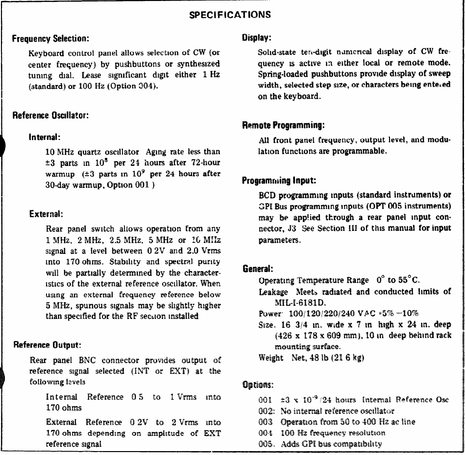
1-6. SPECIFICATIONS
1-7. Instrument specifications are listed in Table
l-l. These specifications are the performance
standards, or limits against which the instrument
may be tested. Table 1-2 lists supplemental charac-
teristics. Supplemental characteristics are not
specifications but are typical characteristics in-
cluded as additional information for the user
1-8. INSTRUMENTS COVERED BY MANUAL
1-9. This instrument has a two-part serial number.
The first four digits and the letter comprise the
serial number prefix. The last five digits form the
sequential suffix that is unique to each instrument.
The contents of this manual apply directly to
instruments having the serial prefix
number 1402A.
1-10. An Instrument manufactured after the print-
ing of this manual may have a serial prefix that is
different from that indicated above. If
so, refer to Section VII and make the
applicable man l changes.
1-4. Deleted. 1-11. Deleted.
1-1
TM 11-6625-2837-14&P
1-12. For information concerning a serial number
prefix not covered in this manual,
contact your nearest Hewlett-
Packard office
1-13. DESCRIPTION
1-14. The Model 8660B Synthesized Signal
Generator is a mainframe unit which requires two
plug-in sections to provide a usable RF output The
plug-ins required are an RF Section and a Modula-
tor (or Auxiliary) Section. These plug-m sections
are inserted into the front of the Model 8660
operating controls are on the front
1-15.
cy
Exten n Module (accessory num is
required when sections above 110 MHz are use
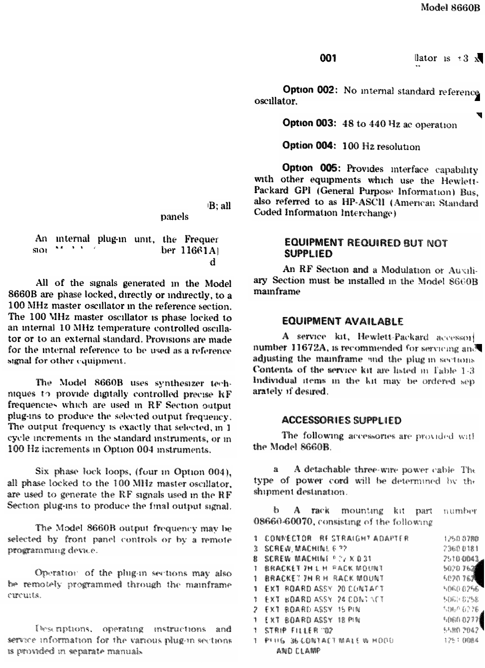
1-22. OPTIONS
1-23. Option : Reference osci
10-9/24 hours internal reference oscillator
1-24.
1-25.
1-26.
1-27.
1-28.
1-29.
1-16.
1-30.
1-31.
1-17.
1-32.
1-33.
1-18.
1-19.
1-20.
1-21.
1-2
Model 8660B
l-34. Deleted.
1-35. Deleted.
TM 11-6625-2837-14&P
1-38. ELECTRICAL PROTECTION
1-39. The safety classification of this instrument is
Safety Class I.
1-40. This apparatus has been designed and tested
according to international safety standards and is
1-36. TEST EQUlPMENT AND ACCESSORIES
1-37. Table 1-3 lists the test equipment and acces-
sories recommended to test, adjust and service the
supplied in safe condition. The Operating and Ser-
vice Manual contains information, warnings and
cautions which must be followed by the user to
ensure safe operation and to retain the instrument
Model 8660B. Refer to the MAC in the app- in safe condition.
endix for the required test equipment,
Table l-l Model 8660B Specifications
1-3


TM 11-6625-2837-14&P Model 8660B
Table 1-3. Test Equipment and Accessories List (2 of 2)
1-6
TM 11-6625-2837-14&P
SECTION II
INSTALLATION
INTRODUCTlON
2-2. This section provides information on in-
coming inspection, selecting the input line voltage,
operating environment, and information applicable
o bench and rack mounted operation of the Model
8660B.
2-3. INITIAL INSPECTION
2-4. Inspect the shipping container for damage. If
he shipping container or cushioning material is
damaged it should be kept until the contents of the
shipment have been checked mechanically and
electrically. The contents of the shipment are
shown in Figure 1-1, and the procedures for
checking electrical performance are given in
Section IV. If the contents are incomplete, if there
is mechanical damage o: defects, or if the instru-
ment does not pass the electrical performance test,
Refer to paragraph O-3. If the
shipping container is damaged or the cushioning
ing materials for the carrier’s inspection. The HP
material
shows signs of stress, notify the carrier as
as the Hewlett-Packard office. Keep the ship-
WARNING
office will arrange for repair or replacment without
waiting for claim settlements.
2-5. Deleted.
2-6. PREPARATION FOR USE
2-7.
2-8. The Model 8660B Synthesized Signal Genera-
tor requires a power source of 100, 120, 220 or
240 Vac +5%, -10%, 48 to 66 Hz single phase.
Power consumption is 345 VA maximum.
2-9. Line Voltage Selection
To prevent damage to the instrument
make the line voltage selection before
connecting the line power. Also ensure
the line power cord is connected to a line
power circuit that is provided th a
protective earth contact.
2-10. A rear panel line power module, (A7), per-
mits operation from 100, 120, 220 or 240 Vac.
The number visible in the window (located on the
module) indicates the nominal line voltage to
which the instrument must be connected.
2-11. To prepare the instrument for operation,
slide the fuse compartment cover to the left (the
line power cable must be disconnected). Pull the
handle marked FUSE PULL and remove the fuse;
rotate the handle to the left. Gently pull the
printed circuit voltage selector card from its slot
and orient it so that the desired operating voltage
appears on the top-left side (see Figure 2-1).
Firmly push the voltage selector card back into its
slot. Rotate the FUSE PULL handle to the right,
install a fuse of the correct rating, and slide the
fuse compartment cover to the right.
To avoid the possibility of injury or
death, the following precautions must be
followed before the instrument is
switched on:
a. Note that the protection provided by
grounding the instrument cabinet may be
lost if any power cable other than the
three-pronged type supplied is used to
couple the ac line voltage to the
instrument.
b. If this instrument is to be energized via
an autotransformer to reduce or increase
the line voltage, make sure that the
common terminal is connected to the
earthed pole of the power source.
c. The power cable plug shall only be
inserted into a socket outlet provided
with a protective earth contact. The pro-
tective action must not be negated by the
use of an extension cord without a protec-
CAUTION
2-1
2-1.

Model 8660B TM 11-6625-2837-14&P
Figure 2-2 Power Cable HP Part Numbers
2-19. Bench Operation
2-20 The instrument has plastic feet and a fold-
away tilt stand for convenience in bench operation
The tilt stand raises the front of the instrument for
r viewing of the control panel and the plastic
are shaped to make full width modular
ments self aligning when stacked
2-21. Rack Mounting
2-22 This Instrument IS supplied with a rack
mounting kit. This kit contains all the necessary
hardware and installation instructions for mount-
ing the Instrument in a rack with 19 inch spacing
(see Figure 2-3)
2-23. STORAGE AND SHIPMENT
2-24. Environment
2-25 The instrument should be stored in a clean.
dry environment The following environmental
limitations apply to both storage and shipment
Temperature -40°C to +75°C
< 95% relative
< 20,000 feet
Original Packaging.
Contamers and materials
tical to those used in factory packaging are
Figure 2-3. Preparation for Rack Mounting
available through Hewlett-Packard offices If the
instrument is being returned to Hewlett-Packard
for servicing, attach a tag indicating the type of
service required, return address, model number,
and full serial number Also, mark the container
FRAGILE to assure careful handling. In any
correspondence, refer to the Instrument by model
number and full serial number
2-28. Other Packaging. The following general in-
structions should be used for re-packaqng with
commercially available materials
aWrap the instrument in heavy paper or
plastic. (If shipping to a Hewlett-Packard office or
service center, attach a tag indicating the type of
service required. return address, model number,
and full serial number )
b.
Use a strong shipping container A double-
wall carton made of 350-pound test material is
adequate.
2-26.
2-27.
2-3/2-4
SECTION III
OPERATION
3-1. INTRODUCTION
3-2 This section provides operating instructions
for the Hewlett-Packard Model 8660B Synthesized
Signal Generator mainframe
3-3 The Model 8660B is designed to provide
precise digitally controlled signals for use in plug-m
sections which provide the selected output fre-
quency It will be necessary to have the operating
manuals for the plug-m sections being used in order
to efficiently operate the instrument
NOTE
If a modulation plug-m section is not used
it will be necessary to have an Auxiliary
Section in place of the modulation plug-m
TM 11-6625-2837-14&P
controls, except when an extern
When an external standard is
u
SELECTOR switch must be in EXT position
3-10. The 20-key keyboard may be use
3-4.
3-5.
3-6.
3-7.
WARNING
3-11.
3-8.
3-9.
3-1

Model 8660B
TM 11-6625-2837-14&P
Figure 3-1. Front and Rear Panel Controls, Indicators and Connectors (2 of 2)
3-2
TM 11-6625-2837-14&P
3-20.
3-21.
center frequency is shown in the AUTO or
SINGLE sweep modes. In the MAN sweep mode
the actual RF output frequency of the RF Section
will be displayed.
3-12. When the SWEEP MODE switch is placed in
the AUTO position the output signal of the RF’
Section is swept about the selected center fre-
quency by the sweep width register. (Example;
center frequency 50 MHz, sweep width 20 MHz,
the RF output is swept from 40 to 60 MHz.) The
sweep rate, selected by the RATE switch, is as
follows. FAST - 100 steps at 1 millisecond per
step, MED - 1000 steps at 1 millisecond per step,
and SLO - 1000 steps at 10 milliseconds per step.
3-13 When the SWEEP MODE switch is placed in
the SINGLE position, pressing the SINGLE push-
button causes the output of the RF Section to be
swept one time. When the single sweep is com-
pleted, the output of the RF Section returns to the
selected center frequency. The sweep width and
sweep rate are selected in the same manner as they
are in the AUTO mode.
3-14 When the SWEEP MODE switch is placed in
the MAN position the step rate of the output
frequency of the RF Section may be manually
controlled by the MANUAL SWEEP control. En
this mode the sweep width is still controlled by the
information m the sweep register. The selected
sweep width, in this mode, is divided by 1000 and
the output of the RF Section may be controlled in
frequency steps that are l/1000 of the sweep
width. (Example; center frequency 50 MHz, sweep
width 20 MHz, output may be stepped manually
from 40 to 60 MHz in 20 kHz steps.)
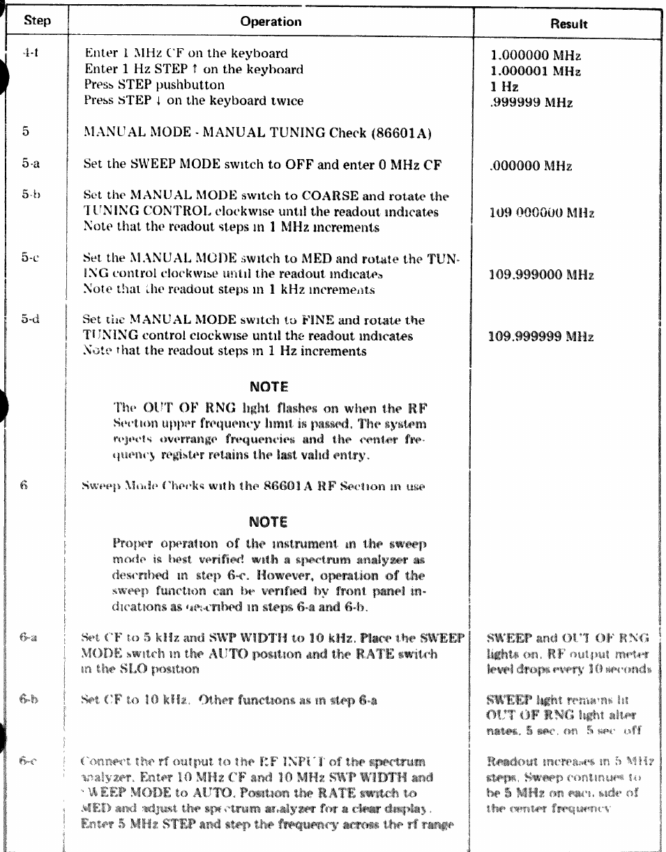
3-15. Step Mode. The center frequency may
stepped up, or down, in any increment wi
frequency range of the RF Section in u
increment selected, including units, must
tered in the keyboard before the STEP o
key is pressed. he step entered into the ste
register remains in the register until c
the instrument is placed in t
may be displayed on the re
STEP pushbutton.
(COARSE) These
by the TUNING
MODE switch is place
3-4
Model 8660B
3-17. Combined Mode. The sweep mode, st
mode and manual mode may all be used sim
taneously. This feature allows the user to quic
determine the frequency parameters of any devi
being tests.
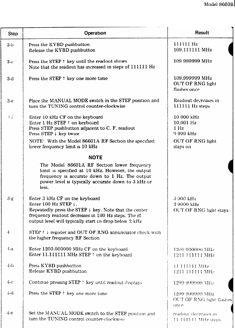
3-18. Operator’s Checks (Local Mode). Duri
final checkout at the factory the Model 8660
Synthesized Signal Generator mainframe is a
justed for proper operation. No adjustment shou
be required when the instrument is received T
operator’s checks listed in Table 3-1 are based c
the assumption that properly operating Mod
86601A (unless otherwise stipulated) RF Sectio
and Model 86632A AM-FM plug-in sections a:
used. Refer to the manuals for the specific plug-i)
for operating parameters.
3-19. The steps listed in Table 3-1 need not
followed in the sequence listed. Their purpose is
aid the operator in familiarizing himself with t
instrument, and to provide assurance that w
functions of the instrument are operating properl
NOTE
Numbers shown in the “Result” column
of Table 3-1 are those which should be
displayed on the CENTER FREQUENCY
readout.
3-22.
3-16.

TM 11-6625-2837-14&P
Table 3-1 Operator’s Checks (Local Operation) (2 of 4)
3-6
TM 11-6625-2837-14&P
Table 3-1
Operator’s Checks (Local Operation) (3 of 4)
3-7
TM 11-6625-2837-14&P
Model 8660B
Table 3-1.
Operator’s Checks (Local Operation) (4 of 4)
3-8
Model 8660B
TM 11-6625-2837-14&P
3-23. BCD Remote Operation
3-24. The information following, pertaining to
BCD programming, does not apply to GPI Bus
programming.
3-25. In the remote mode of operation the main-
frame STEP register and the Center Frequency
er are controlled by the programming device
p cannot be programmed). All front panel
ols (except power) are inhibited.
3-26. In remote operation two four-line parallel
codes are applied to the instrument circuits
through a rear panel connector. These
numeric data, are converted to 2 BCD
Although it is n ssary to program
frequency first, then modulation (If any),
then attenuation. This sequence mini-
mizes the time r
fear entering data
3-34.
3-35.
3-27.
3-36.
3-28.
3-37.
3-29. 3-38.
3-30.
3-31.
3-39.
3-40.
3-32.
3-33. Refer to Figure 3-2.
3-9
TM
TM 11-6625-2837-14&P
Model 8660B
Figure 3-2. Model 8660B Timing
3-41.
GPI
Bus Description
3-42. The GPI bus interface system uses seventeen
lines to effect the transfer of data between the
instruments connected to the bus. Eight of these
lines are used for the actual transfer of data, one
line is ground, and the remaining eight lines are
used for control.
3-43 Table 3-5 illustrates the GPI bus interface
line designations. The ground line, being self-
explanatory, is not shown.
3-44. The structure and operation of the bus is
analogous to an old-fashioned telephone party line,
and many of the conventions which apply to a
party line apply to the GPI bus as well. For
Instance, at any given time only one person may
talk on the party line, while many people may
listen, and most will not be using the party line at
all
3-45. Similiarly, on the GPI bus, only one instru-
ment may talk (send data) at any given time,
although many instruments may listen (receive
data), and most instruments will not interact with
the bus at all
3-46. instrument Addressing
3-47.
In order to determine which instruments are
to ‘talk”, which are to “listen”, and which are to
3-10
remain Inactive, some sort of a controll
required. This controller, which might be a c
lator,
by sending data over th
ments.
listen
listener until the “unl
assigns functions
Any instrument
address is placed
mitted. Talkers, on the other hand, stop function-
ing as talkers whenever another talk address is put
on the data lines. That prevents more than one
device from talking at any given time.
3-48. In order for the instrument to distinguish
between data and addresses, both of which are sent
over the eight data lines, an “address mode/data
mode” selector called the Multiple Response En-
able (MRE) line IS driven by the controller. When
this line is low, all instruments listen to the eight
data lines and interpret the information being
transmitted by the controller as addresses When
the MRE line IS high, information on the eight data
lines is interpreted as data and the instrum
talk, listed, or remain inactive as determ
during the time they were addressed during
MRE “low” period.
3-49. Three-Wire Handshake
3-50. Information, whether addresses, measure-
ment results, or other data, IS transferred on the
data lines under control of a technique called the

TM 11-6625-2837-14&P
Model 8660B
Table 3-3.
Model 8660B Programming Examples (2 of 4)
3-12
TM 11-6625-2837-14&P
Model 8660B
Table 3-3. Model 8660B Programming Examples (3 of 4)
3-13

Model 8660B TM 11-6625-2837-14&P
three-wire handshake. The handshake involves the
useof three control lines, and operates as follows:
A listener Indicates that it is ready to
accept data by letting the Ready for Data (RFD)
line go high. Listeners are connected to the RFD
line in a logical AND configuration so the RFD line
does not go high until all active listeners are ready
for data.
b. After RFD has gone high, the talker
indicates that it has placed a data byte on the eight
data lines by setting the Data Valid (DAV) line
low.
C.
After DAV has gone low, each listener
pulls RFD low, accepts the data, and then lets the
data accepted (DAC) line go high. Again, all
listeners are logically ANDed and DAC does not go
high until all listeners have accepted the data.
dAFter the DAC line has gone high, the
talker can let DAV go high again and take the data
off the lines When DAV goes high, the listeners set
DAC back to low and the sequence is ready to
repeat with Step 1.
3-51. As can be seen from the description, data
transfer is asynchronous, proceeding only as fast as
the slowest active (addressed to talk or listen)
device on the line.
NOTE
Figure 3-3 illustrates a flow chart of the
three-wire handshake operation.
3-52. The four remaining control lines operate as
follows:
a. The Remote Enable (REN) line
controller to put all instruments on the
Table 3-6. GPI Bus Interface Lines
3-15
TM 11-6625-2837-14&P
remote mode. When this line is low, all instruments
will go into remote as soon as they are addressed,
and remain in remote until the line goes high again.
b.
The End Output (EOP) line, when pulled
low by the system controller, will halt all activity
on the bus and cause all instruments to unaddress
themselves
c. The Service Request (SRQ) line allows
instruments to get the attention of the controller.
The Model 8660 does not use this line, so its
function will not be described here
d. The End Or Identify (EOI) line is used to
identify which instrument pulled the SRQ line low.
The Model 8660 does not use this line.
3-53. Modified Instrument Checks
3-54. When a standard Model 8660B is modified
to accept the GPI bus the instructions contained in
the modification kit must be followed to install the
two new circuit boards.
3-55. In addition to following the modification
instructions, special care should be taken to ob-
serve jumper positions on the GPI circuit boards.
3-56. Before installing the GPI circuit boards
check the address jumpers, and change address if
desired. It should be noted that if more than one
Model 8660B is used in a system, it is not likely
that operational parameters will be the same for
each, so different addresses will probably be
required for each instrument.
3-57. When used in a Model 8660B jumper J2
must not be installed.
3-58. Jumper J1 is installed as the operator’s
choice. With it in place the internally generated
BUSY signal is used to delay the RFD response.
Without it the operator must make allowances in
programming for the necessary settling time delays
of the Model 8660B.
3-60. The information co
this manual applies only t
005 instruments
3-16
Model 8660B
3-61. Local control operation of OPT 005 instru-
ments is the same as that described for the ModeI
8660B in other parts of this section.
3-62. Basically, the Model 8660B OPT 005 instru-
ments are the same as the standard Model 8660
instruments except that the capability of remote
operation using the GPI bus is added. Basic
information about GPI is included in the General
Information Section of this manual.
3-63. Remote Control
3-64. OPT 005 allows remote programming via the
GPI bus, of all 8660B front panel controls except
LINE, (POWER), SWEEP MODE, and MANUAL
MODE. All front panel controls except LINE and
FM CAL are locked out when the Model 8660B is
in remote.
3-65. The Model 8660B GPI interface will recog-
nize an internally preset “listen” address and
accept bit-parallel, word serial GPI information.
When addressed to listed, the Model 8660B shifts
incoming data into a temporary storage register.
This data must be presented to the interface leas
significant digit first to satisfy the internal log’
requirements of the Model 8660B. When a pro-
gramming code is detected in the input data, the
contents of the temporary storage register are
shifted into the register selected by the internal
address character. The temporary register is then
cleared to make way for more data.
3-66. Programming Conventions
3-67. There are several conventions which must be
observed when remotely controlling the Model
8660B. Besides providing data least significant digit
first, these conventions include:
3-59.

TM 11-6625-2837-14&P
3-68 One last convention is that after the Model
8660B is placed in remote, the first output of the
GPI bus should be a false address which serves
Model 8660B
to clean the temporary storage register. This
accomplished by first addressing the Model
to listen then placing “/” on the GPI bus.
Table 3-7 General GPI Bus Code Allocations
3-18

Model 8660B TM 11-6625-2837-14&P
SECTION IV
PERFORMANCE TESTS
4-1. INTRODUCTION
4-2. The procedures in this section test the instru-
ments electrical performance using the speci-
fications of Table 1-1 as the performance stand-
ards. A simpler operations test is included in
Section III under Operator’s Checks.
WARNING
4-3. EQUIPMENT REQUIRED
4-4. Equipment required for the performance tests
is listed in the Recommended Test Equipment
table in Section I. Any equipment that satisfies the
critical specifications given in the table may be
substituted for the recommended model(s).
4-5. TEST RECORD
4-6 Results of the performance tests may be
tabulated on the Test Record at the end of the
procedures. The Test Record lists all of the tested
specifications and their acceptable limits. Test
results recorded at incoming inspection can be used
for comparison in periodic maintenance and
troubleshooting and after repairs or adjustments.
Performance test 4-7 requires removal of
the top instrument cover This exposes
the input line voltage and the dc voltage
outputs of the power supply. Care should
be exercised to avoid physical contact
with these voltage points. In addition, the
power source should be disconnected
during cover removal. All required tests
must be performed only by qualified
service personnel.
PERFORMANCE TESTS
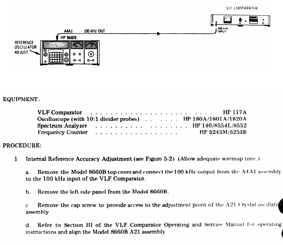
4-7. INTERNAL CRYSTAL OSCILLATOR AGING RATE
SPECIFICATION
Reference Oscillator internal: 10 MHz quartz oscillator. Aging rate less than ±3 parts in 108 per 24 hours
after 72 hour warmup. (±3 parts in 109 per 24 hours after 30 day warmup, Option 001.)
DESCRIPTION
This test verifies the reference oscillator aging rate by comparing it to the National Bureau of Standards
signal from WWVB.
Figure 4-1. Crystal Oscillator Aging Rate Test Setup
4-1
TM 11-6625-2837-14&P
PERFORMANCE TESTS
4-7. INTERNAL CRYSTAL OSCILLATOR AGING RATE (Cont’d)
TEST EQUIPMENT:
VLF Comparator . . . . . . . . . . . . . . . . . . . . . . . . . . HP 117A
PROCEDURE:
1.
Remove the Model 8660B top cover after the instrument has been connected to the ac line for 72
hours
2. Connect a cable from the 100 kHz output of the A4A1 reference es asse
Comparator 100 kHz input.
3. Refer to Section III of the VLF Comparator O
operating instructions.
4.
Aging rate is checked by noting the average offset
hours apart and dividing the offset difference by
offset is then converted to aging rate per day.
Example :
4-8. INPUT SENSITIVITY FOR EXTERNAL REFERENCE
4-2
Model 8660B
PERFORMANCE TESTS
TM 11-6625-2837-14&P
4-8. INPUT SENSITIVITY FOR EXTERNAL REFERENCE (Cont’d)
Figure 4-2.
Input Reference Sensitivity Test
TEST EQUIPMENT
Frequency Counter . . . . . . . . . . . . . . . HP 5245M
RMS Voltmeter . . . . . . . . . . . . . .HP 411A
Synthesizer . . . . . . . . . . . . . . . . . . . . . HP 3320B
PROCEDURE
1.
Connect the Synthesizer to the Model 8660B REFERENCE INPUT (J1) and set the SELECTOR
switch S1 to EXT
2
Set the Model 3320B Synthesizer controls to provide an output of 1 MHz at 0 2 Vrms as indicated
on the RMS voltmeter..
3
Connect the Frequency Counter to the output of the RF Section in use and enter a 5 MHz center
frequency The Counter readout should be about 5 MHz. (Actual frequency will be
stability and settability of the Synthesizer used)
4.
Readjust the Model 3320B Synthesizer output to 2 Vrms The counter readout should remain at
about 5 MHZ.
5
Repeat steps 2 through
4
with the Model
3Synthesizer set to 2, 25, 5 and 10 MHz.
4-3
TM 11-6625-2837-14&P
PERFORMANCE TESTS
4-9. REFERENCE OUTPUT
SPECIFICATION:
About 1 Vrms in internal. When an external reference is used the output refe
mately the same as the input from the external reference.
DESCRIPTION:
This test verifies proper operation of the reference amplifier an
Figure 4-3. Reference Output Test Setup
4-4


TM 11-6625-2837-14&P Model 8660B
PERFORMANCE TESTS
4-10. SWEEP OUTPUT (Cont’d)
2. Set the oscilloscope vertical sensitivity to 2V/Div and the sweep speed to 20 mSec/Div.
3. Enter a center frequency of 5 MHz in the Model 8660B keyboard, set SWEEP MODE to AUTO
and SWEEP MODE RATE switch to FAST.
4. The oscilloscope should display a sweep ramp from 0 to +8V in 100 milliseconds
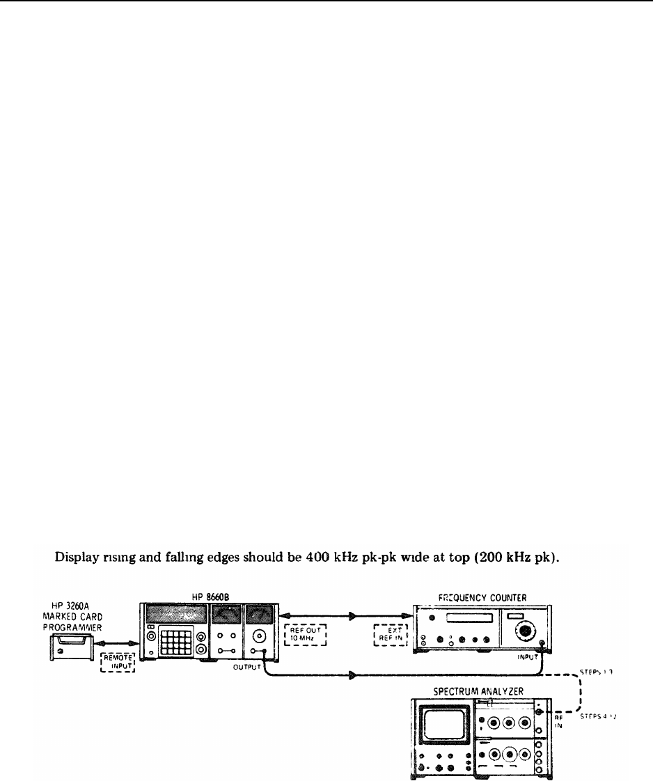
4-11. REMOTE PROGRAMMING
SPECIFICATIONS:
Specifications applying to operational tests in LOCAL mode also apply to operational tests performed by
remote programming (GPI Bus or BCD).
DESCRIPTION:
All front panel frequency, output level, and modulation functions are programmable and can be tested
using an HP 3260A Marked Card Programmer.
The standard remote cable for the 3260A is used with the GPI Bus Programming (Option 005). The 3260A
Option 001 cable is used for standard BCD programming.
TEST EQUIPMENT:
Frequency Counter ............... HP 5340A
Spectrum Analyzer ............... HP 140T/8555/8552
Marked Card Programmer ............HP 3260A Opt 001
PROCEDURE:
Center Frequency Test
1.
Connect Synthesizer 10 MHz Reference output to Frequency Counter external reference input.
2. Program RF Section for 0 dB attenuation and connect RF output to Frequency Counter input
(Figure 4-5).
3. Program mainframe for center frequency within RF Section frequency limits
should display frequency reading of ± digit of pro ammed frequency
4-6
Model 8660B TM 11-6625-2837-14&P
PERFORMANCE TESTS
4-11. REMOTE PROGRAMMING (Cont’d)
Attenuation Test
4. Disconnect Frequency Counter from RF Section and connect RF Section output to Spectrum
Analyzer input.
5
Program mainframe for center frequency of 100 MHz.
6
Program RF Section for 0 dB attenuation. RF Section should be at maximum power output.
AM Modulation Test
7. Program mainframe for center frequency of 50 MHz and RF Section for 0 dB attenuation.
8
Program in AM, 1 kHz Source, and 50% Modulation. Depth of sidebands should be 12 dB + 0.5 dB
from carrier
9. Program in AM, Source, and 25% Modulation. Depth of sidebands should be 15.6 dB+ 0.5 dB from
carrier.
FM Modulation Test
10
11
12
Program mainframe for center frequency of 100 MHz and RF Section for 0 dB attenuation.
Program in 1 kHz, FM Source, and 200 kHz pk deviation.
Set Spectrum Analyzer controls for.
Center Frequency: 100 MHz
Bandwidth: 300 kHz
Scan Width 0.2 MHz/div
Scan Time 50 msec
Figure 4-5. Typical Remote Programming Test Setup
4-7
TM 11-6625-2837-14&P Model 8660B
Table 4-1. Performance Test Record
Tests performed by
Serial No. Date
4-7. Reference Oscillator Internal; aging rate
Specified: ±3 parts in 108 per day
after a 72 hour warmup period Actual
Option 100 Specified: +3 parts in 109 per day
after a 30 day warmup period. Actual
4-8. Input Sensitivity for External Reference
NOTE
Frequency will be determined by the stability and
settability of the reference source used.
4-9. Reference Output Levels
Ref in Ref out ef in ef out
1 MHz 0.2 Vrms ---------- vrms 1 MHz 1.0 vrms
2 MHz 0.2 Vrms vrms 1.0 vrms
2.5 MHz 0.2 Vrms vrms 2.5 MHz vrms
5 MHz 0.2 Vrms vrms
10 MHz 0.2 Vrms vrms 10 MHZ
4-10. Sweep Output Ramp
V to +
4-11. Remote Programming
4-8
Model 8660B TM 11-6625-2837-14&P
SECTION V
ADJUSTMENTS
5-1. INTRODUCTION
5-2. This section describes adjustments and checks
required to return the Model 8660B to peak
operating capability when repairs have been made.
Included in this section are test setups and pro-
cedures
5-3 Except for the power supply adjustment
procedures, which should be performed before
repairs are made to any part of the instrument, the
adjustment procedures are arranged in the same
sequence as the service sheets to which they refer
5-4. EQUIPMENT REQUIRED
5-5. Each adjustment procedure in this section
contains a list of test equipment and accessories
required to perform the procedure. Each test setup
identifies test equipment and accessories by call-
5-6. Minimum specifications for test equipment
outs.
used in the adjustment procedures are detailed in
Table 1-3. Because the Model 8660B is an ex-
tremely accurate instrument, minimum specifica-
tions in Table 1-3 are particularly important in
performing these adjustment procedures.
5-7. ADJUSTMENT AIDS
5-8. The HP 11672A Service Kit is an accessory
item available from Hewlett-Packard for use in
maintaining the Model 8660B Synthesized Signal
Generator. Table 1-3 contains a detailed descrip-
tion of the Service Kit. Any item in the kit may be
ordered separately -
5-9 FACTORY SELECTED COMPONENTS
5-10. Some component values are selected at the
f final checkout at the factory. Usually these
are not extremely critical; they are selected
vide optimum compatibility with associated 5-18.
5-19.
5-11.
Factory selected components and su
range of values are listed in Table 5-1.
5-12. The recommended procedure for replacing a
factory selected component is as follows:
a. Try the original value, then perform the
test specified in Section V of this manual for the
circuit being repaired.
b. If the specified test cannot be satisfactor-
i1y performed, try the typical value shown in the
parts list and repeat the test
C.
If the test results are still not satisfactory,
substitute various values within the tolerances
specified in Table 5-l until the desired result is
achieved.
5-13. RELATED ADJUSTMENTS
5-14. Most of the adjustments within any given
phase lock loop are interrelated. This is especially
true in dig&&to-analog converters. Adjustments
should be made in the order in which they appear
for any given loop.
5-15. Generally, it will not be necessary to adjust
any of the phase lock loops except the one in
which the component failure occupied. An excep-
tion to this will be when adjustment to any phase
lock loop has been attempted while the reference
section is not functioning properly.
5-16. ADJUSTMENT LOCATIONS
5-17. Adjustment locations are identified pictor-
ially on Section VIII foldout service sheets referred
to in the individual procedures.
recorded in spaces provided.
used as reference in
5-1

Model 8660B TM 11-6625-2837-14&P
5-23. Capacitors inside the instrument may still be
charged even if the instrument has been discon-
nected from its source of supply.
inoperative and be secured against any
unintended operation.
NOTE
5-24. Make sure that only fuses with the required
ted current and of the specified type (normal
low, time delay, etc.) are used for replacement.
The use of repaired fuses and the short-circuiting
of fuseholders must be avoided.
5-25. Whenever it is likely that the protection
has been impaired, the instrument must be made
When repairs or adjustments to the instru-
ment are required, such work should not
be performed, even by a skilled techni-
cian, unless another person is in the same
general area. This is not to be interpreted
to mean that two persons are required to
perform the necessary work, but only that
another person should be available, should
the need for assistance arise
ADJUSTMENTS
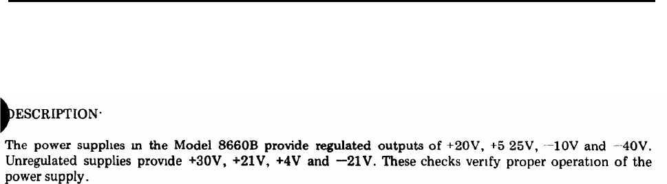
5-26. POWER SUPPLY
REFERENCE
Service Sheet 41
5-3


TM 11-6625-2837-14&P
ADJUSTMENTS
Model 8660B
5-27.
REFERENCE SECTION
REFERENCE.
Service Sheets 2 and 3.
DESCRIPTION:
The reference section contains a voltage controlled master oscillator from which all RF signals generated in
the Model 8660B mainframe are derived. The master oscillator is phase locked to an internal temperature
controlled crystal oscillator or to an external standard. The reference section provides outputs of 500 MHz,
100 MHz, 20 MHz, 10 MHz, 2 MHz, 400 kHz and 100 kHz. These checks verify proper operation of the
circuits within the reference section.
Figure 5-2. Reference Accuracy Adjustment Test Setup
5-6
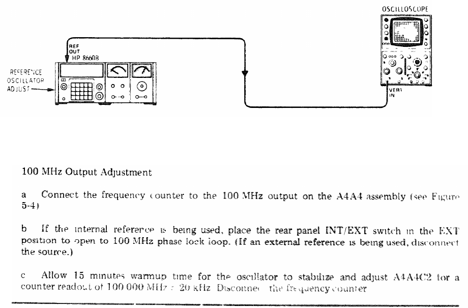
TM 11-6625-2837-14&P
ADJUSTMENTS
5-27. REFERENCE SECTION (Cont’d)
NOTE
If the VLF Comparator is not available, and an accurate signal source is, the
reference oscillator may be adjusted by using an oscilloscope for comparison of
the two signals
2.
Alternate Reference Accuracy Adjustment (see Figure 5-3)
a.
Use the signal source to trigger the oscilloscope at the SYNC INPUT and connect the
reference output from the Model 8660B rear panel reference output to the oscilloscope vertical
input.
b
Observe the 10 MHz sine wave on the oscilloscope and adjust the A21 oscillator until the
oscilloscope display stops drifting.
C
Set the oscilloscope to sweep at 0.1 uSec/Dvision and the sweep magnifier to X10. If drift is
observed readjust the A21 oscillator.
NOTE
When the oscilloscope display drift is less than 1 division inn 10 seconds the
Model 8660 reference oscillator is set within 1 part in 109 of the signal source
Figure 5-3. Alternate Reference Accuracy Adjustment Test Setup
5-7

Model 8660B TM 11-6625-2837-14&P
ADJUSTMENTS
5-27.
REFERENCE SECTION (Cont’d)
5.
20 MHz Output Check
a. Connect the Spectrum Analyzer RF INPUT to the 20 MHz output on the A4A4 assembly and
tune the analyzer to 20 MHz The 20 MHz signal should be >-6 dBm and <-2 dBm. Disconnect
the analyzer
20 MHz dBm
6
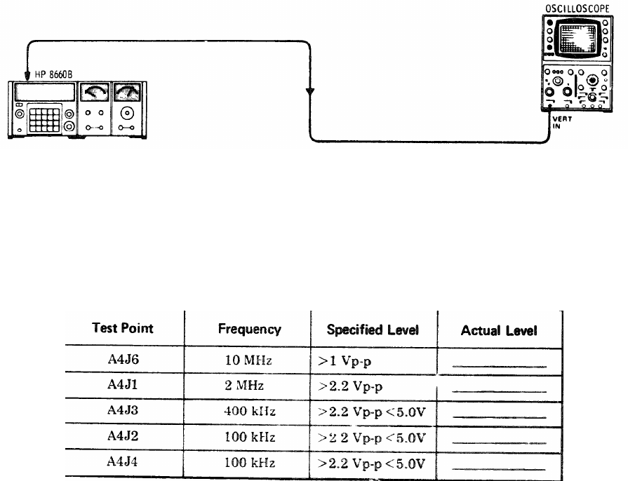
Reference Section Outputs Not Previously Checked
a.
Check the outputs listed in Table 5-3 for the levels shown (see Figure 5-6).
Figure 5-6.
Oscilloscope Level Checks Test Setup
Table 5-4. Reference Section Output Levels
5-9

Model 8660B TM 11-6625-2837-14&P
ADJUSTMENTS
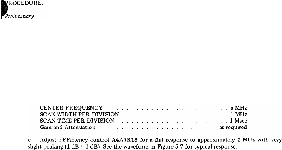
5-28. HIGH FREQUENCY SECTION (Cont’d)
Remove the cover from the A4A7 phase detector assembly. Tighten the screws holding the A4A5 voltage
controlled oscillator assembly cover.
1.
2.
3.
Phase Detector Response Adjustments (see Figure 5-7)
a.
Disconnect the coaxial cable from VCO INPUT A4J11. Connect the PULSE OUTPUT of the
Pulse Generator to A4J11. Set the Pulse Generator for 100 kHz pulse rate, 035 uSec pulse width,
0 5 volt amplitude and + polarity
b
Connect the Spectrum Analyzer RF INPUT to the phase error signal at A4TP1. Set the
analyzer controls as follows:
d. Disconnect the Pulse Generator and the Spectrum Analyzer.
Balance Adjustment
a.
Connect the digital voltmeter to A4TPl
b. Adjust the Balance control (A4A7R22) for a reading of 0 volts ± .05 volt. Disconnect the
digital voltmeter.
Voltage Controlled Oscillator Adjustment (see Figure 5-8)
a.
Remove the A4A6 cover. With the output cable of the A4A5 assembly disconnected from the
VCO OUTPUT (A4J10), connect the Digital Voltmeter to the A4A6 FREQuency control output
(white lead).
b.
Adjust the A4A6 “0” control (A4A6R13) for a Digital Voltmeter reading of -34 volts
(voltage should be adjustable from about -33 to -35 volts)
C.
Connect the Frequency Counter to the A4A5 voltage controlled oscillator output, A4JP2
Replace the A4A6 assembly cover.
5-11


TM 11-6625-2837-14&P
ADJUSTMENTS
5-29. N1 PHASE LOCK LOOP (Cont’d)
(see Figure 5-12)
5-17


Model 8660B TM 11-6625-2837-14&P
ADJUSTMENTS
5-32. SUMMING LOOP 2 (SL2) (Cont’d)
7.
Disconnect the counter, remove the ground from A2TP8 and connect the oscilloscope to A2TP7.
8.
Set center frequencies as shown in Table 5-9 and adjust the associated potentiometers for 50/50
symmetry as seen on the oscilloscope (all must be within 40/60)
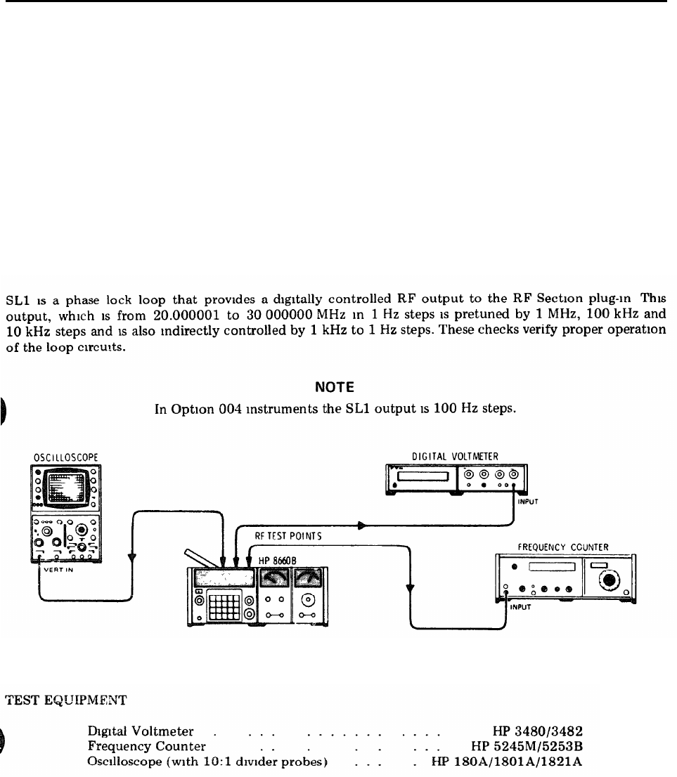
5-33. SUMMING LOOP 1 (SL1)
REFERENCE
Service Sheets 15, 16 and 17
DESCRIPTION
Figure 5-16. SL1 Test Setup
5-25
TM 11-6625-2837-14&P Model 8660B
ADJUSTMENTS
5-33. SUMMING LOOP 1 (SL1) (Cont’d)
PROCEDURE. (see Figure 5-16)
1.
Set center frequency to 5.55 MHz.
a. With the digital voltmeter connected to A2TP14, adjust A19R3 or A19R9 to 0.00 volt ±
10 millivolts.
b
With the oscilloscope connected to A2TP13, adjust A15R14 for 50/50 symmetry.
C.
Disconnect the digital voltmeter and the oscilloscope.
2.
Connect the digital voltmeter to varactor test point A2TP21, ground mother board test point
A2TP14 with the jumper provided, and set center frequency to 0.
a.
Adjust A19R3 or A19R9 to -30 volts and disconnect the digital voltmeter.
b. Connect the counter to SL1 OSC at XA19-1-2 and adjust A19C18 for a counter readout as
close as possible to 30 MHz (must be within ±300 kHz).
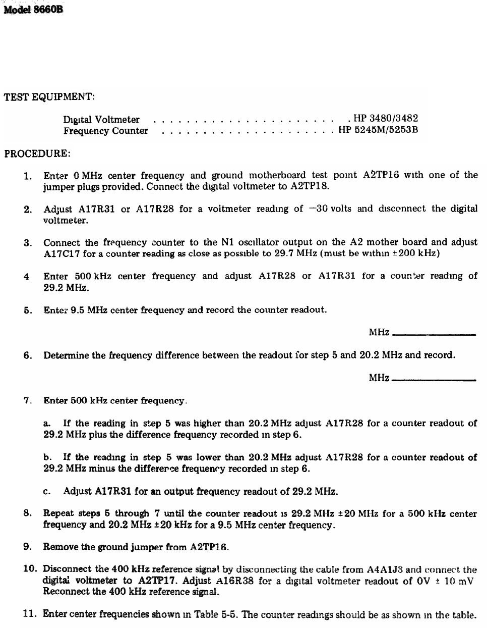
3. Set center frequency to 450 kHz Adjust A19R3 or A19R9 for a counter reading of 29.550 MHz.
4. Set center frequency to 9.45 MHz. Record frequency of output at SL1 OSC at XA19-1-2.
MHz
5.
Determine the difference frequency between that recorded in step 4 and 20.550 MHz and record:
MHz
a.
Set center frequency to 450 kHz.
b
If the frequency readout in step 4 was higher than 20.550 MHz adjust A19R3 to 29.550 MHz
plus the difference frequency recorded in step 5.
C.
If the frequency readout in step 4 was lower than 20.550 MHZ adlust A19R3 to 29.550 MHz
minus the difference recorded in step 5.
d. Reset the frequency to 29.550 MHz with A19R9.
e.
Repeat steps 3 through 5 until the counter indicates 20.550 MHz ± 20 kHz for a center
frequency of 9.45 MHz and 29.550 MHz ± 20 kHz for a center frequency setting of 450 k
6. Set center frequency as shown in Table 5-9. Adjust controls for counter readouts shown
7. Disconnect the counter, remove the ound from A2T and connect e oscilloscope to
A2TP13.
8. Set center frequencies as shown in Tab be metry as
seen on the oscilloscope. Disconnect
(
n 40/60
symmetry.)
5-26
Model 8660B TM 11-6625-2837-14&P
ADJUSTMENTS
5-33. SUMMING LOOP 1 (SL1) (Cont’d)
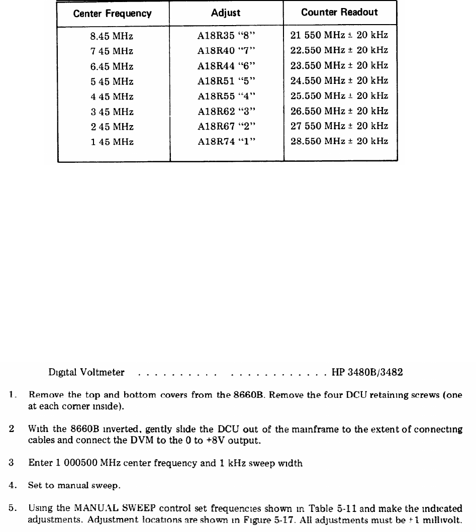
Table 5-10 SL1 Oscillator Output Frequency Adjustments
5-34. DCU SWEEP OUTPUT
REFERENCE.
Service Sheet
DESCRIPTION
The Model 8660B sweep output may be used to drive the horizontal sweep of an oscilloscope while the RF
output is used to determine the characteristics of a device being tested This procedure provides
information required to properly adjust the sweep ramp.
TEST EQUIPMENT
5-27

TM 11-6625-2837-14&P
SECTION VI
REPLACEABLE PARTS
6-1. INTRODUCTION
6-2. This section contains information for ordering
parts. Table 6-2 lists abbreviations used in the parts
list and throughout the manual. Table 6-3 lists all
replaceable parts in reference designator order.
table 6-4 contains the names and addresses that
correspond to the manufacturer’s code numbers.
table 6-5 cross references HP part num-
bers to National Stock Numbers.
6-3. EXCHANGE ASSEMBLIES
6-4. Table 6-1 lists assemblies within the instru-
ment that may be replaced on an exchange basis,
us affording a considerable cost saving. Ex-
ange, factory-repaired and tested assemblies are
available only on a trade-in basis; therefore, the
fective assemblies must be returned for credit.
for this reason, assemblies required for spare parts
stock must be ordered by the new assembly part
number.
6-5. ABBREVIATIONS
6-6. Table 6-2 lists abbreviations used in the parts
t, schematics and throughout the manual. In
me cases, two forms of the abbreviation are used,
the all in capital letters, and one partial or no
pitals. This occurs because the abbreviations in
the parts list are always all capitals. However, in
the schematics and other parts of the manual,
other abbreviation forms are used with both lower
se and upper case letters.
6-7. REPLACEABLE PA
6-8. Table 6-3 is the list of replaceable parts and is
anized as follows.
a.
Electrical assemblies and their com-
ponents in alpha-numerical order by reference
signation.
b. ounted parts in a a-nu
der by designation.
c. iscellaneous parts.
6-9. The information given for each part consists
of the following:
a. The Hewlett-Packard part number.
b. The total quantity (Qty) in the
instrument.
C.
The description of the part.
d. A typical manufacturer of the part in a
five-digit code.
e. The manufacturer’s number for the part.
6-10. The total quantity for each part is given only
once - at the first appearance of the part number in
the list.
NOTE
Total quantities for optional assemblies
are totaled by assembly and not inte-
grated into the standard list.
6-11. ORDERING INFORMATION
6-12. To order a part listed in the replaceable parts
table, note the Hewlett-Packard part number
and then cross-reference that part nuder
to the National Stock Number in table 6-5.
Then order through normal ordering channels.
6-13. If the part number does not have a
r, then order the part
hannels using the
6-14.
6-15.
6-1
TM 11-6625-2837-14&P Model 8660B
based on failure reports and repair data, and parts
support for one year. A complimentary “Recom-
mended Spares” list for this Instrument may be
obtained on request and the “Spare Parts Kit” may
be ordered through your nearest Hewlett-Packard
office.
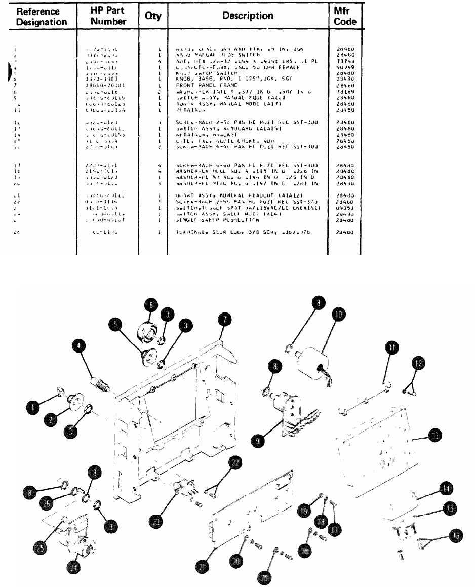
6-16. ILLUSTRATED PARTS BREAKDOWNS
6-17. Illustrated Parts Breakdowns for the
Cabinet Parts (Figure 6-l) and the DCU Front
Panel Details (Figure 6-2) are provided in this
section.
Table 6-1.
Part Numbers for Assembly Exchange Orders
New Part No.
08660-60107
08660-60176
08660-60105
08660-60182
08660-60103
08660-60104
08660-60151
08660-60180
08660-60110
08660-60128
08660-60111
08660-60123
Option 004 Instruments
08660-60162
08660-60161
08660-60163
6-2

TM 11-6625-2837-14&P
Figure 6-1. Cabinet Parts (2 of 2)
6-4

TM 11-6625-2837-14&P
Model 8660B
Table 6-2. Reference Designations and Abbreviations (2 of 2)
6-6
Model 8660B TM 11-6625-2837-14&P
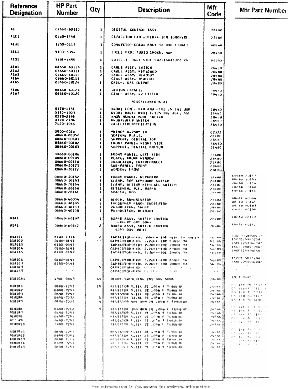
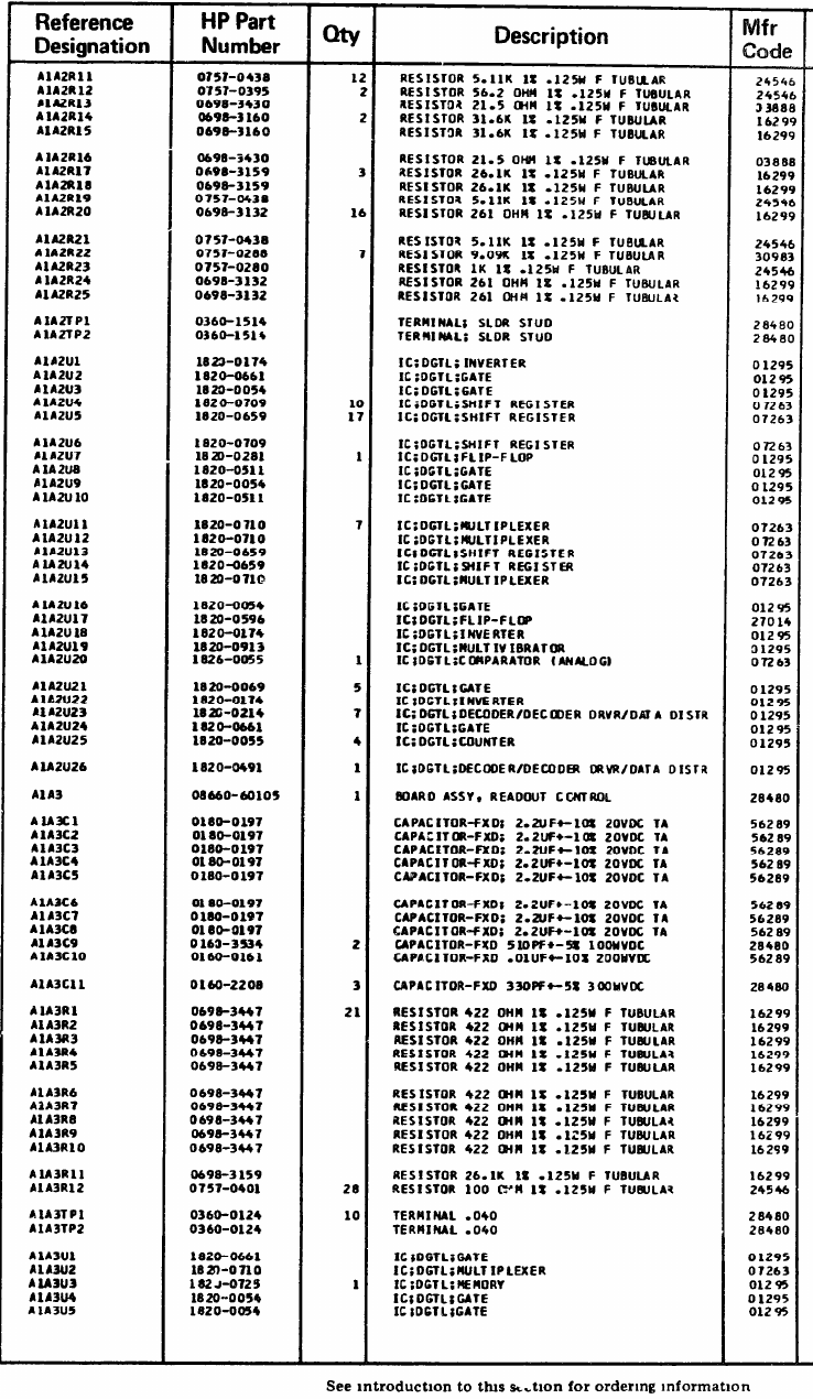
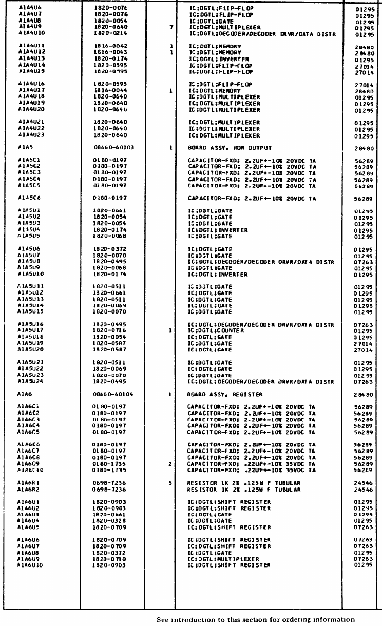
Table 6-3. Replaceable Parts
Mfr Part Number
0370-1131
0370-2193
2x 28200
31-2221-1022
0970-2194
0370-1303
08660-20101
1920-02
06660-60115
08660-60123
08660-20154
0520-0129
08660-60113
08660-20153
9100-3354
2200-0105
2200-0141
2190-0019
8050-0023
3050-0016
08660-60111
0520-0174
7101-J1CX
08660-60114
08660-40107
0860-1190
Figure 6-2. DCU Front Panel Details
6-7
TM 11-6625-2837-14&P
Table 6-3. Replaceable Parts
08660-60110
0160-3448
31-2221-1022
9100-3 x 4
71C1-J1CX
08660-60116
08660-60117
08660-60118
08660-60118
08660-60124
08660-60126
08660-60129
0370-1131
0370-1303
0370-7193
0370-2194
7120-3044
MR 8010
08660-00066
08660-00101
08660-000102
08660-00108
08660-00108
08660-00109
08660-00110
08660-20121
08660-20122
6-8
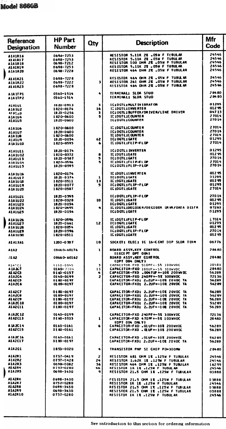
Table 6-3. Replaceable Parts
TM 11-6625-2837-14&P
Mfr Part Number
C3-1/8-TO-5111-G
C3-l/8-TO-5111-G
C3-l/8-TO-100R-G
C3-1/8-TO-5111-G
C3-1/8-TO-464R-G
C3-1/8-TO-464R-G
C3-1/8-TO-261R-G
C3-1/8-TO-464R-G
0360-1514
0360-1514
SN741122N
SN7404N
MC858P
DM74L90N
DM74L90R
DM74L90N
DM74L90N
DM74L90N
SN7400N
DM74L73N
SN7404N
SN74H11N
DM74L10N
DM74L74N
DM74L73N
SN7404N
SN74121N
SN7408N
SN7474N
DM74L10N
DM74L73N
SN7402N
SN7400N
9311DC
SN7400N
DM74L74N
SN7432N
SN7400N
DM74L74N
SN7408N
ICN-163-53W
C8660-60176
08660-60167
0160-0945
0160-2204
292P47292
DM15F241J0300WV1CR
150D225X9020A2
150D225X9020A2
150D225X9020A2
150D225X9020A2
150D225X9020A2
150D225X9020A2
150D225X9020A2
DM15F241J0300WV1CR
016C-3533
292P10392
292P10392
292P10392
150D225X9020A2
1853-0020
C4-1/8-TO-681R-F
C4-1/8-TO-1621-F
C4-1/8-TO-4640-F
C4-1/8-TO-1001-F
PME55-1/8-TO-21R5-F
PME55-1/8-TO-21R5-F
C4-1/8-TO-1001-F
PME55-1/8-TO-2lR5-F
PME55-1/8-TO-21R5-F
C4-1/8-TO-1001-F
6-9
TM 11-6625-2837-14&P
Table 6-3. Replaceable Parts
Model 8660B
Mfr Part Number
C4-1/8-TO-5111-F
C4-1/8-TO-56R2-F
PME55-1/8-TO-21R5-F
C4-1/8-TO-3162-F
C4-1/8-TO-3162-F
PME55-1/8-TO-21R5-F
C4-1/8-TO-2612-F
C4-1/8-TO-2612-F
C4-1/8-TO-5111-F
C4-1/8-TO-2610-F
C4-1/8-TO-5111-F
MF4C1/8-TO-9091-F
C4-1/8-TO-1001-F
C4-1/8-TO-2610-F
C4-1/8-TO-2610-F
0360-1514
0360-1514
SN7404N
SN7432N
SN7400N
93L28DC
93L00DC
93L28DC
SN74107N
SN7408N
SN7400N
SN7408N
93L22DC
93L22DC
93L00DC
93L00DC
93L22DC
SN7400N
DM74174N
SN7404N
SN74L122N
711DC
SN7420N
SN7404N
SN7442N
SN7432N
SN7490N
SN74145N
08660-60105
150D225X9020A2
150D225X9020A2
150D225X9020A2
150D225X9020A2
150D225X9020A2
150D225X9020A2
150D225X9020A2
150D225X9020A2
0160-3534
292P10392
0160-2208
C4-l/8-TO-422R-F
CS-l/8-TO-422R-F
C4-l/8-TO-422R-F
C4-1/8-TO-422R-F
C4-l/8-TO-422R-F
C4-1/8-TO-422R-F
C4-l/8-TO-422R-F
C4-l/8-TO-422R-F
C4-l/8-TO-422R-F
C4-l/8-TO422R-F
C4-l/8-TO-2612-F
C4-l/8-TO-101-F
0360-0124
0360-0124
SN7432N
93L22DC
SN74170J
SN7400N
SN7400N
6-10
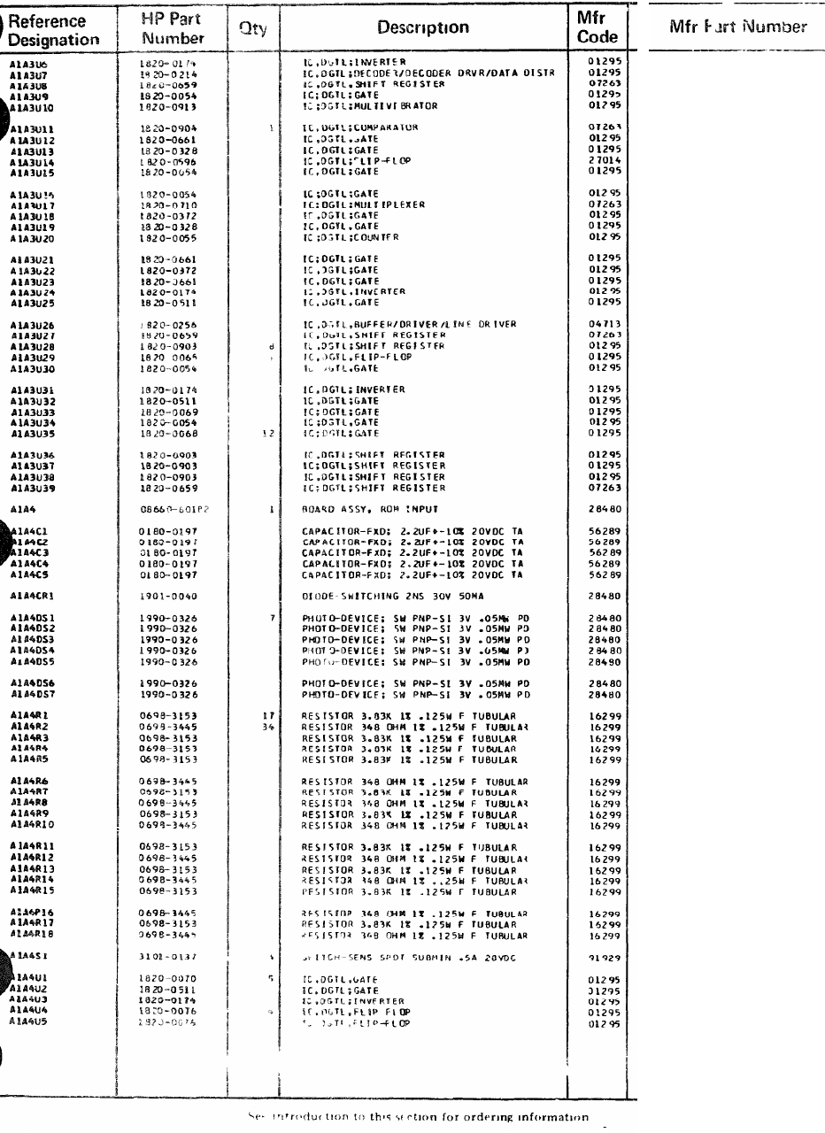
Table 6-3. Replaceable Parts
TM 11-6625-2837-14&P
SN7404N
SN7442N
93L00DC
SN7400N
SN74L122N
93L24DC
SN7432N
SN7402N
DM74L74N
SN7400N
SN7400N
93L22DC
SN74H11N
SN7402N
SN7490N
SN7432N
SN74H11N
SN7432N
SN7404N
SN7408N
HC858P
93L00DC
SN74L164N
SN7470N
SN7400N
SN7404N
SN7408N
SN7420N
SN7400N
SN7410N
SN74L164N
SN74L164N
SN74L164N
93L00DC
08660-60182
150D225X9020A2
150D225X9020A2
150D225X9020A2
150D225X9020A2
150D225X9020A2
1901-0040
1990-0326
1990-0326
1990-0326
1990-0326
1990-0326
1990-0326
1990-0326
C4-1/8-TO-3831-F
C4-1/8-TO-348R-F
C4-1/8-TO-3831-F
C4-1/8-TO-3831-F
C4-1/8-TO-3831-F
C4-1/8-TO-348R-F
C4-1/8-TO-3831-F
C4-1/8-TO-348R-F
C4-1/8-TO-3831-F
C4-1/8-TO-348R-F
C4-1/8-TO-3831-F
C4-1/8-TO-348R-F
C4-1/8-TO-3831-F
C4-1/8-TO-348R-F
C4-1/8-TO-3831-F
C4-1/8-TO-348R-F
C4-1/8-TO-3831-F
C4-1/8-TO-348R-F
1SX1-T
SN7430N
SN7408N
SN7404N
SN7476N
SN7476N
6-11
TM 11-6625-2837-14&P
Table 6-3. Replaceable Parts
Model 8660B
Reference
Designation
HP Part
Number Description
Mfr
Code Mfr Part Number
SN7476N
SN7476N
SN7400N
SN74150N
SN7442N
1816-0042
1816-0043
SN7404N
DM74L73N
DM74L73N
DM74L73N
1816-0044
SN74150N
SN74150N
SN74150N
SN74150N
SN74150R
SN74150N
08660-60103
150D225X9020A2
150D225X9020A2
150D225X9020A2
150D225X9020A2
150D225X9020A2
150D225X9020A2
SN7432N
SN7400N
SN7400N
SN7404N
SN7410N
SN74H11N
SN7430N
9311DC
SN7410N
SN7404N
SN7408N
SN7432N
SN7408N
SN7420N
SN7430N
9311DC
SN74161N
SNN7400N
DM74L10N
DM74L10N
SN7408N
SN71420N
SN7430N
9311DC
08660-60104
150D225X9020A2
150D225X9020A2
150D225X9020A2
150D225X9020A2
150D225X9020A2
150D225X9020A2
150D225X9020A2
150D225X9020A2
150D225X9020A2
150D225X9020A2
C3-1/8-TO-1001-G
C3-1/8-TO-1001-G
SN74L164N
SN74L164N
SN7432N
SN7402N
93L28DC
93L28DC
93L28DC
SN74H11N
93L22DC
SN74L164N
6-12
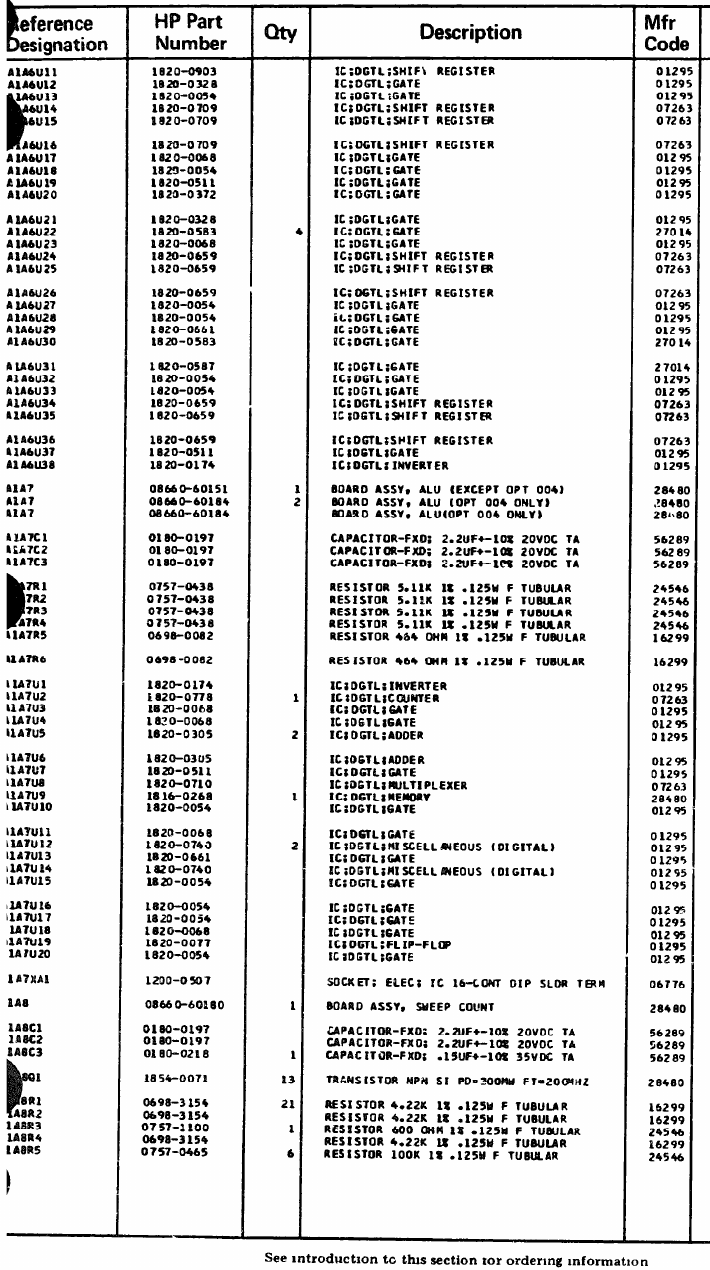
Mode1 8660B
TM 11-6625-2837-14&P
Table 6-3. Replaceable Parts
Mfr Part Number
SN74Ll64N
SN7402N
SN7400N
93L28DC
93L28DC
93L28DC
SN7410N
SN7400N
SN7408N
SN74H11N
SN7402N
DM74L00N
SN7410N
93L00DC
93L00DC
93L00DC
SN7400N
SN7400N
SN7432N
DM74L00N
DM74L10N
SN740N
SN7400N
93L00DC
93L00DC
93L00DC
SN7408N
SN7404N
08660-60151
08660-60184
O8660-60184
150D225X9020A2
150D225X9020A2
150D225X9020A2
C4-1/8-TO-5111-F
C4-1/8-TO-5111-F
C4-1/8-TO-5111-F
C4-1/8-TO-5111-F
C4-1/8-TO-4640-F
C4-1/8-TO-4640-F
SN7404N
93L16DC
SN7410N
SN7410N
SN7483N
SN7483N
SN7408N
93L22DC
1816-0268
SN7400N
SN7410N
SN74H87N
SN7432N
SN74H87N
SN7400N
SN7400N
SN7400N
SN7410N
SN7474N
SN7400N
ICN-163-S3w
08660-60180
150D225X9020A2
150D225X9020A2
150D225X9020A2
1854-0071
C4-1/8-TO-4221-F
C4-1/8-TO-4221-F
C4-1/8-TO-601-F
C4-l/8-TO-4221-F
C4-l/8-TO-1003-F
6-13
TM 11-6625-2837-14&P
Table 6-3 Replaceable Parts
C4-1/8-TO-2003-F
C4-1/8-TO-4003-F
C4-1/8-TO-4003-F
C4-1/8-TO-6811-F
MF4C1/8-TO-4502-F
3OO6Y-1-101
MF4Cl/8-TO-4003-F
C4-l/8-TO-751-F
C4-1/8-TO-1213-F
C4-1/8-TO-1002-F
C4-1/8-TO-2002-F
C4-1/8-TO-4002-F
C4-1/8-TO-8002-F
C4-1/8-TO-1001-F
C4-1/8-TO-4221-F
C4-1/8-TO-909R-F
C4-1/8-TO-2001-F
C4-1/8-TO-4001-F
C4-1/8-TO-8001-F
C4-1/8-TO-751-F
C4-1/8-TO-7221-F
C4-1/8-TO-4221-F
3006Y-1-101
3006Y-1-101
3006Y-1-101
1826-0013
DM74L00N
DM74L00N
SN7430N
SN74192N
SN7410N
SN7416k
SN74192N
SN7402N
SN74192N
SN7414N
SN7402N
SN7416N
08660-60110
150D225X9020A2
150D225X9020A2
150D225X9020A2
93L28DC
93L28DC
93L00DC
93L00DC
93L00DC
93L00DC
93L00DC
SN7400N
SN74H11N
SN74H11N
SN7400N
SN7400N
SN7400N
08660-60128
150D225X9020A2
DM15F151J0300WV1CR
150D225X9020A2
C4-1/8-T0-4640-F
C4-1/8-TO-4640-F
93L101DC
SN75451BP
SN7400N
93L08DC
93L08DC
93L08DC
93L08DC
93L08DC
08660-60112
6-14
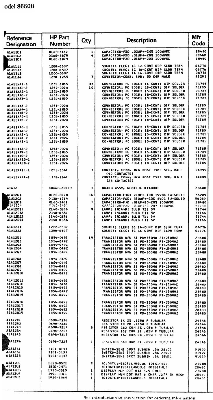
TM 11-6625-2837-14&P
Table 6-3 Replaceable Parts
Mfr Part Number
0160-3452
0160-3879
0160-3879
ICN-163-S3W
ICN-163-S3W
ICN-163-S3W
51-051-0000
252-15-30-300
252-18-30-300
252-15-30-300
252-18-30-300
252-15-30-300
252-18-30-300
252-15-30-300
252-18-30-300
252-15-30-300
252-18-30-300
252-15-30-300
252-18-30-300
252-15-30-300
252-18-30-300
252-15-30-300
252-18-30-300
252-15-30-300
252-18-30-300
252-15-30-300
252-18-30-300
86091-2
86091-2
08660-60111
150D226X901582
150D337X9006S2
0160-3451
0160-3451
CM7-7683
CM7-7683
CM7-7683
CM7-7683
ICN-163-S3W
ICN-163-S3W
1854-0492
1854-0492
1854-0492
1854-0492
1854-0492
1854-0492
1854-0492
1854-0492
1854-0492
1854-0492
1854-0492
1854-0492
1854-0492
1854-0492
1854-0492
1854-0492
1854-0492
1854-0492
1854-0492
C3-1/8-TO-1001-G
C3-1/8-TO-1001-G
C3-1/8-TO-162R-G
C3-1/8-TO-162R-G
C3-1/8-TO-162R-G
C3-1/8-TO-348R-G
1SX1-T
1SX1-T
1SX1-T
1820-0571
1820-0571
1990-0315
1990-0311
1820-1060
6-15
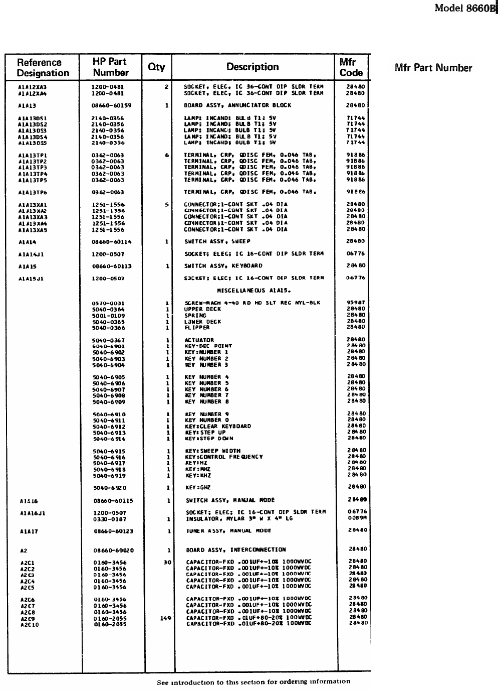
TM 11-6625-2837-14&P
Table 6-3. Replaceable Parts
1200-0481
1200-0481
08660-60159
CM7-7683
CM7-7683
CM7-7683
CM7-7683
CM7-7683
122-0192-019
122-0192-019
122-0192-019
122-0192-019
122-0192-019
122-0192-019
1251-1556
1251-1556
1251-1556
1251-1556
1251-1556
08660-60114
ICN-163-S3W
08660-60113
ICN-163-S3W
N-440-1/2
5040-0364
5001-0109
5040-0365
5050-0366
5040-0367
5040-6901
5040-6902
5040-6903
5040-6904
5040-6905
5040-6906
5040-6907
5040-6908
5040-6909
5040-6910
5040-6911
5040-6912
5040-6913
5040-6914
5040-6915
5040-6916
5040-6917
5040-6918
5040-6919
08660-60115
ICN-163-S3W
OBD
0866O-60123
08660-60020
0160-3456
0160-3456
0160-3456
0160-3456
0160-3456
0160-3456
0160-3456
0160-3456
0160-2055
0l60-2055
6-16
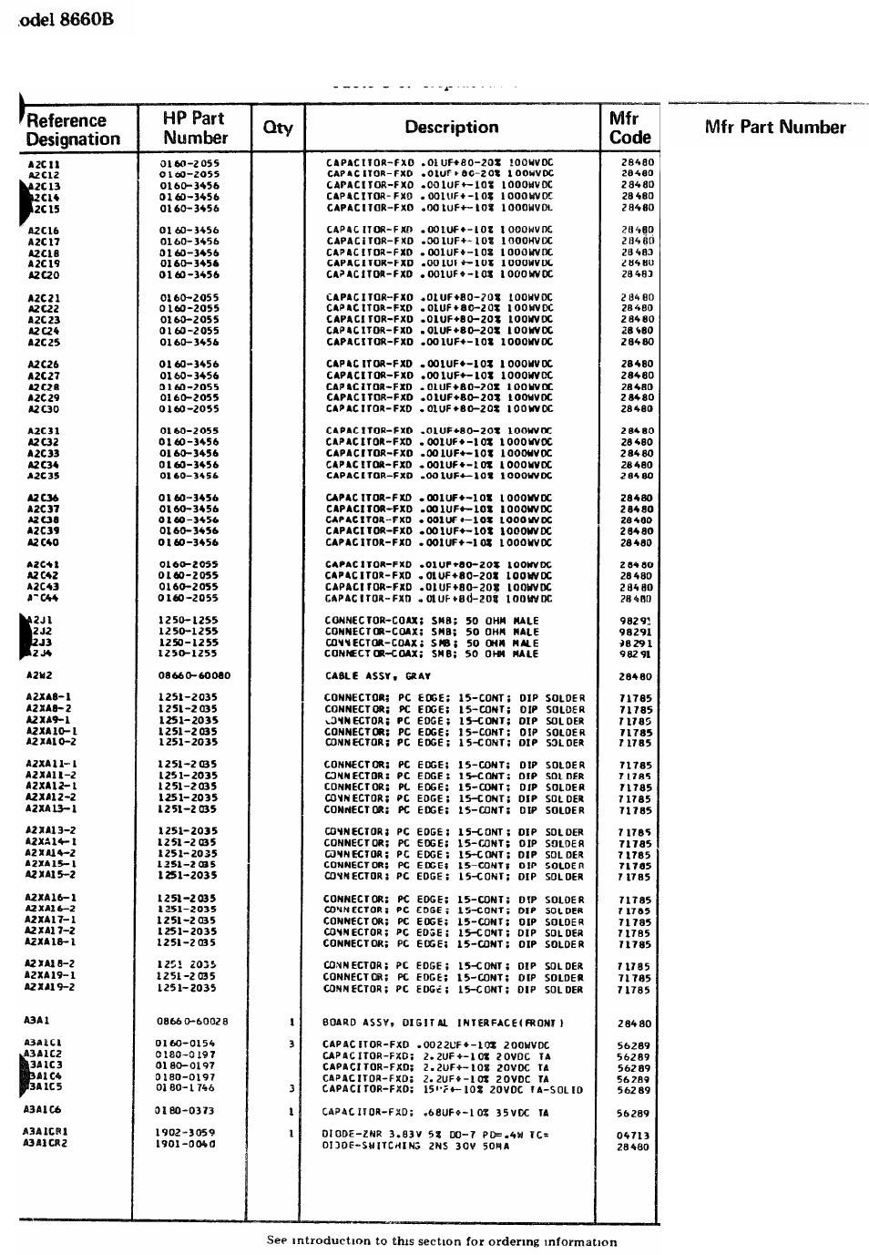
Table 6-3. Replaceable Parts
0160-2055
0160-2055
0160-3456
0160-3456
0146-3456
0160-3456
0160-3456
0160-3456
0160-3456
0160-3456
0160-2055
0160-2055
1060-2055
0160-2055
0160-3456
0160-3456
0160-3456
0160-2055
0160-2055
0160-2055
0160-2055
0160-3456
0160-3456
0160-3456
0160-3456
0160-3456
0160-3456
0160-3456
0160-3456
0160-3456
0160-2055
0160-2055
0160-2055
0160-2055
51-051-0000
51-051-0000
51-051-0000
51-051-0000
08660-60080
252-15-30-300
252-15-30-300
252-15-30-300
252-15-30-300
252-15-30-300
252-15-30-300
252-15-30-300
252-l5-30-300
252-15-30-300
252-15-30-300
252-15-30-300
252-15-30-300
252-15-30-300
252-15-30-300
252-15-30-300
252-15-30-300
252-15-30-300
252-15-30-300
252-15-30-300
252-15-30-300
252-15-30-300
252-15-30-300
252-15-30-300
08660-60028
292P22292
150D225X9020A2
150D225X9020A2
150D225X9020A2
150D156X9020A2
150D684X9035A2
SZ10939-62
1901-0040
6-17
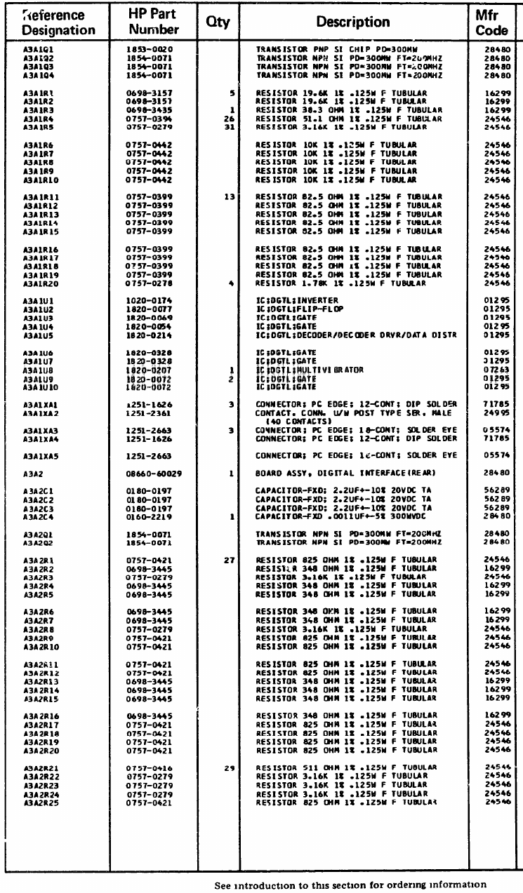
TM 11-6625-2837-14&P
Table 6-3. Replaceable Paris
Model 8660B
Mfr Part Number
1853-0020
1854-0071
1854-0071
1854-0071
C4-1/8-TO-1962-F
C4-l/8-TO-1962-F
C4-1/8-TO-38R3-F
C4-1/8-TO-51R1-F
C4-l/8-TO-3161-F
C4-l/8-TO-1002-F
C4-l/8-TO-1002-F
C4-1/8-TO-1002-F
C4-l/8-TO-1002-F
C4-1/8-TO-1002-F
C4-1/8-TO-82R5-F
C4-l/8-TO-82R5-F
C4-1/8-TO-82R5-F
C4-1/8-TO-82R5-F
C4-1/8-TO-82R5-F
C4-1/8-TO-82R5-F
C4-1/8-TO-82R5-F
C4-1/8-TO-82R5-F
C4-1/8-TO-82R5-F
C4-1/8-TO-1781-F
SN7404N
SN7474N
SN7420N
SN7400N
SN7442N
SN7402N
SN7402N
9601PC
SN7450N
SN7450N
252-12-30-300
86091-2
3VH18/1JN5
252-12-30-300
3VH18/1JN5
08660-60029
150D225X9020A2
150D225X9020A2
150D225X9020A2
0160-2219
1854-0071
1854-0071
C4-1/8-TO-825R-F
C4-1/8-TO-348R-F
C4-1/8-TO-3161-F
C4-1/8-TO-348R-F
C4-1/B-TO-348R-F
C4-1/8-TO-348R-F
C4-1/8-TO-348R-F
C4-1/8-TO-3161-F
C4-1/8-TO-825R-F
C4-1/8-TO-825R-F
C4-1/8-TO-825R-F
C4-1/8-TO-825R-F
C4-1/8-TO-348R-F
C4-1/8-TO-348R-F
C4-1/8-TO-348R-F
C4-1/8-TO-348R-F
C4-1/8-TO-825R-F
C4-1/8-TO-825R-F
C4-1/8-TO-825R-F
C4-1/8-TO-825R-F
C4-1/8-TO-511R-F
C4-1/8-TO-3161-F
C4-1/8-TO-3161-F
C4-1/8-TO-3161-F
C4-1/8-TO-825R-F
6-18
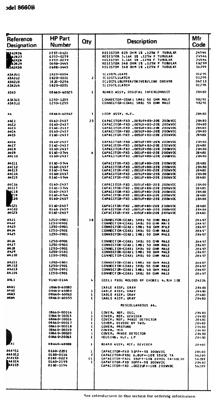
TM 11-6625-2837-14&P
Table 6-3. Replaceable Parts
Mfr Part Number
C4-1/8-TO-825R-F
C4-1/8-TO-3161-F
C4-1/8-TO-3161-F
C4-1/8-TO-348R-F
C4-1/8-TO-348R-F
SN7400N
SN7475N
MC858P
SN7475N
08660-60025
51-051-0000
51-051-0000
08660-60042
0160-2437
0160-2437
0160-2437
0160-2437
0160-2437
0160-2437
0160-2437
0160-2437
0160-3744
0160-2737
0160-3744
0160-2437
0160-3744
0160-2437
0160-3744
0160-2437
0160-3744
0160-2437
0160-3744
0160-2437
0160-2437
0160-2437
0160-2437
700166
700166
700166
700166
700166
700166
700166
700166
700166
700166
700166
700166
700166
700166
10/471
0866-60080
08660-60050
08660-60063
08660-60055
08660-00014
08660-00015
08660-00016
08660-00017
08660-00018
08660-00019
08660-00020
08660-20063
08660-60003
0160-2201
150D685X903582
150D336X901082
0160-2199
292P22292
6-19
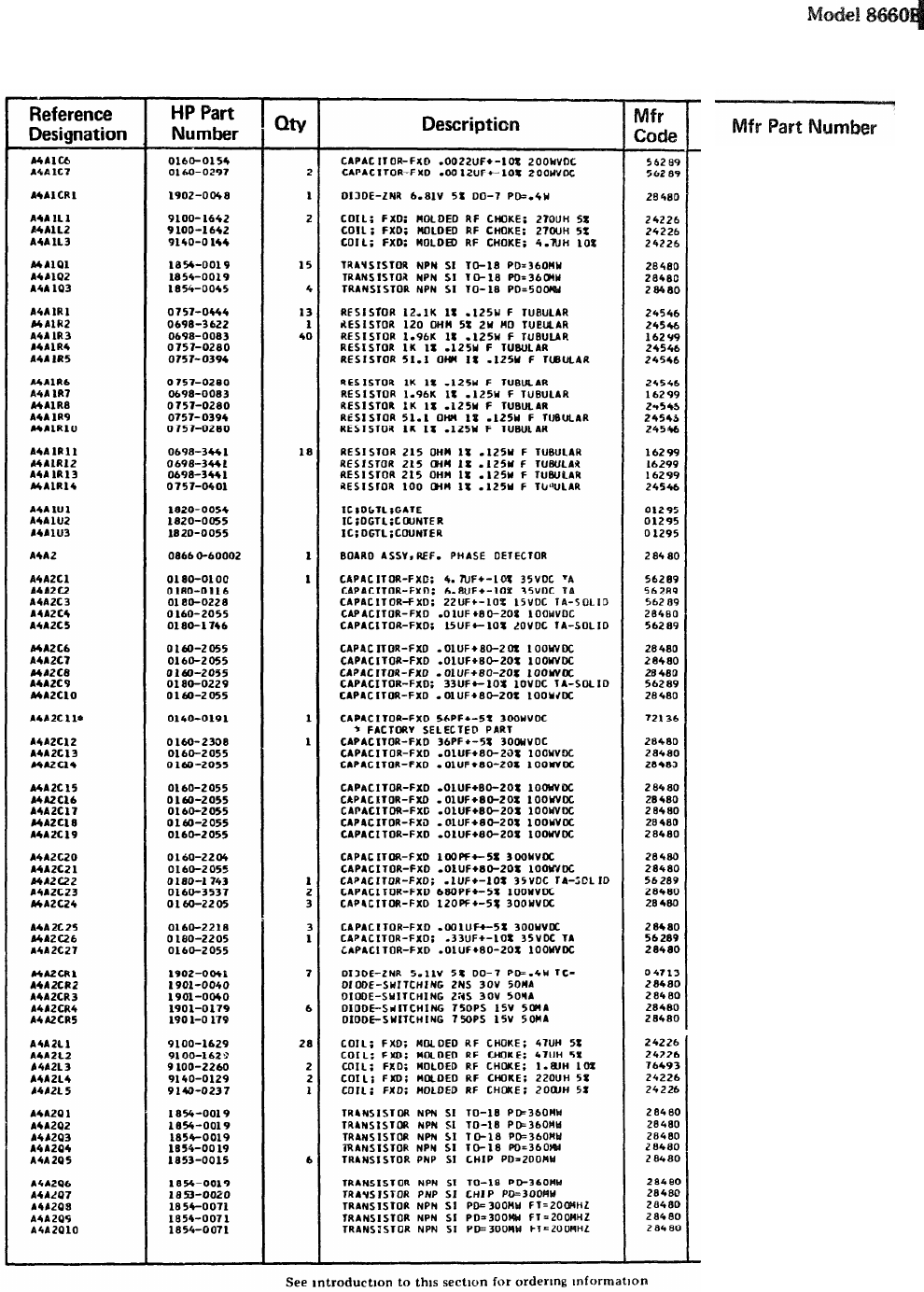
TM 11-6625-2837-14&P
Table 6-3. Replaceable Parts
292P22292
292P12292
1902-0048
19/273
19/273
10/471
1854-0019
1854-0019
1854-0045
C4-1/8-TO-1212-F
FP42-2-TOO-120R-J
C4-1/8-TO-1961-F
C4-1/8-TO-1001-F
C4-1/8-TO-51R1-F
C4-1/8-TO-1001-F
C4-1/8-TO-1961-F
C4-1/8-TO-1001-F
C4-l/8-TO-51Rl-F
C4-l/8-TO-1001-F
C4-1/8-TO-215R-F
C4-1/8-TO-215R-F
C4-1/8-TO-215R-F
C4-1/8-TO-101-F
SN7400N
SN7490N
SN7490N
08660-60002
150D475X9035B2
150D685X9035B2
150D226X9015B2
0160-2055
150D156X9020B2
0160-2055
0160-2055
0160-2055
150D336X9010B2
0160-2055
DM15E560J0300WV1CR
0160-2308
0160-2055
0160-2055
0160-2055
0160-2055
0160-2055
0160-2055
0160-2055
0160-2204
0160-2055
150D104X9035A2
0160-3537
0160-2205
0160-2218
150D334X9035A2
0160-2055
SZ 10939-98
1901-0040
1901-0040
1901-0179
1901-0179
15/472
15/472
9230-26
15/223
15/203
1854-0019
1854-0019
1854-0019
1854-0019
1853-0015
1854-0019
1853-0020
1854-0071
1854-0071
1854-0071
6-20
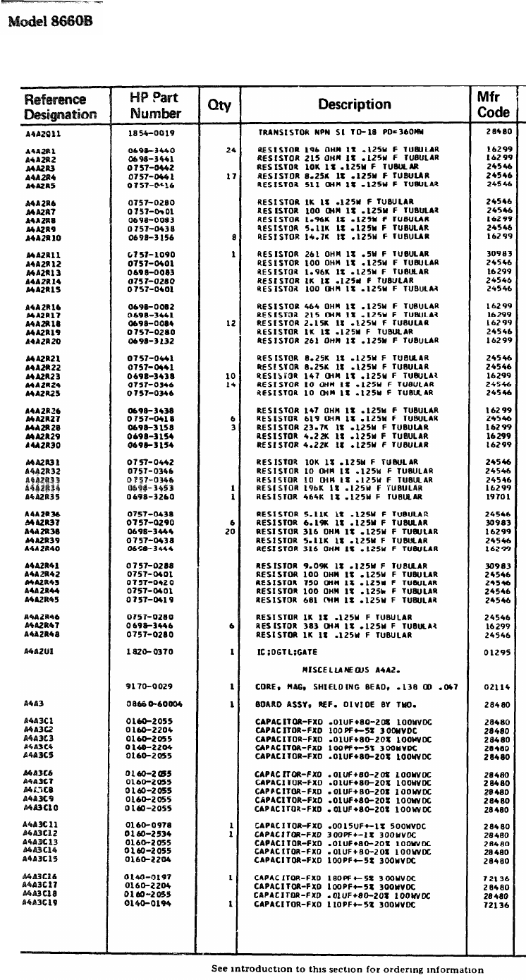
Table 6-3. Replaceable Parts
TM 11-6625-2837-14&P
Mfr Part Number
C4-1/8-TO-196R-F
C4-1/8-TO-215R-F
C4-1/8-TO-1002-F
C4-1/8-TO-8251-F
C4-1/8-TO-511R-F
C4-1/8-TO-1001-F
C4-1/8-TO-101-F
C4-1/8-TO-1961-F
C4-1/8-TO-5111-F
C4-1/8-TO-1472-F
MF7C1/2-TO-261R-F
C4-1/8-TO-101-F
C4-1/8-TO-1961-F
C4-1/8-TO-1001-F
C4-1/8-TO-101-F
C4-1/8-TO-4640-F
C4-1/8-TO-215R-F
C4-1/8-TO-2151-F
C4-1/8-TO-1001-F
C4-1/8-TO-2610-F
C4-1/8-TO-8251-F
C4-1/8-TO-8251-F
C4-1/8-TO-147R-F
C4-1/8-TO-10R0-F
C4-1/8-TO-10R0-F
C4-1/8-TO-147R-F
C4-1/8-TO-619R-F
C4-1/8-TO-2372-F
C4-1/8-TO-4221-F
C4-1/8-TO-4221-F
C4-1/8-TO-1002-F
C4-1/8-TO-10R0-F
C4-1/8-TO-10R0-F
C4-1/8-TO-1963-F
MF4C1/8-TO-4643-F
C4-1/8-TO-5111-F
C4-1/8-TO-6191-F
C4-1/8-TO-316R-F
C4-1/8-TO-5111-F
C4-1/8-TO-316R-F
MFRC1/8-TO-9091-F
C4-1/8-TO-101-F
C4-1/8-TO-751-F
C4-1/8-TO-101-F
C4-1/8-TO-681R-F
C4-1/8-TO-1001-F
C4-1/8-TO-383R-F
C4-1/8-TO-1001-F
SN744H00N
56-590-65A2/4A
08660-60004
0160-2055
0160-2204
0160-2055
0160-2204
0160-2055
0160-2055
0160-2055
0160-2055
0160-2055
0160-2055
0160-0978
0160-2534
0160-2055
0160-2055
0160-2204
DMl5Fl8lJ0300MV1CR
0160-2204
0160-2055
DM15F111J0300WV1CR
6-21
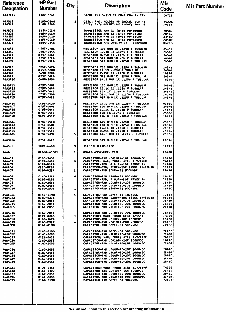
TM 11-6625-2837-14&P
Table 6-3. Replaceable Parts
6-22
SZ 10939-98
1854-0019
1854-0019
1854-0019
1854-0019
2N5179
C4-1/8-TO-101-F
C4-1/8-10-1212-F
C4-1/8-TO-8251-F
C4-1/8-TO-511R-F
C4-1/8-TO-511R-F
C4-1/8-TO-751-F
C4-1/8-TO-1001-F
C4-1/8-TO-2151-F
C4-1/8-TO-511R-F
C4-1/8-TO-34R8-F
C4-1/8-TO-101-F
C4-1/8-TO-1212-F
C4-1/8-TO-1002-F
C4-1/8-TO-51R1-F
C4-1/8-TO-825R-F
C4-1/8-TO-19R6-F
C4-1/8-TO-101-F
C4-1/8-TO-1212-F
C4-1/8-TO-1002-F
C4-1/8-TO-196R-F
C4-1/8-TO-619R-F
C4-1/8-TO-101-F
C4-1/8-TO-1212-F
C4-1/8-TO-8251-F
C4-1/8-TO-68R1-F
C4-1/8-TO-619R-F
SN74H102M
08660-60001
0160-3456
187-0106-005
15OD685X9035B2
150D226X9015B2
0160-0214
0160-2266
150D685X9035B2
0160-2055
0160-2055
O160-2306
DM15E390J0300WV1CR
150D226X9015B2
0160-2055
0160-2055
0160-2055
0160-2055
DV11PS35D
0160-3879
0160-2327
DM15E390J0300WV1CR
DM15E390J0300WV1CR
0160-2055
187-0106-005
O16O-2327
0160-2055
0160-2055
0160-2055
0160-2055
0160-2055
0160-2055
187-0106-005
0160-2327
0160-2055
0160-2055
DM15E390J0300WV1CR
9378
9378
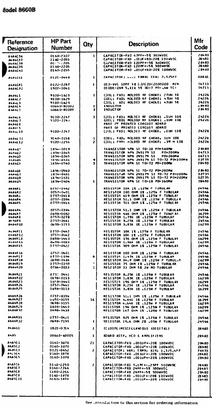
TM 11-6625-2837-14&P
Table 6-3. Replaceable Parts
Mfr Part Number
0160-2307
0160-2055
0160-2055
0160-2055
0160-2055
5S-TR1KD-03, 2.5 -
SMV389-287
SZ 10939-98
15/272
15/472
15/472
08660-80002
08660-80009
10/100
10/100
10/100
10/101
10/390
1854-0019
2N5179
2N5179
2N5179
1854-0540
1854-0540
2N5179
2N5179
1854-0404
C4-1/8-TO-1002-F
C4-1/8-TO-101-F
C4-1/8-TO-619R-F
C4-1/8-TO-51R1-F
C4-1/8-TO-511R-F
C4-1/8-TO-51R1-F
C4-1/8-TO-4640-F
C4-1/8-TO-1781-F
C4-1/8-TO-8251-F
C4-1/8-TO-3831-F
C4-1/8-TO-1002-F
C4-1/8-TO-1002-F
C4-1/8-TO-196R-F
C4-1/8-TO-1961-F
C4-1/8-TO-909R-F
C4-1/8-TO-101-F
C4-1/8-TO-1471-F
C4-1/8-TO-34R8-F
C4-1/8-TO-75R0-F
FP42-2-TOO-3302-J
C4-1/8-TO-8251-F
C4-1/8-TO-3831-F
C4-1/8-TO-196R-F
C4-1/8-TO-8251-F
C4-1/8-TO-3831-F
C4-1/8-TO-51R1-F
C4-1/8-TO-4641-F
C4-1/8-TO-4641-F
C4-1/8-TO-196R-F
C4-1/8-TO-147R-F
C4-1/8-TO-825R-F
C3-1/8-TOO-19R6-G
1820-0714
08660-60005
0160-3878
0160-3878
187-0103-005
0160-3878
0160-3878
0160-2250
0160-2266
0160-2266
0160-3878
0160-3878
6-23
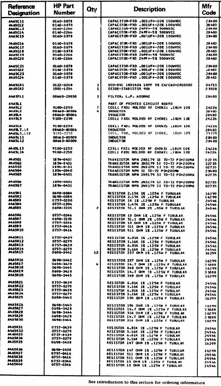
TM 11-6625-2837-14&P
Table 6-3. Replaceable Parts
Model 8660B
Mfr Part Number
0160-3878
0160-3878
0160-2266
0160-2266
0160-3878
0160-3878
0160-3878
0160-3878
0160-2266
0160-2266
0160-3878
0160-3878
0160-3878
0160-3878
1N5140A
MPD400
08660-20038
10/180
08660-80006
08660-80006
10/180
10/180
08660-80006
10/180
08660-80009
08660-80009
10/180
10/180
2N5179
2N5179
2N5179
1854-0540
2N5179
2N5179
2N5179
C4-1/8-T0-2151-F
C4-1/8-T0-2151-F
C4-1/8-T0-1001-F
C4-1/8-T0-1471-F
C3-1/8-T00-51R1-G
C4-1/8-T0-10R0-F
C3-1/8-T00-51R1-G
C4-1/8-T0-l0R0-F
C4-1/8-T0-511R-F
C4-1/8-T0-511R-F
C4-1/8-T0-6811-F
C4-1/8-T0-3161-F
C4-1/8-T0-6811-F
C1-1/8-T0-3161-F
C4-1/8-T0-237R-F
C4-1/8-T0-237R-F
PMF55-1/8-T0-14R7-F
C4-1/8-T0-348R-F
PME55-1/8-T0-14R7-F
C4-1/8-T0-348R-F
C4-1/8-T0-6811-F
C4-l/8-T0-3161-F
C4-l/8-T0-6811-F
C4-l/8-T0-3161-F
C4-1/8-T0-196R-F
C4-1/8-T0-196R-F
PME55-1/8-T0-14R7-F
C4-1/8-T0-316R-F
PME55-1/8-T0-14R7-F
C4-1/8-T0-316R-F
C4-l/8-T0-6811-F
C4-1/8-T0-3161-F
C4-1/8-T0-6811-F
C4-1/8-T0-3161-F
C4-1/8-T0-147R-F
C4-1/8-T0-147R-F
C4-1/8-T0-
C4-1/8-T0-511R-F
C4-1/8-T0-10R0-F
C4-1/8-T0-10R0-F
6-24
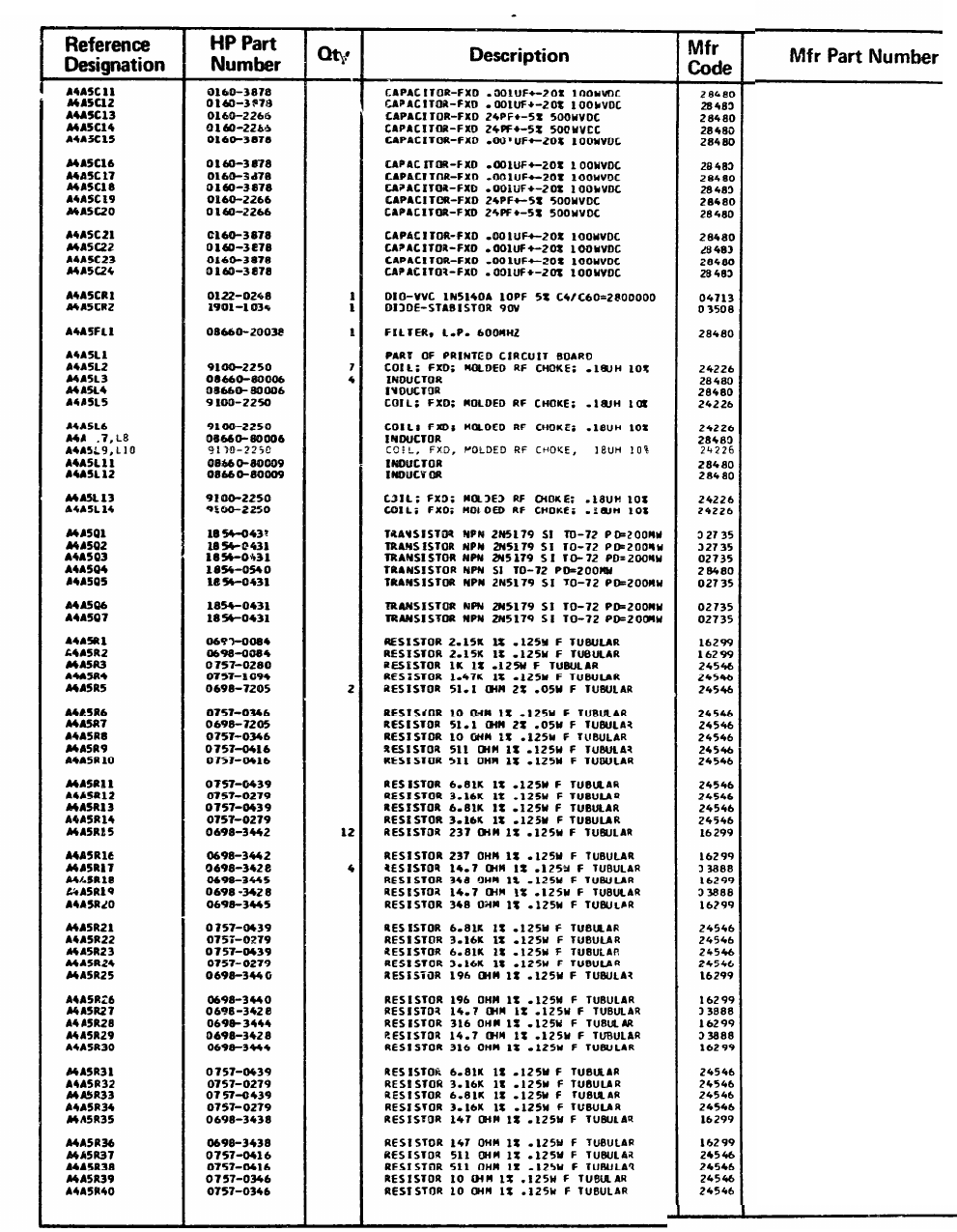
TM 11-6625-2837-14&P Model 8660B
Table 6-3. Replaceable Parts
0160-3878
0160-3878
0160-2266
0160-2266
0160-3878
0160-3878
0160-3878
0160-3878
0160-2266
0160-2266
0160-3878
0160-3878
0160-3878
0160-3878
1N5140A
MPD400
08660-2003B
10/180
08660-8006
08660-80006
10/180
10/180
08660-80006
10/180
08660-8009
08660-80009
10/180
10/180
2N5179
2N5179
2N5179
1854-0540
2N5179
2N5179
2N5179
C4-1/8-T0-2151-F
C4-1/8-T0-2151-F
C4-1/8-T0-1001-F
C4-1/8-T0-1471-F
C3-1/8-T00-51R1-G
C4-1/8-T0-10R0-F
C3-1/8-T00-51R1-G
C4-1/8-T0-10R0-F
C4-1/8-T0-511R-F
C4-1/8-T0-511R-F
C4-1/8-T0-6811-F
C4-1/8-T0-3161-F
C4-1/8-T0-6811-F
C4-1/8-T0-3161-F
C4-1/8-T0-237R-F
C4-1/8-T0-237R-F
PME55-1/8-T0-14R7-F
C4-1/8-T0-348R-F
PME55-1/8-T0-14R7-F
C4-1/8-T0-348R-F
C4-1/8-T0-6811-F
C4-1/8-T0-3161-F
C4-1/8-T0-6811-F
C4-1/8-T0-3161-F
C4-1/8-T0-196R-F
C4-1/8-T0-196R-F
PMF55-1/8-T0-14R7-F
C4-1/8-T0-316R-F
PME55-1/8-T0-14R7-F
C4-1/8-T0-316R-F
C4-1/8-T0-6811-F
C4-1/8-T0-3161-F
C4-1/8-T0-6811-F
C4-1/8-T0-3161-F
C4-1/8-T0-147R-F
C4-1/8-T0-147R-F
C4-1/8-T0-511R-F
C4-1/8-T0-511R-F
C4-1/8-T0-10R0-F
C4-1/8-T0-10R0-F
6-24
See introduction to this section for ordering informatlon
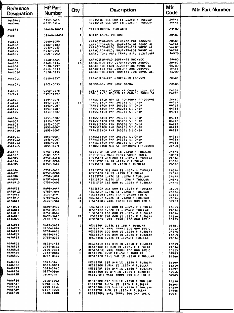
Model 8660B TM 11-6625-2837-14&P
Table 6-3. Replaceable Parts
C4-1/8-T0-511R-F
C4-1/8-T0-511R-F
016C-3537
1901-0033
15/122
19/303
2N3251
2N3251
2N3251
2N3251
2N3251
2N3251
2N3251
2N3251
2N3251
2N3251
2N3251
2N3251
1854-0071
C4-1/8-T0-10R0-F
ET50W502
C4-1/8-T0-619R-F
C4-1/8-T0-1001-F
C4-1/8-T0-1002-F
C4-1/8-T0-215R-F
C4-1/8-T0-7501-F
FT50W501
08660-80003
08660-80007
0160-2055
300106G050C82
3000106G050C82
300506G050DD2
187-0103-005
0160-2264
0160-0174
150D225X9020A2
0160-3879
300106G050C82
1854-0071
C4-1/8-T0-511R-F
C4-1/8-T0-1001-F
C4-1/8-T0-1471-F
C4-1/8-T0-8251-F
C4-1/8-T0-162R-F
C4-1/8-T0-316R-F
C4-1/8-T0-1471-F
ET502W202
C4-1/8-T0-5621-F
ET50W101
C4-1/8-T0-178R-F
C4-1/8-T0-1621-F
C4-1/8-T0-162R-F
C4-1/8-T0-287R-F
ET50W101
MF7C1/2-T0-2371-F
ET50W101
C4-1/8-T0-101-F
C4-1/8-T0-196R-F
C4-1/8-T0-1781-F
C4-1/8-T0-147R-F
C4-1/8-T0-10R0-F
ET50W201
MF7C1/2-T0-7501-F
C4-1/8-T0-51R1-F
C4-1/8-T0-215R-F
C4-1/8-T0-1961-F
C4-1/8-T0-196R-F
C4-1/8-T0-10R0-F
ET5CW201
C4-1/8-T0-237R-F
C4-1/8-T0-2151-F
See Introduction to this section for ordering information
6-25
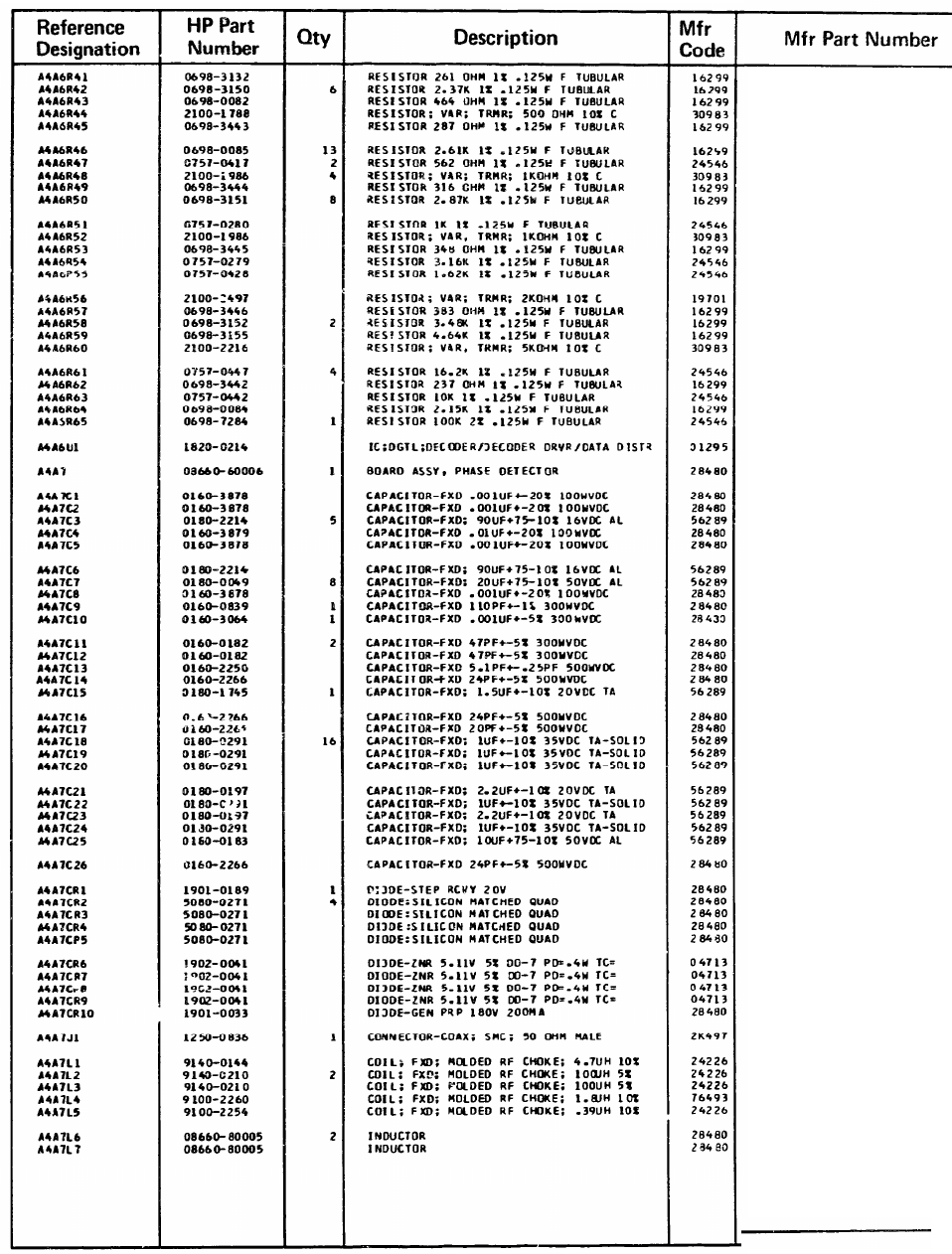
TM 11-6625-2837-14&P Model 8660B
Table 6-3. Replaceable Parts
See introduction to this section for ordering m
6-26
C4-1/8-T0-2010-F
C4-1/8-T0-2371-F
C4-1/8-T0-4640-F
FT50W501
C4-1/8-T0-287R-F
C4-1/8-T0-2611-F
C4-1/8-T0-5628-F
FT50W102
C4-1/8-T0-316R-F
C4-1/8-T0-2871-F
C4-1/8-T0-1001-F
ET50W102
C4-1/8-T0-248R-F
C4-1/8-T0-3161-F
C4-1/8-T0-1621-F
ET50W202
C4-1/8-T0-383R-F
C4-1/8-T0-3481-F
C4-1/8-T0-4641-F
ET50W502
C4-1/8-T0-1622
C4-1/8-T0-237R-F
C4-1/8-T0-1002-F
C4-1/8-T0-2151-F
C3-1/8-T0-1003-G
SN7442N
08660-60006
0160-3878
0160-3878
300906G016CC2
0160-3879
0160-3878
300906G016CC2
300206G050002
0160-3878
0160-0839
0160-3064
0160-0182
0160-0182
0160-2250
0160-2266
1500155X902A2
0160-2266
0160-2264
1500105X9035A2
1500105X9035A2
01500105X9035A2
1500225X902A2
1500105X9035A2
1500225X9020A2
1500105X9035A2
300106G0500R2
0160-2266
1901-0189
5080-0271
5080-0271
5080-0271
5080-0271
SZ 10939-98
SZ 10939-98
SZ 10939-98
SZ 10939-98
1901-0033
CD-700141
10/471
15/103
15/103
9230-26
10/390
08660-80005
08660-80005
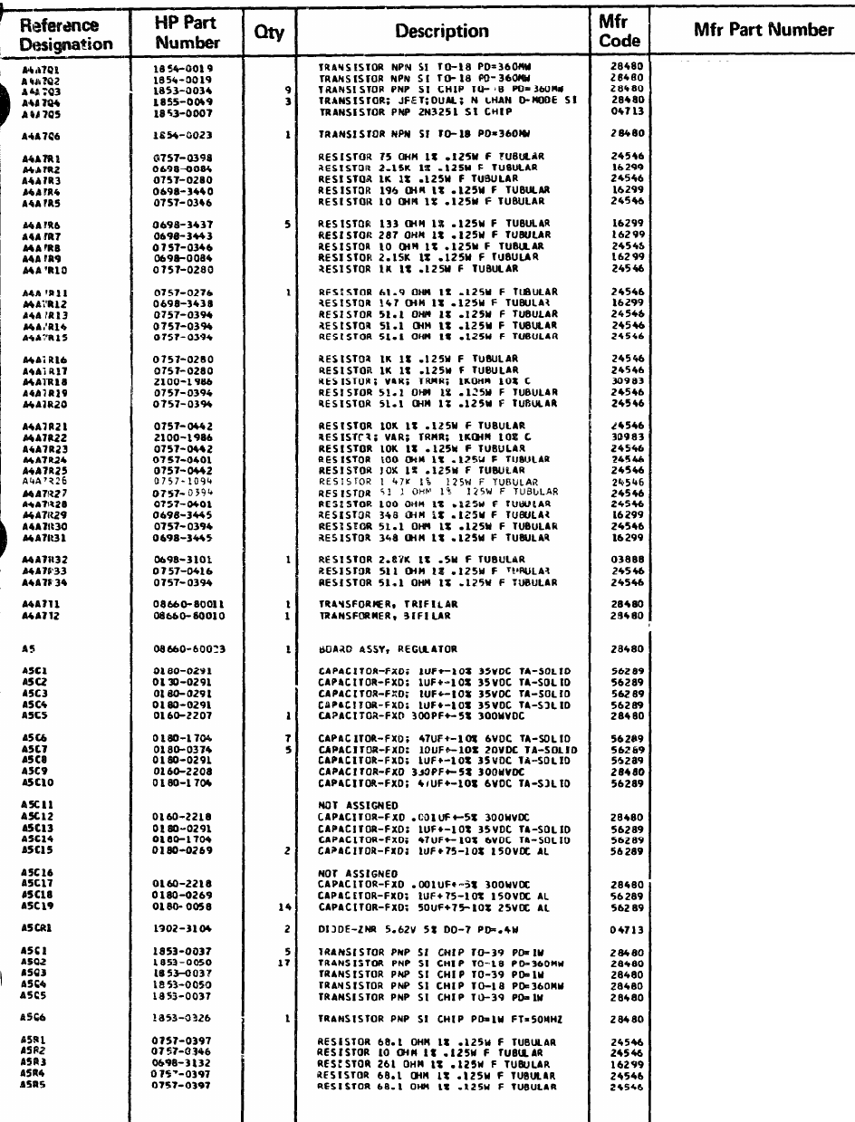
Model 8660B TM 11-6625-2837-14&P
Table 6-3. Replaceable Parts
1854-0019
1854-0019
1853-0034
1855-0049
2N3251
1854-0023
C4-1/8-T0-75R0-F
C4-1/8-T0-2151-F
C4-1/8-T0-1001-F
C4-1/8-T0-1968-F
C4-1/8-T0-10R0-F
C4-1/8-T0-133R-F
C4-1/8-T0-287R-F
C4-1/8-T0-10R0-F
C4-1/8-T0-2151-F
C4-1/8-T0-1001-F
C4-1/8-T0-5192-F
C4-1/8-T0-147R-F
C4-1/8-T0-51R1-F
C4-1/8-T0-51R1-F
C4-1/8-T0-51R1-F
C4-1/8-T0-1001-F
C4-1/8-T0-1001-F
ET50W102
C4-1/8-T0-51R1-F
C4-1/8-T0-51R1-F
C4-1/8-T0-1002-F
ET501102
C4-1/8-T0-1002-F
C4-1/8-T0-101-F
C4-1/8-T0-1002-F
C4-1/8-T0-1471-F
C4-1/8-T0-51R1-F
C4-1/8-T0-101-F
C4-1/8-T0-348R-F
C4-1/8-T0-51R1-F
C4-1/8-T0-348R-F
PME65-1/2-T0-2871-F
C4-1/8-T0-511R-F
C4-1/8-T0-51R1-F
08660-80011
08660-80010
08660-60023
15000105X9035A2
15000105X9035A2
1500105X9035A2
1500105X8035A2
0160-2207
1500476X9006B2
1500106X9020B2
1500105X9005A2
0160-2208
1500476X9006B2
0160-2218
1500105X9035A2
1500476X900682
300105G1508A2
0160-2218
300105G150BA2
300506G025CC2
SZ 13939-110
1853-0037
1853-0050
1853-0037
1853-0050
1853-0037
1853-0326
C4-1/8-T0-68R1-F
C4-1/8-T0-10R0-F
C4-1/8-T0-2610-F
C4-1/8-T0-68R1-F
C4-1/8-T0-68R1-F
See introduction to this section for ordering information.
6-27
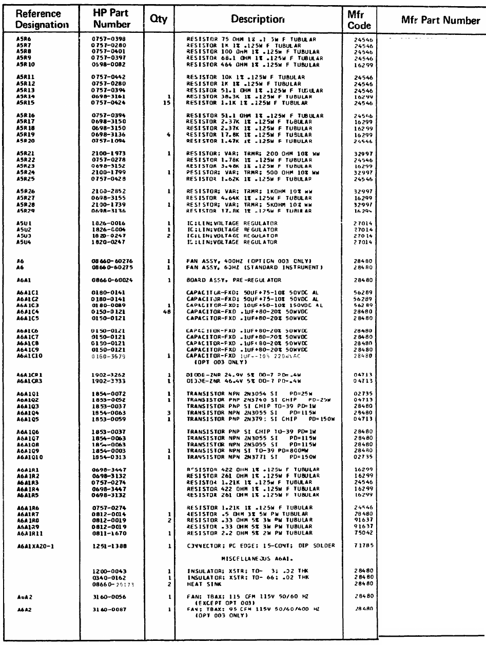
TM 11-6625-2837-14&P Model 8660B
Table 6-3. Replaceable Parts
See Introduction to this section for ordering information
C4-1/8-T0-75R0-F
C4-1/8-T0-1001-F
C4-1/8-T0-101-F
C4-1/8-T0-68R1-F
C4-1/8-T0-4640-F
C4-1/8-T0-1002-F
C4-1/8-T0-1001-F
C4-1/8-T0-51R1-F
C4-1/8-T0-3832-F
C4-1/8-T0-1101-F
C4-1/8-T0-51R1-F
C4-1/8-T0-2371-F
C4-1/8-T0-2371-F
C4-1/8-T0-1782-F
C4-1/8-T0-1471-F
3005P-1-201
C4-1/8-T0-1781-F
C4-1/8-T0-3481-F
3005P-1-501
C4-1/8-T0-1621-F
3005P-1-102
C4-1/8-T0-4641-F
3005P-1-502
C4-1/8-T0-1782-F
LM204H
LM304H
LM305
LM305
08660-60276
08660-60275
08660-60024
3005060050002
300506G050002
300106F150002
0150-0121
0150-0121
0150-0121
0150-0121
0150-0121
0150-0121
0160-3679
SZ 10939-296
SZ 10939-374
2N3054
2N3740
1853-0037
1854-0063
2N3791
1853-0037
1854-0063
1854-0063
1854-0003
2N3771
C4-1/8-T0-422R-F
C4-1/8-T0-2610-F
C4-1/8-T0-1213-F
C4-1/8-T0-422R-F
C4-1/8-T0-2610-F
C4-1/8-T0-1213-F
0812-0014
CW28-1
CW28-1
8WH2-2R2-J
252-15-30-008
1200-0043
0340-0162
08660-2013
3160-0056
3160-0087
6-28
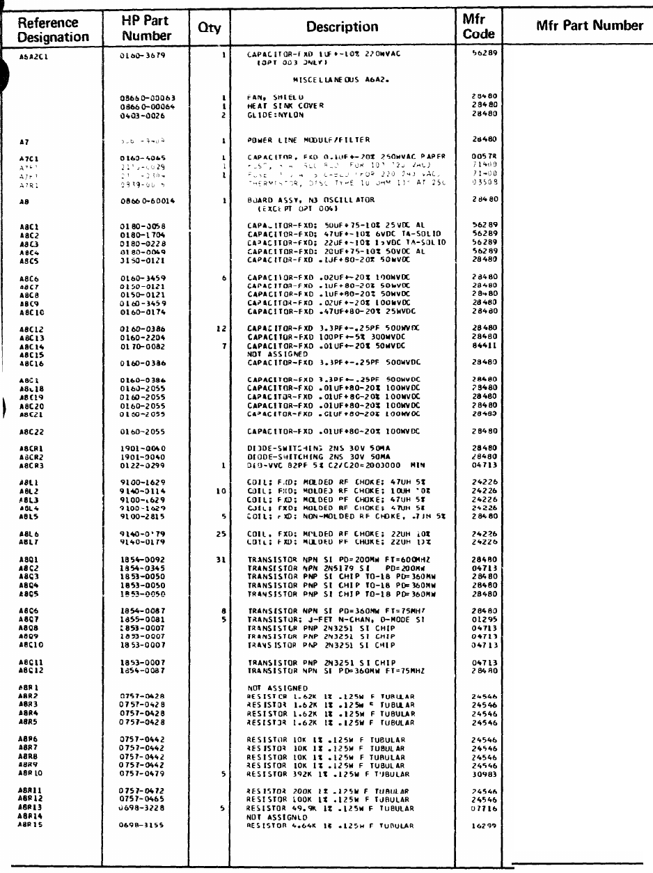
Model 3660B
Table 6-3. Replaceable Parts
TM 11-6625-2837-14&P
439P1059220
08660-00063
08660-0064
0403-0026
5060-9409
PME
271
M610
MDX-3
YDX-
1-1/2
A
2D-754
08660-60014
300506G025002
1500476X900682
1500226X901582
300206G050002
0150-0121
0160-3459
0150-0121
0159-0121
0160-3459
0160-0174
0160-0386
0160-2204
601PE1030R5W1
0160-0386
0160-0386
0160-2055
0160-2055
0160-2055
0160-2055
0160-2055
1901-0040
1901-0040
SMV389-299
15/472
15/102
15/472
15/472
9100-2815
15/222
15/222
1854-0092
2N5179
1853-0050
1853-0050
1853-0050
1854-0087
2N5245
2N3251
2N3251
2N3251
2N3251
1854-0087
C4-1/8-T0-1621-F
C4-1/8-T0- 521-F
C4-1/8-T0-1521-F
C4-1/8-T0-1621-F
C4-1/8-T0-1002-F
C4-1/8-T0-1002-F
C4-1/8-T0-1002-F
C4-1/8-T0-1002-F
MF4C1/8-T0-3923-F
C4-1/8-T0-2003-F
C4-1/8-T0-1003-F
CEA1/8-T0-4991-F
C4-1/8-T0-4641-F
See lntroduction to this section for ordering information
6-29
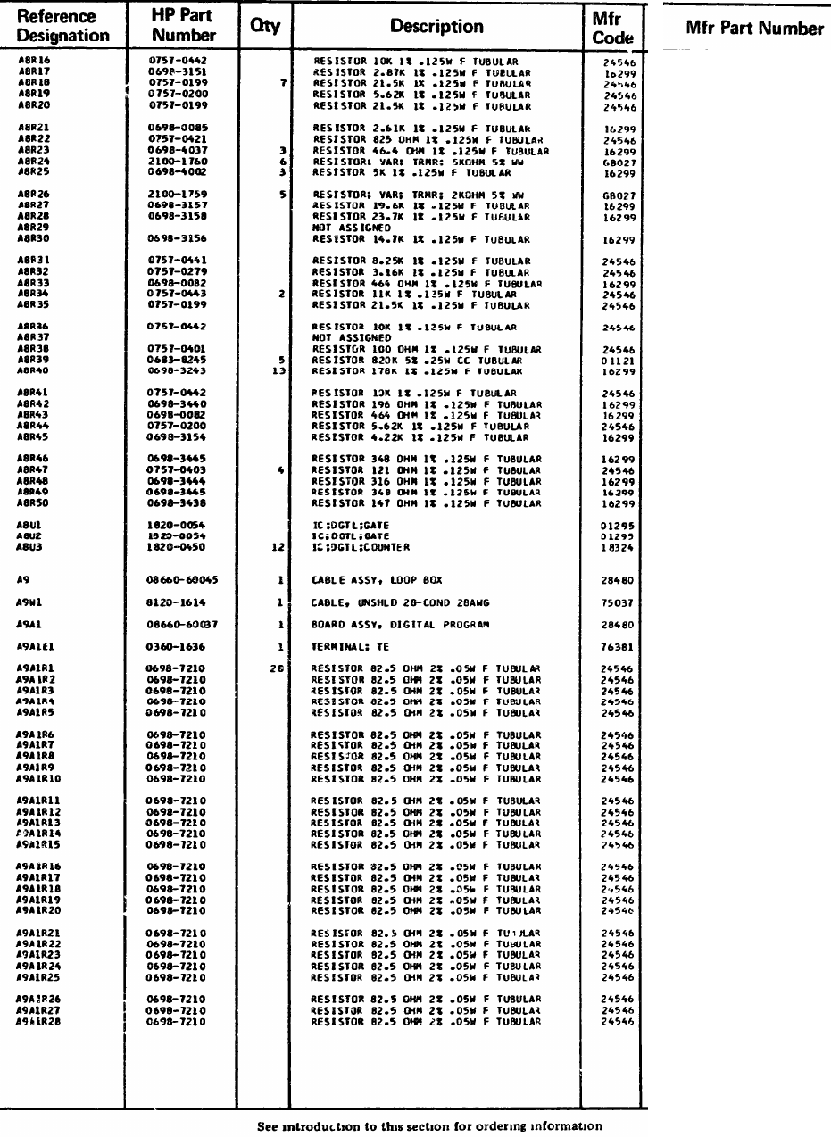
TM 11-6625-2837-14&P
Table 6-3. Replaceable Parts
C4-1/8-TO-1002-F
C4-1/8-TO-2871-F
C4-1/8-TO-2152-F
C4-1/8-TO-5621-F
C4-1/8-TO-2152-F
C4-1/8-TO-2611-F
C4-1/8-TO-8258-F
C4-1/8-TO-46R4-F
CT-106-4
C4-1/8-TO-5001-F
CT-106-4
C4-1/8-TO-1962-F
C4-1/8-TO-2372-F
C4-1/8-TO-1472-F
C4-1/8-TO-8251-F
C4-1/8-TO-3161-F
C4-1/8-TO-4640-F
C4-1/8-TO-1102-F
C4-1/8-TO-2152-F
C4-1/8-TO-1002-F
C4-1/8-TO-101-F
C8E245
C4-1/8-TO-1783-F
C4-1/8-TO-1002-F
C4-1/8-TO-1968-F
C4-1/8-TO-4640-F
C4-1/8-TO-5621-F
C4-1/8-TO-4221-F
C4-1/8-TO-348R-F
C4-1/8-TO-121R-F
C4-1/8-TO-316R-F
C4-1/8-TO-348R-F
C4-1/8-TO-147R-F
SN7400N
SN7400N
N8290A
08660-60045
08660-60037
3402
C3-1/8-TOO-82R5-G
C3-1/8-TOO-82R5-G
C3-1/8-TOO-82R5-G
C3-1/8-TOO-82R5-G
C3-1/8-TOO-82R5-G
C3-1/8-TOO-82R5-G
C3-1/8-TOO-82R5-G
C3-1/8-TOO-82R5-G
C3-1/8-TOO-82R5-G
C3-1/8-TOO-82R5-G
C3-1/8-TOO-82R5-G
C3-1/8-TOO-82R5-G
C3-1/8-TOO-82R5-G
C3-1/8-TOO-82R5-G
C3-1/8-TOO-82R5-G
C3-1/8-TOO-82R5-G
C3-1/8-TOO-82R5-G
C3-1/8-TOO-82R5-G
C3-1/8-TOO-82R5-G
C3-1/8-TOO-82R5-G
C3-1/8-TOO-82R5-G
C3-1/8-TOO-82R5-G
C3-1/8-TOO-82R5-G
C3-1/8-TOO-82R5-G
C3-1/8-TOO-82R5-G
C3-1/8-TOO-82R5-G
C3-1/8-TOO-82R5-G
C3-1/8-TOO-82R5-G
6-30
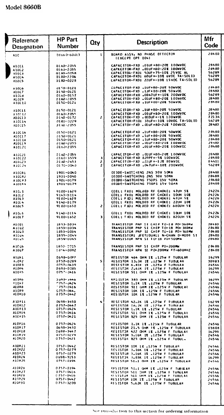
TM 11-6625-2837-14&P
Table 6-3. Replaceable Parts
Mfr Part Number
08660-60013
0160-20555
0160-2055
30D506G025CC2
150C606X9006B2
150D226X9015B2
0150-0121
0150-0121
292P47292
0160-2055
0150-0121
0150-0121
0160-2055
DM19F302F0100WV1CR
150D336X9010B2
0160-2055
0150-0121
0150-0121
0150-0121
0160-2055
0160-2055
0160-2055
0160-3539
HEW-2381
292P47392
1901-0040
1901-0040
1901-0179
1901-0179
15/472
15/102
15/472
15/222
19/683
15/102
19/823
1853-0034
1853-0034
1853-0034
1855-0049
1854-0045
1853-0015
1854-0092
C4-1/8-TO-4640-F
MF4C1/8-TO-1332-F
C4-1/8-TO-6811-F
C4-1/8-TO-2611-F
C4-1/8-TO-511R-F
C4-1/8-TO-383R-F
C4-1/8-TO-1101-F
C4-1/8-TO-511R-F
C4-1/8-TO-1002-F
C4-1/8-TO-1002-F
C4-1/8-TO-4222-F
C4-1/8-TO-1622-F
C4-1/8-TO-1101-F
C4-1/8-TO-511R-F
C4-1/8-TO-825R-F
C4-1/8-TO-1101-F
PME55-1/8-TO-21R5-F
C4-1/8-TO-4228-F
C4-1/8-TO-3161-F
C4-1/8-TO-825R-F
C4-1/8-TO-1002-F
C4-1/8-TO-3161-F
C4-1/8-TO-3161-F
C4-1/8-TO-3831-F
C4-1/8-TO-51R1-F
C4-1/8-TO-51R1-F
C4-1/8-TO-511R-F
C4-1/8-TO-511R-F
C4-1/8-TO-1002-F
C4-1/8-TO-5621-F
6-31
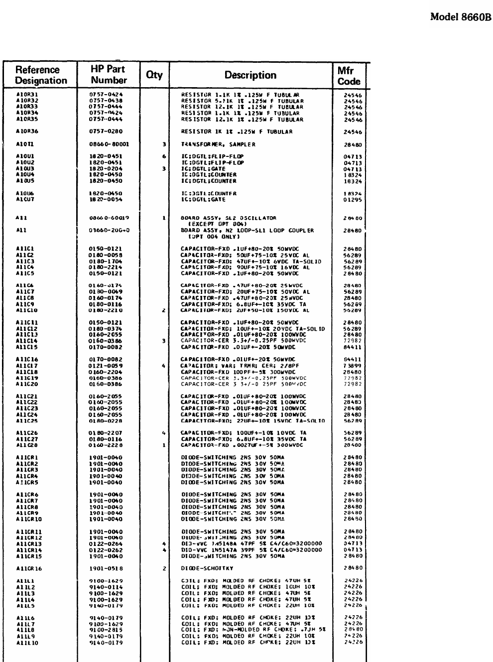
TM 11-6625-2837-14&P
Table 6-3. Replaceable Parts
6-32
Mfr Part Number
C4-1/8-TO-1101-F
C4-1/8-TO-5111-F
C4-1/8-TO-1212-F
C4-1/8-TO-1101-F
C4-1/8-TO-1212-F
C4-1/8-TO-1001-F
08660-80001
MC 3062P
MC3062P
MC 3006P
N8290A
N8290A
N8290A
SN7400N
00660-60019
08660-20040
0150-0121
30D506G025CC2
150D476X9006B2
30D506G016CC2
0150-0121
0160-0174
30D206G050CC2
0160-0174
150D685X903582
30D205F150BB2
0150-0121
150D106X9020B2
0160-2055
501-000-S2H0-3390
601PE1030R5W1
601PE1030R5W1
DV11PR8A
0160-2204
301-000-S2H0-3390
301-000-S2H0-3390
0160-2055
0160-2055
0160-2055
0160-2055
150D226X901582
150D107X9010R2
150D685X903582
0160-2228
1901-0040
1901-0040
1901-0040
1901-0040
1901-0040
1901-0040
1901-0040
1901-0040
1901-0040
1901-0040
1901-0040
1901-0040
1N5148A
1N5147A
1901-0040
1901-0518
15/472
15/102
15/472
15/472
15/222
15/222
15/472
910C-2815
15/222
15/222
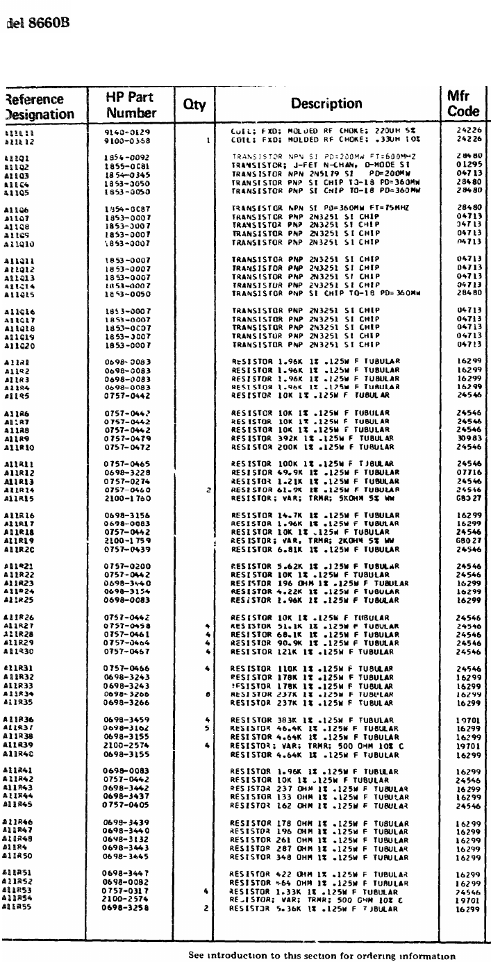
TM 11-6625-2837-14&P
Table 6-3. Replaceable Parts
Mfr Part Number
15/223
10/330
1854-0092
2N5245
2N5179
1853-0050
1853-0050
1854-0087
2N3251
2N3251
2N3251
2N3251
2N3251
2N3251
2N3251
2N3251
1853-0050
2N3251
2N3251
2N3251
2N3251
2N3251
C4-1/8-TO-1961-F
C4-1/8-TO-1961-F
C4-1/8-TO-1961-F
C4-1/8-TO-1961-F
C4-1/8-TO-1002-F
C4-1/8-TO-1002-F
C4-1/8-TO-1002-F
C4-1/8-TO-1002-F
MF4C1/8-TO-3923-F
C4-1/8-TO-2003-F
C4-1/8-TO-1003-F
CEA1/8-TO-4991-F
C4-1/8-TO-1213-F
C4-1/8-TO-6192-F
CT-106-4
C4-1/8-TO-1472-F
C4-1/8-TO-1961-F
C4-1/8-TO-1002-F
CT-106-4
C4-1/8-TO-6811-F
C4-1/8-TO-5621-F
C4-1/8-TO-1002-F
C4-1/8-TO-196R-F
C4-1/8-TO-4221-F
C4-1/8-TO-1961-F
C4-1/8-TO-1002-F
C4-1/8-TO-5112-F
C4-1/8-TO-6812-F
C4-1/8-TO-9092-F
C4-1/8-TO-1213-F
C4-1/8-TO-1103-F
C4-1/8-TO-1783-F
C4-1/8-TO-1783-F
C4-1/8-TO-2373-F
C4-1/8-TO-2373-F
MF4C1/8-TO-3833-F
C4-1/8-TO-4642-F
C4-1/8-TO-4641-F
ET50X501
C4-1/8-TO-4641-F
C4-1/8-TO-1961-F
C4-1/8-TO-1002-F
C4-1/8-TO-237R-F
C4-1/8-TO-133R-F
C4-1/8-TO-162R-F
C4-1/8-TO-178R-F
C4-1/8-TO-196R-F
C4-1/8-TO-2610-F
C4-1/8-TO-287R-F
C4-1/8-TO-348R-F
C4-1/8-TO-422R-F
C4-1/8-TO-4640-F
C4-1/8-TO-1331-F
E750X501
C4-1/8-TO-5361-F
6-33
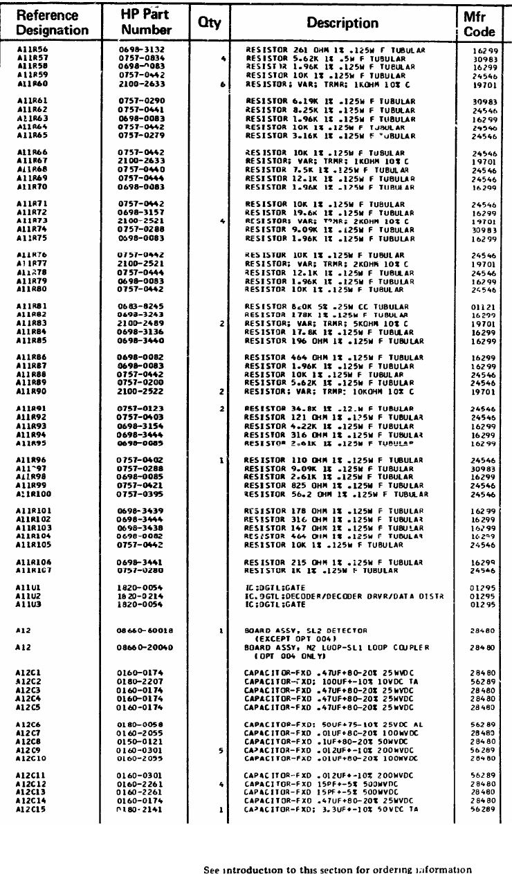
TM 11-6625-2837-14&P
Table 6-3. Replaceable Parts
Model 8660B
Mfr Part Number
C4-1/8-TO-2610-F
MF7C1/2-TO-5621-F
C4-1/8-TO-1961-F
C4-1/8-TO-1002-F
ET0X102
MF4C1/8-TO-6191-F
C4-1/8-TO-8251-F
C4-1/8-TO-1961-F
C4-1/8-TO-1002-F
C4-1/8-TO-3161-F
C4-1/8-TO-1002-F
ET50X102
C4-1/8-TO-7501-F
C4-1/8-TO-1212-F
C4-1/8-TO-1961-F
C4-1/8-TO-1002-F
C4-1/8-TO-1962-F
ET50X202
MF4C1/8-TO-9091-F
C4-1/8-TO-1961-F
C4-1/8-TO-1002-F
ET50X202
C4-1/8-TO-1212-F
C4-1/8-TO-1961-F
C4-1/8-TO-1002-F
C88245
C4-1/8-TO-1783-F
ET50X502
C4-1/8-TO-1782-F
C4-1/8-TO-196R-F
C4-1/8-TO-4640-F
C4-1/8-TO-1961-F
C4-1/8-TO-1002-F
C4-1/8-TO-5621-F
ET50X103
C5-1/4-TO-3482-F
C4-1/8-TO-121R-F
C4-1/8-TO-4221-F
C4-1/8-TO-316R-F
C4-1/8-TO-2611-F
C4-1/8-TO-111-F
C4-1/8-TO-9091-F
C4-1/8-TO-2611-F
C4-1/8-TO-825R-F
C4-1/8-TO-56R2-F
C4-1/8-TO-178R-F
C4-1/8-TO-316R-F
C4-1/8-TO-147R-F
C4-1/8-TO-4640-F
C4-1/8-TO-1002-F
C4-1/8-TO-215R-F
C4-1/8-TO-1001-F
SN7400H
SN7442N
SN7400N
08660-60018
08660-20040
0160-0174
150D107X9010R2
0160-0174
0160-0174
0160-0174
30D506G025CC2
0160-2055
0150-0121
292P12392
0160-2055
292P12392
0160-2261
0160-2261
0160-0174
150D335X9050L2
6-34
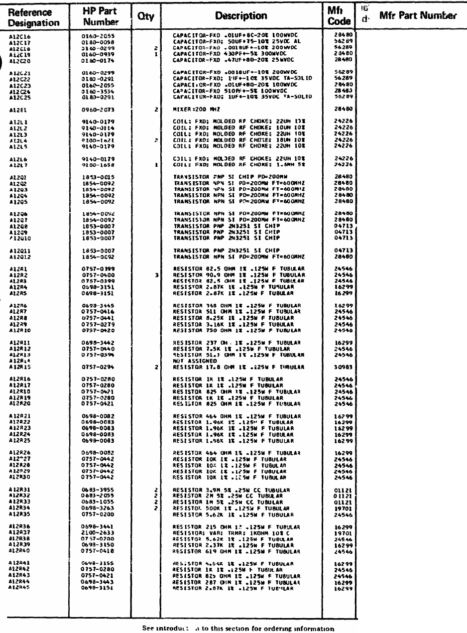
Model 8660B TM 11-6625-2837-14&P
Table 6-3. Replaceable Parts
C160-2055
30D506G025CC2
292P18292
0160-0939
0160-0174
292P18292
150D105X9035A2
0160-2055
0160-3534
150D105X9035A2
0960-2073
15/222
15/102
15/222
15/182
15/222
15/222
22/164
1853-0015
1854-0092
1854-0092
1854-0092
1854-0092
185-0092
1854-0092
2N3251
2N3251
2N3251
2N3251
1854-0092
C4-1/8-TO-82R5-F
C4-1/8-TO-90R9-F
C4-1/8-TO-82R5-F
C4-1/8-TO-2871-F
C4-1/8-TO-2871-F
C4-1/8-TO-348R-F
C4-1/8-TO-511R-F
C4-1/8-TO-8251-F
C4-1/8-TO-3161-F
C4-1/8-TO-751-F
C4-1/8-TO-237R-F
C4-1/8-TO-7501-F
C4-1/8-TO-51R1-F
MF4C1/8-TO-17R8-F
C4-1/8-TO-1001-F
C4-1/8-TO-1001-F
C4-1/8-TO-825R-F
C4-1/8-TO-1001-F
C4-1/8-TO-825R-F
C4-1/8-TO-4640-F
C4-1/8-TO-1961-F
C4-1/8-TO-1961-F
C4-1/8-TO-1961-F
C4-1/8-TO-1961-F
C4-1/8-TO-4640-F
C4-1/8-TO-1002-F
C4-1/8-TO-1002-F
C4-1/8-TO-1002-F
C4-1/8-TO-1002-F
CB3955
CB2C55
CB1055
MF5C1/8-TO-5003-F
C4-1/8-TO-5621-F
C4-1/8-TO-215R-F
ET50X102
C4-1/8-TO-5621-F
C4-1/8-TO-2371-F
C4-1/8-TO-6198-F
C4-1/8-TO-4641-F
C4-1/8-TO-1001-F
C4-1/8-TO-825R-F
C4-1/8-TO-2878-F
C4-1/8-TO-2871-F
6-35
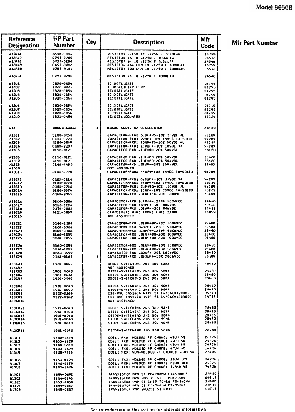
TM 11-6625-2837-14&P
Table 6-3. Replaceable Parts
6-36
C4-1/8-TO-2151-F
C4-1/8-TO-1001-F
C4-1/8-TO-1001-F
C4-1/8-TO-4640-F
C4-1/8-TO-101-F
C4-1/8-TO-1001-F
SN7400N
SN7474N
SN7400N
SN7400N
SN7410N
SN7400N
SN7400N
SN7400N
N8250A
08660-60012
30D506G025CC2
150D226X9015B2
30D206G050CC2
150D107X9010R2
0150-0121
0150-0121
015O-0121
0160-3459
150D226X9015B2
150D685X9035B2
150D226X9015B2
30D205F150BB2
150D106X9020B2
0160-2055
0160-0386
0160-2204
601PE1030P5W1
DV11PR8A
0160-2055
0160-0386
0160-0386
0160-2055
0160-2055
0160-2055
0160-2055
0160-3459
292P33392
1901-0040
1901-0040
1901-0040
1901-0040
1901-0040
1901-0040
1N51484
1N5147A
1901-0040
1901-0040
1901-0040
1901-0040
1901-0040
1901-0040
15/472
15/472
15/472
15/472
9100-2815
15/222
15/222
24-754
1854-0092
2N5179
1853-0050
1854-0087
2N3251
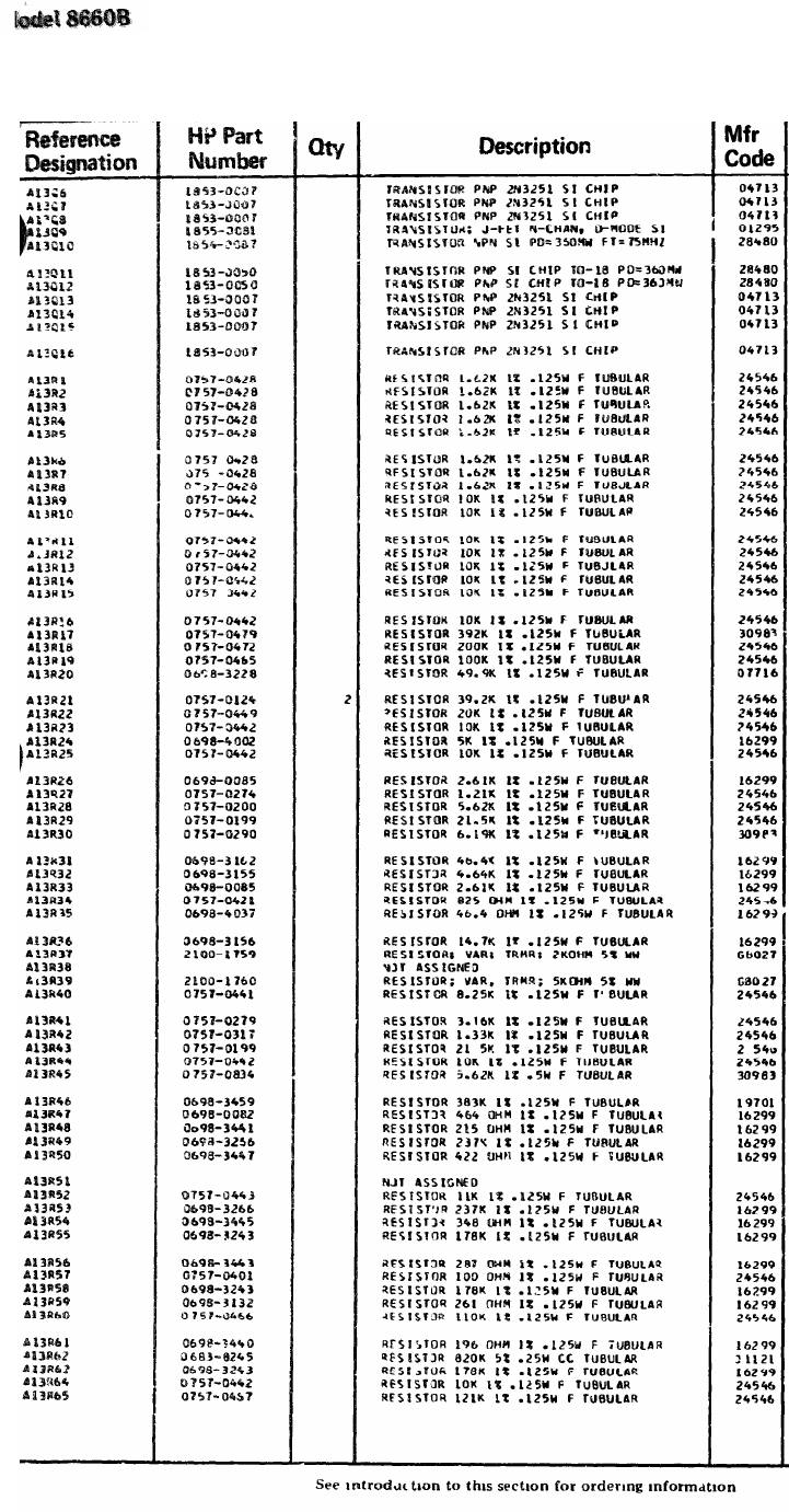
TM 11-6625-2837-14&P
Table 6-3. Replaceable Parts
Mfr Part Number
2N3251
2N3251
2N3251
2N5245
1854-0087
2N3251
2N3251
2N3251
2N3251
C4-1/8-TO-1621-F
C4-1/8-TO-1621-F
C4-1/8-TO-1621-F
C4-1/8-TO-1621-F
C4-1/8-TO-1621-F
C4-1/8-TO-1621-F
C4-1/8-TO-1621-F
C4-1/8-TO-1621-F
C4-1/8-TO-1002-F
C4-1/8-TO-1002-F
C4-1/8-TO-1002-F
C4-1/8-TO-1002-F
C4-1/8-TO-1002-F
C4-1/8-TO-1002-F
C4-1/8-TO-1002-F
C4-1/8-TO-1002-F
MF4C1/8-TO-3923-F
C4-1/8-TO-2003-F
C4-1/8-TO-1003-F
CEA1/8-TO-4991-F
C5-1/4-TO-3922-F
C4-1/8-TO-2002-F
C4-1/8-TO-1002-F
C4-1/8-TO-5001-F
C4-1/8-TO-1002-F
C4-1/8-TO-2611-F
C4-1/8-TO-1213-F
C4-1/8-TO-5621-F
C4-1/8-TO-2152-F
MF4C1/8-TO-6191-F
C4-1/8-TO-4642-F
C4-1/8-TO-4641-F
C4-1/8-TO-2611-F
C4-1/8-TO-825R-F
C4-1/8-TO-46R4-F
C4-1/8-TO-1472-F
CT-106-4
CT-106-4
C4-1/8-TO-8251-F
C4-1/8-TO-3161-F
C4-1/8-TO-1331-F
C4-1/8-TO-2152-F
C4-1/8-TO-1002-F
MF7C1/2-TO-5621-F
MFC1/8-TO-3833-F
C4-1/8-TO-4640-F
C4-1/8-TO-215R-F
C4-1/8-TO-2373-F
C4-1/8-TO-422R-F
C4-1/8-TO-1102-F
C4-1/8-TO-2373-F
C4-1/8-TO-348R-F
C4-1/8-TO-1783-F
C4-1/8-TO-287R-F
C4-1/8-TO-101-F
C4-1/8-TO-1783-F
C4-1/8-TO-2610-F
C4-1/8-TO-1103-F
C4-1/8-TO-196R-F
CB8245
C4-1/8-TO-1783-F
C4-1/8-TO-1002-F
C4-1/8-TO-1213-F
6-37
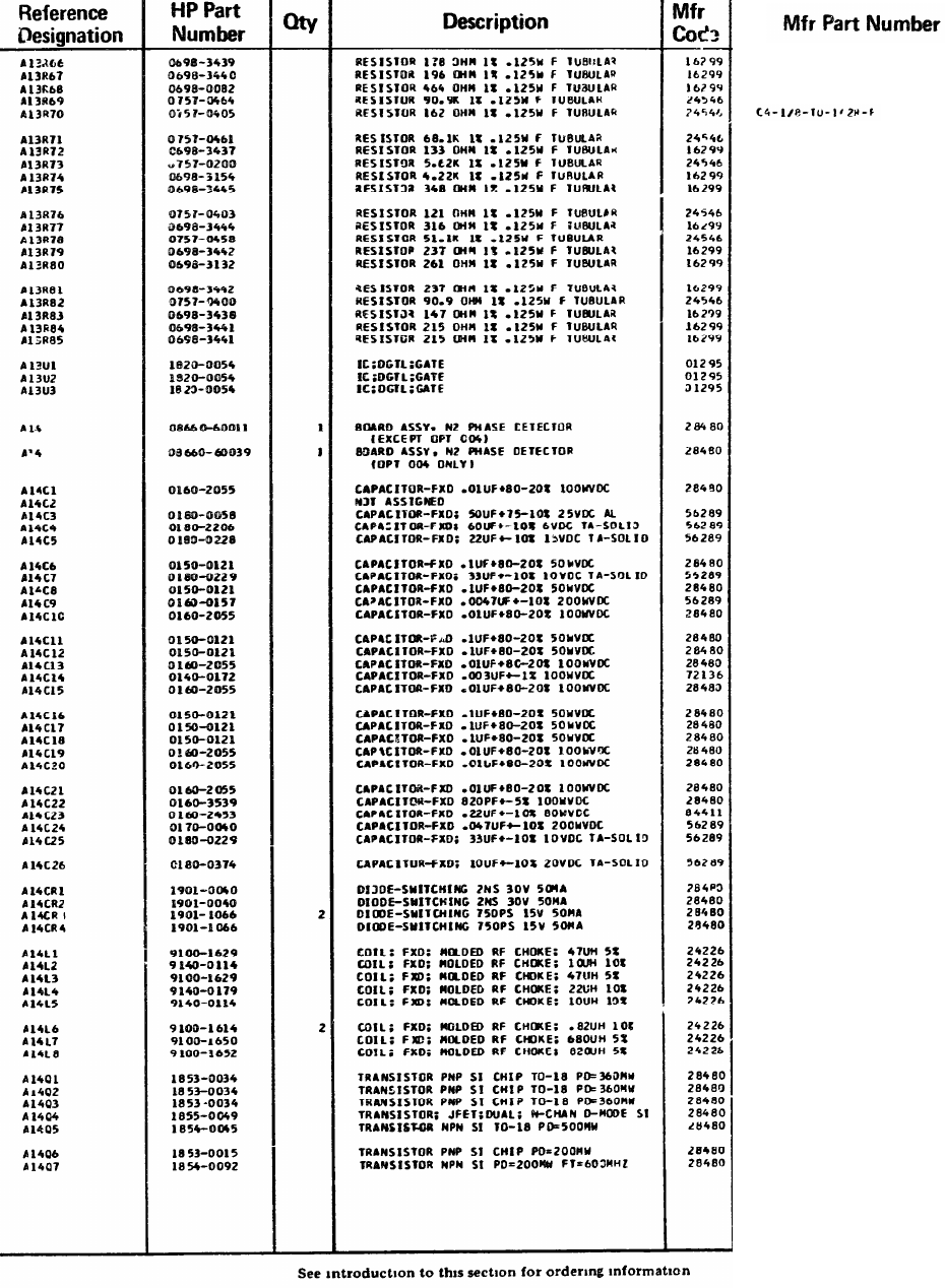
TM 11-6625-2837-14&P
Table 6-3. Replaceable Parts
C4-1/8-TO-178R-F
C4-1/8-TO-1968-F
C4-1/8-TO-4640-F
C4-1/8-TO-9092-F
C4-1/8-TO-6812-F
C4-1/8-TO-1338-F
C4-1/8-TO-5621-F
C4-1/8-TO-4221-F
C4-1/8-TO-348R-F
C4-1/8-TO-1218-F
C4-1/8-TO-316R-F
C4-1/8-TO-5112-F
C4-1/8-TO-237R-F
C4-1/8-TO-2610-F
C4-1/8-TO-237R-F
C4-1/8-TO-90R9-F
C4-1/8-TO-147R-F
C4-1/8-TO-215R-F
C4-1/8-TO-2158-F
SN7400N
SN7400N
SN7400N
08660-60011
08660-60039
0160-2055
30D506F025CC2
150D606C9006B2
150D226X9015B2
0150-0121
150D336X9010B2
0150-0121
292P47292
0160-2055
0150-0121
0150-0121
0160-2055
DM19F302F0100WV1CR
0160-2055
0150-0121
0150-0121
0150-0121
0160-2055
0160-2055
O160-2055
0160-3539
HEW-238T
292P47392
150D336X9010B2
5OD106X9020B2
1901-0040
1901-0040
1901-1066
1901-1066
15/472
15/102
15/472
15/222
15/102
15/820
19/683
19/823
1853-0034
1853-0034
1853-0034
1855-0049
1854-0045
1853-0015
1854-0092
6-38
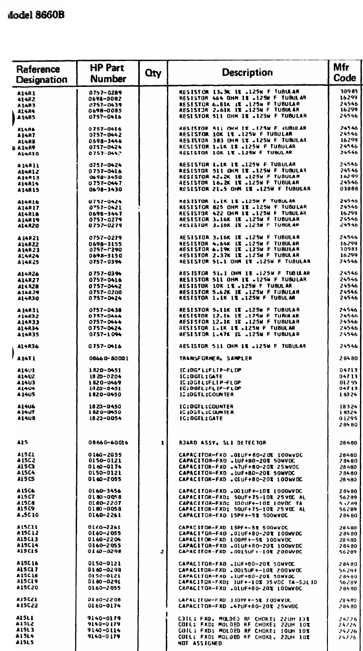
TM 11-6625-2837-14&P
Table 6-3. Replaceable Parts
Mfr Part Number
MF4C1/8-TO-1332-F
C4-1/8-TO-4640-F
C4-1/8-TO-6811-F
C4-1/8-TO-2611-F
C4-1/8-TO-511R-F
C4-1/8-TO-511R-F
C4-1/8-TO-1002-F
C4-1/8-TO-3838-F
C4-1/8-TO-1101-F
C4-1/8-TO-1002-F
C4-1/8-TO-1101-F
C4-1/8-TO-511R-F
C4-1/8-TO-4222-F
C4-1/8-TO-4622-F
C4-1/8-TO-21R5-F
C4-1/8-TO-1101-F
C4-1/8-TO-825R-F
C4-1/8-TO-422R-F
C4-1/8-TO-3161-F
C4-1/8-TO-3161-F
C4-1/8-TO-3161-F
C4-1/8-TO-4641-F
C4-1/8-TO-6191-F
C4-1/8-TO-2371-F
C4-1/8-TO-51R1-F
C4-1/8-TO-51R1-F
C4-1/8-TO-511R-F
C4-1/8-TO-1002-F
C4-1/8-TO-5621-F
C4-1/8-TO-1101-F
C4-1/8-TO-5111-F
C4-1/8-TO-1212-F
C4-1/8-TO-1212-F
C4-1/8-TO-1101-F
C4-1/8-TO-1471-F
C4-1/8-TO-511R-F
08660-80001
MC3C62P
M3006P
SN74H102W
MC3062P
N8290A
N8290A
N8290A
SN7400N
08660-6003
08660-60016
0160-2055
0150-0121
0160-0174
0150-0121
0160-2055
0160-3456
30D506G025CC2
150D107X9010R2
30D506G025CC2
0160-2261
0160-2261
0160-2055
0160-2204
0160-2055
292P15292
0150-0121
292P15292
0150-0121
150D1D5X9035A2
0160-2055
0160-2208
0160-0174
15/222
15/222
15/102
15/222
6-39
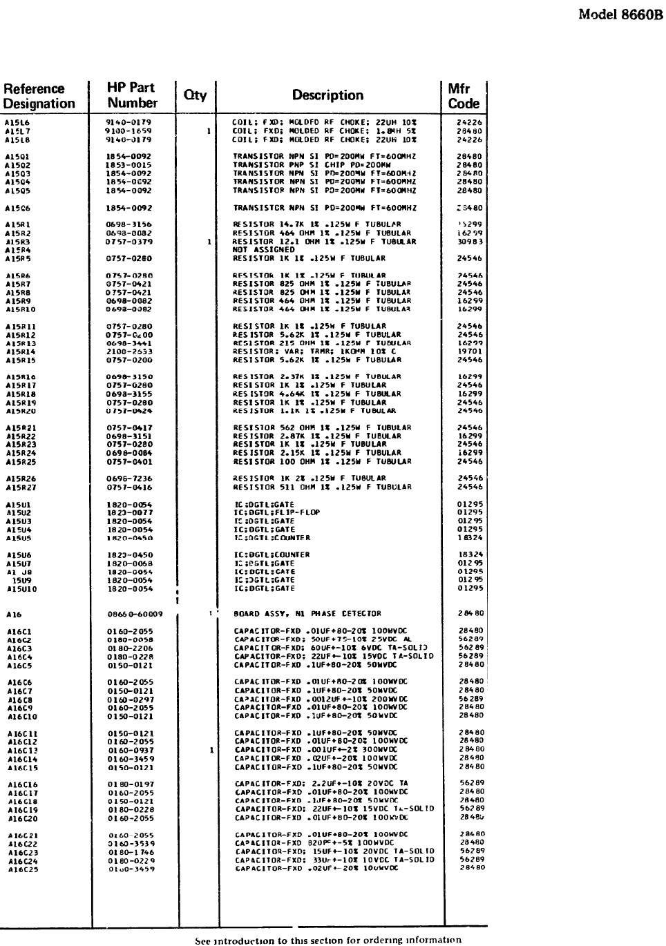
TM 11-6625-2837-14&P
Table 6-3. Replaceable Parts
Mfr Part Number
15/222
9100-1659
15/222
1854-0092
1853-0015
1854-0092
1854-0092
1854-0092
1854-0092
C4-1/8-TO-1472-F
C4-1/8-TO-4640-F
C4-1/8-TO-12R1-F
C4-1/8-TO-1001-F
C4-1/8-TO-1001-F
C4-1/8-TO-825R-F
C4-1/8-TO-825R-F
C4-1/8-TO-4640-F
C4-1/8-TO-4640-F
C4-1/8-TO-1001-F
C4-1/8-TO-5621-F
C4-1/8-TO-215R-F
ET5CX102
C4-1/8-TO-5621-F
C4-1/8-TO-2371-F
C4-1/8-TO-1001-F
C4-1/8-TO-4641-F
C4-1/8-TO-1001-F
C4-1/8-TO-1101-F
C4-1/8-TO-562R-F
C4-1/8-TO-2871-F
C4-1/8-TO-1001-F
C4-1/8-TO-2151-F
C4-1/8-TO-101-F
C4-1/8-TO-1001-G
C4-1/8-TO-511R-F
SN7400N
SN7474N
SN7400N
SN7400N
N8290A
N8290A
SN7410N
SN7400N
SN7400N
SN7400N
08660-60009
0160-2055
30D506G025CC2
150D606X9006B2
150D226X9015B2
0150-0121
0160-2055
0150-0121
292P12292
0160-2055
0150-0121
0150-021
O160-255
0160-0937
0160-3459
0150-0121
150D225X9020A2
0160-2055
0150-0121
150D226X9015B2
0160-2055
0160-2055
0160-3539
150D156X9020B2
150D336X9010B2
0160-3459
6-40
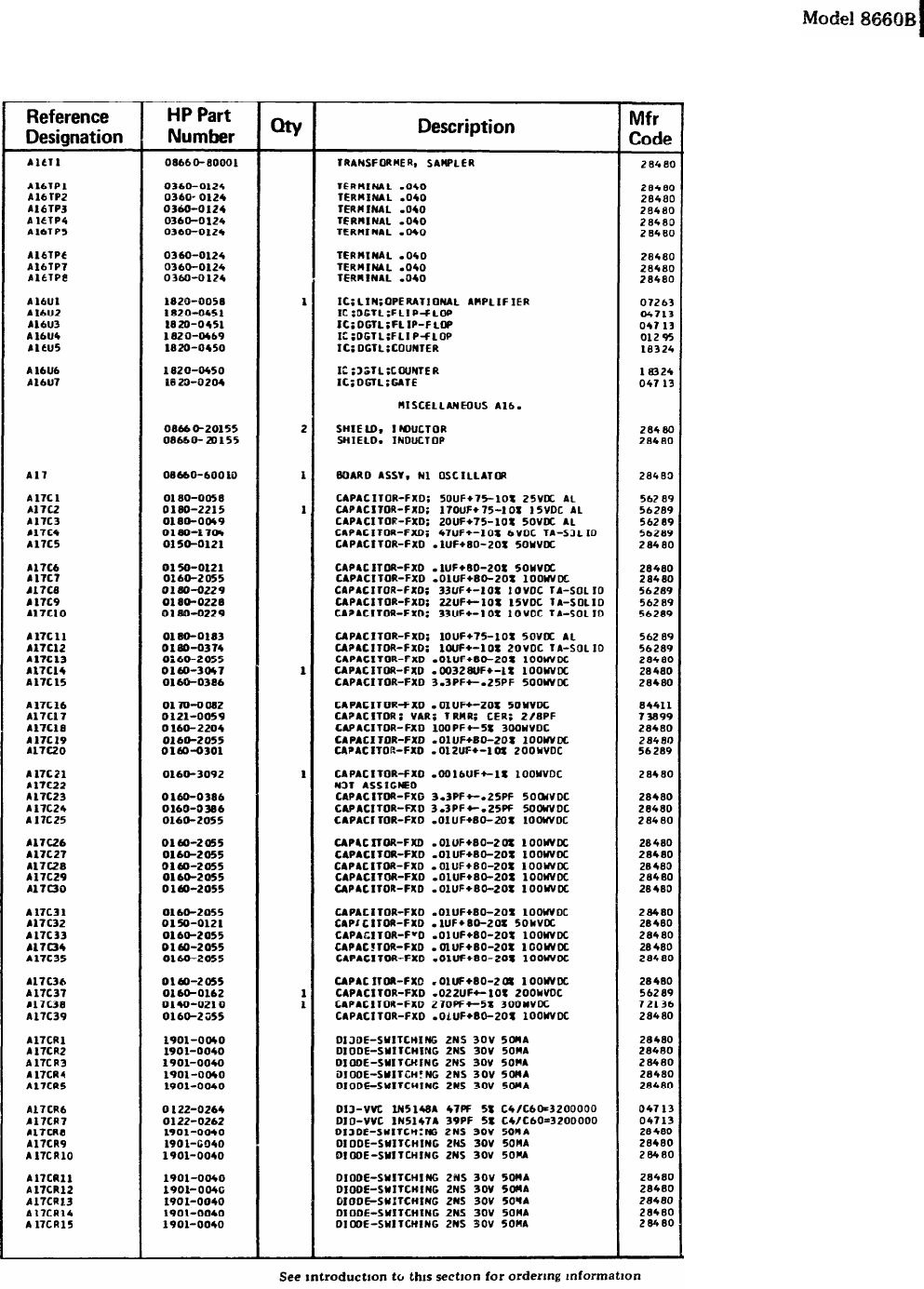
TM 11-6625-2837-14&P
Table 6-3. Replaceable Parts
Mfr Part Number
08660-80001
0360-0124
0360-0124
0360-0124
0360-0124
0360-0124
0360-0124
0360-0124
0360-0124
709HC
MC3062P
MC3062P
SN74H102N
N8290A
N8290A
MC3006P
08660-20155
08660-20155
08660-60010
30D506G025CC2
30D177G015DD2
30D206G050CC2
150D476X9006B2
0150-0121
0150-0121
0160-2055
150D336X9010B2
150D226X9015B2
150D336X9010B2
30D106G050CB2
150D106X9020B2
0160-2055
0160-3047
0160-0386
601PE1030R5W1
DV11PRBA
0160-2204
0160-2055
292P12392
0160-3092
0160-0386
0160-0386
0160-2055
0160-2055
0160-2055
0160-2055
0160-2055
0160-2055
0160-2055
0150-0121
0160-2055
0160-2055
0160-2055
0160-2055
292P22392
DM15F271J0300WV1CR
0160-2055
1901-0040
1901-0040
1901-0040
1901-0040
1901-0040
1N5148A
1N5147A
1901-0040
1901-0040
1901-0040
6-42
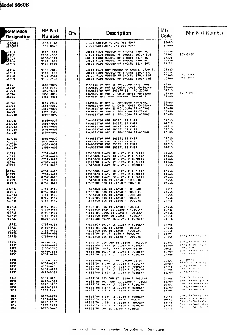
TM 11-6625-2837-14&P
Table 6-3 Replaceable Parts
1901-0040
1901-0040
15/472
15/472
15-472
15/222
9100-2815
19/823
1854-0092
1853-0050
2N5179
2N5245
1854-0087
1853-0050
1854-0092
1854-0087
1854-0092
2N3251
2N3251
2N3251
2N3251
1854-0092
2N3251
2N3251
2N3251
2N3251
C4-1/8-TO-1621-F
C4-1/8-TO-1621-F
C4-1/8-TO-1621-F
C4-1/8-TO-1621-F
C4-1/8-TO-1621-F
C4-1/8-TO-1621-F
C4-1/8-TO-1621-F
C4-1/8-TO-1621-F
C4-1/8-TO-1002-F
C4-1/8-TO-1002-F
C4-1/8-TO-1002-F
C4-1/8-TO-1002-F
C4-1/8-TO-1002-F
C4-1/8-TO-1002-F
C4-1/8-TO-1002-F
C4-1/8-TO-1002-F
MF4C1/8-TO-3923-F
C4-1/8-TO-2003-F
C4-1/8-TO-1002-F
CEA1/8/TO-4991-F
C5-1/4-TO-3922-F
C4-1/8-TO-2002-F
C4-1/8-TO-1002-F
C4-1/8-TO-5001-F
6-43
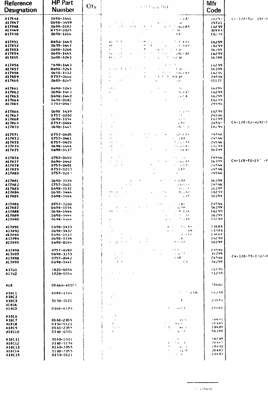
TM 11-6625-2837-14&P
Model 8660B
Table 6-3. Replaceable Parts
Mfr Part Number
MF4C1/8-TO-3833
C4-1/8-TO-4640-F
MF7C1/2-TO-6811-F
C4-1/8-TO2373-F
C4-1/8-TO-1968-F
C4-1/8-TO-4228-F
C4-1/8-TO-2373-F
C4-1/8-T0-348R-F
C4-1/8-TO-1783-F
C4-1/8-TO-287R-F
C4-1/8-TO-1783-F
C4-1/8-TO-2610-F
C4-1/8-TO-1103-F
CBB245
C4-1/8-TO-1783-F
C4-1/8-TO-196R-F
C4-1/8-TO-196R-F
C4-1/8-TO-4640-F
C4-1/8-TO-1213-F
C4-1/8-TO-178R-F
C4-1/8-TO-5621-F
C4-1/8-TO-4221-F
C4-1/8-TO-3488-F
C4-1/8-TO-1628-F
C4-1/8-TO-6812-F
C4-1/8-TO-1218-F
C4-1/8-TO-3168-F
C4-1/8-TO-1338-F
C4-1/8-TO-5112-F
C4-1/8-TO-101-F
C4-1/8-TO-5621-F
C4-1/8-TO-1001-F
C4-1/8-TO-4221-F
C4-1/8-TO-101-F
C4-1/8-TO-2610-F
C4-1/8-TO-3168-F
C4-1/8-TO-316R-F
C4-1/8-TO-5621-F
C4-1/8-TO-4221-F
C4-1/8-TO-316R-F
C4-1/8-TO-316R-F
C4-1/8-TO-316R-F
PME55-1/8-TO-2BR7-F
PME55-1/8-TO-26R1-F
PME55-1/8-TO-1BR7-F
C4-1/8-TO-4221-F
C4-1/8-TO-2151-F
C4-1/8-TO-1001-F
C4-1/8-TO-3831-F
C4-1/8-TO-2158-F
SN7400N
SN7400N
08660-60015
150D476X900682
0150-0121
0160-0174
0160-2055
0150-0121
0160-2055
292P12392
292P12392
0160-0174
0160-2055
0160-2055
0150-0121
6-44
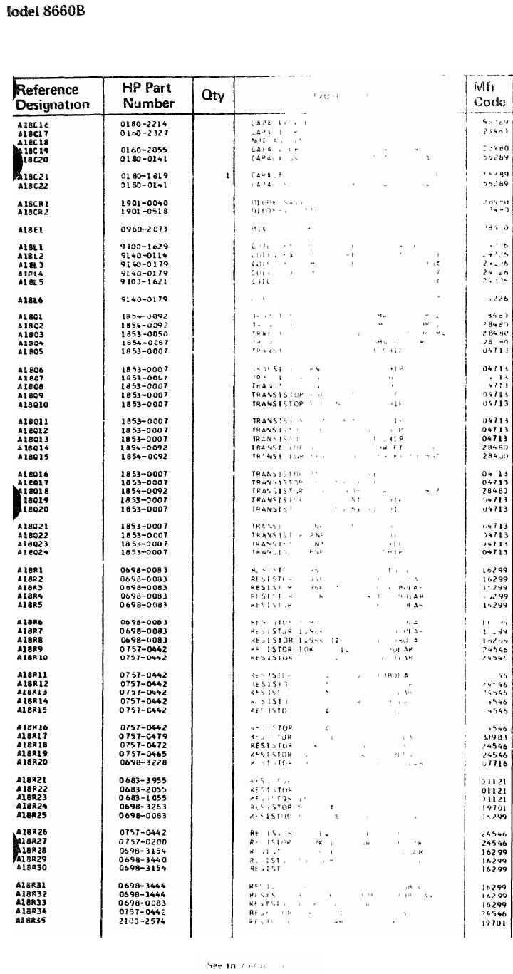
Table 6-3. Replaceable Parts
TM 11-6625-2837-14&P
Mfr Part Number
30D906G016CC2
0160-2327
0160-2055
30D506G050DD2
30D107G050DH2
305506G050FF2
1901-0040
1901-0518
0960-2073
15/472
15/102
15/222
15/222
15/182
15/222
1854-0092
1854-0092
1853-0050
1854-0087
2N3251
2N3251
2N3251
2N3251
2N3251
2N3251
2N3251
2N3251
2N3251
1854-0092
1854-0092
2N3251
2N3251
1854-0092
2N3251
2N3251
2N3251
2N3251
2N3251
2N3251
C4-1/8-TO-1961-F
C4-1/8-TO-1961-F
C4-1/8-TO-1961-F
C4-1/8-TO-1961-F
C4-1/8-TO-1961-F
C4-1/8-TO-1961-F
C4-1/8-TO-1961-F
C4-1/8-TO-1961-F
C4-1/8-TO-1002-F
C4-1/8-TO-1002-F
C4-1/8-TO-1002-F
C4-1/8-TO-1002-F
C4-1/8-TO-1002-F
C4-1/8-TO-1002-F
C4-1/8-TO-1002-F
C4-1/8-TO-1002-F
MF4C1/8-TO-3924-F
C4-1/8-TO-2003-F
C4-1/8-TO-1003-F
CEA1/8-TO-4991-F
CB3955
CB2055
CB1055
MF5C1/8-TO-5003-F
C4-1/8-TO-1961-F
C4-1/8-TO-1002-F
C4-1/8-TO-5621-F
C4-1/8-TO-4221-F
C4-1/8-TO-196R-F
C4-1/8-TO-4221-F
C4-1/8-TO-316R-F
C4-1/8-TO-316R-F
C4-1/8-TO-1961-F
C4-1/8-TO-1002-F
ET5CX501
6-45
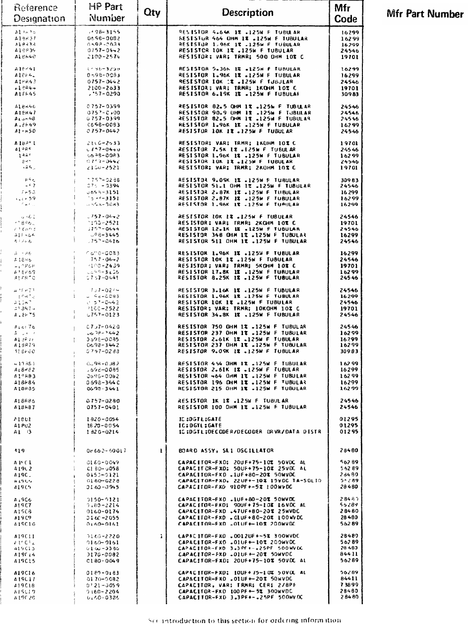
TM 11-6625-2837-14&P
Table 6-3. Replaceable Parts
Model 8660B
C4-1/8-TO-4641-F
C4-1/8-TO-4640-F
C4-1/8-TO-1961-F
C4-1/8-TO-1002-F
ET50X501
C4-1/8-TO-5361-F
C4-1/8-TO-1961-F
C4-1/8-TO-1002-F
ET50X102
MF4C/18-TO-6191-F
C4-1/8-TO-82R5-F
C4-1/8-TO-90R9-F
C4-1/8-TO-82R5-F
C4-1/8-TO-1961-F
C4-1/8-TO-1002-F
ET50X102
C4-1/8-TO-7501-F
C4-1/8-TO-1961-F
C4-1/8-TO-1002-F
ET50X202
MF4C/18-TO-9091-F
C4-1/8-TO-51R1-F
C4-1/8-TO-2871-F
C4-1/8-TO-2871-F
C4-1/8-TO-1961-F
C4-1/8-TO-1002-F
ET50X202
C4-1/8-TO-1212-F
C4-1/8-TO-348R-F
C4-1/8-TO-511R-F
C4-1/8-TO-1961-F
C4-1/8-TO-1002-F
ET50X502
C4-1/8-TO-1782-F
C4-1/8-TO-8251-F
C4-1/8-TO-3161-F
C4-1/8-TO-1961-F
C4-1/8-TO-1002-F
ET50X103
C5-1/4-TO-3482-F
C4-1/8-TO-751-F
C4-1/8-TO-237R-F
C4-1/8-TO-2611-F
C4-1/8-TO-237R-F
MF4C1/8-TO-9091-F
C4-1/8-TO-4640-F
C4-1/8-TO-2611-F
C4-1/8-TO-4640-F
C4-1/8-TO-196R-F
C4-1/8-TO-215R-F
C4-1/8-TO-1001-F
C4-1/8-TO-101-F
SN7400N
SN7400N
SN7442H
08660-60017
30D206G050CC2
30D506G25CC2
0150-0121
150D226X9015B2
0160-0945
0150-0121
30D906G016CC2
0160-0174
0160-2055
292P10392
0260-2220
292P10392
0160-0386
601PE1030R5W1
30D206G050CC2
30D106G050CB2
601PE1030R5W1
DV11PR8A
0160-2204
0160-0386
6-46
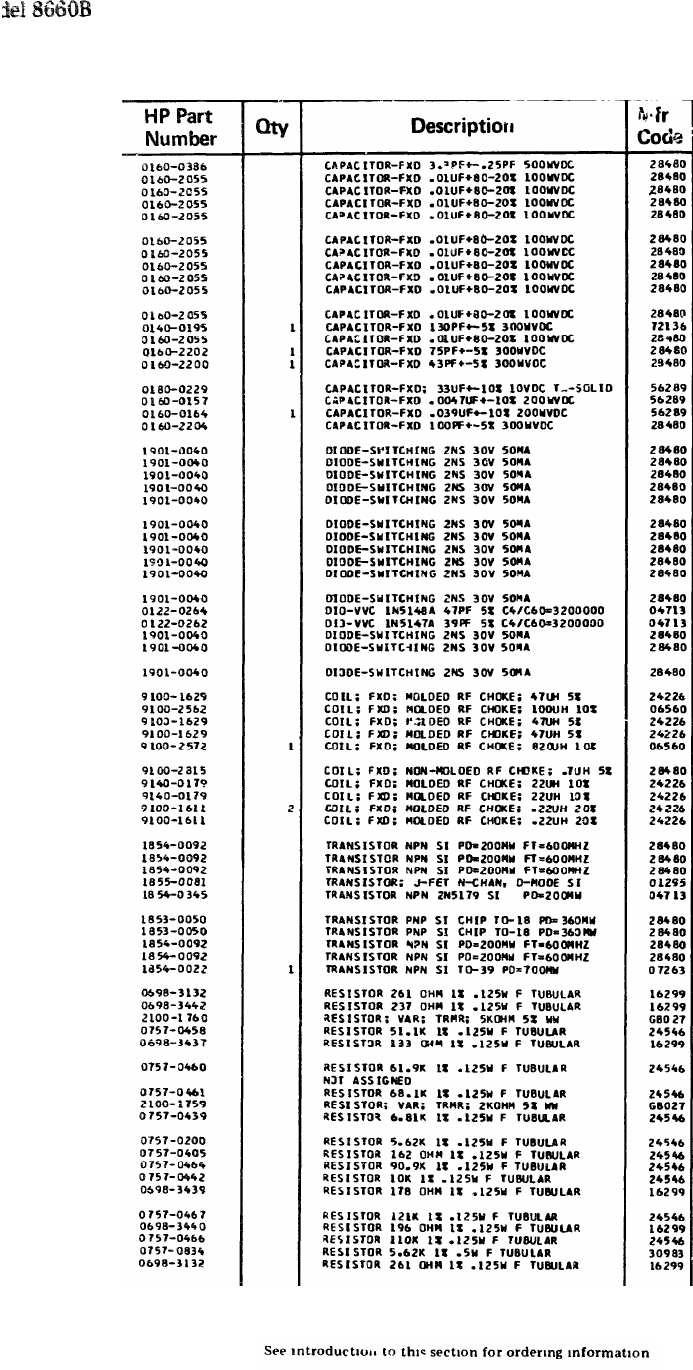
TM 11-6625-2837-14&P
Table 6-3. Replaceable Parts
Mfr Part Number
0160-0386
0160-2055
0160-2055
0160-2055
0160-2055
0160-2055
0160-2055
0160-2055
0160-2055
0160-2055
0160-2055
DM15F131J0300WV1CR
0160-2055
0160-2202
0160-2200
150D336X9010B2
292P47292
292P39392
0160-2204
1901-0040
1901-0040
1901-0040
1901-0040
1901-0040
1901-0040
1901-0040
1901-0040
1901-0040
1901-0040
1901-0040
1N5148A
1N5147A
1901-0040
1901-0040
1901-0040
15/472
l5S-101K
15/472
15/472
15S-821K
9100-2815
15/222
15/222
15/220
15/220
1854-0092
1854-0092
1854-0992
2N5245
215179
1853-0050
1853-0050
1854-0092
1854-0092
S17843
C4-1/8-TO-2610-F
C4-1/8-TO-237R-F
CT-106-4
C4-1/8-TO-5112-F
C4-1/8-TO-133R-F
C4-1/8-TO-6192-F
C4-1/8-TO-6812-F
CT-106-4
C4-1/8-TO-6811-F
C4-1/8-TO-5621-F
C4-1/8-TO-162R-F
C4-1/8-TO-9092-F
C4-l/8-TO-1002-F
C4-l/8-TO-178R-F
C4-1/8-TO-1213-F
C4-1/8-TO-196R-F
C4-1/8-TO-1103-F
MF7C1/2-TO-5621-F
C4-1/8-TO-2610-F
6-47
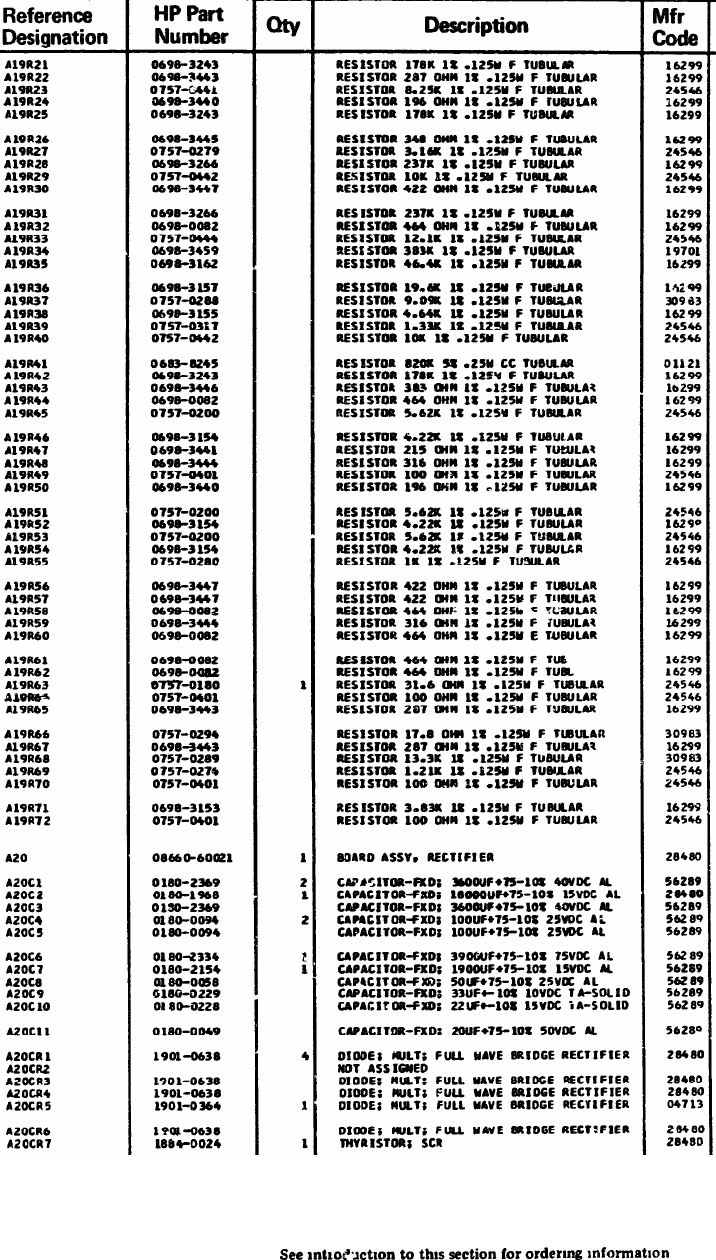
TM 11-6625-2837-14&P
Table 6-3. Replaceable Parts
Model 8660B
Mfr Part Number
C4-1/8-TO-1783-F
C4-1/8-TO-287R-F
C4-1/8-TO-8251-F
C4-1/8-TO-196R-F
C4-1/8-TO-1783-F
C4-1/8-TO-348R-F
C4-1/8-TO-3161-F
C4-1/8-TO-2373-F
C4-1/8-TO-1002-F
C4-1/8-TO-422R-F
C4-1/8-TO-2373-F
C4-1/8-TO-4640-F
C4-1/8-TO-1212-F
C4-1/8-TO-3833-F
C4-1/8-TO-4642-F
C4-1/8-TO-1962-F
C4-1/8-TO-9091-F
C4-1/8-TO-4641-F
C4-1/8-TO-1331-F
C4-1/8-TO-1002-F
CB8245
C4-1/8-TO-1783-F
C4-1/8-TO-383R-F
C4-1/8-TO-4640-F
C4-1/8-TO-5621-F
C4-1/8-TO-4221-F
C4-1/8-TO-215R-F
C4-1/8-TO-316R-F
C4-1/8-TO-101-F
C4-1/8-TO-196R-F
C4-1/8-TO-5621-F
C4-1/8-TO-4221-F
C4-1/8-TO-5621-F
C4-1/8-TO-4221-F
C4-1/8-TO-1001-F
C4-1/8-TO-422R-F
C4-1/8-TO-422R-F
C4-1/8-TO-4640-F
C4-1/8-TO-316R-F
C4-1/8-TO-4640-F
C4-1/8-TO-4640-F
C4-1/8-TO-4640-F
C4-1/8-TO-31R6-F
C4-1/8-TO-101-F
C4-1/8-TO-287R-F
MF4C17R8-F
C4-1/8-TO-287R-F
MF4C1/8-TO-1332-F
C4-1/8-TO-1213-F
C4-1/8-TO-101-F
C4-1/8-TO-3831-F
C4-1/8-TO-101-F
08660-60021
36D362G040AB2B
0180-1968
36D362G040AB2B
30D107G025DD2
30D107G025DD2
36D392F075BB2B
39D19BG015GL4
30D506G025CC2
150D336X9010B2
150D226X9015B2
30D203G05CC2
1901-0638
1901-0638
1901-0638
SDA 10185-4
1901-0638
18B4-0024
6-48
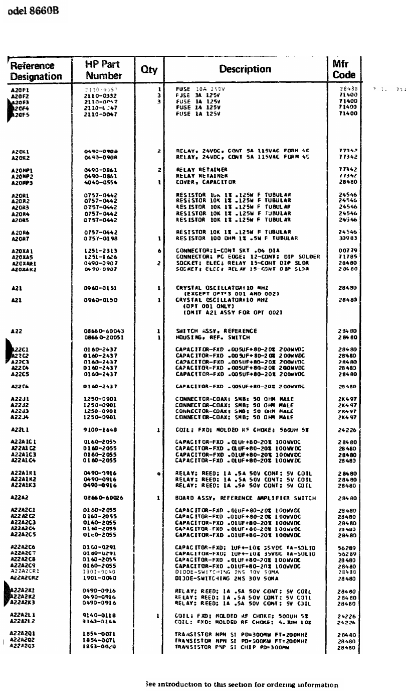
TM 11-6625-2837-14
Table 6-3. Replaceable Parts
Mfr Part Number
GMW 3
TYPE GMW-l/2
TYPE GMW-1/2
TYPE GMW-1/2
R40-F1-X4-V800
R40-E1-X4-V800
R40-P33
R40-P33
4040-0554
C4-1/8-TO-1002-F
C4-1/8-TO-1002-F
C4-1/8-TO-1002-F
C4-1/8-TO-1002-F
C4-1/8-TO-1002-F
C4-1/8-TO-1002-F
MF7C1/2-TO-101-F
3-332070-5
252-12-30-300
0490-0907
0490-0907
0960-0151
0960-0150
08660-60043
08660-20051
0160-2437
0160-2437
0160-2437
0160-2437
0160-2437
0160-2437
700166
700166
700166
700166
19/563
0160-2055
0160-2055
0160-2055
0160-2055
0490-0916
0490-0916
0490-0916
C8660-60026
0160-2055
0160-2055
0160-2055
0160-2055
0160-2055
150D105X9035A2
0160-2055
0160-2055
1901-0040
1901-0040
0490-0916
0490-0916
0490-0916
19/503
10/471
1854-0071
1854-0071
1853-0020
6-49
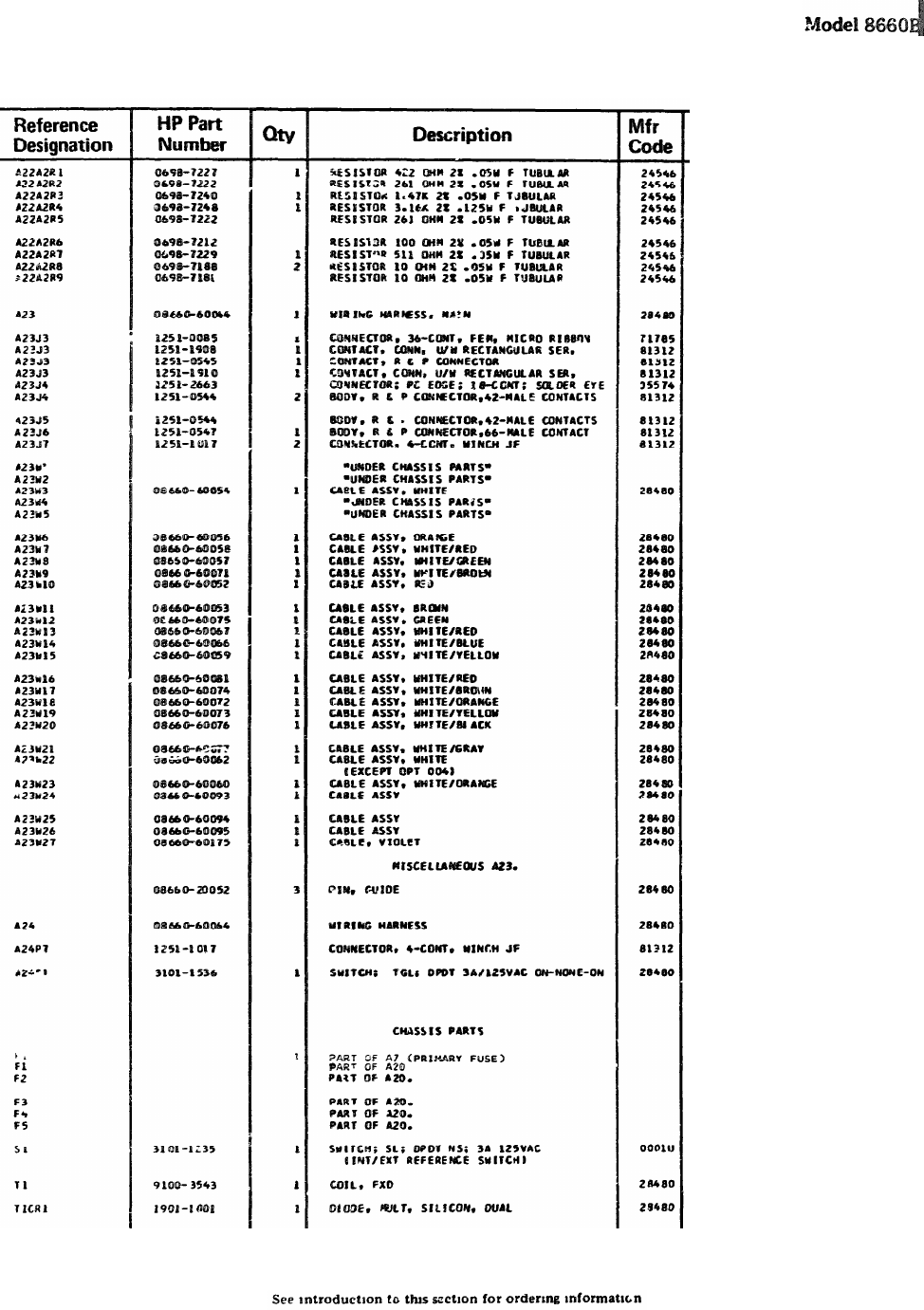
TM 11-6625-2837-14&P
Table 6-3. Replaceable Parts
Mfr Part Number
C3-1/8-TO-4223-G
G3-1/8-TO-2618-G
C3-1/8-TO-1471-G
C3-1/8-TO-3161-G
C3-l/8-TO-2618-G
C3-1/8-TO-100R-G
C3-1/8-TO-511R-G
C3-1/8-TOO-108-G
C3-1/8-TOO-10R-G
08660-60044
57-40360-375
l00-1022P
111-17054P
100-1016P
3VH18/1JN5
MRAC42PG-4192
MRAC42PG-4192
MRAC66PG-4193
JF2S-2P-AB
08660-60054
08660-60056
08660-60058
08660-60057
08660-60072
08660-60052
08660-60053
08660-60075
08660-60067
08660-6066
08660-60059
08660-60081
08660-60074
08660-60072
08660-60073
08660-60076
08660-60077
08660-60062
08660-60060
08660-60093
08660-60094
08660-60095
08660-60175
08660-20052
08660-60064
JF2S 2P-AB
3101-1536
SW 322
9100-3543
1901-1001
6-50
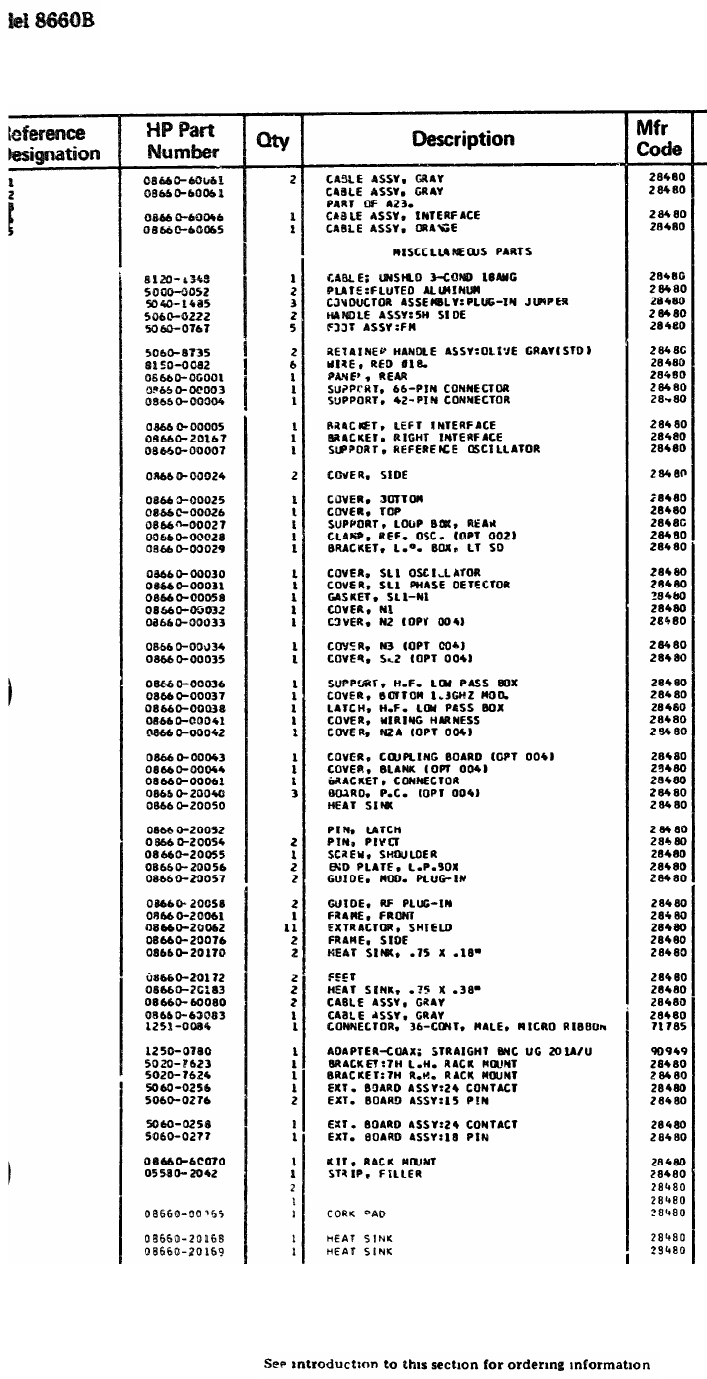
TM 11-6625-2837-14&P
Table 6-3. Replaceable Parts
Mfr Part Number
08660-60061
08660-60061
08660-60046
08660-60065
8120-1348
5000-0052
5040-1485
5060-0222
5060-0767
5060-8735
8150-0082
08660-00001
08660-00003
08660-00004
08660-00005
08660-20167
08660-00007
08660-00024
08660-00025
08660-00026
08660-00027
08660-00028
08660-00029
08660-00030
08660-00031
08660-00058
08660-00032
08660-00033
08660-00034
08660-00035
08660-00036
08660-00037
08660-00038
08660-00041
08660-00042
08660-00043
08660-00044
08660-00061
08660-20040
08660-20050
08660-20052
08660-20054
08660-20055
08660-20056
08660-20057
08660-20058
08660-20061
08660-20062
08660-20076
08660-20170
08660-20172
08660-20183
08660-60080
08660-60083
57-30360-375
31-216-1020
5020-7623
5020-7624
5060-0256
5060-0276
5060-0258
5060-0277
08660-60070
05580-2042
08660-00055
08660-20168
08660-20169
6-51
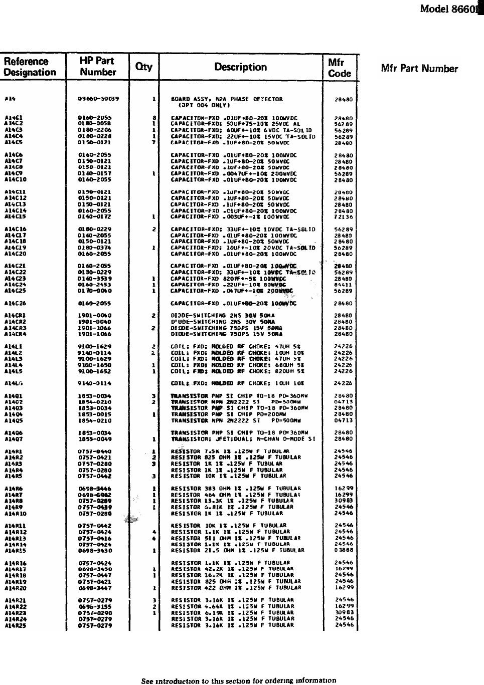
TM 11-6625-2837-14&P
Table 6-3. Replaceable Parts
08660-60039
0160-2055
30D506G025CC2
150D606X9006B2
150D226X9015B2
0150-0121
0160-2055
0150-0121
0150-0121
252P47292
0160-2055
0150-0121
0150-0121
0150-0121
0160-2055
DM19F302F0100WV1CR
150D336X9010B2
0160-2055
0150-0121
150Dl06X9020B2
0160-2055
0160-2055
150D336X9010B2
0160-3539
HEW-238T
292P47392
0160-2055
1901-0040
1901-0040
1901-1066
190l-1066
15/472
15/102
15/472
19/683
19/823
15/102
1853-0034
2N2222
1853-0034
1853-0015
2N2222
1853-0034
1855-0049
C4-7501-F
C4-1/8-TO-825R-F
C4-1/8-TO-1001-F
C4-1/8-TO-1001-F
C4-1/8-TO-1002-F
C4-1/8-TO-383R-F
C4-1/8-TO-4640-F
MF4C1/8-TO-1332-F
C4-1/8-TO-6811-F
C4-1/8-TO-1001-F
C4-1/8-TO-1002-F
C4-1/8-TO-1101-F
C4-1/8-TO-511R-F
C4-1/8-TO-1101-F
PME55-1/8-TO-21R5-F
C4-1/8-TO-1101-F
C4-1/8-TO-4222-F
C4-1/8-TO-1622-F
C4-1/8-TO-825R-F
C4-1/8-TO-422R-F
C4-1/8-TO-3161-F
C4-1/8-TO-4641-F
MF4C1/8-TO-6191-F
C4-1/8-TO-3161-F
C4-1/8-TO-3161-F
6-52
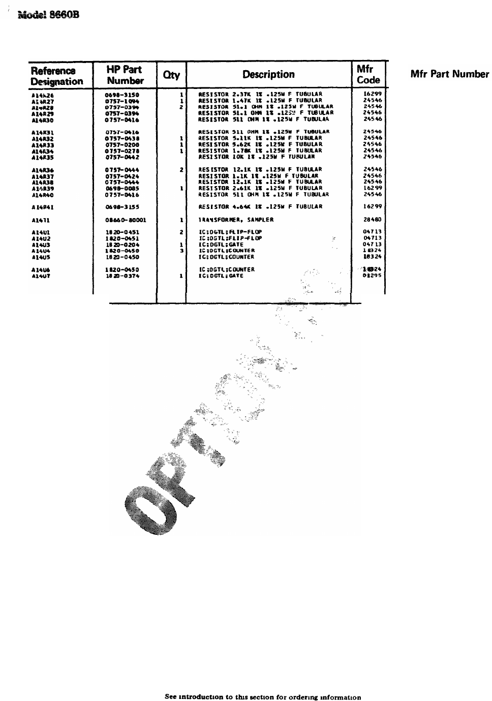
TM 11-6625-2837-14&P
Table 6-3. Replaceable Parts
C4-1/8-TO-2371-F
C4-1/8-TO-1471-F
C4-1/8-TO-51R1-F
C4-1/8-TO-51R1-F
C4-1/8-TO-511R-F
C4-1/8-TO-511R-F
C4-1/8-TO-5111-F
C4-1/8-TO-5621-F
C4-1/8-TO-1781-F
C4-1/8-TO-1002-F
C4-1/8-TO-1212-F
C4-1/8-TO-1101-F
C4-1/8-TO-1212-F
C4-1/8-TO-2611-F
C4-1/8-TO-511R-F
C4-1/8-TO-4641-F
08660-80001
MC3062P
MC3062P
MC3006P
N8290A
N8290A
N8290A
SN74H21N
6-53

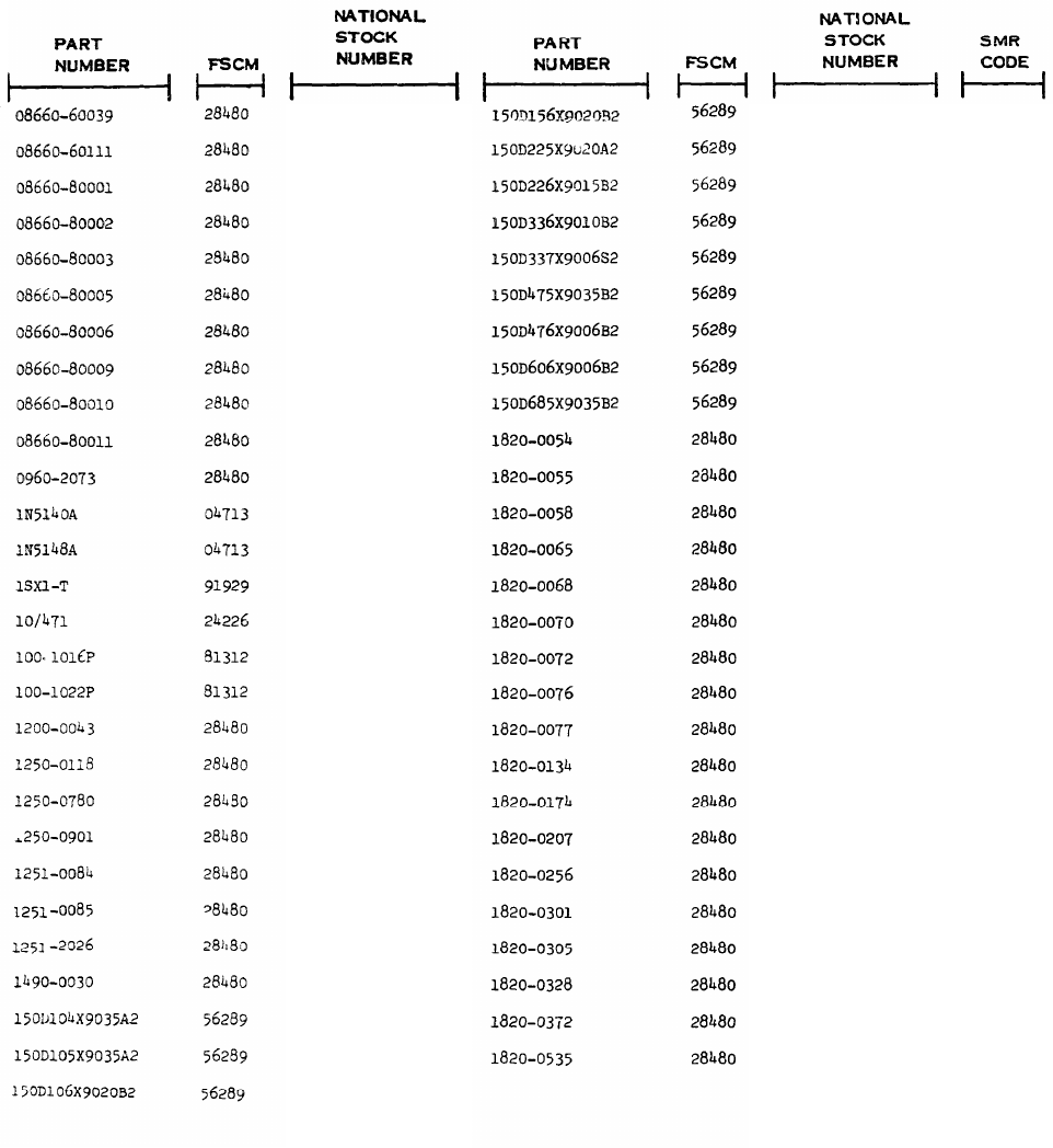
PART NUMBER - NATIONAL STOCK NUMBER
TABLE 6-5.
CROSS REFERENCE INDEX
TM 11-6625-2837-14&P
6625-01-022-8441
6625-00-532-3071
5950-00-443-9519
5950-00-443-4515
5950-00-443-9516
5950-00-443-9518
5950-00-511-324
5950-00-511-3125
5950-00-511-3130
5950-90-511-3134
5985-00-443-9520
5961-00-257-1688
5961-00-110-0919
5930-00-450-0856
5950-00-961-9600
5999-00-688-4420
5999-00-831-4101
5970-00-805-7166
5935-00-897-9351
5935-00-761-5765
5935-00-477-1147
5935-00-828-0536
5935-00-778-9955
5935-00-446-8768
6625-00-760-9521
5910-00-189-3178
5910-00-104-0144
5910-00-812-2752
5910-00-235-2356
5910-00-177-2581
5910-00-807-7253
5910-00-722-4117
5910-00-878-6691
5910-00-177-4300
5910-00-851-2092
5910-00-897-7313
5910-00-809-4701
5962-00-138-5248
5962-00-493-5961
5962-00-001-3105
5962-00-420-1654
5962-00-865-4626
5962-00-166-3842
5962-00-409-3517
5962-00-420-1677
5962-00-138-5250
5962-00-460-5744
5962-00-404-2559
5962-01-030-0239
596200-184-8205
5962-00-270-1960
5962-00-011-2762
5962-00-009-1356
5962-00-495-4981
5962-00-788-0298
6-55
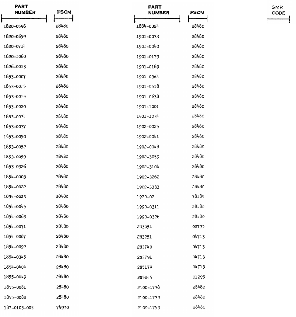
TM 11-6625-2837-14&P
TABLE 6-5.
PART NUMBER -
NATIONAL STOCK NUMBER
CROSS REFERENCE INDEX
6-56
NATIONAL
STOCK
NUMBER
5962-00-615-7767
5962-01-006-3618
5962-00-504-0491
5962-00-511-3891
5962-00-247-9568
5961-00-765-6071
5961-00-927-0845
5961-00-950-1642
5961-00-904-2540
5961-00-987-4700
5961-00-229-1962
5961-00-138-7314
5961-00-927-5042
5961-00-904-2021
5961-00-471-2984
5961-00-990-5369
5961-00-917-0660
5961-00-998-1923
5961-00-059-3063
5961-00-985-9074
5961-00-137-4608
5961-00-824-7567
5961-00-943-7572
5961-00-401-0507
5961-00-408-9807
5961-00-520-5000
5961-00-350-8299
5961-00-442-9470
5910-00-513-0848
NATIONAL
STOCK
NUMBER
5961-00-517-9588
5961-00-821-0710
5961-00-965-5917
5961-00-853-7934
5961-00-739-0069
5961-00-009-8094
5961-00-430-6819
5961-00-471-2987
5961-00-405-8240
5961-00-486-7171
5961-00-914-3087
5961-00-858-7372
5961-00-912-3099
5961-00-458-4506
5961-00-494-8988
5961-00-471-2985
5961-00-137-4685
5310-00-262-0359
5961-00-513-2830
5961-00-513-2831
5961-00-012-4215
5961-00-760-0960
5961-00-927-5042
5961-00-827-4997
5961-00-401-0507
5961-00-350-8299
5905-00-256-8993
5905-00-885-7041
5905-00-221-7472
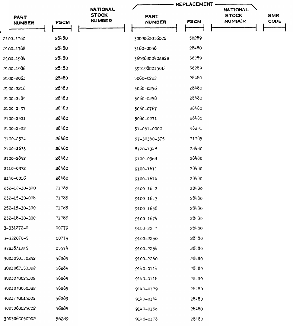
TM 11-6625-2837-14&P
TABLE 6-5.
PART NUMBER -
NATIONAL STOCK NUMBER
CROSS REFERENCE INDEX
5905-00-229-1971
5905-00-407-2402
5905-00-139-2305
5905-00-139-2306
5905-00-105-1775
5905-00-113-3613
5905-00-105-1774
5905-00-405-1341
5905-00-170-3842
5905-00-476-5797
5905-00-139-2307
5905-00-476-5796
5905-00-488-3222
5920-00-921-6502
6240-00-060-2941
5935-00-448-2236
5935-00-138-5209
5935-00-405-7720
5935-00-446-8768
5999-00-137-1142
5935-00-104-1184
5935-01-014-6185
5910-00-043-1396
5910-00-823-1548
5910-00-827-1209
5910-00-843-0354
5910-00-187-2609
5910-00-027-7069
5910-00-879-0123
5910-00-138-7324
4140-00-758-6113
5910-00-488-3010
5910-00-938-7424
5340-00-435-5340
6625-00-004-9601
6625-00-003-3633
6625-00-903-0348
5961-00-513-2726
5935-00-539-1940
5935-00-807-5357
6150-01-004-8773
5950-00-131-8317
5950-00-438-4375
5950-00-431-3192
5950-00-443-9513
5050-00-443-3517
5950-00-850-8016
5950-00-443-9521
5950-00-405-3735
5950-00-138-1356
5950-00-008-4471
5950-00-922-9179
5950-00-657-8167
5950-00-932-2727
5950-00-845-6927
5950-00-337-6029
5950-00-059-5920
5950-00-199-7652
6-57
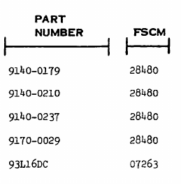
TM 11-6625-2837-14&P
TABLE 6-5.
PART NUMBER -
NATIONAL
STOCK NUMBER
CROSS REFERENCE INDEX
NATIONAL
NATIONAL
STOCK PART
STOCK
NUMBER NUMBER
FSCM
NUMBER
5950-00-225-2177
5950-00-431-3215
5950-00-431-3216
5950-00-406-6419
5962-01-006-7496
6-58
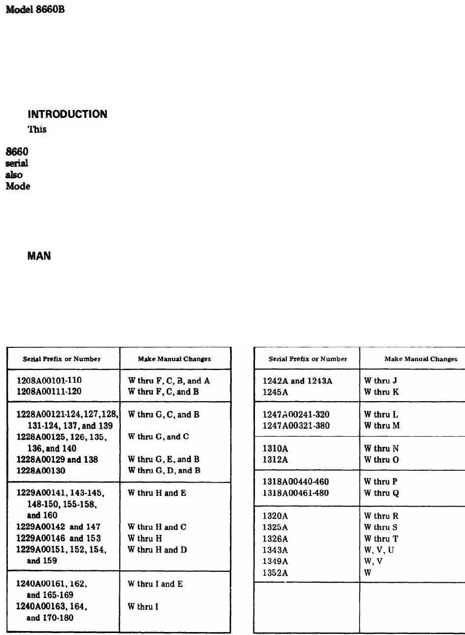
TM 11-6625-2837-14&P
SECTION VII
MANUAL CHANGES
7-1.
7-2.
section contains manual change infor-
mation for backdating this manual for HP Model
B Synthesized Signal Generators which have
number prefixes below 1402A. This section
contains information relative to updating
l 8660B instruments having serial prefixes of
1349A and below. The recommended Field Update
Kit is designed to improve the performance and
reliability of your synthesized Signal Generator.
which are adjacent to your instrument serial prefix
number. The changes should be made in the
sequence listed. For example, for the instrument
with serial number 1228A00138 make changes W
through G, E, and B in that order.
Table 7-2 is a cross reference of changes to
assemblies to which they apply.
7-5. Refer to paragraph 7-12 for manual
changes pertaining to later serial num-
bered instruments,
7-3. UAL CHANGES
7-4. To adapt this manual to your instrument,
refer to Table 7-1 and make all of the changes
Table 7-1. Manual Changes by Serial Number
7-1

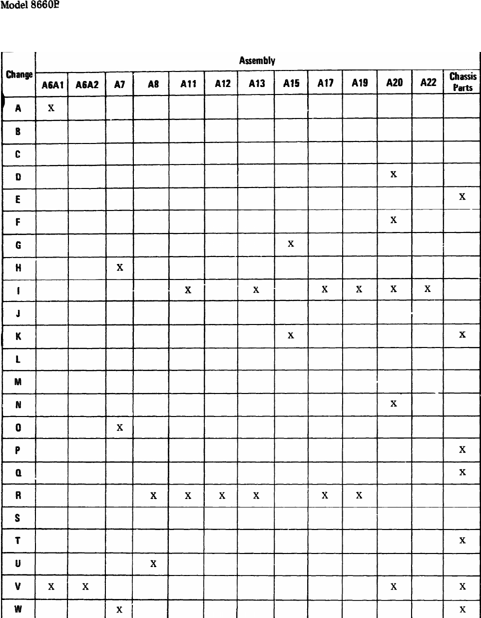
TM 11-6625-2837-14&P
Table 7-2. Summary of Changes by Assembly (2 of 2)
7-3

TM 11-6625-2837-14&P Model 8660B
7-6. MANUAL CHANGE INSTRUCTIONS
CHANGE A
Table 6-3 and A1A1 Schematic (SS19 and 20):
Change A1A1U19 to 1820-0596 IC Digital
Delete A1A1R23 from A1A1U19 pin 1 to ground
A1A2 Schematic (SS21):
Delete ground connection from A1A2U7 pin 12
Table 6-3 and A1A7 Schematic (SS32):
Delete A1A7R5 from A1A7U19 pin 19 to A1A7U19 pin 7
Table 6-3 and Power Supply Schematic (SS42):
Change A6A1C10 to 0160-0013 CF 0.1 uF
CHANGE B
Table 6-3 and A1A8 Schematic (SS33):
CHANGE C
Table 6-3 and A1A12 Schematic (SS36)
Delete A1A12C3
CHANGE D
Table 6-3 and A20 Schematic (SS42)
Add A20C12, 0160-3451 CF 0.01 uF connected between the +4V point and ground on A20
Table 6-3 and A1A12 Schematic (SS36):
Delete A1A12C3
CHANGE E
Table 6-3:
Add Cl, 0160-3451 CF 0.01 uF connected between the yellow and black wires on A23J7.
Table 6-3 and A1A12 Schematic (SS36):
Delete A1A12C3
CHANGE F
Table 6-3 and A1A3 Schematic (SS24):
Delete A1A3R12 in series with A1A3U15B pin 6. Replace with jumper wire.
Delete A1A C11 from A1A3U22C pin 10 to ground
Change A1A3 C9 to 0140-0196 CF 150 pF
7-4
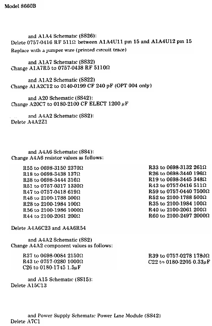
TM 11-6625-2837-14&P
CHANGE F (Cont'd)
Table 6-3.
Table 6-3.
Table 6-3.
Table 6-3.
Table 6-3.
CHANGE G
Table 6-3.
Table 6-3.
Table 6-3.
CHANGE H
Table 6-3.
7-5
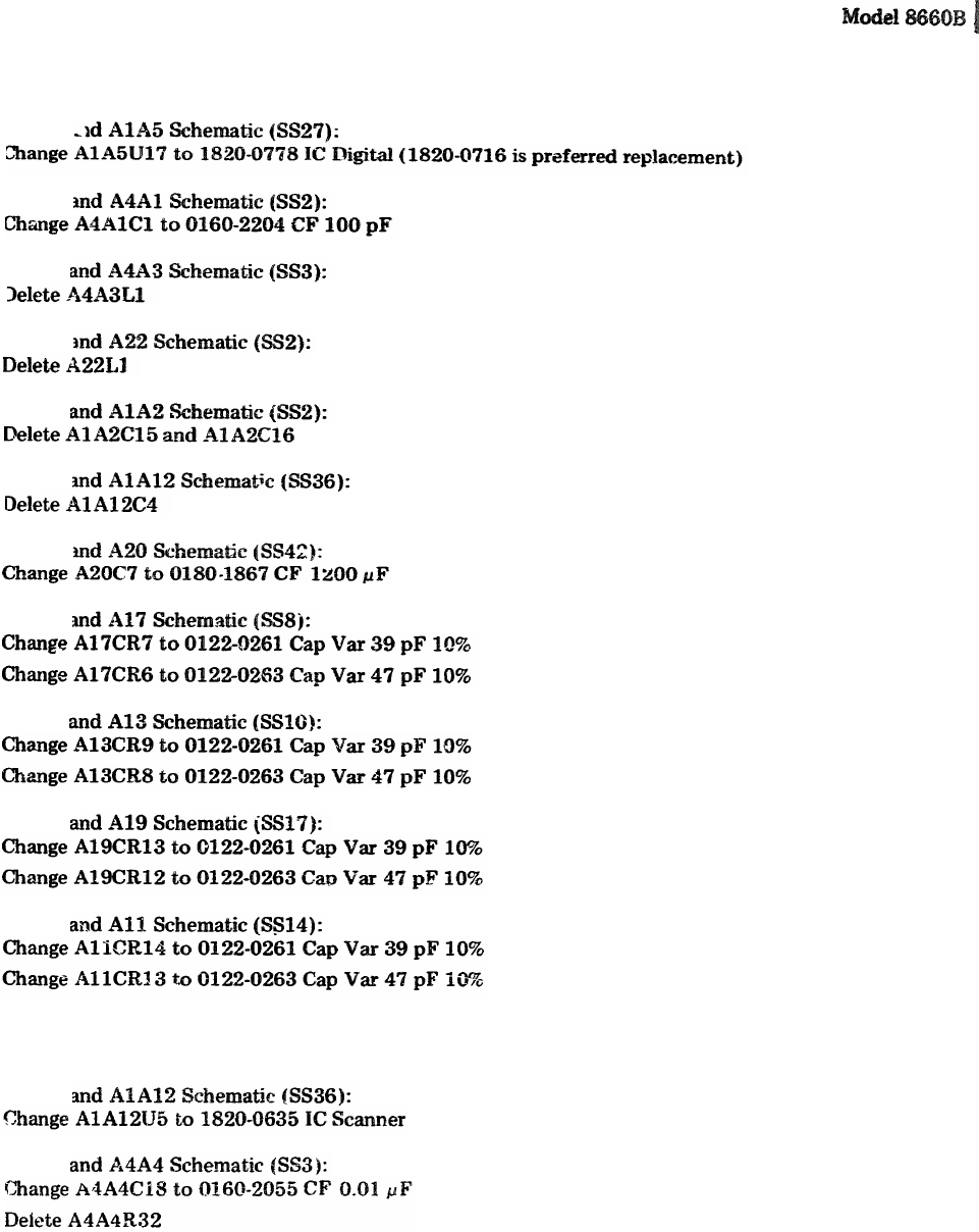
TM 11-6625-2837-14&P
CHANGE I
Table 6-3.
Table 6-3.
Table 6-3.
Table 6-3.
Table 6-3.
Table 6-3.
Table 6-3.
Table 6-3.
Table 6-3.
Table 6-3.
Table 6-3.
CHANGE J
Table 6-3.
Table 6-3.
7-6
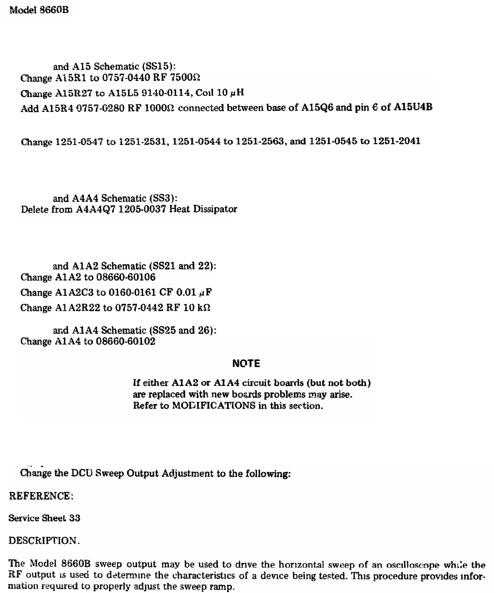
TM 11-6625-2837-14&P
CHANGE K
Table 6-3.
Table 6-3:
CHANGE L
Table 6-3.
CHANGE M
Table 6-3.
Table 6-3.
CHANGE N
Paragraph 5-21:
7-7
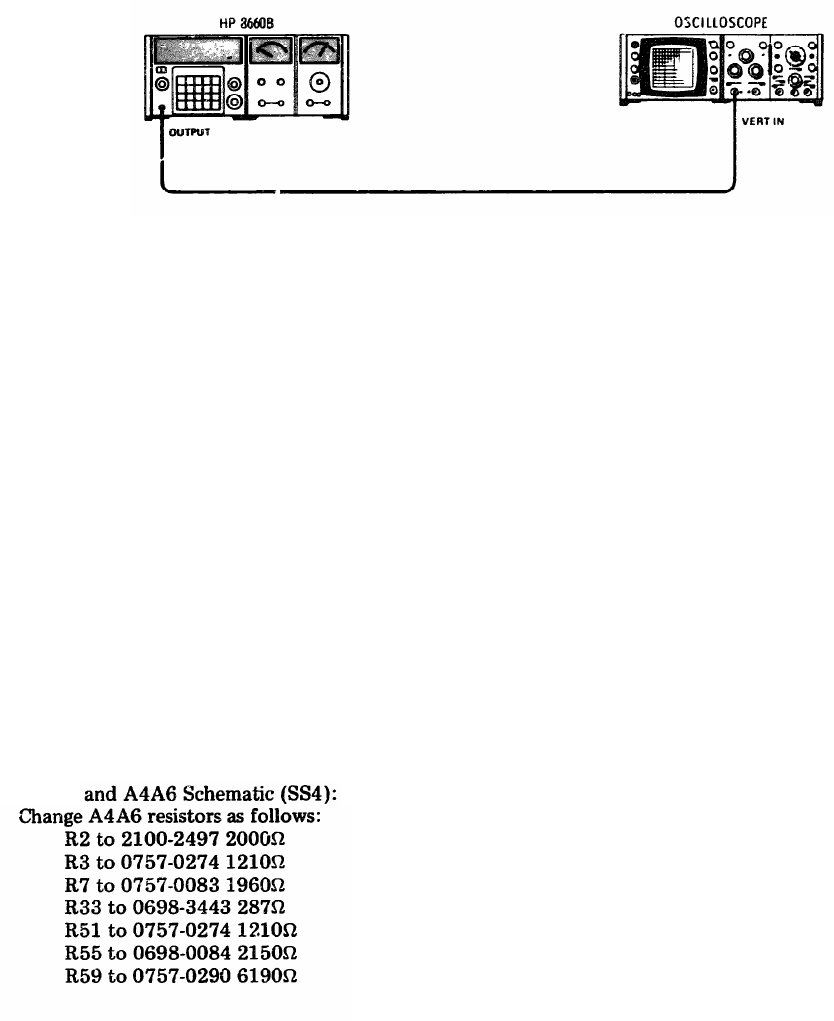
TM 11-6625-2837-14&P
CHANGE N (Cont’d)
Figure 7-1. Sweep Ramp Test Setup
RECOMMENDED TEST EQUIPMENT:
Oscilloscope (with 10:1 divider probes) . . . . . . HP 180A/1801A/1820A
PROCEDURE: (See Figure 7-1)
1. Connect the oscilloscope to the 8660B mainframe OUTPUT (0 - 5V). Set the oscilloscope
vertical sensitivity to 2 V/Div and the sweep speed to 20 ms/Div.
2.
Set the Model 8660B center frequency to 5 MHz, SWEEP MODE switch to AUTO and the SWEEP
MODE RATE to FAST.
3. Sweep ramp should go from 0 to +5 volts in 100 milliseconds. Adjust A1A8R4 for a ramp peak of
+5v.
4. Set the SWEEP RATE switch to MED. Set the oscilloscope to 0.2 Sec/Div Sweep ramp should
go from 0 to +5 volts in 1 second.
5. Set the SWEEP RATE switch to SLO. Set the oscilloscope to 1 Sec/Div. The sweep ramp should
go from 0 to +5 volts in 10 seconds.
Table 6-3.
7-8


TM 11-6625-2837-14&P
CHANGE O
Table 6-3:
Delete A1A1C2 and C3
Table 6-3 and A7 Schematic (SS24):
Change A7C1 to 0160-3229 CF 0.1 uF
CHANGE P
Table 6-3:
Add 08660-00021 Filter: Side
CHANGE Q
Table 6-3:
Add 08660-00006 Bracket; Interface, Right
Delete 08660-00061 and 08660-20167
CHANGE R
Table 6-3 and A8 Schematic (SS12):
Change A8Q8 through Q11 to 1853-0066
Table 6-3 and A11 Schematic (SS14):
Change A11Q7 through Q14 and Q16 through Q20 to 1853-0066
Table 6-3 and A12 Schematic (SS13):
Change A12Q8 through Q11 to 1853-0066
Table 6-3 and A13 Schematic (SS10):
Change A13Q5 through Q8 and Q13 through Q16 to 1853-0066
Table 6-3 and A17 Schematic (SS8):
Change A17Q1l through Q14 and Q16 through Q19 to 1853-0066
Table 6-3 and A18 Schematic (SS16):
Change A19Q5 through Q13, Q16, Q17, and Q19 through Q24 to 1853-0066
CHANGES
Table 6-3 and A1A7 Schematic (SS32):
Change A1A7 to 08660-60108 (except Opt 004)
Change A1A7 to 08660-60163 (Opt 004 only)
Change A1A7U9 to 1816-0045, ROM #4
Change A1A7U15 to 1820-0069 IC: DIGITAL
Change A1A7 Schematic as shown in Figure 7-3
7-10
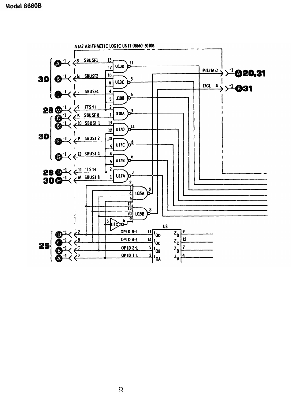
TM 11-6625-2837-14&P
CHANGE S (Cont'd)
Figure 7-3. Partial Schematic of Arithmetic Logic Unit
(Serial Prefixes 1325A and below)
CHANGE T
Table 6-3:
Delete 08660-20168, 08660-20169, 08660-20170, and 08660-20183.
CHANGE U
Page 5-5, paragraph 5-14 (Part 3 100 MHz Output Adjustment):
Add a sentence to step d, "The 100 MHz signal should be >+10 dBm”.
Table 6-3 and A4A2 Schematic (SS2).
Change A4A2R2 to 0757-0401 RF 100
7-11
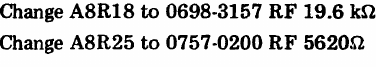
TM 11-6625-2837-14&P
Model 8660B
CHANGE U (Cont’d)
Table 6-3 and A4A4 Schematic (SS3):
Delete A4A4C41 and L12. On the schematic show a direct connection from A4J8 center conductor t
junction of A4A4C35, C36, and R29.
Table 6-3 and A8 Schematic (SS12):
CHANGE V
Table 6-3 and Power Supply Schematic (SS42):
Change A20F1 to 2110-0036 Fuse 8A
Change A6A1C10 to 0160-0015, CF 0.47 uF
Table 6-3:
Change A6A1 miscellaneous part from 08660-20173 to 08660-20050
Change A6A2 miscellaneous parts from 3160-0056 to 3160-0232 and from 3160-0087 to 3160-0253
Add 08660-00008 Heat Sink Cover
Delete 0403-0026
Delete 08660-00063, 08660-00065, and 08660-20172
Add 1520-0006 Vibration Mount
CHANGE W
Table 6-3.
Change T1 to 9100-3131, Power Transformer
Change A7 to 5060-1188, Line Module
Service Sheet 42 (Power Supply Schematic):
Change the diagram as shown by Figure 7-3.
7-12
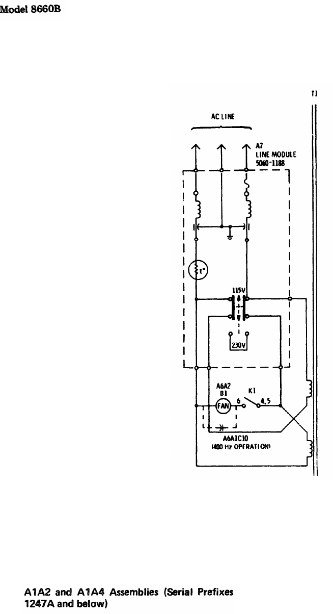
CHANGE W (Cont'd)
TM 11-6625-2837-14&P
Figure 7-4. Partial Schematic of Power Supplies (SS41)
(Serial Prefixes 1352A or below)
7-7.
MODIFICATIONS
to next table), the circuit boards may be replaced
with the new board or modification procedures 1
7-8.
7-9. New A1A Key Control and A1A4 ROM
Input Assemblies are now available. If both of the
old style board assemblies are being used and
trouble symptoms A, B, and C are apparent (refer
and 2 (which follow) may be performed. If a new
A1A board is used with an old A1A4 board and
symptoms B and C are present, order a new A1A4
board or perform modification 2. If an old A1A2
board is used with a new A1A4 board and
symptom A is present, order a new Al A2 board or
perform modification 1.
7-13
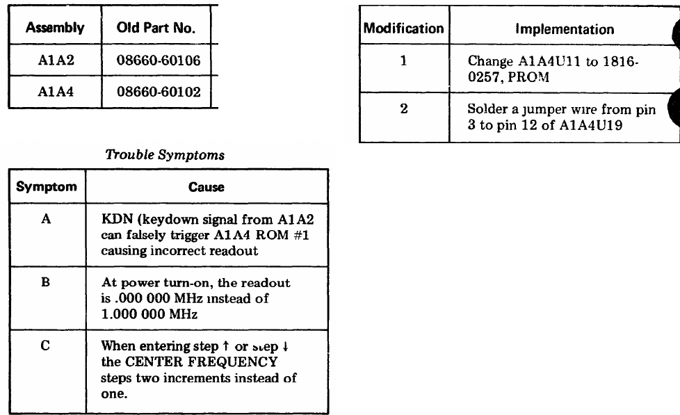
TM 11-6625-2837-14&P Model 8660B
New Part No.
08660-60176
08660-60182
7-10. Field Update Kits (Serial Prefixes 1349A
and below)
7-11. The Field Update Kit and modification
instructions for increased reliability of the Syn-
thesized Signal Generator System are available
through the nearest Hewlett-Packard office.
7-14
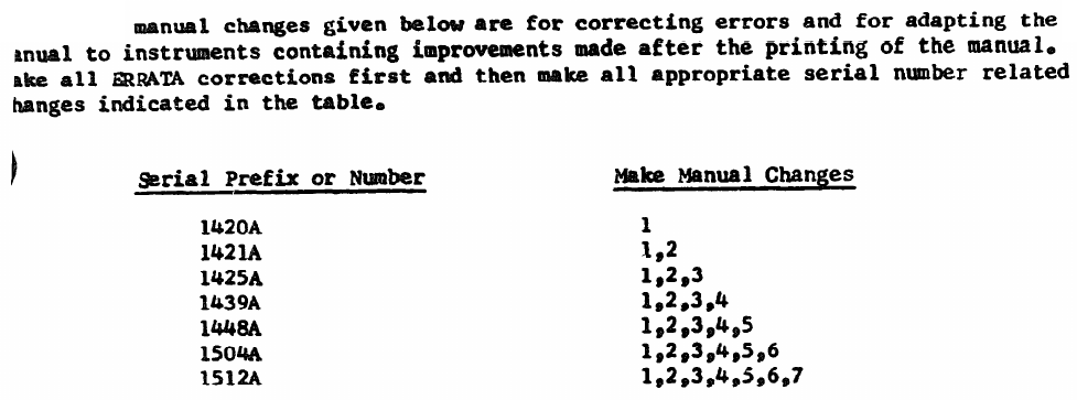
TM 11-6625-2837-14&P
Manual Changes
7-12. The
ERRATA
Page ii and page 4-5:
Change Section 4-10 to read
“DCU Sweep Output”.
Page 1-2 and all other pages throughout this manual
that refer to
Option 005, Hewlett-Packard GPI
(General
Purpose Information) Bus
or HP-ASCII (American Standard Coded Information Interchange) should be
referred to as Option 005
and/or Hewlett-Packard Interface Bus (HP-IB). While the HP Interface Bus is
partly compatible with some ASCII terminology, the term ASCII should
not
be
used, because compatibility
IS
not complete.
Page 1-4, Table 1-2:
Change the first and third characteristics as follows:
Synthesized Search: Synthesized Search dial changes the synthesized
output frequency 180 steps per
revolution.
Resolution
is 1
Hz, 1
kHz or 1 MHz per step depending upon MANUAL MODE switch position.
Sweep Width: Continuously adjustable over the range of the RF Section Installed. The smallest step size
IS
equal
to frequency
resolution
of
mainframe.
Page 3-6, Table 3-1 :
Change Step 3-f second line, Result column to
read 10.001 kHz.
Page 3-9:
Paragraph 3-34. Change reference to Figure 3-2 to Figure 3-2 Section A.
Paragraph 3-37. Change reference to Figure 3-2 to Figure 3-2 Section B.
7-15
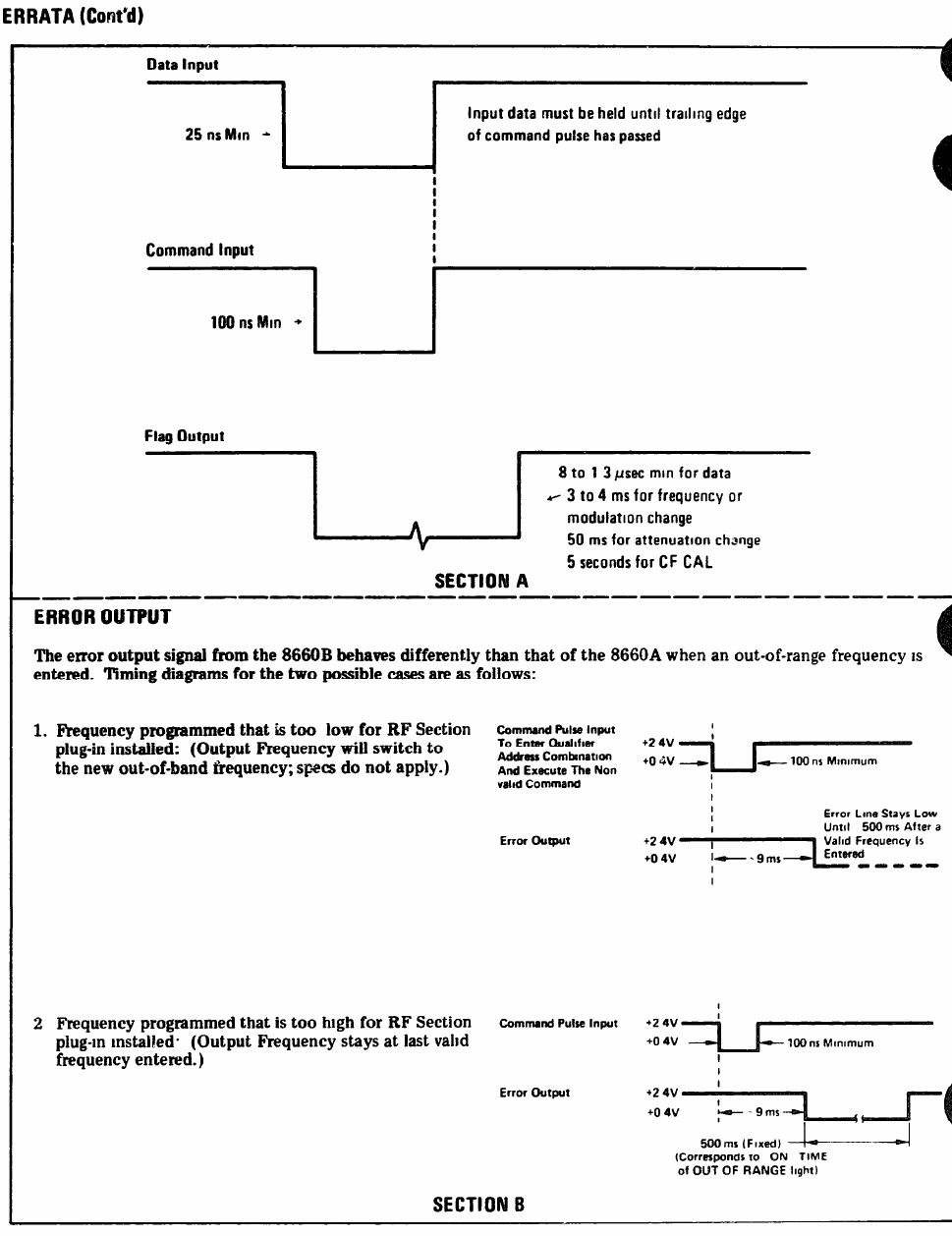
TM 11-6625-2837-14&P
TM 11-6625-2837-14&P
Manual Changes
7-16
Figure 3-2. Model 8660B Timing
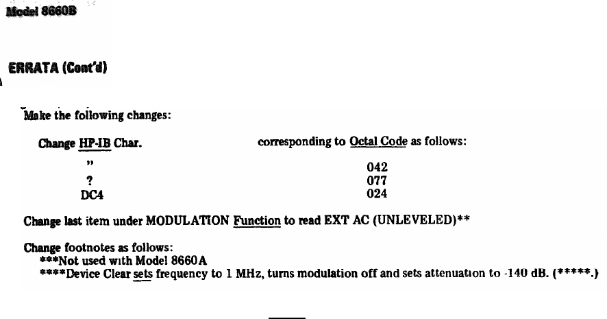
TM 11-6625-2837-14&P
Manual Changes
Page 3-19/3-20, Table 3-8:
Page 5-5, Table 5-2:
Entry below Typical +4.4V should read Actual (Actual misspelled.)
Page 6-3, Figure 6-1:
Cabinet Parts (1 of 2); substitute the table on the next page.
7-17
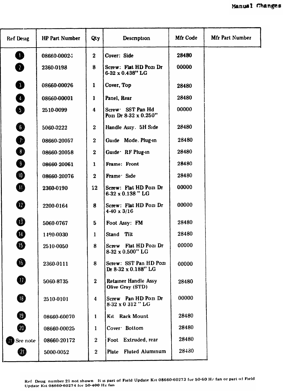
TM 11-6625-2837-14&P
ERRATA (Cont’d)
08660-00024
OBD
08660-00026
08660-00001
OBD
5060-0222
08660-20057
08660-20058
08660-20061
08660-20076
OBD
OBD
5060-0767
1490-0030
OBD
OBD
5060-8735
OBD
08660-60070
08660-00025
08660-20172
5000-0052
Figure 6-1.
Cabinet Parts (1 of 2) (ERRATA)
This Ref Desig is also not shown in Figure 6-1. Cabinet Parts (2 of 2) page 6-4 for the same reasons shown in
note above
7-18
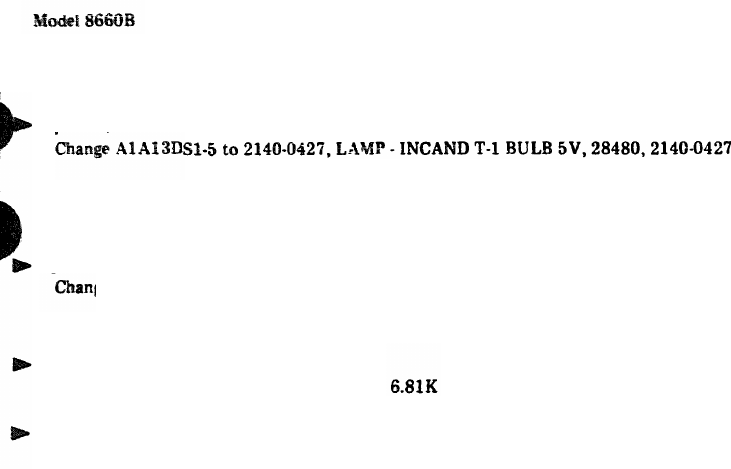
TM 11-6625-2837-14&P
Manual Changes
ERRATA (cont'd)
Page 6-16, Table 6-3:
page 6-25. Table 6-3:
Change
Part Number of A4A6 to 08668-60013.
Page 6-28, Table 6-3:
ge
A6A2, 3160-0056 to 08660 20184.
Change A6A2, 3160-0087 to 08660-20185.
Table 6-3:
A13R20 to
Page 6-37,
Change
0757-0439,
RESISTOR
Page 6-51,
Table 6-3:
Change
08660-20168
to
08660-20183.
Change
08660-20169 to
08660-20183.
1% 125W F TC = 0 ± 100, 24546,
C4-1/8-TO-6811-F.
(continued)
7-19

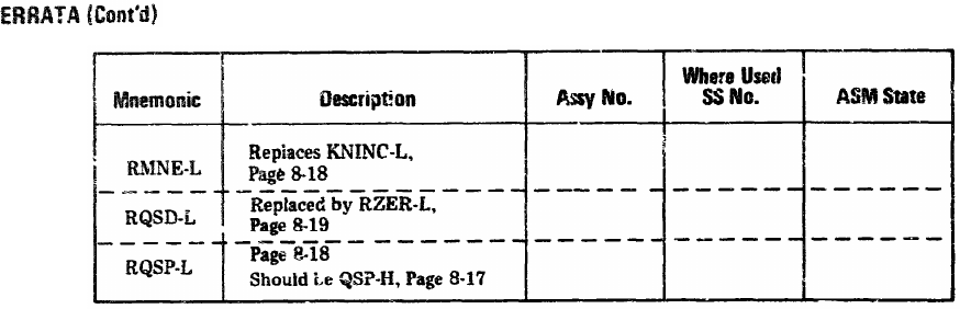
Model 8660B
TM 11-6625-2837-14&P
Manual Changes
Table 8-23 Mnemonics Information (ERRATA) (2 of 2)
Page 8-22
The NOTE following paragraph 8-60, first sentence should read “The seven state” LED’s, test points and stepping
microswitch are shown on the lower right hand side of the DCU block diagram.
Page 8-37, Table 8-7
The last sentence of Step 4 should read “IC corresponding to faulty digit on A1A10 may be replaced”.
Page 8-63, Table 8-27.
A3, A3Al and A3A2 should be referenced to Service Sheet 41, not Service Sheet 42.
Page 8-63. Figure 8-6
LEFT VIEW; references to A9 and A21 are reversed.
Page 8-71, Service Sheet 2:
A22AlKl and A22A2Kl (relays) pins 1 and 4 are reversed.
Lead from A22A1 to A4A2 should be color coded 9 and labeled A23W23.
Lead from A21 pin 3 to A22A1 should be identified as W2 "INT".
Lead from Reference Input should be identified as Wl “EXT”.
A4A2C21 should be 0.01 uF.
2 MHz DCU lead from A4Al should be labeled A23W26.
100 kHz lead from A4A1 to N2 should be labeled A23W11.
100 kHz lead from A4Al to N3 should be labeled A23W12.
400 kHz lead from A4Al to Nl should be labeled A23W10.
Page 8-72, Text for Service Sheet 3:
Test l-a. Substitute the Spectrum Analyzer for the Oscilloscope. Signal should be > +3 dBm.
Test l-b Oscilloscope should indicate approximately 2.5 Vp-p.
Test 3-c
There
IS
no Internal connection to A4A4Ul (see Figure 8-7) test should be made from A4A4Ul pin 1.
Page 8-73, Service Sheet 3:
A4A4Q7 and A4A4Q8 should be 1854-0540* (Factory Select)
A4A4 100 MHz output from A4J8 goes to J6 Pm 65.
Page 8-75, Service Sheet 4
The correct part number for the A4A6 assembly
IS
08660-60013
Page 8-76, Text for Service Sheet 5
Reference composite waveform 5-l, A4A7Ql and A4A7Q2 output should be labeled 9 Vp-p.
Page 8-77. Service Sheet 5.
350/450 MHz input at A4J11 should be labeled A4W4
IO MHz input at A4J13 should be labeled A4W2.
A4A7L5 should be labeled 0 39 uH (not 39 uH).
7-21

TM 11-6625-2837-14&P
ERRATA (Cont’d)
Page 8-79, Service Sheet 6:
350/450 MHz output at A4J10 should be
labeled A4W4.
350/450 MHz output at A4J12 should be labeled A23W15.
Page 8-80, Text for Service Sheet 7:
Level for Test Procedure l-a, paragraph 3 should he 2.5 Vp-p.
Composite waveform SS7-1; TP5 should read 2.8 Vp-p and TP4 should read 10.2 Vp-p.
Composite waveform SS7-2 U4 Pin 3 should read 5.6 Vp-p.
Page 8-84,
Text for Service Sheet 9:
Composite waveform SS9-1; TP5 should read 2.75 Vp-p, XA14-l-2 should read 2.8 Vp-p, TP4 should
read 8 Vp-p.
Test l-b second paragraph
should read C21, not C20.
Composite waveform SS9-2;
TP1 should read 3.2 Vp-p. U6 Pin 2 should read 4.8 Vp-p.
Composite waveform SS9-4; U6 Pin 15 should be U6 Pin 5.
Composite waveform SS9-6; Pins 1 and 2 are reversed.
Page 8-90, Text for Service Sheet 11:
Composite waveform SS11-1; TP5 should read 3 Vp-p. Junction of R19 and C20 should read 8 Vp-p and C20
should be C21
Composite
waveform SS11-2; W5 Pin 8 should read 3.8 Vp-p.
Composite wavefo
.
rm SS11-6; U3 Pin 8 should read 5.3 Vp-p. U3 Pin 10 should read 5.0 Vp-p. U3 Pin 11
should read 5.3 Vp-p.
Composite waveform SS11-7; U1 Pm 11 should read 5.2 Vp-p. U1 Pin 5 should read 3.75 Vp-p. TP1 should
read 3.8 Vp-p.
Test Procedure l-c paragraph 1; TP3 should read 4.0 Vp-p.
Test Procedure l-d; U7C Pin 8 should read 4 Vp-p. XA10 Pin 2-15 should read 0.06 Vp-p.
Page 8-92, Text for Service Sheet 12:
Composite waveform SS12-1; Waveform for TP2 and U1 Pin 11 both alike. U1
Pin
11 is
correct.
Page 8-93, Service Sheet 12:
A12R18
IS
nominally 21.5K, A12R25 is nominally 5000 ohms. Both Factory Select.
Page 97, Service Sheet 14:
Transistors Q16, Q7, Q8, Q9, Q10, Q11, Q12, Q13 and Q14 are 1853-0007.
Page 8-98, Text for Service Sheet 15:
A15Q1 is 1854-0092. Add C2, 0.47 uF to +5V power supply.
Page 8-102, Text for Service Sheet 17:
Change Test procedure as follows: TP3 to 0.8 Vp-p, TP4 to 0.6
Vp-p, TP2 to 0.4 Vp-p.
Page 8-103, Service Sheet 17:
Change
A19R55, 1300 ohms to factory select.
Page 8-113, Service Sheet 22:
Label
Pin 9 of U10C JUS-L.
Page 8-115, Service Sheet 23:
Label
Pin 3 of U35B CK; Label Pin 2 of U13A CK.
Page
8-117, Service Sheet 24:
Label Pin 12 of U29 (SCAN F/F),
CK, Label Pin 2 of U34C TTRO-H and show output of U24A as a negative-going
200 ns pulse.
Label gates in
lower
right
of schematic as Blanking Gates.
Page 8-119,
Service Sheet 25:
Label inputs shown
as
F, G,
H, E, D, C and B as state codes 1, 2, 4, 8, 4, 2 and 1 respectively.
Label U10 Decoder.
Label OFS-L Service Sheet 42 instead of Service Sheet 37.
7-22

Model 8660B
TM 11-6625-2837-14&P
Manual Changes
Page 8-123, Service Sheet 27
In lower right of schematic label leads to Service Sheet 28, E, F, and G as 01, 10 and 11 respectively.
Page 8-125, Service Sheet 28
Change ADOF-L at the input of U4D Pin 9 to Service Sheet 42.
Add CK12 to connector labeled D 27 (input from U8 Pin 0
1
).
Page 8-133, Service Sheet 32:
Change the OPID inputs to U8 from Service Sheet 29 to Service Sheet 42.
U12 and U14 are complimenters.
For a BC input of 00, the output is A, for a BC input of 01, the output is A, for a
BC input of 11 the output is 0, and for a BC input of 10, the output is 1.
Page 8-135, Service Sheet 33:
Change R20, in the collector circuit of Ql to R30. Add 0 to 8V to D/A output.
Page 8-139, Service Sheet 35:
Change all outputs on right of schematic from Service Sheet 37 to Service Sheet 42.
Page 8-141, Service Sheet 36
Change S2 to PBI-L
Page 8-143, Figure 8-93:
The jack identified as J2 to W5 should be further identified as the 2 MHz clock input.
Page 8-143, Service Sheet 37:
Show reference designators for A3XA1, A3XA2 and A3XA3 as follows; A3XAl-8, E, 5, D, N, 7, 4, F, C, 1, 12 and 3
to Service Sheet 38; A3XA2-24, 27, 23, 20, 36, 34, 33, 35 and 32 to Service Sheet 42; Service Sheet 37 on left of
schematic to Service Sheet 42, A3XA3-15, D, K, L, 16, T, U, 18 and V to Service Sheet 42. Change A3XA3-15 to
FLAG-L. Change A2XA1-B to LCL-H. Change A3XA3-L to FM-H. Change A3XA2-32 to FLIM-L. Change A3XA2-40
to FM-H. Change ASXAl-11 to FLIM-L, Service Sheet 32. A3XA2-30 add Service Sheet 22. A3XAl-6 change to
Service Sheet 38 A3XA2-29 change to Service Sheets 20, 21 and 23.
Page 8-145, Service Sheet 38
Change reference designations for A3XA4 and A3XA5 as follows: A3XA5-15, 16, 17, 18, 11, S, T, U, V, 4, D, 5,
J, 2, a and all designations shown in the lower right of schematic to go to Service Sheet 42. A3XA4-3, 11, 9, 3 to
Service Sheet 37, -11 to Service Sheet 38, -9 to Service Sheet 37 (also change to FLAG-H) A, 5, 4, B, c, N, M, 7,
2, 2, 12, 8 and 10 all to Service Sheet 37 (also change A3XA4-8 to LCL-H )
Page 8-151, Service Sheet 40.
All data bits and mnemomcs which match on Service Sheet 37 and 38 should match on Service Sheets 40 and 41.
Page 8-153, Service Sheet 41:
C7 of A20 should be 1900 uF.
Page 8-154. Service Sheet 42:
53 Pin 17 should change to BUSY-L.
A3XA-D is grounded through the 86601 when used, and through the 11661 when the 86602 or 86603 are used.
A3XA3-L should be labeled FM MODE-H.
All references to Service Sheet 39 should be deleted from the A1A11 Mother Board
In the left hand side of the
schematic references to Digits 7-8, 7-4, 7-2 and 7-1 should be changed to A2XA9 pins 14, R, 15 and S
respectively
Page 8-155
DCU ASM should be labeled Figure 8-116 (not Service Sheet 42)
Page 8- 156
J6 connections should be changed as follows, Pm 9 - 958, OFS-L, Pin 10 - 947 ADOF-L, Pin 33 - OPID-1, Pin 34 -
OPID-4 and Pin 36 - OPID-8.
7-23

TM 11-6625-2837-14&P
CHANGE 1
To Table 6-3 M
ISC
., add the following:
1 ea 1251-1910 Contact RP1 pin and 1 ea 8150-0456 Wire-Elec, 24 AWG Wht, 14½".
Power Supply Schematic and Table 6-3:
Change A20F3, A20F4 and A20F5 to 2110-0332 Fuse 3 amp.
Change A6R7 to 0812-0014 RF 0.5 Ohm 3% and A6R10 to 1812-0020 RF 0.39 Ohm 5%.
Change A20K1 and A20K2 to 0490-0559 Relay.
Change A20R7 to 0757-0795 RF 75 Ohm 1%.
A1A1 Assembly and Table 63:
Delete 2140-0356 Lamp-Incd, 4 per.
AlA12 Assembly and Table 6-3:
Delete 1251-1556 Conn Spring Socket, 8 per and add 2140-0016 Lamp-Incd, 4 per.
A1A13 Assembly and Table 6-3:
Delete 1251-1556 Conn Spring Socket, 10 per.
CHANGE 2
High Frequency VCO and Table 6-3:
Change A4A5Q2, Q3, Q4, Q5, and Q6 to 1854-0540 Transistor-NPN.
Pretune Assembly A4A6 and Table 6-3:
Change A4A6R35 to 2100-1788 RV 1K 10%.
Change A4A6R52 to 2100-2497 RV 2K 10%.
Change A4A6R56 to 2100-2216 RV 5K 10%
Change A4A6R60 to 2100-1738 RV 10K 10%.
Change potentiometers only as needed for adjustment. The transistors should be replaced only in roase of failures.
CHANGE 3
Change Sweep Control Assembly and Table 6-3:
Change A1A8R9 to 3480 ohms 1% 0698-3152
Change A1A8R10 to 2150 ohms 1% 0698-0084
Change A1A8R11 to 200 ohms 10% 2100-3095
CHANGE 4
Reference VCO and Dividers Schematic (A4A4) and Table 6-3:
Change A4A4R30 to 0757-0401, 100 ohm, 1%
Change A4A4R31 to 0757-0422, 909 ohm, 1%
Change A4A4Q7 to 1854-0540 Transistor NPN SI.
Change SL1 VCO Schematic (A19) and Table 6-3:
Change A19R55 to 0757-1094, 1.47K 1% 1/8W.
CHANGE 5
Page 6-16, Table 6-3.
Change AlAl2XA3 and XA4 to AlA12XU3 and XU4 1200-0563.
Page 6-51, Table 6-3.
Under MISCELLANEOUS PARTS, add the following:
08660-20175 SUPPORT, PC BOARD 28480 08660-20175.
7-24
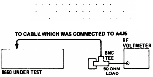
Model 8660B
TM 11-6625-2837-14&P
Manual Changes
CHANGE 5 (cont'd)
Table 6-3:
Change the components on the following list to 1820-0751, IC SN74 196 N, 01295, SN74196N.
Page 6-30, A8U3
Page 6-32, A10U4,
U5, and U6
Page 6-36, A12U9
Page 6-39, A14U5, U6, and U7
Page 6-40, A15U5 and U6
Page 6-42, A16U5 and U6
Page 6-53, A14U4, U5, and U6.
CHANGE 6
‘age 5-9, Paragraph 5-27.
Because the A22A1 sub-assembly (now part number 08660-60323) has been changed to a bandpass filter, it is necessary to
add ADJUSTMENT paragraphs 5-27a and 5-27b following paragraph 5-27 to ensure proper operation of the instrument.
5-27a. 10 MHZ BANDPASS FILTER ADJUSTMENT
NOTE
It is recommended that this procedure, along with the Reference
Section procedure (paragraph 5-27 in the manual) be performed
at least every six months.
DESCRIPTION
The A22.41 Reference sub-assembly (10 MHz Crystal Bandpass Filter 08660-60323)
IS
adjusted to the Internal 10 MHz refer-
we frequency
The assembly level
IS
adjusted for 270 mV into 50 ohms.
TEST EQUIPMENT:
RF Voltmeter
HP 411A
BNC Tee
UG 274B/U
50 Ohm Termination HP 11593A
PROCEDURE
Figure 5-27a. A22A1 Adjustment Test Setup
Perform Test Procedure 5-27 in the mainframe manual.
7-25
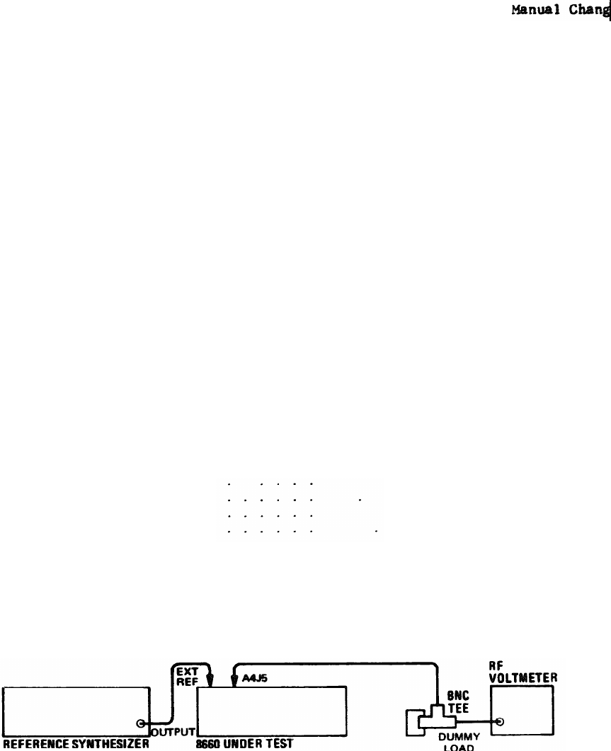
TM 11-6625-2837-14&P
CHANGE 6 (cont’d)
5-27a. 10 MHz BANDPASS FILTER ADJUSTMEMT (cont’d)
2.
Remove 8660 left side and top covers. Turn power ON and allow 8660 to operate for 2 hours to ensure reference
stability. Set INT/EXT Reference switch to INT
3.
Remove 5/10 MHz Reference input cable from A4J5. Connect the cable to the RF Voltmeter as shown in Figure
5-27a.
4.
Adjust A22A1C3 (using a non-metallic tool) accessible through hole in A22 assembly for maximum reading on the
RF Voltmeter.
5.
Adjust A22A1R2 (accessible through a hole in the A22 assembly) for an RF Voltmeter reading of 270 mVrms
6.
Reconnect A4J5 cable to the A4A2 assembly.
5-27b. 10 MHz BANDPASS FILTER ADJUSTMENT
DESCRIPTION:
The 700 Hz sidebands are set at least 20 dB down from the 10 MHz reference oscillator signal
TEST EQUIPMENT:
Synthesizer
RF Voltmeter
BNC Tee
50-Ohm Termination
HP 8660 or HP 3320B
HP 411A
UG 274B/U
HP 11593A
NOTE
It is necessary to remove this assembly from the mainframe
in order to perform the adjustments
Therefore, the adjust-
ment is to be performed ONLY if the Reference Assembly
is repaved.
Figure 5-27b. A22A1 Adjustment Test Setup
PROCEDURE:
1.
Connect equipment as shown in Figure 5-27b
2.
Release and rotate the A4 assembly up and out of the chassis. (Locate A21 output cable Jl [white] and disconnect
from reference source A22.) Connect external synthesizer to cable Set Reference Synthesizer to 10 000000 MHz
+13 dBm.
7-26
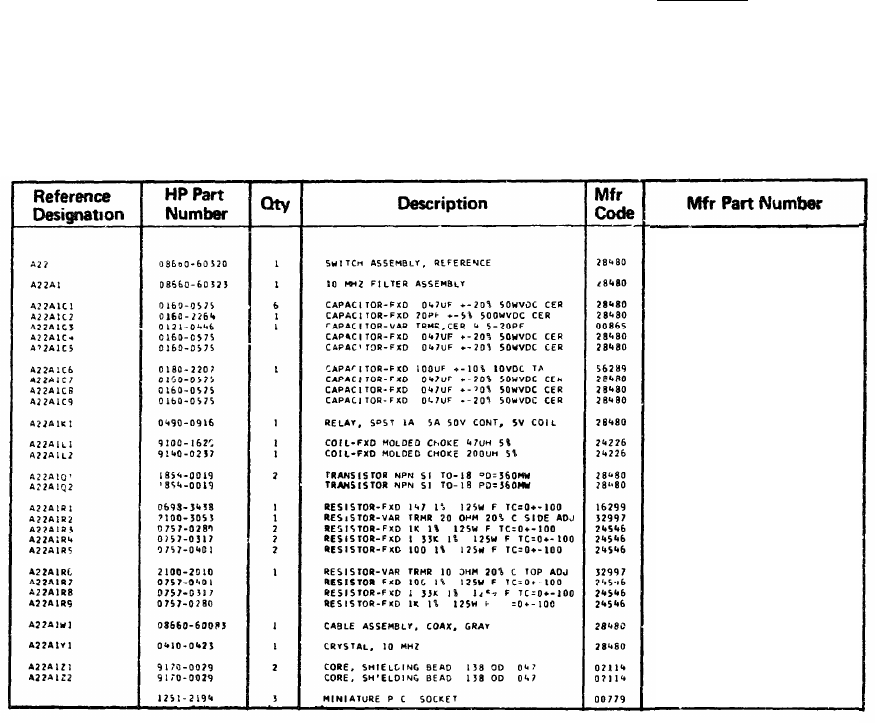
Model 8660B TM 11-6625-2837-14&P
Manual Changes
CHANGE 6 (cont'd)
10.000000 MHz. Adjust A22A1R6 for a voltmeter reading 20 dB above the reference.
Example: Reference level -18 dBm
+20 dB
Step 8 level
+2 dBm
9.
Reconnect coupling cable to normal configuration and return reference switch to INT.
Page 6-49, Table 6-3:
Change
the parts list for the A22 Assembly as shown in this supplement. Designators not listed remain as is.
Table 6-3 Replaceable Parts
7-27
5-27b. 10 MHz BANDPASS FILTER ADJUSTMENT (cont'd)
3.
Set the reference switch of the unit under test to INTERNAL.
4.
Adjust A22A1C3 for maximum RF Voltmeter wading (use a non-metallic adjustment tool).
5.
Adjust A22A1R2 for an RF Voltmeter reading of 270 mVrms.
6.
Set the Reference Synthesizer to l0.000700 MHz, record RF Voltmeter reading in dBm.
7.
Set the Reference Synthesizer to 0.999300 MHz, record RF Voltmeter reading in dBm.
a.
Establish the higher of the power levels in steps 6 and 7 as a reference. Reset the Reference Synthesizer to
08660-60328
08660-60325
0160-0575
0160-2265
75-TR1K0-19-45-20PF
0160-0575
0160-0575
1500107X9010R2
0160-0575
0160-0575
0160-0575
0490-0916
15/472
15/205
1854-0019
1854-0019
C4-1/8-T0-147R-F
3096P-1-200
C4-1/8-T0-1001-F
C4-1/8-T0-1331-F
C4-1/8-T0-101-F
3329M-1-10R
C4-1/8-T0-101-F
C4-1/8-T0-1351-F
C4-1/8-T0-1001-F
08660-60083
0410-0423
56-590-65A2/4A
56-590-65A2/4A
3-3312/2-0
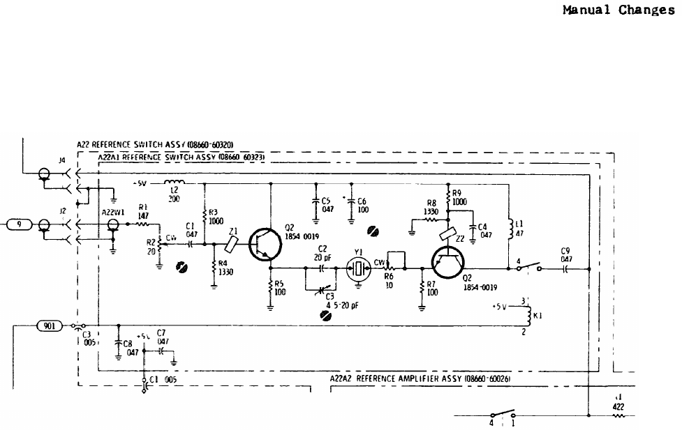
TM 11-6625-2837-14&P
CHANGE 6 (cont’d)
Page 8-71, Figure 8-16 (Service Sheet 2)
Change the diagram with the partial schematic shown in this supplement
Figure 8-16.
Reference Circuit Schematics (Partial Diagram, Part of Change 6)
Page 6-17, Table 6-3.
Change the A3Al Assembly parts list as shown in the table in this supplement for HP-IB Instruments (Option 005 only)
Change the A3Al Assembly parts lists as follows for all instruments except Option 005
A3A1, 08660-60278. Front interface Assembly. BCD (except Option 005), 28480, 08660-60278
A3A1U5 and U11. 1820-0328, IC SN 74 02N, 01295, SN7402N
A3A1U6, 1820-0065. IC SN 74 70N, 01295, SN7470N
A3A1U7, 1820-0207, IC MULTIVIBRATOR, 07263, 9601PC
A3A1U8 and U9, 1820-0072, IC SN74 50 N, 01295, SN7450N
A3A1U10, 1820-0214, IC SN74 42 N, 01295, SN7442N
A3A1CR1 to A3A1VR1.
A3A1CR2 to A3A1CR1.
Page 6-49, Table 6-3
Change A20F1 to 2110-0523, FUSE 10A 32V Normal Blow, 75915, 311010
Page 8-134, Figure 8-95 (Service Sheet 37)
Replace the schematic with the diagram in this supplement
Page 8-151, Figure 8-107 (Service Sheet 40)
Replace the schematic with the diagram in this supplement (the new title
IS
“HP-IB Output Assembly Schematic”)
7-28
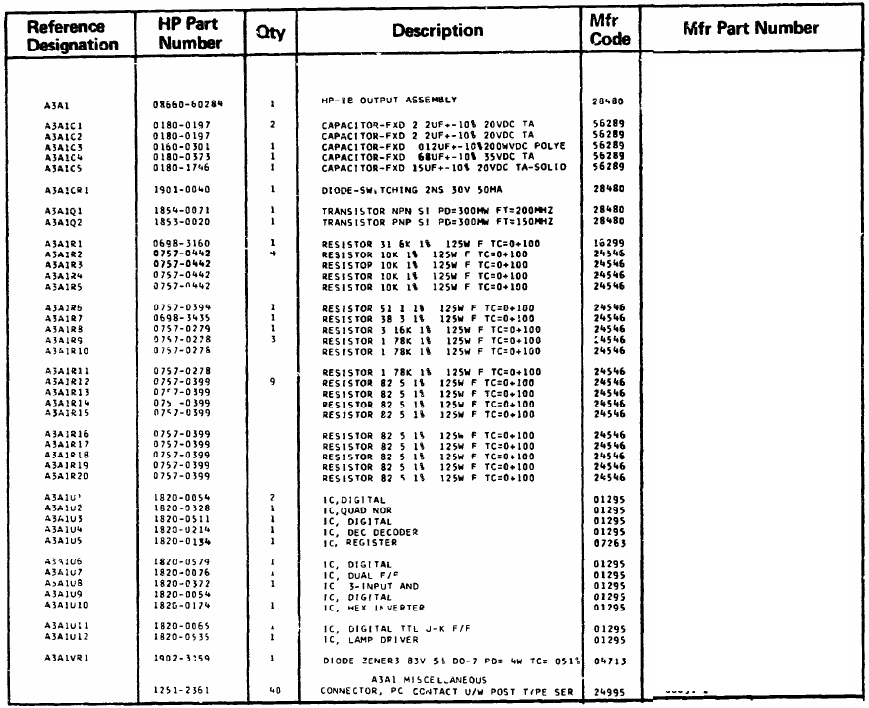
Model 8660B
CHANGE 6 (cont’d)
Table 6-3 Replacecable Parts (Part of Change 6)
TM 11-6625-2837-14&P
Manual Changes
08660-60284
1500225X9020A2
1500225X9020A2
292P12392
1500684X9035A2
1500158X90282
1901-0040
1854-0071
1853-0020
C4-l/8-T0-2612-F
c4-1/8-10-1002-F
C4-l/8-T0-1002-F
C4-1/8-T0-1002-F
C0-1/8-10-1002-F
C4-1/8-T0-51R1-F
C4-1/8-T0-38R3-F
C4-1/8-T0-3161-F
C4-1/8-TO-l78l-F
C4-1/8-T0-1781-F
C4-1/8-T0-1781-F
C4-1/8-T0-82R5-F
C4-1/8-T0-82R5-F
C4-1/8-T0-82R5-F
C4-1/8-T0-82R5-F
C4-1/8-T0-82R5-F
C4-1/8-T0-82R5-F
C4-1/8-T0-82R5-F
C4-1/8-T0-82R5-F
C4-1/8-T0-82R5-F
5N7400N
5N7402N
5N7408N
5N7442N
9300DC
5N74123N
5N7476N
5N74H11N
5N7400N
5N7404N
5N7470N
5N75451BP
SZ 10939-62
86091-2
CHANGE 7
Page 6-51, Table 6-3.
Add 4324-0080, 4, Pad Silicone Sponge
Add 08660-00085, 1,
Plate
Oscillator Top, 28480, 08660-00085.
Add 08660-00086, 1,
Plate
Oscillator Bottom, 28480, 08660-00086
Add 08660-20203, 1,
Plate
Oscillator Mounting, 28480, 08660-20203.
Delete 08660-00028.
7-29

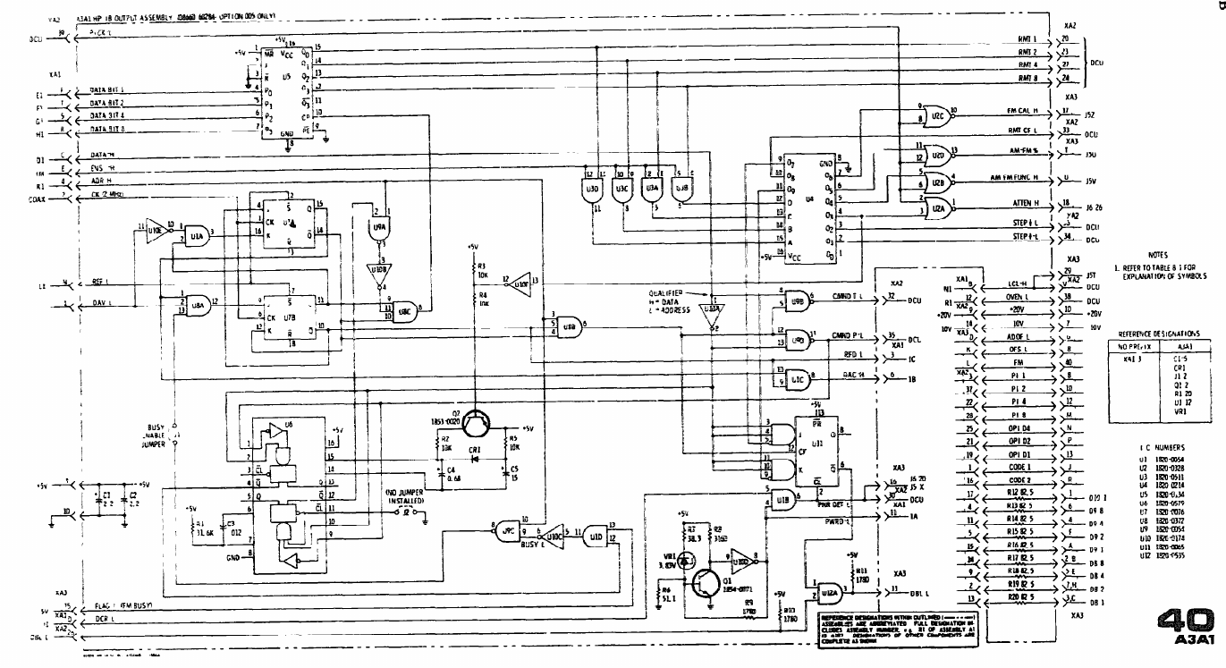
TM 11-6625-2837-14&P
Figure 8-107 HP-IB Output Assembly Schematic (Part of Change 6)
7-31


Model 8660B TM 11-6625-2837-14&P
SECTION VIII
8-1. INTRODUCTION
8-2. This section provides instructions for testing,
troubleshooting and repairing the Hewlett-Packard
Mode1
8660B Synthesized Signal Generator.
8-3.PRlNClPLES OF OPERATION
8-4.Figure 8-1, Simplified Block Diagram, and the
Troubleshooting information for the in-
strument is grouped on the last few
single pages and the first few foldout
pages of this section. This will enable the
technician to locate this information
easily without searching through the
section for it.
following discussion illustrates the basic principles
of operationof the Model 8660B. The frequencies
own at the output of the phase lock loop blocks
are those which appear at these given points when
a
centerfrequency of 107.654321 MHz is selected.
Moredetailed information about principles of
operation for the phase lock loops and the Digrtal
Control Unit appears on Service Sheets 1 and 18
respectively In addition, detailed information to
the circuit level is provided on individual Service
Sheets.
8-5. General. The Model 8660B was designed to
provide precise digitally controlled output fre-
quencies utilizing indirect synthesizer techniques.
Unlike conventional signal generators, the output
frequencyis not± some percentage factor. the
output frequency of the Model 8660B is exactly
that selected (the only factor which must be
consideredhere is the accuracy and stability of the
reference source). The output frequency range is
determinedby the RF Section plug-m being used.
8-6. All of the phase lock loops are phase locked,
directly orindirectly, to a very stable temperature
controlled internal 10 MHz source or to an
external reference source.(The term 'indirect
synthesis' as used in paragraph 8-5 refers to a
synthesizer that derives all frequencies from a
single source, as opposed to a ‘direct synthesizer’
which uses different crystal oscillators for each
frequency generated.)
8-7. Reference Section. A 100 MHz voltage con-
trolled oscillator which is phase locked to an
internal reference, or to an external reference
source, serves as a master oscillator. The internal
reference is a 10 MHz standard temperature con-
trolled crystal oscillator. The external reference
source may be 1, 2, 2.5, 5 or 10 MHz at 0.2 to 2
Vrms. All of the outputs from the reference
section are derived from the 100 MHz master
oscillator.
8-8. The reference section provides the following
outputs.
a. 500 MHz to the RF Output Section.
b. 100 MHz to the RF Output Section.
This 100 MHz IS coupled out of the RF section for
use in other circuits.
C.
20 MHz to the Modulator Section. This
20 MHz is coupled out of the Modulator Section
for use in the RF Section and the Frequency
Extension Module.
d. 10 MHz to the High Frequency Loop
phase detector for use as a reference signal.
e. 2 MHz to the Digital Control Unit to be
used as a clock.
f. 400 kHz to the N1 loop for a reference
signal.
g.
Separate 100 kHz signals to the N2 and
N3 loops for reference signals.
NOTE
In the following discussion the terms
digit 1, digit 2, through digit 10 are used
to refer to the 10 digits of frequency
selection. Digit 1 refers to the least
significant digit (1 Hz increments). Digit
numbers progress from right to left until
digit 10 refers to the most significant
digit (1 GHz increments).
8-1
TM 11-6625-2837-14&P
Model 8660B
8-9. High Frequency Loop. The HF loop contains
a voltage controlled oscillator which provides
eleven discrete outputs between 350 and 450 MHz
in 10 MHz increments when the Model 86601A RF
Section is used. When other RF Sections are used
the output of the HF loop will still step in 10 MHz
increments, but there will be more than, or less
than, eleven steps.
8-10. Pretuning tunes the voltage controlled oscil-
lator to a point within the capture range of the
phase lock loop and the phase detector then causes
the loop to be phase locked to the 10 MHz
reference signal at the exact frequency selected.
8-11. When a 0.01 to 110 MHz RF Section such as
the HP Model 86601A is used, the output of the
HF loop is applied to the RF Section. When a
higher frequency RF Section is used, the output of
the HF loop is applied to the Frequency Extension
Module.
8-12. N1 Phase Lock Loop. The N1 loop provides
an output to Summing Loop 1 (SL1) that is
between 19.8 and 29.7 MHz in 100 kHz steps. The
N1 voltage controlled oscillator is roughly pre-
tuned by a digital to analog converter which is
controlled by digits 6 and 7.
8-13. The N1 sampling phase detector is driven by
pulses derived from the N1 voltage controlled
oscillator through a programmable divider and a
pulse shaper. The programmable divider is con-
trolled by digits 6 and 7. When the loop is phase
locked the 400 kHz reference input is sampled at a
100 kHz rate. The error voltage from the phase
detector is summed with the digital to analog
converter output to precisely control the voltage
controlled oscillator frequency.
NOTE
In Option 004 instruments the N2A
programmable divider is used. The N2
loop output is then between 20.01 and
30.00 MHz.
8-14. N2 Phase Lock Loop. The N2 loop provides
an output to Summing Loop 2 (SL2) that is
between 19.80 and 29.79 MHz in 10 kHz steps.
The N2 voltage controlled oscillator is roughly
pretuned by a digital to analog converter which is
controlled by digits 4 and 5.
8-15 The N2 sampling phase detector is driven by
pulses derived from the N2 voltage controlled
oscilator through a programmable divider and
pulse shaper. The programmable divider is con
trolled by digits 3, 4 and 5. When the loop is phase
locked the 100 kHz reference signal input is
sampled at a 10 kHz rate. The error voltage from
the phase detector is summed with the digital to
analog converter output to precisely control the
voltage controlled oscillator.
8-16. N3 Phase Lock Loop. The N3 loop provide
an output to Summing Loop 2 (SL2) that is
between 2.001 and 2.100 MHz in 1 kHz steps. The
N3 voltage controlled oscillator is roughly pre-
tuned by a digital to analog converter which is
controlled by digit 2.
8-17. The N3 sampling phase detector is driven by
pulses derived from the N3 voltage controlled
oscilator through a programmable divider and
pulse shaper. The programmable divider is con-
trolled by digits 1 and 2. When the loop is phase
locked the 100 kHz reference signal is sampled at
10 kHz rate. The error voltage from the phase
detector is summed with the digital to analog
converter output to precisely control the voltage
controlled oscillator frequency.
NOTE
In Option 004 instruments Summing
Loop 2 (SL2) is not used
8-18. Summing Loop 2. SL2 provides an output to
SL1 that is between 20.0001 and 30.0000 MHz in
100 Hz steps. The SL2 voltage controlled oscillator
is roughly pretuned by a digital to analog converter
which is controlled by digits 3, 4 and 5.
8-19. The output from the SL2 voltage controlled
oscilator is also applied to a mixer where it is
mixed with the output of the N2 loop. The output
of this mixer is applied to one input of a digital
phase detector through a pulse shaper. The other
input to the digital phase detector is the divided by
ten output of the N3 loop assembly in pulse form.
When SL2 IS phase locked the frequency ratio of
the two inputs to the phase detector is always 1:1;
the mixer output frequency must exactly match
the divided by ten output of the N2 loop assembly
(the pulses are received alternately).
8-2

Model 8660B
NOTE
In Option 004 instruments the Summing
Loop 1 output is from 20.0001 to
30 MHZ.
8-20. Summing Loop 1. SL1 provides an output to
the RF Section that is between 20.0000001 and 30
MHz in 1 Hz steps. The SL1 voltage controlled
oscillator is roughly pretuned by a digital to analog
converter which is controlled by digits 5, 6 and 7.
8-21. The output from the SL1 voltage controlled
oscillator is also applied to a mixer where it is
mixed with the output of the N1 loop. The output
of this mixer is applied to one input of a digital
phase detector through a pulse shaper. The other
input to the digital phase detector is the divided-
by-one hundred output of the SL2 voltage con-
trolled oscillator in pulse form. When SL2 is phase
locked the frequency ratio of the two inputs to the
phase detector is 1:1; the mixer output frequency
must exactly match the divided by one hundred
output of the SL2 voltage controlled oscillator (the
pulses are received alternately).
8-22. Digital Control Unit (DCU). In the local
mode all functions of the Model 8660B are
controlled by the DCU. These functions are
itemized and described in Section III of this
manual.
8-23. Interface Circuits. The interface circuits pro-
vide the capability of operating the Model 8660B
with the front panel controls (local mode}, or by a
remote programming device via a rear panel con-
nector (remote mode).
8-24. RF Section. An RF Section plug-in is re-
quired to produce a useable rf output. Figure 8-1
shows a simplified block diagram of the Model
8660B with a Model 86601A RF Section used in
the system. All plug-in sections are covered by
separate manuals.
8-25. Modulation Section. If a modulation section
is not available, it will be necessary to have an
auxiliary section in the modulator drawer to
complete necessary connections.
8-26. RECOMMENDED TEST EQUIPMENT
8-27. Test equipment and accessories required to
maintain the Model 8660B are listed in Table 1-3.
If the equipment listed is not available, equipment
that meets the minimum specifications shown may
be substituted.
TM 11-6625-2837-14&P
8-28. SAFETY CONSIDERATIONS
8-29. Although this instrument has been designed
in accordance with international safety standards,
this manual contains information and warnings
which must be followed to ensure safe operation
and to retain the instrument in a safe condition
(see Section II). Service and adjustment should be
performed only by qualified service personnel.
WARNING
Any interruption of the protective
(grounding) conductor inside or outside
the instrument or disconnection of the
protective earth terminal is likely to
make the apparatus dangerous. Inten-
tional interruption is prohibited.
8-30. Any adjustment, maintenance, and repair of
the opened instrument under voltage should be
avoided as much as possible and, when inevitable,
should be carried out only by a skilled person who
is aware of the hazards involved. The opening of
covers or removal of parts, except those to which
access can be gained by hand, may expose live
parts, and also accessible terminals may be live.
8-31. Capacitors inside the instrument may still be
charged even if the instrument has been discon-
nected from its source of supply.
8-32. Make sure that only fuses with the required
rated current and of the specified type (normal
blow, time delay, etc.) are used for replacement.
The use of repaired fuses and the short-circuiting
of fuse-holders must be avoided.
8-33. Whenever it is likely that the protection has
been impaired, the instrument must be made
inoperative and secured against any unintended
operation.
NOTE
When repairs or adjustments to the
instrument are required, such work
should not be performed, even by a
skilled technician, unless another person
is in the same general area. This is not to
be interpreted to mean that two persons
are required to perform the necessary
work, but only that another person
should be available, should the need for
assistance arise.
8-3
TM 11-6625-2837-14&P
8-34. REPAIR
8-35. Module Exchange. This instrument, because
of its modular design, may be repaired by simply
replacing a defective module. Modular design is a
method of construction that groups individual
circuits on a replaceable assembly. Modular design,
coupled with a factory-repaired module exchange
program, eliminates the need to repair to the
component level for some assemblies. Factory-
repaired modules are available on an exchange-for-
credit basis that reduces module cost substantially
below the cost of a new module.
8-36. This manual provides a procedure which
enables the technician to quickly isolate the cause
of a malfunction to the defective module.
8-37. Exchange modules should be ordered by the
exchange numbers shown in Table 6-1 from the
nearest Hewlett-Packard Sales/Service office.
8.38. Figure 8-2 illustrates the module exchange
procedure.
NOTE
Do not send a defective module to the
HP office until the replacement module
is received.
8-39. Line Voltage Requirement. During adjust-
ment, testing and use, the Model 8660B must be
connected to a source of power capable of deliver-
ing 345VA maximum at 100, 120, 220 or 240 Vac
+5% --10%, 48 to 440 Hz single phase. If adjust-
ment of the dc voltage regulators is required, the
Model 8660B should be connected to the ac source
through an adjustable auto-transformer. The line
voltage may then be adjusted to check the Model
8660B regulators when the line voltage is changed
± 10%.
8-40. Servicing Aids on Printed Circuit Boards.
Servicing aids on printed circuit boards include test
points, transistor and integrated circuit reference
designators, adjustment callouts and assembly
stock numbers. Figure 8-3 illustrates the proper
method of identifying pm numbers on the circuit
boards.
8-41. Circuit Board Extenders. Circuit board ex-
tenders are provided with the instrument. These
extenders enable the technician to extend plug-m
boards clear of the assembly to provide easy access
8-4
Model
to components and test points. See Figure 8-4
for
typical example of extender board use.
NOTE
Extending some circuit boards, partic-
ularly those containing oscillators, may
cause a change in operating frequency.
Adjustment of variable components
should not be attempted, except as
required for troubleshooting purposes,
while the circuit boards are extended.
8-42. Diagram Notes. Table 8-1, Schematic Dia-
gram Notes, provides information relative
symbols and values shown on schematic diagrams
8-43. Part Location Aids. The locations of chas-
is mounted parts and major assemblies are shown
in Figure 8-6. The location of individual com-
ponents mounted on printed circuit boards o
other assemblies are shown on the appropriate
schematic page or the page opposite it. The part
reference designator is the assembly designation
plus the part designation. (Example: A10R1 is R1
on the A10 assembly.) For specific component
descriptions and ordering information refer to
parts list in Section VI of this manual.
8-44. Table 8-27 lists all assemblies and provides
location information for photos, schematics, etc.
8-45. Integrated Circuits. Many types of integrated
circuits are used throughout the Model 8660B. In
order to avoid duplicating information on the
individual schematics, all IC outpines and pin
numbers are shown in Figure 8-7.
8-46. MNEMONICS
8-47. There are about 280 terms used to describe
signals, instructions and qualifiers in the DCU.
Some of these terms are complicated and some are
used in many places in this manual. In order to
minimize schematic clutter these terms have been
assgned mnemonics. These mnemonics and the
descriptions appear in Table 8-2. In addition, Table
8-2 provides the following “where used
information
a. The assembly column lists the assembly
numbers where the mnemonic appears. The as-
sembly number followed by an asterisk indicate
where the qualifier or instruction originates.


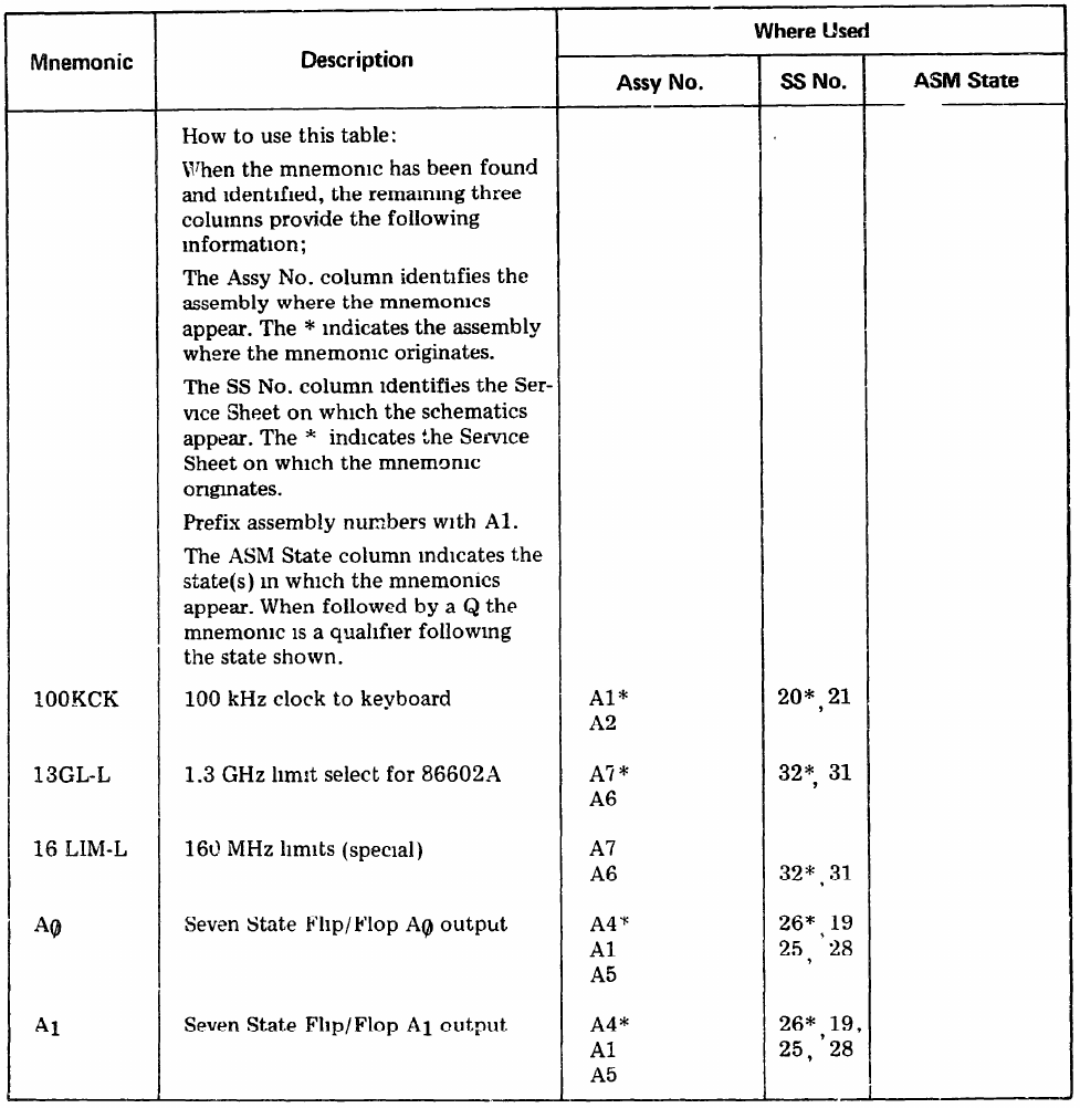
Model 8660B TM 11-6625-2837-14&P
b. The Service Sheet (SS) column indicates
the schematic on which the mnemonic appears.
The SS number followed by an asterisk indicates the
schematic on which the qualifier or instruction
originates.
state machine diagram. The states which are fol-
lowed by a “Q” indicate a qualifier following the
state shown. All other states are instructions.
C.
The ASM state column shows the state(s)
in which the term appears on the algorithmic
8-48. These mnemonics are also used in the
Service Sheet Text and the DCU block diagram.
Table 8-2. Mnemonics In formatron (1 of 13)
8-9
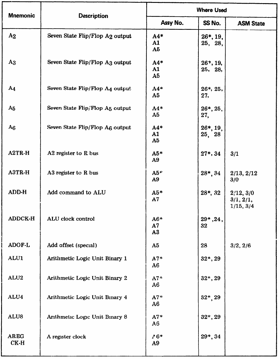
TM 11-6625-2837-14&P Model 8660B
Table 8-2. Mnemonics Information (2 of 13)
8-10

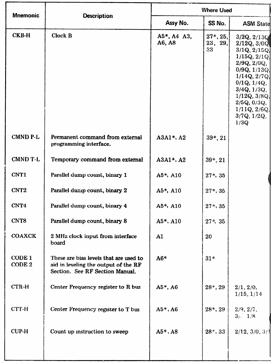
TM 11-6625-2837-14&P
Model 8660B
Table 8-2. Mnemonics Information (4 of 13)
8-12
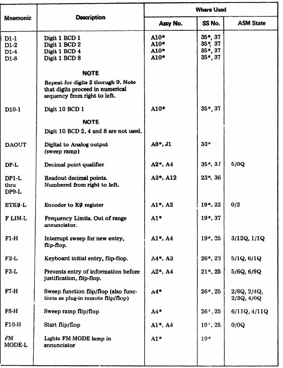
Model 8660B TM 11-6625-2837-14&P
Table 8-2. Mnemonics Information (5 of 13)
8-13
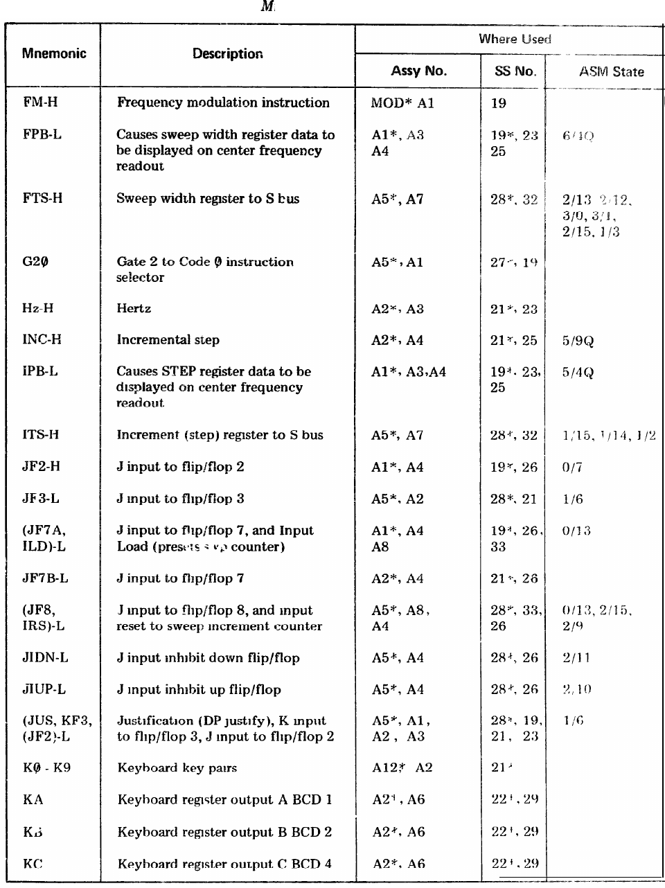
TM 11-6625-2837-14&P Model 8660B
Table 8-2. nemoiaics Information (6 of 13)
8-14
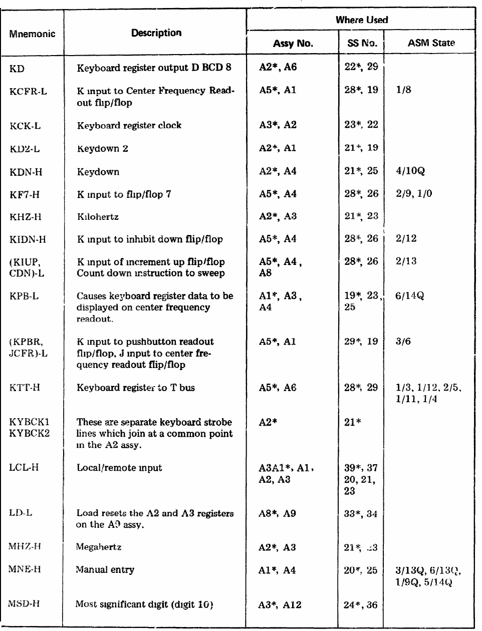
Model 8660B
Table 8-2.Mnemonics Information
(7 of 13)
TM 11-6625-2837-14&P
8-15
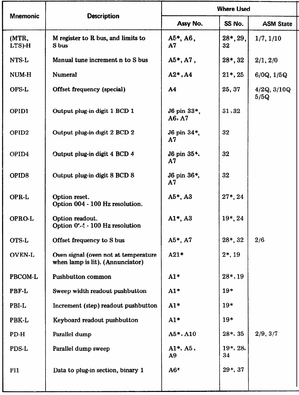
TM 11-6625-2837-14&P Model 8660B
8-16
Table 8-2. Mnemonics information (8 of 13)
Mode1 8660B
TM 11-6625-2837-14&P
Table 8-2. Mnemonics Information (9 of 13)
8-17
TM 11-6625-2837-14&P Model 8660B
Table 8-2. Mnemonica Information (10 of 13)
8-18
Model 8660B TM 11-6625-2837-14&P
Table 8-2. Mnemonics Information (11 of 13)
8-19
TM 11-6625-2837-14&P Model 8660B
Table 8-2. Mnemonics Information (12 of 13)
8-20
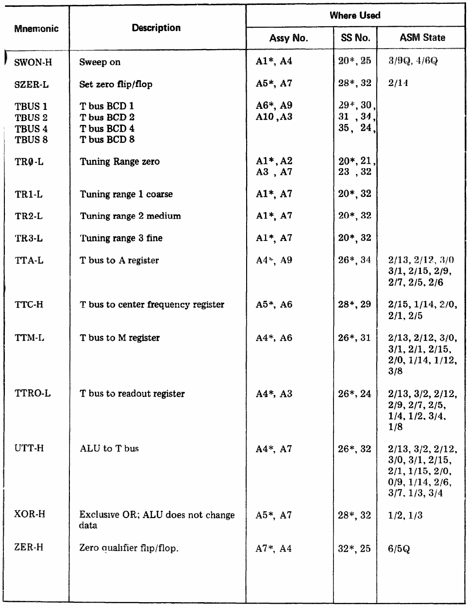
Model 8660B TM 11-6625-2837-14&P
Table 8-2. Mnemonics Information (13 of 13)
8-21
TM 11-6625-2837-14&P
8-49. ALGORlTHMIC STATE MACHINE
8-50. Algorithmic state machines (ASM’s), some-
times called flow graphs, are the most practical
approach to understanding circuitry as complex as
that in the Model 8660B DCU.
Algorithm:
DEFINITIONS:
A fixed step-by-step
finding the solution procedure for
to a problem.
State: A condition, or a set of conditions
which exist at a given point in time.
8-51. While ASM’s have been in existence for quite
a while, they have been used more as a design
engineering tool than a troubleshooting aid.
8-52. It is not within the scope of this manual to
provide a complete treatise on the design, or even
the interpretation of ASM’s. However, the follow-
ing information should enable the technician to
understand the logic of ASM’s, and to use them to
decrease the time required to find the cause of a
malfunction
8-53 ASM’s are particularly valuable in servicing
the Model 8660B because built in test features
permit the technician to set the DCU to any state.
Seven LED’s verify or deny that the DCU is in the
state selected. The DCU may be held in the
selected state, manually stepped to succeeding
states or reset to any other state.
8-54.
Figure 8-5 represents a portion of the overall
DCU ASM which is shown in it’s entirety in Figure
8-116. The following description of the information
shown in Figure 8-5 is equally applicable to the
overall ASM.
8-55. The mnemonics in the state (rectangular)
boxes and the qualifier (diamond shaped) boxes
are not truly representative of specific electrical
points in the circuit; the function represented by
the mnemonic may appear at many points in the
DCU Table 8-2 Mnemonics Information will
enable the technician to quickly locate the points
in the DCU where the function appears. The -H or
-L following the mnemonics indicates that the
function is High or Low in the assertive state.
8-56. The lines connecting the qualifiers and the
states are not representative of electrical connec-
tions. Their purpose is to provide information as to
what the next state will be. Usually the qualifier
determines which of two states is next. In some
Model 8660B
cases however, the qualifier holds the present
machine state for a predetermined period of time
8-57. In the Model 8660B there are about 112
machine states. Some of these states are used
many operations. Seven “state” flip/flops
mine the present machine state by their
conditions. The outputs of these flip/flops
mine the present machine state by their logic
conditions. The outputs of these flip/flops are
designated at A0 through A6 and their binary
weighting determines the state number. Take, for
instance, the state of 5/11; A6, A5 and A4, with
weighting of 4, 2 and 1 provides the binary number
5, or BCD 1 0 1 for the first part of the number
and A3, A2, Al and A0 with weighting of 8, 4, 2
and 1 provide the binary number 11 or BCD 1 0 1
1 for the second part of the number. Breaking the
number into two parts is for convenience only - it
is shown in both numerals and BCD format for
each state box (in the example it would be 5/11 -
1011011).
8-58.
this ASM
Refer to Figure 8-5. The starting point for
is in the upper left hand corner
8-59. State 7/15 is an invalid state. It is representa-
tive of ROM addresses which are not normally
addressable. There is a remote possibility that one
of these addresses might be randomly selected at
initial turn on, m which case state 7/15 would
force the machine state to 0/0, the normal starting
point.
8-60. Figure 8-5 illustrates the state path for an
entry of a number or decimal point. It also
illustrates the start of the state path for Justification
(decimal point placement) when a decimal point is
entered.
NOTE
The seven “state” LED’s, test points
the stepping microswitch are shown on
the right hand side of the DCU block
diagram. This service sheet may be
folded out for ready reference while
going through the following state
sequences
8-61. Numeral Entry State Path (heavy line),
When the first entry is made with the keyboard
(JF10)-L (J input to flip/flop 10 goes low) is
active. Qualifier F10 goes high and the next state is
4/0. (JSW1)-L is a sweep function and has no
effect on entries other than sweep functions.
8-22


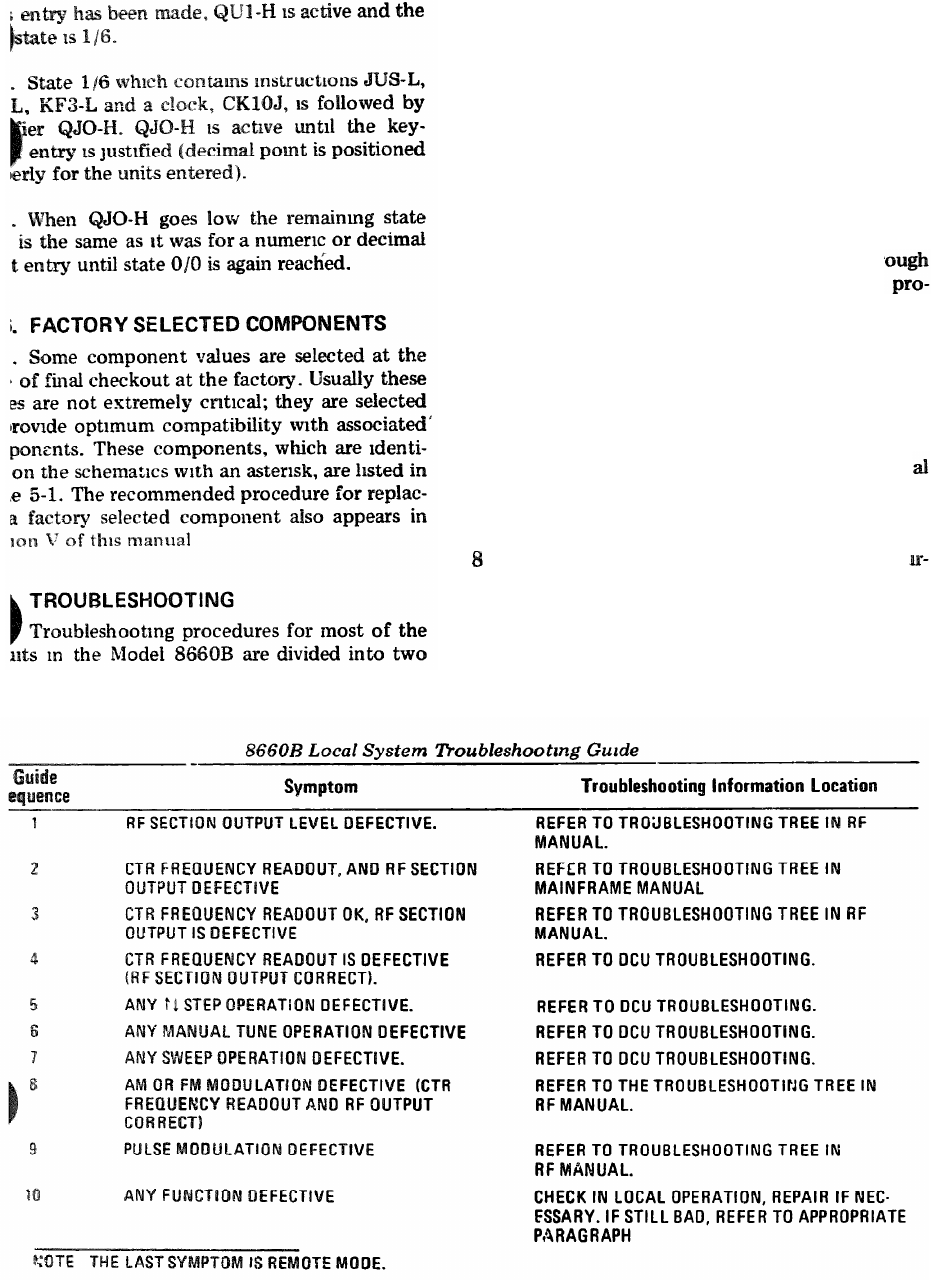
Model 8660B
TM 11-6625-2837-14&P
maintenance levels in this manual. An exception to
this is the Digital Control Unit circuits. Table 8-3
provides information which serves as a guide to
return the instrument to proper operating condi-
tion if the cause of trouble has been localized to
the DCU and a spare set of circuit boards are on
hand. For best results the circuit boards should be
replaced in the order listed.
8-90.Troubleshooting to the Module Level. This
level of maintenance is designed to utilize the HP
Module Exchange Program. Tables 8-4 thr
8-26 provide module level troubleshooting
cedures for the DCU. Foldout troubleshooting
trees provide the module level troubleshooting
procedures for the rest of the circuits within the
mainframe. A factory repaired replacement for the
defective circuit board or assembly may be ordered
through the nearest HP Sales/Service office using
the special part numbers listed in Table 6-1. Refer
to paragraph 8-35 and figure 8-2 for addition
information relative to the Module Exchange
Program.
-91. The final maintenance level involves repa
ing the instrument to the component level. Addi-
tional information for this maintenance level is
provided on the page facing the schematic of the
circuit to be repaired.
8-25
8-86.
8-88.

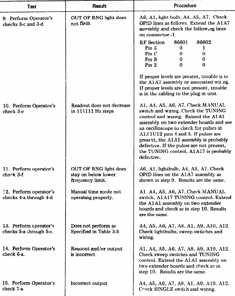
Model 8660B
TM 11-6625-2837-14&P
Table 8-3. Troubleshooting DCU by Replacement (2 of 2)
8-27

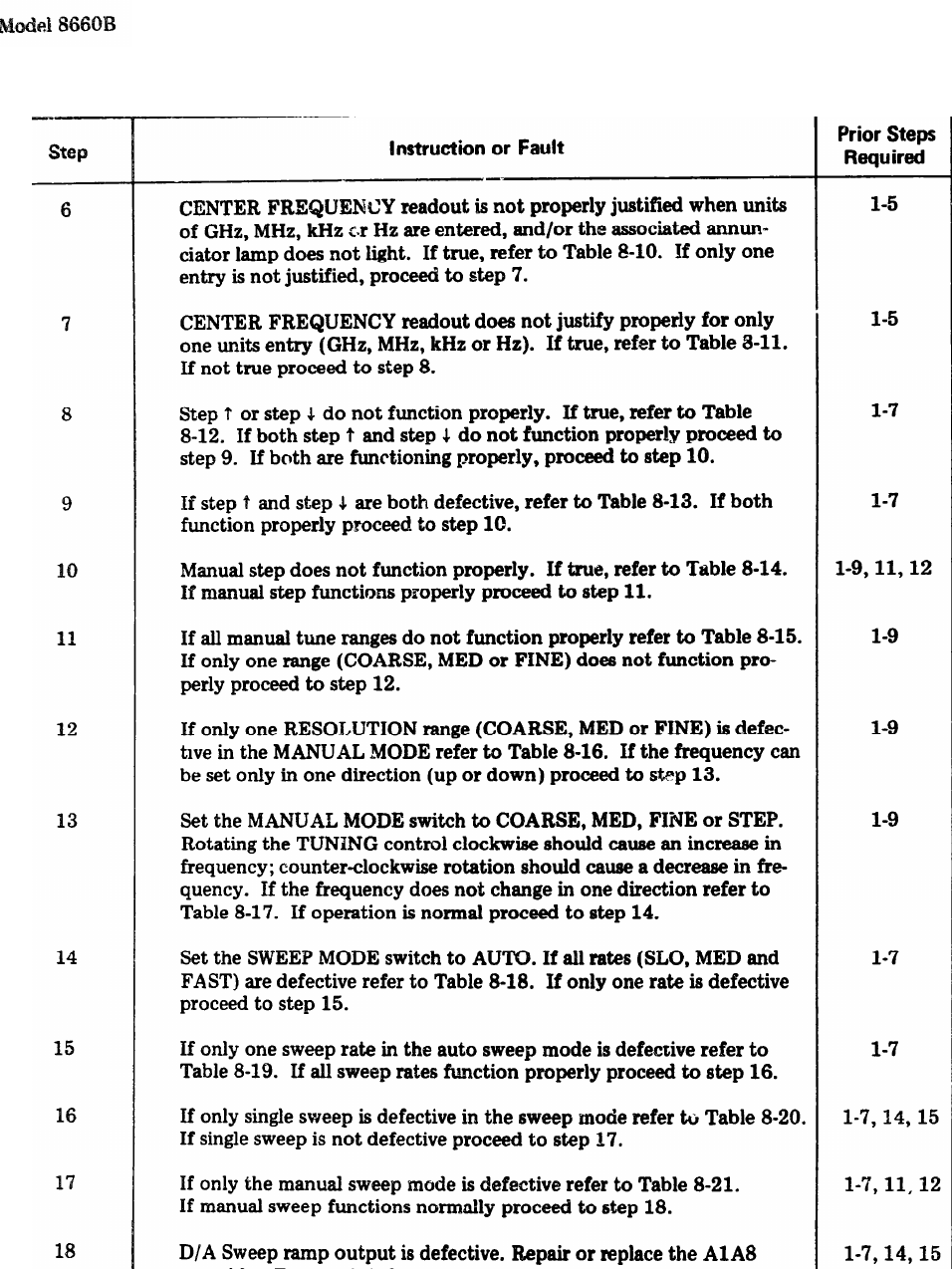
TM 11-6625-2837-14&P
Table 8-4. DCU and Interface Troubleshooting Guide (2 of 3)
8-29
TM 11-6625-2837-14&P
Table 8-4. DCU and Interface Troubleshooting Guide (3 of 3)
Model 8660B
8-30

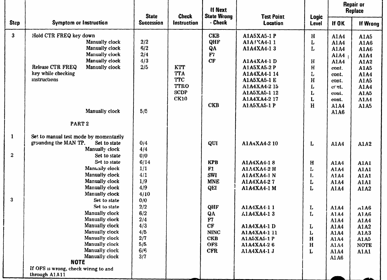
Model 8660B
TM 11-6625-2837-14&P
Table 8-6. Center Frequency Readout Faulty (3 of 5)
8-34
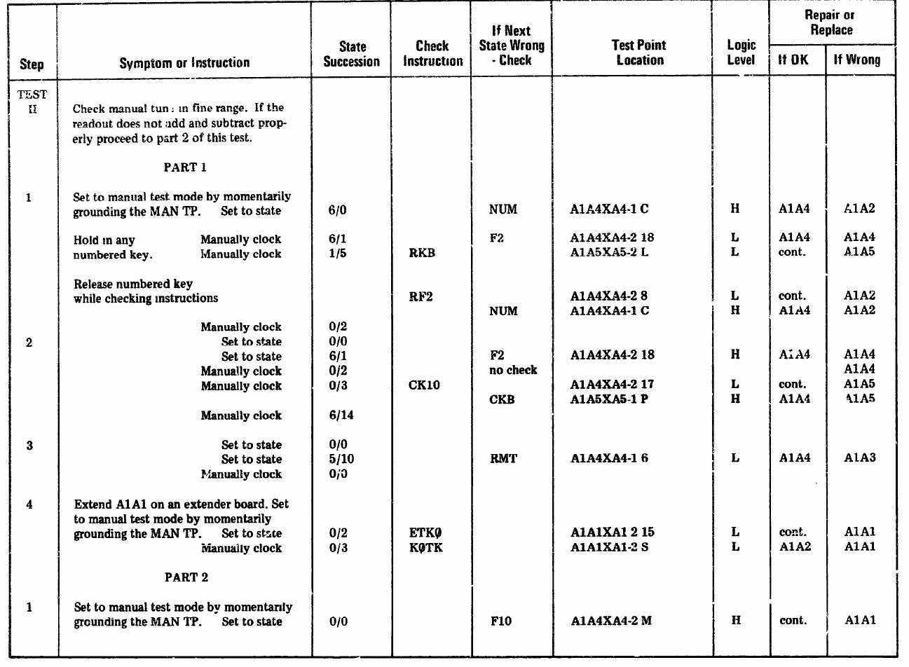
Model 8660B
TM 11-6625-2837-14&P
Table 8-6. Center Frequency Readout Faulty (4 of 5)
8-35


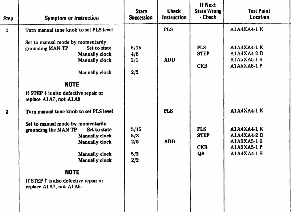
TM 11-6625-2837-14&P Model 8660B
Table 8-17. Either Up or Down Manual Tune Defective (2 of 2)
8-45

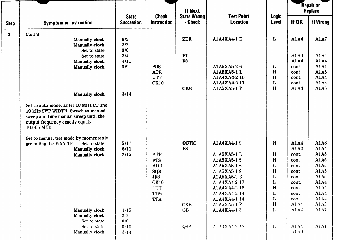
TM 11-6625-2837-14&P
Model 8660B
8-47


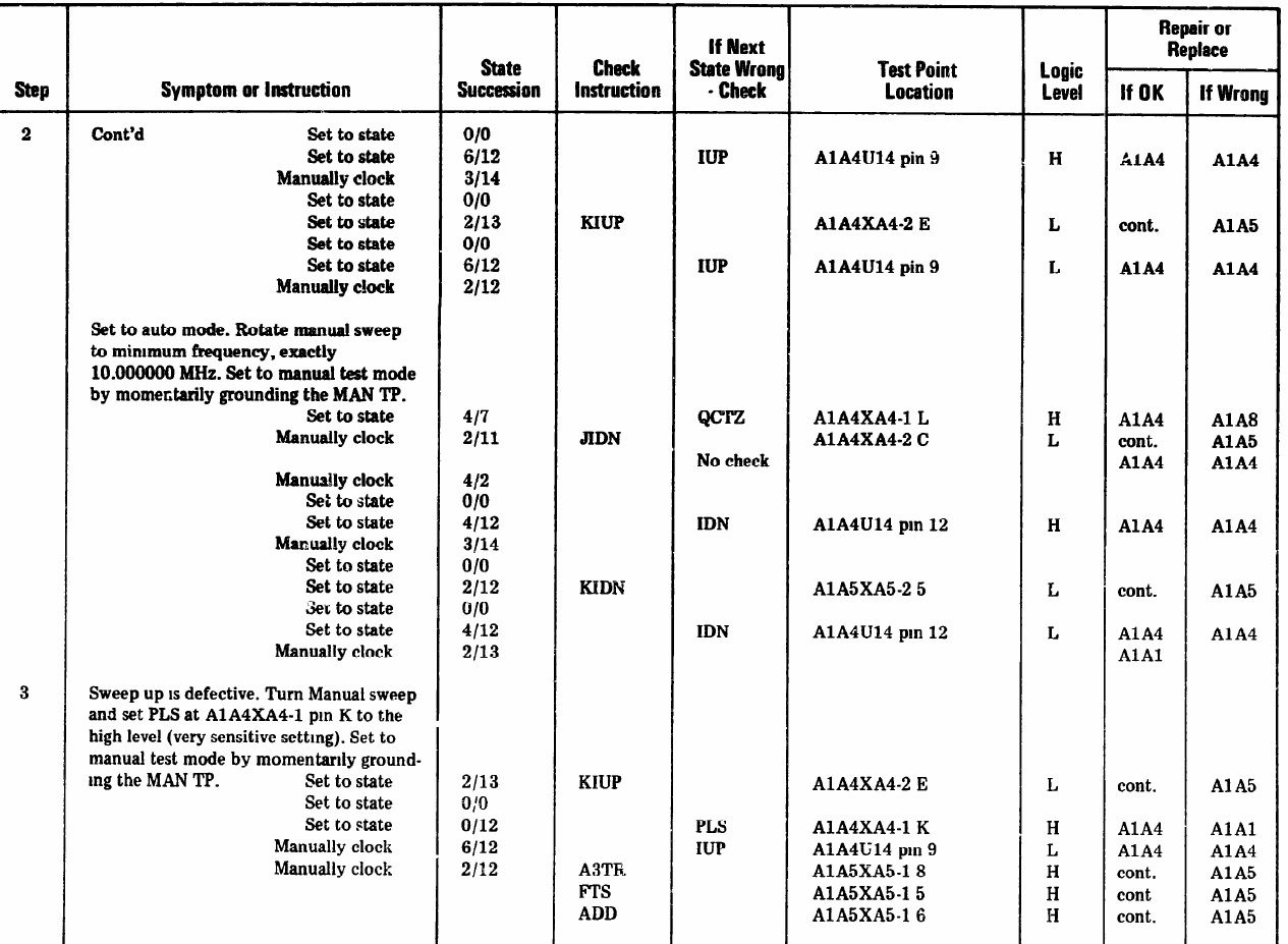
TM 11-6625-2837-14&P
Model 8660B
Table 8-21. Manual Sweep Defective (2 of 4)
8-51

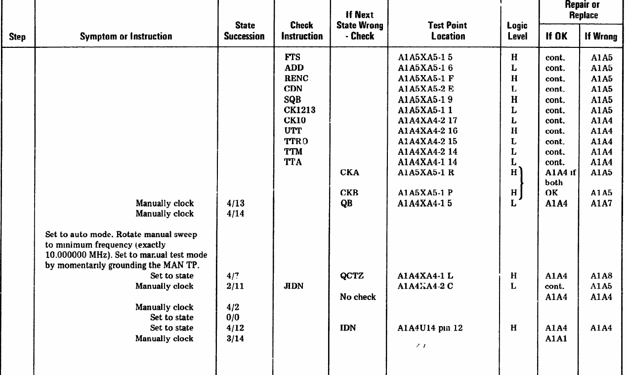
TM 11-6625-2837-14&P
Model 8660B
Table 8-21. Manual Sweep Defective (4 of 4)
8-53


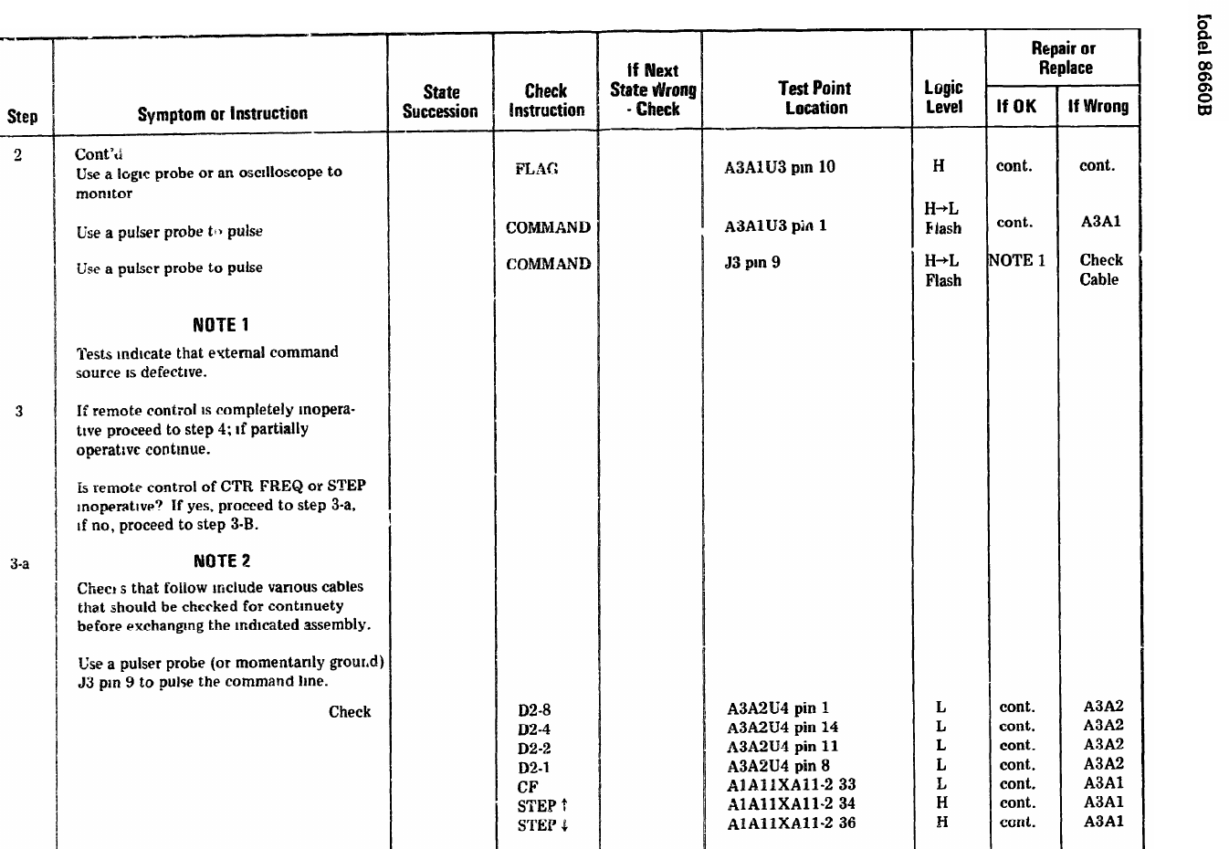
TM 11-6625-2837-14&P
Table 8-26. Remote Control Problems (2 of 7)
8-57
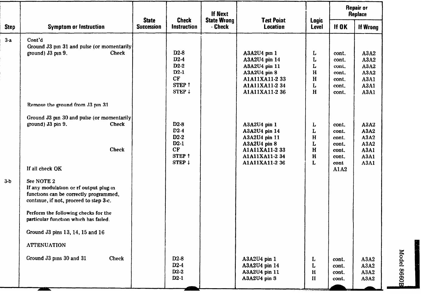
TM 11-6625-2837-14&P
Table 8-26. Remote Control Problems (3 of 7)
8-58
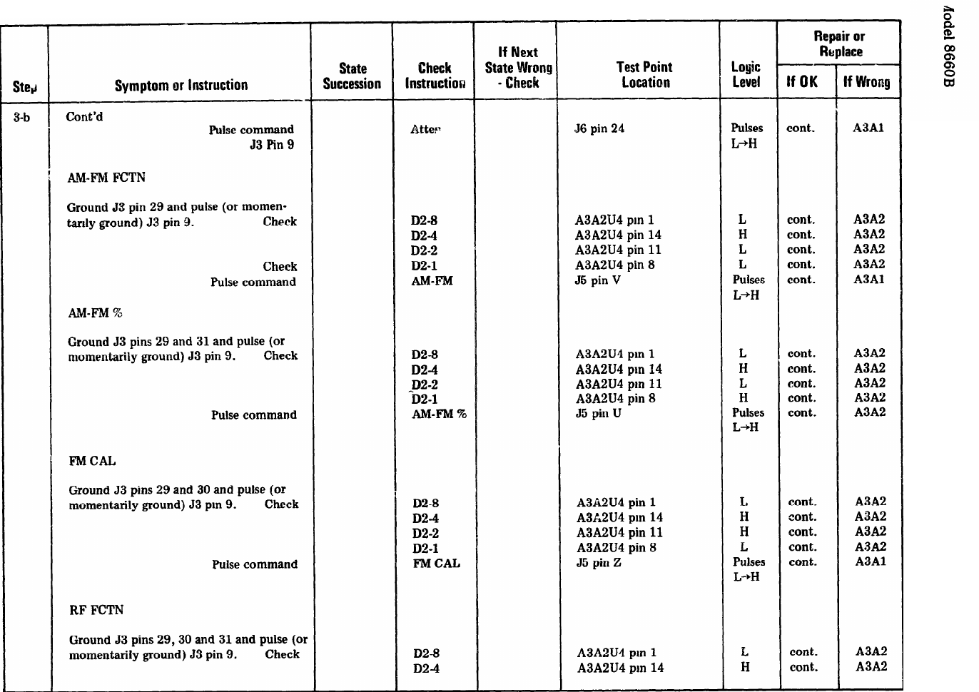
TM 11-6625-2837-14&P
Table 8-26. Remote Control Problems (4 of 7)
8-59
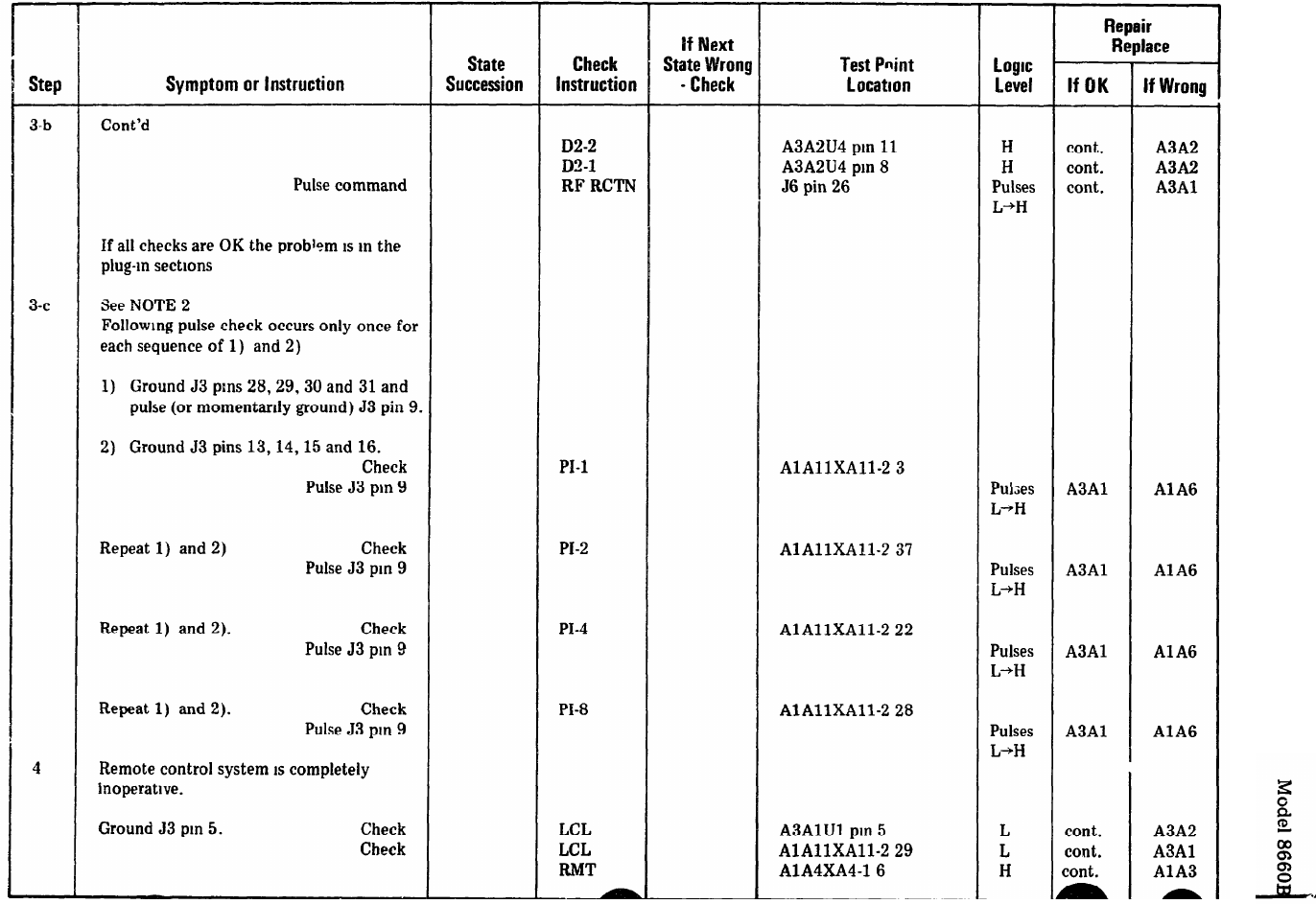
TM 11-6625-2837-14&P
Table 8-26. Remote Control Problems (5 of 7)
8-60
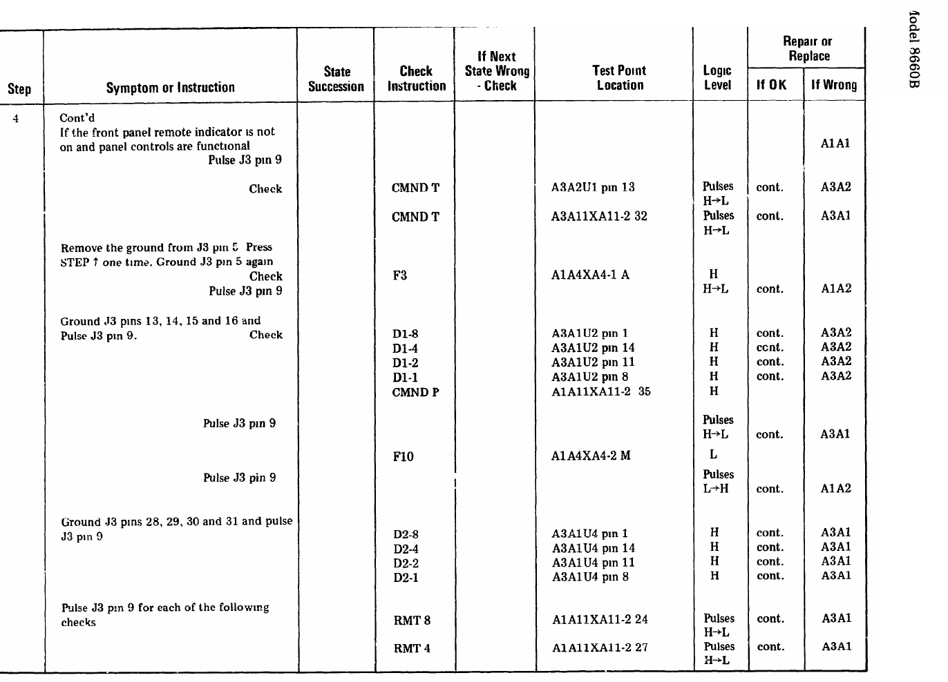
TM 11-6625-2837-14&P
Table 8-26. Remote Control Problems (6 of 7)
8-61
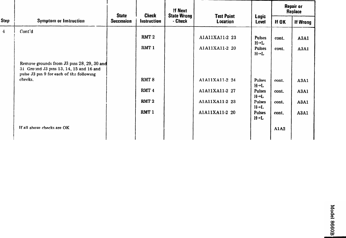
TM 11-6625-2837-14&P
Table 8-26. Remote Control Problems (7 of 7)
8-62


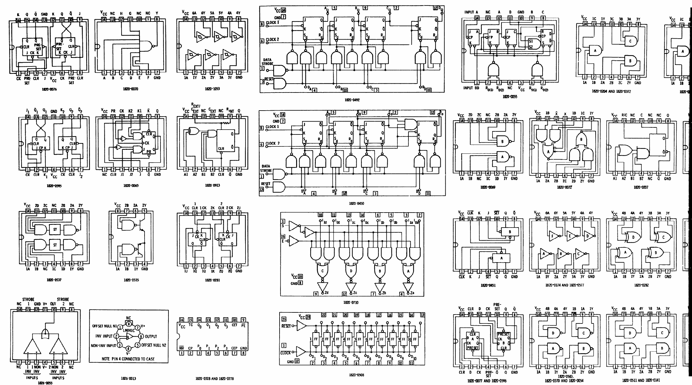
TM 11-6625-2837-14&P

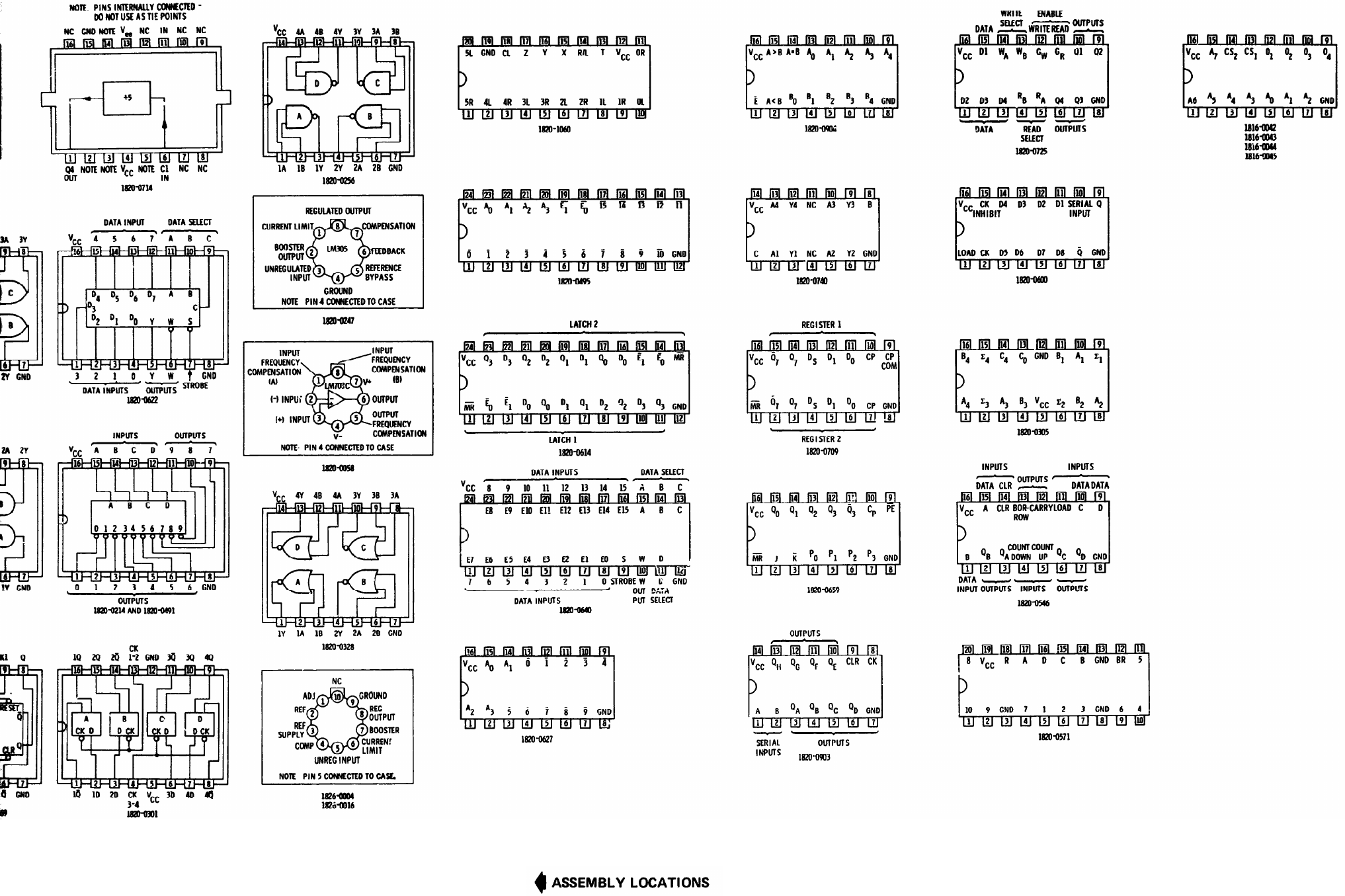
TM 11-6625-2837-14&P Model 8660B
Figure 8-7. Integrated Circuits Used in the 8660B
8-64


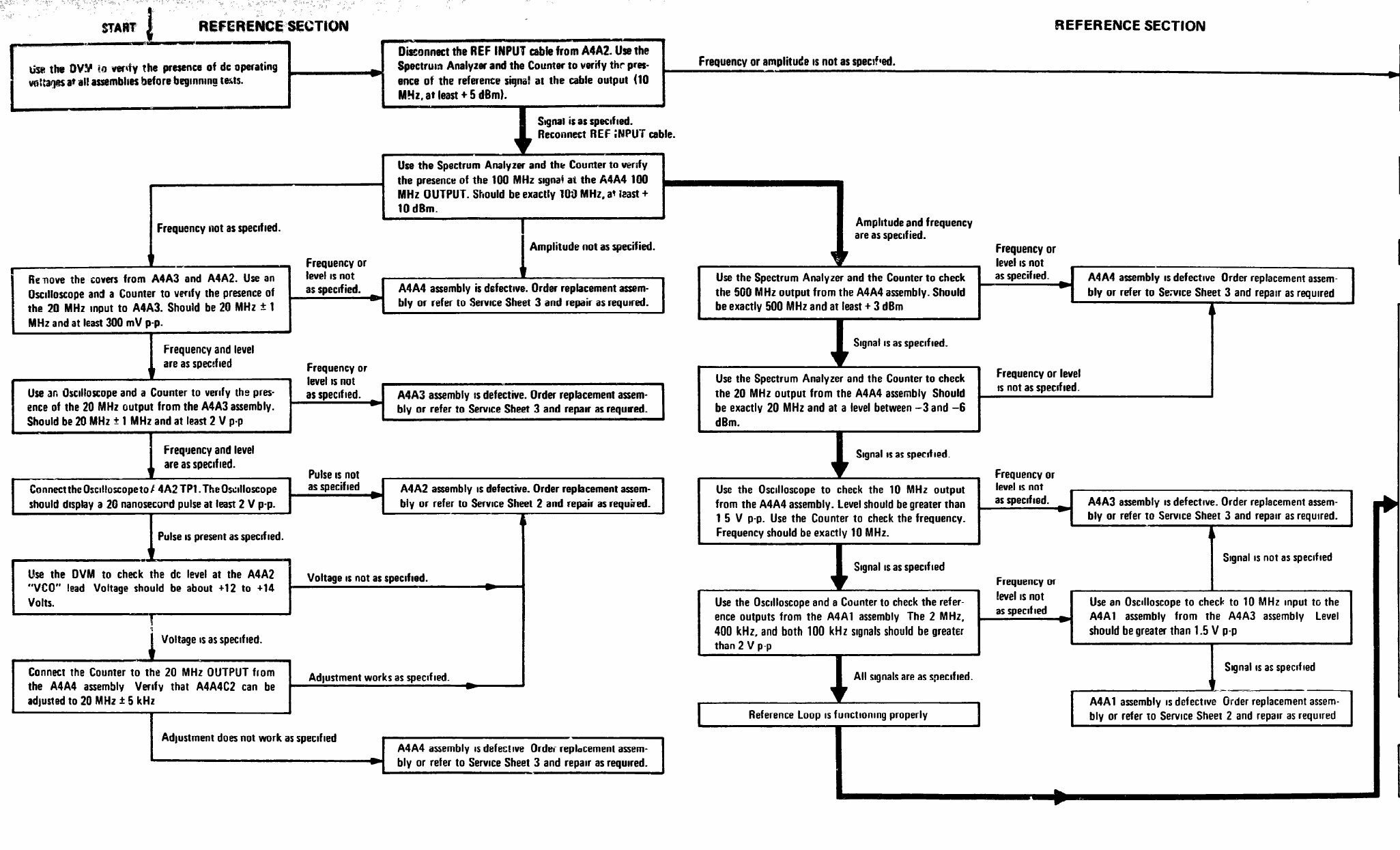
TM 11-6625-2837-14&P

TM 11-6625-2837-14&P
Figure 8-10. RF Loops Troubleshooting Tree (2 of 2)
8-67
SERVICE SHEET 1 SERVICE SHEET 1 (Cont'd) SERVICE SHEET 1 (Cont'd)

SERVICE SHEET 1 (Cont'd) SERVICE SHEET 1 (Cont'd) SERVICE SHEET 1 (Cont'd)
TM 11-6625-2837-14&P Model 8660B
SERVICE SHEET 1 (Cont'd) SERVICE SHEET 1 (Cont'd)
8-68
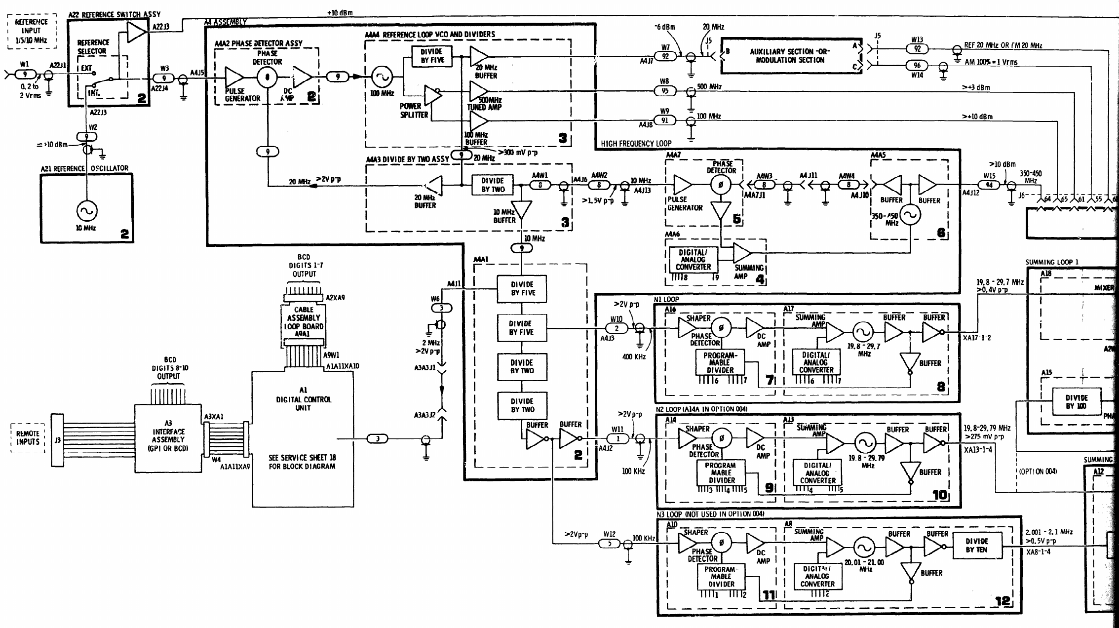

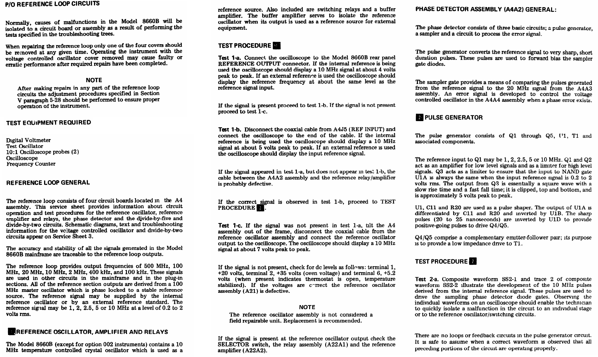
SERVICE SHEET 2 SERVICE SHEET 2 (Cont'd) SERVICE SHEET 2 (Cont'd)
(See Table 1-3)
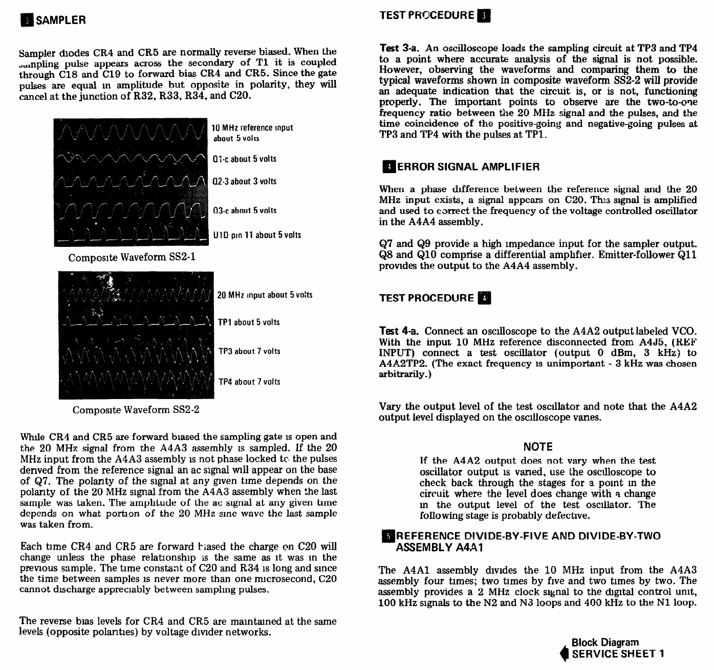
TM 11-6625-2837-14&P
SERVICE SHEET 2 (Cont'd) SERVICE SHEET 2 (Cont'd)
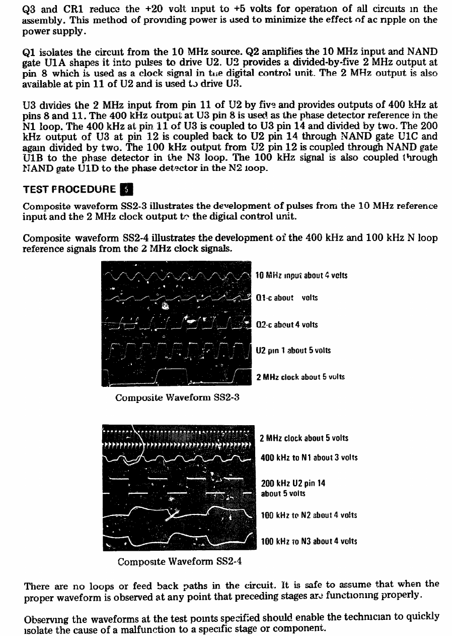
TM 11-6625-2837-14&P
8-70
Model 8660B
SERVICE SHEET 2 (Cont'd)

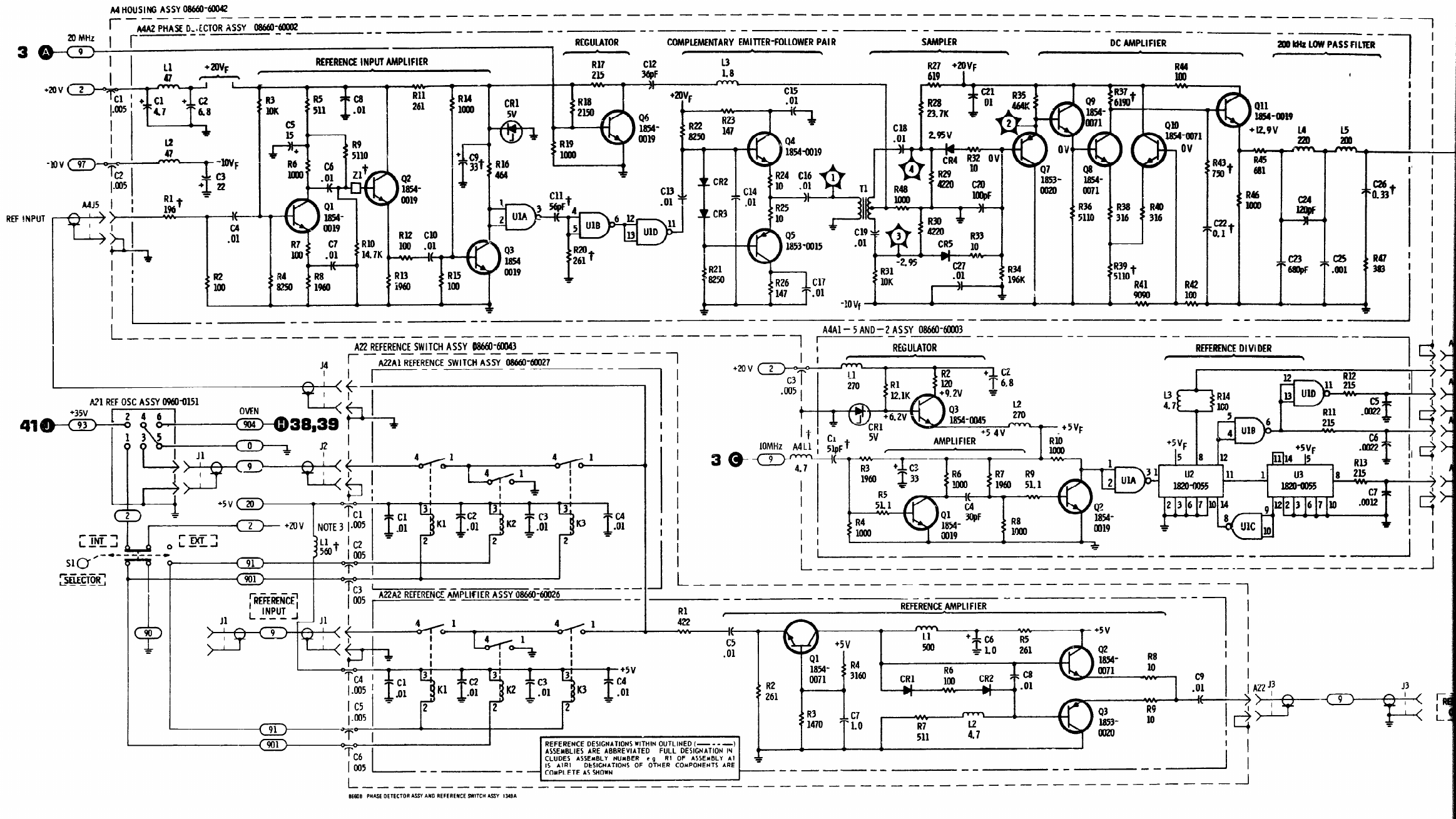
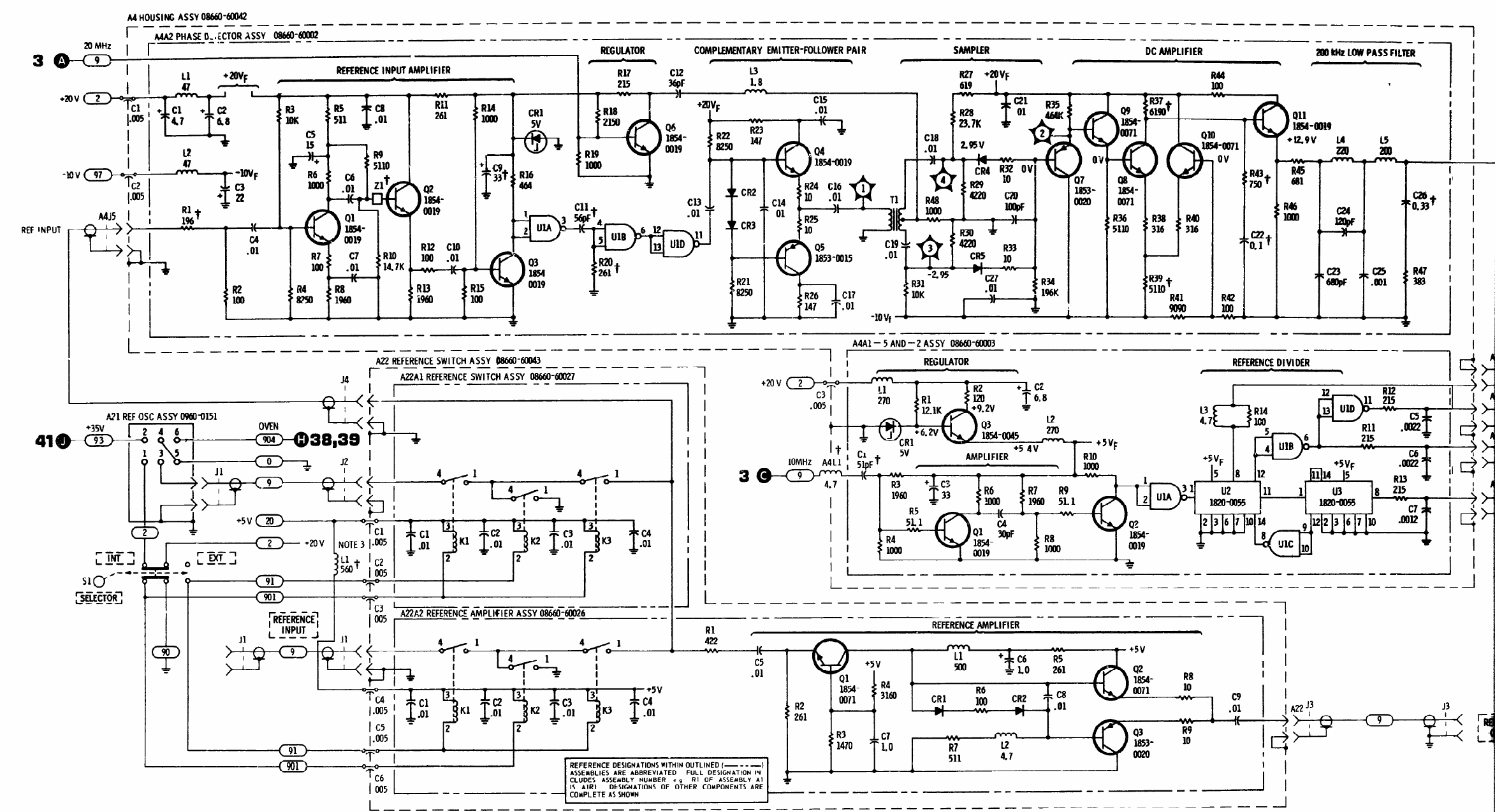
TM 11-6625-2837-14&P

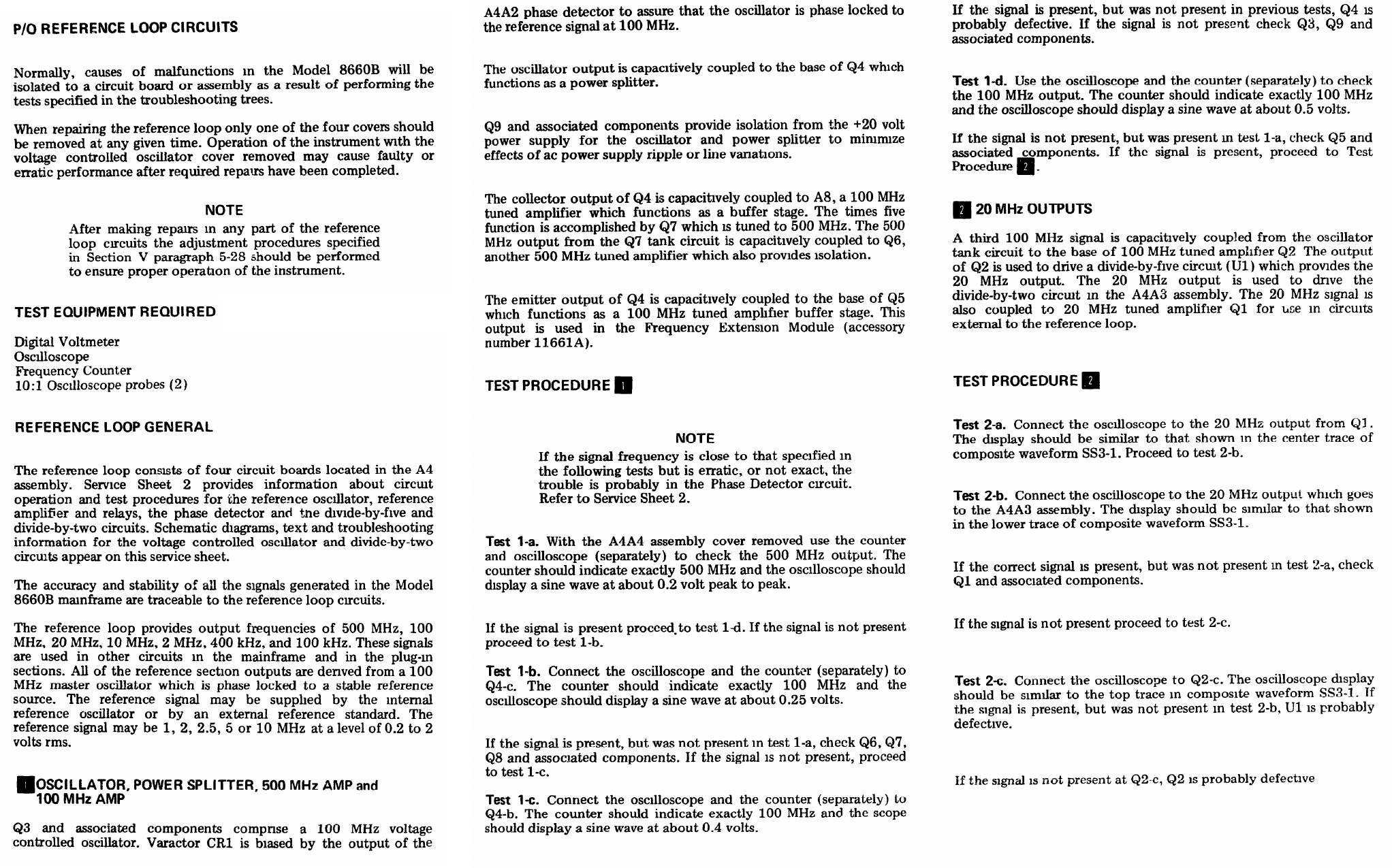
SERVICE SHEET 3 SERVICE SHEET 3 (Cont'd) SERVICE SHEET (Cont'd)
(See Table 1-3)
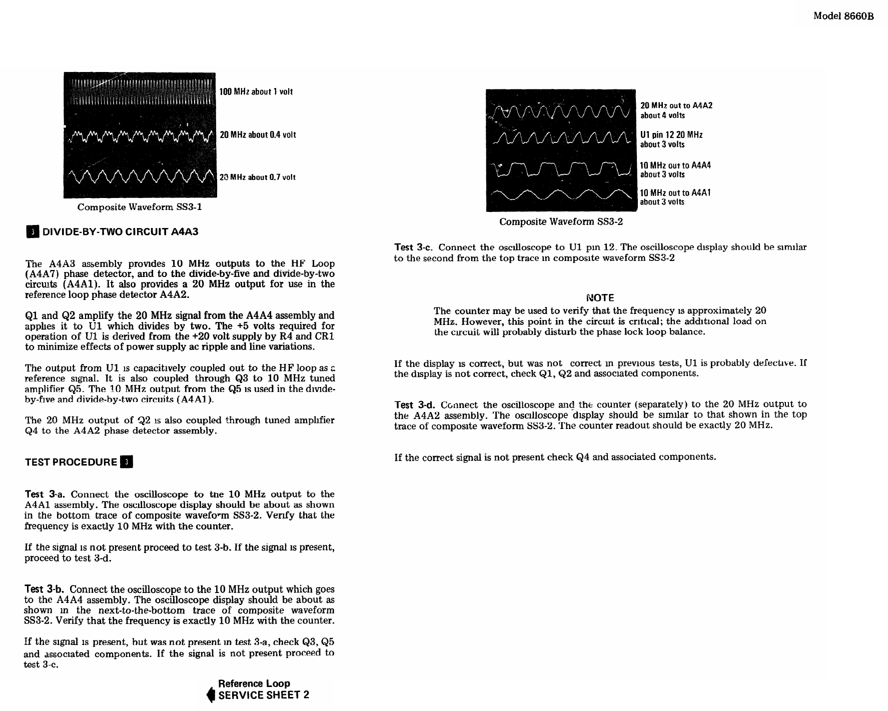
TM 11-6625-2837-14&P
SERVICE SHEET 3 (cont'd) SERVICE SHEET 3 (Cont'd)
8-72


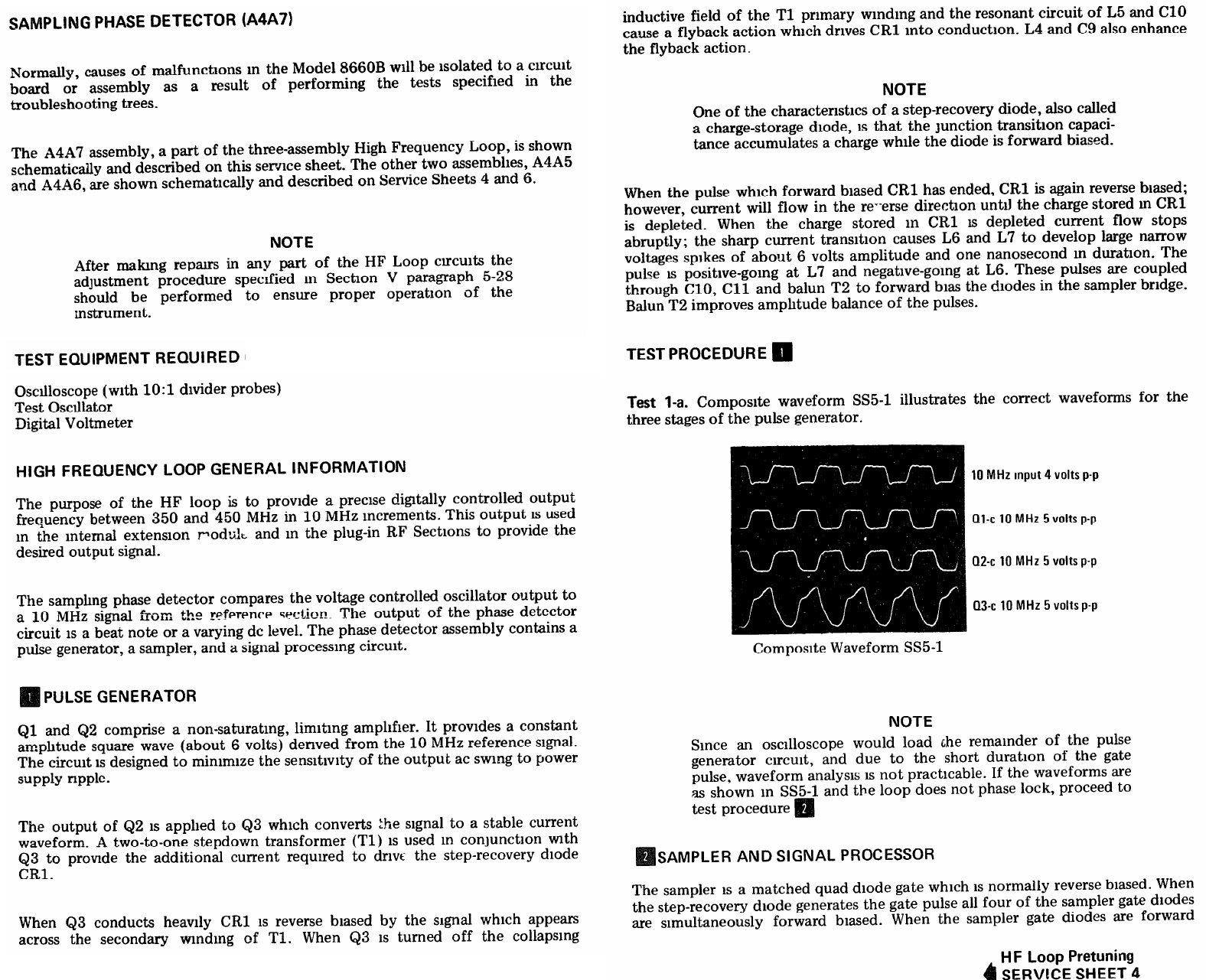
TM 11-6625-2837-14&P
SERVICE SHEET 5 SERVICE SHEET 5 (Cont'd)
(see Table 1-3)
8-76
TM 11-6625-2837-14&P Model 8660B
SERVICE SHEET 5 (Cont'd)
8-76


SERVICE SHEET 7 SERVICE SHEET 7 (Cont'd) SERVICE SHEET 7 (Cont'd)
(see Table 1-3)
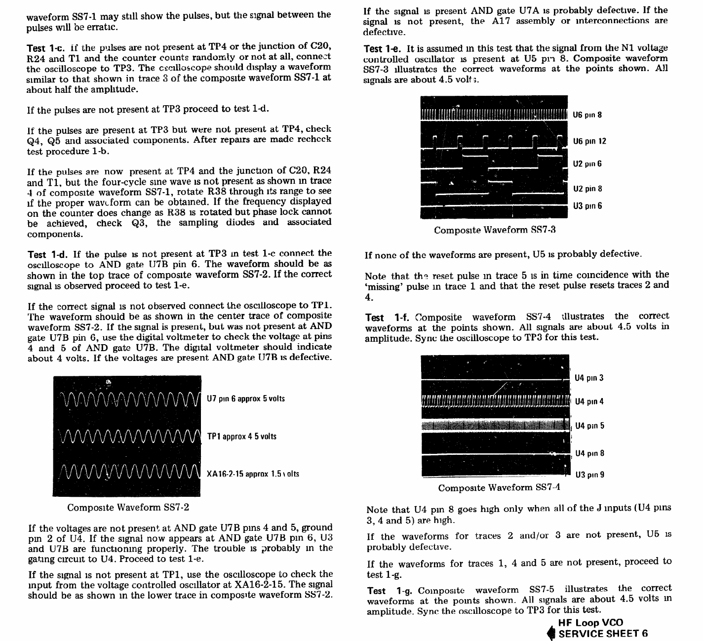
TM 11-6625-2837-14&P
SERVICE SHEET 7 (Cont’d) SERVICE SHEET 7 (Cont’d)
8-80
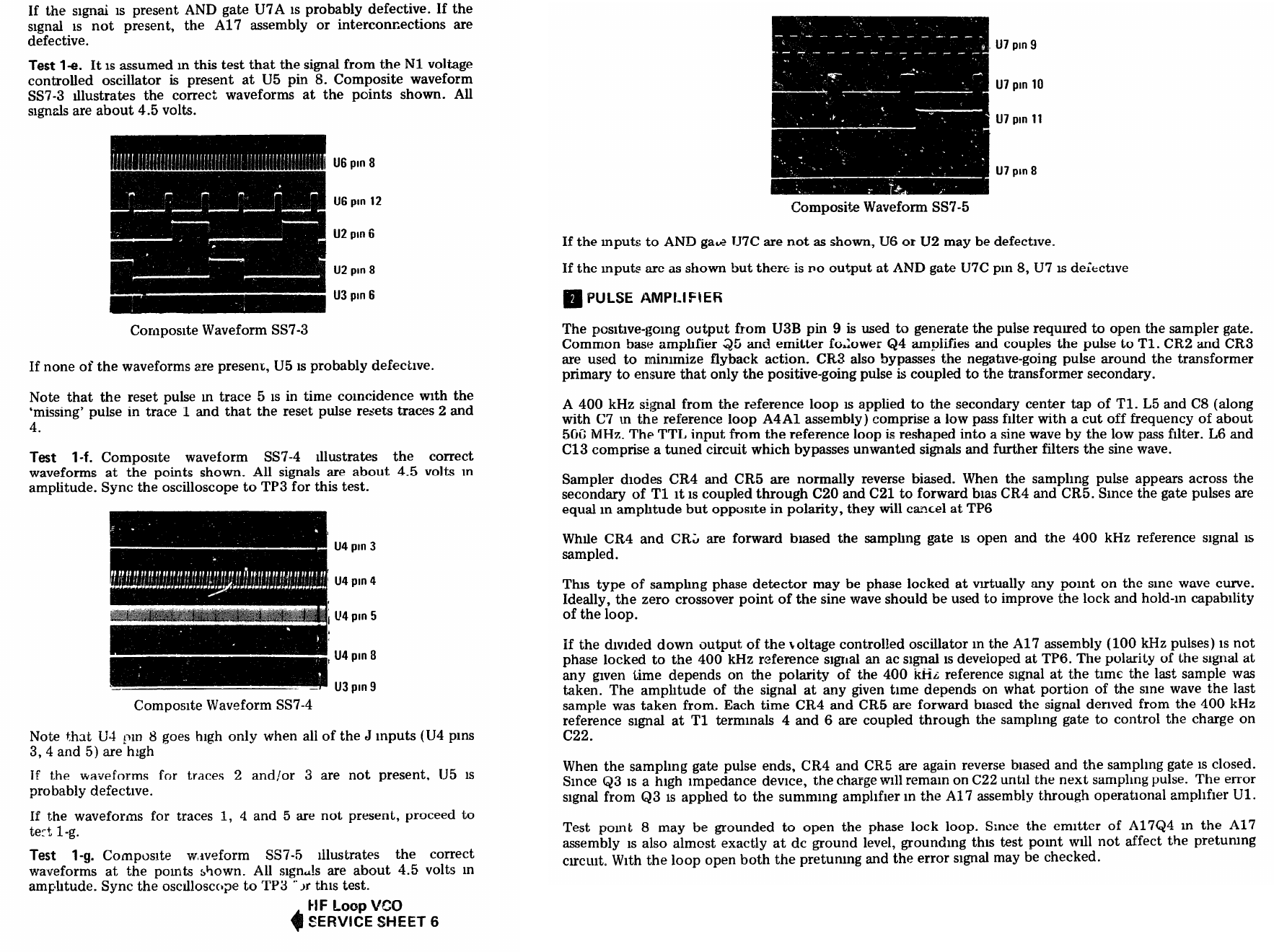
SERVICE SHEET 7 (Cont’d)
TM 11-6625-2837-14&P
SERVICE SHEET 7 (Cont’d)
Model 8660B
8-80


SERVICE SHEET 8
TEST EQUIPMENT REQUIRED (see Table 1-3)
SERVICE SHEET 8 (Cont’d)


SERVICE SHEET 9 SERVICE SHEET 9 (Cont’d) SERVICE SHEET 9 (Cont’d)
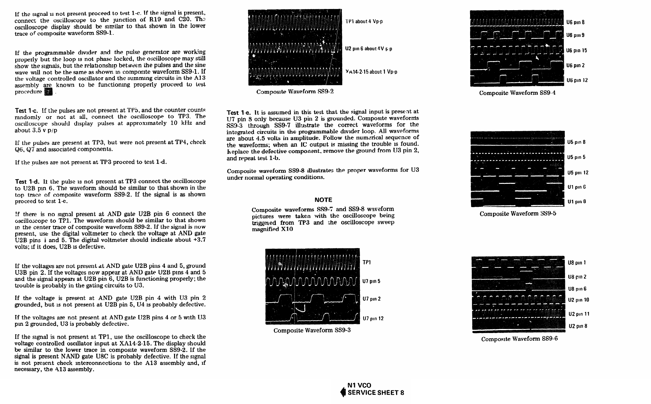
SERVICE SHEET 9 (Cont’d)
SERVICE SHEET 9 (Cont'd)
TM 11-6625-2837-14&P
SERVICE SHEET 9 (Cont’d)
8-84


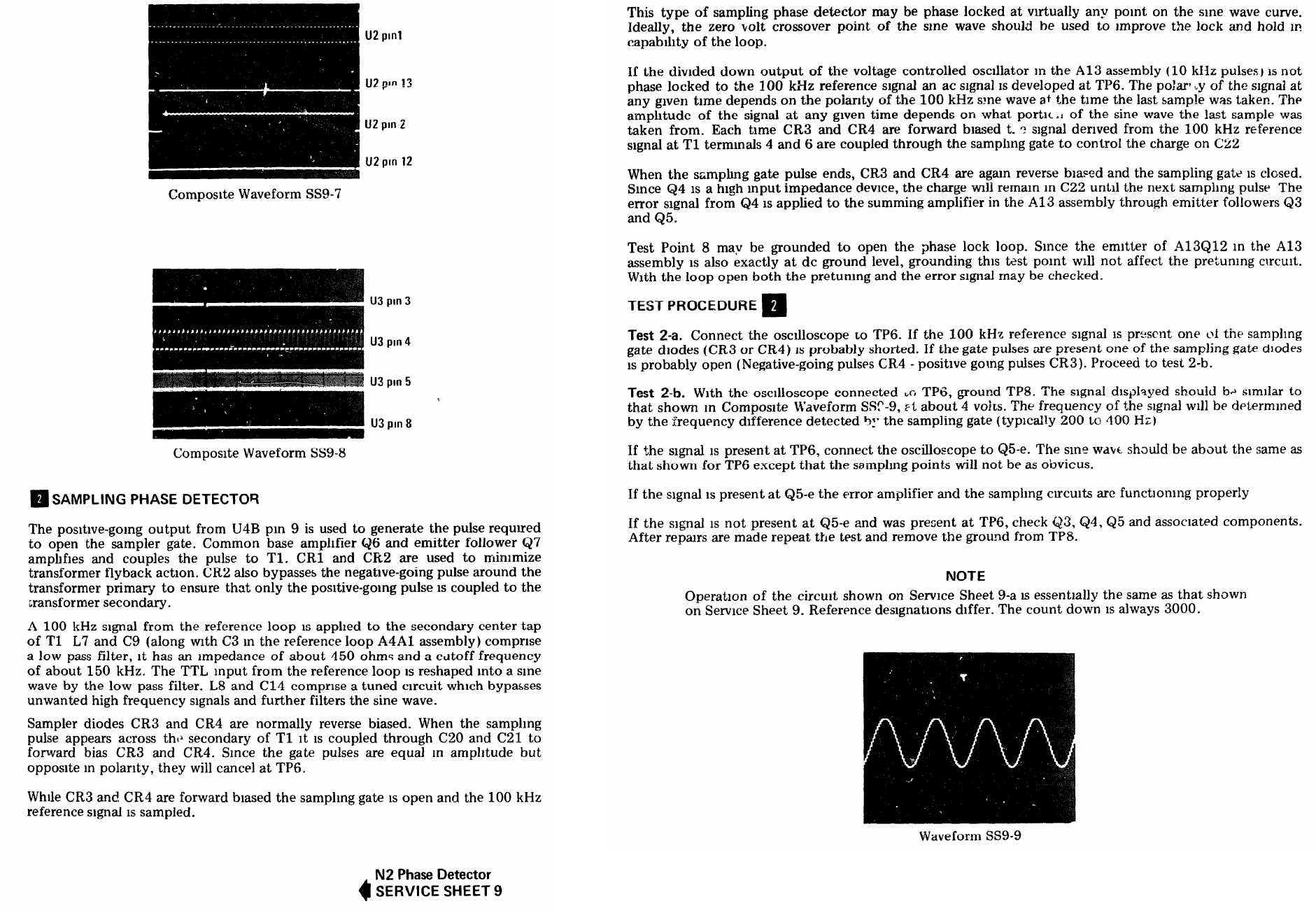
SERVICE SHEET 9 (Cont’d)
TM ll-6625-2837-14&P Model 8660B
SERVICE SHEET 9 (Cont’d)
8-86


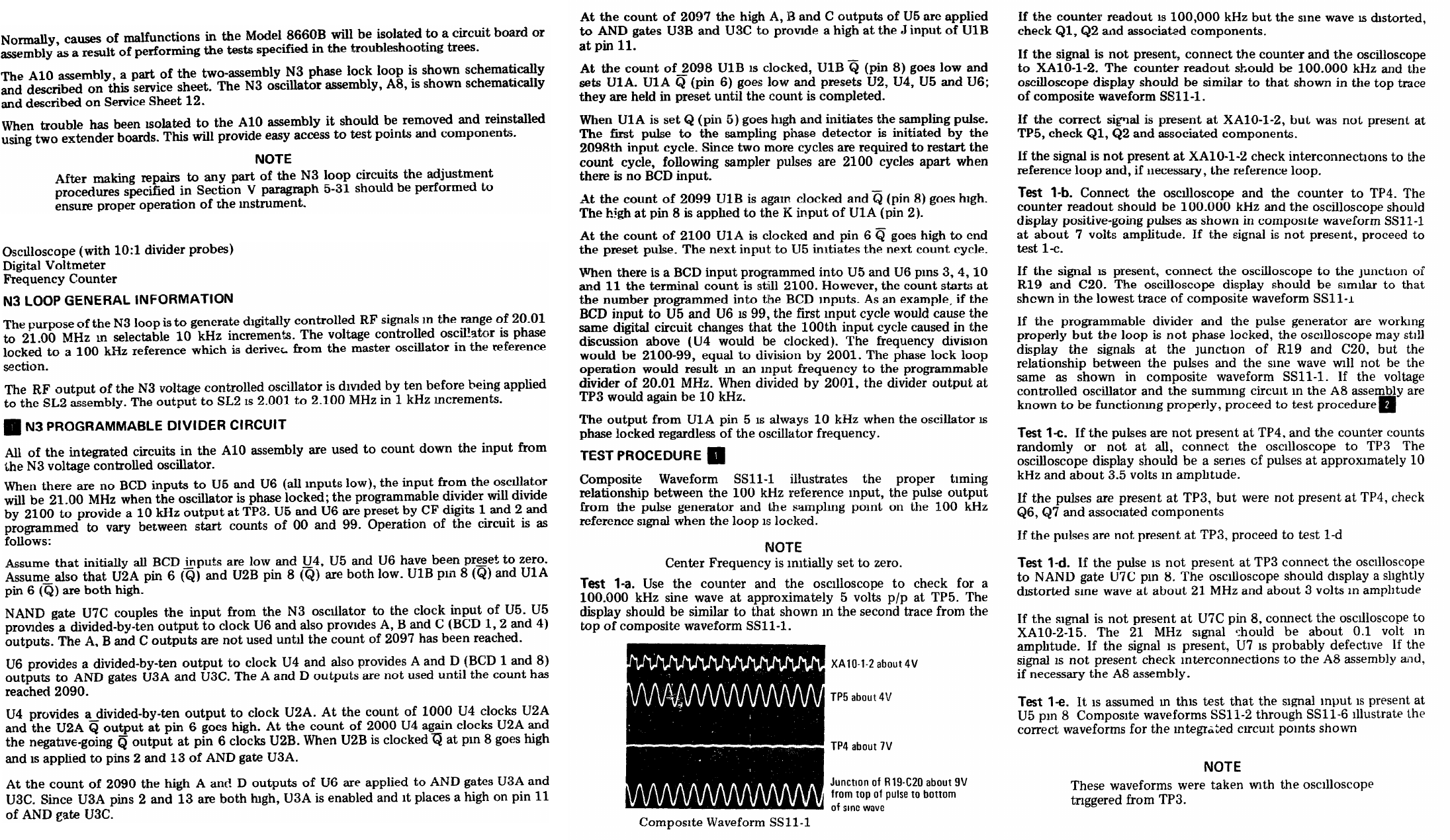
SERVICE SHEET 11
N3 PHASE DETECTOR ASSEMBLY A10
TEST EQUIPMENT REQUIRED (See Table 1-3)
SERVICE SHEET 11 (Cont’d) SERVICE SHEET 11 (Cont’d)
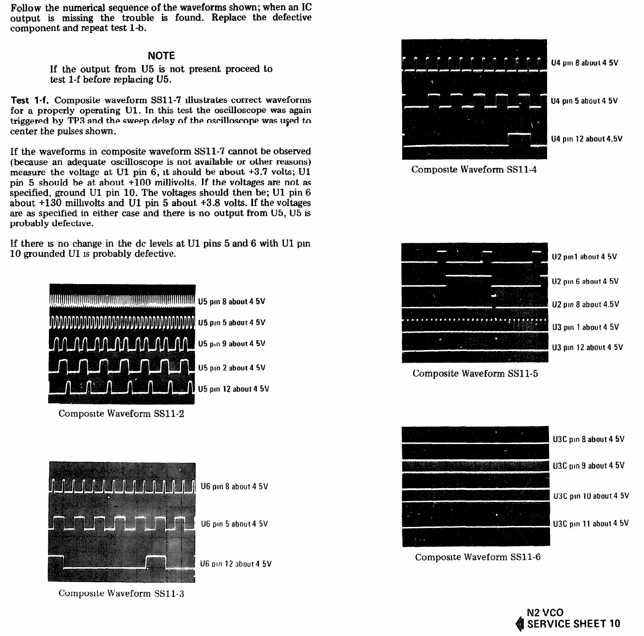
TM 11-6625-2837-14&P
SERVICE SHEET 11 (Cont'd) SERVICE SHEET (Cont'd)
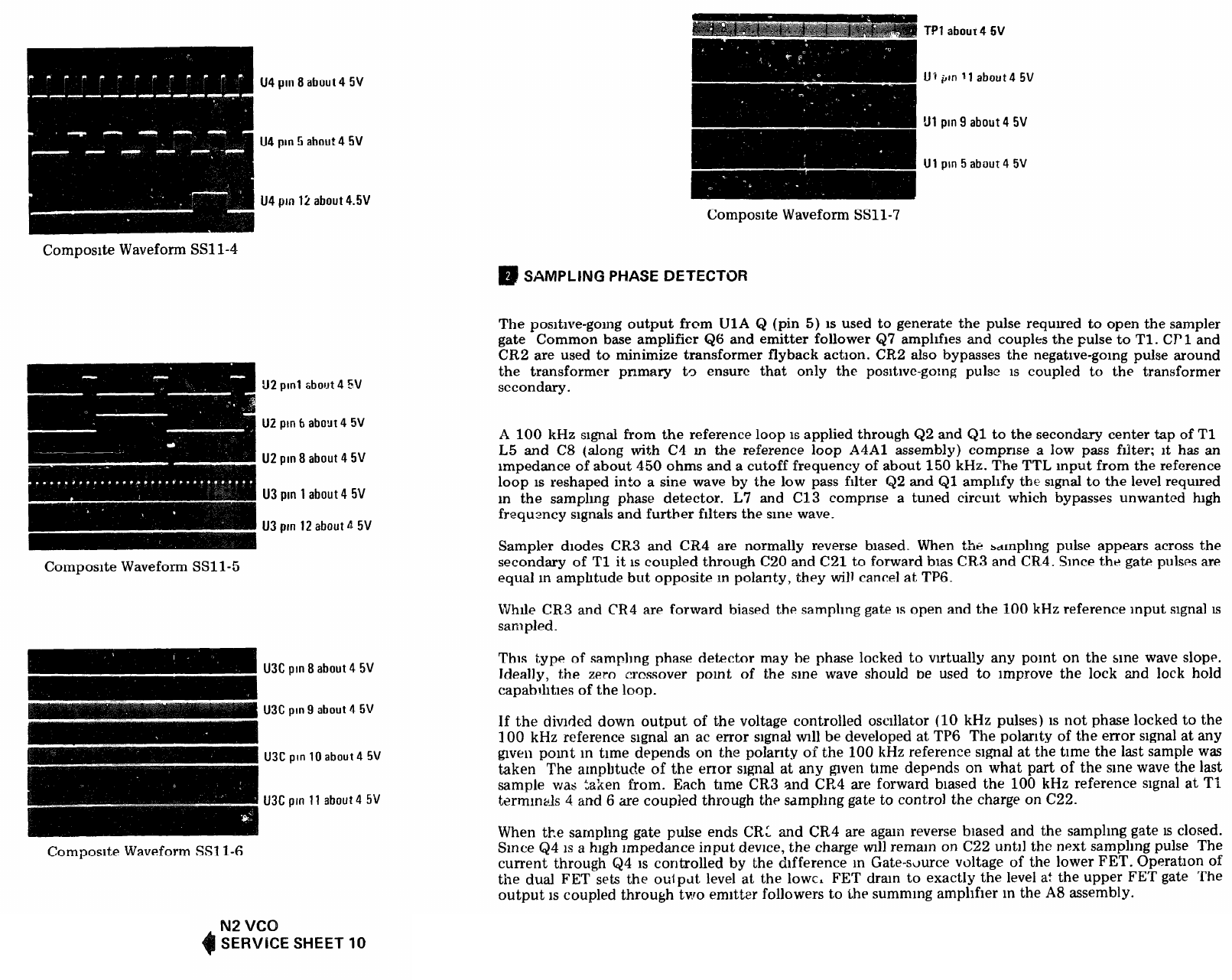
TM 11-6625-2837-14&P Model 8660B
SERVICE SHEET 11 (Cont’d) SERVICE SHEET 11 (Cont’d)
8-90


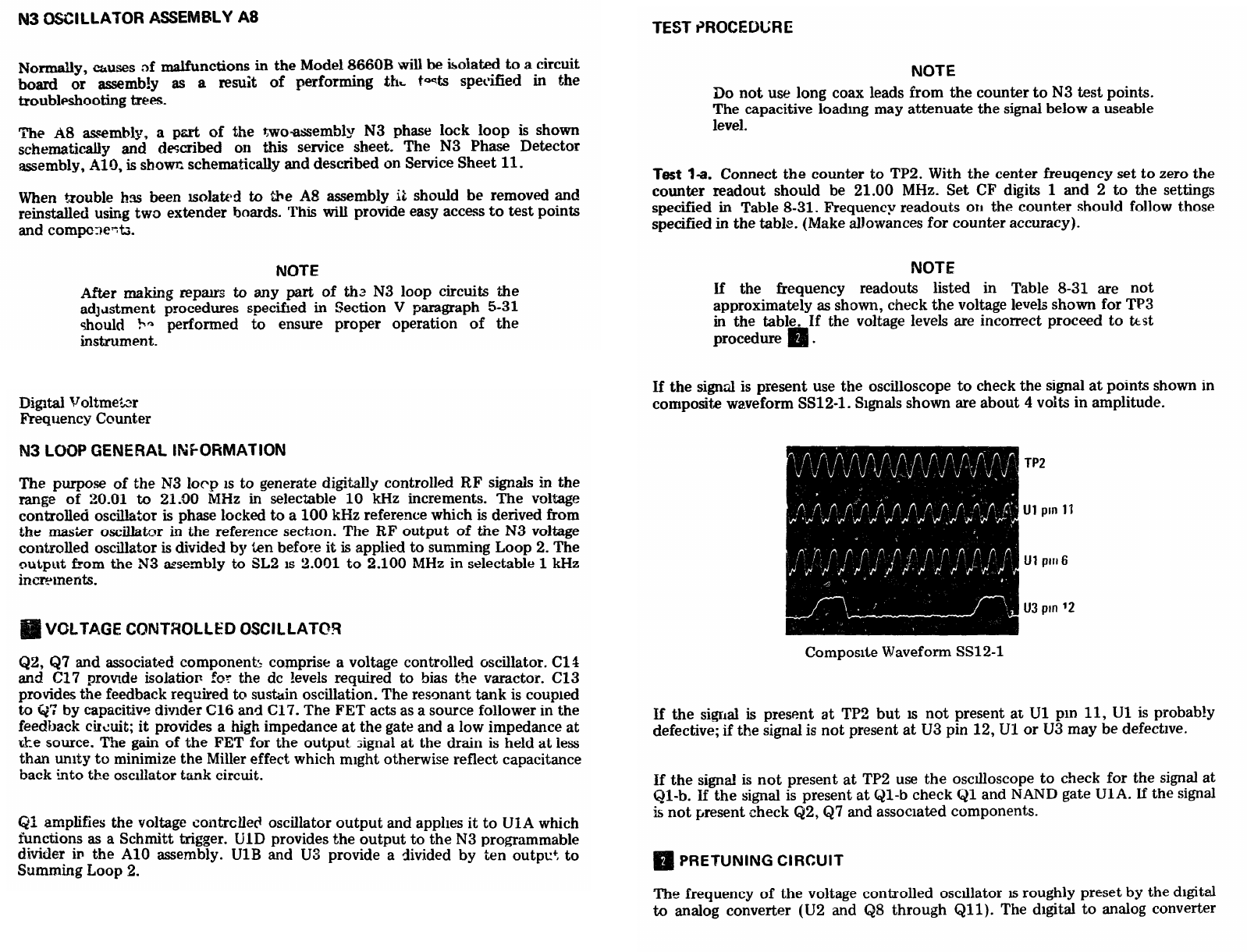
SERVICE SHEET 12
TEST EQUIPMENT REQUIRED (See Table 1-3)
SERVICE SHEET 12 (Cont’d)


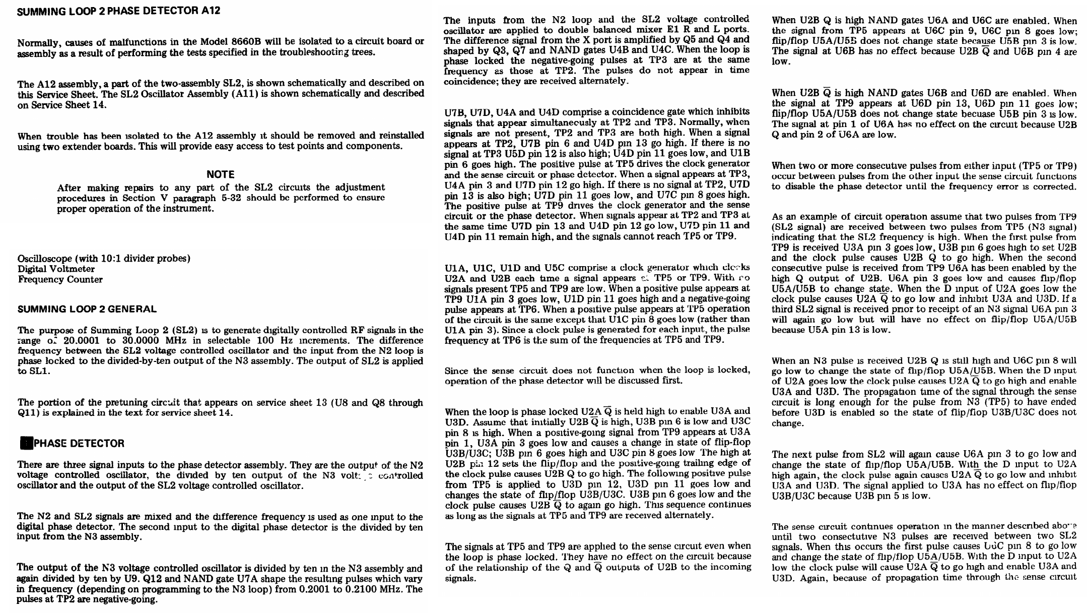
SERVICE SHEET 13
TEST EQUIPMENT REQUIRED (See Table 1-3)
SERVICE SHEET 13 (Cont’d) SERVICE SHEET 13 (Cont’d)
TM 11-6625-2837-14&P
SERVICE SHEET 13 (Cont’d)
SERVICE SHEET 13 (Cont’d) SERVICE SHEET 13 (Cont’d)
8-94
SERVICE SHEET 13 (Cont’d)
TM 11-6625-2837-14&P Model 8660B
SERVICE SHEET 13 (Cont’d)
8-94


SERVICE SHEET 15
After making repairs to any part of the SL1 circuits the adjustment procedures in
Section V paragraph 5-33 should be performed to ensure proper operation of the
instrument.
TEST EQUIPMENT REQUIRED (See Table 1-3)
Oscilloscope (with 10: 1 divider probes)
Digital Voltmeter
Frequency Counter
SUMMING LOOP 1 GENERAL
SERVICE SHEET 15 (Cont’d)
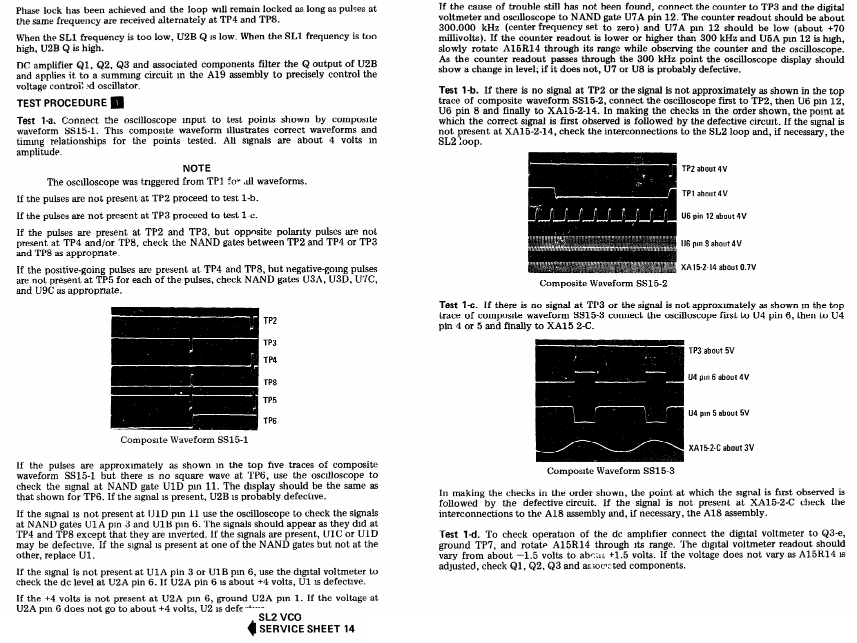
TM 11-6625-2837-14&P
SERVICE SHEET 15 (Cont’d)
Model 8660B
SERVICE SHEET 15 (Cont’d)
8-98


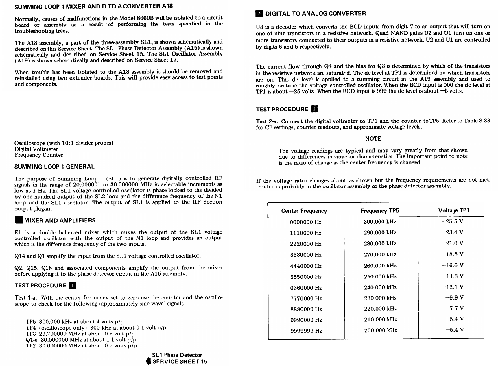
SERVICE SHEET 16
NOTE
After making repairs to any part of the SL1 circuits the
adjustment procedures in Section V paragraph 5-33 should be
performed to ensure proper operation of the instrument.
TEST EQUIPMENT REQUIRED (See Table 1-3)
TM 11-6625-2837-14&P
SERVICE SHEET 16 (Cont’d)
8-100
Model 8660B
Table 8-33. SL1 Frequency Versus Voltage Chart


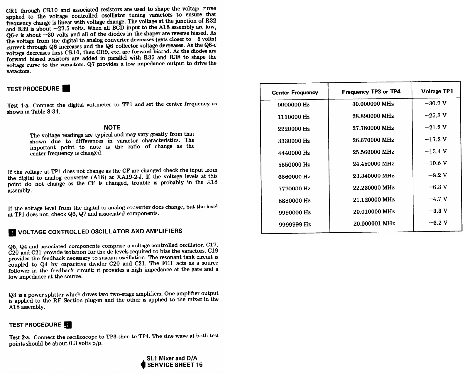
SERVICE SHEET 17 (Cont’d)
TM 11-6625-2837-14&P Model 8660B
SERVICE SHEET 17 (Cont’d)
If the signal is not present at either TP3 or TP4 connect the oscilloscope to Q3-b.
The signal level should be about 0.2 volts p/p. If the signal is present at Q3-b but
was not present at TP3 or TP4, Q3 is probably defective. If the signal is not
present at Q3-b, check Q5, Q4 and associated components.
Test 2-b. Connect the counter to TP3 or TP4 and check for correct frequencies at
the CF shown in Table 8-34.
Table 8-34 Varactor Bias Versus Frequency SL1
8-102


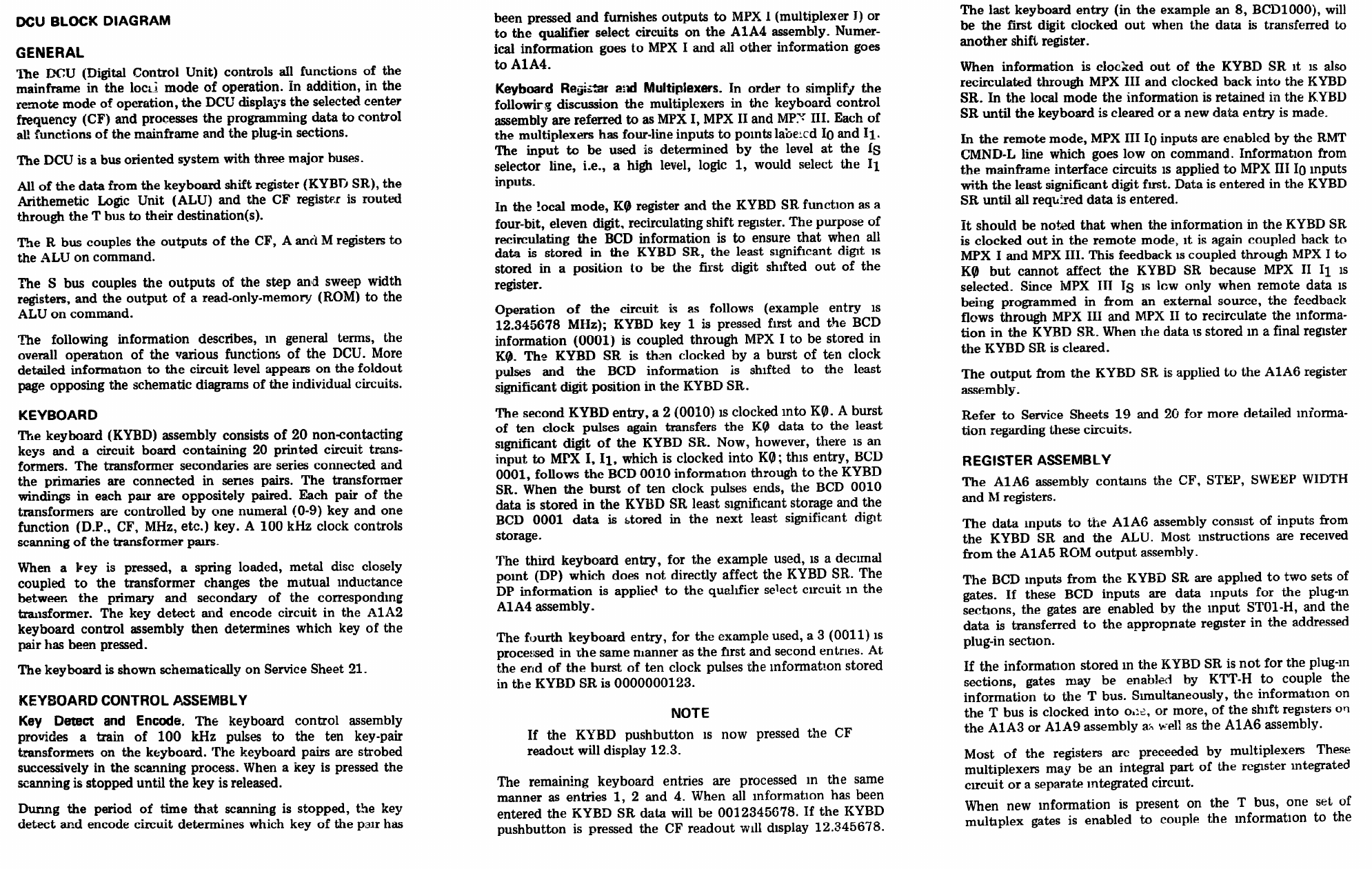
SERVICE SHEET 18 SERVICE SHEET 18 (Cont’d) SERVICE SHEET 18 (Cont’d)
SERVICE SHEET 18 (Cont’d) SERVICE SHEET 18 (Cont’d)
TM 11-6625-2837-14&P
8-104
SERVICE SHEET 18 (Cont’d)
TM 11-6625-2837-14&P
SERVICE SHEET 18 (Cont’d)
8-104
Model 8660B


SERVICE SHEET 20 SERVICE SHEET 20 (Cont’d)
TM 11-6625-2837-14&P
SERVICE SHEET 20 (Cont'd)
8-108
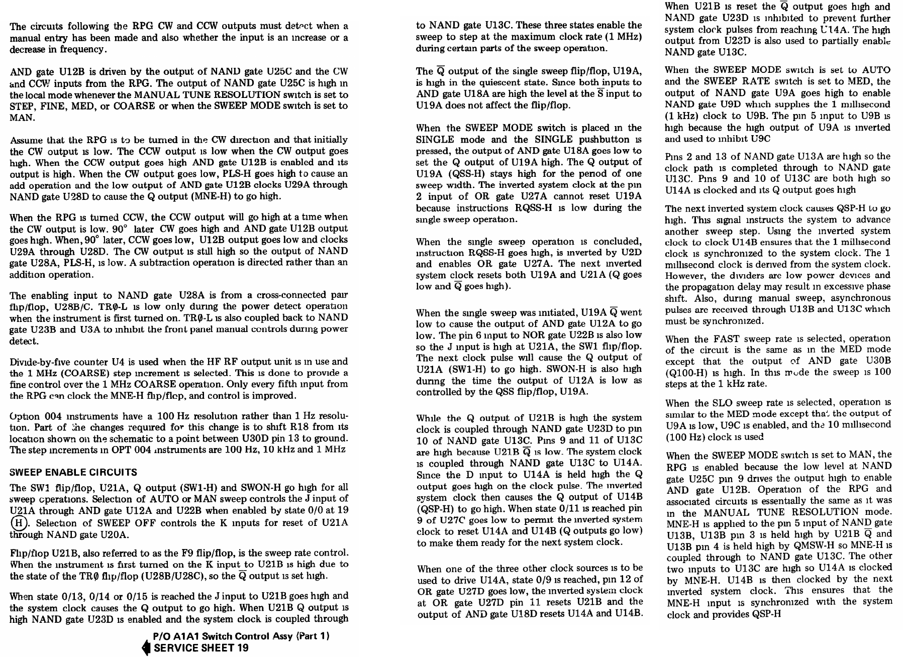
SERVICE SHEET 20 (Cont’d)
TM 11-6625-2837-14&P
SERVICE SHEET 20 (Cont’d)
8-108
Model 8660B

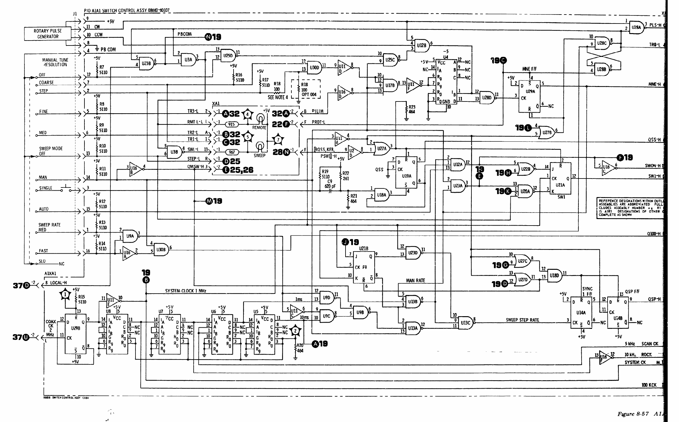


TM 11-6625-2837-14&P
SERVICE SHEET 21 (Cont'd)
The gating circuits to the right of U15 and U23 generate various qualifiers
and instructions. As an example, if the CF key is pressed (code 8,1000) the
08 output of U23 is low, U15ZC is low and the output of U22D is high. At
all other times, when the CF function has not been initiated, qualifier CF-H
is low.
Flip/flop U7B functions in the microprogram to prevent an entry operation
from being made before a unit key is pressed. A unit key must be pressed to
complete the justification process. The F3 flip/flop (U7B) K input goes high
when qualifier QU1 (U21B pin 8) is high and instruction KF3-L is low which
occurs in state 1/6. The next dock pulse resets U7B and qualifier F3 goes
low The F3 J input must go high in order to make the Q output go high to
complete the cycle. This is accomplished when the JF3-L input (pin 11)
becomes active when the machine is active in any one of four states, 1/11,
1/12, 1/13 or 1/0 and U7B is clocked. The Q output will also go high if the
CLEAR KYBD key is pressed generating output 02 from U23. U17A Q
(KD2-L) provides a signal to the F10 flip/flop on the A1A1 assembly when a
key has been pressed or when CMND-P-L goes low in the remote mode.
J-K flip/flop U7A is used in a synchronizing process; it is connected as a “D”
type flip/flop. The “D” input from U19 is asynchronous since it IS a
response to manual press and release of a key. The synchronized KDN-H
output ensures correct machine state action.
NOTE
For instruments with serial prefix numbers below 1310A refer to
Section VII of this manual for information referring to prior use
of A1A2U7
.
Model 8660B
Figure 8-58. Keyboard Assembly Front View
Figure 8-59. Key board Assembly Rear View
8-110

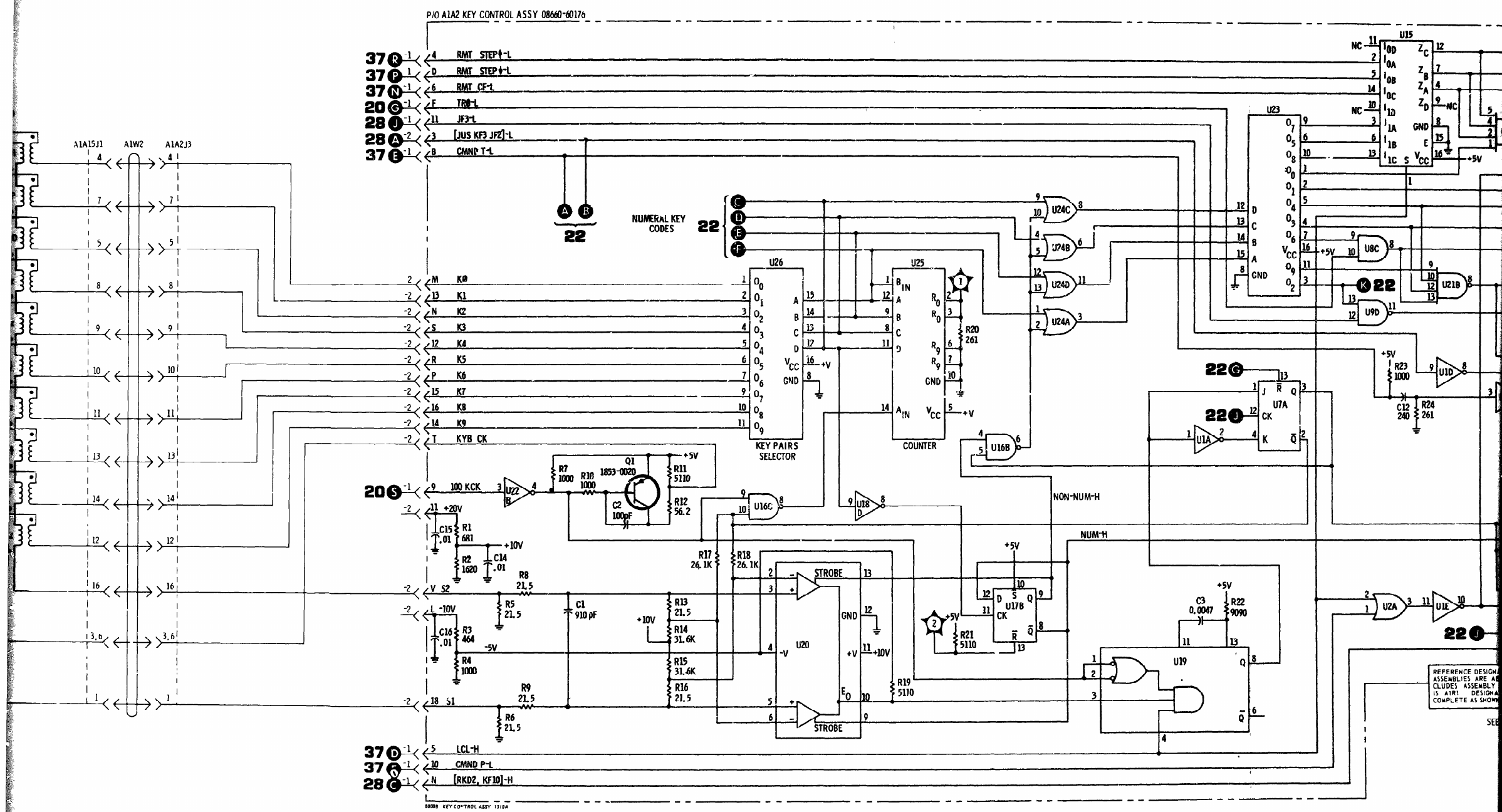


TM 11-6625-2837-14&P
SERVICE SHEET 22
P/O A1A2 KEY CONTROL ASSEMBLY
The A1A2 key control assembly circuits are shown
schematically on Service Sheets 21 and 22. The
circuits shown on this Service Sheet consist of the
recirculating keyboard register and the circuits
which control it.
Multiplexer U12, when a keyboard numeral is
being entered (ETK0-L is active), couples the data
to U5 which is a one digit, 4 bit-register (referred
to as the K0 register).
After the data is stored in K0 a train of 10 clock
pulses transfer the data to the main keyboard shift
register consisting of U4, U6, U14 and U13.
U6 and U4 are dual 8 bit registers. Data bits 1 and
2 for digits 3 through 10 are stored in U6 and data
bits 4 and 8 for digits 3 through 10 are stored in
U4. U14 and U13 are one digit four bit registers.
U14 stores digit 2 and U13 stores digit 1.
Note that the output of the main keyboard register
is coupled back to U5 thorugh U12 while the train
of 10 clock pulses is present. This is true because
ETK0-L is now in the quiescent (high) state. The
cycle continues until all of the required numeric
entries are made. When the last digit has been
entered (the least significant digit) it will be so
positioned in the register that it will be the first
digit clocked out. The first digit clocked in will be
the last digit clocked out.
In the local mode when the keyboard data is
clocked out, it is also clocked back into the main
keyboard register, through multiplexer U11. U12
and U5 are bypassed.
The control
conventional. gates for the keyboard register
8-112


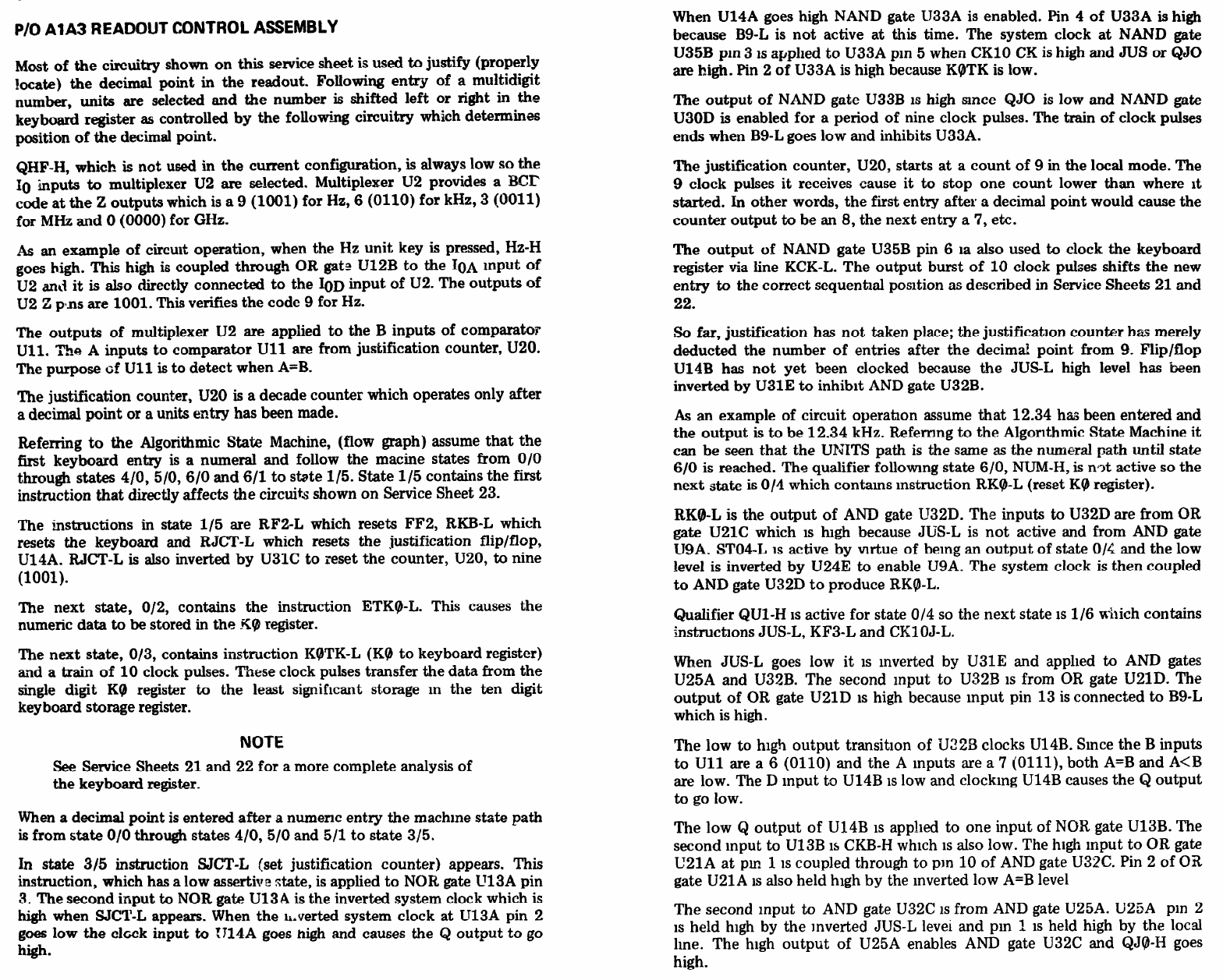
SERVICE SHEET 23 SERVICE SHEET 23 (Cont’d)
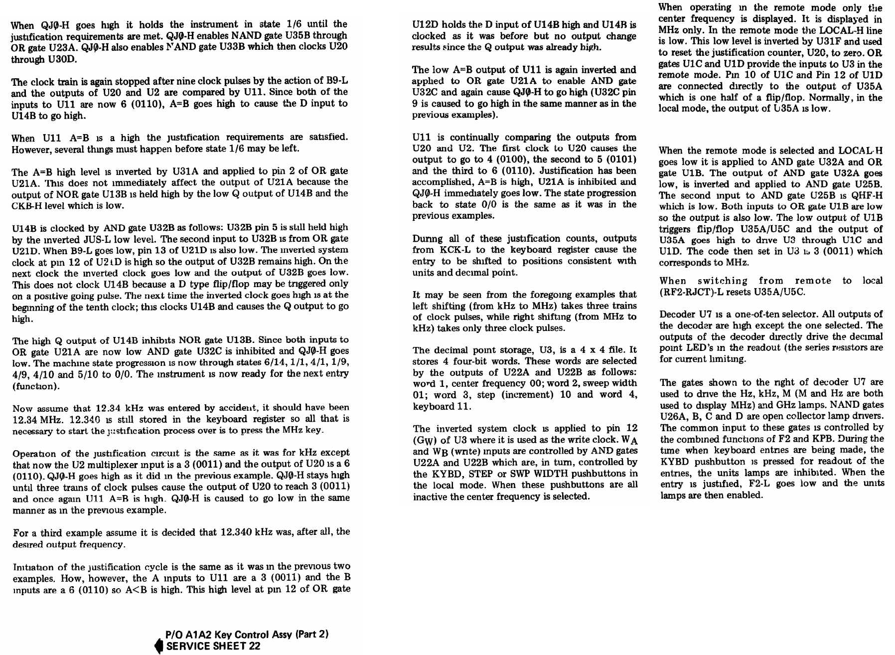
TM 11-6625-2837-14&P Model 8660B
SERVICE SHEET 23 (Cont’d) SERVICE SHEET 23 (Cont’d)
8-114


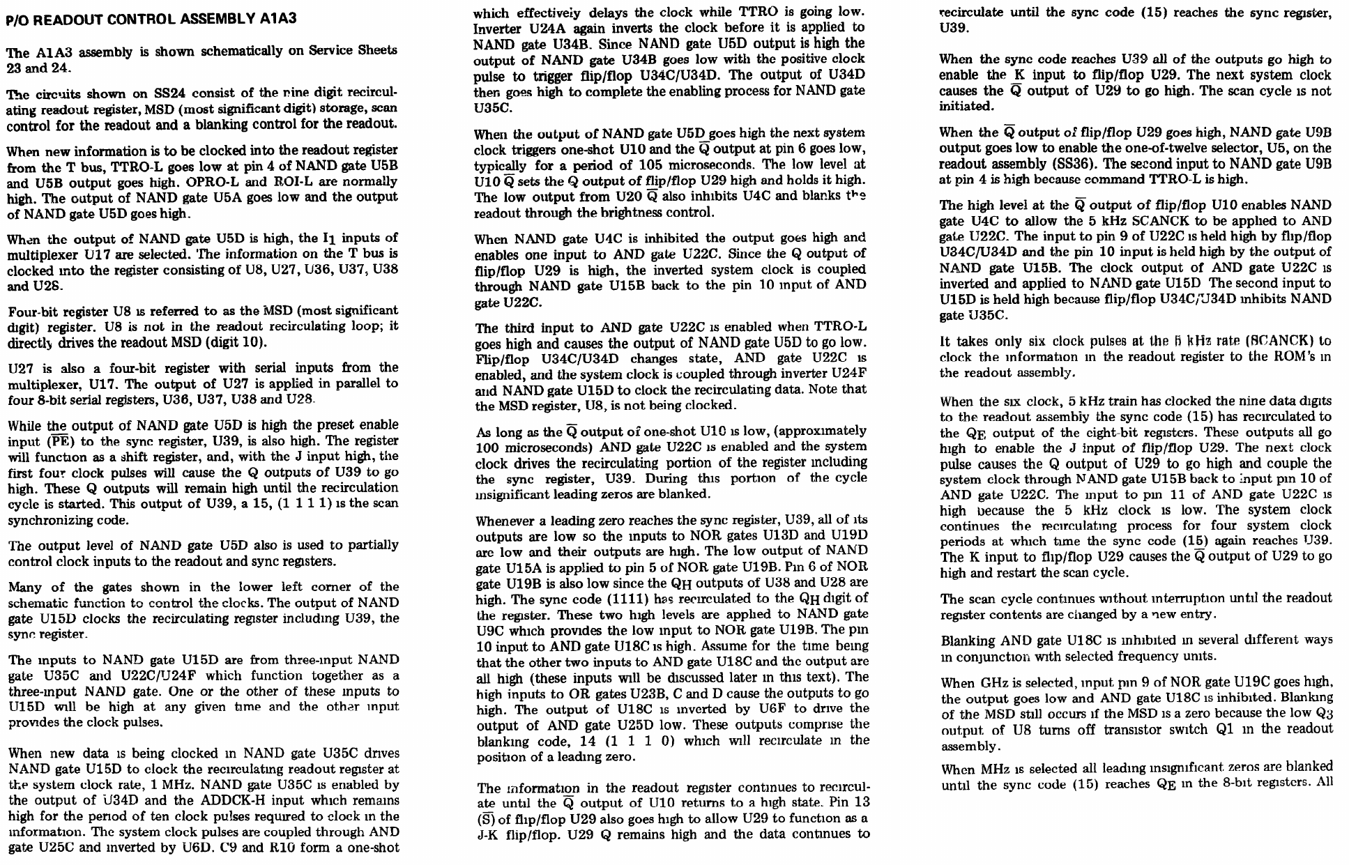
SERVICE SHEET 24 SERVICE SHEET 24 (Cont’d) SERVICE SHEET 24 (Cont’d)


TM 11-6625-2837-14&P
SERVICE SHEET 25
8-118


SERVICE SHEET 26
TM 11-6625-2837-14&P
SERVICE SHEET 26 (Cont'd)
8-120


TM 11-6625-2837-14&P Model 8660B
SERVICE SHEET 27
8-122


TM 11-6625-2837-14&P
SERVICE SHEET 28
8-124

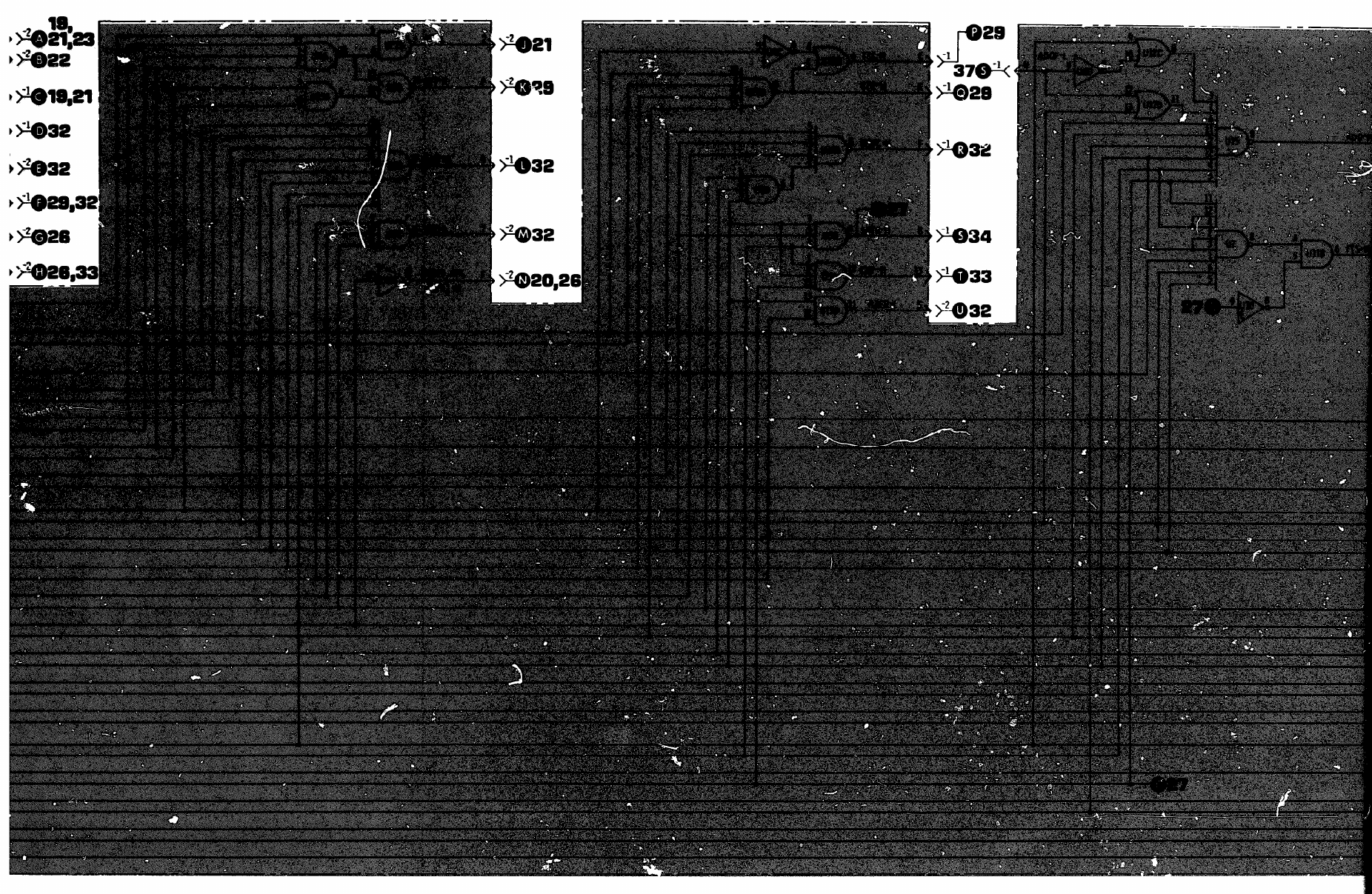


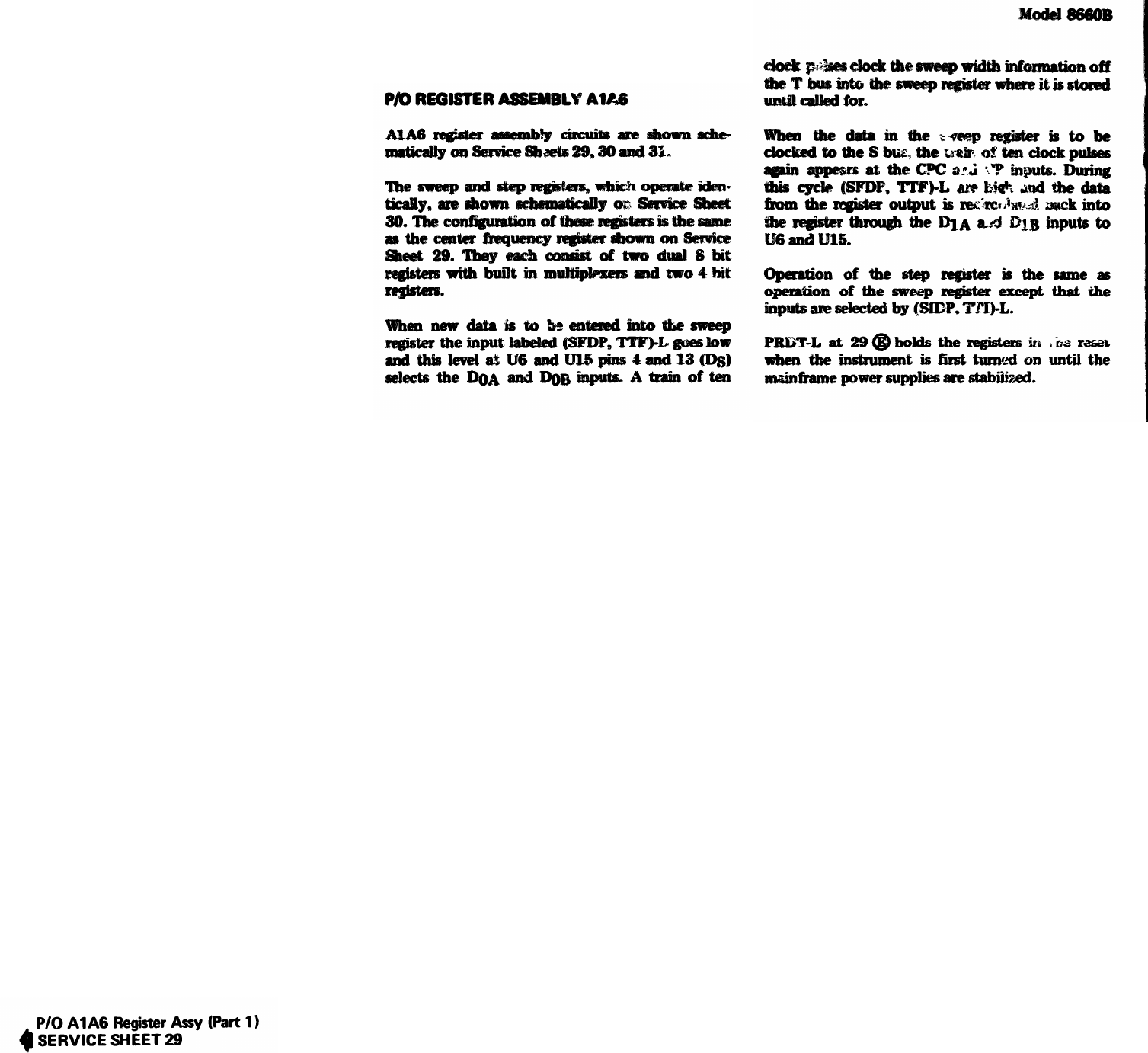
TM 11-6625-2837-14&P
SERVICE SHEET 30
8-128
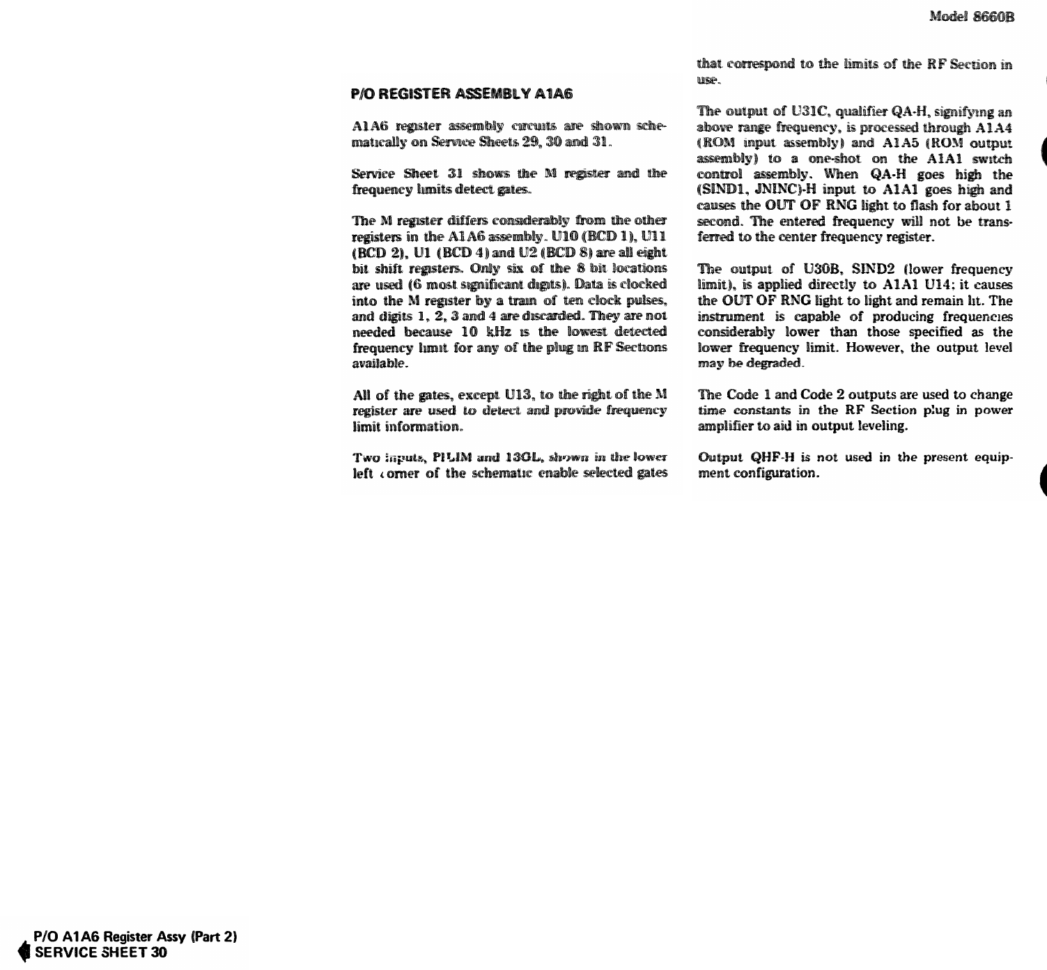
TM 11-6625-2837-14&P
SERVICE SHEET 31
8-130


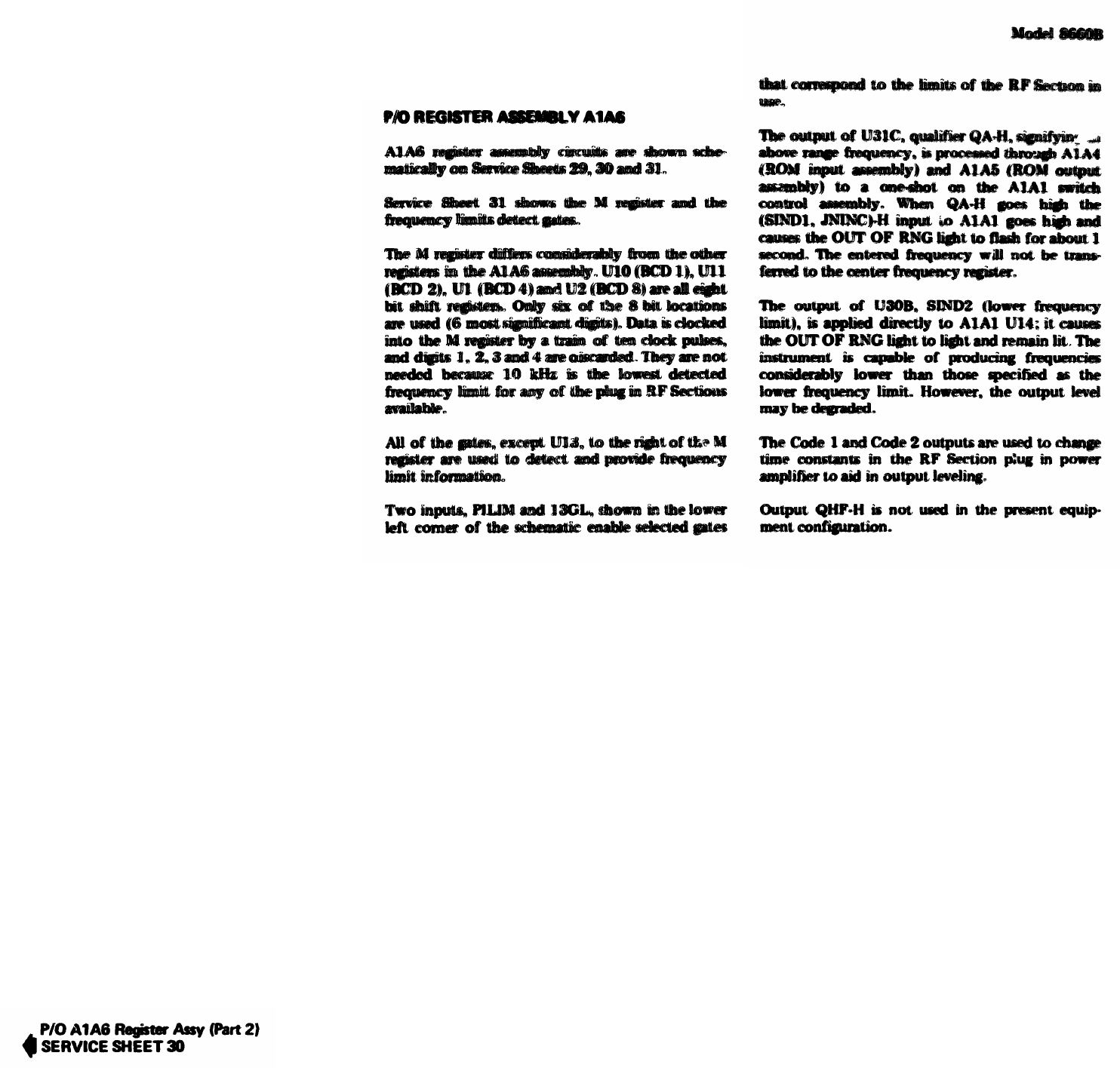
TM 11-6625-2837-14&P
SERVICE SHEET 31
8-130


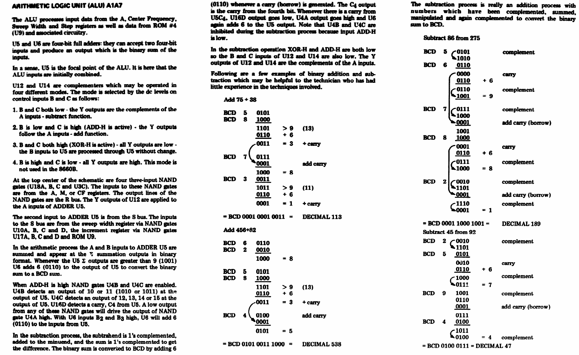
SERVICE SHEET 32 SERVICE SHEET 32 (Cont'd) SERVICE SHEET 32 (Cont'd)
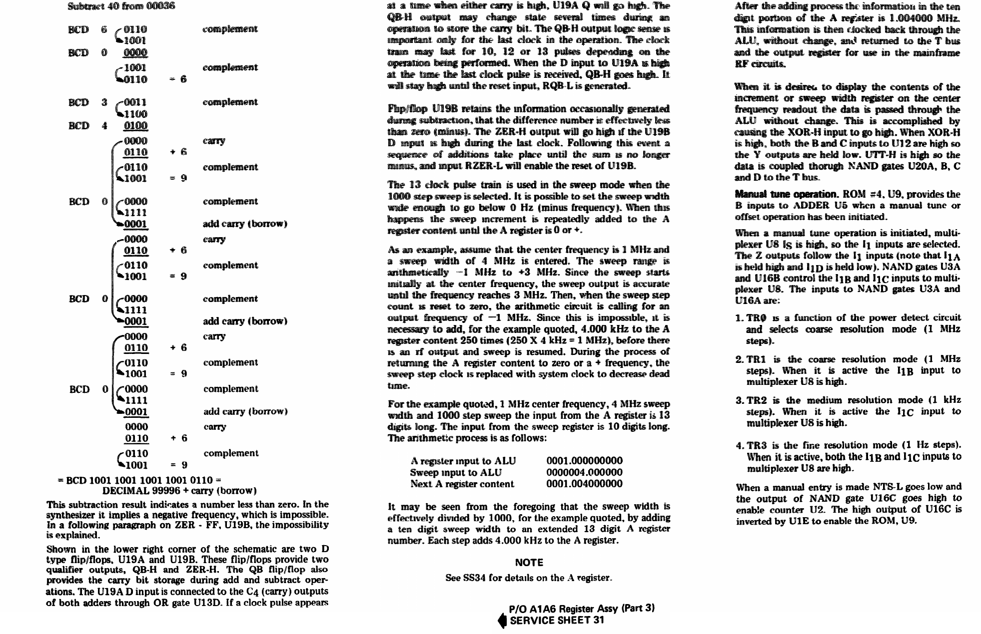
TM 11-6625-2837-14&P
SERVICE SHEET 32 (Cont'd)
SERVICE SHEET 32 (Cont'd) SERVICE SHEET 32 (Cont'd)
8-132
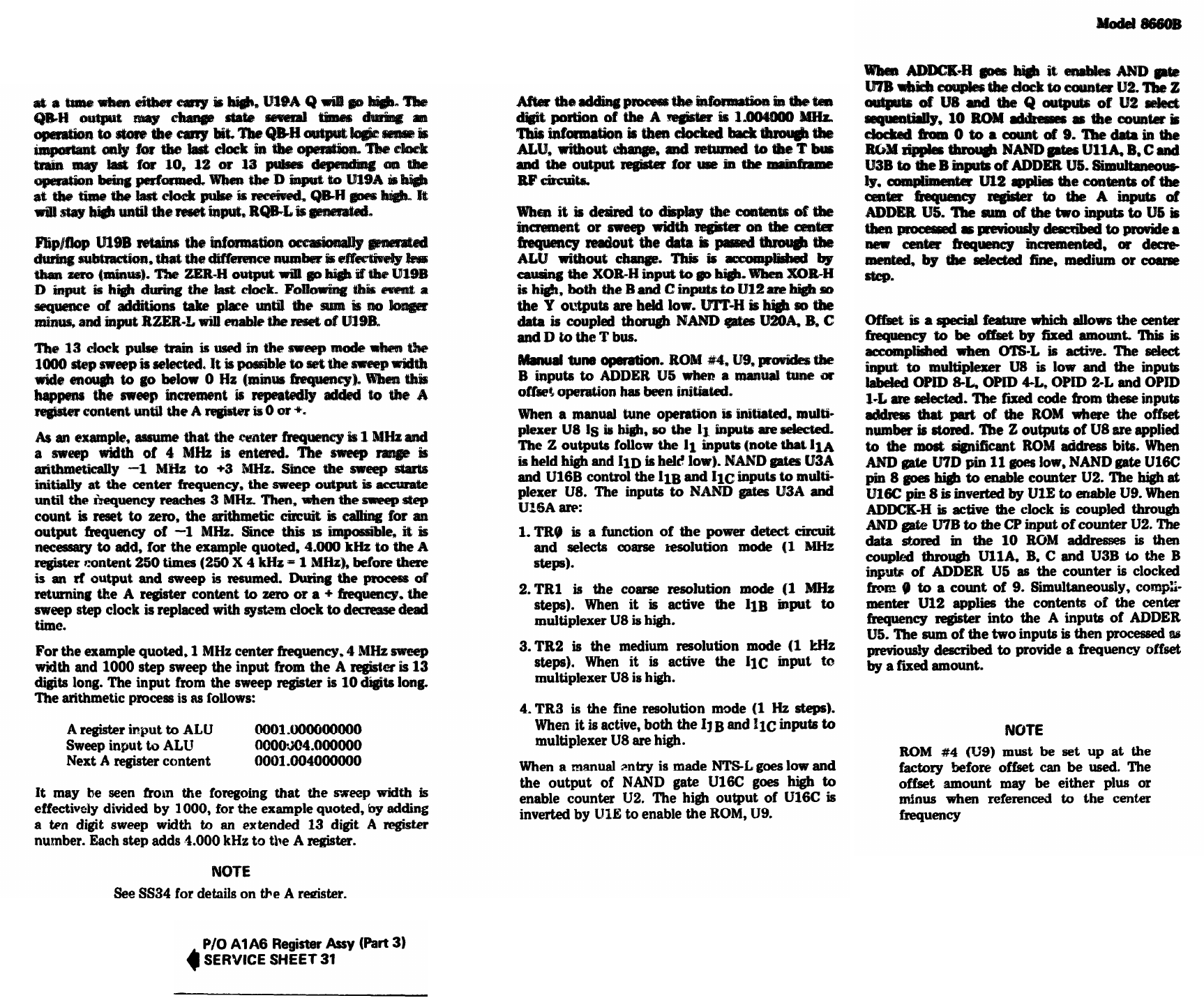
TM 11-6625-2837-14&P
SERVICE SHEET 32 (Cont'd)
SERVICE SHEET 32 (Cont'd)
8-132


TM 11-6625-2837-14&P
SERVICE SHEET 33
8-134


TM 11-6625-2837-14&P
SERVICE SHEET 34
8-136


TM 11-6625-2837-14&P
SERVICE SHEET 35
8-138


SERVICE SHEET 36 SERVICE SHEET 36 (Cont'd)


TM 11-6625-2837-14&P
SERVICE SHEET 37 (Cont'd)
SERVICE SHEET 37 (Cont'd)
8-142


SERVICE SHEET 38
TM 11-6625-2837-14&P
SERVICE SHEET 38 (Cont'd)
8-144


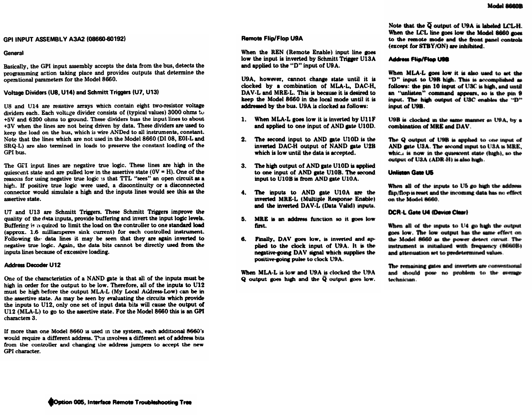
TM 11-6625-2837-14&P
SERVICE SHEET 39 (Cont'd)SERVICE SHEET 39
8-148


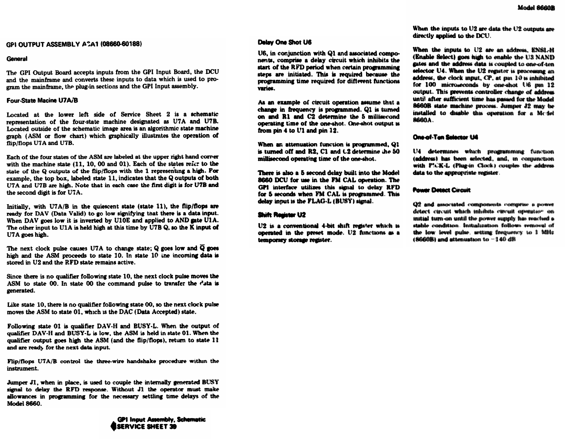
TM 11-6625-2837-14&P
SERVICE SHEET 40 (Cont'd)
SERVICE SHEET 40
8-150


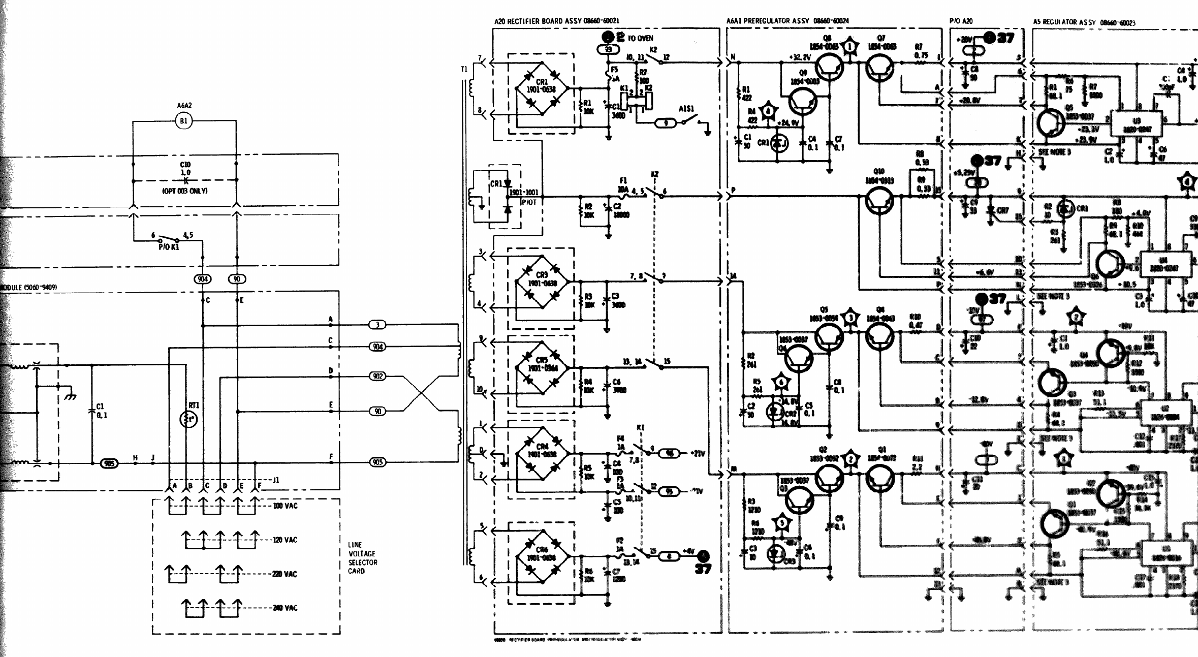


TM 11-6625-2837-14&P
Figure 8-116.

Figure 8-117.


TM 11-6625-2837-14&P
8-156

APPENDIX B
COMPONENTS OF END ITEM LIST
Section I.
INTRODUCTION
B-1. scope
This appendix lists integral components of and basic
issue items for Signal Generator, Hewlett-Packard
Model 8660B to help you inventory items required for
safe and efficient operation.
B-2. General
This Components of End Item List is divided into the
following sections.
a. Section II. Integral Components of the End Item
These items, when assembled, comprise the 8660B and
must accompany it whenever it is transferred or
turned in The illustrations will help you identify these
items.
b. Section III. Basic Issue Items. These are the
minimum essential items required to place the 8660B
in operation, to operate it, and to perform emergency
repairs. Although shipped separately packed they
must accompany the 8660B during operation and
whenever it is transferred between accountable of-
ficers. The illustrations will assist you with hard-to-
identify items. This manual is your authority to requi-
sition replacement BII, based on TOE/MTOE author-
ization of the end item.
B-3. Explanation of Columns
and, if required, a minimum description to identify the
B-1
TM 11-6625-2837-14&P
(2)
NATIONAL
STOCK
NUMBER
6625-01-011-2491
SECTION II INTEGRAL COMPONENTS
OF
END ITEM
B-2
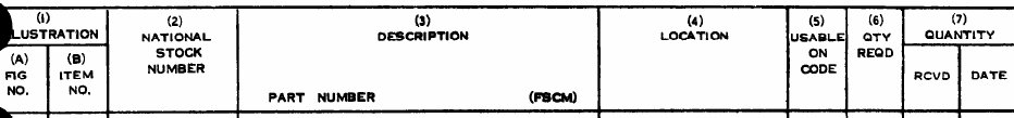
TM 11-6625-2837-14&P
SECTION III
BASIC ISSUE ITEMS
TECHNICAL MANUAL:
TM 11-6625-2837-14&P
B-3
APPENDIX C
ADDITIONAL AUTHORIZATION LIST
Section I. INTRODUCTION
C-1. Scope
This appendix lists additional items you are authorized
for the support of the Signal General Hewlett-Packard
Model 8660B.
with it. These items are all authorized to you by CTA,
MTOE, TDA, or JTA.
C-3. Explanation of Listing
National stock numbers, descriptions, and quantities
C-2. General
This list identifies items that do not have to accom-
pany the 8660B and that do not have to be turned in
are provided to help you identify and request the addi-
tional items you require to support this equipment.
C-1
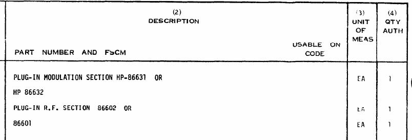
TM 11-6625-2837-14&P
(1)
NATIONAL
STOCK
NUMBER
6625-00-356-3172
6625-00-005-6848
SECTION II ADDITIONAL AUTHORIZATION LIST
C-2
APPENDIX D
MAINTENANCE ALLOCATION
Section I. INTRODUCTION
D-1. General
This appendix provides a summary of the maintenance
operations for Signal Generator Hewlett-Packard
Model 8660B. It authorizes categories of maintenance
for specific maintenance functions on repairable items
and components and the tools and equipment required
to perform each function. This appendix may be used
as an aid in planning maintenance operations.
D-2. Maintenance Function.
Maintenance functions will be limited to and defined
as follows:
a. Inspect. To determine the serviceability of an
item by comparing its physical, mechanical, and/or
electrical characteristics with established standards
through examination
b.
Test. To verify serviceability and to detect incip
ent failure by measuring the mechanical or electrical
characteristics of an item and comparing those charac-
teristics with prescribed standards.
c Service Operations required periodically to keep
an item in proper operating condition, i.e., to clean
(decontaminate), to preserve, to drain, to paint, or to
replenish fuel, lubricants, hydraulic fluids, or com-
pressed air supplies.
i. Repair. The application of maintenance services
(inspect, test, service, adjust, align, calibrate, replace)
or other maintenance actions (welding, grinding, rivet-
ing, straightening, facing, remachining, or resurfac-
ing) to restore serviceability to an item by correcting
specific damage, fault, malfunction, or failure in a
part, subassembly, module (component or assembly),
end item, or system.
j. Overhaul. That maintenance effort (service/ac-
tion) necessary to restore an item to a completely serv-
iceable/operational condition as prescribed by mainte-
nance standards (i.e., DMWR) in appropriate technical
publications. Overhaul is normally the highest degree
of maintenance performed by the Army. Overhaul
does not normally return an item to like new condi-
tion.
k. Rebuild. Consists of those services/actions neces-
sary for the restoration of unserviceable equipment to
a like new condition in accordance with original manu-
facturing standards. Rebuild is the highest degree of
materiel maintenance applied to Army equipment.
The rebuild operation includes the act of returning to
zero those age measurements (hours, miles, etc.) con-
sidered in classifying Army equipments/components
D-3. Column Entries.
D-1
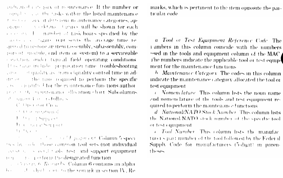
D-4. Tool and Test Equipment Require-
ment (Sect. III).
D-5. Remarks (Sect. IV). Not applicable
D-2
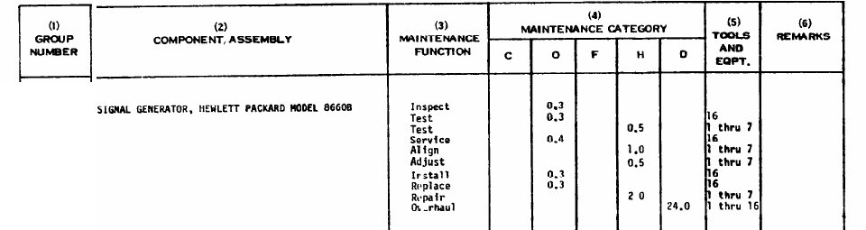
TM 11-6625-2837-14&P
SECTION II MAINTENANCE ALLOCATION CHART
FOR
SIGNAL GENERATOR, HEWLETT
PACKARD MODEL 8660B
00
D-3
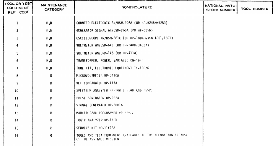
TM 11-6625-2837-14&P
SECTION III TOOL AND TEST EQUIPMENT REQUIREMENTS
FOR
SIGNAL GENERATOR, HEWLETT PACKARD MODEL 8660B
6625-00-044-3228
6625-00-788-9672
6625-00-106-9622
6625-00-022-7894
6625-00-973-3986
5950-00-235-2056
5180-00-605-0079
D-4