Hardware_ACIA Hardware ACIA
User Manual: Hardware_ACIA
Open the PDF directly: View PDF ![]() .
.
Page Count: 9

ACIA-1
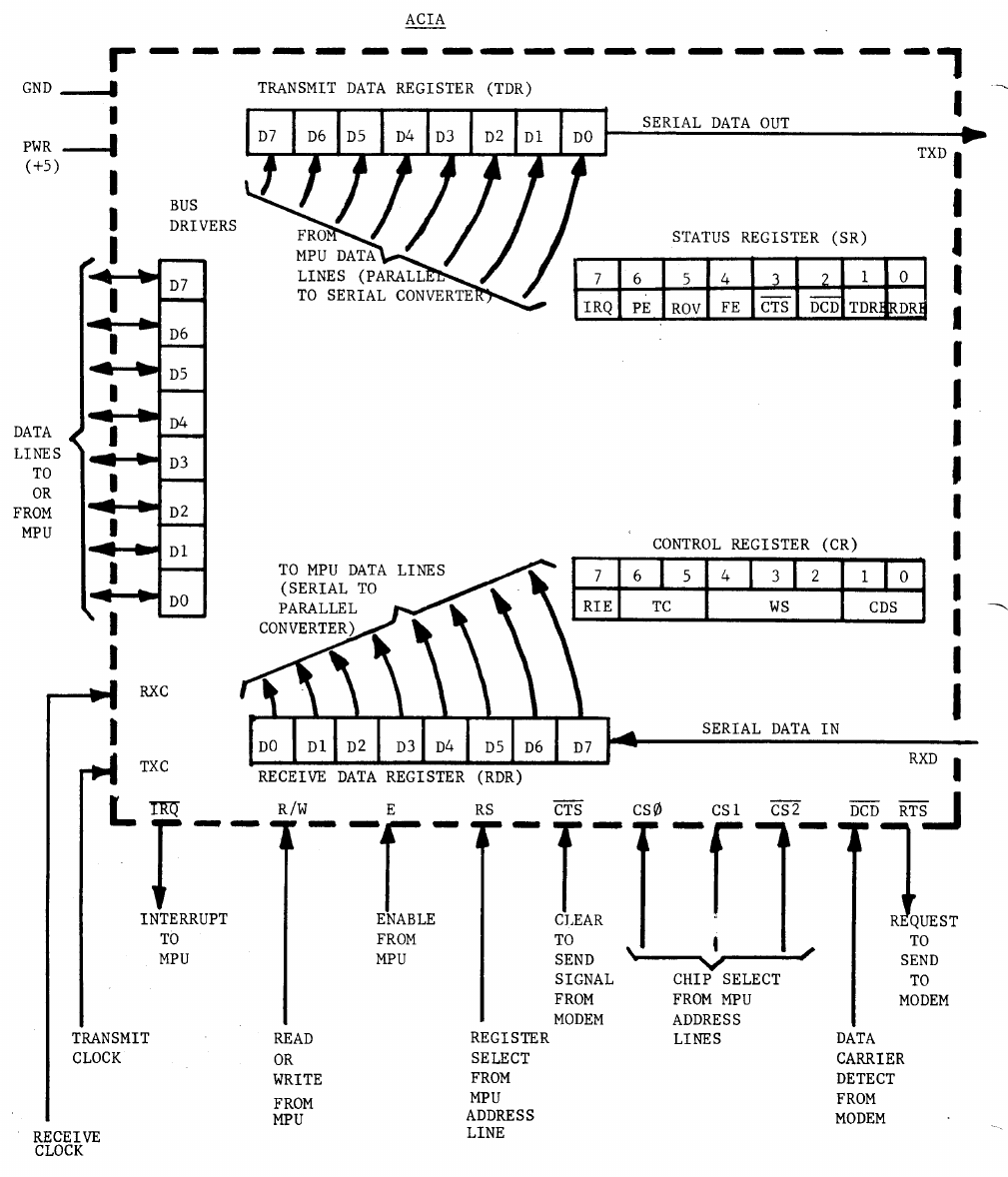
ASYNCHRONOUS COMMUNICATIONS INTERFACE ADAPTER (ACIA) - MC6850
The Asynchronous Communications Interface Adapter (ACIA) is a means
used to receive and transmit up to eight bits of data for serial data
communications. The ACIA communicates with the MPU via an eight bit
bi-directional data bus, three chip select lines, one register select line,
one interrupt request line, an enable line, and one read/write line. The ACIA
has four registers which may be addressed by the MPU. The Status Register
(SR) and the Receiver Data Register (RDR) are "read only" registers in that
the MPU cannot write into two registers. The transmit Data Register (TDR) and
the Control Register (CR) are "write only" registers in that the MPU cannot
read from these registers.
MPU INTERFACE LINES
A. Bi-Directional Data Lines (DO - D7)
The eight bi-directional data lines permit transfer of data to and from
the ACIA and the MPU. The MPU receives data from the outside world from
the ACIA via these eight data lines or sends data to the outside world
through the ACIA's via the eight data lines. The data bus output drivers
are three state devices that remain in the high impedance (off) state
except when the MPU performs a ACIA read operation.
B. Chip Select Lines (CSO, CS1, 02)
These are the lines which are tied to the address lines of the MPU. It is
through these lines that a particular ACIA is selected (addressed). For
selection of an ACIA, the CSO and CS1 lines must be high and the CS2 must
be low. After the chip selects have been addressed, they must be held in
that state for the duration of the E enable pulse, which is the only
timing signal supplied by the MPU to the ACIA.
ACIA-2

ACIA-3
C. Enable Signal (E)
The enable pulse is a high impedance TTL compatible input from the MPU
that enables the ACIA input or output buffers and clocks data to or from
the ACIA.
D. Read/Write Line (R/W)
The Read/Write line is a high impedance TTL compatible input that is used
to control the direction of data flow between the ACIA's eight bit
parallel data bus and the MPU. When Read/Write is high (MPU read), the
ACIA output driver is turned on and a selected register is read by the
MPU. When the Read/Write line is low (MPU write), the ACIA output driver
is turned off and the MPU writes into a selected register. Thus, the
Read/Write signal, in conjunction with the register select line, is used
to select the-registers within the ACIA that are read only.
Register Select
RS
Read/Write
(R/W)
ACIA Register
Selected
MPU
Read or Write
0 0 Control Write
0 1 Status Read
1 0 Transmit Data Write
1 1 Receive Data Read
E. Register Select (RS)
The Register Select line is a high impedance TTL compatible input from the
MPU that is used to select, in conjunction with the Read/Write line,
either the Transmit/Receiver Data Register or the Control/Status register
in the ACIA as shown in part D of this section.

ACIA-4
F. Interrupt Request Line (IRQ)
The Interrupt Request Line is a TTL compatible output line to the MPU that
is used to interrupt the MPU upon the occurrence of certain events. This
line is active in the low state and remains low as long as the course of
the interrupt is present and the appropriate interrupt enable within the
ACIA is set.
ACIA REGISTERS
A. Status Register (Read Only)
The Status Register can only be read by the MPU. This register is selected
when the Register Select (RS) line is low and the Read/Write (R/W) line is
high (RS . R/W = 01)
STATUS REGISTERS (SR)
7 6 5 4 3 2 1 0
IRQ PE ROV FE TS DC6 THE RDRF
Bit 0 - Receiver Data Register Full (RDRF)
"1" - The Receiver Data Register is full. When this bit gets set to a logic
"1" indicating the Receiver Data Register is full, the IRQ bit (bit 7)
gets set also and remains set until the data is read into the MPU.
"0" - The Receiver Data Register has been read by the MPU. The non-
destructive read cycle clears the RDRF bit although the data in the
Receiver Data Register is retained. If the DCD line goes high
indicating loss of carrier, the RDRF bit is clamped at logic "0"
indicating the contents of the Receiver Data Register are not current.

ACIA-5
Bit 1 - Transmit Data Register Empty (TDRE)
"1" - The Transmit Data Register is empty and new data may be transferred. -
IRQ (bit 7 gets set)
"0" - The Transmit Data Register is full
Bit 2 - Data Carrier Detect (DCD)
"1" - There is no carrier from the modem. When this bit goes to a logic "1" -
the IRQ bit (bit 7) of the status register gets set and remains set
until the MPU reads the Status Register and the Receiver Data Register.
"0" - The carrier from the modem is present.
Bit 3 - Clear to Send (CTS)
"1" - The Clear to Send line from the modem is high, thus inhibiting the
Transmit Data Register Empty (TDRE) bit. Modem is not ready for data.
"0" - The Clear to Send line from the modem is low. Modem is ready for data.
Bit 4 - Framing Error (FE)
"1" - Framing error indicates that the received character is improperly
framed by the start and stop bit and is detected by the absence of the
first stop bit. This error indicates a synchronization error, faulty
transmission, or a break condition. This error flag is set or reset
during the receiver data transfer time. Therefore, this error indicator
is present throughout the time that the associated character is
available.
"0" - The received character is properly framed.

ACIA-6
Bit 5 - Receiver Overrun (ROV)
"1" - Overrun is an error flag that indicates that one or more characters in
the data stream were lost. That is, a character or a number of
characters were received but not read from the Receiver Data Register
(RDR) prior to subsequent being received. The overrun condition begins
at the midpoint of the last bit of the second character received in
succession without a read of the RDR having occurred. The Overrun does
not occur in the Status Register until the valid character prior to
Overrun has been read. Character synchronization is maintained during
the Overrun condition. The Overrun indication is reset after the
reading of data from the Receive Data Register. Overrun is also reset
by the Master Reset.
"0" - No Receiver Data Overrun have occurred.
Bit 6 - Parity Error (PE)
"1" - The parity error flag indicates that the number of highs (ones) in the
character does not agree with the preselected odd or even parity. Odd
parity is defined to be when the total number of ones is odd. The
parity error indication will be present as long as the data character
is in the RDR. If no parity is selected, then both the transmitter
parity generator output and the receiver parity check results are
inhibited.
"0" - No parity error occurred.
Bit 7 - Interrupt Request (IRQ)
"1" - There is an interrupt in the ACIA. This bit being high causes the IRQ
output line to be low. This will be cleared by reading the Status
Register and writing into the Transmit Data Register or reading the
Receiving Data Register.
"0" - No interrupt present.

ACIA-7
B. Control Register (Write Only)
The Control Register can only be written into by the MPU. This register
is selected when the Register Select (RS) line and the Read/Write line
are both low (RS . R/W = 00)
CONTROL REGISTER (CR)
7 6 5 4 3 2 1 0
Receiver
Interrupt
Enable
Transmitter
Control
Word
Select
Counter
Divide
Bit 0 and 1 - Counter Divide Select Bits (CDS)
CR1 CR0 FUNCTION
0 0 : 1
0 1 : 16
1 0 : 64
1 1 Master Reset
Bit 2, 3, 4 - Word Select Bits (WS)
CR4 CR3 CR2 FUNCTION
0 0 0 7 Bit + EP + 2SB
0 0 1 7 Bit + OP + 2SB EP – Even
OP – Odd
0 1 0 7 Bit + EP + 1SB SB - Stop bits
0 1 1 7 Bit + OP + 1SB
1 0 0 8 Bit + 2SB
1 0 1 8 Bit + 1SB
1 1 0 8 Bit + EP + 1SB
1 1 1 8 Bit + OP + 1SB

ACIA-8
Bit 6 and 5 - Transmitter Control (TC)
CR6 CR5
FUNCTION
0 0 RTS =
Low Transmitting Interrupt Disabled (TIE)
0 1 RTS =
Low Transmitting Enabled (TIE)
1 0 RTS =
High Transmitting Interrupt Disabled (TIE)
1 1 RTS =
Low Transmitting Interrupt Disabled (TIE)
and transmits a Break level on the transmit
data output.
Bit 7 - Receiver Interrupt Enable
"1" - Enables interrupts caused by
a) Receiver Data Register Full going high
b) A low to high transition on the Data Carrier Detect signal line
"0" - Cleared by selecting the Receiver Data Register or by resetting the
Receiver Interrupt Enable Bit.
CLOCK INPUTS
Separate high impedance TTL compatible inputs are provided for clocking
of transmitted and received data. Clock frequencies of 1, 16, or 64 times the
data rate may be selected.
A. Transmit Clock (TXC)
The transmit clock input is used for the clocking of transmitted data.
The transmitter initiates data on the negative transition of the clock.
B. Receive Clock (RXC)
The Receive Clock input is used for synchronization of received data.
The receiver strokes the data on the positive transition of the clock.
(In the divide by 1 mode, the clock and data must be synchronized
externally).

ACIA-9
MODEM CONTROL
The ACIA includes several functions that permit limited control of a
data modem. The functions included are Clear-to-Send, Request-to-Send and
Data Carrier Detect.
A. Clear-to-Send (CTS)
This high impedance TTL compatible input provides automatic control of
the transmitting end of a communications link via the modem's
"clear-to-send" active low output.
B. Request-to-Send (RTS)
The Request-to-Send output enables the MPU to control a modem via the
data bus. The active state is low.
C. Data Carrier Detected (DCD)
This high impedance TTL compatible input provides automatic control of
the receiving end of a communication link by means of the modem
"Data-Carrier-Detect" or "Received-Line-Signal Detect" output. The DCD
input inhibits and initializes the receiver section of the ACIA when
high. A low to high transition of the Data Carrier Detect initiates an
interrupt to the MPU to indicate the occurrence of a loss of carrier.
RECEIVED DATA LINE (RX)
The Received Data line is a high impedance TTL compatible input through
which data is received in a serial NRZ (Non Return to Zero) format.
Synchronization with a clock for detection of data is accomplished internally
when clock rates of 16 or 64 times the bit rate are used. Data rates are in
the range of 0 to 500Kbps when external synchronization is utilized.
TRANSMITTED DATA LINES (TX)
The Transmit Data Output line transfers serial NRZ data to a modem or
other peripheral at the same range of rates as the received data.
