Hi3518 User Guide
User Manual:
Open the PDF directly: View PDF ![]() .
.
Page Count: 38

Hi3518 Hardware Design
User Guide
Issue 01
Date 2013-06-30

Copyright © HiSilicon Technologies Co., Ltd. 2012-2013. All rights reserved.
No part of this document may be reproduced or transmitted in any form or by any means without prior
written consent of HiSilicon Technologies Co., Ltd.
Trademarks and Permissions
, , and other HiSilicon icons are trademarks of HiSilicon Technologies Co., Ltd.
All other trademarks and trade names mentioned in this document are the property of their respective
holders.
Notice
The purchased products, services and features are stipulated by the contract made between HiSilicon and
the customer. All or part of the products, services and features described in this document may not be
within the purchase scope or the usage scope. Unless otherwise specified in the contract, all statements,
information, and recommendations in this document are provided "AS IS" without warranties, guarantees or
representations of any kind, either express or implied.
The information in this document is subject to change without notice. Every effort has been made in the
preparation of this document to ensure accuracy of the contents, but all statements, information, and
recommendations in this document do not constitute a warranty of any kind, express or implied.
HiSilicon Technologies Co., Ltd.
Address: Huawei Industrial Base
Bantian, Longgang
Shenzhen 518129
People's Republic of China
Website: http://www.hisilicon.com
Email: support@hisilicon.com
Hi3518 Hardware Design
User Guide About This Document
Issue 01 (2013-06-30) HiSilicon Proprietary and Confidential
Copyright © HiSilicon Technologies Co., Ltd i
About This Document
Purpose
This document describes the design recommendations for the schematic diagrams, printed
circuit board (PCB), and board heat dissipation of the Hi3518.
It also provides the hardware design methods of the Hi3518.
Related Version
The following table lists the product version related to this document.
Product Name Version
Hi3518 V100
Intended Audience
This document is intended for:
z Technical support personnel
z Board hardware engineers
Symbol Conventions
The symbols that may be found in this document are defined as follows.
Symbol Description
Alerts you to a high risk hazard that could, if not avoided,
result in serious injury or death.
Alerts you to a medium or low risk hazard that could, if not
avoided, result in moderate or minor injury.

1 Design Recommendations for Schematic Diagrams
Hi3518 Hardware Design
User Guide
ii HiSilicon Proprietary and Confidential
Copyright © HiSilicon Technologies Co., Ltd Issue 01 (2013-06-30)
Symbol Description
Alerts you to a potentially hazardous situation that could, if not
avoided, result in equipment damage, data loss, performance
deterioration, or unanticipated results.
Provides a tip that may help you solve a problem or save time.
Provides additional information to emphasize or supplement
important points in the main text.
Change History
Changes between document issues are cumulative. Therefore, the latest document issue
contains all changes made in previous issues.
Issue 01 (2013-06-30)
This issue is the first official release, which incorporates the following changes:
Chapter 1 Design Recommendations for Schematic Diagrams
In section 1.1.2, the descriptions related to internal reset are added.
In section 1.1.4, a note related to the NAND flash is added below Table 1-3.
Section 1.3.4 "RTC Interface" is added.
Issue 00B06 (2013-02-28)
This issue is the sixth draft release, which incorporates the following changes:
Chapter 1 Design Recommendations for Schematic Diagrams
In section 1.1.5.2, the figures are updated, and the descriptions of the DDR parts of the
Hi3518C_BGA and Hi3518C_QFP are added.
In section 1.3.3, a recommendation for excellent audio quality is added.
Issue 00B05 (2013-02-05)
This issue is the fifth draft release, which incorporates the following changes:
Chapter 1 Design Recommendations for Schematic Diagrams
In section 1.1.5.5, descriptions on how to connect the two differential clock signals of the
Hi3518C to a DDR3 SDRAM are added.
Issue 00B04 (2012-12-26)
This issue is the fourth draft release, which incorporates the following changes:
Chapter 1 Design Recommendations for Schematic Diagrams
In section 1.2.2, the DDR power supply design is modified.

Hi3518 Hardware Design
User Guide About This Document
Issue 01 (2013-06-30) HiSilicon Proprietary and Confidential
Copyright © HiSilicon Technologies Co., Ltd iii
Issue 00B03 (2012-11-25)
This issue is the third draft release, which incorporates the following changes:
Chapter 2 PCB Design Recommendations
In section 2.1.1, Figure 2-2 and related descriptions are added.
Issue 00B02 (2012-10-30)
This issue is the second draft release, which incorporates the following changes:
Chapter 1 Design Recommendations for Schematic Diagrams
Figure 1-1 is updated.
In sections 1.1.3, 1.1.5.3, 1.2.1, 1.2.2, 1.3.2, 1.3.3, and 1.4, the descriptions are updated.
Section 1.2.5 "Power-on and Power-off Sequences" is added.
Chapter 2 PCB Design Recommendations
In sections 2.1.1, 2.1.3, 2.1.4, 2.1.5, 2.2.1, 2.2.2.1, and 2.2.2.2, the descriptions are updated.
The section "I/O Power" is added.
Chapter 3 Heat Design Recommendations
Table 3-1 and Table 3-2 are updated.
In section 3.2.1, the low-power configurations for idle modules in the schematic diagram are
updated.
Issue 00B01 (2012-08-30)
This issue is the first draft release.

1 Design Recommendations for Schematic Diagrams
Hi3518 Hardware Design
User Guide
iv HiSilicon Proprietary and Confidential
Copyright © HiSilicon Technologies Co., Ltd Issue 01 (2013-06-30)
Contents
About This Document ...................................................................................................................... i
1 Design Recommendations for Schematic Diagrams .............................................................. 1
1.1 Design Recommendations for the Small System ............................................................................................. 1
1.1.1 Clocking Circuit ...................................................................................................................................... 1
1.1.2 Reset and Watchdog Circuit .................................................................................................................... 2
1.1.3 JTAG Debug Interface ............................................................................................................................ 3
1.1.4 System Configuration Circuit for Hardware Initialization ...................................................................... 4
1.1.5 DDR Circuits .......................................................................................................................................... 5
1.1.6 Design Recommendations for the Flash Schematic Diagrams ................................................................ 9
1.2 Design Recommendations for Power Supplies .............................................................................................. 10
1.2.1 Core Power Supply ............................................................................................................................... 10
1.2.2 DDR Power Supply ............................................................................................................................... 10
1.2.3 I/O Power Supply .................................................................................................................................. 11
1.2.4 PLL Power Supply ................................................................................................................................ 11
1.2.5 Power-on and Power-off Sequences ...................................................................................................... 11
1.2.6 Notes ..................................................................................................................................................... 12
1.3 Design Recommendations for Peripheral Interfaces ...................................................................................... 13
1.3.1 USB Ports ............................................................................................................................................. 13
1.3.2 MAC Interfaces ..................................................................................................................................... 13
1.3.3 Audio and Video Interfaces ................................................................................................................... 17
1.3.4 RTC Interface ........................................................................................................................................ 18
1.4 Unused Pins .................................................................................................................................................... 18
1.5 Sensor Board .................................................................................................................................................. 19
2 PCB Design Recommendations ............................................................................................... 20
2.1 PCB Design Recommendations for the Small System ................................................................................... 20
2.1.1 Power Supplies of the Small System .................................................................................................... 20
2.1.2 Clock and Reset Circuits ....................................................................................................................... 23
2.1.3 DDR Signals ......................................................................................................................................... 23
2.1.4 SPI Flash ............................................................................................................................................... 24
2.1.5 Ethernet Port Signal .............................................................................................................................. 25
2.2 PCB Design Recommendations for Peripheral Interfaces .............................................................................. 25
2.2.1 USB Port Design ................................................................................................................................... 25

Hi3518 Hardware Design
User Guide Contents
Issue 01 (2013-06-30) HiSilicon Proprietary and Confidential
Copyright © HiSilicon Technologies Co., Ltd v
2.2.2 Audio Circuit Design ............................................................................................................................ 26
3 Heat Design Recommendations ............................................................................................... 28
3.1 Working Condition ......................................................................................................................................... 28
3.2 Reference Design for Circuit Heat Dissipation .............................................................................................. 28
3.2.1 Schematic Diagram ............................................................................................................................... 28
3.2.2 PCB ....................................................................................................................................................... 28

1 Design Recommendations for Schematic Diagrams
Hi3518 Hardware Design
User Guide
vi HiSilicon Proprietary and Confidential
Copyright © HiSilicon Technologies Co., Ltd Issue 01 (2013-06-30)
Figures
Figure 1-1 Crystal oscillator circuit ....................................................................................................................... 1
Figure 1-2 Typical external reset and watchdog circuit ......................................................................................... 3
Figure 1-3 JTAG connection mode and standard connector pins .......................................................................... 4
Figure 1-4 Typical topology of connecting the Hi3518A to an external DDR3 SDRAM ..................................... 6
Figure 1-5 Typical topology of connecting the Hi3518A to an external DDR2 SDRAM ..................................... 7
Figure 1-6 Hi3518A differential clocks DDR_CLK_N and DDR_CLK_P in one-drive-one mode when a DDR3
SDRAM is connected ............................................................................................................................................. 8
Figure 1-7 Hi3518C differential clocks DDR_CLK_N and DDR_CLK_P in one-drive-one mode when a DDR3
SDRAM is connected ............................................................................................................................................. 8
Figure 1-8 Address signals in one-drive-one mode when a DDR2 or DDR3 SDRAM is connected .................... 9
Figure 1-9 Reference design of the DDR3 voltage-divider circuit ...................................................................... 11
Figure 1-10 Power-on sequence .......................................................................................................................... 12
Figure 1-11 Power-off sequence .......................................................................................................................... 12
Figure 1-12 Signal connections in MII mode (clocks provided by the Hi3518) ................................................. 14
Figure 1-13 Signal connections in MII mode (clocks provided by external components) .................................. 14
Figure 1-14 Signal connections in RMII mode (clocks provided by the Hi3518) ............................................... 15
Figure 1-15 Signal connections in RMII mode (clocks provided by external components) ................................ 16
Figure 2-1 Core power pins on the Hi3518A ...................................................................................................... 21
Figure 2-2 Core power pins on the Hi3518C ...................................................................................................... 22

Hi3518 Hardware Design
User Guide Tables
Issue 01 (2013-06-30) HiSilicon Proprietary and Confidential
Copyright © HiSilicon Technologies Co., Ltd vii
Tables
Table 1-1 Signals on the JTAG debug interface .................................................................................................... 3
Table 1-2 TEST_MODE pin configuration ........................................................................................................... 4
Table 1-3 Signal configurations ............................................................................................................................. 4
Table 1-4 Recommended design when an external SPI flash is connected............................................................ 9
Table 1-5 Recommended design when an external NAND flash is connected .................................................... 10

Hi3518 Hardware Design
User Guide 1 Design Recommendations for Schematic Diagrams
Issue 01 (2013-06-30) HiSilicon Proprietary and Confidential
Copyright © HiSilicon Technologies Co., Ltd 1
1 Design Recommendations for Schematic
Diagrams
1.1 Design Recommendations for the Small System
1.1.1 Clocking Circuit
System clocks can be generated in either of the following ways:
z Generate clocks by combining the internal feedback circuit of Hi3518 with an external
24 MHz crystal oscillator circuit.
Figure 1-1 shows the recommended connection mode of the crystal oscillator and other
components.
Figure 1-1 Crystal oscillator circuit
z Generates clocks by using the external clock circuit and transmits clocks over the XIN
pin.

1 Design Recommendations for Schematic Diagrams
Hi3518 Hardware Design
User Guide
2 HiSilicon Proprietary and Confidential
Copyright © HiSilicon Technologies Co., Ltd Issue 01 (2013-06-30)
1.1.2 Reset and Watchdog Circuit
The Hi3518 selects the internal or external reset mode by checking the status of the POR_SEL
pin during power-on:
The Hi3518A supports various reset modes, whereas the Hi3518C supports only internal reset.
z When the POR_SEL level is low, internal reset is selected. After the master chip is
powered on, the power-on-reset (POR) circuit resets the entire chip (the pulse width of
the reset signal is about 140 ms), and the RSTN pin is invalid.
When internal reset is selected, the RSTN and WDG_RSTN pins can be floated. In this
case, peripherals (such as the flash memory) must be reset before the system is reset or
peripherals and the system are reset at the same time. Otherwise, the system cannot boot.
In addition, when internal reset is selected and the WDG_RSTN pin is floated, the
watchdog generates a reset signal in the chip to reset the system, and the
SYS_RSTN_OUT pin outputs a reset signal to reset peripherals. You are advised to
output the reset signal by using the SYS_RSTN_OUT pin of the Hi3518 to reset
peripherals. The SYS_RSTN_OUT pin of the Hi3518A or Hi3518C_BGA is located in
V18. The Hi3518C_QFP supports only internal reset, and its SYS_RSTN_OUT pin is
pin 82.
z When the POR_SEL level is high, external reset is selected. In this case, the RSTN pin is
a reset signal input pin. The valid reset signal must have low-level pulse, and the pulse
width must be greater than 12 input clock cycles for the XIN pin. Typically, the pulse
width of the reset signal is 100–300 ms.
During board design, if external reset is selected, you are advised to use a dedicated reset
chip to generate a reset signal to ensure system stability.
When an exception occurs in the system, the WDG_RSTN pin can generate a low-level
pulse. The pulse triggers an external reset chip to generate a reset signal. The
WDG_RSTN pin cannot directly connect to the RSTN pin.
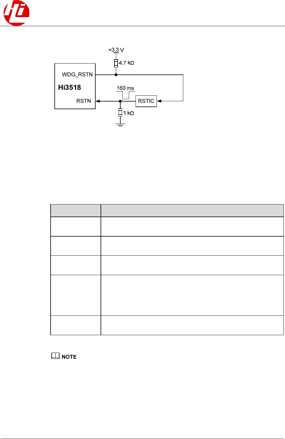
As the WDG_RSTN pin is an open drain (OD) output pin, it must connect to an external
pull-up resistor. A 4.7 k resistor is recommended.
Figure 1-2 shows the typical external reset and watchdog circuit.
Hi3518 Hardware Design
User Guide 1 Design Recommendations for Schematic Diagrams
Issue 01 (2013-06-30) HiSilicon Proprietary and Confidential
Copyright © HiSilicon Technologies Co., Ltd 3
Figure 1-2 Typical external reset and watchdog circuit
1.1.3 JTAG Debug Interface
The Hi3518 Joint Test Action Group (JTAG) interface complies with the IEEE1149.1 standard.
The PC can connect to the Realview-ICE simulator over this interface for debugging the A9
CPU. Table 1-1 describes the signals on the JTAG debug interface.
Table 1-1 Signals on the JTAG debug interface
Signal Description
TCK JTAG clock input, internal pull-down. You are advised to connect a
pull-down resistor to this signal on the board.
TDI JTAG data input, internal pull-up. You are advised to connect a
pull-up resistor to this signal on the board.
TMS JTAG mode select input, internal pull-up. You are advised to connect a
pull-up resistor to this signal on the board.
TRSTN JTAG reset input, internal pull-down. When Hi3518 works properly,
you are advised to connect a pull-down resistor to this signal on the
board. When a debugger such as Realview-ICE is connected over the
JTAG interface, you are advised to connect a pull-up resistor on the
board.
TDO JTAG data output. You are advised to connect a pull-up resistor to this
signal on the board.
For details about the impedance of pull-up and pull-down resistors described in Table 1-1, see Figure
1-3.
The Hi3518 can be set to normal mode or test mode by configuring the TEST_MODE pin.
For details, see Table 1-2.

1 Design Recommendations for Schematic Diagrams
Hi3518 Hardware Design
User Guide
4 HiSilicon Proprietary and Confidential
Copyright © HiSilicon Technologies Co., Ltd Issue 01 (2013-06-30)
Table 1-2 TEST_MODE pin configuration
TEST_MODE Description
0 The Hi3518 works in normal mode.
1 The Hi3518 works in test mode. In this case, the design for test (DFT)
can be performed.
Figure 1-3 shows the JTAG connection mode and standard connector pins. To use the JTAG
function, connect the JTAG_EN pin on the board to a 4.7 k pull-up resistor.
Figure 1-3 JTAG connection mode and standard connector pins
1.1.4 System Configuration Circuit for Hardware Initialization
The Hi3518A can boot from the serial peripheral interface (SPI) flash or NAND flash and
supports the NAND flash memories in various specifications. The Hi3518C can boot only
from the SPI flash. The related pin must connect to pull-up or pull-down resistors as required
during hardware initialization. Table 1-3 describes signal configurations.
Table 1-3 Signal configurations
Signal Direction Description
JTAG_EN I JTAG debug enable.
0: disabled
1: enabled

Hi3518 Hardware Design
User Guide 1 Design Recommendations for Schematic Diagrams
Issue 01 (2013-06-30) HiSilicon Proprietary and Confidential
Copyright © HiSilicon Technologies Co., Ltd 5
Signal Direction Description
BOOT_SEL I Boot mode.
0: SPI flash
1: NAND flash
Note: For the Hi3518C, BOOT_SEL must be set to 0
because the Hi3518C can boot only from the SPI flash.
NF_BOOT_PIN[4:
0]
I NAND type.
00001: 2 KB page size; 1-bit error correcting code
(ECC); 64-page block size
00011: 2 KB page size; 4-bit ECC; 64-page block size
00101: 2 KB page size; 24-bit ECC; 64-page block size
00110: 2 KB page size; 1-bit ECC; 64-page block size
01000: 4 KB page size; 4-bit ECC; 128-page block size
01001: 4 KB page size; 4-bit ECC; 64-page block size
01010: 2 KB page size; 4-bit ECC; 64-page block size
01011: 4 KB page size; 24-bit ECC; 128-page block
size
01101: 8 KB page size; 24-bit ECC; 128-page block
size
10000: 8 KB page size; 24-bit ECC; 64-page block size
10001: 4 KB page size; 24-bit ECC; 64-page block size
10011: 4 KB page size; 1-bit ECC; 64-page block size
10101: 2 KB page size; 4-bit ECC; 128-page block size
11001: 2 KB page size; 24-bit ECC; 128-page block
size
SFC_ADDR_MO
DE
I SPI flash controller (SFC) address mode.
0:3-byte address mode
1: 4-byte address mode
NOTE
If the NANF flash is not used for the Hi3518A, NF_BOOT_PIN[0:3] must be floated. If the NAND
flash is used for the Hi3518A, the value of NF_BOOT_PIN[4:0] must fall within the specified range.
1.1.5 DDR Circuits
1.1.5.1 Introduction
The double-data rate controller (DDRC) interface can be a DDR2 interface complying with
the stub series terminated logic for 1.8 V (SSTL-18) standard or a DDR3 interface complying
with the SSTL-15 standard.
The DDRC has the following features:

1 Design Recommendations for Schematic Diagrams
Hi3518 Hardware Design
User Guide
6 HiSilicon Proprietary and Confidential
Copyright © HiSilicon Technologies Co., Ltd Issue 01 (2013-06-30)
z Provides a DDRC interface and supports 8-bit or 16-bit data bus and 13-bit (for the
Hi3518C) or 14-bit (for the Hi3518A) address bus. The Hi3518A DDRC supports a
DDRn SDRAM chip select (CS), whereas the Hi3518C does not support CS.
z Supports 16-bit DDR2 SDRAM and 300440 MHz DDR clock frequency. The
maximum memory capacity is 256 MB (2 Gbits) for the Hi3518A or 128 MB (1 Gbit)
for the Hi3518C.
z Supports 16-bit DDR3 SDRAM and 300440 MHz DDR clock frequency. The
maximum memory capacity is 256 MB (2 Gbits) for the Hi3518A or 128 MB (1 Gbit)
for the Hi3518C.
z Supports various low-power modes for the DDRn SDRAM, such as power-down and
self-refresh.
1.1.5.2 DDR Topology
z The Hi3518C_QFP does not have the DDR_CS_N pin. The DDR CS pin must connect to
a 4.7 k pull-down resistor. The DDR part of the Hi3518C_QFP has only 13 address lines
(A0A12). The maximum capacity of the interconnected DDR is 1 Gbit.
z The DDR part of the Hi3518A has 14 address lines, whereas the DDR part of the
Hi3518C_BGA has only 13 address lines. The maximum capacity of the interconnected
DDR is 1 Gbit.
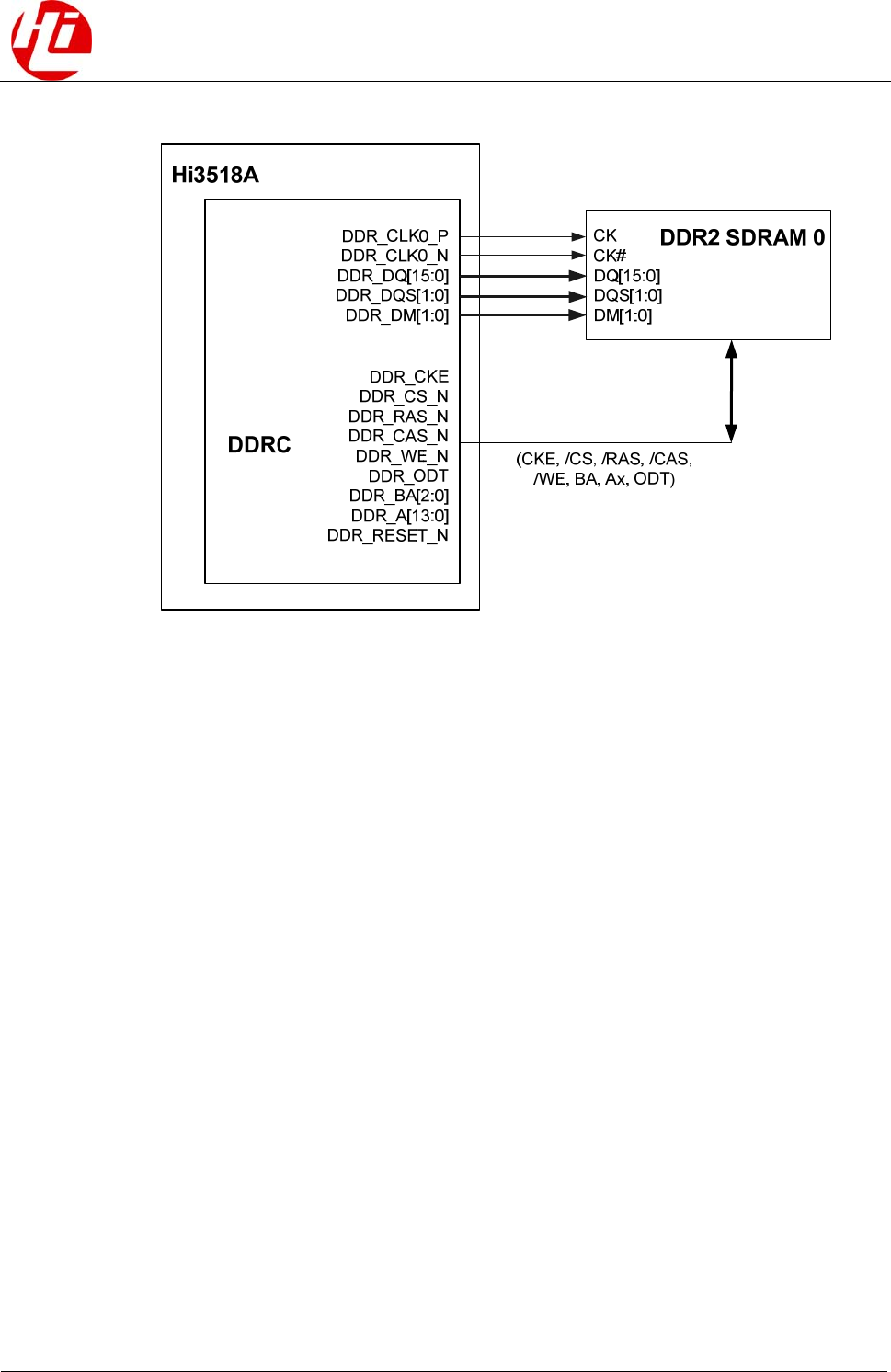
Figure 1-4 shows the typical topology of connecting the Hi3518A to an external DDR3
SDRAM. Figure 1-5 shows the typical topology of connecting the Hi3518A to an external
DDR2 SDRAM.
Figure 1-4 Typical topology of connecting the Hi3518A to an external DDR3 SDRAM
Hi3518 Hardware Design
User Guide 1 Design Recommendations for Schematic Diagrams
Issue 01 (2013-06-30) HiSilicon Proprietary and Confidential
Copyright © HiSilicon Technologies Co., Ltd 7
Figure 1-5 Typical topology of connecting the Hi3518A to an external DDR2 SDRAM
1.1.5.3 Design Recommendations for Matched Modes
Bidirectional DQ and DQS Signals
When the Hi3518 connects to a DDR, the DQ, DQS_P, and DQS_N signals of the Hi3518
connect directly to the DQ, DQS_P, and DQS_N signals of the DDR respectively. The details
are as follows:
z When an external DDR2 SDRAM is connected:
If data is written to the DDR2 SDRAM (the Hi3518 acts as the output end), the DQ
and DQS signals of the Hi3518 connect directly to the DQ and DQS signals of the
DDR2 SDRAM respectively. The output impedance of the Hi3518 is 40 , and the
on-die termination (ODT) resistor in the DDR2 SDRAM is 75 .
If data is read from the DDR2 SDRAM (the Hi3518 acts as the input end), the DQ
and DQS signals of the Hi3518 connect directly to the DQ and DQS signals of the
DDR2 SDRAM respectively. The output impedance of the DDR2 SDRAM is 40 ,
and the ODT resistor in the Hi3518 is 75 .
z When an external DDR3 SDRAM is connected:
If data is written to the DDR3 SDRAM (the Hi3518 acts as the output end), the DQ
and DQS signals of the Hi3518 connect directly to the DQ and DQS signals of the
DDR3 SDRAM respectively. The output impedance of the Hi3518 is 34 , and the
ODT resistor in the DDR3 SDRAM is 60 .
If data is read from the DDR3 SDRAM (the Hi3518 acts as the input end), the DQ
and DQS signals of the Hi3518 connect directly to the DQ and DQS signals of the
DDR3 SDRAM respectively. The output impedance of the DDR3 SDRAM is 34 ,
and the ODT resistor in the Hi3518 is 60 .
1 Design Recommendations for Schematic Diagrams
Hi3518 Hardware Design
User Guide
8 HiSilicon Proprietary and Confidential
Copyright © HiSilicon Technologies Co., Ltd Issue 01 (2013-06-30)
Differential Clocks
The following describes how to connect DDR_CLK_N and DDR_CLK_P signals to DDR2 or
DDR3.
z Hi3518A
The mode of connecting clock signals to the DDR2 SDRAM is the same as that of
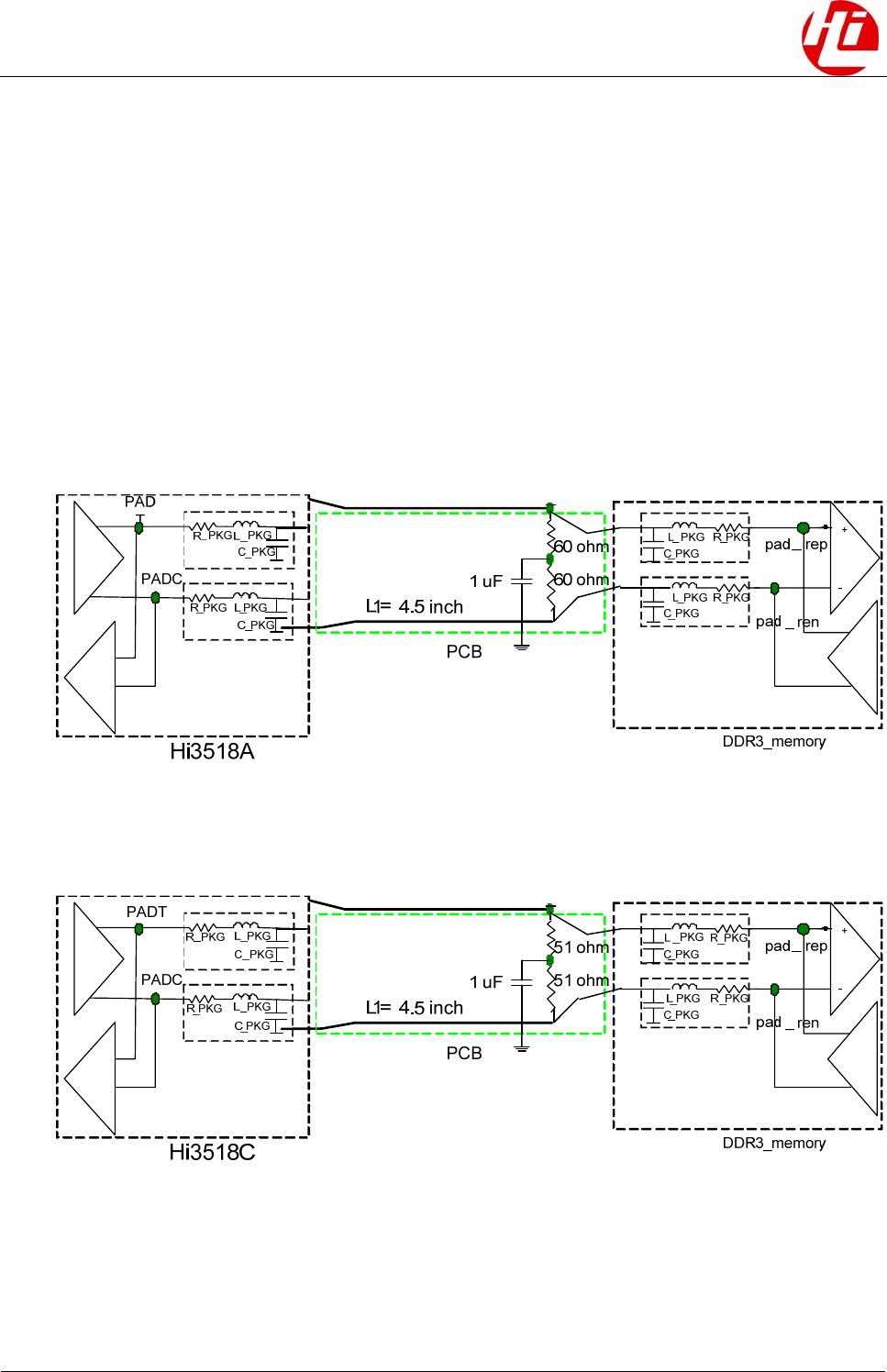
connecting clock signals to the DDR3 SDRAM. In single-load mode, two 60 ±1%
resistors are connected in series between DDR_CLK_N and DDR_CLK_P at the load
end, as shown in Figure 1-6.
z Hi3518C
In single-load mode, two 51 ±1% resistors are connected in series between
DDR_CLK_N and DDR_CLK_P at the load end, as shown in Figure 1-7.
Figure 1-6 Hi3518A differential clocks DDR_CLK_N and DDR_CLK_P in one-drive-one mode
when a DDR3 SDRAM is connected
Figure 1-7 Hi3518C differential clocks DDR_CLK_N and DDR_CLK_P in one-drive-one mode
when a DDR3 SDRAM is connected
Address Signals
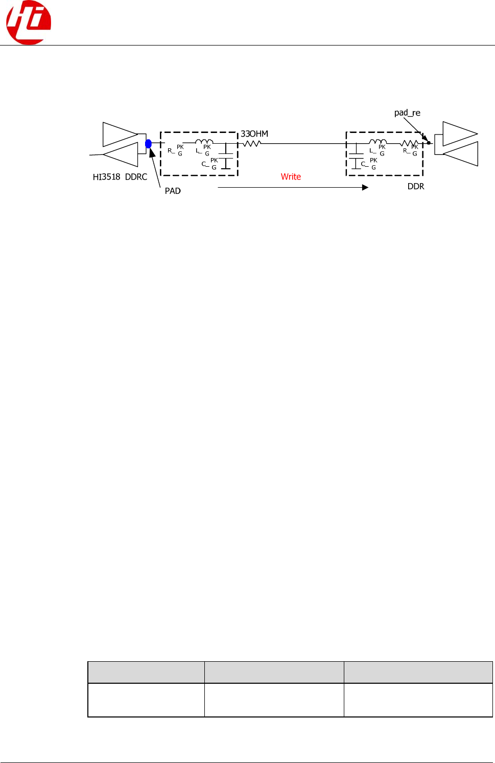
The following takes a 16-bit DDR SDRAM as an example. The modes of connecting address
signals are the same for the DDR2 and DDR3 SDRAMs.
Hi3518 Hardware Design
User Guide 1 Design Recommendations for Schematic Diagrams
Issue 01 (2013-06-30) HiSilicon Proprietary and Confidential
Copyright © HiSilicon Technologies Co., Ltd 9
A 33 resistor is connected in series at the Hi3518 end, as shown in Figure 1-8.
Figure 1-8 Address signals in one-drive-one mode when a DDR2 or DDR3 SDRAM is connected
Control Signals
The control signals of the DDR2 or DDR3 SDRAM connect directly to those of the Hi3518.
DM Signals
The data mask (DM) signals of the DDR2 or DDR3 SDRAM connect directly to those of the
Hi3518.
1.1.6 Design Recommendations for the Flash Schematic Diagrams
1.1.6.1 Introduction
The flash interface has the following features:
z When an SPI flash connects to the flash interface, the maximum capacity is MB SPI
flash, and the clock frequency is 56 MHz.
z When a NAND flash connects to the flash interface, the maximum capacity is 512 GB.
z The multi-level cell (MLC) or single-level cell (SLC) NAND flash is supported, and the
ECC mode is 1-, 4-, 8-, or 24-bit mode.
z The Hi3518 NAND flash controller (NFC) has two CSs for supporting two flash
memories or a component with two CS pins. If the Hi3518A boots from the NAND flash,
the NAND flash CS must connect to the NF_CSN0 pin.
z The Hi3518C does not support the NAND flash.
1.1.6.2 Signal Processing
Matched Design for the SPI Flash
Table 1-4 describes the recommended design when an external SPI flash is connected.
Table 1-4 Recommended design when an external SPI flash is connected
Signal 4-Layer PCB 6-Layer PCB
SFC_CLK A 33 resistor is connected
in series at the Hi3518 end.
A 33 resistor is connected in
series at the Hi3518 end.

1 Design Recommendations for Schematic Diagrams
Hi3518 Hardware Design
User Guide
10 HiSilicon Proprietary and Confidential
Copyright © HiSilicon Technologies Co., Ltd Issue 01 (2013-06-30)
Signal 4-Layer PCB 6-Layer PCB
SFC_DIO/SFC_DOI
/SFC_WP/SFC_HOLD
The signal is connected
directly, and SFC_WP must
connect to a 4.7 k
pull-down resistor.
The signal is connected
directly, and SFC_WP must
connect to a 4.7 k pull-down
resistor.
Matched Design for the NAND Flash
The NAND flash interface supports 8-bit SLC or MLC NAND flash.
Table 1-5 describes the recommended design when an external NAND flash is connected.
Table 1-5 Recommended design when an external NAND flash is connected
Signal 4-Layer PCB 6-Layer PCB
NF_WEN/NF_REN A 33 resistor is connected in
series at the Hi3518 end.
A 33 resistor is connected in
series at the Hi3518 end.
DQ[0:7]
/NF_ALE/NF_CLE
The signal is connected
directly.
The signal is connected directly.
1.2 Design Recommendations for Power Supplies
For details about system power supply design, see the schematic diagram of the Hi3518A
demo board.
1.2.1 Core Power Supply
The core power pins DVDD12 connect to the 1.2 V digital power. The current of the power
chip for DVDD12 must be greater than or equal to 1 A. Each DVDD12 pin connects to at
least two 10 F filtering bypass capacitors and then to GND. At least one 100 nF decoupling
capacitor connects to each DVDD12 pin close to the power pin.
1.2.2 DDR Power Supply
The DDRC and interface comply with the DDR3 SSTL-15 and SSTL-18 standards. The 1.5 V
or 1.8 V power and 0.75 V or 0.9 V reference voltage Vref are required. The Hi3518 and DDR
SDRAM must share the 1.5 V or 1.8 V power.
The DDR power pins DDR_VDDQ connect to the 1.5 V or 1.8 V digital power. It is
recommended that the Hi3518 DDR share the same power supply as that of the connected
DDR.
A 100 nF ceramic filtering capacitor needs to be connected close to each power pin. At least
one 10 F filtering capacitor connects to the power supply of the DDR3 SDRAM and then to
GND.
Hi3518 Hardware Design
User Guide 1 Design Recommendations for Schematic Diagrams
Issue 01 (2013-06-30) HiSilicon Proprietary and Confidential
Copyright © HiSilicon Technologies Co., Ltd 11
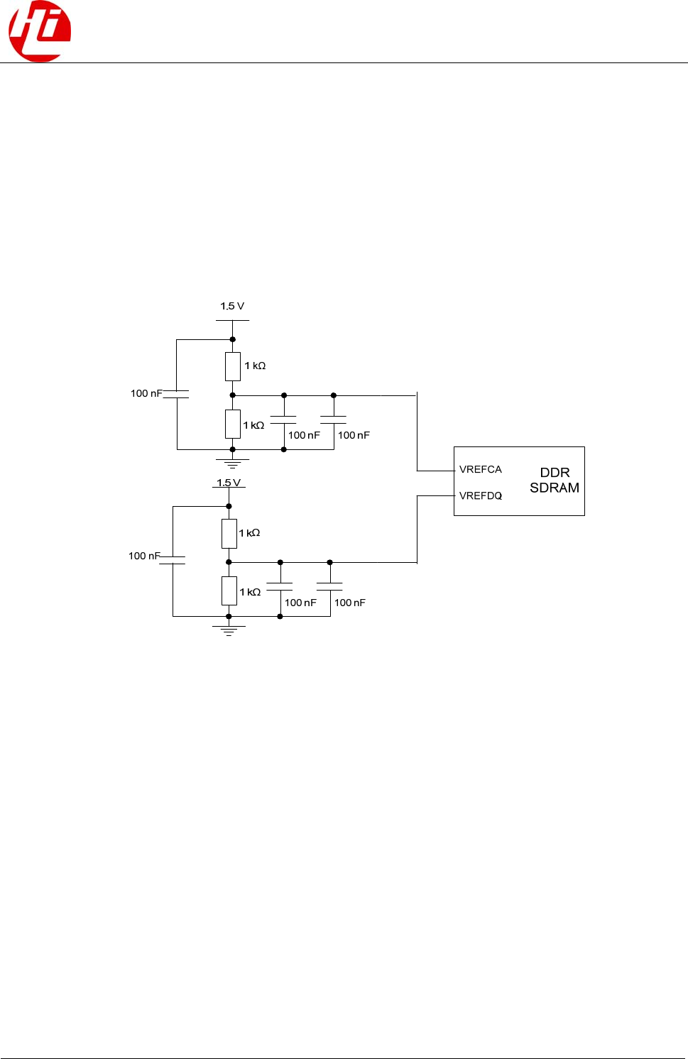
You are advised to design a separate direct current (DC) to DC circuit on the board to supply
power to the DDR2 SDRAM or DDR3 SDRAM and the 1.5 V or 1.8 V power pins of the
DDRC. The power is supplied to the DDR3 SDRAM (0.75 V) or DDR2 SDRAM (0.9 V) and
reference power pin Vref of the DDRC by using 1% 1 k voltage-divider resistors. One 0.1
F decoupling capacitor is connected close to each power pin and reference power pin.
Figure 1-9 shows the reference design of the DDR3 voltage-divider circuit. The DDR2
voltage-divider circuit is similar to the circuit shown in Figure 1-14. The difference is that the
power voltage needs to be changed to 1.8 V. Note that power must be separately supplied
to VREFCA and VREFDQ.
Figure 1-9 Reference design of the DDR3 voltage-divider circuit
1.2.3 I/O Power Supply
The I/O power pins DVDD33 connect to the 3.3 V digital power. Each VDD33 pin connects
to at least one 10 F filtering bypass capacitor and then to GND. In addition, a 100 nF
decoupling capacitor connects to each DVDD33 pin close to the power pin.
For the video input (VI) interface power (DVDD3318 pin), the I/O power supplies for the
sensor CLK, VI, and SPI0 parts can be 1.8 V or 3.3 V, and the I/O level standards of various
sensors are supported.
1.2.4 PLL Power Supply
The phase-locked loop (PLL) power supply is isolated by using an electromagnetic
interference (EMI) bead. For details, see the schematic diagram of the Hi3518A demo board.
1.2.5 Power-on and Power-off Sequences
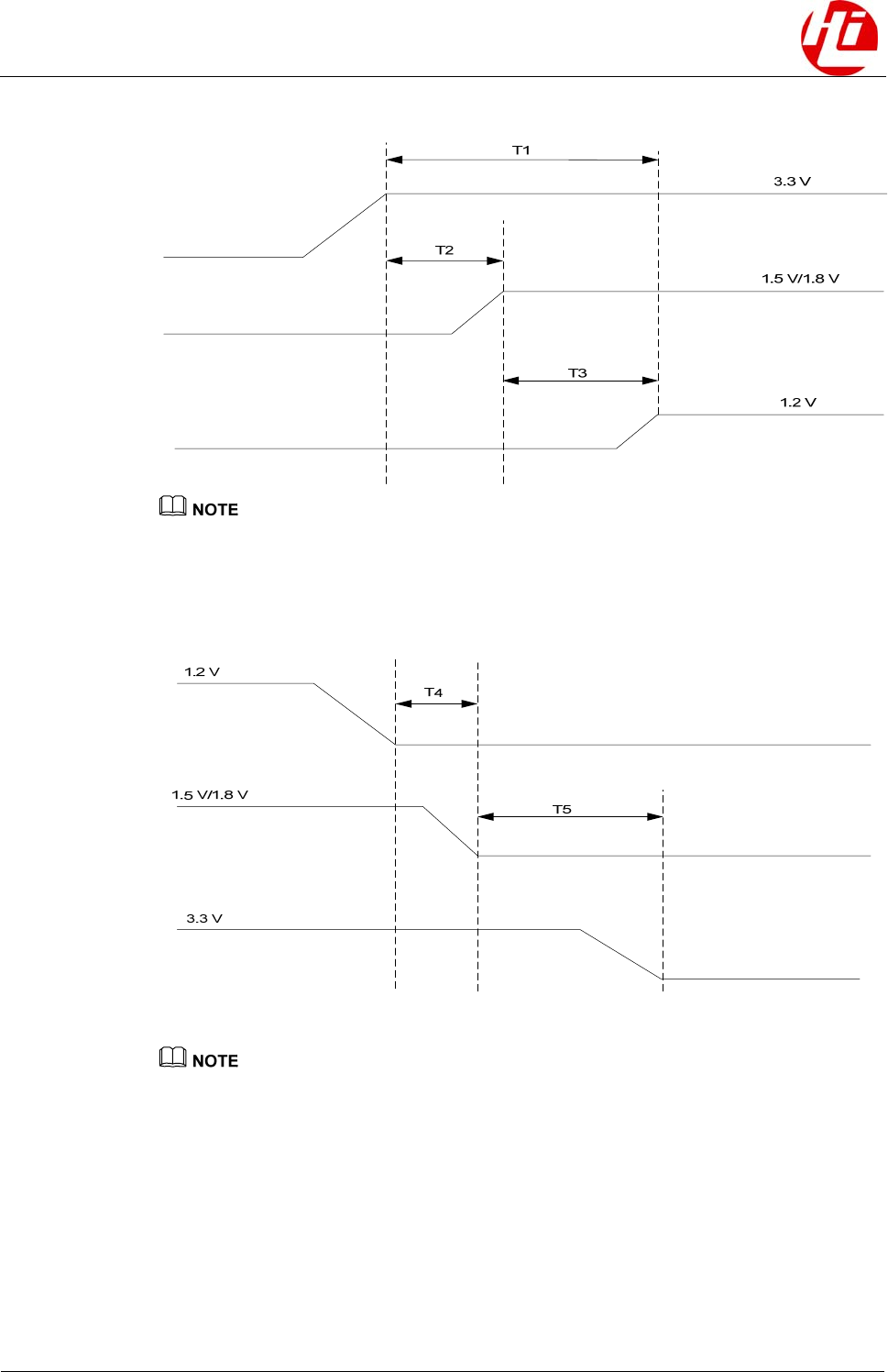
There are requirements on the power-on and power-off sequences for the core power, DDR
power, and I/O power. For details, see Figure 1-10, and Figure 1-11.
1 Design Recommendations for Schematic Diagrams
Hi3518 Hardware Design
User Guide
12 HiSilicon Proprietary and Confidential
Copyright © HiSilicon Technologies Co., Ltd Issue 01 (2013-06-30)
Figure 1-10 Power-on sequence
0 < T1 100 ms, T2 > 0, T3 > 0
Figure 1-11 Power-off sequence
T4 > 0, T5 > 0
1.2.6 Notes
Ensure that the output voltage of power supplies meets the requirements of the Hi3518 when
ripples and noises occur. For details about the requirements on the power supply of each
module, see the "Electrical Specifications" section in the Hi3518 720p Processor Data Sheet.

Hi3518 Hardware Design
User Guide 1 Design Recommendations for Schematic Diagrams
Issue 01 (2013-06-30) HiSilicon Proprietary and Confidential
Copyright © HiSilicon Technologies Co., Ltd 13
1.3 Design Recommendations for Peripheral Interfaces
1.3.1 USB Ports
USB Power Supply
The analog power AVDD33_USB must be isolated from the digital power. You are advised to
use planes to reduce the parasitic effect, decoupling noise, and power supply impedance. In
addition, filtering capacitors are placed close to pins.
The digital power DVDD12_USB and digital GND DVSS_USB must not be interfered.
Ensure that short and wide traces are used.
USB Protective Circuit
A protective circuit must be designed on the USB circuit to ensure electrostatic discharge
(ESD) protection. To prevent the USB routing signals from being affected by protective
components, design the PCB according to the following guidelines:
z Place the protective components close to the USB connector port.
z Use the TVS pipes with low parasitic capacitors as protective components, and ensure
that the breakdown voltage is 8 kV, and the breakdown time is less than 1 ns.
z Ensure that the parasitic capacitors of the protective components connected to the
high-speed USB 2.0 port are less than 1 pF.
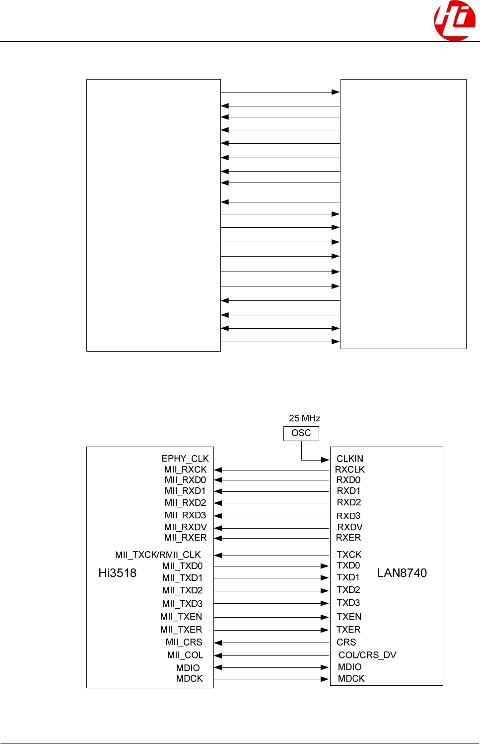
1.3.2 MAC Interfaces
The MAC interfaces support the reduced media-independent interface (RMII) and media
independent interface (MII) modes. For details about the signal connections in the two modes,
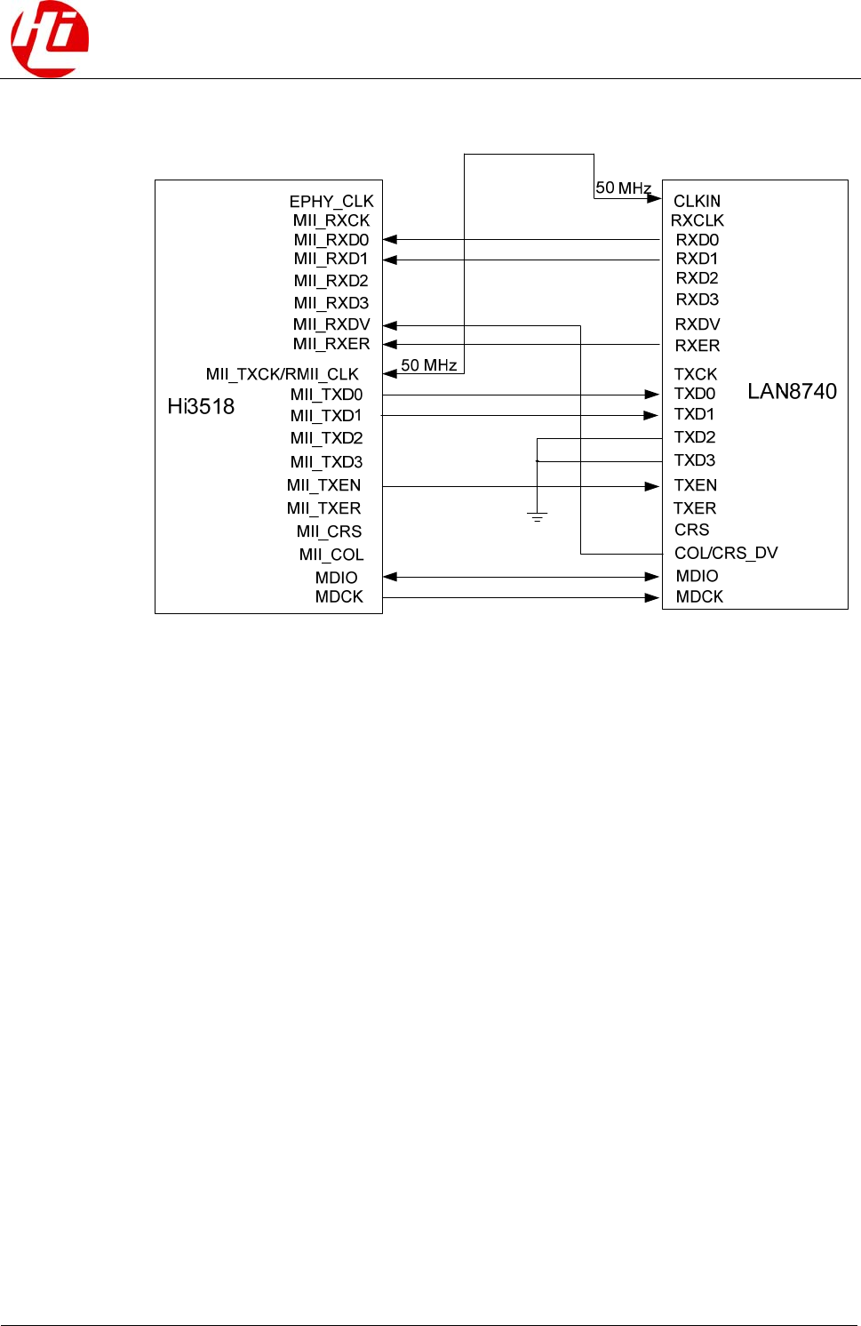
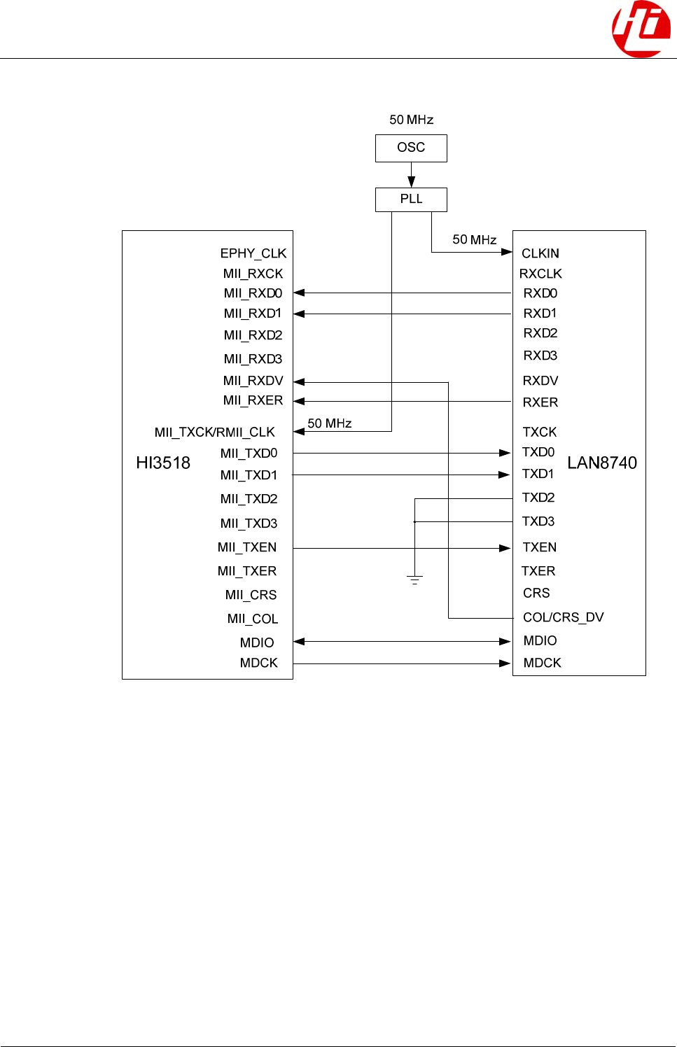
see Figure 1-12 to Figure 1-15. The following uses LAN8740 (Ethernet PHY) as an example.
1 Design Recommendations for Schematic Diagrams
Hi3518 Hardware Design
User Guide
14 HiSilicon Proprietary and Confidential
Copyright © HiSilicon Technologies Co., Ltd Issue 01 (2013-06-30)
Figure 1-12 Signal connections in MII mode (clocks provided by the Hi3518)
EPHY_CLK
Hi3518
MII_RXCK
MII_RXD0
MII_RXD1
MII_RXD2
MII_RXD3
MII_RXDV
MII_TXCK/RMII_CLK
MII_TXD0
MII_TXD1
MII_TXD2
MII_TXD3
MII_TXEN
MII_CRS
MII_COL
MDIO
MDCK
LAN8740
CLKIN
RXCLK
RXD0
RXD1
RXD2
RXD3
RXDV
TXCK
TXD0
TXD1
TXD2
TXD3
TXEN
CRS
COL/CRS_DV
MDIO
MDCK
RXERMII_RXER
MII_TXER
25 MHz
TXER
Figure 1-13 Signal connections in MII mode (clocks provided by external components)
Hi3518 Hardware Design
User Guide 1 Design Recommendations for Schematic Diagrams
Issue 01 (2013-06-30) HiSilicon Proprietary and Confidential
Copyright © HiSilicon Technologies Co., Ltd 15
Figure 1-14 Signal connections in RMII mode (clocks provided by the Hi3518)
1 Design Recommendations for Schematic Diagrams
Hi3518 Hardware Design
User Guide
16 HiSilicon Proprietary and Confidential
Copyright © HiSilicon Technologies Co., Ltd Issue 01 (2013-06-30)
Figure 1-15 Signal connections in RMII mode (clocks provided by external components)
All MAC signals are connected in point-to-point topology. It is recommended that each PCB
trace is less than or equal to 6 inches. The following are recommendations for designing
matched resistors:
z Connect a 4.7 k pull-up resistor to the MDIO signal.
z Connect a 22 resistor to the MDCK signal in series at the source end to ensure signal
quality.
z Connect the signals TXD0TXD3 directly to the Hi3518.
z Connect a 33 resistor in series to the TXCLK signal close to the PHY chip. In RMII
mode, the TXCK signal is multiplexed as the RMII_CLK signal, and a 33 resistor is
connected in series at the Hi3518 end.
z Connect the signals RXD0RXD3 directly to the Hi3518.
z Connect a 33 resistor in series to the RXCK signal close to the PHY chip.

Hi3518 Hardware Design
User Guide 1 Design Recommendations for Schematic Diagrams
Issue 01 (2013-06-30) HiSilicon Proprietary and Confidential
Copyright © HiSilicon Technologies Co., Ltd 17
1.3.3 Audio and Video Interfaces
Analog DAC Interface
The Hi3518A provides a video digital-to-analog converter (VDAC), whereas the Hi3518C
does not provide a VDAC.
z The VDAC_IOUT pin is a composite video broadcast signal (CVBS) output pin. It must
connect to an external 75 resistor and then to GND. For details, see the schematic
diagram of the Hi3518A demo board.
z The 3.3 V power supply for the VDAC must be isolated from the 3.3 V system power
supply. Ensure that sufficient filtering capacitors connect to 3.3 V power pins. For details,
see the schematic diagram of the Hi3518A demo board.
z The Hi3518 supports automatic CVBS detection. When no CVBS monitor is connected,
the Hi3518 automatically disables the VDAC to reduce power consumption. If automatic
CVBS detection is required, do not design the video buffer. If isolation and ESD are
essential, the video buffer is recommended.
Analog Audio Interface
The Hi3518A provides stereo-channel input and output interfaces: AC_LINEL, AC_LINER,
AC_OUTL, and AC_OUTR. The Hi3518C provides mono-channel input and output
interfaces: AC_OUTL and AC_LINEL.
z The 3.3 power for the audio DAC must be isolated from the 3.3 V system power. The
filtering capacitor connected to the AC_VREF pin must be greater than or equal to 10 F.
For details, see the schematic diagram of the Hi3518A demo board.
z AC_LINEL and AC_LINER can act as line or MIC input channels. If the input device is
a passive MIC, connect the input signal to a resistor and then to the MIC_BIAS pin. If
the input device is an active line device such as the PC, the input signal does not need to
connect to the MIC_BIAS pin.
z Three series of sampling rates are supported: 32 kHz, 44.1 kHz, and 48 kHz.
The 32 kHz series sampling rates include 8 kHz, 16 kHz, 32 kHz, 64 kHz, and 128
kHz.
The 44.1 kHz series sampling rates include 11.025 kHz, 22.05 kHz, 44.1 kHz, 88.2
kHz, and 176.4 kHz.
The 48 kHz series sampling rates include 12 kHz, 24 kHz, 48 kHz, 96 kHz, and 192
kHz.
z The amplitude of the audio DAC is 0.875 Vrms for full outputs.
z You are advised to connect an audio frequency amplifier and filtering circuit to the audio
output pins AC_OUTL and AC_OUTR, which ensures excellent audio quality. For
details, see the latest schematic diagram of the Hi3518PERB board.
VI Interface
The Hi3518 has only one physical VI interface. This interface is called VI0.
z VI0 supports the raw data input, a maximum of 12-bit width, and a maximum of 74.25
MHz interface frequency.
z For a 12-bit sensor, the raw data pins connect to D0D11 of VI0 in sequence.

1 Design Recommendations for Schematic Diagrams
Hi3518 Hardware Design
User Guide
18 HiSilicon Proprietary and Confidential
Copyright © HiSilicon Technologies Co., Ltd Issue 01 (2013-06-30)
z For a 10-bit sensor, the raw data pins connect to any 10-bit pins of VI0 in sequence. The
pins D2 to D11 are recommended. Connect any unused pin to a 4.7 k resistor and then
to GND.
VO Interface
The Hi3518 has only one physical video output (VO) interface. This interface is called VOU
interface.
z If the VOU interface acts as the BT.1120 output, the bit width is 16 bits, and the
maximum interface frequency is 74.25 MHz.
z The VOU interface does not provide external row sync and field sync signals and
supports only internal synchronization.
z The VOU interface signal is multiplexed with the Ethernet (ETH) interface signal. If the
ETH interface is used, the VOU interface is unavailable.
z For a BT.1120 signal, the upper eight bits are the Y (luminance) signal, and the lower
eight bits are the C (chrominance) signal.
1.3.4 RTC Interface
The timing accuracy of the embedded RTC is affected by the manufacturing accuracy and
temperature offset of the external crystal oscillator. For details, see the RTC Correction
Scheme Application Notes.
If high timing accuracy is required, you are advised to select the external RTC with an
embedded crystal oscillator or a crystal oscillator with the temperature compensation
function.
1.4 Unused Pins
Do as follows if some pins are not used:
z If the JTAG function is not used, connect the JTAG_EN pin to a 4.7 k pull-down
resistor, set the functional mode of the JTAG_TCK, JTAG_TMS, JTAG_TRSTN,
JTAG_TDO, and JTAG_TDI pins to GPIO, and set pin directions to output. No external
processing is required.
z If the master chip is reset by the internal POR module, connect the POR_SEL pin to a
pull-down resistor. The RSTN pin can be floated.
z If the NAND flash is not used, set the functional modes of corresponding pins to GPIO
and set pin directions to output. No external processing is required.
z If SPI0 and SPI1 are not used, set the functional modes of related pins to GPIO and set
pin directions to output. No external processing is required.
z If the SAR_ADC, VDAC, audio CODEC, and USB module are not used, retain their
power supplies.
z If over-current protection is not required for the USB module, set the functional mode of
the USB_OVRCUR pin to GPIO and set the pin direction to output. No external
processing is required.

Hi3518 Hardware Design
User Guide 1 Design Recommendations for Schematic Diagrams
Issue 01 (2013-06-30) HiSilicon Proprietary and Confidential
Copyright © HiSilicon Technologies Co., Ltd 19
1.5 Sensor Board
The following are design recommendations for the sensor board:
z To ensure picture quality, you are advised to use a low dropout (LDO) regulator to
supply power to the sensor. Pay attention to the analog power and PLL power of the
sensor. Typically, the core units of the sensor require a large current. The efficiency and
heat dissipation of the LDO regulator need to be considered.
z The analog part and digital part of the sensor are separated. To be specific, the analog
GND and digital GND are separated and connected by using 0 resistors in single-point
mode. The analog power branch has an independent LDO regulator and does not share
power branch with the digital power. During design of PCB layout and stacked
architecture, ensure that the digital part and analog part do not intersect, avoiding
interference and coupling.
z If the sensor board connects to the main board by using a connector, ensure that current
return paths are provided for the data signals from the connector when specifying signals
for connector pins. This avoids signal crosstalk. That is, each data signal trace or clock
signal trace connects to an independent GND trace to form a current return path. Note
that a clock signal trace is designed between two GND traces, and two data signal traces
are designed between two GND traces. For details, see schematic diagrams.

2 PCB Design Recommendations
Hi3518 Hardware Design
User Guide
20 HiSilicon Proprietary and Confidential
Copyright © HiSilicon Technologies Co., Ltd Issue 01 (2013-06-30)
2 PCB Design Recommendations
2.1 PCB Design Recommendations for the Small System
2.1.1 Power Supplies of the Small System
Core Power Supply
The current of the core power plane must be at least 1 A.
If the plane is used to supply power, 100 nF filtering capacitors must evenly connect to core
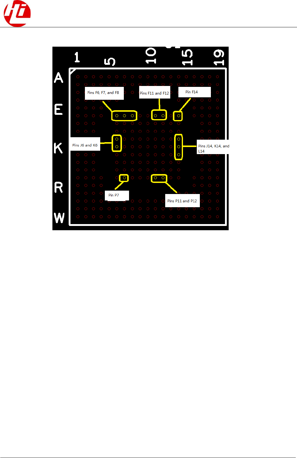
power pins to reduce parasitic inductance. Figure 2-1 shows the core power pins on the
Hi3518A. Connect decoupling capacitors to these pins as follows:
z Ensure that capacitors are placed close to pins.
z Connect at least one 2.2 F capacitor to each of the pins F6, F7, and F8.
z Connect at least one 1 F capacitor to each of the pins J6 and K6.
z Connect at least one 10 F capacitor to each of the pins P11 and P12.
z Connect at least one 10 F capacitor to each of the pins J14, K14, and L14.
z Connect at least one 100 F capacitor to other pins each.
Hi3518 Hardware Design
User Guide 2 PCB Design Recommendations
Issue 01 (2013-06-30) HiSilicon Proprietary and Confidential
Copyright © HiSilicon Technologies Co., Ltd 21
Figure 2-1 Core power pins on the Hi3518A
Figure 2-2 shows the core power pins on the Hi3518C. Connect decoupling capacitors to
these pins as follows:
z Ensure that capacitors are placed close to pins.
z Connect at least one 10 F capacitor to each of the pins P58 and P85.
z Connect at least one 10 F capacitor to each of the pins P161, P7, P153, and P104.
z Connect at least one 100 nF capacitor to other pins each.

2 PCB Design Recommendations
Hi3518 Hardware Design
User Guide
22 HiSilicon Proprietary and Confidential
Copyright © HiSilicon Technologies Co., Ltd Issue 01 (2013-06-30)
Figure 2-2 Core power pins on the Hi3518C
DDR Power Supply
The 1.5 V/1.8 V power pins of the DDR2/DDR3 and the Hi3518 DDR need to be connected
on the same power network. Decoupling capacitors need to be placed close to the power pins.
At least one 10 F filtering capacitor connects to the Hi3518 DDR power and then to GND.
The VREF power supplies of the Hi3518 and DDR2/3 SDRAM (0.9 V for the DDR2
SDRAM and 0.75 V for the DDR3 SDRAM) must be isolated from other power supplies. You
can use 20 mils or wider traces. Ensure that decoupling capacitors are placed close to each
power pin and the VREF is shielded by surrounding ground traces.
The VREF design recommendations are as follows:
z Pay attention to the VREF routing when designing the VREF. According to the SSTL-15
standard, the noise of the VREF cannot be greater than ±1% of the VREF level. To
reduce the noise, ensure that the VREF traces are as wide as possible. In addition, you
are advised to route the VREF traces at the power layer over a copper plane. This copper
plane cannot be used as the reference plane for routing signal traces.
z A decoupling capacitor needs to connect to each VREF pin. The trace of each VREF pin
must be as wide as possible, and the spacing between the trace and other signal traces
must be 20–25 mils.
I/O Power
Connect at least one 10 F filtering bypass capacitor to each DVDD33 pin and then to GND.
Connect one 100 nF decoupling capacitor to each DVDD33 pin close to the power pin.

Hi3518 Hardware Design
User Guide 2 PCB Design Recommendations
Issue 01 (2013-06-30) HiSilicon Proprietary and Confidential
Copyright © HiSilicon Technologies Co., Ltd 23
2.1.2 Clock and Reset Circuits
Clock
The power and GND pins of the Hi3518 PLL unit include AVDD12_PLL, AVDD33_PLL, and
AVSS_PLL. Design the PCB according to the following guidelines:
z AVDD12_PLL is the 1.2 V PLL power. You are advised to isolate it from the 1.2 V board
digital power by using an EMI bead. The level deviation of the 1.2 V power must be
within ±5%.
z AVDD33_PLL is the 3.3 V PLL power. You are advised to isolate it from the 3.3 V
digital power by using an EMI bead. The level deviation of the 3.3 V power must be
within ±5%.
z AVSS_PLL is the reference GND of the PLL circuit. The decoupling capacitors for
AVDD12_PLL and AVDD33_PLL must be connected by referring to AVSS_PLL as the
GND plane. AVSS_PLL must connect to the digital board GND through a single point.
z The traces of system clocks and crystal oscillator circuit must be as short as possible.
The traces must be surrounded by GND traces.
Reset
The Hi3518 can be reset internally or externally by configuring the POR_SEL pin. During
power-on, if POR_SEL is 0, internal reset is enabled; if POR_SEL is 1, internal reset is
disabled, and the chip is reset externally. For details about the circuit design, see the
schematic diagram of the Hi3518A demo board.
2.1.3 DDR Signals
In this section, the DDR signal design is described by using the 16-bit DDR as an example.
Clock Signal CLK
The following are requirements on the trace length of the clock signal CLK:
z The trace length of the CLK signal must be shorter than or equal to 4.5 inches.
z The traces of CLK differential signals must be routed in differential mode, and the
deviation of each pair of differential traces is ±5 mils.
DQS Signals
For DQS signals, the trace requirements are as follows:
z Each pair of DQS differential traces must have the same length, and the deviation of
each pair of differential traces is less than 5 mils.
z DQS traces are routed based on the CLK trace length. The deviation of the DQS trace is
±250 mils relative to the CLK trace length.
Data Signals DQ[0:15]
The trace length of data signals DQ[15:0] is based on the DQS trace length.

2 PCB Design Recommendations
Hi3518 Hardware Design
User Guide
24 HiSilicon Proprietary and Confidential
Copyright © HiSilicon Technologies Co., Ltd Issue 01 (2013-06-30)
z DQ[7:0] are routed based on the DQS 0 trace length, and the length deviation is ±200
mils.
z DQ[15:8] are routed based on the DQS 1 trace length, and the length deviation is ±200
mils.
Data Mask Signals
The data mask (DM) signal traces are routed based on the DQS trace length. The
requirements are as follows:
z The DM 0 trace is routed based on the DQS 0 trace length, and the length deviation is
±200 mils.
z The DM 1 trace is routed based on the DQS 1 trace length, and the length deviation is
±200 mils.
Address Signals ADDR[0:14]
ADDR[0:14] traces are routed based on the CLK trace length, and the length deviation is
±700 mils.
Control Signals
The traces of the control signals including BA[0:2], DM, CKE, CSN, WEN, CASN, RASN,
and ODT are routed based on the CLK trace length, and the length deviation is ±700 mils.
PCB Routing Recommendations
Route traces on a PCB according to the following guidelines:
z Route DDR3 SDRAM data traces by referring to the GND plane and avoid crossing the
power and GND plane splits. Ensure that all DDR signal traces are routed by referring to
a complete plane.
z Ensure that signal traces are as short as possible, and minimize the use of vias to ensure
the impedance continuity of traces. The impedance of the single-end signal PCB trace is
50 ±10%, and the impedance of the differential PCB trace is 100 ±10%.
z Ensure that the spacing between adjacent traces meets the 3W rule. The 3W rule
indicates that the trace spacing is three times of the trace width.
z The spacing between a DDR3 SDRAM signal trace and a non-DDR3 SDRAM signal
trace must be at least 20 mils.
z Connect a decoupling capacitor to each VREF pin. The trace of each VREF pin must be
as wide as possible, and the spacing between the VREF pin trace and other signal traces
is 20–25 mils.
z The Hi3518 does not support DDR training.
2.1.4 SPI Flash
Route traces on a PCB according to the following guidelines:
z Ensure that the spacing between adjacent traces meets the 3W rule.
z Connect a 33 resistor to the clock signal in series to ensure signal quality.

Hi3518 Hardware Design
User Guide 2 PCB Design Recommendations
Issue 01 (2013-06-30) HiSilicon Proprietary and Confidential
Copyright © HiSilicon Technologies Co., Ltd 25
2.1.5 Ethernet Port Signal
z Ensure that the spacing between adjacent traces meets the 3W rule.
z Connect a 33 resistor to the clock signal in series to ensure signal quality.
2.2 PCB Design Recommendations for Peripheral
Interfaces
2.2.1 USB Port Design
USB PCB Design
Route the data signal traces of the USB 2.0 host port in differential mode to ensure signal
quality. You are advised to design the PCB routing according to the following guidelines to
meet the 480 MHz requirement for the USB 2.0 port:
z The differential data traces must be short and straight and the internal differential traces
must have the same length. It is recommended that the trace deviation be within 5 mils.
z The impedance deviation of each USB differential trace is 90 ±10%.
z Route traces on the routing planes close to GND, and do not change the routing plane.
z Route differential data traces by referring to complete GND planes, and do not cross the
plane splits.
z Minimize the use of vias and corners when routing differential data traces. When corners
are required, use arcs or 135° turns but not a 90° turn. This reduces signal reflection and
impedance variance.
z Route the differential data traces away from other high-speed cyclic signals and strong
current signals, and ensure that the spacing is greater than 50 mils, reducing crosstalk. In
addition, route the differential data traces away from low-speed non-cyclic signals and
ensure that the spacing is at least 20 mils.
z Place the REXT resistor close to the Hi3518.
Power Supply of USB Unit
The Hi3518 has one USB host port. The power pins and GND pins of the USB unit are
AVDD33_USB, AVSS_USB, and DVDD12_USB that correspond to the 3.3 V power, 3.3 V
GND, and 3.3 V core power respectively.
AVDD33_USB is the 3.3 V analog power, and AVSS_USB is the 3.3 V analog GND. The
level deviation of AVDD33_USB must be within ±7%. You are advised to isolate the 3.3 V
analog USB power from the 3.3 V digital board power by using an EMI bead, and place
filtering capacitors close to AVDD33_USB and AVSS_USB pins.
Routing of the USB Protective Circuit
A USB protective circuit is required to implement electrostatic discharge (ESD) protection. To
avoid the USB trace signals from being attenuated by the protective components, design the
PCB according to the following guidelines:
z Place protective components close to the USB port.

2 PCB Design Recommendations
Hi3518 Hardware Design
User Guide
26 HiSilicon Proprietary and Confidential
Copyright © HiSilicon Technologies Co., Ltd Issue 01 (2013-06-30)
z Use the TVS pipes with low parasitic capacitors as protective components.
z The parasitic capacitors connected to the protective components on the high-speed USB
2.0 port must be less than 2 pF.
2.2.2 Audio Circuit Design
2.2.2.1 DAC Interface
The Hi3518A provides a VDAC, whereas the Hi3518C does not provide a VDAC.
VDAC PCB Design
To ensure the output picture quality of the VDAC, design PCB routing according to the
following guidelines:
z Connect the VDAC output pin to a resistor and then to GND. The resistor is placed close
to the Hi3518A.
z Place the analog video filtering circuit close to the Hi3518A.
z Use a VDAC to drive only a single load. If you need to drive multiple loads to output
multi-channel video signals, drives are recommended.
z The VDAC unit has a separate analog video GND plane. All analog signal traces are
routed by referring to this plane.
z Route all analog signal traces on the planes close to the analog video GND plane, and do
not change the routing plane.
z Do not route other signal traces by referring to the analog video GND plane.
z When corners are required, use arcs or 45° turns but not a 90° turn to reduce signal
reflection.
Power Supply of the VDAC Unit
AVDD3V3_VDAC of the VDAC unit is an analog video power pin. Design the PCB
according to the following guidelines:
z Use a GND plane as the analog video GND and digital GND.
z The deviation of the 3.3 V analog video power must be within ±5%.
z Isolate the 3.3 V analog VDAC power from the 3.3 V digital board power by using an
EMI bead, and place filtering capacitors close to the AVDD33_VDAC pin.
z Connect the VDAC_COMP to a 10 capacitor and a 10 nF capacitor in parallel, and
then to the AVDD33_VADC pin.
Protective Circuit of the VDAC Port
A protective circuit for the VDAC output port is required to implement ESD protection. You
are advised to design the PCB according to the following guidelines:
z Use the video buffer circuit for video output to separate the video port of the Hi3518
from the add-on port.
z Place the protective components close to the connector of the VDAC output port.
z Use TVS pipes or switch diodes as protective components.

Hi3518 Hardware Design
User Guide 2 PCB Design Recommendations
Issue 01 (2013-06-30) HiSilicon Proprietary and Confidential
Copyright © HiSilicon Technologies Co., Ltd 27
2.2.2.2 VI and VO Interfaces
The Hi3518 has a VO interface and a VI interface. The following are routing requirements:
z The VO data signal trace is routed based on the CLK signal trace. The deviation length is
less than or equal to 1000 mils.
z Route traces of the VI data signal, row sync signal, and field sync signal based on the
CLK signal trace. The deviation length is less than or equal to 1000 mils.
z The VI interface has 1.8 V and 3.3 V power domains. Route the traces of the VI data
signal, row sync signal, field sync signal, and SPI 0 at the top layer by referring to the
GND plane. This avoids sharp changes of characteristic impedance when signal traces
are routed by referring to the 1.8 V or 3.3 V power plane.
z If the 1.8 V power domain is selected for the VI interface, the signal trace must be less
than or equal to 4 inches.

3 Heat Design Recommendations
Hi3518 Hardware Design
User Guide
28 HiSilicon Proprietary and Confidential
Copyright © HiSilicon Technologies Co., Ltd Issue 01 (2013-06-30)
3 Heat Design Recommendations
3.1 Working Condition
For details about power supply parameters, temperature parameters, and thermal resistance
parameters for the Hi3518, see section 2.6 "Electrical Specifications" in the Hi3518 HD IP
Camera SoC Data Sheet.
3.2 Reference Design for Circuit Heat Dissipation
3.2.1 Schematic Diagram
Power Supply
Ensure the efficiency of the board power tree as long as the power supply is stable. That is,
you design the board power supply optimally and use few large-voltage-difference LDO
components. This reduces the heat produced during power supply conversion.
The board power supplies for peripherals such as the secure digital (SD) card and USB device
can be reserved during board design. These power supplies can be shut down when they are
not used. The main integrated circuits (ICs) of the board must support the power-down mode.
Low-Power Configurations for Idle Modules
Modules such as the VDAC, USB module and NANDC may not be used in actual scenarios.
You can set the modes of these modules to power-down mode or default mode.
3.2.2 PCB
Component Layout
Lay out components based on the product architecture and heat dissipation design:
z Place the components that consume much power and generate much heat in a distributed
manner to avoid overheating of some parts and ensure the reliability and efficiency of
components. You are advised to place the Hi3518 away from power supplies.

Hi3518 Hardware Design
User Guide 3 Heat Design Recommendations
Issue 01 (2013-06-30) HiSilicon Proprietary and Confidential
Copyright © HiSilicon Technologies Co., Ltd 29
z Design the product architecture optimally to ensure that the heat produced internally can
be dissipated.
Routing
The routing recommendations are as follows:
z For the connection style of the vias under the Hi3518, select the full connection style but
not the thermal connection style to improve the board dissipation efficiency.
z Connect the GND signals and 1.2 V, 1.5 V (or 1.8 V), and 3.3 V power signals over
copper planes. When the signal over-current performance is ensured, you are advised to
punch more vias on copper planes.
z Increase the size of copper planes under and around the components that produce much
heat to ensure that the heat of the PCB can be dissipated effectively. For the inductors
and power chips, place them in a distributed manner and increase the size of copper
planes around them.