JN517x DK005 Development Kit User Guide
User Manual:
Open the PDF directly: View PDF ![]() .
.
Page Count: 66
- Contents
- Preface
- 1. Introduction to the Development Kit
- 2. ZigBee Smart Home Demonstration
- 3. Where Next?
- Appendices

JN517x-DK005 Development Kit
User Guide
JN-UG-3121
Revision 1.1
8 February 2017

JN517x-DK005 Development Kit
User Guide
2 © NXP Semiconductors 2017 JN-UG-3121 v1.1

JN517x-DK005 Development Kit
User Guide
JN-UG-3121 v1.1 © NXP Semiconductors 2017 3
Contents
Preface 5
Organisation 5
Conventions 6
Acronyms and Abbreviations 6
Related Documents 7
Support Resources 7
Optional Components 8
Trademarks 8
1. Introduction to the Development Kit 9
1.1 Kit Contents 10
1.2 Wireless Network Fundamentals 12
1.2.1 Radio Frequency 12
1.2.2 Network Identification 13
1.2.3 Node Types 13
1.2.4 Network Formation and Topology 14
1.2.4.1 Star Networks 14
1.2.4.2 Tree Networks 15
1.2.4.3 Mesh Networks 15
1.2.5 Wireless Network Protocol Stack 16
1.3 Internet of Things (IoT) 17
1.3.1 IoT Gateway 17
1.3.2 IP Connectivity of the Kit 18
1.4 Network Commissioning 19
1.4.1 NFC Commissioning Process 20
1.4.2 Addressing, Binding and Grouping 21
1.5 ZigBee Smart Home Demonstration 22
2. ZigBee Smart Home Demonstration 23
2.1 Demo System Overview 23
2.2 Setting Up the IoT Gateway 25
2.3 Commissioning Nodes 28
2.4 Controlling the Light 32
2.4.1 Controlling the Dimmable Light from the Dimmer Switch 32
2.4.2 Controlling the Dimmable Light from the PC 33

Contents
4 © NXP Semiconductors 2017 JN-UG-3121 v1.1
3. Where Next? 35
3.1 Which Protocol? 35
3.2 Software Developer’s Kit (SDK) 36
3.2.1 LPCXpresso 36
3.2.2 IEEE 802.15.4 SDK (JN-SW-4263) 37
3.2.3 ZigBee 3.0 SDK (JN-SW-4270) 37
3.3 Support Resources 38
3.3.1 IEEE 802.15.4 Resources 38
3.3.2 ZigBee 3.0 Resources 39
Appendices 41
A. Kit Hardware 41
A.1 Carrier Boards 42
A.1.1 Power Source Selection 46
A.1.2 Pre-assembled Boards 48
A.2 Lighting/Sensor Expansion Boards 50
A.3 Generic Expansion Boards 52
A.4 JN5179 Modules 54
A.5 USB Dongles 54
A.6 Raspberry Pi 2 56
A.7 NFC Controller 58
B. Installing a Packet Sniffer 60
C. Firmware Re-programming 61
C.1 Re-programming JN5179 Modules 61
C.2 Re-programming JN5179 USB Dongles 61
D. Installing the FTDI Device Driver for USB Connections 62
E. Regulatory Information 63
E.1 FCC Regulatory Statements 63

JN517x-DK005 Development Kit
User Guide
JN-UG-3121 v1.1 © NXP Semiconductors 2017 5
Preface
This manual provides an introduction to the NXP JN517x-DK005 Development Kit,
based around the JN517x family of wireless microcontrollers. The manual also
describes how to run the pre-loaded ZigBee Smart Home Demonstration using
components from the kit. In addition, information is provided on the wireless network
protocols supported by the development kit and the NXP resources available to
develop custom JN517x applications using these protocols.
Organisation
This manual consists of three chapters and five appendices, as follows:
Chapter 1 introduces the JN517x-DK005 Development Kit and outlines the key
concepts for an understanding of wireless networks.
Chapter 2 describes how to use the development kit to set up and run the
pre-loaded ZigBee Smart Home Demonstration.
Chapter 3 provides guidance on where to go next in order to develop custom
JN517x applications that can be run on the components of the kit.
The Appendices provide:
Details of the individual kit components
Guidance on setting up a packet sniffer using one of the supplied dongles
Guidance on re-programming the firmware of certain kit components
Instructions for installing the FTDI device driver for USB connections
Regulatory information for the kit
About this Manual
6 © NXP Semiconductors 2017 JN-UG-3121 v1.1
Conventions
Files, folders, functions and parameter types are represented in bold type.
Function parameters are represented in italics type.
Code fragments are represented in the Courier New typeface.
Acronyms and Abbreviations
ADC Analogue to Digital Converter
API Application Programming Interface
DC Direct Current
DHCP Dynamic Host Configuration Protocol
DIO Digital Input/Output
FTDI Future Technology Devices International
GPIO General Purpose Input/Output
HA Home Automation
IEEE Institute of Electrical and Electronics Engineers
IoT Internet of Things
IP Internet Protocol
JTAG Joint Test Action Group
LAN Local Area Network
LED Light Emitting Diode
This is a Tip. It indicates useful or practical information.
This is a Note. It highlights important additional
information.
This is a Caution. It warns of situations that may result
in equipment malfunction or damage.

JN517x-DK005 Development Kit
User Guide
JN-UG-3121 v1.1 © NXP Semiconductors 2017 7
LPRF Lower Power Radio Frequency
NFC Near Field Communication
PSU Power Supply Unit
PWM Pulse Width Modulation
RF Radio Frequency
RTOS Real Time Operating System
SBC Single Board Computer
SDK Software Developer’s Kit
SMA SubMiniature version A
SSID Service Set Identifier
UART Universal Asynchronous Receiver/Transmitter
USB Universal Serial Bus
WAN Wide Area Network
WPAN Wireless Personal Area Network
ZCL ZigBee Cluster Library
ZLL ZigBee Light Link
Related Documents
JN-UG-3109 JN517x LPCXpresso Installation and User Guide
JN-UG-3099 JN51xx Production Flash Programmer User Guide
JN-UG-3112 NFC Commissioning User Guide
JN-AN-1216 ZigBee 3.0 IoT Control Bridge Application Note
JN-AN-1217 ZigBee 3.0 Base Device Template Application Note
JN-AN-1218 ZigBee 3.0 Light Bulbs Application Note
JN-AN-1219 ZigBee 3.0 Controller and Switch Application Note
JN-AN-1220 ZigBee 3.0 Sensors Application Note
JN-RD-6036 Carrier Boards and Expansion Boards Reference Design
Support Resources
To access online support resources such as SDKs, Application Notes and User
Guides, visit the Wireless Connectivity area of the NXP web site:
www.nxp.com/products/wireless-connectivity
All NXP resources referred to in this manual can be found at the above address,
unless otherwise stated.

About this Manual
8 © NXP Semiconductors 2017 JN-UG-3121 v1.1
Optional Components
The following additional/optional hardware components are available for use with the
JN517x-DK005 Development Kit:
These products can be individually ordered via the NXP web site (www.nxp.com).
Trademarks
All trademarks are the property of their respective owners.
Part Number Name
JN517x-XK030 Generic Node Expansion Kit
JN517x-XK040 Lighting/Sensor Node Expansion Kit
OM15021 JN5179 USB Dongle
JN517x-DK005 Development Kit
User Guide
JN-UG-3121 v1.1 © NXP Semiconductors 2017 9
1. Introduction to the Development Kit
Welcome to the JN517x-DK005 Development Kit, which is based around the NXP
JN517x family of wireless microcontrollers. A ZigBee Smart Home Demonstration is
pre-loaded into certain kit components, allowing a small wireless network with IP
connectivity to be quickly assembled and used. The development kit can also be used
in conjunction with NXP’s range of Software Developer’s Kits (SDKs) to develop new
wireless network applications for the JN517x devices. Support resources are also
provided to allow the integration of a network into the ‘Internet of Things’ (IoT).
The wireless network protocols supported by the development kit are as follows:
IEEE 802.15.4
ZigBee 3.0 with ZigBee Lighting & Occupancy (ZLO) devices
This chapter introduces you to the development kit and wireless networks by
describing:
Contents of the kit - see Section 1.1
Wireless network fundamentals - see Section 1.2
IP connectivity - see Section 1.3
Network commissioning - see Section 1.4
Pre-loaded ZigBee Smart Home Demonstration - see Section 1.5
Note: The pre-loaded ZigBee Smart Home
Demonstration is based on ZigBee 3.0 with ZLO
devices.
Note 1: Details of the individual hardware components
of the kit are provided in Appendix A.
Note 2: If you wish to run the pre-loaded ZigBee Smart
Home Demonstration, go to Chapter 2. A Quick Start
procedure for running this demonstration is also
provided on the JN517x-DK005 Getting Started sheet
(JN-UG-3120), which is supplied in the kit box.
Chapter 1
Introduction to the Development Kit
10 © NXP Semiconductors 2017 JN-UG-3121 v1.1
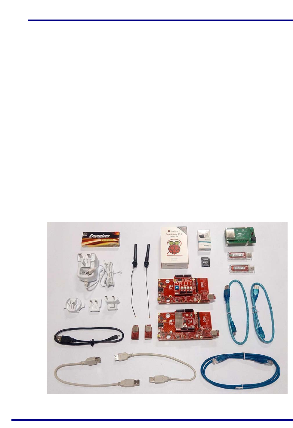
1.1 Kit Contents
The JN517x-DK005 Development Kit contains the hardware components required to
assemble a wireless network which may be connected to an IP-based network (such
as the Internet). The principal network components included in the kit are:
Carrier Boards which host a JN5179 module and which can be fitted with the
supplied Expansion Boards (see below) to achieve the desired functionality -
they are fitted with NFC tags that can be read using the supplied NFC reader
Expansion Boards which can be mounted on the Carrier Boards in order to
provide them with the required functionality: Lighting/Sensor or Generic
Modules including the JN5179 standard-power modules pre-fitted to the
Carrier Boards and JN5179 high-power modules (for use in territories where
the local RF regulations allow)
Dongles including JN5179 USB Dongles (featuring the JN5179 wireless
microcontroller) and a Wi-Fi adaptor for the Raspberry Pi board (see below)
Raspberry Pi 2 Computer which, together with a JN5179 USB Dongle, forms
an IoT Gateway that allows the wireless network to be connected to an IP-
based network, including the Internet.
NFC Controller Board which connects to the Raspberry Pi board and can be
used to read the NFC tags on the Carrier Boards to implement NFC
commissioning
The contents of the kit are shown in the photograph below.
Figure 1: JN517x-DK005 Development Kit
2
3
4a
5
6
7
8
9
10
11
12
13
14
4b

JN517x-DK005 Development Kit
User Guide
JN-UG-3121 v1.1 © NXP Semiconductors 2017 11
The full contents of the kit are listed below (numbers refer to Figure 1 above).
1. Raspberry Pi 2 single-board computer (Model B) and microSD card (Note a)
2. Wi-Pi Raspberry Pi 802.11n wireless adaptor (for Wi-Fi connectivity)
3. 2 JN5179 USB Dongles with integrated antenna (Note b)
4. 2 Carrier Boards with integrated NFC tags:
4a. One pre-fitted with a Generic Expansion Board and a
JN5179 standard-power module with integrated antenna (Note b)
4b. One pre-fitted with a Lighting/Sensor Expansion Board and a
JN5179 standard-power module with integrated antenna (Note b)
5. 2 JN5179 high-power modules (Note c)
6. 2 antennas with fly-leads for JN5179 modules with uFL connectors
7. PN7120 NFC Controller Board with Raspberry Pi Interface Board
8. 5V DC power supply unit (universal type) with USB ports for Raspberry Pi
9. ‘USB to Micro USB’ cable (for powering Raspberry Pi from 5V PSU)
10. 2 'USB to USB' extension cables (for use with Wi-Pi adaptor and USB dongle)
11. 2 'USB A to Mini B' cables
12. RJ45 Ethernet cable
13. microSD card adaptor
14. Pack of 10 AAA batteries
Notes:
a) The Raspberry Pi 2 board’s microSD card is programmed with NXP firmware (an adaptor is
provided to allow re-programming of the microSD card from a PC).
b) The pre-fitted JN5179 modules and the JN5179 USB Dongle with a green sticker are pre-
programmed with the relevant binaries for the ZigBee Smart Home Demonstration. The
JN5179 USB Dongle with a red sticker is pre-programmed as a packet sniffer.
c) The JN5179 high-power modules provide an RF output of +20dBm (compared with the
+10dBm of a standard-power module) and can only be used in territories where the RF
regulations allow them.
For more details on the hardware components of the kit, refer to Appendix A.
Additional Nodes (Available Separately)
JN517x-XK030 Generic Node Expansion Kit: Carrier Board with a Generic
Expansion Board and JN5179 module with integrated antenna
JN517x-XK040 Lighting/Sensor Node Expansion Kit: Carrier Board with a
Lighting/Sensor Expansion Board and JN5179 module with integrated antenna
JN5179 USB Dongle (OM15021): Pre-programmed as a packet sniffer
Chapter 1
Introduction to the Development Kit
12 © NXP Semiconductors 2017 JN-UG-3121 v1.1
1.2 Wireless Network Fundamentals
This section covers the basic concepts that are relevant to the wireless network
protocols supported by the JN517x-DK005 Development Kit, notably IEEE 802.15.4
and ZigBee PRO (which is itself built on IEEE 802.15.4) used in the ZigBee 3.0
standard. For a more complete introduction to wireless networks, refer to the manual
for the relevant protocol (see Section 3.3).
The topics covered are:
Radio frequency - see Section 1.2.1
Network identification - see Section 1.2.2
Node types - see Section 1.2.3
Network formation and topology - see Section 1.2.4
Wireless network protocol stacks - Section 1.2.5
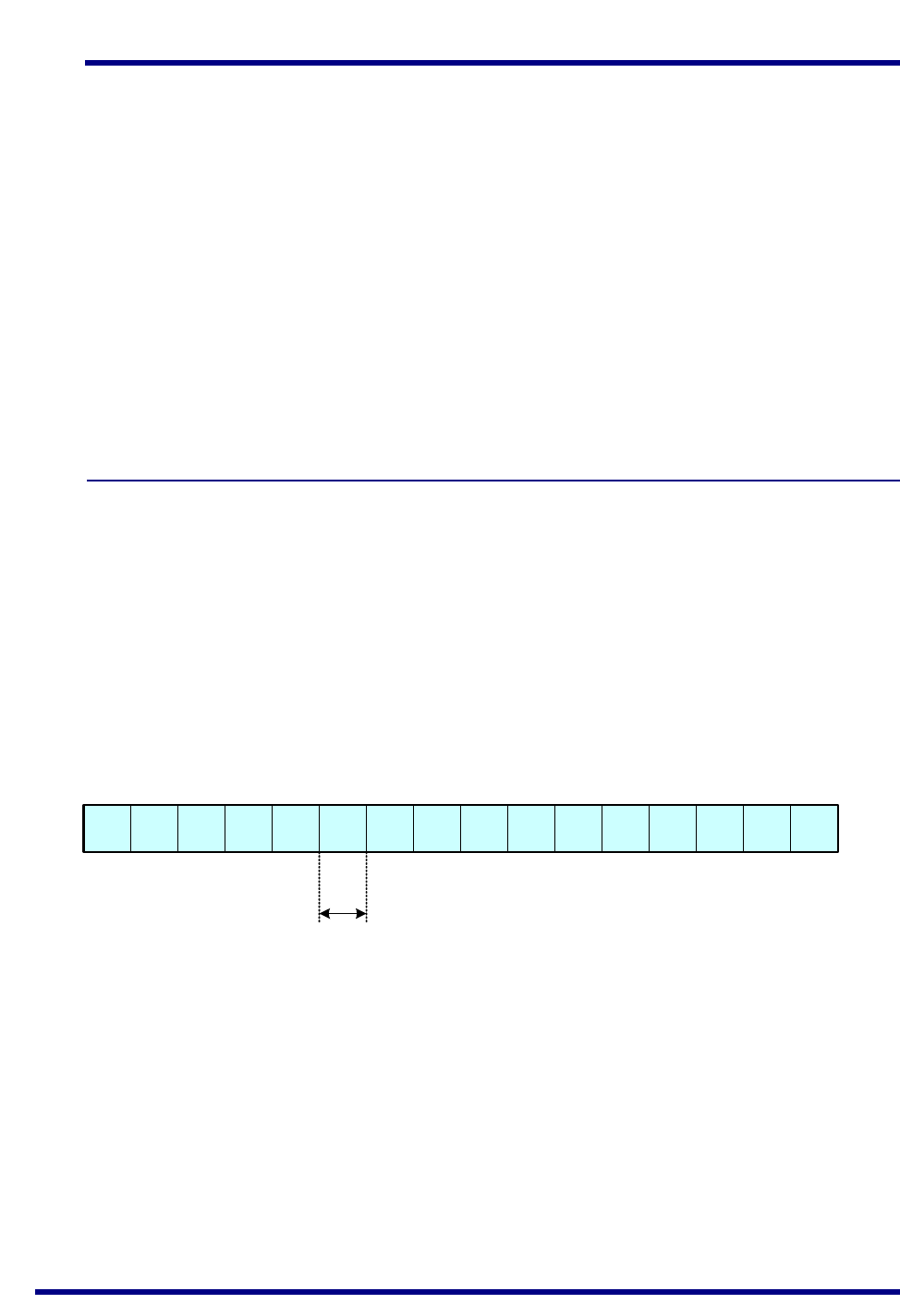
1.2.1 Radio Frequency
The JN5179-based devices of the development kit communicate in the 2400-MHz
radio frequency (RF) band. This is one of the standard RF bands used by the IEEE
802.15.4 wireless network protocol (on which all the supported protocols are based),
and is available for unlicensed use in most geographical areas (check your local radio
communication regulations).
The 2400-MHz band spans radio frequencies 2400 to 2483.5 MHz and is divided into
16 channels, numbered 11 to 26 (the numbers up to 10 are used for other RF bands)
- see Figure 2 below.
The channel of operation for a network can be specified by the application or,
alternatively, the network can search for the best channel (the one with least detected
activity) at system start-up.
Figure 2: 2400-MHz RF Band
2400 MHz 2483.5 MHz
Ch11 Ch12 Ch26Ch13 .....
5 MHz
JN517x-DK005 Development Kit
User Guide
JN-UG-3121 v1.1 © NXP Semiconductors 2017 13
1.2.2 Network Identification
A wireless network must have a unique identifier which allows it to be distinguished
from other networks in the same operating neighbourhood. IEEE 802.15.4-based
protocols use a 16-bit value called the PAN ID. This identifier can be pre-defined in the
user application or chosen by the PAN Co-ordinator which creates the network (see
Section 1.2.3), but it must not clash with the PAN ID of a neighbouring network.
A wireless network protocol may also use its own network identifier (in addition to the
PAN ID) - for example, in the ZigBee PRO protocol, a 64-bit Extended PAN ID (EPID)
is also used.
1.2.3 Node Types
In addition to running an application (e.g. temperature measurement), each node of a
wireless network has a networking role. Most IEEE 802.15.4-based networks can
contain three types of node differentiated by their networking roles, as follows:
Node Type Description
Co-ordinator A wireless network has one and only one Co-ordinator, or PAN Co-ordinator. This
node has a role in starting and forming the network, and can also have a routing role
(passes messages from one node to another). Messages can also originate and
terminate here.
Router This node passes messages from one node to another. Messages can also originate
and/or terminate at a Router. This node type is also sometimes referred to as a Local
Co-ordinator.
End Device This node is simply a place where messages can originate and/or terminate (the
node does not have a routing role). In order to conserve power, an End Device can
sleep when it is not required to be active.
Table 1: Node Types in a Wireless Network
Chapter 1
Introduction to the Development Kit
14 © NXP Semiconductors 2017 JN-UG-3121 v1.1
1.2.4 Network Formation and Topology
A wireless network is formed as follows:
1. The first node to be started is the Co-ordinator, which performs network
initialisation including the selection of the radio channel in which the network
will operate (see Section 1.2.1) and the PAN ID of the network (see Section
1.2.2).
2. Once the initialisation is complete, the Co-ordinator allows other nodes to join
it as its ‘children’ - the Co-ordinator is referred to as a ‘parent’. These child
nodes can be Routers and/or End Devices.
3. Each Router may itself become a parent by allowing child nodes to join it
(which may themselves be Routers and/or End Devices). In this way, the
network grows.
A number of network shapes or topologies are possible, which are dependent on the
wireless network protocol used. These are the Star, Tree and Mesh topologies,
described in the sub-sections below.
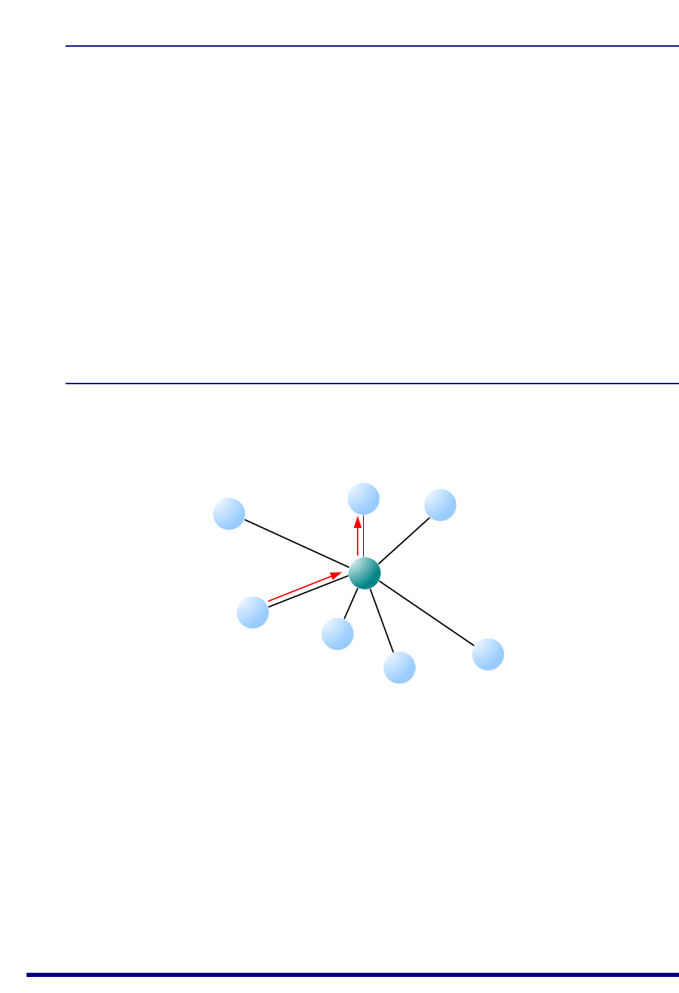
1.2.4.1 Star Networks
A Star network contains only one routing node, which is the Co-ordinator. Thus, all
messages between the network nodes are routed via the central Co-ordinator.
Figure 3: Star Network
Co-ordinator
JN517x-DK005 Development Kit
User Guide
JN-UG-3121 v1.1 © NXP Semiconductors 2017 15
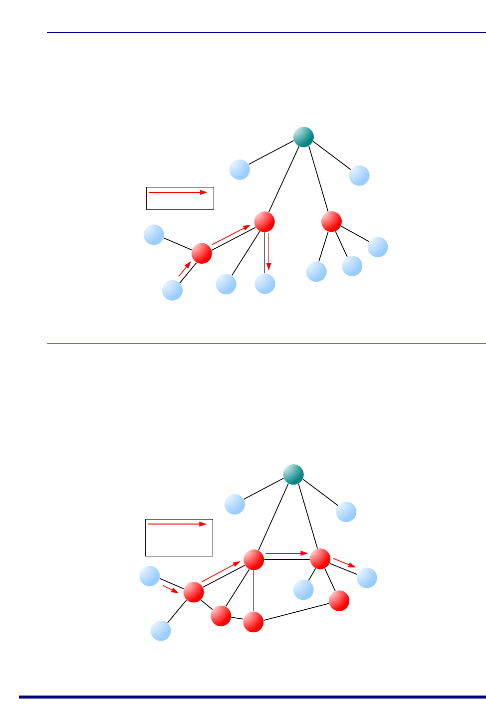
1.2.4.2 Tree Networks
A Tree network may contain the full range of node types - Co-ordinator, Routers and
End Devices - with the Co-ordinator at the top of the (inverted) tree. Any node can only
communicate directly with its parent and children (if any). Thus, a message for a
remote node must be passed up the tree until it can passed down to its destination.
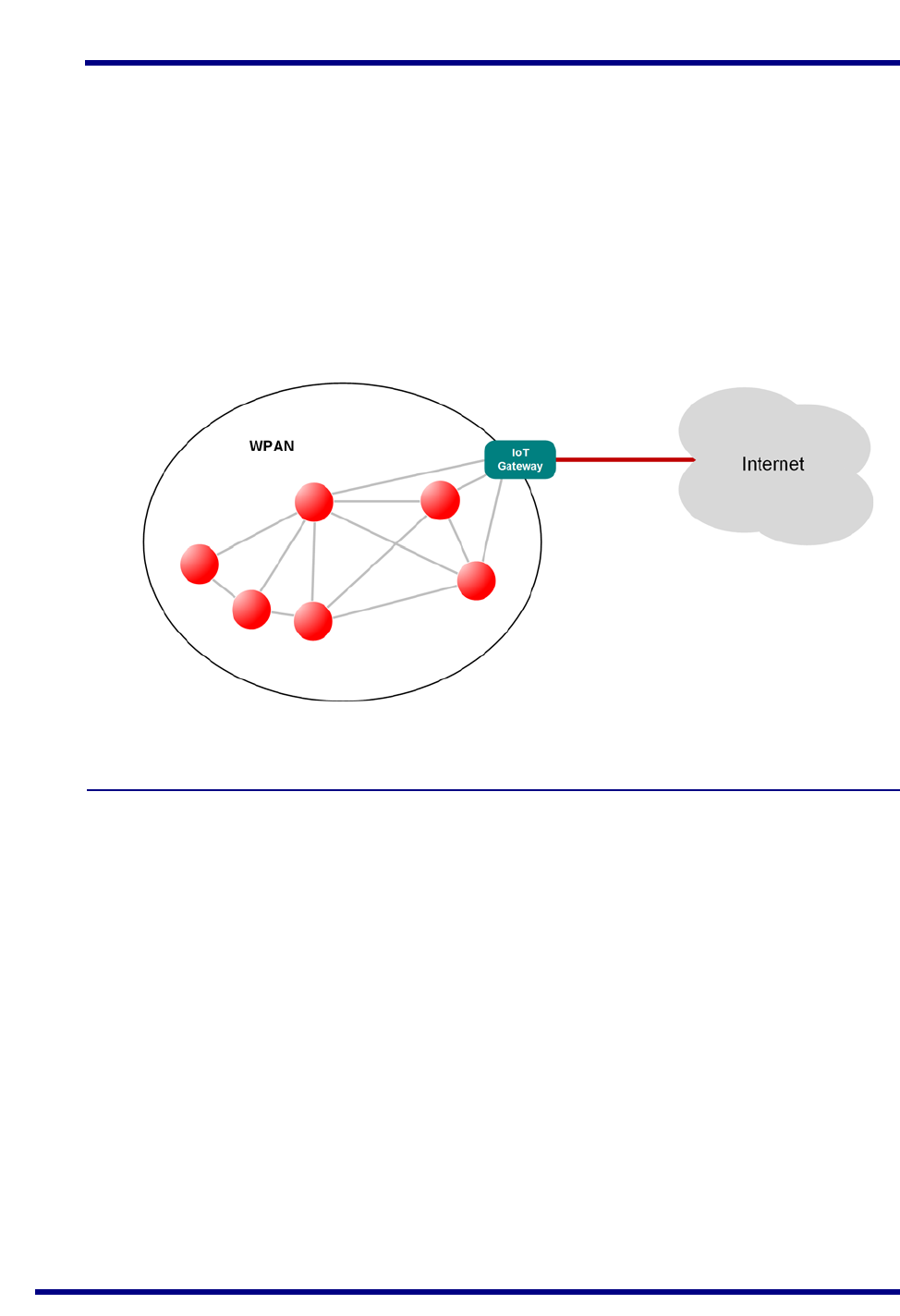
1.2.4.3 Mesh Networks
A Mesh network may contain the full range of node types - Co-ordinator, Routers and
End Devices. Any routing node (Router or Co-ordinator) can communicate directly
with any other routing node within radio range. However, an End Device can only
communicate directly with its parent. When sending a message between two nodes
that cannot communicate directly, the message is routed via intermediate routing
nodes (for which there may be more than one possible route).
Figure 4: Tree Network
Figure 5: Mesh Topology
Indicates route taken by
message
Indicates route taken by
message, although a
number of alternative
routes are available

Chapter 1
Introduction to the Development Kit
16 © NXP Semiconductors 2017 JN-UG-3121 v1.1
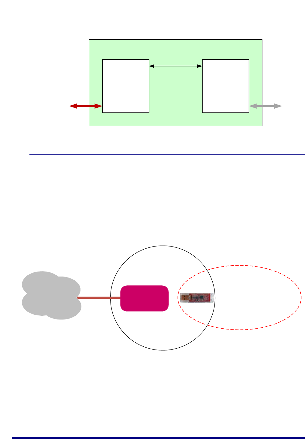
1.2.5 Wireless Network Protocol Stack
The software which runs on a wireless network node deals with both application-
specific tasks (e.g. temperature measurement) and networking tasks (e.g. assembling
a message to send to another node). The software on a node is organised as a
number of layers, forming a stack, with the user application at the top. The basic layers
of a wireless network protocol stack are typically as illustrated in Figure 6 below.
The stack layers are outlined below, from top to bottom:
Application layer: Contains the user applications which run on the network
node and provides an interface to the lower layers
Network layer: Provides the networking functionality and an interface to the
IEEE 802.15.4 layers (see below) - for example, this layer could be provided by
the ZigBee PRO protocol, but is not required for a pure IEEE 802.15.4 network
Data Link layer: Provided by the MAC (Media Access Control) layer of the
IEEE 802.15.4 standard, and responsible for message assembly/disassembly
and addressing (e.g. specifying the destination of outgoing messages)
Physical layer: Provided by the PHY (Physical) layer of the IEEE 802.15.4
standard and concerned with interfacing to the physical transmission medium
(radio, in this case)
A number of C APIs (Application Programming Interfaces) are provided to allow a user
application to easily interact with the layers of the stack. The required APIs depend on
the protocol used (e.g. IEEE 802.15.4, ZigBee PRO) and are supplied in the relevant
NXP Software Developer’s Kit (SDK) - see Section 3.1.
The software components that implement the Data Link and Physical layers of the
stack are pre-programmed in on-chip ROM. The user application is developed and
built on a PC. The resulting application binary file also incorporates the Network layer
of the stack and is loaded into the Flash memory of the node.
In order to use the ZigBee Smart Home Demonstration that is pre-loaded in the
JN517x-DK005 Development Kit boards, no knowledge of the protocol software is
required. However, you should familiarise yourself with the software for your chosen
protocol before starting your own application development - refer to Section 3.3 for
details of the user documentation for the different protocols.
Figure 6: Basic Layers of Stack
Data Link layer
Network layer
Application layer
Physical layer
JN517x-DK005 Development Kit
User Guide
JN-UG-3121 v1.1 © NXP Semiconductors 2017 17
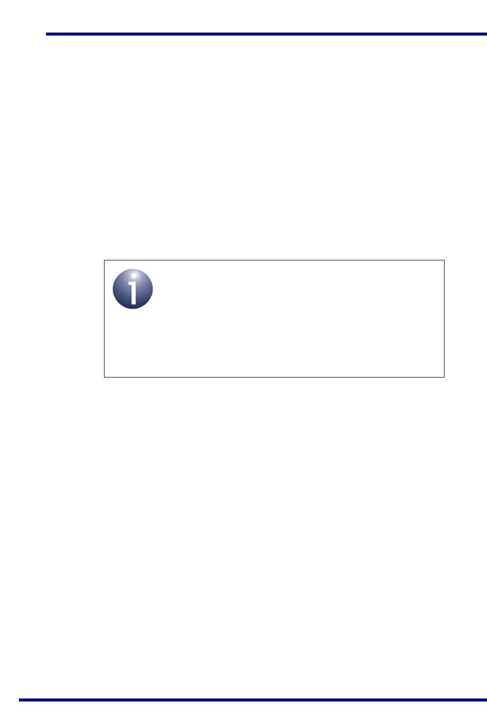
1.3 Internet of Things (IoT)
The ‘Internet of Things’ (IoT) refers to the concept of electrical devices being
connected via the Internet, irrespective of their basic functionality. This allows the
devices to be remotely controlled and monitored from other devices on the Internet -
for example, from a PC, tablet or smart phone.
The IoT idea includes the possibility of connecting a WPAN, such as a ZigBee
network, to the Internet. In this case, the WPAN may have a single connection to the
Internet shared by all the nodes of the network, but the nodes will be individually
accessible from the Internet. The Internet connection for a WPAN is provided by a
device called an IoT Gateway. A basic system is shown in Figure 7 below.
1.3.1 IoT Gateway
The IoT Gateway allows commands and data to be passed between the Internet and
WPAN domains, in both directions. The device runs a protocol stack for each of its two
sides, which are as follows:
IP Host: This side runs an IP stack to send/receive data packets to/from the
Internet - this is normally an IPv6 stack.
Control Bridge: This side runs a wireless network protocol stack to send/
receive data packets to/from the WPAN - this may be an IEEE 802.15.4-based
stack, such as the ZigBee PRO stack. This part of the Gateway usually acts as
a WPAN node, such as a Co-ordinator or Router.
The two stacks are connected within the IoT Gateway. The basic architecture of an
IoT Gateway is illustrated in Figure 8 below.
Figure 7: WPAN Connected to IoT
Chapter 1
Introduction to the Development Kit
18 © NXP Semiconductors 2017 JN-UG-3121 v1.1
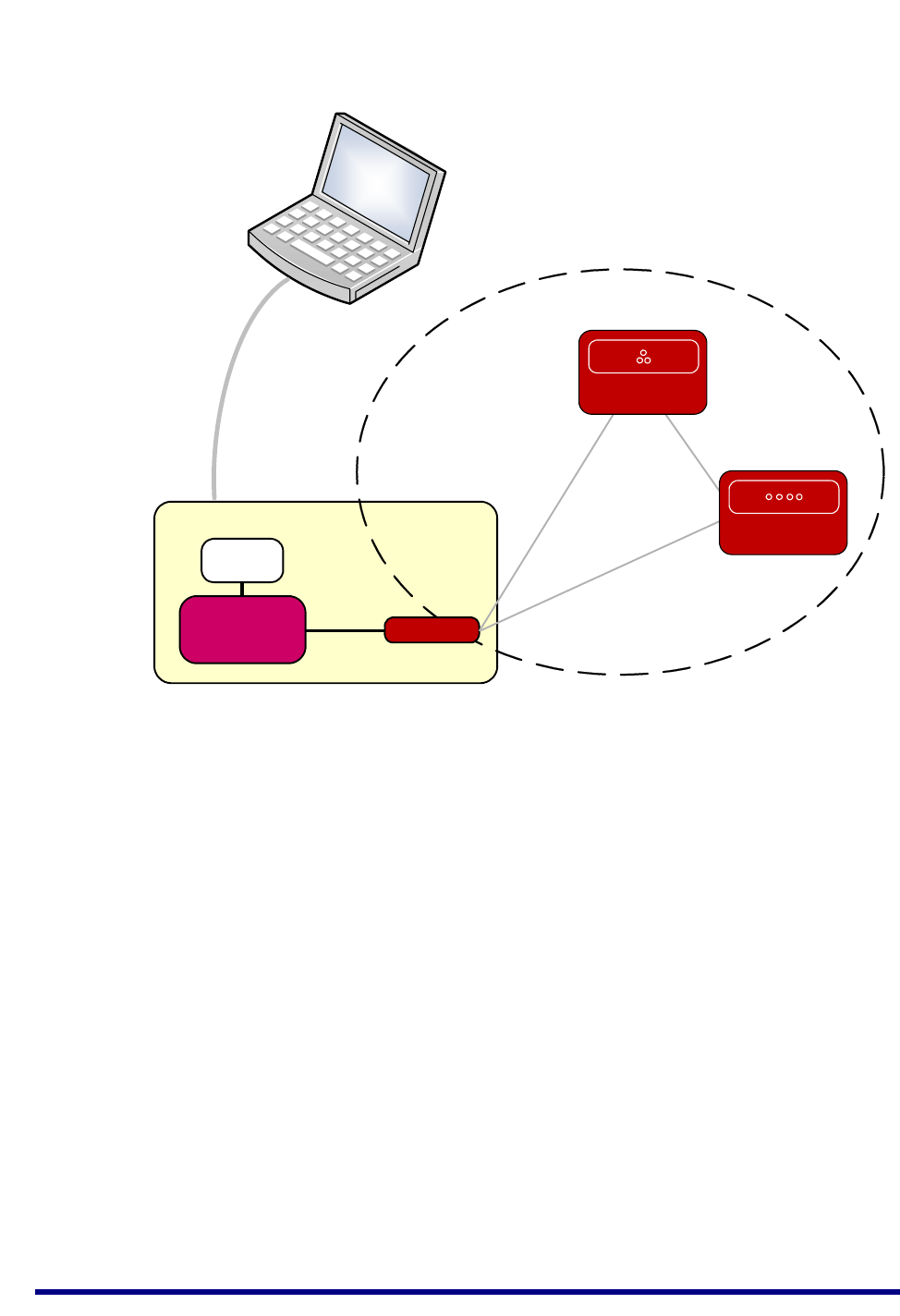
1.3.2 IP Connectivity of the Kit
In the JN517x-DK005 Development Kit, an IoT Gateway can be formed from the
Raspberry Pi board together with a JN5179 USB Dongle:
The Raspberry Pi provides the IP Host, interfacing to the IP domain
The JN5179 USB Dongle provides the Control Bridge, interfacing to the WPAN,
and also acts as the WPAN Co-ordinator
This IoT Gateway implementation is illustrated in Figure 9 below.
The Raspberry Pi microSD card is pre-programmed with NXP firmware which allows
the IP Host to operate in conjunction with a ZigBee Control Bridge. The JN5179 USB
Dongle with a green sticker is pre-programmed with firmware for a ZigBee Control
Bridge and Co-ordinator.
Figure 8: Basic Architecture of an IoT Gateway
Figure 9: IoT Gateway Implementation
IP Stack
Wireless
Network
Protocol
Stack
IP Host Control Bridge
To/from
Internet To/from
WPAN
+WPAN
Raspberry Pi
LAN
IoT Gateway

JN517x-DK005 Development Kit
User Guide
JN-UG-3121 v1.1 © NXP Semiconductors 2017 19
The JN5179 USB Dongle can be plugged into any USB port of the Raspberry Pi. In
the case where the IP connection will be provided via Wi-Fi, the supplied Wi-Pi adaptor
must be plugged into another USB port of the Raspberry Pi (the Wi-Pi adaptor creates
its own Wi-Fi network). If both the dongle and adaptor are required, the dongle must
be connected to a port via a USB cable to ensure isolation of the two devices.
The IP connection can be to an existing wired LAN or via a new Wi-Fi LAN:
To connect to an existing wired LAN, the supplied Ethernet cable must be used
to connect the Raspberry Pi to a router in the LAN. The LAN must include a
DHCP server to allocate an IP address to the Raspberry Pi. The DHCP leases
in the router will need to be examined in order to determine the IP address
allocated to the Raspberry Pi.
To use a Wi-Fi connection, the Wi-Pi adaptor must be plugged into the
Raspberry Pi. The Wi-Pi adaptor will create its own Wi-Fi network (rather than
join an existing Wi-Fi network). A PC can then interact with the Raspberry Pi by
joining this Wi-Fi network (which has the SSID Iot_GW_NXP). In this case, the
Raspberry Pi is allocated the fixed IP address 192.168.2.1.
The pre-programmed ZigBee Smart Home Demonstration uses a Wi-Fi connection.
1.4 Network Commissioning
A WPAN is started by the Co-ordinator and other nodes can then join the network, as
indicated in Section 1.2.4. Network commissioning may also include the following:
Network joining and subsequent network operation may employ security keys
to implement encrypted communications between nodes, to make the network
secure from malicious tampering. NFC commissioning is becoming an
important technique in establishing this security and is supported by the
JN517x-DK005 Development Kit. NFC commissioning is outlined in Section
1.4.1.
Once a node has joined a network, it may need to be linked to one or more
other nodes from a functional point-of-view. For example, when a new light is
added to a lighting network, it may be required that a particular light switch
(already in the network) is used to control the new light. There are different
ways of establishing this link and these are described in Section 1.4.2.

Chapter 1
Introduction to the Development Kit
20 © NXP Semiconductors 2017 JN-UG-3121 v1.1
1.4.1 NFC Commissioning Process
The commissioning of network nodes can be performed via Near-Field
Communications (NFC). This involves the exchange of a unique security key, through
the close proximity required by NFC, to ensure that all communications to/from the
joining node are encrypted during the commissioning process. Node commissioning
is therefore secure and cannot be conducted remotely by third parties to introduce
nodes for malicious purposes.
In its basic form, the NFC commissioning of a node to a WPAN requires the following
security keys:
Unique Link Key: An NFC tag on the node must be pre-programmed with a
link key that is unique to the node and that will be used in the commissioning
process.
Network Key: The network Co-ordinator contains a network key that is used to
encrypt all radio communications between the nodes during normal operation
of the network.
As part of the commissioning process, the network key must be communicated from
the Co-ordinator to the joining node in a secure manner, so that the node can later use
the key to encrypt and decrypt network-level communications. The commissioning
process works as follows:
1. The NFC tag of the joining node is brought close to the NFC Controller
(mounted on the Raspberry Pi board, which is itself connected to the JN5179
USB Dongle that acts as the network Co-ordinator). This action is known as
an ‘NFC tap’.
2. During this NFC tap, the NFC Controller reads the unique link key from the
NFC tag of the joining node and this key is internally passed to the
Co-ordinator.
3. During this same NFC tap, the Co-ordinator uses the unique link key to
encrypt the network key and sends it by NFC to the joining node.
4. The joining node receives the encrypted network key and decrypts it using the
unique link key.
The joining node now has the network key which allows it to subsequently participate
in secure network-level communications. Therefore, the network credentials are never
sent over the air, providing a safer method of commissioning.
The JN517x-DK005 Development Kit is equipped with the necessary components for
NFC commissioning:
The supplied Carrier Boards (see Appendix A.1) feature ‘NFC connected tags’.
A Carrier Board is the basis of a WPAN node and the NFC tag is used to join
the node to the network.
The supplied NFC Controller (see Appendix A.7) attaches to the Raspberry Pi
board. The NFC Controller is able to read data from the NFC tag of a Carrier
Board (node) as part of the secure commissioning process.
For more information on NFC commissioning, refer to the NFC Commissioning User
Guide (JN-UG-3112).

JN517x-DK005 Development Kit
User Guide
JN-UG-3121 v1.1 © NXP Semiconductors 2017 21
1.4.2 Addressing, Binding and Grouping
The available methods for establishing a functional link between a controlling node or
source node and a target node are as follows:
Direct Addressing: The source node can simply send commands to the
address of the target node. This may be the permanent 64-bit IEEE/MAC
address of the node or a 16-bit network (or short) address allocated to the node
when it joined the network.
Binding: In a ZigBee PRO network, ‘binding’ can be used to set up this link. An
application on the source node can be bound to an application on the target
node such that commands issued by the source application are always sent to
the target node without needing to specify an address. The source node can be
bound to multiple target nodes.
Grouping: In a ZigBee PRO network, ‘grouping’ can alternatively be used to
set up this link, particularly when controlling multiple target nodes
simultaneously (e.g. several lights in unison). The target nodes are collected
into a group with an associated 16-bit group address. A target node ‘knows’
which groups it belongs to - this information is held in a table on the node.
When the source node sends a command to a group address, the command is
broadcast to all nodes in the network. A receiving node is able to identify
whether it is a member of the relevant group and only the nodes in the group
react to the command.
Chapter 1
Introduction to the Development Kit
22 © NXP Semiconductors 2017 JN-UG-3121 v1.1
1.5 ZigBee Smart Home Demonstration
Certain components of the kit are pre-loaded with the software for a simple
demonstration network. Running this ZigBee Smart Home Demonstration will allow
you to use components of the kit without programming them yourself.
The demonstration is a lighting system which allows the white LEDs on a node/board
(Dimmable Light) of a WPAN to be controlled (switched on/off, brightness adjusted) in
the following ways:
From within the WPAN using the buttons on a controller node/board
(Dimmer Switch)
From outside the WPAN via an IP connection from a PC
The demonstration system is of the form shown in Figure 8 on page 18.
More detailed information and instructions on how to run the demonstration are
provided in Chapter 2.
Note 1: A Quick Start procedure for running this
demonstration is also provided on the JN517x-DK005
Getting Started sheet (JN-UG-3120), which is supplied
in the kit box.
Note 2: The demonstration applications are based on
the ZigBee 3.0 devices detailed in the Application Notes
listed in “Related Documents” on page 7.
JN517x-DK005 Development Kit
User Guide
JN-UG-3121 v1.1 © NXP Semiconductors 2017 23
2. ZigBee Smart Home Demonstration
The chapter describes how to use the contents of the JN517x-DK005 Development
Kit to set up and run the pre-loaded ZigBee Smart Home Demonstration. The
demonstration is concerned with the control of a light in a ‘Smart Home’ and has the
following features:
ZigBee wireless network: This network contains the light to be controlled, as
well as a dimmer switch that can be used to wirelessly control the light.
‘Internet of Things’ (IoT) Gateway: This device connects the ZigBee wireless
network to the IP domain, allowing the light to be controlled from a web browser
on a PC.
NFC commissioning: The formation of the ZigBee wireless network is
simplified by means of NFC commissioning, which allows a node to be joined to
the network through the simple action of an NFC tap.
2.1 Demo System Overview
This ZigBee Smart Home Demonstration is based on a ZigBee WPAN containing a
light node (Dimmable Light) that can be controlled as follows:
From within the WPAN using the buttons on a controller node (Dimmer Switch)
From a web browser on a PC located in a Wi-Fi LAN that is connected via an
IoT Gateway to the WPAN
The demonstration system is illustrated in Figure 10.
Note 1: A Quick Start procedure for running this
demonstration is provided on the JN517x-DK005
Getting Started sheet (JN-UG-3120), which is supplied
in the kit box.
Note 2: This demonstration is based on the ZigBee 3.0
protocol with Lighting & Occupancy devices.
Note 3: The demonstration applications are based on
the ZigBee 3.0 devices detailed in the Application Notes
listed in “Related Documents” on page 7.
Chapter 2
ZigBee Smart Home Demonstration
24 © NXP Semiconductors 2017 JN-UG-3121 v1.1
The system is made up from components of the development kit as follows:
Dimmable Light:
Carrier Board with JN5179 module
Lighting/Sensor Expansion Board, providing the LEDs
Dimmer Switch:
Carrier Board with JN5179 module
Generic Expansion Board, providing the control buttons
IoT Gateway:
Raspberry Pi 2 board
Wi-Pi adaptor, providing the Wi-Fi connection (and DHCP server)
JN5179 USB Dongle, acting as the ZigBee Co-ordinator and providing the
connection to the WPAN
NFC Controller Board, providing NFC commissioning
The Dimmable Light and Dimmer Switch nodes both act as ZigBee Routers.
Figure 10: ZigBee Smart Home Demonstration System
USB Dongle
ZigBee PRO WPAN
IoT Gateway
Co-ordinator
USB
Raspberry Pi
Wi-Pi
Adaptor
Wi-Fi
PC
Control commands issued
from web browser
Carrier Board
Carrier Board
Dimmer Switch
Dimmable Light
JN517x-DK005 Development Kit
User Guide
JN-UG-3121 v1.1 © NXP Semiconductors 2017 25
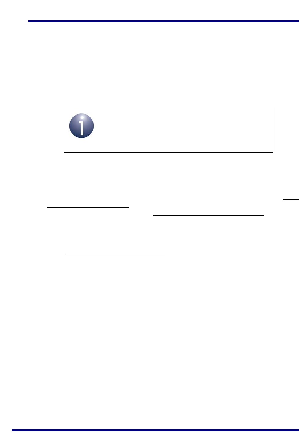
2.2 Setting Up the IoT Gateway
This section describes how to set up the IoT Gateway for the ZigBee Smart Home
Demonstration. As detailed in Section 2.1, the IoT Gateway comprises:
Raspberry Pi 2 board
Wi-Pi adaptor
JN5179 USB Dongle (with a green sticker)
NFC Controller
Step 1 Ensure that the PC is up and running
If not already done, power-up the PC and wait for the boot process to complete.
Step 2 Connect the Wi-Pi adaptor to the Raspberry Pi board
Plug the supplied Wi-Pi adaptor into any USB socket of the Raspberry Pi board via a
supplied USB-to-USB cable (use of this cable ensures that the adaptor will be isolated
from the JN5179 USB Dongle), but do not power-up the Raspberry Pi yet.
Step 3 Connect the JN5179 USB Dongle to the Raspberry Pi board
Connect the JN5179 USB Dongle with a green sticker (this dongle is programmed as
a Control Bridge and ZigBee Co-ordinator) to any USB socket of the Raspberry Pi
board via a supplied USB-to-USB cable (use of this cable ensures that the dongle is
isolated from the Wi-Pi adaptor).
Also check that the pre-installed microSD card is securely fitted to the Raspberry Pi.
Step 4 Mount the NFC Controller onto the Raspberry Pi board
Install the NXP PN7120 NFC Controller assembly (NFC Controller Board pre-mounted
on a Raspberry Pi Interface Board) on the Raspberry Pi board. For information on the
NFC Controller and related documentation, refer to Appendix A.7. If in doubt about this
installation, refer to the PN7120 NFC Controller SBC Kit Quick Start Guide (AN11646)
- note that the supplied Raspberry Pi 2 board is a B model.
Step 5 Connect the Raspberry Pi board to a power supply
Power-up the Raspberry Pi board (and therefore IoT Gateway) by connecting it to a
power supply. To do this, connect the supplied 5V DC PSU to the mains supply and
then use the ‘USB to Micro USB’ cable to connect the Raspberry Pi board to a USB
port on the PSU.
Step 6 Position the Gateway components with sufficient distance between them
For radio certification compliancy, make sure there is at least 20 cm between the USB
dongle and Wi-Pi adaptor, and between these components and the Raspberry Pi.
Also, position the dongle and adaptor roughly perpendicular to each other.
Note: The IoT Gateway is fully detailed in the
Application Notes ZigBee IoT Gateway Host with NFC
(JN-AN-1222) and ZigBee IoT Gateway Control Bridge
(JN-AN-1223).
Chapter 2
ZigBee Smart Home Demonstration
26 © NXP Semiconductors 2017 JN-UG-3121 v1.1
The equipment should now be as shown below.
Step 7 Wait for the IoT Gateway to start up
Wait about 20 seconds for the IoT Gateway to boot. During the boot process, the
following will occur:
a) The red LED on the Raspberry Pi board will illuminate.
b) The green LED on the Raspberry Pi board will flash.
c) After around 20 seconds, an audible beep will be sounded by the Raspberry Pi.
The IoT Gateway is then ready. When in this state, the green LED on the NFC
Controller board flashes.
The Wi-Pi adaptor will have created a Wi-Fi network (initially consisting of only itself).
JN517x-DK005 Development Kit
User Guide
JN-UG-3121 v1.1 © NXP Semiconductors 2017 27
Step 8 Direct a web browser on the PC to the IoT Gateway
a) Connect the PC to the ZigBee network via the IoT Gateway by specifying the
SSID (name) of the network, which is Iot_GW_NXP.
b) Direct a web browser on the PC to the IoT Gateway’s web interface using either
the default IP address 192.168.2.1 or the URL http://iot-gw.nxp.
The first page of the interface displayed in the browser is the “Controls” tab (shown in
the next step).
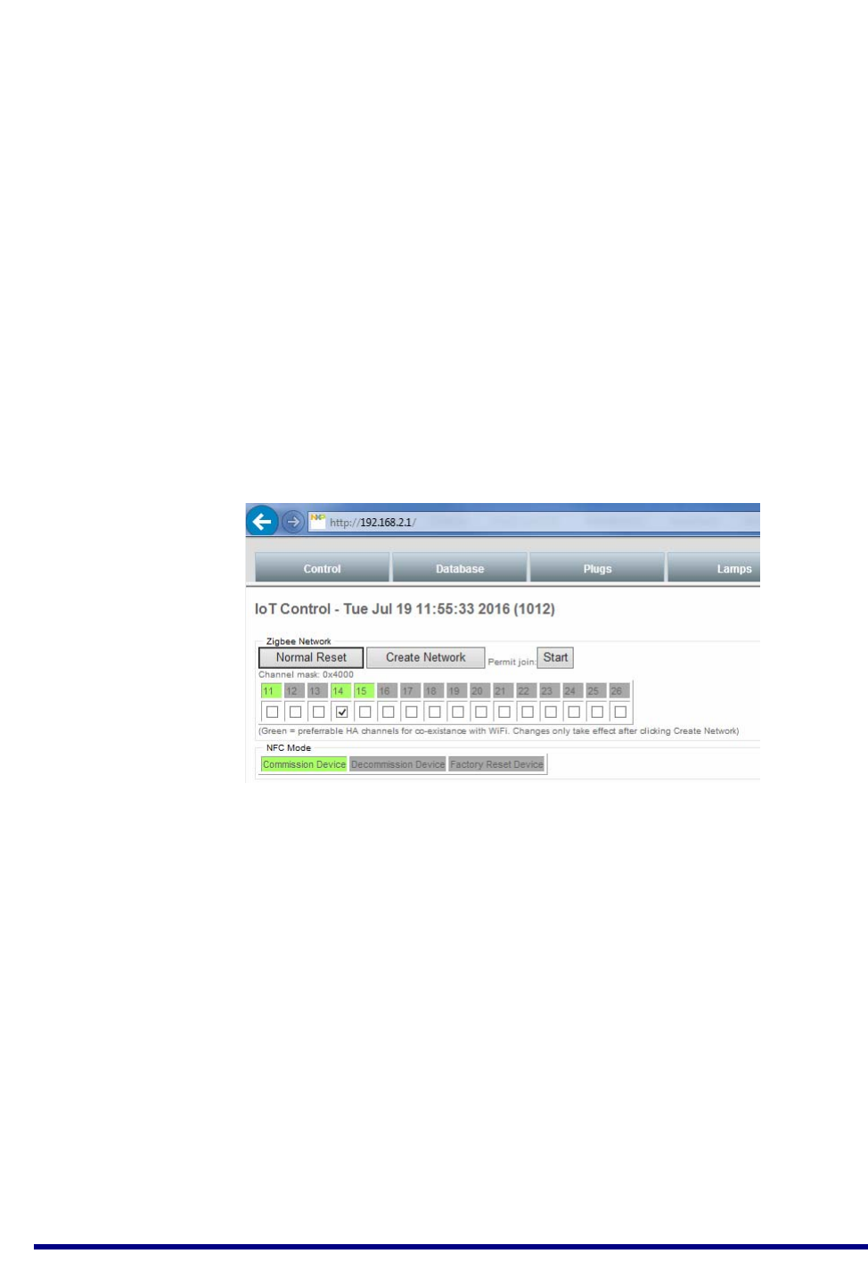
Step 9 Select a ZigBee network channel and create a network
This step is needed only the first time the demonstration is used.
On the Control tab of the IoT Gateway interface, do the following in the ZigBee
Network area:
a) Set the radio channel to be used in the ZigBee network to channel 14 by clicking
(ticking) the box labelled “14”.
b) Create the ZigBee network (initially containing only the Co-ordinator) by clicking
the Create Network button.
The ZigBee network will be created on channel 14. A successful network start will be
indicated by the illumination of the green and orange LEDs on the JN5179 USB
Dongle.
You can now add further nodes to the network using NFC commissioning, as
described in Section 2.3.
Chapter 2
ZigBee Smart Home Demonstration
28 © NXP Semiconductors 2017 JN-UG-3121 v1.1
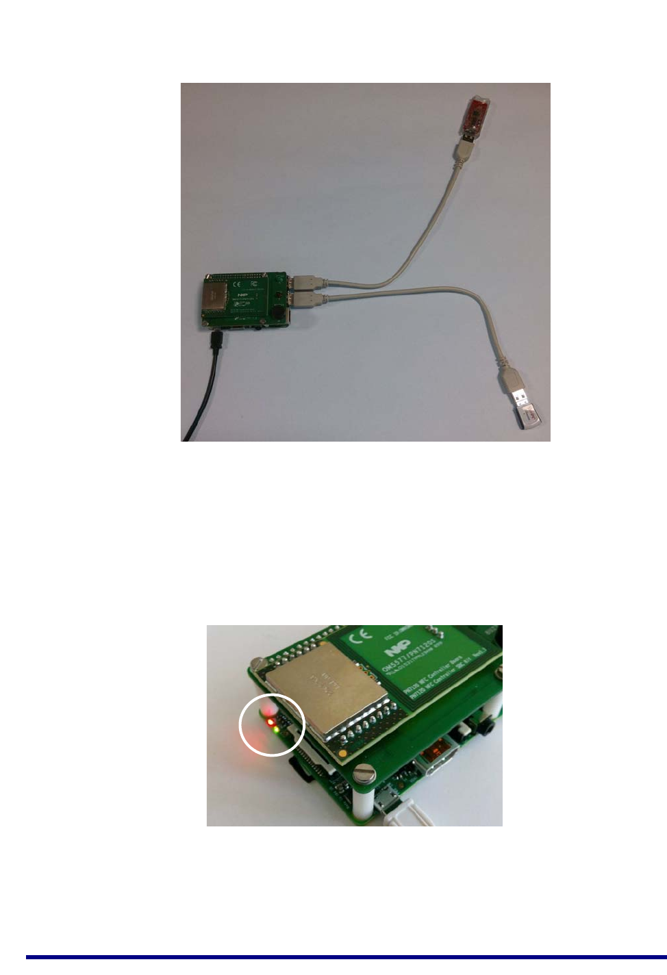
2.3 Commissioning Nodes
This section describes how to complete the set-up of the ZigBee Smart Home
Demonstration by adding nodes to the ZigBee network by means of NFC
commissioning.
You will add two nodes to the network already established by the Co-ordinator
(JN5179 USB Dongle):
Dimmable Light
Dimmer Switch
These nodes are made up from components of the kit, as detailed in Section 2.1.
The NFC commissioning of each node into the ZigBee network is identical. It is
performed by simply holding the NFC antenna of the node’s Carrier Board (see
Appendix A.1) above the NFC antenna of the NFC Controller (mounted on the
Raspberry Pi board) while the Raspberry Pi is in commissioning mode - this action is
known as an ‘NFC tap’ and is shown in Figure 11. An audible signal is sounded if the
NFC communication between the two devices was successful, after which the node
will join the ZigBee network.
Note: This section assumes that you have set up the
IoT Gateway as detailed in Section 2.2.
Figure 11: NFC Tap
JN517x-DK005 Development Kit
User Guide
JN-UG-3121 v1.1 © NXP Semiconductors 2017 29
The commissioning procedure is described below.
Step 1 Ensure that the WPAN is open for joining
Before continuing with this procedure, make sure that the Co-ordinator has created a
WPAN that is open for joining, indicated by illuminated green and orange LEDs on the
JN5179 USB Dongle.
If the above LEDs are not illuminated, perform a reset by clicking the Normal Reset
button on the Control page of the IoT Gateway interface in the web browser.
Step 2 Ensure that the Raspberry Pi is in commissioning mode
On the Control page of the IoT Gateway interface in the web browser, ensure that the
NFC mode is set to Commission Device (which should be highlighted in green).
Step 3 Power-up the Dimmer Switch node
First ensure that the batteries have been selected as the power source for the Carrier
Board of the Dimmer Switch node, with the jumper JP1 in the BAT position (as
described in Appendix A.1.1). Then insert four of the supplied AAA batteries onto the
rear of the Carrier Board.
Step 4 Commission the Dimmer Switch node into the network
Move the NFC antenna of the Dimmer Switch node over the NFC antenna of the NFC
Controller Board, as shown in Figure 11. If data is successfully exchanged in this NFC
tap, the Raspberry Pi board will sound a long beep.
An unsuccessful NFC tap will be indicated by four short beeps. In this case, click the
Decommission Device button on the Control page of the IoT Gateway interface and
repeat the NFC tap (successful decommissioning is indicated by two beeps), then
click the Commission Device button and repeat this step.
Caution: In performing an NFC tap, do not allow the
components to get close enough to short the pins on the
bottom of the Carrier Board to the metal screening
shield of the NFC board.
Note 1: If at any stage you need to factory-reset a node,
hold down the GPIO4 button, then press the RESET
button and then release GPIO4, where both buttons are
on the Carrier Board.
Note 2: If a node has previously been used, it will retain
settings (e.g. PAN ID) from the previous network to
which it belonged. To clear this information and return to
the factory settings, perform a factory-reset as
described above.
Chapter 2
ZigBee Smart Home Demonstration
30 © NXP Semiconductors 2017 JN-UG-3121 v1.1
During NFC commissioning, all network-related information and a join command are
transferred from the IoT Gateway to the joining node. Therefore, after NFC
commissioning, the node automatically joins the ZigBee network.
Step 5 Power-up the Dimmable Light node
First ensure that the batteries have been selected as the power source for the Carrier
Board of the Dimmable Light node, with the jumper JP1 in the BAT position (as
described in Appendix A.1.1). Then insert four of the supplied AAA batteries onto the
rear of the Carrier Board (the required polarities are indicated on the board).
Step 6 Commission the Dimmable Light node into the network
Move the NFC antenna of the Dimmable Light node over the NFC antenna of the NFC
Controller Board, as shown in Figure 11. If data is successfully exchanged in this NFC
tap, the Raspberry Pi board will sound a long beep.
An unsuccessful NFC tap will be indicated by four short beeps. In this case, click the
Decommission Device button on the Control page of the IoT Gateway interface and
repeat the NFC tap (successful decommissioning is indicated by two beeps), then
click the Commission Device button and repeat this step.
The Dimmable Light node will now automatically join the network and the three white
LEDs on the node’s Lighting/Sensor Expansion Board will flash once.
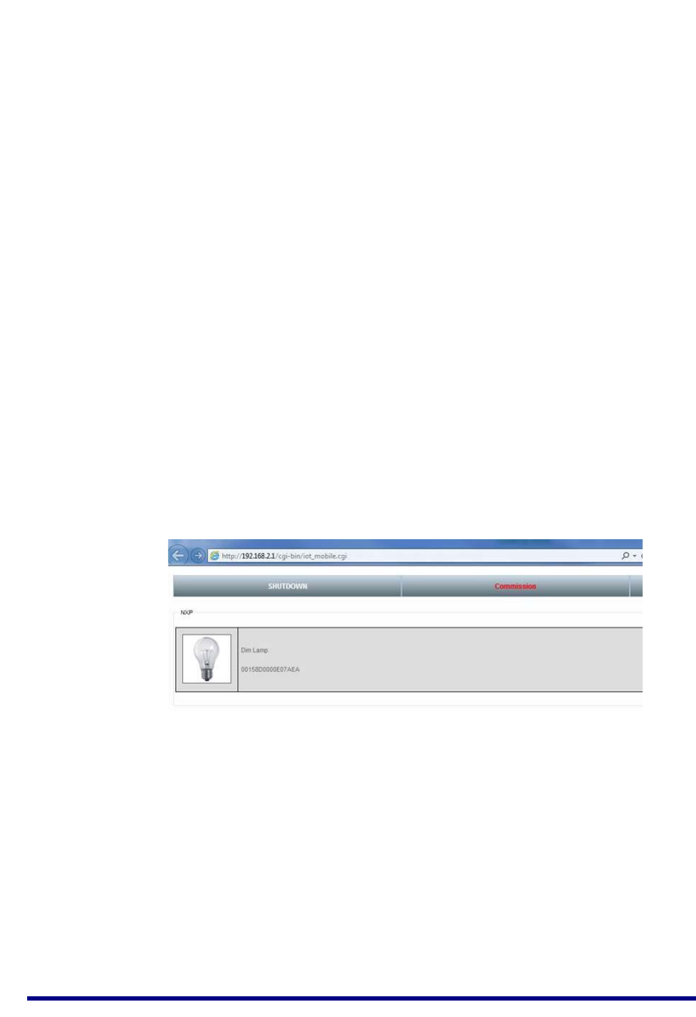
Step 7 Check that the Dimmable Light has appeared in the web browser on the PC
In the web browser on the PC, go to the “Mobile Site” tab by clicking the Mobile Site
button (right-most button across the top) and check that the Dimmable Light appears
on the page - the light will be identified by its IEEE/MAC address.
JN517x-DK005 Development Kit
User Guide
JN-UG-3121 v1.1 © NXP Semiconductors 2017 31
Step 8 Bind the Dimmer Switch to the Dimmable Light
It is now possible to bind the Dimmer Switch to the Dimmable Light (so that they will
operate together).
To bind the Dimmer Switch to the Dimmable Light:
a) Press and release the Commissioning button (GPIO4) on the Carrier Board of the
Dimmable Light node. The three white LEDs on the Lighting/Sensor Expansion
Board will flash.
b) Press and hold down the Commissioning button (GPIO4) on the Carrier Board of
the Dimmer Switch node.
c) Press and hold down the SW2 button on the Generic Expansion Board of the
Dimmer Switch node for up to 10 seconds (or longer) until the three white LEDs
stop flashing on the Lighting/Sensor Expansion Board of the Dimmable Light
node. If these LEDs fail to stop flashing, press the RESET button on the Carrier
Board of the Dimmable Light node and restart the procedure from Step 8a
(above).
d) Release the button GPIO4 on the Dimmer Switch node.
e) Repeat sub-steps 8a to 8d above but pressing button SW3 instead of SW2 on the
Dimmer Switch node.
The Dimmer Switch is now in Control mode and can be used to control the Dimmable
Light, as described in Section 2.4.
Note: If you wish to unbind the two nodes, you can do
this from the Carrier Board of the Dimmer Switch node,
as follows: press and hold down the RESET button,
then press and hold down the GPIO4 button, then
release the RESET button and finally release the GPIO4
button.
Chapter 2
ZigBee Smart Home Demonstration
32 © NXP Semiconductors 2017 JN-UG-3121 v1.1
2.4 Controlling the Light
Once you have set up the ZigBee Smart Home Demonstration, as described in
Section 2.2 and Section 2.3, you can control the Dimmable Light from inside and/or
outside the ZigBee WPAN:
Control from the Dimmer Switch within the WPAN is described in Section 2.4.1
Control from a PC outside the WPAN is described in Section 2.4.2
2.4.1 Controlling the Dimmable Light from the Dimmer Switch
The Dimmer Switch node can be used to control the Dimmable Light node:
The controlled lights are the three white LEDs (D1-D3) on the Lighting/Sensor
Expansion Board.
The four buttons SW1-SW4 on the Generic Expansion Board are used to
control the lights, as follows:
Caution: The LEDs on the Lighting/Sensor Expansion
Boards are very bright at maximum intensity. To avoid
damage to your eyes, do not look into them directly for
an extended period of time.
Button Action
SW1 Switch on lights
SW2 Switch off lights
SW3 Increase brightness of lights
SW4 Decrease brightness of lights
Table 2: Button Usage on Dimmer Switch
JN517x-DK005 Development Kit
User Guide
JN-UG-3121 v1.1 © NXP Semiconductors 2017 33
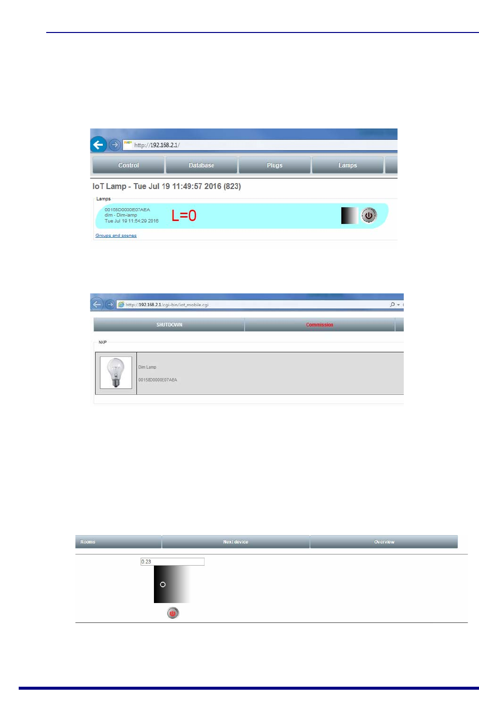
2.4.2 Controlling the Dimmable Light from the PC
The Dimmable Light within the ZigBee network can be controlled from the IoT
Gateway interface on a web browser on a PC (refer to the step “Direct a web browser
on the PC to the IoT Gateway” on page 27). The light is accessible in the interface via
the “Lamps” tab or the “Mobile Site” tab, shown below.
To control the Dimmable Light from the IoT Gateway interface:
Step 1 Access the Dimmable Light in the web browser on the PC
Select the “Lamps” or “Mobile Site” tab in the IoT Gateway interface on the PC.
If on the “Mobile Site” tab, click on the lamp icon that represents the Dimmable Light.
The following controls for the light will now be displayed:
If on the “Lamps” tab, the above controls are already displayed on the right side.
Figure 12: Dimmable Light on Lamps Tab
Figure 13: Dimmable Light on Mobile Site Tab

Chapter 2
ZigBee Smart Home Demonstration
34 © NXP Semiconductors 2017 JN-UG-3121 v1.1
Step 2 Control the light from the PC
The Dimmable Light can be controlled from the PC using the controls shown above,
as follows:
Toggle the light on and off by clicking on button.
Vary the brightness of the light by either of the following methods:
Enter a brightness level as a decimal fraction in the range 0 to 1.0 into the
numerical field.
Click on and move the widget on the greyscale background to the desired
brightness level.

JN517x-DK005 Development Kit
User Guide
JN-UG-3121 v1.1 © NXP Semiconductors 2017 35
3. Where Next?
Once you have set up and run the pre-loaded ZigBee Smart Home Demonstration,
you may wish to start developing your own wireless network applications to run on the
components of the JN517x-DK005 Development Kit. This chapter helps you to get
started in this application development, as follows:
Section 3.1 provides information on the wireless network protocols supported
for JN517x application development on the development kit components.
Section 3.2 outlines the NXP Software Developer’s Kits (SDKs) that are
available to support application development using the different protocols.
Section 3.3 directs you to the support resources for each protocol, including
User Guides and Application Notes.
3.1 Which Protocol?
The JN517x-DK005 Development Kit supports the following wireless network
protocols that can be used to develop applications for the JN517x wireless
microcontroller:
IEEE 802.15.4: This is an industry-standard protocol which provides the low-
level functionality for implementing wireless network communications. APIs are
provided to facilitate interactions between the application and IEEE 802.15.4
stack layers. Developing an application directly on top of IEEE 802.15.4
requires lower level programming than using a protocol (such as ZigBee) that
provides a networking layer between the application and IEEE 802.15.4 layers.
ZigBee 3.0: This is the latest edition of the ZigBee protocol that uses the
ZigBee PRO stack, which provides a Network stack layer (over IEEE 802.15.4)
that supports Mesh networking. APIs are provided to facilitate the interaction
between the application and the ZigBee PRO stack. The NXP ZigBee 3.0
software supports the ZigBee Lighting & Occupancy (ZLO) devices.
A full range of support resources, including example applications, are available for
using the above protocols with the JN517x-DK005 Development Kit (see Section 3.3).
Chapter 3
Where Next?
36 © NXP Semiconductors 2017 JN-UG-3121 v1.1
3.2 Software Developer’s Kit (SDK)
NXP provide Software Developer’s Kits (SDKs) to facilitate the development of
JN517x wireless network applications on a PC. These SDKs include Application
Programming Interfaces (APIs) and associated resources. They are designed be used
within the NXP LPCXpresso Integrated Development Environment (IDE).
The SDK installers for the protocols supported by the kit are as follows:
JN517x IEEE 802.15.4 SDK (JN-SW-4263)
JN517x ZigBee 3.0 SDK (JN-SW-4270)
The above SDK installers can be requested free-of-charge via the NXP web site (see
“Support Resources” on page 7). LPCXpresso must be installed before the SDK - for
guidance, refer to the JN517x LPCXpresso Installation and User Guide
(JN-UG-3109).
The contents of the installers are outlined in the sub-sections below.
3.2.1 LPCXpresso
LPCXpresso is an Eclipse-based IDE and must be installed first, before the SDK. The
LPCXpresso installer can be obtained from
www.nxp.com/lpcxpresso
In order to develop JN517x applications without limitation, we recommend that you
purchase the Pro edition of LPCXpresso. The required version of LPCXpresso is
specified in the Release Notes for the SDK.
Customisation of LPCXpresso for use with JN517x devices is provided by plug-ins that
are supplied in the SDK installer. These plug-ins include:
JN517x SDK for relevant networking protocol
JN517x Flash programmer
Serial terminal view
For installation and operational guidance, first refer to the JN517x LPCXpresso
Installation and User Guide (JN-UG-3109).
Note: The software required to develop applications
directly on the IEEE 802.15.4 stack layers is also
included in the ZigBee 3.0 SDK.

JN517x-DK005 Development Kit
User Guide
JN-UG-3121 v1.1 © NXP Semiconductors 2017 37
3.2.2 IEEE 802.15.4 SDK (JN-SW-4263)
The IEEE 802.15.4 SDK includes the IEEE 802.15.4 stack software and the following
components:
802.15.4 Stack APIs for developing wireless network applications
Application Queue APIs for optional use in conjunction with the above API
JN517x Integrated Peripherals APIs for interacting with on-chip peripherals
LPRF Board APIs for interacting with development kit board resources
The SDK installer also includes the Application Note JN517x IEEE 802.15.4
Application Template (JN-AN-1211) as a Wizard.
3.2.3 ZigBee 3.0 SDK (JN-SW-4270)
The ZigBee 3.0 SDK includes the ZigBee PRO stack software and the following
components:
ZigBee PRO APIs for developing wireless network applications
ZigBee Base Device and associated APIs for fundamental operations such as
commissioning
ZigBee Lighting & Occupancy (ZLO) device types and associated APIs
ZigBee Cluster Library (ZCL) and associated APIs
JN51xx Core Utilities (JCU) and associated APIs for system management
802.15.4 Stack APIs
JN517x Integrated Peripherals APIs for interacting with on-chip peripherals
LPRF Board APIs for interacting with development kit board resources
ZPS Configuration Editor
Chapter 3
Where Next?
38 © NXP Semiconductors 2017 JN-UG-3121 v1.1
3.3 Support Resources
Support resources, including user documentation and example application software,
are provided for each wireless network protocol supported by the development kit.
These resources are available from the NXP web site (see “Support Resources” on
page 7).
The main resources for each protocol are detailed in the following sub-sections:
IEEE 802.14.5 in Section 3.3.1
ZigBee 3.0 in Section 3.3.2
3.3.1 IEEE 802.15.4 Resources
A complete list of the support resources relevant to IEEE 802.15.4 is provided in
Table 3 below.
1. First study Part I of the IEEE 802.15.4 Stack User Guide (JN-UG-3024) to
familiarise yourself with essential IEEE 802.15.4 concepts.
2. During application development, you should refer to the above User Guide for
details of the API resources to use.
In addition, the Application Note JN517x IEEE 802.15.4 Application Template
(JN-AN-1211) provides a skeleton application as a starting point for your own
application coding (and is supplied in the SDK).
Part Number Title Description
Application Coding
JN-UG-3024 IEEE 802.15.4 Stack User Guide Introduces IEEE 802.15.4 and details the software
resources for developing wireless network applications
that run directly on the IEEE 802.15.4 stack layers.
JN-AN-1211 JN517x IEEE 802.15.4 Application
Template
Application Note containing a template from which to
start 802.15.4 application coding. This Application Note
is supplied as a Wizard in the JN-SW-4263 SDK.
JN-UG-3118 JN517x Integrated Peripherals API
User Guide
Details the JN517x Integrated Peripherals API, used in
application code to interact with on-chip peripherals.
JN-RM-2003 LPRF Board API Reference Manual Details the Board API, used in application code to inter-
act with components on boards supplied in the develop-
ment kit.
Development Tools
JN-UG-3109 JN517x LPCXpresso Installation and
User Guide
Describes how to install and use the NXP LPCXpresso
platform for JN517x application development. This man-
ual supplements the information provided in the
LPCXpresso User Guide, available from
www.nxp.com/lpcxpresso
Table 3: IEEE 802.15.4 Support Resources

JN517x-DK005 Development Kit
User Guide
JN-UG-3121 v1.1 © NXP Semiconductors 2017 39
3.3.2 ZigBee 3.0 Resources
A complete list of the support resources relevant to ZigBee 3.0 is provided in Table 4
below.
1. First study Part I of the ZigBee 3.0 Stack User Guide (JN-UG-3113) in order to
familiarise yourself with the relevant concepts.
2. During application development, you should refer to:
ZigBee 3.0 Stack User Guide (JN-UG-3113)
ZigBee Devices User Guide (JN-UG-3114)
ZigBee Cluster Library User Guide (JN-UG-3115)
Depending on your application, you may also wish to refer to one or more of
the following Application Notes that provide example code which may be used
as a starting point or template:
ZigBee 3.0 Base Device Template (JN-AN-1217)
ZigBee 3.0 Light Bulbs (JN-AN-1218)
ZigBee 3.0 Controller and Switch (JN-AN-1219)
ZigBee 3.0 Sensors (JN-AN-1220)
ZigBee 3.0 Control Bridge (JN-AN-1216)
Part Number Title Description
Application Coding
JN-UG-3113 ZigBee 3.0 Stack User Guide Introduces essential ZigBee PRO concepts and details the
APIs for developing ZigBee 3.0 applications.
JN-UG-3114 ZigBee Devices User Guide Details the ZigBee Base Device and the ZigBee Lighting &
Occupancy (ZLO) device types.
JN-UG-3115 ZigBee Cluster Library User
Guide
Describes the NXP implementation of the ZigBee Cluster
Library (ZCL) for ZigBee 3.0.
JN-UG-3119 ZigBee Green Power User Guide Describes the use of ZigBee Green Power (GP) with
ZigBee 3.0.
JN-UG-3116 JN51xx Core Utilities User Guide Details software utilities that may be incorporated in ZigBee
3.0 applications.
JN-AN-1216 ZigBee 3.0 Control Bridge Provides an example application for a ZigBee Control Bridge
to facilitate an IP connection.
JN-AN-1217 ZigBee 3.0 Base Device
Template
Provides example ZigBee Base Device code, required in all
ZigBee 3.0 applications.
JN-AN-1218 ZigBee 3.0 Light Bulbs Provides example applications for ZigBee lighting devices.
JN-AN-1219 ZigBee 3.0 Controller and Switch Provides example applications for ZigBee controller and
switch devices.
JN-AN-1220 ZigBee 3.0 Sensors Provides example applications for ZigBee sensor devices.
Table 4: ZigBee 3.0 Support Resources

Chapter 3
Where Next?
40 © NXP Semiconductors 2017 JN-UG-3121 v1.1
JN-AN-1229 ZigBee PRO Application Tem-
plate for ZigBee 3.0
Provides a set of ZigBee PRO application code templates
based on the NXP ZigBee PRO stack for ZigBee 3.0.
JN-UG-3118 JN517x Integrated Peripherals
API User Guide
Details the JN517x Integrated Peripherals API, used in appli-
cation code to interact with on-chip peripherals.
JN-RM-2003 LPRF Board API Reference
Manual
Details the functions and associated resources used to inter-
act with components on boards supplied in the development
kit.
Development Tools
JN-UG-3109 JN517x LPCXpresso Installation
and User Guide
Describes how to install and use the NXP LPCXpresso plat-
form for JN517x application development. This manual sup-
plements the information provided in the LPCXpresso User
Guide, available from www.nxp.com/lpcxpresso
Part Number Title Description
Table 4: ZigBee 3.0 Support Resources
JN517x-DK005 Development Kit
User Guide
JN-UG-3121 v1.1 © NXP Semiconductors 2017 41
Appendices
A. Kit Hardware
This appendix details the hardware devices supplied in the JN517x-DK005
Development Kit (see Section 1.1 for full kit contents):
Carrier Boards - see Appendix A.1
Lighting/Sensor Expansion Boards - see Appendix A.2
Generic Expansion Boards - see Appendix A.3
JN5179 Modules - see Appendix A.4
JN5179 USB Dongles - see Appendix A.5
Raspberry Pi 2 Board - see Appendix A.6
NFC Controller - see Appendix A.7
Note: The Carrier Board and Expansion Boards are fully
detailed in the Carrier Boards and Expansion Boards
Reference Design (JN-RD-6036).

Appendices
42 © NXP Semiconductors 2017 JN-UG-3121 v1.1
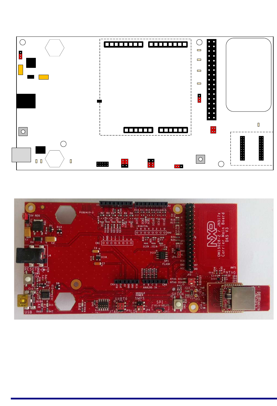
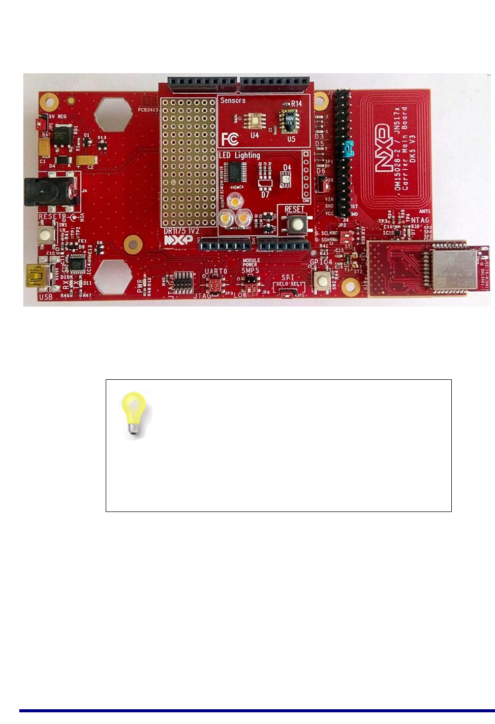
A.1 Carrier Boards
The two carrier boards (part number: OM15028) supplied in the development kit are
physically identical. They are both pre-fitted with an Arduino-compatible expansion
board and a JN5179-based module with integrated antenna (see Section 1.1).
Each Carrier Board has the following features (also refer to Figure 14 and Figure 15):
JN51xx module site containing two connectors (J1 and J2)
Arduino-compatible connector (in four parts - CN1, CN2, CN3, CN4)
34-way expansion header (J3)
10-way JTAG debug header (J6)
USB Mini B port for JN51xx module programming or UART connection
FTDI FT232 driver chip for USB port
On-board 4-Mbit Flash memory device (connected to SPISSZ line of module)
On-board 32-kHz crystal oscillator (connected across DIO9 and DIO10 of
module but not routed to Arduino-compatible header)
2 hexagonal apertures for push-through antennas
Reset button (labelled RESET)
User-input button (labelled GPIO4 and connected to DIO4 of JN517x module)
8 ultra-low-power LEDs (D2, D3, D5, D6, D7, D10, D11, D12)
6 jumpers for board configuration (JP1-JP6)
Powered from one of the following (see Appendix A.1.1):
4 AAA batteries on the board
External 5-12V DC supply via 2.1mm connector
External device via USB Mini B connector
JN517x-DK005 Development Kit
User Guide
JN-UG-3121 v1.1 © NXP Semiconductors 2017 43
Figure 14: Carrier Board Layout
Figure 15: Carrier Board (with a JN5179 Module)
USBPort
DCPower
J3 NFC Antenna
J1 J2
JN51xx
Module
Site
JTAG
J6
CN1 CN2
CN3 CN4
Expansion
Board
Site
GPIO4
RESET
JP1
JP6
JP2
UART0/JTAG
JP3
MODULE
POWER
JP4 SPI
JP5
J4
D10 D11 D12
D2
D3
D5
D6
D7
5V
Regulator
FTDI
Driver
RX TX PWR
I2C/NFC
12
Antenna
Site
Antenna
Site
Module
Power
07814
3.3V
Regulator

Appendices
44 © NXP Semiconductors 2017 JN-UG-3121 v1.1
Note the following:
The expansion board is an Arduino-compatible shield attached to the Arduino-
compatible header.
The JN5179-based module which is pre-fitted to the module site has been pre-
loaded with the ZigBee Smart Home Demonstration.
The Carrier Boards are supplied with the correct hardware configurations for
the pre-loaded ZigBee Smart Home Demonstration. Once you have run this
demonstration, you can re-configure the Carrier Boards as you wish - for
example, by replacing the fitted module with another JN517x module and/or
replacing the expansion board with a different expansion board.
The antenna apertures can each accommodate a push-through external
antenna.
The board is supplied with the JP1 jumper configured for internal batteries as
the power source (see table below).
The board is supplied with access to the on-board Flash memory device
enabled through the SPI jumper (see table below).
The main jumpers and their settings are listed in Table 5 below.
The LEDs D2 and D3 on the board are user-controllable via DIO0 and DIO1,
respectively, of the JN517x device.
To return to the factory settings (including for the fitted JN517x module), wait at
least 2 seconds following power-up, then hold down the GPIO4 button, then
press the RESET button, and finally release the GPIO4 button.

JN517x-DK005 Development Kit
User Guide
JN-UG-3121 v1.1 © NXP Semiconductors 2017 45
Jumper Name Use/Settings Default Setting
JP1 -Selects power source and 5V voltage regulator:
• BAT: Batteries (unregulated)
• 5V REG: External DC/USB (5V regulated)
BAT
JP2 -Selects use of I2C bus on JN517x:
• Jumper On: NTAG signals for NFC
• Jumper Off: I2C SCL/SDA signals
Jumper on (NTAG)
JP3 -Enables/disables mapping from UART0 to JTAG header
(J6)
• UART0: Enable mapping
• JTAG: Disable mapping
UART0
JP4 MODULE POWER Selects power source for JN517x module:
• SMPS: External 12V power supply for JN517x module
• LOW: 5V power supply for JN517x module
LOW
JP5 SPI Enables/disables JN517x SPI access to on-board Flash
memory:
• SEL0: SPI-bus master select output 0
• SEL1: SPI-bus master select output 1
SEL0
JP6 -Enables/disables use of a JN517x high-power module:
• M06: Enable (for high-power module)
• NC: Disable (for standard-power module)
NC
FD -Enables the Field Detect pin (FD signal) on the Generic
and Lighting/Sensor Expansion Boards when jumper is
connected across the J3-16 and J3-18 pins
NC
Table 5: Carrier Board Jumpers and Settings
Appendices
46 © NXP Semiconductors 2017 JN-UG-3121 v1.1
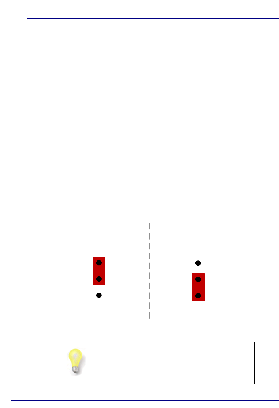
A.1.1 Power Source Selection
Power configuration on the Carrier Board involves two stages with corresponding
jumpers:
5V Regulator: Jumper JP1 is used to enable/disable the 5V voltage regulator
that is required when using external power sources (DC or USB) but not for
battery power
Module Power: Jumpers JP4-1 and JP4-2 are used to select the supply
voltage for the JN517x module site
The locations of the JP1 and JP4 jumpers are shown in Figure 14 on page 43. The
use of these jumpers is described below. For more detailed information about the
power supplies, refer to the Carrier Boards and Expansion Boards Reference Design
(JN-RD-6036).
Voltage Regulator
The Carrier Board can be powered from any one of:
4 AAA batteries on underside of the board
External 5-12V DC supply via 2.1mm connector
External device via USB Mini B connector
The on-board 5V voltage regulator must be enabled for the external DC and USB
power supplies but must be disabled for battery power. The regulator is enabled by
putting the jumper JP1 in the 5V REG position and disabled by putting the jumper in
the BAT position, as illustrated in the figure below.
Figure 16: JP1 Jumper Positions
Tip: If batteries are being used and the board is going to
be left in the idle state for a significant length of time, the
batteries should be removed in order to conserve their
power.
JP1
DC or USB (regulator used) Batteries (regulator not used)
5V REG
BAT
5V REG
BAT
JN517x-DK005 Development Kit
User Guide
JN-UG-3121 v1.1 © NXP Semiconductors 2017 47
Module Power
The JN517x module site can be supplied with a voltage of 5V or 12V, which is
controlled by the Switches Module Power Supply (SMPS) and configured using the
jumpers JP4-1 and JP4-2:
5V supply: Both JP4 jumpers must be in the factory-default LOW position.
This setting is used when the power supply to the Carrier Board is regulated 5V
from an external DC/USB source or unregulated 5V from batteries.
12V supply: Both JP4 jumpers must be in the SMPS position. This setting
must be used when the power supply to the Carrier Board is 12V from an
external DC source.
The above jumper settings are illustrated in Figure 17 and summarised in Table 6.
Caution: When using an external DC Power Supply
Unit (PSU) with a Carrier Board, only a 7-12V PSU with
a 2.1-mm connector must be used.
Figure 17: JP4 Jumper Positions
Caution: The JN5179 modules supplied in the
development kit require a 5V supply. Using a 12V supply
will damage them. The 12V option on the Carrier Board
is provided for future use.
JP4-1
5V (DC, USB or Batteries) 12V (DC)
SMPS
LOW
SMPS
LOW
JP4-2 JP4-1 JP4-2
Appendices
48 © NXP Semiconductors 2017 JN-UG-3121 v1.1
* Requires JN51xx module that supports 12V supply
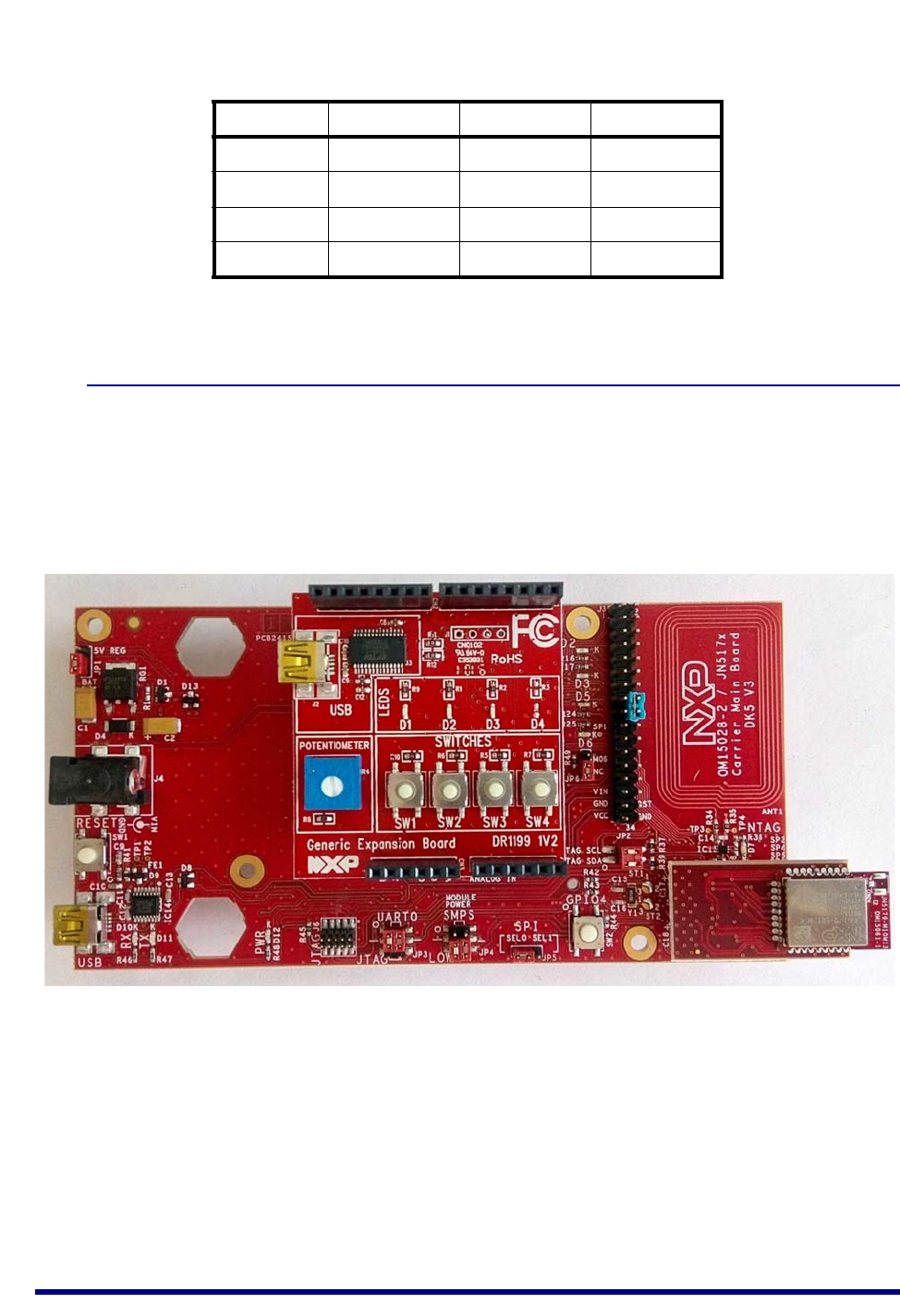
A.1.2 Pre-assembled Boards
As indicated above, each Carrier Board is supplied pre-fitted with a JN5179 module
with integrated antenna and an expansion board.
Figure 18 below shows a pre-assembled board fitted with a Generic Expansion Board
(DR1199).
Source JP1 JP4-1 JP4-2
Batteries BAT LOW LOW
USB 5V REG LOW LOW
5V DC 5V REG LOW LOW
12V DC * 5V REG SMPS * SMPS *
Table 6: Summary of JP1/JP4 Jumper Settings
Figure 18: Carrier Board Fitted with Module and DR1199 Expansion Board
JN517x-DK005 Development Kit
User Guide
JN-UG-3121 v1.1 © NXP Semiconductors 2017 49
Figure 19 below shows a pre-assembled board fitted with a Lighting/Sensor
Expansion Board (DR1175).
The expansion boards are described in Appendix A.2, Appendix A.3 and Appendix
A.4. The JN5179 modules are described in Appendix A.4.
Figure 19: Carrier Board Fitted with Module and DR1175 Expansion Board
Tip 1: The pre-assembled board shown in Figure 18 is
also available to purchase separately as the
JN517x-XK030 Generic Node Expansion Kit. See
“Optional Components” on page 8.
Tip 2: The pre-assembled board shown in Figure 19 is
also available to purchase separately as the
JN517x-XK040 Lighting/Sensor Node Expansion Kit.
See “Optional Components” on page 8.
Appendices
50 © NXP Semiconductors 2017 JN-UG-3121 v1.1
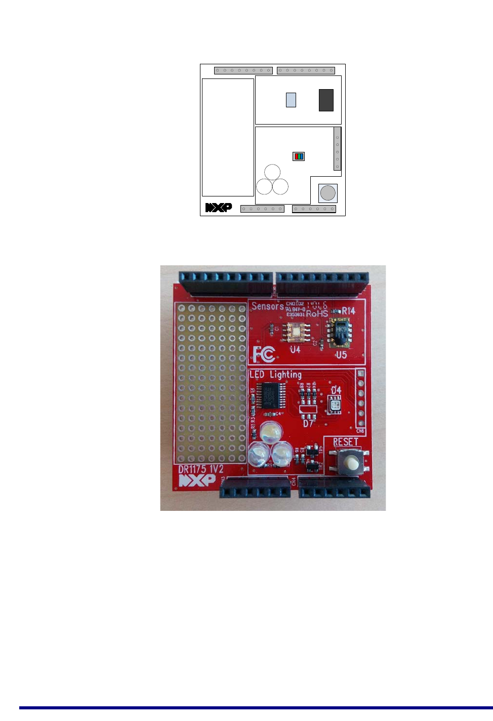
A.2 Lighting/Sensor Expansion Boards
The Lighting/Sensor Expansion Board (part number: DR1175) is an Arduino-
compatible shield that is supplied pre-fitted to the Arduino-compatible header of one
of the Carrier Boards in the development kit (see Appendix A.1).
The Lighting/Sensor Expansion Board has the following features (also see Figure 20):
Arduino-compatible expansion header (in four parts, CN1-CN4)
3 white dimmable LEDs:
Controlled in unison by Pulse Width Modulation (PWM)
Driven by the PWM output of JN517x Timer 1 on the module on the Carrier
Board, via DIO3 on the module (for details of the JN517x timers and DIOs,
refer to the datasheet for the relevant chip).
Colour LED module containing 3 miniature LEDs:
LEDs are independently controlled by PWM from an on-chip multi-channel
PMW controller, connected via the 2-wire Serial Interface (see below)
Connected to the 2-wire Serial Interface (I2C) of the JN517x module on the
Carrier Board, via DIO14 (clock) and DIO15 (data) on the module
Humidity/temperature sensor (of the type SHT1x) connected to the JN517x
module on the Carrier Board, via DIO12 (data) and DIO17 (clock) on the
module
Light sensor (of the type TSL2550), connected to the 2-wire Serial Interface
(I2C) of the JN517x module on the Carrier Board, via DIO14 (clock) and DIO15
(data) on the module
Reset button (to reset the Carrier Board)
Note: For full details of the board, refer to the Carrier
Boards and Expansion Boards Reference Design
(JN-RD-6036), available from the NXP web site (see
“Support Resources” on page 7).
Caution: The LEDs on the Lighting/Sensor Expansion
Board are very bright at maximum intensity. To avoid
damage to your eyes, do not look into them directly for
an extended period of time.
JN517x-DK005 Development Kit
User Guide
JN-UG-3121 v1.1 © NXP Semiconductors 2017 51
Figure 20: Lighting/Sensor Expansion Board Layout
Figure 21: Lighting/Sensor Expansion Board
DR1175
LED Lighting
Sensors
RESET
CN4
CN3
CN2
CN1
CN6
D7
U4 U5
SW1
White LEDs
Multi-Colour
LED Module
D1, D2, D3
Light
Sensor
Temp/
Humidity
Sensor
Prototype
Area
Appendices
52 © NXP Semiconductors 2017 JN-UG-3121 v1.1
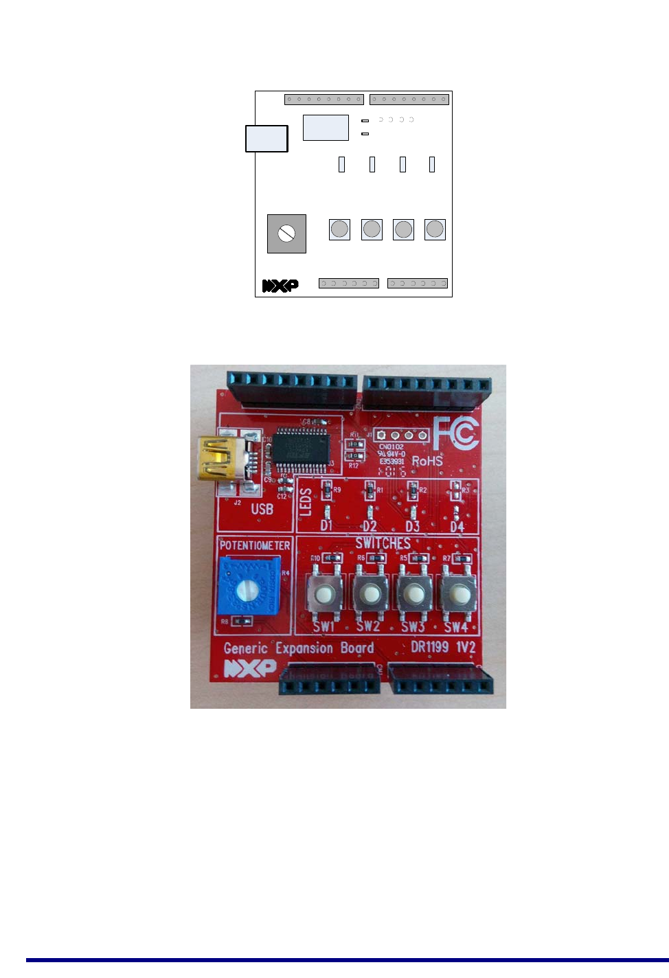
A.3 Generic Expansion Boards
The Generic Expansion Board (part number: DR1199) is an Arduino-compatible shield
that is supplied pre-fitted to the Arduino-compatible header of one of the Carrier
Boards in the development kit (see Appendix A.1).
The Generic Expansion Board has the following features (also see Figure 22):
Arduino-compatible expansion header (in four parts, CN1-CN4)
4 user-input buttons (SW1, SW2, SW3, SW4) connected to DIOs on the
JN517x module on the Carrier Board:
SW1 is connected to DIO1
SW2 is connected to DIO11
SW3 is connected to DIO12
SW4 is connected to DIO17
4 LEDs (D1, D2, D3, D4) connected to DIOs on the JN517x module on the
Carrier Board:
D1 is connected to DIO0
D2 is connected to DIO13 (same as for the PWM output used on the
Lighting/Sensor Expansion Board to drive the three white LEDs)
D3 is connected to DIO16
D4 is an optional LED which is not fitted on the supplied board and shares
DIO1 with button SW1
Potentiometer connected to JN517x ADC1, with a 0-1.8V DC voltage swing
USB Mini B port to provide access to JN517x UART1 via DIO14 and DIO15 of
JN517x module (or alternatively to UART0, depending on the internal
configuration of the device)
FTDI FT232 driver chip for USB port
PCB pads for 4-way GPIO header (3V3, VCC, DIO14, DIO15), where DIO14 and
DIO15 can be used to access JN517x UART1 (in this case, the FTDI driver chip for
the USB port must be isolated by removing resistors R11 and R12).
Note: For full details of the board, refer to the Carrier
Boards and Expansion Boards Reference Design
(JN-RD-6036), available from the NXP web site (see
“Support Resources” on page 7).
JN517x-DK005 Development Kit
User Guide
JN-UG-3121 v1.1 © NXP Semiconductors 2017 53
Figure 22: Generic Expansion Board Layout
Figure 23: Generic Expansion Board
SW1 SW3 SW4
D2D1 D3 D4
FTDI
Chip
USB
Port
Potentiometer
GPIO
R11
R12
CN1
CN2
CN3 CN4
SW2
Appendices
54 © NXP Semiconductors 2017 JN-UG-3121 v1.1
A.4 JN5179 Modules
Two types of JN5179-based module are supplied in the kit. Each is a
JN5179-001-M1y module mounted on a Mezzanine Board (OM15024), the part
number of the combined component being JN5179-001-T1y.
JN5179-001-T10 (JN5179-001-M10 mounted on Mezzanine Board)
Two of these modules are supplied, pre-fitted on the Carrier Boards, and
provide a 10dBm power output suitable for worldwide use. The module features
a JN5179-001 wireless microcontroller and an integrated PCB antenna. The
module’s mezzanine board has a footprint for a uFL connector, which can be
fitted to allow connection to an external antenna.
JN5179-001-T16 (JN5179-001-M16 mounted on Mezzanine Board)
Two of these modules are supplied to provide a 20dBm high-power output and
are intended for the North American (FCC and IC) markets. The module
features a JN5179-001 wireless microcontroller and an integrated PCB
antenna. A uFL connector is also provided, which can be used to connect the
module to an antenna (supplied) on the Carrier Board via a flying lead. When
using a high-power module, the jumper JP6 on the Carrier Board (see Appendix
A.1) must be in the M06 position. The module can be used to replace a pre-fitted
module in order to achieve a larger radio transmission range.
A.5 USB Dongles
Two JN5179 USB Dongles (part number: OM15021) are supplied in the kit. One is
intended for use in the ZigBee Smart Home Demonstration and the other can be
employed in some other capacity, such as packet sniffing (see below).
The JN5179 USB Dongle has the following features:
JN5179-001 wireless microcontroller (mounted directly on the board)
Integrated PCB antenna
FTDI FT232 driver chip for USB connection
Two LEDs (one green, one orange)
Caution: The JN5179-001-T16 high-power module is
intended only for use in the North American (FCC and
IC) markets. It is not compliant for use in Europe.
Note 1: When used, the supplied external antenna
provides a gain of up to 2 dBi.
Note 2: The JN5179 modules that are pre-fitted to
Carrier Boards are pre-programmed with the ZigBee
Smart Home Demonstration. Firmware re-programming
of JN517x modules is described in Appendix C.1.
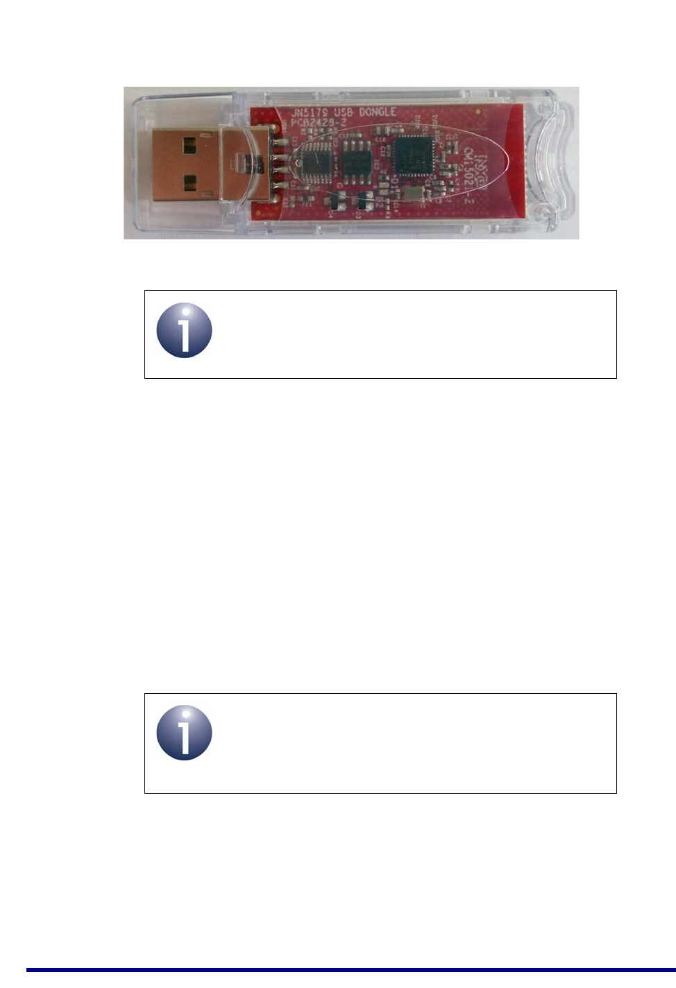
JN517x-DK005 Development Kit
User Guide
JN-UG-3121 v1.1 © NXP Semiconductors 2017 55
The two dongles are pre-programmed with different software, as described below. The
dongles can be re-programmed with other applications (firmware re-programming of
the JN5179 USB Dongles is described in Appendix C.2).
Control Bridge
The JN5179 USB Dongle with a green sticker is pre-programmed as a Control Bridge
that can be used in the ZigBee Smart Home Demonstration. This software allows the
dongle to be plugged into a USB port of the Raspberry Pi board (see Appendix A.6) to
form an IoT Gateway:
The dongle provides the interface with the wireless network (WPAN) side of the
demonstration system, also acting as the network Co-ordinator
The Raspberry Pi board provides the interface with the IP (LAN/WAN) side of
the demonstration system
For more details of the demonstration system, refer to Section 1.5 and Chapter 2.
Packet Sniffer
The JN5179 USB Dongle with a red sticker is pre-programmed with an NXP packet
sniffer application. To use this application, the dongle should be plugged into the USB
port of a PC. You will need to install and use the Ubiqua Protocol Analyzer software
on the PC. This software which can be obtained from the Ubilogix web site
(www.ubilogix.com/products/ubiqua). A free trial of this software is available.
Figure 24: JN5179 USB Dongle
Note: The JN5179 USB Dongle is also available to
purchase separately (part number OM15021). See
“Optional Components” on page 8.
Note: This JN5179 USB Dongle should not be plugged
directly into a USB port of the Raspberry Pi board. This
connection should be made via the USB-to-USB cable,
especially when the Wi-Pi adaptor is also used.
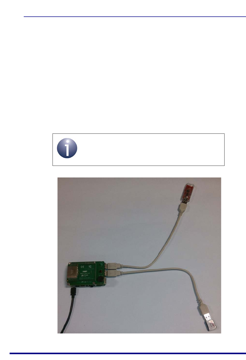
Appendices
56 © NXP Semiconductors 2017 JN-UG-3121 v1.1
A.6 Raspberry Pi 2
The Raspberry Pi 2 single-board computer (Model B) is intended to be used in an IoT
Gateway to form an interface between a low-power wireless network and an
IP-based network (see Section 1.3). It is supplied with accessories consisting of:
Dedicated 5V DC power supply unit (universal type) with USB port
microSD card (pre-installed and pre-programmed with NXP firmware)
Wi-Pi Raspberry Pi 802.11n wireless adaptor
NXP PN7120 NFC Controller (described in Appendix A.7)
RJ45 Ethernet cable
‘USB to Micro USB’ cable (for power supply)
The Raspberry Pi with NFC Controller board mounted is shown in Figure 25 below,
which also shows the Wi-Pi adaptor and a JN5179 USB Dongle connected via ‘USB
to USB’ extension cables to allow radio isolation between the dongle and adaptor.
Note: Any two of the three components must be at least
20 cm apart, and the USB dongle and Wi-Pi adaptor
should be roughly perpendicular to each other
Figure 25: Raspberry Pi Board and Accessories

JN517x-DK005 Development Kit
User Guide
JN-UG-3121 v1.1 © NXP Semiconductors 2017 57
Note the following:
The ‘USB to Micro USB’ cable allows the board to be powered from a USB port
on the 5V DC PSU.
The Raspberry Pi must be located near to the mains outlet socket in which the
PSU is plugged and the PSU/socket must be easily accessible.
A JN5179 USB Dongle can be plugged into any of the USB ports of the
Raspberry Pi board to form an IoT Gateway (see Section 1.3). However, it is
recommended that this connection is made via a supplied USB-to-USB cable,
especially when the Wi-Pi adaptor is also used (in order to ensure radio
isolation between the dongle and adaptor).
The JN5179 USB Dongle that is to be connected to the Raspberry Pi board for
the ZigBee Smart Home Demonstration is the one with a green sticker (see
Appendix A.5). This dongle is pre-programmed as a Control Bridge.
The Wi-Pi wireless adaptor can be connected to any of the USB ports of the
Raspberry Pi board in order to provide Wi-Fi connectivity. However, it is
recommended that this connection is made via a supplied USB-to-USB cable,
especially when a JN5179 USB Dongle is also used (in order to ensure radio
isolation between the dongle and adaptor).
The supplied NFC Controller (see Appendix A.7) can be connected to the
Raspberry Pi board to facilitate NFC commissioning (see Section 1.4.1).
The IoT Gateway software and documentation are available two Application
Notes: ZigBee IoT Gateway Host with NFC (JN-AN-1222) and ZigBee IoT
Gateway Control Bridge (JN-AN-1223).
PSU Specifications
The supplied 5V DC PSU is a Stontronics T5454DV Raspberry Pi Power Supply and
its specifications are as follows:
Input
Input Voltage Range: 90-264V AC
Input Frequency: 47-63Hz
Input Current: 0.3A Max
AC Inlet: UK, European, Australian and US changeable heads
Output
Output Voltage: +5V DC
Minimum Load Current: 0A
Nominal Load Current: 2A
Nominal Output Power: 10W
Protection: Short circuit, over current, over voltage
Output Cable: 1500mm Micro USB B 5 pin
Other
Operating Temperature: 0°C to 50°C
Certification
CE, FCC, RoHS
Appendices
58 © NXP Semiconductors 2017 JN-UG-3121 v1.1
A.7 NFC Controller
The NXP PN7120 NFC Controller is supplied in the JN517x-DK005 Development Kit
to facilitate NFC commissioning (see Section 1.4.1), allowing an NFC tag on a Carrier
Board to be read. The NFC Controller is supplied pre-mounted on a Raspberry Pi
Interface Board.
This NFC Controller Board assembly must be mounted on the Raspberry Pi 2
Interface Board. Figure 26 shows the two components and Figure 27 shows the
assembled components.
The supplied NFC Controller assembly is a high-performance fully NFC-compliant
expansion board for the Raspberry Pi. It complies with the Reader mode, P2P mode
and Card Emulation mode standards. The board features an integrated high-
performance RF antenna to ensure good interoperability with NFC devices.
Figure 26: NFC Controller and Raspberry Pi Boards
Figure 27: NFC Controller Board Mounted on Raspberry Pi Board

JN517x-DK005 Development Kit
User Guide
JN-UG-3121 v1.1 © NXP Semiconductors 2017 59
For more information and operational instructions relating to the NFC Controller, refer
to the following NXP documentation:
AN11646: PN7120 NFC Controller SBC Kit Quick Start Guide
UM10878: PN7120 NFC Controller SBC Kit User Manual
The above documents can be obtained from the NXP web site.

Appendices
60 © NXP Semiconductors 2017 JN-UG-3121 v1.1
B. Installing a Packet Sniffer
One of the JN5179 USB Dongles supplied in the development kit is programmed with
an NXP packet sniffer application - this dongle is indicated with a red sticker. For more
information on the JN5179 USB Dongles, refer to Appendix A.5.
This section describes how re-program either of the dongles with the packet sniffer
application. To use a dongle as a sniffer, you must also install the Ubiqua Protocol
Analyzer software on the PC from which the packet sniffing will be conducted.
Proceed as follows:
1. Plug the JN5179 USB Dongle into the PC.
2. Program the sniffer application binary into the JN5179 device on the dongle:
The sniffer binary file JennicSniffer_JN5179_1000000_HP.bin is
provided in the JN517x Software Developer’s Kit (SDK), in the directory
<SDK root>\bstudio_nxp\sdk\JN-SW-42xx\Tools\JennicSniffer.
For information on re-programming a JN5179 USB Dongle, refer to
Section C.2
3. Download the Ubiqua Protocol Analyzer software and install it on the PC:
You can obtain the Ubiqua Protocol Analyzer software from the following
web site: www.ubilogix.com/products/ubiqua (a free trial version is
available)
Run the downloaded installer and follow the on-screen installation
instructions
4. Start the Ubiqua Protocol Analyzer (ensure that the PC is connected to the
Internet).
User documentation for the Ubiqua Protocol Analyzer is available from the above
Ubiqua web site.
JN517x-DK005 Development Kit
User Guide
JN-UG-3121 v1.1 © NXP Semiconductors 2017 61
C. Firmware Re-programming
The following components of the JN517x-DK005 Development Kit can be
programmed with application binaries as described in this section:
JN5179 modules - see Appendix C.1
JN5179 USB dongles - see Appendix C.2
The dongles and the modules that are pre-fitted to Carrier Boards are already
programmed with applications but can be re-programmed.
Flash Programmers
The firmware re-programming described in the sub-sections below require the use of
one of the following Flash programmers:
JN517x Flash Programmer built into LPCXpresso and described in the JN517x
LPCXpresso Installation and User Guide (JN-UG-3109)
JN51xx Production Flash Programmer (JN-SW-4107) described in the JN51xx
Production Flash Programmer User Guide (JN-UG-3099)
C.1 Re-programming JN5179 Modules
In order to re-program the Flash memory of the supplied JN5179 modules, you must
connect the Carrier Board (on which the module is located) to your PC (see below).
To perform the re-programming from your PC, you must use a JN51xx Flash
Programmer utility (see Flash Programmers above).
When re-programming the JN5179 modules on the Carrier Boards in this kit, you must
use one of the supplied ‘USB A to Mini B’ cables to connect a USB port of your PC to
the USB Mini B port of the Carrier Board. When you make this connection for the first
time, you may be prompted to install the device driver for the FTDI chip which is
located on the Carrier Board - if this is the case, refer to Appendix D.
C.2 Re-programming JN5179 USB Dongles
In order to re-program the Flash memory of the supplied JN5179 USB Dongles, you
must plug the dongle into a USB port of a PC. To perform the re-programming from
your PC, you must use a JN51xx Flash Programmer utility (see Flash Programmers
above).
When you make the USB connection for the first time, you may be prompted to install
the device driver for the FTDI chip which is located on the dongle - if this is the case,
refer to Appendix D.
Note: The LPCXpresso internal Flash programmer
cannot be used to erase and re-program JN517x
external Flash memory.

Appendices
62 © NXP Semiconductors 2017 JN-UG-3121 v1.1
D. Installing the FTDI Device Driver for USB Connections
The first time that you make a USB connection between your PC and a kit component
which features the FTDI FT232 chip, you may be prompted to install the device driver
for the chip on your PC. You will need to obtain the driver from the Internet.
You must obtain the driver for your operating system from the VCP drivers page of the
FTDI web site:
www.ftdichip.com/Drivers/VCP.htm
Download the required driver to your desktop and double-click on its icon to install. To
perform the installation, a device or cable containing an FTDI chip must be connected
to a USB port of your PC.

JN517x-DK005 Development Kit
User Guide
JN-UG-3121 v1.1 © NXP Semiconductors 2017 63
E. Regulatory Information
For compliance and certification information on the JN517x wireless microcontrollers
and the contents of this development kit, refer to the JN516x/7x Product Compliance
and Certification page on the NXP web site:
www.nxp.com/products/wireless-connectivity/2.4-ghz-wireless-solutions/jn516x-7x-product-certification
E.1 FCC Regulatory Statements
The following Federal Communication Commission (FCC) regulatory statements
apply to the contents for the JN517x-DK005 Development Kit.
This device complies with Part 15 of the FCC Rules. Operation is subject to the
following two conditions: (1) this device may not cause harmful interference, and
(2) this device must accept any interference received, including interference that may
cause undesired operation.
CAUTION: This equipment may not be modified, altered, or changed in any way
without signed written permission from NXP Semiconductors. Unauthorized
modification may void the equipment authorization from the FCC and will void the NXP
Semiconductors warranty.
NOTE: This equipment has been tested and found to comply with the limits for a Class
B digital device, pursuant to part 15 of the FCC Rules. These limits are designed to
provide reasonable protection against harmful interference in a residential installation.
This equipment generates, uses and can radiate radio frequency energy and, if not
installed and used in accordance with the instruction, may cause harmful interference
to radio communications. However, there is no guarantee that interference will not
occur in a particular installation. If this equipment does cause harmful interference to
radio or television reception which can be determined by turning the equipment off and
on, the user is encouraged to try to correct interference by one or more of the following
measures:
Reorient or relocate the receiving antenna.
Increase the separation between the equipment and receiver.
Connect the equipment into an outlet on circuit different from that to which the
receiver is connected.
Consult the dealer or an experienced radio/TV technician for help.

Appendices
64 © NXP Semiconductors 2017 JN-UG-3121 v1.1

JN517x-DK005 Development Kit
User Guide
JN-UG-3121 v1.1 © NXP Semiconductors 2017 65
Revision History
Version Date Comments
1.0 13-Oct-2016 First release
1.1 8-Feb-2017 Minor updates and improvements made, including new web
addresses for LPCXpresso and JN517x certification information

JN517x-DK005 Development Kit
User Guide
66 © NXP Semiconductors 2017 JN-UG-3121 v1.1
Important Notice
Limited warranty and liability - Information in this document is believed to be accurate and reliable. However, NXP
Semiconductors does not give any representations or warranties, expressed or implied, as to the accuracy or
completeness of such information and shall have no liability for the consequences of use of such information. NXP
Semiconductors takes no responsibility for the content in this document if provided by an information source outside
of NXP Semiconductors.
In no event shall NXP Semiconductors be liable for any indirect, incidental, punitive, special or consequential damages
(including - without limitation - lost profits, lost savings, business interruption, costs related to the removal or
replacement of any products or rework charges) whether or not such damages are based on tort (including
negligence), warranty, breach of contract or any other legal theory.
Notwithstanding any damages that customer might incur for any reason whatsoever, NXP Semiconductors' aggregate
and cumulative liability towards customer for the products described herein shall be limited in accordance with the
Terms and conditions of commercial sale of NXP Semiconductors.
Right to make changes - NXP Semiconductors reserves the right to make changes to information published in this
document, including without limitation specifications and product descriptions, at any time and without notice. This
document supersedes and replaces all information supplied prior to the publication hereof.
Suitability for use - NXP Semiconductors products are not designed, authorized or warranted to be suitable for use
in life support, life-critical or safety-critical systems or equipment, nor in applications where failure or malfunction of an
NXP Semiconductors product can reasonably be expected to result in personal injury, death or severe property or
environmental damage. NXP Semiconductors and its suppliers accept no liability for inclusion and/or use of NXP
Semiconductors products in such equipment or applications and therefore such inclusion and/or use is at the
customer's own risk.
Applications - Applications that are described herein for any of these products are for illustrative purposes only. NXP
Semiconductors makes no representation or warranty that such applications will be suitable for the specified use
without further testing or modification.
Customers are responsible for the design and operation of their applications and products using NXP Semiconductors
products, and NXP Semiconductors accepts no liability for any assistance with applications or customer product
design. It is customer's sole responsibility to determine whether the NXP Semiconductors product is suitable and fit
for the customer's applications and products planned, as well as for the planned application and use of customer's
third party customer(s). Customers should provide appropriate design and operating safeguards to minimize the risks
associated with their applications and products.
NXP Semiconductors does not accept any liability related to any default, damage, costs or problem which is based on
any weakness or default in the customer's applications or products, or the application or use by customer's third party
customer(s). Customer is responsible for doing all necessary testing for the customer's applications and products
using NXP Semiconductors products in order to avoid a default of the applications and the products or of the
application or use by customer's third party customer(s). NXP does not accept any liability in this respect.
Export control - This document as well as the item(s) described herein may be subject to export control regulations.
Export might require a prior authorization from competent authorities.
NXP Semiconductors
For online support resources and contact details of your local NXP office or distributor, refer to:
www.nxp.com
