CRT3321 KEHM8547
User Manual: KEHM8547
Open the PDF directly: View PDF ![]() .
.
Page Count: 56
- SAFETY INFORMATION
- CONTENTS
- 1. SPECIFICATIONS
- 2. EXPLODED VIEWS AND PARTS LIST
- 2.1 EXTERIOR
- 2.2 CASSETTE MECHANISM MODULE
- 3. BLOCK DIAGRAM AND SCHEMATIC DIAGRAM
- 3.1 BLOCK DIAGRAM
- 3.2 OVERALL CONNECTION DIAGRAM(GUIDE PAGE)
- 3.3 KEYBOARD UNIT
- 3.4 CASSETTE MECHANISM MODULE
- 4. PCB CONNECTION DIAGRAM
- 4.1 MAIN UNIT
- 4.2 KEYBOARD UNIT(KEX-M8547ZT/EW)
- 4.3 KEYBOARD UNIT(KEX-M8647ZT/EW)
- 4.4 CASSETTE MECHANISM MODULE
- 5. ELECTRICAL PARTS LIST
- 6. ADJUSTMENT
- 6.1 JIG CONNECTION DIAGRAM
- 6.2 CASSETTE AND AUDIO ADJUSTMENT
- 6.3 SELF-DIAGNOSIS FUNCTION
- 7. GENERAL INFORMATION
- 7.1 DIAGNOSIS
- 7.1.1 DISASSEMBLY
- 7.1.2 CONNECTOR FUNCTION DESCRIPTION
- 7.1.3 TROUBLE-SHOOTING
- 7.2 IC
- 7.3 EXPLANATION
- 7.3.1 SYSTEM BLOCK DIAGRAM
- 7.3.2 OPERATIONAL FLOW CHART
- 7.4 CLEANING
- 8. OPERATIONS
ORDER NO.
PIONEER CORPORATION 4-1, Meguro 1-chome, Meguro-ku, Tokyo 153-8654, Japan
PIONEER ELECTRONICS (USA) INC. P.O. Box 1760, Long Beach, CA 90801-1760, U.S.A.
PIONEER EUROPE NV Haven 1087, Keetberglaan 1, 9120 Melsele, Belgium
PIONEER ELECTRONICS ASIACENTRE PTE. LTD. 253 Alexandra Road, #04-01, Singapore 159936
PIONEER CORPORATION 2004
ZT/EW
KEX-M8547
KEX-M8547ZT/EW
CRT3321
RECEIVER ASSY, RADIO
KEX-M8547
ZT
/EW
KEX-M8547
ZT-91
/EW
KEX-M8647
ZT
/EW
KEX-M8647
ZT-91
/EW
VEHICLE DESTINATION PRODUCED
AFTER OEM PARTS No. ID No. PIONEER MODEL No.
LAND CRUISER PRADO EUROPE August 2004 86120-60461 P3745 KEX-M8547ZT/EW
LAND CRUISER PRADO EUROPE August 2004 86120-60461 P3745 KEX-M8547ZT-91/EW
LAND CRUISER PRADO EUROPE August 2004 86120-60451 P3746 KEX-M8647ZT/EW
LAND CRUISER PRADO EUROPE August 2004 86120-60451 P3746 KEX-M8647ZT-91/EW
For details, refer to "Important symbols for good services".
K-ZZA. JULY 2004 printed in Japan
TOYOTA
KEX-M8547ZT/EW
2
1234
1234
C
D
F
A
B
E
This service manual should be used together with the following manual(s):
Model No. Order No. Mech.Module Remarks
CX-1011 CRT2406 3L Cassette Mech. Module : Mech. Description, Disassembly
Dolby noise reduction manufactured under license from Dolby Laboratories Licensing Corporation.
"Dolby" and the double-D symbol are trademarks of Dolby Laboratories Licensing Corporation.
This service manual does not describe the CD test mode.
For the operations in the CD test mode, refer to the CD player's service manual.
- Supplementary model is identical to the original except for the addition of following items.
Description
Polyethylene Bag
Cover
Carton
Contain Box
* Air Cap
KEX-M8547ZT-91/EW
KEX-M8647ZT-91/EW
CEG1026
CEG1045(x2)
CHG4857
CHL4857(x1/4)
CHW1947
* : Non spare part
KEX-M8547ZT/EW 3
5678
5678
C
D
F
A
B
E
SAFETY INFORMATION
- Service Precaution
1. You should conform to the regulations governing
the product (safety, radio and noise, and other
regulations), and should keep the safety during
servicing by following the safety instructions
described in this manual.
2. When you exchange the CN473 (mentioned P.6 PART
No.11) for new part. Cut all terminals about 0.5mm
to 1mm. ( There is some possibility to touch the
terminal with under chassis because of long terminals.)
This service manual is intended for qualified service technicians; it is not meant for the casual do-it-yourselfer.
Qualified technicians have the necessary test equipment and tools, and have been trained to properly and safely
complex products such as those covered by this manual.
Improperly performed repairs can adversely affect the safety and reliability of the product and may void the
If you are not qualified to perform the repair of this product properly and safely, you should not risk
and refer the repair to a qualified service technician.
repair
warranty.
trying to do so
[ Important symbols for good services ]
In this manual, the symbols shown-below indicate that adjustments, settings or cleaning should be made securely.
When you find the procedures bearing any of the symbols, be sure to fulfill them:
2. Adjustments
To keep the original performances of the product, optimum adjustments or specification confirmation is indispensable.
In accordance with the procedures or instructions described in this manual, adjustments should be performed.
3. Cleaning
For optical pickups, tape-deck heads, lenses and mirrors used in projection monitors, and other parts requiring cleaning,
proper cleaning should be performed to restore their performances.
5. Lubricants, glues, and replacement parts
Appropriately applying grease or glue can maintain the product performances. But improper lubrication or applying
glue may lead to failures or troubles in the product. By following the instructions in this manual, be sure to apply the
prescribed grease or glue to proper portions by the appropriate amount.For replacement parts or tools, the prescribed
ones should be used.
4. Shipping mode and shipping screws
To protect the product from damages or failures that may be caused during transit, the shipping mode should be set or
the shipping screws should be installed before shipping out in accordance with this manual, if necessary.
1. Product safety
You should conform to the regulations governing the product (safety, radio and noise, and other regulations), and
should keep the safety during servicing by following the safety instructions described in this manual.

KEX-M8547ZT/EW
4
1234
1234
C
D
F
A
B
E
CONTENTS
SAFETY INFORMATION..................................................................................................................................... 3
1. SPECIFICATIONS ............................................................................................................................................ 5
2. EXPLODED VIEWS AND PARTS LIST ............................................................................................................ 6
2.1 EXTERIOR................................................................................................................................................. 6
2.2 CASSETTE MECHANISM MODULE......................................................................................................... 8
3. BLOCK DIAGRAM AND SCHEMATIC DIAGRAM..........................................................................................10
3.1 BLOCK DIAGRAM ................................................................................................................................... 10
3.2 OVERALL CONNECTION DIAGRAM(GUIDE PAGE).............................................................................. 12
3.3 KEYBOARD UNIT.................................................................................................................................... 18
3.4 CASSETTE MECHANISM MODULE....................................................................................................... 20
4. PCB CONNECTION DIAGRAM ..................................................................................................................... 22
4.1 MAIN UNIT............................................................................................................................................... 22
4.2 KEYBOARD UNIT(KEX-M8547ZT/EW)................................................................................................... 26
4.3 KEYBOARD UNIT(KEX-M8647ZT/EW)................................................................................................... 27
4.4 CASSETTE MECHANISM MODULE....................................................................................................... 28
5. ELECTRICAL PARTS LIST ............................................................................................................................ 30
6. ADJUSTMENT ............................................................................................................................................... 38
6.1 JIG CONNECTION DIAGRAM................................................................................................................. 38
6.2 CASSETTE AND AUDIO ADJUSTMENT ................................................................................................ 39
6.3 SELF-DIAGNOSIS FUNCTION ............................................................................................................... 41
7. GENERAL INFORMATION............................................................................................................................. 45
7.1 DIAGNOSIS ............................................................................................................................................. 45
7.1.1 DISASSEMBLY ..................................................................................................................................... 45
7.1.2 CONNECTOR FUNCTION DESCRIPTION.......................................................................................... 46
7.1.3 TROUBLE-SHOOTING ......................................................................................................................... 47
7.2 IC ............................................................................................................................................................. 48
7.3 EXPLANATION ........................................................................................................................................ 51
7.3.1 SYSTEM BLOCK DIAGRAM ................................................................................................................ 51
7.3.2 OPERATIONAL FLOW CHART ............................................................................................................ 52
7.4 CLEANING............................................................................................................................................... 53
8. OPERATIONS ................................................................................................................................................ 54

KEX-M8547ZT/EW 5
5678
5678
C
D
F
A
B
E
1. SPECIFICATIONS
General
Power source . . . . . . . 13.2 V(10.5V - 16.0V allowable)
Backup current. . . . . . . . . . . . . . Less than 0.3 mA
Grounding system . . . . . . . . . . . . . . Negative type
Weight . . . . . . . . . . . . . . . . . . . . . . . . 1.18 kg
Tape player
Tape . . . . . . . . . Compact cassette tape (C-30 - C-90)
Tape speed . . 4.76 cm/sec.(+0.14 cm/sec.,-0.05 cm/sec.)
Wow & flutter. . . . . . . . . . . Less than 0.2 %(WRMS)
Fast forward/rewind time. . . . Less than 120 sec. for C-60
Stereo separation . . . . . . . . . . . . . More than 30 dB
Signal-to-noise ratio . . . . . . . . . . . . More than 40 dB
FM tuner
Frequency range. . . . . . . . . . . . . 87.5 - 108.0 MHz
Usable sensitivity . . . . . Less than14 dBµV (S/N: 30 dB)
Signal-to-noise ratio . . . . .More than 46 dB(54dBµ input)
Distortion . . . . . . . . . . . . . . . . . Less than 1.5%
Digital noise . . . . . . Less than 25 mVp-p (74 dBµ input)
MW tuner
Frequency range. . . . . . . . . . . . . . 522 - 1,611 kHz
Usable sensitivity . . . . 34 dBµV(S / N : 20 dB)
Selectivity . . . . . . . . . . . . More than 20 dB (±9 kHz)
Signal-to-noise ratio . . . . More than 42 dB (74 dBµ input)
Distortion . . . . . . . . . . . . . . . . . Less than 1.5%
LW tuner
Frequency range. . . . . . . . . . . . . . . 153 - 279 kHz
Usable sensitivity . . . . 40 dBµV(S / N : 20 dB)
Selectivity . . . . . . . . . . . . More than 20 dB (±9 kHz)
Signal-to-noise ratio . . . . More than 42 dB (74 dBµ input)
Distortion . . . . . . . . . . . . . . . . . Less than 1.5%
Less than
Less than
KEX-M8547ZT/EW
6
1234
1234
C
D
F
A
B
E
2. EXPLODED VIEWS AND PARTS LIST
2.1 EXTERIOR
N
OTES : • Parts marked by " * " are generally unavailable because they are not in our Master Spare Parts List.
• Screw adjacent to mark on the product are used for disassembly.
• For the applying amount of lobricants or glue, follow the instructions in this manual.
(In the case of no amount instructions,apply as you think it appropriate.)
"
KEX-M8547ZT/EW 7
5678
5678
C
D
F
A
B
E
(1) EXTERIOR SECTION PARTS LIST
(2) CONTRAST TABLE
KEX-M8547ZT/EW and KEX-M8647ZT/EW are constructed the same except for the following:
Mark No. Description Part No.
1 Screw BMZ30P050FTC
2 Screw BSZ26P060FTC
3 Upper Case CNB3080
4 Front Frame CNC9684
5 Insulator CNM7528
6 Main Unit See Contrast table(2)
7 Screw BMZ30P060FTC
8 Screw(M3x6) CBA1393
9 Terminal(CN502) CKF1064
10 Connector(CN801) CKM1322
11 Connector(CN473) *1 CKM1350
12 Connector(CN472) CKM1351
13 Plug(CN804) CKS3539
14 Connector(CN353) CKS3568
15 Antenna Jack(CN501) CKX1024
16 Holder CNC9686
17 Rear Frame CND2155
18 FM Tuner Unit CWE1679
19 FM/AM Tuner Unit CWE1773
20 Holder CNC8855
21 Terminal(CN802) VNF1084
22 Shield Unit CXB9781
23 Screw BPZ20P080FTC
24 Button See Contrast table(2)
25 Button See Contrast table(2)
26 Button See Contrast table(2)
27 Button See Contrast table(2)
28 Button See Contrast table(2)
29 Button See Contrast table(2)
30 Button See Contrast table(2)
31 Button See Contrast table(2)
32 Cushion CNM9194
33 Rubber CNV6939
34 Lighting Conductor CNV6942
35 Lighting Conductor CNV6943
36 Lighting Conductor CNV6944
37 Lighting Conductor CNV6948
38 Holder CNV6951
39 Holder CNV6952
40 Holder CNV6953
41 Keyboard Unit See Contrast table(2)
42 Socket(CN901) CKS3552
43 Knob Unit(TUNE)(PWR, VOL) CXB7979
44 Grille Unit See Contrast table(2)
45 Door CAT2293
46 Spring CBH1371
47 Chassis Unit CXC3861
48 Cassette Mechanism Module EXK4290
49 Screw ISS26P055FTC
50 Transistor(Q810, 811) 2SB1185
Mark No. Description Part No.
Mark No. Description KEX-M8547ZT/EW KEX-M8647ZT/EW
6 Main Unit CWM9554 CWM9555
24 Button CAC7276(TA) CAC7277(CS-EJECT)
25 Button CAC7278(CS-EJECT) CAC7279(TA)
26 Button CAC7280(DISC) CAC7268(AM)
27 Button CAC7281(TAPE) CAC7269(FM)
28 Button CAC7282(FM) CAC7270(TAPE)
29 Button CAC7283(AM) CAC7271(DISC)
30 Button CAC7284(CH, PROG, DISC) CAC7272(SEEK, TRACK)
31 Button CAC7285(SEEK, TRACK) CAC7273(CH, PROG, DISC)
41 Keyboard Unit CWS1338 CWS1339
44 Grille Unit CXC3340 CXC3341
*1 : The cautions in the case of exchanging parts (mentioned P.7 PART No.11) are indicated to P.3.
KEX-M8547ZT/EW
8
1234
1234
C
D
F
A
B
E
2.2 CASSETTE MECHANISM MODULE
C
D
For grease application, refer to the service manual for CX-1011 (CRT2406).

KEX-M8547ZT/EW 9
5678
5678
C
D
F
A
B
E
CASSETTE MECHANISM MODULE SECTION PARTS LIST
Mark No. Description Part No.
1 Screw BSZ20P040FTC
2 Washer CBF1037
3 Washer CBG1003
4 Screw EBA1028
5 Screw BMZ20P022FTC
6 Spring EBH1653
7 Spring EBH1642
8 Spring EBH1641
9 Spring EBH1626
10 Spring EBH1627
11 Spring EBH1648
12 Cord EDD1024
13 Photo-reflector(Q101) EGN1004
14 Arm ENC1526
15 Lever Unit EXA1610
16 Lever ENC1543
17 Arm ENC1532
18 Frame ENC1533
19 Holder ENC1547
20 Gear ENC1535
21 Arm ENC1550
22 Roller ENR1040
23 Belt ENT1027
24 Collar ENV1508
25 Arm ENV1539
26 Arm ENV1540
27 Gear ENV1569
28 Gear ENV1547
29 Gear ENR1044
30 Worm Wheel ENV1559
31 Lever ENV1551
32 Flywheel ENV1607
33 Gathering PCB ENX1073
34 Switch(S101,S102,S103) ESG1007
35 Deck Unit EWM1031
36 Plug(CN251) CKS3540
37 Gathering PCB ENX1066
38 Motor Unit(M1) EXA1618
39 Motor EXM1035
40 Head Assy(HD1) EXA1594
41 Arm ENC1537
42 Screw EBA1031
43 Bracket ENC1559
44 Chassis Unit EXA1636
45 Pinch Holder Unit EXA1608
46 Pinch Roller ENV1518
47 Pinch Holder Unit EXA1607
48 Pinch Roller ENV1518
49 Reel Unit EXA1625
50 Head Base Unit EXA1611
51 Lever Unit EXA1587
52 Gear Unit EXA1596
53 Motor Unit(M2) EXA1660
54 Washer HBF-179
55 Spring EBH1537
56 Worm Gear ENV1564
57 Spring EBH1672
58 Lever ENC1548
59 Washer YE15FTC
60 Tube ENM1039
61 Spring EBH1645
62 Spring EBH1545
63 Sensor Unit EWM1041
Mark No. Description Part No.
KEX-M8547ZT/EW
10
1234
1234
C
D
F
A
B
E
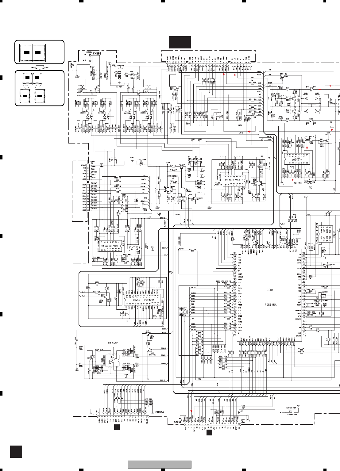
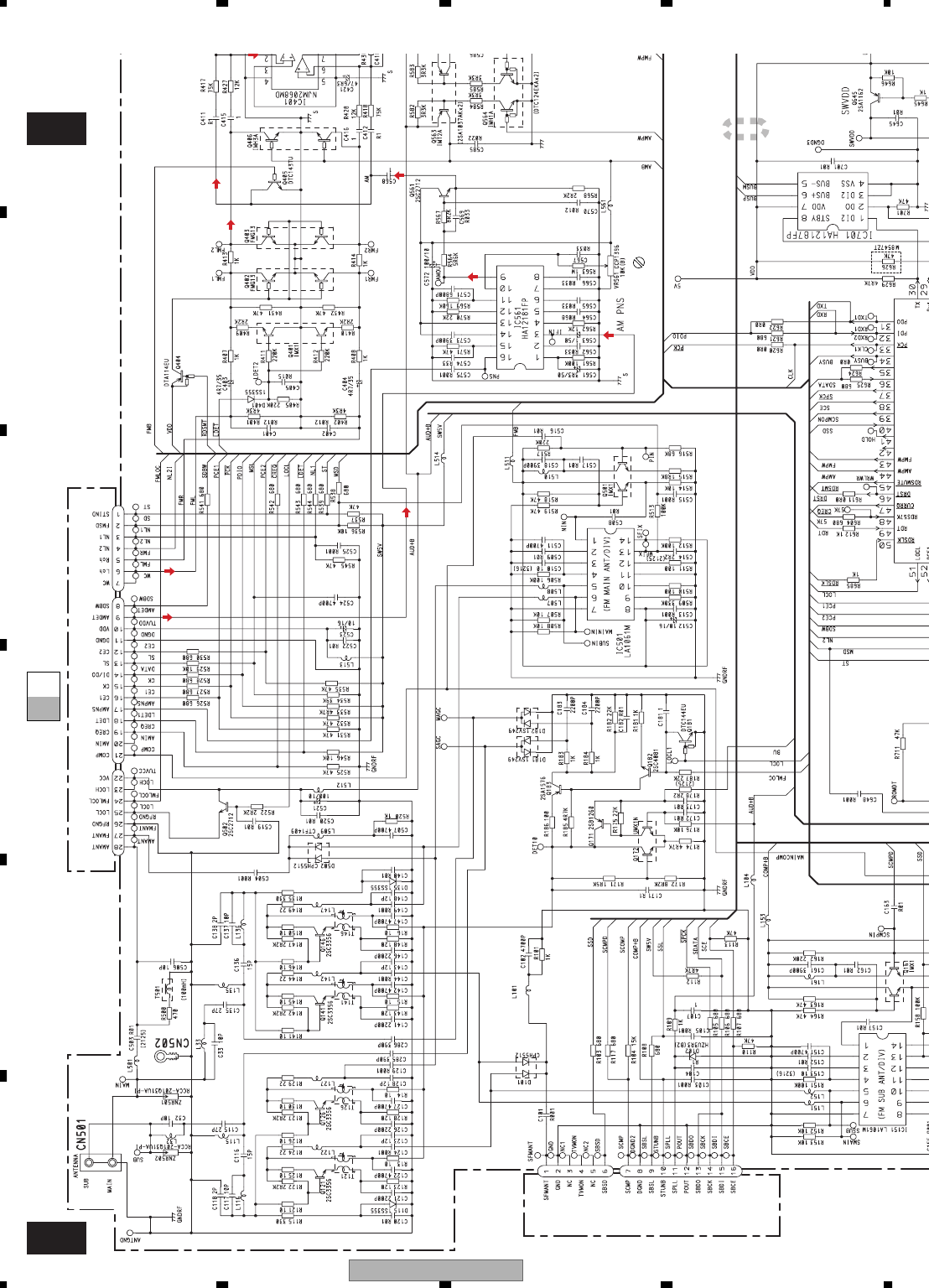
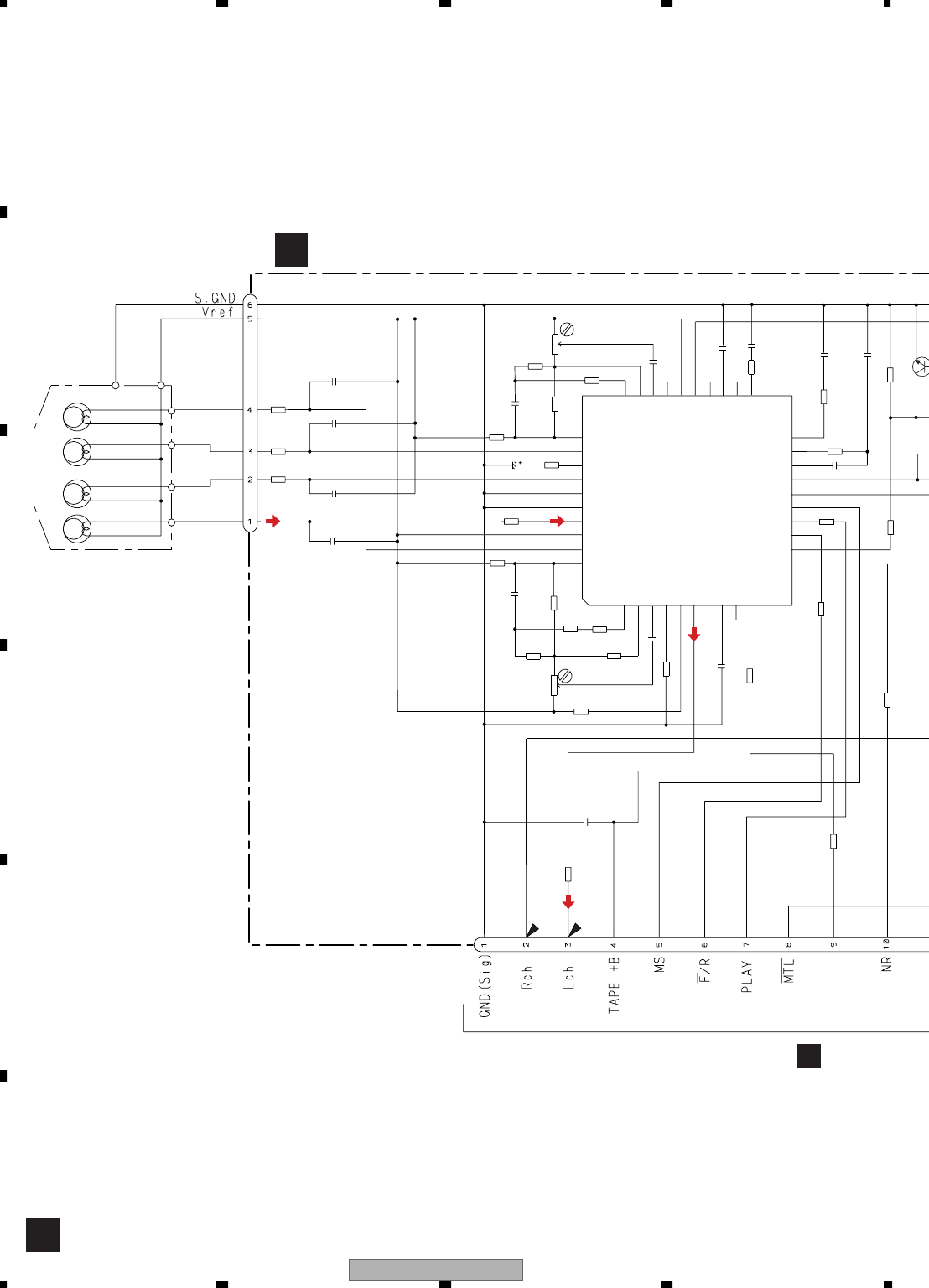
3. BLOCK DIAGRAM AND SCHEMATIC DIAGRAM
3.1 BLOCK DIAGRAM
CN501
ANTENNA
IC561
HA12181FP
16 3
9
S-80835CNNB-B8U
IC602
21
RESET
VDD
FML
13
12
reset
XOUT
AMAIN UNIT
FM/AM TUNER UNIT
KEYBOARD UNIT
B
51
LOCL
53
PCE2
33
pck
5
31
PDO
IC 3
EEPROM
28
27
FM/AM 1ST IF 10.7MHz
T51 Q51 CF51 CF52 CF53
IC1
MIXER, IF AMP, DET.
6
21
COMP
22
25 10 14 12 15 16 8 13 2 4
CF202
VDD
VCC
DI/DO
CE2
CK
CE1
SDBW
SL
FMSD
NL2
IC 2 FM MPX
AMANT
FMANT
ATT
ATT
AMRF
FMRF
IMG ADJ
RF ADJ
X901
10.25MHz
ANT ADJ
LOCL
AMDET
MPXREF 41kHz
AM 2ND IF
450kHz
1
STIND
L ch
9
AMDET
17
AMPNS
26 RFGND
C
KEY MATRIX
ILLUMINATION
Q502
AUD+B
SW5V
AM PNS
Q561
Q183
FM COMP
IC562
NJM2068MD
1
7
2
5
1613
15 14 6
9
SBSD
SBSL
SBCK
SBDI
SBDO
SBCE
Q172
Q565
BU
AUD+B
Q171
Q182
Q141
Q181
24
FMLOC
Q146
FM TUNER UNIT
17
SFMANT SCMP
32
PDI
A
B
(1
AUD+B
COMP+B
Q566
10
STUNB
COMP+B
SSL
SSD
SSL
spck
SCE
SDATA
ST
creq
MSD
PCE1
PCE2
PDIO
pck
Q121 FM SUB ANT/DIV
IC151
LA1061M
Q161
65
13
1
Q126 FM MAIN ANT/DIV
IC501
LA1061M
Q501
6
5
13
1
MAIN
SUB
1
2
D
C
C
D
NL2I
NL1
SDBW
MSL
CN251
CN252
CN253
CN255
CN256
CN254
IC251
HA12216F
TAPE EQUALIZER
MECHANISM DRIVER
IC351
PA2020B
Q271
BU
M
SUB
MOTOR
M
MAIN
MOTOR
7
+B
TAPE-L
MTL
MTL
VR302
VREF
6
16
11
12
28
37
39
17
5
2
NR
1
STBY
LOAD
LOAD
SWITCH
MODE
SENSE
1
4
5
2
1
4
3
20
64
1
64
1
CDECK UNIT
DSENSOR UNIT
SWITCH
70µs
19
CREQ
47
currq
BU
CN353
4
3
20
AUD+B
CSL
MS,DIR,PLAY,MTL,NR,CSLOAD,POS,ES,SC2,SC1,CM,STBY
3
NL1
18
LDET
Q401
19
FWD
LcH
REV
LcH
ldet
39 SCPON
40
92
37
38
36
35
spck
SPDI
SPDO
SSD
SCE
KEX-M8547ZT/EW 11
5678
5678
C
D
F
A
B
E
Q811 Q813
Q816
ILLB
NJM2068MD
IC204
NJM2068MD
IC203
L+
L+
L-
ANT
TX+
TX+
TX-
TX-
RSL-
RSL+
TX1-
TX1+
LANL
2
5
5
75
CN804
5,613,14
Q810
Q817
ILL+
ACC
13 15
e
t
HA12187FP
IC701
S-812C56AUA-C3K
IC870
XIN
4
LAMP
94
ILL-
XOUT
SYSTEM CONTROLLER
AVC-LAN
IC601
SW5V
AUD+B
KDT0-KDT3,kst0-kst@
6
sysmute
5
sysmute@
RX1
TX
IPPW 22
30
29
86
1
2
CN801
CN473
BU
+B
+B
U
NIT
51
LOCL
53
PCE2
33
pck
52
PCE1
93
MSL
56
FMSD
57
st
43
FMPW
31
PDO
TC4052BF
IC202
2TC4052BF
IC302
NJM2068MD
IC201
CN901
MATRIX
INATION
BU
7
NJM2068MD
IC304
Q205Q204
NJM2068MD
IC303
6
2
CN472
Q305Q304
Q867Q865
Q866Q864
Q860
Q861
Q862
Q863
BU
BU
3
Q563
Q405
Q564
44
AMPW
Q252
55
NL2
Q406
IC401
NJM2068MD
ACC
Q870
100
ANTB
5
32
BU
BU
VDD
73
2
asens
bsens
ISENS
Q807
ASEN
ACC
Q805
ISEN ILL+
75 Q806
BSEN
BU
AMP
AUD+B
Q453
Q645
Q644
11
SWVDD
VDD
SW5V
Q451
Q452
Q882
BU
Q884
AUDIO SELECTOR
FOR AMP
AUDIO SELECTOR
FOR RSA
RDS
DECODER
TUNER MIXING AMP UNBALANCE TO BALANCE
UNBALANCE TO BALANCE
BALANCE TO
UNBALANCE
SYSTEM MUTE
SYSTEM MUTE
5R6V IC
16763
7676
FML
AM
6
L-
LANLP
LANLM
CSL
TUL
LANL
TUL
CSL
FMB
AMB
FMB
AMB
32
PDI
VDD
Q404
Q203
Q303
96
Inh B
Inh B
9
25 28
SEL2b
SEL1b
Q302
Q202
95
97
STSW1
STSW2
A
BCMP+
CMP-
mute
mute
LANLP
LANLM
SWVDD
1
SYSPWR
LANMUTE
RSEMUTE 7
10
Q801
Q497
LAN MUTE
RES MUTE
Q825
SW5V
ILL-
X601
(10MHz)
RDS MUTE
AMP+
ILL-
111
10 20
10
1
11
20
SW1
SW2
rmut
12
67
1
AUDIO+B
21
RX2
DX251
(3.648MHz)
sysmt!
sysmt@
SEL2b
SEL1b
ANT+B
STSW1
STSW2
TX+
TX-
BUSP
BUSM
LP
LM
ANTPB
RSALP
RSALM
47
currq
54
SDBW
PD5945A
1
1
91
NL1
IC252
PM4009A
820
Q401 Q402 Q403
9
RCK,RDT,rdslk,57K,drst
O
N
k
D
I
D
O
E
45
rdsmute
12
11
ISEN
ASEN
BSEN
MUTE
RSEMT
KEX-M8547ZT/EW
12
1234
1234
C
D
F
A
B
E
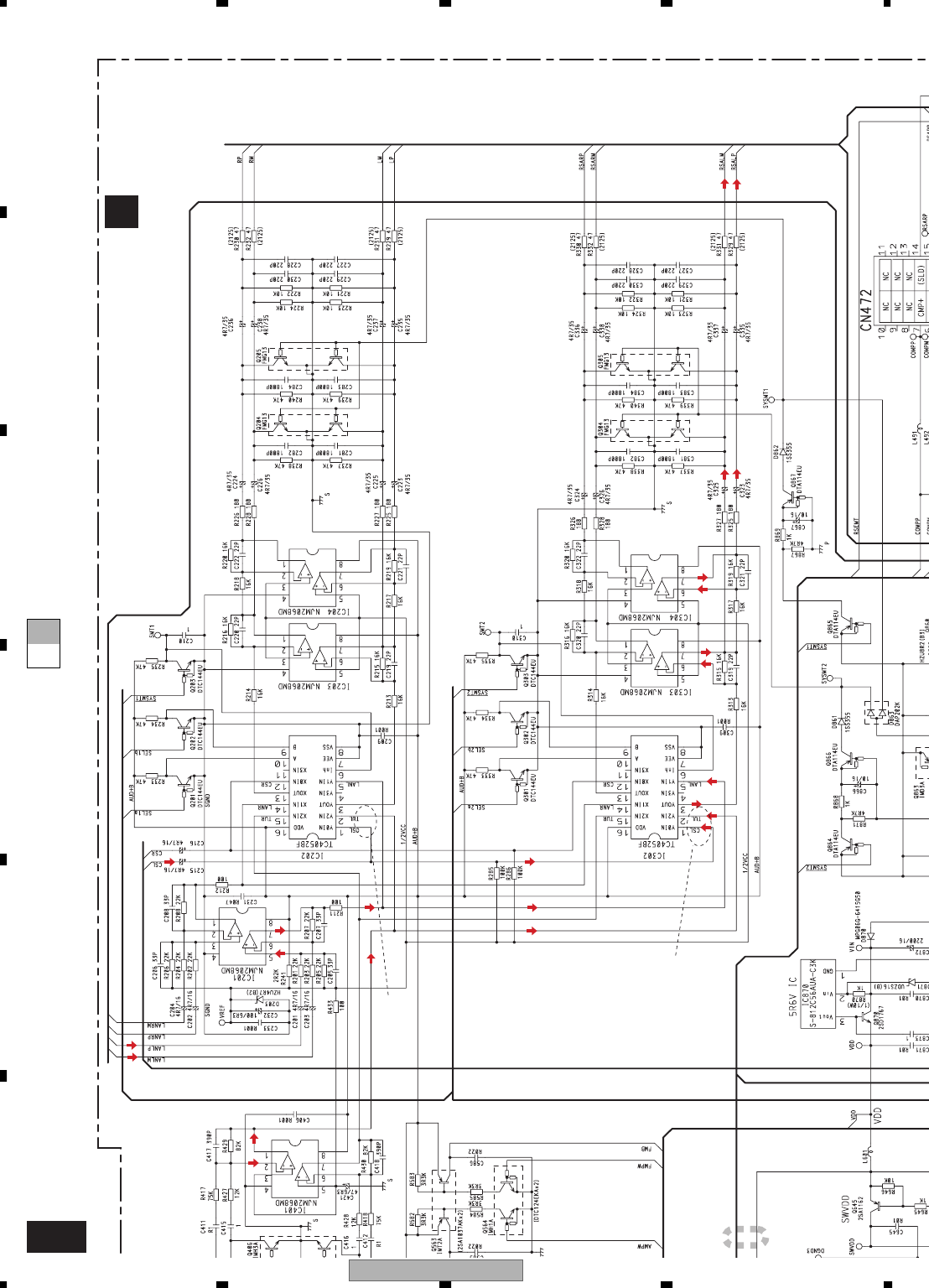
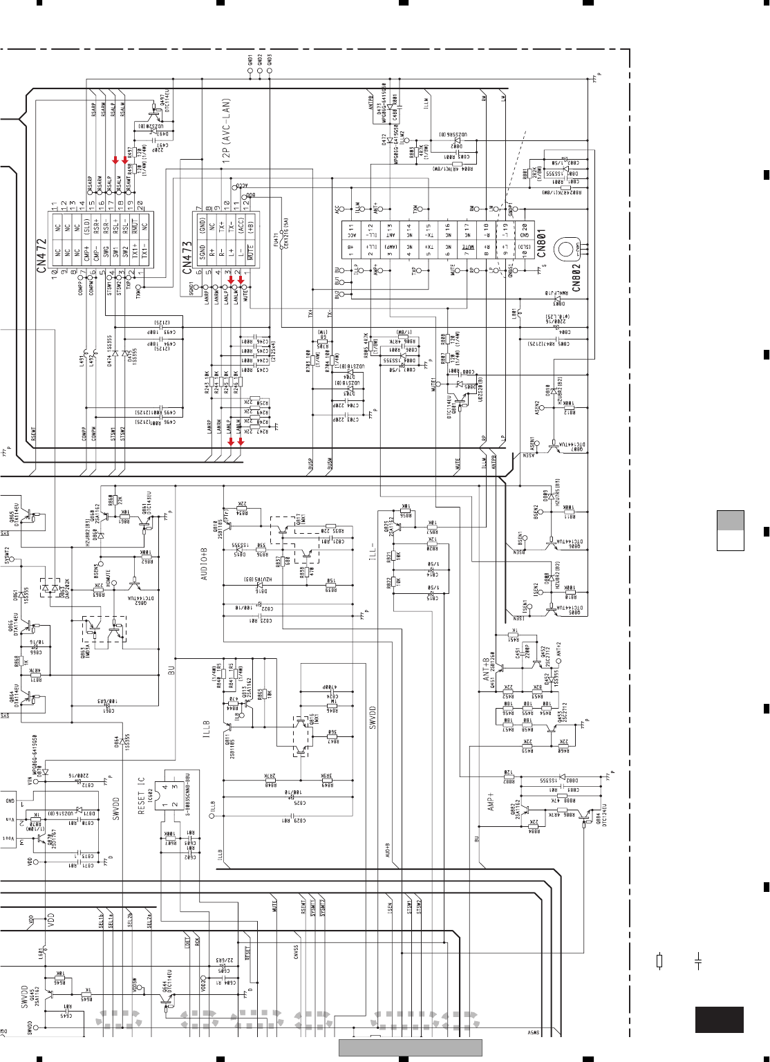
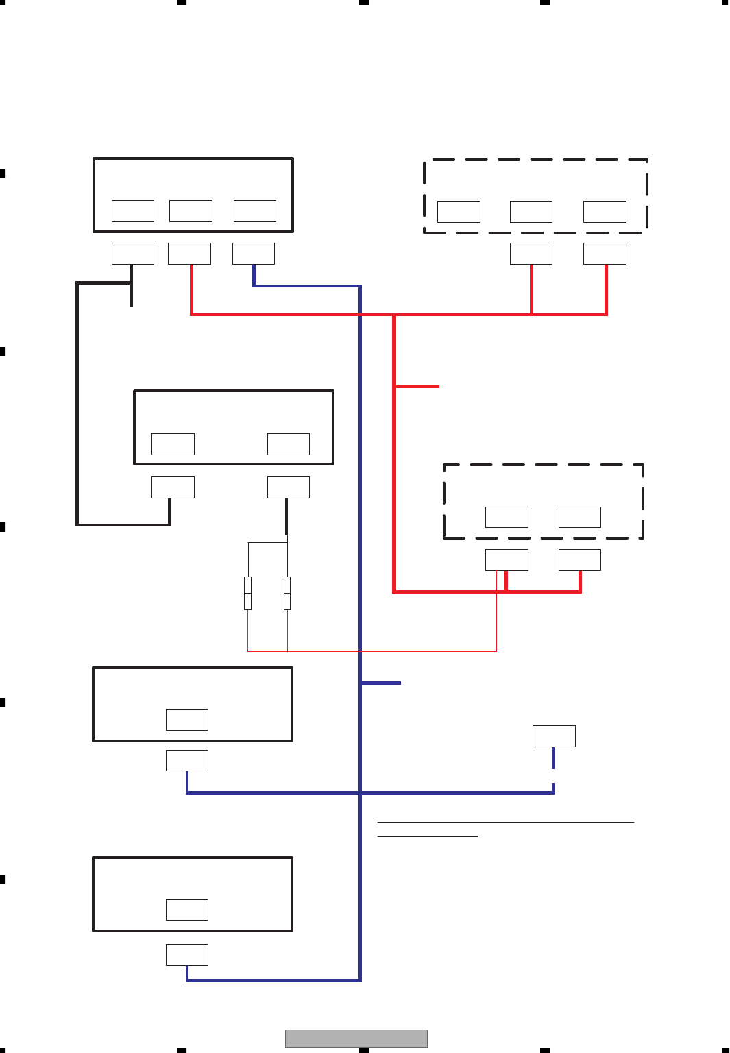
3.2 OVERALL CONNECTION DIAGRAM(GUIDE PAGE)
A-a A-b
A-a A-b
A-b
A-a
Large size
SCH diagram
Guide page
Detailed page
Note: When ordering service parts, be sure to refer to " EXPLODED VIEWS AND PARTS LIST" or
"ELECTRICAL PARTS LIST". A-a
A
KISYU
VCC
NC
NC
SHIMUKE
sysmute@
sysmute
SWVDD
NC
NC
NC
SPDI
spck
SPDO
SCE
SCPON
SSD
f/R
SSL
MSL
CCN251
BCN901
FM TUNER UNIT
FM/AM TUNER UNIT
SYSTEM CONTROLLER
RDS MUTE
RDS DECODER
KEX-M8547ZT/EW 13
5678
5678
C
D
F
A
B
E
A-b
A-a A-b
A-a A-b
A-b
A-a
A
>
AMAIN UNIT
Decimal points for resistor
and capacitor fixed values
are expressed as :
2.2 2R2
0.022 R022
←
←
The > mark found on some component parts indicates
the importance of the safety factor of the part.
Therefore, when replacing, be sure to use parts of
identical designation.
Symbol indicates a resistor.
No differentiation is made between chip resistors and
discrete resistors.
NOTE :
Symbol indicates a capacitor.
No differentiation is made between chip capacitors and
discrete capacitors.
ILL
SENSE B.UP
SENSE ACC
SENSE
R+
R-
L-
L+
(RSA)
L-
L+
(AMP)
UNBALANCE TO BALANCE
SYSTEM MUTE
SYSTEM MUTE
UNBALANCE TO BALANCE
TUNER MIXING AMP
BALANCE TO UNBALANCE
AUDIO SELECTOR
FOR AMP
AUDIO
SELECTOR
FOR RSA
VDD 5V
HARD MUTE
FM:-9.5dBs
AM:-13.4dBs
TAPE:-7.5dBs
FM:-9.5dBs
AM:-13.4dBs
TAPE:-7.5dBs
FM:-3.8dBs
AM:-7.7dBs
TAPE:-1.8dBs
KEX-M8547ZT/EW 17
5678
5678
C
D
F
A
B
E
A-a A-b
A-b
2345 6 7
>
Decimal points for resistor
and capacitor fixed values
are expressed as :
2.2 2R2
0.022 R022
←
←
The > mark found on some component parts indicates
the importance of the safety factor of the part.
Therefore, when replacing, be sure to use parts of
identical designation.
Symbol indicates a resistor.
No differentiation is made between chip resistors and
discrete resistors.
NOTE :
Symbol indicates a capacitor.
No differentiation is made between chip capacitors and
discrete capacitors.
ILL
SENSE B.UP
SENSE ACC
SENSE
VDD
5V
HARD MUTE
FM:-3.8dBs
AM:-7.7dBs
TAPE:-1.8dBs
KEX-M8547ZT/EW
20
1234
1234
C
D
F
A
B
E
3.4 CASSETTE MECHANISM MODULE
C
MUTE
HA12216F
11
12
13
14
15
16
17
18
19
20
40
39
38
37
36
35
34
33
32
31
30
29
28
27
26
25
24
23
22
21
1
2
3
4
5
6
7
8
9
10
R256
180
R291
0R0
C271
1/50
R283 0R0
R284 0R0
R282 0R0
C253 390P
C254 390P
C252 390P
C251 390P
R281 0R0
R255
180
C256
R01
R258
18K
R402
3R3K
R403 910
R322
0R0
R293
0R0
C272 R1
R287
0R0
R285 0R0
HD1
HEAD ASSY
EXA1594
TEST TAPE
NCT-150
(400Hz, 200nWb/m)
RL
RR
FR
FL
C302
R1
VR302
33K(B)
-8.24dBs(300mV)–1dB
Fwd-R
Fwd-L
Rev-R
Rev-L
NFI(L)
RIN(L)
RIP
FIN(L)
GND
GND
FIN(R)
VREF
RIN(R)
NFI(R)
M-OUT(R)
EQOUT(R)
TAI(R)
BIAS
RAI(R)
PBOUT(R)
DET(L)
MUTE
MSGV(R)
MAOUT
MSI
MSDET
MSGV
F/R
120/70
NR
MOUT(L)
EQOUT(L)
TAI(L)
NC
RAI(L)
PBOUT(L)
NC
DET(L)
MSGV(S)
CN252
CN251
DOLBY B NR
IC251
VR301
33K(B)
C310
R1
C309
R1
R321
0R0
VCC
CCP1280
CCP1280
NC
MSOUT
NC
NC
R260
13K
R262
270K
C401
3900P
R401
15K
R276
100K
C402
R33
C404 R01
C403
R022
R274
0R0
R273
0R0
R272
0R0
Q2
7
2S
C
R292
0R0
R271
18K
C301
R1
R294
0R0
R259
13K
C255
R01
R257
18K
R261
270K
DECK UNIT
A
C
CN353
KEX-M8547ZT/EW 21
5678
5678
C
D
F
A
B
E
C D
MUTE
SWITCHES:
REEL SENSE PCB
S101:LOAD SWITCH..........EJECT-PLAY
S102:MODE SWITCH............ON-OFF
S103:70 s SWITCH...............ON-OFF
The underlined indicates the switch position.
910
R275
47K
0R0
R351 1K
R352 1K
R353 1K
R354 1K
R373 0R0
R355
270K
C352
3900P
R362 300
C351 R22
C353 R01
C354 R01
R374 0R0
C356 R01
C355 R1
D352 1SS355
M1 MOTOR UNIT
(MAIN MOTOR)
EXA1618
S101
LOAD
ESG1007x3
S102 MODE
Q101
EGN1004
M2
MOTOR UNIT
(SUB MOTOR)
EXA1660
RS3
RS2
RS1
SC2
SC1
TAB
MC
CE
VCC2
NC
VCC
MCS
RRS
FRS
RSB
C
TAB
MS2
NC
NC
MM
SM1
RSB
GND
RS
mtl
MCS
load
CN255 CN253 CN256
CN254
MECHANISM
DRIVER
IC351 PA2020B
R321
0R0
R375 0R0
S103 70 s
R276
100K
R01
C403
R022
R274
0R0
3
R404
270K
C405 R033
R277
220K
R278 100K
Q271
2SC4116
L101
L102
SENSOR UNIT
D
C
N353
KEX-M8547ZT/EW
22
1234
1234
C
D
F
A
B
E
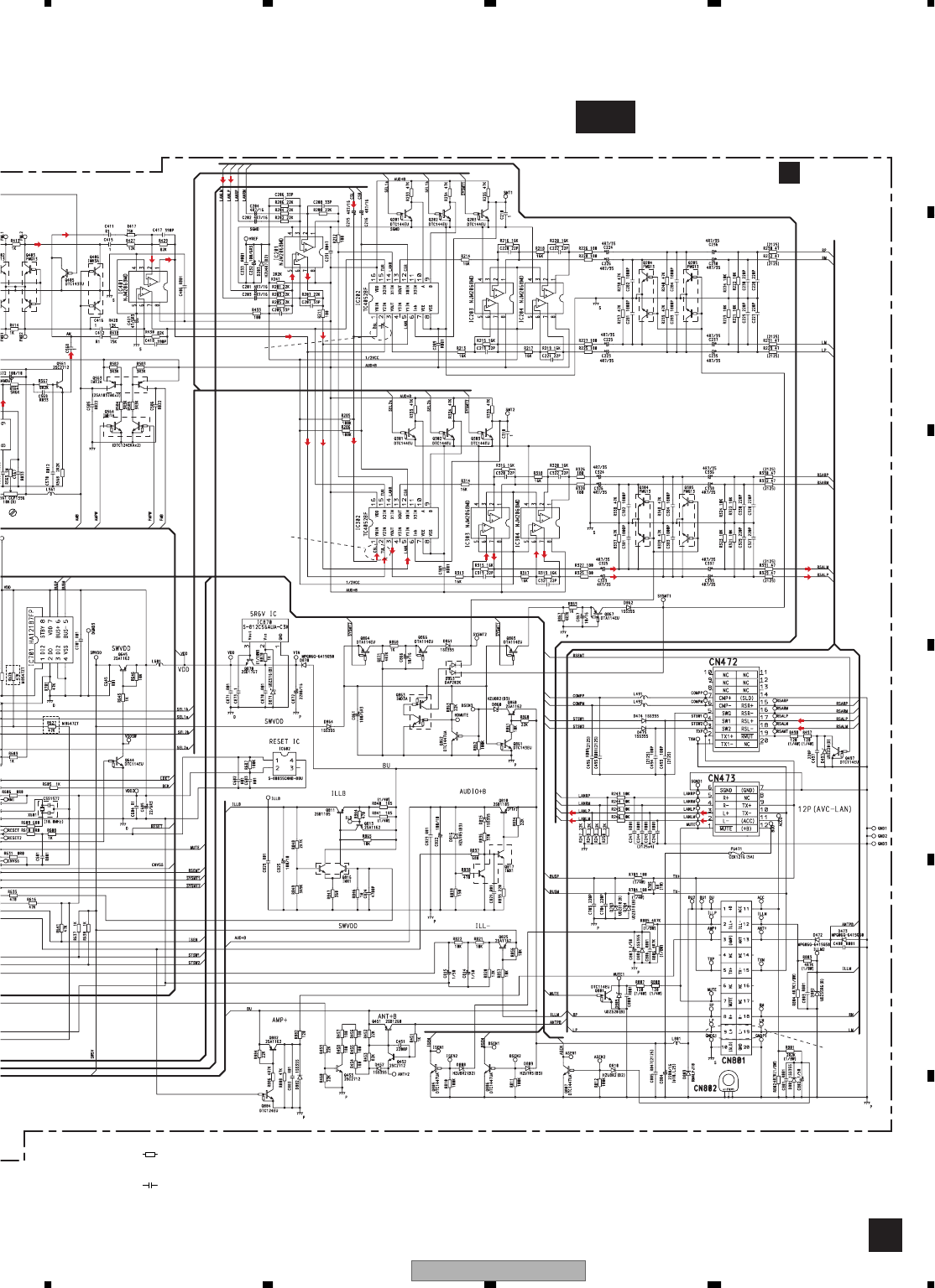
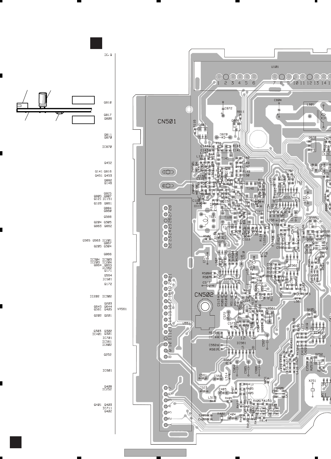
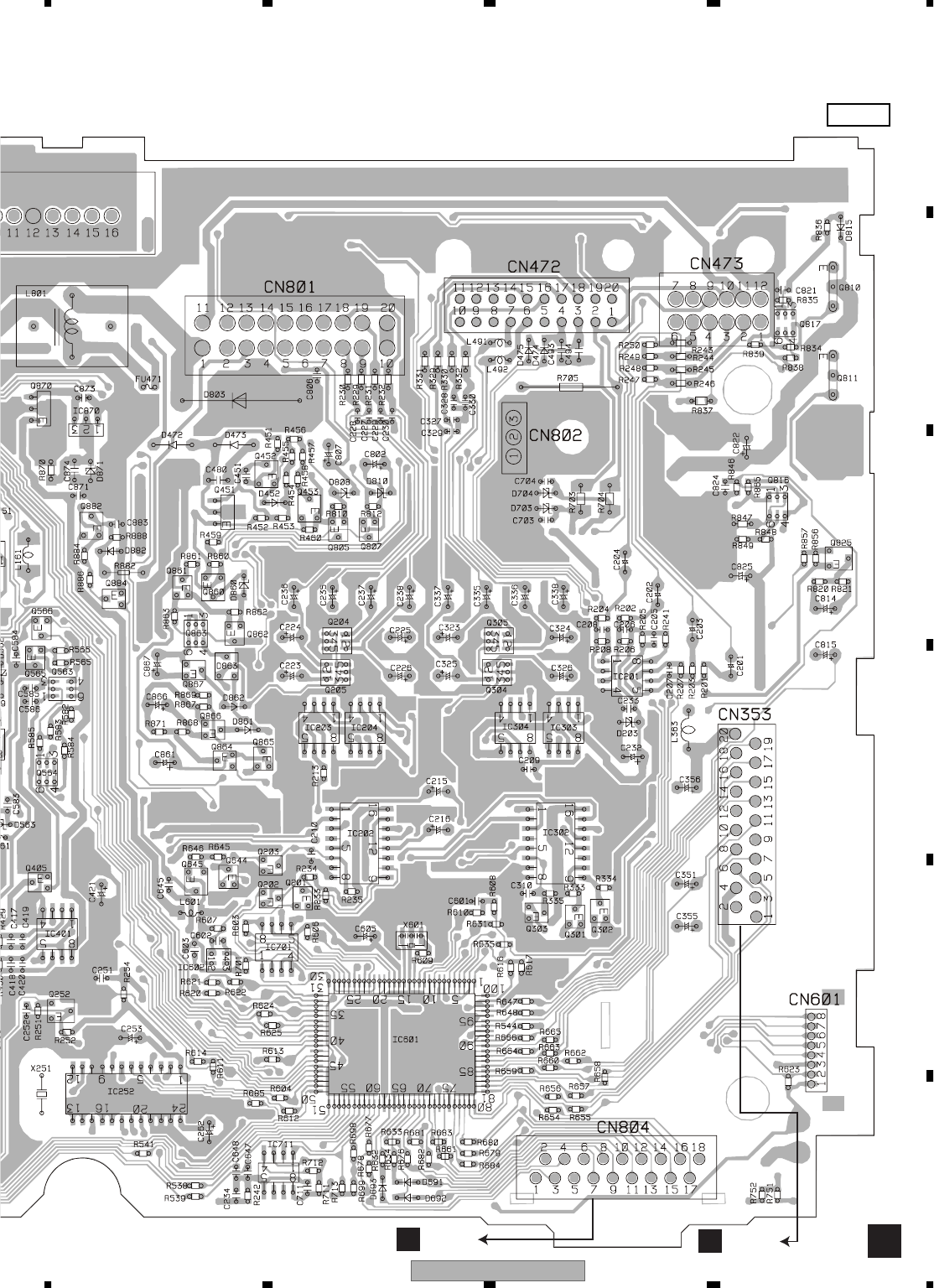
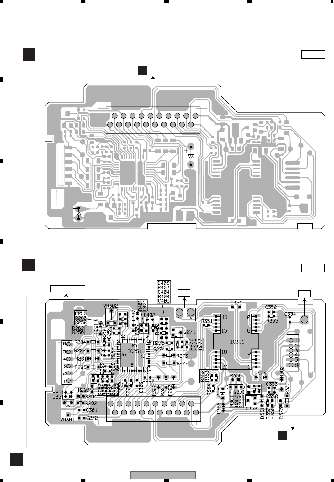
4. PCB CONNECTION DIAGRAM
4.1 MAIN UNIT
Capacitor
Connector
P.C.Board Chip Part
A
AMAIN UNIT
SIDE B
SIDE A
NOTE FOR PCB DIAGRAMS
1.The parts mounted on this PCB
include all necessary parts for
several destination.
For further information for
respective destinations, be sure
to check with the schematic dia-
gram.
2.Viewpoint of PCB diagrams
ADJ
ANTENNA
FM/AM TUNER UNIT
FM TUNER U
N
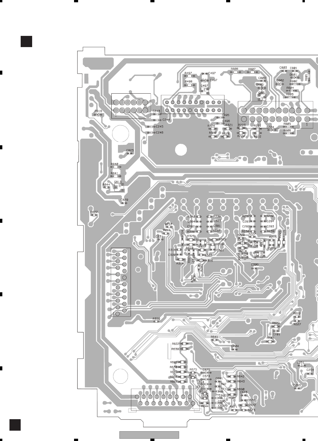
KEX-M8547ZT/EW
26
1234
1234
C
D
F
A
B
E
4.2 KEYBOARD UNIT(KEX-M8547ZT/EW)
B
BKEYBOARD UNIT BKEYBOARD UNIT
SIDE A SIDE B
A
CN804
TA
TUNE
DISC
SEEK
TRACK
>
>
SEEK
TRACK
TAPE
FM
AM
EJECT
PWR•VOL
>
CH
PROG
DISC
>
CH
PROG
DISC
KEX-M8547ZT/EW 27
5678
5678
C
D
F
A
B
E
4.3 KEYBOARD UNIT(KEX-M8647ZT/EW)
B
BKEYBOARD UNIT BKEYBOARD UNIT
SIDE A SIDE B
A
CN804
EJECT
PWR•VOL
AM
SEEK
TRACK
>
>
SEEK
TRACK
FM
TAPE
DISC
TA
TUNE
>
>
CH
PROG
DISC
CH
PROG
DISC
KEX-M8547ZT/EW
28
1234
1234
C
D
F
A
B
E
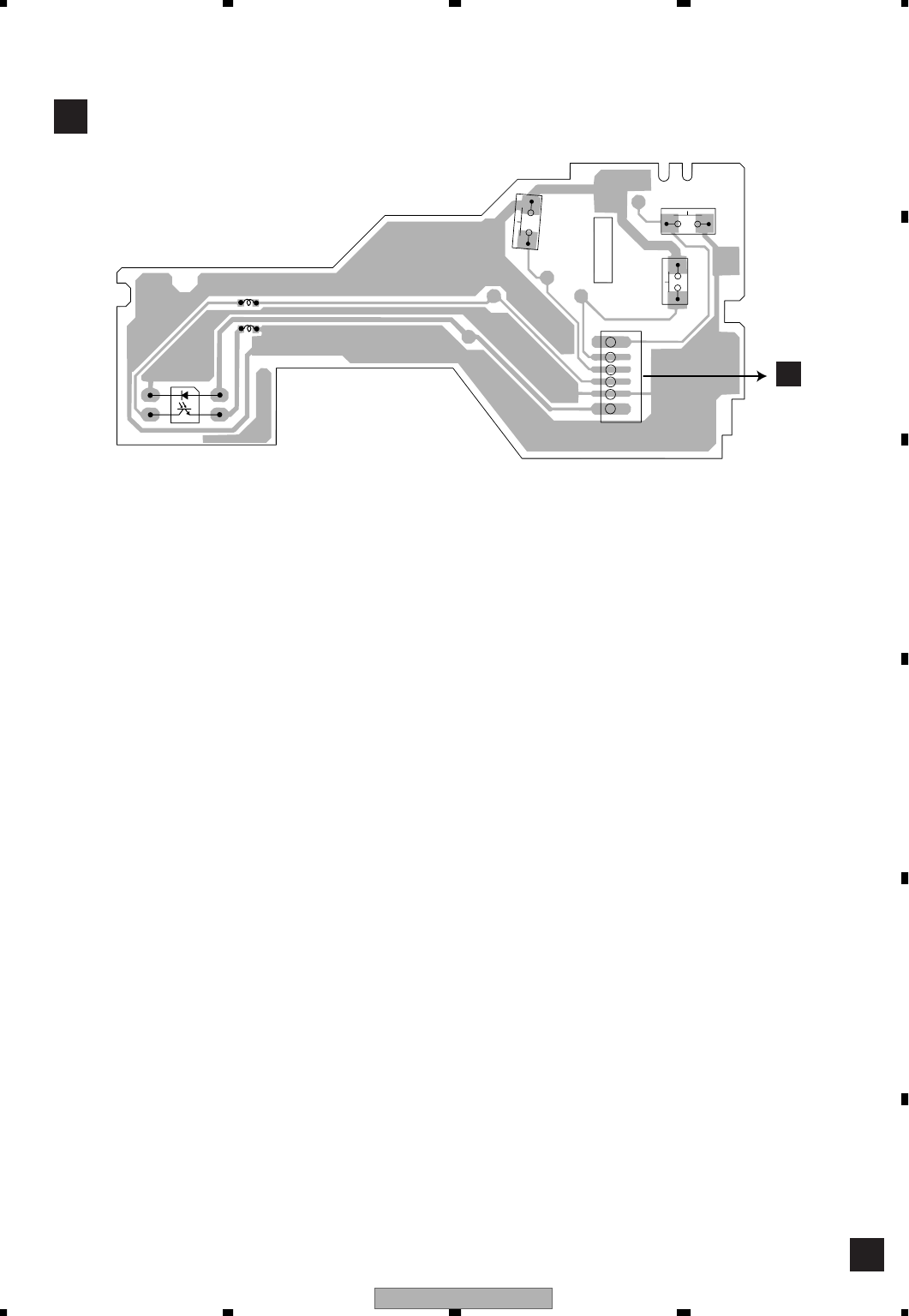
4.4 CASSETTE MECHANISM MODULE
C
CDECK UNIT
CDECK UNIT
SIDE A
SIDE B
C321
C271
19
17
15
13
11
9
7
5
3
1
16
14
12
10
8
6
4
220
18
CN251
IC,Q
IC251
Q351
Q352
ADJ
VR302
VR301
IC253
CN252
CN254
CN253
CN255
M1
M2
HEAD ASSY
21
22
ACN353
1
DCN256
KEX-M8547ZT/EW 29
5678
5678
C
D
F
A
B
E
D
DSENSOR UNIT
1
2
3
4
5
6
S101
LOAD
S102
MODE
S103
70µs
CN256
Q101
REEL SENSE
L101
L102
C
CN253

KEX-M8547ZT/EW
30
1234
1234
C
D
F
A
B
E
5. ELECTRICAL PARTS LIST
NOTE:
• Parts whose parts numbers are omitted are subject to being not supplied.
• The part numbers shown below indicate chip components.
Chip Resistor
RS1/_S___J,RS1/__S___J
Chip Capacitor (except for CQS.....)
CKS....., CCS....., CSZS.....
Circuit Symbol and No. Part No.
A
Unit Number:CWM9554 (M8547ZT)
Unit Number:CWM9555 (M8647ZT)
Unit Name:Main Unit
MISCELLANEOUS
IC 151 IC LA1061M
IC 201 IC NJM2068MD
IC 202 IC TC4052BF
IC 203 IC NJM2068MD
IC 204 IC NJM2068MD
IC 252 IC PM4009A
IC 302 IC TC4052BF
IC 303 IC NJM2068MD
IC 304 IC NJM2068MD
IC 401 IC NJM2068MD
IC 501 IC LA1061M
IC 561 IC HA12181FP
IC 562 IC NJM2068MD
IC 601 IC PD5945A
IC 602 IC S-80835CNNB-B8U
IC 701 IC HA12187FP
IC 870 IC S-812C56AUA-C3K
Q 121 Transistor 2SC3356
Q 126 Transistor 2SC3356
Q 141 Transistor 2SC3356
Q 146 Transistor 2SC3356
Q 161 Transistor IMX1
Q 171 Transistor 2SB1260
Q 172 Transistor UMX1N
Q 181 Transistor DTC144EU
Q 182 Transistor 2SC4081
Q 183 Transistor 2SA1576
Q 201 Transistor DTC144EU
Q 202 Transistor DTC144EU
Q 203 Transistor DTC144EU
Q 204 Transistor FMG13
Q 205 Transistor FMG13
Q 252 Transistor 2SC3052-12
Q 301 Transistor DTC144EU
Q 302 Transistor DTC144EU
Q 303 Transistor DTC144EU
Q 304 Transistor FMG13
Q 305 Transistor FMG13
Q 401 Transistor IMX1
Q 402 Transistor FMG13
Q 403 Transistor FMG13
Q 404 Transistor DTA114EU
Q 405 Transistor DTC143TU
Q 406 Transistor IMH3A
Q 451 Transistor 2SB1260
Q 452 Transistor 2SC2712
Q 453 Transistor 2SC2712
Q 497 Transistor DTC114EU
Q 501 Transistor IMX1
Q 502 Transistor 2SC2712
Q 561 Transistor 2SC2712
Q 563 Transistor IMT2A
Q 564 Transistor IMH1A
Q 565 Transistor 2SB1689
Q 566 Transistor DTC114EU
Q 644 Transistor DTC114EU
Q 645 Transistor 2SA1162
Q 801 Transistor DTC114EU
Q 805 Transistor DTC144TUA
Q 806 Transistor DTC144TUA
Q 807 Transistor DTC144TUA
Q 810 Transistor 2SB1185
Q 811 Transistor 2SB1185
Q 813 Transistor 2SA1162
Q 816 Transistor IMX1
Q 817 Transistor IMX1
Q 825 Transistor 2SA1162
Q 860 Transistor 2SA1162
Q 861 Transistor DTC143EU
Q 862 Transistor DTC144TUA
Q 863 Transistor IMD3A
Q 864 Transistor DTA114EU
Q 865 Transistor DTA114EU
Q 866 Transistor DTA114EU
Q 867 Transistor DTA114EU
Q 870 Transistor 2SD1767
Q 882 Transistor 2SA1162
Q 884 Transistor DTC124EU
D 101 Diode CPH5512
D 102 Diode HZU3R3(B2)
D 115 Diode 1SS355
D 135 Diode 1SS355
D 181 Diode 1SV249
D 182 Diode 1SV249
D 203 Diode HZU4R7(B2)
D 401 Diode 1SS355
D 452 Diode 1SS355
D 472 Diode MPG06G-6415G50
Circuit Symbol and No. Part No.

KEX-M8547ZT/EW 31
5678
5678
C
D
F
A
B
E
D 473 Diode MPG06G-6415G50
D 474 Diode 1SS355
D 475 Diode 1SS355
D 497 Diode UDZS20(B)
D 502 Diode CPH5512
D 562 Diode UDZS10(B)
D 563 Diode UDZS10(B)
D 691 Diode 1SS355
D 692 Diode 1SS355
D 693 Diode 1SS355
D 703 Diode UDZS18(B)
D 704 Diode UDZS18(B)
D 801 Diode 1SS355
D 802 Diode UDZS5R6(B)
D 803 Diode RM4LFJ10
D 804 Diode 1SS355
D 805 Diode UDZS20(B)
D 808 Diode HZU8R2(B2)
D 809 Diode HZU7R5(B3)
D 810 Diode HZU8R2(B2)
D 815 Diode 1SS355
D 816 Diode HZU7R5(B3)
D 860 Diode HZU8R2(B3)
D 861 Diode 1SS355
D 862 Diode 1SS355
D 863 Diode DAP202K
D 864 Diode 1SS355
D 870 Diode MPG06G-6415G50
D 871 Diode UDZS16(B)
D 882 Diode 1SS355
ZNR501 Surge Protector RCCA-201Q31UA-PI
ZNR502 Surge Protector RCCA-201Q31UA-PI
L 32 Inductor LCYB12NJ1608
L 33 Inductor LCYB12NJ1608
L 101 Inductor CTF1409
L 104 Inductor CTF1473
L 115 Inductor LCYBR12J1608
L 116 Inductor LCYBR12J1608
L 122 Inductor LCYBR10J1608
L 127 Inductor LCYBR10J1608
L 135 Inductor LCYBR12J1608
L 136 Inductor LCYBR12J1608
L 142 Inductor LCYBR10J1608
L 147 Inductor LCYBR10J1608
L 151 Inductor CTF1409
L 152 Inductor CTF1409
L 153 Inductor CTF1473
L 161 Inductor LCTA561J4532
L 251 Inductor LCTA101J2520
L 363 Inductor LFEA4R7J
L 491 Inductor CTF1578
L 492 Inductor CTF1578
L 501 Inductor LCTA4R7J2520
L 507 Inductor CTF1409
L 508 Inductor CTF1409
L 509 Inductor CTF1409
L 510 Inductor LCTA561J4532
L 511 Inductor CTF1473
L 512 Inductor LCTA1R0J2520
L 513 Inductor CTF1473
Circuit Symbol and No. Part No.
L 514 Inductor CTF1473
L 561 Inductor CTF1473
L 601 Inductor LCTA100J3225
L 801 Coil 350µH CTH1276
T 121 Coil CTC1187
T 126 Coil CTC1187
T 141 Coil CTC1187
T 146 Coil CTC1187
T 501 Coil CTB1102
X 251 Crystal Resonator 3.648MHz CSS1447
X 601 Radiator 10.0MHz CSS1577
VR561 Semi-fixed 10kΩ(B) CCP1396
FU471 Fuse 5A CEK1216
FM Tuner Unit CWE1679
FM/AM Tuner Unit CWE1773
RESISTORS
R 13 RS1/16S100J
R 14 RS1/16S100J
R 15 RS1/16S100J
R 16 RS1/16S100J
R 101 RS1/16S102J
R 103 RS1/16S681J
R 104 RS1/16S153J
R 105 RS1/16S681J
R 106 RS1/16S681J
R 107 RS1/16S681J
R 108 RS1/16S681J
R 109 RS1/16S102J
R 110 RS1/16S473J
R 112 RS1/16S472J
R 113 RS1/16S473J
R 115 RS1/16S331J
R 117 RS1/16S681J
R 121 RS1/16S100J
R 122 RS1/16S222J
R 123 RS1/16S121J
R 124 RS1/16S220J
R 125 RS1/16S100J
R 126 RS1/16S100J
R 127 RS1/16S222J
R 128 RS1/16S121J
R 129 RS1/16S220J
R 130 RS1/16S100J
R 135 RS1/16S331J
R 141 RS1/16S100J
R 142 RS1/16S222J
R 143 RS1/16S121J
R 144 RS1/16S220J
R 145 RS1/16S100J
R 146 RS1/16S100J
R 147 RS1/16S222J
R 148 RS1/16S121J
R 149 RS1/16S220J
R 150 RS1/16S100J
R 151 RS1/16S104J
R 152 RS1/16S103J
R 153 RS1/16S103J
R 154 RS1/16S334J
Circuit Symbol and No. Part No.

KEX-M8547ZT/EW
32
1234
1234
C
D
F
A
B
E
R 155 RS1/16S101J
R 156 RS1/16S101J
R 157 RS1/16S104J
R 158 RS1/16S104J
R 161 RS1/16S683J
R 162 RS1/16S224J
R 163 RS1/16S473J
R 164 RS1/16S473J
R 165 RS1/16S182J
R 166 RS1/16S103J
R 171 RS1/16S152J
R 172 RS1/16S822J
R 174 RS1/16S472J
R 175 RS1/16S223J
R 176 RS1/16S103J
R 178 RS1/10S2R2J
R 181 RS1/16S102J
R 182 RS1/16S223J
R 183 RS1/16S102J
R 184 RS1/16S102J
R 185 RS1/16S472J
R 186 RS1/16S101J
R 187 RS1/16S223J
R 201 RS1/16S223J
R 202 RS1/16S223J
R 203 RS1/16S223J
R 204 RS1/16S223J
R 205 RS1/16S223J
R 206 RS1/16S223J
R 207 RS1/16S223J
R 208 RS1/16S223J
R 211 RS1/16S101J
R 212 RS1/16S101J
R 213 RS1/16S163J
R 214 RS1/16S163J
R 215 RS1/16S163J
R 216 RS1/16S163J
R 217 RS1/16S163J
R 218 RS1/16S163J
R 219 RS1/16S163J
R 220 RS1/16S163J
R 221 RS1/16S103J
R 222 RS1/16S103J
R 223 RS1/16S103J
R 224 RS1/16S103J
R 225 RS1/16S181J
R 226 RS1/16S181J
R 227 RS1/16S181J
R 228 RS1/16S181J
R 229 RS1/10S470J
R 230 RS1/10S470J
R 231 RS1/10S470J
R 232 RS1/10S470J
R 233 RS1/16S473J
R 234 RS1/16S473J
R 235 RS1/16S473J
R 237 RS1/16S473J
R 238 RS1/16S473J
R 239 RS1/16S473J
R 240 RS1/16S473J
Circuit Symbol and No. Part No.
R 241 RS1/16S222J
R 243 RS1/10S103J
R 244 RS1/10S103J
R 245 RS1/10S103J
R 246 RS1/10S103J
R 247 RS1/16S223J
R 248 RS1/16S223J
R 249 RS1/16S223J
R 250 RS1/16S223J
R 251 RS1/16S153J
R 252 RS1/16S474J
R 253 RS1/16S681J
R 254 RS1/16S0R0J
R 257 RS1/16S102J
R 261 RS1/16S225J
R 285 RS1/16S104J
R 286 RS1/16S104J
R 313 RS1/16S163J
R 314 RS1/16S163J
R 315 RS1/16S163J
R 316 RS1/16S163J
R 317 RS1/16S163J
R 318 RS1/16S163J
R 319 RS1/16S163J
R 320 RS1/16S163J
R 321 RS1/16S103J
R 322 RS1/16S103J
R 323 RS1/16S103J
R 324 RS1/16S103J
R 325 RS1/16S181J
R 326 RS1/16S181J
R 327 RS1/16S181J
R 328 RS1/16S181J
R 329 RS1/10S470J
R 330 RS1/10S470J
R 331 RS1/10S470J
R 332 RS1/10S470J
R 333 RS1/16S473J
R 334 RS1/16S473J
R 335 RS1/16S473J
R 337 RS1/16S473J
R 338 RS1/16S473J
R 339 RS1/16S473J
R 340 RS1/16S473J
R 359 RS1/16S100J
R 401 RS1/16S432J
R 402 RS1/16S432J
R 405 RS1/16S224J
R 407 RS1/16S102J
R 408 RS1/16S102J
R 409 RS1/16S222J
R 410 RS1/16S222J
R 411 RS1/16S224J
R 412 RS1/16S224J
R 413 RS1/16S102J
R 414 RS1/16S102J
R 417 RS1/16S753J
R 418 RS1/16S753J
R 427 RS1/16S123J
R 428 RS1/16S123J
Circuit Symbol and No. Part No.

KEX-M8547ZT/EW 33
5678
5678
C
D
F
A
B
E
R 429 RS1/16S823J
R 430 RS1/16S823J
R 431 RS1/16S473J
R 432 RS1/16S473J
R 433 RS1/16S101J
R 451 RS1/16S102J
R 452 RS1/16S223J
R 453 RS1/16S823J
R 454 RS1/16S181J
R 455 RS1/16S181J
R 456 RS1/16S181J
R 457 RS1/16S181J
R 458 RS1/16S181J
R 459 RS1/16S223J
R 460 RS1/16S223J
R 497 RS1/4S121J
R 498 RS1/4S121J
R 500 RS1/16S471J
R 506 RS1/16S104J
R 507 RS1/16S103J
R 508 RS1/16S103J
R 509 RS1/16S334J
R 510 RS1/16S101J
R 511 RS1/16S101J
R 512 RS1/16S104J
R 513 RS1/16S104J
R 514 RS1/16S103J
R 515 RS1/16S182J
R 516 RS1/16S683J
R 517 RS1/16S224J
R 518 RS1/16S473J
R 519 RS1/16S473J
R 520 RS1/16S102J
R 522 RS1/16S222J
R 525 RS1/16S473J
R 526 RS1/16S681J
R 527 RS1/16S681J
R 528 RS1/16S681J
R 529 RS1/16S103J
R 530 RS1/16S681J
R 531 RS1/16S473J
R 532 RS1/16S473J
R 533 RS1/16S472J
R 534 RS1/16S393J
R 535 RS1/16S473J
R 536 RS1/16S103J
R 537 RS1/16S473J
R 538 RS1/16S681J
R 539 RS1/16S681J
R 541 RS1/16S681J
R 542 RS1/16S681J
R 543 RS1/16S681J
R 544 RS1/16S681J
R 545 RS1/16S473J
R 546 RS1/16S103J
R 561 RS1/16S104J
R 562 RS1/16S123J
R 563 RS1/16S105J
R 564 RS1/16S562J
R 565 RS1/16S223J
Circuit Symbol and No. Part No.
R 566 RS1/16S222J
R 567 RS1/16S822J
R 568 RS1/16S222J
R 569 RS1/16S164J
R 570 RS1/16S223J
R 571 RS1/16S473J
R 572 RS1/16S472J
R 573 RS1/16S332J
R 574 RS1/16S332J
R 575 RS1/16S332J
R 576 RS1/16S683J
R 577 RS1/16S332J
R 578 RS1/16S683J
R 579 RS1/16S221J
R 580 RS1/16S221J
R 581 RS1/16S683J
R 582 RS1/16S332J
R 583 RS1/16S332J
R 584 RS1/16S332J
R 585 RS1/16S332J
R 588 RS1/16S562J
R 603 RS1/16S102J
R 604 RS1/16S681J
R 605 RS1/16S102J
R 606 RS1/16S0R0J
R 607 RS1/16S104J
R 608 RS1/16S102J
R 609 RS1/16S681J
R 610 RS1/16S0R0J
R 611 RS1/16S0R0J
R 612 RS1/16S102J
R 616 RS1/16S473J
R 620 RS1/16S0R0J
R 621 RS1/16S681J
R 622 RS1/16S0R0J
R 624 RS1/16S0R0J
R 625 RS1/16S681J
R 626 (M8547ZT) RS1/16S473J
R 627 (M8647ZT) RS1/16S473J
R 629 RS1/16S472J
R 631 RS1/16S0R0J
R 632 RS1/16S102J
R 633 RS1/16S102J
R 634 RS1/16S102J
R 635 RS1/16S471J
R 637 RS1/16S102J
R 638 RS1/16S102J
R 641 RS1/16S473J
R 642 RS1/16S104J
R 643 RS1/16S104J
R 644 RS1/16S473J
R 645 RS1/16S102J
R 646 RS1/16S103J
R 647 RS1/16S102J
R 648 RS1/16S102J
R 654 RS1/16S102J
R 655 RS1/16S102J
R 656 RS1/16S102J
R 657 RS1/16S102J
R 658 RS1/16S223J
Circuit Symbol and No. Part No.

KEX-M8547ZT/EW
34
1234
1234
C
D
F
A
B
E
R 659 RS1/16S102J
R 660 RS1/16S102J
R 661 RS1/16S102J
R 662 RS1/16S102J
R 663 RS1/16S102J
R 664 RS1/16S102J
R 665 RS1/16S102J
R 666 RS1/16S681J
R 667 RS1/16S473J
R 668 RS1/16S473J
R 669 RS1/16S473J
R 670 RS1/16S473J
R 671 RS1/16S473J
R 672 RS1/16S473J
R 673 RS1/16S473J
R 674 RS1/16S473J
R 675 RS1/16S473J
R 676 RS1/16S102J
R 677 RS1/16S102J
R 678 RS1/16S102J
R 679 RS1/16S102J
R 680 RS1/16S102J
R 681 RS1/16S102J
R 682 RS1/16S102J
R 683 RS1/16S102J
R 684 RS1/16S102J
R 685 RS1/16S102J
R 687 RS1/16S473J
R 690 RS1/16S473J
R 691 RS1/16S473J
R 692 RS1/16S473J
R 693 RS1/16S473J
R 698 RS1/16S102J
R 699 RS1/16S473J
R 701 RS1/16S473J
R 703 RS1/4S101J
R 704 RS1/4S101J
R 705 RS1PMF680J
R 711 RS1/16S473J
R 751 (M8647ZT) RS1/16S822J
R 801 RS1/8S222J
R 802 RS1/8S472J
R 803 RS1/8S472J
R 804 RS1/8S472J
R 805 RS1/8S472J
R 806 RS1/8S472J
R 807 RS1/4S121J
R 808 RS1/4S121J
R 810 RS1/16S104J
R 811 RS1/16S104J
R 812 RS1/16S104J
R 820 RS1/16S123J
R 821 RS1/16S103J
R 822 RS1/16S103J
R 834 RS1/16S223J
R 835 RS1/16S221J
R 836 RS1/16S331J
R 837 RS1/16S681J
R 838 RS1/16S471J
R 839 RS1/16S151J
Circuit Symbol and No. Part No.
R 840 RS1/4S1R5J
R 841 RS1/4S1R5J
R 844 RS1/16S471J
R 846 RS1/16S105J
R 847 RS1/10S361J
R 848 RS1/16S272J
R 849 RS1/16S392J
R 856 RS1/16S103J
R 857 RS1/16S103J
R 860 RS1/16S223J
R 861 RS1/16S103J
R 862 RS1/16S104J
R 863 RS1/16S223J
R 865 RS1/16S103J
R 867 RS1/16S472J
R 868 RS1/16S102J
R 869 RS1/16S102J
R 870 RS1/10S102J
R 871 RS1/16S472J
R 882 RD1/4PU121J
R 884 RS1/16S223J
R 886 RS1/16S472J
R 888 RS1/16S473J
CAPACITORS
C 32 CCSRCH100D50
C 33 CCSRCH100D50
C 101 CKSRYB102K50
C 102 CKSRYB472K50
C 103 CKSRYB102K50
C 104 CKSRYB104K25
C 105 CKSRYB102K50
C 107 CKSRYB105K10
C 115 CCSRCH270J50
C 116 CCSRCH150J50
C 117 CCSRCH100D50
C 118 CCSRCK2R0C50
C 120 CKSRYB103K50
C 121 CKSRYB222K50
C 122 CKSRYB472K50
C 123 CCSRCH120J50
C 124 CKSRYB102K50
C 126 CKSRYB222K50
C 127 CKSRYB472K50
C 128 CCSRCH120J50
C 129 CKSRYB102K50
C 135 CCSRCH270J50
C 136 CCSRCH150J50
C 137 CCSRCH100D50
C 138 CCSRCK2R0C50
C 140 CKSRYB103K50
C 141 CKSRYB222K50
C 142 CKSRYB472K50
C 143 CCSRCH120J50
C 144 CKSRYB102K50
C 146 CKSRYB222K50
C 147 CKSRYB472K50
C 148 CCSRCH120J50
C 149 CKSRYB102K50
C 151 CKSRYB472K50
Circuit Symbol and No. Part No.

KEX-M8547ZT/EW 35
5678
5678
C
D
F
A
B
E
C 152 CKSRYB103K50
C 153 CKSYB106K6R3
C 154 CKSRYB105K10
C 155 CKSRYB102K50
C 156 CKSQYB225K10
C 157 CKSRYB103K50
C 158 CKSRYB102K50
C 161 CKSRYB392K50
C 162 CKSRYB103K50
C 163 CKSRYB103K50
C 171 CKSRYB104K16
C 172 CKSRYB103K50
C 173 CKSRYB103K50
C 181 CKSRYB105K10
C 182 CKSRYB103K50
C 183 CKSRYB222K50
C 184 CKSRYB222K50
C 201 CEJQNP4R7M16
C 202 CEJQNP4R7M16
C 203 CEJQNP4R7M16
C 204 CEJQNP4R7M16
C 205 CCSRCH330J50
C 206 CCSRCH330J50
C 207 CCSRCH330J50
C 208 CCSRCH330J50
C 209 CKSRYB102K50
C 210 CKSRYB105K10
C 215 CEJQNP4R7M16
C 216 CEJQNP4R7M16
C 219 CCSRCH220J50
C 220 CCSRCH220J50
C 221 CCSRCH220J50
C 222 CCSRCH220J50
C 223 4.7µF/35V CCH1432
C 224 4.7µF/35V CCH1432
C 225 4.7µF/35V CCH1432
C 226 4.7µF/35V CCH1432
C 227 CCSRCH221J50
C 228 CCSRCH221J50
C 229 CCSRCH221J50
C 230 CCSRCH221J50
C 231 CKSRYB473K50
C 232 CEJQ101M6R3
C 233 CKSRYB102K50
C 235 4.7µF/35V CCH1432
C 236 4.7µF/35V CCH1432
C 237 4.7µF/35V CCH1432
C 238 4.7µF/35V CCH1432
C 243 CKSQYB102K50
C 244 CKSQYB102K50
C 245 CKSQYB102K50
C 246 CKSQYB102K50
C 251 CKSRYB104K16
C 252 CKSRYB472K50
C 253 CEJQ220M6R3
C 254 CKSRYB104K16
C 256 CCSRCH270J50
C 257 CCSRCH270J50
C 259 CKSRYB104K16
C 260 CCSRCH471J50
Circuit Symbol and No. Part No.
C 261 CCSRCH471J50
C 262 CEJQ4R7M35
C 263 CKSRYB473K50
C 281 CKSRYB182K50
C 282 CKSRYB182K50
C 283 CKSRYB182K50
C 284 CKSRYB182K50
C 285 CCSRCH391J50
C 286 CCSRCH391J50
C 309 CKSRYB102K50
C 310 CKSRYB105K10
C 319 CCSRCH220J50
C 320 CCSRCH220J50
C 321 CCSRCH220J50
C 322 CCSRCH220J50
C 323 4.7µF/35V CCH1432
C 324 4.7µF/35V CCH1432
C 325 4.7µF/35V CCH1432
C 326 4.7µF/35V CCH1432
C 327 CCSRCH221J50
C 328 CCSRCH221J50
C 329 CCSRCH221J50
C 330 CCSRCH221J50
C 335 4.7µF/35V CCH1432
C 336 4.7µF/35V CCH1432
C 337 4.7µF/35V CCH1432
C 338 4.7µF/35V CCH1432
C 351 CEJQ4R7M35
C 355 CEJQ220M10
C 356 CEJQ100M16
C 381 CKSRYB182K50
C 382 CKSRYB182K50
C 383 CKSRYB182K50
C 384 CKSRYB182K50
C 401 CKSRYB123K50
C 402 CKSRYB123K50
C 403 4.7µF/35V CCH1432
C 404 4.7µF/35V CCH1432
C 405 CKSRYB153K50
C 406 CKSRYB102K50
C 411 CKSRYB104K16
C 412 CKSRYB104K16
C 415 CKSRYB105K10
C 416 CKSRYB105K10
C 417 CCSRCH391J50
C 418 CCSRCH391J50
C 421 CEJQ470M6R3
C 451 CKSRYB222K50
C 480 CKSQYB102K50
C 493 CCSQCH181J50
C 494 CCSQCH181J50
C 495 CKSQYB102K50
C 496 CKSQYB102K50
C 497 CCSRCH221J50
C 503 CKSQYB103K50
C 504 CKSRYB102K50
C 506 CCSRCH100D50
C 507 CKSRYB472K50
C 508 CKSRYB103K50
C 509 CKSRYB103K50
Circuit Symbol and No. Part No.

KEX-M8547ZT/EW
36
1234
1234
C
D
F
A
B
E
C 510 CKSYB106K6R3
C 511 CKSRYB472K50
C 512 CEV100M16
C 513 CKSRYB102K50
C 514 CKSQYB225K10
C 515 CKSRYB102K50
C 516 CKSRYB103K50
C 517 CKSRYB103K50
C 518 CKSRYB392K50
C 519 CKSRYB103K50
C 520 CKSRYB103K50
C 521 CEV101M10
C 522 CKSRYB103K50
C 523 CEJQ100M16
C 524 CKSRYB472K50
C 525 CKSRYB102K50
C 561 CEJQ3R3M50
C 562 CKSRYB333K16
C 563 CEJQNP1R0M50
C 564 CQMA683J50
C 565 CQMA333J50
C 566 CQMA333J50
C 567 CQMA333J50
C 568 CKSRYB105K10
C 569 CKSRYB333K16
C 570 CKSRYB123K50
C 571 CKSRYB682K50
C 572 CEJQ101M10
C 573 CKSRYB392K50
C 574 CKSRYB334K10
C 575 CKSRYB102K50
C 576 CCSRCH151J50
C 579 CCSRCH470J50
C 580 CCSRCH470J50
C 581 CCSRCH470J50
C 582 CKSRYB473K50
C 583 CKSRYB473K50
C 584 CKSRYB473K50
C 585 CKSRYB223K50
C 586 CKSRYB223K50
C 587 CKSRYB104K16
C 601 CKSRYB102K50
C 602 CKSRYB103K50
C 603 CKSRYB103K50
C 604 CKSRYB104K16
C 605 CEJQ220M6R3
C 645 CKSRYB103K50
C 648 CKSRYB102K50
C 671 CCSRCH101J50
C 672 CCSRCH101J50
C 673 CCSRCH101J50
C 674 CCSRCH101J50
C 675 CCSRCH101J50
C 691 CKSRYB102K50
C 692 CKSRYB102K50
C 693 CKSRYB102K50
C 694 CKSRYB102K50
C 695 CKSRYB102K50
C 696 CKSRYB102K50
C 697 CKSRYB102K50
Circuit Symbol and No. Part No.
C 701 CKSRYB103K50
C 703 CCSRCH221J50
C 704 CCSRCH221J50
C 801 CKSRYB102K50
C 802 CEJQ1R0M50
C 803 CKSRYB102K50
C 804 2200µF/16V CCH1405(P35)
C 805 CKSQYB473K50
C 806 CKSRYB102K50
C 807 CEJQ1R0M50
C 808 CKSRYB102K50
C 814 CEJQ1R0M50
C 815 CEJQ1R0M50
C 821 CKSRYB103K50
C 822 100µF/10V CCH1402
C 823 CKSRYB103K50
C 824 CKSRYB472K50
C 825 100µF/10V CCH1402
C 829 CKSRYB103K50
C 861 CEJQ101M6R3
C 866 CEJQ100M16
C 867 CEJQ100M16
C 870 CKSRYB103K50
C 871 CKSRYB103K50
C 872 2200µF/16V CCH1405(P35)
C 873 CKSRYB105K10
C 883 CKSRYB103K50
B
Unit Number:CWS1338(M8547ZT)
Unit Number:CWS1339(M8647ZT)
Unit Name:Keyboard Unit
MISCELLANEOUS
S 901 Encoder(M8547ZT) CSD1083
S 901 Encoder(M8647ZT) CSD1080
S 902 Encoder(M8547ZT) CSD1080
S 902 Encoder(M8647ZT) CSD1083
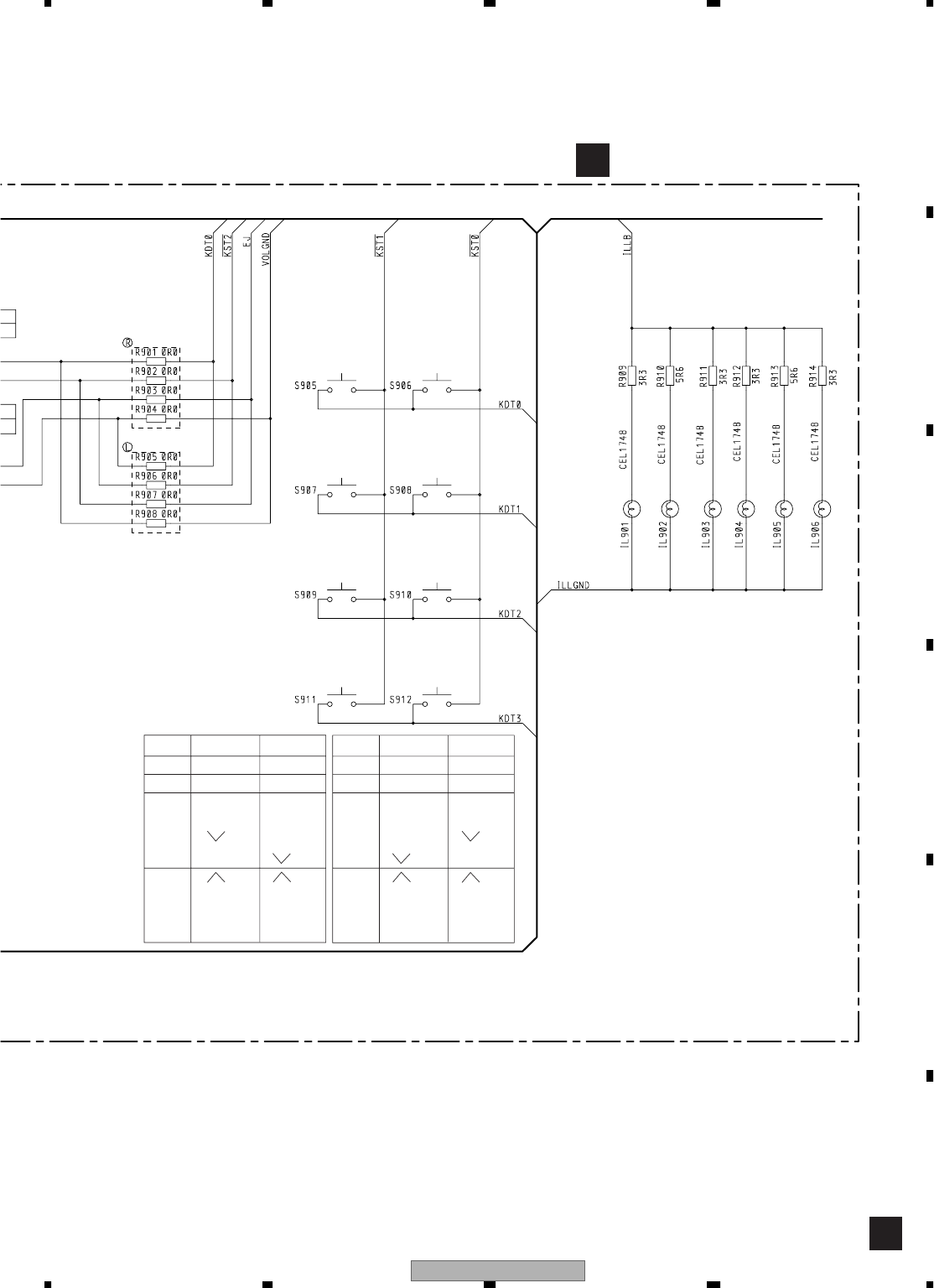
IL 901 Lamp 8V 85mA CEL1748
IL 902 Lamp 8V 85mA CEL1748
IL 903 Lamp 8V 85mA CEL1748
IL 904 Lamp 8V 85mA CEL1748
IL 905 Lamp 8V 85mA CEL1748
IL 906 Lamp 8V 85mA CEL1748
RESISTORS
R 901 (M8647ZT) RS1/16S0R0J
R 902 (M8647ZT) RS1/16S0R0J
R 903 (M8647ZT) RS1/16S0R0J
R 904 (M8647ZT) RS1/16S0R0J
R 905 (M8547ZT) RS1/16S0R0J
R 906 (M8547ZT) RS1/16S0R0J
R 907 RS1/16S0R0J
R 908 (M8547ZT) RS1/16S0R0J
R 909 RS1/16S3R3J
R 910 RS1/16S5R6J
R 911 RS1/16S3R3J
R 912 RS1/16S3R3J
Circuit Symbol and No. Part No.

KEX-M8547ZT/EW 37
5678
5678
C
D
F
A
B
E
R 913 RS1/16S5R6J
R 914 RS1/16S3R3J
C
Unit Number:EWM1031
Unit Name:Deck Unit
MISCELLANEOUS
IC 251 IC HA12216F
IC 351 IC PA2020B
Q 271 Transistor 2SC4116
D 352 Diode 1SS355
VR301 Semi-fixed 33kΩ(B) CCP1280
VR302 Semi-fixed 33kΩ(B) CCP1280
RESISTORS
R 255 RS1/16S181J
R 256 RS1/16S181J
R 257 RS1/16S183J
R 258 RS1/16S183J
R 259 RS1/16S133J
R 260 RS1/16S133J
R 261 RS1/16S274J
R 262 RS1/16S274J
R 271 RS1/16S183J
R 272 RS1/8S0R0J
R 273 RS1/8S0R0J
R 274 RS1/16S0R0J
R 275 RS1/16S473J
R 276 RS1/16S104J
R 277 RS1/16S224J
R 278 RS1/16S104J
R 281 RS1/8S0R0J
R 282 RS1/8S0R0J
R 283 RS1/8S0R0J
R 284 RS1/8S0R0J
R 285 RS1/16S0R0J
R 287 RS1/16S0R0J
R 291 RS1/8S0R0J
R 292 RS1/10S0R0J
R 293 RS1/10S0R0J
R 294 RS1/10S0R0J
R 321 RS1/8S0R0J
R 322 RS1/8S0R0J
R 351 RS1/16S102J
R 352 RS1/16S102J
R 353 RS1/16S102J
R 354 RS1/16S102J
R 355 RS1/16S274J
R 362 RS1/8S301J
R 373 RS1/16S0R0J
R 374 RS1/8S0R0J
R 375 RS1/8S0R0J
R 401 RS1/16S153J
R 402 RS1/16S332J
R 403 RS1/16S911J
R 404 RS1/16S274J
Circuit Symbol and No. Part No.
CAPACITORS
C 251 CKSRYB391K50
C 252 CKSRYB391K50
C 253 CKSRYB391K50
C 254 CKSRYB391K50
C 255 CKSRYB103K50
C 256 CKSRYB103K50
C 271 1µF/50V ECH0002
C 272 CKSRYB104K25
C 301 CKSRYB104K25
C 302 CKSRYB104K25
C 309 CKSRYB104K25
C 310 CKSRYB104K25
C 351 CKSQYB224K16
C 352 CKSRYB392K50
C 353 CKSRYB103K50
C 354 CKSRYB103K50
C 355 CKSQYB104K50
C 356 CKSRYB103K50
C 401 CKSRYB392K50
C 402 CKSRYB334K10
C 403 CKSRYB223K25
C 404 CKSRYB103K50
C 405 CKSRYB333K16
D
Unit Number:EWM1041
Unit Name:Sensor Unit
MISCELLANEOUS
L 101 Inductor CTF1546
L 102 Inductor CTF1546
S 101 Switch(LOAD) ESG1007
S 102 Switch(MODE) ESG1007
S 103 Switch(70µS) ESG1007
Q 101 Photo-reflector EGN1004
Miscellaneous Parts List
M 1 Motor Unit(MAIN) EXA1618
M 2 Motor Unit(SUB) EXA1660
HD1 Head Assy EXA1594
Circuit Symbol and No. Part No.
KEX-M8547ZT/EW
38
1234
1234
C
D
F
A
B
E
6. ADJUSTMENT
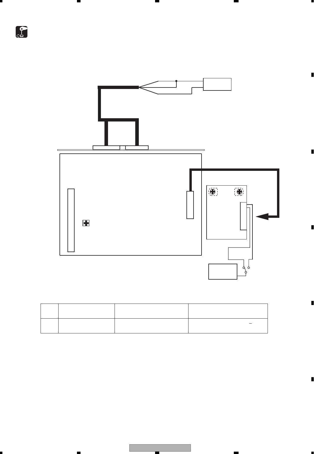
6.1 JIG CONNECTION DIAGRAM
KEX-M8547ZT/EW(L)
KEX-M8647ZT/EW(R)
GM-9127ZT-02/EW(L)
GM-9427ZT-02/WL(R)
CDX-M9027ZT/WL(R)
GGD1169
GGD1304
Bullet connector
(To DC Regulated Power Supply)
Bullet connector
SP Line
Bullet connector
(To DC Regulated Power Supply)
H/U EMV(DENSO)
24P
12P20P 6P 28P 26P
10P18P
24P
18P 10P
28P 26P12P20P
20P
25P 16P
16P
20P
25P
GGD1240
AUI+AUI-
FR+FR-
12P
GGD1346
AMP
MCD
NAVI ECU(A/W)
12P
MCD
CDX-M8086ZT/E(L)
32P
Bullet connector
(To DC Regulated Power Supply)
*Please don't connect the MCD(L) and MCD(R)
at the same time
- Connection Diagram TOYOTA EMV SYSTEM MODEL
Non-connected
For MCD(used for another system)
KEX-M8547ZT/EW 39
5678
5678
C
D
F
A
B
E
6.2 CASSETTE AND AUDIO ADJUSTMENT
-Connection Diagram
BACK UP
ACC
GND
+13.2V
GND DC Regulated
Power Supply
MAIN UNIT
CN353
FM/AM TUNER UNIT
VR561
VR302
mV
Meter
VR301
L-CH
R-CH
Pin2
Pin3
CN251
DECK UNIT
Extension Cord GGD1121
DOLBY B NR ADJUSTMENT
No. Test Tape Adjustment Point Adjustment Method
(Switch Position)
1 NCT-150 VR301(Lch), VR302(Rch) mV Meter : - 8.24dBm 1dB
(400Hz, 200nwb/m) (DOLBY NR Switch : OFF)
+
KEX-M8547ZT/EW
40
1234
1234
C
D
F
A
B
E
Connection:
Setting of the pulse generator. (setting of superimposed pulse)
Adjustment:
1. Setting of SSG
Receiving frequency : 999 kHz
Percentage modulation : 30%
Modulation frequency : 400 Hz
Antenna input : 74 dBµV (EMF)
2. Tune a RADIO to the "999kHz" with 1 condition.
3. .Mix signal with the above-mentioned pulse and
SSG moduration OFF.
4. Variable resistance adjust noise level to a
minimum.
Adjustment point : VR561
Pulse generator
(equivalent to HP8011A)
SSG
2-signal pad AM dummy KEX-M8406ZT
KEX-M9406ZT
Output
Noise meter
Pulse width :50µsec
Pulse intervals :5msec
Pulse voltage :4Vp-p
4Vp-p(EMF)
50us
5ms
AM NOISE CANCELER ADJUSTMENT
KEX-M8547ZT/EW
KEX-M8647ZT/EW
KEX-M8547ZT/EW 41
5678
5678
C
D
F
A
B
E
6.3 SELF-DIAGNOSIS FUNCTION
1.To Service Check
1. Press [AUDIO] key of EMV .
2. Press [DISPLAY] key of EMV .
3. The position of A and B is order of pushed 6 times in A,B,A,B,A and B.
->Service Check screen is displayed.
->As it is, it waits for a while.
(In general less than 1 minute)
DISPLAY
Display
Frame of display adjustment
Audio mode
The name of each apparatus,
such as an Audio H/U,
is displayed.
B
A
2.Service Check
Service Check
EMV Audio H/U
DSP AMP
CD-CH
LAN Monitor
KEX-M8547ZT/EW
42
1234
1234
C
D
F
A
B
E
3.How to exit from the diagnostic test mode
The diagnostic result of each model is displayed.
Results are [OK], [NCON],[CHEK], and [EXCH].
OK : No error code
NCON : EMV has judged it as the thing without connection.
(Disconnection being possible if there is actually connection)
CHEK : An error code indicating that diagnosis is judged to be necessary is entered.
EXCH : An error code indicating that exchange is judged to be necessary is entered.
ACC-OFF
Unit Check Mode Audio H/U
Current Memory
61-40
Occurred Date/Time
When displayed as [CHEK] or
[EXCH], details will be displayed
if the portion is touched.
It changes on the screen
which displays the
abnormalities on
communication.
The detected abnormalities
(Diagnosis code) are displayed.
At this example, it is 40
(abnormalities in mechanism or
media) of 61 (= cassette).
OK CHEK
OK
NCON
Service Check
EMV Audio H/U
DSP AMP
CD-CH
LAN Monitor
KEX-M8547ZT/EW 43
5678
5678
C
D
F
A
B
E
Logical
address name
Logical
address
Diagnosis
code
Diagnosis details
AM tuner PLL unlocked
FM tuner PLL unlocked
No antenna connected
Antenna power supply abnormal
Tuner power supply abnormal
AM tuner abnormal
FM tuner abnormal
SW tuner abnormal
TV tuner PLL unlocked
FRONTEND abnormal
TV divergence shifting error
TV – no reception
VNR screen error
No antenna connected
Antenna power supply abnormal
SEL +B current – small
SEL +B current – large
Belt broken
Mechanical failure or cassette broken
EJECT failure
TAPE jamming
Dirty head
Mech power supply abnormal
CD Mech abnormal
CD loading/unloading abnormal
CD lead-in abnormal
No disc loaded
Incorrect disc
Disc unreadable
CD-ROM abnormal
CD abnormal
EJECT abnormal
Scratches or non-recorded side
CD high temperature detected
Excessive current detected
Tray IN/OUT abnormal
Elevator abnormal
Clamp abnormal
MD mech abnormal
MD IN/OUT abnormal
MD lead-in abnormal
No disc loaded
Incorrect disc
Disc unreadable
MD-ROM abnormal
MD abnormal
EJECT error
Scratches or non-recorded side
MD high temperature detected
Excessive current detected
Tray IN/OUT abnormal
Elevator abnormal
Clamp abnormal
10
11
40
41
42
43
44
45
10
11
40
41
42
43
44
45
46
10
40
41
42
43
44
10
11
12
40
41
42
43
44
45
46
47
48
50
51
52
10
11
12
40
41
42
43
44
45
46
47
48
50
51
52
Radio
TV tuner
Cassette
tape
CD
CD-P
CD-CH
MD
MD-CH
60H
40H
61H
43H
62H
63H
64H
65H
Logical
address name
Logical
address
Diagnosis
code
Diagnosis details
No diagnosis
Abnormal reset
Abnormal +B
Abnormal ACC
Abnormal MUTE
Fuse broken
Microcomputer - abnormal
ROM - abnormal
RAM - abnormal
Bus - abnormal
F-ROM - abnormal
V-RAM - abnormal
Gate allay abnormal
Paint controller abnormal
Backup memory abnormal
Voice output controller abnormal
Internal power supply abnormal
Sync signal abnormal (input)
Sync signal abnormal (output)
ECU not connected
Transmission abnormal
Connecting confirmation: abnormal
Connecting confirmation: no response
Registered device data missing
(History of registered devices)
Master unavailable
Connecting confirmation: abnormal
Connecting confirmation: no response
Last mode abnormal
Command/order: no response
Mode status abnormal
Transmission fault
Master reset
Slave reset
Master abnormal
Registration completion
acknowledgement error
Voice processor ON abnormal
ON/OFF command or parameter abnormal
Registration command transmission
Multiple frames intermit.
Diagnosis - no response
00
01
10
11
12
13
20
21
22
23
24
25
26
27
28
29
2A
30
31
D0
D1
D2
D4
D5
D6
D7
D8
D9
DA
DB
DC
DD
DE
DF
E0
E1
E2
E3
E4
FF
Communi
-cation
control
01H
Logical
address name
Logical
address
Diagnosis
code
Diagnosis details
Gyroscope abnormal
GPS receiver abnormal
RTC abnormal
SS section abnormal
No Time updating
TCXO abnormal
PLL lock abnormal
GPS antenna abnormal
GPS antenna power supply abnormal
Map disc reading abnormal
SPD signal abnormal
Player abnormal
High temperature abnormal
Antenna power supply abnormal
Radio wave beacon - no antenna connected
Optical beacon - no antenna connected
No FM antenna connected
FM receiver abnormal
Radio wave beacon abnormal
Optical beacon abnormal
Voice-control activation SW abnormal
Voice-control Microphone abnormal
Multi-CD-CH (optical cable) abnormal
Multi-CD-CH (optical cable) not connected
Multi-CD-CH (CarNet) abnormal
Multi-CD-CH (CarNet) not connected
HIT64 communication not connected
HIT64 communication abnormal
HIT64 BRQ disconnection
HIT64 BRQ short-circuit
HIT64 disconnection
CarNet communication not connected
CarNet communication abnormal
CarNet periodical communication abnormal
Video circuit abnormal
Back light abnormal (with no current)
Back light abnormal (with excessive current)
Panel open/close mechanical operation abnormal
Front seat monitor abnormal
Heater abnormal
Panel SW abnormal
Touch SW failure
PLL Unlock
CODEC Communication Error
SSDEC Communication Error
SSDEC No Response Error
NVM Error
CAP Error
ANTENNA No Contact
ANTENNA Short
10
11
12
13
14
15
16
40
41
42
43
44
45
41
45
46
47
4A
4B
4C
40
41
40
41
42
43
50
51
52
53
54
55
56
57
10
11
12
13
40
41
10
11
11
12
13
14
15
16
40
41
Navigation
/GPS
Extended
communi
-cation
Information
display/front
monitors
58H
80H
02H
32H
34H
Diagnosis code table
FM multiplex
(VICS), radio
wave beacon,
beacon, optical
beacon, FM
multiplex (data),
and FM
multiplex tuner
5AH
84H
5BH
83H
82H
9AH
Voice
control
85H
SW, Audio
SW, SW
shifting,
Command
SW
XM tuner
21H
23H
24H
25H
C0H
KEX-M8547ZT/EW
44
1234
1234
C
D
F
A
B
E
Diagnosis code table
Logical
address name
Logical
address
Diagnosis
code
Diagnosis details
PLL unlocked
CDEC communication error
SSDEC communication error
SSDEC
no response
NVM error
CAP error
No antenna connected
Antenna short-circuited
Disc unreadable
DVD abnormal
EJECT abnormal
Scratches or non-recorded side
DVD high temperature detected
Excessive current detected
Tray IN/OUT abnormal
Elevator abnormal
11
12
13
14
15
16
40
41
42
44
45
46
47
48
50
51
XM C0H
DVD-CH 45H
KEX-M8547ZT/EW 45
5678
5678
C
D
F
A
B
E
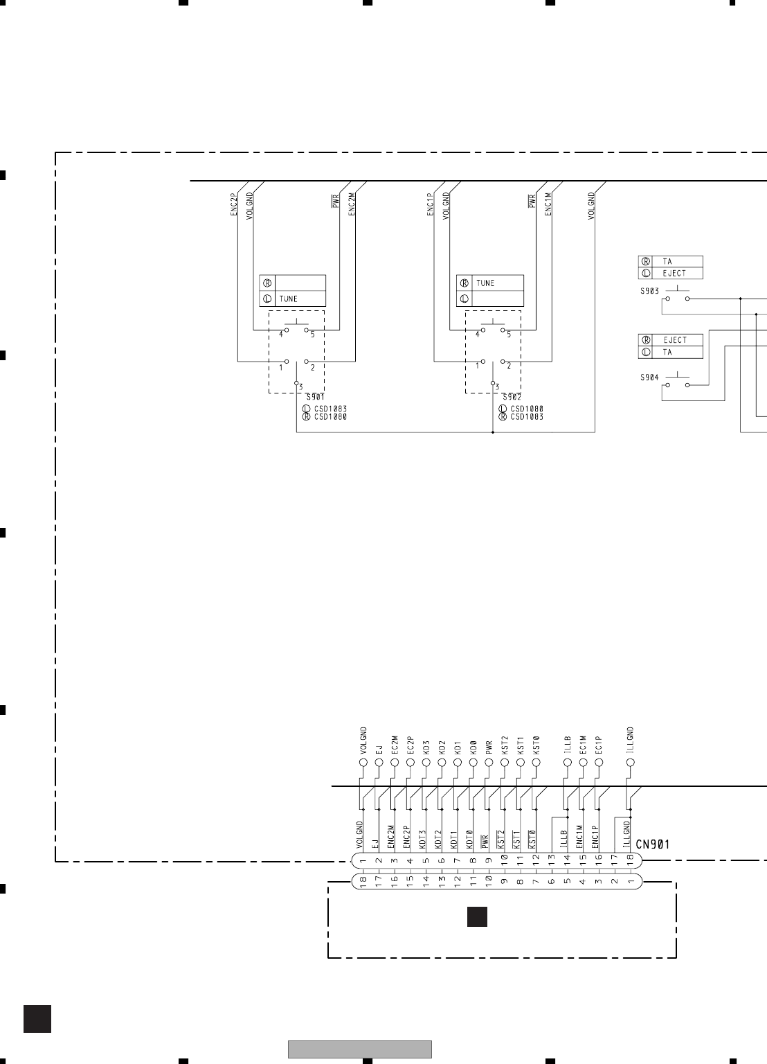
7. GENERAL INFORMATION
7.1 DIAGNOSIS
7.1.1 DISASSEMBLY
- Removing the Cassette Mechanism Module (Fig.1)
1
Fig.2
- Removing the Upper Case (not shown)
Grille Assy
- Removing the Grille Assy (Fig.1)
1. Remove the Case.
Cassette Mechanism Module
1
1
1
1
Fig.3
Main Unit
- Removing the Main Unit (Fig.3)
Straighten the tabs at two locations
indicated.
1
Remove the four screws and then remove
the Cassette Mechanism Module.
2Remove the two screws and then remove
the Grille Assy.
2
2
1
1
Remove the two screws.
2
Remove the two screws and then remove
the Main Unit.
3
3
3
Fig.1
- Removing the Front Frame (Fig.2)
Remove the three screws and then remove
the Front Frame.
1
Front Frame
1
1
1
22
KEX-M8547ZT/EW
46
1234
1234
C
D
F
A
B
E
7.1.2 CONNECTOR FUNCTION DESCRIPTION
(SLD)
GND
L-
L+ R+
R-
MUTE
NC NC
TX-
TX+
NC
NC
NC
(AMP+B)
ANT+B
ILL+
BU
ACC
ILL-
NC
TX+
TX-
(ACC)
(BU)
MUTE
L- R- R+
SGND
(GND)
L+
NC
NC
TX-
RSR-
RMU
RSL+
SW2 CMP-
RSL-
CMP+
SWG
RSR+ (SLD)
NC
NCNC
NC
NC
SW1
TX+
SUB ANTENNA
MAIN ANTENNA
KEX-M8547ZT/EW 47
5678
5678
C
D
F
A
B
E
7.1.3 TROUBLE-SHOOTING
Is B-UP ON?
bsens terminal
Pin 75(IC601)
NO Check +B
(Check a power supply.)
YES
Is ACC ON?
asens terminal NO Turn on ACC
(Check a power supply.)
Pin 73(IC601)
YES
Does illumination
come on? NO Check illumination circuit?
ISENS terminal Pin 2(IC601)
YES
Is PWR-ON enabled? NO Check PWRSW terminal
power Pin 69(IC601)
YES
Is voice output? NO Is amplifier connected
correctly? YES Is any sound of FM, AM and
TAPE (internal sources) output?
NO
Connect amp correctly
YES
Is VOL adjustment
enabled? NO Check encoder input.
ENC1- Pin 65(IC601)
ENC1+ Pin 63(IC601)
YES
Normal operation
NO Check the following terminals
SYSPW Pin 1(IC601)
sysmute2 Pin 5(IC601)
sysmute1 Pin 6(IC601)
YES
Are FM and AM
sounds output? NO Check the following terminals
FMPW Pin 43(IC601)
AMPW Pin 44(IC601)
YES
Is TAPE sound output? NO Recheck hardware
YES
IsTAPE mechanical unit
operated normally?
NO Check the following terminals
stby Pin 90(IC601)
CM Pin 89(IC601)
SC1 Pin 88(IC601)
SC2 Pin 87(IC601)
YES
Check the following terminals
SYSPWR Pin1(IC601)

KEX-M8547ZT/EW
48
1234
1234
C
D
F
A
B
E
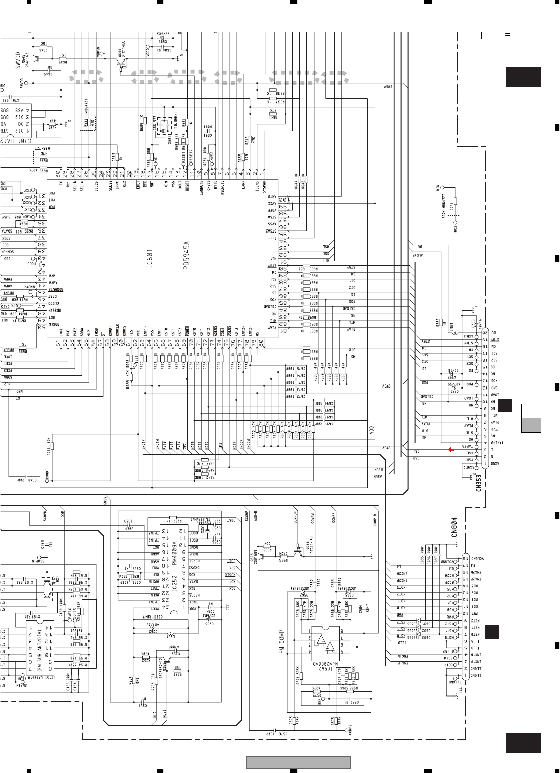
7.2 IC
-Pin Functions(PD5945A)
Pin No. Pin Name I/O Function and Operation
1 SYSPWR O Power supply control output
O
I
2 ISENS Illumination sense input
3 KISYU Model input
4 LAMP Lamp power supply control(D/A) output
6sysmute O System mute output
O5 sysmute@ System mute output for RSE
7 RSEMUTE O RSE mute output
8 BYTE I
I
I
Vss(Single chip) input
9 CNVSS CNVSS input
10 LANMUTE O AVC-LAN mute output
11 SWVDD O SWVDD output
12 reset I
I
Reset input
I
13 XOUT O Main clock output
14 VSS GND input
15 XIN Main clock input
I
I
16 VCC Power supply(2.7-5.5V) input
17 nmi VDD input
18 rck I RDS data clock input
19 ldet I
I
PLL lock signal input
20 NC Not used
Model input(L, R)
21 RX2 (BUS)
22 IPPW O BUS power supply output
23 SEL2a O
O
Selector switch a output for RSE
OSelector switch b output for RSE
24 NC Not used
Sub tuner data output
25 SEL2b O
26 SHIMUKE
27 SEL1a O
I
I
Selector switch a output for AMP
28 SEL1b O
O
Selector switch b output for AMP
29 RX1 (BUS)
30 TX (BUS)
31 PDO O PLL data output
32 PDI I PLL data input
33 pck O
O
PLL data clock output
O
34 NC Not used
35 SPDO
39 SCPON O
ISub tuner power supply control output
O
40 SSD Sub tuner station ON signal input
41, 42 NC Not used
43 FMPW O
44 AMPW O AM power output
FM power output
36 SPDI I
OSub tuner data input
37 spck Sub tuner data clock output
38 SCE O Sub tuner chip enable output
45 rdsmute O RDS mute output
46 drst O RDS decoder IC reset output
47 currq O Current request output
48 RDS57K I
IRDS 57kHz ON/OFF input
49 RDT RDS data input
50 rdslk I RDS station ON signal input
51 LOCL O Local L output
O
52, 53 PCE1, 2 PLL chip enable 1, 2 output
54 SDBW I SD bandwidth ON signal input
55 NL2 I NL2 ON signal input
56 FMSD I FM ON signal input
I
57 st Stereo input
KEX-M8547ZT/EW 49
5678
5678
C
D
F
A
B
E
Pin No. Pin Name I/O Function and Operation
60 ROMCS O ROM correction chip select output
61 TEST I Test mode input
I
I
62 VCC Power supply(2.7-5.5V) input
63 ENC1+ I VOL encoder input +
64 VSS GND input
65 ENC1- I VOL encoder input -
66-68 KST0-2 O Key strobe output 0-2
69 power I
I
POWER key input
70-72 KDT0-2 Key data input 0-2
73 asens I ACC sense input
74 csej I Tape eject sense input
75 bsens I Back up sense input
76 KDT3 IKey data input 3
77 ENC2+ IAUD encoder input +
78 ENC2- IAUD encoder input -
79 MS Music sense input
80 f/R O
I
O
Head forward/reverse select output
81 PLAY MS gain select output
82 mtl IMETAL input
83 NR O
I
I
Dolby B NR ON/OFF output
84 CSLOAD Tape loading detect input
85 POS Position sense input
86 ES I
O
Tape end detect input
87, 88 SC2, 1 OSub motor control output 2, 1
89 CM Capstan control output
I
I
I
I
I
I
I
I
I
90 stby OTape stand-by output
O
91 NL1 Noise level input
92 SSL Sub tuner signal level input
93 MSL Main tuner signal level input
94 ILL- Illumination - input
95 STSW2 Stearing SW 2 input
96 AVSS A/D converter GND input
97 STSW1 Stearing SW 1 input
98 VREF A/D converter reference voltage input
99 AVCC A/D converter power supply input
100 ANTB Antenna power supply control output
30
31
50
51
80
81
100
1
* PD5945A IC's marked by * are MOS type.
Be careful in handling them because they are very liable
to be damaged by electrostatic induction.
O
58 ROMDT ROM correction data output
59 ROMCLK O ROM correction clock output
KEX-M8547ZT/EW
50
1234
1234
C
D
F
A
B
E
No. Symbol I/O Explain
1 STIND O stereo "Low" when the FM stereo signals are received.
indicator To be pulled up to the "VDD" at 47kΩ.
2 FMSD FM station "High" when signals are received. To be pulled up to the "VDD" at 47kΩ
detector Meanwhile, 10kΩ should be used when taking diver FIX trigger from here
and "High: 0.9VDD or more" and "Low: 250mV or less".
(Should satisfy the diver IC specifications)
3 NL1 O noise level-1 "High" when noise is received. Output for the RDS. GND at 47kΩ//1,800pF.
4 NL2 O noise level-2 "High" when noise is received. Output for the RDS. GND at 36kΩ//330pF.
5 Rch O R channel FM stereo "R-ch" signal output or AM audio output.
output Add the specified de-emphasis constant.
6 Lch O L channel FM stereo "L-ch" signal output or AM audio output.
output Add the specified de-emphasis constant.
7 WC write control EEPROM write control. Writing permissible at "Low". Normally open.
8 SDBW O SD bandwidth SD bandwidth signal output. For detection of detuning data for the RDS.
9 AMDET O AM detector AM detector output. r out < 100Ω
output
10 VDD power Power supply pin for the digital section.
supply DC 5V +/- 0.25V. Be careful about overlapping noise in the logic section.
11 DGND digital ground Grounding for the digital section.
12 CE2 I chip enable-2 EEPROM chip enable. Active a "Low"
To be pulled up to the "VDD" at 47kΩ
13 SL I/O signal level Received FM/AM signal level (strength) output.
Connect the specified load resistor and capacitor (10k Ω+ 39k Ω//4,700pF)
14 DI/DO I/O data input/ Data input/Data output
data output To be pulled up to the "VDD" at 47kΩ
15 CK I clock Clock input To be pulled up to the "VDD" at 47kΩ
16 CE1 I chip enable-1 AF·RF chip enable. Active at "High"To be grounded at 47kΩ
17 AMPNS AM PNS IF signal IF signal output for AM PNS circuit.
18 LDET O lock detector Active at "Low". To be pulled up to the "VDD" at 47kΩ
19 CREQ I current request Active at "Low". To be grounded at 47kΩ
20 AMINI AM audio input The frequency response and the level are set by connecting an external CR
network with terminal AMIN as terminal AMDET. r in = 50kΩ
21 COMP O composite signal FM composite signal output. r out < 100Ω
22 VCC power supply Analog section power supply pin.DC 8.4V +/- 0.3V
23 LOCH I local high FM local high pin. When seeking local high, apply 5V together with "LOCL".
24 FMLOCL I FM local low FM local low pin. When seeking local low, apply 5V to the base of the NPN
transistor with which the specified resistor is being connected to the emitter.
Keep it open in case of ordinary marketed models.
25 LOCL I local low FM/AM local low pin. When seeking local low, apply 5V to the base of the
NPN transistor.
Since this pin is exclusive for AM when the FMLOCL is in use,
do not drive it under FM.
26 RFGND RF ground Grounding for the antenna section.
27 FMANT I FM antenna input FM antenna input. 75Ω. Surge absorber (DSP-201M-S00B) is necessary.
28 AMANT I AM antenna input AM antenna input. High impedance.
Connect to the antenna through an L (LAU type) of 4.7µH.To cope with the
power transmission line hums, insert a series circuit consisting of an L
(a coil of about 100mH) + R (a resistor of 470 Ω to 2.2kΩ) between the GND.
IC 3
EEPROM
28
27
FM/AM 1ST IF 10.7MHz
T51 Q51 CF51 CF52 CF53
IC1
MIXER, IF AMP, DET.
6
21
18
LDET
COMP
22
25 10 14 12 15 16 8 13 3
CF202
VDD
VCC
DI/DO
CE2
CK
CE1
SDBW
SL
FMSD
NL1
NL2
IC 2 FM MPX
AMANT
FMANT
ATT
ATT
AMRF
FMRF
IMG ADJ
RF ADJ
X901
10.25MHz
ANT ADJ
LOCL
23 LOCH
AMDET
MPXREF 41kHz
AM 2ND IF
450kHz
19
CREQ
11
DGND
1
STIND
L ch
5
R ch
924
AMDET
FMLOCL
20
177
AMPNS
WC
26 RFGND
AMIN
-FM/AM Tuner Unit
O
O
42
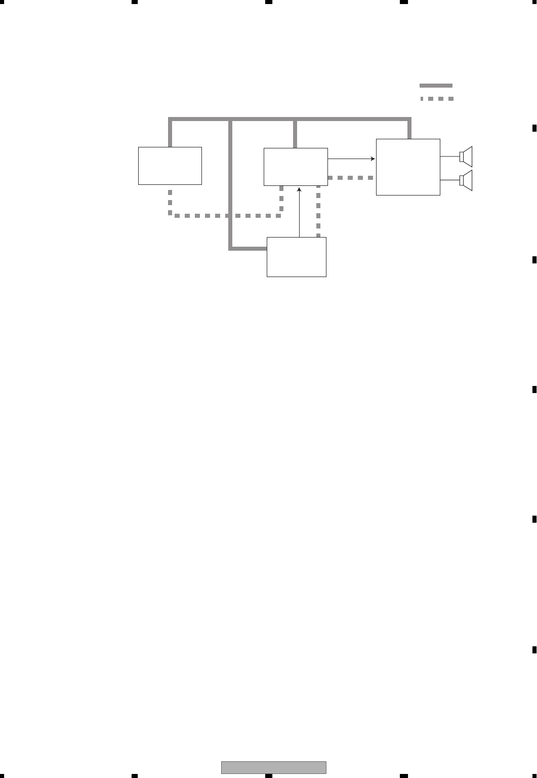
KEX-M8547ZT/EW 51
5678
5678
C
D
F
A
B
E
7.3 EXPLANATION
7.3.1 SYSTEM BLOCK DIAGRAM
+B, ACC
AVC-LAN
L/R
AVC-LAN
L/R AMPLIFIER
PIONEER
SPEAKER
1DIN
HEAD UNIT AVC-LAN
+B, ACC
CD-CH
EMV
OTHER MAKERS
AVC-LAN
PIONEER
KEX-M8547ZT/EW
KEX-M8647ZT/EW
KEX-M8547ZT/EW
52
1234
1234
C
D
F
A
B
E
7.3.2 OPERATIONAL FLOW CHART
VCC=5V
Pin 16, 62
Power ON
bsens=L
asens=L
YES
bsens
Pin 75
asens
Pin 73
SYSPWR←H
Pin 1
IPPW←H
Pin 22
SWVDD←H
Pin 11
Source keys
operative
Completes power-on operation.
(After that, proceed to each source operation)
Source ON
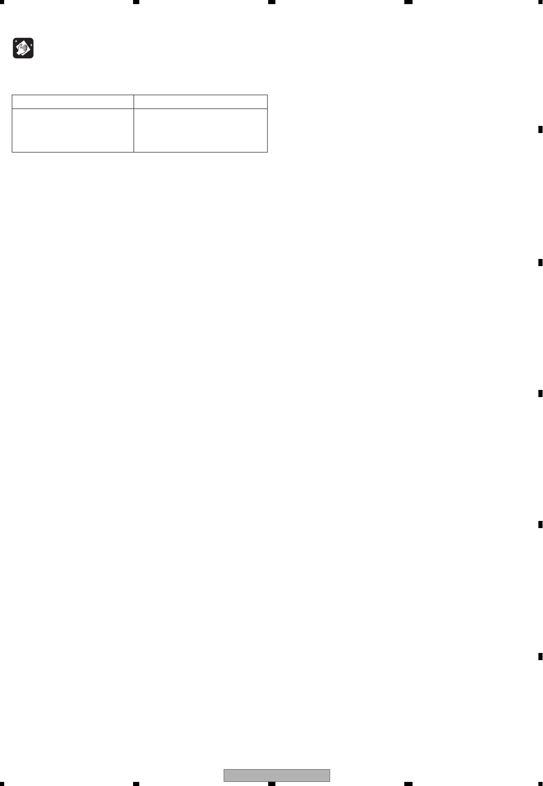
KEX-M8547ZT/EW 53
5678
5678
C
D
F
A
B
E
7.4 CLEANING
Before shipping out the product, be sure to clean the following portions by using the prescribed cleaning tools:
Portions to be cleaned Cleaning tools
Cassette heads
Pinch rollers
Capstans Cleaning paper : GED-008
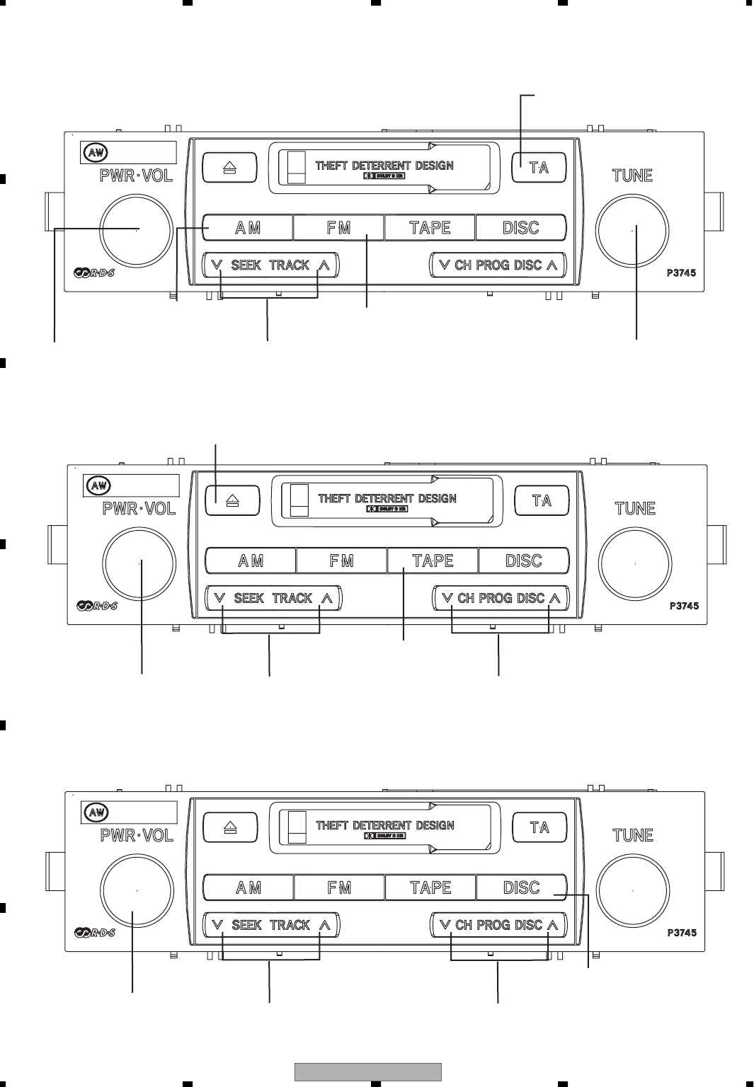
KEX-M8547ZT/EW
54
1234
1234
C
D
F
A
B
E
8. OPERATIONS
ZT/EW
KEX-M8547
ZT/EW
KEX-M8547
ZT/EW
KEX-M8547
MANUAL TUNING
POWER
ON/OFF,
VOLUME
AM
SEEK
UP/DOWN
FM
DISC
SELECT
CD,DVD
DIRECTION
CHANGE
TAPE
AUTO
PROGRAM
SEARCH
TRACK
SELECT
EJECT
TRAFFIC ANNOUNCEMENT
POWER
ON/OFF,
VOLUME
POWER
ON/OFF,
VOLUME
- KEX-M8547ZT/EW
- RADIO
- CD, DVD
- TAPE
KEX-M8547ZT/EW 55
5678
5678
C
D
F
A
B
E
ZT/EW
KEX-M8647
ZT/EW
KEX-M8647
ZT/EW
KEX-M8647
MANUAL TUNING POWER
ON/OFF,
VOLUME
AM
SEEK
UP/DOWN
FM
DISC
SELECT
CD,DVD
DIRECTION
CHANGE
TAPE
AUTO
PROGRAM
SEARCH
TRACK
SELECT
EJECT
TRAFFIC ANNOUNCEMENT
POWER
ON/OFF,
VOLUME
POWER
ON/OFF,
VOLUME
- KEX-M8647ZT/EW
- RADIO
- CD, DVD
- TAPE

KEX-M8547ZT/EW
56
1234
1234
C
D
F
A
B
E
-
J
ig
s L
i
st
Extension cor
d
Extension cor
d
Extension cor
d
Extension cor
d
Extension cor
d
T
est tap
e
C
leaning pape
r
GG
D11
69
GG
D124
0
GG
D1
30
4
GG
D1346
GG
D112
1
NC
T-1
50
G
ED-
008
A
d
j
ustmen
t
j
A
d
j
ustmen
t
j
A
d
j
ustmen
t
j
A
d
j
ustmen
t
j
Cassette mechanism module ad
j
ustment
j
C
assette mechanism module ad
j
ustment
C
leanin
g
cassette heads, pinch rollers and capstans
N
ame
Ji
g No
.
R
emark
s
g
j
