L010550 LSI LS7314, LS7315
User Manual: L010550 - LSI-LS7314, LSI-LS7315
Open the PDF directly: View PDF ![]() .
.
Page Count: 4
AC POWER CONTROLLERS
DESCRIPTION:
The LS7314 - LS7315 are MOS integrated circuits specifically
designed for appliance motor speed control, lighting control,
etc. I/Os (PLs) are provided for selecting/indicating from one to
ten power levels. The LS7315 is designed for pushbutton con-
trol. The LS7314 is designed for touch control.
(See Figures 4A and 4B)
INPUT/OUTPUT DESCRIPTION:
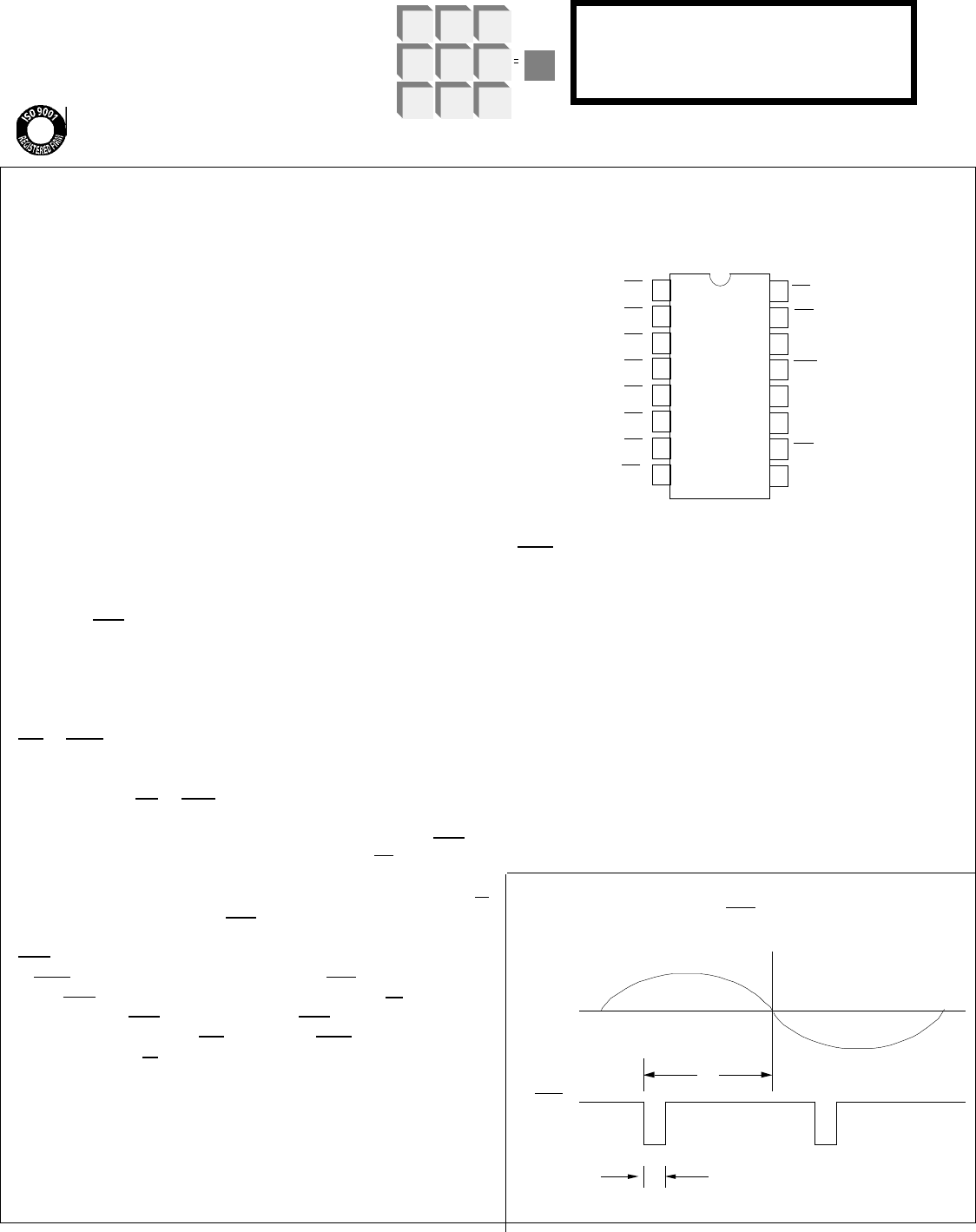
PL1 - PL10 (Pins 1 - 8, 15, 16)
Ten inputs/outputs for selecting ten output phase angles (pow-
er levels). When no power level is selected (such as after sys-
tem power-up) PL1 - PL10 all act as inputs. When a power lev-
el is selected by applying a logic zero at one of these inputs for
TH time (See Dynamic Characteristics), the output (TRIG) is
turned on at the phase angle selected and the PL input switch-
es status to become an output in order to drive a display, such
as an LED. It switches back to the input state when another PL
input is activated or when OFF is selected. (See Note 1)
OFF (Pin 10)
If TRIG is on, a logic 0 applied to the OFF input for TH time
turns TRIG output off and switches the selected PL back to the
input state. If TRIG is off, activating OFF leaves the circuit un-
affected. Following an OFF activation, TRIG can be turned on
by applying any PL input. (See Note 1)
SYNC (Pin 12)
Input for PLL reference frequency (50Hz/60Hz). All internal
clock frequencies are synchronized with the SYNC input.
CAP (Pin 11)
Input for component connection for the PLL filter capacitor.
1
2
3
4
5
6
7
8
9
10
11
12
13
14
15
16
PL3
PL4
PL5
PL6
PL7
PL8
PL9
PL10
PL2
TRIG
Vss (+V)
SYNC
CAP
OFF
V
DD
(-V)
LSI
CONNECTION DIAGRAM - TOP VIEW
LS7314
FIGURE 1
PL1
7314-012703-1
APPLICATIONS:
• Universal and shaded-pole motor speed control for modern
appliance designs. Eliminates awkward mechanical switch
assemblies and multi-tapped motor windings. (See Fig. 4C)
• Multi-level light switches. (See Fig. 4D)
TRIG (Pin 13)
This output is designed to drive a triac in series with the
load and control its firing angle with respect to the AC line.
A 1ms output pulse width is provided to enable the triac to
fire even with inductive loads which cause significant phase
delays between voltage and current.
Vss (Pin 14)
Supply voltage positive terminal.
VDD (Pin 9)
Supply voltage negative terminal (ground).
NOTE 1: LS7315 has an internal pullup resistor on this in-
put and LS7314 does not. (See DC Electrical Character-
istics.)
LSI/CSI
LSI Computer Systems, Inc. 1235 Walt Whitman Road, Melville, NY 11747 (631) 271-0400 FAX (631) 271-0405
LS7314-7315
UL
®
A3800
Ø
T
W
FIGURE 2. TRIG PHASE ANGLE Ø
SYNC
TRIG
FEATURES:
• 10 I/Os to Select/Indicate up to ten Power Levels
• Inputs activated by Touch or Pushbutton Switch
• Output switches pure and precise AC Power to Load
• Operates with 50Hz/60Hz line frequency
• Rugged, latchup-free process technology
• +10V to +14V operation (Vss - VDD)
• LS7314, LS7315 (DIP);
LS7314-S, LS7315-S (SOIC) - See Figure 1
January 2003
7314-012703-2
*LS7314 & LS7315 **LS7315-51
(1) The TRIG Phase Angles shown in TABLE 1 are referenced
to the SYNC input. Ø values are mask programmable.
(2) The percentage of Full Power delivered to a resistive load
by the Triac Switch.
FIGURE 4C VALUE TABLE
CONDITION C2(µF)
(1), (3) 0.47
(1), (4) 0.33
(2), (3) 0.68
(2), (4) 0.47
(1) No LEDs (2) 5mA LEDs
(3) 115VAC, C2 = 200V (4) 220VAC, C2 = 400V
FIGURE 4C and 4D NOTES
NOTE 1: Value for 5mA LEDs.
NOTE 2: Use zener which produces 6.2V ±5% at 500µA or
less, i.e. P/N MZ4627.
NOTE 3: R6-C6 Snubber Network may be required for large
inductive loads.
NOTE 4: Tie all unused touch inputs together and return to Vss
through 100k Ohm, 1/4W resistor.
NOTE 5: The AC Mains Polarity shown is required for Touch
Control applications.
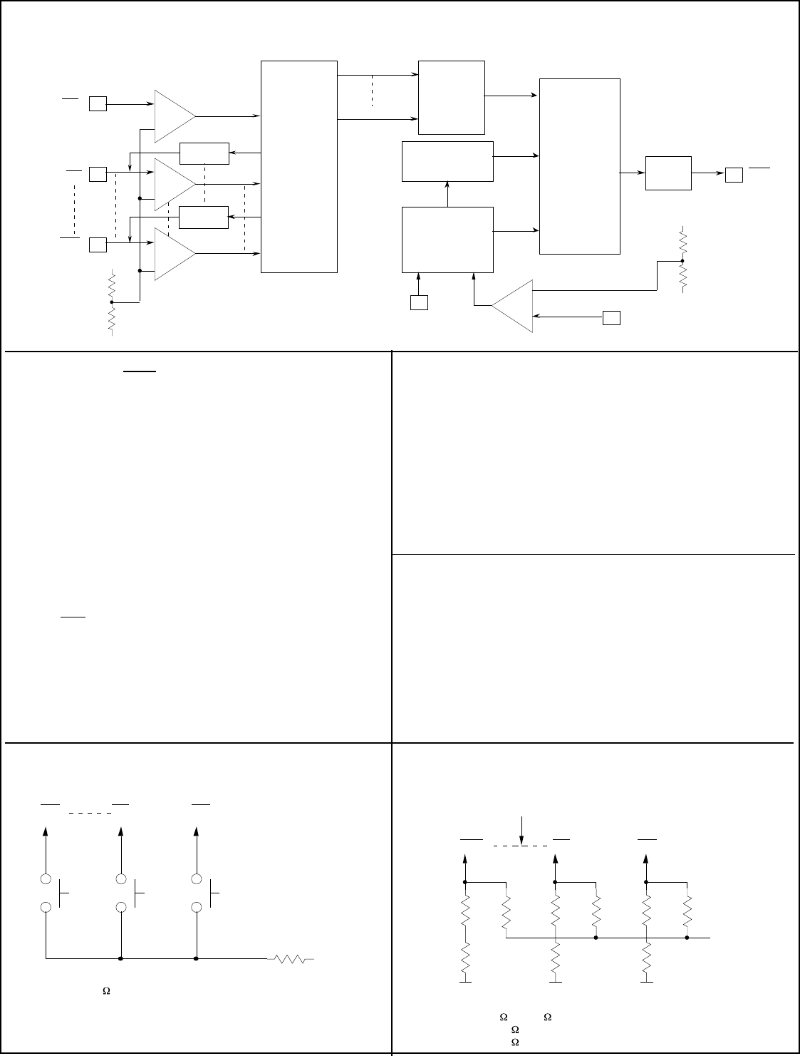
DRIVER
DRIVER
10
15
8
CONTROL
LOGIC DRIVER
DIGITAL
COMPARATOR
POWER
LEVEL
ROM
PHASE
ANGLE
POINTER
PHASE-LOCKED
LOOP
AND
CLOCK
GENERATOR
LEVEL 1
LEVEL 10
11
+
-
+
-
+
-
VSS
VDD
TRIG
CAP
OFF
PL1
PL10
13
FIGURE 3. LS7314-LS7315 BLOCK DIAGRAM
12
+
-
VSS
VDD
SYNC
TABLE 1. TRIG PHASE ANGLES, Ø (1)
PL Ø * % PWR (2) Ø ** %PWR (2)
1 43° 8 81° 40
2 55° 16 105° 67
3 68° 26 116° 77
4 81° 40 120° 80
5 95° 55 123° 83
6 108° 69 129° 87
7 122° 82 134° 90
8 134° 90 160° 99
9 147° 96 167° 99
10 160° 99 175° 99
R3
OFFPL1PL10
FIGURE 4A. PUSHBUTTON INTERFACE FOR LS7315
VDD
R3 = 10K , 1/4W
R8
R8
R7 R8
R8
R7 R8
R8
R7
Vss
TP TP TP
PL10 PL1 OFF
FIGURE 4B. TOUCH INTERFACE FOR LS7314
SEE NOTE 4
R7 = 1M to 5M , 1/4W (Select for Sensitivity)
R8 = 2.7M , 1/4W for 115VAC Mains
R8 = 4.7M , 1/4W for 220VAC Mains
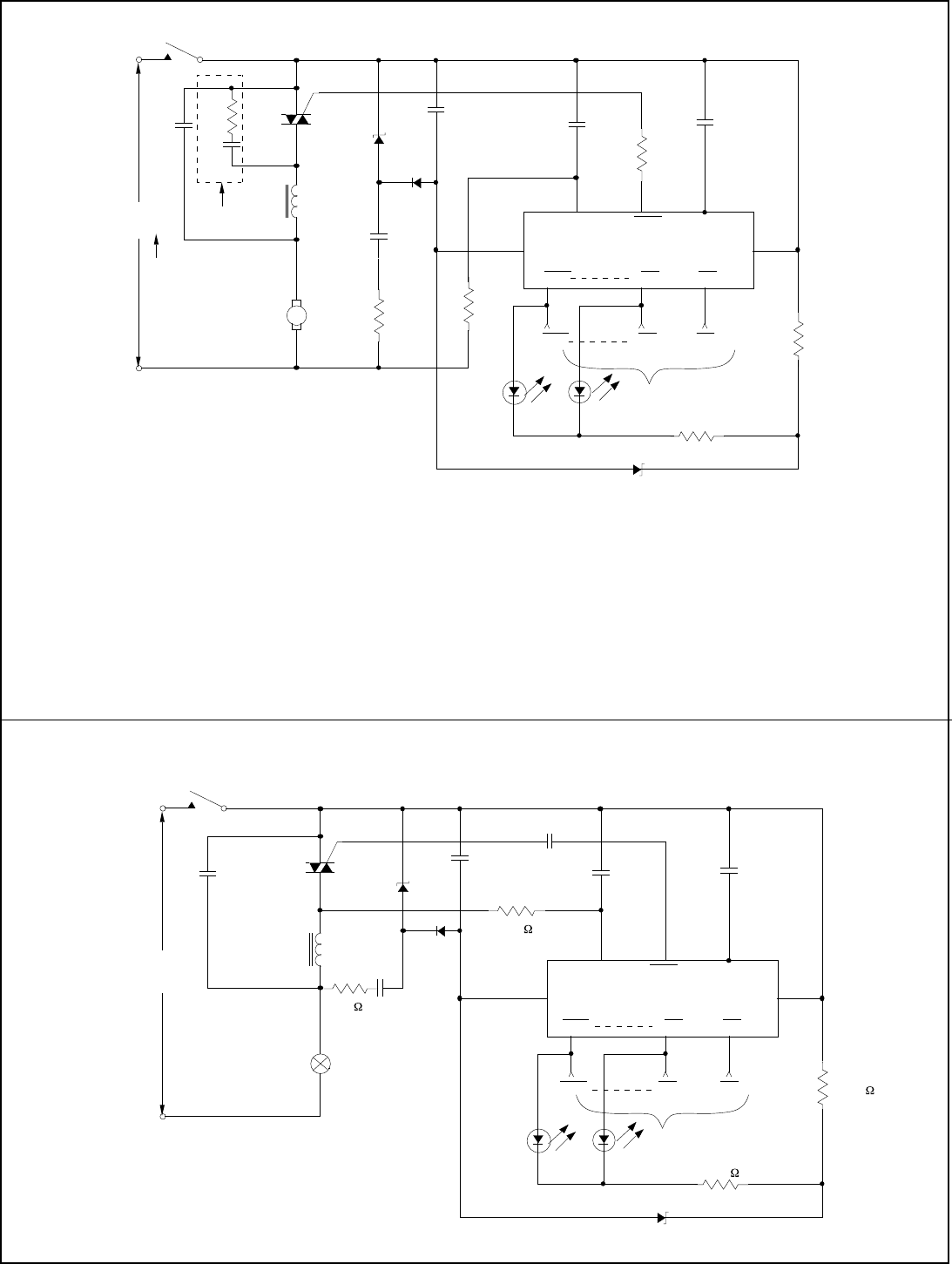
M
P
N
L
MT2
G
MT1
C1
R1
R2
R9
C2
Z1
C5
D1
-
+
C4 C3
13 11
SYNC CAP
12
9
10158
14
Z2
R4
R5
VSS
OFF
PL1
PL10
LS7314 - LS7315
FIGURE 4C. MOTOR SPEED CONTROL APPLICATION
VDD
R6
C6
TRIG
OFF
PL1
PL10
AC
MAINS SEE NOTE 3
T
SEE NOTE 5
Use Fig. 4A or 4B
Interface Circuits
C1 = 0.15µF, 200V (400V) R1 = 82Ω
C2 = See Figure 4 Value Table R2 = 1.5MΩ
C3 = 0.047µF R4 = 560Ω (See Note 1)
C4 = 470pF R5 = 10kΩ
C5 = 220uF R6 = 1.8kΩ, 1W (2W)
C6 = 0.47µF, 200V (400V) R9 = 100Ω
L = 100µH (200µH) Z1 = 13V ± 5%, 1W
D1 = 1N4148 Z2 = 6.2V, 1/4W (See Note 2)
T = Q4004L4 (Q5004L4) Typical
All resistors 1/4W, all capacitors 25V unless otherwise specified.
Indicates component change for 220VAC Mains.
*
*
**
*
7314-012703-3
*
P
N
100µH
MT2
G
MT1
200V 13V
220µF
1N4148
-
+
470pF
13 11
SYNC CAP
12
9
10158
14
6.2V, 1/4W (See Note 2)
1K
10K
VSS
OFF
PL1
PL10
LS7314 - LS7315
FIGURE 4D. MULTI-LEVEL WALL SWITCH DIMMER APPLICATION
VDD
TRIG
OFF
PL1
PL10
115V
AC
MAINS
Q40044L4
0.15µF
INCANDESCENT
LAMP LOAD
2W 200V
0.68µF
.047µF
.047µF
82
Use Fig. 4A or Fig. 4B
Interface Circuits
1.5M
All Resistors 1/4W, all Capacitors 25V
unless otherwise specified.
Component Values are for use with
115VAC Mains and 2.5mA LEDs.
1W

Input Pull-up Resistance:
For LS7315
PL, OFF RIN 50 100 200 kΩ-
Output Voltage:
TRIG, HI VOH Vss - - V -
TRIG, LO VOL - Vss - 8 - V -
Output Current:
TRIG, Sink IOS 25 - - mA Vss = +12V
VOL = Vss - 4V
PL Source IOPL 5 - - mA VOPL= Vss - 1V
DYNAMIC CHARACTERISTICS:
SYMBOL MIN TYP MAX UNIT CONDITION
SYNC frequency fS40 - 70 Hz -
PL, OFF hold time TH50 - infinite ms 60Hz SYNC
TH60 - infinite ms 50Hz SYNC
TRIG Pulse Width Tw- 1.0 - ms 60Hz SYNC
Tw- 1.2 - ms 50Hz SYNC
MAXIMUM RATINGS:
PARAMETER SYMBOL VALUE UNIT
DC Supply Voltage Vss - VDD +20 V
Any Input Voltage VIN Vss - 20 to Vss + 0.5 V
Storage Temperature TSTG -65 to +150 °C
Operating Temperature TA0 to +80 °C
DC ELECTRICAL CHARACTERISTICS:
(TA = 25˚C, all voltages referenced to VDD)
SYMBOL MIN TYP MAX UNIT CONDITION
Supply Voltage VSS +10 +12 +14 V -
Supply Current IDD - 1.2 2 mA Vss = 12V, outputs off
Input Voltage:
SYNC, LO VISL 0 - 1/3Vss V -
SYNC, HI VISH 2/3Vss - Vss V -
All other inputs, LO VIL 0 - 1/4Vss V -
All other inputs, HI VIH 1/2Vss - Vss V -
Input Current:
SYNC Input IH- - 110 µA With Series 1.5MΩ
Resistor to 115VAC
7314-012703-4
The information included herein is believed to be
accurate and reliable. However, LSI Computer Systems,
Inc. assumes no responsibilities for inaccuracies, nor for
any infringements of patent rights of others which may
result from its use.
