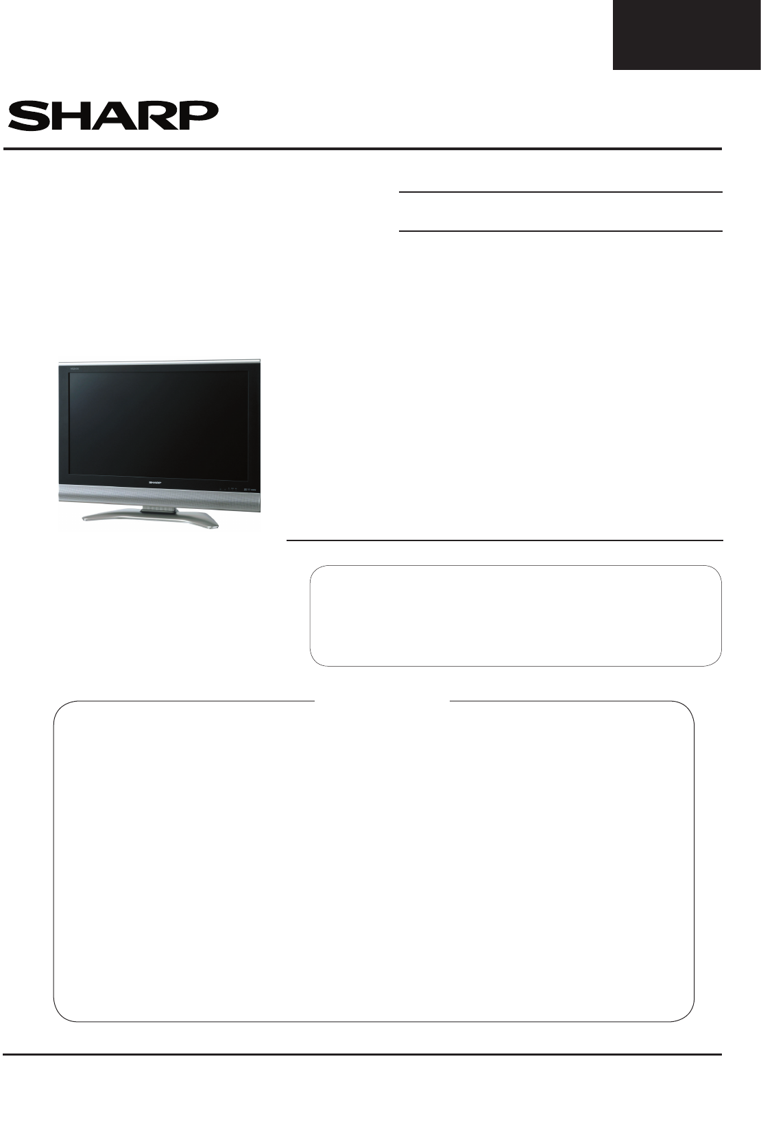
LC32GD8E
User Manual: LC32GD8E
Open the PDF directly: View PDF ![]() .
.
Page Count: 169 [warning: Documents this large are best viewed by clicking the View PDF Link!]
1
LC-26GA5E
LC-32GA5E
LC-32GD8E/RU
LC-32BT8E/RU
LC-37GD8E/RU
LC-37BT8E/RU
LC-32/37GD8E/RU
LC-32/37BT8E/RU
MODELS
LC-32GD8EE/EF/EI/EK/RU
LC-32BT8EE/EF/EI/EK/RU
LC-37GD8EE/EF/EI/EK/RU
LC-37BT8EE/EF/EI/EK/RU
Issued: 15
th
June 2006
SE00LC32GD800
ELECTRICAL SPECIFICATIONS .............................................................................. 3
IMPORTANT SERVICE SAFETY PRECAUTIONS...................................................... 4
OPERATION MANUAL ............................................................................................... 6
DIMENSIONS ......................................................................................................... 10
REMOVING OF MAJOR PARTS ..................................................................................... 11
SERVICE ADJUSTMENTS ..................................................................................... 15
SOFTWARE UPDATING .................................................................................... 23
TROUBLESHOOTING TABLE .................................................................................. 41
MAJOR ICs INFORMATION ..................................................................................... 58
SOURCE OF DOCUMENTATION ................................................................................ 98
CHASSIS LAYOUT .................................................................................................. 99
OVERALL WIRING DIAGRAMS ................................................................................ 105
BLOCK DIAGRAM ...................................................................................................... 106
SCHEMATIC DIAGRAMS ......................................................................................... 108
PRINTED WIRING BOARDS ..................................................................................... 130
REPLACEMENT PARTS LIST .................................................................................. 149
PACKING OF THE SET ........................................................................................... 168
SERVICE MANUAL
LCD COLOUR TELEVISION
In the interests of user safety (required by safety
regulations in some countries) the set should be re-
stored to its original condition and only parts identical
to those specifi ed should be used.
160mm
125mm
100mm
80mm
63mm
50mm
40mm
31.5mm
25mm
20mm
A-data-1
sharp.
Corporate Trademark
PAL B/G, I / SECAM B/G, D/K, L/L’ SYSTEM COLOUR TELEVISION
SHARP CORPORATION
This document has been published to
be used for after sales service only.
CONTENTS

2
LC-26GA5E
LC-32GA5E
LC-32/37GD8E/RU
LC-32/37BT8E/RU
Use this page to keep any special servicing information as Technical Report (Bulletin), Technical Information, etc.
If only part number changes are required, just change part number directly the part number in the Parts Listing Sec-
tion.
SERVICE MANUAL UPDATE LOG SHEET
Part No.
Technical Report No.
Technical Bulletin No. Cause / Solution Page No. Application
Data /Serial No.

3
LC-26GA5E
LC-32GA5E
LC-32GD8E/RU
LC-32BT8E/RU
LC-37GD8E/RU
LC-37BT8E/RU
LC-32/37GD8E/RU
LC-32/37BT8E/RU
35
Item
Video Colour System PAL/SECAM/NTSC 3.58/NTSC 4.43/PAL 60
TV
Function
CCIR (B/G, I, D/K, L, L’)
TV-Standard
Specifications
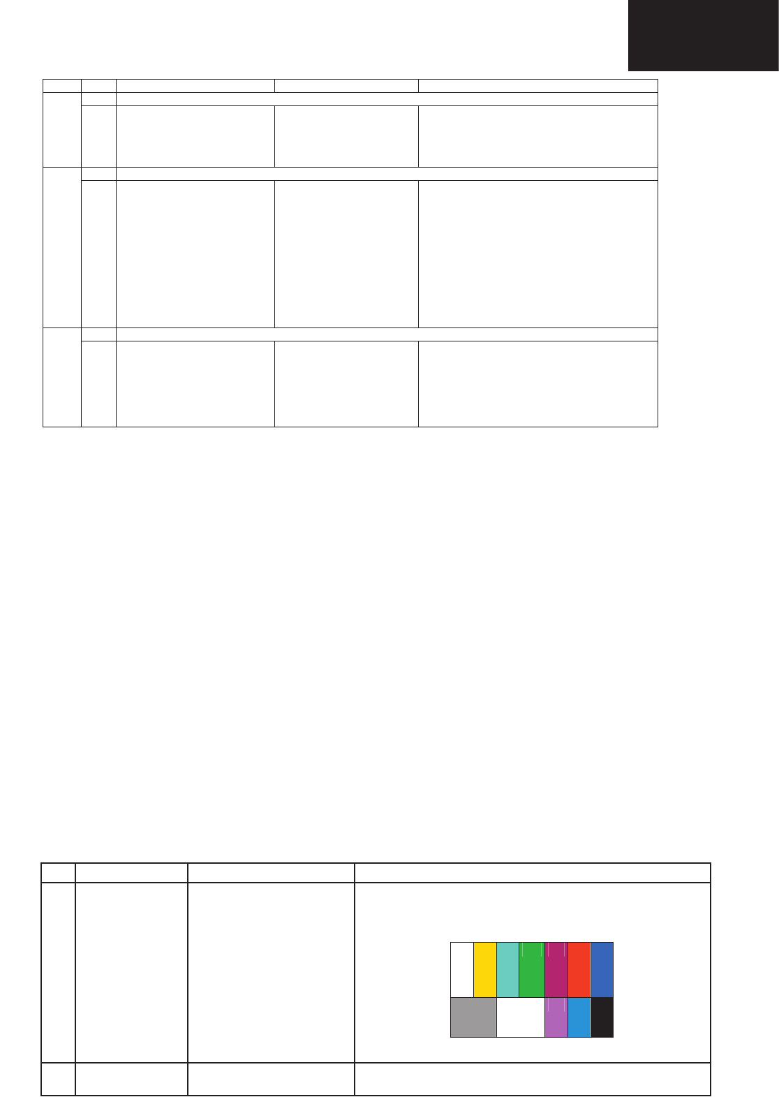
LCD panel
Number of dots 3,147,264 dots (1366 g 768 g 3 dots)
•As a part of policy of continuous improvement, SHARP reserves the right to make design and specification changes for
product improvement without prior notice. The performance specification figures indicated are nominal values of production
units. There may be some deviations from these values in individual units.
NOTE
•Refer to inside back cover for dimensional drawings.
VHF/UHF E2–E69ch, F2–F10ch, I21–I69ch, IR A–IR Jch, (Digital: E5–E69ch)
CATV Hyper-band, S1–S41ch
TV-Tuning System Auto Preset 99 ch, Auto Label, Auto Sort
STEREO/BILINGUAL NICAM/A2
Receiving
Channel
Brightness 450 cd/m2
Backlight life 60,000 hours (at Backlight Standard position)
Viewing angles H : 176° V : 176°
Audio amplifier 10W g 2
Speaker 130 mm g60 mm
Terminals
9 pin MINI-DIN male connector
EXT 2
EXT 3 S-VIDEO (Y/C input), RCA pin (AV input)
Rear
RS-232C
UHF/VHF 75q Din type (Analogue & Digital)
SCART (AV input/output, Y/C input, RGB input, AV Link)
Antenna input
EXT 5 HDMI, Ø 3.5 mm jack (Audio input)
OSD language English/German/French/Italian/Spanish/Dutch/Swedish/Portuguese/Finnish/Turkish/Greek/
Russian/Polish
Power Requirement AC 220–240 V, 50 Hz
Power Consumption
Weight
Appendix
32o LCD COLOUR TV,
Model: LC-32GD8, LC-32BT8
32o Advanced Super View &
BLACK TFT LCD
37o LCD COLOUR TV,
Model: LC-37GD8, LC-37BT8
37o Advanced Super View &
BLACK TFT LCD
17 kg (Display only),
19 kg (Display with stand)
20.5 kg (Display only),
23 kg (Display with stand)
160 W (0.9 W Standby)
(Method IEC60107)
168 W (0.9 W Standby)
(Method IEC60107)
OUTPUT RCA pin (Audio)
Headphones Ø 3.5 mm jack (Audio output)
EXT 1 SCART (AV input, Y/C input, RGB input, TV output)
EXT 4 Ø 3.5 mm jack (Audio input), 15 pin mini D-sub (PC/Component)
C. I. (Common Interface)
EN50221, R206001
Digital DVB-T (2K/8K OFDM)
Analogue
The listed optional accessories are available for the LCD
colour TV. Please purchase them at your nearest shop.
•Additional optional accessories may be available in near
future. When purchasing, please read the newest
catalogue for compatibility and check the availability.
No. Part name Part number
Wall mount bracket
(LC-32GD8E, LC-32BT8E,
LC-37GD8E, LC-37BT8E)
1AN-37AG2
9 pin D-sub/MINI-DIN
conversion cable
2 AN-A1RS
Optional accessories
Operating temperature 0°C to e40°C
LC-32GD8E_GB_f 06.5.1, 0:11 PM35
136 W
ELECTRICAL SPECIFICATIONS
Cautions regarding use in high and low temperature environments
•When the unit is used in a low temperature space (e.g. room, offi ce), the picture may leave trails or appear slightly delayed.
This is not a malfunction, and the unit will recover when the temperature returns to normal.
• Do not leave the unit in a hot or cold location. Also, do not leave the unit in a location exposed to direct sunlight or near a
heater, as this may cause the cabinet to deform and the LCD panel to malfunction.
Storage temperature: –20°C to +60°C.
4
LC-26GA5E
LC-32GA5E
LC-32/37GD8E/RU
LC-32/37BT8E/RU
SAFETY NOTICE
Many electrical and mechanical parts in LCD television have special safety-related characteristics.
These characteristics are often not evident from visual inspection, nor can protection afforded by them be necessarily
increased by using replacement components rated for higher voltage, wattage, etc.
Replacement parts which have these special safety characteristics are identifi ed in this manual; electrical components
having such features are identifi ed by “ “.
For continued protection, replacement parts must be identical to those used in the original circuit.
The use of a substitute replacement parts which do not have the same safety characteristics as the factory recommended
replacement parts shown in this service manual, may create shock, fi re or other hazards.
2
LC-20B5E
SAFETY NOTICE
Many electrical and mechanical parts in LCD television
have special safety-related characteristics.
These characteristics are often not evident from visual
inspection, nor can protection afforded by them be
necessarily increased by using replacement components
rated for higher voltage, wattage, etc.
Replacement parts which have these special safety
characteristics are identified in this manual; electrical
components having such features are identified by " å"
IMPORTANT SERVICE SAFETY PRECAUTION
ËService work should be performed only by qualified service technicians who are
thoroughly familiar with all safety checks and the servicing guidelines which follow:
and shaded areas in the
Replacement Parts Lists and
Schematic Diagrams.
For continued protection, replacement parts must be
identical to those used in the original circuit.
The use of a substitute replacement parts which do not
have the same safety characteristics as the factory
recommended replacement parts shown in this service
manual, may create shock, fire or other hazards.
WARNING
1. For continued safety, no modification of any circuit
should be attempted.
2. Disconnect AC power before servicing.
TO EXPOSED
METAL PARTS CONNECT TO
KNOWN EARTH
GROUND
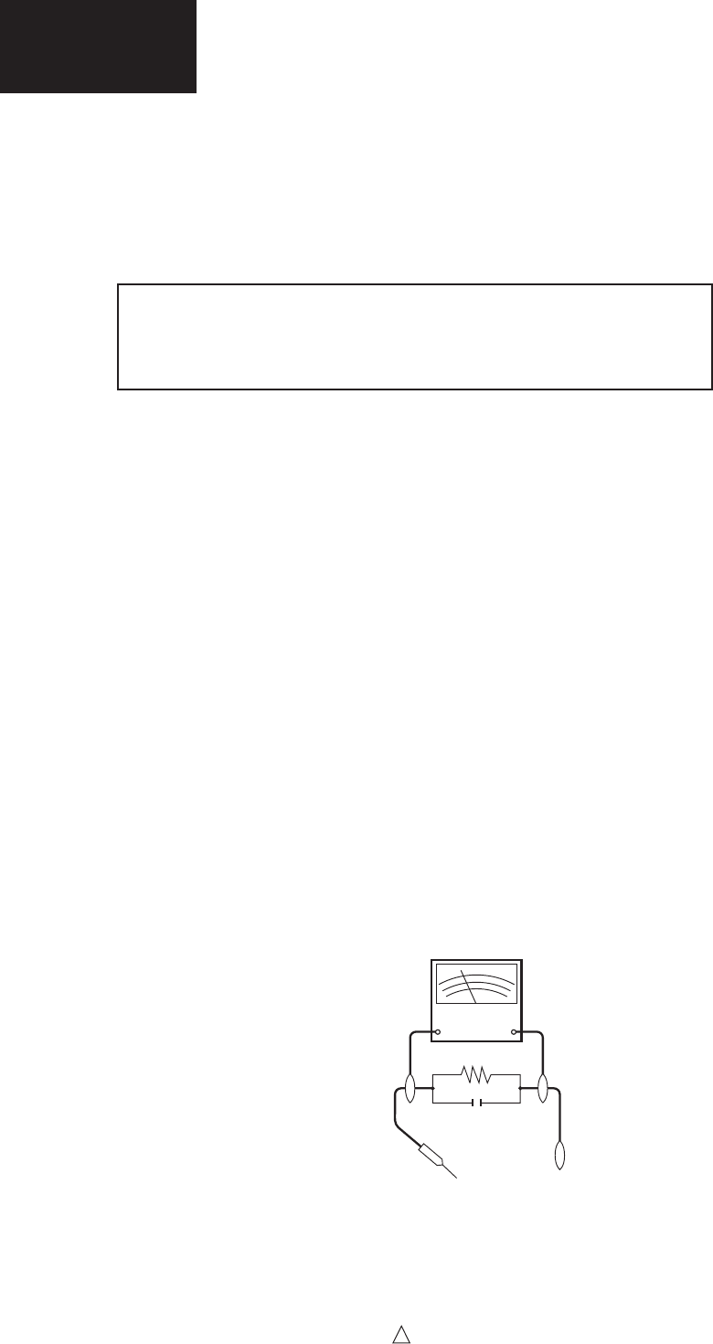
•Use an AC voltmeter having with 5000 ohm per volt, or
higher, sensitivity or measure the AC voltage drop
across the resistor.
•Connect the resistor connection to all exposed metal
parts having a return to the chassis (antenna, metal
cabinet, screw heads, knobs and control shafts,
escutcheon, etc.) and measure the AC voltage drop
across the resistor.
All checks must be repeated with the AC cord plug
connection reversed. (If necessary, a nonpolarized
adaptor plug must be used only for the purpose of
completing these checks.)
Any reading of 0.75V peak (this corresponds to 0.5
mA. peak AC.) or more is excessive and indicates a
potential shock hazard which must be corrected before
returning the monitor to the owner.
BEFORE RETURNING THE RECEIVER
(Fire & Shock Hazard)
Before returning the receiver to the user, perform
the following safety checks:
1. Inspect all lead dress to make certain that leads are
not pinched, and check that hardware is not lodged
between the chassis and other metal parts in the
receiver.
2. Inspect all protective devices such as non-metallic
control knobs, insulation materials, cabinet backs,
adjustment and compartment covers or shields,
isolation resistor-capacitor networks, mechanical
insulators, etc.
3. To be sure that no shock hazard exists, check for
leakage current in the following manner.
•Plug the AC cord directly into a 110~240 volt AC outlet,
and connect the DC power cable into the receiver's
DC jack. (Do not use an isolation transformer for this
test).
•Using two clip leads, connect a 50k ohm, 10 watt
resistor paralleled by a 0.15µF capacitor in series with
all exposed metal cabinet parts and a known earth
ground, such as electrical conduit or electrical ground
connected to an earth ground.
CAUTION: FOR CONTINUED PROTECTION
AGAINST A RISK OF FIRE REPLACE ONLY WITH
SAME TYPE F3701 (2A, 250V), F3702 (1.25A, 250V),
F6700 (1.25A, 250V), F6701 (1.25A, 250V), F6702
(1.25A, 250V), F6703 (1.25A, 250V) AND F6704
(1.25A, 250V) FUSE.
DVM
AC SCALE
1.5k ohm
10W
0.15 µF
TEST PROBE
CAUTION: FOR CONTINUED PROTECTION AGAINST A RISK OF
FIRE REPLACE ONLY WITH SAME TYPE
F701 (4A / 250 V)
IMPORTANT SERVICE SAFETY PRECAUTION
Service work should be performed only by qualifi ed service technicians who are thoroughly familiar with all
safety checks and the servicing guidelines which follow:
WARNING
1. For continued safety, no modifi cation of any circuit should be attempted.
2. Disconnect AC power before servicing.
BEFORE RETURNING THE RECEIVER (Fire & Shock Hazard)
Before returning the receiver to the user, perform the following safety checks:
1. Inspect all lead dress to make certain that leads are not pinched, and check that hardware is not lodged between the
chassis and other metal parts in the receiver.
2. Inspect all protective devices such as non-metallic control knobs, insulation materials, cabinet backs, adjustment and
compartment covers or shields, isolation resistor-capacitor networks, mechanical insulators, etc.
3. To be sure that no shock hazard exists, check for leakage current in the following manner.
• Plug the AC cord directly into a 220~240 volt AC outlet. (Do not use an isolation transformer for this test).
•Using two clip leads, connect a 1.5k ohm, 10 watt resistor paralleled by a 0.15µF capacitor in series with all exposed metal
cabinet parts and a known earth ground, such as electrical conduit or electrical ground connected to an earth ground.
•A true RMS reading multimeter should be used for this test, especially where the equipment uses a switch mode
power supply which may result in very non-sinusoidal leakage current.
•Connect the resistor connection to all exposed metal parts having a return to the chassis (antenna, metal cabinet,
screw heads, knobs and control shafts, escutcheon, etc.) and measure the AC voltage drop across the resistor.
All checks must be repeated with the AC cord plug connection reversed. (If necessary, a nonpolarized adaptor plug must
be used only for the purpose of completing these checks.)
Any reading of 1.05V peak (this corresponds to 0.7 mA. peak AC.) or more is excessive and indicates a potential shock
hazard which must be corrected before returning the monitor to the owner.
!
5
LC-26GA5E
LC-32GA5E
LC-32GD8E/RU
LC-32BT8E/RU
LC-37GD8E/RU
LC-37BT8E/RU
LC-32/37GD8E/RU
LC-32/37BT8E/RU
In the case of LC-37GD8 and LC-37BT8, for the Inverter PWB Units the type used is nickel, so they are marked as LFn:
PRECAUTIONS FOR USING LEAD-FREE SOLDER
1 Employing lead-free solder
“ALL PWB” of this model employs lead-free solder. The LF symbol indicates lead-free solder, and is attached on the
PWBs and service manuals. The alphabetical character following LF shows the type of lead-free solder.
Example:
2 Using lead-free wire solder
When fi xing the PWB soldered with the lead-free solder, apply lead-free wire solder. Repairing with conventional lead
wire solder may cause damage or accident due to cracks.
As the melting point of lead-free solder (Sn-Ag-Cu) is higher than the lead wire solder by 40°C, we recommend you to
use a dedicated soldering bit, if you are not familiar with how to obtain lead-free wire solder or soldering bit, contact our
service station or service branch in your area.
3 Soldering
As the melting point of lead-free solder (Sn-Ag-Cu) is about 220°C which is higher than the conventional lead solder by
40°C, and as it has poor solder wettability, you may be apt to keep the soldering bit in contact with the PWB for extended
period of time. However, Since the land may be peeled off or the maximum heat-resistance temperature of parts may be
exceeded, remove the bit from the PWB as soon as you confi rm the steady soldering condition.
Lead-free solder contains more tin, and the end of the soldering bit may be easily corroded. Make sure to turn on and
off the power of the bit as required.
If a different type of solder stays on the tip of the soldering bit, it is alloyed with lead-free solder. Clean the bit after every
use of it.
When the tip of the soldering bit is blackened during use, fi le it with steel wool or fi ne sandpaper.
Be careful when replacing parts with polarity indication on the PWB silk.
Lead-free wire solder for servicing.
e:
Indicates lead-free solder of tin, silver and copper.
LF a
Indicates lead-free solder of tin, silver and nickel.
LFn
Sn-Ag-Ni
6
LC-26GA5E
LC-32GA5E
LC-32/37GD8E/RU
LC-32/37BT8E/RU
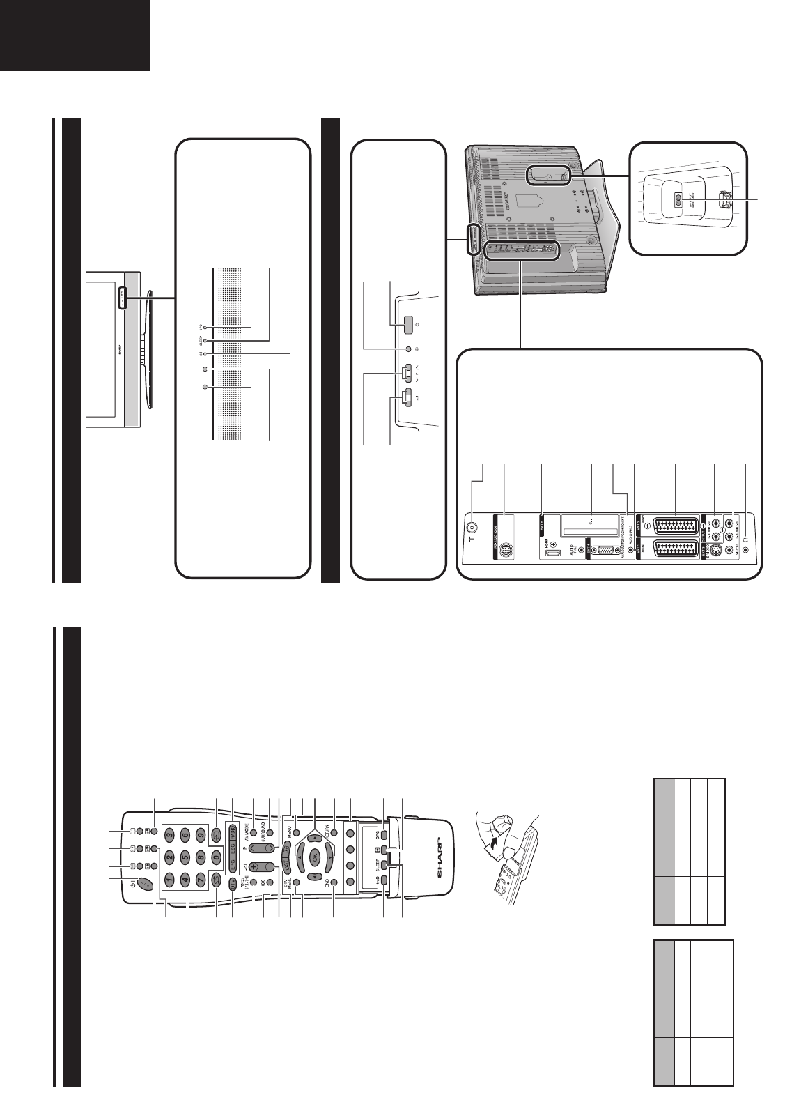
6
Remote control unit
Quick guide
1 2 34
7
9
10
15
16
12
8
5
6
11
14
17
13
18
19
21
27
29
30
22
23
25
24
28
26
20
1B (Standby/On)
Enter standby mode or turn on the
power. (See page 8.)
2m (Teletext)
Select the TELETEXT mode. (all TV
image, DTV/DATA image, all TEXT
image, TV/TEXT image) (See pages
21 and 31.)
DTV: Select DTV data broadcasting
and TELETEXT.
3k (Reveal hidden Teletext)
(See page 21.)
4[ (Subtitle for Teletext)
TV/External: To turn the subtitles on
and off. (See page 21.)
DTV: Display the subtitle selection
screen. (See page 31.)
53 (Freeze/Hold)
(See page 21.)
61 (Subpage)
(See page 21.)
7 0–9
Set the channel in TV and DTV mode.
Set the page in Teletext mode.
8A (Flashback)
Press to return to the previous image
in normal viewing mode. (Will not
work while operating in EPG/ESG
screen.)
9 DTV
Press to access DTV mode while
watching other input sources, and
vice versa.
(This button will not work if you were
watching DTV immediately before
turning off the TV. In this case first
select any other input source except
DTV using the b button.)
10 2 (Sound mode)
Select the sound multiplex mode.
(See below.)
11 e (Mute)
Switch the sound on and off.
12 i (k/l) (Volume)
i (k) Increase the volume.
i (l) Decrease the volume.
13 LIST
DTV: Display the programme list.
14 DTV MENU
Display DTV Menu screen.
15 END
Exit the menu screen.
16 truD
This button is not available in case
of using LC-32/37GD8E/BT8E
models.
17 SLEEP
Set the sleep timer in units of 30 min.
up to max. 2hr. 30min.
18 v (Top/Bottom/Full)
Set the area of magnification in
Teletext mode. (See page 21.)
19 b (INPUT SOURCE)
Select an input source.
(TV, DTV, EXT1, EXT2, EXT3, EXT4,
EXT5) (See page 9.)
20 EPG
DTV: To display EPG (Electronic
Programme Guide) screen.
ESG
DTV: To display ESG (Electronic
Service Guide) screen.
RADIO
DTV: Switch between RADIO and
DTV mode.
21 AV MODE
Select a video setting. (See page 13.)
22 SURROUND
Switch the surround effects on and
off.
23 P (r/s)
TV/DTV: Select the channel.
External: Switch to TV or DTV input
mode.
Teletext: Move to the next/previous
page.
24 p (Display information)
(See pages 21, 29 and 30.)
25 MENU
Display the MENU screen.
(See page 11.)
26 a/b/c/d (Cursor)
Select a desired item on the setting
screen.
OK
Execute a command within the menu
screen.
Display the programme list.
27 RETURN
Return to the previous menu screen.
28 Colour (Red/Green/Yellow/Blue)
TELETEXT: Select a page. (See page
21.)
DTV: The coloured buttons are used
to select correspondingly to the
coloured items in the menu screen.
29 OPC
To switch the Optical Picture Control
on and off. (See page 13.)
30 f (WIDE MODE)
Select the wide mode.
(See page 20.)
Selectable items
NICAM STEREO, MONO
NICAM CH A, NICAM CH B,
NICAM CH AB, MONO
NICAM MONO, MONO
Signal
Stereo
Bilingual
Monaural
Selectable items
STEREO, MONO
CH A, CH B, CH AB
MONO
Signal
Stereo
Bilingual
Monaural
NOTE
• When no signal is input, the sound mode will display “MONO”.
NICAM TV broadcasts selection A2 TV broadcasts selection
E Using 2 on the remote control unit
DTV mode:
Press 2 to open the multi audio screen. (See page 31.)
Analogue TV mode:
Each time you press 2, the mode switches as illustrated in the following tables.
LC-32GD8E_GB_a 06.5.1, 0:07 PM6
7
TV (Front view)
Quick guide
TV (Rear view)
NOTE
• Only if you use an
active terrestrial
antenna, select
“On (5V)” under
“Supply Voltage”.
(See page 18.)
AC INPUT terminal
OPC sensor
Remote control sensor
B (Standby/On) indicator
OPC indicator
a (Power button)
b (Input button)
i (l/k) (Volume buttons)
P (s/r)
(Programme [channel] buttons)
SLEEP indicator
EXT 2 (RGB) terminal
EXT 3 terminals
Headphone jack
EXT 1 (RGB) terminal
EXT 5 (HDMI/AUDIO)
terminals
Antenna input terminal
(DVB-T 5V=/80 mA)
OUTPUT (Audio) terminals
EXT 4 terminals
RS-232C terminal
COMMON INTERFACE slot
LC-32GD8E_GB_a 06.5.1, 0:07 PM7
OPERATION MANUAL
7
LC-26GA5E
LC-32GA5E
LC-32GD8E/RU
LC-32BT8E/RU
LC-37GD8E/RU
LC-37BT8E/RU
LC-32/37GD8E/RU
LC-32/37BT8E/RU
9
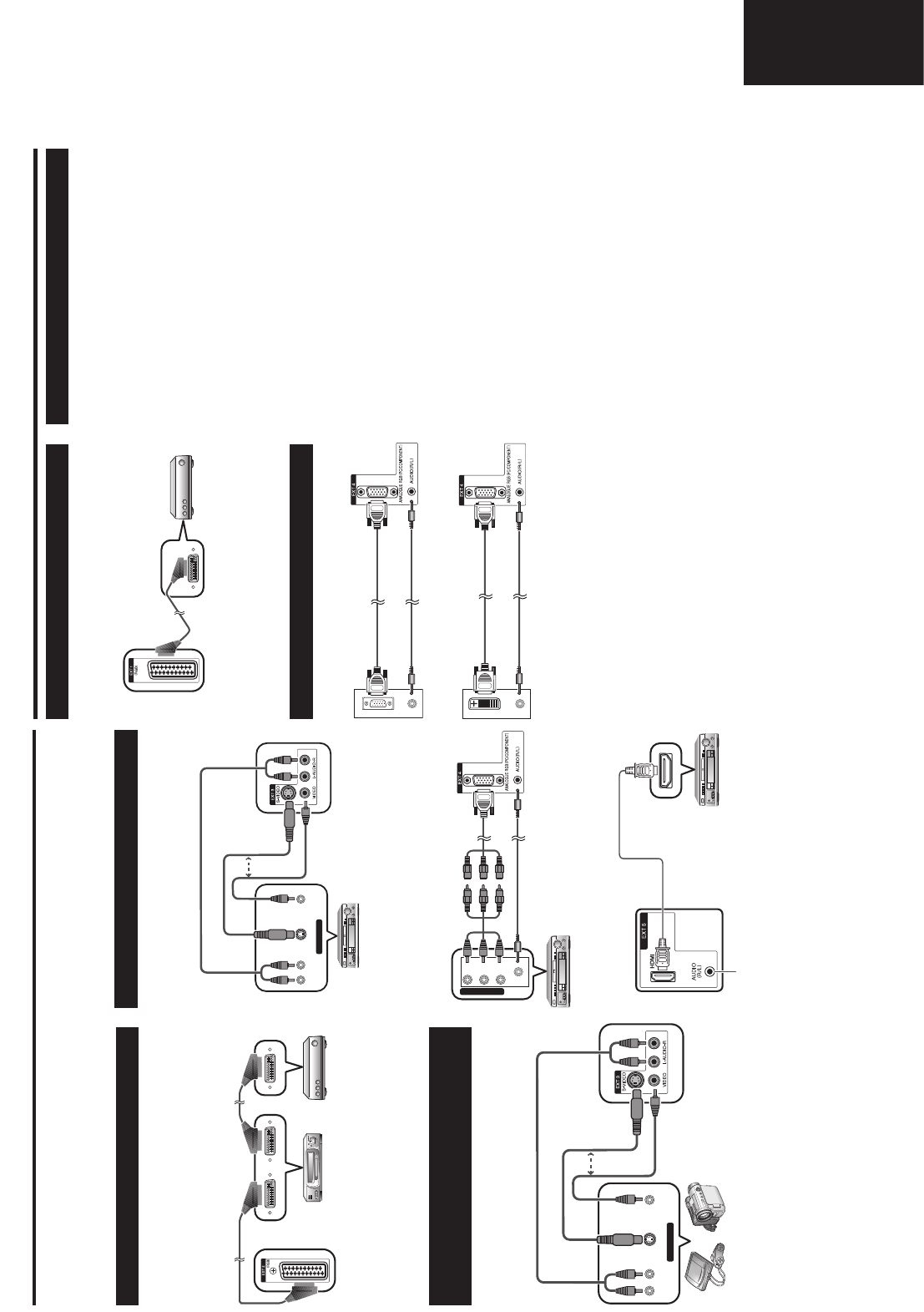
Using external equipment
Setting the input source
To view external source images, select the input source using b on the remote control unit or TV.
NOTE
• The cables marked with * are commercially available items.
Connecting a VCR
You can use the EXT 1 or 2 terminals when connecting
a VCR and other audiovisual equipment.
If your VCR supports TV-VCR advanced AV Link
systems, you can connect the VCR to the EXT 2
terminal of the TV using the fully-wired SCART cable.
NOTE
• TV-VCR advanced AV Link systems may not be compatible
with some external sources.
• TV-OUT from EXT 1 is not outputted when EXT 5 (HDMI)
or DTV is selected as the input.
VCR Decoder
SCART cable* SCART cable*
EXT 1 or 2
VIDEOS-VIDEOL-AUDIO-R
AV OUTPUT
Connecting a DVD player
You can use the EXT 2, 3, 4 or 5 (HDMI) terminals
when connecting to a DVD player and other
audiovisual equipment.
DVD player
EXT 3
A game console, camcorder and some other
audiovisual equipment are conveniently connected
using the EXT 3 terminals.
NOTE
• EXT 3: The S-VIDEO terminal has priority over the VIDEO
terminals.
Connecting a game console or
camcorder
Game console Camcorder
or
S-video cable*
Composite
video cable*
AUDIO cable*
EXT 3
VIDEOS-VIDEOL-AUDIO-R
AV OUTPUT
or
AUDIO cable*
S-video cable*
Composite
video cable*
Y P
B
(
C
B)
P
R
(
C
R)
COMPONENT
EXT 4
ø 3.5 mm stereo minijack cable*
Component
cable*
3 RCA to 15-pin
D-sub adapter
(Supplied)
DVD player
HDMI cable*
When using an HDMI-DVI conversion
adapter/cable, input the Audio signal
here.
EXT 5
DVD player
NOTE
• When connecting an HDMI-DVI conversion adapter/cable
to the HDMI terminal, the image may not come in clearly.
NOTE
• EXT 3: The S-VIDEO terminal has priority over the VIDEO
terminals.
LC-32GD8E_GB_a 06.5.1, 0:07 PM9
10
Using external equipment
NOTE
• The cables marked with * are commercially available
items.
• The PC input terminals are DDC1/2B-compatible.
• Refer to page 33 for a list of PC signals compatible with
the TV.
• Macintosh adaptor may be required for use for some
Macintosh computers.
• When connecting to a PC, the correct input signal type is
automatically detected.
This TV incorporates three typical AV Link functions
for smooth connections between the TV and other
audiovisual equipment.
One Touch Play
While the TV is in standby mode, it automatically turns
on and plays back the image from the audiovisual
source (e.g. VCR, DVD).
WYSIWYR (What You See Is What You Record)
When the remote control unit of the connected VCR
has the WYSIWYR button, you can automatically start
recording by pressing the WYSIWYR button.
Preset Download
Automatically transfers the channel preset information
from the tuner on the TV to the one on the connected
audiovisual equipment (e.g. VCR) via the EXT 2
terminal.
NOTE
• Refer to operation manuals of each external equipment
for the details.
• Only works when the audiovisual equipment is connected
to the EXT 2 terminal on the TV with AV Link via a fully
wired SCART.
• The use of the AV Link function is only possible if the TV-
set has enforced a complete auto-installation with the
connected audiovisual equipment (page 8, Initial auto
installation).
The availability of the AV Link function depends on the
audiovisual equipment used. Depending on the
manufacturer and type of equipment used, it is possible
that the described functions may be completely or partially
unusable.
Using AV Link function
Connecting a PC
Use the EXT 4 terminals to connect a PC.
PC
ø 3.5 mm stereo minijack cable*
RGB cable*
PC
RGB/DVI conversion cable*
ø 3.5 mm stereo minijack cable*
EXT 4
EXT 4
Connecting a decoder
You can use the EXT 1 terminal when connecting a
decoder and other audiovisual equipment.
NOTE
• In cases when the decoder needs to receive signal from
the TV, make sure to set “Decoder” to “EXT1” in the
Programme Setup “Manual Adjust” menu. (See page 16.)
• Do not connect the decoder to the EXT 2 terminal.
Decoder
EXT 1
SCART cable*
LC-32GD8E_GB_b 06.5.1, 0:07 PM10
Operation Manual (Continued)
8
LC-26GA5E
LC-32GA5E
LC-32/37GD8E/RU
LC-32/37BT8E/RU
3
Supplied accessories
Quick guide
Remote control unit (g1) AC cord (g1)
Pages 5 and 6
Product shape varies in
some countries.
Page 4
• “AAA” size battery (g2) ...... Page 5
Cable clamp (g1)
Page 4
Cable tie (g1)
Page 4
3 RCA to 15-pin D-sub
adapter (g1)
Page 9
• Operation manual (This publication)
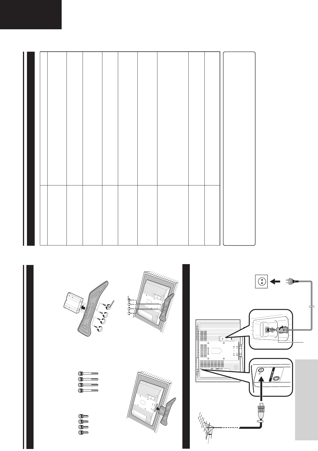
Stand unit (g1)
Page 3
Attaching the stand
Before attaching (or detaching) stand, unplug the AC cord from the AC INPUT terminal.
1Confirm the 8 screws supplied with the TV.
Short screws (m4)
(used in step 2)
Long screws (m4)
(used in step 4)
2Attach the two parts of the stand unit to each other
using the 4 short screws as shown.
3Insert the stand into the opening on the bottom of
the TV.
4Insert and tighten the 4 long screws on the rear
of the TV as shown.
NOTE
• To detach the stand, perform the above steps in reverse order.
Before performing work spread cushioning over the base area to lay the TV on, making sure the area is
completely flat. This will prevent it from being damaged.
LC-32GD8E_GB_a 06.5.1, 0:06 PM3
4
Quick guide
Setting the TV
Bundling the cables
Setting the TV on the wall
•Installing the LCD Colour TV requires special skill that should only be performed by qualified service personnel.
Customers should not attempt to do the work themselves. SHARP bears no responsibility for improper mounting
or mounting that results in accident or injury.
• You can ask a qualified service personnel about using an optional bracket to mount the TV to the wall.
Standard DIN45325 plug
(IEC 169-2)
75-ohm coaxial cable
Antenna
Connect the antenna cable from your antenna-/
cable socket or the (room-/roof) antenna for
antenna input terminal on the back of your TV set
to receive digitally/terrestrially broadcast stations.
An indoor antenna can also be used under good
reception conditions. Passive and active room
antennas are offered commercially. In an active
antenna its power is supplied via the antenna
input terminal.
The supply voltage (5V) must be correspondingly
set under “Supply Voltage”. (See page 18.)
Ferrite Core
The Ferrite Core should be permanently attached
and never removed from the AC cord.
AC cord
Product shape
varies in some
countries.
Cable clampCable tie
Place the TV close
to the AC outlet, and
keep the power plug
within reach.
Ferrite Core
LC-32GD8E_GB_a 06.5.1, 0:06 PM4
32
• Check if you pressed B on the remote control unit. (See page 8.)
If the indicator on the TV lights up red, press B.
• Is the AC cord disconnected? (See page 4.)
• Check if you pressed a on the TV. (See page 8.)
• External influences such as lightning, static electricity, etc., may cause improper
operation. In this case, operate the unit after first turning the power off, or
unplugging the AC cord and re-plugging it in after 1 or 2 minutes.
• Are batteries inserted with polarity (e,f) aligned? (See page 5.)
• Are batteries worn out? (Replace with new batteries.)
• Are you using it under strong or fluorescent lighting?
• Is a fluorescent light illuminated to remote control sensor?
• Is the image position correct? (See page 18.)
• Are screen mode adjustments (4:3 Mode/WSS) such as picture size made
correctly? (See pages 18 and 20.)
• Adjust the picture tone. (See pages 13 and 14.)
• Is the room too bright? The picture may look dark in a room that is too bright.
• Check the colour system setting. (See pages 16 and 19.)
• Check the HDMI Setup setting. (See page 19.)
• The unit’s internal temperature has increased.
Remove any objects blocking vent or clean.
• Check the power control setting. (See page 15.)
• Is sleep timer set? Press SLEEP on the remote control unit until it sets to Off.
• Is connection to other components correct? (See pages 9 and 10.)
• Is input signal type selected correctly after connection? (See page 19.)
• Is the correct input source selected? (See page 9.)
• Is non-compatible signal being input? (See page 33.)
• Is picture adjustment correct? (See pages 13 and 14.)
• Is the antenna connected properly? (See page 4.)
• Is “On” selected in “Audio Only”? (See page 18.)
• Is the volume too low? (See pages 6 and 7.)
• Make sure that headphones are not connected. (See page 7.)
• Check if you pressed e on the remote control unit. (See page 6.)
• Check if “Monochrome” is set to “On”. If so, set it to “Off”. (See page 14.)
Troubleshooting
Appendix
IMPORTANT NOTE ON RESETTING THE PIN
We suggest that you remove the following instruction from the operation manual to prevent children from
reading it. As this operation manual is multilingual, we also suggest the same with each language. Keep it in
a safe space for future reference.
Cautions regarding use in high and low temperature environments
• When the unit is used in a low temperature space (e.g. room, office), the picture may leave trails or appear slightly
delayed. This is not a malfunction, and the unit will recover when the temperature returns to normal.
• Do not leave the unit in a hot or cold location. Also, do not leave the unit in a location exposed to direct sunlight or near
a heater, as this may cause the cabinet to deform and the LCD panel to malfunction.
Storage temperature: –20°C to e60°C.
1Repeat steps 1 to 3 in Changing the PIN. (See page 17.)
2Enter “3001” to cancel out the current PIN.
• The PIN resets to the factory preset “1234”.
Problem Possible Solution
• No power.
• Unit cannot be operated.
• Remote control unit does not
operate.
• Picture is cut off.
• Strange colour, light colour, or
dark, or colour misalignment.
• Power is suddenly turned off.
• No picture.
• No sound.
• The DTV menu screen is
displayed in monochrome and
hard to select the item.
LC-32GD8E_GB_f 06.5.1, 0:11 PM32
Operation Manual (Continued)
9
LC-26GA5E
LC-32GA5E
LC-32GD8E/RU
LC-32BT8E/RU
LC-37GD8E/RU
LC-37BT8E/RU
LC-32/37GD8E/RU
LC-32/37BT8E/RU
33
Appendix
PC compatibility chart
Resolution
Horizontal
Frequency
Vertical
Frequency
VESA
Standard
640 g 480VGA 31.5 kHz 60 Hz �
800 g 600SVGA 37.9 kHz 60 Hz �
1024 g 768XGA 48.4 kHz 60 Hz �
Communication procedure
Send the control commands from the PC via the RS-
232C connector.
The TV operates according to the received command
and sends a response message to the PC.
Do not send multiple commands at the same time. Wait
until the PC receives the OK response before sending
the next command.
Return codeCommand 4-digits Parameter 4-digits
Command format
Eight ASCII codes e CR
Command 4-digits: Command. The text of four characters.
Parameter 4-digits: arameter 0 – 9, g, blank, ?
C1 C2 C3 C4 P1 P2 P3 P4
Parameter
Input the parameter values, aligning left, and fill with
blank(s) for the remainder. (Be sure that four values are
input for the parameter.)
When the input parameter is not within an adjustable
range, “ERR” returns. (Refer to “Response code format”.)
When “?” is input for some commands, the present setting
value responds.
0055
100
–3 0
0009
0
????
?
Return code (0DH)
Response code format
Normal response
Problem response (communication error or incorrect
command)
Return code (0DH)
O K
E R R
RS-232C port specifications
PC Control of the TV
•When a program is set, the TV can be controlled
from the PC using the RS-232C terminal.
The input signal (PC/video) can be selected, the
volume can be adjusted and various other
adjustments and settings can be made, enabling
automatic programmed playing.
•Attach an RS-232C cable cross-type (commercially
available) to a 9 pin D-sub/MINI-DIN (optional: AN-
A1RS) for the connections.
NOTE
• This operation system should be used by a person who is
accustomed to using PCs.
Communication conditions
Set the RS-232C communications settings on the PC
to match the TV’s communications conditions. The TV’s
communications settings are as follows:
Baud rate:
Parity bit:
Data length:
Stop bit:
Flow control:
9,600 bps
8 bits
None
1 bit
None
RS-232C serial control cable
(cross type, commercially available)
9 pin D-sub/MINI-DIN
conversion cable
(optional: AN-A1RS)
VGA, SVGA and XGA are registered trademarks
of International Business Machines Co., Inc.
NOTE
•This TV has only limited PC compatibility, correct operation
can only be guaranteed if the video card conforms exactly
to the VESA 60Hz standard. Any variations from this
standard will result in picture distortions.
LC-32GD8E_GB_f 06.5.1, 0:11 PM33
34
Appendix
Commands
P
I
I
I
I
I
D
D
C
C
D
D
D
D
I
I
I
I
I
I
I
I
I
I
I
I
I
A
A
A
A
A
A
A
V
V
POWER OFF
INPUT SWITCHING (Toggle)
TV (CHANNEL FIXED)
DTV (CHANNEL FIXED)
EXT1 – 5 (1 – 5)
1 to 5, ERR (TV/DTV)
TV DIRECT CHANNEL (1 – 99)
1 to 99
CHANNEL UP
CHANNEL DOWN
DTV DIRECT CHANNEL (1 to 999)
1 to 999
DTV CHANNEL UP
DTV CHANNEL DOWN
EXT1 (Y/C)
EXT1 (CVBS)
EXT1 (RGB)
0 to 2
EXT2 (Y/C)
EXT2 (CVBS)
EXT2 (RGB)
0 to 2
EXT3
EXT4 (RGB)
EXT4 (COMPONENT)
0 to 1
EXT5 (HDMI)
AV MODE SELECTION (Toggle)
STANDARD
SOFT
ECO
USER
DYNAMIC
1 to 5
VOLUME (0 – 60)
0 to 60
POWER SETTING
INPUT SELECTION A
CHANNEL
INPUT SELECTION B
AV MODE
SELECTION
VOLUME
O
T
T
D
A
A
C
C
H
H
T
T
T
T
N
N
N
N
N
N
N
N
N
N
N
N
N
V
V
V
V
V
V
V
O
O
W
G
V
T
V
V
C
C
U
D
V
V
U
D
P
P
P
P
P
P
P
P
P
P
P
P
P
M
M
M
M
M
M
M
L
L
R
D
D
V
D
D
H
H
P
W
D
D
P
W
1
1
1
1
2
2
2
2
3
4
4
4
5
D
D
D
D
D
D
D
M
M
0
_
_
_
*
?
*
?
_
_
*
?
_
_
0
1
2
?
0
1
2
?
0
0
1
?
0
0
1
2
3
4
5
?
*
?
_
_
_
_
_
?
*
?
_
_
*
?
_
_
_
_
_
?
_
_
_
?
_
_
_
?
_
_
_
_
_
_
_
?
*
?
_
_
_
_
_
?
_
?
_
_
*
?
_
_
_
_
_
?
_
_
_
?
_
_
_
?
_
_
_
_
_
_
_
?
_
?
_
_
_
_
_
?
_
?
_
_
_
?
_
_
_
_
_
?
_
_
_
?
_
_
_
?
_
_
_
_
_
_
_
?
_
?
CONTROL ITEM
COMMAND PARAMETER
CONTROL
CONTENTS CONTROL ITEM
COMMAND PARAMETER
CONTROL
CONTENTS
H
H
V
V
C
C
P
P
W
W
W
W
W
W
W
W
W
W
M
M
M
M
A
A
A
A
A
O
O
O
O
O
O
O
T
T
T
D
D
H-POSITION AV (10 –10)
AV (10 –10)
V-POSITION AV (20 –20)
AV (20 –20)
CLOCK (0 – 180)
0 to 180
PHASE (0 – 40)
0 to 40
WIDE MODE (Toggle)
NORMAL (AV)
ZOOM 14:9 (AV)
PANORAMA (AV)
FULL (AV)
CINEMA 16:9 (AV)
CINEMA 14:9 (AV)
NORMAL (PC)
FULL (PC)
1 to 10
MUTE (Toggle)
MUTE ON
MUTE OFF
1 to 2
SURROUND (Toggle)
SURROUND ON
SURROUND OFF
1 to 2
SOUND SELECT (ST/Bilingual/mono)
OFF
30 m
1 h 00 m
1 h 30 m
2 h 00 m
2 h 30 m
0 to 150
TEXT OFF
TEXT CHANGE (Toggle)
0 to 1
DIRECT PAGE JUMP (100 – 899)
100 to 899
P
P
P
P
L
L
H
H
I
I
I
I
I
I
I
I
I
I
U
U
U
U
C
C
C
C
C
F
F
F
F
F
F
F
E
E
E
C
C
O
O
O
O
C
C
S
S
D
D
D
D
D
D
D
D
D
D
T
T
T
T
D
D
D
D
H
T
T
T
T
T
T
T
X
X
X
P
P
S
S
S
S
K
K
E
E
E
E
E
E
E
E
E
E
E
E
E
E
E
E
V
V
V
V
A
M
M
M
M
M
M
M
T
T
T
G
G
*
?
*
?
*
?
*
?
0
1
2
3
4
5
6
9
1
?
0
1
2
?
0
1
2
?
_
0
1
2
3
4
5
?
0
1
?
*
?
*
?
*
?
*
?
*
?
_
_
_
_
_
_
_
_
0
?
_
_
_
?
_
_
_
?
_
_
_
_
_
_
_
?
_
_
?
*
?
*
?
*
?
*
?
_
?
_
_
_
_
_
_
_
_
_
?
_
_
_
?
_
_
_
?
_
_
_
_
_
_
_
?
_
_
?
*
?
_
?
_
?
_
?
_
?
_
_
_
_
_
_
_
_
_
?
_
_
_
?
_
_
_
?
_
_
_
_
_
_
_
?
_
_
?
_
?
WIDE MODE
POSITION
SURROUND
MUTE
AUDIO CHANGE
SLEEP TIMER
TEXT
NOTE
•If an underbar (_) appears in the parameter column, enter a space.
•If an asterisk (*) appears, enter a value in the range indicated in brackets under CONTROL CONTENTS.
User-
adjusted rating
Universal
Parental
X-rated
Universal Parental X-rated
—
�
�
—
�
—
—
—
—
Rating table for Child Lock
Broadcasted
rating
User-
adjusted rating
Broadcasted
rating
4 5 6 7 8 9 10 11 12 13 14 15 16 17 18
AGE
Universal
Parental
X-rated
�
�
�
� � � � — — — — — — — — — —
� � � � � � � � � � � � � �
— — — — — — — — — — — — — —
LC-32GD8E_GB_f 06.5.1, 0:11 PM34
Operation Manual (Continued)
10
LC-26GA5E
LC-32GA5E
LC-32/37GD8E/RU
LC-32/37BT8E/RU
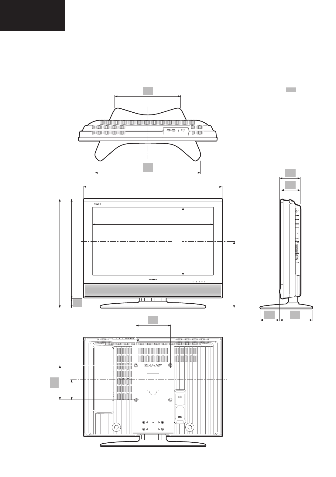
396.0
396,0
612.0
612,0
(804.0) / [926.0]
(804,0) / [926,0]
(699.6) / [822.6]
(699,6) / [822,6]
(388.5) / [422.9]
(388,5) / [422,9]
(636.0) / [705.0]
(636,0) / [705,0]
(575.0) / [644.0]
(575,0) / [644,0]
119.2
119,2
115.7
115,7
200.0
200,0
200.0
200,0
188.6
188,6
115.7
115,7
(394.3) / [463.8]
(394,3) / [463,8]
61.0
61,0
(115.0) / [104.0]
(115,0) / [104,0]
LC-32GD8E / LC-32BT8E / LC-37GD8E / LC-37BT8E
( ) : LC-32GD8E
LC-32BT8E
[ ] : LC-37GD8E
LC-37BT8E
: LC-32GD8E
LC-32BT8E
LC-37GD8E
LC-37BT8E
SPECIAL NOTE FOR USERS IN THE U.K.
The mains lead of this product is fitted with a non-rewireable (moulded) plug incorporating a 13A fuse. Should
the fuse need to be replaced, a BSI or ASTA approved BS 1362 fuse marked or
ASA
and of the same rating
as above, which is also indicated on the pin face of the plug, must be used.
Always refit the fuse cover after replacing the fuse. Never use the plug without the fuse cover fitted.
In the unlikely event of the socket outlet in your home not being compatible with the plug supplied, cut off the
mains plug and fit an appropriate type.
DANGER:
The fuse from the cut-off plug should be removed and the cut-off plug destroyed immediately and disposed of
in a safe manner.
Under no circumstances should the cut-off plug be inserted elsewhere into a 13A socket outlet, as a serious
electric shock may occur.
To fit an appropriate plug to the mains lead, follow the instructions below:
IMPORTANT:
The wires in the mains lead are coloured in accordance with the following code:
Blue: Neutral
Brown: Live
As the colours of the wires in the mains lead of this product may not correspond with the coloured markings
identifying the terminals in your plug, proceed as follows:
• The wire which is coloured blue must be connected to the plug terminal which is marked N or coloured black.
• The wire which is coloured brown must be connected to the plug terminal which is marked L or coloured red.
Ensure that neither the brown nor the blue wire is connected to the earth terminal in your three-pin plug.
Before replacing the plug cover make sure that:
• If the new fitted plug contains a fuse, its value is the same as that removed from the cut-off plug.
• The cord grip is clamped over the sheath of the mains lead, and not simply over the lead wires.
IF YOU HAVE ANY DOUBT, CONSULT A QUALIFIED ELECTRICIAN.
DIMENSIONS
11
LC-26GA5E
LC-32GA5E
LC-32GD8E/RU
LC-32BT8E/RU
LC-37GD8E/RU
LC-37BT8E/RU
LC-32/37GD8E/RU
LC-32/37BT8E/RU
9
LC-32/37GD8E/RU
LC-32/37BT8E/RU
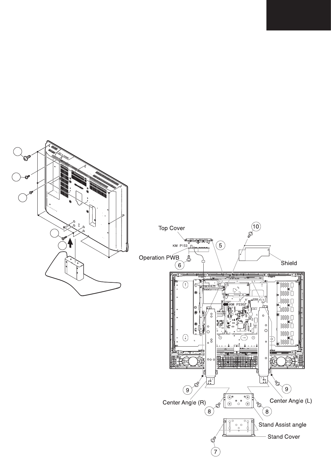
REMOVING OF MAJOR PARTS
1. Remove the stand fixing screws (4 pcs.).
2. Remove the terminal screws (6 pcs.).
3. Remove the cabinet B fixing screws (9 pcs.).
4. Remove the cabinet B after opening from the direction of an arrow.
5. Remove the top cover ass’y.
6. Remove the operation PWB fixing screws (3 pcs.).
7. Remove the stand cover fixing screws (2 pcs.).
8. Remove the stand assist angle fixing screws (2 pcs.).
9. Remove the 6 lock screws from the right and left center angles and take out both center angles.
10. Remove the Shield screws (2 pcs.).
2
2
2
1
4
REMOVING OF MAJOR PARTS
12
LC-26GA5E
LC-32GA5E
LC-32/37GD8E/RU
LC-32/37BT8E/RU
10
LC-32/37GD8E/RU
LC-32/37BT8E/RU
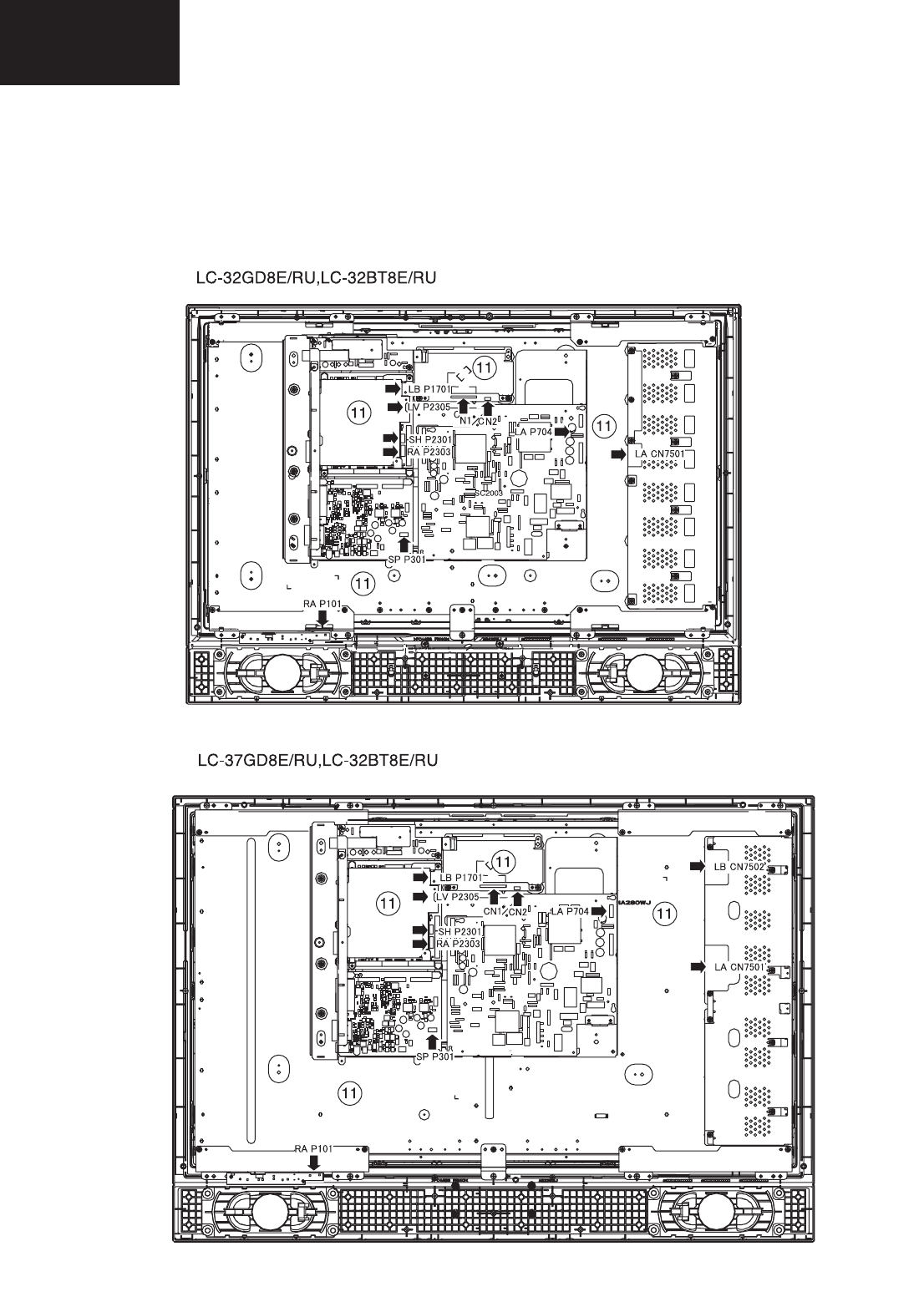
11. Disconnect all the connectors from all the PWBs.
Removing of Major Parts (Continued)
13
LC-26GA5E
LC-32GA5E
LC-32GD8E/RU
LC-32BT8E/RU
LC-37GD8E/RU
LC-37BT8E/RU
LC-32/37GD8E/RU
LC-32/37BT8E/RU
11
LC-32/37GD8E/RU
LC-32/37BT8E/RU
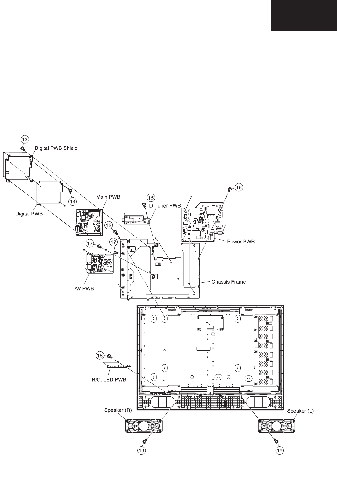
12. Remove the chassis frame fixing screws (5 pcs.).
13. Remove the Digital PWB with Digital PWB Shield fixing screws (4 pcs.).
14. Remove the Digital PWB from Digital PWB Shield (4 pcs.).
15. Remove the D-tuner PWB fixing angle fixing screws (2 pcs.).
16. Remove the power PWB fixing screws (4 pcs.).
17. Remove the AV PWB fixing screws (5 pcs.).
18. Remove the R/C,LED PWB fixing screws (3 pcs.).
19. Remove the 2 lock screws from the right and left speakers and take out both speakers.
Removing of Major Parts (Continued)
14
LC-26GA5E
LC-32GA5E
LC-32/37GD8E/RU
LC-32/37BT8E/RU
12
LC-32/37GD8E/RU
LC-32/37BT8E/RU
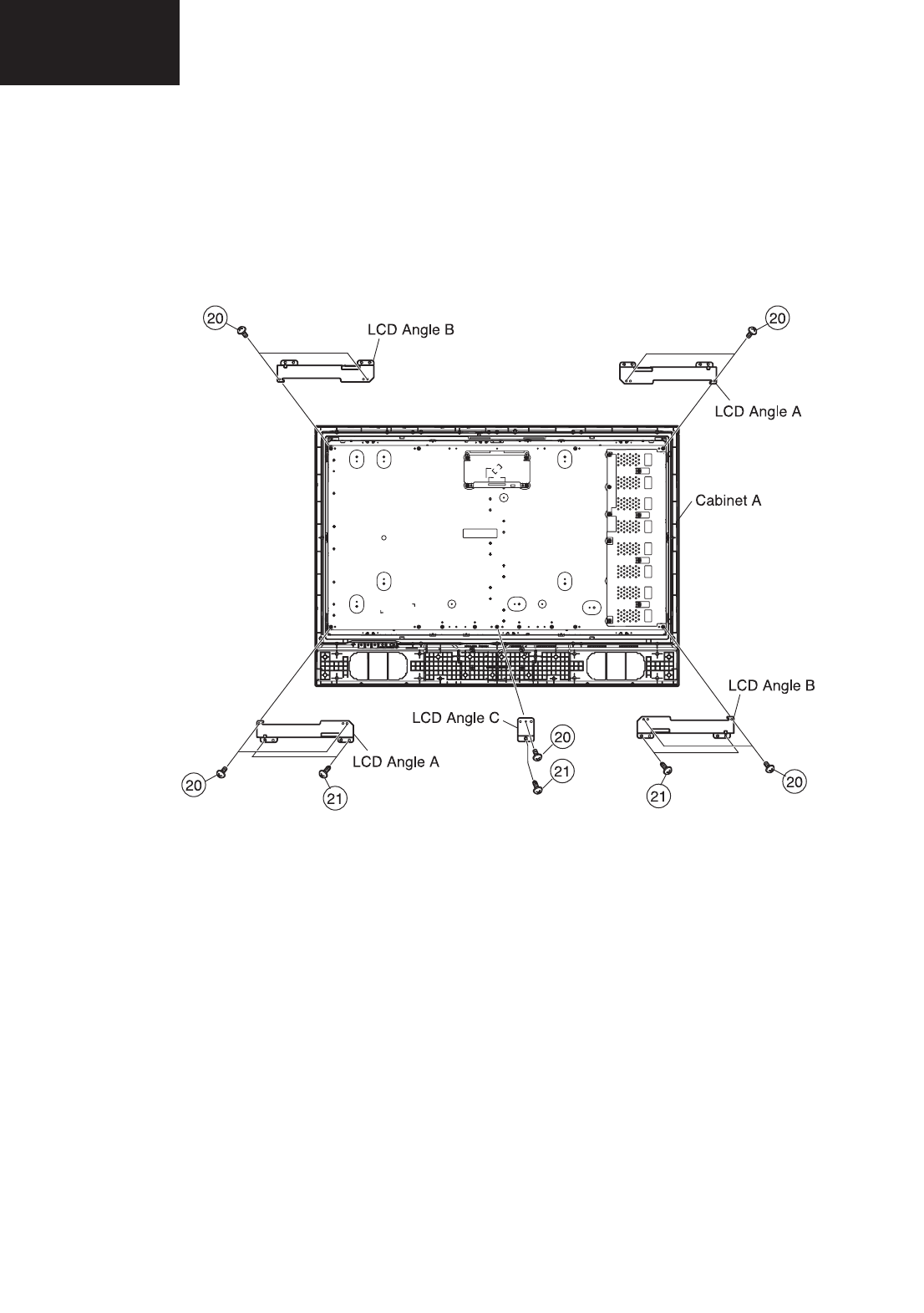
20. Remove the LCD angle to LCD Panel fixing screws (9 pcs.).
21. Remove the LCD angle to Cabinet-A fixing screws (5 pcs.).
Removing of Major Parts (Continued)

15
LC-26GA5E
LC-32GA5E
LC-32GD8E/RU
LC-32BT8E/RU
LC-37GD8E/RU
LC-37BT8E/RU
LC-32/37GD8E/RU
LC-32/37BT8E/RU
2.1 Key operation
Remote controller key Main unit key Function
P (Λ / V) P (Λ / V) Moving an item (line) by one (UP/DOWN)
VOL (+/-) VOL (+/-) Changing a selected item setting (+1/-1)
Cursor (UP / DOWN) ———— Turning a page (PREVIOUS / NEXT)
Cursor (LEFT / RIGHT) ———— Changing a selected line setting (+10/-10)
INPUT SOURCE
on remote controller
INPUT button Input source switching (toggle switching)
(TV→DTV→EXT1→EXT2→EXT3→EXT4→EXT5)
(Not Operative)
OK ———— Executing a function
The adjustment values are set to their optimum at the factory before shipping. If by any chance a value should become im-
proper or a readjustment is required due to part replacement, make an adjustment according to the following procedure.
1. Entering and exiting the adjustment process mode
1- Unplug the AC power cord of TV set to force power off.
2- While holding down the “VOL (–)” and “INPUT” keys on the set at once, plug in the AC power cord to turn on the
set. The letter K appears on the screen. (Factory mode)
3- Next, hold down the “VOL (—)” and “P ( V )” keys on the set at once. Multiple lines of orange characters appearing
on the screen indicate that the set is now in the adjustment process mode. If you fail to enter the adjustment process
mode (the display is the same as normal start up), retry the procedure.
4- To exit the adjustment process mode after the adjustment is done, unplug the AC power cord to force off the
power. (When the power is turned off by the remote controller, unplug also the AC power cord and wait for 10
seconds before plug it in again.)
5- To remove “K” mode, just repeat steps 1 and 2. This time the letter K disappears from screen.
2. Remote Controller Key Operation and Description of Display in Adjustment Process Mode
Input mode is switched automatically when relevant adjustment is started so far as the necessary input signal
available.
2.2 Description of display
SERVICE ADJUSTMENTS
Parameters
Adjustment process menu
header
Destination (EURO just as example. See Factory Init,
it may be EURO, UK, ITALY, FRANCE or RUSSIA)
Current color TV system
Currently selected input
Current page title
Current page/ Total pages
1/11 [INFO] TV AUTO 32: EURO
Main Version
Dev Version
Dev Loader Version
Pic Version
TEMP SENSOR
NORMAL STANDBY CAUSE
ERROR STANDBY CAUSE
LEW05 01.XXXX (YYYY/MM/DD X) X
X.XXX
X.X
XX.XX
XXX
XXXXX
[1] 0 XXHXXM
[2] 0 XXHXXM
[3] 0 XXHXXM
[4] 0 XXHXXM
[5] 0 XXHXXM
Inch Setting (32 just as example, it may be: --/32/37)
Caution: Use due care in handling the information described here lest the users should
know how to enter the adjustment process mode. If the settings tampered with in
this mode, unrecoverable system damage may result.

16
LC-26GA5E
LC-32GA5E
LC-32/37GD8E/RU
LC-32/37BT8E/RU
3. Adjustment process mode menu
The character string in brackets [ ] will appear as a page title in the adjustment process menu header.
Page Line Item Description Remarks (Adjustment detail, etc.)
[INFO]
1/11
1
2
3
4
5
6
7
Main Version
Dev Version
Dev Loader Version
PIC Version
TEMP SENSOR
NORMAL STANDBY CAUSE
ERROR STANDBY CAUSE
1.xxx (xx/xx/xxxx) x
x.xxx
x.x
xx.xx
xxx
[X]0
xxHxxM (X5)
Main microprocessor version (VCTP)
Digital Module version
Digital Module loader version
PIC version
Temp inside cabinet (near panel)
Last status which cause standby
Error standby cause
Total operating time before error
[INIT]
2/11
1
2
3
4
5
6
7
8
9
10
Factory Init
Inch Setting
PUBLIC MODE
Center Acutime
RESET
Backlight Acutime
RESET
Picture Read Pos X
Picture Read Pos Y
Picture Read
(--/EURO/UK/ITALY/FRANCE/RUSSIA)ENTER
(--/26/32/37/45)
OFF/ON
XxH xxM
OFF/ON
XxH xxM
OFF/ON
0
0
ON/OFF
Initialization to factory settings
Initialization data for different panel sizes
PUBLIC MODE flag setting
Main operating hours (Not Operative)
Main operating hours reset
Backlight operating hours
Backlight operating hours reset
x-axis setting of picture data
y-axis setting of picture data
Start/stop of picture data
[PAL. SECAM. N358]
3/11
1
2
3
4
5
6
7
8
9
RF-AGC ADJ
PAL+TUNER ADJ
PAL ADJ
TUNER ADJ
CONTRAST SD
SECAM CB OFFSET
SECAM CR OFFSET
TUNER A DAC
RF AGC
ENTER
ENTER
ENTER
ENTER
32
1
1
32
20
RF AGC auto adjustment
PALTUNER auto adjustment
PAL auto adjustment
TUNER auto adjustment
SD contrast adjustment
SECAM contrast adjustment
SECAM contrast adjustment
TUNER DAC adjustment
RF AGC adjustment
[COMP 15K]
4/11
1
2
COMP 15K ADJ
COMP 15K CONTRAST
ENTER
32
COMP 15K auto adjustment
Contrast adjustment
[HDTV]
5/11
1 HDTV CONTRAST 32 Contrast adjustment
[SMPTE]
6/11
1
2
3
4
5
6
7
8
9
RF-AGC ADJ
PAL+TUNER ADJ
PAL ADJ
TUNER ADJ
CONTRAST SD
SECAM CB OFFSET
SECAM CR OFFSET
TUNER A DAC
RF AGC
ENTER
ENTER
ENTER
ENTER
32
1
1
34
25
RF AGC auto adjustment
PALTUNER auto adjustment
PAL auto adjustment
TUNER auto adjustment
SD contrast adjustment
SECAM contrast adjustment
SECAM contrast adjustment
TUNER DAC adjustment
RF AGC adjustment
[M GAMMA INFO]
7/11
1
2
3
4
5
6
7
8
MGAMMA IN 1
MGAMMA IN 2
MGAMMA IN 3
MGAMMA IN 4
MGAMMA IN 5
MGAMMA IN 6
MGAMMA WRITE
MGAMMA RESET
160
320
480
640
800
960
OFF/ON
OFF/ON
W/B adjustment, gradation 1 input setting
W/B adjustment, gradation 2 input setting
W/B adjustment, gradation 3 input setting
W/B adjustment, gradation 4 input setting
W/B adjustment, gradation 5 input setting
W/B adjustment, gradation 6 input setting
EEP writing of adjustment values
Initialization of adjustment values
[M GAMMA 1-3]
8/11
1
2
3
4
5
6
7
8
9
10
MGAMMA R 1
MGAMMA G 1
MGAMMA B 1
MGAMMA R 2
MGAMMA G 2
MGAMMA B 2
MGAMMA R 3
MGAMMA G 3
MGAMMA B 3
MGAMMA WRITE
0
0
0
0
0
0
0
0
0
OFF/ON
W/B adjustment, gradation 1R adjustment value
W/B adjustment, gradation 1G adjustment value
W/B adjustment, gradation 1B adjustment value
W/B adjustment, gradation 2R adjustment value
W/B adjustment, gradation 2G adjustment value
W/B adjustment, gradation 2B adjustment value
W/B adjustment, gradation 3R adjustment value
W/B adjustment, gradation 3G adjustment value
W/B adjustment, gradation 3B adjustment value
EEP writing of adjustment values
[M GAMMA 4-6]
9/11
1
2
3
4
5
MGAMMA R 4
MGAMMA G 4
MGAMMA B 4
MGAMMA R 5
MGAMMA G 5
0
0
0
0
0
W/B adjustment, gradation 4R adjustment value
W/B adjustment, gradation 4G adjustment value
W/B adjustment, gradation 4B adjustment value
W/B adjustment, gradation 5R adjustment value
W/B adjustment, gradation 5G adjustment value
17
LC-26GA5E
LC-32GA5E
LC-32GD8E/RU
LC-32BT8E/RU
LC-37GD8E/RU
LC-37BT8E/RU
LC-32/37GD8E/RU
LC-32/37BT8E/RU
Page Line Item Description Remarks (Adjustment detail, etc.)
[M GAMMA 4-6]
9/11
(Continued) 6
7
8
9
10
MGAMMA B 5
MGAMMA R 6
MGAMMA G 6
MGAMMA B 6
MGAMMA WRITE
0
0
0
0
OFF/ON
W/B adjustment, gradation 5B adjustment value
W/B adjustment, gradation 6R adjustment value
W/B adjustment, gradation 6G adjustment value
W/B adjustment, gradation 6B adjustment value
EEP writing of adjustment values
[ETC]
10/11
1
2
3
4
5
6
7
8
9
10
EEP CLEAR
EEP CLEAR B
STAND BY CAUSE RESET
AUTO INSTALLATION SW
OPTION
COUNTRY
L ERR RESET
L ERR STOP
DTV CLR
I2C-OFF
OFF/ON
OFF/ON
OFF/ON
0/1
0
(--/EURO/UK/ITALY/FRANCE/RUSSIA)
0
0/1
0/1
ENTER
Restore NVM data to default values
Restore NVM data to default values except
adjustment data
Clearing of standby cause error list
0: unfinished 1:finish (The setting takes effect
the next time the power is turned on.)
Selected country
Lamp error counter
Stops Lamp Error feature
Restore Digital Module NVM to default values
BUS STOP
LCD
11/11
1
2
3
4
5
6
7
OSC FREQ 50
OSC FREQ 60
PWM FREQ 50
PWM FREQ 60
PWM FREQ
PWM DUTY
PWM CTRL
144
144
1
1
424
227
0
17
LC-26GA5E
LC-32GA5E
LC-32GA8/LC-32BV8
LC-37GA8/LC-37BV8
4. Special Features
- ERROR STAND-BY CAUSE (Page 1/11)
When the unit enters standby due to operational error, total time before the error and the cause of error is recorded
on EEPROM, if possible. The values can be used to locate the fault for repair.
- EEP CLEAR (Page 10/11)
Restore NVM data to default values.
- EEP CLEAR B (Page 10/11)
Restore NVM data to default values except adjustment data.
5. Video Signal Adjustment Procedure
The adjustment process mode menu is listed in Section 3.
5.1. Signal check
Signal generator level adjustment check (Adjustment to the specified level).
- Composite signal PAL : 0.7Vp-p ± 0.02Vp-p (Pedestal to white level)
- 15K Component signal : Y level 0.7Vp-p ± 0.02Vp-p (Pedestal to white level)
(50Hz) (576i/50Hz) PB, PR level 0.7Vp-p ± 0.02Vp-p
5.2. Entering the adjustment process mode
Enter the adjustment process mode according to Section 1.
5.3. RF AGC Adjustment
Adjustment Point Adjustment conditions Adjustment procedure
1 Setting [Signal]
PAL
Field Color Bar
RF signal
[Terminal]
TUNER
• Feed the PAL color bar signal (E-12ch) to TUNER.
Signal level: 50 ±1dB µV (75Ω LOAD)
2 Auto adjustment
performance
Adjustment process page 3. Bring the cursor on [▪RF AGC ADJ] and press [OK].
[▪RF AGC ADJ OK] appears when finished.
�����������������������������
↑ 100% white
[TUNER]
18
LC-26GA5E
LC-32GA5E
LC-32/37GD8E/RU
LC-32/37BT8E/RU
18
LC-26GA5E
LC-32GA5E
LC-32GA8/LC-32BV8
LC-37GA8/LC-37BV8
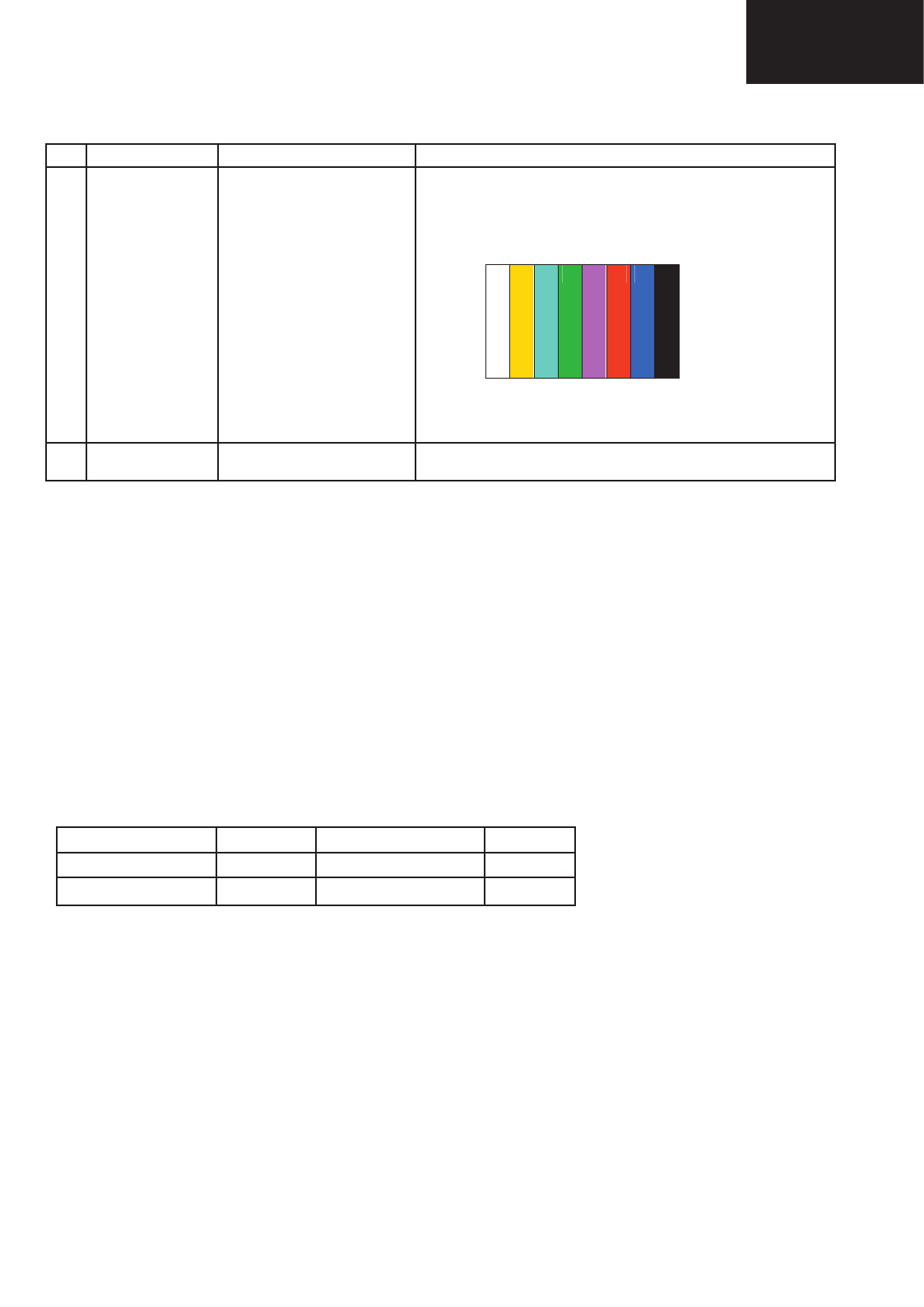
5.5. PAL Signal & Tuner Adjustment
5.4. RF AGC Adjustment (SMPTE RF SIGNAL- Alternative Method)
Adjustment Point Adjustment conditions Adjustment procedure
1 Setting [Signal]
PAL
SMPTE Field Color Bar
RF signal
[Terminal]
TUNER
• Feed the PAL SMPTE color bar signal (E-12ch) to TUNER.
Signal level: 50 ±1dB µV (75Ω LOAD)
2 Auto adjustment
performance
Adjustment process page 6. Bring the cursor on [▪RF AGC ADJ] and press [OK].
[▪RF AGC ADJ OK] appears when finished.
↑ 100% white
Adjustment Point Adjustment conditions Adjustment procedure
1 Setting [Signal]
PAL
FULL Field Color Bar
Composite or RF signal
[Terminal]
EXT3 VIDEO IN
TUNER
• Feed the PAL full field color bar signal (75% color saturation) to
EXT3 VIDEO IN.
• Feed the RF signal PAL color bar (E-12) to TUNER.
• Make sure the PAL color bar pattern (E-12) has the sync level of 7:3
with the picture level.
2 Auto adjustment
performance
Adjustment process page 3. Bring the cursor on [▪PAL +TUNER ADJ] and press [OK].
[▪PAL+ TUNER ADJ OK] appears when finished.
↑ 100% white
�����������������������������
↑ 100% white
5.6. PAL Signal & Tuner Adjustment (SMPTE RF SIGNAL-Alternative Method)
Adjustment Point Adjustment conditions Adjustment procedure
1 Setting [Signal]
PAL
FULL Field Color Bar
Composite or RF SMPTE signal
[Terminal]
EXT3 VIDEO IN
TUNER
• Feed the PAL full field color bar signal (75% color saturation) to
EXT3 VIDEO IN.
• Feed the RF signal SMPTE color bar (E-12) to TUNER.
• Make sure the SMPTE color bar pattern (E-12) has the sync level of
7:3 with the picture level.
2 Auto adjustment
performance
Adjustment process page 6. Bring the cursor on [▪PAL +TUNER ADJ] and press [OK].
[▪PAL+ TUNER ADJ OK] appears when finished.
↑ 100% white
↑ 100% white
[EXT 3] [TUNER]
[EXT 3] [TUNER]
[TUNER]
19
LC-26GA5E
LC-32GA5E
LC-32GD8E/RU
LC-32BT8E/RU
LC-37GD8E/RU
LC-37BT8E/RU
LC-32/37GD8E/RU
LC-32/37BT8E/RU
19
LC-26GA5E
LC-32GA5E
LC-32GA8/LC-32BV8
LC-37GA8/LC-37BV8
5.7. ADC Adjustment (Component 15K)
Adjustment Point Adjustment conditions Adjustment procedure
1 Setting [Signal] (576i/50)
COMP 15K, 50Hz
100% Full Field Color Bar
[Terminal]
EXT4 [COMPONENT]
• Feed the COMPONENT 15K 100% full field color bar signal (100%
color saturation) to EXT4 COMPONENT IN.
2 Auto adjustment
performance
Adjustment process page 4. Bring the cursor on [▪COMP15K ADJ] and press [OK].
[▪COMP15 ADJ OK] appears when finished.
↑ 100% white
[EXT 4]
6. White Balance Adjustment
Adjustment procedure Page 7/11 shows the value of adjustment gradation (IN value) and Adjustment procedure Page
8/11 & 9/11 show adj. offset value (initial value : 0). White balance adjustment is executed adjusting the adj. offset value,
indicated on Page 8/11 & 9/11.
Condition of the inspection: • Backlight: MAX (+8) [DYNAMIC]
• Colorimeter at screen centre
Adjustment reference device: Minolta CA-210
Tolerance adjustment spec. ±0.004, Inspection spec. : ±0.006 (GAMMA 1)
Tolerance adjustment spec. ±0.002, Inspection spec. : ±0.004 (GAMMA 2...6)
Adjustment: Check that the values on page 7/11 of process adjustment are set as below. If not, change them ac-
cordingly.
M GAMMA IN 1 160 M GAMMA IN 2 320
M GAMMA IN 3 480 M GAMMA IN 4 640
M GAMMA IN 5 800 M GAMMA IN 6 960
1- Display the current adjustment status at point 6. (Page 9/11 of process adjustment)
The pattern for checking the adjustment status is toggled by pressing the “6” button on the remote control. (Normal
OSD display -> “6” -> pattern for check (OSD disappears) -> “6” -> normal OSD display -> …)
2- Read the value of the luminance meter.
3- Change M GAMMA R6/M GAMMA B6 (adjustment offset value) on page 9/11 of process adjustment so that the
values of the luminance meter approach x = 0.272 and y = 0.277.
(Basically, G is not changed. If adjustment fails only with R and B, then G should be reduced. In this case, the weaker
of R and B must be fixed.)
4- If G is changed in step “3”, change the values of M GAMMA G1 - M GAMMA G5 on pages 8/11 and 9/11 of process
adjustment as follows. When not changed, go to step “5”.
Offset value of M GAMMA G1 = (Offset value of M GAMMA G6)*(160/960)
Offset value of M GAMMA G2 = (Offset value of M GAMMA G6)*(320/960)
Offset value of M GAMMA G3 = (Offset value of M GAMMA G6)*(480/960)
Offset value of M GAMMA G4 = (Offset value of M GAMMA G6)*(640/960)
Offset value of M GAMMA G5 = (Offset value of M GAMMA G6)*(800/960)
← Black
20
LC-26GA5E
LC-32GA5E
LC-32/37GD8E/RU
LC-32/37BT8E/RU
20
LC-26GA5E
LC-32GA5E
LC-32GA8/LC-32BV8
LC-37GA8/LC-37BV8
�
�
�
[FACTORY INIT]
8. Initialization to factory settings
7. QS Temperature NVM Data Confirmation
During servicing of the LCD TV set , by software upgrading or by any cleaning NVM, it’s mandatory select the “Inch
Setting” in Service Mode, Page 2, according to the size of the TV set.
02/11 [ INIT ] INPUT 4 PAL --:--
Factory Init --
Inch Setting --
Public Mode OFF
Center Acutime 00H
RESET OFF
Backlight Acutime 00H
RESET OFF
Picture Read Pos X 0
Picture Read Pos Y 0
Picture Read OFF
Default picture after cleaning NVM. Picture with [Inch Setting] to 32.
02/11 [ INIT ] INPUT 4 PAL 32:--
Factory Init --
Inch Setting 32
Public Mode OFF
Center Acutime 00H
RESET OFF
Backlight Acutime 00H
RESET OFF
Picture Read Pos X 0
Picture Read Pos Y 0
Picture Read OFF
5- Display the adjustment status of the current point 5. (Each time the “5” button on the remote control is pressed, the
adjustment status check pattern is toggled.)
(Normal OSD display -> “5” -> Pattern display (OSD disappears) -> “5” -> Normal OSD display ->…)
Change M GAMMA R5/M GAMMA B5 (adjustment offset value) on page 9/11 of process adjustment so that the val-
ues of the luminance meter approach x = 0.272 and y = 0.277.
6- Repeat step “5” for GAMMA points 4, 3, 2, and 1.

21
LC-26GA5E
LC-32GA5E
LC-32GD8E/RU
LC-32BT8E/RU
LC-37GD8E/RU
LC-37BT8E/RU
LC-32/37GD8E/RU
LC-32/37BT8E/RU
21
LC-26GA5E
LC-32GA5E
LC-32GA8/LC-32BV8
LC-37GA8/LC-37BV8
9. Lamp error detection
9.1. For 37” LCD TV
9.1.1. Functional description
This LCD colour television has a function (lamp error detection) to be turned OFF automatically for safety when the
lamp or lamp circuit is abnormal.
If the lamp or lamp circuit is abnormal, or some other errors happen, and the lamp error detection is executed, the
following occur.
1- The main unit of television is turned OFF 5 seconds after it is turned ON. (The power LED on the front side of
TV
turns from green to red.)
2 - If the situation “1” happens 5 times sequentially, television can not be turned ON. (The power LED remains red.)
9.1.2. Countermeasures
When television is turned OFF by the lamp error detection mentioned above, it enters the adjustment process with
the power LED red. Entering the adjustment process turns OFF the error detection and turns ON TV. This enables
the operation check to detect errors in the lamp or lamp circuit.
Check whether “L ERROR RESET” on point 7, page 10/11 of the adjustment process is 1 or more. If it is 1 or more,
it indicates the lamp error detection was executed. After confirming that the lamp or lamp circuit is normal, reset
the lamp error counter pushing “OK” in the R/C. After resetting counter the label “***OK***” appears on Screen.
9.1.3. Reset standby cause error list
After confirming that the lamp error counter has been erased, select “STAND BY CAUSE RESET” on point 3, page
10/11 of the adjustment process and select ON using the right cursor. For execute press “OK” in the R/C and the
label “***OK***” appears on Screen.
9.2 For 32” LCD TV
9.2.1. Functional description
This LCD colour television has a function (lamp error detection) to be turned OFF automatically (Inverter unit) for
safety when the lamp or lamp circuit is abnormal.
If the lamp or lamp circuit is abnormal, or some other errors happen, and the lamp error detection is executed, the
following occur.The Inverter circuit stops but the rest of TV continues working. The power led is green.
9.2.2 Countermeasures
Proceed to repair the inverter unit to solve the problem that produces the lamp error.
9.2.3. Reset standby cause error list
For 32” this is not necessary because the lamp error detection is not operative by software.

22
LC-26GA5E
LC-32GA5E
LC-32/37GD8E/RU
LC-32/37BT8E/RU
10. Public Mode (Hotel Mode)
10.1 How to Enter in the Public Mode (Hotel Mode).
Turn on the power and enter in the Adjustment Process mode (ADJ1 or Service Mode) as usual.
In the [INIT], Page 2/11 of Service, turns ON the Public Mode option.
Turn off TV by pressing Main Power switch.
While pressing “VOL+”and “P^” keys at the same time, press Main Power switch for more than 2 seconds.
After this sequence the TV will turn on showing the Public Mode setting screen as follows:
Is possible to select each item of function by pressing cursor UP/DOWN keys on the remote control or CH(∧)(∨) keys
on the LCD TV.
The setting position of each item of functions is made by pressing cursor RIGHT/LEFT keys on the remote control
or VOL(+)(-) keys on the LCD TV.
Select ENTER position after you set all function, and press cursor RIGHT/LEFT keys on the remote control or
VOL(+)/(-) keys on the LCD TC for confi rmation.
10.2. Public Mode Settings.
1. POWER ON FIXED [VARIABLE FIXED]
When it is set to “FIXED” the TV is impossible to be switch off by Main Switch or Remote Control.
2. MAXIMUM VOLUME [0 60]
Is possible to set the maximum volume at limited level.
3. VOLUME FIXED [VARIABLE FIXED]
Is possible to fi x the sound volume at limited level.
When “FIXED” is selected the sound volume before limited is fi xed.
4.VOLUME FIXED LEVEL [0 60]
If “FIXED” has been selected, is possible to set a fi xed volume at the level that is choosen.
5. RC BUTTON [RESPOND NO RESPOND]
If “NO RESPOND” is selected, the remote control keys are inoperative.
6. PANEL BUTTON [RESPOND NO RESPOND]
If “NO RESPOND” has been selected, the set´s keys remain deactivated (Except POWER key).
7. MENU BUTTON [RESPOND NO RESPOND]
If “NO RESPOND” has been selected, “MENU” keys on the remote control, is inoperative.
8. ON SCREEN DISPLAY [YES NO]
If “NO” has been selected, the On Screen Display does not appear.
9. INPUT MODE START [ NORMALTV (X)DTVINPUT1 INPUT2INPUT3 INPUT4 INPUT5]
When any other item than “NORMAL” has been selected, the sets will start in a selected input mode at the next
power-on.
10. INPUT MODE FIXED [VARIABLE FIXED]
If “FIXED” has been selected, any channels and input modes other than those selected at the start mode cannot be
picked up.
11. RESET
Cancel all Public Mode settings. (It returns to the factory settings)
12. EXECUTE
After select this item, all positions that has been selected will be set.
MAXIMUM VOLUME [60]
VOLUME FIXED [VARIABLE]
VOLUME FIXED LEVEL [0]
RC BUTTON [RESPOND]
PANEL BUTTON [RESPOND]
MENU BUTTON [RESPOND]
ON SCREEN DISPLAY [YES]
INPUT MODE START [NORMAL]
INPUT MODE FIXED [VARIABLE]
RESET
EXECUTE
POWER ON FIXED [VARIABLE]
Public Mode
23
LC-26GA5E
LC-32GA5E
LC-32GD8E/RU
LC-32BT8E/RU
LC-37GD8E/RU
LC-37BT8E/RU
LC-32/37GD8E/RU
LC-32/37BT8E/RU
SOFTWARE UPDATING
There are 3 methods to update software in the VCTp: I2C method, RS-232C HyperTerminal and RS-232C Tera Term
method.
· RS-232C method is allowed when the TV is working properly and the action should be only software upgrade.
· I2C method is required when the VCTp fl ash is empty or corrupted (it means, any software inside IC running).
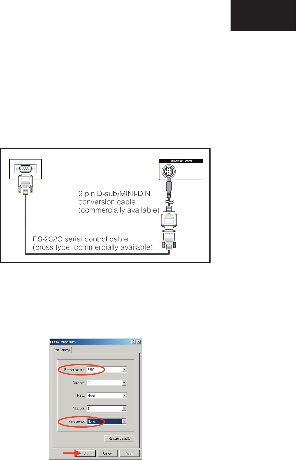
1. RS-232C Method Description (HyperTerminal).
The hardware tools requirement are:
1. A Modem-null (Cross type) DB9 female to DB9 female cable.
2. An adaptor DB9 male to mini-Din 9 pin male cable (Sharp Code: QCNWGA015WJPZ)
3. Make the connections as indicated in the fi gure:
Before using RS-232C updating method is necessary to confi gure a Terminal PC software. HyperTerminal has been
selected as a Terminal software because it’s include in all Windows versions as an accessory, and you can fi nd it inside
“Accessories\Communications” folder. For this reason, please follow carefully the next steps:
1. First time HyperTerminal is used, it’s necessary to confi gure some settings. Follows next action to confi gure two
connection: low speed (9600bps) and high speed (115200bps).
2. Create a New Connection fi le with name “P55_9600bps”.
3. Select a free COM port and select the Port Settings properties as follows:
RS-232C METHOD DESCRIPTION.
The hardware tools requirement are:
1. A Modem-null (Cross type) DB9 female to DB9 female cable.
2. An adaptor DB9 male to mini-Din 9 pin male cable (Sharp Code: QCNWGA015WJPZ)
3. Make the connections as indicated in the figure:
Before using RS-232C updating method is necessary to configure a Terminal PC software.
HyperTerminal has been selected as a Terminal software because it’s include in all Windows
versions as an accessory, and you can find it inside “Accessories\Communications” folder. For
this reason, please follow carefully the next steps:
1. First time HyperTerminal is used, it’s necessary to
configure some settings. Follows next action to configure
two connection: low speed (9600bps) and high speed
(115200bps).
2. Create a New Connection file with name “P55_9600bps”.
3. Select a free COM port and select the Port Settings
properties as follows:
Computer TV set
24
LC-26GA5E
LC-32GA5E
LC-32/37GD8E/RU
LC-32/37BT8E/RU
26
LC-26GA5E
LC-32GA5E
LC-26P55E
LC-32P55E
LC-37P55E
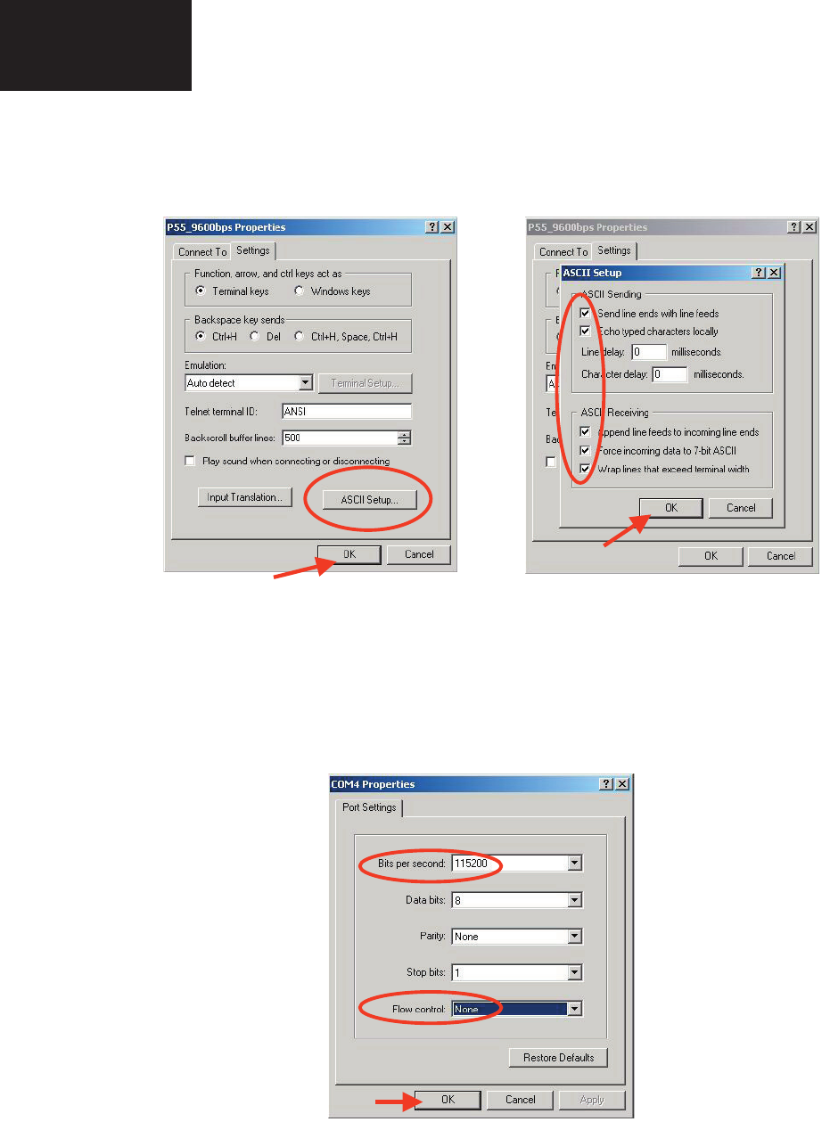
4. Click on “File\Properties” menu for selecting the General and ASCII properties as follows:
5. Select “New Connection” in the File Menu.
6. Answer “Yes” to close current connection and “Yes” to save session “P55_9600bps”.
7. Create a new connection with the name “P55_115200bps”.
8. Select a the same COM port used in item 2 and select the Port Settings properties as follows:
9. Select the same General and ASCII properties as item 3.
10. Close HyperTerminal session, answering “Yes” to close current connection and “Yes” to save session
“P55_115200bps”.
To start updating session, click over “P55_9600bps” icon that you can fi nd in the “START\All programs\Accessories\
Communications\HyperTerminal\HyperTerminal” folder and follow next procedure:
1. Check the connection between TV set and PC, sending a wrong command, as for example: “aaa”. TV set returns
an “ERR” label as an syntaxis ERROR (Not correct order or sequence).
VCTp Software Updating, HyperTerminal (continued)
(*)
(*)
(*)
(*)
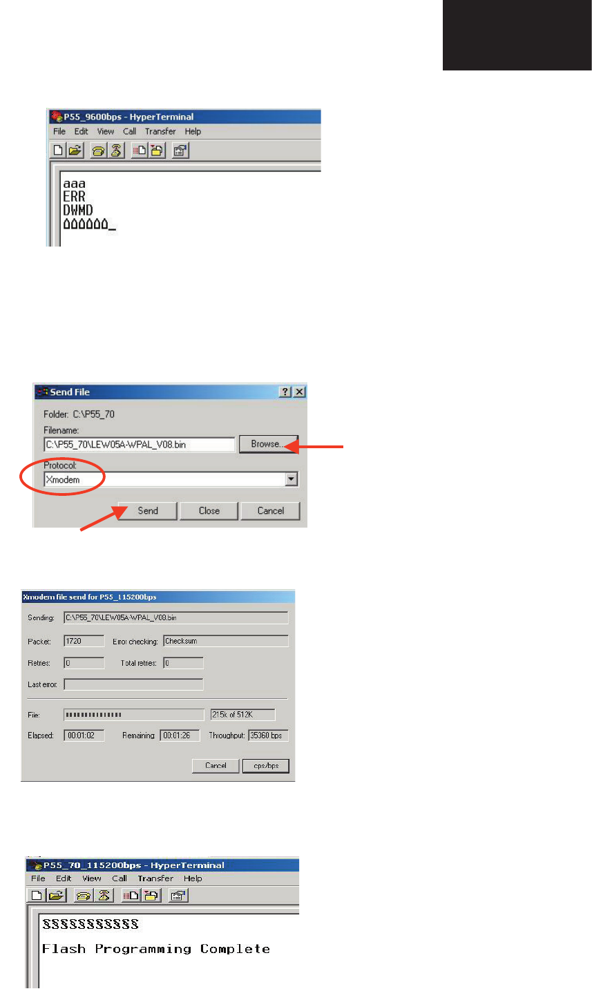
25
LC-26GA5E
LC-32GA5E
LC-32GD8E/RU
LC-32BT8E/RU
LC-37GD8E/RU
LC-37BT8E/RU
LC-32/37GD8E/RU
LC-32/37BT8E/RU
27
LC-26GA5E
LC-32GA5E
LC-26P55E
LC-32P55E
LC-37P55E
2. Send the command “DWMD” to enter TV set in Download Mode. The TV set answer sending same symbol con-
tinuosly. If this symbol character doesn’t appear, please don’t worry and pass to next step.
3. Close this connection and open “P55_115200bps” connection clicking over the “P55_115200bps” that
you can find in “START\All programs\Accessories\ Communications\HyperTerminal\HyperTerminal” folder.
4. Using “Transfer\Send fi le…” menu, select desired fi le (.bin format) and the transmission protocol (Xmodem) as
show below.
5. After press “Send” button the updating process starts as follows:
VERY IMPORTANT NOTE:
During the updating time, please don’t use the PC for other purpouses, in order to abolish communication
problems between TV set and PC. If TV set was not updated properly, the TV won’t have the software to startup
again, and you must follow the “I2C method” to update another time the TV set.
6. When fl ash update process fi nishes, the ” Flash programming complete “ label appear in the screen , the device
automatically go to switch off, and in a few seconds go to switch on again.
VCTp Software Updating, HyperTerminal (continued)
(*) (*)
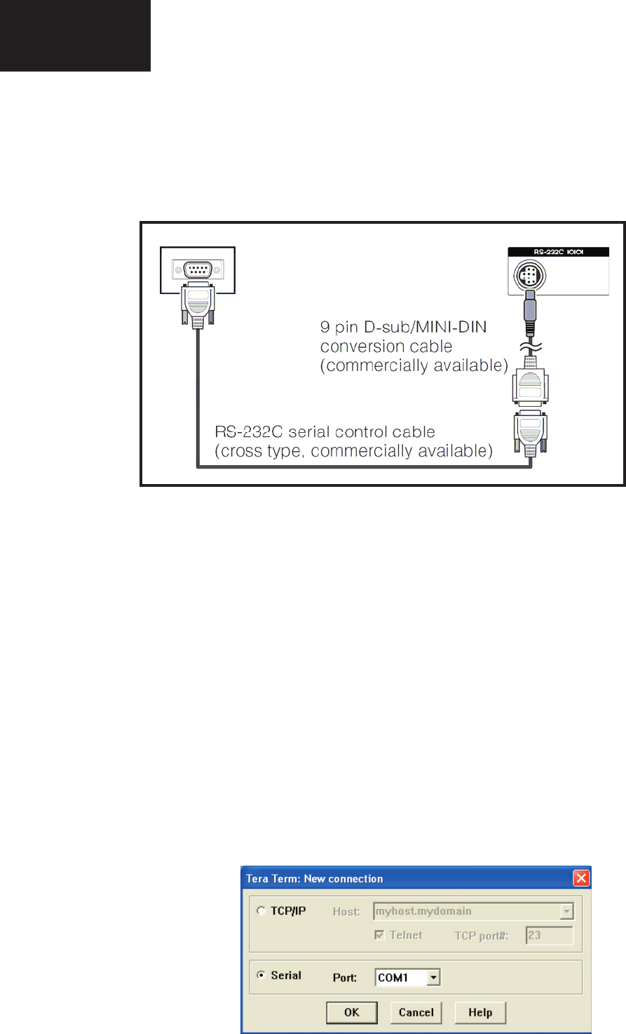
26
LC-26GA5E
LC-32GA5E
LC-32/37GD8E/RU
LC-32/37BT8E/RU
28
LC-26GA5E
LC-32GA5E
LC-26P55E
LC-32P55E
LC-37P55E
2. RS-232C Method Description (Tera Term)
The hardware tools requirement are:
1. A Modem-null (Cross type) DB9 female to DB9 female cable.
2. An adaptor DB9 male to mini-Din 9 pin male cable (Sharp Code: QCNWGA015WJPZ)
3. Make the connections as indicated in the fi gure:
Software requirements :
To upgrade VCTp software from RS-232C external connector is necessary to use a Tera Term (Pro) free software.
The URL of Tera Term home page is:
http://hp.vector.co.jp/authors/VA002416/teraterm.html
(The address may be changed in future)
Tera Term (Pro) supported operating systems:
MS-Windows 95 or upper
MS-Windows NT 3.5 and 4.0 or upper
Note.- For Windows 3.1 use Tera Term version 1.X.
Copy all the distribution fi les to an empty fl oppy disk or temporary directory (for example C:\ TEMP ).
Run SETUP.EXE and follow the instruction given by it.
After the installation, the distribution fi les are no longer needed, you can delete them or may keep them in the fl oppy
disk.
How to use Tera Term Pro :
When the Tera Term (Pro) program is used, it’s necessary to shape some settings. Follows next action to confi gure
the connection:
g
Computer TV set
1. Select: Serial ⇒ COM X ⇒ O.K.
1.
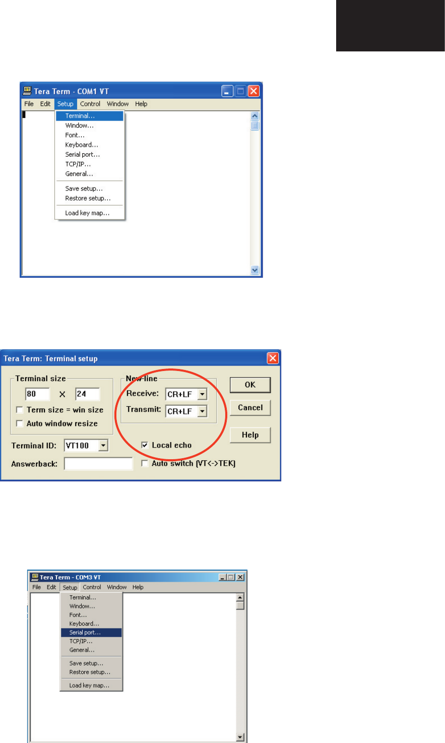
27
LC-26GA5E
LC-32GA5E
LC-32GD8E/RU
LC-32BT8E/RU
LC-37GD8E/RU
LC-37BT8E/RU
LC-32/37GD8E/RU
LC-32/37BT8E/RU
VCTp Software Updating, Tera Term (continued)
29
LC-26GA5E
LC-32GA5E
LC-26P55E
LC-32P55E
LC-37P55E
4. Select Setup ⇒ Serial port ⇒ O.K. Appear the follow screen:
2. Select: Terminal
3. Choose the same options as the above picture.
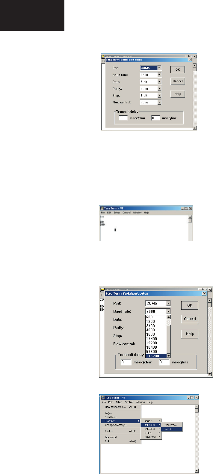
28
LC-26GA5E
LC-32GA5E
LC-32/37GD8E/RU
LC-32/37BT8E/RU
30
LC-26GA5E
LC-32GA5E
LC-26P55E
LC-32P55E
LC-37P55E
6. Check the connection between TV set and PC, sending a wrong command, as for example: “aaa”. TV set returns
an “err” label as an syntaxes ERROR (Not correct order or sequence).
Send a “DWMD” (capital letters) command to enter TV set in Download Mode.
Change a baud rate to 115200.
Select: Setup ⇒ Baud rate ⇒ 115200 ⇒ O.K.
5. Select follows settings:
Serial port to use: COM x
Baud rate: 9600
Data: 8 bits
Parity: none
Stop: 1 bit
Flow control: none
Enter O.K.
7. Select: File ⇒ Transfer ⇒ XMODEM ⇒ Sent
VCTp Software Updating, Tera Term (continued)
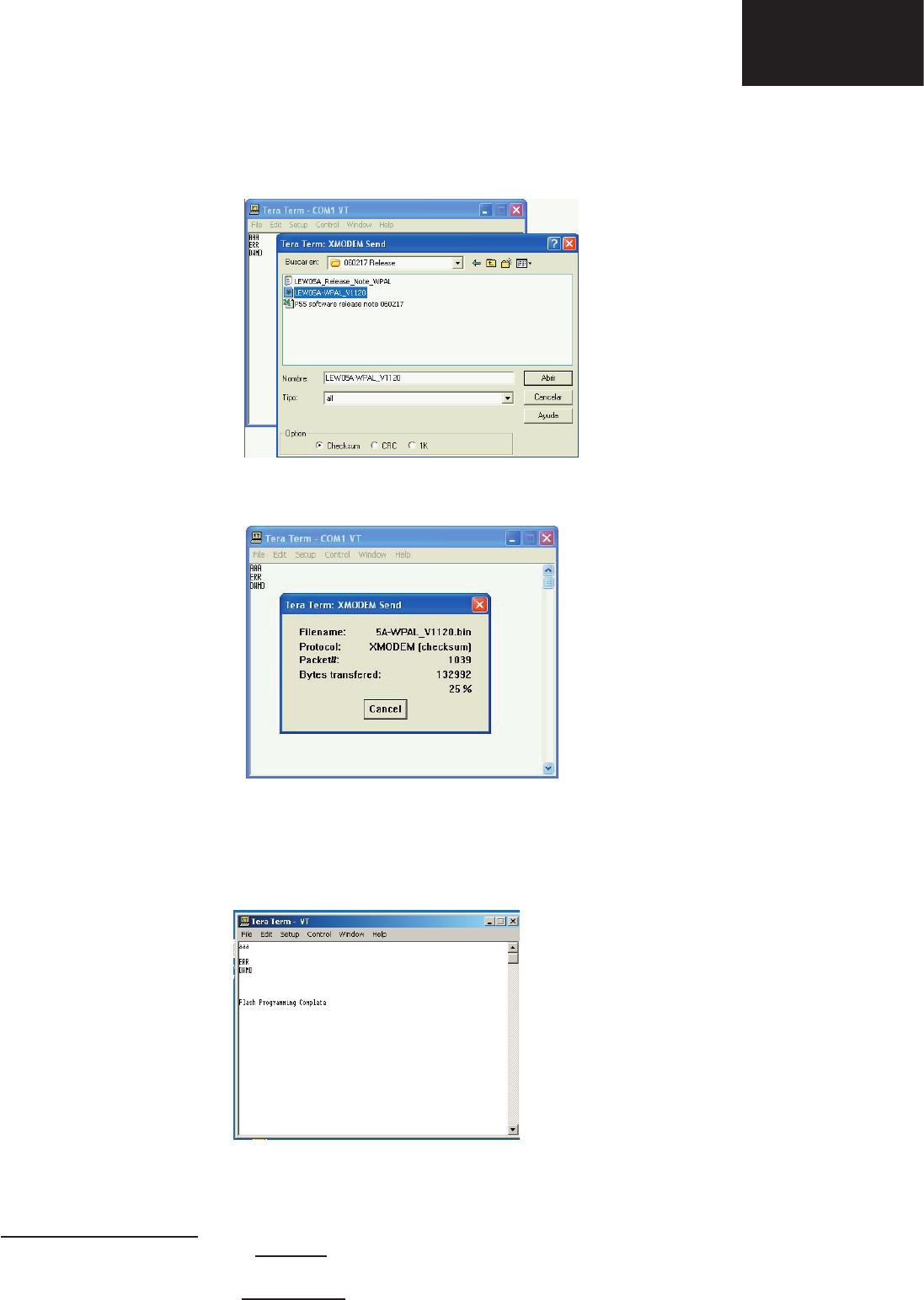
29
LC-26GA5E
LC-32GA5E
LC-32GD8E/RU
LC-32BT8E/RU
LC-37GD8E/RU
LC-37BT8E/RU
LC-32/37GD8E/RU
LC-32/37BT8E/RU
VCTp Software Updating, Tera Term (continued)
31
LC-26GA5E
LC-32GA5E
LC-26P55E
LC-32P55E
LC-37P55E
9. After select “Open” the upgrade process starts as follows:
VERY IMPORTANT NOTE:
During the updating time, please don’t use the PC for other purposes, in order to abolish communication prob-
lems between TV set and PC. If TV set was not updated properly, the TV won’t have the software to startup
again, and you must follow the “I2C method” to update another time the TV set.
8. Choose the fi le for upgrade and click “Open”.
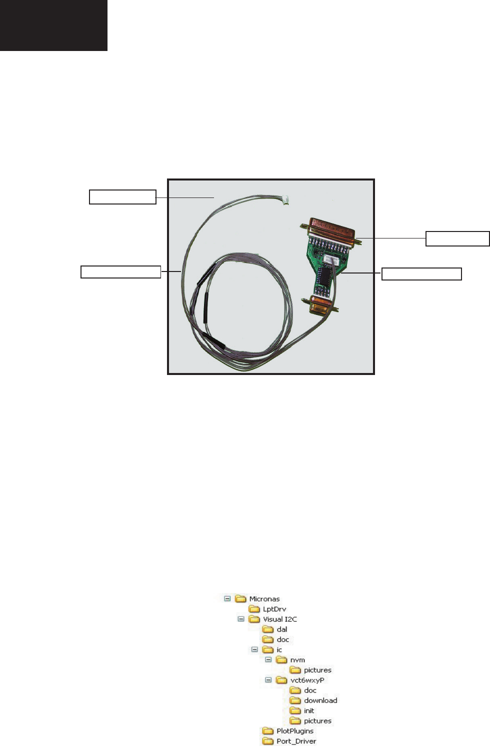
30
LC-26GA5E
LC-32GA5E
LC-32/37GD8E/RU
LC-32/37BT8E/RU
32
LC-26GA5E
LC-32GA5E
LC-26P55E
LC-32P55E
LC-37P55E
3. I2C Method Description
The hardware tools requirement are:
1. A Parallel port I2C interface with 20 pin to 3 pin cable (Sharp Code: CKIT-0004WJV0).
2 . Make the connections as indicated below:
a. Connect Parallel port I2C interface to LPT port of the computer.
b. Connect the 20 to 3 pin cable from the I2C interface to the P2306 socket in the main board (XD603).
Before using I2C method is necessary to install Visual I2C software following next procedure.
1. Install Visual I2C release V3.2.3b from fi le (“Setup_Visual_I2C_v3-2-3b8h.exe”).
•It’s strongly recommended to accept the suggested default folder (“C:\Program Files\Micronas\Visual I2C”).
2. Install Visual I2C VCTp extension from fi le (“Setup_VI2C_for_VCT6wxyP_v0111.exe”).
•It’s interesting to change default folder to same as Visual I2C (“C:\Program Files\Micronas\Visual I2C”).
•During this installation process is possible to install also a complementary software to manage NVM memories .
This installation is not needed, for this reason uncheck the option when the setup program ask to you. In case of
installation it’s interesting to change default folder to same as Visual I2C (“C:\Program Files\Micronas\Visual I2C”).
3. Install Parallel driver depending of your Windows version from existing fi les inside the Visual I2C installation
folder “C:\Program Files\Micronas\Visual I2C\Port_Driver”, following next criteria:.
a. Windows 98/Me (“Setup_LptDrv_v0104_9x.exe”).
b. Windows NT (“Setup_LptDrv_v0104_NT_2000.exe”).
c. Windows Xp/2000 (“Setup_LptDrv_v020201_XP_2000.exe”).
After installing Visual I2C, the new generated fi le structure should look like this:
To PC
To P2306
I2C Interface (CKIT-0004WJV0)
QCNWGA100WJZZ QPWBX0004WJZZ
1.
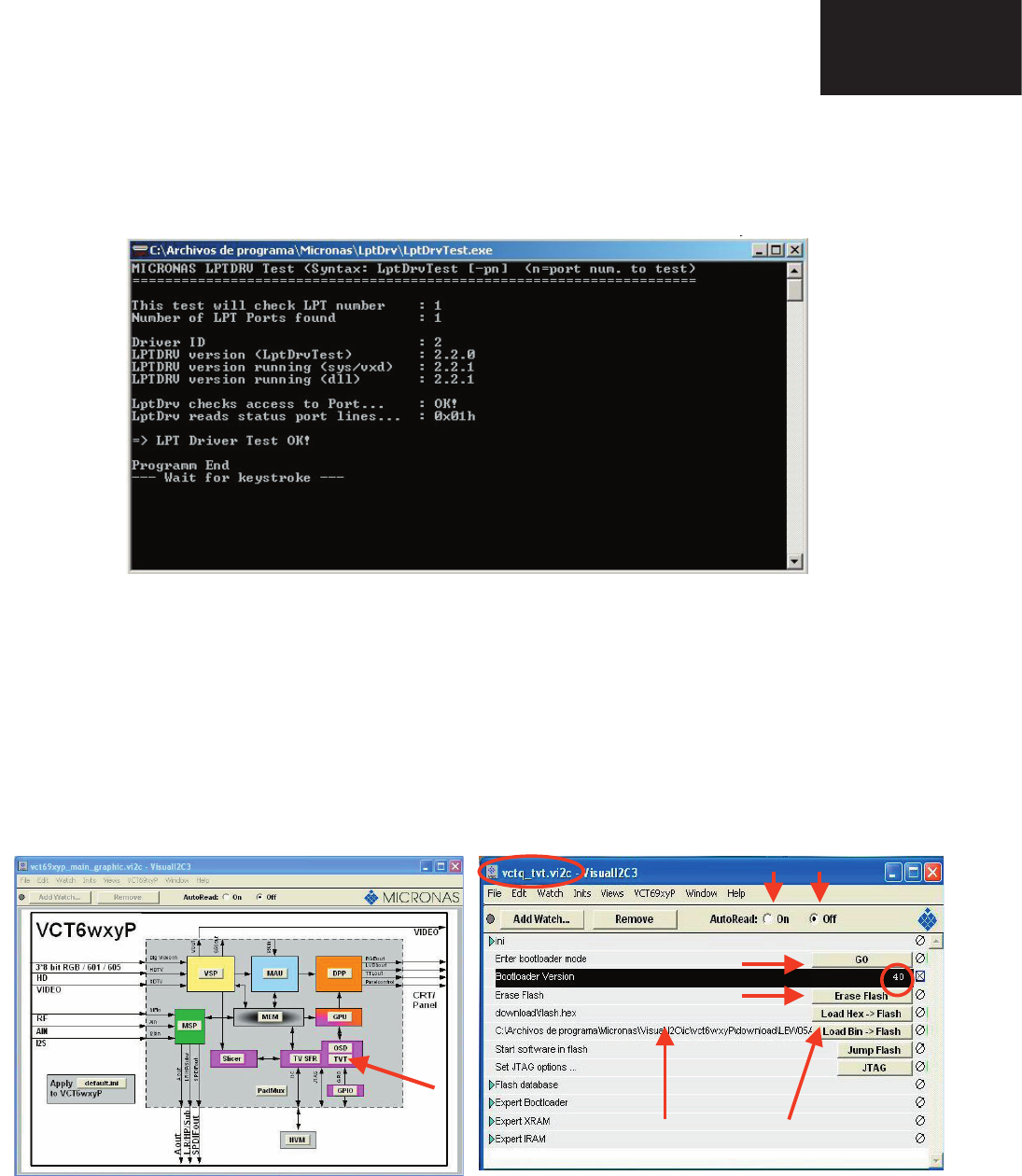
31
LC-26GA5E
LC-32GA5E
LC-32GD8E/RU
LC-32BT8E/RU
LC-37GD8E/RU
LC-37BT8E/RU
LC-32/37GD8E/RU
LC-32/37BT8E/RU
28
LC-26GA5E
LC-32GA5E
LC-26P55E
LC-32P55E
LC-37P55E
4. Check installation LPT driver using “C:\Program Files\Micronas\LptDrv\LptDrvTest.exe”. After run this software, if
LPT driver is installed properly must appear this screen:
•If the result is not OK, check inside PC bios: Parallel Port Mode=EPP
To run VCTp software update program, please click over “VCTP” icon from “START\All programs\Micronas\Visual
I2C\IC\VCTP” and after Visual I2C finish their starting process click on “TVT” module. As additional method, it’s pos-
sible to create a direct access to “C:\Program Files\Micronas\Visual I2C\ic\vct6wxyP\vctq_tvt.vi2c” and launch it from
Windows Desktop.
To start updating process follow next instructions:
1. Set Autoread in ON option.
2. Click on “GO” button.
3. Wait until “40” appears in Bootloader Version field.
4. Close DOS pop up windows pressing any key (“Press any key to continue…”.).
5. Click on the “Erase flash” button and wait for a seconds and set the AutoRead to OFF.
6. Check in the desired software version is selected in the “Load BinàFlash” option. If it’s not the correct one,
please double click on the file name and select it. The first time this software is use it’s necessary to confirm write
Addressing margin as from 0x0 to 0x7ffff.
VCTp Software Updating, I2C (continued)
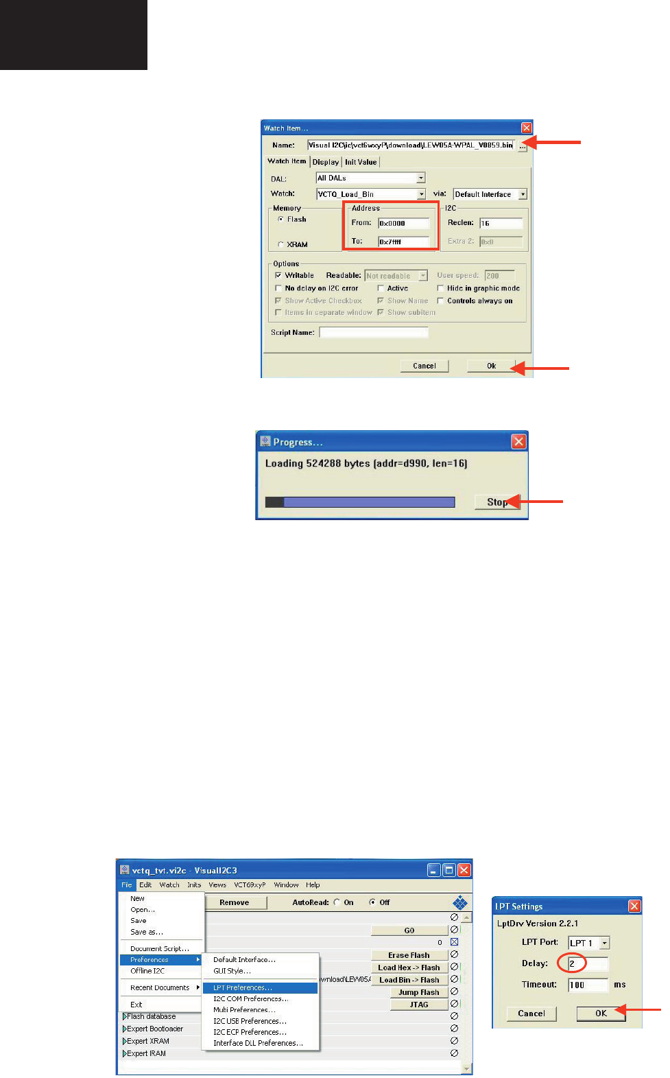
32
LC-26GA5E
LC-32GA5E
LC-32/37GD8E/RU
LC-32/37BT8E/RU
29
LC-26GA5E
LC-32GA5E
LC-26P55E
LC-32P55E
LC-37P55E
7. Click on the “Load Bin à Flash” to start updating process.
�
8. When the updating process finishes, the “Progress” pop up window automatically closes. If appears some problem
during the updating process a error label appears in the filename information line.
If the TV has problem to enters in the “Bootloader mode”, it’s possible to force it by hardware method. This alternative
method is described below:
1.Switch off TV set or hold VCTp RESET line to GND.
2.Pull down SCL line (pin 1) to GND (pin 3) in P2306 connector.
3.Switch on TV set or release VCTp RESET line.
4.Release SCL pull down after minimum of 2 seconds.
5.Check if VCTp is in bootloader mode with Autoread setting in ON.
6.Wait until “40” appears in Bootloader Version field.
7.Follow instruction from item 5 on software method.
Sometimes, depending on the PC hardware, the progress bar runs very fast (Normal time: 1 minute) or some error mes-
sage appears in the filename information line. This means it’s necessary to modify some parameter of LPT port, for this
reason select “LPT Preferences” on the “File\Preferences…” menu and increase Delay from “0” to “1” or “2” (normally,
these values are the best choice).
VCTp Software Updating, I2C (continued)
33
LC-26GA5E
LC-32GA5E
LC-32GD8E/RU
LC-32BT8E/RU
LC-37GD8E/RU
LC-37BT8E/RU
LC-32/37GD8E/RU
LC-32/37BT8E/RU
2. How to update the Digital Board Software.
There are 2 methods to update the Digital Board Software on Flash Memory (IC4203) throught the Digital Proces-
sor (IC4001).
• Jig RS-232 Method (From PC trough RS-232C COM port).
• PCMCIA CARD (Compact Flash Memory) Method.
Note: The PCMCIA method is only compatible with those PCs running XP Windows Version.
2.1. Jig RS-232 Method Description
• Hardware requirements:
1. A modem null (Cross type) DB9 female to DB9 female cable.
2. The Jig Kit (Sharp Code: QCNWKA012WJZZ)
3. Make the connections as in the below fi gure.
33
LC-26GA5E
LC-32GA5E
LC-26P70E
LC-32P70E
LC-37P70E
DRAFT
0.
3
24
LC-26GA5E
LC-32GA5E
LC-26P55E
LC-32P55E
LC-37P55E
SOFTWARE UPDATING
There are 2 methods to update software in the VCTp: I2C method and RS-232C method.
· RS-232C method is allowed when the TV is working properly and the action should be only software upgrade.
· I2C method is required when the VCTp flash is empty or corrupted (it means, any software inside IC running).
1 RS-232C Method Description
The hardware tools requirement are:
1. A Modem-null (Cross type) DB9 female to DB9 female cable.
2. An adaptor DB9 male to mini-Din 9 pin male cable (Sharp Code: QCNWGA015WJPZ)
3. Make the connections as indicated in the figure:
Software requirements :
To upgrade VCTp software from RS-232C external connector is necessary to use a Tera Term (Pro) free software.
The URL of Tera Term home page is:
http://hp.vector.co.jp/authors/VA002416/teraterm.html
(The address may be changed in future)
Tera Term (Pro) supported operating systems:
MS-Windows 95 or upper
MS-Windows NT 3.5 and 4.0 or upper
Note.- For Windows 3.1 use Tera Term version 1.X.
Copy all the distribution files to an empty floppy disk or temporary directory (for example C:\ TEMP ).
Run SETUP.EXE and follow the instruction given by it.
After the installation, the distribution files are no longer needed, you can delete them or may keep them in the floppy
disk.
How to use Tera Term Pro :
When the Tera Term (Pro) program is used, it’s necessary to configure some settings. Follows next action to config-
ure the connection:
~
~
Computer
TV Set
(CI Terminal)
Jig
RS-232C serial control cable
(cross type, commercially available)
• Software requirements:
1. “Winupload” application software on PC.
• How to setup the “Winupload” software for the fi rst time:
1. Start “Winupload”. It will appear the following picture.
34
LC-26GA5E
LC-32GA5E
LC-32/37GD8E/RU
LC-32/37BT8E/RU
Digital Board Software Updating , Jig RS-232 (continued)
2. Select the most suitable RS232 Serial Port from “Port Setting” - “Process” Menu.
3. Select the following settings from “Port Settings” Menu.
Bits Per Second: 115200
Parity: None
Data bits: 8
Stop bits: 1
Hardware Flow Control: OFF
• Procedure for updating the TV set.
1. Switch off the TV set to be updated, in DTV mode.
2. Start “Winupload”. It will appear the following picture on PC.
3. Establish connection on Winupload Software.
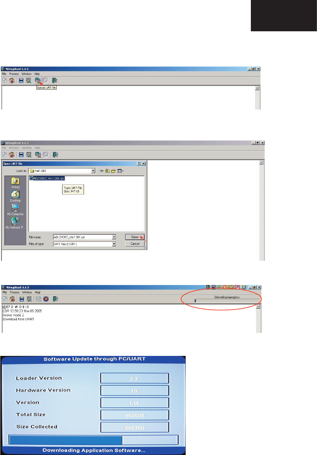
35
LC-26GA5E
LC-32GA5E
LC-32GD8E/RU
LC-32BT8E/RU
LC-37GD8E/RU
LC-37BT8E/RU
LC-32/37GD8E/RU
LC-32/37BT8E/RU
4. Select “Upload URT fi le”
5. Select and open the “.urt” data fi le from data directory
Note: Consider the version shown below just an example, may be is not the latest one, and could be
different depending on the TV set destination (market/Country) or model.
6. Switch On the TV Set (previously in DTV Mode). The Uploading Process starts automatically.
While the TV set is uploading the software, the following information is shown on the TV set screen.
Digital Board Software Updating , Jig RS-232 (continued)
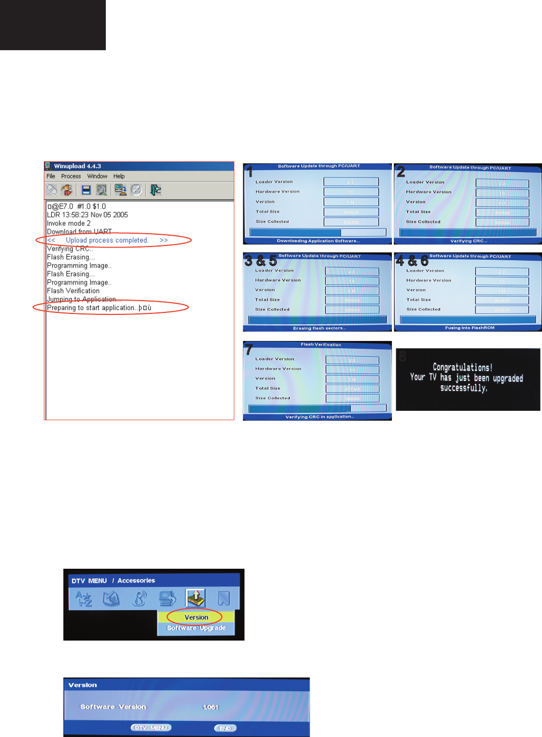
36
LC-26GA5E
LC-32GA5E
LC-32/37GD8E/RU
LC-32/37BT8E/RU
Digital Board Software Updating , Jig RS-232 (continued)
Then, data transfer from PC to TV set fi nishes when the “Upload progress completed” label appears in the
“Winupload” screen. Now, the TV set made some additional verifi cation (Items #2 to #7). When the full
uploading process is fi nished, in the “Winupload” window appears the label “Preparing to start application” for
a new TV Set, and just now, in the TV screen of the updated set, appears a congratulations label (Item #8).
PC SCREEN PROGRESS TV SCREEN PROGRESS
Note: Do not turn off the TV set while the software updating was in progress.
7. Unplug the AC cord.
8. Disconnect the Jig from TV Set.
• Software Version verifi cation procedure.
1. Connect the AC cord and Switch On the TV Set.
2. Select DTV Menu on TV Set. The following On Screen Display will appear.
3. Select “Version”. The updated version can be verifi ed.
Note: Consider the version shown above just as example, may be is not the latest one, and could be
different depending on the TV set destination (market/Country) or model.
1
2
3
4
5
6
7
8
TV INDICATION
1 2
3 & 5 4 & 6
78
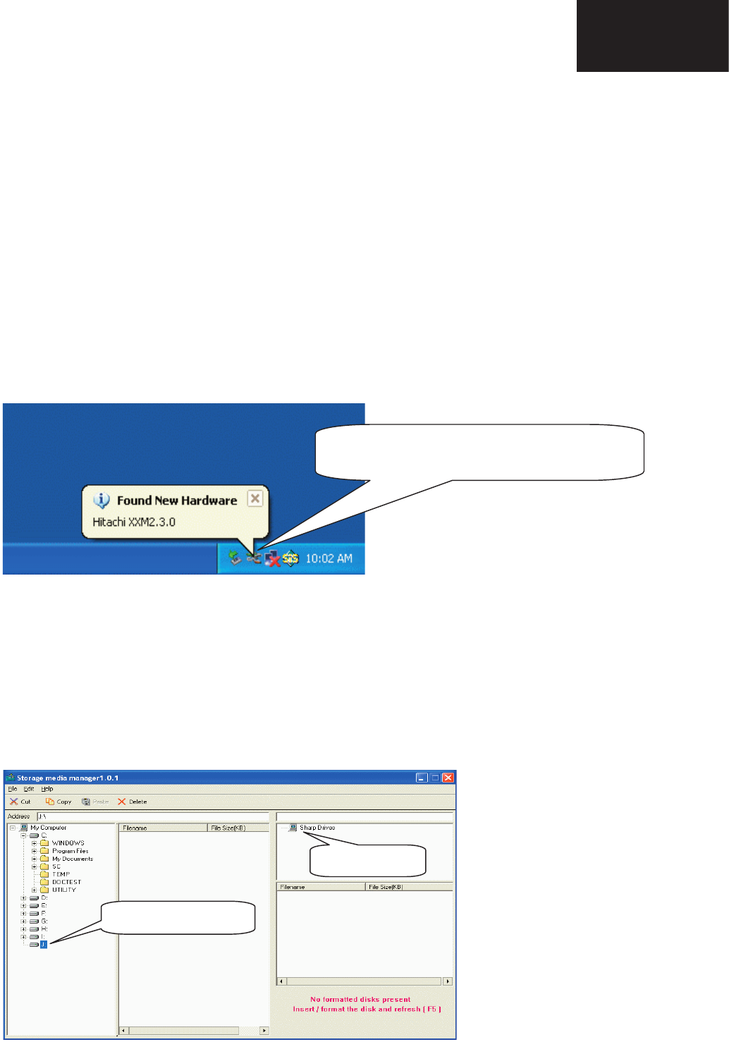
37
LC-26GA5E
LC-32GA5E
LC-32GD8E/RU
LC-32BT8E/RU
LC-37GD8E/RU
LC-37BT8E/RU
LC-32/37GD8E/RU
LC-32/37BT8E/RU
2.2. PCMCIA Card (Compact Flash) Method.
• Hardware requirements:
1. Compact Flash Memory Card.
2. PCMCIA Compact Flash Adapter or USB Multi Card Reader.
• Software requirements:
1. “StorageMediaManager1.0.1“ application software, installed on PC.
2. “Loader 2.2” or higher application software, installed on DTV Set.
Note: Storage Media Manager only for Windows XP.
• How to prepare the CF Card using the “Storage Media Manager 1.0.1” (SMM):
1. Insert PCMCIA (Compact Flash(CF) + CF-Adapter)
5
2.B. PCMCIA Card (Compact Flash) Method.
Hardware requirements:
1. Compact Flash Memory Card.
2. PCMCIA Compact Flash Adapter or USB Multi Card Reader.
Software requirements:
1. “StorageMediaManager1.0.1“ application software, installed on PC.
2. “Loader 2.2” or higher application software, installed on DTV Set.
Note: SMM only for Windows XP.
How to prepare the CF Card using the “Storage Media Manager 1.0.1” (SMM):
1. Insert PCMCIA (Compact Flash(CF) + CF-Adapter)
2. Execute SMM. If SMM does not appear or a Windows Error Box appears, please verify there are no USB
media drives connected to the PC.
Note: Consider that it’s recommended remove unnecessary media during SMM execution. Probably, If you try to use an USB Multi Card
Reader with SMM doesn’t work fine.
3. If the CF card has never been formatted for the SMM (is not same format type used in Windows), the SMM
will show you the PCMCIA-CF drive as a Windows Media Drives, hanged of the “My Computer” tree (“J” Drive
in the picture showed below).
But, if the PCMCIA-CF card had been formatted previously by SMM, directly the PCMCIA-CF drive will appear
in the SMM formatted Drives box (Sharp Drives). Please go to Item #6.
Please wait until OS recognizes the CARD.
Note: Sometimes this message doesn't appear.
N
EW PCMCIA-CF drive.
CARD is not SMM formatted yet.
Already SMM Formatted
CF CARDS!!!
2. Execute SMM. If SMM does not appear or a Windows Error Box appears, please verify there are no USB
media drives connected to the PC.
Note: Consider that it’s recommended remove unnecessary media during SMM execution. Probably, If you try
to use an USB Multi Card Reader with SMM doesn’t work fi ne.
3. If the CF card has never been formatted for the SMM (is not same format type used in Windows), the SMM
will show you the PCMCIA-CF drive as a Windows Media Drives, hanged of the “My Computer” tree (“J” Drive
in the picture showed below).
5
2.B. PCMCIA Card (Compact Flash) Method.
Hardware requirements:
1. Compact Flash Memory Card.
2. PCMCIA Compact Flash Adapter or USB Multi Card Reader.
Software requirements:
1. “StorageMediaManager1.0.1“ application software, installed on PC.
2. “Loader 2.2” or higher application software, installed on DTV Set.
Note: SMM only for Windows XP.
How to prepare the CF Card using the “Storage Media Manager 1.0.1” (SMM):
1. Insert PCMCIA (Compact Flash(CF) + CF-Adapter)
2. Execute SMM. If SMM does not appear or a Windows Error Box appears, please verify there are no USB
media drives connected to the PC.
Note: Consider that it’s recommended remove unnecessary media during SMM execution. Probably, If you try to use an USB Multi Card
Reader with SMM doesn’t work fine.
3. If the CF card has never been formatted for the SMM (is not same format type used in Windows), the SMM
will show you the PCMCIA-CF drive as a Windows Media Drives, hanged of the “My Computer” tree (“J” Drive
in the picture showed below).
But, if the PCMCIA-CF card had been formatted previously by SMM, directly the PCMCIA-CF drive will appear
in the SMM formatted Drives box (Sharp Drives). Please go to Item #6.
Please wait until OS recognizes the CARD.
Note: Sometimes this message doesn't appear.
NEW PCMCIA-CF drive.
CARD is not SMM formatted.
Already SMM Formatted
CF CARDS!!!
But, if the PCMCIA-CF card had been formatted previously by SMM, directly the PCMCIA-CF drive will appear
in the SMM formatted Drives box (Sharp Drives). Please go to Item #6.
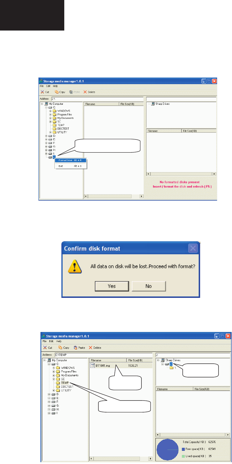
38
LC-26GA5E
LC-32GA5E
LC-32/37GD8E/RU
LC-32/37BT8E/RU
Digital Board Software Updating , PCMCIA (continued)
4. In case of not SMM formatted card, select PCMCIA-CD Drive and using the Right-Click Pop up Menu
please format the Drive.
6
4. In case of not SMM formatted card, select PCMCIA-CD Drive and using the Right-Click Popup Menu please
format the Drive.
5. Formatting the CF card. Select “Yes” to confirm the action.
NOTICE: All FC’s data of the inside are erased.
6. If SMM formatted card already appears under SHARP DRIVES box please continue, if not try to repeat from
item #1. Select origin folder and “.img” data file to be written in the CF card.
Select PCMCIA-CF Drive.
Select FormatDrive from Popup Menu.
selecting origin data folder
selecting origin
data ".img" file
SMM f tt d
5. Formatting the CF card. Select “Yes” to confi rm the action.
NOTICE: All FC’s data of the inside are erased.
#4 Select Ye
s
NOTICE: All FC's data of the inside are erased
#5 select write ver. of "
.
img" file folder.
#6 select copy drive. (This is important.) and Drag&drop "img" file.
select write ver. of ".img" file
f ld
at first, select copy drive.
This is important.
next, Drag&Drop "img" file.
6. If SMM formatted card already appears under SHARP DRIVES box please continue, if not try to repeat from
item #1. Select origin folder and “.img” data fi le to be written in the CF card.
6
4. In case of not SMM formatted card, select PCMCIA-CD Drive and using the Right-Click Popup Menu please
format the Drive.
5. Formatting the CF card. Select “Yes” to confirm the action.
NOTICE: All FC’s data of the inside are erased.
6. If SMM formatted card already appears under SHARP DRIVES box please continue, if not try to repeat from
item #1. Select origin folder and “.img” data file to be written in the CF card.
Select PCMCIA-CF Drive.
Select FormatDrive from Popup Menu.
selecting origin data folder
selecting origin data
".img" file
SMM formatted
Card
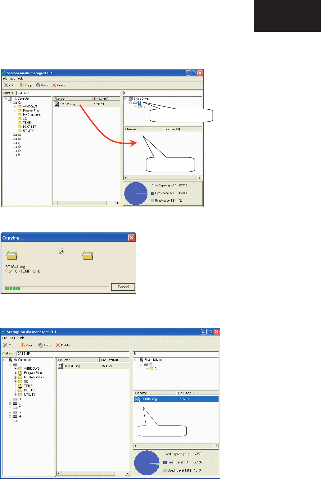
39
LC-26GA5E
LC-32GA5E
LC-32GD8E/RU
LC-32BT8E/RU
LC-37GD8E/RU
LC-37BT8E/RU
LC-32/37GD8E/RU
LC-32/37BT8E/RU
Digital Board Software Updating , PCMCIA (continued)
7. First of all, select copy target drive and then use Drag & drop for the “.img” fi le.
7
7. First of all, select copy target drive and then use Drag & drop for the “.img” file.
8. Wait, copy is in process.
9. Copy is finished, when the Copying progress bar disappears and the name of data file appears in the File
Box.
At first, take care and select copy
drive. This is important.
After select copy drive,
Drag&Drop of ".img" file.
8. Wait, copy is in process.
#7 wait copyin
g
#8 copy is finished
.
#9 End SMM "X" butto
n
#1
0
Remove PCMCIA (Windows Task bar popup menu
)
#11 end
copy is finished.
9. Copy is fi nished, when the Copying progress bar disappears and the name of data fi le appears in the File
Box.
#7 wait copyin
g
#8 copy is finished
.
#9 End SMM "X" butto
n
#1
0
Remove PCMCIA (Windows Task bar popup menu
)
#11 end
copy is finished.

40
LC-26GA5E
LC-32GA5E
LC-32/37GD8E/RU
LC-32/37BT8E/RU
10. Close SMM application.
11. Remove PCMCIA safely using the Windows Task bar pop up menu (Right-click over the Tray Icon).
#7 wait copyin
g
#8 copy is finished
.
#9 End SMM "X" butto
n
#1
0
Remove PCMCIA (Windows Task bar popup menu
)
#11 end
copy is finished.
12. Now, the PCMCIA-CF card is prepared to update the TV set.
• Procedure to update the TV Set using PCMCIA-CF Card:
1. Switch Off the LCD TV Set.
2. Insert PCMCIA Card (already prepared according the details before given at “How to prepare the CF Card
using the “Storage Media Manager 1.0.1” (SMM))”.
3. Switch On the LCD TV Set (it starts automatically the updating, Items #1 to #4).
12
4
3
4. Wait till the fi nishing indication is shown.
5. For checking the correct update, please Select DTV Menu on TV Set. The following On Screen Display will
appear.
6. Select “Version”. The updated version can be verifi ed.
Digital Board Software Updating , PCMCIA (continued)

41
LC-26GA5E
LC-32GA5E
LC-32GD8E/RU
LC-32BT8E/RU
LC-37GD8E/RU
LC-37BT8E/RU
LC-32/37GD8E/RU
LC-32/37BT8E/RU
26
LC-32/37GD8E/RU
LC-32/37BT8E/RU
TROUBLESHOOTING TABLE
NO
YES
NO
YES YES
NO
YES
YES
Power unit operation check
Are the power cord and harness in the unit properly connected?
Are both ends of C704 and C705 (32"/37") short-circuited when
checking their resistance values?
Connect the power cord and harness properly, and turn on the
power.
Is a voltage of BU5V applied to pin (20) of P701? (Set the main
power SW to OFF.)
C704 ••• Check VA701, VA702 and D701.
C705(32”/37”)••• Check IC704 and 705.
Is F701 normal?
Does the same symptom appear even if R858 (2.7k) is removed
and the power is supplied again?
Is a voltage of approx. 8 – 15V to pin (4) of IC705?
NO
Replace F701.
YES
Check short circuit of 5V line (D737, C752, etc.).
NO
Check IC705, IC708, D725
and Q724.
NO
Check IC704, D728, D762 and D736. If there are no problems,
check the resistance value between pins (1) and (6) of P704.
When the value is low (several Ω- several hundred Ω),
disconnect P704. If the value is still low, the parts of 24V line are
defective. When the resistance value is several kΩ, check the
inverter unit.
YES
Check Q724, D731, D734, IC707, D751, D753, D754, D741,
D759 and D746.
Does a relay noise sound? (Once)
YES
NO
Check peripheral circuits of D738, R828 and D735.
NO
Are PCON1 and 2 [pins (1) and (2) of P702] at Hi (3V or more)?
NO
There is a possibility that control by P-CON is not performed
properly. Check whether the "PS-ON" and "PS-ON2" signals are
sent from pins (97) and (91) of IC1710 (FPGA) of MAIN-UNIT.
YES
Check peripheral circuits of Q712, Q713, Q721, Q723 and
RY701.
Is it a symptom that the relay clatters twice as soon as the main
power SW is set to ON and the power is not supplied?
TROUBLESHOOTING TABLE

42
LC-26GA5E
LC-32GA5E
LC-32/37GD8E/RU
LC-32/37BT8E/RU
27
LC-32/37GD8E/RU
LC-32/37BT8E/RU
TROUBLESHOOTING TABLE (Continued)
No sound (1) (during the reception of TV broadcasting)
No audio output during UHF/VHF reception
Checklist:
1) Is the volume set to MIN or MUTE on the remote control? ··· Set the desired volume.
2) Are headphones connected to HEADPHONE (J1301)? ··· Disconnect them.
3) Is ANT-CABLE disconnected or connected improperly? ··· Connect it correctly as per the operation manual.
NO
Is the audio signal (L/R) sent from pins (28) and (27) of IC3002
(VCT)?
NO
YES
Is the audio signal of pins (3)
and (5) of IC303 (OP-AMP)
sent properly?
(AV-UNIT)
(TUNER)
Check IC303 or peripheral
circuits.
NO
YES
YES
Is the audio signal of pin (4)
of IC301/IC302 (AUDIO-
AMP) sent properly?
Check HEAD-PHONE
(J1301) or peripheral
circuits.
NO
Is the audio signal output of
pins (2) and (4) of P301
(AUDIO-CONNECTOR)
normal?
YES
Check Speaker (right and
left) and wire harness.
Check P301 (AUDIO-
CONNECTOR) and
peripheral circuits.
YES
NO
Is the audio signal (SIF) sent
from pin (1) of CONNECTOR
(SC2705)?
Check pin (31) of IC3002
(VCT) and peripheral
circuits.
YES
Is the SIF signal (SIF_IN+)
sent to pin (31) of IC3002
(VCT)?
Check whether +5V and +8V
are supplied to pins (33) and
(18) of IC3002 respectively.
Or, check peripheral circuits.
YES
NO
NO
NO
NO
Is the audio signal (SIF) sent
from pin (12) of IC201 (IF-
DEMOD)?
Check Q203 (AMP) and
peripheral circuits.
YES
Is the SIF signal sent to pins
(23) and (24) of IC201 (IF-
DEMOD)?
Check IC201 and peripheral
circuits.
YES
Is the IF signal sent from pin
(8) of TUNER (TU201)?
Check FL202 and peripheral
circuits.
YES
Check whether 5V (CONT)
and 5V are supplied to pins
(1) and (7) of TUNER
(TU201) respectively. Check
SDA/SCL and AGC signal.
Replace TUNER (TU201).
Troubleshooting Table (continued)

43
LC-26GA5E
LC-32GA5E
LC-32GD8E/RU
LC-32BT8E/RU
LC-37GD8E/RU
LC-37BT8E/RU
LC-32/37GD8E/RU
LC-32/37BT8E/RU
28
LC-32/37GD8E/RU
LC-32/37BT8E/RU
No sound from external input devices (2)
No sound from an external
input device connected to
EXT1 (SCART1).
No sound from an external
input device connected to
EXT2 (SCART2).
No sound from an
external input device
connected to EXT3.
No sound from EXT4
(AUDIO) connecting an
external input device.
No sound from EXT5
(AUDIO) connecting an
external input device.
YES
<EXT1>
Is IN1-L audio signal sent
from pin (6) of SCART1
terminal (J1101) to pin
(14) of IC3002 (VCT)?
Is IN1-R audio signal sent
from pin (2) of SCART1
terminal (J1101) to pin
(13) of IC3002 (VCT)?
<EXT2>
Is IN2-L audio signal sent
from pin (27) of SCART2
terminal (J1101) to pin
(12) of IC3002 (VCT)?
Is IN2-R audio signal sent
from pin (23) of SCART2
terminal (J1101) to pin
(11) of IC3002 (VCT)?
<EXT3>
Is IN3-L audio signal
sent from pin (3) of
J1201 terminal to pin
(16) of IC3002?
Is IN3-R audio signal
sent from pin (5) of
J1201 terminal to pin
(15) of IC3002?
Is the audio signal
properly sent from pins
(28) and (27) of IC3002?
Check IC3002 or
peripheral circuits.
Is the audio signal of
pins (1) and (7) of IC303
(OP-AMP) sent properly?
Check IC303 or
peripheral circuits.
<EXT4>
Is D-SUB-L audio signal
sent from J2702 to pin
(15) of IC2704?
Is D-SUB-R audio signal
sent from J2702 to pin
(2) of IC2704?
Is D-SUB-L audio signal
sent to pin (10) of
IC3002?
Is D-SUB-R audio signal
sent to pin (9) of
IC3002?
<EXT5>
Is HDMI-L audio signal
sent from J2701 to pin
(14) of IC2704?
Is HDMI-R audio signal
sent from J2701 to pin
(5) of IC2704?
Check pins (6) and
(2) of SCART1 and
connection to an
external input
device.
Check pins (27) and
(23) of SCART2 and
connection to an
external input
device.
Check pins 3
(J1201) and 5
(J1201) of EXT3
and connection to
an external input
device.
Is HDMI-L audio
signal sent to pin
(10) of IC3002?
Is HDMI-R audio
signal sent to pin (9)
of IC3002?
Is the audio output
signal of pins (13) and
(16) of IC302/IC301
(MAIN-AMP) normal?
Check IC302/IC301
(MAIN-AMP),
HEADPHONE and
peripheral circuits.
Check CONNECTOR
(P301) and Speaker
(right and left).
YES
YES
NO NO
Check output of pins
(13) and (3) of
IC2704 and
peripheral circuits.
NO
Check that Option-
HDMI Setup-Audio
select is set to
"Analog".
YES YES
YES
OK
NOYES
YES YES
NO
YES
NO
NO
TROUBLESHOOTING TABLE (Continued)
Troubleshooting Table (continued)
44
LC-26GA5E
LC-32GA5E
LC-32/37GD8E/RU
LC-32/37BT8E/RU
29
LC-32/37GD8E/RU
LC-32/37BT8E/RU
TROUBLESHOOTING TABLE (Continued)
No sound except from speakers (3)
Check audio input signal of pin (31) of IC3002 (VCT), pins (18)
and (33) of the power line, pins (84) and (83) of I2C-LINE, and
peripheral circuits.
NO NO
NO NO
No audio output from the
headphones
No audio output from EXT1
(SCART) terminal.
NO
Is there audio output on pins
(2) and (3) of the headphone
terminal (J1301)?
Checklist:
1) Is the MUTE button on the remote control set to ON? ··· Set to OFF.
2) Check the connection to external devices. ··· Is there any improper connection?
Is audio input/output signal of
pins (3) and (5)/(1) and (7) of
IC303 (OP-AMP) normal?
NO
NO
YES
YES
NO
YES
NO
NO
NO
YES
YES
Is audio output signal (SPK-
OUT L/R) properly sent from
pins (28) and (27) of IC3002
(VCT)?
Check the connection to
EXT1 (J1101) and external
devices.
Check the connection to
EXT2 (J1101) and external
devices.
Is S-MUTE-LINE [IC1710 (pin
100)] or S2-MUTE-LINE
[IC3003 (pin 26)] at H?
(Check Q1102/Q1101
operation.)
Is audio signal sent from pins
(22) and (21) of IC3002?
Check the audio signal
output line from pins (22) and
(21) of IC3002 to
Q1103/Q1104/Q1201/Q1202.
Check the connection to
AUDIO OUTPUT terminal
(J1201) and external devices.
Is S-MUTE-LINE [IC1710 (pin
100)] at H?
(Check Q1204/Q1203
operation.)
Is audio signal sent to pins
(3) and (1) of EXT1 (J1101)?
Is S-MUTE-LINE [IC1710
(pin 100)] at H?
(Check Q1106/Q1105
operation.)
Is audio signal sent from
pins (24) and (23) of
IC3002?
Check the audio signal
output line from pins (24)
and (23) of IC3002 to pins
(3) and (1) of EXT1.
Check the power supply 8/5
V pins (18) and (33) of
IC3002 and peripheral
circuits.
Is audio signal sent to pins
(24) and (22) of EXT2
(J1101)?
Is audio signal sent to pins
(13) and (15) [L/R (white)
(red)] of AUDIO OUTPUT
terminal (J1201)?
No audio output from EXT2
(SCART) terminal.
No audio output from AUDIO
OUTPUT terminal.
Is the MUTE button on the
remote control set to ON?
... Set to OFF.
29
LC-32/37GD8E/RU
LC-32/37BT8E/RU
TROUBLESHOOTING TABLE (Continued)
No sound except from speakers (3)
Check audio input signal of pin (31) of IC3002 (VCT), pins (18)
and (33) of the power line, pins (84) and (83) of I2C-LINE, and
peripheral circuits.
NO NO
NO NO
No audio output from the
headphones
No audio output from EXT1
(SCART) terminal.
NO
Is there audio output on pins
(2) and (3) of the headphone
terminal (J1301)?
Checklist:
1) Is the MUTE button on the remote control set to ON? ··· Set to OFF.
2) Check the connection to external devices. ··· Is there any improper connection?
Is audio input/output signal of
pins (3) and (5)/(1) and (7) of
IC303 (OP-AMP) normal?
NO
NO
YES
YES
NO
YES
NO
NO
NO
YES
YES
Is audio output signal (SPK-
OUT L/R) properly sent from
pins (28) and (27) of IC3002
(VCT)?
Check the connection to
EXT1 (J1101) and external
devices.
Check the connection to
EXT2 (J1101) and external
devices.
Is S-MUTE-LINE [IC1710 (pin
100)] or S2-MUTE-LINE
[IC3003 (pin 26)] at H?
(Check Q1102/Q1101
operation.)
Is audio signal sent from pins
(22) and (21) of IC3002?
Check the audio signal
output line from pins (22) and
(21) of IC3002 to
Q1103/Q1104/Q1201/Q1202.
Check the connection to
AUDIO OUTPUT terminal
(J1201) and external devices.
Is S-MUTE-LINE [IC1710 (pin
100)] at H?
(Check Q1204/Q1203
operation.)
Is audio signal sent to pins
(3) and (1) of EXT1 (J1101)?
Is S-MUTE-LINE [IC1710
(pin 100)] at H?
(Check Q1106/Q1105
operation.)
Is audio signal sent from
pins (24) and (23) of
IC3002?
Check the audio signal
output line from pins (24)
and (23) of IC3002 to pins
(3) and (1) of EXT1.
Check the power supply 8/5
V pins (18) and (33) of
IC3002 and peripheral
circuits.
Is audio signal sent to pins
(24) and (22) of EXT2
(J1101)?
Is audio signal sent to pins
(13) and (15) [L/R (white)
(red)] of AUDIO OUTPUT
terminal (J1201)?
No audio output from EXT2
(SCART) terminal.
No audio output from AUDIO
OUTPUT terminal.
Troubleshooting Table (continued)
45
LC-26GA5E
LC-32GA5E
LC-32GD8E/RU
LC-32BT8E/RU
LC-37GD8E/RU
LC-37BT8E/RU
LC-32/37GD8E/RU
LC-32/37BT8E/RU
30
LC-32/37GD8E/RU
LC-32/37BT8E/RU
TROUBLESHOOTING TABLE (Continued)
YES
The unit does not enter the DTV mode. Or, the DTV menu does
not appear.
NO
MAIN UNIT:
Check around the pin (1) of IC1710(FPGA).
Go to "The unit does not enter the DTV mode. Or, the DTV menu
does not appear."
No video output during DTV reception. Go to "No video output during DTV reception."
YES
NO
No audio output during DTV reception. Go to "No audio output during DTV reception."
YES
DTV troubleshooting
NO
Digital UNIT:
Is a voltage supplied from IC4701(3.3V-REG)/IC4704(1.8V-REG)?
D-TUNER UNIT:
Is a voltage of 5V supplied from IC205(SW) and IC206(SW)?
Is a voltage applied to pin(20) (I2CSEL) of P202?
(High=3.3V)
YES
Do X4001/X4002 oscillate?
Check peripheral circuits of IC4701/IC4704 and pin(7) of IC4701.
Check peripheral circuits of X4001/X4002.
Check peripheral circuits of IC205/IC206.
NO
YES
NO
Is CLK/DATA signal sent to pins (21) and (22) of P202 and pins (1)
and (13) of IC204 (COFDM).
YES
Check peripheral circuits of IC202(COFDM)/ IC4001(D-Processor).
NO
YES
NO
YES
Does X202 oscillate?
Check IC202(COFDM)/IC4001(D-Processor).
Check peripheral circuits of X202.
NO
YES
The unit does not enter the DTV mode. Or, the DTV menu does not appear.
Troubleshooting Table (continued)
46
LC-26GA5E
LC-32GA5E
LC-32/37GD8E/RU
LC-32/37BT8E/RU
31
LC-32/37GD8E/RU
LC-32/37BT8E/RU
TROUBLESHOOTING TABLE (Continued)
NO
YES
Check power supply and pins (9) and (10)of IC2704(SW) and
audio signal input of pins (4) and (11) of IC2704.
Check Q4601... Q4607 and their peripheral circuits.
NO
Check R272 and R273.
Are scrambled images not displayed?
YES
No video output during DTV reception. Colors of Images are not right.
NO
DIGITAL UNIT:
Is audio signal fed to pins (5) and (10) of IC4604 (OP-AMP)?
Are video signals (R/G/B,CVBS) send from the
C4636/C4637/C4638 and emitters of Q4607?
Check power supply and pin (1) of IC2705(SW).
NO
YES
MAIN UNIT:
Is video signal (CVBS) sent from pin (2) of IC2705(SW).
YES
Are video signals (R/G/B,CVBS) fed from pins (179),(180),(181)
and (184) of IC3002?
YES
NO
MAIN UNIT:
Is audio signal sent to pin (3) and (13) of IC2704 (SW)?
YES
Is audio signal sent from pins (7) and (8) of IC4604(OP-AMP)?
Check R4002(AD2pin) and IC4001(D-Processor).
Check power supply of IC4604(OP-AMP) and its peripheral circuits.
NO
YES
NO
YES
No audio output during DTV reception. Sound is low.
D-TUNER UNIT:
Is data FED[0:7] sent from pins (3),(4),(5),(6),(8),(9),(10) and (11)
of P202?
DIGITAL UNIT:
Check 5V output of pin (1) of IC4702.
Check 5V of pin (6) of Q4401.
NO
YES
Check R4011(AC8pin),R4013(AC9pin) and IC4001(D-Processor).
DIGITAL UNIT:
Are video signals (R/G/B,CVBS) sent from
C4639/C4640/C4641/C4625?
34
LC-32/37GD8E/RU
LC-32/37BT8E/RU
TROUBLESHOOTING TABLE (Continued)
<When EXT1 is used for external input>
No EXT1-Composite output of the external
input system.
Checklist:
1) Is "INPUT SOURCE" button on the remote control set up correctly? ··· See the operation manual and set "INPUT SOURCE" to "EXT1".
2) Is MENU-PICTURE-CONTRAST/BRIGHTNESS set to "MIN"? ··· Set it to an appropriate level.
3) Check the connection to the external device ··· Connect it correctly as per the operation manual for the device.
No EXT1-RGB output of the external input
system.
No EXT1-Y/C output of the external input
system.
NO
Is composite video
signal sent to pin
(20) of SCART1
(J1101)?
Check external
connection, input
setting, SCART1
(J1101) and
peripheral circuits.
Is RGB signal sent
to pins (15), (11)
and (7) of SCART1
(J1101)?
NO
Check external
connection, input
setting, SCART1
(J1101) and
peripheral circuits.
Is Y/C signal sent
to pins (20) and
(15) of SCART1
(J1101)?
NO
Check external
connection, input
setting, SCART1
(J1101) and
peripheral circuits.
YES YES YES
NO
Is composite video
signal (VIN_1)
sent to input
terminal pin (6) of
IC2702 (SW)?
Check
CONNECTOR
(SC2702/P1101),
SCART1 (J1101)
and peripheral
circuits.
Is RGB signal
(R1/G1/B1=VIN_6/
5/9) sent to input
terminal pins
(187), (175) and
(182) of IC3002
(VCT)?
NO
Check
CONNECTOR
(SC2702/P1101),
SCART1 (J1101)
and peripheral
circuits.
Is Y/C signal
(VIN1=Y1/C1) sent
to input terminal
pins (190) and
(187) of IC3002
(VCT)?
NO
Check
CONNECTOR
(SC2702/P1101),
SCART1 (J1101)
and peripheral
circuits.
YES
NO
Is composite video
signal
(CVBS1=VIN2)
sent to input
terminal pin (190)
of IC3002 (VCT)?
Check IC2702
(SW) and
peripheral circuits.
YES
NO
YES
YES
Is LVDS signal (LVDS_0N/0P-3N/3P) sent from pins (141) and (140) - (129) and (128) of IC3002
(VCTP), and is CLK signal (LVDS_CN/CP) sent from pins (132) and (131)?
Check pins (192), (170) and (133) of BU3.3V
power line and pins (185), (169) and (142) of
BU1.8V power line of IC3002 (VCTP), and
peripheral circuits.
YES
YES
Replace LCD-CONT-UNIT.
YES
NO
NO
Is LVDS signal (LVDS_0N/0P-3N/3P) sent to pins (12) and (13) - (24) and (25) of CONNECTOR
CN1 in LCD-CONT-UNIT, and is CLK signal (LVDS_CN/CP) sent to pins (21) and (22)?
Check CONNECTOR (P2305, CN1) and
Harness Wire (LV).
Is power (LCD5V) supplied to pins (2) – (5) of CONNECTOR CN1 in LCD-CONT-UNIT?
No picture on the display (3)
Check HARNESSWIRE (LV).
Is IC1705 supplying LCD 5V?
NO
Check IC1705 and peripheral parts. YES
NO
Change IC1705.
Is LCD5V supplied to pins (31) - (28) of
CONNECTOR (P2305)?
YES
Troubleshooting Table (continued)

47
LC-26GA5E
LC-32GA5E
LC-32GD8E/RU
LC-32BT8E/RU
LC-37GD8E/RU
LC-37BT8E/RU
LC-32/37GD8E/RU
LC-32/37BT8E/RU
31
LC-32/37GD8E/RU
LC-32/37BT8E/RU
TROUBLESHOOTING TABLE (Continued)
NO
YES
Check power supply and pins (9) and (10)of IC2704(SW) and
audio signal input of pins (4) and (11) of IC2704.
Check Q4601... Q4607 and their peripheral circuits.
NO
Check R272 and R273.
Are scrambled images not displayed?
YES
No video output during DTV reception. Colors of Images are not right.
NO
DIGITAL UNIT:
Is audio signal fed to pins (5) and (10) of IC4604 (OP-AMP)?
Are video signals (R/G/B,CVBS) send from the
C4636/C4637/C4638 and emitters of Q4607?
Check power supply and pin (1) of IC2705(SW).
NO
YES
MAIN UNIT:
Is video signal (CVBS) sent from pin (2) of IC2705(SW).
YES
Are video signals (R/G/B,CVBS) fed from pins (179),(180),(181)
and (184) of IC3002?
YES
NO
MAIN UNIT:
Is audio signal sent to pin (3) and (13) of IC2704 (SW)?
YES
Is audio signal sent from pins (7) and (8) of IC4604(OP-AMP)?
Check R4002(AD2pin) and IC4001(D-Processor).
Check power supply of IC4604(OP-AMP) and its peripheral circuits.
NO
YES
NO
YES
No audio output during DTV reception. Sound is low.
D-TUNER UNIT:
Is data FED[0:7] sent from pins (3),(4),(5),(6),(8),(9),(10) and (11)
of P202?
DIGITAL UNIT:
Check 5V output of pin (1) of IC4702.
Check 5V of pin (6) of Q4401.
NO
YES
Check R4011(AC8pin),R4013(AC9pin) and IC4001(D-Processor).
DIGITAL UNIT:
Are video signals (R/G/B,CVBS) sent from
C4639/C4640/C4641/C4625?
28
LC-32/37GD8E/RU
LC-32/37BT8E/RU
No sound from external input devices (2)
No sound from an external
input device connected to
EXT1 (SCART1).
No sound from an external
input device connected to
EXT2 (SCART2).
No sound from an
external input device
connected to EXT3.
No sound from EXT4
(AUDIO) connecting an
external input device.
No sound from EXT5
(AUDIO) connecting an
external input device.
YES
<EXT1>
Is IN1-L audio signal sent
from pin (6) of SCART1
terminal (J1101) to pin
(14) of IC3002 (VCT)?
Is IN1-R audio signal sent
from pin (2) of SCART1
terminal (J1101) to pin
(13) of IC3002 (VCT)?
<EXT2>
Is IN2-L audio signal sent
from pin (27) of SCART2
terminal (J1101) to pin
(12) of IC3002 (VCT)?
Is IN2-R audio signal sent
from pin (23) of SCART2
terminal (J1101) to pin
(11) of IC3002 (VCT)?
<EXT3>
Is IN3-L audio signal
sent from pin (3) of
J1201 terminal to pin
(16) of IC3002?
Is IN3-R audio signal
sent from pin (5) of
J1201 terminal to pin
(15) of IC3002?
Is the audio signal
properly sent from pins
(28) and (27) of IC3002?
Check IC3002 or
peripheral circuits.
Is the audio signal of
pins (1) and (7) of IC303
(OP-AMP) sent properly?
Check IC303 or
peripheral circuits.
<EXT4>
Is D-SUB-L audio signal
sent from J2702 to pin
(15) of IC2704?
Is D-SUB-R audio signal
sent from J2702 to pin
(2) of IC2704?
Is D-SUB-L audio signal
sent to pin (10) of
IC3002?
Is D-SUB-R audio signal
sent to pin (9) of
IC3002?
<EXT5>
Is HDMI-L audio signal
sent from J2701 to pin
(14) of IC2704?
Is HDMI-R audio signal
sent from J2701 to pin
(5) of IC2704?
Check pins (6) and
(2) of SCART1 and
connection to an
external input
device.
Check pins (27) and
(23) of SCART2 and
connection to an
external input
device.
Check pins 3
(J1201) and 5
(J1201) of EXT3
and connection to
an external input
device.
Is HDMI-L audio
signal sent to pin
(10) of IC3002?
Is HDMI-R audio
signal sent to pin (9)
of IC3002?
Is the audio output
signal of pins (13) and
(16) of IC302/IC301
(MAIN-AMP) normal?
Check IC302/IC301
(MAIN-AMP),
HEADPHONE and
peripheral circuits.
Check CONNECTOR
(P301) and Speaker
(right and left).
YES
YES
NO NO
Check output of pins
(13) and (3) of
IC2704 and
peripheral circuits.
NO
Check that Option-
HDMI Setup-Audio
select is set to
"Analog".
YES YES
YES
OK
NOYES
YES YES
NO
YES
NO
NO
TROUBLESHOOTING TABLE (Continued)
Troubleshooting Table (continued)

48
LC-26GA5E
LC-32GA5E
LC-32/37GD8E/RU
LC-32/37BT8E/RU
32
LC-32/37GD8E/RU
LC-32/37BT8E/RU
TROUBLESHOOTING TABLE (Continued)
<On input of the tuner>(U/V)>
No picture appears on LCD during the tuner reception.(U/V) reception.
Checklist:
1) Is "INPUT SOURCE" button on the remote control set up correctly? ··· See the operation manual and set "INPUT SOURCE" to "TV".
2) Is MENU-PICTURE-Contrast/Brightness set to "MIN"? ··· Set it to an appropriate level.
3) Is ANT-CABLE disconnected or connected improperly? ··· Connect it correctly as per the operation manual.
NO
Is level of pins (4) and (5) of
tuner (TU201) and pins (10)
and (11) of IC201 (IF-
DEMOD) at H?
These are communications
lines for control (I2C). Follow
the path and check whether
they are forced to L
(PULL_DOWN).
YES
NO
Is the video signal (IF) sent
from pin (8) of tuner
(TU201)?
Check the tuner (TU201)
and peripheral circuits.
NO
YES
YES
YES
Is video signal sent from pin
(17) of IC201 (IF-DEMOD)?
Check FL201 (SAW-FIL),
IC201 and peripheral
circuits.
NO
Is the video signal VIN1
(ATUNER-CVBS) sent to pin
(191) of IC3002 (VCT)?
Check IC201 (IF-DEMOD),
CONNECTOR
(P201/SC2705) and
peripheral circuits.
NO
YES
Is LVDS video signal (LVDS_0N/0P-3N/3P) sent to pins
(141)/(140) - (129)/(128) of IC3002 (VCTP), and is CLK signal
(LVDS_CN/CP) sent to pins (132)/(131)?
Check pins (192)/(170)/(133) of BU3.3V line of IC3002 (VCTP),
pins (185)/(169)/(142) of 1.8V line and peripheral circuits.
NO
YES
Is LVDS video signal (LVDS_0N/0P-3N/3P) sent to pins (12)/(13) -
(24)/(25) of CONNECTOR CN1 of LCD-CONT-UNIT, and is CLK
signal (LVDS_CN/CP) sent to pins (21)/(22)?
Check CONNECTOR (P2305, CN1) and HARNESSWIRE (LV).
NO
YES
Is power (LCD5V) supplied to pins (2) – (5) of CONNECTOR CN1
in LCD-CONT-UNIT?
YES
Replace LCD-CONT-UNIT.
Is LCD5V supplied to pins (31) – (28) of CONNECTOR (P2305)?
No picture on the display (1)
Check HARNESSWIRE (LV).
Is IC 1705 supplying LCD 5V?
NO
Check IC1705 and peripheral parts. YES
NO
Change IC1705.
YES
Troubleshooting Table (continued)

49
LC-26GA5E
LC-32GA5E
LC-32GD8E/RU
LC-32BT8E/RU
LC-37GD8E/RU
LC-37BT8E/RU
LC-32/37GD8E/RU
LC-32/37BT8E/RU
33
LC-32/37GD8E/RU
LC-32/37BT8E/RU
TROUBLESHOOTING TABLE (Continued)
<During external connection>
SCART1:
No picture appears on EXT1-connected
monitor during the tuner reception.
SCART2:
No picture from EXT1 appears on EXT2-
connected monitor.
Note: Normally, if the screen during display is
sent to EXT2, no picture is sent to EXT2.
SCART2:
No picture from EXT3 appears on EXT2-
connected monitor.
YES
Is video signal
sent to pin (19) of
SCART1 (J1101)?
Check SCART1,
external
connection or input
setting.
Is video signal
sent to pin (40) of
SCART2 (J1101)?
YES
Check SCART2,
external
connection or input
setting.
Is video signal
sent to pin (40) of
SCART2 (J1101)?
YES
Check SCART2,
external
connection or input
setting.
NO NO NO
No picture on the monitor (2)
Checklist:
1) Are input terminal on back of TV and "INPUT SOURCE" button on the remote control set up correctly? ··· See the operation manual and set
"INPUT SOURCE" appropriately.
2) Is the Signal Type (item) in MENU-Option-Input Select set to the same as that of the external device? ··· Set it to "CVBS", "Y/C" or "RGB".
3) Is ANT-CABLE disconnected or connected improperly? ··· Connect it correctly as per the operation manual.
4) The picture is sent to the monitor in a CVBS signal if the source during display is TV, CVBS or Y/C of EXT1-3. When sent by component, etc., that
signal is not sent to the monitor.
5) When the monitor picture is not sent and is not displayed on the monitor, refer to “No picture” for each terminal.
6) The video output from EXT1 is not the monitor output (output of the picture now watching). The picture of the last selected TV channel is always sent to
EXT1. (Specification)
YES
Is video signal (V-
OUT1) sent from
pin (2) of IC1102
(SW)?
Check SCART1
(J1101) and
peripheral circuits.
Is video signal (V-
OUT2) sent from
pin (2) of IC1101
(SW)?
YES
Check SCART2
(J1101) and
peripheral circuits.
Is video signal (V-
OUT2) sent from
pin (2) of IC1101
(SW)?
YES
Check SCART2
(J1101) and
peripheral circuits.
NO NO NO
YES
Is video signal (V-
OUT1) sent from
pin (195) of
IC3002 (VCT)?
Check IC1102
(SW), Connector
(P1101, SC2702)
and peripheral
circuits.
Is video signal (V-
OUT2) sent from
pin (194) of
IC3002 (VCT)?
YES
Check IC1101
(SW), Connector
(P1102, SC2703)
and peripheral
circuits.
Is video signal (V-
OUT2) sent from
pin (194) of
IC3002 (VCT)?
YES
Check IC1101
(SW), Connector
(P1102, SC2703)
and peripheral
circuits.
NO NO NO
YES
Is video signal
(CVBS) sent to pin
(191) of IC3002
(VCT)?
Check power
supply of IC1102
(SW), Connector
(P1101, SC2702)
and peripheral
Is video signal
(VIN1) from EXT1
sent to pin (190) of
IC3002 (VCT)?
YES
Check power
supply of IC1101
(SW), Connector
(P1102, SC2703)
and peripheral
Is video signal
(VIN7) from EXT3
sent to pin (184) of
IC3002 (VCT)?
YES
Check power
supply of IC1101
(SW), Connector
(P1102, SC2703)
and peripheral
NO NO NO
YES
Is video signal
(CVBS) sent from
pin (17) of IC201
(IF-DEMOD)?
Check
CONNECTOR
(P201, SC2705) and
peripheral circuits.
Check whether
video signal is sent
to pin (20) of
SCART1.
YES
Check SCART1,
IC2702 (SW),
CONNECTOR
(SC2702, P1101)
and peripheral
circuits.
Is video signal
(IN3YV) sent to pin
(2) of IC1201
(SW)?
YES
Check pin (184) of
IC3002 (VCT),
CONNECTOR
(SC2703, P1102)
and peripheral
circuits.
NO NO NO
YES
Is video signal (IF)
sent from pin (8) of
tuner (TU201)?
Check IC201,
FL201 (SAW-FIL),
Q202 and
peripheral circuits. Check SCART1,
external
connection or input
setting.
Is video signal
(CVBS) sent from
pin (1) of A/V-
TERMINAL
(J1201)? (EXT3)
YES
Check pin (1)
(IN3SW) of IC1201
(SW), power
supply and
peripheral circuits.
NO
Check A/V-
TERMINAL
(J1201), external
connection or input
setting.
NO
Check 5/5 (CONT) V power supply pins (7)
and (1), I2C line pins (5) and (4) of tuner
(TU201) and peripheral circuits.
Troubleshooting Table (continued)

50
LC-26GA5E
LC-32GA5E
LC-32/37GD8E/RU
LC-32/37BT8E/RU
34
LC-32/37GD8E/RU
LC-32/37BT8E/RU
TROUBLESHOOTING TABLE (Continued)
<When EXT1 is used for external input>
No EXT1-Composite output of the external
input system.
Checklist:
1) Is "INPUT SOURCE" button on the remote control set up correctly? ··· See the operation manual and set "INPUT SOURCE" to "EXT1".
2) Is MENU-PICTURE-CONTRAST/BRIGHTNESS set to "MIN"? ··· Set it to an appropriate level.
3) Check the connection to the external device ··· Connect it correctly as per the operation manual for the device.
No EXT1-RGB output of the external input
system.
No EXT1-Y/C output of the external input
system.
NO
Is composite video
signal sent to pin
(20) of SCART1
(J1101)?
Check external
connection, input
setting, SCART1
(J1101) and
peripheral circuits.
Is RGB signal sent
to pins (15), (11)
and (7) of SCART1
(J1101)?
NO
Check external
connection, input
setting, SCART1
(J1101) and
peripheral circuits.
Is Y/C signal sent
to pins (20) and
(15) of SCART1
(J1101)?
NO
Check external
connection, input
setting, SCART1
(J1101) and
peripheral circuits.
YES YES YES
NO
Is composite video
signal (VIN_1)
sent to input
terminal pin (6) of
IC2702 (SW)?
Check
CONNECTOR
(SC2702/P1101),
SCART1 (J1101)
and peripheral
circuits.
Is RGB signal
(R1/G1/B1=VIN_6/
5/9) sent to input
terminal pins
(187), (175) and
(182) of IC3002
(VCT)?
NO
Check
CONNECTOR
(SC2702/P1101),
SCART1 (J1101)
and peripheral
circuits.
Is Y/C signal
(VIN1=Y1/C1) sent
to input terminal
pins (190) and
(187) of IC3002
(VCT)?
NO
Check
CONNECTOR
(SC2702/P1101),
SCART1 (J1101)
and peripheral
circuits.
YES
NO
Is composite video
signal
(CVBS1=VIN2)
sent to input
terminal pin (190)
of IC3002 (VCT)?
Check IC2702
(SW) and
peripheral circuits.
YES
NO
YES
YES
Is LVDS signal (LVDS_0N/0P-3N/3P) sent from pins (141) and (140) - (129) and (128) of IC3002
(VCTP), and is CLK signal (LVDS_CN/CP) sent from pins (132) and (131)?
Check pins (192), (170) and (133) of BU3.3V
power line and pins (185), (169) and (142) of
BU1.8V power line of IC3002 (VCTP), and
peripheral circuits.
YES
YES
Replace LCD-CONT-UNIT.
YES
NO
NO
Is LVDS signal (LVDS_0N/0P-3N/3P) sent to pins (12) and (13) - (24) and (25) of CONNECTOR
CN1 in LCD-CONT-UNIT, and is CLK signal (LVDS_CN/CP) sent to pins (21) and (22)?
Check CONNECTOR (P2305, CN1) and
Harness Wire (LV).
Is power (LCD5V) supplied to pins (2) – (5) of CONNECTOR CN1 in LCD-CONT-UNIT?
No picture on the display (3)
Check HARNESSWIRE (LV).
Is IC 1705 supplying LCD 5V?
NO
Check IC1705 and peripheral parts. YES
NO
Change IC1705.
Is LCD5V supplied to pins (31) - (28) of
CONNECTOR (P2305)?
YES
Troubleshooting Table (continued)
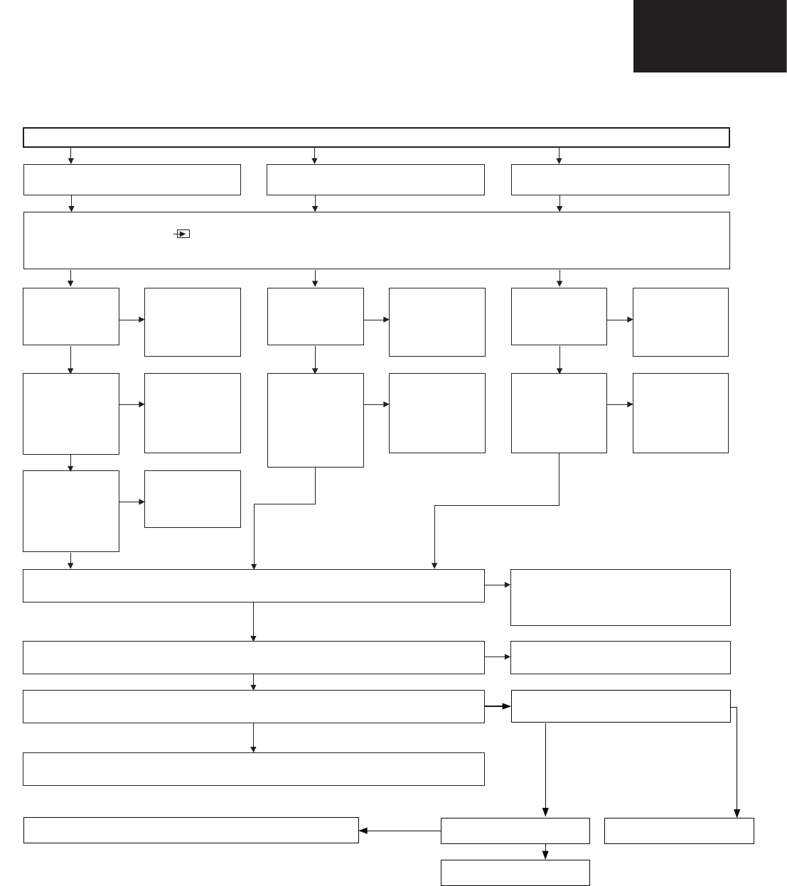
51
LC-26GA5E
LC-32GA5E
LC-32GD8E/RU
LC-32BT8E/RU
LC-37GD8E/RU
LC-37BT8E/RU
LC-32/37GD8E/RU
LC-32/37BT8E/RU
35
LC-32/37GD8E/RU
LC-32/37BT8E/RU
TROUBLESHOOTING TABLE (Continued)
<When EXT2 is used for external input>
No EXT2-Composite output of the external
input system.
Checklist:
1) Is "INPUT SOURCE" button on the remote control set up correctly? ··· See the operation manual and set "INPUT SOURCE" to "EXT2".
2) Is MENU-PICTURE-CONTRAST/BRIGHTNESS set to "MIN"? ··· Set it to an appropriate level.
3) Check the connection to the external device ··· Connect it correctly as per the operation manual for the device.
No EXT2-RGB output of the external input
system.
No EXT2-Y/C output of the external input
system.
NO
Is composite video
signal sent to pin
(41) of SCART2
(J1101)?
Check external
connection, input
setting, SCART2
(J1101) and
peripheral circuits.
Is RGB signal sent
to pins (36), (32)
and (28) of
SCART2 (J1101)?
NO
Check external
connection, input
setting, SCART2
(J1101) and
peripheral circuits.
Is Y/C signal sent
to pins (41) and
(36) of SCART2
(J1101)?
NO
Check external
connection, input
setting, SCART2
(J1101) and
peripheral circuits.
YES YES YES
NO
Is composite video
signal (VIN_2)
sent to input
terminal pin (4) of
IC2702 (SW)?
Check
CONNECTOR
(SC2702/P1101),
SCART2 (J1101)
and peripheral
circuits.
Is RGB signal
(R2/G2/B2=VIN_1
5/16/17) sent to
input terminal pins
(178), (177) and
(176) of IC3002
(VCT)?
NO
Check
CONNECTOR
(SC2702/P1101),
SCART2 (J1101)
and peripheral
circuits.
Is Y/C signal
(VIN2=Y2/C2) sent
to input terminal
pins (190) and
(178) of IC3002
(VCT)?
NO
Check
CONNECTOR
(SC2702/P1101),
SCART2 (J1101)
and peripheral
circuits.
YES
NO
Is composite video
signal
(CVBS2=VIN2)
sent to input
terminal pin (190)
of IC3002 (VCT)?
Check IC2702
(SW) and
peripheral circuits.
YES
NO
YES
YES
Is LVDS signal (LVDS_0N/0P-3N/3P) sent from pins (141) and (140) - (129) and (128) of IC3002
(VCTP), and is CLK signal (LVDS_CN/CP) sent from pins (132) and (131)?
Check pins (192), (170) and (133) of BU3.3V
power line and pins (185), (169) and (142) of
BU1.8V power line of IC3002 (VCTP), and
peripheral circuits.
YES
YES
Replace LCD-CONT-UNIT.
YES
NO
NO
Is LVDS signal (LVDS_0N/0P-3N/3P) sent to pins (12) and (13) - (24) and (25) of CONNECTOR
CN1 in LCD-CONT-UNIT, and is CLK signal (LVDS_CN/CP) sent to pins (21) and (22)?
Check CONNECTOR (P2305, CN1) and
Harness Wire (LV).
Is power (LCD5V) supplied to pins (2) – (5) of CONNECTOR CN1 in LCD-CONT-UNIT?
No picture on the display (4)
Check HARNESSWIRE (LV).
Is IC 1705 supplying LCD 5V?
NO
Check IC1705 and peripheral parts. YES
NO
Change IC1705.
Is LCD5V supplied to pins (31) - (28) of
CONNECTOR (P2305)?
YES
Troubleshooting Table (continued)

52
LC-26GA5E
LC-32GA5E
LC-32/37GD8E/RU
LC-32/37BT8E/RU
36
LC-32/37GD8E/RU
LC-32/37BT8E/RU
TROUBLESHOOTING TABLE (Continued)
NO
NO
NO
YES
YES
Is composite video signal sent to
pin (1) of A/V-IN-TERMINAL
(J1201)?
Check external connection,
input setting, A/V-IN-TERMINAL
(J1201) and peripheral circuits.
YES
Is composite video signal (IN3-
CVBS) sent to input terminal pin
(4) of IC1201 (SW)?
Check A/V-IN-TERMINAL
(J1201) and peripheral circuits.
Is composite video signal
(CVBS=VIN7) sent to input
terminal pin (184) of IC3002
(VCT)?
Check CONNECTOR
(SC2703/P1102), IC3002 (VCT)
and peripheral circuits.
NO
NO
YES
YES
Is Y/C signal sent to pins (11)
and (7) of S-TERMINAL
(J1201)?
Check external connection,
input setting, S-TERMINAL
(J1201) and peripheral circuits.
YES
YES
Is Y3 signal (IN3-Y) sent to input
terminal pin (6) of IC1201 (SW)?
Is Y/C signal (VIN7/VIN8) sent to
input terminal pins (184) and
(183) of IC3002 (VCT)?
Check S-TERMINAL (J1201)
and peripheral circuits.
NO
Check CONNECTOR
(SC2703/P1102), IC3002 (VCT)
and peripheral circuits.
YES
Is LVDS signal (LVDS_0N/0P-3N/3P) sent from pins (141) and (140) - (129) and (128) of IC3002 (VCTP), and is
CLK signal (LVDS_CN/CP) sent from pins (132) and (131)?
NO
Check pins (192), (170) and
(133) of BU3.3V power line and
pins (185), (169) and (142) of
BU1.8V power line of IC3002
(VCTP), and peripheral circuits.
YES
Is LVDS signal (LVDS_0N/0P-3N/3P) sent to pins (12) and (13) - (24) and (25) of CONNECTOR CN1 in LCD-
CONT-UNIT, and is CLK signal (LVDS_CN/CP) sent to pins (21) and (22)?
NO
Check CONNECTOR (P2305,
CN1) and Harness Wire (LV).
YES
Is power (LCD5V) supplied to pins (2) – (5) of CONNECTOR CN1 in LCD-CONT-UNIT?
NO
YES
Replace LCD-CONT-UNIT.
<When EXT3 is used for external input>
No EXT3 output of the external
input system.
Checklist:
1) Is "INPUT SOURCE" button on the remote control set up correctly? ··· See the operation manual and set "INPUT SOURCE" to "EXT3".
2) Is MENU-PICTURE-CONTRAST/BRIGHTNESS set to "MIN"? ··· Set it to an appropriate level.
3) Check the connection to the external device ··· Connect it correctly as per the operation manual for the device.
No EXT3-Y/C output of the
external input system.
No picture on the display (5)
Check HARNESSWIRE (LV).
Is IC 1705 supplying LCD 5V?
NO YES
Check IC1705 and peripheral parts. YES
NO
Change IC1705.
Is LCD5V supplied to pins (31) -
(28) of CONNECTOR (P2305)?
Troubleshooting Table (continued)

53
LC-26GA5E
LC-32GA5E
LC-32GD8E/RU
LC-32BT8E/RU
LC-37GD8E/RU
LC-37BT8E/RU
LC-32/37GD8E/RU
LC-32/37BT8E/RU
37
LC-32/37GD8E/RU
LC-32/37BT8E/RU
TROUBLESHOOTING TABLE (Continued)
NO
NO
NO
YES
YES
Is "EXT4" selected with
button on the remote control?
Select "EXT4" with button
on the remote control.
YES
Is D-SUB-COMPONENT signal
(PCV_R/G/B) sent to pins (1),
(2) and (3) of EXT4-TERMINAL
(SC2303)?
Check D-SUB-adaptor and
external connection.
Is D-SUB-COMPONENT signal
(PCV_R/G/B=VIN19/20/21))
sent to pins (174), (173) and
(172) of IC3002 (VCT)?
Check EXT4-TERMINAL and
peripheral circuits.
YES
Is LVDS signal (LVDS_0N/0P-3N/3P) sent from pins (141) and (140) - (129) and (128) of IC3002 (VCTP), and is
CLK signal (LVDS_CN/CP) sent from pins (132) and (131)?
NO
Check pins (192), (170) and
(133) of BU3.3V power line and
pins (185), (169) and (142) of
BU1.8V power line of IC3002
(VCTP), and peripheral circuits.
YES
Is LVDS signal (LVDS_0N/0P-3N/3P) sent to pins (12) and (13) - (24) and (25) of CONNECTOR CN1 in LCD-
CONT-UNIT, and is CLK signal (LVDS_CN/CP) sent to pins (21) and (22)?
NO
Check CONNECTOR (P2305,
CN1) and Hareness Wire (LV).
YES
Is power (LCD5V) supplied to pins (2) – (5) of CONNECTOR CN1 in LCD-CONT-UNIT?
NO
Replace LCD-CONT-UNIT.
<When EXT4 is used for external input>
No EXT4 (15pin-D-SUB-terminal)
output of the external input system.
Checklist:
1) Is "INPUT SOURCE" button on the remote control set up correctly? ··· See the operation manual and set "INPUT SOURCE" to "EXT4".
2) Connect the included D-SUB-Adapter-Cable to the COMPONENT terminal of an external device. ··· See the operation manual (use a commercially
available Component-Cable to connect to the external device).
3) Is ANT-CABLE disconnected or connected improperly? ··· Connect it correctly as per the operation manual.
No picture on the display (6)
YES
Check HARNESSWIRE (LV).
Is IC 1705 supplying LCD 5V?
NO YES
Check IC1705 and peripheral parts. YES
NO
Change IC1705.
Is LCD5V supplied to pins (31) -
(28) of CONNECTOR (P2305)?
Troubleshooting Table (continued)

54
LC-26GA5E
LC-32GA5E
LC-32/37GD8E/RU
LC-32/37BT8E/RU
38
LC-32/37GD8E/RU
LC-32/37BT8E/RU
TROUBLESHOOTING TABLE (Continued)
NO
NO
NO
YES
YES
Is "EXT5" selected with
button on the remote control?
Select "EXT5" with button
on the remote control.
YES
Is the type of video signal
(Signal Type) from HDMI-
connected external device set?
From MENU-Option-HDMI
Setup-Signal Type, select a
signal type ("RGB", "YCbCr
4:4:4" or "YCbCr 4:2:2").
Is the type of colour signal
(Colour Matrix) from HDMI-
connected external device set?
From Option-HDMI Setup-
Colour Matrix, select a color
signal type ("AUTO", "ITU601"
or "ITU709").
NO
NO
YES
YES
Is TMDS data (RX`± signal)
sent to pins (1) – (12) of EXT5
(HDMI) terminal (SC1901)?
Is I2C signal (SDA/SCL signal)
sent to pins (16) and (15) of
EXT5 (HDMI) terminal? Check
external connection and
peripheral circuits.
Is 8bit-DIGITAL signal (HDMI-
R/G/B) sent from pins (110) –
(144) of IC1905 (HDMI-
RECEIVER)?
Check power supply (3.3/1.8V)
pins (99) and (74) of IC1905,
SDA/SCL signal pins (29) and
(30), and peripheral circuits.
NO
YES
Is 8bit-DIGITAL signal (HDMI-
R/G/B) sent to pins (73) – (50) of
IC3002 (VCT)?
Check SDA3/SCL3 signal pins
(27) and (28), interface between
IC1905 and IC3002, and
peripheral circuits.
YES
Is LVDS signal (LVDS_0N/0P-3N/3P) sent from pins (141) and (140) - (129) and (128) of IC3002 (VCTP), and is
CLK signal (LVDS_CN/CP) sent from pins (132) and (131)?
NO
Check pins (192), (170) and
(133) of BU3.3V power line and
pins (185), (169) and (142) of
BU1.8V power line of IC3002
(VCTP), and peripheral circuits.
YES
Is LVDS signal (LVDS_0N/0P-3N/3P) sent to pins (12) and (13) - (24) and (25) of CONNECTOR CN1 in LCD-
CONT-UNIT, and is CLK signal (LVDS_CN/CP) sent to pins (21) and (22)?
NO
Check CONNECTOR (P2305,
CN1) and Hareness Wire (LV).
Is power (LCD5V) supplied to pins (2) – (5) of CONNECTOR CN1 in LCD-CONT-UNIT?
NO
Replace LCD-CONT-UNIT.
<When EXT5 is used for external input>
No EXT5 (HDMI) output of the
external input system.
Checklist:
1) Is "INPUT SOURCE" button on the remote control set up correctly? ··· See the operation manual and set "INPUT SOURCE" to "EXT5".
2) Have you checked the type of video signal sent from HDMI-connected external device? ··· Confirm the type (it should be "RGB", "YCbCr 4:4:4" or
"YCbCr 4:2:2").
3) Have you checked the type of Colour Matrix sent from HDMI-connected external device? ··· Confirm the type (it should be “ITU601’ or “ITU709”.)
4) Is ANT-CABLE disconnected or connected improperly? ··· Connect it correctly as per the operation manual.
No picture on the display (7)
YES
YES
Check HARNESSWIRE (LV).
Is IC 1705 supplying LCD 5V?
NO YES
Check IC1705 and peripheral parts. YES
NO
Change IC1705.
Is LCD5V supplied to pins (31) -
(28) of CONNECTOR (P2305)?
Troubleshooting Table (continued)

55
LC-26GA5E
LC-32GA5E
LC-32GD8E/RU
LC-32BT8E/RU
LC-37GD8E/RU
LC-37BT8E/RU
LC-32/37GD8E/RU
LC-32/37BT8E/RU
39
LC-32/37GD8E/RU
LC-32/37BT8E/RU
TROUBLESHOOTING TABLE (Continued)
NO
YES
YES
Do all the fluorescent tubes light up? Check the individual fluorescent
tubes for light-up failure.
NO
Is the specified control signal
inputted at IC1 (INV-CTL) on the
inverter unit?
Check the line between CN3 and
IC1.
NO
Are the Q16-Q19 transistors at the
primary side of T1 functioning? Replace IC1 (INV-CTL) or check its
peripheral circuits.
NO
Is the secondary circuit of T1-T8
functioning?
Replace the T1-T8 transformer for
the fluorescent tubes, or check their
peripheral circuits.
Replace any defective fluorescent
tube (s) with new one (s).
NO YES
Replace the blown-out CP4/CP3/CP1
fuse on the inverter unit. Turn on the
power again. If the fuse gets blown out
again, check the short-circuited spot.
Check T1-T8 and their peripheral
circuits as well as Q16-Q19 and their
peripheral circuits.
NO
YES
YES
Is the power supplied to CP3 on the
inverter unit?
Is the CP4/CP3/CP1 fuse in the
inverter unit circuit functioning?
Check the connection between
power unit and inverter unit.
NO NO
Are there the INV-ON and INV-BRT
signals at P704 on the power unit,
and the (INV-ON and INV-BRT)
signals at SC1702 on the main PWB?
Check pins (5) and (7) of IC1710
(main PWB).
YES
YES
YES
YES
Are there control signals (INV-ON,
INV-BRT, PWM-SEL) at CN3 on the
inverter unit?
NO
Check the circuit connected with the
VCC terminal on the inverter control
IC (IC1).
Is the VCC power supplied to the
inverter control IC (IC1) on the
inverter unit?
Backlight failure to light up<32”>
Troubleshooting Table (continued)
56
LC-26GA5E
LC-32GA5E
LC-32/37GD8E/RU
LC-32/37BT8E/RU
40
LC-32/37GD8E/RU
LC-32/37BT8E/RU
TROUBLESHOOTING TABLE (Continued)
NO
YES
YES
Do all the fluorescent tubes light up? Check the individual fluorescent
tubes for light-up failure.
NO
Is the specified control signal
inputted at IC7501 (INV-CTL) on the
inverter unit?
Check the line between CN7502 and
IC7501.
NO
Are the Q7528 and Q7525
transistors at the primary side of
T7501 functioning?
Replace IC7501 (INV-CTL) or check
its peripheral circuits.
NO
Is the secondary circuit of T7501
functioning?
Replace T7501 or the T75**
transformer for the fluorescent tubes,
or check their peripheral circuits.
Replace any defective fluorescent
tube (s) with new one (s).
NO YES
Replace the blown-out F7501 fuse on
the inverter unit. Turn on the power
again. If the fuse gets blown out
again, check the short-circuited spot.
Check T7501 and T7502 and their
peripheral circuits as well as IC7501
and their peripheral circuits.
NO
YES
YES
Is the power supplied to CN7501 on
the inverter unit?
Is the F7501 fuse in the inverter unit
circuit functioning?
Check the connection between
power unit and inverter unit.
NO NO
Are there the INV-OFL, INV-OSC,
INV-STB (ON/OFF) signals at P1701
on the main PWB?
Check pins (5), (7) and (8) of IC1710
(main PWB).
YES
YES
YES
YES
Are there control signals (INV-OFL,
INV-BRT, INV-OSC, INV-STB (ON))
at CN7502 on the inverter unit?
NO
Check the circuit connected with the
VCC terminal on the inverter control
IC (IC7501).
Is the VCC power supplied to the
inverter control IC (IC7501) on the
inverter unit?
Backlight failure to light up<37”>
Troubleshooting Table (continued)

57
LC-26GA5E
LC-32GA5E
LC-32GD8E/RU
LC-32BT8E/RU
LC-37GD8E/RU
LC-37BT8E/RU
LC-32/37GD8E/RU
LC-32/37BT8E/RU
41
LC-32/37GD8E/RU
LC-32/37BT8E/RU
TROUBLESHOOTING TABLE (Continued)
LCD failure
Does a single or several vertical stripes
appear on the LCD screen?
Does a single or several horizontal
stripes appear on the LCD screen?
Do luminescent or black dots appear on
the screen?
Is the on-screen image rippling or
distorted?
The backlight functions. Is there an
image on the LCD screen (screen not
black)?
Does the entire LCD screen look whitish
all over?
Does the QS drive function?
Are there data bit drop-outs?
(No solution even when turning on and
off the QS drive)
Is the gamma correction as specified?
Replace the LCD panel. Replace the LCD control unit.
Troubleshooting Table (continued)

58
LC-26GA5E
LC-32GA5E
LC-32/37GD8E/RU
LC-32/37BT8E/RU
1. General ICs Information
XD890WJ (MAIN UNIT):
· IC1905 : HDMI RECEIVER
Part number: Sii9021
Sharp code: VHISII9021+-1Q
The Sii9021 is a second generation panel link cinema receiver that is compatible with the HDMI 1.1 (High Defi nition
Multimedia Interface) specifi cation. The Sii9021 is capable of receiving and outputting two channel digital audio sig-
nals at up to 192 kHz— an excellent solution for digital TVs.
This IC features the following.
1) Digital video interface supports video processors.
2) Analog RGB and YPbPr output: 10-bit DAC.
3) Digital audio interface supports high-end audio systems.
· IC1901: NVM OF HDMI (E-EDID)
Part number: 24LC2BIN
Sharp code: VHI24LC2BIN-1Y
This IC is a 2-wire (I2C bus type) serial EEPROM this is electrically programmable. This EEPROM chip stores the
data structure used to carry confi guration information for optimal use of a display (EDID data).
· IC2701 : SYNC SELECT
Part number: TVHC153T
Sharp code: VHITVHC153T-1Y
This VHC153 is a high-speed Dual 4-input multiplexer with common select inputs and individual enable inputs for
each section.
· IC2704 : HDMI & RGB SOUND MULTIPLEXER
Part number: CD4052BP
Sharp code: VHICD4052BP-1Y
The TC74HC4052A is a high-speed CMOS analog multiplexer/demultiplexer backed by silicon gate CMOS technol-
ogy. The multiplexer function includes the selection and mixing of analog and digital signals. The chip consists of 4
channels (x 2). A digital signal through the control terminal turns on the switch of a corresponding channel.
· IC3002 : VIDEO PROCESSOR
Part number: VCTP
Sharp code: RH-IXB624WJN1Q
The VCT 6wxyP family is dedicated to high-quality FPD and double-scan TV sets. The memory and program ROM
are integrated in the IC. Modular design and deep submicron technology allow the integration of audio, video, tele-
text, OSD, and controller-related functionalities. They cover the whole range of fl at-panel display TVs. The IC is
based on proven functional blocks of existing products like VCT 49xxI, VSP 94x5B, and DPS 94xxB.
Each member of the IC family contains the entire audio, video, upconversion processing for 4:3 and 16:9 50/60 Hz
progressive or 100/120 Hz interlaced stereo TV sets plus the control/data interface for fl at-panel displays. The inte-
grated microcontroller is supported by a powerful OSD and graphics generator with integrated teletext acquisition.
The VCT 6wxyP family provides a front-end video processing unit with 4 CVBS-Y/C or component inputs for HDTV,
EDTV, and SDTV. A VBI slicer, support of 1000 pages of teletext, and a 3-D comb fi lter for PAL and NTSC (in certain
versions) are also available. The front-end unit further allows to process an SD and an HD source in parallel, thus
enabling PiP and PaP functionality. Motion-adaptive de-interlacing, temporal noise reduction, and fi lm mode detec-
tion are based on a unifi ed memory technology.
Post-scaling in the display processing block ensures the desired output format. Display processing is supported by
an 8-bit 8051-compatible controller. By means of powerful alpha-blending, the graphics mixer composes the output
image from following image layers: the video layer, the OSD layer and the pixel graphics layer.
The audio part consists of a multistandard sound IF demodulator and a baseband processor supporting all desired
sound features in this range.
A connection for additional features, such as advanced motion compensation via -Micronas’ FRC 94xyA, is also
provided.
MAJOR ICs INFORMATION

59
LC-26GA5E
LC-32GA5E
LC-32GD8E/RU
LC-32BT8E/RU
LC-37GD8E/RU
LC-37BT8E/RU
LC-32/37GD8E/RU
LC-32/37BT8E/RU
· IC2702 & IC2705: VIDEO INPUT SELECTOR.
Part number: MM1507XN
Sharp code: VHIMM1507XN-1Y
This IC extends the series of ICs for video/audio signal switching, with a
2-input 1-output single video switch with 75Ω driver and input clamp.
· IC3001 : NVM 64Kb-E2PROM
Part number: BR24L64F
Sharp code: VHIBR24L64F-1Y
The BR24L64F is a 2-wire (I2C bus type) serial EEPROM that is electrically programmable. This IC stores the control
data of system contents (last memory, for example) for the main microprocessor’s AV PWB and main PWB. The data
is given out by commands from the main microprocessor.
· IC3003 : PIC MICROCONTROLLER
Part number: PIC16F913
Sharp code: RH-IXB664WJZZY
28 Pin Flash-Based, 8 bit CMOS Microcontrollers with LCD Driver and nanoWatt Technology.
This IC is controlled via I2C and works how expander of ports. This IC has led control and include A/D converter.
· IC3005: RESET IC FOR VCTP (IC3002)
Part number: BU4215G
Sharp code: VHIBU4215G+-1Y
Low voltage detector IC with adjustable output delay. Standard detection
voltage = 1.5V
· IC2301 : RS-232 TRANSMITTERS/RECEIVERS
Part number: ISL83220
Sharp code: VHIISL83220-1Y
The ISL83220E is a 3.0V to 5.5V powered RS-232 transmitter/receiver,+/-15kV ESD protected, minimum data rate
250 kpbs.
· IC2303 : NVM OF PC MODE (EDID)
Part number: BR24C21F
Sharp code: VHIBR24C21F-1Y
This IC is a 2-wire (I2C bus type) serial EEPROM this is electrically programmable. This EEPROM chip stores the
data structure used to carry confi guration information for optimal use of a display (EDID data).
· IC1701: POWER RESET OF +BU1.8V
Part number: BU4239G
Sharp code: VHIBU4239G+-1Y
Low voltage detector IC with adjustable output delay. Standard Detection Voltage = 3.9V
· IC1702: BU+3.3V (VOLTAGE INPUT: BU+5V)
Part number: PQ20WZ11
Sharp code: VHIPQ20WZ11-1Y
Low power-loss voltage regulators. Variable Output. Output current 1A. Built-in overcurrent, overheat protection func-
tions, ASO protection circuit.

60
LC-26GA5E
LC-32GA5E
LC-32/37GD8E/RU
LC-32/37BT8E/RU
· IC1703: S+8V (VOLTAGE INPUT: POW+12V)
Part number: PQ20WZ11
Sharp code: VHIPQ20WZ11-1Y
Low power-loss voltage regulators. Variable Output. Output current 1A. Built-in overcurrent, overheat protection func-
tions, ASO protection circuit.
· IC1707: +3.3V (VOLTAGE INPUT: POW+5V)
Part number: PQ20WZ11
Sharp code: VHIPQ20WZ11-1Y
Low power-loss voltage regulators. Variable Output. Output current 1A. Built-in overcurrent, overheat protection func-
tions, ASO protection circuit.
· IC1708: +1.8V (VOLTAGE INPUT: POW+5V)
Part number: MP1410
Sharp code: VHIMP1410ES-1Y
DC to DC Converter. 2A Step down switch mode regulator with a built in internal Power Mosfet. Fault condition pro-
tection includes cycle-by-cycle current limiting and thermal shutdown.
· IC1706: BU+1.8V (VOLTAGE INPUT: BU+5V)
Part number: MP1410
Sharp code: VHIMP1410ES-1Y
DC to DC Converter. 2A Step down switch mode regulator with a built in internal Power Mosfet. Fault condition pro-
tection includes cycle-by-cycle current limiting and thermal shutdown.
· IC1710: CPLD
Part number: EPM240T
Sharp code: RH-IXB823WJZZQ
This IC is a CPLD of Altera MAXII family and use 240 logic elements (LEs) (192 equivalent macrocells)
MAX II devices offer high I/O counts, fast performance. MAX II devices are designed to reduce cost and power while
providing programmable solutions for applications such as bus bridging, I/O expansion, power-on reset (POR)
and sequencing control, and device confi guration control.
This device controls ON/OFF power supply, signals for inverter unit and etc.
FD604WJ (AV UNIT):
· IC301 & IC302 : AUDIO AMPLIFIER
Part number: TDA8931T
Sharp code: VHITDA893T-1Y
The TDA8931 is a switching power stage for high effi ciency class-D audio power amplifi er systems. The IC has a high
effi ciency so that a heat sink is not required up to 20W (RMS).
· IC303 : HEADPHONE AMPLIFIER
Part number: NJM4558M
Sharp code: VHINJM4558M-1Y
The NJM4558 is a dual high-gain operational amplifi er internally compensated and constructed on a single silicon
chip using an advanced epitaxial process.
IC1101 & IC1102: SCART VIDEO OUTPUT DRIVER.
Part number: MM1506XN
Sharp code: VHIMM1506XN-1Y
This IC extends the series of ICs for video/audio signal switching, with a 2-input 1-output single video switch with 75Ω
driver and input bias (6dB gain).
IC1201: VIDEO INPUT SELECTOR.
Part number: MM1507XN
Sharp code: VHIMM1507XN-1Y
This IC extends the series of ICs for video/audio signal switching, with a 2-input 1-output single video switch with 75Ω
driver and input clamp.

61
LC-26GA5E
LC-32GA5E
LC-32GD8E/RU
LC-32BT8E/RU
LC-37GD8E/RU
LC-37BT8E/RU
LC-32/37GD8E/RU
LC-32/37BT8E/RU
FD605WJ (POWER SUPPLY UNIT):
· IC704: POWER SUPPLY CONTROLLER FOR SIGNAL BOARD
Part number: MR4030
Sharp code: VHIMR4030++-1
A high speed 900V IGBT makes ideal partial resonance operation which ensures high effi ciency and low noise.
Very low power consumption at micro-loads (burst mode).
Start-up circuit eliminates the need for start-up resistor.
Excess current protection (ON period limitation, primary current limitation), excess voltage protection, and thermal
shut-down function are incorporated.
· IC705: POWER SUPPLY CONTROLLER FOR INVERTER
Part number: MR4020
Sharp code: VHIMR4020++-1
A high speed 900V IGBT makes ideal partial resonance operation which ensures high effi ciency and low noise.
Very low power consumption at micro-loads (burst mode).
Start-up circuit eliminates the need for start-up resistor.
Excess current protection (ON period limitation, primary current limitation), excess voltage protection, and thermal
shut-down function are incorporated.
· IC706 & IC707: FEEDBACK CONTROL
Part number: TA76431R
Sharp code: VHITA76431R-1Y
Adjustable precision shunt regulator for feedback control for driving an optocoupler in power supplies
IC708: LOW AC MAINS VOLTAGE DETECTOR.
Part number: NJM2904M
Sharp code: VHINJM2904M-1Y
The IC consists of two independent, high gain internally frequency compensated operation amplifi ers which were
designed specifi cally to operate from single power supply.
IC709: +24V/+5V VOLTAGE SUPERVISOR.
Part number: NJM2903M
Sharp code: VHINJM2903M-1Y
The IC consist of two independent precision voltage comparator, high gain internally frequency compensated opera-
tion amplifi ers which were designed specifi cally to operate from single power supply.
FD607WJ (RC/LED UNIT):
· IC101 : OPC
Part number: TPS850
Sharp code: VHITPS850++-1Y
The TPS850 is a linear-output photo-IC which incorporates a photodiode and current amp circuit in a single chip. This
photo-IC is current output type, so can set up output voltage freely by arbitrary load resistance.
FD609WJ (TUNER UNIT):
· IC201 : IF-Demodulator/PLL
Part number: TDA9886
Sharp code: VHITDA9886+-1Y
The TDA9886 is an alignment-free multi-standard (PAL, SECAM and NTSC) vision and sound IF signal PLL
demodulator for positive and negative modulation including sound AM and FM processing.
This IC features the following.
* Gain controlled wide-band vision intermediate frequency (VIF) amplifi er (AC-coupled).
* Multi-standard true synchronous demodulation with active carrier regeneration (very linear demodulation,
good intermodulation fi gures reduced harmonics, excellent pulse response).
* Gate phase detector for L/L accent standard.
* Fully integrated VIF Voltage Controlled Oscillator (VCO), alignment-free; frequencies switchable for all
negative modulated standards via I2C bus.

62
LC-26GA5E
LC-32GA5E
LC-32/37GD8E/RU
LC-32/37BT8E/RU
* 4MHz reference frequency input [signal from phase-locked loop (PLL) tuning system] or operating as crystal
oscillator.
* VIF Automatic Gain Control (AGC) detector for gain control operating as a peak sync detector for negative
modulated signals and as a peak white detector for positive modulated signals.
IC 202: COFDM DECODER.
Part number: STV0360C
Sharp code: RH-IXB682WJZZQ
The STV0360C is a COFDM ( codec orthogonal frequency division multiplex) demodulator that performs IF to MPEG-
2 block processing of OFDM carriers. It is intended for digital terrestrial receivers for compressed video, sound
and data services. It implements all the functions from the tuner IF output to the MPEG-2 transport stream input. The
STV0360C integrates an A/D converter that delivers the required performance to handle up to 64 QAM
carriers in a direct IF sampling architecture.
IC204: I2C BUS SELECTOR (TUNER CONTROLLED FROM VCTP OR COFDM DECODER).
Part number: SN74LV4053APWR
Sharp code: VHILV4053AT-1Y
The SN74LV4053APWR is a high-speed CMOS analog multiplexer/demultiplexer backed by silicon gate CMOS tech-
nology. The multiplexer function includes the selection and mixing of analog and digital signals. The chip include two
independent 3 channels selectors. A digital signal through the control terminal turns on the switch of a corresponding
channel.
KD628WJ (DIGITAL UNIT):
IC4001: DIGITAL PROCESSOR MPEG 1/2 DECODER (Audio/Video).
Part number: STI5516AUCL
Sharp code: RH-IXB680WJZZQ
The STi5516 is a device that integrates all of the back-end functions required for mainstream set-top boxes . These
include:
An enhanced ST20 32-bit RISC CPU with a 166MHz clock, 8Kbytes of instruction cache, 8Kbytes of data cache and
8Kbytes of embedded SRAM.
A 16-bit, 133MHz Shared Memory Interface, with support for 64- and 128-bit confi gurations.
A programmable External Memory Interface supporting six separately confi gurable banks of SRAM, Flash and
DRAM.
An MPEG-2 (MP@ML) decoder, including trick modes such as smooth fast-forward and rewind.
A Graphics/Display unit with fi ve display panes, alpha blending, antialiasing and antifl utter fi lters, subpicture decoder,
and display compositor with separate OSD (On-Screen Display) controls for TV and VCR outputs.
PAL/NTSC/SECAM encoder.
Audio subsystem with embedded DSP for all popular audio formats.
A full range of on-chip peripherals, including fi ve UARTs, six parallel I/O banks, two smart card interfaces, four PWM
channels, teletext serializer, multi-channel IR transmitter/receiver, and a modem analog front-end interface.
IC 4203: 16 Mbit Flash Memory (Program Memory).
Part number: MBM29LV160BE70TN
Sharp code: RH-IXA964WJN1
IC 4201 & IC 4202: 64Mbit SDRAM (Temporary Data).
Part number: KAS641632H-UC75
Sharp code: RH-IXB076WJZZQ
IC4204: NVM 64Kb-E2PROM FOR DIGITAL PROCESSOR (IC4001).
Part number: BR24L64F
Sharp code: VHIBR24L64F-1Y
The BR24L64F is a 2-wire (I2C bus type) serial EEPROM that is electrically programmable. This IC stores all data
related to the Digital Module (Channels, User settings, etc.).
IC4003: RESET ICs FOR DIGITAL PROCESSOR (IC4001).
Part number: BU4228G
Sharp code: VHIBU4228G+-1Y
Low voltage detector IC with adjustable output delay. Standard detection voltage = 2.8V.

63
LC-26GA5E
LC-32GA5E
LC-32GD8E/RU
LC-32BT8E/RU
LC-37GD8E/RU
LC-37BT8E/RU
LC-32/37GD8E/RU
LC-32/37BT8E/RU
IC4402 & IC4405: OCTAL TRANSPARENT D-TYPE LATCHES WITH 3-STATE OUTPUTS.
Part number: SN74LVC573APWR
Sharp code: VHILVC573AP-1Y
These devices feature 3-state outputs designed specifi cally for driving highly capacitive or relatively low-impedance
loads. They are particularly suitable for implementing buffer registers, input/output (I/O) ports,
bidirectional bus drivers, and working registers. In this design additionally are isolating digital processor (IC4001)
from PCMCIA connector.
IC4401: LOW VOLTAGE OCTAL BUS TRANSCEIVER WITH 5V TOLERANT INPUTS AND
OUTPUTS.
Part number: TC74LCX245FS
Sharp code: VHICLCX245-2Y
The device is designed for working in 3.3V systems but could be used to interface to 5V supply environment for both
inputs and outputs. The direction of the data transmission is controlled by the level of the DIR
input. The OE input could be used to isolate the device of the busses (PCMCIA and Digital Processor).
IC4404: LOW VOLTAGE BUFFER / LINE DRIVER WITH 5V TOLERANT INPUTS AND
OUTPUTS.
Part number: 74LCX244AE
Sharp code: VHILCX244MT-1Y
The LCX244 contains eight non-inverting buffers with 3-STATE outputs. The device may be employed as a memory
address driver, clock driver and bus-oriented transmitter/receiver. The LCX244 is designed for low voltage
(2.5V or 3.3V) VCC applications with capability of interfacing to a 5V signal environment.
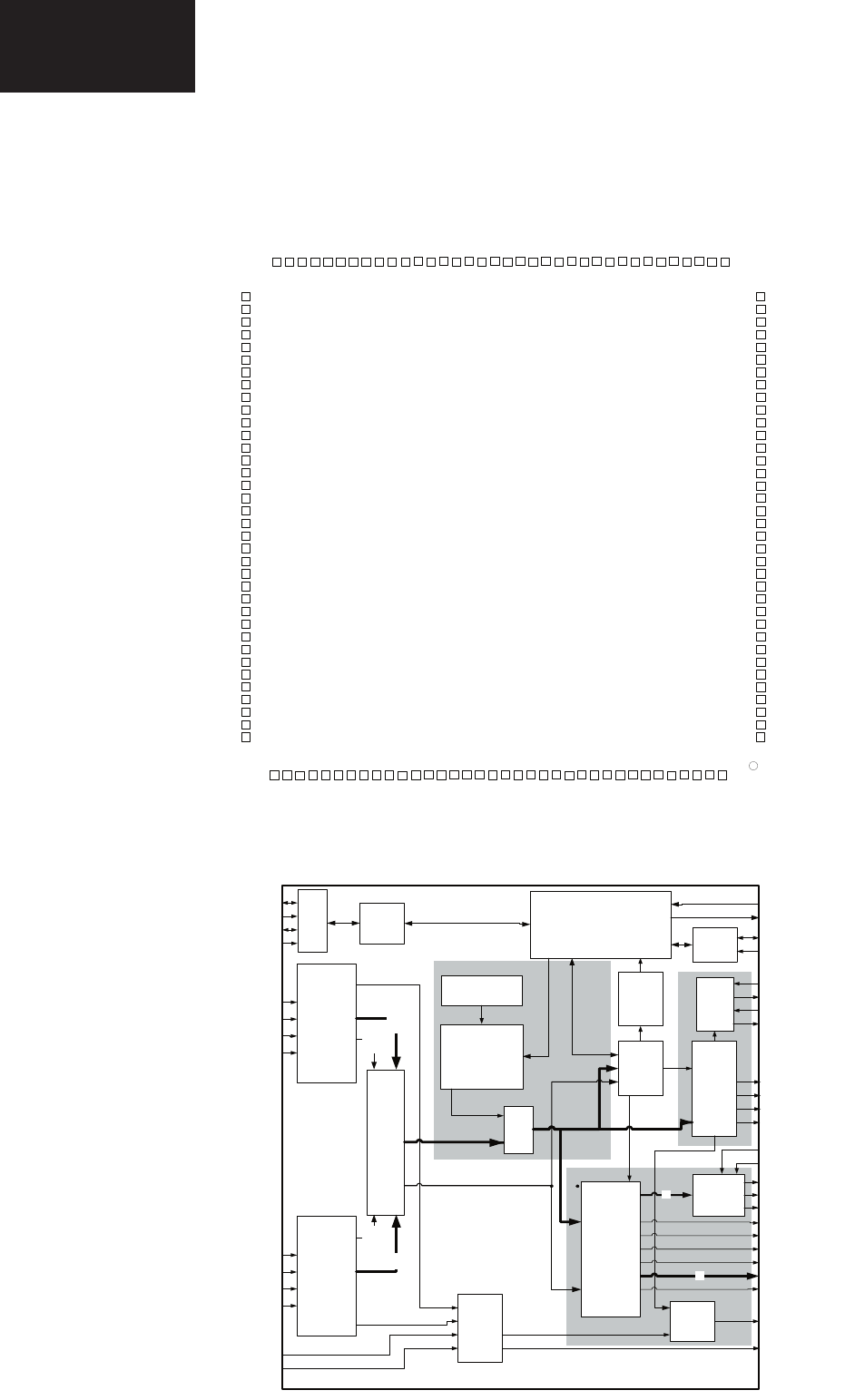
64
LC-26GA5E
LC-32GA5E
LC-32/37GD8E/RU
LC-32/37BT8E/RU
SiI 9021 -
SiI-DS-0117
Pin Diagram
144-Pin
TQFP
SiI 9021
(Top View)
Figure 1. Pin Diagram
-
2. Detailed ICs Information
2.1.2. Block Diagram
SiI 9021 -
SiI-DS-0117
SiliconImage Confidential
For
Sharp
Internal use Only
Functional Description
SiI 9021 - - - - -
-- SiI 9021 - - -
- - - -
- -
-
-
PanelLink
TMDS
-
-
PanelLink
TMDS
-
- -
-
-
-
-
-
-
Figure 3. Functional Block Diagram
SiI 9021 -
The SiI 9021 supports two HDMI input ports. Only one port may be active at any time.
2.1. IC1905 (VHISII9021+-1Q)
2.1.1. Pinning

65
LC-26GA5E
LC-32GA5E
LC-32GD8E/RU
LC-32BT8E/RU
LC-37GD8E/RU
LC-37BT8E/RU
LC-32/37GD8E/RU
LC-32/37BT8E/RU
2.2. IC3002 (RH-IXD624WJN1Q)
2.2.1. Pin Connections and Short Description
ADVANCE INFORMATION
VCT 69xyP
Volume 1: General Description
Micronas November 3, 2004; 6251-644-1-1AI
1-55
3.12.Pin Connections and Short Description
NC = not connected
LV = if not used, leave vacant
OBL = obligatory; connect as described in circuit
diagram
IN = Input Pin
ANA = Analog Pin
OUT = Output Pin
SUPPLY = Supply Pin
VCTP Pin No.
Pin Name
Type
Connection
Short Description
PLQFP
208-1
(If not used)
1 656O6
P4_6
TDOFW
IN/OUT LV Digital 656 Bit 6 Output
Port 4, Bit 6 Input/Output
JTAG Interface Data Output (firmw. Controler)
2 656O5
P4_5
TDIFW
IN/OUT LV Digital 656 Bit 5 Output
Port 4, Bit 5 Input/Output
JTAG Interface Data Input (firmw. Controler)
3 656O4
P4_4
TMSFW
IN/OUT LV Digital 656 Bit 4 Output
Port 4, Bit 4 Input/Output
JTAG Interface Mode Select Input (fw. Contr.)
4 656O3
P4_3
TCLK
IN/OUT LV Digital 656 Bit 3 Output
Port 4, Bit 3 Input/Output
JTAG Interface Clock Input (TV Controler)
5 656O2
P4_2
TDO
IN/OUT LV Digital 656 Bit 2 Output
Port 4, Bit 2 Input/Output
JTAG Interface Data Output (TV Controler)
6 656O1
P4_1
TDI
IN/OUT LV Digital 656 Bit 1 Output
Port 4, Bit 1 Input/Output
JTAG Interface Data Input (TV Controler)
7 656O0
P4_0
TMS
IN/OUT LV Digital 656 Bit 0 Output (LSB)
Port 4, Bit 0 Input/Output
JTAG Interface Mode Select Input (TV Contr.)
8 RESETQ IN/OUT OBL Reset
Input/Output
9 AIN1R IN GND Analog Audio 1 Input, Right
10 AIN1L IN GND Analog Audio 1 Input, Left
11 AIN2R IN GND Analog Audio 2 Input, Right
12 AIN2L IN GND Analog Audio 2 Input, Left
13 AIN3R IN GND Analog Audio 3 Input, Right
14 AIN3L IN GND Analog Audio 3 Input, Left
15 AIN4R IN GND Analog Audio 4 Input, Right
16 AIN4L IN GND Analog Audio 4 Input, Left
17 VREFAU ANA OBL Reference Voltage, Audio
18 VSUP8.0AU SUPPLY OBL Supply Voltage Analog Audio, 8.0 V
19 GNDA SUPPLY OBL Ground Analog Audio, Platform Ground
20 SGND ANA OBL Analog Signal GND

66
LC-26GA5E
LC-32GA5E
LC-32/37GD8E/RU
LC-32/37BT8E/RU
VCT 69xyP ADVANCE INFORMATION
Volume 1: General Description
1-56 November 3, 2004; 6251-644-1-1AI Micronas
21 AOUT2R
AIN5R
IN/OUT LV Analog Audio 2 Output, Right
Analog Audio 5 Input, Right
22 AOUT2L
AIN5L
IN/OUT LV Analog Audio 2 Output, Left
Analog Audio 5 Input, Left
23 AOUT1R OUT LV Analog Audio 1 Output, Right
24 AOUT1L OUT LV Analog Audio 1 Output, Left
25 HEADPHONER OUT LV Analog Headphone Output, Right
26 HEADPHONEL OUT LV Analog Headphone Output, Left
27 SPEAKERR OUT LV Analog Loudspeaker Output, Right
28 SPEAKERL OUT LV Analog Loudspeaker Output, Left
29 SUBWOOFER
TEST
IN/OUT LV Analog SUBWOOFER Output
Test Input
30 VREFSIF ANA OBL Reference Voltage, Audio SIF
31 SIFIN+ IN VREFIF Differential IF Input
32 SIFIN- IN VREFIF Differential IF Input
33 VSUP5.0SIF SUPPLY OBL Supply Voltage Analog SIF, 5.0 V
34 GNDA SUPPLY OBL Ground Analog SIF, Platform Ground
35 GND3.3DIG SUPPLY OBL Ground Digital Audio Core
36 VSUP3.3DIG SUPPLY OBL Supply Voltage Digital Audio Core, 3.3 V
37 SPDIF_OUT OUT LV SPDIF Output
38 I2S_DA_IN IN LV Audio Bus Data Input
39 I2S_CL IN LV Audio Bus Clock Input
40 I2S_WS IN LV Audio Bus Word Strobe Input
41 I2S_DEL_OUT OUT LV Audio Delay Line Bus Data Output
42 I2S_DEL_IN IN LV Audio Delay Line Bus Data Input
43 I2S_DEL_CL OUT LV Audio Delay Line Bus Clock Output
44 I2S_DEL_WS OUT LV Audio Delay Line Bus Word Strobe Output
45 VSUP3.3RAM SUPPLY OBL Supply Voltage Ram, 3.3 V
46 GND3.3RAM SUPPLY OBL Ground Ram
47 DVS IN LV Digital or Analog Video VSYNC HD Input
48 DEN IN LV Digital Video Enable Input
49 DCLK IN LV Digital Video Clock Input
50 DRI7 IN LV Digital Video Red 7 Input
VCTP Pin No. Pin Name Type Connection Short Description
PLQFP
208-1
(If not used)
2.2.1. Pin Connections and Short Description (Continued)

67
LC-26GA5E
LC-32GA5E
LC-32GD8E/RU
LC-32BT8E/RU
LC-37GD8E/RU
LC-37BT8E/RU
LC-32/37GD8E/RU
LC-32/37BT8E/RU
ADVANCE INFORMATION VCT 69xyP
Volume 1: General Description
Micronas November 3, 2004; 6251-644-1-1AI 1-57
51 DRI6 IN LV Digital Video Red 6 Input
52 DRI5 IN LV Digital Video Red 5 Input
53 DRI4 IN LV Digital Video Red 4 Input
54 DRI3 IN LV Digital Video Red 3 Input
55 DRI2 IN LV Digital Video Red 2 Input
56 DRI1 IN LV Digital Video Red 1 Input
57 DRI0 IN LV Digital Video Red 0 Input (LSB)
58 DGI7 IN LV Digital Video Green 7 Input
59 DGI6 IN LV Digital Video Green 6 Input
60 DGI5 IN LV Digital Video Green 5 Input
61 DGI4 IN LV Digital Video Green 4 Input
62 DGI3 IN LV Digital Video Green 3 Input
63 DGI2 IN LV Digital Video Green 2 Input
64 DGI1 IN LV Digital Video Green 1 Input
65 DGI0 IN LV Digital Video Green 0 Input (LSB)
66 DBI7 IN LV Digital Video Blue 7 Input
67 DBI6 IN LV Digital Video Blue 6 Input
68 DBI5 IN LV Digital Video Blue 5 Input
69 DBI4 IN LV Digital Video Blue 4 Input
70 DBI3 IN LV Digital Video Blue 3 Input
71 DBI2 IN LV Digital Video Blue 2 Input
72 DBI1 IN LV Digital Video Blue 1 Input
73 DBI0 IN LV Digital Video Blue 0 Input (LSB)
74 GND3.3DRI SUPPLY OBL Ground Digital Ram Interface
75 VSUP3.3DRI SUPPLY OBL Supply Voltage Digital Ram Interface, 3.3 V
76 GND3.3COM SUPPLY OBL Ground Common
77 VSUP3.3COM SUPPLY OBL Supply Voltage Common, 3.3V
78 XTALIN IN OBL Analog Crystal Input
79 XTALOUT OUT OBL Analog Crystal Output
80 CLKOUT OUT LV Digital 20MHz Clock Output
81 VSO OUT LV Vertical Sync Output, Frontend
VCTP Pin No. Pin Name Type Connection Short Description
PLQFP
208-1
(If not used)
2.2.1. Pin Connections and Short Description (Continued)

68
LC-26GA5E
LC-32GA5E
LC-32/37GD8E/RU
LC-32/37BT8E/RU
2.2.1. Pin Connections and Short Description (Continued)
VCT 69xyP ADVANCE INFORMATION
Volume 1: General Description
1-58 November 3, 2004; 6251-644-1-1AI Micronas
82 HSO OUT LV Horizontal Sync Output, Frontend
83 SCL IN/OUT OBL I2C Bus Clock Input/Output
84 SDA IN/OUT OBL I2C Bus Data Input/Output
85 GND3.3FL SUPPLY OBL Ground Flash
86 VSUP3.3FL SUPPLY OBL Supply Voltage Flash, 3.3 V
87 P2_0 IN/OUT LV Port 2, Bit 0 Input/Output
88 P2_1 IN/OUT LV Port 2, Bit 1 Input/Output
89 P2_2 IN/OUT LV Port 2, Bit 2 Input/Output
90 P2_3 IN/OUT LV Port 2, Bit 3 Input/Output
91 P2_4
TDI
IN/OUT LV Port 2, Bit 4 Input/Output
JTAG Interface Data Input
92 P2_5
TMS
IN/OUT LV Port 2, Bit 5 Input/Output
JTAG Interface Mode Select Input
93 OSDV
DBO2_0
IN/OUT LV Graphic Vertical Sync Input/Output
Channel 2 Digital 0 Blue Output (LSB)
94 OSDH
DBO2_1
IN/OUT LV Graphic Horizontal Sync Input/Output
Channel 2 Digital 1 Blue Output
95 GND3.3IO1 SUPPLY OBL Ground Digital Input/Output Port 1
96 VSUP3.3IO1 SUPPLY OBL Supply Voltage Input/Output Port 1, 3.3 V
97 OSDCLK
DBO2_2
IN/OUT LV Graphic Clock Input/Output
Channel 2 Digital 2 Blue Output
98 OSDFSW
DBO2_3
IN/OUT LV Graphic Fast Switch Input/Output
Channel 2 Digital 3 Blue Output
99 OSDHCS1
P3_7
DBO2_4
IN/OUT LV Graphic Half Contrast 1 Input/Output
Port 3, Bit 7 Input/Output
Channel 2 Digital 4 Blue Output
100 OSDHCS0
P3_6
DBO2_5
IN/OUT LV Graphic Half Contrast 0 Input/Output (LSB)
Port 3, Bit 6 Input/Output
Channel 2 Digital 5 Blue Output
101 OSDB3
P3_5
DBO2_6
IN/OUT LV Graphic Blue 3 Input/Output (MSB)
Port 3, Bit 5 Input/Output
Channel 2 Digital 6 Blue Output
102 OSDB2
P3_4
DBO2_7
IN/OUT LV Graphic Blue 2 Input/Output
Port 3, Bit 4 Input/Output
Channel 2 Digital 7 Blue Output (MSB)
103 OSDB1
DGO2_0
IN/OUT LV Graphic Blue 1 Input/Output
Channel 2 Digital 0 Green Output (LSB)
104 OSDB0
DGO2_1
IN/OUT LV Graphic Blue 0 Input/Output
Channel 2 Digital 1 Green Output
VCTP Pin No. Pin Name Type Connection Short Description
PLQFP
208-1
(If not used)

69
LC-26GA5E
LC-32GA5E
LC-32GD8E/RU
LC-32BT8E/RU
LC-37GD8E/RU
LC-37BT8E/RU
LC-32/37GD8E/RU
LC-32/37BT8E/RU
2.2.1. Pin Connections and Short Description (Continued)
ADVANCE INFORMATION VCT 69xyP
Volume 1: General Description
Micronas November 3, 2004; 6251-644-1-1AI 1-59
VCTP Pin No. Pin Name Type Connection Short Description
PLQFP
208-1
(If not used)
105 OSDG3
P3_3
DGO2_2
IN/OUT LV Graphic Green 3 Input/Output (MSB)
Port 3, Bit 3 Input/Output
Channel 2 Digital 2 Green Output
106 OSDG2
P3_2
DGO2_3
IN/OUT LV Graphic Green 2 Input/Output
Port 3, Bit 2 Input/Output
Channel 2 Digital 3 Green Output
107 OSDG1
DGO2_4
IN/OUT LV Graphic Green 1 Input/Output
Channel 2 Digital 4 Green Output
108 OSDG0
DGO2_5
IN/OUT LV Graphic Green 0 Input/Output
Channel 2 Digital 5 Green Output
109 OSDR3
P3_1
DGO2_6
IN/OUT LV Graphic Red 3 Input/Output (MSB)
Port 3, Bit 1 Input/Output
Channel 2 Digital 6 Green Output
110 OSDR2
P3_0
DGO2_7
IN/OUT LV Graphic Red 2 Input/Output
Port 3, Bit 0 Input/Output
Channel 2 Digital 7 Green Output (MSB)
111 OSDR1
DRO2_0
IN/OUT LV Graphic Red 1 Input/Output
Channel 2 Digital 0 Red Output (LSB)
112 OSDR0
DRO2_1
IN/OUT LV Graphic Red 0 Input/Output (LSB)
Channel 2 Digital 1 Red Output
113 GND3.3IO1 SUPPLY OBL Ground Digital Input/Output Port 1
114 VSUP3.3IO1 SUPPLY OBL Supply Voltage Input/Output Port 1, 3.3 V
115 PCS5
P2_6
IN/OUT LV Flat Panel Control Select 5 PWM Output
Port 2, Bit 6 Input/Output
116 PCS4
P2_7
IN/OUT LV Flat Panel Control Select 4 REV Output
Port 2, Bit 7 Input/Output
117 PCS3
P4_0
IN/OUT LV Flat Panel Control Select 3 DE2 Output
Port 4, Bit 0 Input/Output
118 PCS2
P4_1
IN/OUT LV Flat Panel Control Select 2 DE1 Output
Port 4, Bit 1 Input/Output
119 PCS1
P4_2
IN/OUT LV Flat Panel Control Select 1 V Output
Port 4, Bit 2 Input/Output
120 PCS0
P4_3
IN/OUT LV Flat Panel Control Select 0 H Output
Port 4, Bit 3 Input/Output
121 PCLK2 OUT LV Flat Panel Control Clock 2 Output
122 PCLK1 OUT LV Flat Panel Control Clock 1 Output
123 GND1.8DIG SUPPLY OBL Ground Digital Core
124 VSUP1.8DIG SUPPLY OBL Supply Voltage Digital Core, 1.8 V
125 DBO1_0
DRO2_2
LVDSA_4P
OUT LV Channel 1 Digital 0 Blue Output1) (LSB)
Channel 2 Digital 2 Red Output1)
LVDS Channel 1 bit 4 Positive Output2)

70
LC-26GA5E
LC-32GA5E
LC-32/37GD8E/RU
LC-32/37BT8E/RU
2.2.1. Pin Connections and Short Description (Continued)
VCT 69xyP ADVANCE INFORMATION
Volume 1: General Description
1-60 November 3, 2004; 6251-644-1-1AI Micronas
VCTP Pin No. Pin Name Type Connection Short Description
PLQFP
208-1
(If not used)
126 DBO1_1
DRO2_3
LVDSA_4N
OUT LV Channel 1 Digital 1 Blue Output1)
Channel 2 Digital 3 Red Output1)
LVDS Channel 1 bit 4 Negative Output2)
127 DBO1_2
DRO2_4
VSUP3.3LVDS
OUT
SUPPLY
LV
OBL
Channel 1 Digital 2 Blue Output1)
Channel 2 Digital 4 Red Output1)
Supply Digital Voltage LVDS2) Port, 3.3 V
128 DBO1_3
DRO2_5
LVDSA_3P
OUT LV Channel 1 Digital 3 Blue Output1)
Channel 2 Digital 5 Red Output1)
LVDS Channel 1 bit 3 Positive Output2)
129 DBO1_4
DRO2_6
LVDSA_3N
OUT LV Channel 1 Digital 4 Blue Output1)
Channel 2 Digital 6 Red Output1)
LVDS Channel 1 bit 3 Negative Output2)
130 DBO1_5
DRO2_7
GND3.3LVDS
OUT
SUPPLY
LV
OBL
Channel 1 Digital 5 Blue Output1)
Channel 2 Digital 7 Red Output1) (MSB)
Ground Digital LVDS2), 3.3 V
131 DBO1_6
DBO1_0
LVDSA_CLKP
OUT LV Channel 1 Digital 6 Blue Output1)
Channel 1 Digital 0 Blue Output1) (LSB)
LVDS Channel 1 Clock Positive Output2)
132 DBO1_7
DBO1_1
LVDSA_CLKN
OUT LV Channel 1 Digital 7 Blue Output1)
Channel 1 Digital 1 Blue Output1)
LVDS Channel 1 Clock Negative Output2)
133 VSUP3.3IO2
VSUP3.3LVDS
SUPPLY OBL Supply Digital Output1) Port 2
Supply Digital Voltage LVDS2), 3.3 V
134 GND3.3IO2
LVDSA_2P
SUPPLY
OUT
OBL
LV
Ground Voltage Output1) Port 2, 3.3 V
LVDS Channel 1 bit 2 Positive Output2)
135 DBO1_8
DBO1_2
LVDSA_2N
OUT LV Channel 1 Digital 8 Blue Output1)
Channel 1 Digital 2 Blue Output1)
LVDS Channel 1 bit 2 Negative Output2)
136 DBO1_9
DBO1_3
GND3.3LVDS
OUT
SUPPLY
LV
OBL
Channel 1 Digital 9 Blue Output1) (MSB)
Channel 1 Digital 3 Blue Output1)
Ground Digital LVDS2), 3.3 V
137 DGO1_0
DBO1_4
LVDSA_1P
OUT LV Channel 1 Digital 0 Green Output1) (LSB)
Channel 1 Digital 4 Blue Output1)
LVDS Channel 1 bit 1 Positive Output2)
138 DGO1_1
DBO1_5
LVDSA_1N
OUT LV Channel 1 Digital 1 Green Output1)
Channel 1 Digital 5 Blue Output1)
LVDS Channel 1 bit 1 Negative Output2)
139 DGO1_2
DBO1_6
VSUP3.3LVDS
OUT
SUPPLY
LV
OBL
Channel 1 Digital 2 Green Output1)
Channel 1 Digital 6 Blue Output1)
Supply Digital Voltage LVDS2), 3.3 V
140 DGO1_3
DBO1_7
LVDSA_0P
OUT LV Channel 1 Digital 3 Green Output1)
Channel 1 Digital 7 Blue Output1) (MSB)
LVDS Channel 1 bit 0 Positive Output2)

71
LC-26GA5E
LC-32GA5E
LC-32GD8E/RU
LC-32BT8E/RU
LC-37GD8E/RU
LC-37BT8E/RU
LC-32/37GD8E/RU
LC-32/37BT8E/RU
2.2.1. Pin Connections and Short Description (Continued)
ADVANCE INFORMATION VCT 69xyP
Volume 1: General Description
Micronas November 3, 2004; 6251-644-1-1AI 1-61
VCTP Pin No. Pin Name Type Connection Short Description
PLQFP
208-1
(If not used)
141 DGO1_4
DGO1_0
LVDSA_0N
OUT LV Channel 1 Digital 4 Green Output1)
Channel 1 Digital 0 Green Output1) (LSB)
LVDS Channel 1 bit 0 Negative Output2)
142 DGO1_5
DGO1_1
VSUP1.8LVDS
OUT
SUPPLY
LV
OBL
Channel 1 Digital 5 Green Output1)
Channel 1 Digital 1 Green Output1)
Supply Analog Voltage LVDS2), 1.8 V
143 DGO1_6
DGO1_2
REXT
OUT
ANA
LV
OBL
Channel 1 Digital 6 Green Output1)
Channel 1 Digital 2 Green Output1)
LVDS External Resistor2)
144 DGO1_7
DGO1_3
GND1.8LVDS
OUT
SUPPLY
LV
OBL
Channel 1 Digital 7 Green Output1)
Channel 1 Digital 3 Green Output1)
Ground Analog LVDS2), 1.8 V
145 DGO1_8
DGO1_4
LVDSB_3P
OUT LV Channel 1 Digital 8 Green Output1)
Channel 1 Digital 4 Green Output1)
Dual-LVDS Channel 2 bit 3 Positive Output2)
146 DGO1_9
DGO1_5
LVDSB_3N
OUT LV Channel 1 Digital 9 Green Output1) (MSB)
Channel 1 Digital 5 Green Output1)
Dual-LVDS Channel 2 bit 3 Negative Output2)
147 DRO1_0
DGO1_6
GND3.3LVDS
OUT
SUPPLY
LV
OBL
Channel 1 Digital 0 Red Output1) (LSB)
Channel 1 Digital 6 Green Output1)
Ground Digital LVDS2), 3.3 V
148 DRO1_1
DGO1_7
LVDSBCLKP
OUT LV Channel 1 Digital 1 Red Output1)
Channel 1 Digital 7 Green Output1) (MSB)
Dual-LVDS Channel 2 Clock Positive Output2)
149 GND3.3IO2
LVDSBCLKN
SUPPLY
OUT
OBL
LV
Ground Digital Output1) Port 2
Dual-LVDS Channel 2 Clock Negative Output2)
150 VSUP3.3IO2
VSUP3.3LVDS
SUPPLY OBL Supply Voltage Output1) Port 2, 3.3 V
Supply Digital Voltage LVDS2), 3.3 V
151 DRO1_2
DRO1_0
LVDSB_2P
OUT LV Channel 1 Digital 2 Red Output1)
Channel 1 Digital 0 Red Output1) (LSB)
Dual-LVDS Channel 2 bit 2 Positive Output2)
152 DRO1_3
DRO1_1
LVDSB_2N
OUT LV Channel 1 Digital 3 Red Output1)
Channel 1 Digital 1 Red Output1)
Dual-LVDS Channel 2 bit 2 Negative Output2)
153 DRO1_4
DRO1_2
GND3.3LVDS
OUT
SUPPLY
LV
OBL
Channel 1 Digital 4 Red Output1)
Channel 1 Digital 2 Red Output1)
Ground Digital LVDS2), 3.3 V
154 DRO1_5
DRO1_3
LVDSB_1P
OUT LV Channel 1 Digital 5 Red Output1)
Channel 1 Digital 3 Red Output1)
Dual-LVDS Channel 2 bit 1 Positive Output2)
155 DRO1_6
DRO1_4
LVDSB_1N
OUT LV Channel 1 Digital 6 Red Output1)
Channel 1 Digital 4 Red Output1)
Dual-LVDS Channel 2 bit 1 Negative Output2)

72
LC-26GA5E
LC-32GA5E
LC-32/37GD8E/RU
LC-32/37BT8E/RU
2.2.1. Pin Connections and Short Description (Continued)
VCT 69xyP ADVANCE INFORMATION
Volume 1: General Description
1-62 November 3, 2004; 6251-644-1-1AI Micronas
VCTP Pin No. Pin Name Type Connection Short Description
PLQFP
208-1
(If not used)
156 DRO1_7
DRO1_5
VSUP3.3LVDS
OUT
SUPPLY
LV
OBL
Channel 1 Digital 7 Red Output1)
Channel 1 Digital 5 Red Output1)
Supply Digital Voltage LVDS2), 3.3 V
157 DRO1_8
DRO1_6
LVDSB_0P
OUT LV Channel 1 Digital 8 Red Output1)
Channel 1 Digital 6 Red Output1)
Dual-LVDS Channel 2 bit 0 Positive Output2)
158 DRO1_9
DRO1_7
LVDSB_0N
OUT LV Channel 1 Digital 9 Red Output1) (MSB)
Channel 1 Digital 7 Red Output1) (MSB)
Dual-LVDS Channel 2 bit 0 Negative Output2)
159 P1_7
TDO
IN/OUT OBL Port 1, Bit 7 Input/Output
JTAG Interface Data Output
160 P1_6
TCLK
IN/OUT OBL Port 1, Bit 6 Input/Output
JTAG Interface Clock Input
161 P1_5 IN/OUT LV Port 1, Bit 5 Input/Output
162 P1_4 IN/OUT LV Port 1, Bit 4 Input/Output
163 GND3.3DAC SUPPLY OBL Ground DAC
164 VSUP3.3DAC SUPPLY OBL Supply Voltage DAC, 3.3V
165 P1_3
ROUT
IN/OUT LV Port 1, Bit 3 Input/Output
Analog Red Output
166 P1_2
GOUT
IN/OUT LV Port 1, Bit 2 Input/Output
Analog Green Output
167 P1_1
BOUT
IN/OUT LV Port 1, Bit 1 Input/Output
Analog Blue Output
168 P1_0
SVMOUT
IN/OUT LV Port 1, Bit 0 Input/Output
Scan Velocity Modulation Output
169 VSUP1.8FE SUPPLY OBL Supply Voltage Analog Video Frontend, 1.8 V
170 VSUP3.3FE SUPPLY OBL Supply Voltage Analog Video Frontend, 3.3 V
171 VIN22
DHS
IN GND Analog Video 22 H-Sync Input
Digital Video H-Sync Input
172 VIN21 IN GND Analog Video 21 B HD Input
173 VIN20 IN GND Analog Video 20 G HD Input
174 VIN19 IN GND Analog Video 19 R HD Input
175 VIN18 IN GND Analog Video 18 Fast Blank 2 Input
176 VIN17 IN GND Analog Video 17 B HD Input
177 VIN16 IN GND Analog Video 16 G HD Input
178 VIN15 IN GND Analog Video 15 R HD Input
179 VIN13 IN GND Analog Video 13 B HD Input

73
LC-26GA5E
LC-32GA5E
LC-32GD8E/RU
LC-32BT8E/RU
LC-37GD8E/RU
LC-37BT8E/RU
LC-32/37GD8E/RU
LC-32/37BT8E/RU
2.2.1. Pin Connections and Short Description (Continued)
ADVANCE INFORMATION VCT 69xyP
Volume 1: General Description
Micronas November 3, 2004; 6251-644-1-1AI 1-63
VCTP Pin No. Pin Name Type Connection Short Description
PLQFP
208-1
(If not used)
180 VIN12 IN GND Analog Video 12 G HD Input
181 VIN11 IN GND Analog Video 11 R HD Input
182 VIN9 IN GND Analog Video 9 Y or B SD Input
183 VIN8 IN GND Analog Video 8 C or Fast Blank 1 Input
184 VIN7 IN GND Analog Video 7 Y or G SD Input
185 VSUP1.8FE SUPPLY OBL Supply Voltage Analog Video Frontend, 1.8 V
186 GNDA SUPPLY OBL Analog Video Frontend, Platform Ground
187 VIN6 IN GND Analog Video 6 C or R SD Input
188 VIN5 IN GND Analog Video 5 Y/CVBS Input
189 VIN3 IN GND Analog Video 3 CVBS Input
190 VIN2 IN GND Analog Video 2 CVBS Input
191 VIN1 IN GND Analog Video 1 CVBS Input
192 VSUP3.3VO SUPPLY OBL Supply Voltage Analog Video Output, 3.3 V
193 VOUT3 OUT LV Analog cvbs Video 3 Output
194 VOUT2 OUT OBL Analog cvbs Video 2 Output
195 VOUT1 OUT OBL Analog cvbs Video 1 Output
196 GND3.3IO3 SUPPLY OBL Ground Digital Input/Output Port 1
197 VSUP3.3IO3 SUPPLY OBL Supply Voltage Input/Output Port 1, 3.3 V
198 656I0
P3_0
IN/OUT LV Digital 656 Bit 0 Input (LSB)
Port 3, Bit 0 Input/Output
199 656I1
P3_1
IN/OUT LV Digital 656 Bit 1 Input
Port 3, Bit 1 Input/Output
200 656I2
P3_2
IN/OUT LV Digital 656 Bit 2 Input
Port 3, Bit 2 Input/Output
201 656I3
P3_3
IN/OUT LV Digital 656 Bit 3 Input
Port 3, Bit 3 Input/Output
202 656I4
P3_4
IN/OUT LV Digital 656 Bit 4 Input
Port 3, Bit 4 Input/Output
203 656I5
P3_5
IN/OUT LV Digital 656 Bit 5 Input
Port 3, Bit 5 Input/Output
204 656I6
P3_6
IN/OUT LV Digital 656 Bit 6 Input
Port 3, Bit 6 Input/Output
205 656I7
P3_7
IN/OUT LV Digital 656 Bit 7 Input
Port 3, Bit 7 Input/Output
206 656CLKI IN/OUT GND Digital 656 Clock Input
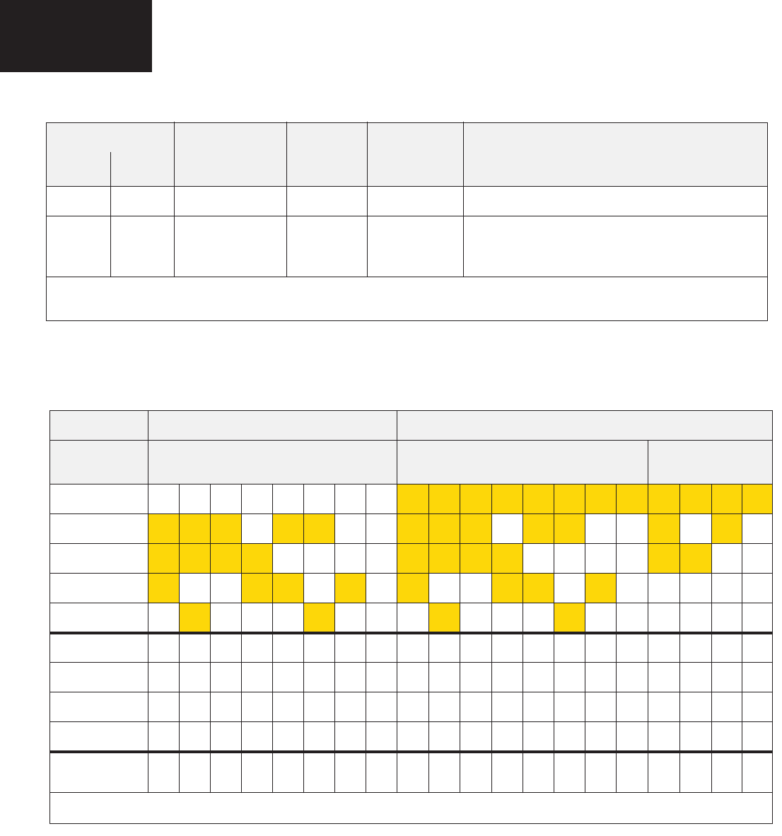
74
LC-26GA5E
LC-32GA5E
LC-32/37GD8E/RU
LC-32/37BT8E/RU
VCT 69xyP ADVANCE INFORMATION
Volume 1: General Description
1-64 November 3, 2004; 6251-644-1-1AI Micronas
207 656CLKO OUT LV Digital 656 Clock Output
208 656O7
P4_7
TCLKFW
IN/OUT LV Digital 656 Bit 7 Output
Port 4, Bit 7 Input/Output
JTAG Interface Clock Input (firmw. Controler)
1) only in RGB output version
2) only in LVDS output version
VCTP Pin No. Pin Name Type Connection Short Description
PLQFP
208-1
(If not used)
2.2.1. Pin Connections and Short Description (Continued)
VCT 69xyP ADVANCE INFORMATION
Volume 1: General Description
1-68 November 3, 2004; 6251-644-1-1AI Micronas
Table 3–10: Maximum Number of Ports
Display CRT FPD
Application
Analog RGB + SVMOUT + H + V TTL (Single RGB),
LVDS (Dual or Single)
TTL (Dual RGB)
Panel control X X X X X X X X X X X X
656IN X X X X X X X X X X X X
656OUT X X X X X X X X X X
OSD444 X X X X X X X X
OSD222 X X X X
Port 1 4 4 4 4 4 4 4 4 8 8 8 8 8 8 8 8 8 8 8 8
Port 2 8 8 8 8 8 8 8 8 6 6 6 6 6 6 6 6 6 6 6 6
Port 3 6 8 8 6 8 8 6 6 8 6 8 8 8 8
Port 4 2 2 2 2 8 8 8 8 8 8 8 8 8 8
Max Number
of Ports 14 20 22 22 20 26 28 28 14 20 20 22 22 28 30 30 14 22 22 30
Note: 24bit RGB input is always available
Maximum Number of Ports

75
LC-26GA5E
LC-32GA5E
LC-32GD8E/RU
LC-32BT8E/RU
LC-37GD8E/RU
LC-37BT8E/RU
LC-32/37GD8E/RU
LC-32/37BT8E/RU
ADVANCE INFORMATION VCT 69xyP
Volume 1: General Description
Micronas November 3, 2004; 6251-644-1-1AI 1-65
3.13.Pin Descriptions
3.13.1.Supply Pins
VSUP1.8DIG − Supply Voltage 1.8 V
This pin is main and standby supply for the digital core
logic of controller, video and display processing.
VSUP1.8FE − Supply Voltage 1.8 V
This pin is main and standby supply for the analog
video frontend.
VSUP3.3FE − Supply Voltage 3.3 V
This pin is main and standby supply for the analog
video frontend.
VSUP3.3VO − Supply Voltage 3.3 V
This pin is main and standby supply for the analog
video outputs.
VSUP1.8LVDS − Supply Voltage 1.8 V
This pin is main and standby supply for the analog
LVDS core.
VSUP3.3LVDS − Supply Voltage 3.3 V
This pin is main and standby supply for the Digital
LVDS port.
VSUP3.3FL − Supply Voltage 3.3 V
This pin is main and standby supply for the Flash
device.
VSUP3.3DRI − Supply Voltage 3.3 V
This pin is main supply for the digital RAM interface.
VSUP3.3RAM − Supply Voltage 3.3 V
This pin is main supply for the RAM device
VSUP3.3IO 1-3 − Supply Voltage 3.3 V
This 3 pins are main and standby supply for the digital
I/O-ports.
VSUP3.3COM − Supply Voltage 3.3 V
This pin is main and standby supply for the digital Input
ports and common digital logic.
VSUP3.3DIG − Supply Voltage 3.3 V
This pin is main supply for the digital core logic of IF
and audio processing and digital video backend.
VSUP8.0AU − Supply Voltage 8.0 V
This pin is main supply for the analog audio process-
ing.
VSUP5.0SIF − Supply Voltage 5.0 V
This pin is main supply for the SIF processing.
VSUP3.3DAC − Supply Voltage 3.3 V
This pin is main and standby supply for the Analog
DAC.
GND* − Ground
This pin are main ground for all digital analog and port
supplies.
Application Note:
All GND pins must be connected to a low-resistive
ground plane underneath the IC. All supply pins must
be connected separately with short and low-resistive
lines to the power supply. Decoupling capacitors from
VSUPxx to GND have to be placed as closely as pos-
sible to these pins. It is recommended to use more
than one capacitor. By choosing different values, the
frequency range of active decoupling can be extended.
3.13.2.Audio Pins
VREFAU – Reference Voltage for Analog Audio
This pin serves as the internal ground connection for
the analog audio circuitry. It must be connected to the
GND pin with a 3.3 µF and a 100 nF capacitor in paral-
lel.
SGND − Analog Reference Input
This is the reference ground Analog Audio part.
AIN1 R/L – Audio 1 Inputs
The analog input signal for audio 1 is fed to this pin.
Analog input connection must be AC coupled.
AIN2 R/L – Audio 2 Inputs
The analog input signal for audio 2 is fed to this pin.
Analog input connection must be AC coupled.
AIN3 R/L – Audio 3 Inputs
The analog input signal for audio 3 is fed to this pin.
Analog input connection must be AC coupled.
AIN4 R/L – Audio 4 Inputs
The analog input signal for audio 4 is fed to this pin.
Analog input connection must be AC coupled.
AIN5 R/L – Audio 5 Inputs
The analog input signal for audio 5 is fed to this pin.
Analog input connection must be AC coupled.
AOUT1 R/L – Audio 1 Outputs
Output of the analog audio 1 signal. Connections to
these pins are intended to be AC coupled.
AOUT2 R/L – Audio 2 Outputs
Output of the analog audio 2 signal. Connections to
these pins are intended to be AC coupled.
SPEAKER R/L – Loudspeaker Outputs
Output of the loudspeaker signal.
HEADPHONES R/L – Headphones Outputs
Output of the headphones signal.
2.2.2. Pin Descriptions
2.2.2.1. Supply Pins
2.2.2.2 Audio Pins

76
LC-26GA5E
LC-32GA5E
LC-32/37GD8E/RU
LC-32/37BT8E/RU
VCT 69xyP ADVANCE INFORMATION
Volume 1: General Description
1-66 November 3, 2004; 6251-644-1-1AI Micronas
SUBWOOFER – Subwoofer Outputs
Output of the subwoofer signal
I2S_DEL_WS - Delay Line Bus Word Strobe
This is the word strobe signal of the delay line bus.
I2S_DEL_CL - Delay Line Bus Clock
This is the Clock signal of the delay line bus.
I2S_DEL_IN - Delay Line Bus Data Input
This is the data input signal of the delay line bus.
I2S_DEL_OUT - Delay Line Bus Data Output
This is the data output signal of the delay line bus.
I2S_WS - I2S Word Strobe
This is the word strobe signal of I2S bus.
I2S_DA_IN - I2S Data Input
This is the data input signal of I2S bus.
I2S_CL - I2S Clock
This is the Clock signal of I2S bus.
SPDIF_OUT -
This is an SPDIF output signal to connect to an A/V
receiver.
SIF −/+ − Sound IF Input
This is the SIF input to connect to an external DRX.
VREFSIF – Reference Voltage for SIF
This pin serves as the internal ground connection for
the analog audio circuitry.
3.13.3.Video Pins
656I 0-7 − Digital 656 Data Input
These are the 8 bits digital 656 video inputs.
656CLKI − Digital 656 Input clock
This is the clock for the digital 656 video inputs.
656O 0-7 − Digital 656 Data Output
These are the 8 bits digital 656 video outputs.
656CLKO− Digital 656 output clock
This is the clock for the digital 656 video outputs.
OSDR 0-3 − Graphic Data input/output
These are the 2 or 4 bit graphic input/output
OSDG 0-3 − Graphic Data input/output
These are the 2 or 4 bit graphic input/output
OSDB 0-3 − Graphic Data input/output
These are the 2 or 4 bit graphic input/output
OSDHCS 0-1 − Graphic Half Contrast Input/Output
This is the half contrast for the graphic input/output
OSDFSW − Graphic Fast Switch Input/Output
This is the fast switch for the graphic input/output
OSDCLK − Graphic clock Input/Output
This is the clock for the graphic video input/output
OSDV − Graphic vertical sync Input/Output
This is the vertical sync for the graphic input/output
OSDH − Graphic horizontal sync Input/Output
This is the horizontal sync signal for the graphic I/O
DRO1_ 0-9 - Digital Red Outputs
This are 10 bits digital signals for red outputs,
for dual RGB use bits (0-7).
DGO1_ 0-9 - Digital Green Output
This are 10 bits digital signals for green outputs,
for dual RGB use bits (0-7).
DBO1_ 0-9 - Digital Blue Outputs
This are 10 bits digital signals for blue outputs,
for dual RGB use bits (0-7).
DRO2_ 0-7 - Digital dual Red Outputs
This are 8 bits digital signals for red outputs.
DGO2_ 0-7 - Digital dual Green Output
This are 8 bits digital signals for green outputs.
DBO2_ 0-7 - Digital dual Blue Outputs
This are 8 bits digital signals for blue outputs.
PCS 0-5 - LCD Panel Control Select Outputs
This are 6 control select signals for LCD outputs.
For CRT application use PCS_0 as H sync and PCS_1
as V sync Back End.
PCLK1,2 - LCD Panel Clock Outputs
This are the clock signals for LCD/RGB outputs.
LVDSA_* - LCD Panel LVDS Outputs
This are 12 signals and clocks for LVDS single or dual
output.
LVDSB_* - LCD Panel LVDS Outputs
This are 10 signals and clocks for LVDS dual output.
REXT - LVDS External Resistor
This pin is connected to the external LVDS resistor.
(6.2 kOhm to gnd)
DRI 0-7 - Digital video inputs for Red
This are 8 bits digital inputs for red signal
DGI 0-7- Digital video inputs for Green
This are 8 bits digital inputs for green signal
DBI 0-7- Digital video inputs for Blue
This are 8 bits digital inputs for blue signal.
2.2.2.3 Video Pins
2.2.2. Pin Descriptions (Continued)

77
LC-26GA5E
LC-32GA5E
LC-32GD8E/RU
LC-32BT8E/RU
LC-37GD8E/RU
LC-37BT8E/RU
LC-32/37GD8E/RU
LC-32/37BT8E/RU
ADVANCE INFORMATION VCT 69xyP
Volume 1: General Description
Micronas November 3, 2004; 6251-644-1-1AI 1-67
DEN - Digital video inputs Enable
This is the enable signal for the Digital Video Inputs.
DHS - Digital video inputs Horizontal Sync
This is the H Sync signal for the Digital RGB input bus
or for the VGA Video Inputs.
DVS - Digital video inputs Vertical Sync
This is the V Sync signal for the Digital RGB input bus
or for the VGA Video Inputs.
DCLK - Digital video inputs Clock
This is the Clock signal for the Digital Video Inputs.
CLKOUT − Digital Output clock
This is a 20MHz clock for the external video ICs.
VIN 1–22 − Analog Video Input
These are the 19 analog video inputs.
(Vin 4,10 and 14 are missing)
A CVBS, S-VHS, YCrCb or RGB signal is converted
using the luma, chroma and component AD converter.
Vin 8,18 are fast blank inputs. Vin22 is an Hsync input.
The input signals must be AC-coupled.
VOUT 1-3 − Analog Video Output
The analog video inputs that are selected by the video
matrix are output at these pins.
ROUT, GOUT, BOUT − Analog RGB Output
These pins are the analog Red/Green/Blue outputs of
the back-end.
SVMOUT − Scan Velocity Modulation Output
This output delivers the analog SVM signal. The D/A
converter is a current sink like the RGB D/A convert-
ers. At zero signal the output current is 50% of the
maximum output current.
3.13.4.Controller Pins
XTALIN Crystal Input and XTALOUT Crystal Output
These pins are connected to an 20.25 MHz crystal
oscillator. An external clock can be fed into XTALIN.
RESETQ − Reset Input/Output
A low level on this pin resets the VCT 69xyP. The
internal CPU can pull down this pin to reset external
devices connected to this pin.
TEST − Test Input
This pin enables factory test modes. For normal opera-
tion, it must be connected to ground.
SCL − I2C Bus Clock
This pin delivers the I2C bus clock line. The signal can
be pulled down by external slave ICs to slow down
data transfer.
SDA − I2C Bus Data
This pin delivers the I2C bus data line.
P1_0−P1_3 − I/O Port
These pins provide CPU controlled I/O ports.
P1_4−P1_7 − I/O Port
These pins provide CPU controlled I/O ports.
Also used as CADC1−4− Controller A/D inputs 1 to 4.
This 4 pins are analog/digital converters from the con-
troller
P2_0−P2_7 − I/O Port
These pins provide CPU controlled I/O ports.
P3_0−P3_7 − I/O Port
These pins provide CPU controlled I/O ports.
P4_0−P4_7 − I/O Port
These pins provide CPU controlled I/O ports.
TDO-TCLK-TDI-TMS -JTAG Interface Pins for TV con-
troler.
TCLK at pin 4 (656O3) has during reset an internal pull
up: (TCLK=0) at end of reset enables the JTAG mode
at 656 LSB’s, this can also be done via I2C.
This JTAG is also available at Port(1 and 2) but only
via I2C.
TDOFW-TCLKFW-TDIFW-TMSFW -JTAG Interface
Pins for firmware controler.
TCLKFW at pin 208 (656O7) has during reset an inter-
nal pull up: (TCLKFW=0) at end of reset enables the
JTAG mode, this can also be done via I2C.
2.2.2.4 Controller Pins
78
LC-26GA5E
LC-32GA5E
LC-32/37GD8E/RU
LC-32/37BT8E/RU
VCT 69xyP ADVANCE INFORMATION
Volume 1: General Description
1-70 November 3, 2004; 6251-644-1-1AI Micronas
VCT 69xyP
LVDS output
1
2
3
4
5
6
7
8
9
10
11
12
13
14
15
16
17
18
19
20
21
22
23
24
25
26
27
28
29
30
31
32
33
34
35
36
37
38
39
40
41
42
43
44
45
46
47
48
49
50
51
52
154
153
152
151
150
149
148
147
146
145
145
144
143
142
141
140
139
138
137
136
135
134
133
132
131
130
129
128
127
126
125
124
123
122
121
120
119
118
117
116
115
114
113
112
111
110
109
108
107
106
105
156
104
103
102
101
100
99
98
97
96
95
94
93
92
91
90
89
88
87
86
85
84
83
82
81
80
79
78
77
76
75
74
73
72
71
70
69
68
67
66
65
64
63
62
61
60
59
58
57
56
55
54
53
656O6
656O5
656O4
656O3
656O2
656O1
656O0
RESETQ
AIN1R
AIN1L
AIN2R
AIN2L
AIN3R
AIN3L
AIN4R
AIN4L
VREFAU
VSUP8.OAU
AOUT2R
AOUT2L
AOUT1R
SGND
GNDA
AOUT1L
HEADPHONER
HEADPHONEL
SPEAKERR
SUBWOOFER
VREFSIF
SIFIN+
SIFIN-
SPEAKERL
VSUP5.0SIF
GNDA
GND3.3DIG
VSUP3.3DIG
SPDIF_OUT
I2S_DA_IN
I2S_DEL_OUT
I2S_DEL_IN
I2S_DEL_CL
I2S_WS
I2S_CL
I2S_DEL_WS
VSUP3.3RAM
GND3.3RAM
DVS
DCLK
DRI7
DRI6
DRI5
DEN
VSUP1.8DIG
GND1.8DIG
VSUP3.3LVDS
LVDSA_4P
PCLK1
PCLK2
PCS0
PCS1
PCS4
PCS5
VSUP3.3IO1
PCS3
PCS2
GND3.3IO1
OSDR0
OSDR1
OSDR2
OSDG0
OSDG1
OSDG2
OSDG3
OSDR3
LVDSA_4N
GND3.3LVDS
LVDSA_3P
LVDSA_3N
VSUP3.3LVDS
LVDSA_CLKP
LVDSA_CLKN
GND3.3LVDS
LVDSA_2P
LVDSA_2N
VSUP3.3LVDS
LVDSA_1P
LVDSA_1N
VSUP1.8LVDS
LVDSA_0P
LVDSA_0N
GND1.8LVDS
REXT
LVDSB_3P
GND3.3LVDS
LVDSB_3N
VSUP3.3LVDS
LVDSB_CLKP
LVDSB_CLKN
GND3.3LVDS
LVDSB_2P
LVDSB_2N
VSUP3.3LVDS
LVDSB_1P
LVDSB_1N
VIN16
VIN15
VIN13
VIN12
VIN11
VIN9
VIN8
VIN6
VIN5
VIN3
VIN2
VIN7
VIN1
VIN22
VIN21
VIN20
VIN19
VIN17
VIN18
GNDA
VSUP1.8FE
VSUP3.3VO
VOUT3
VOUT2
VSUP3.3IO3
656I0
656I1
GND3.3IO3
VOUT1
656I2
656I3
656I4
656I5
656I7
656CLKI
656CLKO
656O7
656I6
P1_7
P1_6
P1_5
P1_4
GND3.3DAC
VSUP3.3DAC
P1_3
P1_2
P1_1
P1_0
VSUP1.8FE
VSUP3.3FE
LVDSB_0P
LVDSB_0N
CLKOUT
SDA
SCL
XTALOUT
XTALIN
HSO
VSO
GND3.3COM
VSUP3.3DRI
GND3.3DRI
DBI0
VSUP3.3COM
DBI1
OSDB0
OSDB1
OSDB2
OSDB3
OSDHCS0
OSDHCS1
OSDFSW
OSDCLK
VSUP3.3IO1
GND3.3IO1
OSDH
OSDV
P2_5
P2_4
P2_3
P2_2
P2_1
P2_0
GND3.3FL
VSUP3.3FL
DBI2
DBI3
DBI4
DBI5
DBI6
DGI1
DGI2
DGI3
DGI0
DBI7
DGI4
DGI5
DGI6
DGI7
DRI1
DRI2
DRI3
DRI4
DRI0
157
158
159
160
161
162
163
164
165
166
167
168
169
170
171
172
173
174
175
176
177
178
179
180
181
182
183
184
185
186
187
188
189
190
191
192
193
194
195
196
197
198
199
200
201
202
203
204
205
206
207
208
2.2.3. Pinning
Important Note from MICRONAS:
All information and data contained in the data sheet are without any commitment, are not to be considered as an offer
for conclusion of a contract, not shall they be construed as to create any liability. Any new issue of this data sheet in-
validates previous issues. Product availability and delivery are exclusively subject to our respective order confi rmation
form; the same applies to orders based on development samples delivered.
By this publication, Micronas GmbH does not assume responsibility for patent infringements or other rights of third par-
ties which may result from its use.
Further, Micronas GmbH reserves the right to revise this publication and to make changes to its content, at any time,
without obligation to notify any person or entity of such revisions or changes.
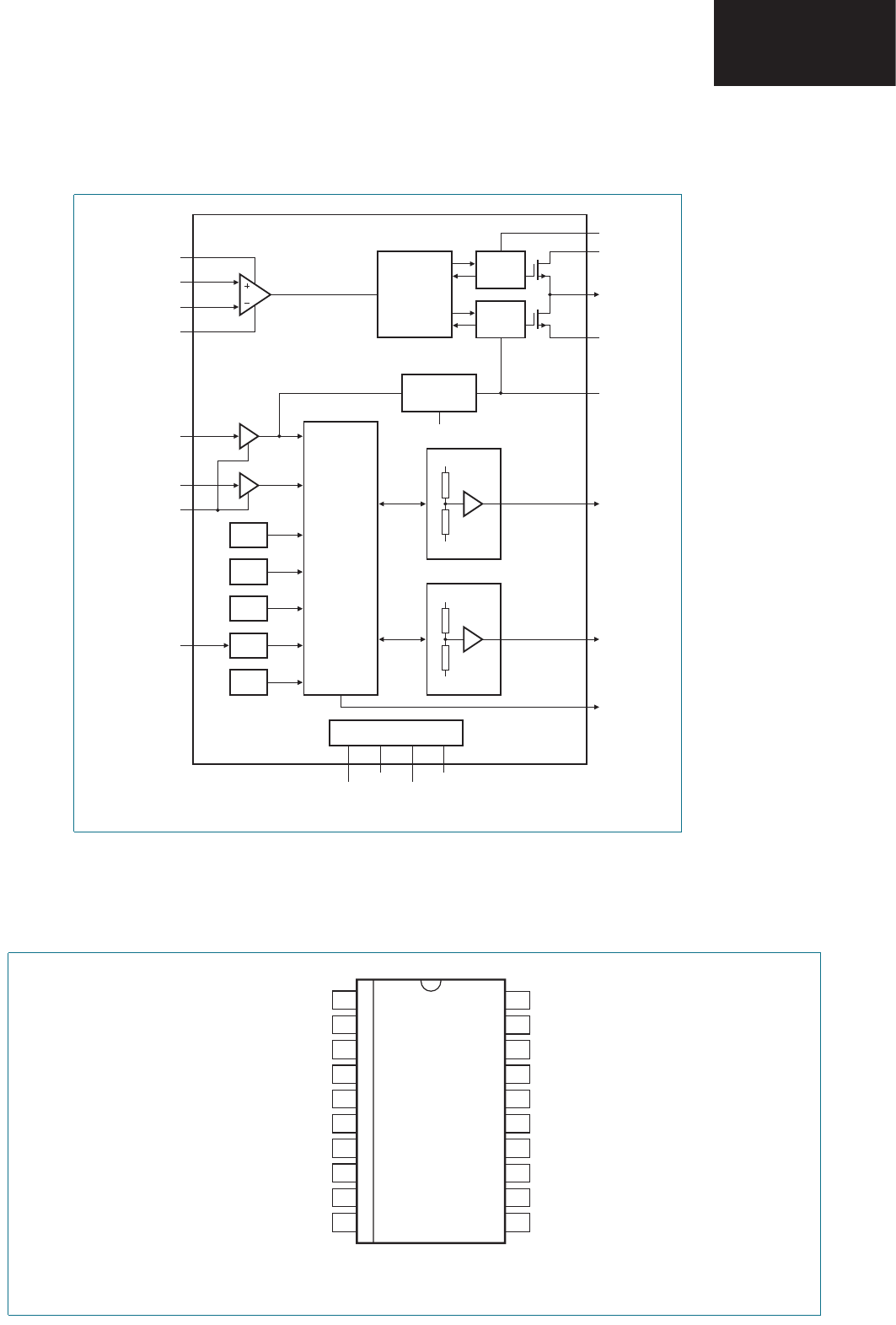
79
LC-26GA5E
LC-32GA5E
LC-32GD8E/RU
LC-32BT8E/RU
LC-37GD8E/RU
LC-37BT8E/RU
LC-32/37GD8E/RU
LC-32/37BT8E/RU
2.3. IC301, IC302 (VHITDA8931T-1Y)
2.3.1. Block Diagram
9397 750 13847 © Koninklijke Philips Electronics N.V. 2005. All rights reserved.
Preliminary data sheet Rev. 01 — 14 January 2004 3 of 31
Philips Semiconductors TDA8931
Power comparator 1 × 20 W
6. Block diagram
Fig 1. Block diagram
001aab807
TDA8931
UVP
HEAT SPREADER
CONTROL
comparator
CONTROL
DRIVER
HIGH
STABILIZER
12V
BOOT
VDDP
17
18
OUT
16
VSSP
15
STABI
VSSD
VDDP
VSSP
14
HVP
13
VDDP
VSSP
HVPI
19
DIAG
8
12
1 10 11 20
VSSD
VSSD
VSSD
VSSD
DRIVER
LOW
OVP
OVP
9
CGND
7
ENABLE
6
POWERUP
3
INN
4
INP
OCP
OTP
2
VSSA
5
VDDA
ODP
2.3.2. Pinning
9397 750 13847 © Koninklijke Philips Electronics N.V. 2005. All rights reserved.
Preliminary data sheet Rev. 01 — 14 January 2004 4 of 31
Philips Semiconductors TDA8931
Power comparator 1 × 20 W
7. Pinning information
7.1 Pinning
7.2 Pin description
Fig 2. Pin configuration
TDA8931
VSSD VSSD
VSSA HVPI
INN VDDP
INP BOOT
VDDA OUT
POWERUP VSSP
ENABLE STABI
DIAG HVP
CGND OVP
VSSD VSSD
001aab811
1
2
3
4
5
6
7
8
9
10
12
11
14
13
16
15
18
17
20
19
Table 3: Pin description
Symbol Pin Description
VSSD 1 negative digital supply voltage; heat spreader
VSSA 2 negative analog supply voltage
INN 3 inverting input
INP 4 non inverting input
VDDA 5 positive analog supply voltage
POWERUP 6 power-up input
ENABLE 7 enable input
DIAG 8 diagnostic output
CGND 9 control ground; reference ground for pins POWERUP, ENABLE and DIAG
VSSD 10 negative digital supply voltage; heat spreader
VSSD 11 negative digital supply voltage; heat spreader
OVP 12 overvoltage protection reference input
HVP 13 half supply voltage output for charging SE capacitor
STABI 14 decoupling of internal stabilizer
VSSP 15 negative power supply voltage
OUT 16 PWM output
BOOT 17 bootstrap capacitor connection
VDDP 18 positive power supply voltage
HVPI 19 half supply voltage output for reference voltage of input circuitry
VSSD 20 negative digital supply voltage; heat spreader
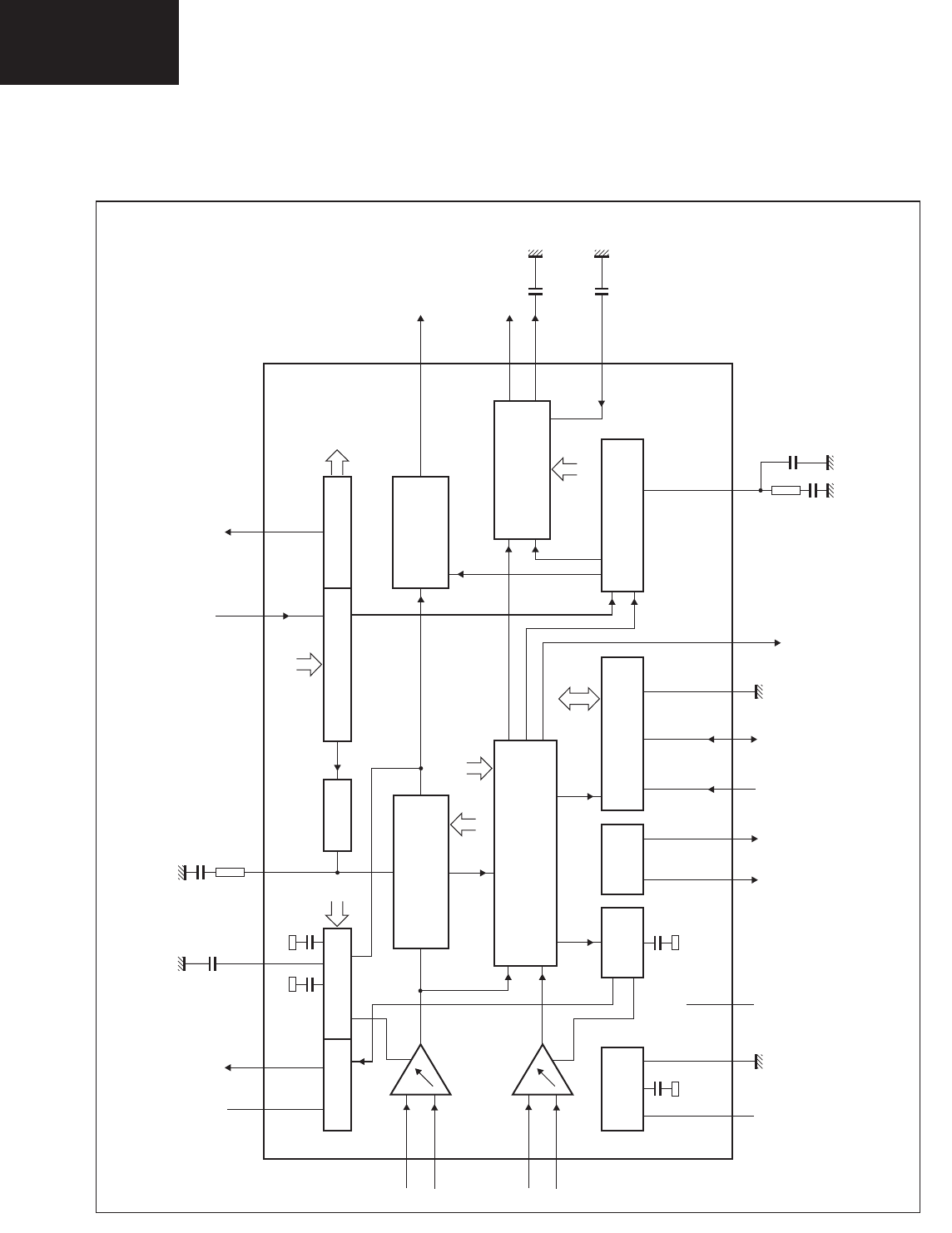
80
LC-26GA5E
LC-32GA5E
LC-32/37GD8E/RU
LC-32/37BT8E/RU
2.4. IC201 (VHITDA9886+-1Y)
2.4.1. Block Diagram
2003 Oct 02 7
Philips Semiconductors Product specification
I2C-bus controlled single and multistandard
alignment-free IF-PLL demodulators TDA9885; TDA9886
This text is here in white to force landscape pages to be rotated correctly when browsing through the pdf in the Acrobat reader.This text is here in
_white to force landscape pages to be rotated correctly when browsing through the pdf in the Acrobat reader.This text is here inThis text is here in
white to force landscape pages to be rotated correctly when browsing through the pdf in the Acrobat reader. white to force landscape pages to be ...
6 BLOCK DIAGRAM
handbook, full pagewidth
MHC108
DIGITAL VCO CONTROL AFC DETECTOR
RC VCO
VIF-PLL
VIF-AGC
TUNER AGC
SUPPLY SIF-AGC
AUDIO PROCESSING
AND SWITCHES
NARROW-BAND
FM-PLL DEMODULATOR
SINGLE REFERENCE QSS MIXER
INTERCARRIER MIXER
AND AM DEMODULATOR
SOUND CARRIER
TRAPS
4.5 to 6.5 MHz
TAGC
CVAGC(pos)
CAGC(neg) CBL
VAGC(1)
TOP
14 (15)
VPLL
19 (21)9 (8) 16 (17) 15 (16) 21 (23)
4 (2)10 (9)
11 (10) 12 (11)18 (20)20 (22)
2 (31)
1 (30)
(18) 17
(7) 8
(3) 5
(4) 6
external reference signal
or 4 MHz crystal
REF AFC
AUD
CVBS
audio output
video output: 2 V (p-p)
[1.1 V (p-p) without trap]
CAF
SIOMADSDASCL
MAD
VP
CAGC
(6, 12, 13, 14, 17,
19, 25, 28, 29, 32)
13
n.c.
AGND
7 (5)
DGND
OUTPUT
PORTS I2C-BUS TRANSCEIVER
22 (24)3 (1)
OP1 OP2 FMPLL
DEEM
AFD
sound intercarrier output
and MAD select
FM-PLL
filter
VIF-PLL
filter
de-emphasis
network
VIF2
VIF1
24 (27)
23 (26)
SIF2
SIF1
TDA9885
TDA9886
Fig.1 Block diagram.
(1) Not connected for TDA9885.
Pin numbers for TDA9885HN and TDA9886HN in parenthesis.

81
LC-26GA5E
LC-32GA5E
LC-32GD8E/RU
LC-32BT8E/RU
LC-37GD8E/RU
LC-37BT8E/RU
LC-32/37GD8E/RU
LC-32/37BT8E/RU
2003 Oct 02 8
Philips Semiconductors Product specification
I2C-bus controlled single and multistandard
alignment-free IF-PLL demodulators TDA9885; TDA9886
7 PINNING
SYMBOL
PIN
DESCRIPTION
TDA9885T
TDA9885TS
TDA9886T
TDA9886TS TDA9885HN TDA9886HN
VIF1 1 1 30 30 VIF differential input 1
VIF2 2 2 31 31 VIF differential input 2
n.c. − − 32 32 not connected
OP1 3 3 1 1 output port 1; open-collector
FMPLL 4 4 2 2 FM-PLL for loop filter
DEEM 5 5 3 3 de-emphasis output for capacitor
AFD 6 6 4 4 AF decoupling input for capacitor
DGND 7 7 5 5 digital ground
n.c. − − 6 6 not connected
AUD 8 8 7 7 audio output
TOP 9 9 8 8 tuner AGC TakeOver Point (TOP) for resistor
adjustment
SDA 10 10 9 9 I2C-bus data input and output
SCL 11 11 10 10 I2C-bus clock input
SIOMAD 12 12 11 11 sound intercarrier output and MAD select with
resistor
n.c. − − 12 12 not connected
n.c. 13 13 13 13 not connected
n.c. − − 14 14 not connected
TAGC 14 14 15 15 tuner AGC output
REF 15 15 16 16 4 MHz crystal or reference signal input
VAGC −16 −17 VIF-AGC for capacitor
n.c. 16 −17 −not connected
CVBS 17 17 18 18 composite video output
n.c. − − 19 19 not connected
AGND 18 18 20 20 analog ground
VPLL 19 19 21 21 VIF-PLL for loop filter
VP20 20 22 22 supply voltage
AFC 21 21 23 23 AFC output
OP2 22 22 24 24 output port 2; open-collector
n.c. − − 25 25 not connected
SIF1 23 23 26 26 SIF differential input 1 and MAD select with
resistor
SIF2 24 24 27 27 SIF differential input 2 and MAD select with
resistor
n.c. − − 28 28 not connected
n.c. − − 29 29 not connected
2.4.2. Pinning
82
LC-26GA5E
LC-32GA5E
LC-32/37GD8E/RU
LC-32/37BT8E/RU
2.4.2. Pinning (Continued)
2003 Oct 02 9
Philips Semiconductors Product specification
I2C-bus controlled single and multistandard
alignment-free IF-PLL demodulators TDA9885; TDA9886
handbook, halfpage
1
2
3
4
5
6
7
8
9
10
11
12
24
23
22
21
20
19
18
17
16
15
14
13
TDA9885T
TDA9886T
MHC109
VIF1
VIF2
OP1
FMPLL
DEEM
AFD
DGND
AUD
TOP
SDA
SCL
SIOMAD
SIF2
SIF1
OP2
AFC
VP
VPLL
AGND
CVBS
VAGC(1)
REF
TAGC
n.c.
Fig.2 Pin configuration for SO24.
(1) Not connected for TDA9885T.
handbook, halfpage
TDA9885TS
TDA9886TS
MHC110
VIF1
VIF2
OP1
FMPLL
DEEM
AFD
DGND
AUD
TOP
SDA
SCL
SIOMAD
SIF2
SIF1
OP2
AFC
VP
VPLL
AGND
CVBS
VAGC(1)
REF
TAGC
n.c.
1
2
3
4
5
6
7
8
9
10
11
12
24
23
22
21
20
19
18
17
16
15
14
13
Fig.3 Pin configuration for SSOP24.
(1) Not connected for TDA9885TS.
handbook, halfpage
MHC111
TDA9885HN
TDA9886HN
OP2
FMPLL
OP1
AFC
DEEM VP
AFD VPLL
DGND AGND
n.c. n.c.
AUD CVBS
TOP VAGC(1)
n.c.
VIF2
VIF1
n.c.
n.c.
SIF2
SIF1
n.c.
SDA
SCL
SIOMAD
n.c.
n.c.
n.c.
TAGC
REF
1
24
2
23
3
22
4
21
5
20
6
19
7
18
8
17
32
31
30
29
28
27
26
25
9
10
11
12
13
14
15
16
terminal 1
index area
Fig.4 Pin configuration for HVQFN32.
Bottom view.
(1) Not connected for TDA9885HN.
83
LC-26GA5E
LC-32GA5E
LC-32GD8E/RU
LC-32BT8E/RU
LC-37GD8E/RU
LC-37BT8E/RU
LC-32/37GD8E/RU
LC-32/37BT8E/RU
2.5. IC202 (STV0360)
2.5.1. Pinning
Pin information STV0360
6/66 STMicroelectronics Confidential 7283434C
Confidential
3 Pin information
3.1 Pin connections (preliminary)
Figure 3: Pin out for 64-pin TQFP (10 x 10 mm)
XTALO
GNDXTAL
TEST
XTALI
D2
GND
SDA
STR_OUT
GND
D7
D6
VDD
D4
SCLT
SDAT
SCL
TEST
AGC1
AGC2
INP
DGNDA
DVCCA1.8
GNDA
D1
LOCK/OP2
GND
AUX_CLK
GND
OP0
CIQ/HFEC3
1
2
3
4
5
6
7
8
9
10
11
12
13
14
15
16
48
47
46
45
44
43
42
41
40
39
38
37
36
35
34
33
64 62 61 60 59 58 57 56 5563 54 53 52 51 50 49
17 19 20 21 22 23 24 25 2618 27 28 29 30 31 32
D5
VCCA1.8
REFP
GNDA
RESET
VDD
VDD_3.3
LOCK/OP1
GND
ERROR
VDD
D/P
CLK_OUT
VDD_3.3
D0
D3
VDD_3.3
VCCXTAL1.8
VR
VCCA3.3
REFM
INM
GND
IP0
VDD
GND
CS0
CS1
GND
VDD_3.3
HFEC0
CCLK/HFEC1
CDATA/.HFEC2
VDD_3.3: 3.3V output buffer supply
VDD: 1.8V core and input buffer supply
GND: both core and buffer ground
TQFP64
STV0360
VDD
GND
84
LC-26GA5E
LC-32GA5E
LC-32/37GD8E/RU
LC-32/37BT8E/RU
2.5.2. Pin Description
7283434C STMicroelectronics Confidential 7/66
STV0360 Pin information
Confidential
3.2 Pinout description (preliminary)
Table 1: STV0360 pin description
Pin number Name Type Description Drive (mA)
Clock and resets
12 RESET I1Hardware reset, active low -
62 XTALI Analog Crystal oscillator input/external clock (1.8 V) -
63 XTALO Analog Crystal oscillator output -
61 VCCXTAL1.8 Supply Analog oscillator supply (1.8 V) -
64 GNDXTAL Ground Analog oscillator ground -
Analog interface
2 DVCCA1.8 Supply Analog part digital supply (1.8 V) -
5 REFM Analog Internal negative reference -
6 REFP Analog Internal positive reference
3 VCCA1.8 Supply Analog supply (1.8 V) -
9 INM Analog Negative analog input -
10 INP Analog Positive analog input -
4, 11 GNDA Supply Analog ground -
1 DGNDA Ground Analog ground -
7 VR Analog Reference -
8 VCCA3.3 Supply Analog supply (3.3 V)
I2C interface
21 SDA IO2Serial data (open drain) 8
20 SCL I Serial clock (open drain) -
19 SDAT IO SDA tuner (open drain) 4
18 SCLT I SCL tuner
MPEG interface
25, 26, 27, 29,
31, 32, 33, 34
D7/0 O3Serial D7, MPEG data 8/4
36 CLK_OUT O MPEG byte or bit clock 4
23 STR_OUT O MPEG first byte sync 2
38 D/P O MPEG data valid/parity 4
40 ERROR O MPEG packet error 2
51 HFEC0 O Hierarchical FEC output bit 0 2
50 CCLK/HFEC1 O Hierarchical FEC output bit 1 or clock for
constellation display
2
49 CDATA/HFEC2 O Hierarchical FEC output bit 2 or data for
constellation display
2
48 CIQ/HFEC3 O Hierarchical FEC output bit 3 or IQ validation for
constellation display
2
85
LC-26GA5E
LC-32GA5E
LC-32GD8E/RU
LC-32BT8E/RU
LC-37GD8E/RU
LC-37BT8E/RU
LC-32/37GD8E/RU
LC-32/37BT8E/RU
2.5.2. Pin Description (Continued)
Pin information STV0360
8/66 STMicroelectronics Confidential 7283434C
Confidential
Front end controls
16 AGC1 IO RF AGC control Σ∆ 4
14 AGC2 IO IF AGC control Σ∆ 4
17, 60 TEST Reserved test mode, must be grounded
58 IP0 I General-purpose input port 0 and ADC input for
RF level monitoring
-
45 OP0 IO General-purpose output port 0 4
43 LOCK/OP1 IO General-purpose output port 1 or lock indicator 4
42 LOCK/OP2 O General-purpose output port 2 or lock indicator 4
47 AUX_CLK IO Auxiliary clock 8
55 CS0 I Chip select LSB -
53 CS1 I Chip select MSB -
Power supply
13, 28, 39, 57 VDD Supply Digital core supply
22, 35, 44, 52 VDD_3.3 Supply Digital IO supply
15, 24, 30, 37,
41, 46, 54, 56,
59
GND Ground
1. All inputs are 3.3 V compatible
2. All bidirectional pads are 3.3 V capable
3. All outputs are 3.3 V capable
Table 1: STV0360 pin description
Pin number Name Type Description Drive (mA)
86
LC-26GA5E
LC-32GA5E
LC-32/37GD8E/RU
LC-32/37BT8E/RU
2.6. IC4001 (Sti5516)
2.6.1. Pinning
7368868E STMicroelectronics Confidential 27/709
STi5516 Pin list
Confidential
Note: 1 NC (not connected): indicates that the pin has no electrical connection, and may be used to route
power or signals on the PCB.
2 Do not connect: pin is reserved. It may have an electrical connection and must not be used.
14 15 16 17 18 19 20 21 22 23 24 25 26
EMIADDR
[5]
GND VDDGEN
FSYN NC CLK27MA VDD18
VDD33 GND Do not
connect
GND GND
GND GND A
EMIADDR
[4] GND GNDGEN
FSYN
VDD
AUDIO
FSYN
VDD18 VDD33
GND GND
VDD18 GND
GND GND
NOT_P1284
STROBE B
EMIADDR
[3]
VDDVPLL
CLK
SPEED
SEL
GND
AUDIO
FSYN
VDD18
VDD33 GND
GND GND
GND GND
P1284
BUSY
NOT_P1284
ACK C
EMIADDR
[2] GND
GND AUXCLK
OUT VDD18
VDD33 GND
GND GND
GND NOT_P1284
AUTOFD
P1284
SELECT
P1284
PERROR D
VDD33 NOT_P1284
SELECTIN
NOT_P1284
INIT
NOT_P1284
FAULT E
P1284
DATA[4]
P1284
DATA[5]
P1284
DATA[6]
P1284
DATA[7] F
GND P1284
DATA[1]
P1284
DATA[2]
P1284
DATA[3] G
TSIN2L
DATA[5]
TSIN2L
DATA[6]
TSIN2L
DATA[7]
P1284
DATA[0] H
VDD33 TSIN2L
DATA[3]
TSIN2L
PACKET
CLK
TSIN2L
DATA[4] J
GND TSIN2L
DATA[0]
TSIN2L
DATA[1]
TSIN2L
DATA[2] K
GND GND
GND VDD18
TSIN2L
BYTE
CLK
TSIN2L
ERROR
TSIN2L
BYTE
CLKVALID
L
GND
GND GND
TSIN1
DATA[4]
TSIN1
DATA[5]
TSIN1
DATA[6]
TSIN1
DATA[7] M
GND GND
GND TSIN1
DATA[0]
TSIN1
DATA[1]
TSIN1
DATA[2]
TSIN1
DATA[3] N
GND
GND GND
TSIN1
BYTE
CLK
TSIN1
PACKET
CLK
TSIN1
ERROR
TSIN1
BYTE
CLKVALID
P
GND GND
GND VDD18
VDD18 VDD18
VDD18 R
GND
GND GND
SMIMEM
CLKIN
SMIDATA
ML
SMIDATA
MU NC T
NOT_SMI
CAS
NOT_SMI
RAS NOT_SMIWE
SMIMEM
CLKOUT U
VDD33
SMIDATA
[15]
NOT_SMI
CS0
NOT_SMI
CS1 V
SMIDATA
[11]
SMIDATA
[12]
SMIDATA
[13]
SMIDATA
[14] W
VDD33
SMIDATA
[8]
SMIDATA
[9]
SMIDATA
[10] Y
GND
SMIDATA
[5]
SMIDATA
[6]
SMIDATA
[7]
A
A
VDD33
SMIDATA
[2]
SMIDATA
[3]
SMIDATA
[4]
A
B
GND
SPDIF VDD18
PIO4[4] VDD33
PIO5[3] GND
VDD18 VDD33
SMIADDR
[12]
SMIADDR
[13]
SMIDATA
[0]
SMIDATA
[1]
A
C
DO NOT
CONNECT
PIO3[5] PIO4[1]
PIO4[5] PIO5[1]
PIO5[4] PIO5[7]
GND VDD33
SMIADDR
[8]
SMIADDR
[9]
SMIADDR
[10]
SMIADDR
[11]
A
D
PCM
DATA[1] PIO3[7]
PIO4[2] PIO4[7]
PIO5[2] PIO5[5]
NOT_
HSYNC GND
VDD33 SMIADDR
[4]
SMIADDR
[5]
SMIADDR
[6]
SMIADDR
[7]
A
E
DO NOT
CONNECT PIO4[0]
PIO4[3] PIO5[0]
PIO4[6] PIO5[6]
EVENNOT
ODD GND
VDD33 SMIADDR
[0]
SMIADDR
[1]
SMIADDR
[2]
SMIADDR
[3]
A
F
Pin list STi5516
26/709 STMicroelectronics Confidential 7368868E
Confidential
4 Pin list
4.1 Pin-out
The following pages give the allocation of pins to the package, shown from the top looking down.
1 2 3 4 5 6 7 8 9 10 11 12 13
AEMI
SDRAM
CLK
EMIFLASH
CLK
EMIDATA
[14]
EMIDATA
[13]
EMIDATA
[10]
EMIDATA
[7]
EMIDATA
[3]
EMIDATA
[0]
EMIADDR
[23]
EMIADDR
[19]
EMIADDR
[16]
EMIADDR
[13]
EMIADDR
[9]
BVDD33 VDD33 EMIDATA
[15]
EMIDATA
[12]
EMIDATA
[9]
EMIDATA
[6]
EMIDATA
[2]
EMIADDR
[25]
EMIADDR
[22]
EMIADDR
[18]
EMIADDR
[15]
EMIADDR
[12]
EMIADDR
[8]
CVDD33 VDD33 VDD33 EMIDATA
[11]
EMIDATA
[8]
EMIDATA
[5]
EMIDATA
[1]
EMIADDR
[24]
EMIADDR
[21]
EMIADDR
[17]
EMIADDR
[14]
EMIADDR
[11]
EMIADDR
[7]
DVDD33 VDD33 VDD33 VDD33 VDD33 EMIDATA
[4] GND VDD33 EMIADDR
[20] VDD18 VDD33 EMIADDR
[10]
EMIADDR
[6]
EGND GND GND VDD33
FGND GND GND VDD33
GVDD18 VDD18 VDD18 GND
HNOT_EMI
ACKREQ NC EMIBOOT
MODE[0] VDD18
JNOT_EMI
CAS
NOT_EMI
RAS
NOT_EMI
REQGNT VDD33
KNOT_EMI
CSD
NOT_EMI
CSC
NOT_EMI
CSB
NOT_EMI
CSA
LNOT_EMIBE
[1]
NOT_EMIBE
[0]
NOT_EMI
CSF
NOT_EMI
CSE GND GND GND
MNOT_EMIOE VDD33 VDD33 VDD33 GND GND GND
NVDD33 EMIRD
NOTWR
NOT_EMI
LBA
EMIWAIT
NOT
TREADY
GND GND GND
PDCU
TRIGGER
IN
VDD18 VDD18 VDD18 GND GND GND
RVDD18 VDD18
DCU
TRIGGER
OUT
VDD18 GND GND GND
TINTER
RUPT[3]
INTER
RUPT[2]
INTER
RUPT[1]
INTER
RUPT[0] GND GND GND
UPIO0[1] PIO0[0] PIO0[2] VDD33
VPIO0[6] PIO0[5] PIO0[4] PIO0[3]
WPIO1[2] PIO1[1] PIO1[0] PIO0[7]
YPIO1[5] PIO1[4] PIO1[3] GND
A
A
VSSAA
DAC
VDDAA
DAC
VDDASA
DAC PIO1[6]
A
B
OUTM
LEFT
VCCAA
DAC
GNDAA
DAC
OUTM
RIGHT
A
C
VCCASA
DAC IREF OUTP
LEFT
OUTP
RIGHT GND VDD33 TDI LPCLKIN SHIELDV
DAC
GNDVDAC
YCC
VREFDAC
RGB
GNDVDAC
RGB VDD18
A
DVBGFIL PIO2[1] PIO2[5] PIO2[7] PIO3[6] PIO3[4] TMS LPCLK
OSC
VREFDAC
YCC CVOUT IREFDAC
RGB BOUT SCLK
A
EPIO1[7] PIO2[2] PIO2[6] PIO3[1] PIO3[0] NOT_TRST NOT_RESET RTCVDD IREFDAC
YCC YOUT GOUT VDDVDAC
RGB PCMCLK
A
FPIO2[0] PIO2[3] PIO2[4] PIO3[3] PIO3[2] TDO TCK NOT_WDOG
RSTOUT COUT VDDVDAC
YCC ROUT NC LRCLK
87
LC-26GA5E
LC-32GA5E
LC-32GD8E/RU
LC-32BT8E/RU
LC-37GD8E/RU
LC-37BT8E/RU
LC-32/37GD8E/RU
LC-32/37BT8E/RU
2.6.2. Pin Description
Pin list STi5516
28/709 STMicroelectronics Confidential 7368868E
Confidential
4.2 STi5516 pin list
Signal names are prefixed by NOT_ if they are active low; otherwise they are active high.
All signals are only 3.3 V capable unless otherwise indicated as 1.8 V or 5 V tolerant.
Table 2: I/O load capacitance and DC loading
Pad type Functional pin
group
Maximum load
capacitance (pF) Drive (mA) Notes
C4 Others 75 4
S8 SDRAM/EMI 75 8
S8b SDRAM/EMI 75 8
E8 EMI
(programmable)
35 8 a
a. Typical load, but the maximum is 75 pF
25 6 a
15 4 a
5 2 a
P4 PIO 400 4
Table 3: Analog power supply pins
Pin Location Number Function
VDDVDACRGB AE12 1 3.3 V power supply for RGB video DAC
VDDVDACYCC AF10 1 3.3 V power supply for YCC video DAC
GNDVDACRGB AC12 1 Ground for RGB video DAC
GNDVDACYCC AC10 1 Ground for YCC video DAC
SHIELDVDAC AC9 1 Shield ground for 2 x video DACs
IREFDACRGB AD11 1 RGB video DAC current reference
IREFDACYCC AE9 1 YCC video DAC current reference
VREFDACRGB AC11 1 RGB video DAC voltage reference
VREFDACYCC AD9 1 YCC video DAC voltage reference
VDDVPLL C15 1 3.3 V power for video PLL
VDDAUDIOFSYN B17 1 1.8 V dedicated power for low jitter audio clock
frequency synthesizer
GNDAUDIOFSYN C17 1 Dedicated ground for low jitter audio clock frequency
synthesizer
VDDGENFSYN A16 1 1.8 V dedicated power for nonaudio clock frequency
synthesizer
GNDGENFSYN B16 1 Dedicated ground for nonaudio clock frequency
synthesizer
VDDAADAC AA2 1 3.3 V power for audio DAC
VSSAADAC AA1 1 Ground for audio DAC command switches
88
LC-26GA5E
LC-32GA5E
LC-32/37GD8E/RU
LC-32/37BT8E/RU
7368868E STMicroelectronics Confidential 29/709
STi5516 Pin list
Confidential
VDDASADAC AA3 1 3.3 V power for audio DAC substrate
VCCAADAC AB2 1 3.3 V power for audio DAC command switches
GNDAADAC AB3 1 Ground for audio DAC
VCCASADAC AC1 1 3.3 V power for audio DAC command switches
substrate
IREF AC2 1 Audio DAC output reference current
VBGFIL AD1 1 Audio DAC filtered output reference voltage
Table 4: Digital power supply pins
Pin Location Number Function
VDD18 a24 1.8 V power supply
VDD33 b35 3.3 V power supply
RTCVDD AE8 1 Low power controller 1.8 V power supply
GND c76 Ground for power supplies
a. A19, B18, B22, C18, D10, D18, G1 to G3, H4, L23, P2 to P4, R1, R2, R4, R23 to R26, AC13,
AC16 and AC21.
b. A20, B1, B2, B19, C1 to C3, C19, D1 to D5, D8, D11, D19, E4, E23, F4, J4, J23, M2 to M4,
N1, U4, V23, Y23, AB23, AC6, AC18, AC22, AD22, AE22 and AF22.
c. A15, A21, A23 to A26, B15, B20, B21, B23 to B25, C20 to C24, D7, D15, D16, D20 to D23,
E1 to E3, F1 to F3, G4, G23, K23, L11 to L16, M11 to M16, N11 to N16, P11 to P16, R11 to
R16, T11 to T16, Y4, AA23, AC5, AC14, AC20, AD21, AE21 and AF21.
Table 5: RTC pins
Pin Location I/O Function
LPCLKINaAC8 I Low power clock input
LPCLKOSCAAD8 I/O Low power clock oscillator
a. 1.8 V tolerant
Table 3: Analog power supply pins
Pin Location Number Function
2.6.2. Pin Description (Continued)

89
LC-26GA5E
LC-32GA5E
LC-32GD8E/RU
LC-32BT8E/RU
LC-37GD8E/RU
LC-37BT8E/RU
LC-32/37GD8E/RU
LC-32/37BT8E/RU
2.6.2. Pin Description (Continued)
Pin list STi5516
30/709 STMicroelectronics Confidential 7368868E
Confidential
Table 6: System pins
Pin Location I/O Function Pad
type
CLK27MAAA18 I Selectable input clock to PLL or for x1 mode C4
CLKSPEEDSELaC16 I PLL speed select C4
AUXCLKOUTaD17 O Auxiliary clock for general use C4
NOT_RESETBAE7 I System reset -
NOT_WDOGRSTOUTaAF8 O Internal watchdog timer reset. C4
a. 5 V tolerant
b. 1.8 V tolerant
Table 7: JTAG pins
Pin Location I/O Function Pad
type
TDIAAC7 I Boundary scan test data input C4
TMSaAD7 I Boundary scan test mode select C4
TCKaAF7 I Boundary scan test clock -
NOT_TRSTaAE6 I Boundary scan test logic reset C4
TDOaAF6 O Boundary scan test data output C4
a. 5 V tolerant
Table 8: DCU pins
Pin Location I/O Function Pad
type
DCUTRIGGERINaP1 I External trigger input to DCU C4
DCUTRIGGEROUTAR3 O Signal to trigger external debug circuitry C4
a. 5 V tolerant

90
LC-26GA5E
LC-32GA5E
LC-32/37GD8E/RU
LC-32/37BT8E/RU
2.6.2. Pin Description (Continued)
7368868E STMicroelectronics Confidential 31/709
STi5516 Pin list
Confidential
Table 9: EMI pins
Pin Location I/O Function Pad
type
NOT_EMIRAS or
NOT_CI_IORDa
J2 O Row address strobe for SDRAM C4
NOT_EMICAS or
NOT_CI_IOWa
J1 O Column address strobe for SDRAM E8
NOT_EMICSA K4 O Peripheral chip select A E8
NOT_EMICSB K3 O Peripheral chip select B E8
NOT_EMICSC K2 O Peripheral chip select C E8
NOT_EMICSD K1 O Peripheral chip select D E8
NOT_EMICSE L4 O Peripheral chip select E E8
NOT_EMICSF L3 O Peripheral chip select F E8
NOT_EMIBE[1:0] L1, L2 O External device data bus byte enable. 1 bit per
byte of the data bus.
E8
NOT_EMIOE or
NOT_CI_OE
M1 O External device output enable. E8
NOT_EMILBA or
NOT_CI_WEA
N3 O Flash device load burst address. E8
EMIWAITNOTTREADYbN4 I External memory device target ready indicator C4
EMIRDNOTWR N2 O External read/write access indicator. Common to
all devices.
E8
EMIDATA[15:0] cI/O External common data bus. E8
EMIADDR[25:2]d e O External common address bus E8
NOT_EMIREQGNT J3 O Bus request/grant indicator E8
NOT_EMIACKREQbH1 I Bus grant/request indicator C4
EMIBOOTMODE0bH3 I External power-up port size indicator C4
EMISDRAMCLK A1 O SDRAM clock E8
EMIFLASHCLK A2 O Peripheral clock E8
a. Or equivalent ATA HDD interface signal.
b. 5 V tolerant
c. B3, A3, A4, B4, C4, A5, B5, C5, A6, B6, C6, D6, A7, B7, C7 and A8.
d. EMIADDR[19:20] are used as ATA HDD interface function: ATA CS0 and CS1. There is no
interconnect configuration control register bit to select this function. The addresses are just
reused as chip selects.
e. B8, C8, A9, B9, C9, D9, A10, B10, C10, A11, B11, C11, A12, B12, C12, D12, A13, B13, C13,
D13, A14, B14, C14 and D14.

91
LC-26GA5E
LC-32GA5E
LC-32GD8E/RU
LC-32BT8E/RU
LC-37GD8E/RU
LC-37BT8E/RU
LC-32/37GD8E/RU
LC-32/37BT8E/RU
2.6.2. Pin Description (Continued)
Pin list STi5516
32/709 STMicroelectronics Confidential 7368868E
Confidential
Table 10: Transport stream 2 pins
Pin Location I/O Function Pad
type
TSIN2LBYTECLKaL24 I/O Transport stream bit clock C4
TSIN2LBYTECLKVALIDaL26 I/O Transport stream bit clock valid edge C4
TSIN2LERRORaL25 I/O Transport stream packet error C4
TSIN2LPACKETCLKaJ25 I/O Transport stream packet strobe C4
TSIN2LDATA[7:0]ab c I/O Transport stream data C4
a. 5 V tolerant
b. H25, H24, H23, J26, J24, K26, K25 and K24
c. TSIN2LDATA7 is used for data input in serial mode.
Table 11: Transport stream 1 pins
Pin Location I/O Function Pad
type
TSIN1BYTECLKaP23 I Transport stream bit/byte clock C4
TSIN1BYTECLKVALIDaP26 I Transport stream bit/byte clock valid edge C4
TSIN1ERRORaP25 I Transport stream packet error C4
TSIN1PACKETCLKaP24 I Transport stream packet strobe C4
TSIN1DATA[7:0]a b,cI Transport stream data in C4
a. 5 V tolerant
b. M26, M25, M24, M23, N26, N25, N24 and N23.
c. TSIN1DATA7 is used for data input in serial mode.

92
LC-26GA5E
LC-32GA5E
LC-32/37GD8E/RU
LC-32/37BT8E/RU
2.6.2. Pin Description (Continued)
7368868E STMicroelectronics Confidential 33/709
STi5516 Pin list
Confidential
Table 12: Programmable I/O pins
Pin Location I/O Function Pad
type
PIO0[0:7]A b I/O Parallel input/output pin or alternative function P4
PIO1[0:7]acI/O P4
PIO2[0:7]adI/O P4
PIO3[0:7]aeI/O P4
PIO4[0:7]afI/O P4
PIO5[0:7]agI/O P4
a. 5 V tolerant
b. U2, U1, U3, V4, V3, V2, V1 and W4
c. W3, W2, W1, Y3, Y2, Y1, AA4 and AE1
d. AF1, AD2, AE2, AF2, AF3, AD3, AE3 and AD4
e. AE5, AE4, AF5, AF4, AD6, AD15, AD5 and AE15
f. AF15, AD16, AE16, AF16, AC17, AD17, AF18 and AE17
g. AF17, AD18, AE18, AC19, AD19, AE19, AF19 and AD20
Table 13: Digital audio pinsa
Pin Location I/O Function Pad
type
SCLKBAD13 O Serial clock C4
PCMDATA[1]bAE14 O PCM data out C4
PCMCLKbAE13 I/O External PCM clock input or internal PCM clock
output
C4
LRCLKbAF13 O Left/right clock C4
SPDIFbAC15 O Digital audio output C4
a. Note: Digital audio input pins PCMI_SCLK, PCMI_DATA and PCMI_LRCLK are alternate
functions for NOT_CD_REQ[1], I1284HOSTLOGICHIGH, and NOT_CD_REQ[0], on PIO port
3 bits [6:4]
b. 5 V tolerant

93
LC-26GA5E
LC-32GA5E
LC-32GD8E/RU
LC-32BT8E/RU
LC-37GD8E/RU
LC-37BT8E/RU
LC-32/37GD8E/RU
LC-32/37BT8E/RU
2.6.2. Pin Description (Continued)
Pin list STi5516
34/709 STMicroelectronics Confidential 7368868E
Confidential
Table 14: AVSDRAM pins (SMI)
Pin Location I/O Function Pad
type
SMIADDR[13:0] aO Audio/video core SDRAM address bus S8
SMIDATA[15:0] bI/O Audio/video core SDRAM data bus S8
NOT_SMICS0 V25 O Audio/video core SDRAM chip select for 1st
SDRAM
S8
NOT_SMICS1 V26 O Audio/video core SDRAM chip select for 2nd
16 Mbit SDRAM
S8
NOT_SMICAS U23 O Audio/video core SDRAM column address strobe S8
NOT_SMIRAS U24 O Audio/video core SDRAM row address strobe S8
NOT_SMIWE U25 O Audio/video core SDRAM write enable S8
SMIMEMCLKIN T23 I Audio/video core SDRAM memory clock input S8b
SMIMEMCLKOUT U26 O Audio/video core SDRAM memory clock output S8
SMIDATAML T24 O Audio/video core SDRAM data bus lower byte
enable
S8
SMIDATAMU T25 O Audio/video core SDRAM data bus upper byte
enable
S8
a. AC24, AC23, AD26, AD25, AD24, AD23, AE26, AE25, AE24, AE23, AF26, AF25, AF24 and
AF23.
b. V24, W26, W25, W24, W23, Y26, Y25, Y24, AA26, AA25, AA24, AB26, AB25, AB24, AC26
and AC25.
Table 15: IEEE 1284/1394 pins
Pin Location I/O Function Pad
type
P1284DATA[7:0]A b I/O 1284 data or 1394 AV data I14
NOT_P1284SELECTINaE24 I/O 1284 or 1394 AV control signals I14
NOT_P1284INITaE25 I/O I14
NOT_P1284FAULTaE26 I/O I14
NOT_P1284AUTOFDaD24 I/O I14
P1284SELECTaD25 I/O I14
P1284PERRORaD26 I/O I14
P1284BUSYaC25 I/O I14
NOT_P1284ACKaC26 I/O I14
NOT_P1284STROBEaB26 I/O I14
a. 5 V tolerant
b. F26, F25, F24, F23, G26, G25, G24 and H26.
94
LC-26GA5E
LC-32GA5E
LC-32/37GD8E/RU
LC-32/37BT8E/RU
2.6.3. Pin Description (Continued)
7368868E STMicroelectronics Confidential 35/709
STi5516 Pin list
Confidential
Table 16: Interrupt pins
Pin Location I/O Function Pad
type
INTERRUPT[3:0]A b I/O External interrupts C4
a. 5 V tolerant
b. T1, T2, T3 and T4.
Table 17: Analog audio DAC (digital-to-analog converter) pins
Pin Location I/O Function
OUTPLEFT AC3 O Left channel, differential positive current output
OUTMLEFT AB1 O Left channel, differential negative current output
OUTPRIGHT AC4 O Right channel, differential positive current output
OUTMRIGHT AB4 O Right channel, differential negative current output
Table 18: Analog video DAC pins
Pin Location I/O Function
ROUT AF11 O Red output
GOUT AE11 O Green output
BOUT AD12 O Blue output
COUT AF9 O Chroma output
CVOUT AD10 O Composite video output
YOUT AE10 O Luma output
Table 19: Digital video pins
Pin Location I/O Function Pad
type
NOT_HSYNCAAE20 I/O Horizontal sync C4
EVENNOTODDaAF20 I/O Vertical sync C4
a. 5 V tolerant

95
LC-26GA5E
LC-32GA5E
LC-32GD8E/RU
LC-32BT8E/RU
LC-37GD8E/RU
LC-37BT8E/RU
LC-32/37GD8E/RU
LC-32/37BT8E/RU
2.6.3. Pin Description (Continued)
7368868E STMicroelectronics Confidential 37/709
STi5516 Pin list
Confidential
Table 20: Port 0 PIO signal assignments
Port 0 bit Input Output
Bit 0 SC0_DATAOUT or ASC0_TXDa
Bit 1 SC0_DATAIN or ASC0_RXDa
Bit 2 SC0_CG_EXTCLK
Bit 3 SC0CG_CLK or SMCDSS_CLKb
Bit 4 (SCO_RESET)
Bit 5 (SC0_NOT_SETVCC)
Bit 6 SC0_DIR or ASC0_NOTOEc,
(SC0_NOT_SETVPP)
Bit 7 (SC0_DETECT)
a. ASC0 TX/RX data becomes smartcard TX/RX data when the ASC module is used in
smartcard mode.
b. Output function between PIO or smartcard module clock generator alternate function and
clock generator module frequency synthesizer clock is selected by bit 28 in the interconnect
register CONFIG_CONTROL_A (SMCARDA_DSSSMCLK_NOT_PIOBIT3). If the DSS
smartcard mode is selected (bit 28 = 1), this overrides the normal PIO or PIO alternate
function output.
c. When ASC0 is used in nonsmartcard mode, the smartcard direction signal becomes an active
low ASC TX output enable signal. The signals are in fact the same, that is, SC0_DIR = 0
means smartcard TX is active.
Table 21: Port 1 PIO signal assignments
Port 1 bit Input Output
Bit 0 SC1_DATAOUT or ASC1_TXDa
Bit 1 SC1_DATAIN or ASC1_RXDa
Bit 2 SC1_CG_EXTCLK
Bit 3 SC1CG_CLK or SMCDSS_CLKb
Bit 4 (SC1_RESET)
Bit 5 YC[1] YC[1], (SC1_NOT_SETVCC)
Bit 6 SC1_DIR or ASC1_NOTOEc,
(SC1_NOT_SETVPP)
Bit 7 YC[0] (SC1_DETECT) YC[0]
a. ASC1 TX/RX data becomes smartcard TX/RX data when the ASC module is used in
smartcard mode.
b. Output function between PIO or smartcard module clock generator alternate function and
clock generator module frequency synthesizer clock is selected by bit 29 in the interconnect
register CONFIG_CONTROL_A (SMCARDB_DSSSMCLK_NOT_PIOBIT3). If the DSS
smartcard mode is selected (bit 29 = 1) this overrides the normal PIO or PIO alternate function
output.
c. When ASC1 is used in nonsmartcard mode the smartcard direction signal becomes an active
low ASC TX output enable signal. The signals are in fact the same, that is, SC1_DIR = 0
means smartcard TX is active.
96
LC-26GA5E
LC-32GA5E
LC-32/37GD8E/RU
LC-32/37BT8E/RU
2.6.3. Pin Description (Continued)
Pin list STi5516
38/709 STMicroelectronics Confidential 7368868E
Confidential
Table 22: Port 2 PIO signal assignments
Port 2 bit Input Output
Bit 0 MAFE_HC1 or NOT_ASC4_RTSa
Bit 1 MAFE_DOUT or ASC4_TXDa
Bit 2 MAFE_DIN or ASC4_RXDa
Bit 3 MAFE_FS or NOT_ASC4_CTSa
Bit 4 MAFE_SCLK
Bit 5 PWM_CAPTURE0
Bit 6 PWM_COMPARE0
Bit 7 PWM_OUT0
a. Controlled by bit MAFE_OR_UART4_SEL in interconnect register CONFIG_CONTROL_D
(bit 20).
Table 23: Port 3 PIO signal assignments
Port 3 bit Input Output
Bit 0 SSC0_MTSR_DIN or SSC0_MRST_DIN SSC0_MTSR_DOUT or SSC0_MRST_DOUTa
Bit 1 SSC0_SCLKIN SSC0_SCLKOUT
Bit 2 SSC1_MTSR_DIN or SSC1_MRST_DIN SSC1_MTSR_DOUT or SSC1_MRST_DOUTb
Bit 3 SSC1_SCLK SSC1_SCLK
Bit 4 NOT_CD_REQ[0] or PCMI_LRCLK I1284PERILOGICHIGH
Bit 5 Slave mode I1284HOSTLOGICHIGH or
PCMI_DATA
Master mode I1284HOSTLOGICHIGH
Bit 6 NOT_CD_REQ[1] or PCMI_SCLK I1284INNOTOUT
Bit 7 PWM_OUT1
a. Output function selected by bit 24 in interconnect configuration register
CONFIG_CONTROL_B (COMMS_SSC0_DOUT_MRST_NOTMTSR_MUXSEL)
b. Output function selected by bit 25 in interconnect configuration register
CONFIG_CONTROL_B (COMMS_SSC1_DOUT_MRST_NOTMTSR_MUXSEL)

97
LC-26GA5E
LC-32GA5E
LC-32GD8E/RU
LC-32BT8E/RU
LC-37GD8E/RU
LC-37BT8E/RU
LC-32/37GD8E/RU
LC-32/37BT8E/RU
2.6.3. Pin Description (Continued)
7368868E STMicroelectronics Confidential 39/709
STi5516 Pin list
Confidential
Table 24: Port 4 PIO signal assignments
Port 4 bit Input Output
Bit 0 TTXTREQUEST or OSDENABLE OSDENABLEa
Bit 1 CFC TXTDATAOUTb
Bit 2 YC[7] YC[7]
Bit 3 ASC2_RXD
Bit 4 ASC2_TXD c
Bit 5 PWM_CAPTURE2 or YC[6] YC[6]
Bit 6 SCCG_EXTCLK PWM_COMPARE2
Bit 7 PWM_OUT2
a. OSDENABLE output function is selected rather than PIO by interconnect configuration
register CONFIG_CONTROL_C, bit 2 (CONFIG_OTHER_ALT_PIOPORT4[0]). The output
can then be turned off by the MPEG video decoder to use OSDENABLE as an input.
b. TXTDATAOUT function selected by interconnect configuration register
CONFIG_CONTROL_C, bit 3 (CONFIG_OTHER_ALT_PIOPORT4[1])
c. After reset, register CONFIG_CONTROL_C bit 4 must be set to 1 to pass PIO data or to use
ASC2_TXD in alternate output PIO mode.
Table 25: Port 5 PIO signal assignments
Port 5 bit Input Output
Bit 0 IRB_IR_INa
Bit 1 IRB_UHF_INb
Bit 2 Infrared transmitter/receiver drive PPM
Bit 3 Infrared transmitter/receiver drive jack (0 or z)
open drain jack output c, d
Bit 4 YC[5] ASC3_TXD or YC[5]e
Bit 5 ASC3_RXD or YC[4] YC[4]
Bit 6 NOT_ASC3_CTS or YC[3] YC[3]
Bit 7 YC[2] NOT_ASC3RTS or YC[2]e
a. The wake-up from low power mode function is enabled by interconnect configuration register
CONFIG_CONTROL_D, bit 21 (RC_IRDA_DATA_IN_EN).
b. The wake-up from low power mode function is enabled by interconnect configuration register
CONFIG_CONTROL_D, bit 22 (UHF_IN_EN).
c. PIO needs to be configured as open drain in alternate output mode to use infrared transmitter/
receiver drive jack.
d. After reset, bit 5 in CONFIG_CONTROL_C must be set to 1 to pass PIO data or use infrared
transmitter/receiver drive jack in alternate function mode.
e. Output function selected by bit 11 in CONFIG_CONTROL_E
(CONFIG_OTHER_ALT_PIO_YC)

98
LC-26GA5E
LC-32GA5E
LC-32/37GD8E/RU
LC-32/37BT8E/RU
IC1905 Sil9021.
SILICON IMAGE Data Sheet:
SiI9021 HDMI PanelLink Cinema Receiver
Doc: SiL-DS-0117-A . August 2004.
IC201 TDA9886.
PHILIPS Semiconductors Product Specifi cation:
TDA9885;TDA9886 I2C-bus controlled single and multistandard alignment-free IF-PLL demodula-
tors. 2003 Oct 02
http://www.semiconductors.philips.com/acrobat_download/datasheets/TDA9885_TDA9886_2.pdf
IC301, IC302 TDA8931.
PHILIPS Semiconductors Preliminary Data Sheet:
TDA8931 Power Comparator 1x20W
Doc: 9397 750 13847 Rev.01. 14 January 2004
http://www.semiconductors.philips.com/acrobat_download/datasheets/TDA8931_1.pdf
IC3002 VCT69xyP.
MICRONAS Avance Information:
VCT69xyP Video-Controller-Text-Audio IC Family for DoubleScan and FPD TV
Doc: 6251-644-1-1AI. November 3, 2004
IC202 STV0360.
STMicroelectronics Data Sheet:
STV0360 COFDM demodulator IC with A/D converter.
Doc: 7283434C. January 2003.
IC4001 STi5516.
STMicroelectronics Data Sheet:
STi5516. Decoder.
Doc: 73688668. Oct 2003.
SOURCE OF DOCUMENTATION
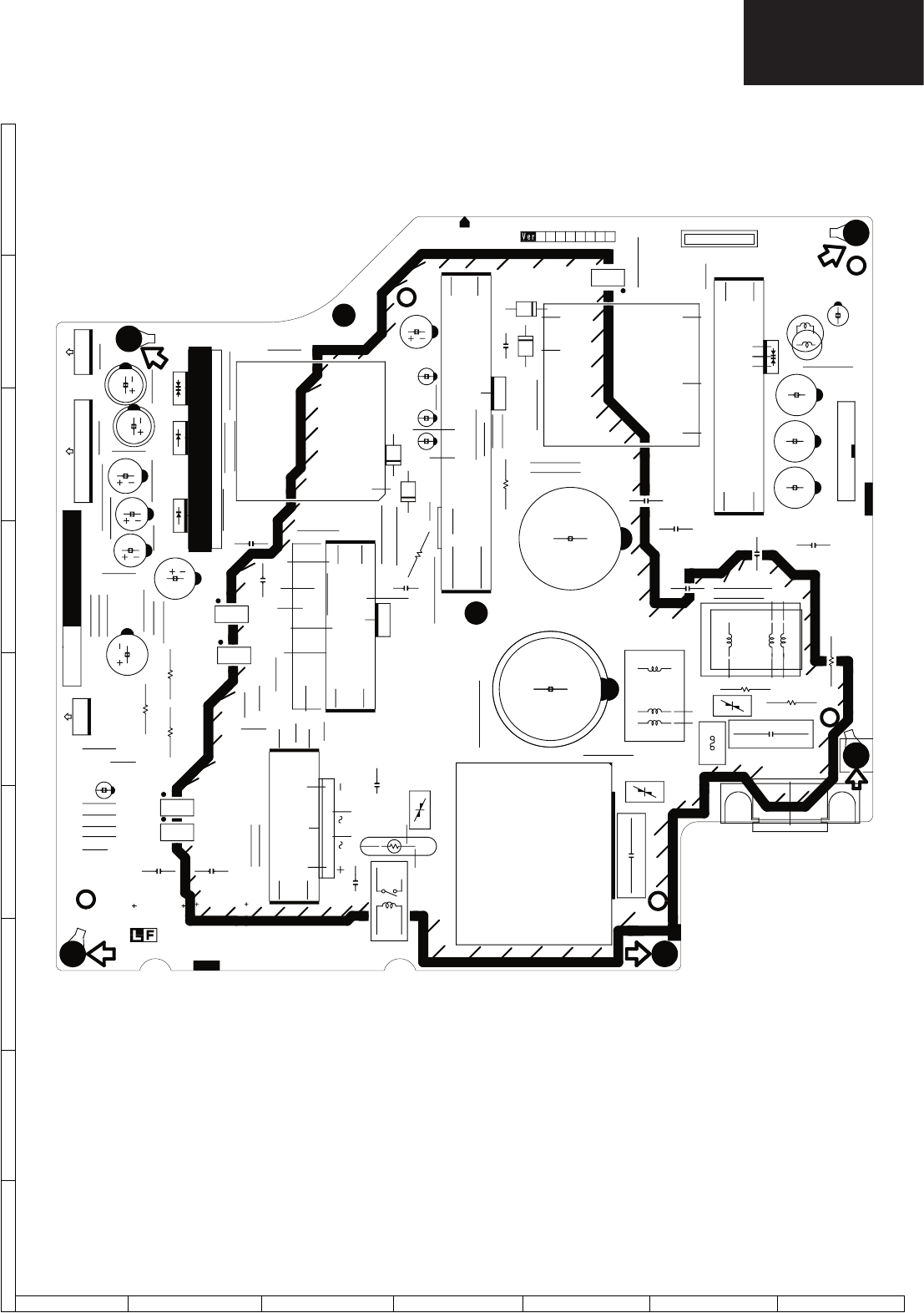
99
LC-26GA5E
LC-32GA5E
LC-32GD8E/RU
LC-32BT8E/RU
LC-37GD8E/RU
LC-37BT8E/RU
LC-32/37GD8E/RU
LC-32/37BT8E/RU
CHASSIS LAYOUT
Power Supply Unit Layout QPWBFD605WJN5
1
I
H
G
F
E
D
C
B
A
234 5 6 7
1
9
19
1 7
1
9
123
1
2
3
4
1
23
4
1
23
4
1
23
4
1
2
3
4
13
1
2
3
P701
P703
P704
203
204
401
405
408
409
410
415
416
417
801
L702
R701
R702
R704
SC701
C704
C708
C712
R751
C723
R760
302
114
C735
116
C736
C740
RY701
C742
C743
C744
C751
C754
C755
C756
C757
C758
C761
D701
C762
C767
IC704
IC705
D729
D730
D731
D732
D733
D734
D735
D736
D737
D739
T4AL 250V
QPWBSD605WJN5
103
106
108
a
1
14
115
420
C768 C752
LUG701
LUG703
LUG704
LUG702
421
404
903
708
704
706
701
702
703
C709
DUNTKD605WE
716
107
109
117
202
305
307
308
402
412
414
418
902
719
721
D762
313
419
312
709
411
725
802
309
720
723
724
112
206
207
805
317
306
315
102
413
316
727
205
111
210
729
728
733
732
731
739
740
C778
C777
C779
C780
18
9
16
1
7
9
16
T701
T702
D728
C782
726
118
745
F701
2
1
(L) (N)
734
738
422
423
211
TH701
SEC. PRI.
VA701
VA702
VA703
705
707
D771
E701
LA
PRI. SEC.
1
6
712
RDA701
RDA702
RDA703
T703
712
C705
C706
R853
R854
R855
RDA705
RDA704
C707
L701
804
P702
323
120
212
324
2
119
735
113
C741
C781
746
747
213
904
C734
C725
L752
L753
741
742
743
749
744
748
711
750
n4-02/22
A B C D E F G H
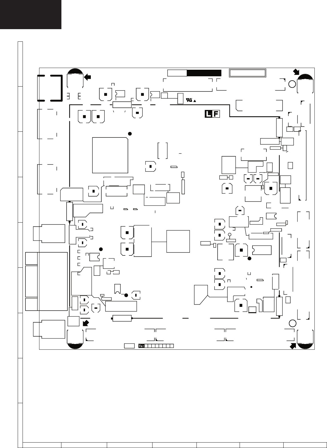
100
LC-26GA5E
LC-32GA5E
LC-32/37GD8E/RU
LC-32/37BT8E/RU
RJ1705
RJ1708
C1703
C1706
C1707
Q1703
C1708
C1901
C1902
C1903
C1904
C1715
C1716
C1718
Q1909
C1910
C1911
C1720
Q1910
C1721
C1722
C1723
C1724
D1702
D1703
D1704
1 7
P2301
D1706
1
3
P2302
D1707
1
10
P2303
1 20
P2304
132
P2305
P2306
C1922
C1923
D1901
D1902
C1733
IC1704
D1904
D1710 C1735
C1929
R1901
1
4
5
IC1706
R1902
D1713
R1903
D1908
C1739
RJ2301
D1909
RJ2302
R1906
R1713
RJ2303
R1714
R1909
IC1901
IC1902
C1740
C1934
D1910
C1741
1
36
37
72
73 108
109
144
IC1905
1
2
59
60
P2702
C1748
R1720
C1749
R1724
C2306
C1942
C2307
C1943
C1750
C2308
R1728
C1751
C2309
RJ2702
C1753
RJ2703
RJ2704
R1920
C1755
RJ2705
R1921
C1756
R1922 R1923
C2310
R1924
C2311
RJ2709
R1925
C2312
a
R1732
R1926
R1927
R1734
R1928
R1735
R1929
C2316
C1953
R1738
C1954
R1739
C1761
RJ2712
C2702
C1762
RJ2713
C2703
RJ2714
C2704
C2705
Q2701
R1932
C2706
Q2702
RJ2717
R1933
C2707
R1740
C2708
Q2704
RJ2719
R1935
C2709
Q2705
C1961
C2711
R1749
RJ2721
D2305
RJ2722
RJ2723
C2714
R2305
RJ2725
D2309
RJ2726
RJ2727
R2307
RJ2728
RJ2729
C2719
R2309
R1752
14
58
IC2303
D2310
D2311
D2312
RJ2730
C2720
R1759
RJ2731
R2311
RJ2732
C1976 C1977
RJ2734
R2315
RJ2735
D2701
RJ2736
C2727
RJ2737
C2728
D2705
R2703
R2704
R2705
R2706
R2707
C2731
R2709
R2321
IC2701
C2732
13
46
IC2705
R1770
R2711
R2713
R2715
FL1901
X3001
FL1902
R2717
R2718
R2719
R2333
R2335
R2720
R2721
R2339
C3302
R2724
C3306
R2341
FB3002
FB3003
FB3004
FB3005
FB3006
FB3009
FB3010
FB3012
D3301
FB3015
C3325
FB3016
C3327
C3328
FB3019
C3329
R3305
R3306
R3307
R3308
C3330
FL2301
C3331
FL2302
C3332
FL2303
C3333
13
IC3303
1
IC3304
C3334
C3335
C3336
C3338
R3313
R3314
R3315
R3316
R3317
R3318
C3340
R3319
C3342
R3320
X1901
FB1701
LUG1701
LUG1702
LUG1703
LUG1704
LUG1705
LUG1706
LUG1707
LUG1708
LUG1709
FB1902
FB1906
1
222
23
SC1701
1
2 8
9
SC1702
DCBA E F G H
119
SC1901
119
SC1902
L1701
L1702
L1901
L1902
L1903
L1904
L1905
L1906
L1907
L1908
J2701
J2702
FB2301
FB2302
FB2303
FB2304
SC2301
SC2303
RJ3001
FB2705
RJ3002
FB2706
RJ3003
FB2707
RJ3004
FB2708
FB2709
FB2710
FB2715
C3002
RJ3013
RJ3014
C3004
C3005
RJ3016
1
222
23
SC2702
C3006
1
222
23
SC2703
C3007
RJ3018
1
222
23
SC2704
C3008
1
2
14
15
SC2705
C3009
1
2
22
23
SC2707
RJ3020
C3010
RJ3022
C3012
RJ3023
RJ3024
RJ3025
C3016
C3019
RJ3030
C3020
RJ3031
C3021
RJ3032
RJ3033
RJ3034
RJ3035
RJ3036
RJ3039
R3002
C3030
R3009
RJ3041
114
1528
IC3003
3
4 5
IC3004
C3035
FB3301
C3036
FB3302
FB3303
FB3304
R3011
FB3305
FB3306
FB3307
R3013
FB3308
C3040
TH3001
C3041
C3042
C3043
C3044
1
8
P1701
C3048
RJ1701
14
5
88
5
4
1
1
8
9
16
1
3
XD890WJN2
KD890
CPU
+5V
+3.3V
P+35V
BU+12V
+1.8V
BU3.3V
BU1.8V
S+8V
LCD+5V
BU+5V
RESET-TP
LB
LV
SH
KM
RA
4
6
ANT+5V
3
1
I
H
G
F
E
D
C
B
A
234 5 6 7
Main Unit Layout QPWBXD890WJN2
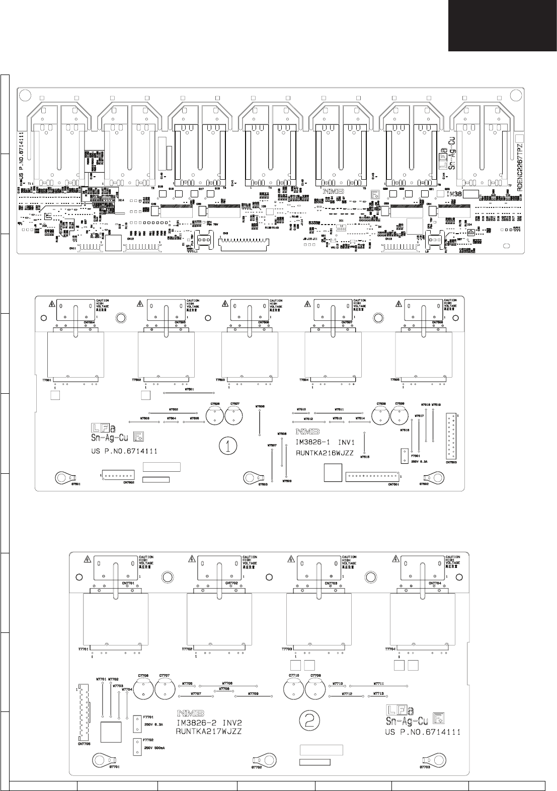
101
LC-26GA5E
LC-32GA5E
LC-32GD8E/RU
LC-32BT8E/RU
LC-37GD8E/RU
LC-37BT8E/RU
LC-32/37GD8E/RU
LC-32/37BT8E/RU
Inverter Unit Layout RDENC2266TPZC
70
LC-26GA5E
LC-32GA5E
LC-32GA8/LC-32BV8
LC-37GA8/LC-37BV8
1
I
H
G
F
E
D
C
B
A
234 5 6 7
Inverter Unit Layout RDENC2266TPZC
Inverter Unit Layout RUNTKA216WJZZ
Inverter Unit Layout RUNTKA217WJZZ
1
I
H
G
F
E
D
C
B
A
234 5 6 7
Inverter Unit Layout RUNTKA216WJZZ
Inverter Unit Layout RUNTKA217WJZZ
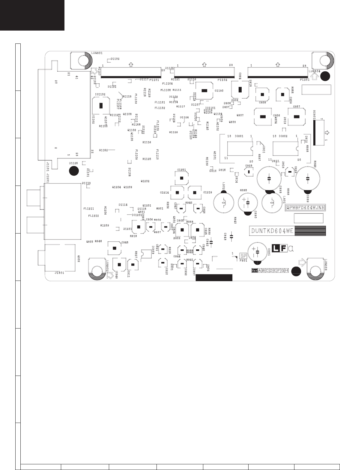
102
LC-26GA5E
LC-32GA5E
LC-32/37GD8E/RU
LC-32/37BT8E/RU
1
I
H
G
F
E
D
C
B
A
234 5 6 7
AV Unit Layout QPWBX604WJN3
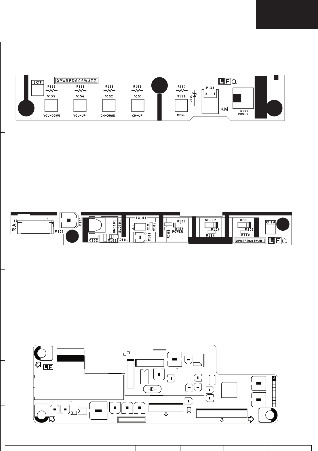
103
LC-26GA5E
LC-32GA5E
LC-32GD8E/RU
LC-32BT8E/RU
LC-37GD8E/RU
LC-37BT8E/RU
LC-32/37GD8E/RU
LC-32/37BT8E/RU
1
I
H
G
F
E
D
C
B
A
234 5 6 7
TUNER Unit Layout QPWBX609WJN3
RC/LED Unit Layout QPWBX607WJN1
KEY Unit Layout QPWBX606WJZZ
112
13
24
1
16
17
32
33
48
49
64
1
4
5
8
1
8
9
16
12
3 4
123
TU201
C201
C241 Q209
IC204
IC203 C204
C206
C217 C230
X201
IC201
C221
FL201
C249
C261
C237
C242
C252
C247
IC205
C246
P202
IC202
X202
C244
C226
FL202
D204
D203
R245
R272
R273
IC206
R263
DUNTKD609WE
QPWBND609WJN3
a
115
P201
C270
C273
1
3
4 5
Q205
IC207
1
6
4
3
LUG203
LUG201
LUG202
DCBA E F G H
C279
L206
L207
L212
14
5 8
IC208
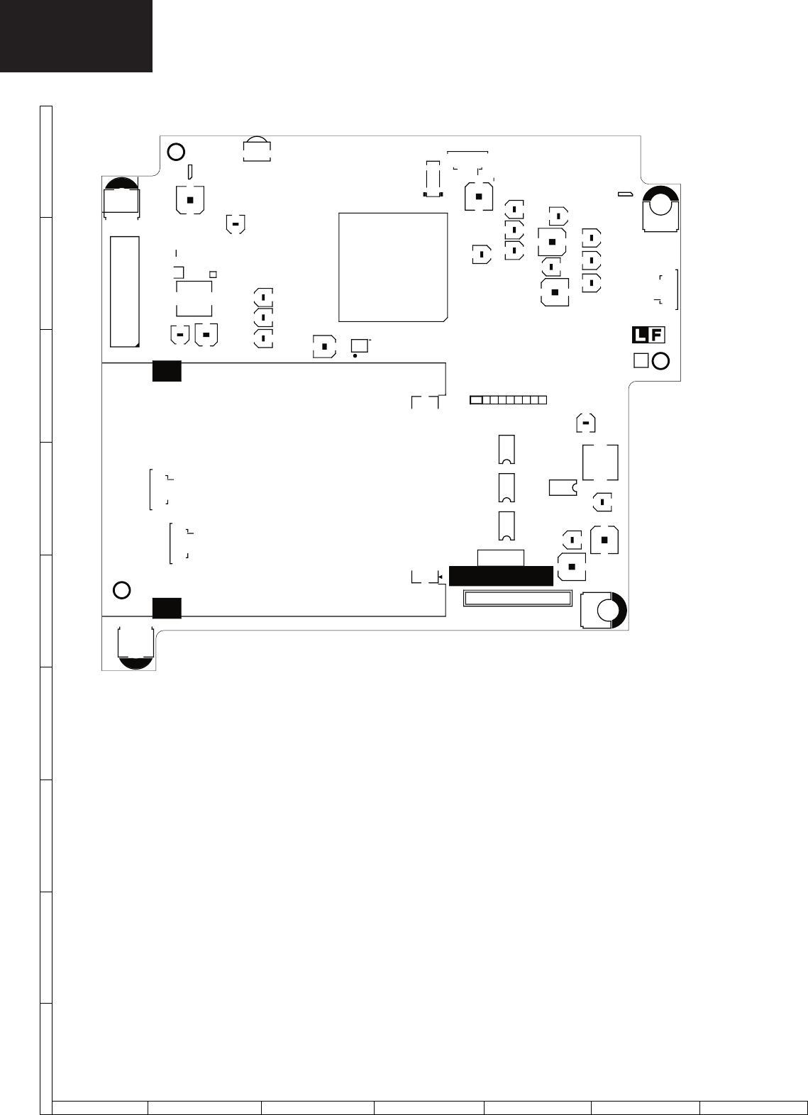
104
LC-26GA5E
LC-32GA5E
LC-32/37GD8E/RU
LC-32/37BT8E/RU
1
I
H
G
F
E
D
C
B
A
234 5 6 7
Digital Unit Layout QPWBX628WJN2
102
LC-26GA5E
LC-32GA5E
LC-26P70E
LC-32P70E
LC-37P70E
1
I
H
G
F
E
D
C
B
A
234 5 6 7
LC-26/32/37P70E Digital Unit Layout QPWBXD628WJN2
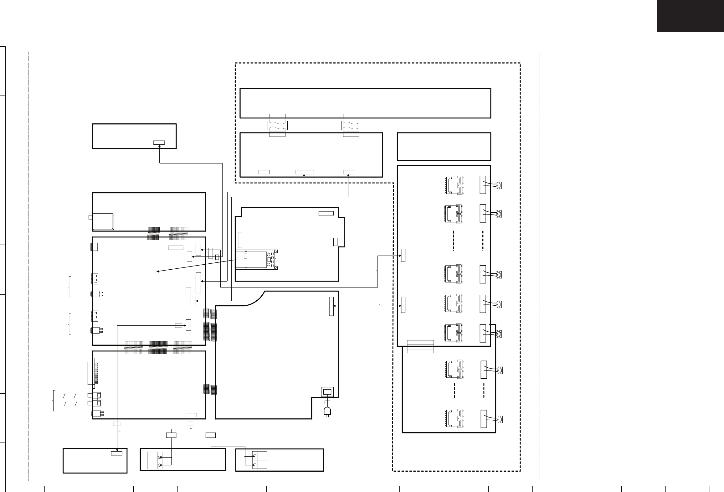
105
LC-32/37GD8E/RU
LC-32/37BT8E/RU
EXT4
(SERVICE)
DUNTKD890FM06 (32)
RCORF0103CEZZ (37)
14
P201
1
IN
1
1
CN1
CN9 (32)
- (32)
EXT2/
QCNW-E801WJQZ(37)
(SERVICE)
(32/37)
LA
SC2707
1
8
OUT
100
CN2
CORE
- (37)
*4(37)
EXT3
P1101
SC2705
23
(32/37)
QCNW-E684WJPZ(32/37)
OUT
CORE
*4(37)
P1102
P2301
23
A3IU32D8E1
4
CORE
CORE
R1LK315T3LF15 (32)
QCNW-E419WJQZ(37)
DUNTKD628FM01
T8 (32)
P1201
7
1
1
A3KU37D8E1
*8(32)
R1LK370T3LZ5BX(37)
QCNW-E799WJQZ(32)
P101
SC301
P2303
1
80
*5(37)
QCNW-E546WJZZ (7P)
CN10 (32)
RCORFA023WJZZ(37only)
QCNW-E413WJQZ(37)
(32/37)
T7704(37)
1
P1701
23
SERVICE EXTENSION CABLE
- (37)
CORE
DUNTKD604FM10
QCNW-E415WJQZ(37)
SP
7
LB
P301
37 UNIT 2/2
*5(37)
1
RCORFA064WJZZ
CN7704(37)
QCNW-E542WJZZ (23P)
P153
- (32)
QCNW-E233WJQZ(32)
HDMI
P2305
SC2301
1
80
*8(32)
RUNTKA217WJZZ
- (37)
P202
QCNW-E543WJZZ (9P)
RCORFA064WJZZ
DUNTKD607FMV0
1
1
J1301
1
RA
RUNTKA216WJZZ
15
D-SUB
AUDIO L/R
- (37)
DUNTKD605FM14(32)
QCNW-E544WJZZ (15P)
CN4 (32)
P2702
32
3
J1201
R
80
37 UNIT 1/2
1
1
HEADPHONE
A3KU2655EJ
P2306
T1 (32)
DUNTKD605FM03(37)
SC2702
CARD SLOT
L
KM
J1101
P702
1
CN7501
1
3
TUNER
B to B
CKITKD609FM01
1
SC2703
RSP-ZA184WJN2
(32/37)
P2302
L
T7501(37)
P4003
80
1
23
QCNW-E232WJQZ(32)
TU201
B to B
9
SC2704
SC4602
1
QCNWKA012WJZZ (FOR DIGITAL SOFT WRITING)
R
T6 (32)
R
CN5
T7502(37)
14
CN7504(37)
SC701
KM
23
SC1701
QCNCMA199WJSA
23
CVBS
B
CN4
T7 (32)
(E/I/F/R)
CN5 (32)
QCNWKA011WJZZ (FOR DIGITAL 60P)
LA
- (37)
AC-IN
QCNW-E234WJQZ(32)
1
SC1702
15
IN
QACCKA021WJPZ
1
P4001
T2 (32)
RCORF0103CEZZ(32/37)
QCNW-E412WJQZ(37)
CN11 (32)
P701
SC2303
1
IN
CN4190
10
QACCBA073WJPZ (K)
R
CN7505(37)
EXT5
RCORFA023WJZZ(37only)
T7701(37)
SC7503
P703
J2701
1
IN
1
B
1
(32/37)
- (32)
CN7705 - (32)
HDMI
AUDIO L/R
7
J2702
1
OUT
2
RSP-ZA184WJZN1
(32/37)
32
EXT1
DUNTKD609FM01
1
SC1901
CORE
10
R
20
1
D-SUB
(32/37)
CORE
CN7502
P704
LV
CN7701(37)
RA
L
19
7
RS-232C
QCNW-E800WJQZ(32)
DUNTKD606FMV0
(32/37)
LB(37only)
1
SH
8
Y/C
- (37)
SC4601
CN3
DUNTKD890FM07 (37)
QCNW-E609WJQZ(37)
RCORFA023WJZZ (32)
CN3
(37)
(32)
QCNWKA015WJZZ (FOR MAIN SOFT WRITING)
RCORF0103CEZZ(32only)
(RCORFA020WJZZ)
1M3819(32)
LCD-MODULE
DIGITAL UNIT
TFT LCD PANEL
KEY UNIT
AC-IN
TUNER-UNIT
AC-CORD
MAIN-UNIT
AV-UNIT
LCD-CONT-UNIT
POWER-UNIT
R/C LED UNIT
BACK LIGHT
SPEAKER R SPEAKER L
INVERTER
-UNIT
LC32/37BT8E WIRING DIAGRAM
LC32/37GD8E/K/F/I/RU
OVERALL WIRING DIAGRAM
1234567 8 9 10 11 12 13 14 15 16
I
H
G
F
E
D
C
B
A
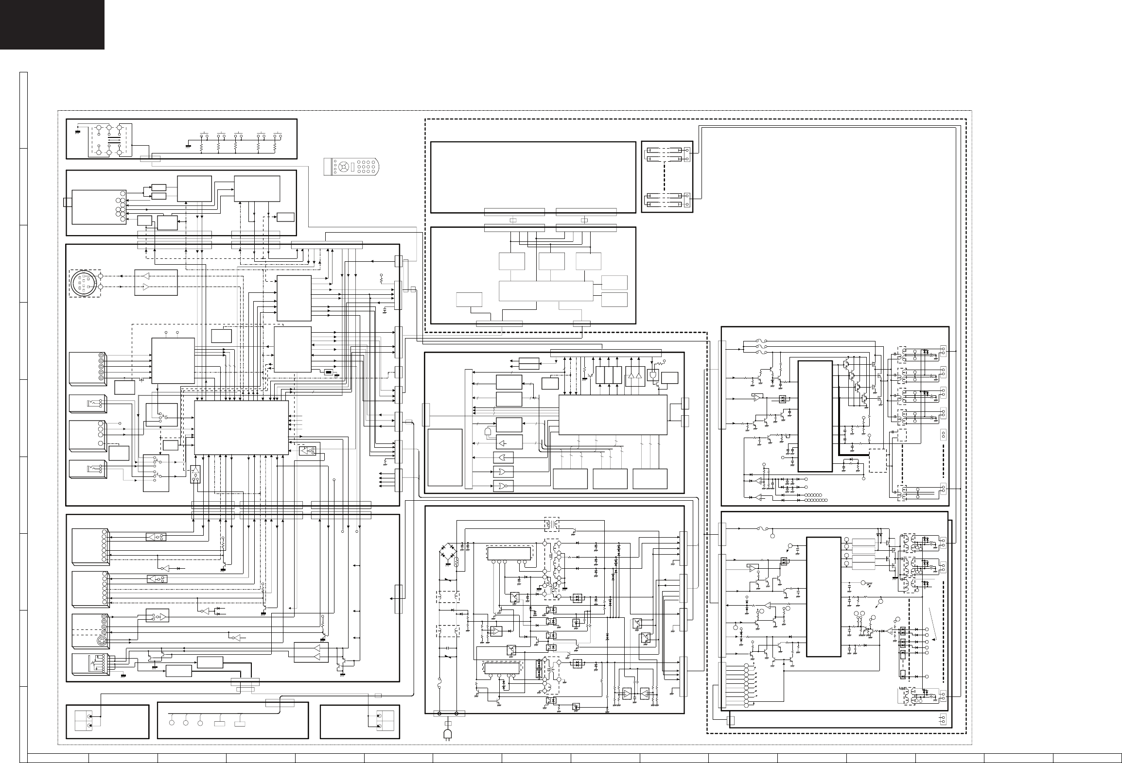
106
LC-32/37GD8E/RU
LC-32/37BT8E/RU
ON
OFF
5/6
E2PROM
181
180
179
2
NJM2904
FPGA
7
SC301
CARD-SLOT
3
ROMSEL0
CPU
WAIT
ERR
A-IN-L/R
RXC+/-
2/3
4/6
I-DET
J2701
DTVPC
DTVHDMI
(A/B)
OPC-IN
LVC573AP
5
OP-AMP
CN7505
PRE-DRIVE
S2_MUTE
AD1
AB1
L
3
POW
-LED
SLOW_SW2
IN3YV
OFL
24
23
65
|
58
AV
14
SDA
SCL
8
9
4
Q7525
PIC16F913
3
EQ
OUT3-L/R
32
5
MUTE
12
2
71/70
P2702
DRAM
RXD
SENS
VIN_1
IC704
PCON2
REG
Q4607
FESDA
FESCL
30V
3
Q7503
IF-AGC
1-5
OR
P0035GE
270
IC4406
FL201
(32/37)
P-CON1
24V
CD4052BP
4
12
LOUT/ROUT
4/5
I-sen
(32)
(32/37)
8
4
7
E
27/28
VOUT2
400V
HPMUTE
S_MUTE
9-11
P1701
C762
POWON
Reg
3
M2
2
7
D7517
1-5
TXD
3
IC301
SDIDM
M5
1
21
20
5/6
5
8
R
QJAKJA007WJZZ
57
|
50
SC4602
DTUNER_R/G/B
OCTAL
TRANCEIVER
IC4204
8
A-IN-L/R T703
AV
OSC
178
177
176
6
400V
16/15
CN7705
184
QSOCDA036WJ
IC4003
6
9
8
220
AF9
OUT1-L/R
22
21
H/V
D759
VIN2
4
28
&L
14/15
P153
20
Q7517/22/18
15
R
RMC101
IF(D1/D2)
104
C705
9
EPROM
FL202
13.5V
8
SENS
SLOW_SW1
&L
9
10
Q1101
OSC
MUTE-SP
EQ
1
39
41
Q7504
&L
31
IC4408
OR
20
11
43
45
IC708
(RCORFA020WJZZ)
HDMI
HS/VS
&L
VA1
159
S2_MUTE
SDA3
SCL3
3
1
FB
P2305
C706
V-SENCE
R
EMIDM
22
B
11
REG
8
I2CSEL
4
23
TH3002
M6
2
IC302
BUFFER
/LINE
DRIVER
D7525
GND
P1101
1
187
175
182
A-OUT
3
|
11
1/3
QJAKZA033WJZZ
H/V
1
R(C2)/G/B
11
270
13.5V
G
BR24L64F
AC11
AE6
IC2705
6
IC2303
8
10
400V
12/15
17
18
CN7508
IC7502
1
IF(A)
D724
BRT
B
A-OUT-L/R
C706
VIN2
25/26
Q1102 S_MUTE
BU4228G
R(C1)/G/B
(37)
33
IC101
41
14
13
OUT2-L/R
11
SDA
SCK
SDE
Q730
400V
HDMI
RECEIVER
43
45
PANEL CONTROL
M3
REG
VA1
Q702
8
220
D104
CI***
EMIAM
88 183
REG2
7
L701
PRE-DRIVE
CORE
C705
Vcc
12
IC4203
22
KEY,KEY-PSW
900V
P2301
IC7502
R
L
M5
84
83
I2C
SEL
IC4403
3-STATE
OUTPUT
2
AA3
AE1
P1102
VA2
A/V-IN
7/9
REG
I-DET
CN5
(32/37)
I-SENCE
31
IXB680WJ
15
5
RSP-ZA184WJN2 L
13/16
IF(D1/D2)
P-CON2
CN7503
7
SDA
SCL
M2
7
IC7502
29
27
21
22
DTUNER-CVBS
7
40
INV-BRT(FL-OFL)
Q7508
DH/DV
SYNC
BU+5V
DUNTKD606FMV0
12
11
G
CN7704
+8V
-AIN
OPEN
BU5V
G
RCORFA023WJZZ(37)
174
173
172
1/2/3
RXD
AE12
AC5
MICRO
CONTROLLER
13
12
3/1
VA2
D735
10
8
50
|
57
A
RCORF0103CEZZ(32)
16
DIGITAL
PROCESSOR
2
3
13.5V
4
B3.3V
CN4190
HDMI-G
21
CORE
188
161
OSC(37)
99
52
IC2301
35V
RCORF0103CEZZ (32/37)
20
17
OPC
OFL
21
3-STATE
OUTPUT
24V
P2303
BU3.3V
115
116
117
FE**
29/30
4
D732
D-L/R
R
15
SDA/SCL
OPC
-LED
Vcc
IC1901
IC4202
VCC
CN4
F7701 6.3A
VB2
1
IC203
M1
G
13/16
10
7
SCART1
191
P1201
LB
Q1203
Q7515/21/18
LIN/RIN
VIN7
Q731
4
3OVP
LA
37/29
16/15
H/V
GPIOO/IOI
SC2301
OPEN
6-10
12
23
36
38
40
16
20-21
29
27
LVDS_CN/CP
(26/32/37)
Vcc
R
Q1201
Q1202
VB2
5-7
R
Q205
Q209
SDA/SCL
33
N4
N3
IXB076WJ
11/10
M2
Q7509
2
5
T7501
TVSCA
TVSCL
EMIA
9
23
LVDS_
CN/CP
22
B
ISL83220
R858
13
12
CORE
4
OPC/SLP
HDMI-B
132
131
IC4002
IC707
4
87
D-L/R
SC1702
FAST-SW1/
SLOW-SW1
IF-AGC
2
M2
3
VA701 6
SC4601
OPC/SLP
FESDA
FESCL
24LC2BIN
P701
AC21
AD21
25
15/11/7
L
E2PROM
195
Vcc
CORE
10/12
119
120
D728
11
4
OVP
VB1
REG/
REG2
D2
Duty
R
13/1
CORE
B
24V
AV-LINK2
CCP-1
IC4201
AGC
D1
Q1204
J1201
RA
REMOCON
20-21
CKITKD609FM01
4
6
8
5
D1
27/23
IC1102
IN1_L/R
RA
PRE-DRIVE
2
RSP-ZA184WJN1 R
VB1
EMIA
RS-232C
35V
TXD
RXD
(26/32/37)
P4
CORE
C754
4
SC1701
D4
M6
6
RCORFA023WJZZ(37)
64MSDRAM
TS2D[0-7]
380V
L
+8V
-AIN
I2CSDA
I2SSCL
1
|
23
OP-AMP
15
7
D751
Q7505
RS-232C
TU201
9
T7505
D2
102
LEDPOWR/G
Q708
171
47
24
J1101
7
2
1
10/9
D2
28/27
D733
C
KM
11
D2
2
D746
Q4001
Q4002
D-R/G/B
LB(37)
SIF
26
REG
4
4
D3
194
Vcc
5V
RCORFA064WJZZ
(32/37)
4
6
8
4
TXD
RXD
7
D3
BCT
IC1905
Q712
TSDA/SCL
CVBS
STB
EMI
E2PROM
IC4001
12
D3
S_MUTE
L
D730
DUNTKD607FMV0
MUTE_-SP
132-123
QCNCMA012WJ
L
D3
16/8
CORE
1
16
IN2_L/R
SC2702
5
POW_5V
10
D3
RCORF0103CEZZ(37)
IC1101
NJM2903M
R3
Tra/Receiver
D7501
Q7514/20
D-SUB-15
D3
FE**
7
RTUNQA033WJZZ
(P70E)
M1
Vin=24V
D737
+8V
-AIN
L
D3
SDA/SCL
HDMI-RST
M5
5V
64MSDRAM
CH+
11
L
3.3V
R
M5
MR4020
TEMP1-3
A-OUT-L/R
Q7506
5V
I
CE1
Q710
10
DTUNER-CVBS
2/3
VIF
7
TDI/TDO
24V
19
/
21
18
17
D777
189
160
3
9/7
D
S2_MUTE
TMS/TCK
TDA8931T
2
1
D778
12
IC709
FAST-SW2/
SLOW-SW2
RSTIN
8
R1(C1)/G1/B1
HDMI-IN
(SERVICE)
8
7
5/6
8
S-MUTE
DUNITKD605FM14/03
S-MUTE
59/58
15
144-133
7
P4001
LVDSxx
RESET
19
2
1-3
FED
IN3_L/R
L
EMIDM
R
IC4604
QCNCMA250WJ
M3
IXB731WJ
(SERVICE)
M3
IC2702
RQ1
ZD7502
1
IC3005
11
24LC2BINEES
(SERVICE)
CVBS-IN
19/18
R
SC701
SC2703
OPC
QSOCNA229WJ
16
WAIT
RESET
(32/37)
2
12
1-5
R
PRE-DRIVE
B
Q1107
Q1108
41
/
39
11
IC705
20
VOL+
MULTIPLEX
5
PCLK
24V
IXB076WJ
(32/37)
7
FRAME
2
9
TS2D***
J
2
RX2+/-
CVBS
19
Q7507
5
18
17
122
HDMI-WP
SS
P-CON2
IC4401
25
13
VIN1(Y/V)
IC2701
9
M3
IC3003
VOUT2
SW-REG
84-86
162
90
E
M2
3
109
TDA8931T
6/2
F701
10/9
Vcc
R
20
SMIAM
P4003
5
(SERVICE)
AGC
ATUNER-CVBS
M6
PCON1
SPK_L/R
GRAY LEVEL
ADJ.DRIVE
8
R2(C2)/G2/B2
19
BL-ERR
28/27
EMIDM
TDA9886
D762
6
R
D102
AOUT1_R/L
ZD7501
Q4601/2
BL-ERR
4-6
Q1901
Q1903
4A
S/VIDEO
3
AUDIO
P201
CS3
BE0
PCV
R/G/B
D2
CD1
(32/37)
P2302
D726
2
5
6
EMIA AF13
9/10
FED[0:7]
1
FE***
CH-
DTU-ON
AV-LINK1
4
IC7501
FED[0:7]
C757
SIF
Q7513/19
10
LCDUD/LR
J
87
Q1103
Q1104
P704
FRAME
3
S2_MUTE
Q7511
6
5
IC4402
S_MUTE
P301
11
IN1_FSW
12
D701
16M-FLASH
KEY
KEY-PSW
FED[0:7]
M1
AGC
RX0+/-
S_MUTE
F7702 1A
10
IXB664WJ
67/66
P702
RY701
IC201
R
D
M2
2
TH701
CT
SCART2
SPL MR4030
D738
SII9021
AF6
102
18
14
HXA033WJ
SDA3
SCL3
H/V
M6
IXB682WJ
Q726
VA702
8
2
PCON1
SMI
D-L/R
EMICS3
EMIBE0
10
16
S-MUTE
SIF
3
IC706
14
13
QSOCZA117WJ
SLEEP
14
15
Q4603/4
COM-BIAS
ADJ
13
10-15
P2306
T702
PCON2
6
M2
9
10
Q7528
CIA
AOUT2_L/R
AF11
LEDPOWR/G
LCX244MT
Q713
1
13/15
P202
EMI
CN5
9
C704
SW-REG
4
1
4
13/14
BD9777FV
D741
2
CN7502
VOL-
2
AV-LINK
LVDSxx
IN2_FSW
D731
13
L
Q7512
11
P703
T7502
P101
15
IC4405
HDMI-
INT
VCC
Q301
7
2
1
C744
5/11
Q1106
9
10
6
3
4/6
35V
SPR
VIN2(Y/V)
IC202
6
A
24/22
FE**
900V
IC3002
IXB681WJ
VOUT1
6
Q723
RESET
M2
5
10
FED[0:7]
IC1201
5V
IF-DEMOD
M5
7
13
IC1710
Vcc
38
39
40
17
8
141
|
128
GND
CIIRQ0
EMI
IC303
(32/37)
8
16
25
24
CIA
PANEL
POW BLOCK
380V
INPUT
4
2
D103
10/9
14
DUNTKD628FM01(32/37)
CN4
PCV
H/V
L702
Q302
OUTMON_L/R
HEAD
PHONE
QJAKEA073WJ
J2702
QFS-ZA007WJZZ
Q7527
Q4605/6
AF12
D736
TCLCX245
1
3
23
Vcc
2
SC2707
Q721
36/32/28
10/11
30V
5/4
U1
TEMP1-3
INV-CTL
1
EMIAM
RT
14
F7501
IXB624WJ(GD8E)
CN7501
L
S156
D754
50
|
57
14
C752
119-110
IC4404
Q7501
24/23
4
13
2
AV
I2CSEL
VIN_2
REG
4-6
CVBS/Y-IN
RX1+/-
6
10
QCNCMA199WJSA
8
H-SYNC
V-SYNC
Q1105
9
I-sen
91
Y
FB
C
3/5
35V
63/62
BR24C21F
CID
1
CPUWAIT
M5
IC4701
23
24
16
SC2704
D753
COFDM-
DEMOD-IC
CN2
D756
PCON1
34-25
EMIAM
IXB823WJ
QJAKEA073WJ
14
14
15
STB
36
32
28
MAIN
-AMP
DTM-RESET
HDMI-
SDO/
WS/
SCK
NJM4558M
14/2
T701
FED
Q305
16
J1101
MAIN
-AMP
CN7504
6
73
|
66
1
5
AUDIO
IN3YV
21
19
H/V
SELECTOR
A3KU2655EK
HPOUT_L/R
SC2303
4/5
6/7
Q7526
11
2
6
LVC573AP
M2
5
AF1
AC1
A3KU2655EJ
R
SC2705
Q724
1
3
VOLTAGE
REG
J1301
AV
37
|
58
EQ
IC204
8
D739
1
2
6.3A
VCT6973
190
36
POWER SW
D725
2
TXD
(32/37)
EMIDM
13
D734
Q7502
LCDUD/LR
12
IC4407
IC3001
20
92
14
1
2
Q704
7/9
S_MUTE
C
SC1901
8
E2PROM
NOR
D7516
CIOE
C
10-15
B
VOUT1
EMI
HDMI-R
BR24L64F
H-SYNC
V-SYNC
CN1
PCON2
IC2704
13.5V
IC4702
M2
M5
14
FESDA
FESCL
Q306
B
C
E
J
RT
VA1
VB1
REG
D
NK
OVP
T4
BCT
F
8
19
E
P
6
I
Q14
F
4
G
A
CN3
18
D65
T8
IC4
IC5
17
T5
Q17
H
Vcc
INV-CTL
C
CN5
20
IC3
T2
4
Q18
VA2
DRIVE
CIRCUIT2
P
F/B
CN4
24V
Q19
3
PWM-SEL
13
G
T1
CN7
16
L
2
9
T3
5A
IC1
CN8
1
M
1-5
CP3
CN11
Duty
D
14
CP1
A
V
CP4
CN6
1A
5A
H
3
12
3
INV-ON
SS
Q16
12
5
14
3
CT 10
VB2
INV-BRT
I
O
B
O
9
5
INV_ON
INV_BRT
PWM-SEL
INV_ON
INV_BRT
PWM-SEL
12
13
14
4
5
4
PWM-SEL 9
INV_ON
INV_BRT
RDA703
RDA706(37)
RDA702
R828
27/26
12
42/35/41
14
1
3
2
8
100
91
97
7
I2C
SEL
INV-ON(BL-ON) STB
5 2
37only
17 5V/5V(CONT)
QSOCZA116WJ
QSOCZA116WJ
LV
5V
8V
BU3.3V
BU1.8V
33
18
192/170/133
185/169/142
95V
3.3V
74 99
1.8V
30V
8
6/7
RCORFA023WJZZ(32)
RCORFA064WJZZ
(32/37)
DUNTKD604FM10
SPEAKER L
AV-UNIT
QACCKA021WJPZ(E/F/I/R)
KEY-UNIT
PC-INPUT
LCD
QACCBA073WJPZ(K)
BACK-LIGHT
DUNTKD890FM06/07
TUNER-UNIT
EXT-4
TFT LCD PANEL
EXT-5
MAIN-UNIT
POWER-UNIT
LCD-CONT-UNIT
INVERTER UNIT 1/2
RUNTKA217WJZZ
SPEAKER R
EXT-1
37 INCH
INVERTER UNIT 2/2
AC-IN
RUNTKA216WJZZ
37 INCH
AC-CORD
EXT-2
LCD-MODULE
R/C LED UNIT
DIGITAL-UNIT
RRMCGA472WJSA(GD8E)
EXT-3
A3IU32D8E1R1LK315T3LF15(32)
R1LK370T3LZ5BX(37) A3KU37D8E1
INVERTER UNIT 32 INCH IM3819
RRMCGA490WJSA(BT8E)
12 3
45 6
32/37GD8E/KS/F/I/RU BLOCK DIAGRAM
BT8E
BLOCK DIAGRAM
System Block Diagram
1234567 8 9 10 11 12 13 14 15 16
I
H
G
F
E
D
C
B
A
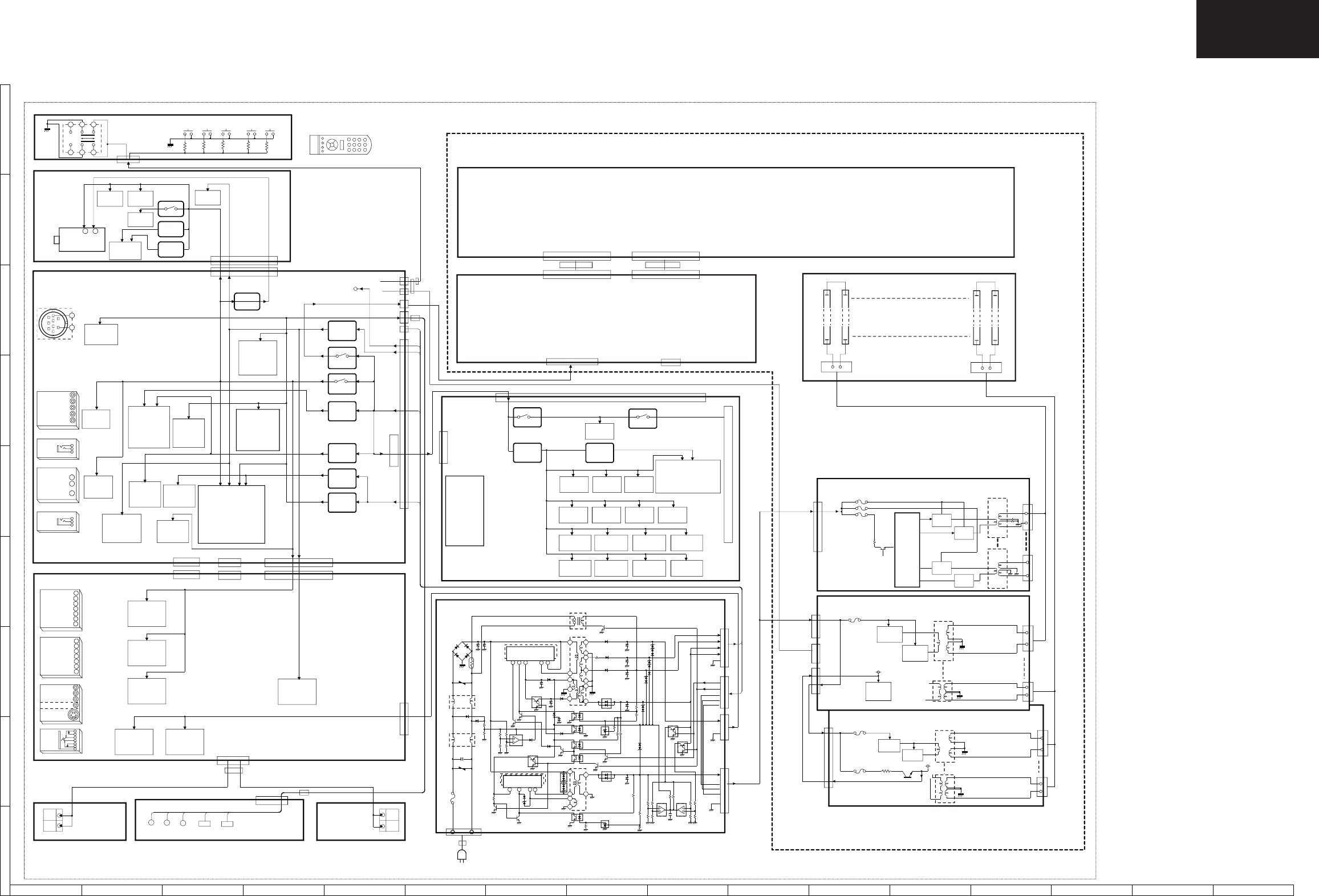
107
LC-32/37GD8E/RU
LC-32/37BT8E/RU
ON
OFF
12 3
45 6
Vcc
Vcc
AUDIO
M2
J2702
M2
J2701
SC2301
QSOCDA036WJ
12/15
1/2/3
D-SUB-15
QSOCNA229WJ
13/14
SC2303
16/15
1/3
7/9
HDMI-IN
4/6
SC1901
CN5 CN4
CN2CN1
P2305
P2303
SC1702
SC1701
P201
SC2705 P2302
CN5
CN4
D-TU201
CH+ VOL+CH- VOL-
S156
POWER SW
P0035GE
P153
DUNTKD606FMV0
(32/37)
INPUT
AUDIO
CKITKD609FM01
QCNCMA012WJ
7
8V
1
Q203
HDMI
RECEIVER
IC1905
SII9021
IC1901
24LC2BIN
E2PROM
IC3002
IXB624WJ
VCT6973
2
3
QSOCZA117WJ
QJAKEA073WJ
QJAKEA073WJ
M1
M2
SC2704
M2
M3
M6
M3
M6
M6
M5
M5
S8V
7
6/2
40
D103
SENS
1
20
3
SCART2
SCART1
P101
SENS
2
31
15/11/7
B
D104
SC301
POW
-LED
S/VIDEO
4
3/5
J1101
41
RSP-ZA184WJN2
(32/37)
OPC
-LED
RMC101
13/15
5
36/32/28
AV
3/1
10
G
DUNTKD604FM10
REMOCON
IC101
HEAD
PHONE
R
AV
J1101
37/29
G
DUNTKD607FMV0
7
RSP-ZA184WJN1
(32/37)
J1301
AV
A-OUT
27/23
QJAKJA007WJZZ
P1101
R
11
OPC
A/V-IN
1
R
16/8
24/22
QJAKZA033WJZZ
P1102
D102
AV
B
8
19
P1201
SLEEP
J1201
M1
10/12
IC2702/5
MM1507XN
M2
M5
IC2301
ISL83220
RS-232C
BU3.3V
BU+5V
IC1706
MP1410ES
M6
BU+1.8V
IC1702
PQ20WZ11
M6
3.3V REG
IC1703
M6
8V REG
PQ20WZ11
IC1705
IC1708
M6
MP1410ES
8V+5V
S8V
S+8V
+1.8V
LCD+5V
LCD5V
BU3.3V
+3.3V
IC1101
MM1506XN
SWITCH
AV1
AV1
IC1201
MM1507XN
SWITCH
A+5V
IC1102
MM1506XN
SWITCH
AV1
IC302 IC301
TDA8931T TDA8931T
SOUND AMP SOUND AMP
B+30V B+30V
POW+5V
SSM6J51TU
M6
TERMINAL+5V
SC2703
SC2702
13.5V
SSM6J51TU
M6
IC1704
+3.3V REG
PQ20WZ11
IC1707
M6
5V
A+5V
AV1
IC303
NJM4558M
A8V
8V
68
5V(CONT)
Q211
IC203
IC2701
+3.3V
TVHC153T
M2
(32/37)
RS-232C
(32/37)
+1.8V
EDID5V
+3.3V
BU+1.8V
IC1710
IXB823WJ
FPGA
PIC16F913
MICRO
CONTROLLER
IC3003
IXB664WJ
IC2704
CD4052BP
M2
4-6
20-21
BU3.3V
10-15
35V
1
VIDEO
PROCESSOR
SYSNC
SELECTOR
LCD+5V
BU3.3V
P301
68
28-31
2
19 22
23
23
22
19
1-3
1-2 3-4
ANALOG SW
SWITCH
5V-REG.
5V-REG.
5V
1.8V-REG.
1.8V-REG.
RTUNQA033WJ
OP-AMP
(32/37)
BU3.3V
S+8V 8V
AV1 AV1
BU3.3V
+1.8V
IC204
IC207
IC206
IC205IC202
IC201
3.3V
1.8V
SSM6J51TU
TDA9886
LV4053AT SN2G53CT
MM3033E
PQ1M185M
IXB682WJ
IF-DEMOD
MULTIPLEX
14
DE-MODIC
MULTIPLEX
SC4601
3.3V
IC4003
D3
D3
RACHE
SN1G02DC
TSH73CPT
IC4001
BUFFER/LINE
DRIVER
IC4406
LVC573AP
64MSDRAM
SN1G08DC
IC4702
IC4005
OUTPUT
D2
IC4401
D3
BU4228G
IC4704
D3
DUNTKD628FM01
3.3VREG
QCNCMA199WJSA
OCTAL
SN1G08DC
IXB680WJ
SSM6J51TU
D4
IC4407
OUTPUT
LCX244MT
IXB076WJ
IC4203
D2
IC4402
D3
D1
SC4602
1.8V REG
D3
SN1G32DC
CARD-SLOT
TXA026WJ
MP1583
P3V3
IC4408
RACHE
IXB076WJ
POW5V
IC4202
LVC573AP
16M-FLASH
D2
IC4404
DIGITAL
PROCESSOR
BR24L64F
D3
IC4002
D1
D3
PQ018ENA
D4
P3V3
CN4190
SN1G32DC
IC4403
P5V
Q4401
TCLCX245
IC4201
64MSDRAM
TRANCEIVER
IC4405
P3V3
IXB681WJ
IC4604
D2
IC4701
IC4204
D1
D3
P2702
16-6
E2PROM
IC2303
M5
EDID5V
BR24C21F
D1
(32/37)
SW
OP-AMP
SW
1.8V
3.3V
INVERTER
SN1GU04C
AND GATE RESET
EEPROM
OR GATE OR GATE NOR GATE AND GATE
D4
3.3V REG
1.8V REG
SW
COFDM
D4
24LC2BINEES
(SERVICE)
IXB731WJZZS
(SERVICE)
SSM6J51TU
PQ1R50
IC1711
IC1709
5V
E2PROM
BR24L64F
8
IC3001
1833
IC3005
RESET
BU4215G
M3
74 99
20
OPEN
9
BU3.3V
M3
DUNTKD890FM06(32)
DUNTKD890FM07(37)
(32/37)
T702
35V
4
220
RDA706(37)
2
D734
13.5V
MR4020
5V
D724
1-3
13
&L
7
Q702
BU5V
CORE
(32)
Q724
D759
6
D739
C752
I-DET
4
SW-REG
C762
6
Q731
380V
900V
IC708
IC705
INV_BRT 13
D730
3
RY701
QFS-ZA007WJZZ
D701
35V
2
C704
D726
9
C706
1
3
11
D756
INV_BRT
C706
L701
7
D751
D725
2
Q710
C705
PCON2
P703
DUNITKD605FM14/03
P-CON1
MR4030
Q713
VCC
400V
900V
&L
D741
F701
C705
VCC
9
GND
R858
RDA702
P701
D777
(37)
13.5V
Q730
PCON1
10-15
5
&L
270
(RCORFA020WJZZ)
D731
D736
400V
16
SC701
D735
Q712
220
1
PWM-SEL
7
P704
30V
T701
30V
NJM2903M
FB
L702
IC709
Q726
GND
IC706
5-7
1
C754
10
I-DET
14
14
RDA703
T703
P-CON2
35V
D733
24V
12
6-10
1
20-21
14
D754
D762
380V
C744
9
Q708
IC704
1
Q723
1
SW-REG
P702
D778
D728
IC707
D737
P-CON2
VA701
24V
5V
4
TH701
6
400V Q721
PWM-SEL
2
13.5V 4-6
15
(32/37)
D746
(32/37)
D732
C757
Q704
1-5
12
15
HXA033WJ
5
5
D738
400V
INV_ON
270
5V
FB
INV_ON
4A
NJM2904
7
1
&L
VA702
D753
5
3
Q7523
Q7527
F7501 6.3A
CN7705
Vcc
Q18
T1
T7704
*4
CN7502
Q7525
IC7501
Q17
INV-CTL
20
CN7704
*5
VCC
24V
15-19
Q19
CP3 5A
5A
F7701 6.3A
BD9777FV
Q7524
T7501
Q14
Q21
CN4
1-5
INV(37) UNIT 2/2
1.0A
CN7501
CN7701
6
INV-CTL
Q20
CP1
CN3
LA
CN7504
CN7508
Q7524
Q7526
1-5
Q23
CN11
CP4
LB
RUNTKA216WJZZ(37)
CN7503
RUNTKA217WJZZ(37)
Q7526
15-19
Q22
24V
IC1
INV(37) UNIT 1/2
T7505
Q7529
6
T7701
F7702
1A
Q16
(32) *8
(37) *9
M1
M5
FL202
T8
R828
QSOCZA116WJ
QSOCZA116WJ
P1701
M6
192
142
169170 185
133
CORERCORFA064WJZZ(37) RCORFA064WJZZ CORE
RCORF0103CEZZ (37)
RCORFA023WJZZ (32)
CORE
CORE
RCORFA023WJZZ(37only)
CORE
RCORF0103CEZZ(32only)
RCORFA023WJZZ(37only)
RCORF0103CEZZ(32/37)
CORE
MAIN-UNIT LCD-CONT-UNIT
PC-INPUT
EXT-4
EXT-5
TFT LCD PANEL
KEY-UNIT
TUNER-UNIT
RRMCGA472WJSA(GD8E)
SPEAKER R
R/C LED UNIT
SPEAKER L
EXT-3
AV-UNIT
EXT-1
EXT-2
LCD-MODULE
DIGITAL-UNIT
A3IU32D8E1
A3KU37D8E1
RRMCGA490WJSA(BT8E)
R1LK315T3LF15 (32)
R1LK370T3LZ5BX(37)
AC-CORD QACCKA021WJPZ(E/F/I/R)
POWER-UNIT
QACCBA073WJPZ(K)
AC-IN
INVERTER UNIT 32 INCH IM3819
LCD
BACK-LIGHT
32/37GD8E/BT8E/K/F/I/RU POWER-BLOCK-DIAGRAM
Power-Source Block Diagram
1234567 8 910 11 12 13 14 15 16
I
H
G
F
E
D
C
B
A
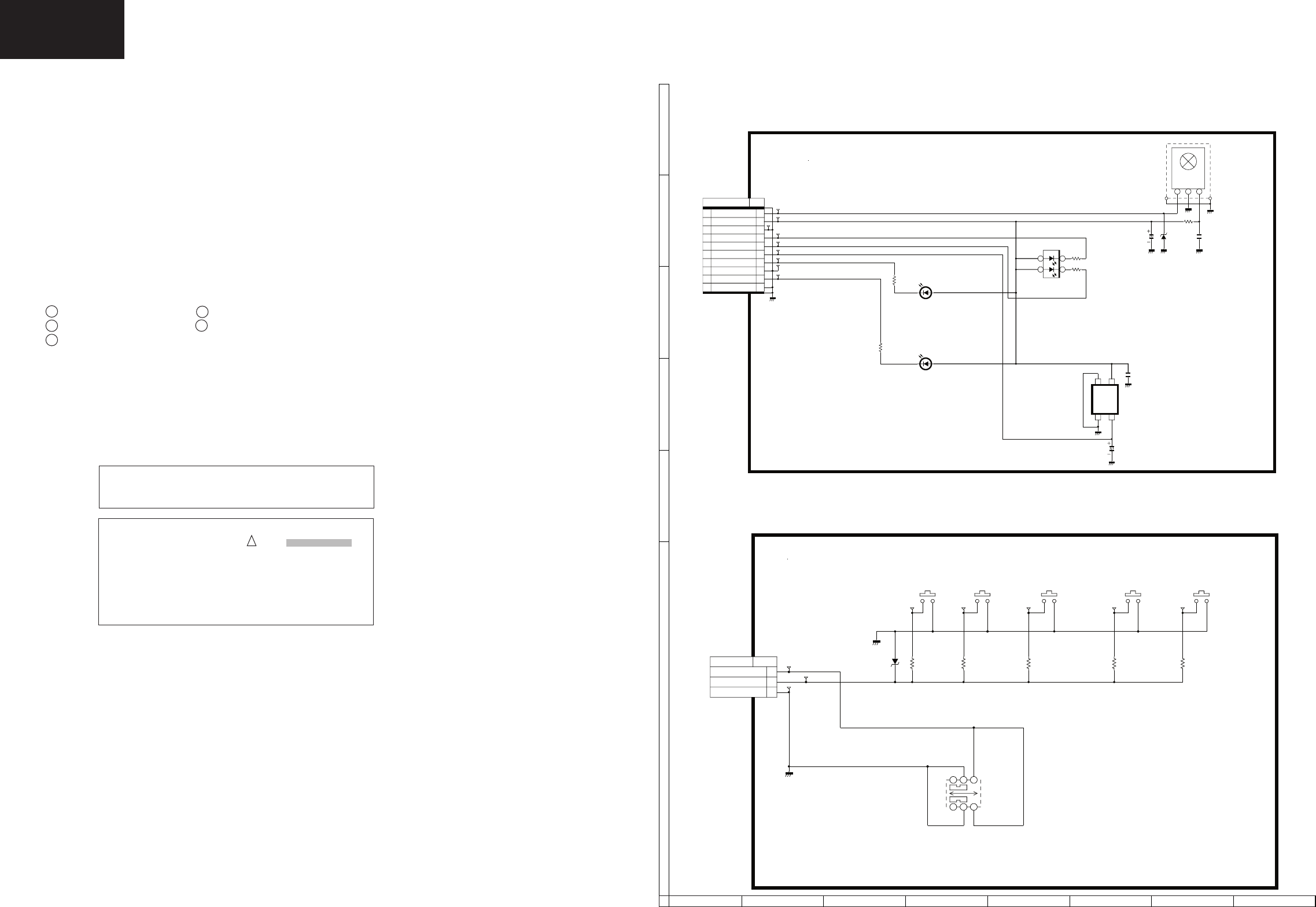
108
LC-32/37GD8E/RU
LC-32/37BT8E/RU
LC-32/37GD8, LC-32/37BT8 RC/LED Unit Diagram
LC-32/37GD8, LC-32/37BT8 KEY Unit Diagram
IMPORTANT SAFETY NOTICE:
PARTS MARKED WITH “ ” ( )
ARE
IMPORTANT FOR MAINTAINING THE SAFETY OF
THE SET. BE SURE TO REPLACE THESE PARTS
WITH SPECIFIED ONES FOR MAINTAINING THE
SAFETY AND PERFORMANCE OF THE SET.
SCHEMATIC DIAGRAMS
Description:
VOLTAGE MEASUREMENT CONDITION:
1. The voltages at test points are measured on exclusive AC adaptor and the stable supply voltage of AC 230V.
Signals are fed by a color bar signal generator for servicing purpose and the above voltages are measured with a
20k ohm/V tester.
INDICATION OF RESISTOR & CAPACITOR:
RESISTOR
1. The unit of resistance “Ω ” is omitted. (K=kΩ=1000 Ω, M=MΩ).
2. All resistors are ± 5%, unless otherwise noted. (J= ± 5%, F= ± 1%, D= ± 0.5%)
3. All resistors are 1/16W, unless otherwise noted.
4. All resistors are Carbon type, unless otherwise noted.
C : Solid W : Cement
S : Oxide Film T : Special
N : Metal Coating
CAPACITOR
1. All capacitors are µF, unless otherwise noted. (P=pF=µµ F).
2. All capacitors are 50V, unless otherwise noted.
3. All capacitors are Ceramic type, unless otherwise noted.
(ML): Mylar (TA): Tantalum
(PF): Polypro Film (ST): Styrol
CAUTION:
This circuit diagram is original one, therefore there may be a
slight difference from yours.
!
I
H
G
F
E
D
C
B
12 3 4 5 67 8
A
It D9 I{;2;v 78 D9 C4 Ev
TL152
TL153
TL151
P153
NA057WJ
KM
TO MAIN 5
1
POW
2
KEY
3
GND
D151
EX0641GE
S151
K0003AJ
CH-UP
"%
S152
K0003AJ
CH-DOWN
!!"’
S153
K0003AJ
INPUT
S154
K0003AJ
VOL-UP
"%
S155
K0003AJ
VOL-DOWN
!!"’
TL159 TL160 TL161 TL162 TL163
R152
430
1/8W
R153
8.2K
1/8W
R151
1.8K
1/8W
R155
4.3K
1/8W
R156
910
1/8W
S156
P0035GE
1
2
3
4
5
6
1U>=%G%8%?%k%7%9%F%‘Bh#3;v6HItBh#25;=QIt
Ver.ZZ (2006.01.26)
LC-32P70E/LC-26P70E/LC-37P70E
LC-32P55E/LC-26P55E/LC-37P55E
LC-32GA9E/LC-37GA9E
LC-32GD9E/LC-37GD9E/LC-45GD9E
LC-32GA8E/LC-37GA8E
LC-32GD8E/LC-37GD8E
DUNTKD606WEV0
KEY
It D9 I{;2;v 78 D9 C4 Ev
BU+3.3V
BU+3.3V
BU+3.3V
BU+3.3V
D101
EXA092WJ
12V
TPS850
OPC
1
23
4
SLD101
PSLDM4646CEFW
C101
100u
16V
ASY
C102
2.2u
TVF
16V
C104
10u
16V
ASX
C105
0.01u
50V
Z
R101
100
D103
PX0210TA
TV POW
12
3 4
D102
PX0202TA
R114
820
R108
270
R109
1.2K
R112
470
P101
NA344WJ
TO MAIN 5 RA
1
R/C
2
BU+3.3V
3
GND
4
POWG_LED
5
POWR_LED
6
OPC
7
SLEEP_LED
8
NC
9
LED_OPC
10
GND
TL101
TL102
TL103
TL104
TL105
TL106
TL107
TL108
TL109 D104
PX0419CE
1U>=%G%8%?%k%7%9%F%‘Bh#3;v6HItBh#25
RMC101
IR RECEIVER MODULE
RRMCUA053WJZZ
1
OUT
2
GND
3
VCC
Ver.N1 (2006.01.26)
IC101
DUNTKD607WEV0
0
03.3
2.5
LC-32P70E/LC-26P70E/LC-37P70E
LC-32P55E/LC-26P55E/LC-37P55E
LC-32GA9E/LC-37GA9E
LC-32GD9E/LC-37GD9E/LC-45GD9E
LC-32GA8E/LC-37GA8E
LC-32GD8E/LC-37GD8E R/C.LED
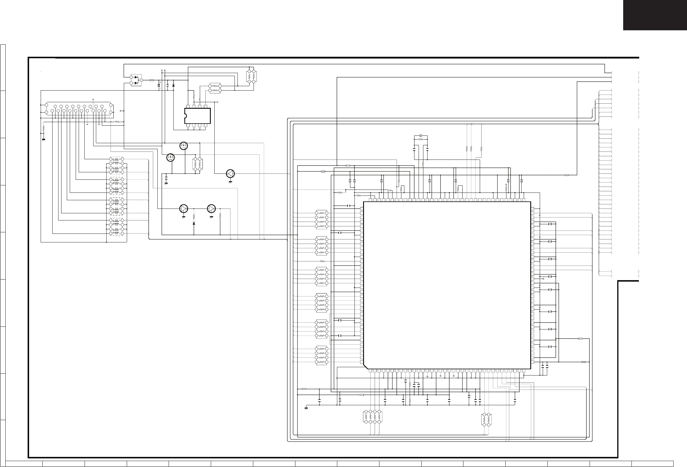
109
LC-32/37GD8E/RU
LC-32/37BT8E/RU
LC-32GD8, LC-32BT8 Main Unit Diagram 1/6 (HDMI)
+3.3V(D)_FB1903
+3.3V(D)_FB1902
RR1X2-
RR1X2+
RR1X1+
RR1X1-
RR1X0+
RR1X0-
RR1XC+
RR1XC-
DINR[7]
DINR[6]
DINR[4]
DINR[5]
DINR[2]
DINR[3]
DINR[1]
DINR[0]
DING[6]
DING[7]
DING[5]
DING[1]
DING[3]
DING[4]
DING[2]
DING[0]
DINB[6]
DINB[0]
DINB[2]
DINB[4]
DINB[3]
DINB[1]
DINB[5]
DINB[7]
HDMI_CLK
DINCK
R0PWR5V
DSDA0
DSCL0
+3.3V_IOVCC
+3.3V_IOVCC
+3.3V_IOVCC +3.3V_IOVCC
HOTP_CONT1
RR1X2+
RR1X2-
RR1X1+
RR1X1-
RR1X0+
RR1X0-
RR1XC+
RR1XC-
DSCL1
DSDA1
R1PWR5V
SDA3
SCL3
HDMI_WP
HDMI-VS
HDMI-HS
DINEN
DSDA1
DSCL1
HDMI_SCK
HDMI_WS
HDMI_SDO
R1PWR5V
HDMI_RST
HDMI_RST
HDMI_INT
+1.8V_SIICVCC
EDID5V
+3.3V
+3.3VSIIAVCC
+3.3VSIIAVCC
+3.3VSIIAVCC
+3.3V(D)_SIIPVCC
C1948
1000P
C1923
1000P
FB1903
0060TA
C1924
1000P
C1953
0.1u
25V
Z
C1968
1000P
SII9021
HDMI RECEIVER
1
DE
2
HSYNC
3
VSYNC
4
0OGND
5
OVCC
6
DACOVCC
7
DACAVCC
8
DACAGND
9
VREF
10
RSET
11
COMP
12
DACGNDR
13
DACVCCR
14
AnRPr
15
DACGNDG
16
DACVCCG
17
AnGY
18
DACGNDB
19
DACVCCB
20
AnBPb
21
DACDGND
22
DACDVCC
23
VCC
24
GND
25
OGND
26
OVCC
27
CSDA
28
CSCL
29
DSDA1
30
DSCL1
31
DSDA0
32
DSCL0
33
R1PWR5V
34
R0PWR5V
35
DVCC
36
DGND
37
PVCC0
38
AVCC
39
R0XC-
40
R0XC+
41
AGND
42
AVCC
43
R0X0-
44
R0X0+
45
AGND
46
AVCC
47
R0X1-
48
R0X1+
49
AGND
50
AVCC
51
R0X2-
52
R0X2+
53
AGND
54
PGND
55
PVCC1
56
ANTSTO
57
AVCC
58
R1XC-
59
R1XC+
60
AGND
61
AVCC
62
R1X0-
63
R1X0+
64
AGND
65
AVCC
66
R1X1-
67
R1X1+
68
AGND
69
AVCC
70
R1X2-
71
R1X2+
72
AGND
73
DGND
74
DVCC
75
OGND
76
OVCC
77
MUTEOUT
78
SPDIF
79
VCC
80
GND
81
NC
82
NC
83
NC
84
SD0
85
WS
86
SCK
87
MCLKIN
88
MCLKOUT
89
OVCC
90
OGND
91
GND
92
VCC
93
NC
94
DVCC2
95
DGND2
96
XTALOUT
97
XTALIN
98
XTALVCC
99
REGVCC
100
NC
101
TEST
102
RESET#
103
SCDT
104
INT
105
VCC
106
GND
107
CLK48B
108
OGND
109
OVCC
110
Q23
111
Q22
112
Q21
113
Q20
114
VCC
115
GND
116
Q19
117
Q18
118
Q17
119
Q16
120
OGND
121
ODCK
122
OVCC
123
Q15
124
Q14
125
Q13
126
Q12
127
GND
128
VCC
129
Q11
130
Q10
131
Q9
132
Q8
133
Q7
134
OVCC
135
OGND
136
Q6
137
Q5
138
GND
139
VCC
140
Q4
141
Q3
142
Q2
143
Q1
144
Q0
R1917
10K
C1956
1000P
L1903
FA134WJ
1
2
3
4
5
6
7
8
C1955
1000P
C1913
1000P
R1933
1.5K
C1928
0.01u
FB1904
0060TA
R1932
1M
C1943
1000P
D1903
1SS355
+1.8V
C1930
1000P
SDA3
HDMI_INT
C1912
1000P
C1929
12P
(CH)
FB1901
0060TA
C1934
12P
(CH)
C1974
1000P
L1902
FA134WJ
1
2
3
4
5
6
7
8
R1929
4.7K
R1906
47K
EDID5V
R1908
10K
SCL3
C1927
1000P
HDMI_RST
C1941
1000P
L1901
FA134WJ
1
2
3
4
5
6
7
8
FB1906
0060TA
HOTP_CONT0
Q1909
DTC144EE
R1930
91 F
C1975
1000P
C1946
1000P
C1916
1000P
Q1907
DTC144EE
FB1905
0060TA
C1959
0.1u
25V
Z
+3.3V
D1901
DAN202K
1
2
3
R1926
4.7K
C1960
1000P
C1947
0.1u
25V
Z
C1967
1000P
*C1901
47u
16V
ASY
C1965
1000P
R1928
22K
*C1906
0.1u
25V Z
Q1905
DTC144EE
C1917
1000P
R1903
1.5K
FB1909
0210TA
SC1901
ZA117WJ
1
2
3
4
5
6
7
8
9
10
11
12
13
14
15
16
17
18
19
20 21
22 23
C1903
0.1u
25V
Z
X1901
SCA108WJ
28.322MHz
R1931
91 F
C1971
1000P
C1973
1000P
D1905
1SS355
FB1908
0060TA
C1969
1000P
Q1903
2SK536
SD
G
R1901
2.7K
R1935
33
C1936
1000P
Q1901
2SK536
S
D
G
L1904
FA134WJ
1
2
3
4
5
6
7
8
R1920
10
1
2
3
4
5
6
7
8
R1921
10
1
2
3
4
5
6
7
8
R1922
10
1
2
3
4
5
6
7
8
R1923
10
1
2
3
4
5
6
7
8
R1924
10
1
2
3
4
5
6
7
8
R1925
10
1
2
3
4
5
6
7
8
R1919 10
DINR[7]
DINR[6]
DINR[5]
DINR[4]
DINR[3]
DINR[1]
DINR[2]
DINR[0]
DING[7]
DING[3]
DING[5]
DING[0]
DING[6]
DING[4]
DING[1]
DING[2]
DINB[0]
DINB[1]
DINB[5]
DINB[2]
DINB[4]
DINB[7]
DINB[6]
DINB[3]
DINCK
HDMI_WP
HDMI_WS
HDMI_SDO
HDMI_SCK
FB1907
0210TA
HOTP_CONT1
HDMI-VS
DINEN
HDMI-HS
R1914
10
21
3
4
R1913
47K
21
3
4
R1911
470K
21
3
4
R1934
100
21
3
4
C1935
10u
KZA073WJ
16V
C1921
10u
16V
KZA073WJ
C1910
10u
16V
KZA073WJ
C1918
10u
16V
KZA073WJ
C1931
10u
16V
KZA073WJ
C1919
10u
16V
KZA073WJ
R1927
10
1
2
3
4
5
6
7
8
TL1909
TL1915
TP1913
TP1916
TP1909
TP1911
TL1911
TP1901
TP1902
TP1907
TP1903
TP1908
TP1904
R3306
22 R3307
22
R3308
22
DUNTKD890WE06
R1936
33
R1937
10K
24LC2BIN
EEPROM
1
A0
2
A1
3
A2
4
VSS
5
SDA
6
SCL
7
WP
8
VCC
TO MAIN 6/6
TO MAIN 3/6
TO MAIN 2/6
Ver.N2 (2006.05.16)
IC1905
IC1901
HDMI
(MAIN 1)
0
0
0
3.3
3.3
3.3
0
0
0
3.3
0
3.3
0
0
3.3
0
0
3.3
0
0
1.8
1.8
0
0
3.3
3.3
3.3
3.3
3.3
3.3
3.3
0
0
1.8
0
3.3
3.3
3.3
3.3
0
3.3
3.3
3.3
0
3.3
3.3
3.3
0
3.3
3.3
3.3
0
0
3.3
0
3.3
3.3
3.3
0
3.3
3.3
3.3
0
3.3
3.3
3.3
0
3.3
3.3
3.3
0
0
1.8
0
3.3
0
0
1.8
0
0
0
0
0
0
0
0
0
3.3
0
0
1.8
0
1.8
0
1.75
1.67
3.3
3.3
0
0
3.3
0
0
1.8
0
0
0
3.3
3.3
3.3
3.3
0
1.8
0
3.3
3.3
3.3
3.3
0
0
3.3
3.3
3.3
3.3
3.3
0
1.8
0
0
3.3
3.3
0
3.3
0
3.3
3.3
0
1.8
3.3
0
0
3.3
3.3
0
5.0 0
0
0
2.4
0
2.4
0
3.2
4.5
3.3
3.2
4.5
3.3
0000
5.05.05.05.0
LC-32GD8E CONFIDENTIAL
Ver.N2 (2006.05.16)
12 3 4 5 6 7 8 9 10 11 12 13 14 15 16
I
H
G
F
E
D
C
B
A
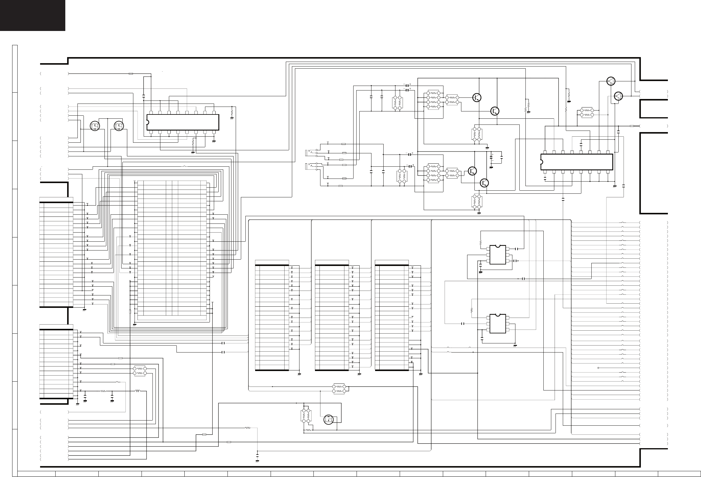
110
LC-32/37GD8E/RU
LC-32/37BT8E/RU
LC-32GD8, LC-32BT8 Main Unit Diagram 2/6 (Signal IN OUT)
OUTTNR
IN2R
SPKR
ATUNER-SIF
IN2L
SPKL
GREEN2
IN2FSW
DTUNER-G
DTUNER-R
IN3C
RED/C2
BULE1
DTUNER-B
GREEN1
ATUNER-CVBS
HPOUT-R
HPOUT-L
RED/C1
OUTV
IN3L
IN3R
IN1L
IN1R
OUTMONL
OUTMONR
HDMI-VS
HDMIA_L
HD1AR
HD1AL
RGB_R
HDMIA_R
AUDIO2_L
VIN_2
VIN_1
DTVHDMI
SLOWSW2
SLOWSW1
OUTTNV
BLUE2
OUTTNL
PCVH
PCVV
IN1FSW
MUTE_SP
SV1JSW
S_MUTE
AUDIO2_R
ATUNER-SIF
IN1FSW
AVLINK1
SLOWSW1
RED/C1
GREEN1
BULE1
VIN_1
IN1R
IN1L
OUTTNV
OUTTNR
OUTTNL
IN2FSW
AVLINK2
SLOWSW2
RED/C2
GREEN2
BLUE2
VIN_2
IN2R
IN2L
OUTV
OUTMONR
OUTMONL
SV1JSW
IN3Y
IN3C
IN3R
IN3L
OUTMONR
OUTMONL
S_MUTE
HPOUT-R
HPOUT-L
SPKR
SPKL
MUTE_SP
AVLINK1
BU+5V
AVLINK2
RGB_L
DPC_L
DPC_R
ATUNER-CVBS
DTM_POWON
DTMSDA
ATUNER+8V
SCL3
SDA3
ATUNER+5V
ATUNER-IFAGC
ATUNER-SDA
ATUNER-SCL
BU+3.3V
DTUNER-G
DTUNER-R
DTUNER-B
DTUNER-AR
DTUNER-CVBS
DTUIN3Y
DTUNER-H
DTUNER-AL
DTVPC
HDMI-HS
DHSYNC
DVSYNC
DTUNER-V
DTUNER-V
B+8V
+5V
S+8V
S2_MUTE
S2_MUTE
PO_MUTE
DTM12V
POW+12V
DTMSCL
TERMINAL+5V
IN3Y
POW_AUDIOSEL
AVLK1
PO_MUTE
DHSYNC
DVSYNC
TVHC153T
1
/1G
2
B
3
1C3
4
1C2
5
1C1
6
1C0
7
1Y
8
GND
9
2Y
10
1C0
11
2C1
12
2C2
13
2C3
14
A
15
/2G
16
VCC
HDMI-VS
HDMI-HS
FB2704
0061TA
+3.3V
SBW_TEST
AOUT2R
VIN15
VIN5
VIN18
VIN16
AIN4R
AOUT1R
AIN2L
AIN3L
AOUT2L
VIN13
AIN1L
AIN3R
AOUT1L
VIN6
SPKOUTL
CVO2
VIN2
VIN8
VIN11
VIN3
VIN12
AIN2R
SPKOUTR
SIF
CVO1
AIN1R
VIN17
AIN4L
VIN1
VIN7
VIN9
FB2702
0254TA
FB2703
0254TA
S+8V
+5V TERMINAL+5V
MUTE_SP
S_MUTE
SV1JSW
BU+3.3V
AVLK1
HPOUTR
HPOUTL
CADC3
CADC4
DTUIN3Y
SDA3
SCL3
CD4052BP
1
0
2
2
3
Y
4
3
5
1
6
INH
7
VEE
8
VSS
9
B
10
A
11
3
12
0
13
X
14
1
15
2
16
VDD
FB2711
0061TA
DTVPC
TL2701
DTVHDMI
TL2706
TL2705
S+8V
C2722
0.1u
25V
Z
C2723
0.1u
25V Z
PCVV
PCVH
TL2702
TL2703
TL2704
R2702
100
21
3
4
C2724
0.1u
25V
Z
C2701
0.1u
25V
Z
Q2704
2SC3928AR
C2703
100P
(CH)
R2709
100K
12
34
56
78
Q2705
2SC3928AR
1u
50V
C2709
ASX
C2705
100P
(CH)
C2714
10u
16V
ASX
1u
50V
C2707
ASX
C2715
0.1u
25V
Z
R2713
4.7K
21
3
4
R2707
220K
21
3
4
1u
50V
C2708
ASX
C2702
100P
(CH)
1u
50V
C2706
ASX
R2712
4.7K
21
3
4
Q2706
2SC3928AR
R2708
100K
12
34
56
78
Q2703
2SC3928AR
C2704
100P
(CH)
R2706
220K
21
3
4
MM1507XN
2-IN,1-OUT,SWITCH
SW(L=IN1,H=IN2)
1SW
2OUT
3VCC 4
IN2
5
GND
6
IN1
SCART12
C2712
0.1u
25V Z
R2714
100
Q2708
DTC144EE
R2716
10K
21
3
4
Q2707
DTC144EE
R2711
10K
2
1
34
R2710
10K
2
1
34
SC2704
WA251WJ
TO AV
1
IN3R
2
IN3L
3
GND
4
PO_MUTE
5
OUTMONR
6
OUTMONL
7
S_MUTE
8
NC
9
HPOUTR
10
HPOUTL
11
(HPMUTE)
12
HPPLUG
13
SPKR
14
SPKL
15
SPMUTE
16
SPPOW
17
GND
18
GND
19
A+5V
20
GND
21
GND
22
8V
23
8V
NC
NC
SC2702
WA251WJ
TO AV
1
IN1FSW
2
AVLINK1
3
SLOWSW1
4
RED/C1
5
GND
6
GREEN1
7
GND
8
BLUE1
9
GND
10
VIN1
11
GND
12
IN1R
13
IN1L
14
GND
15
OUTTNV
16
GND
17
OUTTNR
18
OUTTNL
19
GND
20
NC
21
NC
22
NC
23
NC
NC
NC
SC2703
WA251WJ
TO AV
1
IN2FSW
2
AVLIN2
3
SLOWSW2
4
RED/C2
5
GND
6
GREEN2
7
GND
8
BLUE2
9
GND
10
VIN2
11
GND
12
IN2R
13
IN2L
14
GND
15
OUTV
16
GND
17
OUT2R
18
OUT2L
19
S2_MUTE
20
IN3SW
21
IN3YV
22
GND
23
IN3C
NC
NC
R2703
47K
21
3
4
BU+5V
AVLK2
P1_5
TP2701
C2718
1u
16V
C2719
1u
16V
C2725
220P
RJ2701
RJ2702
RJ2704
RJ2713
RJ2714
RJ2708
RJ2703
RJ2712
RJ2711
RJ2706
RJ2705
RJ2716
RJ2718
RJ2709
RJ2707
RJ2710
RJ2715
RJ2717
RJ2726
RJ2728
RJ2722
RJ2723
RJ2732
RJ2724
RJ2731
RJ2725
RJ2730
RJ2727
RJ2721
RJ2719
RJ2729
RJ2720
RJ2735
RJ2733
RJ2734
RJ2738
RJ2736
RJ2737
TL2737
TL2738
TL2739
TL2740
TL2741
TL2742
TL2743
TL2744
TL2745
TL2746
TL2747
TL2748
TL2749
TL2750
TL2751
TL2752
TL2753
TL2754
TL2755
TL2756
TL2757
TL2758
TL2759
TL2760
TL2761
TL2762
TL2763
TL2764
TL2765
TL2766
TL2767
TL2768
TL2769
TL2770
TL2771
TL2772
TL2773
TL2774
TL2775
TL2776
TL2777
TL2778
TL2779
TL2780
TL2781
TL2782
R2704
10K
2
1
34
FB2708
0061TA
FB2707
0061TA
FB2706
0061TA
FB2709
0061TA
FB2710
0061TA
FB2705
0061TA
J2702
EA073WJ
for RGB INPUT
J2701
EA073WJ
for HDMI INPUT
DTU_ON
SC2705
WA010WJ
TO ATUNER
1
SIF
2
CVBS
3
GND
4
+35V
5
GND
6
+8V
7
GND
8
+5V
9
SCL3
10
SDA3
11
GND
12
IFAGC
13
GND
14
+5V(CONT)
15
GND
*SC2707
WA251WJ
TO DTUNIT
1
FECLK
2
GND
3
FED0
4
FED1
5
FED2
6
FED3
7
GND
8
FED4
9
FED5
10
FED6
11
FED7
12
GND
13
FEERR_UNCOR
14
FEVAL_DEN
15
FESTR_PSYNC
16
FEOFF_X4M
17
GND
18
FEGP0_COMP
19
FEGP1_LOCK
20
I2CSEL
21
FESDA
22
FESCL
23
FERESETn
*P2702
MA202WJ
TO DTUNER
1
+12V
2
GND
3
+12V
4
GND
5
GND
6
+5V
7
GND
8
+5V
9
GND
10
+5V
11
GND
12
+5V
13
GND
14
+5V
15
GND
16
+5V
17
ASPECT
18
GND
19
SCL
20
RESETn
21
SDA
22
IRQ
23
POWON
24
R
25
L
26
GND
27
V
28
BLUE
29
H
30
GND
31
GND
32
GREEN
33
CVBS
34
GND
35
GND
36
RED
37
FERESETn
38
GND
39
FESCL
40
FEOFF_X4M
41
FESDA
42
GND
43
FEGP0_COMP
44
FESTR_PSYNC
45
FEGP1_LOCK
46
FEVAL_DEN
47
FEERR_UNCOR
48
GND
49
GND
50
FED0
51
FED1
52
FED2
53
FED3
54
FED4
55
FED5
56
FED6
57
FED7
58
FECLK
59
GND
60
GND
TL2712
TL2714
TL2710
TL2715
TL2713
TL2708
TL2711
TL2709
TL2707
*TL2723
*TL2722
*TL2721
*TL2731
*TL2728
*TL2724
*TL2720
*TL2730
*TL2719
*TL2733
*TL2717
*TL2726
*TL2734
*TL2729
*TL2725
*TL2718
*TL2732
*TL2716
*TL2727
ANT+5V
POW+5V
POW+12V
*TL2735
DTM_IRQ
DTM_RESET
*RJ2739
*FB2713
0254TA
*FB2714
0254TA
DTI2CSEL
*TL2736
*TL2783
*TL2784
*TL2785
*TL2786
*TL2788
*TL2787
*TL2789
*TL2791
*TL2792
*TL2793
*TL2794
*TL2795
*TL2796
*TL2797
BU_SCL3
BU_SDA3
*TL2798
*TL2799
*TL2800
FB2715
0210TA
MM1507XN
2-IN,1-OUT,SWITCH
SW(L=IN1,H=IN2)
1SW
2OUT
3VCC 4
IN2
5
GND
6
IN1
*R2717
100
*C2727
0.1u
25V
Z
C2710
0.1u
25V
C2726
0.1u
TVB
BU_SDA3
BU_SCL3
*R2701
10K
*R2705
10K
*R2715
1K
*R2719
1K
*R2721
100K
*R2720
100K
TO MAIN 6/6
*C2728
1u
16V
Z
*C2711
1u
16V
Z
C2729
0.1u
S2_MUTE
*Q2710
3LN01S
SD
G
*Q2709
3LN01S
SD
G
Q2702
3LN01S
SD
G
RESET_N
R2722
100
*R2723
4.7
*C2731
0.01u
*C2730
10u
16V
KZA073WJ
1.5uH
*L2701
CUN
R2724
0
C2732
0.01u
(B,A)=
00:C0 DTV
01:C1 PC
10:C2 HDMI
11:C3 *
SYNC SELECT
(DTVHDMI,DTVPC)=
00:C0 DTV
01:C1 PC
10:C2 HDMI
11:C3 *
TTL LEVEL INPUT
5V Tolerant
INPUT PROTECT WHEN POWERDOWN
(B,A)=
11:C3 DTV
10:C2 PC
01:C1 HDMI
00:C0 *
3.3V to 8V LEVEL Shift
TO MAIN 3/6
TO MAIN 6/6
TO MAIN 5/6
TO MAIN 3/6
TO MAIN 6/6
TO MAIN 6/6
TO MAIN 5/6
TO MAIN 3/6
TO MAIN 3/6
TO MAIN 6/6
TO MAIN 1/6
TO MAIN 5/6
Ver.N2 (2006.05.16)
LC-32GD8E
IC2701
IC2704
IC2702
DUNTKD890WE06
*IC2705
Signal INOUT
(MAIN 2)
00000000
00000003.3
0 3.3 0.2 0 0 0 0 0
8.18.1
0003.33.38.1
3.5
8.1
4.0
3.5
8.1
4.0
3.3
8.1
3.9
3.3
8.1
3.9
0
1.4
4.8 1.5
0
1.4
0
8.1 0
0
8.1 0
3.3
4.8
3.3
CONFIDENTIAL
Ver.N2 (2006.05.16)
1234567 8 9 10 11 12 13 14 15 16
I
H
G
F
E
D
C
B
A
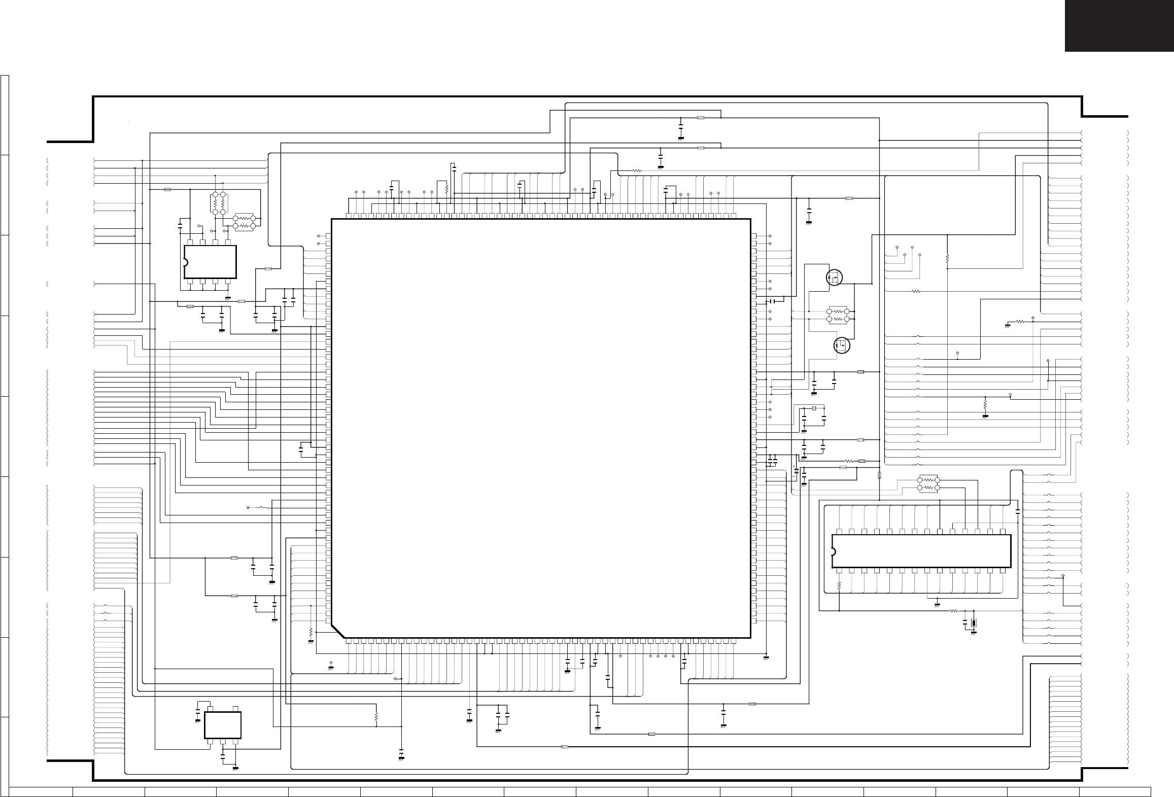
111
LC-32/37GD8E/RU
LC-32/37BT8E/RU
LC-32GD8, LC-32BT8 Main Unit Diagram 3/6 (VCTP)
DVSYNC
DINEN
DINCK
DING[6]
DING[7]
DING[5]
DING[2]
DINB[5]
DING[4]
DING[3]
DINB[7]
DING[0]
DING[1]
DINB[6]
DINB[2]
DINB[0]
DINB[3]
DINB[4]
DINB[1]
DVSYNC
DINEN
DINCK
DINR[7]
DINR[4]
DINR[5]
DINR[6]
DING[5]
DING[7]
DINR[3]
DING[6]
DINR[0]
DINR[1]
DINR[2]
DING[4]
DINB[5]
DINB[7]
DING[3]
DINB[6]
DING[0]
DING[1]
DING[2]
DINB[4]
DINB[0]
DINB[3]
DINB[2]
DINB[1]
FRCO[0]
FRCO[1]
FRCO[3]
FRCO[2]
FRCO[7]
FRCO[6]
FRCO[5]
FRCO[4]
FRCCKI
FRCI[7]
FRCI[6]
FRCI[5]
FRCI[4]
FRCI[2]
FRCI[1]
FRCI[0]
FRCI[1]
FRCI[2]
FRCI[0]
FRCI[6]
FRCI[7]
FRCI[5]
FRCI[4]
FRCI[3]
FRCO[1]
FRCO[2]
FRCO[0]
FRCO[6]
FRCO[5]
FRCO[4]
FRCO[3]
FRCCKO
FRCCKI
LVDS0N
LVDS0P
LVDS1N
LVDS1P
LVDS2N
LVDS2P
LVDSCN
LVDSCP
LVDS3P
LVDS3N
VSUP3.3VO
VSUP3.3COM
VSUP3.3FL
SIF
SBW_TEST
SPKOUTL
SPKOUTR
HPOUTL
AOUT1L
AOUT1R
AOUT2L
AOUT2R
AIN4L
AIN4R
AIN3R
AIN3L
AIN2R
AIN1R
AIN1L
AIN2L
I2S_DI
I2S_WS
I2S_CL
P1_7
P1_6
P1_5
P1_4
P1_3
P1_2
P1_1
P1_0
P4_2
P4_3
P4_0
P4_1
P2_6
P2_7
P3_0
P3_1
P3_2
P3_4
P2_0
P2_1
P2_2/IR
P2_3
TXD
RXD
P3_6
P3_7
P3_5
P3_4
SPKOUTR
SPKOUTL
SIF
SBW_TEST
HPOUTL
AOUT1R
AOUT2L
AOUT1L
AIN4R
AOUT2R
AIN4L
AIN3R
AIN2R
AIN1L
AIN3L
AIN2L
AIN1R
I2S_CL
I2S_DI
I2S_WS
TXD
RXD
P1_7
P1_6
P1_5
P1_4
DINR[0]
DINR[1]
DINR[3]
DINR[2]
DINR[4]
DINR[5]
DINR[6]
DINR[7]
FRCO[7]
S+8V
S+8V
P1_0
P1_1
P2_1
P2_0
P2_7
P3_7
P3_1
P2_6
P3_0
P3_4
P3_2
P3_5
P3_6
P4_0
P4_1
P4_2
P4_3
+5V
+5V
DHSYNC
PICB1
PICB0
PICB5
PICB3
PICA5
PICB6
PICA4
PICA6
PICA3
PICA2
PICB2
PICAA0
HPOUTR
HPOUTR
VSUP3.3IO1 VSUP3.3IO1
P2_3
BU+1.8V
VSUP8.0AU
VSUP5.0SIF
VIN1
VIN1
VIN2
VIN3
VIN18
VIN6
VIN7
VIN8
VIN9
VIN11
VIN12
VIN16
VIN15
VIN13
VIN21
CVO2
CVO1
BU_SCL3
BU_SDA3
LVDS1.8V
VSUP3.3FE
VIN20
VIN19
AVLK1
HOTP_CONT0
HSYNC_OSC
FPGA_SDE
TEMP3
TEMP2
TEMP1
LEDPOWG
LEDPOWR
LEDSLP
LEDOPC
PWMOUT
LCDLR
FRAME
QSSET
OPCIN
AVLK2
PICA7
FAN_ERR
KEY_PSW
FRCCKO
PICAA0
PICAA1
PICA3
PICA4
PICA5
PICA7
PICA6
PICC0
PICC1
PICC2
PICC3 PICC4
CCP1
PICB0
PICB1
PICB2
PICB3
PICB4
PICB5
PICB6
PICB7
PICA2
SV1JSW
PICB7
PICB4
PICC0
PICC1
PICC2
PICC3
CCP1
LCDUD
HDMI_WP
HDMI_RST
SCART12
DTUIN3Y
HOTP_CONT1
HDMI_INT
BU_SCL3
BU_SDA3
FPGA_SCK
FPGA_SDA
DTVPC
DTVHDMI
PCLK
VSYNC_OSC
P1_2
P1_3
BL_ERR
PICC4
SCL3SCL3
SDA3
PICAA1
VIN5
SDA3
VSUP3.3DIG
BU_SDA3
SCL3
BU_SCL3
DTM_IRQ
LVDS3.3V
+3.3V
POW_ERR
FRCI[3]
VSUP3.3IO3
VSUP1.8FE
RESET_N
VSUP3.3RAM
BU+3.3V
BU+3.3V
VSUP3.3DRI
P2_2/IR IRIN
DINB[0]
DINB[7]
DINB[1]
DING[3]
DINR[1]
DHSYNC
DINB[5]
DINR[4]
DING[4]
DINR[7]
DINR[5]
DINB[4]
DINB[2]
DING[7]
DINR[6]
DINB[3]
DING[1]
DINB[6]
DINR[0]
DINR[2]
DVSYNC
DINR[3]
DINCK
DING[0]
DING[6]
DINEN
DING[2]
DING[5] FRCO[7]
FRCCKO
FRCCKI
FRCO[4]
FRCO[5]
FRCO[0]
FRCI[3]
FRCI[6]
FRCI[1]
FRCO[3]
FRCO[1]
FRCI[7]
FRCO[2]
FRCI[5]
FRCI[0]
FRCI[2]
FRCO[6]
FRCI[4]
LVDS3N
LVDSCN
FRAME
LVDS3P
LVDS1N
LVDS2N
LVDSCP
TEMP1
LCDUD
LVDS0P
QSSET
LVDS2P
TEMP3
TEMP2
LCDLR
LVDS0N
LVDS1P
FB3003
0254TA
FB3004
0254TA
C3007
0.1u
25V
Z
C3004
10u
16V
KZA073WJ
C3009
0.1u
25V
Z
C3006
10u
16V
KZA073WJ
C3008
0.1u
25V
Z
C3005
10u
16V
KZA073WJ
FB3006
0254TA
C3003
0.1u
25V
Z
C3002
10u
16V
KZA073WJ
FB3002
0254TA
C3035
10u
16V
KZA073WJ
FB3012
0254TA
C3040
10u
16V
KZA073WJ
C3037
0.1u
FB3015
0254TA
C3041
10u
16V
KZA073WJ
FB3014
0254TA
C3038
0.1u
FB3009
0254TA
C3029
10u
16V
KZA073WJ
FB3010
0254TA
C3027
10u
16V
KZA073WJ
C3031
10u
16V
KZA073WJ
FB3011
0254TA
BU+3.3V
BU+1.8V
C3020
0.1u
C3016
0.1u
C3021
56P
(CH)
R3007
6.2K
FB3013
0254TA
C3036
10u
16V
KZA073WJ
C3034
15P
(CH)
C3039
18P
(CH)
SIF
SPKOUTL
SPKOUTR
SBW_TEST
HPOUTL
AIN4R
AOUT1L
AOUT2L
AOUT1R
AOUT2R
AIN3L
AIN3R
AIN1L
AIN4L
AIN2L
AIN2R
AIN1R
RXD
TXD
P1_6
P1_7
P1_4
P1_5
SCL3
SDA3
FB3008
0254TA
FB3007
0254TA
S+8V
+5V
LEDPOWR
LEDSLP
LEDPOWG
VIN5
VIN6
VIN3
CVO2
VIN2
CVO1
VIN1
VIN15
VIN16
VIN13
VIN8
VIN12
VIN7
VIN9
VIN11
VIN20
VIN17
VIN21
VIN19
VIN18
LEDOPC
FB3016
0254TA
OPCIN
C3042
0.1u
SCL3
HDMI_RST
HDMI_INT
HDMI_SCK
IRIN
HDMI_WS
SDA3
HOTP_CONT0
HDMI_SDO
HOTP_CONT1
FAN_ERR
HPOUTR
C3024
0.1u
25V
Z
C3025
0.1u
25V
Z
C3030
0.1u
25V
Z
C3032
0.1u
25V
Z
C3033
0.1u
25V
Z
C3028
0.1u
25V
Z
C3019
0.1u
25V
Z
C3023
0.1u
25V
Z
C3013
0.1u
25V
Z
C3011
0.1u
25V
Z
C3012
0.1u
25V
Z
+3.3V
MUTE_SP
AVLK1
KEY_PSW
VSYNC_OSC
SCART12
DTUIN3Y
HDMI_WP
C3014
0.1u
R3006
4.7K
RESET_N
C3001
0.1u
25V
Z
BR24L64F
1
A0
2
A1
3
A2
4
GND
5
SDA
6
SCL
7
WP
8
VCC
FB3001
0254TA
SDA3
SCL3
R3004
100
21
3
4
R3005
4.7K
21
3
4
R3009
100
21
3
4
X3001
SC0012CE
20.25MHz
C3010
10u
16V
KZA073WJ
C3018
0.1u
25V
Z
C3017
10u
16V
KZA073WJ
C3022
10u
16V
KZA073WJ
R3010
4.7K
*R3008
4.7K
2
1
34
FPGA_SDE
PWMOUT
SDA3
SCL3
C3015
0.1u
25V
Z
FB3005
0254TA
AVLK2
TP3038
TP3004
TP3001
TP3002
TP3003
TP3006
TP3005
TP3007
TP3009
TP3010
TP3008
TP3012
TP3013
TP3014
TP3011
TP3018
TP3017
TP3015
TP3016
TP3024
TP3025
TP3026
TP3027
TP3029
TP3031
TP3030
TP3028
TP3033
TP3032
TP3034
TP3035
TP3036
TP3022
TP3021
TP3020
TP3023
TP3019
TP3037
RJ3002
RJ3003
RJ3001
RJ3004
RJ3018
RJ3013
RJ3022
RJ3009
RJ3017
RJ3019
RJ3014
RJ3010
RJ3021
RJ3025
RJ3024
RJ3020
RJ3015
RJ3012
RJ3016
RJ3023
RJ3029
RJ3034
RJ3036
RJ3032
RJ3031
RJ3028
RJ3026
RJ3030
RJ3027
RJ3033
RJ3035
RJ3038
SV1JSW
RJ3039
*R3013
10K
RJ3040
RJ3042
RJ3043
RJ3044
RJ3041
RJ3045
RJ3047
RJ3046
TP3040
TP3041
TP3042
TP3043
DTM_IRQ
BU_SDA3
BU_SCL3
TP3044
TP3039
DTVPC
DTVHDMI
IXB624WJ
VCT6973
1
656O6
TDOFW
2
656O5/TDIFW
3
656O4/TMSFW
4
656O3/TCLK
5
656O2/TDO
6
656O1/TDI
7
656O0/TMS
8
RESETQ
9
AIN1R
10
AIN1L
11
AIN2R
12
AIN2L
13
AIN3R
14
AIN3L
15
AIN4R
16
AIN4L
17
VREFAU
18
VSUP8.0AU
19
GNDA
20
SGND
21
AOUT2R
22
AOUT2L
23
AOUT1R
24
AOUT1L
25
HEADPHONER
26
HEADPHONEL
27
SPEAKERR
28
SPEAKERL
29
SUBWOOFER TEST
30
VREFSIF
31
SIFIN+
32
SIFIN-
33
VSUP5.0SIF
34
GNDA
35
GND3.3DIG
36
VSUP3.3DIG
37
SPDIF_OUT
38
I2S_DA_IN
39
I2S_CL
40
I2S_WS
41
I2S_DEL_OUT
42
I2S_DEL_IN
43
I2S_DEL_CL
44
I2S_DEL_WS
45
VSUP3.3RAM
46
GND3.3RAM
47
DVS
48
DEN
49
DCLK
50
DRI7
51
DRI6
52
DRI5
53
DRI4
54
DRI3
55
DRI2
56
DRI1
57
DRI0
58
DGI7
59
DGI6
60
DGI5
61
DGI4
62
DGI3
63
DGI2
64
DGI1
65
DGI0
66
DBI7
67
DBI6
68
DBI5
69
DBI4
70
DBI3
71
DBI2
72
DBI1
73
DBI0
74
GND3.3DRI
75
VSUP3.3DRI
76
GND3.3COM
77
VSUP3.3COM
78
XTALIN
79
XTALOUT
80
CLKOUT
81
VSO
82
HSO
83
SCL
84
SDA
85
GND3.3FL
86
VSUP3.3FL
87
P2_0
88
P2_1
89
P2_2
90
P2_3
91
P2_4/TDI/TXD
92
P4_5/TMS/RXD
93
OSDV
94
OSDH
95
GND3.3IO1
96
VSUP3.3IO1
97
OSDCLK
98
PSDFSW
99
P3_6
100
P3_7
101
P3_5
102
P3_4
103
OSDB1
104
OSDB0
105
P3_3
106
P3_2
107
OSDG1
108
OSDG0
109
P3_1
110
P3_0
111
OSDR1
112
PSDR0
113
GND3.3IO1
114
VSUP3.3IO1
115
P2_7/PCS5
116
P2_6/PCS4
117
P4_1/PCS3
118
P4_0/PCS2
119
P4_3/PCS1
120
P4_2/PCS0
121
PCLK2
122
PCLK1
123
GND1.8DIG
124
VSUP1.8DIG
125
LVDSA_4P
126
LVDSA_4N
127
VSUP3.3LVDS
128
LVDSA_3P
129
LVDSA_3N
130
GND3.3_LVDS
131
LVDSA_CLKP
132
LVDSA_CLKN
133
VSUP3.3LVDS
134
LVDSA_2P
135
LVDSA_2N
136
GND3.3LVDS
137
LVDSA_1P
138
LVDSA_1N
139
VSUP3.3LVDS
140
LVDSA_0P
141
LVDSA_0N
142
VSUP1.8LVDS
143
REXT
144
GND1.8LVDS
145
LVDSB_3P
146
LVDSB_3N
147
GD3.3LVDS
148
LVDSBCLKP
149
LVDSBCLKN
150
VSUP3.3LVDS
151
LVDSB_2P
152
LVDSB_2N
153
GND3.3LVDS
154
LVDSB_1P
155
LVDSB_1N
156
VSUP3.3LVDS
157
LVDSB_0P
158
LVDSB_0N
159
CADC4/P1_7/TDO
160
CADC3/P1_6/TCLK
161
CADC2/P1_5
162
CADC1/P1_4
163
GND3.3DAC
164
VSUP3.3DAC(ADC)
165
P1_3/ROUT
166
P1_2/GOUT
167
P1_1/BOUT
168
P1_0/SVMOUT
169
VSUP1.8FE
170
VSUP3.3FE
171
VIN22/DHS
172
VIN21
173
VIN20
174
VIN19
175
VIN5
176
VIN17
177
VIN16
178
VIN15
179
VIN13
180
VIN12
181
VIN11
182
VIN9
183
VIN8
184
VIN7
185
VSUP1.8FE
186
GNDA
187
VIN6
188
VIN18
189
VIN3
190
VIN2
191
VIN1
192
VSUP3.3VO
193
VOUT3
194
VOUT2
195
VOUT1
196
GND3.3IO3
197
VSUP3.3IO3
198
656I0
199
656I1
200
656I2
201
656I3
202
656I4
203
656I5
204
656I6
205
656I7
206
656CLKI
207
656CLKO
208
656O7
TCLKFW
12345678910 11 12 13 14
1516
171819202122232425262728
PCLK
HSYNC_OSC
FPGA_SCK
FPGA_SDA
BL_ERR
TP3045
R3001
1K
TP3046
TP3047
R3002
22
RESET_N
TH3002
M1103J03
R3003
10K
C3044
0.01u
S2_MUTE
Q3003
3LN01S
S
D
G
Q3004
3LN01S
S
D
G
BU4215G
123
45
C3045
0.01u
RESET_N
R3012
10K
*R3014
4.7K
POW_ERR
C3046
10u
16V
KZA073WJ
BU+3.3V
C3049
1000P
C3048
47u
6.3V
ASX
FB3018
0254TA
R3017
39
R3018
0
if not used, leave vacant
RA total<=100mA,RB total<=100mA
20mA(Icc Clamp) 25mA(Max) /PIN
POWER ON -> INPUT
(RA[4:0] Analog Input)
TO MAIN 5/6
TO MAIN 6/6
TO MAIN 2/6
TO MAIN 6/6
TO MAIN 1/6
TO MAIN 5/6
TO MAIN 4/6
TO MAIN 6/6
TO MAIN 2/6TO MAIN 1/6
TO MAIN 2/6
TO MAIN 5/6
TO MAIN 2/6
TO MAIN 1/6
TO MAIN 4/6
TO MAIN 6/6
Ver.N2 (2006.05.16)
LC-32GD8E
IC3001
DUNTKD890WE06
*IC3002
IC3003 IXB664WJ
PIC16F913
IC3005
VCTP
(MAIN 3)
0000
3.33.303.3
0
0
0
0
0
0
0
3.3
3.7
3.7
3.7
3.7
3.7
3.7
3.7
3.7
3.0
8.0
0
0
3.8
3.8
3.8
3.8
3.8
3.8
3.8
3.8
0
2.7
1.67
1.6
4.7
0
0
3.3
0
0
0
0
0
0
0
0
3.3
0
0
0
0
0
0
0
0
0
0
0
0
0
0
0
0
0
0
0
0
0
0
0
0
0
0
0
0
0
3.3
0
3.3
1.8
1.8
2.3
0.2
0.6
3.3
3.3
0
3.3
0
0
3.2
0
3.3
3.3
0
0
0
3.3
0
0
3.3
0
0
0
0
0
0
0
0
0
0
0
0
0
0
3.3
0
0
0
3.2
2.5
0
0
0
0
1.8
0
3.0
3.3
1.2
1.3
0
1.3
1.2
3.3
1.2
1.2
0
1.2
1.2
3.3
1.2
1.3
1.8
0
0
0
0
0
0
0
3.3
0
0
0
0
0
3.3
0
0
1.0
0
0
0
0
3.3
3.3
0
0
3.3
1.8
3.3
0
0
0
1.0
0
1.0
1.0
0
1.0
1.0
1.0
0
1.0
1.0
1.8
0
1.0
1.0
0
1.0
1.0
3.3
0
1.8
1.0
0
3.3
0
0
0
0
0
0
0
0
0
0.1
0
3.3 2.7 00 0 03.3 0 3.3 0 0 0 0 0
003.33.303.300003.303.33.3
3.3
3.3
3.3
3.3
3.3
3.3
3.2 1.7 0
0.94
CONFIDENTIAL
Ver.N2 (2006.05.16)
12 3 4 5 67 8 9 10 11 12 13 14 15 16
I
H
G
F
E
D
C
B
A
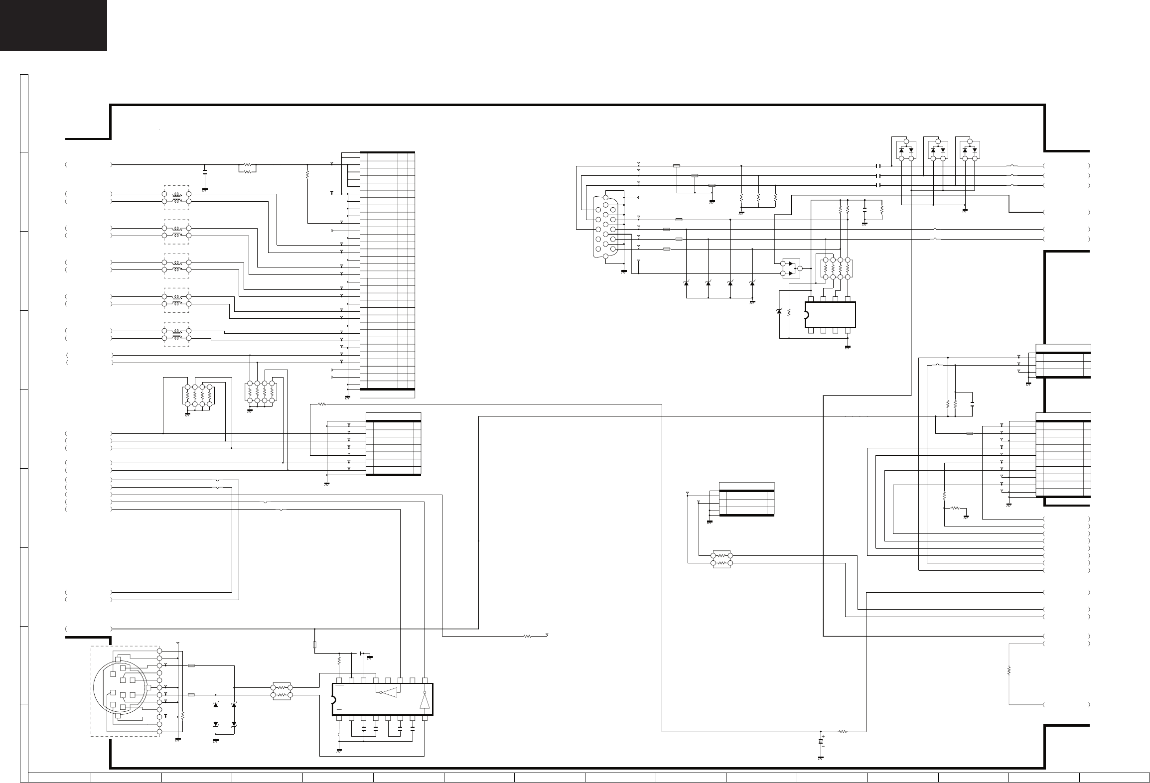
112
LC-32/37GD8E/RU
LC-32/37BT8E/RU
LC-32GD8, LC-32BT8 Main Unit Diagram 4/6 (FRC) Not used for these models
LC-32GD8, LC-32BT8 Main Unit Diagram 5/6 (MISC)
RS232C_3.3V
LVDS0P
LVDS0N
LVDSCP
LVDS1N
LVDS1P
LVDS2N
LVDS2P
LVDSCN
LVDS3N
LVDS3P
PCVV
RGB_V
APC_B
PCVHRGB_H
EDID5V
EDID5V
DSUB_DDC5V
RIN3+
RIN3-
CLKIN+
CLKIN-
RIN2+
RIN2-
RIN1+
RIN1-
RIN0+
RIN0-
SEL_LVDS
IR_VCC
LCD+5V
LEDPOWG
LEDOPC
LEDSLP
LEDPOWR
TEMP1
TEMP2 TEMP2
TEMP3
QSSET
FRAME
APC_G
APC_R
BU_SDA3
PCVG
PCVR
PCVB
PC_DDC5V
LCD5V
KEY_PSW
KEY_ETC
BU+3.3V
BU+3.3V
BU+3.3V
R2301
0
*
TL2306
C2302
0.1u
25V
Z
TL2301
D2303
EX1271CE
12V
R2307
100
2
1
34
R2314
10K
TL2302
C2304
0.1u
25V
Z
TL2305
C2301
0.1u
25V
Z
D2304
EX1271CE
12V
D2302
EX1271CE
12V
FB2309
0061TA
C2305
0.1u
25V
Z
D2301
EX1271CE
12V
TL2303
TL2304
C2303
0.1u
25V
Z
1
EN
2
C1+
3
V+
4
C1-
5
C2+
6
C2-
7
V-
8
910
NC
1112
NC
1314
GND
15
VCC
16
SHDN
BU+3.3V
RXD
TXD
P1_6
P1_7
CADC3
CADC4
RESET_N
R2343
1K F
R2342
10K
P1_4
KEY_PSW
LEDPOWR
LEDSLP
LEDOPC
LEDPOWG
OPCIN
SC2301
DA036WJ
12 3456 78 9 10 1112
IRIN
R2339
1K
R2341
39K
PWMOUT
R2334
10K
C2306
10u
16V
ASX
BL_ON
BL_ON5
QSSET
LCDLR
LVDSCN
LVDS3N
LVDS1P
LVDS1N
LVDS0N
TEMP2
LVDS2P
L2302
FA071WJ
1
2
3
4
TEMP3
R2302
10K
1
2
3
4
5
6
7
8
LVDS0P
FRAME
LVDS3P
LCD5V
TEMP1
LVDS2N
L2301
FA071WJ
1
2
3
4
L2303
FA071WJ
1
2
3
4
R2309
4.7K
L2304
FA071WJ
1
2
3
4
LCDUD
L2305
FA071WJ
1
2
3
4
LVDSCP
R2313
10
R2305
10K
1
2
3
4
5
6
7
8
D2311
1SS226
1 2
3
D2306
EX1247CE
5.6V
D2308
EX1247CE
5.6V
TL2316
FB2306
0061TA
TL2315
C2307
0.1u
FL2303
N0003TA
FB2307
0061TA
TL2313
D2310
1SS226
1 2
3
TL2314
FB2308
0061TA
R2322
75
1/4W
R2332
47K
D2309
DAN202K
1
2
3
1234
GND
5
SDA
6
SCL
7
VCLK
8
VCC
FL2302
N0003TA
R2335
1K
TL2311
TL2317
PCVH
R2333
100
CH
12
34
56
78
FB2305
0061TA
TL2319
FL2301
N0003TA
D2312
1SS226
1 2
3
PCVV
SC2303
NA229WJ
1
2
3
4
5
6
7
8
9
10
11
12
13
14
15
16
17
EDID5V
D2307
EX1247CE
5.6V
R2325
75
1/4W
R2329
10K
TL2312
D2305
EX1247CE
5.6V
R2324
75
1/4W
TL2318
R2326
1K
TL2308
TL2309
TL2310
VIN20
VIN21
VIN19
RJ2302
RJ2301
RJ2303
RJ2304
RJ2305
TL2322
TL2323
TL2324
TL2325
TL2326
TL2327
TL2328
TL2329
TL2330
TL2331
TL2332
TL2333
TL2334
TL2335
TL2336
TL2337
TL2338
TL2339
TL2340
TL2341
TL2342
TL2343
TL2344
TL2353
TL2355
TL2356
TL2357
TL2358
TL2359
TL2360
TL2361
TL2362
TL2363
TL2364
TL2365
TL2366
TL2367
FB2302
0061TA
FB2301
0061TA
RJ2307
RJ2306
FB2310
0210TA
P2301
NA341WJ
SH
1
2
TEMP1
3
TEMP2
4
TEMP3
5
ROMSEL0
6
OSEN
7
ROMSEL1
P2305
NA493WJ
LV
1
2
3
4
5
6
7
8
9
10
11
12
13
14
15
16
17
18
19
20
21
22
23
24
25
26
27
28
29
30
31
32
R2315
100
2
1
34
TL2345
TL2346
P2302
NA337WJ
KM TO KEY
1
KEY_PSW
2
KEY_ETC
3
GND
P2303
NA344WJ
RA TO LED/IR/OPC
1
R/C
2
BU+3.3V
3
GND
4
LED-G
5
POWR_LED
6
OPC
7
SLEEP_LED
8
NC
9
LED_OPC
10
GND
P2306
N0565FJ
1
2
3
C2308
0.1u
C2309
0.1u
C2310
0.1u
R2321
0
RJ2309
RJ2308
RJ2311
RJ2310
BU_SDA3
BU_SCL3
D2313
EX1247CE
5.6V
+3.3V
C2312
0.1u
25V
Z
*C2318
100P
(CH)
*R2303
0
FB2304
0.56
1/4W
FB2303
0.56
1/4W
TO MAIN 6/6
TO MAIN 3/6
TO MAIN 6/6
TO MAIN 2/6
TO MAIN 6/6
TO MAIN 3/6
TO MAIN 2/6
TO MAIN 3/6
TO MAIN 2/6
TO MAIN 6/6
Ver.N2 (2006.05.16)
IC2301
ISL83220
IC2303
BR24C21F
DUNTKD890WE06
1366x768 PANEL Connect
JAE FIX30M
0 6.2 6.2 3.3 5.7 -3.0 -5.6 0
3.3
03.30-5.603.33.3
0000
4.24.4
0
4.4
LC-32GD8E
MISC
(MAIN 5) CONFIDENTIAL
Ver.N2 (2006.05.16)
12 3 4 5 67 8 9 10 11 12 13 14 15 16
I
H
G
F
E
D
C
B
A
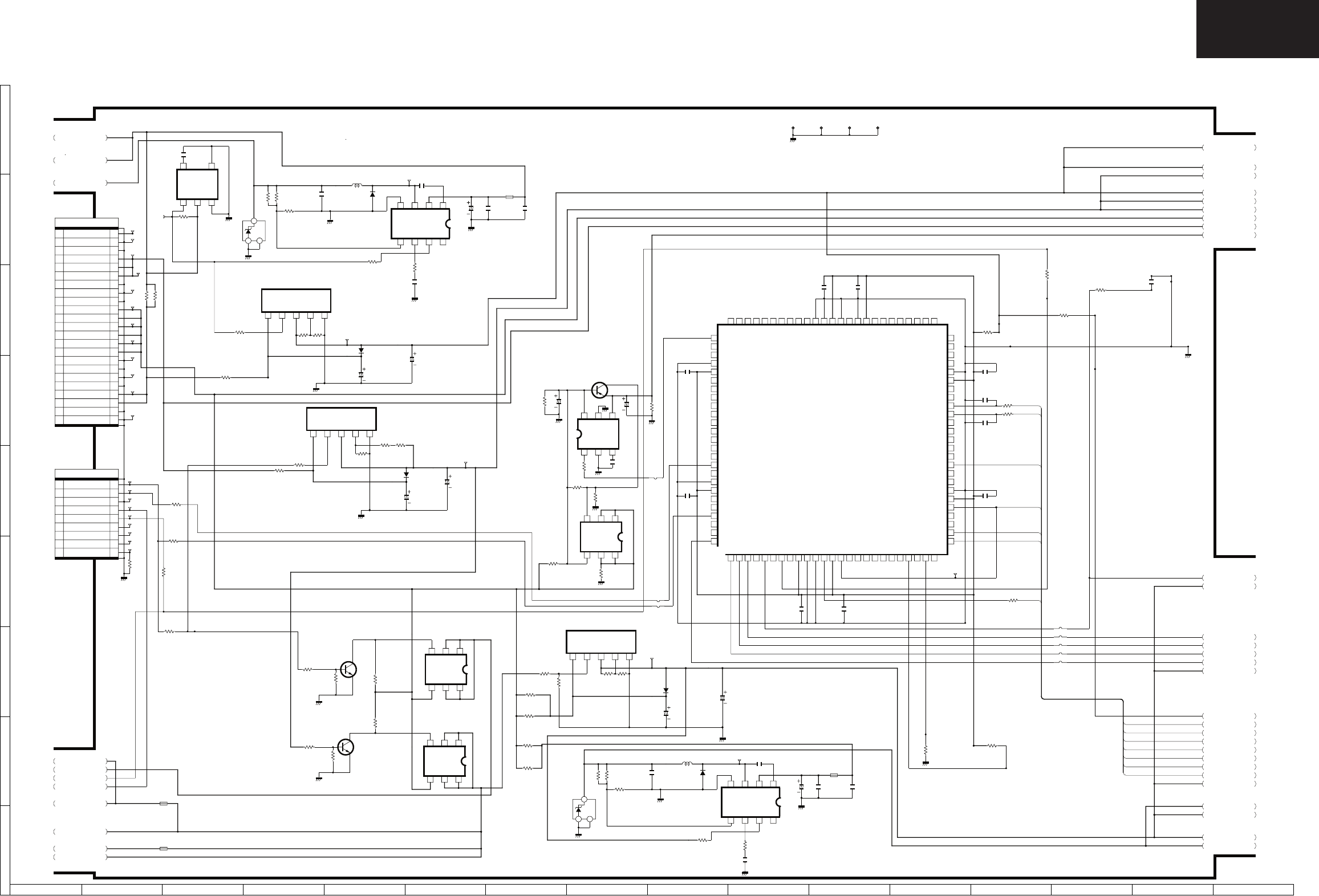
113
LC-32/37GD8E/RU
LC-32/37BT8E/RU
LC-32GD8, LC-32BT8 Main Unit Diagram 6/6 (POWER DC-DC)
POW+35V
PCON2
DTU_ON
DTI2CSEL
DTM_RESET
S_MUTE
FPGA_EP6
FPGA_EP5
FPGA_SDA
FPGA_SDE
FPGA_SCK
HSYNC_OSC
VSYNC_OSC
PCON1
BU+5V
BU+5V_FB1706
+3.3V
+1.8V
POW5V_FB1702
ANT+5V
S+8V
FPGA_EP7
PCLK
FPGA_EP1
FPGA_EP4
FPGA_EP2
FPGA_EP0
RESET_N
FPGA_EP3
FPGA_VCC
FL_OFL
POW+5V
+5V
+5V
INPUT 4.5V to 25V
VHIMP1410ES-1Y BS
12
IN
3
SW
4
GND
5
FB
6
COMP
7
EN NC
8
R1733
100
R1719
6.2K
F
R1737
5.6K
R1723
6.2K
F
C1721
68u
10V
AAPD
D1704
SFPA73
D1702
EX0487CE
2.0V
1
2
3
C1706
22u
6.3V
KZA070WJ
R1709
10K
FB1701
0250TA
C1717
2700P
15uH
L1701
PA213WJ
R1721
5.6K
F
R1724
100
C1720
22u
16V
ASX
D1705
HSU119
D1703
HSU119
R1729
2K
C3340
47u
6.3V
ASX
C1716
22u
16V
ASX
S+8V
PQ20WZ11
1
Vin
2
Vc
3
Vo
4
Vadj
5
GND
LCD5V
+5V
TERMINAL+5V
D1706
HSU119 C1733
22u
16V
ASX
C3338
47u
6.3V
ASX
+3.3V
+1.8V
BU+3.3V
BU+1.8V
R1707
0
+1.8V
+3.3V
S+8V
S+8V
+5V
+3.3V
BU+3.3V
R1726
510
R1747
510
R1748
2K
R1732
2K
R1735
2K
R1734
2.2K
BU+3.3V
+3.3V
R1727
3.3K
R1728
3.3K
R1722
10K
R1716
5.6K
R1720
10K
R1713
5.6K
PQ20WZ11
1
Vin
2
Vc
3
Vo
4
Vadj
5
GND
PQ20WZ11
1
Vin
2
Vc
3
Vo
4
Vadj
5
GND
R1745
1.3K
R1746
2K
Q1704
2SC3928AR
Q1703
2SC3928AR
EDID5V
EDID5V
C1724
10u
16V
KZA073WJ
C1723
10u
16V
KZA073WJ
C1718
0.1u
BU+5V
C1715
22u
35V
ASX
VBRT
BL_ON5
R1705
0
R1704
0
SC1701
WA251WJ
TO POWER
1
+35V
2
GND
3
GND
4
+13.5V
5
+13.5V
6
+13.5V
7
GND
8
GND
9
GND
10
+5V
11
+5V
12
+5V
13
+5V
14
+5V
15
+5V
16
GND
17
GND
18
GND
19
GND
20
BU+5V
21
BU+5V
22
GND
23
GND
SC1702
WA248WJ
TO POWER
1
PCON1
2
PCON2
3
SGND
4
INV_ON(BL_ON5)
5
INV_BRT(VBRT)
6
POW_ERR
7
FAN_ERR
8
NC
9
PWM SEL
BU+5V
SSM6J51TU
VDSS=12V,ID=4A
1
D
2
D
3
G
4
S
5
D
6
D
SSM6J51TU
1
D
2
D
3
G
4
S
5
D
6
D
TL1704
TL1707
TL1708
TL1702
TL1710
TL1706
TL1703
TL1701
TL1705
TL1709
TL1716
TL1717
TL1718
TL1719
TL1720
TL1721
TL1722
TL1723
TL1724
TL1725
TL1726
TL1727
TL1728
TL1729
TL1730
TL1731
TL1732
FB3307
0061TA
FB3308
0061TA
SSM6J51TU
1
D
2
D
3
G
4
S
5
D
6
D
ANT+5V
*C1711
0.01u
*R1712
10K
*R1711
10K
POW+5V
POW+12V
R1739
1
1/2W
R1740
1
1/2W
R1741
1
1/2W
R1742
1
1/2W
LUG1701
HA006WJ
LUG1702
HA006WJ
LUG1703
HA006WJ
LUG1704
HA006WJ
TP1703
VSYNC_OSC
HSYNC_OSC
PCLK
FPGA_SCK
FPGA_SDE
FPGA_SDA
*R1717
0
BL_ERR
S_MUTE
DTU_ON
DTI2CSEL
DTM_RESET
RJ1701
*RJ1702
RJ1704
RJ1703
RJ1706
RJ1707
RJ1705
RJ1708
BL_ON
R1714
0
*R1752
47
C1730
2700P
15uH
L1702
PA213WJ
D1708
SFPA73
R1755
5.6K
R1754
6.2K
F
D1707
EX0487CE
2.0V
1
2
3
R1743
100
FB1702
0250TA
C1737
10u
16V
KZA073WJ
R1744
5.6K
F
R1753
6.2K
F
C1734
0.1u
C1735
68u
10V
AAPD
C1738
10u
16V
KZA073WJ
C1726
22u
6.3V
KZA070WJ
INPUT 4.5V to 25V
VHIMP1410ES-1Y BS
12
IN
3
SW
4
GND
5
FB
6
COMP
7
EN NC
8
*R1756
100K
R1757
1
1/2W
R1758
1
1/2W
R1759
1
1/2W
R1760
1
1/2W
C1702
0.1u
R1761
100
C1739
0.1u Z
*C1740
1000P K
*C1741
100P
C1742
0.1u Z
R1763
22
R1764
22
C1744
100P
(CH)
C1745
100P
(CH)
RESET_N
+3.3V
BU4239G
123
45
TO MAIN 5/6
R1767
10K
R1768
10K
*C1746
1000P
(CH)
*C1753
0.1u Z
*C1754
0.1u Z
PQ1R50
123
456
*Q1705
2SA1530AR
VS2
*C1756
10u
16V
ASX
*C1755
10u
16V
ASX
*R1770
10K
*R1771
100
*R1769
10K
*R1772
10K
R1762
22
C1758
0.1u Z
C1757
0.1u Z
IXB823WJ
1 2 3 4 5 6 7 8 9 10 11 12 13 14 15 16 17 18 19 20 21 22 23 24 25
26
27
28
29
30
31
32
33
34
35
36
37
38
39
40
41
42
43
44
45
46
47
48
49
50
51525354555657585960616263646566676869707172737475
76
77
78
79
80
81
82
83
84
85
86
87
88
89
90
91
92
93
94
95
96
97
98
99
100
*R1774
47
*R1775
10K
*R1773
0
<0.4A
<0.86A
TO MAIN 2/6
TO MAIN 3/6
TO MAIN 3/6
TO MAIN 1/6
TO MAIN 5/6
TO MAIN 2/6
TO MAIN 5/6
TO MAIN 2/6
TO MAIN 3/6
TO MAIN 5/6
TO MAIN 2/6
TO MAIN 4/6
TO MAIN 3/6
TO MAIN 1/6
Ver.N2 (2006.05.16)
IC1706
MP1410ES
IC1702
IC1703
IC1707
IC1705
IC1704
DUNTKD890WE06
*IC1709
IC1708
MP1410ES
IC1701
*IC1711 IC1710
DC-DC 1.8V
<0.57A
<0.24A
DC-DC 1.8V
6.35.23.00
1.5 1.5 3.8 0
5.0 3.6 3.3 2.6 0
13.1 3.3 8.0 2.6 0
4.8 2.8 3.3 2.6 0
0
0
0.63
0
0
0.67
5.05.0
0
5.0 5.0 5.0
5.05.00
5.0 5.0 5.0
6.35.03.00
1.3 1.5 3.3 0
3.8 5.0 0
04.8
LC-32GD8E
PowerDC-DC
(MAIN 6) CONFIDENTIAL
Ver.N2 (2006.05.16)
1234567 8 9 10 11 12 13 14 15 16
I
H
G
F
E
D
C
B
A
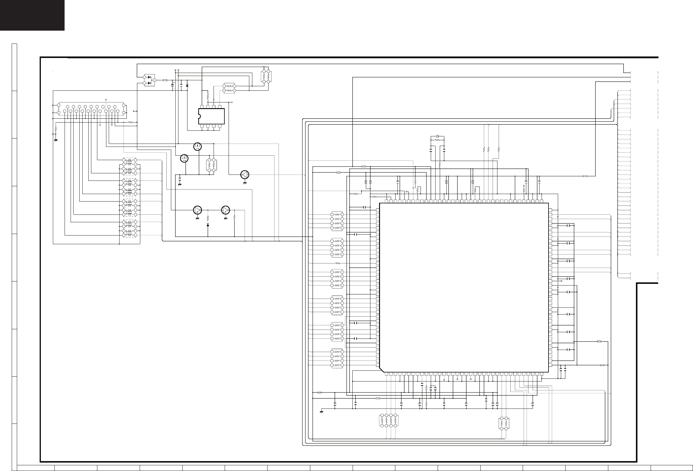
114
LC-32/37GD8E/RU
LC-32/37BT8E/RU
LC-37GD8, LC-37BT8 Main Unit Diagram 1/6 (HDMI)
+3.3V(D)_FB1903
+3.3V(D)_FB1902
RR1X2-
RR1X2+
RR1X1+
RR1X1-
RR1X0+
RR1X0-
RR1XC+
RR1XC-
DINR[7]
DINR[6]
DINR[4]
DINR[5]
DINR[2]
DINR[3]
DINR[1]
DINR[0]
DING[6]
DING[7]
DING[5]
DING[1]
DING[3]
DING[4]
DING[2]
DING[0]
DINB[6]
DINB[0]
DINB[2]
DINB[4]
DINB[3]
DINB[1]
DINB[5]
DINB[7]
HDMI_CLK
DINCK
R0PWR5V
DSDA0
DSCL0
+3.3V_IOVCC
+3.3V_IOVCC
+3.3V_IOVCC +3.3V_IOVCC
HOTP_CONT1
RR1X2+
RR1X2-
RR1X1+
RR1X1-
RR1X0+
RR1X0-
RR1XC+
RR1XC-
DSCL1
DSDA1
R1PWR5V
SDA3
SCL3
HDMI_WP
HDMI-VS
HDMI-HS
DINEN
DSDA1
DSCL1
HDMI_SCK
HDMI_WS
HDMI_SDO
R1PWR5V
HDMI_RST
HDMI_RST
HDMI_INT
+1.8V_SIICVCC
EDID5V
+3.3V
+3.3VSIIAVCC
+3.3VSIIAVCC
+3.3VSIIAVCC
+3.3V(D)_SIIPVCC
C1948
1000P
C1923
1000P
FB1903
0060TA
C1924
1000P
C1953
0.1u
25V
Z
C1968
1000P
SII9021
HDMI RECEIVER
1
DE
2
HSYNC
3
VSYNC
4
0OGND
5
OVCC
6
DACOVCC
7
DACAVCC
8
DACAGND
9
VREF
10
RSET
11
COMP
12
DACGNDR
13
DACVCCR
14
AnRPr
15
DACGNDG
16
DACVCCG
17
AnGY
18
DACGNDB
19
DACVCCB
20
AnBPb
21
DACDGND
22
DACDVCC
23
VCC
24
GND
25
OGND
26
OVCC
27
CSDA
28
CSCL
29
DSDA1
30
DSCL1
31
DSDA0
32
DSCL0
33
R1PWR5V
34
R0PWR5V
35
DVCC
36
DGND
37
PVCC0
38
AVCC
39
R0XC-
40
R0XC+
41
AGND
42
AVCC
43
R0X0-
44
R0X0+
45
AGND
46
AVCC
47
R0X1-
48
R0X1+
49
AGND
50
AVCC
51
R0X2-
52
R0X2+
53
AGND
54
PGND
55
PVCC1
56
ANTSTO
57
AVCC
58
R1XC-
59
R1XC+
60
AGND
61
AVCC
62
R1X0-
63
R1X0+
64
AGND
65
AVCC
66
R1X1-
67
R1X1+
68
AGND
69
AVCC
70
R1X2-
71
R1X2+
72
AGND
73
DGND
74
DVCC
75
OGND
76
OVCC
77
MUTEOUT
78
SPDIF
79
VCC
80
GND
81
NC
82
NC
83
NC
84
SD0
85
WS
86
SCK
87
MCLKIN
88
MCLKOUT
89
OVCC
90
OGND
91
GND
92
VCC
93
NC
94
DVCC2
95
DGND2
96
XTALOUT
97
XTALIN
98
XTALVCC
99
REGVCC
100
NC
101
TEST
102
RESET#
103
SCDT
104
INT
105
VCC
106
GND
107
CLK48B
108
OGND
109
OVCC
110
Q23
111
Q22
112
Q21
113
Q20
114
VCC
115
GND
116
Q19
117
Q18
118
Q17
119
Q16
120
OGND
121
ODCK
122
OVCC
123
Q15
124
Q14
125
Q13
126
Q12
127
GND
128
VCC
129
Q11
130
Q10
131
Q9
132
Q8
133
Q7
134
OVCC
135
OGND
136
Q6
137
Q5
138
GND
139
VCC
140
Q4
141
Q3
142
Q2
143
Q1
144
Q0
R1917
10K
C1956
1000P
L1903
FA134WJ
1
2
3
4
5
6
7
8
C1955
1000P
C1913
1000P
R1933
1.5K
C1928
0.01u
FB1904
0060TA
R1932
1M
C1943
1000P
D1903
1SS355
+1.8V
C1930
1000P
SDA3
HDMI_INT
C1912
1000P
C1929
12P
(CH)
FB1901
0060TA
C1934
12P
(CH)
C1974
1000P
L1902
FA134WJ
1
2
3
4
5
6
7
8
R1929
4.7K
R1906
47K
EDID5V
R1908
10K
SCL3
C1927
1000P
HDMI_RST
C1941
1000P
L1901
FA134WJ
1
2
3
4
5
6
7
8
FB1906
0060TA
HOTP_CONT0
Q1909
DTC144EE
R1930
91 F
C1975
1000P
C1946
1000P
C1916
1000P
Q1907
DTC144EE
FB1905
0060TA
C1959
0.1u
25V
Z
+3.3V
D1901
DAN202K
1
2
3
R1926
4.7K
C1960
1000P
C1947
0.1u
25V
Z
C1967
1000P
*C1901
47u
16V
ASY
C1965
1000P
R1928
22K
*C1906
0.1u
25V Z
Q1905
DTC144EE
C1917
1000P
R1903
1.5K
FB1909
0210TA
SC1901
ZA117WJ
1
2
3
4
5
6
7
8
9
10
11
12
13
14
15
16
17
18
19
20 21
22 23
C1903
0.1u
25V
Z
X1901
SCA108WJ
28.322MHz
R1931
91 F
C1971
1000P
C1973
1000P
D1905
1SS355
FB1908
0060TA
C1969
1000P
Q1903
2SK536
SD
G
R1901
2.7K
R1935
33
C1936
1000P
Q1901
2SK536
S
D
G
L1904
FA134WJ
1
2
3
4
5
6
7
8
R1920
10
1
2
3
4
5
6
7
8
R1921
10
1
2
3
4
5
6
7
8
R1922
10
1
2
3
4
5
6
7
8
R1923
10
1
2
3
4
5
6
7
8
R1924
10
1
2
3
4
5
6
7
8
R1925
10
1
2
3
4
5
6
7
8
R1919 10
DINR[7]
DINR[6]
DINR[5]
DINR[4]
DINR[3]
DINR[1]
DINR[2]
DINR[0]
DING[7]
DING[3]
DING[5]
DING[0]
DING[6]
DING[4]
DING[1]
DING[2]
DINB[0]
DINB[1]
DINB[5]
DINB[2]
DINB[4]
DINB[7]
DINB[6]
DINB[3]
DINCK
HDMI_WP
HDMI_WS
HDMI_SDO
HDMI_SCK
FB1907
0210TA
HOTP_CONT1
HDMI-VS
DINEN
HDMI-HS
R1914
10
21
3
4
R1913
47K
21
3
4
R1911
470K
21
3
4
R1934
100
21
3
4
C1935
10u
KZA073WJ
16V
C1921
10u
16V
KZA073WJ
C1910
10u
16V
KZA073WJ
C1918
10u
16V
KZA073WJ
C1931
10u
16V
KZA073WJ
C1919
10u
16V
KZA073WJ
R1927
10
1
2
3
4
5
6
7
8
TL1909
TL1915
TP1913
TP1916
TP1909
TP1911
TL1911
TP1901
TP1902
TP1907
TP1903
TP1908
TP1904
R3306
22 R3307
22
R3308
22
DUNTKD890WE07
R1936
33
R1937
10K
24LC2BIN
EEPROM
1
A0
2
A1
3
A2
4
VSS
5
SDA
6
SCL
7
WP
8
VCC
TO MAIN 6/6
TO MAIN 3/6
TO MAIN 2/6
Ver.N2 (2006.05.16)
IC1905
IC1901
HDMI
(MAIN 1)
0
0
0
3.3
3.3
3.3
0
0
0
3.3
0
3.3
0
0
3.3
0
0
3.3
0
0
1.8
1.8
0
0
3.3
3.3
3.3
3.3
3.3
3.3
3.3
0
0
1.8
0
3.3
3.3
3.3
3.3
0
3.3
3.3
3.3
0
3.3
3.3
3.3
0
3.3
3.3
3.3
0
0
3.3
0
3.3
3.3
3.3
0
3.3
3.3
3.3
0
3.3
3.3
3.3
0
3.3
3.3
3.3
0
0
1.8
0
3.3
0
0
1.8
0
0
0
0
0
0
0
0
0
3.3
0
0
1.8
0
1.8
0
1.75
1.67
3.3
3.3
0
0
3.3
0
0
1.8
0
0
0
3.3
3.3
3.3
3.3
0
1.8
0
3.3
3.3
3.3
3.3
0
0
3.3
3.3
3.3
3.3
3.3
0
1.8
0
0
3.3
3.3
0
3.3
0
3.3
3.3
0
1.8
3.3
0
0
3.3
3.3
0
5.0 0
0
0
2.4
0
2.4
0
3.2
4.5
3.3
3.2
4.5
3.3
0000
5.05.05.05.0
LC-37GD8E CONFIDENTIAL
Ver.N2 (2006.05.16)
12 3 4 5 6 7 8 9 10 11 12 13 14 15 16
I
H
G
F
E
D
C
B
A
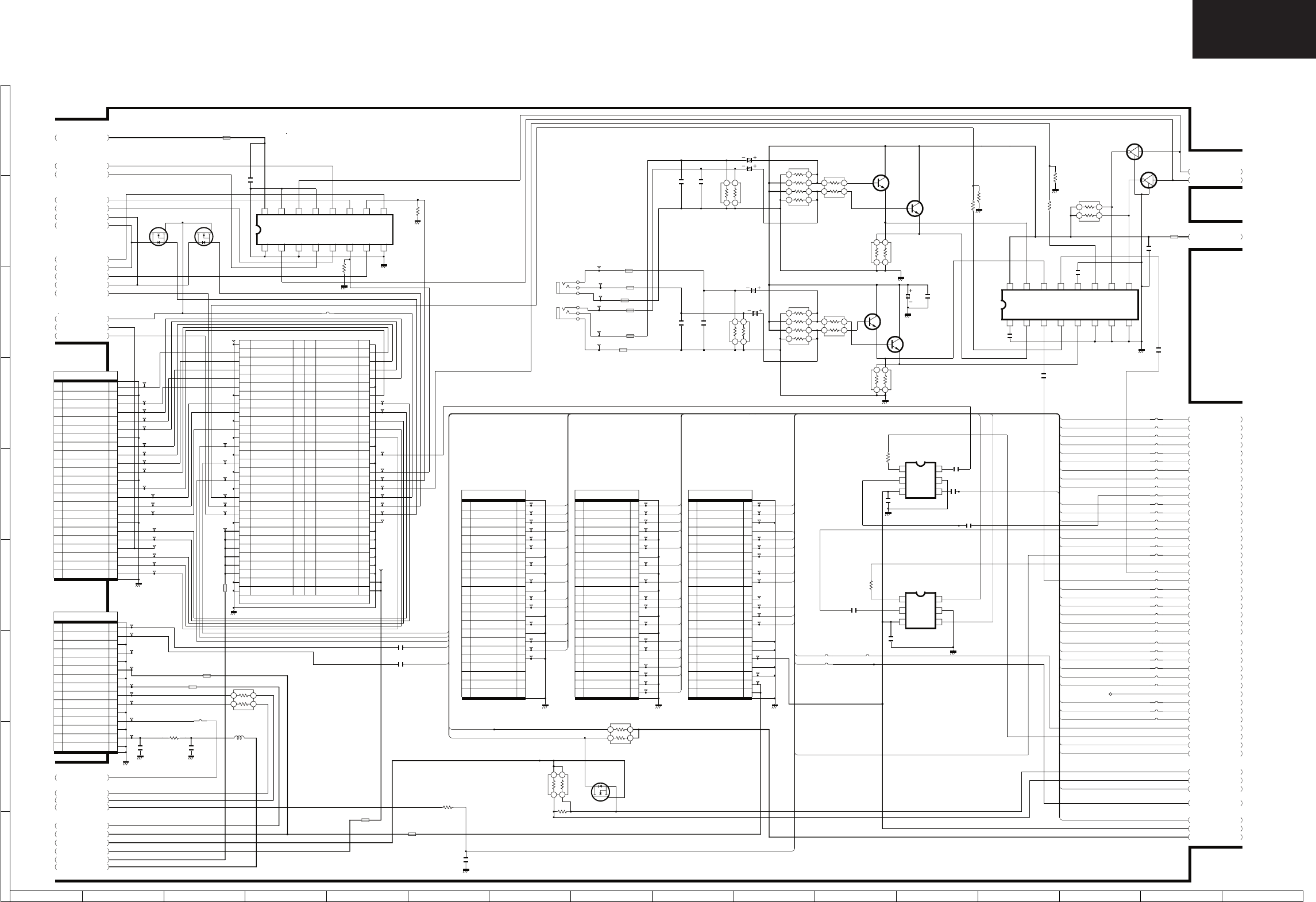
115
LC-32/37GD8E/RU
LC-32/37BT8E/RU
LC-37GD8, LC-37BT8 Main Unit Diagram 2/6 (Signal IN OUT)
OUTTNR
IN2R
SPKR
ATUNER-SIF
IN2L
SPKL
GREEN2
IN2FSW
DTUNER-G
DTUNER-R
IN3C
RED/C2
BULE1
DTUNER-B
GREEN1
ATUNER-CVBS
HPOUT-R
HPOUT-L
RED/C1
OUTV
IN3L
IN3R
IN1L
IN1R
OUTMONL
OUTMONR
HDMI-VS
HDMIA_L
HD1AR
HD1AL
RGB_R
HDMIA_R
AUDIO2_L
VIN_2
VIN_1
DTVHDMI
SLOWSW2
SLOWSW1
OUTTNV
BLUE2
OUTTNL
PCVH
PCVV
IN1FSW
MUTE_SP
SV1JSW
S_MUTE
AUDIO2_R
ATUNER-SIF
IN1FSW
AVLINK1
SLOWSW1
RED/C1
GREEN1
BULE1
VIN_1
IN1R
IN1L
OUTTNV
OUTTNR
OUTTNL
IN2FSW
AVLINK2
SLOWSW2
RED/C2
GREEN2
BLUE2
VIN_2
IN2R
IN2L
OUTV
OUTMONR
OUTMONL
SV1JSW
IN3Y
IN3C
IN3R
IN3L
OUTMONR
OUTMONL
S_MUTE
HPOUT-R
HPOUT-L
SPKR
SPKL
MUTE_SP
AVLINK1
BU+5V
AVLINK2
RGB_L
DPC_L
DPC_R
ATUNER-CVBS
DTM_POWON
DTMSDA
ATUNER+8V
SCL3
SDA3
ATUNER+5V
ATUNER-IFAGC
ATUNER-SDA
ATUNER-SCL
BU+3.3V
DTUNER-G
DTUNER-R
DTUNER-B
DTUNER-AR
DTUNER-CVBS
DTUIN3Y
DTUNER-H
DTUNER-AL
DTVPC
HDMI-HS
DHSYNC
DVSYNC
DTUNER-V
DTUNER-V
B+8V
+5V
S+8V
S2_MUTE
S2_MUTE
PO_MUTE
DTM12V
POW+12V
DTMSCL
TERMINAL+5V
IN3Y
POW_AUDIOSEL
AVLK1
PO_MUTE
DHSYNC
DVSYNC
TVHC153T
1
/1G
2
B
3
1C3
4
1C2
5
1C1
6
1C0
7
1Y
8
GND
9
2Y
10
1C0
11
2C1
12
2C2
13
2C3
14
A
15
/2G
16
VCC
HDMI-VS
HDMI-HS
FB2704
0061TA
+3.3V
SBW_TEST
AOUT2R
VIN15
VIN5
VIN18
VIN16
AIN4R
AOUT1R
AIN2L
AIN3L
AOUT2L
VIN13
AIN1L
AIN3R
AOUT1L
VIN6
SPKOUTL
CVO2
VIN2
VIN8
VIN11
VIN3
VIN12
AIN2R
SPKOUTR
SIF
CVO1
AIN1R
VIN17
AIN4L
VIN1
VIN7
VIN9
FB2702
0254TA
FB2703
0254TA
S+8V
+5V TERMINAL+5V
MUTE_SP
S_MUTE
SV1JSW
BU+3.3V
AVLK1
HPOUTR
HPOUTL
CADC3
CADC4
DTUIN3Y
SDA3
SCL3
CD4052BP
1
0
2
2
3
Y
4
3
5
1
6
INH
7
VEE
8
VSS
9
B
10
A
11
3
12
0
13
X
14
1
15
2
16
VDD
FB2711
0061TA
DTVPC
TL2701
DTVHDMI
TL2706
TL2705
S+8V
C2722
0.1u
25V
Z
C2723
0.1u
25V Z
PCVV
PCVH
TL2702
TL2703
TL2704
R2702
100
21
3
4
C2724
0.1u
25V
Z
C2701
0.1u
25V
Z
Q2704
2SC3928AR
C2703
100P
(CH)
R2709
100K
12
34
56
78
Q2705
2SC3928AR
1u
50V
C2709
ASX
C2705
100P
(CH)
C2714
10u
16V
ASX
1u
50V
C2707
ASX
C2715
0.1u
25V
Z
R2713
4.7K
21
3
4
R2707
220K
21
3
4
1u
50V
C2708
ASX
C2702
100P
(CH)
1u
50V
C2706
ASX
R2712
4.7K
21
3
4
Q2706
2SC3928AR
R2708
100K
12
34
56
78
Q2703
2SC3928AR
C2704
100P
(CH)
R2706
220K
21
3
4
MM1507XN
2-IN,1-OUT,SWITCH
SW(L=IN1,H=IN2)
1SW
2OUT
3VCC 4
IN2
5
GND
6
IN1
SCART12
C2712
0.1u
25V Z
R2714
100
Q2708
DTC144EE
R2716
10K
21
3
4
Q2707
DTC144EE
R2711
10K
2
1
34
R2710
10K
2
1
34
SC2704
WA251WJ
TO AV
1
IN3R
2
IN3L
3
GND
4
PO_MUTE
5
OUTMONR
6
OUTMONL
7
S_MUTE
8
NC
9
HPOUTR
10
HPOUTL
11
(HPMUTE)
12
HPPLUG
13
SPKR
14
SPKL
15
SPMUTE
16
SPPOW
17
GND
18
GND
19
A+5V
20
GND
21
GND
22
8V
23
8V
NC
NC
SC2702
WA251WJ
TO AV
1
IN1FSW
2
AVLINK1
3
SLOWSW1
4
RED/C1
5
GND
6
GREEN1
7
GND
8
BLUE1
9
GND
10
VIN1
11
GND
12
IN1R
13
IN1L
14
GND
15
OUTTNV
16
GND
17
OUTTNR
18
OUTTNL
19
GND
20
NC
21
NC
22
NC
23
NC
NC
NC
SC2703
WA251WJ
TO AV
1
IN2FSW
2
AVLIN2
3
SLOWSW2
4
RED/C2
5
GND
6
GREEN2
7
GND
8
BLUE2
9
GND
10
VIN2
11
GND
12
IN2R
13
IN2L
14
GND
15
OUTV
16
GND
17
OUT2R
18
OUT2L
19
S2_MUTE
20
IN3SW
21
IN3YV
22
GND
23
IN3C
NC
NC
R2703
47K
21
3
4
BU+5V
AVLK2
P1_5
TP2701
C2718
1u
16V
C2719
1u
16V
C2725
220P
RJ2701
RJ2702
RJ2704
RJ2713
RJ2714
RJ2708
RJ2703
RJ2712
RJ2711
RJ2706
RJ2705
RJ2716
RJ2718
RJ2709
RJ2707
RJ2710
RJ2715
RJ2717
RJ2726
RJ2728
RJ2722
RJ2723
RJ2732
RJ2724
RJ2731
RJ2725
RJ2730
RJ2727
RJ2721
RJ2719
RJ2729
RJ2720
RJ2735
RJ2733
RJ2734
RJ2738
RJ2736
RJ2737
TL2737
TL2738
TL2739
TL2740
TL2741
TL2742
TL2743
TL2744
TL2745
TL2746
TL2747
TL2748
TL2749
TL2750
TL2751
TL2752
TL2753
TL2754
TL2755
TL2756
TL2757
TL2758
TL2759
TL2760
TL2761
TL2762
TL2763
TL2764
TL2765
TL2766
TL2767
TL2768
TL2769
TL2770
TL2771
TL2772
TL2773
TL2774
TL2775
TL2776
TL2777
TL2778
TL2779
TL2780
TL2781
TL2782
R2704
10K
2
1
34
FB2708
0061TA
FB2707
0061TA
FB2706
0061TA
FB2709
0061TA
FB2710
0061TA
FB2705
0061TA
J2702
EA073WJ
for RGB INPUT
J2701
EA073WJ
for HDMI INPUT
DTU_ON
SC2705
WA010WJ
TO ATUNER
1
SIF
2
CVBS
3
GND
4
+35V
5
GND
6
+8V
7
GND
8
+5V
9
SCL3
10
SDA3
11
GND
12
IFAGC
13
GND
14
+5V(CONT)
15
GND
*SC2707
WA251WJ
TO DTUNIT
1
FECLK
2
GND
3
FED0
4
FED1
5
FED2
6
FED3
7
GND
8
FED4
9
FED5
10
FED6
11
FED7
12
GND
13
FEERR_UNCOR
14
FEVAL_DEN
15
FESTR_PSYNC
16
FEOFF_X4M
17
GND
18
FEGP0_COMP
19
FEGP1_LOCK
20
I2CSEL
21
FESDA
22
FESCL
23
FERESETn
*P2702
MA202WJ
TO DTUNER
1
+12V
2
GND
3
+12V
4
GND
5
GND
6
+5V
7
GND
8
+5V
9
GND
10
+5V
11
GND
12
+5V
13
GND
14
+5V
15
GND
16
+5V
17
ASPECT
18
GND
19
SCL
20
RESETn
21
SDA
22
IRQ
23
POWON
24
R
25
L
26
GND
27
V
28
BLUE
29
H
30
GND
31
GND
32
GREEN
33
CVBS
34
GND
35
GND
36
RED
37
FERESETn
38
GND
39
FESCL
40
FEOFF_X4M
41
FESDA
42
GND
43
FEGP0_COMP
44
FESTR_PSYNC
45
FEGP1_LOCK
46
FEVAL_DEN
47
FEERR_UNCOR
48
GND
49
GND
50
FED0
51
FED1
52
FED2
53
FED3
54
FED4
55
FED5
56
FED6
57
FED7
58
FECLK
59
GND
60
GND
TL2712
TL2714
TL2710
TL2715
TL2713
TL2708
TL2711
TL2709
TL2707
*TL2723
*TL2722
*TL2721
*TL2731
*TL2728
*TL2724
*TL2720
*TL2730
*TL2719
*TL2733
*TL2717
*TL2726
*TL2734
*TL2729
*TL2725
*TL2718
*TL2732
*TL2716
*TL2727
ANT+5V
POW+5V
POW+12V
*TL2735
DTM_IRQ
DTM_RESET
*RJ2739
*FB2713
0254TA
*FB2714
0254TA
DTI2CSEL
*TL2736
*TL2783
*TL2784
*TL2785
*TL2786
*TL2788
*TL2787
*TL2789
*TL2791
*TL2792
*TL2793
*TL2794
*TL2795
*TL2796
*TL2797
BU_SCL3
BU_SDA3
*TL2798
*TL2799
*TL2800
FB2715
0210TA
MM1507XN
2-IN,1-OUT,SWITCH
SW(L=IN1,H=IN2)
1SW
2OUT
3VCC 4
IN2
5
GND
6
IN1
*R2717
100
*C2727
0.1u
25V
Z
C2710
0.1u
25V
C2726
0.1u
TVB
BU_SDA3
BU_SCL3
*R2701
10K
*R2705
10K
*R2715
1K
*R2719
1K
*R2721
100K
*R2720
100K
TO MAIN 6/6
*C2728
1u
16V
Z
*C2711
1u
16V
Z
C2729
0.1u
S2_MUTE
*Q2710
3LN01S
SD
G
*Q2709
3LN01S
SD
G
Q2702
3LN01S
SD
G
RESET_N
R2722
100
*R2723
4.7
*C2731
0.01u
*C2730
10u
16V
KZA073WJ
1.5uH
*L2701
CUN
R2724
0
C2732
0.01u
(B,A)=
00:C0 DTV
01:C1 PC
10:C2 HDMI
11:C3 *
SYNC SELECT
(DTVHDMI,DTVPC)=
00:C0 DTV
01:C1 PC
10:C2 HDMI
11:C3 *
TTL LEVEL INPUT
5V Tolerant
INPUT PROTECT WHEN POWERDOWN
(B,A)=
11:C3 DTV
10:C2 PC
01:C1 HDMI
00:C0 *
3.3V to 8V LEVEL Shift
TO MAIN 3/6
TO MAIN 6/6
TO MAIN 5/6
TO MAIN 3/6
TO MAIN 6/6
TO MAIN 6/6
TO MAIN 5/6
TO MAIN 3/6
TO MAIN 3/6
TO MAIN 6/6
TO MAIN 1/6
TO MAIN 5/6
Ver.N2 (2006.05.16)
LC-37GD8E
IC2701
IC2704
IC2702
DUNTKD890WE07
*IC2705
Signal INOUT
(MAIN 2)
00000000
00000003.3
0 3.3 0.2 0 0 0 0 0
8.18.1
0003.33.38.1
3.5
8.1
4.0
3.5
8.1
4.0
3.3
8.1
3.9
3.3
8.1
3.9
0
1.4
4.8 1.5
0
1.4
0
8.1 0
0
8.1 0
3.3
4.8
3.3
CONFIDENTIAL
Ver.N2 (2006.05.16)
1234567 8 9 10 11 12 13 14 15 16
I
H
G
F
E
D
C
B
A
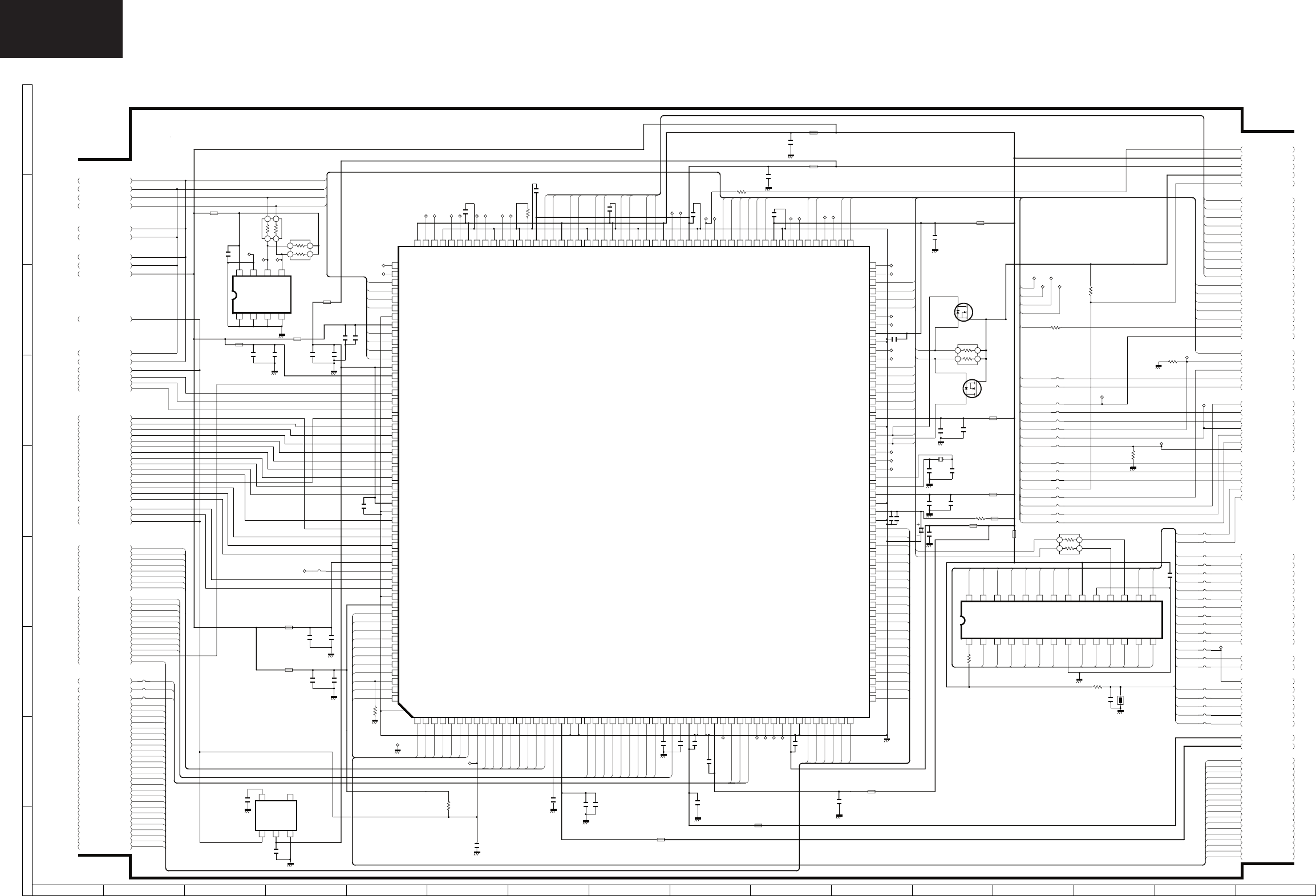
116
LC-32/37GD8E/RU
LC-32/37BT8E/RU
LC-37GD8, LC-37BT8 Main Unit Diagram 3/6 (VCTP)
DVSYNC
DINEN
DINCK
DING[6]
DING[7]
DING[5]
DING[2]
DINB[5]
DING[4]
DING[3]
DINB[7]
DING[0]
DING[1]
DINB[6]
DINB[2]
DINB[0]
DINB[3]
DINB[4]
DINB[1]
DVSYNC
DINEN
DINCK
DINR[7]
DINR[4]
DINR[5]
DINR[6]
DING[5]
DING[7]
DINR[3]
DING[6]
DINR[0]
DINR[1]
DINR[2]
DING[4]
DINB[5]
DINB[7]
DING[3]
DINB[6]
DING[0]
DING[1]
DING[2]
DINB[4]
DINB[0]
DINB[3]
DINB[2]
DINB[1]
FRCO[0]
FRCO[1]
FRCO[3]
FRCO[2]
FRCO[7]
FRCO[6]
FRCO[5]
FRCO[4]
FRCCKI
FRCI[7]
FRCI[6]
FRCI[5]
FRCI[4]
FRCI[2]
FRCI[1]
FRCI[0]
FRCI[1]
FRCI[2]
FRCI[0]
FRCI[6]
FRCI[7]
FRCI[5]
FRCI[4]
FRCI[3]
FRCO[1]
FRCO[2]
FRCO[0]
FRCO[6]
FRCO[5]
FRCO[4]
FRCO[3]
FRCCKO
FRCCKI
LVDS0N
LVDS0P
LVDS1N
LVDS1P
LVDS2N
LVDS2P
LVDSCN
LVDSCP
LVDS3P
LVDS3N
VSUP3.3VO
VSUP3.3COM
VSUP3.3FL
SIF
SBW_TEST
SPKOUTL
SPKOUTR
HPOUTL
AOUT1L
AOUT1R
AOUT2L
AOUT2R
AIN4L
AIN4R
AIN3R
AIN3L
AIN2R
AIN1R
AIN1L
AIN2L
I2S_DI
I2S_WS
I2S_CL
P1_7
P1_6
P1_5
P1_4
P1_3
P1_2
P1_1
P1_0
P4_2
P4_3
P4_0
P4_1
P2_6
P2_7
P3_0
P3_1
P3_2
P3_4
P2_0
P2_1
P2_2/IR
P2_3
TXD
RXD
P3_6
P3_7
P3_5
P3_4
SPKOUTR
SPKOUTL
SIF
SBW_TEST
HPOUTL
AOUT1R
AOUT2L
AOUT1L
AIN4R
AOUT2R
AIN4L
AIN3R
AIN2R
AIN1L
AIN3L
AIN2L
AIN1R
I2S_CL
I2S_DI
I2S_WS
TXD
RXD
P1_7
P1_6
P1_5
P1_4
DINR[0]
DINR[1]
DINR[3]
DINR[2]
DINR[4]
DINR[5]
DINR[6]
DINR[7]
FRCO[7]
S+8V
S+8V
P1_0
P1_1
P2_1
P2_0
P2_7
P3_7
P3_1
P2_6
P3_0
P3_4
P3_2
P3_5
P3_6
P4_0
P4_1
P4_2
P4_3
+5V
+5V
DHSYNC
PICB1
PICB0
PICB5
PICB3
PICA5
PICB6
PICA4
PICA6
PICA3
PICA2
PICB2
PICAA0
HPOUTR
HPOUTR
VSUP3.3IO1 VSUP3.3IO1
P2_3
BU+1.8V
VSUP8.0AU
VSUP5.0SIF
VIN1
VIN1
VIN2
VIN3
VIN18
VIN6
VIN7
VIN8
VIN9
VIN11
VIN12
VIN16
VIN15
VIN13
VIN21
CVO2
CVO1
BU_SCL3
BU_SDA3
LVDS1.8V
VSUP3.3FE
VIN20
VIN19
AVLK1
HOTP_CONT0
HSYNC_OSC
FPGA_SDE
TEMP3
TEMP2
TEMP1
LEDPOWG
LEDPOWR
LEDSLP
LEDOPC
PWMOUT
LCDLR
FRAME
QSSET
OPCIN
AVLK2
PICA7
FAN_ERR
KEY_PSW
FRCCKO
PICAA0
PICAA1
PICA3
PICA4
PICA5
PICA7
PICA6
PICC0
PICC1
PICC2
PICC3 PICC4
CCP1
PICB0
PICB1
PICB2
PICB3
PICB4
PICB5
PICB6
PICB7
PICA2
SV1JSW
PICB7
PICB4
PICC0
PICC1
PICC2
PICC3
CCP1
LCDUD
HDMI_WP
HDMI_RST
SCART12
DTUIN3Y
HOTP_CONT1
HDMI_INT
BU_SCL3
BU_SDA3
FPGA_SCK
FPGA_SDA
DTVPC
DTVHDMI
PCLK
VSYNC_OSC
P1_2
P1_3
BL_ERR
PICC4
SCL3SCL3
SDA3
PICAA1
VIN5
SDA3
VSUP3.3DIG
BU_SDA3
SCL3
BU_SCL3
DTM_IRQ
LVDS3.3V
+3.3V
POW_ERR
FRCI[3]
VSUP3.3IO3
VSUP1.8FE
RESET_N
VSUP3.3RAM
BU+3.3V
BU+3.3V
VSUP3.3DRI
P2_2/IR IRIN
DINB[0]
DINB[7]
DINB[1]
DING[3]
DINR[1]
DHSYNC
DINB[5]
DINR[4]
DING[4]
DINR[7]
DINR[5]
DINB[4]
DINB[2]
DING[7]
DINR[6]
DINB[3]
DING[1]
DINB[6]
DINR[0]
DINR[2]
DVSYNC
DINR[3]
DINCK
DING[0]
DING[6]
DINEN
DING[2]
DING[5] FRCO[7]
FRCCKO
FRCCKI
FRCO[4]
FRCO[5]
FRCO[0]
FRCI[3]
FRCI[6]
FRCI[1]
FRCO[3]
FRCO[1]
FRCI[7]
FRCO[2]
FRCI[5]
FRCI[0]
FRCI[2]
FRCO[6]
FRCI[4]
LVDS3N
LVDSCN
FRAME
LVDS3P
LVDS1N
LVDS2N
LVDSCP
TEMP1
LCDUD
LVDS0P
QSSET
LVDS2P
TEMP3
TEMP2
LCDLR
LVDS0N
LVDS1P
FB3003
0254TA
FB3004
0254TA
C3007
0.1u
25V
Z
C3004
10u
16V
KZA073WJ
C3009
0.1u
25V
Z
C3006
10u
16V
KZA073WJ
C3008
0.1u
25V
Z
C3005
10u
16V
KZA073WJ
FB3006
0254TA
C3003
0.1u
25V
Z
C3002
10u
16V
KZA073WJ
FB3002
0254TA
C3035
10u
16V
KZA073WJ
FB3012
0254TA
C3040
10u
16V
KZA073WJ
C3037
0.1u
FB3015
0254TA
C3041
10u
16V
KZA073WJ
FB3014
0254TA
C3038
0.1u
FB3009
0254TA
C3029
10u
16V
KZA073WJ
FB3010
0254TA
C3027
10u
16V
KZA073WJ
C3031
10u
16V
KZA073WJ
FB3011
0254TA
BU+3.3V
BU+1.8V
C3020
0.1u
C3016
0.1u
C3021
56P
(CH)
R3007
6.2K
FB3013
0254TA
C3036
10u
16V
KZA073WJ
C3034
15P
(CH)
C3039
18P
(CH)
SIF
SPKOUTL
SPKOUTR
SBW_TEST
HPOUTL
AIN4R
AOUT1L
AOUT2L
AOUT1R
AOUT2R
AIN3L
AIN3R
AIN1L
AIN4L
AIN2L
AIN2R
AIN1R
RXD
TXD
P1_6
P1_7
P1_4
P1_5
SCL3
SDA3
FB3008
0254TA
FB3007
0254TA
S+8V
+5V
LEDPOWR
LEDSLP
LEDPOWG
VIN5
VIN6
VIN3
CVO2
VIN2
CVO1
VIN1
VIN15
VIN16
VIN13
VIN8
VIN12
VIN7
VIN9
VIN11
VIN20
VIN17
VIN21
VIN19
VIN18
LEDOPC
FB3016
0254TA
OPCIN
C3042
0.1u
SCL3
HDMI_RST
HDMI_INT
HDMI_SCK
IRIN
HDMI_WS
SDA3
HOTP_CONT0
HDMI_SDO
HOTP_CONT1
FAN_ERR
HPOUTR
C3024
0.1u
25V
Z
C3025
0.1u
25V
Z
C3030
0.1u
25V
Z
C3032
0.1u
25V
Z
C3033
0.1u
25V
Z
C3028
0.1u
25V
Z
C3019
0.1u
25V
Z
C3023
0.1u
25V
Z
C3013
0.1u
25V
Z
C3011
0.1u
25V
Z
C3012
0.1u
25V
Z
+3.3V
MUTE_SP
AVLK1
KEY_PSW
VSYNC_OSC
SCART12
DTUIN3Y
HDMI_WP
C3014
0.1u
R3006
4.7K
RESET_N
C3001
0.1u
25V
Z
BR24L64F
1
A0
2
A1
3
A2
4
GND
5
SDA
6
SCL
7
WP
8
VCC
FB3001
0254TA
SDA3
SCL3
R3004
100
21
3
4
R3005
4.7K
21
3
4
R3009
100
21
3
4
X3001
SC0012CE
20.25MHz
C3010
10u
16V
KZA073WJ
C3018
0.1u
25V
Z
C3017
10u
16V
KZA073WJ
C3022
10u
16V
KZA073WJ
R3010
4.7K
*R3008
4.7K
2
1
34
FPGA_SDE
PWMOUT
SDA3
SCL3
C3015
0.1u
25V
Z
FB3005
0254TA
AVLK2
TP3038
TP3004
TP3001
TP3002
TP3003
TP3006
TP3005
TP3007
TP3009
TP3010
TP3008
TP3012
TP3013
TP3014
TP3011
TP3018
TP3017
TP3015
TP3016
TP3024
TP3025
TP3026
TP3027
TP3029
TP3031
TP3030
TP3028
TP3033
TP3032
TP3034
TP3035
TP3036
TP3022
TP3021
TP3020
TP3023
TP3019
TP3037
RJ3002
RJ3003
RJ3001
RJ3004
RJ3018
RJ3013
RJ3022
RJ3009
RJ3017
RJ3019
RJ3014
RJ3010
RJ3021
RJ3025
RJ3024
RJ3020
RJ3015
RJ3012
RJ3016
RJ3023
RJ3029
RJ3034
RJ3036
RJ3032
RJ3031
RJ3028
RJ3026
RJ3030
RJ3027
RJ3033
RJ3035
RJ3038
SV1JSW
RJ3039
*R3013
10K
RJ3040
RJ3042
RJ3043
RJ3044
RJ3041
RJ3045
RJ3047
RJ3046
TP3040
TP3041
TP3042
TP3043
DTM_IRQ
BU_SDA3
BU_SCL3
TP3044
TP3039
DTVPC
DTVHDMI
IXB624WJ
VCT6973
1
656O6
TDOFW
2
656O5/TDIFW
3
656O4/TMSFW
4
656O3/TCLK
5
656O2/TDO
6
656O1/TDI
7
656O0/TMS
8
RESETQ
9
AIN1R
10
AIN1L
11
AIN2R
12
AIN2L
13
AIN3R
14
AIN3L
15
AIN4R
16
AIN4L
17
VREFAU
18
VSUP8.0AU
19
GNDA
20
SGND
21
AOUT2R
22
AOUT2L
23
AOUT1R
24
AOUT1L
25
HEADPHONER
26
HEADPHONEL
27
SPEAKERR
28
SPEAKERL
29
SUBWOOFER TEST
30
VREFSIF
31
SIFIN+
32
SIFIN-
33
VSUP5.0SIF
34
GNDA
35
GND3.3DIG
36
VSUP3.3DIG
37
SPDIF_OUT
38
I2S_DA_IN
39
I2S_CL
40
I2S_WS
41
I2S_DEL_OUT
42
I2S_DEL_IN
43
I2S_DEL_CL
44
I2S_DEL_WS
45
VSUP3.3RAM
46
GND3.3RAM
47
DVS
48
DEN
49
DCLK
50
DRI7
51
DRI6
52
DRI5
53
DRI4
54
DRI3
55
DRI2
56
DRI1
57
DRI0
58
DGI7
59
DGI6
60
DGI5
61
DGI4
62
DGI3
63
DGI2
64
DGI1
65
DGI0
66
DBI7
67
DBI6
68
DBI5
69
DBI4
70
DBI3
71
DBI2
72
DBI1
73
DBI0
74
GND3.3DRI
75
VSUP3.3DRI
76
GND3.3COM
77
VSUP3.3COM
78
XTALIN
79
XTALOUT
80
CLKOUT
81
VSO
82
HSO
83
SCL
84
SDA
85
GND3.3FL
86
VSUP3.3FL
87
P2_0
88
P2_1
89
P2_2
90
P2_3
91
P2_4/TDI/TXD
92
P4_5/TMS/RXD
93
OSDV
94
OSDH
95
GND3.3IO1
96
VSUP3.3IO1
97
OSDCLK
98
PSDFSW
99
P3_6
100
P3_7
101
P3_5
102
P3_4
103
OSDB1
104
OSDB0
105
P3_3
106
P3_2
107
OSDG1
108
OSDG0
109
P3_1
110
P3_0
111
OSDR1
112
PSDR0
113
GND3.3IO1
114
VSUP3.3IO1
115
P2_7/PCS5
116
P2_6/PCS4
117
P4_1/PCS3
118
P4_0/PCS2
119
P4_3/PCS1
120
P4_2/PCS0
121
PCLK2
122
PCLK1
123
GND1.8DIG
124
VSUP1.8DIG
125
LVDSA_4P
126
LVDSA_4N
127
VSUP3.3LVDS
128
LVDSA_3P
129
LVDSA_3N
130
GND3.3_LVDS
131
LVDSA_CLKP
132
LVDSA_CLKN
133
VSUP3.3LVDS
134
LVDSA_2P
135
LVDSA_2N
136
GND3.3LVDS
137
LVDSA_1P
138
LVDSA_1N
139
VSUP3.3LVDS
140
LVDSA_0P
141
LVDSA_0N
142
VSUP1.8LVDS
143
REXT
144
GND1.8LVDS
145
LVDSB_3P
146
LVDSB_3N
147
GD3.3LVDS
148
LVDSBCLKP
149
LVDSBCLKN
150
VSUP3.3LVDS
151
LVDSB_2P
152
LVDSB_2N
153
GND3.3LVDS
154
LVDSB_1P
155
LVDSB_1N
156
VSUP3.3LVDS
157
LVDSB_0P
158
LVDSB_0N
159
CADC4/P1_7/TDO
160
CADC3/P1_6/TCLK
161
CADC2/P1_5
162
CADC1/P1_4
163
GND3.3DAC
164
VSUP3.3DAC(ADC)
165
P1_3/ROUT
166
P1_2/GOUT
167
P1_1/BOUT
168
P1_0/SVMOUT
169
VSUP1.8FE
170
VSUP3.3FE
171
VIN22/DHS
172
VIN21
173
VIN20
174
VIN19
175
VIN5
176
VIN17
177
VIN16
178
VIN15
179
VIN13
180
VIN12
181
VIN11
182
VIN9
183
VIN8
184
VIN7
185
VSUP1.8FE
186
GNDA
187
VIN6
188
VIN18
189
VIN3
190
VIN2
191
VIN1
192
VSUP3.3VO
193
VOUT3
194
VOUT2
195
VOUT1
196
GND3.3IO3
197
VSUP3.3IO3
198
656I0
199
656I1
200
656I2
201
656I3
202
656I4
203
656I5
204
656I6
205
656I7
206
656CLKI
207
656CLKO
208
656O7
TCLKFW
12345678910 11 12 13 14
1516
171819202122232425262728
PCLK
HSYNC_OSC
FPGA_SCK
FPGA_SDA
BL_ERR
TP3045
R3001
1K
TP3046
TP3047
R3002
22
RESET_N
TH3002
M1103J03
R3003
10K
C3044
0.01u
S2_MUTE
Q3003
3LN01S
S
D
G
Q3004
3LN01S
S
D
G
BU4215G
123
45
C3045
0.01u
RESET_N
R3012
10K
*R3014
4.7K
POW_ERR
C3046
10u
16V
KZA073WJ
BU+3.3V
C3049
1000P
C3048
47u
6.3V
ASX
FB3018
0254TA
R3017
39
R3018
0
if not used, leave vacant
RA total<=100mA,RB total<=100mA
20mA(Icc Clamp) 25mA(Max) /PIN
POWER ON -> INPUT
(RA[4:0] Analog Input)
TO MAIN 5/6
TO MAIN 6/6
TO MAIN 2/6
TO MAIN 6/6
TO MAIN 1/6
TO MAIN 5/6
TO MAIN 4/6
TO MAIN 6/6
TO MAIN 2/6TO MAIN 1/6
TO MAIN 2/6
TO MAIN 5/6
TO MAIN 2/6
TO MAIN 1/6
TO MAIN 4/6
TO MAIN 6/6
Ver.N2 (2006.05.16)
LC-37GD8E
IC3001
DUNTKD890WE07
*IC3002
IC3003 IXB664WJ
PIC16F913
IC3005
VCTP
(MAIN 3)
0000
3.33.303.3
0
0
0
0
0
0
0
3.3
3.7
3.7
3.7
3.7
3.7
3.7
3.7
3.7
3.0
8.0
0
0
3.8
3.8
3.8
3.8
3.8
3.8
3.8
3.8
0
2.7
1.67
1.6
4.7
0
0
3.3
0
0
0
0
0
0
0
0
3.3
0
0
0
0
0
0
0
0
0
0
0
0
0
0
0
0
0
0
0
0
0
0
0
0
0
0
0
0
0
3.3
0
3.3
1.8
1.8
2.3
0.2
0.6
3.3
3.3
0
3.3
0
0
3.2
0
3.3
3.3
0
0
0
3.3
0
0
3.3
0
0
0
0
0
0
0
0
0
0
0
0
0
0
3.3
0
0
0
3.2
2.5
0
0
0
0
1.8
0
3.0
3.3
1.2
1.3
0
1.3
1.2
3.3
1.2
1.2
0
1.2
1.2
3.3
1.2
1.3
1.8
0
0
0
0
0
0
0
3.3
0
0
0
0
0
3.3
0
0
1.0
0
0
0
0
3.3
3.3
0
0
3.3
1.8
3.3
0
0
0
1.0
0
1.0
1.0
0
1.0
1.0
1.0
0
1.0
1.0
1.8
0
1.0
1.0
0
1.0
1.0
3.3
0
1.8
1.0
0
3.3
0
0
0
0
0
0
0
0
0
0.1
0
3.3 2.7 00 0 03.3 0 3.3 0 0 0 0 0
003.33.303.300003.303.33.3
3.3
3.3
3.3
3.3
3.3
3.3
3.2 1.7 0
0.94
CONFIDENTIAL
Ver.N2 (2006.05.16)
1234567 8 9 10 11 12 13 14 15 16
I
H
G
F
E
D
C
B
A
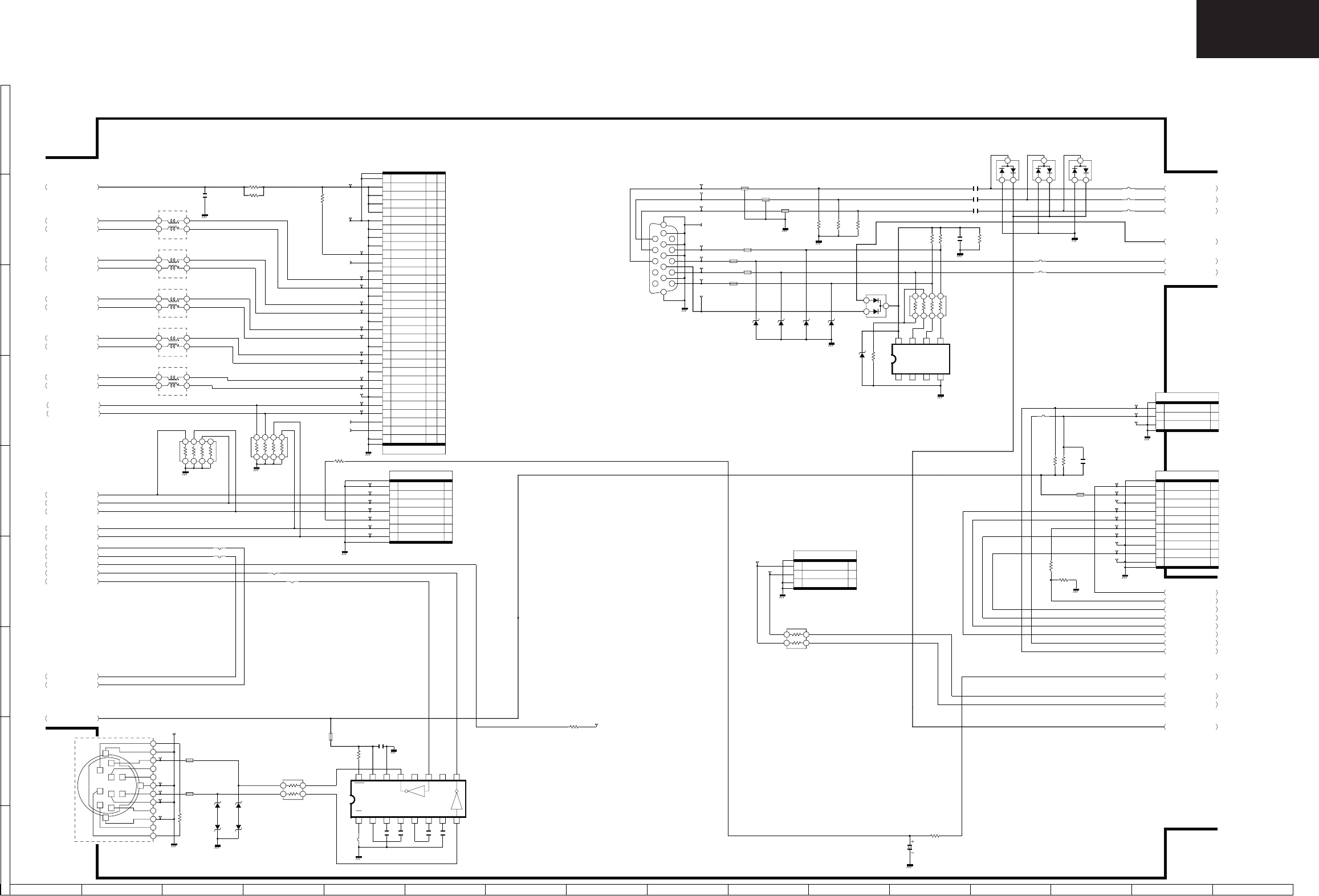
117
LC-32/37GD8E/RU
LC-32/37BT8E/RU
LC-37GD8, LC-37BT8 Main Unit Diagram 4/6 (FRC) Not used for these models
LC-37GD8, LC-37BT8 Main Unit Diagram 5/6 (MISC)
RS232C_3.3V
LVDS0P
LVDS0N
LVDSCP
LVDS1N
LVDS1P
LVDS2N
LVDS2P
LVDSCN
LVDS3N
LVDS3P
PCVV
RGB_V
APC_B
PCVHRGB_H
EDID5V
EDID5V
DSUB_DDC5V
RIN3+
RIN3-
CLKIN+
CLKIN-
RIN2+
RIN2-
RIN1+
RIN1-
RIN0+
RIN0-
SEL_LVDS
IR_VCC
LCD+5V
LEDPOWG
LEDOPC
LEDSLP
LEDPOWR
TEMP1
TEMP2 TEMP2
TEMP3
QSSET
FRAME
APC_G
APC_R
BU_SDA3
PCVG
PCVR
PCVB
PC_DDC5V
LCD5V
KEY_PSW
KEY_ETC
BU+3.3V
BU+3.3V
BU+3.3V
R2301
0
*
TL2306
C2302
0.1u
25V
Z
TL2301
D2303
EX1271CE
12V
R2307
100
2
1
34
R2314
10K
TL2302
C2304
0.1u
25V
Z
TL2305
C2301
0.1u
25V
Z
D2304
EX1271CE
12V
D2302
EX1271CE
12V
FB2309
0061TA
C2305
0.1u
25V
Z
D2301
EX1271CE
12V
TL2303
TL2304
C2303
0.1u
25V
Z
1
EN
2
C1+
3
V+
4
C1-
5
C2+
6
C2-
7
V-
8
910
NC
1112
NC
1314
GND
15
VCC
16
SHDN
BU+3.3V
RXD
TXD
P1_6
P1_7
CADC3
CADC4
RESET_N
R2343
1K F
R2342
10K
P1_4
KEY_PSW
LEDPOWR
LEDSLP
LEDOPC
LEDPOWG
OPCIN
SC2301
DA036WJ
12 3456 78 9 10 1112
IRIN
R2339
1K
R2341
39K
PWMOUT
R2334
10K
C2306
10u
16V
ASX
QSSET
LCDLR
LVDSCN
LVDS3N
LVDS1P
LVDS1N
LVDS0N
TEMP2
LVDS2P
L2302
FA071WJ
1
2
3
4
TEMP3
R2302
10K
1
2
3
4
5
6
7
8
LVDS0P
FRAME
LVDS3P
LCD5V
TEMP1
LVDS2N
L2301
FA071WJ
1
2
3
4
L2303
FA071WJ
1
2
3
4
R2309
4.7K
L2304
FA071WJ
1
2
3
4
LCDUD
L2305
FA071WJ
1
2
3
4
LVDSCP
R2313
10
R2305
10K
1
2
3
4
5
6
7
8
D2311
1SS226
1 2
3
D2306
EX1247CE
5.6V
D2308
EX1247CE
5.6V
TL2316
FB2306
0061TA
TL2315
C2307
0.1u
FL2303
N0003TA
FB2307
0061TA
TL2313
D2310
1SS226
1 2
3
TL2314
FB2308
0061TA
R2322
75
1/4W
R2332
47K
D2309
DAN202K
1
2
3
1234
GND
5
SDA
6
SCL
7
VCLK
8
VCC
FL2302
N0003TA
R2335
1K
TL2311
TL2317
PCVH
R2333
100
CH
12
34
56
78
FB2305
0061TA
TL2319
FL2301
N0003TA
D2312
1SS226
1 2
3
PCVV
SC2303
NA229WJ
1
2
3
4
5
6
7
8
9
10
11
12
13
14
15
16
17
EDID5V
D2307
EX1247CE
5.6V
R2325
75
1/4W
R2329
10K
TL2312
D2305
EX1247CE
5.6V
R2324
75
1/4W
TL2318
R2326
1K
TL2308
TL2309
TL2310
VIN20
VIN21
VIN19
RJ2302
RJ2301
RJ2303
RJ2304
RJ2305
TL2322
TL2323
TL2324
TL2325
TL2326
TL2327
TL2328
TL2329
TL2330
TL2331
TL2332
TL2333
TL2334
TL2335
TL2336
TL2337
TL2338
TL2339
TL2340
TL2341
TL2342
TL2343
TL2344
TL2353
TL2355
TL2356
TL2357
TL2358
TL2359
TL2360
TL2361
TL2362
TL2363
TL2364
TL2365
TL2366
TL2367
FB2302
0061TA
FB2301
0061TA
RJ2307
RJ2306
FB2310
0210TA
P2301
NA341WJ
SH
1
2
TEMP1
3
TEMP2
4
TEMP3
5
ROMSEL0
6
OSEN
7
ROMSEL1
P2305
NA493WJ
LV
1
2
3
4
5
6
7
8
9
10
11
12
13
14
15
16
17
18
19
20
21
22
23
24
25
26
27
28
29
30
31
32
R2315
100
2
1
34
TL2345
TL2346
P2302
NA337WJ
KM TO KEY
1
KEY_PSW
2
KEY_ETC
3
GND
P2303
NA344WJ
RA TO LED/IR/OPC
1
R/C
2
BU+3.3V
3
GND
4
LED-G
5
POWR_LED
6
OPC
7
SLEEP_LED
8
NC
9
LED_OPC
10
GND
P2306
N0565FJ
1
2
3
C2308
0.1u
C2309
0.1u
C2310
0.1u
R2321
0
RJ2309
RJ2308
RJ2311
RJ2310
BU_SDA3
BU_SCL3
D2313
EX1247CE
5.6V
+3.3V
C2312
0.1u
25V
Z
*C2318
100P
(CH)
FB2304
0.56
1/4W
FB2303
0.56
1/4W
TO MAIN 6/6
TO MAIN 3/6
TO MAIN 6/6
TO MAIN 2/6
TO MAIN 6/6
TO MAIN 3/6
TO MAIN 2/6
TO MAIN 3/6
TO MAIN 2/6
TO MAIN 6/6
Ver.N2 (2006.05.16)
IC2301
ISL83220
IC2303
BR24C21F
DUNTKD890WE07
1366x768 PANEL Connect
JAE FIX30M
0 6.2 6.2 3.3 5.7 -3.0 -5.6 0
3.3
03.30-5.603.33.3
0000
4.24.4
0
4.4
LC-37GD8E
MISC
(MAIN 5) CONFIDENTIAL
Ver.N2 (2006.05.16)
12 3 4 5 67 8 9 10 11 12 13 14 15 16
I
H
G
F
E
D
C
B
A
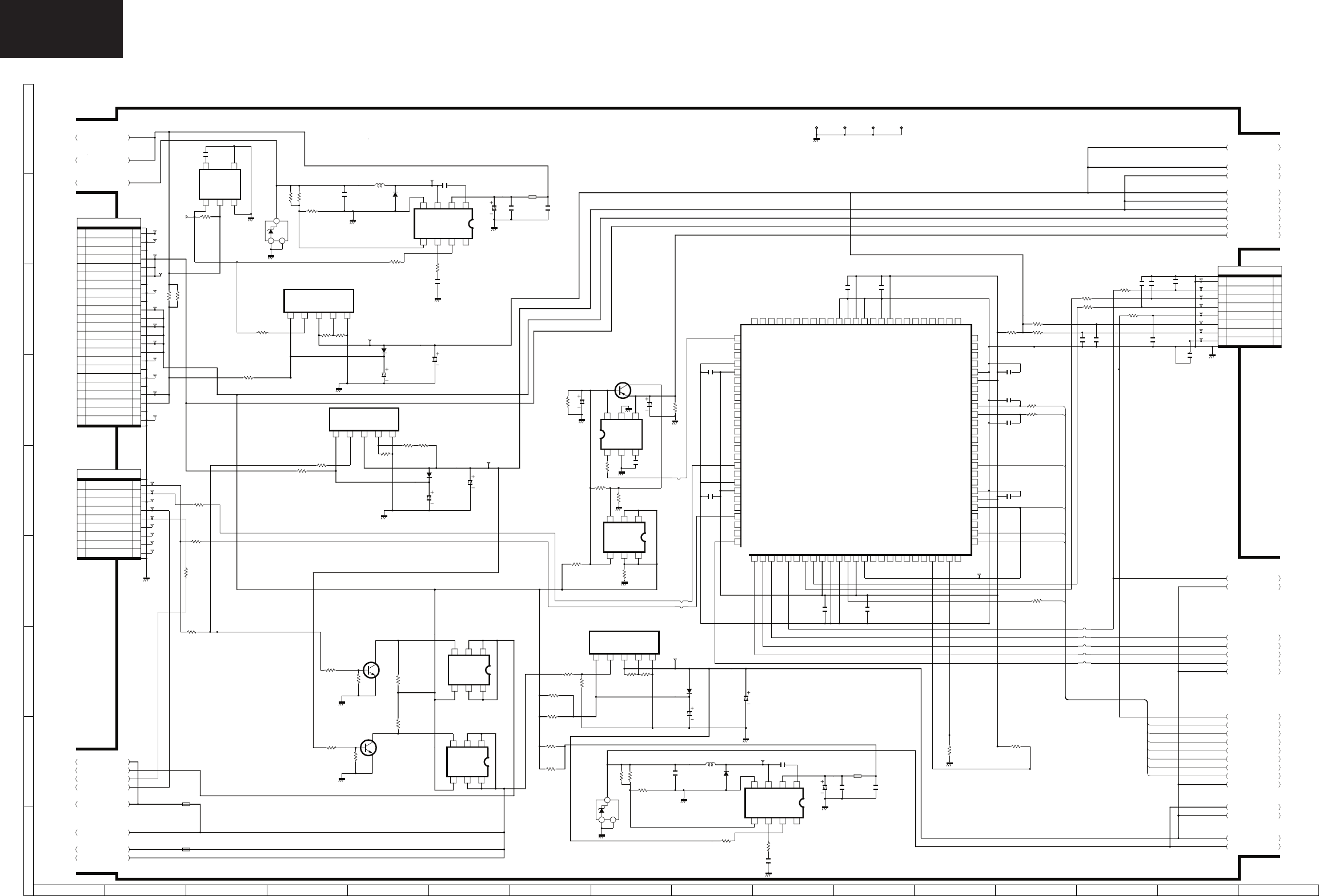
118
LC-32/37GD8E/RU
LC-32/37BT8E/RU
LC-37GD8, LC-37BT8 Main Unit Diagram 6/6 (POWER DC-DC)
POW+35V
PCON2
DTU_ON
DTI2CSEL
DTM_RESET
S_MUTE
FPGA_EP6
FPGA_EP5
FPGA_SDA
FPGA_SDE
FPGA_SCK
HSYNC_OSC
VSYNC_OSC
PCON1
BU+5V
BU+5V_FB1706
+3.3V
+1.8V
POW5V_FB1702
ANT+5V
S+8V
FPGA_EP7
PCLK
FPGA_EP1
FPGA_EP4
FPGA_EP2
FPGA_EP0
RESET_N
FPGA_EP3
FL_OSC
FPGA_VCC
FL_OFL
POW+5V
+5V
+5V
INPUT 4.5V to 25V
VHIMP1410ES-1Y BS
12
IN
3
SW
4
GND
5
FB
6
COMP
7
EN NC
8
R1733
100
R1719
6.2K
F
R1737
5.6K
R1723
6.2K
F
C1721
68u
10V
AAPD
D1704
SFPA73
D1702
EX0487CE
2.0V
1
2
3
C1706
22u
6.3V
KZA070WJ
R1709
10K
FB1701
0250TA
C1717
2700P
15uH
L1701
PA213WJ
R1721
5.6K
F
R1724
100
C1720
22u
16V
ASX
D1705
HSU119
D1703
HSU119
R1729
2K
C3340
47u
6.3V
ASX
C1716
22u
16V
ASX
S+8V
PQ20WZ11
1
Vin
2
Vc
3
Vo
4
Vadj
5
GND
LCD5V
+5V
TERMINAL+5V
D1706
HSU119 C1733
22u
16V
ASX
C3338
47u
6.3V
ASX
+3.3V
+1.8V
BU+3.3V
BU+1.8V
R1707
0
+1.8V
+3.3V
S+8V
S+8V
+5V
+3.3V
BU+3.3V
R1726
510
R1747
510
R1748
2K
R1732
2K
R1735
2K
R1734
2.2K
BU+3.3V
+3.3V
R1727
3.3K
R1728
3.3K
R1722
10K
R1716
5.6K
R1720
10K
R1713
5.6K
PQ20WZ11
1
Vin
2
Vc
3
Vo
4
Vadj
5
GND
PQ20WZ11
1
Vin
2
Vc
3
Vo
4
Vadj
5
GND
R1745
1.3K
R1746
2K
Q1704
2SC3928AR
Q1703
2SC3928AR
EDID5V
EDID5V
C1724
10u
16V
KZA073WJ
C1723
10u
16V
KZA073WJ
C1718
0.1u
BU+5V
C1715
22u
35V
ASX
VBRT
BL_ON5
R1705
0
R1704
0
SC1701
WA251WJ
TO POWER
1
+35V
2
GND
3
GND
4
+13.5V
5
+13.5V
6
+13.5V
7
GND
8
GND
9
GND
10
+5V
11
+5V
12
+5V
13
+5V
14
+5V
15
+5V
16
GND
17
GND
18
GND
19
GND
20
BU+5V
21
BU+5V
22
GND
23
GND
SC1702
WA248WJ
TO POWER
1
PCON1
2
PCON2
3
SGND
4
INV_ON(BL_ON5)
5
INV_BRT(VBRT)
6
POW_ERR
7
FAN_ERR
8
NC
9
PWM SEL
BU+5V
SSM6J51TU
VDSS=12V,ID=4A
1
D
2
D
3
G
4
S
5
D
6
D
SSM6J51TU
1
D
2
D
3
G
4
S
5
D
6
D
TL1704
TL1707
TL1708
TL1702
TL1710
TL1706
TL1703
TL1701
TL1705
TL1709
TL1716
TL1717
TL1718
TL1719
TL1720
TL1721
TL1722
TL1723
TL1724
TL1725
TL1726
TL1727
TL1728
TL1729
TL1730
TL1731
TL1732
FB3307
0061TA
FB3308
0061TA
SSM6J51TU
1
D
2
D
3
G
4
S
5
D
6
D
ANT+5V
*C1711
0.01u
*R1712
10K
*R1711
10K
POW+5V
POW+12V
R1739
1
1/2W
R1740
1
1/2W
R1741
1
1/2W
R1742
1
1/2W
LUG1701
HA006WJ
LUG1702
HA006WJ
LUG1703
HA006WJ
LUG1704
HA006WJ
TP1703
VSYNC_OSC
HSYNC_OSC
PCLK
FPGA_SCK
FPGA_SDE
FPGA_SDA
*P1701
NA342WJ
LB
1
SGND
2
STB
3
OFL
4
OSC
5
ERR
6
REG
7
REG2
8
BRT
*R1731 1K
*R1736 1K
*R1730
47
*R1718
47
*R1715 47
*R1717
47
BL_ERR
S_MUTE
DTU_ON
DTI2CSEL
DTM_RESET
RJ1701
*RJ1702
RJ1704
RJ1703
RJ1706
RJ1707
RJ1705
RJ1708
BL_ON
R1714
0
*R1752
47
*TL1733
*TL1734
*TL1735
*TL1736
*TL1737
*TL1738
*TL1739
*TL1740
C1730
2700P
15uH
L1702
PA213WJ
D1708
SFPA73
R1755
5.6K
R1754
6.2K
F
D1707
EX0487CE
2.0V
1
2
3
R1743
100
FB1702
0250TA
C1737
10u
16V
KZA073WJ
R1744
5.6K
F
R1753
6.2K
F
C1734
0.1u
C1735
68u
10V
AAPD
C1738
10u
16V
KZA073WJ
C1726
22u
6.3V
KZA070WJ
INPUT 4.5V to 25V
VHIMP1410ES-1Y BS
12
IN
3
SW
4
GND
5
FB
6
COMP
7
EN NC
8
*R1756
100K
R1757
1
1/2W
R1758
1
1/2W
R1759
1
1/2W
R1760
1
1/2W
C1702
0.1u
R1761
100
C1739
0.1u Z
*C1740
1000P K
*C1741
100P
C1742
0.1u Z
R1763
22
R1764
22
C1744
100P
(CH)
C1745
100P
(CH)
RESET_N
+3.3V
BU4239G
123
45
TO MAIN 5/6
R1767
10K
R1768
10K
*C1751
100P
(CH)
*C1750
100P
(CH)
*C1749
100P
*C1752
100P
(CH)
*C1748
100P
(CH)
*C1747
100P
(CH)
*C1746
1000P
(CH)
*C1753
0.1u Z
*C1754
0.1u Z
PQ1R50
123
456
*Q1705
2SA1530AR
VS2
*C1756
10u
16V
ASX
*C1755
10u
16V
ASX
*R1770
10K
*R1771
100
*R1769
10K
*R1772
10K
R1762
22
C1758
0.1u Z
C1757
0.1u Z
IXB823WJ
1 2 3 4 5 6 7 8 9 10 11 12 13 14 15 16 17 18 19 20 21 22 23 24 25
26
27
28
29
30
31
32
33
34
35
36
37
38
39
40
41
42
43
44
45
46
47
48
49
50
51525354555657585960616263646566676869707172737475
76
77
78
79
80
81
82
83
84
85
86
87
88
89
90
91
92
93
94
95
96
97
98
99
100
<0.4A
<0.86A
TO MAIN 2/6
TO MAIN 3/6
TO MAIN 3/6
TO MAIN 1/6
TO MAIN 5/6
TO MAIN 2/6
TO MAIN 5/6
TO MAIN 2/6
TO MAIN 3/6
TO MAIN 5/6
TO MAIN 2/6
TO MAIN 4/6
TO MAIN 3/6
TO MAIN 1/6
Ver.N2 (2006.05.16)
IC1706
MP1410ES
IC1702
IC1703
IC1707
IC1705
IC1704
DUNTKD890WE07
*IC1709
IC1708
MP1410ES
IC1701
*IC1711 IC1710
DC-DC 1.8V
<0.57A
<0.24A
DC-DC 1.8V
6.35.23.00
1.5 1.5 3.8 0
5.0 3.6 3.3 2.6 0
13.1 3.3 8.0 2.6 0
4.8 2.8 3.3 2.6 0
0
0
0.63
0
0
0.67
5.05.0
0
5.0 5.0 5.0
5.05.00
5.0 5.0 5.0
6.35.03.00
1.3 1.5 3.3 0
3.8 5.0 0
04.8
LC-37GD8E
PowerDC-DC
(MAIN 6) CONFIDENTIAL
Ver.N2 (2006.05.16)
1234567 8 9 10 11 12 13 14 15 16
I
H
G
F
E
D
C
B
A
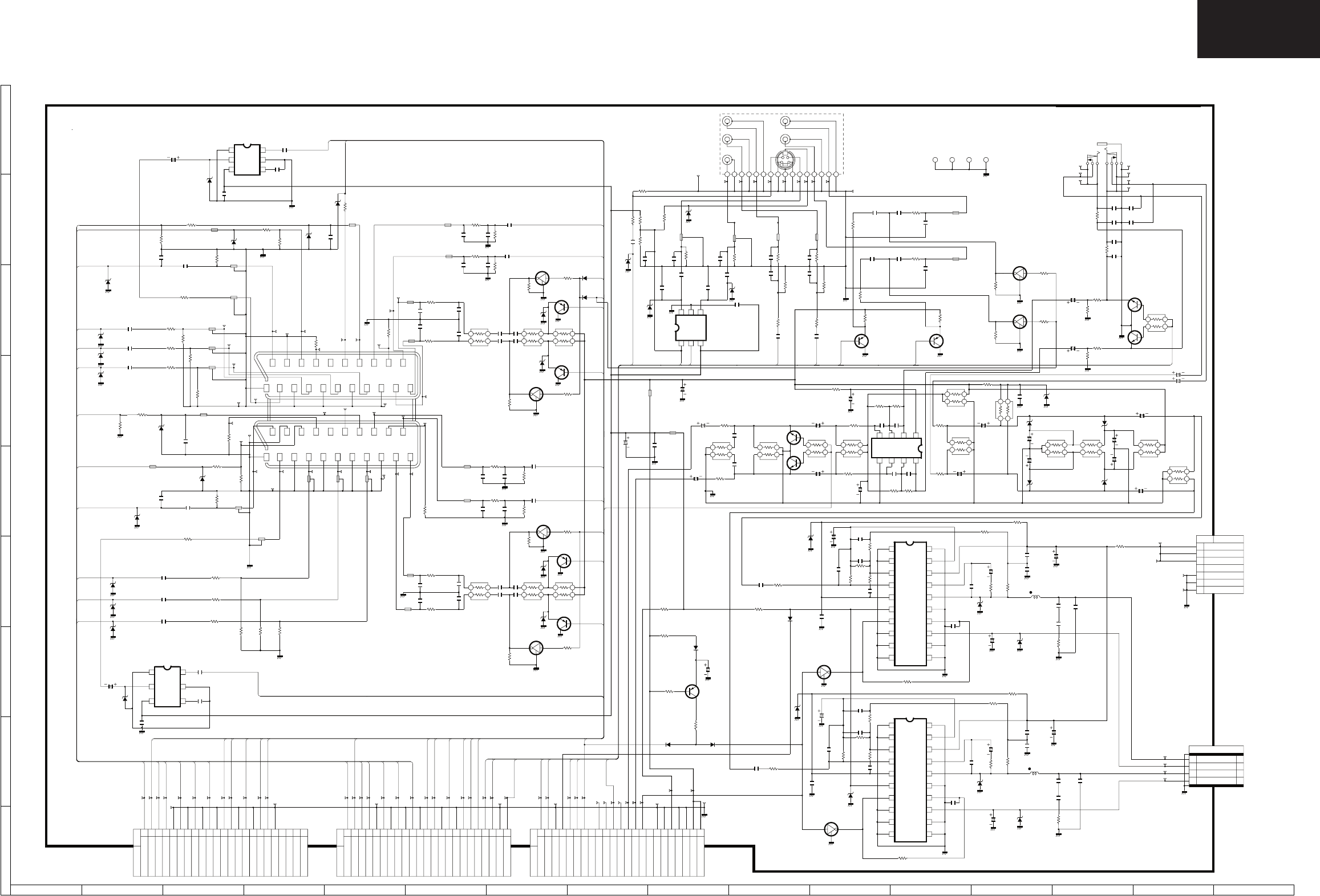
119
LC-32/37GD8E/RU
LC-32/37BT8E/RU
LC-32/37GD8, LC-32/37BT8 AV Unit Diagram
OUTMONL
OUTMONR
IN3L
IN3R
CVBS_OUT
IN3YV
TDA_EN
RED/C2
GREEN2
BLUE2
IN1FSW
RED/C1
GREEN1
BLUE1
IN1L
IN1R
OUTV
IN2R
IN2L
OUT2L
OUT2R
OUTTNL
OUTTNR
S_MUTE
AVLINK2
IN2FSW IN2_BLANK
SC_AVLINK
HPMUTE
OUTMONL
OUTMONR
IN3L
IN3R
IN3SW
OUT2L
OUT2R
OUTV
IN2L
IN2R
VIN2
BLUE2
GREEN2
RED/C2
SLOWSW2
AVLINK2
IN2FSW
OUTTNL
OUTTNR
OUTTNV
IN1L
IN1R
VIN1
BLUE1
GREEN1
RED/C1
SLOWSW1
AVLINK1
IN1FSW
B+29V
SC1FSW
IN3C
TDA_VP
PRE_R
PRE_L
PRE_L
HPMUTE
S_MUTE
HPOI_L
OUTTNV
HP_LOUT
HPO_L
HPO_R
HP_ROUTHP_R
HP_R
HP_L
HP_L
SPKR
SPKL
SPKL+
SPKR+
IN3YV
+8V_AIN
A+5V
A+8V
A+8V
S2_MUTE
S_MUTE
S2_MUTE
IN3SW
S_MUTE
IN3C
TDA_VPA
SPKR-
HPOI_R
VIN2
VIN1
SCART+5V
SLOWSW2
SLOWSW1
SPKL-
C1108
100P
(CH)
C1101
0.1u
25V
C1102
0.1u
25V
C1103
0.1u
25V
FL1104
N0017TA
FL1105
N0017TA
Q1203
DTC314TK
MUTE
Q1204
DTC314TK
MUTE
R1128
100
R1121
75
1/4W
R1111
68
1/4W
R1104
0
R1105
0
R1106
0
R1217
330
R1221
330
R1224
560K
R1226
1K
R1227
1K
R1225
560K
DUNTKD604WE10
FB1102
0062TA
R1130
0
R1114
75
1/4W
FL1103
N0017TA
FB1104
0077TA
FL1102
N0017TA
FL1101
N0017TA
R1129
75
1/4W
R1123
75
1/4W
R1117
75
1/4W
*C1110
10u
16V
KZA073WJ
C1131
0.01u
Z
C1147
0.1u
25V
Z
C1148
10u
16V
KZA073WJ
MM1506XN
2-IN,1-OUT,SWITCH
1SW
2OUT
3VCC 4
IN2
5
GND
6
IN1
FL1109
N0017TA
R1116
75
1/4W
R1120
0
R1153
100K
FL1108
N0017TA
C1135
1000P
R1125
75
1/4W
R1113
75
1/4W
FL1107
N0017TA
R1127
75
1/4W
FL1110
N0017TA
R1112
68
1/4W
C1107
0.1u
25V
R1115
0
FB1103
0077TA
C1142
1u
16V
FB1101
0062TA
C1106
0.1u
25V
C1134
1000P
FB1111
0051TA
FB1112
0051TA
R1118
75
1/4W
*C1109
10u
16V
KZA073WJ
FL1106
N0017TA
C1138
1u
16V
R1119
100
R1110
0
C1105
0.1u
25V
C1104
100P
(CH)
R1154
100K
R1126
0
R1201
100
C1201
1000P
R1204
75
C1208
10u
16V
KZA073WJ
R1209
75
1/4W
C1207
10P
(CH)
C1206
100P
(CH)
FL1212
N0017TA
C1218
1u
16V
C1212
1u
16V
R1211
1K
R1214
1K
C1211
1000P C1217
1000P
R1212
100K
R1210
1K
FB1201
0051TA
R1215
100K
R1213
1K
FB1202
0051TA
C1216
100P
(CH)
C1210
100P
(CH)
C1116
220P
C1114
220P
C1127
100P
(CH)
C1128
100P
(CH)
R1218
2.7K
R1222
2.7K
Q1202
2SA1530AR
Q1201
2SA1530AR
R1138
0
C1202
0.01u
Z
R1102
15K F
R1103
39K F
R1108
39K F
R1101
15K F
FB1218
0254TA
FB1213
0210TA
R1137
0
R1131
220
R1203
6.8K
R1202
3.9K
FL1211
N0017TA
C1204
10P
(CH)
C1203
100P
(CH)
C1205
10u
16V
KZA073WJ
R1206
75
1/4W
C1252
1u
16V
*C1251
100u
16V
ASX
J1301
JA007WJ
8
L
2
5 7
R
3
4 1
C1253
0.1u
25V
Z
MM1507XN
2-IN,1-OUT,SWITCH
1
SW
2
OUT
3
VCC
4
IN2
5
GND
6
IN1
P1101
MA250WJ
TO MAIN 2
1
IN1FSW
2
AVLINK1
3
SLOWSW1
4
RED/C1
5
GND
6
GREEN1
7
GND
8
BLUE1
9
GND
10
VIN1
11
GND
12
IN1R
13
IN1L
14
GND
15
OUTTNV
16
GND
17
OUTTNR
18
OUTTNL
19
GND
20
NC
21
NC
22
NC
23
NC
R309
47K
R343
0
1/4W
R339
22
1/4W
C310
2200P
C305
0.1u
R304
2.2K
C313
2200P
C327
0.015u
R317
470K
R303
2.2K
R324
47K
C334
220P
R336
10
1/4W
R308
47K
R316
3.9K
R330
2.2K
C303
0.22u Z
R329
6.8K
R340
22
1/4W
R331
2.2K
R314
3.9K
R323
47K
C326
0.015u
C341
0.22u
25V
R315
470K
C322
0.22u
R335
10
1/4W
R338
10
1/4W
C309
2200P
R337
10
1/4W
C314
0.015u
R313
1K
C312
2200P
*C343
0.33u
FYF
(ML)
Q304
DTC314TK
MUTE
C308
0.1u
R312
1K
C335
220P
C333
220P
C332
220P
C315
0.015u
Q303
DTC314TK
MUTE
R334
6.8K
*C342
0.33u
FYF
(ML)
C340
0.22u
25V
C323
0.22u Z
R1177
1K
R1179
1K
P1102
MA250WJ
TO MAIN 2
1
IN2FSW
2
AVLINK2
3
SLOWSW2
4
RED/C2
5
GND
6
GREEN2
7
GND
8
BLUE2
9
GND
10
VIN2
11
GND
12
IN2R
13
IN2L
14
GND
15
OUTV
16
GND
17
OUT2R
18
OUT2L
19
S2_MUTE
20
IN3SW
21
IN3Y
22
GND
23
IN3C
2.2u
50V
C328
ASX
2.2u
50V
C329
ASX
P1201
MA250WJ
TO MAIN 2
1
IN3R
2
IN3L
3
GND
4
PO_MUTE
5
OUTMONR
6
OUTMONL
7
S_MUTE
8
PO_MUTE
9
HPOUTR
10
HPOUTL
11
HPMUTE
12
HPPLUG
13
SPKR
14
SPKL
15
MUTE
16
SPPOW
17
GND
18
GND
19
A+5V
20
GND
21
GND
22
8V
23
8V
FB1204
0062TA
R1219
270
C1225
100P
(CH)
C1224
100P
(CH)
R1216
270
FB1203
0062TA
FB1105
0051TA
C1118
100P
(CH)
R1134
1K
R1173
100K
FB1107
0051TA
C1120
1000P
C1119
1000P
C1124
1u
16V
R1147
1K
R1150
100K
C1117
100P
(CH)
C1121
1u
16V
SC301
Z0738CE
TO POWER
1
+30V
2
+30V
3
+30V
4
NC
5
GND
6
GND
7
GND
C1126
470P
R1109
220
1/10W
Q1103
2SA1530AR
Q1102
DTC314TK
R1144
1K
FB1108
0062TA
Q1104
2SA1530AR
Q1101
DTC314TK
C1125
470P
C1122
330P
R1141
560K
R1145
1K
R1107
220
1/10W
FB1106
0062TA
R1142
560K
C1123
330P
R1140
330
2
1
34
R1143
2.7K
2
1
34
R1139
100
2
1
34
Q1108
2SA1530AR
C1139
330P
FB1110
0062TA
C1143
470P
R1157
560K
R1152
100
2
1
34
R1156
560K
R1146
220
1/10W
FB1109
0062TA
C1144
470P
R1160
1K
R1155
330
2
1
34
Q1107
2SA1530AR
R1148
220
1/10W
Q1105
DTC314TK
C1140
330P
R1159
1K
R1158
2.7K
2
1
34
Q1106
DTC314TK
TDA8931T
1
VSSD
2
VSSA
3
INN
4
INP
5
VDDA
6
PWRUP
7
ENA
8
DIAG
9
CGND
10
VSSD
11
VSSD
12
OVP
13
HVP
14
STABI
15
VSSP
16
OUT
17
BOOT
18
VDDP
19
HVPI
20
VSSD
TDA8931T
1
VSSD
2
VSSA
3
INN
4
INP
5
VDDA
6
PWRUP
7
ENA
8
DIAG
9
CGND
10
VSSD
11
VSSD
12
OVP
13
HVP
14
STABI
15
VSSP
16
OUT
17
BOOT
18
VDDP
19
HVPI
20
VSSD
C1145
10u
16V
KZA073WJ
C1157
10u
16V
C1158
10u
16V
C1146
10u
16V
KZA073WJ
C1132
10u
16V
KZA073WJ
C1136
10u
16V
C1137
10u
16V
C1133
10u
16V
KZA073WJ
C1220
10u
16V
KZA073WJ
C1222
10u
16V
KZA073WJ
C1221
10u
16V
KZA073WJ
C1223
10u
16V
KZA073WJ
TL1106
TL1104
TL1102
TL1101
TL1107
TL1105
TL1103
TL1108
TL1109
TL1110
TL1111
TL1112
TL1113
TL1114
TL1115
TL1116
TL1117
TL1118
TL1119 TL1120
TL1121 TL1122
TL1123
TL1124
TL1125
TL1126
TL1127
TL1128
TL1129
TL1130
TL1131
TL1132
TL1133
TL1134
TL1135
TL1136
TL1137 TL1138
TL1139
TL1140
TL1141
TL1142
TL1143
TL1144
TL1145
TL1146
TL1147
TL1148
TL1149
TL1150
TL1151
TL1152
TL1153
TL1154
TL1155
TL1156
TL1157
TL1158
TL1159
TL1160
TL1161
TL1162
TL1163
TL1164
TL1165
TL1166
TL1167
TL1168
TL1169
TL1170
TL1171
TL1172
TL1173
TL1174
TL1175
TL1176
TL1177
TL1178
TL1179
TL1180
TL1181
TL1182
TL1183
TL1184
TL1185
TL1186
TL1187
TL1188
TL1189
TL1190
TL1191
TL1192
TL1193
TL1194
TL1195
TL1196
TL1197
TL1198
TL1199
TL302
TL301
TL307
TL308
TL303
TL304
TL305
TL306
C1130
470u
16V
ASY
R310
1K
R307
100K
2
1
34
R327
10K
2
1
34
C337
1u
50V
ASX
NJM4558M
1234
5678
R319
1.2K
R311
1K
R306
4.7K
2
1
34
*R325
2.7K
R322
10K
R301
1K
2
1
34
R328
3.9K
2
1
34
R345
10K
21
3
4
R320
1.2K
R318
82
1/2W
*C301
0.027u
10u
50V
C324
ASX
2.2u
50V
C307
ASX
*R326
2.7K
R321
10K
C316
33P
(CH)
C319
47P
(CH)
C345
1u
50V
ASX
C318
47P
(CH)
R344
10K
21
3
4
R342
3.3K
21
3
4
C344
1u
50V
ASX
Q302
2SC3928AR
*C302
0.027u
C336
1u
50V
ASX
C317
33P
(CH)
10u
50V
C325
ASX
R341
10K
21
3
4
Q301
2SC3928AR
R302
4.7K
2
1
34
2.2u
50V
C306
ASX
C304
0.22u Z
R305
2.2K
22u
35V
C349
ASX
Q306
2SC3928AR
R347
56
Q305
2SC3928AR
R348
2.2K
2
1
34
R346
56
22u
35V
C348
ASX
J1101
ZA116WJ
SCART 1
SCART 2
1
AO-R
2
AIN-R
3
AO-L
4
AGND
5
(G7)
6
AIN-L
7
BLUE
8
SLOWSW
9
(G11)
10
CTRL
11
GREEN
12
RSV
13
(G15)
14
(G16)
15
RED/C
16
BLANK
17
(G19)
18
(G20)
19
VOUT/L
20
VIN
21
22
AO-R
23
AIN-R
24
AO-L
25
AGND
26
(G7)
27
AIN-L
28
BLUE
29
SLOWSW
30
(G11)
31
CTRL
32
GREEN
33
RSV
34
(G15)
35
(G16)
36
RED/C
37
BLANK
38
(G19)
39
(G20)
40
VOUT/L
41
VIN
42
2.2u
50V
C320
ASX
2.2u
50V
C321
ASX
*C331
470u
35V
SYA
*C330
470u
35V
SYA
D303
EXA092WJ
12V
D302
EXA092WJ
12V
D304
EXA092WJ
12V
D301
EXA092WJ
12V
J1201
ZA033WJ
135
2 4 78910 11 12 13 14 15 16
6
MM1506XN
123
4 5 6
C1159
0.01u Z
C1160
0.1u
25V
Z
C1161
10u
16V
KZA073WJ
*D1106
EX1034CE
5.1V
C1162
470u
16V
ASY
C350
0.01u
C351
0.01u
R349
100
C352
0.01u
R350
100 C353
0.01u
C354
1000P
C355
1000P
LUG301 LUG302 LUG303 LUG304
47u
50V
C356
ASY
47u
50V
C357
ASY
R351
10K
R352
10K
10u
50V
C358
ASX
10u
50V
C359
ASX
R353
1K
R354
1K
C1219
47u
16V
ASY
R333
10K
2
1
34
R332
1K
C361
10u
16V
KZA073WJ
C360
47u
16V
ASY
P301
NA173WJ
SP
SPKL-
1
SPKL+
2
SPKR-
3
SPKR+
4
D305
EXA089WJ
4.3V
22u
16V
C311
ASX
C346
1u
50V
ASX
C347
1u
50V
ASX
C338
470u
50V
EZA513WJ
C339
470u
50V
EZA513WJ
R355
2.7
1/4W C362
0.22u
25V
C363
0.22u
25V
Q307
2SA1530AR
R356
10K
D306
1SS390
D307
1SS390
D308
1SS390
R360
4.7K
R358
0
C364
470u
16V
ASY
D309
1SS390
D310
1SS390
R1228
0
*D1201
EX1239CE
4.3V
C365
2200P
C366
2200P
*L301
47uH
PA386WJ
*L302
47uH
PA386WJ
*D314
EXA101WJ
30V
*D315
EXA101WJ
30V
*D316
EXA101WJ
30V
*D317
EXA101WJ
30V
D311
EXA103WJ
36V
D312
EXA103WJ
36V
D318
1SS390
*D1107
EX1034CE
5.1V
*D1113
EX1034CE
5.1V
*D1114
EX1034CE
5.1V
*D1115
EX1034CE
5.1V
*D1116
EX1034CE
5.1V
*D1117
EX1034CE
5.1V
*D1109
EX1049CE
8.2V
*D1110
EX1049CE
8.2V
*D1111
EX1049CE
8.2V
*D1112
EX1049CE
8.2V
*D313
EX1026CE
3.9V
*D1102
EX1026CE
3.9V
*D1103
EX1026CE
3.9V
*D1118
EX1026CE
3.9V
*D1119
EX1026CE
3.9V
*D1120
EX1026CE
3.9V
*D1121
EX1026CE
3.9V
*D1123
EX1026CE
3.9V
*D1122
EX1026CE
3.9V
*D1105
EX1064CE
13V
*D1101
EX1068CE
15V
*D1104
EX1068CE
15V
Ver.N3 (2006.05.16)
IC1101
IC1201
IC302 IC301
IC303
IC1102
CVBS IN Y/C IN
L IN
R OUT
HeadPhone OUT
Reference Design
Reference Design
QSOCZA116WJZZ
R IN
L OUT
0
0.36 0.1
0
0.36
0.1
0
2.4
5.3 2.0
0
2.1
4.4
0
3.7
4.4
0
3.7
3.1 1.5 5.3
1.4
01.5
0
10.0
0
0
10.1
0
4.4
0
3.8
0
0.36
0.1
4.4
0
3.8
0
0.36 0.1
4.4
0
3.8
4.4
0
3.8
0
0.84 0
0
0.86
0
0
0
15.5
12.4
30.3
4.5
10.3
0
0
00
0
15.5
12.4
0
21.6
30.6
30.5
15.5
0
0
0
15.5
12.4
30.3
4.5
10.3
0
0
00
0
15.5
12.4
0
21.6
30.6
30.5
15.5
0
4.24.24.0
0
4.0 4.2 4.2 8.0
0
0
0
0
0
0
0
0
0
0
0
0
0
2.4
5.3 2.0
0
2.1
7.7
0.15
8.2
LC-32GA8E/LC-37GA8E
LC-32GD8E/LC-37GD8E AV
INPUT2
INPUT1
INPUT3
CONFIDENTIAL
Ver.N3 (2006.05.16)
12 3 4 5 67 8 9 10 11 12 13 14 15 16
I
H
G
F
E
D
C
B
A
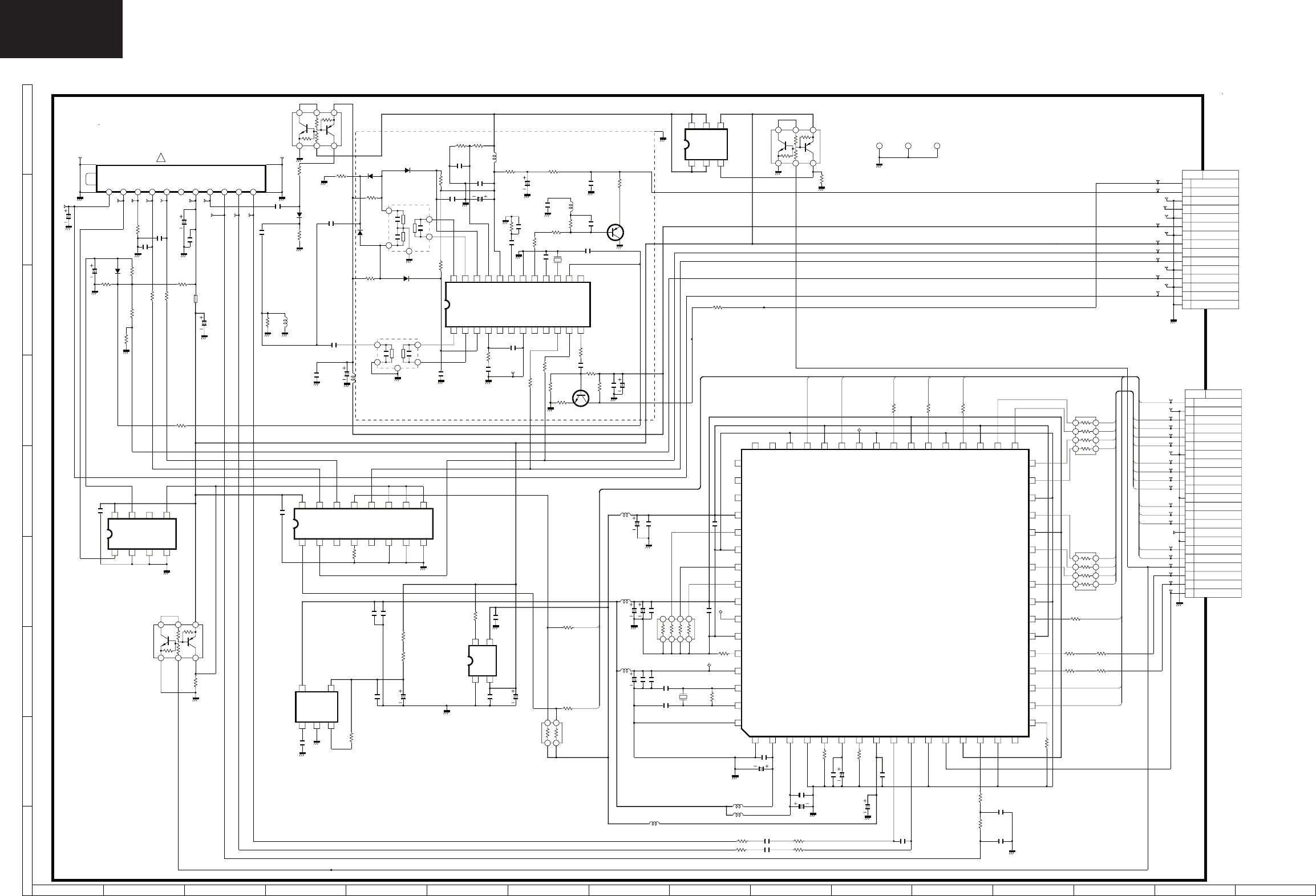
120
LC-32/37GD8E/RU
LC-32/37BT8E/RU
LC-32/37GD8, LC-32/37BT8 TUNER Unit Diagram
1234567 8 9 10 11 12 13 14 15 16
I
H
G
F
E
D
C
B
A
FED[4]
FED[3]
TSDA
TIPO
FED[2]
TSCL
AGC
FED[7]
FED[1]
FED[6]
FED[0]
FEERROR
FED[5]
FERESET
TSCL
TSDA
FEGP1_LOCK
FEGP0_COMP
FEGP1_LOCK
FEGP0_COMP
FESTR_PSYNC
FEVAL_DEN
I2C_DAT5
I2C_DAT5
I2C_CLK5
I2C_CLK5
FECLK
FED[2]
FED[3]
FED[1]
FED[0]
FED[7]
FED[6]
FED[5]
FED[4]
FECLK
FEVAL_DEN
FESTR_PSYNC
T3V3D
FEERROR
T1V8X
T1V8D
+5V
+5V
+8V
CVBS
R234
270
TL203
C225
1500P
C233
1000P
R247
0
R204
12K
R207
47
R237
330
D206
1SS390
R236
100
R241
10K
C0294BM
K9456
1
2
3
4
5
R235
100
C222
0.1u
25V
Z
TL221
C223
390P
(CH)
R242
3.9K
R233
820
TL220
TL201
R205
47K
R223
5.6K
C232
33P
(CH)
R206
0
TL213
C224
0.22u
16V
R231
33
TQ
1/8W
R238
150
C219
0.1u
25V
Z
R256
47
TL219
C231
0.01u Z
R208
47
P201
MA012WJ
TO MAIN 2/6
1
SIF
2
CVBS
3
GND
4
+35V
5
GND
6
+8V
7
GND
8
+5V
9
SCL5
10
SDA5
11
GND
12
AGC
13
GND
14
+5V(CONT)
15
GND
C206
100u
16V
ASX
C241
33u
10V
ASX
R209
12K
C220
0.01u Z
100u
16V
C221
ASX
TL218
C203
22P
(CH)
C218
0.01u
R224
5.6K
TP201
C204
470u
16V
ASX
TL217
R239
100
Q204
2SA1530AR
BUFFER
TL205
R244
220
R240
330
D205
1SS390
X201
SAA029WJ
TL207
R226
10K
TL204
C236
0.01u Z
R227
10K
TL202
D203
1SS390
R203
68K
R232
330
R255
47
R230
5.6K
TL209
DUNTKD609WE01
C227
0.01u Z
R229
22K
TL210
C215
0.01u Z
C216
0.01u Z
C0278BM
K3953
1
2
3
4
5
FB201
0210TA
C226
220u
10V
ASX
TL215
C217
10u
50V
ASX
R201
100K
TL214
R270
510K
R245
10K
1
2
3
4
5
6
7
8
C237
2.2u
50V
ASX
TL212
Q203
2SC3928AR
TL211
R228
22K
C230
10u
50V
ASX
C205
0.01u
Z
TL216
R248
15K
D201
1SS390
D204
1SS390
C229
12P
(CH)
TDA9886
IF-DEMOD
12345678910 11 12
131415161718192021222324
TL208
R243
100
C228
0.47u
16V
C202
22P
(CH)
R219
2.2K
P202
MA250WJ
TO MAIN /6
1
FECLK
2
GND
3
FED0
4
FED1
5
FED2
6
FED3
7
GND
8
FED4
9
FED5
10
FED6
11
FED7
12
GND
13
FEERR_UNCOR
14
FEVAL_DEN
15
FESTR_PSYNC
16
FEOFF_X4M
17
GND
18
FEGP0_COMP
19
FEGP1_LOCK
20
I2CSEL
21
FESDA
22
FESCL
23
FERESETn
TP202
R263
4.7K
21
3
4
R202
680
C255
0.1u
25V
ZC256
0.1u
25V
Z
R259
150
C254
0.01u Z
10u
16V
C242
ASX
C253
0.01u Z
C251
0.01u
Z
10u
16V
C252
ASX
C248
0.01u
Z
MM3033E
1
GND
2
VDD
3
VO
4
CE
C244
22u
6.3V
ASX
C243
0.1u
25V
Z
C246
10u
16V
ASX
C245
0.1u
25V
Z
R264
100
R265
100
TP203
R266
0
R267
0
C258
0.01u
R268
0
R269
0
C234
0.1u
25V
Z
R246
680
10u
16V
C247
ASX
10u
16V
C249
ASX
SN2G53CT
1
C
2
INH
3
VEE
4
GND
5
A
6
I
7
O
8
VDD
LV4053AT
1
1Y
2
0Y
3
1Z
4
ZC
5
0Z
6
INH
7
VEE
8
G
9
C
10
B
11
A
12
0X
13
1X
14
XC
15
Y1
16
VDD
10u
16V
C261
ASX
C263
0.1u
25V
Z
C262
0.1u
25V
Z
L203
10uH
CNN
L204
12uH
CNN
L205
33uH
CNN
L206
1.5uH
CUN
L207
2.2uH
CNN
L208
2.2uH
CNN
L209
2.2uH
CNN
L210
2.2uH
CNN
C201
33u
10V
ASX
C259
2P
(CH)
C257
0.01u
C260
15P
(CH)
C235
15P
(CH)
R274
0R272
0
1
2
3
4
5
6
7
8
R273
0
1
2
3
4
5
6
7
8
Q209
RN4904
123
456
R271
1K
X202
SCA039WJ
IXB682WJ
12345678910 11 12 13 14 15 16
17
18
19
20
21
22
23
24
25
26
27
28
29
30
31
32
33343536373839404142434445464748
49
50
51
52
53
54
55
56
57
58
59
60
61
62
63
64
R281
0
R282
0
C266
0.01u Z
C250
0.01u Z
C267
0.01u Z
R283
0
R284
10K
R285
10K
R288
0
TL241
TL242
TL243
TL244
TL245
TL246
TL247
R289
10K
R290
180
C268
0.1u
25V
C269
0.1u
25V
C270
220u
6.3V
AAPD
C271
0.01u Z
C272
1000P
C273
220u
6.3V
AAPD
PQ1M185M
123
45
C207
0.01u
Q205
RN4904
123
456
SSM6J51TU
1
D
2
D
3
G
4
S
5
D
6
D
R251
3.3K
R276
2.7
1/2W
R275
2.7
1/2W
LUG201
HA009WJ
LUG202
HA009WJ
LUG203
HA009WJ
Q211
RN4904
123
456
R291
3.3K
D207
1SS390
C274
0.1u
25V
Z
C275
0.1u
25V
Z
R292
3.3K
C276
0.01u
SLD201
MA898WJFW
L212
0.18uH
D9Mj
L213
33uH
CKM
C279
10u
16V
KZA073WJ
R293
0
R294
0
R211
0
R213
0
TU201
NQA033WJ
1
DC-POW
2
AGC
3
ADDR
4
SCL
5
SDA
6
NC
7
5V
8
IF(A)
9
IFAGC
10
IF(D1)
11
IF(D2)
TL222
TP204
TL225
TL226
TL239
TL237
TL240
TL228
TL236
TL230
TL206
TL231
TL233
TL224
TL232
TL227
TL235
TL234
TL223
TL238
TL229
C281
330P
(CH)
VOLTAGE ( ) = DTV-MODE
!*
FL202
FL201
IC201
IC206
IC203
IC204
IC202
IC205
IC207
3.03
(0)
0
2.38
(0)
1.6
4.8
2.3
1.98
(0)
1.95
(0)
5.04
(0)
2.22
(0)
2.34
(0)
2.22
(0)
0 1.53
(0)
3.53
(0)
3.3
(0)
3.3
(0)
2.03
(0)
0.3
(0)
1.86
(0)
2.59
(0)
0.09
(0)
2.38
(0)
01.71
(0)
5.05
(0)
2.83
(0)
0.23
(0)
1.95
(0)
1.95
(0)
0 0 (5.18)
0 (3.36)
0(5.09)
2.0 0 0 0
002.05.16
0
(3.3) (0)
3.3 0 0 000 0
0
(5.09)
0
(5.09)
0
(5.09)(0)
3.30
(3.3)
(0)
3.3
(0)
3.3
(0)
5.16
5.18
(0)
5.12
(0.02)
5.12
(0.02)
0 0
(3.3)
0
(5.09)
0 0
(1.77)
0
(1.75)
0 0 0
(0.83)
0 0
(3.36)
0
(1.7)
0
(1.7)
0 0
(3.29)
0
(1.74)
0
(0.8)
0 0
0
0
(3.3)
0
(3.3)
0
(3.3)
0
(3.3)
0
(3.35)
0
(0.1)
0
0
(1.5)
0
(1.5)
0
(1.5)
0
(0.74)
0
(1.5)
0
0
(1.5)
0
(1.5)
0
(1.5)
0
(1.5)
0
(3.35)
0
(1.7)
00
(0.7)
0
(1.74)
000
(3.3)
0
(3.3)
0
(3.35)
0
(3.3)
00
(1.6)
0
(1.6)
0
(1.6)
0
(1.2)
0
(3.3)
0
(3.35)
0
0
0
0
0
(1.74)
0
(1.7)
0
0
0
(1.76)
0
(0.4)
0
(0.9)
0
0
(1.23)
0 0
(3.3)
5.18
(5.0)
0
(1.77)
(0)
5.18
(0)
5.18(0) 5.12
(0)
5.12
(0)
0(5.1)
0
(0)
5.18
(0)
5.18 0
(5.1)
(0)5.18
(0)
5.18
(0) 5.18
8.1
(0)(8.1)
0.03
(8.1)
0.03
05.18
(0)
8.1
(0)
LC-32P70E/LC-26P70E/LC-37P70E
LC-32GD9E/LC-37GD9E/LC-32GD8E/LC-37GD8E D-TUNER
VOLTAGE () = DTV-MODE
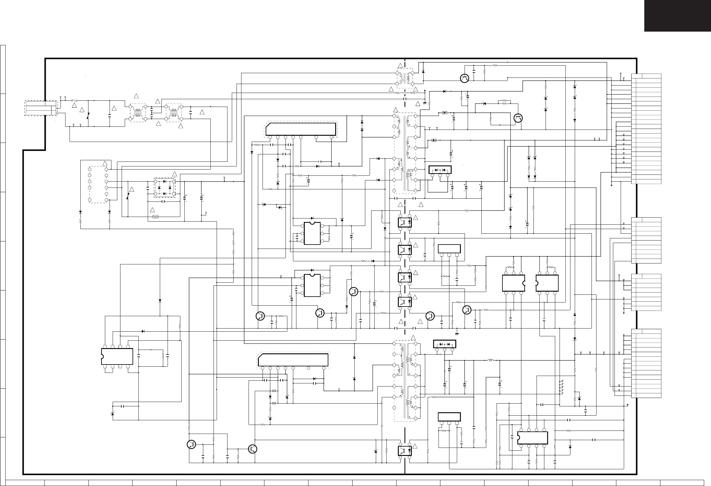
121
LC-32/37GD8E/RU
LC-32/37BT8E/RU
LC-32GD8, LC-32BT8 POWER SUPPLY Unit Diagram
900V
900V
900V
C732
0.1u
R795
20K
1/10W
R783
22K
1/10W
Q702
2SC3928AR
R788
2K
1/10W
F
D721
EXA096WJ
18V
C728
3300P
D736
DXA080WJ
123
D701
DX0477CE
1
2
3
4
C753
0.068u
C755
1200u
35V
EZA499WJ
R757
10K
1/10W
R817
1.2K
1/4W
D726
D1FL20U
R776
1K
1/10W
TL708
P703
Z0738CE
TO AV
1
+30V
2
+30V
3
+30V
4
NC
5
GND
6
GND
7
GND
Q710
2SC3928AR
R779
10K
1/10W
R794
820
1/10W
Q713
2SC3928AR
D756
EXA101WJ
30V
R702
HZ0008GE
R756
18K
1/10W
R748
10K
1/10W
D747
1SS355
*D714
EX1398CE
@COMME
R778
2.4K
1/10W
F
TL704
R758
560K
1/10W
D717
D1FL20U
D741
EX1398CE
8.2V
R755
20K
1/10W
F
R780
6.8K
1/10W
R773
10K
1/10W
D725
D1FL20U
R701
HZ0008GE
R785
10K
1/10W
C730
0.1u
D754
EXA101WJ
30V
R801
1.2K
R805
220K
1/10W
R742
10K
1/10W
C733
2200P
R784
2.4K
1/10W
P702
MA247WJ
TO MAIN 6
1
PCON1
2
PCON2
3
SGND
4
INV_ON(BL_ON5)
5
INV_BRT(VBRT)
6
NC
7
NC
8
NC
9
PWM SEL
C704
0.47u
275V
FZA026WJ
R740
560K
1/10W
R789
680
1/10W
F
R777
2.4K
1/10W
F
D724
D1FL20U
R775
15K
1/10W
R770
0
1/8W
C740
2200P
250V
KZ0105GE
C749
0.068u
R753
13K
1/10W
R792
2.7K
1/10W
R765
100K
1/10W
R820
1.2K
P704
NA053WJ
LA TO INVERTER
1
+24V
2
+24V
3
+24V
4
+24V
5
+24V
6
GND
7
GND
8
GND
9
GND
10
GND
11
NC
12
INV-ON
13
INV-BRT
14
PWM SEL
TL701
D737
DXA081WJ
123
C726
100P
(CH)
R764
10K
1/10W
C741
2200P
250V
KZ0105GE
C712
0.47u
275V
FZA026WJ
R812
1.2K
Q708
2SC3928AR
R774
10K
1/10W
C716
0.1u
C709
2200P
250V
KZ0105GE
R796
2.7K
1/10W
D715
D1FL20U
D757
1SS355
R793
10K
1/10W
C742
2200P
250V
KZ0105GE
D753
EXA094WJ
15V
R766
10K
1/10W
R752
0
1/10W
R791
10K
1/10W
C720
0.1u
R809
1.2K
C708
2200P
250V
KZ0105GE
TL702
*T702
WA231WJ
1
2
3
4
5
6
7
9
10
11
12
13
14
15
16
D742
1SS355
Q712
2SC3928AR
C722
47P
(CH)
D722
1SS355
R759
10K
1/10W
MR4030
12345 7 9
D746
EXA102WJ
33V
D751
EX1398CE
8.2V
R787
10K
1/10W
R760
0.15
NVV
2W
R745
9.1K
1/10W
R746
10K
1/10W
R741
10K
1/10W
*R747
10K
1/10W
F
TL703
R727
56K
1/10W
R761
10K
1/10W
*R751
0.1
NVV
2W
Q704
2SC3928AR
D718
EXA091WJ
11V
TL707
R767
390
1/4W
MR4020
12345 7 9
D755
1SS355
R824
3.3K
1/4W
D749
EX1400CE
10V
DUNTKD605WE14
D735
SF6L20U
F701
ZA007WJ
AC250V T4AL
C736
47u
35V
EZA489WJ
C743
470u
50V
EZA513WJ
C744
1200u
35V
EZA499WJ
C751
1200u
35V
EZA499WJ
2200u
10V
C752
EZA452WJ
C754
220u
50V
EZA510WJ
C756
2200u
10V
EZA452WJ
C757
680u
25V
EZA480WJ
C758
100u
35V
EZA490WJ
Q721
2SC3928AR
D707
1SS355
R823
10K
1/10W
RY701
DA008WJ
12
3
4
C765
0.1u
C764
0.1u
C763
0.1u
R825
10K
1/10W
C767
220u
50V
EZA510WJ
VA701
VXA071WJQZ
VA702
VXA071WJQZ
P701
MA250WJ
TO MAIN 6
1
+35V
2
GND
3
GND
4
+13.5V
5
+13.5V
6
+13.5V
7
GND
8
GND
9
GND
10
+5V
11
+5V
12
+5V
13
+5V
14
+5V
15
+5V
16
GND
17
GND
18
GND
19
GND
20
BU+5V
21
BU+5V
22
GND
23
GND
LUG701
HA002WJ
LUG702
HA002WJ
LUG703
HA002WJ
LUG704
HA002WJ
C768
2200u
10V
EZA452WJ
D748
EXA094WJ
15V
D759
EXA101WJ
30V
C739
1000P
(CH)
C745
4700P
R782
1K
1/10W
R781
2.4K
1/10W
F
TL709
TL710
TL711
TL713
TL714
TL715
TL716
TL717
TL718
TL719
TL720
TL721
TL722
TL723
TL724
TL725TL726 TL727 TL728
TL729
TL730
TL731
TL732
TL733
TL734
TL735
TL736
TL737
TL738
SC701
AA008WJ
1
L
2
N
D752
1SS355
D763
EX1394CE
R833
22K
1/4W
D765
1SS355
R831
10K
1/10W
R732
120K
1/4W
F
R731
120K
1/4W
F
R730
120K
1/4W
F
Q726
2SC3928AR
R834
10K
1/10W
C772
0.1u
TXA037WJ
POWER_HOT
1
2
3
4
5
6
TXA037WJ
1
2
3
4
5
6
C771
2700P
D761
D1FL20U
R828
22
1/4W
R835
0
1/8W
*L701
FA211WJ
12
3
4
*L702
F0024PE
12
3
4
TL739
TL740
TL741
D767
1SS355
R836
10K
1/10W
C774
0.1u
16V
C777
2200P
250V
KZ0105GE
C778
2200P
250V
KZ0105GE
T701
WA230WJ
1
2
3
8
5
6
7
9
10
11
12
13
14
15
16
D716
U05NU44
D720
U05NU44
*C705
220u
400V
EZA985WJ
*C706
220u
400V
EZA985WJ
E701
QA027WJFW
D734
FXA003WJ
1
23
4
D733
FXA003WJ
1
23
4
D732
FXA003WJ
1
23
4
47u
35V
C723
EZA489WJ
NJM2904M
1234
5678
D730
FXA003WJ
1
23
4
D731
FXA003WJ
1
23
4
47u
35V
C735
EZA489WJ
470u
50V
C762
EZA513WJ
RDA701
RA323WJFW
RDA702
RA306WJFW
*RDA703
RA307WJFW
RDA704
RA308WJFW
RDA705
RA309WJFW
D772
EXA102WJ
33V
R851
220
1/4W
R852
220
1/4W
R854
1K
RVV
2WD729
ST03D170
D771
ST03D-82
TA76431R
123
TA76431R
123
D728
ST03D170
D762
ST03D170
*T703
CA022WJ
1
2
3
4
5
6
7
9
10
11
12
D738
DXA088WJ
D739
DXA085WJ
L753
PA642WJ
TH701
HXA033WJ
C789
0.1u
C790
0.1u
R857
0
1/8W
D774
1SS355
D773
1SS355
C713
10u
KZA388WJ
6.3V
C717
0.1u
C792
1u
10V
R859
12K
1/16W
R860
4.7K
R861
2.7K
R862
2.7K R863
4.7K
NJM2903M
1234
5678
R864
33K
R865
33K C793
0.1u
16V
R866
47K
R867
12K
D775
1SS355
R868
1.2K
R870
2.2K
R869
3.3K
R871
1.2K
R872
4.7K
R873
1.2K
C794
10u
6.3V
KZA388WJ
C795
1u
10V
C796
1u
10V
C798
0.1u
16V
C799
0.1u
16V
TXA026WJ
123
456
C800
0.1u
16V
TXA026WJ
123
456
C801
0.1u
16V
D776
EX1234CE
3.6V
D779
1SS355
D778
U05NU44
R878
120K
1/4W
F
D777
U05NU44
R877
120K
1/4W
F
C783
4.7u
25V
KZA213WJ
C776
4.7u
KZA213WJ
25V
TL712
R743
220K
1/16W
R858
2.7K
1/10W
C804
0.1u
16V
Q729
2SD2185R
C734
470P
2000V
KZA304WJ
C725
470P
2000V
KZA304WJ
D780
EX1015GE
16V
D781
EX1015GE
16V
D782
EXA359WJ
33VB
D783
EXA359WJ
33VB
R797
100K
1/10W
F
C782
0.01u
630V
C781
0.01u
630V
Ver.N5 (2006.04.20)
!*
!*
!* !*
!*
!*
!*
!*
!*
!*
!*
!*
!*
!*
!*
!*
!*
!*
!*
!*
!* !*
!*
!*
!*
!* !*
*IC704
IC705
Q723
Q724
IC708
IC706
IC707
IC709
Q730 Q731
AC-INLET
POWER
PRIMARY SECONDARY
0
0
0.6
0
0
0.6
0
0.3
0.3
3.05 1.7 0 15.9 0 7.7 239.2
0
1.7
0
3.65 2.0 0 15.9 0 278.5 252.9
0
0
0.6
0
2.0
0.3
15.9
15.3
0
0
3.2
15.9
25.2
23.9
24.0
0
0
15.9
0000
8.29.97015.8
2.4 0 4.4
2.4 0 4.4
0 3.2 3.5 0
2.63.3
05.3
5.34.6
0
0 5.3 0
5.3 4.6 0
05.30.1
0
30.4
0.6
LC-32GA8E/LC-32GD8E
CONFIDENTIAL
Ver.N5 (2006.04.20)
1234567 8 9 10 11 12 13 14 15 16
I
H
G
F
E
D
C
B
A
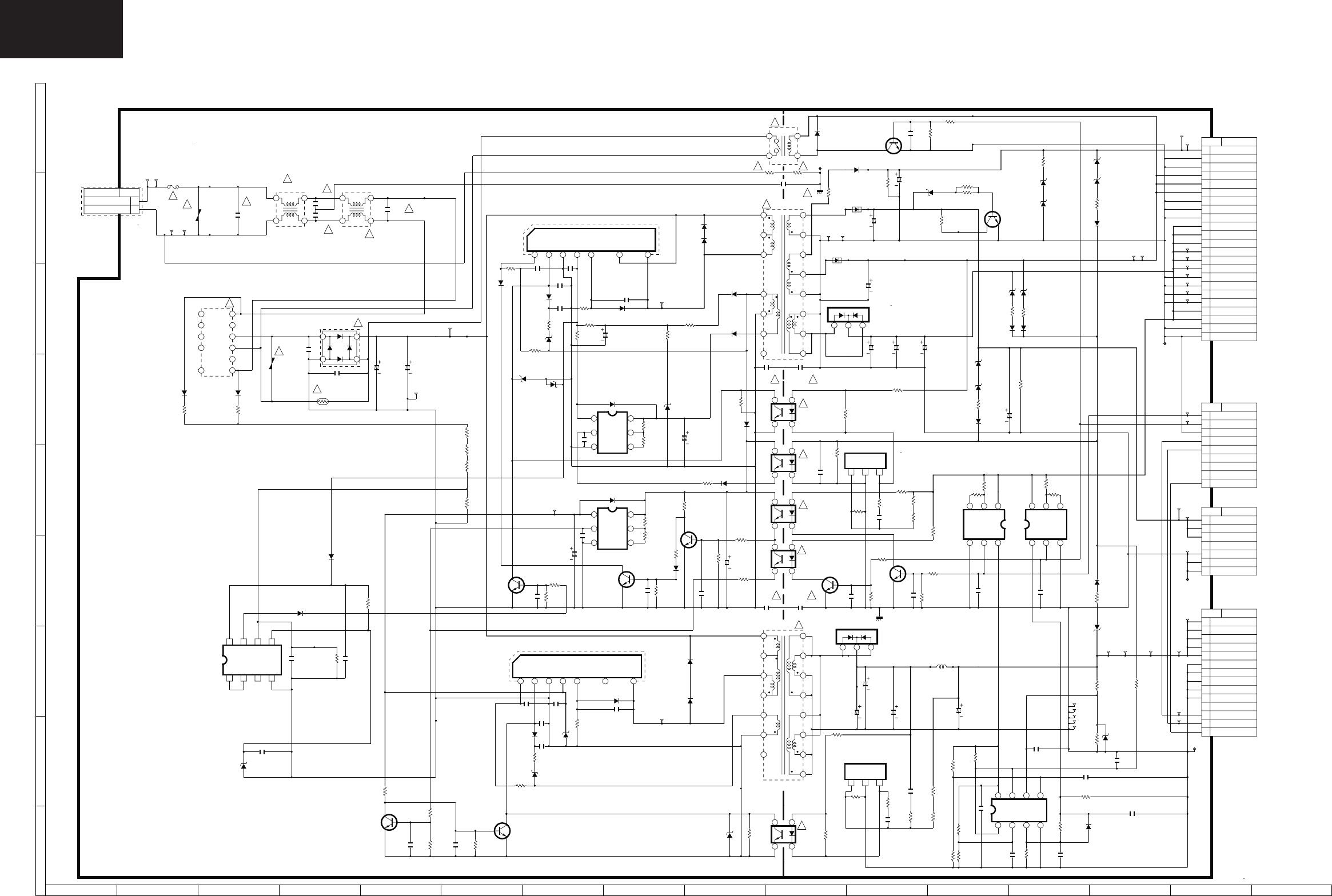
122
LC-32/37GD8E/RU
LC-32/37BT8E/RU
LC-37GD8, LC-37BT8 POWER SUPPLY Unit Diagram
12 3 4 5 67 8 9 10 11 12 13 14 15 16
I
H
G
F
E
D
C
B
A
900V
900V
900V
C732
0.1u
R795
20K
1/10W
R783
22K
1/10W
Q702
2SC3928AR
R788
2K
1/10W
F
D721
EXA096WJ
18V
C728
3300P
D736
DXA080WJ
123
D701
DX0477CE
1
2
3
4
C753
0.068u
C755
1200u
35V
EZA499WJ
R757
10K
1/10W
R817
1.2K
1/4W
D726
D1FL20U
R776
1K
1/10W
TL708
P703
Z0738CE
TO AV
1
+30V
2
+30V
3
+30V
4
NC
5
GND
6
GND
7
GND
Q710
2SC3928AR
R779
10K
1/10W
R794
820
1/10W
Q713
2SC3928AR
D756
EXA101WJ
30V
R702
HZ0008GE
R756
18K
1/10W
R748
10K
1/10W
D747
1SS355
*D714
EX1398CE
8.2V
R778
2.4K
1/10W
F
TL704
R758
560K
1/10W
D717
D1FL20U
D741
EX1398CE
8.2V
R755
20K
1/10W
F
R780
6.8K
1/10W
R773
10K
1/10W
D725
D1FL20U
R701
HZ0008GE
R785
10K
1/10W
C730
0.1u
D754
EXA101WJ
30V
R801
1.2K
R805
220K
1/10W
R742
10K
1/10W
C733
2200P
R784
2.4K
1/10W
P702
MA247WJ
TO MAIN 6
1
PCON1
2
PCON2
3
SGND
4
INV_ON(BL_ON5)
5
INV_BRT(VBRT)
6
NC
7
NC
8
NC
9
PWM SEL
C704
0.47u
275V
FZA026WJ
R740
560K
1/10W
R789
680
1/10W
F
R777
2.4K
1/10W
F
D724
D1FL20U
R775
15K
1/10W
R770
0
1/8W
C740
2200P
250V
KZ0105GE
C749
0.068u
R753
13K
1/10W
R792
2.7K
1/10W
R765
100K
1/10W
R820
1.2K
P704
NA053WJ
LA TO INVERTER
1
+24V
2
+24V
3
+24V
4
+24V
5
+24V
6
GND
7
GND
8
GND
9
GND
10
GND
11
NC
12
INV-ON
13
INV-BRT
14
PWM SEL
TL701
D737
DXA081WJ
123
C726
100P
(CH)
R764
10K
1/10W
C741
2200P
250V
KZ0105GE
C712
0.47u
275V
FZA026WJ
R812
1.2K
Q708
2SC3928AR
R774
10K
1/10W
C716
0.1u
C709
2200P
250V
KZ0105GE
R796
2.7K
1/10W
D715
D1FL20U
D757
1SS355
R793
10K
1/10W
C742
2200P
250V
KZ0105GE
D753
EXA094WJ
15V
R766
10K
1/10W
R752
0
1/10W
R791
10K
1/10W
C720
0.1u
R809
1.2K
C708
2200P
250V
KZ0105GE
TL702
*T702
WA231WJ
1
2
3
4
5
6
7
9
10
11
12
13
14
15
16
D742
1SS355
Q712
2SC3928AR
C722
47P
(CH)
D722
1SS355
R759
10K
1/10W
MR4030
12345 7 9
D746
EXA102WJ
33V
D751
EX1398CE
8.2V
R787
10K
1/10W
R760
0.15
NVV
2W
R745
9.1K
1/10W
R746
10K
1/10W
R741
10K
1/10W
*R747
10K
1/10W
F
TL703
R727
56K
1/10W
R761
10K
1/10W
*R751
0.1
NVV
2W
Q704
2SC3928AR
D718
EXA091WJ
11V
TL707
R767
390
1/4W
MR4020
12345 7 9
D755
1SS355
R824
3.3K
1/4W
D749
EX1400CE
10V
DUNTKD605WE03
D735
SF6L20U
F701
ZA007WJ
AC250V T4AL
C736
47u
35V
EZA489WJ
C743
470u
50V
EZA513WJ
C744
1200u
35V
EZA499WJ
C751
1200u
35V
EZA499WJ
2200u
10V
C752
EZA452WJ
C754
220u
50V
EZA510WJ
C756
2200u
10V
EZA452WJ
C757
680u
25V
EZA480WJ
C758
100u
35V
EZA490WJ
Q721
2SC3928AR
D707
1SS355
R823
10K
1/10W
RY701
DA008WJ
12
3
4
C765
0.1u
C764
0.1u
C763
0.1u
R825
10K
1/10W
C767
220u
50V
EZA510WJ
VA701
VXA071WJQZ
VA702
VXA071WJQZ
P701
MA250WJ
TO MAIN 6
1
+35V
2
GND
3
GND
4
+13.5V
5
+13.5V
6
+13.5V
7
GND
8
GND
9
GND
10
+5V
11
+5V
12
+5V
13
+5V
14
+5V
15
+5V
16
GND
17
GND
18
GND
19
GND
20
BU+5V
21
BU+5V
22
GND
23
GND
LUG701
HA002WJ
LUG702
HA002WJ
LUG703
HA002WJ
LUG704
HA002WJ
C768
2200u
10V
EZA452WJ
D748
EXA094WJ
15V
D759
EXA101WJ
30V
C739
1000P
(CH)
C745
4700P
R782
1K
1/10W
R781
2.4K
1/10W
F
TL709
TL710
TL711
TL713
TL714
TL715
TL716
TL717
TL718
TL719
TL720
TL721
TL722
TL723
TL724
TL725TL726 TL727 TL728
TL729
TL730
TL731
TL732
TL733
TL734
TL735
TL736
TL737
TL738
SC701
AA008WJ
1
L
2
N
D752
1SS355
D763
EX1394CE
R833
22K
1/4W
D765
1SS355
R831
10K
1/10W
R732
120K
1/4W
F
R731
120K
1/4W
F
R730
120K
1/4W
F
Q726
2SC3928AR
R834
10K
1/10W
C772
0.1u
TXA037WJ
POWER_HOT
1
2
3
4
5
6
TXA037WJ
1
2
3
4
5
6
C771
2700P
D761
D1FL20U
R828
22
1/4W
R835
0
1/8W
*L701
FA211WJ
12
3
4
*L702
F0024PE
12
3
4
TL739
TL740
TL741
D767
1SS355
R836
10K
1/10W
C774
0.1u
16V
C777
2200P
250V
KZ0105GE
C778
2200P
250V
KZ0105GE
T701
WA230WJ
1
2
3
8
5
6
7
9
10
11
12
13
14
15
16
D716
U05NU44
D720
U05NU44
*C705
270u
400V
EZA986WJ
*C706
270u
400V
EZA986WJ
E701
QA027WJFW
D734
FXA003WJ
1
23
4
D733
FXA003WJ
1
23
4
D732
FXA003WJ
1
23
4
47u
35V
C723
EZA489WJ
NJM2904M
1234
5678
D730
FXA003WJ
1
23
4
D731
FXA003WJ
1
23
4
47u
35V
C735
EZA489WJ
470u
50V
C762
EZA513WJ
RDA701
RA323WJFW
RDA702
RA306WJFW
*RDA703
RA340WJFW
RDA704
RA308WJFW
RDA705
RA309WJFW
D772
EXA102WJ
33V
R851
220
1/4W
R852
220
1/4W
R854
1K
RVV
2WD729
ST03D170
D771
ST03D-82
TA76431R
123
TA76431R
123
D728
ST03D170
D762
ST03D170
*T703
CA023WJ
1
2
3
4
5
6
7
9
10
11
12
D738
DXA088WJ
D739
DXA085WJ
L753
PA642WJ
TH701
HXA033WJ
C789
0.1u
C790
0.1u
R857
0
1/8W
D774
1SS355
D773
1SS355
C713
10u
KZA388WJ
6.3V
C717
0.1u
C792
1u
10V
R859
12K
1/16W
R860
4.7K
R861
2.7K
R862
2.7K R863
4.7K
NJM2903M
1234
5678
R864
33K
R865
33K C793
0.1u
16V
R866
47K
R867
12K
D775
1SS355
R868
1.2K
R870
2.2K
R869
3.3K
R871
1.2K
R872
4.7K
R873
1.2K
C794
10u
6.3V
KZA388WJ
C795
1u
10V
C796
1u
10V
C798
0.1u
16V
C799
0.1u
16V
TXA026WJ
123
456
C800
0.1u
16V
TXA026WJ
123
456
C801
0.1u
16V
D776
EX1234CE
3.6V
D779
1SS355
D778
U05NU44
R878
120K
1/4W
F
D777
U05NU44
R877
120K
1/4W
F
C783
4.7u
25V
KZA213WJ
C776
4.7u
KZA213WJ
25V
TL712
R743
220K
1/16W
R858
2.7K
1/10W
C804
0.1u
16V
Q729
2SD2185R
C734
470P
2000V
KZA304WJ
C725
470P
2000V
KZA304WJ
D780
EX1015GE
16V
D781
EX1015GE
16V
D782
EXA359WJ
33VB
D783
EXA359WJ
33VB
R797
100K
1/10W
F
C782
0.01u
630V
C781
0.01u
630V
*RDA706
RA334WJFW
Ver.N5 (2006.04.20)
!*
!*
!* !*
!*
!*
!*
!*
!*
!*
!*
!*
!*
!*
!*
!*
!*
!*
!*
!*
!* !*
!*
!*
!*
!* !*
*IC704
IC705
Q723
Q724
IC708
IC706
IC707
IC709
Q730 Q731
AC-INLET
POWER
PRIMARY SECONDARY
0
0
0.6
0
0
0.6
0
0.3
0.3
3.05 1.7 0 15.9 0 7.7 239.2
0
1.7
0
3.65 2.0 0 15.9 0 278.5 252.9
0
0
0.6
0
2.0
0.3
15.9
15.3
0
0
3.2
15.9
25.2
23.9
24.0
0
0
15.9
0000
8.29.97015.8
2.4 0 4.4
2.4 0 4.4
0 3.2 3.5 0
2.63.3
05.3
5.34.6
0
0 5.3 0
5.3 4.6 0
05.30.1
0
30.4
0.6
LC-37P55E/LC-37P70E
LC-37GA9E/LC-37GD9E
LC-37GA8E/LC-37GD8E
CONFIDENTIAL
Ver.N5 (2006.04.20)
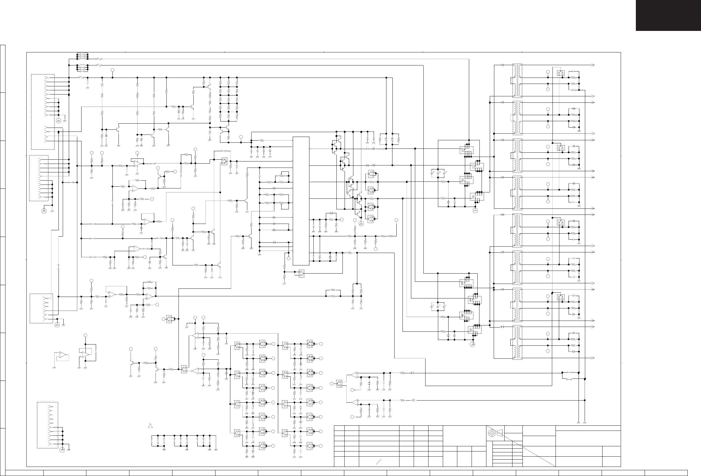
123
LC-32/37GD8E/RU
LC-32/37BT8E/RU
LC-32GD8, LC-32BT8 INVERTER Unit Diagram (RDENC2266TPZC)
1234567 8 9 10 11 12 13 14 15 16
I
H
G
F
E
D
C
B
A
LC-32GA8E INVERTER Unit Diagram (RDENC2266TPZC)
D A T E
日付 R E A S ON
変更事由 E CN N O . ENG I NEER
担当 照査
CH ECK ED APPROVED
承認
CH ECK EDAPPROVED
表面処理
±0.5
改訂 REV .
SHEET
葉番
図番 DRAW I NG NO.
PART NO. (MODEL NO . )
品番
DESCR I PT I ON
品名
DATE
作成日
F I N I S H
ミネベア株式会社
HEAT TRE AT
熱処理
表面粗サ SUR F . ROUGH .
MA TER I AL
材質
D R AW N
±0.8
±0.5
±0.3
±0.2
±0.1
公差
DEG
角度
2 5 0<L≦1 0 0 0
6 3 <L≦2 5 0
1 6 <L≦6 3
4<L≦1 6
L≦4
L
寸法
TOL
一
般
公
差
S C A L E
尺度
U N I T
単位
M I NEBEA CO . , LTD .
MA R K
符号
1
1
2
2
3
3
4
4
5
5
6
6
D D
C C
B B
A A
1 0
8
9
GND
GND
GND
R 1 9 1
R 1 2 9
R 1 3 0 R
JP
JP
JP
JP
JPJ 1 1 3
J 1 1 2
J 1 1 1
J 1 1 0
RRR 1 0 R
NF N FR 1 9 0 N F
NFNF NF
NF
NF
NF
NF
NF
NF
NF
NF
NF
R
RR
JP
JP
1 R0 J
J 6
NF
R
RNF
R
NF
NF
NF
NF
NF
NF
NF
NF
RR
R
3
6
2
V i n
V i n
GND
V i n
V i n
V i n
GND 7
4
5
JP
JP
JP
JP
JP
JP
JP
JP
JP
CBA
J 1 0 9
J 1 0 8
J 1 0 6
J 1 0 5
J 1 0 4
J 1 0 2
J PJ 1 0 7 J P N F
NF
NF
NF
NF
NF
NF
NF
NF
NF
JP
JP
JPJP
JP
NFNF
NF
NF A
ED
NF
NF
NF
NF
JP
1
CN 1 5
J 7
1 R0 J
J 9
1 R0 J
J11
J 8 J10 J14
J13
J12
R 6 9
D 2 7
R 6 8 C 3 7
C 3 8
N / F
N / F N / F N / F N / F N / F
R 6 7
D 2 6
D 2 5
D 1 4
C 3 6
R 1 2 2
C 1 2 5
D 2 4
D 1 3
C 3 5
C 3 4
R 6 6
D 2 3
R 6 5
C 4 6
R 7 7
R 7 6 C 4 5
HP
A
D3 5
Change J6,J9,J129.MAR. '06
G
FR 7 5
D1 8
C 4 4 N
D3 3
D3 4
O
3
R 4 7 R4 8
C 2 4
E
R 7 3 C 4 2
C 4 3
D
R 7 4
D1 7
M
4
L
D3 1
D3 2
R 1 9 3
C 1 5 0
2
13
I C4 - 1 / 4
R 1 9 2
3
C 1 4 9
Terazawa Matsushima
M . Ma t s u R . Ma s h i o
C 2 5
R 4 9
R 1 9 7
N/ F
D5
R 1 9 4
2 3 /MAR/ ' 0 6
A
J 1 1 8
U84PC-E1 00310 1
1/1IM3 819CA
C i r c u i t D i a g r am
ON/OF F
AD I M
GND
PD I M
NC
NC
1 4
1 3 34
1 1
1C 1 2 3
Q3 2
R 1 7 2
12
3
Q3 3 R1 7 1
1 2 I C3 - 4 / 4
2
I C3
2
- 4 / 1
S
5
6
R 1 3 5
4
3
2R 1 3 6 C 1 3 4 R1 6 1
3 . 3V R 1 5 9
C 1 3 5 R 1 6 0
CN1 3
1
C 1 4 6
9
1 0
I C5
3
R 1 5 4
- 3 / 4
R 1 8 2
R 1 5 3
R 1 5 6
8R 1 5 5
ZD6
1 3 1 4
1 2
I C5
- 4 / 4
R 1 5 7
R 1 5 8
J 1 0 9
J 1 0 8
R 1 8 3
7
C 1 4 8
R 1 8 6
R 1 8 5 R1 8 7
R 1 8 1
6
5
C 1 4 7
3
J 1 0 6
J 1 0 2
6
5
- 2 / 4
7
3
R 1 4 2
J111
C 1 3 3
I C3
- 2 / 4
R 1 9 1
GND
GND
V i n
V i n
GND
GND
GND
V i n
V i n
PD I M
PWM
CN1 4
V i n
Se l e c t i o n
1 0
9
J 1 0 7
C 1 2 9 I C 5
I C4
3
R 1 2 7
R 1 2 6
R 1 2 5
- 4 / 4
5
3
8
7
4
6
J 1 1 0
R 1 2 9
R 1 7 8
R 1 2 8
1 3 1 4
1 2
R 1 1 9
C 1 3 0
1 1
3
N / F
Q3 4
1
1 4
2
2
R 1 9 5
R 1 3 0
3
R 1 9 0
C 1 2 2
R 1 3 1
2
J 1 0 4
21
I C5
4
2
R 4 4
- 1 / 4
R 1 6 9
8
I C3
2
3R 1 6 8
1
R 1 7 0
D9
R 1 1 8
R 1 1 6
1 0 R1 2 3
3
9
C 1 2 6
- 3 / 4
R 1 2 4
R 6 4
D 1 2
C 3 2
C 3 3
D 2 2
R 6 3
D 2 1
2
8
R 2 3
- 3 / 4 R 2 4
R 5 3
4
C 3 0
1 0
I C4
9
C 2 9
1 1
R 5 4
R 2 2
D 2 0
D 1 1
R 6 2 C 3 1
4C2 8
3
D4 23
C 4 0
CC 4 1
BR 7 1
D1 6
R 7 2
D3 0
K
D6 7
J
D2 9
I C4 5
76
- 3 / 4
AD1 5
R 7 0 C 3 9
D2 8
I
R 1 0 9 R 1 1 0
R 1 9 6 D 6 6
C 6 4
C 6 3
R8 3
8
3
2
7
6
1
4
5
Q2 3
C 5 8 C 5 3
C 5 4
R8 2
3
2
7
6
1
4
5
Q2 2 7
68
8
1
5
N/ F
Q3 5
1
2
3
C 1 3 6
R 1 4 9
R 1 4 8
1
2
3
Q3 0
C 1 3 1
2
R 1 4 4
J 1 1 2 R1 4 5
R 1 4 3
J113
R 1 5 2
3
R 1 4 7
R 1 3 7
Q2 8
Q2 9
3
1
1
2
3
R4 0
R 1 6 3
1
2
3Q1 3
R 4 1
R 1 2
R 1 6 2
R 1 6 4 R 2 6 R 2 7
3F / B
GND
SG
R 1 1
1 5
D7
7
C 1 5
IC 1 3
8
1 0
R 1 6 6 C1 4
R2 5
S
C1 2
OVP
CP
C1 1
REG
SS
C1 2 4
4
1 3
9
R3 5
1 4
R 3 4
4
C 1 7 R 1 0 8
V
C 1 6
R3 3
R 3 2 R 1 7 4
R 1 6 5
3
R 1 6 7
R3 1
3
2
3
6
Q2 1
8
7
1
4
5
Q2 0
4
2
R 1 7 3
1
3
R 1 5 0
R 1 4 6
Q3 1
R 1 3 8 1
2
3
R2 0
R2 1
2
3
R 1 7 7
2
J 1 0 5
R 1 7 6
1
3
R 1 4 1
R 1 3 4
R 1 5 1
R 1 8
C 1 3 2
C8
1
R 1 3 2
Q3 7
R 1 3 3
J114
D 6 5
8 . 2B
R 1 3 9
3C2 C3
2R8
C4
VB1
RT
2
VR2
C1 0 1 2
36
1
R 4 2
D1
Q3 9
1 6
21
3
Q1 2
1
2
3
D8
R 3 7
Q1 1
1
23
1
23
Q4 0
D3
1
BCT
C9
2
5CT
BRT
3
2
VR1
3
R1 9
VA2
VB2 1 7
1 8
2
1
Q7
2
3Q 1 0
3
1
3
1
R 3 6
D6
Q9
2
D2
1
2 0
Du t y
V c c
ST
1
1 1
VA1
C5
2
Q3
Q5
3
1 9
Q4
1
2
3
1
2
1
3
2
2Q6
Q8
C2 1
C1 8
3
C2 0
3
R 3 8
C1 9
1
R8 1
C 6 2
C 6 1
8
3
2
7
6
1
4
5
Q1 9
C 5 0
R8 0
C 4 9
C 5 7
1
3
2
7
6
1
4
5
Q1 8 8
3
2
8
4
57
6
ZD1 R3 9
ZD2
Q1 7
8
3
2
7
6
1
4
5
Q1 6
7
6
J 1 1 7
P
OUT ( H ) +
1CN1 1
45
1 0
32
1
R 1 0 1
OR 1 0 0
OUT ( H ) -
C1 1 8
C1 1 7
2
4
T8 7
C1 4 5
5
32
6
N
R9 8
R9 9
OUT ( H ) -
C1 1 6
CN1 1
1CN1 0
1
T7
7
4
6
1 0
C1 4 4
D 6 2
L
M
CN1 0
2
C1 1 4
CN9
1
OUT ( H ) +
OUT ( H ) +
C1 1 5
3
C1 4 3
7
5
1 0
2
1
T6
6
R9 6
K
R9 7
OUT ( H ) -
C1 1 3
1
OUT ( H ) -
2CN9
4
5
3
2
I
D 6 0
R9 4
J
R9 5
C1 1 2
CN8
C1 1 1
1 0
1
7
4
5
6
T5
C1 4 2
R9 3
H
1CN7
2CN8
C1 1 0
OUT ( H ) +
OUT ( H ) +
7
6
1 0
2
T4
1
3
C1 4 1
G
R9 2
F
CN7
C1 0 9
2
1CN6
OUT ( H ) -
OUT ( H ) -
4
1 0
3
2
C1 4 0
T3
1
5
E
R9 1
R9 0
D 5 8
C1 0 8
2CN6
C1 0 7 OUT ( H ) +
AD I M
GND
GND
GND
GND
GND
V i n
V i n
V i n
V i n
V i n
ON/OF F
1 1
1 3
1 2
1 0
9
R 1 8 9
2
C 1 2 1
R4
Q3 8
1
3
5
6
7
3
4
8
2 7B
ZD7
R 4 3
1 6B
ZD4
R3
CN3
1
J17
J18
2
J20
J19
5ACP3
C1
5ACP4
1
L 1
1A
CP1
L 2
J16
J15
R6 C6
1
2
3
Q3 6
R 1 8 8
3
R2
Q1 5
R 1 2 0 R 1 0 4
1
2
3
3
1
2
R 1 2 1
1
ZD3 Q1 4
R 1 1 5
R 1 0 6
R 1 0 5
R 1 0
R1
R5
2
R 1 1 2
R 5 5
Q2
1
3
R 1 1 1
2
3
R 1 1 3
R 1 1 4
R 5 8
Q1
R 5 0
R 5 2
R 6 0R 5 9
R 5 7
R 5 1
R 5 6
R 2 8
R 2 9 R 3 0
I C1
C 2 6
8 . 2B
C 2 7
8 . 2B
5
7
4
2
3
6
D
C
R8 9
R8 8
1CN5
C1 0 6
OUT ( H ) +
C1 3 9
7
4
5
6
1 0
1
T2
B
C1 0 4
2CN5
C1 0 5
1CN4
OUT ( H ) -
OUT ( H ) -
1 0
3
2
1
T1
C1 3 8
D 5 6
R8 7
R8 6
AC1 0 3
CN4
OUT ( H ) +
2
91
LC-32GA8/LC-32BV8
LC-37GA8/LC-37BV8
1234567 8 9 10 11 12 13 14 15 16
I
H
G
F
E
D
C
B
A
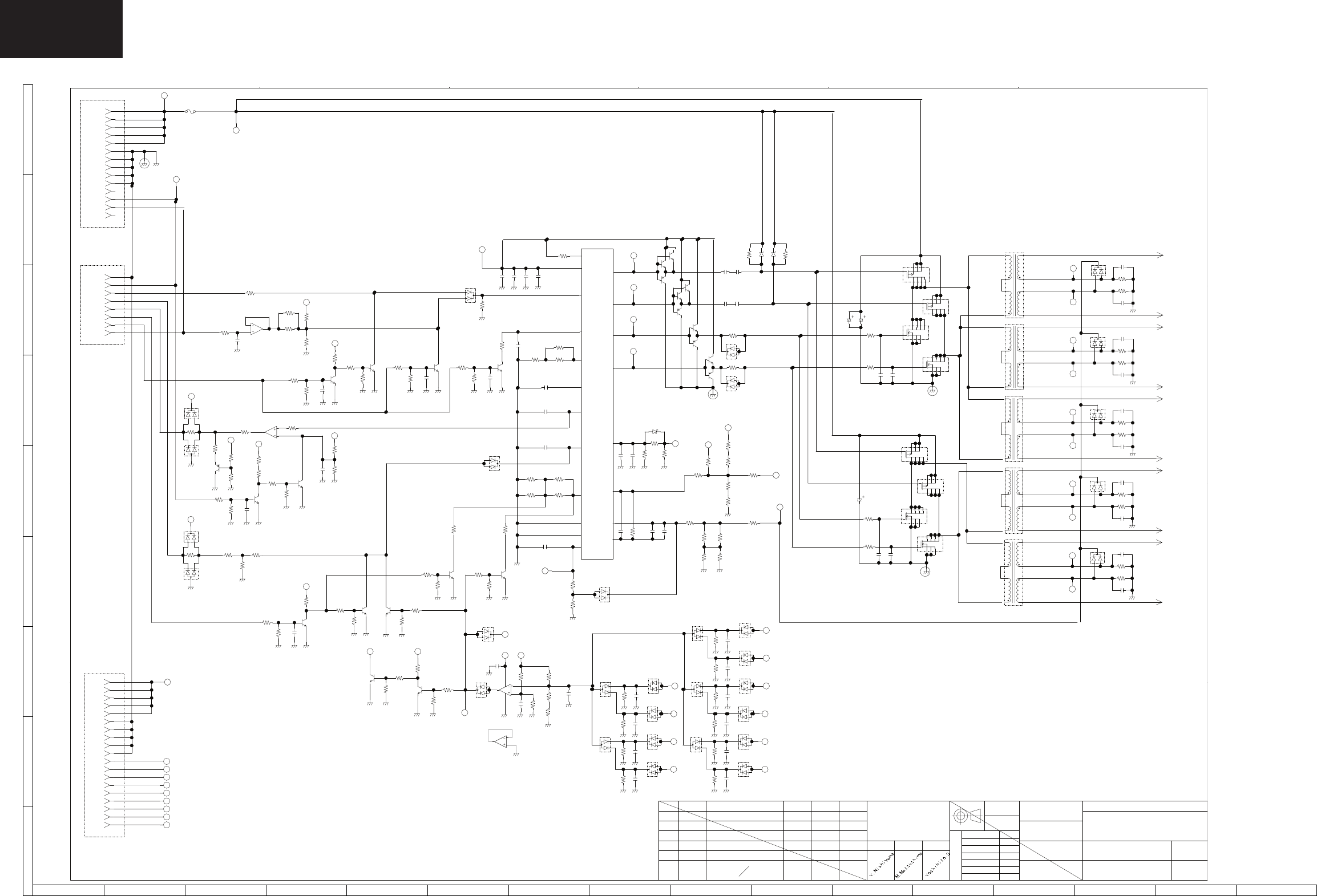
124
LC-32/37GD8E/RU
LC-32/37BT8E/RU
LC-37GD8, LC-37BT8 INVERTER Unit Diagram (RUNTKA216WJZZ)
1234567 8 9 10 11 12 13 14 15 16
I
H
G
F
E
D
C
B
A
D A T E
日付 R E A S ON
変更事由 E CN N O . ENGI NEER
担当 照査
CH ECKED APPROVED
承認
CH ECKEDAPPROVED
表面処理
±0.5
改訂 REV .
SHEET
葉番
図番 DRAW I NG NO.
PART NO . (MODEL NO . )
品番
DESCR I PT I ON
品名
DATE
作成日
F I N I S H
ミネベア株式会社
HEAT TRE AT
熱処理
表面粗サ SUR F . ROUGH .
MA TER I AL
材質
D R AW N
±0.8
±0.5
±0.3
±0.2
±0.1
公差
DEG
角度
2 5 0<L≦1 0 0 0
6 3 <L≦2 5 0
1 6 <L≦6 3
4<L≦1 6
L≦4
L
寸法
TOL
一
般
公
差
S C A L E
尺度
U N I T
単位
M I NEBEA CO . , LTD .
MA R K
符号
1
1
2
2
3
3
4
4
5
5
6
6
D D
C C
B B
A A
GND
GND
Vc c
Re g
I s e n
STB
VB1
VB2
VA1
VA2
OVP
GND
V i n
GND
GND
110
3
412
7
2
9
13
7
8
8
5
2
6
3
1 4
1 3
11
9
1 0
1 2
1 1 5
- 4 / 4
R 7 6 0 6
12
I C 7 5 0 2
6
7
C 7 5 5 5
R 7 5 9 4
R 7 5 9 5
D
C 7 5 4 7
R 7 6 0 1
R 7 6 0 0
C 7 5 5 3
D7 5 2 7
C 7 5 4 6
B
D7 5 1 8
D7 5 1 9
C
R 7 5 9 3
C 7 5 4 5
C 7 5 5 2
D7 5 2 4
D7 5 2 5
D 7 5 3 0 R 7 5 9 9
C 7 5 5 1
J
H
I
U8 4PC-E1 002 2 2 1
1/1IM3826-1
C i r c u i t D i ag r am
1 3 /MAR/ ' 0 6
-
V i n
V i n
V i n
V i n
CN7 5 0 3
1 8
1 5
1 9 6
1 7
1 6
1
Q7 5 0 5
C 7 5 1 9
R 7 5 6 0
R 7 5 6 1
2
3
R 7 5 5 8
D 7 5 0 5
R 7 5 6 2
2
2
D 7 5 0 4
C 7 5 2 0
R 7 5 7 5
R 7 5 5 6 R7 5 5 7
R 7 5 7 8
R 7 5 5 9
R 7 5 7 2
12
3
Q7 5 1 0
D 7 5 0 7
R 7 5 7 3
R 7 5 7 4
R 7 5 7 7
3
2
1
2
3
Q7 5 1 2
1
Q7 5 1 1
R 7 5 7 6
R 7 6 1 4
3
R 7 6 1 2
R 7 6 1 3
R 7 5 7 1
D 7 5 0 6
1 3
1 4 1 2
I C 7 5 0 2 R 7 5 8 1
14
- 3 / 4
REG
BRT
REG2
ERR
OSC
OF L
STB
SGND
CN7 5 0 2
2
C 7 5 1 5
C 7 5 1 6
R7 54 7
R 7 5 4 8
7
5
8
6
R 7 5 4 2 R 7 5 4 3
I C 7 5 0 2
R 7 5 4 4 2
21
3R 7 5 4 6
R 7 5 4 5
- 2 / 2
1
4
2
3R 7 5 3 9
2
3
1
Q7 5 3 2 Q 7 5 3 1
R 7 6 1 0
R 7 6 0 7
R 7 6 1 1 3
R 7 6 0 8
12
R 7 6 0 9
- 1 / 4
1 0
I C 7 5 0 2
C7 5 5 6
9
81 1
D 7 5 3 1 R 7 6 0 5
4
1
R 7 5 6 4
5
1
22
R 7 5 6 8
22
4
D7 5 3 2
3
33
Q7 5 0 6
R 7 5 6 3
R 7 5 6 6
R 7 5 6 7
1
2
3
Q7 5 0 8
R 7 5 6 5 Q 7 5 0 7 R 7 5 6 9 Q7 5 0 9
R 7 5 7 0 1
3
2
R 7 6 0 4
D7 5 2 6
R 7 6 0 3
R 7 6 0 2
C 7 5 5 4
D7 5 1 6
R 7 5 9 2
A
D7 5 1 7
C 7 5 4 4
D7 5 2 3
D 7 5 2 9
C 7 5 4 9
D7 5 2 2
R 7 5 9 8
C 7 5 5 0
R 7 5 9 7
D 7 5 2 8
C 7 5 4 8
D7 5 2 1
D7 5 2 0
R 7 5 9 6
R 7 5 0 7
3
R 7 5 0 6 D 7 5 0 2
G
E
F
C 7 5 3 3C 7 5 3 2
R 7 5 1 2 R 7 5 1 3
C 7 5 2 1
R 7 5 8 0 R7 51 1
R7 51 0
R 7 5 7 9
3
D 7 5 0 3
7
1 5
4F / B
GND
SG
REG
C7 5 0 6
I
8C 7 5 1 0C 7 5 0 8
R 7 5 1 4
C 7 5 0 9
1 0
R 7 5 2 4
R 7 5 2 5
R 7 5 2 3
R 7 6 1 5
R 7 5 2 2
R 7 5 2 6
R7 50 8
R7 50 9
RT
6V
R 7 5 3 0
C 7 5 1 4
C 7 5 1 3
9
R 7 5 2 0
R7 51 5
R 7 5 2 1
R 7 5 1 6
R 7 5 1 7
R 7 5 1 9
C7 5 1 1 1 2
C7 5 0 7 OVP
5
SS
CT 1 4 R 7 5 2 9
R 7 5 2 8
D 7 5 0 8
4R 7 5 1 8
3
14
11
R7 53 7
R7 53 8
8
23
7
6
1
4
5
1
4
58
Q7 5 2 7
3
2
7
6
5
Q7 5 2 8
C 7 5 2 8
4
578
Q7 5 2 9
6
2
8
3
7
6
1
5
Q7 5 3 0 1
43
2
R 7 5 4 9
1
2
3
R 7 5 5 0
1
2
3
Q7 5 0 2
Q7 5 0 1
R 7 5 5 1
Q7 5 0 3
1
2
3
R 7 5 5 2 R 7 5 5 4
R 7 5 5 3 C 7 5 1 7
1
2
3
Q7 5 0 4
C 7 5 1 8
R 7 5 0 5
R 7 5 5 5
2C 7 5 0 5R7 5 0 2
R 7 5 0 1
C 7 5 0 3
D 7 5 0 1 C 7 5 0 4
2
C 7 5 0 2
R7 50 3
1 3
VB1
C7 5 1 2 CP
BRT
310
1 6 Q 7 5 1 3 R 7 5 3 1
Q7 5 1 9
D 7 5 0 9
1
2
3
1
2
3
D 7 5 1 0
R7 50 4
2
VA2
VB2
BCT
9
1 8
2
Q7 5 2 1
Q7 5 2 0
1 7 Q7 5 1 4
1
R 7 5 3 2
2
3
1
2
3
1
3
1
2 0
R7 52 7 1 1
VA1
C 7 5 0 1 1Du t y
V c c
ST
2
1
Q7 5 2 2
1 9
Q7 5 1 5
2
3
1
2
3
71
2
3
Q7 5 1 7
82
3
C7 5 2 3
R 7 5 3 4
3
C7 5 2 2
1
C7 5 2 4 C7 5 2 5
Q7 5 1 6
C 7 5 3 1C 7 5 3 0
R7 53 5
6
1
4
58
3
2
7
R7 53 6
C 7 5 2 6 C 7 5 2 7 Q7 5 2 4
Q7 5 2 3
7
4
5
2
1
6
1
4
58
3
7
8
3
2
6
R 7 5 3 3
Q7 5 2 6 1
4
5
Q7 5 2 5
8
3
2
7
6
7
4
32
6
5R 7 5 9 1
JC7 5 4 3
R 7 5 9 0
1CN7 5 0 8
OUT ( H ) -
T 7 5 0 5 7
4
1 0
6
1
ID 7 5 1 5 C 7 5 4 2
C7 5 4 1
H
OUT ( H ) +
OUT ( H ) +
2CN7 5 0 8
CN7 5 0 7
1
6
5
2
11 0
3
7
T 7 5 0 4
D 7 5 1 4 C 7 5 4 0
R 7 5 8 8
R 7 5 8 9
G
CN7 5 0 7
OUT ( H ) -
OUT ( H ) -
1
2
2
45
3
R 7 5 8 7
E
F
R 7 5 8 6
C7 5 3 9
C7 5 3 8
D 7 5 1 3
CN7 5 0 6
7
45
6
1
T 7 5 0 3
1 0
C7 5 3 7
R 7 5 8 5
D
2OUT ( H ) +
OUT ( H ) +
CN7 5 0 6
1CN7 5 0 5
1 0
7
2
1
3
T 7 5 0 2
6
CD 7 5 1 2 C 7 5 3 6
B
R 7 5 8 4
1
2
CN7 5 0 4
CN7 5 0 5
OUT ( H ) -
OUT ( H ) -
T 7 5 0 1
45
1 0
32
1
R7 58 2
R7 58 3
D 7 5 1 1 C 7 53 4
C7 5 3 5
A
2CN7 5 0 4
OUT ( H ) +
ON/OF F
BRT
N . C
GND
GND
GND
GND
GND
V i n
V i n
V i n
V i n
V i n
N . C
CN 7 5 0 1
1 2
1 3
1 4
7
9
8
1 1
1 0
6
13
4
1
3
2
6
5
14
F 7 5 0 1
I C7 50 1 Q7 5 1 8 ZD7 5 0 2 ZD 7 5 0 1
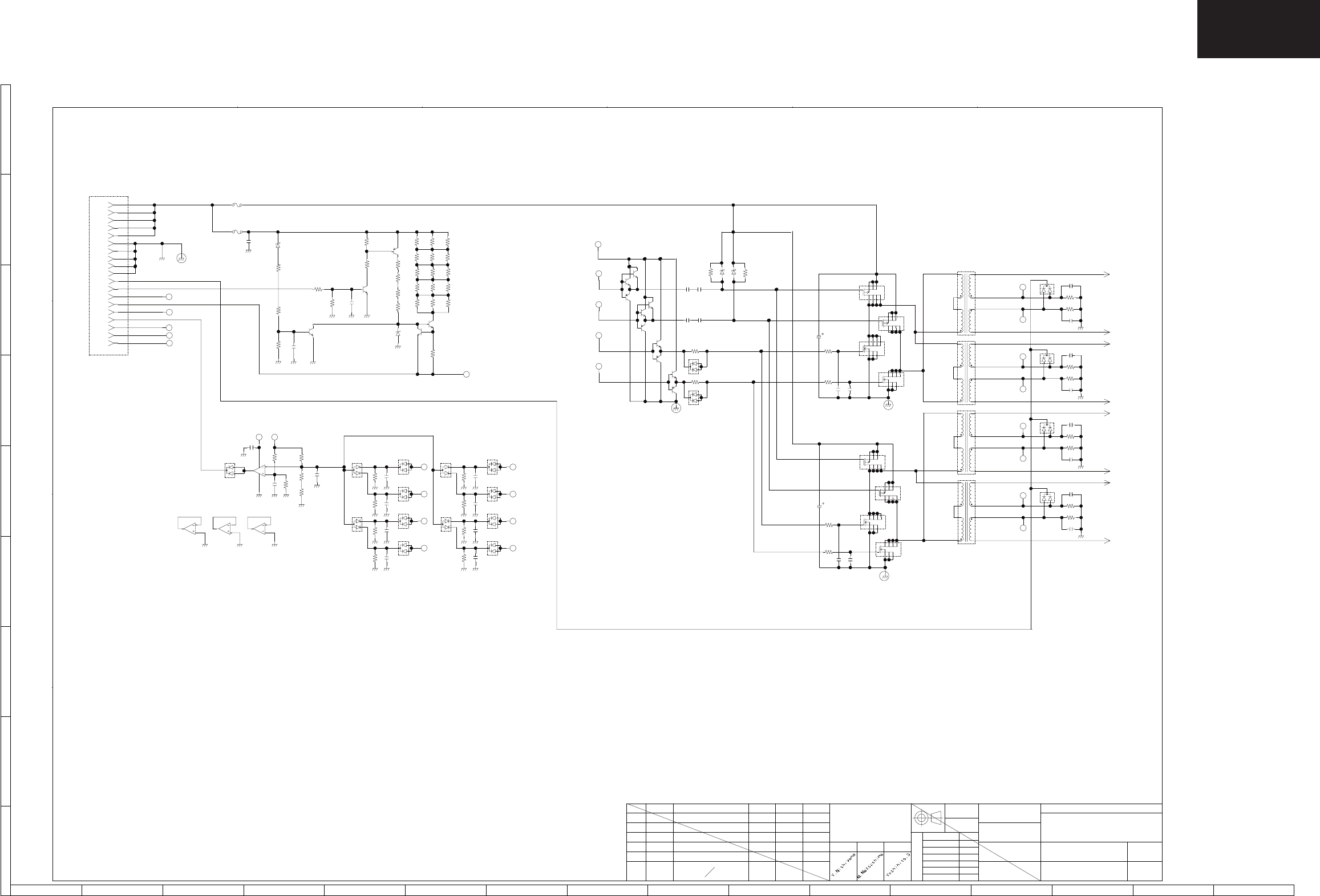
125
LC-32/37GD8E/RU
LC-32/37BT8E/RU
LC-37GD8, LC-37BT8 INVERTER Unit Diagram (RUNTKA217WJZZ)
D A T E
日付 R E A S ON
変更事由 E CN NO . ENG I NEER
担当 照査
CH ECK E D APPROVED
承認
CH ECK E DAPPROVED
表面処理
±0.5
改訂 REV .
SHEET
葉番
図番 DRAW I NG NO.
PART NO. (MODEL NO . )
品番
DESCR I PT I ON
品名
DATE
作成日
F I N I S H
ミネベア株式会社
HEAT TREAT
熱処理
表面粗サ SURF . ROUGH .
MA TER I AL
材質
D R AW N
±0.8
±0.5
±0.3
±0.2
±0.1
公差
DEG
角度
2 5 0<L≦1 0 0 0
6 3 <L≦2 5 0
1 6 <L≦6 3
4<L≦1 6
L≦4
L
寸法
TOL
一
般
公
差
S C A L E
尺度
U N I T
単位
M I NEBEA CO . , LTD .
MA R K
符号
1
1
2
2
3
3
4
4
5
5
6
6
D D
C C
B B
A A
-
1 3 /MAR/ ' 0 6
C i r c u i t D i a g r am
IM3826-2 1/1
U84PC-E1 0 0 3119
8
- 2 / 4
6
75
I C 7 7 0 1 I C 7 7 0 1
9
1 0
2
13
I C7 70 1
- 3 / 4 - 4 / 4
C 7 7 3 2
I C 7 7 0 1
- 1 / 4
R 7 7 5 3
R 7 7 5 0
1 1 1 3
1 4 1 2
4
D7 7 1 9
C7 7 3 3 2 3
R 7 7 5 2
OVP
VA2
VB1
Re g
3
1
2
4
8
10
3
R 7 7 5 6
5
7
6
1 0
GND
GND
VA1
VB2
STB
I s e n
V c c
9
8
9
7R 7 7 5 5
R 7 7 5 4
C 7 7 1 4C 7 7 1 3
R 7 7 4 4 C 7 7 2 6
R 7 7 4 3
C 7 7 2 5
N
D7 7 1 0
M
R 7 7 4 8
C 7 7 2 9
C 7 7 3 0
D7 7 1 4
R 7 7 4 7
C 7 7 3 1
R 7 7 5 1
D7 7 1 6
R 7 7 4 2
D7 7 0 8
R 7 7 4 1 L
D7 7 0 9
C 7 7 2 4
K
C 7 7 2 3 C 7 7 2 7
D7 7 1 2
D 7 7 1 8
R 7 7 4 5
D7 7 1 3
C 7 7 2 8
R 7 7 4 6
D7 7 1 5
R 7 7 4 9 D7 7 0 7 D7 7 1 1
D 7 7 1 7
R
Q
P
O
R 7 7 3 1
R7 73 2
8
6
3
2
7
1
4
5
Q7 7 1 9
8
3
2
7
6
1
4
5
Q7 7 2 0
C 7 7 0 9
7
4
5
Q7 7 2 1
8
3
2
8
6
1
7
6
5
Q7 7 2 213
42
2
1
2
3Q7 7 2 3
C 7 7 3 8
Q7 7 0 4
12
3
ZD 7 70 1
1
R 7 7 2 4
Q7 7 0 3
3
2
R 7 7 0 1
R 7 7 0 2 C 7 7 0 2
Q7 7 0 1
3
2
R 7 7 0 8
1
R 7 7 0 6 R 7 7 1 8
R 7 7 2 1
R 7 7 0 7
R 7 7 1 5
R 7 7 2 0
R 7 7 2 3
R 7 7 1 9
R 7 7 1 6 R 7 7 1 7
R 7 7 2 2
10
1
2
3
Q7 7 0 5 R 7 7 2 5
D7 7 0 1
1
2
Q7 7 1 1 3
D7 7 0 2
Q7 7 1 3 2
9
Q7 7 1 2
Q7 7 0 6 1
2
3
1
1
3
R 7 7 2 6
2
3
1
7
2
1
2
31
2
3
83
Q7 7 0 7
Q7 7 0 9
1
2
Q7 7 1 4 3
C7 7 0 6
R 7 7 2 8
1
3
Q7 7 0 8
2
C7 7 0 3
C7 7 0 5
C7 7 0 4
C 7 7 1 2C 7 7 1 1
R 7 7 2 9
3
8
2
7
6
1
4
5
R7 7 3 0
Q7 7 1 6
C 7 7 0 7
2
8
3
2
7
6
1
4
5
6
1
8
3
7
Q7 7 1 5
4
5
R 7 7 2 7
Q7 7 1 8
Q7 7 1 7
8
3
7
6
1
4
5
2
67
4C7 7 2 2
R
1CN7 7 0 4
OUT ( H ) +
1
T 7 7 0 4 7
1 0
2
6
5
3
R7 7 4 0
R7 7 3 9
C7 7 2 1
D 7 7 0 6
Q
OUT ( H ) -
OUT ( H ) -
CN7 7 0 4
2
1
45
32
C7 7 2 0
D 7 7 0 5
OR 7 7 3 7
C7 7 1 9
P
R 7 7 3 8
CN7 7 0 3
45
6
1 0
1
T 7 7 0 3 7
R 7 7 3 6
C7 7 1 8
N
OUT ( H ) +
OUT ( H ) +
1CN7 7 0 2
2CN7 7 0 3
T 7 7 0 2
1 0
32
1
7
6
L
MC7 7 1 7
R 7 7 3 5
D 7 7 0 4
OUT ( H ) -
OUT ( H ) -
1CN7 7 0 1
2CN7 7 0 2
5
T 7 7 0 1
4
1 0
32
1
KD 7 7 0 3
R 7 7 3 4
C7 7 1 6
C7 7 1 5
R 7 7 3 3
OUT ( H ) +
2CN7 7 0 1
1 6
1 4
GND
GND
1 3
V i n
V i n
GND
V i n 1 5
1 7
1 1
1 2
F 7 7 0 2
ZD 7 70 4
C 7 7 0 1
5 0 0mA
V i n 1 9
1 8
CN7 7 0 5
V i n 6 . 3 A
F 7 7 0 1
R 7 7 0 4
R 7 7 0 3
R 7 7 0 5
R 7 7 0 9
R 7 7 1 2
1
2
3Q 7 7 0 2
R 7 7 1 1
R 7 7 1 3
R 7 7 1 0
R 7 7 1 4 2
ZD 7 70 3
Q7 7 1 0 ZD7 7 0 2
1234567 8 9 10 11 12 13 14 15 16
I
H
G
F
E
D
C
B
A
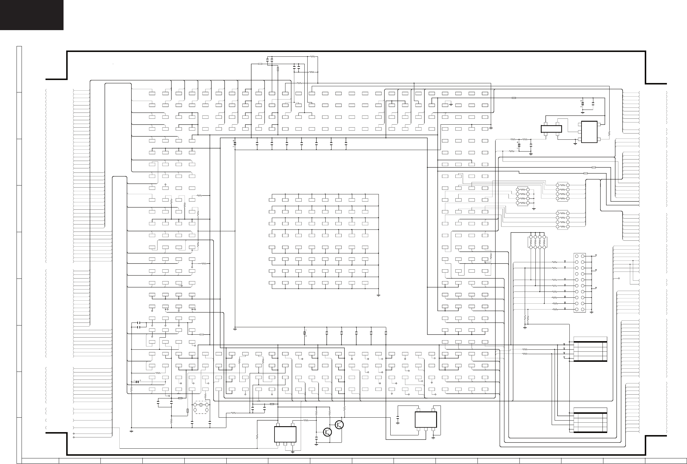
126
LC-32/37GD8E/RU
LC-32/37BT8E/RU
LC-32/37GD8, LC-32/37BT8 Digital Unit Diagram 1/4 (STI5516)
EMID[0]
EMID[1]
EMID[7] EMID[14] EMID[15] EMID[12]
EMID[8]EMID[9] EMID[10]
EMID[11]EMID[3]EMID[13]
EMID[5]EMID[6]
EMID[2] EMID[4]
EMIA[4]
EMIA[5]
EMIA[6]
EMIA[7]
EMIA[12]
EMIA[9]
EMIA[13]
EMIA[8]EMIA[10]
EMIA[23]
EMIA[11]
EMIA[16]
EMIA[15]
EMIA[17]
EMIA[18]
EMIA[19]
EMIA[22]
EMIA[21]
EMIA[20]
EMIA[14]
EMIA[3]
EMIA[2]
EMIBE1
EMIBE0
EMICAS
EMIRAS
EMIOE
EMICS0
EMICS3
EMICS4
EMICS5
EMIRW
EMICLK
EMILBA
CPUWAIT
MODEMIRQCIIRQ1
CIIRQ0
TDI
TMS
TDO
TCK
NOTTRST
CIRESET FERESET
MDMRESET VIDEOOFF
MUTE FEOFF CION
GPIO0
GPIO1
ASPECT
I2CSDA
I2CSCL
TVSDA
TVSCL
TXD
RXD
SMICS
SMICLK
SMIDQML SMIDQMU
SMICAS
SMIRAS
SMIWE
SMID[0]
SMID[1]
SMID[2]
SMID[3] SMID[5] SMID[4]
SMID[6] SMID[7]
SMID[8] SMID[9] SMID[11] SMID[12]
SMID[13]
SMID[14] SMID[15]
SMID[10]
SMIA[0]
SMIA[1] SMIA[2]
SMIA[3]
SMIA[4]
SMIA[5]
SMIA[6]
SMIA[7]
SMIA[8]
SMIA[9]
SMIA[10]
SMIA[11] SMIA[12]
SMIA[13]
TS2CLK
TS2STRT
TS2VAL
TS2D[7]
TS2D[6]
TS2D[5]
TS2D[4] TS2D[3]
TS2D[2] TS2D[0]
TS2D[1]
FEVALID FEERROR
FESTROUT
FECLK
SPDIF
LEFTM
LEFTP
CVBS
VBGFIL
BG R
VDDFS
GNDFS
27MHZPWM
CLK27MHZ
27MHZPWM
GNDADAC
RIGHTP RIGHTM
EMID[0]
EMID[1]
EMID[2]
EMID[3]
EMID[4]
EMID[5]
EMID[6]
EMID[7]
EMID[8]
EMID[9]
EMID[10]
EMID[11]
EMID[12]
EMID[13]
EMID[14]
EMID[15]
EMIA[23]
EMIA[22]
EMIA[21]
EMIA[20]
EMIA[19]
EMIA[18]
EMIA[17]
EMIA[16]
EMIA[15]
EMIA[14]
EMIA[13]
EMIA[12]
EMIA[11]
EMIA[10]
EMIA[9]
EMIA[8]
EMIA[7]
EMIA[6]
EMIA[5]
EMIA[4]
EMIA[3]
EMIA[2]
TS2D[0]
TS2D[1]
TS2D[2]
TS2D[3]
TS2D[4]
TS2D[5]
TS2D[6]
TS2D[7]
TS2CLK
TS2STRT
TS2VAL
FED[0]
FED[1]
FED[2]
FED[3]
FED[4]
FED[5]
FED[6]
FED[7]
SMID[0]
SMID[1]
SMID[2]
SMID[3]
SMID[4]
SMID[5]
SMID[6]
SMID[7]
SMID[8]
SMID[9]
SMID[10]
SMID[11]
SMID[12]
SMID[13]
SMID[14]
SMID[15]
SMIA[0]
SMIA[1]
SMIA[2]
SMIA[3]
SMIA[4]
SMIA[5]
SMIA[6]
SMIA[7]
SMIA[8]
SMIA[9]
SMIA[10]
SMIA[11]
SMIA[12]
SMIA[13]
SMICAS
SMICLK
SMICS
SMIDQML
SMIDQMU
SMIRAS
SMIWE
GNDDAC
B
G
R
CVBS
TVSCL
TVSDA
SPDIF
ASPECT
CIIRQ0
CIIRQ1
CION
CIRESET
CPUWAIT
EMIBE0
EMIBE1
EMICAS
EMICLK
EMICS0
EMICS3
EMICS5
EMILBA
EMIOE
EMIRAS
EMIRW
FEOFF
FERESET
GPIO0
LEFTM
LEFTP
MUTE
RIGHTM
RIGHTP
VBGFIL
VIDEOOFF
GNDPLL
GPIO1
EMIA[11]
EMIA[12]
EMIA[13]
EMIA[14]
EMIA[15]
EMIA[16]
EMIA[18]
EMIA[2]
EMIA[3]
EMIA[4]
EMIA[5]
EMIA[6]
EMIA[7]
EMIA[8]
EMIA[9]
EMIA[10]
FED[0]
FED[1]
FED[2]
FED[3]
FED[5]
FED[7]
FED[6]
FED[4]
VDDA
GNDA
VDDADAC
VDDDAC
VDDPLL
SYSRESET
P1V8
P1.8V
P3V3
TVRX TVTX
IRQ
IRQ
COUT
YOUT
MDMRESET
MODEMIRQ
NOTJRST
RSTIN
TRIGIN
TRIGOUT
TRIGOUT
TRIGIN
EMIBE0
FED[5]
FED[4]
FED[3]
FED[2]
FED[7]
FED[6]
FED[1]
FED[0]
FECLK
FESTROUT
FEVALID
FEERROR
FECLK
FESTROUT
FEVALID
I2CSCL
I2CSDA
IR
TMS
TDO
TCK
TDI
IR
NOTJRST
NOTTRST
TXD
RXD
P3.3V
P3.3V
DUNTKD628WE01
R4003
10K
R4005
10K
R4008
10K
R4006
10K
R4007
10K
R4018
0
R4015
10K
R4025
0
R4027
0
12
34
56
78
1u
50V
C4001
ASX
R4011
10K
R4013
10K
R4009
100K
C4006
18P
(CH)
R4019
0
R4010
0
R4004
0
R4001
0
R4026
10K
47u
6.3V
C4030
ASX
R4028
10K
R4029
33
10u
16V
C4032
ASX
EMID[0]
EMID[1]
EMID[2]
EMID[3]
EMID[4]
EMID[5]
EMID[6]
EMID[7]
EMID[8]
EMID[9]
EMID[10]
EMID[11]
EMID[12]
EMID[13]
EMID[14]
EMID[15]
EMIA[23]
EMIA[22]
EMIA[21]
EMIA[20]
EMIA[19]
EMIA[18]
EMIA[17]
EMIA[16]
EMIA[15]
EMIA[14]
EMIA[13]
EMIA[12]
EMIA[11]
EMIA[10]
EMIA[9]
EMIA[8]
EMIA[7]
EMIA[6]
EMIA[5]
EMIA[4]
EMIA[3]
EMIA[2]
TS2D[0]
TS2D[1]
TS2D[2]
TS2D[3]
TS2D[4]
TS2D[5]
TS2D[6]
TS2D[7]
TS2CLK
TS2STRT
TS2VAL
FED[0]
FED[1]
FED[2]
FED[3]
FED[4]
FED[5]
FED[6]
FED[7]
SMID[0]
SMID[1]
SMID[2]
SMID[3]
SMID[4]
SMID[5]
SMID[6]
SMID[7]
SMID[8]
SMID[9]
SMID[10]
SMID[11]
SMID[12]
SMID[13]
SMID[14]
SMID[15]
SMIA[0]
SMIA[1]
SMIA[2]
SMIA[3]
SMIA[4]
SMIA[5]
SMIA[6]
SMIA[7]
SMIA[8]
SMIA[9]
SMIA[10]
SMIA[11]
SMIA[12]
SMIA[13]
FECLK
FEERROR
FESTROUT
FEVALID
SMICAS
SMICLK
SMICS
SMIDQML
SMIDQMU
SMIRAS
SMIWE
R4021
2.2K
Q4002
2SC3928AR
Q4001
2SC3928AR
R4020
4.7K
R4017
10K
R4016
100
R4012
10K
RSTIN
B
G
R
CVBS
I2CSCL
I2CSDA
TVSCL
TVSDA
ASPECT
CIIRQ0
CIIRQ1
CION
CIRESET
CPUWAIT
EMIBE0
EMIBE1
EMICAS
EMICLK
EMICS0
EMICS3
EMICS5
EMILBA
EMIOE
EMIRAS
EMIRW
FEOFF
FERESET
GPIO0
LEFTM
LEFTP
MUTE
RIGHTM
RIGHTP
VBGFIL
VIDEOOFF
IXB680WJ
STI5516
A1
B1
C1
D1
E1
F1
G1
H1
J1
K1
L1
M1
N1
P1
R1
T1
U1
V1
W1
Y1
AA1
AB1
AC1
AD1
AE1
AF1 AF2 AF3 AF4 AF5 AF6 AF7 AF8 AF9 AF10 AF11 AF12 AF13 AF14 AF15 AF16 AF17 AF18 AF19 AF20 AF21 AF22 AF23 AF24 AF25 AF26
AE26
AD26
AC26
AB26
AA26
Y26
W26
V26
U26
T26
R26
P26
N26
M26
L26
K26
J26
H26
G26
F26
E26
D26
C26
B26
A26A25A24A23A22A21A20A19A18A17A16A15A14A13A12A11A10
A9A8A7A6A5A4A3A2
B2
C2
D2
E2
F2
G2
H2
J2
K2
L2
M2
N2
P2
R2
T2
U2
V2
W2
Y2
AA2
AB2
AC2
AD2
AE2 AE3 AE4 AE5 AE6 AE7 AE8 AE9 AE10 AE11 AE12 AE13 AE14 AE15 AE16 AE17 AE18 AE19 AE20 AE21 AE22 AE23 AE24 AE25
AD25
AC25
AB25
AA25
Y25
W25
V25
U25
T25
R25
P25
N25
M25
L25
K25
J25
H25
G25
F25
E25
D25
C25
B25B24B23B22B21B20B19B18B17B16B15B14B13B12B11B10
B9B8B7B6B5B4B3
C3
D3
E3
F3
G3
H3
J3
K3
L3
M3
N3
P3
R3
T3
U3
V3
W3
Y3
AA3
AB3
AC3
AD3 AD4 AD5 AD6 AD7 AD8 AD9 AD10 AD11 AD12 AD13 AD14 AD15 AD16 AD17 AD18 AD19 AD20 AD21 AD22 AD23 AD24
AC24
AB24
AA24
Y24
W24
V24
U24
T24
R24
P24
N24
M24
L24
K24
J24
H24
G24
F24
E24
D24
C24C23C22C21C20C19C18C17C16C15C14C13C12C11C10
C9C8C7C6C5C4
D4
E4
F4
G4
H4
J4
K4
L4
M4
N4
P4
R4
T4
U4
V4
W4
Y4
AA4
AB4
AC4 AC5 AC6 AC7 AC8 AC9 AC10 AC11 AC12 AC13 AC14 AC15 AC16 AC17 AC18 AC19 AC20 AC21 AC22 AC23
AB23
AA23
Y23
W23
V23
U23
T23
R23
P23
N23
M23
L23
K23
J23
H23
G23
F23
E23
D23D22D21D20D19D18D17D16D15D14D13D12D11D10
D9D8D7D6D5
K10
L10
M10
N10
P10
R10
T10
U10 U11 U12 U13 U14 U15 U16 U17
T17
R17
P17
N17
M17
L17
K17K16K15K14K13K12K11
L11
M11
N11
P11
R11
T11 T12 T13 T14 T15 T16
R16
P16
N16
M16
L16L15L14L13L12
M12
N12
P12
R12 R13 R14 R15
P15
N15
M15M14M13
N13
P13 P14
N14
GPIO1
EMIA[3]
EMIA[14]
EMIA[8]
EMIA[2]
EMIA[13]
EMIA[7]
EMIA[18]
EMIA[12]
EMIA[6]
EMIA[11]
EMIA[5]
EMIA[16]
EMIA[10]
EMIA[4]
EMIA[15]
EMIA[9]
TL4001 TL4002
TL4003
TL4004
SN1G08DC
123
45
SN1GU04C
1
2
34
5
C4002
0.01u
C4005
0.01u
C4009
0.01u
C4013
0.01u C4016
0.01u
C4003
0.1u
C4004
0.1u
C4010
0.1u
C4014
0.1u
C4015
0.1u
C4018
0.1u
C4021
0.1u
C4023
0.1u
C4025
0.1u
C4011
0.1u
C4012
0.1u
C4017
0.1u
C4020
0.1u
C4022
0.1u
C4024
0.1u
C4026
0.1u
C4027
0.1u
C4028
0.1u
C4031
0.1u
C4033
0.1u
C4007
15P
(CH)
10u
16V
C4008
ASX
10u
16V
C4019
ASX
R4002
200 F
R4030
47
12
34
56
78
R4031
47
12
34
56
78
FB4003
A215WJ
FB4004
A215WJ FB4006
A215WJ
FB4002
A215WJ
FB4001
A215WJ
FB4005
A215WJ
FB4007
A215WJ
C4029
0.01u
X4001
SC0032TA
32.768kHz
1
23
4
P1V8
P3V3
TL4005
TL4007 TL4008
TL4009
TL4006
TL4010
R4032
10K
IRQ
TL4011 TL4012
TL4013
TL4014
TL4015
TL4016
TL4017
TL4018
TL4019
TL4020
TL4021
TL4022
TL4023
TL4024
TL4025
TL4026 TL4027
TL4028 TL4029
TL4030
TL4031
TL4032
TL4033
TL4034
TL4035
TL4036
TL4037
R4036
10K
12
34
56
78
R4035
10K
R4037
10K
EMIBE0
FESTROUT
FEVALID
FECLK
FED[4]
FED[1]
FED[7]
FED[6]
FED[2]
FED[3]
FED[0]
FED[5]
I2CSCL
I2CSDA
X4002
UAA075WJ
27MHz
VCXO
1 2
34
R4197
100
R4193
100
R4194
100
R4192
100
R4195
100
R4196
100
R4190
100
R4191
100
IR
R4024
0
P4001
N0463TA
RS
1
B+3.3VDC
2
TXD1
3
RXD1
4
GND
BU4228G
123
45
TL4038
TL4039
TL4040
TL4041
TL4046
TL4047
TL4048
TL4049
TL4050
TL4051
TL4052
TL4053
*TL4054
*TL4055
*TL4056
P4003
N0463TA
RS1
1
B+3.3VDC
2
TXD1
3
RXD1
4
GND
R4038 100
R4039 100
*CN4190
NA524WJ
18
9
19
8
4
5
20
6
7
16
11
3
14
15
12
10
17
12
13
FB4008
A303WJ
FB4009
A303WJ
TO 2/4
TO 2/4
TO 3/4
TO 3/4
TO 4/4
TO 4/4
Ver.N2 (2006.05.16)
LC-32P70E/LC-26P70E/LC-37P70E
LC-32GD9E/LC-37GD9E
LC-32GD8E/LC-37GD8E
!!
STI5516
(DIGITAL 1/4)
IC4001
IC4002
IC4005
IC4003
0
1.790.01
0
0.01
0.7
3.29 3.29 0
2.753.29
0
1.7
01.7
3.29
1.6 0
1.7
3.29
1.79 3.29 0
03.29
CONFIDENTIAL
Ver.N2 (2006.05.16)
1234567 8 9 10 11 12 13 14 15 16
I
H
G
F
E
D
C
B
A
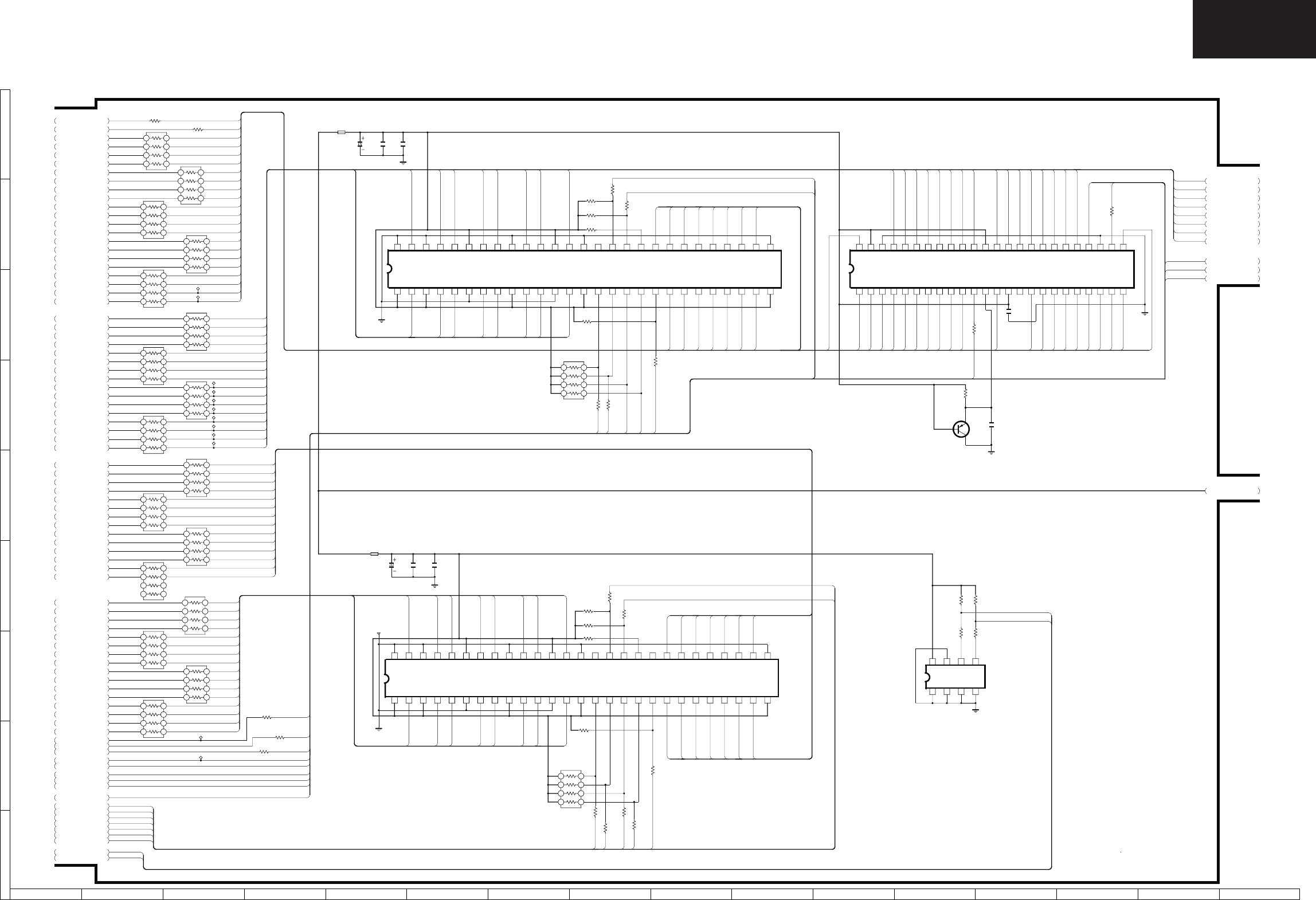
127
LC-32/37GD8E/RU
LC-32/37BT8E/RU
LC-32/37GD8, LC-32/37BT8 Digital Unit Diagram 2/4 (MEMORIES)
EMIAM[23]
EMIAM[22]
EMIAM[21]
EMIAM[20]
EMIAM[19]
EMIAM[18]
EMIAM[4]
EMIAM[5]
EMIAM[13]
EMIAM[12]
EMIAM[11]
EMIAM[10]
EMIAM[17]
EMIAM[16]
EMIAM[15]
EMIAM[14]
EMIAM[9]
EMIAM[8]
EMIAM[7]
EMIAM[6]
EMIAM[17]
EMIAM[18]
EMIAM[12]
EMIAM[2]
EMIAM[3]
EMIAM[4]
EMIAM[5] EMIAM[6]
EMIAM[7]
EMIAM[8]
EMIAM[9]
EMIAM[10]
EMIAM[11]
EMIAM[13]
EMIAM[2]
EMIAM[3]
EMIAM[4]
EMIAM[5]
EMIAM[6]
EMIAM[7]
EMIAM[8]
EMIAM[9]
EMIAM[19]
EMIAM[20]
EMIAM[17]
EMIAM[16]
EMIAM[15]
EMIAM[14]
EMIAM[13]
EMIAM[12]
EMIAM[11]
EMIAM[10]
EMIAM[21]
EMIAM[18]
EMIDM[10]
EMIDM[9]
EMIDM[11]
EMIDM[8]
EMIDM[12]
EMIDM[13]
EMIDM[14]
EMIDM[15]
EMIDM[14]
EMIDM[13]
EMIDM[12]
EMIDM[11]
EMIDM[10]
EMIDM[9]
EMIDM[8]EMIDM[7]
EMIDM[6]
EMIDM[5]
EMIDM[4]
EMIDM[3]
EMIDM[2]
EMIDM[1]
EMIDM[0]
EMIDM[0]
EMIDM[1]
EMIDM[2]
EMIDM[3]
EMIDM[4]
EMIDM[5]
EMIDM[6]
EMIDM[7]
EMIDM[8]
EMIDM[9]
EMIDM[10]
EMIDM[11]
EMIDM[12]
EMIDM[13]
EMIDM[14]
EMIDM[15]
EMIAM[14]
EMIRASM
EMICASM
EMIAM[22]
EMIAM[23]
EMIRW
EMIOEM
EMICS5
EMIRW
EMIBE1
EMICLK
EMIBE0
EMICS0
SMIAM[12]
SMIAM[11]
SMIAM[10]
SMIAM[13]
SMIAM[9]
SMIAM[8]
SMIAM[7]
SMIAM[6]
SMIAM[5]
SMIAM[4]
SMIAM[3]
SMIAM[2]
SMIAM[1]
SMIAM[2]
SMIAM[9]SMIAM[13]
SMIAM[3]
SMIAM[5]
SMIDM[1]
SMIDM[4]
SMIDM[15]
SMIDM[13]
SMIDM[12]
SMIDM[11]
SMIAM[6]
SMIAM[8]
SMIDM[3]
SMICS
SMIDM[14]
SMIAM[7]
SMIDM[8]
SMIAM[11]
SMIWE
SMIDQML
SMIDM[5]
SMIDQMU
SMIDM[2]
SMIAM[12]
SMICLK
SMIAM[1]
SMIAM[10]
SMIDM[0]
SMIDM[7]
SMIDM[6]
SMIDM[10]
SMIDM[9]
SMIAM[0]
SMIDM[15]
SMIDM[14]
SMIDM[13]
SMIDM[12]
SMIDM[6]
SMIDM[7]
SMIDM[5]
SMIDM[4]
SMIDM[11]
SMIDM[10]
SMIDM[9]
SMIDM[8]
SMIDM[3]
SMIDM[0]
SMIDM[1]
SMIDM[2]
EMIOEM
EMIRASM
EMICASM
EMIRW
EMICLK
EMICS0
EMICS5
EMIDM[15]
SMIDQMU
SMIDQML
SMIRAS
SMICAS
SMIWE
SMICLK
SMICS
I2CSCL
I2CSDA
SMIAM[0]
SMIAM[4]
P3V3_SM
EMIBE1
EMICASM
EMIRASM
EMIOEM
EMIDM[7]
EMIDM[6]
EMIDM[5]
EMIDM[4]
EMIDM[3]
EMIDM[2]
EMIDM[1]
EMIDM[0]
SMICAS
SMIRAS
P3V3
P3V3
EMIDM[7]
EMIDM[0]
EMIDM[1]
EMIDM[2]
EMIDM[3]
EMIDM[4]
EMIDM[5]
EMIDM[6]
EMIAM[3]
EMIAM[2]
EMIBE0
I2CSDA
I2CSCL
DUNTKD628WE01
R4209
47
12
34
56
78
R4211
47
12
34
56
78
R4206
47
12
34
56
78
R4214
47
12
34
56
78
R4207
47
12
34
56
78
R4215
47
12
34
56
78
R4208
47
12
34
56
78
R4216
47
12
34
56
78
R4201
47
12
34
56
78
R4217
47
12
34
56
78
R4202
47
12
34
56
78
R4218
47
12
34
56
78
R4203
47
12
34
56
78
R4212
47
12
34
56
78
R4204
47
12
34
56
78
R4213
47
12
34
56
78
R4205
47
12
34
56
78
R4210
47 R4219
47
R4221
47
R4222
47
R4220
47
R4237
47
R4234
47
R4238
47
R4241
47
R4244
47
R4231
10K
R4230
10K
R4226
10K
R4232
10K
R4224
10K
12
34
56
78
R4228
10K
R4239
47
R4227
10K
R4235
47
R4229
10K
R4243
47
R4225
10K
R4236
47
R4223
10K
12
34
56
78
R4233
47
R4248
47
R4251
47
R4246
47
R4250
47
R4245
5.6K
R4249
5.6K
C4209
0.1u
25V
Z
C4202
0.1u
25V
Z
C4205
0.1u
25V
Z
C4207
0.1u
25V
Z
R4247
10K
Q4201
2SA1530AR
FB4201
A215WJ
FB4202
A215WJ
EMIA[21]
EMIA[20]
EMIA[19]
EMIA[18]
EMIA[11]
EMIA[13]
EMIA[12]
EMIA[10]
EMIA[4]
EMIA[2]
EMIA[5]
EMIA[3]
EMID[10]
EMID[8]
EMID[11]
EMID[9]
EMID[2]
EMID[0]
EMID[3]
EMID[1]
SMIA[8]
SMIA[6]
SMIA[9]
SMIA[7]
SMIA[0]
SMIA[1]
SMID[10]
SMID[8]
SMID[11]
SMID[9]
SMID[2]
SMID[0]
SMID[3]
SMID[1]
SMID[6]
SMID[4]
SMID[7]
SMID[5]
SMID[13]
SMID[12]
SMID[14]
SMID[15]
SMIA[3]
SMIA[2]
SMIA[4]
SMIA[5]
SMIA[11]
SMIA[10]
SMIA[12]
SMIA[13]
EMID[5]
EMID[4]
EMID[6]
EMID[7]
EMID[13]
EMID[12]
EMID[14]
EMID[15]
EMIA[7]
EMIA[6]
EMIA[8]
EMIA[9]
EMIA[15]
EMIA[14]
EMIA[16]
EMIA[17]
EMIA[22]
EMIA[23]
EMIOE
EMIRAS
EMICAS
EMIRW
EMICLK
EMICS0
EMICS5
SMIDQMU
SMIDQML
SMIRAS
SMICAS
SMIWE
SMICLK
SMICS
I2CSCL
I2CSDA
EMIBE0
EMIBE1
EMICASM
EMIRASM
EMIOEM
EMIDM[0]
EMIDM[1]
EMIDM[2]
EMIDM[3]
EMIDM[4]
EMIDM[5]
EMIDM[6]
EMIDM[7]
R4240
47
R4242
47
IXB076WJ
12345678910 11 12 13 14 15 16 17 18 19 20 21 22 23 24 25 26 27
282930313233343536373839404142434445464748495051525354
IXB076WJ
12345678910 11 12 13 14 15 16 17 18 19 20 21 22 23 24 25 26 27
282930313233343536373839404142434445464748495051525354
C4201
10u
16V
ASX
C4203
10u
16V
ASX
C4204
0.01u
C4206
0.01u
P3V3
TL4205
TL4206
TL4207
TL4208
TL4209
TL4210
TL4211
TL4212
TL4202
TL4203
TL4201
TL4204
IXB681WJ
12345678910 11 12 13 14 15 16 17 18 19 20 21 22 23 24
252627282930313233343536373839404142434445464748
BR24L64F
1234
5678
TL4213
TO 1/4
TO 3/4
TO 4/4
Ver.N2 (2006.03.31)
LC-32P70E/LC-26P70E/LC-37P70E
LC-32GD9E/LC-37GD9E
LC-32GD8E/LC-37GD8E
MEMORIES
(DIGITAL 2/4)
*IC4202
*IC4201
IC4203
IC4204
3.29
0
3.29
3.29 0.7 3.29 0.4 0.4 00.4 0.5 3.29 0.7 1.0 0 0.3 3.29 3.29 3.29 3.29 3.29 3.29 1.5 1.5 1.5 1.5 1.5 1.5 1.5 3.29
01.51.51.51.51.51.51.51.53.291.63.29000.33.290.40.300.40.33.290.31.501.50
3.29 0.3 3.29 0.3 0.3 00.3 0.3 3.29 0.3 0.3 0 0.3 3.29 02.7 3.2 3.2 0.3 0.3 0.3 0.3 0.3 0.3 0.3 0.3 3.29
00.30.30.30.30.30.30.303.291.70.02000.33.290.30.300.30.33.290.30.300.30
1.5 1.5 1.5 1.5 1.5 1.5 1.5 1.5 1.5 1.5 3.27 3.29 0.02 3.29 01.5 1.5 1.5 1.5 1.5 1.5 1.5 1.5 1.5
1.53.24
03.240.90.30.40.40.40.30.40.43.290.50.31.00.30.31.50.31.503.39
0000
2.12.1
03.29
CONFIDENTIAL
Ver.N2 (2006.03.31)
12 3 4 5 67 8 9 10 11 12 13 14 15 16
I
H
G
F
E
D
C
B
A
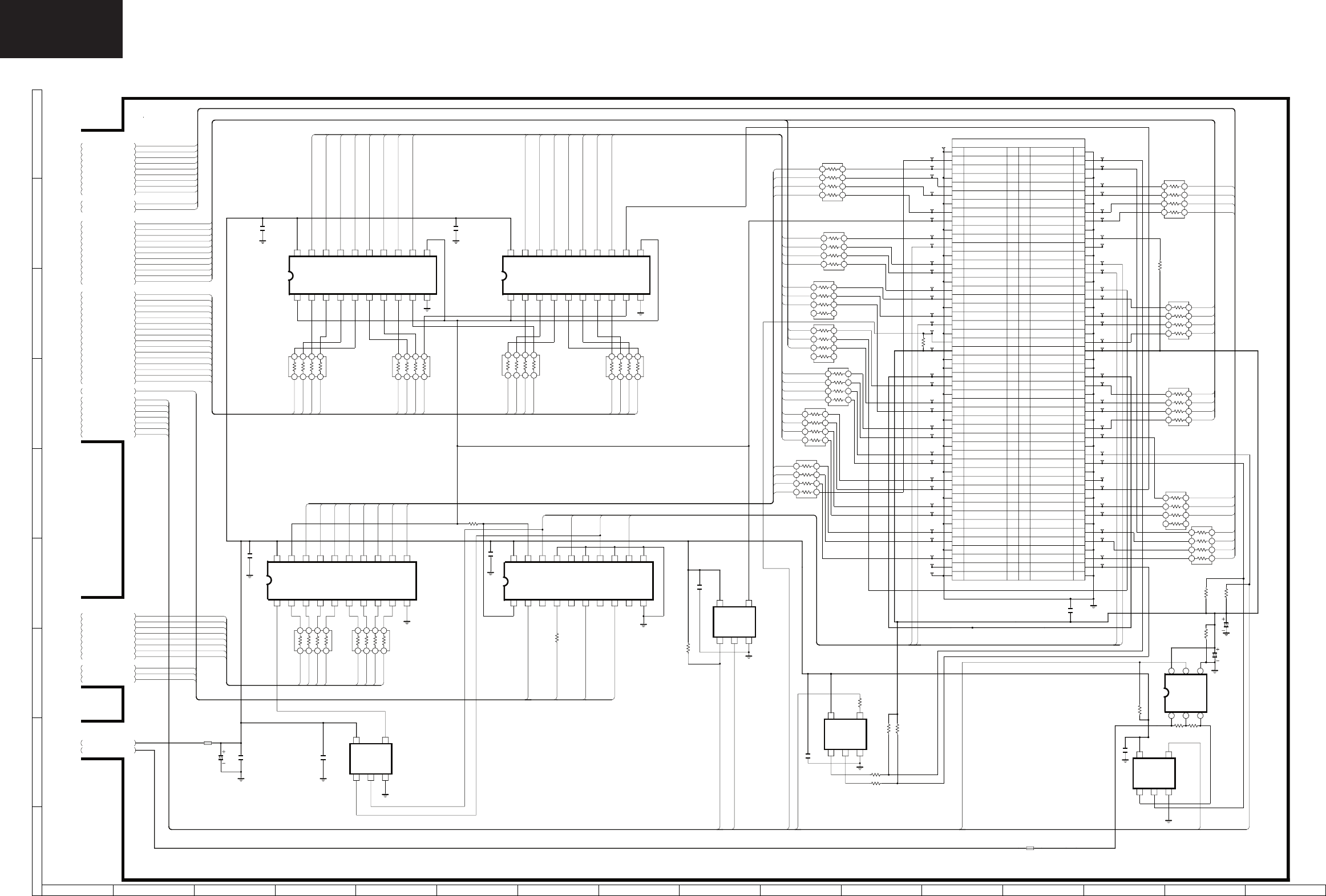
128
LC-32/37GD8E/RU
LC-32/37BT8E/RU
LC-32/37GD8, LC-32/37BT8 Digital Unit Diagram 3/4 (CI)
EMIA[2]
EMIA[3]
EMIA[4]
EMIA[5]
EMIA[6]
EMIA[7]
EMIA[8]
EMIA[9]
EMIA[10]
EMIA[11]
EMIA[12]
EMIA[13]
EMIA[14]
EMIA[15]
EMIA[16]
EMIA[18]
CID[7]
CID[6]
CID[5]
CID[4]
CID[0]
CID[1]
CID[2]
CID[3]
EMIDM[3]
EMIDM[2]
EMIDM[1]
EMIDM[0]
EMIDM[4]
EMIDM[5]
EMIDM[6]
EMIDM[7]
CIIOWR
EMILBA
EMIOEM
EMIRASM
EMICASM
CIDDIR
CIIORD
CIIORD
CIIOWR
CIOE
CIWE
CIA[12]
CIA[14]
CIA[13]
CIA[0]
CIA[1]
CIA[2]
CIA[3]
CIA[4]
CIA[5]
CIA[7]
CIA[8]
CIA[9]
CIA[11]
CIA[10]
CID[0]
CID[1]
CID[2]
CID[3]
CID[4]
CID[5]
CID[6]
CID[7]
FECLK
FESTROUT
FEVALID
FED[7]
FED[6]
FED[5]
FED[4]
FED[3]
FED[2]
FED[1]
FED[0]
TS2D[7]
TS2D[6]
TS2D[5]
TS2D[4]
TS2D[0]
TS2D[1]
TS2D[2]
TS2D[3]
TS2STRT
TS2VAL
TS2CLK
CPUWAIT
CIIRQ0
EMIBE0
EMICS3EMICS3
FED[7]
FED[6]
FED[5]
FED[4]
FED[3]
FED[2]
FED[1]
FED[0]
FEVALID
FESTROUT
FECLK
EMIDM[0]
EMIDM[1]
EMIDM[2]
EMIDM[3]
EMIDM[4]
EMIDM[5]
EMIDM[6]
EMIDM[7]
EMIOEM
EMILBA
EMIRASM
EMICASM
CIIRQ0
CIIRQ1
CION
CIRESET
CPUWAIT
EMIBE0
EMICS3
P3V3
CIWE
CIOE
CIA[6]
CICD1
TS2D[0]
TS2D[1]
TS2D[2]
TS2D[3]
TS2D[4]
TS2D[5]
TS2D[6]
TS2D[7]
TS2CLK
TS2STRT
TS2VAL
CIA[0]
CIA[1]
CIA[3]
CIA[5]
CIA[4]
CIA[2]
CIA[7]
CIA[12]
CIA[13]
CIA[8]
CIA[9]
CIA[10]
CIA[11]
EMIA[13]
EMIA[12]
EMIA[10]
EMIA[11]
EMIA[15]
EMIA[9]
EMIA[14]
CIA[6]
CIA[14]
EMIA[7]
EMIA[8]
EMIA[5]
EMIA[6]
EMIA[4]
EMIA[3]
EMIA[18]
EMIA[2]
EMIA[16]
CIOFF
CIREG
CIIRQ1
CIRESET
CION
P5V
P3V3CI
VPPPCMCIA
P5VPCMCIA
DUNTKD628WE01
R4404
47
12
34
56
78
R4402
47
12
34
56
78
R4408
47
12
34
56
78
R4407
47
12
34
56
78
R4401
47
12
34
56
78
R4403
47
12
34
56
78
R4414
47
12
34
56
78
R4410
47
12
34
56
78
C4404
0.1u
C4407
0.1u
C4403
0.1u
R4405
47
R4406
47
R4413
47
12
34
56
78
R4415
47
12
34
56
78
R4412
47
12
34
56
78
R4416
47
12
34
56
78
R4421
47
12
34
56
78
R4427
47
12
34
56
78
R4422
47
12
34
56
78
R4428
47
12
34
56
78
R4429
47
12
34
56
78
R4411
47 12
34
56
78
C4405
0.1u
C4411
0.1u
C4409
0.1u
C4408
0.1u
C4402
0.1u
R4419
10K
R4420
10K
R4409
10K
R4425
10K
R4426
10K
R4431
10K
R4417
10K
R4432
10K
C4410
0.1u
FB4401
A215WJ
FB4402
A215WJ
EMIA[2]
EMIA[3]
EMIA[4]
EMIA[5]
EMIA[6]
EMIA[7]
EMIA[8]
EMIA[9]
EMIA[10]
EMIA[11]
EMIA[12]
EMIA[13]
EMIA[14]
EMIA[15]
EMIA[16]
EMIA[18]
C4406
0.1u
R4418
47
FED[7]
FED[6]
FED[5]
FED[4]
FED[3]
FED[2]
FED[1]
FED[0]
FEVALID
FESTROUT
FECLK
TS2D[7]
TS2D[6]
TS2D[5]
TS2D[4]
TS2D[3]
TS2D[2]
TS2D[1]
TS2D[0]
TS2VAL
TS2STRT
TS2CLK
EMIDM[0]
EMIDM[1]
EMIDM[2]
EMIDM[3]
EMIDM[4]
EMIDM[5]
EMIDM[6]
EMIDM[7]
EMIOEM
EMILBA
EMIRASM
EMICASM
CIIRQ0
CIIRQ1
CION
CIRESET
CPUWAIT
EMIBE0
EMICS3
P3V3
P5V
LCX244MT
12345678910
11121314151617181920
SN1G32DC
123
45
SN1G08DC
123
45
SN1G32DC
123
45
SN1G02DC
123
45
C4401
10u
16V
ASX
C4412
10u
16V
ASX
R4433
47
R4434
47
SC4602
NA003WJ
1
GND
2
D3
3
D4
4
GND
5
D5
6
D6
7
GND
8
D7
9
CE1
10
GND
11
A10
12
OE
13
GND
14
A11
15
A9
16
GND
17
A9
18
A13
19
GND
20
A14
21
WE/PGM
22
GND
23
IREQ
24
VCC
25
GND
26
GND
27
VPP1
28
MIVAL
29
GND
30
MICLK
31
A12
32
GND
33
A7
34
A6
35
GND
36
A5
37
A4
38
GND
39
A3
40
A2
41
GND
42
A1
43
A0
44
GND
45
D0
46
D1
47
GND
48
D2
49
IOCS16
50
GND
51
GND
52
CD1
53
MOD3
54
GND
55
MOD4
56
MOD5
57
GND
58
MOD6
59
MOD7
60
GND
61
CE2
62
VTGSENS
63
GND
64
IORD
65
IOWR
66
GND
67
MISTRT
68
MDI0
69
GND
70
MDI1
71
MDI2
72
GND
73
MDI3
74
VCC
75
GND
76
GND
77
VPP1
78
MDI4
79
GND
80
MDI5
81
MDI6
82
GND
83
MDI7
84
MOCLK
85
GND
86
RESET
87
WAIT
88
GND
89
INP_ACK
90
REG
91
GND
92
MOVAL
93
MOSTRT
94
GND
95
MOD0
96
MOD1
97
GND
98
MOD2
99
D2
100
GND
TL4431
TL4432
TL4418
TL4419
TL4416
TL4420
TL4421
TL4422
TL4423
TL4424
TL4425
TL4426
TL4427
TL4428
TL4429
TL4433
TL4430
TL4417
TL4401
TL4402
TL4403
TL4404
TL4405
TL4406
TL4407
TL4408
TL4409
TL4410
TL4411
TL4412
TL4413
TL4414
TL4415
TL4434
TL4459
TL4458
TL4457
TL4456
TL4460
TL4445
TL4464
TL4463
TL4462
TL4461
TL4444
TL4443
TL4442
TL4441
TL4440
TL4439
TL4438
TL4437
TL4436
TL4435
TL4448
TL4455
TL4454
TL4453
TL4452
TL4451
TL4450
TL4449
TL4446
TL4447
TXA026WJ
1
E1
2
B1
3
C2
4
E2
5
B2
6
C1
LVC573AP
1
OC
2
1D
3
2D
4
3D
5
4D
6
5D
7
6D
8
7D
9
8D
10
GND
11
C
12
8Q
13
7Q
14
6Q
15
5Q
16
4Q
17
3Q
18
2Q
19
1Q
20
VCC
LVC573AP
1
OC
2
1D
3
2D
4
3D
5
4D
6
5D
7
6D
8
7D
9
8D
10
GND
11
C
12
8Q
13
7Q
14
6Q
15
5Q
16
4Q
17
3Q
18
2Q
19
1Q
20
VCC
TL4466
TL4465
TCLCX245
12345678910
1112131415
1617181920
R4430
470
R4441
10K
C4420
68u
10V
AAPD
R4447
1K
TO 1/4
TO 2/4
TO 4/4
Ver.N2 (2006.04.12)
LC-32P70E/LC-26P70E/LC-37P70E
LC-32GD9E/LC-37GD9E
LC-32GD8E/LC-37GD8E
CI
(DIGITAL 3/4)
*IC4404
IC4406
IC4403
IC4407
IC4408
Q4401
*IC4405
*IC4402
IC4401
3.29 3.29 0 3.29 0 3.29 0 3.29 00
00.300.300.300.33.293.29
3.29 3.29 0
3.293.29
0.3 0.3 0
03.29
5.18 5.18 0
3.293.29
0.03 5.18 0
3.283.29
5.18 4.4 0.03
03.265.18
3.29 1.5 1.5 1.5 1.5 1.5 1.5 1.5 1.5 0
3.29
000000003.29
3.29 1.5 1.5 1.5 1.5 1.5 1.5 1.5 1.5 0
3.29
000000003.29
3.29 0.5 0.7 1.0 0.3 0.7 0.4 0.4 0.4 0
000000003.293.29
CONFIDENTIAL
Ver.N2 (2006.04.12)
12 3 4 5 67 8 9 10 11 12 13 14 15 16
I
H
G
F
E
D
C
B
A
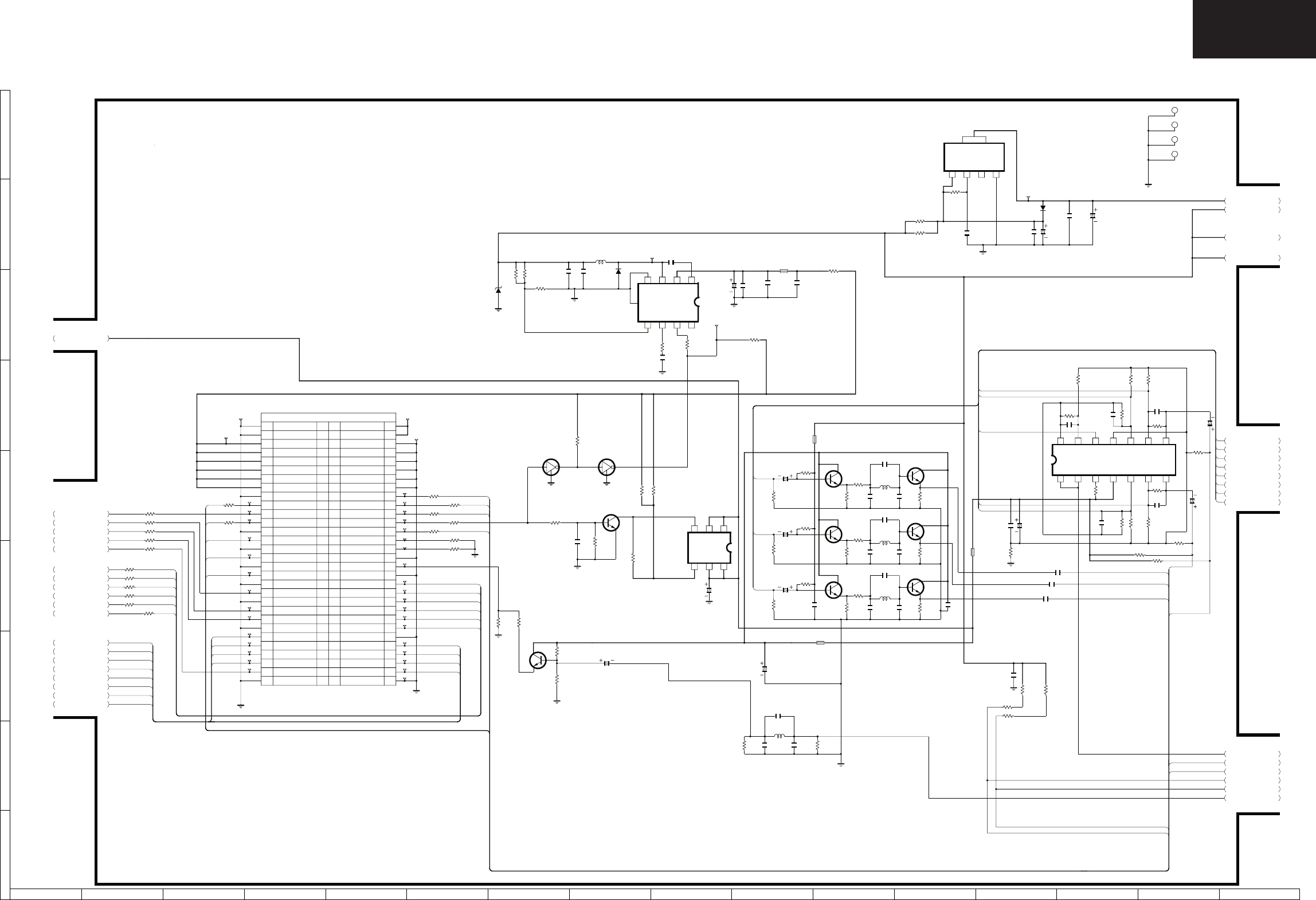
129
LC-32/37GD8E/RU
LC-32/37BT8E/RU
LC-32/37GD8, LC-32/37BT8 Digital Unit Diagram 4/4 (AUDIO / VIDEO OUT / REG)
FED[4]
FED[2]
FED[6]
FED[0]
FED[5]
FED[3]
FED[1]
FED[7]
VBGFIL
VMID
LEFTP
LEFTM
RIGHTP
RIGHTM
ASPECT
RSTIN
CVBS
FED[1]
FED[4]
FED[6]
FED[3]
FED[5]
FED[7]
MUTE
GPIO01
TVSDA
TVSCL
ASPECT
TVSCL
TVSDA
AOUTL
FEERROR1
GPIO00
FERESET1
RSTIN
I2CSCL1
I2CSDA1
GPIO00
FEERROR1
FERESET1 ROUT
GOUT
BOUT
BB
GG
RR
RR
GG
+12V
GPIO01
AOUTR
BOUT
GOUT
ROUT
FED[0]
FED[2] P5V
P1V8
B
AOUTR
AOUTL
P5VAUD
P3V3
P3V3
P3V3
I2CSDA1
I2CSCL1
+5V
P5VVID
GNDAUD
DUNTKD628WE01
R4633
4.7K
R4629
47
R4630
47
R4638
4.7K
TVSCL
TVSDA
R4617
330 F
R4616
47
10u
16V
C4606
ASX
FED[0]
GPIO1
GPIO0
FEOFF
I2CSDA
I2CSCL
FESTROUT
FEVALID
FEERROR
FERESET
FED[6]
FED[7]
FED[5]
FED[4]
FED[3]
FED[2]
FED[1]
TSH73CPT
1 2 3 4 5 6 7
89
1011121314
10u
16V
C4634
ASX
10u
16V
C4635
ASX
R4639
470
R4636
24
R4631
470
R4634
24
R4640
470
R4637
24
R4635
24R4632
47010u
16V
C4623
ASX
R4626
0
ASPECT
RSTIN
P1V8
CVBS
VBGFIL
RIGHTP
RIGHTM
R
LEFTP
LEFTM
G
B
SC4601
WA202WJ
TO MAIN
1
+12V
2
GND
3
+12V
4
GND
5
GND
6
+5V
7
GND
8
+5V
9
GND
10
+5V
11
GND
12
+5V
13
GND
14
+5V
15
GND
16
+5V
17
ASPECT
18
GND
19
SCL
20
RESETn
21
SDA
22
IRQ
23
POWON
24
R
25
L
26
GND
27
V
28
BLUE
29
H
30
GND
31
GND
32
GREEN
33
CVBS
34
GND
35
GND
36
RED
37
FERESETn
38
GND
39
FESCL
40
FEOFF_X4M
41
FESDA
42
GND
43
FEGP0_COMP
44
FESTR_PSYNC
45
FEGP1_LOCK
46
FEVAL_DEN
47
FEERR_UNCOR
48
GND
49
GND
50
FED0
51
FED1
52
FED2
53
FED3
54
FED4
55
FED5
56
FED6
57
FED7
58
FECLK
59
GND
60
GND
MUTE
IRQ
C4711
10u
16V
KZA073WJ
R4702
27K F
D4702
SFPA73
C4701
22u
6.3V
KZA070WJ
C4707
68u
10V
AAPD
R4703
15K F
22uH
L4701
PA214WJ
R4701
470K F C4709
10u
16V
KZA073WJ
R4707
10K
R4713
1
1/2W
C4708
0.1u
C4705
1500P
C4706
0.1u
25V
Z
TL4701
C4702
1u
16V
R4710
100
FB4701
0250TA
Q4701
DTC144EE
TL4702
R4712
10K
Q4702
DTC144EE
R4708
3.3K
Q4703
2SC3928AR
SSM6J51TU
1
D
2
D
3
G
4
S
5
D
6
D
R4706
10K
R4704
5.6K
R4717
100
C4716
1u
10V
TL4703
C4715
47u
6.3V
ASX
C4717
22u
6.3V
ASX
C4713
0.1u
R4716
0
1/2W
*D4703
HSU119
C4714
0.1u
R4715
0
1/2W
TL4603
TL4601
FECLK
R4711
0
1/2W
R4709
0
1/2W
47u
16V
C4710
ASY
P3V3
TL4602 R4657
100
R4658
100
C4607
47P
(CH)
C4608
10P
(CH)
C4610
47P
(CH)
C4611
33P
(CH)
C4612
33P
(CH)
C4613
33P
(CH)
C4617
82P
(CH)
C4618
82P
(CH)
C4619
82P
(CH)
C4614
6P
(CH)
C4615
6P
(CH)
C4616
6P
(CH)
C4621
0.1u
C4626
0.1u
C4627
3300P
C4628
3300P
C4632
3300P
C4633
3300P
C4629
0.1u Z
R4618
330 F
R4619
270 F
R4620
270 F
R4621
270 F
R4622
270 F
R4623
270 F
R4624
270 F
R4627
2.7K F
R4628
2.4K
F
R4646
47 R4647
47
R4648
47
R4649
47
R4650
47
R4645
47
R4601
47
R4602
47
R4604
47
R4603
47
R4605
47
R4607
47
R4608
47
R4606
47
R4643
47
R4609
47
R4644
47
10uH
L4601
D9Mj
FB4601
A215WJ
FB4602
A215WJ
5.6uH
L4603
D9Mj
5.6uH
L4604
D9Mj
5.6uH
L4605
D9Mj
R4659
330
C4636
0.1u
C4637
0.1u
C4638
0.1u
Q4606
2SC3928AR
Q4604
2SC3928AR
Q4602
2SC3928AR
R4662
270 F
R4663
270 F
R4664
270 F
Q4601
2SC3928AR
Q4603
2SC3928AR
Q4605
2SC3928AR
R4666
10K
FB4603
A215WJ
R4668
10K
R4670
10K
C4622
10u
16V
KZA073WJ
C4624
0.1u Z
Q4607
2SC3928AR
R4672
10K
R4673
10K
C4703
0.1u Z
R4705
10K
R4674
0
D4701
EX1234CE
3.6V
MP1583
1
BS
2
IN
3
SW
4
GND
5
FB
6
COMP
7
EN
8
NC
R4675
47
TL4606
TL4605 TL4637
TL4607
TL4608
TL4609
TL4610
TL4611
TL4612
TL4613
TL4614
TL4615
TL4616
TL4617
TL4618
TL4619
TL4620 TL4631
TL4630
TL4629
TL4628
TL4632
TL4627
TL4626
TL4625
TL4624
TL4623
TL4622
TL4621
TL4636
TL4635
TL4634
TL4633
P3V3
P3V3
TL4604
P5V
PQ018ENA
1 2
3
4 5
10u
16V
C4625
ASX
10u
16V
C4639
ASX
10u
16V
C4640
ASX
10u
16V
C4641
ASX
LUG4604
LUG4601
LUG4602
LUG4603
R4665
160 F
R4667
160 F
R4669
160 F
R4660
47K
R4661
47K
R4651
18K
R4652
18K
TO 1/4
TO 1/4
TO 1/4
TO 3/4
TO 1/4
TO 3/4
TO 2/4
Ver.N2 (2006.04.12)
LC-32P70E/LC-26P70E/LC-37P70E
LC-32GD9E/LC-37GD9E
LC-32GD8E/LC-37GD8E
AUDIO/VIDEO OUT / REG
(DIGITAL 4/4)
IC4604
IC4702
IC4701
DC-DC 3.3V
IC4704
2.4 2.4 5.18 5.18 0.5 0.5 2.04
2.040.50.5
01.231.232.63
0
0.03
3.27
0
5.17
0.03
0
0.02
0.64
5.185.180.02
5.18 5.18 5.18
1.68
5.182.34
1.68
5.182.34
1.68
5.182.34
2.34
5.18
3.0
2.34
5.18
3.0
2.34
5.18
3.0
1.79
5.18
2.5
6.94.933.35
0
1.25 1.19 5.17 1.49
3.3 3.3
1.8
0 0
CONFIDENTIAL
Ver.N2 (2006.04.12)
1234567 8 9 10 11 12 13 14 15 16
I
H
G
F
E
D
C
B
A
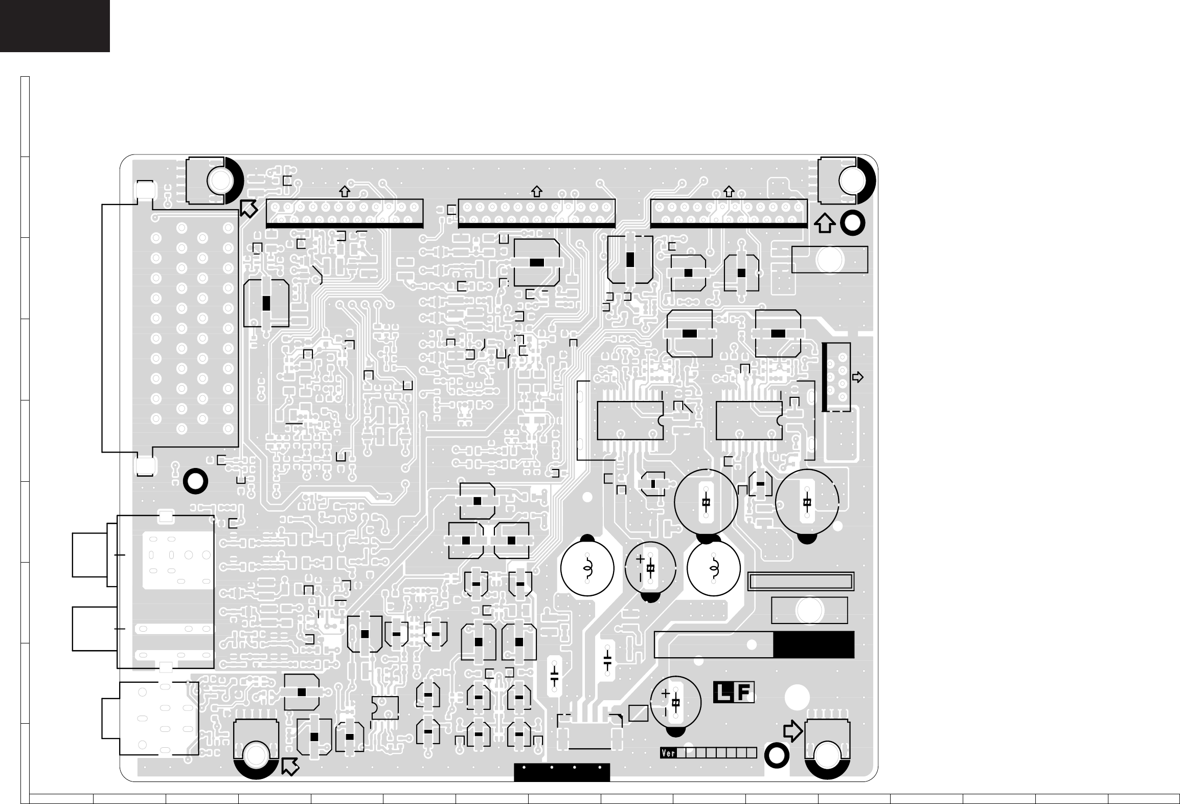
130
LC-32/37GD8E/RU
LC-32/37BT8E/RU
12 3 4 5 67 8 9 10 11 12 13 14 15 16
I
H
G
F
E
D
C
B
A
PRINTED WIRING BOARD
AV Unit PWB (FD604WJN3)
AV Unit, Side A
123
1
23
123
1
7
10
11 20
10
11
20
a
DUNTKD604WE
QPWBFD604WJN3
1
2
20
21
22
23
41
42
SC301
C339
L301
C338
L302
C330
C331
P301
J1301
J1101
P1101 P1102 P1201
IC302
Q304
R343
C329
R336
Q303
IC301
R337
C328
R335
Q1102
Q1101
R1140
R1143
Q1104
Q1103
R1139
C1251
R1123
D1104
C1219
C1214
R345
C346
C347
R306
Q302
R333
C325
C324
R339
R340
D304
D303
C345
R344
C344
R328
D302
C337
R341
C336
R342
D301C307
Q301
R301
R302
R307
C306
C321
C320
IC303
C311
R327
R318
IC1201
R1206
R1209
FL1212
FL1211
R348 C348
C349
Q306
Q305
Q1204 Q1203
Q1202
Q1201
D1108
R1125
R1116
Q1105
D1101
Q1107
R1155
Q1108
R1158
Q1106
R1117
R1114
D1103
D1107
IC1101
C1130
R1111
R1121
FL1104
D1105
FL1105
R1129
FL1101
FL1102
FL1103
R1118
FL1106
R1113
FL1107
FL1108
R1112
D1102
R1127
FL1109
R1152
FL1110
J1201
LUG302
LUG304
LUG301
LUG303
C1162
IC1102
D1106
C357
C356
C343
C342
C359
C358
1
C360
D305
DCBA E F G H
SP
1
1
R355
C364
D308
D306
D307
Q307
D309
D310
D1110 D1109
D1112
D1111
D1113
D1114
D1115
D313
D312 R338
D311
D316
D317
D314
D315
D1201
D1117
D1123
D1122
D1121
D1118
D1119
D1120
D1116
D1125
D1124
D318
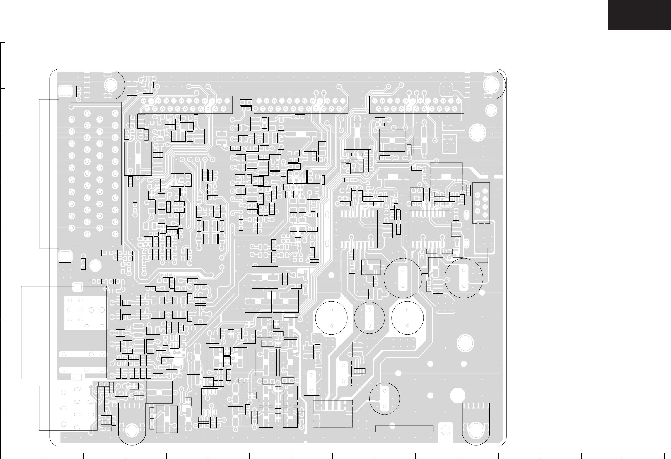
131
LC-32/37GD8E/RU
LC-32/37BT8E/RU
FB1101
D1102
R1119
R1127
P1101
IC1102
D1121
C1105
C1154
R1110
D1117
C1109
R1113
R1124
C1115
C1162
Q1108
Q1106
R1159
R1160
Q1105
C1144
C1145
C1143
R1102
C1114
R1179
C1128
FB1112
R1128
R1116
R1125
C1201R1201R1204
D1125
R1227
R1225
Q1203
R1224
Q1204
C1223
C1222
C1221
C1220
FB1204
FB1203
D1113
R1222
R1218
Q1201
D1115
C1205
FL1211
FL1212
C1207
FB1202
C1215 R1214
R1211
C1218
C1212
R346
R351
Q306
Q305
R348
C355
J1201
J1101
J1301
R349
C350
C354
C349
C348
C311 R322
C319
R318 C318
R321 C316
C360 C306 C307
R325
R328
C321
C320 C336
C344
D303
Q302Q301
Q1202
R306 C347
R332
D305 C361
C346
C325C324
D304
C345
C337
C1214 C1219
C1251 FB1213
FB1218
FB1108
FB1106 R1109
R1107
Q1101
D310
R1147 C1121
R1134
C1117
FL1103
FB1104
C1116
FL1102
FL1101
FL1104
FL1105
R1131
D1105
D1103
R1104
FB1102
C1101
C1151
C1152
R1105
R1101
R1108
D1124 D1109
D1119
C1131
D1107
R1111
C1130
C1108
P1102
IC1101 C1147
Q1104Q1103
Q1102
R1143
R1141
R1142
D315 C328
R335
IC301 R337
D311
R314
R315C314
R309
C310 C365
R312
R324
C304
Q307
D307
D308 D306
C364
P1201
R361
D318
C358 C359
C303
R353
Q304 C309
R308
C315 R317
C366
R313
C357
IC302
C327 C335
C334
D316
D317
R336
R323
C329
C326
C363
C341
P301
C343
C342
R339
R345
C331
VER1
LUG303
L301C330L302
C338 C339
R343
R338
SC301
C356
R355
R1203
R1228
D1201
C1216
R1213
IC303
Q1107
R354
R304
C313
R316
D313
C305
D312
R334
C312
R329
C333
C332
C323
R331
R330
D314 C322 R303
C308
Q303
R305
R356
R358
R357
R359
R360
R340
C340 C362
C1252
R1133
C1126
R1145
R1139
C1125
R1132
C1122C1123
C1132
C1133
D302
R341 R342 R344
D301
R326
R333
C302
R301
C301
R302R307
R311
R310
R319
R327
R320
C317
C1253R1202
IC1201
C1206
C1203
C1202 D1114
R1217 R1221
C1208
R1209 R1206
C1204
C1209
R1215
C1217C1211
R1212
R1210
C1210
FB1201
C1213
C353
R350
C352
C351
R352 R347
R1216
C1224
R1220 R1223
C1225
R1219
C1227C1226
R1226
R1137
D1101
FB1103
R1103
FB1111 R1177
C1127
C1139
FB1109
C1140
FB1110
D1108
R1161
R1148
R1157
R1151
R1146
R1149
R1153
C1134
C1142
R1152 C1146
FL1109
FL1110 R1120
R1115
C1157
R1138
R1130
R1155
C1158 D1112
R1158
D1111
R1156
D1122
C1106
C1155
C1156
C1107
D1123
C1135
R1154
C1138
FB1107FB1105C1118
C1119
R1150
C1124
R1173
C1120 R1106
R1123 D1104 R1114
R1117
C1103C1153
D1120
C1136
C1137
R1144
R1140
D1110
C1102
D309
R1112 FL1107
C1160
C1161
D1106
C1159
R1118
FL1106
C1111
C1104
R1129
R1122
C1113
C1112
R1121
C1110
D1116D1118
C1148
FL1108
R1126
AV Unit PWB (FD604WJN3)
AV Unit, Side A Chip Parts
12 3 4 5 67 8 9 10 11 12 13 14 15 16
I
H
G
F
E
D
C
B
A
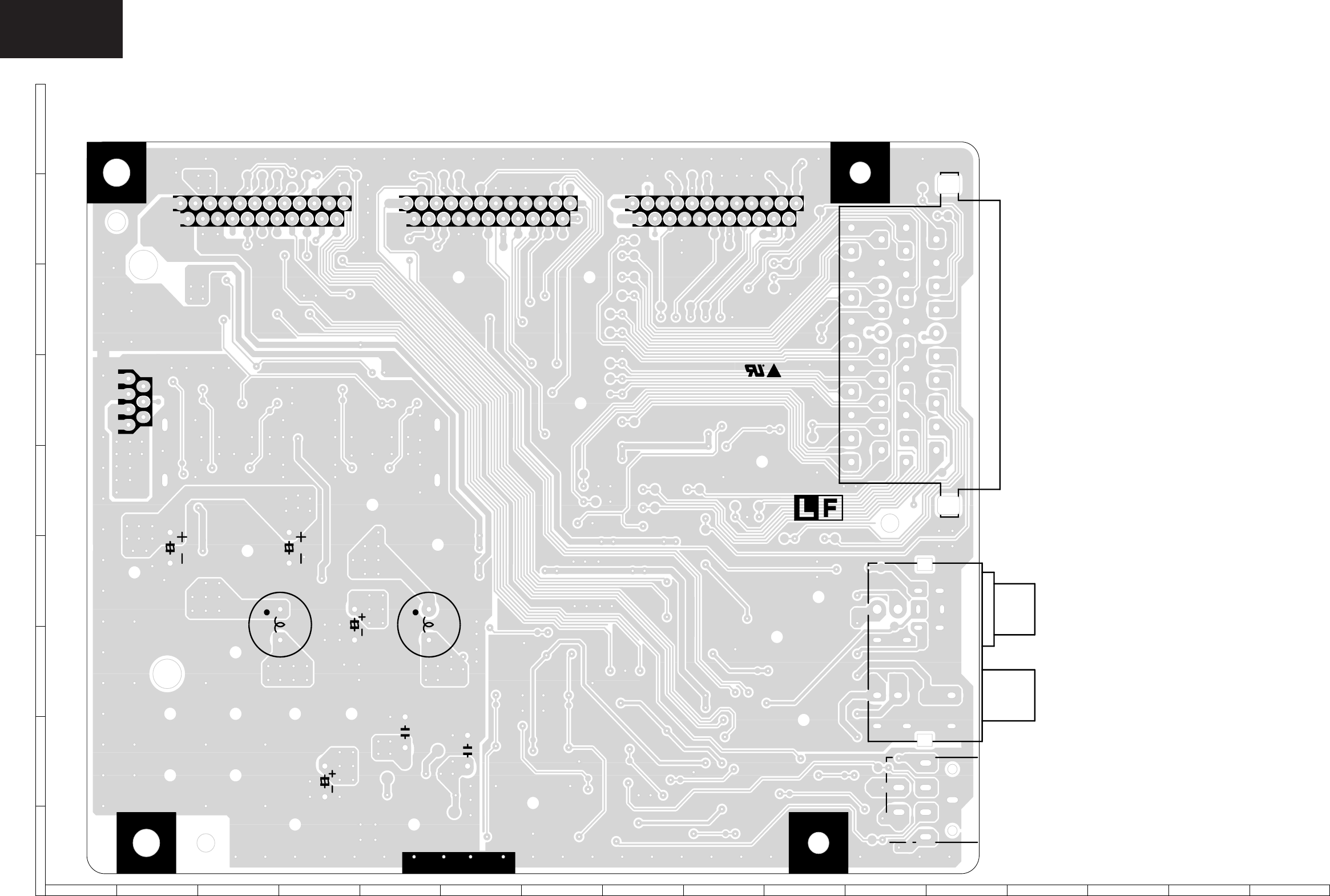
132
LC-32/37GD8E/RU
LC-32/37BT8E/RU
1
2
22
23
1
2
22
23
1
2
22
23
1
6
7
a
1
2 20
21
22
23
41
42
C339
L301
C338
L302
SC301
C331
C330
J1301
J1101
P1101
P1102
P1201
J1201
C343
C342
12 3 4 5 67 8 9 10 11 12 13 14 15 16
I
H
G
F
E
D
C
B
A
AV Unit PWB (FD604WJN3)
AV Unit, Side B
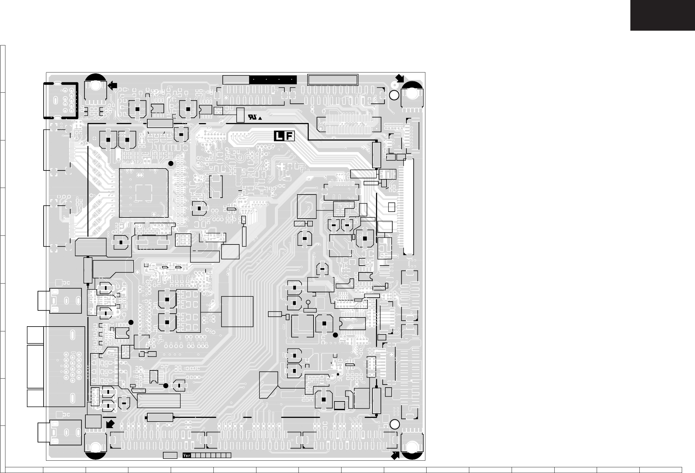
133
LC-32/37GD8E/RU
LC-32/37BT8E/RU
1234567 8 9 10 11 12 13 14 15 16
I
H
G
F
E
D
C
B
A
MAIN Unit PWB (XD890WJN2)
MAIN Unit, Side A
RJ1705
RJ1708
C1703
C1706
C1707
Q1703
C1708
C1901
C1902
C1903
C1904
C1715
C1716
C1718
Q1909
C1910
C1911
C1720
Q1910
C1721
C1722
C1723
C1724
D1702
D1703
D1704
1 7
P2301
D1706
1
3
P2302
D1707
1
10
P2303
1 20
P2304
132
P2305
P2306
C1922
C1923
D1901
D1902
C1733
IC1704
D1904
D1710 C1735
C1929
R1901
1
4
5
IC1706
R1902
D1713
R1903
D1908
C1739
RJ2301
D1909
RJ2302
R1906
R1713
RJ2303
R1714
R1909
IC1901
IC1902
C1740
C1934
D1910
C1741
1
36
37
72
73 108
109
144
IC1905
1
2
59
60
P2702
C1748
R1720
C1749
R1724
C2306
C1942
C2307
C1943
C1750
C2308
R1728
C1751
C2309
RJ2702
C1753
RJ2703
RJ2704
R1920
C1755
RJ2705
R1921
C1756
R1922 R1923
C2310
R1924
C2311
RJ2709
R1925
C2312
a
R1732
R1926
R1927
R1734
R1928
R1735
R1929
C2316
C1953
R1738
C1954
R1739
C1761
RJ2712
C2702
C1762
RJ2713
C2703
RJ2714
C2704
C2705
Q2701
R1932
C2706
Q2702
RJ2717
R1933
C2707
R1740
C2708
Q2704
RJ2719
R1935
C2709
Q2705
C1961
C2711
R1749
RJ2721
D2305
RJ2722
RJ2723
C2714
R2305
RJ2725
D2309
RJ2726
RJ2727
R2307
RJ2728
RJ2729
C2719
R2309
R1752
14
58
IC2303
D2310
D2311
D2312
RJ2730
C2720
R1759
RJ2731
R2311
RJ2732
C1976 C1977
RJ2734
R2315
RJ2735
D2701
RJ2736
C2727
RJ2737
C2728
D2705
R2703
R2704
R2705
R2706
R2707
C2731
R2709
R2321
IC2701
C2732
13
46
IC2705
R1770
R2711
R2713
R2715
FL1901
X3001
FL1902
R2717
R2718
R2719
R2333
R2335
R2720
R2721
R2339
C3302
R2724
C3306
R2341
FB3002
FB3003
FB3004
FB3005
FB3006
FB3009
FB3010
FB3012
D3301
FB3015
C3325
FB3016
C3327
C3328
FB3019
C3329
R3305
R3306
R3307
R3308
C3330
FL2301
C3331
FL2302
C3332
FL2303
C3333
13
IC3303
1
IC3304
C3334
C3335
C3336
C3338
R3313
R3314
R3315
R3316
R3317
R3318
C3340
R3319
C3342
R3320
X1901
FB1701
LUG1701
LUG1702
LUG1703
LUG1704
LUG1705
LUG1706
LUG1707
LUG1708
LUG1709
FB1902
FB1906
1
222
23
SC1701
1
2 8
9
SC1702
DCBA E F G H
119
SC1901
119
SC1902
L1701
L1702
L1901
L1902
L1903
L1904
L1905
L1906
L1907
L1908
J2701
J2702
FB2301
FB2302
FB2303
FB2304
SC2301
SC2303
RJ3001
FB2705
RJ3002
FB2706
RJ3003
FB2707
RJ3004
FB2708
FB2709
FB2710
FB2715
C3002
RJ3013
RJ3014
C3004
C3005
RJ3016
1
222
23
SC2702
C3006
1
222
23
SC2703
C3007
RJ3018
1
222
23
SC2704
C3008
1
2
14
15
SC2705
C3009
1
2
22
23
SC2707
RJ3020
C3010
RJ3022
C3012
RJ3023
RJ3024
RJ3025
C3016
C3019
RJ3030
C3020
RJ3031
C3021
RJ3032
RJ3033
RJ3034
RJ3035
RJ3036
RJ3039
R3002
C3030
R3009
RJ3041
114
1528
IC3003
3
4 5
IC3004
C3035
FB3301
C3036
FB3302
FB3303
FB3304
R3011
FB3305
FB3306
FB3307
R3013
FB3308
C3040
TH3001
C3041
C3042
C3043
C3044
1
8
P1701
C3048
RJ1701
14
5
88
5
4
1
1
8
9
16
1
3
XD890WJN2
KD890
CPU
+5V
+3.3V
P+35V
BU+12V
+1.8V
BU3.3V
BU1.8V
S+8V
LCD+5V
BU+5V
RESET-TP
LB
LV
SH
KM
RA
4
6
ANT+5V
3
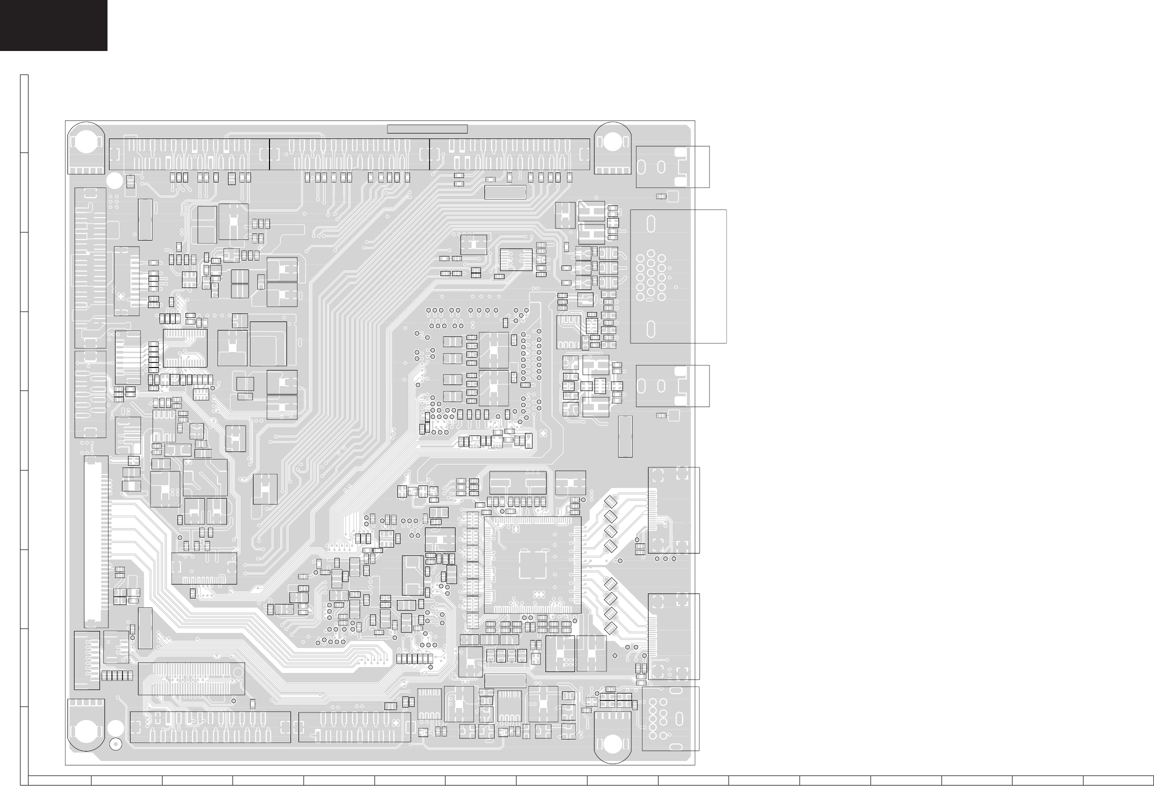
134
LC-32/37GD8E/RU
LC-32/37BT8E/RU
12 3 4 5 67 8 9 10 11 12 13 14 15 16
I
H
G
F
E
D
C
B
A
MAIN Unit PWB (XD890WJN2)
MAIN Unit, Side A Chip Parts
R3002
RJ3024
RJ3025
RJ3023
RJ3013
RJ3014
RJ3016
TH3001
C1903
R1906
R1909
C1904
D1904
FL1902
FB1906
FL1901
FB1903
C1952
C1951
C1939
C1941
R1902
R1904
R1927R1925R1924R1923R1922R1921R1920
C3040
C3037
FB3015
FB3018
R3017
C3034 C3039
C3038 C3033
C3023
C3027
FB3009FB3004
C3014
R3006
R3309
R3310
R3311
C3016
C3020
C3021 C3043
C3030
C1942
C1943
C1934
R1933
R1932
C1929
R1929
C1923
C1922
C3009
RJ3004
C3029
FB3010
C3015
Q2701
R2703
R2704
R3013
C3325R3305
R3316
R3318
C3342
R3314
C3310
C3312
C3314
C3319
C3307
R3315
R3317
D3301
D2313
R2333
C2308C2310C2309
RJ2302
RJ2714
RJ2737
RJ2712
RJ2713
RJ2709
RJ2724 C3306
FB3306 FB3305
RJ2702
RJ2736
RJ2705
RJ2704
RJ2703
RJ2722
RJ2721
RJ2717
RJ2730
RJ2729
RJ3022
R1734
R1735
R1732 C1707
R1724 R1713
C1703
D1706
R1720
RJ2726
RJ2725
RJ1701
C2732
RJ2732
RJ2731
RJ2735
RJ2734
RJ3041
RJ2711
C2728
C2729
R2718
C2711
C2727 C1762 C1761
D1710
R2717
RJ3045
RJ3044
RJ3043
R3001
R3003
FB2715
LUG1708
D1713
R2337
RJ3047
R3009
R3011
FB3016
C3042
RJ3033
RJ3034
RJ3035
RJ3036
C1710
R1733
R1737 IC1706
P2306
R1723
P2305
R1770
C1740
R1714
C1739
C1753
C1741
C2316 R1738
C1751
R1749
C1750
C1749
C1748
RJ1708
FB3006
FB3003
LUG1706
D1908IC2303
R2301
D1902 D1910
FB2302
R2307
D2301
D2303D2304
D2302
FB2301
RJ3020
RJ3019
SC2301
FB1902
C1902 IC1902
LUG1705
D1903
FB1901
D1907
D1901
Q1910 D1909
C1901 IC1901
Q1909
C2731
SC2705
C3044
C1911
C1910C1909C1935
C1924
C1925C1926
C1927C1932
C1937
R1934
C1944
C1945
C1946
C1948
C1947C1957
C1955
C1977C1976
C3028
C3041 FB3013
FB3014
C3019
C3036
C3013
C3026
C3011
FB3005 C3010
C3007 C3012
FB3002
C3002
C3008
C3003 C3005
C3004
C3006
X3001
C3032
C3049
C3048 IC3004
R3016 R3312
FB3012
C3035
R1928 R1926
RJ3018
R3306
R3307
R3308 RJ3002
RJ3003
R2724
RJ3001 Q2702
R1935
C1954
C1953
C1961 X1901
R3319
R3313 R3320
IC3303 IC3304
FB2706
FB2708
C2703
R2707
FB2707
C2705
C2709
R2709 R2711
D2701
Q2705
R2713
D2705
Q2704
C2707
D2308
FB2306
D2307
FB2307
D2306
FB2308
FB2305
D2305
FL2301
FL2303
FL2302
SC2303
C2702
FB2710
R2706
FB2709
C2704 C2708
C2706
D2311
D2312
D2310
D2309
R2326
C2307
R2335
FB3307
RJ2301
RJ2303
R2332
R2329
R2701
RJ2305
Q2707
C2701
FB2704
IC2701
R2705
C2720
LUG1707
C2714
R2719
R2721 R2715
C2719 RJ2719
R2720
FB2705
J2702
SC2702
RJ2723 RJ2728
RJ2727
C3302
C3327
FB3301
FB3302
C3328
C3330
FB3304
FB3303
C3329 C3333
C3334
C3332
C3331
R1901
R1903
L1904
L1903
L1902
L1901
L1908
L1907
L1906
L1905
P1
SC2707
P2702
P2302
LUG1709
C2312
C2311 FB2304
FB2303
R2309
R2311
R2321
P2304
C1720
C1756 C1755
L1701
C1721 C1724
FB1701
R2315
C1723
C1722
C1718
D1704
C1706
C1708
D1702
C2306
D1703
R1759
C1716
C3340
C1714
C1717
R1721
R1719
R2305 RJ1705
RJ1703 R1704
R1705
R1752
SC1702
P1701
R2334
RJ3046
RJ3029
R2313
RJ3026
RJ3027
RJ3028
P2301
RJ3038
R2341
FB3019
R3018
RJ3030
RJ3039
R2339
RJ3031
RJ3032
R1739
D1707
L1702 C1735
C1733
C3338
R1740 R1728
IC1704
FB3308
Q1703
IC2705
C1715
P2303
IC3003
RJ3042
SC1701
SC2703 SC2704
J2701
SC1901
SC1902
C3335
C3336
IC1905
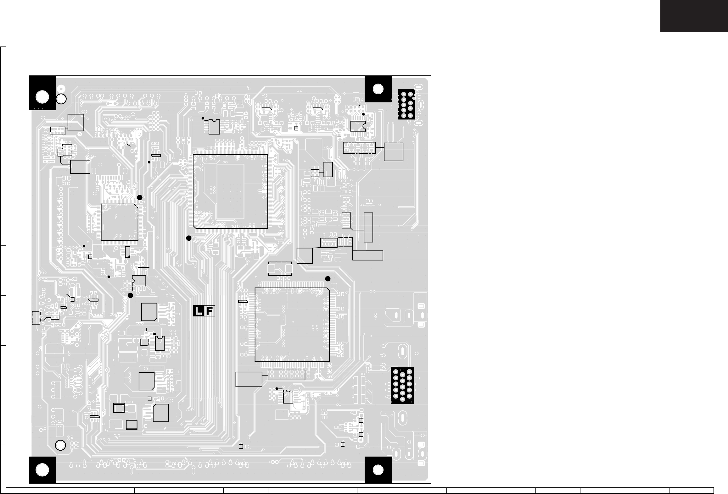
135
LC-32/37GD8E/RU
LC-32/37BT8E/RU
1234567 8 9 10 11 12 13 14 15 16
I
H
G
F
E
D
C
B
A
MAIN Unit PWB (XD890WJN2)
MAIN Unit, Side B
RJ1704
RJ1706
RJ1707
C1701
C1702
C1704
Q1701 C1705
Q1702
Q1704
Q1705
C1709
C1711
Q1901
C1712
Q1902
C1713
C1907
Q1903
C1908
Q1904
Q1905
Q1906
Q1907
Q1908
C1719
C1912
C1913
C1914
C1915
C1916
C1917
C1918
C1725
D1701
C1919
C1726
C1727
C1728
C1729
D1705
R1702
R1703
D1708
C1920
C1921
R1707
C1730
R1708
R1709
C1731
1 3
4
5
IC1701
C1732
1 5
IC1702
5
1
IC1703
C1734
C1928
IC1705
D1905
C1737
1 5
IC1707
C1738
1
4
8
IC1708
R1710
D1714
IC1709
R1711
D1715
R1712
RJ2304
C1930
R1715
C1931
R1716
RJ2306
R1717
RJ2307
C1933
13
45
IC1903
R1718
RJ2308
13
4 5
IC1904
1
25
26
50
51 75
76
100
IC1710
1
3
4
6
IC1711
RJ2309
C1742
C1936
C1743
C1744
C1938
C1745
R1911
C1746
R1912
C1747
R1913
RJ2310
R1914
RJ2311
R1915
C2301
R1722
R1916
C2302
C2303
C1940
R1918
C2304
R1725
R1919
C2305
Q2301
R1726
R1727
R1729
RJ2701
C1752
C1754
C1949
RJ2706
RJ2707
C1757
R1730
RJ2708
C1758
R1731
C2313
a
C2314
C1950
C2315
R1736
C2317
RJ2710
C2318
C1956
C1958
R1930
RJ2715
C1959
R1931
RJ2716
Q2703
RJ2718
R1741
R1936
R1742
Q2706
R1937
R1743
R1744
C1960
Q2708
R1745
Q2709
R1746
C1962
R1747
C1963
C2710
R1748
RJ2720
C1964
C1965
R2302
C2712
C1966
C1967
Q2710
C1968
C1969
C2715
R1750
C2718
R1751
18
916
IC2301
IC2302
R1753
R1754
13
5
IC2304
C1970
R1755
C1971
C1972
R1757
C1973
R1758
C1974
R2310
C1975
C2721
C2722
R2312
RJ2733
C2723
C1978
C2724
R2314
C1979
C2725
C2726
D2702
D2703
R1760
RJ2738
D2704
RJ2739
R1762
R2702
D2706
R1763
R1764
R1765
R1766
R1767
C2730
R1768
R2708
R1769
13
4 6
IC2702
R2322
R2323
R2324
IC2704
R2325
R2327
R2328
R2710
R1771
R2712
R1773
R1774
R2714
R2716
FL1903
R2330
FL1904
R2331
FL1905
R2336
C3301
R2722
R2723
C3303
C3304
C3305
C3308
C3309
R2342
R2343
R2344
FB3001
C3311
C3313
C3315
C3316
FB3007
C3317
FB3008
C3318
C3320
FB3011
C3321
C3322
C3323
C3324
C3326
FB3017
R3301
R3302
R3303
R3304
136
37
72
73 108
109
144
IC3301
3
45
IC3302
C3337
C3339
C3341
FB1702
FB1904
FB1905
FB1907
FB1908
FB1909
J2701
J2702
FB2309
FB2310
FB2701
SC2301
FB2702
1 5
6 10
11 15
SC2303
FB2703
RJ3009
FB2711
FB2712
FB2713
FB2714
RJ3010
RJ3012
RJ3015
Q3003
Q3004
RJ3021
L2701
C3017
C3018
X3301
C3022
C3024
C3025
R3004
R3005
R3007
RJ3040
R3008
C3031
IC3001
1 52
53
104
105
156
157
208
IC3002
13
45
IC3005
R3010
R3012
R3014
TH3002
C3045
P1702
C3046
C3047
RJ1702
1
45
8
85
4
1
1
89
16
10
1
1
6
3
4
6 1
3
4
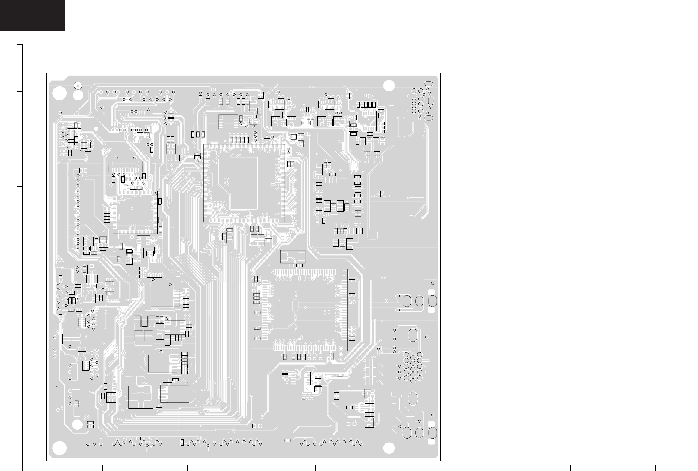
136
LC-32/37GD8E/RU
LC-32/37BT8E/RU
12 3 4 5 67 8 9 10 11 12 13 14 15 16
I
H
G
F
E
D
C
B
A
MAIN Unit PWB (XD890WJN2)
MAIN Unit, Side B Chip Parts
FB2309
C1908
Q1906Q1908
R1905
D1906
R1918 R2316
RJ2306
Q2301
C2301
R2310
R2314
IC2301
R1912
Q1904
IC1904R1916 R1915
Q1905Q1907
D1905
Q1901
R3015 Q3004
Q3003
R3008
C1963
C1962 C1960
C1959
C1975
C1974
C1969
C1968
C1956
C1958C1949
C1950
R1936
C1913
C1912
R1919
C1914
C1915
C1916
C1917 C1931
C1930
R1931
C3304
C3303
C3301
R3302
R3304
R3303
C3305
R2322
R2325
R2324
Q2703
D2704
R2710
D2703
C2721
D2706
R2716
Q2708
C2723
IC2704
C2722
C2718
RJ2720
RJ2304
C3315C3318
FB3011
FB3017
FB3008
C3018
R3014
C1907
C2730
FB3001
R3004IC3001
R3007
FB2701
R3012
RJ3015
RJ2706
RJ2707
RJ2708
C3046
RJ2308
RJ2738
C3341
C3324
IC3302
C3321
C3326
C3323
C3322
D2702
RJ2718
R2708
Q2706
R2712
C1712
D1705 C1719
IC1703
R1745
C1727
C1725
R1746
C1731
R1747
R1748
R1760
D1714 D1715IC2702
IC1707
R1755
R1743
C1732
C1709
R1725
C1705
R1761
C1713
R1726
R1729
RJ3021
R3010
FB2310
R2328
R2330
C2317
R1712
R1769
IC1710
C1743C1757
P1702
RJ1706
IC3005
R1751
R1718
R1715
R1730
R1731
R1736
RJ3012
RJ2307
R2343
C2313
C2314
R1763
C1744
C1745
R1764
C1754
IC1705
Q1704
C1704
R1722 R1716
C1759
IC1711
R2327
Q1705
IC1709
Q1702
R1703
D1701 IC1701
Q1701
IC2304
R2336
R1766
R2303
R1707 R1701
RJ3040
R2722
R2312
C2302
C2303
C2304
C2305
RJ2311
RJ2310
Q1902
C1905
R1910
C1978
FL1905
FB1909
FL1904
FB1908
R1930
C1928
C1918
RJ3009
RJ3010
R1908
R1907
R1917
R1913
IC1903
C1906R1911
Q1903
R1914
R2702
TH3002
L2701
RJ3017
C1972
C1973
C1970
C1971
C1966
C1967C1964
C1965
FB1904
C1921
FB1905
C1919
C1979
R1937
C1933
C1936
C1938
C1940
FB1907
C1920
FL1903
X3301
IC3301
IC1702
IC2302
IC3002
FB2714
C2712 R2714
C2710 RJ2715
R2331
R1758
R1757
R2302
R1765
R1742
R1741
D1708
C1726
C1728
R1754
R1744
R1753
C1729
C1730
C1734
C1736
C1737
FB1702
C1738
IC1708
R1708
R2344
R1773
R1702
C1701
R1706 R1709
C1702
R1727
D1709
C2318
R1711 FB2713
R1756
R1772
R2323
C1711
R1771 RJ1702 C1742 C1758
R1762
R1767
R1768
C1752
R1750
R1774
C2315 R1775
R2342
RJ1704
R1717
C1746
C1747
RJ1707
Q2709
Q2710
RJ2739
C3045
C3047
RJ2733
RJ2716
RJ2309
L2301
L2302
L2303
L2304
L2305 R3005
C3001
C2726
C2725
FB2702
FB2703
RJ2701
R2723
FB2712
C3031
C3022 C3024
C3025
C3017
FB3007
R3301
C3308
C3309
C3311
C3313
C3316
C3317
C3320
FB2711
C2724
C2715
RJ2710
C3339
C3337
R1710
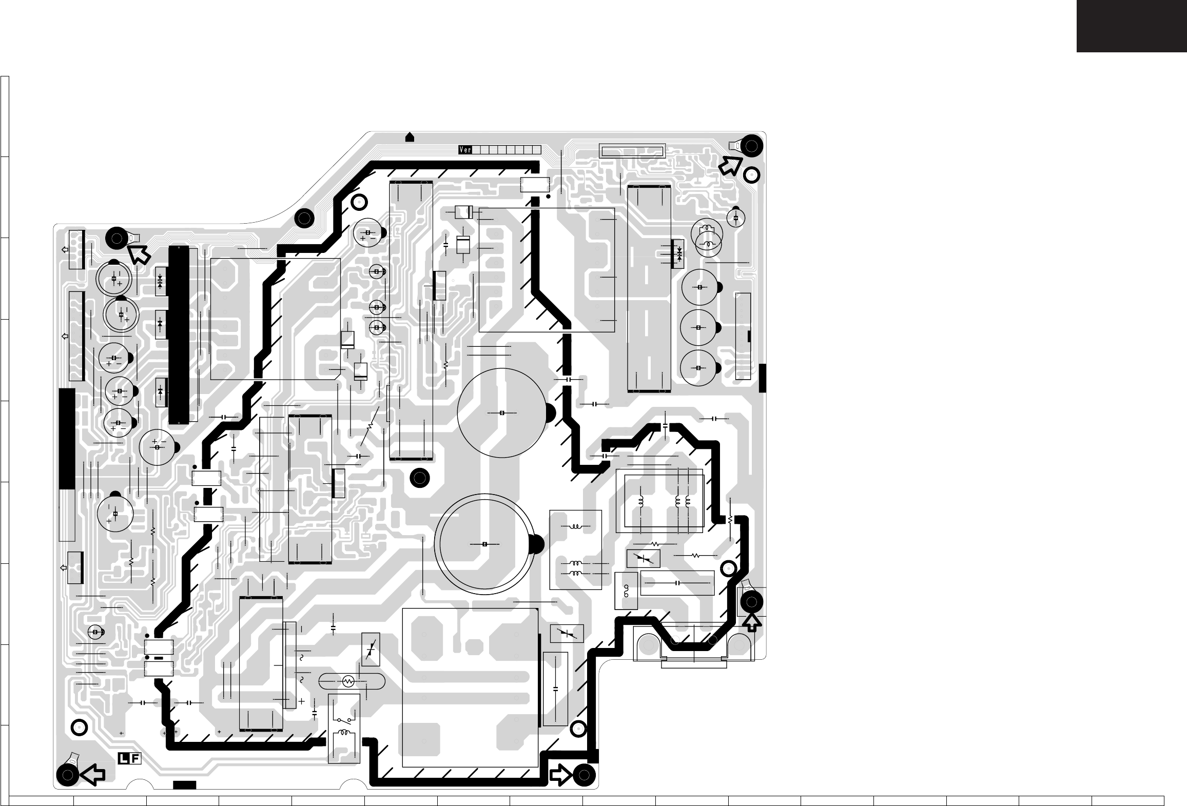
137
LC-32/37GD8E/RU
LC-32/37BT8E/RU
12 3 4 5 67 8 9 10 11 12 13 14 15 16
I
H
G
F
E
D
C
B
A
POWER SUPPLY Unit PWB (FD605WJN5)
POWER SUPPLY Unit, Side A
1
9
19
1 7
1
9
123
1
2
3
4
1
23
4
1
23
4
1
23
4
1
2
3
4
13
1
2
3
P701
P703
P704
203
204
401
405
408
409
410
415
416
417
801
L702
R701
R702
R704
SC701
C704
C708
C712
R751
C723
R760
302
114
C735
116
C736
C740
RY701
C742
C743
C744
C751
C754
C755
C756
C757
C758
C761
D701
C762
C767
IC704
IC705
D729
D730
D731
D732
D733
D734
D735
D736
D737
D739
T4AL 250V
QPWBSD605WJN5
103
106
108
a
1
14
115
420
C768 C752
LUG701
LUG703
LUG704
LUG702
421
404
903
708
704
706
701
702
703
C709
DUNTKD605WE
716
107
109
117
202
305
307
308
402
412
414
418
902
719
721
D762
313
419
312
709
411
725
802
309
720
723
724
112
206
207
805
317
306
315
102
413
316
727
205
111
210
729
728
733
732
731
739
740
C778
C777
C779
C780
18
9
16
1
7
9
16
T701
T702
D728
C782
726
118
745
F701
2
1
(L) (N)
734
738
422
423
211
TH701
SEC. PRI.
VA701
VA702
VA703
705
707
D771
E701
LA
PRI. SEC.
1
6
712
RDA701
RDA702
RDA703
T703
712
C705
C706
R853
R854
R855
RDA705
RDA704
C707
L701
804
P702
323
120
212
324
2
119
735
113
C741
C781
746
747
213
904
C734
C725
L752
L753
741
742
743
749
744
748
711
750
n4-02/22
A B C D E F G H
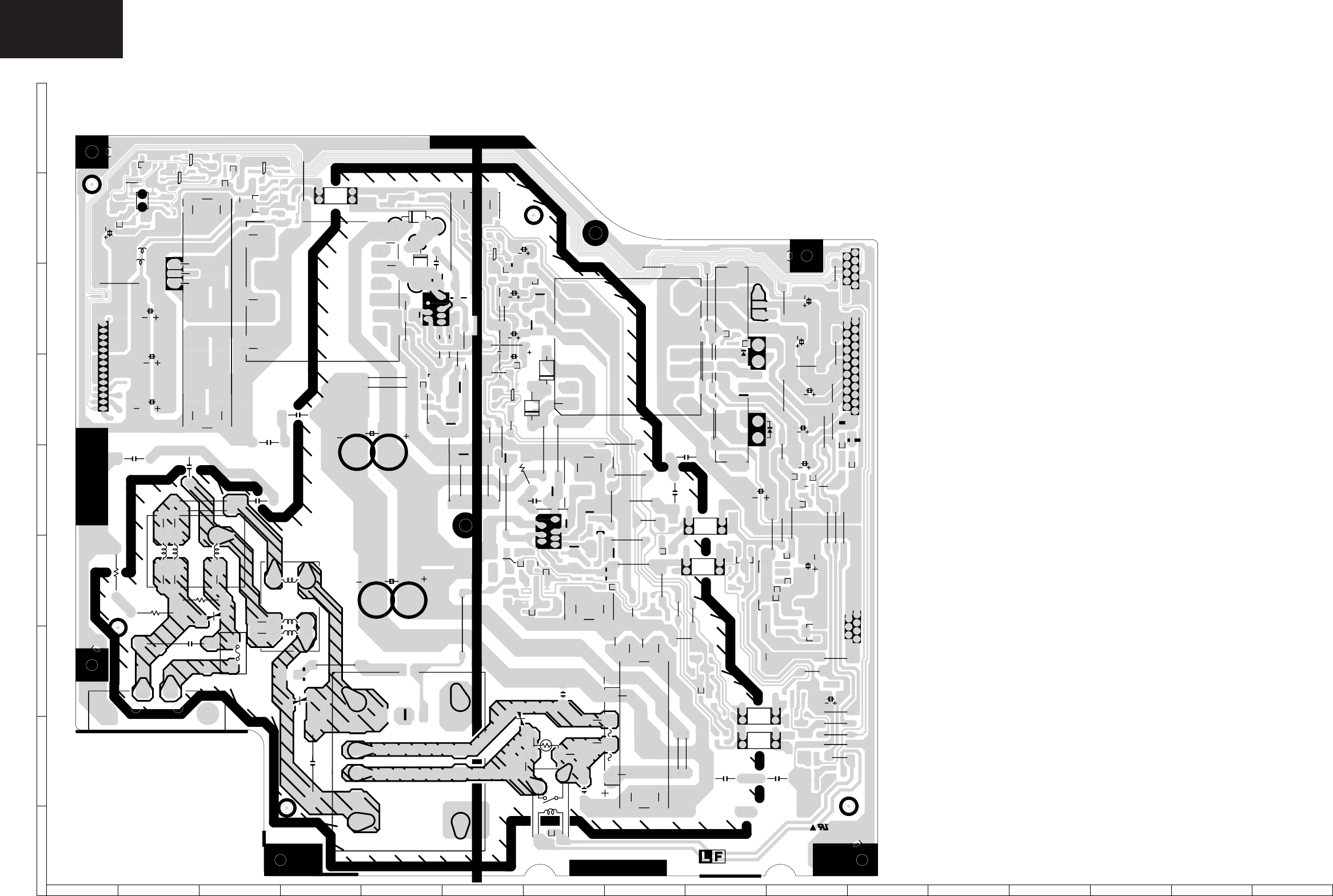
138
LC-32/37GD8E/RU
LC-32/37BT8E/RU
1234567 8 9 10 11 12 13 14 15 16
I
H
G
F
E
D
C
B
A
POWER SUPPLY Unit PWB (FD605WJN5)
POWER SUPPLY Unit, Side B
19
1
2
8
91
2
6
7
1
9
1
2
22
23
12
3
4
12
34
1 2
3
4
12
3
4
1
2
3
4
1
2
3
123
P701
P702 P703
P704
203
204
401
405
408
409
410
415
416
417
801
L702
R701
R702
R704
SC701
C704
C708
C709
R751
C723
R760
302
114
115
C735
116
C736
C740
RY701
C742
C743
C744
C751
C754
C755
C756
C757
C758
C761
D701
C762
C767
IC704
IC705
D729
D730
D731
D732
D733
D734
D735
D736
D737
D739
D751
D752
D753 D754
D755
D756
D757
R801
R805
R809
R812
R813
R814
R817
R820
R823
R824
R825
Q702
Q704
Q708
Q710
Q712
Q713
Q721
R727
R740
R741
R742
R745
R746
R747
R748
R752
C716
R753
R755
R756
R757
R758
R759
C720
C722
R761
C726
R764
C728
R765
R766
R767
C730
C732
C733
R770
R773
R774
C739
R775
R776
R777
R778
R779
R780
C745
R781
R782 R783
R784 C749
R785
R787
R788
R789
C753
R791
R792
R793
R794
R795
R796
C763
C764
D707
D714
D715
D717
D718
D721
D722
D724
D725
D726
IC706
IC707
D738
D741
D742
D746
D747
D748 D749
103
106
a
420
T4AL 250V
PRI.
SEC.
SEC.
PRI.
D759
C768
C769
C770
C747
C752
C748
C746
421
404
903
D716
D720
704
706
701
702
703
708
C712
107
109
117
305
307
308
402
412
414
902
D761
D763
D764
D765
R828
R829
R830
R832
R833
R834
R835
Q723
Q724
Q726
R728
R730
R731
R732
C771
C772
IC708
716
418
720
D762
312
419
725
309
108
802 202
723
724
721
719
313
709
C765
112
206
207
805
C776
C775
C774
111
317
D767
315
102
411
316
727
733
732
731
729
728
739
740
PRI.
SEC.
C779 C780
C777
C778
726
16
9
81
16 9
7
1
306
T701
T702
D728
C781
C782
118
745
205
413
F701
(L)
(N) 1
2
210
734
738
422
423
211
TH701
VA701
VA702
VA703
705
707
D771
C783
IC709
E701
114 24681012
LUG702
LUG704
LUG701
1
6
7
12
RDA703
RDA701
RDA702
T703
712
C706
14
5
8
D772
R851
R852
R853
R854
R855
R836
RDA705
RDA704
C707
L701
R856
R857
C789
C790
R729
119
D773
D774
D775
R859
R860
R861
C717
C792
735
804
R862
R863
R864
R865
R866
R867
R868
R869
R870
R871
R872
R873
Q730
Q731
C793
C794
C795
C796
C797
C798
C799
13
45
D776
C800
C801
C802
C803 R875
R876
IC710
323
113
120
212
324
R874
RJ2
RJ3
RJ1
C741
746
747
LA
D777
D778
D779
R877
R878
904
213
C784
R831
R743
C725
C734
R858
C804
Q729
L752
L753
1
4
5
8
D782
D783
D784
D785
D781
D780
741
742
743
744
748
749
C713
R797
711
750
D787
D786
C705
RJ4
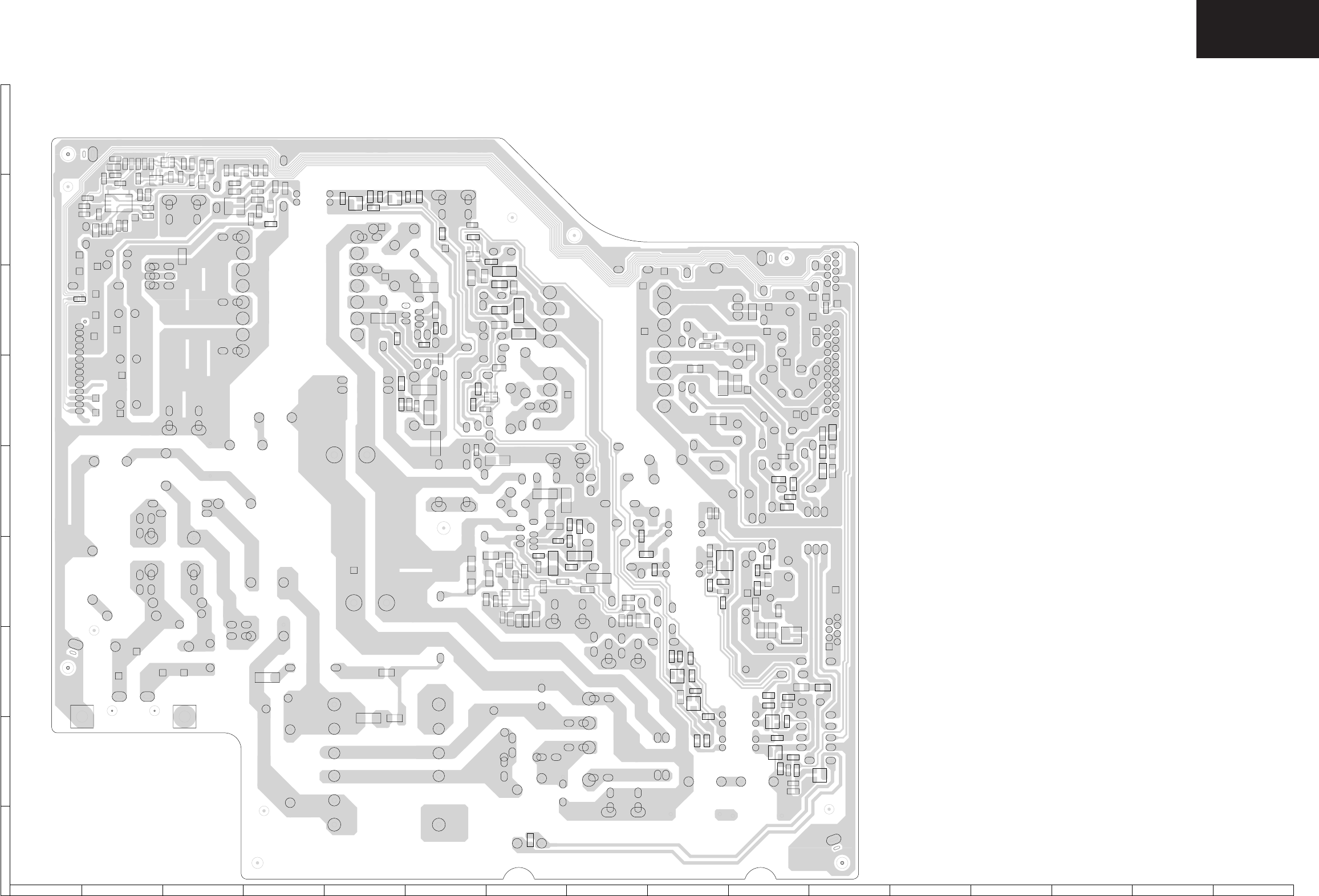
139
LC-32/37GD8E/RU
LC-32/37BT8E/RU
1234567 8 9 10 11 12 13 14 15 16
I
H
G
F
E
D
C
B
A
POWER SUPPLY Unit PWB (FD605WJN5)
POWER SUPPLY Unit, Side B Chip Parts
RJ1
C747 C748
D738
C746
D757
R820 D756
R828
C769
C713
R759
Q724
R764
D724
R767
R770
R857
D726
D716
Q702
R727
C722
D783
D725
D721
D774
R835
R741
R740
C716
C720
R742
D787 C733
R745
R756
Q704
R780
R778
RJ3
R795
IC710
R875
R794
IC707
Q731
Q730
R868
D775
R867
R870
IC709
C793
C794
C797
R776
R784
C802
R876
C803
D747
C753
R787
C749
D746R809
R862
R863
R874
R861
R860
C801
RJ2
C795
C796
C804
C800
R869
R871
R858
R866
R865
C798
C799
R873
D776
C770
R872
R864
RJ4
D773
Q723
D781
R748
R746
D761
C790
D714
C771
R856
R747
C717
D755
R743
R812
D752
R824
D753
D748
D754
D749
R817
D751
C792
R859
R765
D718
D784 R753
C789
R752
D720
D786
D782
C726
D785
R728 R729
R730
D764
R732
R831
D779
C739
C783
D717
C775
R832
C774
D763
C776
R797
R833
R834
C772
R775
D722
D715
R755
R830
D765
D780
R731 C728
IC708
R836
R829
Q726
R777
C745
Q729
R783R781R782
R801 D741 D772
D759
D742
R805
R851
R852
R789
R791
R823
C764
R779
R757
R773
D767
R766
R761
C730
R758
R814 R813
R785
C763
R788
R792
Q713
R796
Q712
R793
Q721
R774
Q710
C732
Q708
R878
R877D777
D778
D707
C765
R825
IC706
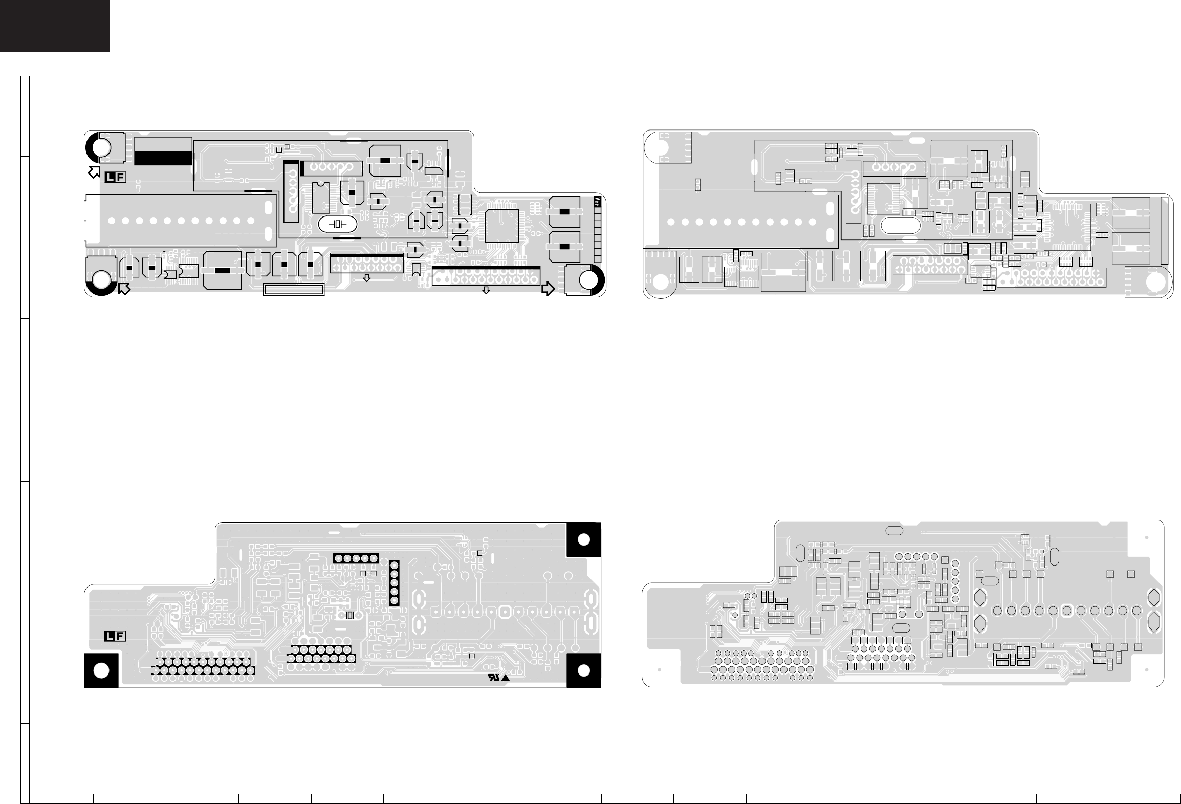
140
LC-32/37GD8E/RU
LC-32/37BT8E/RU
1234567 8 9 10 11 12 13 14 15 16
I
H
G
F
E
D
C
B
A
TUNER Unit PWB (KD609WJN3)
TUNER Unit, Side A TUNER Unit, Side A Chip Parts
TUNER Unit, Side B TUNER Unit, Side B Chip Parts
C267
C268
R289 R290
C269
C253
C251
C271
C248 R265
R211
R244
R234 R235 R233
C229
C281
C259
C258 R267
C257 R266
R213
C276
R226
R227
C218
R243
C231 C233 R242
R238
R288
Q210
R287
R237
C234
R203
R202 R201
C278
R259
R250
D207
TL245TL201TL203
C203
R207
R208
C255
R283
R281
C266
C254 R285
C272
R247
R248
L210
L213
R269
R268
R276R275
L209
L208
R212
R264
L205
R240
C232
C220
C219
R229
R228
L204R231
D206
D205
C223R230
C222
C228
R241
R286C227
FB201
R205
R209
R204
D201
C202
C277
C274
C275
R291
R292
Q211
R210
L203
Q203
C205
112
13
24
1
16
17
32
33
48
49
64
1
4
5
8
1
8
9
16
12
3 4
123
TU201
C201
C241 Q209
IC204
IC203 C204
C206
C217 C230
X201
IC201
C221
FL201
C249
C261
C237
C242
C252
C247
IC205
C246
P202
IC202
X202
C244
C226
FL202
D204
D203
R245
R272
R273
IC206
R263
DUNTKD609WE
QPWBND609WJN3
a
115
P201
C270
C273
1
3
4 5
Q205
IC207
1
6
4
3
LUG203
LUG201
LUG202
DCBA E F G H
C279
L206
L207
L212
14
5 8
IC208
C216
R224
R219
C215 D203
TU201
C256
Q209
C206
C204
C217 C230
IC204
IC203
C201C241
P201
L207
X201
C225
R232
C224
IC201
C221
FL202
FL201
C226
IC207 Q205 C243
R251
C244
IC205
C262
L206 C252
C247
R263IC206
C263
C242
IC208
C249
C280 R295
C240
R296
R297 R255
C239
R256
R282
R284
C237
C261
R273 R272
P202
C273
C270
R274
IC202
VER1
R245
R270
X202
C260C235
C279
C236
R299
R298
R293
R294
C250
C245
C246
R236
R239
R223
D204
L212
R246
R206
C207
1
2
22
23
a
P202
X201
FL201
FL202
TU201
R275
R276
Q204
R231
D205
D206
Q203
D201
Q210
1
2
14
15
P201
Q211
D207
L203
L204
L205
L208
L209
L210
L213
1
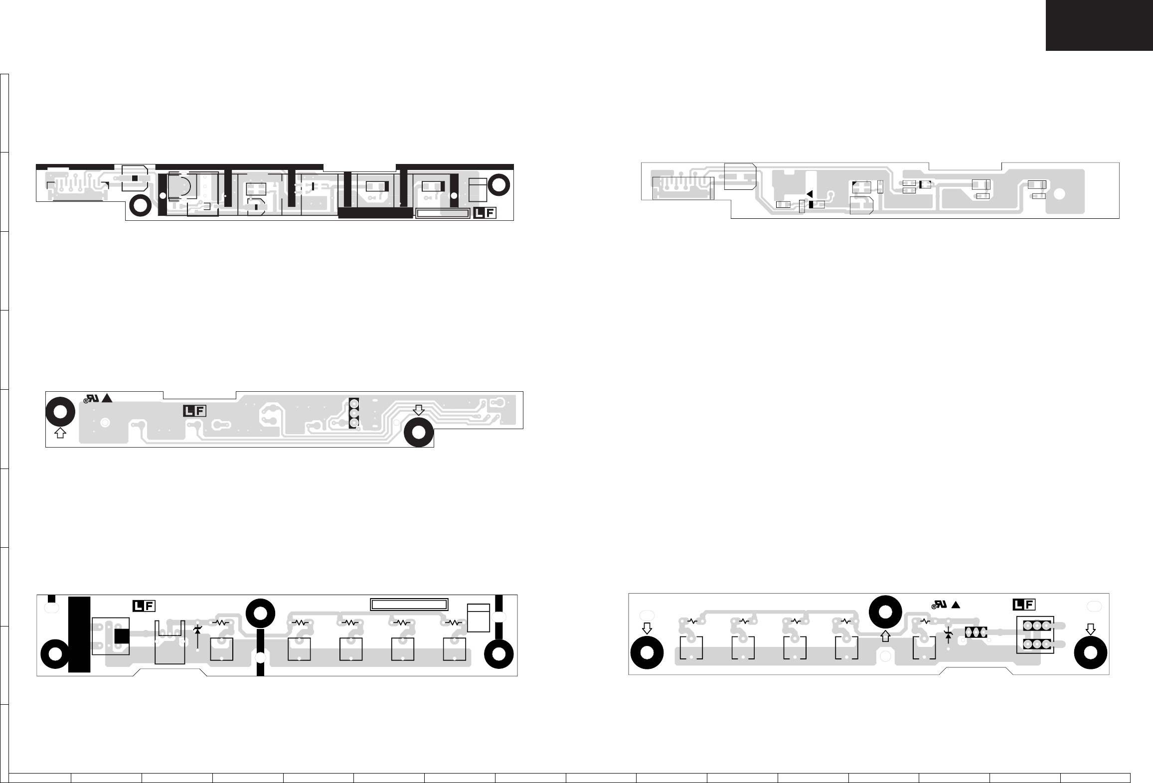
141
LC-32/37GD8E/RU
LC-32/37BT8E/RU
12 3 4 5 67 8 9 10 11 12 13 14 15 16
I
H
G
F
E
D
C
B
A
RC / LED Unit PWB (FD607WJN1)
RC/LED Unit, Side A RC / LED Unit, Side A Chip Parts
RC/LED Unit, Side B
1
10
1 2
34
QPWBFD607WJN1
P101
R101
R108
R109
R112
R114
C101
C102
C104
C105
RMC101
D101
D102
D103 D104
IC101
SLD101
a
POWER
SLEEP OPC
RA
CHK
C101
C102 D101
P101 RMC101
SLD101
R101
IC101
C104
R108
R109 D103
C105
D104
R114 R112
D102
a
SLD101
RMC101
13
KEY Unit PWB (FD606WJZZ)
KEY Unit, Side A KEY Unit, Side B
1 3
P153 R151 R152 R153 R155R156
S151 S152S153 S154 S155
S156
D151
POWER MENU VOL-UP VOL-DOWNCH-DOWNCH-UP
QPWBFD606WJZZ
a
KM
ICT
13
P153
R151R152R153R155 R156
S151
S152
S153
S154
S155
S156
D151
MENUVOL-UP CH-DOWN CH-UPVOL-DOWN POWER
a
KM
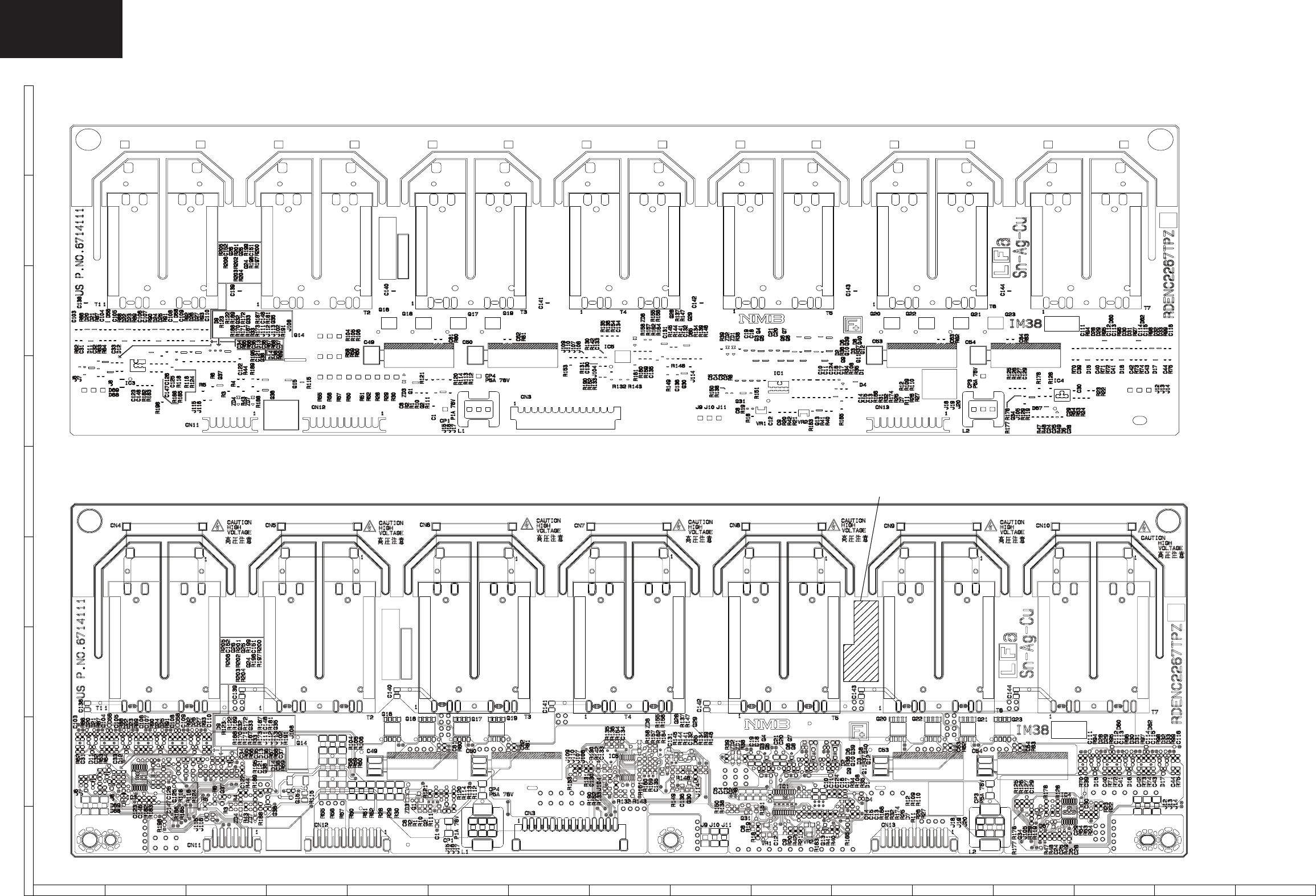
142
LC-32/37GD8E/RU
LC-32/37BT8E/RU
INVERTER Unit PWB
LC32GD8, LC32BT8 INVERTER Unit, Side A (RDENC2266TPZC)
1234567 8 9 10 11 12 13 14 15 16
I
H
G
F
E
D
C
B
A
INVERTER Unit PWB
LC32GA8E INVERTER Unit, Side A (RDENC2266TPZC)
LC32GA8E INVERTER Unit, Side A Chip Parts
106
LC-32GA8/LC-32BV8
LC-37GA8/LC-37BV8
1234567 8 9 10 11 12 13 14 15 16
I
H
G
F
E
D
C
B
A
INVERTER Unit PWB
LC32GA8E INVERTER Unit, Side A (RDENC2266TPZC)
LC32GA8E INVERTER Unit, Side A Chip Parts
106
LC-32GA8/LC-32BV8
LC-37GA8/LC-37BV8
LC32GD8, LC32BT8 INVERTER Unit, Side A Chip Parts
1234567 8 9 10 11 12 13 14 15 16
I
H
G
F
E
D
C
B
A
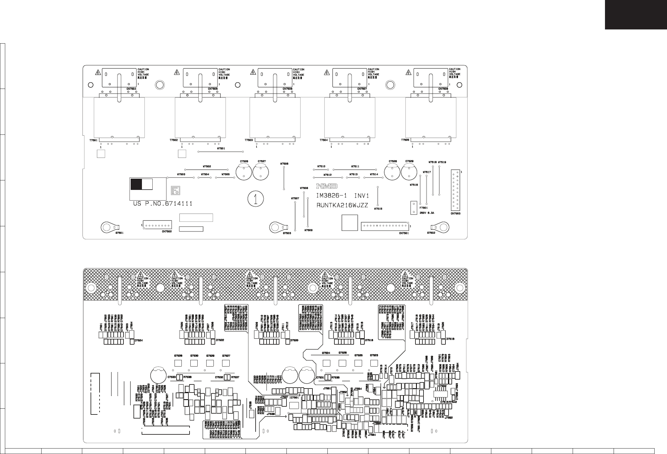
143
LC-32/37GD8E/RU
LC-32/37BT8E/RU
INVERTER Unit PWB (Continued)
LC-37GD8, LC-37BT8 INVERTER Unit, Side A (RUNTKA216WJZZ)
LC-37GD8, LC-37BT8 INVERTER Unit, Side B (RUNTKA216WJZZ)
12 3 4 5 67 8 9 10 11 12 13 14 15 16
I
H
G
F
E
D
C
B
A
5
LC-26GA5E
LC-32GA5E
LC-32GD9E
LC-37GD9E
In the case of LC-37GD9E, for the Inverter PWB Units the type used is nickel, so they are marked as LFn:
PRECAUTIONS FOR USING LEAD-FREE SOLDER
1 Employing lead-free solder
“ALL PWB” of this model employs lead-free solder. The LF symbol indicates lead-free solder, and is attached on the
PWBs and service manuals. The alphabetical character following LF shows the type of lead-free solder.
Example:
2 Using lead-free wire solder
When fi xing the PWB soldered with the lead-free solder, apply lead-free wire solder. Repairing with conventional lead
wire solder may cause damage or accident due to cracks.
As the melting point of lead-free solder (Sn-Ag-Cu) is higher than the lead wire solder by 40°C, we recommend you to
use a dedicated soldering bit, if you are not familiar with how to obtain lead-free wire solder or soldering bit, contact our
service station or service branch in your area.
3 Soldering
As the melting point of lead-free solder (Sn-Ag-Cu) is about 220°C which is higher than the conventional lead solder by
40°C, and as it has poor solder wettability, you may be apt to keep the soldering bit in contact with the PWB for extended
period of time. However, Since the land may be peeled off or the maximum heat-resistance temperature of parts may be
exceeded, remove the bit from the PWB as soon as you confi rm the steady soldering condition.
Lead-free solder contains more tin, and the end of the soldering bit may be easily corroded. Make sure to turn on and
off the power of the bit as required.
If a different type of solder stays on the tip of the soldering bit, it is alloyed with lead-free solder. Clean the bit after every
use of it.
When the tip of the soldering bit is blackened during use, fi le it with steel wool or fi ne sandpaper.
Be careful when replacing parts with polarity indication on the PWB silk.
Lead-free wire solder for servicing.
�
Sn-Ag-Ni
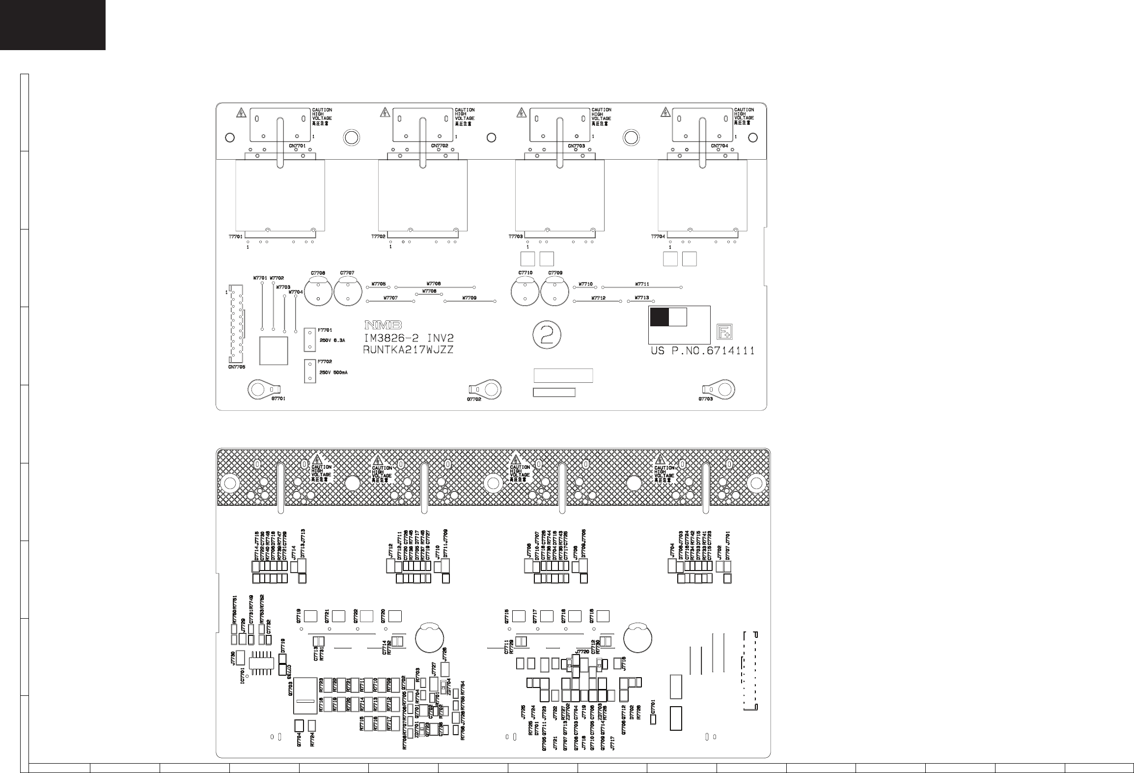
144
LC-32/37GD8E/RU
LC-32/37BT8E/RU
INVERTER Unit PWB (Continued)
LC-37GD8, LC-37BT8 INVERTER Unit, Side A (RUNTKA217WJZZ)
LC-37GD8, LC-37BT8 INVERTER Unit, Side B (RUNTKA217WJZZ)
1234567 8 9 10 11 12 13 14 15 16
I
H
G
F
E
D
C
B
A
5
LC-26GA5E
LC-32GA5E
LC-32GD9E
LC-37GD9E
In the case of LC-37GD9E, for the Inverter PWB Units the type used is nickel, so they are marked as LFn:
PRECAUTIONS FOR USING LEAD-FREE SOLDER
1 Employing lead-free solder
“ALL PWB” of this model employs lead-free solder. The LF symbol indicates lead-free solder, and is attached on the
PWBs and service manuals. The alphabetical character following LF shows the type of lead-free solder.
Example:
2 Using lead-free wire solder
When fi xing the PWB soldered with the lead-free solder, apply lead-free wire solder. Repairing with conventional lead
wire solder may cause damage or accident due to cracks.
As the melting point of lead-free solder (Sn-Ag-Cu) is higher than the lead wire solder by 40°C, we recommend you to
use a dedicated soldering bit, if you are not familiar with how to obtain lead-free wire solder or soldering bit, contact our
service station or service branch in your area.
3 Soldering
As the melting point of lead-free solder (Sn-Ag-Cu) is about 220°C which is higher than the conventional lead solder by
40°C, and as it has poor solder wettability, you may be apt to keep the soldering bit in contact with the PWB for extended
period of time. However, Since the land may be peeled off or the maximum heat-resistance temperature of parts may be
exceeded, remove the bit from the PWB as soon as you confi rm the steady soldering condition.
Lead-free solder contains more tin, and the end of the soldering bit may be easily corroded. Make sure to turn on and
off the power of the bit as required.
If a different type of solder stays on the tip of the soldering bit, it is alloyed with lead-free solder. Clean the bit after every
use of it.
When the tip of the soldering bit is blackened during use, fi le it with steel wool or fi ne sandpaper.
Be careful when replacing parts with polarity indication on the PWB silk.
Lead-free wire solder for servicing.
�
Sn-Ag-Ni
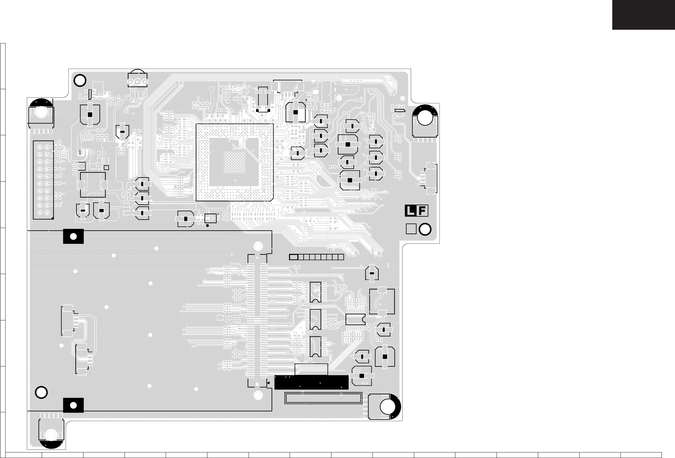
145
LC-32/37GD8E/RU
LC-32/37BT8E/RU
12 3 4 5 67 8 9 10 11 12 13 14 15 16
I
H
G
F
E
D
C
B
A
DIGITAL Unit PWB (KD628WJN2)
DIGITAL Unit, Side A
A
AF
26 1
1
4
5
1
34
5
110
20
1
10
11
20
1
10
11
20
150
51 100
1
34
5
KD628
QPWBXD628WJN2
a
CN4190
LUG4602
C4707
IC4703
Q4702 Q4701 C4782
R4782
R4781
C4781
RMC4601
P4001
X4001
P4002 R4711
R4709
R4650
Q4607
C4625
C4639
C4640
C4641
C4601
C4606
C4609
C4635
C4604
C4623C4634
IC4702
FB4602
R4234
R4238
R4244
R4237
R4201 R4208
R4216
R4219
R4220
R4221
C4001
IC4002
Q4001
R4218
R4202
R4204
R4212
R4205
R4217
R4213
C4203
IC4701
L4701
D4702
C4701
D4701
R4036
C4702
C4019
C4032
C4008
C4030 IC4005
R4207
R4214
R4206
R4211
IC4405
R4435
IC4406
IC4401
C4412
C4401
C4201
R4421R4427
R4436
R4431
R4432
R4428
FB4403
R4422
R4411
R4437
R4426
R4429
C4415C4410
C4416
R4406
R4416
R4414
R4622
C4636
R4623
R4624
R4675
1
10
11
20
IC4001
X4002
C4710
R4616
R4659
R4671
C4715
C4717
FB4202
R4243
R4710
Q4002
LUG4601
Q4703
C4637
C4638
R4215
R4636
R4412
R4415
R4413
R4410
IC4402
IC4404
R4405
C4408
R4409
R4403
R4401
C4406
R4417
R4031R4030
FB4007
R4233
R4236
R4242
C4206
C4205
R4705
R4197
R4193
R4035
R4194
R4192
R4195
C4706
R4037
LUG4603
LUG4604
R4039
C4034
R4038
C4035
R4017
C4020
P4003
SC4602
DCBA E F G H
Ver
R4718
R4441
1
3
4 5
IC4705
C4718
C4420
P4004
1
2
19
20
FB4009
FB4008
L4401
C4421
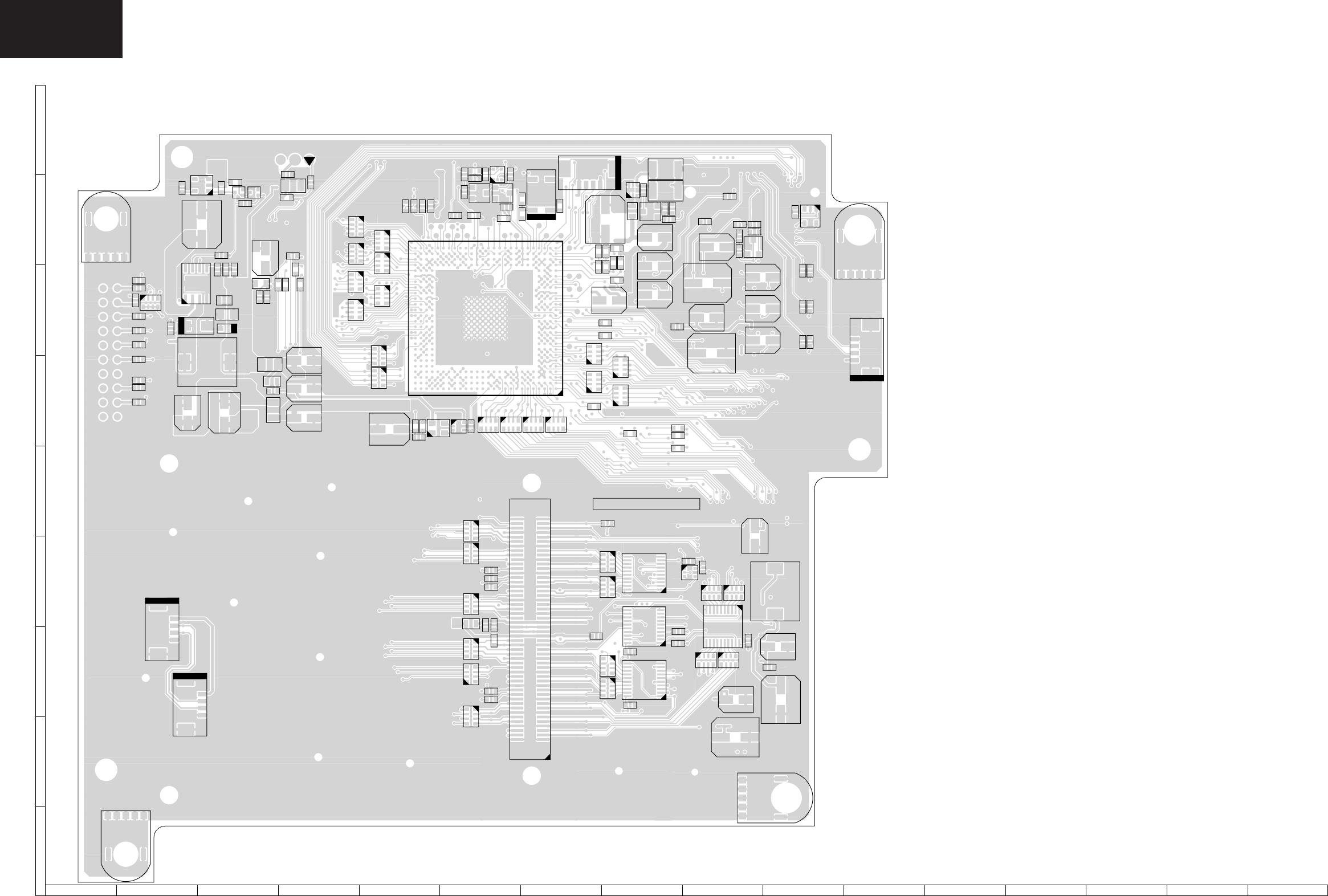
146
LC-32/37GD8E/RU
LC-32/37BT8E/RU
12 3 4 5 67 8 9 10 11 12 13 14 15 16
I
H
G
F
E
D
C
B
A
DIGITAL Unit PWB (KD628WJN2)
DIGITAL Unit, Side A Chip Parts
IC4703 C4782
LUG4602 C4707
C4203
Q4001 Q4002 X4001
P4002
C4710
R4711
R4709
C4623
C4634
C4625 Q4607
IC4705
LUG4601
P4003
C4641
C4640
C4639
C4604
C4606
C4601
C4635
C4001
IC4001
IC4701
C4701
D4702
R4036
L4701
C4717 C4715
C4019
C4032
C4008
C4030 X4002 R4207 R4214 R4206 R4211
C4201
L4401
R4401R4403
IC4405
SC4602
P4001
P4004
IC4404
IC4402
IC4401
C4401 C4421
C4412
R4414R4416
C4420
LUG4604
LUG4603
R4705
R4718
R4782
C4781
R4710 R4243
R4024 C4023
R4016
R4034
R4021
C4010 R4704
R4635
R4636
R4675
R4650
R4659 R4616
R4671
C4609
R4221
R4220
R4215
R4216
R4208
R4201
C4702
FB4202
R4037
R4191
R4196
R4195
R4192
D4701
R4194
R4035
R4193
R4197
FB4009
FB4007
C4033
R4218
R4217
R4202
R4205
R4213
R4212
R4204
R4031
R4030
R4028
IC4005
R4219
R4237
R4234
R4238
R4244
Ver1
R4409
IC4406
R4435
R4412
R4415
R4406
R4405
C4406
R4417
R4421
R4427
R4436
R4431
R4432
R4428
FB4403
R4422
R4411
R4429
R4437
R4426
R4413
R4410
C4407
R4441
IC4702
Q4703
C4712
R4712
Q4702 Q4701
R4190
R4703
R4702
R4701
C4205
C4206
R4242
R4236
R4240
R4233
R4781
C4035
R4038
C4034
R4039
C4020 R4017
R4012
R4020
C4007R4009
IC4002
C4006
FB4602
R4708
C4627
R4632R4631
C4628
R4634
R4637
R4706
C4703
R4673R4672
C4718
R4622
C4636C4637
R4623R4624
C4638
C4706
FB4008
R4026
C4031
R4029
C4408
C4416
C4415C4410
C4403
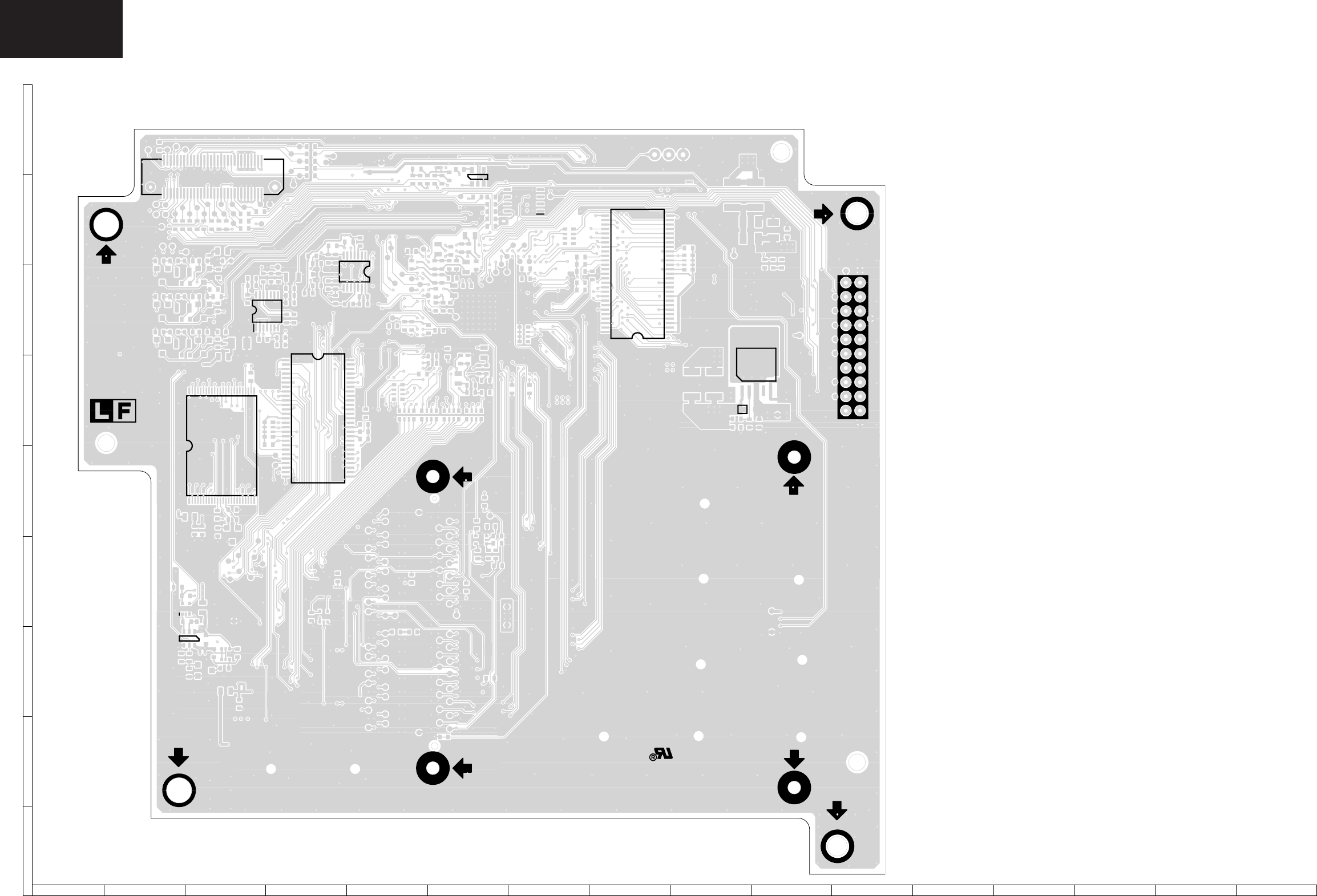
148
LC-32/37GD8E/RU
LC-32/37BT8E/RU
12 3 4 5 67 8 9 10 11 12 13 14 15 16
I
H
G
F
E
D
C
B
A
DIGITAL Unit PWB (KD628WJN2)
DIGITAL Unit, Side B
1
2
59
60
1
27 28
54
1
27
28
54
1
7
814
13
45
1 3
45
124
25
48
1
4
5
a
R4605
R4604
R4601
R4645
IC4003
FB4005
IC4204
IC4604
L4601
IC4601
Q4602 Q4601
Q4604
Q4606
FB4601
C4622
FB4603
IC4203
IC4202
R4232
R4231
R4241
R4209R4404
R4408
R4407
R4402
FB4004
R4027
IC4201
R4223
R4225
FB4701
C4711
R4714
R4713
C4709
C4708
C4704
R4707
C4705
IC4704
D4703
R4717
C4714
C4713
C4716
Q4201
FB4201
Q4401
FB4401
C4402
IC4403
C4405
C4404
IC4407
R4419
R4418
C4409
FB4402
R4425
IC4408
R4716
R4715
R4025
R4203
C4026
C4014
FB4006
R4222
R4674
C4621
R4642
R4633
R4629
C4630
C4629
C4631
R4630
R4638
R4249
R4646
R4649
15
FB4002
SC4601
Q4603
Q4605
R4224
1
3
5 4
13
4
6
14
5
8
C4414
R4434
R4433
C4012
R4230
R4651
R4424
R4439
C4417
R4438
R4440
R4423
Q4402
IC4409
R4445
R4444
R4447
19
20
1
2
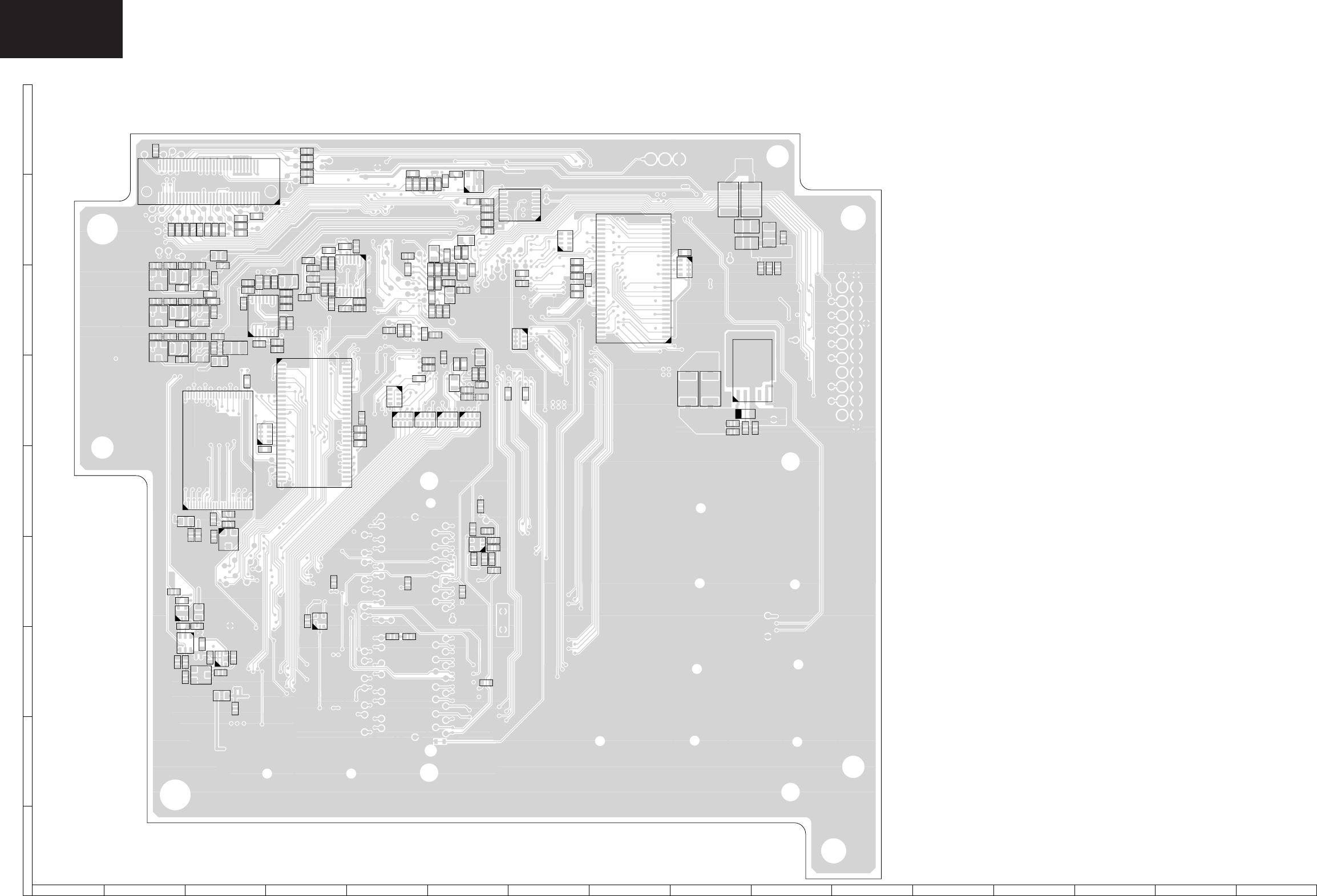
148
LC-32/37GD8E/RU
LC-32/37BT8E/RU
12 3 4 5 67 8 9 10 11 12 13 14 15 16
I
H
G
F
E
D
C
B
A
DIGITAL Unit PWB (KD628WJN2)
DIGITAL Unit, Side B Chip Parts
FB4701
C4711
R4225
R4714 R4713
C4709
R4223
IC4201
R4203
R4229
R4228
R4227
R4239
R4025
C4027
C4025
IC4204
IC4003
C4029
C4208 R4250
R4246
C4210
R4245
R4249
FB4005
R4633
C4022
R4001
R4013
C4621
IC4604
R4642
R4651
R4661
R4626
R4660
R4652 R4627
L4601
R4601
R4645
R4602
R4603
R4604
R4646
R4647
R4648
R4649
C4608
C4610
C4603
R4612
R4665
FB4601
SC4601
R4619C4611C4614C4617
Q4601
L4603
Q4602
R4662
C4624
R4667R4620C4612C4615C4618
Q4604 L4604
R4663
Q4603
C4619 C4616 C4613 R4621 R4669
Q4605
R4664
L4605
Q4606 C4622
FB4603
IC4601
R4618
R4611
C4602
R4610
R4628 C4626
R4222 R4006
C4015
C4024
R4210
C4012
C4013 R4018
R4019
R4027
R4716 R4715
IC4704
D4703
R4717
C4714
R4408R4407R4402R4404
R4209
C4414
R4434
IC4407
R4230
R4231
R4232
IC4202
R4226
R4224
IC4203
FB4201 R4247
C4209
Q4201
R4447
C4411
IC4408
R4430 R4425
Q4402 R4444
FB4401
R4423 C4417
R4419
R4439
C4708
C4705
R4707
C4704
R4235
R4638
R4630
C4631
C4629
C4630
R4629
FB4002
R4011
C4011
C4009
R4010
FB4001
C4028
R4004
C4004
C4005
R4002
C4002
C4003
R4674
R4640
C4633
C4632
R4639
C4607
R4617
C4605
R4657
R4658
R4606
R4644
R4643
R4608
R4609
R4607
R4666
R4605
R4668
R4613
R4670
R4251
R4614
R4615
R4641
R4003
R4005
R4008
R4007
R4033
R4032
FB4003
C4021
C4018
FB4006
R4014
R4015
FB4004 C4016
C4017
R4241
C4014
C4026
C4716
C4713
R4440
R4418
R4420
C4413
C4409
R4433
R4248 C4207
C4204
C4202
FB4402 R4446
C4418
IC4409
R4445
R4443R4442
C4419
Q4401
C4405
IC4403
C4404
R4424
R4438
C4402
149
LC-26GA5E
LC-32GA5E
LC-32GD8E/RU
LC-32BT8E/RU
LC-37GD8E/RU
LC-37BT8E/RU
LC-32/37GD8E/RU
LC-32/37BT8E/RU
MARK *: SPARE PARTS DELIVERY SECTION
REF No. PARTS DESCRIPTION * SN CODE EX CODE
R1LK315T3LF15 32" LCD Panel Module Unit R
R1LK370T3LZ5BX 37" LCD Panel Module Unit R EZ EZ
DUNTKD890FM06 MAIN Unit (LC-32GD8E/RU, LC-32BT8E/RU) R
DUNTKD890FM07 MAIN Unit (LC-37GD8E/RU, LC-37BT8E/RU) R
DUNTKD604FM10 AV Unit R
DUNTKD605FM14 POWER Unit (LC-32GD8E/RU, LC-32BT8E/RU) R
DUNTKD605FM03 POWER Unit (LC-37GD8E/RU, LC-37BT8E/RU) R
DUNTKD606FMV0 KEY Unit R
DUNTKD607FMV0 R/C,LED Unit R
CKITKD609FM01 DIGITAL TUNER Unit S AY BN
DUNTKD628FM01 DIGITAL Unit R
IC1701 VHIBU4239G+-1Y BU4239G-TR D AE AE
IC1702 VHIPQ20WZ11-1Y PQ20WZ1UJ00H D AF AF
IC1703 VHIPQ20WZ11-1Y PQ20WZ1UJ00H D AF AF
IC1704 VSSSM6J51TU-1Y SSM6J51TU(TE85L,F) D AF AF
IC1705 VSSSM6J51TU-1Y SSM6J51TU(TE85L,F) D AF AF
IC1706 VHIMP1410ES-1Y MP1410ES-LF-Z D AP AP
IC1707 VHIPQ20WZ11-1Y PQ20WZ1UJ00H D AF AF
IC1708 VHIMP1410ES-1Y MP1410ES-LF-Z D AP AP
IC1709 VSSSM6J51TU-1Y SSM6J51TU(TE85L,F) D AF AF
IC1710 RH-IXB823WJZZQ EPM240T100C5N D AR AR
IC1711 VHIPQ1R50//-1Y PQ1R50J0000H D AF AF
IC1901 VHI24LC2BIN-1Y 24LC02BT-I/SN D AF AF
IC1905 VHISII9021+-1Q SII9021CTU D BC BC
IC2301 VHIISL83220-1Y ISL83220ECVZ-T D AQ AQ
IC2303 VHIBR24C21F-1Y BR24C21F-E2 D AG AG
IC2701 VHITVHC153T-1Y TC74VHC153FT(EL,M) D AE AE
IC2702 VHIMM1507XN-1Y MM1507XNRE D AD AD
IC2704 VHICD4052BP-1Y CD4052BPWR D AD AD
IC2705 VHIMM1507XN-1Y MM1507XNRE D AD AD
IC3001 VHIBR24L64F-1Y BR24L64F-WE2 D AK AK
IC3002 RH-IXB624WJN1Q VCT6973 D
IC3003 RH-IXB664WJZZY PIC16F913-I/SS-G-GW902T D AY AY
IC3005 VHIBU4215G+-1Y BU4215G-TR D AE AE
Q1703 VS2SC3928AR-1Y 2SC3928AR D AB AB
Q1704 VS2SC3928AR-1Y 2SC3928AR D AB AB
Q1705 VS2SA1530AR-1Y 2SA1530AR D AB AB
DUNTKD890FM07 (LC-37GD8E/RU,LC-37BT8E/RU)
TRANSISTORS
NOTE : THE PARTS HERE SHOWN ARE SUPPLIED AS AN ASSEMBLY BUT NOT INDEPENDENTLY
LCD PANEL
PRINTED WIRING BOARDS
DUNTKD890FM06 (LC-32GD8E/RU,LC-32BT8E/RU)
MAIN Unit
INTEGRATED CIRCUITS
REF No. PARTS DESCRIPTION * SN CODE EX CODE
Q1901 VS2SK536///-1Y 2SK536 D AE AE
Q1903 VS2SK536///-1Y 2SK536 D AE AE
Q1905 VSDTC144EE/-1Y DTC144EE D AA AA
Q1907 VSDTC144EE/-1Y DTC144EE D AA AA
Q1909 VSDTC144EE/-1Y DTC144EE D AA AA
Q2702 VS3LN01S///-1Y 3LN01S D AC AC
Q2703 VS2SC3928AR-1Y 2SC3928AR D AB AB
Q2704 VS2SC3928AR-1Y 2SC3928AR D AB AB
Q2705 VS2SC3928AR-1Y 2SC3928AR D AB AB
Q2706 VS2SC3928AR-1Y 2SC3928AR D AB AB
Q2707 VSDTC144EE/-1Y DTC144EE D AA AA
Q2708 VSDTC144EE/-1Y DTC144EE D AA AA
Q2709 VS3LN01S///-1Y 3LN01S D AC AC
Q2710 VS3LN01S///-1Y 3LN01S D AC AC
Q3003 VS3LN01S///-1Y 3LN01S D AC AC
Q3004 VS3LN01S///-1Y 3LN01S D AC AC
D1702 RH-EX0487CEZZY HZM2.0NBTL-E D AC AC
D1703 VHDHSU119//-1Y HSU119TRF-E D AB AB
D1704 VHDSFPA73//2EY SFPA-73VL D AD AD
D1705 VHDHSU119//-1Y HSU119TRF-E D AB AB
D1706 VHDHSU119//-1Y HSU119TRF-E D AB AB
D1707 RH-EX0487CEZZY HZM2.0NBTL-E D AC AC
D1708 VHDSFPA73//2EY SFPA-73VL D AD AD
D1901 VHDDAN202K/-1Y DAN202KT146 D AB AB
D1903 VHD1SS355//-1Y 1SS355TE-17 D AB AB
D1905 VHD1SS355//-1Y 1SS355TE-17 D AB AB
D2301 RH-EX1271CEZZY Zener Diode, 12V D AB AB
D2302 RH-EX1271CEZZY Zener Diode, 12V D AB AB
D2303 RH-EX1271CEZZY Zener Diode, 12V D AB AB
D2304 RH-EX1271CEZZY Zener Diode, 12V D AB AB
D2305 RH-EX1247CEZZY Zener Diode, 5.6V D AB AB
D2306 RH-EX1247CEZZY Zener Diode, 5.6V D AB AB
D2307 RH-EX1247CEZZY Zener Diode, 5.6V D AB AB
D2308 RH-EX1247CEZZY Zener Diode, 5.6V D AB AB
D2309 VHDDAN202K/-1Y DAN202KT146 D AB AB
D2310 VHD1SS226//-1Y 1SS226(T5L,F,T) D AC AC
D2311 VHD1SS226//-1Y 1SS226(T5L,F,T) D AC AC
D2312 VHD1SS226//-1Y 1SS226(T5L,F,T) D AC AC
D2313 RH-EX1247CEZZY ZENER DIODE, 5.6V D AB AB
TH3002 VHHM1103J03-1Y Thermistor D AC AC
X1901 RCRSCA108WJZZY Crystal D AF AF
X3001 RCRSC0012CEZZY Crystal D AH AH
FL2301 RFILN0003TAZZY Filter D AD AD
FL2302 RFILN0003TAZZY Filter D AD AD
FL2303 RFILN0003TAZZY Filter D AD AD
L1701 RCILPA213WJZZY Coil D AG AG
L1702 RCILPA213WJZZY Coil D AG AG
L1901 RCILFA134WJZZY Coil D AF AF
L1902 RCILFA134WJZZY Coil D AF AF
L1903 RCILFA134WJZZY Coil D AF AF
L1904 RCILFA134WJZZY Coil D AF AF
L2301 RCILFA071WJZZY Coil D AD AD
L2302 RCILFA071WJZZY Coil D AD AD
L2303 RCILFA071WJZZY Coil D AD AD
L2304 RCILFA071WJZZY Coil D AD AD
L2305 RCILFA071WJZZY Coil D AD AD
L2701 VPCUN1R5MR12NY Peaking 1.5�H D
C1702 VCKYCY1EF104ZY 0.1 25V Ceramic D AA AA
C1706 RC-KZA070WJZZY 22 6.3V Ceramic D AD AD
C1711 VCKYCY1HB103KY 0.01 50V Ceramic D AA AA
C1715 VCEASX1VN226MY 22 35V Electrolytic D AC AC
DIODES
PACKAGED CIRCUITS
CAPACITORS
COILS AND FILTERS
PARTS LISTING
REPLACEMENT PARTS
Replacement parts which have special safety characteristics are identifi ed in this manual.
Electrical components having such features are identifi ed by in the Replacement Parts
Listing.
The use of a substitute replacement part which does not have the same safety characteristics
as the factory recommended is not permitted.
Replacement parts not shown in this service manual may create shock fi re, or other hazards.
HOW TO ORDER REPLACEMENT PARTS
To have your order completed promptly and correctly please supply the following information.
1. MODEL NUMBER 2. REF. NO.
3. PART NO. 4. DESCRIPTION
5. CODE 6. QUANTITY
!

150
LC-26GA5E
LC-32GA5E
LC-32/37GD8E/RU
LC-32/37BT8E/RU
REF No. PARTS DESCRIPTION * SN CODE EX CODE
C1716 VCEASX1CN226MY 22 16V Electrolytic D AC AC
C1717 VCKYCY1HB272KY 2700p 50V Ceramic D AA AA
C1718 VCKYCY1EF104ZY 0.1 25V Ceramic D AA AA
C1720 VCEASX1CN226MY 22 16V Electrolytic D AC AC
C1721 VCAAPD1AJ686MY 68 10V Electrolytic D AE AE
C1723 RC-KZA073WJZZY 10 16V Ceramic D AD AD
C1724 RC-KZA073WJZZY 10 16V Ceramic D AD AD
C1726 RC-KZA070WJZZY 22 6.3V Ceramic D AD AD
C1730 VCKYCY1HB272KY 2700p 50V Ceramic D AA AA
C1733 VCEASX1CN226MY 22 16V Electrolytic D AC AC
C1734 VCKYCY1EF104ZY 0.1 25V Ceramic D AA AA
C1735 VCAAPD1AJ686MY 68 10V Electrolytic D AE AE
C1737 RC-KZA073WJZZY 10 16V Ceramic D AD AD
C1738 RC-KZA073WJZZY 10 16V Ceramic D AD AD
C1739 VCKYCY1EF104ZY 0.1 25V Ceramic D AA AA
C1740 VCCCCY1HH101JY 100p 50V Ceramic D AA AA
C1741 VCKYCY1HB102KY 1000p 50V Ceramic D AA AA
C1742 VCKYCY1EF104ZY 0.1 25V Ceramic D AA AA
C1744 VCCCCY1HH101JY 100p 50V Ceramic D AA AA
C1745 VCCCCY1HH101JY 100p 50V Ceramic D AA AA
C1746 VCCCCY1HH102JY 1000p 50V Ceramic D AB AB
C1747 VCCCCY1HH101JY 1SS390TE61 D AA AA
(LC-37GD8E/RU, LC-37BT8E/RU)
C1748 VCCCCY1HH101JY 1SS390TE61 D AA AA
(LC-37GD8E/RU, LC-37BT8E/RU)
C1749 VCKYCY1HB221KY 1SS390TE61 D AA AA
(LC-37GD8E/RU, LC-37BT8E/RU)
C1750 VCCCCY1HH101JY 1SS390TE61 D AA AA
(LC-37GD8E/RU, LC-37BT8E/RU)
C1751 VCCCCY1HH101JY 1SS390TE61 D AA AA
(LC-37GD8E/RU, LC-37BT8E/RU)
C1752 VCCCCY1HH101JY 1SS390TE61 D AA AA
(LC-37GD8E/RU, LC-37BT8E/RU)
C1753 VCKYCY1EF104ZY 0.1 25V Ceramic D AA AA
C1754 VCKYCY1EF104ZY 0.1 25V Ceramic D AA AA
C1755 VCEASX1CN106MY 10 16V Electrolytic D AC AC
C1756 VCEASX1CN106MY 10 16V Electrolytic D AC AC
C1757 VCKYCY1EF104ZY 0.1 25V Ceramic D AA AA
C1758 VCKYCY1EF104ZY 0.1 25V Ceramic D AA AA
C1901 VCEASY1CN476MY 47 16V Electrolytic D AC AC
C1903 VCKYCY1EF104ZY 0.1 25V Ceramic D AA AA
C1906 VCKYCY1EF104ZY 0.1 25V Ceramic D AA AA
C1910 RC-KZA073WJZZY 10 16V Ceramic D AD AD
C1912 VCKYCY1HB102KY 1000p 50V Ceramic D AA AA
C1913 VCKYCY1HB102KY 1000p 50V Ceramic D AA AA
C1916 VCKYCY1HB102KY 1000p 50V Ceramic D AA AA
C1917 VCKYCY1HB102KY 1000p 50V Ceramic D AA AA
C1918 RC-KZA073WJZZY 10 16V Ceramic D AD AD
C1919 RC-KZA073WJZZY 10 16V Ceramic D AD AD
C1921 RC-KZA073WJZZY 10 16V Ceramic D AD AD
C1923 VCKYCY1HB102KY 1000p 50V Ceramic D AA AA
C1924 VCKYCY1HB102KY 1000p 50V Ceramic D AA AA
C1927 VCKYCY1HB102KY 1000p 50V Ceramic D AA AA
C1928 VCKYCY1HB103KY 0.01 50V Ceramic D AA AA
C1929 VCCCCY1HH120JY 12p 50V Ceramic D AA AA
C1930 VCKYCY1HB102KY 1000p 50V Ceramic D AA AA
C1931 RC-KZA073WJZZY 10 16V Ceramic D AD AD
C1934 VCCCCY1HH120JY 12p 50V Ceramic D AA AA
C1935 RC-KZA073WJZZY 10 16V Ceramic D AD AD
C1936 VCKYCY1HB102KY 1000p 50V Ceramic D AA AA
C1941 VCKYCY1HB102KY 1000p 50V Ceramic D AA AA
C1943 VCKYCY1HB102KY 1000p 50V Ceramic D AA AA
DUNTKD890FM06/07 (LC-32GD8, LC-32BT8 / (LC-37GD8, LC-37BT8)
MAIN Unit (Continued)
REF No. PARTS DESCRIPTION * SN CODE EX CODE
C1946 VCKYCY1HB102KY 1000p 50V Ceramic D AA AA
C1947 VCKYCY1EF104ZY 0.1 25V Ceramic D AA AA
C1948 VCKYCY1HB102KY 1000p 50V Ceramic D AA AA
C1953 VCKYCY1EF104ZY 0.1 25V Ceramic D AA AA
C1955 VCKYCY1HB102KY 1000p 50V Ceramic D AA AA
C1956 VCKYCY1HB102KY 1000p 50V Ceramic D AA AA
C1959 VCKYCY1EF104ZY 0.1 25V Ceramic D AA AA
C1960 VCKYCY1HB102KY 1000p 50V Ceramic D AA AA
C1965 VCKYCY1HB102KY 1000p 50V Ceramic D AA AA
C1967 VCKYCY1HB102KY 1000p 50V Ceramic D AA AA
C1968 VCKYCY1HB102KY 1000p 50V Ceramic D AA AA
C1969 VCKYCY1HB102KY 1000p 50V Ceramic D AA AA
C1971 VCKYCY1HB102KY 1000p 50V Ceramic D AA AA
C1973 VCKYCY1HB102KY 1000p 50V Ceramic D AA AA
C1974 VCKYCY1HB102KY 1000p 50V Ceramic D AA AA
C1975 VCKYCY1HB102KY 1000p 50V Ceramic D AA AA
C2301 VCKYCY1EF104ZY 0.1 25V Ceramic D AA AA
C2302 VCKYCY1EF104ZY 0.1 25V Ceramic D AA AA
C2303 VCKYCY1EF104ZY 0.1 25V Ceramic D AA AA
C2304 VCKYCY1EF104ZY 0.1 25V Ceramic D AA AA
C2305 VCKYCY1EF104ZY 0.1 25V Ceramic D AA AA
C2306 VCEASX1CN106MY 10 16V Electrolytic D AC AC
C2307 VCKYCY1EF104ZY 0.1 25V Ceramic D AA AA
C2308 VCKYCY1HB104KY 0.1 50V Ceramic D AA AA
C2309 VCKYCY1HB104KY 0.1 50V Ceramic D AA AA
C2310 VCKYCY1HB104KY 0.1 50V Ceramic D AA AA
C2312 VCKYCY1EF104ZY 0.1 25V Ceramic D AA AA
C2318 VCCCCY1HH101JY 100p 50V Ceramic D AA AA
C2701 VCKYCY1EF104ZY 0.1 25V Ceramic D AA AA
C2702 VCCCCY1HH101JY 100p 50V Ceramic D AA AA
C2703 VCCCCY1HH101JY 100p 50V Ceramic D AA AA
C2704 VCCCCY1HH101JY 100p 50V Ceramic D AA AA
C2705 VCCCCY1HH101JY 100p 50V Ceramic D AA AA
C2706 VCEASX1HN105MY 1 50V Electrolytic D AB AB
C2707 VCEASX1HN105MY 1 50V Electrolytic D AB AB
C2708 VCEASX1HN105MY 1 50V Electrolytic D AB AB
C2709 VCEASX1HN105MY 1 50V Electrolytic D AB AB
C2710 VCKYTV1EB104KY 0.1 25V Ceramic D AB AB
C2711 VCKYCY1CF105ZY 1 16V Ceramic D AA AA
C2712 VCKYCY1EF104ZY 0.1 25V Ceramic D AA AA
C2714 VCEASX1CN106MY 10 16V Electrolytic D AC AC
C2715 VCKYCY1EF104ZY 0.1 25V Ceramic D AA AA
C2718 VCKYCY1CF105ZY 1 16V Ceramic D AA AA
C2719 VCKYCY1CF105ZY 1 16V Ceramic D AA AA
C2722 VCKYCY1EF104ZY 0.1 25V Ceramic D AA AA
C2723 VCKYCY1EF104ZY 0.1 25V Ceramic D AA AA
C2724 VCKYCY1EF104ZY 0.1 25V Ceramic D AA AA
C2725 VCKYCY1HB221KY 220p 50V Ceramic D AA AA
C2726 VCKYTV1EB104KY 0.1 25V Ceramic D AB AB
C2727 VCKYCY1EF104ZY 0.1 25V Ceramic D AA AA
C2728 VCKYCY1CF105ZY 1 16V Ceramic D AA AA
C2729 VCKYCY1HB104KY 0.1 50V Ceramic D AA AA
C2730 RC-KZA073WJZZY 10 16V Ceramic D AD AD
C2731 VCKYTV1HB103KY 0.01 50V Ceramic D AA AA
C2732 VCKYTV1HB103KY 0.01 50V Ceramic D AA AA
C3001 VCKYCY1EF104ZY 0.1 25V Ceramic D AA AA
C3002 RC-KZA073WJZZY 10 16V Ceramic D AD AD
C3003 VCKYCY1EF104ZY 0.1 25V Ceramic D AA AA
C3004 RC-KZA073WJZZY 10 16V Ceramic D AD AD
C3005 RC-KZA073WJZZY 10 16V Ceramic D AD AD
C3006 RC-KZA073WJZZY 10 16V Ceramic D AD AD
C3007 VCKYCY1EF104ZY 0.1 25V Ceramic D AA AA
C3008 VCKYCY1EF104ZY 0.1 25V Ceramic D AA AA
C3009 VCKYCY1EF104ZY 0.1 25V Ceramic D AA AA

151
LC-26GA5E
LC-32GA5E
LC-32GD8E/RU
LC-32BT8E/RU
LC-37GD8E/RU
LC-37BT8E/RU
LC-32/37GD8E/RU
LC-32/37BT8E/RU
REF No. PARTS DESCRIPTION * SN CODE EX CODE
C3010 RC-KZA073WJZZY 10 16V Ceramic D AD AD
C3011 VCKYCY1EF104ZY 0.1 25V Ceramic D AA AA
C3012 VCKYCY1EF104ZY 0.1 25V Ceramic D AA AA
C3013 VCKYCY1EF104ZY 0.1 25V Ceramic D AA AA
C3014 VCKYCY1HB104KY 0.1 50V Ceramic D AA AA
C3015 VCKYCY1EF104ZY 0.1 25V Ceramic D AA AA
C3016 VCKYCY1HB104KY 0.1 50V Ceramic D AA AA
C3017 RC-KZA073WJZZY 10 16V Ceramic D AD AD
C3018 VCKYCY1EF104ZY 0.1 25V Ceramic D AA AA
C3019 VCKYCY1EF104ZY 0.1 25V Ceramic D AA AA
C3020 VCKYCY1HB104KY 0.1 50V Ceramic D AA AA
C3021 VCCCCY1HH560JY 56p 50V Ceramic D AB AB
C3022 RC-KZA073WJZZY 10 16V Ceramic D AD AD
C3023 VCKYCY1EF104ZY 0.1 25V Ceramic D AA AA
C3024 VCKYCY1EF104ZY 0.1 25V Ceramic D AA AA
C3025 VCKYCY1EF104ZY 0.1 25V Ceramic D AA AA
C3027 RC-KZA073WJZZY 10 16V Ceramic D AD AD
C3028 VCKYCY1EF104ZY 0.1 25V Ceramic D AA AA
C3029 RC-KZA073WJZZY 10 16V Ceramic D AD AD
C3030 VCKYCY1EF104ZY 0.1 25V Ceramic D AA AA
C3031 RC-KZA073WJZZY 10 16V Ceramic D AD AD
C3032 VCKYCY1EF104ZY 0.1 25V Ceramic D AA AA
C3033 VCKYCY1EF104ZY 0.1 25V Ceramic D AA AA
C3034 VCCCCY1HH150JY 15p 50V Ceramic D AA AA
C3035 RC-KZA073WJZZY 10 16V Ceramic D AD AD
C3036 RC-KZA073WJZZY 10 16V Ceramic D AD AD
C3037 VCKYCY1EF104ZY 0.1 25V Ceramic D AA AA
C3038 VCKYCY1EF104ZY 0.1 25V Ceramic D AA AA
C3039 VCCCCY1HH180JY 18p 50V Ceramic D AA AA
C3040 RC-KZA073WJZZY 10 16V Ceramic D AD AD
C3041 RC-KZA073WJZZY 10 16V Ceramic D AD AD
C3042 VCKYCY1EF104ZY 0.1 25V Ceramic D AA AA
C3044 VCKYCY1HB103KY 0.01 50V Ceramic D AA AA
C3045 VCKYCY1HB103KY 0.01 50V Ceramic D AA AA
C3046 RC-KZA073WJZZY 10 16V Ceramic D AD AD
C3048 VCEASX0JN476MY 47 6.3V Electrolytic D AC AC
C3049 VCKYCY1HB102KY 1000p 50V Ceramic D AA AA
C3338 VCEASX0JN476MY 47 6.3V Electrolytic D AC AC
C3340 VCEASX0JN476MY 47 6.3V Electrolytic D AC AC
R1704 VRS-CY1JF000JY 0 1/16W Metal Oxide D AA AA
R1705 VRS-CY1JF000JY 0 1/16W Metal Oxide D AA AA
R1707 VRS-CY1JF000JY 0 1/16W Metal Oxide D AA AA
R1709 VRS-CY1JF103JY 10k 1/16W Metal Oxide D AA AA
R1711 VRS-CY1JF103JY 10k 1/16W Metal Oxide D AA AA
R1712 VRS-CY1JF103JY 10k 1/16W Metal Oxide D AA AA
R1713 VRS-CY1JF562JY 5.6k 1/16W Metal Oxide D AA AA
R1714 VRS-CY1JF000JY 0 1/16W Metal Oxide D AA AA
R1715 VRS-CY1JF470JY 1SS390TE61 D AA AA
(LC-37GD8E/RU, LC-37BT8E/RU)
R1716 VRS-CY1JF562JY 5.6k 1/16W Metal Oxide D AA AA
R1717 VRS-CY1JF000JY 0 1/16W Metal Oxide D AA AA
(LC-32GD8E/RU, LC-32BT8E/RU)
R1717 VRS-CY1JF470JY 1SS390TE61 D AA AA
(LC-37GD8E/RU, LC-37BT8E/RU)
R1718 VRS-CY1JF470JY 1SS390TE61 D AA AA
(LC-37GD8E/RU, LC-37BT8E/RU)
R1719 VRS-CY1JF622FY 6.2k 1/16W Metal Oxide D AA AA
R1720 VRS-CY1JF103JY 10k 1/16W Metal Oxide D AA AA
R1721 VRS-CY1JF562FY 5.6k 1/16W Metal Oxide D AA AA
R1722 VRS-CY1JF103JY 10k 1/16W Metal Oxide D AA AA
R1723 VRS-CY1JF622FY 6.2k 1/16W Metal Oxide D AA AA
R1724 VRS-CY1JF101JY 100 1/16W Metal Oxide D AA AA
R1726 VRS-CY1JF511FY 510 1/16W Metal Oxide D AA AA
R1727 VRS-CY1JF332JY 3.3k 1/16W Metal Oxide D AA AA
RESISTORS
REF No. PARTS DESCRIPTION * SN CODE EX CODE
R1728 VRS-CY1JF332JY 3.3k 1/16W Metal Oxide D AA AA
R1729 VRS-CY1JF202FY 2.0k 1/16W Metal Oxide D AA AA
R1730 VRS-CY1JF470JY 1SS390TE61 D AA AA
(LC-37GD8E/RU, LC-37BT8E/RU)
R1731 VRS-CY1JF102JY 1SS390TE61 D AA AA
(LC-37GD8E/RU, LC-37BT8E/RU)
R1732 VRS-CY1JF202FY 2.0k 1/16W Metal Oxide D AA AA
R1733 VRS-CY1JF101JY 100 1/16W Metal Oxide D AA AA
R1734 VRS-CY1JF222FY 2.2k 1/16W Metal Oxide D AA AA
R1735 VRS-CY1JF202FY 2.0k 1/16W Metal Oxide D AA AA
R1736 VRS-CY1JF102JY 1SS390TE61 D AA AA
(LC-37GD8E/RU, LC-37BT8E/RU)
R1737 VRS-CY1JF562JY 5.6k 1/16W Metal Oxide D AA AA
R1739 VRS-TW2HF1R0JY 1 1/2W Metal Oxide D AA AA
R1740 VRS-TW2HF1R0JY 1 1/2W Metal Oxide D AA AA
R1741 VRS-TW2HF1R0JY 1 1/2W Metal Oxide D AA AA
R1742 VRS-TW2HF1R0JY 1 1/2W Metal Oxide D AA AA
R1743 VRS-CY1JF101JY 100 1/16W Metal Oxide D AA AA
R1744 VRS-CY1JF562FY 5.6k 1/16W Metal Oxide D AA AA
R1745 VRS-CY1JF132JY 1.3k 1/16W Metal Oxide D AG AG
R1746 VRS-CY1JF202JY 2.0k 1/16W Metal Oxide D AA AA
R1747 VRS-CY1JF511FY 510 1/16W Metal Oxide D AA AA
R1748 VRS-CY1JF202FY 2.0k 1/16W Metal Oxide D AA AA
R1752 VRS-CY1JF470JY 47 1/16W Metal Oxide D AA AA
R1753 VRS-CY1JF622FY 6.2k 1/16W Metal Oxide D AA AA
R1754 VRS-CY1JF622FY 6.2k 1/16W Metal Oxide D AA AA
R1755 VRS-CY1JF562JY 5.6k 1/16W Metal Oxide D AA AA
R1756 VRS-CY1JF104JY 100k 1/16W Metal Oxide D AA AA
R1757 VRS-TW2HF1R0JY 1 1/2W Metal Oxide D AA AA
R1758 VRS-TW2HF1R0JY 1 1/2W Metal Oxide D AA AA
R1759 VRS-TW2HF1R0JY 1 1/2W Metal Oxide D AA AA
R1760 VRS-TW2HF1R0JY 1 1/2W Metal Oxide D AA AA
R1761 VRS-CY1JF101JY 100 1/16W Metal Oxide D AA AA
R1762 VRS-CY1JF220JY 22 1/16W Metal Oxide D AA AA
R1763 VRS-CY1JF220JY 22 1/16W Metal Oxide D AA AA
R1764 VRS-CY1JF220JY 22 1/16W Metal Oxide D AA AA
R1767 VRS-CY1JF103JY 10k 1/16W Metal Oxide D AA AA
R1768 VRS-CY1JF103JY 10k 1/16W Metal Oxide D AA AA
R1769 VRS-CY1JF103JY 10k 1/16W Metal Oxide D AA AA
R1770 VRS-CY1JF103JY 10k 1/16W Metal Oxide D AA AA
R1771 VRS-CY1JF101JY 100 1/16W Metal Oxide D AA AA
R1772 VRS-CY1JF103JY 10k 1/16W Metal Oxide D AA AA
R1773 VRS-CY1JF000JY 0 1/16W Metal Oxide D AA AA
(LC-32GD8E/RU, LC-32BT8E/RU)
R1774 VRS-CY1JF470JY 47 1/16W Metal Oxide D AA AA
(LC-32GD8E/RU, LC-32BT8E/RU)
R1775 VRS-CY1JF103JY 10k 1/16W Metal Oxide D AA AA
(LC-32GD8E/RU, LC-32BT8E/RU)
R1901 VRS-CY1JF272JY 2.7k 1/16W Metal Oxide D AA AA
R1903 VRS-CY1JF152JY 1.5k 1/16W Metal Oxide D AA AA
R1906 VRS-CY1JF473JY 47k 1/16W Metal Oxide D AA AA
R1908 VRS-CY1JF103JY 10k 1/16W Metal Oxide D AA AA
R1911 VRS-CJ1JF474JY 470k 1/16W Metal Oxide D AA AA
R1913 VRS-CJ1JF473JY 47k 1/16W Metal Oxide D AB AB
R1914 VRS-CJ1JF100JY 10 1/16W Metal Oxide D AA AA
R1917 VRS-CY1JF103JY 10k 1/16W Metal Oxide D AA AA
R1919 VRS-CY1JF100JY 10 1/16W Metal Oxide D AA AA
R1920 VRS-CH1JF100JY 10 1/16W Metal Oxide D AA AA
R1921 VRS-CH1JF100JY 10 1/16W Metal Oxide D AA AA
R1922 VRS-CH1JF100JY 10 1/16W Metal Oxide D AA AA
R1923 VRS-CH1JF100JY 10 1/16W Metal Oxide D AA AA
R1924 VRS-CH1JF100JY 10 1/16W Metal Oxide D AA AA
R1925 VRS-CH1JF100JY 10 1/16W Metal Oxide D AA AA
R1926 VRS-CY1JF472JY 4.7k 1/16W Metal Oxide D AA AA
R1927 VRS-CH1JF100JY 10 1/16W Metal Oxide D AA AA
R1928 VRS-CY1JF223JY 22k 1/16W Metal Oxide D AA AA
R1929 VRS-CY1JF472JY 4.7k 1/16W Metal Oxide D AA AA
R1930 VRS-CY1JF910FY 91 1/16W Metal Oxide D AA AA

152
LC-26GA5E
LC-32GA5E
LC-32/37GD8E/RU
LC-32/37BT8E/RU
REF No. PARTS DESCRIPTION * SN CODE EX CODE
R1931 VRS-CY1JF910FY 91 1/16W Metal Oxide D AA AA
R1932 VRS-CY1JF105JY 1M 1/16W Metal Oxide D AA AA
R1933 VRS-CY1JF152JY 1.5k 1/16W Metal Oxide D AA AA
R1934 VRS-CJ1JF101JY 100 1/16W Metal Oxide D AA AA
R1935 VRS-CY1JF330JY 33 1/16W Metal Oxide D AA AA
R1936 VRS-CY1JF330JY 33 1/16W Metal Oxide D AA AA
R1937 VRS-CY1JF103JY 10k 1/16W Metal Oxide D AA AA
R2301 VRS-CY1JF000JY 0 1/16W Metal Oxide D AA AA
R2302 VRS-CH1JF103JY 10k 1/16W Metal Oxide D AA AA
R2303 VRS-CY1JF000JY 0 1/16W Metal Oxide D AA AA
(LC-32GD8E/RU, LC-32BT8E/RU)
R2305 VRS-CH1JF103JY 10k 1/16W Metal Oxide D AA AA
R2307 VRS-CJ1JF101JY 100 1/16W Metal Oxide D AA AA
R2309 VRS-CY1JF472JY 4.7k 1/16W Metal Oxide D AA AA
R2313 VRS-CY1JF100JY 10 1/16W Metal Oxide D AA AA
R2314 VRS-CY1JF103JY 10k 1/16W Metal Oxide D AA AA
R2315 VRS-CJ1JF101JY 100 1/16W Metal Oxide D AA AA
R2321 VRS-CY1JF000JY 0 1/16W Metal Oxide D AA AA
R2322 VRS-TW2ED750JY 75 1/4W Metal Oxide D AA AA
R2324 VRS-TW2ED750JY 75 1/4W Metal Oxide D AA AA
R2325 VRS-TW2ED750JY 75 1/4W Metal Oxide D AA AA
R2326 VRS-CY1JF102JY 1k 1/16W Metal Oxide D AA AA
R2329 VRS-CY1JF103JY 10k 1/16W Metal Oxide D AA AA
R2332 VRS-CY1JF473JY 47k 1/16W Metal Oxide D AA AA
R2333 VRS-CH1JF101JY 100 1/16W Metal Oxide D AA AA
R2334 VRS-CY1JF103FY 10k 1/16W Metal Oxide D AA AA
R2335 VRS-CY1JF102JY 1k 1/16W Metal Oxide D AA AA
R2339 VRS-CY1JF102FY 1k 1/16W Metal Oxide D AA AA
R2341 VRS-CY1JF393FY 39k 1/16W Metal Oxide D AA AA
R2342 VRS-CY1JF103JY 10k 1/16W Metal Oxide D AA AA
R2343 VRS-CY1JF102FY 1k 1/16W Metal Oxide D AA AA
R2701 VRS-CY1JF103JY 10k 1/16W Metal Oxide D AA AA
R2702 VRS-CJ1JF101JY 100 1/16W Metal Oxide D AA AA
R2703 VRS-CJ1JF473JY 47k 1/16W Metal Oxide D AB AB
R2704 VRS-CJ1JF103JY 10k 1/16W Metal Oxide D AA AA
R2705 VRS-CY1JF103JY 10k 1/16W Metal Oxide D AA AA
R2706 VRS-CJ1JF224JY 220k 1/16W Metal Oxide D AA AA
R2707 VRS-CJ1JF224JY 220k 1/16W Metal Oxide D AA AA
R2708 VRS-CH1JF104JY 100k 1/16W Metal Oxide D AA AA
R2709 VRS-CH1JF104JY 100k 1/16W Metal Oxide D AA AA
R2710 VRS-CJ1JF103JY 10k 1/16W Metal Oxide D AA AA
R2711 VRS-CJ1JF103JY 10k 1/16W Metal Oxide D AA AA
R2712 VRS-CJ1JF472JY 4.7k 1/16W Metal Oxide D AA AA
R2713 VRS-CJ1JF472JY 4.7k 1/16W Metal Oxide D AA AA
R2714 VRS-CY1JF101JY 100 1/16W Metal Oxide D AA AA
R2715 VRS-CY1JF102JY 1k 1/16W Metal Oxide D AA AA
R2716 VRS-CJ1JF103JY 10k 1/16W Metal Oxide D AA AA
R2717 VRS-CY1JF101JY 100 1/16W Metal Oxide D AA AA
R2719 VRS-CY1JF102JY 1k 1/16W Metal Oxide D AA AA
R2720 VRS-CY1JF104JY 100k 1/16W Metal Oxide D AA AA
R2721 VRS-CY1JF104JY 100k 1/16W Metal Oxide D AA AA
R2722 VRS-CY1JF101JY 100 1/16W Metal Oxide D AA AA
R2723 VRS-CY1JF4R7JY 4.7 1/16W Metal Oxide D AA AA
R2724 VRS-CY1JF000JY 0 1/16W Metal Oxide D AA AA
R3001 VRS-CY1JF102JY 1k 1/16W Metal Oxide D AA AA
R3002 VRS-CY1JF220JY 22 1/16W Metal Oxide D AA AA
R3003 VRS-CY1JF103JY 10k 1/16W Metal Oxide D AA AA
R3004 VRS-CJ1JF101JY 100 1/16W Metal Oxide D AA AA
R3005 VRS-CJ1JF472JY 4.7k 1/16W Metal Oxide D AA AA
R3006 VRS-CY1JF472JY 4.7k 1/16W Metal Oxide D AA AA
R3007 VRS-CY1JF622JY 6.2k 1/16W Metal Oxide D AA AA
R3008 VRS-CJ1JF472JY 4.7k 1/16W Metal Oxide D AA AA
R3009 VRS-CJ1JF101JY 100 1/16W Metal Oxide D AA AA
R3010 VRS-CY1JF472JY 4.7k 1/16W Metal Oxide D AA AA
R3012 VRS-CY1JF103JY 10k 1/16W Metal Oxide D AA AA
R3013 VRS-CY1JF103JY 10k 1/16W Metal Oxide D AA AA
DUNTKD890FM06/07 (LC-32GD8, LC-32BT8 / (LC-37GD8, LC-37BT8)
MAIN Unit (Continued)
REF No. PARTS DESCRIPTION * SN CODE EX CODE
R3014 VRS-CY1JF472JY 4.7k 1/16W Metal Oxide D AA AA
R3017 VRS-CY1JF390JY 39 1/16W Metal Oxide D AA AA
R3018 VRS-CY1JF000JY 0 1/16W Metal Oxide D AA AA
R3306 VRS-CY1JF220JY 22 1/16W Metal Oxide D AA AA
R3307 VRS-CY1JF220JY 22 1/16W Metal Oxide D AA AA
R3308 VRS-CY1JF220JY 22 1/16W Metal Oxide D AA AA
FB1701 RBLN-0250TAZZY 1SS390TE61 D AC AC
FB1702 RBLN-0250TAZZY 1SS390TE61 D AC AC
FB1901 RBLN-0060TAZZY 1SS390TE61 D AB AB
FB1903 RBLN-0060TAZZY 1SS390TE61 D AB AB
FB1904 RBLN-0060TAZZY 1SS390TE61 D AB AB
FB1905 RBLN-0060TAZZY 1SS390TE61 D AB AB
FB1906 RBLN-0060TAZZY Ferrite Bead D AB AB
FB1907 RBLN-0210TAZZY Ferrite Bead D AB AB
FB1908 RBLN-0060TAZZY Ferrite Bead D AB AB
FB1909 RBLN-0210TAZZY Ferrite Bead D AB AB
FB2301 RBLN-0061TAZZY Ferrite Bead D AD AD
FB2302 RBLN-0061TAZZY Ferrite Bead D AD AD
FB2303 VRS-TV2BDR56JY 0.56 1/8W Metal Oxide D
FB2304 VRS-TV2BDR56JY 0.56 1/8W Metal Oxide D
FB2305 RBLN-0061TAZZY Ferrite Bead D AD AD
FB2306 RBLN-0061TAZZY Ferrite Bead D AD AD
FB2307 RBLN-0061TAZZY Ferrite Bead D AD AD
FB2308 RBLN-0061TAZZY Ferrite Bead D AD AD
FB2309 RBLN-0061TAZZY Ferrite Bead D AD AD
FB2310 RBLN-0210TAZZY Ferrite Bead D AB AB
FB2702 RBLN-0254TAZZY Ferrite Bead D AB AB
FB2703 RBLN-0254TAZZY Ferrite Bead D AB AB
FB2704 RBLN-0061TAZZY Ferrite Bead D AD AD
FB2705 RBLN-0061TAZZY Ferrite Bead D AD AD
FB2706 RBLN-0061TAZZY Ferrite Bead D AD AD
FB2707 RBLN-0061TAZZY Ferrite Bead D AD AD
FB2708 RBLN-0061TAZZY Ferrite Bead D AD AD
FB2709 RBLN-0061TAZZY Ferrite Bead D AD AD
FB2710 RBLN-0061TAZZY Ferrite Bead D AD AD
FB2711 RBLN-0061TAZZY Ferrite Bead D AD AD
FB2713 RBLN-0254TAZZY Ferrite Bead D AB AB
FB2714 RBLN-0254TAZZY Ferrite Bead D AB AB
FB2715 RBLN-0210TAZZY Ferrite Bead D AB AB
FB3001 RBLN-0254TAZZY Ferrite Bead D AB AB
FB3002 RBLN-0254TAZZY Ferrite Bead D AB AB
FB3003 RBLN-0254TAZZY Ferrite Bead D AB AB
FB3004 RBLN-0254TAZZY Ferrite Bead D AB AB
FB3005 RBLN-0254TAZZY Ferrite Bead D AB AB
FB3006 RBLN-0254TAZZY Ferrite Bead D AB AB
FB3007 RBLN-0254TAZZY Ferrite Bead D AB AB
FB3008 RBLN-0254TAZZY Ferrite Bead D AB AB
FB3009 RBLN-0254TAZZY Ferrite Bead D AB AB
FB3010 RBLN-0254TAZZY Ferrite Bead D AB AB
FB3011 RBLN-0254TAZZY Ferrite Bead D AB AB
FB3012 RBLN-0254TAZZY Ferrite Bead D AB AB
FB3013 RBLN-0254TAZZY Ferrite Bead D AB AB
FB3014 RBLN-0254TAZZY Ferrite Bead D AB AB
FB3015 RBLN-0254TAZZY Ferrite Bead D AB AB
FB3016 RBLN-0254TAZZY Ferrite Bead D AB AB
FB3018 RBLN-0254TAZZY Ferrite Bead D AB AB
FB3307 RBLN-0061TAZZY Ferrite Bead D AD AD
FB3308 RBLN-0061TAZZY Ferrite Bead D AD AD
J2701 QJAKEA073WJZZ Audio Terminal D AD AD
J2702 QJAKEA073WJZZ Audio Terminal D AD AD
LUG1701 QLUGHA006WJZZY Lug D AC AC
FERRITE BEAD
MISCELLANEOUS PARTS

153
LC-26GA5E
LC-32GA5E
LC-32GD8E/RU
LC-32BT8E/RU
LC-37GD8E/RU
LC-37BT8E/RU
LC-32/37GD8E/RU
LC-32/37BT8E/RU
REF No. PARTS DESCRIPTION * SN CODE EX CODE
LUG1702 QLUGHA006WJZZY Lug D AC AC
LUG1703 QLUGHA006WJZZY Lug D AC AC
LUG1704 QLUGHA006WJZZY Lug D AC AC
P1701 QPLGNA342WJZZY Plug, 8-pin(LB) D AD AD
(LC-37GD8E/RU, LC-37BT8E/RU)
P1702 QPLGN1075TAZZY Plug, 10-pin D AD AD
P2301 QPLGNA341WJZZY Plug, 7-pin(SH) D AD AD
P2302 QPLGNA337WJZZY Plug, 3-pin(KM) D AC AC
P2303 QPLGNA344WJZZY Plug, 10-pin(RA) D AD AD
P2305 QPLGNA493WJZZY Plug, 32-pin(LV) D AM AM
P2306 QPLGN0565FJZZY Plug, 3-pin D AE AE
P2702 QCNCMA202WJZZY Connector,�60-pin D AK AK
SC1701 QCNCWA251WJZZY Connector, 23-pin D AH AH
SC1702 QCNCWA248WJZZY Connector, 9-pin D AD AD
SC1901 QSOCZA117WJZZQ EXT5/HDMI Terminal D AK AK
SC2301 QSOCDA036WJZZ PC-INPUT(RS-232C) Terminal D AF AF
SC2303 QSOCNA229WJZZ EXT4/D-SUB-15 Terminal D AH AH
SC2702 QCNCWA251WJZZY Connector, 23-pin D AH AH
SC2703 QCNCWA251WJZZY Connector, 23-pin D AH AH
SC2704 QCNCWA251WJZZY Connector, 23-pin D AH AH
SC2705 QCNCWA010WJZZY Connector, 15-pin D AE AE
SC2707 QCNCWA251WJZZY Connector, 23-pin D AH AH
IC704 VHIMR4030++-1 MR4030-7101 R AR AR
IC705 VHIMR4020++-1 MR4020-7101 R AQ AQ
IC706 VHITA76431R-1Y TA76431FR(TE12L,F) R AE AE
IC707 VHITA76431R-1Y TA76431FR(TE12L,F) R AE AE
IC708 VHINJM2904M-1Y NJM2904M-TE1 R AE AE
IC709 VHINJM2903M-1Y NJM2903M-TE1 R AE AE
Q301 VS2SC3928AR-1Y 2SC3928AR R AB AB
Q302 VS2SC3928AR-1Y 2SC3928AR R AB AB
Q303 VSDTC314TK/-1Y DTC314TK R AC AC
Q304 VSDTC314TK/-1Y DTC314TK R AC AC
Q305 VS2SC3928AR-1Y 2SC3928AR R AB AB
Q306 VS2SC3928AR-1Y 2SC3928AR R AB AB
Q307 VS2SA1530AR-1Y 2SA1530AR R AB AB
Q1101 VSDTC314TK/-1Y DTC314TK R AC AC
Q1102 VSDTC314TK/-1Y DTC314TK R AC AC
Q1103 VS2SA1530AR-1Y 2SA1530AR R AB AB
Q1104 VS2SA1530AR-1Y 2SA1530AR R AB AB
Q1105 VSDTC314TK/-1Y DTC314TK R AC AC
Q1106 VSDTC314TK/-1Y DTC314TK R AC AC
Q1107 VS2SA1530AR-1Y 2SA1530AR R AB AB
Q1108 VS2SA1530AR-1Y 2SA1530AR R AB AB
Q1201 VS2SA1530AR-1Y 2SA1530AR R AB AB
Q1202 VS2SA1530AR-1Y 2SA1530AR R AB AB
Q1203 VSDTC314TK/-1Y DTC314TK R AC AC
Q1204 VSDTC314TK/-1Y DTC314TK R AC AC
D301 RH-EXA092WJZZY Zener Diode, 12V R AB AB
D302 RH-EXA092WJZZY Zener Diode, 12V R AB AB
D303 RH-EXA092WJZZY Zener Diode, 12V R AB AB
D304 RH-EXA092WJZZY Zener Diode, 12V R AB AB
D305 RH-EXA089WJZZY Zener Diode, 4.3V R AB AB
D306 VHD1SS390++-1Y 1SS390 R AB AB
D307 VHD1SS390++-1Y 1SS390 R AB AB
D308 VHD1SS390++-1Y 1SS390 R AB AB
D309 VHD1SS390++-1Y 1SS390 R AB AB
D310 VHD1SS390++-1Y 1SS390 R AB AB
DIODES
TRANSISTORS
INTEGRATED CIRCUITS
AV Unit
DUNTKD604FM10
REF No. PARTS DESCRIPTION * SN CODE EX CODE
D311 RH-EXA103WJZZY Zener Diode R
D312 RH-EXA103WJZZY Zener Diode R
D313 RH-EX1393CEZZY Zener Diode R AB AB
D314 RH-EXA101WJZZY Zener Diode R AB AB
D315 RH-EXA101WJZZY Zener Diode R AB AB
D316 RH-EXA101WJZZY Zener Diode R AB AB
D317 RH-EXA101WJZZY Zener Diode R AB AB
D1101 RH-EXA094WJZZY Zener Diode R AB AB
D1102 RH-EXA088WJZZY Zener Diode, 10V R
D1103 RH-EXA088WJZZY Zener Diode, 10V R
D1104 RH-EXA094WJZZY Zener Diode R AB AB
D1105 RH-EXA093WJZZY Zener Diode, 13V R AB AB
D1106 RH-EX1393CEZZY Zener Diode R AB AB
D1107 RH-EX1393CEZZY Zener Diode R AB AB
D1108 RH-EXA093WJZZY Zener Diode, 13V R AB AB
D1109 RH-EX1398CEZZY Zener Diode R AB AB
D1110 RH-EX1398CEZZY Zener Diode R AB AB
D1111 RH-EX1398CEZZY Zener Diode R AB AB
D1112 RH-EX1398CEZZY Zener Diode R AB AB
D1113 RH-EX1393CEZZY Zener Diode R AB AB
D1114 RH-EX1393CEZZY Zener Diode R AB AB
D1115 RH-EX1393CEZZY Zener Diode R AB AB
D1116 RH-EX1393CEZZY Zener Diode R AB AB
D1117 RH-EX1393CEZZY Zener Diode R AB AB
D1118 RH-EXA088WJZZY Zener Diode R
D1119 RH-EXA088WJZZY Zener Diode R
D1120 RH-EXA088WJZZY Zener Diode R
D1121 RH-EXA088WJZZY Zener Diode R
D1122 RH-EXA088WJZZY Zener Diode R
D1123 RH-EXA088WJZZY Zener Diode R
D1201 RH-EX1239CEZZY Zener Diode R AB AB
FL1101 RFiLN0017TAZZY Filter R AC AC
FL1102 RFiLN0017TAZZY Filter R AC AC
FL1103 RFiLN0017TAZZY Filter R AC AC
FL1104 RFiLN0017TAZZY Filter R AC AC
FL1105 RFiLN0017TAZZY Filter R AC AC
FL1106 RFiLN0017TAZZY Filter R AC AC
FL1107 RFiLN0017TAZZY Filter R AC AC
FL1108 RFiLN0017TAZZY Filter R AC AC
FL1109 RFiLN0017TAZZY Filter R AC AC
FL1110 RFiLN0017TAZZY Filter R AC AC
FL1211 RFiLN0017TAZZY Filter R AC AC
FL1212 RFiLN0017TAZZY Filter R AC AC
L301 RCiLPA386WJZZ Coil, 47uH R
L302 RCiLPA386WJZZ Coil, 47uH R
C301 VCKYCY1CB273KY Ceramic 0.027 16V R AB AB
C302 VCKYCY1CB273KY Ceramic 0.027 16V R AB AB
C303 VCKYCY1HF224ZY Ceramic 0.22 50V R AA AA
C304 VCKYCY1HF224ZY Ceramic 0.22 50V R AA AA
C305 VCKYCY1HB104KY Ceramic 0.1 50V R AA AA
C306 VCEASX1HN225MY Electrolytic 2.2 50V R AB AB
C307 VCEASX1HN225MY Electrolytic 2.2 50V R AB AB
C308 VCKYCY1HB104KY Ceramic 0.1 50V R AA AA
C309 VCKYCY1HB222KY Ceramic 2200p 50V R AA AA
C310 VCKYCY1HB222KY Ceramic 2200p 50V R AA AA
C311 VCEASX1CN226MY Electrolytic 22 16V R AC AC
C312 VCKYCY1HB222KY Ceramic 2200p 50V R AA AA
C313 VCKYCY1HB222KY Ceramic 2200p 50V R AA AA
C314 VCKYCY1HB153KY Ceramic 0.015 50V R AA AA
C315 VCKYCY1HB153KY Ceramic 0.015 50V R AA AA
C316 VCCCCY1HH330JY Ceramic 33p 50V R AA AA
CAPACITORS
COILS AND FILTERS

154
LC-26GA5E
LC-32GA5E
LC-32/37GD8E/RU
LC-32/37BT8E/RU
REF No. PARTS DESCRIPTION * SN CODE EX CODE
C317 VCCCCY1HH330JY Ceramic 33p 50V R AA AA
C318 VCCCCY1HH470JY Ceramic 47p 50V R AA AA
C319 VCCCCY1HH470JY Ceramic 47p 50V R AA AA
C320 VCEASX1HN225MY Electrolytic 2.2 50V R AB AB
C321 VCEASX1HN225MY Electrolytic 2.2 50V R AB AB
C322 VCKYCY1HF224ZY Ceramic 0.22 50V R AA AA
C323 VCKYCY1HF224ZY Ceramic 0.22 50V R AA AA
C324 VCEASX1HN106MY Electrolytic 10 50V R AC AC
C325 VCEASX1HN106MY Electrolytic 10 50V R AC AC
C326 VCKYCY1HB153KY Ceramic 0.015 50V R AA AA
C327 VCKYCY1HB153KY Ceramic 0.015 50V R AA AA
C328 VCEASX1HN225MY Electrolytic 2.2 50V R AB AB
C329 VCEASX1HN225MY Electrolytic 2.2 50V R AB AB
C330 VCEA0A1VW477M+ Electrolytic 470 35V R AB AB
C331 VCEA0A1VW477M+ Electrolytic 470 35V R AB AB
C332 VCKYCY1HB221KY Ceramic 220p 50V R AA AA
C333 VCKYCY1HB221KY Ceramic 220p 50V R AA AA
C334 VCKYCY1HB221KY Ceramic 220p 50V R AA AA
C335 VCKYCY1HB221KY Ceramic 220p 50V R AA AA
C336 VCEASX1HN105MY Electrolytic 1 50V R AB AB
C337 VCEASX1HN105MY Electrolytic 1 50V R AB AB
C338 RC-EZA513WJZZ 470 50V R
C339 RC-EZA513WJZZ 470 50V R
C340 VCKYTV1EB224KY Ceramic 0.22 25V R AA AA
C341 VCKYTV1EB224KY Ceramic 0.22 25V R AA AA
C342 VCFYFA1HA334J+ 0.33 50V R AB AB
C343 VCFYFA1HA334J+ 0.33 50V R AB AB
C344 VCEASX1HN105MY Electrolytic 1 50V R AB AB
C345 VCEASX1HN105MY Electrolytic 1 50V R AB AB
C346 VCEASX1HN105MY Electrolytic 1 50V R AB AB
C347 VCEASX1HN105MY Electrolytic 1 50V R AB AB
C348 VCEASX1VN226MY Electrolytic 22 35V R AC AC
C349 VCEASX1VN226MY Electrolytic 22 35V R AC AC
C350 VCKYCY1HB102KY Ceramic 1000p 50V R AA AA
C351 VCKYCY1HB102KY Ceramic 1000p 50V R AA AA
C352 VCKYCY1HB102KY Ceramic 1000p 50V R AA AA
C353 VCKYCY1HB102KY Ceramic 1000p 50V R AA AA
C354 VCKYCY1HB102KY Ceramic 1000p 50V R AA AA
C355 VCKYCY1HB102KY Ceramic 1000p 50V R AA AA
C356 VCEASY1HN476MY Electrolytic 47 50V R AD AD
C357 VCEASY1HN476MY Electrolytic 47 50V R AD AD
C358 VCEASX1HN106MY Electrolytic 10 50V R AC AC
C359 VCEASX1HN106MY Electrolytic 10 50V R AC AC
C360 VCEASY1CN476MY Electrolytic 47 16V R AC AC
C361 RC-KZA073WJZZY Ceramic 10 16V R AD AD
C362 VCKYTV1EB224KY Ceramic 0.22 25V R AA AA
C363 VCKYTV1EB224KY Ceramic 0.22 25V R AA AA
C364 VCEASY1CN477MY Electrolytic 470 16V R AD AD
C365 VCKYCY1HB222KY Ceramic 2200p 50V R AA AA
C366 VCKYCY1HB222KY Ceramic 2200p 50V R AA AA
C1101 VCKYTV1EB104KY Ceramic 0.1 25V R AB AB
C1102 VCKYTV1EB104KY Ceramic 0.1 25V R AB AB
C1103 VCKYTV1EB104KY Ceramic 0.1 25V R AB AB
C1104 VCCCCY1HH101JY Ceramic 100p 50V R AA AA
C1105 VCKYTV1EB104KY Ceramic 0.1 25V R AB AB
C1106 VCKYTV1EB104KY Ceramic 0.1 25V R AB AB
C1107 VCKYTV1EB104KY Ceramic 0.1 25V R AB AB
C1108 VCCCCY1HH101JY Ceramic 100p 50V R AA AA
C1109 RC-KZA073WJZZY Ceramic 10 16V R AD AD
C1110 RC-KZA073WJZZY Ceramic 10 16V R AD AD
C1114 VCKYCY1HB221KY Ceramic 220p 50V R AA AA
C1116 VCKYCY1HB221KY Ceramic 220p 50V R AA AA
DUNTKD604FM10
AV Unit (Continued)
REF No. PARTS DESCRIPTION * SN CODE EX CODE
C1119 VCKYCY1HB102KY Ceramic 1000p 50V R AA AA
C1120 VCKYCY1HB102KY Ceramic 1000p 50V R AA AA
C1121 VCKYTV1CB105KY Ceramic 1 16V R AC AC
C1122 VCKYCY1HB331KY Ceramic 330p 50V R AA AA
C1123 VCKYCY1HB331KY Ceramic 330p 50V R AA AA
C1124 VCKYTV1CB105KY Ceramic 1 16V R AC AC
C1125 VCKYCY1HB471KY Ceramic 470p 50V R AA AA
C1126 VCKYCY1HB471KY Ceramic 470p 50V R AA AA
C1130 VCEASY1CN477MY Electrolytic 470 16V R AD AD
C1131 VCKYCY1HF103ZY Ceramic 0.01 50V R AA AA
C1132 RC-KZA073WJZZY Ceramic 10 16V R AD AD
C1133 RC-KZA073WJZZY Ceramic 10 16V R AD AD
C1134 VCKYCY1HB102KY Ceramic 1000p 50V R AA AA
C1135 VCKYCY1HB102KY Ceramic 1000p 50V R AA AA
C1136 RC-KZA073WJZZY Ceramic 10 16V R AD AD
C1137 RC-KZA073WJZZY Ceramic 10 16V R AD AD
C1138 VCKYTV1CB105KY Ceramic 1 16V R AC AC
C1139 VCKYCY1HB331KY Ceramic 330p 50V R AA AA
C1140 VCKYCY1HB331KY Ceramic 330p 50V R AA AA
C1142 VCKYTV1CB105KY Ceramic 1 16V R AC AC
C1143 VCKYCY1HB471KY Ceramic 470p 50V R AA AA
C1144 VCKYCY1HB471KY Ceramic 470p 50V R AA AA
C1145 RC-KZA073WJZZY Ceramic 10 16V R AD AD
C1146 RC-KZA073WJZZY Ceramic 10 16V R AD AD
C1147 VCKYCY1EF104ZY Ceramic 0.1 25V R AA AA
C1148 RC-KZA073WJZZY Ceramic 10 16V R AD AD
C1157 RC-KZA073WJZZY Ceramic 10 16V R AD AD
C1158 RC-KZA073WJZZY Ceramic 10 16V R AD AD
C1159 VCKYCY1HF103ZY Ceramic 0.01 50V R AA AA
C1160 VCKYCY1EF104ZY Ceramic 0.1 25V R AA AA
C1161 RC-KZA073WJZZY Ceramic 10 16V R AD AD
C1162 VCEASY1CN477MY Electrolytic 470 16V R AD AD
C1201 VCKYCY1HB102KY Ceramic 1000p 50V R AA AA
C1202 VCKYCY1HF103ZY Ceramic 0.01 50V R AA AA
C1203 VCCCCY1HH101JY Ceramic 100p 50V R AA AA
C1204 VCCCCY1HH100DY Ceramic 10p 50V R AA AA
C1205 RC-KZA073WJZZY Ceramic 10 16V R AD AD
C1206 VCCCCY1HH101JY Ceramic 100p 50V R AA AA
C1207 VCCCCY1HH100DY Ceramic 10p 50V R AA AA
C1208 RC-KZA073WJZZY Ceramic 10 16V R AD AD
C1210 VCCCCY1HH101JY Ceramic 100p 50V R AA AA
C1211 VCKYCY1HB102KY Ceramic 1000p 50V R AA AA
C1212 VCKYTV1CB105KY Ceramic 1 16V R AC AC
C1216 VCCCCY1HH101JY Ceramic 100p 50V R AA AA
C1217 VCKYCY1HB102KY Ceramic 1000p 50V R AA AA
C1218 VCKYTV1CB105KY Ceramic 1 16V R AC AC
C1219 VCEASY1CN476MY Electrolytic 47 16V R AC AC
C1220 RC-KZA073WJZZY Ceramic 10 16V R AD AD
C1221 RC-KZA073WJZZY Ceramic 10 16V R AD AD
C1222 RC-KZA073WJZZY Ceramic 10 16V R AD AD
C1223 RC-KZA073WJZZY Ceramic 10 16V R AD AD
C1224 VCCCCY1HH101JY Ceramic 100p 50V R AA AA
C1225 VCCCCY1HH101JY Ceramic 100p 50V R AA AA
C1252 VCKYTV1CB105KY Ceramic 1 16V R AC AC
C1253 VCKYCY1EF104ZY Ceramic 0.1 25V R AA AA
R301 VRS-CJ1JF102JY Metal Oxide 1k 1/16W R AA AA
R302 VRS-CJ1JF472JY Metal Oxide 4.7k 1/16W R AA AA
R304 VRS-CY1JF222JY Metal Oxide 2.2k 1/16W R AA AA
R305 VRS-CY1JF222JY Metal Oxide 2.2k 1/16W R AA AA
R306 VRS-CJ1JF472JY Metal Oxide 4.7k 1/16W R AA AA
R307 VRS-CJ1JF104JY Metal Oxide 100k 1/16W R AA AA
R308 VRS-CY1JF473JY Metal Oxide 47k 1/16W R AA AA
RESISTORS

155
LC-26GA5E
LC-32GA5E
LC-32GD8E/RU
LC-32BT8E/RU
LC-37GD8E/RU
LC-37BT8E/RU
LC-32/37GD8E/RU
LC-32/37BT8E/RU
REF No. PARTS DESCRIPTION * SN CODE EX CODE
R309 VRS-CY1JF473JY Metal Oxide 47k 1/16W R AA AA
R310 VRS-CY1JF102JY Metal Oxide 1k 1/16W R AA AA
R311 VRS-CY1JF102JY Metal Oxide 1k 1/16W R AA AA
R312 VRS-CY1JF102JY Metal Oxide 1k 1/16W R AA AA
R313 VRS-CY1JF102JY Metal Oxide 1k 1/16W R AA AA
R314 VRS-CY1JF392JY Metal Oxide 3.9k 1/16W R AA AA
R315 VRS-CY1JF474JY Metal Oxide 470k 1/16W R AA AA
R316 VRS-CY1JF392JY Metal Oxide 3.9k 1/16W R AA AA
R317 VRS-CY1JF474JY Metal Oxide 470k 1/16W R AA AA
R318 VRS-TW2HF820JY Metal Oxide 82 1/2W R
R319 VRS-CY1JF122JY Metal Oxide 1.2k 1/16W R AA AA
R320 VRS-CY1JF122JY Metal Oxide 1.2k 1/16W R AA AA
R321 VRS-CY1JF103JY Metal Oxide 10k 1/16W R AA AA
R322 VRS-CY1JF103JY Metal Oxide 10k 1/16W R AA AA
R323 VRS-CY1JF473JY Metal Oxide 47k 1/16W R AA AA
R324 VRS-CY1JF473JY Metal Oxide 47k 1/16W R AA AA
R325 VRS-CY1JF332JY Metal Oxide 3.3k 1/16W R AA AA
R326 VRS-CY1JF332JY Metal Oxide 3.3k 1/16W R AA AA
R327 VRS-CJ1JF103JY Metal Oxide 10k 1/16W R AA AA
R328 VRS-CJ1JF392JY Metal Oxide 3.9k 1/16W R AA AA
R329 VRS-CY1JF682JY Metal Oxide 6.8k 1/16W R AA AA
R330 VRS-CY1JF222JY Metal Oxide 2.2k 1/16W R AA AA
R331 VRS-CY1JF222JY Metal Oxide 2.2k 1/16W R AA AA
R332 VRS-CY1JF102JY Metal Oxide 1k 1/16W R AA AA
R333 VRS-CJ1JF103JY Metal Oxide 10k 1/16W R AA AA
R334 VRS-CY1JF682JY Metal Oxide 6.8k 1/16W R AA AA
R335 VRS-TW2ED100JY Metal Oxide 10 1/4W R AA AA
R336 VRS-TW2ED100JY Metal Oxide 10 1/4W R AA AA
R337 VRS-TW2ED100JY Metal Oxide 10 1/4W R AA AA
R338 VRS-TW2ED100JY Metal Oxide 10 1/4W R AA AA
R339 VRS-TW2ED220JY Metal Oxide 22 1/4W R AB AB
R340 VRS-TW2ED220JY Metal Oxide 22 1/4W R AB AB
R341 VRS-CJ1JF103JY Metal Oxide 10k 1/16W R AA AA
R342 VRS-CJ1JF332JY Metal Oxide 3.3k 1/16W R AA AA
R343 VRS-TW2ED000JY Metal Oxide 0 1/4W R AB AB
R344 VRS-CJ1JF103JY Metal Oxide 10k 1/16W R AA AA
R345 VRS-CJ1JF103JY Metal Oxide 10k 1/16W R AA AA
R346 VRS-CY1JF560JY Metal Oxide 56 1/16W R AA AA
R347 VRS-CY1JF560JY Metal Oxide 56 1/16W R AA AA
R348 VRS-CJ1JF222JY Metal Oxide 2.2k 1/16W R AA AA
R349 VRS-CY1JF101JY Metal Oxide 100 1/16W R AA AA
R350 VRS-CY1JF101JY Metal Oxide 100 1/16W R AA AA
R351 VRS-CY1JF103JY Metal Oxide 10k 1/16W R AA AA
R352 VRS-CY1JF103JY Metal Oxide 10k 1/16W R AA AA
R353 VRS-CY1JF102JY Metal Oxide 1k 1/16W R AA AA
R354 VRS-CY1JF102JY Metal Oxide 1k 1/16W R AA AA
R355 VRS-TW2ED2R7JY Metal Oxide 2.7 1/4W R
R356 VRS-CY1JF103JY Metal Oxide 10k 1/16W R AA AA
R358 VRS-CY1JF000JY Metal Oxide 0 1/16W R AA AA
R360 VRS-CY1JF472JY Metal Oxide 4.7k 1/16W R AA AA
R361 VRS-CY1JF101JY Metal Oxide 100 1/16W R AA AA
R1101 VRS-CY1JF153FY Metal Oxide 15k 1/16W R AA AA
R1102 VRS-CY1JF153FY Metal Oxide 15k 1/16W R AA AA
R1103 VRS-CY1JF393FY Metal Oxide 39k 1/16W R AA AA
R1104 VRS-CY1JF000JY Metal Oxide 0 1/16W R AA AA
R1105 VRS-CY1JF000JY Metal Oxide 0 1/16W R AA AA
R1106 VRS-CY1JF000JY Metal Oxide 0 1/16W R AA AA
R1107 VRS-TV1JD221JY Metal Oxide 220 1/16W R AA AA
R1108 VRS-CY1JF393FY Metal Oxide 39k 1/16W R AA AA
R1109 VRS-TV1JD221JY Metal Oxide 220 1/16W R AA AA
R1110 VRS-CY1JF000JY Metal Oxide 0 1/16W R AA AA
R1111 VRS-TW2ED680JY Metal Oxide 68 1/4W R AA AA
R1112 VRS-TW2ED680JY Metal Oxide 68 1/4W R AA AA
R1113 VRS-TW2ED750JY Metal Oxide 75 1/4W R AA AA
REF No. PARTS DESCRIPTION * SN CODE EX CODE
R1114 VRS-TW2ED750JY Metal Oxide 75 1/4W R AA AA
R1115 VRS-CY1JF000JY Metal Oxide 0 1/16W R AA AA
R1116 VRS-TW2ED750JY Metal Oxide 75 1/4W R AA AA
R1117 VRS-TW2ED750JY Metal Oxide 75 1/4W R AA AA
R1118 VRS-TW2ED750JY Metal Oxide 75 1/4W R AA AA
R1119 VRS-CY1JF101JY Metal Oxide 100 1/16W R AA AA
R1120 VRS-CY1JF000JY Metal Oxide 0 1/16W R AA AA
R1121 VRS-TW2ED750JY Metal Oxide 75 1/4W R AA AA
R1123 VRS-TW2ED750JY Metal Oxide 75 1/4W R AA AA
R1125 VRS-TW2ED750JY Metal Oxide 75 1/4W R AA AA
R1126 VRS-CY1JF000JY Metal Oxide 0 1/16W R AA AA
R1127 VRS-TW2ED750JY Metal Oxide 75 1/4W R AA AA
R1128 VRS-CY1JF101JY Metal Oxide 100 1/16W R AA AA
R1129 VRS-TW2ED750JY Metal Oxide 75 1/4W R AA AA
R1130 VRS-CY1JF000JY Metal Oxide 0 1/16W R AA AA
R1131 VRS-CY1JF221JY Metal Oxide 220 1/16W R AA AA
R1134 VRS-CY1JF102JY Metal Oxide 1k 1/16W R AA AA
R1137 VRS-CY1JF000JY Metal Oxide 0 1/16W R AA AA
R1138 VRS-CY1JF000JY Metal Oxide 0 1/16W R AA AA
R1139 VRS-CJ1JF101JY Metal Oxide 100 1/16W R AA AA
R1140 VRS-CJ1JF331JY Metal Oxide 330 1/16W R AA AA
R1141 VRS-CY1JF564JY Metal Oxide 560k 1/16W R AA AA
R1142 VRS-CY1JF564JY Metal Oxide 560k 1/16W R AA AA
R1143 VRS-CJ1JF272JY Metal Oxide 2.7k 1/16W R AA AA
R1144 VRS-CY1JF102JY Metal Oxide 1k 1/16W R AA AA
R1145 VRS-CY1JF102JY Metal Oxide 1k 1/16W R AA AA
R1146 VRS-TV1JD221JY Metal Oxide 220 1/16W R AA AA
R1147 VRS-CY1JF102JY Metal Oxide 1k 1/16W R AA AA
R1148 VRS-TV1JD221JY Metal Oxide 220 1/16W R AA AA
R1152 VRS-CJ1JF101JY Metal Oxide 100 1/16W R AA AA
R1155 VRS-CJ1JF331JY Metal Oxide 330 1/16W R AA AA
R1156 VRS-CY1JF564JY Metal Oxide 560k 1/16W R AA AA
R1157 VRS-CY1JF564JY Metal Oxide 560k 1/16W R AA AA
R1158 VRS-CJ1JF272JY Metal Oxide 2.7k 1/16W R AA AA
R1159 VRS-CY1JF102JY Metal Oxide 1k 1/16W R AA AA
R1160 VRS-CY1JF102JY Metal Oxide 1k 1/16W R AA AA
R1161 VRS-CY1JF221JY Metal Oxide 220 1/16W R AA AA
R1177 VRS-CY1JF102JY Metal Oxide 1k 1/16W R AA AA
R1179 VRS-CY1JF102JY Metal Oxide 1k 1/16W R AA AA
R1201 VRS-CY1JF101JY Metal Oxide 100 1/16W R AA AA
R1202 VRS-CY1JF392JY Metal Oxide 3.9k 1/16W R AA AA
R1203 VRS-CY1JF682JY Metal Oxide 6.8k 1/16W R AA AA
R1204 VRS-CY1JF750JY Metal Oxide 75 1/16W R AA AA
R1206 VRS-TW2ED750JY Metal Oxide 75 1/4W R AA AA
R1209 VRS-TW2ED750JY Metal Oxide 75 1/4W R AA AA
R1210 VRS-CY1JF102JY Metal Oxide 1k 1/16W R AA AA
R1211 VRS-CY1JF102JY Metal Oxide 1k 1/16W R AA AA
R1212 VRS-CY1JF104JY Metal Oxide 100k 1/16W R AA AA
R1213 VRS-CY1JF102JY Metal Oxide 1k 1/16W R AA AA
R1214 VRS-CY1JF102JY Metal Oxide 1k 1/16W R AA AA
R1215 VRS-CY1JF104JY Metal Oxide 100k 1/16W R AA AA
R1216 VRS-CY1JF271JY Metal Oxide 270 1/16W R AA AA
R1217 VRS-CY1JF331JY Metal Oxide 330 1/16W R AA AA
R1218 VRS-CY1JF272JY Metal Oxide 2.7k 1/16W R AA AA
R1219 VRS-CY1JF271JY Metal Oxide 270 1/16W R AA AA
R1221 VRS-CY1JF331JY Metal Oxide 330 1/16W R AA AA
R1222 VRS-CY1JF272JY Metal Oxide 2.7k 1/16W R AA AA
R1224 VRS-CY1JF564JY Metal Oxide 560k 1/16W R AA AA
R1225 VRS-CY1JF564JY Metal Oxide 560k 1/16W R AA AA
R1226 VRS-CY1JF102JY Metal Oxide 1k 1/16W R AA AA
R1227 VRS-CY1JF102JY Metal Oxide 1k 1/16W R AA AA
R1228 VRS-CY1JF000JY Metal Oxide 0 1/16W R AA AA

156
LC-26GA5E
LC-32GA5E
LC-32/37GD8E/RU
LC-32/37BT8E/RU
REF No. PARTS DESCRIPTION * SN CODE EX CODE
FB1101 RBLN-0062TAZZY Ferrite Beads R AB AB
FB1102 RBLN-0062TAZZY Ferrite Beads R AB AB
FB1103 RBLN-0077TAZZY Ferrite Beads R AB AB
FB1104 RBLN-0077TAZZY Ferrite Beads R AB AB
FB1105 RBLN-0051TAZZY Ferrite Beads R AC AC
FB1106 RBLN-0062TAZZY Ferrite Beads R AB AB
FB1107 RBLN-0051TAZZY Ferrite Beads R AC AC
FB1108 RBLN-0062TAZZY Ferrite Beads R AB AB
FB1109 RBLN-0062TAZZY Ferrite Beads R AB AB
FB1110 RBLN-0062TAZZY Ferrite Beads R AB AB
FB1111 RBLN-0051TAZZY Ferrite Beads R AC AC
FB1112 RBLN-0051TAZZY Ferrite Beads R AC AC
FB1201 RBLN-0051TAZZY Ferrite Beads R AC AC
FB1202 RBLN-0051TAZZY Ferrite Beads R AC AC
FB1203 RBLN-0062TAZZY Ferrite Beads R AB AB
FB1204 RBLN-0062TAZZY Ferrite Beads R AB AB
FB1213 RBLN-0210TAZZY Ferrite Beads R AB AB
FB1218 RBLN-0254TAZZY Ferrite Beads R AB AB
J1101 QSOCZA116WJZZ Socket, 42pin R
J1201 QJAKZA033WJZZ Jack, 16pin (INPUT3) R
J1301 QJAKJA007WJZZ Jack 7pin (HEAD PHONE OUT) R AD AD
LUG301 QLUGHA009WJZZY Lug R AC AC
LUG302 QLUGHA009WJZZY Lug R AC AC
LUG303 QLUGHA009WJZZY Lug R AC AC
LUG304 QLUGHA009WJZZY Lug R AC AC
P301 QPLGNA173WJZZY Plug, 4pin (SP) R AD AD
P1101 QCNCMA250WJZZ Connector, 23pin (to MAIN2) R AE AE
P1102 QCNCMA250WJZZ Connector, 23pin (to MAIN2) R AE AE
P1201 QCNCMA250WJZZ Connector, 23pin (to MAIN2) R AE AE
SC301 QSOCZ0738CEZZ Socket, 7pin (to POWER) R AE AE
IC704 VHiMR4030++-1 MR4030-7101 R
IC705 VHiMR4020++-1 MR4020-7101 R
IC706 VHiTA76431R-1Y TA76431FR(TE12) R
IC707 VHiTA76431R-1Y TA76431FR(TE12) R
IC708 VHiNJM2904M-1Y NJM2904M R AE AE
IC709 VHiNJM2903M-1Y NJM2903M R
Q702 VS2SC3928AR-1Y 2SC3928AR R AB AB
Q704 VS2SC3928AR-1Y 2SC3928AR R AB AB
Q708 VS2SC3928AR-1Y 2SC3928AR R AB AB
Q710 VS2SC3928AR-1Y 2SC3928AR R AB AB
Q712 VS2SC3928AR-1Y 2SC3928AR R AB AB
Q713 VS2SC3928AR-1Y 2SC3928AR R AB AB
Q721 VS2SC3928AR-1Y 2SC3928AR R AB AB
Q723 RH-TXA037WJZZY TXA037WJ R AE AE
Q724 RH-TXA037WJZZY TXA038WJ R AE AE
Q726 VS2SC3928AR-1Y 2SC3928AR R AB AB
Q729 VS2SD2185R+-1Y 2SD2185R R AF AF
Q730 RH-TXA026WJZZY TXA026WJ R AD AD
Q731 RH-TXA026WJZZY TXA027WJ R AD AD
! D701 RH-DX0477CEZZ D5SB60 R AF AF
D707 VHD1SS355//-1Y 1SS355TE-17 R AB AB
D714 RH-EX1398CEZZY UDZSTE-178.2B R AB AB
DUNTKD604FM10
DIODES
TRANSISTORS
INTEGRATED CIRCUITS
MISCELLANEOUS PARTS
DUNTKD605FM14/03 (LC-32GD8, LC-32BT8 / (LC-37GD8, LC-37BT8)
POWER Unit
AV Unit (Continued)
REF No. PARTS DESCRIPTION * SN CODE EX CODE
D715 VHDD1FL20U/-1Y D1FL20U R AC AC
D716 VHDU05NU44+-1Y U05NU44(TE12L,Q) R AE AE
D717 VHDD1FL20U/-1Y D1FL20U R AC AC
D718 RH-EXA091WJZZY UDZSTE-1711B R AB AB
D720 VHDU05NU44+-1Y U05NU44(TE12L,Q) R AE AE
D721 RH-EXA096WJZZY UDZSTE-1718B R AB AB
D722 VHD1SS355//-1Y 1SS355TE-17 R AB AB
D724 VHDD1FL20U/-1Y D1FL20U R AC AC
D725 VHDD1FL20U/-1Y D1FL20U R AC AC
D726 VHDD1FL20U/-1Y D1FL20U R AC AC
D728 VHEST03D170-1 ZENER DIODE R AG AG
D729 VHEST03D170-1 ZENER DIODE R AG AG
! D730 RH-FXA003WJZZ PC123Y82 R AD AD
! D731 RH-FXA003WJZZ PC123Y82 R AD AD
! D732 RH-FXA003WJZZ PC123Y82 R AD AD
! D733 RH-FXA003WJZZ PC123Y82 R AD AD
! D734 RH-FXA003WJZZ PC123Y82 R AD AD
D735 VHDSF6L20U+-1 SF6L20U R AG AG
D736 RH-DXA080WJZZ SF20JC10-7100 R AK AK
D737 RH-DXA081WJZZ D15SCA4M-7000 R AH AH
D738 RH-DXA088WJZZY D1FL40-5063 R AD AD
D739 RH-DXA085WJZZ D5S9M-7000 R AK AK
D741 RH-EX1398CEZZY UDZSTE-178.2B R AB AB
D742 VHD1SS355//-1Y 1SS355TE-17 R AB AB
D746 RH-EXA102WJZZY UDZSTE-1733B R AB AB
D747 VHD1SS355//-1Y 1SS355TE-17 R AB AB
D748 RH-EXA094WJZZY UDZSTE-1715B R AB AB
D749 RH-EX1400CEZZY UDZSTE-1710B R AB AB
D751 RH-EX1398CEZZY UDZSTE-178.2B R AB AB
D752 VHD1SS355//-1Y 1SS355TE-17 R AB AB
D753 RH-EXA094WJZZY UDZSTE-1715B R AB AB
D754 RH-EXA101WJZZY UDZSTE-1730B R AB AB
D755 VHD1SS355//-1Y 1SS355TE-17 R AB AB
D756 RH-EXA101WJZZY UDZSTE-1730B R AB AB
D757 VHD1SS355//-1Y 1SS355TE-17 R AB AB
D759 RH-EXA101WJZZY UDZSTE-1730B R AB AB
D761 VHDD1FL20U/-1Y D1FL20U R AC AC
D762 VHEST03D170-1 ZENER DIODE R AG AG
D763 RH-EX1394CEZZY ZENER DIODE, 5.6V R AB AB
D765 VHD1SS355//-1Y 1SS355TE-17 R AB AB
D767 VHD1SS355//-1Y 1SS355TE-17 R AB AB
D771 VHEST03D-82-1 ZENER DIODE R AG AG
D772 RH-EXA102WJZZY UDZSTE-1733B R AB AB
D773 VHD1SS355//-1Y 1SS355TE-17 R AB AB
D774 VHD1SS355//-1Y 1SS355TE-17 R AB AB
D775 VHD1SS355//-1Y 1SS355TE-17 R AB AB
D776 RH-EX1234CEZZY ZENER DIODE, 3.6V R AE AE
D777 VHDU05NU44+-1Y U05NU44(TE12L,Q) R AE AE
D778 VHDU05NU44+-1Y U05NU44(TE12L,Q) R AE AE
D779 VHD1SS355//-1Y 1SS355TE-17 R AB AB
D780 RH-EX1015GEZZY PTZTE2516B R AD AD
D781 RH-EX1015GEZZY PTZTE2516B R AD AD
D782 RH-EXA359WJZZY ZENER DIODE, 33V R AE AE
D783 RH-EXA359WJZZY ZENER DIODE, 33V R AE AE
! TH701 RH-HXA033WJZZ Thermistor R AG AG
! VA701 RH-VXA071WJQZ ERZV10D471CS R AD AD
! VA702 RH-VXA071WJQZ ERZV10D471CS R AD AD
! L701 RCILFA211WJZZ Coil R AG AG
! L702 RCILF0024PEZZ Coil R AN AN
THERMISTOR
VARISTOR
COILS AND TRANSFORMERS

157
LC-26GA5E
LC-32GA5E
LC-32GD8E/RU
LC-32BT8E/RU
LC-37GD8E/RU
LC-37BT8E/RU
LC-32/37GD8E/RU
LC-32/37BT8E/RU
REF No. PARTS DESCRIPTION * SN CODE EX CODE
L753 RCILPA642WJZZ Coil R AE AE
! T701 RTRNWA230WJZZ Transformer R AP AP
! T702 RTRNWA231WJZZ Transformer R AR AR
! T703 RTRNCA022WJZZ Choke Transformer R AW AW
(LC-32GD8E/RU, LC-32BT8E/RU)
! T703 RTRNCA023WJZZ Choke Transformer R AW AW
(LC-37GD8E/RU, LC-37BT8E/RU)
! C704 RC-FZA026WJZZ 0.47 275V Film R AE AE
C705 RC-EZA985WJZZ Capacitor R AR AR
(LC-32GD8E/RU, LC-32BT8E/RU)
C705 RC-EZA986WJZZ 1SS390TE61 R AT AT
(LC-37GD8E/RU, LC-37BT8E/RU)
C706 RC-EZA985WJZZ Capacitor R AR AR
(LC-32GD8E/RU, LC-32BT8E/RU)
C706 RC-EZA986WJZZ 1SS390TE61 R AT AT
(LC-37GD8E/RU, LC-37BT8E/RU)
! C708 RC-KZ0105GEZZ 2200p 250V Ceramic R AD AD
! C709 RC-KZ0105GEZZ 2200p 250V Ceramic R AD AD
! C712 RC-FZA026WJZZ 0.47 275V Film R AE AE
C713 RC-KZA388WJZZY 10 6.3V Ceramic R AC AC
C716 VCKYCY1HB104KY 0.1 50V Ceramic R AA AA
C717 VCKYCY1HB104KY 0.1 50V Ceramic R AA AA
C720 VCKYCY1HB104KY 0.1 50V Ceramic R AA AA
C722 VCCCCY1HH470JY 47p 50V Ceramic R AA AA
C723 RC-EZA489WJZZ+ 47 35V Electrolytic R AC AC
C725 RC-KZA304WJZZ 470p 2kV Ceramic R AD AD
C726 VCCCCY1HH101JY 100p 50V Ceramic R AA AA
C728 VCKYCY1HB332KY 3300p 50V Ceramic R AA AA
C730 VCKYCY1HB104KY 0.1 50V Ceramic R AA AA
C732 VCKYCY1HB104KY 0.1 50V Ceramic R AA AA
C733 VCKYCY1HB222KY 2200p 50V Ceramic R AA AA
C734 RC-KZA304WJZZ 470p 2kV Ceramic R AD AD
C735 RC-EZA489WJZZ+ 47 35V Electrolytic R AC AC
C736 RC-EZA489WJZZ+ 47 35V Electrolytic R AC AC
C739 VCCCCY1HH102JY 1000p 50V Ceramic R AB AB
! C740 RC-KZ0105GEZZ 2200p 250V Ceramic R AD AD
! C741 RC-KZ0105GEZZ 2200p 250V Ceramic R AD AD
! C742 RC-KZ0105GEZZ 2200p 250V Ceramic R AD AD
C743 RC-EZA513WJZZ 470 50V Electrolytic R AH AH
C744 RC-EZA499WJZZ 330 25V Electrolytic R AH AH
C745 VCKYCY1HB472KY 4700p 50V Ceramic R AA AA
C749 VCKYTV1HB683KY 0.068 50V Ceramic R AB AB
C751 RC-EZA499WJZZ 330 25V Electrolytic R AH AH
C752 RC-EZA452WJZZ 2200 10V Electrolytic R AG AG
C753 VCKYTV1HB683KY 0.068 50V Ceramic R AB AB
C754 RC-EZA510WJZZ 220 50V Electrolytic R AF AF
C755 RC-EZA499WJZZ 330 25V Electrolytic R AH AH
C756 RC-EZA452WJZZ 2200 10V Electrolytic R AG AG
C757 RC-EZA480WJZZ 680 25V Electrolytic R AD AD
C758 RC-EZA490WJZZ+ 100 35V Electrolytic R AD AD
C762 RC-EZA513WJZZ 470 50V Electrolytic R AH AH
C763 VCKYCY1HB104KY 0.1 50V Ceramic R AA AA
C764 VCKYCY1HB104KY 0.1 50V Ceramic R AA AA
C765 VCKYCY1HB104KY 0.1 50V Ceramic R AA AA
C767 RC-EZA510WJZZ 220 50V Electrolytic R AF AF
C768 RC-EZA452WJZZ 2200 10V Electrolytic R AG AG
C771 VCKYCY1HB272KY 2700p 50V Ceramic R AA AA
C772 VCKYCY1HB104KY 0.1 50V Ceramic R AA AA
C774 VCKYCY1CB104KY 0.1 16V Ceramic R AB AB
C776 RC-KZA213WJZZY 4.7 25V Ceramic R AC AC
! C777 RC-KZ0105GEZZ 2200p 250V Ceramic R AD AD
! C778 RC-KZ0105GEZZ 2200p 250V Ceramic R AD AD
CAPACITORS
REF No. PARTS DESCRIPTION * SN CODE EX CODE
C781 VCFYAA2JA103K+ 0.01 630V Capacitor R AC AC
C782 VCFYAA2JA103K+ 0.01 630V Capacitor R AC AC
C783 RC-KZA213WJZZY 4.7 25V Ceramic R AC AC
C789 VCKYCY1HB104KY 0.1 50V Ceramic R AA AA
C790 VCKYCY1HB104KY 0.1 50V Ceramic R AA AA
C792 VCKYCY1AB105KY 1 10V Ceramic R AB AB
C793 VCKYCY1CB104KY 0.1 16V Ceramic R AB AB
C794 RC-KZA388WJZZY 10 6.3V Ceramic R AC AC
C795 VCKYCY1AB105KY 1 10V Ceramic R AB AB
C796 VCKYCY1AB105KY 1 10V Ceramic R AB AB
C798 VCKYCY1CB104KY 0.1 16V Ceramic R AB AB
C799 VCKYCY1CB104KY 0.1 16V Ceramic R AB AB
C800 VCKYCY1CB104KY 0.1 16V Ceramic R AB AB
C801 VCKYCY1CB104KY 0.1 16V Ceramic R AB AB
C804 VCKYCY1CB104KY 0.1 16V Ceramic R AB AB
! R701 RR-HZ0008GEZZY Resistor R AE AE
! R702 RR-HZ0008GEZZY Resistor R AE AE
R727 VRS-TV1JD563JY 56k 1/10W Metal Oxide R AA AA
R730 VRS-TQ2EF124FY 120k 1/4W Metal Oxide R AA AA
R731 VRS-TQ2EF124FY 120k 1/4W Metal Oxide R AA AA
R732 VRS-TQ2EF124FY 120k 1/4W Metal Oxide R AA AA
R740 VRS-TV1JD564JY 560k 1/10W Metal Oxide R AA AA
R741 VRS-TV1JD103JY 10k 1/10W Metal Oxide R AA AA
R742 VRS-TV1JD103JY 10k 1/10W Metal Oxide R AA AA
R743 VRS-CY1JF224JY 220k 1/16W Metal Oxide R AA AA
R745 VRS-TV1JD912JY 9.1k 1/10W Metal Oxide R AA AA
R746 VRS-TV1JD103JY 10k 1/10W Metal Oxide R AA AA
R747 VRS-TV1JD103FY 10k 1/10W Metal Oxide R AA AA
R748 VRS-TV1JD103JY 10k 1/10W Metal Oxide R AA AA
R751 VRN-VV3DBR10J 0.1 2W Metal Film R AB AB
R752 VRS-TV1JD000JY 0 1/10W Metal Oxide R AA AA
R753 VRS-TV1JD133JY 13k 1/10W Metal Oxide R AA AA
R755 VRS-TV1JD203FY 20k 1/10W Metal Oxide R AA AA
R756 VRS-TV1JD183FY 18k 1/10W Metal Oxide R AA AA
R757 VRS-TV1JD103JY 10k 1/10W Metal Oxide R AA AA
R758 VRS-TV1JD564JY 560k 1/10W Metal Oxide R AA AA
R759 VRS-TV1JD103JY 10k 1/10W Metal Oxide R AA AA
R760 VRN-VV3DBR15J 0.15 2W Metal Film R AB AB
R761 VRS-TV1JD103JY 10k 1/10W Metal Oxide R AA AA
R764 VRS-TV1JD103JY 10k 1/10W Metal Oxide R AA AA
R765 VRS-TV1JD104JY 100k 1/10W Metal Oxide R AA AA
R766 VRS-TV1JD103JY 10k 1/10W Metal Oxide R AA AA
R767 VRS-TQ2EF391JY 390 1/4W Metal Oxide R AA AA
R770 VRS-TQ2BD000JY 0 1/8W Metal Oxide R AA AA
R773 VRS-TV1JD103JY 10k 1/10W Metal Oxide R AA AA
R774 VRS-TV1JD103JY 10k 1/10W Metal Oxide R AA AA
R775 VRS-TV1JD153FY 15k 1/10W Metal Oxide R AA AA
R776 VRS-TV1JD102JY 1k 1/10W Metal Oxide R AA AA
R777 VRS-TV1JD242FY 2.4k 1/10W Metal Oxide R AA AA
R778 VRS-TV1JD242FY 2.4k 1/10W Metal Oxide R AA AA
R779 VRS-TV1JD103JY 10k 1/10W Metal Oxide R AA AA
R780 VRS-TV1JD682JY 6.8k 1/10W Metal Oxide R AA AA
R781 VRS-TV1JD242FY 2.4k 1/10W Metal Oxide R AA AA
R782 VRS-TV1JD102JY 1k 1/10W Metal Oxide R AA AA
R783 VRS-TV1JD223JY 22k 1/10W Metal Oxide R AA AA
R784 VRS-TV1JD242JY 2.4k 1/10W Metal Oxide R AA AA
R785 VRS-TV1JD103JY 10k 1/10W Metal Oxide R AA AA
R787 VRS-TV1JD103JY 10k 1/10W Metal Oxide R AA AA
R788 VRS-TV1JD202FY 2.0k 1/10W Metal Oxide R AA AA
R789 VRS-TV1JD681FY 680 1/10W Metal Oxide R AA AA
POWER Unit (Continued)
DUNTKD605FM14/03 (LC-32GD8, LC-32BT8 / (LC-37GD8, LC-37BT8)
RESISTORS

158
LC-26GA5E
LC-32GA5E
LC-32/37GD8E/RU
LC-32/37BT8E/RU
REF No. PARTS DESCRIPTION * SN CODE EX CODE
R791 VRS-TV1JD103JY 10k 1/10W Metal Oxide R AA AA
R792 VRS-TV1JD272JY 2.7k 1/10W Metal Oxide R AA AA
R793 VRS-TV1JD103JY 10k 1/10W Metal Oxide R AA AA
R794 VRS-TV1JD821FY 820 1/10W Metal Oxide R AA AA
R795 VRS-TV1JD203FY 20k 1/10W Metal Oxide R AA AA
R796 VRS-TV1JD272JY 2.7k 1/10W Metal Oxide R AA AA
R797 VRS-TV1JD104FY 100k 1/10W Metal Oxide R AA AA
R801 VRS-CY1JF122JY 1.2k 1/16W Metal Oxide R AA AA
R805 VRS-TV1JD224JY 220k 1/10W Metal Oxide R AA AA
R809 VRS-CY1JF122JY 1.2k 1/16W Metal Oxide R AA AA
R812 VRS-CY1JF122JY 1.2k 1/16W Metal Oxide R AA AA
R817 VRS-TQ2EF122JY 1.2k 1/4W Metal Oxide R AA AA
R820 VRS-CY1JF122JY 1.2k 1/16W Metal Oxide R AA AA
R823 VRS-TV1JD103JY 10k 1/10W Metal Oxide R AA AA
R824 VRS-TQ2EF332JY 3.3k 1/4W Metal Oxide R AA AA
R825 VRS-TV1JD103JY 10k 1/10W Metal Oxide R AA AA
R828 VRS-TQ2EF220JY 22 1/4W Metal Oxide R AA AA
R831 VRS-TV1JD103JY 10k 1/10W Metal Oxide R AA AA
R833 VRS-TQ2EF223FY 22k 1/4W Metal Oxide R AA AA
R834 VRS-TV1JD103JY 10k 1/10W Metal Oxide R AA AA
R835 VRS-TQ2BD000JY 0 1/8W Metal Oxide R AA AA
R836 VRS-TV1JD103JY 10k 1/10W Metal Oxide R AA AA
R851 VRS-TQ2EF221JY 220 1/4W Metal Oxide R AA AA
R852 VRS-TQ2EF221JY 220 1/4W Metal Oxide R AA AA
R854 VRS-VV3DB102J 1k 2W Metal Oxide R AA AA
R857 VRS-TQ2BD000JY 0 1/8W Metal Oxide R AA AA
R858 VRS-TV1JD272JY 2.7k 1/10W Metal Oxide R AA AA
R859 VRS-CY1JF123JY 12k 1/16W Metal Oxide R AA AA
R860 VRS-CY1JF472JY 4.7k 1/16W Metal Oxide R AA AA
R861 VRS-CY1JF272JY 2.7k 1/16W Metal Oxide R AA AA
R862 VRS-CY1JF272JY 2.7k 1/16W Metal Oxide R AA AA
R863 VRS-CY1JF472JY 4.7k 1/16W Metal Oxide R AA AA
R864 VRS-CY1JF333JY 33k 1/16W Metal Oxide R AA AA
R865 VRS-CY1JF333JY 33k 1/16W Metal Oxide R AA AA
R866 VRS-CY1JF473JY 47k 1/16W Metal Oxide R AA AA
R867 VRS-CY1JF123JY 12k 1/16W Metal Oxide R AA AA
R868 VRS-CY1JF122JY 1.2k 1/16W Metal Oxide R AA AA
R869 VRS-CY1JF332JY 3.3k 1/16W Metal Oxide R AA AA
R870 VRS-CY1JF222JY 2.2k 1/16W Metal Oxide R AA AA
R871 VRS-CY1JF122JY 1.2k 1/16W Metal Oxide R AA AA
R872 VRS-CY1JF472JY 4.7k 1/16W Metal Oxide R AA AA
R873 VRS-CY1JF122JY 1.2k 1/16W Metal Oxide R AA AA
R877 VRS-TQ2EF124FY 120k 1/4W Metal Oxide R AA AA
R878 VRS-TQ2EF124FY 120k 1/4W Metal Oxide R AA AA
! F701 QFS-ZA007WJZZ Fuse, 4A/250V R AC AC
! RY701 RRLYDA008WJZZ Relay R AG AG
! SC701 QSOCAA008WJZZ AC INPUT Terminal R AE AE
LUG701 QLUGHA002WJZZ Lug R AB AB
LUG702 QLUGHA002WJZZ Lug R AB AB
LUG703 QLUGHA002WJZZ Lug R AB AB
LUG704 QLUGHA002WJZZ Lug R AB AB
P701 QCNCMA250WJZZ Connector, 23-pin R AE AE
P702 QCNCMA247WJZZ Connector, 9-pin R AD AD
P703 QPLGZ0738CEZZ Plug, 7-pin R AC AC
P704 QPLGNA053WJZZ Plug, 14-pin(LA) R AF AF
E701 LANGQA027WJFW Fixing Metal R AE AE
RDA701 PRDARA323WJFW Heat Sink R AG AG
RDA702 PRDARA306WJFW Heat Sink R AG AG
RDA703 PRDARA307WJFW Heat Sink R AK AK
(LC-32GD8E/RU, LC-32BT8E/RU)
RDA703 PRDARA340WJFW Heat Sink R AL AL
(LC-37GD8E/RU, LC-37BT8E/RU)
MISCELLANEOUS PARTS
REF No. PARTS DESCRIPTION * SN CODE EX CODE
RDA704 PRDARA308WJFW Heat Sink R AH AH
RDA705 PRDARA309WJFW Heat Sink R AH AH
RDA706 PRDARA334WJFW 1SS390TE61 R AF AF
(LC-37GD8E/RU, LC-37BT8E/RU)
RJ1 VRS-CY1JF000JY 0 1/16W Metal Oxide R AA AA
RJ2 VRS-CY1JF000JY 0 1/16W Metal Oxide R AA AA
RJ3 VRS-CY1JF000JY 0 1/16W Metal Oxide R AA AA
RJ4 VRS-CY1JF000JY 0 1/16W Metal Oxide R AA AA
LX-BZ3049GEF7 Screw, x7 R AA AA
LX-BZA165WJZZ Screw R
XBSSN30P06000 Screw R AA AA
(LC-37GD8E/RU, LC-37BT8E/RU)
D151 RH-EX0641GEZZY Zener Diode R AA AA
R151 VRD-RA2BE182JY Carbon 1.8k 1/8W R AA AA
R152 VRD-RA2BE431JY Carbon 430 1/8W R
R153 VRD-RA2BE822JY Carbon 8.2k 1/8W R AA AA
R155 VRD-RA2BE432JY Carbon 4.3k 1/8W R
R156 VRD-RA2BE911JY Carbon 910 1/8W R
S151 QSW-K0003AJZZ+ Switch, CH-UP R AB AB
S152 QSW-K0003AJZZ+ Switch, CH-DOWN R AB AB
S153 QSW-K0003AJZZ+ Switch, MENU R AB AB
S154 QSW-K0003AJZZ+ Switch, VOL-UP R AB AB
S155 QSW-K0003AJZZ+ Switch, VOL-DOWN R AB AB
S156 QSW-PA020WJZZ Switch, R
P153 QPLGNA057WJZZ Plug, 3pin (KM) (to MAIN5) R AB AB
IC101 VHiTPS8501Y TPS850 R AG AG
D101 RH-EXA092WJZZY Zener Diode,12V R AB AB
D102 RH-PX0202TAZZY GR1102W-330-TR R AC AC
D103 RH-PX0210TAZZY BRPG1211C-TR R AC AC
D104 RH-PX0419CEZZY PhotoDiode R AC AC
C101 VCEASY1CN107MY Electrolytic 100 16V R AC AC
C102 VCKYTV1CF225ZY Ceramic 2.2 16V R AB AB
C104 VCEASX1CN106MY Electrolytic 10 16V R AC AC
C105 VCKYCY1HF103ZY Ceramic 0.01 50V R AA AA
R101 VRS-CY1JF101JY Metal Oxide 100 1/16W R AA AA
R108 VRS-CY1JF271JY Metal Oxide 270 1/16W R AA AA
R109 VRS-CY1JF122JY Metal Oxide 1.2k 1/16W R AA AA
R112 VRS-CY1JF471JY Metal Oxide 470 1/16W R AA AA
R114 VRS-CY1JF821JY Metal Oxide 820 1/16W R AA AA
P101 QPLGNA344WJZZY Plug, 10pin (RA) (to MAIN5) R AD AD
RMC101 RRMCUA053WJZZ Remote Receiver R
SLD101 PSLDM4646CEFW Shield R AD AD
CAPACITORS
RESISTORS
MISCELLANEOUS PARTS
MISCELLANEOUS PART
DUNTKD607FMV0
R/C, LED Unit
DIODE
INTEGRATED CIRCUITS
KEY Unit
DIODE
RESISTORS
SWITCHES
DUNTKD606FMV0

159
LC-26GA5E
LC-32GA5E
LC-32GD8E/RU
LC-32BT8E/RU
LC-37GD8E/RU
LC-37BT8E/RU
LC-32/37GD8E/RU
LC-32/37BT8E/RU
REF No. PARTS DESCRIPTION * SN CODE EX CODE
TU201 RTUNQA033WJZZ Tuner S AN AZ
IC201 VHiTDA9886+-1Y TDA9886 R
IC202 RH-iXB682WJZZQ STV0360C R
IC203 VHiSN2G53CT-1Y SN74AHC2G53HDC R AE AE
IC204 VHiLV4053AT-1Y SN74LV4053APWR R AE AE
IC205 VHiPQ1M185M-1Y PQ1M185M2SPQ R AD AD
IC206 VHiMM3033E+-1Y MM3033EURE R
IC207 VSSSM6J51TU-1Y SSM6J51TU R
IC201 VHiTDA9886+-1Y TDA9886 R
IC202 RH-iXB682WJZZQ STV0360C R
IC203 VHiSN2G53CT-1Y SN74AHC2G53HDC R AE AE
IC204 VHiLV4053AT-1Y SN74LV4053APWR R AE AE
IC205 VHiPQ1M185M-1Y PQ1M185M2SPQ R AD AD
IC206 VHiMM3033E+-1Y MM3033EURE R
IC207 VSSSM6J51TU-1Y SSM6J51TU R
D201 VHD1SS390++-1Y 1SS390 R AB AB
D203 VHD1SS390++-1Y 1SS390 R AB AB
D204 VHD1SS390++-1Y 1SS390 R AB AB
D205 VHD1SS390++-1Y 1SS390 R AB AB
D206 VHD1SS390++-1Y 1SS390 R AB AB
D207 VHD1SS390++-1Y 1SS390 R AB AB
X201 RCRSAA029WJZZ Crystal R AF AF
X202 RCRSCA039WJZZY Crystal AG R
FL201 RFiLC0278BMZZ Filter R AM AM
FL202 RFiLC0294BMZZ Filter R
L203 VPCNN100J1R6NY Peaking, 10µH R AB AB
L204 VPCNN120J1R9NY Peaking, 12µH R
L205 VPCNN330J4R2NY Peaking, 33µH R
L206 VPCUN1R5MR12NY Peaking, 1.5µH R
L207 VPCNN2R2JR77NY Peaking, 2.2µH R
L208 VPCNN2R2JR77NY Peaking, 2.2µH R
L209 VPCNN2R2JR77NY Peaking, 2.2µH R
L210 VPCNN2R2JR77NY Peaking, 2.2µH R
L212 VPD9MR18JR21NY Peaking, 0.18µH R
L213 VPCKM330J3R9NY Peaking, 33µH R AB AB
C201 VCEASX1AN336MY 33 10V Electrolytic R AC AC
C202 VCCCCY1HH220JY 22p 50V Ceramic R AA AA
C203 VCCCCY1HH220JY 22p 50V Ceramic R AA AA
C204 VCEASX1CN477MY 470 16V Electrolytic R AE AE
C205 VCKYCY1HF103ZY 0.01 50V Ceramic R AA AA
C206 VCEASX1CN107MY 100 16V Electrolytic R AC AC
C207 VCKYCY1HF103ZY 0.01 50V Ceramic R AA AA
C215 VCKYCY1HF103ZY 0.01 50V Ceramic R AA AA
C216 VCKYCY1HF103ZY 0.01 50V Ceramic R AA AA
C217 VCEASX1HN106MY 10 50V Electrolytic R AC AC
C218 VCKYCY1HB103KY 0.01 50V Ceramic R AA AA
C219 VCKYCY1EF104ZY 0.1 25V Ceramic R AA AA
C220 VCKYCY1HF103ZY 0.01 50V Ceramic R AA AA
C221 VCEASX1CN107MY 100 16V Electrolytic R AC AC
C222 VCKYCY1EF104ZY 0.1 25V Ceramic R AA AA
DIGITAL TUNER Unit
TUNER
INTEGRATED CIRCUITS
TRANSISTORS
CKITKD609FM01
PACKAGED CIRCUITS
COILS AND FILTERS
DIODES
CAPACITORS
REF No. PARTS DESCRIPTION * SN CODE EX CODE
C223 VCCCCY1HH391JY 390p 50V Ceramic R AB AB
C224 VCKYTV1CB224KY 0.22 16V Ceramic R AB AB
C225 VCKYCY1HB152KY 1500p 50V Ceramic R AA AA
C226 VCEASX1AN227MY 220 10V Electrolytic R AD AD
C227 VCKYCY1HF103ZY 0.01 50V Ceramic R AA AA
C228 VCKYTV1CB474KY 0.47 16V Ceramic R AC AC
C229 VCCCCY1HH120JY 12p 50V Ceramic R AA AA
C230 VCEASX1HN106MY 10 50V Electrolytic R AC AC
C231 VCKYCY1HF103ZY 0.01 50V Ceramic R AA AA
C232 VCCCCY1HH330JY 33p 50V Ceramic R AA AA
C233 VCKYCY1HB102KY 1000p 50V Ceramic R AA AA
C234 VCKYCY1EF104ZY 0.1 25V Ceramic R AA AA
C235 VCCCCY1HH150JY 15p 50V Ceramic R AA AA
C236 VCKYCY1HF103ZY 0.01 50V Ceramic R AA AA
C237 VCEASX1HN225MY 2.2 50V Electrolytic R AB AB
C241 VCEASX1AN336MY 33 10V Electrolytic R AC AC
C242 VCEASX1CN106MY 10 16V Electrolytic R AC AC
C243 VCKYCY1EF104ZY 0.1 25V Ceramic R AA AA
C244 VCEASX0JN226MY 22 6.3V Electrolytic R AB AB
C245 VCKYCY1EF104ZY 0.1 25V Ceramic R AA AA
C246 VCEASX1CN106MY 10 16V Electrolytic R AC AC
C247 VCEASX1CN106MY 10 16V Electrolytic R AC AC
C248 VCKYCY1HF103ZY 0.01 50V Ceramic R AA AA
C249 VCEASX1CN106MY 10 16V Electrolytic R AC AC
C250 VCKYCY1HF103ZY 0.01 50V Ceramic R AA AA
C251 VCKYCY1HF103ZY 0.01 50V Ceramic R AA AA
C252 VCEASX1CN106MY 10 16V Electrolytic R AC AC
C253 VCKYCY1HF103ZY 0.01 50V Ceramic R AA AA
C254 VCKYCY1HF103ZY 0.01 50V Ceramic R AA AA
C255 VCKYCY1EF104ZY 0.1 25V Ceramic R AA AA
C256 VCKYCY1EF104ZY 0.1 25V Ceramic R AA AA
C257 VCKYCY1HB103KY 0.01 50V Ceramic R AA AA
C258 VCKYCY1HB103KY 0.01 50V Ceramic R AA AA
C259 VCCCCY1HH2R0CY 2.0p 50V Ceramic R AA AA
C260 VCCCCY1HH150JY 15p 50V Ceramic R AA AA
C261 VCEASX1CN106MY 10 16V Electrolytic R AC AC
C262 VCKYCY1EF104ZY 0.1 25V Ceramic R AA AA
C263 VCKYCY1EF104ZY 0.1 25V Ceramic R AA AA
C266 VCKYCY1HF103ZY 0.01 50V Ceramic R AA AA
C267 VCKYCY1HF103ZY 0.01 50V Ceramic R AA AA
C268 VCKYCY1EB104KY 0.1 25V Ceramic R AB AB
C269 VCKYCY1EB104KY 0.1 25V Ceramic R AB AB
C270 VCAAPD0JJ227MY 220 6.3V Electrolytic R AF AF
C271 VCKYCY1HF103ZY 0.01 50V Ceramic R AA AA
C272 VCKYCY1HB102KY 1000p 50V Ceramic R AA AA
C273 VCAAPD0JJ227MY 220 6.3V Electrolytic R AF AF
C274 VCKYCY1EF104ZY 0.1 25V Ceramic R AA AA
C275 VCKYCY1EF104ZY 0.1 25V Ceramic R AA AA
C276 VCKYCY1HB103KY 0.01 50V Ceramic R AA AA
C279 RC-KZA073WJZZY 10 16V Ceramic R
R201 VRS-CY1JF104JY 100k 1/16W Metal Oxide R AA AA
R202 VRS-CY1JF681JY 680 1/16W Metal Oxide R AA AA
R203 VRS-CY1JF683JY 68k 1/16W Metal Oxide R AA AA
R204 VRS-CY1JF123JY 12k 1/16W Metal Oxide R AA AA
R205 VRS-CY1JF473JY 47k 1/16W Metal Oxide R AA AA
R206 VRS-CY1JF000JY 0 1/16W Metal Oxide R AA AA
R207 VRS-CY1JF470JY 47 1/16W Metal Oxide R AA AA
R208 VRS-CY1JF470JY 47 1/16W Metal Oxide R AA AA
R209 VRS-CY1JF123JY 12k 1/16W Metal Oxide R AA AA
R219 VRS-CY1JF222JY 2.2k 1/16W Metal Oxide R AA AA
CKITKD609FM01
RESISTORS
DIGITAL TUNER Unit (Continued)

160
LC-26GA5E
LC-32GA5E
LC-32/37GD8E/RU
LC-32/37BT8E/RU
REF No. PARTS DESCRIPTION * SN CODE EX CODE
R223 VRS-CY1JF562JY 5.6k 1/16W Metal Oxide R AA AA
R224 VRS-CY1JF562JY 5.6k 1/16W Metal Oxide R AA AA
R226 VRS-CY1JF103JY 10k 1/16W Metal Oxide R AA AA
R227 VRS-CY1JF103JY 10k 1/16W Metal Oxide R AA AA
R228 VRS-CY1JF223JY 22k 1/16W Metal Oxide R AA AA
R229 VRS-CY1JF223JY 22k 1/16W Metal Oxide R AA AA
R230 VRS-CY1JF562JY 5.6k 1/16W Metal Oxide R AA AA
R231 VRS-TQ2BD330JY 33 1/8W Metal Oxide R AA AA
R232 VRS-CY1JF331JY 330 1/16W Metal Oxide R AA AA
R233 VRS-CY1JF821JY 820 1/16W Metal Oxide R AA AA
R234 VRS-CY1JF271JY 270 1/16W Metal Oxide R AA AA
R235 VRS-CY1JF101JY 100 1/16W Metal Oxide R AA AA
R236 VRS-CY1JF101JY 100 1/16W Metal Oxide R AA AA
R237 VRS-CY1JF331JY 330 1/16W Metal Oxide R AA AA
R238 VRS-CY1JF151JY 150 1/16W Metal Oxide R AA AA
R239 VRS-CY1JF101JY 100 1/16W Metal Oxide R AA AA
R240 VRS-CY1JF331JY 330 1/16W Metal Oxide R AA AA
R241 VRS-CY1JF103JY 10k 1/16W Metal Oxide R AA AA
R242 VRS-CY1JF392JY 3.9k 1/16W Metal Oxide R AA AA
R243 VRS-CY1JF101JY 100 1/16W Metal Oxide R AA AA
R244 VRS-CY1JF221JY 220 1/16W Metal Oxide R AA AA
R245 VRS-CH1JF103JY 10k 1/16W Metal Oxide R AA AA
R246 VRS-CY1JF681JY 680 1/16W Metal Oxide R AA AA
R247 VRS-CY1JF000JY 0 1/16W Metal Oxide R AA AA
R248 VRS-CY1JF153JY 15k 1/16W Metal Oxide R AA AA
R251 VRS-CY1JF332JY 3.3k 1/16W Metal Oxide R AA AA
R255 VRS-CY1JF470JY 47 1/16W Metal Oxide R AA AA
R256 VRS-CY1JF470JY 47 1/16W Metal Oxide R AA AA
R259 VRS-CY1JF151JY 150 1/16W Metal Oxide R AA AA
R263 VRS-CJ1JF472JY 4.7k 1/16W Metal Oxide R AA AA
R264 VRS-CY1JF101JY 100 1/16W Metal Oxide R AA AA
R265 VRS-CY1JF101JY 100 1/16W Metal Oxide R AA AA
R266 VRS-CY1JF000JY 0 1/16W Metal Oxide R AA AA
R267 VRS-CY1JF000JY 0 1/16W Metal Oxide R AA AA
R268 VRS-CY1JF000JY 0 1/16W Metal Oxide R AA AA
R269 VRS-CY1JF000JY 0 1/16W Metal Oxide R AA AA
R270 VRS-CY1JF514JY 510k 1/16W Metal Oxide R AA AA
R271 VRS-CY1JF102JY 1k 1/16W Metal Oxide R AA AA
R272 VRS-CH1JF000JY 0 1/16W Metal Oxide R AA AA
R273 VRS-CH1JF000JY 0 1/16W Metal Oxide R AA AA
R274 VRS-CY1JF000JY 0 1/16W Metal Oxide R AA AA
R275 VRS-TW2HF2R7JY 2.7 1/2W Metal Oxide R
R276 VRS-TW2HF2R7JY 2.7 1/2W Metal Oxide R
R281 VRS-CY1JF000JY 0 1/16W Metal Oxide R AA AA
R282 VRS-CY1JF000JY 0 1/16W Metal Oxide R AA AA
R283 VRS-CY1JF000JY 0 1/16W Metal Oxide R AA AA
R284 VRS-CY1JF103JY 10k 1/16W Metal Oxide R AA AA
R285 VRS-CY1JF103JY 10k 1/16W Metal Oxide R AA AA
R288 VRS-CY1JF000JY 0 1/16W Metal Oxide R AA AA
R289 VRS-CY1JF103JY 10k 1/16W Metal Oxide R AA AA
R290 VRS-CY1JF181JY 180 1/16W Metal Oxide R AA AA
R291 VRS-CY1JF332JY 3.3k 1/16W Metal Oxide R AA AA
R292 VRS-CY1JF332JY 3.3k 1/16W Metal Oxide R AA AA
P202 QCNCMA250WJZZ Connector R AE AE
LHLDW1072GEZZ Holder R AA AA
SLD201 PSLDMA898WJFW Shield R
IC4001 RH-iXB680WJZZQ STI5516AUCL R
IC4002 VHiSN1G08DC-1Y SN74AHC1G08HDC R AD AD
IC4003 VHiBU4228G+-1Y BU4228G-TR R
DIGITAL Unit
INTEGRATED CIRCUITS
MISCELLANEOUS PARTS
DUNTKD628FM01
REF No. PARTS DESCRIPTION * SN CODE EX CODE
IC4005 VHiSN1GU04C-1Y SN74AHC1GU04DC R AD AD
IC4201 RH-iXB076WJZZQ K4S641632H-UC7 R BB BB
IC4202 RH-iXB076WJZZQ K4S641632H-UC7 R BB BB
IC4203 RH-iXB681WJZZQ M29W160ET70N6E R
IC4204 VHiBR24L64F-1Y BR24L64F-WE2 R AK AK
IC4401 VHiTCLCX245-2Y TC74LCX245FS R
IC4402 VHiLVC573AP-1Y SN74LVC573APWR R AF AF
IC4403 VHiSN1G08DC-1Y SN74AHC1G08HDC R AD AD
IC4404 VHiLCX244MT-1Y 74LCX244 AE R
IC4405 VHiLVC573AP-1Y SN74LVC573APWR R AF AF
IC4406 VHiSN1G32DC-1Y SN74AHC1G32HDC R AD AD
IC4407 VHiSN1G32DC-1Y SN74AHC1G32HDC R AD AD
IC4408 VHiSN1G02DC-1Y SN74AHC1G02HDC R AD AD
IC4604 VHiTSH73CPT-1Y TSH73CPT R
IC4701 VHiMP1583++-1Y MP1583DN-LF-Z R AH AH
IC4704 VHiPQ018ENA-1Y PQ018ENA1ZPH R
IC4702 VSSSM6J51TU-1Y SSM6J51TU R
Q4001 VS2SC3928AR-1Y 2SC3928AR R AB AB
Q4002 VS2SC3928AR-1Y 2SC3928AR R AB AB
Q4201 VS2SA1530AR-1Y 2SA1530AR R AB AB
Q4601 VS2SC3928AR-1Y 2SC3928AR R AB AB
Q4602 VS2SC3928AR-1Y 2SC3928AR R AB AB
Q4603 VS2SC3928AR-1Y 2SC3928AR R AB AB
Q4604 VS2SC3928AR-1Y 2SC3928AR R AB AB
Q4605 VS2SC3928AR-1Y 2SC3928AR R AB AB
Q4606 VS2SC3928AR-1Y 2SC3928AR R AB AB
Q4607 VS2SC3928AR-1Y 2SC3928AR R AB AB
Q4701 VSDTC144EE/-1Y DTC144EE R AA AA
Q4702 VSDTC144EE/-1Y DTC144EE R AA AA
Q4703 VS2SC3928AR-1Y 2SC3928AR R AB AB
D4701 RH-EX1234CEZZY Zener Diode, 3.6V R AE AE
D4702 VHDSFPA73//2EY SFPA73 R AD AD
D4703 VHDHSU119//-1Y HSU119 R AB AB
Q4401 RH-TXA026WJZZY TXA026WJ R
X4001 RCRSC0032TAZZY Crystal R AG AG
X4002 RCRUAA075WJZZY R
L4601 VPD9M100J1R7NY Peaking, 10µH R AC AC
L4603 VPD9M5R6J1R6NY Peaking, 5.6µH R AB AB
L4604 VPD9M5R6J1R6NY Peaking, 5.6µH R AB AB
L4605 VPD9M5R6J1R6NY Peaking, 5.6µH R AB AB
L4701 RCiLPA214WJZZY Coil R AG AG
C4001 VCEASX1HN105MY 1 50V Electrolytic R AB AB
C4002 VCKYCY1HB103KY 0.01 50V Ceramic R AA AA
C4003 VCKYCY1EF104ZY 0.1 25V Ceramic R AA AA
C4004 VCKYCY1EF104ZY 0.1 25V Ceramic R AA AA
C4005 VCKYCY1HB103KY 0.01 50V Ceramic R AA AA
C4006 VCCCCY1HH180JY 18p 50V Ceramic R AA AA
C4007 VCCCCY1HH150JY 15p 50V Ceramic R AA AA
C4008 VCEASX1CN106MY 10 16V Electrolytic R AC AC
C4009 VCKYCY1HB103KY 0.01 50V Ceramic R AA AA
C4010 VCKYCY1EF104ZY 0.1 25V Ceramic R AA AA
C4011 VCKYCY1EF104ZY 0.1 25V Ceramic R AA AA
C4012 VCKYCY1EF104ZY 0.1 25V Ceramic R AA AA
C4013 VCKYCY1HB103KY 0.01 50V Ceramic R AA AA
C4014 VCKYCY1EF104ZY 0.1 25V Ceramic R AA AA
TRANSISTORS
DIODES AND LEDS
PACKAGED CIRCUITS
COILS
CAPACITORS

161
LC-26GA5E
LC-32GA5E
LC-32GD8E/RU
LC-32BT8E/RU
LC-37GD8E/RU
LC-37BT8E/RU
LC-32/37GD8E/RU
LC-32/37BT8E/RU
REF No. PARTS DESCRIPTION * SN CODE EX CODE
C4015 VCKYCY1EF104ZY 0.1 25V Ceramic R AA AA
C4016 VCKYCY1HB103KY 0.01 50V Ceramic R AA AA
C4018 VCKYCY1EF104ZY 0.1 25V Ceramic R AA AA
C4019 VCEASX1CN106MY 10 16V Electrolytic R AC AC
C4020 VCKYCY1EF104ZY 0.1 25V Ceramic R AA AA
C4021 VCKYCY1EF104ZY 0.1 25V Ceramic R AA AA
C4022 VCKYCY1EF104ZY 0.1 25V Ceramic R AA AA
C4023 VCKYCY1EF104ZY 0.1 25V Ceramic R AA AA
C4024 VCKYCY1EF104ZY 0.1 25V Ceramic R AA AA
C4025 VCKYCY1EF104ZY 0.1 25V Ceramic R AA AA
C4026 VCKYCY1EF104ZY 0.1 25V Ceramic R AA AA
C4027 VCKYCY1EF104ZY 0.1 25V Ceramic R AA AA
C4028 VCKYCY1EF104ZY 0.1 25V Ceramic R AA AA
C4029 VCKYCY1HB103KY 0.01 50V Ceramic R AA AA
C4030 VCEASX0JN476MY 47 6.3V Electrolytic R AC AC
C4031 VCKYCY1EF104ZY 0.1 25V Ceramic R AA AA
C4032 VCEASX1CN106MY 10 16V Electrolytic R AC AC
C4033 VCKYCY1EF104ZY 0.1 25V Ceramic R AA AA
C4201 VCEASX1CN106MY 10 16V Electrolytic R AC AC
C4202 VCKYCY1EF104ZY 0.1 25V Ceramic R AA AA
C4203 VCEASX1CN106MY 10 16V Electrolytic R AC AC
C4204 VCKYCY1HB103KY 0.01 50V Ceramic R AA AA
C4205 VCKYCY1EF104ZY 0.1 25V Ceramic R AA AA
C4206 VCKYCY1HB103KY 0.01 50V Ceramic R AA AA
C4207 VCKYCY1EF104ZY 0.1 25V Ceramic R AA AA
C4209 VCKYCY1EF104ZY 0.1 25V Ceramic R AA AA
C4401 VCEASX1CN106MY 10 16V Electrolytic R AC AC
C4402 VCKYCY1EF104ZY 0.1 25V Ceramic R AA AA
C4403 VCKYCY1EF104ZY 0.1 25V Ceramic R AA AA
C4404 VCKYCY1EF104ZY 0.1 25V Ceramic R AA AA
C4405 VCKYCY1EF104ZY 0.1 25V Ceramic R AA AA
C4406 VCKYCY1EF104ZY 0.1 25V Ceramic R AA AA
C4407 VCKYCY1EF104ZY 0.1 25V Ceramic R AA AA
C4408 VCKYCY1EF104ZY 0.1 25V Ceramic R AA AA
C4409 VCKYCY1EF104ZY 0.1 25V Ceramic R AA AA
C4410 VCKYCY1EF104ZY 0.1 25V Ceramic R AA AA
C4411 VCKYCY1EF104ZY 0.1 25V Ceramic R AA AA
C4412 VCEASX1CN106MY 10 16V Electrolytic R AC AC
C4420 VCAAPD1AJ686MY 68 10V Electrolytic R AE AE
C4606 VCEASX1CN106MY 10 16V Electrolytic R AC AC
C4607 VCCCCY1HH470JY 47p 50V Ceramic R AA AA
C4608 VCCCCY1HH100DY 10p 50V Ceramic R AA AA
C4610 VCCCCY1HH470JY 47p 50V Ceramic R AA AA
C4611 VCCCCY1HH330JY 33p 50V Ceramic R AA AA
C4612 VCCCCY1HH330JY 33p 50V Ceramic R AA AA
C4613 VCCCCY1HH330JY 33p 50V Ceramic R AA AA
C4614 VCCCCY1HH6R0DY 6.0p 50V Ceramic R AA AA
C4615 VCCCCY1HH6R0DY 6.0p 50V Ceramic R AA AA
C4616 VCCCCY1HH6R0DY 6.0p 50V Ceramic R AA AA
C4617 VCCCCY1HH820JY 82p 50V Ceramic R AA AA
C4618 VCCCCY1HH820JY 82p 50V Ceramic R AA AA
C4619 VCCCCY1HH820JY 82p 50V Ceramic R AA AA
C4621 VCKYCY1EF104ZY 0.1 25V Ceramic R AA AA
C4622 RC-KZA073WJZZY 10 16V Ceramic R
C4623 VCEASX1CN106MY 10 16V Electrolytic R AC AC
C4624 VCKYCY1EF104ZY 0.1 25V Ceramic R AA AA
C4625 VCEASX1CN106MY 10 16V Electrolytic R AC AC
C4626 VCKYCY1EF104ZY 0.1 25V Ceramic R AA AA
C4627 VCKYCY1HB332KY 3300p 50V Ceramic R AA AA
C4628 VCKYCY1HB332KY 3300p 50V Ceramic R AA AA
C4629 VCKYCY1EF104ZY 0.1 25V Ceramic R AA AA
C4632 VCKYCY1HB332KY 3300p 50V Ceramic R AA AA
C4633 VCKYCY1HB332KY 3300p 50V Ceramic R AA AA
C4634 VCEASX1CN106MY 10 16V Electrolytic R AC AC
REF No. PARTS DESCRIPTION * SN CODE EX CODE
C4635 VCEASX1CN106MY 10 16V Electrolytic R AC AC
C4636 VCKYCY1HB104KY 0.1 50V Ceramic R AA AA
C4637 VCKYCY1HB104KY 0.1 50V Ceramic R AA AA
C4638 VCKYCY1HB104KY 0.1 50V Ceramic R AA AA
C4639 VCEASX1CN106MY 10 16V Electrolytic R AC AC
C4640 VCEASX1CN106MY 10 16V Electrolytic R AC AC
C4641 VCEASX1CN106MY 10 16V Electrolytic R AC AC
C4701 RC-KZA070WJZZY 22 6.3V Ceramic R AD AD
C4702 VCKYTV1CB105KY 1 16V Ceramic R
C4703 VCKYCY1EF104ZY 0.1 25V Ceramic R AA AA
C4705 VCKYCY1HB152KY 1500p 50V Ceramic R AA AA
C4706 VCKYCY1EF104ZY 0.1 25V Ceramic R AA AA
C4707 VCAAPD1AJ686MY 68 10V Electrolytic R AE AE
C4708 VCKYCY1EF104ZY 0.1 25V Ceramic R AA AA
C4709 RC-KZA073WJZZY 10 16V Ceramic R
C4710 VCEASY1CN476MY 47 16V Electrolytic R AC AC
C4711 RC-KZA073WJZZY 10 16V Ceramic R
C4713 VCKYCY1EF104ZY 0.1 25V Ceramic R AA AA
C4714 VCKYCY1EF104ZY 0.1 25V Ceramic R AA AA
C4715 VCEASX0JN476MY 47 6.3V Electrolytic R AC AC
C4716 VCKYCY1EF104ZY 0.1 25V Ceramic R AA AA
C4717 VCEASX0JN226MY 22 6.3V Electrolytic R AB AB
R4001 VRS-CY1JF000JY 0 1/16W Metal Oxide R AA AA
R4002 VRS-CY1JF201FY 200 1/16W Metal Oxide R AA AA
R4003 VRS-CY1JF103JY 10k 1/16W Metal Oxide R AA AA
R4004 VRS-CY1JF000JY 0 1/16W Metal Oxide R AA AA
R4005 VRS-CY1JF103JY 10k 1/16W Metal Oxide R AA AA
R4006 VRS-CY1JF103JY 10k 1/16W Metal Oxide R AA AA
R4007 VRS-CY1JF103JY 10k 1/16W Metal Oxide R AA AA
R4008 VRS-CY1JF103JY 10k 1/16W Metal Oxide R AA AA
R4009 VRS-CY1JF104JY 100k 1/16W Metal Oxide R AA AA
R4010 VRS-CY1JF000JY 0 1/16W Metal Oxide R AA AA
R4011 VRS-CY1JF103JY 10k 1/16W Metal Oxide R AA AA
R4012 VRS-CY1JF103JY 10k 1/16W Metal Oxide R AA AA
R4013 VRS-CY1JF103JY 10k 1/16W Metal Oxide R AA AA
R4015 VRS-CY1JF103JY 10k 1/16W Metal Oxide R AA AA
R4016 VRS-CY1JF101JY 100 1/16W Metal Oxide R AA AA
R4017 VRS-CY1JF103JY 10k 1/16W Metal Oxide R AA AA
R4018 VRS-CY1JF000JY 0 1/16W Metal Oxide R AA AA
R4019 VRS-CY1JF000JY 0 1/16W Metal Oxide R AA AA
R4020 VRS-CY1JF472JY 4.7k 1/16W Metal Oxide R AA AA
R4021 VRS-CY1JF222JY 2.2k 1/16W Metal Oxide R AA AA
R4024 VRS-CY1JF000JY 0 1/16W Metal Oxide R AA AA
R4025 VRS-CY1JF000JY 0 1/16W Metal Oxide R AA AA
R4026 VRS-CY1JF103JY 10k 1/16W Metal Oxide R AA AA
R4027 VRS-CH1JF000JY 0 1/16W Metal Oxide R AA AA
R4028 VRS-CY1JF103JY 10k 1/16W Metal Oxide R AA AA
R4029 VRS-CY1JF330JY 33 1/16W Metal Oxide R AA AA
R4030 VRS-CH1JF470JY 47 1/16W Metal Oxide R AA AA
R4031 VRS-CH1JF470JY 47 1/16W Metal Oxide R AA AA
R4032 VRS-CY1JF103JY 10k 1/16W Metal Oxide R AA AA
R4035 VRS-CY1JF103JY 10k 1/16W Metal Oxide R AA AA
R4036 VRS-CH1JF103JY 10k 1/16W Metal Oxide R AA AA
R4037 VRS-CY1JF103JY 10k 1/16W Metal Oxide R AA AA
R4038 VRS-CY1JF101JY 100 1/16W Metal Oxide R AA AA
R4039 VRS-CY1JF101JY 100 1/16W Metal Oxide R AA AA
R4190 VRS-CY1JF101JY 100 1/16W Metal Oxide R AA AA
R4191 VRS-CY1JF101JY 100 1/16W Metal Oxide R AA AA
R4192 VRS-CY1JF101JY 100 1/16W Metal Oxide R AA AA
R4193 VRS-CY1JF101JY 100 1/16W Metal Oxide R AA AA
DUNTKD628FM01
DIGITAL Unit (Continued)
RESISTORS

162
LC-26GA5E
LC-32GA5E
LC-32/37GD8E/RU
LC-32/37BT8E/RU
REF No. PARTS DESCRIPTION * SN CODE EX CODE
R4194 VRS-CY1JF101JY 100 1/16W Metal Oxide R AA AA
R4195 VRS-CY1JF101JY 100 1/16W Metal Oxide R AA AA
R4196 VRS-CY1JF101JY 100 1/16W Metal Oxide R AA AA
R4197 VRS-CY1JF101JY 100 1/16W Metal Oxide R AA AA
R4201 VRS-CH1JF470JY 47 1/16W Metal Oxide R AA AA
R4202 VRS-CH1JF470JY 47 1/16W Metal Oxide R AA AA
R4203 VRS-CH1JF470JY 47 1/16W Metal Oxide R AA AA
R4204 VRS-CH1JF470JY 47 1/16W Metal Oxide R AA AA
R4205 VRS-CH1JF470JY 47 1/16W Metal Oxide R AA AA
R4206 VRS-CH1JF470JY 47 1/16W Metal Oxide R AA AA
R4207 VRS-CH1JF470JY 47 1/16W Metal Oxide R AA AA
R4208 VRS-CH1JF470JY 47 1/16W Metal Oxide R AA AA
R4209 VRS-CH1JF470JY 47 1/16W Metal Oxide R AA AA
R4210 VRS-CY1JF470JY 47 1/16W Metal Oxide R AA AA
R4211 VRS-CH1JF470JY 47 1/16W Metal Oxide R AA AA
R4212 VRS-CH1JF470JY 47 1/16W Metal Oxide R AA AA
R4213 VRS-CH1JF470JY 47 1/16W Metal Oxide R AA AA
R4214 VRS-CH1JF470JY 47 1/16W Metal Oxide R AA AA
R4215 VRS-CH1JF470JY 47 1/16W Metal Oxide R AA AA
R4216 VRS-CH1JF470JY 47 1/16W Metal Oxide R AA AA
R4217 VRS-CH1JF470JY 47 1/16W Metal Oxide R AA AA
R4218 VRS-CH1JF470JY 47 1/16W Metal Oxide R AA AA
R4219 VRS-CY1JF470JY 47 1/16W Metal Oxide R AA AA
R4220 VRS-CY1JF470JY 47 1/16W Metal Oxide R AA AA
R4221 VRS-CY1JF470JY 47 1/16W Metal Oxide R AA AA
R4222 VRS-CY1JF470JY 47 1/16W Metal Oxide R AA AA
R4223 VRS-CH1JF103JY 10k 1/16W Metal Oxide R AA AA
R4224 VRS-CH1JF103JY 10k 1/16W Metal Oxide R AA AA
R4225 VRS-CY1JF103JY 10k 1/16W Metal Oxide R AA AA
R4226 VRS-CY1JF103JY 10k 1/16W Metal Oxide R AA AA
R4227 VRS-CY1JF103JY 10k 1/16W Metal Oxide R AA AA
R4228 VRS-CY1JF103JY 10k 1/16W Metal Oxide R AA AA
R4229 VRS-CY1JF103JY 10k 1/16W Metal Oxide R AA AA
R4230 VRS-CY1JF103JY 10k 1/16W Metal Oxide R AA AA
R4231 VRS-CY1JF103JY 10k 1/16W Metal Oxide R AA AA
R4232 VRS-CY1JF103JY 10k 1/16W Metal Oxide R AA AA
R4233 VRS-CY1JF470JY 47 1/16W Metal Oxide R AA AA
R4234 VRS-CY1JF470JY 47 1/16W Metal Oxide R AA AA
R4235 VRS-CY1JF470JY 47 1/16W Metal Oxide R AA AA
R4236 VRS-CY1JF470JY 47 1/16W Metal Oxide R AA AA
R4237 VRS-CY1JF470JY 47 1/16W Metal Oxide R AA AA
R4238 VRS-CY1JF470JY 47 1/16W Metal Oxide R AA AA
R4239 VRS-CY1JF470JY 47 1/16W Metal Oxide R AA AA
R4240 VRS-CY1JF470JY 47 1/16W Metal Oxide R AA AA
R4241 VRS-CY1JF470JY 47 1/16W Metal Oxide R AA AA
R4242 VRS-CY1JF470JY 47 1/16W Metal Oxide R AA AA
R4243 VRS-CY1JF470JY 47 1/16W Metal Oxide R AA AA
R4244 VRS-CY1JF470JY 47 1/16W Metal Oxide R AA AA
R4245 VRS-CY1JF562JY 5.6k 1/16W Metal Oxide R AA AA
R4246 VRS-CY1JF470JY 47 1/16W Metal Oxide R AA AA
R4247 VRS-CY1JF103JY 10k 1/16W Metal Oxide R AA AA
R4248 VRS-CY1JF470JY 47 1/16W Metal Oxide R AA AA
R4249 VRS-CY1JF562JY 5.6k 1/16W Metal Oxide R AA AA
R4250 VRS-CY1JF470JY 47 1/16W Metal Oxide R AA AA
R4251 VRS-CY1JF470JY 47 1/16W Metal Oxide R AA AA
R4401 VRS-CH1JF470JY 47 1/16W Metal Oxide R AA AA
R4402 VRS-CH1JF470JY 47 1/16W Metal Oxide R AA AA
R4403 VRS-CH1JF470JY 47 1/16W Metal Oxide R AA AA
R4404 VRS-CH1JF470JY 47 1/16W Metal Oxide R AA AA
R4405 VRS-CY1JF470JY 47 1/16W Metal Oxide R AA AA
R4406 VRS-CY1JF470JY 47 1/16W Metal Oxide R AA AA
R4407 VRS-CH1JF470JY 47 1/16W Metal Oxide R AA AA
R4408 VRS-CH1JF470JY 47 1/16W Metal Oxide R AA AA
R4409 VRS-CY1JF103JY 10k 1/16W Metal Oxide R AA AA
REF No. PARTS DESCRIPTION * SN CODE EX CODE
R4410 VRS-CH1JF470JY 47 1/16W Metal Oxide R AA AA
R4411 VRS-CH1JF470JY 47 1/16W Metal Oxide R AA AA
R4412 VRS-CH1JF470JY 47 1/16W Metal Oxide R AA AA
R4413 VRS-CH1JF470JY 47 1/16W Metal Oxide R AA AA
R4414 VRS-CH1JF470JY 47 1/16W Metal Oxide R AA AA
R4415 VRS-CH1JF470JY 47 1/16W Metal Oxide R AA AA
R4416 VRS-CH1JF470JY 47 1/16W Metal Oxide R AA AA
R4417 VRS-CY1JF103JY 10k 1/16W Metal Oxide R AA AA
R4418 VRS-CY1JF470JY 47 1/16W Metal Oxide R AA AA
R4419 VRS-CY1JF103JY 10k 1/16W Metal Oxide R AA AA
R4420 VRS-CY1JF103JY 10k 1/16W Metal Oxide R AA AA
R4421 VRS-CH1JF470JY 47 1/16W Metal Oxide R AA AA
R4422 VRS-CH1JF470JY 47 1/16W Metal Oxide R AA AA
R4425 VRS-CY1JF103JY 10k 1/16W Metal Oxide R AA AA
R4426 VRS-CY1JF103JY 10k 1/16W Metal Oxide R AA AA
R4427 VRS-CH1JF470JY 47 1/16W Metal Oxide R AA AA
R4428 VRS-CH1JF470JY 47 1/16W Metal Oxide R AA AA
R4429 VRS-CH1JF470JY 47 1/16W Metal Oxide R AA AA
R4430 VRS-CY1JF471JY 470 1/16W Metal Oxide R AA AA
R4431 VRS-CY1JF103JY 10k 1/16W Metal Oxide R AA AA
R4432 VRS-CY1JF103JY 10k 1/16W Metal Oxide R AA AA
R4433 VRS-CY1JF470JY 47 1/16W Metal Oxide R AA AA
R4434 VRS-CY1JF470JY 47 1/16W Metal Oxide R AA AA
R4441 VRS-CY1JF103JY 10k 1/16W Metal Oxide R AA AA
R4447 VRS-CY1JF102JY 1k 1/16W Metal Oxide R AA AA
R4601 VRS-CY1JF470JY 47 1/16W Metal Oxide R AA AA
R4602 VRS-CY1JF470JY 47 1/16W Metal Oxide R AA AA
R4603 VRS-CY1JF470JY 47 1/16W Metal Oxide R AA AA
R4604 VRS-CY1JF470JY 47 1/16W Metal Oxide R AA AA
R4605 VRS-CY1JF470JY 47 1/16W Metal Oxide R AA AA
R4606 VRS-CY1JF470JY 47 1/16W Metal Oxide R AA AA
R4607 VRS-CY1JF470JY 47 1/16W Metal Oxide R AA AA
R4608 VRS-CY1JF470JY 47 1/16W Metal Oxide R AA AA
R4609 VRS-CY1JF470JY 47 1/16W Metal Oxide R AA AA
R4616 VRS-CY1JF470FY 47 1/16W Metal Oxide R AA AA
R4617 VRS-CY1JF331FY 330 1/16W Metal Oxide R AA AA
R4618 VRS-CY1JF331FY 330 1/16W Metal Oxide R AA AA
R4619 VRS-CY1JF271FY 270 1/16W Metal Oxide R AA AA
R4620 VRS-CY1JF271FY 270 1/16W Metal Oxide R AA AA
R4621 VRS-CY1JF271FY 270 1/16W Metal Oxide R AA AA
R4622 VRS-CY1JF271FY 270 1/16W Metal Oxide R AA AA
R4623 VRS-CY1JF271FY 270 1/16W Metal Oxide R AA AA
R4624 VRS-CY1JF271FY 270 1/16W Metal Oxide R AA AA
R4626 VRS-CY1JF000JY 0 1/16W Metal Oxide R AA AA
R4627 VRS-CY1JF272FY 2.7k 1/16W Metal Oxide R AA AA
R4628 VRS-CY1JF242FY 2.4k 1/16W Metal Oxide R AA AA
R4629 VRS-CY1JF470JY 47 1/16W Metal Oxide R AA AA
R4630 VRS-CY1JF470JY 47 1/16W Metal Oxide R AA AA
R4631 VRS-CY1JF201FY 200 1/16W Metal Oxide R AA AA
R4632 VRS-CY1JF201FY 200 1/16W Metal Oxide R AA AA
R4633 VRS-CY1JF472JY 4.7k 1/16W Metal Oxide R AA AA
R4634 VRS-CY1JF240JY 24 1/16W Metal Oxide R AA AA
R4635 VRS-CY1JF240JY 24 1/16W Metal Oxide R AA AA
R4636 VRS-CY1JF240JY 24 1/16W Metal Oxide R AA AA
R4637 VRS-CY1JF240JY 24 1/16W Metal Oxide R AA AA
R4638 VRS-CY1JF472JY 4.7k 1/16W Metal Oxide R AA AA
R4639 VRS-CY1JF201FY 200 1/16W Metal Oxide R AA AA
R4640 VRS-CY1JF201FY 200 1/16W Metal Oxide R AA AA
R4643 VRS-CY1JF470JY 47 1/16W Metal Oxide R AA AA
R4644 VRS-CY1JF470JY 47 1/16W Metal Oxide R AA AA
R4645 VRS-CY1JF470JY 47 1/16W Metal Oxide R AA AA
R4646 VRS-CY1JF470JY 47 1/16W Metal Oxide R AA AA
R4647 VRS-CY1JF470JY 47 1/16W Metal Oxide R AA AA
R4648 VRS-CY1JF470JY 47 1/16W Metal Oxide R AA AA

163
LC-26GA5E
LC-32GA5E
LC-32GD8E/RU
LC-32BT8E/RU
LC-37GD8E/RU
LC-37BT8E/RU
LC-32/37GD8E/RU
LC-32/37BT8E/RU
REF No. PARTS DESCRIPTION * SN CODE EX CODE
R4649 VRS-CY1JF470JY 47 1/16W Metal Oxide R AA AA
R4650 VRS-CY1JF470JY 47 1/16W Metal Oxide R AA AA
R4651 VRS-CY1JF183JY 18k 1/16W Metal Oxide R AA AA
R4652 VRS-CY1JF183JY 18k 1/16W Metal Oxide R AA AA
R4657 VRS-CY1JF101JY 100 1/16W Metal Oxide R AA AA
R4658 VRS-CY1JF101JY 100 1/16W Metal Oxide R AA AA
R4659 VRS-CY1JF331FY 330 1/16W Metal Oxide R AA AA
R4660 VRS-CY1JF473JY 47k 1/16W Metal Oxide R AA AA
R4661 VRS-CY1JF473JY 47k 1/16W Metal Oxide R AA AA
R4662 VRS-CY1JF271FY 270 1/16W Metal Oxide R AA AA
R4663 VRS-CY1JF271FY 270 1/16W Metal Oxide R AA AA
R4664 VRS-CY1JF271FY 270 1/16W Metal Oxide R AA AA
R4665 VRS-CY1JF161FY 160 1/16W Metal Oxide R AA AA
R4666 VRS-CY1JF103JY 10k 1/16W Metal Oxide R AA AA
R4667 VRS-CY1JF161FY 160 1/16W Metal Oxide R AA AA
R4668 VRS-CY1JF103JY 10k 1/16W Metal Oxide R AA AA
R4669 VRS-CY1JF161FY 160 1/16W Metal Oxide R AA AA
R4670 VRS-CY1JF103JY 10k 1/16W Metal Oxide R AA AA
R4672 VRS-CY1JF103JY 10k 1/16W Metal Oxide R AA AA
R4673 VRS-CY1JF103JY 10k 1/16W Metal Oxide R AA AA
R4674 VRS-CY1JF000JY 0 1/16W Metal Oxide R AA AA
R4675 VRS-CY1JF470JY 47 1/16W Metal Oxide R AA AA
R4701 VRS-CY1JF474FY 470k 1/16W Metal Oxide R AA AA
R4702 VRS-CY1JF273FY 27k 1/16W Metal Oxide R AA AA
R4703 VRS-CY1JF153FY 15k 1/16W Metal Oxide R AA AA
R4704 VRS-CY1JF562JY 5.6k 1/16W Metal Oxide R AA AA
R4705 VRS-CY1JF103JY 10k 1/16W Metal Oxide R AA AA
R4706 VRS-CY1JF103JY 10k 1/16W Metal Oxide R AA AA
R4707 VRS-CY1JF103JY 10k 1/16W Metal Oxide R AA AA
R4708 VRS-CY1JF332JY 3.3k 1/16W Metal Oxide R AA AA
R4709 VRS-TX2HF000JY 0 1/2W Metal Oxide R AB AB
R4710 VRS-CY1JF101JY 100 1/16W Metal Oxide R AA AA
R4711 VRS-TX2HF000JY 0 1/2W Metal Oxide R AB AB
R4712 VRS-CY1JF103JY 10k 1/16W Metal Oxide R AA AA
R4713 VRS-TX2HF1R0JY 1 1/2W Metal Oxide R AB AB
R4715 VRS-TX2HF000JY 0 1/2W Metal Oxide R AB AB
R4716 VRS-TX2HF000JY 0 1/2W Metal Oxide R AB AB
R4717 VRS-CY1JF101JY 100 1/16W Metal Oxide R AA AA
CN4190 QPLGNA524WJZZ Plug R
FB4001 RBLN-A215WJZZY Ferrite Beads R AB AB
FB4002 RBLN-A215WJZZY Ferrite Beads R AB AB
FB4003 RBLN-A215WJZZY Ferrite Beads R AB AB
FB4004 RBLN-A215WJZZY Ferrite Beads R AB AB
FB4005 RBLN-A215WJZZY Ferrite Beads R AB AB
FB4006 RBLN-A215WJZZY Ferrite Beads R AB AB
FB4007 RBLN-A215WJZZY Ferrite Beads R AB AB
FB4008 RBLN-A303WJZZY Ferrite Beads R AB AB
FB4009 RBLN-A303WJZZY Ferrite Beads R AB AB
FB4201 RBLN-A215WJZZY Ferrite Beads R AB AB
FB4202 RBLN-A215WJZZY Ferrite Beads R AB AB
FB4401 RBLN-A215WJZZY Ferrite Beads R AB AB
FB4402 RBLN-A215WJZZY Ferrite Beads R AB AB
FB4601 RBLN-A215WJZZY Ferrite Beads R AB AB
FB4602 RBLN-A215WJZZY Ferrite Beads R AB AB
FB4603 RBLN-A215WJZZY Ferrite Beads R AB AB
FB4701 RBLN-0250TAZZY Ferrite Beads R AC AC
LUG4601 QLUGHA009WJZZY Lug R AC AC
LUG4602 QLUGHA006WJZZY Lug R AC AC
LUG4603 QLUGHA006WJZZY Lug R AC AC
LUG4604 QLUGHA009WJZZY Lug R AC AC
P4001 QPLGN0463TAZZY Plug R AC AC
P4003 QPLGN0463TAZZY Plug R AC AC
MISCELLANEOUS PARTS
REF No. PARTS DESCRIPTION * SN CODE EX CODE
SC4601 QCNCWA202WJZZY Connector R AK AK
SC4602 QSOCNA003WJZZY Socket R AM AM
LCHSMA283WJZZ Chassis R
LHLDW1033CE00 Holder, LB R AA AA
LHLDW1123GEZZ Wire Holder, CONTROL R AB AB
LHLDW1205CEZZ Wire Holder, CHASSIS TRAY R AC AC
LHLDWA055WJKZ Wire Holder, CHASSIS TRAY R AC AC
LHLDWA137WJZZ Wire Holder, LED R
PMLT-A255WJZZ Absorber R AD AD
PMLT-A314WJZZ Absorber R
PSLDMA943WJFW DIGTAL Shield R
QCNCMA199WJSA Connector R
QCNW-E232WJQZ Connecting Cord (KM) (LC-32GD9E) R
QCNW-E609WJQZ Connecting Cord (SH) R
QCNW-E235WJQZ Connecting Cord (LA) (LC-32GD9E) R
QCNW-E399WJQZ Connecting Cord (LB) (LC-32GD9E) R
QCNW-E412WJQZ Connecting Cord (KM) (LC-37GD9E) R
QCNW-E415WJQZ Connecting Cord (LA) (LC-37GD9E) R
QCNW-E419WJQZ Connecting Cord (LB) (LC-37GD9E) R
QEARPA212WJFW Ground-Part R
RCORFA023WJZZ Core, for LB Wire R AK AK
XBPS830P06000 Screw, for HDMI R AA AA
XBPSN20P14JS0 Screw, x4 for Card Slot R
XEBS930P08000 Screw, x3 R AA AA
XJPS730P08WS0 Screw, x14 for PWB,SLD R AA AA
XNESN20-16000 Nut, x4 for Card Slot Nut R AA AA

164
LC-26GA5E
LC-32GA5E
LC-32/37GD8E/RU
LC-32/37BT8E/RU
REF No. PARTS DESCRIPTION * SN CODE EX CODE
1CCABAB441WJ01 Cabinet A Ass'y (LC32-GD8E/RU) S -- --
1CCABAB441WJ02 Cabinet A Ass'y (LC32-BT8E/RU) S -- --
1_1 Not Available Cabinet A - -- --
1_2 GCOVAB478WJSA R/C LED Cover S -- --
1_3 HBDGBA056WJSA Badge, "SHARP" S -- --
1_4 LHLDW1033PEZZ Wire Holder, x1 R AA AA
1_5 PSPAHA607WJZZ Mask Spacer, x2 S -- --
1_6 PSPAHA608WJZZ Mask Spacer, x2 S -- --
1_7 PSPAHA786WJZZ Spacer, x2 S -- --
1_8 PSPAHA790WJZZ Spacer, x2 S -- --
1_9 PSPAZB211WJZZ Spacer, x4 S -- --
1_10 QCNW-E233WJQZ Connecting Cord S -- --
1_11 QCNW-E800WJQZ Connecting Cord S -- --
1_12 RCORF0103CEZZ Ferrite Core, x2 R AK AK
1_13 RSP-ZA184WJN1 Speaker, (L) S -- --
1_14 RSP-ZA184WJN2 Speaker, (R�S -- --
1_15 XEBS930P08000 Screw, x2 R AA AA
1_16 LX-HZA003WJFN Screw, x2 R AC AC
2CCABBA861WJ01 Cabinet B Ass'y S AW BK
2_1 Not Available Cabinet B -
2_2 LHLDWA055WJKZ Wire Holder, x1 R AC AC
3CCOVAB480WJ01 Top Cover Ass'y S -- --
3_1 Not Available Top Cover - -- --
3_2 JBTN-A524WJKA Power Button S -- --
3_3 JBTN-A525WJKA Operation Button S -- --
3_4 MSPRCA068WJFW Spring, for Power Button S -- --
3_5 XEBS930P08000 Screw, x2 R AA AA
4CDAI-A290WJ01 Stand Support Ass'y (LC32-GD8E/RU) S -- --
4CDAI-A290WJ03 Stand Support Ass'y (LC32-BT8E/RU) S -- --
4_1 Not Available Stand Support - -- --
4_2 GDAI-A290WJSA Support Cover (LC32-GD) S -- --
4_2 GDAI-A290WJSC Support Cover (LC32-BT) S -- --
4_3 HDECQA600WJKA Decoration Cover, x4 S -- --
5CDAI-A287WJ01 Stand Base Ass'y (LC32-GD8E/RU) S -- --
5CDAI-A287WJ05 Stand Base Ass'y (LC32-BT8E/RU) S -- --
5_1 Not Available Base Cover - -- --
5_2 LANGKA748WJZZ Base Angle S -- --
5_3 PSPAZA949WJZZ Leg Cushion A, x4 S -- --
5_4 PSPAZA950WJZZ Leg Cushion B, x4 S -- --
5_5 XEBS740P10000 Screw, x10 S -- --
6R1LK315T3LF15 32" LCD Panel Module R
7GCOVAB488WJKA Stand Cover S -- --
8HINDPB760WJSA Model Label (LC32-GD8EE/EK/EF) S -- --
8HINDPB761WJSA Model Label (LC32-GD8EI) S -- --
8HINDPB762WJSA Model Label (LC32-GD8RU) S -- --
8HINDPB791WJSA Model Label (LC32-BT8EE/EK/EF) S -- --
8HINDPB792WJSA Model Label (LC32-BT8EI) S -- --
8HINDPB793WJSA Model Label (LC32-BT8RU) S -- --
9LANGKA638WJFW LCD Angle-A, x2 S -- --
10 LANGKA639WJFW LCD Angle-B, x2 S -- --
11 LANGKA672WJFW LCD Angle-C, x1 S -- --
12 LANGTA263WJFW Center Angle (L) S -- --
13 LANGTA266WJFW Stand Angle S -- --
14 LANGTA267WJFW Center Angle (R) S -- --
15 LCHSMA324WJZZ Chassis Tray R -- --
16 LHLDW1033CE00 Wire Holder, x1 R AA AA
17 LHLDW1123GEZZ Wire Holder, x1 R AB AB
18 LHLDW1173CEZZ Wire Holder, x2 R AD AD
19 LHLDW1205CEZZ Wire Holder, x2 R AC AC
20 LHLDWA055WJKZ Wire Holder, x1 R AC AC
21 LHLDWA137WJZZ Wire Holder, x2 R AB AB
(LC-32GD8E/RU, LC-32BT8E/RU)
CABINET AND MECHANICAL PARTS LISTING
REF No. PARTS DESCRIPTION * SN CODE EX CODE
22 LHLDW1072GEZZ Wire Holder, x1 R AA AA
23 PCUSGA009WJKZ Cushion Spacer, x1 S -- --
24 PFLT-A004WJZZ Felt Sheet, x4 R AE AE
25 PMLT-A255WJZZ Spacer, x1 R AD AD
26 PMLT-A315WJZZ Spacer, x2 R AP AP
27 PSLDMA584WJZZ Shield, x1 R AE AE
28 PSLDMA770WJZZ Shield, x1 S -- --
29 PSLDMA877WJFW Control PWB Shield, x1 S -- --
30 PSLDMA943WJFW Digital PWB Shield, x1 S -- --
31 PSPAHA902WJZZ Spacer, x2 S -- --
32 DUNTKD890FM06 Main Unit - -- --
33 DUNTKD604FM10 AV Unit - -- --
34 DUNTKD605FM01 Power Unit - -- --
35 DUNTKD628FM01 Digital Unit - - -
36 CKITKD609FM01 DIGITAL TUNER Unit S AY BN
37 DUNTKD606FMV0 Operation Unit - - -
38 DUNTKD607FMV0 R/C, LED Unit - - -
39 QCNW-E232WJQZ Connecting Cord R AG AG
40 QCNW-E234WJQZ Connecting Cord R AH AH
41 QCNW-E237WJPZ Connecting Cord S -- --
42 QCNW-E799WJQZ Connecting Cord R
43 QEARPA212WJFW Ground Part R AE AE
44 QEARZA096WJFW Ground Part R
45 RCORFA023WJZZ Ferrite Core, x1 R AK AK
46 TLABZB122WJZZ POP Label S -- --
47 Not Available Serial No Label - - -
48 LX-WZA042WJZZ Washer, x1 S -- --
49 LX-BZA146WJF7 Screw, x4 S -- --
50 LX-BZA147WJF7 Screw, x4 S -- --
51 XBBS930P06000 Screw, x10 R AA AA
52 XBPS730P06WS0 Screw, x17 R AA AA
53 XBPS830P06000 Screw, x1 R AA AA
54 XEBS930P08000 Screw, x4 S -- --
55 XEBS940P16000 Screw, x11 R AB AB
56 XEBSN40P10000 Screw, x5 R AB AB
57 XJPS730P04WS0 Screw, x2 S -- --
58 XJPS730P08WS0 Screw, x19 R AA AA
59 RCORFA064WJZZ FPC Wire Ferrite Core, x2 D
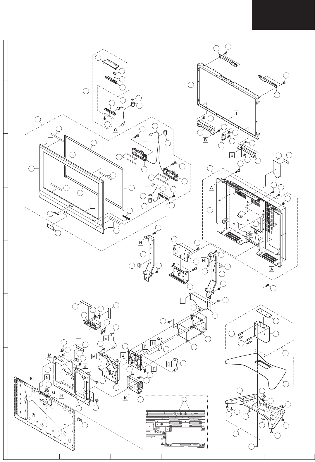
165
LC-26GA5E
LC-32GA5E
LC-32GD8E/RU
LC-32BT8E/RU
LC-37GD8E/RU
LC-37BT8E/RU
LC-32/37GD8E/RU
LC-32/37BT8E/RU
CABINET AND MECHANICAL PARTS (LC-32GD8E/RU, LC-32BT8E/RU)
55
LC-32/37GD8E/RU
LC-32/37BT8E/RU
CABINET AND MECHANICAL PARTS (LC-32GD8E/RU, LC-32BT8E/RU)
654321
A
B
C
D
E
F
G
H
23
L
L
D
A
A
A
B
K
1
38
46
1-1
1-7
1-8
1-8
1-7
1-9
1-9
1-5
1-5
1-4
1-3 1-2
1-6
1-6
1-12
1-12
1-11
1-16
1-16
1-13
1-14
1-15
1-10
39
6
952
52
10
52
52
52
12
10
16
45
9
847
51
52
52
52
58
58
41
40
32
42
44
58 22
36
24 24
58
58
48
33
54
53
43
21
18
26
15
51
19
20
34
30
35
29
12 52
52
57
28
4
5
49
55
27
7
14
50
13
54
55
2
56
56
56
37
3
3-3
3-5
2-1
2-3
4-2
4-1
4-3
4-3
5-1
5-4
5-4
5-3
5-3
5-3
5-3
5-5
5-4
5-4
5-2
2-2
3-4
3-2
3-1
17
17
25
59
59
166
LC-26GA5E
LC-32GA5E
LC-32/37GD8E/RU
LC-32/37BT8E/RU
REF No. PARTS DESCRIPTION * SN CODE EX CODE
17 LHLDW1173CEZZ Wire Holder, x3 R AD AD
18 LHLDW1205CEZZ Wire Holder, x2 R AC AC
19 LHLDWA055WJKZ Wire Holder, x1 R AC AC
20 LHLDW1072GEZZ Wire Holder, x1 R
21 PCUSGA009WJKZ Cushion Spacer
22 PFLT-A004WJZZ Felt Sheet, x2 R AE AE
23 PMLT-A255WJZZ Spacer, x1 R AD AD
24 PMLT-A315WJZZ Spacer, x2 R AP AP
25 PSHEFA018WJZZ Sheet, x1 S -- --
26 PSLDMA770WJZZ Shield, x1 S -- --
27 PSLDMA584WJZZ Shield, x1 R AE AE
28 PSLDMA877WJFW Control PWB Shield S -- --
29 PSLDMA943WJFW Digital PWB Shield S -- --
30 PSLDMA840WJZZ Shield, x1 R AD AD
31 PSPAHA902WJZZ Spacer, x2 S -- --
32 DUNTKD890FM07 Main Unit - - -
33 DUNTKD604FM10 AV Unit - - -
34 DUNTKD605FM03 Power Unit - - -
35 DUNTKD628FM01 Digital Unit - - -
36 CKITKD609FM01 DIGITAL TUNER Unit S AY BN
37 DUNTKD606FMV0 Operation Unit - - -
38 DUNTKD607FMV0 R/C LED Unit - - -
39 QCNW-E412WJQZ Connecting Cord R AG AG
40 QCNW-E415WJQZ Connecting Cord R AP AP
41 QCNW-E237WJPZ Connecting Cord S -- --
42 QCNW-E419WJQZ Connecting Cord R AM AM
43 QCNW-E609WJQZ Connecting Cord R AH AH
44 QEARPA212WJFW Grounding Part R AE AE
45 QEARZA096WJFW Grounding Part S -- --
46 RCORF0103CEZZ Ferrite Core, x2 S AK AK
47 TLABZB122WJZZ POP�Label S -- --
48 Not Available Serial No Label - - -
49 LX-BZA146WJF7 Screw, x4 S -- --
50 LX-BZA147WJF7 Screw, x4 S -- --
51 XBBS930P06000 Screw, x10 R AA AA
52 XBPS730P06WS0 Screw, x17 R AA AA
53 XBPS830P06000 Screw, x1 R AA AA
54 XEBS930P08000 Screw, x4 S AA AA
55 XEBS940P16000 Screw, x11 R AB AB
56 XEBSN40P10000 Screw, x5 R AB AB
57 XJPS730P04WS0 Screw, x2 S -- --
58 XJPS730P08WS0 Screw, x4 R AA AA
59 RCORFA064WJZZ FPC WireFerrite Core, x2 D
REF No. PARTS DESCRIPTION * SN CODE EX CODE
1CCABAB443WJ01 Cabinet A Ass'y (LC-37GD8E/RU) S -- --
1CCABAB443WJ02 Cabinet A Ass'y (LC-37BT8E/RU) S -- --
1_1 Not Available Cabinet A - - -
1_2 GCOVAB478WJSA R/C, LED Cover S -- --
1_3 HBDGBA060WJSA Badge, "SHARP" S -- --
1_4 LX-HZA003WJFN Screw, x2 S -- --
1_5 PSPAHA858WJZZ Mask Spacer, x2 S -- --
1_6 PSPAHA859WJZZ Mask Spacer, x2 S -- --
1_7 PSPAZB211WJZZ Spacer for Speaker, x4 S -- --
1_8 QCNW-E413WJQZ Connecting Cord S -- --
1_9 QCNW-E801WJQZ Connecting Cord S -- --
1_10 RCORF0103CEZZ Ferrite Core, x1 R AK AK
1_11 RCORFA023WJZZ Ferrite Core, x2 R AK AK
1_12 RSP-ZA184WJN1 Speaker-L S -- --
1_13 RSP-ZA184WJN2 Speaker-R S -- --
1-14 XEBS930P08000 Screw, x2 R AA AA
2CCABBA714WJ01 Cabinet B Ass'y S AY BM
2_1 Not Available Cabinet B - - -
2_2 LHLDWA055WJKZ Wire Holder, x1 R AC AC
2_3 PSPAHA823WJZZ Spacer-A, x1 S -- --
2_4 PSPAHA824WJZZ Spacer-B, x1 S -- --
2_5 PSPAHA834WJZZ Spacer-C, x2 S -- --
2_6 PSPAHA826WJZZ Spacer-D, x2 S -- --
3CCOVAB480WJ01 Top Cover Ass'y S -- --
3_1 Not Available Top Cover - - -
3_2 JBTN-A524WJKA Power Button S -- --
3_3 JBTN-A525WJKA Operation Button S -- --
3_4 MSPRCA068WJFW Spring, for Power Button S -- --
3_5 XEBS930P08000 Screw, x3 R AA AA
4CDAI-A290WJ01 Stand Support Ass'y (LC-37GD8E/RU) S -- --
4CDAI-A290WJ03 Stand Support Ass'y (LC-37BT8E/RU) S -- --
4_1 Not Available Stand Support - - -
4_2 GDAI-A290WJSA Support Cover (LC-37GD8E/RU) S -- --
4_2 GDAI-A290WJSC Support Cover (LC-37BT8E/RU) S -- --
4_3 HDECQA600WJKA Decoration Cover, x4 S -- --
5CDAI-A301WJ01 Stand Base Ass'y (LC-37GD8E/RU) S -- --
5CDAI-A301WJ03 Stand Base Ass'y (LC-37BT8E/RU) S -- --
5_1 Not Available Stand Base Cover - - -
5_2 LANGKA635WJZZ Base Angle S -- --
5_3 PSPAZA949WJZZ Leg Cushion A, x4 S -- --
5_4 PSPAZA950WJZZ Leg Cushion B, x4 S -- --
5_5 XEBS740P10000 Screw, x10 S -- --
6R1LK370T3LZ5BX 37" LCD Panel Module R EZ EZ
7GCOVAB488WJKA Stand Cover S -- --
8HINDPB763WJSA Model Label�(LC-37GD8EE/EK/EF) S -- --
8HINDPB764WJSA Model Label�(LC-37GD8EI) S -- --
8HINDPB765WJSA Model Label�(LC-37GD8RU) S -- --
8HINDPB794WJSA Model Label�(LC-37BT8EE/EK/EF) S -- --
8HINDPB795WJSA Model Label�(LC-37BT8EI) S -- --
8HINDPB796WJSA Model Label�(LC-37BT8RU) S -- --
9LANGKA672WJFW LCD Angle C, x1 S -- --
10 LANGKA675WJFW LCD Angle, x4 S -- --
11 LANGTA266WJFW Stand Angle S -- --
12 LANGTA268WJFW Center Angle (L) S -- --
13 LANGTA269WJFW Center Angle (R) S -- --
14 LCHSMA324WJZZ Chassis Tray R
15 LHLDW1033CE00 Wire Holder, x1 R
16 LHLDW1123GEZZ Wire Holder, x3 R AB AB
(LC-37GD8E/RU, LC-37BT8E/RU)
CABINET AND MECHANICAL PARTS LISTING
167
LC-26GA5E
LC-32GA5E
LC-32GD8E/RU
LC-32BT8E/RU
LC-37GD8E/RU
LC-37BT8E/RU
LC-32/37GD8E/RU
LC-32/37BT8E/RU
CABINET AND MECHANICAL PARTS (LC-37GD8E/RU, LC-37BT8E/RU)
56
LC-32/37GD8E/RU
LC-32/37BT8E/RU
CABINET AND MECHANICAL PARTS
(LC-37GD8E/RU, LC-37BT8E/RU)
654321
A
B
C
D
E
F
G
H
L
29
58
L
32 43
44
58
41
35
42
15
46
2-4
2-3
D
A
A
A
B
K
1-10
1-13
1-12
1-11 1-14
1-14
1-8
1-9
1-4
1-4
1-3
1-1
1-7
1-6
1-5
1-5
1-2
1
47
38
1-6
52
56
10
9
3-1
3-5
2-2
4-2
4-1
5-1
5-4
5-4
5-4
5-4
5-5
5-2
5-3
5-3
5-3
5-3
4-3
4-3
2-1
2-6
2-6
3-3
3-4
3-2
3
37 39
25
6
52
52
10
10
52
52
56
56
848
51
2
52
52
52
4
5
49
55
13
26
50
11
52
58
52
17
40
34
21
12
54
55
10
2-5
7
45
58 20
36
22 22
58
33
54
53
24
14
51
23
18
19
16
28
57
16
27
59
59
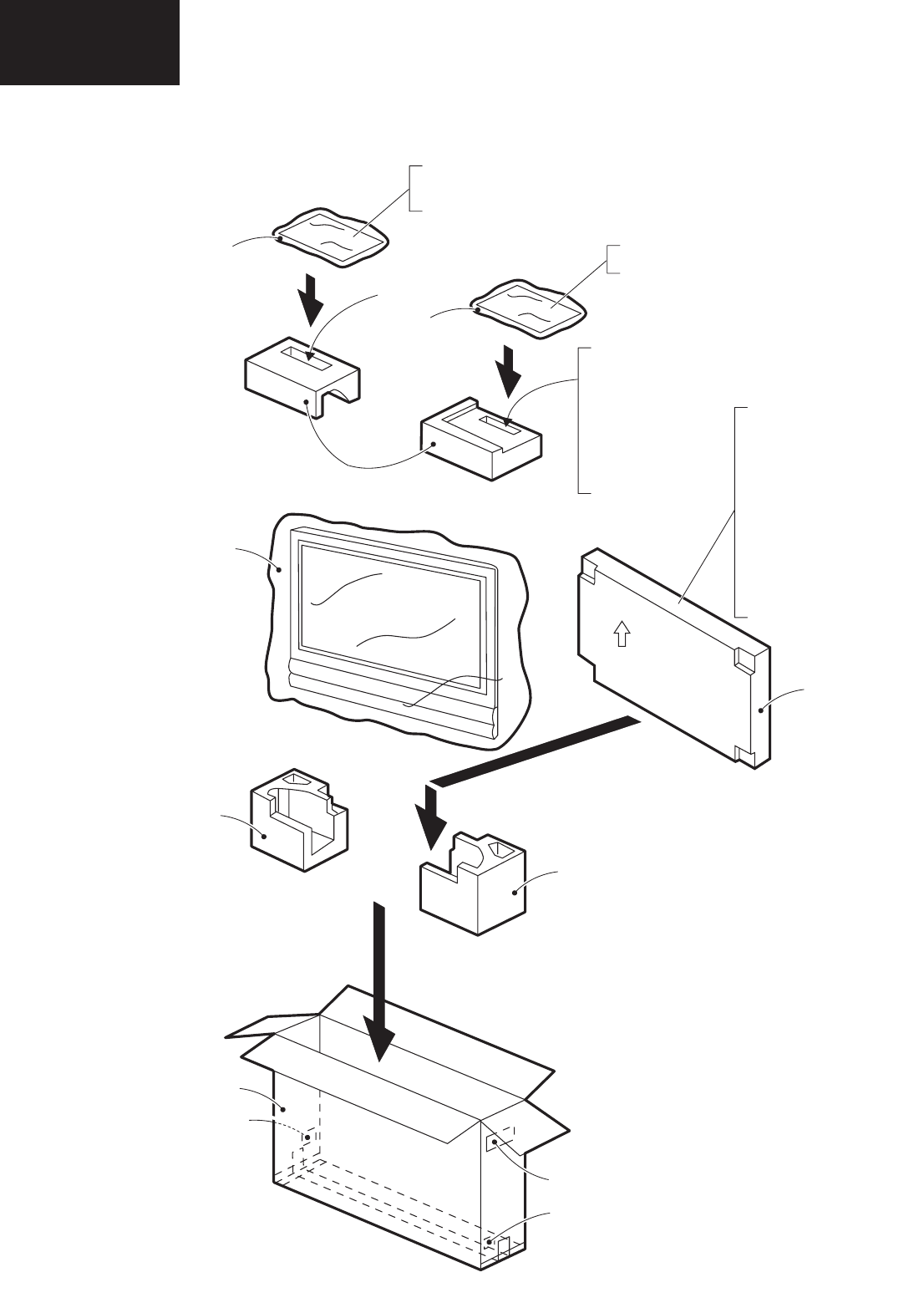
168
LC-26GA5E
LC-32GA5E
LC-32/37GD8E/RU
LC-32/37BT8E/RU
58
LC-32/37GD8E/RU
LC-32/37BT8E/RU
PACKING OF THE SET
S6
X1
X2
X3
X4
X9
S8
X5
S6
S11
FRONT
S12
S2
S6
S1
S13
S9
S3
X8
X10
X11
X12
X13
X14
X15
S4
S5
S7
S10
S9
X6
X7
PACKING OF THE SET
169
LC-26GA5E
LC-32GA5E
LC-32GD8E/RU
LC-32BT8E/RU
LC-37GD8E/RU
LC-37BT8E/RU
LC-32/37GD8E/RU
LC-32/37BT8E/RU
REF No. PARTS DESCRIPTION * SN CODE EX CODE
S1 SPAKCC720WJZZ Packing Case (LC-32GD8EE/EK/EF/EI) - - -
S1 SPAKCC795WJZZ Packing Case (LC-32GD8RU) - - -
S1 SPAKCC756WJZZ Packing Case (LC-32BT8EE/EK/EF/EI) - - -
S1 SPAKCC759WJZZ Packing Case (LC-32BT8RU) - - -
S1 SPAKCC721WJZZ Packing Case (LC-37GD8EE/EK/EF/EI) - - -
S1 SPAKCC796WJZZ Packing Case (LC-37GD8RU) - - -
S1 SPAKCC757WJZZ Packing Case (LC-37BT8EE/EK/EF/EI) - - -
S1 SPAKCC760WJZZ Packing Case (LC-37BT8RU) - - -
S2 SPAKFB018WJZZ Packing Case (Stand) - - -
(LC-32GD8E/RU, LC-32BT8E/RU)
S2 SPAKFA916WJZZ Packing Case (Stand) - - -
(LC-37GD8E/RU, LC-37BT8E/RU)
S3 SPAKPA382WJZZ Wrapping Paper (LC-32GD8E/RU, LC-32BT8E/RU) - - -
S3 SPAKPA338WJZZ Wrapping Paper (LC-37GD8E/RU, LC-37BT8E/RU)
S4 SPAKPA601WJZZ Wrapping Paper (Stand) - - -
(LC-37GD8E/RU, LC-37BT8E/RU)
S5 SPAKPA602WJZZ Wrapping Paper (Stand) - - -
(LC-37GD8E/RU, LC-37BT8E/RU)
S4 SPAKPA684WJZZ Wrapping Paper (Stand) - - -
(LC-32GD8E/RU, LC-32BT8E/RU)
S5 SPAKPA685WJZZ Wrapping Paper (Stand) - - -
(LC-32GD8E/RU, LC-32BT8E/RU)
S6 SPAKXA919WJZZ Buffer Material - - -
(LC-32GD8E/RU, LC-32BT8E/RU)
S6 SPAKXA920WJZZ Buffer Material - - -
(LC-37GD8E/RU, LC-37BT8E/RU)
S7 SPAKFB019WJZZ Buffer Material (Stand) (LC-32GD8E/RU) - - -
S7 SPAKFB027WJZZ Buffer Material (Stand) (LC-32BT8E/RU) - - -
S7 SPAKFB043WJZZ Buffer Material (Stand) (LC-37GD8E/RU) - - -
S7 SPAKFB029WJZZ Buffer Material (Stand) (LC-37BT8E/RU) - - -
S8 SSAKAA009WJZZ Polyethylene Bag - - -
S9 SSAKAA010WJZZ Polyethylene Bag, x2 - - -
S10 SSAKHA020WJZZ Polyethylene Bag (Stand) - - -
S11 TLABKA002WJZZ No. Label - - -
S12 TLABSA050WJZZ Green Dot Label - - -
(LC-32/37GD8E(F),LC-32/37BT8E(F))
PACKING PARTS LISTING
REF No. PARTS DESCRIPTION * SN CODE EX CODE
X1 LHLDW0110CESB Cable Clamp S -- --
X2 LHLDWA083WJ00 Cable Tie S -- --
! X3 QACCBA073WJPZ AC Cord S -- --
(LC-32/37GD8EK, LC-32/37BT8EK)
! X3 QACCKA021WJPZ AC Cord S -- --
(LC-32/37GD8EE/EF/EI/RU, LC-32/37BT8EE/EF/EI/RU)
X4 QCNWGA075WJPZ 3 RCA to 15-pin D-sub Adapter S -- --
X5 RRMCGA472WJSA Remote Control Unit (LC-32/37GD8E/RU) S -- --
X5 RRMCGA490WJSA Remote Control Unit (LC-32/37BT8E/RU) S -- --
X6 TGAN-A077WJZZ Guarantee card S -- --
(LC-32/37GD8RU, LC-32/37BT8RU)
X6 TGAN-A342WJZZ Guarantee card S -- --
(LC-32/37GD8EK, LC-32/37BT8EK)
X6 TGAN-A512WJZZ Guarantee card S -- --
(LC-32/37GD8EK, LC-32/37BT8EK)
X7 TINS-C483WJZZ Operation Manual S AK AW
(LC-32/37GD8EE/EK/EF/EI, LC-32/37BT8EE/EK/EF/EI)
X7 TINS-C484WJZZ Operation Manual S AK AW
(LC-32/37GD8EE/EF, LC-32/37BT8EE/EF)
X8 TINS-C485WJZZ Operation Manual S AH AT
(LC-32/37GD8EE, LC-32/37BT8EE)
X7 TINS-C486WJZZ Operation Manual S AD AL
(LC-32/37GD8RU, LC-32/37BT8RU)
X9 Not Available "AAA" size Battery, x2 - - -
X10 CDAI-A290WJ01 Stand Support (LC-32/37GD8E/RU) S -- --
X10 CDAI-A290WJ03 Stand Support (LC-32/37BT8E/RU) S -- --
X11 CDAI-A287WJ01 Stand Base (LC-32GD8E/RU) S -- --
X11 CDAI-A287WJ05 Stand Base (LC-32BT8E/RU) S -- --
X11 CDAI-A301WJ01 Stand Base (LC-37GD8E/RU) S -- --
X11 CDAI-A301WJ03 Stand Base (LC-37BT8E/RU) S -- --
X12 LX-BZA146WJF7 Screw, x4 S -- --
X13 LX-BZA147WJF7 Screw, x4 S -- --
X14 TCAUZA229WJZZ Caution Sheet (LC-37BT8E/RU) S -- --
X15 UKOGLA001WJZZ Tool For Stand S -- --
SUPPLIED ACCESSORIES PARTS LISTING
REF No. PARTS DESCRIPTION * SN CODE EX CODE
QCNW-E542WJZZ 23pins Board to Board J
QCNW-E543WJZZ 9pins Board to Board J
QCNW-E544WJZZ 15pins Board to Board J
QCNW-E546WJZZ 7pins Board to Board J
QCNWKA011WJZZ Extension Cable for Digital Unit S AW BH
1CKIT-0004WJV0 P55 VCTP SOFT UPDATING WITH WIRE 20 TO 3 S BC BT
1.1 QPWBX0004WJZZ P55 I2C INTERFACE PWB (NOT AVAILABLE) - - -
1.2 QCNWGA100WJZZ WIRE 20 TO 3 PIN SOFT UPDATING P55 S AM AY
2 QCNWGA015WJPZ Cable adaptor (DB9 male to mini-Din 9 pin male) S AG AS
3 QCNWKA012WJZZ P70 Digital Board Software Updating Jig S AZ BP
SERVICE JIGS
(USE FOR SERVICING)
EXTENSION CABLES
SOFTWARE UPGRADING JIG
