C 100 Series Controller Manual LC.400 V1.18
User Manual:
Open the PDF directly: View PDF ![]() .
.
Page Count: 72
1
Chapter 1 Introduction ---------------------------------------------------------------------------------------------------------------------------------------------- 3
1.1 Introduction -------------------------------------------------------------------------------------------------------------------------------------------------- 3
1.2 Unpacking ----------------------------------------------------------------------------------------------------------------------------------------------------- 3
1.3 Software Installation --------------------------------------------------------------------------------------------------------------------------------------- 4
Chapter 2 Controller Interfaces ----------------------------------------------------------------------------------------------------------------------------------- 5
2.1 Back Panel ---------------------------------------------------------------------------------------------------------------------------------------------------- 5
2.1 Front Panel --------------------------------------------------------------------------------------------------------------------------------------------------- 6
Chapter 3 Operation ------------------------------------------------------------------------------------------------------------------------------------------------- 7
3.1 Control Loop Tuning --------------------------------------------------------------------------------------------------------------------------------------- 7
3.1.1 PID Control Loop Tuning ------------------------------------------------------------------------------------------------------------------------------ 8
3.1.2 Notch Filters ---------------------------------------------------------------------------------------------------------------------------------------------- 9
3.1.3 2nd Integrator ------------------------------------------------------------------------------------------------------------------------------------------- 12
3.2 Waveforms and Position Monitoring ---------------------------------------------------------------------------------------------------------------- 15
3.2.1 Internal Waveform Generation ------------------------------------------------------------------------------------------------------------------- 15
3.2.2 Continuous Position Monitoring ------------------------------------------------------------------------------------------------------------------ 16
3.2.3 High Resolution Recording ------------------------------------------------------------------------------------------------------------------------- 17
3.2.4 Custom Waveform Files ----------------------------------------------------------------------------------------------------------------------------- 17
3.3 Digital I/O --------------------------------------------------------------------------------------------------------------------------------------------------- 18
3.3.1 Digital Inputs - Start Signal-------------------------------------------------------------------------------------------------------------------------- 20
3.3.2 Digital Inputs - Start and Stop --------------------------------------------------------------------------------------------------------------------- 20
3.3.3 Digital Inputs - Pause and Resume --------------------------------------------------------------------------------------------------------------- 21
3.3.4 Digital Outputs – Control Loop Error------------------------------------------------------------------------------------------------------------- 22
3.3.5 Digital Outputs – Waveform Index --------------------------------------------------------------------------------------------------------------- 23
3.3.6 Digital Outputs – Fault ------------------------------------------------------------------------------------------------------------------------------- 23
3.3.7 Digital Outputs – Sensor Based Position Pulse ------------------------------------------------------------------------------------------------ 23
3.3.8 Digital Encoder Interface ---------------------------------------------------------------------------------------------------------------------------- 24
3.4 Graph Controls -------------------------------------------------------------------------------------------------------------------------------------------- 25
3.5 Additional Software Features ------------------------------------------------------------------------------------------------------------------------- 26
3.5.1 Trajectory Generation ------------------------------------------------------------------------------------------------------------------------------- 28
3.5.2 Raster Scanning ---------------------------------------------------------------------------------------------------------------------------------------- 29
3.5.3 Spiral Scanning ----------------------------------------------------------------------------------------------------------------------------------------- 31
Chapter 4 Advanced Controller Communication ---------------------------------------------------------------------------------------------------------- 32
4.1 LC.400 USB Drivers --------------------------------------------------------------------------------------------------------------------------------------- 32
4.2 Ethernet Interface ---------------------------------------------------------------------------------------------------------------------------------------- 32
4.3 Memory Read/Write Commands --------------------------------------------------------------------------------------------------------------------- 33
4.3.1 Read Single Location Command ------------------------------------------------------------------------------------------------------------------- 33
4.3.2 Write Single Location Command ------------------------------------------------------------------------------------------------------------------ 34
4.3.3 Read Array Command -------------------------------------------------------------------------------------------------------------------------------- 34
4.3.4 Write Next Command -------------------------------------------------------------------------------------------------------------------------------- 34
4.4 Controller Memory Locations ------------------------------------------------------------------------------------------------------------------------- 35
4.4.1 Channel Base Memory Addresses ---------------------------------------------------------------------------------------------------------------- 35
4.4.2 Static Positioning Addresses ----------------------------------------------------------------------------------------------------------------------- 35
4.4.3 Control Loop Addresses ----------------------------------------------------------------------------------------------------------------------------- 35
4.4.4 Wavetable Addresses -------------------------------------------------------------------------------------------------------------------------------- 36
4.4.5 Digital I/O Trigger Addresses ----------------------------------------------------------------------------------------------------------------------- 37
2
4.4.6 General Addresses ------------------------------------------------------------------------------------------------------------------------------------ 39
4.4.7 Trajectory Generation Addresses ----------------------------------------------------------------------------------------------------------------- 40
4.4.8 Raster Scan Addresses ------------------------------------------------------------------------------------------------------------------------------- 42
4.4.9 Recording Addresses --------------------------------------------------------------------------------------------------------------------------------- 42
4.4.10 Spiral Scan Addresses ---------------------------------------------------------------------------------------------------------------------------- 44
Chapter 5 Maintenance and Cleaning ------------------------------------------------------------------------------------------------------------------------ 45
5.1 Maintenance ----------------------------------------------------------------------------------------------------------------------------------------------- 45
5.2 Cleaning ----------------------------------------------------------------------------------------------------------------------------------------------------- 45
Chapter 6 Safety----------------------------------------------------------------------------------------------------------------------------------------------------- 46
Appendix A Specifications -------------------------------------------------------------------------------------------------------------------------------------- 47
Appendix B Instructions for connecting new stages with EEPROM -------------------------------------------------------------------------------- 48
Appendix C Parallel Interface Specifications -------------------------------------------------------------------------------------------------------------- 50
General-------------------------------------------------------------------------------------------------------------------------------------------------------------- 50
Position Monitoring --------------------------------------------------------------------------------------------------------------------------------------------- 50
Demand Input ----------------------------------------------------------------------------------------------------------------------------------------------------- 51
Configuration ------------------------------------------------------------------------------------------------------------------------------------------------------ 52
Timing --------------------------------------------------------------------------------------------------------------------------------------------------------------- 53
Connector Pin-out and Considerations --------------------------------------------------------------------------------------------------------------------- 54
Timing Waveforms ----------------------------------------------------------------------------------------------------------------------------------------------- 57
Appendix D PFM Interface Specifications ------------------------------------------------------------------------------------------------------------------ 59
Overview ----------------------------------------------------------------------------------------------------------------------------------------------------------- 59
PFM Pulse (Pin 15) / Direction (Pin 8) ---------------------------------------------------------------------------------------------------------------------- 59
PFM Scaling -------------------------------------------------------------------------------------------------------------------------------------------------------- 59
Position Monitoring Data -------------------------------------------------------------------------------------------------------------------------------------- 60
End of Travel (EOT) Limit Switches , Positive (Pin 1), Negative (Pin 9) ----------------------------------------------------------------------------- 61
Enable (Pin 7) ------------------------------------------------------------------------------------------------------------------------------------------------------ 61
Interface Connector --------------------------------------------------------------------------------------------------------------------------------------------- 61
Appendix E Digital Encoder Interface ----------------------------------------------------------------------------------------------------------------------- 62
Overview ----------------------------------------------------------------------------------------------------------------------------------------------------------- 62
15-pin Connector Schematic ---------------------------------------------------------------------------------------------------------------------------------- 62
Signal Descriptions ----------------------------------------------------------------------------------------------------------------------------------------------- 62
Status LED’s -------------------------------------------------------------------------------------------------------------------------------------------------------- 63
Software Commands -------------------------------------------------------------------------------------------------------------------------------------------- 63
Appendix F AFM Interface Specifications ------------------------------------------------------------------------------------------------------------------ 65
Overview ----------------------------------------------------------------------------------------------------------------------------------------------------------- 65
AFM interface functionality ----------------------------------------------------------------------------------------------------------------------------------- 65
Appendix G Control loop error signal ------------------------------------------------------------------------------------------------------------------------ 66

3
Chapter 1 Introduction
1.1 Introduction
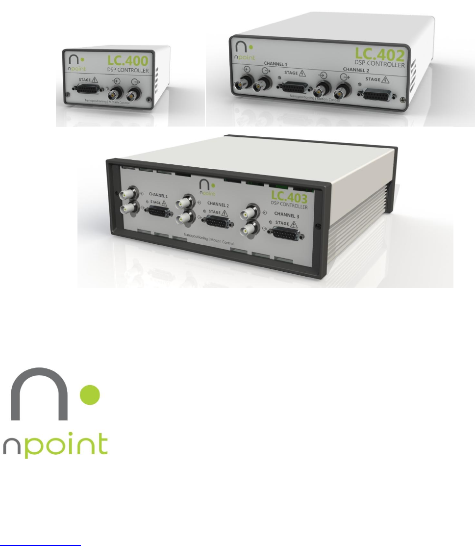
The LC.400 series DSP controllers are designed to control nPoint nanopositioners. They are available in 1, 2, or 3 channel
configurations. A complete nanopositioning system consists of the nanopositioner, controller and software.
This manual applies to the following LC.400 models:
LC.400 (1 Channel)
LC.402 (2 Channels)
LC.403 (3 Channels)
1.2 Unpacking
The following items are included in a standard closed-loop system package:
Nanopositioner
Nanopositioner test specifications sheet
Controller
External 12V power supply with AC power cord
USB cable
CD-ROM with installation software, manual, and Labview VIs
Carefully remove the items from the package. Report any damage or missing items immediately by phone (608-824-
1770 ext.207) or e-mail (support@npoint.com).
Controller Installation:
1. The controller box features an exhaust cooling fan on the back panel, and air intake holes in the sides or front
panel. Position the controller on a hard flat surface such that the ventilation holes are not obstructed.
2. Connect the power supply to the 12V DC power jack on the back panel (see Figure 2-1).
3. Power can be switched ON and OFF with the power switch on the back panel adjacent to the 12V DC power jack.
NOTE: To provide proper EMC shielding it is required to connect the AC power cord to a fully earth grounded (3-
terminal) receptacle.
4
1.3 Software Installation
1) Load the nPoint CD in your PC CD-ROM drive.
2) Connect the LC.400 series controller to your PC via USB, and power on the controller.
a. For Windows 7/8/10: the USB driver may load automatically if the PC is connected to the internet. This
may take several minutes.
b. For Windows XP: if the Add New Hardware Wizard appears, choose to automatically install the USB
driver.
c. If the USB drivers fail to install correctly, the drivers can be manually installed from the Windows Device
Manager by right clicking the device “USB Serial Converter A” or “USB Serial Converter” and selecting
the menu item “Update Driver Software”. Choose to specify the driver location, and browse to the USB
driver directory on the nPoint CD.
3) In the nPControl Software Installation directory of the CD, run setup.exe to complete installation of the nPoint
PC software. Windows 8 or Windows 10 may display a message regarding unrecognized software, select “Run
Anyway”.
a. If prompted to install version 4.0 of the Microsoft .NET Framework, run “dotNetFx40_Full_Setup.exe”
located on the nPoint CD, and then run setup.exe again to complete the installation.
4) After installation is complete, a shortcut to the nPControl software will be available in the Windows Start menu
by selecting “All Programs” and the nPoint folder, alternatively search for “nPControl”.
5
Chapter 2 Controller Interfaces
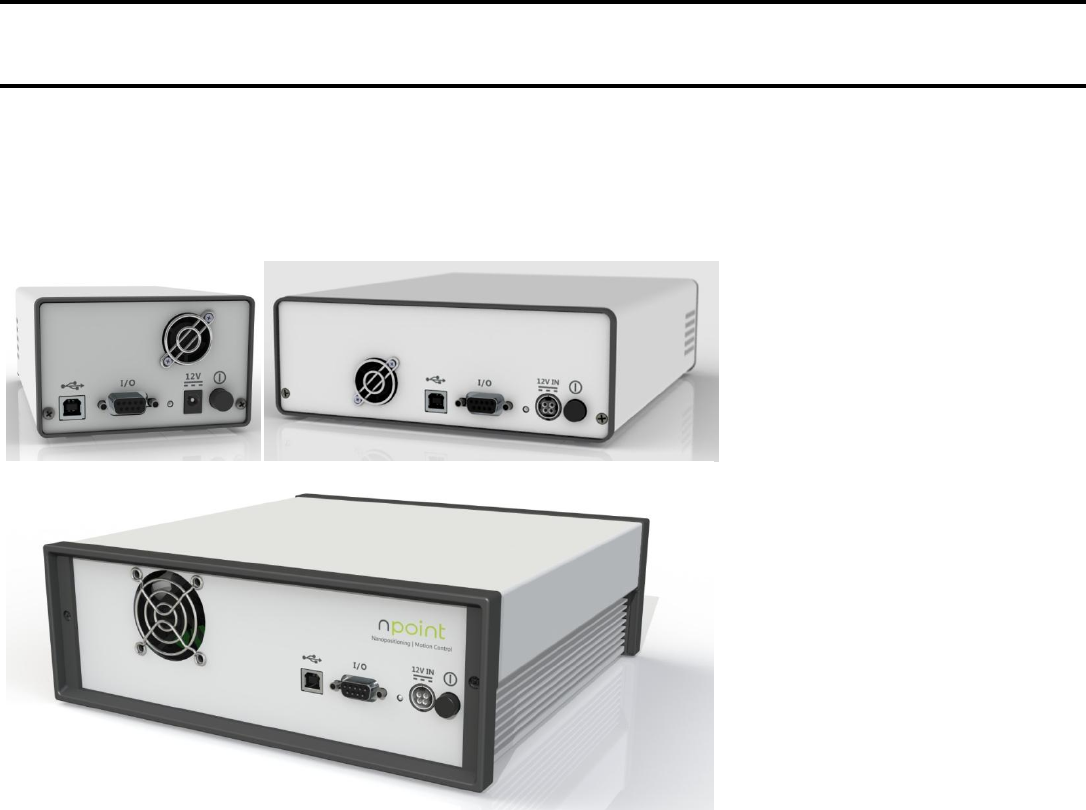
2.1 Back Panel
The controller back panel features the power ON/OFF switch, 12V DC power jack, 9-pin digital I/O connector, and the
USB interface connector. The back panel may also include an optional interface, such as a High Speed Parallel interface,
PFM interface, or AFM interface.
Figure 2-1: The back panel of the LC.400 series controllers.
6
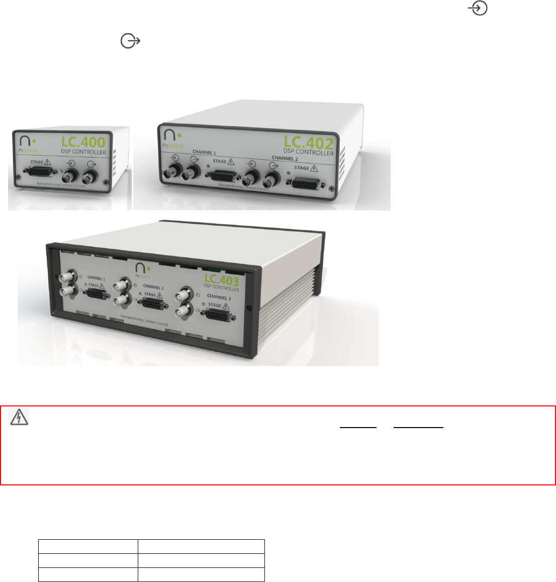
2.1 Front Panel
The front panel (see Figure 2-2) features the nanopositioner D-15 connectors and the analog I/O connectors. The D-15
connectors contain the sensor signals and the high voltage piezo signals. The BNC connectors labeled provides the
option to control position with an external voltage source. The standard voltage range of the BNC input is 10V. The
BNC connectors labeled is the position sensor monitor output with a standard voltage range of 10V. The sensor
monitor value provides position measurement with a 5 kHz bandwidth. The sensor monitor bandwidth can be
decreased with a software filter in the Settings menu.
Figure 2-2: The front panel of the LC.400 series controllers.
CAUTION: For the safety of both the user and the device, do not connect or disconnect the stage to/from the
controller while the controller is powered on. If a nanopositioner is disconnected while the controller is on, wait 2
minutes before reconnecting it. The nanopositioner has a high capacitance and may hold a high voltage charge. Never
touch the pins on the connectors. When the stage is connected to the controller, always fully tighten the connector
screws prior to powering on the controller.
The front panel LED’s have two colors to indicate the channel’s operating status. (When the LED’s are off, the power is
off):
LED Color
Channel Status
Red
Open-loop
Green
Closed-loop
7
Chapter 3 Operation
nPoint PC Software: nPControl
The nPControl consists of three main tabs:
Control Loop Tuning
Waveform & Position Monitoring
Digital I/O
Their functionality is described below. Additional software features are described in section 3.5.
3.1 Control Loop Tuning
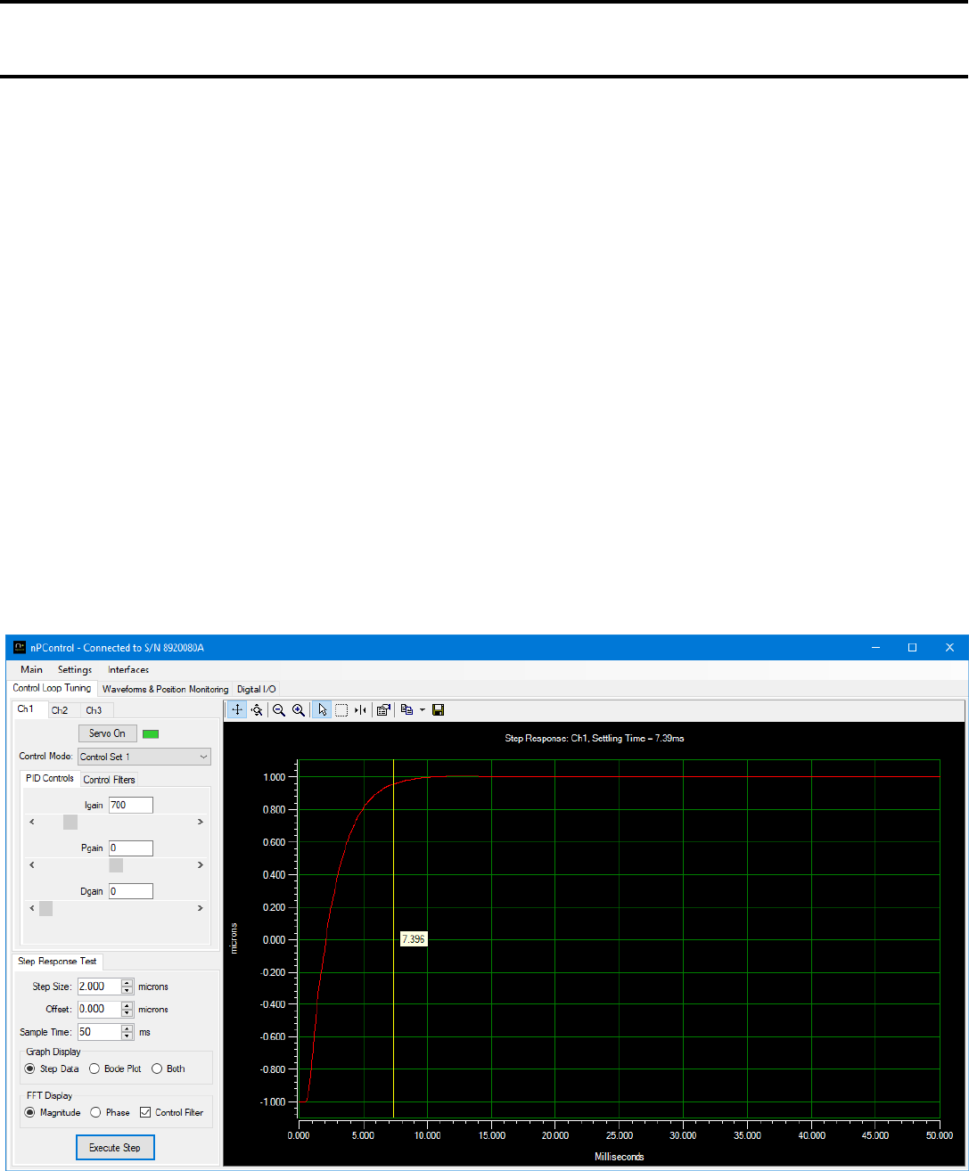
The Control Loop Tuning tab, shown in Figure 3-1, consists of:
Servo state: Servo ON – the system is in closed-loop mode; Servo OFF – the system is in open-loop mode.
Control Mode Selection for choosing among four customizable control sets.
P, I, and D sliders and text boxes used for changing P, I, and D parameters to optimize the step response.
Step response parameters to test PID and notch filter tuning
Step Response Graph to display the change in position over time during the step response test. Calculated settling
time is displayed at the top of the graph. A yellow cursor is displayed at the time the stage has settled (defined as
the time when the stage settles to within 2% of the commanded position). If the stage does not settle within the
user selected sample time, no settling time is displayed, and the sampling time should be increased.
Figure 3-1: The control loop tuning tab showing a 2µm step response.

8
3.1.1 PID Control Loop Tuning
The recommended P, I, and D parameters for each axis of the unloaded nanopositioner are provided in the product
Calibration Results document that shipped with the system. When the nanopositioner is installed at the user’s site and
loaded with a mass, the control loop bandwidth needs to be tuned properly to achieve the desired performance. This is
achieved by enabling appropriate notch filters and tuning one or more of the P, I, and D parameters. I gain is the main
parameter for tuning control loop bandwidth. P gain may be added to minimize overshoot. D gain is typically set to
zero. Optimization of the P, I, and D parameters is application specific. The user can vary the control parameters by
changing the values in the text boxes or by using the sliders. Section 3.1.2 describes how to tune the control parameters
via the nPControl GUI.
Once the desired control parameters have been identified they can be saved by selecting Save Configuration to
Controller in the Settings menu (see Figure 3-2).
Figure 3-2: The control configuration can be saved to the flash memory of the DSP controller by selecting the Save
Configuration to Controller in the Settings menu.
9
3.1.2 Notch Filters
The controller has the capability of storing up to four different control sets per channel. Each set includes two
independent notch filters and a 2nd integrator. The 2nd integrator is described in section 3.1.3. Notch filter tuning has a
significant impact on control loop bandwidth. Follow these steps to tune the notch filter parameters:
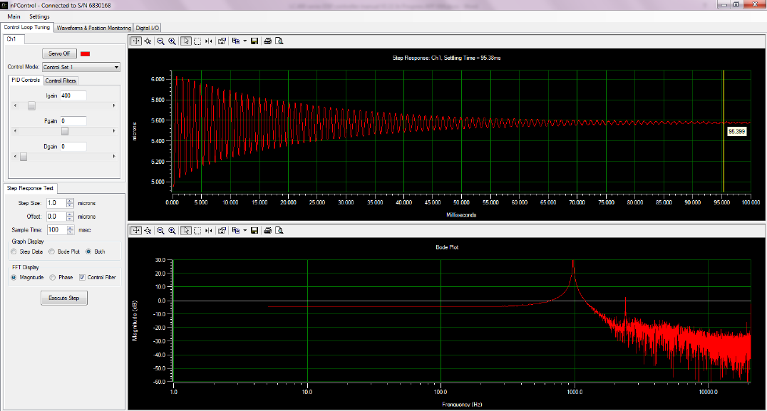
Set the system to open-loop mode (the servo toggle button should display Servo Off). Perform a 1um step response
to identify the resonant frequency of the system. The resonance peaks are identified in the Bode Plot, as shown in
Figure 3-3.
Figure 3-3: Step response of a system with a resonant frequency near 1000 Hz.
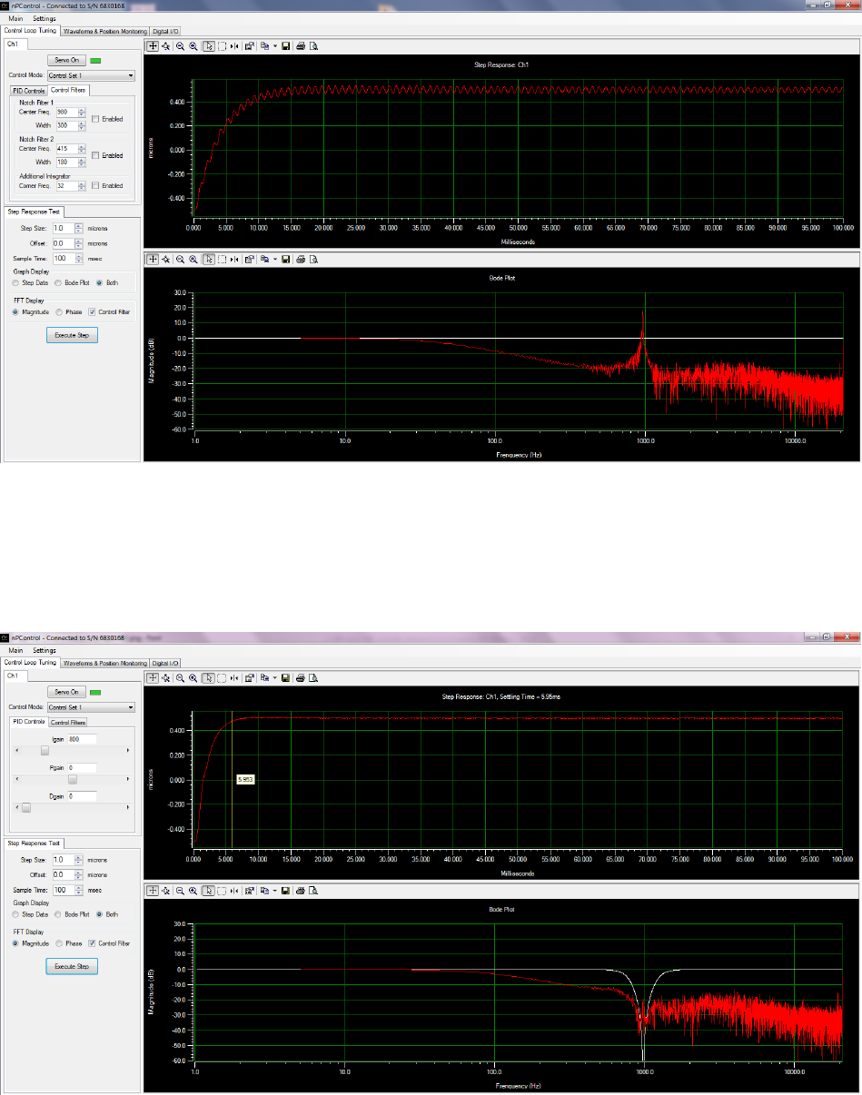
In the Control Filters tab, set the Center Frequency of the notch filter to match the resonant frequency.
Set the Width of the notch filter to match the width of the resonance as shown in Figure 3-4. In some instances a
wider filter will improve system stability. A filter that is too wide can cause step response overshot.
Check the Enabled checkbox to enable the filter.

10
Figure 3-4: Applying single notch filter for the resonance identified in Figure 3-3.
Set the system to closed-loop mode (the servo toggle button should display Servo On).
Execute a step to observe the effects of the control filters, as shown in Figure 3-5.
Figure 3-5: Step response of a system in closed-loop with the proper notch filters enabled and an Integral gain equal to
400.
11
For comparison, the step response of the system without the notch filter enabled is shown in Figure 3-6. The same I
gain used in both cases.
Figure 3-6: Step response of the system shown in Figure 3-5 in closed-loop without the proper notch filters enabled.
For multiple resonances, use both notch filters at the lowest frequency resonances.
Once the appropriate notch filter parameters have been enabled, a faster settling time can be achieved by
increasing the Integral gain (in the PID Controls tab). This is shown below in Figure 3-7 where an I gain of 800 has
been used.
Figure 3-7: Step response of a system in closed-loop with the proper notch filters enabled and an Integral gain equal to
800.

12
The new control settings can be saved by selecting Save Configuration to Controller in the Settings menu (Figure 3-2).
With careful control parameter optimization one can achieve a closed-loop system bandwidth of approximately 1/3
of the resonance frequency of the system.
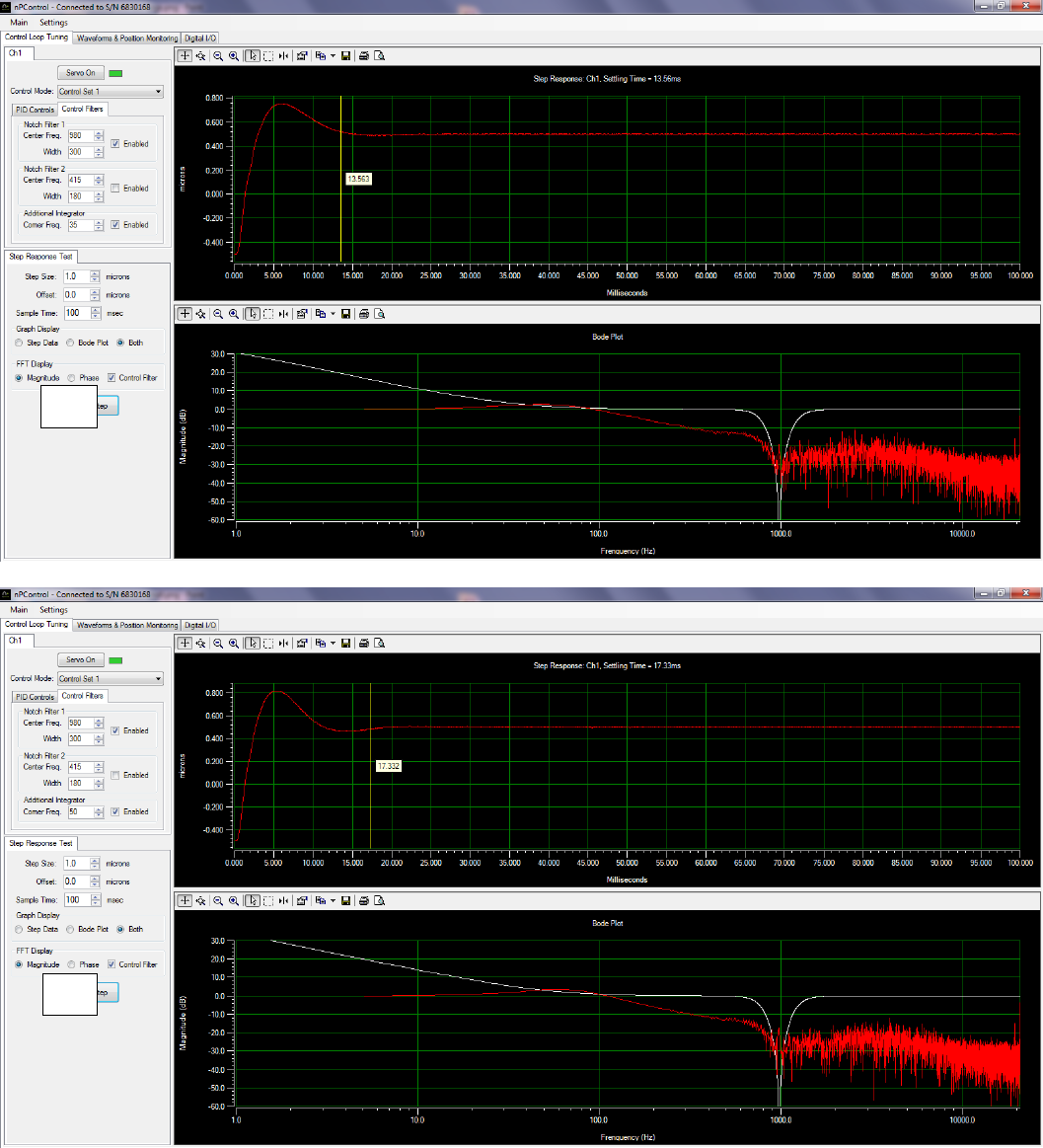
3.1.3 2nd Integrator
As described in the previous section, notch filters can help achieve a fast step response. In some applications the
nanopositioning system is used for constant velocity scanning rather than stepping. In this case using the Additional
Integrator control feature, in combination with notch filters, may provide the best performance. Enabling the Additional
Integrator and selecting the optimum corner frequency minimizes phase lag between the commanded position and the
actual position of the system (as measured by the sensor value).
Tuning this control feature is explained below.
Make sure the system is in closed-loop mode with the appropriate notch filters enabled and the I gain set to an
optimized value (Servo On).
Set the Corner Frequency value of the Additional Integrator to a low number (significantly lower than the
bandwidth of the system and, in some cases, as low as 1).
Check the Enabled checkbox to enable the filter.
Perform a step response and note the settling time. Note that the step response looks different than the step
response with the Additional Integrator disabled; however, the main optimization goal is still to minimize the
settling time.
Keep adjusting the Corner Frequency value until the settling time is minimized.
The figure below shows three cases during the tuning process: one where the Corner Frequency value is set too low (a),
optimized (b) and too high (c).
(a)
13
Figure 3-8: Optimizing the Additional Integrator Corner Frequency value. The step response is shown for a value that is
too low (a), optimized (b), and too high (c).
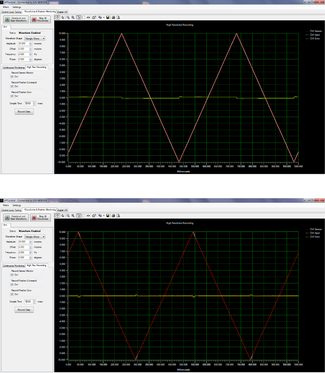
Use of the Additional Integrator improves scanning performance for constant velocity scanning applications. The
tracking error between commanded position and actual position is minimized when the Additional Integrator is
enabled. Tracking errors can be monitored by using the high resolution recording interface.
(b)
(c)
14
Figure 3-9: High resolution recording with the Additional Integrator disabled.
Figure 3-10: High resolution recording with the Additional Integrator enabled. Constant velocity tracking error is driven
to zero after the nanopositioner changes direction.
15
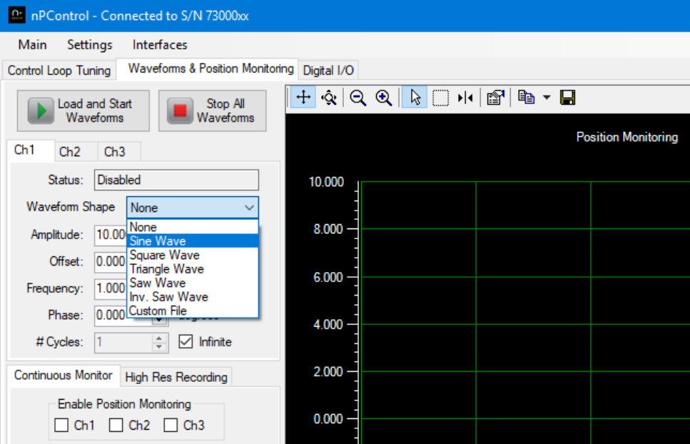
3.2 Waveforms and Position Monitoring
3.2.1 Internal Waveform Generation
The LC.400 series controllers feature internal function generator capability. The user can choose from a variety of
waveform shapes or load an arbitrary shape from a user created file. The waveform shape, amplitude, offset, and
frequency can be independently configured for each channel (see Figure 3-11). After configuring waveform parameters,
click the Download and Start Waveforms button to start the waveform. If parameters are changed while the waveform
is running, click the Download and Start Waveforms button again to start scanning with the new configuration. The
status indicator for each channel tab will display “Waveform Enabled” when the waveform is currently active for that
channel.
When the Infinite checkbox is checked, the waveform period will repeat indefinitely. If the Infinite checkbox is not
checked, the waveform will pause at the end of the number of cycles specified. Note that if the position at the end of
the waveform period is non-zero, the stage will pause at that position until the Stop All Waveforms button is clicked to
disable the Internal Waveform function.
The Static Digital Position command located on the Digital I/O tab is summed with the Internal Waveform function, and
can be used as an offset to the waveform that can be adjusted while the waveform is running.
Figure 3-11: The Waveform Generation GUI.
16
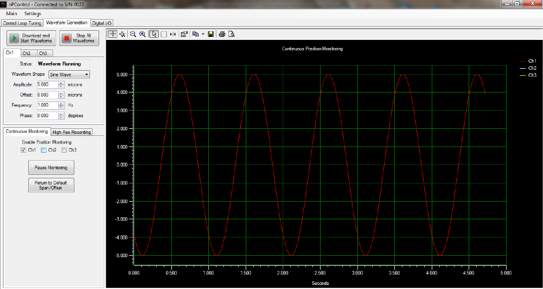
3.2.2 Continuous Position Monitoring
To monitor nanopositioner motion during scanning, check the Enable Position Monitoring checkboxes for the desired
controller channels in the Continuous Monitoring tab. Multiple controller channels can be monitored simultaneously.
When continuous monitoring is selected, the sensor signal is updated continuously on the screen, as shown in Figure
3-12.
Figure 3-12: Continuous monitoring of a Ch1 waveform.

17
3.2.3 High Resolution Recording
Figure 3-13 - High Resolution Recording user interface
The High Res Recording tab allows recording of high resolution data for a specified time. The recorded data is sampled
simultaneously at an exact sample rate in controller buffers. The buffers are then read back to the PC when the
recording is complete. If the recording time is less than 2 seconds, the data is sampled every 24 µs. If the recording
time is between 2 seconds and 4 seconds, the data is sampled every 48 µs, and so on. This functionality can be used to
better understand how control loop parameters affect the nanopositioner dynamic performance. For alignment
applications, this can be used to record an external analog signal (such as detector intensity) relative to stage sensor
readings. The BNC analog input values are displayed in volts.
3.2.4 Custom Waveform Files
A custom file can be loaded to scan with an arbitrary waveform shape. The file format is a text file (“.txt” extension)
with a single position specified in each line. For example, a 100 micron stage would have values between “-50.000” to
“50.000” for each line. The controller increments through the positions every 24 µsec, and loops back to the beginning
after reading the last position. The maximum number of positions is 83,333, which is equal to a 2 second period (0.5Hz
frequency). A single column of positions in a spreadsheet can be saved as a text file for a convenient way to edit the file.
Once the file is created, select Custom File as the waveform shape parameter and a file selection window will open.
After the file has been selected, click Download and Start Waveform to begin scanning with the custom file.
18
An example waveform file is included on the software CD. The example file contains the positions for a 1 micron peak to
peak 2 Hz sawtooth shape waveform. The position ramps from zero microns to 1 micron over a period of 0.5 seconds.
For viewing results after loading the example file, it is recommended that the high resolution recording feature is used
to display the position command and sensor monitor.
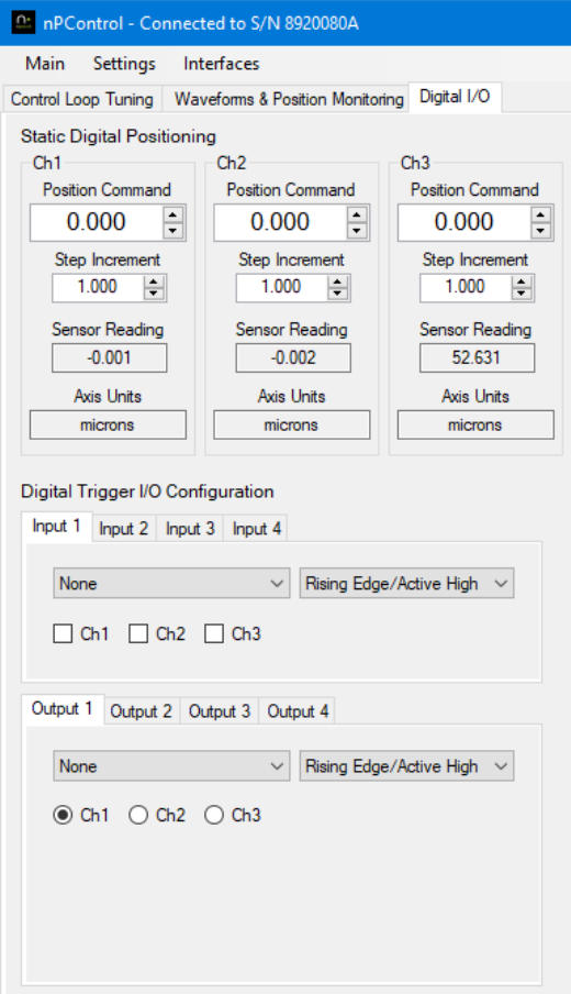
3.3 Digital I/O
The LC.400 series controllers are equipped with programmable digital I/O capabilities through the 9-pin D-sub connector
located on the back panel. The software interface for configuring the digital I/O pins is shown in Figure 3-14.
Figure 3-14: The Digital I/O tab.
19
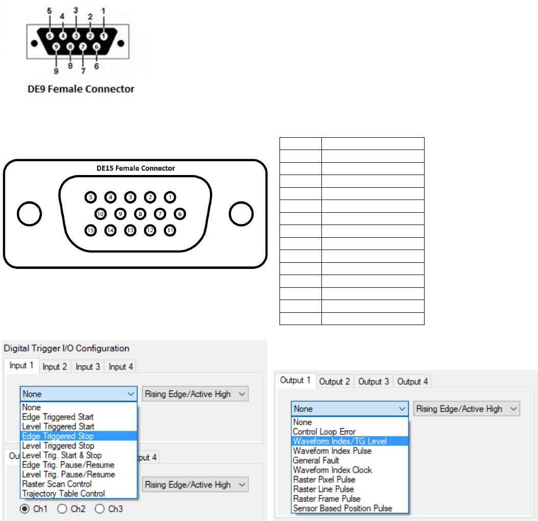
The four inputs and four outputs can be configured independently as shown in Figure 3-15. For controllers with a DE9
connector the four inputs correspond to pins 1-4, and the four outputs correspond to pins 6-9. Pin 5 is ground.
For controllers with a D15 connector in standard single ended configuration, the pinout is:
Figure 3-15: Configuration of the 9-pin digital I/O connector located on the back panel of the LC.400 series controllers.
Any channel can be assigned to any of the I/O pins. It is also possible for a single channel to be controlled by multiple
inputs and to control multiple outputs. Each trigger function is explained in the following sections.
Pin 1
Output 1
Pin 2
Output 3
Pin 3
Not Used
Pin 4
Not Used
Pin 5
Ground
Pin 6
Output 2
Pin 7
Output 4
Pin 8
Not Used
Pin 9
Not Used
Pin 10
Not Used
Pin 11
Input 1
Pin 12
Input 2
Pin 13
Input 3
Pin 14
Input 4
Pin 15
Not Used
20
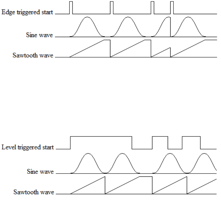
3.3.1 Digital Inputs - Start Signal
In the simplest configuration, an axis uses the digital input as a start signal. When the rising edge of the input is
detected, the waveform index is set to zero and it advances through the waveform one entry time each time the control
loop runs. When it gets to the end of the array, the index holds at the last location until the next start command is
received. If the start command is received before the index reaches the end, the index is immediately reset at zero and
continues to progress through the end of the waveform. Figure 3-16 shows the channel input when the edge-triggered
start command is used.
Figure 3-16: Edge Triggered Start Signal.
At the first start pulse the waveform starts running. Since it gets to the end before anything else happens, it holds the
final value. At the next start pulse, the index resets to zero and the waveform starts running again. If a start pulse occurs
before the index gets to the end of the array, the index will jump to zero and continue on.
When the start signal is used in a level triggering mode, the input will not hold at the end of the array if the signal is still
high. If the start signal goes low, then the input will hold at the end of the array until the next time the start signal goes
high. This is shown in Figure 3-17.
Figure 3-17: Level Triggered Start Signal.
When the start signal goes high, the index starts through the array. Since the start signal is still high when the index gets
to the end, the index will automatically start back at zero and continue. The second time the index gets to the end, the
start signal is low (it changed midway through the array) so the index stays at the end of the array until the start signal
goes high again. This time through the array, the start signal goes low and then high before the array gets to the end.
Since this is not edge triggered, the rising edge is ignored and the indexing resets to zero as if the start signal had
remained high for the whole period.
3.3.2 Digital Inputs - Start and Stop
The next configuration shown has an edge triggered start signal and an edge triggered stop signal. The start signal will
cause the indexing to start and run to the end of the array. The stop signal will force the index to stay at zero.
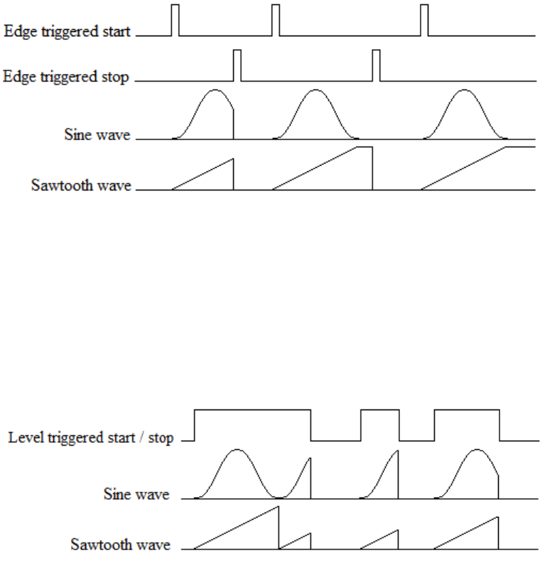
21
Figure 3-18 shows this. The waveform starts at the first start pulse, but the index is interrupted by the first stop pulse
and is set to zero. At the second start pulse, the waveform starts again, runs to the end and holds. The stop pulse resets
the index to zero, but the waveform does not begin until the next start pulse occurs.
Figure 3-18: Edge Triggered Start and Stop Signal.
If the start and stop signals are received at the same time, then the stop signal will have priority and no motion will
occur. These two configurations can be combined onto the same input pin by using a level triggered start and a level
triggered stop. When the signal is high, the input will be in free run mode, when it goes low, the index is set to zero and
held there. This is shown in Figure 3-19. The waveform starts when the signal goes high. Since the signal is still high
when the index gets to the end of the array, the index goes back to zero and continues. When the signal goes low, the
index is set to zero and is held at that value until the signal goes high again. In the next period, the signal is set low
before the index reaches the end of the array and the index is set to zero and is held at that value.
Figure 3-19: Level Triggered Start and Stop Signal.
The mixed cases where one signal is edge triggered and the other is level triggered will be similar. Since a level triggered
stop signal has priority over the start, it must be low (for positive polarity) in order for the start signal to have an effect.
3.3.3 Digital Inputs - Pause and Resume
In order to stop the motion, but start from the last position, a configuration that has an edge triggered pause/resume
signal can be used. The pause signal works just like the pause button on a music player where the same button is used to
pause then resume the song. In this case the first edge will pause the index and the second edge will cause the
waveform to resume.
In Figure 3-20 this is shown in combination with an edge triggered start.
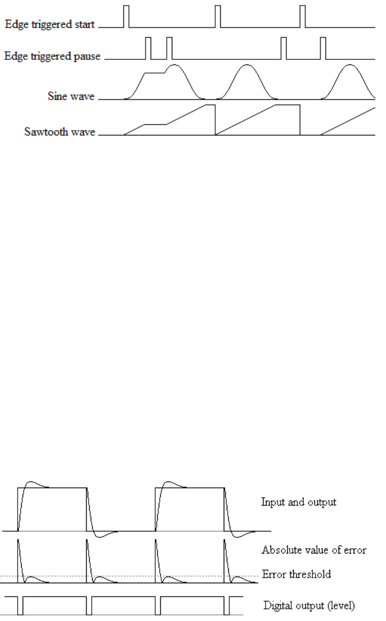
22
Figure 3-20: Level Triggered Start and Stop Signal.
The waveform starts with the rising edge of the start signal. As soon as the first pause edge is encountered, the indexing
stops but the index is not reset to zero; it is held constant. When the next edge is sent on the pause line, the indexing
resumes. Another pause signal is sent while the index is holding at the end of the array. The index is then set to zero, but
it does not advance. When the resume signal is sent, then the index begins to increment through the array.
The order of precedence here is that the start signal can reset the index even when the waveform is in the paused state.
However, the reset needs to be given before the waveform runs again.
If the pause/resume signal is configured as a level trigger rather than an edge trigger, there is no qualitative change in
the behavior. The rising edge and high level will pause the waveform and the falling edge and low level will resume it.
All the edge triggered examples shown so far use the positive edge as the main source for the trigger point. However,
they can be configured to use the negative edge instead. Likewise, the level actuated signals can have their polarity
reversed.
3.3.4 Digital Outputs – Control Loop Error
In this configuration the digital output monitors the control loop error signal. When the error is small, this means that
stage position is in the desired location.
This is illustrated in Figure 3-21.
Figure 3-21: Digital Output Based on the Control Loop Error.
Here the input is the square wave shown in the top line along with the stage response. The difference between these
two is the position error. When the absolute value of the position error is less than the specified error tolerance as

23
denoted by the dashed line, then the digital output is set high. When the error is larger than the tolerance, the output is
low. A more detailed explanation on how the control loop error output works is given in Appendix G Control loop
error signal.
3.3.5 Digital Outputs – Waveform Index
In this configuration the digital output changes the output level when the index of the stored waveform reaches a
specified index. Each channel can store an array of such index values. In Figure 3-22 the waveform is a triangle wave.
There are two index values where the output is set high (open circles) and two indexes where the output is set low
(filled circles). The resulting level on the digital output is shown on the second line. The third line shows an optional
pulsed version where the output is set high and then low again as each index (open or filled circle) is reached.
Figure 3-22: Digital Output Marking Points in the Waveform.
3.3.6 Digital Outputs – Fault
The digital output can also be used as an error indicator. If the control loop error stays larger than a given threshold for
longer than some time limit, then the error signal would be activated. This can be an indication of mechanical
obstruction. Default values for the tolerance and time limit will be 10% of the range for 1 second.
3.3.7 Digital Outputs – Sensor Based Position Pulse
Figure 3-23 - Sensor Based Position Pulse
The Sensor Based Position Pulse digital output function will pulse the selected output for 24 µs each time the stage
sensor reading passes through the specified Spacing increment. The Offset defines the sensor reading at which the
pulses begin, and the Number of pulses defines the total number of pulses including the pulse at the starting offset. For
example an offset of -5, spacing of 1, and Number of Pulses set to 11 would pulse the output at -5, -4, -3, -2, -1, 0, 1, 2, 3,
4, 5. The hysteresis value can be set slightly above the sensor noise to prevent pulses when the stage holding a static
position at one of the specified pulse positions. The sensor monitor lowpass filter can be used to reduce sensor noise
magnitude, but the phase delay added by the filter can be an issue in some fast scanning applications.
24
3.3.8 Digital Encoder Interface
Figure 3-24: Digital Encoder user interface
For controllers equipped with a Digital Encoder Interface option, parameters can be adjusted with the Digital Encoder
user interface located on the Digital I/O tab of the main nPControl window.
The Zero Count button will set the encoder position counter to zero for the current position. This function is typically
used when the controller is in open loop, and all position input commands are set to the zero position (the center of
stage travel). Position input commands include the Static Digital Position, Waveforms, and the BNC Analog Input.
The Alarm Status label and color indicator displays the state of the alarm signal. This value is updated once every second
when connected to the controller via USB.
The Sensor Gain value is used to adjust the system based on the distance per encoder count of the connected encoder.
The formula for calculating sensor gain is:
For example using a 100 micron range stage with an encoder distance of 1.582 nanometers per count:
1048576 control loop counts / 100 microns = 10485.76 control loop counts/micron
1 encoder count / 1.582 nanometers = 0.6321 encoder counts/nanometer
0.6321 * 1000 = 632.1 encoder counts per micron
10485.76/632.1 = 16.5888 Sensor Gain

25
3.4 Graph Controls
This section describes the graph controls available to the user.
Toolbar
Function
Allows the user to scroll the y-axis (position) up and down and the x-axis (time)
left and right, by clicking and dragging the X or Y graph axis region.
Allows the user to zoom in or out in the X or Y graph axis by clicking and
dragging in the X or Y graph axis region.
Allows the user to zoom out by clicking the button. If an axis region is selected
zooming is applied only to that axis. If the main graph region is selected both
the X and Y axes zoom out.
Allows the user to zoom in by clicking the button. If an axis region is selected
zooming is applied only to that axis. If the main graph region is selected both
the X and Y axes zoom in.
Allows the user to drag the main graph area, and hides the data cursor when
selected.
Allows the user to zoom in to part of the main graph area by clicking and
dragging a box.
Toggles cursor visibility, allows the user to click and drag the position of the
cursor, and allows the user to right click on the cursor to change the cursor
style.
Allows the user to edit the graph options.
Copies an image of the graph to the clipboard for pasting in another application.
Allows the user to copy an image or data to the clipboard for pasting in another
application.
Allows the graph to be saved either as an image or data file.
Table 3.1: Description of the toolbar button functions in the step response and monitoring graphs.
26
3.5 Additional Software Features
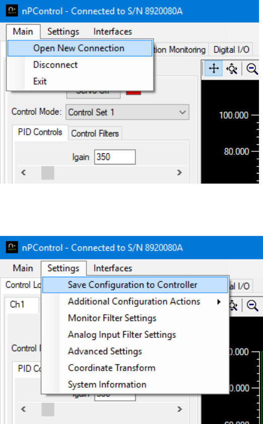
In the Main menu the user can connect to the controller, as shown below. When multiple controllers are connected to
the PC, selecting Open New Connection will bring up a new window that allows you to choose which controller to
connect to.
Figure 3-25: The nPControl software Main menu.
Figure 3-26: The nPControl software Settings menu.
The controller configuration can be saved to controller flash memory by selecting Save Configuration to Controller (See
Figure 3-26).
27
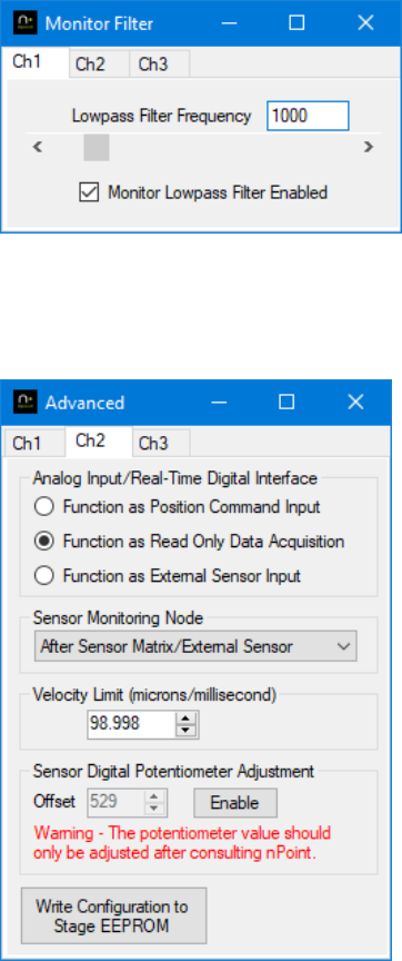
Figure 3-27: The Monitor Filter Settings window.
A low pass filter can be applied to the sensor monitor (including the analog BNC) by selecting Monitor Filter Settings.
The filter has a range of 50 Hz to 8000 Hz.
Figure 3-28: The Advanced Settings menu.
The Advanced Settings menu (see Figure 3-28) allows the user to:
Set the mode of the analog input BNC. External sensor mode uses the external signal for closed loop operation,
bypassing the internal sensor signal.
Set the Sensor Monitor Node for the PC UI and analog BNC monitor output.
Program an overall velocity limit for the control loop output. This feature works in closed-loop mode only. The
velocity limit is useful as a safety feature to prevent high voltage driver current limit during large steps, and to
reduce the severity of unstable oscillation. For example, unstable oscillation could happen if the stage load was
removed and the controller was accidentally left in closed loop mode.
Write the stage configuration to the stage D15 connector EEPROM. This is useful if you would like the current
control loop configuration (Igain and notch filter values etc.) to travel with the stage to another controller.
28
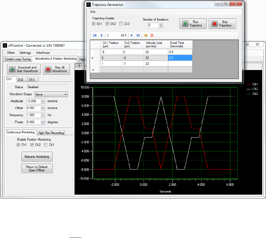
3.5.1 Trajectory Generation
The trajectory generation interface can be accessed from the Interfaces menu. The trajectory generation interface
allows you to scan through up to 500 position coordinates, with velocity and dwell time specified individually for each
move.
3-29: Trajectory Generation Interface
Each row in the trajectory generation grid represents a coordinate. In each row enter the axis positions, the velocity for
the stage to travel to the next coordinate, and the desired dwell time after reaching the next coordinate. Begin typing in
the row marked with the “*” symbol to start a new row. Click the Run Trajectory button to begin the scan. The
nanopositioner will immediately jump to the first coordinate if the stage is not positioned at the first coordinate prior to
starting the scan. The static position can be set using the controls on the Digital I/O tab of the main window.
The current set of coordinates can be saved to a CSV file, or coordinate sets can be loaded from a CSV file using the File
menu. This allows generation or editing of coordinate sets from programs like Microsoft Excel or Matlab.
When saving a coordinate set to a CSV file, the characters “//” at the beginning of the first line indicate a comment line
of column header labels. There must be 10 comma delimited columns for the file to load correctly, however any
columns that are not relevant can be left blank. For example a file for a three channel controller would leave Channels
4, 5, and 6 blank. The columns in the CSV file are defined as follows:
1. Channel 1 Position (in axis units, typically microns)
2. Channel 2 Position (in axis units, typically microns)
3. Channel 3 Position (in axis units, typically microns)
29
4. Channel 4 Position (in axis units, typically microns)
5. Channel 5 Position (in axis units, typically microns)
6. Channel 6 Position (in axis units, typically microns)
7. Velocity Limit (in axis units per ms, typically microns/ms)
8. Acceleration Limit (reserved for future use)
9. Jerk Limit (reserved for future use)
10. Dwell Time (in seconds)
For TTL control of the trajectory moves, select Trajectory Table Control for the input function of a TTL input pin in the
Digital Trigger I/O configuration section of the nPControl software. When TTL control is enabled, click the Run Trajectory
button to load the coordinate table to the controller and start the trajectory function. In this mode the trajectory
function will wait for a pulse on the TTL Input pin before each trajectory move in the table. The number of iterations
value is still used, and when the number of iterations is complete the Run Trajectory button will need to be used to start
a new set of iterations. The Stop Trajectory button can still be used to end the controller function in TTL mode.
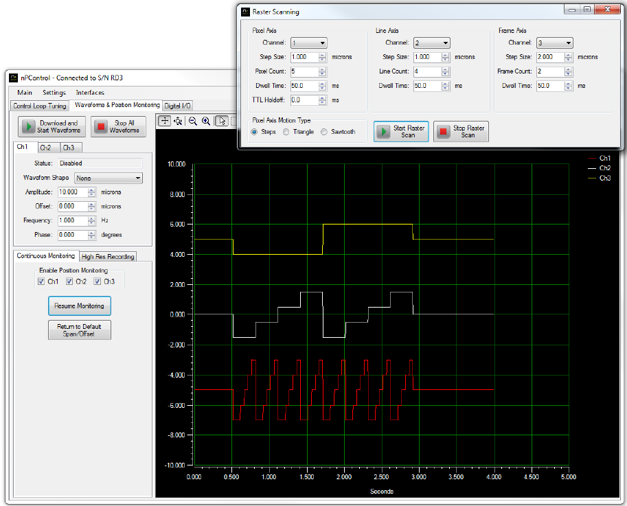
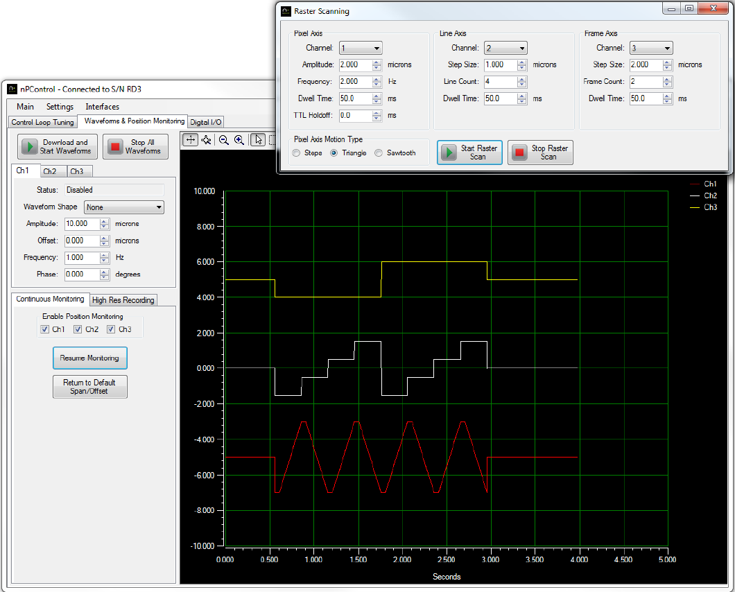
3.5.2 Raster Scanning
The raster scanning interface can be accessed from the Interfaces menu. The center point of the raster scan is
determined by the Static Digital Positioning values located on the Digital I/O tab of the main software window. When
the raster scan is completed, the stage position will return to the center point.
Figure 3-30: Raster scan stepping in the pixel (fast) axis.
30
Figure 3-31: Raster scan with a triangle waveform shape in the pixel (fast) axis.
31
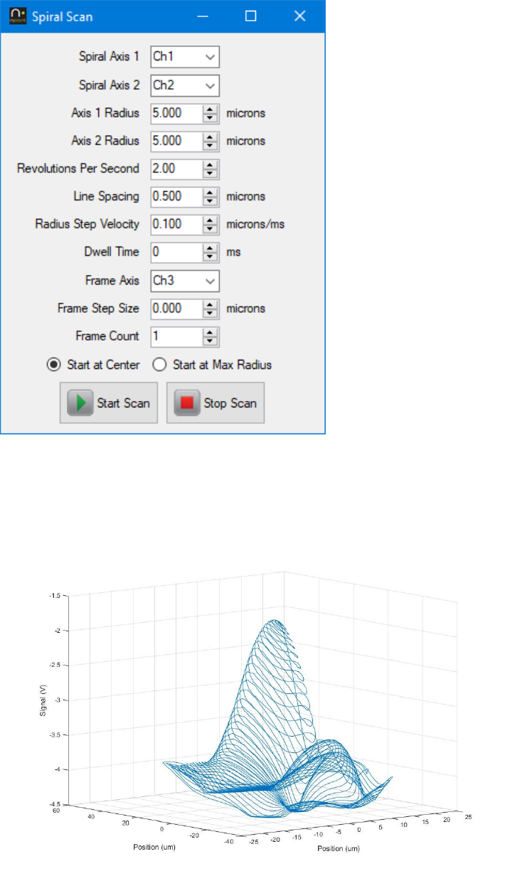
3.5.3 Spiral Scanning
Figure 3-32: Spiral scan interface
The Spiral Scan interface can be accessed from the Interfaces menu. Spiral scanning is a 2 or 3 axis scan that uses a sine
wave shape of increasing or decreasing amplitude in at least two axes. If multiple frames will be scanned, the frame axis
moves to a new position prior to each frame.
Figure 3-33: 3D plot of detector signal vs. spiral scan position. The detector signal was recorded using the LC.402 BNC
analog input and High Resolution Recording controller function.

32
Chapter 4 Advanced Controller Communication
4.1 LC.400 USB Drivers
The drivers for the LC.400 USB interface are provided by Future Technology Devices International Ltd. Some LC.400
series controllers have two ports in the FTDI IC (A and B), however these controllers only use Port A. The FTDI drivers
provide both a “Virtual COM Port” interface and a “direct” interface (FTDI refers to the direct interface as “D2XX”). The
FTDI D2XX interface provides the fastest communication speed for applications where communication speed is critical.
A Visual Studio .Net programming example is located on the provided CD-ROM. Additional programming examples for
the FTDI D2XX interface are available at:
http://www.ftdichip.com/Support/SoftwareExamples/CodeExamples.htm
Visual Basic .NET programs can use the “managed .NET wrapper class” that can be downloaded in the C# section of the
code examples.
To enable the “Virtual COM Port” interface in Windows OS, perform the following steps:
1) With the LC.400 series controller connected via USB and powered on, open the Device Manager.
2) In the Universal Serial Bus controllers section, right click on USB Serial Converter A and select “Properties”.
3) In the Advanced tab, check the “Load VCP” checkbox and click the “OK” button.
4) Unplug the controller USB cable, wait several seconds, and plug the USB cable back in.
5) In the device manager under “Ports” there will now be a listing for USB Serial Port followed by a COM port number.
Once the Virtual COM Port is enabled for a controller, a program can use standard COM port read and write functions to
communicate with the LC.400 series controller via the COM port number assigned by the operating system.
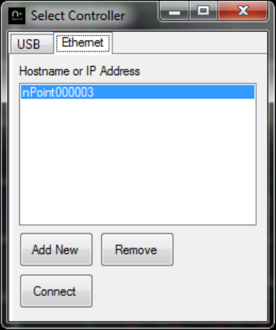
4.2 Ethernet Interface
The optional Ethernet interface allows setup and control of the system on a network. The standard nPoint software can
be used with the Ethernet interface as well as the standard communication protocol from your own program. When
connecting from your own program, connect to port 23 of the controller hostname or IP address. The MAC address for
the controller is located on a sticker near the controller Ethernet port, along with the hostname that the controller will
request via DHCP. The requested hostname is “nPoint” (without quotations) followed by the last six digits of the MAC
address.
If the hostname request is not compatible with your network, it is recommended that you set a DHCP reservation for the
controller so that it retains the same IP address.
If the network does not use DHCP and you would like to set a static IP address, connect via USB and select System
Information from the Settings Menu. Click the Set Ethernet Address button to set a static IP address. To return the
nPoint controller to DHCP mode, set the IP Address to 0.0.0.0 with the Set Ethernet Address button.
When a port is open on the Ethernet connection, the controller will not respond to USB communication. Once the port
is closed, a USB connection can be established. The Ethernet cable does not need to be unplugged to use the USB
connection.
33
Figure 4-1: Connect via Ethernet with nPControl software.
To connect with the nPControl software, first add a hostname or IP address to the list. The list of hostnames and IP
addresses will be saved on the PC for future use. Then double click the selection to connect, or click the Connect button
after making a selection.
4.3 Memory Read/Write Commands
The following sections describe the commands needed to read and write values to the LC.400 series controller. The
sample transmission text is written with the bytes sent from left to right, meaning that the A# byte is sent first and the
55 byte is sent last. The bytes in each element (such as [addr], [data] etc.) are transmitted with significance increasing
(LSB transmitted first and MSB transmitted last).
4.3.1 Read Single Location Command
Number of bytes: 6
Format: 0xA0 [addr] 0x55
Return Value: 0xA0 [addr] [data] 0x55
Sample Hex Transmission from PC to C.400: A0 18 12 83 11 55
Sample Hex Return Transmission from LC.400 to PC: A0 18 12 83 11 64 00 00 00 55
The A0 command reads one 32 bit value from the specified address. In this sample the address used is 0x11831218 and
the return data value is 0x64, or 100 in decimal. The address and data bytes are both 32 bit values, and are transmitted
with significance increasing (LSB transmitted first and MSB transmitted last).
34
4.3.2 Write Single Location Command
Number of bytes: 10
Format: 0xA2 [addr] [data] 0x55
Return Value: none
Sample Hex Transmission from PC to C.400: A2 18 12 83 11 E8 03 00 00 55
The A2 command writes one 32 bit value to the specified address. In this sample the address used is 0x11831218 and
the data value written is 0x3E8, or 1000 in decimal. The address and data are 32 bit values. Bytes are transmitted with
significance increasing (LSB transmitted first and MSB transmitted last).
4.3.3 Read Array Command
Number of bytes: 10
Format: 0xA4[addr] [numReads] 0x55
Return Value: 0xA4 [addr] [data 1]…..[data N] 0x55
Sample Hex Transmission from PC to C.400: A4 28 17 83 11 02 00 00 00 55
Sample Hex Return Transmission from C.400 to PC: A4 28 17 83 11 AE 47 E1 7A 14 AE F3 3F 55
The A4 command reads multiple 32 bit values starting at a specified memory address. In this sample the address used is
0x11831728 and the return data is a 64 bit float with a value of 1.23 = 0x3FF3AE147AE147AE. To maintain transmission
integrity with slow computers using USB 1.1, testing has shown it is best to keep the number of values to read at 2000 or
less. The address, number of values to read, and data are 32 bit values. Bytes are transmitted with significance
increasing (LSB transmitted first and MSB transmitted last).
4.3.4 Write Next Command
Number of bytes: 6
Format: 0xA3[data] 0x55
Return Value: none
Sample Hex Transmission from PC to C.400: A3 E8 03 00 00 55
The A3 command increments the memory address pointer by 4 bytes after issuing a Write Single Location Command
(described in section 4.3.2) to set the initial address, and then writes a 32 bit value to the new memory location. After
the initial address is set, you can use multiple Write Next commands to continue incrementing the memory address.
Care must be taken to not use a read command in between multiple Write Next commands. Read commands will also
set the initial memory location. In this sample the data value written is 0x3E8, or 1000 in decimal. Bytes are transmitted
with significance increasing (LSB transmitted first and MSB transmitted last).

35
4.4 Controller Memory Locations
4.4.1 Channel Base Memory Addresses
The nPoint LC.400 series controllers can have up to three stage axes populated in a single controller. The following base
addresses are the start of the majority of memory locations of interest to the user. Note that the channels are
separated by an offset of 0x1000.
Address
Description
0x11831000
Ch1 base address
0x11832000
Ch2 base address
0x11833000
Ch3 base address
4.4.2 Static Positioning Addresses
Memory offsets are summed with a channel base address to set the parameter for a specific channel.
Offset
Data Type
Description
0x078
32 Bit Integer
Range - Stage axis range. For example, a 100 micron axis has a value
of 0x64.
0x044
32 Bit Integer
Range Type – The type of units used for the Range parameter.
0 = microns 3 = radians
1 = millimeters 4 = nanometers
2 = µradians 5 = milliradians
0x218
32 Bit Signed
Integer
Digital Position Command - 20 bit digital position command (decimal
range of +/-524287). For example, if travel range is 100 microns and
you want to command the stage to move to +15 microns from
center, you would set this address to 0x26666 = (1048574/100 * 15)
0x334
32 Bit Signed
Integer
Digital Sensor Reading - 20 bit sensor reading for the current DSP
cycle (decimal range of +/-524287). For example, if an axis is 100
microns and the sensor value was 15 microns from the center
position, the sensor reading at this address would be 0x26666 =
(1048574/100 * 15).
4.4.3 Control Loop Addresses
Memory offsets are summed with a channel base address to set the parameter for a specific channel.
Offset
Data Type
Description
0x084
32 Bit Integer
Servo State – A value of 1 enables the servo loop, a value of 0 disables the
servo (sets the channel to open loop).
0x720
64 Bit Float
Proportional Gain – Sets the proportional gain of the control loop.
0x728
64 Bit Float
Integral Gain – Sets the integral gain of the control loop.
0x730
64 Bit Float
Derivative Gain – Sets the derivative gain of the control loop.

36
4.4.4 Wavetable Addresses
Memory offsets are summed with a channel base address to set the parameter for a specific channel.
Offset
Data Type
Description
0x1F4
32 Bit Integer
Wavetable Enable – A value of 1 enables wavetable scanning for
the channel that will continue indefinitely, a value of 2 enables
wavetable scanning for a specified number of iterations, a value of
0 disables wavetable scanning.
0x1F8
32 Bit Integer
Wavetable Index – The index of the wavetable point that will be
output during the current clock cycle if the waveform is running.
Users will typically want to set this to 0 before starting a waveform.
0x200
32 Bit Integer
Wavetable Cycle Delay – The number of clock cycles to wait before
the next wavetable point is output. This can be used to achieve
waveform shapes that are longer than two seconds. For example a
Wavetable Buffer Size of 83,333 with a Wavetable Cycle Delay of 1
will have a period of 4 seconds.
0x204
32 Bit Integer
End of Wavetable Index – Specifies the waveform point index at
which the controller will return to the first point of the waveform.
This value should be set to the number of points in the buffer minus
one (the first point is index zero). For example a 100 point
waveform for channel 1 would have memory 0x11831204 set to a
value of 99, and the last point would be located at memory address
0xC000018C. The maximum buffer size is 83,333 points, 2 seconds
of data at full loop speed (1 clock cycle every 24 µsec).
0x208
32 Bit Integer
Wavetable Active – Set the value to 1 as a software trigger to start
the wavetable output (if Wavetable Enable is also 1), a value of 0
will stop the wavetable output. This value will also be set to 1 or 0
by TTL I/O triggers if they are configured to start or stop the
waveform.
0xD50
32 Bit Integer
Waveform Iterations – When running the waveform with a
specified finite number of iterations, this offset should be initialized
to the number of iterations. This offset will hold the specified
iteration value.
0xD54
32 Bit Integer
Waveform Iterations Count – When running the waveform with a
specified finite number of iterations, this offset should be initialized
to the number of iterations. The value at this offset will be
decremented by the DSP for each iteration.
The following table contains base addresses for the arrays of wavetable position points the controller will output when
the wavetable is running. Each point in the array is a 20 bit digital position in the same format as the Digital Position
Command in section 4.4.2. These addresses are not related to the channel base addresses.
Address
Description
0xC0000000
Ch1 wavetable base address
0xC0054000
Ch2 wavetable base address
0xC00A8000
Ch3 wavetable base address

37
4.4.5 Digital I/O Trigger Addresses
Memory offsets are summed with a channel base address to set the parameter for a specific channel.
Offset
Data Type
Description
0x94
32 Bit Integer
TTL Input Pin 1 Function – Specifies the trigger type for pin 1 of the
TTL I/O connector. It is recommended that the user does not
program different functions (other than None) for different
channels on the same pin.
0 = None
1 = Edge Triggered Start
2 = Level Triggered Start
3 = Edge Triggered Stop
4 = Level Triggered Stop
5 = Level Triggered Start and Stop
6 = Edge Triggered Pause and Resume
7 = Level Triggered Pause and Resume
8 = Raster Stepping Control
16 = Edge Triggered Start Recording
0x98
32 Bit Integer
TTL Input Pin 2 Function
0x9C
32 Bit Integer
TTL Input Pin 3 Function
0xA0
32 Bit Integer
TTL Input Pin 4 Function
0xB4
32 Bit Integer
TTL Input Pin 1 Polarity – Specifies the polarity for pin 1 of the TTL
I/O connector. Note that if the user wants multiple channels to
have a function for TTL Input Pin 1 with the same polarity, the
polarity must be programmed for each channel individually.
0 = Rising Edge/Active High
1 = Falling Edge/ Active Low
0xB8
32 Bit Integer
TTL Input Pin 2 Polarity
0xBC
32 Bit Integer
TTL Input Pin 3 Polarity
0xC0
32 Bit Integer
TTL Input Pin 4 Polarity
0xF4
32 Bit Integer
TTL Output Pin 6 Function – Specifies the output type for pin 1 of
the TTL I/O connector. An output pin should typically only have a
function other than None for one channel at a time.
0 = None 5 = Waveform Index Clock
1 = Control Loop Error 6 = Raster Pixel Pulse
2 = Wavefrm/TG Index Level 7 = Raster Line Pulse
3 = Waveform Index Pulse 8 = Raster Frame Pulse
4 = General Fault 10 = Sensor Based Position Pulse
0xF8
32 Bit Integer
TTL Output Pin 7 Function
0xFC
32 Bit Integer
TTL Output Pin 8 Function
0x100
32 Bit Integer
TTL Output Pin 9 Function
0x114
32 Bit Integer
TTL Output Pin 6 Polarity – Specifies the polarity for Pin 6 of the TTL
I/O connector.
0 = Rising Edge/Active High
1 = Falling Edge/Active Low
0x118
32 Bit Integer
TTL Output Pin 7 Polarity
0x11C
32 Bit Integer
TTL Output Pin 8 Polarity
0x120
32 Bit Integer
TTL Output Pin 9 Polarity

38
0x154
32 Bit Integer
TTL Output Error Function Tolerance – Specifies the control loop
error threshold for the TTL Output Error function type. The
threshold value is compared to the absolute value of the control
loop error to determine the output state. This integer value is in 20
bit counts. Since this function operates inside the control loop,
when scaling from Axis Distance Units to 20 bit counts the read only
32 bit single precision float scale factor from offset 0x22C must also
be applied.
0x158
32 Bit Integer
TTL Output Waveform Index Count – Specifies the number of low
and high index pairs. For example, if two low indexes are specified
and two high indexes are specified, the Index Count value should be
2 (not 4).
0x15C
32 Bit Integer
TTL Output Off Index Array Base Offset – The base offset for an
array of up to 16 waveform indexes. At the specified indexes, an
output set to type Waveform Index Level will transition to the
opposite level (High or Low depends on polarity). At the specified
indexes an output function set to type Waveform Index Pulse will
output a single pulse.
0x19C
32 Bit Integer
TTL Output On Index Array Base Offset – The base offset for an
array of up to 16 waveform indexes. At the specified indexes, an
output set to type Waveform Index Level will transition to the
opposite level (High or Low depends on polarity). At the specified
indexes an output function set to type Waveform Index Pulse will
output a single pulse.
0xC60
32 Bit Integer
Sensor Based Position Pulse Spacing – Sets the stage travel
between each pulse. This integer value is in 20 bit counts. Since this
function operates inside the control loop, when scaling from Axis
Distance Units to 20 bit counts the read only 32 bit single precision
float scale factor from offset 0x22C must also be applied.
0xC64
32 Bit Integer
Sensor Based Position Pulse Offset – Sets the sensor value for the
first output pulse. This integer value is in 20 bit counts. Since this
function operates inside the control loop, when scaling from Axis
Distance Units to 20 bit counts the read only 32 bit single precision
float scale factor from offset 0x22C must also be applied.
0xC68
32 Bit Integer
Sensor Based Position Pulse Number of Pulses – Sets the number
of pulses to specify the width of the pulse band.
0xC7C
32 Bit Integer
Sensor Based Position Pulse Hysteresis – Sets the amount the
sensor must change from the most recent pulse before the output
will pulse again. This can be set slightly higher than the sensor
noise so that the output doesn’t pulse constantly when the stage is
holding at an output pulse position. Since this function operates
inside the control loop, when scaling from Axis Distance Units to 20
bit counts the read only 32 bit single precision float scale factor
from offset 0x22C must also be applied.
0xC6C
32 Bit Integer
Sensor Based Position Pulse Index - Set to zero when Sensor Based
Position Pulse parameters are changed to ensure that the index is
not out of range.

39
4.4.6 General Addresses
These are full addresses that are not related to the channel base addresses.
Address
Data Type
Description
0x118303A0
32 Bit Integer
Channel Boards Connected – Shows how many channels are
physically present in the controller. The least significant six bits each
represent a channel of the controller, with the least significant
representing channel 1, and the third bit representing channel 3. If a
channel board is physically present the bit will have a value of zero, if
a board is not present it will have a value of 1. For example, if a
controller had the first three channels populated with channel boards,
the value at this memory address would be 0xFFFFFFF8.
0x11829010
32 bit Integer
Save Configuration To Flash Command –Writing a value of 1 will save
the current controller configuration to flash memory. The controller
will subsequently power up with the current configuration. When the
save to flash command has completed execution, this address will
read 0 when queried. The save to flash command can take several
seconds to execute. Care should be taken to not power down the
controller during execution.
0x11829020
32 bit Integer
Save Wavetable Data To Flash Command –Writing a C.400 channel
number will save the wavetable data for that channel to flash
memory. When the save to flash command has completed
execution, this address will read 0 when queried. The save to flash
command can take several seconds to execute.
Memory offsets are summed with a channel base address to set the parameter for a specific channel.
Offset
Data Type
Description
0x210
32 Bit Integer
BNC Analog Input Reading – A 20 bit value that represents the voltage at the
analog input. For the standard -10V to +10V analog input circuit, divide the
20 bit value by approximately 51570 to scale to volts. Due to analog
component tolerances, this scaling will be off by a small amount.
0x404
32 Bit Integer
Summed Position Command – A 20 bit value that represents all summed
position commands used by the control loop. This includes static digital
position, waveforms, and the BNC analog input or real-time digital interface if
enabled as a position command. Prior to scaling from 20 bit counts to
distance units, the read only 32 bit single precision float “inverse input scale
factor” from offset 0x230 must also be applied.

40
4.4.7 Trajectory Generation Addresses
Memory offsets are summed with a channel base address to set the parameter for a specific channel.
Offset
Data Type
Description
0xB10
32 Bit Integer
Trajectory Generation Enable – A value of 1 enables trajectory generation
for the channel, a value of 0 disables trajectory generation.
These are full addresses that are not related to the channel base addresses.
Address
Data Type
Description
0x11829048
32 Bit Integer
Start Trajectory – Send a value of 1 to start the trajectory path. This
address will return a value of zero when the trajectory has completed.
0x1182904C
32 bit Integer
Stop Trajectory – Send a value of 1 to stop the trajectory path.
0x1182A000
32 bit Integer
Number of Trajectory Coordinates – Sets the number of coordinates
in the trajectory path. The maximum number of coordinates is 500.
0x1182A004
32 bit Integer
Number of Trajectory Iterations – Sets the number of trajectory path
iterations.
0x118304E8
32 bit Integer
TTL Control Pin Number – Sets the input pin number to be used for
controlling the start of each trajectory move. A value of zero disables
TTL trajectory control, and the specified dwell time is used prior to
the next trajectory move.
0x118304EC
32 bit Integer
TTL Control Pin Polarity – Sets the polarity of the input pin used for
controlling the start of each trajectory move. Set a value of zero for
triggering on the rising edge, 1 for falling edge.
0x1182A6A0
Various
Trajectory Generation Parameters Array - Start address for the array
of trajectory path parameters including coordinates, velocity limit,
and dwell time. There are 10 parameters in a set, and a maximum of
500 sets. The 10 parameters in a set are as follows:
1. Ch1 Position (32 bit Integer)*
2. Ch2 Position (32 bit Integer)*
3. Ch3 Position (32 bit Integer)*
4. Ch4 Position (32 bit Integer)*
5. Ch5 Position (32 bit Integer)*
6. Ch6 Position (32 bit Integer)*
7. Velocity Limit for travel to next position (32 bit Float)**
8. Acceleration Limit for travel to next position (32 bit Float)
9. Jerk Limit for travel to next position (32 bit Float)
10. Dwell Time at current position (32 bit Integer)***
* Ch1 – Ch6 positions are sent to the controller in 20 bit counts from -524287 to +524287. This is the same as the digital
position format described in Section 4.4.2.
** The Velocity Limit is sent to the controller in counts per control loop cycle. The Velocity Limit is scaled by
determining the magnitude of the distance vector between the current coordinate and the next coordinate in both
range units and in 20 bit counts. Then use the following equation:
VelLimit(counts/control loop cycle) = VelLimit(range units/ms) * dCounts/dRangeUnits * 0.024

41
An example of a 100 micron x 100 micron x 25 micron stage moving from 0,0,0 to 10,20,5 at 0.1 microns/ms velocity is
as follows:
counts/micron for 100 micron axis = 1048575/100 = 10485.75
counts/micron for 25 micron axis = 1048575/25 = 41943
dRangeUnits = = 22.9128784747792
dCounts = = 314572.5
VelLimit(counts/control loop cycle) = 0.1 * 314572.5/22.9128784747792 * 0.024 = 3.29497671
*** Dwell time is sent to the controller in control loop cycle counts. The control loop cycle is every 24 microseconds.
For example a 1 second delay would be 41667 counts.

42
4.4.8 Raster Scan Addresses
These are full addresses that are not related to the channel base addresses.
Address
Data Type
Description
0x11830448
32 Bit Integer
Pixel ID – Set to the fast axis channel number, 0 = none
0x11830464
32 bit Integer
Line ID – Set to the slow axis channel number, 0 = none
0x11830480
32 bit Integer
Frame ID – Set to the slowest axis channel number, 0 = none
0x1183044C
32 bit Integer
Pixel Step Size – 20 bit number with the same counts per distance
scale factor as the Digital Position Command in section 4.4.2
0x11830468
32 bit Integer
Line Step Size - 20 bit number with the same counts per distance
scale factor as the Digital Position Command in section 4.4.2
0x11830484
32 bit Integer
Frame Step Size -20 bit number with the same counts per distance
scale factor as the Digital Position Command in section 4.4.2
0x11830450
32 bit Integer
Pixel Step Count – The number of steps per line, 1 less than the total
number of pixels.
0x1183046C
32 bit Integer
Line Step Count – The number of steps per frame, 1 less than the
total number of lines.
0x11830488
32 bit Integer
Frame Step Count – The number of steps per scan, 1 less than the
total number of frames.
0x11830454
32 bit Integer
Pixel Dwell Time - The number of control loop cycles to dwell after
stepping to the next pixel. One control loop cycle = 24 µsec
0x11830470
32 bit Integer
Line Dwell Time - The number of control loop cycles to dwell after
stepping to the next line. One control loop cycle = 24 µsec
0x1183048C
32 bit Integer
Frame Dwell Time - The number of control loop cycles to dwell after
stepping to the next frame. One control loop cycle = 24 µsec
0x11830458
32 bit Integer
TTL Holdoff Time - The number of control loop cycles prior to pulsing
the pixel TTL output after stepping to a new pixel. One control loop
cycle = 24 µsec
0x1183045C
32 bit Integer
Index 1 – Fast axis waveform index at which the line axis should step
to a new line.
0x11830460
32 bit Integer
Index 2 - Fast axis waveform index at which the line axis should step
to a new line, for sawtooth type waveforms this can be set to a value
higher than the number of waveform samples to “disable” it.
0x1182906C
32 bit Integer
Start Raster Scan – Set a value of 1 to start a stepping scan, set a
value of 2 to start a waveform scan, set a value of 3 to start a TTL
Input controlled raster scan. This will be set to a value of zero at the
end of the scan for stepping and waveform scans. TTL Input
controlled scans will start over again if the input continues to pulse.
0x11829070
32 bit Integer
Stop Raster Scan – Set a value of 1 to stop a raster scan.
4.4.9 Recording Addresses
These are full addresses that are not related to the channel base addresses.
Address
Data Type
Description
0x1183036C
32 Bit Integer
Number of Samples to Record – Sets the number of recording
samples
0x118300F4
32 bit Integer
Control Loop Cycles Per Sample – Sets the number of 24 µs control
loop cycles for each sample. A value of zero or one will sample every
24 µs, a value of 2 every 48 µs, a value of 3 every 72 µs, and so on.
0x1183037C
32 bit Integer
Record Pointer 1 – The value of the controller address to record to

43
Buffer 1. A value of zero does not record anything to Buffer 1.
0x11830380
32 bit Integer
Record Pointer 2 – The value of the controller address to record to
Buffer 1. A value of zero does not record anything to Buffer 2.
0x11830384
32 bit Integer
Record Pointer 3 – The value of the controller address to record to
Buffer 1. A value of zero does not record anything to Buffer 3.
0x11830388
32 bit Integer
Record Pointer 4 – The value of the controller address to record to
Buffer 1. A value of zero does not record anything to Buffer 4.
0x1183038C
32 bit Integer
Record Pointer 5 – The value of the controller address to record to
Buffer 1. A value of zero does not record anything to Buffer 5.
0x11830390
32 bit Integer
Record Pointer 6 – The value of the controller address to record to
Buffer 1. A value of zero does not record anything to Buffer 6.
0x11830394
32 bit Integer
Record Pointer 7 – The value of the controller address to record to
Buffer 1. A value of zero does not record anything to Buffer 7.
0x11830398
32 bit Integer
Record Pointer 8 – The value of the controller address to record to
Buffer 1. A value of zero does not record anything to Buffer 8.
0xC03F0000
32 bit Integer
Record Buffer 1 – The start address for the buffer that stores samples
from the controller address specified by Record Pointer 1.
0xC0444000
32 bit Integer
Record Buffer 2 – The start address for the buffer that stores samples
from the controller address specified by Record Pointer 2.
0xC0498000
32 bit Integer
Record Buffer 3 – The start address for the buffer that stores samples
from the controller address specified by Record Pointer 3.
0xC04EC000
32 bit Integer
Record Buffer 4 – The start address for the buffer that stores samples
from the controller address specified by Record Pointer 4.
0xC0540000
32 bit Integer
Record Buffer 5 – The start address for the buffer that stores samples
from the controller address specified by Record Pointer 5.
0xC0594000
32 bit Integer
Record Buffer 6 – The start address for the buffer that stores samples
from the controller address specified by Record Pointer 6.
0xC05E8000
32 bit Integer
Record Buffer 7 – The start address for the buffer that stores samples
from the controller address specified by Record Pointer 7.
0xC063C000
32 bit Integer
Record Buffer 8 – The start address for the buffer that stores samples
from the controller address specified by Record Pointer 8.
0x11830374
32 bit Integer
Start Recording – Write a value of 1 to start the recording. The DSP
will set the value back to zero when the recording is completed. The
value can be polled to determine when the recording has completed.

44
4.4.10 Spiral Scan Addresses
Address
Data Type
Description
0x118290D8
32 Bit Integer
Start Spiral Scan – Set to a value of 1 to start the spiral scan at the
radius moving toward the center. Set to a value of 2 to start the spiral
scan at the center moving toward the radius. When the scan has
completed, the DSP will set this to a value of 0. The value can be
polled by the PC to determine when the scan has completed.
0x11830510
32 bit Integer
Spiral Axis 1 – Sets the controller channel to be used for Axis 1.
0x11830514
32 bit Integer
Spiral Axis 2 – Sets the controller channel to be used for Axis 2.
0x11830518
32 bit Integer
Spiral Axis 3 – Sets the controller channel to be used for the Frame
axis.
0x1183051C
32 bit Integer
Spiral Control Loop Cycles/Revolution – Sets the spiral scan
revolutions per second. Each control loop cycle is 24 µs, so use the
formula 1/(0.000024 * revs/sec) to determine the control loop cycles
per revolution.
0x11830520
32 bit Integer
Spiral Radius 1 – Sets the Axis 1 scan radius in 20 bit counts. The
scaling is the same as the Digital Position Command described in
section 4.4.2.
0x11830524
32 bit Integer
Spiral Radius 2 – Sets the Axis 2 scan radius in 20 bit counts. The
scaling is the same as the Digital Position Command described in
section 4.4.2.
0x11830528
32 bit Integer
Spiral Line Spacing – Sets the spacing between lines in 20 bit counts.
The scaling is the same as the Digital Position Command described in
section 4.4.2.
0x1183052C
32 bit Integer
Spiral Radius Move Velocity – Sets the velocity of the move from the
center to the radius or radius to the center in 20 bit counts per
control loop cycle. The calculation for counts per control loop cycle is
described in the Trajectory section 4.4.7.
0x11830530
32 bit Integer
Spiral Dwell Time – Sets the dwell time after the move from the
center to the radius or radius to center in control loop cycle counts.
Each control loop cycle is 24 µs, so the formula is
dwellSeconds/0.000024.
0x11830534
32 bit Integer
Sprial Frame Count – Sets the number of scan frames.
0x11830538
32 bit Integer
Spiral Frame Step Size – Sets the move size for Axis 3 between each
frame. The scaling is the same as the Digital Position Command
described in section 4.4.2.

45
Chapter 5 Maintenance and Cleaning
5.1 Maintenance
Periodically inspect the cooling vents on the case side to insure that they are not obstructed with dust or debris and
clear as needed.
Periodically inspect the fan grill on the back cover to insure that it is not obstructed with dust or debris and clear as
needed.
5.2 Cleaning
If desired the outside surfaces of the case may be wiped with a damp cloth using a mild cleaner or water. Take care not
to allow liquid to penetrate the seams as the controller case is not watertight.

46
Chapter 6 Safety
This product has been tested to the requirements of CAN/CSA-C22.2 No. 61010-1, second edition,
including Amendment 1, or a later version of the same standard incorporating the same level of testing
requirements.

47
Appendix A Specifications
Number of channels: 1 (LC.400), 2 (LC.402), 3 (LC.403)
Resolution: 20-bit
Processor: 32-bit floating point DSP
Sampling rate: 24 μsec servo-loop
Controller Interfaces: USB 2.0
9-pin D-sub Digital I/O with 4 inputs and 4 outputs, 5V TTL
High speed parallel, PFM, AFM (LC.403)
Channel Connectors: BNC analog command input (-10V to +10V)
BNC analog monitor output (-10V to +10V)
15-pin Dsub stage connector
HV driver voltage: -30V to 150V piezo driver signal
HV driver current: 100mA/channel
Sensor Type: Capacitive or Strain Gage, others optional
Software: nPControl (nPoint control panel)
LabVIEW and DLL drivers
Wave form generator
Software requirements: Microsoft Windows XP/Vista/7/8
Operating temperature: 10° C to 40° C
Maximum relative humidity: 80% to 31°C decreasing linearly to 50% at 40°C
Operating altitude: 2000 meters maximum
Dimensions: Height: 67 mm (LC.400 and LC.402), 88 mm (LC.403)
Width: 106 mm (LC.400), 185 mm (LC.402), 260 mm (LC.403)
Depth: 172 mm (LC.400), 240mm (LC.402), 264 mm (LC.403)
Weight: 1 kg (LC.400), 1.5 kg (LC.402), 3 Kg (LC.403)
DC Input Voltage: 12 VDC
DC Input Current: 1.7 A max (LC.400), 3 A max (LC.402), 3.5 A max (LC403)
Mains Voltage: 100 – 240 VAC, 50-60 Hz, recommended AC supply is
CUI V-Infinity model ETMA120750U
Mains Current: 0.5 A max (LC.400), 1.0 A max (LC.402, LC.403)

48
Appendix B Instructions for connecting new stages with EEPROM
When an nPoint stage and controller are shipped, the LC.400 series controller has the configuration of the stage that
ships with it stored in controller memory. When connecting a different stage to the controller, the controller must read
the calibration settings from the stage EEPROM in to the controller. To complete this process, please perform the
following steps:
1. When connecting or disconnecting a stage axis from the controller, always power down the controller first.
2. Connect the new stage axis to the controller. Please make sure that the connector is fully plugged in and the
two connector screws are tightened down.
3. Power on the controller. When a new stage axis is detected, the controller will start in open loop since the
calibration settings and control loop tuning in the controller memory are for a previous stage axis. This
prevents the stage from becoming unstable and oscillating.
4. Start the nPControl PC software version 1.1.5 or later. If you don’t have the latest software, it can be
downloaded from the nPoint FTP server at:
ftp.npoint.com
username = xnpoint-guest
password = nPguest52
5. When the nPControl PC software connects to the controller, it will detect that the serial number and/or
timestamp of the stage EEPROM does not match the values stored in controller memory. The nPControl PC
software will then ask if you would like to load settings from the stage in to the controller for each channel,
one at a time. Click “Yes” in the dialog box to load the settings from the stage EEPROM to the controller.
After clicking “Yes”, the LED on the front of the controller will flash while the controller is reading the
configuration from the stage EEPROM. Reading the EEPROM can take several minutes.
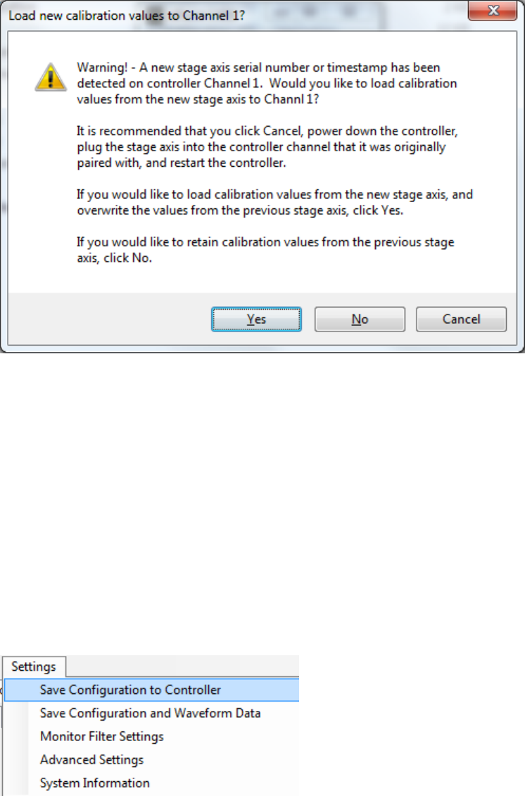
49
6. After the settings have been loaded for each channel that has a new stage axis, the software will start
normally. The stage axes that had new configurations loaded will be in open loop, and have default control
loop tuning loaded from the stage EEPROM. The control loop tuning should be adjusted to match your
physical setup by adjusting the integral gain and notch filter settings. Please follow the control loop tuning
procedure in the LC.400 series controller user manual, or use previously tested values.
7. After the stage performance is tested for each axis in Step 6, set each axis to the state you would like when
the system is powered on (open loop or closed loop). In the Settings menu, click “Save Configuration to
Controller” to save the configuration to controller flash memory. The configuration stored in the controller
flash memory is loaded the next time the controller is powered on. This step is necessary so that the
controller and stage configuration match, otherwise the process of loading the configuration from the stage
axes will need to be repeated next time the controller is powered on.

50
Appendix C Parallel Interface Specifications
General
The high speed digital interface has been designed to interface directly to a National Instruments PCIe-6535, PCIe-6536,
or PCIe6537 32-bit DIO board. The timing of the 16-bit parallel transfers is straight forward hence the communication
can be supported by other hardware as described in this document.
Position Monitoring
On the nPoint interface, data bits DIO16 through DIO31 are configured for 16-bit output, with DIO16 containing the LS
bit and DIO31 the MS bit. These bits are used to read position monitoring data. Because position data is 20-bits, and
the port is only 16-bits, position data for each channel is sent as two 16-bit words.
To receive the data for all three channels, six words are sent in sequence. The data is always sent in the following order:
Channel 1, LSW
Channel 1, MSW
Channel 2, LSW
Channel 2, MSW
Channel 3, LSW
Channel 3, MSW
The high speed digital position data is formatted as follows:
LSW:
Bit
15
14
13
12
11
10
9
8
7
6
5
4
3
2
1
0
Value
d3
d2
d1
d0
p
0
0
0
0
0
0
0
i1
i0
0
e
MSW:
Bit
15
14
13
12
11
10
9
8
7
6
5
4
3
2
1
0
Value
d19
d18
d17
d16
d15
d14
d13
d12
d11
d10
d9
d8
d7
d6
d5
d4
d[19..0]: 20-bit position in Two’s Complement (7FFFFh = positive full scale, 80000h= negative full scale, 00000h = 0)
p: parity bit (0 = even number of 1’s in 20-bit data)
e: parity receive error in previous cycle 20-bit demand for this channel
i[1..0]: Channel ID (‘01’= Channel 1, ‘10’=Channel 2, ‘11’ = Channel 3)

51
Demand Input
On the nPoint interface, data ports DIO0 through DIO15 are configured for 16-bit input, with DIO0 containing the LS bit
and DIO15 the MS bit. These bits are used to write position demand data. Because position data is 20-bits, and the port
is only 16-bits, position data for each channel is sent as two 16-bit words.
To write the data for all three channels, six words are sent in sequence. The data is always sent in the following order:
Channel 1, LSW
Channel 1, MSW
Channel 2, LSW
Channel 2, MSW
Channel 3, LSW
Channel 3, MSW
The high speed digital demand data is formatted as follows:
LSW:
Bit
15
14
13
12
11
10
9
8
7
6
5
4
3
2
1
0
Value
d3
d2
d1
d0
p
0
0
0
0
0
0
0
0
0
n1
n0
MSW:
Bit
15
14
13
12
11
10
9
8
7
6
5
4
3
2
1
0
Value
d19
d18
d17
d16
d15
d14
d13
d12
d11
d10
d9
d8
d7
d6
d5
d4
d[19..0]: 20-bit position in Two’s Complement (7FFFFh = positive full scale, 80000h= negative full scale, 00000h = 0)
p: parity bit (0 = even number of 1’s in 20-bit data) The parity bit is optional, as it will not prevent the word from being
used if wrong. If wrong, it will report an error bit in the position monitoring data for that channel (See Position
Monitoring section).
n[1..0]: data enable (‘01’ = enable) The lower two bits of the LSW must be ‘01’ to indicate new data. If they are any
other combination, ie, ‘00’, ‘10’, or ‘11’, the previous data sample is used. This may be useful when you wish to set your
output buffer to all 0’s or 1’s to maintain the current stage position. However, setting ‘10’ is used to indicate
configuration data words (See Configuration section). For example, setting the output buffer to all 0’s is one method to
maintain the current stage position without having to repeatedly update the buffer.
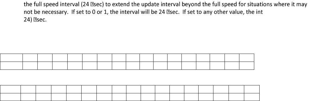
52
Configuration
If the lower two bits of the first demand word are ‘10’, that word along with the following word will be treated as
configuration data. Other words sent in the same data cycle will be ignored.
There are three configuration parameters that must be set in these two words before using the high speed port:
1. Number of channels to be enabled for digital demand (e[1..0]). This can be 0, 1, 2, or 3. If set to 0, the high
speed port is only being used for monitoring and all three analog inputs on the controller are still active. If set to
1, then channel 1 will use digital demand and channels 2 and 3 will use analog. If set to 2, then channels 1 and 2
will use digital demand and channel 3 will use analog. If set to 3, then all 3 channels will use digital demand and
all three analog inputs are disabled. Once enabled, digital demand for a channel cannot be disabled until
controller reset (cycle power).
2. Number of positioning monitoring channels to read on the high speed port (m[1..0]). This can be 1, 2, or 3. If
set to 1, then channel 1 monitoring is enabled. If set to 2, then channels 1 and 2 are enabled. If set to 3, then all
three channels are enabled. There will always be at least channel 1 enabled for monitoring. If set to 0, channel
1 will still be enabled. The analog monitoring outputs always remain enabled in addition to the high speed
digital monitoring.
3. The interval multiplier, a 16-bit value set in the second configuration word (i[15..0]. The number will multiply
erval will be (i *
The two configuration words are formatted as follows:
LSW:
Bit
15
14
13
12
11
10
9
8
7
6
5
4
3
2
1
0
Value
x
x
x
x
x
x
x
x
x
x
m1
m0
e1
e0
1
0
MSW:
Bit
15
14
13
12
11
10
9
8
7
6
5
4
3
2
1
0
Value
i15
i14
i13
i12
i11
i10
i9
i8
i7
i6
i5
i4
i3
i2
i1
i0
x = not used
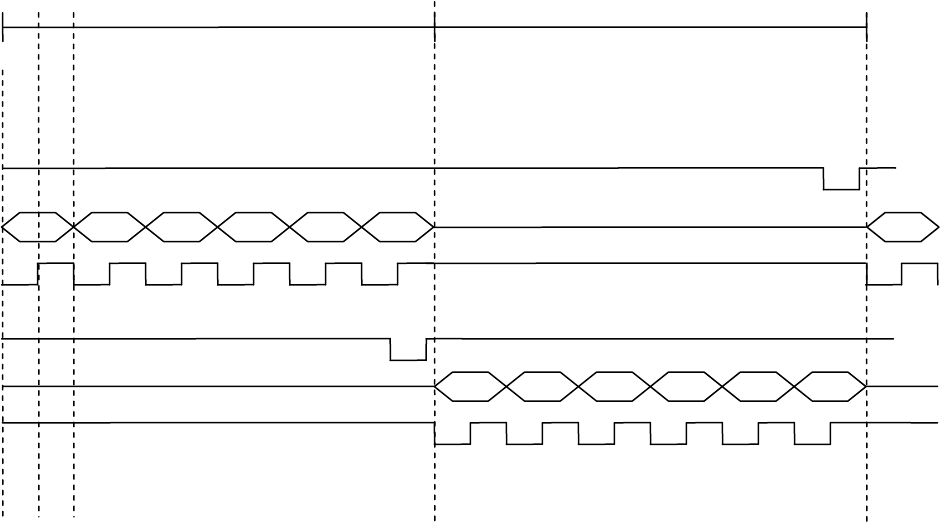
53
Timing
Data is strobed on rising edge of REQ2 and REQ1, outputs from the nPoint interface. In the timing diagram below, 0µs =
24µs.
On National Instruments 6535/6536/6537 devices:
STARTTRIG 1 = PFI 1
REQ1 = PFI 4
STARTTRIG 2 = PFI 2
REQ2 = PFI 5
DIO[16..31]
12 s
us
24 s
us
Position Data from nPoint Controller
Demand Data to nPoint Controller
REQ1
12 s
24 s
0 s
1A
1B
2A
2B
3A
3B
DIO[0..15]
1A
1B
2A
2B
3A
3B
REQ2
2us
1us
0 s
1A
STARTTRIG1
STARTTRIG2

54
Connector Pin-out and Considerations
Pin 68, ‘CABLE_DETECT’, must be connected to GND (0V) to enable the interface. This input is pulled up to +3.3V via a
50K resistor in the Npoint interface.
The data and control output signals, STARTTRIG1, REQ1, STARTTRIG2, and REQ2, are interfaced using 74ACT244 line
drivers. The output voltage swing is 5V.
The connector on the nPoint interface is a 68-pin VHDCI receptacle connector. nPoint uses a R/A Molex 71430-0008
connector. Compatible interface cables with plug mating connectors on both ends are available in several different
lengths from National Instruments, part number 196275-01, SHC68-C68-D4 Shielded Single-Ended Cable.
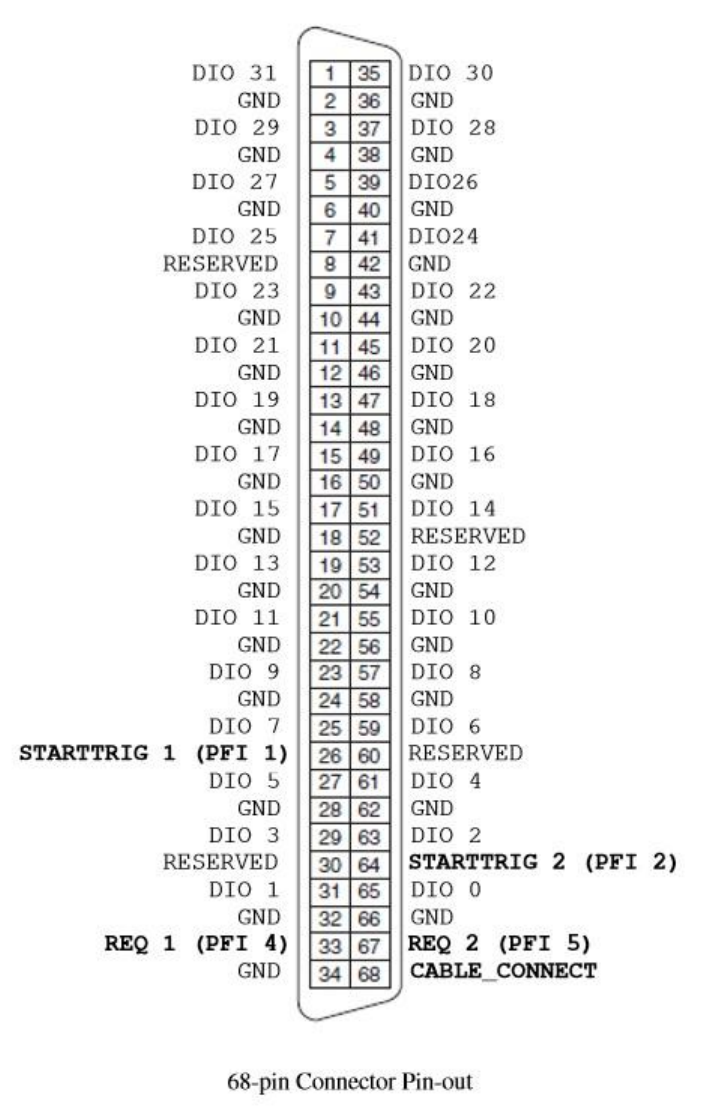
55
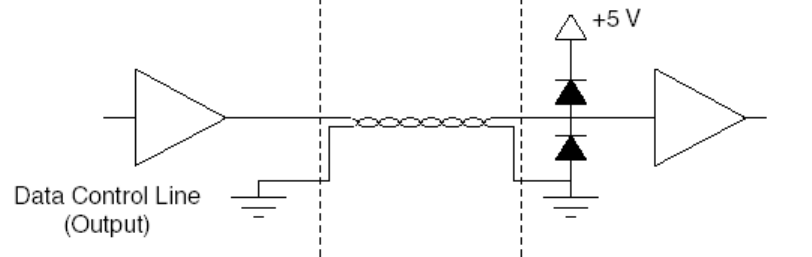
56
For the 16 output data lines, DIO[16..31], and the four control signals, STARTTRIG1, REQ1, STARTTRIG2, and REQ2, it is
recommended to use a Schottky diode termination on each of the lines at the user equipment.
Schottky Termination
From the National Instruments NI-6534 manual:
“One suitable Schottky diode is the 1N5711, available from several manufacturers. For more specialized use, you may be
able to find diodes packaged in higher densities appropriate to your application. For example, the Central
Semiconductor CMPSH-35 contains two diodes, suitable for terminating one line. The California Micro Devices PDN001
contains 32 diodes, suitable for terminating 16 lines.”
It is not necessary to add diodes to terminate the user’s output signals. The nPoint interface contains onboard Schottky
diode termination for the DIO[0..15] data lines.
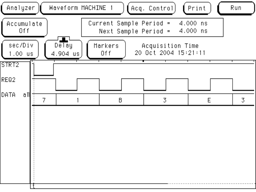
57
Timing Waveforms
The picture below shows an actual capture of the positioning monitoring signals. The STARTTRIG2 (STRT2) signal may be
used for synchronization. Note that the 16-bit data bus changes on the falling edge of REQ2 and should be clocked in on
the rising edge.
Position Monitoring Timing
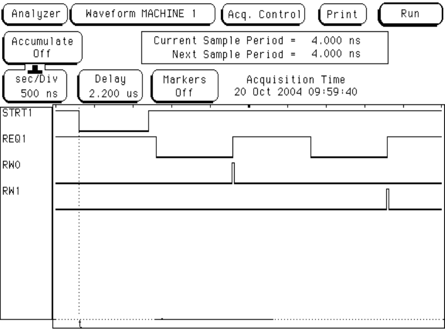
58
The picture below shows an actual capture of the Demand Input signals. STARTTRIG1 (STRT1) may be used for
synchronization. The signals RW0 and RW1 are internal FPGA signals brought out to test points to show when the data
bus is read for the first two (of the six) 16-bit words. User demand data is clocked in on the rising edge of these signals.
Therefore, the data should be stable for at least 100ns before and after the rising edge of REQ1. Normally the user
would place new data on the bus on the falling edge of REQ1.
Demand Input Timing
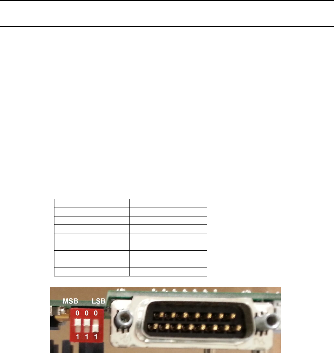
59
Appendix D PFM Interface Specifications
Overview
The nPoint PFM (Pulse Frequency Modulation) Interface is designed to receive position commands and output position
data in real-time. Position demand data is received as standard Pulse/Direction logic signals. Position monitor reporting
by the LC.400 is output as standard differential quadrature A, B, and Z signals. An input/output scaling function is also
provided by the interface. Positive and negative End of Travel (EOT) limit switch outputs are also provided for each axis.
PFM Pulse (Pin 15) / Direction (Pin 8)
The nPoint receivers are TTL compatible. TTL low is defined as 0V to 0.8V and high is defined as 2.0V to 5.0V. These
inputs are compatible with either 5V or 3.3V logic. The nPoint interface has 10K ohm pull-down resistors on these
inputs. The minimum pulse width is 100ns and the minimum time between pulses is 250ns. Direction change must be a
minimum of 100ns prior to the next pulse.
PFM Scaling
The nPoint interface has a 3-bit scalar select function. The purpose of this is to allow the Pulse/Direction inputs to
command larger steps if 20-bit resolution is not needed for a particular application. Scaling is selected by a 3 position
DIP switch at the rear of the interface. This is only accessible by dropping the back panel of the controller (remove 2
panel screws). The switch is only read on power-up.
3-bit Scalar Select
PFM Increment
000
1
001
2
010
4
011
8
100
16
101
32
110
64
111
128
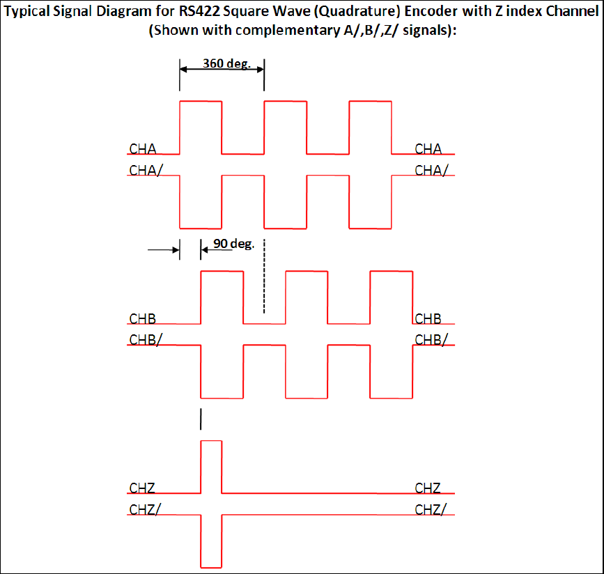
60
Position Monitoring Data
The nPoint position monitoring is supplied as a standard 5V compatible differential quadrature outputs A and B with Z-
index channel output. This is an RS-422 type driver.
Minimum time for 360 degrees as shown below is 500ns. Therefore the fastest A to B edge changes (90 degrees) is
125ns.
If 125ns is too fast for the quadrature encoder receiving system they can be extended through the use of the
Pulse/Direction scaling. These times will be multiplied by the scaling factor of the Pulse/Direction inputs. For example, if
the scaling factor is x4, the fastest A to B edge change is 500ns.
Whenever the reported position crosses the mid-point (zero), the Z index will toggle.
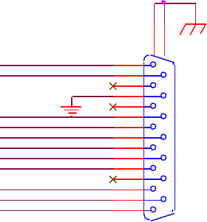
61
Z1-
Pulse1+
B1-
A1-
Dir1+
Z1+
B1+
A1+
EOT_POS1
EOT_NEG1
ENABLE_1
DB15 Male
8
15
7
14
6
13
5
12
4
11
3
10
2
9
1
16
17
End of Travel (EOT) Limit Switches , Positive (Pin 1), Negative (Pin 9)
There are two simulated EOT switches per axis. The purpose of the EOT switches is to signal the PFM controller when
motion is near either end of the axis so that the controller can decelerate the motion before reaching the end of the
range. They are set by default to 1% before the end of the range. This value can be changed by request.
The EOT outputs are active high, 5V.
Enable (Pin 7)
Pin 7 on the interface connector is an active high Enable input which must be pulled to 3.3V or 5V to enable the PFM
function on the LC.400. It has an internal 10K ohm pull-down resistor to GND. Toggling this pin is also a way to reset the
Pulse/Direction counter to zero (mid-range) on all axes.
Interface Connector
The interface connector is a R/A pcb mounted standard 15-pin male DSUB. Use pin 10 as the GND reference for all
signals.
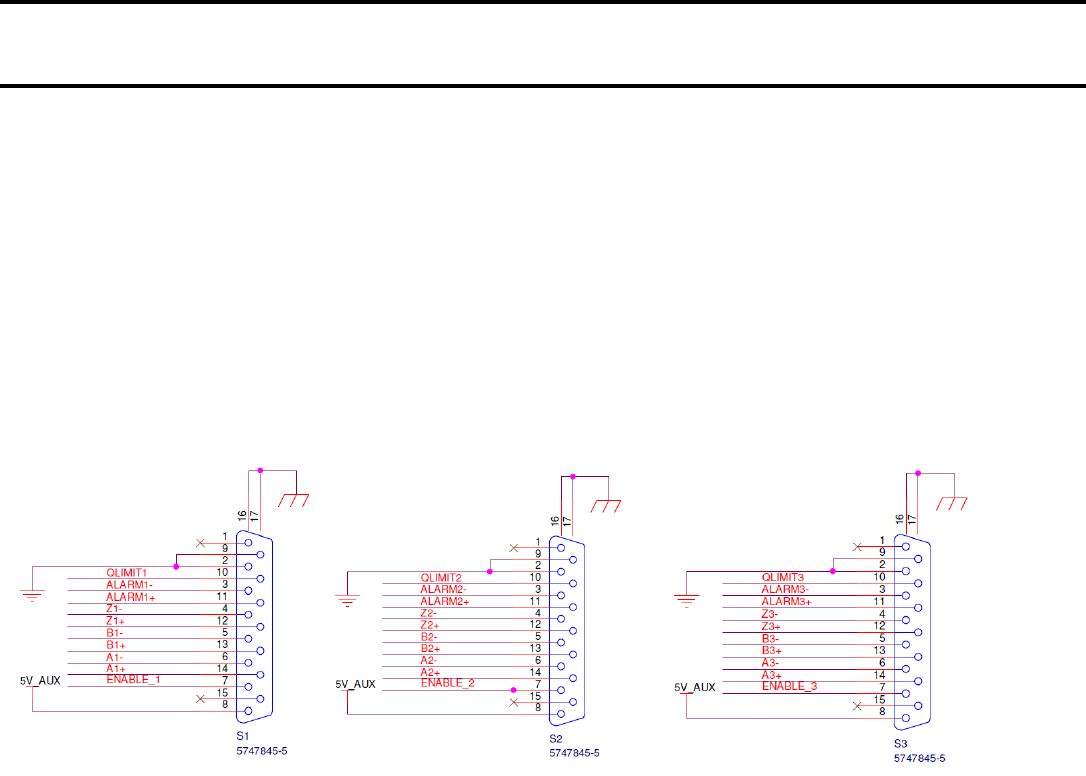
62
Appendix E Digital Encoder Interface
Overview
The nPoint Digital Encoder Interface enables integration of an nPoint nanopositioning system with a quadrature
encoder. The encoder signal is used instead of an internal sensor signal (such as capacitive or strain gage sensor) thus
maintaining the functionality of the LC.400 series controllers. This interface is intended to allow the use of optical or
interferometric encoders as the sensor input to an nPoint nanopositioning system.
The functionality and connector signals of the nPoint Digital Encoder Interface for the LC.403 are defined below. The
interface connects directly to standard RS-422 type differential quadrature encoder outputs. A separate 15-pin Dsub
socket is provided for each of the 3 channels.
15-pin Connector Schematic
Channel 1 Channel 2 Channel 3
Note: These are standard 15-pin Dsub sockets. Renishaw REE series interpolators match the above pinout and may
be plugged directly into the back of the LC.403 or use an appropriate multi twisted pair extension cable, plug to
socket.
Signal Descriptions
Notes about RS-422 signals: The following are RS-422 signal pairs: A, B, Z, ALARM. These signals are terminated with
110 ohms inside the Npoint controller.
‘A and B’: A1+ / A1- and B1+/B1- are the differential quadrature AB signals from the interpolator for channel 1.
Channels 2 and 3 are the same.
‘Z’ : Z1+/Z1- are the differential quadrature Z signals from the interpolator for channel 1. Channels 2 and 3 are the
same. This may not be functional in the Npoint system as shipped. Check with Npoint if this functionality is needed.
‘ALARM’: ALARM1+/ALARM1- are the differential quadrature ALARM signals from the interpolator for channel 1.
Channels 2 and 3 are the same. This signal is provided by the interpolator to indicate that the A/B signals are NOT good,
such as:
- Incremental signal <20% of nominal
- Incremental signal >135% of nominal
- Readhead speed in excess of specification

63
- Signal offset excessive
‘QLIMIT’: QLIMIT1 is an optional limit switch input, active low. This may not be functional in the Npoint system as
shipped. Check with Npoint if this functionality is needed.
‘5V_AUX’: 5VDC @ 330 mA is available for each channel to power interpolater electronics. If not needed or desired a
zero ohm resistor (R44) should be removed from the interface board.
‘ENABLE_X’: 5VDC is detected on this pin by the interface to know that an interpolator is connected. This enables the
channel to use the quadrature input as the sensor.
Status LED’s
The LED on the back of the interface indicates status of the connection for each channel.
LED State Description
OFF No encoder attached
Red Encoder detected but the ALARM signal is active
Green Encoder signal good
Software Commands
The user may send the following commands via the USB interface. See the controller user manual for details
on the command structure.
Set position zero
Write to address h’EC000004’
Lower 3 bits of data are channel zeroing bits.
Send a "1" to set the sensor to zero
Bit
31-3
2
1
0
Value
x
z3
z2
z1
z1 is channel 1
z2 is channel 2
z3 is channel 3
This bit is cleared automatically so there is no need to send "0" after sending "1".
Enable Encoder Interface Channel
Write to address h’EC000000’
Lower 3 bits of data are enable bits, active low.
Bit
31-3
2
1
0
Value
x
e3
e2
e1
Send a "0" to enable the encoder interface channel, otherwise controller uses the internal sensor.
e1 is channel 1
e2 is channel 2
e3 is channel 3
Set Sensor Gain

64
Ch1 Sensor Gain address: h’11831245’
Ch2 Sensor Gain address: h’11832245’
Ch3 Sensor Gain address: h’11832245’
Sensor Gain is a 32 bit floating point value. The formula to calculate the gain is:
Read status
Read address h’11820024’
Bit
31
30
29
28
27
26
25
24
23-0
Value
0
s3
s2
s1
0
e3
e2
e1
x
s1 is channel 1 signal status
s2 is channel 2 signal status
s3 is channel 3 signal status
Signal status bit is “1” when there is an alarm fault, “0” when the signal is good
e1 is channel 1 enable status
e2 is channel 1 enable status
e3 is channel 1 enable status

65
Appendix F AFM Interface Specifications
Overview
nPoint nanopositioning systems are often integrated into commercial AFMs to provide closed-loop scanning
functionality. nPoint facilitates the integration for Bruker or Agilent AFMs by providing a built-in AFM interface. The AFM
interface is only available in LC.403 controllers.
AFM interface functionality
A photo of the back panel of the LC.403 with an AFM interface is shown below.
The AFM interface is installed in-between the Microscope and the AFM controller. The cable from the AFM now plugs
into the connector labeled “TO MICROSCOPE”. The cable provided by nPoint plugs into the connector labeled “TO AFM
CONTROLLER” and the AFM controller.
The two toggle switches enable the user to select the nPoint scanner or the original AFM scanner. This functionality is
particular useful when the original AFM scanner is physically present even after the nPoint scanner is integrated (as is
the case in DimensionTM AFMs). The Z SCANNER Selection switch is disabled when an XY-only scanner is integrated in the
AFM.
When the switches point towards “npoint” the analog input BNC’s on the front panel are disabled.
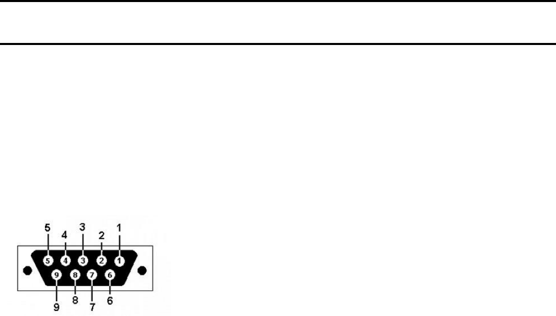
66
Appendix G Control loop error signal
1. Overview
The position error provided by the LC.400 and C.400 series of controllers is the calculated difference between the
summed position input command, and the nanopositioner sensor reading. The position error is calculated during every
24 microsecond control loop cycle. The position error can be used to evaluate how control loop tuning affects position
tracking accuracy, and the position error can be used to determine if there is a system malfunction. The position error
can be recorded in nPControl PC software, used for an error threshold TTL output signal, or read via USB from a user
program.
The TTL inputs and outputs correspond to the DB9 pinout as follows:
DB9 pins 1-4: Input 1-4
DB9 pin 5: Ground
DB9 pins 6-9: Output 1-4
2. Recording the Position Error in the nPControl PC Software
The position error can be recorded in the High Resolution Recording section of nPControl Waveform tab. Below is an
example of the position error recorded for a conservatively tuned 100 micron nanopositioner.
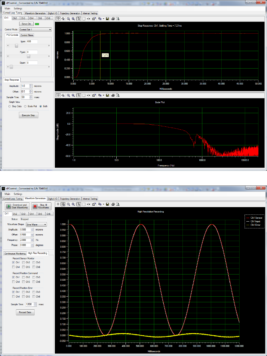
67
Figure 1: Conservative control loop tuning with a settling time of 7.3 milliseconds
Figure 2: Tracking Error of +/- 15 nanometers scanning a 1 micron peak to peak sine waveform
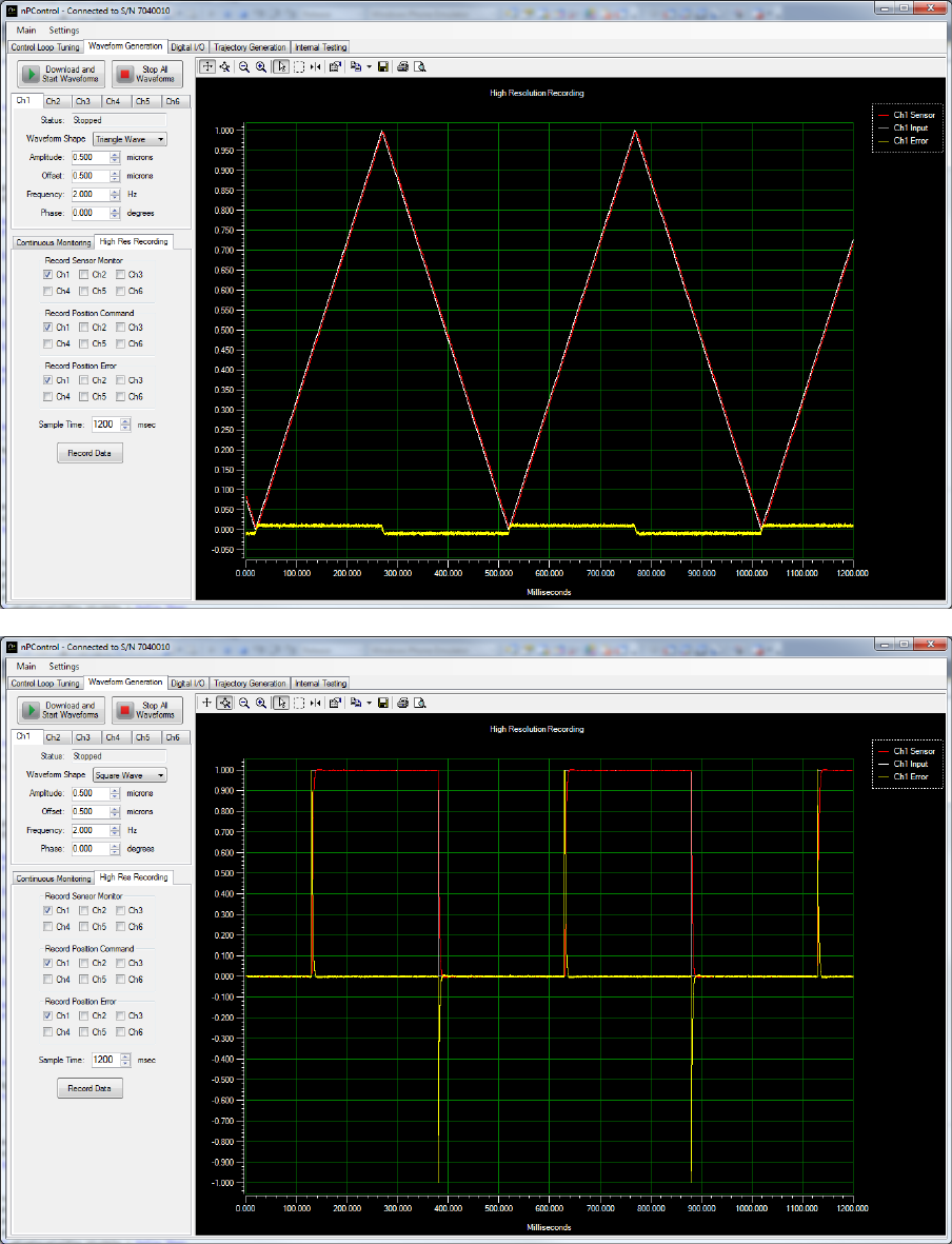
68
Figure 3: Tracking error of +/- 12 nanometers scanning a 1 micron peak to peak triangle waveform shape
Figure 4: Tracking error of +/- 1 micron for short periods of time due to the instantaneous change in position command
scanning a 1 micron peak to peak square waveform shape
3. Error Threshold TTL Output Signal
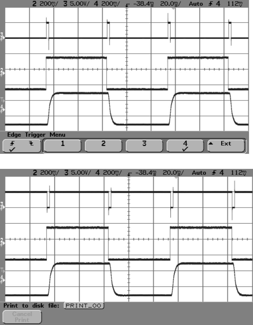
69
Using the nPControl PC software, the controller TTL output signals can be independently programmed to activate when
the position error is above or below a specified threshold. After “Control Loop Error” is selected in the dropdown box
for an output pin function, the user can then select a controller channel and specify an Error tolerance level. A polarity
of “Active High” sets the TTL output high when the error level is below the specified tolerance. A polarity of “Active
Low” sets the TTL output high when the error level is above the specified tolerance.
Figure 5: Active Low TTL top trace, input command middle trace, sensor monitor bottom trace
Figure 6: Active High TTL top trace, input command middle trace, sensor monitor bottom trace

70
4. Reading the Position Error Via USB
The position error can be read for each channel via USB by reading the controller memory address offset from the
controller channel base memory address. For more information about general USB communication and programming,
please refer to Chapter 4 in the general LC.400 or C.400 user manual, and refer to the programming example located on
the nPControl software CD. If you need the latest version of the nPControl CD, please email support@npoint.com for
download instructions.
4.1 Channel Base Memory Addresses
The nPoint C400 controller can have up to six stage axes populated in a single controller. The following base addresses
are the start of the majority of memory locations of interest to the user. Note that the channels are separated by an
offset of 0x1000.
Address
Description
0x11831000
Ch1 base address
0x11832000
Ch2 base address
0x11833000
Ch3 base address
0x11834000
Ch4 base address
0x11835000
Ch5 base address
0x11836000
Ch6 base address
4.2 Position Error Memory Addresses
Memory offsets are summed with a channel base address to set the parameter for a specific channel.
Offset
Data Type
Description
0x078
32 Bit Integer
Range - Stage axis range. For example, a 100 micron axis has a value of 0x64.
0x230
32 Bit Float
Digital Monitor Scale Factor – Value used to scale digital sensor monitor
values. Typically this value is the exact inverse of the Digital Input Scale
Factor.
0x408
32 Bit Signed
Integer
Position Error - 20 bit value (decimal range of +/-524287).
4.3 Position Error Scaling
To scale the 20 bit Position Error value to nanopositioner travel range units of measure (typically microns), perform the
following calculation:
Digital Counts Per Range Unit = 1048574 / Range
Scaled Position Error = Position Error / Digital Counts Per Range Unit * Digital Monitor Scale Factor
4.4 Error Threshold TTL Output Signal Memory Address
Address
Data Type
Description
0x118303B4
32 Bit
Integer
TTL Output Pin State – The least significant four bits represent the TTL output
states, with the least significant bit representing TTL Output 1. A bit value of 0 =
TTL output low, a bit value of 1 = TTL output high.
To read a Boolean value indicating that the position error is either above or below a specified threshold, the user can set
a TTL output function and scaled threshold through the nPControl user interface (described in Section 4.4.5). The state

71
of the output can then be read by “AND-ing” the value at address 0x118303B4 with a bit mask. For example if the TTL
Output Pin State memory address has a value of 6, then TTL Output 1 = low, TTL Output 2 = high, TTL Output 3 = high,
and TTL Output 4 = low. An example of using a bit mask to query the status of a bit can be viewed here.
In the special case of checking the error threshold state for only a single channel, and using only TTL Output 1 (TTL
Output 2, 3, and 4 are set to a function of “none”), then the TTL Output Pin State memory address can simply be
checked for an integer value of either 0 or 1.
