LC 42XL2xx/46XL2xx/46X20xx/52XL2xx/52X20xx Service Manual GB LC52X20E
User Manual: LC52X20E
Open the PDF directly: View PDF ![]() .
.
Page Count: 270 [warning: Documents this large are best viewed by clicking the View PDF Link!]
- LC42XL2xx-46XL2xx-46X20xx-52XL2xx-52X20xx_SM_GB.pdf
- TopPage
- EndPage
- V0D0014901.pdf
- V0D0014902.pdf
- V0D0014903.pdf
- V0D0014904.pdf
- TopPage
- ADJUSTMENT PROCEDURE
- [1] ADJUSTMENT PROCEDURE
- 1. Adjustment method after PWB and/or IC replacement due to repair
- 2. Entering and exiting the adjustment process mode
- 3. Remote controller key operation and description of display in adjustment process mode.
- 4. Description of display
- 5. Adjustment process mode menu
- 6. Special features
- 7. Lamp error detection
- 8. Public Mode (Hotel Mode)
- 9. Video signal adjustment procedure
- 10. White Balance Adjustment
- 11. Confirmation item
- 12. Initialization to factory settings
- 13. Upgrading the software
- [1] ADJUSTMENT PROCEDURE
- EndPage
- V0D0014905.pdf
- V0D0014906.pdf
- V0D0014907.pdf
- V0D0014908.pdf
- V0D0014909.pdf
- V0D0014910.pdf
- TopPage
- PartsGuide
- [1] PRINTED WIRING BOARD ASSEMBLIES
- [2] LCD PANEL AND TUNER (NOTE: THE PARTS HERE SHOWN ARE SUPPLIED AS AN ASSEMBLY BUT NOT INDEPENDENTLY.)
- [3] DUNTKE186FM01/FM02 (MAIN Unit)
- [4] DUNTKE187FM01/FM02 (TERMINAL Unit)
- [5] DUNTKE264FM01 (R/C, LED Unit)
- [6] DUNTKE266FM01 (KEY Unit)
- [7] DUNTKE188FM01 (MINI AV Unit)
- [8] DUNTKE270FM01 (ILLUMI Unit)
- [9] CABINET PARTS (LC-42XL2E/S/RU)
- [10] CABINET PARTS(LC-46XL2E/S/RU)
- [11] CABINET PARTS (LC-46X20E/S/RU)
- [12] CABINET PARTS (LC-52XL2E/S/RU)
- [13] CABINET PARTS (LC-52X20E/S/RU)
- [14] SUPPLIED ACCESSOORIES (LC-42/46/52XL2E/S/RU)
- [15] OPERATION MANUALS (SMPL models: (LC-42/46/52XL2E/S/RU))
- [16] OPERATION MANUALS (SMPL models:LC-46/52X20E/S/RU)
- [17] OPERATION MANUALS (SEES models:LC-46/52X20E/S/RU)
- [18] PACKING PARTS (LC-42XL2E/S/RU)
- [19] PACKING PARTS (LC-46XL2E/S/RU, 46X20E/S/RU)
- [20] PACKING PARTS (LC-52XL2E/S/RU, 52X20E/S/RU)
- [21] SERVICE JIGS
- nINDEX
- EndPage
- EndPage.pdf
- LC52X20E-S-RU_SM_Supplement_GB.pdf
SAFETY PRECAUTION
IMPORTANT SERVICE SAFETY
PRECAUTION...............................................
.............. i
Precautions for using lead-free solder ..........
............. ii
CHAPTER 1. OPERATION MANUAL
[1] SPECIFICATIONS
(LC-42/46/52XL2E/S/RU)..............................
..........1-1
[2] SPECIFICATIONS
(LC-46/52X20E/S/RU)...................................
..........1-2
[3] OPERATION MANUAL
(LC-42/46/52XL2E/S/RU)..............................
..........1-3
[4] OPERATION MANUAL
(LC-46/52X20E/S/RU)...................................
..........1-8
[5] DIMENSIONS (LC-42/46/52XL2E/S/RU)......
........1-13
[6] DIMENSIONS (LC-46/52X20E/S/RU)...........
........1-14
CHAPTER 2. REMOVING OF MAJOR PARTS
[1] REMOVING OF MAJOR PARTS
(LC-42XL2E/S/RU)........................................
..........2-1
[2] REMOVING OF MAJOR PARTS
(LC-46XL2E/S/RU)........................................
........2-14
[3] REMOVING OF MAJOR PARTS
(LC-46X20E/S/RU)........................................
........2-26
[4] REMOVING OF MAJOR PARTS
(LC-52XL2E/S/RU)........................................
........2-38
[5] REMOVING OF MAJOR PARTS
(LC-52X20E/S/RU)........................................
........2-50
CHAPTER 3. ADJUSTMENT PROCEDURE
[1] ADJUSTMENT PROCEDURE ......................
..........3-1
CHAPTER 4. TROUBLESHOOTING TABLE
[1] TROUBLESHOOTING TABLE......................
..........4-1
CHAPTER 5. MAJOR IC INFORMATIONS
[1] MAJOR IC INFORMATIONS.........................
..........5-1
CHAPTER 6. BLOCK DIAGRAM/WIRING DIAGRAM
[1] SYSTEM BLOCK DIAGRAM ........................
..........6-1
[2] TERMINAL BLOCK DIAGRAM .....................
..........6-2
[3] MAIN BLOCK DIAGRAM ..............................
..........6-3
[4] POWER BLOCK DIAGRAM..........................
..........6-4
[5] WIRING DIAGRAM (LC-42XL2E/S/RU) .......
..........6-5
[6] WIRING DIAGRAM (LC-46XL2E/S/RU) .......
..........6-6
[7] WIRING DIAGRAM (LC-46X20E/S/RU) .......
..........6-7
[8] WIRING DIAGRAM (LC-52XL2E/S/RU) .......
..........6-8
[9] WIRING DIAGRAM (LC-52X20E/S/RU) .......
..........6-9
CHAPTER 7. PRINTED WIRING BOARD
[1] MAIN UNIT PRINTED WIRING BOARD.......
..........7-1
[2] TERMINAL UNIT PRINTED WIRING BOARD
..........7-5
[3] R/C, LED UNIT PRINTED WIRING BOARD.
..........7-7
[4] KEY UNIT PRINTED WIRING BOARD.........
..........7-7
[5] MINI AV UNIT PRINTED WIRING
BOARD .........................................................
..........7-8
[6] ILLUMINATION UNIT PRINTED WIRING
BOARD .........................................................
........7-10
[7] POWER UNIT PRINTED WIRING BOARD ..
........7-11
[8] AC INLET UNIT PRINTED WIRING BOARD
........7-13
CHAPTER 8. SCHEMATIC DIAGRAM
[1] DESCRIPTION OF SCHEMATIC DIAGRAM
..........8-1
[2] SCHEMATIC DIAGRAM ...............................
..........8-2
Parts Guide
SERVICE MANUAL
xxxxxxxxx
Parts marked with " " are important for maintaining the safety of the set. Be sure to replace these parts with specified ones for maintaining the
safety and performance of the set.
This document has been published to be used for
after sales service only.
The contents are subject to change without notice.
TopPage
CONTENTS
No.S87O7LC42XL2E
In the interests of user-safety (Required by safety regulations in some countries) the set should be restored to its orig-
inal condition and only parts identical to those specified should be used.
LCD COLOUR TELEVISION
LC-42XL2E/S/RU
LC-46XL2E/S/RU
LC-46X20E/S/RU
LC-52XL2E/S/RU
LC-52X20E/S/RU
MODELS
LC-42XL2E/S/RU, LC-46XL2E/S/RU, LC-46X20E/S/RU, LC-52XL2E/S/RU, LC-52X20E/S/RU
LC-42/46/52XL2E/S/RU LC-46/52X20E/S/RU
LC-42XL2E/S/RU, LC-46XL2E/S/RU, LC-46X20E/S/RU, LC-52XL2E/S/RU, LC-52X20E/S/RU
i
LC42XL2E Service Manual
SAFETY PRECAUTION
IMPORTANT SERVICE SAFETY PRECAUTION
WARNING
1. For continued safety, no modification of any circuit should be
attempted.
2. Disconnect AC power before servicing.
BEFORE RETURNING THE RECEIVER
(Fire & Shock Hazard)
Before returning the receiver to the user, perform the following
safety checks:
3. Inspect all lead dress to make certain that leads are not pinched,
and check that hardware is not lodged between the chassis and
other metal parts in the receiver.
4. Inspect all protective devices such as non-metallic control knobs,
insulation materials, cabinet backs, adjustment and compartment
covers or shields, isolation resistor-capacitor networks, mechanical
insulators, etc.
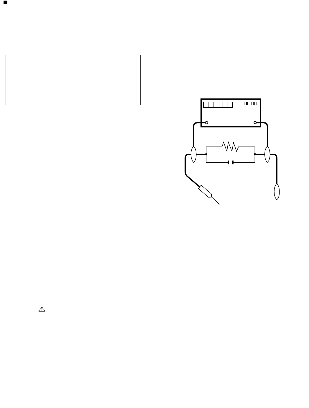
5. To be sure that no shock hazard exists, check for leakage current in
the following manner.
• Plug the AC cord directly into a 220~240 volt AC outlet.
• Using two clip leads, connect a 1.5k ohm, 10 watt resistor paral-
leled by a 0.15µF capacitor in series with all exposed metal cabinet
parts and a known earth ground, such as electrical conduit or elec-
trical ground connected to an earth ground.
• Use an AC voltmeter having with 5000 ohm per volt, or higher, sen-
sitivity or measure the AC voltage drop across the resistor.
• Connect the resistor connection to all exposed metal parts having a
return to the chassis (antenna, metal cabinet, screw heads, knobs
and control shafts, escutcheon, etc.) and measure the AC voltage
drop across the resistor.
All checks must be repeated with the AC cord plug connection
reversed. (If necessary, a nonpolarized adaptor plug must be used
only for the purpose of completing these checks.)
Any reading of 1.05 V peak (this corresponds to 0.7 mA peak AC.)
or more is excessive and indicates a potential shock hazard which
must be corrected before returning the monitor to the owner.
///////////////////////////////////////////////////////////////////////////////////////////////////////////////////////////////////////////////////////////////////////////////////////////////////////////////////////////////////////////
SAFETY NOTICE
Many electrical and mechanical parts in LCD color television have
special safety-related characteristics.
These characteristics are often not evident from visual inspection, nor
can protection afforded by them be necessarily increased by using
replacement components rated for higher voltage, wattage, etc.
Replacement parts which have these special safety characteristics are
identified in this manual; electrical components having such features
are identified by “ ” and shaded areas in the Replacement Parts
List and Schematic Diagrams.
For continued protection, replacement parts must be identical to those
used in the original circuit.
The use of a substitute replacement parts which do not have the same
safety characteristics as the factory recommended replacement parts
shown in this service manual, may create shock, fire or other hazards.
///////////////////////////////////////////////////////////////////////////////////////////////////////////////////////////////////////////////////////////////////////////////////////////////////////////////////////////////////////////
Service work should be performed only by qualified service technicians who are thoroughly familiar with all safety checks and the
servicing guidelines which follow:
CAUTION:
FOR CONTINUED PROTECTION AGAINST A
RISK OF FIRE REPLACE ONLY WITH SAME
TYPE FUSE.
F7000 (6.3A/250V)
DVM
AC SCALE
1.5k ohm
10W
TO EXPOSED
METAL PARTS
CONNECT TO
KNOWN EARTH
GROUND
0.15
µ
F
TEST PROBE
LC-42XL2E/S/RU, LC-46XL2E/S/RU, LC-46X20E/S/RU, LC-52XL2E/S/RU, LC-52X20E/S/RU
ii
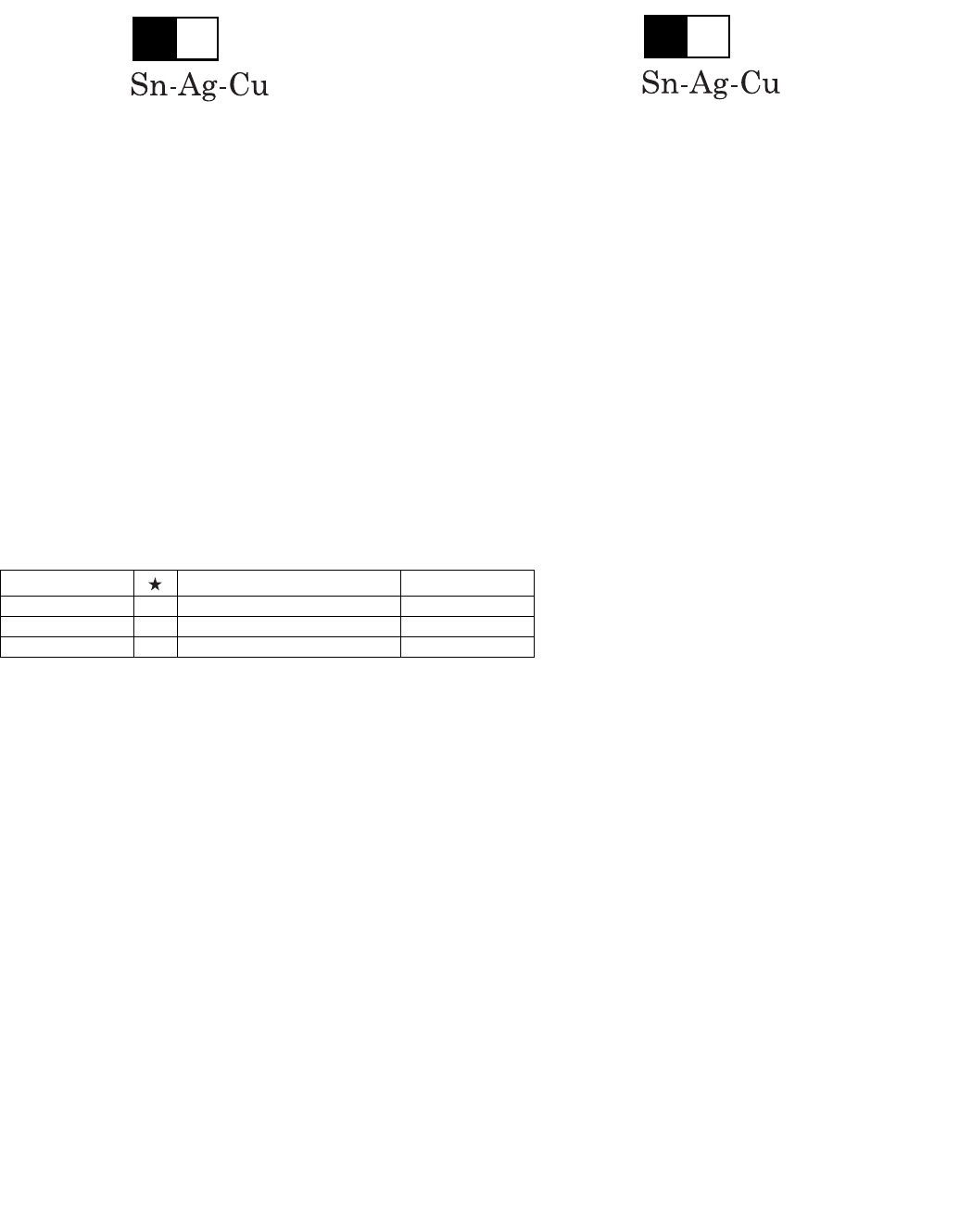
Precautions for using lead-free solder
Employing lead-free solder
• “PWBs” of this model employs lead-free solder. The LF symbol indicates lead-free solder, and is attached on the PWBs and service manuals. The
alphabetical character following LF shows the type of lead-free solder.
Example:
Using lead-free wire solder
• When fixing the PWB soldered with the lead-free solder, apply lead-free wire solder. Repairing with conventional lead wire solder may cause dam-
age or accident due to cracks.
As the melting point of lead-free solder (Sn-Ag-Cu) is higher than the lead wire solder by 40 °C, we recommend you to use a dedicated soldering
bit, if you are not familiar with how to obtain lead-free wire solder or soldering bit, contact our service station or service branch in your area.
Soldering
• As the melting point of lead-free solder (Sn-Ag-Cu) is about 220 °C which is higher than the conventional lead solder by 40 °C, and as it has poor
solder wettability, you may be apt to keep the soldering bit in contact with the PWB for extended period of time. However, Since the land may be
peeled off or the maximum heat-resistance temperature of parts may be exceeded, remove the bit from the PWB as soon as you confirm the
steady soldering condition.
Lead-free solder contains more tin, and the end of the soldering bit may be easily corroded. Make sure to turn on and off the power of the bit as
required.
If a different type of solder stays on the tip of the soldering bit, it is alloyed with lead-free solder. Clean the bit after every use of it.
When the tip of the soldering bit is blackened during use, file it with steel wool or fine sandpaper.
• Be careful when replacing parts with polarity indication on the PWB silk.
Lead-free wire solder for servicing
LFa
Indicates lead-free solder of tin, silver and copper.
LF a/a
Indicates lead-free solder of tin, silver and copper.
Part No. Description Code
ZHNDAi123250E J φ0.3mm 250g (1roll) BL
ZHNDAi126500E J φ0.6mm 500g (1roll) BK
ZHNDAi12801KE J φ1.0mm 1kg (1roll) BM
LC-42XL2E/S/RU, LC-46XL2E/S/RU, LC-46X20E/S/RU, LC-52XL2E/S/RU, LC-52X20E/S/RU
1 – 1
LC42XL2E Service Manual
CHAPTER 1. OPERATION MANUAL
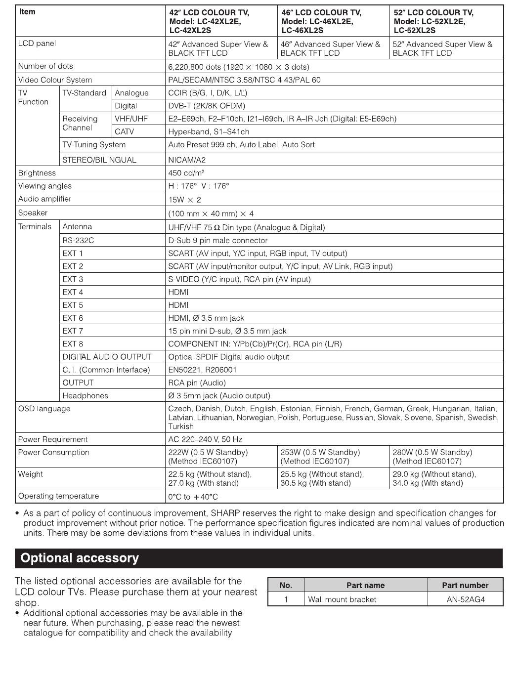
[1] SPECIFICATIONS (LC-42/46/52XL2E/S/RU)
LC-42XL2E/S/RU, LC-46XL2E/S/RU, LC-46X20E/S/RU, LC-52XL2E/S/RU, LC-52X20E/S/RU
1 – 2
[2] SPECIFICATIONS (LC-46/52X20E/S/RU)
LC-42XL2E/S/RU, LC-46XL2E/S/RU, LC-46X20E/S/RU, LC-52XL2E/S/RU, LC-52X20E/S/RU
1 – 3
[3] OPERATION MANUAL (LC-42/46/52XL2E/S/RU)
LC-42XL2E/S/RU, LC-46XL2E/S/RU, LC-46X20E/S/RU, LC-52XL2E/S/RU, LC-52X20E/S/RU
1 – 4
2
3
4
12
13
16
67891011
1
15
14
5
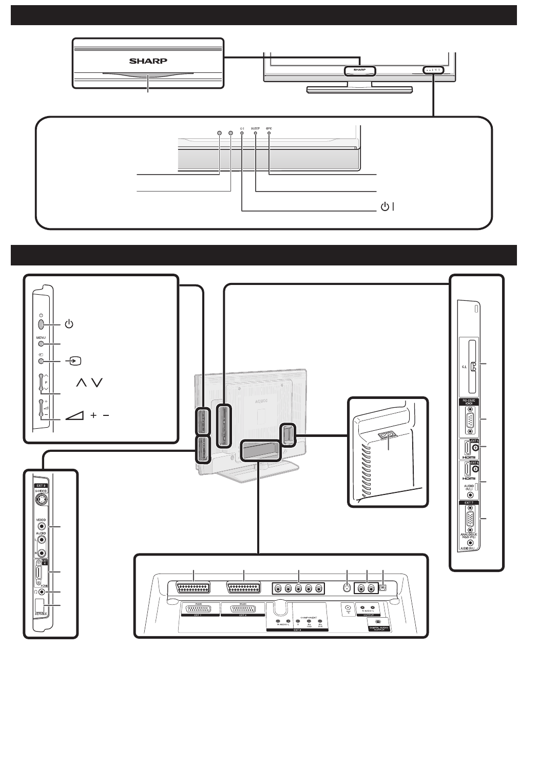
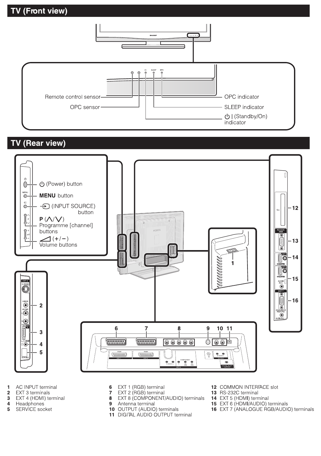
1AC INPUT terminal
2EXT 3 terminals
3EXT 4 (HDMI) terminal
4Headphones
5SERVICE socket
6EXT 1 (RGB) terminal
7EXT 2 (RGB) terminal
8EXT 8 (COMPONENT/AUDIO) terminals
9Antenna terminal
10 OUTPUT (AUDIO) terminals
11 DIGITAL AUDIO OUTPUT terminal
12 COMMON INTERFACE slot
* Remove the cover when inserting the CI
Module.
13 RS-232C terminal
14 EXT 5 (HDMI) terminal
15 EXT 6 (HDMI/AUDIO) terminals
16 EXT 7 (ANALOGUE RGB/AUDIO) terminals
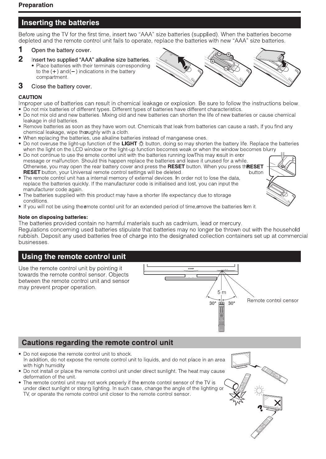
TV (Front view)
TV (Rear view)
Remote control censor
OPC censor
OPC indicator
SLEEP indicator
(Standby/On)
indicator
MENU button
(Power) button
( / )
Volume buttons
P(/ )
Programme [channel]
buttons
(Input source) button
Blue illumination LED indicator
LC-42XL2E/S/RU, LC-46XL2E/S/RU, LC-46X20E/S/RU, LC-52XL2E/S/RU, LC-52X20E/S/RU
1 – 5
LC-42XL2E/S/RU, LC-46XL2E/S/RU, LC-46X20E/S/RU, LC-52XL2E/S/RU, LC-52X20E/S/RU
1 – 6
LC-42XL2E/S/RU, LC-46XL2E/S/RU, LC-46X20E/S/RU, LC-52XL2E/S/RU, LC-52X20E/S/RU
1 – 7
LC-42XL2E/S/RU, LC-46XL2E/S/RU, LC-46X20E/S/RU, LC-52XL2E/S/RU, LC-52X20E/S/RU
1 – 8
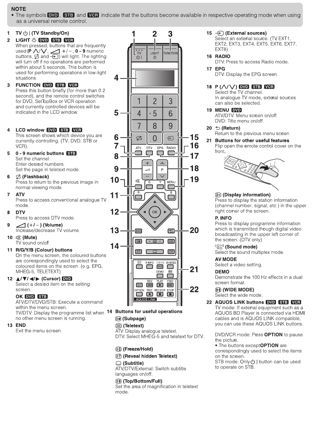
[4] OPERATION MANUAL (LC-46/52X20E/S/RU)
15
16
17
18
19
20
21
22
23
24
25
4
3
2
5
6
7
8
9
10
11
12
13
14
1
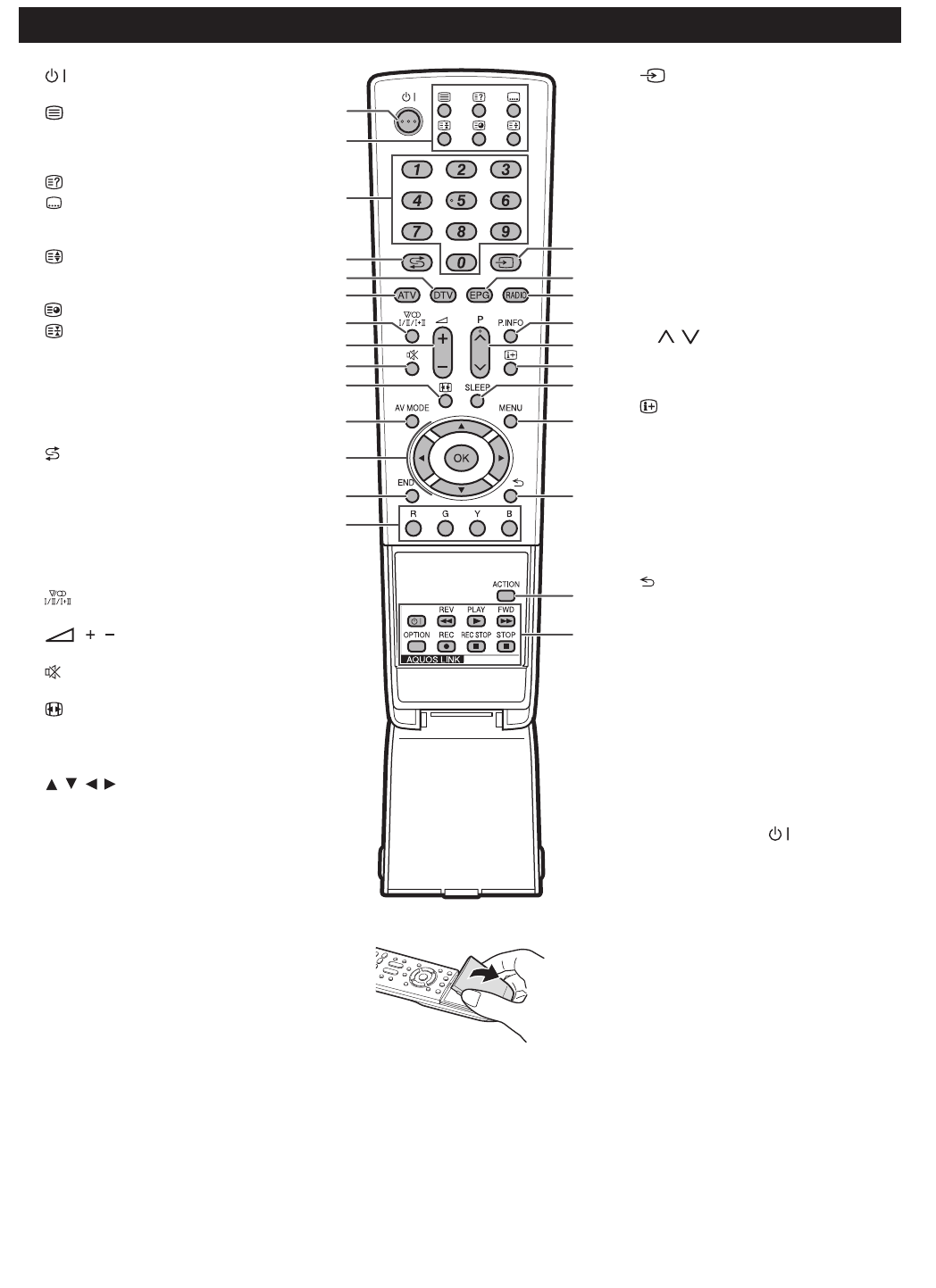
1(Standby/On)
2 Buttons for useful operations
(Teletext)
ATV: Display analogue teletext.
DTV: Select MHEG-5 and teletext for DTV.
(Reveal hidden Teletext)
(Subtitle)
ATV/DTV/External: Switch subtitle
languages on/off.
(Top/Bottom/Full)
Set the area of magnification in teletext
mode.
(Subpage)
(Freeze/Hold)
Press to freeze a moving image on the
screen.
3 0 - 9 numeric buttons
Set the channel.
Enter desired numbers.
Set the page in teletext mode.
4(Flashback)
Press to return to the previous image in
normal viewing mode.
5DTV
Press to access DTV mode.
6ATV
Press to access conventional analogue TV
mode.
7(Sound mode)
Select the sound multiplex mode.
8 ( / ) (Volume)
Increase/decrease TV volume.
9(Mute)
TV sound on/off
10 (WIDE MODE)
Select the wide mode.
11 AV MODE
Select a video setting.
12 / / / (Cursor)
Select a desired item on the setting
screen.
OK
ATV/DTV/DVD/STB: Execute a command
within the menu screen.
ATV/DTV: Display the programme list
when no other menu screen is running.
13 END
Exit the menu screen.
14 R/G/Y/B (Colour) buttons
On the menu screen, the coloured buttons
are correspondingly used to select the
coloured items on the screen. (e.g. EPG,
MHEG-5, TELETEXT)
15 (INPUT SOURCE)
Select an input source. (TV, EXT1, EXT2,
EXT3, EXT4, EXT5, EXT6, EXT7, EXT8)
16 EPG
DTV: Display the EPG screen.
17 RADIO
DTV: Switch between Radio and Data
mode.
18 P. INFO
Press to display programme information
which is transmitted through digital video
broadcasting in the upper left corner of
the screen. (DTV only)
19 P ( / )
Select the TV channel.
In analogue TV mode, external sources
can also be selected.
20 (Display information)
Press to display the station information
(channel number, signal, etc.) in the upper
right corner of the screen.
21 SLEEP
Press to schedule a time for the TV to
automatically standby.
22 MENU
ATV/DTV: Menu screen on/off.
DVD: Title menu on/off.
23 (Return)
Return to the previous menu screen.
24 ACTION (Action Mode)
Action Mode on/off.
25 AQUOS LINK buttons
TV mode: If external equipment such as a
AQUOS BD Player is connected via HDMI
cables and is AQUOS LINK compatible,
you can use these AQUOS LINK buttons.
DVD/VCR mode: Press OPTION to pause
the picture.
• The buttons except OPTION are
correspondingly used to select the items
on the screen.
STB mode: Only the button can be
used to operate on STB.
Remote control unit
LC-42XL2E/S/RU, LC-46XL2E/S/RU, LC-46X20E/S/RU, LC-52XL2E/S/RU, LC-52X20E/S/RU
1 – 9
LC-42XL2E/S/RU, LC-46XL2E/S/RU, LC-46X20E/S/RU, LC-52XL2E/S/RU, LC-52X20E/S/RU
1 – 10
LC-42XL2E/S/RU, LC-46XL2E/S/RU, LC-46X20E/S/RU, LC-52XL2E/S/RU, LC-52X20E/S/RU
1 – 11
LC-42XL2E/S/RU, LC-46XL2E/S/RU, LC-46X20E/S/RU, LC-52XL2E/S/RU, LC-52X20E/S/RU
1 – 12
LC-42XL2E/S/RU, LC-46XL2E/S/RU, LC-46X20E/S/RU, LC-52XL2E/S/RU, LC-52X20E/S/RU
1 – 13
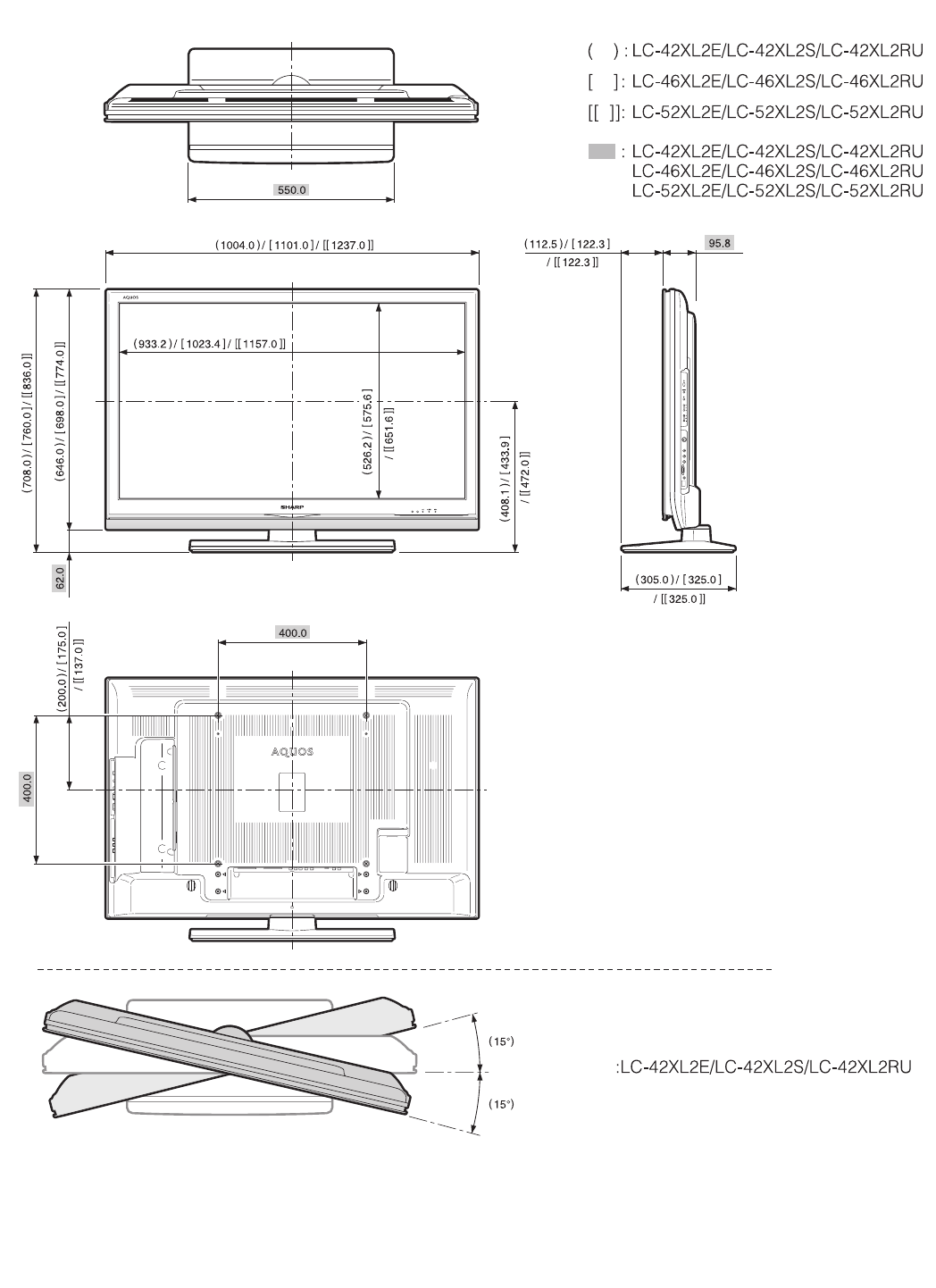
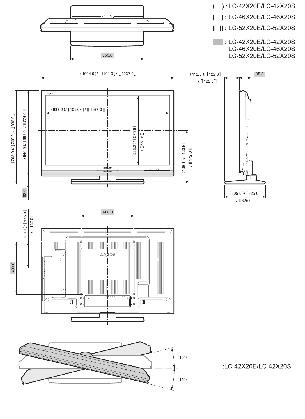
[5] DIMENSIONS (LC-42/46/52XL2E/S/RU)
Unit: mm
LC-42XL2E/S/RU, LC-46XL2E/S/RU, LC-46X20E/S/RU, LC-52XL2E/S/RU, LC-52X20E/S/RU
1 – 14
[6] DIMENSIONS (LC-46/52X20E/S/RU)
Unit: mm
LC-42XL2E/S/RU, LC-46XL2E/S/RU, LC-46X20E/S/RU, LC-52XL2E/S/RU, LC-52X20E/S/RU
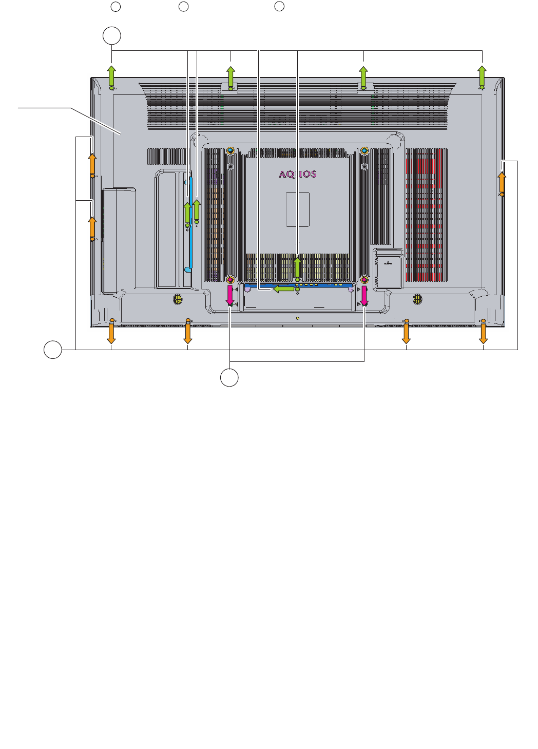
2 – 1
LC42XL2E Service Manual
CHAPTER 2. REMOVING OF MAJOR PARTS
[1] REMOVING OF MAJOR PARTS (LC-42XL2E/S/RU)
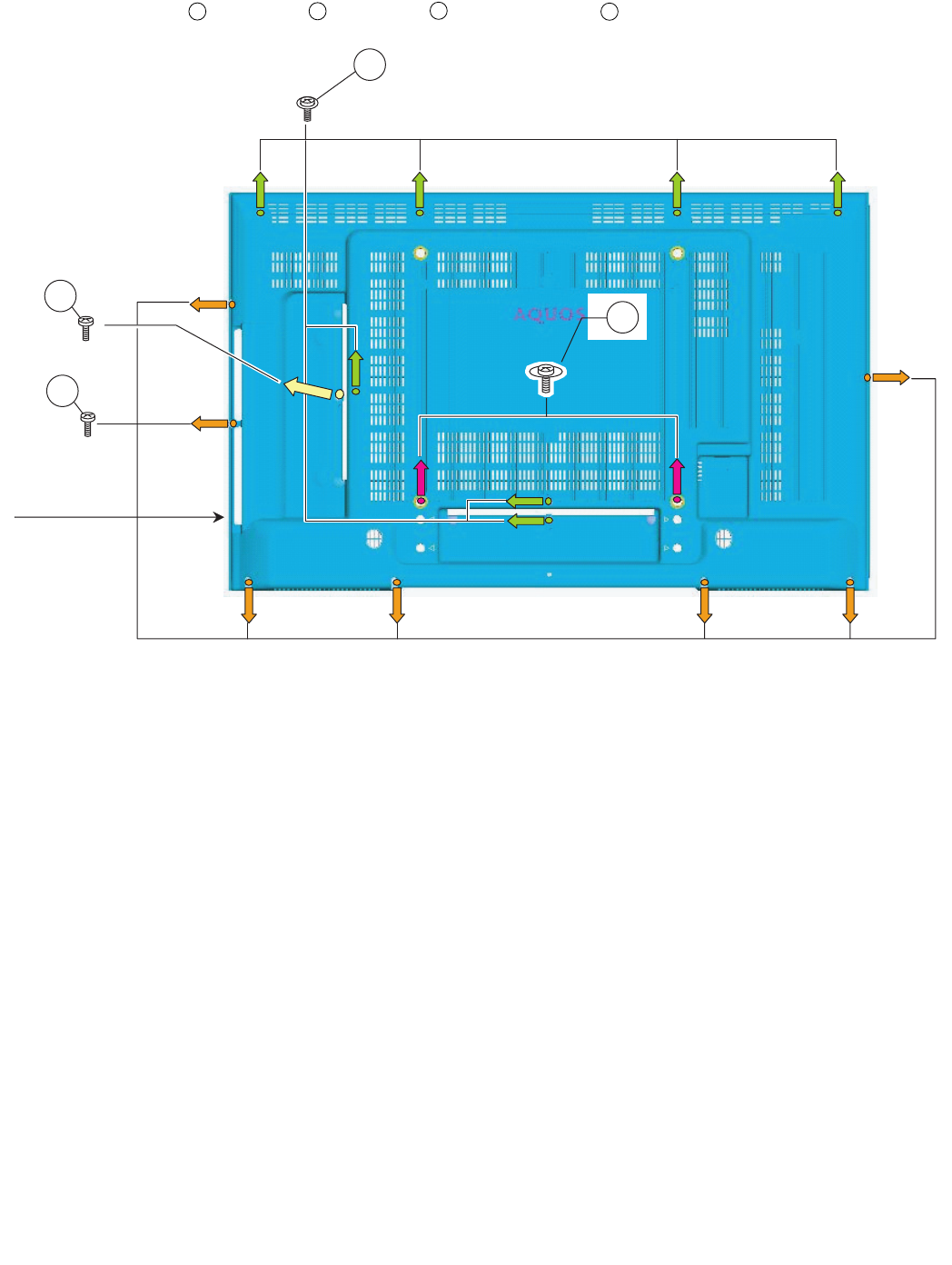
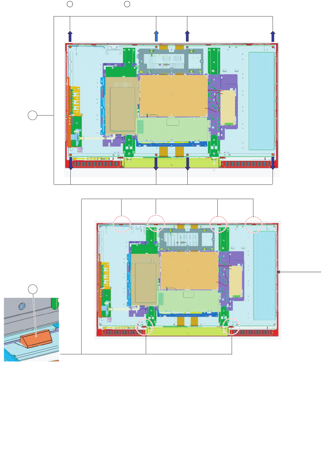
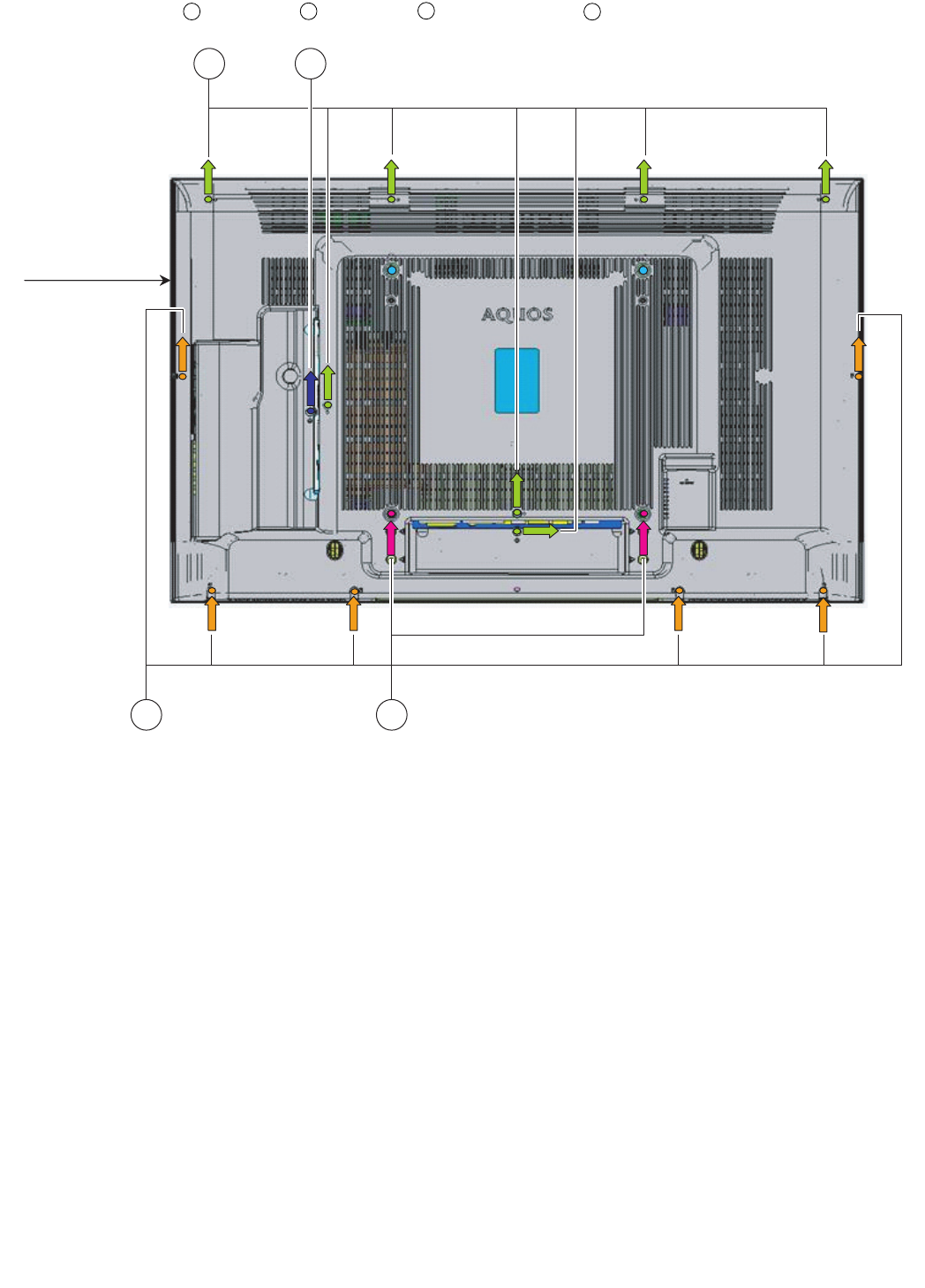
1. Remove the 1 lock screw , 2 lock screws , 7 lock screws and the 7 lock screws . Detach the Rear Cabinet.
1234
REAR CABINET
1
3
2
4
LC-42XL2E/S/RU, LC-46XL2E/S/RU, LC-46X20E/S/RU, LC-52XL2E/S/RU, LC-52X20E/S/RU
2 – 2
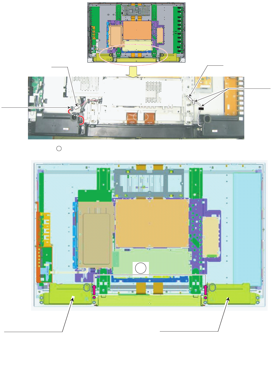
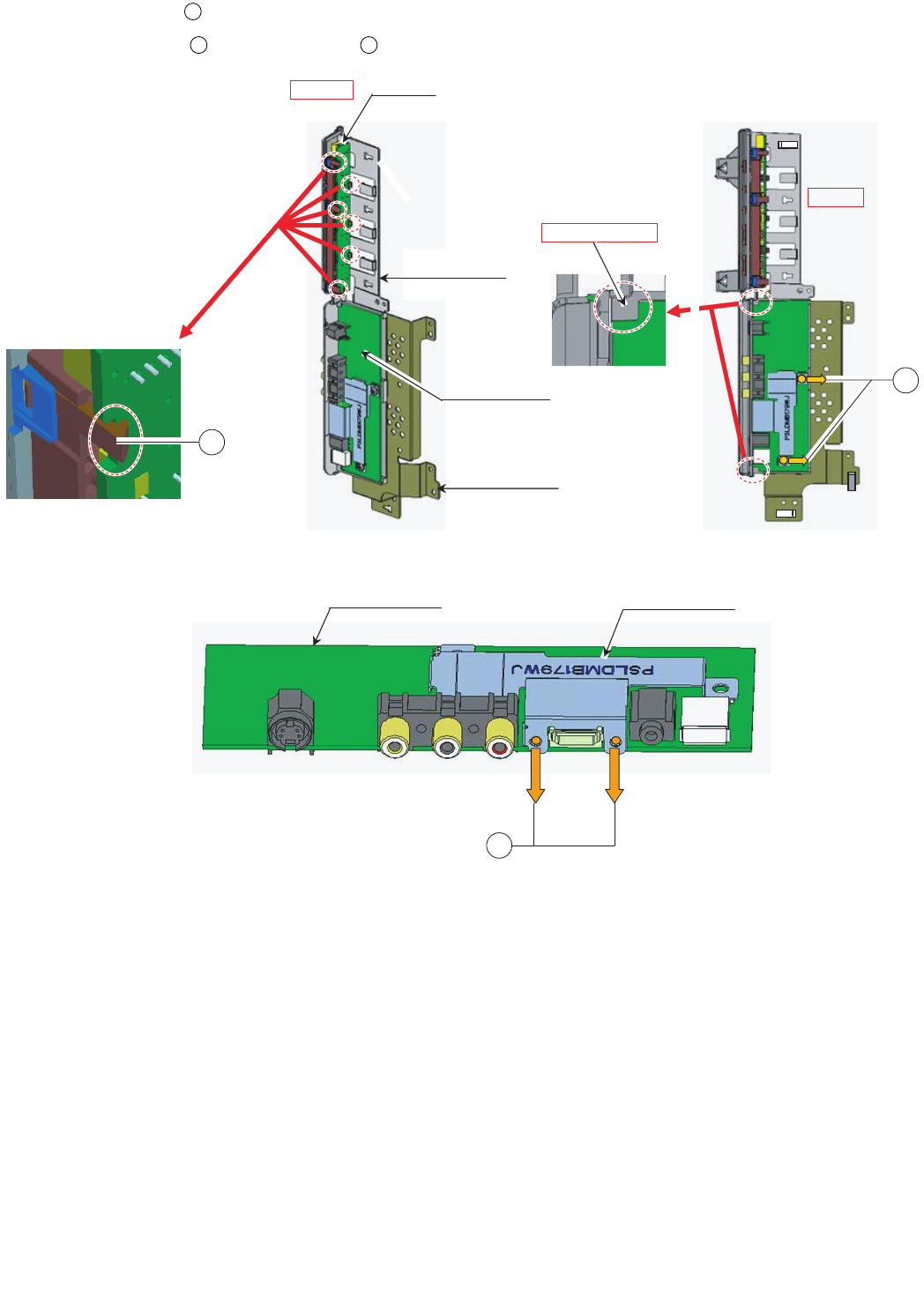
2. Remove all the connectors from PWBs.
3. Remove the 2 lock screws . and detach the Speaker L/R.
Wire "SP"
Wire "SP"
Wire "SP" to WH
Wire "SP" to WH
5
Speaker R Speaker L
5
LC-42XL2E/S/RU, LC-46XL2E/S/RU, LC-46X20E/S/RU, LC-52XL2E/S/RU, LC-52X20E/S/RU
2 – 3
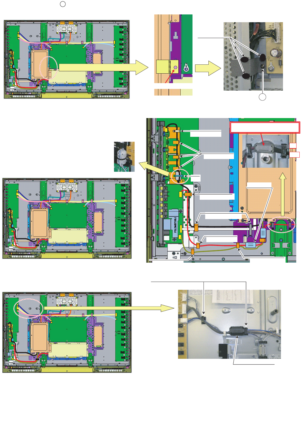
4. Remove all the connectors from PWBs.
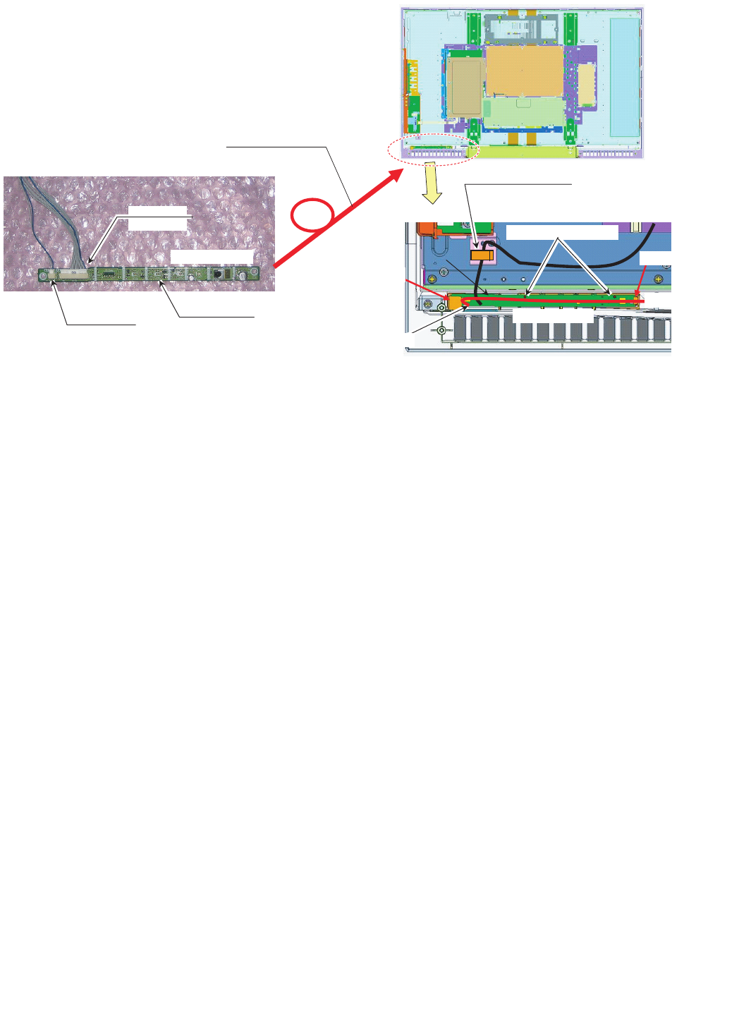
5. Remove the R/C, LED Unit.
LED PWB
Wire "RA"
from OBON
Wire "IL"
from Illumination
Wire "RA"
LED PWB Front side
LED PWB Back side
Pull out Wire "IL","RA" from bottom
1st, Set LED PWB Under LIB
LED PWB
(with wire)
#Set PWB to gide lib surely
Next,Push PWB hooked
Wire "IL"
Wire "RA" to WH
LC-42XL2E/S/RU, LC-46XL2E/S/RU, LC-46X20E/S/RU, LC-52XL2E/S/RU, LC-52X20E/S/RU
2 – 4
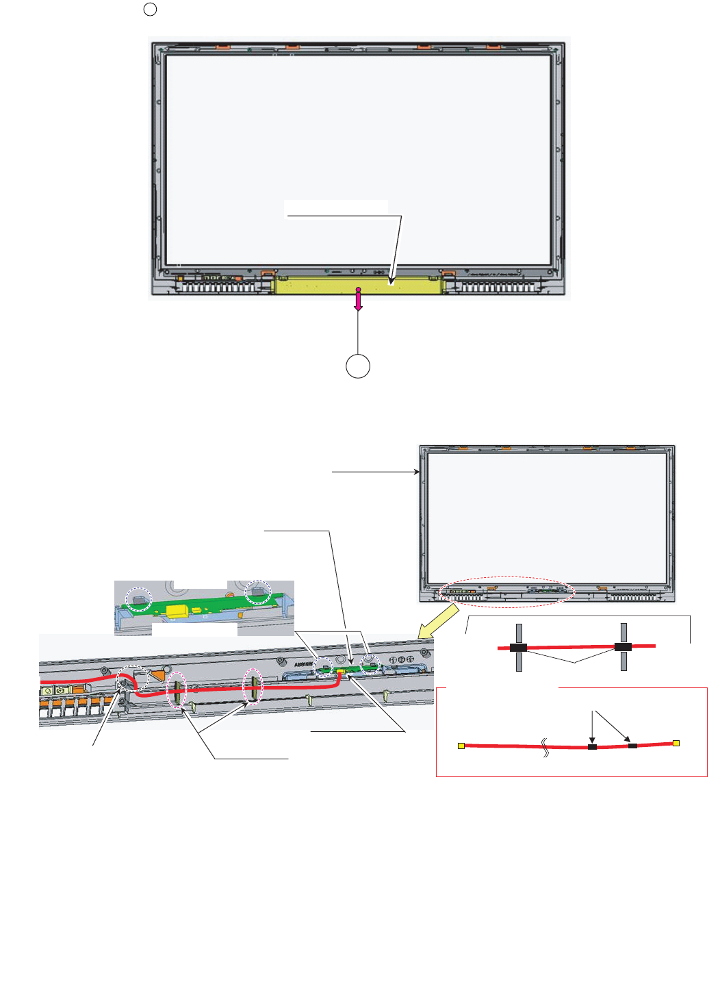
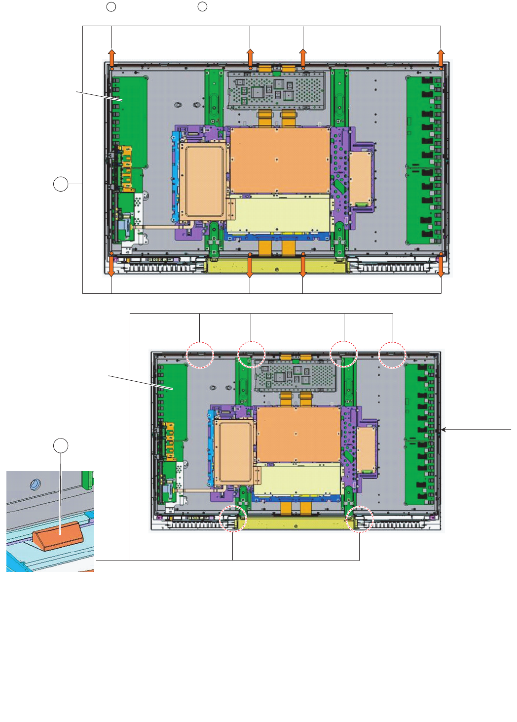
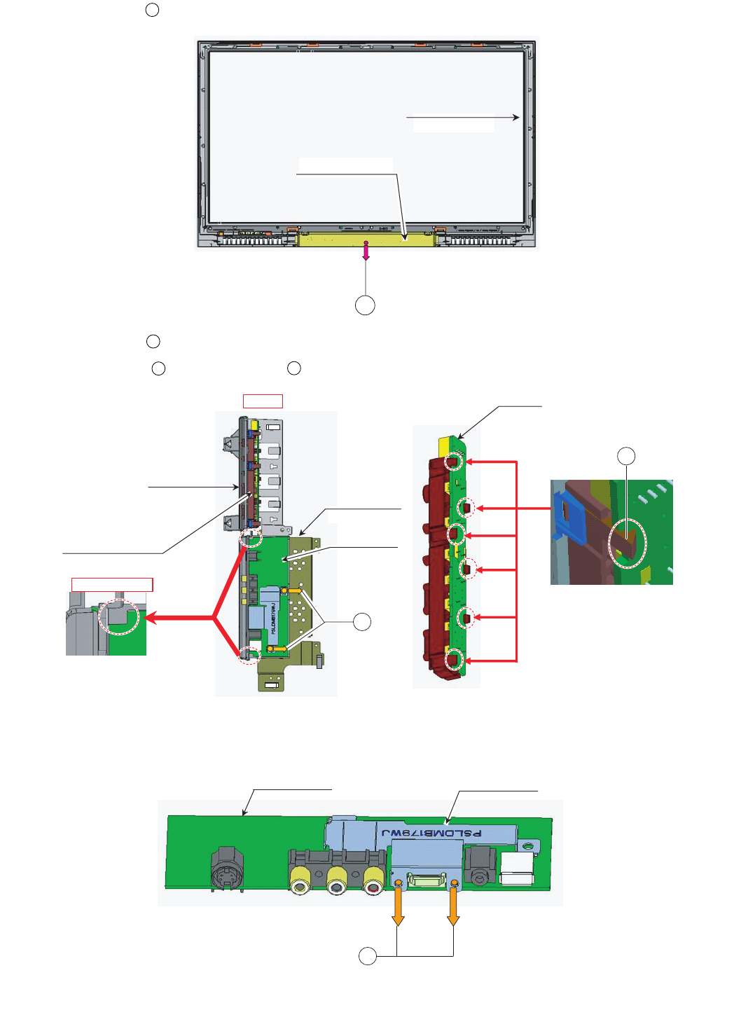
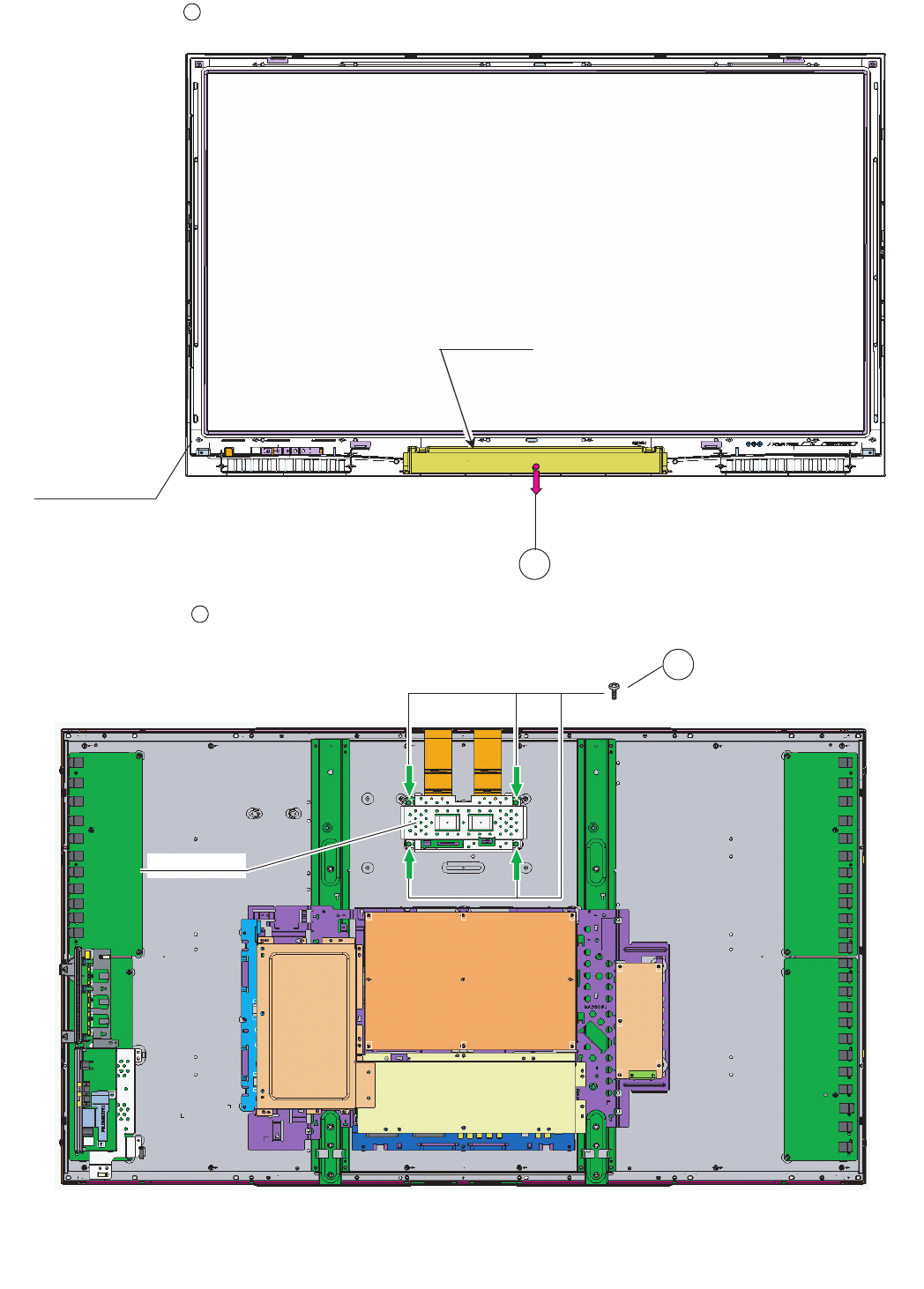
6. Remove the 8 lock screws , and the 6 lock hooks . Detach the LCD Panel Module.
6 7
6
FRONT CABINET
7
LC-42XL2E/S/RU, LC-46XL2E/S/RU, LC-46X20E/S/RU, LC-52XL2E/S/RU, LC-52X20E/S/RU
2 – 5
7. Remove the 1 lock screw . and detach the Bottom Cover.
8. Remove all the connectors from PWBs.
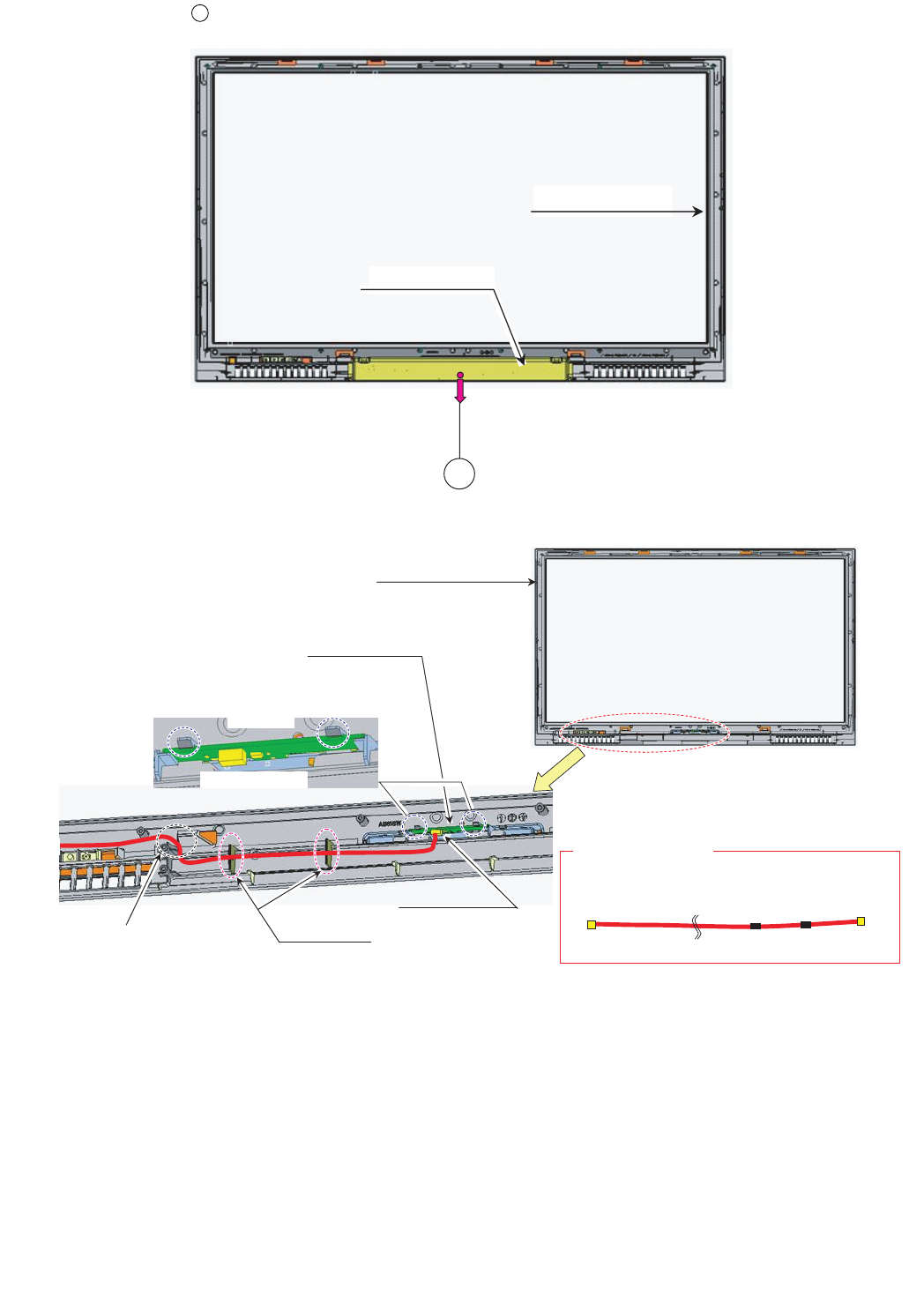
9. Remove the Illumination Unit.
8
BOTTOM COVER
8
FRONT CABINET
Wire "IL"
Wire "IL" to rib
Illumination Unit
Wire "IL"
#Hook Surely
#Connector side Down
#Wire "IL" pass between SP Boss
and Panel hooker
Illumination Unit
To LED PWB
TAPING
Wire "IL" Connection Direction
Wire "IL"
Tape
Lib
Lib
LC-42XL2E/S/RU, LC-46XL2E/S/RU, LC-46X20E/S/RU, LC-52XL2E/S/RU, LC-52X20E/S/RU
2 – 6
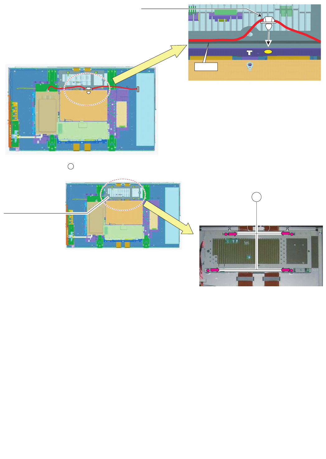
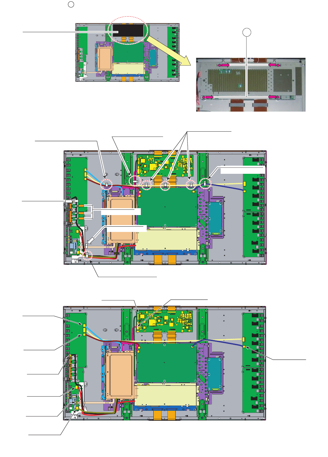
10.Remove the 4 lock screws . and detach the CTL SHIELD with RADIATOR.
Wire "LB" to Hole
㪮㫀㫉㪼㩷㪣㪙
9
CTL-SHIELD with RADIATOR
9
LC-42XL2E/S/RU, LC-46XL2E/S/RU, LC-46X20E/S/RU, LC-52XL2E/S/RU, LC-52X20E/S/RU
2 – 7
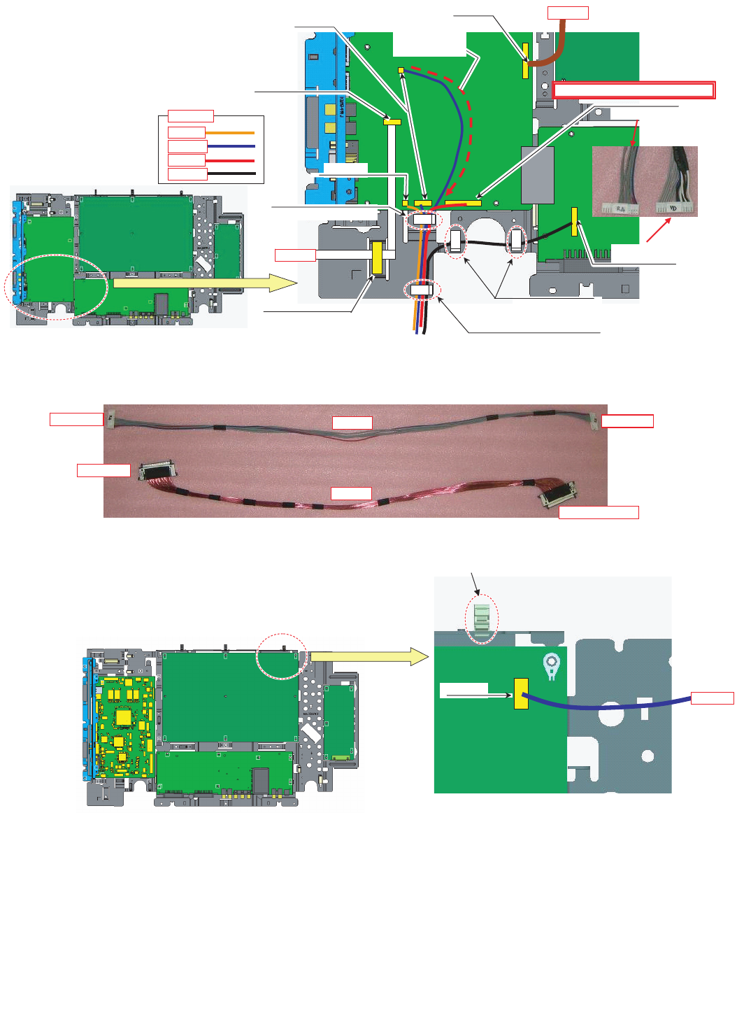
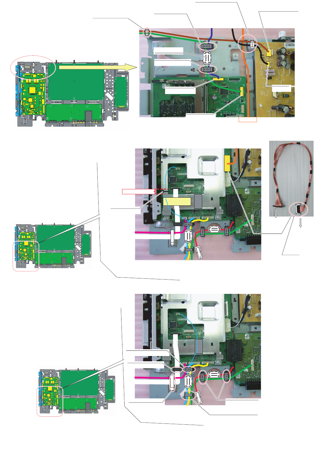
11.Remove all the connectors from PWBs.
Wire "LB", "LA1" to WH
FFC "HM" to WH
Wire "KM" to Hook
Wire "KM" to WH
Wire "KM", "VD", "US" to WH
Wire "RA"
Wire "KM", "VD"to WH
Wire "LB"
FFC "HM"
Wire "US"
Wire "VD"
Wire "KM"
Wire "FR"
Wire "LW"
Wire "LA1"
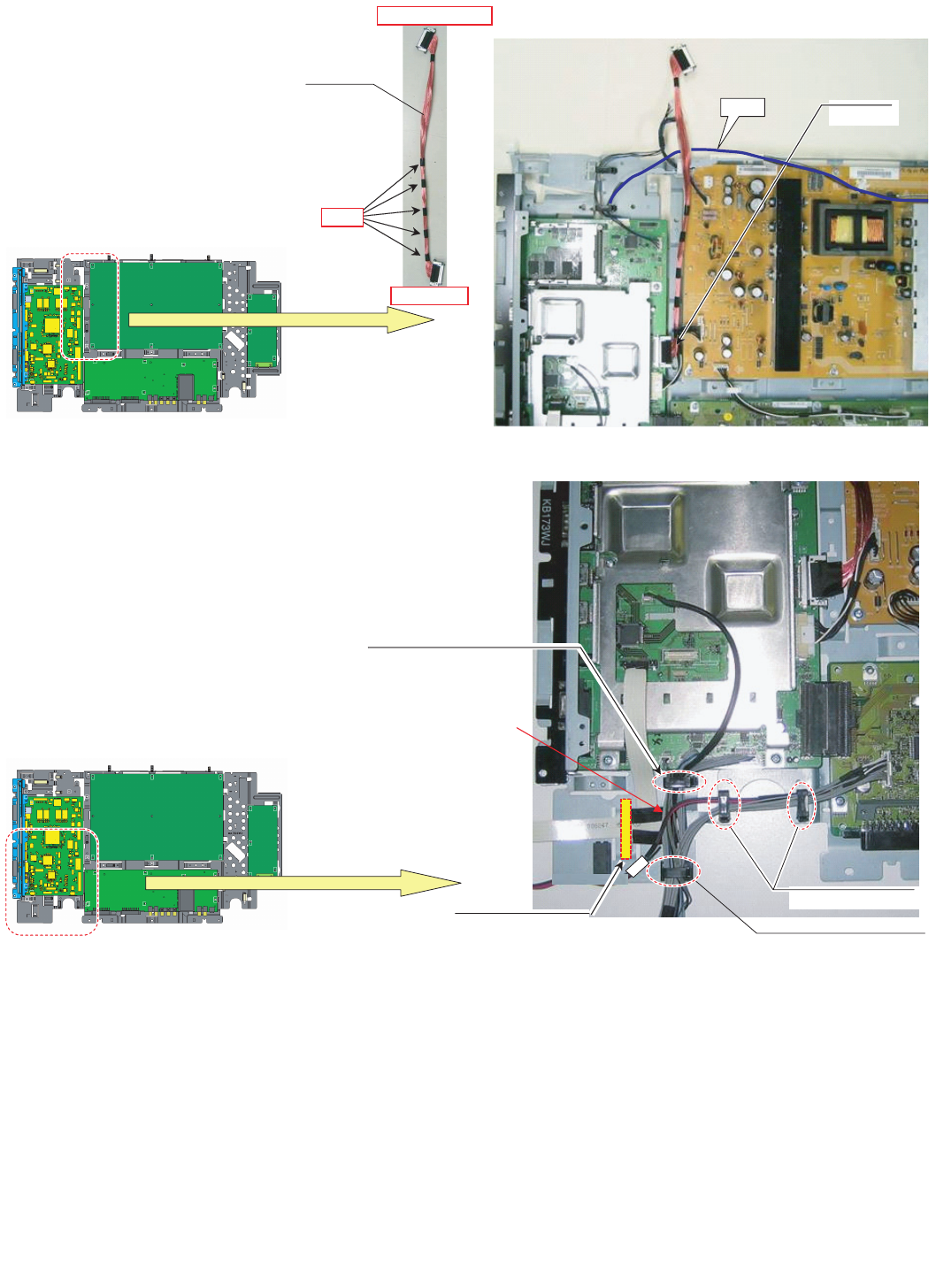
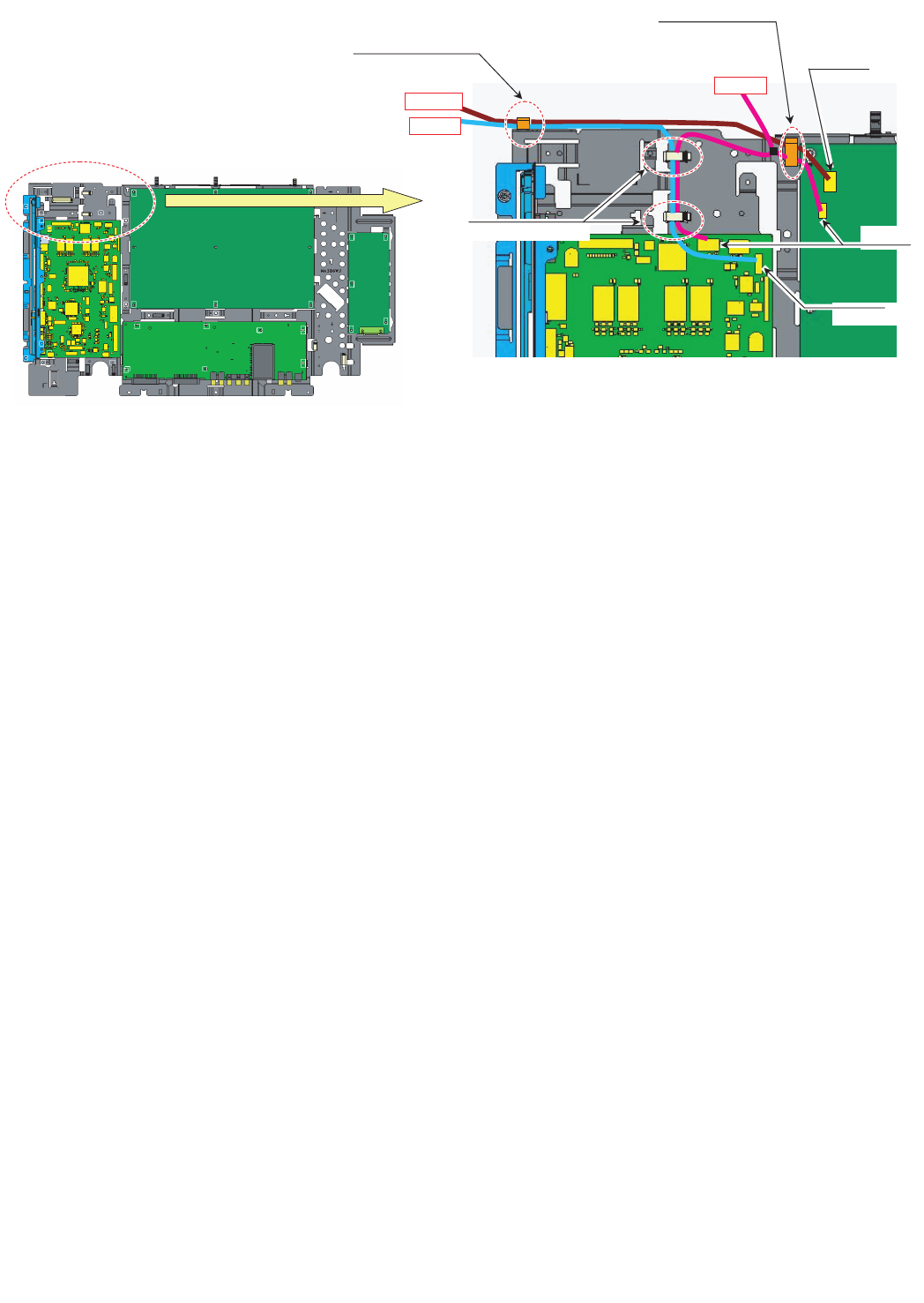
LC-42XL2E/S/RU, LC-46XL2E/S/RU, LC-46X20E/S/RU, LC-52XL2E/S/RU, LC-52X20E/S/RU
2 – 8
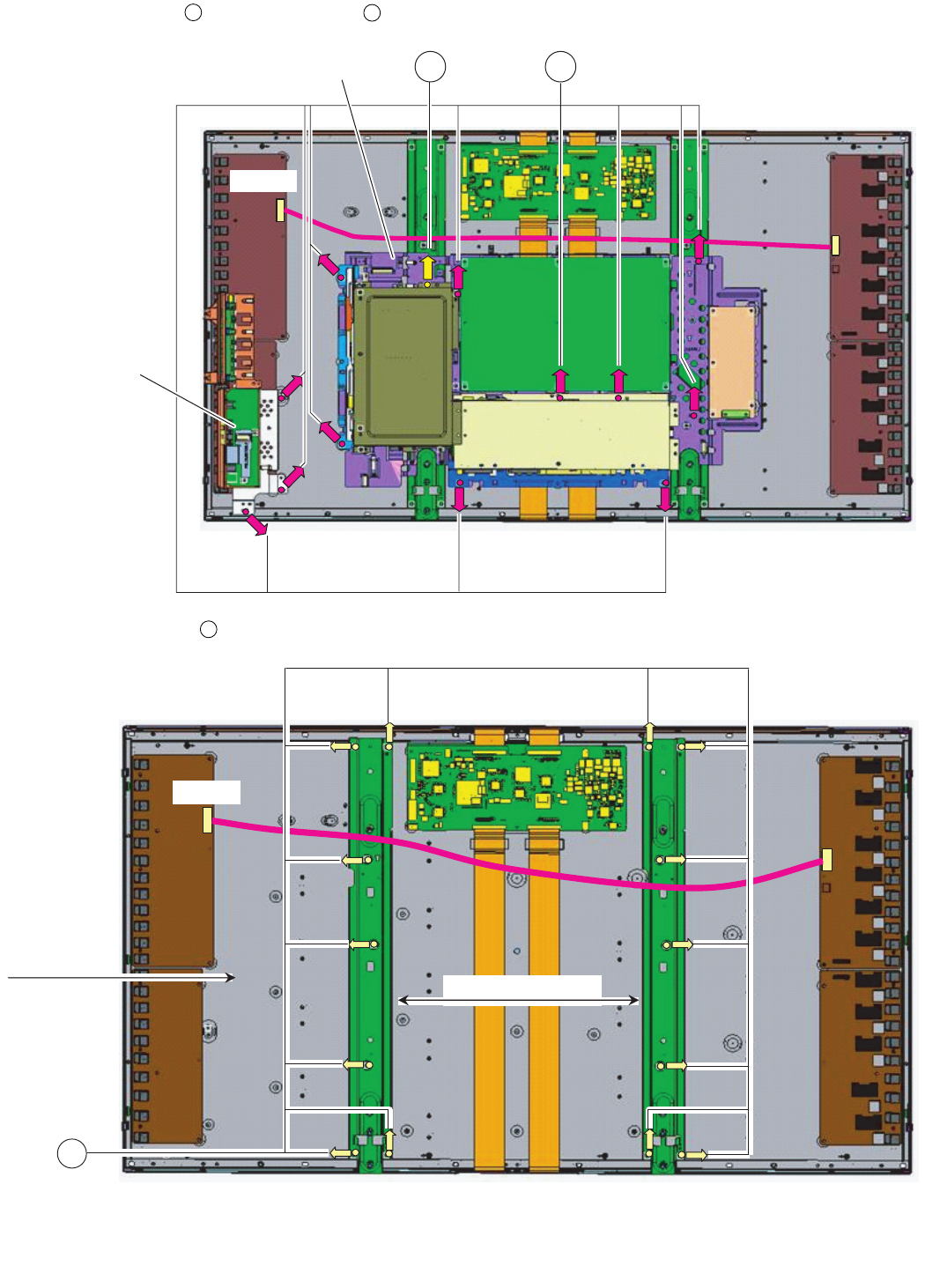
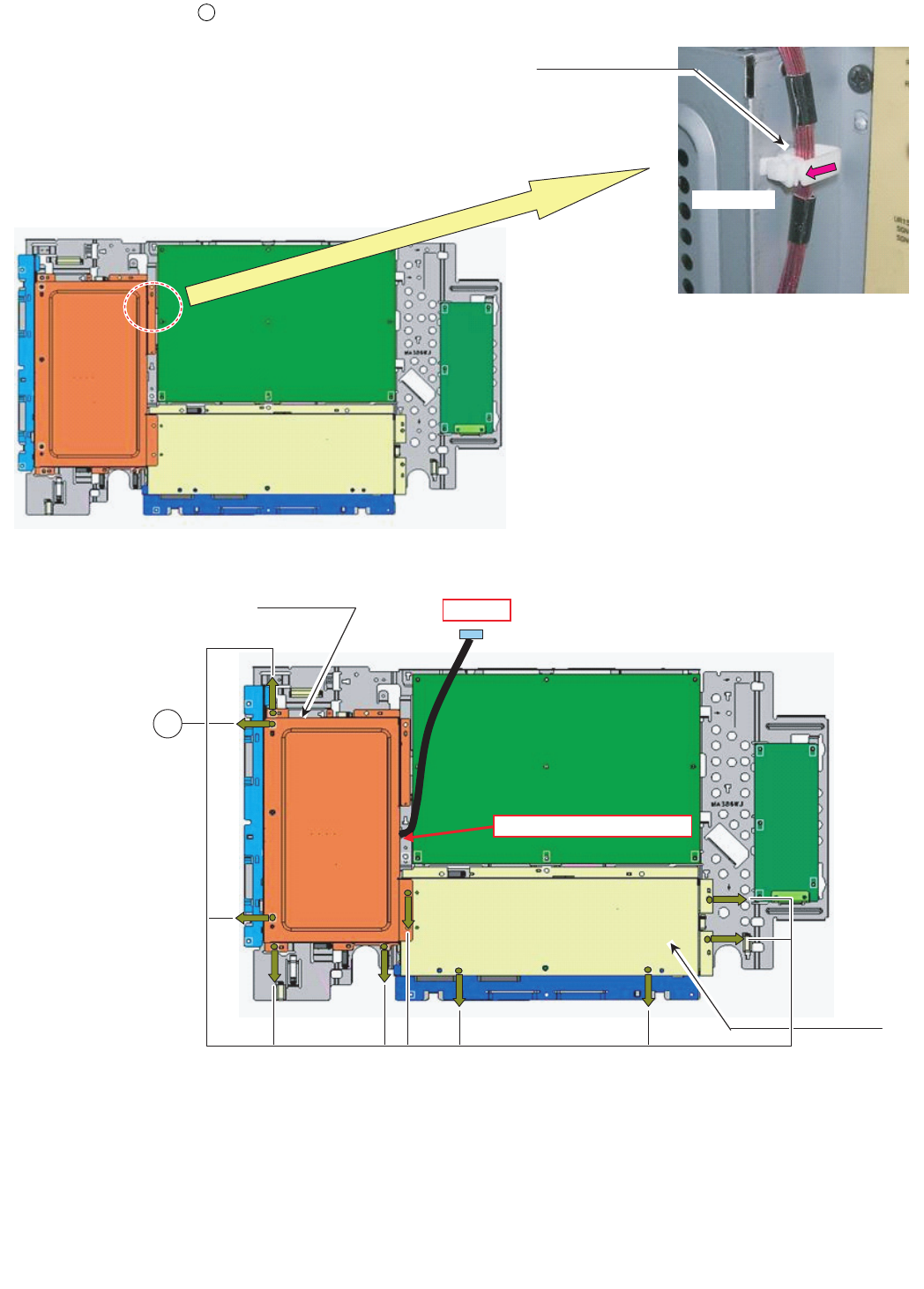
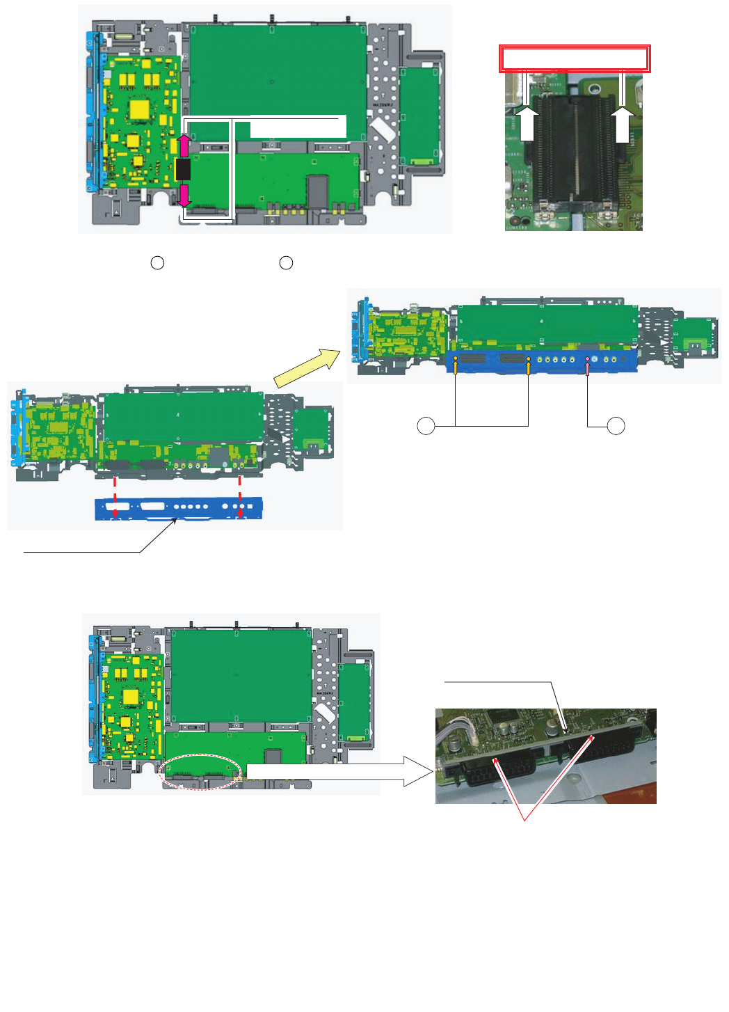
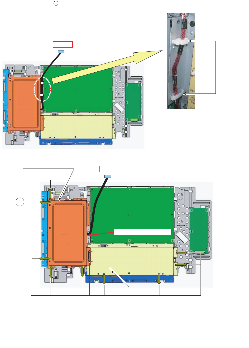
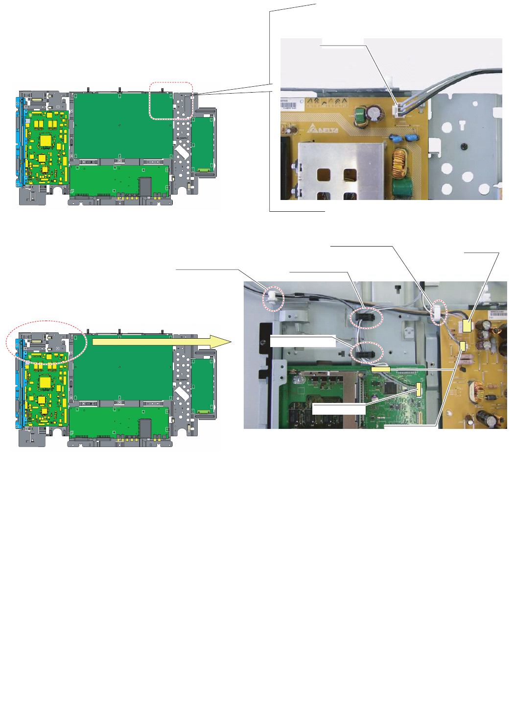
12.Remove the 1 lock screw , and the 11 lock screws . Detach the Chassis Tray and MINI AV Sub Ass’y.
13.Remove the 14 lock screws . and detach the Panel Support Angle.
10 11
11
10
12
PNL SUPPORT ANG
LCD MODULE
1212
LC-42XL2E/S/RU, LC-46XL2E/S/RU, LC-46X20E/S/RU, LC-52XL2E/S/RU, LC-52X20E/S/RU
2 – 9
14.Remove the 6 lock hooks . and detach the KEY Unit.
15.Remove the 2 lock screws , and the 2 lock screws . Detach the MINI AV Unit.
13
14 15
M-AV KEY COV
KEY PWB
MINI AV PWB
MINI AV ANG
Slant View
Top View
#Set PWB under LIB
Open side
14
13
15
MINI AV PWB MINI-AV SHIELD
LC-42XL2E/S/RU, LC-46XL2E/S/RU, LC-46X20E/S/RU, LC-52XL2E/S/RU, LC-52X20E/S/RU
2 – 10
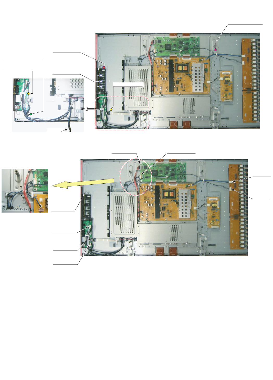
16.Remove all the connectors from PWBs.
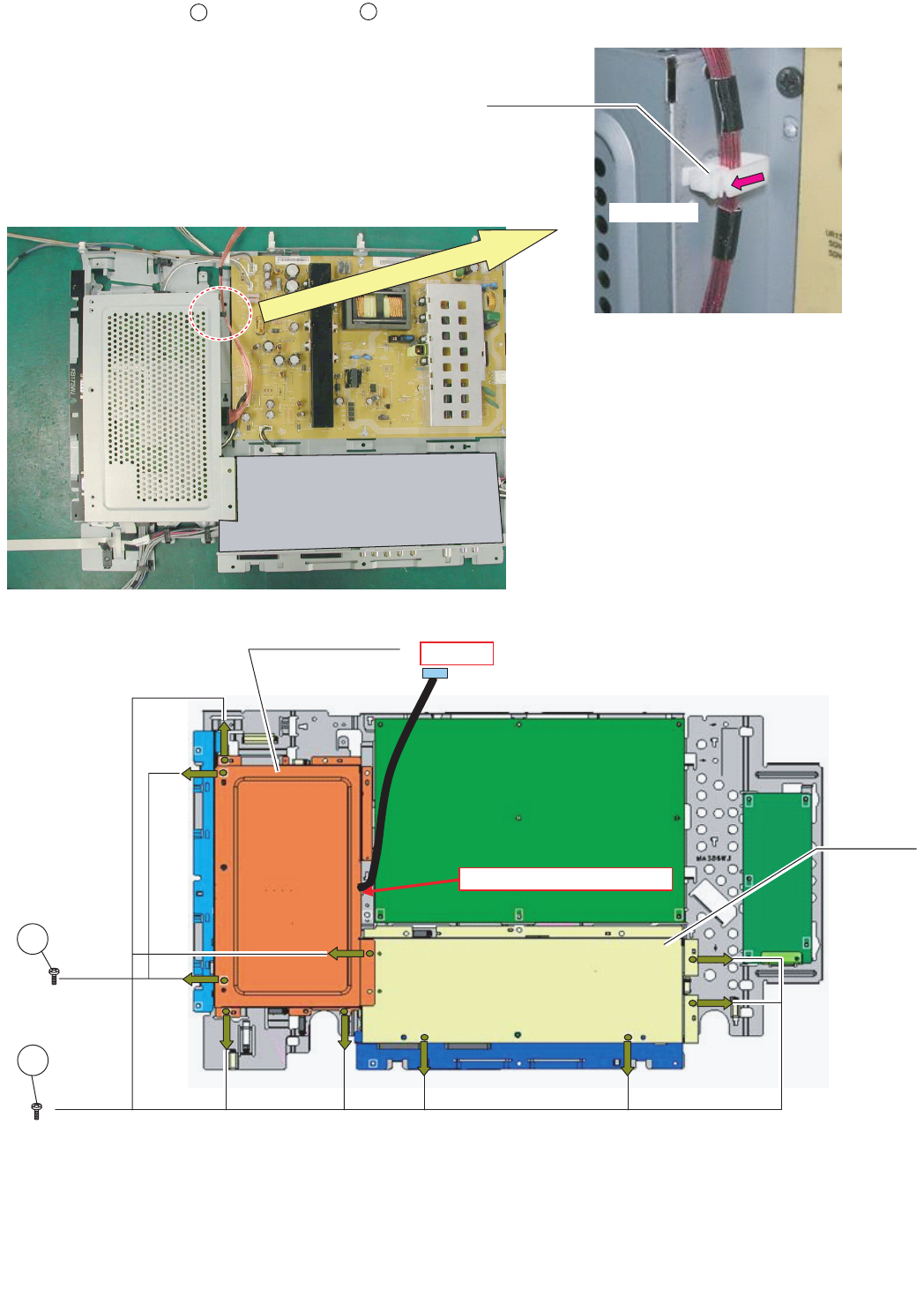
17.Remove the 10 lock screws . and detach the Main Shield and AV Shield.
16
Open Side
Wire "LW" to WH
AV SHIELD
MAIN SHIELD
Pull out Wire "LW" form Opening
Wire "LW"
16
LC-42XL2E/S/RU, LC-46XL2E/S/RU, LC-46X20E/S/RU, LC-52XL2E/S/RU, LC-52X20E/S/RU
2 – 11
18.Remove all the connectors from PWBs.
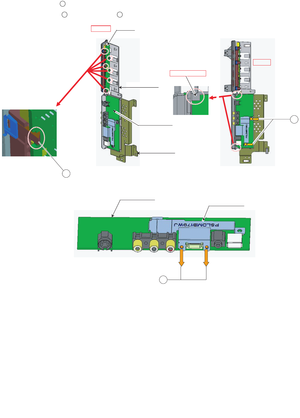
19.Remove the 2 lock screws , and the 1 lock screw . Detach the Terminal Angle Bottom.
B to B connection
Pull same time
17 18
TML ANG BTM
18 17
SCART ANGLE
#SCART Angle Stepping on terminal
LC-42XL2E/S/RU, LC-46XL2E/S/RU, LC-46X20E/S/RU, LC-52XL2E/S/RU, LC-52X20E/S/RU
2 – 12
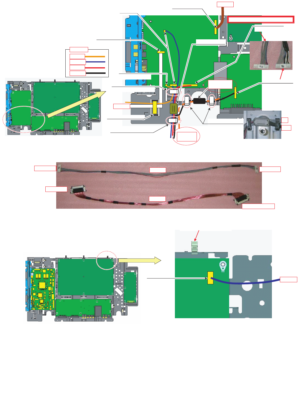
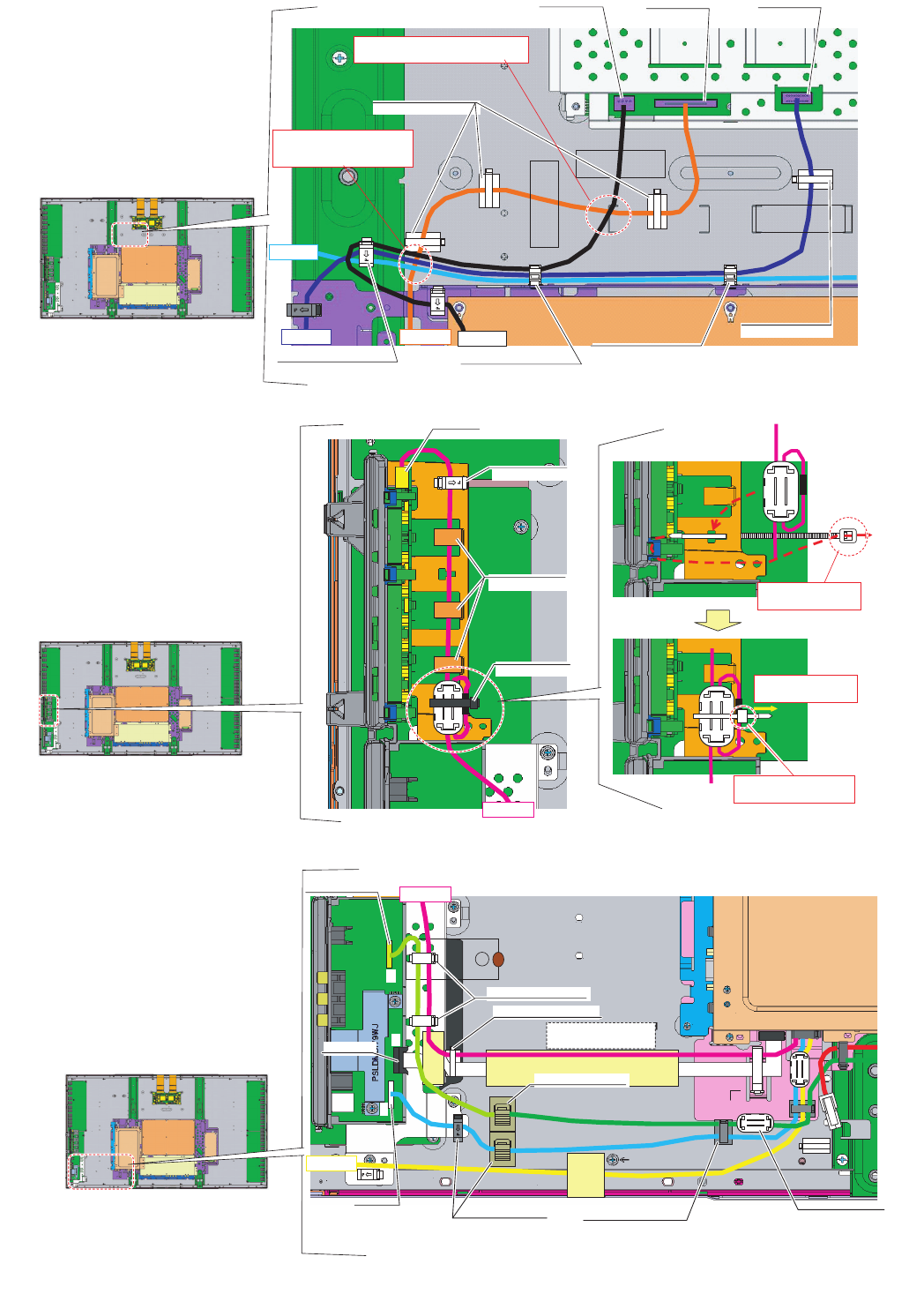
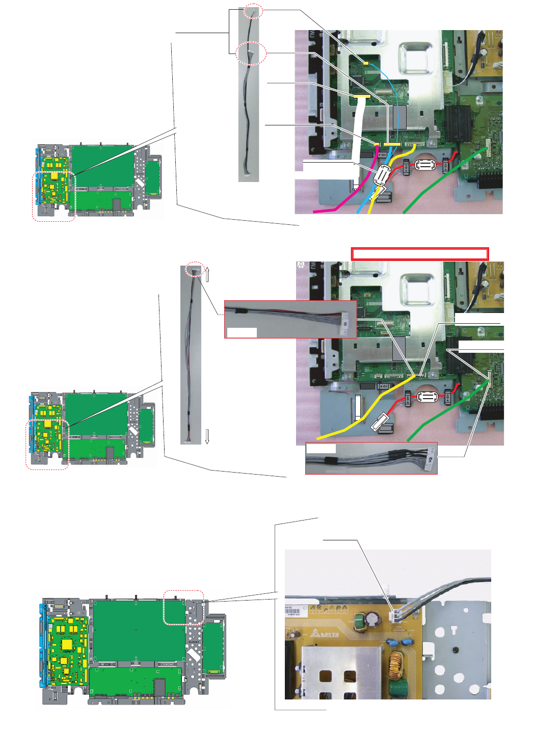
20.Remove all the connectors from PWBs.
Wire "LW"
wire LB
To Main PWB
To LCD Control PWB
Wire "LW"
Taping
Wire "VD","SP_R" to WH
Wire "RA","US","KM" to WH
Wire "RA","US","KM","VD" to WH
Wire "HM" to WH
Upper side wire SP_R
LC-42XL2E/S/RU, LC-46XL2E/S/RU, LC-46X20E/S/RU, LC-52XL2E/S/RU, LC-52X20E/S/RU
2 – 13
Wire "LA1"
Wire ”PL”
Wire "PL" to WH
Wire "PL" to WH
Wire "LB","PL" to WH
Wire "LB" to this WH
Wire "LB"

LC-42XL2E/S/RU, LC-46XL2E/S/RU, LC-46X20E/S/RU, LC-52XL2E/S/RU, LC-52X20E/S/RU
2 – 14
[2] REMOVING OF MAJOR PARTS (LC-46XL2E/S/RU)
1. Remove the 2 lock screws , 6 lock screws and the 8 lock screws . Detach the Rear Cabinet.
123
REAR CABNET
3
2 1
LC-42XL2E/S/RU, LC-46XL2E/S/RU, LC-46X20E/S/RU, LC-52XL2E/S/RU, LC-52X20E/S/RU
2 – 15
2. Remove all the connectors from PWBs.
3. Remove the 2 lock screws . and detach the Speaker L/R.
Wire "SP"
Wire "SP"
Wire "SP" to WH
Wire "SP" to WH
Wire "SP" to PIN
4
Speaker R Speaker L
4
LC-42XL2E/S/RU, LC-46XL2E/S/RU, LC-46X20E/S/RU, LC-52XL2E/S/RU, LC-52X20E/S/RU
2 – 16
4. Remove all the connectors from PWBs.
5. Remove the R/C, LED Unit.
R/C, LED PWB
Wire "RA"
from OBON
Wire "IL"
from Illumination
Wire "IL"
Wire
R/C, LED PWB Front side
LED PWB Back side
(3-3)Pull out Wire "IL","RA" from bottom
(3-1) Set R/C, LED PWB Under LIB
R/C, LED PWB
(with wire)
(3-2) Push PWB hooked
#Set PWB to gide lib surely
Wire "RA" to WH
LC-42XL2E/S/RU, LC-46XL2E/S/RU, LC-46X20E/S/RU, LC-52XL2E/S/RU, LC-52X20E/S/RU
2 – 17
6. Remove the 8 lock screws , and the 6 lock hooks . Detach the LCD Panel Module.
56
5
FRONT CABINET
6
LCD PANEL MODULE
LCD PANEL MODULE
LC-42XL2E/S/RU, LC-46XL2E/S/RU, LC-46X20E/S/RU, LC-52XL2E/S/RU, LC-52X20E/S/RU
2 – 18
7. Remove the 2 lock screws . and detach the Bottom Cover.
8. Remove all the connectors from PWBs.
7
BOTTOM COVER
FRONT CABINET
7
FRONT CABINET
Wire "IL"
Wire "IL" to rib
Illumination Unit
Wire "IL"
#Hook Surely
#Connector side Down
#Wire "IL" pass between SP Boss
and Panel hooker
To Illumination UnitTo R/C, LED PWB
Wire "IL" Connection Direction
LC-42XL2E/S/RU, LC-46XL2E/S/RU, LC-46X20E/S/RU, LC-52XL2E/S/RU, LC-52X20E/S/RU
2 – 19
9. Remove the Illumination Unit.
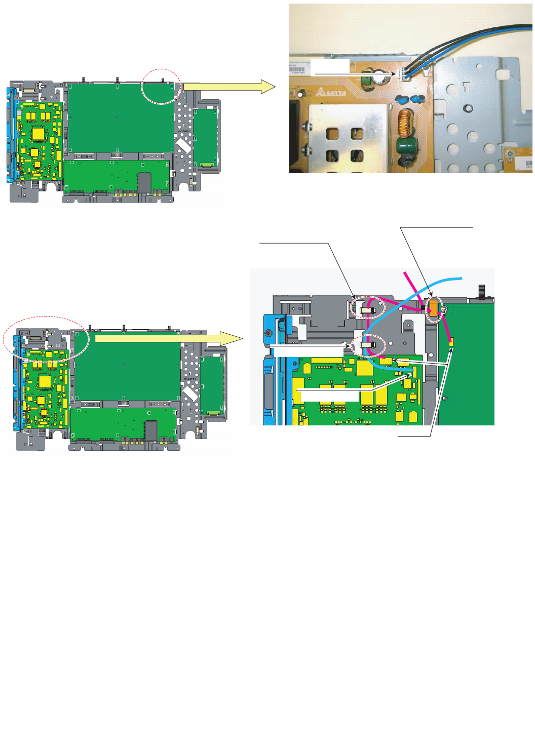
10.Remove the 4 lock screws . and detach the CTL SHIELD with RADIATOR.
11.Remove all the connectors from PWBs.
8
CTL-SHIELD with RADIATOR
8
Wire "LC" to WH
Wire "KM", "VD", "US" to WH
FFC "HM" to WH
Wire "KM" to Hook
Wire "KM" to WH
Wire "LC", "LA2", "LB" to WH
Wire "LW", "PL" to WH
Wire "LC", "LA1" to WH
Wire "LA1"
Wire "LA2"
Wire "LB"
FFC "HM"
Wire "US"
Wire "VD"
Wire "KM"
Wire "LP"
Wire "LW"
LC-42XL2E/S/RU, LC-46XL2E/S/RU, LC-46X20E/S/RU, LC-52XL2E/S/RU, LC-52X20E/S/RU
2 – 20
12.Remove the 1 lock screw , and the 12 lock screws . Detach the Chassis Tray and MINI AV Sub Ass’y.
13.Remove the 14 lock screws . and detach the Panel Support Angle.
910
10
Wire "LC"
MINI AV SUB ASSY
CHASSIS TRAY
9
11
PNL SUPPORT ANG
LCD MODULE
Wire "LC"
11
LC-42XL2E/S/RU, LC-46XL2E/S/RU, LC-46X20E/S/RU, LC-52XL2E/S/RU, LC-52X20E/S/RU
2 – 21
14.Remove the 6 lock hooks . and detach the KEY Unit.
15.Remove the 2 lock screws , and the 2 lock screws . Detach the MINI AV Unit.
12
13 14
M-AV KEY COV
KEY PWB
MINI AV PWB
MINI AV ANG
Slant View
Top View
#Set PWB under LIB
13
14
12
MINI AV PWB MINI-AV SHIELD
LC-42XL2E/S/RU, LC-46XL2E/S/RU, LC-46X20E/S/RU, LC-52XL2E/S/RU, LC-52X20E/S/RU
2 – 22
16.Remove all the connectors from PWBs.
17.Remove the 10 lock screws . and detach the Main Shield and AV Shield.
15
Open Side
Wire "LW" to WH
AV SHIELD
MAIN SHIELD
Wire "LW"
Pull out Wire "LW" form Opening
15
LC-42XL2E/S/RU, LC-46XL2E/S/RU, LC-46X20E/S/RU, LC-52XL2E/S/RU, LC-52X20E/S/RU
2 – 23
18.Remove all the connectors from PWBs.
19.Remove the 2 lock screws , and the 1 lock screw . Detach the Terminal Angle Bottom.
B to B connection
Pull same time
16 17
TML ANG BTM
1716
SCART ANGLE
#SCART Angle Stepping on terminal
LC-42XL2E/S/RU, LC-46XL2E/S/RU, LC-46X20E/S/RU, LC-52XL2E/S/RU, LC-52X20E/S/RU
2 – 24
20.Remove all the connectors from PWBs.
Wire "VD" to WH
Wire "KM"
Wire "HM"
Wire "LW"
Wire "RA","US","KM","VD" to WH
Wire "HM" to WH
#Shape Wire "US"
like this
Wire "RA","US","KM" to WH
Wire "US"
Wire "VD"
Wire "RA"
#Don't make mistake Wire "VD" and "RA"
Wire "LW"
Wire "HM"
Wire
Wire "US"
Wire
Wire "VD"
Wire
Wire "RA"
Wire "LW"
To Main PWB
To LED PWB
To Main PWB
To LCD Control PWB
Wire "LA1"
Wire "LA1"
#No shape Wire "LA1" to WH
LC-42XL2E/S/RU, LC-46XL2E/S/RU, LC-46X20E/S/RU, LC-52XL2E/S/RU, LC-52X20E/S/RU
2 – 25
Wire "LA2"
Wire "LB"
Wire "LB","PL" to WH
Wire "LA2","PL" to WH
Wire "LA2","LB" to WH
Wire "PL"
Wire "LA2"
Wire "LB"
Wire "PL"
LC-42XL2E/S/RU, LC-46XL2E/S/RU, LC-46X20E/S/RU, LC-52XL2E/S/RU, LC-52X20E/S/RU
2 – 26
[3] REMOVING OF MAJOR PARTS (LC-46X20E/S/RU)
1. Remove the 1 lock screw , 2 lock screws , 6 lock screws and the 7 lock screws . Detach the Rear Cabinet.
1234
REAR CABINET
4 1
23
LC-42XL2E/S/RU, LC-46XL2E/S/RU, LC-46X20E/S/RU, LC-52XL2E/S/RU, LC-52X20E/S/RU
2 – 27
2. Remove all the connectors from PWBs.
3. Remove the 2 lock screws . and detach the Speaker L/R.
Wire "SP" to WH
Wire "SP" to PIN
Wire "SP" to WH
Wire "SP"
Wire "SP"
5
Speaker R Speaker L
5
LC-42XL2E/S/RU, LC-46XL2E/S/RU, LC-46X20E/S/RU, LC-52XL2E/S/RU, LC-52X20E/S/RU
2 – 28
4. Remove the 1 lock screw .
5. Remove all the connectors from PWBs.
6
#Fit CONDUCTIVE Tape hole to SCREW hole
SILICON BOND
6
#For EMC
Set Wire "VD" under Wire "SP-R" (with core)
VD
SP-R
for Wire "VD"
Wire "HM","KM" to WH
Wire "US","VD" to WH
Wire "US" to WH
Wire "VD" to WH
Wire "VD","KM to WH
Wire "KM to WH
Wire "KM" to Hook
WH
for Wire "LA2","LB","LC"
Wire "LA2","LB","LC" to WH
LC-42XL2E/S/RU, LC-46XL2E/S/RU, LC-46X20E/S/RU, LC-52XL2E/S/RU, LC-52X20E/S/RU
2 – 29
Wire "LC", "LA1" to WH
Wire "LC" to WH
Wire "LW" to WH
Wire "LW" to WH
#For EMC
Set Wire "LW" under other wires
Wire "FR" to WH
Wire "LC","PL","FR" to WH
Wire "LC","FR" to WH
Wire "KM"
Wire "LW"
Wire "PL" Wire "FR"
Wire "LA1"
Wire "LB"
Wire "LA2"
Wire "VD"
FFC "HM"
Wire "US"
for Wire "KM"
#Wind Wire "KM" one time to core
Set taping to core inside.
To Main PWB
To Key PWB
Wind wire "KM" one
time to core.
#For EMC,Set Wire "LW" under other wires.
LC-42XL2E/S/RU, LC-46XL2E/S/RU, LC-46X20E/S/RU, LC-52XL2E/S/RU, LC-52X20E/S/RU
2 – 30
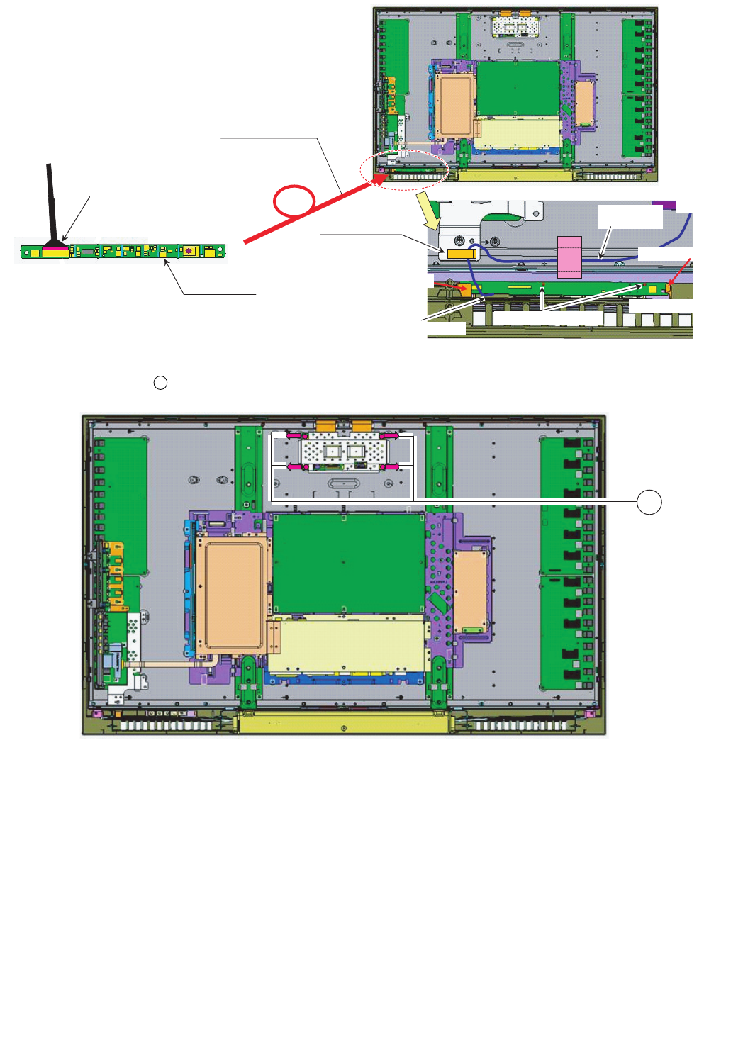
6. Remove the R/C, LED Unit.
7. Remove the 4 lock screws . and detach the CTL SHIELD.
R/C, LED PWB
Wire "RA"
from OBON
Wire "RA"
R/C, LED PWBFront side
LED PWB Back side
Pull out Wire "RA" from bottom
1st,Set R/C, LED PWB Under LIB
R/C, LED PWB
(with wire)
Next,Push PWB hooked
#Set PWB to gide lib surely
Wire "RA" to WH
Set Wire "RA" to
panel hollow.
7
7
LC-42XL2E/S/RU, LC-46XL2E/S/RU, LC-46X20E/S/RU, LC-52XL2E/S/RU, LC-52X20E/S/RU
2 – 31
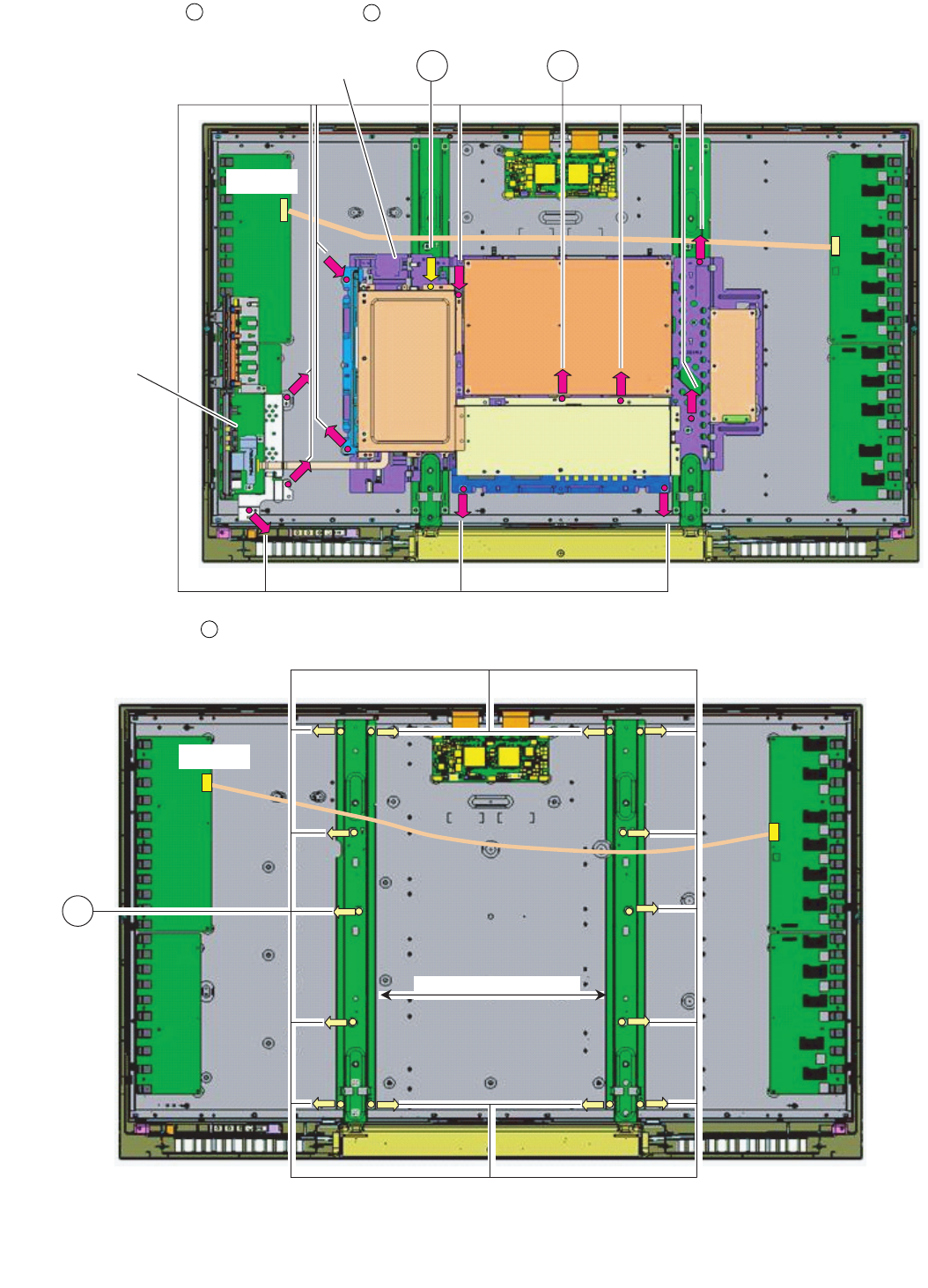
8. Remove the 1 lock screw , and the 11 lock screws . Detach the Chassis Tray and MINI AV Sub Ass’y.
9. Remove the 14 lock screws . and detach the Panel Support Angle.
89
Wire "LC"
9
MINI AV SUB ASSY
CHASSIS TRAY
8
10
PNL SUPPORT ANG
Wire "LC"
10
LC-42XL2E/S/RU, LC-46XL2E/S/RU, LC-46X20E/S/RU, LC-52XL2E/S/RU, LC-52X20E/S/RU
2 – 32
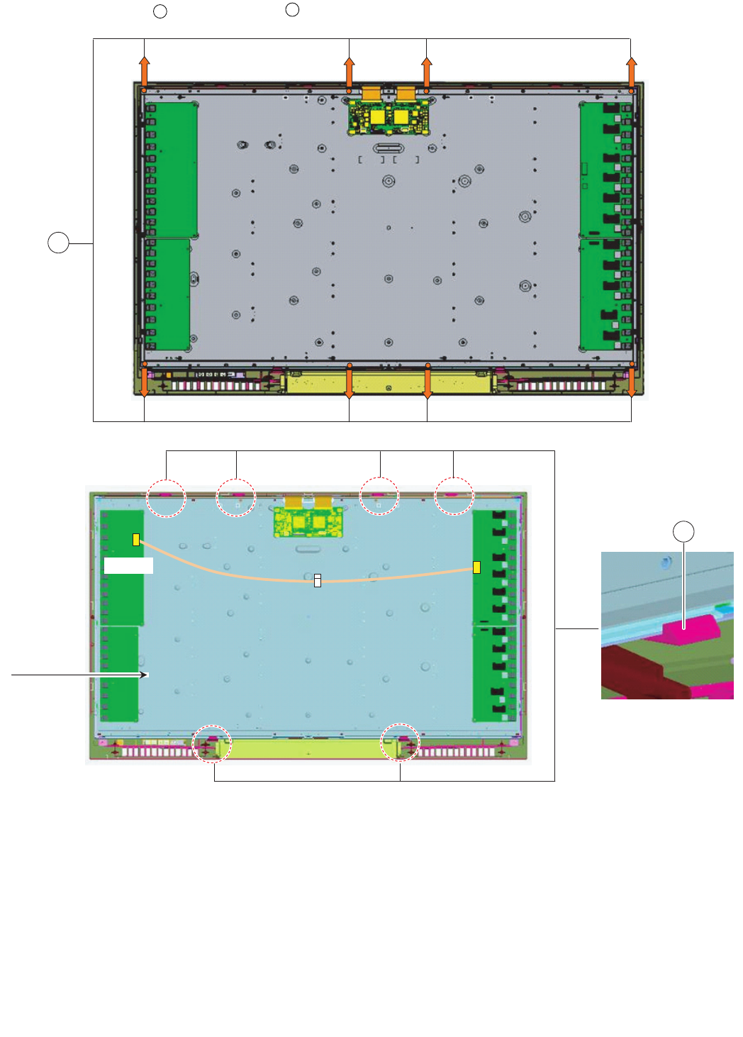
10.Remove the 8 lock screws , and the 6 lock hooks . Detach the LCD Panel Module.
11 12
11
LCD MODULE
Wire "LC"
12
LC-42XL2E/S/RU, LC-46XL2E/S/RU, LC-46X20E/S/RU, LC-52XL2E/S/RU, LC-52X20E/S/RU
2 – 33
11.Remove the 1 lock screw . and detach the Bottom Cover.
12.Remove the 6 lock hooks . and detach the KEY Unit.
13.Remove the 2 lock screws , and the 2 lock screws . Detach the MINI AV Unit.
13
FRONT CABINET
BOTTOM COVER
13
14
15 16
M-AV KEY COV
MINI AV ANG
Top View
#Set PWB under LIB
MINI AV PWB
KEY Button with PWB
15
16
KEY PWB
14
MINI AV PWB MINI-AV SHIELD
LC-42XL2E/S/RU, LC-46XL2E/S/RU, LC-46X20E/S/RU, LC-52XL2E/S/RU, LC-52X20E/S/RU
2 – 34
14.Remove all the connectors from PWBs.
15.Remove the 10 lock screws . and detach the Main Shield and AV Shield.
17
AV SHIELD
MAIN SHIELD
Wire "LW"
Pull out Wire "LW" form Opening
Wire "LW" to WH
Wire "LW"
17
LC-42XL2E/S/RU, LC-46XL2E/S/RU, LC-46X20E/S/RU, LC-52XL2E/S/RU, LC-52X20E/S/RU
2 – 35
16.Remove all the connectors from PWBs.
17.Remove the 2 lock screws , and the 1 lock screw . Detach the Terminal Angle Bottom.
B to B connection
Pull same time
18 19
TML ANG BTM
18 19
SCART ANGLE
#SCART Angle Stepping on terminal
LC-42XL2E/S/RU, LC-46XL2E/S/RU, LC-46X20E/S/RU, LC-52XL2E/S/RU, LC-52X20E/S/RU
2 – 36
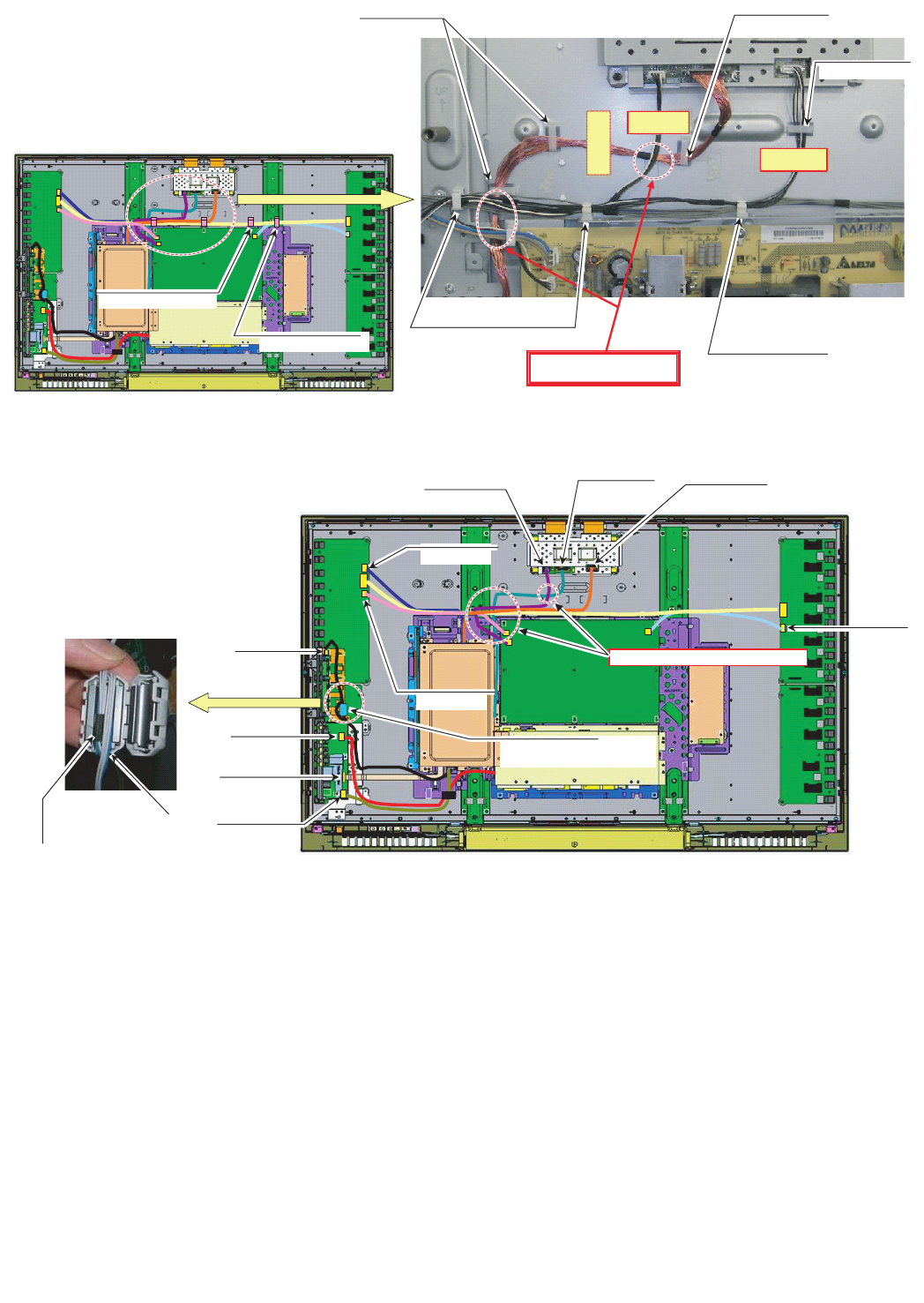
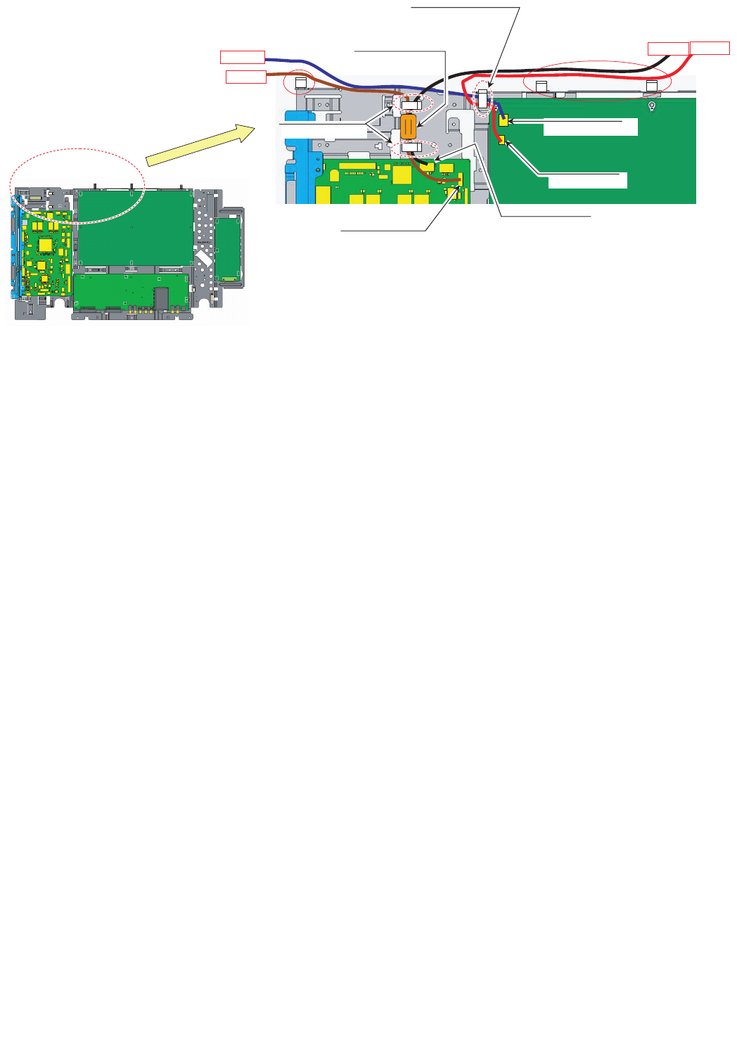
18.Remove all the connectors from PWBs.
Wire"VD"toWH
Wire "KM"
Wire "HM"
Wire "LW"
Wire "RA","US","VD" to WH
Wire "KM,"HM" to WH
Wire "RA","US","KM" to WH
Wire "US"
Wire "RA"
#Don't make mistake Wire "VD" and "RA"
Wire "LW"
Wire "HM"
Wire
Wire "US"
Wire
Wire "VD"
Wire
for Wire "FR","LB"
Wire "VD"
Wire "SP-R"
#Set at SRC
Core for "SP-R"
#Set at SRC
VD
SP-R
Wire "RA"
Wire "LW"
To Main PWB
To LED PWB
To Main PWB
To LCD Control PWB
Wire "LA1"
#No Shape/Lock Wire "LA1" to WH
Wire "LA1"
LC-42XL2E/S/RU, LC-46XL2E/S/RU, LC-46X20E/S/RU, LC-52XL2E/S/RU, LC-52X20E/S/RU
2 – 37
Wire "LB"
Wire "LA2"
Wire "PL"
Wire "FR"
Wire "LB"
Wire "LA2"
Wire "PL"
Wire "FR"
Wire "LB","FR" to WH
for Wire "FR","LB"
Wire "PL","LA2" to WH
LC-42XL2E/S/RU, LC-46XL2E/S/RU, LC-46X20E/S/RU, LC-52XL2E/S/RU, LC-52X20E/S/RU
2 – 38
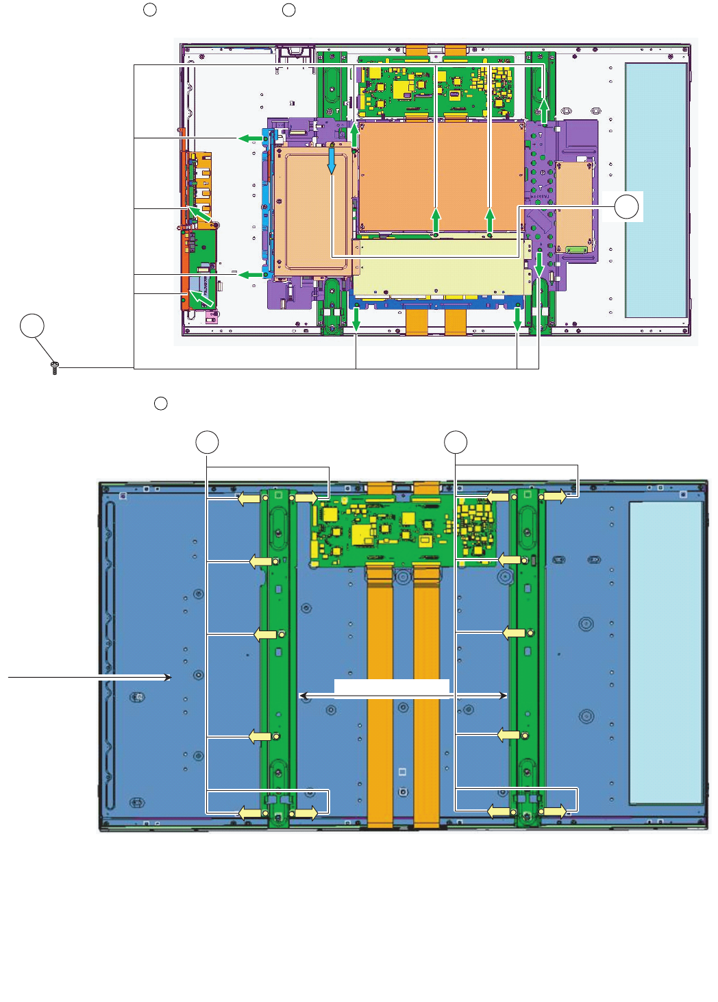
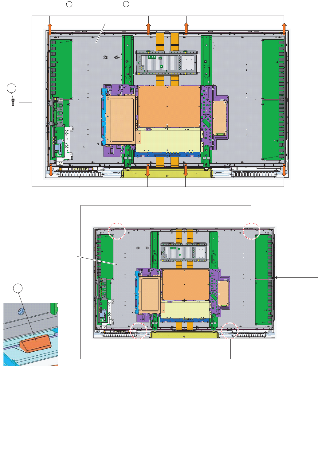
[4] REMOVING OF MAJOR PARTS (LC-52XL2E/S/RU)
1. Remove the 2 lock screws , 7 lock screws and the 8 lock screws . Detach the Rear Cabinet.
123
Rear Cabinet
3
2
1
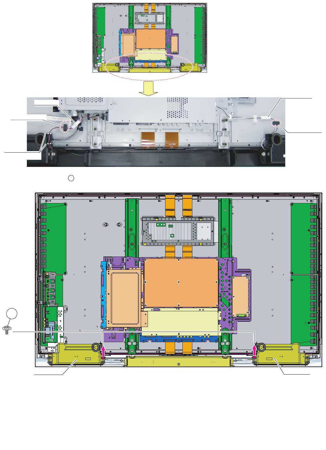
LC-42XL2E/S/RU, LC-46XL2E/S/RU, LC-46X20E/S/RU, LC-52XL2E/S/RU, LC-52X20E/S/RU
2 – 39
2. Remove all the connectors from PWBs.
3. Remove the 2 lock screws . and detach the Speaker L/R.
Wire "SP"
Wire "SP"
Wire "SP" to WH
Wire "SP" to PIN
Wire "SP" to WH
4
Speaker R Speaker L
4
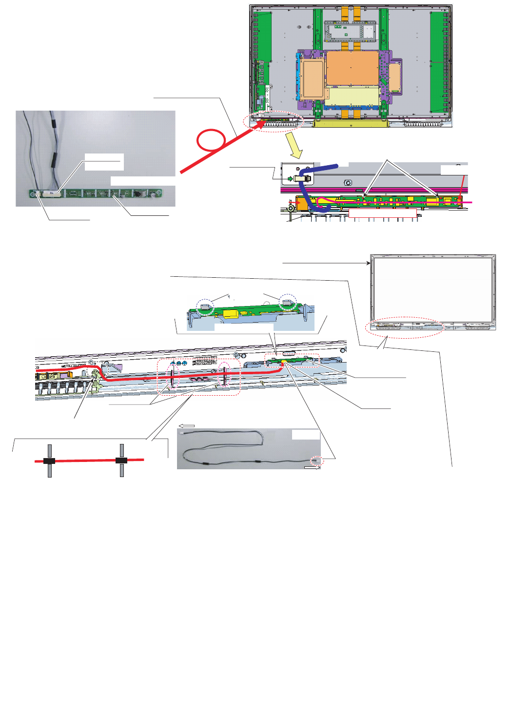
LC-42XL2E/S/RU, LC-46XL2E/S/RU, LC-46X20E/S/RU, LC-52XL2E/S/RU, LC-52X20E/S/RU
2 – 40
4. Remove all the connectors from PWBs.
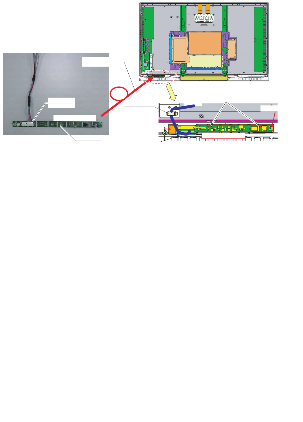
5. Remove the R/C, LED Unit and Illumination Unit.
R/C, LED PWB
Wire "RA"
from OBON
Wire "IL"
from Illumination
R/C, LED PWB Front side
R/C, LED PWB
(with wire)
Wire "RA"
R/C, LED PWB Back side
Pull out Wire "RA" from bottom
Set R/C, LED PWB Under LIB
Next,Push PWB hooked
#Set PWB to gide lib surely
Wire "RA" to WH
Wire "IL"
#Please let the IL wire go
through over R/C, LED PWB.
FRONT CABINET
Wire "IL"
Wire "IL" to rib
Illumination Unit
Wire "IL"
#Hook Surely
#Connector side Down
#Wire "IL" pass between SP Boss
and Panel hooker
R/C, LED PWB side
Illumination Unit side
Wire "IL"
Wire "IL"
Lib
Lib
LC-42XL2E/S/RU, LC-46XL2E/S/RU, LC-46X20E/S/RU, LC-52XL2E/S/RU, LC-52X20E/S/RU
2 – 41
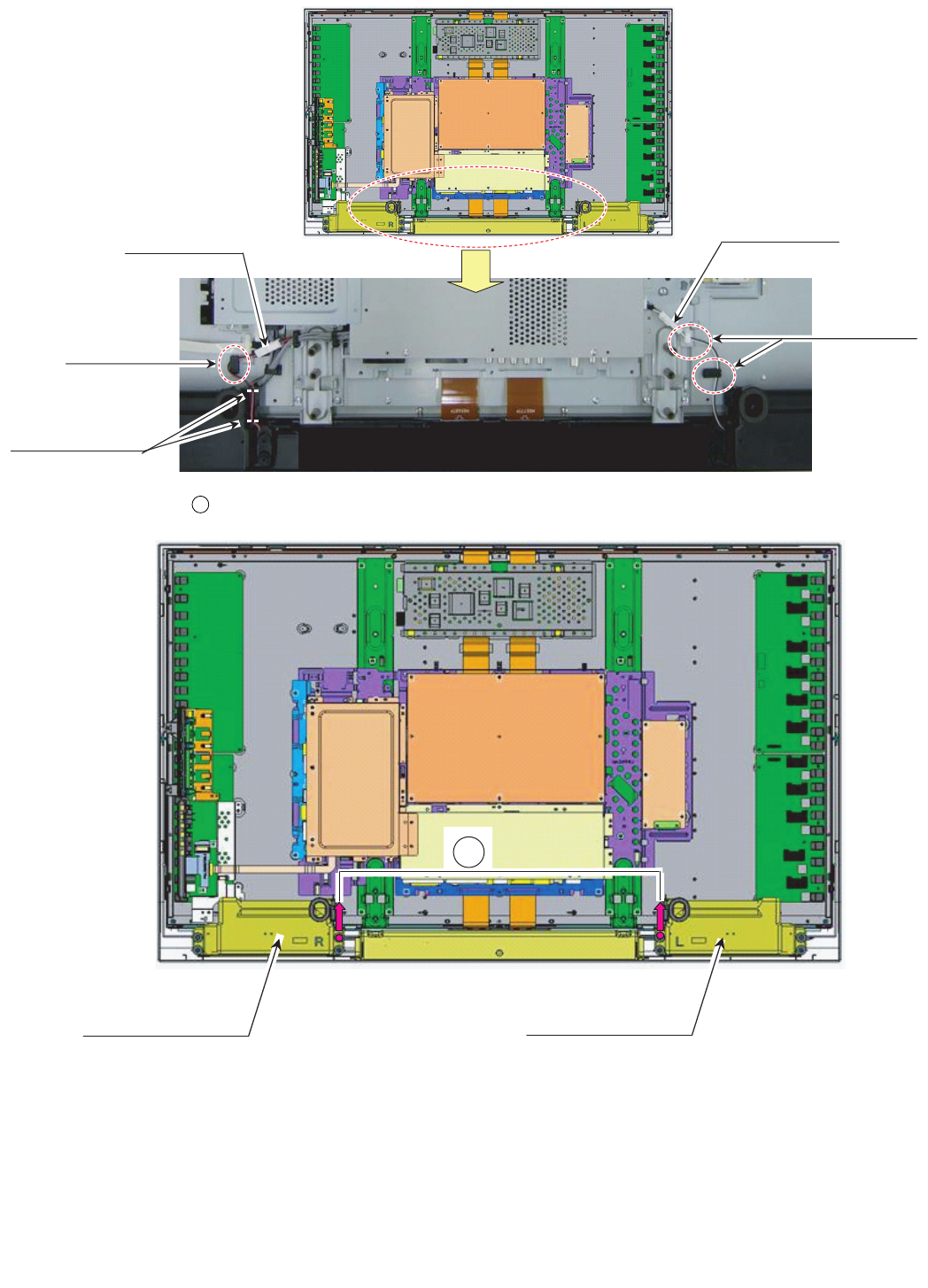
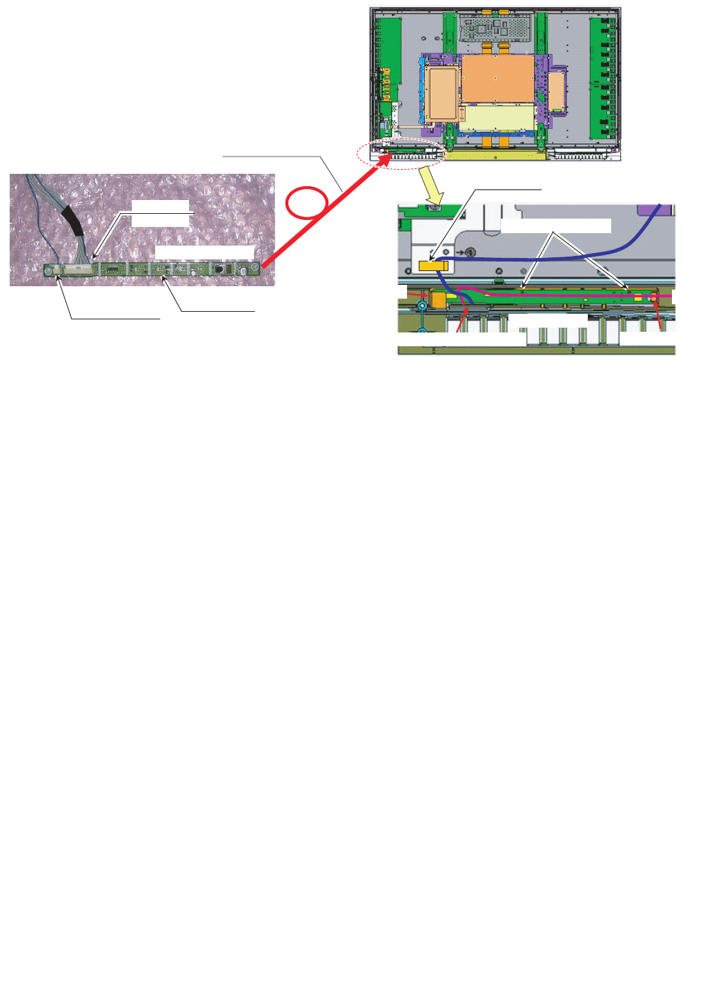
6. Remove the 8 lock screws , and the 6 lock hooks . Detach the LCD Panel Module.
56
5
6
FRONT CABINET
LCD PANEL MODULE
LCD PANEL MODULE
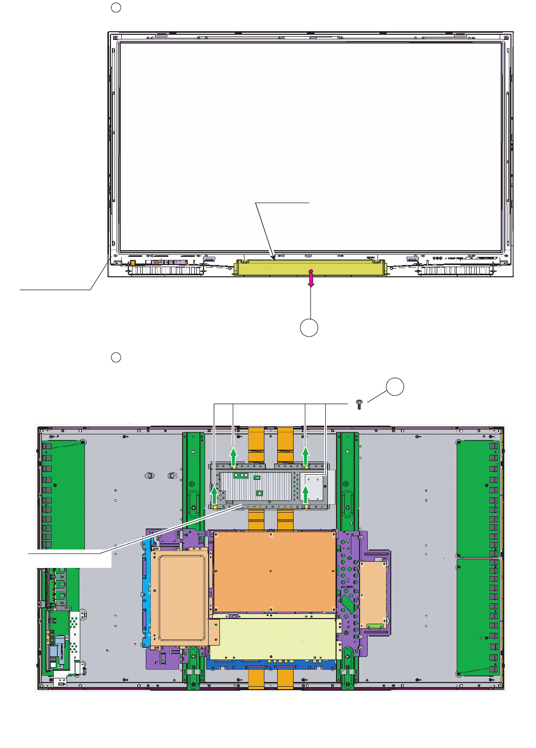
LC-42XL2E/S/RU, LC-46XL2E/S/RU, LC-46X20E/S/RU, LC-52XL2E/S/RU, LC-52X20E/S/RU
2 – 42
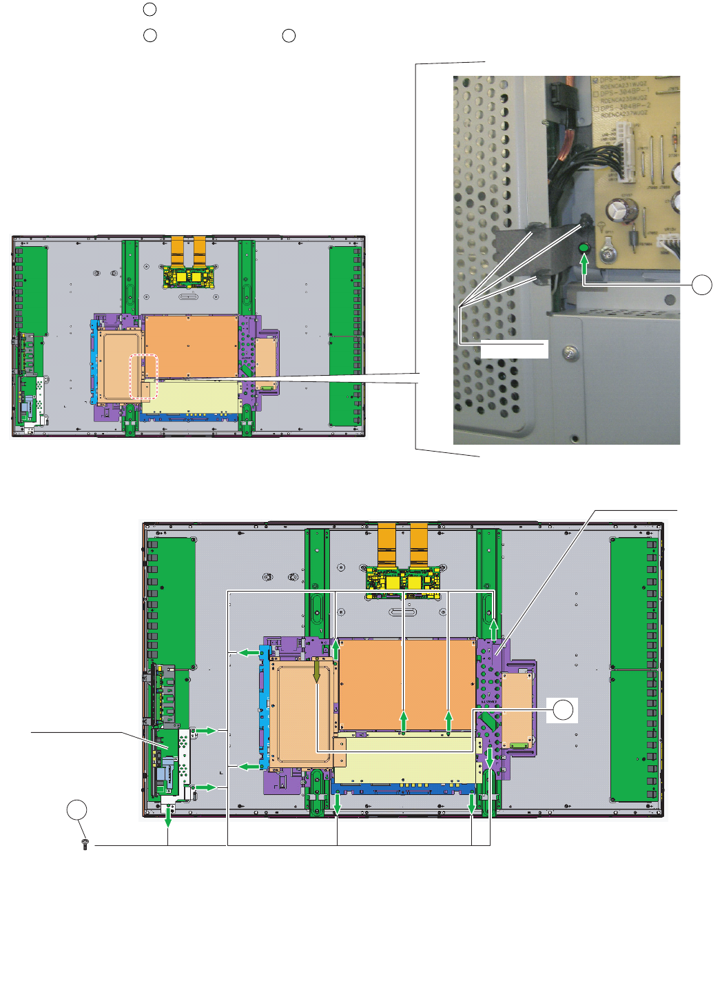
7. Remove the 2 lock screws . and detach the Bottom Cover.
8. Remove the 4 lock screws . and detach the CTL SHIELD with RADIATOR.
7
FRONT CABINET
Bottom Cover
7
8
CTL Shield Sub Ass'y
8
LC-42XL2E/S/RU, LC-46XL2E/S/RU, LC-46X20E/S/RU, LC-52XL2E/S/RU, LC-52X20E/S/RU
2 – 43
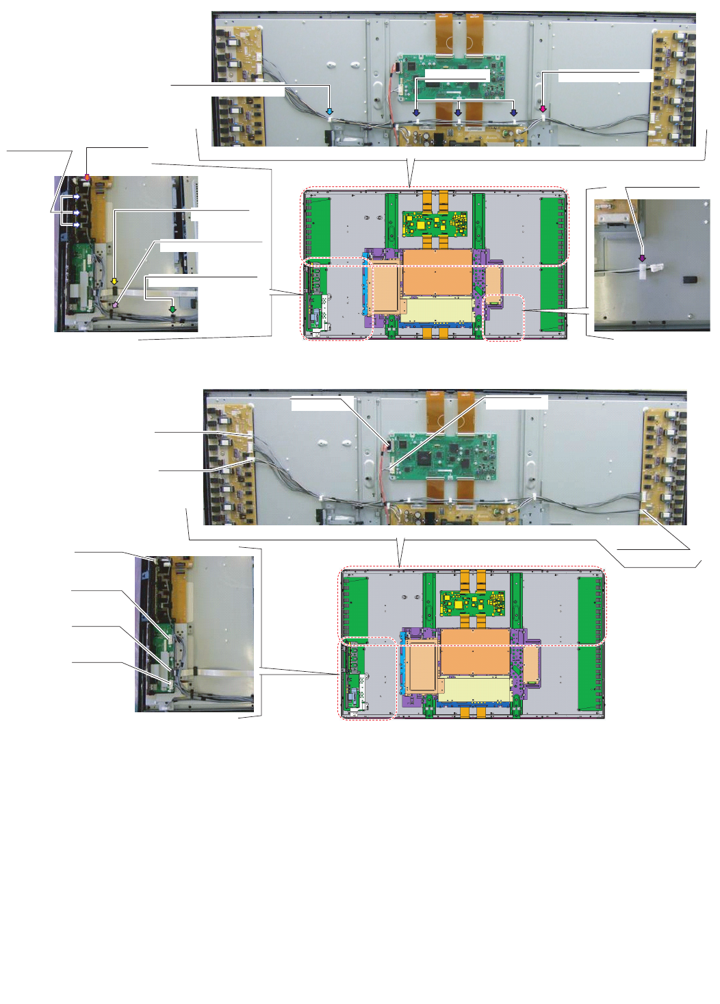
9. Remove all the connectors from PWBs.
Wire "LC", "LA2", "LB" to WH
Wire "LC" to WH
Wire "LC", "LA1" to WH
FFC "HM" to WH
Wire "KM", "VD", "US" to WH
Wire "KM" to Hook Wire "KM" to WH
Wire "RA", "KM", "VD", "US" to
Wire "SP" to WH
Wire "LA1"
Wire "LA2"
Wire "LB"
FFC "HM"
Wire "US"
Wire "VD"
Wire "KM"
Wire "FR"
Wire "LW"
LC-42XL2E/S/RU, LC-46XL2E/S/RU, LC-46X20E/S/RU, LC-52XL2E/S/RU, LC-52X20E/S/RU
2 – 44
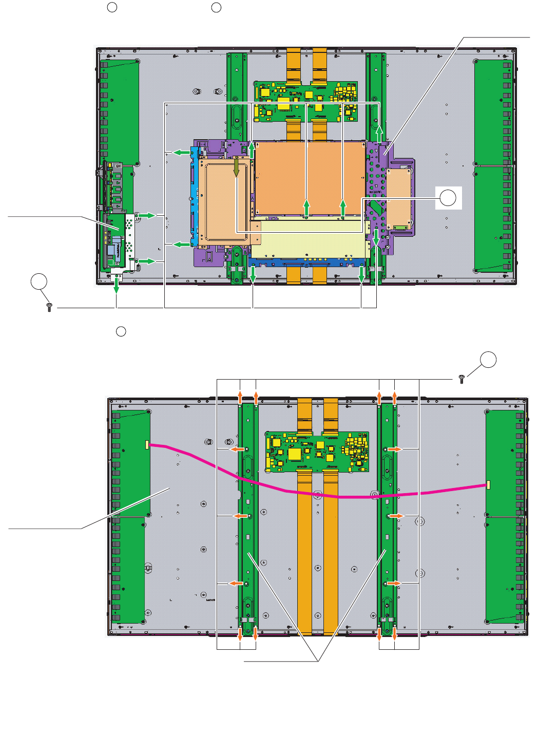
10.Remove the 1 lock screw , and the 12 lock screws . Detach the Chassis Tray and MINI AV Sub Ass’y.
11.Remove the 14 lock screws . and detach the Panel Support Angle.
910
10
9
MINI-AV SUB ASSY
CHASSIS TRAY
11
PNL SUPPORT ANG
LCD PANEL MODULE
11
LC-42XL2E/S/RU, LC-46XL2E/S/RU, LC-46X20E/S/RU, LC-52XL2E/S/RU, LC-52X20E/S/RU
2 – 45
12.Remove the 6 lock hooks . and detach the KEY Unit.
13.Remove the 2 lock screws , and the 2 lock screws . Detach the MINI AV Unit.
12
13 14
M-AV KEY COV
KEY PWB
MINI AV PWB
MINI AV ANG
Slant View
Top View
#Set PWB under LIB
13
12
14
MINI AV PWB
MINI-AV SHIELD
LC-42XL2E/S/RU, LC-46XL2E/S/RU, LC-46X20E/S/RU, LC-52XL2E/S/RU, LC-52X20E/S/RU
2 – 46
14.Remove all the connectors from PWBs.
15.Remove the 8 lock screws , and the 2 lock screws . Detach the Main Shield and AV Shield.
15 16
Open Side
Wire "LV" to WH
15
16
AV SHIELD
MAIN SHIELD
Wire "LW"
Pull out Wire "LW" form Opening
LC-42XL2E/S/RU, LC-46XL2E/S/RU, LC-46X20E/S/RU, LC-52XL2E/S/RU, LC-52X20E/S/RU
2 – 47
16.Remove all the connectors from PWBs.
17.Remove the 2 lock screws , and the 1 lock screw . Detach the Terminal Angle Bottom.
B to B connection
Pull same time
17 18
TML ANG BTM
17 18
SCART ANGLE
#SCART Angle Stepping on terminal
LC-42XL2E/S/RU, LC-46XL2E/S/RU, LC-46X20E/S/RU, LC-52XL2E/S/RU, LC-52X20E/S/RU
2 – 48
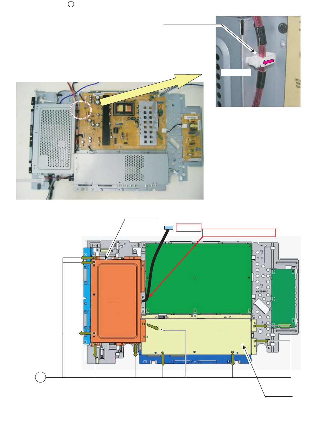
18.Remove all the connectors from PWBs.
Wire "VD","SP" to WH
Wire "RA","US","KM" to WH
Wire "LW"
Wire "RA","US","KM","VD" to WH
Wire "HM" to WH
Main
PWB side
LCD Controler
side
Wire "KM"
Wire "HM"
Wire "US"
#Shape Wire "US"
like this
Wire "VD"
Wire "RA"
Main
PWB side
LED
PWB side
Wire "RA"
#Don't make mistake Wire "VD" and "RA"
Wire "RA"
Wire "VD"
LC-42XL2E/S/RU, LC-46XL2E/S/RU, LC-46X20E/S/RU, LC-52XL2E/S/RU, LC-52X20E/S/RU
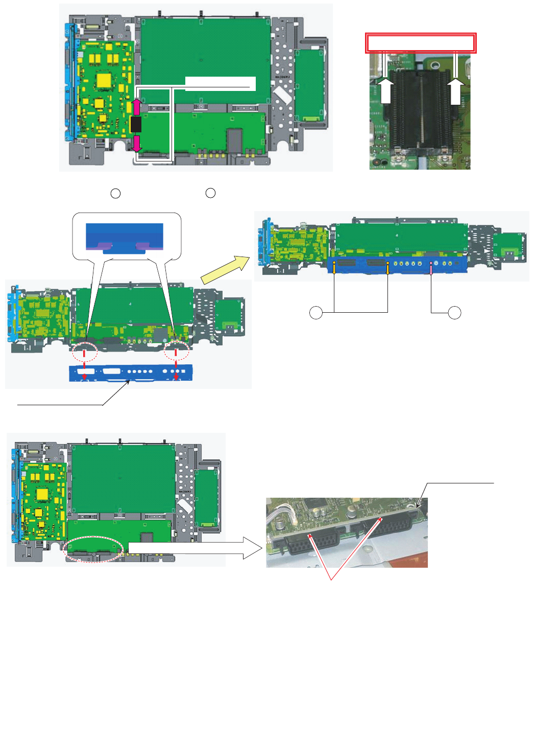
2 – 49
Wire "LA1"
Wire "LA2"
Wire "FR"
Wire "LB"
Wire "LB","FR" to WH
Wire "LB","FR" to WH
Wire "LA2","FR" to WH
Wire "LA2","LB" to WH

LC-42XL2E/S/RU, LC-46XL2E/S/RU, LC-46X20E/S/RU, LC-52XL2E/S/RU, LC-52X20E/S/RU
2 – 50
[5] REMOVING OF MAJOR PARTS (LC-52X20E/S/RU)
1. Remove the 1 lock screw , 2 lock screws , 7 lock screws and the 7 lock screws . Detach the Rear Cabinet.
1234
Rear Cabinet
1
2
3 4
LC-42XL2E/S/RU, LC-46XL2E/S/RU, LC-46X20E/S/RU, LC-52XL2E/S/RU, LC-52X20E/S/RU
2 – 51
2. Remove all the connectors from PWBs.
3. Remove the 2 lock screws . and detach the Speaker L/R.
Wire "SP"
Wire "SP" to WH
Wire "SP"
Wire "SP" to WH
Wire "SP" to PIN
5
Speaker R Speaker L
5
LC-42XL2E/S/RU, LC-46XL2E/S/RU, LC-46X20E/S/RU, LC-52XL2E/S/RU, LC-52X20E/S/RU
2 – 52
4. Remove all the connectors from PWBs.
5. Remove the R/C, LED Unit.
R/C, LED PWB
Wire "RA"
from OBON
Wire "RA"
R/C, LED PWB Front side
R/C, LED PWB Back side
Pull out Wire "RA" from bottom
Set R/C, LED PWB Under LIB
R/C, LED PWB
(with wire)
Next,Push PWB hooked
#Set PWB to gide lib surely
Wire "RA" to WH
LC-42XL2E/S/RU, LC-46XL2E/S/RU, LC-46X20E/S/RU, LC-52XL2E/S/RU, LC-52X20E/S/RU
2 – 53
6. Remove the 8 lock screws , and the 6 lock hooks . Detach the LCD Panel Module.
67
6
7
FRONT CABINET
LCD PANEL MODULE
LCD PANEL MODULE
LC-42XL2E/S/RU, LC-46XL2E/S/RU, LC-46X20E/S/RU, LC-52XL2E/S/RU, LC-52X20E/S/RU
2 – 54
7. Remove the 1 lock screw . and detach the Bottom Cover.
8. Remove the 4 lock screws . and detach the CTL SHIELD.
8
FRONT CABINET
Bottom Cover
8
9
9
CTL Shield
LC-42XL2E/S/RU, LC-46XL2E/S/RU, LC-46X20E/S/RU, LC-52XL2E/S/RU, LC-52X20E/S/RU
2 – 55
9. Remove all the connectors from PWBs.
Wire "LA1"
Wire "LC"
Wire "LA1"
Wire "SP-L"
Wire "SP" to WH
Wire "LA1","LC" to WH
Wire "LC" to WH
Wire "LA2","LB","LC" to WH
Wire "LA2","LB","LC" to WH
Wire "LC"
Wire "FR"
Wire "PL"
Wire "LA2"
Wire "LB"
Wire "LA 2"
for Wire "LB","LA2","LC"
LC-42XL2E/S/RU, LC-46XL2E/S/RU, LC-46X20E/S/RU, LC-52XL2E/S/RU, LC-52X20E/S/RU
2 – 56
Wire "LW"
Wire "FR" Wire "PL"
Wire "LW" to WH
Wire "PL", "LC" to WH
Wire "FR", "PL", "LC" to WH
Wire "PL" to WH
Wire "LC"
Wire "FR", "PL", "LC" to WH
Wire "FR"
Wire "LW"
Wire "PL"
#Please arrange wire"LW"
below than wire"PL",wire"LC"
and wire"FR".
#Please arrange wire"LW" below than
wire"PL".
Wire "KM"
#Please pull it to the
direction of the arrow.
#Please put it through
the hole.
#Please lock it to become
it beside a core.
Wire "KM"
Wire "KM" to WH
Wire "KM" to Hook
Wire "KM" to WH
HM
US
VD
Wire "KM"
Wire "RA"
Wire "VD"
Wire "VD","KM" to WH
for Wire "VD"
Wire "VD","US" to WH
Wire "HM","KM" to WH
Wire "US" to WH
Wire "VD" to WH
Wire "HM"
Wire "US"
LC-42XL2E/S/RU, LC-46XL2E/S/RU, LC-46X20E/S/RU, LC-52XL2E/S/RU, LC-52X20E/S/RU
2 – 57
10.Remove all the connectors from PWBs.
11.Remove the 1 lock screw .
12.Remove the 1 lock screw , and the 12 lock screws . Detach the Chassis Tray and MINI AV Sub Ass’y.
10
11 12
Silicone Bond
10
12
11
MINI-AV SUB ASSY
CHASSIS TRAY
LC-42XL2E/S/RU, LC-46XL2E/S/RU, LC-46X20E/S/RU, LC-52XL2E/S/RU, LC-52X20E/S/RU
2 – 58
13.Remove the 14 lock screws . and detach the Panel Support Angle.
13
PNL SUPPORT ANG
LCD PANEL MODULE
13
LC-42XL2E/S/RU, LC-46XL2E/S/RU, LC-46X20E/S/RU, LC-52XL2E/S/RU, LC-52X20E/S/RU
2 – 59
14.Remove the 6 lock hooks . and detach the KEY Unit.
15.Remove the 2 lock screws , and the 2 lock screws . Detach the MINI AV Unit.
14
15 16
M-AV KEY COV
KEY PWB
MINI AV PWB
MINI AV ANG
Slant View
Top View
#Set PWB under LIB
15
14
16
MINI AV PWB
MINI-AV SHIELD
LC-42XL2E/S/RU, LC-46XL2E/S/RU, LC-46X20E/S/RU, LC-52XL2E/S/RU, LC-52X20E/S/RU
2 – 60
16.Remove the 8 lock screws , and the 2 lock screws . Detach the Main Shield and AV Shield.
17 18
Wire "LW" to WH
Wire "LW"
17
18
AV SHIELD
MAIN SHIELD
Wire "LW"
Pull out Wire "LW" form Opening
LC-42XL2E/S/RU, LC-46XL2E/S/RU, LC-46X20E/S/RU, LC-52XL2E/S/RU, LC-52X20E/S/RU
2 – 61
17.Remove all the connectors from PWBs.
18.Remove the 2 lock screws , and the 1 lock screw . Detach the Terminal Angle Bottom.
B to B connection
Pull same time
19 20
TML ANG BTM
19 20
SCART ANGLE
#SCART Angle Stepping on terminal
LC-42XL2E/S/RU, LC-46XL2E/S/RU, LC-46X20E/S/RU, LC-52XL2E/S/RU, LC-52X20E/S/RU
2 – 62
19.Remove all the connectors from PWBs.
Wire "LA2"
Wire "PL"
Wire "LB"
Wire "LB","FR" to WH
Wire "LA2","PL" to WH
Wire "FR"
Wire "LW"
Wire "LB","FR" to WH
Wire "LA2","LB" to WH
for Wire "FR","LB"
Lock it in this range.
Wire "US" to WH
Wire "LW"
Main
PWB side
LCD Controler
side
Wire "VD","SP" to WH
Wire "RA","US","VD" to WH
Wire "HM","KM" to WH
Wire "RA","US","KM" to WH
Wire "KM","HM" to WH
LC-42XL2E/S/RU, LC-46XL2E/S/RU, LC-46X20E/S/RU, LC-52XL2E/S/RU, LC-52X20E/S/RU
2 – 63
Wire "KM"
Wire "HM"
Wire "US"
for Wire "US","RA"
Wire "VD"
Wire "RA"
Main
PWB side
LED
PWB side
Wire "RA"
#Don't make mistake Wire "VD" and "RA"
Wire "VD"
Wire "RA"
Wire "LA1"

LC-42XL2E/S/RU, LC-46XL2E/S/RU, LC-46X20E/S/RU, LC-52XL2E/S/RU, LC-52X20E/S/RU
3 – 1
LC42XL2E Service Manual
CHAPTER 3. ADJUSTMENT PROCEDURE
[1] ADJUSTMENT PROCEDURE
1. Adjustment method after PWB and/or IC replacement due to repair
The unit is set to the optimum at the time of shipment from the factory. If any value should become improper or any adjustment is necessary due to
the part replacement, make an adjustment according to the following procedure.
1. Procure the following units in order to replace the main unit, IC3301, IC8101, IC3501, IC3502, IC8301, IC8302, IC8303, or IC8304.
NOTE: [Caution when replacing ICs in the main unit (IC1501/IC1502/IC1503/IC2002) or the mini av unit (IC802)]
The above ICs are EEPROMs storing the EDID data of HDMI and the monitor microcomputer. Before replacing the relevant part, procure the
following parts in which the data have been rewritten.
2. After replacing the LCD panel or LCD control PWB, check PANEL_SIZE in the following procedure.
1) Enter the process adjustment mode.
2) Use the cursor keys / and P / of R/C to select the item [PANEL_SIZE] on the page 33/33.
3) Verify that the panel size is displayed.
4) If the size doesn't match, select the values of the panel size with the Vol / keys.
5) After selection in Step 4), press the OK key, and it is completed with OK displayed.
3. After replacing the LCD panel or LCD control PWB, adjust the VCOM in the following procedure.
1) Enter the process adjustment mode.
2) Use the cursor keys / and P / of R/C to select the item [VCOM ADJ] on the page 10/33.
3) Press the OK key to verify that the adjustment pattern is displayed.
4) Use the +/- keys of VOL of L/C to adjust the flicker in the center of the screen to minimum.
5) When the optimal state is achieved in Step 4, press the OK key to turn the pattern to OFF.
4. After replacing LCD panel or LCD control PWB, perform the up/down brightness difference adjustment in the following procedure. (Note: It is appli-
cable to LC-42/46/52XL2E only.)
1) Enter the process adjustment mode.
2) Use the cursor keys / and P / of R/C to select the item [LCD_LUMA_ADJ] on the page 10/33.
3) Press the OK key to verify that the adjustment pattern (all gray) is displayed.
4) Use the VOL +/- keys of R/C to adjust the upper/lower brightness difference in the center of the screen to minimum.
5) When the optimal state is achieved in Step 4, press the OK key to turn the pattern to OFF.
NOTE: LCD LUMA UD ** ←The value at the ** part is changed.
LCD LUMA DOWN 0 (Note that the value is changed if the P / keys are pressed in Step 4 above.)
MAIN UNIT: DUNTKE186FM01 (LC-42/46/52XL2E)
DUNTKE186FM02 (LC-46/52XL20E)
IC2002 RH-IXB986WJN8Q Monitor microcomputer
IC802 RH-IXC284WJQZS HDMI_EXT4
IC1501 RH-IXC285WJQZS HDMI_EXT5
IC1502 RH-IXC286WJQZS HDMI_EXT6
IC1503 RH-IXC287WJQZS RGB (PC)_EXT7
LC-42XL2E/S/RU, LC-46XL2E/S/RU, LC-46X20E/S/RU, LC-52XL2E/S/RU, LC-52X20E/S/RU
3 – 2
2. Entering and exiting the adjustment process mode
1. Press the “POWER” key on the set of running TV set to force off the power.
2. While holding down the “VOL (-)” and “INPUT” keys on the set at once, plug in the AC power cord to turn on the power.
The letter “K” appears on the screen.
3. Next, hold down the “VOL (-)” and “P (V)” keys on the set at once.
Multiple lines of character string appearing on the screen indicate that the set is now in the adjustment Process mode. If you fail to enter the
adjustment process mode (the display is the same as normal startup), retry the procedure. (Another procedure)
4. Press the “MENU” key on the main unit to display OSD.
5. Move the cursor to SERVICE (OSD) using the cursor keys on the remote control.
Then press the “MENU” key on the remote control to enter the service mode (adjustment process mode).
6. To exit the adjustment process mode after the adjustment is done, unplug the AC power cord to force off the power. (When the power is turned off
with the remote controller, once unplug the AC power cord and plug it in again. In this case, wait 10 seconds or so before plugging.)
3. Remote controller key operation and description of display in adjustment process mode.
1. key operation
Input mode is switched automatically when relevant adjustment is started so far as the necessary input signal is available.
4. Description of display
CAUTION: Use due care in handling the information described here lest the users should know how to enter the adjustment process mode. If the
settings are tampered with in this mode, unrecoverable system damage may result.
Remote controller key Main unit key Function
P ( / ) P ( / ) Moving an item (line) by one (UP/DOWN)
VOL (+/-) VOL (+/-) Changing a selected item setting (+1/-1)
Cursor (UP/DOWN) — Turning a page (PREVIOUS / NEXT)
Cursor (</>) — Changing a selected line setting (+10/-10)
INPUT SOURCE on
remote controller
— Input source switching (toggle switching) (TV→EXT1~8)
RETURN — Returning to a present page
OK — Executing a function
No. Description Display specification
(1) Page/ of present number of total pages 2char/2char Decimal Number mark.
(2) Page present title It bundles it by Max. 15 char “[“ ”]”.
(3) Input that has been selected now TV/INPUT1/INPUT2/INPUT3/INPUT5/INPUT6/INPUT7/INPUT8
(4) Present colour system NTSC/PAL/SECAM/COMP15K/COMP33K/COMP45K/COMP28K/COMP31K
(5) Inducing display EUROPE/RUSSIA/SWEDEN
(6) Model name MODEL NAME
(7) Item name Max. 30 char
(8) Parameter Max. 60 char
(1) Page/ of present number of total pages (5) Inducing display
(3) Input that has been selected now
(2) Page present title (4) Present colour system (6) Model name
1/33 [INFO] INPUT1 AUTO ??? 46E_XL2
MAIN Version
BOOT Version
Monitor Version
CPLD Version
FRC Version
EQ DATA CHECKSUM
LAMP ERROR
MONITOR ERR CAUSE
NORMAL STANDBY CAUSE
ERROR STANDBY CAUSE
1.00 (E 2007/07/10 D)
1.0
a6
ROM
0
11 11 11 11
0
1) 0 2) 0 3) 0
0H 0M 0H 0M 0H 0M
4) 0 5) 0
0H 0M 0H 0M
(7) Item name (8) Parameter

LC-42XL2E/S/RU, LC-46XL2E/S/RU, LC-46X20E/S/RU, LC-52XL2E/S/RU, LC-52X20E/S/RU
3 – 3
5. Adjustment process mode menu
The character string in brackets [ ] will appear as a page title in the adjustment process menu header.
Page Line Item Description Remarks (adjustment detail, etc.)
1/33 [INFO]
1 MAIN Version Main software version
2 BOOT Version BOOT Version.
3 Monitor Version Monitor software version
4 FRC Version FRC Version
5 CPLD Version CPLD Version.
6 EQ DATA CHECKSUM Audio data checksum.
7 LAMP ERROR Number of termination due to lamp error.
8 MONITOR ERR CAUSE Last error standby cause.
9 NORMALSTANDBY CAUSE Situation that became standby at the end.
(Excluding the error)
10 ERROR STANDBY CAUSE [1] 00H 00M Error standby cause Total operating time before error.
[2] 00H 00M
[3] 00H 00M
[4] 00H 00M
[5] 00H 00M
2/33 [INIT]
1 INDUSTRY INIT Enter Initialization to factory settings execution.
2 INDUSTRY INIT(-Hotel) OFF Initialization to factory settings execution.
(Hotel mode is excluded)
3 HOTEL MODE OFF Hotel mode setting execution.
4 Center Acutime 5H 0M Main operating hours.
5 RESET OFF Main operating hours reset.
6 Backlight Acutime 19H 35M Backlight operating hours.
7 RESET OFF Backlight operating hours reset.
8 LAMP ERROR RESET OFF Lamp error reset.
9 ADJ PARAM SET Enter ADJ PARAM SET
10 VIC XPOS 0 X-coordinate setting for VIC READ
11 VIC YPOS 0 Y-coordinate setting for VIC READ
12 VIC SIGNAL TYPE MAIN Signal type setting for VIC READ
13 VIC READ OFF Picture level acquisition function
(Level appears in green on the upper right)
3/33 [TUNER ADJ]
1 RF AGC ADJ Enter RF-AGC auto adjustment execution
2 TUNER ADJ Enter TUNER auto adjustment execution
3 PAL+TUNER ADJ Enter PAL TUNER auto adjustment execution
4 RF AGC ADJ(CA-8CH) Enter RF-AGC auto adjustment execution (CA-8CH)
5 TUNER ADJ(CA-8CH) Enter TUNER auto adjustment execution (CA-8CH)
6 PAL+TUNER ADJ(CA-8CH) Enter PAL TUNER auto adjustment execution (CA-8CH)
7 RF AGC 16 RF AGC adjustment
8 TUNER DAC 150 TUNER signal level adjustment
9RF AGC READ OFF
4/33 [PAL MAIN]
1 PAL ADJ Enter PAL adjustment
2 SECAM ADJ Enter SECAM adjustment
3 N358 ADJ Enter N358 adjustment
4 PAL CONTRAST 130 PAL contrast adjustment
5 SECAM CONTRAST 137 SECAM CONTRAST adjustment
6 N358 CONTRAST 120 N358 CONTRAST adjustment
5/33 [CEC TEST]
1 HDMI CEC TEST Enter CEC test
2 INSPECT USB TERM Enter
3 MONIDATA READ[TEMP/OPC] OFF MONITOR Temperature/ OPC Acquisition tool.
4 CAUSE RESET Enter
6/33 [COMP15KMAIN]
1 COMP15K ALL ADJ Enter Component 15K picture level adjustment
2 COMP15K MAIN Y GAIN 194 Y GAIN adjustment value
3 COMP15K MAIN CB GAIN 215 Cb GAIN adjustment value
4 COMP15K MAIN CR GAIN 212 Cr GAIN adjustment value
5 COMP15K Y OFFSET 66 Y OFFSET adjustment value
6 COMP15K CB OFFSET 512 Cb OFFSET adjustment value
7 COMP15K CR OFFSET 513 Cr OFFSET adjustment value
LC-42XL2E/S/RU, LC-46XL2E/S/RU, LC-46X20E/S/RU, LC-52XL2E/S/RU, LC-52X20E/S/RU
3 – 4
Page Line Item Description Remarks (adjustment detail, etc.)
7/33 [HDTV]
1 HDTV ADJ Enter HDTV video level adjustment
2 HDTV Y GAIN 195 HDTV Y GAIN adjustment value
3 HDTV CB GAIN 205 HDTV Cb adjustment value
4 HDTV CR GAIN 203 HDTV Cr adjustment value
5 HDTV Y OFFSET 65 HDTV Y OFFSET adjustment value
6 HDTV CB OFFSET 512 HDTV Cb OFFSET adjustment value
7 HDTV CR OFFSET 512 HDTV Cr OFFSET adjustment value
8/33 [ANALOG PC]
1 ANALOG PC ADJ Enter DVI ANALOG video level adjustment
2 R OFFSET 64 R CUTOFF adjustment value
3 G OFFSET 64 G CUTOFF adjustment value
4 B OFFSET 66 B CUTOFF adjustment value
5 R GAIN 193 R DRIVE adjustment value
6 G GAIN 189 G DRIVE adjustment value
7 B GAIN 194 B DRIVE adjustment value
9/33 [SCART]
1 SCART RGB ADJ Enter SCART RGB level adjustment
2 SCART R CUTOFF 65 SCART R CUTOFF adjustment value
3 SCART G CUTOFF 60 SCART G CUTOFF adjustment value
4 SCART B CUTOFF 64 SCART B CUTOFF adjustment value
5 SCART R GAIN 200 SCART R GAIN adjustment value
6 SCART G GAIN 195 SCART G GAIN adjustment value
7 SCART B GAIN 201 SCART B GAIN adjustment value
10/33 [LUMAADJ]
1VCOM ADJ 69
2 LCD LUMA ADJ Enter
3 LCD LUMA UP 26
4 LCD LUMA DOWN 13
11/33 [FR DDRTEST]
1 DDRA TEST1 Enter
2 DDRA TEST2 Enter
3 DDRB TEST1 Enter
4 DDRB TEST2 Enter
5 DDRB TEST3 Enter
6 FRC ON/OFF Enter
7 SOUSAM DDR BIST Enter
8 SOUSAS DDR BIST Enter
12/33 [LEV]
1 LEV1 176
2 LEV2 352
3 LEV3 528
4 LEV4 656
5 LEV5 800
6 LEV6 928
13/33 [MGXX1]
1 MG1R 178 W/B adjustment, gradation 1R adjustment value
2 MG1G 184 W/B adjustment, gradation 1G adjustment value
3 MG1B 138 W/B adjustment, gradation 1B adjustment value
4 MG2R 227 W/B adjustment, gradation 2R adjustment value
5 MG2G 232 W/B adjustment, gradation 2G adjustment value
6 MG2B 177 W/B adjustment, gradation 2B adjustment value
7 MG3R 316 W/B adjustment, gradation 3R adjustment value
8 MG3G 322 W/B adjustment, gradation 3G adjustment value
9 MG3B 249 W/B adjustment, gradation 3B adjustment value
LC-42XL2E/S/RU, LC-46XL2E/S/RU, LC-46X20E/S/RU, LC-52XL2E/S/RU, LC-52X20E/S/RU
3 – 5
Page Line Item Description Remarks (adjustment detail, etc.)
14/33 [MGXX2]
1 MG4R 474 W/B adjustment, gradation 4R adjustment value
2 MG4G 485 W/B adjustment, gradation 4G adjustment value
3 MG4B 384 W/B adjustment, gradation 4B adjustment value
4 MG5R 791 W/B adjustment, gradation 5R adjustment value
5 MG5G 815 W/B adjustment, gradation 5G adjustment value
6 MG5B 673 W/B adjustment, gradation 5B adjustment value
7 MG6R 905 W/B adjustment, gradation 6R adjustment value
8 MG6G 948 W/B adjustment, gradation 6G adjustment value
9 MG6B 800 W/B adjustment, gradation 6B adjustment value
15/33 [ACTIVEBL1]
1 ABL TEST MODE Enter
2 PRINT DEBUG OFF
16/33 [SOUND1]
1 AUDIO_PARAMETER_SWITCH ROM
2AU_FLAT
3 INPUT_MIXER_GAIN
4 OUTPUT_MIXER_GAIN
5 PEQ1_F0
6 PEQ1_Q
7 PEQ1_GAIN
8 PEQ2_F0
9 PEQ2_Q
10 PEQ2_GAIN
11 PEQ3_F0
12 PEQ3_Q
13 PEQ3_GAIN
17/33 [SOUND 2]
1 PEQ4_F0
2 PEQ4_Q
3 PEQ4_GAIN
4 PEQ5_F0
5 PEQ5_Q
6 PEQ5_GAIN
7 GAIN_ADJUSTER1
8 GAIN_ADJUSTER2
9 GAIN_ADJUSTER3
10 GAIN_ADJUSTER4
11 GAIN_ADJUSTER5
12 GAIN_ADJUSTER6_SP
13 GAIN_ADJUSTER6_HP
18/33 [SOUND 3]
1 LOUT1_VOLUME_CONTROL
2 ROUT1_VOLUME_CONTROL
19/33 [M PWM]
1PWM
2PWM FREQ
3 PWM DUTY
4OSC FREQ
5 OSC DUTY
20/33 [M OPC1]
1 OPC LDUTY0
2 OPC LDUTY1
3 OPC LDUTY2
4 OPC LDUTY3
5 OPC LDUTY4
6 OPC LDUTY5
7 OPC LDUTY6
8 OPC LDUTY7
9 OPC LDUTY8
10 OPC LDUTY9
11 OPC LDUTY10
12 OPC LDUTY11
LC-42XL2E/S/RU, LC-46XL2E/S/RU, LC-46X20E/S/RU, LC-52XL2E/S/RU, LC-52X20E/S/RU
3 – 6
Page Line Item Description Remarks (adjustment detail, etc.)
21/33 [M OPC2]
1 OPC LDUTY12
2 OPC LDUTY13
3 OPC LDUTY14
4 OPC LDUTY15
5 OPC LDUTY16
6 OPC LDUTY17
7 OPC LDUTY18
8 OPC LDUTY19
9 OPC LDUTY20
10 OPC LDUTY21
11 OPC LDUTY22
22/33 [M OPC3]
1 OPC LDUTY23
2 OPC LDUTY24
3 OPC LDUTY25
4 OPC LDUTY26
5 OPC LDUTY27
6 OPC LDUTY28
7 OPC LDUTY29
8 OPC LDUTY30
9 OPC LDUTY31
10 OPC LDUTY32
23/33 [M ADL1]
1 OPC33 ADLEVEL 0
2 OPC33 ADLEVEL 1
3 OPC33 ADLEVEL 2
4 OPC33 ADLEVEL 3
5 OPC33 ADLEVEL 4
6 OPC33 ADLEVEL 5
7 OPC33 ADLEVEL 6
8 OPC33 ADLEVEL 7
9 OPC33 ADLEVEL 8
10 OPC33 ADLEVEL 9
11 OPC33 ADLEVEL 10
12 OPC33 ADLEVEL 11
24/33 [M ADL2]
1 OPC33 ADLEVEL 12
2 OPC33 ADLEVEL 13
3 OPC33 ADLEVEL 14
4 OPC33 ADLEVEL 15
5 OPC33 ADLEVEL 16
6 OPC33 ADLEVEL 17
7 OPC33 ADLEVEL 18
8 OPC33 ADLEVEL 19
9 OPC33 ADLEVEL 20
10 OPC33 ADLEVEL 21
11 OPC33 ADLEVEL 22
25/33 [M ADL3]
1 OPC33 ADLEVEL 23
2 OPC33 ADLEVEL 24
3 OPC33 ADLEVEL 25
4 OPC33 ADLEVEL 26
5 OPC33 ADLEVEL 27
6 OPC33 ADLEVEL 28
7 OPC33 ADLEVEL 29
8 OPC33 ADLEVEL 30
9 OPC33 ADLEVEL 31
LC-42XL2E/S/RU, LC-46XL2E/S/RU, LC-46X20E/S/RU, LC-52XL2E/S/RU, LC-52X20E/S/RU
3 – 7
Page Line Item Description Remarks (adjustment detail, etc.)
26/33 [M V6THE]
1V6 OS THERMO 1 64
2V6 OS THERMO 2 77
3V6 OS THERMO 3 87
4V6 OS THERMO 4 97
5 V6 OS THERMO 5 108
6 V6 OS THERMO 6 119
7 V6 OS THERMO 7 131
27/33 [M V5THE]
1V5 OS THERMO 1 64
2V5 OS THERMO 2 77
3V5 OS THERMO 3 87
4V5 OS THERMO 4 97
5 V5 OS THERMO 5 108
6 V5 OS THERMO 6 119
7 V5 OS THERMO 7 131
28/33 [M BLCTL TEMP]
1BL TEMP1
2BL TEMP2
3BL TDUTY
29/33 [M EEP SET]
1 MONITOR TIME OUT ON Monitor and the main communication time-out setting
2 MONITOR MAX TEMP 43 MONITOR MAX temperature setting
3 MONITOR EEP READ / WRITE WRITE MONITOR EEPROM READ/WRITE Setting/execution
4 MONITOR EEP ADR 0x 0 MONITOR EEPROM arbitrary addressing
5 MONITOR EEP DATA 0x 0 MONITOR EEPROM arbitrary data specification
30/33 [M TEST PATTERN]
1 LCD TEST PATTERN OFF Pattern with built-in LCD controller display
31/33 [MEM CLEAR]
1 KEY LOCK(1217) Enter
2 KOUTEI AREA ALL CLEAR Adjustment value clearness in all areas in process
3 A MODE AREA CLEAR Adjustment value clearness of process A mode
4 BACKUP AREA CLEAR Adjustment value clearness in process backup area
5 B MODE AREA CLEAR Adjustment value clearness of process B mode
6 EXECUTION Clear execution
32/33 [FR REGI]
1 READ/WRITE READ
2 SLAVE ADDRESS SLAVE0
3 REGISTOR ADDRESS 0x 0
0x 0
4 WRITE DATA 0x 0
0x 0
5 READ DATA 0x 0
0x 0
33/33 [ETC]
1 EEP SAVE OFF Writing setting values to EEPROM.
2 EEP RECOVER OFF Reading setting values from EEPROM.
3 MONITOR ERROR CAUSE RESET OFF
4 STANDBY CAUSE RESET OFF Reset stand by cause.
5 MODEL NAME XL2 Model name setting
6 PANEL SIZE 52 Panel size setting.
7 PRODUCT EEP ADR 0x 0
8 PRODUCT EEP DATA 0x 0
LC-42XL2E/S/RU, LC-46XL2E/S/RU, LC-46X20E/S/RU, LC-52XL2E/S/RU, LC-52X20E/S/RU
3 – 8
6. Special features
1. NORMAL STANDBY CAUSE (Page 1/33)
Display of a cause (code) of the last standby.
The cause of the last standby is recorded in EEPROM whenever possible.
Checking this code will be useful in finding a problem when you repair the troubled set.
2. EEP SAVE (Page 33/33)
Storage of EEP adjustment value
3. EEP RECOVER (Page 33/33)
Retrieval of EEP adjustment value from storage area.
7. Lamp error detection
1. Function
This LCD color TV set incorporates a lamp error detection feature that automatically turns off the power for safety under abnormal lamp or lamp
circuit conditions. If by any chance anything is wrong with the lamp or lamp circuit or if the lamp error detection feature is activated for some rea-
son, the following will result.
1) The power is interrupted in about 6 seconds after it is turned on.
(The power LED on the front of the TV set turns red from green and keeps blinking in red: ON for 250 ms and OFF for 1 sec.).
2) If the above phenomenon 1) occurs 5 times consecutively, it becomes impossible to turn on the power. (The power LED remained red).
2. Measures
1) Checking with lamp error detection OFF
Enter the adjustment process mode, referring to 1. Entering and exiting the adjustment process mode.
If there is a problem with the lamp or lamp circuit, the lamp will go out. (The power LED is green.)
Then, you can check the operation to see if the lamp and lamp circuit are in trouble.
2) Resetting the lamp error count
After the lamp and lamp circuit are found out of trouble, reset the lamp error count. If a lamp error is detected five consecutive times, the power
cannot be turned on. Using the cursor (UP/DOWN) key, move to the cursor to [LAMP ERROR RESET], Line 8 on adjustment process mode
service page 2/33. With the cursor (LEFT/RIGHT) keys, select the [LAMP ERROR RESET] value. Finally press the cursor (OK) eys to reset the
value to “0”.
Table of contents of adjustment process mode Page 2/33
[INIT]
INDUSTRY INIT Enter
INDUSTRY INIT(-Hotel) OFF
HOTEL MODE OFF
Center Acutime
RESET OFF
Backlight Acutime
RESET OFF
LAMP ERROR RESET OFF
ADJ PARAM SET Enter
VIC XPOS 0
VIC YPOS 0
VIC SIGNAL TYPE MAIN
VIC READ OFF
Resetting to "0"
LC-42XL2E/S/RU, LC-46XL2E/S/RU, LC-46X20E/S/RU, LC-52XL2E/S/RU, LC-52X20E/S/RU
3 – 9
8. Public Mode (Hotel Mode)
1. Starting the Public Mode
• There are two following ways to display the PUBLIC Mode setting screen.
1) On the process adjustment mode screen (2/33), set the “HOTEL MODE” Flag to ON.
Turn off the power, and turn it on again, pressing the and keys of the main unit at the same time.
2) Enter the Pass Word, and start the unit.
a) Turn on the power, pressing the and keys of the main unit at the same time.
b) Display the Pass Word input screen.
Operation procedure
• The initial input position is the digit at the left end.
• For the numeric keys to of R/C, key input is accepted. Input of the other keys is prohibited.
• Change “-” to “*” by inputting the numeric key at the input position, and shift the input position rightward one digit.
• When three digits are completely input, the Pass Word is judged.
c) Check the Pass Word by inputting three digits.
If the Pass Word is , it shifts to the PUBLIC Mode setting screen.
In another case, the screen is erased, and it operates in the ordinary mode.
2. Exiting the Public Mode screen
• There are two following ways to exit the Public Mode setting screen.
1) Turn off the power.
2) Select “Execution” in the PUBLIC_Mode to execute it.
Activate the restart under the set content. Here, the START input SOURCE setting is excluded since this item is referred to only when the
power is turned on.
3. Set value of the Public Mode
• Each set value in the PUBLIC Mode is initialized when the factory setting is applied.
(The setting of the PUBLIC MODE Flag in the process adjustment mode screen is not changed.)
CHANNEL UP
Volume UP
INPUT
Volume UP
09
02 7

LC-42XL2E/S/RU, LC-46XL2E/S/RU, LC-46X20E/S/RU, LC-52XL2E/S/RU, LC-52X20E/S/RU
3 – 10
4. Basic operation in the Public Mode
5. Operation after “RESET”
Select “RESET” in the PUBLIC Mode, and it operates as follows when it is executed (refer to the basic operation).
• The set contents in the PUBLIC mode are initialized.
• It does not exit the PUBLIC mode.
• PUBLIC MODE Flag does not change. (It is not set to OFF.)
Volume / or Cursor ←/→Change or execution of the set value.
Channel / or Cursor ↑/↓Movement to the selected item.
Decision (ok) Execution (Used by the items “Execution” and “RESET”.)
PUBLIC Mode R/C Ordinary operation mode: It enters the PUBLIC Mode.
PUBLIC MODE Flag is set to “ON”.
PUBLIC Mode: It exits the PUBLIC Mode.
PUBLIC MODE Flag does not change.
Any set item in PUBLIC Mode is not initialized.
Public Mode
POWER ON FIXED [VARIABLE]
SHUT DOWN MODE [NORMAL]
MAXIMUM VOLUME [60]
VOLUME FIXED [VARIABLE]
VOLUME FIXED LEVEL [20]
RC BUTTON [RESPOND]
PANEL BUTTON [RESPOND]
MENU BUTTON [RESPOND]
AV POSITION FIXED [VARIABLE]
ON SCREEN DISPLAY [YES]
INPUT MODE START [NORMAL]
INPUT MODE FIXED [VARIABLE]
LOUD SPEAKER [ON]
RC PATH THROUGH [OFF]
232C POWON [DISABLE]
HOTELMODE [ON]
RESET
EXECUTE
LC-42XL2E/S/RU, LC-46XL2E/S/RU, LC-46X20E/S/RU, LC-52XL2E/S/RU, LC-52X20E/S/RU
3 – 11
6. Setting items (* Item names and selective items are expressed in English.)
1) Power ON Fixed (POWER ON FIXED)
If the power button is pressed in the ordinary mode when set to “FIXED”, the caution is displayed for 5 seconds.
When power button on the main unit is pressed When power button on R/C is pressed
* The OSD display is an example.
If another ODS is previously displayed, the status is reset (MENU or similar).
2) Volume Maximum Level [MAXIMUM VOLUME]
3) Volume Fixed [VOLUME FIXED]
4) Volume Fixed Level [VOLUME FIXED LEVEL]
Selection “VARIABLE” or “FIXED” is selectable. (Loop is provided.)
Default “VARIABLE”
Function • When "FIXED" is set, “Power ON/Standby Key” of the main unit and R/C is disabled.
Keys disabled when not
set to Default
• OFF_TIMER (SLEEP)
Remarks The function does not work for any other standby factors (see below).
• No operation OFF
• No signal OFF (including the power management)
Selection 0~60 (Loop is not provided.)
Default 60
Function • Even if VOL is adjusted to a value higher than the adjusted one, it is not set to that value. (Only the speakers of
the main unit)
Exception
Remarks • When it is set to 59 or less, the number is displayed and the volume bar is not displayed during operation in the
ordinary mode.
• VOLUME can be abbreviated to VOL.
Selection “VARIABLE” or “FIXED” is selectable. (Loop is provided.)
Default “VARIABLE”
Function It is selectable whether or not the volume is fixed to the value adjusted in the volume fixed level mode. (Only the
speakers of the main unit)
Exception • In the adjustment process, the volume can be set as desired regardless of this setting.
Keys disabled when not
set to Default
• Volume high/low (VOL+/-) (Both R/C and main unit)
• Mute (MUTE)
Remarks • Volume Fixed is prior to Volume Maximum Level.
• Even if the above disabled keys are operated, the volume is not displayed.
• VOLUME can be abbreviated to VOL.
Selection 0~60 (Loop is not provided.)
Default Currently set volume
Function The volume is fixed to the adjusted value. (Only the speakers of the main unit)
Exception • In the adjustment process, the volume can be set as desired regardless of this setting.
Keys disabled when not
set to Default
Remarks • When Volume Fixed is set to “VARIABLE”, the setting is inhibited to change.
• VOLUME can be abbreviated to VOL.
No Power off by power button. No Power off by remote control.
LC-42XL2E/S/RU, LC-46XL2E/S/RU, LC-46X20E/S/RU, LC-52XL2E/S/RU, LC-52X20E/S/RU
3 – 12
5) R/C Operation [RC BUTTON]
6) Main Unit Operation [PANEL BUTTON]
7) MENU Operation [MENU BUTTON]
8) ODS Display [ON SCREEN DISPLAY]
9) Start Mode [INPUT MODE START]
Selection “RESP0ND” or “NO RESPOND” is selectable. (Loop is provided.)
Default RESP0ND
Function R/C key operation is set.
When set to “NO RESPOND”, the R/C keys are disabled in the ordinary mode.
The power key (Power ON/Standby Key) is also disabled.
Exception • Regardless of the setting contents, the process mode, inspection mode and PUBLIC_Mode Key are enabled.
• Regardless of the setting contents, all keys can be used while entering the process mode, inspection mode or
PUBLIC_Mode.
Remarks The CARD function stops all functions including the input switching and direct key when set to “NO RESPOND”.
Selection “RESP0ND” or “NO RESPOND” is selectable. (Loop is provided.)
Default RESP0ND
Function NO RESPOND: Excluding power supply (Video/Standby key), the main unit keys are disabled.
Exception • Regardless of the setting contents, the start operation of the process mode, inspection mode and PUBLIC_Mode
is enabled.
• Regardless of the setting contents, all keys can be used while entering the process mode, inspection mode and
PUBLIC_Mode.
Selection “RESP0ND” or “NO RESPOND” is selectable. (Loop is provided.)
Default RESP0ND
Function The MENU keys on the main unit and R/C MENU are disabled.
Exception • Regardless of the setting contents, the start operation of the process mode, inspection mode and PUBLIC_Mode
is enabled.
• Regardless of the setting contents, all keys can be used whileentering the process mode, inspection mode or
PUBLIC_Mode.
Key that becomes
invalid excluding Default
besides MENU Key
because of setting
ON_TIMER, Auto Preset, Manual_Memory, and clock setting
All Direct Shift keys to the MENU display
Remarks When set to “NO RESPOND”,
• ON_TIMER is set to “OFF”.
Selection “YES” or “NO” is selectable. (Loop is provided.)
Default YES
Function When set to “ON”, the following OSD is not displayed.
Register, Setting, Adjustment MENU, Channel_Call, Volume Bar
In the case of Wide Model, if the following operation is performed, it is immediately switched (since MENU can not be
displayed).
Input switching
Keys which can be
enabled (Exquisite
example)
Brightness sensor, light control
Keys disabled when not
set to Default (Example)
Still screen, screen display, MENU, OFF_TIMER, A V Position, Wide Mode switch, Auto Instolation
Remarks • When set to “ON”,
a) The OFF_TIMER (SLEEP TIMER) setting time is cleared.
Selection “NORMAL”, “TV(*Channel)”, “INPUT1”, “INPUT2” (Loop is provided.)
Default NORMAL
Function When the power is ON, the input source or channel to start is set.
In the NORMAL mode, it follows the contents of Last_Memory.
Remarks • When set to a mode other than “NORMAL”,
a) It is inhibited to display the Channel Setting MENU and to set the Channel.
b) On start with “ON_TIMER”, the set Channel of ON_TIMER is prior.
• When set to “NORMAL”, “Mode Fixed (START MODE FIXED)” is set to “VARIABLE” to inhibit the selection.
LC-42XL2E/S/RU, LC-46XL2E/S/RU, LC-46X20E/S/RU, LC-52XL2E/S/RU, LC-52X20E/S/RU
3 – 13
10)Mode Fixed [INPUT MODE FIXED]
9. Video signal adjustment procedure
* The adjustment process mode menu is listed in Section 4.
Signal generator level adjustment check (Adjustment to the specified level)
1. Entering the adjustment process mode
Enter the adjustment process mode according to Section 3.
2. RF AGC adjustment
3. PAL signal & tuner adjustment
Selection “VARIABLE” or “FIXED” is selectable. (Loop is provided.)
Default VARIABLE
Function When set to “FIXED”, it is disable to switch to other channel or input after start in the set value of “Start Mode (INPUT
MODE START)”.
Keys disabled when not
set to Default (Example)
Channel UP/Down, Direct, Channel Button, FLASHBACK, INPUT, STILL, Digit Select and Direct input switching
Remarks • When “START MODE” is set to “NORMAL”, this item is disable to set. (Automatically set to “VARIABLE”.)
• When set to “FIXED”,
The Channel setting MENU (Menu-setup-Auto Installation, Programme setup and Child Lock item hatching) and
Input Selection MENU in MENU are not displayed.
• Composite signal PAL : 0.7Vp-p ± 0.02Vp-p (Pedestal to white level)
• RGB signal : 0.7Vp-p ± 0.02Vp-p
• 15K component signal (50 Hz) : Y level : 0.7Vp-p ± 0.02Vp-p (Pedestal to white level)
: PB, PR level : 0.7Vp-p ± 0.02Vp-p
Adjustment point Adjustment Conditions Adjustment procedure
1 Setting [Signal]
PAL
Split Field Colour Bar RF signal
U/V
[Terminal]
TUNER
• Feed the PAL Split Field colour bar signal (E-12ch) to TUNER.
Signal level: 55 dB µV ± 1dB (75Ω LOAD)
2 Auto adjustment
performance
Page 3/33 Bring the cursor on [RF AGC ADJ] and press [OK] [RF AGC ADJ OK] appears
when finished.
Adjustment point Adjustment Conditions Adjustment procedure
1 Setting [Signal]
PAL
Full Field Color Bar Composite
or RF signal
[Terminal]
EXT1 SCART IN TUNER
• Feed the PAL full field colour bar signal (75% colour saturation) to EXT1
SCART IN.
• Feed the RF signal (PAL colour bar) to TUNER.
• Make sure the PAL colour bar pattern has the sync level of 7:3 with the pic-
ture level.
2 Auto adjustment
performance
Page 3/33 Bring the cursor on [PAL+TUNER ADJ] and press [OK] [PAL+TUNER ADJ OK]
appears when finished.
[E-12CH]
㸡100% white
㸡100% white
㪲VIDEO IN SIGNAL]
㸡100% white
[RF Signal]
LC-42XL2E/S/RU, LC-46XL2E/S/RU, LC-46X20E/S/RU, LC-52XL2E/S/RU, LC-52X20E/S/RU
3 – 14
4. SECAM adjustment
5. ADC adjustment (Component 15K)
6. ADC adjustment (Component 33K)
Adjustment point Adjustment Conditions Adjustment procedure
1 Setting [Signal]
SECAM
Full Field Colour Bar signal
[Terminal]
EXT1 SCART IN
• Feed the SECAM full field colour bar signal (75% colour saturation) to EXT1
SCART IN.
2 Auto adjustment
performance
Page 4/33 Bring the cursor on [SECAM ADJ] and press [OK] [SECAM ADJ OK] appears
when finished.
Adjustment point Adjustment Conditions Adjustment procedure
1 Setting [Signal]
COMP15K, 50Hz
100% Full Field Colour Bar sig-
nal
[Terminal]
EXT8 COMPONENT IN
• Feed the COMPONENT 15K 100% full field colour bar signal (100% colour
saturation) to EXT8 COMPONENT IN.
2 Auto adjustment
performance
Page 6/33 Bring the cursor on [COMP15k ALL ADJ] and press [OK] [COMP15k ALL ADJ
OK] appears when finished.
Adjustment point Adjustment Conditions Adjustment procedure
1 Setting [Signal]
COMP33K, 50Hz
100% Full Field Colour Bar sig-
nal
[Terminal]
EXT8 COMPONENT IN
• Feed the COMPONENT 33K 100% full field colour bar signal (100% colour
saturation) to EXT8 COMPONENT IN.
2 Auto adjustment
performance
Page 7/33 Bring the cursor on [HDTV ADJ] and press [OK] [HDTV ADJ OK] appears when
finished.
100% white Black
100% white Black
100% white Black
LC-42XL2E/S/RU, LC-46XL2E/S/RU, LC-46X20E/S/RU, LC-52XL2E/S/RU, LC-52X20E/S/RU
3 – 15
7. DVI-I adjustment (ANALOG D-sub15PIN)
8. RGB adjustment (SCART)
10. White Balance Adjustment
Adjustment gradation values (IN) appear on page 12/33 of process adjustment, and adjustment initial values (offset value) appear on pages 13/33
and 14/33.
For white balance adjustment, adjust the offset values on pages 13/33 and 14/33.
[Condition of the unit for inspection]: Modulated light: MAX (+8)
[Adjustment reference device] : Minolta CA-210
[Adjustment]
Check that the values on page 12/33 of process adjustment are set as below. If not, change them accordingly.
1) Display the current adjustment status at point 6. (Page 12/33 of process adjustment)
The display for checking the adjustment status is toggled by pressing the “6” button on the remote control.
(Normal OSD display → “6” → display for check (OSD disappears) → “6” → normal OSD display → . . . )
2) Read the value of the luminance meter. x=0.272, y =0.277
3) Change MG6R/MG6B (Adjustment offset value) on page 14/33 of process adjustment so that the values of the luminance meter approach x=0.272
and y =0.277.
(Basically, G is not changed. If adjustment fails with R and B, change G. When G is lowered, the weaker of R and B must be fixed.)
4) Display the adjustment status of the current point 5. (Each time the “5” button on the remote control is pressed, the adjustment status check dis-
play is toggled.)
(Normal OSD display → “5” → Check display (OSD disappears) → “5” → Normal OSD display → . . . )
Change MG5R/MG5B (adjustment offset value) on page 14/33 of process adjustment so that the values of the luminance meter approach x =
0.272 and y = 0.277.
Adjustment point Adjustment Conditions Adjustment procedure
1 Setting [Signal]
XGA 60Hz
100% Full Field Colour Bar sig-
nal
[Terminal]
EXT7 PC IN
• Feed the XGA 60Hz 100% full field colour bar signal (100% colour satura-
tion) to EXT7 PC IN.
2 Auto adjustment
performance
Page 8/33 Bring the cursor on [DVI ANALOG PC ADJ] and press [OK] [DVI ANALOG PC
ADJ OK] appears when finished.
Adjustment point Adjustment Conditions Adjustment procedure
1 Setting [Signal]
RGB15K, 50Hz
100% Full Field Colour Bar sig-
nal
[Terminal]
EXT1 SCART IN
• Feed the RGB15k 50Hz 100% full field colour bar signal (100% colour satu-
ration) to EXT1 SCART IN.
2 Auto adjustment
performance
Page 9/33 Bring the cursor on [SCART RGB ADJ] and press [OK] [SCART RGB ADJ OK]
appears when finished.
Point 1 (LEV1) 176
Point 2 (LEV2) 352
Point 3 (LEV3) 528
Point 4 (LEV4) 656
Point 5 (LEV5) 800
Point 6 (LEV6) 928
100% white Black
100% white Black

LC-42XL2E/S/RU, LC-46XL2E/S/RU, LC-46X20E/S/RU, LC-52XL2E/S/RU, LC-52X20E/S/RU
3 – 16
5) Repeat step 4) for points 4, 3, 2, and 1.
[Adjustment reference standard value]
Adjustment spec ± 0.002 Inspection spec ± 0.004 (point 1 and 2)
Adjustment spec ± 0.001 Inspection spec ± 0.002 (Excluding the above-mentioned)
* Adjusting procedure by use of [RS-232C]
1. Get ready the PC with COM port (RS-232C) running on Windows 95/98/ME/2000/XP operating system, as well as the RS-232C cross cable.
2. Start the unit with the RS-232C cable connected.
3. Start the terminal software. (The freeware readily available on the Internet will do.)
4. Make the following settings.
5. If the settings are correct, the terminal software indicates “ERR” against pressing of the “ENTER” key.
6. After the settings are done correctly, it is possible to make an adjustment by typing in the command shown in the table below and pressing the
“ENTER” key on the keyboard.
7. Command entry is successful if the terminal software indicates “OK” when the “ENTER” is pressed. If “ERR” is shown, retry to enter the command.
8. Send the process mode switching command to switch from the RS232C operation mode to the process mode.
KRSW0001: “ERR” is returned.
KKT10037: When “OK” is returned, the process mode becomes active. When “ERR”, start over from KRSW0001.
9. Send each adjustment command.
RS-232C command list
Baud rate 9,600 bps
Data LENGTH 8 bit
Parity bit None
Stop bit 1 bit
Flow control None
Command Function Remarks
KYOF0000 Remote control disabled
OSDS0001 OSD display inhibited
SBSL0016 Light control level MAX
MSET0001 Background adjustment start
MSET0004 Initialization of adjustment value
LEV60928 Graduation 6 (928-graduation adjustment)
MG6G **** Adjustment of G of graduation 6 0000 ~ 4095
MG6R **** Adjustment of R of graduation 6 0000 ~ 4095
MG6B **** Adjustment of B of graduation 6 0000 ~ 4095
LEV50800 Graduation 5 (800-graduation adjustment)
MG5G **** Adjustment of G of graduation 5 Calculated value
MG5R **** Adjustment of R of graduation 5 0000 ~ 4095
MG5B **** Adjustment of B of graduation 5 0000 ~ 4095
LEV40656 Graduation 4 (656-graduation adjustment)
MG4G **** Adjustment of G of graduation 4 Calculated value
MG4R **** Adjustment of R of graduation 4 0000 ~ 4095
MG4B **** Adjustment of B of graduation 4 0000 ~ 4095
LEV30528 Graduation 3 (528-graduation adjustment)
MG3G **** Adjustment of G of graduation 3 Calculated value
MG3R **** Adjustment of R of graduation 3 0000 ~ 4095
MG3B **** Adjustment of B of graduation 3 0000 ~ 4095
LEV20352 Graduation 2 (352-graduation adjustment)
MG2G **** Adjustment of G of graduation 2 Calculated value
MG2R **** Adjustment of R of graduation 2 0000 ~ 4095
MG2B **** Adjustment of B of graduation 2 0000 ~ 4095
LEV10184 Graduation 1 (176-graduation adjustment)
MG1G **** Adjustment of G of graduation 1 Calculated value
MG1R **** Adjustment of R of graduation 1 0000 ~ 4095
MG1B **** Adjustment of B of graduation 1 0000 ~ 4095
MSET0003 Writing of adjustment value

LC-42XL2E/S/RU, LC-46XL2E/S/RU, LC-46X20E/S/RU, LC-52XL2E/S/RU, LC-52X20E/S/RU
3 – 17
11. Confirmation item
1. Magi-Link Inspection
The thing that the Magi-Link circuit operates is confirmed.
2. HDMI-CEC Inspection
The thing that the HDMI-CEC circuit operates is confirmed.
12. Initialization to factory settings
13. Upgrading the software
1. Turn off the AC power (Unplug the AC power cord).
2. Insert the upgrading USB flash memory for upgrade into the service slot.
3. While holding down the power button, plug in the AC power cord of the main unit to turn on the power.
4. Upgrade begins automatically.
After the set starts, the upgrade screen like the figure below is displayed.
CAUTION: When the factory settings have been made, all user setting data, including the channel settings, are initialized.
(The adjustments done in the adjustment process mode are not initialized.) Keep this in mind when initializing these settings.
Adjustment item Adjustment conditions Adjustment procedure
1 Factory settings ends by turning off the
MAIN POWER key.
(See to below caution)
[Factory setting with adjustment process mode]
• Enter the adjustment process mode.
• Move the cursor to [INDUSTRY INIT] on page 2/33.
• Use the R/C key to select a region from [EUROPE/RUSSIA/SWEDEN] and press the
[OK] key.
• “EXECUTING” display appears.
• After a while, “SUCCESS” display appears, the setting is completed.
When succeeding: Background color (green)
When failing: Background color (red)
The following items are initialized in the factory setting.
1) User settings
2) Channel data (e.g. broadcast frequencies)
3) Maker option setting
4) Password data
After adjustments, exit the adjustment process mode.
To exit the adjustment process mode, turn off the MAIN power key.
When the power is turned off with the remote control, unplug the AC power cord and plug it back in.
<SYSTEM UPGRADE>
System Version: E0708021
BANK 1
BANK 2
STATUS
UPDATING. . .
30%
0%

LC-42XL2E/S/RU, LC-46XL2E/S/RU, LC-46X20E/S/RU, LC-52XL2E/S/RU, LC-52X20E/S/RU
3 – 18
5. If any of the procedures fails, the following upgrade failure screen shows up. For the failing procedure, the “NG” marking turns red.
NOTE: In such case, try to upgrade the software again. If it still fails, the hardware may be in trouble.
6. When all the procedures are complete, the following upgrade success screen shows up. The new software version can be confirmed on screen.
The version number appears when each item has been successfully upgraded. Finally the main version number appears on screen.
7. Turn off the AC power (Unplug the AC power cord). Take out the upgrading USB flash memory.
8. Now the software has been upgraded.
NOTE: Then get the set started and call the process adjustment screen 1/33 to check the main software version.
CAUTION
1) Do not take out and put in the USB flash memory during formatting.
2) It takes about one minute to the rewriting completion.
Please confirm the upgrade status on the screen becomes 100%.
<SYSTEM UPGRADE>
System Version: E0708021
BANK 1
OK
BANK 2
STATUS
UPDATING. . .
100%
44%
<SYSTEM UPGRADE>
System Version: E0708021
BANK 1
OK
BANK 2
OK
STATUS
UPGRADE COMPLETE
100%
100%
LC-42XL2E/S/RU, LC-46XL2E/S/RU, LC-46X20E/S/RU, LC-52XL2E/S/RU, LC-52X20E/S/RU
4 – 1
LC42XL2E Service Manual
CHAPTER 4. TROUBLESHOOTING TABLE
[1] TROUBLESHOOTING TABLE
Power unit operation check.
Are the power cord and harness in the unit properly connected? NO Connect the power cord and harness properly, and turn on the
power.
LINE_FILTER_UNIT: YES
Is F7000 normal?
NO
LINE_FILTER_UNIT:
Isn't FL7001, L7001, R7002, CX7000-1, Z7000, etc. out of order?
Moreover, whether the short-circuit with the circumference circuit
is checked.
POWER_UNIT:
BD7000, TH7000-1, IC7801,Z7800, etc. out of order?
Moreover, whether the short-circuit with the circumference circuit
is checked.
POWER_UNIT YES
Is B_BUS (+320V) output? (Set the main power SW to OFF.)
* When power on/off switch is on • • • About +400V
NO Does the PFC circuit operate normally?
(L7800, L7801, T7800, D7806, Q7804-5, IC7800-1 and etc. And,
the circuit around the protection circuit etc. is checked.)
YES
Is a voltage of BU5V applied to pin (8) of connector (PD)?
(Set the main power SW to OFF.)
NO Does the switching circuit operate normally?
Check circuit around the primary side (T7901, IC7905, Q7902,
Q7912-3, D7908-9, D7904, D7910, etc.), the secondary side
(D7918, L7900, etc.), the AC_DET circuit (D7911-2, IC7909,
IC7902, Q7910, Q7901, etc.), and the protection circuit.
YES
Are INV60V, UR15, and S15V output as for the power on/off
switch when it is on?
NO Does the inverter circuit operate normally?
Check circuit around the primary side (T7001, T7601, IC7603,
IC7601, IC7600, Q7600-2, D7608, D7610, D7613, etc.), the sec-
ondary side (D7560-3, L7560, D7150-1, L7150, L7152, Q7911,
etc.), the PS_ON circuit (Q7300-1, etc.), and the protection cir-
cuit.
YES
Similarly, is PNL12V output as for the power on/off switch when it
is on?
NO Check PNL_POW circuit of Q7121-2, etc. and the circuit around
the regulator circuit etc. of IC7121, L7121, D7121, etc.
LC-42XL2E/S/RU, LC-46XL2E/S/RU, LC-46X20E/S/RU, LC-52XL2E/S/RU, LC-52X20E/S/RU
4 – 2
The sound is not emitted from the speaker though the picture has come out.
No sound output in all modes?
TEREMINAL UNIT:
Is the audio signal output of pins (38) (L-ch) and (39) (R-ch) of
IC1404 (CODEC) normal?
NO Check IC1404 and its peripheral circuits.
YES
Is audio signal input to pin (5/L), pin (9/R) of IC1301 (AMP)? NO Check the line between IC1404 and IC1301.
YES
Is MUTE circuit [SP_MUTE_LINE, S_STBY_LINE] normal? NO Check the SP_MUTE_LINE and S_STBY_LINE.
(Q1302, etc.)
YES
Is the audio signal output of pins (2, 1) (L-ch) and (3, 4) (R-ch) of
P1301(AOUDIO-CONNECTOR) normal?
NO Check IC1301 and its peripheral circuits.
YES
Check Speaker Box (right and left) and wire harness.
No sound (during the reception of TV(ANALOG) broadcasting)
Does not the sound go out though the picture has come out when UHF/VHF is received?
TEREMINAL UNIT:
Is the IF signal output from pin (17) of TUNER (TU7501)? NO Check the tuner and its peripheral circuits.
Replace as required.
YES
Is the SIF signal sent to pins (23) and (24) of IC7504 (IFDE-
MOD)?
NO Check FL7501 and its peripheral circuits.
YES
Is the SIF signal input from pin (12) of IC7504 to pin (3) of IC1402
(SOUND MULTIPLEX DECODER)?
NO Check the line between IC7504 and IC1402.
(Q7504, etc.)
YES
Is audio signal input from pin (24/L-ch), (22/R-ch) of IC1402 to
pin (61, 62) of IC1404 (CODEC)?
NO Check the line between IC1402 and IC1404.
YES
Refer to “No sound output in all modes”.
LC-42XL2E/S/RU, LC-46XL2E/S/RU, LC-46X20E/S/RU, LC-52XL2E/S/RU, LC-52X20E/S/RU
4 – 3
No sound (during the reception of TV (DIGITAL) broadcasting)
Does not the sound go out though the picture has come out when DTV is received?
MAIN UNIT:
Is DTV_SPDIF audio signal output from pin (T2) of IC8101 (CPU/
DECODER) to pin (42) of connector SC1101?
NO Check the line between IC8101 and SC1101, and their peripheral
circuits.
TERMINAL UNIT: YES
Is DTV_SPDIF audio signal input from pin(42) of connector
SC501 to pin(4) of IC1404(CODEC)?
NO Check the line between SC501 and IC1404.
(SC1101/SC501, etc.)
YES
Refer to “No sound output in all modes”.
No sound from external input devices (1)
Does not the sound of the audio signal input to EXT1(SCART1) go out?
Does not the sound of the audio signal input to EXT2(SCART2) go out?
TEREMINAL UNIT:
EXT1
Is the audio signal properly sent to pins (6) (IN1_L) and (2)
(IN1_R) of SCART1(SC502)?
NO Check the setting of an external input device that connects of
SC502.
EXT2
Is the audio signal properly sent to pins (6) (IN2_L) and (2)
(IN2_R) of SCART2(SC503)?
NO Check the setting of an external input device that connects of
SC503.
YES
EXT1
Is the audio signal properly sent to pins (51) (IN1_L) and (52)
(IN1_R) of IC1404(CODEC)?
NO Check the line between SC502 and IC1404.
EXT2
Is the audio signal properly sent to pins (53) (IN2_L) and (54)
(IN2_R) of IC1404(CODEC)?
NO Check the line between SC503 and IC1404.
YES
Refer to “No sound output in all modes”.
LC-42XL2E/S/RU, LC-46XL2E/S/RU, LC-46X20E/S/RU, LC-52XL2E/S/RU, LC-52X20E/S/RU
4 – 4
No sound from external input devices (2)
Does not the sound of the audio signal input to EXT3 go out?
MINI AV_UNIT:
Is audio signal output from pin (5/IN3-L), (4/IN3-R) of input termi-
nal J901 to pin (3), (1) of connector P901?
NO Check connection of between from J901 to P901 and the exter-
nal input device.
TERMINAL UNIT: YES
Is audio signal input to pin (3/IN3-L), (1/IN3-R) of connector
P501?
NO Check the connector (P901/P501).
YES
Is audio signal input to pin (55/IN3-L), (56/IN3-R) of IC1404
(CODEC)?
NO Check the line between P501 and IC1404.
YES
Is CVBS signal detection signal V3_PLUG signal from pin (7) in
input terminal J901 normal?
NO Check the connection to J901 and external devices.
YES
Is V3_PLUG signal input to pin (2) of IC506 (VIDEO SELEC-
TOR)?
NO Everything from V3_PLUG_LINE J901 to pin (2) of IC506 is
checked. (connector P901/P501 and etc.)
YES
Refer to “No sound output in all modes”.
No sound from external input devices (3)
Does not the sound of the audio signal input to EXT4/5/6 (HDMI) go out?
Is picture of the signal input from EXT4/5/6 displayed? NO Refer to “Does not the picture of the HDMI signal input to EXT4/
5/6 go out?”.
MAIN UNIT: YES
Is the HDMI_SPDIF audio signal output from pin (W12) of
IC3301 (VIDEO PROCESSOR) to pin (44) of connector
SC1101?
NO Check the line between IC3301 and SC1101, and their peripheral
circuits.
TERMINAL UNIT: YES
Is HDMI_SPDIF audio signal input from pin (44) of connector
SC501 to pin (5) of IC1404 (CODEC)?
NO Check the line between SC501 and IC1404.
(SC1101/SC501, etc.)
YES
Refer to “No sound output in all modes”.
LC-42XL2E/S/RU, LC-46XL2E/S/RU, LC-46X20E/S/RU, LC-52XL2E/S/RU, LC-52X20E/S/RU
4 – 5
No sound from external input devices (4)
Does not the sound of the audio signal input to EXT6 (Analog) go
out?
Does not the sound of the audio signal input to EXT7 go out?
MAIN UnIT:
Whether “Analog” has selected it in the Audio setup of the HDMI
option is checked.
MAIN UNIT: YES
Is audio signal sent from pin (2/L) and (3/R) of input terminal
J1502 to pin (1) and (6) of IC1504 (SW)?
YES Is audio signal sent from pin (2/L) and (3/R) of input terminal
J1501 to pin (3) and (7) of IC1504 (SW)?
NO NO
Check the connection between J1502 and the peripheral circuit,
the external input devices.
Check the connection between J1501 and the peripheral circuit,
the external input devices.
Is audio signal output from pin (15/HDMI_PC_L) and pin (11/HDMI_PC_R) of IC1504 to pin (24) and (26) of connector SC1101?
TERMINAL UNIT: YES
NO
Check the line between IC1504 and SC1101, and their peripheral
circuits.
Is audio signal (HDMI_PC_L=MAIN_L, HDMI_PC_R=MAIN_R)
sent to pins (24) and (26) of SC501?
NO Check the connector (SC1101/SC501)
YES
Is audio signal input to pin (59/MAIN_L) and (60/MAIN_R) of
IC1404 (CODEC)?
NO Check the line between P501 and IC1404.
YES
Refer to “No sound output in all modes”.
No sound from external input devices (5)
Does not the sound of the audio signal input to EXT8 go out?
TEREMINAL UNIT:
Is audio signal sent from pins (2/IN4-L) and (4/IN4-R) of input ter-
minal J502?
NO Check the connection to J502 and external devices.
YES
Is audio signal sent from pins (57/IN4-L) and (58/IN4-R) of
IC1404?
NO Check the line between J502 and IC1404.
YES
Refer to “No sound output in all modes”.
LC-42XL2E/S/RU, LC-46XL2E/S/RU, LC-46X20E/S/RU, LC-52XL2E/S/RU, LC-52X20E/S/RU
4 – 6
The audio signal is not output (1)
The audio signal of UHF/VHF and DTV is not output from EXT1 (SCART).
TEREMINAL UNIT:
Is audio signal sent to pins (3/L-ch) and (1/R-ch) of SCART1
(SC502)?
YES Check the connection to SCART1 and external devices.
NO
Is S-MUTE-LINE [MAIN_UNIT pin (93) of IC9101 (CPLD)] at H? YES Check the peripheral circuits of IC9101 and S-MUTE_LINE.
(Q502, Q504, etc.)
NO
Is audio signal sent to pins (24/L-ch) and (22/R-ch) of IC1402
(SOUND MULTIPLEX DECODER)?
YES Check the line between SC502 and IC1402.
(Q508, Q507, IC1407, etc.)
NO
Check IC1402 and its peripheral circuits.
The audio signal is not output (2)
The audio signal of UHF/VHF and DTV is not output from EXT2 (SCART).
TEREMINAL UNIT:
Is audio signal sent to pins (3/L-ch) and (1/R-ch) of SCART2
(SC503)?
YES Check the connection to SCART2 and external devices.
NO
Is S2-MUTE-LINE [MAIN_UNIT pin (91) of IC9101 (CPLD)] at H? YES Check the peripheral circuits of IC9101 and S2-MUTE_LINE.
(Q501, Q503, etc.)
NO
Is audio signal sent to pins (3/L-ch) and (13/R-ch) of IC7510
(SW)?
YES Check the line between IC7510 and SC503.
(Q506, Q505, etc.)
NO
Is audio signal input to pins (2/L-ch) and (15/R-ch) of IC7510? YES Check IC7510 or peripheral circuits.
(SC_AUD_SEL_LINE, etc.)
NO
Is audio signal sent to pins (24/L-ch) and (22/R-ch) of IC1402
(SOUND MULTIPLEX DECODER)?
YES Check the line between IC7510 and IC1402.
(IC1407, etc.)
NO
Check IC1402 and its peripheral circuits.
LC-42XL2E/S/RU, LC-46XL2E/S/RU, LC-46X20E/S/RU, LC-52XL2E/S/RU, LC-52X20E/S/RU
4 – 7
The audio signal is not output (3)
The audio signal of MONITOR is not output from EXT2 (SCART).
TEREMINAL UNIT:
Is audio signal sent to pins (3/L-ch) and (1/R-ch) of SCART2
(SC503)?
YES Check the connection to SCART2 and external devices.
NO
Is S2-MUTE-LINE [MAIN_UNIT pin (91) of IC9101 (CPLD)] at H? YES Check the peripheral circuits of IC9101 and S2-MUTE_LINE.
(Q501, Q503, etc.)
NO
Is audio signal sent to pins (3/L-ch) and (13/R-ch) of IC7510
(SW)?
YES Check the line between IC7510 and SC503.
(Q506, Q505, etc.)
NO
Is audio signal input to pins (1/L-ch) and (12/R-ch) of IC7510? YES Check IC7510 or peripheral circuits.
(SC_AUD_SEL_LINE, etc.)
NO
Is audio signal sent to pins (40/L-ch) and (41/R-ch) of IC1404
(CODEC)?
YES Check the line between IC7510 and IC1404.
(IC1405, etc.)
NO
Check IC1404 and its peripheral circuits.
The audio signal is not output (4)
No audio signal output from AUDIO_OUTPUT terminal.
TEREMINAL UNIT:
Is audio signal output to pin (4/L-ch), (2/R-ch) of audio output ter-
minal J503?
YES Check the connection to J502 and external devices.
NO
Do pin (72)] of MONITOR_MUTE_LINE [IC506
(VIDEO_SELECTOR), pin (55)] of MUTE-A_ALL_LINE
[MAIN_UNIT IC2002 (UCON) become H?
YES Check the IC506,IC2002, its peripheral circuit and
MONITOR_MUTE_LINE, MUTE-A_ALL_LINE.
(Q512, Q511, D551, etc.)
NO
Is the audio signal output of pins (40/L-ch) and (41/R-ch) of
IC1404 (CODEC)?
YES Check the line between IC1404 and J503.
(IC1405, Q509, Q510, etc.)
NO
Check IC1404 and its peripheral circuits.
LC-42XL2E/S/RU, LC-46XL2E/S/RU, LC-46X20E/S/RU, LC-52XL2E/S/RU, LC-52X20E/S/RU
4 – 8
The audio signal is not output (5)
No audio signal output from DIGITAL_AUDIO_OUTPUT terminal.
TEREMINAL UNIT:
Is audio signal output to pin (1) of digital sound output terminal
D501?
YES Check D501 or peripheral circuits.
(B3.3V_LINE, etc.)
NO
Do pin (92) of SPDIF_MUTE_LINE [MAIN_UNIT IC9101
(CPLD)], pin (55) of MUTE-A_ALL_LINE [MAIN_UNIT IC2002
(UCON)] become H?
YES Check IC9101, IC2002, its circumference circuit and
SPDIF_MUTE_LINE, MUTE-A_ALL_LINE.
(Q521, D521, etc.)
NO
Is an audio signal input from pin (23) of IC1404 (CODEC) to pin
(2) of IC502, and is the logic signal input into pin (1)?
YES Check IC502 or peripheral circuits.
NO
Check IC1404 and its peripheral circuits.
The audio signal is not output (6)
No sound from HEDPHONE_OUTPUT terminal.
MINI AV_UNIT:
Is the HP_PLUG signal input into pin (87) of MAIN_UNIT’s
IC9101 (CPLD) from pin (6) of a headphone terminal (J802)?
NO Check the line between J802 and IC9101.
(P801/P1101, IC9105, etc.)
YES
Is the audio signal output to pin (2)/L pin (3)/R of headphone ter-
minal J802?
YES Check HEAD-PHONE (J802) or peripheral circuits.
MAIN UNIT: NO
Is the audio signal input into pin (5) and (7)of connector P1101
from pin (68)/L, (70)/R of connector SC1101?
YES Check the line between P1101 and J802.
(P801/P1101, etc.)
TERMINAL UNIT: NO
Is audio signal sent to pins (68/L-ch), (70/R-ch) of SC501? YES Check the connector SC501/SC1101.
NO
Is audio signal sent to pins (36/L-ch), (35/R-ch) of IC1404
(CODEC)?
YES Check pin (86) of MUTE circuit HP_MUTE_LINE [MAIN_UNIT
IC9101 (CPLD) pin (86)] becomes H or not.
(Q1402, Q1401, IC9101, etc.)
NO
Check IC1404 or peripheral circuits.
LC-42XL2E/S/RU, LC-46XL2E/S/RU, LC-46X20E/S/RU, LC-52XL2E/S/RU, LC-52X20E/S/RU
4 – 9
No picture on the display (1)
The picture doesn't appear in all modes.
MAIN UNIT:
Is LVDS signal output from 1st_channel and 2nd_channel of IC3301(VIDEO PROCESSER) in each mode?
TA1_P/M (A14/B14), TB1_P/M (A15/B15), TC1_P/M (A16/B16), TD1_P/M (A18/B18), TE1_P/M (A19/B19), TCLK1_P/M (A17/B17), TA2_P/M
(A20/B20), TB2_P/M (C20/D19), TC2_P/M (D20/E19), TD2_P/M (F20/G19), TE2_P/M (G20/H19), TCLK2_P/M (E20/F19)
YES
NO
Check IC3301 and its peripheral control circuits.
(IC2002, IC8101, IC3501, IC3502, etc.)
Is the above-mentioned LVDS signal output to connector P2601? NO Check the line between IC3301 and P2601.
YES
Is LCD controller's control signal normal? NO control signals R/L_LINE, U/D_LINE, TEMP1/2/3_LINE,
DET_PNL12V, ROMSEL0_LINE, ROMSEL1_LINE, and it peels
off and whether normality is checked.
PANEL_UNIT: YES
Similarly, is the LVDS signal input to connector SC4801 (XL2E)/
CN4804 (X20E) of the panel module?
NO Wire harness (LW) is checked.
YES
Check the panel module.
No picture on the display (2)
Does not the picture come out when VHF/UHF is received?
TERMINAL UNIT:
Is IF signal output from pin (17) of TUNRE (TU7501)? NO Check whether I2C is normally accessed between named
TU7501 and IC7507 (COFDM).
YES
Is IF signal input to pin (1) and (2) of IC7504 (IF-DEMO)? NO Check the FL7502 (VIF_SAW) and their peripheral circuits.
YES
Is picture signal input from pin (17) of IC7504 to pin (9) of IC506
(VIDEO_SELECTOR)?
NO Check the line between IC7504 and IC506.
(Q7505, IC7508, etc.)
YES
Is CVBS signal (MAIN_Y/V) output from pin (52) of IC506 to pin
(2) of connector SC501?
NO Check the line between IC506 and SC501.
MAIN UNIT: YES
Is CVBS signal (MAIN_Y/V) input to pin (2) of connector
SC1101?
NO Check the connector SC501/SC1101.
YES
Is CVBS signal (MAIN_Y/V) input to pin (Y4) of IC3301
(VIDEO_PROCESSOR)?
NO Check the line between SC1101 and IC3301.
YES
Refer to “The picture doesn't appear in all modes.”
LC-42XL2E/S/RU, LC-46XL2E/S/RU, LC-46X20E/S/RU, LC-52XL2E/S/RU, LC-52X20E/S/RU
4 – 10
No picture on the display (3)
Does not the picture come out when DTV is received?
TERMINAL UNIT:
Is the voltage of regulation for a TUNER circuit and the power
supply terminal of IC7507 (COFDM) supplied?
(Refer to the circuit diagram)
NO Each power supply circuit is checked.
YES
Is IF signal output from pin (20), (21) of TUNER (TU7501) to pin
(30), (30) of IC7507 (COFDM)?
NO Check the tuner, IC7507 and their peripheral circuits.
Replace as required.
TERMINAL UNIT: YES
Similarly, is communication control carried out between pin
(14),(15) of TU7501, and pin (4), (5)of IC7507?
NO
YES
Does X7502 (20.48MHz) oscillate? NO Check X7502 and its peripheral circuits.
YES
Is MPEG data (FECLK, FED_D, FESTR_PSYNC, FEVAL_DEN)
from IC7507 are output to pin (1)/FECLK, (3)/FED_D of a con-
nector (P7501) and pin (51)/FESTR_PSYNC, (50)/FEVAL_DEN
of a connector (SC501)?
NO Is the control signal named IC7507 and IC9101 (CPLD) normal?
(FE_RST_LINE, FEERR_LINE, FEPG0_COMP_LINE,
FEPG1_LOCK_LINE, etc.)
MAIN UNIT: YES
Is the digital signal input into pin (1)/FECLK, (3)/FED_D of a con-
nector (P1103) and pin (51)/FESTR_PSYNC, (50)/FEVAL_DEN
of a connector (SC1101)?
NO Connector SC501/SC1101 and P7501/P1103 are checked.
YES
Is the digital signal input into pin (AF3)/FECLK, (AF2)/ FED_D,
(AF4)/FESTR_PSYNC, (AH3)/FEVAL_DEN of IC8101 (CPU/
DECODER)?
NO Check the line between SC1101,P1103 and IC8101.
YES
Do X8101 (24.00MHz)/ X8102 (32.768kMHz) oscillate? NO Check the X8101/ X8102 and their peripheral circuits.
YES
Are video signal VDB_R [0:9], VDB_G [0:9], VDB_B [0:9], and
VBD_CLK/DE/HD/VD are output from IC8101 to IC3301 (VIDEO
PROCESSOR)?
NO Check IC8101, IC3301 and their peripheral circuits.
(IC8301-IC8304 (DDR2_SDRAM), etc.)
YES
Refer to “The picture doesn't appear in all modes.”
LC-42XL2E/S/RU, LC-46XL2E/S/RU, LC-46X20E/S/RU, LC-52XL2E/S/RU, LC-52X20E/S/RU
4 – 11
<External input EXT1,EXT2> No picture on the display (4)
Does not the picture of the CVBS signal input to EXT1 go out?
Does not the picture of the CVBS signal input to EXT2 go out?
TERMINAL UNIT:
<EXT1>
Is CVBS signal sent to pin (20) of SCART1 (SC502)?
NO Check the setting of an external input device that connects of
SC502.
<EXT2>
Is CVBS signal sent to pin (20) of SCART2 (SC503)?
NO Check the setting of an external input device that connects of
SC503.
YES
<EXT1>
Is CVBS signal sent to pin (65) of IC506?
NO Check the line between SC502 and IC506.
<EXT2>
Is CVBS signal sent to pin (71) of IC506?
NO Check the line between SC503 and IC506.
YES
Is Y/C signal output to pin (2) of connector SC501 from pin (52)
of IC506?
NO Check the line between IC506 and SC501.
MAIN UNIT: YES
Is CVBS signal (MAIN_Y/V) input to pin (2) of connector
SC1101?
NO Check the connector SC501/SC1101.
YES
Is CVBS signal (MAIN_Y/V) input to pins (Y4) of IC3301
(VIDEO_PROCESSOR)?
NO Check the line between SC1101 and IC3301.
YES
Refer to “The picture doesn't appear in all modes.”
LC-42XL2E/S/RU, LC-46XL2E/S/RU, LC-46X20E/S/RU, LC-52XL2E/S/RU, LC-52X20E/S/RU
4 – 12
<External input EXT1,EXT2> No picture on the display (5)
Does not the picture of the R/G/B video signal input to EXT1 go out?
Does not the picture of the R/G/B video signal input to EXT2 go out?
TERMINAL UNIT:
<EXT1>
Is RGB1 signal sent to pins (15)/R1, (11)/G1 and (7)/B1 of
SCART1 (SC502)?
NO Check the setting of an external input device that connects of
SC502.
<EXT2>
Is RGB2 signal sent to pins (15)/R2, (11)/G2 and (7)/B2 of
SCART2 (SC503)?
NO Check the setting of an external input device that connects of
SC503.
YES
<EXT1>
Is RGB1 signal sent to pins (25)/R1, (21)/G1 and (23)/B1 of
IC506?
NO Check the line between SC502 and IC506.
<EXT2>
Is RGB2 signal sent to pins (31)/R2, (27)/G2 and (29)/B2 of
IC506?
NO Check the line between SC503 and IC506.
YES
Is RGB signal output from pin (54), (56), and (55) of IC506 to pin
(12), (14), and (16) of connector (SC501)?
NO Check the line between IC506 and SC501.
MAIN UNIT: YES
Is RGB signal sent to pins (12), (14), (16) of connector
(SC1101)?
NO Check the connector (SC501/SC1101)
YES
Is RGB signal sent to pins (Y8), (V6), (W9) of IC3301
(VIDEO_PROCESSOR)?
NO Check the line between SC1101 and IC3301.
(Q1104, Q1105, Q1106, etc.)
YES
Refer to “The picture doesn't appear in all modes.”
LC-42XL2E/S/RU, LC-46XL2E/S/RU, LC-46X20E/S/RU, LC-52XL2E/S/RU, LC-52X20E/S/RU
4 – 13
<External input EXT1,EXT2> No picture on the display (6)
Does not the picture of the Y/C video signal input to EXT1 go out?
Does not the picture of the Y/C video signal input to EXT2 go out?
TERMINAL UNIT:
<EXT1>
Is Y/C video signal sent to pins (20) and (15) of SCART1
(SC502)?
NO Check the setting of an external input device that connects of
SC502.
<EXT2>
Is Y/C video signal sent to pins (20) and (15) of SCART2
(SC503)?
NO Check the setting of an external input device that connects of
SC503.
YES
<EXT1>
Is Y/C signal sent to pins (67), (69) of IC506?
NO Check the line between SC502 and IC506.
<EXT2>
Is Y/C signal sent to pins (73), (75) of IC506?
NO Check the line between SC503 and IC506.
YES
Is Y/C signal output to pin (2), (4) of connector SC501 from pin
(52/Y), (50/C) of IC506?
NO Check the line between IC506 and SC501.
MAIN UNIT: YES
Is Y/C signal sent to pins (2), (4) of connector (SC1101)? NO Check the connector (SC501/SC1101)
YES
Is Y/C signal sent to pins (Y4), (V9) of IC3301
(VIDEO_PROCESSOR)?
NO Check the line between SC1101 and IC3301.
YES
Refer to “The picture doesn't appear in all modes.”
LC-42XL2E/S/RU, LC-46XL2E/S/RU, LC-46X20E/S/RU, LC-52XL2E/S/RU, LC-52X20E/S/RU
4 – 14
<When EXT3 is used for external input> No picture on the display (7)
Does not the picture of the composite video signal input to EXT3 go out?
MAIN UNIT:
Is CVBS signal output from pin (6) in input terminal J901 to pin
(5) of connector P901?
NO Check the line between J901 and P901.
TERMINAL UNIT: YES
Is the CVBS signal input from pin (5) of connector P501 to pin (3)
of IC506 (VIDEO SELECTOR)?
NO Check the line between P501 and IC506.
(Connector P901/P501, etc.)
YES
Is the composite video signal detection signal V3_PLUG signal
from pin (7) of the input terminal J901 normal?
NO Check J901 or peripheral circuits.
YES
Is the V3_PLUG signal input to pin (2) of IC506? NO Check the between V3_PLUG_LINE J901 and pin (2) of TERMI-
NAL UNIT's IC506. (ConnectorP901/P501,etc)
YES
Is video signal MAIN_Y/V output into pin (2) of connector SC501
from pin (52) of IC506?
NO Check the line between IC506 and SC501.
MINI AV UNIT: YES
Is picture signal MAIN_Y/V input to pin (2) of connector SC1101? NO Check the connector (SC501/SC1101)
YES
Is picture signal MAIN_Y/V input to pin (Y4) of IC3301
(VIDEO_PROCESSOR)?
NO Check the line between SC1101 and IC3301.
YES
Refer to “The picture doesn't appear in all modes.”
LC-42XL2E/S/RU, LC-46XL2E/S/RU, LC-46X20E/S/RU, LC-52XL2E/S/RU, LC-52X20E/S/RU
4 – 15
<When EXT3 is used for external input> No picture on the display (8)
Does not the picture of the Y/C video signal input to EXT3 go out?
MINI AV_UNIT:
Is Y/S signal input into pin (13), (11) of connector P901 from pin
(3)/Y, (4)/C of J902?
NO Check the line between J901 and P901.
TERMINAL UNIT: YES
Is Y/C signal input into pin (5), (7) of IC506 (VIDEO SELECTOR)
from pin (13)/Y, (11)/C of connector P501?
NO Check the line between P501 and IC506.
(Connector P901/P501, etc.)
YES
Is the Y/C video signal detection function S3_PLUG signal from
pin (6) of the input terminal J902 normal?
NO Check J902 or peripheral circuits.
YES
Is the S3_PLUG signal input to pin (42) of IC506? NO Check the between S3_PLUG_LINE J902 and pin (42) of TER-
MINAL UNIT’s IC506. (connector P901/P501, etc.)
YES
Is Y/C signal output into pin (2), (4) of connector SC501 from pin
(52)/Y, (50)/C of IC506?
NO Check the line between IC506 and SC501.
MAIN UNIT: YES
Is Y/C signal input to pin (2), (4) of connector SC1101? NO Check the connector (SC501/SC1101)
YES
Is Y/C signal input to pin (Y4), (V9) of IC3301
(VIDEO_PROCESSOR)?
NO Check the line between SC1101 and IC3301.
YES
Refer to “The picture doesn’t appear in all modes.”
LC-42XL2E/S/RU, LC-46XL2E/S/RU, LC-46X20E/S/RU, LC-52XL2E/S/RU, LC-52X20E/S/RU
4 – 16
<When EXT4 is used for external input> No picture on the display (9)
Does not the picture of the HDMI signal input to EXT4 go out?
MINI AV_UNIT:
Is the HOT_PLUG detection function of pin (19) of a HDMI termi-
nal (SC801) normal?
NO Check the between pin (25) of IC803 (HDMI_BUFFER) and pin
(19) of SC801. (IC807, etc.)
YES
Check the connection and setup with the external HDMI devices.
Are EDID data pin (6)/SCL of IC802 (EEPROM), pin (5) / SDA
accessed, and is it read from pin (15), (16) of a HDMI terminal
(SC801)?
NO Is access possible in the re-writing or exchange of EDID data of
IC802?
YES
NO
Check SC801, IC802, IC803 and peripheral circuits.
Is TMDS signal input into pin (28, 27)/RXC±, (30, 29)/RX0±, (33,
32)/RX1±, (35, 34)/RX2± of IC803 (HDMI_BUFFER) of IC803
from SC801?
NO Check the line between SC801 and IC803.
YES
Is TMDS signal output into pin (11, 12), (8, 9), (5, 6), (2, 3) of the
connector SC802 from pin (8, 9)/CLK±, (6, 7)/DAT0±, (3, 4)/
DAT1±, (1, 2)/DAT2± of IC803?
NO Check the line between IC803 and SC802.
YES
Is TMDS signal input into pin(59,58)/TMDS6_CLK±, (62, 61)/
TMDS6_D0±, (65, 64)/TMDS6_D1±, (68, 67)/TMDS6_D2± of
IC1507?
NO Check the line between connector (SC802) and IC1507.
(SC802, SC1503 and Wire harness (HM))
YES
Is each signal output from pin (10, 11)/TMDS_CLKP/N, (7, 8)/
TMDS_D0P/N, (4, 5)/TMDS_D1P/N, (1, 2)/TMDS_D2P/N, (77,
78)/SDA_SINK/SCL_SINK, (79)/DDC5VOR_A of IC1507?
NO Is the control signal named IC1507 and IC9101 (CPLD) normal?
(HDMI_SW_INT, HDMI_RST, etc.)
YES
Is each signal of IC3301 (VIDEO_PROCESSOR) pin (L1, L2)/TMDS_CLKP/N, (M1, M2)/TMDS_D0P/N, (N1, N2)/TMDS_D1P/N, (P1, P2)/
TMDS_D2P/N, (T11, U11)/SDA_SINK/SCL_SINK, (T10)/DDC5VOR_A input?
YES NO
Refer to “The picture doesn't appear in all modes.” Check the line between SC1101 and IC3301.
LC-42XL2E/S/RU, LC-46XL2E/S/RU, LC-46X20E/S/RU, LC-52XL2E/S/RU, LC-52X20E/S/RU
4 – 17
<When EXT5/6 is used for external input> No picture on the display (10)
Does not the picture of the HDMI signal input to EXT5/6 go out?
MAIN UNIT:
EXT5
Is the HDMI detection function output from pin (19) of the HDMI
terminal (SC1501) normal?
NO EXT5
Check between SC1501and IC1507(HDMI_SW)of pin(16).
(IC1506, etc.)
EXT6
Is the HDMI detection function output from pin (19) of the HDMI
terminal (SC1502) normal?
NO EXT6
Check between SC1502 and IC1507(HDMI_SW) of pin(36).
(IC1506, etc.)
YES
YES
Check the connection and setup with the external HDMI devices.
EXT5
Is EDID data pin (6)/SCL, pin (5)/SDA of IC1501 (EEPROM)
accessed, and is it read from pin (15), (16) of a HDMI terminal
(SC1501) pin(15), (16)?
NO Is access possible in the re-writing or exchange of EDID data of
IC1501?
NO
Check the circumference circuit of SC1501, IC1501and IC1507.
EXT6
Is EDID data pin (6)/SCL, pin (5)/SDA of IC1502 (EEPROM)
accessed, and is it read from pin (15), (16) of a HDMI terminal
(SC1501) pin (15), (16)?
NO Is access possible in the re-writing or exchange of EDID data of
IC1502?
NO
Check the circumference circuit of SC1501, IC1501and IC1507.
YES
EXT5
Is TMDS signal input into pin (19, 18)/TMDS2_CLKP/N±,
(22, 21)/TMDS2_D0P/N, (25, 24)/TMDS2_D1P/N, (28, 27)/
TMDS2_D2P/N of IC1507 from SC1501?
NO Check the line between SC1501 and IC1507.
EXT6
Is TMDS signal input into pin (39, 38)/TMDS1_CLKP/N±, 42, 41)/
TMDS1_D0P/N, (45, 44)/TMDS1_D1P/N, (48, 47)/TMDS1_D2P/
N of IC1507 from SC1502?
NO Check the line between SC1502 and IC1507.
YES
Is each signal output from pin (10, 11)/TMDS_CLKP/N, (7, 8)/
TMDS_D0P/N, (4, 5)/TMDS_D1P/N, (1, 2)/TMDS_D2P/N, (77,
78)/SDA_SINK/SCL_SINK, (79)/DDC5VOR_A of IC1507?
NO Is the control signal of IC1507 and IC9101 (CPLD) normal?
(HDMI_SW_INT, HDMI_RST, etc.)
YES
Is each signal of IC3301 (VIDEO_PROCESSOR) pin (L1, L2)/TMDS_CLKP/N, (M1, M2)/TMDS_D0P/N, (N1, N2)/TMDS_D1P/N, (P1, P2)/
TMDS_D2P/N, (T11, U11)/SDA_SINK/SCL_SINK, (T10)/DDC5VOR_A input?
YES NO
Refer to “The picture doesn't appear in all modes.” Check the line between IC1507 and IC3301.
LC-42XL2E/S/RU, LC-46XL2E/S/RU, LC-46X20E/S/RU, LC-52XL2E/S/RU, LC-52X20E/S/RU
4 – 18
<When EXT7 is used for external input> No picture on the display (11)
Does not the picture of the DVI(ANALOG) video signal input to EXT7(15pin-D-SUB terminal) go out?
MAIN_UNIT:
Are the video signal and the synchronized signal input from pin
(1, 2, 3)/(R, G, B), (13 and 14)/(V, H) of input terminal D-SUB
(SC1504)?
YES Check the connection and setup between SC1504 and its cir-
cumference circuit as well as the external HDMI devices.
(IC1503, etc.)
NO
Are the video signal and the synchronized signal input from pin
(U8, Y7, W10)/ (R, G, B), pin (V10, U10)/(H, V) of IC3301 (VIDEO
PROCESSOR)?
YES Check the line between SC1504 and IC3301.
NO
Refer to “The picture doesn't appear in all modes.”
<When EXT8 is used for external input> No picture on the display (12)
Does not the picture of the component video signal input to EXT8 go out?
TERMINAL UNIT:
Is COMPONENT video signal input into pin (6)/Y, (5)/Pb, (4)/Pr of
the input terminal J508?
NO Check the connection of J508 and the external input device.
YES
Is COMPONENT video signal input into pin (33)/Y, (35)/Pb, (37)/
Pr of IC506 (VIDEO SELECTOR)?
NO Check the line between J508 and IC506.
YES
Is detection signal COMP1_PLUG of the COMPONENT video
signal from pin (7) of the input terminal J508 normal?
NO Check from the input terminal J508 to pin (38) of IC506.
YES
Is COMPONENT signal output into pin (6), (8), (10) of the con-
nector SC501 from pin (60)/Y, (59)/PB, (58)/PR of IC506?
NO Check the line between IC506 and SC501.
(Q516, Q518, Q520, etc.)
MAIN UNIT: YES
Is COMPONENT signal output from pin (6), (8), (10) of the con-
nector (SC1101)?
NO Check the connector (SC501/SC1101)
YES
Is COMPONENT signal input into pin (W6), (Y9), (W8) of IC3301
(VIDEO_PROCESSOR)?
NO Check the line between SC1101 and IC3301.
YES
Refer to “The picture doesn't appear in all modes.”
LC-42XL2E/S/RU, LC-46XL2E/S/RU, LC-46X20E/S/RU, LC-52XL2E/S/RU, LC-52X20E/S/RU
4 – 19
<During external connection> No picture on the monitor (1)
No picture appears on EXT1 - connected monitor during the tuner (U/V) reception.
Checklist:
1) Is the Signal Type (item) in MENU-Option-Input Select equal to Signal Type of an external device? ⋅ ⋅ ⋅ Set it to “CVBS”, “Y/C” or “RGB”.
2) Is ANT-CABLE disconnected or connected improperly? ⋅ ⋅ ⋅ Connect it correctly as per the operation manual.
3) The picture is sent to the monitor in a CVBS signal if the source during display is TV, CVBS or Y/C of EXT1-3.
When sent by component, etc., that signal is not sent to the monitor.
4) When the monitor picture is not sent and is not displayed on the monitor, refer to “No picture” for each terminal.
5) The video output from EXT1 is not the monitor output (output of the picture now watching).
The picture of the last selected TV channel is always sent to EXT1. (Specification)
TERMINAL UNIT:
Is CVBS signal output into pin (19) of SC502 (SCART1) from pin
(2) of IC1501 (SW)?
YES Check the setting of an external input device that connects of
SC502.
NO
Is TUNRE_CVBS signal input into pin (6) of IC503 (SW)? YES Check the IC501 (SW), IC503 (SW) and their peripheral circuits.
NO
Is TUNRECVBS signal output from pin (17) of IC7504 (IF-
DEMO)?
YES Check the line between IC7504 and IC503.
(Q7505, IC7508, etc.)
NO
Is IF signal output from pin (17) of TUNRE (TU7501)? YES Check the IC7504/FL7502 (VIF_SAW) and its peripheral circuits.
NO
Check whether I2C is normally accessed between TU7501 and
IC7507 (COFDM).
LC-42XL2E/S/RU, LC-46XL2E/S/RU, LC-46X20E/S/RU, LC-52XL2E/S/RU, LC-52X20E/S/RU
4 – 20
<During external connection> No picture on the monitor (2)
No picture appears on EXT1 - connected monitor during the tuner (DTV) reception.
Checklist:
1) Is the Signal Type (item) in MENU-Option-Input Select equal to Signal Type of an external device? ⋅ ⋅ ⋅ Set it to “CVBS”, “Y/C” or “RGB”.
2) Is ANT-CABLE disconnected or connected improperly? ⋅ ⋅ ⋅ Connect it correctly as per the operation manual.
3) The picture is sent to the monitor in a CVBS signal if the source during display is TV, CVBS or Y/C of EXT1-3.
When sent by component, etc., that signal is not sent to the monitor.
4) When the monitor picture is not sent and is not displayed on the monitor, refer to “No picture” for each terminal.
5) The video output from EXT1 is not the monitor output (output of the picture now watching).
The picture of the last selected TV channel is always sent to EXT1. (Specification)
TERMINAL UNIT:
Is CVBS signal outputted from pin (2) of IC1501 (SW) to pin (19)
of SC502 (SCART1)?
YES Check the setting of an external input device that connects of
SC502.
NO
Is DTV_CVBS signal sent to pin (4) of IC503 (SW)? YES Check the IC501 (SW), IC503 (SW) and their peripheral circuits.
MAIN UNIT: NO
Is DTV_CVBS signal output to pin (18) of connector (SC1101)? YES Check the line between SC1101 (MAIN_UNIT)/ SC501 (TERMI-
NAL UNIT) and IC503.
NO
Is DTM_CVBS signal output to pin (AD4) of IC8101? YES Check the line between IC8101 and SC1101.
NO
Check the IC8101 and its peripheral circuits.
LC-42XL2E/S/RU, LC-46XL2E/S/RU, LC-46X20E/S/RU, LC-52XL2E/S/RU, LC-52X20E/S/RU
4 – 21
<During external connection> No picture on the monitor (3)
SCART2:
No picture from EXT1 appears on EXT2-connected monitor.
NOTE: Normally, if the screen during display is sent to EXT2, no picture is sent to EXT2.
Checklist:
1) Is the Signal Type (item) in MENU-Option-Input Select equal to Signal Type of an external device? ⋅ ⋅ ⋅ Set it to “CVBS”, “Y/C” or “RGB”.
2) The picture is sent to the monitor in a CVBS signal if the source during display is TV, CVBS or Y/C of EXT1-3.
When sent by component, etc., that signal is not sent to the monitor.
3) When the monitor picture is not sent and is not displayed on the monitor, refer to “No picture” for each terminal.
4) The video output from EXT1 is not the monitor output (output of the picture now watching).
The picture of the last selected TV channel is always sent to EXT1. (Specification)
TERMINAL UNIT:
Is CVBS signal input from pin (51) of IC506 to pin (19) of
SCART2 (SC503)?
YES Check the setting of an external input device that connects of
SC503.
NO
Is CVBS signal sent to pin (65) of IC506 (VIDEO_SELECTOR)? YES Check the IC506 and its peripheral circuits.
NO
Is CVBS signal sent to pin (20) of SCART1 (SC502)? YES Check the line between S502 and IC506.
NO
Check the setting of an external input device that connects of
SC502.
LC-42XL2E/S/RU, LC-46XL2E/S/RU, LC-46X20E/S/RU, LC-52XL2E/S/RU, LC-52X20E/S/RU
4 – 22
<During external connection> No picture on the monitor (4)
SCART2:
No picture from EXT3 appears on EXT2- connected monitor.
Checklist:
1) Is the Signal Type (item) in MENU-Option-Input Select equal to Signal Type of an external device? ⋅ ⋅ ⋅ Set it to “CVBS”, “Y/C” or “RGB”.
2) The picture is sent to the monitor in a CVBS signal if the source during display is TV, CVBS or Y/C of EXT1-3.
When sent by component, etc., that signal is not sent to the monitor.
3) When the monitor picture is not sent and is not displayed on the monitor, refer to “No picture” for each terminal.
4) The video output from EXT1 is not the monitor output (output of the picture now watching).
The picture of the last selected TV channel is always sent to EXT1. (Specification)
TERMINAL UNIT:
Is CVBS signal input from pin (51) of IC506 to pin (19) of
SCART2 (SC503)?
YES Check the setting of an external input device that connects of
SC503.
NO
Is CVBS signal input from pin (5) of the connector P501 to pin (3)
of IC506 (VIDEO SELECTOR)?
YES Check the IC506 and its peripheral circuits.
MINI AV UNIT: NO
Is CVBS signal input from pin (6) of the input terminal J901 to pin
(5) of the connector (P501)?
YES Check the connector (P501/P901)
NO
Is V3_PLUG signal of the CVBS signal detection function from
pin (7) of the input terminal J901 normal?
YES Check the setting of an external input device that connects of
J901.
NO
Check between V3_PLUG_LINE J901 and pin (2) of IC506 in the
TERMINAL UNIT. (Connector P901/P501, etc.)
LED flashing atterns for error notification
250ms 1sec
1) Power red LED Remarks
H: On
Lamp failure
Flashes once: Fast L: Off
H: On Refer to "Power failure details".
Power failure
Flashes twice L: Off
Communication failure H: On Refer to "Communication failure details".
with main CPU Communication line failure or main CPU(IC8101) communication failure. ψCheck main CPU (IC8101).
Flashes 3 times L: Off
H: On
Monitor temp. failure
Flashes 5 times L: Off
2) Power failure details (Power LED flashes twice and OPC LED flashes) Remarks
H: On
12V failure
Flashes once L: Off
H: On
10V failure
Flashes 3 times L: Off
H: On
Digital 3.3V failure
Flashes 4 times L: Off
H: On
Panel 5V failure
Flashes 5 times L: Off
H: On
Main failure
Flashes 7 times L: Off
3) Communication failure details (Power LED flashes 3 times and OPC LED flashes)
Remarks
Initial communication H: On
reception failure
Flashes once L: Off
Start-up confirmation H: On
reception failure
Flashes twice L: Off
Regular communication
H: On
failure
Flashes 3 times L: Off
H: On
Restart failure
Flashes 4 times L: Off
When restarted by a software with the standby off/on, restart completion notification is not received.
ψMain CPU (IC8101)restart failure to monitor microprocessor (IC2002) reception failure
ψMain CPU (IC8101) start-up failure or monitor microprocessor (IC2002) reception failure
Regular communication that is performed at 1 second intervals in the normal operation is interrupted.
ψMain CPU (IC8101) operation failure or monitor microprocessor (IC2002) reception failure
Initial communication from the main CPU (IC8101) is not received.
ψCommunication line failure or main CPU (IC8101) start-up failure
Start-up reason confirmation from the main CP(IC8101) is not received.
Main microprocessor detection error
The details are displayed on page 1 of process adjustment for the main microprocessor (IC8101).
Error type OPC LED operation (1 cycle) Description
PANEL_POW DET_PNL5V(IC2002_58pin): Abnormal (L). Panel power is not applied.
If error is detected during start-up or operation, the power is turned on again by polling.
D_POW DET_D3V3(IC2002_59pin): Abnormal (L). D3.3V is not applied.
If error is detected during start-up or operation, the power is turned on again by polling.
PS_ON DET_10V(IC2002_57pin): Abnormal (L). Main power UR15V is not applied.
If error is detected during start-up or operation, the power is turned on again by polling.
PS_ON AC_DET(IC2002_16pin): Abnormal (L). Main converter 12V is not applied.
If error is detected during operation, the power is turned on again by interrupt handling (instantaneous bl
If the panel temperature is 60 C or more for 15 seconds or more in a row, error standby is activated.
(MONITOR MAX TEMP of process adjustment (28/31): Change of temperature failure AD value): Thermistor
Error type OPC LED operation (1 cycle) Description
Note that after five detection counts, the lamp cannot be activated except in the monitoring process. (For
V
Accumulated counts are cleared to 0 when the corresponding setting in the process A is made, when the power
If the panel temperature is 60 C or more for 15 seconds or more in a row, CAUTION appears on the OSD of AVC
Error type Power red LED operation (1 cycle) Description
ERR_PNL(IC2002_43pin): Abnormal L. Confirmed after 5 consecutive detections at 1 second intervals (detected

LC-42XL2E/S/RU, LC-46XL2E/S/RU, LC-46X20E/S/RU, LC-52XL2E/S/RU, LC-52X20E/S/RU
5 – 1
LC42XL2E Service Manual
CHAPTER 5. MAJOR IC INFORMATIONS
[1] MAJOR IC INFORMATIONS
1. MAJOR IC INFORMATIONS
1.1. IC7504 (VHiTDA9886+-1Y)
The TDA9886 is an alignment-free multistandard (PAL, SECAM and NTSC) vision and sound IF signal PLL demodulator for positive and negative
modulation, including sound AM and FM processing.
1.2. IC7507 (VHiCE6353++-1Q)
CE6353 DVB-T demodulator meets the performance requirements of NorDig Unified 1.0.2 standard. The device includes a high-performance 10-bit
A/D converter capable of accepting direct IF integrated digital filtering and requires only a single 8 MHz channel SAW filter for 6, 7 and 8 MHz COFDM
signal reception, plus a 7-bit ADC for RF level indication.
1.3. IC506 (VHiMM3151XQ-1Q)
This video switch controlled by the I2C bus is used to switch between component signal, S-video signal and composite signal.
The signal group input from each input terminal and the tuner is selected by the control signal of the I2C bus.
The selected output signal is fed to IC3301 (IXC010WJ) of the video processor circuit.
1.4. IC1402 (VHiR2S15502-1Y)
R2S15502SP is a Sound Multiplex Decoder IC.
It supports the NICAM and A2 system.
It incorporates the high-speed ADC, and all processings are digitally implemented including demodulation.
1.5. IC1403 (VHiTAS3108D-1Y)
This IC is an audio processor for the digital TV and a 1-chip IC equipping the DSP only for audio with the AD/DA converter.
The 48bit DSP core has a processing capability of 135MHz and 675MIPS and realizes the high-quality audio processing.
1.6. IC1404 (VHiAK4683EQ-1Q)
1-chip 24bit CODEC (COmpression/DECompression) with a built-in 2ch ADC and 4ch ADC. The ADC has the enhanced dual bit architecture to real-
ize the wide dynamic range. The DAC adopts the newly-developed advanced multi-bit architecture to achieve wider dynamic range and low outband
noise. It also incorporates the digital audio receiver (DIR) and transmitter (DIT) compatible with 192kHz and 24bit. The DIR automatically detects
Non-PCM data stream such as Dolby Digital (AC-3). For the digital audio output, ADC output or external digital input can be selected. The control is
set through the serial µP I/F.
1.7. IC1301 (VHiYDA147SZ-1Y)
High-efficiency digital audio power amplifier IC with maximum power output of 20W (Vddp=14V, RL=4Ω) x 2ch.
It incorporates the “DRC (Dynamic range compression)” function. Since the volume is increased at low volume level and is decreased at high volume
level, it is possible to prevent sudden volume change. It is also provided with the “power limiter” which can set the output limit.
1.8. IC402 (VHiBD9305AF-1Y)
1ch step-down switching regulator control
It supplies a power supply voltage of +5.0V.
1.9. IC9601/9603/9604/9606 (VHiTPS40055-1Y)
DC/DC converter IC. It supplies power supply voltages of 3.3/1.8/1.3/1.2V.
This IC has various user programming functions such as operation frequency, soft-start time, voltage feed forward, high-side current limit, and exter-
nal loop compensation. It is also provided with the stabilized 10V gate drive power supply for the boot strap charging circuit of the high-side N channel
MOSFET and the driver for the low-side synchronous rectification MOSFET.
1.10. IC9602 (VHiMP2367DN-1Y)
Monolithic step down regulator.
It supplies a power supply voltage of D5.0V.
• Programmable Soft-Start.
• Fixed 340kHz frequency.
• Cycle-by-Cycle over current protection.
• Input Under Voltage Lockout.

LC-42XL2E/S/RU, LC-46XL2E/S/RU, LC-46X20E/S/RU, LC-52XL2E/S/RU, LC-52X20E/S/RU
5 – 2
1.11. IC1507 (VHiSii9185+-1Q)
Sil9185 is a 3-input/1-output switch compatible with HDMI1.3.
• Built in Consumer Electronics Control (CEC) support
• Individual control of Hot Plug Detect (HPD) for each port
• 5V detect to help speed soft mute of audio during plug-in, plug-out conditions
• Control via local I2C bus.
• Supports video resolutions up to 1080p, 60Hz, 12-bit or 720p/1080i, 120Hz, 12-bit
• Built-in adaptive equalizer provides long cable support even at deep color resolutions
• Pre-emphasis in transmitter
• DVI 1.0, HDCP 1.1 and HDMI 1.3 compliant receiver and transmitter
1.12. IC803 (VHiSii9181+-1Q)
Single output, Single input HDMI buffer.
• Built in Consumer Electronics Control (CEC) support
• Control of the Hot Plug Detect (HPD) signal
• 5V detect to help speed soft mute of audio during plug-in, plug-out conditions
• Control via local I2C bus.
• Supports video resolutions up to 1080p, 60Hz, 12-bit or 720p/1080i, 120Hz, 12-bit
• Built-in adaptive equalizer provides long cable support even at deep color resolutions
• Pre-emphasis in transmitter
• DVI 1.0, HDCP 1.1 and HDMI 1.3 compliant receiver and transmitter
1.13. IC9101 (RH-iXC121WJQZQ)
This IC performs the CPLD (Complex Programmable Logic Device) RESET, I/O and Bus control.
1.14. IC8101 (RH-iXC011WJQZQ)
HIDTVPro-LX Digital AV decoder & Main CPU.
• Master CPU with MMU.
• DDR2 memory up to 256mHz.
• Two Transport stream inputs, DVB compliant.
• Two HD MPEG2 video decoders.
• Demux, supports two TS inputs and one PS input.
• DVB_CI, up to two PCMCIA slots for CAM cards.
• DVB/DES.
• AC3/MPEG2/MP3/AAC ⋅ ⋅ ⋅ audio.
• 1920 x 1080p de-interlacing.
• Graphics engine.
• Two video planes and graphics planes with Alpha blender, overlay, scrolling, flashing, colour key, ARB support.
• Smart-Cards/UART/infrared IR/RTC/two HW timers/interrupt/Key button ADCs.
• Flash/IDE/PCI Host.
• Audio interface: AC97 link/I2S_out/I2S_in/SPDIF and lip-sync.
• Digital 24-bit RGB/YUV inputs.
• Dual port/Single port LVDS output.
• USB2.0 HOST/PHY built with EHCI.
• CVBS/S-video/YCbCr output.
• Two HD, 1920 x 1080p.
1.15. IC8701 (VHiS29GL128-1Q)
128Mbit Flash memory.
3.0V single power supply, page mode flash memory. It memorizes the program and broadcast data area.

LC-42XL2E/S/RU, LC-46XL2E/S/RU, LC-46X20E/S/RU, LC-52XL2E/S/RU, LC-52X20E/S/RU
5 – 3
1.16. IC8702 (RH-iXC150WJQZY)
The ICS275 field programmable VCXO clock synthesizer generates up to four high-quality, high-frequency clock outputs including multiple reference
clocks from a low-frequency crystal input. Using ICS’ VersaClockTM software to configure PLLs and outputs, the ICS275 contains a One-Time Pro-
grammable (OTP) ROM for field programmability. Programming features include VCXO, eight selectable configuration registers and up to two sets of
two low-skew outputs.
Using Phase-Locked Loop (PLL) techniques, the device runs from a standard fundamental mode, inexpensive crystal, or clock.
1.17. IC8301-4 (RH-iXC154WJQZQ)
4M x 16Bit x 4 Banks graphic DDR2 Synchronous DRAM with Differential Data Strobe.
Program, DTV video buffer.
1.18. IC3301 (RH-IXC010WJQZQ)
SVP-WX Video Processor.
• Integrated HDMI Receiver
• Integrated De-interlacing
• Integrated ADC
• SRC (Scan Rate Conversion) Improvement
• PC Auto Tune
• Built-in LVDS Transmitter
• Scaling Engine
• DNR-Digital Noise Reduction Filter
• Advanced Chroma Processing
• Color Management
• RCR (Real Color Reproducer)
• Dynamic Contrast Improvement
• Integrated 3D Digital Comb Video Decoder with Programmable Filter
• Inverse Color Space Conversion (ICSC)
• Frame Rate Conversion
• Fast Blank
• Built-in ADC to decode one FB and two FS signals to support dual SCART solutions
• Teletext
• Memory Interface
• DCR Advanced Image Processing
• Multi Screen Display Mode
• OSD and VBI/Closed Caption
• Advanced OSD Engine
1.19. IC3501-2 (RH-iXC163WJQZQ)
1M x 32Bit x 4 Banks Double Data Rate Synchronous DRA with Bi-directional Data Strobe and DLL.
Video buffer.
1.20. IC2002 (RH-iXB986WJQZQ)
The monitor microprocessor is intended to communicate with the main microprocessor and to operate the system. It also controls power of the entire
system.
1.21. IC7801 (9NK2510067610) L6562DTR
Transition-mode PFC (Power Factor Corrector) controller.
The PFC circuit is adopted to improve the power factor of electricity and total harmonic distortion (THD).
• Realised in BCD (Bipolar-CMOS-DMOS) technology.
• Transition-mode control of Pre-Regulators.
• Proprietary multiplier design for minimum THD (Total Harmonic Distortion) of AC input current.
• Very precise adjustable output Over-voltage protection.

LC-42XL2E/S/RU, LC-46XL2E/S/RU, LC-46X20E/S/RU, LC-52XL2E/S/RU, LC-52X20E/S/RU
5 – 4
1.22. IC7905 (9NK2510293234) TNY264PN
Enhanced, Energy Efficient, Low Power Off-line Switcher.
It supplies a power supply voltage of BU5V.
• Fully integrated auto restart for short circuit and open loop fault protection saves external component costs
• Built-in circuitry practically eliminates audible noise with ordinary varnished transformer
• Programmable line under voltage detect feature prevents power on/off glitches saves external components
• Frequency jittering dramatically reduces EMI (~10 dB)- minimizes EMI filter component costs
1.23. IC7603 (9NK2633003842) DLA001DTR
High voltage resonant controller.
It supplies power supply voltages of INV60V/S15V/UR15V/PNL12V.
• High voltage rail up to 600V.
• CMOS shut down input.
• Under voltage lock out.
• Soft start frequency sgifting timming.
• Sense OP AMP for closed loop control or protection features.
• High accuracy current controlled oscillator.
• Integrated bootstrap diode.
• Clamping ON Vs.

LC-42XL2E/S/RU, LC-46XL2E/S/RU, LC-46X20E/S/RU, LC-52XL2E/S/RU, LC-52X20E/S/RU
5 – 5
2. Detailed ICs Information
2.1. IC402 (VHiBD9305AF-1Y)
2.1.1 Pin Connections and short description
2.2. IC506 (VHiMM3151XQ-1Q)
2.2.1 Pin Connections and short description
Pin No. Pin Name I/O Pin Function
1 RT — Timing resistor external terminal
2 CT — Timing capacitor external terminal
3 ENB I Control input terminal
4 GD O Gate drive output terminal
5 VCC — Power terminal
6 GND — Ground terminal
7 COMP O Error amplifier output terminal
8 FB I Error amplifier inversion input terminal
Pin No. Pin Name I/O Pin Function
69 C1 I Chroma signal input
75 C2 I
1C3 I
7C4 I
70 S1 I The terminal which detects the connection state of S-connector.
76 S2 I
2S3 I
65 V1 I Composite signal input.
71 V2 I
77 V3 I
3V4 I
9V5 I
15 V6 I
68 S2-1 I The terminal which detects the aspect ratio information of S-connector.
74 S2-2 I
80 S2-3/ FS3 I The terminal which detects the aspect ratio information of S-connector, or which detects
the voltage of FS pin of a scart connector.
67 Y1 I Luminance signal input.
73 Y2 I
79 Y3 I
5Y4 I
14 ADR I Slave address select pin.
16 BIAS I BIAS
32 L13 I The terminal which detects the number of scanning lines information on D-connector.
20 L11/ FS1 I The terminal which detects the number of scanning lines information on D-connector, or
which detects the voltage of FS pin of a scart connector.
26 L12/ FS2 I
21 CY1 I Component Y-signal input.
27 CY2 I
33 CY3 I
22 L21 I The terminal which detects the I/P information of D-connector.
28 L22 I
34 L23 I
24 L31 I The terminal which detects the aspect ratio information of D-connector.
30 L32 I
36 L33 I
23 PB1 I Colour difference PB-signal input.
29 PB2 I
35 PB3 I
25 PR1 I Colour difference PR-signal input.
31 PR2 I
37 PR3 I
38 SW1 I The terminal which detects the connection state of D-connector.
40 SW2 I
42 SW3 I
45 SDA I/O Data I/O of I2C bus
46 SCL I Clock input of I2C bus
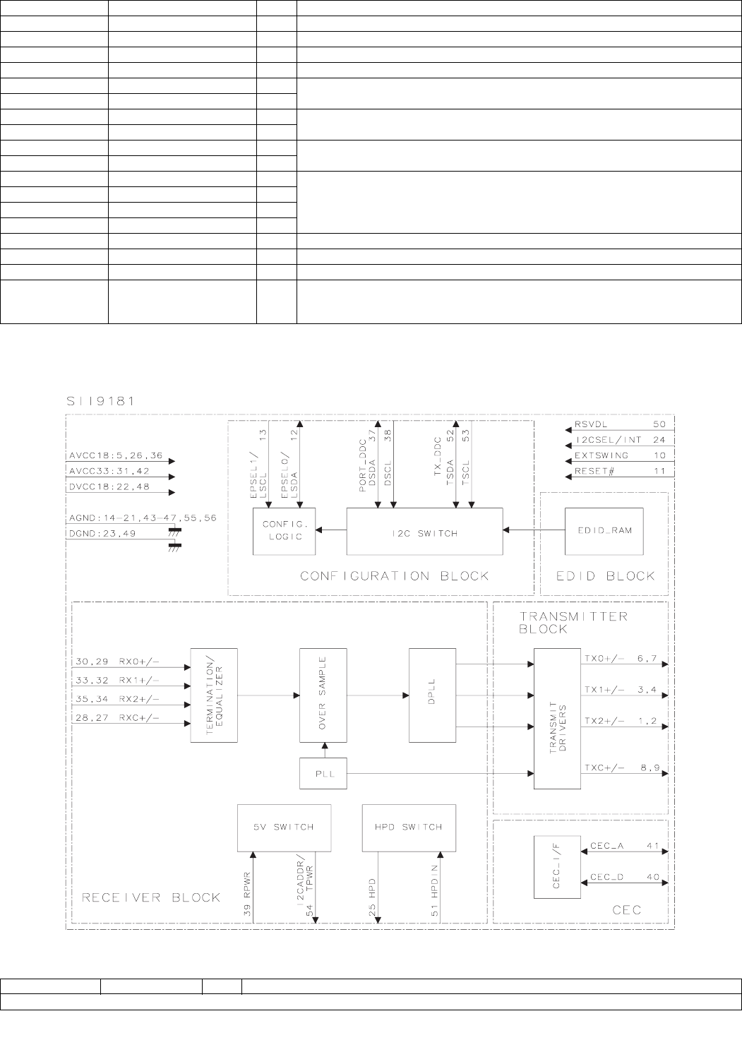
LC-42XL2E/S/RU, LC-46XL2E/S/RU, LC-46X20E/S/RU, LC-52XL2E/S/RU, LC-52X20E/S/RU
5 – 6
2.3. IC803 (VHiSii9181+-1Q)
2.3.1 Block Diagram
2.3.2 Pin Connections and short description
49 DCOUT O DC output for S-terminal.
51 VOUT3 O Monitor output (composit signal)
50 COUT3/VOUT6 O Monitor output (Chroma or composite signal)
52 YOUT3/ VOUT5 O Monitor output (Luminance or composite signal)
54 PROUT2 O Colour difference PR-signal output.
58 PROUT1 O
55 PBOUT2/ COUT2 O Colour difference PB-signal or chroma signal output.
59 PBOUT1/ COUT1 O
56 CYOUT2/ YOUT2/ VOUT2 O Colour difference signal, Luminance or composite signal output.
60 CYOUT1/ YOUT1/ VOUT1 O
64 O1 O Output port.
66 O2 O
72 O3 O
78 O4 O
53, 57 VDD1 — Power supply (+9V)
8, 47 VDD2 — Power supply (+5V)
18, 44, 62 GND — Ground
4, 6, 10, 11, 12, 13,
17, 19, 39, 41, 43,
48, 61, 63
NC — Unconnected pins.
Pin No. Pin Name I/O Pin Function
System Switching
Pin No. Pin Name I/O Pin Function
LC-42XL2E/S/RU, LC-46XL2E/S/RU, LC-46X20E/S/RU, LC-52XL2E/S/RU, LC-52X20E/S/RU
5 – 7
37 DSDA I/O DDC I2C Data for respective port.
38 DSCL I DDC I2C Clock.
39 RPWR I 5V Port detection input. Connect to 5V signal from HDMI input connector.
25 HPD O Hot Plug Detect Output. Connect to HOTPLUG of HDMI input connector.
51 HPDIN I Hot Plug Detect Input.
53 TSCL O Master DDC I2C Clock (Open Drain Output) to HDMI receiver.
I2C transactions required for HDCP operation are performed over this I2C bus.
52 TSDA I/O Master DDC Data (Open drain output.) to HDMI receiver.
I2C transactions required for HDCP operation are performed over this I2C bus.
Configuration
54 I2CADDR/TPWR I/O I2C Slave Address input/Transmit Power Sense output pin.
When RESET# is low, this pin is used as an input to latch the I2C sub-address.
The level on this pin is latched when the RESET# pin transitions from low to high.
When RESET# is high, this pin is used as the TPWR output, indicating that the Rx-port has 5V
present.
24 I2CSEL/INT# I/O I2C Selection input/ Interrupt output pin.
The SiI9181 has two modes of operation: Local I2C control and Standalone.
The mode is determined by the level of the I2CSEL/INT pin at the rising edge of RESET#.
A high indicates I2C mode, and a low indicates Standalone mode.
In Local I2C mode, all functions are controlled and observed with I2C registers using the pins
LSCL/EPSEL1 and LSDA/EPSEL0 as the local I2C bus.
In Standalone mode, the external pins LSCL/ EPSEL1 and LSDA/ EPSEL0 are use to determine
whether the SiI9181 is in Normal mode or Standby mode.
After reset, this pin becomes the Interrupt output.
This is an open-drain output and requires an external pull-up.
50 RSVDL — Reserved for use by Silicon Image and must be tied low.
Control Pins
11 RESET# I Reset Pin (Active LOW). Certain configuration inputs are latched when RESET# transitions from
low to high.
13 LSCL/EPSEL1 I Local I2C Clock / External Port Select 1. When I2CSEL is high, this becomes the Local I2C bus
clock pin, LSCL. When I2CSEL is low, this becomes the external port select pin, EPSEL1.
True open drain, so does not pull to ground if power not applied.
An external pull-up is required.
12 LSDA/EPSEL0 I/O Local I2C Data / External Port Select 0. When I2CSEL is high, this becomes the Local I2C bus
data pin, LSDA. When I2CSEL is low, this becomes the external port select pin, EPSEL0.
True open drain, so does not pull to ground if power not applied.
An external pull-up is required.
CEC Pins
41 CEC_A I/O HDMI compliant CEC I/O used to interface to CEC devices.
CEC electrically compliant signal. This pin connects to the CEC signal of all HDMI connectors in
the system.
As an input, the pad acts as a LVTTL Schmitt triggered input and is 5V tolerant. As an output, the
pad acts as an NMOS driver with resistive pull-up. This pin has an internal pull-up resistor.
40 CEC_D I/O CEC interface to local system. True open-drain. An external pull-up is required. This pin typically
connects to the local CPU.
Differential Signal Data Pins
30 RX0+ I TMDS input data pairs.
29 RX0- I
33 RX1+ I
32 RX1- I
35 RX2+ I
34 RX2- I
28 RXC+ I TMDS input clock pair.
27 RXC- I
6 TX0+ O TMDS output data pairs.
7TX0-O
3TX1+O
4TX1-O
1TX2+O
2TX2-O
8 TXC+ O TMDS output clock pair.
9TXC-O
10 EXT_SWING O Voltage Swing Adjust. A resistor tied from this pin to AVCC18 determines the amplitude of the volt-
age swing. The recommended value is 750 Ω.
Power and Ground Pins
Pin No. Pin Name I/O Pin Function
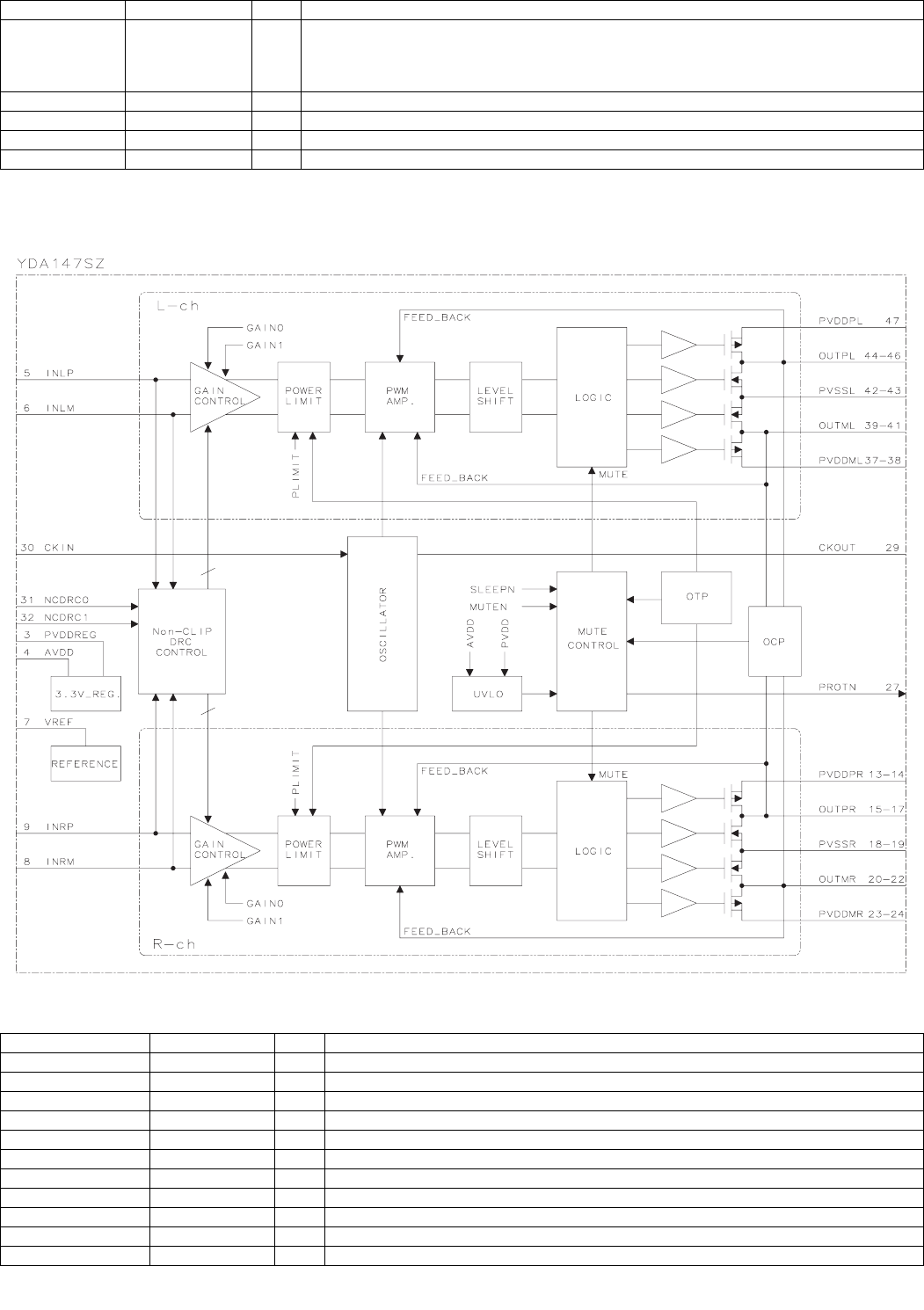
LC-42XL2E/S/RU, LC-46XL2E/S/RU, LC-46X20E/S/RU, LC-52XL2E/S/RU, LC-52X20E/S/RU
5 – 8
2.4. IC1301 (VHiYDA147SZ-1Y)
2.4.1 Block Diagram
2.4.2 Pin Connections and short description
14, 15, 16, 17,
18, 19, 20, 21,
43, 44, 45, 46,
47, 55, 56
AGND — Analog GND.
5, 26, 36 AVCC18 — Analog VCC. Connect to 1.8V supply.
22, 48 DVCC18 — Digital VCC. Connect to 1.8V supply.
23, 49 DGND — Digital GND.
31, 42 AVCC33 — Analog VCC. Connect to 3.3V supply.
Pin No. Pin Name I/O Pin Function
1, 2, 12, 25, 35, 36 NC — No connection
3 PVDDREG — Power terminal for regulator (PVDD)
4 AVDD — Output terminal for 3.3V regulator
5 INLP I Analog input terminal (Lch+)
6 INLM I Analog input terminal (Lch-)
7 VREF VREF terminal
8 INRM I Analog input terminal (Rch-)
9 INRP I Analog input terminal (Rch+)
10 AVSS — GND terminal for analog
11 PLIMIT I Power limit setting terminal
13, 14 PVDDPR — Power terminal for digital amplifier output (Rch+)
Pin No. Pin Name I/O Pin Function

LC-42XL2E/S/RU, LC-46XL2E/S/RU, LC-46X20E/S/RU, LC-52XL2E/S/RU, LC-52X20E/S/RU
5 – 9
2.5. IC1402 (VHiR2S15502-1Y)
2.5.1 Pin Connections and short description
15, 16, 17 OUTPR O Digital amplifier output terminal (Rch+)
18, 19 PVSSR — Ground terminal for digital amplifier output (Rch)
20, 21, 22 OUTMR O Digital amplifier output terminal (Rch-)
23, 24 PVDDMR — Power terminal for digital amplifier output (Rch-)
26 SLEEPN I Sleep control terminal
27 PROTN O Error flag output terminal
28 MUTEN I Mute control terminal
29 CKOUT O Clock output terminal for synchronization
30 CKIN I External clock input terminal
31 NCDRC0 I Non-clip/DRC1/DRC2 mode selection terminal 0
32 NCDRC1 I Non-clip/DRC1/DRC2 mode selection terminal 1
33 GAIN0 I GAIN setting terminal 0
34 GAIN1 I GAIN setting terminal 1
37, 38 PVDDML — Power terminal for digital amplifier output (Lch-)
39, 40, 41 OUTML O Digital amplifier output terminal (Lch-)
42, 43 PVSSL — Ground terminal for digital amplifier output (Lch)
44, 45, 46 OUTPL O Digital amplifier output terminal (Lch+)
47, 48 PVDDPL — Power terminal for digital amplifier output (Lch+)
Pin No. Pin Name I/O Pin Function
1 AVSS — 0V Power Supply for Analog Core
2 AVDD — 3.3V Power Supply for Analog Core
3 SIF I Sound IF Input
4 VREF1 — ADC Voltage Reference 1
5 VREF2 — ADC Voltage Reference 2
6 TEST I Test pin
7 XI I Crystal Oscillator Input
8 XO O Crystal Oscillator Output
9 IVDD — 3.3V Power Supply for I/O Buffer
10 IVSS — 0V Power Supply for I/O Buffer
11 DVSS — 0V Power Supply for Logic Core
12 DVDD — 1.5V Power Supply for Logic Core
13 DACCLK I/O DAC Clock
14 BCK I/O Bit Clock
15 LRCK I/O LR Clock
16 SD0 O Digital Output for External DAC
17 SDI I Digital Input for Internal DAC
18 SDA I/O I2C bus Serial Data
19 SCL I I2C bus Serial Clock
20 STATUS I/O PLL Setting / Status Signal
21 RESET I Hardware Reset (Active low)
22 ROUT O Rch Analog Output
23 VCOM — DAC Voltage Reference
24 LOUT O Lch Analog Output
Pin No. Pin Name I/O Pin Function
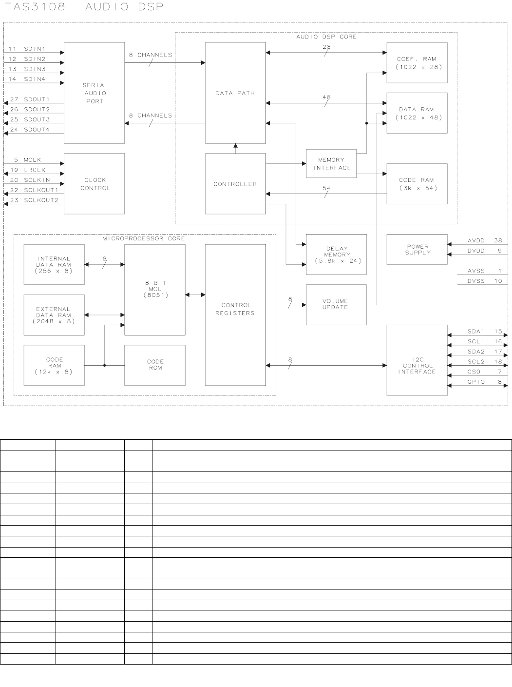
LC-42XL2E/S/RU, LC-46XL2E/S/RU, LC-46X20E/S/RU, LC-52XL2E/S/RU, LC-52X20E/S/RU
5 – 10
2.6. IC1403 (VHiTAS3108D-1Y)
2.6.1 Block Diagram
2.6.2 Pin Connections and short description
Pin No. Pin Name I/O Pin Function
38 AVDD — Analog power-supply input (3.3V)
1 AVSS — Analog ground
7 CS0 I Pull-down Chip select
9, 30 DVDD — Digital power-supply input (3.3V)
10, 29 DVSS — Digital ground
8 GPIO I/O Pull-up GPIO control pin (user programmable)
19 LRCLK I/O Pull-down Sample rate clock (fS) input or output
5 MCLKIN I Master clock input (Connect to ground when not in use.)
21 MCLKO O Master clock output
6 MICROCLK_DIV I Pull-down Internal microprocessor clock divide control
31 PDN I Pull-up Powers down all logic and stops all clocks, active-low. Coefficient memory remains stable
through power-down cycle.
34 PLL0 I Pull-up PLL control 0
35 PLL1 I Pull-down PLL control 1
36 PLL2 I Pull-down PLL control 2
33, 37 RESERVED — Connect to ground
32 RESET I Pull-up Reset, active-low
16 SCL1 I/O I2C port #1 clock (always a slave)
18 SCL2 I/O I2C port #2 clock (always a slave)
20 SCLKIN I Pull-down Bit clock input
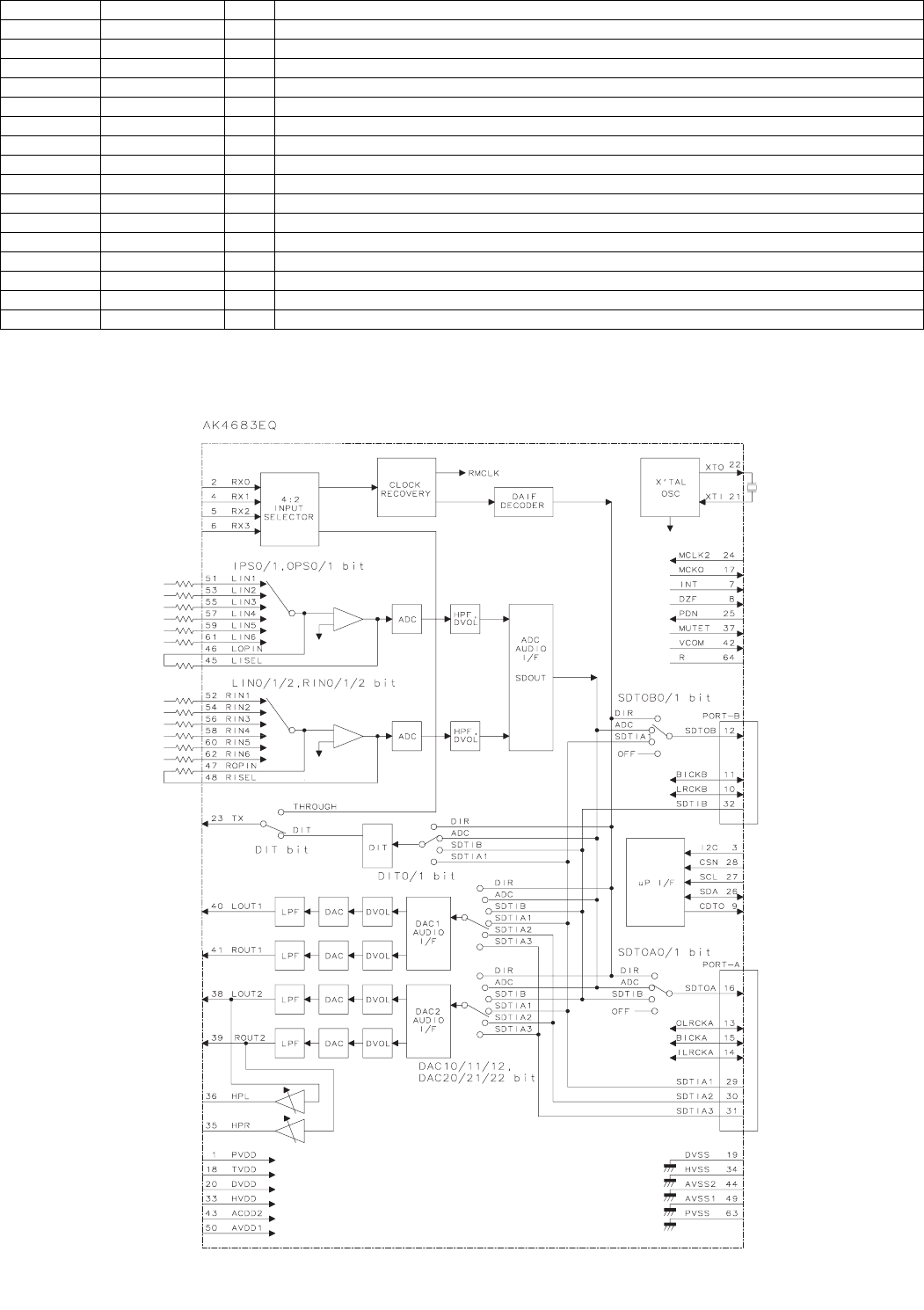
LC-42XL2E/S/RU, LC-46XL2E/S/RU, LC-46X20E/S/RU, LC-52XL2E/S/RU, LC-52X20E/S/RU
5 – 11
2.7. IC1404 (VHiAK4683EQ-1Q)
2.7.1 Block Diagram
22 SCLKOUT1 O Bit clock #1 out. Used to receive input serial data.
23 SCLKOUT2 O Bit clock #2 out. Used to clock output serial data.
15 SDA1 I/O I2C port #1 data (always a slave)
17 SDA2 I/O I2C port #2 data (always a slave)
11 SDIN1 I Pull-down Serial data input 1
12 SDIN2 I Pull-down Serial data input 2
13 SDIN3 I Pull-down Serial data input 3
14 SDIN4 I Pull-down Serial data input 4
27 SDOUT1 O Serial data output 1
26 SDOUT2 O Serial data output 2
25 SDOUT3 O Serial data output 3
24 SDOUT4 O Serial data output 4
2 VR_PLL — Internal regulator. This pin must not be used to power external devices.
3 XTALI I Oscillator input (connect to ground when not in use)
4 XTALO O Oscillator output
28 VR_DIG --- Internal regulator. This pin must not be used to power external devices.
Pin No. Pin Name I/O Pin Function

LC-42XL2E/S/RU, LC-46XL2E/S/RU, LC-46X20E/S/RU, LC-52XL2E/S/RU, LC-52X20E/S/RU
5 – 12
2.7.2 Pin Connections and short description
Pin No. Pin Name I/O Pin Function
1 PVDD — PLL Power supply, 4.5V~5.5V.
2 RX0 I Receiver Channel 0 (Internal biased pin. Internally biased at PVDD/2).
3 I2C I Control Mode Select.
“L”: 4-wire Serial, “H”: I2C Bus
4 RX1 I Receiver Channel 1.
5 RX2 I Receiver Channel 2.
6 RX3 I Receiver Channel 3.
7 INT O Interrupt
8 DZF O Zero Input Detect.
When the input data of DAC follow total 8192 LRCK cycles with “0” input data, this pin goes to “H”. And
when RSTN1 bit is “0”, PWDA bit is “0”, this pin goes to “H”
9 CDTO O Control Data Output in Serial Mode and I2C pin = “L”.
10 LRCKB I/O Channel Clock B
11 BICKB I/O Audio Serial Data Clock B
12 SDTOB O Audio Serial Data Output B
13 OLRCKA I/O Output Channel Clock A
14 ILRCKA I/O Input Channel Clock A
15 BICKA I/O Audio Serial Data Clock A
16 SDTOA O Audio Serial Data Output A
17 MCKO O Master Clock Output
18 TVDD — Output Buffer Power Supply, 2.7V~5.5V
19 DVSS — Digital Ground
20 DVDD — Digital Power Supply, 4.5V~5.5V
21 XTI I X’tal Input
22 XTO O X’tal Output
23 TX O Transmit Channel Output
When DIT bit = “0”, RX0~3 Through.
When DIT bit = “1”, Internal DIT Output.
24 MCLK2 I Master Clock Input
25 PDN I Power-Down Mode & Reset
When “L”, the AK4683 is powered-down, all registers are reset. And then all digital output pins go “L”.
The AK4683 must be reset once upon power-up.
26 SDA I/O Control Data in Serial Mode and I2C pin = “H”.
27 SCL I Control Data Clock in Serial Mode and I2C pin = “H”.
28 CSN I Chip Select in Serial Mode and I2C pin = “L”.
29 SDTIA1 I Audio Serial Data Input A1
30 SDTIA2 I Audio Serial Data Input A2
31 SDTIA3 I Audio Serial Data Input A3
32 SDTIB I Audio Serial Data Input B
33 HVDD — HP Power Supply, 4.5V~5.5V
34 HVSS — HP Ground
35 HPR O HP Rch Output.
36 HPL O HP Lch Output.
37 MUTET — HP Common Voltage Output
38 LOUT2 O DAC2 Lch Positive Analog Output
39 ROUT2 O DAC2 Rch Positive Analog Output
40 LOUT1 O DAC1 Lch Positive Analog Output
41 ROUT1 O DAC1 Rch Positive Analog Output
42 VCOM — DAC/ADC Common Voltage Output
43 AVDD2 — DAC Power Supply, 4.5V~5.5V
44 AVSS2 — DAC Ground
45 LISEL O Lch Feedback Resistor Output
46 LOPIN O Lch Feedback Resistor Input. 0.5 x AVDD1.
47 ROPIN O Rch Feedback Resistor Input. 0.5 x AVDD1.
48 RISEL O Rch Feedback Resistor Output
49 AVSS1 — ADC Ground
50 AVDD1 — ADC Power Supply, 4.5V~5.5V
51 LIN1 I Lch Input 1
52 RIN1 I Rch Input 1
53 LIN2 I Lch Input 2
54 RIN2 I Rch Input 2
55 LIN3 I Lch Input 3
56 RIN3 I Rch Input 3
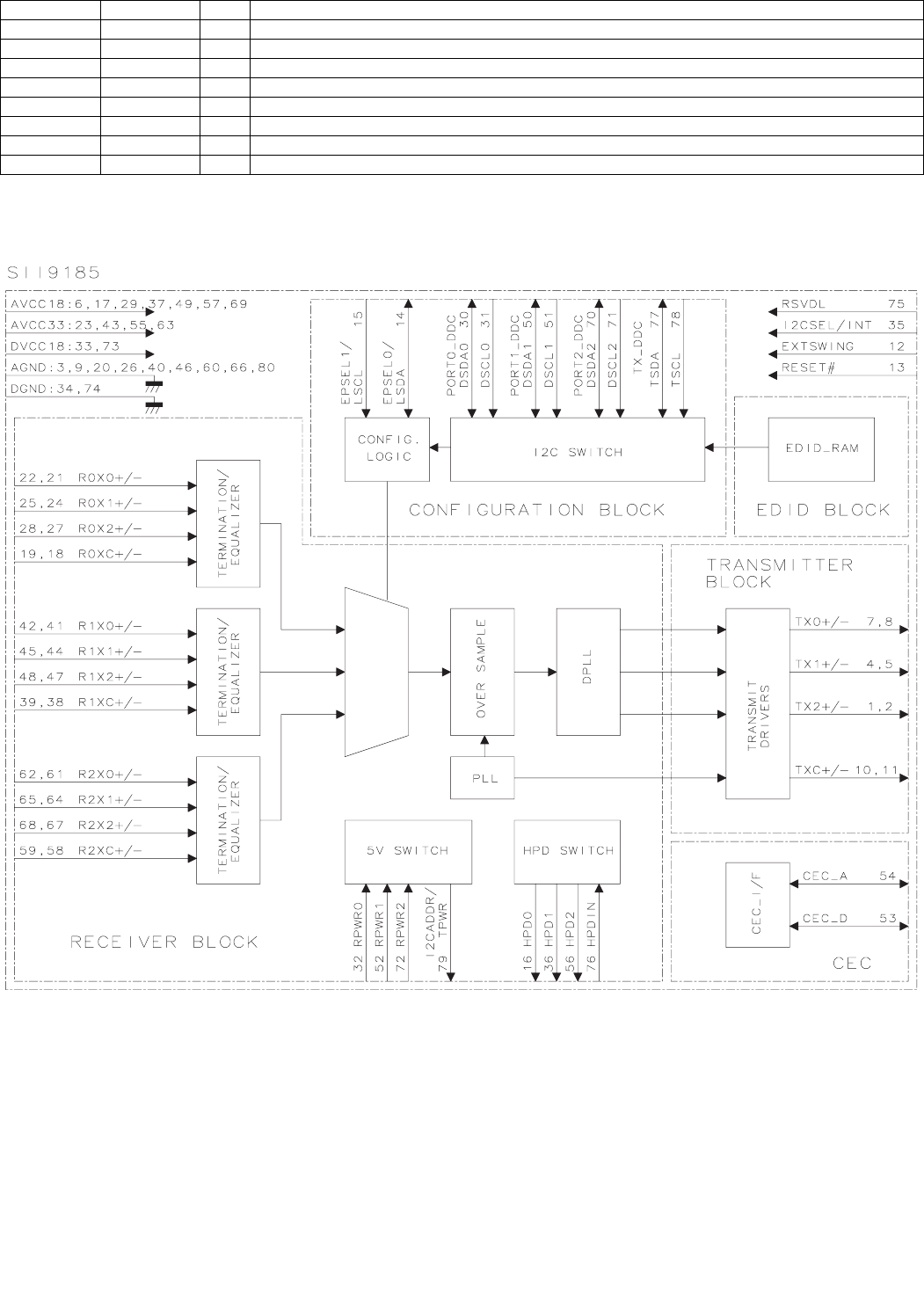
LC-42XL2E/S/RU, LC-46XL2E/S/RU, LC-46X20E/S/RU, LC-52XL2E/S/RU, LC-52X20E/S/RU
5 – 13
2.8. IC1507 (VHiSii9185+-1Q)
2.8.1 Block Diagram
57 LIN4 I Lch Input 4
58 RIN4 I Rch Input 4
59 LIN5 I Lch Input 5
60 RIN5 I Rch Input 5
61 LIN6 I Lch Input 6
62 RIN6 I Rch Input 6
63 PVSS — PLL Ground
64 R — External Resistor
Pin No. Pin Name I/O Pin Function
LC-42XL2E/S/RU, LC-46XL2E/S/RU, LC-46X20E/S/RU, LC-52XL2E/S/RU, LC-52X20E/S/RU
5 – 14
2.8.2 Pin Connections and short description
Pin No. Pin Name I/O Pin Function
System Switching Pins
30, 50, 70 DSDA0, DSDA1, DSDA2 I/O DDC I2C Data for respective port.
31, 51, 71 DSCL0, DSCL1, DSCL2 I DDC I2C Clock for respective port.
32, 52, 72 RPWR0, RPWR1, RPWR2 I 5V Port detection input for respective port.
Connect to 5V signal from HDMI input connector.
16, 36, 56 HPD0, HDP1, HPD2 O Hot Plug Detect Output for respective port.
Connect to HOTPLUG of HDMI input connector.
76 HPDIN I Hot Plug Detect Input.
78 TSCL O Master DDC I2C Clock (Open Drain Output) to HDMI receiver.
I2C transactions required for HDCP operation are performed over this I2C bus.
77 TSDA I/O Master DDC Data (Open drain output.) to HDMI receiver. I2C transactions required for
HDCP operation are performed over this I2C bus.
Configuration Pins
79 I2CADDR/TPWR I/O I2C Slave Address input / Transmit Power Sense output pin.
When RESET# is low, this pin is used as an input to latch the I2C sub-address.
The level on this pin is latched when the RESET# pin transitions from low to high.
When RESET# is high, this pin is used as the TPWR output, indicating that the selected
Rx-port has 5V present. When none of the Rx ports are selected, this signal is low.
35 I2CSEL/INT# I/O I2C Selection input / Interrupt output pin.
When RESET# is low, this pin is used as an input to latch the External Port Detection
signal. The level on this pin is latched when the RESET# pin transitions from low to high.
When this pin is low during reset, the external pins EPSEL1/LSCL and EPSEL0/LSDA
are used to select the Rx-port as EPSEL[1:0].
When this pin is high during reset, the internal local I2C register is used to select the Rx-
port.
75 RSVDL I Reserved for use by Silicon Image and must be tied low.
Control Pins
13 RESET# I Reset Pin (Active LOW). Certain configuration inputs are latched when RESET# transi-
tions from low to high.
15 LSCL/EPSEL1 I Local I2C Clock / External Port Select 1. When I2CSEL is high, this becomes the Local
I2C bus clock pin, LSCL. When I2CSEL is low, this becomes the external port select pin,
EPSEL1. True open drain, so does not pull to ground if power not applied. An external
pull-up is required.
14 LSDA/EPSEL0 I/O Local I2C Data / External Port Select 0. When I2CSEL is high, this becomes the Local
I2C bus data pin, LSDA. When I2CSEL is low, this becomes the external port select pin,
EPSEL0. True open drain, so does not pull to ground if power not applied. An external
pull-up is required.
CEC Pins
54 CEC_A I/O HDMI compliant CEC I/O used to interface to CEC devices.
CEC electrically compliant signal. This pin connects to the CEC signal of all HDMI con-
nectors in the system. As an input, the pad acts as a LVTTL Schmitt triggered input and
is 5V tolerant. As an output, the pad acts as an NMOS driver with resistive pull-up. This
pin has an internal pull-up resistor.
53 CEC_D I/O CEC interface to local system. True open-drain. An external pull-up is required.
This pin typically connects to the local CPU.
Differential Signal Data Pins
22 R0X0+ I TMDS input Port 0 data pairs.
21 R0X0- I
25 R0X1+ I
24 R0X1- I
28 R0X2+ I
27 R0X2- I
19 R0C+ I TMDS input Port 0 clock pair.
18 R0C- I
42 R1X0+ I TMDS input Port 1 data pairs.
41 R1X0- I
45 R1X1+ I
44 R1X1- I
48 R1X2+ I
47 R1X2- I
39 R1C+ I TMDS input Port 1 clock pair.
38 R1C- I

LC-42XL2E/S/RU, LC-46XL2E/S/RU, LC-46X20E/S/RU, LC-52XL2E/S/RU, LC-52X20E/S/RU
5 – 15
2.9. IC2002 (RH-iXB986WJN8Q)
2.9.1 Pin Connections and short description
62 R2X0+ I TMDS input Port 2 data pairs.
61 R2X0- I
65 R2X1+ I
64 R2X1- I
68 R2X2+ I
67 R2X2- I
59 R2C+ I TMDS input Port 2 clock pair.
58 R2C- I
7 TX0+ O TMDS output data pairs.
8TX0- O
4TX1+ O
5TX1- O
1TX2+ O
2TX2- O
10 TXC+ O TMDS output clock pair.
11 TXC- O
12 EXT_SWING I Voltage Swing Adjust. A resistor tied from this pin to AVCC18 determines the amplitude
of the voltage swing. The recommended value is 750Ω.
Power and Ground Pins
23, 43, 55, 63 AVCC33 — Analog VCC. Connect to 3.3V supply.
6, 17, 29, 37, 49,
57, 69
AVCC18 — Analog VCC. Connect to 1.8V supply.
3, 9, 20, 26, 40,
46, 60, 66, 80
AGND — Analog GND.
33, 73 DVCC18 — Digital VCC. Connect to 1.8V supply.
34, 74 DGND — Digital GND.
Pin No. Pin Name I/O Pin Function
1 SHIP_EN O SHIP (CSI) processing enabled/disabled selection signal
2 CS_CPLD O CPLD chip select
3 N_SRESET O Reset
4 PM_REQ O Request signal (Communication request at H)
5 IR_PASS O Remote control signal external through switching
6 Vc1 — Internal voltage drop power terminal
7 X2 I Sub clock (32.768kHz)
8 X1 O Sub clock (32.768kHz)
9 N_RESET I System reset
10 OSC2 O System clock (20.00MHz)
11 Vss — GND
12 OSC1 I System clock (20.00MHz)
13 Vcc — Power supply (+3.3V)
14 N_NMI I For FLASH rewrite
15 WAKE_UP I For WAIT mode return
16 AC_DET I For instantaneous blackout detection
17 POW_SW I Power SW
18 FRAME O Panel controller control (50/60 setting)
19 ROMSEL0 O For test pattern control
20 O_S_SET O Panel controller control ON/OFF
21 TEMP1 O Panel controller control, temperature information 1
22 TEMP2 O Panel controller control, temperature information 2
23 TEMP3 O Panel controller control, temperature information 3
24 L_R O Panel controller control, flip horizontal
25 U_D O Panel controller control, flip vertical
26 UARXD_M I Serial for MAIN CPU communication (To TXD of MAIN CPU)
27 UATXD_M O Serial for MAIN CPU communication (To RXD of MAIN CPU)
28 TXD O For debugger (E8) connection
29 RXD I For debugger (E8) connection
30 SCLD I For debugger (E8) connection
31 BUSY I For debugger (E8) connection
32 LED_R O Power LED, red
33 LED_G O Power LED, green
34 LED_OPC O OPC LED
Pin No. Pin Name I/O Pin Function

LC-42XL2E/S/RU, LC-46XL2E/S/RU, LC-46X20E/S/RU, LC-52XL2E/S/RU, LC-52X20E/S/RU
5 – 16
35 LED_SLEEP O SLEEP_LED
36 AV_LINK_O O AV_LINK output
37 ANT_POW O Antenna power control
38 EXE_LED O Microprocessor operation check LED
39 I2C_GATE O I2C bus SW
40 N_SYSRST_IN I SYSTEM RESET switch detection
41 RS_ON O RS232C power control
42 STB O Backlight control.
43 ERR_PNL I Lamp error detection (L: error)
44 AV_LINK_I I AV_LINK input
45 SYNC_DET O PC power management setting
46 VSYNC I VSYNC interrupt
47 CEC_O O CEC output
48 CEC_I I CEC input
49 RC I Remote control signal input.
50 I2C1_SCL O I2C CH1
51 I2C1_SDA I/O I2C CH1
52 W_PROT_M O EEP write protection
53 P16 — For debugger (E8) connection
54 DVIA_DET I DVI analog detection (for PC power management)
55 MUTE_A_ALL O Audio mute
56 DET_6V I 6V detection
57 DET_10V I 10V detection
58 DET_PNL12V I Panel 12V detection
59 DER_D3V3 I D3.3V detection
60 DET_3V3 I 3.3V detection
61 EU_POW O Digital system power control
62 LINK_POW O i.Link power control
63 PNL_POW O 5V ON/OFF SW for panel
64 D_POW O Main power ON/OFF control
65 SMPOW O Power control
66 PSIZ_L I Panel size discrimination terminal (Mounting discrimination)
67 PSIZ_H I Panel size discrimination terminal (Mounting discrimination)
68 QSTEMP I Thermistor input (Panel temperature)
69 KEY1 I Main unit key input 1
70 KEY2 I Main unit key input 2
71 AREA1 I Panel size discrimination terminal (Mounting discrimination)
72 PNL_TYPE I Panel manufacturer discrimination (Mounting discrimination)
73 OPC I Brightness sensor input
74 AFT/AGC I Tuner AFT/ACG input
75 Avss — Analog GND for A/D
76 LNBSHORT I Antenna short detection (Low: OK, High: NG)
77 Vref — A/D converter reference voltage
78 Avcc — Analog power for A/D
79 PNL_TYPE I Panel solution discrimination (Mounting discrimination)
80 ILLUMI O Illumination LED
Pin No. Pin Name I/O Pin Function

LC-42XL2E/S/RU, LC-46XL2E/S/RU, LC-46X20E/S/RU, LC-52XL2E/S/RU, LC-52X20E/S/RU
5 – 17
2.10. IC3301 (RH-iXC010WJQZQ)
2.10.1 Pin Connections and short description
Pin No. Pin Name I/O Pin Function
Ball Assignments for CPU Host Interface.
K20, K19, K18, K17, L20,
L19, L18, L17
A_D[7:0] I/O Multiplexed address and data bus powered by VDDH/VSS.
M17, M18, M119, M20,
N20, N19, N18, N17
ADDR[7:0] I CPU Address. (Not connected)
J18 ALE I Address latch enables.
J19 WR# I CPU Write.
J20 RD# I CPU Read.
H17 SDA I/O I2C data.
H18 SCL I I2C clock.
J17 CPU_CS I UX chip select pin from MCU. Active Low.
Ball Assignments for Analog Support Interface.
W1 XTALI I Input for Clock Synthesizer. Supports 24MHz Oscillator or crystal powered by ana-
log PLL.
Y1 XTALO O Used in conjunction with XTALI for 24MHz crystal output powered by analog PLL.
U2 MLF1 I Low pass filter node for memory clock PLL powered by analog PLL.
R4 PLF2 I Low pass filter node for video clock PLL powered by analog PLL.
Ball Assignments for Analog Input Interface.
Y4 CVBS1 I Composite video input 1.
V6 Y_G1 I Y input 1 of component or G input 1 of PC RGB.
W6 Y_G2 I Y input 2 of component or G input 2 of PC RGB.
Y6 Y_G3 I Y input 3 of component or G input 3 of PC RGB.
W2 CVBS_OUT1 I CVBS Output 1. (Not connected)
V2 CVBS_OUT2 I CVBS Output 2. (Not connected)
V9 C I C input of S-Video.
W9 PB_B1 I PB input 1 of component.
Y9 PB_B2 I PB input 2 of component.
Y10 PB_B3 I PB input 3 of component.
Y8 PR_R1 I PR input 1 of component.
W8 PR_R2 I PR input 2 of component.
V8 PR_R3 I PR input 3 of component.
W4, V4 FS2, FS1 I SCART function select 2, 1.
U4, Y5 FB2, FB1 I SCART FB input for Port 2, Port 1.
V10 AIN_H I Hsync input (PC RGB input)
U10 AIN_V I Vsync input (PC RGB input)
U8 PC_R I PC Red input.
Y7 PC_G I PC Green input.
W10 PC_B I PC Blue INPUT.
Ball Assignments for Capture Interface (TV & RGB).
U18, U19, U20, T20, T18,
T17, R19, R20
DPB[15:8] (DP_B[15:8]) I/O Digital input port [15:8] (Output reserved)
Y12, U13, V13, W13,
Y13, Y14, W14, V14,
U14, U15, V15, W15,
Y16, W16, V16, U16,
U17, V17, W17, Y17,
Y18, W18, V18, W19
DPA[23:0] (DP_A[23:0]) I/O Digital input/output port [23:0]
T19 DPB_CLK (CLK_B) I/O Digital port B CLK input/output. (Not connected)
Y15 DPA_CLK (CLK_A) I/O Digital port A CLK input/output.
W20 DPE_DE (DE_B) I/O DE input/output of Digital port B.
Y20 DPA_VS (VS_A) I/O Vsync input/output of Digital port A.
Y19 DPA_HS (HS_A) I/O Hsync input/output of Digital port A.
V20 DPB_VS (VS_B) I/O Vsync input/output of Digital port B. (Not connected)
V19 DPB_HS (HS_B) I/O Hsync input/output of Digital port B. (Not connected)
P19 HS I/O Hsync output for Digital port.
P17 VS I/O Vsync output for Digital port.
LC-42XL2E/S/RU, LC-46XL2E/S/RU, LC-46X20E/S/RU, LC-52XL2E/S/RU, LC-52X20E/S/RU
5 – 18
Pin No. Pin Name I/O Pin Function
Ball Assignments for Frame Buffer Memory.
D3, C3, C2, C1, A1, A2,
A3, C5, A4, B5, A5, D6,
A7, B7, C7, D7, D8, C8,
B8, A8, D9, D10, C10,
B10, A10, A11, B11, C11,
D12, A13, B13, C13
MD[31:0] I/O Memory data.
F1, F2, F3, F4, G4, G3,
G2, G1, H1, H2, H3, H4
MA[11-0] I/O Memory Address.
J2 RAS# O RAS# signal powered by VDDH/VSS.
J1 CAS# O CAS# signal powered by VDDH/VSS.
K1 WE# O WE#, write enable signal powered by VDDH/VSS.
J3 CS1# O Chip select 0 for the first 2/4 Mbyte of SGRAM/SDRAM powered by VDDH/VSS.
J4 CS0# O Chip select 1 for the first 2/4 Mbyte of SGRAM/SDRAM powered by VDDH/VSS.
D1 MCK0 O Memory clock+.
E1 MCK0# O Memory clock-.
B1, A6, A9, A12 DQM[3:0] O Read/Write bytes enable powered by VDDH/VSS.
K2 CLKE O Memory clock enable.
B2, B6, B9, B12 DQS[3:0] I/O Memory data strobe.
E3 MVREF — DDR voltage reference.
K3 BA0 O Bank address select.
K4 BA1 O Bank address select.
Ball Assignments for Power and Ground.
C14, C15, D13, D14,
D15, E13, E14, E15,
G16, H5, H16, J5, J16,
K5, K16, R16, T14, T15
VDDC — 1.2V Digital core power.
E4, E7 VSSR — Digital memory reference Ground.
E2, E8 VDDR — 2.5V Digital power for Memory.
B4, C4, D4, D5, D11, E5,
E6, E9, E10, E11, E12,
F5, G5
VDDM — 2.5V Memory interface power. Output driver.
L16, M16, N16, P16, T12,
T13, R17, R18
VDDH — 3.3V Digital I/O power.
B3, C6, C9, C12, D2, H8,
H9, H10, H11, H12, H13,
J8, J9, J10, J11, J12, J13,
K8, K9, K10, K11,K12,
K13, L5, L8, L9, L10, L11,
L12, L13, M8, M9, M10,
M11, M12, M13, N8, N9,
N10, N11, N12, N13,
P18, T16, H20
VSS — Core and Digital IO ground.
W3 AVSS_BG_ASS — ADC ground.
V3 AVDD3_BG_ASS — 3.3V ADC power.
T3 PAVDD1 — 3.3V power for MCLK PLL.
T2 PAVSS1 — Ground for MCLK PLL.
R3 PAVSS2 — Ground for PCLK PLL.
T4 PAVDD2 — 3.3V power for PCLK PLL.
U6, T8, U7, U5 AVDD_ADC[4, 3, 2, 1] — 1.2V power for analog ADC.
T6, T9, T7, T5 AVSS_ADC[4, 3, 2, 1] — Ground for analog ADC.
U9, Y3 AVDD3_ADC[2, 1] — 3.3V ADC power.
U3 AVDD3_OUTBUF — 3.3V power for output buffer.
Y2 AVSS_OUTBUF — 3.3V ground for output buffer.
C18, C19 LVDS_VSSO — LVDS out buffer ground.
C16 LVDS_VSSD — LVDS Digital ground.
E16 LVDS_VSSA — LVDS analog ground.
E18 LVDS_VSSP — LVDS PLL GND.
D18 LVDS_VDDP — LVDS PLL VDD.
E17 LVDS_VDDA — LVDS analog VDD.
D16 LVDS_VDDD — LVDS Digital VDD.
C17, D17 LVDS_VDDO — LVDS out buffer VDD.
P20 NC — Not connected.
U1 AVDDAPLL — 1.2V analog PLL power.
V1 AVSSAPLL — 1.2V analog GND.
R2 AVDDLLPLL — 1.2V Line Lock PLL power.

LC-42XL2E/S/RU, LC-46XL2E/S/RU, LC-46X20E/S/RU, LC-52XL2E/S/RU, LC-52X20E/S/RU
5 – 19
T1 AVSSLLPLL — 1.2V Line Lock PLL GND.
Miscellaneous Ball Assignments.
F18 RESET I System reset forces the chip to a known state. Active High.
G18 INTN I/O Interrupt signal (active low).
G17 PWM0 I/O PWM I/O. (Not connected)
F16 V5SF I 5V reference voltage (must be connected to 5V even in standby mode, when CPU
I/O is 5V)
F17 TESTMODE I Reserved (Connected to ground).
LVDS Output Ball Assignments.
A14 TA1P O LVDS 1st Channel Differential positive data out.
B14 TA1M O LVDS 1st Channel Differential negative data out.
A15 TB1P O LVDS 1st Channel Differential positive data out.
B15 TB1M O LVDS 1st Channel Differential negative data out.
A16 TC1P O LVDS 1st Channel Differential positive data out.
B16 TC1M O LVDS 1st Channel Differential negative data out.
A18 TD1P O LVDS 1st Channel Differential positive data out.
B18 TD1M O LVDS 1st Channel Differential negative data out.
A19 TE1P O LVDS 1st Channel Differential positive data out.
B19 TE1M O LVDS 1st Channel Differential negative data out.
B17 TCLK1M O LVDS 1st Channel Differential positive CLK out.
A17 TCLK1P O LVDS 1st Channel Differential negative CLK out.
F19 TCLK2M O LVDS 2st Channel Differential positive CLK out.
E20 TCLK2P O LVDS 2st Channel Differential negative CLK out.
H19 TE2P O LVDS 2st Channel Differential positive data out.
G20 TE2M O LVDS 2st Channel Differential negative data out.
G19 TD2P O LVDS 2st Channel Differential positive data out.
F20 TD2M O LVDS 2st Channel Differential negative data out.
E19 TC2P O LVDS 2st Channel Differential positive data out.
D20 TC2M O LVDS 2st Channel Differential negative data out.
B20 TB2P O LVDS 2st Channel Differential positive data out.
A20 TB2M O LVDS 2st Channel Differential negative data out.
D19 TA2P O LVDS 2st Channel Differential positive data out.
C20 TA2M O LVDS 2st Channel Differential negative data out.
HDMI Interface Ball Assignments.
L4 PVCC — TMDS PLL supply voltage.
M5 ANTSTO O Test pin. (Not connected)
M4, N4, N5, P4 AVCC — TMDS analog supply voltage.
L2 RXC- I TMDS differential CLK-.
L1 RXC+ I TMDS differential CLK+.
L3, M3, N3, P3, R1 TMDS_GND — TMDS GND.
M2 RX0- I HDMI Differential input pair 0-
M1 RX0+ I HDMI Differential input pair 0+
N2 RX1- I HDMI Differential input pair 1-
N1 RX1+ I HDMI Differential input pair 1+
P2 RX2- I HDMI Differential input pair 2-
P1 RX2+ I HDMI Differential input pair 2+
R5 REGVCC — ACR PLL Regulator supply voltage.
P5 DGND — ACR PLL GND.
T10 PWR5V I TMDS port Transmitter Detect (5V tolerant).
T11 DSCL I/O DDC I2C clock for DDC (5V tolerant).
U11 DSDA I/O DDC I2C data for DDC (5V tolerant).
U12 WS O I2S Word select output.
V11 SCDT O Indicates Active video at HDMI input port.
V12 SD0 O I2S serial data output.
W11 AUDIOCLK I Audio master clock input reference.
W12 SPDIF O S/PDIF audio output.
Y11 SCK O I2S serial clock output.
Pin Assignments for Reference Voltage.
V5 VREFN1 — ADC1 voltage reference-.
W5 VREFP1 — ADC1 voltage reference+.
V7 VREFN2 — ADC2 voltage reference-.
W7 VREFP2 — ADC2 voltage reference+.
Pin No. Pin Name I/O Pin Function
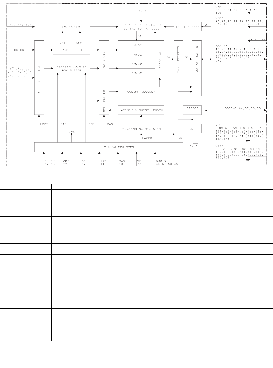
LC-42XL2E/S/RU, LC-46XL2E/S/RU, LC-46X20E/S/RU, LC-52XL2E/S/RU, LC-52X20E/S/RU
5 – 20
2.11. IC3501-2 (RH-iXC163WJQZQ)
2.11.1 Block Diagram
2.11.2 Pin Connections and short description
Pin No. Pin Name I/O Pin Function
62, 63 CK, CK I The differential system clock Input.
All of the inputs are sampled on the rising edge of the clock except DQ’s and DM’s that are
sampled on both edges of the DQS.
22 CKE I Activates the CK signal when high and deactivates the CK signal when low. By deactivating
the clock, CKE low indicates the Power down mode or Self refresh mode.
12 CS ICS enables the command decoder when low and disabled the command decoder when high.
When the command decoder is disabled, new commands are ignored but previous operations
continue.
11 RAS I Latches row addresses on the positive going edge of the CK with RAS low.
Enables row access & precharge.
10 CAS I Latches column addresses on the positive going edge of the CK with CAS low.
Enables column access.
53 WE I Enables write operation and row precharge.
Latches data in starting from CAS, WE active.
1, 28, 7, 34 DQS0-3 I/O Data input and output are synchronized with both edge of DQS.
44, 67, 50, 35 DM0-3 I Data In mask. Data In is masked by DM Latency=0 when DM is high in burst write. DM0 for
DQ0 ~ DQ7, DM1 for DQ8 ~ DQ15, DM2 for DQ16 ~ DQ23, DM3 for DQ24 ~ DQ31.
40, 78, 41, 42, 2, 46, 3, 4,
26, 65, 27, 66, 29, 68, 30,
69, 48, 5, 49, 6, 51, 8, 9,
52, 31, 32, 71, 33, 37, 38,
75, 39
DQ0-31 I/O Data inputs/Outputs are multiplexed on the same pins.
14, 56 BA0, BA1 I Selects which bank is to be active.
15, 16, 57, 17, 18, 60, 19,
20, 21, 59, 90, 58
A0-11 I Row/Column addresses are multiplexed on the same pins.
Row addresses: RA0 ~ RA11, Column addresses: CA0 ~ CA7.
Column address CA8 is used for auto precharge.
82, 88, 91, 92, 95, 101,
105, 106
VDD — Power for the input buffers and core logic.
LC-42XL2E/S/RU, LC-46XL2E/S/RU, LC-46X20E/S/RU, LC-52XL2E/S/RU, LC-52X20E/S/RU
5 – 21
2.12. IC7507 (VHiCE6353++-1Q)
2.12.1 Block Diagram
89, 94, 109, 115, 116,
117, 118, 124, 126, 127,
129, 130, 131, 132, 133,
134, 135, 136, 137, 138,
139, 140, 141, 142, 143,
144
VSS — Ground for the input buffers and core logic.
45, 47, 70, 72, 74, 76, 77,
79, 83, 84, 86, 87, 96, 97,
99, 100
VDDQ — Isolated power supply for the output buffers to provide improved noise immunity.
36, 43, 81, 102, 103, 104,
107, 108, 110, 111, 112,
113, 114, 119, 120, 121,
122, 123, 125, 128
VSSQ — Isolated ground for the output buffers to provide improved noise immunity.
23 VREF — Reference voltage for inputs, used for SSTL interface.
93, 61 RFU1/RFU2 — Reserved for Future Use.
13, 24, 25, 54, 55, 64, 73,
80, 85, 98
NC — No Connection.
Pin No. Pin Name I/O Pin Function
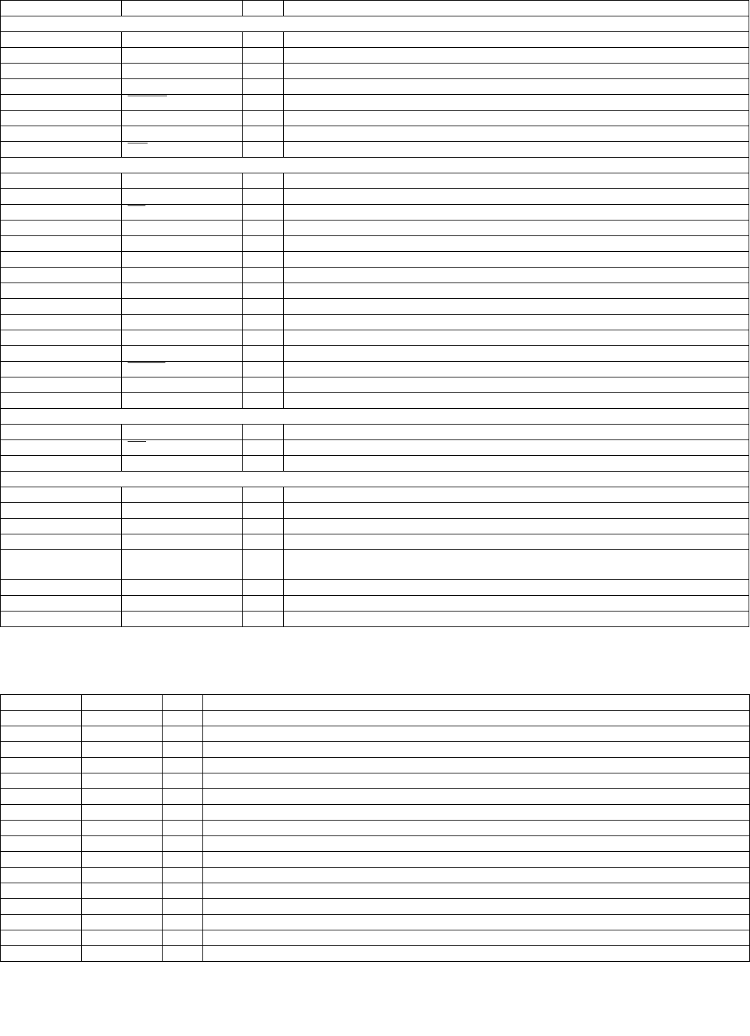
LC-42XL2E/S/RU, LC-46XL2E/S/RU, LC-46X20E/S/RU, LC-52XL2E/S/RU, LC-52X20E/S/RU
5 – 22
2.12.2 Pin Connections and short description
2.13. IC7603 (9NK2633003842)
2.13.1 Pin Connections and short description
Pin No. Pin Name I/O Pin Function
MPEG pins
47 MOSTRT O MPEG packet start
48 MOVAL O MPEG data valid
49-53, 56-58 MDO[0:4]/ MDO[5:7] O MPEG data bus
61 MOCLK O MPEG clock out
62 BKERR OBlock error
63 MICLK I MPEG clock in
11 STATUS O Status output
6IRQ
O Interrupt output
Control pins
4 CLK1 I Serial clock
5 DATA1 I/O Serial data
23 XTI I Low phase noise oscillator
24 XTO O
10 SLEEP I Device power down
12, 15-18 SADD[4:0] I Serial address set
44 SMTEST I Production test (only set low)
35 CLK2/GPP0 I/O Serial clock tuner
36 DATA2/GPP1 I/O Serial data tuner
42 AGC1 O Primary AGC
41 AGC2/GPP2 I/O Secondary AGC
43 GPP3 I/O General purpose I/O
9 RESET IDevice reset
27 OSCMODE I Crystal oscillator mode
26 PLLTEST O PLL analog test
Analog inputs
30 VIN I positive input
31 VIN I negative input
34 RFLEV I RF level
Supply pins
21 PLLVdd — PLL supply
22 PLLGND — GND
7, 19, 37, 39, 59, 64 CVdd — Core logic power
2, 13, 45, 54 Vdd — I/O ring power
1, 3, 8, 14, 20, 25, 38,
40, 46, 55, 60
Vss — Core and I/O ground
28 Avdd — ADC analog supply
29, 32 AGnd — GND
33 Vdd — 2nd ADC supply
Pin No. Pin Name I/O Pin Function
1 Css I Soft start timing capacitor.
2 Rfstart — Soft start frequency setting-low impedance voltage source-see also Cf.
3 Cf — Oscillator frequency setting-see also Rfmin, Rfstart.
4 Rfmin I Minimum oscillation frequency setting-low impedance voltage source-see also Cf.
5 OPOUT O Sense OP Amp output-low impedance.
6 OPIN- I Sense OP Amp inverting input-high impedance.
7 OPIN+ I Sense OP Amp non inverting input-high impedance.
8 EN1 I Half bridge latched enable.
9 EN2 I Half bridge unlatched enable.
10 GND — Ground.
11 LVG O Low side driver output.
12 Vss — Supply voltage with internal zener clamp.
13 N.C. — Not connected.
14 OUT O High side driver reference.
15 HVG O High side driver output.
16 VBOOT I Bootstrapped supply voltage.
LC-42XL2E/S/RU, LC-46XL2E/S/RU, LC-46X20E/S/RU, LC-52XL2E/S/RU, LC-52X20E/S/RU
5 – 23
2.14. IC7801 (9NK2510067610)
2.14.1 Pin Connections and short description
2.15. IC7905 (9NK2510293234)
2.15.1 Pin Connections and short description
Pin No. Pin Name I/O Pin Function
1 INV I Inverting input of the error amplifier. The information on the output voltage of the PFC preregulator is fed
into the pin through a resistor divider.
2 COMP O Output of the error amplifier. A compensation network is placed between this pin and INV (pin #1) to
achieve stability of the voltage control loop and ensure high power factor and low THD.
3 MULT I Main input to the multiplier. This pin is connected to the rectified mains voltage via a resistor divider and
provides the sinusoidal reference to the current loop.
4 CS I Input to the PWM comparator. The current flowing in the MOSFET is sensed through a resistor, the result-
ing voltage is applied to this pin and compared with an internal sinusoidal-shaped reference, generated by
the multiplier, to determine MOSFET’s turn-off.
5 ZCD I Boost inductor’s demagnetization sensing input for transition-mode operation. A negative-going edge trig-
gers MOSFET’s turn-on.
6 GND — Ground. Current return for both the signal part of the IC and the gate driver.
7 GD O Gate driver output. The totem pole output stage is able to drive power MOSFET’s and IGBT’s with a peak
current of 600 mA source and 800 mA sink. The high-level voltage of this pin is clamped at about 12V to
avoid excessive gate voltages in case the pin is supplied with a high Vcc.
8 VCC — Supply Voltage of both the signal part of the IC and the gate driver. The supply voltage upper limit is
extended to 22V min. to provide more headroom for supply voltage changes.
Pin No. Pin Name Pin Function
5 DRAIN (D) Pin: Power MOSFET drain connection. Provides internal operating current for both start-up
and steady-state operation.
1 BYPASS (BP) Pin: Connection point for a 0.1 µF external bypass capacitor for the internally generated 5.8
V supply.
4 ENABLE/UNDER-VOLTAGE (EN/UV)
Pin:
This pin has dual functions: enable input and line under-voltage sense. During normal
operation, switching of the power MOSFET is controlled by this pin. MOSFET switch-
ing is terminated when a current greater than 240 µA is drawn from this pin. This pin
also senses line under-voltage conditions through an external resistor connected to the
DC line voltage. If there is no external resistor connected to this pin, TinySwitch-II
detects its absence and disables the line undervoltage function.
2,3 SOURCE (S) Pin: Control circuit common, internally connected to output MOSFET source.

LC-42XL2E/S/RU, LC-46XL2E/S/RU, LC-46X20E/S/RU, LC-52XL2E/S/RU, LC-52X20E/S/RU
5 – 24
2.16. IC8101 (RH-iXC011WJQZQ)
2.16.1 Pin Connections and short description
Ref No. Pin Name I/O Pin Function
DAC Interface
AD2 VDDZ_DAC — Digital power for DAC (+3.3V).
AD3 VSSZ_DAC — Digital ground for DAC.
AD1 DAC_VS I/O DAC vsync.
AE1 DAC_HS I/O DAC hsync.
AE2 DAC_CLK I/O DAC clock
AE4 DAC_DE I/O DAC DE
AE3 DAC_FLD I/O DAC field.
AA5 AVSS51 — Analog ground for DAC (for bias circuit).
AB5 COMP — Bias for DAC coupling capacitor.
AB4 IRSET I Bias for DAC current source.
AB3 CVBS_B I DAC blue or PB (Not used).
AB2 ADVSS2 — Analog ground for DAC (for DAC’s AVSS52).
AB1 ADVDD2 — Analog power for DAC (+3.3V).
AC1 C_G I DAC green or Y (Not used).
AC2 AVSS50 — Digital ground for DAC.
AC3 AVDD50 — Analog power for DAC (+3.3V).
AC4 Y_R I DAC red or PR (Not used).
AC5 ADVSS2 — Analog ground for DAC (for DAC’s AVSS52).
AD5 ADVDD2 — Analog power for DAC (+3.3V).
AD4 VM I DAC VM
ADC Interface
N2 AVDD — ADC power +3.3V.
N3 VIN1 I VRADC INPUT1 (Not used)
N4 VIN2 I VRADC INPUT2 (Not used)
N5 AVSS — ADC ground.
USB Interface
R3 USB_PPON_PP O USB Power on control.
R2 USB_OC_PP I USB over current control.
P5 VDDA — Analog core +3.3V supply.
P4 DN O Negative output channel.
P3 DP O Positive output control.
P2 VSSA — Analog core ground.
P1 RREFEXT — External resistor connection for current reference.
R5 VSSP — PLL ground pin Double Bond.
R4 VDDP — PLL +1.2V supply Double Bond.
LVDS Interface
AJ5 LVDS_VSSP — LVDS PLL Ground.
AJ3 LVDS_VDDP — LVDS PLL Power supply (+3.3V).
AK5 LVDS_VSSO — LVDS Output buffer VSS (Long pad)
AK4 LVDS_VDDO — LVDS Output buffer VDD (+3.3V).
AK1 TF2P O LVDS Positive Output. (Not used)
AK2 TF2M O LVDS Negative Output. (Not used)
AL1 TE2P O LVDS Positive Output. (Not used)
AL2 TE2M O LVDS Negative Output. (Not used)
AM1 TD2P O LVDS Positive Output. (Not used)
AM2 TD2M O LVDS Negative Output. (Not used)
AN1 TCLK2P O LVDS Positive clock Output. (Not used)
AN2 TCLK2M O LVDS Negative clock Output. (Not used)
AP1 TC2P O LVDS Positive Output. (Not used)
AP2 TC2M O LVDS Negative Output. (Not used)
AM4 LVDS_VDDO — LVDS Output buffer VDD (+3.3V).
AP3 TB2P O LVDS Positive Output. (Not used)
AN3 TB2M O LVDS Negative Output. (Not used)
AP4 TA2P O LVDS Positive Output. (Not used)
AN4 TA2M O LVDS Negative Output. (Not used)
AJ6 LVDS_VSSO — LVDS Output buffer VSS.
AP5 TF1P O LVDS Positive Output. (Not used)
AN5 TF1M O LVDS Negative Output. (Not used)
AP6 TE1P O LVDS Positive Output. (Not used)
AN6 TE1M O LVDS Negative Output. (Not used)

LC-42XL2E/S/RU, LC-46XL2E/S/RU, LC-46X20E/S/RU, LC-52XL2E/S/RU, LC-52X20E/S/RU
5 – 25
AP7 TD1P O LVDS Positive Output. (Not used)
AN7 TD1M O LVDS Negative Output. (Not used)
AP8 TCLK1P O LVDS Positive clock Output. (Not used)
AN8 TCLK1M O LVDS Negative clock Output. (Not used)
AP9 TC1P O LVDS Positive Output. (Not used)
AN9 TC1M O LVDS Negative Output. (Not used)
AJ4 LVDS_VDDO — LVDS Output buffer VDD (+3.3V).
AP10 TB1P O LVDS Positive Output. (Not used)
AN10 TB1M O LVDS Negative Output. (Not used)
AP11 TA1P O LVDS Positive Output. (Not used)
AN11 TA1M O LVDS Negative Output. (Not used)
AL5 LVDS_VSSO — LVDS Output buffer VSS.
AM5 LVDS_VDDO — LVDS Output buffer VDD (+3.3V).
AL3 LVDS_VSSA — LVDS Analog VSS.
AL4 LVDS_VDDA — LVDS Analog VDD (+3.3V).
AK3 LVDS_VSSD — LVDS Digital VSS.
AM3 LVDS_VDDD — LVDS Digital VDD (+3.3V).
PLL Interface
B7 DVSS22 — PLL ground related to DVDD22; supply for VCO circuit.
A7 DVDD22 — PLL power= 1.2V; supply for VCO circuit.
A6 DVSS21 — PLL ground related to DVDD21; supply for digital circuit.
B6 DVDD21 — PLL power= 1.2V; supply for digital circuit.
C6 AVSS7 — PLL ground related to AVDD7.
D6 MCLK2LF — Low pass filter for MCLK2PLL.
E6 AVDD7 — PLL analog power= 3.3V; supply for MCLK2PLL.
D5 AVSS6 — PLL ground related to AVSS6.
C5 MPEGCLK2LF — Low pass filter for MPEGCLK2PLL.
B5 AVDD6 — PLL analog power= 3.3V; supply for MPEGCLK2PLL.
A5 AVSS5 — PLL ground related to AVSS5.
A4 MPEGCLK1LF — Low pass filter for MPEGCLK1PLL.
B4 AVDD5 — PLL analog power= 3.3V; supply for MPEGCLK1PLL.
C4 AVSS2 — PLL ground related to AVSS2.
D4 PLF — Low pass filter for PCLKPLL.
C3 AVDD2 — PLL analog power= 3.3V; supply for PCLKPLL.
B3 AVSS1 — PLL ground related to AVSS1.
A3 MLF — Low pass filter for MCLKPLL.
A2 AVDD1 — PLL analog power= 3.3V; supply for MCLKPLL.
B2 AVSS4 — PLL ground related to AVSS4.
A1 IDELF — Low pass filter for IDECLKPLL.
B1 AVDD4 — PLL analog power= 3.3V; supply for IDECLKPLL.
C1 AVDD3 — PLL analog power= 3.3V; supply for CK48MPLL.
C2 CK48MLF — Low pass filter for CK48MPLL.
D3 AVSS3 — PLL ground related to AVSS3.
D2 XTLI — 24MHz_PLL crystal input.
D1 XTLO — 24MHz_PLL crystal output.
E1 DVSS12 — PLL ground related to DVDD12; supply for VCO circuit.
E2 DVDD12 — PLL power= 1.2V; supply for VCO circuit.
E3 DVSS11 — PLL ground related to DVDD11; supply for digital circuit.
E4 DVDD11 — PLL power= 1.2V; supply for digital circuit.
FLASH Interface
E25 AD30_FRA14 I/O Flash address 14/PCI AD bus bit 30.
D24 AD28_FRA12 I/O Flash address 12/PCI AD bus bit 28.
E24 AD26_FRA10 I/O Flash address 10/PCI AD bus bit 26.
A23 AD29_FRA13 I/O Flash address 13/PCI AD bus bit 29.
B23 AD31_FRA15 I/O Flash address 15/PCI AD bus bit 31.
D23 AD24_FRA8 I/O Flash address 8/PCI AD bus bit 24.
E23 AD22_FRA6 I/O Flash address 6/PCI AD bus bit 22.
A22 CBE3#_FRA19 I/O Flash address 19/PCI CBE#[3].
B22 AD25_FRA9 I/O Flash address 9/PCI AD bus bit 25.
C22 AD27_FRA11 I/O Flash address 11/PCI AD bus bit 27.
D22 AD20_FRA4 O Flash address 4/PCI AD bus bit 20/POD host interface Card access register selec-
tion.
E22 AD18_FRA2 O Flash address 2/PCI AD bus bit 18/POD host interface Card I/O output enable.
A21 AD19_FRA3 O Flash address 3/PCI AD bus bit 19/POD host interface Card I/O Write enable.
B21 AD21_FRA5 O Flash address 5/PCI AD bus bit 21.
Ref No. Pin Name I/O Pin Function

LC-42XL2E/S/RU, LC-46XL2E/S/RU, LC-46X20E/S/RU, LC-52XL2E/S/RU, LC-52X20E/S/RU
5 – 26
C21 AD23_FRA7 O Flash address 7/PCI AD bus bit 23.
D21 AD16_FRA0 O Flash address 0/PCI AD bus bit 16/POD host interface Card I/O output enable.
A20 IRDY_PCAS I/O PCI bus IRDY# signal/M68K CPU interface address strobe signal.
B20 CBE2#_FRA18 O Flash address 18/PCI CBE#[2].
C20 AD17_FRA1 O Flash address 1/PCI AD bus bit 17/POD host interface Card I/O Write enable.
A19 CBE1#_FRA17 O Flash address 17/PCI CBE#[1].
E19 AD15_FRD15 I/O Flash Data bus bit 15/PCI AD bus bit 15.
A18 AD7_FRD7 I/O Flash Data bus 7/PCI AD bus bit 7.
B18 AD10_FRD10 I/O Flash Data bus bit 10/PCI AD bus bit 10/POD host interface address bit 2.
C18 AD12_FRD12 I/O Flash Data bus bit 12/PCI AD bus bit 12/POD host interface address bit 10.
D18 AD13_FRD13 I/O Flash Data bus bit 13/PCI AD bus bit 13/POD host interface address bit 13.
E18 AD11_FRD11 I/O Flash Data bus bit 11/PCI AD bus bit 11/POD host interface address bit 3.
A17 AD8_FRD8 I/O Flash Data bus bit 8/PCI AD bus bit 8/POD host interface address bit 0.
B17 AD14_FRD14 I/O Flash Data bus bit 14/PCI AD bus bit 14/POD host interface address bit 12.
C17 AD9_FRD9 I/O Flash Data bus bit 9/PCI AD bus bit 9/POD host interface address bit 1.
D17 AD6_FRD6 I/O Flash Data bus bit 6/PCI AD bus bit 6/POD host interface Data bus bit 6.
E17 CBE0#_FRA16 O Flash address 16/PCI CBE#[0].
A16 AD5_FRD5 O Flash Data bus bit 5/PCI AD bus bit 5/POD host interface Data bus bit 5.
B16 AD1_FRD1 I/O Flash Data bus bit 1/PCI AD bus bit 1/POD host interface Data bus bit 1.
C16 AD3_FRD3 I/O Flash Data bus bit 3/PCI AD bus bit 3/POD host interface Data bus bit 3.
D16 AD2_FRD2 I/O Flash Data bus bit 2/PCI AD bus bit 2/POD host interface Data bus bit 2.
E16 AD4_FRD4 I/O Flash Data bus bit 4/PCI AD bus bit 4/POD host interface Data bus bit 4.
E15 AD0_FRD0 I/O Flash Data bus bit 0/PCI AD bus bit 0/POD host interface Data bus bit 0.
D15 FRA25 I/O Flash address bit 25.
C15 FRA24 I/O Flash address bit 24.
B15 FRA23 I/O Flash address bit 23.
A15 FRA22 I/O Flash address bit 22.
A14 FRA21 I/O Flash address bit 21.
B14 FRA20 I/O Flash address bit 20.
C14 GCS3 I/O Flash chip select (0:Active).
D14 GCS2 I/O Flash chip select (0:Active).
E14 GCS1 I/O Flash chip select (0:Active).
E13 GCS0 I/O Flash chip select (0:Active).
D13 BOOTCS O EPPROM chip select (0:Active).
C13 FWE# O Write enable signal of Flash Rom.
B13 FOE# O Read enable signal of Flash Rom.
A13 NAND_CE# O Chip select signal of NAND Flash Rom.
A12 NAND_RDY I Ready signal of NAND Flash Rom.
PCI Interface
A27 INTA I PCI interrupt A.
C25 INTB I PCI interrupt B.
B27 INTC I PCI interrupt C.
B25 INTD I PCI interrupt D.
D27 GNT0 O PCI gnt signal. (Not used)
D26 GNT1 O PCI gnt signal. (Not used)
E26 GNT2 O PCI gnt signal. (Not used)
D25 GNT3 O PCI gnt signal. (Not used)
C27 PCIRST# O PCIRSTN/68K clock output.
A25 PCICLK O PCI clock.
C24 REQ0 I PCI req signal.
B24 REQ1 I PCI req signal.
A24 REQ2 I PCI req signal.
C23 REQ3 I PCI req signal.
E21 FRAME#_SIZI I/O PCI bus FRAME# signal/68K Transfer size bit 1. (analog with Transfer size bit 0 to
indicate the number byte to be transferred during a bus cycle M68K CPU bus.)
A20 IRDY_PCAS I/O PCI bus IRDY# signal/68K address strobe signal.
B20 CBE2#_FRA18 I/O PCI bus CBE#[2]/Flash address bit 18.
D20 TRDY#_SIZ0 I/O PCI bus TRDY# signal/68K Transfer size bit 0.
B19 SEPR#_DSACK1 I/O PCI bus SERR# signal/68K Data and Size acknowledge signal bit 1.
C19 DVSEL_PCDS I/O PCI bus DEVSEL# signal/68K Data Strobe signal.
D19 PAR_DSACK0 I/O PCI bus PAR signal/68K Data and Size acknowledge signal bit 0.
E20 STOP#_PCRW I/O Flash, 3.3V CMOS IF, 16mA output pad.
POD Interface
B12 POD_ITX I POD OOB TXI Channel.
C12 POD_WAIT I POD WAIT# signal to expand bus cycle.
Ref No. Pin Name I/O Pin Function

LC-42XL2E/S/RU, LC-46XL2E/S/RU, LC-46X20E/S/RU, LC-52XL2E/S/RU, LC-52X20E/S/RU
5 – 27
D12 POD_CE1 O Card enable.
E12 POD_CTX O POD OOB TX Gapped Symbol clock.
A11 POD_DRX O POD OOB RX data.
B11 POD_CD1 I Card Detect.
C11 POD_IREQ I Ready/IRQ
D11 POD_CRX O POD OOB RX Gapped clock.
E11 POD_RESET O POD Card reset signal.
A10 POD_QTX I POD OOB TX Q Channel.
B10 POD_VS1 I Card voltage Sense.
C10 POD_ETX I POD OOB TX enable.
D10 POD_CD2 I Card Detect.
E10 POD_CE2 O Card enable.
A9 POD_VPP_EN O Slot VPP enable.
B9 POD_OVERLOAD I Current overload detect.
C9 POD_VPP_EN# O Slot VPP enable.
D9 POD_VCC_EN# O Slot VCC enable.
E9 POD_VCC_EN O Slot VCC enable.
A8 POD_A9 O POD Host interface address bit 9.
B8 POD_A8 O POD Host interface address bit 8.
C8 POD_A7 I/O POD Host interface address bit 7.
D8 POD_A6 I/O POD Host interface address bit 6.
D7 POD_A5 I/O POD Host interface address bit 5.
C7 POD_A4 O POD Host interface address bit 4.
VDA Interface
AP13, AN13, AM13, AL13,
AK13, AP14, AN14, AM14,
AL14, AK14
VDA_R[9:0] I Video input, R channel. (Not used)
AP15, AN15, AM15, AL15,
AK15, AM16, AL16, AK16,
AP17, AN17
VDA_B[9:0] I Video input, B channel. (Not used)
AM17, AL17, AK17, AP18,
AN18, AM18, AL18, AK18,
AP19, AN19
VDA_G[9:0] I Video input, G channel. (Not used)
AP16 VDA_CLK I Video input, Clock. (Not used)
AM19 VDA_VS I Video input, Vertical sync. (Not used)
AL19 VDA_HS I Video input, Horizontal sync. (Not used)
AK19 VDA_DE I Video input, Data enable. (Not used)
VDB Interface, EJTAG, IDE and POD2 share with VDB
AK20 VDB_DE I/O Video input/output; data enable;
IDE: IDE bus interrupt.
EJTAG: NOP
POD2: POD_CE2B#, the second POD Card enable.
AL20 VDB_HS I/O Video input/output; Horizontal sync;
IDE: PDLAGCBLID, Passed diagnostics, cable assembly type identifier.
EJTAG: TDI2, TDI EJTAG input of slave CPU.
POD2: POD_A_B5, the second POD host interface address bit 5.
AM20 VDB_VS I/O Video input/output; Vertical sync;
IDE: DMAREQ, IDE bus DMA request.
EJTAG: NOP
POD2: POD_A_B4, the second POD host interface address bit 4.
AN20 VDB_G0 I/O Video input/output; Green channel bit 0;
IDE: IDE data bus bit 0.
EJTAG: TDO2, TDO EJTAG input of slave CPU CPU.
POD2: POD_A_B6, the second POD host interface address bit 6.
AP20 VDB_G1 I/O Video input/output; Green channel bit 1;
IDE: IDE data bus bit 1.
EJTAG: TMS2, TMS EJTAG input of slave CPU CPU.
POD2: POD_A_B7, the second POD host interface address bit 7.
AK21 VDB_G2 I/O Video input/output; Green channel bit 2;
IDE: IDE data bus bit 2.
EJTAG: TCK2, TCK EJTAG input of slave CPU CPU.
POD2: POD_A_B8, the second POD host interface address bit 8.
AL21 VDB_G3 I/O Video input/output; Green channel bit 3;
IDE: IDE data bus bit 3.
EJTAG: DCLK EJTAG output of both CPU CPUs.
POD2: POD_A_B8, the second POD host interface address bit 9.
Ref No. Pin Name I/O Pin Function

LC-42XL2E/S/RU, LC-46XL2E/S/RU, LC-46X20E/S/RU, LC-52XL2E/S/RU, LC-52X20E/S/RU
5 – 28
AM21 VDB_G4 I/O Video input/output; Green channel bit 4;
IDE: IDE data bus bit 4.
EJTAG: TPC[0], output as EJTAG PC Trace bus, bit 0.
POD2: POD_CD2B#, the second POD interface card detect.
AN21 VDB_G5 I/O Video input/output; Green channel bit 5;
IDE: IDE data bus bit 5.
EJTAG: TPC[1], output as EJTAG PC Trace bus, bit 1.
POD2: POD_CD1B#, the second POD interface card detect.
AP21 VDB_G6 I/O Video input/output; Green channel bit 6;
IDE: IDE data bus bit 6.
EJTAG: TPC[2], output as EJTAG PC Trace bus, bit 2.
POD2: POD_RSTB, the second POD host interface reset.
AK22 VDB_G7 I/O Video input/output; Green channel bit 7;
IDE: IDE data bus bit 7.
EJTAG: TPC[3], output as EJTAG PC Trace bus, bit 3.
POD3: POD_A_B14, the second POD host interface address bit 14.
AL22 VDB_G8 I/O Video input/output; Green channel bit 8;
IDE: IDE data bus bit 8.
EJTAG: TPC[4], output as EJTAG PC Trace bus, bit 4.
POD3: POD2_TS2_D0, the second POD_TS2 data[0].
AM22 VDB_G9 I/O Video input/output; Green channel bit 9;
IDE: IDE data bus bit 9.
EJTAG: TPC[5], output as EJTAG PC Trace bus, bit 5.
POD3: POD2_TS2_D2, the second POD_TS2 data[1].
AN22 VDB_B0 I/O Video input/output; Blue channel bit 0;
IDE: IDE data bus bit 10.
EJTAG: TPC[6], output as EJTAG PC Trace bus, bit 6.
POD3: POD2_TS2_D2, the second POD_TS2 data[2].
AP22 VDB_B1 I/O Video input/output; Blue channel bit 1;
IDE: IDE data bus bit 11.
EJTAG: TPC[7], output as EJTAG PC Trace bus, bit 7.
POD3: POD2_TS2_D3, the second POD_TS2 data[3].
AK23 VDB_B2 I/O Video input/output; Blue channel bit 2;
IDE: IDE data bus bit 12.
EJTAG: PCST[0], output as EJTAG PC Trace bus, bit 0.
POD3: POD2_TS2_D4, the second POD_TS2 data[4].
AL23 VDB_B3 I/O Video input/output; Blue channel bit 3;
IDE: IDE data bus bit 13.
EJTAG: PCST[1], output as EJTAG PC Trace bus, bit 1.
POD3: POD2_TS2_D5, the second POD_TS2 data[5].
AM23 VDB_B4 I/O Video input/output; Blue channel bit 4;
IDE: IDE data bus bit 14.
EJTAG: PCST[2], output as EJTAG PC Trace bus, bit 2.
POD3: POD2_TS2_D6, the second POD_TS2 data[6].
AP23 VDB_CLK I/O Video input/output; Clock;
IDE: IDE data bus IO access complete.
EJTAG: NOP
POD3: POD_CE1B#, the second POD interface card enable.
AK24 VDB_B5 I/O Video input/output; Blue channel bit 5;
IDE: IDE data bus bit 15.
EJTAG: PCST[3], output as EJTAG PC Trace bus, bit 3.
POD3: POD2_TS2_D7, the second POD_TS2 data[7].
AL24 VDB_B6 I/O Video input/output; Blue channel bit 6;
IDE: Chip Select 0 for IDE interface.
EJTAG: PCST[4], output as EJTAG PC Trace bus, bit 4.
POD3: POD2_TS2_DEN, the second POD_TS2 data valid.
AM24 VDB_B7 I/O Video input/output; Blue channel bit 7;
IDE: Chip Select 1 for IDE interface.
EJTAG: PCST[5], output as EJTAG PC Trace bus, bit 5.
POD2: POD2_TS2_CLK, the second POD_TS2 clock.
AN24 VDB_B8 I/O Video input/output; Blue channel bit 8;
IDE: IDE address bus bit 0.
EJTAG: PCST[6], output as EJTAG PC Trace bus, bit 6.
POD2: POD2_TS2_SYNC, the second POD_TS2 SYNC.
AP24 VDB_B9 I/O Video input/output; Blue channel bit 9;
IDE: IDE address bus bit 1.
EJTAG: PCST[7], output as EJTAG PC Trace bus, bit 7.
POD2: POD2_TS1_D0, the second POD_TS1 data[0].
Ref No. Pin Name I/O Pin Function

LC-42XL2E/S/RU, LC-46XL2E/S/RU, LC-46X20E/S/RU, LC-52XL2E/S/RU, LC-52X20E/S/RU
5 – 29
AK25 VDB_R0 I/O Video input/output; Red channel bit 0;
IDE: IDE address bus bit 2.
EJTAG: PCST[8], output as EJTAG PC Trace bus, bit 8.
POD2: POD2_TS1_D1, the second POD_TS1 data[1].
AL25 VDB_R1 I/O Video input/output; Red channel bit 1;
IDE: IDE bus DMA acknowledge.
EJTAG: PCST[9], output as EJTAG PC Trace bus, bit 9.
POD2: POD2_TS1_D2, the second POD_TS1 data[2].
AM25 VDB_R2 I/O Video input/output; Red channel bit 2;
IDE: IDE bus IO Read Strobe signal.
EJTAG: PCST[10], output as EJTAG PC Trace bus, bit 10.
POD2: POD2_TS1_D3, the second POD_TS1 data[3].
AN25 VDB_R3 I/O Video input/output; Red channel bit 3;
IDE: IDE bus IO Write Strobe signal.
EJTAG: PCST[11], output as EJTAG PC Trace bus, bit 11.
POD2: POD2_TS1_D4, the second POD_TS1 data[4].
AP25 VDB_R4 I/O Video input/output; Red channel bit 4;
IDE: NOP
EJTAG:
S1=0, select DCLK/TPC[7:0]/PCST[11:0] of host CPU as output.
S1=1, select DCLK/TPC[7:0]/PCST[11:0] of slave CPU as output.
POD2: POD2_TS1_D5, the second POD_TS1 data[5].
AK26 VDB_R5 I/O Video input/output; Red channel bit 5;
IDE: NOP
EJTAG:
S1=0, two EJTAG are separately used.
S1=1, two EJTAG are used in a daisy chain style.
POD2: POD2_TS1_D6, the second POD_TS1 data[6].
AL26 VDB_R6 I/O Video input/output; Red channel bit 6;
IDE: NOP
EJTAG: TDI1, TDI EJTAG input of host CPU CPU.
POD2: POD2_TS1_D7, the second POD_TS1 data[7].
AM26 VDB_R7 I/O Video input/output; Red channel bit 7;
IDE: NOP
EJTAG: TDO1, TDO EJTAG input of host CPU CPU.
POD2: POD2_TS1_DEN, the second POD_TS1 data valid.
AN26 VDB_R8 I/O Video input/output; Red channel bit 8;
IDE: NOP
EJTAG: TMS1, TMS EJTAG input of host CPU CPU.
POD2: POD2_TS1_CLK, the second POD_TS1 clock.
AP26 VDB_R9 I/O Video input/output; Red channel bit 9;
IDE: NOP
EJTAG: TCK1, TCK EJTAG input of host CPU CPU.
POD2: POD2_TS1_SYNC, the second POD_TS1 SYNC.
IEEE1394 Interface, 8051 and 656 share with 1394
AM7, AL7, AK7, AK8, AL8,
AM8, AK9, AL9
HSD[7:0] I/O 1394: Parallel data.
Video 656 port; 656D[9:2], data[9:2]
8051: AD[7:0], AD bus.
AM9 HSDCLK I/O 1394: clock.
Video 656 port; 656CLK, clock.
8051: RD, ALE, address latch enable.
AM10 HSDRW I/O 1394: Not used.
Video 656 port; 656CHS, horizontal sync.
8051: RD, read signal, low active.
AL10 HSDSYNC I/O 1394: Packet synchronization.
Video 656 port; 656VS, vertical sync.
8051: WR, write signal, low active.
AK10 HSDAV I/O 1394: Not used.
Video 656 port; data[1].
8051: NOP
AM11 HSDEN I/O 1394: Data valid.
Video 656 port; data[0].
8051: CS, chip select.
Transport Stream Interface
G4, G5, F1, F2, F3, F4, F5,
E5
TS2_D[7:0] I Transport Stream 2, data bus.
G3 TS2_DEN I Transport Stream 2, data enable.
G2 TS2_SYNC I Transport Stream 2, sync signal.
G1 TS2_CLK I Transport Stream 2, clock.
Ref No. Pin Name I/O Pin Function

LC-42XL2E/S/RU, LC-46XL2E/S/RU, LC-46X20E/S/RU, LC-52XL2E/S/RU, LC-52X20E/S/RU
5 – 30
J3, J2, J1, H1, H2, H3, H4,
H5
TS1_D[7:0] I Transport Stream 1, data bus.
J4 TS1_DEN I Transport Stream 1, data enable.
J5 TS1_SYNC I Transport Stream 1, sync signal.
K1 TS1_CLK I Transport Stream 1, clock.
Memory Interface
AM30 DRVIMP I Driving strength impedance match reference pin.
AP29 MD0 I/O Memory data bus.
AP30 MD1 I/O Memory data bus.
AN30 MD2 I/O Memory data bus.
AN31 MD3 I/O Memory data bus.
AM33 DQM0 O Memory data write mask enable for byte 0.
AM32 DQS0 I/O Data strobe for memory data bus MD[7:0].
AL32 DQS0N I/O Data strobe for memory data bus MD[7:0].
AK30 MD4 I/O Memory data bus.
AK31 MD5 I/O Memory data bus.
AJ29 MD6 I/O Memory data bus.
AJ30 MD7 I/O Memory data bus.
AP32 MD8 I/O Memory data bus.
AP33 MD9 I/O Memory data bus.
AN33 MD10 I/O Memory data bus.
AN34 MD11 I/O Memory data bus.
AM34 DQM1 O Memory data write mask enable for byte 1.
AL33 DQS1 I/O Data strobe for memory data bus MD[15:8].
AL34 DQS1N I/O Data strobe for memory data bus MD[15:8].
AK33 MD12 I/O Memory data bus.
AK34 MD13 I/O Memory data bus.
AJ32 MD14 I/O Memory data bus.
AJ33 MD15 I/O Memory data bus.
AH33 MCLK0 O Memory clock for MD[31:0].
AH34 MCLK0N O Memory clock for MD[31:0] - active LOW.
AG29 MD16 I/O Memory data bus.
AG30 MD17 I/O Memory data bus.
AF30 MD18 I/O Memory data bus.
AF31 MD19 I/O Memory data bus.
AE33 DQM2 O Memory data write mask enable for byte 2.
AE32 DQS2 I/O Data strobe for memory data bus MD[23:16].
AD32 DQS2N I/O Data strobe for memory data bus MD[23:16].
AC30 MD20 I/O Memory data bus.
AC31 MD21 I/O Memory data bus.
AB29 MD22 I/O Memory data bus.
AB30 MD23 I/O Memory data bus.
AG32 MD24 I/O Memory data bus.
AG33 MD25 I/O Memory data bus.
AF33 MD26 I/O Memory data bus.
AF34 MD27 I/O Memory data bus.
AE34 DQM3 O Memory data write mask enable for byte 3.
AD33 DQS3 I/O Data strobe for memory data bus MD[31:24].
AD34 DQS3N I/O Data strobe for memory data bus MD[31:24].
AC33 MD28 I/O Memory data bus.
AC34 MD29 I/O Memory data bus.
AB32 MD30 I/O Memory data bus.
AB33 MD31 I/O Memory data bus.
Y33 ODT O ODT
W34 CAS O Column Access Strobe of Port A or SCAN data input.
W33 RAS O Row Access Strobe of Port A or SCAN data input.
W31 WE O Write Enable of Port A or SCAN data input.
W30 CKE O Clock enable.
V34 CS0 O Chip select for Ext Mem.
Y32 CS1 O Chip select for Ext Mem.
U33 MAA10 O Memory Address line of Port A or SCAN data input.
U32 BA1 O Internal Bank Address Select for SDRAM.
U30 BA0 O Internal Bank Address Select for SDRAM.
T34 MAA0 O Memory Address line of Port A or SCAN data output.
T31 MAA1 O Memory Address line of Port A or SCAN data output.
Ref No. Pin Name I/O Pin Function

LC-42XL2E/S/RU, LC-46XL2E/S/RU, LC-46X20E/S/RU, LC-52XL2E/S/RU, LC-52X20E/S/RU
5 – 31
T33 MAA2 O Memory Address line of Port A or SCAN data output.
T30 MAA3 O Memory Address line of Port A or SCAN data output.
R32 MAA4 O Memory Address line of Port A or SCAN data output.
R30 MAA5 O Memory Address line of Port A or SCAN data output.
R33 MAA6 O Memory Address line of Port A or SCAN data output.
R29 MAA7 O Memory Address line of Port A or SCAN data output.
P34 MAA11 O Memory Address line of Port A or SCAN data output.
P33 MAA8 O Memory Address line of Port A or SCAN data output.
P30 MAA9 O Memory Address line of Port A or SCAN data output.
N29 MD32 I/O Memory data bus.
N30 MD33 I/O Memory data bus.
M30 MD34 I/O Memory data bus.
M31 MD35 I/O Memory data bus.
L33 DQM4 O Memory data write mask enable for byte 4.
L32 DQS4 I/O Data strobe for memory data bus MD[39:32].
K32 DQS4N I/O Data strobe for memory data bus MD[39:32].
J30 MD36 I/O Memory data bus.
J31 MD37 I/O Memory data bus.
H29 MD38 I/O Memory data bus.
H30 MD39 I/O Memory data bus.
N32 MD40 I/O Memory data bus.
N33 MD41 I/O Memory data bus.
M33 MD42 I/O Memory data bus.
M34 MD43 I/O Memory data bus.
L34 DQM5 O Memory data write mask enable for byte 5.
K33 DQS5 I/O Data strobe for memory data bus MD[47:40].
K34 DQS5N I/O Data strobe for memory data bus MD[47:40].
J33 MD44 I/O Memory data bus.
J34 MD45 I/O Memory data bus.
H32 MD46 I/O Memory data bus.
H33 MD47 I/O Memory data bus.
G33 MCLK1 O Memory clock for MD[63:32].
G34 MCLK1N O Memory clock for MD[63:32] - active LOW.
F29 MD48 I/O Memory data bus.
F30 MD49 I/O Memory data bus.
E30 MD50 I/O Memory data bus.
E31 MD51 I/O Memory data bus.
D33 DQM6 O Memory data write mask enable for byte 6.
D32 DQS6 I/O Data strobe for memory data bus MD[55:48].
C32 DQS6N I/O Data strobe for memory data bus MD[55:48].
B30 MD52 I/O Memory data bus.
B31 MD53 I/O Memory data bus.
A29 MD54 I/O Memory data bus.
A30 MD55 I/O Memory data bus.
F32 MD56 I/O Memory data bus.
F33 MD57 I/O Memory data bus.
E33 MD58 I/O Memory data bus.
E34 MD59 I/O Memory data bus.
D34 DQM7 O Memory data write mask enable for byte 7.
C33 DQS7 I/O Data strobe for memory data bus MD[63:56].
C34 DQS7N I/O Data strobe for memory data bus MD[63:56].
B33 MD60 I/O Memory data bus.
B34 MD61 I/O Memory data bus.
A32 MD62 I/O Memory data bus.
A33 MD63 I/O Memory data bus.
CPU Interface
B26 MASTSEL I Lexra bus master select, H:I2C, L:1x5180.
Interrupt Interface
T1 INT1 I External interrupt, low active Edge or level.
I2C Interface
W5 SCLMAST2 I/O I2C master 2 clock.
Y5 SDAMAST2 I/O I2C master 2 data.
AE5 SCLMAST1 I/O I2C master 1 clock.
AF5 SDAMAST1 I/O I2C master 1 data.
Ref No. Pin Name I/O Pin Function

LC-42XL2E/S/RU, LC-46XL2E/S/RU, LC-46X20E/S/RU, LC-52XL2E/S/RU, LC-52X20E/S/RU
5 – 32
I2S Interface
T3 SCKIN O I2S: SCK of I2S input port. (Not used)
AC Link: SDATA_OUT
POD2: POD_DRXB, the second POD OOB RX data.
T4 WSI2S I I2S: WS of I2S input port. (Not used)
AC Link: ACLINK_RSTN
POD2: POD_CRXB, the second POD OOB RX gapped clock.
T5 SDI2S I I2S: SD of I2S input port. (Not used)
AC Link: SYNC
POD2: POD_QTXB, the second POD OOB TXQ channel.
U1 WS O I2S: WS of I2S output port.
AC Link: SDATA_IN_2
U2 SCK O I2S: SCK of I2S output port.
AC Link: SDATA_IN_3
U3 SD1 O I2S: SD of I2S output port.
AC Link: BIT_CLK
U4 SD2 O I2S: SD of I2S output port. (Not used)
AC Link: SDATA_IN_0
U5 SD3 O I2S: SD of I2S output port. (Not used)
AC Link: SDATA_IN_1
V5 I2SCLK O I2S: 1, 2, 4, 8 times of SCK of I2S output port, used by D/A chip.
V4 SD4 I I2S: SCK of second I2S input port. (Not used)
POD2: POD_ETXB, the second POD OOB TX enable.
V3 SD5 I I2S: WS of second I2S input port. (Not used)
POD2: POD_ITXB, the second POD OOB TXI channel.
V2 SD6 I I2S: SD of second I2S input port. (Not used)
POD2: POD_CTXB, the second POD OOB TX gapped symbol clock.
SPDIF Interface
T2 SPDIF I/O SPDIF output.
UART Interface
Y4 TXD O Data output for UART.
Y3 RTS O Request to send output for UART (8mA output pad).
Y2 DTR O Data terminal Ready output for UART (8mA output pad, 5V TTL interface 25PF, 6ns
rise timing).
Y1 RXD I Data input for UART.
AA1 CTS I Clear to send input for UART.
AA2 DSR I Data set ready for UART.
AA3 DCD I Receive line signal detect for UART. (Not used)
AA4 RI I Ring indicator for UART. (Not used)
Smart card Interface
V1 SCRST I Smart card reset 0, 8mA open-drain output pad. (Not used)
W1 SCPFET I Smart card power FET control output, 8mA open-drain output. The smart card reader
interface requires this pin to drive an external power FET to supply the current for the
Smart Card (65mA typical, 100mA short to ground). (Not used)
W2 SCIO I/O Smart card serial data, 8mA open-drain in out pad. (Not used)
W3 SCCLK O Smart card clock, 8mA open-drain output pad (7.1M to 3.5M) (Not used)
W4 SCPRES I Smart card present detect. (Not used)
CIR, RTC Interface
M1 VCCH12 — 1.2V RTC power for logic.
N1 VSSH12 — RTC ground for logic.
L1 WDOG O Watch dog reset.
L2 VCCH33 — 3.3V RTC power for logic.
L3 CK32 I 32.768 kHz crystal oscillator input.
L4 CK32E O 32.768 kHz crystal oscillator output.
L5 VSSH33 — RTC ground for logic.
M5 CRX0 I CIR0, receive data for CIRo interface.
M4 PWRON O Main power, power On control signal, low active, 4mA output pad. (Not used)
M3 PWRBT I Power switch button.
M2 VCCHRST I VCCH RST
K4 VCCH12 — 1.2V RTC power for logic.
K5 VSSH12 — RTC ground for logic.
R1 CTX0 O Transmission data for CIR interface.
Program IO
AF4 GP15 I/O Program IO.
PWM: Pulse-Width Modulation.
POD: OVERLOAD, the second POD interface current overload.
Ref No. Pin Name I/O Pin Function

LC-42XL2E/S/RU, LC-46XL2E/S/RU, LC-46X20E/S/RU, LC-52XL2E/S/RU, LC-52X20E/S/RU
5 – 33
AF3 GP14 I/O Program IO.
PWM: Pulse-Width Modulation.
POD: VS1, the second POD interface voltage sense.
AF2 GP13 I/O Program IO.
PWM: Pulse-Width Modulation.
POD: VPP_EN#, the second POD interface slot VPP enable.
AF1 GP12 I/O Program IO.
PWM: Pulse-Width Modulation.
POD: VPP_EN, the second POD interface slot VPP enable.
AG1 GP11 I/O Program IO.
PWM: Pulse-Width Modulation.
POD: VCC_EN#, the second POD interface slot VCC enable.
AG2 GP10 I/O Program IO.
PWM: Pulse-Width Modulation.
POD: VCC_EN, the second POD interface slot VCC enable.
AG3 GP9 I/O Program IO.
PWM: Pulse-Width Modulation.
POD: WAIT#, WAIT# signal to expend bus cycle.
AG4 GP8 I/O Program IO.
PWM: Pulse-Width Modulation.
POD: Ready and IREQ.
AG5 GP7 I/O Program IO.
PWM: Pulse-Width Modulation.
POD: SI2C1_SDA, I2C bus SDA.
AH5 GP6 I/O Program IO.
PWM: Pulse-Width Modulation.
POD: SI2C1_SCL, I2C bus SCL.
AH4 GP5 I/O Program IO.
PWM: Pulse-Width Modulation.
POD: SI2C1_DEVID, I2C bus DEVID.
AH3 GP4 I/O Program IO.
PWM: Pulse-Width Modulation.
POD: SI2C2_SDA, I2C bus SDA.
AH2 GP3 I/O Program IO.
PWM: Pulse-Width Modulation.
AH1 GP2 I/O Program IO.
PWM: Pulse-Width Modulation.
AJ1 GP1 I/O Program IO.
PWM: Pulse-Width Modulation.
POD: SI2C2_SCL, I2C bus SCL.
AJ2 GP0 I/O Program IO.
PWM: Pulse-Width Modulation.
POD: SI2C2_DEVID, I2C bus DEVID.
Power and ground pins
A26, AJ20, Y6 V5SF — 5V safe power.
AA13, AA22, AB13, AB14,
AB21, AB22, AD6, AE6,
AF6, AG6, AH6, AJ8, AJ9,
AJ10, AJ11, AJ12, AJ16,
AJ17, AJ18, AJ19, AK11,
AK12, AL11, AL12, AM12,
AN12, AP12, E7, E8, F6, F7,
F8, F9, G6, H6, J6, N13,
N14, N21, N22, P13, P22,
T6, U6, V6, W6
VDDC — Core power supply= 1.2V
A28, B28, C28, C29, D28,
D29, E27, E28, F16, F17,
F18, F19, F23, F24, F25,
F26, F27, F28, K6, L 6, M6
VDDF — Power supply= 3.3V
AE31, AM31, C31, L31 VDDI33 — 3.3V power for DDR IO input buffer.
AA29, AA30, AA31, AA32,
AA33, AA34, AD29, AD30,
AE29, AE30, AH29, AH30,
AH31, AJ27, AJ28, AK27,
AK28, AL27, AL28, AM27,
AM28, AM29, AN27, AN28,
AP27, AP28, G29, G30,
G31, K29, K30, L29, L30,
V31, V32, W29, Y29, Y30
VDDM — 2.5V supply ring for memory interface (Long PAD).
Ref No. Pin Name I/O Pin Function
LC-42XL2E/S/RU, LC-46XL2E/S/RU, LC-46X20E/S/RU, LC-52XL2E/S/RU, LC-52X20E/S/RU
5 – 34
2.17. IC8301-4 (RH-iXC154WJQZQ)
2.17.1 Pin Connections and short description
— VSS — IO ground related to VDDF./Core ground related to VDDC.
A31, A34, AA6, AA14, AA15, AA16, AA17, AA18, AA19, AA20, AA21, AB6, AB15,
AB16, AB17, AB18, AB19, AB20, AB31, AB34, AC6, AC29, AC32, AD31, AF29,
AF32, AG31, AG34, AH32, AJ13, AJ14, AJ15, AJ21, AJ23, AJ24, AJ25, AJ26, AJ31,
AJ34, AK32, AL31, AN16, AN23, AN29, AN32, AP31, AP34, B32, D31, E29, E32,
F10, F11, F12, F13, F14, F15, F20, F21, F22, F31, F34, G32, H31, H34, J29, J32,
K31, M29, M32, N6, N15, N16, N17, N18, N19, N20, N31, N34, P6, P14, P15, P16,
P17, P18, P19, P20, P21, P29, P32, R6, R13, R14, R15, R16, R17, R18, R19, R20,
R21, R22, R31, R34, T13, T14, T15, T16, T17, T18, T19, T20, T21, T22, T29, T32,
U13, U14, U15, U16, U17, U18, U19, U20, U21, U22, U31, V13, V14, V15, V16, V17,
V18, V19, V20, V21, V22, V33, W13, W14, W15, W16, W17, W18, W19, W20, W21,
W22, W32, Y13, Y14, Y15, Y16, Y17, Y18, Y19, Y20, Y21, Y22, Y31, Y34
AL29, V29, C30 MVREF — Memory interface voltage reference.
AL30, V30, D30 VDDR — 1.8V input buffer reference power.
AK29 VSSR — Ground of input buffer reference power.
OTHER
C26 RESET# I System reset input, high active.
AJ7 FULL_EJTAG I 1: Full EJTAG, 0:simple EJTAG.
K3 VCOTP O DEMUX output.
K2 CLK27M I DEMUX input.
AM6 PCMOD I 1: PC MODE (Not used)
AL6 TESTCON I Test mode control.
AK6 TESTMOD I Test mode input.
Pin No. Pin Name I/O Pin Function
53, 52 CK, CK I Clock: CK and CK are differential clock inputs. CMD, ADD inputs are sampled on the crossing of the
positive edge of CK and negative edge of CK. Output (read) data is referenced to the crossings of CK
and CK (both directions of crossing).
41 CKE I Clock Enable: CKE HIGH activates, and CKE Low deactivates, internal clock signals and device input
buffers and output drivers. Taking CKE Low provides Precharge Power-Down and Self Refresh opera-
tion (all banks idle), or Active Power-Down (row Active in any bank). CKE is synchronous for power
down entry and exit, and for self refresh entry. CKE is asynchronous for self refresh exit. CKE must be
maintained high throughout read and write accesses. Input buffers, excluding CK, and CKE are disabled
during powerdown. Input buffers, excluding CKE, are disabled during self refresh.
51 CS I Chip Select: All commands are masked when CS is registered HIGH. CS provides for external bank
selection on systems with multiple banks. CS is considered part of the command code.
19 ODT I On Die Termination: ODT (registered HIGH) enables termination resistance internal to the gDDR2
SDRAM. When enabled, ODT is only applied to each DQ, UDQS/UDQS, LDQS/LDQS, UDM, and LDM
signal for x16 configurations. The ODT pin will be ignored if the Extended Mode Register (EMRS) is pro-
grammed to disable ODT.
77, 76, 70 RAS, CAS, WE I Command Inputs: RAS, CAS and WE (along with CS) define the command being entered.
66, 62 (L) UDM I Input Data Mask: DM is an input mask signal for write data. Input data is masked when DM is sampled
HIGH coincident with that input data during a Write access. DM is sampled on both edges of DQS.
Although DM pins are input only, the DM loading matches the DQ and DQS loading.
42, 71 BA0 - BA1 I Bank Address Inputs: BA0 and BA1 define to which bank an Active, Read, Write or Precharge com-
mand is being applied. BA0 also determines if the mode register or extended mode register is to be
accessed during a MRS or EMRS cycle.
50, 72, 75,
44, 49, 73,
74, 45, 48,
46, 43, 47, 13
A0 - A12 I Address Inputs: Provided the row address for Active commands and the column address and Auto Pre-
charge bit for Read/Write commands to select one location out of the memory array in the respective
bank. A10 is sampled during a Precharge command to determine whether the Precharge applies to one
bank (A10 LOW) or all banks (A10 HIGH). If only one bank is to be precharged, the bank is selected by
BA0, BA1. The address inputs also provide the op-code during Mode Register Set commands.
DQ I/O Data Input/ Output: Bi-directional data bus.
81, 57,
61, 29
LDQS, (LDQS)
UDQS, (UDQS)
I/O Data Strobe: output with read data, input with write data. Edge-aligned with read data, centered in write
data. LDQS corresponds to the data on DQ0-DQ7; UDQS corresponds to the data on DQ8-DQ15.
The data strobes LDQS and UDQS may be used in single ended mode or paired with optional comple-
mentary signals LDQSand UDQS to provide differential pair signaling to the system during both reads
and writes. An EMRS (1) control bit enables or disables all complementary data strobe signals.
10, 14, 15,
16, 32, 36,
NC/RFU — No Connect: No internal electrical connection is present.
3, 7, 22, 24,
26, 28, 63,
67, 80, 84
VDDQ — DQ Power Supply: 1.8V ± 0.1V.
Ref No. Pin Name I/O Pin Function
LC-42XL2E/S/RU, LC-46XL2E/S/RU, LC-46X20E/S/RU, LC-52XL2E/S/RU, LC-52X20E/S/RU
5 – 35
2.18. IC8451 (VHiS29GL128-1Q)
2.18.1 Block Diagram
33, 35, 37,
39, 54, 56,
58, 60, 82
VSSQ — DQ Ground.
9 VDDL — DLL Power Supply: 1.8V ± 0.1V.
78 VSSL — DLL Ground.
5, 12, 18, 20 VDD — Power Supply: 1.8V ± 0.1V.
11. 17, 65, 69 VSS — Ground.
40 VREF — Reference voltage.
Pin No. Pin Name I/O Pin Function
LC-42XL2E/S/RU, LC-46XL2E/S/RU, LC-46X20E/S/RU, LC-52XL2E/S/RU, LC-52X20E/S/RU
5 – 36
2.18.2 Pin Connections and short description
Pin No. Pin Name I/O Pin Function
2 A22 I 23 Address inputs
15 A21 I
12 A20 I
11 A19 I
18 A18 I
19 A17 I
54 A16 I
3A15I
4A14I
5A13I
6A12I
7A11I
8A10I
9A9I
10 A8 I
20 A7 I
21 A6 I
22 A5 I
23 A4 I
24 A3 I
25 A2 I
26 A1 I
31 A0 I
51 DQ15/A-1 I/O DQ15 (Data input/output, word mode), A-1(LSB Address input, byte mode)
49 DQ14 I/O 15 Data inputs/outputs
47 DQ13 I/O
45 DQ12 I/O
42 DQ11 I/O
40 DQ10 I/O
38 DQ9 I/O
36 DQ8 I/O
50 DQ7 I/O
48 DQ6 I/O
46 DQ5 I/O
44 DQ4 I/O
41 DQ3 I/O
39 DQ2 I/O
37 DQ1 I/O
35 DQ0 I/O
32 CE# I Chip Enable input
34 OE# I Output Enable input
13 WE# I Write Enable input
16 WP#/ACC I Hardware Write Protect input/Programming Acceleration input
14 RESET# I Hardware Reset Pin input
53 BYTE# I Selects 8-bit or 16-bit mode
17 RY/BY# O Ready/Busy output
43 VCC — 3.0 volt-only single power supply
29 VIO O Output Buffer power.
33, 52 VSS — Device Ground
1, 27, 28, 30, 55, 56 N.C — Pin not Connected Internally.
LC-42XL2E/S/RU, LC-46XL2E/S/RU, LC-46X20E/S/RU, LC-52XL2E/S/RU, LC-52X20E/S/RU
5 – 37
2.19. IC8702 (RH-iXC0150WJQZY)
2.19.1 Block Diagram
2.19.2 Pin Connections and short description
Pin No. Pin Name I/O Pin Function
1 VIN I Voltage input to VCXO. Zero to 3.3V signal which controls the VCXO frequency.
2 S0 I Select pin 0. Internal pull-up resistor.
3 S1 I Select pin 1. Internal pull-up resistor.
4 VDD — Connect to +3.3 V.
5 CLK1 O Output clock 1. Weak internal pull-down when tri-state.
6 CLK2 O Output clock 2. Weak internal pull-down when tri-state.
7 GND — Connect to ground.
8 X1 I Crystal input. Connect this pin to a crystal.
9 X2 O Crystal Output. Connect this pin to a crystal.
10 VDD — Connect to +3.3 V.
11 CLK3 O Output clock 3. Weak internal pull-down when tri-state.
12 CLK4 O Output clock 4. Weak internal pull-down when tri-state.
13 GND — Connect to ground.
14 PDTS I Power-down tri-state. Powers down entire chip and tri-states clock outputs when low. Internal pull-up resistor.
15 VDD — Connect to +3.3 V.
16 S2 I Select pin 2. Internal pull-up resistor.

LC-42XL2E/S/RU, LC-46XL2E/S/RU, LC-46X20E/S/RU, LC-52XL2E/S/RU, LC-52X20E/S/RU
5 – 38
2.20. IC9101 (RH-iXC121WJN8Q)
2.20.1 Pin Connections and short description
Pin No. Pin Name I/O Pin Function
1 D3.3V — Power supply(+3.3V)
2 N_CPLD_CS0 I HiDTV CS0 ⋅⋅⋅ Flash
3 XERE I HiDTV PCI_BUS OE#
4 ROM_CE I BOOT ROM CE input
5 N_CPLD_CS1 I HiDTV CS1 ⋅⋅⋅ CPLD
6 XEWE I HiDTV PCI_BUS WE#
7 NC O HiDTV PCI_BUS ACK#
8 D3.3V — Power supply (+3.3V)
9 FRDA_0 I/O For HiDTV PCI_BUS DATA0/CPLD control
10 FRDA_1 I/O For HiDTV PCI_BUS DATA1/CPLD control
11 FRDA_2 I/O For HiDTV PCI_BUS DATA2/CPLD control
12 FRDA_3 I/O For HiDTV PCI_BUS DATA3/CPLD control
13 FRDA_4 I/O For HiDTV PCI_BUS DATA4/CPLD control
14 FRDA_5 I/O For HiDTV PCI_BUS DATA5/CPLD control
15 FRDA_6 I/O For HiDTV PCI_BUS DATA6/CPLD control
16 FRDA_7 I/O For HiDTV PCI_BUS DATA7/CPLD control
17 FRAA_0 I HiDTV PCI_BUS ADDRESS0
18 GND_B — Ground
19 FRAA_1 I For HiDTV PCI_BUS ADDRESS1/CPLD control
20 FRAA_2 I For HiDTV PCI_BUS ADDRESS2/CPLD control
21 FRAA_3 I For HiDTV PCI_BUS ADDRESS3/CPLD control
22 FRAA_4 I For HiDTV PCI_BUS ADDRESS4/CPLD control
23 FRAA_5 I For HiDTV PCI_BUS ADDRESS5/CPLD control
24 N_CPLD2_CNF_DONE I FPGA Config
25 FRAA_6 I For HiDTV PCI_BUS ADDRESS6/CPLD control
26 FRAA_22 I HiDTV PCI_BUS ADDRESS22
27 FRAA_23 I HiDTV PCI_BUS ADDRESS23
28 FRAA_24 I HiDTV PCI_BUS ADDRESS24
29 GND_B — Ground
30 SBCLK_27M I HiDTV PCI_BUS CLOCK (27MHz)
31 3.3V_DPOW_DETECT I DPOW system 3.3V detection
32 NACE_N I NAND-FLASH CE output
33 CODEC_RST O CODEC reset
34 N_VCCH_RST O HiDTV standby reset
35 N_COLD_RST O HiDTV main reset
36 GND_B — Ground
37 D3.3V — Power supply (+3.3V)
38 CPLD_33M I System clock (33MHz)
39 N_FLS_RST O On-Board Flash reset
40 N_EXT_RST O External Flash reset
41 N_EXT_BOOT I Flash start-up discrimination (H = On-Board, L = External)
42 D3.3V — Power supply(+3.3V)
43 ROM_ADD22 O On-Board/External Flash ADDRESS22
44 ROM_ADD23 O On-Board/External Flash ADDRESS23
45 ROM_ADD24 O On-Board/External Flash ADDRESS24
46 N_ROM_OE O On-Board/External Flash OE#
47 GND_B — Ground
48 N_ROM_WE O On-Board/External Flash WE#
49 N_EXT_CE O External Flash CE#
50 N_FLS_CS0 O On-Board Flash CE0#
51 N_CPLD_INT0 O HiDTV (Level interrupt, Active Low)
52 N_CPLD_INT1 O SVP_WX (Level interrupt, Active Low)
53 DSP_RST O DSP reset
54 N_TUNER_INT INT CE6353 (Level interrupt, Active Low)
55 D3.3V — Power supply (+3.3V)
56 VON O Inverter ON/OFF control
57 PE O PANEL controller control signal
58 A_MUTE_ADIF I HDMI_MUTE control signal
59 BUS_SPLIT O Slow bus/video bus enable (Isplation supported)
60 I2C_EXT O I2C bus enable (Isolation supported)
61 STB O Inverter ON/OFF control

LC-42XL2E/S/RU, LC-46XL2E/S/RU, LC-46X20E/S/RU, LC-52XL2E/S/RU, LC-52X20E/S/RU
5 – 39
62 GND_B — Ground
63 CPLD_TDI I
64 PNL_WP O VCOM Write Protect control signal
65 CPLD_TMS O
66 FE_RST O CE6353 reset
67 CPLD_TCK O
68 FEPG0_COMP O Sleep signal
69 FEPG1_LOCK I Signal LOCK detection
70 FERR_UNCOR I Error flag
71 N_TS1_DEMORST O TS1 demodulator reset
72 GND_B — Ground
73 D3.3V — Power supply (+3.3V)
74 EXTRG O Partner
75 DRSTMSK O Partner
76 N_IRS_INT I IrSS interrupt request
77 CLON_RC O For controlling clone remote control
78 DTM_RST O Reset signal for DTM
79 N_IRS_RST O IrSS reset signal
80 DTM_GPIO0 I Control signal for DTM (GPIO0)
81 DTM_GPIO1 O Control signal for DTM (GPIO1)
82 DTM_UART_INT I Interrupt request of UART-I2C conversion IC for DTM
83 DTM_UART_RST O Reset of UART-I2C conversion IC for DTM
84 D3.3V — Power supply (+3.3V)
85 AGC_SEL O Digital/Analog AGC switching control
86 HP_MUTE O HP audio mute control
87 HP_PLUG I HP connection detection
88 CION O VCC/ON signal for PCMCIA
89 GND_B — Ground
90 GND_B — Ground
91 SC2_MUTE O SCART2 audio mute control
92 SPDIF_MUTE O SPDIF audio mute control
93 SC_MUTE O SCART1 audio mute control
94 S_STBY O Audio AMP shutdown control
95 DU_LINK_ACK0 I ACK from IEEE1394 chip
96 SIF_SW O I2C line SW control of sound multiplex decoder
97 DU_LINK_IRQ I IEEE1394 chip interrupt request
98 CNVSS O Monitor microprocessor write mode control
99 GND_B — Ground
100 N_PCI_RST O PCI reset
101 RS_BUF_CNT O Monitor microprocessor UART mode switching
102 PNL_I2C_EN O VCOM/I2C switch control
103 AUDIO_SEL2 O DTV/HDMI analog audio switching control 2
104 PCHD_AUDIO_SEL O PC/HDMI external audio input switching
105 N_DVOUT_EN O DTV/AD YPbPr switching
106 MSP_RESET O MSP reset
107 HDMI_RESET O HDMI-TMDS_SW reset
108 GND_B — Ground
109 D3.3V — Power supply(+3.3V)
110 SVP_RESET O SVP_WX reset
111 N_PHY_RESET O i.Link PHY reset
112 N_LINK_RESET O i.Link LINK reset
113 FL_VPP0 O Flash WP
114 GND_B — Ground
115 AREA_4 I Destination setting (L: Europe/H: Asia)
116 DIG_AD I DTV add-on Unit presence/absence setting
117 HDMI_SEL1 O HDMI_Select_1
118 HDMI_SEL2 O HDMI_Select_2
119 HDMI_SEL3 O HDMI_Select_3
120 HDMI_HPG1 I HDMI_HotPlug_1
121 HDMI_HPG2 I HDMI_HotPlug_2
122 CPLD_TDO O
123 GND_B — Ground
124 HDMI_HPG3 I HDMI_HotPlug_3 (for temporary insertion)
125 HDMI_SW_EMP O HDMI output waveform adjustment
Pin No. Pin Name I/O Pin Function
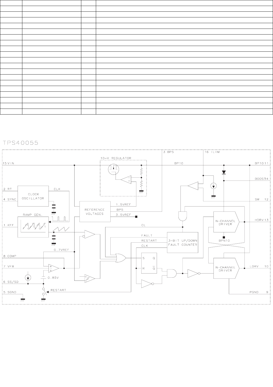
LC-42XL2E/S/RU, LC-46XL2E/S/RU, LC-46X20E/S/RU, LC-52XL2E/S/RU, LC-52X20E/S/RU
5 – 40
2.21. IC9601, 9603, 9604, 9606 (VHiTPS40055-1Y)
2.21.1 Block Diagram
126 HDMI_PLG_EN O HDMI output control
127 D3.3V — Power supply(+3.3V)
128 MUTE_HDMI O HDMI_MUTE initial value Low
129 HPLUGOUT_A I HDMI Plug Out detection
130 HDMIKEY_WP O EDIT_Write Protect
131 N_CPLD2_RST O CPLD2 reset
132 PNL_POW O Panel power control
133 HDMI_SW_INT INT HDMI SW IC interrupt request
134 HDELAY_DOUT O HDMI Data Delay Serial_Data_OUTPUT
135 N_MICOM_FLSW O Monitor microprocessor write control
136 N_MICOM_RST O Monitor microprocessor reset control
137 SMPOWHOLD O Power holding signal
138 PM_REQ INT Panel Maicon REQ
139 N_DBOOTS I Microprocessor write request
140 CBOOTS I SD card activation detection
141 D3.3V — Power supply(+3.3V)
142 N_DBG_RST I Debugger (Partner) reset
143 N_SRESET I System reset
144 GND_B — Ground
Pin No. Pin Name I/O Pin Function

LC-42XL2E/S/RU, LC-46XL2E/S/RU, LC-46X20E/S/RU, LC-52XL2E/S/RU, LC-52X20E/S/RU
5 – 41
2.21.2 Pin Connections and short description
Pin No. Pin Name I/O Pin Function
14 BOOST O Gate drive voltage for the high side N-channel MOSFET.
The BOOST voltage is 9 V greater than the input voltage.
A 0.1-µF ceramic capacitor should be connected from this pin to the drain of the lower MOSFET.
3 BP5 O 5-V reference.
This pin should be bypassed to ground with a 0.1-µF ceramic capacitor.
This pin may be used with an external DC load of 1 mA or less.
11 BP10 O 10-V reference used for gate drive of the N-channel synchronous rectifier.
This pin should be bypassed by a 1-µf ceramic capacitor.
This pin may be used with an external DC load of 1 mA or less.
8 COMP O Output of the error amplifier, input to the PWM comparator.
A feedback network is connected from this pin to the VFB pin to compensate the overall loop.
The comp pin is internally clamped above the peak of the ramp to improve large signal transient response.
13 HDRV O Floating gate drive for the high-side N-channel MOSFET.
This pin switches from BOOST (MOSFET on) to SW (MOSFET off).
16 ILIM I Current limit pin, used to set the overcurrent threshold.
An internal current sink from this pin to ground sets a voltage drop across an external resistor connected from
this pin to VCC.
The voltage on this pin is compared to the voltage drop (VIN-SW) across the high side MOSFET during con-
duction.
1 KFF I A resistor is connected from this pin to VIN to program the amount of voltage feed-forward.
The current fed into this pin is internally divided and used to control the slope of the PWM ramp.
10 LDRV O Gate drive for the N-channel synchronous rectifier.
This pin switches from BP10 (MOSFET on) to ground (MOSFET off).
9 PGND — Power ground reference for the device.
There should be a low-impedance path from this pin to the source (s) of the lower MOSFET (s).
2 RT I A resistor is connected from this pin to ground to set the internal oscillator and switching frequency.
5 SGND — Signal ground reference for the device.
6 SS/SD I Soft-start programming pin.
A capacitor connected from this pin to ground programs the soft-start time.
The capacitor is charged with an internal current source of 2.3 µA.
The resulting voltage ramp on the SS pin is used as a second non-inverting input to the error amplifier.
The output voltage begins to rise when VSS/SD is approximately 0.85 V.
The output continues to rise and reaches regulation when VSS/SD is approximately 1.55 V.
The controller is considered shut down when VSS/SD is 125 mV or less. All internal circuitry is inactive.
The internal circuitry is enabled when VSS/SD is 210 mV or greater.
When VSS/SD is less than approximately 0.85 V, the outputs cease switching and the output voltage (VOUT)
decays while the internal circuitry remains active.
12 SW I This pin is connected to the switched node of the converter and used for overcurrent sensing.
4 SYNC I Syncronization input for the device.
This pin can be used to synchronize the oscillator to an external master frequency.
If synchronization is not used, connect this pin to SGND.
7 VFB I Inverting input to the error amplifier.
In normal operation the voltage on this pin is equal to the internal reference voltage, 0.7 V.
15 VIN I Supply voltage for the device.
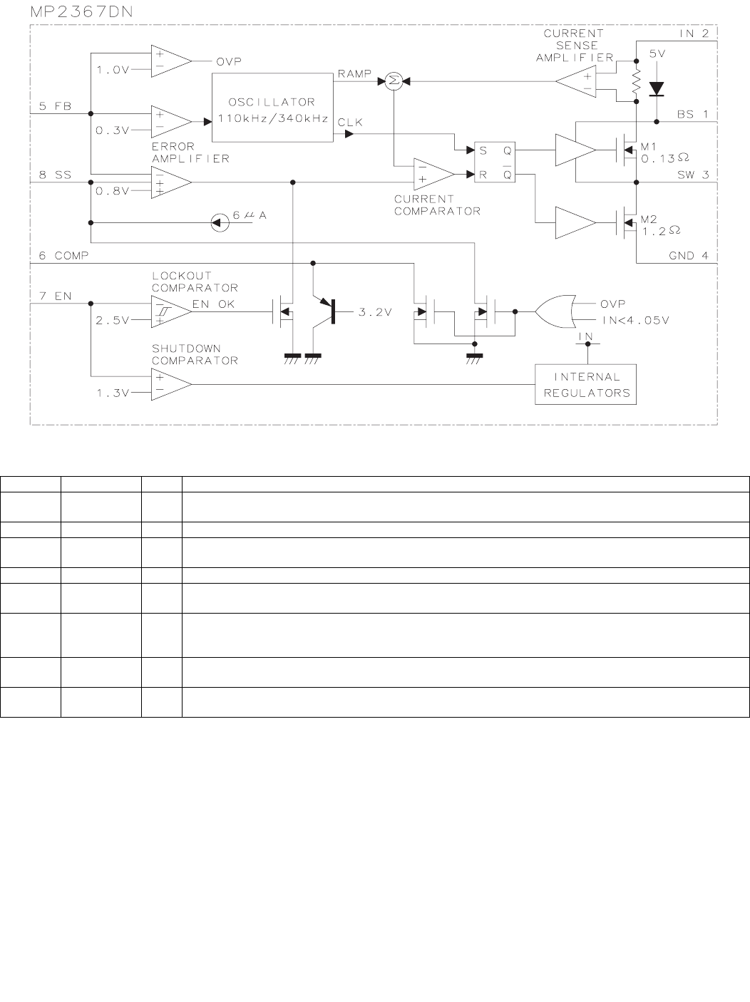
LC-42XL2E/S/RU, LC-46XL2E/S/RU, LC-46X20E/S/RU, LC-52XL2E/S/RU, LC-52X20E/S/RU
5 – 42
2.22. IC9602 (VHiMP2367DN-1Y)
2.22.1 Block Diagram
2.22.2 Pin Connections and short description
Pin No. Pin Name I/O Pin Function
1 BS I High-Side Gate Drive Boost Input. BS supplies the drive for the high-side N-Channel MOSFET switch.
Connect a 0.01µF or greater capacitor from SW to BS to power the high side switch.
2 IN I Power Input. IN supplies the power to the IC, as well as the step-down converter switches.
3 SW Drive IN with a 4.45V to 28V power source. Bypass IN to GND with a suitably large capacitor to eliminate noise
on the input to the IC.
4 GND Ground.
5 FB Feedback Input. FB senses the output voltage to regulate that voltage. Drive FB with a resistive voltage divider
from the output voltage. The feedback reference voltage is 0.8V.
6 COMP Compensation Node. COMP is used to compensate the regulation control loop. Connect a series RC network
from COMP to GND to compensate the regulation control loop. In same cases, an additional capacitor from
COMP to GND is required.
7 EN Enable Input. EN is a digital input that turns the regulator on or off. Drive EN high to turn on the regulator, drive
it low to turn it off.
8 SS Soft-start Control Input. SS controls the soft-start period. Connect a capacitor from SS to GND to set the soft-
start period.
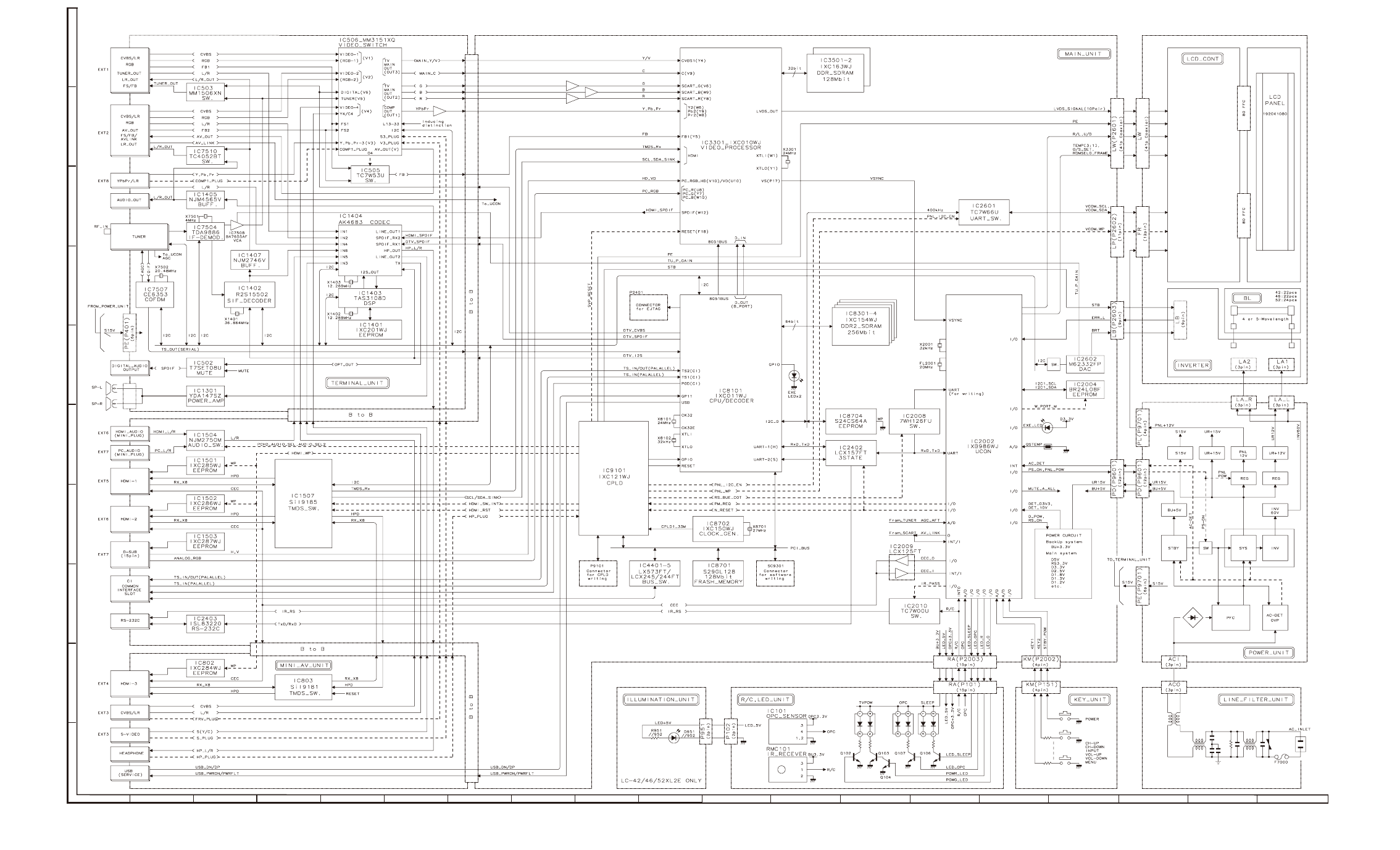
LC-42XL2E/S/RU, LC-46XL2E/S/RU, LC-46X20E/S/RU, LC-52XL2E/S/RU, LC-52X20E/S/RU
6 – 1
LC42XL2E Service Manual
CHAPTER 6. BLOCK DIAGRAM/WIRING DIAGRAM
[1] SYSTEM BLOCK DIAGRAM
123
1097654
8
J
A
B
C
D
E
F
G
H
I
1311 191816151412 17
SYSTEM BLOCK DIAGRAM
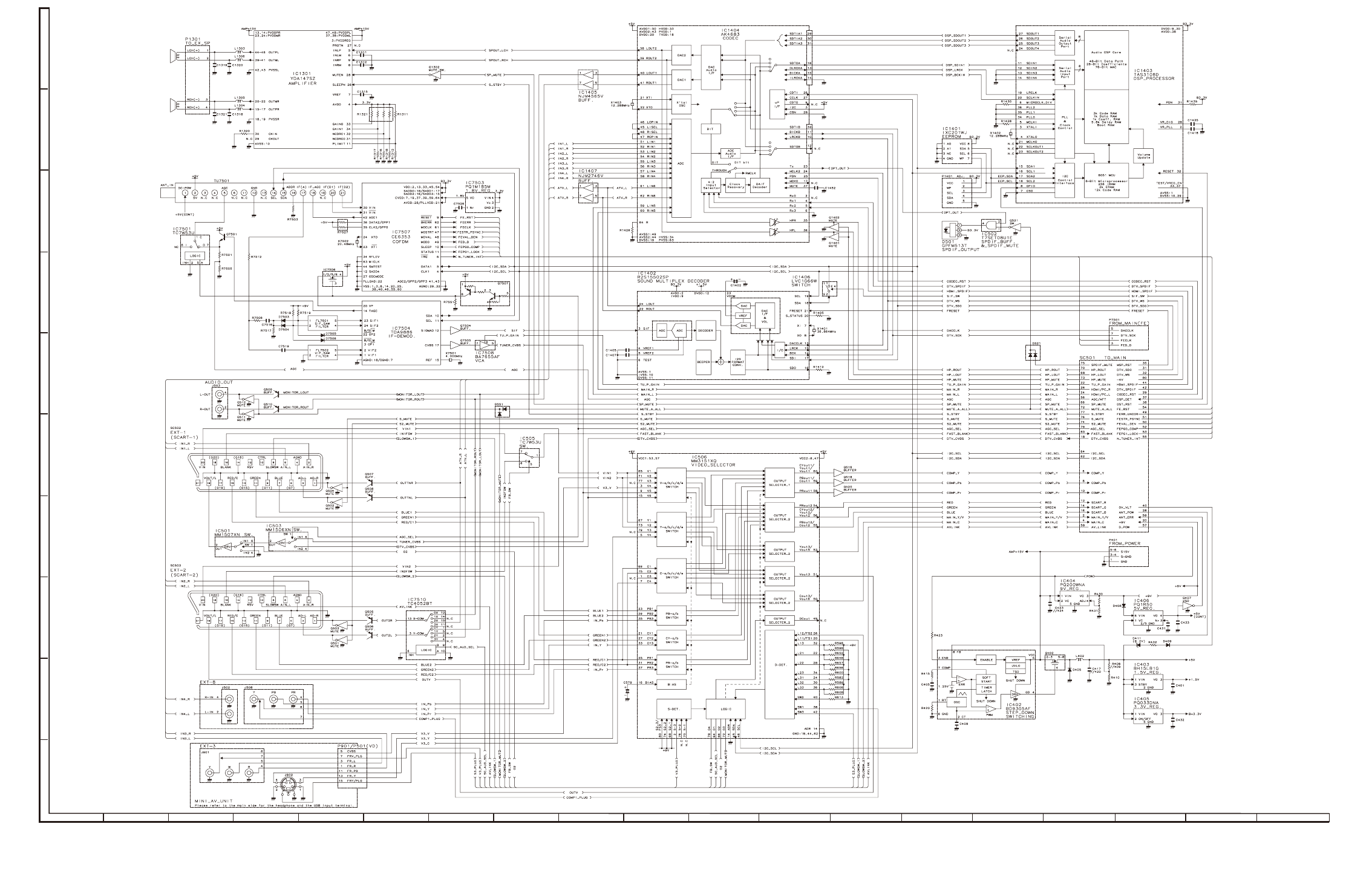
LC-42XL2E/S/RU, LC-46XL2E/S/RU, LC-46X20E/S/RU, LC-52XL2E/S/RU, LC-52X20E/S/RU
6 – 2
[2] TERMINAL BLOCK DIAGRAM
123
1097654
8
J
A
B
C
D
E
F
G
H
I
1311 191816151412 17
TERMINAL BLOCK DIAGRAM
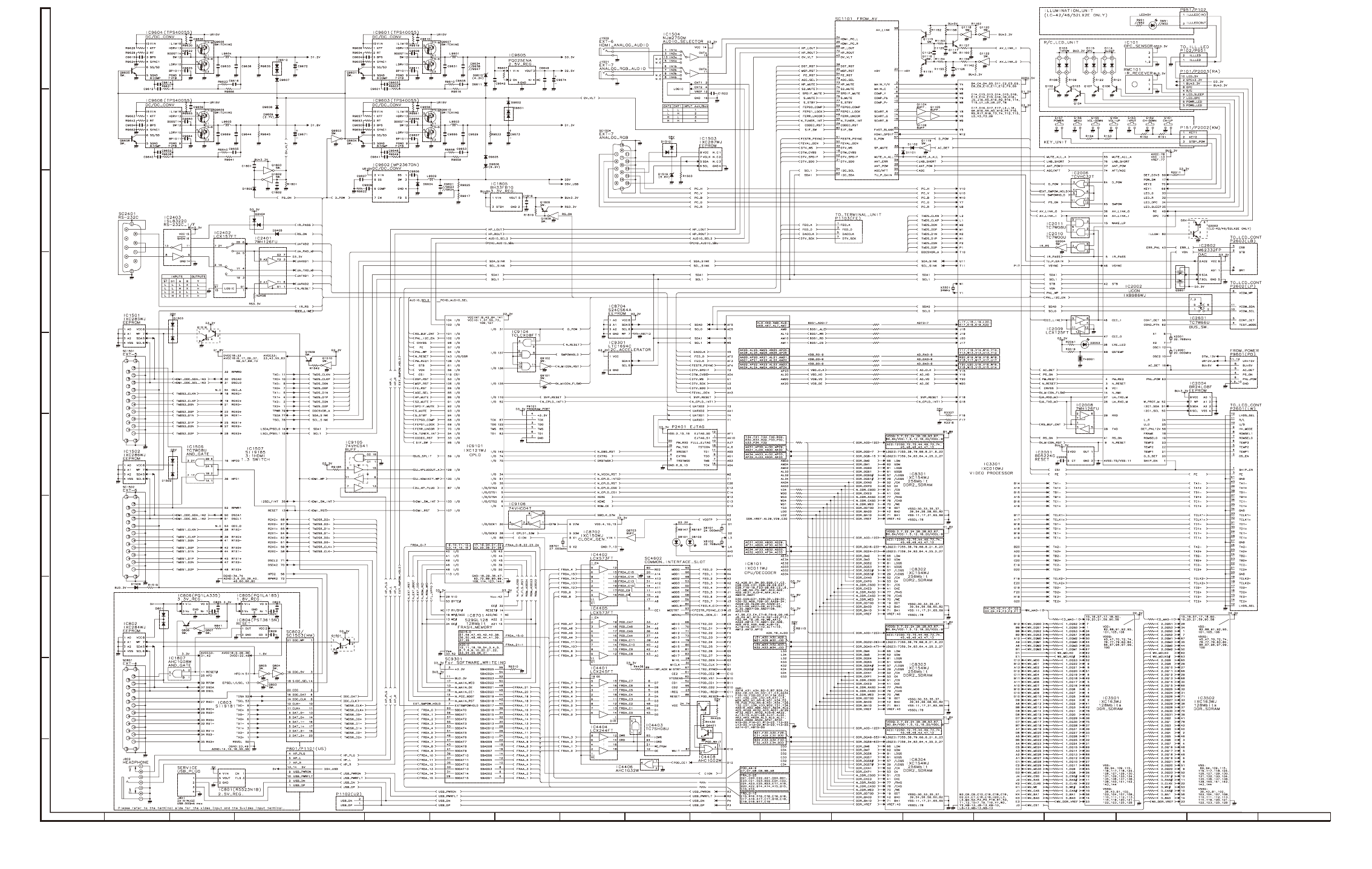
LC-42XL2E/S/RU, LC-46XL2E/S/RU, LC-46X20E/S/RU, LC-52XL2E/S/RU, LC-52X20E/S/RU
6 – 3
[3] MAIN BLOCK DIAGRAM
123
1097654
8
J
A
B
C
D
E
F
G
H
I
1311 191816151412 17
MAIN BLOCK DIAGRAM
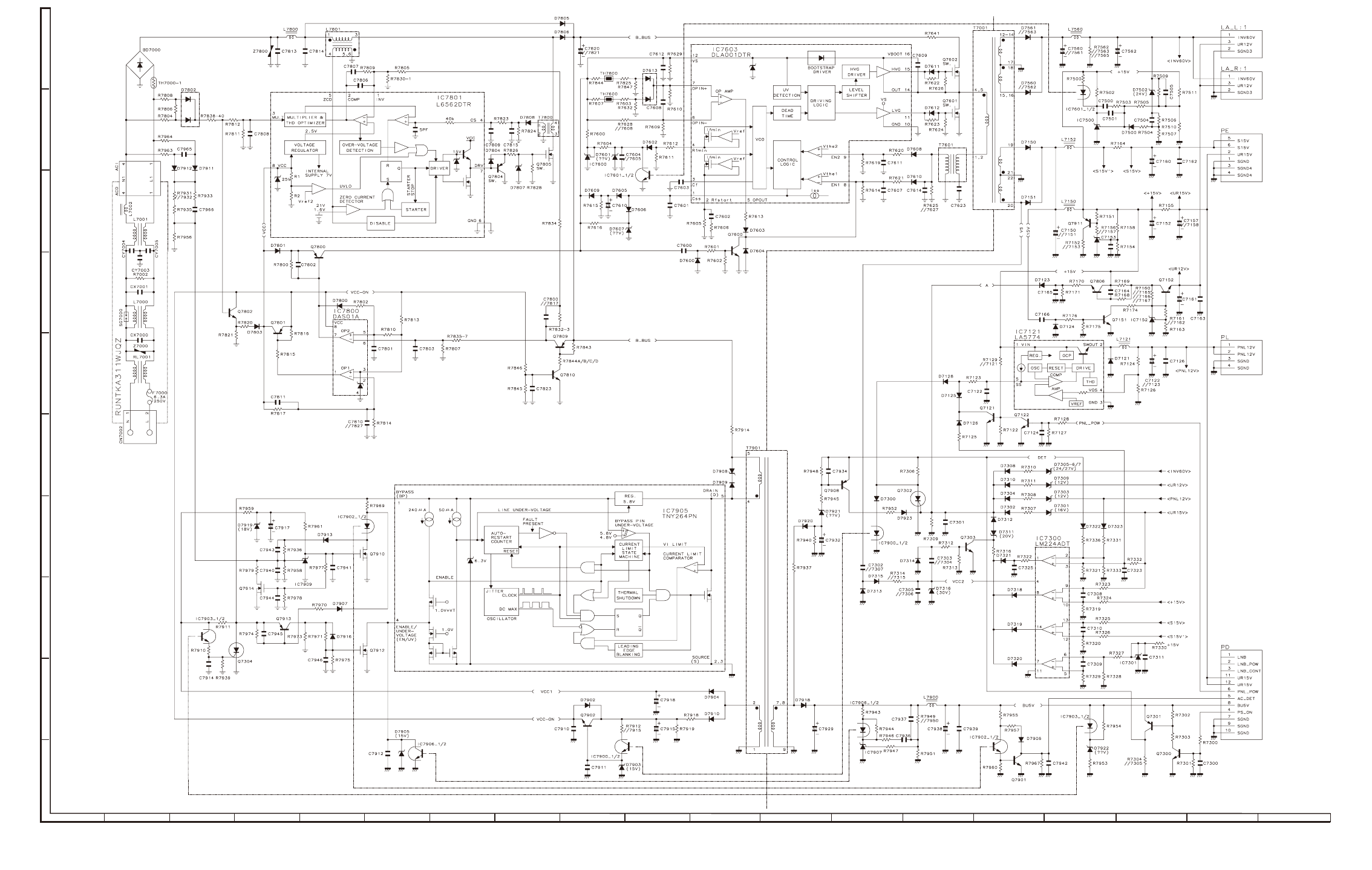
LC-42XL2E/S/RU, LC-46XL2E/S/RU, LC-46X20E/S/RU, LC-52XL2E/S/RU, LC-52X20E/S/RU
6 – 4
[4] POWER BLOCK DIAGRAM
123
1097654
8
J
A
B
C
D
E
F
G
H
I
1311 191816151412 17
POWER BLOCK DIAGRAM
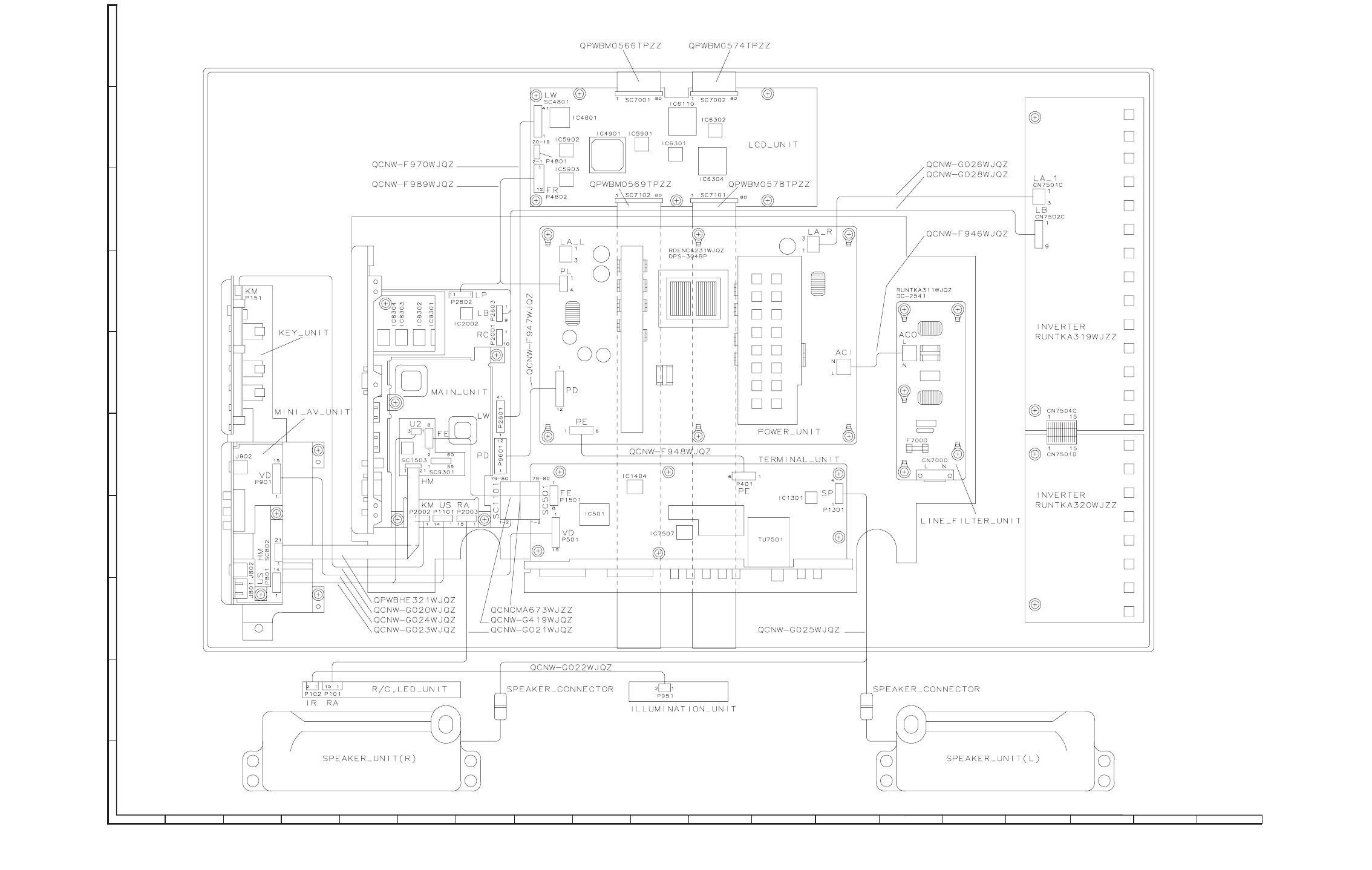
LC-42XL2E/S/RU, LC-46XL2E/S/RU, LC-46X20E/S/RU, LC-52XL2E/S/RU, LC-52X20E/S/RU
6 – 5
[5] WIRING DIAGRAM (LC-42XL2E/S/RU)
123
4567 910
8
J
A
B
C
D
E
F
G
H
I
WIRING DIAGRAM (LC-42XL2E/S/RU)
11 1312 14 15 16 18 1917
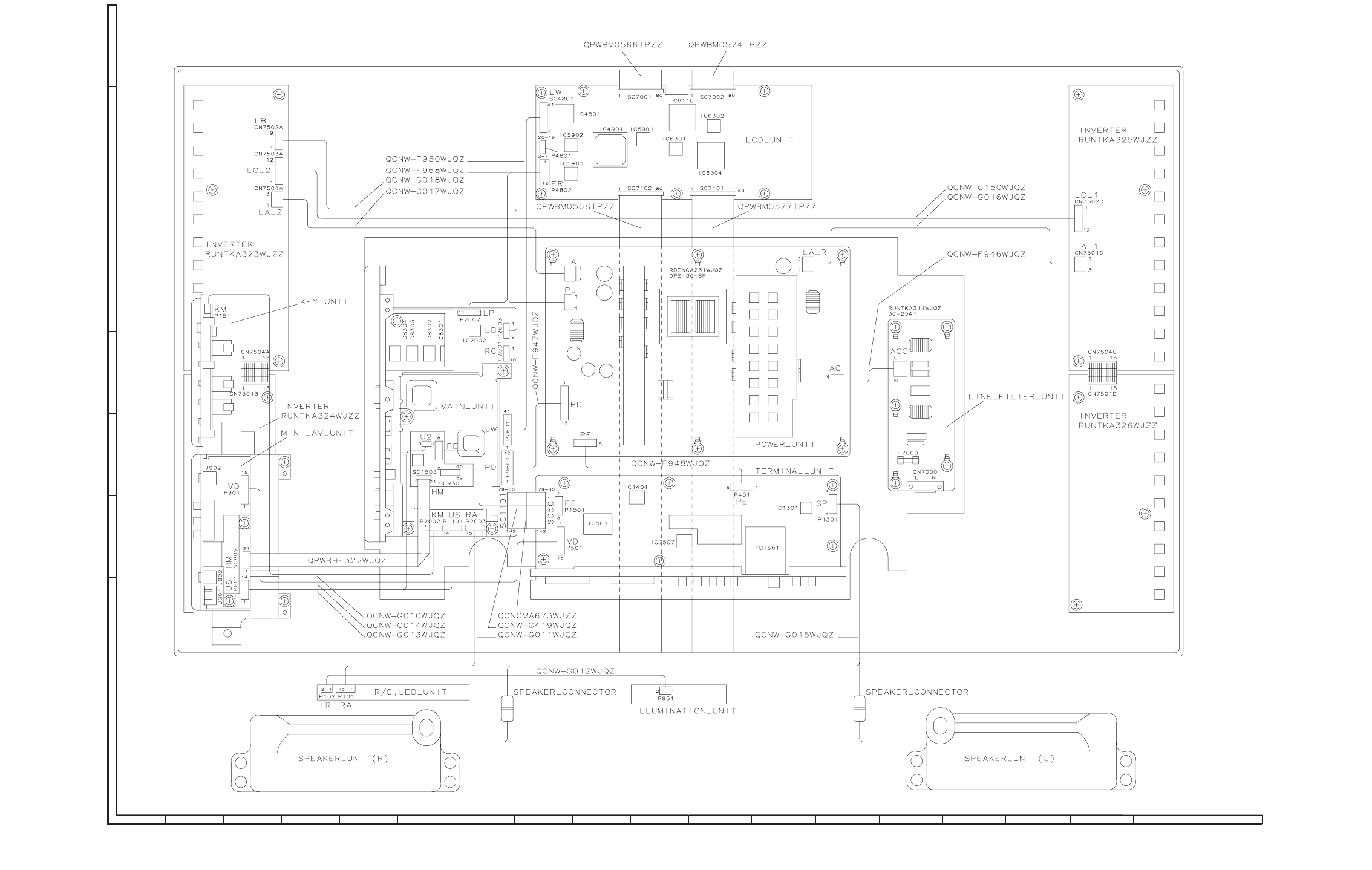
LC-42XL2E/S/RU, LC-46XL2E/S/RU, LC-46X20E/S/RU, LC-52XL2E/S/RU, LC-52X20E/S/RU
6 – 6
[6] WIRING DIAGRAM (LC-46XL2E/S/RU)
123
4567 910
8
J
A
B
C
D
E
F
G
H
I
WIRING DIAGRAM (LC-46XL2E/S/RU)
11 1312 14 15 16 18 1917
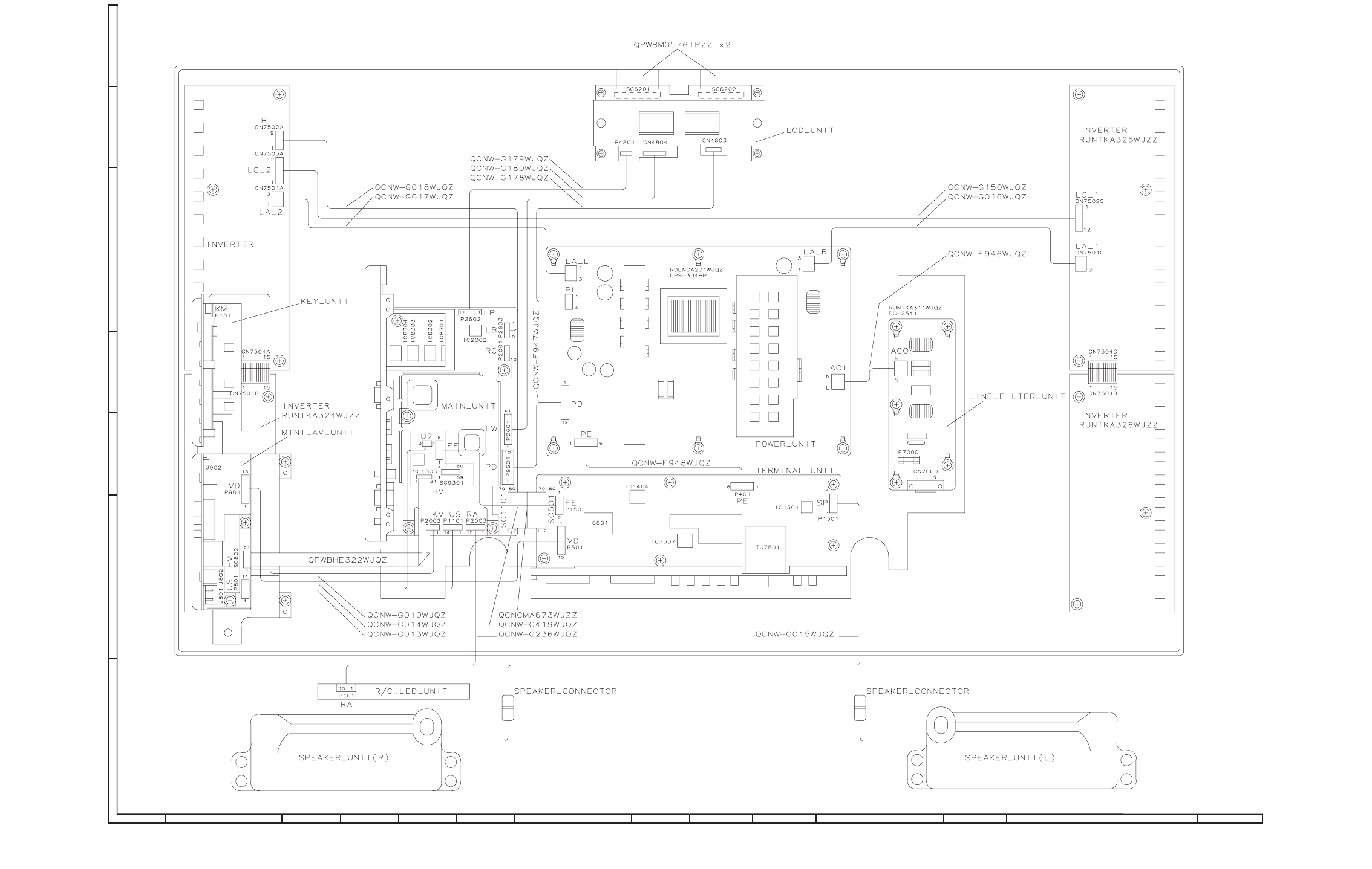
LC-42XL2E/S/RU, LC-46XL2E/S/RU, LC-46X20E/S/RU, LC-52XL2E/S/RU, LC-52X20E/S/RU
6 – 7
[7] WIRING DIAGRAM (LC-46X20E/S/RU)
123
4567 910
8
J
A
B
C
D
E
F
G
H
I
WIRING DIAGRAM (LC-46X20E)
11 1312 14 15 16 18 1917
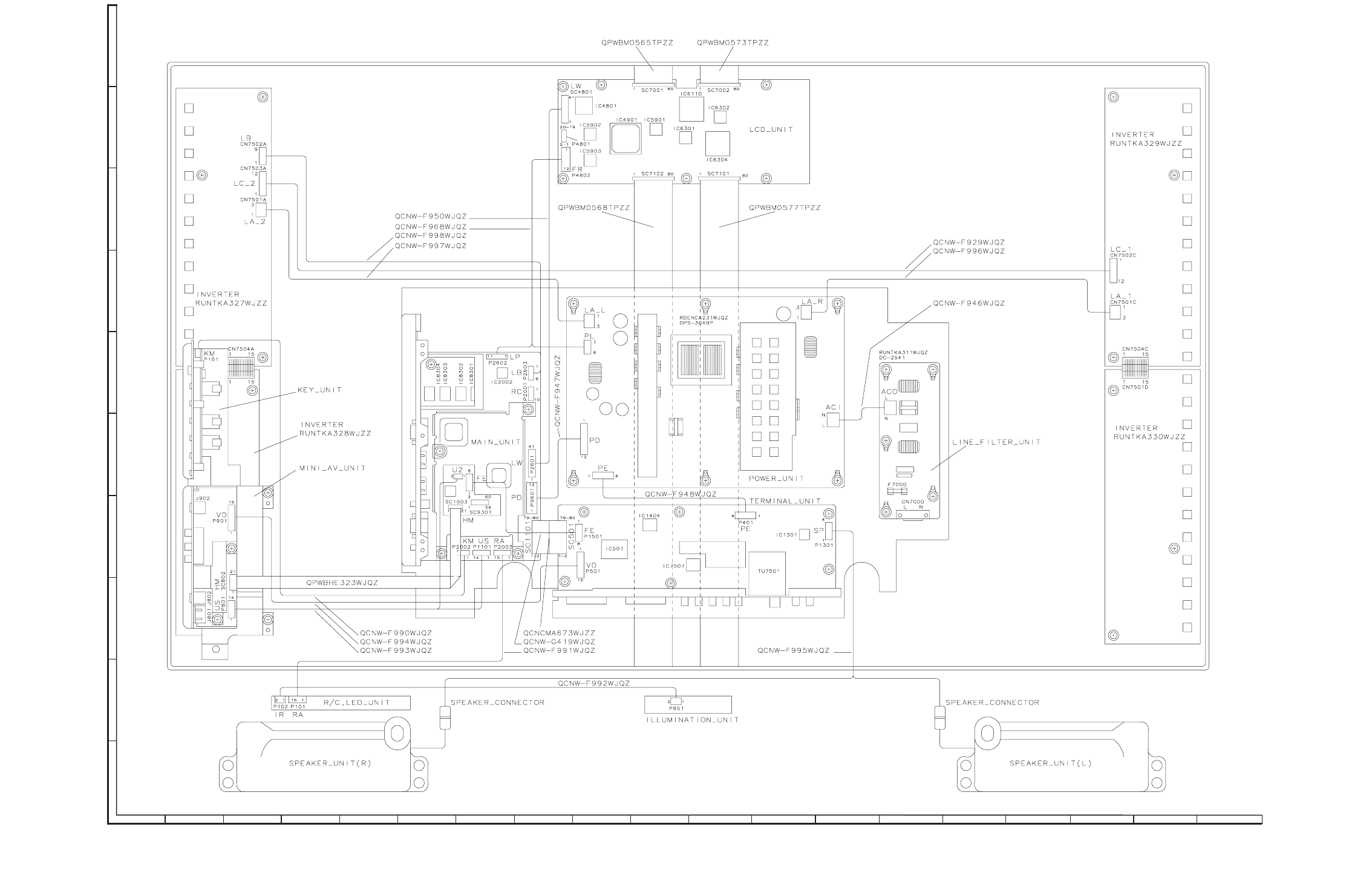
LC-42XL2E/S/RU, LC-46XL2E/S/RU, LC-46X20E/S/RU, LC-52XL2E/S/RU, LC-52X20E/S/RU
6 – 8
[8] WIRING DIAGRAM (LC-52XL2E/S/RU)
123
4567 910
8
J
A
B
C
D
E
F
G
H
I
WIRING DIAGRAM (LC-52XL2E/S/RU)
11 1312 14 15 16 18 1917
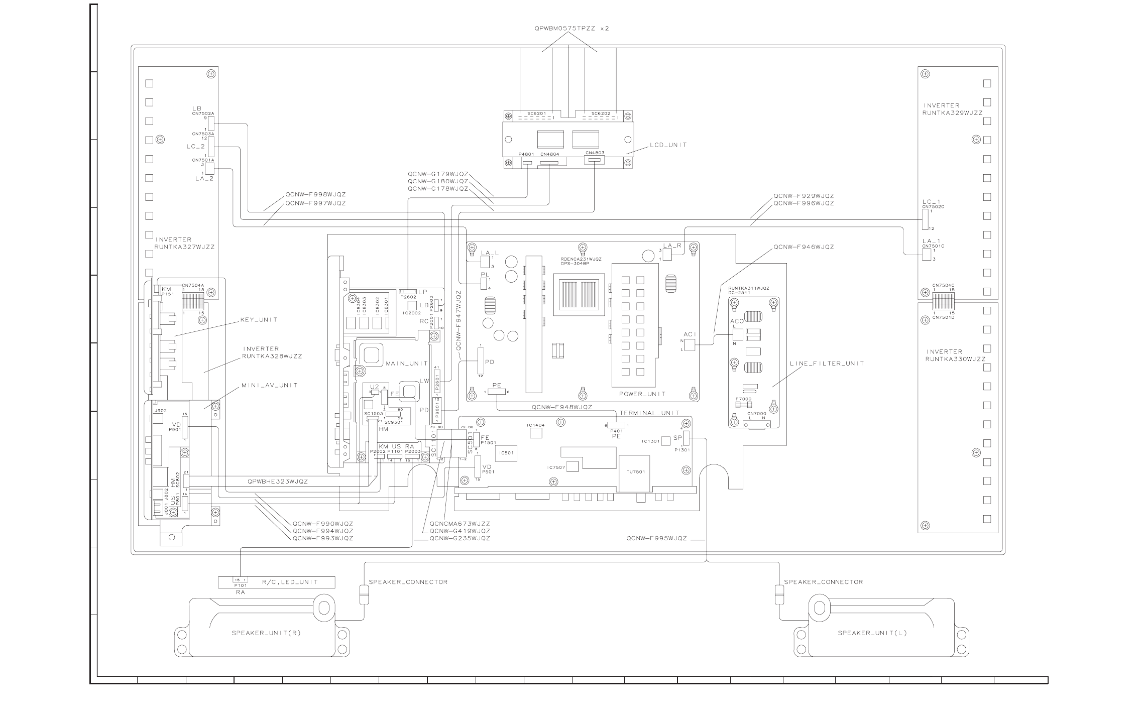
LC-42XL2E/S/RU, LC-46XL2E/S/RU, LC-46X20E/S/RU, LC-52XL2E/S/RU, LC-52X20E/S/RU
6 – 9
[9] WIRING DIAGRAM (LC-52X20E/S/RU)
123
4567 910
8
J
A
B
C
D
E
F
G
H
I
WIRING DIAGRAM (LC-52X20E)
11 1312 14 15 16 18 1917
LC-42XL2E/S/RU, LC-46XL2E/S/RU, LC-46X20E/S/RU, LC-52XL2E/S/RU, LC-52X20E/S/RU
7 – 1
LC42XL2E Service Manual
CHAPTER 7. PRINTED WIRING BOARD
[1] MAIN UNIT PRINTED WIRING BOARD
123
4567 910
8
J
A
B
C
D
E
F
G
H
I
11 1312 14 15 16 18 1917
MAIN Unit (Side-A)
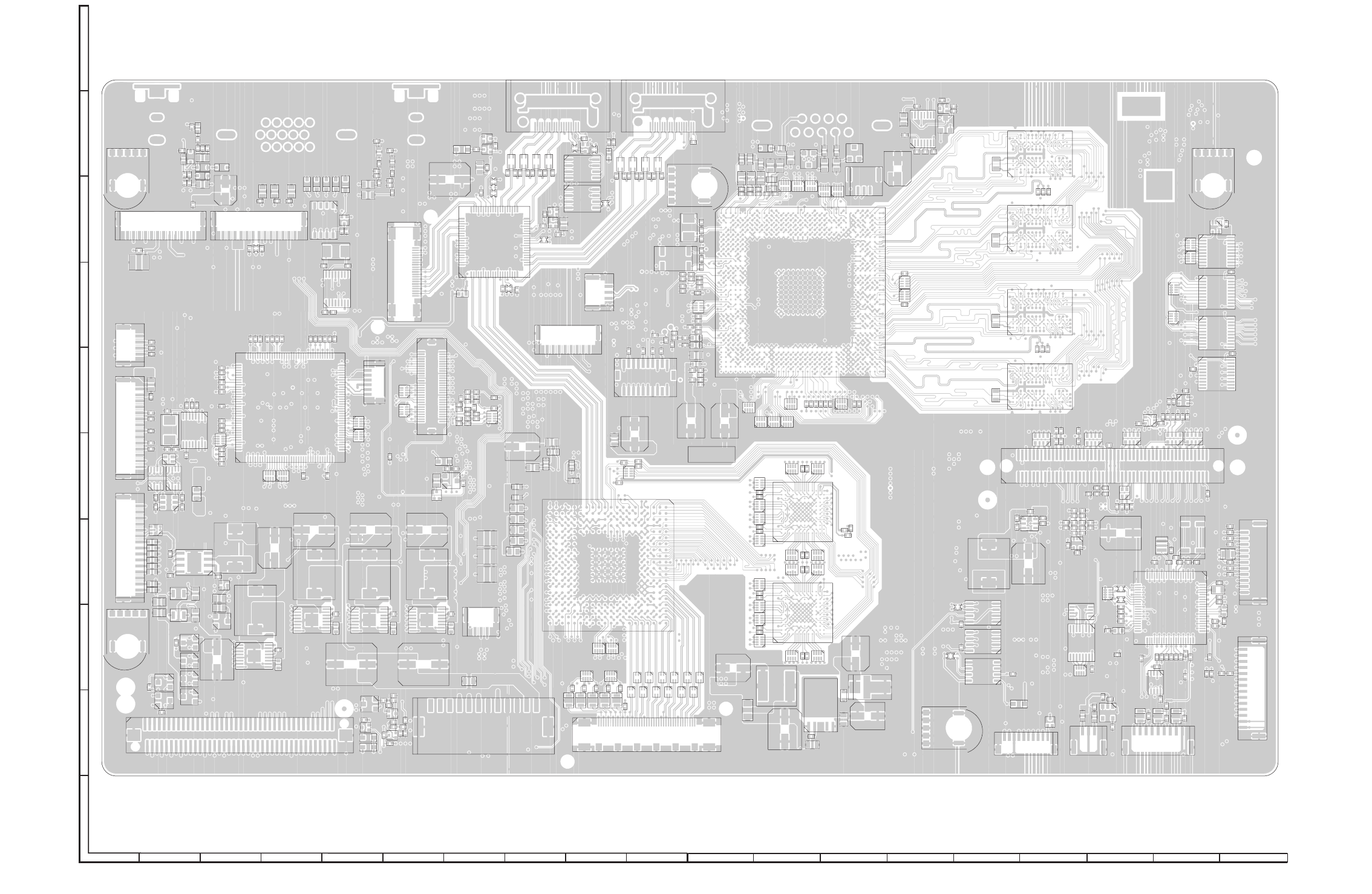
LC-42XL2E/S/RU, LC-46XL2E/S/RU, LC-46X20E/S/RU, LC-52XL2E/S/RU, LC-52X20E/S/RU
7 – 2
123
4567 910
8
J
A
B
C
D
E
F
G
H
I
11 1312 14 15 16 18 1917
FL2605
C1502
Q1117
FL2607
C1503
Q1119
L3301
C1505
R2095
L3302
C1506
R2096
L3303
L3304
Q1504
L3305
C1509
Q1506
FL2611
Q1121
D1101
Q1122
D1102
C1126
FL2613
C1128
C1510
R1101
C1511
FL2615
C1512
FL2616
C1513
FL2617
C1514
C1515
C1516
Q1517
Q1519
C1136
C9606
C1137
C9607
C1138
C9608
C1520
C1139
C1521
R1112
R1113
C1523
R1114
C1524
C4404
R1115
D1501
Q4401
C4405
D1502
C4406
C4407
C1527
C1140
D1504
C4408
C1141
C9611
R1501
C4409
R1502
D1506
D1507
R1504
D1508
R1505
D1509
X4501
C9618
C1530
C4410
IC1501IC1502
IC1503
C1533
C4413C4414
R1125 R1126
D1512
IC1507
C4417
R1511
C9622
D1518
C9625
C9628
R1518
C1540
C4420
R1519
SC9301
C4421
FB9702
R1133
R1134
R1135
R9607
IC9601
D1525
X2001
R4401
IC9602
D1526
R4402
IC9603
R1523
D1527
R4403
IC9604
D1528
R4404
IC9605
IC9606
R1526
R4406
R1528
R4408
R1529
R4409
IC4401
R1142
IC4402
IC4403
IC4404IC4405
IC4406
IC4407
R4410
IC4409
R4411
R1532
C9642
R1533
R4413
R1534
R1536
R1537
R4417
R1538
R4418
R4419
C9649
R1154 R1155
FB2001
R9625
FB2002
R1157
R1158
R1540
R4420
R1159
R1541
R4421
FB2006
R4422
FB2007
R1543
R4423
FB2008
R1544
R1545
FB2009
R4425
C9656
C9657
R4427
R1160
R1548
R4428
R1161
R1549
R4429
FB2010
R1164
R1165
FB2011
R1166
P8102
FB2012
FB2013
C9660
R1550
R4430
C9662
R1552
R1553
R4433
C9664
R1554
R4434
R4435
FB2402
FB2403
FB2404
R4439R4440
C9671
R4441
C9672C9673
C9674
C9675
R1565
R1566
R4446
R4447
P3301
C8104 7018C6018C5018C
C8108
C8109
R1575
R1576
R4456
R1577
R4457
R4458
C8301
R4459
C8302
C8110
C8111
R9667
R4460
R4461
R4464
R4465
R4467
L2601
R4469
L2602
L2603
L2604
C8120
L2605
L2606
L2607
L2608
L2609
D8101
R4471
C8702
D8102
R4472
R1593
R4473
R1594
C8704
R4474
Q8701
C8705
R8101
R4475
Q8702
C8706
R4476
C8707
R4477
L2610
C8708
R4478
L2611
R8105
C8709
R4479
L2612
IC8101
R4480
C8135
R8301
R4481
C8136
R4482
R8302
R8303
R4483
R8304
R8111
C8139
R8112
IC8301
R8116
IC8302
R8117
IC8303
C8140
R8118
IC8304
R8119
P9101
R8310
C3518
R8311
C8146
R8120
D8701
C8149
R8123 R8124
R8701
R3306
R8703
R3307
R3308
R8704
C8150
R8705
IC3301
C8151
C8345C8346
R3501
R3502
IC8702
R3503
4078CI3078CI
R3311
R8131
R3506
R8132
R3507
R8710
LUG1
R8135
R3509
IC3501
R8136
IC3502
R8137
R8138
R8714
R8139
R8718
C3539
R3512
R8332
R8333
R8140
R3514
R8141
R8142
R3516
R8143
R8144
R8145
P4501 P4502
R8147
R8148
R8149
C3548
R8729
R3521
LUG1101
C9116
C8176
LUG1102
LUG1103
C3357
LUG1104
R3524
LUG1105
C8179
R3525
R8152
R3526
R8153
R3527
R8154
R3528
Q1801
Q1804
C8180
R3530
C8379
R3532
SC1101
R3341
P2001
R3342
P2002 P2003
R9103
R3344
C8380
P2004
R3345
C4501
FB1505
R3539
P2005
C4502
FB1506
R8167
R3347
C4503
FB1507
R3348
FB1508
R8169
IC9101
C3374
1453R0453R
R3542 R3543
C3377
R1604
FB1510
R3544
C3378
L1101
R9111
R3351
L1102
R3352
R9306
R8172
R9112
R3546
R8173
R9307
R9113
R3354
R8175
R9116
R9117
P2401
SC1501
R1802
SC1502
FB9603
C8397
SC1503
R1804
R9311
R9312
R9313
C3388
R9314
R9120
R3554
C3389
R9121
R9315
R3555
C2001
R9316
R3556
C2002
R9317
R3557
C2003
R9318
R3558
R9125
R9319
Q2001
P2601
Q2002
P2602
R9127
P2603
R9129
C2009
R9320
R3560
R9321
R1622
L1506
R9322
L1507
R9323
R9324
L1508
C2010
L1509
R9131
R9325
C2011
R9132
R9326
R9327
R9133
R4507
R4508
R9328
R4509
IC4501
R9329
R9136
R9138
L1510
L1511
R9139
C2019
L1512
C2402
C2403
L1513
C2404
R9330
R3570
C2405
R3571
C2406
R3572
R4513
C2407
R3573
Q2404
C2408
C2020
R3574
L9601
R9335
R3575
L9602
R9336
R3576
L9603
R9143
R9337
Q2407
R3577
L9604
R9144
R4518
R3578
L9605
L9606
SC4602
D2003
C2027
C2028
C2604
C2410
R9149
C2029
L4401
C2605
R2002
C2609
R2005
R2006
R2007
IC2001
R2009
IC2002
R2011
R2012
R2013
D2401
D2402
D2403
R2017
D2404
R9161
TH2001 R2019
IC2011
R9162
R2405
R2407
R2408
R2020
R2409
D2601
IC2401
IC2402
R2022
IC2403
IC2404
R2601
IC2405
R2602
R2027
R2603
R2604
R2410
R2028
R2606
R2608
R2414
R9174
R2415
R9176
IC2602
R9178
X8101
R9179
R2031
X8102
R2610
R2034
R2611
R2612
R2036
R2613
R2614
R9180
R2038
R2615
R2421
R9181
R9182
R2423
R9183
R2617
R2424
R2618
R2425
R2619
R2426
R2427
R2428
R2429
R2041
R2620
R2044
R2045
R2621
R2430
R2048
R2432
FB8101
R2435
R2436
FB8102
FB8105
R2051
FB8107
R2053
R2054
FB8109
X8701
R2055
R2056
R2057
P1101
P1102
P1103
FB8110
C8232
R2062
C8233
R2063
FL2001
R2069
VA1501
VA1502
FB3303
VA1503
FB3304
VA1504
FB3305
VA1505
FB3306
VA1506
VA1507
VA1508
VA1509
R2075
R2076
R2077
FB3501
C1102
C1103
VA1510
VA1511
VA1512
FB3313
Q1103
VA1513
FB3314
Q1104
VA1514
Q1105
VA1515
Q1106
VA1516
R2082
Q1109
P9601
Q1110
FL2601
FL2603
MAINUnit (Chip Parts Side-A)
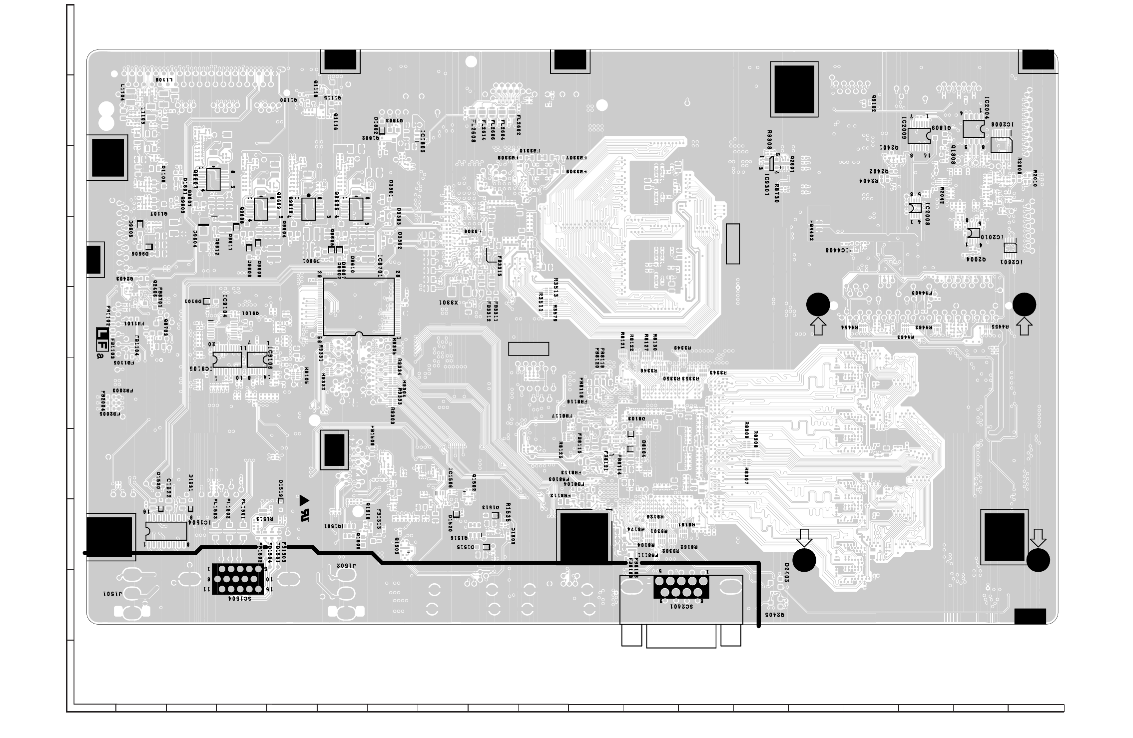
LC-42XL2E/S/RU, LC-46XL2E/S/RU, LC-46X20E/S/RU, LC-52XL2E/S/RU, LC-52X20E/S/RU
7 – 3
123
4567 910
8
J
A
B
C
D
E
F
G
H
I
11 1312 14 15 16 18 1917
MAIN Unit (Side-B)
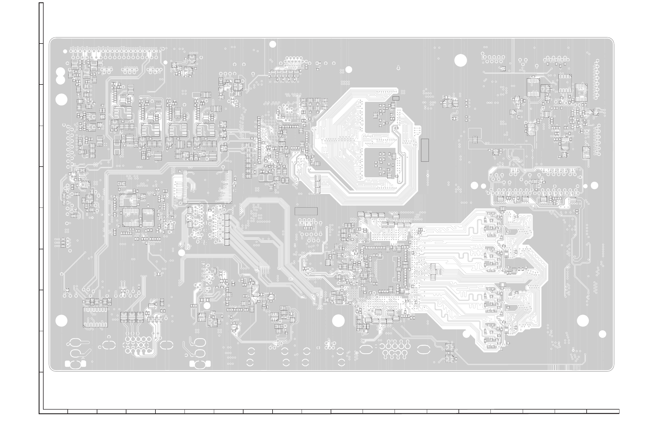
LC-42XL2E/S/RU, LC-46XL2E/S/RU, LC-46X20E/S/RU, LC-52XL2E/S/RU, LC-52X20E/S/RU
7 – 4
123
4567 910
8
J
A
B
C
D
E
F
G
H
I
11 1312 14 15 16 18 1917
MAINUnit (Chip Parts Side-B)
C1118
FL2604
C1119
Q1115
C1501
R2091
Q1116
FL2606
R2092
R2093
Q1118
FL2608
C1504
R2094
Q1501
Q1502
C1507
C1120
C1508
C1121
Q1505
C1122
L3306
C1123
Q1120
C1124
C1125
Q1509
C1127
FL2614
C1129
R1102
R1103
R1104
Q1510
R1105
R1106
R1107
C1517
C1130
R1108
C1131
R1109
C9601 C1132
C9602
Q1516
C1133
C9603
C1134
C9604
C1135
Q9601
C9605
Q9603
R1110
Q9604
R1111
Q9605
C9609
Q9606
C1522
Q9607
Q9608
Q9609
C1525
R1116
C1526
R1117
D1503
C9610
R1118
R1119
C9612
C9613
R1503
Q9610
C9614
C9615
C9616
R1506
C9617
R1507
R1120
R1508
R1121
C9619
C1531
R1509
C4411
R1122
C1532
R1123
C1534
R1124
IC1504
C4415
IC1506
C4416
R1127
D1513
R1128
C9620
C1538
R1510
R1129
C9621
D1515
R1512
C9623
R1513
C9624
R1514
D9601
R1515
D1519
D9602
C9626
R1516
C9627
R1517
D9604
R1130
D9605
R1131
R9601
C9629
R1132
D9606
R9602
R9603
D9607
C1543
R9604
D9608
C1544
D1520
D9609
R9605
C1545
R9606
C1546
R1136
R1137
C1547
C9630
R9608
R1520
C1548
R9609
C9631
R1521
C9632
R1522
C9633
D9610
C9634
R1524
D9611
C9635
R4405
C9636
D9612
R4407
C9637
R1527
C9638
R9610
R9611
C9639
C1551
R9612
R9613
R9614
D1530
R9615
D1531
R9616
R9617
R9618
C9640
R1148
IC4408
C9641
R9619
R1149
C9643
C9644
C9645
R1535
C9646
C9647
R9620
C9648
R1151
R9621
R1539
R1152
R9622
R1153
R9623
R9624
R1156
R9626
R9627
FB2003
C9650
R9628
FB2004
R9629
C9651
FB2005
C9652
R1542
C9653
C9654
R4424
C9655
R4426
C9658
R9630
C9659
R9631
R1162
R9632
R9633
R9634
R9635
R9636
R9637
R9638
C1578
C9661
R9639
C1579
R4431
R4432
C9663
C9665
C9666
R4436
R4437
R1558
C9668
R9640
R4438
R1559
C9669
R9641
R9642
C1582
R9643
C1583
R9644
R9645
R9646
C1586
R9647
C1587
R9648
R1560
R9649
R1561
C1589
R1562
R1563
R1568
FL1501
C1591
R9652
FL1502
C1592
R9653
FL1503
R9654
R9655
C8101
R9656
C8102
C1596
R9657
C8103
C1597
R9658
R1570
R9659
C1599
R1571
R4452
R4453
R4454
R4455
R9660
R9661
R1579
R9662
R9663
C8303
R9664
C8304
R9665
R9666
C8112
C8113
R1580
C8114
C8115
C8116
R4462
C8117
R4463
C8118
C8119
R4466
R4468
C8314
C3301
C8121
C8315
C3302
C8122
C8316
C3303
C8123
C8317
C3304
C8124
C8318
R4470
C3305
C8701
C8125
C8319
C3306
C8126
D8103
C3307
C8703
C8127
D8104
C3308
C8128
C3309
C8129
R1595
R8102
R8103
Q8703
R8104
C8320
C8321
R8106
C8322
C3502
R8107
C3503
C3310
C8130
R8108
C3504
C3311
C8131
R8109
C3505
C3312
C8132
C3506
C3313
C8133
C3507
C8327
C3314
C8134
C8328
C3508
C3315
C8329
C8711
C3316
C8712
C3317
C8137
C8713
C3318
C8138
R4484
C8714
C3319
C8715
R8305
R4485
R4486
R8306
R8307
R8113
C8717
R4487
R8308
R8114
C8718
C8330
R8309
R8115
C8331
C8332
C8333
C3513
C3320
C8334
C3514
C3321
C8141
C3515
C8335
C3322
C8142
C3516
C8336
C3323
C8143
C3517
C8337
C3324
C8144
C8338
C3325
D3301
C8145
C8339
C3326
D3302
D3303
C3327
C8147
C3328
C8148
C3329
R3301
R8121
R3302
R8122
R3303
R3304
C8340
C3520
R3305
R8125
C8341
C3521
R8126
C3522
C8342
R8127
C3523
C8343
C3330
R8128
C8344
C3524
R3309
C3331
R8129
C3525
C3332
C8152
R8706
C3526
C3333
C8153
C8347
C3334
C8154
C8348
C3335
C8155
IC8701
C8349
C3336
C8156
C3337
C8157
C3338
R3310
C8158
R8130
C3339
C8159
R3312
R8133
R3314
C8350
R3315
C3531
C8351
R3316
R8712
C3532
C8352
R3317
C8353
C3533
R8713
R3318
C3340
C8160
C8354
C3534
C3341
R3319
C9101
C8161
C8355
C3535
LUG6
C3342
C8162
C8356
C3343
C8163
C3537
C8357
LUG8
C9104
C3344
C8164
C3538
C8358
R3511
C3345
C9105
C8165
Q9101
C8359
C9106
C3346
C8166
Q9102
C3347
R3513
C8167
C9107
C3348
R3320
C8168
C9108
C3349
R3321
C8169
C9109
R3322
R3323
C3540
C8360
R3325
C3541
C9301
C8361
R8146
R8722
C3542
C8362
R3327
R8723
C8363
C3543
R3328
C3350
C8170
C9110
C8364
C3544
FB1101
R3329
C3351
C8171
C9111
C3545
C8365
FB1102
C3352
C8172
C9112
C8366
C3546
FB1103
C3353
C8173
C9113
C3547
C8367
FB1104
C3354
R8728
C8174
C1608
C9114
C8368
FB1105
C3355
C8175
C9115
C8369
C3356
C8177
C9117
R3330
C3358
R8150
C8178
C3359
C1801
R3331
R8151
C1802
R3332
C1803
R3333
C1804
R3334
C8370
R8730
R3335
R8155
C8371
Q1802
R3336
R8156
C8372
R3337
Q1803
R8157
C1613
C8373
C3360
R3338
C1614
R8158
C8374
C3361
R3339
R8159
C8181
C1615
C8375
C3362
C8182
C1616
C8376
C3363
C8183
C8377
C3364
C8184
C8378
Q1808
C3365
D9101
C8185
Q1809
C3366
C8186
C3367
C8187
C3368
R3340
C8188
R8160
C3369
C8189
R8161
FB1501
R9101
R9102
R8162
FB1502
C1813
R3343
R8163
FB1503
R9104
R8164
FB1504
R8165
R9105
C8381
C1816
R3346
R8166
R9106
C8382
R9107
C8383
C3370
C8190
R9108
C8384
C3371
C8191
R3349
R9109
FB1509
C8385
C3372
C8192
C8386
C3373
C8193
C8387
C8194
IC9104
C8388
C3375
R9301
C8195
IC9105
R1601
C8389
C3376
C8196
R9302
IC9106
C8197
R9303
R8170
C8198
R3350
R9110
R9304
C3379
R1605
C8199
R8171
R9305
R1606
L1103
R3353
R1607
L1104
R8174
R9114
C8390
R9308
L1105
D1801
R3355
R9115
FB1515
R1609
C8391
IC9301
L1106
D1802
C8392
C8393
C3380
R9118
C8394
R1801
C3381
R9119
C8395
C3382
R1803
C3383
C3384
R9310
C3385
C3386
C3387
R9122
FB4402
R9123
FB4403
R9124
C2004
IC1805
C2005
R9126
C2006
C2007
C3390
R9128
Q2004
C2008
C3391
C3392
C3393
C3394
C3395
C3396
C3397
R1817
C3398
R9130
C3399
R1819
C2012
C2013
R9134
C2014
R9135
C2015
C2016
R9137
C2017
R1820
C2018
C2401
R9331
R4511
Q2401
R4512
R9332
Q2402
Q2403
R9333R9334
R9140
R4514
C2021
C2409
R9141
R4515
Q2405
Q2406
R9142
C2023
R3579
R9145
R9146
C2026
R9147
R9148
R2001
Q2601
C2606
C2607
R2003
C2608
R2004
R9150
C2030
R2008
R9151
R9152
R9153
C2033
R9154
C2034
IC2004
R9155
R9156
IC2006
R9157
R9158
R2010
IC2008
R9159
IC2009
R2014
R2015
R2016
R9160
IC2010
R2018
D2405
R2401
R2402
R9163
R2403
R9164
R2404
R3599
R9165
R9166
R2406
R9167
R9168
R9169
R2021
R2023
R2024
R2025
R2026
R9170
R2605
R9171
R2029
R9172
R2413
R2607
R9173
R2609
R9175
IC2601
R2416
R9177
R2417
R2418
C8200
R2030
R2419
C8201
C8202
R2032
C8203
R2033
C8204
C8205
R2035
C8206
C8207
R2037
C8208
R2420
C8209
R2039
R2616
R2422
R9184
R9185
R9186
R9187
C8210
R9188
R2040
C8211
C8212
R2042
C8213
R2043
C8214
C8215
C8216
R2046
R2622
R2623
C8217
R2047
R2624
C8218
R2625
R2431
C8219
R2049
R2626
R2627
R2433
R2434
R2628
R2629
FB8103
FB8104
C8220
R2050
X3301
C8221
R2052
FB8106
C8222
C8223
FB8108
C8224
C8225
C8226
C8227
C8228
C8229
FB8111
FB8112
FB8113
C8230
FB8114
FB8115
R2061
FB8116
FB8117
C8234
FB8118
C8235
FB8119
C8236
R2066
C8237
R2067
R2068
FB8120
FB8121
R2070
FB8701
R2071
R2072
FB3307
FB3308
R2074
FB3309
R2079
FB3310 C1104
FB3311
C1105
C1106
FB3312
C1107
C1108
R2080
C1109
FB3315
R2081
Q1107Q1108
R2086
C1110
R2088 R2089
C1112
C1113
C1115
C1116
FL2602
C1117
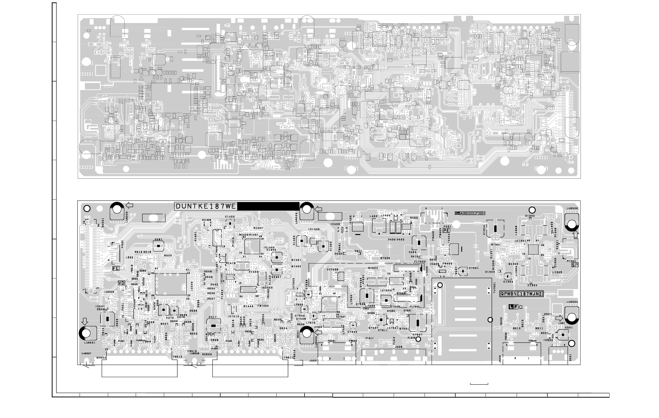
LC-42XL2E/S/RU, LC-46XL2E/S/RU, LC-46X20E/S/RU, LC-52XL2E/S/RU, LC-52X20E/S/RU
7 – 5
[2] TERMINAL UNIT PRINTED WIRING BOARD
123
4567 910
8
J
A
B
C
D
E
F
G
H
I
11 1312 14 15 16 18 1917
TERMINAL Unit (Side-A)
TERMINALUnit (Chip Parts Side-A)
X1401
R402
X1402
X1403
C1311
C1312 C1313
C1314
R408
C1315
R409
C1316
C1317
C1318
R600
C1319
R410
R604
R606
C1320
R608
C1321
R415
R609
C1322
C1323
C1324
D1301
C1326
D1302
C1327
D1303
C1328
D1304
R610
C1329
D1305
R1301
FB1401
FB1402
D1306
R1302
R612
R1303
R613
FB1403
R1304
R420
R614
R1305
R615
R1306
R616
R1307
R423
C1330
R1308
R618
R1309
IC1301
LUG501
R426
LUG502 LUG503
LUG504
LUG505
LUG506
R1310
R620
P7501
R1311
R621
R1312
R622
R1313
R623
R1314
R430
R1315
R431
R625
R432
R1316
R626
R433
R1317
R627
R1318
R628
R1319
R629
R438
R1320
R630
R1321
R631
C401
R632
C402
R1323
R633
C403
R1324
R634
C404
R1325
P501
R635
C405
C406
R1326
R636
C407
R1327
R1328
C408
R1329
C600
C601
C602
C603
R1330
C604
R1331
C411
C605
C7501
R1332
C606
C7502
R1333
R643
C607
C7503
R644
C414
C7504 C7505
Q7501
R646
C7506
Q7502
C417
C7507
C7508
Q7504
R649
C7509
Q7505
Q7506
Q7507
C610
C612
C613
C7510
R650
C420
C614
C615
C7511
R652
C422
C423
C617
C7514
C424
C7515
R656
C426
C7516
R657
C7517
C7518
C428
C429
C7519
C620
C621
C622
C623
C624
C7520
R660
C430
C625
R661
C431
C7521
C626
C432
C7522
C627
C433
C7523
C628
C434
C7524
C629
C7525
D7501
C7526
C7527
D7503
C7528
D7504
C7529
D7505
R7501
D7506
R7502
R7503
R7504
R7505
R7506
R670
C7530
R7508
R671
R7509
IC7501
R672
C7532
C7533
IC7503
IC7504
C7535
C7536
IC7506
C7537
IC7507
C7538
R7510
IC7508
C7539
R7512
R7516
R7517
C7540
R7518
IC7510
C7541
R7519
C7542
C7543
C7544
C7545
C7547
C7548
R7520 R7521
R7522
R7523
R7524
R7525
R7526
R7527
C7550
R7528
R7529
C7552
D402
C7553
C7554
D405
Q501
C7556
Q502
C7557
Q503
R7530
D408
Q504
D409
605Q505Q
R7533
Q507
R7534
Q508
R7535
Q509
R7536
R7537
D410
C7560
R7538
D411
C7561
R7539
D412
C7563
C7564
Q510
C7565
Q511
C7566
Q512
C7567
C7568
R7540
R7541
L501
Q516
L502
R7544
Q518
R7545
R7546
R7547
R7548
R7549
C7572
IC402
IC403
C7573
C7574
Q520
IC404
C7575
Q521
IC405
C7576
IC406
C7577
R7550
R7551
R7552
FL501
FL502
FL503
C7580
FL504
FL505
FL506
FL507
FL508
FL509
P1401
R7564
FL510
FL511
FL512
R7566
R7567
FL513
R7568
R7569 R7570
FB501
FB502
FB503
FB504
FB505
C1401
FB506
C1402
FB507
C1403
FB508
C1404
FB509
C1405
Q1401
C1406
Q1402
C1407
C1408
C1409
FB510
FB511
R501
FB512
FB513
R503
FB514
C1410
FB515
C1411
R505
FB516
C1412
FB517
C1413
R507
FB518
C1414
R508
FB519
C1415
R509
C1416
C1417
C1418
C1419
FB520
R510
FB521
R511
FB522
R512
FB523
R513
FB524
C1420
R514
C1421
R515
C1422
R516
C1423
R517
C1424
R518
C1425
R519
C1426
C1427
C1428
C1429
R1401
R1402
R1403
R520
R1404
R521
R1405
R522
R1406
R523
R1407
C1430
R524
R1408
R1409
C1431
R525
IC1401
C1432
R526
IC1402
C1433
R527
IC1403
R528
C1434
IC1404
R529
C1435
IC1405
IC1406
C1436
IC1407
C1437 C1438
R1410
C1439
R1411
R1412
R1413
R1414
R530
R531
R1415
R532
R1416
R1417
R533
R1418
C1440
R534
P401
C1441
R535
R1419
C1442
R536
C1443
R537
C1444
R538
C1445
R539
C1446
L1303
C1447
L1304
C1448
R1420
L1305
C1449
R1421
C501
L1306
R1422
C502
R1423
C503
R540
C504
R541
C505
R542
R1426
C506
R543
R1427
C507
C1450
R544
R1428
C508
C1451
R1429
R545
C509
C1452
R546
C1453
R547
C1454
R548
C1455
R549
C1456
C1457
C1458
R1430
C510
R1431
C1459
C511
X7501
C512
X7502
R1433
C513
R550
R1434
C514
R551
R1435
C515
R552
R1436
C516
R1437
R553
C517
R1438
C1460
R554
C518
C1461
R555
R1439
C519
C1462
R556
C1463
R557
C1464
R558
C1465
R559
C1466
C1467
C1468
R1440
C520
C1469
C521
R1442
C522
R1443
C523
R560
C524
R561
R1445
C525
R562
R1446
C526
R563
C527
R564
C528
R565
C529
R566
R569
FB7501
R1450
C530
C531
C532
R1453
C533
R570
R1454
C534
R571
R1455
R572
R1456
R573
R574
C538
R575
R576
R577
R578
R579
R1460
C540
R1461
C541
R1462
C542
R1463
C543
R580
R1464
C544
R581
R1465
C545
R582
R1466
C546
R583
R1467
C547
R584
R1468
C548
R585
R1469
C549
R586 R587
R588
R589
R1470
C550
C551
R1472
C552
R1473
C553
C554
R591
C555
R592
R1476
C556
L7502
R1477
C557
L7503
R1478
C558
L7504
R595
R1479
C559
L7505
R596
L7506
Q402
R598
R599
L7509
Q407
R1480
C560
R1481
C561
R1482
C562
D502
R1483
C563
D503
C564
L7510
D504
C565
L7511
D505
C566
D506
C567
D507
C568
D508
C569
D509
L402
C570
D510
C571
D511
C572
D512
C573
D513
C574
C575
D515
C576
C577
D517
C578
D518
C579
D519
C580
D520
C581
D521
IC501
C582
D522
IC502
C583
D523
IC503
C584
D524
C585
D525
IC505
C586
D526
IC506
C587
C588
C589
D529
P1301
D530
D531
C592
D532
C593
D533
D534
D535
D536D537
D541
D542
D543
D544
D545
D546
D548
FB401
FB402
FB404
C1301
FB405
C1302
FB406
C1303
C1304
D550
C1305
Q1301
D551
C1306
Q1302
C1307
Q1303
C1308
C1309
LC-42XL2E/S/RU, LC-46XL2E/S/RU, LC-46X20E/S/RU, LC-52XL2E/S/RU, LC-52X20E/S/RU
7 – 6
123
4567 910
8
J
A
B
C
D
E
F
G
H
I
11 1312 14 15 16 18 1917
TERMINAL Unit (Side-B)
LC-42XL2E/S/RU, LC-46XL2E/S/RU, LC-46X20E/S/RU, LC-52XL2E/S/RU, LC-52X20E/S/RU
7 – 7
[3] R/C, LED UNIT PRINTED WIRING BOARD [4] KEY UNIT PRINTED WIRING BOARD
123
4567 910
8
J
A
B
C
D
E
F
G
H
I
3
R101
C107
C102
SLD101
RMC101
D101
R132
IC101
C105
C104
R136
R135
R102
R105
D103
R117
R137 R108
Q104
R109
R104
R107 Q102
Q103
D114
R138
R106
Q105
R121
R126
R110
R123
Q106
D115
R127
R122
Q107
R124
C110
C108
C101
R103
RMC102
R119
R120
D116
IC102
R116
R118
C103
C111
P101
R139 R140
P102
R/C, LED Unit (Side A) R/C, LED Unit
(Chip Parts Side-A)
123
4567 910
8
J
A
B
C
D
E
F
G
H
I
S155
R153
D152
S154
S152
R151
D151
S151
R152
S153
R154
S156
S157
D155
P151
KEY Unit (Side A) KEY Unit
(Chip Parts Side-A)
LC-42XL2E/S/RU, LC-46XL2E/S/RU, LC-46X20E/S/RU, LC-52XL2E/S/RU, LC-52X20E/S/RU
7 – 8
[5] MINI AV UNIT PRINTED WIRING BOARD
123
4567 910
8
J
A
B
C
D
E
F
G
H
I
11 1312 14 15 16 18 1917
MINI AV Unit (Side-A)
MINI AV Unit (Chip Parts Side-A)
VA810
FB802
FB805
R801
R802
R803
R804
R805
R806
R807 R808
R809
R810
R811
R812
R813
R814
R815
R816
R817
R818
R819
R820
R821
R822
R823
R824
R825
LUG901
R826
LUG902
R827
R828
R829
R830
R831
SC802
R832
R834
R838
R839
C801
C802
C803
R840
C804
C805
P901
C806
C807
C808
C809
C810
C811
C812
C813
C814
C815
C816
C817
C818
C819
C820
C821 C822
C823
C824
C825
C826
C827
C828
C829
C830
C831
C832
D801
D802
D803
D804 D805
D806
D807
D808 D809
D810
IC801
IC802
IC803
IC804
IC805
IC806
IC807
FL901
FL902
FL903
FB902
FB903
R906
R907
R908
R909
R910
R911R912
R914
R915
P801
C903
C904
Q801
Q802
Q803
Q804
Q805
Q806
Q807
D903 D904D905
L801
L802
L803
L804 L805
L806
L807
L808
L809
VA801 VA802
VA803
VA804
VA805
VA806
VA807
VA808
VA809
LC-42XL2E/S/RU, LC-46XL2E/S/RU, LC-46X20E/S/RU, LC-52XL2E/S/RU, LC-52X20E/S/RU
7 – 9
123
4567 910
8
J
A
B
C
D
E
F
G
H
I
11 1312 14 15 16 18 1917
MINI AV Unit (Side-B)
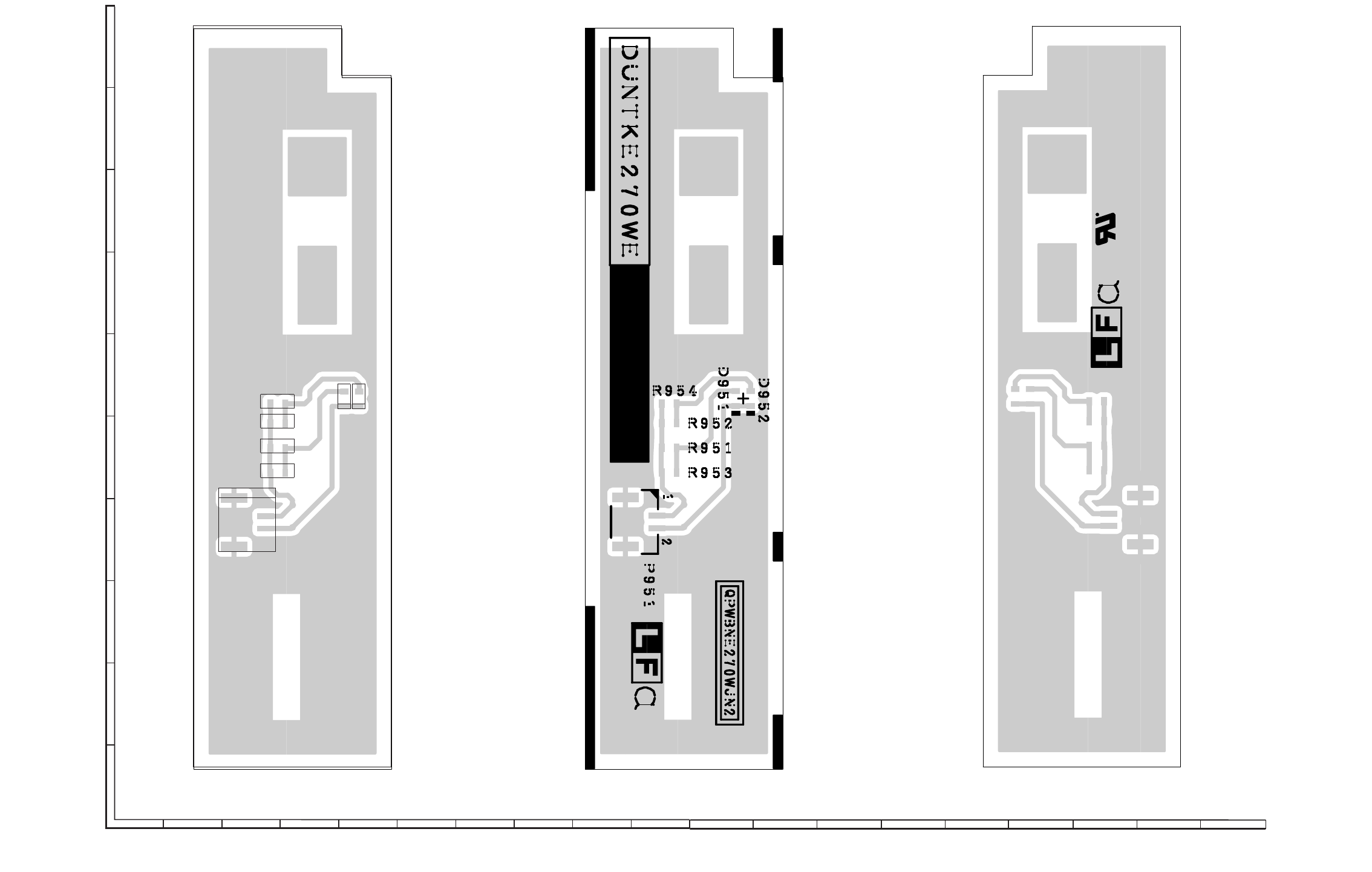
LC-42XL2E/S/RU, LC-46XL2E/S/RU, LC-46X20E/S/RU, LC-52XL2E/S/RU, LC-52X20E/S/RU
7 – 10
[6] ILLUMINATION UNIT PRINTED WIRING BOARD
123
4567 910
8
J
A
B
C
D
E
F
G
H
I
11 1312 14 15 16 18 1917
ILLUMINATION Unit (Side-A) ILLUMINATION Unit (Side-B)
ILLUMINATION Unit (Chip Parts Side-A)
D951
D952
P951
R951
R952
R953
R954
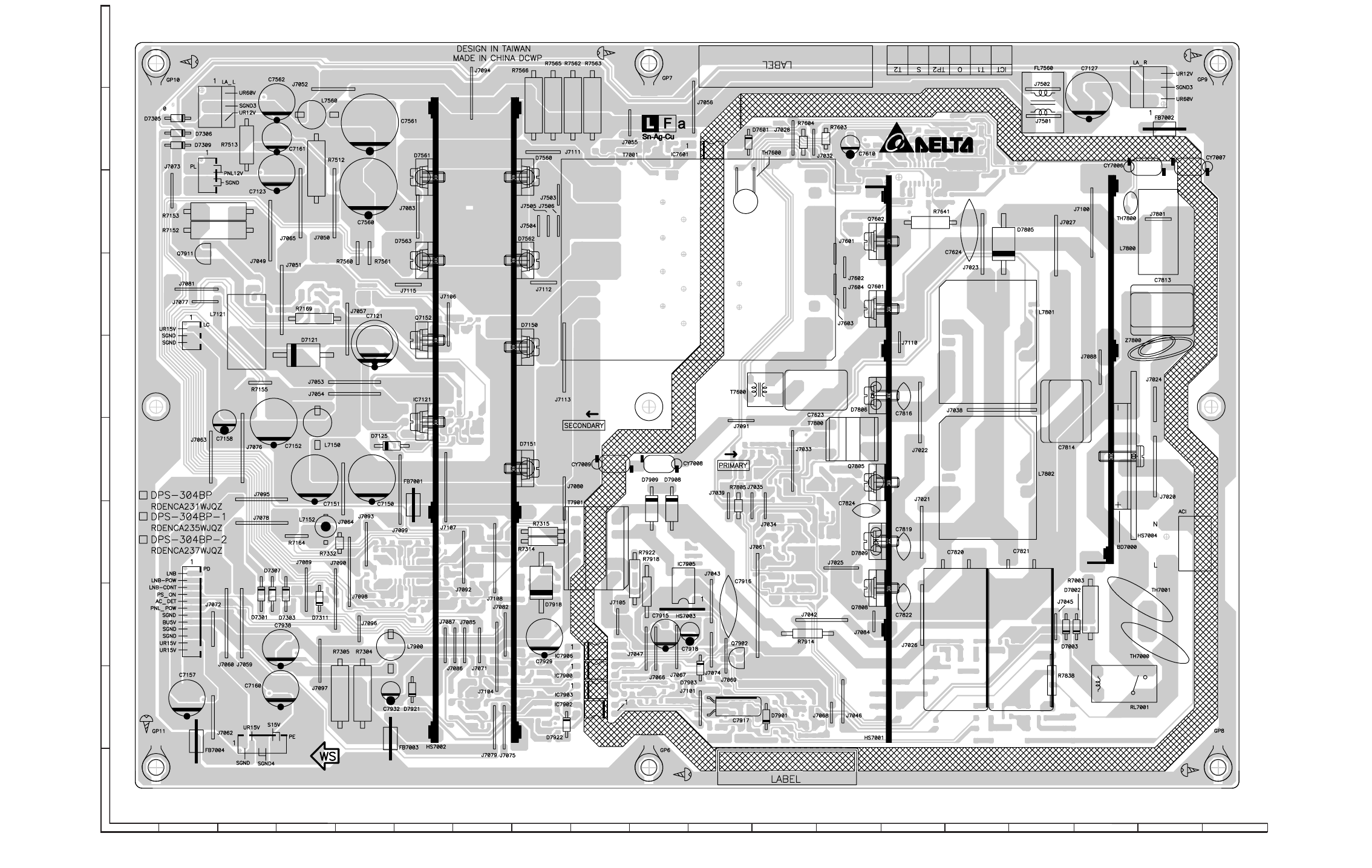
LC-42XL2E/S/RU, LC-46XL2E/S/RU, LC-46X20E/S/RU, LC-52XL2E/S/RU, LC-52X20E/S/RU
7 – 11
[7] POWER UNIT PRINTED WIRING BOARD
123
4567 910
8
J
A
B
C
D
E
F
G
H
I
POWER Unit (Side-A)
11 1312 14 15 16 18 1917
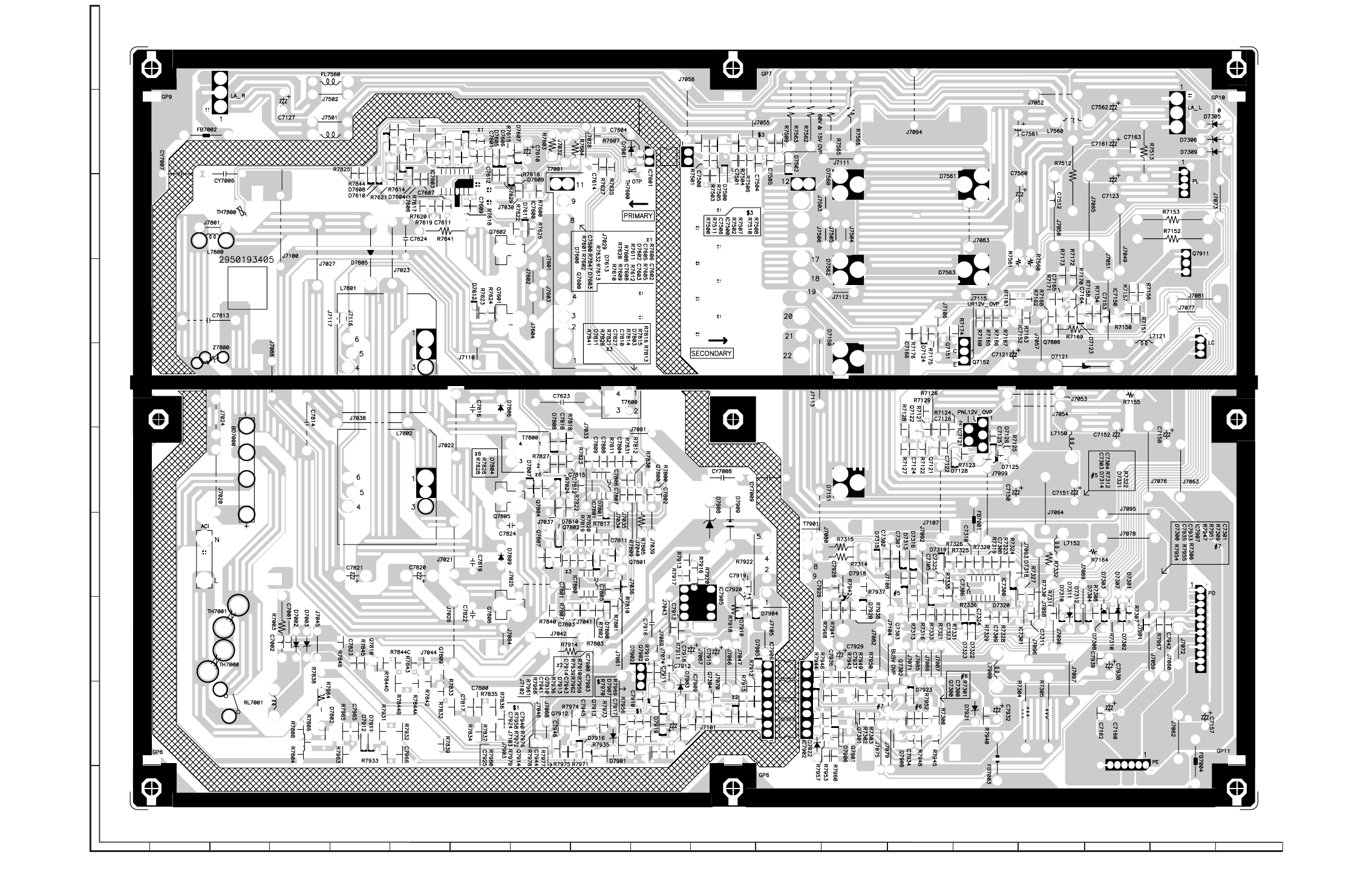
LC-42XL2E/S/RU, LC-46XL2E/S/RU, LC-46X20E/S/RU, LC-52XL2E/S/RU, LC-52X20E/S/RU
7 – 12
123
4567 910
8
J
A
B
C
D
E
F
G
H
I
POWER Unit (Side-B)
11 1312 14 15 16 18 1917
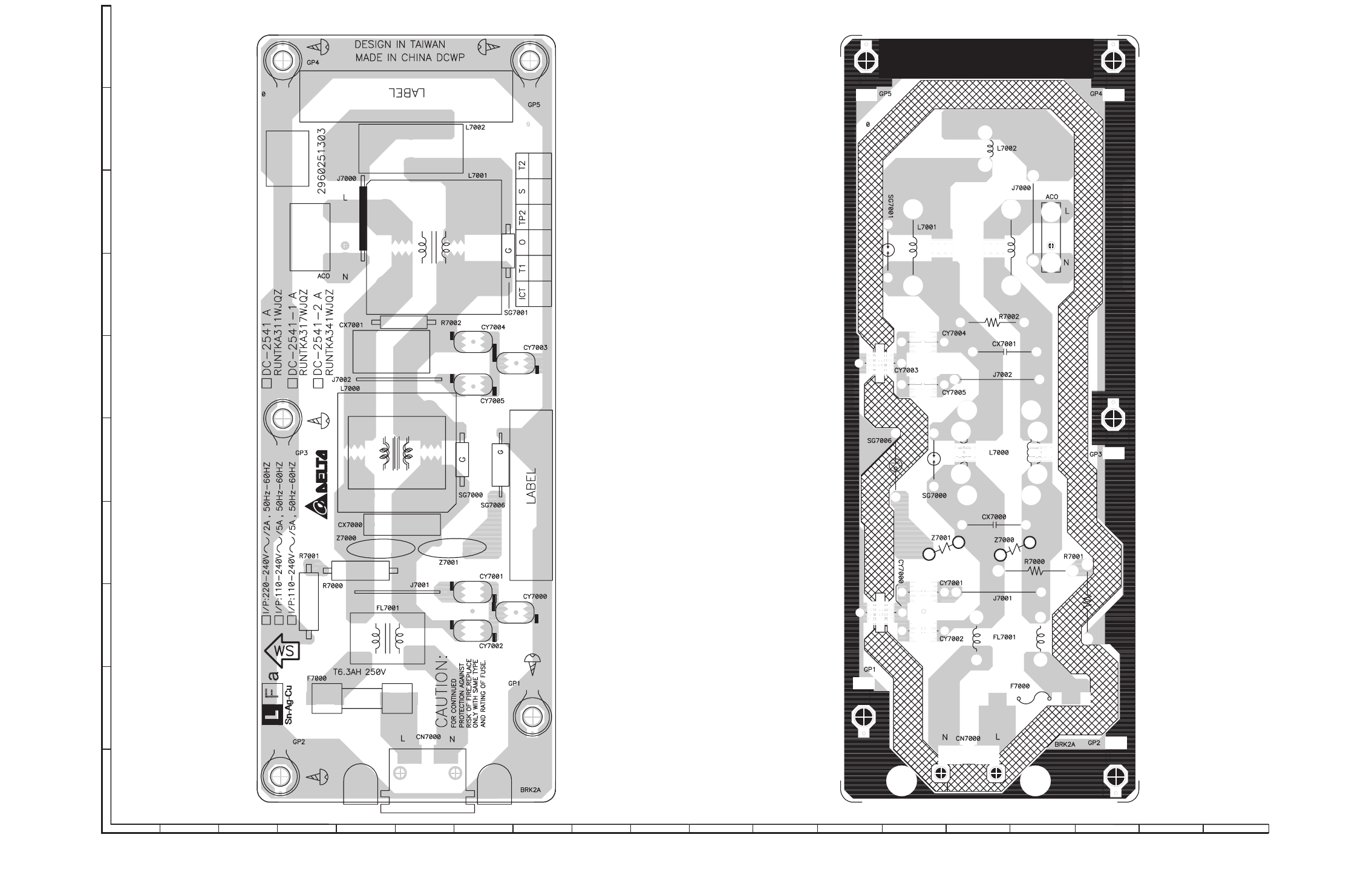
LC-42XL2E/S/RU, LC-46XL2E/S/RU, LC-46X20E/S/RU, LC-52XL2E/S/RU, LC-52X20E/S/RU
7 – 13
[8] AC INLET UNIT PRINTED WIRING BOARD
123
4567 910
8
J
A
B
C
D
E
F
G
H
I
AC INLET Unit (Side-A) AC INLET Unit (Side-B)
11 1312 14 15 16 18 1917

LC-42XL2E/S/RU, LC-46XL2E/S/RU, LC-46X20E/S/RU, LC-52XL2E/S/RU, LC-52X20E/S/RU
8 – 1
LC42XL2E Service Manual
CHAPTER 8. SCHEMATIC DIAGRAM
[1] DESCRIPTION OF SCHEMATIC DIAGRAM
VOLTAGE MEASUREMENT CONDITION:
1. The voltages at test points are measured on exclusive AC adaptor and the stable supply voltage of AC 230V.
Signals are fed by a colour bar signal generator for servicing purpose and the above voltages are measured with a 20k ohm/V tester.
INDICATION OF RESISTOR & CAPACITOR:
RESISTOR
1. The unit of resistance “Ω” is omitted.
(K=kΩ=1000 Ω, M=MΩ).
2. All resistors are ± 5%, unless otherwise noted.
(K= ± 10%, F= ± 1%, D= ± 0.5%)
3. All resistors are 1/16W, unless otherwise noted.
CAPACITOR
1. All capacitors are µF, unless otherwise noted.
(P=pF=µµF).
2. All capacitors are 50V, unless otherwise noted.
CAUTION:
This circuit diagram is original one, therefore there may be a
slight difference from yours.
SAFETY NOTES:
1. DISCONNECT THE AC PLUG FROM THE AC
OUTLET BEFORE REPLACING PARTS.
2. SEMICONDUCTOR HEAT SINKS SHOULD BE
REGARDED AS POTENTIAL SHOCK HAZARDS
WHEN THE CHASSIS IS OPERATING.
IMPORTANT SAFETY NOTICE:
PARTS MARKED WITH “ ” ( ) ARE
IMPORTANT FOR MAINTAINING THE SAFETY OF THE
SET. BE SURE TO REPLACE THESE PARTS WITH
SPECIFIED ONES FOR MAINTAINING THE SAFETY AND
PERFORMANCE OF THE SET.
LC-42XL2E/S/RU, LC-46XL2E/S/RU, LC-46X20E/S/RU, LC-52XL2E/S/RU, LC-52X20E/S/RU
8 – 2
[2] SCHEMATIC DIAGRAM
123
4567 910
8
J
A
B
C
D
E
F
G
H
I
MAIN Unit-1
11 1312 14 15 16 18 1917
LC-42XL2E/S/RU, LC-46XL2E/S/RU, LC-46X20E/S/RU, LC-52XL2E/S/RU, LC-52X20E/S/RU
8 – 3
123
4567 910
8
J
A
B
C
D
E
F
G
H
I
MAIN Unit-2
11 1312 14 15 16 18 1917
LC-42XL2E/S/RU, LC-46XL2E/S/RU, LC-46X20E/S/RU, LC-52XL2E/S/RU, LC-52X20E/S/RU
8 – 4
123
4567 910
8
J
A
B
C
D
E
F
G
H
I
MAIN Unit-3
11 1312 14 15 16 18 1917
LC-42XL2E/S/RU, LC-46XL2E/S/RU, LC-46X20E/S/RU, LC-52XL2E/S/RU, LC-52X20E/S/RU
8 – 5
123
4567 910
8
J
A
B
C
D
E
F
G
H
I
MAIN Unit-4
11 1312 14 15 16 18 1917
(LC-42/46/52XL2E/S/RU)
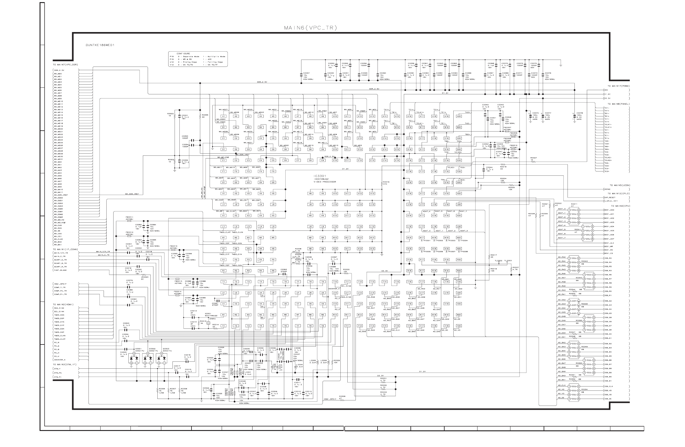
LC-42XL2E/S/RU, LC-46XL2E/S/RU, LC-46X20E/S/RU, LC-52XL2E/S/RU, LC-52X20E/S/RU
8 – 6
123
4567 910
8
J
A
B
C
D
E
F
G
H
I
MAIN Unit-5
11 1312 14 15 16 18 1917
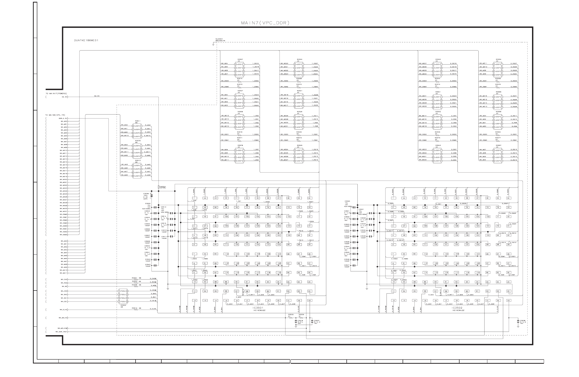
LC-42XL2E/S/RU, LC-46XL2E/S/RU, LC-46X20E/S/RU, LC-52XL2E/S/RU, LC-52X20E/S/RU
8 – 7
123
4567 910
8
J
A
B
C
D
E
F
G
H
I
MAIN Unit-6
11 1312 14 15 16 18 1917
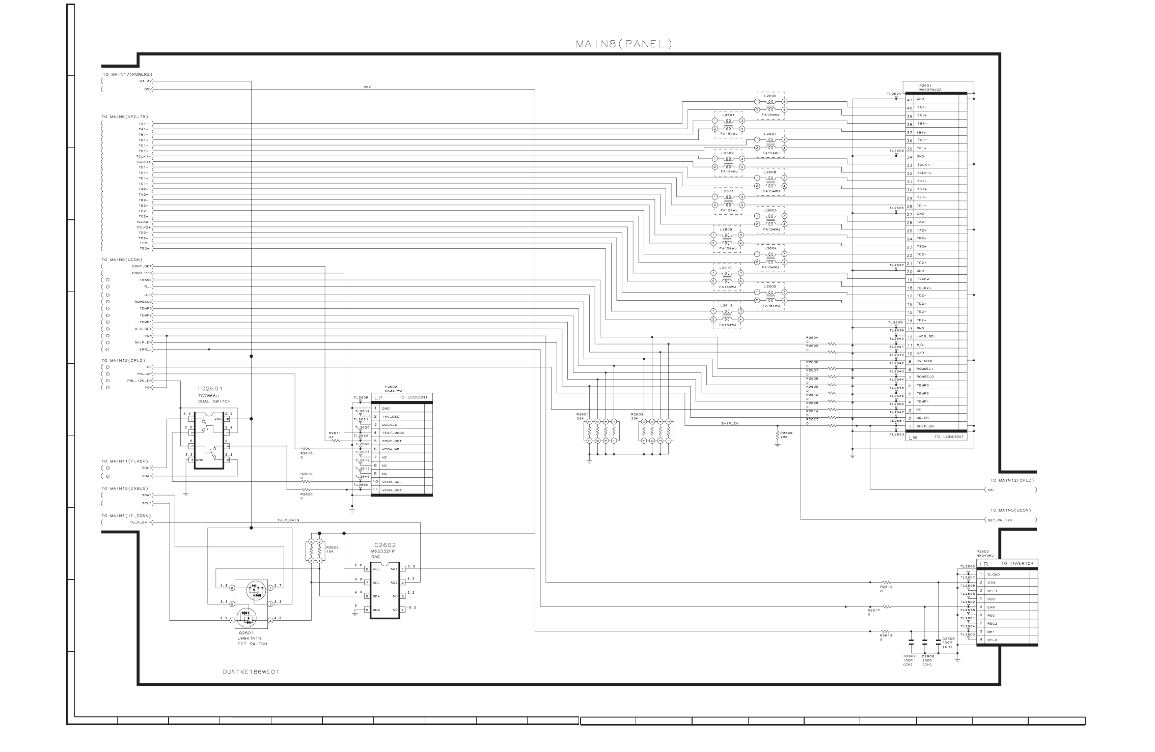
LC-42XL2E/S/RU, LC-46XL2E/S/RU, LC-46X20E/S/RU, LC-52XL2E/S/RU, LC-52X20E/S/RU
8 – 8
123
4567 910
8
J
A
B
C
D
E
F
G
H
I
MAIN Unit-7
11 1312 14 15 16 18 1917
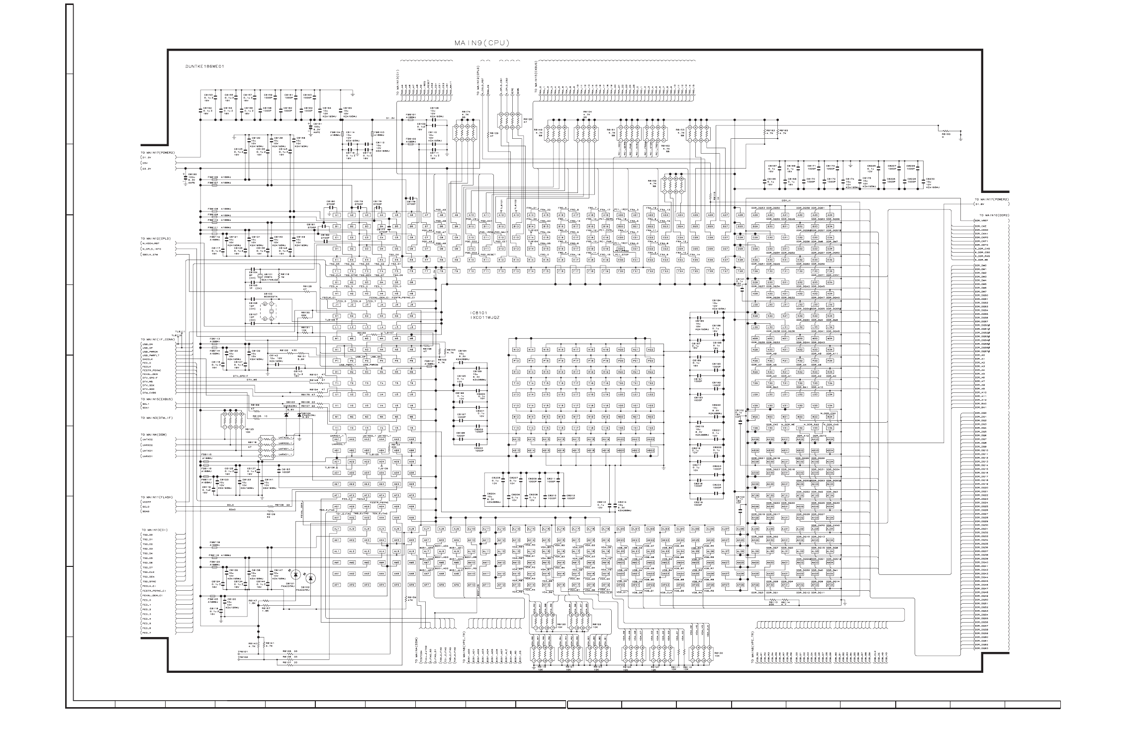
LC-42XL2E/S/RU, LC-46XL2E/S/RU, LC-46X20E/S/RU, LC-52XL2E/S/RU, LC-52X20E/S/RU
8 – 9
123
4567 910
8
J
A
B
C
D
E
F
G
H
I
MAIN Unit-8
11 1312 14 15 16 18 1917
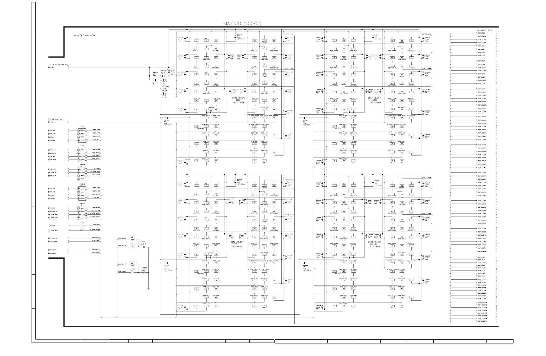
LC-42XL2E/S/RU, LC-46XL2E/S/RU, LC-46X20E/S/RU, LC-52XL2E/S/RU, LC-52X20E/S/RU
8 – 10
123
4567 910
8
J
A
B
C
D
E
F
G
H
I
MAIN Unit-9
11 1312 14 15 16 18 1917
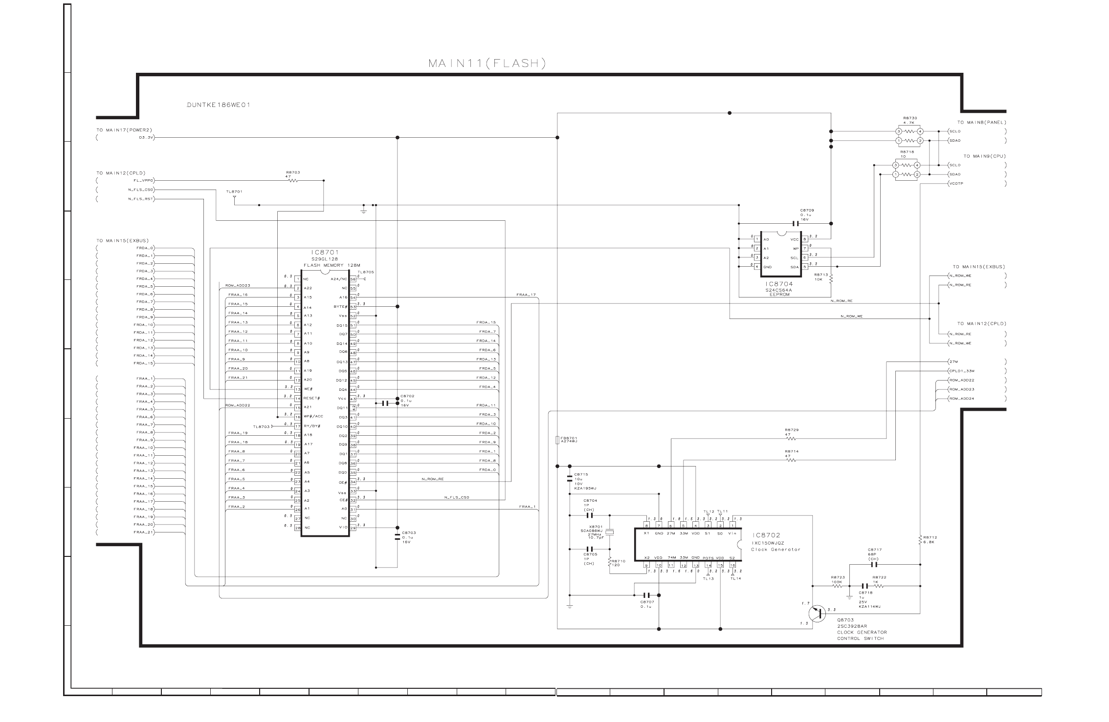
LC-42XL2E/S/RU, LC-46XL2E/S/RU, LC-46X20E/S/RU, LC-52XL2E/S/RU, LC-52X20E/S/RU
8 – 11
123
4567 910
8
J
A
B
C
D
E
F
G
H
I
MAIN Unit-10
11 1312 14 15 16 18 1917
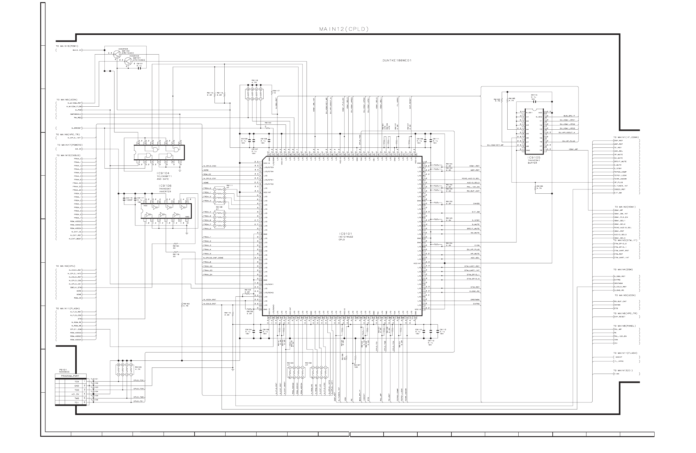
LC-42XL2E/S/RU, LC-46XL2E/S/RU, LC-46X20E/S/RU, LC-52XL2E/S/RU, LC-52X20E/S/RU
8 – 12
123
4567 910
8
J
A
B
C
D
E
F
G
H
I
MAIN Unit-11
11 1312 14 15 16 18 1917
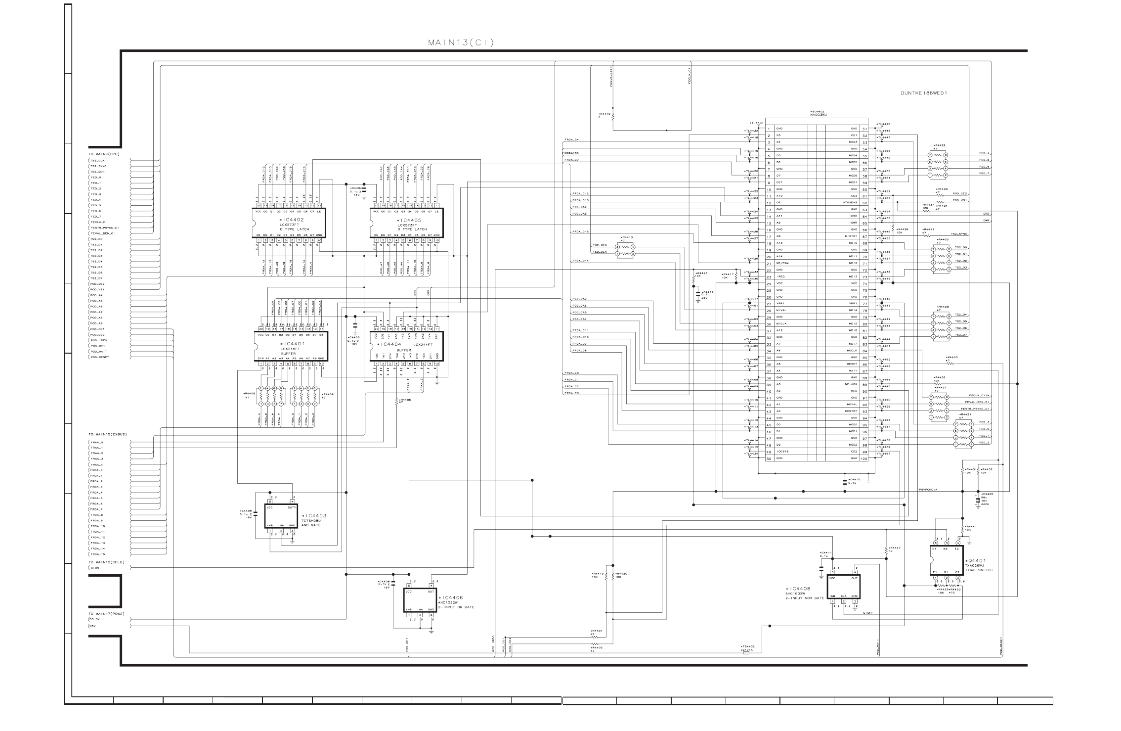
LC-42XL2E/S/RU, LC-46XL2E/S/RU, LC-46X20E/S/RU, LC-52XL2E/S/RU, LC-52X20E/S/RU
8 – 13
123
4567 910
8
J
A
B
C
D
E
F
G
H
I
MAIN Unit-12
11 1312 14 15 16 18 1917
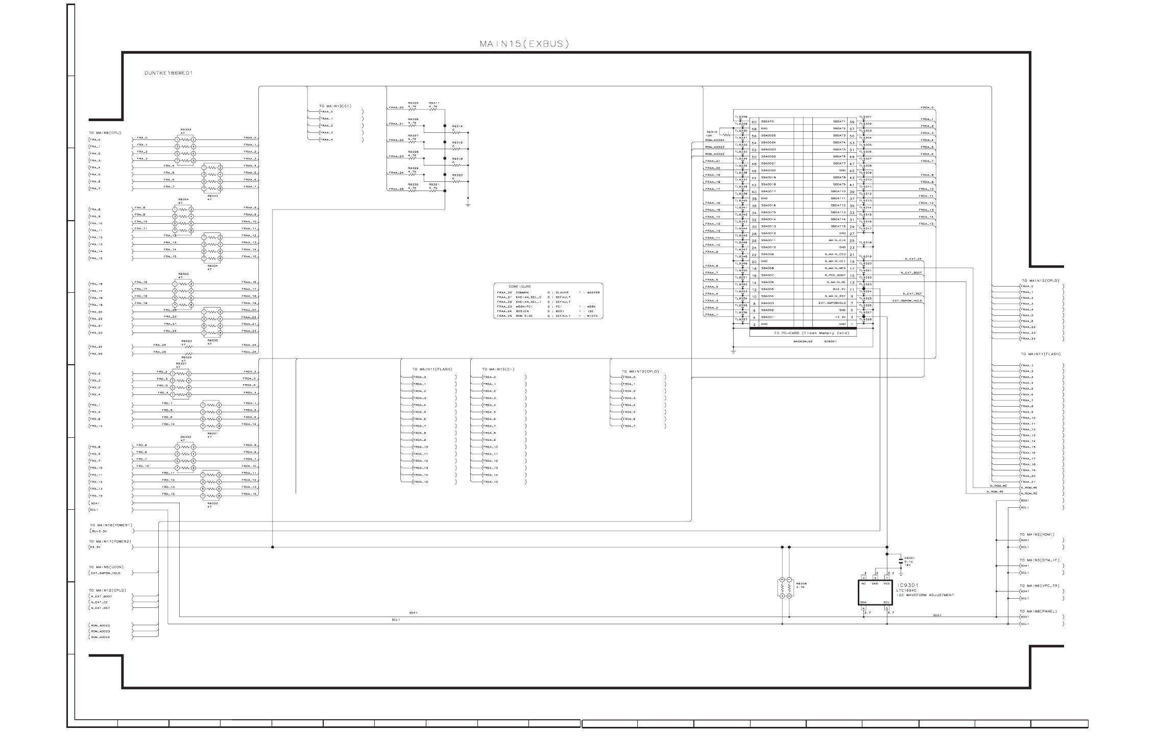
LC-42XL2E/S/RU, LC-46XL2E/S/RU, LC-46X20E/S/RU, LC-52XL2E/S/RU, LC-52X20E/S/RU
8 – 14
123
4567 910
8
J
A
B
C
D
E
F
G
H
I
MAIN Unit-13
11 1312 14 15 16 18 1917
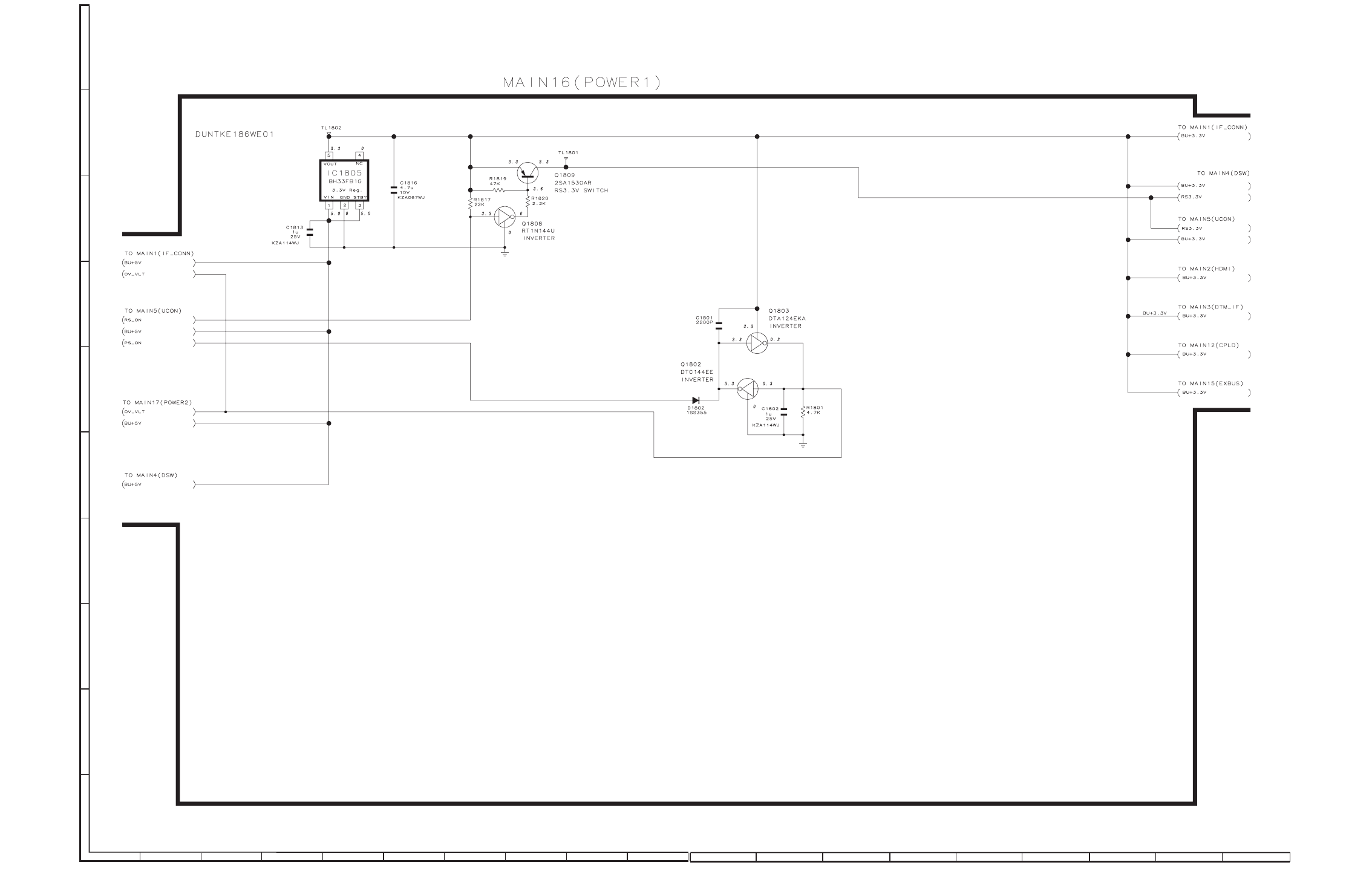
LC-42XL2E/S/RU, LC-46XL2E/S/RU, LC-46X20E/S/RU, LC-52XL2E/S/RU, LC-52X20E/S/RU
8 – 15
123
4567 910
8
J
A
B
C
D
E
F
G
H
I
MAIN UNit-14
11 1312 14 15 16 18 1917
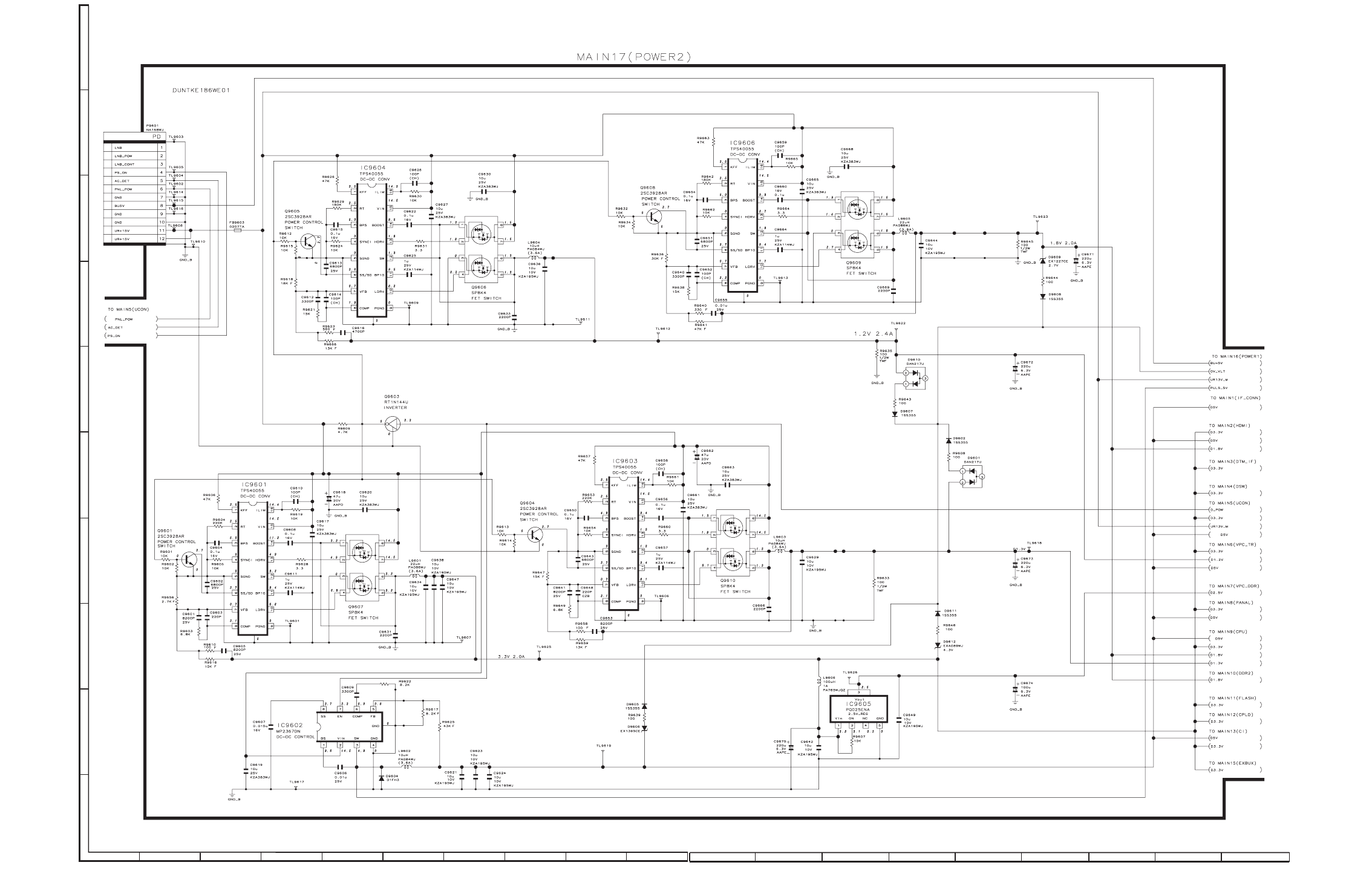
LC-42XL2E/S/RU, LC-46XL2E/S/RU, LC-46X20E/S/RU, LC-52XL2E/S/RU, LC-52X20E/S/RU
8 – 16
123
4567 910
8
J
A
B
C
D
E
F
G
H
I
MAIN Unit-15
11 1312 14 15 16 18 1917
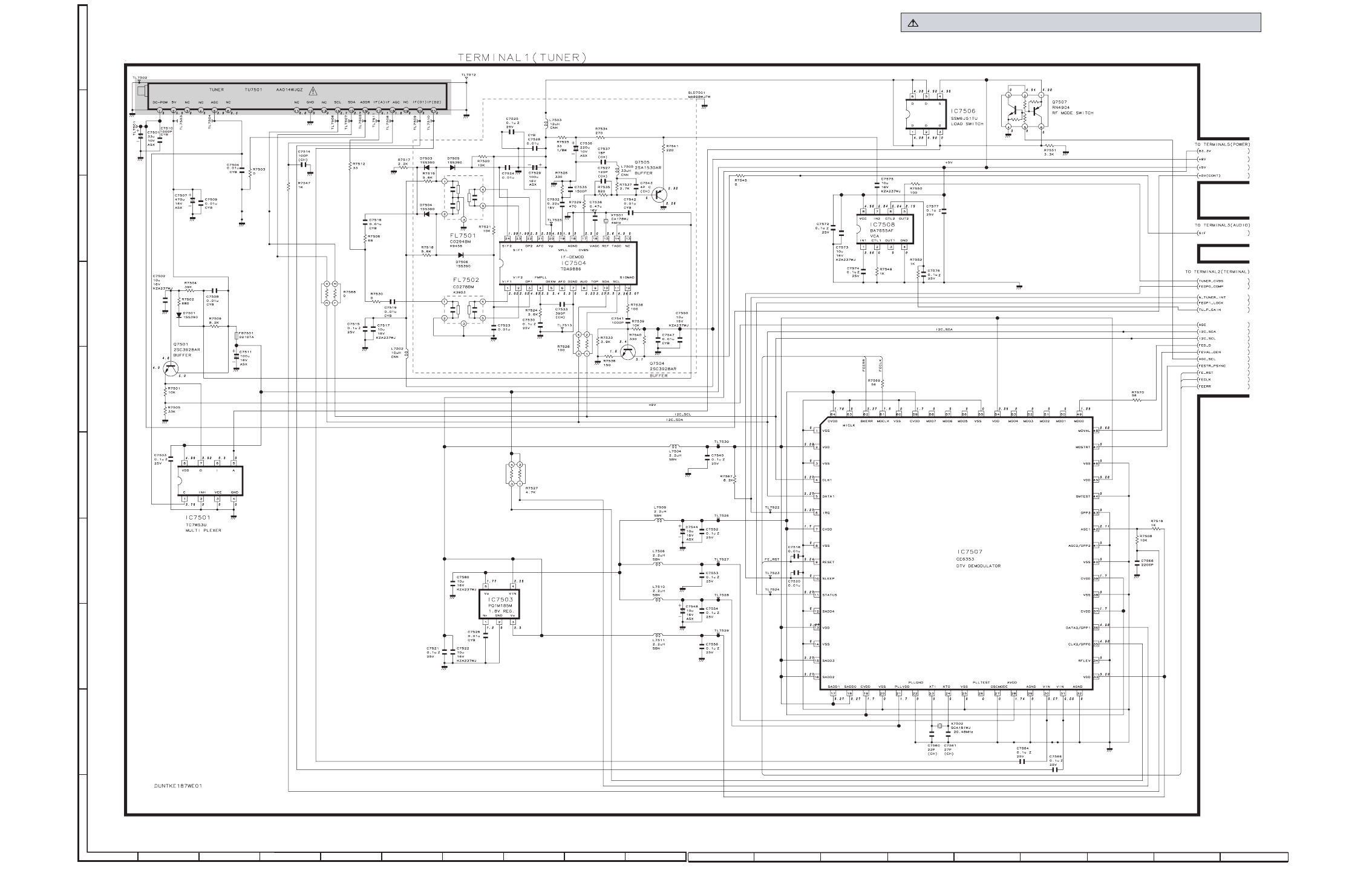
LC-42XL2E/S/RU, LC-46XL2E/S/RU, LC-46X20E/S/RU, LC-52XL2E/S/RU, LC-52X20E/S/RU
8 – 17
123
4567 910
8
J
A
B
C
D
E
F
G
H
I
TERMINAL Unit-1
11 1312 14 15 16 18 1917
AND SHADED COMPONENTS=SAFETY RELATED PARTS
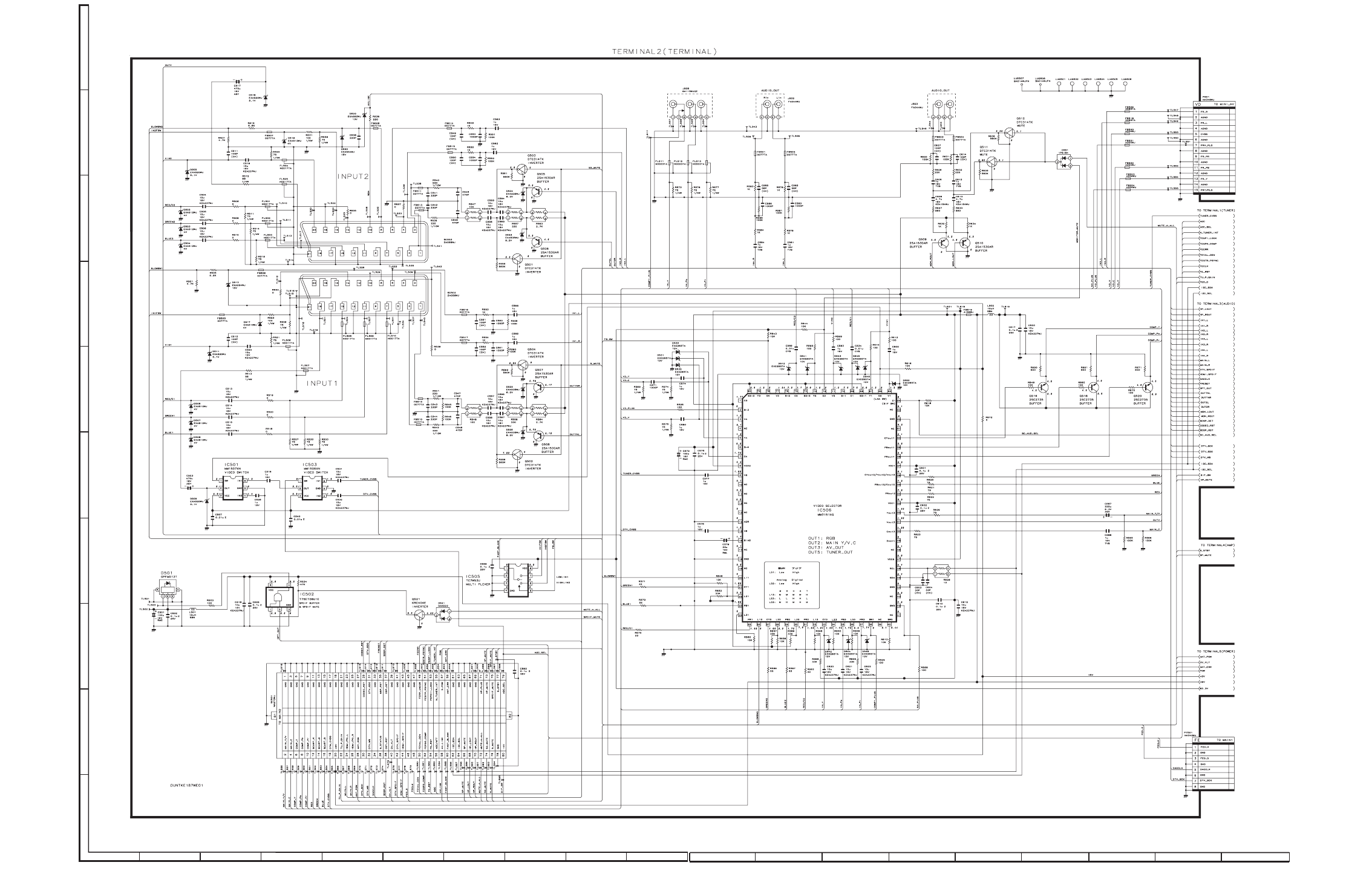
LC-42XL2E/S/RU, LC-46XL2E/S/RU, LC-46X20E/S/RU, LC-52XL2E/S/RU, LC-52X20E/S/RU
8 – 18
123
4567 910
8
J
A
B
C
D
E
F
G
H
I
TERMINAL Unit-2
11 1312 14 15 16 18 1917
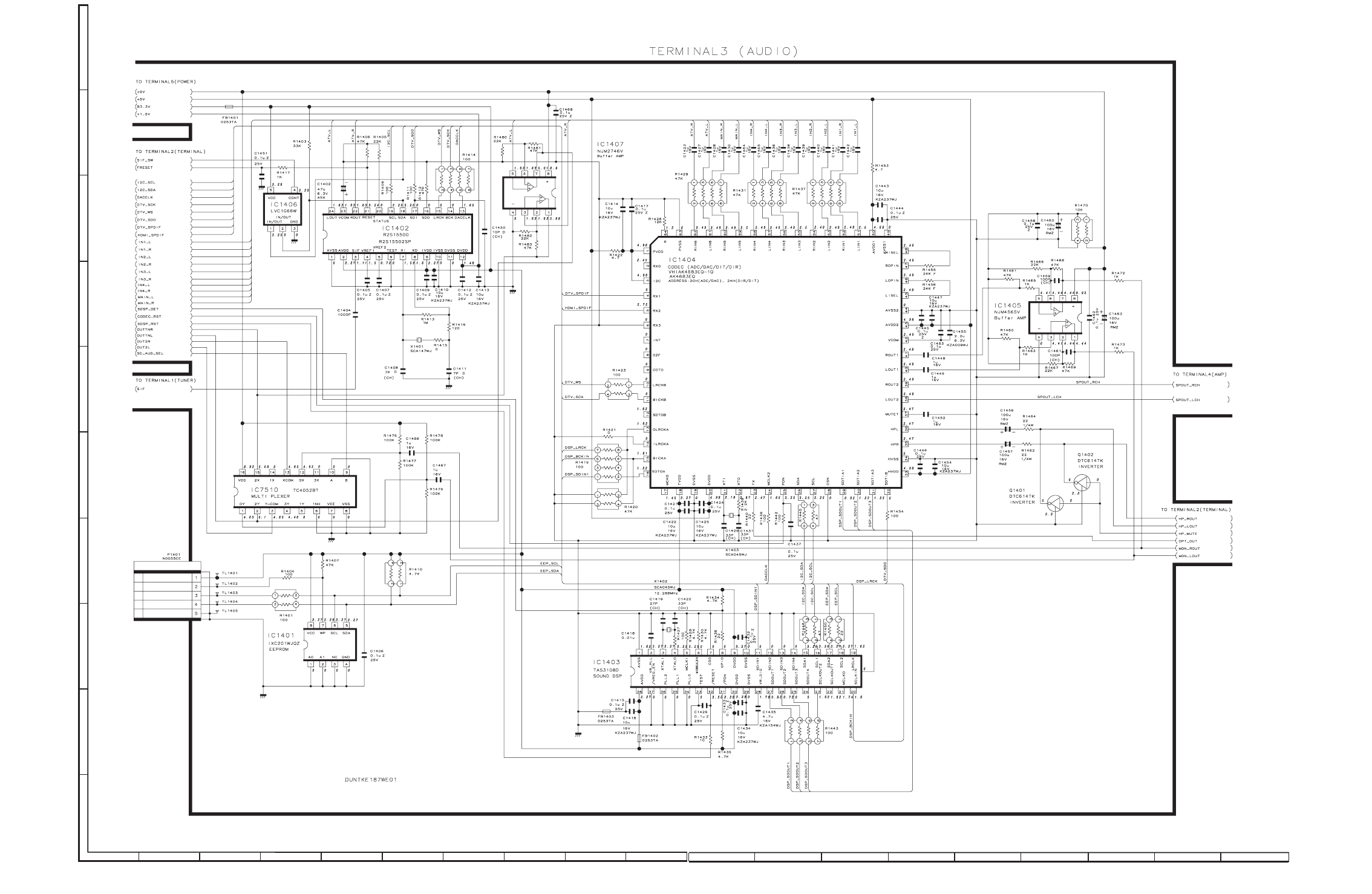
LC-42XL2E/S/RU, LC-46XL2E/S/RU, LC-46X20E/S/RU, LC-52XL2E/S/RU, LC-52X20E/S/RU
8 – 19
123
4567 910
8
J
A
B
C
D
E
F
G
H
I
TERMINAL Unit-3
11 1312 14 15 16 18 1917
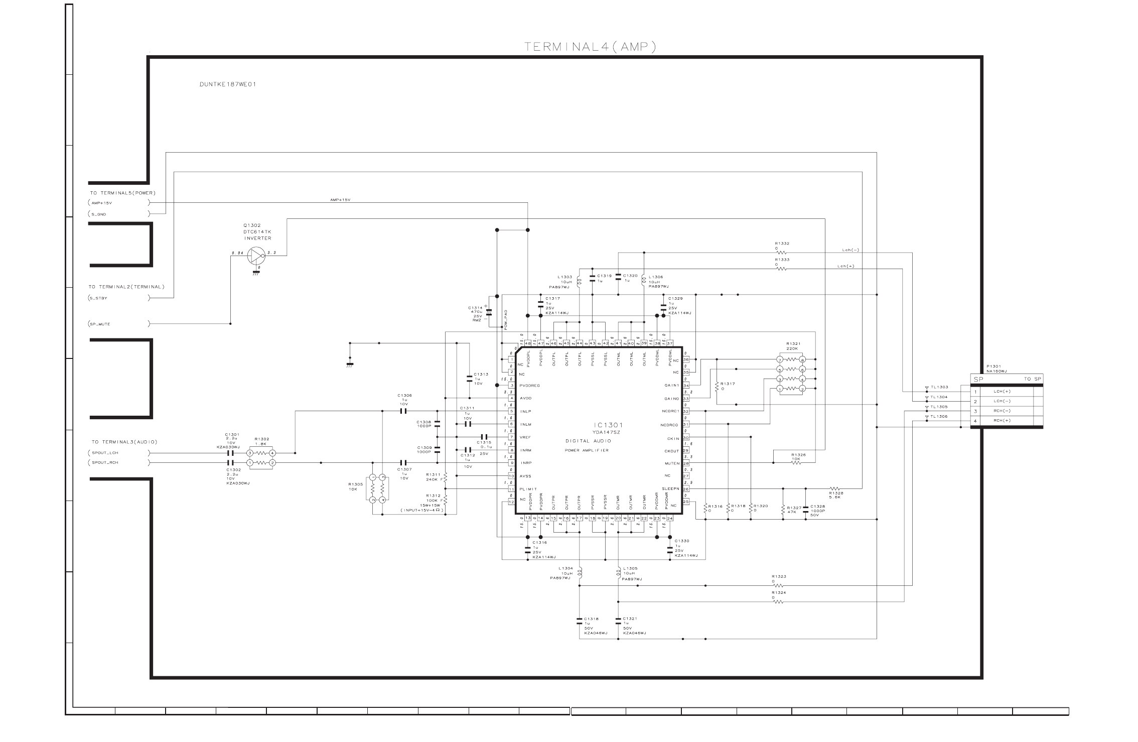
LC-42XL2E/S/RU, LC-46XL2E/S/RU, LC-46X20E/S/RU, LC-52XL2E/S/RU, LC-52X20E/S/RU
8 – 20
123
4567 910
8
J
A
B
C
D
E
F
G
H
I
TERMINAL Unit-4
11 1312 14 15 16 18 1917
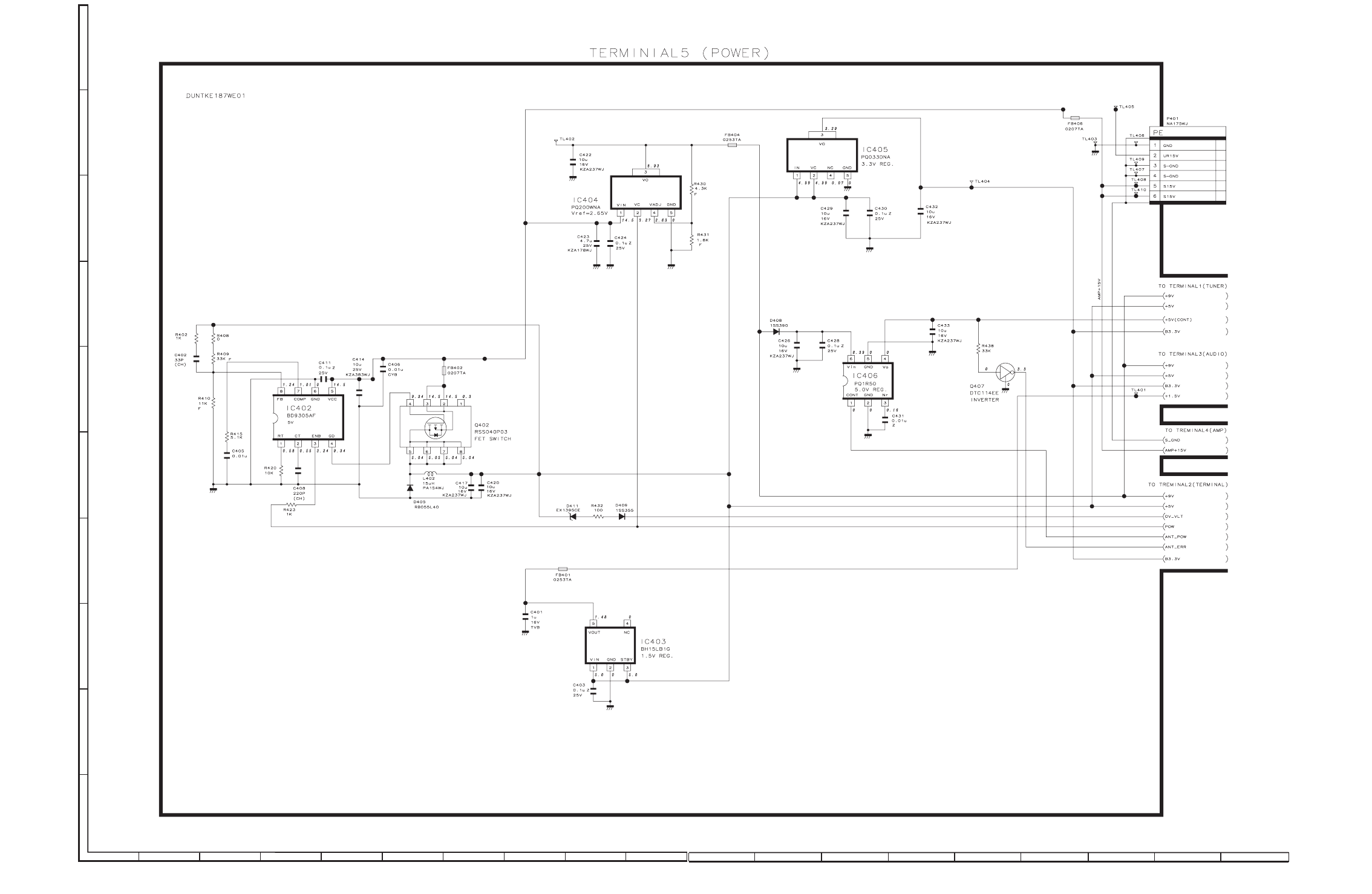
LC-42XL2E/S/RU, LC-46XL2E/S/RU, LC-46X20E/S/RU, LC-52XL2E/S/RU, LC-52X20E/S/RU
8 – 21
123
4567 910
8
J
A
B
C
D
E
F
G
H
I
TERMINAL Unit-5
11 1312 14 15 16 18 1917
LC-42XL2E/S/RU, LC-46XL2E/S/RU, LC-46X20E/S/RU, LC-52XL2E/S/RU, LC-52X20E/S/RU
8 – 22
123
4567 910
8
J
A
B
C
D
E
F
G
H
I
11 1312 14 15 16 18 1917
R/C, LED Unit
LC-42XL2E/S/RU, LC-46XL2E/S/RU, LC-46X20E/S/RU, LC-52XL2E/S/RU, LC-52X20E/S/RU
8 – 23
123
4567 910
8
J
A
B
C
D
E
F
G
H
I
11 1312 14 15 16 18 1917
KEY Unit
LC-42XL2E/S/RU, LC-46XL2E/S/RU, LC-46X20E/S/RU, LC-52XL2E/S/RU, LC-52X20E/S/RU
8 – 24
123
4567 910
8
J
A
B
C
D
E
F
G
H
I
MINI AV Unit
11 1312 14 15 16 18 1917
LC-42XL2E/S/RU, LC-46XL2E/S/RU, LC-46X20E/S/RU, LC-52XL2E/S/RU, LC-52X20E/S/RU
8 – 25
123
4567 910
8
J
A
B
C
D
E
F
G
H
I
11 1312 14 15 16 18 1917
ILLUMINATION Unit
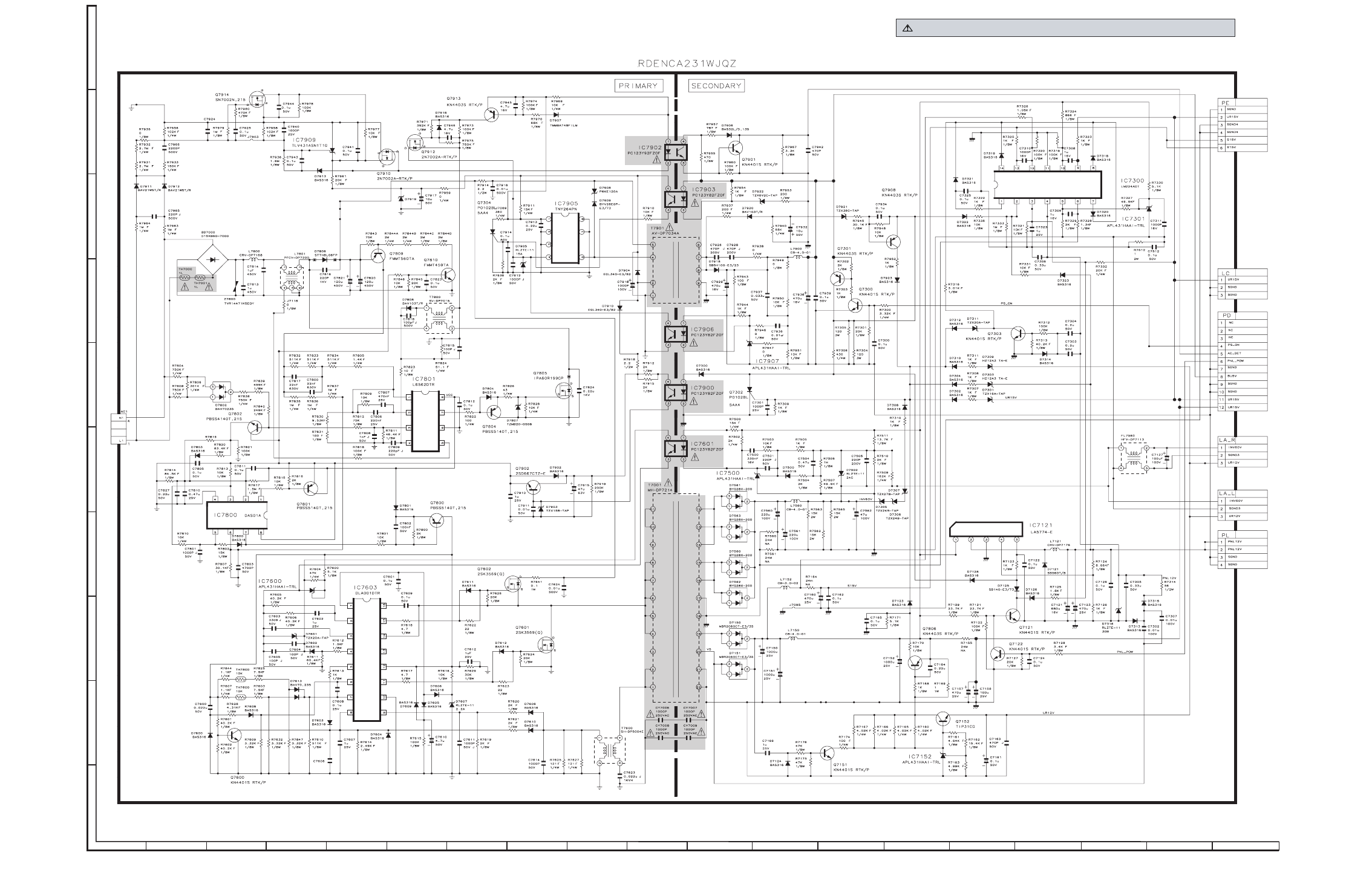
LC-42XL2E/S/RU, LC-46XL2E/S/RU, LC-46X20E/S/RU, LC-52XL2E/S/RU, LC-52X20E/S/RU
8 – 26
123
4567 910
8
J
A
B
C
D
E
F
G
H
I
POWER Unit
11 1312 14 15 16 18 1917
AND SHADED COMPONENTS=SAFETY RELATED PARTS
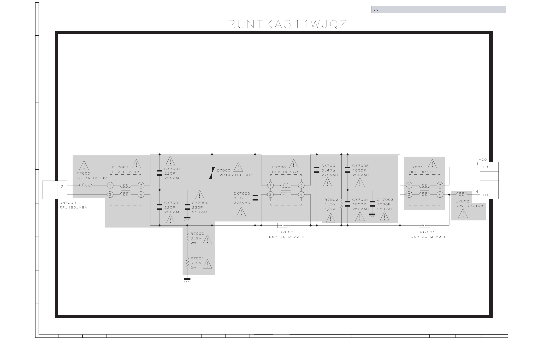
LC-42XL2E/S/RU, LC-46XL2E/S/RU, LC-46X20E/S/RU, LC-52XL2E/S/RU, LC-52X20E/S/RU
8 – 27
123
4567 910
8
J
A
B
C
D
E
F
G
H
I
AC INLET Unit
11 1312 14 15 16 18 1917
AND SHADED COMPONENTS=SAFETY RELATED PARTS

LC-42XL2E/S/RU, LC-46XL2E/S/RU, LC-46X20E/S/RU, LC-52XL2E/S/RU, LC-52X20E/S/RU
8 – 28
— M E M O —
PARTS GUIDE
Parts marked with " " are important for maintaining the safety of the set. Be sure to replace these
parts with specified ones for maintaining the safety and performance of the set.
This document has been published to be used
for after sales service only.
The contents are subject to change without notice.
LC-42XL2E/S/RU, LC-46XL2E/S/RU, LC-46X20E/S/RU, LC-52XL2E/S/RU, LC-52X20E/S/RU
PartsGuide
[1] PRINTED WIRING BOARD
ASSEMBLIES
[2] LCD PANEL AND TUNER (NOTE:
THE PARTS HERE SHOWN ARE
SUPPLIED AS AN ASSEMBLY BUT
NOT INDEPENDENTLY.)
[3] DUNTKE186FM01/FM02
(MAIN Unit)
[4] DUNTKE187FM01/FM02
(TERMINAL Unit)
[5] DUNTKE264FM01 (R/C, LED Unit)
[6] DUNTKE266FM01 (KEY Unit)
[7] DUNTKE188FM01 (MINI AV Unit)
[8] DUNTKE270FM01 (ILLUMI Unit)
[9] CABINET PARTS
(LC-42XL2E/S/RU)
[10] CABINET PARTS
(LC-46XL2E/S/RU)
[11] CABINET PARTS
(LC-46X20E/S/RU)
[12] CABINET PARTS
(LC-52XL2E/S/RU)
[13] CABINET PARTS
(LC-52X20E/S/RU)
[14] SUPPLIED ACCESSOORIES
(LC-42/46/52XL2E/S/RU)
[15] OPERATION MANUALS
(SMPL models: (LC-42/46/52XL2E/
S/RU))
[16] OPERATION MANUALS
(SMPL models:LC-46/52X20E/S/
RU)
[17] OPERATION MANUALS
(SEES models:LC-46/52X20E/S/
RU)
[18] PACKING PARTS
(LC-42XL2E/S/RU)
[19] PACKING PARTS
(LC-46XL2E/S/RU, 46X20E/S/RU)
[20] PACKING PARTS
(LC-52XL2E/S/RU, 52X20E/S/RU)
[21] SERVICE JIGS
CONTENTS
No.S87O7LC42XL2E
LCD COLOUR TELEVISION
LC-42XL2E/S/RU
LC-46XL2E/S/RU
LC-46X20E/S/RU
LC-52XL2E/S/RU
LC-52X20E/S/RU
LC-42/46/52XL2E/S/RU LC-46/52X20E/S/RU
LC-42XL2E/S/RU, LC-46XL2E/S/RU, LC-46X20E/S/RU, LC-52XL2E/S/RU, LC-52X20E/S/RU
2
NO. PARTS CODE PRICE
RANK NEW
MARK PART
DELIVERY
DESCRIPTION
[1] PRINTED WIRING BOARD ASSEMBLIES
NDUNTKE186FM01 N R MAIN Unit (LC-42/46/52XL2E/S/RU)
NDUNTKE186FM02 N R MAIN Unit (LC-46/52X20E/S/RU)
NDUNTKE187FM01 N R TERMINAL Unit (LC-42XL2E/S/RU, 46XL2E/S/RU, 52XL2E/S/RU)
NDUNTKE187FM02 N R TERMINAL Unit (LC-46X20E/S/RU, 52X20E/S/RU)
NDUNTKE264FM01 N R R/C, LED Unit
NDUNTKE266FM01 N R KEY Unit
NDUNTKE188FM01 N R MIN IAV Unit
NDUNTKE270FM01 N R ILLUMINATION Unit (LC-42/46/52XL2E/S/RU only)
NRDENCA231WJQZ - N P POWER Unit (Unit Replacement Item)
NRUNTKA311WJQZ - N P AC INLET Unit (Unit Replacement Item)
[2] LCD PANEL AND TUNER (NOTE: THE PARTS HERE SHOWN ARE SUPPLIED AS AN ASSEMBLY BUT
NOT INDEPENDENTLY.)
NR1LK420D3LZ60Y N J 42" Full HD LCD Panel Module (LC-42XL2E/S/RU)
NR1LK460D3LZ60Y FT N J 46" Full HD LCD Panel Module (LC-46XL2E/S/RU)
NR1LK460D3LZ50Y ** N J 46" Full HD LCD Panel Module (LC-46X20E/S/RU)
NR1LK520D3LZ60Y N J 52" Full HD LCD Panel Module (LC-52XL2E/S/RU)
NR1LK520D3LZ50Y N J 52" Full HD LCD Panel Module (LC-52X20E/S/RU)
!
TU7501 RTUDAA014WJQZ AX N P Tuner
[3] DUNTKE186FM01/FM02 (MAIN Unit)
C1112 RC-KZA510WJPZY AB J Capacitor 10 16V Ceramic
C1117 VCCCCZ1HH3R0CY AA J Capacitor 30p 50V Ceramic
C1118 VCCCCZ1HH3R0CY AA J Capacitor 30p 50V Ceramic
C1119 VCCCCZ1HH3R0CY AA J Capacitor 30p 50V Ceramic
C1120 VCCCCZ1HH390JY AB J Capacitor 39p 50V Ceramic
C1121 VCCCCZ1HH390JY AB J Capacitor 39p 50V Ceramic
C1122 VCCCCZ1HH390JY AB J Capacitor 39p 50V Ceramic
C1123 VCCCCZ1HH150JY AB J Capacitor 15p 50V Ceramic
C1124 VCCCCZ1HH181JY AB J Capacitor 180p 50V Ceramic
C1125 VCCCCZ1HH101JY AB J Capacitor 100p 50V Ceramic
C1126 VCCCCZ1HH471JY AA J Capacitor 470p 50V Ceramic
C1128 VCAAPE1CJ686MY AE J Capacitor 68 16V Electrolytic
C1129 VCCCCZ1HH150JY AB J Capacitor 15p 50V Ceramic
C1130 VCCCCZ1HH150JY AB J Capacitor 15p 50V Ceramic
C1137 VCKYCZ1HB221KY AA J Capacitor 220p 50V Ceramic
C1138 VCKYCZ1HB221KY AA J Capacitor 220p 50V Ceramic
C1501 VCKYCZ1CF104ZY AA J Capacitor 0.1 16V Ceramic
C1502 VCKYCZ1CF104ZY AA J Capacitor 0.1 16V Ceramic
C1503 VCKYCZ1HB221KY AA J Capacitor 220p 50V Ceramic
C1504 VCKYCZ1CF104ZY AA J Capacitor 0.1 16V Ceramic
C1505 VCKYCZ1HB221KY AA J Capacitor 220p 50V Ceramic
C1506 VCKYCZ1HB221KY AA J Capacitor 220p 50V Ceramic
C1507 RC-KZA195WJZZY AB J Capacitor 10 10V Ceramic
C1508 RC-KZA195WJZZY AB J Capacitor 10 10V Ceramic
C1509 VCKYCZ1HB221KY AA J Capacitor 220p 50V Ceramic
C1510 VCKYCZ1HB102KY AB J Capacitor 1000p 50V Ceramic
C1511 VCKYCZ1HB102KY AB J Capacitor 1000p 50V Ceramic
C1512 VCKYTV1CB105KY AC J Capacitor 1 16V Ceramic
C1513 VCKYTV1CB105KY AC J Capacitor 1 16V Ceramic
C1514 VCERML1CN106MY AC J Capacitor 10 16V Electrolytic
C1515 VCKYCZ1CF104ZY AA J Capacitor 0.1 16V Ceramic
C1516 VCKYCZ1HB102KY AB J Capacitor 1000p 50V Ceramic
C1517 RC-KZA195WJZZY AB J Capacitor 10 10V Ceramic
C1521 VCKYCZ1HB102KY AB J Capacitor 1000p 50V Ceramic
C1522 RC-KZA510WJPZY AB J Capacitor 10 16V Ceramic
C1523 VCKYTV1CB105KY AC J Capacitor 1 16V Ceramic
C1524 VCKYTV1CB105KY AC J Capacitor 1 16V Ceramic
C1525 VCKYTV1CB105KY AC J Capacitor 1 16V Ceramic
C1526 VCKYTV1CB105KY AC J Capacitor 1 16V Ceramic
C1531 VCKYCZ1CF104ZY AA J Capacitor 0.1 16V Ceramic
C1532 VCKYCZ1HB102KY AB J Capacitor 1000p 50V Ceramic
C1534 VCKYCZ1CF104ZY AA J Capacitor 0.1 16V Ceramic
C1538 VCKYCZ1CF104ZY AA J Capacitor 0.1 16V Ceramic
C1540 VCAAPE0JJ227MY AE J Capacitor 220 6.3V Electrolytic
C1543 VCKYCZ1CF104ZY AA J Capacitor 0.1 16V Ceramic
C1544 VCKYCZ1HB102KY AB J Capacitor 1000p 50V Ceramic
C1545 VCKYCZ1CF104ZY AA J Capacitor 0.1 16V Ceramic
C1546 VCKYCZ1HB102KY AB J Capacitor 1000p 50V Ceramic
C1547 VCKYCZ1CF104ZY AA J Capacitor 0.1 16V Ceramic
C1548 VCKYCZ1HB102KY AB J Capacitor 1000p 50V Ceramic
C1551 RC-KZA195WJZZY AB J Capacitor 10 10V Ceramic
C1578 VCKYCZ1CF104ZY AA J Capacitor 0.1 16V Ceramic
C1579 VCKYCZ1HB102KY AB J Capacitor 1000p 50V Ceramic
C1582 VCKYCZ1CF104ZY AA J Capacitor 0.1 16V Ceramic
C1583 VCKYCZ1HB102KY AB J Capacitor 1000p 50V Ceramic
C1586 VCKYCZ1CF104ZY AA J Capacitor 0.1 16V Ceramic
C1587 VCKYCZ1HB102KY AB J Capacitor 1000p 50V Ceramic
C1589 VCKYCZ1CF104ZY AA J Capacitor 0.1 16V Ceramic
C1591 VCKYCZ1HB102KY AB J Capacitor 1000p 50V Ceramic
C1592 VCKYCZ1CF104ZY AA J Capacitor 0.1 16V Ceramic
C1596 VCKYCZ1CF104ZY AA J Capacitor 0.1 16V Ceramic
C1597 VCKYCZ1HB102KY AB J Capacitor 1000p 50V Ceramic
C1599 VCKYCZ1HB102KY AB J Capacitor 1000p 50V Ceramic

LC-42XL2E/S/RU, LC-46XL2E/S/RU, LC-46X20E/S/RU, LC-52XL2E/S/RU, LC-52X20E/S/RU
3
NO. PARTS CODE PRICE
RANK NEW
MARK PART
DELIVERY
DESCRIPTION
C1608 RC-KZA195WJZZY AB J Capacitor 10 10V Ceramic
C1613 VCKYCZ1CF104ZY AA J Capacitor 0.1 16V Ceramic
C1614 VCKYCZ1HB102KY AB J Capacitor 1000p 50V Ceramic
C1615 VCKYCZ1CF104ZY AA J Capacitor 0.1 16V Ceramic
C1616 VCKYCZ1HB102KY AB J Capacitor 1000p 50V Ceramic
C1801 VCKYCZ1HB222KY AB J Capacitor 2200p 50V Ceramic
C1802 RC-KZA114WJZZY AB J Capacitor 1 25V Ceramic
C1813 RC-KZA114WJZZY AB J Capacitor 1 25V Ceramic
C1816 RC-KZA067WJZZY AB J Capacitor 4.7 10V Ceramic
C2001 VCKYCZ1CF104ZY AA J Capacitor 0.1 16V Ceramic
C2002 VCKYCZ1HB152KY AB J Capacitor 1500p 50V Ceramic
C2003 VCKYCZ1CF104ZY AA J Capacitor 0.1 16V Ceramic
C2009 VCCCCZ1HH120JY AB J Capacitor 12p 50V Ceramic
C2011 VCCCCZ1HH120JY AB J Capacitor 12p 50V Ceramic
C2012 VCKYCZ1CF104ZY AA J Capacitor 0.1 16V Ceramic
C2016 VCKYCZ1CF104ZY AA J Capacitor 0.1 16V Ceramic
C2019 RC-KZA195WJZZY AB J Capacitor 10 10V Ceramic
C2020 VCKYCZ1HB102KY AB J Capacitor 1000p 50V Ceramic
C2021 VCKYCZ1CF104ZY AA J Capacitor 0.1 16V Ceramic
C2023 VCKYCZ1CF104ZY AA J Capacitor 0.1 16V Ceramic
C2026 VCKYCZ1CF104ZY AA J Capacitor 0.1 16V Ceramic
C2027 VCKYCZ1CF104ZY AA J Capacitor 0.1 16V Ceramic
C2030 VCKYCZ1CB103KY AB J Capacitor 0.01 16V Ceramic
C2034 VCKYCZ1CF104ZY AA J Capacitor 0.1 16V Ceramic
C2401 VCKYCZ1CF104ZY AA J Capacitor 0.1 16V Ceramic
C2402 VCKYCZ1CF104ZY AA J Capacitor 0.1 16V Ceramic
C2403 RC-KZA195WJZZY AB J Capacitor 10 10V Ceramic
C2404 VCKYCZ1CF104ZY AA J Capacitor 0.1 16V Ceramic
C2405 VCKYCZ1CF104ZY AA J Capacitor 0.1 16V Ceramic
C2406 VCKYCZ1CF104ZY AA J Capacitor 0.1 16V Ceramic
C2407 VCKYCZ1CF104ZY AA J Capacitor 0.1 16V Ceramic
C2408 VCKYCZ1CF104ZY AA J Capacitor 0.1 16V Ceramic
C2410 VCKYCZ1CF104ZY AA J Capacitor 0.1 16V Ceramic
C2606 VCCCCZ1HH101JY AB J Capacitor 100p 50V Ceramic
C2607 VCCCCZ1HH101JY AB J Capacitor 100p 50V Ceramic
C2608 VCCCCZ1HH101JY AB J Capacitor 100p 50V Ceramic
C3301 VCKYCZ1CF104ZY AA J Capacitor 0.1 16V Ceramic
C3302 VCKYCZ1CF104ZY AA J Capacitor 0.1 16V Ceramic
C3303 VCKYCZ1CF104ZY AA J Capacitor 0.1 16V Ceramic
C3304 VCKYCZ1CF104ZY AA J Capacitor 0.1 16V Ceramic
C3305 VCKYCZ1CF104ZY AA J Capacitor 0.1 16V Ceramic
C3306 VCKYCZ1CF104ZY AA J Capacitor 0.1 16V Ceramic
C3307 VCKYCZ1CF104ZY AA J Capacitor 0.1 16V Ceramic
C3308 VCKYCZ1CF104ZY AA J Capacitor 0.1 16V Ceramic
C3309 VCKYCZ1CF104ZY AA J Capacitor 0.1 16V Ceramic
C3310 VCKYCZ1CF104ZY AA J Capacitor 0.1 16V Ceramic
C3311 VCKYCZ1CF104ZY AA J Capacitor 0.1 16V Ceramic
C3312 VCKYCZ1CF104ZY AA J Capacitor 0.1 16V Ceramic
C3313 VCCCCZ1HH3R0CY AA J Capacitor 30p 50V Ceramic
C3314 VCCCCZ1HH3R0CY AA J Capacitor 30p 50V Ceramic
C3315 VCKYCZ1CF104ZY AA J Capacitor 0.1 16V Ceramic
C3316 VCKYCZ1CF104ZY AA J Capacitor 0.1 16V Ceramic
C3317 VCKYCZ1CF104ZY AA J Capacitor 0.1 16V Ceramic
C3318 VCKYCZ1CF104ZY AA J Capacitor 0.1 16V Ceramic
C3319 VCKYCZ1CF104ZY AA J Capacitor 0.1 16V Ceramic
C3320 VCKYCZ1CF104ZY AA J Capacitor 0.1 16V Ceramic
C3321 VCKYCZ1CF104ZY AA J Capacitor 0.1 16V Ceramic
C3322 VCKYCZ1CF104ZY AA J Capacitor 0.1 16V Ceramic
C3323 VCKYCZ1CF104ZY AA J Capacitor 0.1 16V Ceramic
C3324 VCKYCZ1CF104ZY AA J Capacitor 0.1 16V Ceramic
C3325 RC-KZA195WJZZY AB J Capacitor 10 10V Ceramic
C3326 RC-KZA195WJZZY AB J Capacitor 10 10V Ceramic
C3327 RC-KZA195WJZZY AB J Capacitor 10 10V Ceramic
C3328 VCKYCZ1CF104ZY AA J Capacitor 0.1 16V Ceramic
C3329 RC-KZA195WJZZY AB J Capacitor 10 10V Ceramic
C3330 VCKYCZ1CF104ZY AA J Capacitor 0.1 16V Ceramic
C3331 RC-KZA195WJZZY AB J Capacitor 10 10V Ceramic
C3332 VCKYCZ1CF104ZY AA J Capacitor 0.1 16V Ceramic
C3333 RC-KZA195WJZZY AB J Capacitor 10 10V Ceramic
C3334 VCKYCZ1CF104ZY AA J Capacitor 0.1 16V Ceramic
C3335 RC-KZA195WJZZY AB J Capacitor 10 10V Ceramic
C3336 VCKYCZ1CF104ZY AA J Capacitor 0.1 16V Ceramic
C3337 RC-KZA195WJZZY AB J Capacitor 10 10V Ceramic
C3338 VCKYCZ1CF104ZY AA J Capacitor 0.1 16V Ceramic
C3339 RC-KZA195WJZZY AB J Capacitor 10 10V Ceramic
C3340 VCKYCZ1CF104ZY AA J Capacitor 0.1 16V Ceramic
C3341 RC-KZA195WJZZY AB J Capacitor 10 10V Ceramic
C3342 VCKYCZ1CF104ZY AA J Capacitor 0.1 16V Ceramic
C3343 RC-KZA195WJZZY AB J Capacitor 10 10V Ceramic
C3344 VCKYCZ1CF104ZY AA J Capacitor 0.1 16V Ceramic
C3345 VCKYCZ1CF104ZY AA J Capacitor 0.1 16V Ceramic
C3346 RC-KZA195WJZZY AB J Capacitor 10 10V Ceramic
C3347 VCKYCZ1CF104ZY AA J Capacitor 0.1 16V Ceramic
C3348 RC-KZA195WJZZY AB J Capacitor 10 10V Ceramic
C3349 VCKYCZ1CF104ZY AA J Capacitor 0.1 16V Ceramic
[3] DUNTKE186FM01/FM02 (MAIN Unit)

LC-42XL2E/S/RU, LC-46XL2E/S/RU, LC-46X20E/S/RU, LC-52XL2E/S/RU, LC-52X20E/S/RU
4
NO. PARTS CODE PRICE
RANK NEW
MARK PART
DELIVERY
DESCRIPTION
C3350 VCKYCZ1CF104ZY AA J Capacitor 0.1 16V Ceramic
C3351 VCKYCZ1CF104ZY AA J Capacitor 0.1 16V Ceramic
C3352 VCKYCZ1CF104ZY AA J Capacitor 0.1 16V Ceramic
C3353 VCKYCZ1HB102KY AB J Capacitor 1000p 50V Ceramic
C3354 VCKYCZ1HB102KY AB J Capacitor 1000p 50V Ceramic
C3355 VCKYCZ1HB102KY AB J Capacitor 1000p 50V Ceramic
C3356 VCKYCZ1HB102KY AB J Capacitor 1000p 50V Ceramic
C3357 RC-KZA195WJZZY AB J Capacitor 10 10V Ceramic
C3358 VCKYCZ1CF104ZY AA J Capacitor 0.1 16V Ceramic
C3359 VCKYCZ1CF104ZY AA J Capacitor 0.1 16V Ceramic
C3360 VCKYCZ1CF104ZY AA J Capacitor 0.1 16V Ceramic
C3361 VCKYCZ1CF104ZY AA J Capacitor 0.1 16V Ceramic
C3362 VCKYCZ1HB102KY AB J Capacitor 1000p 50V Ceramic
C3363 VCKYCZ1HB102KY AB J Capacitor 1000p 50V Ceramic
C3364 VCKYCZ1HB102KY AB J Capacitor 1000p 50V Ceramic
C3365 VCKYCZ1HB102KY AB J Capacitor 1000p 50V Ceramic
C3366 RC-KZA195WJZZY AB J Capacitor 10 10V Ceramic
C3367 VCKYCZ1CF104ZY AA J Capacitor 0.1 16V Ceramic
C3368 VCKYCZ1CF104ZY AA J Capacitor 0.1 16V Ceramic
C3369 VCKYCZ1CF104ZY AA J Capacitor 0.1 16V Ceramic
C3370 VCKYCZ1CF104ZY AA J Capacitor 0.1 16V Ceramic
C3371 VCKYCZ1HB102KY AB J Capacitor 1000p 50V Ceramic
C3372 VCKYCZ1HB102KY AB J Capacitor 1000p 50V Ceramic
C3373 VCKYCZ1HB102KY AB J Capacitor 1000p 50V Ceramic
C3374 VCAAPE0JJ107MY AE J Capacitor 100 6.3V Electrolytic
C3375 VCKYCZ1HB102KY AB J Capacitor 1000p 50V Ceramic
C3376 RC-KZA195WJZZY AB J Capacitor 10 10V Ceramic
C3377 VCAAPE0JJ107MY AE J Capacitor 100 6.3V Electrolytic
C3378 VCAAPE0JJ107MY AE J Capacitor 100 6.3V Electrolytic
C3379 VCKYCZ1CF104ZY AA J Capacitor 0.1 16V Ceramic
C3380 VCKYCZ1CF104ZY AA J Capacitor 0.1 16V Ceramic
C3381 VCKYCZ1CF104ZY AA J Capacitor 0.1 16V Ceramic
C3382 VCKYCZ1CF104ZY AA J Capacitor 0.1 16V Ceramic
C3383 VCKYCZ1CF104ZY AA J Capacitor 0.1 16V Ceramic
C3384 RC-KZA195WJZZY AB J Capacitor 10 10V Ceramic
C3385 RC-KZA195WJZZY AB J Capacitor 10 10V Ceramic
C3386 VCKYCZ1CF104ZY AA J Capacitor 0.1 16V Ceramic
C3387 VCKYCZ1CF104ZY AA J Capacitor 0.1 16V Ceramic
C3388 RC-KZA195WJZZY AB J Capacitor 10 10V Ceramic
C3389 RC-KZA195WJZZY AB J Capacitor 10 10V Ceramic
C3390 RC-KZA195WJZZY AB J Capacitor 10 10V Ceramic
C3391 VCKYCZ1HB272KY AA J Capacitor 2700p 50V Ceramic
C3393 VCKYCZ1HB272KY AA J Capacitor 2700p 50V Ceramic
C3395 VCKYCZ1CF104ZY AA J Capacitor 0.1 16V Ceramic
C3396 RC-KZA195WJZZY AB J Capacitor 10 10V Ceramic
C3397 VCKYCZ1CF104ZY AA J Capacitor 0.1 16V Ceramic
C3398 RC-KZA195WJZZY AB J Capacitor 10 10V Ceramic
C3502 RC-KZA195WJZZY AB J Capacitor 10 10V Ceramic
C3503 VCKYCZ1CF104ZY AA J Capacitor 0.1 16V Ceramic
C3504 VCKYCZ1CF104ZY AA J Capacitor 0.1 16V Ceramic
C3505 VCKYCZ1HB102KY AB J Capacitor 1000p 50V Ceramic
C3506 VCKYCZ1HB102KY AB J Capacitor 1000p 50V Ceramic
C3507 VCKYCZ1HB102KY AB J Capacitor 1000p 50V Ceramic
C3508 VCKYCZ1HB102KY AB J Capacitor 1000p 50V Ceramic
C3513 RC-KZA195WJZZY AB J Capacitor 10 10V Ceramic
C3514 VCKYCZ1CF104ZY AA J Capacitor 0.1 16V Ceramic
C3515 VCKYCZ1CF104ZY AA J Capacitor 0.1 16V Ceramic
C3516 VCKYCZ1HB102KY AB J Capacitor 1000p 50V Ceramic
C3517 VCKYCZ1HB102KY AB J Capacitor 1000p 50V Ceramic
C3518 VCKYCZ1EB103KY AA J Capacitor 0.01 25V Ceramic
C3520 RC-KZA195WJZZY AB J Capacitor 10 10V Ceramic
C3521 VCKYCZ1CF104ZY AA J Capacitor 0.1 16V Ceramic
C3522 VCKYCZ1CF104ZY AA J Capacitor 0.1 16V Ceramic
C3523 VCKYCZ1HB102KY AB J Capacitor 1000p 50V Ceramic
C3524 VCKYCZ1HB102KY AB J Capacitor 1000p 50V Ceramic
C3525 VCKYCZ1HB102KY AB J Capacitor 1000p 50V Ceramic
C3526 VCKYCZ1HB102KY AB J Capacitor 1000p 50V Ceramic
C3531 RC-KZA195WJZZY AB J Capacitor 10 10V Ceramic
C3532 VCKYCZ1CF104ZY AA J Capacitor 0.1 16V Ceramic
C3533 VCKYCZ1CF104ZY AA J Capacitor 0.1 16V Ceramic
C3534 VCKYCZ1HB102KY AB J Capacitor 1000p 50V Ceramic
C3535 VCKYCZ1HB102KY AB J Capacitor 1000p 50V Ceramic
C3537 VCKYCZ1CF104ZY AA J Capacitor 0.1 16V Ceramic
C3538 VCKYCZ1CF104ZY AA J Capacitor 0.1 16V Ceramic
C3539 VCAAPE0JJ107MY AE J Capacitor 100 6.3V Electrolytic
C3540 VCKYCZ1CF104ZY AA J Capacitor 0.1 16V Ceramic
C3541 VCKYCZ1CF104ZY AA J Capacitor 0.1 16V Ceramic
C3542 VCKYCZ1HB102KY AB J Capacitor 1000p 50V Ceramic
C3543 VCKYCZ1HB102KY AB J Capacitor 1000p 50V Ceramic
C3544 VCKYCZ1CF104ZY AA J Capacitor 0.1 16V Ceramic
C3545 VCKYCZ1CF104ZY AA J Capacitor 0.1 16V Ceramic
C3546 VCKYCZ1HB102KY AB J Capacitor 1000p 50V Ceramic
C3547 VCKYCZ1HB102KY AB J Capacitor 1000p 50V Ceramic
C4404 VCKYCZ1CF104ZY AA J Capacitor 0.1 16V Ceramic
C4405 VCKYCZ1CF104ZY AA J Capacitor 0.1 16V Ceramic
[3] DUNTKE186FM01/FM02 (MAIN Unit)

LC-42XL2E/S/RU, LC-46XL2E/S/RU, LC-46X20E/S/RU, LC-52XL2E/S/RU, LC-52X20E/S/RU
5
NO. PARTS CODE PRICE
RANK NEW
MARK PART
DELIVERY
DESCRIPTION
C4406 VCKYCZ1CF104ZY AA J Capacitor 0.1 16V Ceramic
C4408 VCKYCZ1CF104ZY AA J Capacitor 0.1 16V Ceramic
C4410 VCKYCZ1CF104ZY AA J Capacitor 0.1 16V Ceramic
C4411 VCKYCZ1CF104ZY AA J Capacitor 0.1 16V Ceramic
C4417 VCKYCZ1EF104ZY AA J Capacitor 0.1 25V Ceramic
C4420 VCAAPE1CJ686MY AE J Capacitor 68 16V Electrolytic
C8101 VCKYCZ1CF104ZY AA J Capacitor 0.1 16V Ceramic
C8102 VCKYCZ1CF104ZY AA J Capacitor 0.1 16V Ceramic
C8103 VCKYCZ1CF104ZY AA J Capacitor 0.1 16V Ceramic
C8104 VCCCCZ1HH2R0CY AA J Capacitor 20p 50V Ceramic
C8105 VCCCCZ1HH1R0CY AB J Capacitor 10p 50V Ceramic
C8106 VCCCCZ1HH120JY AB J Capacitor 12p 50V Ceramic
C8107 VCCCCZ1HH120JY AB J Capacitor 12p 50V Ceramic
C8108 RC-KZA195WJZZY AB J Capacitor 10 10V Ceramic
C8109 VCKYCZ1CF104ZY AA J Capacitor 0.1 16V Ceramic
C8110 RC-KZA195WJZZY AB J Capacitor 10 10V Ceramic
C8111 VCKYCZ1CF104ZY AA J Capacitor 0.1 16V Ceramic
C8112 RC-KZA195WJZZY AB J Capacitor 10 10V Ceramic
C8113 VCKYCZ1CF104ZY AA J Capacitor 0.1 16V Ceramic
C8114 RC-KZA195WJZZY AB J Capacitor 10 10V Ceramic
C8115 VCKYCZ1CF104ZY AA J Capacitor 0.1 16V Ceramic
C8116 VCKYCZ1CF104ZY AA J Capacitor 0.1 16V Ceramic
C8117 VCKYCZ1CF104ZY AA J Capacitor 0.1 16V Ceramic
C8118 VCKYCZ1CF104ZY AA J Capacitor 0.1 16V Ceramic
C8119 VCKYCZ1CF104ZY AA J Capacitor 0.1 16V Ceramic
C8120 RC-KZA195WJZZY AB J Capacitor 10 10V Ceramic
C8121 RC-KZA195WJZZY AB J Capacitor 10 10V Ceramic
C8122 RC-KZA195WJZZY AB J Capacitor 10 10V Ceramic
C8123 RC-KZA195WJZZY AB J Capacitor 10 10V Ceramic
C8124 VCKYCZ1CF104ZY AA J Capacitor 0.1 16V Ceramic
C8125 VCKYCZ1CF104ZY AA J Capacitor 0.1 16V Ceramic
C8126 VCKYCZ1CF104ZY AA J Capacitor 0.1 16V Ceramic
C8127 VCKYCZ1CF104ZY AA J Capacitor 0.1 16V Ceramic
C8128 VCKYCZ1CF104ZY AA J Capacitor 0.1 16V Ceramic
C8129 RC-KZA195WJZZY AB J Capacitor 10 10V Ceramic
C8130 RC-KZA195WJZZY AB J Capacitor 10 10V Ceramic
C8131 RC-KZA195WJZZY AB J Capacitor 10 10V Ceramic
C8132 RC-KZA195WJZZY AB J Capacitor 10 10V Ceramic
C8133 RC-KZA195WJZZY AB J Capacitor 10 10V Ceramic
C8134 VCKYCZ1CF104ZY AA J Capacitor 0.1 16V Ceramic
C8135 VCKYCZ1CF104ZY AA J Capacitor 0.1 16V Ceramic
C8136 VCKYCZ1CF104ZY AA J Capacitor 0.1 16V Ceramic
C8137 VCKYCZ1CF104ZY AA J Capacitor 0.1 16V Ceramic
C8138 RC-KZA195WJZZY AB J Capacitor 10 10V Ceramic
C8139 RC-KZA195WJZZY AB J Capacitor 10 10V Ceramic
C8140 RC-KZA195WJZZY AB J Capacitor 10 10V Ceramic
C8141 RC-KZA195WJZZY AB J Capacitor 10 10V Ceramic
C8142 RC-KZA195WJZZY AB J Capacitor 10 10V Ceramic
C8143 VCKYCZ1CF104ZY AA J Capacitor 0.1 16V Ceramic
C8144 VCKYCZ1CF104ZY AA J Capacitor 0.1 16V Ceramic
C8145 VCKYCZ1CF104ZY AA J Capacitor 0.1 16V Ceramic
C8146 VCKYCZ1CF104ZY AA J Capacitor 0.1 16V Ceramic
C8147 RC-KZA195WJZZY AB J Capacitor 10 10V Ceramic
C8148 RC-KZA195WJZZY AB J Capacitor 10 10V Ceramic
C8149 RC-KZA195WJZZY AB J Capacitor 10 10V Ceramic
C8150 VCAAPE0JJ107MY AE J Capacitor 100 6.3V Electrolytic
C8151 VCAAPE0JJ107MY AE J Capacitor 100 6.3V Electrolytic
C8152 VCKYCZ1CF104ZY AA J Capacitor 0.1 16V Ceramic
C8153 VCKYCZ1CF104ZY AA J Capacitor 0.1 16V Ceramic
C8154 VCKYCZ1CF104ZY AA J Capacitor 0.1 16V Ceramic
C8155 VCKYCZ1CF104ZY AA J Capacitor 0.1 16V Ceramic
C8156 VCKYCZ1CF104ZY AA J Capacitor 0.1 16V Ceramic
C8157 VCKYCZ1CF104ZY AA J Capacitor 0.1 16V Ceramic
C8158 VCKYCZ1HB102KY AB J Capacitor 1000p 50V Ceramic
C8159 VCKYCZ1HB102KY AB J Capacitor 1000p 50V Ceramic
C8160 VCKYCZ1HB102KY AB J Capacitor 1000p 50V Ceramic
C8161 VCKYCZ1HB102KY AB J Capacitor 1000p 50V Ceramic
C8162 VCKYCZ1HB102KY AB J Capacitor 1000p 50V Ceramic
C8163 VCKYCZ1HB102KY AB J Capacitor 1000p 50V Ceramic
C8164 RC-KZA195WJZZY AB J Capacitor 10 10V Ceramic
C8165 RC-KZA195WJZZY AB J Capacitor 10 10V Ceramic
C8166 VCKYCZ1CF104ZY AA J Capacitor 0.1 16V Ceramic
C8167 VCKYCZ1CF104ZY AA J Capacitor 0.1 16V Ceramic
C8168 VCKYCZ1CF104ZY AA J Capacitor 0.1 16V Ceramic
C8169 VCKYCZ1CF104ZY AA J Capacitor 0.1 16V Ceramic
C8170 VCKYCZ1HB102KY AB J Capacitor 1000p 50V Ceramic
C8171 VCKYCZ1HB102KY AB J Capacitor 1000p 50V Ceramic
C8172 VCKYCZ1HB102KY AB J Capacitor 1000p 50V Ceramic
C8173 VCKYCZ1HB102KY AB J Capacitor 1000p 50V Ceramic
C8174 RC-KZA195WJZZY AB J Capacitor 10 10V Ceramic
C8175 RC-KZA195WJZZY AB J Capacitor 10 10V Ceramic
C8176 VCKYCZ1HB272KY AA J Capacitor 2700p 50V Ceramic
C8177 VCKYCZ1HB272KY AA J Capacitor 2700p 50V Ceramic
C8178 VCKYCZ1HB272KY AA J Capacitor 2700p 50V Ceramic
C8179 VCKYCZ1HB272KY AA J Capacitor 2700p 50V Ceramic
[3] DUNTKE186FM01/FM02 (MAIN Unit)

LC-42XL2E/S/RU, LC-46XL2E/S/RU, LC-46X20E/S/RU, LC-52XL2E/S/RU, LC-52X20E/S/RU
6
NO. PARTS CODE PRICE
RANK NEW
MARK PART
DELIVERY
DESCRIPTION
C8180 VCKYCZ1HB272KY AA J Capacitor 2700p 50V Ceramic
C8181 VCKYCZ1HB272KY AA J Capacitor 2700p 50V Ceramic
C8182 VCKYCZ1HB272KY AA J Capacitor 2700p 50V Ceramic
C8183 VCKYCZ1HB102KY AB J Capacitor 1000p 50V Ceramic
C8184 RC-KZA195WJZZY AB J Capacitor 10 10V Ceramic
C8185 RC-KZA195WJZZY AB J Capacitor 10 10V Ceramic
C8186 VCKYCZ1CF104ZY AA J Capacitor 0.1 16V Ceramic
C8187 VCKYCZ1CF104ZY AA J Capacitor 0.1 16V Ceramic
C8188 VCKYCZ1CF104ZY AA J Capacitor 0.1 16V Ceramic
C8189 VCKYCZ1CF104ZY AA J Capacitor 0.1 16V Ceramic
C8190 VCKYCZ1HB102KY AB J Capacitor 1000p 50V Ceramic
C8191 VCKYCZ1HB102KY AB J Capacitor 1000p 50V Ceramic
C8192 VCKYCZ1HB102KY AB J Capacitor 1000p 50V Ceramic
C8193 VCKYCZ1HB102KY AB J Capacitor 1000p 50V Ceramic
C8194 RC-KZA388WJZZY AC J Capacitor 10 6.3V Ceramic
C8195 VCKYCZ1AB104KY AB J Capacitor 0.1 10V Ceramic
C8196 VCKYCZ1AB104KY AB J Capacitor 0.1 10V Ceramic
C8197 VCKYCZ1HB102KY AB J Capacitor 1000p 50V Ceramic
C8198 VCKYCZ1HB102KY AB J Capacitor 1000p 50V Ceramic
C8199 RC-KZA388WJZZY AC J Capacitor 10 6.3V Ceramic
C8200 VCKYCZ1AB104KY AB J Capacitor 0.1 10V Ceramic
C8201 VCKYCZ1AB104KY AB J Capacitor 0.1 10V Ceramic
C8202 VCKYCZ1HB102KY AB J Capacitor 1000p 50V Ceramic
C8203 VCKYCZ1HB102KY AB J Capacitor 1000p 50V Ceramic
C8204 RC-KZA388WJZZY AC J Capacitor 10 6.3V Ceramic
C8205 VCKYCZ1AB104KY AB J Capacitor 0.1 10V Ceramic
C8206 VCKYCZ1AB104KY AB J Capacitor 0.1 10V Ceramic
C8207 VCKYCZ1AB104KY AB J Capacitor 0.1 10V Ceramic
C8208 VCKYCZ1AB104KY AB J Capacitor 0.1 10V Ceramic
C8209 VCKYCZ1HB102KY AB J Capacitor 1000p 50V Ceramic
C8210 VCKYCZ1HB102KY AB J Capacitor 1000p 50V Ceramic
C8211 VCKYCZ1HB102KY AB J Capacitor 1000p 50V Ceramic
C8212 VCKYCZ1HB102KY AB J Capacitor 1000p 50V Ceramic
C8213 VCKYCZ1AB104KY AB J Capacitor 0.1 10V Ceramic
C8214 RC-KZA388WJZZY AC J Capacitor 10 6.3V Ceramic
C8215 RC-KZA388WJZZY AC J Capacitor 10 6.3V Ceramic
C8216 VCKYCZ1AB104KY AB J Capacitor 0.1 10V Ceramic
C8217 VCKYCZ1AB104KY AB J Capacitor 0.1 10V Ceramic
C8218 VCKYCZ1HB102KY AB J Capacitor 1000p 50V Ceramic
C8219 VCKYCZ1HB102KY AB J Capacitor 1000p 50V Ceramic
C8220 RC-KZA388WJZZY AC J Capacitor 10 6.3V Ceramic
C8221 VCKYCZ1AB104KY AB J Capacitor 0.1 10V Ceramic
C8222 VCKYCZ1AB104KY AB J Capacitor 0.1 10V Ceramic
C8223 VCKYCZ1HB102KY AB J Capacitor 1000p 50V Ceramic
C8224 VCKYCZ1HB102KY AB J Capacitor 1000p 50V Ceramic
C8225 VCKYCZ1AB104KY AB J Capacitor 0.1 10V Ceramic
C8226 VCKYCZ1HB102KY AB J Capacitor 1000p 50V Ceramic
C8227 VCKYCZ1HB102KY AB J Capacitor 1000p 50V Ceramic
C8228 VCKYCZ1HB102KY AB J Capacitor 1000p 50V Ceramic
C8229 VCKYCZ1HB102KY AB J Capacitor 1000p 50V Ceramic
C8230 RC-KZA195WJZZY AB J Capacitor 10 10V Ceramic
C8301 VCKYCZ1EB103KY AA J Capacitor 0.01 25V Ceramic
C8302 VCKYCZ1EB103KY AA J Capacitor 0.01 25V Ceramic
C8303 VCKYCZ1CF104ZY AA J Capacitor 0.1 16V Ceramic
C8304 VCKYCZ1CF104ZY AA J Capacitor 0.1 16V Ceramic
C8314 VCKYCZ1CF104ZY AA J Capacitor 0.1 16V Ceramic
C8315 VCKYCZ1CF104ZY AA J Capacitor 0.1 16V Ceramic
C8316 VCKYCZ1CF104ZY AA J Capacitor 0.1 16V Ceramic
C8317 VCKYCZ1CF104ZY AA J Capacitor 0.1 16V Ceramic
C8318 RC-KZA195WJZZY AB J Capacitor 10 10V Ceramic
C8319 RC-KZA195WJZZY AB J Capacitor 10 10V Ceramic
C8320 RC-KZA195WJZZY AB J Capacitor 10 10V Ceramic
C8321 RC-KZA195WJZZY AB J Capacitor 10 10V Ceramic
C8322 RC-KZA195WJZZY AB J Capacitor 10 10V Ceramic
C8327 VCKYCZ1CF104ZY AA J Capacitor 0.1 16V Ceramic
C8328 VCKYCZ1CF104ZY AA J Capacitor 0.1 16V Ceramic
C8329 VCKYCZ1CF104ZY AA J Capacitor 0.1 16V Ceramic
C8330 VCKYCZ1CF104ZY AA J Capacitor 0.1 16V Ceramic
C8331 VCKYCZ1CF104ZY AA J Capacitor 0.1 16V Ceramic
C8332 VCKYCZ1CF104ZY AA J Capacitor 0.1 16V Ceramic
C8333 VCKYCZ1CF104ZY AA J Capacitor 0.1 16V Ceramic
C8334 VCKYCZ1CF104ZY AA J Capacitor 0.1 16V Ceramic
C8335 VCKYCZ1CF104ZY AA J Capacitor 0.1 16V Ceramic
C8336 VCKYCZ1CF104ZY AA J Capacitor 0.1 16V Ceramic
C8337 VCKYCZ1CF104ZY AA J Capacitor 0.1 16V Ceramic
C8338 VCKYCZ1CF104ZY AA J Capacitor 0.1 16V Ceramic
C8339 VCKYCZ1CF104ZY AA J Capacitor 0.1 16V Ceramic
C8340 VCKYCZ1CF104ZY AA J Capacitor 0.1 16V Ceramic
C8341 VCKYCZ1CF104ZY AA J Capacitor 0.1 16V Ceramic
C8342 VCKYCZ1CF104ZY AA J Capacitor 0.1 16V Ceramic
C8343 VCKYCZ1CF104ZY AA J Capacitor 0.1 16V Ceramic
C8344 VCKYCZ1CF104ZY AA J Capacitor 0.1 16V Ceramic
C8345 RC-KZA195WJZZY AB J Capacitor 10 10V Ceramic
C8346 RC-KZA195WJZZY AB J Capacitor 10 10V Ceramic
C8347 VCKYCZ1CF104ZY AA J Capacitor 0.1 16V Ceramic
[3] DUNTKE186FM01/FM02 (MAIN Unit)

LC-42XL2E/S/RU, LC-46XL2E/S/RU, LC-46X20E/S/RU, LC-52XL2E/S/RU, LC-52X20E/S/RU
7
NO. PARTS CODE PRICE
RANK NEW
MARK PART
DELIVERY
DESCRIPTION
C8348 VCKYCZ1CF104ZY AA J Capacitor 0.1 16V Ceramic
C8349 VCKYCZ1CF104ZY AA J Capacitor 0.1 16V Ceramic
C8350 VCKYCZ1CF104ZY AA J Capacitor 0.1 16V Ceramic
C8351 VCKYCZ1CF104ZY AA J Capacitor 0.1 16V Ceramic
C8352 VCKYCZ1CF104ZY AA J Capacitor 0.1 16V Ceramic
C8353 VCKYCZ1CF104ZY AA J Capacitor 0.1 16V Ceramic
C8354 VCKYCZ1CF104ZY AA J Capacitor 0.1 16V Ceramic
C8355 VCKYCZ1CF104ZY AA J Capacitor 0.1 16V Ceramic
C8356 VCKYCZ1CF104ZY AA J Capacitor 0.1 16V Ceramic
C8357 VCKYCZ1CF104ZY AA J Capacitor 0.1 16V Ceramic
C8358 VCKYCZ1CF104ZY AA J Capacitor 0.1 16V Ceramic
C8359 VCKYCZ1CF104ZY AA J Capacitor 0.1 16V Ceramic
C8360 VCKYCZ1CF104ZY AA J Capacitor 0.1 16V Ceramic
C8361 VCKYCZ1CF104ZY AA J Capacitor 0.1 16V Ceramic
C8362 VCKYCZ1CF104ZY AA J Capacitor 0.1 16V Ceramic
C8363 VCKYCZ1CF104ZY AA J Capacitor 0.1 16V Ceramic
C8364 VCKYCZ1CF104ZY AA J Capacitor 0.1 16V Ceramic
C8365 VCKYCZ1CF104ZY AA J Capacitor 0.1 16V Ceramic
C8366 VCKYCZ1CF104ZY AA J Capacitor 0.1 16V Ceramic
C8367 VCKYCZ1CF104ZY AA J Capacitor 0.1 16V Ceramic
C8368 VCKYCZ1CF104ZY AA J Capacitor 0.1 16V Ceramic
C8369 VCKYCZ1CF104ZY AA J Capacitor 0.1 16V Ceramic
C8370 VCKYCZ1CF104ZY AA J Capacitor 0.1 16V Ceramic
C8371 VCKYCZ1CF104ZY AA J Capacitor 0.1 16V Ceramic
C8372 VCKYCZ1CF104ZY AA J Capacitor 0.1 16V Ceramic
C8373 VCKYCZ1CF104ZY AA J Capacitor 0.1 16V Ceramic
C8374 VCKYCZ1CF104ZY AA J Capacitor 0.1 16V Ceramic
C8375 VCKYCZ1CF104ZY AA J Capacitor 0.1 16V Ceramic
C8376 VCKYCZ1CF104ZY AA J Capacitor 0.1 16V Ceramic
C8377 VCKYCZ1CF104ZY AA J Capacitor 0.1 16V Ceramic
C8378 VCKYCZ1CF104ZY AA J Capacitor 0.1 16V Ceramic
C8379 RC-KZA195WJZZY AB J Capacitor 10 10V Ceramic
C8380 RC-KZA195WJZZY AB J Capacitor 10 10V Ceramic
C8381 VCKYCZ1CF104ZY AA J Capacitor 0.1 16V Ceramic
C8382 VCKYCZ1CF104ZY AA J Capacitor 0.1 16V Ceramic
C8383 VCKYCZ1CF104ZY AA J Capacitor 0.1 16V Ceramic
C8384 VCKYCZ1CF104ZY AA J Capacitor 0.1 16V Ceramic
C8385 VCKYCZ1CF104ZY AA J Capacitor 0.1 16V Ceramic
C8386 VCKYCZ1CF104ZY AA J Capacitor 0.1 16V Ceramic
C8387 VCKYCZ1CF104ZY AA J Capacitor 0.1 16V Ceramic
C8388 VCKYCZ1CF104ZY AA J Capacitor 0.1 16V Ceramic
C8389 VCKYCZ1CF104ZY AA J Capacitor 0.1 16V Ceramic
C8390 VCKYCZ1CF104ZY AA J Capacitor 0.1 16V Ceramic
C8391 VCKYCZ1CF104ZY AA J Capacitor 0.1 16V Ceramic
C8392 VCKYCZ1CF104ZY AA J Capacitor 0.1 16V Ceramic
C8393 VCKYCZ1CF104ZY AA J Capacitor 0.1 16V Ceramic
C8394 VCKYCZ1CF104ZY AA J Capacitor 0.1 16V Ceramic
C8395 VCKYCZ1CF104ZY AA J Capacitor 0.1 16V Ceramic
C8397 VCAAPE0JJ107MY AE J Capacitor 100 6.3V Electrolytic
C8702 VCKYCZ1CF104ZY AA J Capacitor 0.1 16V Ceramic
C8703 VCKYCZ1CF104ZY AA J Capacitor 0.1 16V Ceramic
C8704 VCCCCZ1HH1R0CY AB J Capacitor 10p 50V Ceramic
C8705 VCCCCZ1HH1R0CY AB J Capacitor 10p 50V Ceramic
C8707 VCKYCZ1CF104ZY AA J Capacitor 0.1 16V Ceramic
C8709 VCKYCZ1CF104ZY AA J Capacitor 0.1 16V Ceramic
C8715 RC-KZA195WJZZY AB J Capacitor 10 10V Ceramic
C8717 VCCCCZ1HH680JY AB J Capacitor 68p 50V Ceramic
C8718 RC-KZA114WJZZY AB J Capacitor 1 25V Ceramic
C9101 VCKYCZ1CF104ZY AA J Capacitor 0.1 16V Ceramic
C9104 VCKYCZ1CF104ZY AA J Capacitor 0.1 16V Ceramic
C9105 VCKYCZ1CF104ZY AA J Capacitor 0.1 16V Ceramic
C9106 VCKYCZ1CF104ZY AA J Capacitor 0.1 16V Ceramic
C9107 VCKYCZ1CF104ZY AA J Capacitor 0.1 16V Ceramic
C9108 VCKYCZ1CF104ZY AA J Capacitor 0.1 16V Ceramic
C9109 VCKYCZ1CF104ZY AA J Capacitor 0.1 16V Ceramic
C9110 VCKYCZ1CF104ZY AA J Capacitor 0.1 16V Ceramic
C9111 VCKYCZ1CF104ZY AA J Capacitor 0.1 16V Ceramic
C9112 VCKYCZ1CF104ZY AA J Capacitor 0.1 16V Ceramic
C9113 VCKYCZ1CF104ZY AA J Capacitor 0.1 16V Ceramic
C9114 VCKYCZ1CF104ZY AA J Capacitor 0.1 16V Ceramic
C9115 VCKYCZ1HB102KY AB J Capacitor 1000p 50V Ceramic
C9117 VCKYCZ1CF104ZY AA J Capacitor 0.1 16V Ceramic
C9301 VCKYCZ1CF104ZY AA J Capacitor 0.1 16V Ceramic
C9601 VCKYCZ1EB822KY AA J Capacitor 8200p 25V Ceramic
C9602 VCKYCZ1EB682KY AB J Capacitor 6800p 25V Ceramic
C9603 VCKYCZ1HB221KY AA J Capacitor 220p 50V Ceramic
C9604 VCKYCZ1CF104ZY AA J Capacitor 0.1 16V Ceramic
C9605 VCKYCZ1EB822KY AA J Capacitor 8200p 25V Ceramic
C9606 VCKYCZ1EB103KY AA J Capacitor 0.01 25V Ceramic
C9607 VCKYCZ1CB153KY AB J Capacitor 0.015 16V Ceramic
C9608 VCKYCZ1CF104ZY AA J Capacitor 0.1 16V Ceramic
C9609 VCKYCZ1HB332KY AA J Capacitor 3300p 50V Ceramic
C9610 VCCCCZ1HH101JY AB J Capacitor 100p 50V Ceramic
C9611 RC-KZA114WJZZY AB J Capacitor 1 25V Ceramic
C9612 VCKYCZ1HB332KY AA J Capacitor 3300p 50V Ceramic
[3] DUNTKE186FM01/FM02 (MAIN Unit)

LC-42XL2E/S/RU, LC-46XL2E/S/RU, LC-46X20E/S/RU, LC-52XL2E/S/RU, LC-52X20E/S/RU
8
NO. PARTS CODE PRICE
RANK NEW
MARK PART
DELIVERY
DESCRIPTION
C9613 VCKYCZ1EB682KY AB J Capacitor 6800p 25V Ceramic
C9614 VCCCCZ1HH101JY AB J Capacitor 100p 50V Ceramic
C9615 VCKYCZ1CF104ZY AA J Capacitor 0.1 16V Ceramic
C9616 VCKYCZ1HB472KY AA J Capacitor 4700p 50V Ceramic
C9617 RC-KZA383WJZZY AC J Capacitor 10 25V Ceramic
C9618 VCAAPD1DJ476MY AF J Capacitor 47 20V Electrolytic
C9619 RC-KZA383WJZZY AC J Capacitor 10 25V Ceramic
C9620 RC-KZA383WJZZY AC J Capacitor 10 25V Ceramic
C9621 RC-KZA195WJZZY AB J Capacitor 10 10V Ceramic
C9622 VCKYCZ1CF104ZY AA J Capacitor 0.1 16V Ceramic
C9623 RC-KZA195WJZZY AB J Capacitor 10 10V Ceramic
C9624 RC-KZA195WJZZY AB J Capacitor 10 10V Ceramic
C9625 RC-KZA114WJZZY AB J Capacitor 1 25V Ceramic
C9626 VCCCCZ1HH101JY AB J Capacitor 100p 50V Ceramic
C9627 RC-KZA383WJZZY AC J Capacitor 10 25V Ceramic
C9629 RC-KZA195WJZZY AB J Capacitor 10 10V Ceramic
C9630 RC-KZA383WJZZY AC J Capacitor 10 25V Ceramic
C9631 VCKYCZ1HB222KY AB J Capacitor 2200p 50V Ceramic
C9633 VCKYCZ1HB222KY AB J Capacitor 2200p 50V Ceramic
C9634 RC-KZA195WJZZY AB J Capacitor 10 10V Ceramic
C9636 RC-KZA195WJZZY AB J Capacitor 10 10V Ceramic
C9638 RC-KZA195WJZZY AB J Capacitor 10 10V Ceramic
C9640 VCKYCZ1HB332KY AA J Capacitor 3300p 50V Ceramic
C9641 VCKYCZ1EB822KY AA J Capacitor 8200p 25V Ceramic
C9642 RC-KZA195WJZZY AB J Capacitor 10 10V Ceramic
C9643 VCKYCZ1EB682KY AB J Capacitor 6800p 25V Ceramic
C9644 RC-KZA195WJZZY AB J Capacitor 10 10V Ceramic
C9647 RC-KZA195WJZZY AB J Capacitor 10 10V Ceramic
C9648 VCKYCZ1HB221KY AA J Capacitor 220p 50V Ceramic
C9649 RC-KZA195WJZZY AB J Capacitor 10 10V Ceramic
C9650 VCKYCZ1CF104ZY AA J Capacitor 0.1 16V Ceramic
C9651 VCKYCZ1EB682KY AB J Capacitor 6800p 25V Ceramic
C9652 VCCCCZ1HH101JY AB J Capacitor 100p 50V Ceramic
C9653 VCKYCZ1EB822KY AA J Capacitor 8200p 25V Ceramic
C9654 VCKYCZ1CF104ZY AA J Capacitor 0.1 16V Ceramic
C9655 VCKYCZ1EB103KY AA J Capacitor 0.01 25V Ceramic
C9656 VCKYCZ1CF104ZY AA J Capacitor 0.1 16V Ceramic
C9657 RC-KZA114WJZZY AB J Capacitor 1 25V Ceramic
C9658 VCCCCZ1HH101JY AB J Capacitor 100p 50V Ceramic
C9659 VCCCCZ1HH101JY AB J Capacitor 100p 50V Ceramic
C9660 VCKYCZ1CF104ZY AA J Capacitor 0.1 16V Ceramic
C9661 RC-KZA383WJZZY AC J Capacitor 10 25V Ceramic
C9662 VCAAPD1DJ476MY AF J Capacitor 47 20V Electrolytic
C9663 RC-KZA383WJZZY AC J Capacitor 10 25V Ceramic
C9664 RC-KZA114WJZZY AB J Capacitor 1 25V Ceramic
C9665 RC-KZA383WJZZY AC J Capacitor 10 25V Ceramic
C9666 VCKYCZ1HB222KY AB J Capacitor 2200p 50V Ceramic
C9668 RC-KZA383WJZZY AC J Capacitor 10 25V Ceramic
C9669 VCKYCZ1HB222KY AB J Capacitor 2200p 50V Ceramic
C9671 VCAAPE0JJ227MY AE J Capacitor 220 6.3V Electrolytic
C9672 VCAAPE0JJ227MY AE J Capacitor 220 6.3V Electrolytic
C9673 VCAAPE0JJ227MY AE J Capacitor 220 6.3V Electrolytic
C9674 VCAAPE0JJ107MY AE J Capacitor 100 6.3V Electrolytic
C9675 VCAAPE0JJ227MY AE J Capacitor 220 6.3V Electrolytic
D1101 VHD1SS355//-1Y AB J Diode 1SS355TE-17
D1102 VHD1SS355//-1Y AB J Diode 1SS355TE-17
D1502 VHDDAN222//-1Y AA J Diode DAN222TL
D1503 VHDDAN222//-1Y AA J Diode DAN222TL
D1504 RH-EXA523WJZZY AB N R Zener Diode MAZ8056GML
D1506 RH-EXA523WJZZY AB N R Zener Diode MAZ8056GML
D1507 RH-EXA523WJZZY AB N R Zener Diode MAZ8056GML
D1508 RH-EXA523WJZZY AB N R Zener Diode MAZ8056GML
D1509 VHDRB520S30-1Y AC J Diode RB520S-30TE61
D1512 VHDDAN222//-1Y AA J Diode DAN222TL
D1513 VHD1SS355//-1Y AB J Diode 1SS355TE-17
D1515 VHD1SS355//-1Y AB J Diode 1SS355TE-17
D1519 RH-EX0259TAZZY AB J Zener Diode PDZ5.6B,115
D1802 VHD1SS355//-1Y AB J Diode 1SS355TE-17
D2003 RH-PXA037WJZZY AB J Diode SML-310MTT86
D2401 VHDMA3120WA-1Y AD J Diode MAZ3120D0L
D2402 VHDMA3120WA-1Y AD J Diode MAZ3120D0L
D2403 RH-EX0259TAZZY AB J Zener Diode PDZ5.6B,115
D2404 VHD1PS184++-1Y AB J Diode 1PS184,115
D2405 VHD1PS184++-1Y AB J Diode 1PS184,115
D3301 VHDDAN217U+-1Y AB J Diode DAN217UT106
D3302 VHDDAN217U+-1Y AB J Diode DAN217UT106
D3303 VHDDAN217U+-1Y AB J Diode DAN217UT106
D8101 RH-PXA037WJZZY AB J Diode SML-310MTT86
D8102 RH-PXA037WJZZY AB J Diode SML-310MTT86
D8103 RH-EXA523WJZZY AB N R Zener Diode MAZ8056GML
D8104 RH-EXA523WJZZY AB N R Zener Diode MAZ8056GML
D9601 VHDDAN217U+-1Y AB J Diode DAN217UT106
D9602 VHD1SS355//-1Y AB J Diode 1SS355TE-17
D9604 VHDD1FH3+++-1Y AD J Diode D1FH3
D9605 VHD1SS355//-1Y AB J Diode 1SS355TE-17
[3] DUNTKE186FM01/FM02 (MAIN Unit)

LC-42XL2E/S/RU, LC-46XL2E/S/RU, LC-46X20E/S/RU, LC-52XL2E/S/RU, LC-52X20E/S/RU
9
NO. PARTS CODE PRICE
RANK NEW
MARK PART
DELIVERY
DESCRIPTION
D9606 RH-EX1395CEZZY AC J Zener Diode UDZSNPTE-176.2B
D9607 VHD1SS355//-1Y AB J Diode 1SS355TE-17
D9608 VHD1SS355//-1Y AB J Diode 1SS355TE-17
D9609 RH-EX1227CEZZY AB J Zener Diode HZU2.7B1TRF-E
D9610 VHDDAN217U+-1Y AB J Diode DAN217UT106
D9611 VHD1SS355//-1Y AB J Diode 1SS355TE-17
D9612 RH-EXA089WJZZY AB J Zener Diode UDZSNPTE-174.3B
FB1101 RBLN-A204WJZZY AA J Balun BLN-A204WJ
FB1102 RBLN-A204WJZZY AA J Balun BLN-A204WJ
FB1103 RBLN-A204WJZZY AA J Balun BLN-A204WJ
FB1104 RBLN-A204WJZZY AA J Balun BLN-A204WJ
FB1105 RBLN-A204WJZZY AA J Balun BLN-A204WJ
FB1501 RBLN-0061TAZZY AD J Balun BLN-0061TA
FB1502 RBLN-0061TAZZY AD J Balun BLN-0061TA
FB1503 RBLN-0061TAZZY AD J Balun BLN-0061TA
FB1504 RBLN-0061TAZZY AD J Balun BLN-0061TA
FB1505 RBLN-0077TAZZY AB J Balun BLN-0077TA
FB1506 RBLN-0077TAZZY AB J Balun BLN-0077TA
FB1507 RBLN-0077TAZZY AB J Balun BLN-0077TA
FB1508 RBLN-0077TAZZY AB J Balun BLN-0077TA
FB1509 RBLN-A274WJZZY AB J Balun BLN-A274WJ
FB1510 RBLN-A274WJZZY AB J Balun BLN-A274WJ
FB1515 RBLN-A274WJZZY AB J Balun BLN-A274WJ
FB2001 RBLN-0061TAZZY AD J Balun BLN-0061TA
FB2002 RBLN-A188WJZZY AA J Balun BLN-A188WJ
FB2003 RBLN-0061TAZZY AD J Balun BLN-0061TA
FB2004 RBLN-0061TAZZY AD J Balun BLN-0061TA
FB2005 RBLN-0061TAZZY AD J Balun BLN-0061TA
FB2006 RBLN-A188WJZZY AA J Balun BLN-A188WJ
FB2007 RBLN-0061TAZZY AD J Balun BLN-0061TA
FB2008 RBLN-0061TAZZY AD J Balun BLN-0061TA
FB2009 RBLN-0061TAZZY AD J Balun BLN-0061TA
FB2010 RBLN-0061TAZZY AD J Balun BLN-0061TA
FB2011 RBLN-0061TAZZY AD J Balun BLN-0061TA
FB2402 RBLN-0061TAZZY AD J Balun BLN-0061TA
FB2403 RBLN-0061TAZZY AD J Balun BLN-0061TA
FB2404 RBLN-0061TAZZY AD J Balun BLN-0061TA
FB3303 RBLN-A021WJZZY AA J Balun BLN-A021WJ
FB3304 RBLN-A021WJZZY AA J Balun BLN-A021WJ
FB3305 RBLN-A021WJZZY AA J Balun BLN-A021WJ
FB3306 RBLN-A021WJZZY AA J Balun BLN-A021WJ
FB3307 RBLN-A274WJZZY AB J Balun BLN-A274WJ
FB3308 RBLN-A274WJZZY AB J Balun BLN-A274WJ
FB3309 RBLN-A274WJZZY AB J Balun BLN-A274WJ
FB3310 RBLN-A274WJZZY AB J Balun BLN-A274WJ
FB3311 RBLN-A274WJZZY AB J Balun BLN-A274WJ
FB3312 RBLN-A021WJZZY AA J Balun BLN-A021WJ
FB3313 RBLN-A274WJZZY AB J Balun BLN-A274WJ
FB3314 RBLN-A274WJZZY AB J Balun BLN-A274WJ
FB3315 RBLN-A274WJZZY AB J Balun BLN-A274WJ
FB3501 RBLN-A274WJZZY AB J Balun BLN-A274WJ
FB4402 RBLN-0210TAZZY AB J Balun BLN-0210TA
FB8101 RBLN-A188WJZZY AA J Balun BLN-A188WJ
FB8102 RBLN-A188WJZZY AA J Balun BLN-A188WJ
FB8103 RBLN-A188WJZZY AA J Balun BLN-A188WJ
FB8104 RBLN-A188WJZZY AA J Balun BLN-A188WJ
FB8105 RBLN-A188WJZZY AA J Balun BLN-A188WJ
FB8106 RBLN-A188WJZZY AA J Balun BLN-A188WJ
FB8107 RBLN-A188WJZZY AA J Balun BLN-A188WJ
FB8108 RBLN-A188WJZZY AA J Balun BLN-A188WJ
FB8109 RBLN-A188WJZZY AA J Balun BLN-A188WJ
FB8110 RBLN-A188WJZZY AA J Balun BLN-A188WJ
FB8111 RBLN-A188WJZZY AA J Balun BLN-A188WJ
FB8112 RBLN-A188WJZZY AA J Balun BLN-A188WJ
FB8113 RBLN-A188WJZZY AA J Balun BLN-A188WJ
FB8114 RBLN-A188WJZZY AA J Balun BLN-A188WJ
FB8115 RBLN-A188WJZZY AA J Balun BLN-A188WJ
FB8116 RBLN-A188WJZZY AA J Balun BLN-A188WJ
FB8117 RBLN-A188WJZZY AA J Balun BLN-A188WJ
FB8118 RBLN-A188WJZZY AA J Balun BLN-A188WJ
FB8119 RBLN-A188WJZZY AA J Balun BLN-A188WJ
FB8120 RBLN-A188WJZZY AA J Balun BLN-A188WJ
FB8121 RBLN-A188WJZZY AA J Balun BLN-A188WJ
FB8701 RBLN-A274WJZZY AB J Balun BLN-A274WJ
FB9603 RBLN-0207TAZZY AB J Balun BLN-0207TA
FL1501 RFILN0003TAZZY AD J Filter
FL1502 RFILN0003TAZZY AD J Filter
FL1503 RFILN0003TAZZY AD J Filter
FL2001 RFILZA023WJQZY AD J Filter
IC1501 RH-IXC285WJQZS J IC IC HDMI EXT5
IC1502 RH-IXC286WJQZS J IC IC HDMI EXT6
IC1503 RH-IXC287WJQZS J IC IC RGB (PC) EXT7
IC1504 VHINJM2750M-1Y AH J IC NJM2750M(TE2)
IC1506 VHITC7W08U/-1Y AD J IC TC7W08FU(TE12L,F)
IC1507 VHISII9185+-1Q AP N J IC SII9185CTU
[3] DUNTKE186FM01/FM02 (MAIN Unit)

LC-42XL2E/S/RU, LC-46XL2E/S/RU, LC-46X20E/S/RU, LC-52XL2E/S/RU, LC-52X20E/S/RU
10
NO. PARTS CODE PRICE
RANK NEW
MARK PART
DELIVERY
DESCRIPTION
IC1805 VHIBH33FB1G-1Y AD J IC BH33FB1WG-TR
IC2001 VHIBD5224G+-1Y AD J IC BD5224G-TR
IC2002 RH-IXB986WJN8Q AW N J IC IC MONITOR MICON
IC2004 VHIBR24L08F-1Y AE J IC BR24L08F-WE2
IC2006 VHITCVHC32T-1Y AE J IC TC74VHC32FT(EL)
IC2008 VHI7WH126FU-1Y AE J IC TC7WH126FU(TE12L,F)
IC2009 VHILCX125FT-1Y AD J IC TC74LCX125FT(EL,K)
IC2010 VHITC7W00U/-1Y AE J IC TC7W00FU(TE12L,F)
IC2011 VHITC7W08U/-1Y AD J IC TC7W08FU(TE12L,F)
IC2401 VHI7WH126FU-1Y AE J IC TC7WH126FU(TE12L,F)
IC2402 VHILCX157FT-1Y AD J IC TC74LCX157FT(EKJ)
IC2403 VHIISL83220-1Y AQ J IC ISL83220ECVZ-T
IC2601 VHITC7W66U/-1Y AE J IC TC7W66FU(TE12L,F)
IC2602 VHIM62332FP-1Y AL J IC M62332FPCF5J
IC3301 RH-IXC010WJQZQ BU N R IC SVP-WX68(7568W-LF)
IC3501 RH-IXC163WJQZQ AZ N R IC K4D263238-VC40
IC3502 RH-IXC163WJQZQ AZ N R IC K4D263238-VC40
IC4401 VHILCX245FT-1Y AD J IC TC74LCX245FT(EKJ)
IC4402 VHILCX573FT-1Y AF J IC TC74LCX573FT(EKJ)
IC4403 VHITC7SH08U-1Y AF J IC TC7SH08FU(TE85L,JF)
IC4404 VHILCX244FT-1Y AE J IC TC74LCX244FT(EL,K)
IC4405 VHILCX573FT-1Y AF J IC TC74LCX573FT(EKJ)
IC4406 VHIAHC1G32W-1Y AD J IC 74AHC1G32GW,125
IC4408 VHIAHC1G02W-1Y AD J IC 74AHC1G02GW,125
IC8101 RH-IXC011WJQZQ BU N R IC HiDTVPro-LX66(8166LF)
IC8301 RH-IXC154WJQZQ AZ N R IC K4N56163QI-ZC2A
IC8302 RH-IXC154WJQZQ AZ N R IC K4N56163QI-ZC2A
IC8303 RH-IXC154WJQZQ AZ N R IC K4N56163QI-ZC2A
IC8304 RH-IXC154WJQZQ AZ N R IC K4N56163QI-ZC2A
IC8701 VHIS29GL128-1Q AZ J IC S29GL128N90TFIR20H
IC8702 RH-IXC150WJQZY AQ N R IC ICS475GI-14LFT
IC8704 VHIS24CS64A-1Y AF R IC S-24CS64AOI-J8T1G
IC9101 RH-IXC121WJQZQ AX N R IC XC95288XL-10TQG144C
IC9104 VHITCLCX08FT1Y AD J IC TC74LCX08FT(EL,K)
IC9105 VHI74VHC541-1Y AE J IC TC74VHC541FT(EKJ)
IC9106 VHI74VHC04T-1Y AD N R IC TC74VHC04FT(EL,K)
IC9301 VHILTC1694C-1Y AM J IC LTC1694CS5#TRPBF
IC9601 VHITPS40055-1Y AN J IC TPS40055PWPR
IC9602 VHIMP2367DN-1Y AH J IC MP2367DN-LF-Z
IC9603 VHITPS40055-1Y AN J IC TPS40055PWPR
IC9604 VHITPS40055-1Y AN J IC TPS40055PWPR
IC9605 VHIPQ025ENA-1Y AE J IC PQ025ENA1ZPH
IC9606 VHITPS40055-1Y AN J IC TPS40055PWPR
J1501 QJAKEA073WJZZ AD J Jack HDMI Input
J1502 QJAKEA073WJZZ AD J Jack HDMI Input
L1103 VPSBN100J1R2NY AB R Coil Peaking 10µH
L1104 VPCNN120J1R9NY AB J Coil Peaking 12µH
L1105 VPCNN120J1R9NY AB J Coil Peaking 12µH
L1106 VPCNN120J1R9NY AB J Coil Peaking 12µH
L1506 RCILFA116WJZZY AE J Coil
L1507 RCILFA116WJZZY AE J Coil
L1508 RCILFA116WJZZY AE J Coil
L1509 RCILFA116WJZZY AE J Coil
L1510 RCILFA116WJZZY AE J Coil
L1511 RCILFA116WJZZY AE J Coil
L1512 RCILFA116WJZZY AE J Coil
L1513 RCILFA116WJZZY AE J Coil
L2601 RCILFA154WJZZY AC J Coil
L2602 RCILFA154WJZZY AC J Coil
L2603 RCILFA154WJZZY AC J Coil
L2604 RCILFA154WJZZY AC J Coil
L2605 RCILFA154WJZZY AC J Coil
L2606 RCILFA154WJZZY AC J Coil
L2607 RCILFA154WJZZY AC J Coil
L2608 RCILFA154WJZZY AC J Coil
L2609 RCILFA154WJZZY AC J Coil
L2610 RCILFA154WJZZY AC J Coil
L2611 RCILFA154WJZZY AC J Coil
L2612 RCILFA154WJZZY AC J Coil
L3301 VPCWM2R2MR10NY AC R Coil Peaking 2.2µH
L3302 VPCWM2R2MR10NY AC R Coil Peaking 2.2µH
L3303 VPCWM2R2MR10NY AC R Coil Peaking 2.2µH
L3304 VPCWM2R2MR10NY AC R Coil Peaking 2.2µH
L3305 VPCWM2R2MR10NY AC R Coil Peaking 2.2µH
L3306 VPCWM2R2MR10NY AC R Coil Peaking 2.2µH
L9601 RCILPA086WJZZY AE J Coil
L9602 RCILPA084WJZZY AE J Coil
L9603 RCILPA084WJZZY AE J Coil
L9604 RCILPA084WJZZY AE J Coil
L9605 RCILPA086WJZZY AE J Coil
L9606 RCILPA765WJQZY AE N R Coil
LUG1010 QEARBA014WJFN AE R Lug
LUG1101 QLUGHA006WJZZY AC J Lug
LUG1102 QLUGHA006WJZZY AC J Lug
LUG1103 QLUGHA006WJZZY AC J Lug
[3] DUNTKE186FM01/FM02 (MAIN Unit)

LC-42XL2E/S/RU, LC-46XL2E/S/RU, LC-46X20E/S/RU, LC-52XL2E/S/RU, LC-52X20E/S/RU
11
NO. PARTS CODE PRICE
RANK NEW
MARK PART
DELIVERY
DESCRIPTION
LUG1104 QLUGHA006WJZZY AC J Lug
LUG1105 QLUGHA006WJZZY AC J Lug
P1101 QPLGNA348WJZZY AE J Plug 14Pin(US)
P1102 QPLGNA337WJZZY AC J Plug 3PiN(U2)
P1103 QPLGNA342WJZZY AD J Plug 8Pin(FE)
P2002 QPLGNA338WJZZY AD J Plug 4Pin(KM)
P2003 QPLGNA349WJZZY AE J Plug 15Pin(RA)
P2401 QPLGNA144WJZZY AF J Plug 20Pin
P2601 QCNCWA507WJQZY AM J Connector 41Pin(LW)
P2602 QPLGNA331WJZZY AD J Plug 11Pin(LP)
P2603 QPLGNA343WJZZY AD J Plug 9Pin(LB)
P9101 QPLGN0056CEZZY AD J Plug 6Pin(Program Port)
P9601 QPLGNA168WJZZY AF J Plug 12Pin(PD)
Q1104 VS2SC3928AR-1Y AA J Transistor 2SC3928A-T112-1R
Q1105 VS2SC3928AR-1Y AA J Transistor 2SC3928A-T112-1R
Q1106 VS2SC3928AR-1Y AA J Transistor 2SC3928A-T112-1R
Q1115 VS2SC3928AR-1Y AA J Transistor 2SC3928A-T112-1R
Q1116 VS2SC3928AR-1Y AA J Transistor 2SC3928A-T112-1R
Q1117 VS2SC3928AR-1Y AA J Transistor 2SC3928A-T112-1R
Q1118 VSDTC144EE/-1Y AA J Transistor DTC144EETL
Q1119 VSDTC144EE/-1Y AA J Transistor DTC144EETL
Q1120 VSDTC144EE/-1Y AA J Transistor DTC144EETL
Q1122 VSDTC144EE/-1Y AA J Transistor DTC144EETL
Q1501 VSIMD2A////-1Y AC J Transistor IMD2AT108
Q1509 VSKTA1535T+-1Y AC J Transistor KTA1535T-RTK/P
Q1510 VSRT1N141U/-1Y AB J Transistor RT1N141U-T111-1
Q1516 VSIMD2A////-1Y AC J Transistor IMD2AT108
Q1802 VSDTC144EE/-1Y AA J Transistor DTC144EETL
Q1803 VSDTA124EKA-1Y AB J Transistor DTA124EKAT146
Q1808 VSRT1N144U/-1Y AB J Transistor RT1N144U-T111-1
Q1809 VS2SA1530AR-1Y AB J Transistor 2SA1530A-T112-1R
Q2002 VSRN4901///-1Y AC N R Transistor RN4901(TE85L,F) (LC-42/46/52XL2E/S/RU only)
Q2004 VSRN1102///-1Y AB J Transistor RN1102(TE85L,F)
Q2601 VSUM6K1NTN+-1Y AC J Transistor UM6K1N TN
Q4401 RH-TXA026WJZZY AD J Transistor PBLS2001D,115
Q8703 VS2SC3928AR-1Y AA J Transistor 2SC3928A-T112-1R
Q9101 VSDTC144EE/-1Y AA J Transistor DTC144EETL
Q9102 VSDTC144EE/-1Y AA J Transistor DTC144EETL
Q9601 VS2SC3928AR-1Y AA J Transistor 2SC3928A-T112-1R
Q9603 VSRT1N144U/-1Y AB J Transistor RT1N144U-T111-1
Q9604 VS2SC3928AR-1Y AA J Transistor 2SC3928A-T112-1R
Q9605 VS2SC3928AR-1Y AA J Transistor 2SC3928A-T112-1R
Q9606 VSSP8K4++++-1Y AF J Transistor SP8K4TB
Q9607 VSSP8K4++++-1Y AF J Transistor SP8K4TB
Q9608 VS2SC3928AR-1Y AA J Transistor 2SC3928A-T112-1R
Q9609 VSSP8K4++++-1Y AF J Transistor SP8K4TB
Q9610 VSSP8K4++++-1Y AF J Transistor SP8K4TB
R1101 VRS-CZ1JF470JY AA J Resistor 47 1/16W Metal Oxide
R1103 VRS-CZ1JF000JY AA J Resistor 0 1/16W Metal Oxide
R1104 VRS-CZ1JF000JY AA J Resistor 0 1/16W Metal Oxide
R1105 VRS-CZ1JF750JY AA J Resistor 75 1/16W Metal Oxide
R1106 VRS-CZ1JF750JY AA J Resistor 75 1/16W Metal Oxide
R1112 VRS-CZ1JF101JY AA J Resistor 100 1/16W Metal Oxide
R1113 VRS-CZ1JF101JY AA J Resistor 100 1/16W Metal Oxide
R1114 VRS-CZ1JF101JY AA J Resistor 100 1/16W Metal Oxide
R1116 VRS-CZ1JF471JY AA J Resistor 470 1/16W Metal Oxide
R1121 VRS-TV1JD102JY AA J Resistor 1k 1/16W Metal Oxide
R1122 VRS-TV1JD102JY AA J Resistor 1k 1/16W Metal Oxide
R1123 VRS-TV1JD102JY AA J Resistor 1k 1/16W Metal Oxide
R1128 VRS-CZ1JF471JY AA J Resistor 470 1/16W Metal Oxide
R1132 VRS-CZ1JF471JY AA J Resistor 470 1/16W Metal Oxide
R1133 VRS-CZ1JF000JY AA J Resistor 0 1/16W Metal Oxide
R1135 VRS-CZ1JF000JY AA J Resistor 0 1/16W Metal Oxide
R1142 VRS-CZ1JF102JY AA J Resistor 1k 1/16W Metal Oxide
R1151 VRS-CZ1JF101JY AA J Resistor 100 1/16W Metal Oxide
R1152 VRS-CZ1JF563JY AA J Resistor 56k 1/16W Metal Oxide
R1153 VRS-CZ1JF123JY AA J Resistor 12k 1/16W Metal Oxide
R1154 VRS-CZ1JF333JY AA J Resistor 33k 1/16W Metal Oxide
R1155 VRS-CZ1JF104JY AA J Resistor 100k 1/16W Metal Oxide
R1156 VRS-CZ1JF393JY AA J Resistor 39k 1/16W Metal Oxide
R1157 VRS-CZ1JF272JY AA J Resistor 2.7k 1/16W Metal Oxide
R1158 VRS-CZ1JF223JY AA J Resistor 22k 1/16W Metal Oxide
R1159 VRS-CZ1JF473JY AA J Resistor 47k 1/16W Metal Oxide
R1160 VRS-CZ1JF822JY AA J Resistor 8.2k 1/16W Metal Oxide
R1162 VRS-CZ1JF103JY AA J Resistor 10k 1/16W Metal Oxide
R1164 VRS-CZ1JF103JY AA J Resistor 10k 1/16W Metal Oxide
R1166 VRS-TV1JD000JY AA J Resistor 0 1/16W Metal Oxide
R1503 VRS-CZ1JF102JY AA J Resistor 1k 1/16W Metal Oxide
R1504 VRS-CZ1JF102JY AA J Resistor 1k 1/16W Metal Oxide
R1506 VRS-CZ1JF000JY AA J Resistor 0 1/16W Metal Oxide
R1508 VRS-CZ1JF101JY AA J Resistor 100 1/16W Metal Oxide
R1509 VRS-CZ1JF473JY AA J Resistor 47k 1/16W Metal Oxide
R1510 VRS-CZ1JF473JY AA J Resistor 47k 1/16W Metal Oxide
R1511 VRK-SA1JF100JY AB J Resistor 10 1/16W Metal Composition
R1513 VRK-SB1FF101JY AA J Resistor 100 1/32W Metal Composition
[3] DUNTKE186FM01/FM02 (MAIN Unit)

LC-42XL2E/S/RU, LC-46XL2E/S/RU, LC-46X20E/S/RU, LC-52XL2E/S/RU, LC-52X20E/S/RU
12
NO. PARTS CODE PRICE
RANK NEW
MARK PART
DELIVERY
DESCRIPTION
R1515 VRS-CZ1JF000JY AA J Resistor 0 1/16W Metal Oxide
R1516 VRS-CZ1JF000JY AA J Resistor 0 1/16W Metal Oxide
R1517 VRS-CZ1JF000JY AA J Resistor 0 1/16W Metal Oxide
R1519 VRS-CZ1JF273JY AA J Resistor 27k 1/16W Metal Oxide
R1520 VRS-CZ1JF000JY AA J Resistor 0 1/16W Metal Oxide
R1521 VRS-CZ1JF000JY AA J Resistor 0 1/16W Metal Oxide
R1522 VRS-CZ1JF473JY AA J Resistor 47k 1/16W Metal Oxide
R1523 VRK-SA1JF100JY AB J Resistor 10 1/16W Metal Composition
R1524 VRS-CZ1JF103JY AA J Resistor 10k 1/16W Metal Oxide
R1526 VRS-CZ1JF102JY AA J Resistor 1k 1/16W Metal Oxide
R1527 VRS-CZ1JF473JY AA J Resistor 47k 1/16W Metal Oxide
R1528 VRS-CZ1JF102JY AA J Resistor 1k 1/16W Metal Oxide
R1529 VRS-CZ1JF104JY AA J Resistor 100k 1/16W Metal Oxide
R1532 VRS-CZ1JF104JY AA J Resistor 100k 1/16W Metal Oxide
R1533 VRS-CZ1JF102JY AA J Resistor 1k 1/16W Metal Oxide
R1534 VRS-CZ1JF102JY AA J Resistor 1k 1/16W Metal Oxide
R1535 VRK-SA1JF473JY AC J Resistor 47k 1/16W Metal Composition
R1536 VRS-CZ1JF102JY AA J Resistor 1k 1/16W Metal Oxide
R1537 VRK-SA1JF473JY AC J Resistor 47k 1/16W Metal Composition
R1538 VRS-CZ1JF102JY AA J Resistor 1k 1/16W Metal Oxide
R1540 VRS-CZ1JF104JY AA J Resistor 100k 1/16W Metal Oxide
R1541 VRS-CZ1JF104JY AA J Resistor 100k 1/16W Metal Oxide
R1542 VRS-CZ1JF331JY AA J Resistor 330 1/16W Metal Oxide
R1543 VRS-CZ1JF102JY AA J Resistor 1k 1/16W Metal Oxide
R1544 VRS-CZ1JF102JY AA J Resistor 1k 1/16W Metal Oxide
R1552 VRS-TV1JD750JY AA J Resistor 75 1/16W Metal Oxide
R1553 VRS-TV1JD750JY AA J Resistor 75 1/16W Metal Oxide
R1554 VRS-TV1JD750JY AA J Resistor 75 1/16W Metal Oxide
R1560 VRS-CZ1JF102JY AA J Resistor 1k 1/16W Metal Oxide
R1561 VRS-CZ1JF102JY AA J Resistor 1k 1/16W Metal Oxide
R1562 VRS-CZ1JF221JY AA J Resistor 220 1/16W Metal Oxide
R1563 VRS-CZ1JF221JY AA J Resistor 220 1/16W Metal Oxide
R1565 VRS-CZ1JF102JY AA J Resistor 1k 1/16W Metal Oxide
R1568 VRS-CZ1JF103JY AA J Resistor 10k 1/16W Metal Oxide
R1570 VRS-CZ1JF152JY AA J Resistor 1.5k 1/16W Metal Oxide
R1575 VRK-SA1JF100JY AB J Resistor 10 1/16W Metal Composition
R1579 VRS-CZ1JF000JY AA J Resistor 0 1/16W Metal Oxide
R1593 VRK-SA1JF100JY AB J Resistor 10 1/16W Metal Composition
R1595 VRK-SA1JF100JY AB J Resistor 10 1/16W Metal Composition
R1601 VRK-SA1JF472JY AA R Resistor 4.7k 1/16W Metal Composition
R1604 VRK-SA1JF100JY AB J Resistor 10 1/16W Metal Composition
R1606 VRS-CZ1JF152JY AA J Resistor 1.5k 1/16W Metal Oxide
R1607 VRK-SA1JF100JY AB J Resistor 10 1/16W Metal Composition
R1609 VRK-SA1JF472JY AA R Resistor 4.7k 1/16W Metal Composition
R1622 VRS-CZ1JF102JY AA J Resistor 1k 1/16W Metal Oxide
R1801 VRS-CZ1JF472JY AA J Resistor 4.7k 1/16W Metal Oxide
R1817 VRS-CZ1JF223JY AA J Resistor 22k 1/16W Metal Oxide
R1819 VRS-CZ1JF473JY AA J Resistor 47k 1/16W Metal Oxide
R1820 VRS-CZ1JF222JY AA J Resistor 2.2k 1/16W Metal Oxide
R2001 VRS-CZ1JF101JY AA J Resistor 100 1/16W Metal Oxide
R2003 VRS-CZ1JF100JY AA J Resistor 10 1/16W Metal Oxide
R2004 VRS-CZ1JF103JY AA J Resistor 10k 1/16W Metal Oxide
R2005 VRS-CZ1JF103JY AA J Resistor 10k 1/16W Metal Oxide
R2007 VRS-CZ1JF472JY AA J Resistor 4.7k 1/16W Metal Oxide
R2008 VRS-CJ1JF102JY AA J Resistor 1k 1/16W Metal Oxide
R2010 VRS-CJ1JF333JY AA J Resistor 33k 1/16W Metal Oxide
R2011 VRS-CZ1JF472JY AA J Resistor 4.7k 1/16W Metal Oxide
R2012 VRK-SA1JF100JY AB J Resistor 10 1/16W Metal Composition
R2013 VRS-CZ1JF470JY AA J Resistor 47 1/16W Metal Oxide
R2016 VRS-CZ1JF103JY AA J Resistor 10k 1/16W Metal Oxide
R2018 VRS-CZ1JF473JY AA J Resistor 47k 1/16W Metal Oxide
R2019 VRS-CZ1JF103FY AB J Resistor 10k 1/16W Metal Oxide
R2023 VRS-CZ1JF473JY AA J Resistor 47k 1/16W Metal Oxide
R2024 VRS-CZ1JF102JY AA J Resistor 1k 1/16W Metal Oxide
R2025 VRS-CZ1JF223JY AA J Resistor 22k 1/16W Metal Oxide
R2026 VRS-CZ1JF103JY AA J Resistor 10k 1/16W Metal Oxide
R2027 VRS-CZ1JF394JY AA J Resistor 390k 1/16W Metal Oxide
R2028 VRS-CZ1JF106JY AA J Resistor 10M 1/16W Metal Oxide
R2030 VRS-CZ1JF473JY AA J Resistor 47k 1/16W Metal Oxide
R2032 VRS-CZ1JF223JY AA J Resistor 22k 1/16W Metal Oxide
R2033 VRS-CZ1JF101JY AA J Resistor 100 1/16W Metal Oxide
R2035 VRS-CZ1JF223JY AA J Resistor 22k 1/16W Metal Oxide
R2036 VRK-SB1FF223JY AA J Resistor 22k 1/32W Metal Composition
R2038 VRS-CZ1JF104JY AA J Resistor 100k 1/16W Metal Oxide
R2039 VRS-CZ1JF103JY AA J Resistor 10k 1/16W Metal Oxide
R2040 VRS-CZ1JF103JY AA J Resistor 10k 1/16W Metal Oxide
R2041 VRS-CZ1JF152JY AA J Resistor 1.5k 1/16W Metal Oxide
R2042 VRK-SB1FF101JY AA J Resistor 100 1/32W Metal Composition
R2043 VRS-CZ1JF103JY AA J Resistor 10k 1/16W Metal Oxide
R2044 VRS-CZ1JF100JY AA J Resistor 10 1/16W Metal Oxide
R2045 VRS-CZ1JF102JY AA J Resistor 1k 1/16W Metal Oxide
R2047 VRS-CZ1JF101JY AA J Resistor 100 1/16W Metal Oxide
R2048 VRS-CZ1JF000JY AA J Resistor 0 1/16W Metal Oxide
R2049 VRS-CZ1JF272JY AA J Resistor 2.7k 1/16W Metal Oxide
R2050 VRS-CZ1JF101JY AA J Resistor 100 1/16W Metal Oxide
[3] DUNTKE186FM01/FM02 (MAIN Unit)

LC-42XL2E/S/RU, LC-46XL2E/S/RU, LC-46X20E/S/RU, LC-52XL2E/S/RU, LC-52X20E/S/RU
13
NO. PARTS CODE PRICE
RANK NEW
MARK PART
DELIVERY
DESCRIPTION
R2051 VRK-SA1JF100JY AB J Resistor 10 1/16W Metal Composition
R2052 VRS-CZ1JF101JY AA J Resistor 100 1/16W Metal Oxide
R2053 VRS-CZ1JF102JY AA J Resistor 1k 1/16W Metal Oxide
R2054 VRS-CZ1JF103JY AA J Resistor 10k 1/16W Metal Oxide
R2055 VRS-CZ1JF103JY AA J Resistor 10k 1/16W Metal Oxide
R2057 VRS-CZ1JF103JY AA J Resistor 10k 1/16W Metal Oxide
R2061 VRS-CZ1JF473JY AA J Resistor 47k 1/16W Metal Oxide
R2062 VRS-CZ1JF103JY AA J Resistor 10k 1/16W Metal Oxide
R2063 VRS-CZ1JF103JY AA J Resistor 10k 1/16W Metal Oxide
R2066 VRS-CZ1JF473JY AA J Resistor 47k 1/16W Metal Oxide
R2067 VRS-CZ1JF473JY AA J Resistor 47k 1/16W Metal Oxide
R2068 VRS-CZ1JF473JY AA J Resistor 47k 1/16W Metal Oxide
R2070 VRS-CZ1JF473JY AA J Resistor 47k 1/16W Metal Oxide
R2071 VRS-CZ1JF100JY AA J Resistor 10 1/16W Metal Oxide
R2072 VRS-CZ1JF101JY AA J Resistor 100 1/16W Metal Oxide
R2074 VRS-CZ1JF103JY AA J Resistor 10k 1/16W Metal Oxide
R2075 VRS-CZ1JF103JY AA J Resistor 10k 1/16W Metal Oxide
R2077 VRS-CZ1JF103JY AA J Resistor 10k 1/16W Metal Oxide
R2079 VRS-CZ1JF103JY AA J Resistor 10k 1/16W Metal Oxide
R2081 VRS-CZ1JF000JY AA J Resistor 0 1/16W Metal Oxide
R2082 VRS-CZ1JF103JY AA J Resistor 10k 1/16W Metal Oxide
R2088 VRS-CZ1JF393JY AA J Resistor 39k 1/16W Metal Oxide
R2089 VRS-CZ1JF103JY AA J Resistor 10k 1/16W Metal Oxide
R2091 VRS-CZ1JF101JY AA J Resistor 100 1/16W Metal Oxide
R2092 VRS-CZ1JF104JY AA J Resistor 100k 1/16W Metal Oxide
R2093 VRS-CZ1JF103JY AA J Resistor 10k 1/16W Metal Oxide
R2094 VRS-CZ1JF100JY AA J Resistor 10 1/16W Metal Oxide
R2096 VRS-CZ1JF473JY AA J Resistor 47k 1/16W Metal Oxide
R2402 VRS-CZ1JF470JY AA J Resistor 47 1/16W Metal Oxide
R2405 VRS-CZ1JF103JY AA J Resistor 10k 1/16W Metal Oxide
R2406 VRS-CZ1JF473JY AA J Resistor 47k 1/16W Metal Oxide
R2407 VRK-SB1FF472JY AA J Resistor 4.7k 1/32W Metal Composition
R2408 VRS-TV1JD101JY AA J Resistor 100 1/16W Metal Oxide
R2409 VRS-TV1JD101JY AA J Resistor 100 1/16W Metal Oxide
R2410 VRS-TV1JD101JY AA J Resistor 100 1/16W Metal Oxide
R2414 VRS-CZ1JF000JY AA J Resistor 0 1/16W Metal Oxide
R2415 VRS-CZ1JF000JY AA J Resistor 0 1/16W Metal Oxide
R2417 VRS-CZ1JF000JY AA J Resistor 0 1/16W Metal Oxide
R2418 VRS-CZ1JF103JY AA J Resistor 10k 1/16W Metal Oxide
R2420 VRS-CZ1JF103JY AA J Resistor 10k 1/16W Metal Oxide
R2421 VRS-CZ1JF470JY AA J Resistor 47 1/16W Metal Oxide
R2422 VRS-CZ1JF103JY AA J Resistor 10k 1/16W Metal Oxide
R2423 VRS-CZ1JF000JY AA J Resistor 0 1/16W Metal Oxide
R2425 VRS-CZ1JF470JY AA J Resistor 47 1/16W Metal Oxide
R2426 VRS-CZ1JF103JY AA J Resistor 10k 1/16W Metal Oxide
R2428 VRS-CZ1JF473JY AA J Resistor 47k 1/16W Metal Oxide
R2429 VRS-CZ1JF473JY AA J Resistor 47k 1/16W Metal Oxide
R2430 VRS-CZ1JF105JY AA J Resistor 1.0M 1/16W Metal Oxide
R2432 VRS-CZ1JF105JY AA J Resistor 1.0M 1/16W Metal Oxide
R2436 VRS-CJ1JF000JY AA J Resistor 0 1/16W Metal Oxide
R2601 VRK-SB1FF223JY AA J Resistor 22k 1/32W Metal Composition
R2602 VRK-SB1FF223JY AA J Resistor 22k 1/32W Metal Composition
R2603 VRK-SA1JF103JY AB J Resistor 10k 1/16W Metal Composition
R2604 VRS-CZ1JF000JY AA J Resistor 0 1/16W Metal Oxide
R2605 VRS-CZ1JF000JY AA J Resistor 0 1/16W Metal Oxide
R2606 VRS-CZ1JF000JY AA J Resistor 0 1/16W Metal Oxide
R2607 VRS-CZ1JF000JY AA J Resistor 0 1/16W Metal Oxide
R2608 VRS-CZ1JF000JY AA J Resistor 0 1/16W Metal Oxide
R2609 VRS-CZ1JF000JY AA J Resistor 0 1/16W Metal Oxide
R2610 VRS-CZ1JF000JY AA J Resistor 0 1/16W Metal Oxide
R2611 VRS-CZ1JF470JY AA J Resistor 47 1/16W Metal Oxide
R2612 VRS-CZ1JF000JY AA J Resistor 0 1/16W Metal Oxide
R2613 VRS-CZ1JF000JY AA J Resistor 0 1/16W Metal Oxide
R2614 VRS-CZ1JF000JY AA J Resistor 0 1/16W Metal Oxide
R2617 VRS-CZ1JF000JY AA J Resistor 0 1/16W Metal Oxide
R2618 VRS-CZ1JF000JY AA J Resistor 0 1/16W Metal Oxide
R2619 VRS-CZ1JF000JY AA J Resistor 0 1/16W Metal Oxide
R2620 VRS-CZ1JF000JY AA J Resistor 0 1/16W Metal Oxide
R2623 VRS-CZ1JF000JY AA J Resistor 0 1/16W Metal Oxide
R2628 VRS-CZ1JF000JY AA J Resistor 0 1/16W Metal Oxide
R2629 VRS-CZ1JF223JY AA J Resistor 22k 1/16W Metal Oxide
R3302 VRS-CZ1JF102JY AA J Resistor 1k 1/16W Metal Oxide
R3303 VRS-CZ1JF102JY AA J Resistor 1k 1/16W Metal Oxide
R3304 VRS-CZ1JF103JY AA J Resistor 10k 1/16W Metal Oxide
R3305 VRS-CZ1JF103JY AA J Resistor 10k 1/16W Metal Oxide
R3306 VRS-TW2ED750JY AA J Resistor 75 1/4W Metal Oxide
R3307 VRS-TW2ED750JY AA J Resistor 75 1/4W Metal Oxide
R3308 VRS-TW2ED750JY AA J Resistor 75 1/4W Metal Oxide
R3309 VRS-CZ1JF470JY AA J Resistor 47 1/16W Metal Oxide
R3311 VRK-SB1FF470JY AA J Resistor 47 1/32W Metal Composition
R3314 VRS-CZ1JF330JY AA J Resistor 33 1/16W Metal Oxide
R3315 VRS-CZ1JF105JY AA J Resistor 1.0M 1/16W Metal Oxide
R3316 VRS-CZ1JF471JY AA J Resistor 470 1/16W Metal Oxide
R3317 VRS-CZ1JF330JY AA J Resistor 33 1/16W Metal Oxide
R3318 VRS-CZ1JF103JY AA J Resistor 10k 1/16W Metal Oxide
[3] DUNTKE186FM01/FM02 (MAIN Unit)

LC-42XL2E/S/RU, LC-46XL2E/S/RU, LC-46X20E/S/RU, LC-52XL2E/S/RU, LC-52X20E/S/RU
14
NO. PARTS CODE PRICE
RANK NEW
MARK PART
DELIVERY
DESCRIPTION
R3319 VRS-CZ1JF330JY AA J Resistor 33 1/16W Metal Oxide
R3320 VRS-CZ1JF470JY AA J Resistor 47 1/16W Metal Oxide
R3321 VRS-CZ1JF470JY AA J Resistor 47 1/16W Metal Oxide
R3322 VRS-CZ1JF470JY AA J Resistor 47 1/16W Metal Oxide
R3323 VRS-CZ1JF330JY AA J Resistor 33 1/16W Metal Oxide
R3327 VRS-CZ1JF102JY AA J Resistor 1k 1/16W Metal Oxide
R3328 VRS-CZ1JF470JY AA J Resistor 47 1/16W Metal Oxide
R3329 VRS-CZ1JF103JY AA J Resistor 10k 1/16W Metal Oxide
R3330 VRS-CZ1JF103JY AA J Resistor 10k 1/16W Metal Oxide
R3331 VRS-CZ1JF472JY AA J Resistor 4.7k 1/16W Metal Oxide
R3332 VRS-CZ1JF472JY AA J Resistor 4.7k 1/16W Metal Oxide
R3333 VRS-CZ1JF472JY AA J Resistor 4.7k 1/16W Metal Oxide
R3337 VRS-CZ1JF472JY AA J Resistor 4.7k 1/16W Metal Oxide
R3338 VRS-CZ1JF472JY AA J Resistor 4.7k 1/16W Metal Oxide
R3339 VRS-CZ1JF472JY AA J Resistor 4.7k 1/16W Metal Oxide
R3340 VRS-CZ1JF472JY AA J Resistor 4.7k 1/16W Metal Oxide
R3341 VRK-SB1FF470JY AA J Resistor 47 1/32W Metal Composition
R3342 VRK-SB1FF680JY AA J Resistor 68 1/32W Metal Composition
R3343 VRK-SB1FF680JY AA J Resistor 68 1/32W Metal Composition
R3344 VRS-CZ1JF680JY AB J Resistor 68 1/16W Metal Oxide
R3345 VRS-CZ1JF680JY AB J Resistor 68 1/16W Metal Oxide
R3346 VRK-SB1FF680JY AA J Resistor 68 1/32W Metal Composition
R3347 VRS-CZ1JF680JY AB J Resistor 68 1/16W Metal Oxide
R3348 VRS-CZ1JF680JY AB J Resistor 68 1/16W Metal Oxide
R3349 VRK-SB1FF680JY AA J Resistor 68 1/32W Metal Composition
R3350 VRK-SB1FF680JY AA J Resistor 68 1/32W Metal Composition
R3351 VRS-CZ1JF680JY AB J Resistor 68 1/16W Metal Oxide
R3352 VRS-CZ1JF680JY AB J Resistor 68 1/16W Metal Oxide
R3353 VRK-SB1FF680JY AA J Resistor 68 1/32W Metal Composition
R3354 VRK-SB1FF680JY AA J Resistor 68 1/32W Metal Composition
R3355 VRS-CZ1JF220JY AA J Resistor 22 1/16W Metal Oxide
R3501 VRS-CZ1JF680JY AB J Resistor 68 1/16W Metal Oxide
R3502 VRS-CZ1JF680JY AB J Resistor 68 1/16W Metal Oxide
R3503 VRK-SB1FF680JY AA J Resistor 68 1/32W Metal Composition
R3506 VRS-CZ1JF680JY AB J Resistor 68 1/16W Metal Oxide
R3507 VRK-SB1FF330JY AA J Resistor 33 1/32W Metal Composition
R3509 VRK-SB1FF330JY AA J Resistor 33 1/32W Metal Composition
R3511 VRK-SB1FF680JY AA J Resistor 68 1/32W Metal Composition
R3512 VRS-CZ1JF680JY AB J Resistor 68 1/16W Metal Oxide
R3513 VRK-SB1FF680JY AA J Resistor 68 1/32W Metal Composition
R3514 VRS-CZ1JF330JY AA J Resistor 33 1/16W Metal Oxide
R3516 VRS-CZ1JF330JY AA J Resistor 33 1/16W Metal Oxide
R3521 VRK-SB1FF330JY AA J Resistor 33 1/32W Metal Composition
R3524 VRK-SB1FF330JY AA J Resistor 33 1/32W Metal Composition
R3525 VRK-SB1FF330JY AA J Resistor 33 1/32W Metal Composition
R3526 VRK-SB1FF330JY AA J Resistor 33 1/32W Metal Composition
R3527 VRK-SB1FF330JY AA J Resistor 33 1/32W Metal Composition
R3528 VRS-CZ1JF330JY AA J Resistor 33 1/16W Metal Oxide
R3530 VRS-CZ1JF330JY AA J Resistor 33 1/16W Metal Oxide
R3532 VRS-CZ1JF510JY AA J Resistor 51 1/16W Metal Oxide
R3539 VRS-CZ1JF510JY AA J Resistor 51 1/16W Metal Oxide
R3540 VRK-SB1FF330JY AA J Resistor 33 1/32W Metal Composition
R3541 VRK-SB1FF330JY AA J Resistor 33 1/32W Metal Composition
R3542 VRK-SB1FF330JY AA J Resistor 33 1/32W Metal Composition
R3543 VRK-SB1FF330JY AA J Resistor 33 1/32W Metal Composition
R3544 VRS-CZ1JF330JY AA J Resistor 33 1/16W Metal Oxide
R3546 VRS-CZ1JF330JY AA J Resistor 33 1/16W Metal Oxide
R3554 VRK-SB1FF330JY AA J Resistor 33 1/32W Metal Composition
R3555 VRK-SB1FF330JY AA J Resistor 33 1/32W Metal Composition
R3556 VRK-SB1FF330JY AA J Resistor 33 1/32W Metal Composition
R3557 VRK-SB1FF330JY AA J Resistor 33 1/32W Metal Composition
R3558 VRS-CZ1JF330JY AA J Resistor 33 1/16W Metal Oxide
R3560 VRS-CZ1JF330JY AA J Resistor 33 1/16W Metal Oxide
R3570 VRS-CZ1JF330JY AA J Resistor 33 1/16W Metal Oxide
R3571 VRS-CZ1JF330JY AA J Resistor 33 1/16W Metal Oxide
R3572 VRS-CZ1JF330JY AA J Resistor 33 1/16W Metal Oxide
R3573 VRS-CZ1JF330JY AA J Resistor 33 1/16W Metal Oxide
R3574 VRS-CZ1JF330JY AA J Resistor 33 1/16W Metal Oxide
R3575 VRS-CZ1JF330JY AA J Resistor 33 1/16W Metal Oxide
R3576 VRS-CZ1JF330JY AA J Resistor 33 1/16W Metal Oxide
R3577 VRS-CZ1JF330JY AA J Resistor 33 1/16W Metal Oxide
R3578 VRK-SB1FF330JY AA J Resistor 33 1/32W Metal Composition
R3579 VRK-SB1FF680JY AA J Resistor 68 1/32W Metal Composition
R4401 VRS-CZ1JF470JY AA J Resistor 47 1/16W Metal Oxide
R4402 VRS-CZ1JF470JY AA J Resistor 47 1/16W Metal Oxide
R4403 VRS-CZ1JF470JY AA J Resistor 47 1/16W Metal Oxide
R4404 VRS-CZ1JF470JY AA J Resistor 47 1/16W Metal Oxide
R4405 VRS-CZ1JF470JY AA J Resistor 47 1/16W Metal Oxide
R4406 VRS-CZ1JF470JY AA J Resistor 47 1/16W Metal Oxide
R4408 VRK-SB1FF470JY AA J Resistor 47 1/32W Metal Composition
R4409 VRK-SB1FF470JY AA J Resistor 47 1/32W Metal Composition
R4410 VRS-CZ1JF000JY AA J Resistor 0 1/16W Metal Oxide
R4411 VRS-CZ1JF470JY AA J Resistor 47 1/16W Metal Oxide
R4413 VRS-CJ1JF470JY AA J Resistor 47 1/16W Metal Oxide
R4417 VRS-CZ1JF103JY AA J Resistor 10k 1/16W Metal Oxide
[3] DUNTKE186FM01/FM02 (MAIN Unit)

LC-42XL2E/S/RU, LC-46XL2E/S/RU, LC-46X20E/S/RU, LC-52XL2E/S/RU, LC-52X20E/S/RU
15
NO. PARTS CODE PRICE
RANK NEW
MARK PART
DELIVERY
DESCRIPTION
R4419 VRS-CZ1JF103JY AA J Resistor 10k 1/16W Metal Oxide
R4420 VRS-CZ1JF103JY AA J Resistor 10k 1/16W Metal Oxide
R4421 VRS-CH1JF470JY AA J Resistor 47 1/16W Metal Oxide
R4422 VRS-CH1JF470JY AA J Resistor 47 1/16W Metal Oxide
R4423 VRS-CZ1JF103JY AA J Resistor 10k 1/16W Metal Oxide
R4425 VRS-CZ1JF103JY AA J Resistor 10k 1/16W Metal Oxide
R4426 VRS-CZ1JF103JY AA J Resistor 10k 1/16W Metal Oxide
R4427 VRS-CH1JF470JY AA J Resistor 47 1/16W Metal Oxide
R4428 VRS-CH1JF470JY AA J Resistor 47 1/16W Metal Oxide
R4429 VRS-CH1JF470JY AA J Resistor 47 1/16W Metal Oxide
R4430 VRS-CZ1JF471JY AA J Resistor 470 1/16W Metal Oxide
R4431 VRS-CZ1JF103JY AA J Resistor 10k 1/16W Metal Oxide
R4432 VRS-CZ1JF103JY AA J Resistor 10k 1/16W Metal Oxide
R4436 VRS-CZ1JF103JY AA J Resistor 10k 1/16W Metal Oxide
R4437 VRS-CZ1JF103JY AA J Resistor 10k 1/16W Metal Oxide
R4441 VRS-CZ1JF103JY AA J Resistor 10k 1/16W Metal Oxide
R4447 VRS-CZ1JF102JY AA J Resistor 1k 1/16W Metal Oxide
R8101 VRS-CZ1JF470JY AA J Resistor 47 1/16W Metal Oxide
R8102 VRS-CZ1JF472JY AA J Resistor 4.7k 1/16W Metal Oxide
R8103 VRS-CZ1JF472JY AA J Resistor 4.7k 1/16W Metal Oxide
R8104 VRK-SB1FF472JY AA J Resistor 4.7k 1/32W Metal Composition
R8105 VRS-CZ1JF100JY AA J Resistor 10 1/16W Metal Oxide
R8106 VRS-CZ1JF220JY AA J Resistor 22 1/16W Metal Oxide
R8107 VRS-CZ1JF220JY AA J Resistor 22 1/16W Metal Oxide
R8108 VRS-CZ1JF220JY AA J Resistor 22 1/16W Metal Oxide
R8109 VRS-CZ1JF220JY AA J Resistor 22 1/16W Metal Oxide
R8111 VRS-CZ1JF103JY AA J Resistor 10k 1/16W Metal Oxide
R8112 VRS-CZ1JF103JY AA J Resistor 10k 1/16W Metal Oxide
R8113 VRS-CZ1JF201JY AA J Resistor 200 1/16W Metal Oxide
R8114 VRS-CZ1JF4R7JY AA J Resistor 4.7 1/16W Metal Oxide
R8115 VRS-CZ1JF102JY AA J Resistor 1k 1/16W Metal Oxide
R8116 VRS-CZ1JF105JY AA J Resistor 1.0M 1/16W Metal Oxide
R8118 VRK-SB1FF470JY AA J Resistor 47 1/32W Metal Composition
R8119 VRK-SB1FF103JY AA J Resistor 10k 1/32W Metal Composition
R8120 VRK-SB1FF103JY AA J Resistor 10k 1/32W Metal Composition
R8121 VRK-SB1FF103JY AA J Resistor 10k 1/32W Metal Composition
R8122 VRK-SB1FF103JY AA J Resistor 10k 1/32W Metal Composition
R8123 VRK-SB1FF103JY AA J Resistor 10k 1/32W Metal Composition
R8124 VRK-SB1FF103JY AA J Resistor 10k 1/32W Metal Composition
R8125 VRK-SB1FF103JY AA J Resistor 10k 1/32W Metal Composition
R8126 VRK-SB1FF470JY AA J Resistor 47 1/32W Metal Composition
R8127 VRK-SB1FF103JY AA J Resistor 10k 1/32W Metal Composition
R8128 VRS-CZ1JF470JY AA J Resistor 47 1/16W Metal Oxide
R8129 VRS-CZ1JF470JY AA J Resistor 47 1/16W Metal Oxide
R8130 VRK-SB1FF103JY AA J Resistor 10k 1/32W Metal Composition
R8131 VRS-CZ1JF562JY AA J Resistor 5.6k 1/16W Metal Oxide
R8132 VRS-CZ1JF431JY AA R Resistor 430 1/16W Metal Oxide
R8133 VRS-CZ1JF331JY AA J Resistor 330 1/16W Metal Oxide
R8135 VRS-CZ1JF330JY AA J Resistor 33 1/16W Metal Oxide
R8136 VRS-CZ1JF330JY AA J Resistor 33 1/16W Metal Oxide
R8137 VRS-CZ1JF330JY AA J Resistor 33 1/16W Metal Oxide
R8140 VRS-CZ1JF472JY AA J Resistor 4.7k 1/16W Metal Oxide
R8141 VRS-CZ1JF472JY AA J Resistor 4.7k 1/16W Metal Oxide
R8147 VRS-CZ1JF182JY AA J Resistor 1.8k 1/16W Metal Oxide
R8148 VRS-CZ1JF470JY AA J Resistor 47 1/16W Metal Oxide
R8149 VRK-SB1FF472JY AA J Resistor 4.7k 1/32W Metal Composition
R8150 VRS-CZ1JF683JY AA J Resistor 68k 1/16W Metal Oxide
R8151 VRS-CZ1JF103JY AA J Resistor 10k 1/16W Metal Oxide
R8152 VRK-SB1FF472JY AA J Resistor 4.7k 1/32W Metal Composition
R8153 VRK-SB1FF472JY AA J Resistor 4.7k 1/32W Metal Composition
R8154 VRS-CZ1JF470JY AA J Resistor 47 1/16W Metal Oxide
R8155 VRS-CZ1JF470JY AA J Resistor 47 1/16W Metal Oxide
R8156 VRS-CZ1JF470JY AA J Resistor 47 1/16W Metal Oxide
R8159 VRS-CZ1JF473JY AA J Resistor 47k 1/16W Metal Oxide
R8160 VRS-CZ1JF000JY AA J Resistor 0 1/16W Metal Oxide
R8161 VRK-SB1FF472JY AA J Resistor 4.7k 1/32W Metal Composition
R8162 VRK-SB1FF472JY AA J Resistor 4.7k 1/32W Metal Composition
R8163 VRS-CZ1JF472JY AA J Resistor 4.7k 1/16W Metal Oxide
R8165 VRS-CZ1JF472JY AA J Resistor 4.7k 1/16W Metal Oxide
R8167 VRS-CZ1JF182JY AA J Resistor 1.8k 1/16W Metal Oxide
R8169 VRS-CZ1JF470JY AA J Resistor 47 1/16W Metal Oxide
R8174 VRK-SB1FF472JY AA J Resistor 4.7k 1/32W Metal Composition
R8175 VRS-CZ1JF470JY AA J Resistor 47 1/16W Metal Oxide
R8301 VRS-CZ1JF101JY AA J Resistor 100 1/16W Metal Oxide
R8302 VRS-CZ1JF101JY AA J Resistor 100 1/16W Metal Oxide
R8303 VRS-CZ1JF101JY AA J Resistor 100 1/16W Metal Oxide
R8304 VRS-CZ1JF101JY AA J Resistor 100 1/16W Metal Oxide
R8305 VRS-CZ1JF102JY AA J Resistor 1k 1/16W Metal Oxide
R8306 VRS-CZ1JF102JY AA J Resistor 1k 1/16W Metal Oxide
R8307 VRK-SB1FF100JY AA J Resistor 10 1/32W Metal Composition
R8308 VRK-SB1FF100JY AA J Resistor 10 1/32W Metal Composition
R8309 VRK-SB1FF100JY AA J Resistor 10 1/32W Metal Composition
R8310 VRK-SB1FF100JY AA J Resistor 10 1/32W Metal Composition
R8311 VRK-SB1FF100JY AA J Resistor 10 1/32W Metal Composition
R8332 VRS-CZ1JF100JY AA J Resistor 10 1/16W Metal Oxide
[3] DUNTKE186FM01/FM02 (MAIN Unit)

LC-42XL2E/S/RU, LC-46XL2E/S/RU, LC-46X20E/S/RU, LC-52XL2E/S/RU, LC-52X20E/S/RU
16
NO. PARTS CODE PRICE
RANK NEW
MARK PART
DELIVERY
DESCRIPTION
R8333 VRS-CZ1JF100JY AA J Resistor 10 1/16W Metal Oxide
R8703 VRS-CZ1JF470JY AA J Resistor 47 1/16W Metal Oxide
R8710 VRS-CZ1JF121JY AA J Resistor 120 1/16W Metal Oxide
R8712 VRS-CZ1JF682JY AA J Resistor 6.8k 1/16W Metal Oxide
R8713 VRS-CZ1JF103JY AA J Resistor 10k 1/16W Metal Oxide
R8714 VRS-CZ1JF470JY AA J Resistor 47 1/16W Metal Oxide
R8718 VRK-SA1JF100JY AB J Resistor 10 1/16W Metal Composition
R8722 VRS-CZ1JF102JY AA J Resistor 1k 1/16W Metal Oxide
R8723 VRS-CZ1JF104JY AA J Resistor 100k 1/16W Metal Oxide
R8729 VRS-CZ1JF470JY AA J Resistor 47 1/16W Metal Oxide
R8730 VRK-SA1JF472JY AA R Resistor 4.7k 1/16W Metal Composition
R9103 VRS-CZ1JF000JY AA J Resistor 0 1/16W Metal Oxide
R9105 VRK-SB1FF472JY AA J Resistor 4.7k 1/32W Metal Composition
R9110 VRS-CZ1JF222JY AA J Resistor 2.2k 1/16W Metal Oxide
R9111 VRK-SB1FF470JY AA J Resistor 47 1/32W Metal Composition
R9112 VRS-CZ1JF222JY AA J Resistor 2.2k 1/16W Metal Oxide
R9115 VRS-CZ1JF222JY AA J Resistor 2.2k 1/16W Metal Oxide
R9116 VRK-SB1FF472JY AA J Resistor 4.7k 1/32W Metal Composition
R9117 VRS-CZ1JF102JY AA J Resistor 1k 1/16W Metal Oxide
R9118 VRS-CZ1JF330JY AA J Resistor 33 1/16W Metal Oxide
R9119 VRS-CZ1JF472JY AA J Resistor 4.7k 1/16W Metal Oxide
R9120 VRK-SB1FF470JY AA J Resistor 47 1/32W Metal Composition
R9122 VRS-CZ1JF472JY AA J Resistor 4.7k 1/16W Metal Oxide
R9123 VRS-CZ1JF222JY AA J Resistor 2.2k 1/16W Metal Oxide
R9124 VRS-CZ1JF222JY AA J Resistor 2.2k 1/16W Metal Oxide
R9127 VRS-CZ1JF222JY AA J Resistor 2.2k 1/16W Metal Oxide
R9130 VRS-CZ1JF222JY AA J Resistor 2.2k 1/16W Metal Oxide
R9134 VRS-CZ1JF222JY AA J Resistor 2.2k 1/16W Metal Oxide
R9135 VRS-CZ1JF222JY AA J Resistor 2.2k 1/16W Metal Oxide
R9137 VRS-CZ1JF222JY AA J Resistor 2.2k 1/16W Metal Oxide
R9138 VRK-SB1FF470JY AA J Resistor 47 1/32W Metal Composition
R9139 VRK-SB1FF470JY AA J Resistor 47 1/32W Metal Composition
R9140 VRS-CZ1JF222JY AA J Resistor 2.2k 1/16W Metal Oxide
R9141 VRS-CZ1JF222JY AA J Resistor 2.2k 1/16W Metal Oxide
R9142 VRS-CZ1JF222JY AA J Resistor 2.2k 1/16W Metal Oxide
R9144 VRS-CZ1JF222JY AA J Resistor 2.2k 1/16W Metal Oxide
R9145 VRS-CZ1JF222JY AA J Resistor 2.2k 1/16W Metal Oxide
R9151 VRS-CZ1JF222JY AA J Resistor 2.2k 1/16W Metal Oxide
R9152 VRS-CZ1JF222JY AA J Resistor 2.2k 1/16W Metal Oxide
R9153 VRS-CZ1JF222JY AA J Resistor 2.2k 1/16W Metal Oxide
R9154 VRS-CZ1JF222JY AA J Resistor 2.2k 1/16W Metal Oxide
R9157 VRS-CZ1JF222JY AA J Resistor 2.2k 1/16W Metal Oxide
R9158 VRS-CZ1JF222JY AA J Resistor 2.2k 1/16W Metal Oxide
R9159 VRS-CZ1JF473JY AA J Resistor 47k 1/16W Metal Oxide
R9162 VRS-CZ1JF472JY AA J Resistor 4.7k 1/16W Metal Oxide
R9163 VRS-CZ1JF472JY AA J Resistor 4.7k 1/16W Metal Oxide
R9164 VRS-CZ1JF330JY AA J Resistor 33 1/16W Metal Oxide
R9181 VRS-CZ1JF473JY AA J Resistor 47k 1/16W Metal Oxide
R9185 VRS-CZ1JF472JY AA J Resistor 4.7k 1/16W Metal Oxide
R9186 VRS-CZ1JF472JY AA J Resistor 4.7k 1/16W Metal Oxide
R9187 VRS-CZ1JF103JY AA J Resistor 10k 1/16W Metal Oxide
R9188 VRS-CZ1JF220JY AA J Resistor 22 1/16W Metal Oxide
R9301 VRK-SB1FF470JY AA J Resistor 47 1/32W Metal Composition
R9302 VRK-SB1FF470JY AA J Resistor 47 1/32W Metal Composition
R9303 VRK-SB1FF470JY AA J Resistor 47 1/32W Metal Composition
R9304 VRK-SB1FF470JY AA J Resistor 47 1/32W Metal Composition
R9305 VRK-SB1FF470JY AA J Resistor 47 1/32W Metal Composition
R9308 VRK-SA1JF472JY AA R Resistor 4.7k 1/16W Metal Composition
R9310 VRS-CZ1JF103JY AA J Resistor 10k 1/16W Metal Oxide
R9311 VRS-CZ1JF472JY AA J Resistor 4.7k 1/16W Metal Oxide
R9314 VRS-CZ1JF000JY AA J Resistor 0 1/16W Metal Oxide
R9316 VRS-CZ1JF000JY AA J Resistor 0 1/16W Metal Oxide
R9318 VRS-CZ1JF000JY AA J Resistor 0 1/16W Metal Oxide
R9320 VRS-CZ1JF000JY AA J Resistor 0 1/16W Metal Oxide
R9321 VRS-CZ1JF472JY AA J Resistor 4.7k 1/16W Metal Oxide
R9323 VRS-CZ1JF470JY AA J Resistor 47 1/16W Metal Oxide
R9324 VRS-CZ1JF470JY AA J Resistor 47 1/16W Metal Oxide
R9325 VRS-CZ1JF472JY AA J Resistor 4.7k 1/16W Metal Oxide
R9326 VRS-CZ1JF472JY AA J Resistor 4.7k 1/16W Metal Oxide
R9327 VRS-CZ1JF472JY AA J Resistor 4.7k 1/16W Metal Oxide
R9328 VRS-CZ1JF472JY AA J Resistor 4.7k 1/16W Metal Oxide
R9329 VRS-CZ1JF472JY AA J Resistor 4.7k 1/16W Metal Oxide
R9330 VRS-CZ1JF472JY AA J Resistor 4.7k 1/16W Metal Oxide
R9331 VRK-SB1FF470JY AA J Resistor 47 1/32W Metal Composition
R9332 VRK-SB1FF470JY AA J Resistor 47 1/32W Metal Composition
R9333 VRK-SB1FF470JY AA J Resistor 47 1/32W Metal Composition
R9334 VRK-SB1FF470JY AA J Resistor 47 1/32W Metal Composition
R9335 VRK-SB1FF470JY AA J Resistor 47 1/32W Metal Composition
R9601 VRS-CZ1JF103JY AA J Resistor 10k 1/16W Metal Oxide
R9602 VRS-CZ1JF103JY AA J Resistor 10k 1/16W Metal Oxide
R9603 VRS-CZ1JF682JY AA J Resistor 6.8k 1/16W Metal Oxide
R9604 VRS-CZ1JF224JY AA J Resistor 220k 1/16W Metal Oxide
R9605 VRS-CZ1JF103JY AA J Resistor 10k 1/16W Metal Oxide
R9606 VRS-CZ1JF473JY AA J Resistor 47k 1/16W Metal Oxide
R9607 VRS-CZ1JF103JY AA J Resistor 10k 1/16W Metal Oxide
[3] DUNTKE186FM01/FM02 (MAIN Unit)

LC-42XL2E/S/RU, LC-46XL2E/S/RU, LC-46X20E/S/RU, LC-52XL2E/S/RU, LC-52X20E/S/RU
17
NO. PARTS CODE PRICE
RANK NEW
MARK PART
DELIVERY
DESCRIPTION
R9608 VRS-CZ1JF101JY AA J Resistor 100 1/16W Metal Oxide
R9609 VRS-CZ1JF472JY AA J Resistor 4.7k 1/16W Metal Oxide
R9610 VRS-CZ1JF101FY AA J Resistor 100 1/16W Metal Oxide
R9612 VRS-CZ1JF103JY AA J Resistor 10k 1/16W Metal Oxide
R9613 VRS-CZ1JF103JY AA J Resistor 10k 1/16W Metal Oxide
R9614 VRS-CZ1JF103JY AA J Resistor 10k 1/16W Metal Oxide
R9615 VRS-CZ1JF103JY AA J Resistor 10k 1/16W Metal Oxide
R9616 VRS-CZ1JF103FY AB J Resistor 10k 1/16W Metal Oxide
R9617 VRS-CZ1JF822FY AA J Resistor 8.2k 1/16W Metal Oxide
R9618 VRS-CZ1JF183FY AA J Resistor 18k 1/16W Metal Oxide
R9619 VRS-CZ1JF103JY AA J Resistor 10k 1/16W Metal Oxide
R9621 VRS-CZ1JF153JY AA J Resistor 15k 1/16W Metal Oxide
R9622 VRS-CZ1JF822JY AA J Resistor 8.2k 1/16W Metal Oxide
R9623 VRS-CZ1JF561FY AA J Resistor 560 1/16W Metal Oxide
R9624 VRS-CZ1JF103JY AA J Resistor 10k 1/16W Metal Oxide
R9625 VRS-CZ1JF433FY AA J Resistor 43k 1/16W Metal Oxide
R9626 VRS-CZ1JF473JY AA J Resistor 47k 1/16W Metal Oxide
R9628 VRS-CZ1JF3R3JY AA J Resistor 3.3 1/16W Metal Oxide
R9629 VRS-CZ1JF184JY AA J Resistor 180k 1/16W Metal Oxide
R9630 VRS-CZ1JF103JY AA J Resistor 10k 1/16W Metal Oxide
R9631 VRS-CZ1JF3R3JY AA J Resistor 3.3 1/16W Metal Oxide
R9632 VRS-CZ1JF103JY AA J Resistor 10k 1/16W Metal Oxide
R9633 VRS-TW2HF101JY AA J Resistor 100 1/2W Metal Oxide
R9634 VRS-CZ1JF103JY AA J Resistor 10k 1/16W Metal Oxide
R9635 VRS-TW2HF101JY AA J Resistor 100 1/2W Metal Oxide
R9636 VRS-CZ1JF303FY AA R Resistor 30k 1/16W Metal Oxide
R9638 VRS-CZ1JF153JY AA J Resistor 15k 1/16W Metal Oxide
R9639 VRS-CZ1JF101JY AA J Resistor 100 1/16W Metal Oxide
R9640 VRS-CZ1JF331FY AA J Resistor 330 1/16W Metal Oxide
R9641 VRS-CZ1JF473FY AA J Resistor 47k 1/16W Metal Oxide
R9642 VRS-CZ1JF184JY AA J Resistor 180k 1/16W Metal Oxide
R9643 VRS-CZ1JF101JY AA J Resistor 100 1/16W Metal Oxide
R9644 VRS-CZ1JF101JY AA J Resistor 100 1/16W Metal Oxide
R9645 VRS-TW2HF101JY AA J Resistor 100 1/2W Metal Oxide
R9646 VRS-CZ1JF101JY AA J Resistor 100 1/16W Metal Oxide
R9647 VRS-CZ1JF153FY AA J Resistor 15k 1/16W Metal Oxide
R9649 VRS-CZ1JF682JY AA J Resistor 6.8k 1/16W Metal Oxide
R9653 VRS-CZ1JF224JY AA J Resistor 220k 1/16W Metal Oxide
R9654 VRS-CZ1JF103JY AA J Resistor 10k 1/16W Metal Oxide
R9656 VRS-CZ1JF272FY AA J Resistor 2.7k 1/16W Metal Oxide
R9657 VRS-CZ1JF473JY AA J Resistor 47k 1/16W Metal Oxide
R9658 VRS-CZ1JF101FY AA J Resistor 100 1/16W Metal Oxide
R9659 VRS-CZ1JF133FY AA R Resistor 13k 1/16W Metal Oxide
R9660 VRS-CZ1JF3R3JY AA J Resistor 3.3 1/16W Metal Oxide
R9661 VRS-CZ1JF103JY AA J Resistor 10k 1/16W Metal Oxide
R9662 VRS-CZ1JF103JY AA J Resistor 10k 1/16W Metal Oxide
R9663 VRS-CZ1JF473JY AA J Resistor 47k 1/16W Metal Oxide
R9664 VRS-CZ1JF3R3JY AA J Resistor 3.3 1/16W Metal Oxide
R9665 VRS-CZ1JF103JY AA J Resistor 10k 1/16W Metal Oxide
R9666 VRS-CZ1JF133FY AA R Resistor 13k 1/16W Metal Oxide
SC1101 QCNCWA673WJZZY AF J Connector 82Pin
SC1501 QSOCZA072WJZZQ AH J Sccket 23Pin(TMDS Input 3)
SC1502 QSOCZA072WJZZQ AH J Sccket 23Pin(TMDS Input 2)
SC1503 QCNCWA661WJQZY AG J Connector 21Pin(HM)
SC1504 QSOCNA229WJZZ AH J Socket 17Pin(Black)
SC2401 QSOCNA706WJZZ AF N R Socket 11Pin
SC4602 QSOCNA003WJZZY AM J Socket, 100Pin
SC9301 QCNCWA562WJQZY AF J Connector 60Pin(To PC Card)
SLD3501 PSLDMB235WJFW AD N R Shield
TH2001 VHHM1103J03-1Y AC J Thermistor
VA1501 RH-VXA187WJQZY AB J Varistor EZAEG2A50AX
VA1502 RH-VXA187WJQZY AB J Varistor EZAEG2A50AX
VA1503 RH-VXA187WJQZY AB J Varistor EZAEG2A50AX
VA1504 RH-VXA187WJQZY AB J Varistor EZAEG2A50AX
VA1505 RH-VXA187WJQZY AB J Varistor EZAEG2A50AX
VA1506 RH-VXA187WJQZY AB J Varistor EZAEG2A50AX
VA1507 RH-VXA187WJQZY AB J Varistor EZAEG2A50AX
VA1508 RH-VXA187WJQZY AB J Varistor EZAEG2A50AX
VA1509 RH-VXA187WJQZY AB J Varistor EZAEG2A50AX
VA1510 RH-VXA187WJQZY AB J Varistor EZAEG2A50AX
VA1511 RH-VXA187WJQZY AB J Varistor EZAEG2A50AX
VA1512 RH-VXA187WJQZY AB J Varistor EZAEG2A50AX
VA1513 RH-VXA187WJQZY AB J Varistor EZAEG2A50AX
VA1514 RH-VXA187WJQZY AB J Varistor EZAEG2A50AX
VA1515 RH-VXA187WJQZY AB J Varistor EZAEG2A50AX
VA1516 RH-VXA187WJQZY AB J Varistor EZAEG2A50AX
X2001 RCRSC0032TAZZY AG J Crystal, 32.768kHz
X3301 RCRSCA174WJQZY AG R Crystal
X8101 RCRSCA174WJQZY AG R Crystal
X8102 RCRSC0032TAZZY AG J Crystal 32.768kHz
X8701 RCRSCA086WJZZY AG J Crystal 27MHz
NPSHEPA540WJZZ AD N R Sheet
NQCNCMA225WJSA AY J Card Slot
NQCNWNA883AWPZ AD N R Connecting Cord (DDR1 G_G)
NXBPSN20P14JS0 AB J Screw (Card Slot), x4
[3] DUNTKE186FM01/FM02 (MAIN Unit)

LC-42XL2E/S/RU, LC-46XL2E/S/RU, LC-46X20E/S/RU, LC-52XL2E/S/RU, LC-52X20E/S/RU
18
NO. PARTS CODE PRICE
RANK NEW
MARK PART
DELIVERY
DESCRIPTION
[4] DUNTKE187FM01/FM02 (TERMINAL Unit)
C401 VCKYTV1CB105KY AC J Capacitor 1 16V Ceramic
C402 VCCCCY1HH330JY AA J Capacitor 33p 50V Ceramic
C403 VCKYCY1EF104ZY AA J Capacitor 0.1 25V Ceramic
C405 VCKYCY1HB103KY AA J Capacitor 0.01 50V Ceramic
C406 VCKYCY1HB103KY AA J Capacitor 0.01 50V Ceramic
C408 VCCCCY1HH221JY AA J Capacitor 220p 50V Ceramic
C411 VCKYCY1EF104ZY AA J Capacitor 0.1 25V Ceramic
C414 RC-KZA383WJZZY AC J Capacitor 10 25V Ceramic
C417 RC-KZA237WJZZY AB J Capacitor 10 16V Ceramic
C420 RC-KZA237WJZZY AB J Capacitor 10 16V Ceramic
C422 RC-KZA237WJZZY AB J Capacitor 10 16V Ceramic
C423 RC-KZA178WJZZY AC J Capacitor 4.7 25V Ceramic
C424 VCKYCY1EF104ZY AA J Capacitor 0.1 25V Ceramic
C426 RC-KZA237WJZZY AB J Capacitor 10 16V Ceramic
C428 VCKYCY1EF104ZY AA J Capacitor 0.1 25V Ceramic
C429 RC-KZA237WJZZY AB J Capacitor 10 16V Ceramic
C430 VCKYCY1EF104ZY AA J Capacitor 0.1 25V Ceramic
C431 VCKYCY1HF103ZY AA J Capacitor 0.01 50V Ceramic
C432 RC-KZA237WJZZY AB J Capacitor 10 16V Ceramic
C433 RC-KZA237WJZZY AB J Capacitor 10 16V Ceramic
C501 VCERMZ1CN107MY AD J Capacitor 100 16V Electrolytic
C502 VCKYCY1EF104ZY AA J Capacitor 0.1 25V Ceramic
C503 VCEASY1CN477MY AD J Capacitor 470 16V Electrolytic
C504 RC-KZA237WJZZY AB J Capacitor 10 16V Ceramic
C505 RC-KZA237WJZZY AB J Capacitor 10 16V Ceramic
C506 RC-KZA237WJZZY AB J Capacitor 10 16V Ceramic
C507 VCKYCY1HF103ZY AA J Capacitor 0.01 50V Ceramic
C511 VCCCCY1HH101JY AA J Capacitor 100p 50V Ceramic
C512 VCCCCY1HH101JY AA J Capacitor 100p 50V Ceramic
C513 RC-KZA237WJZZY AB J Capacitor 10 16V Ceramic
C514 RC-KZA237WJZZY AB J Capacitor 10 16V Ceramic
C515 RC-KZA237WJZZY AB J Capacitor 10 16V Ceramic
C516 VCKYTV1CB105KY AC J Capacitor 1 16V Ceramic
C517 VCEASY1CN477MY AD J Capacitor 470 16V Electrolytic
C518 RC-KZA237WJZZY AB J Capacitor 10 16V Ceramic
C519 RC-KZA237WJZZY AB J Capacitor 10 16V Ceramic
C524 RC-KZA237WJZZY AB J Capacitor 10 16V Ceramic
C525 VCKYCY1EF104ZY AA J Capacitor 0.1 25V Ceramic
C528 VCKYTV1CB105KY AC J Capacitor 1 16V Ceramic
C531 RC-KZA237WJZZY AB J Capacitor 10 16V Ceramic
C532 RC-KZA237WJZZY AB J Capacitor 10 16V Ceramic
C533 RC-KZA237WJZZY AB J Capacitor 10 16V Ceramic
C534 VCKYCY1HB103KY AA J Capacitor 0.01 50V Ceramic
C538 VCKYCY1HB221KY AA J Capacitor 220p 50V Ceramic
C540 VCKYCY1HF103ZY AA J Capacitor 0.01 50V Ceramic
C541 VCKYCY1HB331KY AA J Capacitor 330p 50V Ceramic
C542 VCKYCY1HB331KY AA J Capacitor 330p 50V Ceramic
C543 VCKYCY1HB331KY AA J Capacitor 330p 50V Ceramic
C544 VCKYCY1HB331KY AA J Capacitor 330p 50V Ceramic
C545 VCKYCY1HB471KY AA J Capacitor 470p 50V Ceramic
C546 VCKYCY1HB471KY AA J Capacitor 470p 50V Ceramic
C547 VCKYCY1HB471KY AA J Capacitor 470p 50V Ceramic
C548 VCKYCY1HB471KY AA J Capacitor 470p 50V Ceramic
C549 VCCCCY1HH101JY AA J Capacitor 100p 50V Ceramic
C550 VCCCCY1HH101JY AA J Capacitor 100p 50V Ceramic
C551 VCCCCY1HH101JY AA J Capacitor 100p 50V Ceramic
C552 VCCCCY1HH101JY AA J Capacitor 100p 50V Ceramic
C553 VCKYCY1HB102KY AA J Capacitor 1000p 50V Ceramic
C554 VCKYCY1HB102KY AA J Capacitor 1000p 50V Ceramic
C555 RC-KZA237WJZZY AB J Capacitor 10 16V Ceramic
C556 RC-KZA237WJZZY AB J Capacitor 10 16V Ceramic
C557 RC-KZA237WJZZY AB J Capacitor 10 16V Ceramic
C558 RC-KZA237WJZZY AB J Capacitor 10 16V Ceramic
C559 VCKYCY1EF104ZY AA J Capacitor 0.1 25V Ceramic
C560 VCKYCY1HB102KY AA J Capacitor 1000p 50V Ceramic
C561 VCKYCY1HB102KY AA J Capacitor 1000p 50V Ceramic
C562 VCKYTV1CB105KY AC J Capacitor 1 16V Ceramic
C563 VCKYTV1CB105KY AC J Capacitor 1 16V Ceramic
C564 RC-KZA237WJZZY AB J Capacitor 10 16V Ceramic
C565 RC-KZA237WJZZY AB J Capacitor 10 16V Ceramic
C566 RC-KZA237WJZZY AB J Capacitor 10 16V Ceramic
C567 RC-KZA237WJZZY AB J Capacitor 10 16V Ceramic
C568 VCKYTV1CB105KY AC J Capacitor 1 16V Ceramic
C569 VCKYTV1CB105KY AC J Capacitor 1 16V Ceramic
C571 VCKYCY1HB102KY AA J Capacitor 1000p 50V Ceramic
C572 VCERMZ1CN107MY AD J Capacitor 100 16V Electrolytic
C574 VCKYTV1CB105KY AC J Capacitor 1 16V Ceramic
C575 VCKYCY1EF104ZY AA J Capacitor 0.1 25V Ceramic
C577 VCKYTV1CB105KY AC J Capacitor 1 16V Ceramic
C578 VCKYTV1CB105KY AC J Capacitor 1 16V Ceramic
C579 VCERML1CN226MY AC J Resistor 220 1/16W Metal Oxide
C580 VCKYTV1CB105KY AC J Capacitor 1 16V Ceramic
C581 VCKYTV1CB105KY AC J Capacitor 1 16V Ceramic
C582 VCCCCY1HH560JY AB J Capacitor 56p 50V Ceramic
C583 VCKYCY1HB102KY AA J Capacitor 1000p 50V Ceramic

LC-42XL2E/S/RU, LC-46XL2E/S/RU, LC-46X20E/S/RU, LC-52XL2E/S/RU, LC-52X20E/S/RU
19
NO. PARTS CODE PRICE
RANK NEW
MARK PART
DELIVERY
DESCRIPTION
C584 VCKYTV1CB105KY AC J Capacitor 1 16V Ceramic
C585 VCCCCY1HH560JY AB J Capacitor 56p 50V Ceramic
C586 VCKYCY1HB102KY AA J Capacitor 1000p 50V Ceramic
C587 VCEASX0JN227MY AC J Capacitor 220 6.3V Electrolytic
C588 VCKYTV1CB105KY AC J Capacitor 1 16V Ceramic
C589 VCKYCY1HB103KY AA J Capacitor 0.01 50V Ceramic
C592 VCKYCY1EF104ZY AA J Capacitor 0.1 25V Ceramic
C593 VCKYTV1CB105KY AC J Capacitor 1 16V Ceramic
C600 VCKYTV1CB105KY AC J Capacitor 1 16V Ceramic
C601 VCKYCY1EF104ZY AA J Capacitor 0.1 25V Ceramic
C602 VCKYCY1EF104ZY AA J Capacitor 0.1 25V Ceramic
C603 VCCCCY1HH330JY AA J Capacitor 33p 50V Ceramic
C604 VCCCCY1HH330JY AA J Capacitor 33p 50V Ceramic
C605 VCKYTV1CB105KY AC J Capacitor 1 16V Ceramic
C606 RC-KZA154WJZZY AB J Capacitor 4.7 16V Ceramic
C607 VCCCCY1HH101JY AA J Capacitor 100p 50V Ceramic
C610 VCKYCY1EF104ZY AA J Capacitor 0.1 25V Ceramic
C612 VCKYTV1CB105KY AC J Capacitor 1 16V Ceramic
C613 RC-KZA154WJZZY AB J Capacitor 4.7 16V Ceramic
C614 VCCCCY1HH101JY AA J Capacitor 100p 50V Ceramic
C615 RC-KZA237WJZZY AB J Capacitor 10 16V Ceramic
C617 VCKYCY1EF104ZY AA J Capacitor 0.1 25V Ceramic
C620 RC-KZA237WJZZY AB J Capacitor 10 16V Ceramic
C621 RC-KZA237WJZZY AB J Capacitor 10 16V Ceramic
C622 RC-KZA237WJZZY AB J Capacitor 10 16V Ceramic
C1301 RC-KZA030WJZZY AA J Capacitor 2.2 10V Ceramic
C1302 RC-KZA030WJZZY AA J Capacitor 2.2 10V Ceramic
C1306 VCKYCY1AB105KY AB J Capacitor 1 10V Ceramic
C1307 VCKYCY1AB105KY AB J Capacitor 1 10V Ceramic
C1308 VCKYCY1HB102KY AA J Capacitor 1000p 50V Ceramic
C1309 VCKYCY1HB102KY AA J Capacitor 1000p 50V Ceramic
C1311 VCKYCY1AB105KY AB J Capacitor 1 10V Ceramic
C1312 VCKYCY1AB105KY AB J Capacitor 1 10V Ceramic
C1313 VCKYCY1AB105KY AB J Capacitor 1 10V Ceramic
C1314 VCERMZ1EN477MY AE J Capacitor 470 25V Electrolytic
C1315 VCKYCY1EF104ZY AA J Capacitor 0.1 25V Ceramic
C1316 RC-KZA114WJZZY AB J Capacitor 1 25V Ceramic
C1317 RC-KZA114WJZZY AB J Capacitor 1 25V Ceramic
C1318 RC-KZA046WJZZY AC J Capacitor 1 50V Ceramic
C1319 RC-KZA046WJZZY AC J Capacitor 1 50V Ceramic
C1320 RC-KZA046WJZZY AC J Capacitor 1 50V Ceramic
C1321 RC-KZA046WJZZY AC J Capacitor 1 50V Ceramic
C1328 VCKYCY1HB102KY AA J Capacitor 1000p 50V Ceramic
C1329 RC-KZA114WJZZY AB J Capacitor 1 25V Ceramic
C1330 RC-KZA114WJZZY AB J Capacitor 1 25V Ceramic
C1402 VCEASX0JN476MY AC J Capacitor 47 6.3V Electrolytic
C1404 VCKYCY1HB102KY AA J Capacitor 1000p 50V Ceramic
C1405 VCKYCY1EF104ZY AA J Capacitor 0.1 25V Ceramic
C1406 VCKYCY1EF104ZY AA J Capacitor 0.1 25V Ceramic
C1407 VCKYCY1EF104ZY AA J Capacitor 0.1 25V Ceramic
C1408 VCCCCY1HH7R0DY AA J Capacitor 70p 50V Ceramic
C1409 VCKYCY1EF104ZY AA J Capacitor 0.1 25V Ceramic
C1410 RC-KZA237WJZZY AB J Capacitor 10 16V Ceramic
C1411 VCCCCY1HH7R0DY AA J Capacitor 70p 50V Ceramic
C1412 VCKYCY1EF104ZY AA J Capacitor 0.1 25V Ceramic
C1413 RC-KZA237WJZZY AB J Capacitor 10 16V Ceramic
C1414 RC-KZA237WJZZY AB J Capacitor 10 16V Ceramic
C1415 VCKYCY1EF104ZY AA J Capacitor 0.1 25V Ceramic
C1416 RC-KZA237WJZZY AB J Capacitor 10 16V Ceramic
C1417 VCKYCY1EF104ZY AA J Capacitor 0.1 25V Ceramic
C1418 VCKYCY1HB103KY AA J Capacitor 0.01 50V Ceramic
C1419 VCCCCY1HH270JY AA J Capacitor 27p 50V Ceramic
C1420 VCCCCY1HH330JY AA J Capacitor 33p 50V Ceramic
C1421 VCKYCY1EF104ZY AA J Capacitor 0.1 25V Ceramic
C1422 RC-KZA237WJZZY AB J Capacitor 10 16V Ceramic
C1423 VCKYTV1CB105KY AC J Capacitor 1 16V Ceramic
C1424 VCKYCY1EF104ZY AA J Capacitor 0.1 25V Ceramic
C1425 RC-KZA237WJZZY AB J Capacitor 10 16V Ceramic
C1426 VCKYCY1EF104ZY AA J Capacitor 0.1 25V Ceramic
C1427 VCKYTV1CB105KY AC J Capacitor 1 16V Ceramic
C1428 VCKYTV1CB105KY AC J Capacitor 1 16V Ceramic
C1429 VCCCCY1HH330JY AA J Capacitor 33p 50V Ceramic
C1430 VCKYTV1CB105KY AC J Capacitor 1 16V Ceramic
C1431 VCCCCY1HH330JY AA J Capacitor 33p 50V Ceramic
C1432 VCKYCY1EF104ZY AA J Capacitor 0.1 25V Ceramic
C1433 VCKYCY1EF104ZY AA J Capacitor 0.1 25V Ceramic
C1434 RC-KZA237WJZZY AB J Capacitor 10 16V Ceramic
C1435 RC-KZA154WJZZY AB J Capacitor 4.7 16V Ceramic
C1436 VCKYTV1CB105KY AC J Capacitor 1 16V Ceramic
C1437 VCKYCY1EF104ZY AA J Capacitor 0.1 25V Ceramic
C1438 VCKYTV1CB105KY AC J Capacitor 1 16V Ceramic
C1439 VCKYTV1CB105KY AC J Capacitor 1 16V Ceramic
C1440 VCKYTV1CB105KY AC J Capacitor 1 16V Ceramic
C1441 VCKYTV1CB105KY AC J Capacitor 1 16V Ceramic
C1442 VCKYTV1CB105KY AC J Capacitor 1 16V Ceramic
[4] DUNTKE187FM01/FM02 (TERMINAL Unit)

LC-42XL2E/S/RU, LC-46XL2E/S/RU, LC-46X20E/S/RU, LC-52XL2E/S/RU, LC-52X20E/S/RU
20
NO. PARTS CODE PRICE
RANK NEW
MARK PART
DELIVERY
DESCRIPTION
C1443 RC-KZA237WJZZY AB J Capacitor 10 16V Ceramic
C1444 VCKYCY1EF104ZY AA J Capacitor 0.1 25V Ceramic
C1445 VCKYCY1EF104ZY AA J Capacitor 0.1 25V Ceramic
C1446 VCKYCY1EF104ZY AA J Capacitor 0.1 25V Ceramic
C1447 RC-KZA237WJZZY AB J Capacitor 10 16V Ceramic
C1448 VCKYTV1CB105KY AC J Capacitor 1 16V Ceramic
C1449 VCKYTV1CB105KY AC J Capacitor 1 16V Ceramic
C1450 VCCCCY1HH100DY AA J Capacitor 10p 50V Ceramic
C1451 VCKYCY1EF104ZY AA J Capacitor 0.1 25V Ceramic
C1452 VCKYTV1CB105KY AC J Capacitor 1 16V Ceramic
C1453 VCKYCY1EF104ZY AA J Capacitor 0.1 25V Ceramic
C1454 RC-KZA237WJZZY AB J Capacitor 10 16V Ceramic
C1455 RC-KZA009WJZZY AB R Capacitor 2.2 6.3V Ceramic
C1456 VCERMZ1CN107MY AD J Capacitor 100 16V Electrolytic
C1457 VCERMZ1CN107MY AD J Capacitor 100 16V Electrolytic
C1458 VCKYCY1EF104ZY AA J Capacitor 0.1 25V Ceramic
C1459 VCCCCY1HH101JY AA J Capacitor 100p 50V Ceramic
C1460 VCERMZ1CN107MY AD J Capacitor 100 16V Electrolytic
C1461 VCCCCY1HH101JY AA J Capacitor 100p 50V Ceramic
C1462 VCKYCY1EF104ZY AA J Capacitor 0.1 25V Ceramic
C1463 VCERMZ1CN107MY AD J Capacitor 100 16V Electrolytic
C1464 VCKYTV1CB105KY AC J Capacitor 1 16V Ceramic
C1465 VCKYTV1CB105KY AC J Capacitor 1 16V Ceramic
C1466 VCKYTV1CB105KY AC J Capacitor 1 16V Ceramic
C1467 VCKYTV1CB105KY AC J Capacitor 1 16V Ceramic
C1468 VCKYCY1EF104ZY AA J Capacitor 0.1 25V Ceramic
C7501 VCEASX1AN336MY AC J Capacitor 33 10V Electrolytic
C7502 RC-KZA237WJZZY AB J Capacitor 10 16V Ceramic
C7503 VCKYCY1EF104ZY AA J Capacitor 0.1 25V Ceramic
C7504 VCKYCY1HB103KY AA J Capacitor 0.01 50V Ceramic
C7507 VCEASX1CN477MY AE J Capacitor 470 16V Electrolytic
C7508 VCKYCY1HB103KY AA J Capacitor 0.01 50V Ceramic
C7509 VCKYCY1HB103KY AA J Capacitor 0.01 50V Ceramic
C7510 VCKYCY1HB102KY AA J Capacitor 1000p 50V Ceramic
C7511 VCEASX1CN107MY AC J Capacitor 100 16V Electrolytic
C7514 VCCCCY1HH101JY AA J Capacitor 100p 50V Ceramic
C7515 VCKYCY1EF104ZY AA J Capacitor 0.1 25V Ceramic
C7516 VCKYCY1HB103KY AA J Capacitor 0.01 50V Ceramic
C7517 RC-KZA237WJZZY AB J Capacitor 10 16V Ceramic
C7518 VCKYCY1HB103KY AA J Capacitor 0.01 50V Ceramic
C7519 VCKYCY1HB103KY AA J Capacitor 0.01 50V Ceramic
C7520 VCKYCY1HB103KY AA J Capacitor 0.01 50V Ceramic
C7521 VCKYCY1EF104ZY AA J Capacitor 0.1 25V Ceramic
C7522 RC-KZA237WJZZY AB J Capacitor 10 16V Ceramic
C7523 VCKYCY1HB103KY AA J Capacitor 0.01 50V Ceramic
C7524 VCKYCY1HB103KY AA J Capacitor 0.01 50V Ceramic
C7525 VCKYCY1EF104ZY AA J Capacitor 0.1 25V Ceramic
C7526 VCKYCY1HB103KY AA J Capacitor 0.01 50V Ceramic
C7527 VCCCCY1HH121JY AA J Capacitor 120p 50V Ceramic
C7528 VCKYCY1HB103KY AA J Capacitor 0.01 50V Ceramic
C7529 VCEASX1CN107MY AC J Capacitor 100 16V Electrolytic
C7530 VCKYCY1EF104ZY AA J Capacitor 0.1 25V Ceramic
C7532 VCKYTV1CB224KY AB J Capacitor 0.22 16V Ceramic
C7533 VCCCCY1HH391JY AB J Capacitor 390p 50V Ceramic
C7535 VCKYCY1HB152KY AA J Capacitor 1500p 50V Ceramic
C7536 VCEASX1AN227MY AD J Capacitor 220 10V Electrolytic
C7537 VCCCCY1HH180JY AA J Capacitor 18p 50V Ceramic
C7538 VCKYTV1CB474KY AC J Capacitor 0.47 16V Ceramic
C7540 VCKYCY1EF104ZY AA J Capacitor 0.1 25V Ceramic
C7541 VCKYCY1HB102KY AA J Capacitor 1000p 50V Ceramic
C7542 VCKYCY1HB103KY AA J Capacitor 0.01 50V Ceramic
C7543 VCCCCY1HH4R0CY AA J Capacitor 40p 50V Ceramic
C7544 VCEASX1CN106MY AC J Capacitor 10 16V Electrolytic
C7547 VCKYCY1HB103KY AA J Capacitor 0.01 50V Ceramic
C7548 VCEASX1CN106MY AC J Capacitor 10 16V Electrolytic
C7550 RC-KZA237WJZZY AB J Capacitor 10 16V Ceramic
C7552 VCKYCY1EF104ZY AA J Capacitor 0.1 25V Ceramic
C7553 VCKYCY1EF104ZY AA J Capacitor 0.1 25V Ceramic
C7554 VCKYCY1EF104ZY AA J Capacitor 0.1 25V Ceramic
C7556 VCKYCY1EF104ZY AA J Capacitor 0.1 25V Ceramic
C7560 VCCCCY1HH220JY AA J Capacitor 22p 50V Ceramic
C7561 VCCCCY1HH270JY AA J Capacitor 27p 50V Ceramic
C7564 VCKYCY1EF104ZY AA J Capacitor 0.1 25V Ceramic
C7566 VCKYCY1EF104ZY AA J Capacitor 0.1 25V Ceramic
C7568 VCKYCY1HB222KY AA J Capacitor 2200p 50V Ceramic
C7572 VCKYCY1EF104ZY AA J Capacitor 0.1 25V Ceramic
C7573 RC-KZA237WJZZY AB J Capacitor 10 16V Ceramic
C7574 VCKYCY1EF104ZY AA J Capacitor 0.1 25V Ceramic
C7575 RC-KZA237WJZZY AB J Capacitor 10 16V Ceramic
C7576 VCKYCY1EF104ZY AA J Capacitor 0.1 25V Ceramic
C7577 VCKYCY1EF104ZY AA J Capacitor 0.1 25V Ceramic
C7580 RC-KZA237WJZZY AB J Capacitor 10 16V Ceramic
D405 VHDRB055L40-1Y AC J Diode RB055L-40TE25
D408 VHD1SS390++-1Y AB J Diode 1SS390TE61
D409 VHD1SS355//-1Y AB J Diode 1SS355TE-17
[4] DUNTKE187FM01/FM02 (TERMINAL Unit)

LC-42XL2E/S/RU, LC-46XL2E/S/RU, LC-46X20E/S/RU, LC-52XL2E/S/RU, LC-52X20E/S/RU
21
NO. PARTS CODE PRICE
RANK NEW
MARK PART
DELIVERY
DESCRIPTION
D411 RH-EX1395CEZZY AC J Zener Diode UDZSNPTE-176.2B
D501 VHPGPFM513T-1 AH J PHOTODIODE
D502 RH-EXA512WJZZY AB R Zener Diode MAZ8039GHL
D503 RH-EXA512WJZZY AB R Zener Diode MAZ8039GHL
D504 RH-EXA512WJZZY AB R Zener Diode MAZ8039GHL
D505 RH-EXA520WJZZY AB R Zener Diode MAZ8051GML
D506 RH-EXA512WJZZY AB R Zener Diode MAZ8039GHL
D507 RH-EXA512WJZZY AB R Zener Diode MAZ8039GHL
D508 RH-EXA512WJZZY AB R Zener Diode MAZ8039GHL
D509 RH-EXA520WJZZY AB R Zener Diode MAZ8051GML
D511 RH-EXA520WJZZY AB R Zener Diode MAZ8051GML
D512 RH-EX0265TAZZY AB J Zener Diode PDZ10B,115
D513 RH-EXA554WJZZY AB R Zener Diode MAZ8150GML
D517 RH-EXA512WJZZY AB R Zener Diode MAZ8039GHL
D518 RH-EXA520WJZZY AB R Zener Diode MAZ8051GML
D519 RH-EXA512WJZZY AB R Zener Diode MAZ8039GHL
D520 RH-EXA554WJZZY AB R Zener Diode MAZ8150GML
D521 VHDDAN222//-1Y AA J Diode DAN222TL
D522 RH-EXA550WJZZY AB R Zener Diode MAZ8130GML
D523 RH-EXA535WJZZY AM R Zener Diode MAZ8082GML
D524 RH-EXA535WJZZY AM R Zener Diode MAZ8082GML
D525 RH-EXA535WJZZY AM R Zener Diode MAZ8082GML
D526 RH-EXA535WJZZY AM R Zener Diode MAZ8082GML
D541 RH-EX0265TAZZY AB J Zener Diode PDZ10B,115
D542 RH-EX0265TAZZY AB J Zener Diode PDZ10B,115
D543 RH-EX0265TAZZY AB J Zener Diode PDZ10B,115
D544 RH-EX0265TAZZY AB J Zener Diode PDZ10B,115
D545 RH-EX0265TAZZY AB J Zener Diode PDZ10B,115
D546 RH-EX0265TAZZY AB J Zener Diode PDZ10B,115
D548 RH-EX0265TAZZY AB J Zener Diode PDZ10B,115
D550 RH-EX0265TAZZY AB J Zener Diode PDZ10B,115
D551 VHD1PS184++-1Y AB J Diode 1PS184,115
D7501 VHD1SS390++-1Y AB J Diode 1SS390TE61
D7503 VHD1SS390++-1Y AB J Diode 1SS390TE61
D7504 VHD1SS390++-1Y AB J Diode 1SS390TE61
D7505 VHD1SS390++-1Y AB J Diode 1SS390TE61
D7506 VHD1SS390++-1Y AB J Diode 1SS390TE61
FB401 RBLN-0253TAZZY AA J Balun BLN-0253TA
FB402 RBLN-0207TAZZY AB J Balun BLN-0207TA
FB404 RBLN-0253TAZZY AA J Balun BLN-0253TA
FB406 RBLN-0207TAZZY AB J Balun BLN-0207TA
FB501 RBLN-0077TAZZY AB J Balun BLN-0077TA
FB502 RBLN-0077TAZZY AB J Balun BLN-0077TA
FB503 RBLN-0077TAZZY AB J Balun BLN-0077TA
FB504 RBLN-0077TAZZY AB J Balun BLN-0077TA
FB505 RBLN-0077TAZZY AB J Balun BLN-0077TA
FB506 RBLN-0077TAZZY AB J Balun BLN-0077TA
FB507 RBLN-0077TAZZY AB J Balun BLN-0077TA
FB508 RBLN-0077TAZZY AB J Balun BLN-0077TA
FB509 RBLN-0065TAZZY AA J Balun BLN-0065TA
FB510 RBLN-0077TAZZY AB J Balun BLN-0077TA
FB511 RBLN-0077TAZZY AB J Balun BLN-0077TA
FB512 RBLN-0077TAZZY AB J Balun BLN-0077TA
FB513 RBLN-0077TAZZY AB J Balun BLN-0077TA
FB514 RBLN-0077TAZZY AB J Balun BLN-0077TA
FB515 RBLN-0077TAZZY AB J Balun BLN-0077TA
FB516 RBLN-0077TAZZY AB J Balun BLN-0077TA
FB517 RBLN-0077TAZZY AB J Balun BLN-0077TA
FB518 RBLN-0065TAZZY AA J Balun BLN-0065TA
FB519 RBLN-A188WJZZY AA J Balun BLN-A188WJ
FB520 RBLN-A204WJZZY AA J Balun BLN-A204WJ
FB521 RBLN-A204WJZZY AA J Balun BLN-A204WJ
FB522 RBLN-A204WJZZY AA J Balun BLN-A204WJ
FB523 RBLN-A204WJZZY AA J Balun BLN-A204WJ
FB524 RBLN-A204WJZZY AA J Balun BLN-A204WJ
FB1401 RBLN-0253TAZZY AA J Balun BLN-0253TA
FB1403 RBLN-0253TAZZY AA J Balun BLN-0253TA
FB7501 RBLN-0210TAZZY AB J Balun BLN-0210TA
FL501 RFILN0017TAZZY AC J Filter
FL502 RFILN0017TAZZY AC J Filter
FL503 RFILN0017TAZZY AC J Filter
FL504 RFILN0017TAZZY AC J Filter
FL505 RFILN0017TAZZY AC J Filter
FL506 RFILN0017TAZZY AC J Filter
FL507 RFILN0017TAZZY AC J Filter
FL508 RFILN0017TAZZY AC J Filter
FL509 RFILN0017TAZZY AC J Filter
FL510 RFILN0017TAZZY AC J Filter
FL511 RFILN0003TAZZY AD J Filter
FL512 RFILN0003TAZZY AD J Filter
FL513 RFILN0003TAZZY AD J Filter
FL7501 RFILC0294BMZZ AA J Filter
FL7502 RFILC0278BMZZ AM J Filter
IC402 VHIBD9305AF-1Y AK R IC BD9305AFVM-TR
IC403 VHIBH15LB1G-1Y AD J IC BH15LB1WG-TR
[4] DUNTKE187FM01/FM02 (TERMINAL Unit)

LC-42XL2E/S/RU, LC-46XL2E/S/RU, LC-46X20E/S/RU, LC-52XL2E/S/RU, LC-52X20E/S/RU
22
NO. PARTS CODE PRICE
RANK NEW
MARK PART
DELIVERY
DESCRIPTION
IC404 VHIPQ200WNA-1Y AG J IC PQ200WNA1ZPH
IC405 VHIPQ033DNA-1Y AE J IC PQ033DNA1ZPH
IC406 VHIPQ1R50//-1Y AF J IC PQ1R50J0000H
IC501 VHIMM1507XN-1Y AD J IC MM1507XNRE
IC502 VHIT7SET08U1EY AC J IC TC7SET08FU(5L,JF,T
IC503 VHIMM1506XN-1Y AD J IC MM1506XNRE
IC505 VHITC7W53U/-1Y AF J IC TC7W53FU(TE12L,F)
IC506 VHIMM3151XQ-1Q AT J IC MM3151XQ
IC1301 VHIYDA147SZ-1Y AM J IC YDA147-SZE2
IC1401 RH-IXC201WJQZY AQ N R IC 24LC256-I/SN-G-GW1130T
IC1402 VHIR2S15500-1Y AW N R IC R2S15500SP
IC1403 VHITAS3108D-1Y AS J IC TAS3108DCPR
IC1404 VHIAK4683EQ-1Q AR J IC AK4683EQ
IC1405 VHINJM4565V-1Y AF J IC NJM4565V-TE1
IC1406 VHILVC1G66W-1Y AC N R IC 74LVC1G66GW,125
IC1407 VHINJM2746V-1Y AG N R IC NJM2746V(TE1)
IC7501 VHITC7W53U/-1Y AF J IC TC7W53FU(TE12L,F)
IC7503 VHIPQ1M185M-1Y AD J IC PQ1M185M2SPQ
IC7504 VHITDA9886+-1Y AQ J IC TDA9886TS/V4
IC7506 VSSSM6J51TU-1Y AF J IC Transistor IC SSM6J51TU
IC7507 VHICE6353++-1Q AY R IC WJCE6353 882206
IC7508 VHIBA7655AF-1Y AG J IC BA7655AF-T1
IC7510 VHITC4052BT-1Y AF J IC TC4052BFT(EL,N,M)
J502 QJAKFA044WJZZ AC J Jack
J503 QJAKFA044WJZZ AC J Jack
J508 QJAKGA115WJQZ AE R Jack
L402 RCILPA154WJZZY AE J Coil
L501 VPSBN100J1R2NY AB R Coil Peaking 10µH
L502 VPSBN100J1R2NY AB R Coil Peaking 10µH
L1303 RCILPA897WJZZY AD R Coil
L1304 RCILPA897WJZZY AD R Coil
L1305 RCILPA897WJZZY AD R Coil
L1306 RCILPA897WJZZY AD R Coil
L7502 VPCNN100J1R6NY AB J Coil Peaking 10µH
L7503 VPCNN120J1R9NY AB J Coil Peaking 12µH
L7504 VPSBN2R2JR54NY AB R Coil Peaking 2.2µH
L7505 VPCNN330J4R2NY AC J Coil Peaking 33µH
L7506 VPSBN2R2JR54NY AB R Coil Peaking 2.2µH
L7509 VPSBN2R2JR54NY AB R Coil Peaking 2.2µH
L7510 VPSBN2R2JR54NY AB R Coil Peaking 2.2µH
L7511 VPSBN2R2JR54NY AB R Coil Peaking 2.2µH
LUG501 QLUGHA009WJZZY AC J Lug
LUG502 QLUGHA009WJZZY AC J Lug
LUG503 QLUGHA009WJZZY AC J Lug
LUG504 QLUGHA009WJZZY AC J Lug
LUG505 QLUGHA009WJZZY AC J Lug
LUG506 QLUGHA009WJZZY AC J Lug
LUG510 QEARBA014WJFN AE R Lug
LUG511 QEARBA014WJFN AE R Lug
P401 QPLGNA175WJZZY AE J Plug 6Pin(PE)
P501 QPLGNA349WJZZY AE J Plug 15Pin(VD)
P1301 QPLGNA160WJZZY AD J Plug 4Pin(SP)
P1401 QPLGN0055CEZZY AD J Plug 5Pin
P7501 QPLGNA342WJZZY AD J Plug 8Pin(FE)
Q402 VSRSS040P03-1Y AE J Transistor RSS040P03 TB
Q407 VSDTC114EE/-1Y AB J Transistor DTC114EETL
Q501 VSDTC314TK/-1Y AC J Transistor DTC314TKT146
Q502 VSDTC314TK/-1Y AC J Transistor DTC314TKT146
Q503 VSDTC314TK/-1Y AC J Transistor DTC314TKT146
Q504 VSDTC314TK/-1Y AC J Transistor DTC314TKT146
Q505 VS2SA1530AR-1Y AB J Transistor 2SA1530A-T112-1R
Q506 VS2SA1530AR-1Y AB J Transistor 2SA1530A-T112-1R
Q507 VS2SA1530AR-1Y AB J Transistor 2SA1530A-T112-1R
Q508 VS2SA1530AR-1Y AB J Transistor 2SA1530A-T112-1R
Q509 VS2SA1530AR-1Y AB J Transistor 2SA1530A-T112-1R
Q510 VS2SA1530AR-1Y AB J Transistor 2SA1530A-T112-1R
Q511 VSDTC314TK/-1Y AC J Transistor DTC314TKT146
Q512 VSDTC314TK/-1Y AC J Transistor DTC314TKT146
Q516 VS2SC2735//-1Y AB J Transistor 2SC2735JC21TL
Q518 VS2SC2735//-1Y AB J Transistor 2SC2735JC21TL
Q520 VS2SC2735//-1Y AB J Transistor 2SC2735JC21TL
Q521 VSKRC404E++-1Y AB J Transistor KRC404E
Q1302 VSDTC614TK+-1Y AB J Transistor DTC614TKT146
Q1401 VSDTC614TK+-1Y AB J Transistor DTC614TKT146
Q1402 VSDTC614TK+-1Y AB J Transistor DTC614TKT146
Q7501 VS2SC3928AR-1Y AA J Transistor 2SC3928A-T112-1R
Q7504 VS2SC3928AR-1Y AA J Transistor 2SC3928A-T112-1R
Q7505 VS2SA1530AR-1Y AB J Transistor 2SA1530A-T112-1R
Q7507 VSRN4904///-1Y AB J Transistor RN4904
R402 VRS-CY1JF102JY AA J Resistor 1k 1/16W Metal Oxide
R408 VRS-CY1JF000JY AA J Resistor 0 1/16W Metal Oxide
R409 VRS-CY1JF333FY AA J Resistor 33k 1/16W Metal Oxide
R410 VRS-CY1JF113FY AA J Resistor 11k 1/16W Metal Oxide
R415 VRS-CY1JF512JY AA J Resistor 5.1k 1/16W Metal Oxide
R420 VRS-CY1JF103JY AA J Resistor 10k 1/16W Metal Oxide
[4] DUNTKE187FM01/FM02 (TERMINAL Unit)

LC-42XL2E/S/RU, LC-46XL2E/S/RU, LC-46X20E/S/RU, LC-52XL2E/S/RU, LC-52X20E/S/RU
23
NO. PARTS CODE PRICE
RANK NEW
MARK PART
DELIVERY
DESCRIPTION
R423 VRS-CY1JF102JY AA J Resistor 1k 1/16W Metal Oxide
R430 VRS-CY1JF432FY AA J Resistor 4.3k 1/16W Metal Oxide
R431 VRS-CY1JF182FY AA J Resistor 1.8k 1/16W Metal Oxide
R432 VRS-CY1JF101JY AA J Resistor 100 1/16W Metal Oxide
R438 VRS-CY1JF333JY AA J Resistor 33k 1/16W Metal Oxide
R501 VRS-CY1JF472JY AA J Resistor 4.7k 1/16W Metal Oxide
R503 VRS-CY1JF101JY AA J Resistor 100 1/16W Metal Oxide
R505 VRS-CY1JF682JY AA J Resistor 6.8k 1/16W Metal Oxide
R507 VRS-CY1JF472JY AA J Resistor 4.7k 1/16W Metal Oxide
R508 VRS-CY1JF000JY AA J Resistor 0 1/16W Metal Oxide
R509 VRS-CY1JF000JY AA J Resistor 0 1/16W Metal Oxide
R510 VRS-CY1JF000JY AA J Resistor 0 1/16W Metal Oxide
R511 VRS-TQ2EF750JY AA R Resistor 75 1/4W Metal Oxide
R512 VRS-TQ2EF680JY AA R Resistor 68 1/4W Metal Oxide
R513 VRS-TQ2EF680JY AA R Resistor 68 1/4W Metal Oxide
R514 VRS-TQ2EF750JY AA R Resistor 75 1/4W Metal Oxide
R515 VRS-CY1JF682JY AA J Resistor 6.8k 1/16W Metal Oxide
R516 VRS-TQ2EF750JY AA R Resistor 75 1/4W Metal Oxide
R518 VRS-CY1JF000JY AA J Resistor 0 1/16W Metal Oxide
R519 VRS-CY1JF000JY AA J Resistor 0 1/16W Metal Oxide
R520 VRS-CY1JF000JY AA J Resistor 0 1/16W Metal Oxide
R521 VRS-TQ2EF750JY AA R Resistor 75 1/4W Metal Oxide
R522 VRS-TQ2EF750JY AA R Resistor 75 1/4W Metal Oxide
R523 VRS-TQ2EF101JY AA J Resistor 100 1/4W Metal Oxide
R524 VRS-CY1JF000JY AA J Resistor 0 1/16W Metal Oxide
R526 VRS-TQ2EF750JY AA R Resistor 75 1/4W Metal Oxide
R527 VRS-TQ2EF750JY AA R Resistor 75 1/4W Metal Oxide
R528 VRS-CY1JF101JY AA J Resistor 100 1/16W Metal Oxide
R529 VRS-CY1JF101JY AA J Resistor 100 1/16W Metal Oxide
R530 VRS-TQ2EF750JY AA R Resistor 75 1/4W Metal Oxide
R531 VRS-TQ2EF101JY AA J Resistor 100 1/4W Metal Oxide
R532 VRS-TQ2EF750JY AA R Resistor 75 1/4W Metal Oxide
R533 VRS-TQ2EF750JY AA R Resistor 75 1/4W Metal Oxide
R534 VRS-CY1JF473JY AA J Resistor 47k 1/16W Metal Oxide
R535 VRS-CY1JF000JY AA J Resistor 0 1/16W Metal Oxide
R536 VRS-CY1JF221JY AA J Resistor 220 1/16W Metal Oxide
R537 VRS-CY1JF000JY AA J Resistor 0 1/16W Metal Oxide
R538 VRS-CY1JF000JY AA J Resistor 0 1/16W Metal Oxide
R539 VRS-TV1JD221JY AA J Resistor 220 1/16W Metal Oxide
R540 VRS-TV1JD221JY AA J Resistor 220 1/16W Metal Oxide
R541 VRS-TV1JD221JY AA J Resistor 220 1/16W Metal Oxide
R542 VRS-TV1JD221JY AA J Resistor 220 1/16W Metal Oxide
R545 VRS-CY1JF104JY AA J Resistor 100k 1/16W Metal Oxide
R546 VRS-CY1JF104JY AA J Resistor 100k 1/16W Metal Oxide
R547 VRS-CJ1JF101JY AA J Resistor 100 1/16W Metal Oxide
R548 VRS-CJ1JF101JY AA J Resistor 100 1/16W Metal Oxide
R549 VRS-CY1JF102JY AA J Resistor 1k 1/16W Metal Oxide
R550 VRS-CY1JF102JY AA J Resistor 1k 1/16W Metal Oxide
R551 VRS-CY1JF104JY AA J Resistor 100k 1/16W Metal Oxide
R552 VRS-CY1JF104JY AA J Resistor 100k 1/16W Metal Oxide
R553 VRS-CY1JF102JY AA J Resistor 1k 1/16W Metal Oxide
R554 VRS-CY1JF102JY AA J Resistor 1k 1/16W Metal Oxide
R555 VRS-CY1JF564JY AA J Resistor 560k 1/16W Metal Oxide
R556 VRS-CY1JF564JY AA J Resistor 560k 1/16W Metal Oxide
R557 VRS-CJ1JF331JY AA J Resistor 330 1/16W Metal Oxide
R558 VRS-CJ1JF331JY AA J Resistor 330 1/16W Metal Oxide
R559 VRS-CY1JF104JY AA J Resistor 100k 1/16W Metal Oxide
R560 VRS-CY1JF104JY AA J Resistor 100k 1/16W Metal Oxide
R561 VRS-CY1JF564JY AA J Resistor 560k 1/16W Metal Oxide
R562 VRS-CY1JF564JY AA J Resistor 560k 1/16W Metal Oxide
R563 VRS-CJ1JF272JY AA J Resistor 2.7k 1/16W Metal Oxide
R564 VRS-CJ1JF272JY AA J Resistor 2.7k 1/16W Metal Oxide
R565 VRS-CY1JF104JY AA J Resistor 100k 1/16W Metal Oxide
R566 VRS-CY1JF104JY AA J Resistor 100k 1/16W Metal Oxide
R569 VRS-TQ2EF750JY AA R Resistor 75 1/4W Metal Oxide
R570 VRS-CY1JF220JY AA J Resistor 22 1/16W Metal Oxide
R571 VRS-CY1JF220JY AA J Resistor 22 1/16W Metal Oxide
R572 VRS-CY1JF220JY AA J Resistor 22 1/16W Metal Oxide
R573 VRS-TQ2EF750JY AA R Resistor 75 1/4W Metal Oxide
R574 VRS-TQ2EF750JY AA R Resistor 75 1/4W Metal Oxide
R575 VRS-TQ2EF750JY AA R Resistor 75 1/4W Metal Oxide
R576 VRS-TQ2EF750JY AA R Resistor 75 1/4W Metal Oxide
R577 VRS-TQ2EF750JY AA R Resistor 75 1/4W Metal Oxide
R578 VRS-CY1JF102JY AA J Resistor 1k 1/16W Metal Oxide
R579 VRS-CY1JF102JY AA J Resistor 1k 1/16W Metal Oxide
R581 VRS-CY1JF104JY AA J Resistor 100k 1/16W Metal Oxide
R582 VRS-CY1JF103JY AA J Resistor 10k 1/16W Metal Oxide
R583 VRS-CY1JF102JY AA J Resistor 1k 1/16W Metal Oxide
R584 VRS-CY1JF102JY AA J Resistor 1k 1/16W Metal Oxide
R585 VRS-CY1JF104JY AA J Resistor 100k 1/16W Metal Oxide
R586 VRS-CY1JF220JY AA J Resistor 22 1/16W Metal Oxide
R587 VRS-CY1JF220JY AA J Resistor 22 1/16W Metal Oxide
R588 VRS-CY1JF101JY AA J Resistor 100 1/16W Metal Oxide
R589 VRS-CY1JF333JY AA J Resistor 33k 1/16W Metal Oxide
R592 VRS-CY1JF220JY AA J Resistor 22 1/16W Metal Oxide
[4] DUNTKE187FM01/FM02 (TERMINAL Unit)

LC-42XL2E/S/RU, LC-46XL2E/S/RU, LC-46X20E/S/RU, LC-52XL2E/S/RU, LC-52X20E/S/RU
24
NO. PARTS CODE PRICE
RANK NEW
MARK PART
DELIVERY
DESCRIPTION
R595 VRS-CY1JF101JY AA J Resistor 100 1/16W Metal Oxide
R596 VRS-CY1JF103JY AA J Resistor 10k 1/16W Metal Oxide
R598 VRS-CY1JF333JY AA J Resistor 33k 1/16W Metal Oxide
R599 VRS-CY1JF101JY AA J Resistor 100 1/16W Metal Oxide
R600 VRS-CY1JF103JY AA J Resistor 10k 1/16W Metal Oxide
R606 VRS-CY1JF103JY AA J Resistor 10k 1/16W Metal Oxide
R608 VRS-CY1JF333JY AA J Resistor 33k 1/16W Metal Oxide
R610 VRS-CY1JF101JY AA J Resistor 100 1/16W Metal Oxide
R612 VRS-CY1JF101JY AA J Resistor 100 1/16W Metal Oxide
R613 VRS-CY1JF103JY AA J Resistor 10k 1/16W Metal Oxide
R616 VRS-CY1JF103JY AA J Resistor 10k 1/16W Metal Oxide
R618 VRS-CY1JF103JY AA J Resistor 10k 1/16W Metal Oxide
R620 VRS-CY1JF104JY AA J Resistor 100k 1/16W Metal Oxide
R621 VRS-CY1JF750JY AA J Resistor 75 1/16W Metal Oxide
R622 VRS-CY1JF750JY AA J Resistor 75 1/16W Metal Oxide
R623 VRS-CY1JF750JY AA J Resistor 75 1/16W Metal Oxide
R625 VRS-CY1JF750JY AA J Resistor 75 1/16W Metal Oxide
R626 VRS-CY1JF221JY AA J Resistor 220 1/16W Metal Oxide
R627 VRS-CY1JF561JY AA J Resistor 560 1/16W Metal Oxide
R628 VRS-CJ1JF100JY AA J Resistor 10 1/16W Metal Oxide
R629 VRS-CY1JF750JY AA J Resistor 75 1/16W Metal Oxide
R630 VRS-CY1JF102JY AA J Resistor 1k 1/16W Metal Oxide
R631 VRS-CY1JF104JY AA J Resistor 100k 1/16W Metal Oxide
R632 VRS-CY1JF221JY AA J Resistor 220 1/16W Metal Oxide
R633 VRS-CY1JF561JY AA J Resistor 560 1/16W Metal Oxide
R634 VRS-CY1JF102JY AA J Resistor 1k 1/16W Metal Oxide
R635 VRS-CY1JF564JY AA J Resistor 560k 1/16W Metal Oxide
R636 VRS-CY1JF564JY AA J Resistor 560k 1/16W Metal Oxide
R643 VRS-CY1JF103JY AA J Resistor 10k 1/16W Metal Oxide
R644 VRS-CY1JF103JY AA J Resistor 10k 1/16W Metal Oxide
R646 VRS-CY1JF103JY AA J Resistor 10k 1/16W Metal Oxide
R649 VRS-CY1JF101JY AA J Resistor 100 1/16W Metal Oxide
R650 VRS-CY1JF821JY AA J Resistor 820 1/16W Metal Oxide
R652 VRS-CY1JF333JY AA J Resistor 33k 1/16W Metal Oxide
R656 VRS-CY1JF103JY AA J Resistor 10k 1/16W Metal Oxide
R657 VRS-CY1JF333JY AA J Resistor 33k 1/16W Metal Oxide
R660 VRS-CY1JF101JY AA J Resistor 100 1/16W Metal Oxide
R661 VRS-CY1JF821JY AA J Resistor 820 1/16W Metal Oxide
R670 VRS-CY1JF101JY AA J Resistor 100 1/16W Metal Oxide
R671 VRS-CY1JF821JY AA J Resistor 820 1/16W Metal Oxide
R672 VRS-CY1JF000JY AA J Resistor 0 1/16W Metal Oxide
R1302 VRS-CJ1JF182JY AA J Resistor 1.8k 1/16W Metal Oxide
R1305 VRS-CJ1JF103JY AA J Resistor 10k 1/16W Metal Oxide
R1311 VRS-CY1JF244FY AA J Resistor 240k 1/16W Metal Oxide
R1312 VRS-CY1JF104FY AA J Resistor 100k 1/16W Metal Oxide
R1316 VRS-CY1JF000JY AA J Resistor 0 1/16W Metal Oxide
R1317 VRS-CY1JF000JY AA J Resistor 0 1/16W Metal Oxide
R1318 VRS-CY1JF000JY AA J Resistor 0 1/16W Metal Oxide
R1320 VRS-CY1JF000JY AA J Resistor 0 1/16W Metal Oxide
R1321 VRS-CH1JF224JY AA R Resistor 220k 1/16W Metal Oxide
R1323 VRS-TV1JD000JY AA J Resistor 0 1/16W Metal Oxide
R1324 VRS-TV1JD000JY AA J Resistor 0 1/16W Metal Oxide
R1326 VRS-CY1JF103JY AA J Resistor 10k 1/16W Metal Oxide
R1327 VRS-CY1JF473JY AA J Resistor 47k 1/16W Metal Oxide
R1328 VRS-CY1JF562JY AA J Resistor 5.6k 1/16W Metal Oxide
R1332 VRS-TV1JD000JY AA J Resistor 0 1/16W Metal Oxide
R1333 VRS-TV1JD000JY AA J Resistor 0 1/16W Metal Oxide
R1401 VRS-CJ1JF101JY AA J Resistor 100 1/16W Metal Oxide
R1403 VRS-CY1JF333JY AA J Resistor 33k 1/16W Metal Oxide
R1404 VRS-CY1JF101JY AA J Resistor 100 1/16W Metal Oxide
R1405 VRS-CY1JF223JY AA J Resistor 22k 1/16W Metal Oxide
R1406 VRS-CY1JF473JY AA J Resistor 47k 1/16W Metal Oxide
R1407 VRS-CY1JF473JY AA J Resistor 47k 1/16W Metal Oxide
R1409 VRS-CY1JF101JY AA J Resistor 100 1/16W Metal Oxide
R1410 VRS-CJ1JF472JY AA J Resistor 4.7k 1/16W Metal Oxide
R1411 VRS-CY1JF101JY AA J Resistor 100 1/16W Metal Oxide
R1412 VRS-CY1JF473JY AA J Resistor 47k 1/16W Metal Oxide
R1413 VRS-CY1JF105JY AA J Resistor 1M 1/16W Metal Oxide
R1414 VRS-CH1JF101JY AA J Resistor 100 1/16W Metal Oxide
R1415 VRS-CY1JF000JY AA J Resistor 0 1/16W Metal Oxide
R1416 VRS-CY1JF121JY AA J Resistor 120 1/16W Metal Oxide
R1417 VRS-CY1JF102JY AA J Resistor 1k 1/16W Metal Oxide
R1419 VRS-CH1JF101JY AA J Resistor 100 1/16W Metal Oxide
R1420 VRS-CJ1JF473JY AA J Resistor 47k 1/16W Metal Oxide
R1421 VRS-CY1JF000JY AA J Resistor 0 1/16W Metal Oxide
R1422 VRS-CY1JF4R7JY AA J Resistor 4.7 1/16W Metal Oxide
R1423 VRS-CJ1JF101JY AA J Resistor 100 1/16W Metal Oxide
R1425 RBLN-0253TAZZY AA J Balun BLN-0253TA
R1426 VRS-CY1JF123JY AA J Resistor 12k 1/16W Metal Oxide
R1427 VRS-CY1JF101JY AA J Resistor 100 1/16W Metal Oxide
R1428 VRS-CY1JF472JY AA J Resistor 4.7k 1/16W Metal Oxide
R1429 VRS-CH1JF473JY AA J Resistor 47k 1/16W Metal Oxide
R1430 VRS-CY1JF472JY AA J Resistor 4.7k 1/16W Metal Oxide
R1431 VRS-CH1JF473JY AA J Resistor 47k 1/16W Metal Oxide
R1433 VRS-CY1JF100JY AA J Resistor 10 1/16W Metal Oxide
[4] DUNTKE187FM01/FM02 (TERMINAL Unit)

LC-42XL2E/S/RU, LC-46XL2E/S/RU, LC-46X20E/S/RU, LC-52XL2E/S/RU, LC-52X20E/S/RU
25
NO. PARTS CODE PRICE
RANK NEW
MARK PART
DELIVERY
DESCRIPTION
R1434 VRS-CY1JF472JY AA J Resistor 4.7k 1/16W Metal Oxide
R1435 VRS-CY1JF472JY AA J Resistor 4.7k 1/16W Metal Oxide
R1436 VRS-CY1JF220JY AA J Resistor 22 1/16W Metal Oxide
R1437 VRS-CH1JF473JY AA J Resistor 47k 1/16W Metal Oxide
R1438 VRS-CY1JF101JY AA J Resistor 100 1/16W Metal Oxide
R1439 VRS-CY1JF222JY AA J Resistor 2.2k 1/16W Metal Oxide
R1440 VRS-CY1JF220JY AA J Resistor 22 1/16W Metal Oxide
R1442 VRS-CY1JF101JY AA J Resistor 100 1/16W Metal Oxide
R1443 VRS-CH1JF101JY AA J Resistor 100 1/16W Metal Oxide
R1445 VRS-CJ1JF470JY AA J Resistor 47 1/16W Metal Oxide
R1446 VRS-CJ1JF470JY AA J Resistor 47 1/16W Metal Oxide
R1450 VRS-CJ1JF220JY AA J Resistor 22 1/16W Metal Oxide
R1453 VRS-CY1JF4R7JY AA J Resistor 4.7 1/16W Metal Oxide
R1454 VRS-CY1JF101JY AA J Resistor 100 1/16W Metal Oxide
R1455 VRS-CY1JF243FY AA J Resistor 24k 1/16W Metal Oxide
R1456 VRS-CY1JF243FY AA J Resistor 24k 1/16W Metal Oxide
R1460 VRS-CY1JF473JY AA J Resistor 47k 1/16W Metal Oxide
R1461 VRS-CY1JF473JY AA J Resistor 47k 1/16W Metal Oxide
R1462 VRS-TQ2EF220JY AA J Resistor 22 1/4W Metal Oxide
R1463 VRS-CY1JF102JY AA J Resistor 1k 1/16W Metal Oxide
R1464 VRS-TQ2EF220JY AA J Resistor 22 1/4W Metal Oxide
R1465 VRS-CY1JF102JY AA J Resistor 1k 1/16W Metal Oxide
R1466 VRS-CY1JF223JY AA J Resistor 22k 1/16W Metal Oxide
R1467 VRS-CY1JF223JY AA J Resistor 22k 1/16W Metal Oxide
R1468 VRS-CY1JF473JY AA J Resistor 47k 1/16W Metal Oxide
R1469 VRS-CY1JF473JY AA J Resistor 47k 1/16W Metal Oxide
R1470 VRS-CJ1JF103JY AA J Resistor 10k 1/16W Metal Oxide
R1472 VRS-CY1JF102JY AA J Resistor 1k 1/16W Metal Oxide
R1473 VRS-CY1JF102JY AA J Resistor 1k 1/16W Metal Oxide
R1476 VRS-CY1JF104JY AA J Resistor 100k 1/16W Metal Oxide
R1477 VRS-CY1JF104JY AA J Resistor 100k 1/16W Metal Oxide
R1478 VRS-CY1JF104JY AA J Resistor 100k 1/16W Metal Oxide
R1479 VRS-CY1JF104JY AA J Resistor 100k 1/16W Metal Oxide
R1480 VRS-CY1JF223JY AA J Resistor 22k 1/16W Metal Oxide
R1481 VRS-CY1JF473JY AA J Resistor 47k 1/16W Metal Oxide
R1482 VRS-CY1JF223JY AA J Resistor 22k 1/16W Metal Oxide
R1483 VRS-CY1JF473JY AA J Resistor 47k 1/16W Metal Oxide
R7501 VRS-CY1JF103JY AA J Resistor 10k 1/16W Metal Oxide
R7502 VRS-CY1JF681JY AA J Resistor 680 1/16W Metal Oxide
R7503 VRS-CY1JF000JY AA J Resistor 0 1/16W Metal Oxide
R7504 VRS-CY1JF393JY AA J Resistor 39k 1/16W Metal Oxide
R7505 VRS-CY1JF333JY AA J Resistor 33k 1/16W Metal Oxide
R7506 VRS-CY1JF680JY AA J Resistor 68 1/16W Metal Oxide
R7508 VRS-CY1JF103JY AA J Resistor 10k 1/16W Metal Oxide
R7509 VRS-CY1JF822JY AA J Resistor 8.2k 1/16W Metal Oxide
R7512 VRS-CY1JF330JY AA J Resistor 33 1/16W Metal Oxide
R7516 VRS-CY1JF102JY AA J Resistor 1k 1/16W Metal Oxide
R7517 VRS-CY1JF222JY AA J Resistor 2.2k 1/16W Metal Oxide
R7518 VRS-CY1JF562JY AA J Resistor 5.6k 1/16W Metal Oxide
R7519 VRS-CY1JF562JY AA J Resistor 5.6k 1/16W Metal Oxide
R7520 VRS-CY1JF103JY AA J Resistor 10k 1/16W Metal Oxide
R7521 VRS-CY1JF103JY AA J Resistor 10k 1/16W Metal Oxide
R7524 VRS-CY1JF562JY AA J Resistor 5.6k 1/16W Metal Oxide
R7525 VRS-TQ2BD330JY AA J Resistor 33 1/8W Metal Oxide
R7526 VRS-CY1JF331JY AA J Resistor 330 1/16W Metal Oxide
R7527 VRS-CJ1JF472JY AA J Resistor 4.7k 1/16W Metal Oxide
R7528 VRS-CJ1JF101JY AA J Resistor 100 1/16W Metal Oxide
R7529 VRS-CY1JF471JY AA J Resistor 470 1/16W Metal Oxide
R7530 VRS-CY1JF000JY AA J Resistor 0 1/16W Metal Oxide
R7533 VRS-CY1JF392JY AA J Resistor 3.9k 1/16W Metal Oxide
R7534 VRS-CY1JF271JY AA J Resistor 270 1/16W Metal Oxide
R7535 VRS-CY1JF821JY AA J Resistor 820 1/16W Metal Oxide
R7536 VRS-CY1JF151JY AA J Resistor 0 1/16W Metal Oxide
R7537 VRS-CY1JF272JY AA J Resistor 2.7k 1/16W Metal Oxide
R7538 VRS-CY1JF101JY AA J Resistor 100 1/16W Metal Oxide
R7539 VRS-CY1JF103JY AA J Resistor 10k 1/16W Metal Oxide
R7540 VRS-CY1JF331JY AA J Resistor 330 1/16W Metal Oxide
R7541 VRS-CY1JF221JY AA J Resistor 220 1/16W Metal Oxide
R7545 VRS-CY1JF000JY AA J Resistor 0 1/16W Metal Oxide
R7547 VRS-CY1JF102JY AA J Resistor 1k 1/16W Metal Oxide
R7549 VRS-CY1JF102JY AA J Resistor 1k 1/16W Metal Oxide
R7550 VRS-CY1JF101JY AA J Resistor 100 1/16W Metal Oxide
R7551 VRS-CY1JF332JY AA J Resistor 3.3k 1/16W Metal Oxide
R7552 VRS-CY1JF102JY AA J Resistor 1k 1/16W Metal Oxide
R7567 VRS-CY1JF822JY AA J Resistor 8.2k 1/16W Metal Oxide
R7568 VRS-CJ1JF000JY AA J Resistor 0 1/16W Metal Oxide
R7569 VRS-CY1JF560JY AA J Resistor 56 1/16W Metal Oxide
R7570 VRS-CY1JF560JY AA J Resistor 56 1/16W Metal Oxide
SC501 QCNCWA673WJZZY AF J Connector 82Pin
SC502 QSOCZA059WJZZ AG J Socket 21Pin(INPUT1)
SC503 QSOCZA059WJZZ AG J Socket 21Pin(INPUT2)
SLD7501 PSLDMA898WJFW AD J Tuner If Shield
X1401 RCRSCA147WJZZY AG J Crystal
X1402 RCRSCA045WJZZY AG J Crystal
X1403 RCRSCA045WJZZY AG J Crystal
[4] DUNTKE187FM01/FM02 (TERMINAL Unit)
LC-42XL2E/S/RU, LC-46XL2E/S/RU, LC-46X20E/S/RU, LC-52XL2E/S/RU, LC-52X20E/S/RU
26
NO. PARTS CODE PRICE
RANK NEW
MARK PART
DELIVERY
DESCRIPTION
X7501 RCRSCA178WJZZY AG R Crystal 4MHz
X7502 RCRSCA181WJZZY AG R Crystal
[5] DUNTKE264FM01 (R/C, LED Unit)
C102 VCKYTV1CF225ZY AB J Capacitor 2.2 16V Ceramic
C104 VCEASX1CN106MY AC J Capacitor 10 16V Electrolytic
C105 VCKYCY1HF103ZY AA J Capacitor 0.01 50V Ceramic
C107 VCEASY1CN107MY AC J Capacitor 100 16V Electrolytic
D101 RH-EXA092WJZZY AB J Zener Diode UDZSTE-1712B, 12V
D103 RH-PX0421CEZZY AD J Diode CL-165HR/YG-D-T, YOYAKU
D114 RH-PX0421CEZZY AD J Diode CL-165HR/YG-D-T, YOYAKU
D115 RH-PX0421CEZZY AD J Diode CL-165HR/YG-D-T, YOYAKU
IC101 VHIGA1S100W-1Y AE N R IC GA1A1S100WP
P101 QPLGNA335WJZZY AD J Plug 15Pin(RA)
P102 QPLGNA322WJZZY AC R Plug 2Pin
Q102 VS2SC3928AR-1Y AA J Transistor 2SC3928A-T112-1R
Q103 VS2SC3928AR-1Y AA J Transistor 2SC3928A-T112-1R
Q104 VS2SC3928AR-1Y AA J Transistor 2SC3928A-T112-1R
Q106 VS2SC3928AR-1Y AA J Transistor 2SC3928A-T112-1R
Q107 VS2SC3928AR-1Y AA J Transistor 2SC3928A-T112-1R
R101 VRS-CY1JF101JY AA J Resistor 100 1/16W Metal Oxide
R104 VRS-CY1JF273JY AA J Resistor 27k 1/16W Metal Oxide
R105 VRS-CY1JF393JY AA J Resistor 39k 1/16W Metal Oxide
R108 VRS-CY1JF161JY AA J Resistor 160 1/16W Metal Oxide
R109 VRS-CY1JF821JY AA J Resistor 820 1/16W Metal Oxide
R117 VRS-CY1JF103JY AA J Resistor 10k 1/16W Metal Oxide
R121 VRS-CY1JF821JY AA J Resistor 820 1/16W Metal Oxide
R122 VRS-CY1JF161JY AA J Resistor 160 1/16W Metal Oxide
R123 VRS-CJ1JF103JY AA J Resistor 10k 1/16W Metal Oxide
R124 VRS-CJ1JF103JY AA J Resistor 10k 1/16W Metal Oxide
R135 VRS-CY1JF000JY AA J Resistor 0 1/16W Metal Oxide
R140 VRS-CY1JF000JY AA J Resistor 0 1/16W Metal Oxide
RMC101 RRMCUA053WJZZ AE J Remote Receiver
SLD101 PSLDPA076WJFW AD J Shield
[6] DUNTKE266FM01 (KEY Unit)
D151 RH-EX0646GEZZY AA J Zener Diode MTZJT-7215B
D152 RH-EX0646GEZZY AA J Zener Diode MTZJT-7215B
D155 RH-EX0646GEZZY AA J Zener Diode MTZJT-7215B
P151 QPLGNA059WJZZ AC J Plug 5Pin(KM)
R151 VRD-RA2BE822JY AA J Resistor 8.2k 1/8W Carbon
R152 VRD-RA2BE123JY AA J Resistor 12k 1/8W Carbon
R153 VRD-RA2BE822JY AA J Resistor 8.2k 1/8W Carbon
R154 VRD-RA2BE123JY AA J Resistor 12k 1/8W Carbon
S151 QSW-K0003AJZZ+ AA J Switch CH UP
S152 QSW-K0003AJZZ+ AA J Switch CH DOWN
S153 QSW-K0003AJZZ+ AA J Switch CH INPUT
S154 QSW-K0003AJZZ+ AA J Switch VOL UP
S155 QSW-K0003AJZZ+ AA J Switch VOL DOWN
S156 QSW-K0003AJZZ+ AA J Switch CH MENU
S157 QSW-K0003AJZZ+ AA J Switch CH POWER
[7] DUNTKE188FM01 (MINI AV Unit)
C801 RC-KZA067WJZZY AB J Capacitor 4.7 10V Ceramic
C802 RC-KZA237WJZZY AB J Capacitor 10 16V Ceramic
C803 VCKYCZ1EB103KY AA J Capacitor 0.01 25V Ceramic
C804 RC-KZA237WJZZY AB J Capacitor 10 16V Ceramic
C805 VCKYCZ1AB104KY AB J Capacitor 0.1 10V Ceramic
C806 VCKYCZ1AB104KY AB J Capacitor 0.1 10V Ceramic
C807 VCKYCZ1HB102KY AB J Capacitor 1000p 50V Ceramic
C808 VCKYCZ1AB104KY AB J Capacitor 0.1 10V Ceramic
C809 VCKYCZ1HB102KY AB J Capacitor 1000p 50V Ceramic
C810 RC-KZA520WJQZY AA J Capacitor 1 10V Ceramic
C811 VCKYCZ1AB104KY AB J Capacitor 0.1 10V Ceramic
C812 VCKYCZ1HB102KY AB J Capacitor 1000p 50V Ceramic
C813 RC-KZA237WJZZY AB J Capacitor 10 16V Ceramic
C814 VCKYCZ1HB102KY AB J Capacitor 1000p 50V Ceramic
C815 VCKYCZ1AB104KY AB J Capacitor 0.1 10V Ceramic
C816 VCKYCY1HB223KY AA J Capacitor 0.022 50V Ceramic
C817 VCKYCZ1HB102KY AB J Capacitor 1000p 50V Ceramic
C818 VCKYCZ1HB102KY AB J Capacitor 1000p 50V Ceramic
C819 RC-KZA237WJZZY AB J Capacitor 10 16V Ceramic
C820 VCKYCZ1HB102KY AB J Capacitor 1000p 50V Ceramic
C821 VCKYCZ1AB104KY AB J Capacitor 0.1 10V Ceramic
C822 RC-KZA237WJZZY AB J Capacitor 10 16V Ceramic
C823 RC-KZA520WJQZY AA J Capacitor 1 10V Ceramic
C824 VCKYCZ1EB103KY AA J Capacitor 0.01 25V Ceramic
C825 RC-KZA520WJQZY AA J Capacitor 1 10V Ceramic
C826 VCKYCZ1EB103KY AA J Capacitor 0.01 25V Ceramic
C827 VCKYCZ1HB102KY AB J Capacitor 1000p 50V Ceramic
C828 VCKYCZ1HB102KY AB J Capacitor 1000p 50V Ceramic
C829 VCKYCZ1AB104KY AB J Capacitor 0.1 10V Ceramic
C830 VCKYCZ1AB104KY AB J Capacitor 0.1 10V Ceramic
C831 VCKYCZ1HB102KY AB J Capacitor 1000p 50V Ceramic
[4] DUNTKE187FM01/FM02 (TERMINAL Unit)

LC-42XL2E/S/RU, LC-46XL2E/S/RU, LC-46X20E/S/RU, LC-52XL2E/S/RU, LC-52X20E/S/RU
27
NO. PARTS CODE PRICE
RANK NEW
MARK PART
DELIVERY
DESCRIPTION
C832 VCKYCZ1HB102KY AB J Capacitor 1000p 50V Ceramic
C903 VCKYCY1HB472KY AA J Capacitor 4700p 50V Ceramic
C904 VCKYCY1HB472KY AA J Capacitor 4700p 50V Ceramic
D801 VHDMA152WK/-1Y AB J Diode MA152WK-(TX)
D804 VHD1PS226++-1Y AB J Diode 1PS226,115
D805 VHD1PS226++-1Y AB J Diode 1PS226,115
D806 VHD1PS226++-1Y AB J Diode 1PS226,115
D810 VHDMA111+++-1Y AB J Diode MA2J11100L
D903 RH-EX0265TAZZY AB J Zener Diode PDZ10B,115
D904 RH-EX0265TAZZY AB J Zener Diode PDZ10B,115
D905 RH-EX0265TAZZY AB J Zener Diode PDZ10B,115
FB802 RBLN-0210TAZZY AB J Balun BLN-0210TA
FB805 RBLN-A206WJZZY AA J Balun BLN-A206WJ
FB902 RBLN-0077TAZZY AB J Balun BLN-0077TA
FB903 RBLN-0077TAZZY AB J Balun BLN-0077TA
FL901 RFILN0017TAZZY AC J Filter
FL902 RFILN0017TAZZY AC J Filter
FL903 RFILN0017TAZZY AC J Filter
IC801 VHIR5523N1B-1Y AE N J IC R5523N001B-TR-F
IC802 RH-IXC284WJQZS J IC IC HDMI EXT4
IC803 VHISII9181+-1Q AN N J IC SII9181CNU
IC804 VHIPST3615N-1Y AC N J IC PST3615NR
IC805 VHIPQ1LA185-1Y AD J IC PQ1LA185MSPQ
IC806 VHIPQ1LA335-1Y AD R IC PQ1LA355MSPQ
IC807 VHIAHC1G08W-1Y AD J IC 74AHC1G08GW/G,125
J801 QSOCZA151WJQZ AF R Socket 4Pin(USB)
J802 QJAKJ0047CEZZ AG J Jack
J901 QJAKGA079WJZZ AD J Jack
J902 QSOCD0456CEZZ AE J Socket
L801 RCILFA116WJZZY AE J Coil
L802 RCILFA116WJZZY AE J Coil
L803 RCILFA116WJZZY AE J Coil
L804 RCILFA116WJZZY AE J Coil
L805 RCILFA116WJZZY AE J Coil
L806 RCILFA116WJZZY AE J Coil
L807 RCILFA116WJZZY AE J Coil
L808 RCILFA116WJZZY AE J Coil
L809 RCILFA228WJZZY AD J Coil
LUG901 QLUGHA006WJZZY AC J Lug
LUG902 QLUGHA006WJZZY AC J Lug
P801 QPLGNA334WJZZY AD J Plug 14Pin(US)
P901 QPLGNA335WJZZY AD J Plug 15Pin(VD)
Q803 VSKRC404E++-1Y AB J Transistor KRC404E
Q804 VSKRC404E++-1Y AB J Transistor KRC404E
Q805 VSKRC404E++-1Y AB J Transistor KRC404E
Q806 VSKTA1535T+-1Y AC J Transistor KTA1535T-RTK/P
Q807 VSRT1N141U/-1Y AB J Transistor RT1N141U-T111-1
R802 VRS-CZ1JF473JY AA J Resistor 47k 1/16W Metal Oxide
R804 VRS-CZ1JF103JY AA J Resistor 10k 1/16W Metal Oxide
R807 VRS-CJ1JF100JY AA J Resistor 10 1/16W Metal Oxide
R808 VRS-CZ1JF103JY AA J Resistor 10k 1/16W Metal Oxide
R809 VRS-CZ1JF103JY AA J Resistor 10k 1/16W Metal Oxide
R810 VRS-CJ1JF100JY AA J Resistor 10 1/16W Metal Oxide
R812 VRS-CJ1JF473JY AA J Resistor 47k 1/16W Metal Oxide
R815 VRS-CZ1JF000JY AA J Resistor 0 1/16W Metal Oxide
R817 VRS-CZ1JF103JY AA J Resistor 10k 1/16W Metal Oxide
R818 VRS-CZ1JF103JY AA J Resistor 10k 1/16W Metal Oxide
R819 VRS-CZ1JF102JY AA J Resistor 1k 1/16W Metal Oxide
R820 VRS-TW2ED100JY AA J Resistor 10 1/4W Metal Oxide
R821 VRS-CZ1JF104JY AA J Resistor 100k 1/16W Metal Oxide
R822 VRS-TW2ED100JY AA J Resistor 10 1/4W Metal Oxide
R823 VRS-CZ1JF104JY AA J Resistor 100k 1/16W Metal Oxide
R824 VRS-CZ1JF103JY AA J Resistor 10k 1/16W Metal Oxide
R825 VRS-CZ1JF101JY AA J Resistor 100 1/16W Metal Oxide
R826 VRS-CZ1JF103JY AA J Resistor 10k 1/16W Metal Oxide
R827 VRS-CZ1JF751JY AA J Resistor 750 1/16W Metal Oxide
R828 VRS-CZ1JF474JY AA J Resistor 470k 1/16W Metal Oxide
R829 VRS-CJ1JF100JY AA J Resistor 10 1/16W Metal Oxide
R830 VRS-CZ1JF102JY AA J Resistor 1k 1/16W Metal Oxide
R831 VRS-CZ1JF103JY AA J Resistor 10k 1/16W Metal Oxide
R832 VRS-CZ1JF103JY AA J Resistor 10k 1/16W Metal Oxide
R834 VRS-CZ1JF102JY AA J Resistor 1k 1/16W Metal Oxide
R838 VRS-CZ1JF472JY AA J Resistor 4.7k 1/16W Metal Oxide
R839 VRS-CZ1JF101JY AA J Resistor 100 1/16W Metal Oxide
R840 VRS-CZ1JF331JY AA J Resistor 330 1/16W Metal Oxide
R907 VRS-CZ1JF104JY AA J Resistor 100k 1/16W Metal Oxide
R908 VRS-CZ1JF104JY AA J Resistor 100k 1/16W Metal Oxide
R909 VRS-CZ1JF000JY AA J Resistor 0 1/16W Metal Oxide
R910 VRS-CZ1JF000JY AA J Resistor 0 1/16W Metal Oxide
R914 VRS-CZ1JF000JY AA J Resistor 0 1/16W Metal Oxide
R915 VRS-CZ1JF000JY AA J Resistor 0 1/16W Metal Oxide
SC801 QSOCZA149WJQZY AF J Socket 23Pin
SC802 QCNCWA657WJQZY AG J Connector 21Pin(HM)
VA801 RH-VXA074WJZZY AB J Varistor AVRL101A1R1NTB
VA802 RH-VXA074WJZZY AB J Varistor AVRL101A1R1NTB
[7] DUNTKE188FM01 (MINI AV Unit)

LC-42XL2E/S/RU, LC-46XL2E/S/RU, LC-46X20E/S/RU, LC-52XL2E/S/RU, LC-52X20E/S/RU
28
NO. PARTS CODE PRICE
RANK NEW
MARK PART
DELIVERY
DESCRIPTION
VA803 RH-VXA187WJQZY AB J Varistor EZAEG2A50AX
VA804 RH-VXA187WJQZY AB J Varistor EZAEG2A50AX
VA805 RH-VXA187WJQZY AB J Varistor EZAEG2A50AX
VA806 RH-VXA187WJQZY AB J Varistor EZAEG2A50AX
VA807 RH-VXA187WJQZY AB J Varistor EZAEG2A50AX
VA808 RH-VXA187WJQZY AB J Varistor EZAEG2A50AX
VA809 RH-VXA187WJQZY AB J Varistor EZAEG2A50AX
VA810 RH-VXA187WJQZY AB J Varistor EZAEG2A50AX
[8] DUNTKE270FM01 (ILLUMI Unit)
D951 RH-PXA142WJQZY AG N R Illumination LED SML5128BC5TT86
D952 RH-PXA142WJQZY AG N R Illumination LED SML5128BC5TT86
P951 QPLGNA322WJZZY AC R Plug 2Pin
R951 VRS-CY1JF221JY AA J Resistor 220 1/16W Metal Oxide
R952 VRS-CY1JF221JY AA J Resistor 220 1/16W Metal Oxide
[7] DUNTKE188FM01 (MINI AV Unit)
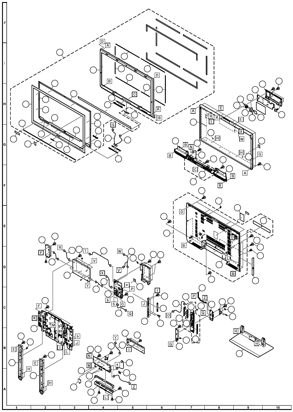
LC-42XL2E/S/RU, LC-46XL2E/S/RU, LC-46X20E/S/RU, LC-52XL2E/S/RU, LC-52X20E/S/RU
29
[9] CABINET PARTS (LC-42XL2E/S/RU)
䎛䎖
䎛䎕
䎔
䎔䎕
䎛䎓
䎚䎘
䎛䎔
䎖䎐䎔
䎖
䎚䎘
䎖䎙
䎛䎘
䎛䎚
䎙䎛
䎙䎚
䎙䎙
䎙䎘
䎙䎗
䎙䎗
䎙䎔
䎙䎓
䎚䎓
䎙
䎛䎙
䎕䎕
䎕䎕
䎚䎜
䎜
䎗䎛
䎔䎐䎖
䎔䎐䎗
䎔䎐䎘
䎔䎐䎔
䎔䎐䎚
䎔䎐䎙
䎔䎐䎜
䎔䎐䎛
䎚䎔
䎙䎜
䎘䎛
䎘䎛
䎔䎜
䎔䎙
䎚䎓
䎖䎕
䎔䎗
䎗䎕
䎗䎕
䎘䎔 䎘䎖
䎖䎖
䎔䎖
䎗䎙
䎚䎕 䎚䎕
䎗䎕
䎗䎜
䎗䎘
䎚
䎕䎛
䎜䎔
䎙䎜
䎗䎓
䎗䎗
䎖䎛
䎖䎚
䎗䎖
䎘䎙 䎘䎘
䎗䎕
䎘䎓
䎖䎔
䎖䎘
䎚䎕
䎙䎕
䎖䎗
䎚䎔
䎗䎕
䎛
䎘䎜
䎔䎛
䎚䎓
䎔䎓
䎗䎚
䎘䎐䎖
䎘䎐䎔
䎘䎐䎕
䎔䎜
䎘䎗
䎕
䎔䎔 䎙䎖 䎚䎕
䎜䎓
䎘䎚
䎘
䎗
䎛䎙
䎚䎗
䎕䎐䎔
䎛䎗
䎚䎖
䎛䎙
䎛䎜
䎕䎐䎕
䎛䎛
䎚䎛
䎛䎗
䎔䎐䎔䎓
䎔䎐䎔䎓
䎔䎐䎔䎓
䎔䎐䎔䎓 䎔䎐䎔䎓
䎔䎐䎔䎕
䎔䎐䎔䎔
䎔䎐䎔䎔
䎔䎐䎔䎕
䎔䎐䎔䎔
䎔䎐䎔䎕
䎔䎐䎔䎕
䎔䎐䎔䎔
䎔䎐䎔䎔
䎔䎐䎔䎕
䎔䎐䎔䎓
䎗䎔
䎚䎓
䎚䎚
䎔䎘
䎚䎙
LC-42XL2E/S/RU, LC-46XL2E/S/RU, LC-46X20E/S/RU, LC-52XL2E/S/RU, LC-52X20E/S/RU
30
NO. PARTS CODE PRICE
RANK NEW
MARK PART
DELIVERY
DESCRIPTION
[9] CABINET PARTS (LC-42XL2E/S/RU)
1CCABAB819WJ11 N P Front Cabinet Ass'y
1-1 Not Available - N - Front Cabinet
1-3 Not Available - N - Front Cover
1-4 HBDGBA061WJSA AF J Sharp Badge
1-5 Not Available - N - Shine Trim
1-6 Not Available - N - Center Dec Holder
1-7 Not Available - N - Front Dec
1-8 Not Available - N - LED Decoration
1-9 Not Available - N - SP Sheet
1-10 Not Available - N - Mask Himeron, x6
1-11 Not Available - N - Front Cover Tape, x5
1-12 Not Available - N - Front Cover Tape, x5
1-13 Not Available - N - Spacer
2CCABBB127WJ11 N P Rear Cabnet Ass'y
2-1 Not Available - N - Rear Cabnet
2-2 Not Available - N - Terminal Label
3CCOVAC336WJ11 N P Bottom Cover Ass'y
3-1 Not Available - - Bottom Cover F
3-2 Not Available - - Bottom_Cov_Spc, x2
4CDAI-A398WJ12 N P Stand Ass'y
5CCOVAC392WJ11 N P MINI AV Key Cover Ass'y
5-1 Not Available - N - Side Key Cover
5-2 Not Available - N - MINI Terminal Label
5-3 Not Available - N - Control Button
6R1LK420D3LZ60Y N J 42" Full HD LCD Panel Module
7DUNTKE186FM01 N R MAIN Unit
8DUNTKE187FM01 N R TERMINAL Unit
9DUNTKE264FM01 N R R/C, LED Unit
10 DUNTKE266FM01 N R KEY Unit
11 DUNTKE188FM01 N R MINI AV Unit
12 DUNTKE270FM01 N R ILLUMINATION Unit
13 RDENCA231WJQZ N P POWER Unit
14 RUNTKA311WJQZ N P AC Inlet Unit
15 LANGKB173WJ1A AN N R Side Terminal Angle
16 LCHSMA386WJ1W BB N R Chassis Tray
17 LHLDFA036WJKZ AB J Wire Holder (Tray), x3
18 LHLDWA133WJKZ AC N J Wire Holder (Tray)
19 LHLDWA143WJKZ AC J Wire Holder (Tray), x5
20 LHLDWA144WJKZ AC N R Wire Holder (Terminal PWB)
21 LHLDWA151WJKZ AB J Wire Holder (Tray), x5
22 LHLDWA163WJKZ AC J Wire Holder (Tray), x5
23 LHLDWA172WJKZ AD R Wire Holder (Tray)
24 PMLT-A487WJZZ AD N R Gasket (10x30x7)
25 PRDARA482WJ1W AV N R Main Radiator
26 PSLDMA702WJZZ AD R Conductiv Shield (10x20), x3
27 PSLDMB154WJQZ AD J 13x30x10 Gasket
28 PSLDMB158WJ1W AP N R Main Shiled
29 PSPAZB312WJKZ AD N J Spacer (25*25 T2.0)
30 PSPAZB313WJKZ AC J Spacer (20*20 T2.0)
31 QCNCMA673WJZZ AG N J Connector (B_To_B_Plug_80)
32 QCNW-F946WJQZ AH N R Connecting Cord (AC:POWERAC)
33 QCNW-F947WJQZ AL N R Connecting Cord (PD:MAINPOWER)
34 QCNW-F948WJQZ AK N R Connecting Cord (PE:TERMINPOWER)
35 QCNW-G001WJQZ AR N R Connecting Cord (FE:MAINTERMINA)
36 QCNW-G025WJQZ N R Connecting Cord (SP:TERMINALSP)
37 QEARZA108WJFW AE N R Earth Plate(L)
38 QEARZA109WJFW AD N R Earth Plate(S), x2
39 RCORFA023WJZZ AK J Core (for SP Wire)
!
40 RTUDAA014WJQZ AX N P Tuner
41 XBPS830P06000 AA J Screw, x2 (FOR HDMI)
42 XJPS730P08WS0 AA J Screw, x22 (Main Pow Termin)
43 LANGKB175WJ1A P Terminal Angle Bottom
44 LANGKB248WJFW P Scart Angle
45 QCNW-F970WJQZ P Connecting Cord (LW:MAINLCDCTL)
46 QCNW-F988WJQZ P Connecting Cord (PL:POWERLCDCTL)
47 QCNW-G020WJQZ P Connecting Cord (KM:MAINKEY)
48 QCNW-G021WJQZ P Connecting Cord (RA:MAINLED)
49 QCNW-G023WJQZ P Connecting Cord (US:MAINMINI_AV)
50 QCNW-G024WJQZ P Connecting Cord (VD:SUBMINI_AV)
51 QCNW-G026WJQZ P Connecting Cord (LA1:POWERINV_R)
53 QCNW-G028WJQZ P Connecting Cord (LB:MAININV)
54 QPWBHE321WJQZ AX J FPC (HM:MAINMINI_AV)
55 XBBS830P08000 AA J Screw (for Scart), x2
56 XBBS930P04000 AA J Screw (for Tuner Fix), x1
57 XIPSN20P04000 AA J Screw (for HDMI), x2
58 LANGKB187WJ1W N P Panel Support Ang, x2
59 LANGKB216WJ1W N P MINI AV Angle
60 PCOVP2605WJZZ AM N J Control Shield
61 PRDARA513WJFW N P Heat Sink
62 PSLDMB159WJ1W N P AV Shield
63 PSLDMB179WJ1W N P MINI AV Shield
64 PSPAZB313WJKZ AC J Sheet (20x20x2.0), x2
65 PSPAZB611WJKZ N P Sheet (10x50x7.5), x2
66 PSPAZB612WJKZ N P Sheet (10x15x8.5)

LC-42XL2E/S/RU, LC-46XL2E/S/RU, LC-46X20E/S/RU, LC-52XL2E/S/RU, LC-52X20E/S/RU
31
NO. PARTS CODE PRICE
RANK NEW
MARK PART
DELIVERY
DESCRIPTION
67 PSPAZB613WJKZ N P Sheet (12x12x2.5), x3
68 PSPAZB614WJKZ N P Sheet (30x30x1.5)
69 XBBS740P08000 AA J Screw (for Center Ang), x14
70 XBBS830P06000 AA J Screw (Mini Av,Tay,Ctl), x15
71 XBPS730P04WS0 AA J Screw (for Heatsink), x4
72 XJPS730P08WS0 AA J Screw (Mini Av,Shild), x11
73 GCOVAC356WJ1A N P Side AV Cover
74 LX-BZA170WJF9 P Screw (for Rear Cabinet), x2
75 LX-HZA003WJFN AC J Screw (for SP), x2
76 PCOVZA105WJKZ N P CI Card Cover
77 PSHEPA541WJZZ N P Terminal Sheet
78 PSHEPA543WJZZ N P Sheet for Boss, x2
79 QCNW-G022WJQZ N P Connecting Cord (IL:LEDILLU)
80 RSP-ZA261WJZZ AY N P Speaker L
81 RSP-ZA262WJZZ AY N P Speaker R
82 TLABZB616WJZZ N P Pop Label A (LC-42XL2E/S)
82 TLABZB618WJZZ N P Pop Label A (LC-42XL2RU)
83 TLABZB672WJZZ N P Pop Label 42
84 XBPS740P10JS0 P Screw (for Rear Cabinet), x8
85 XEBS930P10000 AA J Screw (for Bottom Cover), x1
86 XEBS940P16000 AB J Screw (for Rear Cabinet), x15
87 PSPAHB311WJZZ N P Spacer
88 TLABNC117WJZZ P Model Label
89 LX-BZA214WJ00 Screw, x1
90 LHLDWA164WJKZ Wire Holder
91 LHLDWA186WJKZ N Wire Holder
[9] CABINET PARTS (LC-42XL2E/S/RU)
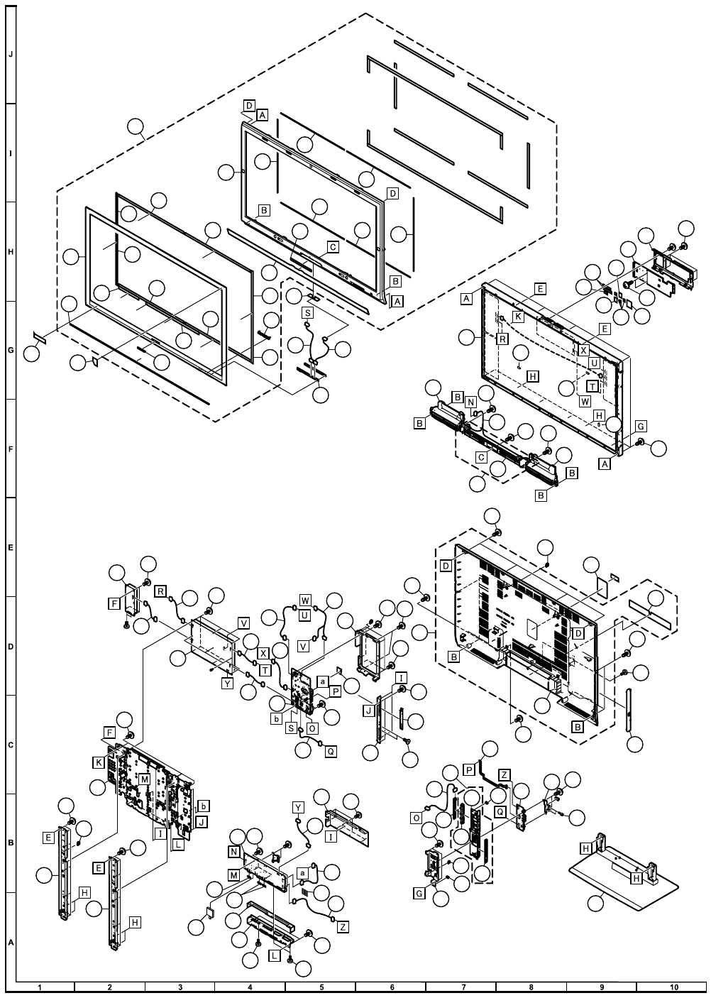
LC-42XL2E/S/RU, LC-46XL2E/S/RU, LC-46X20E/S/RU, LC-52XL2E/S/RU, LC-52X20E/S/RU
32
[10] CABINET PARTS(LC-46XL2E/S/RU)
䎙䎙
䎙䎘 䎙䎗
䎙䎗
䎙䎔
䎙䎓
䎚䎓
䎚䎔
䎙䎛
䎙䎚
䎔
䎜
䎚䎜
䎗䎛
䎔䎕
䎔䎐䎖
䎔䎐䎗
䎔䎐䎛
䎔䎐䎘
䎔䎐䎔
䎔䎐䎚
䎛䎕
䎛䎖
䎛䎓 䎚䎘
䎚䎘
䎖䎙
䎛䎘
䎛䎔
䎖
䎛䎙
䎙
䎕䎕
䎕䎕
䎘䎛
䎘䎛
䎔䎜
䎔䎙
䎚䎓
䎙䎜
䎙䎜
䎔䎗
䎗䎕
䎗䎕
䎗䎕
䎚䎙
䎕䎛
䎗䎙
䎚䎕
䎚䎓
䎘䎗
䎕
䎛䎗
䎛䎚
䎛䎙
䎛䎙
䎛䎗
䎚䎗
䎚䎛
䎚䎖
䎔䎔
䎙䎖 䎚䎕
䎗
䎘䎚
䎚䎕
䎗䎜
䎘䎕
䎘䎖
䎗䎘
䎚
䎔䎖
䎖䎖
䎖䎕
䎘䎔
䎖䎘
䎖䎚
䎖䎛
䎛
䎘䎘
䎘䎙
䎗䎖
䎗䎓
䎗䎗
䎗䎕
䎙䎕 䎚䎓
䎚䎓
䎔䎓
䎗䎚
䎘
䎘䎐䎔
䎘䎐䎖
䎘䎐䎕
䎘䎜
䎔䎜
䎔䎜
䎕䎔
䎖䎗
䎘䎓
䎖䎔
䎗䎕
䎕䎐䎕
䎕䎐䎔
䎔䎐䎔䎔
䎔䎐䎔䎔
䎔䎐䎔䎕
䎔䎐䎔䎕
䎔䎐䎔䎔
䎔䎐䎔䎔
䎔䎐䎔䎔
䎔䎐䎔䎕
䎔䎐䎔䎕
䎔䎐䎔䎕
䎔䎐䎔䎓
䎔䎐䎔䎓
䎔䎐䎔䎓
䎔䎐䎔䎓
䎔䎐䎔䎓
䎔䎐䎔䎓
䎖䎐䎔
䎛䎛
䎚䎚
䎔䎘
䎗䎕
䎗䎔
䎔䎐䎜
LC-42XL2E/S/RU, LC-46XL2E/S/RU, LC-46X20E/S/RU, LC-52XL2E/S/RU, LC-52X20E/S/RU
33
NO. PARTS CODE PRICE
RANK NEW
MARK PART
DELIVERY
DESCRIPTION
[10] CABINET PARTS(LC-46XL2E/S/RU)
1CCABAB818WJ11 N P Front Cabinet Ass'y
1-1 Not Available - N - Front Cabinet
1-2 Not Available - N - Front Mask Ass'y
1-3 Not Available - - Front Cover
1-4 HBDGBA061WJSA AF J Sharp Badge
1-5 Not Available - - Shine Trim
1-6 Not Available - N - Center Dec Holder
1-7 Not Available - N - Front Dec
1-8 Not Available - N - LED Decoration
1-9 Not Available - N - SP Sheet
1-10 Not Available - N - Mask Himeron, x6
1-11 Not Available - N - Front Cover Tape, x5
1-12 Not Available - N - Front Cover Tape, x5
1-13 Not Available - N - Spacer
2CCABBB100WJ11 N P Rear Cabnet Ass'y
2-1 Not Available - N - Rear Cabnet
2-2 Not Available - N - Terminal Label
3CCOVAC336WJ11 N P Bottom Cover Ass'y
3-1 Not Available - - Bottom Cover F
3-2 Not Available - - Bottom_Cov_Spc, x2
4CDAI-A377WJ11 N P Stand Ass'y
5CCOVAC391WJ11 N P MINI AV Key Cover Ass'y
5-1 Not Available - N - Side Key Cover
5-2 Not Available - N - MINI Terminal Label
5-3 Not Available - N - Control Button
6R1LK460D3LZ60Y FT N J 46" Full HD LCD Panel Module
7DUNTKE186FM01 N R MAIN Unit
8DUNTKE187FM01 N R TERMINAL Unit
9DUNTKE264FM01 N R R/C, LED Unit
10 DUNTKE266FM01 N R KEY Unit
11 DUNTKE188FM01 N R MINI AV Unit
12 DUNTKE270FM01 N R ILLUMINATION Unit
13 RDENCA231WJQZ N P POWER Unit
14 RUNTKA311WJQZ N P AC Inlet Unit
15 LANGKB173WJ1A AN N R Side Terminal Angle
16 LCHSMA386WJ1W BB N R Chassis Tray
17 LHLDFA036WJKZ AB J Wire Holder (Tray), x3
18 LHLDWA133WJKZ AC N J Wire Holder (Tray)
19 LHLDWA143WJKZ AC J Wire Holder (Tray), x8
20 LHLDWA144WJKZ AC N R Wire Holder (Terminal PWB)
21 LHLDWA151WJKZ AB J Wire Holder (Tray), x5
22 LHLDWA163WJKZ AC J Wire Holder (Tray), x5
23 LHLDWA172WJKZ AD R Wire Holder (Tray)
24 PMLT-A487WJZZ AD N R Gasket (10x30x7)
25 PRDARA482WJ1W AV N R Main Radiator
26 PSLDMA702WJZZ AD R Conductiv Shield (10x20), x3
27 PSLDMB154WJQZ AD J 13x30x10 Gasket
28 PSLDMB158WJ1W AP N R Main Shiled
29 PSPAZB312WJKZ AD N J Spacer (25*25 T2.0)
30 PSPAZB313WJKZ AC J Spacer (20*20 T2.0)
31 QCNCMA673WJZZ AG N J Connector (B_To_B_Plug_80)
32 QCNW-F946WJQZ AH N R Connecting Cord (AC:POWERAC)
33 QCNW-F947WJQZ AL N R Connecting Cord (PD:MAINPOWER)
34 QCNW-F948WJQZ AK N R Connecting Cord (PE:TERMINPOWER)
35 QCNW-G001WJQZ AR N R Connecting Cord (FE:MAINTERMINA)
36 QCNW-G015WJQZ AL N R Connecting Cord (SP:TERMINALSP)
37 QEARZA108WJFW AE N R Earth Plate(L)
38 QEARZA109WJFW AD N R Earth Plate(S), x2
39 RCORFA023WJZZ AK J Core (for SP Wire)
!
40 RTUDAA014WJQZ AX N P Tuner
41 XBPS830P06000 AA J Screw, x2 (FOR HDMI)
42 XJPS730P08WS0 AA J Screw, x22 (Main Pow Termin)
43 LANGKB175WJ1A P Terminal Angle Bottom
44 LANGKB248WJFW P Scart Angle
45 QCNW-F950WJQZ P Connecting Cord (LW:MAINLCDCTL)
46 QCNW-F968WJQZ P Connecting Cord (PL:POWERLCDCTL)
47 QCNW-G010WJQZ P Connecting Cord (KM:MAINKEY)
48 QCNW-G011WJQZ P Connecting Cord (RA:MAINLED)
49 QCNW-G013WJQZ P Connecting Cord (US:MAINMINI_AV)
50 QCNW-G014WJQZ P Connecting Cord (VD:SUBMINI_AV)
51 QCNW-G016WJQZ P Connecting Cord (LA1:POWERINV_R)
52 QCNW-G017WJQZ P Connecting Cord (LA2:POWER-INV_L)
53 QCNW-G018WJQZ P Connecting Cord (LB:MAININV)
54 QPWBHE322WJQZ AX J FPC (HM:MAINMINI_AV)
55 XBBS830P08000 AA J Screw (for Scart), x2
56 XBBS930P04000 AA J Screw (for Tuner Fix), x1
57 XIPSN20P04000 AA J Screw (for HDMI), x2
58 LANGKB186WJ1W N P Panel Support Ang, x2
59 LANGKB215WJ1W N P MINI AV Angle
60 PCOVP2605WJZZ AM N J Control Shield
61 PRDARA513WJFW N P Heat Sink
62 PSLDMB159WJ1W N P AV Shield
63 PSLDMB179WJ1W N P MINI AV Shield
64 PSPAZB313WJKZ AC J Sheet (20x20x2.0), x2

LC-42XL2E/S/RU, LC-46XL2E/S/RU, LC-46X20E/S/RU, LC-52XL2E/S/RU, LC-52X20E/S/RU
34
NO. PARTS CODE PRICE
RANK NEW
MARK PART
DELIVERY
DESCRIPTION
65 PSPAZB611WJKZ N P Sheet (10x50x7.5), x2
66 PSPAZB612WJKZ N P Sheet (10x15x8.5)
67 PSPAZB613WJKZ N P Sheet (12x12x2.5), x3
68 PSPAZB614WJKZ N P Sheet (30x30x1.5)
69 XBBS740P08000 AA J Screw (for Center Ang), x14
70 XBBS830P06000 AA J Screw (Mini av,Tay,Ctl), x16
71 XBPS730P04WS0 AA J Screw (for Heat Sink), x4
72 XJPS730P08WS0 AA J Screw (Mini Av,Shild), x11
73 GCOVAC356WJ1A N P Side AV Cover
74 LX-BZA170WJF9 P Screw (for Rear Cabinet), x2
75 LX-HZA003WJFN AC J Screw (for SP), x2
76 PCOVZA105WJKZ N P CI Card Cover
77 PSHEPA541WJZZ N P Terminal Sheet
78 PSHEPA543WJZZ N P Sheet for Boss, x2
79 QCNW-G012WJQZ N P Connecting Cord (IL:LEDILLU)
80 RSP-ZA261WJZZ AY N P Speaker L
81 RSP-ZA262WJZZ AY N P Speaker R
82 TLABZB616WJZZ N P Pop Label A (LC-46XL2E/S)
82 TLABZB618WJZZ N P Pop Label A (LC-46XL2RU)
83 TLABZB619WJZZ N P Pop Label 46
84 XBPS740P10JS0 P Screw (for Rear Cabinet), x8
85 XEBS930P10000 AA J Screw (for Bottom Cover), x1
86 XEBS940P16000 AB J Screw (for Rear Cabinet), x14
87 TLABNC117WJZZ - P Model Label
88 LHLDWA164WJKZ Wire Holder
[10] CABINET PARTS(LC-46XL2E/S/RU)
LC-42XL2E/S/RU, LC-46XL2E/S/RU, LC-46X20E/S/RU, LC-52XL2E/S/RU, LC-52X20E/S/RU
35
[11] CABINET PARTS (LC-46X20E/S/RU)
䎙䎗
䎙䎕
䎙䎙
䎔
䎜
䎔䎐䎖
䎔䎐䎖
䎔䎐䎗
䎔䎐䎔䎓
䎔䎐䎔
䎚䎗
䎚䎘
䎚䎕 䎚䎓
䎚䎓
䎖䎙
䎚䎚
䎚䎖
䎖
䎚䎛
䎙
䎕䎕
䎛䎛
䎕䎕
䎙䎓
䎙䎓
䎔䎜
䎔䎙
䎙䎙
䎙䎘
䎙䎘
䎔䎗
䎗䎕
䎗䎕
䎗䎕
䎚䎙
䎕䎛
䎙䎚
䎙䎙
䎘䎙
䎕
䎚䎙
䎚䎜
䎚䎛
䎚䎛
䎚䎙
䎙䎜
䎚䎔
䎙䎛
䎔䎔
䎙䎖 䎙䎚
䎗
䎘䎜
䎙䎚
䎗䎚
䎘䎓
䎘䎔
䎚
䎔䎖
䎖䎖
䎖䎕
䎗䎜
䎖䎘
䎖䎚
䎖䎛
䎛
䎘䎚
䎘䎛
䎗䎖
䎗䎓
䎗䎗
䎗䎕
䎗䎘 䎙䎙
䎙䎙
䎔䎓
䎗䎙
䎘
䎘䎐䎔
䎘䎐䎖
䎘䎐䎕
䎙䎔
䎔䎜
䎔䎜
䎕䎔
䎖䎗
䎗䎛
䎖䎔
䎗䎕
䎕䎐䎕
䎕䎐䎔
䎔䎐䎘
䎔䎐䎛
䎔䎐䎛
䎔䎐䎜
䎔䎐䎜
䎔䎐䎛
䎔䎐䎛
䎔䎐䎙
䎔䎐䎛
䎔䎐䎛
䎔䎐䎚
䎔䎐䎚
䎔䎐䎚
䎔䎐䎚
䎔䎐䎚
䎔䎐䎚
䎔䎐䎔䎕
䎖䎐䎔
䎔䎘
䎗䎕
䎗䎔

LC-42XL2E/S/RU, LC-46XL2E/S/RU, LC-46X20E/S/RU, LC-52XL2E/S/RU, LC-52X20E/S/RU
36
NO. PARTS CODE PRICE
RANK NEW
MARK PART
DELIVERY
DESCRIPTION
[11] CABINET PARTS (LC-46X20E/S/RU)
1CCABAB822WJ11 BU N S Front Cabinet Ass'y
1-1 Not Available - N - Front Cabinet
1-2 Not Available - N - Frot Cover
1-3 HBDGBA061WJSA AF J Sharp Badge
1-4 Not Available - N - LED Decoration
1-5 Not Available - N - Shine Trim
1-6 Not Available - N - Speaker Sheet
1-7 Not Available - N - Mask Himeron, x6
1-8 PSPAZB193WJZZ AD J Front Cover Tape, x6
1-9 Not Available - N - Front Cover Tape B
1-10 Not Available - N - Front Cover Tape C
1-11 Not Available - N - Front Cover Tape D, x2
1-12 XJPS730P08WS0 AA J Screw, x3 (Main Pow Termin)
2CCABBB100WJ12 BM N Rear Cabnet Ass'y
2-1 Not Available - N - Rear Cabnet
2-2 Not Available - N - Terminal Label
3CCOVAC336WJ11 N P Bottom Cover Ass'y
3-1 Not Available - - Bottom Cover F
3-2 Not Available - - Bottom_Cov_Spc, x2
4CDAI-A376WJ12 BN N S Stand Ass'y
5CCOVAC391WJ11 N P MINI AV Key Cover Ass'y
5-1 Not Available - N - MINI AV Key Cover
5-2 Not Available - N - MINI Terminal Label
5-3 Not Available - N - Control Button
6R1LK460D3LZ50Y ** N J 46" Full HD LCD Panel Module
7DUNTKE186FM02 R MAIN Unit
8DUNTKE187FM02 R TERMINAL Unit
9DUNTKE264FM01 R R/C, LED Unit
10 DUNTKE266FM01 R KEY Unit
11 DUNTKE188FM01 R MINI AV Unit
13 RDENCA231WJQZ N P POWER Unit
14 RUNTKA311WJQZ N P AC INLET Unit
15 LANGKB173WJ1A AN N R Side Terminal Angle
16 LCHSMA386WJ1W BB N R Chassis Tray
17 LHLDFA036WJKZ AB J Wire Holder (Tray), x3
18 LHLDWA133WJKZ AC N J Wire Holder (Tray)
19 LHLDWA143WJKZ AC J Wire Holder (Tray), x8
20 LHLDWA144WJKZ AC N R Wire Holder (Terminal PWB)
21 LHLDWA151WJKZ AB J Wire Holder (Tray), x5
22 LHLDWA163WJKZ AC J Wire Holder (Tray), x5
23 LHLDWA172WJKZ AD R Wire Holder (Tray)
24 PMLT-A487WJZZ AD N R Gasket (10x30x7)
25 PRDARA482WJ1W AV N R Main Radiator
26 PSLDMA702WJZZ AD R Conductiv Shield (10x20), x3
27 PSLDMB154WJQZ AD J 13x30x10 Gasket
28 PSLDMB158WJ1W AP N R Main Shiled
29 PSPAZB312WJKZ AD N J Spacer (25*25 T2.0)
30 PSPAZB313WJKZ AC J Spacer (20*20 T2.0)
31 QCNCMA673WJZZ AG N J Connector (B_To_B_Plug_80)
32 QCNW-F946WJQZ AH N R Connecting Cord (AC:POWERAC)
33 QCNW-F947WJQZ AL N R Connecting Cord (PD:MAINPOWER)
34 QCNW-F948WJQZ AK N R Connecting Cord (PE:TERMINPOWER)
35 QCNW-G001WJQZ AR N R Connecting Cord (FE:MAINTERMINA)
36 QCNW-G015WJQZ AL R Connecting Cord (SP:TERMINALSP)
37 QEARZA108WJFW AE N R Earth Plate(L)
38 QEARZA109WJFW AD N R Earth Plate(S), x2
39 RCORFA023WJZZ AK J Core (for SP Wire)
!
40 RTUDAA014WJQZ AX N P Tuner
41 XBPS830P06000 AA J Screw, x2 (FOR HDMI)
42 XJPS730P08WS0 AA J Screw, x22 (Main Pow Termin)
43 LANGKB175WJ1A P Terminal Angle Bottom
44 LANGKB248WJFW P Scart Angle
45 PSLDMB159WJ1W P AV Shield
46 QCNW-G010WJQZ P Connecting Cord (KM:MAINKEY)
47 QCNW-G013WJQZ P Connecting Cord (US:MAINMINI_AV)
48 QCNW-G014WJQZ P Connecting Cord (VD:SUBMINI_AV)
49 QCNW-G016WJQZ P Connecting Cord (LA1:POWERINV_R)
50 QCNW-G017WJQZ P Connecting Cord (LA2:POWER-INV_L)
51 QCNW-G018WJQZ P Connecting Cord (LB:MAININV)
52 QCNW-G178WJQZ AE S Connecting Cord (PL:POWER-LCDCTL)
53 QCNW-G179WJQZ AM S Connecting Cord (FR:MAIN-LCD)
54 QCNW-G180WJQZ BC S Connecting Cord (LW:MAIN-LCDCTL)
55 QCNW-G236WJQZ AH S Connecting Cord (RA:MAIN-LED)
56 QPWBHE322WJQZ AX J FPC (HM:MAINMINI_AV)
57 XBBS830P08000 AA J Screw (for Scart), x2
58 XBBS930P04000 AA J Screw (for Tuner Fix)
59 XIPSN20P04000 AA J Screw (for HDMI), x2
60 LANGKB186WJ1W N P Panel Support Ang, x2
61 LANGKB215WJ1W N P MINI AV Angle
62 PCOVP2609WJZZ AH N S Control Shield
63 PSLDMB179WJ1W N P MINI AV Shield
64 PSPAZB597WJKZ AF S Cooling Sheet, x2
65 XBBS740P08000 AA J Screw (for Center Ang), x14
66 XBBS830P06000 AA J Screw (Mini Av,Tay,Ctl), x11

LC-42XL2E/S/RU, LC-46XL2E/S/RU, LC-46X20E/S/RU, LC-52XL2E/S/RU, LC-52X20E/S/RU
37
NO. PARTS CODE PRICE
RANK NEW
MARK PART
DELIVERY
DESCRIPTION
67 XJPS730P08WS0 AA J Screw, x13 (MINI-AV,SHILD)
68 GCOVAC356WJ1A N P Side AV Cover
69 LX-BZA170WJF9 P Screw (for Rear Cabinet), x2
70 LX-HZA003WJFN AC J Screw (for SP), x2
71 PSHEPA543WJZZ N P Sheet for Boss, x2
72 RSP-ZA261WJZZ AY N P Speaker L
73 RSP-ZA262WJZZ AY N P Speaker R
74 TLABZB620WJZZ AE N S POP Label A ÅiLC-46X20E/S)
74 TLABZB622WJZZ AE N S POP Label A ÅiLC-46X20RU)
75 TLABZB621WJZZ N S POP Label B ÅiLC-46X20E/S)
75 TLABZB623WJZZ N S POP Label B ÅiLC-46X20RU)
76 XBPS740P10JS0 P Screw (for Rear Cabinet), x7
77 XEBS930P10000 AA J Screw (for Bottom Cover), x1
78 XEBS940P16000 AB J Screw (for Rear Cabinet), x14
79 TLABNC117WJZZ P Model Label
80 LX-BZA214WJ00 Screw (for Rear Cabinet)
81 PCOVZA105WJKZ N P CI Card Cover
82 PSHEPA541WJZZ N P Terminal Sheet
83 PFLT-A079WJZZ Conductive Tape 20x70
84 RCORFA012WJZZ Core, x2 (for US/RA, VD)
85 LHLDWA175WJUZ N Wire Holder, x8
86 PFLT-A073WJZZ Conductive Tape 30*90
87 RCORF0103CEZZ Core, x2 (for FR/LB, KM)
88 RCORFA020WJZZ Core (for LA2/LB/LC)
89 LHLDW1033CE00 Wire Holder
90 RCORFA012WJZZ Core (for US/RA)
91 LHLDWA186WJKZ N Wire Holder (Main Shield)
92 PSPAGA389WJZZ N Spacer, x2
[11] CABINET PARTS (LC-46X20E/S/RU)
LC-42XL2E/S/RU, LC-46XL2E/S/RU, LC-46X20E/S/RU, LC-52XL2E/S/RU, LC-52X20E/S/RU
38
[12] CABINET PARTS (LC-52XL2E/S/RU)
1
83
82
1-3
1-1
1-10
1-10
1-10
1-10
1-10
1-10
1-5
1-9
1-7
1-6
1-8
1-4
12
79
9
48
69
70
14 42
42
42
42 42
84
78
88
86
86
2
84
73
74
2-2
2-1
46
28
89
52
53
45
7
49
32
33
13
51
16
69
19
58
58 40 44
38
37
43
56
55
70
50
42
42
59
19
21
70
10
47
19
54
11 63
76
4
5-1
5-2
5-3
8
31
35
34
57
5
1-12
1-12
1-12
1-11
1-11
1-11
1-11
1-11
1-12
1-12
80
6
64
64
67 68 71
70
60
61
65
66
36
85
81 86
22 90
18
22
3
75
75
3-1
70
77
15 41

LC-42XL2E/S/RU, LC-46XL2E/S/RU, LC-46X20E/S/RU, LC-52XL2E/S/RU, LC-52X20E/S/RU
39
NO. PARTS CODE PRICE
RANK NEW
MARK PART
DELIVERY
DESCRIPTION
[12] CABINET PARTS (LC-52XL2E/S/RU)
1CCABAB817WJ11 N P Front Cabinet Ass'y
1-1 Not Available - N - Front Cabinet
1-3 Not Available - N - Front Cover
1-4 HBDGBA061WJSA AF J Sharp Badge
1-5 Not Available - - Shine Trim
1-6 Not Available - N - Center Dec Holder
1-7 Not Available - N - Front Dec
1-8 Not Available - N - LED Decoration
1-9 Not Available - N - SP Sheet
1-10 Not Available - N - Mask Himeron, x6
1-11 Not Available - N - Front Cover Tape, x5
1-12 Not Available - N - Front Cover Tape, x5
1-13 Not Available - N - Spacer
2CCABBB099WJ11 N P Rear Cabnet Ass'y
2-1 Not Available - N - Rear Cabnet
2-2 Not Available - N - Terminal Label
3CCOVAC336WJ11 N P Bottom Cover Ass'y
3-1 Not Available - - Bottom Cover F
3-2 Not Available - - Bottom_Cov_Spc, x2
4CDAI-A397WJ12 N P Stand Ass'y
5CCOVAC391WJ11 N P MINI AV Key Cover Ass'y
5-1 Not Available - N - Side Key Cover
5-2 Not Available - N - MINI Terminal Label
5-3 Not Available - N - Control Button
6R1LK520D3LZ60Y N J 52" Full HD LCD Panel Module
7DUNTKE186FM01 N R MAIN Unit
8DUNTKE187FM01 N R TERMINAL Unit
9DUNTKE264FM01 N R R/C, LED Unit
10 DUNTKE266FM01 N R KEY Unit
11 DUNTKE188FM01 N R MINI AV Unit
12 DUNTKE270FM01 N R ILLUMINATION Unit
13 RDENCA231WJQZ N P POWER Unit
14 RUNTKA311WJQZ N P AC Inlet Unit
15 LANGKB173WJ1A AN N R Side Terminal Angle
16 LCHSMA386WJ1W BB N R Chassis Tray
17 LHLDFA036WJKZ AB J Wire Holder (Tray), x3
18 LHLDWA133WJKZ AC N J Wire Holder (Tray)
19 LHLDWA143WJKZ AC J Wire Holder (Tray), x8
20 LHLDWA144WJKZ AC N R Wire Holder (Terminal PWB)
21 LHLDWA151WJKZ AB J Wire Holder (Tray), x5
22 LHLDWA163WJKZ AC J Wire Holder (Tray), x5
23 LHLDWA172WJKZ AD R Wire Holder (Tray)
24 PMLT-A487WJZZ AD N R Gasket (10x30x7)
25 PRDARA482WJ1W AV N R Main Radiator
26 PSLDMA702WJZZ AD R Conductiv Shield (10x20), x3
27 PSLDMB154WJQZ AD J 13x30x10 Gasket
28 PSLDMB158WJ1W AP N R Main Shield
29 PSPAZB312WJKZ AD N J Spacer (25*25 T2.0)
30 PSPAZB313WJKZ AC J Spacer (20*20 T2.0)
31 QCNCMA673WJZZ AG N J Connector (B_To_B_Plug_80)
32 QCNW-F946WJQZ AH N R Connecting Cord (AC:POWERAC)
33 QCNW-F947WJQZ AL N R Connecting Cord (PD:MAINPOWER)
34 QCNW-F948WJQZ AK N R Connecting Cord (PE:TERMINPOWER)
35 QCNW-G001WJQZ AR N R Connecting Cord (FE:MAINTERMINA)
36 QCNW-F995WJQZ N R Connecting Cord (SP:TERMINALSP)
37 QEARZA108WJFW AE N R Earth Plate(L)
38 QEARZA109WJFW AD N R Earth Plate(S), x2
39 RCORFA023WJZZ AK J Core (for SP Wire)
!
40 RTUDAA014WJQZ AX N P Tuner
41 XBPS830P06000 AA J Screw, x2 (FOR HDMI)
42 XJPS730P08WS0 AA J Screw, x22 (Main Pow Termin)
43 LANGKB175WJ1A P Terminal Angle Bottom
44 LANGKB248WJFW P Scart Angle
45 QCNW-F950WJQZ P Connecting Cord (LW:MAINLCDCTL)
46 QCNW-F968WJQZ P Connecting Cord (PL:POWERLCDCTL)
47 QCNW-F990WJQZ P Connecting Cord (KM:MAINKEY)
48 QCNW-F991WJQZ P Connecting Cord (RA:MAINLED)
49 QCNW-F993WJQZ P Connecting Cord (US:MAINMINI_AV)
50 QCNW-F994WJQZ P Connecting Cord (VD:SUBMINI_AV)
51 QCNW-F996WJQZ P Connecting Cord (LA1:POWERINV_R)
52 QCNW-F997WJQZ P Connecting Cord (LA2:POWER-INV_L)
53 QCNW-F998WJQZ P Connecting Cord (LB:MAININV)
54 QPWBHE323WJQZ AY J FPC (HM:MAINMINI_AV)
55 XBBS830P08000 AA J Screw (for Scart), x2
56 XBBS930P04000 AA J Screw (for Tuner Fix), x1
57 XIPSN20P04000 AA J Screw (for HDMI), x2
58 LANGKB185WJ1W N P Panel Support Ang, x2
59 LANGKB215WJ1W N P MINI AV Angle
60 PCOVP2605WJZZ AM N J Control Shield
61 PRDARA513WJFW N P Heat Sink
62 PSLDMB159WJ1W P AV Shield
63 PSLDMB179WJ1W N P MINI AV Shield
64 PSPAZB313WJKZ AC J Sheet (20x20x2.0), x2
65 PSPAZB611WJKZ N P Sheet (10x50x7.5), x2

LC-42XL2E/S/RU, LC-46XL2E/S/RU, LC-46X20E/S/RU, LC-52XL2E/S/RU, LC-52X20E/S/RU
40
NO. PARTS CODE PRICE
RANK NEW
MARK PART
DELIVERY
DESCRIPTION
66 PSPAZB612WJKZ N P Sheet (10x15x8.5)
67 PSPAZB613WJKZ N P Sheet (12x12x2.5), x3
68 PSPAZB614WJKZ N P Sheet (30x30x1.5)
69 XBBS740P08000 AA J Screw (for Center Ang), x14
70 XBBS830P06000 AA J Screw (Mini Av,Tay,Ctl), x16
71 XBPS730P04WS0 AA J Screw (for Heatsink), x4
72 XJPS730P08WS0 AA J Screw (Mini Av,Shild), x11
73 GCOVAC356WJ1A N P Side AV Cover
74 LX-BZA170WJF9 P Screw (for Rear Cabinet), x2
75 LX-HZA003WJFN AC J Screw (for SP), x2
76 PCOVZA105WJKZ N P CI Card Cover
77 PSHEPA541WJZZ N P Terminal Sheet
78 PSHEPA543WJZZ N P Sheet for Boss, x2
79 QCNW-F992WJQZ N P Connecting Cord (IL:LEDILLU)
80 RSP-ZA261WJZZ AY N P Speaker L
81 RSP-ZA262WJZZ AY N P Speaker R
82 TLABZB617WJZZ N P Pop Label (LC-52XL2E/S)
82 TLABZB619WJZZ N P Pop Label (LC-52XL2RU)
83 TLABZB616WJZZ N P Pop Label A (LC-52XL2E/S)
83 TLABZB618WJZZ N P Pop Label A (LC-52XL2RU)
84 XBPS740P10JS0 P Screw (for Rear Cabinet), x8
85 XEBS930P10000 AA J Screw (for Bottom Cover), x1
86 XEBS940P16000 AB J Screw (for Rear Cabinet), x15
88 TLABNC117WJZZ P Model Label
89 LHLDWA186WJKZ N Wire Holder (Main Shield)
90 LHLDW1173CEZZ Wire Holder (SP wire)
[12] CABINET PARTS (LC-52XL2E/S/RU)
LC-42XL2E/S/RU, LC-46XL2E/S/RU, LC-46X20E/S/RU, LC-52XL2E/S/RU, LC-52X20E/S/RU
41
[13] CABINET PARTS (LC-52X20E/S/RU)
72
6
66
62
64
89
89
89
91
22 18
70
70
73 78
3
36
77
9
1-2
1-3
1-4
1-6
1-1
1-7
1-7
1-7
1-7
1-7
1-7
1-12
1-10
74
75
88
18
18
89 88
65
66
66
66
32
50
84
89
93 28 67
66
67
2
82
82
69
68
76
76
78
83
79
71
2-2
78
2-1
52
51
92
66
66
10
5-3
5-2
5-1
7
33
66
45
66
66
38
37
57
58
34
35
86
8
85
90
47
49
13
16
65
60
60
19
19
40
43
44
31 48
85
20
90
61
19
21
84
46
56
11
63 67
19
20
87
59
4
80
5
1-5
1-8
1-8
1-8
1-8
1-8
1-8
1-9
1-9
1-8
1-8
3-1
66
81
15 41
66
1
LC-42XL2E/S/RU, LC-46XL2E/S/RU, LC-46X20E/S/RU, LC-52XL2E/S/RU, LC-52X20E/S/RU
42
NO. PARTS CODE PRICE
RANK NEW
MARK PART
DELIVERY
DESCRIPTION
[13] CABINET PARTS (LC-52X20E/S/RU)
1CCABAB821WJ11 N P Front Cabinet Ass'y
1-1 Not Available - N - Front Cabinet
1-2 Not Available - N - Frot Cover
1-3 HBDGBA061WJSA AF J Sharp Badge
1-4 Not Available - N - LED Decoration
1-5 Not Available - N - Shine Trim
1-6 Not Available - N - Speaker Sheet
1-7 Not Available - N - Mask Himeron, x6
1-8 PSPAZB194WJZZ AE J Front Cover Tape, x6
1-9 Not Available - N - Front Cover Tape A, x2
1-10 Not Available - N - Front Cover Tape B
1-11 Not Available - N - Front Cover Tape C
1-12 XJPS730P08WS0 AA J Screw, x3 (Main Pow Termin)
2CCABBB099WJ11 N P Rear Cabnet Ass'y
2-1 Not Available - N - Rear Cabnet
2-2 Not Available - N - Terminal Label
3CCOVAC336WJ11 N P Bottom Cover Ass'y
3-1 Not Available - N - Bottom Cover F
3-2 Not Available - - Bottom_Cov_Spc, x2
4CDAI-A376WJ12 BN N S Stand Ass'y
5CCOVAC391WJ11 N P MINI AV Key Cover Ass'y
5-1 Not Available - N - MINI AV Key Cover
5-2 Not Available - N - MINI Terminal Label
5-3 Not Available - N - Control Button
6R1LK520D3LZ50Y N J 52" Full HD LCD Panel Module
7DUNTKE186FM02 N R MAIN Unit
8DUNTKE187FM02 N R TERMINAL Unit
9DUNTKE264FM01 N R R/C, LED Unit
10 DUNTKE266FM01 N R KEY Unit
11 DUNTKE188FM01 N R MINI AV Unit
13 RDENCA231WJQZ N P POWER Unit
14 RUNTKA311WJQZ N P AC INLET Unit
15 LANGKB173WJ1A AN N R Side Terminal Angle
16 LCHSMA386WJ1W BB N R Chassis Tray
17 LHLDFA036WJKZ AB J Wire Holder (Tray), x3
18 LHLDWA133WJKZ AC N J Wire Holder (Tray)
19 LHLDWA143WJKZ AC J Wire Holder (Tray), x8
20 LHLDWA144WJKZ AC N R Wire Holder (Terminal PWB)
21 LHLDWA151WJKZ AB J Wire Holder (Tray), x5
22 LHLDWA163WJKZ AC J Wire Holder (Tray), x5
23 LHLDWA172WJKZ AD R Wire Holder (Tray)
24 PMLT-A487WJZZ AD N R Gasket (10x30x7)
25 PRDARA482WJ1W AV N R Main Radiator
26 PSLDMA702WJZZ AD R Conductiv Shield (10x20), x3
27 PSLDMB154WJQZ AD J 13x30x10 Gasket
28 PSLDMB158WJ1W AP N R Main Shiled
29 PSPAZB312WJKZ AD N J Spacer (25*25 T2.0)
30 PSPAZB313WJKZ AC J Spacer (20*20 T2.0)
31 QCNCMA673WJZZ AG N J Connector (B_To_B_Plug_80)
32 QCNW-F946WJQZ AH N R Connecting Cord (AC:POWERAC)
33 QCNW-F947WJQZ AL N R Connecting Cord (PD:MAINPOWER)
34 QCNW-F948WJQZ AK N R Connecting Cord (PE:TERMINPOWER)
35 QCNW-G001WJQZ AR N R Connecting Cord (FE:MAINTERMINA)
36 QCNW-F995WJQZ N R Connecting Cord (SP:TERMINALSP)
37 QEARZA108WJFW AE N R Earth Plate(L)
38 QEARZA109WJFW AD N R Earth Plate(S), x2
39 RCORFA023WJZZ AK J Core (for SP Wire)
!
40 RTUDAA014WJQZ AX N P Tuner
41 XBPS830P06000 AA J Screw, x2 (FOR HDMI)
42 XJPS730P08WS0 AA J Screw, x22 (Main Pow Termin)
43 LANGKB175WJ1A P Terminal Angle Bottom
44 LANGKB248WJFW P Scart Angle
45 PSLDMB159WJ1W P AV Shield
46 QCNW-F990WJQZ P Connecting Cord (KM:MAINKEY)
47 QCNW-F993WJQZ P Connecting Cord (US:MAINMINI_AV)
48 QCNW-F994WJQZ P Connecting Cord (VD:SUBMINI_AV)
49 QCNW-F996WJQZ P Connecting Cord (LA1:POWERINV_R)
50 QCNW-F997WJQZ P Connecting Cord (LA2:POWER-INV_L)
51 QCNW-F998WJQZ P Connecting Cord (LB:MAININV)
52 QCNW-G178WJQZ AE S Connecting Cord (PL:POWER-LCDCTL)
53 QCNW-G179WJQZ AM S Connecting Cord (FR:MAIN-LCD)
54 QCNW-G180WJQZ BC S Connecting Cord (LW:MAIN-LCDCTL)
55 QCNW-G235WJQZ P Connecting Cord (RA:MAIN-LED)
56 QPWBHE323WJQZ AY J FPC (HM:MAINMINI_AV)
57 XBBS830P08000 AA J Screw (for Scart), x2
58 XBBS930P04000 AA J Screw (for Tuner Fix)
59 XIPSN20P04000 AA J Screw (for HDMI), x2
60 LANGKB185WJ1W N P Panel Support Ang, x2
61 LANGKB215WJ1W N P MINI AV Angle
62 PCOVP2609WJZZ AH N S Control Shield
63 PSLDMB179WJ1W N P MINI AV Shield
64 PSPAZB597WJKZ AF S Cooling Sheet, x2
65 XBBS740P08000 AA J Screw (for Center Ang), x14
66 XBBS830P06000 AA J Screw (Mini Av,Tay,Ctl), x17

LC-42XL2E/S/RU, LC-46XL2E/S/RU, LC-46X20E/S/RU, LC-52XL2E/S/RU, LC-52X20E/S/RU
43
NO. PARTS CODE PRICE
RANK NEW
MARK PART
DELIVERY
DESCRIPTION
67 XJPS730P08WS0 AA J Screw, x11 (MINI-AV,SHILD)
68 GCOVAC356WJ1A N P Side AV Cover
69 LX-BZA170WJF9 P Screw (for Rear Cabinet), x2
70 LX-HZA003WJFN AC J Screw (for SP), x2
71 PSHEPA543WJZZ N P Sheet for Boss, x2
72 RSP-ZA261WJZZ AY N P Speaker L
73 RSP-ZA262WJZZ AY N P Speaker R
74 TLABZB620WJZZ AE N S POP Label AÅiLC-52X20E/S)
74 TLABZB622WJZZ AE N S POP Label AÅiLC-52X20RU)
75 TLABZB617WJZZ N P POP Label 52
76 XBPS740P10JS0 P Screw (for Rear Cabinet), x7
77 XEBS930P10000 AA J Screw (for Bottom Cover), x1
78 XEBS940P16000 AB J Screw (for Rear Cabinet), x15
79 TLABNC117WJZZ P Model Label
80 PCOVZA105WJKZ N P CI Card Cover
81 PSHEPA541WJZZ N P Terminal Sheet
82 PSPAGA389WJZZ N Spacer, x2
83 LX-BZA214WJ00 Screw (for Rear Cabinet)
84 RCORF0103CEZZ Core, x2 (for LP/LB, KM)
85 RCORFA012WJZZ Core, x2 (for US/RA, VD)
86 PFLT-A079WJZZ Conductive Tape 20x70
87 PFLT-A073WJZZ Conductive Tape 30*90
88 LHLDWA141WJZZ Wire Holder, x2
89 LHLDWA175WJUZ N Wire Holder, x7
90 LHLDW1033CE00 Wire Holder (for KM)
91 LHLDW1173CEZZ Wire Holder
92 RCORFA020WJZZ Core (for LA2/LB/LC)
93 LHLDWA186WJKZ N Wire Holder
[13] CABINET PARTS (LC-52X20E/S/RU)
LC-42XL2E/S/RU, LC-46XL2E/S/RU, LC-46X20E/S/RU, LC-52XL2E/S/RU, LC-52X20E/S/RU
44
[14] SUPPLIED ACCESSOORIES (LC-42/46/52XL2E/S/RU)
NO. PARTS CODE PRICE
RANK NEW
MARK PART
DELIVERY
DESCRIPTION
[14] SUPPLIED ACCESSOORIES (LC-42/46/52XL2E/S/RU)
!
X1 QACCBA073WJPZ AV P AC Cord (for UK and Eire)
!
X1 QACCKA021WJPZ P AC Cord (for Europe without UK and Eire)
X2 RRMCGA585WJSA N P Remote Control Unit (LC-42/46/52XL2E/S/RU)
X2 RRMCGA586WJSA AT N P Remote Control Unit (LC-46/52X20E/S/RU)
X3 LHLDWA173WJKZ N P Cable Clamp
X4 TGAN-A077WJZZ AD J Guarrantee Card (R only)
X5 TGAN-A801WJZZ P Guarrantee Card (E only)
X6 TGAN-A802WJZZ P AQUOS Care Plan (E only)
X7 --N-Operation Manual (ENGLISH..) (for "E" and "S" models)
X8 --N-Operation Manual (SWEDISH..) (for "E" and "S" models)
X9 --N-Operation Manual (RUSSIAN..) (for "RU" models)
X10 --N-Operation Manual (POLISH..) (for "E" models)
X11 CDAI-A398WJ12 N P Stand Ass'y (LC-42XL2E/S/RU)
X11 CDAI-A397WJ12 N P Stand Ass'y (LC-46/52XL2E/S/RU)
X11 CDAI-A376WJ12 BN N S Stand Ass'y (LC-46/52X20E/S/RU)
[15] OPERATION MANUALS (SMPL models: (LC-42/46/52XL2E/S/RU))
X7 TINS-D177WJZZ N P Operation Manual (ENGLISH..) (LC-42/46/52XL2E/S)
X8 TINS-D178WJZZ N P Operation Manual (SWEDISH..) (LC-42/46/52XL2E/S)
X9 TINS-D179WJZZ N P Operation Manual (RUSSIAN..) (LC-42/46/52XL2RU)
X10 TINS-D180WJZZ N P Operation Manual (POLISH..) (LC-42/46/52XL2E)
[16] OPERATION MANUALS (SMPL models:LC-46/52X20E/S/RU)
X7 TINS-D181WJZZ N P Operation Manual (ENGLISH..) (LC-46/52X20E/S)
X8 TINS-D182WJZZ N P Operation Manual (SWEDISH..) (LC-46/52X20E/S)
X9 TINS-D184WJZZ N P Operation Manual (RUSSIAN..) (LC-46/52X20RU)
X10 TINS-D183WJZZ N P Operation Manual (POLISH..) (LC-46/52X20E)
[17] OPERATION MANUALS (SEES models:LC-46/52X20E/S/RU)
X7 TINS-D362WJZZ N Operation Manual (ENGLISH..) (LC-46/52X20E/S)
X8 TINS-D363WJZZ N Operation Manual (SWEDISH..) (LC-46/52X20E/S)
X9 TINS-D365WJZZ N Operation Manual (RUSSIAN..) (LC-46/52X20RU)
X10 TINS-D364WJZZ N Operation Manual (POLISH..) (LC-46/52X20E)
X2
X1 X3 X11
X4
X5
X6
X7
X8
X9
X10
LC-42XL2E/S/RU, LC-46XL2E/S/RU, LC-46X20E/S/RU, LC-52XL2E/S/RU, LC-52X20E/S/RU
45
[18] PACKING PARTS (LC-42XL2E/S/RU)
㵘
S3 S3
S2
S1
S3
S5 S5
S4
S3
S6
LC-42XL2E/S/RU, LC-46XL2E/S/RU, LC-46X20E/S/RU, LC-52XL2E/S/RU, LC-52X20E/S/RU
46
NO. PARTS CODE PRICE
RANK NEW
MARK PART
DELIVERY
DESCRIPTION
[18] PACKING PARTS (LC-42XL2E/S/RU)
S1 SPAKCD532WJZZ - N - Packing Case (LC-42XL2E/S)
S1 SPAKCD532WJZZ - N - Packing Case (LC-42XL2RU)
S2 SPAKPA758WJZZ - - Wrapping Paper
S3 SPAKXB535WJZZ - N - Buffer Material
S4 SSAKAA009WJZZ - - Polyethylene Bag
S5 SSAKAA010WJZZ - - Polyethylene Bag
S6 TLABM5584BMZZ - - Case Label
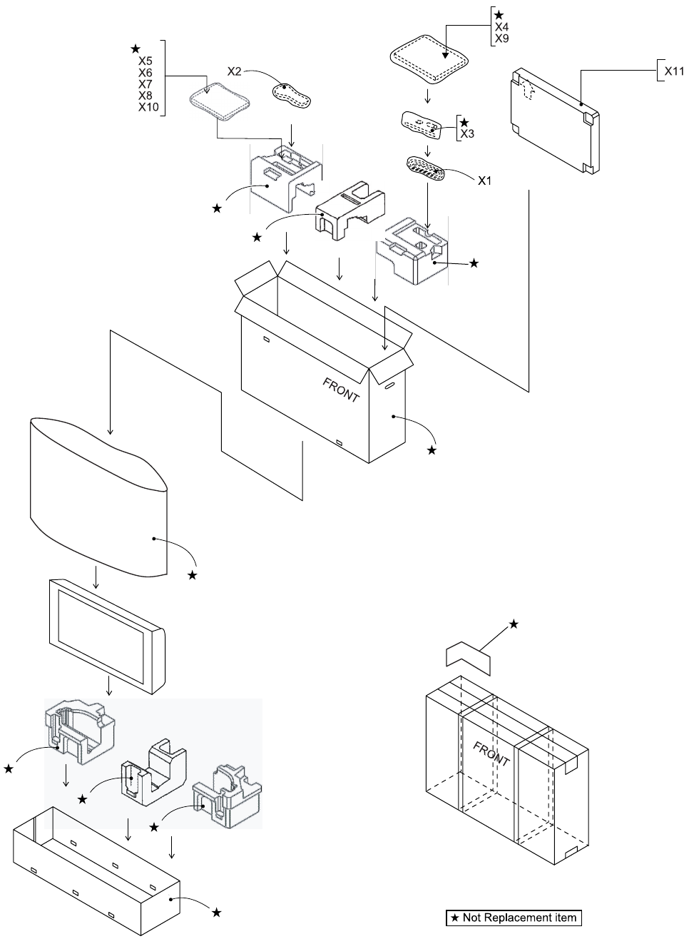
LC-42XL2E/S/RU, LC-46XL2E/S/RU, LC-46X20E/S/RU, LC-52XL2E/S/RU, LC-52X20E/S/RU
47
[19] PACKING PARTS (LC-46XL2E/S/RU, 46X20E/S/RU)
S2
S3
S1
S9
S4
S7
S4
S5
S4
S6
S4
S7
S8
LC-42XL2E/S/RU, LC-46XL2E/S/RU, LC-46X20E/S/RU, LC-52XL2E/S/RU, LC-52X20E/S/RU
48
NO. PARTS CODE PRICE
RANK NEW
MARK PART
DELIVERY
DESCRIPTION
[19] PACKING PARTS (LC-46XL2E/S/RU, 46X20E/S/RU)
S1 SPAKCD522WJZZ - N - Packing Case (Top) (LC-46XL2E/S)
S1 SPAKCD526WJZZ - N - Packing Case (Top) (LC-46X20E/S)
S1 SPAKCD531WJZZ - N - Packing Case (Top) (LC-46XL2RU)
S1 SPAKCD535WJZZ - N - Packing Case (Top) (LC-46X20RU)
S2 SPAKCD540WJZZ - N - Packing Case (Bottom)
S3 SPAKPA711WJZZ - - Wrapping Paper
S4 SPAKXB534WJZZ - N - Top Pad
S5 SPAKXB543WJZZ - N - Buffer Material (Top C)
S6 SPAKXB549WJZZ - N - Buffer Material (Bottom C)
S7 SSAKAA009WJZZ - - Polyethylene Bag
S8 SSAKAA010WJZZ - - Polyethylene Bag
S9 TLABM5584BMZZ - - Case Label

LC-42XL2E/S/RU, LC-46XL2E/S/RU, LC-46X20E/S/RU, LC-52XL2E/S/RU, LC-52X20E/S/RU
49
[20] PACKING PARTS (LC-52XL2E/S/RU, 52X20E/S/RU)
S2
S3
S1
S9
S4
S7
S4
S5
S4
S6
S4
S7
S8

LC-42XL2E/S/RU, LC-46XL2E/S/RU, LC-46X20E/S/RU, LC-52XL2E/S/RU, LC-52X20E/S/RU
50
NO. PARTS CODE PRICE
RANK NEW
MARK PART
DELIVERY
DESCRIPTION
[20] PACKING PARTS (LC-52XL2E/S/RU, 52X20E/S/RU)
S1 SPAKCD521WJZZ - N - Packing Case (Top) (LC-52XL2E/S)
S1 SPAKCD525WJZZ - N - Packing Case (Top) (LC-52X20E/S)
S1 SPAKCD530WJZZ - N - Packing Case (Top) (LC-52XL2RU)
S1 SPAKCD534WJZZ - N - Packing Case (Top) (LC-52X20RU)
S2 SPAKCD539WJZZ - N - Packing Case (Bottom)
S3 SPAKPA712WJZZ - N - Wrapping Paper
S4 SPAKXB533WJZZ - N - Top Pad
S5 SPAKXB542WJZZ - N - Buffer Material (Top C)
S6 SPAKXB548WJZZ - N - Buffer Material (Bottom C)
S7 SSAKAA009WJZZ - - Polyethylene Bag
S8 SSAKAA010WJZZ - - Polyethylene Bag
S9 TLABM5584BMZZ - - Case Label
[21] SERVICE JIGS
NQCNW-G440WJQZ AP N J 4-5pins L=1000mm, Main to Key
NQCNW-G441WJQZ AW N J 15pins L=1000mm, Main to R/C, LED
NQCNW-G442WJQZ AK N J 2pins L=1000mm, R/C, LED to ILLUMINATION
NQCNW-G443WJQZ AY N J 14-14/3pins L=1135mm, MiniAV to Main
NQCNW-G444WJQZ AY N J 15pins L=1000mm, MiniAV to Terminal
NQCNW-G445WJQZ AP N J 4-2/2pins L=1000mm, Terminal to Speaker
NQCNW-G446WJQZ AV N J 12pins L=1000mm, Main to Power
NQCNW-G447WJQZ AS N J 6pins L=1000mm, Terminal to Power
NQCNW-G448WJQZ AP N J 9pins L=1000mmm, Main to Inverter
NQCNW-G449WJQZ AU N J 12-11/4pins L=1000mm, LCD Controller to Main/Power
NQCNW-G616WJQZ BK N J 41pins L=1000mm, Main to LCD Controller
LC-42XL2E/S/RU, LC-46XL2E/S/RU, LC-46X20E/S/RU, LC-52XL2E/S/RU, LC-52X20E/S/RU

LC-42XL2E/S/RU, LC-46XL2E/S/RU, LC-46X20E/S/RU, LC-52XL2E/S/RU, LC-52X20E/S/RU
COPYRIGHT © 2007 BY SHARP CORPORATION
ALL RIGHTS RESERVED.
No Part of this publication may be reproduced,
stored in a retrieval system, or transmitted in
any from or by any means, electronic, mechanical,
photocopying, recording, or otherwise, without
prior written permission of the publisher.
TQ -S SH. DS
SHARP CORPORATION
AV Systems Group
CS Promotion Center
Yaita,Tochigi 329-2193, Japan
SERVICE MANUAL
No. SX7W9LC52X20E
Parts marked with " " are important for maintaining the safety of the set. Be sure to replace these parts with specified ones for maintaining the
safety and performance of the set.
This document has been published to be used for
after sales service only.
The contents are subject to change without notice.
TopPage
LC-52X20E/S/RU
LCD COLOUR TELEVISION
LC-52X20E/S/RU
In the interests of user-safety (Required by safety regulations in some countries) the set should be restored to its orig-
inal condition and only parts identical to those specified should be used.
In this Service Manual, only parts in the LCD module are shown. For the other points, refer to the LC-52X20E/S/RU
(S87O7LC42XL2E) Service Manual.
OUTLINE
SUPPLEMENT
MODELS

LC-52X20E/S/RU
i
LC-52X20E Service Manual
OUTLINE AND ADJUSTMENT
[1] Outline
In this Service Manual, only parts in the LCD module are shown. For the other points, refer to the LC-52X20E/S/RU (S87O7LC42XL2E) Service Man-
ual.
[2] Adjustment
When replacing the LCD panel or the LCD control PWB, perform the PANEL SIZE confirmation and the VCOM adjustment.
For the PANEL SIZE confirmation and the VCOM adjustment method, refer to the service manual for each model.
PARTS GUIDE
Parts marked with " " are important for maintaining the safety of the set. Be sure to replace these
parts with specified ones for maintaining the safety and performance of the set.
This document has been published to be used
for after sales service only.
The contents are subject to change without notice.
LC-52X20E/S/RU
PartsGuide
[1] LCD MODULE Assembly
CONTENTS
No. SX7W9LC52X20E
LCD COLOUR TELEVISION
LC-52X20E/S/RU
MODELS
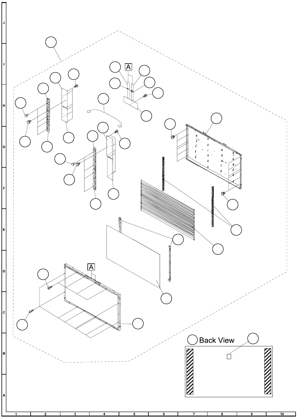
LC-52X20E/S/RU
2
[1] LCD MODULE Assembly
1
7
7
14
5
6
2
18
4
24
8
20
9
15
13
19 19
17 17
16
21
26
25
10
24
22
11 15
15
23
812
3
3

LC-52X20E/S/RU
3
NO. PARTS CODE PRICE
RANK NEW
MARK PART
DELIVERY
DESCRIPTION
[1] LCD MODULE Assembly
1R1LK520D3LZ50Y GR J LCD Module Ass'y
2Not Available - - Bezel Ass'y
3CCHSM0029TP03 CE N J BL Chassis Ass'y
4LHLDZ3763TPZZ AL J Lamp Holder, x2
5RLMPLA007WJN1 AU J Lamp, x24
6PSHEPA552WJZZ BU J Diffusion Panel
7LHLDFA035WJKZ AB J INVERTER Spacer, x12 (for BL Chassis)
8PSPAZB030WJKZ AB J INVERTER Spacer, x2
9RUNTKA327WJZZ BM J INVERTER Unit A
10 RUNTKA328WJZZ BC J INVERTER Unit B
11 RUNTKA329WJZZ BH J INVERTER Unit C
12 RUNTKA330WJZZ BE J INVERTER Unit D
13 QCNW-F929WJQZ AQ J Cable
14 QSOCFA002WJZZ AD J Socket, x48
15 LX-BZA207WJF7 AA J Screw, x13 (for LCD CONTROL Unit, INVERTER Unit)
16 CPWBX3829TPXZ BP J LCD CONTROL Unit
17 QPWBM0575TPZZ AN J CS-FPC, x2
18 PSHEP2828TPZZ AH J Heat Radiation Sheet (for LCD CONTROL Unit)
19 RCORFA061WJZZ AG J Ferrite Core, x2
20 PCOVPA091WJKZ AG J Invasion Prevention Cover A
21 PCOVPA092WJKZ AG J Invasion Prevention Cover B
22 PCOVPA093WJKZ AG J Invasion Prevention Cover C
23 PCOVPA094WJKZ AG J Invasion Prevention Cover D
24 LX-LZA105WJZZ AB J Push Rivet, x8
25 LX-BZA196WJF7 AB J Screw, x8 (for BL Chassis)
26 LX-BZA216WJF7 AC J Screw, x4 (for BL Chassis)

LC-52X20E/S/RU
COPYRIGHT © 2008 BY SHARP CORPORATION
ALL RIGHTS RESERVED.
No Part of this publication may be reproduced,
stored in a retrieval system, or transmitted in
any from or by any means, electronic, mechanical,
photocopying, recording, or otherwise, without
prior written permission of the publisher.
SHARP CORPORATION
AV Systems Group
CS Promotion Center
Yaita,Tochigi 329-2193, Japan
Jan. 2008
TQ2409-S YK. DS
