Dmcman LCD Manual
User Manual:
Open the PDF directly: View PDF ![]() .
.
Page Count: 58
1
DOT MATRIX CHARACTER
LCD MODULE
USER’S MANUAL
OPTREX CORPORATION

2
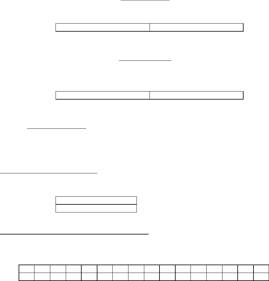
Revision # Description Date Revised
3
Preface
This user’s manual has been prepared for all users of the OPTREX DMC series Liquid Crystal Display (LCD)
modules to assis t in incorporating these character type LCD modules into various applications properly and
efficiently.
4
Table of Contents
1 FUNCTION AND STRUCTURE................................................................................................................................6
1.1 GENERAL ......................................................................................................................................................................6
1.2 CHARACTERISTICS......................................................................................................................................................6
1.3 HANDLING PRECAUTIONS.........................................................................................................................................7
1.4 LIST OF DMC SERIES..................................................................................................................................................8
1.5 PIN ASSIGNMENTS.....................................................................................................................................................11
1.6 BLOCK DIAGRAM ......................................................................................................................................................13
1.7 EXPLANATION OF INTERNAL OPERATION..........................................................................................................14
1.7.1 Register ............................................................................................................................................................14
1.7.2 Busy Flag (BF) ...............................................................................................................................................14
1.7.3 Address Counter (AC)...................................................................................................................................15
1.7.4 Display Data RAM (DD RAM) .....................................................................................................................15
1.7.5 Address Counter (AC)...................................................................................................................................15
1.7.6 DD RAM Addressing......................................................................................................................................16
1.7.7 Character Generator ROM (CG ROM) ......................................................................................................22
1.7.8 Character Generator RAM (CG RAM).......................................................................................................22
2 MPU INTERFACING.................................................................................................................................................30
2.1 GENERAL ....................................................................................................................................................................30
2.2 INITIALIZATION........................................................................................................................................................30
2.2.1 Initialization using the Internal Reset Circuit ..........................................................................................30
2.2.2 Software Initialization ...................................................................................................................................31
3 INSTRUCTIONS........................................................................................................................................................34
3.1 DETAILED EXPLANATIONS.....................................................................................................................................34
3.1.1 Clear Display...................................................................................................................................................34
3.1.2 Return Home.....................................................................................................................................................34
3.1.3 Entry mode set..................................................................................................................................................34
3.1.4 Display ON/OFF Control ..............................................................................................................................35
3.1.5 Cursor or Display Shift ..................................................................................................................................36
3.1.6 Function Set.....................................................................................................................................................36
3.1.7 Set CG RAM Address ......................................................................................................................................37
3.1.8 Set DD RAM Address ......................................................................................................................................37
3.1.9 Read Busy Flag and Address ........................................................................................................................37
3.1.10 Write Data to CG or DD RAM.....................................................................................................................38
3.1.11 Read Data from CG or DD RAM.................................................................................................................38
3.2 EXAMPLES OF INSTRUCTIONS.................................................................................................................................41
3.2.1 16 Character x 1 Line Display (1/8 duty) Using CG RAM......................................................................41
3.2.2 16 Character x 2 Line Display (1/16 duty)................................................................................................44
3.2.3 16 Character x 2 Line Display (4-bit interface, 1/16 duty) ....................................................................46
4 ELECTRICAL CHARACTERISTICS.....................................................................................................................47
4.1 ABSOLUTE MAXIMUM RATINGS............................................................................................................................47
4.2 TIMING CHARACTERISTICS.....................................................................................................................................47
4.2.1 Write Operation...............................................................................................................................................47
4.2.2 Read Operation ...............................................................................................................................................48
4.2.3 Timing Characteristics of Each Drawing...................................................................................................49
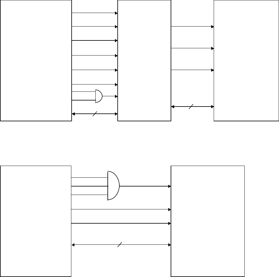
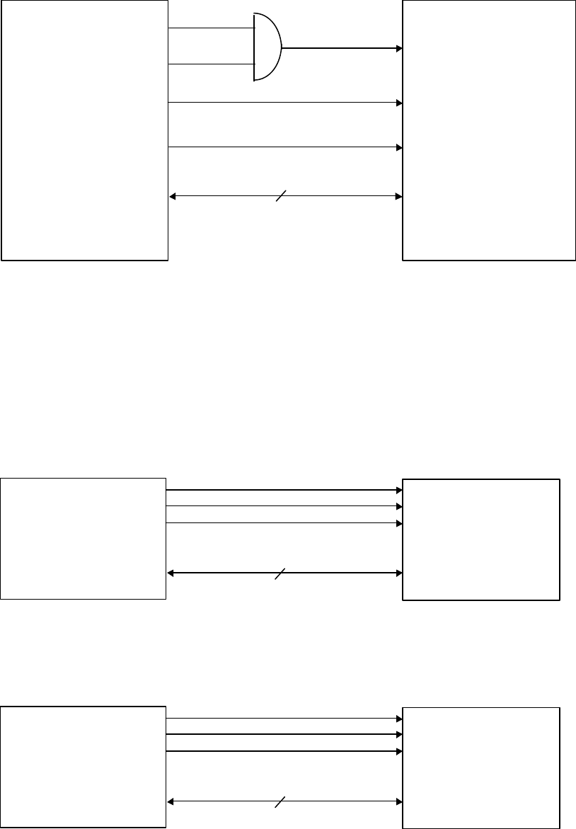
5 CONNECTION BLOCK DIAGRAMS TO MPU...................................................................................................50
5.1 CONNECTION WITH Z-80.........................................................................................................................................50
5
5.2 CONNECTION WITH 8085A .....................................................................................................................................51
5.3 CONNECTION WITH MC 6800.................................................................................................................................52
5.4 CONNECTION WITH MC 6809.................................................................................................................................53
5.5 CONNECTION WITH 80C31 FAMILY (OR SIMILAR MICROCONTROLLER) USING I/O PORT INTERFACE.....53
6 SPECIAL SPECIFICATIONS..................................................................................................................................54
6.1 EL (BACK LIGHT) SPECIFICATIONS FOR DMC SERIES........................................................................................54
6.1.1 Absolute Maximum Ratings...........................................................................................................................54
6.1.2 Electrical and Life Characteristics (Color emission: Blue-green).......................................................54
6.2 LED (BACKLIGHT) SPECIFICATIONS FOR DMC SERIES......................................................................................55
6.3 HIGH RELIABILITY SPECIFICATIONS....................................................................................................................56
6.4 EXAMPLES OF TEMPERATURE COMPENSATION CIRCUITS (FOR REFERENCE ONLY)..................................56
6
1 FUNCTION AND STRUCTURE
1.1 General
DMC series is the name given to the dot matrix character LCD display modules that have been developed by
OPTREX CORPORATION. The modules consist of high contrast and large viewing angle TN and STN type
LC (liquid crystal) panels. Each module contains a CMOS controller and all necessary drivers which have
low power consumption. The controller is equipped with an internal character generator ROM, RAM and
RAM for display data. All display functions are controllable by instructions making interfacing practical.
Both display data RAM and character generator RAM can be read making it possible to use any part not
used for display as general data RAM. The products of this series therefore have wide application
possibilities in the field of terminal display or display for measuring devices.
1.2 Characteristics
1.2.1 5 x 7 dots plus cursor, 5 x 8 dots or 5 x 11 dots, dot matrix LCD (TN and STN mode.)
1.2.2 4 bit or 8 bit interface with MPU is possible.
1.2.3 Display data RAM 80 x bit (max. 80 characters)
1.2.4 Character generator ROM 160 5 x 7 Character fonts.
32 5 x 10 Character fonts.
Custom ROM codes available.
1.2.5 Character generator RAM Program write (64 x 8 bit)
8 5 x 7 character fonts.
4 5 x 10 character fonts.
1.2.6 Both display data RAM and Character generator RAM can be read from MPU.
1.2.7 Duty ratio 1 Line Display: 1/8 duty 5 x 7 dots plus cursor, 5 x 8 dots.
1/11 duty 5 x 11 dots.
1/16 duty 5 x 7 dots plus cursor, 5 x 8 dots.
2 Line Display: 1/16 duty 5 x 7 dots plus cursor, 5 x 8 dots.
4 Line Display: 1/16 duty 5 x 8 dots.
1.2.8 Wide variety of operating instructions:
Display clear, Cursor home, Display ON/OFF, Display cursor blink, Cursor shift, Display shift.
7
1.2.9 Internal automatic reset circuit upon power up.
1.2.10 Internal oscillator circuit.
1.2.11 CMOS circuitry.
1.2.12 Logic power source: Single (+5 V) for normal temperature.
Dual voltage for extended temperature.
1.2.13 Operating temperature range: 0 to +50°C (Standard type)
-20 to +70°C (“H” type)
1.3 Handling Precautions
1. LCD panel is made of glass. Avoid subjecting to strong mechanical shock or applying strong
pressure on to the surface of display area.
2. The polarizer used on the surface of display panel is easily scratched and damaged. Precautions
should be taken when handling.
3. CMOS-LSI is used for module circuit therefore your attention is called to the following:
a) All unused input terminals should be connected to Vcc or GND. The selection of Vcc or
GND will depend upon which connection will satisfy the desired logical function.
b) When power source voltage is not applied avoid applying input signal.
c) Anti-static electricity measures:
i) When working with modules, either use your naked or gloved hand and wear
non-conductive work suit to prevent generating static electricity by friction. ESD
ground straps should be utilized.
ii) Floors, doors, and work tables must be grounded to discharge electricity.
iii) Tools such as soldering iron, cutting pliers and tweezers should be either
grounded or properly treated whenever necessary.
4. For long term storage, avoid places of high temperature and humidity or direct sunlight.
5. Caution should be taken not to get the liquid crystal fluid in one’s mouth or hands if a panel is
broken. If this occurs, immediately wash with water.

8
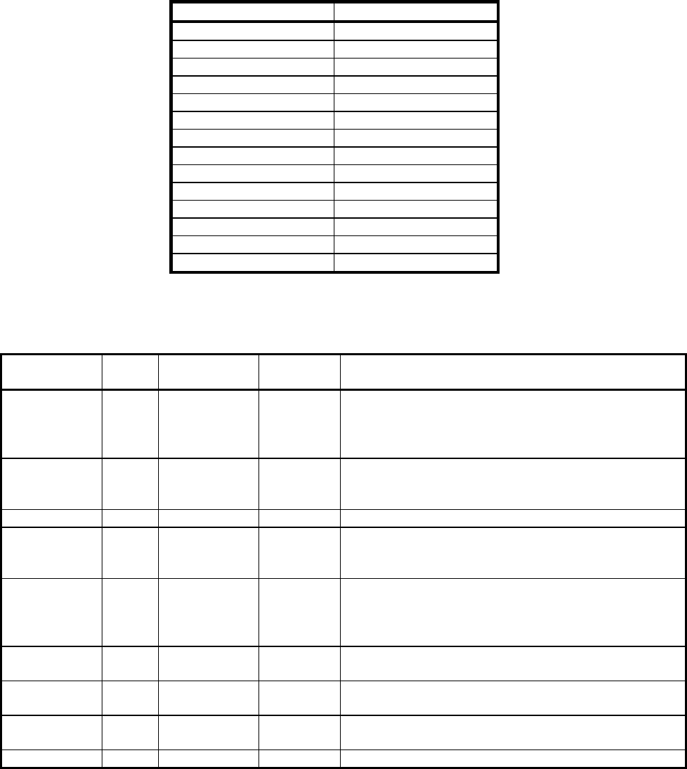
1.4 List of DMC Series
Table 1.1
Display
Format
Characters x
Lines
Character
Font
Hort’l x
Vertical
Duty
Module Size
W x H x T (mm)
View Area
W x H
(mm)
Character
Size
W x H
(mm)
Dot Size
W x H
(mm)
Available Variations
DMC-16105 16 x 1 5 x 8 1/16 80.0 x 36.0 x 15.0
64.5 x 13 3.2 x 5.95 0.6 x 0.7 NY-LY
DMC-16106A 16 x 1 5 x 11 1/11 EL B/L 80.0 x 36.0 x 10.3
Standard 80.0 x 36.0 x 10.0
64.5 x 13.8
64.5 x 13.0
3.2 x 8.2 0.6 x 0.7 E, H, HU, HE
DMC-16117 16 x 1 5 x 8 1/16 EL B/L 80.0 x 36.0 x 10.3
Standard 80.0 x 36.0 x 10.0
64.5 x 26.3 3.2 x 5 95 0.6 x 0.7 A, H, HE
AN, AN-B, ANY, AN-EB
DMC-16128 16 x 1 5 x 8 1/16 LED 122.0 x 33.0 x 15.7
Reflective 122.0 x 33.0 x 11.0
99 x 13 4.84 x 9.66 0.92 x 1.1 N-LY
NY-LY
DMC-16129 16 x 1 5 x8 1/8 122.0 x 33.0 x 11.0 154.0 x 15.3 4.84 x 9.66 0.92 x 1.1 H
U
DMC-16188 16 x 1 5 x 8 1/8 LED 151.0 x 40.0 x 14.2
Reflective & EL 151.0 x 40.0 x
10.0
120.0 x 23.0 6.0 x 14.54 1.152 x 1.765 NY-LY
NYU-LY
DMC-16202 16 x 2 5 x 8 1/16 84.0 x 45.0 x 15.1 61.0 x 31.5 2.95 x 5.55 0.55 x 0.65 LY
N-LY-B
NY-LY
NYJ-LY-D
DMC-16204 16 x 2 5 x 8 1/16 LED 80.0 x 40.0 x 16.1
Reflective & EL 80.0 x 40.0 x
10.9
59.5 x 16 2.95 x 5.55 0.55 x 0.65 NY-LY
U-LY
DMC-16205 16 x 2 5 x 8 1/16 88.0 x 34.0 x 16.1 59.5 x 16.0 2.95 x 5.55 0.55 x 0.65 NY-LY
DMC-16207 16 x 2 5 x 8 1/16 84.0 x 44.0 x 11.0 61.0 x 16.0 2.95 x 5.55 0.55 x 0.65 *
H*
N*
N-B*
N-EB*
NY-B
U*
DMC-16230 16 x 2 5 x 8 1/16 LED 122.0 x 44.0 x 14.6 99.0 x 36.0 4.84 x 9.66 0.92 x 1.1 E

9
Reflective & EL 122.0 x 44.0 x
11.0
H
H-LY
N
N-EB
NY
NY-LY
NY-LY-B
NYJ-LYD
NYU-LY
U
DMC-16249 16 x 2 5 x 8 1/16 80.0 x 36.0 x 11.0 64.5 x 13.8 2.95 x 4.35 0.55 x 0.5 B*
N*
UB*
DMC-16266 V-YGR
DMC-16433 16 x 4 5 x 8 1/16 87.0 x 60.0 x 11.0 61.8 x 25.2 2.95 x 4.75 0.55 x 0.55 E
H
N
N-B
N-EB
N-SEW-B
NU-EB
NY-SEB-B
DMC-20171 20 x 1 5 x 8 1/8 LED 182 x 33.5 x 14.35max
Reflective 182 x 33.5 x 12.7max
154.3 x 15.3 6.7 x 11.5 1.3 x 1.3 E
NY-LY
DMC-20215 20 x 2 5 x 8 1/16 116.0 x 44.0 x 11 83.0 x 18.6 3.2 x 5.55 0.6 x 0.65
DMC-20261 20 x 2 5 x 8 1/16 LED 116.0 x 37.0 x 15.7max
Reflective 116.0 x 37.0 x 11.0
83.0 x 18.6 3.2 x 5.55 0.6 x 0.65 ANY-LY-B
N
N-E
NY-LY
NYJ-LY-D
DMC-20434 20 x 4 5 x 8 1/16 98.5 x 60.0 x 11.0 76.0 x 25.2 2.95 x 4.75 0.55 x 0.55 E
H
HE
N
N-B
N-EB
N-SEW
NY-EB
U
DMC-20481 20 x 4 5 x 8 1/16 98.5 x 61.0 x 15.6 76.0 x 25.2 2.95 x 4.75 0.55 x 0.55 NY-LY

10
NY-LY-B
NYU-LY
DMC-2079 40 x 2 5 x 8 1/16 172.0 x 33.5 x 15.5 142.5 x 16.5 3.2 x 5.55 0.6 x 0.65 LY1
NB-LY-B
NY-LY-B
DMC-24227 24 x 2 5 x 8 1/16 118.0 x 36.0 x 11.0 93.5 x 15.8 3.2 x 5.55 0.6 x 0.65 N
N-B
N-EB
DMC-32132 32 x 1 5 x 11 1/11 174.5 x 31.0 x 11.0 123.5 x 16.5 3.2 x 8.2 0.6 x 0.7 UE
DMC-32239 32 x 2 5 x 8 1/16 174.5 x 31.0 x 11.0 141.0 x 29.7 3.45 x 11.75 0.65 x 0.65 NE
DMC-40131 40 x 1 5 x 11 1/11 182.0 x 33.5 x 11.0 152.5 x 16.5 3.2 x 8.2 0.6 x 0.7
DMC-40202 40 x 2 5 x 8 1/16 182.0 x 34.5 x 15.1 142.5 x 16.5 3.2 x 5.55 0.6 x 0.65 N-LY-B
NY-LY
NY-LY-B
DMC-40205 NY-LY-B
DMC-40218 40 x 2 5 x 8 1/16 182.0 x 33.5 x 11.0 152.5 x 16.5 3.2 x 5.55 0.6 x 0.65 N
N-EB
N-SEW-B
NY
NY-EB
DMC-40267 NY-LY
NYJ-LY
DMC-40457 40 x 4 5 x 8 1/16 LED 190 x 54 x 13.6
Reflective 190 x 54 x 11.0
147 x 29.5 2.78 x 4.89 0.5 x 0.55 N
N-B
N-EB
NY-LY
NY-LYB
NYJ-LYD
DMC-50097 16 x 2 5 x 8 1/16 84.0 x 44.0 x 11.0 61.0 x 16.0 2.95 x 5.55 0.55 x 0.65 H
DMC-50149 24 x 2 5 x 8 1/16 121.5 x 33.5 x 16.1 93.5 x 15.8 3.2 x 5.55 0.6 x 0.65 NYU-LY-B
DMC-50218 20 x 2 5 x 8 1/16 LED 116.0 x 37.0 x 15.7
Reflective 116.0 x 37.0 x 11.0
83.0 x 18.6 3.2 x 5.55 0.6 x 0.65 N-B
DMC-50244 20 x 4 5 x 8 1/16 82.5max x 4.8max x 9.5 71.6 x 25.2 2.95 x 4.75 0.55 x 0.55 N-B
DMC-50292 NY-LY-B
DMC-50448 8 x 2 5 x 8 1/16 40.0 x 35.4 x 8.2 30.4 x 13.9 2.95 x 4.75 0.55 x 0.55 N
11
1.5 Pin Assignments
Table 1.2
Pin Number Symbol
1 Vss
2 Vcc
3 Vee
4 RS
5 R/W
6 E
7 DB0
8 DB1
9 DB2
10 DB3
11 DB4
12 DB5
13 DB6
14 DB7
Pin Descriptions: Table 1.3 List of terminal functions
Signal name No. of
Lines Input/Output Connected
to Function
DB4 ~ DB7 4 Input/Output MPU 4 lines of high order data bus. Bi-directional transfer of data
between MPU and module is done through these lines. Also DB7
can be used as a busy flag. These lines are used as data in 4 bit
operation.
DB0 ~ DB3 4 Input/Output MPU 4 lines of low order data bus. Bi-directional transfer of data
between MPU and module is done through these lines. In 4 bit
operation, these are not used and should be grounded.
E 1 Input MPU Enable - Operation start signal for data read/write.
R/W 1 Input MPU Signal to select Read or Write
“0”: Write
“1”: Read
RS 1 Input MPU Register Select
“0”: Instruction register (Write)
: Busy flag; Address counter (Read)
“1”: Data register (Write, Read)
Vee 1 Power
Supply
Terminal for LCD drive power source.
Vcc 1 Power
Supply
+5V
Vss 1 Power
Supply
0V (GND)
E1 1 Input MPU
Enable 1
-
Operation start signal for data Read/Write of upper 2

12
lines. Applicable to DMC 40457 series only.
E2 1 Input MPU Enable 2 - Operation start signal for data Read/Write of lower 2
lines. Applicable to DMC 40457 series only.
13
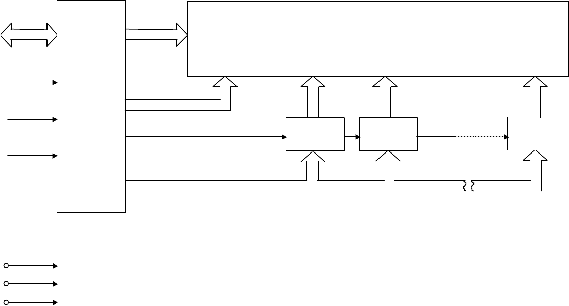
1.6 Block Diagram
Figure 1.1
DB0
~
DB7
RS
R/W
E
Vcc
40
40
40
40
Common
signals
8
Controller
& Driver
IC
Dot matrix LCD panel
Segment
Driver
Segment
Driver
Segment
Driver
3
Timing
signals
Serial data
Segment
signals
14
1.7 Explanation of Internal Operation
1.7.1 Register
The Controller for the DMC series has two 8 bit registers, the Instruction register (IR) and the data register (DR).
The IR is a write only register to store instruction codes like Display Clear or Cursor Shift as well as addresses for the
Display Data RAM (DD RAM) or the Character Generator RAM (CG RAM).
The DR is a read/write register used for temporarily storing data to be read/written to/from the DD RAM or CG RAM.
Data written into the DR is automatically written into DD RAM or CG RAM by an internal operation of the display
controller.
The DR is also used to store data when reading out data from DD RAM or CG RAM. When address information is
written into IR, data is read out from DD RAM or CG RAM to DR by an internal operation. Data transfer is then
completed by reading the DR.
After performing a read from the DR, data in the DD RAM or CG RAM at the next address is sent to the DR for the
next read cycle. The register select (RS) signal determines which of these two registers is selected.
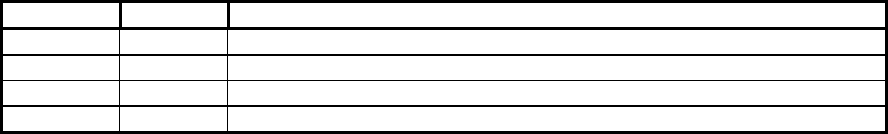
Table 1.4
Selection of Registers
RS R/W Operation
0 0 IR write, internal operation (Display Clear etc.)
0 1 Busy flag (DB7) and Address Counter (DB0 ~ DB6) read
1 0 DR Write, Internal Operation (DR ~ DD RAM or CG RAM)
1 1 DR Read, Internal Operation (DD RAM or CG RAM)
1.7.2 Busy Flag (BF)
When the busy flag is high or “1” the module is performing an internal operation and the next instruction will not be
accepted. As shown in Table 1.4, the busy flag outputs to DB7 when RS=0 and a read operation is performed. The
next instruction must not be written until ensuring that the busy flag is low or “0”.

15
1.7.3 Address Counter (AC)
The address counter (AC) assigns addresses to the DD RAM and the CG RAM.
When the address of an instruction is written into the IR, the address information is sent from the IR to the AC. The
selection of either DD RAM or CG RAM is also determined concurrently by the same instruction.
After writing into or reading from the DD RAM or CG RAM the address counter (AC) is automatically incremented
by 1 or decremented by 1 (determined by the I/D bit in the “Entry Mode Set” command.) AC contents are output to
DB0 ~ DB7 when RS = 0 and a read operation is performed, as shown in Table 1.4.
1.7.4 Display Data RAM (DD RAM)
The Display Data RAM (DD RAM) stores the display data represented in 8 bit character codes. Its capacity is 80 x 8
bits or 80 characters. The Display Data RAM that is not used for the display can be used as a general data RAM.
1.7.5 Address Counter (AC)
The DD RAM address (ADD) is set in the Address Counter (AC) and is represented in hexadecimal notation.
The address counter can be written using the “Set DD RAM Address” instruction and can be read using the “Read
Busy Flag and Address” instruction. In each case, data bits D0-D6 represent the DD RAM address. In the read
operation, bit D7 represents the “Busy Flag”.
MSB LSB
AC: BF AC6 AC5 AC4 AC3 AC2 AC1 AC0
123 14444244443 14444424444443
Busy Flag Hexadecimal Hexadecimal
Example 1 DD RAM address “4E”
BF 1 0 0 1 1 1 0
123 14444244443 14444424444443
Busy Flag 4 E
16
1.7.6 DD RAM Addressing
1.7.6.1 SINGLE LINE DISPLAYS (1/8 duty)
The relationship of a DD RAM address to the actual character position of a particular display varies.
For most single line displays, the addressing is sequential starting at address 00H as the far left character and
incrementing as you move each character position to the right.
1 2 . . . 15 16 . . . 19 20 . . . 23 24 . . . 31 32 . . . 39 40
line 1 00 01 0E 0F 12 13 16 17 1E 1F 26 27
14444244443
16 characters
144444444244444443
20 characters
144444444442444444444443
24 characters
1444444444444442444444444444443
32 characters
14444444444444444244444444444444444443
40 characters
When the display shift operation is performed on single line displays, the window of the display is shifted either right
or left within the full 80 byte DD RAM area.
For example:
A left display shift operation shifts the display/DD RAM as follows:
1 2 3 . . . 15 16 . . . 19 20 . . . 31 32 . . . 39 40
line 1 01 02 03 0F 10 13 14 1F 20 27 28
14444424444443
16 characters
1444444444244444444443
20 characters
144444444444442444444444444443
32 characters
144444444444444444244444444444444444443
40 characters

17
A right display shift operation shifts the display/DD RAM as follows:
1 2 3 . . . 15 16 . . . 19 20 . . . 31 32 . . . 39 40
line 1 4F 00 01 0D 0E 11 12 1D 1E 25 26
144444424444443
16 characters
14444444444244444444443
20 characters
1444444444444442444444444444443
32 characters
144444444444444444244444444444444444443
40 characters
Note: When a display shift operation is performed on a single line display, the display window is incremented or
decremented through the entire 80 byte DD RAM.
1.7.6.2 SINGLE LINE DISPLAYS (1/16 duty)
16 character x 1 line displays (1/16 duty)
In order to properly address these modules, they must be operated as 8 character x 2 line displays where the first 8
characters represent line 1 and the last 8 represent line 2.
For example:
1 2 3 4 5 6 7 8 1 2 3 4 5 6 7 8
144444244443 14444244443
line 1 line 2
The addressing for these types of displays is as follows.
Column
1 2 3 4 5 6 7 8 9 10 11 12 13 14 15 16
line 1 00 01 02 03 04 05 06 07 40 41 42 43 44 45 46 47
18
If the display shift operation is performed, each half of the display shifts simultaneously.
For example:
Left Shift Operation
Column
1 2 3 4 5 6 7 8 9 10 11 12 13 14 15 16
line 1 01 02 03 04 05 06 07 08 41 42 43 44 45 46 47 48
Right Shift Operation
Column
1 2 3 4 5 6 7 8 9 10 11 12 13 14 15 16
line 1 27 00 01 02 03 04 05 06 67 40 41 42 43 44 45 46
1.7.6.3 TWO LINE DISPLAYS
The available two line displays range from 8 characters per line up to 40 characters per line.
In any case, the display addressing begins at address 00H for line 1 and address 40H for line 2.
8 character x 2 line displays (1/16 duty)
Column
1 2 3 4 5 6 7 8
line 1 00 01 02 03 04 05 06 07
line 2 40 41 42 43 44 45 46 47
16 character through 40 character x 2 line display (1/16 duty)
Column
1 2 3 . . . 15 16 . . . 19 20 . . . 31 32 . . . 38 39 40
line 1 00 01 02 0E 0F 12 13 1E 1F 25 26 27
line 2 40 41 42 4E 4F 52 53 5E 5F 65 66 67
144444424444443
16 x 2
14444444444244444444443
20 characters
144444444444444244444444444443
32 characters
144444444444444444442444444444444444443
40 characters
19
When the display shift operation is performed on two line displays, each line is shifted independently.
For example:
A left display shift operation shifts the display as follows:
Column
1 2 3 . . . 15 16 . . . 19 20 . . . 31 32 . . . 38 39 40
line 1 01 02 03 0F 10 13 14 1F 20 26 27 00
line 2 41 42 43 4F 50 53 54 5F 60 66 67 40
144444424444443
16 characters
14444444444244444444443
20 characters
144444444444444244444444444443
32 characters
144444444444444444442444444444444444443
40 characters
A right display shift operation shifts the display as follows:
Column
1 2 3 . . . 15 16 . . . 19 20 . . . 31 32 . . . 38 39 40
line 1 27 00 01 0D 0E 11 12 1D 1E 24 25 26
line 2 67 40 41 4D 4E 51 52 5D 5E 64 65 66
144444424444443
16 characters
14444444444244444444443
20 characters
144444444444444244444444444443
32 characters
144444444444444444442444444444444444443
40 characters
20
1.7.6.4 FOUR LINE DISPLAYS: With 20 characters or less per line.
Four line dis plays with 20 characters or less per line operate the same as a two line display with twice as many
characters per line
For example:
A 20 character x 4 line display operates the same as a 40 character x 2 line display.
This is shown below in each addressing scheme:
16 character x 4 lines (1/16 duty)
Column
1 2 3 . . . 14 15 16
line 1 00 01 02 0D 0E 0F
line 2 40 41 42 4D 4E 4F
line 3 10 11 12 1D 1E 1F
line 4 50 51 52 4D 4E 4F
If the display shift operation is used, the addressing is shifted as follows:
20 character x 4 lines (1/16 duty)
Column
1 2 3 . . . 18 19 20
line 1 00 01 02 11 12 13
line 2 40 41 42 51 52 53
line 3 14 15 16 25 26 27
line 4 54 55 56 65 66 67
Right Shift
Column
1 2 3 . . . 14 15 16
line 1 27 00 01 0C 0D 0E
line 2 67 40 41 4C 4D 4E
line 3 0F 10 11 1C 1D 1E
line 4 4F 50 51 5C 5D 5E
Left Shift
Column
1 2 3 . . . 14 15 16
line 1 01 02 03 0E 0F 10
line 2 41 42 43 4E 4F 50
line 3 11 12 13 1E 1F 20
line 4 51 52 53 5E 5F 60
21
If the display shift operation is used on a 20 x 4 display, the addressing is shifted as follows:
1.7.6.5 FOUR LINE DISPLAYS: With more than 20 characters per line.
40 characters x 4 lines (1/16 duty x 2)
Four line displays with more than 20 characters per line (i.e. 40 characters x 4 lines) operate as two separate 40
character x 2 line displays.
If the display shift operation is used on a 40 x 4 display, the addressing is shifted as follows:
Left Shift
Column
1 2 3 . . . 18 19 20
line 1 01 02 03 12 13 14
line 2 41 42 43 52 53 54
line 3 15 16 17 26 27 28
line 4 55 56 57 66 67 68
Right Shift
Column
1 2 3 . . . 18 19 20
line 1 27 00 01 10 11 12
line 2 67 40 41 50 51 52
line 3 13 14 15 24 25 26
line 4 53 54 55 64 65 66
Column
1 2 3 . . . 38 39 40
line 1 00 01 02 25 26 27
line 2 40 41 42 65 66 67
line 3 00 01 02 25 26 27
line 4 40 41 42 65 66 67
Left Shift
Column
1 2 3 . . . 38 39 40
line 1 01 02 03 26 27 00
line 2 41 42 43 66 67 40
line 3 01 02 03 26 27 00
line 4 41 42 43 66 67 40
Right Shift
Column
1 2 3 . . . 38 39 40
line 1 27 00 01 24 25 26
line 2 67 40 41 64 65 66
line 3 27 00 01 24 25 26
line 4 67 40 41 64 65 66
Upper half
Display
Lower half
Display
Upper half
Display
Lower half
Display

22
The display shift operation can be performed on either the upper or lower half of the display independently of the
other.
In either case, the display shift operation is exactly the same as the display shift operation on the 40 x 2 line display.
Notice that when display shift operations are performed, the 16 character display window is shifted through the full
80 byte DD RAM area.
1.7.7 Character Generator ROM (CG ROM)
The Character Generator Read Only Memory (CG ROM) is an 80 x 8 bit ROM capable of generating 160 types of 5 x 7
dot or 32 types or 5 x 10 dot character patterns from an 8 bit character code. 5 x 10 character patterns cannot be
utilized on all character display modules. Table 5.3 shows the standard character font table.
Custom CG ROM tables can be obtained if necessary. Please contact your local Optrex sales representative for
details.
1.7.8 Character Generator RAM (CG RAM)
The CG RAM is a 64 x 8 bit RAM in which the user can program custom character patterns. Either 8 - 5 x 7 character
patterns or 4 - 5 x 10 character patterns can be written.
To write previously programmed characters from the CG RAM to the DD RAM, character codes 0H through 7H are
used. (See character font table 5.3)
The relationships between CG RAM address and data and the displayed character is shown in tables 5.1 and 5.2
respectively. Unused CG RAM locations can be used for general purpose RAM.
To program a 5 x 8 character pattern into the CG RAM location #2, the following steps should be taken.
A. Use the “Set CG RAM address” command to position the CG RAM pointer to the nth row of character #2.
Ex. RS R/W DB7 DB6 . . . DB1 DB0
0 0 0 1 0 0 1 Y Y Y
144444424444443 14444244443 144442444443
Set CG RAM Address Command Character Location #2 nth row of character #2
(initially YYY=000)
B. Use the “Write Data to CG or DD RAM” Command to write the top row of the custom character.
Ex. RS R/W DB7 DB6 . . . DB1 DB0
1 0 x x x y y y y y
1442443 14444244443 1444444442444444443
Write Data Don’t Care 5 bits of character bit pattern for row n of 7.
Command

23
C. The YYY portion of the “Set CG RAM address” command used in step 1 is auto incremented if the I/O bit is set in the
“Entry Mode Set” command. When this is the case, return to step 2 until all rows of the character are written.
D. After writing all 7 rows of data, use the “Set DD RAM address” command to return the address counter to a DD RAM
location.
E. To display the custom character written above, use the “Write Data to CG or DD RAM” command with the write data
being 02H to display the character in the DD RAM address used in step 4.
Ex. RS R/W DB7 DB6 . . . DB1 DB0
1 0 0 0 0 0 0 0 0 1
24
Table 5.1
Relation between CG RAM address, character codes (DD RAM) and character patterns
Character code
(DD RAM data)
CG RAM address
Character pattern
(CG RAM data)
7 6 5
4 3 2 1
0
ßHigher order Lower
orderà
bit bit
5 4 3 2 1
0
ßHigher order Lower orderà
bit bit
7 6 5 4 3 2 1
0
ßHigher order Lower orderà
bit bit
0 0 0
* *
*
1 1 1 1 0
0 0 1 1 0 0 0 1
0 1 0 1 0 0 0 1
0 0 0 0 * 0 0
0
0 0
0
0 1
1
1 1 1 1 0
1 0 0 1 0 1 0 0
1 0 1 1 0 0 1 0
1 1 0 1 0 0 0 1
1 1 1 * *
*
0 0 0 0 0
0 0 0 * *
*
1 0 0 0 1
0 0 1 0 1 0 1 0
0 1 0 1 1 1 1 1
0 0 0 0 * 0 0
1
0 0
1
0 1 1 0 0 1 0 0
1 0 0 1 1 1 1 1
1 0 1 0 0 1 0 0
1 1 0 0 0 1 0 0
1 1 1 * *
*
0 0 0 0 0
0 0 0 * *
*
0 0 1
0 0 0 0 * 1 1
1
1 1
1
1 0 0
1 0 1
1 1 0
1 1 1 * *
*
Notes:
1. Character code bits 0 ~ 2 correspond to CG RAM address bit 3 ~ 5. (3 bits: 8 types)
2. CG RAM address bits 0 ~ 2 designate the line position within a character pattern. The 8th line is the cursor
position and display is determined by the logical OR of the 8
th line and the cursor. Maintain the 8
th line data,
corresponding to the cursor display position, in the “0” state for cursor display. When the 8th line data is “1” bit 1
lights up regardless of cursor existence.
3. Character pattern row positions correspond to CG RAM data bits 0 ~ 4 as shown in the figure (bit 4 being at the
left end).
* means
Don’t care.
Example of
character (1)
Cursor position
Example of
character (2)
25
Since CG RAM data bits 5 ~ 7 are not used for display, they can be used for the general data RAM as memory still
exits.
4. As shown in Table 5.1, CG RAM character patterns are selected when character code bits 4 ~ 7 are all “0”.
However as character code bit 3 is an ineffective bit the “R” display in the character pattern example is selected by
character code “00” (hexadecimal) or “08” (hexadecimal).
5. “1” for CG RAM data corresponds to selected pixels and “0” for non selected.
26
Table 5.2
Relation between CG RAM address, character codes (DD RAM) and character patterns
Character code
(DD RAM data)
CG RAM address
Character pattern
(CG RAM data)
7 6 5 4 3 2 1
0
ßHigher order Lower
orderà
bit bit
5 4 3 2 1
0
ßHigher order Lower orderà
bit bit
7 6 5 4
3 2 1
0
ßHigher order Lower orderà
bit bit
0 0 0
0
* *
*
0 0 0 0 0
0 0 0
1
0 0 0 0 0
0 0 1
0
1 0 1 1 0
0 0
1
1
1 1 0 0 1
0 0 0 0 * 0 0
0
0 0
0 1 0
0
1 0 0 0 1
0 1 0
1
1 0 0 0 1
0 1 1
0
1 1 1 1 0
0 1 1
1
1 0 0 0 0
1 0
0
0
1 0 0 0 0
1 0 0
1
1 0 0 0 0
1 0 1
0
* *
*
0 0 0 0 0
1 0 1
1
* *
*
* * * * *
1 1 0
0
1 1 0
1
0 0 0 0 * 0 0
1
0 0
1 1 1
0
1 1 1
* * * * *
0 0 0
0
* *
*
0 0 0
1
0 0 0
0 * 1 1
*
1 1
1 0 0
1
1 0 1
0
* *
*
1 0 1
1
* *
*
* * * * *
1 1 0
0
1 1 0
1
1 1
1
0
1 1 1
* * * * * * *
Example of
character pattern
Cursor position
* means
Don’t care.

27
1 *
Note:
1. Character code bits 1,2 correspond to CG RAM address bit 4, 5 (2 bits: 4 types)
2. CG RAM address bits 0 ~ 3 designate the line position within a character pattern. The 11th line is the cursor
position and display is determined by the logical OR of the 11th line and the cursor. Maintain the 11th line data,
corresponding to the cursor display position, in the “0” state for cursor display. When the 11th line data is “1” bit 1
lights up regardless of cursor existence.
3. Character pattern row positions are the same as 5 x 7 dot character pattern positions.
Since CG RAM data bits 5 ~ 7 are not used for display, they can be used for the general data RAM as memory still
exits.
4. As shown in Table 5.2, CG RAM character patterns are selected when character code bits 4 ~ 7 are all “0”.
However, since character code bit 0 and 3 are ineffective bits, the display of character pattern example is selected by
character code “00” “01” “08” “09” (hexadecimal).
5. “1” for CG RAM data corresponds to selected pixels and “0” for non selected.
28
Table 5.3
Standard Character Font Table
High order bit
Low order bit
.
0000
0010
0011
0100
0101
0110
0111
1010
1011
1100
1101
1110
1111
X X X X0000
CG
RAM
(1)
X X X X0001
(2)
X X X X0010
(3)
X X X X0011
(4)
X X X X0100
(5)
X X X X0101
(6)
X X X X0110
(7)
X X X X0111
(8)
X X X X1000
(1)
X X X X1001
(2)
X X X X1010
(3)
X X X X1011
(4)
X X X X1100
(5)
(6)
29
(7)
(8)
Note: Character of high order bit 1110 and 1111 may be inadequate.
30
2 MPU INTERFACING
2.1 General
Each character display can be operated in either 4 or 8 bit mode.
Instructions/Data are written to the display using the signal timing characteristics found in section 4.2.
When operating in 4 bit mode, data is transferred in two 4 bit operations using data bits DB4 - DB7. DB0 - DB3 are not
used and should be tied low. When using 4 bit mode, data is transferred twice before the instruction cycle is
complete. First the high order nibble is transferred then the low order nibble. The busy flag should only be checked
after both nibbles are transferred.
When operating in 8 bit mode, data is transferred using the full 8 bit bus DB0 - DB7.
2.2 Initialization
2.2.1 Initialization using the Internal Reset Circuit
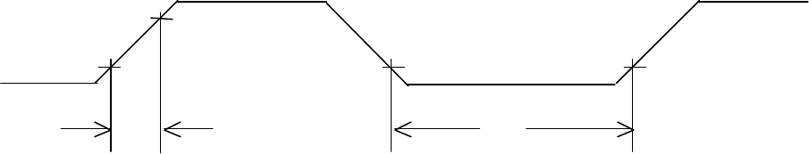
The display can be initialized using the internal reset circuit if the Internal Power Supply Reset timing below is met.
Vcc
4.5V
0.2V 0.2V 0.2V
GND
trcc toff *
0.1ms ≤ trcc ≤ 10ms toff ≥ 1ms
Note: toff represents the time of power off condition for a momentary power supply dip or when cycling power
off then on.
31
If the above conditions are met, the busy flag will go active 10ms after V
cc rises to 4.5V. The busy flag will remain
active until the following instructions are executed fully.
a. Display Clear
b. Function set:
DL = 1 : 8 bit interface operation
N = 0 : 1 - line display
F = 0 : 5 x 7 dot character font
c. Display ON/OFF Control:
D = 0 : Display OFF
C = 0 : Cursor OFF
B = 0 : Blink OFF
d. Entry Mode Set:
I/D = 1 : +1 (Increment Mode)
S = 0 : No Display Shift operation
If the internal power supply reset timing cannot be met, the display will not operate normally. In this case, the display
can be initialized through software.
Note: Variable power supply loading can have an effect on power supply reset timing. If this is the case, then
the software initialization should be performed.
2.2.2 Software Initialization
Although software initialization is not mandatory, it is recommended that this procedure always be performed. When
the internal power supply reset timing cannot be met, then the display must be initialized using one of the following
procedures.
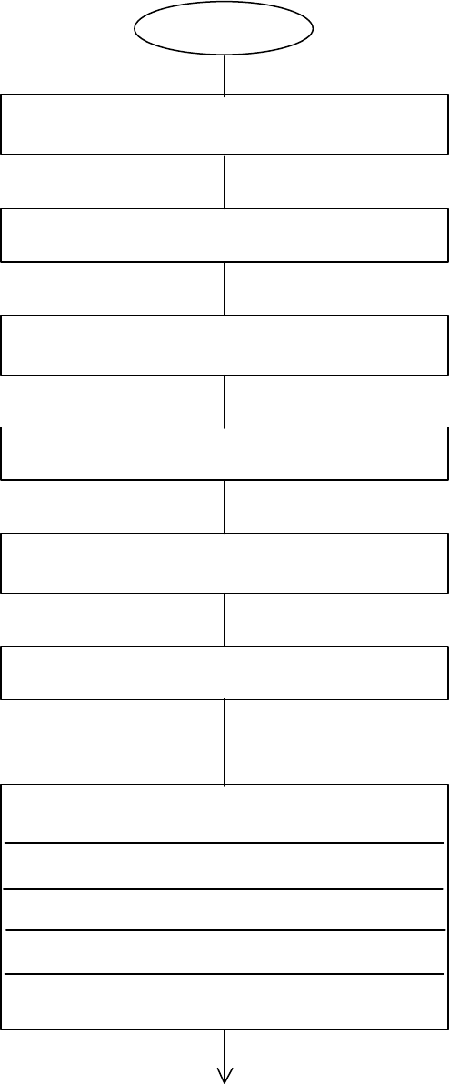
32
No data should be transferred to or from
the display during this time.
Function Set Command: (8-Bit interface)
BF cannot be checked before this command.
No data should be transferred to or from
the display during this time.
No data should be transferred to or from
the display during this time.
Function Set Command: (8-Bit interface)
BF cannot be checked before this command.
Function Set Command: (8-Bit interface)
After this command is written, BF can be checked.
Function Set (Interface = 8 bits, Set No. of
lines and display font)
Display OFF
Clear Display
Entry Mode Set:
Display ON (Set C and B for cursor/Blink
options.)
Note:
BF should be checked before each
of the instructions starting with
Display OFF.
Wait more than 100µs
Power ON
Wait more than 15ms after Vcc = 4.5V
RS R/W DB7 DB6 DB5 DB4 DB3 DB2 DB1 DB0
0 0 0 0 1 1 x x x x
RS R/W DB7 DB6 DB5 DB4 DB3 DB2 DB1 DB0
0 0 0 0 1 1 N F x x
0 0 0 0 0 0 1 0 0 0
0 0 0 0 0 0 0 0 0 1
0 0 0 0 0 0 0 1 I/D S
0 0 0 0 0 0 1 1 C B
Wait more than 4.1ms
RS R/W DB7 DB6 DB5 DB4 DB3 DB2 DB1 DB0
0 0 0 0 1 1 x x x x
RS R/W DB7 DB6 DB5 DB4 DB3 DB2 DB1 DB0
0 0 0 0 1 1 x x x x
Initialization Complete,
Display Ready.
2.2.2.1 8 - Bit Initialization:
33
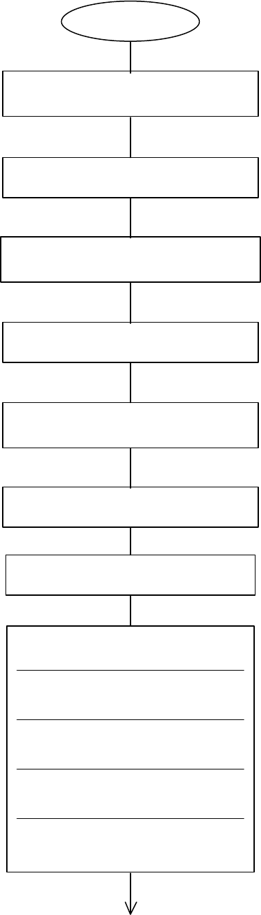
2.2.2.2 4 - Bit Initialization:
Wait more than 100µs
Power ON
Wait more than 15ms after Vcc = 4.5V
RS R/W DB7 DB6 DB5 DB4
0 0 0 0 1 1
0 0 0 0 1 0
0 0 N F x x
0 0 0 0 0 0
0 0 1 0 0 0
0 0 0 0 0 0
0 0 0 0 0 1
0 0 0 0 0 0
0 0 0 1 I/D S
0 0 0 0 0 0
0 0 1 1 C B
Wait more than 4.1ms
Initialization Complete,
Display Ready.
RS R/W DB7 DB6 DB5 DB4
0 0 0 0 1 1
RS R/W DB7 DB6 DB5 DB4
0 0 0 0 1 1
RS R/W DB7 DB6 DB5 DB4
0 0 0 0 1 0
N
o data should be transferred to or from the
display during this time.
Function Set Command: (8-Bit interface)
No data should be transferred to or from the
display during this time.
No data should be transferred to or from the
display during this time.
Function Set Command: (8-Bit interface)
Function Set Command: (8-Bit interface)
After this command is written, BF can be checked.
Function Set (Interface = 4 -bit, Set N and F
for number of lines and character font)
Display OFF
Clear Display
Entry Mode Set:
Display ON (Set C and B for cursor/Blink
options.)
Note:
BF should be checked before each
of the instructions starting with
Display OFF.
Function Set: Sets interface to 4 -bit
34
3 INSTRUCTIONS
Table 3.1 shows the list of instructions recognized by the LCD Controller and their execution times. If the busy flag is
not checked, each instruction must be allotted at least the execution time before writing another instruction or data.
After writing these execution times, the display can be written without conflict.
3.1 Detailed Explanations
3.1.1 Clear Display
RS R/W DB7 DB6 . . . DB1 DB0
Code 0 0 0 0 0 0 0 0 0 1
Writes the space code “20” (hexadecimal) into all addresses of DD RAM. Returns display to its original position if it
was shifted. In other words the display clears and the cursor or blink moves to the upper left edge of the display.
The execution of clear display instruction sets entry mode to increment mode.
3.1.2 Return Home
RS R/W DB7 DB6 . . . DB1 DB0
Code 0 0 0 0 0 0 0 0 1 x
Note: x = Don’t Care
Sets the DD RAM address “0” in address counter. Return display to its original position if it was shifted. DD RAM
contents do not change.
The cursor or the blink moves to the upper left edge of the display. Text on the display remains unchanged.
3.1.3 Entry mode set
RS S/W DB7 DB6 . . . DB1 DB0
Code 0 0 0 0 0 0 0 1 I/D S
Sets the Increment/Decrement and Shift modes to the desired settings.
I/D: Increments (I/D = 1) or decrements (ID = 0) the DD RAM address by 1 when a character code is written into or
read from the DD RAM.
35
The cursor or blink moves to the right when incremented by +1.
The same applies to writing and reading the CG RAM.
S: Shifts the entire display either to the right or to the left when S = 1; shift to the left when I/D = 1 and to the right
when I/D = 0. Thus it looks as if the cursor stands still and only the display seems to move.
The display does not shift when reading from DD RAM nor when S = 0.
3.1.4 Display ON/OFF Control
RS R/W DB7 DB6 . . . DB1 DB0
Code 0 0 0 0 0 0 1 D C B
Controls the display ON/OFF status, Cursor ON/OFF and Cursor Blink function.
D: The display is ON when D = 1 and OFF when D = 0. When OFF due to D = 0, display data remains in the DD
RAM. It can be displayed immediately by setting D = 1.
C: The cursor displays when C = 1 and does not display when C = 0. The cursor is displayed on the 8th line when 5
x 7 dot character font has been selected.
B: The character indicated by the cursor blinks when B = 1. The blink is displayed by switching between all blank
dots and display characters at 0.4 sec intervals.
The cursor and the blink can be set to display simultaneously.
Alternating display
5 x 7 dots 5 x 10 dots
character font character font
(a) Cursor display example (b) Blink display example
C = 1 ; B = 0 C = 1 ; B = 1
Cursor
36
3.1.5 Cursor or Display Shift
RS R/W DB7 DB6 . . . DB1 DB0
Code 0 0 0 0 0 1 S/C R/L x x
Note: x = Don’t Care
Shifts the cursor position or display to the right or left without writing or reading display data. This function is used
to correct or search for the display. In a 2-line display the cursor moves to the 2nd line when it passes the 40th digit of
the 1st line. Notice that the 1st and 2nd line displays will shift at the same time.
When the displayed data is shifted repeatedly each line only moves horizontally but the 2nd line display does not
shift into the 1st line position.
S/C R/L
0 0 Shifts cursor position to the left (AC is decremented by one)
0 1 Shifts cursor position to the right (AC is incremented by one)
1 0 Shifts the entire display to the left. The cursor follows the display shift.
1 1 Shifts the entire display to the right. The cursor follows the display shift.
The contents of Address Counter (AC) do not change if the only action performed is shifting display.
3.1.6 Function Set
Sets the interface data length, the number of lines, and character font.
RS R/W DB7 DB6 . . . DB1 DB0
Code 0 0 0 0 1 DL N F x x
Note: x = Don’t Care
DL: Sets interface data length. Data is sent or received in 8-bit length (DB7 ~ DB0) when DL = “1”, and in 4-bit
length (DB7 ~ DB4) when DL = 0. When the 4-bit length is selected, data must be sent or received twice.
N: Sets the number of lines
N = “0” : 1 line display (1/8 duty)
N = “1” : 2 line display (1/16 duty)
F: Sets character font.
F = “1” : 5 x 10 dots
F = “0” : 5 x 7 dots
Note: Perform the function at the head of the program before executing all instructions (except Busy flag/address
read). From this point, the function set instruction cannot be executed other than to change interface length.
37
3.1.7 Set CG RAM Address
RS R/W DB7 DB6 . . . DB1 DB0
Code 0 0 0 1 A A A A A A
Higher order bits Lower order bits
Sets the address counter to the CG RAM address AAAAAAA. Data is then written/read to from the CG RAM.
3.1.8 Set DD RAM Address
RS R/W DB7 DB6 . . . DB1 DB0
Code 0 0 1 A A A A A A A
Higher order bits Lower order bits
Sets the address counter to the DD RAM address AAAAAAA. Data is then written/read to from the DD RAM.
For a 1-line display module AAAAAAA is “00” ~ “4F” (hexadecimal). For 2-line display module AAAAAAA is “00”
~ “27” (hexadecimal) for the first line and “40” ~ “67” (hexa decimal) for the second line. (See section 1.7.6 “DD RAM
addressing”)
3.1.9 Read Busy Flag and Address
RS R/W DB7 DB6 . . . DB1 DB0
Code 0 1 BF A A A A A A A
Higher order bits Lower order bits
Reads the busy flag (BF) and value of the address counter (AC). BF = 1 indicates that on internal operation is in
progress and the next instruction will not be accepted until BF is set to “0”. If the display is written while BF = 1,
abnormal operation will occur.
The BF status should be checked before each write operation.
At the same time the value of the address counter expressed in binary AAAAAAA is read out. The address counter
is used by both CG and DD RAM and its value is determined by the previous instruction. Address contents are the
same as in sections 3.1.7 and 3.1.8.
38
3.1.10 Write Data to CG or DD RAM
RS R/W DB7 DB6 . . . DB1 DB0
Code 1 0 D D D D D D D D
Higher order bits Lower order bits
Writes binary 8-bit data DDDDDDDD to the CG or DD RAM.
The previous designation determines whether the CG or DD RAM is to be written (CG RAM address set or DD RAM
address set). After a write the entry mode will automatically increase or decrease the address by 1. Display shift will
also follow the entry mode.
3.1.11 Read Data from CG or DD RAM
RS R/W DB7 DB6 . . . DB1 DB0
Code 1 1 D D D D D D D D
Higher order bits Lower order bits
Reads binary 8-bit data DDDDDDDD from the CG RAM or DD RAM.
The previous designation determines whether the CG or DD RAM is to be read.
Before entering the read instruction, you must execute either the CG RAM or DD RAM address set instruction.
If you don’t, the first read data will be invalidated. When serially executing the “read” instruction the next address
data is normally read from the second read.
The “address set” instruction need not be executed just before the “read” instruction when shifting the cursor using
cursor instruction (when reading DD RAM). The cursor shift instruction operation is the same as that of the DD
RAM address set instruction.
After a read, the entry mode automatically increases or decreases the address by 1; however, display shift is not
executed no matter what the entry mode is.
Note: The address counter (AC) is automatically incremented or decremented by 1 after a “write” instruction to
either CG RAM or DD RAM. RAM data selected by the AC cannot then be read out even if “read” instructions are
executed.
The conditions for correct data reads are: (a) Execute either the address set instruction or cursor shift instruction
(only with DD RAM) or (b) The execution of the “read data” instruction from the second time when the read
instruction is performed multiple times in serial.
39
Table 3.1
List of Instructions
Instruction
Code
Description
Execution time
(max.)
when fcp or fosc is
RS R/W DB7 DB6 DB5 DB4 DB3 DB2 DB1 DB0 250 kHz
Clear Display 0 0 0 0 0 0 0 0 0 1 Clears entire display and sets DD RAM address 0 in
address counter.
15.2ms
Return Home 0 0 0 0 0 0 0 0 1 x Sets DD RAM address 0 in address counter. Also
returns shifted display to original position. DD RAM
contents remain unchanged.
15.2ms
Entry Mode
Set
0 0 0 0 0 0 0 1 I/D S Sets cursor move direction and specifies shift or
display. These operations are performed during data
write and read.
40µs
Display
ON/OFF
Control
0 0 0 0 0 0 1 D C B Sets ON/OFF of entire display (D), cursor ON/OFF
(C), and blink of cursor position character (B).
40µs
Cursor or
Display Shift
0 0 0 0 0 1 S/C R/L x x Moves cursor and shifts display without changing DD
RAM contents.
40µs
Function Set 0 0 0 0 1 DL N F x x Sets interface data length (DL), number of display
lines (N) and character font (F).
40µs
Set
CG RAM
Address
0 0 0 1 ACG Sets CG RAM address. CG RAM data is sent and
received after this setting.
40µs
Set
DD RAM
Address
0 0 1 ADD Sets DD RAM address. DD RAM data is sent and
received after this setting.
40µs
Read Busy Flag
& Address
0 1 BF AC Reads busy flag (BF) indicating internal operation is
being performed and reads address counter contents.
40µs
Write Data to
CG or DD
RAM
1 0 Write Data Writes data into DD RAM or CG RAM. 40µs
Read Data
from CG or
DD RAM
1 1 Read Data Reads data from DD RAM or CG RAM. 40µs
I/D=1 : Increment
I/D=0 : Decrement
S=1 : Accompanies display shift
S/C=1 : Display shift
S/C=0 : Cursor move
R/L=1 : Shift to the right
DD RAM : Display Data RAM
CG RAM : Character Generator RAM
ACG : CG RAM address
ADD : DD RAM address.
Corresponds to cursor address.
AC : Address counter used for both
Execution time changes
when frequency
changes.
Example: When fcp or
fosc is 270kHz:

40
R/L=0 : Shifts to the left
DL=1 : 8 bits, DL=0 : 4 bits
N=1 : 2 lines, N=0 : 1 line
F=1 : 5x10 dots, F=0 : 5x7 dots
BF=1 : Internally operating
BF=0 : Can accept instruction
DD and CG RAM address. 40µs x 250/270 = 37 µs
x = don’t care. (No Effect)
41
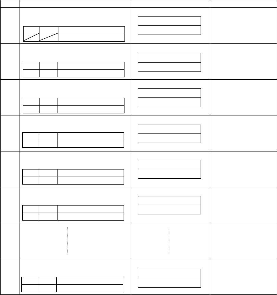
3.2 Examples of Instructions
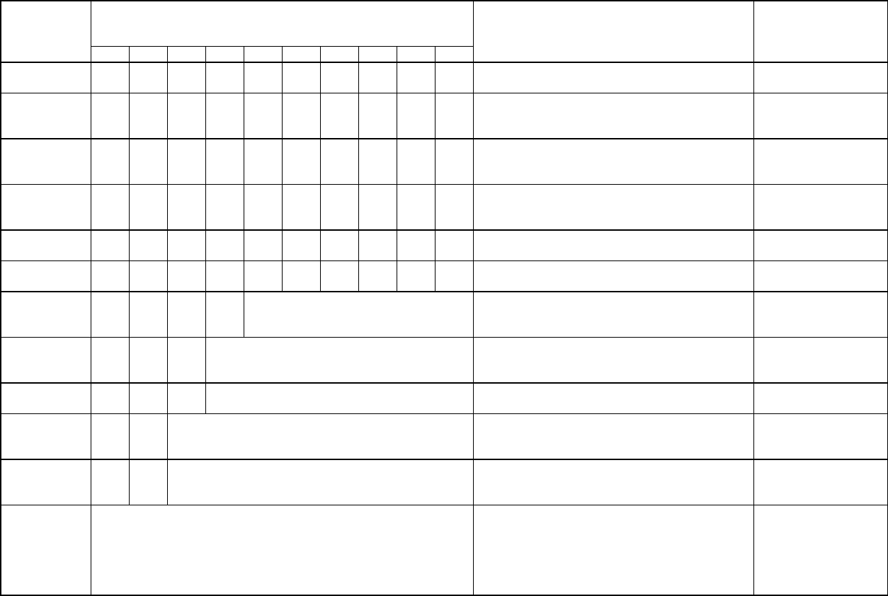
3.2.1 16 Character x 1 Line Display (1/8 duty) Using CG RAM
RS R/W DB7 ~ DB0
RS R/W DB7 ~ DB0
0 0 0 0 1 1 0 0 * *
RS R/W DB7 ~ DB0
0 0 0 0 0 0 1 1 1 0
RS R/W DB7 ~ DB0
0 0 0 0 0 0 0 1 1 0
No. Instruction Display Operation
1
Power supply ON
(Initialized by Internal reset circuit)
Module is initialized.
No display appears.
2
Function set
Sets 8 bit interface data
length, selects 5 x 7 dots,
1-line display
3
Display ON/OFF Control
Turns on display and
cursor.
No display appears.
4
Entry mode set
Sets mode to increment
the address by one and
to shift cursor to the right
at the time of write to
internal RAM.
5
Write data to CG/DD RAM
Writes “L” cursor is
incremented and moves
to the right.
6
Write data to CG/DD RAM
Writes “C”
7
8
Write data to CG/DD RAM
Writes “6” cursor
disappears.
(DD RAM address is
10H)
RS R/W DB7 ~ DB0
1 0 0 0 1 1 0 1 1 0
RS R/W DB7 ~ DB0
1 0 0 1 0 0 0 0 1 1
RS R/W DB7 ~ DB0
1 0 0 1 0 0 1 1 0 0
_
_
L_
LC_
LCD MODULE DMC16
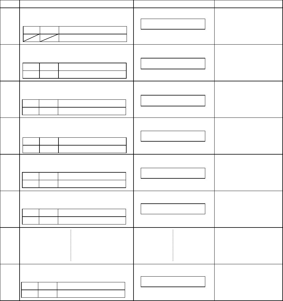
42
RS R/W DB7 ~ DB0
0 0 1 0 0 0 0 0 0 0
RS R/W DB7 ~ DB0
0 0 0 0 0 1 1 1 * *
RS R/W DB7 ~ DB0
0 0 0 0 0 1 1 1 * *
RS R/W DB7 ~ DB0
0 0 0 0 0 0 1 0 0 0
No. Instruction Display Operation
9
DD RAM address set
Cursor appears at home
position
10
Cursor/Display shift
Entire display one digit to
the right.
11
Cursor/Display shift
Entire display shifts one
digit to the right.
12
Display ON/OFF cursor
Entire display disappears.
13
Display ON/OFF
Entire display reappears.
14
Cursor Home
Returns both cursor and
display to original
position.
15
Display clear
Clears entire display
except cursor.
16
Set CG RAM address
Set CG RAM address
pointer to top row of
character 3.
RS R/W DB7 ~ DB0
0 0 0 1 0 1 0 0 0 0
RS R/W DB7 ~ DB0
0 0 0 0 0 0 0 0 1 *
RS R/W DB7 ~ DB0
0 0 0 0 0 0 1 1 1 0
RS R/W DB7 ~ DB0
0 0 0 0 0 0 0 0 0 1
LCD MODULE DMC
LCD MODULE DMC
LCD MODLE DMC1
LCD MODULE DMC16
_
LCD MODULE DMC16
_
43
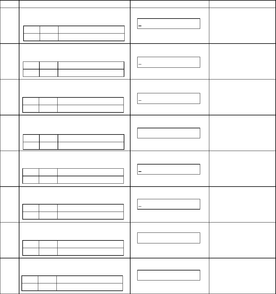
RS R/W DB7 ~ DB0
1 0 0 0 0 1 1 1 1 1
RS R/W DB7 ~ DB0
1 0 0 0 0 1 0 1 0 1
RS R/W DB7 ~ DB0
1 0 0 0 0 1 0 1 0 0
RS R/W DB7 ~ DB0
1 0 0 0 0 1 1 1 1 1
No. Instruction Display Operation
17
Write data to CG RAM
Write top line of custom
character to CG RAM
18
Write data to CG/DD RAM
Write 2nd line of custom
character to CG RAM
19
Write data to CG/DD RAM
Write 3rd line of custom
character to CG RAM
20
Write data to CG/DD RAM
Write 4th line of custom
character to CG RAM
21
Write data to CG/DD RAM
Write 5th line of custom
character to CG RAM
22
Write data to CG/DD RAM
Write 6th line of custom
character to CG RAM
23
Write data to CG/DD RAM
Write 7th line of custom
character to CG RAM
24
Set DD RAM address
Set DD RAM address to
first character position.
25
Write data to CG/DD RAM
Writes previously
programmed character to
display.
Cursor is incremented
and moved to the right.
RS R/W DB7 ~ DB0
0 0 0 0 0 0 0 0 0 0
RS R/W DB7 ~ DB0
1 0 0 0 0 1 0 1 0 1
RS R/W DB7 ~ DB0
1 0 0 1 0 1 0 1 0 1
RS R/W DB7 ~ DB0
1 0 0 0 0 0 0 0 1 0
RS R/W DB7 ~ DB0
1 0 0 0 0 1 1 1 1 1
_
_
_
_
_
_
_
_
44
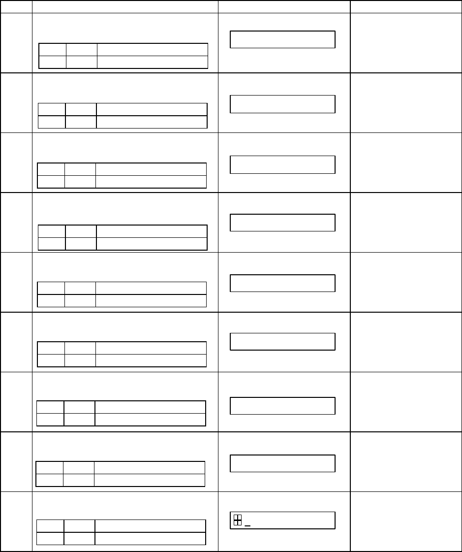
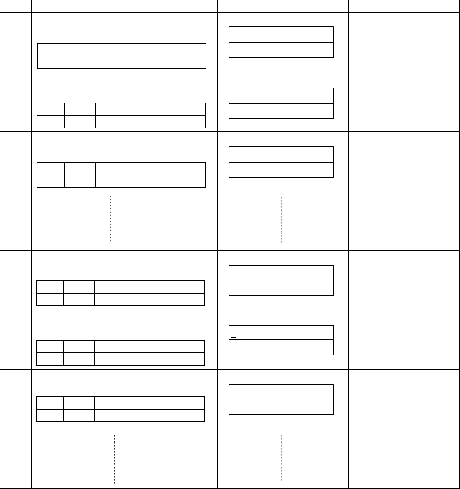
3.2.2 16 Character x 2 Line Display (1/16 duty)
RS R/W DB7 ~ DB0
RS R/W DB7 ~ DB0
0 0 0 0 1 1 1 0 * *
No. Instruction Display Operation
1
Power supply ON
(Initialized by Internal reset circuit)
Module is initialized.
2
Function set
Sets the interface data
length to 8 bits and
selects 2-line display and
5 x 7-dot character font.
3
Display ON/OFF Control
Turns on display and
cursor.
4
Entry mode set
Sets mode to increment
address by one and to
shift the cursor to the
right at the time of write
to internal RAM
5
Write data to CG/DD RAM
Writes “L”.
Cursor is incremented by
one and shifts to the
right.
6
Write data to CG/DD RAM
Writes “C”
7
8
Write data to CG/DD RAM
Writes “6”
RS R/W DB7 ~ DB0
0 0 0 0 0 0 1 1 1 0
RS R/W DB7 ~ DB0
0 0 0 0 0 0 0 1 1 0
RS R/W DB7 ~ DB0
1 0 0 0 1 1 0 1 1 0
RS R/W DB7 ~ DB0
1 0 0 1 0 0 0 0 1 1
RS R/W DB7 ~ DB0
1 0 0 1 0 0 1 1 0 0
LCD MODULE DMC16
LC_
_
_
L_
45
RS R/W DB7 ~ DB0
0 0 1 1 0 0 0 0 0 0
RS R/W DB7 ~ DB0
1 0 0 0 1 1 0 0 1 1
No. Instruction Display Operation
9
Set DD RAM address.
Sets RAM address so
that the cursor is
positioned at the head of
the 2nd line.
10
Write data to CG/DD RAM
Write “1”
11
Write data to CG/DD RAM
Writes “6”
12
13
Write data to CG/DD RAM address
Writes “S”
14
Set DD/RAM address
Moves cursor to original
position
15
Clear display
Return both display and
cursor to the original
position
16
RS R/W DB7 ~ DB0
1 0 0 0 1 1 0 0 1 0
RS R/W DB7 ~ DB0
0 0 1 0 0 0 0 0 0 0
RS R/W DB7 ~ DB0
1 0 0 0 1 0 1 0 1 0
RS R/W DB7 ~ DB0
0 0 0 0 0 0 0 0 0 1
_
16 DIGITS, 2 LINES
LCD MODULE DMC16
_
LCD MODULE DMC16
1_
LCD MODULE DMC16
16_
LCD MODULE DMC16
16 DIGITS, 2 LINES_
LCD MODULE DMC16
46
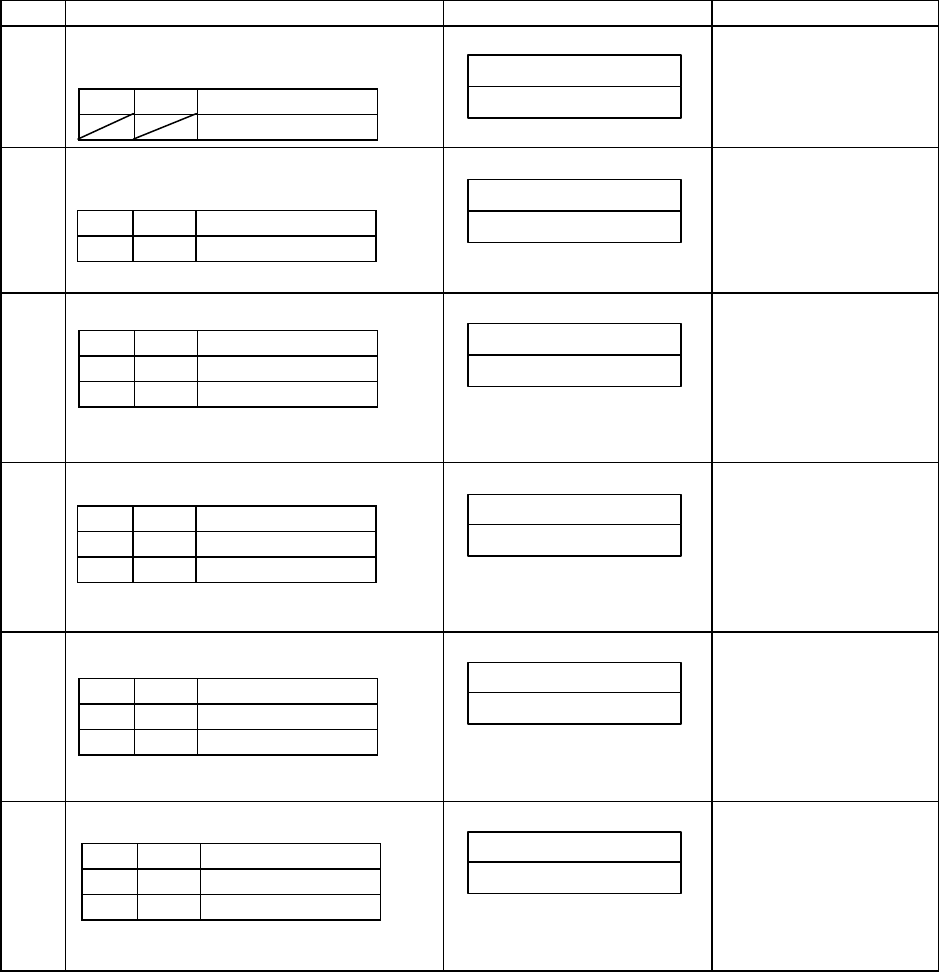
3.2.3 16 Character x 2 Line Display (4-bit interface, 1/16 duty)
RS R/W DB7 ~ DB4
RS R/W DB7 ~ DB4
0 0 0 0 1 0
No. Instruction Display Operation
1
Power supply ON
(Initialized by Internal reset circuit)
Module is initialized.
2
Function set
Sets the interface data
length to 4 bits. Since
the module has been 8
bits by initial set,
instruction is required
only one time.
3
Function set
Set the interface data
length to 4 bits and select
2-line display and 5 x 7-
dot character font.
Since it is operated as 4
bits from here, re-sending
is necessary.
4
Display ON/OFF control
Turn on display and
cursor.
5
Entry mode set
Set mode to increment
address by one and shift
the cursor to the right at
the time of write to
internal RAM.
6
Write data to CG/DD RAM
Writes “L”.
Cursor is incremented by
one and shift to the right.
RS R/W DB7 ~ DB4
0 0 0 0 1 0
0 0 1 x x x
RS R/W DB7 ~ DB4
0 0 0 0 0 0
0 0 1 1 1 0
RS R/W DB7 ~ DB4
0 0 0 0 0 0
0 0 0 1 1 0
RS R/W DB7 ~ DB4
1 1 0 1 0 0
1 0 1 1 0 0
L_
_
_
47
4 Electrical Characteristics
4.1 Absolute Maximum Ratings
The absolute maximum ratings of a display module may vary from one to another. Please contact your local Optrex
Sales Representative for a detailed module specification.
4.2 Timing Characteristics
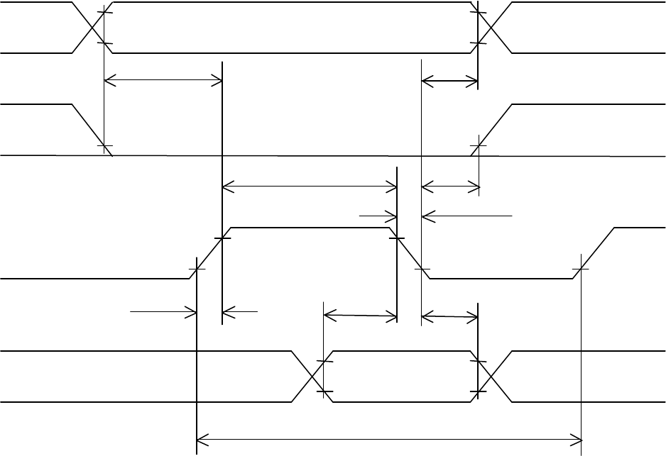
4.2.1 Write Operation
Fig. 4.1
Bus Write Operation Sequence.
(Writing data from MPU to Module)
RS
(LS)
2.0V 2.0V
0.8V 0.8V
0.8V 0.8V
0.8V 0.8V
0.8V 0.8V
0.8V
2.0V 2.0V
2.0V 2.0V
effective data
tcycle
tDSW tH
PWEH tAH
tAH
tAS
tEr
tEr
R/W
E
DB0 ~ DB7
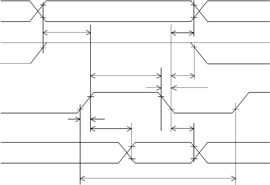
48
4.2.2 Read Operation
Fig. 4.2
Bus Read Operation Sequence
(Reading data from Module to MPU)
RS
(LS)
2.0V 2.0V
0.8V 0.8V
2.0V 2.0V
0.8V 0.8V
0.4V 0.4V
0.8V
2.0V 2.0V
2.4V 2.4V
effective data
tcycle
tDDR tH
PWEH tAH
tAH
tAS
tEr
tEr
R/W
E
DB0 ~ DB7
49
4.2.3 Timing Characteristics of Each Drawing
(Vcc = 5.0V ± 5%, Vxx = 0V, Ta = 0 ~ 50-C)
Write timing characteristics (Fig. 4.1)
Item
Symbol
Specs. Value
Unit
Min. Max.
Enable cycle time tcycle 1000 - ns
Enable pulse width “High” level PWEH 450 - ns
Enable rising, falling time tEr, tEf - 25 ns
Set up time RS, R/W-E tAS 140 - ns
Address hold time tAH 10 - ns
Data set up time tDSW 195 - ns
Data hold time tH 10 - ns
Read timing characteristics (Fig. 4.2)
Item
Symbol
Specs. Value
Unit
Min. Max.
Enable cycle time tcycle 1000 - ns
Enable pulse width “High” level PWEH 450 - ns
Enable rise, fall time tEr, tEf - 25 ns
Set up time RS, R/W-E tAS 140 - ns
Data delay time tDDR - 320 ns
Data hold time tH 20 - ns
Note: These read and write timing characteristics are for reference only. Please contact your local Optrex sales
representative to obtain the complete LCD module specification for more details.
50
5 Connection Block Diagrams to MPU
5.1 Connection with Z-80
A0
A1
A7
D0
D7
Z 80
MPU
φ
_____
IORQ
___
RD
___
WR
RS
E
DMC module
R/W
DB0
DB7
Chip
Select
S
D Q
C
R
+5V
51
5.2 Connection with 8085A
IO/M
RD
WR
8085 A
S1
ALE
A15
A8
AD0
AD7
E
DMC module
R/W
RS
DB0
DB7
Chip
Select
S Q
T
R D
(74LS74)
CS
+5V
AD0
52
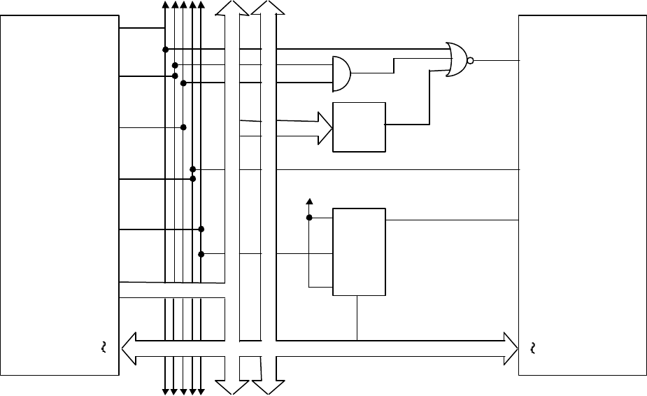
5.3 Connection with MC 6800
A15
A14
A13
A1
MC 6800 A0
R/W
VMA
φ2
DB0 ~ DB7
___
CS2
CS1 PA2
CS0
PA1
RS1
RS0 PA0
R/W MC 6821
E
PB0 ~ PB7
D0 ~ D7
RS
R/W
DMC Module
E
DB0 ~ DB7
8
8
VM A
φ2
A15
A0
MC 6800
R/W
D0 ~ D7
E
DMC Module
RS
R/W
DB0 ~ DB7
8
53
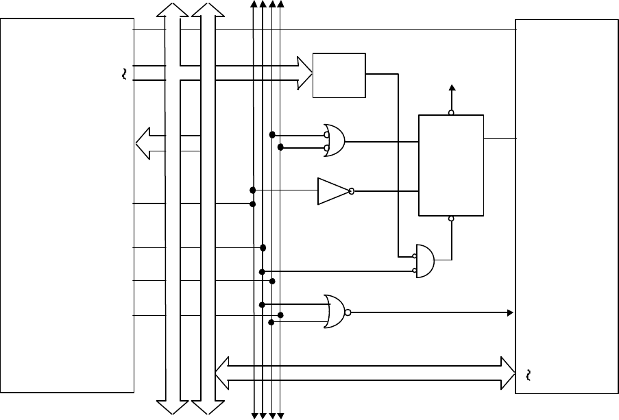
5.4 Connection with MC 6809
5.5 Connection with 80C31 Family (or similar microcontroller) Using I/O Port
Interface
4 bit Mode
8 bit mode
E
A15
A0
MC 6809
R/W
D0 ~ D7
E
DMC Module
RS
R/W
DB0 ~ DB7
8
P1.1
P1.2
P1.3
80C31
P1.4 ~ P1.7
E
RS
R/W
DMC Module
DB4 ~ DB7
4
P3.2
P3.1
P3.0
80C31
P1.0 ~ P1.7
E
RS
R/W
DMC Module
DB0 ~ DB7
8

54
6 Special Specifications
6.1 EL (back light) Specifications for DMC Series
Note (1) These specifications are for explaining general characteristics of electroluminesence (EL).
Detailed data sheets are available from your local Optrex representative for each model.
Please contact your local representative for the data.
Note (2) This product has been developed with the cooperation from NEC Corporation.
Characteristics:
♦ This is a surface light source using organic film as substrate and packaging material.
♦ With the adoption of new materials and production processes, the thickness is reduced to 1.3 mm
Max. (Electrode portion is 1.5mm Max.) making it suitable for high density mounting.
♦ Color emission is blue-green or white.
♦ Driving voltage can be selected from a wide range of 60 ~ 1000 Hz and AC 150V Max.
♦ Also with the help of an inverter, voltage increase from a single DC source is easily achieved.
♦ Please contact your local Optrex representative for the recommended inverter.
6.1.1 Absolute Maximum Ratings
Operating Voltage AC 150V RMS
Operating Temperature Range -10 ~ +50° C
Storage Temperature Range -30 ~ +60° C
6.1.2 Electrical and Life Characteristics (Color emission: Blue-green)
Please contact your local Optrex representative for detailed specifications of the EL Backlighting.
55
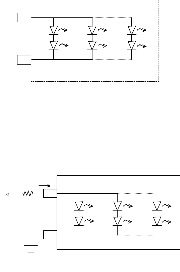
6.2 LED (Backlight) Specifications for DMC Series
LED Backlight characteristics vary from one display module to the next. Please contact your local Optrex
representative for detailed specifications.
In general, LED Backlit modules include an array of LED’s positioned behind the LCD panel.
Optrex specifies the absolute maximum current for the LED array in the detailed module specification.
Also specified is the LED Forward Voltage at optimum current level.
Example: VF @ Inom [mA]
A current limiting resistor should be added in series to limit the current to the LED assembly. The resistor can be
calculated as follows:
Note: Inom can be found in the VF rating of the LCD module specification.
A
K
anode
cathode
K
A
+
VF
-
Vs
I
nom
RL = VS - VF
Inom [ohm]
RL
56
6.3 High Reliability Specifications
Among the DMC series, some of the modules are made to meet high reliability specs., using liquid crystal suitable for
a wide range of temperatures. Those modules have an “H” in their part number to distinguish them from the others.
However, high reliability modules use liquid crystal fluid and power sources of different characteristics. Caution
should be taken when putting them to use.
(1) Operating Temperature -20° C ~ +70° C
(2) Storage Temperature -30° C ~ +80° C
Note: Even in these “H” modules, the specifications for EL Backlight are standard levels. (See section 6.1)
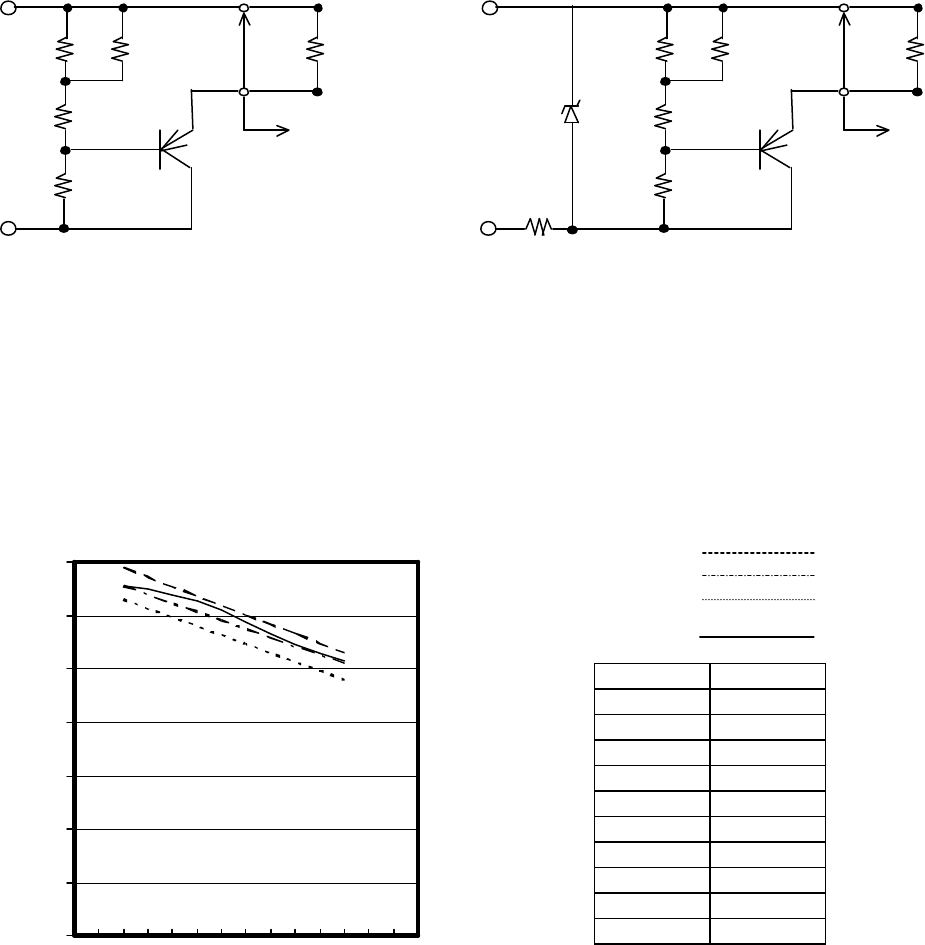
6.4 Examples of Temperature Compensation Circuits (For reference only)
Liquid Crystal materials are temperature dependent. In other words, the Contrast Ratio of an LCD can vary based on
the ambient temperature of the LCD panel. Temperature Compensation circuits can be used to obtain optimum
contrast across the temperature range.
Typical contrast voltage vs. temperature curves for Optrex “H” version LCD modules are shown in Fig 6.1 and 6.2
In order to maintain optimum contrast across the temperature range, the LCD module contrast voltage must be held
as close as possible to the nominal curve.
Note: LCD module contrast voltage is measured with respect to Vcc (i.e. Vcc - Vee = Vo)
The circuits in Fig. 6.1 and 6.2 are examples of how this temperature compensation can be achieved.
Note: RTH should be mounted such that the ambient temperature of R
TH and the LCD panel are as close as
possible to each other.
57
Fig. 6.1
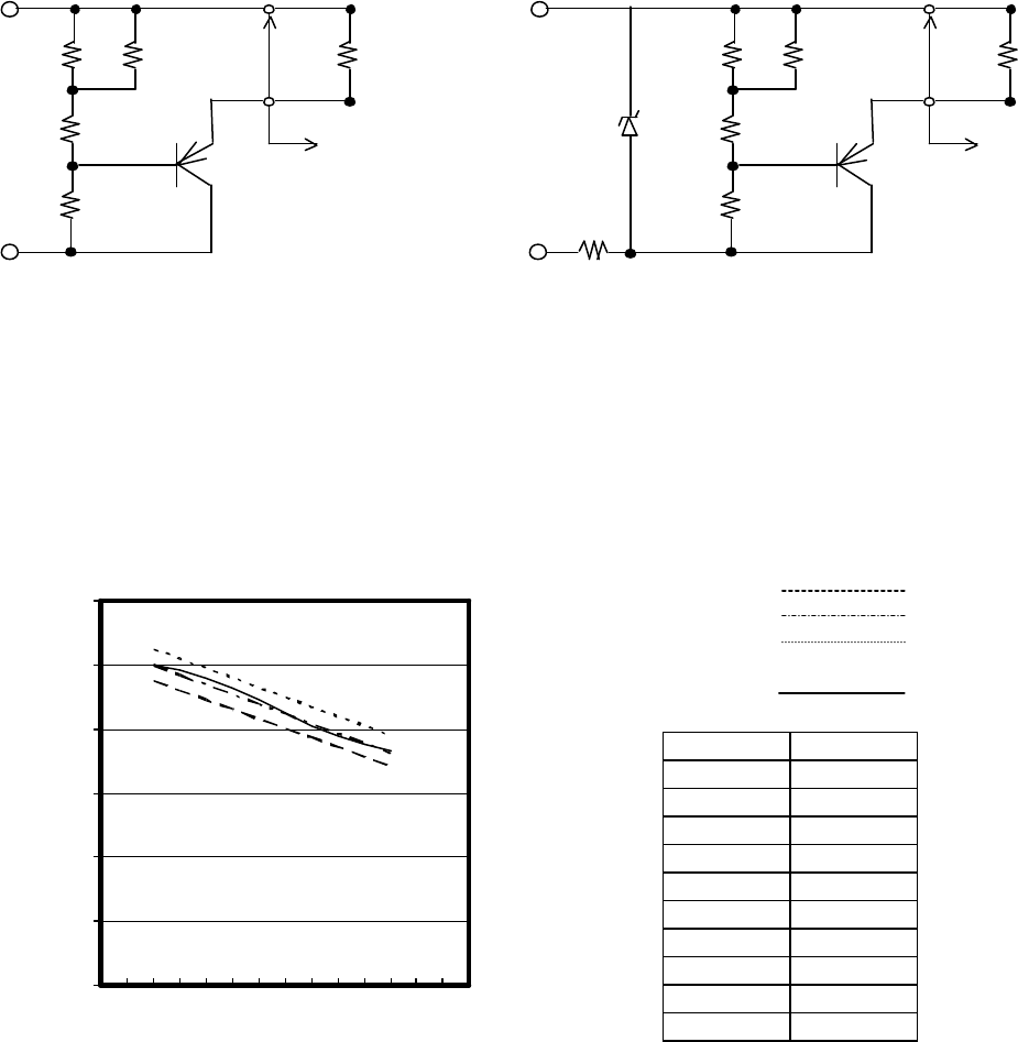
1/8 Duty - 1/3 Bias
Thermistor : RTH (25° C) = 15[k-ohm] , B = 4200[K]
Resistors : Rp = 30[k-ohm] , Rs = 6.8[k-ohm] , Rm = 3.3[k-ohm]
Transistor : PNP Type
Vcc : +5[V] , Vss : 0V (Logic Supply)
Vz : -8[V] (-7.8 to -8.2[V])
Vee<Vz[V] , Rz = (Vz-Vee)/5[k-ohm]
0
1
2
3
4
5
6
7
-40
-20
0
20
40
60
80
100
* Specifications are subject to change without notice.
Rp = 30 [k-ohm] VTH OFF
Rs = 6.8 [k-ohm] VTH Nominal
Rm = 3.3 [k-ohm] VTH ON
VTH Actual
Ta[°C] Vo[V]
-20 6.56
-10 6.50
0 6.40
10 6.26
20 6.09
30 5.88
40 5.67
50 5.47
60 5.29
70 5.15
RTH (25°C) = 15 [k-ohm]
β = 4200 [K]
RTH
Rs
Rm
Rp Vo RL
Module
Vz
Vcc
RTH
Rs
Rm
Rp Vo RL
Module
Vee
Vcc
Vz
Rz
58
Fig. 6.2
1/16 Duty - 1/5 Bias
Thermistor : RTH (25° C) = 15[k-ohm] , B = 4200[K]
Resistors : Rp = 510[k-ohm] , Rs = 8.2[k-ohm] , Rm = 3.9[k-ohm]
Transistor : PNP Type
Vcc : +5[V] , Vss : 0V (Logic Supply)
Vz : -11[V] (-10.725 to -11.275[V])
Vee<Vz[V] , Rz = (Vz-Vee)/5[k-ohm]
0
2
4
6
8
10
12
-40
-20
0
20
40
60
80
100
* Specifications are subject to change without notice.
Rp = 510 [k-ohm] VTH OFF
Rs = 8.2 [k-ohm] VTH Nominal
Rm = 3.9 [k-ohm] VTH ON
VTH Actual
Ta[°C] Vo[V]
-20 10.01
-10 9.84
0 9.60
10 9.28
20 8.89
30 8.49
40 8.11
50 7.79
60 7.53
70 7.33
RTH (25°C) = 15 [k-ohm]
β = 4200 [K]
RTH
Rs
Rm
Rp Vo RL
Module
Vz
Vcc
RTH
Rs
Rm
Rp Vo RL
Module
Vee
Vcc
Vz
Rz
