LIN User Manual
User Manual:
Open the PDF directly: View PDF ![]() .
.
Page Count: 92

LIN Stack Package
For 8/16/32 bit MCU User’s Guide
Document Number: LIN_STACK_UG
Rev2.5.5 11/2015

2 Freescale Semiconductor
Table of Contents
Chapter 1 Introduction .................................................................................................. 4
1.1 Revision History ................................................................................................................................................... 5
1.2 Definitions, Acronyms, and Abbreviation ............................................................................................................ 6
1.3 References ............................................................................................................................................................ 7
Chapter 2 Overview ....................................................................................................... 8
2.1 System Architecture ............................................................................................................................................. 9
2.2 Supported Derivatives ........................................................................................................................................ 10
2.3 LIN Stack Package Components ........................................................................................................................ 11
2.3.1 Node Configuration Tool .......................................................................................................................... 11
2.3.2 LIN Stack Architecture ............................................................................................................................. 12
Chapter 3 LIN Stack Package ..................................................................................... 16
3.1 Generation Configuration Files .......................................................................................................................... 17
3.2 Stack Source Code ............................................................................................................................................. 17
3.2.1 Board Support Package ............................................................................................................................. 17
3.2.2 Low Level layer......................................................................................................................................... 19
3.2.3 Core API Layer ......................................................................................................................................... 19
3.2.4 Transport Layer ......................................................................................................................................... 19
3.2.5 Diagnostic Service ..................................................................................................................................... 20
3.2.6 Include folder ............................................................................................................................................ 20
Chapter 4 How to use LIN Package ............................................................................ 21
4.1 Environment requirements ................................................................................................................................. 22
4.2 Hardware configuration file generation .............................................................................................................. 24
4.3 Target setup ........................................................................................................................................................ 28
4.4 Configuration Files and LIN Stack Source Code Integration ............................................................................. 31
4.4.1 Create an empty project of the target MCU board .................................................................................... 31
4.4.2 Create a folder containing configuration files ........................................................................................... 32
4.4.3 Create a group containing LIN Stack source code .................................................................................... 33
4.5 Configuration in CW10.6 ................................................................................................................................... 40
4.6 Getting Started with LIN application ................................................................................................................. 47
4.6.1 Initialization of hardware utilities.............................................................................................................. 47
4.6.2 Initialization of LIN system....................................................................................................................... 48
4.6.3 Timer for LIN schedule execution (Master mode only) ............................................................................ 49
4.6.4 LIN_PHY Enable ...................................................................................................................................... 51
4.6.5 LIN Applications ....................................................................................................................................... 51
Chapter 5 Demo Application ....................................................................................... 58
5.1 LIN Protocol demo application .......................................................................................................................... 58
5.1.1 Introduction ............................................................................................................................................... 58
5.1.2 Demo Environment Setup ......................................................................................................................... 59
5.1.3 Detail Description of Nodes ...................................................................................................................... 60
5.1.4 LIN System Initialization .......................................................................................................................... 60
5.1.5 Functionality Description .......................................................................................................................... 62
5.1.6 Operation ................................................................................................................................................... 66

3 Freescale Semiconductor
5.2 LIN diagnostic demo application ....................................................................................................................... 70
5.2.1 Introduction ............................................................................................................................................... 70
5.2.2 Diagnostic services support ....................................................................................................................... 71
5.2.3 Demo setup ................................................................................................................................................ 72
5.2.4 Operation description ................................................................................................................................ 75
5.3 Resynchronization demo application ................................................................................................................. 80
5.3.1 Introduction ............................................................................................................................................... 80
5.3.2 Demo setup ................................................................................................................................................ 80
5.3.3 Operation description ................................................................................................................................ 83
Appendix A ....................................................................................................................... 85
Appendix B ....................................................................................................................... 87
Appendix C ....................................................................................................................... 90
Home Page: ...................................................................................................................................................................... 92
Web Support: .................................................................................................................................................................... 92
USA/Europe or Locations Not Listed: .............................................................................................................................. 92
Europe, Middle East, and Africa: ..................................................................................................................................... 92
Japan: ................................................................................................................................................................................ 92
Asia/Pacific: ..................................................................................................................................................................... 92
For Literature Requests Only: .......................................................................................................................................... 92

4 Freescale Semiconductor
Chapter 1
Introduction
This document details the implementation of LIN 2.0/2.1/2.2A and SAE J2602 compliant (see
[1],[2],[3],[4]) SW drivers for Freescale 8, 16 and 32 bit microcontroller portfolio. Throughout the
text the stack will be called LIN2.x/J2602. The aim of the documents is to help the user to easily
utilize these stacks in the project and explain the configuration flow.
The information in this document is subject of change without notice and does not represent a
commitment on the part of Freescale Semiconductor. The software describes in this document is
furnished under a license agreement and may be used or copied in accordance with the terms of that
license agreement. No part of this manual may be reproduced in any form or by any means,
electronically or mechanically, including photocopying and recording for any purpose without the
express written permission of Freescale Semiconductor.

Introduction
5 Freescale Semiconductor
1.1 Revision History
Table 1-1. Revision history
Revision
Date
Author
Description
1.0
2009-09-24
B26340-Cong Tran
Initial release
2.0
2011-03-21
B26340-Cong Tran
Update chapter 2 for new HW supported
Update chapter 3.1 for NPF structure, 3.2 for
SCI folder and add RESYN feature
Update chapter 4.5 for diagnostic example
application
Add demo application for diagnostic and
resynchronization to chapter 6
2.0.1
2011-03-24
B26340-Cong Tran
Update table 2.1
2.1
2011-12-19
B26340-Cong Tran
Update chapter 3.1.2 for NCF tool
Update table MCU support for MM912xxx,
VR64, GN32, SC4, LG32
2.2
2012-06-11
B26340-Cong Tran
Update chapter 4.5 for new CW support
Update support 9S12ZVM128 MCU
2.3
2013-07-13
B26340-Cong Tran
Update table MCU support for Lumen,
QuIBSJ638, RN60, VR64 SCIv6, Knox
Update chapter 4 for LIN_PHY using
2.4
2013-09-17
B26340-Cong Tran
Update application for LIN master, slave
tasks, goto sleep/wake up, multi timer
selection
2.5
2014-08-11
B26340- Cong Tran
Add Kinetis platform support
Add AUTOBAUD feature in LIN Driver
2.5.1
2014-09-11
B26340- Cong Tran
Add Hearst platform support
2.5.2
2015-04-15
B39392- Lan Bui
Update to support 9S12ZVML31, 9S12VR32
MCUs
2.5.3
2015-06-01
B39392- Lan Bui
Changed name of the LIN Driver Package to
LIN Stack Package
2.5.4
2015-09-26
B39392- Lan Bui
Update to support 9S12ZVL128,
9S12ZVMC256 MCUs
2.5.5
2015-11-18
B39392- Lan Bui
Update SCI Version of S12ZVHY64 to SCIV6
Add max_message_length and support_sid
field to network description in npf files

Introduction
6 Freescale Semiconductor
1.2 Definitions, Acronyms, and Abbreviation
BSP
Board Support Package
CAN
Controller Area Network
DTC
Diagnostic Trouble Code.
GPIO
General Purpose Input Output
LIN
Local Interconnect Network
LDF
LIN Description File
MCU
Microcontroller unit
NAD
Node Address for slave nodes. Diagnostic frames are broadcasted and the NAD
specifies the addressed, respectively responding slave node. The NAD is the
address of a logical node.
NCF
Node Capability File
NPF
Node Private File
PCI
Protocol Control Information
PDU
Packet Data Unit
PID
Protected Identifier
RISC
Reduced Instruction Set Computer
SAE
Society of Automotive Engineers
SCI
Serial Communication Interface
SLIC
Slave LIN Interface Controller
SNPD
Slave Node Position Detection. Defines a recommended practice to position and
separate identical slave nodes.
UART
Universal Asynchronous Receiver/Transmitter
UDS
Unified Diagnostic Service.
XGATE
RISC coprocessor that allows autonomous high-speed data processing and
transfers.

Introduction
7 Freescale Semiconductor
1.3 References
[1] LIN Specification Package, rev. 2.1, November 24, 2006
[2] LIN Specification Package, rev. 1.3, December 12, 2002
[3] LIN Specification Package, rev. 2.0, September 23, 2003
[4] LIN Specification Package, rev. 2.2A, December 31, 2010
[5] SAE J2602/1 LIN Network for Vehicle Application, September 2005
[6] MISRA-C:2004 Guidelines for the use of the C language in critical systems, October 2004
[7] MC9S12HZ256 Data Sheet, rev. 2.05, 04/2008
[8] MC9S12P128 Reference Manual, rev. 1.08, 2 July 2008
[9] MC9S12XEP100 Reference Manual, rev. 1.18, 09/2008
[10] MC9S12XDP512 Data Sheet, rev. 2.17, July 2007
[11] MC9S08SG32 Data Sheet, rev. 4, 5/2008
[12] MC9S08SG8 Data Sheet, rev. 5, 6/2008
[13] MC9S08DZ60 Data Sheet, rev. 4, 6/2008
[14] MC9S08DZ128 Data Sheet, rev. 1, 5/2008
[15] MC9S08AW60 Data Sheet, rev. 2, 12/2006
[16] MC9S08QD4 Data Sheet, rev. 3, 11/2007
[17] MC9S08EL32 Data Sheet, rev. 3, 7/2008
[18] MC9S08MP16 Reference Manual, rev.1, 9/2009
[19] MC9S12XHY256 Reference Manual, rev 0.1, 11/2009
[20] MM912F634 Advanced Information, Rev. 4.0, 10/2010
[21] Surface vehicle recommended practice.
[22] CodeWarrior™ Development Studio 8/16-Bit IDE User’s Guide
[23] CANoe as a diagnostic tool, v.1.2, June 06,2006
[24] ISO 14229-1, Road vehicles - Unified diagnostic services (UDS), December 2006
[25] Application note AN3756, Rev. 0, 10/2008

Freescale Semiconductor
8
Chapter 2
Overview
This chapter provides a high-level description of LIN Stack architecture with hardware
independence. This chapter contains information about following:
System architecture of LIN Stack
Node configuration Tool which is used for generation hardware configuration files.
Overview
Freescale Semiconductor
9
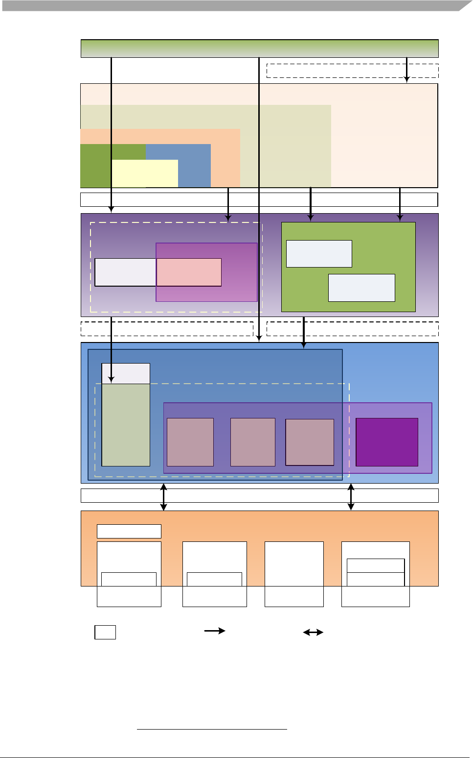
2.1 System Architecture
The layered architecture of the LIN2.x/J2602 Stack package is shown on Figure 2-1. Such
architecture approach aims maximum reusability of common code base for LIN2.x and J2602
standards for 8 bit, 16 bit and 32 bit Freescale automotive MCU portfolio.
The core API layer of LIN2.x/J2602 handles initialization, processing and signal based interaction
between application and LIN Core. The LIN2.x TL (Transport Layer) provides methods for tester
to transmit diagnostic requests.
The low level layer offers method of handling signal transmission between user application and
hardware independence such as byte sending, response receiving, break symbol detection, etc.
The physical transport layer of the Driver supports three standard interfaces SCI, SLIC, GPIO to
operate with 8 bit and 16 bit MCU hardware.
Refer to Chapter 2.3.2 LIN Stack for detail information.
LIN 2.1 TL
LIN 2.1 Core API J2602 Core API
LIN 2.1/J2602
Low Level
MCU HW
SCI/GPIO/SLIC/
UART
J2602 API
LIN2.1 API
Common Core API
LIN2.1/J2602 API
Figure 2-1. LIN Stack Architecture diagram
Overview
Freescale Semiconductor
10
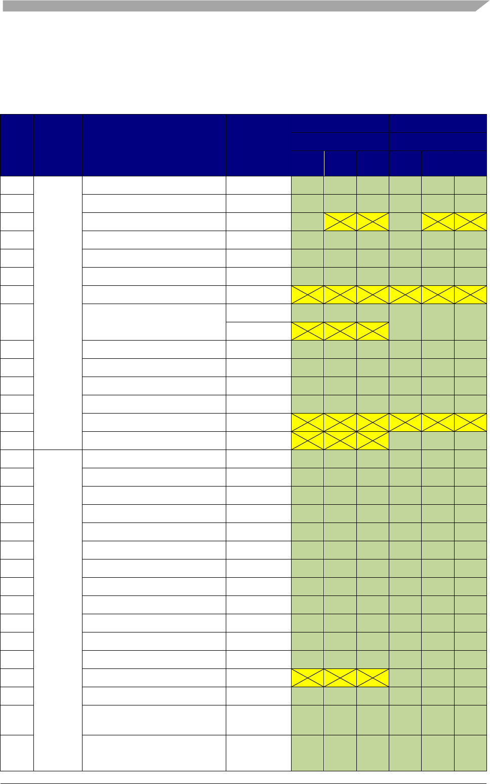
2.2 Supported Derivatives
The following table displays the list of supported MCU derivatives including the functionalities
Note that all derivatives support the LIN2.x and J2602 variant.
Table 2-1. Target Platform
No.
Type
MCU
LIN Module
Version
Master Mode
Slave Mode
Diagnostic
Diagnostic
Class
I
Class
II
Class
III
Class
I
Class
II
Class
III
1
8 bit
MCU
9S08AW16A
SCI_V4
2
9S08SG32
SCI_V4
3
9S08SG8*
SCI_V4
4
9S08DZ60
SCI_V4
5
9S08DZ128
SCI_V4
6
9S08AW60
SCI_V2
7
9S08QD4**
GPIO
8
9S08EL32***
SCI_V4
SLIC
9
9S08MP16
SCI_V4
10
9S08SG4
SCI_V4
11
9S08SG8
SCI_V4
12
9S08LG32
SCI_V4
13
9S08SC4**
SCI_V4
14
9S08RN60
SCI_V4
15
16 bit
MCU
9S12HY64
SCI_V5
16
9S12XHY256
SCI_V5
17
9S12P128
SCI_V5
18
9S12XS128
SCI_V5
19
9S12XS256
SCI_V5
20
9S12XEP100
SCI_V5
21
9S12XEQ512
SCI_V5
22
9S12XET256
SCI_V5
23
9S12XDP512
SCI_V5
24
9S12XF512
SCI_V5
25
9S12G128
SCI_V5
26
9S12G240
SCI_V5
27
9S12GN32
SCI_V5
28
9S12G64
SCI_V5
29
9S12VR64
SCI_V6
LINPHY_V1
30
9S12VR32 Tomarino
SCI V6
LINPHY V2
Overview
Freescale Semiconductor
11
31
16 bit
MagniV
MCU
MM912F634****
SCI_V4
32
MM912G634
SCI_V4
33
MM912H634
SCI_V4
34
MM912J637
SCI_V4
35
S12Z
MM9Z1J638
D2D+SCI4
36
9S12ZVML128_Carcassonne
SCI_V5
37
9S12ZVL_Knox
SCI_V6
38
9S12ZVL128
SCI_V6
LINPHY V2
39
9S12ZVHY64_Lumen
SCI_V6
40
9S12ZVH128_Lumen
SCI_V6
41
9S12ZVC64 Hearst
SCI_V6
42
9S12ZVML31 Obidos
SCI_V6
LINPHY V3
43
9S12ZVMC256
SCI_V6
44
Kinetis
SKEAZN84
UART
45
SKEAZN642
46
SKEAZ1284
Mark:
: Support
: Not support
* 9S08SG8 Supports master and slave modes in diagnostic class I only due
to memory limitation
** 9S08QD4, 9S08SC4 supports LIN protocol only
*** 9S08EL32 contains SCI and SLIC interfaces. SLIC supports slave mode only due to its
function to support slave LIN interface.
**** MM912 integrated LIN frontend / Quest / Quicksilver
2.3 LIN Stack Package Components
LIN Stack Package consists of two major parts:
Node Configuration Tool – PC based script for LIN Stack configuration generation.
LIN Stack – Embedded SW package supporting the LIN2.x and J2602 communication
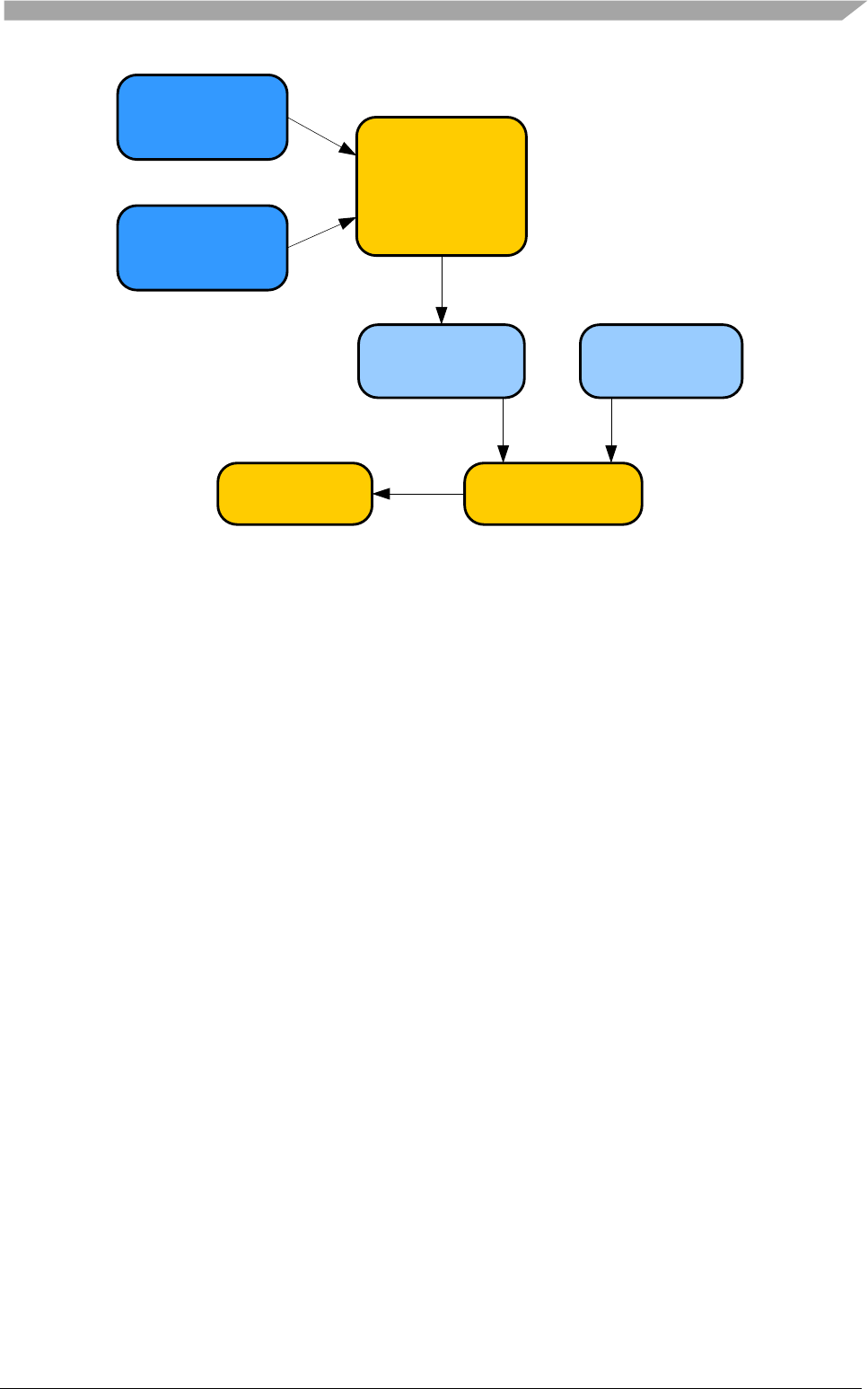
2.3.1 Node Configuration Tool
The Node Configuration Tool is a built-in script of the LIN Stack package which allows user to
easily generate the node configuration .h and .c files based on LIN Configuration Description File
(LCF) and Node Private Description File (LPF) (see more in 3.1 Generation Configuration ).
Those files are then in compiler integrated with LIN Stack source code and user application and
after compilation downloaded to the target derivative. Figure 2-2 shows the diagram of
configuration data flow.
Overview
Freescale Semiconductor
12
LIN Configuration
Description File
(.ldf)
Node Private
Description File
(.npf)
Node Configuration
Tool
Node Configuration
Code (.c and .h) LIN Stack
Code (.c and .h)
Compiler/LinkerTarget Derivative
Figure 2-2. Configuration data
The LDF file describes a complete LIN cluster including Master/slave mode definition and
contains information to handle the cluster.
The NPF file contains information about LIN nodes – such as node name, number of interface,
MCU clock frequency, used communication channel (e.g. SCI channel) and port (e.g. GPIO port),
etc., required for full description of the node.
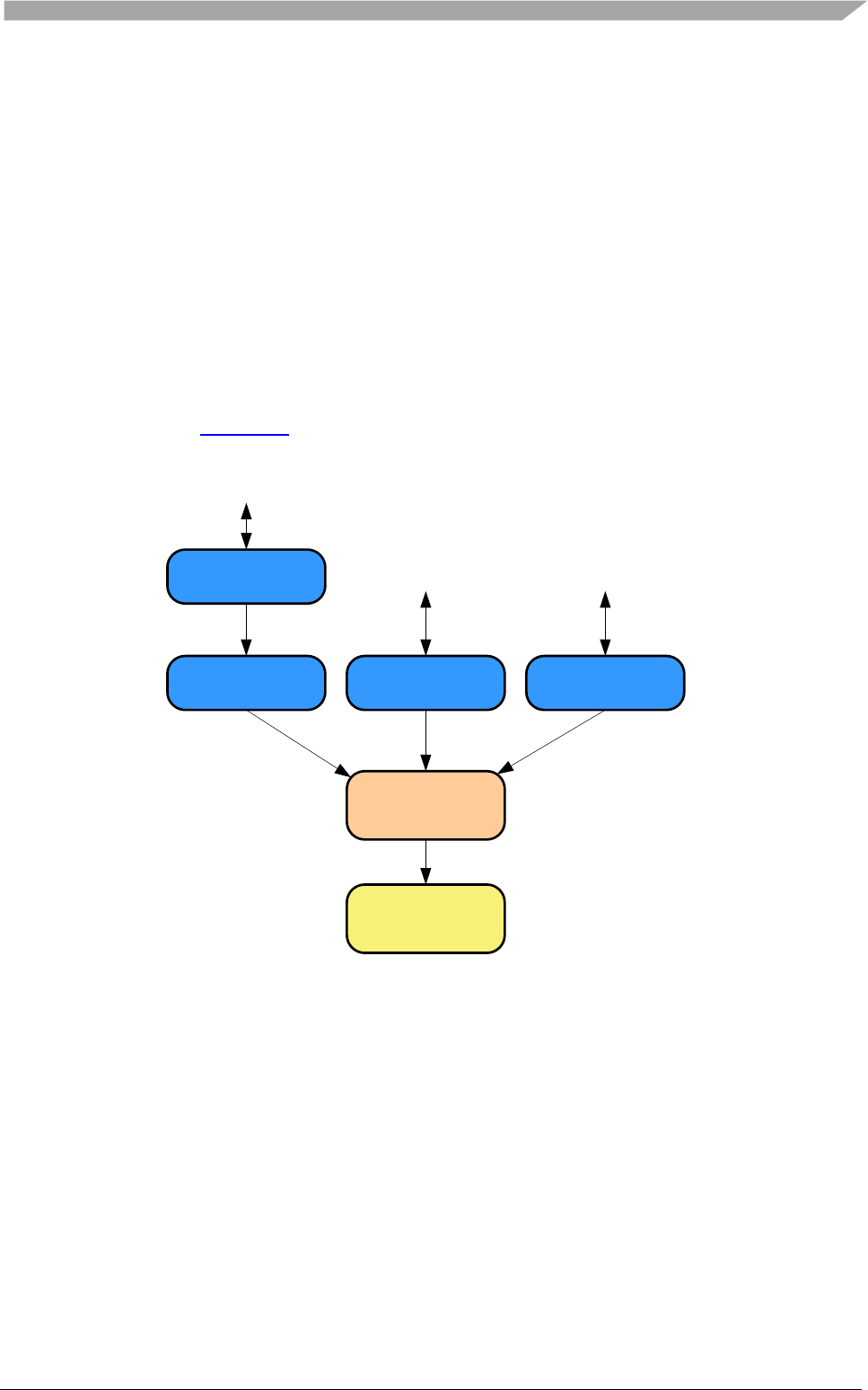
2.3.2 LIN Stack Architecture
The Figure 2-3. shows the details of modules in the LIN Stack package. It also demonstrates the
relationship among modules and the direction of function call among them.
Overview
Freescale Semiconductor
13
Diagnostic class III
TL APIs
LIN core
layer
LIN Low Level Driver (LLD)
Low level API
LIN 2.1 Core API
SLIC GPIO
XGATE
Application
SCI
Controller SLIC Controller GPIO
Controller
Frame
processing
Bit processing
Transport
layer
Low-level
layer
Application
layer
Legend:
J2602 Core API
Function block Function call Interactive
SCI
Frame
processing
LIN 2.0
LIN 2.0
Status
Mgmt J2602 Status
Mgmt
LIN 2.0
Scheduler
LIN 2.0
Network
Mgmt
LIN 2.0
Signal
Mgmt
J2602 Interface
LIN 2.1 Interface
LIN 2.1
Single frame transport Multi frame transport
LIN 2.1
APIs
LIN 2.0 Transport
protocol
LIN 2.1
J2602
LIN 2.1 Transport
protocol
Diagnostic class II
Diagnostic class I
Diagnostic
service
LIN2.1 J2602
LIN 2.0 Node
Config
LIN Diagnostic services
UART
Controller
UART
Frame
processing
Figure 2-3. LIN Stack Layer Diagram
LIN Stack software package provides support for LIN2.x and J2602 communication protocols. The
Stack package is divided into the layers as follows:
1. The lowest layer – Board Support Package (BSP) layer is comprised of codes, which
implements the tasks dedicated to specific MCU platform: interrupt service routines, i/o
Overview
Freescale Semiconductor
14
port setup, memory handling and so on. There are three interfaces implemented within the
Stack package: SCI, SLIC and GPIO.
2. Low level layer consists of core functions for the LIN protocol such as the frames handling,
signals transmission and reception, data preparation, etc. Besides, this layer contains
common implementation functions for the lowest layer to provide the interface abstraction.
Function for LIN cluster setup can be found here as well. This layer interacts with the core
API layer through low level API functions.
3. Core API layer consists of API functions as defined by the LIN2.x/J2602 specification
enabling the user to utilize the LIN2.x/J2602 communication within the user application.
Both the static and dynamic modes for calling the API functions are supported. The core
API layer interacts with the low level layer and can be called by such upper layers as
LIN2.x TL API, LIN TL J2602 or application for diagnostic implementation.
4. Transport layer stands between the application layer and the core API layer including
LIN2.x TL API and LIN TL J2602. This layer provides APIs for the transport protocol,
node configuration and diagnostic. For LIN2.x, all components will be extended from LIN
2.0 specification. The node configuration for J2602 implements only some functions of
LIN 2.0 specification. The layer contains some main components below:
Transport protocol:
- Transport protocol presented in LIN2.x Stack supports single and full frame
transmission. Single frame transmission is applied for diagnostic class I,
whereas the full frame is applied for diagnostic classes II and III.
5. Diagnostic services layer presented in the Stack supports all diagnostic classes as defined in
[1].
Diagnostic class I: Node configuration and Identification
- LIN2.x extends slave configuration and assign frame with ID range to LIN
2.0. The assign frame with ID is removed.
- J2602 simplifies LIN 2.0 Node configuration.
Diagnostic classes II and III:
- The diagnostic services are implemented based on standard diagnostic
specification [24]. The layer supports API functions and OEMs will add to
application source code to complete base on their specific application.
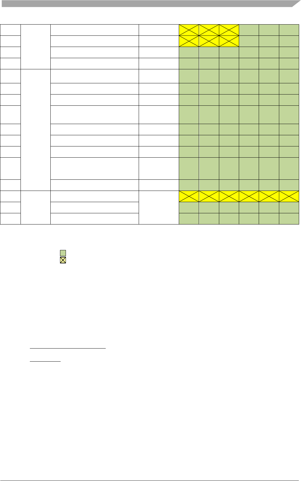
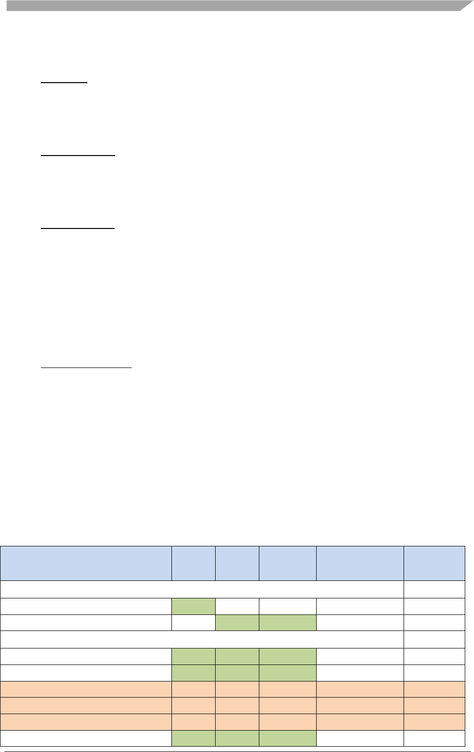
The table below shows the services supported in the LIN Stack
Diagnostic
Class
I
II
III
UDS ser-
vice index [Hex]
Data
Identifier
Diagnostic Transport Protocol Requirements
Single frame transport only
+
Full transport protocol (multi-segment)
+
+
Required Configuration Services
Assign frame identifier range
+
+
+
0xB7
Read by identifier (0 = product id)
+
+
+
0xB2 0x00
Read by identifier (all others)
optional
optional
+
0xB2 0xXX
Assign NAD
optional
optional
optional
0xB0
Conditional change NAD
optional
optional
optional
0xB3
Positive response on
+
+
+
service +

Overview
Freescale Semiconductor
15
supported configuration services
0x40
Required UDS Services
Read data by identifier
+
+
0x22
0x0091
0x0092
Write data by identifier
+
+
0x2F
0x0092
Session control
+
0x10
0x01
Read by identifier for sensor and actuator
data
+
0x22
Implemented
by OEM
I/O control by identifier
+
0x2F
0x08
Read DTC (fault memory)
+
0x19
0x01
Clear DTC (fault memory)
+
0x14
N/A
Routine control
if applicable
0x31
Other diagnostic services
if applicable
…
Flash Reprogramming Services
Flash programming services
optional
0xXX
Table 2-2. LIN2.x diagnostic service specification
Note
* The blue color shows the services are supported by Stack
** The orange color shows the services are not supported by Stack
(+) Plugs are mandatory services for LIN Stack
6. Application layer is the highest layer which stands for user’s applications.
Refer to Stack Source Code for detail about source code files of each layer.

Freescale Semiconductor
16
Chapter 3
LIN Stack Package
This section presents more detail description of products in the package. The content is focused
how to construct input files for Node configuration tool and explore deeply in the source code.
The chapter contains sections:
Generation Configuration Files
Stack Source Code
LIN Stack Package
Freescale Semiconductor
17
3.1 Generation Configuration Files
The language described in this section is used in order to create input files for the Node
configuration tool to generation configuration files. To understand how to run this tool, refer to
Chapter 4.2, Hardware configuration file generation for more information.
NOTE
The LDF and NPF files could be created in notepad or wordpad
text editors in window and saved into .ldf and .npf extension files.
3.2 Stack Source Code
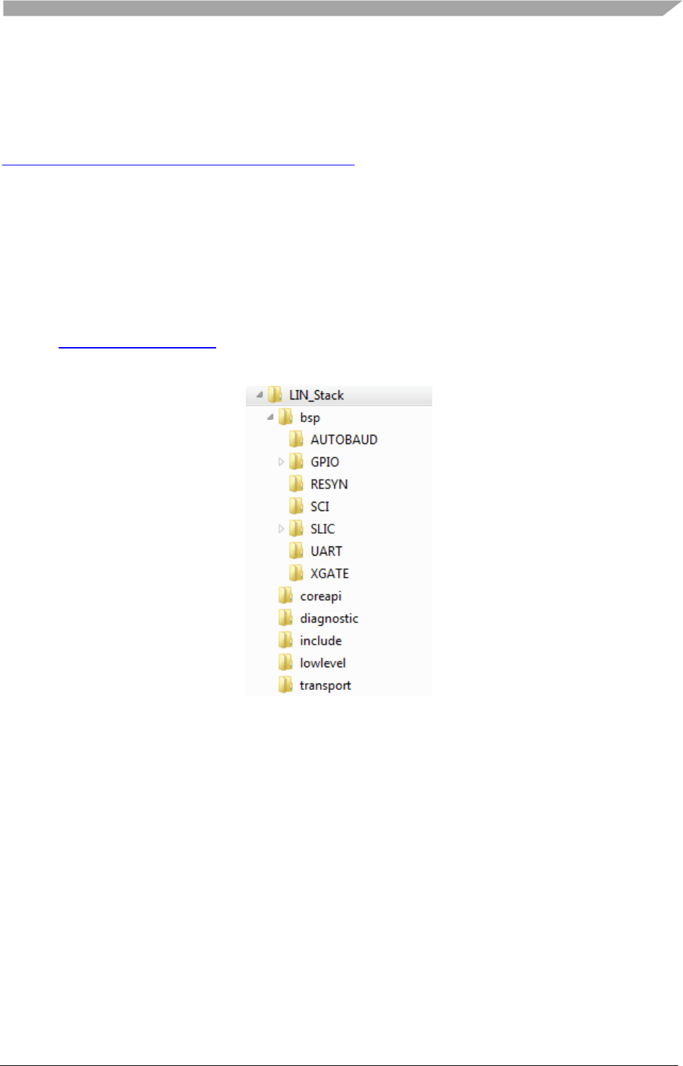
The Stack source code is organized to five folders: bsp, coreapi, diagnostics, include and transport
as shown in Figure 3-1. The structure of source code is based on the LIN system architecture (see
more in Chapter 2.2, LIN Stack).
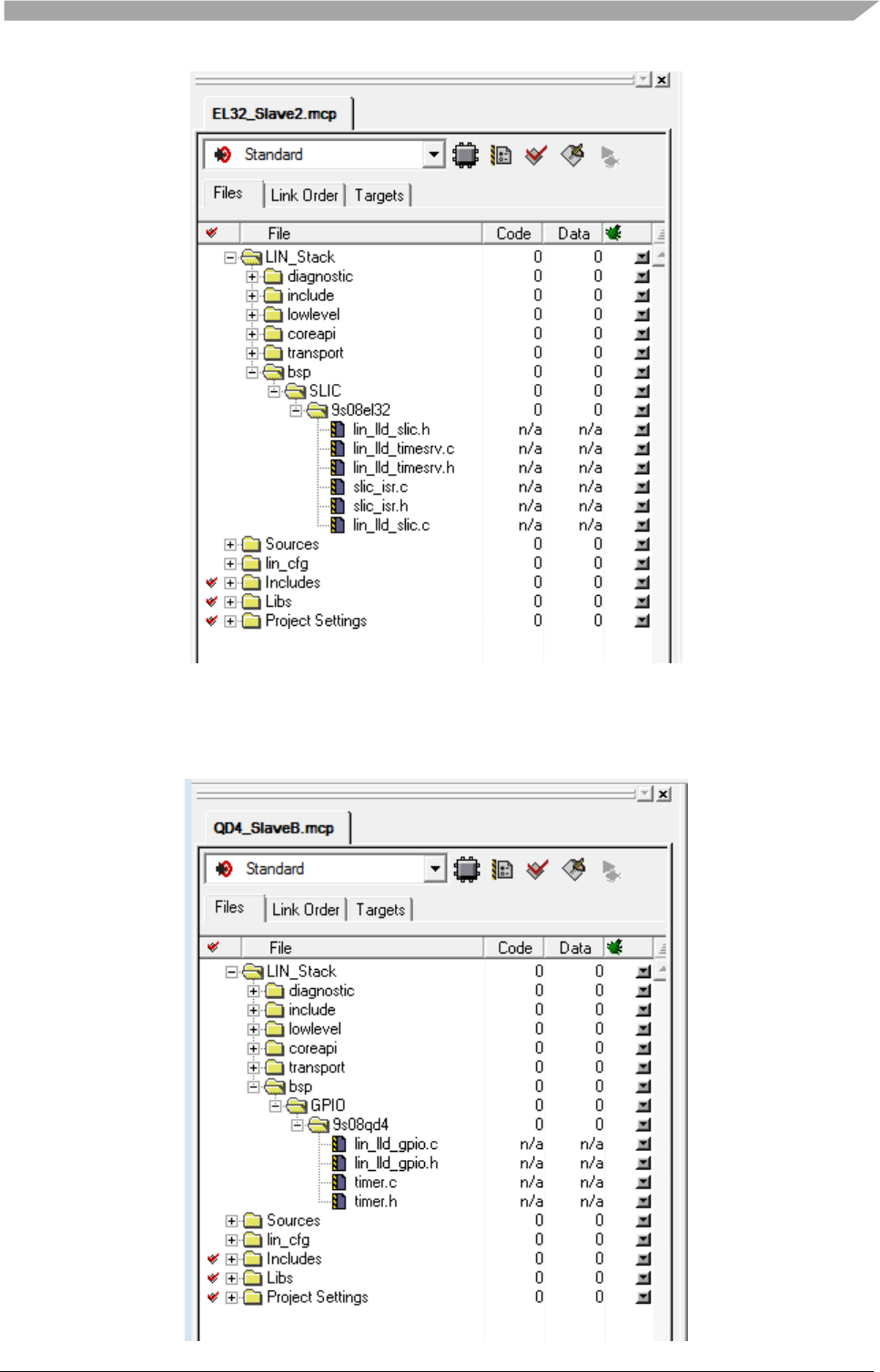
Figure 3-1. LIN Stack Source Code Directory Structure
3.2.1 Board Support Package
Board Support Package (BSP) layer is the lowest layer, which is comprised of functions related to
the specific hardware. Here you could find out the special interrupt service routines, IO
parameters, memory handling and so on. There are three interfaces implemented within the stack
package: SCI, SLIC and GPIO.
3.2.1.1 GPIO
There is only one MCU name 9S08QD4 in the support derivative table (see more in Table 2-1)
support GPIO interface. The source code in this folder is served for this MCUs.
In this folder, there are four files, including lin_lld_gpio.c, lin_lld_gpio.h, timer.c
and timer.h. Namely
lin_lld_gpio.c define initialization, data sending flow of GPIO interface

LIN Stack Package
Freescale Semiconductor
18
timer.c define timeout management, counter for user application, and timer interrupt.
lin_lld_gpio.h , timer.h includes the prototypes for functions served for .c files.
3.2.1.2 RESYN
The source code in this folder support resynchronization feature of LIN Driver as the application
note [25]. The folder contains two source files lin_lld_resyn.c and lin_lld_resyn.h. The
MCUs support this feature include 9S08SG32, 9S08EL32, 9S08DZ60, 9S08DZ128 and
9S08MP16.
3.2.1.3 SCI
There three SCI communication versions supported in the LIN Driver and the version has been
combined in a single module of SCI.
The folder contains files lin_lld_sci.c which implements all the functions universally used for all
MCUs with SCI interface. The lin_lld_sci.h contains the prototypes for functions
implemented in lin_lld_sci.c. The lin_lld_timesrv.c consists of timing and board
frequency setup functions; lin_lld_timesrv.h consists of the prototypes for functions
implemented in lin_lld_timesrv.c and lin_reg.h contains the registry map declaration for
the MCU. The lin_isr.c contains interrupt service routines for SCI communication and timer.
The folder to the target MCU contains the file lin_isr.c which implements the interrupt service
routines and other initial tasks dedicatedly.
3.2.1.4 SLIC
Slave LIN Interface Controller is embedded module that automates LIN message handling to help
increase performance while reducing development time and cost.
In this folder, there are four files, including lin_lld_slic.c, lin_lld_slic.h,
slic_isr.c and slic_isr.h. The contents of the files are described below:
lin_lld_slic.c includes all the initial functions and other related task handling
functions which will be used to directly interact with the physical hardware.
lin_lld_slic.h includes the prototypes for functions implemented in the file
lin_lld_gpio.c, constant declarations and macros.
slic_isr.c consists of interrupt service routines for the physical board.
slic_isr.c consists of the prototypes for functions implemented in the file
slic_isr.h, constant declaration and macros.
3.2.1.5 XGATE
The XGATE module on the advanced S12X family of 16-bit MCUs is a highly flexible, high
performance and cost-sensitive parallel processing solution. The XGATE module is a peripheral
coprocessor that allows autonomous high-speed data processing and transfer between the MCU’s
peripherals and the internal RAM and I/O ports. XGATE uses SCI for I/O communication and
handling interrupt.

LIN Stack Package
Freescale Semiconductor
19
Similar to modules in the SCI structure, the XGATE folder contains modules specific for XGATE
xlin_sci.cxgate, xvector.cxgate. The source code in these modules is stored in the RISC
core.
3.2.1.6 UART
The UART layer provides physical hardware communication handling for Kinetis MCU platforms.
This is based on SCI version-4 communication specified for 32 bit ARM architecture.
3.2.1.7 AUTOBAUD
The signal on the UART receive pin (RX pin) can be internally routed to an Input Capture module
to time the edges of the incoming signal. From that timing the layer can set up the UART at the
correct baud rate.
3.2.2 Low Level layer
Low level layer consists of core functions for the LIN protocol such that frames handling, signals
transmission and reception, data preparation, etc. It also contains the functions used to set up the
LIN cluster. There are two files included in:
lin.c contains the functions for initialization of LIN core features, preparation of current
transmission and interaction with hardware modules.
lin.h consists of function declaration, macro definitions and so on which are
implemented within the lin.c file.
3.2.3 Core API Layer
Core API layer is a set of functions which are intended to be used to develop the applications
interacting with the LIN bus. There are six files in this folder, including:
lin_common_api.c contains the common API functions which are applicable for all
three versions LIN2.x and J2602.
lin_common_proto.c contains the functions which are used to set up the session
environment based on the low level layer.
lin_lin21_api.c contains the API functions for LIN2.x communication protocol.
lin_lin21_proto.c contains the functions which prepares the background tasks for
LIN2.x API functions.
lin_j2602_api.c contains the API functions for J2602 communication protocol.
lin_j2602_proto.c contains the functions which prepares the background tasks for
J2602 API functions.
3.2.4 Transport Layer
Transport layer comprises of functions, which represent the transport layer specification within the
LIN protocol. This layer is only applicable for some types of communication within the LIN bus.
The other types will not use the transport layer but the API and the low-level layer for opening a
working session for transmission and reception of data within the LIN bus.
There are four files in this folder, including:

LIN Stack Package
Freescale Semiconductor
20
Lin_commontl_api.c consists of function calls for data preparation, node identification
and configuration and others which are the implementation of the transport layer
specification.
Lin_commontl_proto.c consists of functions which do the background tasks for setting
up the transport layer.
lin_21tl_api.c consists of functions which implements the transport layer for LIN2.x
communication protocol.
lin_j2602tl_api.c consists of functions which implements the transport layer for
J2602 communication protocol.
3.2.5 Diagnostic Service
The transport layer is also complemented with the diagnostic services, which implement full
diagnostic nodes defined in the LIN specification. Three diagnostic classes are supported where
Class I is using normal signaling and class II and class III uses the transport layer.
This set of functions is built to support the mandatory diagnostic services described in the
communications protocol specification. This folder contains the file lin_diagnostic
_service.c, which implements the diagnostic class I for node configuration and identification
mentioned above.
3.2.6 Include folder
This folder contains all the function declarations, macros and constants definitions and global
variables which could be used throughout the source code. There are eleven files, including
lin_common_api.h, lin_common_proto.h, lin_commontl_api.h, lin_commontl
_proto.h, lin_diagnostic_service.h, lin_j2602_api.h, lin_j2602_proto.h,
lin_j2602tl_api.h, lin_lin21_api.h, lin_lin21_proto.h and lin_lin21tl
_api.h. Among of them, lin_common_proto.h is key one which plays a gateway role to
connect others for handling the protocol layer.

Freescale Semiconductor
21
Chapter 4
How to use LIN Package
The objective of this chapter is to provide user with instructions on how to set up and run LIN
applications as quick as possible. This chapter contains the following sections:
Environment requirement - Recommendation regarding CodeWarrior versions for each
target derivative.
Hardware configuration file generation - Steps to generate configuration files from input
files by using node configuration tool.
Target setup - Steps to setup a target hardware platform
Configuration files and LIN Stack source code integration - Steps to integrate to a project
Getting start with LIN application - Using API functions for user application

How to use LIN Package
Freescale Semiconductor
22
4.1 Environment requirements
The scope of this section is limited to recommend some notices when creating LIN application
projects using Code Warrior. For more detail information about the CodeWarrior Integrated
Development Environment (IDE) and computer programming, refer to the Reference [22].
The three Code Warrior versions 6.2, 5.1 and 4.7 are recommended environments applicable for
LIN Stack respectively with MCU 8/16 bit families as shown in Table 4-1. MCUs respective with
Code Warrior Version
Table 4-1. MCUs respective with Code Warrior Version
CW10.6
CW4.7
CW5.1
9S12ZVM128
9S12HY64
9S12G64
9S08RN60
9S12P128
9S12G128
9S12ZVL32
9S12XS128
9S12G240
9S12ZVL128
9S12XS256
9S12GN32
MM9Z1J638
9S12XEP100
9S12XHY256
9S12ZVHY64
9S12XEQ512
MM912F634
9S12ZVH128
9S12XET256
MM912G634
SKEAZN84
9S12XDP512
MM912H634
SKEAZN642
9S12XF512
MM912J637
SKEAZ1284
9S12XF512
9S12VR64
9S08AW16A
9S08AW60
9S08SG32
9S08SG8
9S08SG4
9S08DZ60
9S08DZ128
9S08QD4
9S08EL32
9S08MP16
9S08LG32
9S08SC4
9S12ZVC64
9S12ZVMC256
NOTE 1
How to use LIN Package
Freescale Semiconductor
23
Check USB interface type of the target hardware platform to match with
connection types in CW (P&E Multilink/Cyclone Pro, SofTec HCS08/16
or HCS08/16 Open Source BDM) for downloading source code action.
NOTE 2
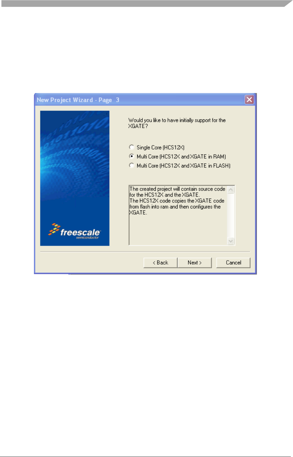
For MCU with XGATE coprocessor support, it is recommended to
selecting the source code of HCS12X and XGATE in RAM (Multi Core
selection) for purpose of faster operation.
Figure 4-1 XGATE option in Code Warrior Studio
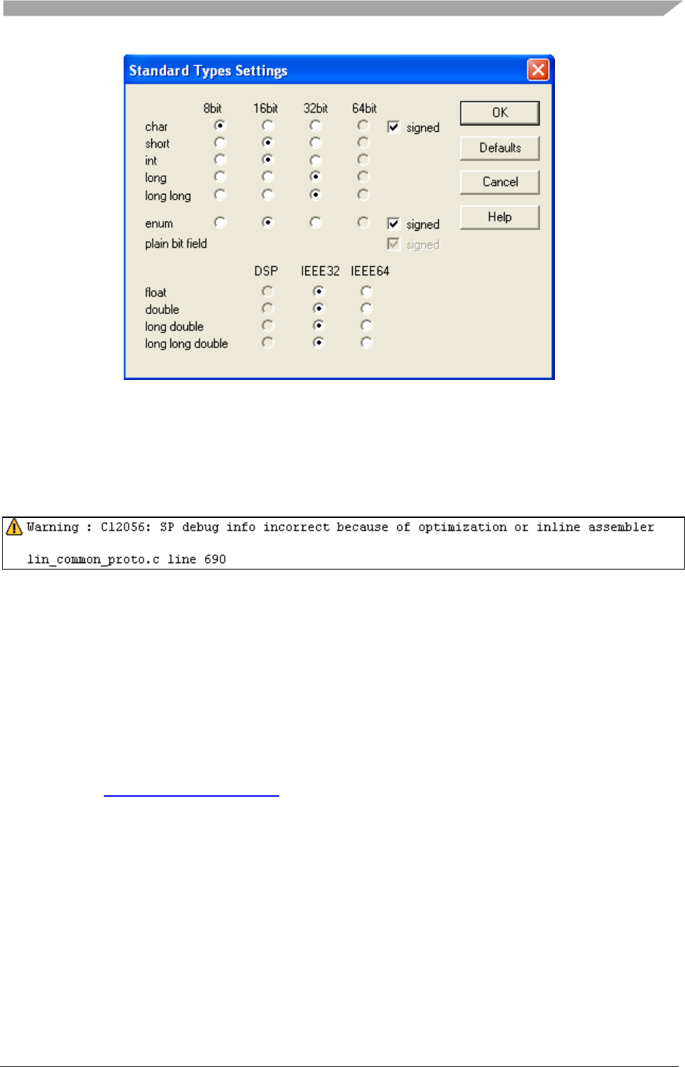
NOTE 3
The data type in Standard Types Settings of CW4.7 is selected as 16 bit.
Whereas, it is selected as 8bit in CW6.2 (Choose Standard Settings-
>Compiler for H08/12->Type sizes).
How to use LIN Package
Freescale Semiconductor
24
Figure 4-2 Data type option in CW4.7 and CW6.2
NOTE 4
When a CPU running with XGATE support, a warning message often
appears as shown in below:
Figure 4-3. Warning message appears in project with XGATE support
To remove this warning, choose SofTec HCS12 Settings -> Compiler for
H12 ->Options-> Optimizations and select Main Optimize Target then
click Optimize for execution time option.
NOTE 5
For 9S12HY64 and 9S12P128 MCUs, in order to compliant with Code
Warrior V4.7, two Code Warrior patches
(CW12_V4_7_HCS12_HY64_HA64_SP.exe, CW12_V4_7_HCS12
_P128_SP.exe) need to be installed. (Access website:
http://www.freescale.com and download these two files).
4.2 Hardware configuration file generation
This section describes steps for generation configuration files (lin_cfg.h, lin_cfg.c,
lin_hw_cfg.c) for a node in LIN network. The input files include one NPF file and one or
several LDF files which the node participates in. These two files could be edited in a text editor
and they must be saved with .ldf and .npf extensions respectively instead of .txt.
In order to start generation files, perform following tasks.
1. Define target MCU (as shown in Table 2-1) used for emulation and its interface type
(GPIO, SCI and SLIC). If SCI interface is selected, verify the SCI version and channel
used as given in Table 4-2 below (This information is also mentioned in
MCU_config.cfg file in NCF tool folder).

How to use LIN Package
Freescale Semiconductor
25
Table 4-2. List of MCUs with SCI number and its address in RAM
MCU
SCI
Version
MCU
Type
Number of
SCI/UART
channel
Address
9S08AW16A
9S08AW60
SCI_V2
_S08_
2
SCI0 0x0038
SCI1 0x0040
9S08DZ60
9S08DZ128
SCI_V4
_S08_
2
SCI0 0x0038
SCI1 0x0040
9S08LG32
SCI_V4
_S08_
2
SCI1 0x0010
SCI2 0x0018
9S08SG8
9S08SG32
9S08EL32
9S08SC4
SCI_V4
_S08_
1
SCI0 0x0038
9S08MP16
SCI_V4
_S08_
1
SCI0 0x0068
9S12I32
SCI_V4
_S12_
1
SCI0 0x0240
9S12HY64
9S12P128
9S12GN32
SCI_V5
_S12_
1
SCI0 0x00C8
9S12XS128
9S12XS256
9S12XHY256
9S12G64
SCI_V5
_S12_
2
SCI0 0x00C8
SCI0 0x00D0
9S12G128
9S12G240
SCI_V5
_S12_
3
SCI0 0x00C8
SCI1 0x00D0
SCI2 0x00E8
9S12XEP100
9S12XEQ512
9S12XET256
9S12XDP512
SCI_V5
_S12X_
6
SCI0 0x00C8
SCI1 0x00D0
SCI2 0x00B8
SCI3 0x00C0
SCI4 0x0130
SCI5 0x0138
9S12XF512
SCI_V5
_S12X_
2
SCI0 0x00C8
SCI1 0x00D0
MM912F634
MM912G634
MM912H634
SCI_V4
_S12_
1
SCI0 0x0240
MM912J637
SCI_V4
D2D
1
SCI0 0x0218
9S12VR64
9S12VR32
SCI_V6
_S12_
2
SCI0 0x00C8
SCI1 0x00D0
9S08RN60
SCI_V4
_S08_
3
SCI0 0x3080
SCI1 0x3088
SCI2 0x3090
MM9Z1J638
SCI_V4
1
SCI0 0x0E18
9S12ZVL32
9S12ZVL128
9S12ZVMC256
9S12ZVC64
9S12ZVML31
SCI_V6
_S12_
2
SCI0 0x0700
SCI1 0x0710

How to use LIN Package
Freescale Semiconductor
26
9S12ZVHY64
9S12ZVML128
SCI_V5
_S12_
2
SCI0 0x0700
SCI1 0x0710
SKEAZN84
UART
_K_
1
0x4006A000
SKEAZN642
3
0x4006A000
0x4006B000
0x4006C000
SKEAZ1284
3
2. Edit LDF and save to a folder.
3. Edit and NPF file and save to the same folder with LDF file above.
The sample .npf code below is targeted for S12ZVML128 platform using SCI0 channel for LIN
communication, 5 second timeouts, 8MHz bus clock, diagnostic class I, and the LDF which this
node participate is LIN21.ldf as master node:
/* *************************************************************************/
/* Initiator: CONG TRAN B26340 */
/* This example is used for S12ZVML128 as Master node */
/* *************************************************************************/
/*** GENERAL DEFINITION ***/
LIN_node_config_file;
/*** MCU DEFINITION ***/
mcu { /* Must check the correct MCU name */
mcu_name = MC9S12ZVML128;
bus_clock = 8000000; /* Frequency bus of system Hz*/
xgate_support = no; /* Support XGATE Co-Processor */
}
/*** LIN HARDWARE DEFINITION ***/
/* SCI config */
sci{
s12_sci0{
sci_channel = 0; /* Check validation of sci_channel */
}
}
/*** NETWORK DEFINITION ***/
network {
idle_timeout = 5s;
diagnostic_class = 1;
max_message_length = 6;
LI0{
node = SeatECU; /* Name of node described in LDF (must check
consistence with LDF) */
file = "LIN21.ldf"; /* Path to LDF file */
device = s12_sci0; /* Identifier to LIN Hardware, related to LIN
HARDWARE DEFINITION */
support_sid {
READ_BY_IDENTIFIER = 178;
ASSIGN_FRAME_ID_RANGE = 183;
ASSIGN_NAD = 176;
CONDITIONAL_CHANGE_NAD = 179;
SAVE_CONFIGURATION = 182; }
}
}
}
How to use LIN Package
Freescale Semiconductor
27
The max_message_length property applies to the diagnostic transport layer only. It defines the
maximum length of a diagnostic message that is number of used data bytes plus one (for the
SID or RSID). For diagnostic class I, max_message_length should be less than or equal to 6.
For diagnostic class II and III, max_message_length should be less than or equal to 4095.
The support_sid lists all SID values (node configuration, identification and diagnostic services)
that are supported by the slave node. For diagnostic class 3, users also can add their User
Defined Diagnostics SIDs. NPF files of Master nodes should list all SID values that are
supported by the slave nodes in the LIN Cluster. For convenience, users can use Eclipse Plugin
to list supported SID according to the supported diagnostic class. In NPF files, support_sid can
be listed using decimal values as above or hexadecimal values, e.g READ_BY_IDENTIFIER
= 0xB2. On Eclipse Plugin GUI, users can only input support_sid using decimal values.
Generate configuration files
There are three different ways to generate configure files that was integrated in the package:
Windows Command Line, Standalone GUI and Eclipse plug-in. This use manual presents the
steps to use Standalone GUI, for more detail of two remain methods, refer to the user guide of
NCF tool in the package.
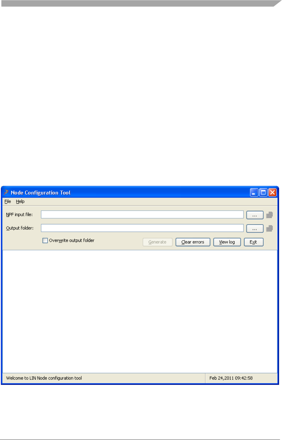
4. Open the execution file NCFGui.jar in Node Configuration Tool at location: …\NCFGUI.
The execution program window appears as shown in Figure4.4.
Figure 4-4 NCF main window
5. Click File => Select NPF file in File menu or press Ctrl + N to include the NPF file.
6. Click File => Select output folder in File menu or press Ctrl + O to select target folder
which contains output files.
How to use LIN Package
Freescale Semiconductor
28
7. Click Generate or press Ctrl + G button to generate files
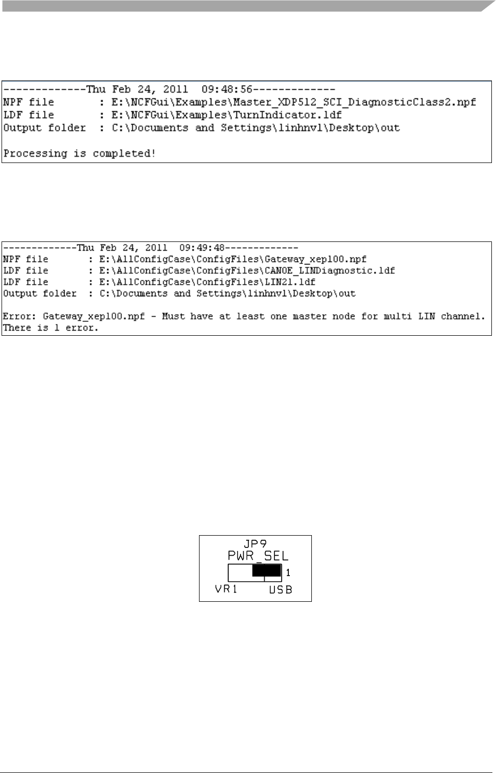
If the NPF file is correct, a message will be displayed as shown in Figure
Figure 4-5. Successful generation message
Otherwise, an error message will appear to show a brief description of error type. Figure
shows an example of error message when lacking the interface field in the NPF file.
Figure 4-6. An error message
4.3 Target setup
This section describes connection steps from a host PC to a demonstration board of target MCU
and some notices when working with some specific boards. The MCU project boards might be
different in hardware configuration such as system clock, mode operation, LIN connector, power
supply, USB/PC interface. It is strongly recommended to check all jumpers setting before getting
with LIN application.
1. Install all required system software for each MCU, it normally includes Code Warrior
patch, SofTec/Multilink Microsystems DLL built-in with board support.
2. Check “POWER SEL” jumper is in the “USB” position. Otherwise a 12V DC power
supply or I/O header connector of the LIN bus must be plugged.
Figure 4-7. POWER SEL jumper on DEMO9S12HY64 board
3. Insert one end of the USB cable into a free USB port of the host PC.
4. Insert the other end of the USB cable into the USB connector on the project board.
How to use LIN Package
Freescale Semiconductor
29
Figure 4-8. USB port on the DEMO9S12XSFRAME
5. Check operation modes. Several hardware platforms are available with two working
modes: “Standalone” mode and “host” mode. In standalone mode, no PC connection is
required. The microcontroller is factory programmed. In the other hand, in the host mode
the program execution is controlled by the host PC through the “USB” connector. Refer to
user manual of each board to see jumper and connector settings.
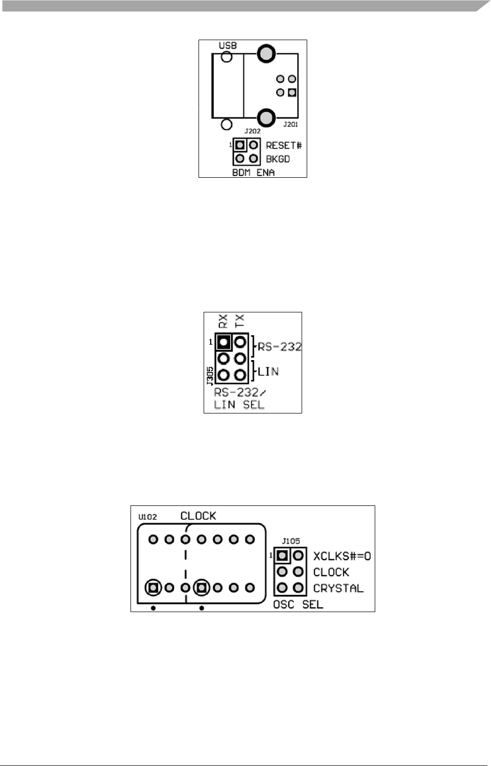
6. Check LIN/RS-232 SEL jumper. Make sure that the jumper is selected for LIN
transceiver.
Figure 4-9. LIN Transceiver selection jumper on DEMO9S12PFRAME
7. For boards support external clock (EVB9S12XEP100, EVB9S12XDP512, DEMO-
9S12XSFRAME, etc.) make sure that the OSC SEL jumper is selected as CLOCK instead
of CRYSTAL.
Figure 4-10. Oscillation selection jumper on DEMO9S12XSFRAME
8. Verify the LIN transceiver of the MCU project board to ensure it works properly by using
built-in test project regarding the MCU and debug in Code Warrior Real Time Debugger
environment. Figure shows an example of LIN transceiver testing on EVB9S12XDP512
board.
How to use LIN Package
Freescale Semiconductor
30
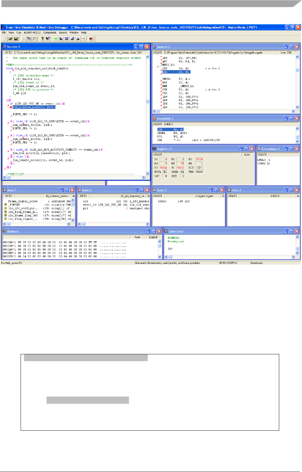
Figure 4-11. Breakpoint at lin_proccess_pid function to test LIN transceiver
o Open TST_9s12xdp512_SCI_XGATE_MasterMode_LIN21.mcp project file in
location
…\tests\integration\TST_MasterMode_LIN21\TST_9s12xdp512_SCI_X
GATE_MasterMode_LIN21
o Set active schedule table as LI0_SendTable in main function
o Call l_sch_tick function in for(;;) loop, the sample code is below
l_sch_set(LI0, LI0_SendTable, 0); // For test LIN transceiver
for(;;) {
/* Delay time */
for(i = 0;i < 6000; i++) {
}
ret = l_sch_tick(LI0);
} /* wait forever */
/* please make sure that you never leave this function */
}
o Download to MCU board and click Start/Continue button.
o Set breakpoint in lin_process_pid(iii,pid) code line of lin_pid_
response_callback_handler function and observe if the program pause at this
breakpoint.
How to use LIN Package
Freescale Semiconductor
31
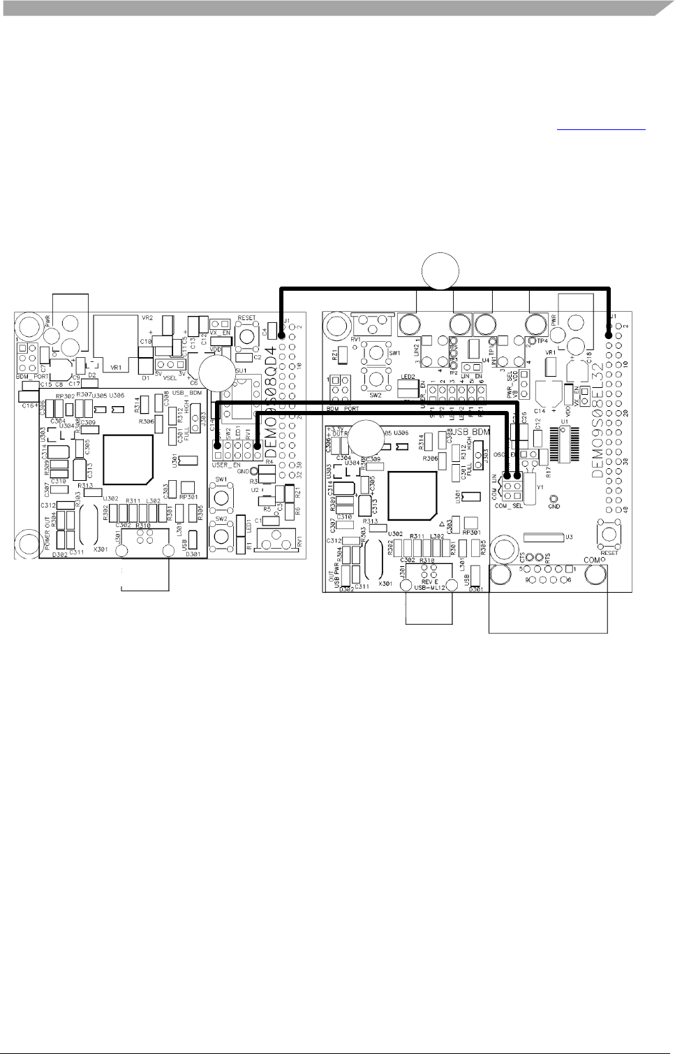
9. For MCU boards without LIN transceiver DEMO9S08AW60E, DEMO9S08QD4,
DEMO9S08SG8, you must connect their Tx/Rx pins of interface used through another
external LIN transceiver. For example, the GPIO pins in DEMO9S08QD4 board are
connected to a LIN transceiver of the DEMO9S08EL32 board as shown in Figure below.
o Identify Tx/Rx pins in the schematic of DEMO9S08QD4
o Connect these pins with Tx/Rx pins on DEMO9S08EL32 board (line1, 2)
o Connect ground terminals between two boards (line 3)
o Supply power 12V to DEMO9S08EL32 board, it is then ready for demonstration.
1
2
3
Figure 4-12. Connect LIN transceiver in DEMO9S08EL32 to DEMO9S08QD4 board.
4.4 Configuration Files and LIN Stack Source Code
Integration
This section will provide a steps-by-steps guide on how to integrate configuration files with LIN
Stack source code in your first project.
4.4.1 Create an empty project of the target MCU board
1. Open Code Warrior Studio V4.7 (or 6.2 refer to target MCU Table 4-2)
2. Create an empty project for a target MCU. Figure shows an example of MCU name
9S12XEP100.
How to use LIN Package
Freescale Semiconductor
32
Figure 4-13. Project Window
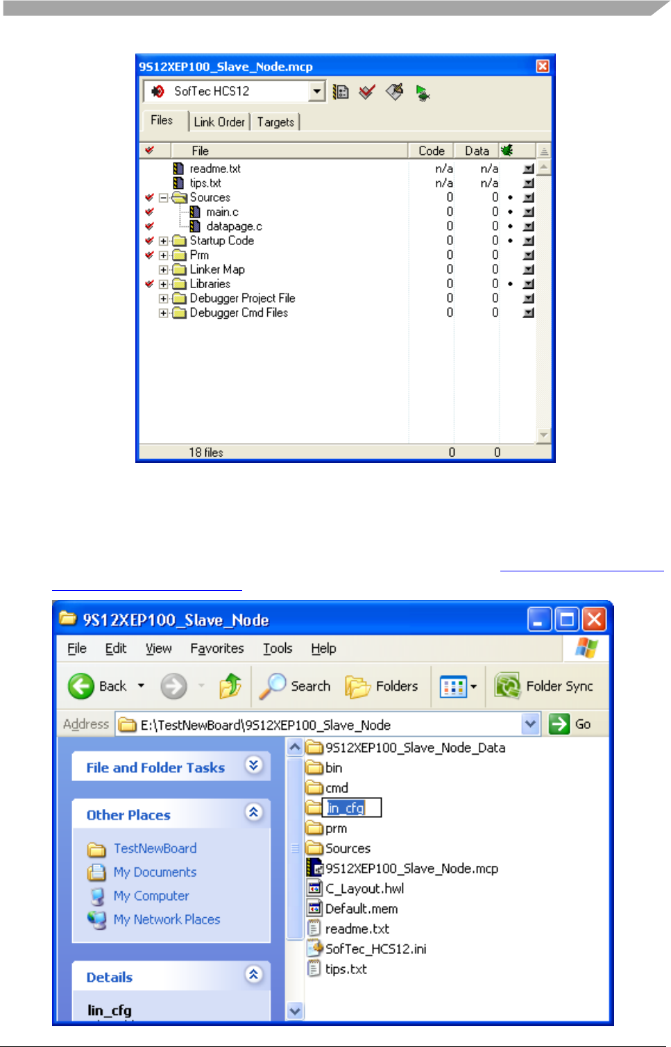
4.4.2 Create a folder containing configuration files
3. Create new folder with name lin_cfg in the project folder and copy configuration files
(lin_cfg.h, lin_cfg.c, lin_hw_cfg.c) generated in Section 4.2, Hardware
configuration file generation to this folder.
How to use LIN Package
Freescale Semiconductor
33
Figure 4-14. Create new folder with name lin_cfg
Add configuration files to this project (drag and drop lin_cfg folder into CodeWarrior project).
Figure 4-15. Add configuration files to the project
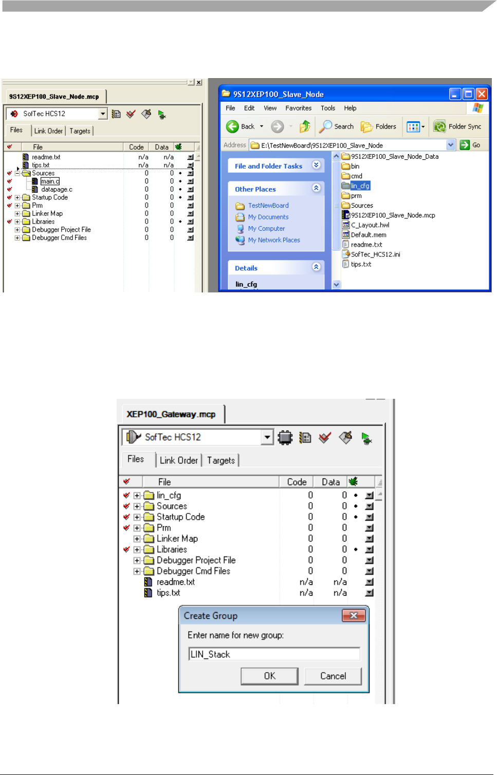
4.4.3 Create a group containing LIN Stack source code
This section will help user to add source code to the application. Notice that every change in the
source code might create serious errors for application.
4. Create new group with name LIN_Stack
Figure 4-16. Create a group name LIN_Stack
5. Drag and drop five sub folders of LIN Stack folder (coreapi, diagnostic, include, lowlevel,
transport) into created LIN_Stack group.
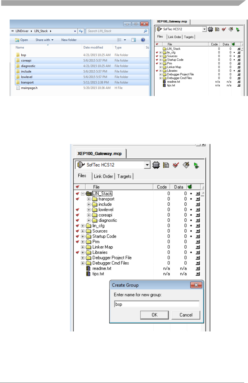
How to use LIN Package
Freescale Semiconductor
34
Figure 4-18. Drag and drop five sub folders of LIN Stack folder into LIN_Stack group
6. Create a new bsp group is subgroup of LIN_Stack and bsp’s subgroup with name of
interface
Create bsp group
Figure 4-19. Create bsp group is subgroup of LIN_Stack group
SCI interface
Drag and drop SCI folder into bsp group.
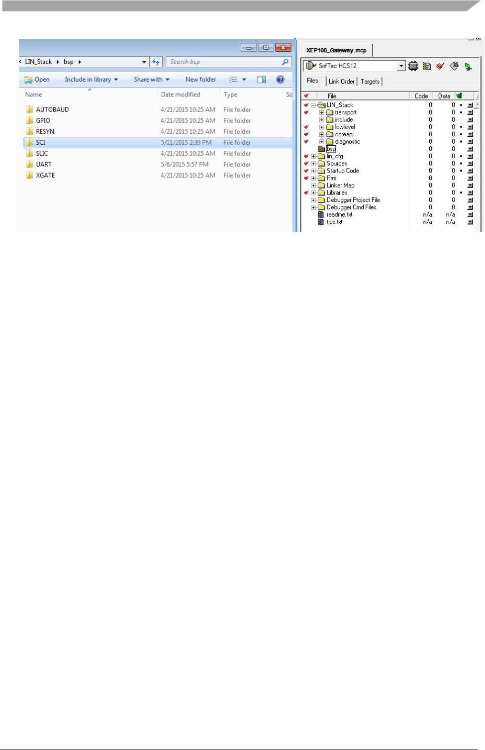
How to use LIN Package
Freescale Semiconductor
35
Figure 4-20. Drag and drop SCI folder into bsp group
After all steps above, we have file architecture of Code Warrior project like this
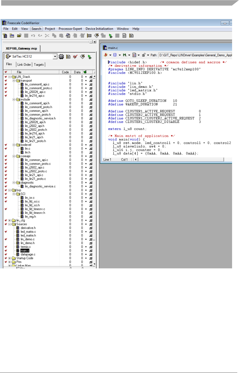
How to use LIN Package
Freescale Semiconductor
36
Figure 4-21. Overview of LIN Stack files architecture.
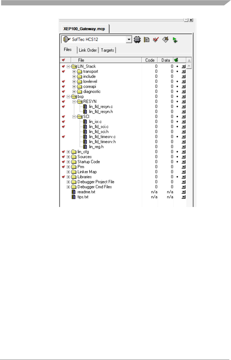
Resynchronization feature
Resynchronization feature currently supports 9S08DZ60, 9S08DZ128, 9S08EL32 and 9S08SG32 boards.
To use this feature, drag and drop RESYN folder into bsp group.
How to use LIN Package
Freescale Semiconductor
39
Figure 4-24. Add all Stack source code to GPIO interface (applied to 9S08QD4 MCU only)
NOTE
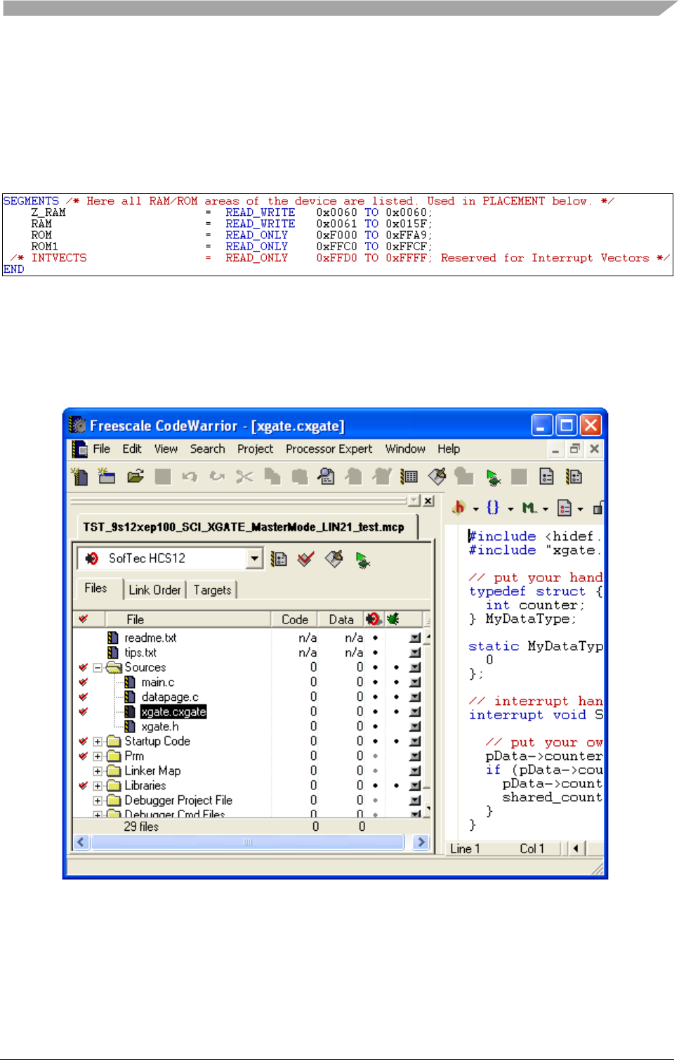
Due to limitation in memory space, the RAM/ROM areas in QD4 MCU
need to be reallocated in Project.prm file to match with the Stack source
code. Namely, Z_RAM = 0x0060 to 0x0060, RAM = 0x0061 to 0x15F.
See more in Figure 4-25.
Figure 4-25. RAM/ROM areas relocation in QD4 MCU
XGATE + SCI interface
If XGATE is selected, the Code Warrior Studio will automatically generate a default
file xgate.cxgate which defines XGATE interrupt handle functions and XGATE
vector table.
Figure 4-26. Remove xgate.cxgate file in the project with XGATE support
This file has been modified which serves for SCI interrupt and request interrupt from
S12X_CPU and saved in location …\LIN_Stack\ bsp\XGATE\common.Therefore,
remove this default file and add the modified file to a group with name common in
SCI_XGATE group as the figure bellow.
NOTE
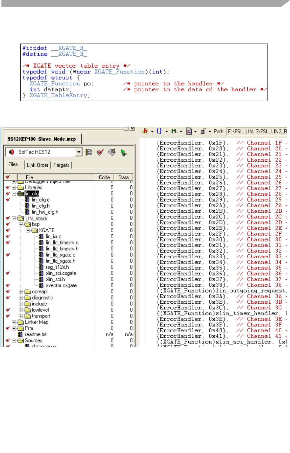
How to use LIN Package
Freescale Semiconductor
40
Remove NEAR segment pointer name by near in xgate.h file to
make XGATE vector table entry works properly. See Figure 4-27.
Figure 4-27. Remove NEAR segment pointer name by near
Figure 4-28. Final source code adding window for the project with XGATE support
Once you completed adding LIN Stack source and compiled without error and warning, you are
now ready for writing LIN applications.
4.5 Configuration in CW10.6
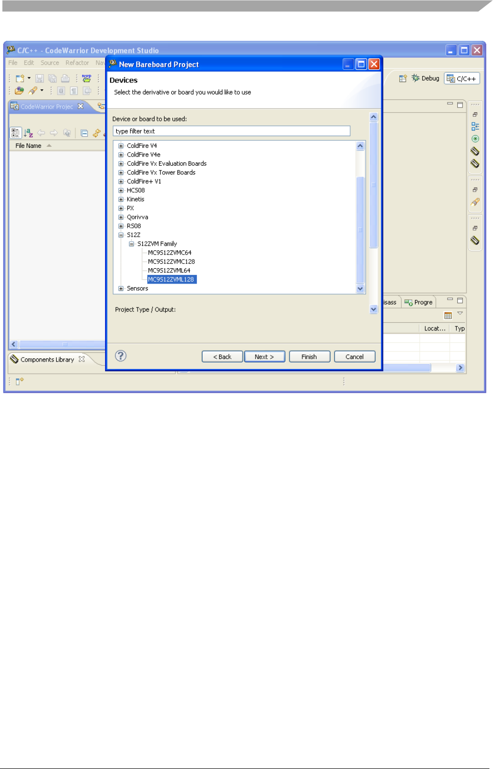
MC9S12ZVM128 is developed base on Code Warrior 10.6. These steps below show how to
configure a LIN application by LIN Stack package in CW10.6.
1. Create empty project target for MC9S12ZVM128 in CW
How to use LIN Package
Freescale Semiconductor
41
Figure 4-29. Select 9S12ZVM128 in Code Warrior
2. Click “Next” button following suggestion from CW default wizard
The final view is shown below
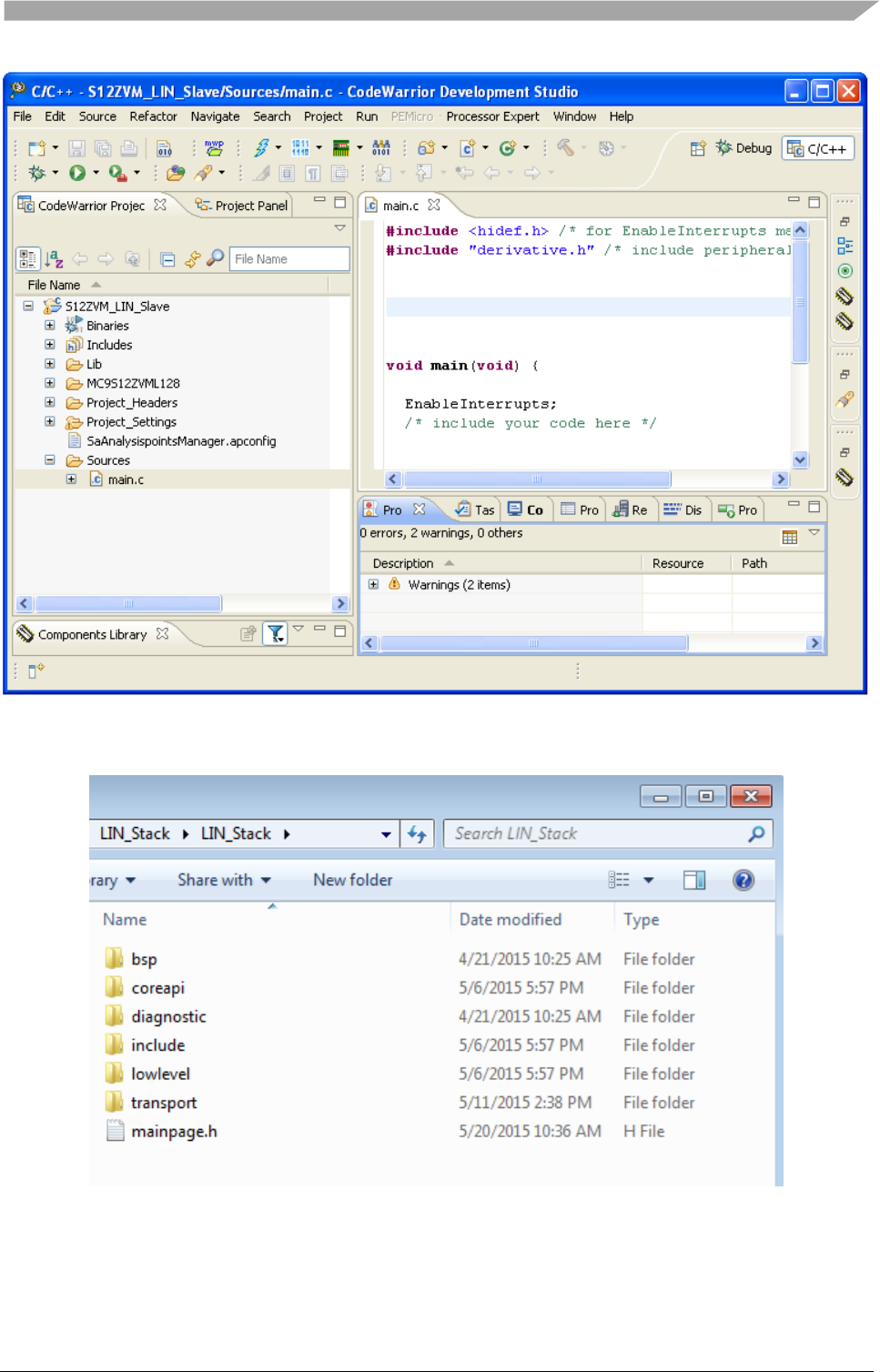
How to use LIN Package
Freescale Semiconductor
42
Figure 4-30. 9S12ZVM128 project in Code Warrior 10
3. Copy “LIN Stack” to project folder in workspace:
Figure 4-31. Add LIN Stack to workspace
4. Keep SCI folder and remove all other folders in “bsp” folder
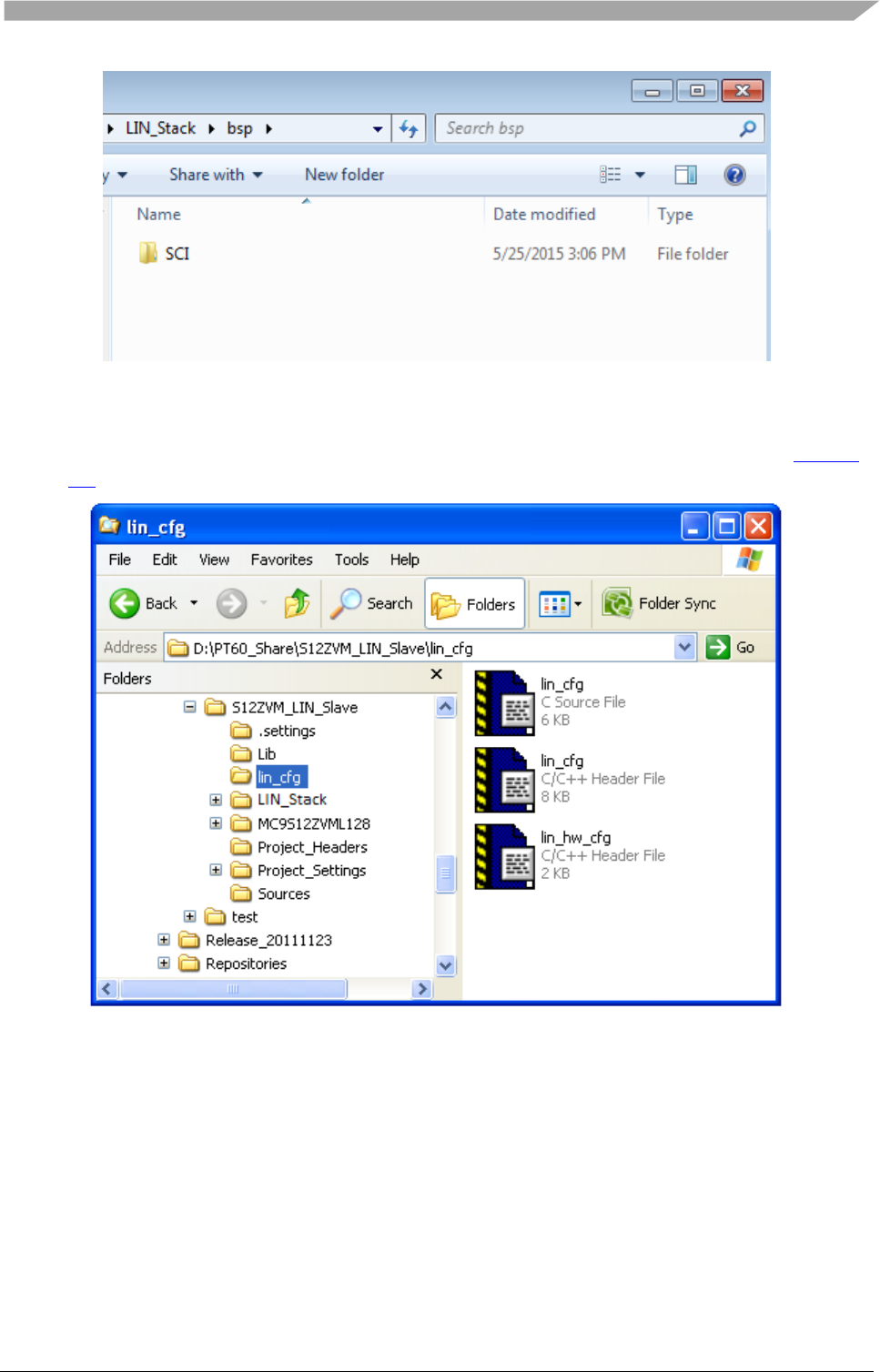
How to use LIN Package
Freescale Semiconductor
43
Figure 4-31. Remove GPIO, SLIC, XGATE interfaces
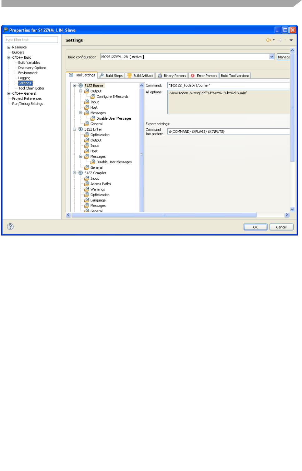
5. Create empty “lin_cfg” folder with the same level directory with LIN_Stack folder
6. Generate configuration files and copy these three files to this folder as mention in Section
4.2
Figure 4-32. Generate configuration files and copy to project folder
7. Back to CW10.6 window, press “F5” in project workspace to update new folders created
8. Click to project selected (S12ZVM_LIN_Slave) ->Right Click -> choose properties
9. Go to C/C++ build item in left sigh of new window, double click to “Settings” item, the
new window is displayed below
How to use LIN Package
Freescale Semiconductor
44
Figure 4-33. Setting path for new folder in project properties
10. Go to S12Z Compiler option, double click to “Access Paths”
In the “Access Paths” right sight view, add the paths for new files in the folders created above
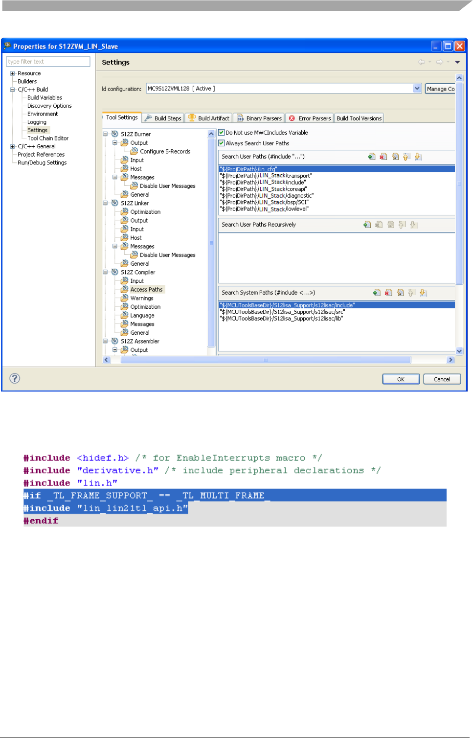
How to use LIN Package
Freescale Semiconductor
45
Figure 4-34. Add path for LIN Stack and configure files
11. Click to “OK” button to finish file configuration
12. Add include files in “main.c”
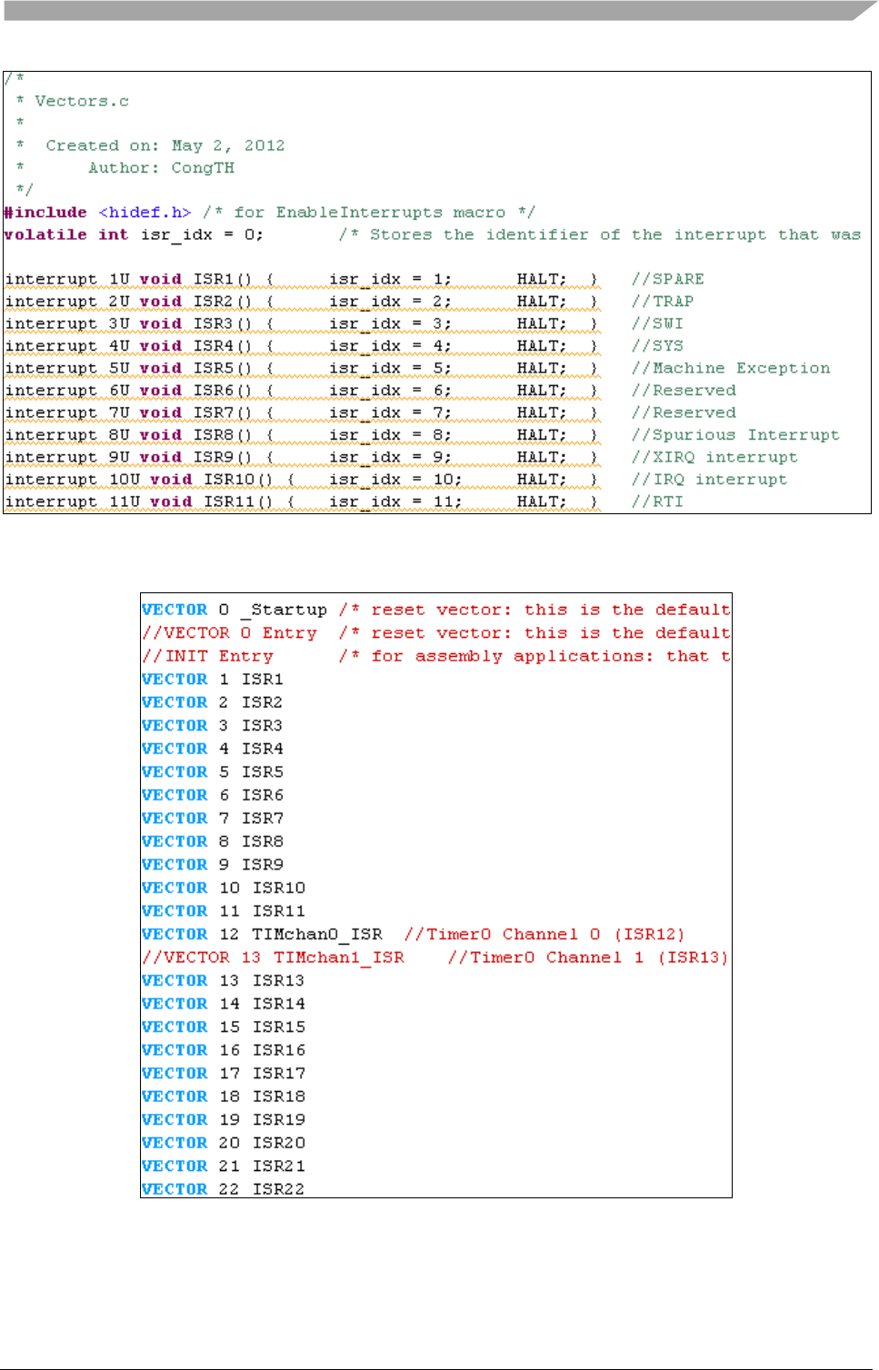
13. Create vectors.c file and save in Source folder (see example in the package for full
implementation)
How to use LIN Package
Freescale Semiconductor
46
Figure 4-35. Interrupt function implementation
14. Add interrupt vector table in .prm file (see example in the package for full implementation)
Figure 4-36. Interrupt vector table redefinition
You are ready for creating application.
How to use LIN Package
Freescale Semiconductor
47
4.6 Getting Started with LIN application
4.6.1 Initialization of hardware utilities
Before getting start with LIN application, some hardware unities must be initialized such as system
clock, timer, I/O ports for demonstration.
NOTE
In order to make the LIN system runs properly, the frequency of each
MCU board should be greater equal to 8MHz. See user manual of each
MCU to setup this value.
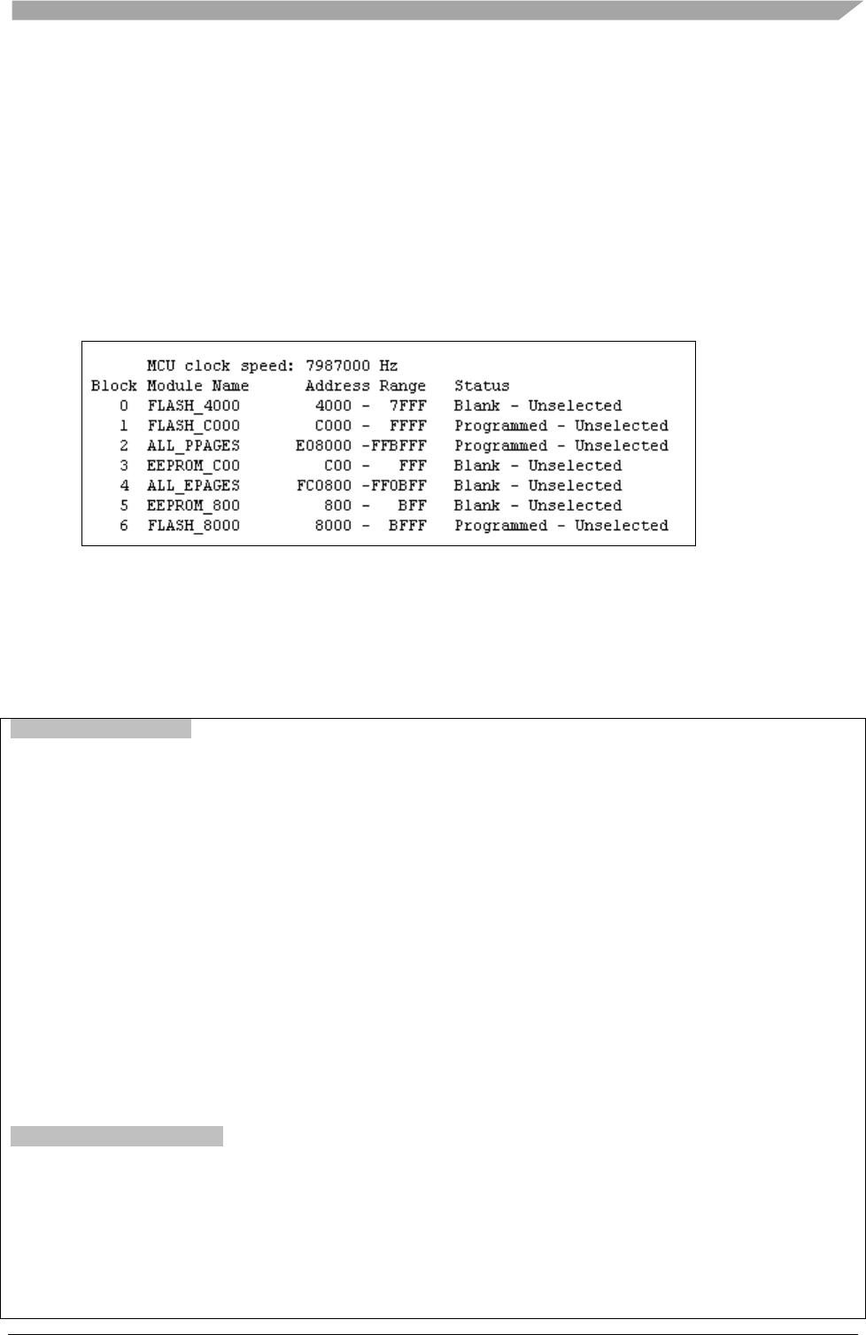
Figure 4-37. MCU clock speed displayed in Command window of CW real time debugger
In the example below, the system clock in DEMO9S08AW60 board is configured as 16MHz and
ports c and d is set as input for press buttons.
void cpu_init() {
/* PE initialization code after reset */
/* Common initialization of the write once registers */
SOPT = 0x53;
// Low-voltage detect
SPMSC1 = 0x1C;
SPMSC2 = 0x00;
/* System clock initialization */
SMCLK = 0x17;
/* Init internal frequency equal to 16Mhz */
ICGC1 = 0x78
ICGFLT = 0xC0;
ICGC2 = 0x20;
/* Initialize ICGTRM register from a non volatile memory */
ICGTRM = *(unsigned char*)0xFFBE;
}
void init_keyboard()
{
PTCDD = 0x10; // set port c as inputs for push button switch input except
for C4 which is accelerometer ST
PTCPE = 0xEF; // enable port c pullups for push button switch operation
except for C4 which is accelerometer ST
PTDDD = 0x00; // set port d as inputs for push button switch and
accelerometer inputs

How to use LIN Package
Freescale Semiconductor
48
PTDPE = 0x0C; // enable port d pullups on D2 and D3 for push button switch
operation
}
4.6.2 Initialization of LIN system
Before the APIs functions of the LIN2.x, J2602 are used, the LIN system must be initialized. In the
example below for EVB9S12XEP100 MCU board, the LIN system is initialized when the
microcomputer is reset. Note that this reflects the points where the API functions for LIN are
called.
#include <hidef.h> /* for EnableInterrupts macro */
#include "derivative.h" /* include peripheral declarations */
#include "lin.h"
void init_keyboard()
{
PTCDD = 0x10; // set port c as inputs for push button switch input except
for C4 which is accelerometer ST
PTCPE = 0xEF; // enable port c pullups for push button switch operation
except for C4 which is accelerometer ST
PTDDD = 0x00; // set port d as inputs for push button switch and
accelerometer inputs
PTDPE = 0x0C; // enable port d pullups on D2 and D3 for push button switch
operation
}
void cpu_init() {
/* PE initialization code after reset */
/* Common initialization of the write once registers */
SOPT = 0x53;
// Low-voltage detect
SPMSC1 = 0x1C;
SPMSC2 = 0x00;
/* System clock initialization */
SMCLK = 0x17;
/* Init internal frequency equal to 16Mhz */
ICGC1 = 0x78;
ICGFLT = 0xC0;
ICGC2 = 0x20;
/* Initialize ICGTRM register from a non volatile memory */
ICGTRM = *(unsigned char*)0xFFBE;
}
/* ......Something to define */
void main(void) {
l_u8 ret;
EnableInterrupts; /* enable interrupts */
/* include your code here */
/* LIN initialization for h_w utilities */

How to use LIN Package
Freescale Semiconductor
49
init_keyboard();
cpu_init();
/* LIN initialization for timer */
ret = l_sys_init();
/* LIN initialization for interface */
ret = l_ifc_init(LI0);
for(;;) {
/* ......Something to do */
} /* loop forever */
/* please make sure that you never leave main */
}
NOTE
If using diagnostic services class II or III you must init transport layer
first. Add this command before using LIN API init transport layer:
- For master node:
ld_init(LI0);
- For slave node:
ld_init();
4.6.3 Timer for LIN schedule execution (Master mode only)
This section is just applied for Master Mode only. In any LIN system, the API function for
schedule execution must be called regularly. The table below lists MCUs with timer names which
could be used for this execution.
Table 4-3: Timer used for LIN Driver
MCU
Timer
Version
Number
of channel
Channel
used
9S08AW16A
9S08AW60
S08TPM
V2
8
0
9S08DZ60
9S08DZ128
9S08SG8
9S08SG32
9S08EL32
S08TPM
V3
8
0
9S08MP16
S08FTM
V2
2
0
9S12HY64
9S12P128
9S12G128
9S12XHY256
TIM16B8C
V2
8
7
9S12XEP100
9S12XEQ512
9S12XET256
9S12XDP512
9S12XF512
S12PIT24B8C
V2
8
0
9S12XS128
9S12XS256
S12PIT24B4C
V1
4
0
9S12I32
TIM16B4C
4
3
9S12ZVML128
TIM0
V3
4
2
9S12ZVL32

How to use LIN Package
Freescale Semiconductor
50
9S12ZVHY64
9S12ZVML31
9S08RN60
S08TPM
V3
8
0
9S12VR64
9S12VR32
TIM16B8C
V3
8
3
MM9Z1J638
TIM16B4C
--
4
3
SKEAZN84
FTM
--
4
2
SKEAZN642
FTM
--
4
2
SKEAZ1284
FTM
--
4
2
9S12ZVC64
TIM16B8C
4
2
9S12ZVL128
TIM16B6C
V3
6
3
9S12ZVMC256
TIM16B4C
V3
4
3
NOTE
In the table, the channel used column shows the channel name in the
highlight timer has been used for the timeout management in each MCU
with time base as 500 ms. In order to use another timer, user could use
another timer type with every time base value.
In the sample code below, TIM timer channel 2 is used to count-up and generate interrupts at an
approximately 2.5ms interval for S12VR64 -Tomar board. Also, in the function (main processing)
for schedule-table execution, the API function for schedule-table execution must be called at or
multiple of the corresponding time-base interval. (See more from demo of S12VR64 in the
package)
Initialized timer function for LIN schedule tick:
void TIM_channel2_init(void){
TIOS |= TIOS_IOS2_MASK;
CFORC |= CFORC_FOC2_MASK;
TTOV |= TTOV_TOV2_MASK;
TIE |= TIE_C2I_MASK;
/* Set counter as 2.5ms timing */
TC2 = 20000;
}
This application code will be defined by user for period of each LIN frame sent in the bus. The
sample code use a loop to increate tick to 15ms for every LIN frame transmission
#pragma CODE_SEG __NEAR_SEG NON_BANKED
interrupt VectorNumber_Vtimch2 void TIM_TIMER2_ISR(void) {
if (LIN_counter>=6){
/* Activate LIN frame transfer for every 15ms */
ret = l_sch_tick(LI0);
/* Reset counter */
LIN_counter = 0;
}
if (LED_counter>=50){
/* Activate LIN frame transfer for every 15ms */
PTT_PTT0 =~ PTT_PTT0;
/* Reset counter */
LED_counter = 0;

How to use LIN Package
Freescale Semiconductor
51
}
LIN_counter++;
LED_counter++;
/* Clear timer flag */
TFLG1 |= TFLG1_C2F_MASK;
/* Reset timer counter */
TC2 = (TC2 + 20000) &0xFFFF;
}
#pragma CODE_SEG DEFAULT /* Return to default code segment */
4.6.4 LIN_PHY Enable
For those MCUs which support LIN_PHY to replace LIN transceiver (9S12VR64, 9S12Zs), there
are two ways to drive this interface. The first one is using SCI to control LIN_PHY and the second
one is directly handle through the LPDR register provided by hardware silicon.
To easy porting and maintenance, this scope of Stack use the first way where SCI physical layer
has been existed.
In order to enable LIN_PHY working with SCI, the steps as below:
1. Enable LIN_PHY
2. Enable LIN Pull-up
3. LIN Slew Rate selection
Due to range of LIN baudrate from 2000bps to 20000 bps, the LIN slew rate bit selection is
defined to mapping optimally with LIN baudrate working.
For more information, refer to LIN Slew Rate Mode Register (LPSRM) of 9S12Zs Reference
Manual.
LIN_PHY Enable example:
Here is code for enabling LIN_PHY in 9S12VR64:
void LIN_Phy(void){
LPCR_LPE = 1; /* Enable LIN Phy */
LPCR_LPPUE = 1; /* Pull up to strong signal */
LPSLRM = 0x01; /* Select Slew Rate */
}
4.6.5 LIN Applications
This section describes sample codes for LIN application using API function (refer to Appendix A)
after initializing hardware utilities and LIN system as well as timer for schedule execution. The
application focuses on contents (frame) transferred on the LIN bus and how to process data
depends on LIN system configuration which is acquired from the status of various nodes,
peripheral devices, and other applications.
4.6.5.1 Master task
This example code below for master task is taken from S12VR64 demo code in the package. For
more application, please refer to directory:
LIN_Package\Examples\VR64_MagniV\VR64_Master_LIN21.

How to use LIN Package
Freescale Semiconductor
52
Base on LDF definition for schedule table, the master task will require user to select which
schedule will be active and the frames associated will be processed.
In this example, here is the table of scheduler defined in the lin_cfg.h file
typedef enum {
/* Interface_name = LI0 */
LI0_LIN_NULL_SCHEDULE
,LI0_GOTO_SLEEP_SCHEDULE
,LI0_MasterReqTable
,LI0_SlaveRespTable
,LI0_NormalTable
,LI0_ETFCollisionResolving
,LI0_InitTable
}l_schedule_handle;
In the main.c file, the schedule is active as the code below
/* Set active schedule table, */
l_sch_set(LI0,LI0_NormalTable, 0);
In this example, the LIN NormalTable is active. There are two more default schedule generated by
tool are LI0_LIN_NULL_SCHEDULE used for no activity in LIN bus request and
LI0_GOTO_SLEEP_SCHEDULE used to send goto sleep request.
In this application, the master will control temperature of motor by reading temperature data stored
in signal Motor1Temp in Motor1State_Cycl frame. If the returned temperature is greater than
maximum value, master will request slave to reduce temperature or if greater than broken value,
master will request slave to stop motor.
if (l_flg_tst_LI0_Motor1Temp_flag()){
/* Clear this flag... */
l_flg_clr_LI0_Motor1Temp_flag();
/* Store temperature data */
Motor1_temp = l_u8_rd_LI0_Motor1Temp();
/* The application will change Motor selection in case
the temperature is greater than maximum value to release motor power
This will be transfered by sporadic frame type in LIN bus */
if (MOTOR1_OVER_TEMP<Motor1_temp) {
/* Request stop motor by power off */
l_u8_wr_LI0_Motor1Selection(MOTOR_SELECTION_STOP);
}else if ((MOTOR1_MAX_TEMP<Motor1_temp)&(MOTOR1_OVER_TEMP > Motor1_temp)){
/* Request to reduce motor speed */
l_u8_wr_LI0_Motor1Selection(MOTOR_SELECTION_DECREASE);
} else {
/* Request to increase motor speed if user request */
l_u8_wr_LI0_Motor1Selection(MOTOR_SELECTION_INCREASE);
}
}
4.6.5.2 Slave task
This example code below for LIN slave tasks is used to check control signal from Master on
temperature selection modes. See VR64_Slave_LIN21 example in the package.
/* Check if temp signal is updated */
if (l_flg_tst_LI0_Motor1Selection_flag()){
/* Clear this flag... */

How to use LIN Package
Freescale Semiconductor
53
l_flg_clr_LI0_Motor1Selection_flag();
/* Store selection data */
Motor1_Selection = l_u8_rd_LI0_Motor1Selection();
/* The application will change Motor selection in case
the temperature is greater than maximum value to
release motor power
This will be transfered by sporadic frame type in LIN bus */
l_u8_wr_LI0_Motor1Temp(Motor1_temp);
/* Check if power off motor due to high temperature */
if (Motor1_Selection == MOTOR_SELECTION_STOP) {
/*---------- add code here to stop motor ------------*/
}
}
4.6.5.3 Goto Sleep and Wakeup applications
This section is taken from the application code of General demo application. Please refer to
directory Examples\General_Demo_Application\XEP100_Gateway for code of master node and
Examples\General_Demo_Application\DZ128_Slave1\ for slave node.
The feature Goto Sleep is only call by master and after this function is called, the LIN status word
which contain a bit for Goto Sleep will be updated. Therefore user can check by reading this word.
NOTE
The call is a read-reset call; meaning that after the call has
returned, the status word is set to 0.
If user press button PB4 in XEP100 EVB board, the Goto Sleep, wakeup features will be enable
and press one more time, it will disable the features.
/* Use the button PB4 in the EVB board to demonstrate goto sleep/wakeup
feedture */
if (!SW4){
for(i = 0; i<60000;i++){
for(j = 0; j<10;j++);
};
if (0 == (sw4%2)){
(void)printf("Enable free counter for test goto sleep\n");
l_sch_set(LI1, LI1_PeriodicalWakeupTable, 0);
l_sch_set(LI2, LI2_PeriodicalWakeupTable, 0);
count = 10;
freecntr_enable();
} else {
(void)printf("Disable free counter\n");
control1 = 0;
control2 = 0;
l_sch_set(LI1, LI1_LIN_NULL_SCHEDULE, 0);
l_sch_set(LI2, LI2_LIN_NULL_SCHEDULE, 0);
count = 10;
freecntr_disable();
}
sw4++;
}
There two ways for wake up LIN bus:
a- The master node issue a break field, e.g. by issuing an ordinary header since the break will act
as a wake up signal

How to use LIN Package
Freescale Semiconductor
54
b- Master node or slave call API function l_ifc_wake_up to send wake up signal in the bus
In this example, the master issue a break field by active LI1_PeriodicalWakeupTable schedule.
By using and reseting counter variable count, the LIN network will be wakeup and in sleep mode
periodically.
/* Send goto sleep command */
if (GOTO_SLEEP_DURATION == count){
(void)printf("Send goto sleep command\n");
l_ifc_goto_sleep(LI2);
l_ifc_goto_sleep(LI1);
count++;
}
/* Run Periodical Wakeup table */
if (WAKEUP_DURATION == count){
(void)printf("Run Periodical Wakeup table\n");
l_sch_set(LI1, LI1_PeriodicalWakeupTable, 0);
l_sch_set(LI2, LI2_PeriodicalWakeupTable, 0);
count = 0;
}
counter++;
if (5 == counter){
counter = 0;
}
In order to check Goto sleep flag, the code below uses a LED in the board to display the status.
If LED is on, mean the node in the sleep state and if the LED is off, the node is in wakeup state.
/* Check if any sleep mode on two cluster by reading the LIN word status */
LIN1_word_status = l_ifc_read_status(LI1);
LIN2_word_status = l_ifc_read_status(LI2);
if (LIN1_word_status != 0){
if((LIN1_word_status>>3)&0x0001){
LED3 = ON; /* cluster1 bus is in sleep mode */
}else{
LED3 = OFF; /* cluster1 bus is in wakeup mode */
}
}
if (LIN2_word_status != 0){
if((LIN2_word_status>>3)&0x0001){
LED4 = ON; /* cluster2 bus is in sleep mode */
}else{
LED4 = OFF; /* cluster2 bus is in wakeup mode */
}
}
At the slave site (DZ128_Slave1) the code to check goto sleep and request send a wakeup signal as
below:
/* Check if the goto sleep command sent by master node */
LIN_word_status = l_ifc_read_status(LI0);
/* The word status is presented below
--------------------Word status------------------------------
|15|14|13|12|11|10|9|8|7|6|5|4|3|2|1|0|
| | | | | | | | |-- Error in response
| | | | | | | |---- Successful tranfer
| | | | | | |------ Overun
| | | | | |-------- Goto sleep
| | | | |---------- Bus activity
| | | |------------ Event trigger collision
How to use LIN Package
Freescale Semiconductor
55
| | |-------------- Save configuration
| |---------------- 0
|------------------------------ Las frame PID */
/* Check if any update from LIN word status*/
if(LIN_word_status != 0){
/* Check if the LIN bus in the sleep mode */
if((LIN_word_status>>3)&0x01){
LED3 = ON;
/* Press PTA4 to wakeup LIN node */
if (!PTAD_PTAD4){
/* Call wakeup function */
l_ifc_wake_up(LI0);
}
}else{
LED3 = OFF;
}
}
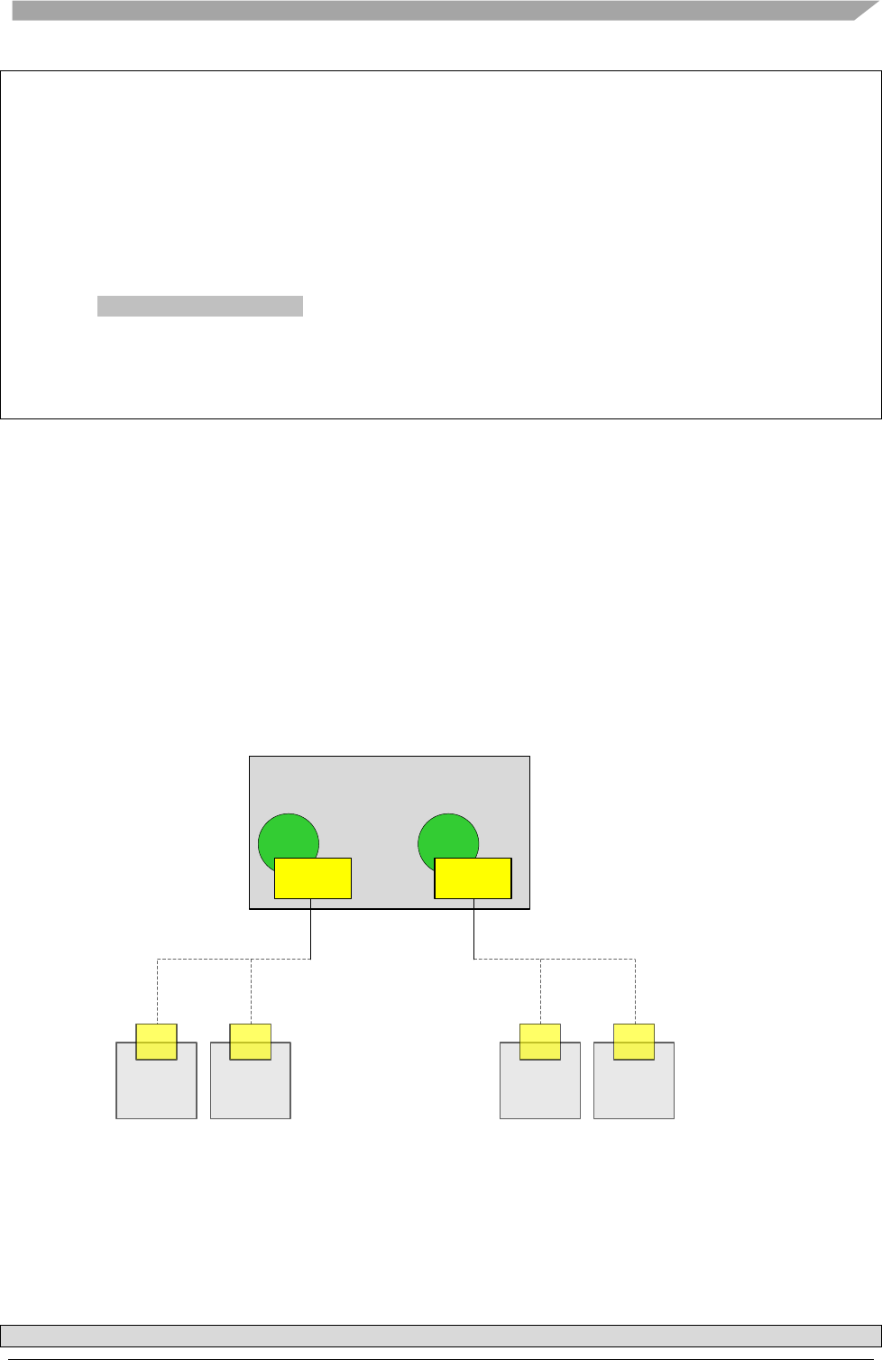
4.6.5.4 Multi LIN master with different timers for S12X MCUs
For S12x MCU family including XEP100, XDP512, XF512, XEQ512 and XET256 contain a PIT
timer with 8 channels.
If those MCUs are used for multi LIN Master, the timer for timeout activity can be selected one
PIT timer channel for all LIN networks or separated channels for each network.
The figure 4-38 below shows a configuration of Multi LIN master with different Time base
required in each network.
9S12XEP100
Slave
task2
LIN
IN
Timer 1
Master
Task 1
Timer 2
Master
Task 2
Slave
task1
LIN
IN
LIN21.ldf
Time base = 5 ms
Slave
task2
LIN
IN
Slave
task1
LIN
IN
LINDiagnostic.ldf
Time base = 1 ms
Figure 4-38. Configuration of multi LIN Master in 9S12XEP100
To select timer channel for each network, user just add timer_channel definition to interface
configuration of npf file
/*** LIN HARDWARE DEFINITION ***/
How to use LIN Package
Freescale Semiconductor
56
/* SCI config */
sci{
s12_sci1{
sci_channel = 1; /* Check validation of sci_channel */
timer_channel = 1; /* PIT timer */
}
s12_sci3{
sci_channel = 3; /* Channel setting */
timer_channel = 2; /* PIT timer */
}
}
NOTE
This timer selection is for timeout activity which time base is
defined in LDF file. In the main.c application, user must define
another timer for scheduler as mention in section Timer for LIN
schedule execution (Master mode only)
If no timer selection defined, the Driver is default to use only one channel where time base is taken
from smallest value of time bases defined in LDF files.
4.6.5.5 AUTOBAUD feature for S12Z MCU family as Slave Node
AUTOBAUD is an extensive feature in LIN Driver which allows a MCU to detect baud rate of
LIN bus and adapt its original baud rate to bus value.
Auto Baud is applied when the baud rate of the incoming data is unknown or the baud rate is fixed
with some specific values. Each LIN network might have different configuration on such baud
rates. One MCU can work with different configurations without flashing.
In this scope of LIN Driver version, two baud rate are supported: 9600 and 19200 bps and verified
on S12Z MCU family.
Figure 4-39. Two baud rate supports for AUTOBAUD feature
In order to use this feature, user just enables an option in NPF file as below:
/*** NETWORK DEFINITION ***/

How to use LIN Package
Freescale Semiconductor
57
network {
idle_timeout = 5s;
diagnostic_class = 1; /* Class selection to use diagnostic services */
autobaud_support = yes;
LI0{
node = Motor1; /* Name of node described in LDF (must
check consistence with LDF) */
file = "LIN21.ldf"; /* Path to LDF file */
device = s12_sci0; /* LIN Hardware
interface, related to INTERFACE SECTION */
}
}
For more application usage case, refer to demo application attached in the package:
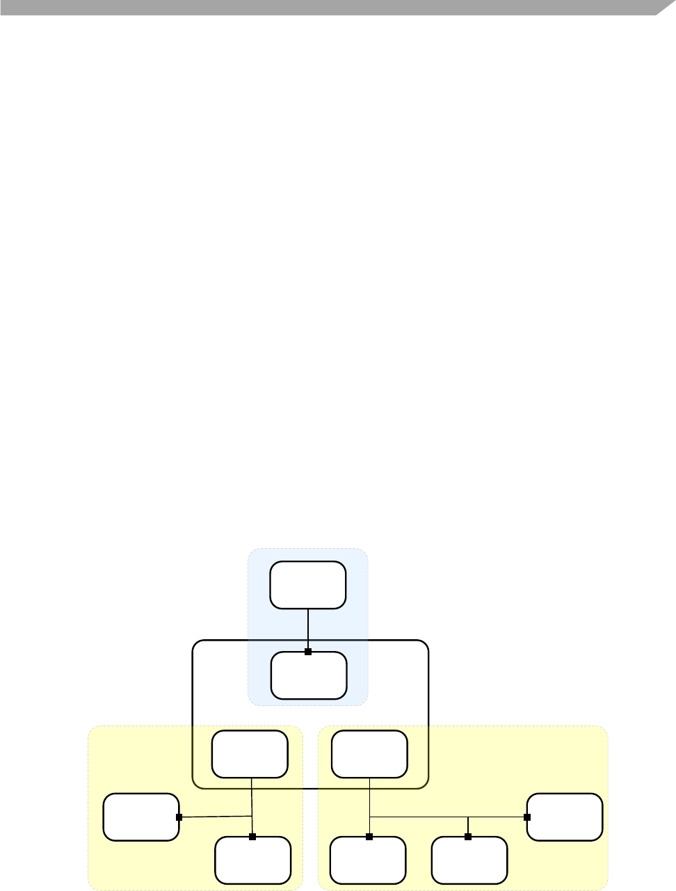
Chapter 5
Demo Application
This section gives detailed instructions on how to set up a LIN node from the source code provided.
By following these guidelines and the referenced documents, the application developers could build
any images for the nodes working on the supported MCUs listed in the scope of work for this
document.
5.1 LIN Protocol demo application
5.1.1 Introduction
The demo application demonstrates a typical application of the LIN. The application covers
functionalities in HVAC and door application, such as control of door locks, mirrors and window
lifters. The best representative application is a gateway, such as one shown in Figure 5-1.
LIN Gateway Node
LIN Cluster 1 LIN Cluster 2
Master
Node
Slave
Task
Master
task 1
Slave
Node
Slave
Node
Master
task 2
Slave
Node Slave
Node
Slave
Node
Figure 5-1. Demo application configuration
The LIN gateway node is one of the controllers with multiple LIN interfaces. It provides connection
to a higher level car network, receiving commands via the slave LIN task. In the same time the two
or more master tasks are specified in the scheduler, allowing transferring the commands further to
the slave LIN clusters.
A set of procedures in transferring messages is implemented in this application:
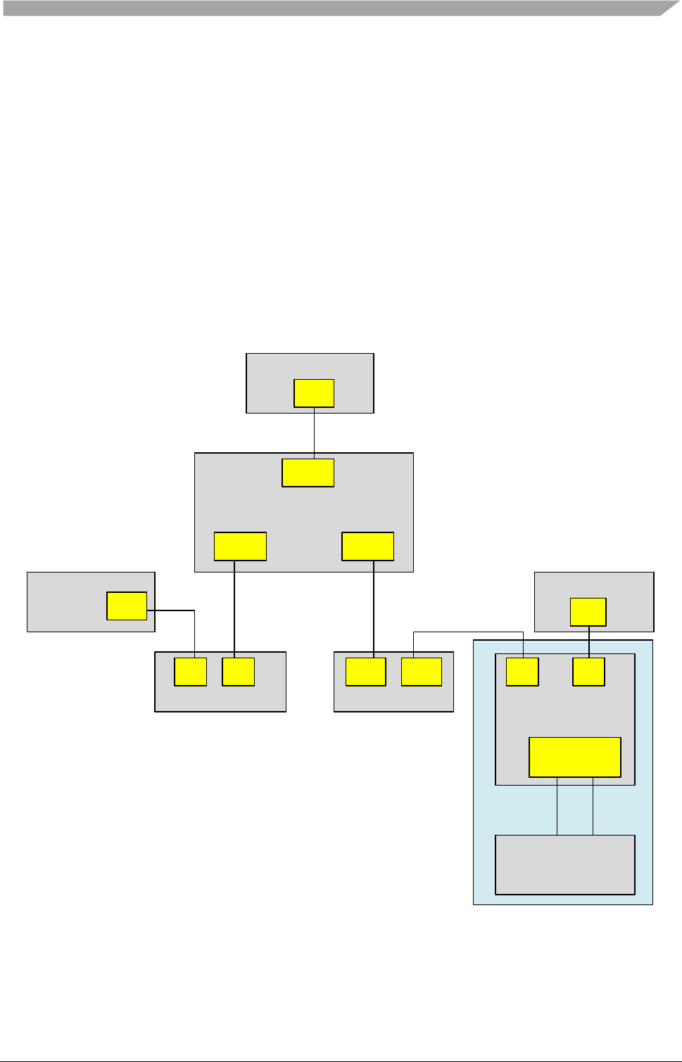
Demo Application
Freescale Semiconductor
59
1. From the Master node to Slave nodes via the Gateway (for example, potentiometer).
2. From the Gateway to request current potentiometer from the slave nodes.
3. Send sleep and wakeup signals from the gateway to the slave nodes.
4. Send diagnostic frames from the gateway to the slave nodes.
5. The node configuration utility must describe the network configuration and the
required properties of the nodes. This configuration should be compiled with the
project files to create the Demonstration Application executable.
6. The LIN gateway node shall log the events and output it in a readable form for the
demonstration and traceability of the LIN functioning.
5.1.2 Demo Environment Setup
The hardware platform for each node is identical based on the demo application configuration as
shown in the Figure 5-2. Three are seven hardware platforms named from B1 to B7 respectively.
9S08QD4(B6)
9S08SG32
LIN 1 LIN 2
LIN Transceiver
TX RX
RX TX
9S12XEP100(B2)
9S08DZ128(B1)
LIN 5
LIN 3 LIN 4
9S08EL32
(B3)
9S08DZ128(B4) 9S08SG32(B5)
9S12HY64(B7)
LIN 1
LIN
OUT LIN
IN LIN 1 LIN 2
J10
LIN
IN
Figure 5-2. Master/Slave/Gateway hardware
NOTE
The 9S08SG32 board in the cluster 2 is not involved to the network but acts
as intermediary role to connect nodes B5, B6 and B7.
Demo Application
Freescale Semiconductor
60
5.1.3 Detail Description of Nodes
The table 6-9 below illustrate in detail description of boards participating in the network including
name, ID, functionality and the buttons used for the application.
Table 5-1. Master
Board
Board ID
Functionality
User I/O
9S08DZ128
B1
Master
Push button: PTA4, PTA5, PTA6,
PTA7
Table 5-2. Gateway
Board
Board ID
Functionality
User I/O
9S12XEP100
B2
Slave on LIN 5
Master on LIN 4
Master on LIN 3
Push button: PB4, PB5, PB6, PB7
Table 5-3. Cluster1
Board
Board ID
Functionality
User I/O
9S08DZ128
B4
Slave1
Push button: PTA4, PTA5, PTA6,
PTA7
9S08EL32
B3
Slave2
Potentiometer: RV1
Led: LED1, LED2
Table 5-4. Cluster2
Board
Board ID
Functionality
User I/O
9S08SG32
B5
Slave A
Potentiometer: RV1
Led: LED1, LED2
9S08QD4
B6
Slave B
Potentiometer: RV1
9S12HY64
B7
Slave C
Potentiometer: RV1
Led: LED1, LED2
5.1.4 LIN System Initialization
Table 5-5 shows the expected hardware and software used for demo application.
Table 5-5. List of hardware and software for demo application
CW6.2
CW4.7
9S08AW16A
9S12XEP100
9S08SG32
9S12HY64
9S08DZ128
9S08QD4
9S08EL32
NOTE
All derivatives use 12V power supply except 9S08QD4 board with 5V
power supply.
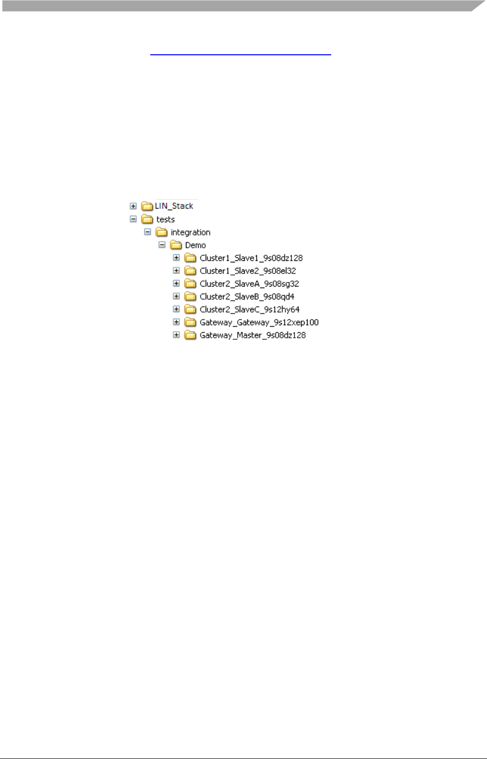
Demo Application
Freescale Semiconductor
61
The steps to initialize the demo from LIN Stack package are detailed in this section. For other LIN
network applications, refer to Chapter 4, How to use LIN Package to create single application for
each derivative involving the network. The remaining steps are similar to this section.
1. Open Code Warrior V4.7 and V6.2 environments.
The MCUs run on Code Warrior V4.7 are 9S12XEP100, 9S12HY64
The MCUs run on Code Warrior V6.2 are 9S08DZ128, 9S08EL32, 9S08SG32,
9S08QD4
2. Open folder for target board in Demo folder as shown in Figure 5-3 (e.g…\tests
\integration\Demo\Cluster1_Slave1_9s08dz128) and drag Code Warrior project
file (.mcp) to one of two Code Warrior environments.
Figure 5-3. Demo Source Code Directory Structure
3. Attach power and turn on the target board. The board must be connected to the PC
through a Multilink or SofTec Interface Device Application. The Combined Interface
Device Application is configured by default to use the USB connector for serial
communication.
4. Download source code to the board.
5. Dispose the boards as illustrated in Figure 5-4 and connect boards via LIN bus wires.
6. Jumper setting:
All boards have their jumper set as default except 9S12XEP100 board whose function as
Gateway.
In 9S12XEP100 board, the OSC SEL jumper is set as CLOCK and LIN TRANCEIVER
SUPPLY SEL jumper is 12V.
7. Attach power to 9S12XEP100 board and make sure that all power led of boards is
turn on which is ready for operation.
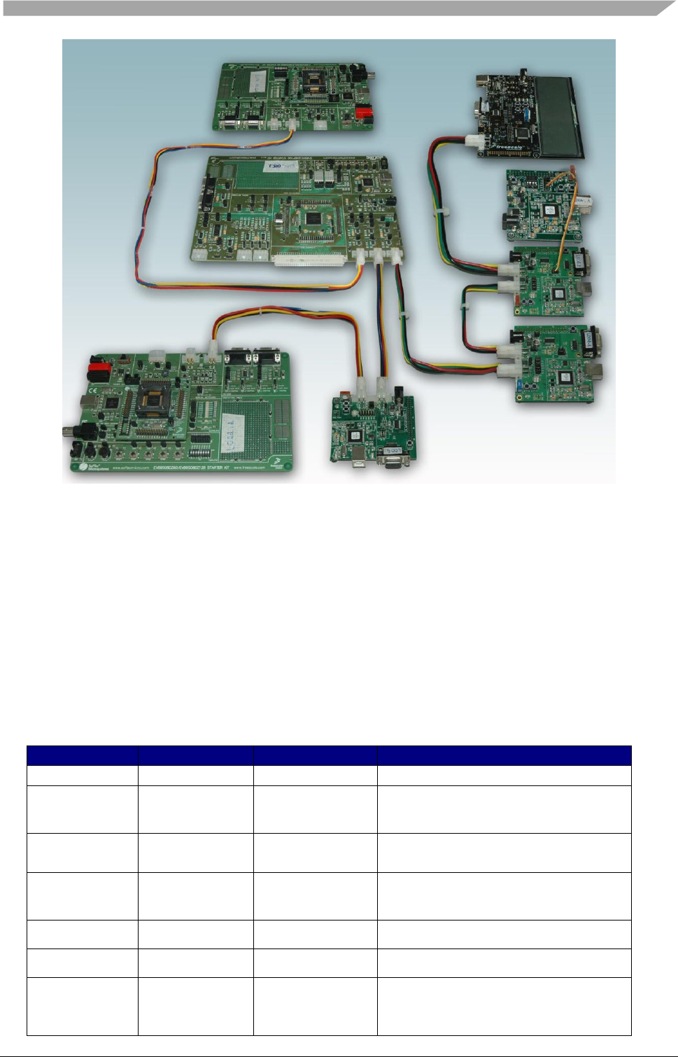
Demo Application
Freescale Semiconductor
62
Figure 5-4. A disposition of seven hardware platforms to match with the configuration
5.1.5 Functionality Description
This section describes in details functionalities and procedures of the Demo Application. It includes
descriptions of PID sending and direction of message transmitting between physical nodes of the
network.
5.1.5.1 Sequence of Frames between Master Node, Gateway
and Slave Nodes
All frames in communication are defined in table below:
Table 5-6. Define functionality of each node respectively with its pid
PID
Publisher
Subscriber
Description
0x01
Master
Gateway
Change schedule table
0x02
Gateway
Master
Master requests potentiometer
status from all slave nodes
0x04
Gateway
Slave 1
Slave 2
Reset signal
0x05
Gateway
Slave 1
Slave 2
Data byte with 2 bit information
about push button
0x06
Slave 1
Gateway
Potentiometer status
0x07
Slave 2
Gateway
Potentiometer status
0x08
Gateway
Slave A
Slave B
Slave C
Reset signal
Demo Application
Freescale Semiconductor
63
0x09
Gateway
Slave A
Slave B
Slave C
Data byte with 2 bit information
about push button
0x0A
Slave A
Gateway
Potentiometer status
0x0B
Slave B
Gateway
Potentiometer status
0x0C
Slave C
Gateway
Potentiometer status
0x3C
Gateway
All slaves
Sleep command
5.1.5.2 Reset Status
After resetting the MCU, the node is ready for communication. The LED status of each board
after resetting is:
Table 5-7. Status of each MCU board after reset
Board
Responsibility
LED1
LED2
9S08EL32
Slave 1 in Cluster 1
OFF
OFF
9S08DZ128
Slave 2 in Cluster 1
OFF
OFF
9S08SG32
Slave A in Cluster 2
OFF
OFF
9S12HY64
Slave C in Cluster 2
OFF
OFF
5.1.5.3 Demonstration use cases
In this chapter we present several typical use cases for the demo setup. The communication between
the nodes in these use cases is explained in form of time diagrams.
Reset signal is to set OFF status for LED1 and LED2 on all Slave boards
Gateway
(Master task 1) Slave 1 Slave 2
PID = 0x04 Gateway sends reset signal to all
Slaves in Cluster 1 in order to set
status of LED1 and LED2 to OFF
Gateway response
Figure 5-5. Timing Diagrams for Reset LED signal from Gateway to Slaves in Cluster 1
Demo Application
Freescale Semiconductor
64
Gateway
(Master task 2) Slave A Slave B
PID = 0x08 Gateway sends reset signal to all
Slaves in Cluster 2 in order to set
status of LED1 and LED2 to OFF
Slave C
Gateway response
Figure 5-6. Timing Diagrams for Reset LED signal from Gateway to Slaves in Cluster 2
Message from Master node to Gateway
Master
node Gateway
PID = 0x01
Gateway response
Master response
PID = 0x02
Master node sends signal to change
schedule table
Master node requests Potentiometer
status from all Slave nodes
Figure 5-7. Timing Diagrams for frames from Master node to Gateway
Message from Gateway to Slave nodes in Cluster 1
Demo Application
Freescale Semiconductor
65
Gateway
(Master task 1) Slave 1 Slave 2
PID = 0x05 Gateway sends signal to turn on/off
the LED1 and LED2
Gateway response
PID = 0x06
Slave 1 response
Gateway requests Potentiometer
status from Slave 1
PID = 0x07
Slave 2 response
Gateway requests Potentiometer
status from Slave 2
Figure 5-8. Timing Diagrams for frames from Gateway to Slaves in Cluster 1
Message from Gateway to Slave nodes in Cluster 2
Gateway
(Master task 2) Slave A Slave B
PID = 0x0A Gateway requests Potentiometer
status to Slave A
Slave A response
Slave C
PID = 0x0B Gateway requests Potentiometer
status to Slave B
Slave B response
PID = 0x0C Gateway requests Potentiometer
status to Slave C
Slave C response
PID = 0x09 Gateway sends signal to turn on/off
LED1 and LED2
Master response
Figure 5-9. Timing Diagrams for frames from Gateway to Slaves in Cluster 2
Sleep signal from Gateway to Slave nodes
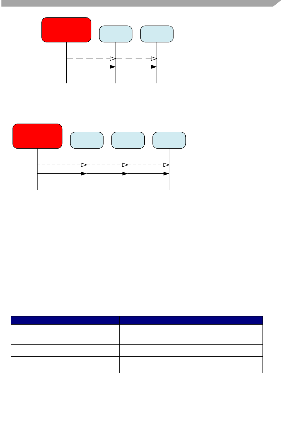
Demo Application
Freescale Semiconductor
66
Gateway
(Master task 1) Slave 1 Slave 2
PID = 0x3C Gateway sends Sleep signal to all
Slaves in Cluster 1
Figure 5-10. Timing Diagrams for Sleep signal from Gateway to Slaves in Cluster 1
Gateway
(Master task 2) Slave A Slave B
PID = 0x3C Gateway sends Sleep signal to all
Slaves in Cluster 2
Slave C
Figure 5-11. Timing Diagrams for Sleep signal from Gateway to Slaves in Cluster 2
5.1.6 Operation
Operation on push buttons of this demo is very simple. By pushing the buttons on board
9S08DZ128 (Master node) user can change the schedule table between the following ones:
- Operates only Cluster 1
- Operates only Cluster 2
- Operates both clusters
- Not operate both clusters
5.1.6.1 Actions on All Boards Before Resetting the LEDs Status
Table 5-8. List of actions and results before resetting the LEDs status
Action
Result
Push button PTA4
Schedule in Cluster 1 is active
Push button PTA5
Schedule in Cluster 2 is active
Push button PTA6
Schedules in both Clusters are active
Push button PTA7
Schedules in both Clusters are inactive
By pressing the buttons on 9S12XEP100 board (Gateway), the user can change the LEDs on
slave nodes as follows:
Table 5-9. List of actions and results after pressing buttons on 9S12XEP100 board
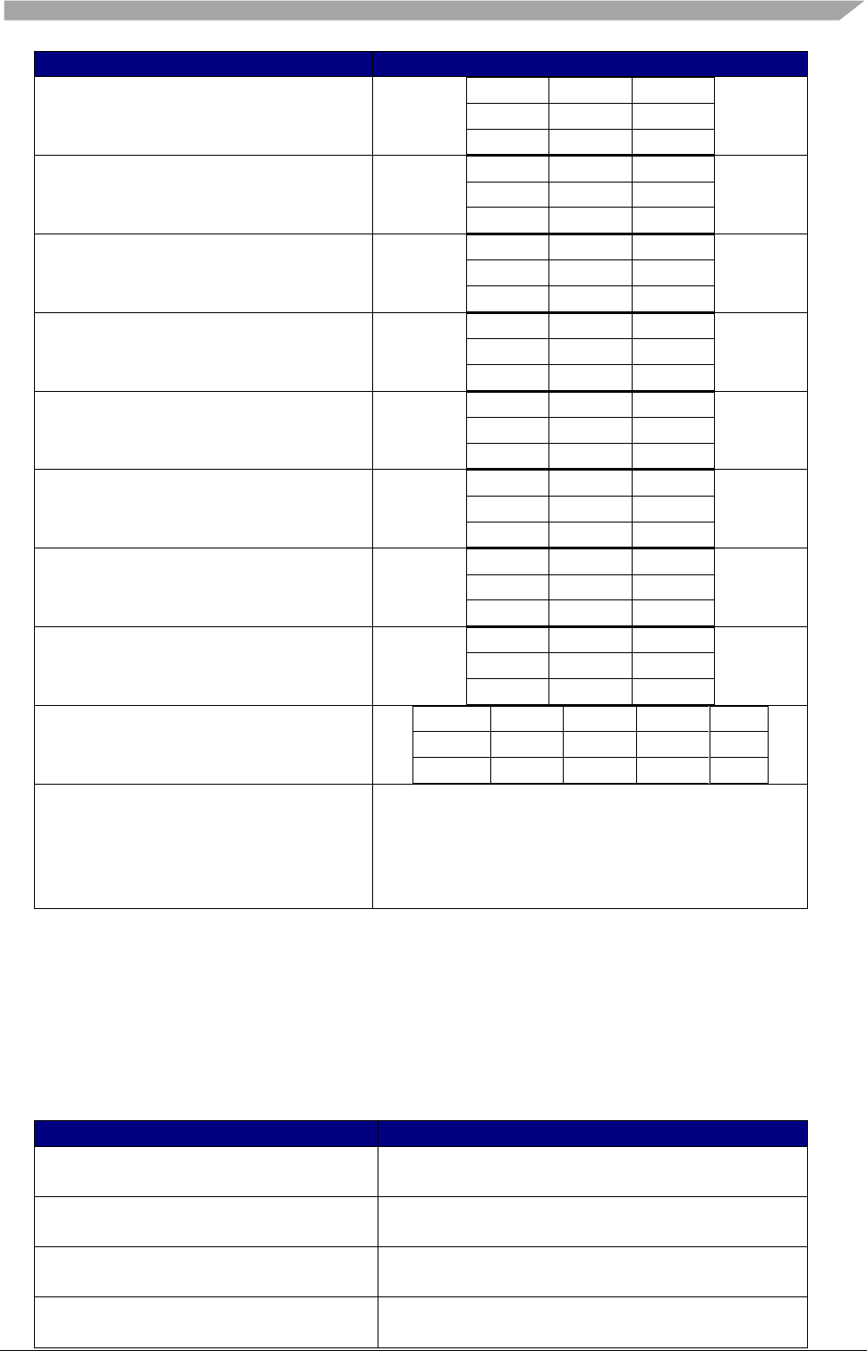
Demo Application
Freescale Semiconductor
67
Action
Result
Push button PB4 in the first time
(data = 0x00)
Board
B3
B4
LED1
ON
ON
LED2
ON
ON
Push button PB4 in the second time
(data = 0x01)
Board
B3
B4
LED1
OFF
OFF
LED2
ON
ON
Push button PB4 in the third time
(data = 0x10)
Board
B3
B4
LED1
ON
ON
LED2
OFF
OFF
Push button PB4 in the fourth time
(data = 0x11)
Board
B3
B4
LED1
OFF
OFF
LED2
OFF
OFF
Push button PB5 in the first time
(data = 0x00)
Board
B5
B7
LED1
ON
ON
LED2
ON
ON
Push button PB5 in the second time
(data = 0x01)
Board
B5
B7
LED1
OFF
OFF
LED2
ON
ON
Push button PB5 in the third time
(data = 0x10)
Board
B5
B7
LED1
ON
ON
LED2
OFF
OFF
Push button PB5 in the fourth time
(data = 0x11)
Board
B5
B7
LED1
OFF
OFF
LED2
OFF
OFF
Push button PB6
Board
B3
B4
B5
B7
LED1
OFF
OFF
OFF
OFF
LED2
OFF
OFF
OFF
OFF
Push button PB7
Send GOTOSLEEP command
After that the application will be in charge of
waking up the network in 10 seconds. And the
schedule will send the header to query states of
Slaves
The data content sent to the slave boards wraps around and is controlled by pressing the PB4
and PB5 buttons on the gateway node.
To demonstrate the data direction from slave to master, user can change the data content of the
messages by changing the potentiometer. This information is accessible via Hyper terminal
window.
Table 5-10. List of actions and results when changing the potentiometer
Action
Result
Change the Potentiometer on board
B3
Value of Potentiometer for Slave 1 will be
changed in log information
Change the Potentiometer on board
B4
Value of Potentiometer for Slave 2 will be
changed in log information
Change the Potentiometer on board
B5
Value of Potentiometer for Slave A will be
changed in log information
Change the Potentiometer on board
B6
Value of Potentiometer for Slave B will be
changed in log information
Demo Application
Freescale Semiconductor
68
Change the Potentiometer on board
B7
Value of Potentiometer for Slave C will be
changed in log information
5.1.6.2 Actions on All Boards After Resetting LEDs Status
After PTA4 on S08DZ128 master board press (Schedule in Cluster 1 is active)
Table 5-11. List of actions and results after resetting LEDs status
Action
Result
PB4 pressed in the first time
Board
B3
B4
B5
B7
LED1
ON
ON
OFF
OFF
LED2
ON
ON
OFF
OFF
PB4 pressed in the second time
Board
B3
B4
B5
B7
LED1
OFF
OFF
OFF
OFF
LED2
ON
ON
OFF
OFF
PB4 pressed in the third time
Board
B3
B4
B5
B7
LED1
ON
ON
OFF
OFF
LED2
OFF
OFF
OFF
OFF
PB4 pressed in the fourth time
Board
B3
B4
B5
B7
LED1
OFF
OFF
OFF
OFF
LED2
OFF
OFF
OFF
OFF
PB5 pressed in the first time/
second time/ third time/ forth
time
Board
B3
B4
B5
B7
LED1
OFF
OFF
OFF
OFF
LED2
OFF
OFF
OFF
OFF
Change the Potentiometer on
board B3
Value of Potentiometer for Slave 1 will be changed in
log information
Change the Potentiometer on
board B4
Value of Potentiometer for Slave 2 will be changed in
log information
Change the Potentiometer on
board B5/ B6/ B7
Value of Potentiometer for Slave A, B and C will not
be changed in log information
After PTA5 on S08DZ128 master board press (Schedule in Cluster 2 is active)
Table 5-12. List of actions and results after pressing the button PTA5 of S08DZ128 board
Action
Result
PB4 pressed in the first time/
second time/ third time/ forth
time
Board
B3
B4
B5
B7
LED1
OFF
OFF
OFF
OFF
LED2
OFF
OFF
OFF
OFF
PB5 pressed in the first time
Board
B3
B4
B5
B7
LED1
OFF
OFF
ON
ON
LED2
OFF
OFF
ON
ON
PB5 pressed in the second time
Board
B3
B4
B5
B7
LED1
OFF
OFF
OFF
OFF
LED2
OFF
OFF
ON
ON
PB5 pressed in the third time
Board
B3
B4
B5
B7
LED1
OFF
OFF
ON
ON
LED2
OFF
OFF
OFF
OFF
PB5 pressed in the fourth time
Board
B3
B4
B5
B7
Demo Application
Freescale Semiconductor
69
LED1
OFF
OFF
OFF
OFF
LED2
OFF
OFF
OFF
OFF
Change the Potentiometer on
board B3/ B4
Value of Potentiometer for Slave 1, 2 will not be
changed in log information
Change the Potentiometer on
board B5
Value of Potentiometer for Slave A will be changed
in log information
Change the Potentiometer on
board B6
Value of Potentiometer for Slave B will be changed
in log information
Change the Potentiometer on
board B7
Value of Potentiometer for Slave C will be changed
in log information
After PTA6 on S08DZ128 master board press (Schedules in both Clusters are active)
Table 5-13. List of actions and results after pressing the button PTA6 of S08DZ128 board
Action
Result
PB4 pressed in the first time
Board
B3
B4
B5
B7
LED1
ON
ON
OFF
OFF
LED2
ON
ON
OFF
OFF
PB4 pressed in the second time
Board
B3
B4
B5
B7
LED1
OFF
OFF
OFF
OFF
LED2
ON
ON
OFF
OFF
PB4 pressed in the third time
Board
B3
B4
B5
B7
LED1
ON
ON
OFF
OFF
LED2
OFF
OFF
OFF
OFF
PB4 pressed in the fourth time
Board
B3
B4
B5
B7
LED1
OFF
OFF
OFF
OFF
LED2
OFF
OFF
OFF
OFF
PB5 pressed in the first time
Board
B3
B4
B5
B7
LED1
OFF
OFF
ON
ON
LED2
OFF
OFF
ON
ON
PB5 pressed in the second time
Board
B3
B4
B5
B7
LED1
OFF
OFF
OFF
OFF
LED2
OFF
OFF
ON
ON
PB5 pressed in the third time
Board
B3
B4
B5
B7
LED1
OFF
OFF
ON
ON
LED2
OFF
OFF
OFF
OFF
PB5 pressed in the fourth time
Board
B3
B4
B5
B7
LED1
OFF
OFF
OFF
OFF
LED2
OFF
OFF
OFF
OFF
Change the Potentiometer on
board B3
Value of Potentiometer for Slave 1 will be changed in
log information
Change the Potentiometer on
board B4
Value of Potentiometer for Slave 2 will be changed in
log information
Change the Potentiometer on
board B5
Value of Potentiometer for Slave A will be changed
in log information
Change the Potentiometer on
board B6
Value of Potentiometer for Slave B will be changed

Demo Application
Freescale Semiconductor
70
in log information
Change the Potentiometer on
board B7
Value of Potentiometer for Slave C will be changed
in log information
After PTA7 on S08DZ128 master board press (Periodically wakeup both clusters.)
Table 5-14. List of actions and results after pressing the button PTA7 of S08DZ128 board
Action
Result
PB4 pressed in the first time/
second time/ third time/ forth
time
Board
B3
B4
B5
B7
LED1
OFF
OFF
OFF
OFF
LED2
OFF
OFF
OFF
OFF
PB5 pressed in the first time/
second time/ third time/ forth
time
Board
B3
B4
B5
B7
LED1
OFF
OFF
OFF
OFF
LED2
OFF
OFF
OFF
OFF
5.1.6.3 Log Description
The LIN gateway node shall log the events and output it in a readable form for the demonstration
and traceability of the LIN functioning via the hyper terminal.
There are 3 types of communication that shall be logged:
Table 5-15. List of message and log description
Message
Log description
Gateway gets request
from Master node
“Master node requested only cluster 1 active”
“Master node requested only cluster 2 active”
“Master node requested cluster1 and cluster2 active”
“Master node requested cluster1 and cluster2 inactive”
“Control LED of Cluster1 from Master node”
“Control LED of Cluster2 from Master node”
Gateway sends requests
to slaves
“Control LED of Cluster1 from GateWay”
“Control LED of Cluster2 from GateWay”
“Reset Leds of all slave”
“Send goto sleep command”
Gateway gets response
from slaves
“Potentiometer value of SlaveX = XXX”
The log information will be printed through COM port (RS_232_0 connector on 9S12XEP100
board) and displayed on Hyper Terminal window.
5.2 LIN diagnostic demo application
5.2.1 Introduction
The diagnostic classes are introduced in the LIN Specification Package v2.1 [1], chapter 5.
Diagnostics functionality such as node identification and enhanced application functions are added.
The scope of this demo application is specific for diagnostic implementation. In the last phase
development of LIN Stack, the diagnostic class I was supported for slave node and class II was
developed for master node only. In the phase 3 of LIN Stack, the full diagnostic classes will be
implemented. This demo application is aimed to expose the diagnostic classes II and III.

Demo Application
Freescale Semiconductor
71
The diagnostic data in this demo is based on diagnostic description file (UDS-ExampleEcu-
4.0.1.cdd) of CANdela Studio integrated in CANoeLIN version 7.1 sp5.
They can be found from Start menu/Programs/CANoe/Demos/CANoeLIN- Diagnostics
tester, or as files directly C:\Documents and Settings\congth\My
Documents\Vector\CANoe\7.1\CANoe Demos\Demo_LIN_CN\LINDiagnosticsTester\CDD.
With this alignment, any LIN physical nodes in the demo could be replaced by CANoe HW
to demonstrate diagnostic communication (see
Table 2-2. LIN2.x diagnostic service specification).
5.2.2 Diagnostic services support
5.2.2.1 Diagnostic class II
Diagnostic class covers services in class II and addition services is listed below
1. Read data by Identifier (0x22)
o Mater node sends Read data by Identifier service- Development data Read (0x22,
0x0091)
o Slave processes the request and send response to master
2. Read data by Identifier (0x22)
o Mater node sends Read data by Identifier service - Serial data Read (0x22, 0x0092)
o Slave processes the request and send response to master
3. Write data by Identifier (0x2E)
o Mater node sends Write data by Identifier service- Serial data Write (0x2E, 0x0092)
o Slave processes the request and send response to master
5.2.2.2 Diagnostic class III
Diagnostic class covers services in class I, II and addition services for class III only is listed below
1. Session control (0x10)
o Mater node sends Section Control - Default section start (0x10, 0x01)
o Slave processes the request and send response to master
2. I/O control by identifier(0x2F)
o Mater node sends I/O control by identifier - Door status read (0x2F, 0x08)
o Slave processes the request and send response to master
3. Read DTC (0x19) (fault memory)
o Mater node sends read DTC by identifier – Fault memory read (0x19, 0x01)
o Slave processes the request and send response to master
4. Write DTC (0x14) (fault memory)
o Mater node sends write DTC by identifier – Fault memory write (0x14)
o Slave processes the request and send response to master
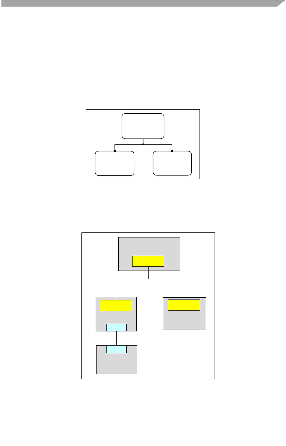
Demo Application
Freescale Semiconductor
72
5.2.3 Demo setup
Figure 5-12 The setup of the Diagnostic Demonstration Applicationshows the setup for diagnostic
communication in the network. The network contains one master node with name LINMaster and
two slave nodes: FontLeftDoor and RearLeftDoor with node address (NAD) are 0x11 and 0x12
respectively.
The slave node RearLeftDoor is configured for execution diagnostic class II. The slave node
FontLeftDoor is configured for execution diagnostic class III.
Due to the diagnostic class III cover services of class II and add some more services, the service of
class II is reused combination with new serviced added.
ECU
RearLeftDoor
Slave (0x12)
ECU
LINMaster
Master
ECU
FrontLeftDoor
Slave (0x11)
Figure 5-12 The setup of the Diagnostic Demonstration Application
5.2.3.1 Hardware description
Base on the demo setup above, the hardware for each node is identical as shown in the figure and
table below.
9S12HY64
(B1)
LIN
TRANSCEIVER
9S12XEP100
(B3)
LIN
TRANSCEIVER
LIN
TRANSCEIVER
9S12G128
(B2)
SCI
SCI
9S08LL64
(B4)
Figure 5-13: Master/Slave hardware configuration
The application utilizes three FSL hardware platforms MC9S12HY64, TWR 9S12G128 and
EVB9S12XEP100 to set up a LIN network as Figure 5-12 The setup of the Diagnostic
Demonstration Application. However, the TWR 9S12G128 board doesn’t have LCD or enough
LEDs to display the signals of FrontLeftDoor node. For this reason, the TWR 9S08LL64 is
used. These boards (9S12G128 & 9S08LL64) are joined together through tower, and
Demo Application
Freescale Semiconductor
73
communicated via SCI. The real hardware sets up as the following Figure 5-14: The real demo
application hardware:
Figure 5-14: The real demo application hardware
5.2.3.2 LCD display
5.2.3.2.1 TWR 9S08LL64 (FrontLeftDoor slave)
The LCD in TWR 9S08LL64 is utilized with two display areas shown in the figure below:
Figure 5-15: The LCD GD-5360P (on the LL64 board) specification
Display description:
1. The LEDs at the position No.1 display the NAD of the target slave
1
2
Demo Application
Freescale Semiconductor
74
2. The LEDs at the position No.2 display the value of FrontLeftDoorSignal of FrontLeftDoor
slave. The signal is sent from the TWR 9S12G128 board.
5.2.3.2.2 DEMO9S12HY64 (RearLeftDoor slave)
The LCD display features in DEMO9S12HY64 are utilized with two display areas which shown in
figures below:
Figure 5-16: The LCD GD-5560P (on the HY64 board) specification
Display description:
1. The LEDs at the position No.1 display the operation mode
2. The LEDs at the position No.2 display the master request (or slave response)
data
3. The LEDs at the position No.3 & No.4 display the FrontLeftDoorSignal and
RearLeftDoorSignal
4. The icon at the position No.5 turns on when the master waits the slave’s response
5. The icon “TRIP A” at the position No.6 turns on when the master’s request is
sent to FrontLeftDoor Node (or slave’s response is received from FrontLeftDoor
Node)
6. The icon “TRIP B” at the position No.6 turns on when the master’s request is
sent to RearLeftDoor Node (or slave’s response is received from RearLeftDoor
Node)
All peripheral devices, which are used in demo application, are listed in Table 4-1:
Table 5-16: Hardware configuration list
Board
Board ID
Responsibility
User I/O
9S12HY64
B1
Master node
Push button: SW1, SW2, SW3 , SW4
LED: LED1, LED2, LED3, LED4
LCD: GD5560P
Potentiometer: RV1
9S12G128
B2
Slave node (0x11)
LED: LED1, LED2, LED3, LED4
Push button: SW1, SW2, SW3 , SW4
Potentiometer: RV1
9S12XEP100
B2
Slave node (0x12)
Potentiometer: RV1
LED: LED-matrix
9S08LL64
B4
Display the
Potentiometer’s value of
9S12G128
LCD: GD5360P
1
2
3
4
5
6
Demo Application
Freescale Semiconductor
75
5.2.4 Operation description
Figure 5-17: Diagnostic operation shows the principle of diagnostic operation in the LIN network.
This is explained in more details in Figure 5-18: Read data by Identifier: UDS = 0x22, SID = 0x0091, Data
record is a sample and Figure 5-19.
Master
Node Slave
Node
LIN bus
Send diag request
Wait for response
Receive response
Receive request
Process request...
Respond to request
Figure 5-17: Diagnostic operation
The diagnostic sequence is to send a request and to wait for a response before continuing with the
next request.
The master node sends a request to slave node via LIN bus. Base on the service definition, the slave
node receives the request and start to process request. After a while, the master requests response
from slave, the data prepared by slave previously will be transmitted by LIN bus.
5.2.4.1 Sequences of frame between Master node and Slave nodes
All frames in communication are defined in table below:
Table 5-17: Operation mode in the demo
No.
Operation
Mode
Description
Frame
Type/PID
Publisher
Subscriber
1
0x00
The LIN network operates in
normal schedule. The master node
reads: FrontLeftDoorSignal from
FrontLeftDoor Node;
RearLeftDoorSignal from
RearLeftDoor Node and displays
them to LCD.
These signals can be changed by
adjusted the slave node’s
Potentiometer
Unconditio
nal Frame
FrontLeftD
oor &
RearLeftD
oor
Master
2
0x20
The Master node prepares data for
master’s request for service: “Read
data by Identifier - Serial number
read (SID = 0x22 & sub-ID =
0x0092)” and displays them on the
LCD.
Master
Request/
0x3C
Master
RearLeftDoo
r
3
0x21
- The Slave will response to the
master’s request (0x22) with two
types:
Positive response: response data
Negative response: response error
Slave
Response/
0x3D
RearLeftD
oor
Master

Demo Application
Freescale Semiconductor
76
code
- The Master node will wait until
received slave’s response and then
display the response to the LCD.
4
0x22
The Master node prepares data for
master’s request for service: “Write
data by Identifier - Serial number
write (SID = 0x2E & sub-ID =
0x0092)” and outputs them to the
LCD.
The serial number can be changed
by changing the define
SERIAL_NUMBER on the source
code
Master
Request/
0x3C
Master
RearLeftDoo
r
5
0x23
- The Slave will response to the
master’s request (0x2E) with two
types:
Positive response: response data
Negative response: response error
code
(If slave response’s type is positive
response, the serial number will be
updated – the master node can read
the updated serial number by calling
the service “read by identifier (SID
= 0x22) with sub-ID = 0092” )
- The Master node will wait until
received slave’s response and then
display the response to the LCD.
Slave
Response/
0x3D
RearLeftD
oor
Master
6
0x30
- The Master node prepares data for
master’s request for service: “IO
control by identifer – IO status read
(SID = 0x22 & sub-ID = 0x0080)”
and displays them to the LCD.
Master
Request/
0x3C
Master
FrontLeftDoo
r
7
0x31
- The Slave will response to the
master’s request (0x22) with two
types:
Positive response: response data
Negative response: response error
code
- The Master node will wait until
received slave’s response and then
display the response to the LCD.
- If the positive response is returned,
the LED status on the master node
(HY64 board) will be updated as the
LED status on the FrontLeftDoor
node (the LL64 board)
Slave
Response/
0x3D
FrontLeftD
oor
Master
8
0x32
- The Master node prepares data for
master’s request for service: “IO
control by identifier – IO status write
(SID = 0x2F & sub-ID = 0x0080) ”
and displays them to the LCD
Master
Request/
0x3C
Master
FrontLeftDoo
r

Demo Application
Freescale Semiconductor
77
- The IO status’ value can be
changed by adjusting the
potentiometer. The value is
displayed both LEDs and LCD (the
last byte on master requested data)
9
0x33
- The Slave will response to the
master’s request (0x2F) with two
types:
Positive response: response data
Negative response: response error
code
- The Master node will wait until
received slave’s response and then
display the response to the LCD.
- If the positive response is returned,
the LED status on the FrontLeftDoor
node (HY64 board) will be updated
as the LED status on the master node
(the G128 board)
Slave
Response/
0x3D
FrontLeftD
oor
Master
10
0x34
- The Master node prepares data for
master’s request for service:
“Session control (0x10), Sub-ID:
(0x01)” and displays them to the
LCD
Master
Request/
0x3C
Master
FrontLeftDoo
r
11
0x35
- The Slave will response to the
master’s request (0x10) with two
types:
Positive response: response data
Negative response: response error
code
- The Master node will wait until
received slave’s response and then
display the response to the LCD.
Slave
Response/
0x3D
FrontLeftD
oor
Master
12
0x36
- The Master node prepares data for
master’s request for service: “Read
DTC (0x19) Sub-ID (0x01)” and
displays them to the LCD
Master
Request/
0x3C
Master
FrontLeftDoo
r
13
0x37
- The Slave will response to the
master’s request (0x10) with two
types:
Positive response: response data
Negative response: response error
code
- The Master node will wait until
received slave’s response and then
display the response to the LCD.
Slave
Response/
0x3D
FrontLeftD
oor
Master
14
0x38
- The Master node prepares data for
master’s request for service: “Clear
Master
Request/
Master
FrontLeftDoo
r

Demo Application
Freescale Semiconductor
78
DTC (0x14)” and displays them to
the LCD
0x3C
15
0x39
- The Slave will response to the
master’s request (0x10) with two
types:
Positive response: response data
Negative response: response error
code
- The Master node will wait until
received slave’s response and then
display the response to the LCD.
Slave
Response/
0x3D
FrontLeftD
oor
Master
Note
The LCD on the master node (the HY64 board) displays the mode
operation at the position No.1, the FrontLeftDoorSignal at the
position No.3, the RearLeftDoorSignal at the No.4 and Master’s request (or
Slave’s response) data at No.2
The LCD on LL64 board (the Front Left Door Node) displays the NAD at
the position No.1, the FrontLeftDoorSignal’s value at No.2. These signals
are sent from TWR 9S12G128 board.
The Led matrix on XEP100 board (the Rear Left Door Node) displays the
NAD or the RearLeftDoorSignal’s value (Press button SW1 to display
NAD, and SW2 to display RearLeftDoorSignal).
5.2.4.2 Reset signal
After resetting the MCU, the node is ready for communication. The status of each board is
described below:
- The LCD on HY64 board displays the mode 0x00. (Please see Table 5.1 for details)
- The LCD on LL64 board displays the value of FrontLeftDoorSignal and the NAD.
- The LED matrix on XEP100 board displays the value of RearLeftDoorSignal.
The LED status of all boards after resetting is OFF.
5.2.4.3 Service Operation
Read data by Identifier: UDS = 0x22, SID = 0x0092
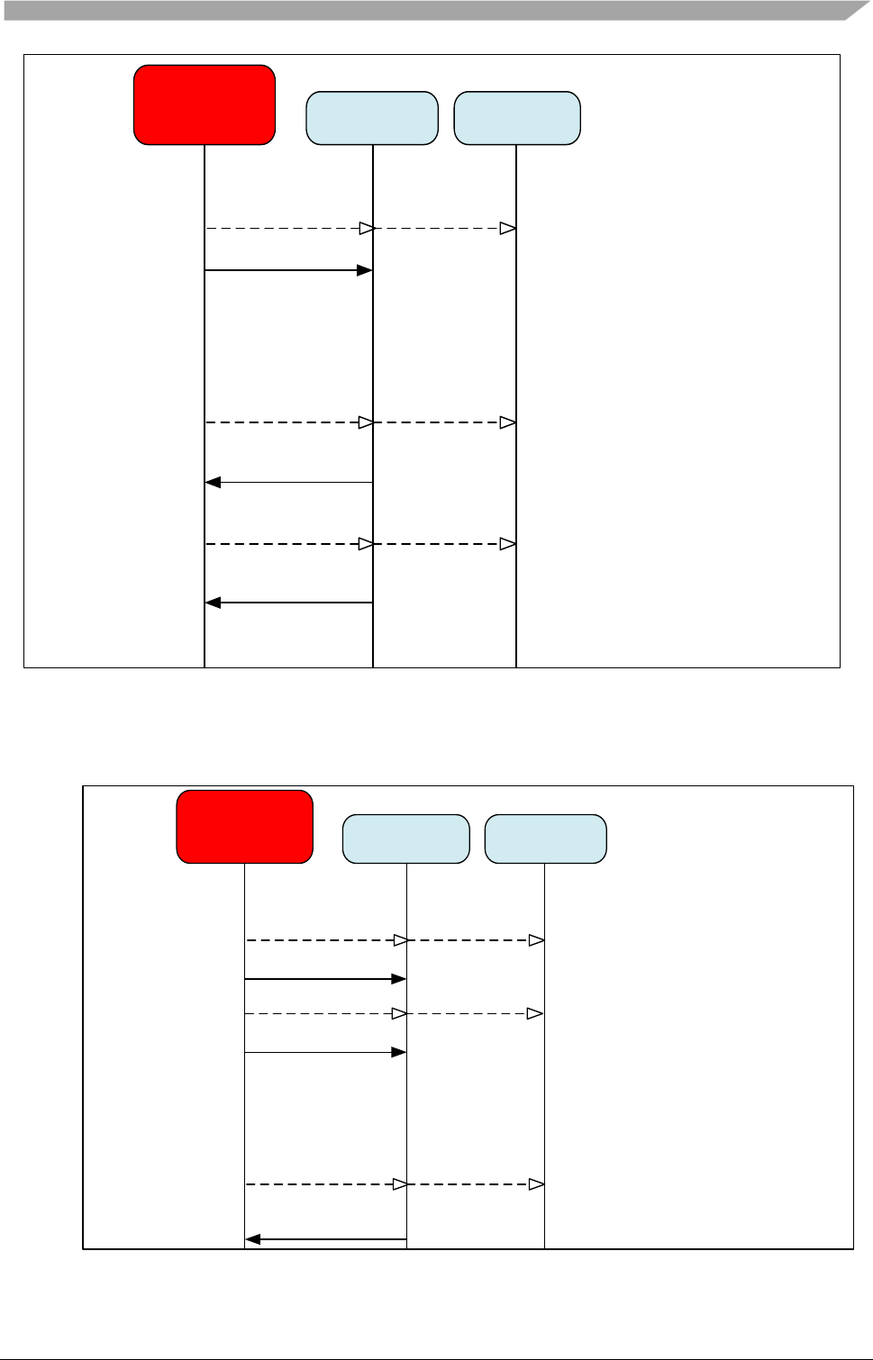
Demo Application
Freescale Semiconductor
79
LINMaster
Master FrontLeftDoor
Slave (0x11) RearLeftDoor
Slave (0x12)
PID = 0x3C
Master sends request to the LIN
bus with UDS = 0x22 Read data by
Identifier SID: (0x0092)
PDU = {0x11, 0x03, 0x22, 0x00,
0x92, 0xFF,0xFF, 0xFF}
Master request
PID = 0x3D
PDU = {0x11, 0x10, 0x07, 0x62,
0x00, 0x92,0x00, 0x02}
PID = 0x3D
PDU = {0x11, 0x21, 0x9B, 0x45,
0xFF, 0xFF,0xFF, 0xFF}
Slave response
Slave response
Data Record
{0x62, 0x00, 0x92,
0x00, 0x02, 0x9B, 0x45}
Process Master request
.
.
.
.
.
.
Wait for response
Figure 5-18: Read data by Identifier: UDS = 0x22, SID = 0x0091, Data record is a sample
Write data by Identifier: UDS = 0x2E, SID = 0x0092
Data Record
{0x6E, 0x00, 0x92}
LINMaster
Master FrontLeftDoor
Slave (0x11) RearLeftDoor
Slave (0x12)
PID = 0x3C
Master sends request to the LIN
bus with UDS = 0x2E Write data
by Identifier SID: (0x0092)
PDU = {0x11, 0x10, 0x07, 0x2E,
0x00, 0x92,0x00, 0x00}
Master request
PID = 0x3D
PDU = {0x11, 0x03, 0x6E, 0x00,
0x92, 0xFF,0xFF, 0xFF}
Slave response
Process Master request
.
.
.
.
.
.
Wait for response
PDU = {0x11, 0x21, 0x00, 0x00,
0xFF, 0xFF,0xFF, 0xFF}
PID = 0x3C
Master request
Figure 5-19: Write data by Identifier: UDS = 0x2E, SID = 0x0092, Data record is a sample
5.2.4.4 Operation on Push button
Demo Application
Freescale Semiconductor
80
Table 5-18: Master node operation on Push button
Action
Result
Push button SW1
The Master node returns to normal schedule, none diagnostic service
is selected. The LCD displays the ForntLeftDoorSignal &
RearLeftDoorSignal from two slave nodes.
Push button SW2
Selecting the diagnostic services for class II. The master request’s data is
displayed on LCD
Push button SW3
Selecting the diagnostic services for class III. The master request’s data is
displayed on LCD
Push button SW4
Sending master request, which is displayed on LCD, to slave node,
and display the slave response’s data which is received on the LCD.
Table 5-19: FrontLeftDoor node (LL64 board) operation on Push button
Action
Result
Push button SW1
Turn on/off LED 1
Push button SW2
Turn on/off LED 2
Push button SW3
Turn on/off LED 3
Push button SW4
Turn on/off LED 4
Table 5-20: RearLeftDoor node (XEP100 board) operation on Push button
Action
Result
Push button SW1
To display NAD on the LED matrix
Push button SW2
To display RearLeftDoorSignal’s value on the LED matrix
5.3 Resynchronization demo application
5.3.1 Introduction
Local interconnect network (LIN) is widely used standard for low cost automotive networks. In
order to ensure reliable communication via LIN bus, a MCU bus clock needs to be accurate enough
to avoid errors. MCU can use crystal or ceramic resonator to provide very accurate bus clocks.
However, LIN protocol was designed to allow more cost-effective solution. An automatic
resynchronization feature allows a cost-effective solution: MCUs can use on-chip oscillators to
implement LIN slaves, even though the on-chip oscillators have less accuracy than a crystal.
The demo application will show the different between the LIN operations with and without
resynchronization feature.
5.3.2 Demo setup
Figure 5-20 Nodes setup of the Resynchronization Demonstration Application shows the setup for
communication in the LIN network. The network contains one master node with name LINMaster
and two slave nodes: FontLeftDoor and RearLeftDoor with node address (NAD) are 0x11 and 0x12
respectively.
The slave node FrontLeftDoor is configured to support the resynchronization feature. But, the slave
node RearLeftDoor is configured without resynchronization feature support.
The master node LINMaster could be able to change baud rate by pressing button.
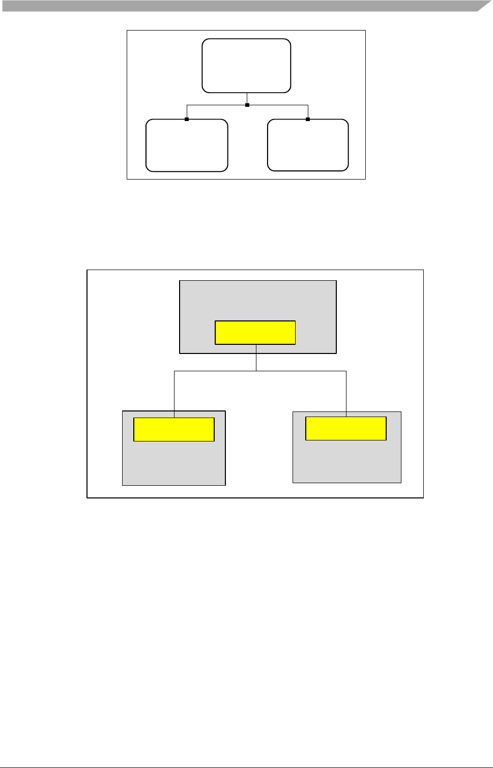
Demo Application
Freescale Semiconductor
81
ECU
RearLeftDoor
Slave (0x12)
ECU
LINMaster
Master
ECU
FrontLeftDoor
Slave (0x11)
Figure 5-20 Nodes setup of the Resynchronization Demonstration Application
5.3.2.1 Hardware description
Base on the demo setup above, the hardware for each node is identical as shown in the figure and
table below.
9S12HY64
(B1)
LIN
TRANSCEIVER
9S08DZ128
(B2)
9S12XEP100
(B3)
LIN
TRANSCEIVER
LIN
TRANSCEIVER
Figure 5-21: Master/Slave hardware configuration
The application utilizes three FSL hardware platforms MC9S12HY64, DEMO9S08DZ128 and
EVB9S12XEP100.
The real hardware sets up as the following Figure 5-22:
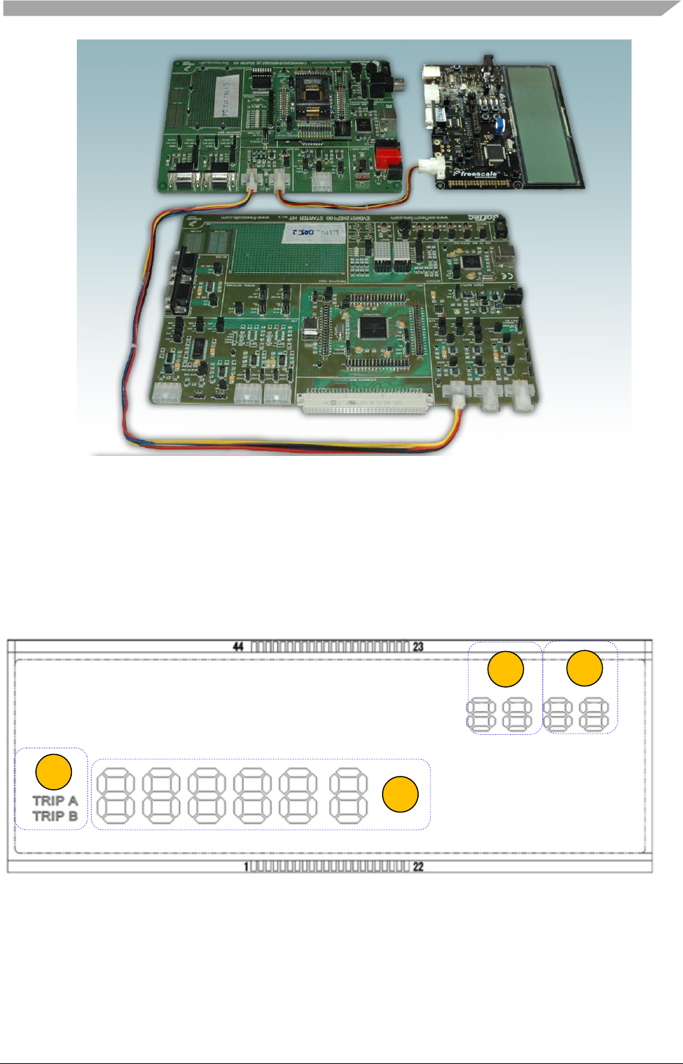
Demo Application
Freescale Semiconductor
82
Figure 5-22: The real demo application hardware
5.3.2.2 LCD Display
5.3.2.2.1 DEMO9S12HY64
The LCD display features in DEMO0S12HY64 are utilized with display areas which shown in
figures below:
Figure 5-23: The LCD GD-5560P (on the HY64 board) specification
Display description:
1 The LEDs at the position No.1 & No.2 display the FrontLeftDoorSignal and
RearLeftDoorSignal
2 The LEDs at the position No.3 display the current baud-rate of master node
3 The icon “TRIP A” at the position No.4 turns off when the master node can’t
receive the signal from FrontLeftDoor Node
3
1
2
4

Demo Application
Freescale Semiconductor
83
4 The icon “TRIP B” at the position No.4 turns off when the master node can’t
receive the signal from RearLeftDoor Node
All peripheral devices, which are used in demo application, are listed in Table 4-1:
Table 5-21: Hardware configuration list
Board
Board ID
Responsibility
User I/O
9S12HY64
B1
Master node
Push button: SW1, SW2, SW3 , SW4
LED: LED1, LED2, LED3, LED4
LCD: GD5560P
Potentiometer: RV1
9S12XEP100
B2
Slave node (0x12)
Potentiometer: RV1
LED: LED-matrix
9S08DZ128
B3
Slave node (0x11)
LED: LED0-7
Potentiometer: RV1
5.3.3 Operation description
This section describes in details functionalities and procedures of each node in Demo application.
The descriptions of each frame and direction of message transmitting between physicals nodes of
the network is listed on the following table
Table 5-22: Sequence frames between nodes of the network
PID
Frame’s Name
Publisher
Subscriber
Description
0x01
FrontLeftDoorMessag
e
FrontLeftDoor
Master
The current POT value of
FrontLeftDoor Node
0x02
RearLeftDoorMessage
RearLeftDoor
Master
The current POT value of
RearLeftDoor Node
0x05
MastertoRearControl
Master
RearLeftDoor
Master sends a “verify”
data to RearLeftDoor
Signal
0x07
ReartoMasterMessage
RearLeftDoor
Master
RearLeftDoorSignal sends
a “verify” data, which is
received from master node,
back to master node.
0x06
MastertoFrontControl
Master
FrontLeftDoo
r
Master sends a “verify”
data to FrontLeftDoor
Signal
0x08
FronttoMasterMessage
FrontLeftDoor
Master
FrontLeftDoorSignal sends
a “verify” data, which is
received from master node,
back to master node.
To verify that LIN network works correctly when the baud-rate is changed, the master node sends a
signal to each slave node. Then, the slave node sends it back, the master node will compare two
signals, one which is sent to slave node, one which is received from slave node. If the two signals is
not equal, the master-node turns LEDs on to notify that the LIN network doesn’t work correctly.
Besides, the user can check by change the POT value. The master node displays the POT values
which are received from two slave nodes on the LCD. When the values which are displayed on
master node’s LCD, is not match with the POT’s values which are displayed on LED of each board,
it is stated that the transmitting and receiving signal via the network is not correctly.
Note

Demo Application
Freescale Semiconductor
84
- The LED 1&2 on the HY64 board is turned on when the master
cannot receive signals from FrontLeftDoor correctly
- The LED 3&4 on the HY64 board is turned on when the master
cannot receive signals from RearLeftDoor correctly
5.3.3.1 Reset signal
After resetting the MCU, the node is ready for communication. The status of each board is
described below:
- The LCD on HY64 board displays the network’s baud-rate, and the RearLeftDoorSignal ‘s
and FrontLeftDoorSignal’s values which are received from two slave node.
- The LED matrix on XEP100 board displays the value of RearLeftDoorSignal.
- The LED on DZ128 board displays the value of FrontLeftDoorSignal
The LED status of all boards after resetting is OFF.
5.3.3.2 Operation on Push button
Table 5-23: Master node operation on Push button
Action
Result
Push button SW1
Increase the master baud-rate and the baud-rate is displays on
the LCD
Push button SW2
Decrease the master baud-rate and the baud-rate is displays on the LCD

Appendix A
List of API function
Name of API function
Master
Support
Slave
Support
LIN2.x
Support
J2602
Support
Description
l_sys_init
Initializes the LIN
system
l_bool_rd
Reads a 1-bit signal
l_u8_rd
Reads a 2- to 8-bit signal
l_u16_rd
Reads a 9- to 16-bit
signal
l_bytes_rd
Reads byte assignment
signals
l_bool_wr
Writes a 1-bit signal
l_u8_wr
Writes a 2- to 8-bit
signals
l_u16_wr
Writes a 9- to 16-bit
signals
l_bytes_wr
Writes data for a byte-
assignment signal
l_flg_tst
Tests a flag
l_flg_clr
Clears a flag
l_sch_set
Sets a schedule
l_sch_tick
Executes a schedule
l_ifc_goto_sleep
Reserves a sleep
command
l_ifc_init
Initializes the interface
l_ifc_wake_up
Outputs a wake-up signal
l_ifc_read_status
Acquires state
information
l_sys_irq_disable
Disable LIN related IRQ
l_sys_irq_restore
Enable LIN related IRQ
l_ifc_connect
Connect the interface to
the LIN cluster
l_ifc_disconnect
Disconnect the interface
to the LIN cluster
ld_assign_NAD
Assigns NAD value
ld_conditional_change_NAD
Assigns conditional
NAD value
ld_read_by_id
Read property associated
with id
ld_is_ready
Verifies a state of node
setting
ld_check_response
Acquires the state

Appendix
Freescale Semiconductor
86
information on response
ld_assign_frame_id_range
Assigns the protected
identifier by range
ld_assign_frame_id
Assigns the protected
identifier
diag_read_data_by_identifier
Read data by identifier
diagnostic class II
service
diag_write_data_by_identifie
r
Write data by identifier
diagnostic class II
service
diag_session_control
Session control
diagnostic class III
service
diag_fault_memory_read
Read fault memory
diagnostic service
diag_fault_memory_clear
Clear fault memory
diagnostic service
diag_IO_control
Input/Output control by
identifier diagnostic
service
diag_get_flag
Get diagnostic service’s
flag.
diag_clear_flag
Clear diagnostic
service’s flag.

Appendix
Freescale Semiconductor
87
Appendix B
LIN Configure File (LDF) for sample application
The completed sample LDF file for LIN2.x network demo master gateway is as follows
LIN_description_file;
LIN_protocol_version = "2.1";
LIN_language_version = "2.1";
LIN_speed = 19.2 kbps;
Nodes {
Master: MasterNode, 5 ms, 0.1 ms ;
Slaves: Gateway ;
}
Signals {
Cluster1Potentiometer1: 8, 0, Gateway, MasterNode;
Cluster1LightSensor1: 8, 0, Gateway, MasterNode;
Cluster1Potentiometer2: 8, 0, Gateway, MasterNode;
Cluster2PotentiometerA: 8, 0, Gateway, MasterNode;
Cluster2LightSensorA: 8, 0, Gateway, MasterNode;
Cluster2PotentiometerB: 8, 0, Gateway, MasterNode;
Cluster2PotentiometerC: 8, 0, Gateway, MasterNode;
GatewayError: 1, 0, Gateway, MasterNode;
ClusterIdentifier: 2, 0, MasterNode, Gateway;
}
Diagnostic_signals {
MasterReqB0: 8, 0 ;
MasterReqB1: 8, 0 ;
MasterReqB2: 8, 0 ;
MasterReqB3: 8, 0 ;
MasterReqB4: 8, 0 ;
MasterReqB5: 8, 0 ;
MasterReqB6: 8, 0 ;
MasterReqB7: 8, 0 ;
SlaveRespB0: 8, 0 ;
SlaveRespB1: 8, 0 ;
SlaveRespB2: 8, 0 ;
SlaveRespB3: 8, 0 ;
SlaveRespB4: 8, 0 ;
SlaveRespB5: 8, 0 ;
SlaveRespB6: 8, 0 ;
SlaveRespB7: 8, 0 ;
}
Frames {
GatewayControl: 1, MasterNode, 1 {
ClusterIdentifier, 0;
}
PotentiometerInfo: 2, Gateway, 5 {
Cluster1Potentiometer1, 0;
Cluster1Potentiometer2, 8;
Cluster2PotentiometerA, 16;
Cluster2PotentiometerB, 24;
Cluster2PotentiometerC, 32;
}
LightSensorInfo: 3, Gateway, 3 {
Cluster1LightSensor1, 0;
Cluster2LightSensorA, 8;

Appendix
Freescale Semiconductor
88
GatewayError, 16;
}
}
Sporadic_frames {
SporadicControlFrame: GatewayControl;
}
Diagnostic_frames {
MasterReq: 0x3c {
MasterReqB0, 0 ;
MasterReqB1, 8 ;
MasterReqB2, 16 ;
MasterReqB3, 24 ;
MasterReqB4, 32 ;
MasterReqB5, 40 ;
MasterReqB6, 48 ;
MasterReqB7, 56 ;
}
SlaveResp: 0x3d {
SlaveRespB0, 0 ;
SlaveRespB1, 8 ;
SlaveRespB2, 16 ;
SlaveRespB3, 24 ;
SlaveRespB4, 32 ;
SlaveRespB5, 40 ;
SlaveRespB6, 48 ;
SlaveRespB7, 56 ;
}
}
Node_attributes {
Gateway{
LIN_protocol = "2.1";
configured_NAD = 0x1;
initial_NAD = 0xa;
product_id = 0x1e, 0x1, 0;
response_error = GatewayError;
P2_min = 100 ms;
ST_min = 20 ms;
N_As_timeout = 1000 ms;
N_Cr_timeout = 1000 ms;
configurable_frames {
GatewayControl;
PotentiometerInfo;
LightSensorInfo;
}
}
}
Schedule_tables {
NormalTable {
PotentiometerInfo delay 50 ms;
LightSensorInfo delay 50 ms;
SporadicControlFrame delay 20 ms;
}
}
Node Private File (NPF) for sample application

Appendix
Freescale Semiconductor
89
The NPF of the node which participates in the gateway is given as follow (the node might
participate to other LIN networks)
/*** GENERAL DEFINITION ***/
LIN_node_config_file;
/*** MCU DEFINITION ***/
mcu { /* Must check the correct MCU name */
mcu_name = MC9S12XEP100;
bus_clock = 8000000; /* Frequency bus of system Hz*/
xgate_support = no; /* Support XGATE Co-Processor */
}
/*** LIN HARDWARE DEFINITION ***/
/* SCI config */
sci{
s12_sci0{
sci_channel = 1; /* Check validation of sci_channel */
timer_channel = 0;
}
s12_sci1{
sci_channel = 3; /* Channel setting */
timer_channel = 1;
}
s12_sci2{
sci_channel = 5; /* Channel setting */
timer_channel = 2;
}
}
/*** NETWORK DEFINITION ***/
network {
idle_timeout = 4s;
diagnostic_class = 1; /* Class selection to use diagnostic
services */
LI0{
node = Gateway;
file = "Demo_Master_Gateway.ldf";
device = s12_sci0;
}
LI1{
node = Gateway;
file = "Demo_Cluster1.ldf";
device = s12_sci1;
}
LI2{
node = Gateway;
file = "Demo_Cluster2.ldf";
device = s12_sci2;
}
}

Appendix
Freescale Semiconductor
90
Appendix C
Data Reference for Node Configuration Tool
mcu_info_sci{
MC9S12XEP100, SCI_V5, _S12X_, 0x00C8, 0x00D0, 0x00B8, 0x00C0,
0x0130, 0x0138;
MC9S12XEQ512, SCI_V5, _S12X_, 0x00C8, 0x00D0, 0x00B8, 0x00C0,
0x0130, 0x0138;
MC9S12XDP512, SCI_V5, _S12X_, 0x00C8, 0x00D0, 0x00B8, 0x00C0,
0x0130, 0x0138;
MC9S12XET256, SCI_V5, _S12X_, 0x00C8, 0x00D0, 0x00B8, 0x0130;
MC9S12XF512, SCI_V5, _S12X_, 0x00C8, 0x00D0;
MC9S12XS128, SCI_V5, _S12_, 0x00C8, 0x00D0;
MC9S12XS256, SCI_V5, _S12_, 0x00C8, 0x00D0;
MC9S12GN32, SCI_V5, _S12_, 0x00C8;
MC9S12G64, SCI_V5, _S12_, 0x00C8, 0x00D0;
MC9S12HY64, SCI_V5, _S12_, 0x00C8;
MC9S12P128, SCI_V5, _S12_, 0x00C8;
MC9S12XHY256, SCI_V5, _S12_, 0x00C8, 0x00D0;
MC9S12G128, SCI_V5, _S12_, 0x00C8, 0x00D0, 0x00E8;
MC9S12G240, SCI_V5, _S12_, 0x00C8, 0x00D0, 0x00E8;
MC9S12VR64, SCI_V6, _S12_, 0x00C8, 0x00D0;
MC9S12VR32, SCI_V6, _S12_, 0x00C8, 0x00D0;
MC9S12ZVML128,SCI_V6, _S12_, 0x0700,0x0710;
MM912F634, SCI_V4, _S12_, 0x0240;
MM912G634, SCI_V4, _S12_, 0x0240;
MM912H634, SCI_V4, _S12_, 0x0240;
MM912J637, SCI_V4, _S12_, 0x0218;
MC9S12I64, SCI_V4, _S12_, 0x0240;
MM9Z1J638, SCI_V4, _S12_, 0x0E18;
MC9S08DZ60, SCI_V4, _S08_, 0x0038, 0x0040;
MC9S08DZ128, SCI_V4, _S08_, 0x0038, 0x0040;
MC9S08EL32, SCI_V4, _S08_, 0x0038;
MC9S08SG4, SCI_V4, _S08_, 0x0038;
MC9S08SG8, SCI_V4, _S08_, 0x0038;
MC9S08SG32, SCI_V4, _S08_, 0x0038;
MC9S08MP16, SCI_V4, _S08_, 0x0068;
MC9S08LL64, SCI_V4, _S08_, 0x0020, 0x1858;
MC9S08LG32, SCI_V4, _S08_, 0x0010, 0x0018;
MC9S08SC4, SCI_V4, _S08_, 0x0038;
MC9S08AW60, SCI_V2, _S08_, 0x0038, 0x0040;
MC9S08AW16A, SCI_V2, _S08_, 0x0038, 0x0040;
MC9S08RN60, SCI_V4, _S08_, 0x3080, 0x3088, 0x3090;
MC9S12ZVL32, SCI_V6, _S12_, 0x0700, 0x0710;
MC9S12ZVL128, SCI_V6, _S12_, 0x0700,0x0710;
MC9S12ZVML31, SCI_V6, _S12_, 0x0700,0x0710;
MC9S12ZVHY64, SCI_V6, _S12_, 0x0700, 0x0710;
MC9S12ZVH128, SCI_V6, _S12_, 0x0700, 0x0710;
MC9S12ZVC64, SCI_V6, _S12_, 0x0700, 0x0710;
MC9S12ZVMC256,SCI_V6, _S12_, 0x0700, 0x0710;
}
mcu_info_gpio{
MC9S08QD4;
}
mcu_info_slic{
MC9S08EL32;

Appendix
Freescale Semiconductor
91
}
mcu_info_uart{
SKEAZN84, _K_, 0x4006A000;
SKEAZN642, _K_, 0x4006A000, 0x4006B000, 0x4006C000;
SKEAZ1284, _K_, 0x4006A000, 0x4006B000, 0x4006C000;
}

How to Reach Us:
Home Page:
www.freescale.com
Web Support:
http://www.freescale.com/support
USA/Europe or Locations Not Listed:
Freescale Semiconductor
Technical Information Center, EL516
2100 East Elliot Road
Tempe, Arizona 85284
+1-800-521-6274 or +1-480-768-2130
www.freescale.com/support
Europe, Middle East, and Africa:
Freescale Halbleiter Deutschland GmbH
Technical Information Center
Schatzbogen 7
81829 Muenchen, Germany
+44 1296 380 456 (English)
+46 8 52200080 (English)
+49 89 92103 559 (German)
+33 1 69 35 48 48 (French)
www.freescale.com/support
Japan:
Freescale Semiconductor Japan Ltd.
Headquarters
ARCO Tower 15F
1-8-1, Shimo-Meguro, Meguro-ku,
Tokyo 153-0064
Japan
0120 191014 or +81 3 5437 9125
support.japan@freescale.com
Asia/Pacific:
Freescale Semiconductor China Ltd.
Exchange Building 23F
No. 118 Jianguo Road
Chaoyang District
Beijing 100022
China
+86 10 5879 8000
support.asia@freescale.com
For Literature Requests Only:
Freescale Semiconductor Literature Distribution Center
1-800-441-2447 or +1-303-675-2140
Fax: +1-303-675-2150
LDCForFreescaleSemiconductor@hibbertgroup.com
Document Number: LIN_STACK_UG
Rev. 2.5.3
Information in this document is provided solely to enable system
and software implementers to use Freescale Semiconductors
products. There are no express or implied copyright licenses
granted hereunder to design or fabricate any integrated circuits or
integrated circuits based on the information in this document.
Freescale Semiconductor reserves the right to make changes
without further notice to any products herein. Freescale
Semiconductor makes no warranty, representation, or guarantee
regarding the suitability of its products for any particular purpose,
nor does Freescale Semiconductor assume any liability arising out
of the application or use of any product or circuit, and specifically
disclaims any liability, including without limitation consequential or
incidental damages. "Typical" parameters that may be provided in
Freescale Semiconductor data sheets and/or specifications can
and do vary in different applications and actual performance may
vary over time. All operating parameters, including "Typicals",
must be validated for each customer application by customer's
technical experts. Freescale Semiconductor does not convey any
license under its patent rights nor the rights of others. Freescale
Semiconductor products are not designed, intended, or authorized
for use as components in systems intended for surgical implant
into the body, or other applications intended to support or sustain
life, or for any other application in which failure of the Freescale
Semiconductor product could create a situation where personal
injury or death may occur. Should Buyer purchase or use
Freescale Semiconductor products for any such unintended or
unauthorized application, Buyer shall indemnify Freescale
Semiconductor and its officers, employees, subsidiaries, affiliates,
and distributors harmless against all claims, costs, damages, and
expenses, and reasonable attorney fees arising out of, directly or
indirectly, any claim of personal injury or death associated with
such unintended or unauthorized use, even if such claims alleges
that Freescale Semiconductor was negligent regarding the design
or manufacture of the part.
RoHS-compliant and/or Pb-free versions of Freescale products
have the functionality and electrical characteristics as their non-
RoHS-complaint and/or non-Pb-free counterparts. For further
information, see http://www.freescale.com or contact your
Freescale sales representative. For information on Freescale's
Environmental Products program, go to
http://www.freescale.com/epp. Freescale™ and the Freescale logo
are trademarks of Freescale Semiconductor, Inc. All other product
or service names are the property of their respective owners.
© 2010 Freescale Semiconductor, Inc.
AUTOSAR and AUTOSAR logo are registered trademarks of
AUTOSAR GbR
(www.autosar.org)
