Size LLT2020
User Manual: LLT2020
Open the PDF directly: View PDF ![]() .
.
Page Count: 34
CODE : 00Z
qSERVICE MANUAL
CONTENTS
Parts marked with " " are important for maintaining the safety of the set. Be sure to replace these parts with specified
ones for maintaining the safety and performance of the set.
SHARP CORPORATION This document has been published to be used
for after sales service only.
The contents are subject to change without notice.
LLT2020SME
LCD MONITOR
MODEL LL-T2020
CHAPTER 1. OUTLINE OF THE PRODUCT,
NOMENCLATURE AND FUNCTION. . . . . . . . . . . . . . . . . .1 - 1
CHAPTER 2. CONNECTION, ADJUSTMENT,
OPERATION, AND FUNCTIONS. . . . . . . . . . . . . . . . . . . . .2 - 1
CHAPTER 3. DISASSEMBLY AND ASSEMBLY. . . . . . . . . . . . . . . . . . . .3 - 1
CHAPTER 4. TROUBLESHOOTING . . . . . . . . . . . . . . . . . . . . . . . . . . . . .4 - 1
CHAPTER 5. WAVE FORM . . . . . . . . . . . . . . . . . . . . . . . . . . . . . . . . . . . .5 - 1
CHAPTER 6. BLOCK DIAGRAM . . . . . . . . . . . . . . . . . . . . . . . . . . . . . . . .6 - 1
CHAPTER 7. CIRCUIT DIAGRAM. . . . . . . . . . . . . . . . . . . . . . . . . . . . . . .7 - 1
CHAPTER 8. PARTS LAYOUT . . . . . . . . . . . . . . . . . . . . . . . . . . . . . . . . .8 - 1
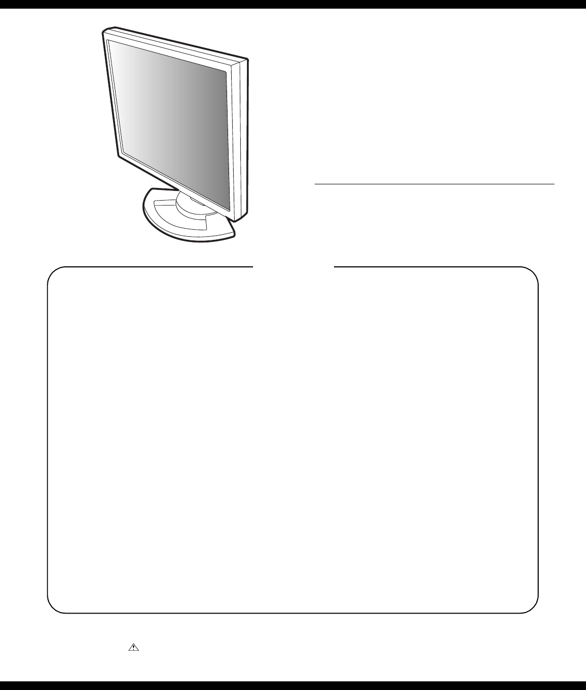
LL-T2020 OUTLINE OF THE PRODUCT, NOMENCLATURE AND FUNCTION
1 – 1
CHAPTER 1. OUTLINE OF THE PRODUCT, NOMENCLATURE AND FUNCTION
1. SPECIFICATIONS
■
■■
■ Product specifications
• LCD display
51 cm measured diagonally
Advanced Super-V and Anti Glare Low Reflection
TFT LCD module
• Resolution (max.)
UXGA 1600 x 1200 pixels
• Displayable colors (max.)
Approx. 16.77 million colors (8 bit)
• Brightness (max.)
220cd/m2
• Dot pitch
0.255 (H) x 0.255 (V) mm
• Contrast ratio
350 : 1
• Angle of visibility
Left-right 170° ; Up-down 170° (contrast ratio 10)
• Screen display size
Horizontal 408 mm x Vertical 306 mm
• Video signal
Analog: Analog RGB (0.7Vp-p) [75Ω]
Digital: DVI standard based on 1.0
• Sync signal
Separate Sync (TTL level: +/-), Sync on Green, Composite Sync
(TTL level: +/-)
• Expansion compensation
Digital scaling
(Enlargement VGA/SVGA/XGA/SXGA etc. to full screen size.)
• Plug & Play
VESA DDC2B compatible
• Power management
VESA: based on DPMS
DVI: based on DMPM
• Input signal terminal
29 pin DVI-I x 2
• USB hub function
1 upstream port, 2 downstream ports
(selfpowered hub based on USB standard Rev 1.1)
• Height adjustment
Adjustment range: Approx. 60 mm
• Screen rotation
Clockwise 0 - 90°
• Screen tilt
Upward approx. 0 - 30° ; downward approx. 0 - 5°
• Screen swivel
Approx. 90° from left through right
• Power supply
AC100 - 240V, 50/60Hz
• Temperature of operating environment
5 - 35°C
• Power consumption
53W (Not using USB hub)
(60W maximum, 3W when in power-saving mode)
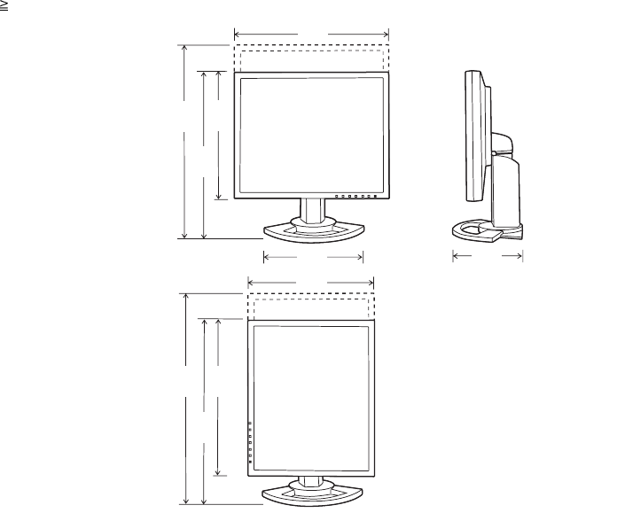
• Dimensions (W x D x H) (Units: mm)
With long width screen: 450 x 228 x 438 - 498
With long height screen: 348 x 228 x 490 - 550
• Weight
Approx. 10 kg
Display area only, approx. 6.5kg
■
■■
■ Dimensions (Units: mm)
• Analog signal cable: Approx. 2.0m
• Digital signal cable: Approx. 2.0m
• USB cable: Approx. 2.0m
• Digital signal cable, NL-C04J (purchased separately): Approx. 2.0m
• Analog signal cable, NL-C02E (purchased separately): Approx. 2.0m
• 2-input cable, NL-C03J (purchased separately): Approx. 0.25m
450
228
438
348
498
348
490
450
550
310
LL-T2020 OUTLINE OF THE PRODUCT, NOMENCLATURE AND FUNCTION
1 – 2
■
■■
■ Relevant signal timings (analog)
• Recommended resolution is 1600 x 1200.
• All are compliant only with non-interlaced.
• Frequencies for Power Macintosh and the Sun Ultra series are refer-
ence values. To connect, another adapter (commercially available)
may be required.
• If the monitor is receiving timing signals that are not compatible, [OUT
OF TIMING] will appear.
Follow your computer's instruction manual to set the timing so that it
is compatible with the monitor.
• If the monitor is not receiving any signal (synch signal), [NO SIGNAL]
will appear.
■
■■
■ Relevant signal timings (digital)
• Recommended resolution is 1600 x 1200.
• All are compliant only with non-interlaced.
• A computer with an output terminal conforming to DVI (DVI-D24 pin
or DVI-I29 pin) and with UXGA output capability can be connected
here.
(Depending on the type of computer to be connected, the display may
not work correctly.)
• If the monitor is receiving timing signals that are not compatible, [OUT
OF TIMING] will appear.
Follow your computer's instruction manual to set the timing so that it
is compatible with the monitor.
• If the monitor is not receiving any signal (synch signal), [NO SIGNAL]
will appear.
■
■■
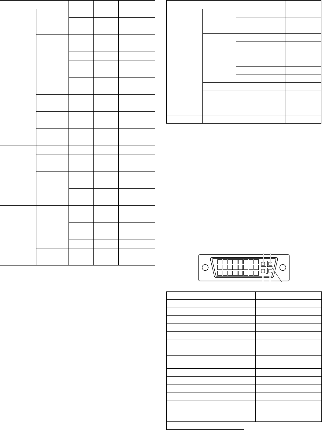
■ The DVI-I input connector pin
(DVI-I connector with 29 pins)
Display mode Hsync Vsync Dot frequency
VESA 640 x 480 31.5kHz 60Hz 25.175MHz
37.9kHz 72Hz 31.5MHz
37.5kHz 75Hz 31.5MHz
800 x 600 35.1kHz 56Hz 36.0MHz
37.9kHz 60Hz 40.0MHz
48.1kHz 72Hz 50.0MHz
46.9kHz 75Hz 49.5MHz
1024 x 768 48.4kHz 60Hz 65.0MHz
56.5kHz 70Hz 75.0MHz
60.0kHz 75Hz 78.75MHz
1152 x 864 67.5kHz 75Hz 108.0MHz
1280 x 960 60.0kHz 60Hz 108.0MHz
1280 x 1024 64.0kHz 60Hz 108.0MHz
80.0kHz 75Hz 135.0MHz
1600 x 1200 75.0kHz 60Hz 162.0MHz
US text 720 x 400 31.5kHz 70Hz 28.3MHz
Power
Macintosh
series
640 x 480 35.0kHz 66.7Hz 30.2MHz
832 x 624 49.7kHz 74.6Hz 57.3MHz
1024 x 768 60.2kHz 75Hz 80.0MHz
1152 x 870 68.7kHz 75Hz 100.0MHz
1280 x 1024 64.0kHz 60Hz 108.0MHz
80.0kHz 75Hz 135.0MHz
1600 x 1200 75.0kHz 60Hz 162.0MHz
Sun Ultra
series 1024 x 768 48.3kHz 60Hz 64.13MHz
53.6kHz 66Hz 70.4MHz
56.6kHz 70Hz 74.25MHz
1152 x 900 61.8kHz 66Hz 94.88MHz
71.8kHz 76.2Hz 108.23MHz
1280 x 1024 71.7kHz 67.2Hz 117.01MHz
81.1kHz 76Hz 134.99MHz
Display mode Hsync Vsync Dot frequency
VESA 640 x 480 31.5kHz 60Hz 25.175MHz
37.9kHz 72Hz 31.5MHz
37.5kHz 75Hz 31.5MHz
800 x 600 37.9kHz 60Hz 40.0MHz
48.1kHz 72Hz 50.0MHz
46.9kHz 75Hz 49.5MHz
1024 x 768 48.4kHz 60Hz 65.0MHz
56.5kHz 70Hz 75.0MHz
60.0kHz 75Hz 78.75MHz
1152 x 864 67.5kHz 75Hz 108.0MHz
1280 x 960 60.0kHz 60Hz 108.0MHz
1280 x 1024 64.0kHz 60Hz 108.0MHz
1600 x 1200 75.0kHz 60Hz 162.0MHz
US text 720 x 400 31.5kHz 70Hz 28.3MHz
No.
Function
No.
Function
1 TMDS data 2- 16 Hot plug detection
2 TMDS data 2+ 17 TMDS data 0-
3 TMDS data 2/4 shield 18 TMDS data 0+
4 N.C. 19 TMDS data 0/5 shield
5N.C. 20N.C.
6 DDC clock 21 N.C.
7 DDC data 22 TMDS clock shield
8 Analog vertically
synchronised signal 23 TMDS clock +
9 TMDS data 1- 24 TMDS clock -
10 TMDS data 1+ C1 Analogue red image signal
11 TMDS data 1/3 shield C2 Analogue green image signal
12 N.C. C3 Analogue blue image signal
13 N.C. C4 Analogue horizontally
synchronised signal
14 +5V C5 Analogue GND
15 GND
1 7
6
5432 8
9
15
14
13121110 16
17 23
22
21201918 24
C1 C2
C3 C4 C5
LL-T2020 OUTLINE OF THE PRODUCT, NOMENCLATURE AND FUNCTION
1 – 3
■
■■
■ Power management
The monitor is based on the VESA DPMS and the DVI DMPM stan-
dards.
To activate the monitor's Power Management function, both the video
card and the computer must conform to the VESA DPMS standard and
the DVI DMPM standard.
DPMS: Display Power Management Signalling
Not using USB hub
DMPM: Digital Monitor Power Management
Not using USB hub
■
■■
■ DDC (Plug & Play)
This monitor supports the VESA DDC (Display Data Channel) standard.
DDC is a signal standard for carrying out Plug & Play functions on the
monitor or PC. It transfers information such as degree of resolution
between the monitor and PC. You can use this function if your PC is
DDC compliant and if it is set so that it can detect the Plug & Play mon-
itor.
There are many varieties of DDC due to the differences between sys-
tems. This monitor works with DDC2B.
2. PRODUCT DESCRIPTION
DPMS mode Screen Power
consumption H-sync V-sync
ON Display on 53W Yes Yes
STANDBY
Display off 3W
No Yes
SUSPEND Yes No
OFF No No
DMPM mode Screen Power
consumption
ON Display on 53W
OFF Display off 3W
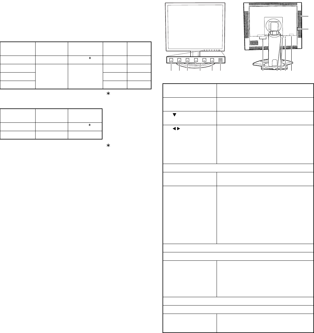
1. INPUT button To switch between the signal's input termi-
nals.
2. MENU button This button is used to pop-up, select and
close the OSD (On Scree Display) Menu.
3. button This button is used to select menu options
when the OSD Menu is displayed.
4. buttons When the OSD Menu is displayed:
These buttons are used to increase or
decrease the value of a selected option.
When the OSD Menu is not displayed:
These buttons are used to adjust back-
light brightness.
5. Power button
6. Power LED This LED is lit green when in use and
orange when in power-saving mode.
7. DVI-I input terminal The computer's digital RGB output terminal
or analogue RGB output terminal can be
connected here.
For a digital signal input: It can be con-
nected to a computer with a DVI-compatible
output terminal (DVI-D24 pin or DVI-I29 pin)
and which has UXGA output ability.
Depending on the computer to be con-
nected, correct display may or may not be
possible.
8. USB port (upstream: 1 port)
9. USB port (downstream: 2 ports)
10.Security lock anchor By connecting a security lock (commercially
available) to the security lock anchor, the
monitor is fixed so that it cannot be trans-
ported.
The security slot works in conjunction with
Kensington Micro Saver Security Systems.
11.Power terminal
12.Main power switch
13.Ventilation openings Note: Never block the ventilation openings
as this may lead to overheating inside
the monitor and result in malfunction.
123 4 56 7 89
10 11
12
13
LL-T2020 OUTLINE OF THE PRODUCT, NOMENCLATURE AND FUNCTION
1 – 4
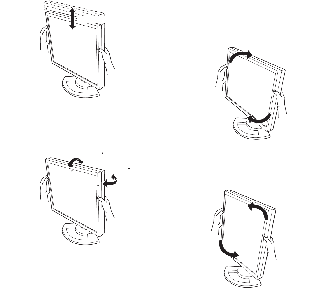
■
■■
■ Height adjustment, angle adjustment, rotation (long height/width)
Caution:
• Pressure from hands on the LCD panel could cause damage.
• Be careful not to allow your fingers to be pinched.
1) Height adjustment
Adjust to an easy to view height.
2) Angle adjustment
Adjust to an easy to view angle.
3) Rotation (long height/width)
The display can be rotated for a long height or width to suit the dis-
played content.
• Before rotating, move the display to its uppermost position. If the dis-
play is rotated while it is set low, it will contact the stand and could
lead to damage.
• The display can only be rotated through a range of 90°. Applying
excessive force may cause malfunction.
• Do not apply excessive force when the cable is connected.
To set to long height
Gently turn in the clockwise direction (to 90°).
To set to long width
Gently turn in the counterclockwise direction (to 90°).
Note: The orientation of the display can be changed using Pivot Soft-
ware.
Approx. 60mm
approx. 45
approx. 45
approx. 30
approx. 5
LL-T2020 CONNECTION, ADJUSTMENT, OPERATION, AND FUNCTIONS
2 – 1
CHAPTER 2. CONNECTION, ADJUSTMENT, OPERATION, AND FUNCTIONS
1. CONNECTING THE MONITOR AND TURNING THE MONITOR ON AND OFF
Caution:
• When connecting, ensure that both the monitor and computer are
switched off.
• Be careful not to overly bend the cable or add extension cords as
this could lead to a malfunction.
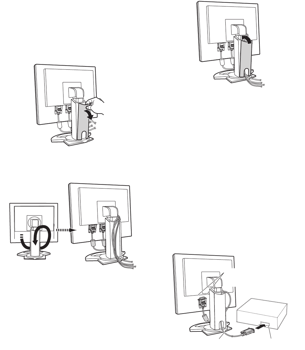
Cable storage
If necessary, excess cable can be housed in the stand.
1. Remove the cover.
Gently pull the top of the cover towards yourself.
2. Run cable along the back of the stand.
Pass cable in front of the stand, and then bring it through the back.
• If the display is to be rotated, first house the cables with the dis-
play in the long height position, so there is sufficient length when
the display is turned.
3. Refit the cover.
Be careful not to pinch the cable.
• If the cover is hard to refit, do not force it.
Check whether cables are trapped.
Caution: If the display is to be rotated, first house the cable, and then
check while gently turning the display. If it cannot be turned,
rehouse the cable with sufficient slack. (If there is insufficient
cable length, rotation will be impossible. Forcing rotation may
cause cable disconnection.)
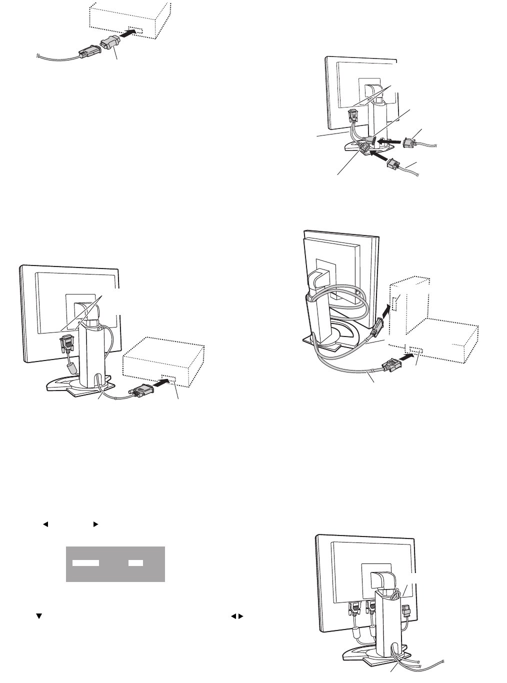
1-1. Connecting the monitor to a computer
The accessory signal cable enables connection of two computers.
(One analog and one digital connection.)
• To achieve an analog and digital connection for two computers, a
separately sold signal cable is required.
• The separately sold 2-input cable enables connection of two comput-
ers to the DVI-I input terminal.
• When using the 2-input cable, set the connecting input terminal
[INPUT-1] or [INPUT-2] to [2LINES] under the MODE SELECT-1
Menu.
■
■■
■ Analog connection
Connect the analog signal cable to the analog RGB output terminal of
the computer.
• Paying attention to connector direction, firmly insert the signal cable
to terminal, and then tighten the screws at both sides.
Input terminal 1 and 2
You can connect to
either side.
Analog RGB output
terminal
Analog signal cable
LL-T2020 CONNECTION, ADJUSTMENT, OPERATION, AND FUNCTIONS
2 – 2
If connecting to a D-sub 15 pin 2 row Apple Power Macintosh, attach a
Macintosh conversion adapter (commercially available) to the analog
signal cable.
Note: If connecting to the Sun Ultra series, a conversion adapter (com-
mercially available) may be required.
■
■■
■ Digital connection
Connect the digital signal cable to the digital RGB output terminal of the
computer.
• For digital RGB connection, the monitor has an input for connecting
to a computer with a DVI-compatible output connector (DVI-D 24 pin
or DVI-I 29 pin) and UXGA output capability.
(Depending on the type of computer to be connected, the display may
not work correctly.)
• Use the accessory digital signal cable or an NL-C04J cable (sold sep-
arately).
If using other commercially available digital signal cables, correctly
display may not be achieved. UXGA resolution may not be available
when using the NL-C01E digital signal cable.
• Paying attention to connector direction, firmly insert the signal cable
to terminal, and then tighten the screws at both sides.
Set the monitor as follows when establishing a digital connection with a
Power Mac using an ADC-DVI adapter made by Belkin. (Operation has
been checked with the Power Mac G4 M7627J/A)
• Perform settings with the Power Mac power supply off.
1. After connecting the power cord, turn on the monitor's main power.
2. Press the button and button simultaneously, and while doing
this press the POWER button (i.e. turn the power on).
3. Set the input terminal to which the Belkin ADC-DVI adapter is con-
nected to ON.
Use the button to select [INPUT1] or [INPUT2], and use the
buttons to select [ON] and [OFF].
• Do not set to [ON] if you are not using a Belkin ADC-DVI adapter,
as this may result in incorrect display.
4. Press the power button, and turn off the monitor power.
This completes setting.
■
■■
■ When connecting using a separately sold 2-input cable
The separately sold 2-input cable (NL-C03J) enables connection
between the DVI-I input terminal on the monitor and the two PCs.
(One analog and one digital connection.)
1. Connect the 2-input cable to the DVI-I input terminal of the monitor,
and then connect the analog signal cable (commercially available)
and the digital signal cable to the 2-input cable.
• For analog connection, use the commercially available analog
signal cable (both ends should be mini D-sub 15 pin).
2. Connect each signal cable to the computers.
• Paying attention to connector orientation, firmly insert the signal
cable into the PC, and then tighten the screws at both sides.
Note:
• When using the 2-input cable, set the connecting input terminal
[INPUT-1] or [INPUT-2] to [2LINES] under the MODE SELECT-1
Menu.
• The monitor connected to the 2-input cable by analog connection
may not be automatically recognized and setup under Plug & Play.
Perform storage of setup information manually.
1-2. Connecting the monitor to a power source
Macintosh conversion adapter
Input terminal 1 and 2
You can connect to
either side.
Digital RGB output
terminal
Digital signal cable
MAC DIGITAL
INPUT-1
INPUT-2
OFF
OFF
ON
ON
2-input cable
(purchased
separately)
mini D-sub 15 pin
Analog signal cable
(commercially available)
Digital signal cable
DVI-D24 pin
Input terminal 1 and 2
You can connect to
either side.
Analog RGB output terminal
Analog signal cable
Digital RGB output terminal
Digital signal cable
Power terminal
AC outlet
Power cord
LL-T2020 CONNECTION, ADJUSTMENT, OPERATION, AND FUNCTIONS
2 – 3
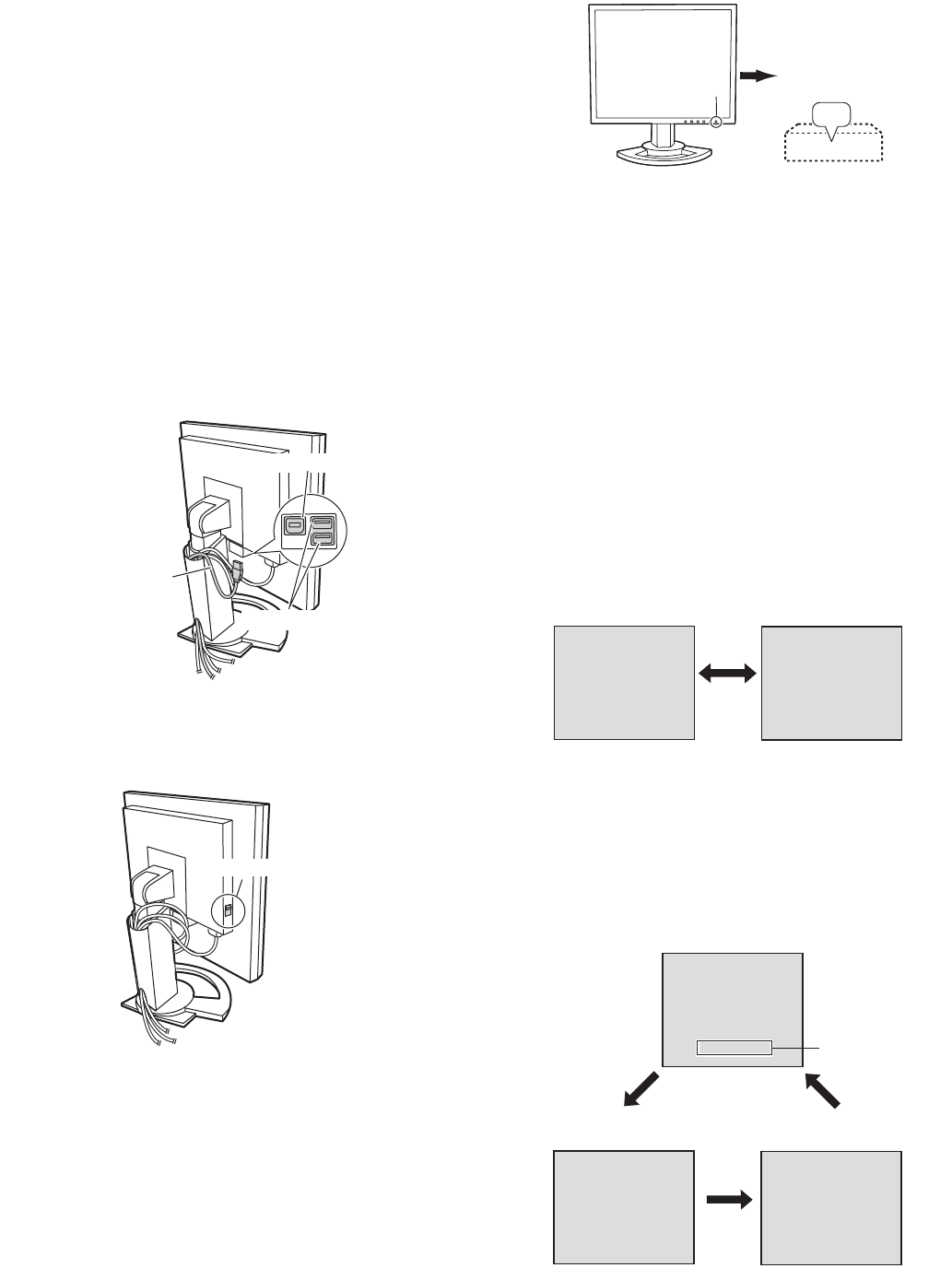
1-3. Connecting a USB device
This monitor is equipped with a USB standard (Rev. 1.1) self-powered
hub.
Downstream (2 ports)
Each of these ports enables connection of a USB device with working
current up to 500 mA.
Upstream (1 port)
This enables connection of a USB compatible computer or USB hub.
Note:
• If a USB cable is required, please use the one included.
• Before connecting, ensure that the shape of the USB cable con-
nector is correct.
• For information regarding the USB function (such as set-up) please
refer to the operation manual of the computer to be connected.
• Some computers, OS and other devices may not be able to be acti-
vated. To ascertain a certain device's USB compatibility, please
contact the manufacturer of the device.
1-4. Turning the power on
1. Turn on the main power of the monitor.
• When switching the main power switch on and off, always wait for
an interval of at least 5 seconds. Rapid switching may result in
malfunction.
2. Press the monitor's POWER button.
The power LED will light up orange.
3. Turn on the computer.
When a signal is input from the computer, the power LED lights up
green, and the screen is displayed (After power is turned on, it may
take a little time until the screen is displayed.)
• If the input terminal to which the computer is connected has not
been selected, the screen will not be displayed. If necessary, per-
form input terminal switching. (right column)
Notes: (when using an analog signal)
• If using the monitor for the first time or after having changed the
system settings during use, perform an automatic screen adjust-
ment.
• When connecting to a notebook, if the notebook computer's screen
is set so that it is displaying at the same time, the MS-DOS screen
may not be able to display properly. In this case, change the set-
tings so that only the monitor is displaying.
1-5. Changing between input terminals
Use the INPUT button to switch between signal input terminals.
When not using a 2-input cable
When using a 2-input cable
When selecting the input terminal connected to the 2-input cable, the
input terminal [INPUT-1] or [INPUT-2] is displayed, followed by the sym-
bol for analog [-A] or digital [-D].
(Example when connecting the 2-input cable to input terminal 2 [INPUT-
2])
Note: When there is no input signal, [NO SIGNAL] is displayed.
Upstream
Downstream
USB cable
Main power switch
ON
Turn on the
computer power
supply.
Press power button
INPUT-1
< > INPUT-2
< >
INPUT
Select [INPUT-1] Select [INPUT-2]
The input signal type (ANALOG/DIGITAL) is
displayed within angle brackets < >.
INPUT-1
< >
INPUT
INPUT INPUT
<ANALOG>
or <DIGITAL>
INPUT-2-A
<ANALOG> INPUT-2-D
<DIGITAL>
Select [INPUT-1]
Select [INPUT-2]
(analog) Select [INPUT-2]
(digital)
LL-T2020 CONNECTION, ADJUSTMENT, OPERATION, AND FUNCTIONS
2 – 4
1-6. Turning the power off
1. Turn the computer off.
2. Press the monitor's POWER button.
The Power LED will disappear.
If the monitor will not be used for a long time, turn off the main power
switch of the monitor, and remove the power plug from the outlet.
1-7. Instructions for attaching a VESA compliant arm
An arm or stand based on the VESA standard (commercially available)
can be attached to the monitor.
Procurement of the arm or stand is at the customer's discretion.
■
■■
■ Arms or stands able to be used
Attachments must satisfy the following.
• Compatible with the VESA standard.
• Have a gap of 100 mm x 100 mm between the screw holes on the
section to be attached.
• Not be likely to fall off or break off after being attached to the monitor.
■
■■
■ How to attach the arm or stand
• Be careful not to overly bend the cable or add extension cords as this
could lead to malfunction.
• While following these instructions, please also refer to the installation
instructions in the operation manual included with the arm or stand.
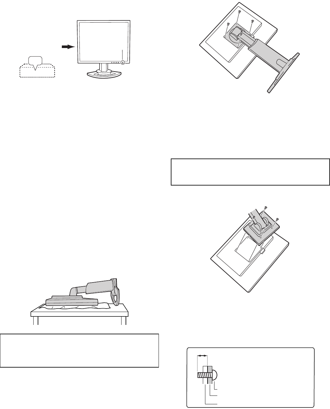
1. Remove the cable.
2. Spread out a soft cloth on a suitable horizontal surface.
3. Being careful not to damage the monitor, gently lay the monitor on it
display-side down.
4. Remove the four screws and then remove the stand from the moni-
tor.
Note:
• The stand is specially made for use with this monitor. Once having
removed the stand, never attempt to attach it to another device.
• Once having removed the screws, store them together with the
stand and if the stand is ever re-attached be sure to use the original
screws.
Using different screws could lead to a malfunction.
5. Attach the arm to the monitor with the four screws.
Note: The screws used to attach the arm should be M4 screws with a
length of 6 mm ~ 8 mm protruding from the surface to be
attached. Using different screws could lead to malfunction or
may lead to the monitor falling off, internal damaged, personal
injury.
Caution:
Securely grasp both the display and stand, and gently tip over.
When the monitor is inclined, the stand may suddenly pop out and
cause injury.
OFF
Turn the computer off Press power button
Caution:
Do not disassemble the stand. Parts may spring out and cause
injury.
6~8mm
Screw used to attach arm
Arm
Part of monitor to which arm is attached
LL-T2020 CONNECTION, ADJUSTMENT, OPERATION, AND FUNCTIONS
2 – 5
1-8. Information about the Pivot Software (Long height/width display)
When rotating the display, change the display orientation using Pivot
Software.
Compatible operating systems (OS) for the Pivot Software that comes
with the monitor:
Windows 98/2000/Me/XP
Macintosh OS 8.x - 9.1
• Depending on the graphics accelerator, it may be impossible to use
Pivot Software, even with a compatible OS.
For production information and inquiries regarding Pivot Software:
Portrait Displays, Inc.
(http://www.portrait.com)
■
■■
■ Installation of Pivot Software
For Windows
1. Quit all applications being used.
2. Load the accessory CD-ROM into the CD-ROM drive of the com-
puter.
3. Open the [My computer] CD-ROM.
4. Double click on the [Pivot] folder.
5. Double click on [SETUP.exe].
6. Click [Next].
7. Choose [I accept the tems in the License Agreement].
8. Click [Next].
9. Input your Customer information [User Name] and [Organization].
10. Click [Next].
11. Click on [Install].
Installation will begin.
12. When the message indicating installation is finished is displayed,
click [Next].
13. Click on [Finish].
14. Click on [Yes] and restart the computer.
For Macintosh
1. Quit all applications being used.
2. Load the accessory CD-ROM into the CD-ROM drive of the com-
puter.
3. Open the CD-ROM.
4. Double click on the [Pivot] folder.
5. Select the desired language.
6. Double click on [Install MacPortrait].
7. Drag the [MacPortrait Install] icon onto the desired disk.
Installation will begin.
8. When the message indicating installation is finished is displayed,
click on [Restart].
■
■■
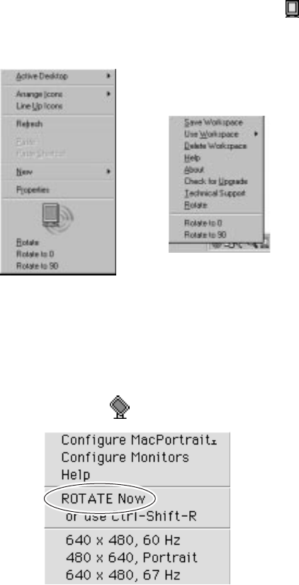
■ Switching display direction
For Windows
1. Click the right mouse button or click the left mouse button on at
the lower right of the screen.
2. Select [Rotate], [Rotate to 0] or [Rotate to 90].
For Macintosh
Choose [ROTATE Now] from at the lower right of the screen.
Each time [ROTATE Now] is selected, the display direction switches.
Note:
• Rotation of the display to match the display direction is done manu-
ally.
• The display direction on the OSD menu is switched using [OSD
PIVOT] on the [MODE SELECT-2] menu.
Rotate: The display direction switches.
Rotate to 0: The display direction is switched to long width.
Rotate to 90: The display direction is switched to long height.
LL-T2020 CONNECTION, ADJUSTMENT, OPERATION, AND FUNCTIONS
2 – 6
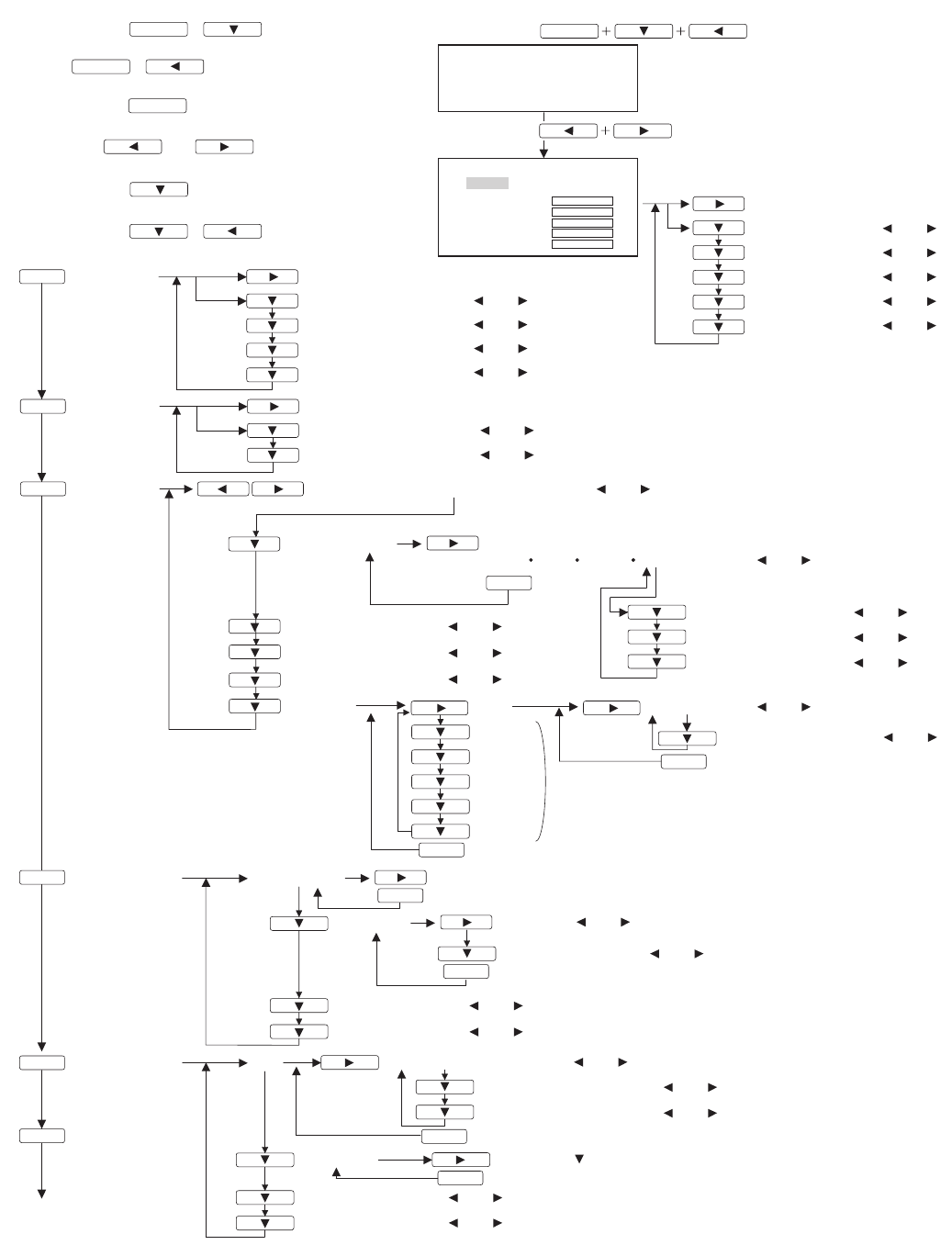
2. ADJUSTMENT
2-1. ADJUSTMENT METHOD
MENU
MENU
MENU
MENU ADJUSTMENT AUTO
CLOCK
PHASE
H-POS
V-POS
GAMMA
MENU GAIN
CONTROL AUTO
BLACK LEVEL
CONTRAST
MENU
COLOR
CONTROL
COLOR MODE (sRGB, STD, VIVID)
COOL STD
WHITE BALANCE WHITE BALANCE
WARM USER
R-CONTRAST
G-CONTRAST
B-CONTRAST
MENU MODE SELECT-2 OSD
OSD V-POSITION
OSD PIVOT
SCALING
LANGUAGE
MENU
MENU
MENU
MENU
MENU
MENU
MENU MODE SELECT-1 INFORMATION
OFF TIMER
INPUT-2
400 LINES
OSD H-POSITION
1) Resetting all adjustment values. 7) SET/RESET of Usage Time
2) ADJUSTMENT menu reset (Analog only)
4) Adjusting the backlight
5) Checking product information
8) Display adjustment
3) Adjustment lock and lock release
While pressing + , turn on the power. , turn on the power.
6) Aging
While pressing + , turn on the power.
simultaneously.Press +
While pressing
While pressing
While pressing
, turn on the power.
Adjust with and
While pressing , turn on the power.
(Analog only)
(Analog only)
(Analog only)
(Adjust with .)and
(Adjust with .)and
(Adjust with .)and
(Adjust with .)and
(Adjust with .)and
(Adjust with .)and
(Adjust with .)and
(Adjust with .)and
(Adjust with .)and
(Adjust with .)and
(Adjust with .)and
(Adjust with .)and
(Adjust with .)and
(Adjust with .)and
(Adjust with .)and
(Adjust with .)and
(Adjust with .)and
INPUT-1 (Adjust with .)and
(Adjust with .)and
(Adjust with .)and
(Adjust with .)and
(Adjust with .)and
(Adjust with .)and
(Adjust with .)and
(Adjust with .)and
(Adjust with .)and
(Adjust with .)and
(Adjust with .)and
(Adjust with .)and
(When ON, Adjust with .)and
(Display)
(Select with .)
x 10000
RESET
x 1000
x 100
x 10
x 1
SET/RESET USAGE TIME
USAGE TIME
10000
1000
100
10
1
0
0
0
0
0
MANUAL RESET
INPUT
HUE
SATURATION
6 COLORS
MENU
RED HUE
SATURATION
YELLOW
GREEN
CYAN
BLUE
MAGENTA
*Same as RED.
MENU
LL-T2020 CONNECTION, ADJUSTMENT, OPERATION, AND FUNCTIONS
2 – 7
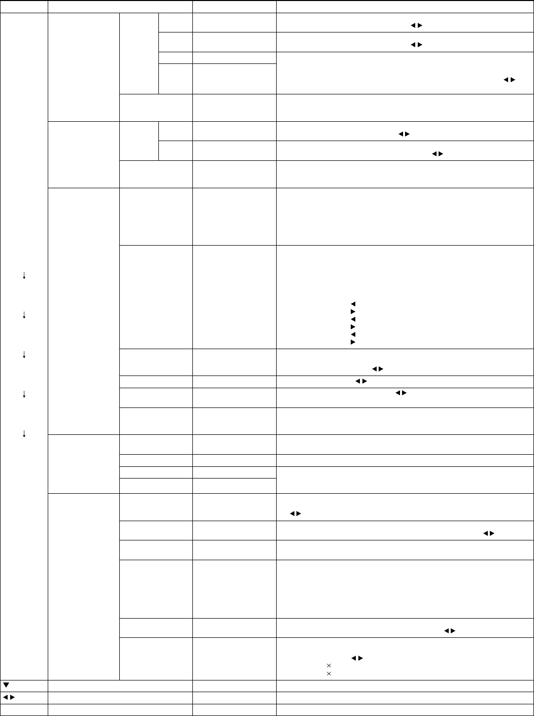
2-2. ADJUSTMENT ITEM LIST
BUTTON ITEM ADJUSTMENT DESCRIPTION
MENU MENU 1:
ADJUSTMENT MANUAL CLOCK 0~255 CLOCK: The figure below demonstrates how to adjust so that vertical
flicker noise is not emitted. ( buttons)
MENU 1
MENU 2
MENU 3
MENU 4
MENU 5
MENU END
PHASE 0~31 PHASE: The figure below demonstrates how to adjust so that horizontal
flicker noise is not emitted. ( buttons)
H-POS 0~ H-POS (horizontal positioning) and
V-POS (vertical positioning)
To center the screen image within the boundaries of the screen, adjust
the left-right (H-POS) values and the up-down (V-POS) values. ( but-
tons)
V-POS 0~
AUTO Automatic screen adjustment
Options in the ADJUSTMENT Menu can be adjusted automatically
(CLOCK, PHASE, H-POS V-POS).
MENU 2:
GAIN CONTROL MANUAL BLACK
LEVEL 0~100 BLACK LEVEL: Total screen brightness can be adjusted while watching
the color pattern. ( buttons)
CON-
TRAST 0~100 CONTRAST: While watching the color pattern, adjustments can be made
so that all graduations appear. ( buttons)
AUTO GAIN CONTROL Menu
AUTO: Every menu option is automatically adjusted using the Auto
Gain Control function.
MENU 3:
COLOR CONTROL COLOR MODE sRGB, STD, VIVID STD: Displays image with the color tone results from original scheme of
liquid crystal panel.
sRGB: sRGB is international standard of color representation specified by
IEC (International Electrotechnical Commission). Color conversion
is made in taking account of liquid crystals characteristics and rep-
resents color tone close to it original image.
VIVID: Displays an image with dynamic and VIVID primary colors.
WHITE BALANCE COOL • STD • WARM
(5 levels),
USER R • G • B:
0~255
WHITE BALANCE Menu
COOL : Color tone bluer than standard
• : Color tone slightly bluer than standard
STD : Color tone standard setting
• : Color tone slightly redder than standard
WARM : Color tone redder than standard
USER
R-CONTRAST : button for blue-green
button for red
G-CONTRAST : button for purple
button for green
B-CONTRAST : button for yellow
button for blue
GAMMA -10~10 Adjust so that dark and bright images are easy to see. If the screen is dark
and hard to see, increase the numerical value. If it is bright and hard to see,
lower the numerical value. ( buttons)
HUE -20~20 Hue can be adjusted. ( buttons)
SATURATION -50~50 Color saturation can be adjusted. ( buttons)
At the minimum value, the screen is black and white.
6 COLORS RED, YELLOW,
GREEN, CYAN,
BLUE, MAGENTA
Hue (HUE) and saturation (SATURATION) may be adjusted by color.
MENU 4:
MODE SELECT-1 IINFORMATION A model name (MODEL), a serial no. (S/N), and usage time (USAGE
TIME) of the display can be checked.
OFF TIMER ON (1 - 23 hours) • OFF Power is automatically shut off when the set time elapses.
INPUT-1 1LINE • 2LINES Set [1 LINE] when connecting digital or analog signal cables to a DVI-I
input terminal (INPUT-2) on the display.
Set [2LINES] when connecting a 2-input cable.
INPUT-2 1LINE • 2LINES
MENU 5:
MODE SELECT-2 OSD H-POSITION OSD H-POSITION (OSD horizontal position)
The position of the OSD display can be moved to the left and right.
( buttons)
OSD V-POSITION OSD V-POSITION (OSD vertical position)
The position of the OSD display can be moved up and down. ( buttons)
OSD PIVOT OFF (landscape) •
ON (portrait ) The orientation of the OSD display can be changed.
LANGUAGE 7 countrys
DEUTSCH, ENGLISH,
ESPANOL,
FRANCAIS, ITAL-
IANO, NETHER-
LAND, SVENSKA
LANGUAGE
Messages displayed on the screen and OSD Menu contents can be
changed to the following languages.
Dutch, English, French, German, Spanish, Italian, Swedish.
SCALING 0~4 SCALING (Level of scaling)
The sharpness of the image can be adjusted. ( buttons)
400 LINES 640 • 720 400 LINES (degree of resolution)
You can specify the horizontal resolution of a 400-line screen when
using US text, etc.( buttons)
640: 640 400 dot mode
720: 720 400 dot mode (US text etc.)
Select the item
0~31 Adjusting the backlight
POWER ON, OFF
LL-T2020 DISASSEMBLY AND ASSEMBLY
3 – 1
CHAPTER 3. DISASSEMBLY AND ASSEMBLY
B
C
F
h
g
H
H
F
F
K
O
P
L
L
M
N
N
j
k
E
F
G
D
B
B
B
B
C
J
J
C
I
I
C
Ca
b
i
c
d
e
f
B
3
4
910
10 11
13
14
15
16
17
18
20
19
21
12
6
7
8
5
A
A2
1
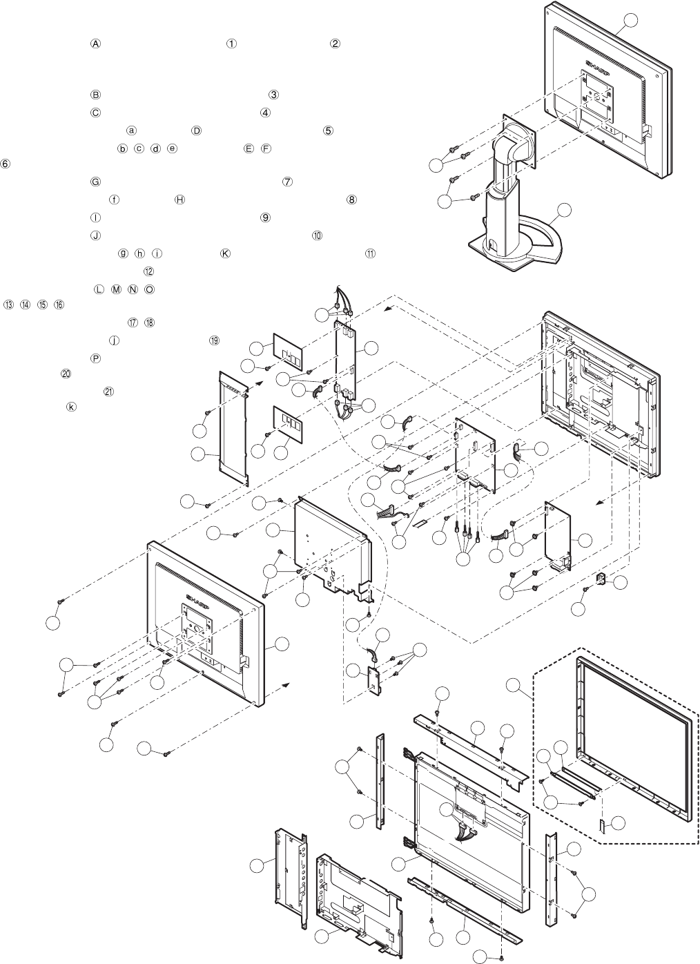
1. SEPARATING DISPLAY UNIT FROM STAND UNIT
1) Remove the screw . Separate the display unit from the stand unit .
2. DISASSEMBLING DISPLAY UNIT
1) Remove the screw and then remove the display cover .
2) Remove the screw and then remove the shield plate .
3) Remove the connector pin and screw . Remove the USB board .
4) Remove the connectors ( , , , ) and screws ( , ). Remove the main board
.
5) Remove the screw and then remove the PS switch cover .
6) Remove the connector and screw . Remove the power supply board .
7) Remove the screw and then remove the shield plate .
8) Remove the screw and then remove the connector locking seat .
9) Remove the connectors ( , , ) and screw . Remove the inverter board .
10) Remove the display mask unit .
11) Remove the screw ( , , , ). Remove the LCD angles
(, , , ).
12) Remove the board angles ( , ).
13) Remove the connector from the LCD unit .
14) Remove the screw . Remove the key
switch angle .
15) Remove the key unit and then remove
the connector .
LL-T2020 DISASSEMBLY AND ASSEMBLY
3 – 2
A
A
B
E
F
H
JJ
J
G
H
I
I
B
B
C
D
D
1
2
34
5
6
7
9
10
14
15
16
17
12
13
11
8
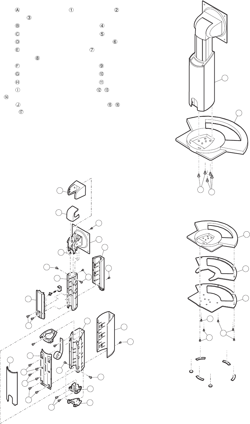
3. DISASSEMBLING STAND UNIT
1) Remove the screw . Separate the arm unit from the base unit .
2
) Remove the cable cover .
3
) Remove the screw and then remove the base arm cover .
4
) Remove the screw and then remove the base arm cover .
5
) Remove the screw and then remove the base arm install angle .
6) Remove the screw and then remove the slide guide .
7
) Remove the base arm angle .
8) Remove the screw and then remove the slide arm cover .
9) Remove the screw and then remove the slide arm cover .
10) Remove the screw and then remove the slide arm angle .
11) Remove the screw and then remove the hinge covers ( , ) from
the hinge unit .
12) Remove the screw and then remove the stand base plates ( , )
from the stand cover .
LL-T2020 TROUBLESHOOTING
4 – 1
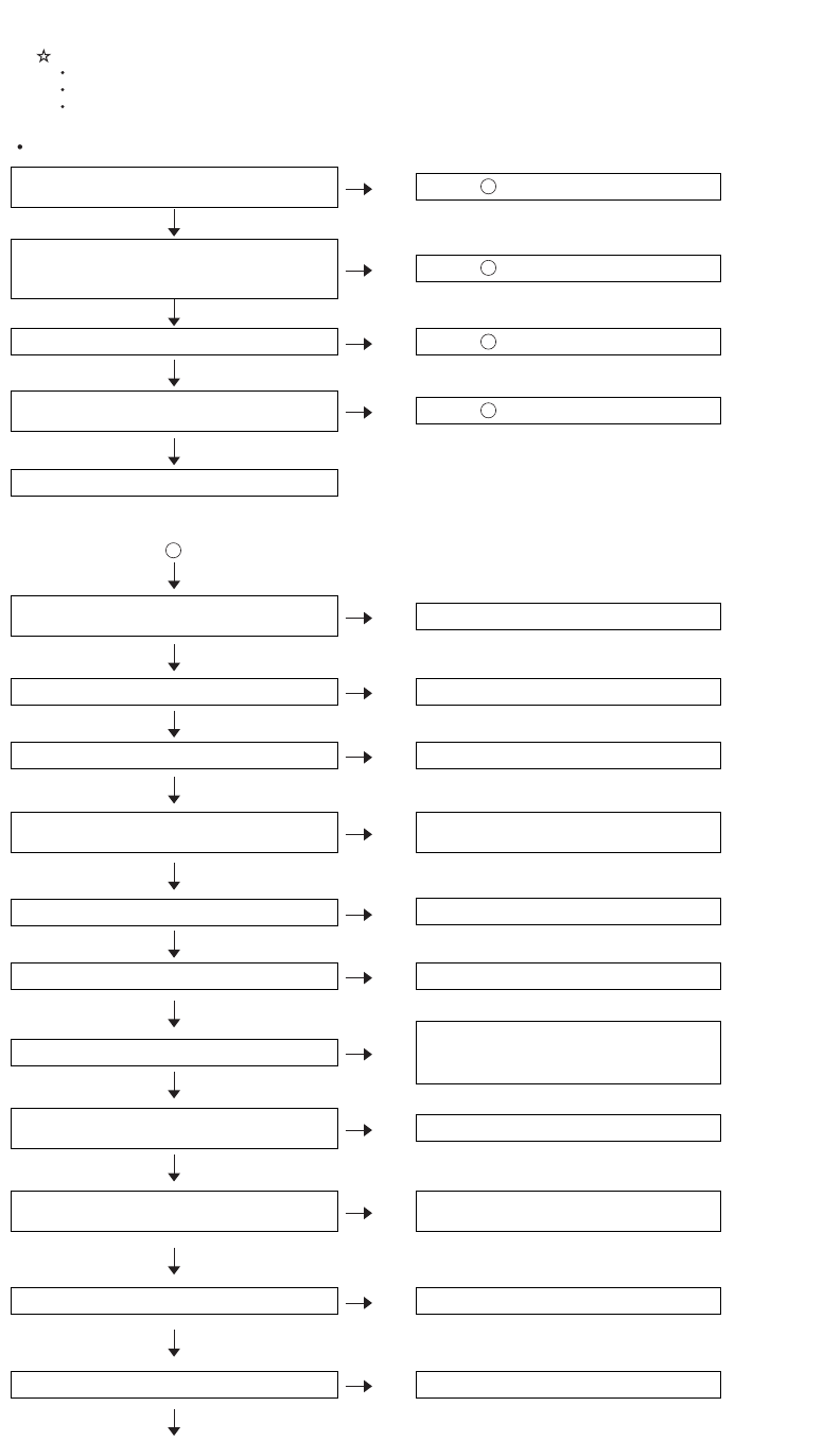
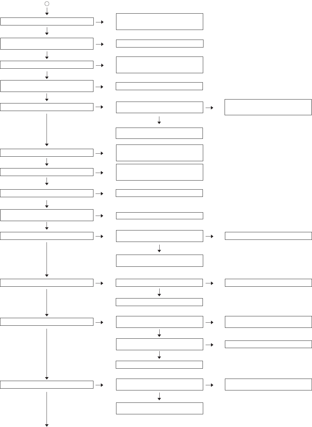
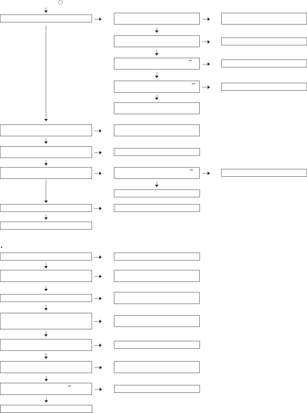
CHAPTER 4. TROUBLESHOOTING
(Yes)
(Yes)
(Yes)
(Yes)
(Yes)
(Yes)
Green LED comes on when the power button is
pressed?
The screen is displayed properly in each video
mode?
AC cable is connected to the power supply
unit?
Input signal port is the one to which analog
signal cable is connected?
Test terminals LD401, LD402, and LD403 are
DC+3.3V?
Test terminal LD623 changes its level when
POWER switch is turned on and off?
Press INPUT key to switch over to the
correct input signal port.
Check DC+5V power supply line (DV5A)
and POWER_CTL1 signal and circuits
around Q807.
Check the connection line of LD623, and
check the CN601, SW PWB and cable.
Remove the analog signal cable. After a short
while time, the LED color changes form green
to orange.
(Yes)
(Yes)
(No)
(No)
(Yes)
(Yes)
(No)
(No)
(No)
(No)
(Yes)
(Yes)
(No)
(No)
(No)
(No)
(No)
(Yes)
(No)
(Yes)
(Yes)
(No)
(No)
(No)
Perform 1
B/L is lit?
No error.
Check AC cable connection.
Check power supply unit switch.
Check circuits around IC601.
Check circuits around IC801.
Check circuits around IC401.
Check RESET circuit around IC602.
Check IC602 and clock circuit around X601.
Check SW101 and circuits around IC101.
The power supply unit is switched on?
SW101 is on 1st pin side?
Test terminal LD811 is DC+5V?
Test terminal LD815 is DC+5V?
4th pin of IC602 is in H level (DC+5 V)?
C610-side terminal signal of X601 is normal?
Test terminal LD608 is DC+3.3V?
1
Perform 2
Perform 3
Perform 4
Check whether the following cables are connected correctly.
In addition, check whether the PCs video mode is properly set to the signal timing which meets this machine.
Attached cables
Dedicated AC adapter
Dedicated analog signal cable (DVI-A cable)
Dedicated digital signal cable (DVI-D cable)
The display does not work. (with analog connection, DVI-A cable use)
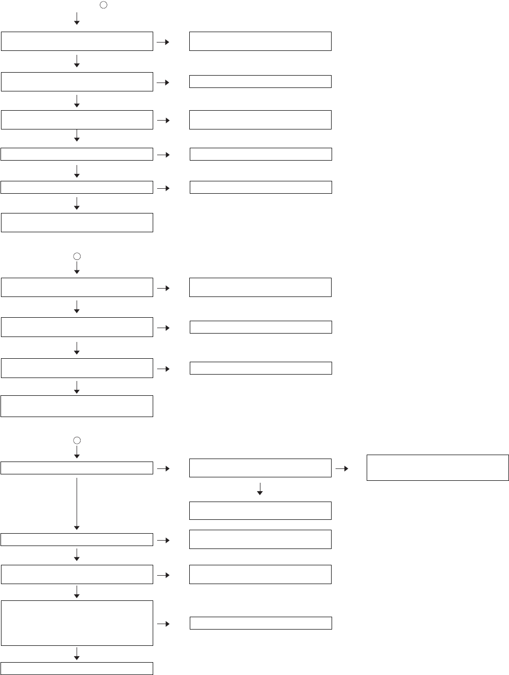
LL-T2020 TROUBLESHOOTING
4 – 2
(No)
(No) (No)
(No)
(No)
(Yes)
(Yes)
(Yes)
(No)
(Yes)
(Yes)
(No)
(Yes)
(Yes)
(No)
(Yes)
(No)
(Yes)
(No)
(Yes)
(No)
(Yes)
(Yes)
(Yes)
(Yes)
(No)
(No)
The port from which the analog signal cable
was removed is the input signal port selected?
48th pin and 49th pins of IC602 are in H level
(DC+3.3V)?
LD613 and LD616 are in H level (about
DC+1.9V)?
LD808 is less than DC+1.0V at maximum
brightness?
1st pin of CN2, CN3, CN4, CN5, CN6, and CN7
on inverter PWB unit is about 790 Vrms? (Use
caution not to get electric shock accident. Use
a high-voltage probe (more than 100:1) for
measuring voltage.)
Check analog signal cable and CN101
(CN201).
Check SDA and SCL signals and circuits
around IC402 and IC602.
Press INPUT key to switch over to the
correct input signal port.
When CN802 cable is removed, check the
LD801 is DC+12V.
Check inverter unit, inverter cable and their
connections.
Check the power unit and cable and their
connections, and DC+12V power supply
line.
Check BL_EN signal and circuits around
CN802.
Check BRT_VR signal and circuits around
IC604.
Signal waveforms of test terminals LD304,
LD305 (LD317, LD318) are normal?
Signal waveforms of test terminals LD312,
LD323 (LD313, LD324) are normal?
Signal waveforms of 31st and 32nd pins of
IC402 are normal?
Check SW PWB and SW cable and their
connections.
48th pin of IC602 is in H level (DC+3.3V)?
continued from 1
LD613 is H in level (about DC+1.9V)?
Check SW PWB and SW cable and their
connections.
Test terminal LD801 is DC+12V?
LD807 is in H level (DC+5V)?
Check lamp inside LCD module.
Check circuits around IC602.
Check Q601 and its surrounding circuits.
Replace inverter PWB unit with a new one.
Check circuits around IC602.
Check Q601 and its surrounding circuit.
Check circuits around IC301 and IC302.
2
3
LL-T2020 TROUBLESHOOTING
4 – 3
(No)
(No)
(No)
(Yes)
(Yes)
(No)
(Yes)
(No)
(Yes)
(No)
(Yes)
(No)
(Yes)
(No)
(Yes)
(Yes)
(Yes)
(No)
(No)
(No)
(Yes)
(Yes)
(Yes)
(Yes)
(No)
(Yes)
(No)
(No)
(No)
(Yes) (No)
(No)
(Yes) (No)
(Yes)
(Yes)
Check DC+5V power supply line (PV5) ,
POWER_CTL3 signal, and circuits around
Q807.
Check DC+2.5V power supply line (DV25),
POWER_CTL4 signal, and circuits around
IC802.
Check DC+12V power supply line (LCDV),
POWER_CTL2 signal, and circuits around
Q803.
Check clock circuit around IC501 and X501.
Clock (R508) and DE (R502) signal outputs
are normal?
ADJUSTMENT and MODE SELECT are set
properly?
Signal waveform of test terminal LD502 is
normal?
ADJUSTMENT and MODE SELECT are set
properly?
Adjust according to "screen adjustment
procedure".
Adjust according to "screen adjustment
procedure".
Check circuits around IC301, IC302, and
IC402.
Check circuits around IC701, and CN701
and LCD module.
Check DC+5V power supply line (DV5A),
POWER_CTL1 signal, and circuits around
Q807.
Test terminals LD405, LD523, and LD701 are
DC+3.3V?
Signal waveform of test terminal LD565 is
normal?
Test terminals LD401, LD402, and LD403 are
DC+3.3V?
Test terminal LD815 is DC+5V?
Test terminal LD806 is DC+5V?
Test terminal LD801 is DC+12V?
Test terminal LD501 is DC+2.5V?
LD816 is DC+12.0V?
36th pin of LC602 is in H level (DC+5V)?
The entire LCD screen is white?
The entire LCD is black?
The size of LCD screen is abnormal?
LCD screen jitters or flickers?
Check circuits around IC401.
Check circuits around IC403.
Check circuits around IC601.
Test terminal of LD701 is DC+12V?
Check circuits around X601 and IC602.
Check circuits around IC502.
Check circuits around CN701.
Check PLL circuits around IC402.
Check circuits around IC502.
4
Check inverter unit, inverter cable and their
connections.
(No)
(Yes)
When CN802 cable is removed, LD801 is
DC+12V?
Check the power unit and cable and their
connections, and DC+12V power supply
line.
LL-T2020 TROUBLESHOOTING
4 – 4
(No)
(No)
(No)
(Yes)
(Yes)
(Yes)
(Yes)
(No)
(No)
(Yes) (No)
(No)
(Yes)
(Yes)
(Yes)
(No)
(Yes)
(No)
(No)
(Yes)
(No)
(Yes)
(No)
(Yes)
(No)
(Yes)
(Yes)
(No)
(Yes)
(Yes)
(No)
(No)
(Yes)
(Yes)
GAIN CONTROL and WHITE BALANCE
are set properly?
Analog color signal output (C302, C303,
C305, C319, C320, and C322) is normal?
Digital color signal output of IC402 (ID0
ID47) is normal?
Digital color signal output of IC502 (OD0
OD47) is normal?
Check circuits around IC701, and CN701
and LCD module.
Check circuits around IC402, IC404, and
IC602.
Digital color signal output of IC402 (ID0
ID47) is normal?
Press INPUT key to switch over to the
correct input signal port.
Check CN101 and 201, and signal source
and digital signal cable.
Check circuits around IC101, IC103 and
IC201.
Check CN101 and 201, and signal source
and digital signal cable.
Display is normal in composite sync and sync-
on-green signal input.
Adjustment settings are stored after display
screen is adjusted?
AUTO function of GAIN CONTROL operates
properly?
Input signal port is the one to which digital
signal cable is connected?
Waveforms of IC103s and 201s 1st and 2nd
pins change normally when resolution is
changed?
Test terminals LD110, LD111, LD112, LD113,
LD210, LD211, LD212, LD213 are DC+3.3V?
CN101 and 201 signals (at 1st, 2nd, 9th, 10th,
17th, 18th, 23rd, and 24th pins) are normal?
IC102 and IC202 signal output (ID0 ID47,
HIS, IVS, ICK, IACT) are normal?
LCD screen color is abnormal?
Input is changed over properly?
No error.
Display is normal in analog input?
LD101 and LD201 are in H level (DC+5V)?
Check circuits around IC502.
Adjust according to "screen adjustment
procedure".
Check circuits around IC402.
Check circuits around IC402 and IC502.
Check circuits around IC502 and IC701.
Check circuits around IC402 and IC404.
Check circuits around IC602.
check circuits around IC602 and IC605.
Check circuits around IC402.
First, check with analog signal input.
Check circuits around IC104 and IC203.
Check circuits around IC102 and IC202.
continued from 4
The display does not work. (with digital connection, DVI-D cable use)
LL-T2020 WAVE FORM
5 – 1
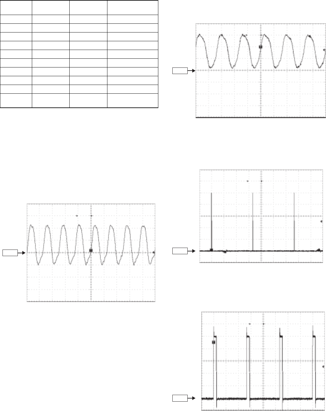
CHAPTER 5. WAVE FORM
Waveform measurement condition: Input each of the display patterns
and measure the waveform (tinming chart).
CAUTION
WAVE FORM 1: REFCK (LD565)
Frequency: 81MHz
Display screen: Arbitrary
2V/DIV, 10ns/DIV
WAVE FORM 2: XTAL (IC601 of 2PIN)
Frequency: 24MHz
Display screen: Arbitrary
1V/DIV, 25ns/DIV
WAVE FORM 3: VSYNC (LD305, LD318)
Frequency: 60Hz
Display screen: Arbitrary
1V/DIV, 5ms/DIV
WAVE FORM 4: HSYNC (LD304, LD317)
Frequency: 75kHz
Display screen: Arbitrary
1V/DIV, 5µ
µµ
µs/DIV
Wave-form
No. Measurement
point Name of
waveform Display pattern
1 LD565 REFCK Arbitrary
2 IC601 of 2PIN XTAL Arbitrary
3 LD305, LD318 VSYNC Arbitrary
4 LD304, LD317 HSYNC Arbitrary
5 LD502 ICK Arbitrary
6 LD504 VS Arbitrary
7 LF505 IHS Arbitrary
8 IC701 of 10PIN DCLK Arbitrary
9 IC701 of 9PIN DEN Arbitrary
10 LD300, LD301,
LD302 RGB OUT 16 monochromatic
gradation patterns
Oscilloscope: Tektronix644B
Input signal: VESA1600 x 1200
H: 75kHz V: 60Hz
DOTCLK: 162MHz
GND
GND
GND
GND
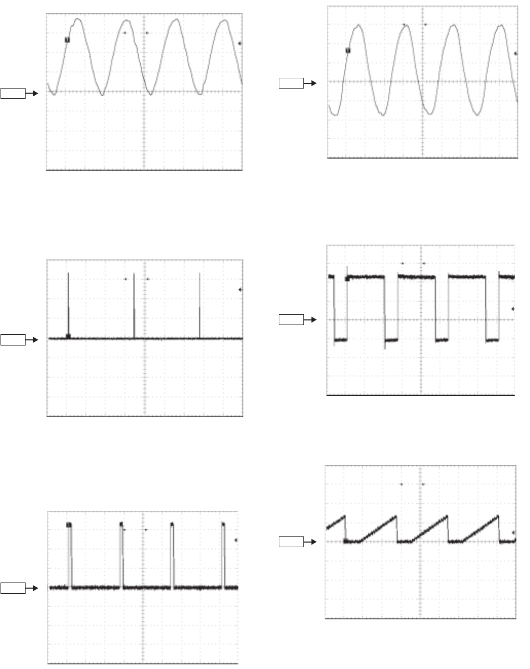
LL-T2020 WAVE FORM
5 – 2
WAVE FORM 5: ICK (LD502)
Frequency: 81MHz
Display screen: Arbitrary
1V/DIV, 5ns/DIV
WAVE FORM 6: VS (LD504)
Frequency: 60Hz
Display screen: Arbitrary
1V/DIV, 5ms/DIV
WAVE FORM 7: IHS (LD505)
Frequency: 75kHz
Display screen: Arbitrary
1V/DIV, 5µ
µµ
µs/DIV
WAVE FORM 8: DCLK (IC701 of 10PIN)
Frequency: 81MHz
Display screen: Arbitrary
1V/DIV, 5ns/DIV
WAVE FORM 9: DEN (IC701 of 9PIN)
Frequency: 75kHz
Display screen: Arbitrary
1V/DIV, 5µ
µµ
µs/DIV
WAVE FORM 10: RGB OUT ( LD300, LD301, LD302)
Display screen: 16 monochromatic gradation patterns
0.5V/DIV, 5µ
µµ
µs/DIV
GND
GND
GND
GND
GND
GND
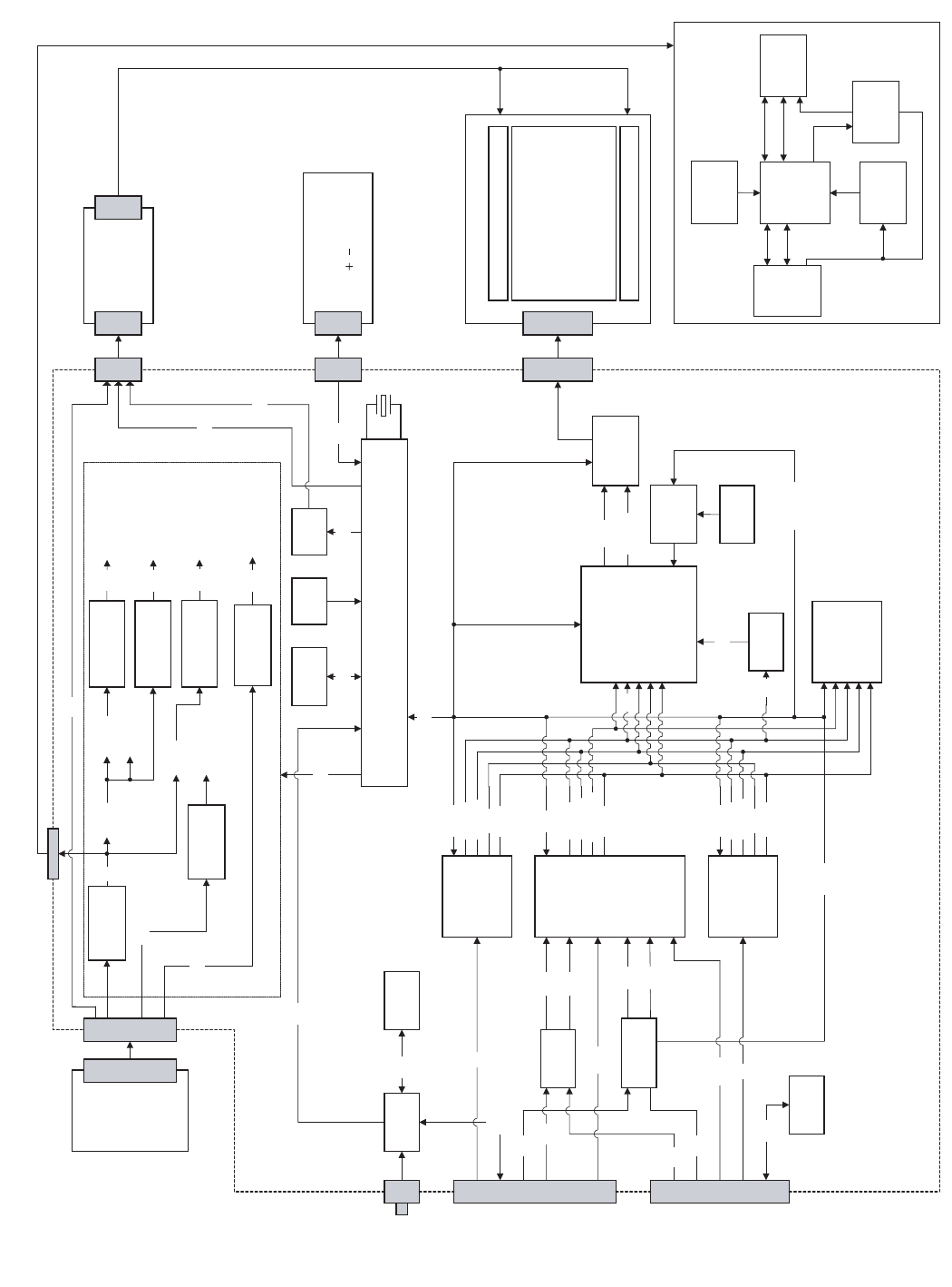
LL-T2020 BLOCK DIAGRAM
6 – 1
Power
Unit
Scaling Chip
iLS-L001
IC502
LVDS
Transmitter
IC701
CTL
EEPROM
IC605
ADC
AD9888-170
IC402
DVI- I
CN201 TMDS
SII161B
IC202
MPU
IC602
RGB1
RXD
TXD
SDA
SCL
SDA
SCL
HS1
SDA/SCL SDA/SCL
Invertor Unit
12V
BRT_VR
IHS/IVS
ASIC
AUTO & AGC
IC404
HIN1
DVI- I
CN101
TMDS
SII161B
IC102
HIN2
VIN2
VIN1
Comparator
IC301
Buffer
IC302
VS1
SDA
SCL
Switch
IC101
HS2
VS2
A/D-DDC
IC103
SDA
SCL
Reset
IC603
X601
DAC
IC604
LCDV
SW PWB
Power/Input/Menu/Selct/
//LED
KEY
Regulator
PQ1CZ21H2Z
IC802 2.5V
5V
3.3V
V33
PV5
POWER_CTL
Logic
IC504
VS
CN701
CN601
CN802
CN801
SW101
I
IHS
IVS
X501
10MHz
PDO1
SDET1
PD1
IHS/IVS
ID[0..47]
PDO2
SDET2
PD2
ID[0..47]
IACT
ID[0..47]
IHS/IVS
ICK(B)
ICK(B)
COMSYN
ICK(B)
Clock
Generator
IC501
DEN
DCLK
OD[0..47]
LCD Panel
Lamp
Lamp
DV25
AV5
DV5 DV5A PV33/AV33/DV33/
OV33/AD33
LV33
3.3V
Regulator LM317
IC601 3.3V
12V BL_EN
RX
USB PWB
IC3
uPD72012
X1
4MHz
CN1
USB-CN
4PIN
CN2
USB-CN
8PIN
IC2
uPD16857
IC1
X62FP3302
DATA+
DATA-
DATA+[1,2]
DATA-[1,2]
OUT[1, 2]
CTL[1,2]
FLG[1,2]
3.3V
5V
HREF1
HREF2
RX
RGB2
Regulator LM317
IC403
Regulator LM317
IC104/203/401
MAIN PWB
A/ D-DDC
IC201
DATAX
STROBE_X
SCLK_X
XCLDWN
Regulator
PQ1CY1032Z
IC801
Regulator
PQ20WZ11
IC803
12V
12V
CN803 5V
ACT
CHAPTER 6. BLOCK DIAGRAM
LL-T2020 CIRCUIT DIAGRAM
7 – 1
A
B
C
D
87654321
12345678
D
C
B
A A
B
C
D
87654321
12345678
D
C
B
A A
B
C
D
87654321
12345678
D
C
B
A A
B
C
D
87654321
12345678
D
C
B
A
1/9
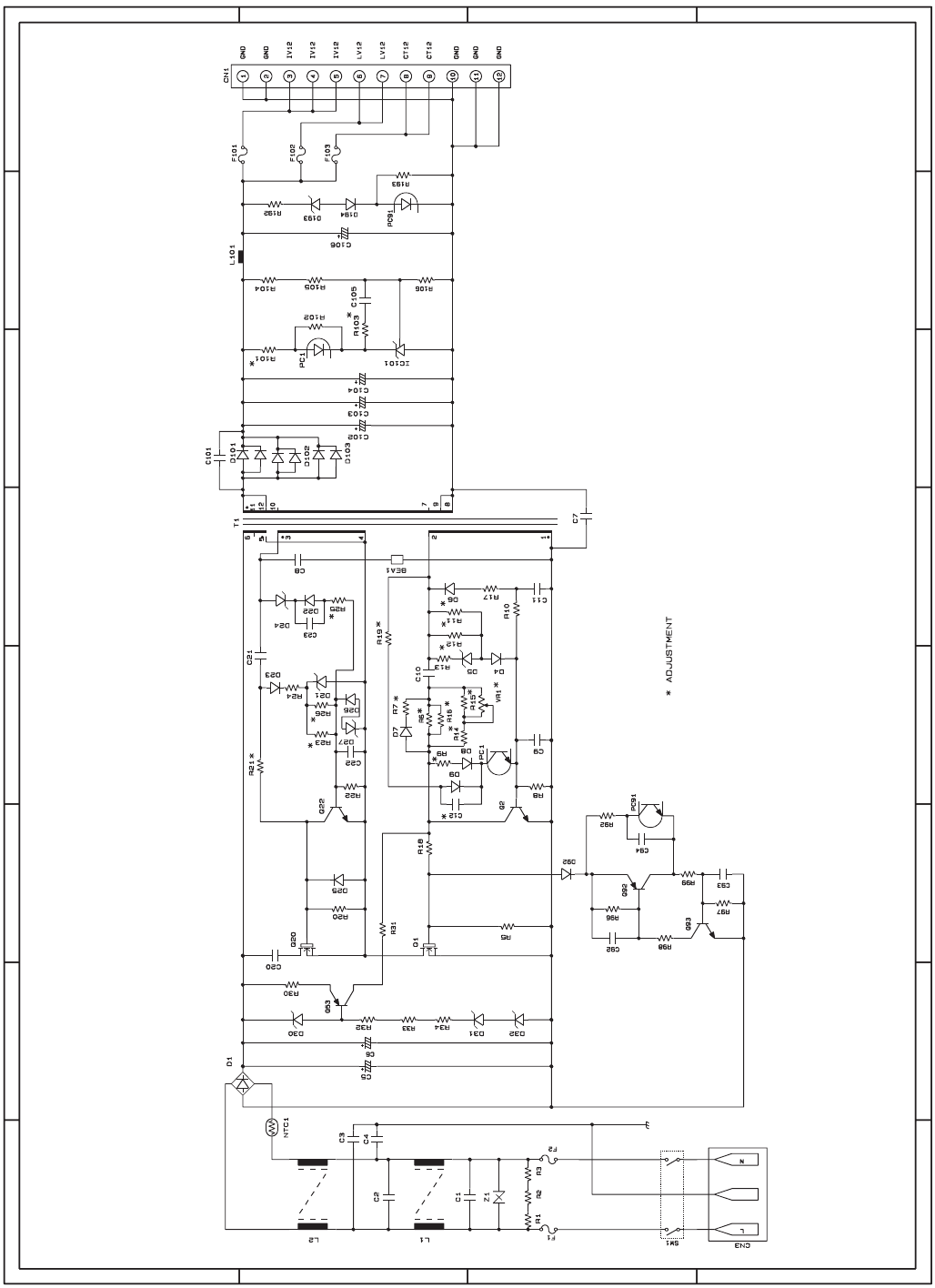
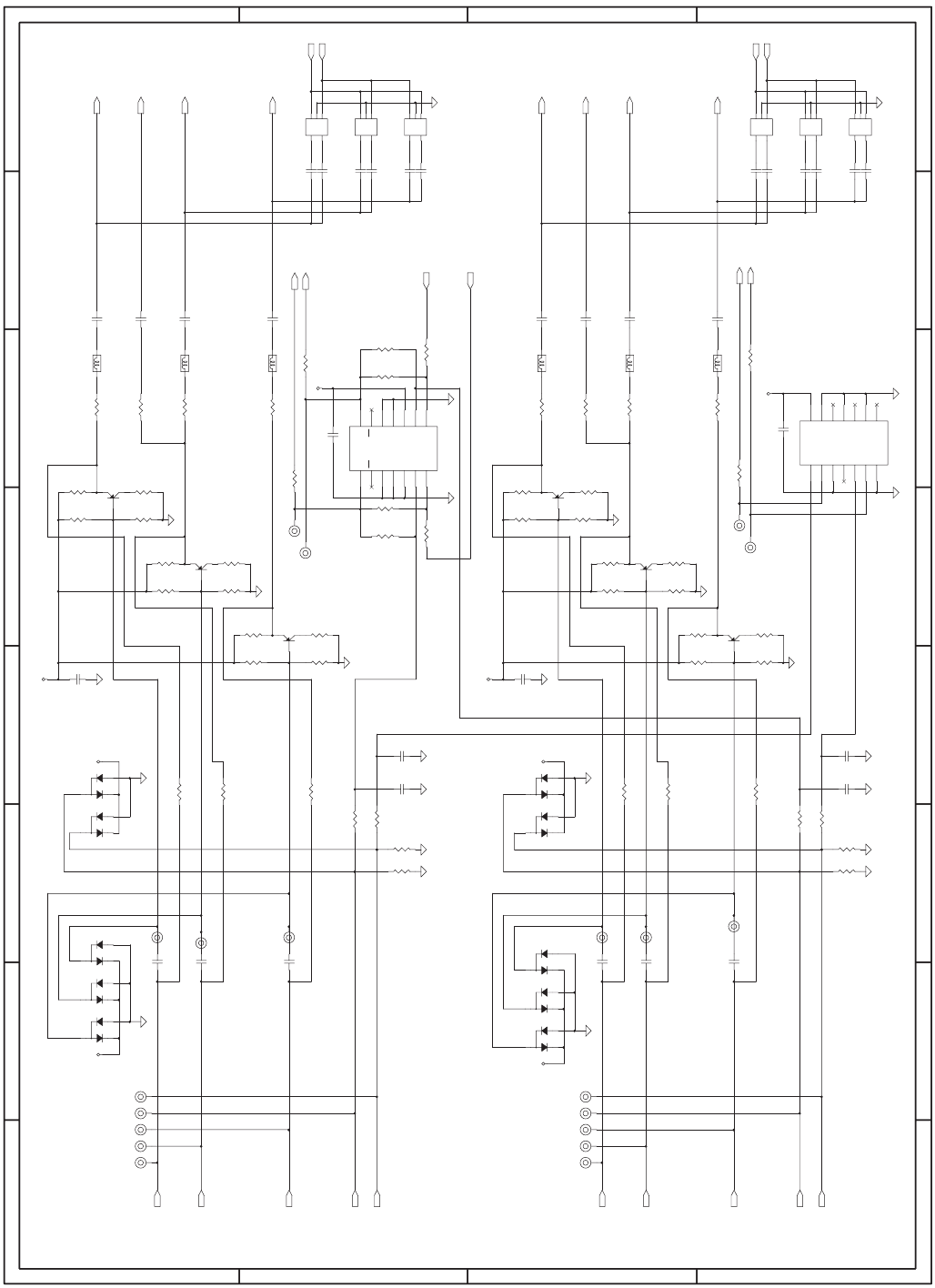
CHAPTER 7. CIRCUIT DIAGRAM
POWER SUPPLY PWB
LL-T2020 CIRCUIT DIAGRAM
7 – 2
INPUT 2
BANKSEL
L : BANK0
H :
BANK1
BANK0 : ANALOG
BANK1 : DIGITAL
ID1
ID34
ID21
ID3
ID14
ID46
ID15
ID37
ID7
ID13
ID31
ID10
ID32
ID29
ID36
ID20
ID5
ID8
ID43
ID11
ID47
ID2
ID44
ID4
ID38
ID0
ID30
ID22
ID42
ID27
ID16
ID39
ID18
ID23
ID25
ID19
ID41
ID17
ID40
ID45
ID33
ID28
ID35
ID12
ID26
ID9
ID24
ID6
DV5
OV33_1
AV33_1
DV5
PV33_1
DV33_1
AV33_2
DV5
DV5A
PV33_2PV33_1 AV33_1
DV5
DV5
R111 0J
D103
UDZS5.6B
Q103
DTC143EE
23
1
R124 510J
C112
0.1uF
C111
100pF
RA106 33J x4
R101
4.7kJ
R115 33J
LDS107
RA112 33J x4 LD112
C102
0.1uF
R112
47kJ
FB101
BLM18PG600SN1
Q102
IMH4A 1
2
34
5
6
R128
EMPTY
R104
75J
C114
0.1uF
C117
0.1uF
R123
4.7kJ
IC104
LM317EMP
1
2
3
ADJ
OUTPUT
INPUT
C101
0.1uF
R126
360F
C123
10uF
R133
EMPTY
LDS108
D101
RB715F
23
1
IC103
BU9882F
1
2
3
4
5
6
78
9
10
11
12
13
14
SCL_PC0
SDA_PC0
NC
SCL_PC1
SDA_PC1
NC
GND SDA_MON
SCL_MON
DDCENA
BANKSEL
DUAL_PCB
WPB
VCC
C120
0.1uF
LD101
LDS104
RA103 33J x4
C127
10uF
RA102 33J x4
C110
0.1uF
R120
4.7kJ
RA109 33J x4
LD113
C124
10uF
R116 33J
R108
47kJ
R119
4.7kJ
LDS109
SW101
SSSS916900
1
2
3
R118
4.7kJ
FB102
BLM18PG600SN1
R110
EMPTY
RA108 33J x4
R106
75J
CN101
SD-74320-1004
1
2
4
5
6
7
9
10
12
13
16
17
18
20
21
23
24
3
15
19
22
11
8
14
C1
C2
C3
C4
C5
RX2-
RX2+
RX4-
RX4+
SCL
SDA
RX1-
RX1+
RX3-
RX3+
HP
RX0-
RX0+
RX5-
RX5+
RXC+
RXC-
GND
GND
GND
GND
GND
VS
5V
ARED
AGREEN
ABLUE
AHSY
ANGND
R117
4.7kJ
L101
NLC322522T-220K
R129
0J
R132
0J
R114
47kJ
C126
10uF
R103
10kJ
R125
220F
R102
47kJ
C107
0.1uF
LD110
FB103
BLM18PG600SN1
R107
47kJ
RA105 33J x4
IC101
FST3257
1
2
3
4
5
6
7
89
10
11
12
13
14
15
16
S
1B1
1B2
1A
2B1
2B2
2A
GND 3A
3B2
3B1
4A
4B2
4B1
OE
VCC
R109 0J
R131
EMPTY
R105
75J
RA111 33J x4
C125
10uF
LDS103
R130
0J
R122 33J
C105
0.1uF C106
0.1uF
D102
UDZS5.6B
RA104 33J x4
LD111
C116
10uF(3216)
C121
EMPTY
RA110 33J x4
R127
47kJ
LDS102
C113
100pF
IC102
THC63DV161
57
58
49
50
51
52
53
54
55
56
59
60
61
62
63
64
65
66
67
68
69
70
71
72
73
74
75
76
77
78
79
80
81
82
83
84
85
86
87
88
89
90
91
92
93
94
95
96
97
98
99
100
1
2
3
4
5
6
7
8
9
10
11
12
13
14
15
16
17
18
19
20
21
22
23
24
25
26
27
28
29
30
31
32
33
34
35
36
37
38
39
40
41
42
43
44
45
46
47
48
OVCC
OGND
QO0
QO1
QO2
QO3
QO4
QO5
QO6
QO7
QO8
QO9
QO10
QO11
QO12
QO13
QO14
QO15
VCC
GND
QO16
QO17
QO18
QO19
QO20
QO21
QO22
OGND
QO23
OVCC
AGND
RX2+
RX2-
AVCC
AGND
AVCC
RX1+
RX1-
AGND
AVCC
AGND
RX0+
RX0-
AGND
RXC+
RXC-
AVCC
EXT_RES
PVCC
PGND
RESERVED
OCK_INV
S_D
PD
ST
PIXS/M_S
GND
VCC
STAG_OUT/SYNC
SCDT
PDO
QE0
QE1
QE2
QE3
QE4
QE5
QE6
QE7
OVCC
OGND
QE8
QE9
QE10
QE11
QE12
QE13
QE14
QE15
OGND
OVCC
QE16
QE17
QE18
QE19
QE20
QE21
QE22
QE23
VCC
GND
CTL1
CTL2
CTL3
OVCC
ODCK
OGND
DE
VSYNC
HSYNC
L102
NLC322522T-220K
RA101 33J x4
LDS105
Q101
DTC143EE
23
1
C104
0.1uF
C119 0.1uF
R121 33J
C115
100pF
C108
0.1uF
C118
100pF
+
C122
EMPTY(22uF/16V(WT))
LDS106
C109
0.1uF
RA107 33J x4
C103
0.1uF
R113
4.7kJ
MD1
BLUE1
IHS
TMDS_PDO1
TXD
IVS
HS1
TMDS_PD1
RXD
VS1
ICK
TMDS_SDET1
RED1
ID[0..47]
INP1B
GREEN1
IACT
INP1A
A
B
C
D
87654321
12345678
D
C
B
A A
B
C
D
87654321
12345678
D
C
B
A A
B
C
D
87654321
12345678
D
C
B
A A
B
C
D
87654321
12345678
D
C
B
A
2/9
DVI1
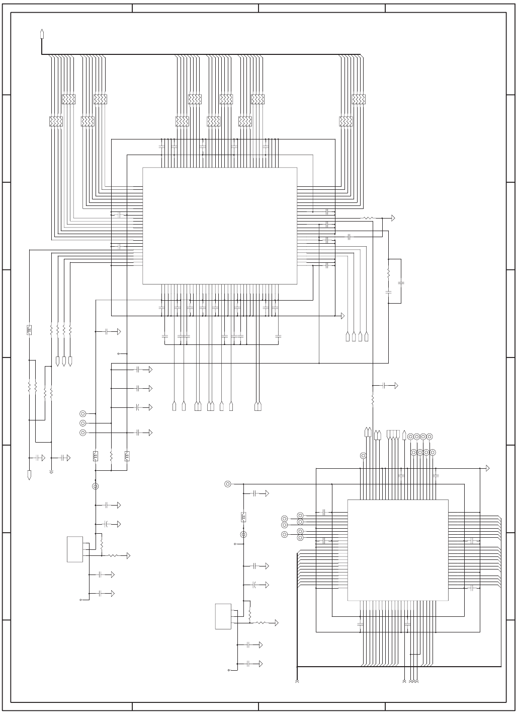
LL-T2020 CIRCUIT DIAGRAM
7 – 3
INPUT 1
BANK0 : ANALOG
BANK1 : DIGITAL
BANKSEL
L : BANK0
H :
BANK1
ID8
ID21
ID46
ID43
ID34
ID13
ID22
ID47
ID19
ID30
ID26
ID12
ID6
ID17
ID11
ID20
ID42
ID10
ID16
ID29
ID32
ID27
ID15
ID24
ID3
ID5
ID18
ID0
ID31
ID1
ID44
ID38
ID2
ID35
ID28
ID39
ID37
ID25
ID45
ID9
ID4
ID40
ID33
ID41
ID7
ID36
ID14
ID23
OV33_2
OV33_2DV33_2
PV33_2
DV33_2
OV33_1
AV33_2
DV33_1
DV5
DV5A
DV5
DV5
DV5
Q203
DTC143EE
23
1
D203
UDZS5.6B
LDS209
C222
10uF
RA212 33J x4
R201
4.7kJ
+
C221
EMPTY(22uF/16V(WT))
R204
75J
IC202
THC63DV161
57
58
49
50
51
52
53
54
55
56
59
60
61
62
63
64
65
66
67
68
69
70
71
72
73
74
75
76
77
78
79
80
81
82
83
84
85
86
87
88
89
90
91
92
93
94
95
96
97
98
99
100
1
2
3
4
5
6
7
8
9
10
11
12
13
14
15
16
17
18
19
20
21
22
23
24
25
26
27
28
29
30
31
32
33
34
35
36
37
38
39
40
41
42
43
44
45
46
47
48
OVCC
OGND
QO0
QO1
QO2
QO3
QO4
QO5
QO6
QO7
QO8
QO9
QO10
QO11
QO12
QO13
QO14
QO15
VCC
GND
QO16
QO17
QO18
QO19
QO20
QO21
QO22
OGND
QO23
OVCC
AGND
RX2+
RX2-
AVCC
AGND
AVCC
RX1+
RX1-
AGND
AVCC
AGND
RX0+
RX0-
AGND
RXC+
RXC-
AVCC
EXT_RES
PVCC
PGND
RESERVED
OCK_INV
S_D
PD
ST
PIXS/M_S
GND
VCC
STAG_OUT/SYNC
SCDT
PDO
QE0
QE1
QE2
QE3
QE4
QE5
QE6
QE7
OVCC
OGND
QE8
QE9
QE10
QE11
QE12
QE13
QE14
QE15
OGND
OVCC
QE16
QE17
QE18
QE19
QE20
QE21
QE22
QE23
VCC
GND
CTL1
CTL2
CTL3
OVCC
ODCK
OGND
DE
VSYNC
HSYNC
R212
47kJ
R205
75J
C211
0.1uF
R220
220F
C223
10uF
R223
EMPTY
Q202
IMH4A 1
2
34
5
6
C215
0.1uF
FB205
BLM18PG600SN1
R216 33J
R211
4.7kJ
LDS203
C202
0.1uF
LD201
IC201
BU9882F
1
2
3
4
5
6
78
9
10
11
12
13
14
SCL_PC0
SDA_PC0
NC
SCL_PC1
SDA_PC1
NC
GND SDA_MON
SCL_MON
DDCENA
BANKSEL
DUAL_PCB
WPB
VCC
C201
0.1uF
C217
0.1uF
LD211
R218
47kJ
C225
10uF
R210
4.7kJ
RA206 33J x4
C206
0.1uF
R222
47kJ
LDS204
R209
4.7kJ
RA203 33J x4
FB201
BLM18PG600SN1
RA211 33J x4
C224
10uF
RA209 33J x4
R208
4.7kJ
R219
510J
R207
4.7kJ
R224
0J
LD212
C212
100pF
LDS205
C226
10uF
R202
10kJ
RA205 33J x4
C219
0.1uF
RA210 33J x4
RA201 33J x4
R215 33J
LDS202
C213
0.1uF
RA207 33J x4
R226
EMPTY
LDS206
R227
0J
C216
100pF
R225
0J
FB203
BLM18PG600SN1
D202
UDZS5.6BR203
75J
LD210
IC203
LM317EMP
1
2
3
ADJ
OUTPUT
INPUT
C209
10uF(3216)
LDS207
RA204 33J x4
LD213
RA208 33J x4
R214 33J
CN201
SD-74320-1004
1
2
4
5
6
7
9
10
12
13
16
17
18
20
21
23
24
3
15
19
22
11
8
14
C1
C2
C3
C4
C5
RX2-
RX2+
RX4-
RX4+
SCL
SDA
RX1-
RX1+
RX3-
RX3+
HP
RX0-
RX0+
RX5-
RX5+
RXC+
RXC-
GND
GND
GND
GND
GND
VS
5V
ARED
AGREEN
ABLUE
AHSY
ANGND
C208
0.1uF
Q201
DTC143EE
23
1
R221
360F
C205
0.1uF
C210 0.1uF
C204
0.1uF
C203
0.1uF
LDS208
D201
RB715F
23
1
FB204
BLM18PG600SN1
R206
EMPTY
RA202 33J x4
C218
100pF
C207
0.1uF
R228
EMPTY
R213
4.7kJ
C220
EMPTY
FB202
BLM18PG600SN1
R217 33J
C214
100pF
HS2
VS2
IVS
RED2
TMDS_PDO2
TMDS_PD2
IACT
ICK
TMDS_SDET2
GREEN2
BLUE2
IHS
ID[0..47]
INP2A
INP2B
A
B
C
D
87654321
12345678
D
C
B
A A
B
C
D
87654321
12345678
D
C
B
A A
B
C
D
87654321
12345678
D
C
B
A A
B
C
D
87654321
12345678
D
C
B
A
3/9
DVI2
LL-T2020 CIRCUIT DIAGRAM
7 – 4
DV5
AV5
AV5
DV5AV5
AV5
AV5
AD33
R328
4.7kJ
C311
0.1uF
LD307
R343
10kJ
FB301
MMZ1608D301B
C310
EMPTY
LD313 Q304
EMPTY(FMG8A)
1
23
4
5
D304
DAN217U
32
1
LD312
C315
33pF
R330
680F
R312
10kJ
R353
330J
C304
10uF(B)
C305
0.047uF(B)
D305
DAN217U
32
1
C320
1000pF(B)
R316
180J
R320
10kJ
LD322
Q311
EMPTY(FMG8A)
1
23
4
5
R333
270J
C323
10uF(B)
R332
10kJ
Q308
2SA1610
R308
270J
R325
2.2kF
D307
DAN217U
32
1
Q306
EMPTY(FMG8A)
1
23
4
5
R306
150J
FB304
MMZ1608D301B
C308
10uF(B)
C306
10uF(B)
C322
0.047uF(B)
R338
10kJ
R317
33J
C331
EMPTY
R341
180J
C330
EMPTY
FB305
MMZ1608D301B
D306
DAN217U
32
1
Q312
EMPTY(FMG8A)
1
23
4
5
R329
4.7kJ
LD323
LD304
R301
10kJ
Q309
2SA1610
C314
EMPTY
R351
10kJ
LD320
R348
33J
D301
DAN217U
32
1
R321
10J
IC301
AD8612
1
2
3
4
5
6
78
9
10
11
12
13
14
QA
QA
GND
LE A
V-
IN A-
IN A+ IN B+
IN B-
V+
LE B
GND
QB
QB
LD318LD317
C303
1000pF(B)
LD302
Q307
2SA1610
R309
EMPTY
C309
EMPTY
C318
0.1uF
C325
10uF(B)
R336
10J
D303
DAN217U
32
1
R327
EMPTY
R334
180J
C316
EMPTY
R323
330J
C313
EMPTY
C319
0.047uF(B)
R346
270J
R355
4.7kJ
C321
10uF(B)
R304
10kJ
R310
180J
C329
EMPTY
R319
EMPTY
LD311
R302
270J
R356
4.7kJ
R305
10J
R322
330J
R326
2.2kF
LD314
R314
10kJ C307
0.047uF(B)
IC302
SN74LVC14A
1
2
3
4
5
6
7
14
13
12
11
10
9
8
1A
1Y
2A
2Y
3A
3Y
GND
VCC
6A
6Y
5A
5Y
4A
4Y
LD316
D302
DAN217U
32
1
R324
EMPTY
R335
10kJ
R318
33J
LD324
R342
EMPTY
Q303
2SA1610
R311
EMPTY
FB302
MMZ1608D301B
C301
0.1uF
Q305
EMPTY(FMG8A)
1
23
4
5
LD301
C312
EMPTY
R347
180J
R315
270J
R352
10J
C333
EMPTY
FB303
MMZ1608D301B
LD309
Q301
2SA1610
D309
DAN217U
32
1
R340
EMPTY
R337
150J
R303
180J
D310
DAN217U
32
1
Q302
2SA1610
C324
0.047uF(B)
R349
33J
R331
680F
C317
EMPTY
R313
10J
C332
33pF
R307
10kJ
C327
EMPTY
FB306
MMZ1608D301B
C334
EMPTY
C302
0.047uF(B)
R354
330J
D308
DAN217U
32
1
Q310
EMPTY(FMG8A)
1
23
4
5
R350
EMPTY C326
EMPTY
LD315
LD305
R345
10kJ
C328
0.1uF
R344
10J
LD319
LD303
R339
270J
VS2
BIN2
BLUE1
GIN2
RED2
GREEN1
BIN1
BLUE2
RED1
VS1
RIN1
HIN1
HREF1
HIN2
HS2
RIN2
GREEN2
HS1
GIN1
NF2
NF1
SOG1
SOG2
NF2
NF1
HREF2
VIN2
VIN1
A
B
C
D
87654321
12345678
D
C
B
A A
B
C
D
87654321
12345678
D
C
B
A A
B
C
D
87654321
12345678
D
C
B
A A
B
C
D
87654321
12345678
D
C
B
A
4/9
ANALOG INPUT
LL-T2020 CIRCUIT DIAGRAM
7 – 5
ID31
ID16
ID12
ID3
ID0
ID45
ID40
ID18
ID14
ID14
ID3
ID1
ID29
ID11
ID5
ID41
ID10
ID47
ID30
ID9
ID7
ID2ID22
ID19
ID6
ID25
ID17
ID29
ID10
ID23
ID13
ID24
ID22
ID5
ID45
ID42
ID33
ID31
ID12
ID1
ID38
ID28
ID21
ID32
ID28
ID38
ID47
ID8
ID20
ID18
ID44
ID42
ID27
ID7
ID36
ID36
ID13
ID24
ID4
ID19
ID40
ID4
ID17
ID0
ID39
ID32
ID21
ID26
ID34
ID25
ID30
ID15
ID15
ID16
ID35
ID34
ID23
ID46
ID9
ID20
ID26
ID39
ID27
ID2
ID6
ID11
ID37
ID37
ID8
ID35
ID44
ID33
ID46
ID43
ID43
ID41
IHS
ID[0..47]
IVS
ICK1
COMSYN
ICK1
DV5A
PV5
AD33
LV33
C442
0.1uF
R404 10J
C429
0.1uF
RA405 33J x4
C437
0.1uF
RA407 33J x4
C436
0.1uF
R411
220F
C401
EMPTY
RA409 33J x4
C450
3900pF(B)
C407
10uFR409
360F
FB403
BLM18PG600SN1
C412
EMPTY
LD416
R412
360F
C414
0.1uF
C433
10uF
RA406 33J x4
C440
0.1uF
R408
220F
C420
0.1uF
FB402
BLM18PG600SN1
IC403
LM317EMP
1
2
3
ADJ
OUTPUT
INPUT
RA411 33J x4
RA403 33J x4
C446
0.1uF
C416
0.1uF(B)
R401 ENPTY
C434
10uF
LD408
IC4 02
AD9888
1
2
3
4
5
6
7
8
9
10
11
12
13
14
15
16
17
18
19
20
21
22
23
24
25
26
27
28
29
30
31
32
33
34
35
36
37
38
39
40
41
42
43
44
45
46
47
48
49
50
51
52
53
54
55
56
57
58
59
60
61
62
63
64
65
66
67
68
69
70
71
72
73
74
75
76
77
78
79
80
81
82
83
84
85
86
87
88
89
90
91
92
93
94
95
96
97
98
99
100
101
102
103
104
105
106
107
108
109
110
111
112
113
114
115
116
117
118
119
120
121
122
123
124
125
126
127
128
VD
REF BYPASS
GND
GND
RAIN0
VD
VD
RAIN1
RMIDSCV
VD
GND
SOGIN0
GAIN0
VD
GND
SOGIN1
GAIN1
VD
GND
BAIN0
VD
GND
BAIN1
BMIDSCV
VD
VD
GND
GND
CKINV
CLAMP
SDA
SCL
A0
VD
GND
GND
VD
VD
VD
GND
GND
VSYNC1
HSYNC1
VSYNC0
HSYNC0
GND
PVD
PVD
GND
FILT
GND
PVD
COAST
CKEXT
GND
VDD
DBB7
DBB6
DBB5
DBB4
DBB3
DBB2
DBB1
DBB0
GND
GND
GND
GND
VDD
DBA7
DBA6
DBA5
DBA4
DBA3
DBA2
DBA1
DBA0
GND
VDD
DGB7
DGB6
DGB5
DGB4
DGB3
DGB2
DGB1
DGB0
GND
VDD
DGA7
DGA6
DGA5
DGA4
DGA3
DGA2
DGA1
DGA0
VDD
GND
GND
GND
VDD
DRB7
DRB6
DRB5
DRB4
DRB3
DRB2
DRB1
DRB0
GND
VDD
DRA7
DRA6
DRA5
DRA4
DRA3
DRA2
DRA1
DRA0
GND
VDD
DATACK
DATACKB
HSOUT
SOGOUT
VSOUT
GND
LD412
C425
0.1uF
C408
0.1uF
LD405
R410
33J
+
C405
EMPTY(22uF/16V(WT))
C438
0.1uF
C443
0.1uF
C423
0.1uF
FB404
BLM18PG600SN1
C419
0.1uF
LD409
+
C432
EMPTY(22uF/16V(WT))
R413
10kJ
C427
0.1uF
LD410
C454
0.1uF
LD415
LD419
C451
0.1uF
LD421
C447
1000pF
+
C411
10SVP33M
LD402
C431
10uF
R403 EMPTY
LD411
C403
0.1uF
C418
0.1uF
LD403
C452
0.1uF
R416 0J
IC40 4
S1L50753F26P
1
2
3
4
5
6
7
8
9
10
11
12
13
14
15
16
17
18
19
20
21
22
23
24
25
26
27
28
29
30
31
32
33
34
35
36
37
38
39
40
41
42
43
44
45
46
47
48
49
50
51
52
53
54
55
56
57
58
59
60
61
62
63
64
65
66
67
68
69
70
71
72
73
74
75
76
77
78
79
80
81
82
83
84
85
86
87
88
89
90
91
92
93
94
95
96
97
98
99
100
1VDD
RD23
RD22
RD21
RD20
GD17
GD16
GD15
GD14
GD13
GD12
GD11
GD10
VSS
ADCK
1VDD
HSYNC
VSYNC
CSYNC1
CSYNC2
GD27
GD26
GD25
GD24
VSS
1VDD
GD23
GD22
GD21
GD20
VSS
BD17
BD16
BD15
BD14
BD13
BD12
BD11
BD10
VSS
1VDD
BD27
BD26
BD25
BD24
BD23
BD22
BD21
BD20
VSS
1VDD
REG0
REG1
REG2
REG3
REG4
REG5
REG6
REG7
VSS
DOUT
1VDD
RESET
DIN
CS
SCK
TST_EN1
VSS
HSYNCO
VSYNCO
COAST
HPOLOUT
VPOLOUT
REG8
VSS
1VDD
REG9
REG10
REG11
REG12
VSS
REG13
REG14
REG15
1VDD
VSS
TST_EN
RD17
RD16
RD15
RD14
RD13
RD12
RD11
RD10
RD27
RD26
RD25
RD24
VSS
LD417
C435
0.1uF
C430
0.1uF
C426
0.1uF
RA412 33J x4
C428
0.1uF
C424
0.1uF
C422
0.1uF
C404
EMPTY C409
0.1uF
RA408 33J x4
LD404
C448
0.039uF(B)
C410
10uF
RA401 33J x4
LD406
C406
10uF
LD414
C444
0.1uF
C402
33pF
C453
0.1uF
C439
0.1uF
LD422
C441
0.1uF
RA402 33J x4
FB401 BLM18PG600SN1
C445
0.1uF
C415
0.1uF
R407 33J
C413
EMPTY
R402 0J
LD418
C421
0.1uF
R414
330J
R406 33J
RA410 33J x4
R405 33J
R415
3.3kF
RA404 33J x4
LD413
C449
0.1uF
LD420
LD401
LD407
C417
0.1uF
IC401
LM317EMP
1
2
3
ADJ
OUTPUT
INPUT
RIN1
RIN2
BIN1
GIN1
BIN2
SOG2
GIN2
SOG1
VIN2
HIN2
HIN1
VIN1
ID[0..47]
IHS
COMSYN
SDA
SCL
IVS
ASIC_CS
SI
RESET
SCLK
SO
VS_IN
HS_IN
VPOL
HPOL
ICK
A
B
C
D
87654321
12345678
D
C
B
A A
B
C
D
87654321
12345678
D
C
B
A A
B
C
D
87654321
12345678
D
C
B
A A
B
C
D
87654321
12345678
D
C
B
A
5/9
ADC
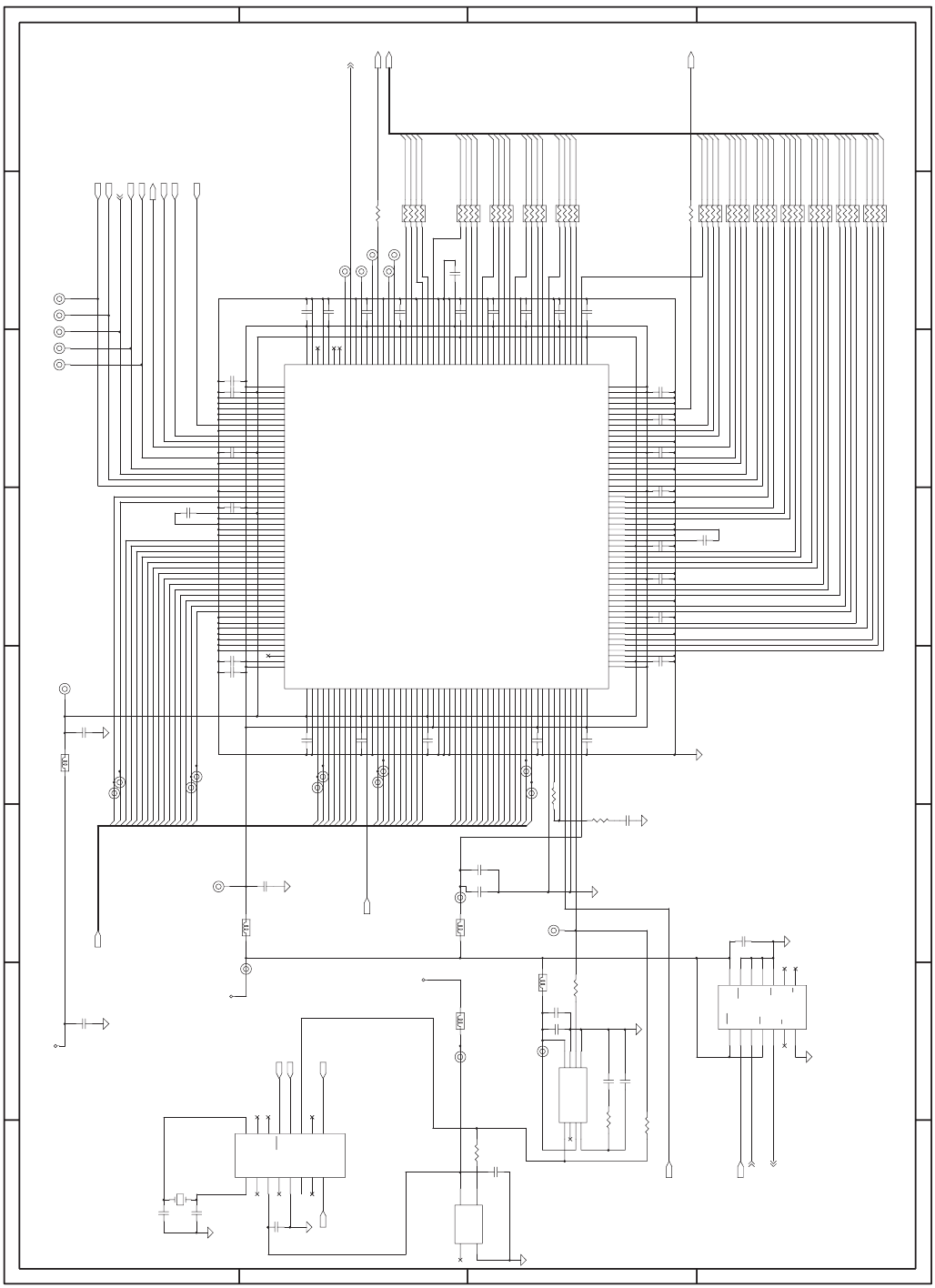
LL-T2020 CIRCUIT DIAGRAM
7 – 6
OD41
OD26
OD17
OD2
OD22
OD28
OD43
OD20
OD37
OD11
OD12
OD9
OD39
OD33
OD32
OD44
OD25
OD27
OD10
OD13
OD45
OD40
OD46
OD36
OD8
OD15
OD16
OD0
OD7
OD35
OD29
OD31
OD14
OD18
OD24
OD34
OD1
OD4
OD23
OD3
OD42
OD38
OD30
OD19
OD6
OD5
OD21
OD47
ID45
ID35
ID32
ID24
ID43
ID26
ID0
ID8
ID9
ID14
ID5
ID16
ID22
ID31
ID18
ID19
ID12
ID37
ID20
ID15
ID6
ID30
ID11
ID17
ID36
ID47
ID7
ID44
ID41
ID13
ID27
ID21
ID38
ID2
ID10
ID3
ID23
ID39
ID42
ID25
ID4
ID1
ID34
ID28
ID33
ID40
ID29
ID46
VS
VS
CLAMP
CLAMP
DV25
LV33
CL33
FB502
BLM18PG600SN1
C530
EMPTY
C514
0.1uF
C506
0.1uF
R501
EMPTY
FB501
BLM18PG600SN1
C536
0.01uF
C526
0.01uF
RA509 33J x4
LD536
R504
EMPTY
C525
0.1uF
C513
0.01uF
LD539
FB505
EMPTY(BLM18PG600SN1)
C542
0.1uF
LD523
LD522
C518
0.1uF
C505
10pF(CH)
C532
0.1uF
LD506
LD562
C534
EMPTY
LD565
IC503
EMPTY(IMIFS781BZB)
1
2
3
45
6
7
8
XIN
XOUT
S1
LF VSS
FSOUT
S0
VDD
RA511 33J x4
C510
0.1uF
LD541
RA505 33J x4
LD564
R505
75F
OSC501
EMPTY(DSO751SV(60MHz))
1
23
4
CNT
GND OUT
VCC
C515
0.1uF
RA506 33J x4
LD525
C533
0.1uF
LD535
C528
0.1uF
C543
0.1uF
RA504 33J x4
C519
0.1uF
C546
0.1uF
IC501
ICS307-02
1
2
3
4
5
6
7
16
15
14
13
12
11
10
89
X1/ICLK
NC
VDD
NC
GND
CLK2
NC
X2
NC
NC
PDTS
DATA
CLK1
NC
SCLK STROBE
FB503
BLM18PG600SN1
LD502
FB504
BLM18PG600SN1
LD537
RA508 33J x4
C523
10uF
C511
0.1uF
C502
10uF
C520
0.1uF
R503
20kF
C539
0.1uF
C538
0.1uF
LD548
LD507
C524
0.1uF
C544
0.1uF
C531
0.1uF
LD503
C504
0.1uF
C509
0.1uF
RA503 33J x4
LD501
C540
0.1uF
RA510 33J x4
C529
EMPTY
LD524
R506
EMPTY
LD526
C508
0.1uF
LD508
IC50 2
iL S-L001
1
2
3
4
5
6
7
8
9
10
11
12
13
14
15
16
17
18
19
20
21
22
23
24
25
26
27
28
29
30
31
32
33
34
35
36
37
38
39
40
41
42
43
44
45
46
47
48
49
50
51
52
53
54
55
56
57
58
59
60
61
62
63
64
65
66
67
68
69
70
71
72
73
74
75
76
77
78
79
80
81
82
83
84
85
86
87
88
89
90
91
92
93
94
95
96
97
98
99
100
101
102
103
104
105
106
107
108
109
110
111
112
113
114
115
116
117
118
119
120
121
122
123
124
125
126
127
128
129
130
131
132
133
134
135
136
137
138
139
140
141
142
143
144
145
146
147
148
149
150
151
152
153
154
155
156
157
158
159
160
161
162
163
164
165
166
167
168
169
170
171
172
173
174
175
176
177
178
179
180
181
182
183
184
185
186
187
188
189
190
191
192
193
194
195
196
197
198
199
200
201
202
203
204
205
207
208
206
VDD
CVDD
GND
OD0
OD1
OD2
GND
OD3
OD4
VDD
OD5
OD6
GND
OD7
OD8
OD9
VDD
GND
OD10
OD11
OD12
OD13
CVDD
VDD
CGND
GND
GND
OD14
OD15
OD16
GND
OD17
VDD
OD18
OD19
OD20
GND
OD21
OD22
VDD
OD23
GND
OD24
OD25
OD26
VDD
GND
OCK
CGND
GND
VDD
VDD
CVDD
OD27
OD28
OD29
OD30
VDD
GND
OD31
OD32
OD33
OD34
VDD
GND
OD35
OD36
OD37
OD38
VDD
GND
OD39
OD40
OD41
OD42
CVDD
VDD
GND
GND
CGND
CD43
CD44
CD45
GND
OD46
OD47
VDD
OVSB
OHSB
GND
OACT
IVSOB
VDD
OST
GND
HSCMP
SYNSPO
OSDVSB
OSDHSB
VDD
CGND
OSDCK
GND
VDD
VDD
CVDD
OSDDE
OSDDI0
OSDDI1
OSDDI2
OSDDI3
CSB
SPL
SCK
SI
SO
CVDD
ICK
CGND
COMSYN
IVSB
IHSB
IACT
IFLD
ID0
ID1
VDD
CVDD
YUVCK
GND
GND
CGND
ID2
ID3
ID4
ID5
ID6
ID7
ID8
ID9
ID10
ID11
ID12
ID13
ID14
ID15
CGND
TEST0
TEST1
TEST2
TEST3
TEST4
TEST5
TESTO
VDD
VDD
CVDD
GND
ID16
ID17
ID18
ID19
ID20
ID21
ID22
ID23
CVDD
RSB
CGND
ID24
ID25
ID26
ID27
ID28
ID29
ID30
ID31
ID32
CVDD
VDD
GND
GND
CGND
ID33
ID34
ID35
ID36
ID37
ID38
ID39
ID40
ID41
ID42
ID43
ID44
ID45
ID46
ID47
VDD
CGND
PLLVSS
PLLPADO
PLLPADI
PLLEN
PLLTEST
PLLVDD
VDD
REFCK
C501
10uF
RA501 33J x4
C512
10uF
IC504
TC74LCX74 FT
1
2
3
4
5
6
7
14
13
12
11
10
9
8
1CLR
1D
1CLK
1PR
1Q
1Q
GND
VCC
2CLR
2D
2CLK
2PR
2Q
2Q
C522
0.1uF
C537
0.1uF
LD504
R502 33J
LD563
C545
0.1uF
X501
SMD-49(24.00MHz)
RA512 33J x4
C517
0.1uF
C527
0.1uF
LD531
RA507 33J x4
LD549 RA502 33J x4
C541
0.1uF
C516
0.1uF
C503
10pF(CH)
LD521
C507
0.1uF
R508 33J
C535
EMPTY
C521
0.1uF
R507 0J
LD534
LD505
L001_CS
SCLK
OD[0..47]
DEN
DCLK
IVS
XCLDWN
DATA_X
STROBE_XSCLK_X
RESET
IHS
IACT
PLL_EN
SI
SO
ICK
COMSYN
ID[0..47]
A
B
C
D
87654321
12345678
D
C
B
A A
B
C
D
87654321
12345678
D
C
B
A A
B
C
D
87654321
12345678
D
C
B
A A
B
C
D
87654321
12345678
D
C
B
A
6/9
West Umeda
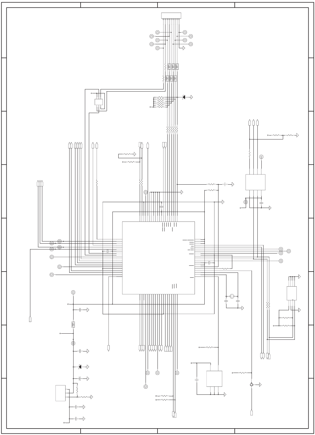
LL-T2020 CIRCUIT DIAGRAM
7 – 7
A
B
C
D
87654321
12345678
D
C
B
A A
B
C
D
87654321
12345678
D
C
B
A A
B
C
D
87654321
12345678
D
C
B
A A
B
C
D
87654321
12345678
D
C
B
A
7/9
MPU
V33
V33
V33V33
V33
V33
V33
V33
V33
V33
DV5
V33
V33
CL33
LD624
R619
LD605
IC605
BR24C16FV 1
2
3
45
6
7
8A0
A1
A2
GNDSDA
SCLK
WP
VCC
R611
R607 100J
LD625
R616
330J
R612
Q601
IMH4A 1
2
34
5
6
R610
LD603
R618
C612
10pF(CH)
R630 100J
R617
330J
R613
R614
EMPTY
R602
360F
CN601
09FLZ-SM1-TB
1
2
3
4
5
6
7
8
9
D602
UDZS5.6B
C601
0.1uF
FB602
R629 680F
C604
10uF
C608
0.1uF
R606 100J
C607
0.1uF
LD612
LD607
R605
EMPTY
R608
47kJ x6
FB601
BLM18PG600SN1
LD619
R631 100J
IC60 2
HD64F2134AVFA10
1
2
3
4
5
6
7
8
9
10
11
12
13
14
15
16
17
18
19
20
21
22
23
24
25
26
27
28
29
30
31
32
33
34
35
36
37
38
39
40
41
42
43
44
45
46
47
48
49
50
51
52
53
54
55
56
57
58
59
60
61
62
63
64
65
66
67
68
69
70
71
72
73
74
75
76
77
78
79
80
RES
XTAL
EXTAL
MD1
MD0
NMI
STBY
VCC2
SCK0/P52
RxD0/P51
TxD0/P50
VSS
WAIT/P97
EXCL/P96
IOS/AS/P95
WR/P94
RD/P93
IRQ0/P92
IRQ1/P91
ADTRG/IRQ2/P90
P60/FTC/CIN0/KIN0
P61/FTC/CIN1/KIN1
P62/FTC/CIN2/KIN2/TMIY
P63/FTC/CIN3/KIN3
P64/FTC/CIN4/KIN4
P65/FTC/CIN5/KIN5
P66/FTOB/CIN6/KIN6/IRQ6
P67/CIN7/KIN7/IRQ7
AVCC
P70/AN0
P71/AN1
P72/AN2
P73/AN3
P74/AN4
P75/AN5
P76/AN6/DA0
P77/AN7/DA1
AVSS
P40/TMCI0/TxD2/IrTxD
P41/TMO0/RxD2/IrRxD
P42/TMRI0/SCK2
P43/TMCI1
P44/TMO1
P45/TMRI1
P46/PWX0
P47/PWX1
VCC1
P27/A15
P26/A14
P25/A13
P24/A12
P23/A11
P22/A10
P21/A9
P20/A8
VSS
P17/A7
P16/A6
P15/A5
P14/A4
A3/P13
A2/P12
A1/P11
A0/P10
D0/P30
D1/P31
D2/P32
D3/P33
D4/P34
D5/P35
D6/P36
D7/P37
VSS
P80
P81
P82
P83
TxD1/IRQ3/P84
RxD1/IRQ4/P85
SCK1/IRQ5/P86
R628
47kJ
C606
0.1uF
R633
47kJ
R620
R625
EMPTY
LD620
FB604
LD623
IC603
PST598I
1
2
34
5
M/R
SUB
GND VOUT
VCC
LD604
Q602
DTC143EE
23
1
C602
10uF
LD613
LD611
R634
47kJ
R621
LD614
R635
2.2kF
LD627
C613
0.1uF
R623
100J x6
FB606
R632
EMPTY
LD615
C605
10uF
R609 LD618
LD602
LD617
LD629
LD622
IC604
M62334FP
1
2
3
45
6
7
8AO1
AO2
AO3
AO4GND
SDA
SCL
VCC
+
C603
100uF/16V(WT)
C611
1000pF
LD621
LD608
LD626
C609
0.1uF
R622
R603 100J
X601
SMD-49(10.00MHz)
FB603
LD601
LD628
LD610
R601
220F
FB605
R624
47kJ
LD616
R604
47kJ
C610
10pF(CH) R627
47kJ
IC601
LM317EMP
1
2
3
ADJ
OUTPUT
INPUT
R626
330J
R615
EMPTY
D601
UDZS5.6B
LD609
FB607
BLM18AG121SN1x6
LD606
ASIC_CS
L001_CS
SDA
SCL
BL_EN
POWER_CTL1
POWER_CTL2
TMDS_PDO1
TMDS_PD1
LVDS_PD
PLL_EN
TMDS_PDO2
TMDS_PD2
HPOL
VPOL
SO
TXD
RXD
MD1
VS_IN
HS_IN
TMDS_SDET2
TMDS_SDET1
SCLK
SI
RESET
POWER_CTL3
POWER_CTL4
INP2A
INP1B
INP2B
INP1A
NF2
NF1
HREF1
BRT_VR
HREF2
SCLK_X
STROBE_X
DATA_X
XCLDWN
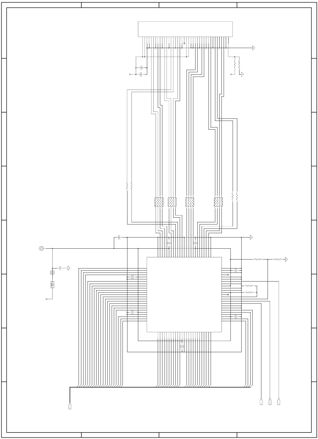
LL-T2020 CIRCUIT DIAGRAM
7 – 8
RAIN3-
RAIN2+
RACLKIN+
RACLKIN-
RAIN2-
RAIN0-
RAIN0+
RBIN0-
RBIN1-
RBIN1+
RAIN1-
RAIN1+
RAIN3+
RBCLKIN+
RBCLKIN-
RBIN0+
RBIN3-
RBIN2-
RBIN3+
RBIN2+
OD31
OD38
OD5
OD26
OD23
OD16
OD9
OD27
OD21
OD15
OD46
OD20
OD42
OD30
OD17
OD45
OD43
OD28
OD11
OD39
OD41
OD35
OD22
OD47
OD14
OD8
OD0
OD36
OD4
OD2
OD33
OD34
OD18
OD10
OD37
OD29
OD25
OD44
OD19
OD7
OD1
OD40
OD12
OD24
OD3
OD32
OD13
OD6
LV33
LV33
LCDV
R702 10J
C703
0.1uF
IC701
THC63LVD823
76
77
78
79
80
81
82
83
84
85
86
87
88
89
90
91
92
93
94
95
96
97
98
99
100
1
2
3
4
5
6
7
8
9
10
11
12
13
14
15
16
17
18
19
20
21
22
23
24
25
26
27
28
29
30
31
32
33
34
35
36
37
38
39
40
41
42
43
44
45
46
47
48
49
50
51
52
53
54
55
56
57
58
59
60
61
62
63
64
65
66
67
68
69
70
71
72
73
74
75
B15
B16
B17
R20
R21
R22
R23
R24
R25
R26
R27
VCC
GND
G20
G21
G22
G23
G24
G25
G26
G27
B20
B21
B22
B23
B24
B25
VCC
GND
B26
B27
HSYNC
VSYNC
DE
CLKIN
R/F
RS
TEST1
TEST2
MODE1
MODE0
OE
6/8
/PDWN
TEST3
TEST4
TEST5
PLL GND
PLL VCC
PLL GND
LVDS GND
TD2+
TD2-
TCLK2+
TCLK2-
TC2+
TC2-
LVDS VCC
TB2+
TB2-
TA2+
TA2-
LVDS GND
TD1+
TD1-
TCLK1+
TCLK1-
TC1+
TC1-
LVDS VCC
TB1+
TB1-
TA1+
TA1-
LVDS GND
R10
R11
R12
R13
VCC
GND
R14
R15
R16
R17
G10
G11
G12
G13
G14
G15
G16
G17
B10
B11
VCC
GND
B12
B13
B14
LD701
C707
0.1uF
R705 10J
R704
4.7kJ
R710
EMPTY
+
C702
EMPTY(22uF/16V(WT))
12
RN701 10J*4
18
27
36
45
+
C705
150uF/25V(WT)
RN702 10J*4
18
27
36
45
C708
0.1uF RN703 10J*4
18
27
36
45
FB701
BLM18PG600SN1
R703 10J
RN704 10J*4
18
27
36
45
C709
0.1uF
C706
0.1uF
R706
EMPTY
LD702
C704
0.1uF CN701
BM40B-SRDS-G-TF
1
2
5
6
29
28
30
27
26
25
24
23
22
21
20
3
4
7
8
9
10
11
12
13
14
15
16
17
18
19
31
32
33
34
35
36
37
38
39
40
VCC
VCC
RAIN0-
RAIN0+
RBIN1+
RBIN1-
VSS
VSS
RBIN0+
RBIN0-
VSS
VSS
VCC
VCC
BLON
VSS
VSS
VSS
RAIN1-
RAIN1+
VSS
RAIN2-
RAIN2+
VSS
CKAIN-
CKAIN+
VSS
RAIN3-
RAIN3+
VSS
RBIN2-
RBIN2+
VSS
CKBIN-
CKBIN+
VSS
RBIN3-
RBIN3+
VSS
SELLVDS
R709
4.7KJ
R707
4.7kJ
C701
10uF
C711
0.1uF
C710
0.1uF
R708
EMPTY
R701 10J
LVDS_PD
DEN
DCLK
OD[0..47]
A
B
C
D
87654321
12345678
D
C
B
A A
B
C
D
87654321
12345678
D
C
B
A A
B
C
D
87654321
12345678
D
C
B
A A
B
C
D
87654321
12345678
D
C
B
A
8/9
LVDS
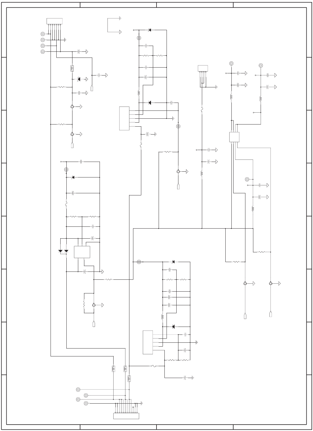
LL-T2020 CIRCUIT DIAGRAM
7 – 9
H : ON
L : OFF
Z : ON
H : ON
L : OFF
Z : OFF
0V:MAX
AV5
DV5
LCDV
DV5A
PV5
USB5
PWGND
DV25
D806 DAN202U
12
3
IC801
PQ1CY1032Z
1
2
3
4
5
VIN
VOUT
COM
OADJ
ON/OFF
Q808
DTC143EE
23
1
R810
47kJ
L805
CDRH73/10uH
R815
10kJ
+
C808
470uF/16V(UX)
C813
0.1uF
+
C818
150uF/25V(WT)
C819
0.1uF
Q802
DTC143EE
23
1
R809
3.3kF
F803
S1.0
IC802
PQ1CZ21H2ZP
1
2
3
4
5
VIN
VOUT
COM
OADJ
ON/OFF
LD805
FB803
BLM41PG600SN1
FB802
BLM41PG600SN1
+
C809
470uF/16V(UX)
CN801
B12B-PH-SM3-TBT
1
2
3
4
5
6
7
8
9
10
11
12
R808
47kJ
+
C807
2.2uF/35V(WT)
C816
0.1uF
LD815
Q803
DTC143EE
23
1
R804
1kF
+
C829
150uF/25V(WT)
C806
0.1uF
+
C831
2.2uF/35V(WT)
LD807
+
C822
47uF/16V(WT)
L807
CDRH73/10uH
+
C812
220uF/25V(WT)
D801
SFPB76
L802
CDRH73/10uH
C825
10uF
C814
0.1uF
+
C804
47uF/16V(WT)
L803
CDRH127/47uH
F804
S1.8
R805
EMPTY
Q807
HAT1025R
1
2
3
45
6
7
8
S
G
S
GD
D
D
D
R807
3.3kF
R803
3kF
F801
S1.8
C805
10uF
R814
47kJ
R811
47kJ
C811
2200pF(B)
LD804
R801
4.7kJ
D805
PTZ3.6B
C823
10uF
LD808
LD813
LD801
LD811
LD814
R812
7.87kF
IC803
PQ20WZ11
24
5
31
ON/OFF
OADJ
GND
VOUTVIN
LD806
D807
PTZ13B
+
C820
100uF/16V(WT)
Q804
EMPTY(DTC143EE)
23
1
D803
PTZ6.8B
C827
0.1uF
CN803
B4B-PH-SM3-TBT
1
2
3
4
LD812
+
C815
470uF/16V(UX)
+
C824
100uF/16V(WT)
LD809
FB801
BLM41PG600SN1
R813
2.2kF
C810
0.1uF
CN802
B7B-PH-SM3-TBT
1
2
3
4
5
6
7
L804
CDRH127/220uH
L806
NLC322522T-220K
Q806
DTC143EE
23
1
+
C826
47uF/16V(WT)
C830
0.1uF
LD810
FB804
BLM41PG600SN1
+
C828
150uF/25V(WT)
F802
S0.7
Q805
DTC143EE
23
1
R802
4.7kJ
C821
10uF
C817
2200pF(B)
LD816
D802
UDZS5.6BR806 0J
D804
SFPB76
LD803
POWER_CTL1
POWER_CTL2
POWER_CTL3
BL_EN
BRT_VR
POWER_CTL4
A
B
C
D
87654321
12345678
D
C
B
A A
B
C
D
87654321
12345678
D
C
B
A A
B
C
D
87654321
12345678
D
C
B
A A
B
C
D
87654321
12345678
D
C
B
A
9/9
POWER
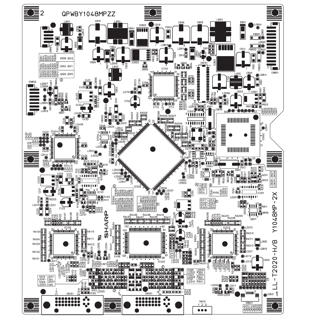
LL-T2020 PARTS LAYOUT
8 – 1
CHAPTER 8. PARTS LAYOUT
MAIN PWB
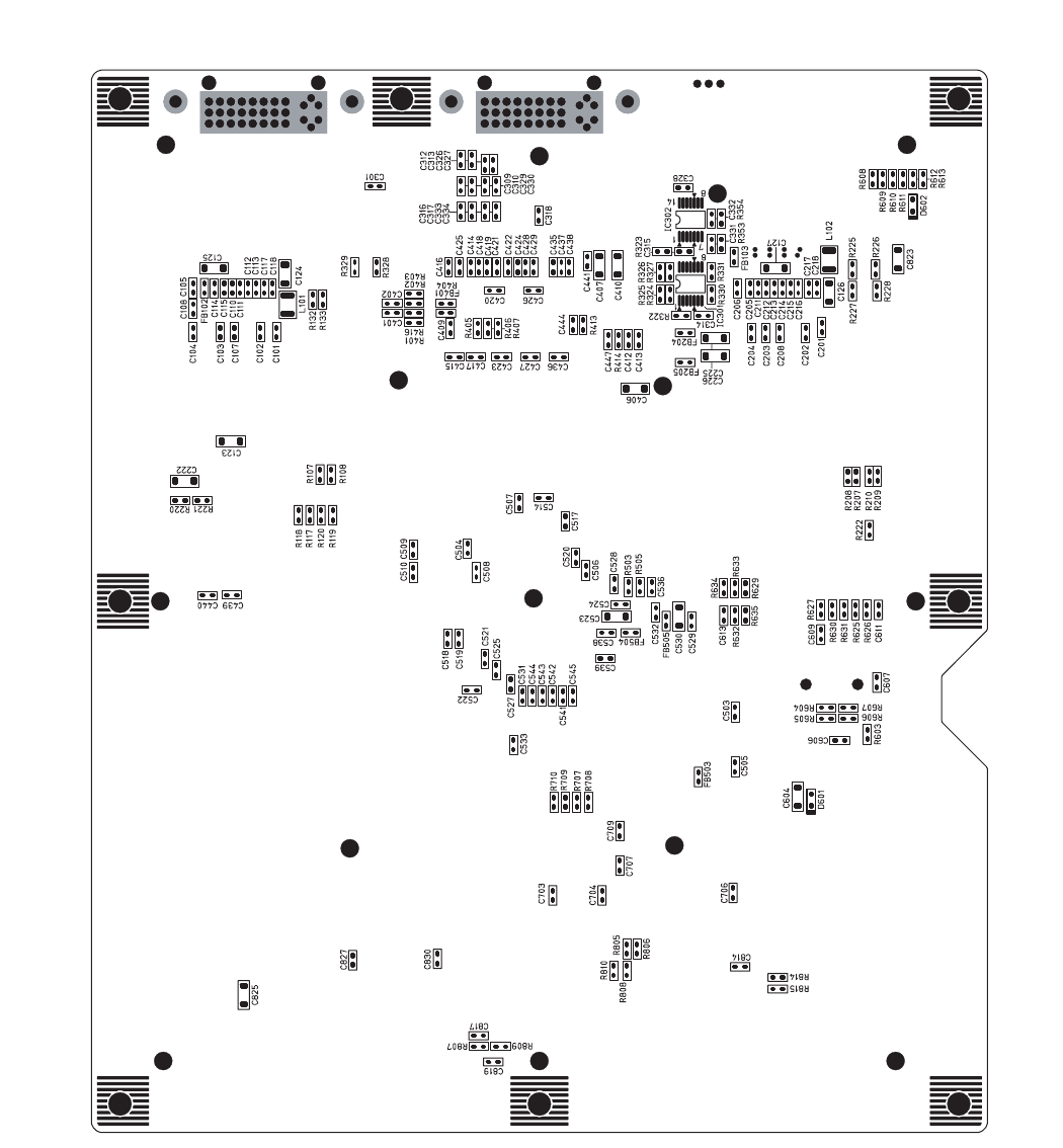
LL-T2020 PARTS LAYOUT
8 – 2
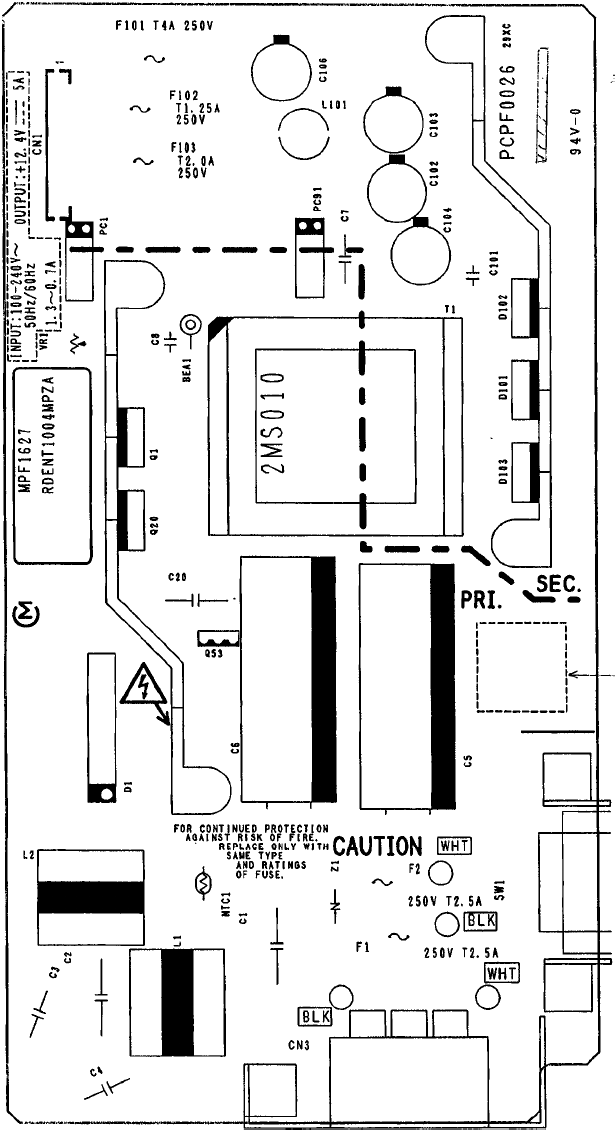
LL-T2020 PARTS LAYOUT
8 – 3
POWER SUPPLY PWB

q
SHARP CORPORATION
Digital Document Systems Group
Products Quality Assurance Department
Yamatokoriyama, Nara 639-1186, Japan
2002 December Printed in Japan
COPYRIGHT 2002 BY SHARP CORPORATION
All rights reserved.
Printed in Japan.
No part of this publication may be reproduced,
stored in a retrieval system, or transmitted.
In any form or by any means,
electronic, mechanical, photocopying, recording, or otherwise,
without prior written permission of the publisher.
