MICROPROCESSOR TI SITARA LPD SOM CLIP1 Logic Product Development Datasheet 11836495
User Manual: MICROPROCESSOR TI SITARA
Open the PDF directly: View PDF ![]() .
.
Page Count: 47
- 1 Introduction
- 2 Functional Specification
- 3 Electrical Specification
- 4 Peripheral Specification
- 5 System Integration
- 6 Memory & I/O Mapping
- 7 Pin Descriptions & Functions
- Appendix A: Mechanical Drawings
- Appendix B: Example Torpedo SOM Retention Methods

PN 1020034 Rev 1 Logic PD, Inc. All Rights Reserved. i
PRELIMINARY DOCUMENTATION—SUBJECT TO CHANGE WITHOUT NOTICE
DM3730/AM3703 Torpedo SOM
Hardware Specification
Hardware Documentation
Logic PD // Products
Published: June 2011
This document contains valuable proprietary and confidential information and the attached file contains source code, ideas, and
techniques that are owned by Logic PD, Inc. (collectively ―Logic PD’s Proprietary Information‖). Logic PD’s Proprietary Information
may not be used by or disclosed to any third party except under written license from Logic PD, Inc.
Logic PD, Inc. makes no representation or warranties of any nature or kind regarding Logic PD’s Proprietary Information or any
products offered by Logic PD, Inc. Logic PD’s Proprietary Information is disclosed herein pursuant and subject to the terms and
conditions of a duly executed license or agreement to purchase or lease equipment. The only warranties made by Logic PD, Inc., if
any, with respect to any products described in this document are set forth in such license or agreement. Logic PD, Inc. shall have no
liability of any kind, express or implied, arising out of the use of the Information in this document, including direct, indirect, special or
consequential damages.
Logic PD, Inc. may have patents, patent applications, trademarks, copyrights, trade secrets, or other intellectual property rights
pertaining to Logic PD’s Proprietary Information and products described in this document (collectively ―Logic PD’s Intellectual
Property‖). Except as expressly provided in any written license or agreement from Logic PD, Inc., this document and the information
contained therein does not create any license to Logic PD’s Intellectual Property.
The Information contained herein is subject to change without notice. Revisions may be issued regarding changes and/or additions.
© Copyright 2011, Logic PD, Inc. All Rights Reserved.

DM3730/AM3703 Torpedo SOM Hardware Specification
PN 1020034 Rev 1 Logic PD, Inc. All Rights Reserved. ii
PRELIMINARY DOCUMENTATION—SUBJECT TO CHANGE WITHOUT NOTICE
Revision History
REV
EDITOR
REVISION DESCRIPTION
Schematic
PN & REV
APPROVAL
DATE
1
NJK
Preliminary Release
1017879
Rev A
JCA
06/23/11
Please check www.logicpd.com for the latest revision of this manual and other documentation.

DM3730/AM3703 Torpedo SOM Hardware Specification
PN 1020034 Rev 1 Logic PD, Inc. All Rights Reserved. iii
PRELIMINARY DOCUMENTATION—SUBJECT TO CHANGE WITHOUT NOTICE
Table of Contents
1 Introduction ........................................................................................................................................... 1
1.1 Product Overview ............................................................................................................................. 1
1.2 Abbreviations, Acronyms, & Definitions ........................................................................................... 1
1.3 Scope of Document .......................................................................................................................... 2
1.4 Additional Documentation Resources .............................................................................................. 2
2 Functional Specification ...................................................................................................................... 3
2.1 Processor ......................................................................................................................................... 3
2.1.1 DM3730 Processor Highlights ................................................................................................... 3
2.1.2 AM3703 Processor Highlights ................................................................................................... 4
2.2 Torpedo SOM Interface.................................................................................................................... 5
2.3 Mechanical Specifications ................................................................................................................ 6
2.3.1 DM3730/AM3703 Torpedo SOM Mechanical Drawings ........................................................... 7
2.3.2 Example Torpedo SOM Retention Methods .............................................................................. 7
2.4 Temperature Specifications ............................................................................................................. 7
3 Electrical Specification ........................................................................................................................ 8
4 Peripheral Specification ....................................................................................................................... 9
4.1 Clocks............................................................................................................................................... 9
4.2 Memory ............................................................................................................................................ 9
4.2.1 Package on Package Memory (Mobile DDR and NAND) ......................................................... 9
4.2.2 External Memory ....................................................................................................................... 9
4.3 Audio Codec ................................................................................................................................... 10
4.4 Display Interface ............................................................................................................................ 10
4.5 Serial Interfaces ............................................................................................................................. 10
4.5.1 UARTA ..................................................................................................................................... 10
4.5.2 UARTB ..................................................................................................................................... 11
4.5.3 UARTC .................................................................................................................................... 11
4.5.4 McSPI ...................................................................................................................................... 11
4.5.5 I2C ........................................................................................................................................... 11
4.5.5.1 Reserved I2C Addresses .................................................................................................. 11
4.6 USB Interface ................................................................................................................................. 11
4.7 General Purpose I/O ...................................................................................................................... 12
4.8 Expansion/Feature Options ........................................................................................................... 12
5 System Integration ............................................................................................................................. 13
5.1 Configuration .................................................................................................................................. 13
5.2 Resets ............................................................................................................................................ 13
5.2.1 Master Reset (MSTR_nRST)—Reset Input ............................................................................ 13
5.2.2 Torpedo SOM Reset (SYS_nRESWARM)—Reset output ...................................................... 13
5.3 Interrupts ........................................................................................................................................ 13
5.4 JTAG Debugger Interface .............................................................................................................. 14
5.5 ETM Adapter Interface ................................................................................................................... 14
5.6 Power Management ....................................................................................................................... 14
5.6.1 System Power Supplies ........................................................................................................... 14
5.6.1.1 MAIN_BATTERY ............................................................................................................... 14
5.6.1.2 BACKUP_BATT ................................................................................................................ 14
5.6.2 System Power Management ................................................................................................... 15
5.6.2.1 T2_REGEN ....................................................................................................................... 15
5.6.3 Processor ................................................................................................................................. 15
5.6.3.1 Run State .......................................................................................................................... 15
5.6.3.2 Suspend State ................................................................................................................... 15
5.6.3.3 Standby State .................................................................................................................... 15
5.7 Boot Modes .................................................................................................................................... 16
5.8 ESD Considerations ....................................................................................................................... 16
6 Memory & I/O Mapping ....................................................................................................................... 17
7 Pin Descriptions & Functions ........................................................................................................... 18

DM3730/AM3703 Torpedo SOM Hardware Specification
PN 1020034 Rev 1 Logic PD, Inc. All Rights Reserved. iv
PRELIMINARY DOCUMENTATION—SUBJECT TO CHANGE WITHOUT NOTICE
7.1 J1 Connector 100-Pin Descriptions ............................................................................................... 18
7.2 J2 Connector 100-Pin Descriptions ............................................................................................... 25
7.3 Configurable Pins ........................................................................................................................... 32
Appendix A: Mechanical Drawings ......................................................................................................... 37
Appendix B: Example Torpedo SOM Retention Methods ..................................................................... 39

DM3730/AM3703 Torpedo SOM Hardware Specification
PN 1020034 Rev 1 Logic PD, Inc. All Rights Reserved. v
PRELIMINARY DOCUMENTATION—SUBJECT TO CHANGE WITHOUT NOTICE
Table of Figures
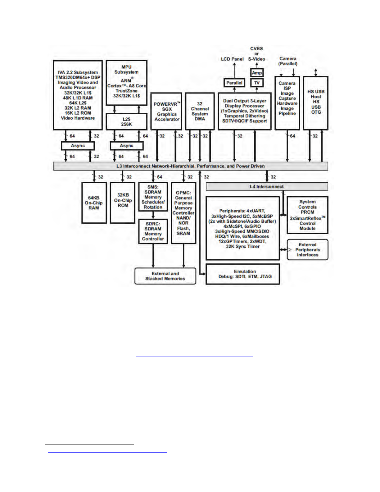
Figure 2.1: DM3730 Processor Block Diagram............................................................................................. 4
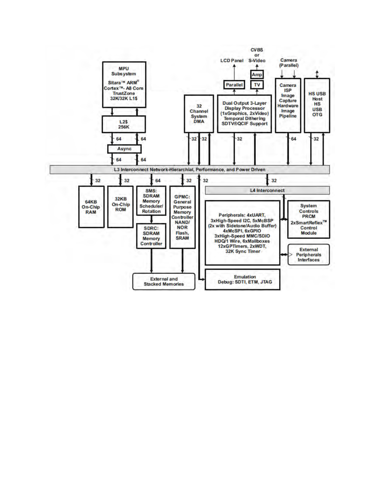
Figure 2.2: AM3703 Processor Block Diagram ............................................................................................. 5
Figure 2.3: DM3730/AM3703 Torpedo SOM Block Diagram ........................................................................ 6
Table of Tables
Table 2.1: Mechanical Characteristics of SOM ............................................................................................. 6
Table 2.2: Baseboard Mating Connectors .................................................................................................... 6
Table 2.3: Temperature Characteristics of SOM .......................................................................................... 7
Table 3.1: Absolute Maximum Ratings ......................................................................................................... 8
Table 3.2: Recommended Operating Conditions .......................................................................................... 8
Table 4.1: Processor Clock Specifications .................................................................................................... 9
Table 5.1: Signals for Multiple Boot Sources .............................................................................................. 16
Table 6.1: Chip Select Signals .................................................................................................................... 17
Table 7.1: Feature Gain/Loss through Customization ................................................................................ 33
Table 7.2: Configurable J1 and J2 Connector Pins .................................................................................... 33

DM3730/AM3703 Torpedo SOM Hardware Specification
PN 1020034 Rev 1 Logic PD, Inc. All Rights Reserved. 1
PRELIMINARY DOCUMENTATION—SUBJECT TO CHANGE WITHOUT NOTICE
1 Introduction
1.1 Product Overview
The Torpedo System on Module (SOM) is an ultra-compact form factor based on Texas
Instruments’ DaVinci™ DM3730 and Sitara™ AM3703 processors.
The DM3730 Torpedo SOM occupies less than one square inch, but boasts PC-like speeds up to
1 GHz with long battery life. Partnered with such high performance is a startlingly low power
consumption of less than 5 mW when in suspend state. This balance of speed and power is
accomplished through Logic PD’s vast system design experience; understanding the most
detailed workings of each component and their interaction with one another creates a product that
operates at optimal efficiency.
The DM3730 Torpedo SOM is available in several standard configurations, including TI’s Sitara
AM3703 ARM microprocessor. By remaining footprint compatible with Logic PD’s existing
OMAP35x Torpedo SOM, the DM3730 Torpedo SOM extends the roadmaps of existing products
and provides an upgrade path from today’s products to future technologies.
The ultra-compact Torpedo SOM is an ideal off-the-shelf solution for applications in markets
where space is a premium. From point-of-care medical devices to hand-held radios to mobile
Internet devices, the Torpedo SOM allows for the powerful versatility and compact designs
needed in today’s market-changing products.
The Zoom™ DM3730 Torpedo Development Kit includes all of the necessary accessories to
immediately begin development, helping customers deliver their products to market sooner.
1.2 Abbreviations, Acronyms, & Definitions
ADC Analog to Digital Converter
BSP Board Support Package
BTB Board-to-Board
DDR Double Data Rate (RAM)
DMA Direct Memory Access
ESD Electrostatic Discharge
FIFO First In First Out
GPIO General Purpose Input Output
GPMC General Purpose Memory Controller
GPO General Purpose Output
I2C Inter-Integrated Circuit
I2S Inter-Integrated Circuit Sound
IC Integrated Circuit
I/O Input/Output
IRQ Interrupt Request
LCD Liquid Crystal Display
LDO Low Dropout (Regulator)
LoLo LogicLoader™
McBSP Multi-channel Buffered Serial Port
OTG On-the-Go (USB)
PCB Printed Circuit Board
PCMCIA Personal Computer Memory Card International Association (PC Cards)
PHY Physical Layer
PLL Phase Lock Loop
PoP Package on Package

DM3730/AM3703 Torpedo SOM Hardware Specification
PN 1020034 Rev 1 Logic PD, Inc. All Rights Reserved. 2
PRELIMINARY DOCUMENTATION—SUBJECT TO CHANGE WITHOUT NOTICE
PWM Pulse Width Modulation
RTC Real Time Clock
SDIO Secure Digital Input Output
SDRAM Synchronous Dynamic Random Access Memory
SOM System on Module
SSP Synchronous Serial Port
SPI Standard Programming Interface
STN Super-Twisted Nematic (LCD)
TFT Thin Film Transistor (LCD)
TI Texas Instruments
TSC Touch Screen Controller
TTL Transistor-Transistor Logic
UART Universal Asynchronous Receive Transmit
1.3 Scope of Document
This Hardware Specification is unique to the design and use of the Torpedo SOM as designed by
Logic PD and does not intend to include information outside of that scope. Detailed information
about the Texas Instruments (TI) DM3730/AM3703 processors or any other device component on
the SOM can be found in their respective manuals and specification documents; please see
Section 1.4 for additional resources.
1.4 Additional Documentation Resources
The following documents or documentation resources are referenced within this Hardware
Specification.
■ TI’s DM3730, DM3725 Digital Media Processors Datasheet
1
■ TI’s AM3715, AM3703 Sitara ARM Microprocessors Datasheet
2
■ TI’s AM/DM37x Multimedia Device Technical Reference Manual (TRM)1
■ TI’s TPS65950 Data Manual
3
■ TI’s TPS65950 OMAP Power Management and System Companion Device TRM3
■ USB 2.0 Specification, available from USB.org
4
■ Logic PD’s Design Files (BOM, Schematic, and Layout) for all boards included in the
development kit (baseboard, SOM, LCD), as well as all standard configuration SOMs. Sign
into your account on Logic PD’s website to access the files.
■ Logic PD’s LogicLoader User Guide
5
1
http://focus.ti.com/docs/prod/folders/print/dm3730.html#technicaldocuments
2
http://focus.ti.com/docs/prod/folders/print/am3703.html#technicaldocuments
3
http://focus.ti.com/docs/prod/folders/print/tps65950.html#technicaldocuments
4
http://www.usb.org/developers/docs/
5
http://support.logicpd.com/downloads/1428/

DM3730/AM3703 Torpedo SOM Hardware Specification
PN 1020034 Rev 1 Logic PD, Inc. All Rights Reserved. 3
PRELIMINARY DOCUMENTATION—SUBJECT TO CHANGE WITHOUT NOTICE
2 Functional Specification
2.1 Processor
The Torpedo SOM uses TI’s DaVinci™ DM3730 and Sitara™ AM3703 processors. The DM3730
is viewed as the superset configuration; the AM3703 does not include a DSP core or graphics
accelerator.
2.1.1 DM3730 Processor Highlights
This list comes from TI’s DM3730 Digital Media Processor webpage.
6
See TI documentation for
more details.
■ Compatible with OMAP™ 3 Architecture
■ ARM® microprocessor (MPU) Subsystem
□ Up to 1-GHz ARM® Cortex™-A8 Core, Also supports 300, 600, and 800-MHz
□ NEON SIMD Coprocessor
■ High Performance Image, Video, Audio (IVA2.2™) Accelerator Subsystem
□ Up to 800-MHz TMS320C64x+™ DSP Core
□ Enhanced Direct Memory Access (EDMA) Controller (128 Independent Channels)
□ Video Hardware Accelerators
■ POWER SGX™ Graphics Accelerator (DM3730 only)
□ Tile Based Acrchitecture Delivering up to 20 MPoly/sec
□ Universal Scalable Shader Engine: Multi-threaded Engine Incorporating Pixel and Vertex
Shader Functionality
□ Industry Standard API Support: OpenGLES 1.1 and 2.0, OpenVG1.0
□ Fine Grained Task Switching, Load Balancing, and Power Management
□ Programmable High Quality Image Anti-Aliasing
■ Advanced Very-Long-Instruction-Word (VLIW) TMS320C64x+™ DSP Core
□ Eight Highly Independent Functional Units
□ Six ALUs (32-/40-Bit); Each Supports Single 32- bit, Dual 16-bit, or Quad 8-bit, Arithmetic
per Clock Cycle
□ Two Multipliers Support Four 16 × 16-Bit Multiplies (32-Bit Results) per Clock Cycle or
Eight 8 × 8-bit Multiplies (16-Bit Results) per Clock Cycle
□ Load-Store Architecture With Non-Aligned Support
6
http://focus.ti.com/docs/prod/folders/print/dm3730.html
DM3730/AM3703 Torpedo SOM Hardware Specification
PN 1020034 Rev 1 Logic PD, Inc. All Rights Reserved. 4
PRELIMINARY DOCUMENTATION—SUBJECT TO CHANGE WITHOUT NOTICE
Figure 2.1: DM3730 Processor Block Diagram
NOTE: The block diagram pictured above comes from TI’s DM3730, DM3725 Digital Media
Processors Datasheet (SPRS685D).
2.1.2 AM3703 Processor Highlights
This list comes from TI’s AM3703 Digital Media Processor webpage.
7
See TI documentation for
more details.
■ Compatible to OMAP™ 3 Architecture
■ MPU Subsystem
□ Up to 1-GHz Sitara™ ARM® Cortex™-A8 Core Also supports 300, 600, and 800-MHz
operation
□ NEON SIMD Coprocessor
7
http://focus.ti.com/docs/prod/folders/print/am3703.html
DM3730/AM3703 Torpedo SOM Hardware Specification
PN 1020034 Rev 1 Logic PD, Inc. All Rights Reserved. 5
PRELIMINARY DOCUMENTATION—SUBJECT TO CHANGE WITHOUT NOTICE
Figure 2.2: AM3703 Processor Block Diagram
NOTE: The block diagram pictured above comes from TI’s AM3715, AM3703 Sitara ARM
Microprocessors Datasheet (SPRS616F).
2.2 Torpedo SOM Interface
Logic PD’s common Torpedo SOM interface allows for easy migration to new processors and
technology. Logic PD is constantly researching and developing new technologies to improve
performance, lower cost, and increase feature capabilities. By using the common Torpedo SOM
footprint, it may be possible to take advantage of Logic PD’s work without having to re-spin the
old design. Contact Logic PD sales for more information.
In fact, encapsulating a significant amount of your design onto the Torpedo SOM reduces any
long-term risk of obsolescence. If a component on the Torpedo SOM design becomes obsolete,
Logic PD will design for an alternative part that is transparent to your product. Furthermore, Logic
PD tests all SOMs prior to delivery, decreasing time-to-market and ensuring a simpler and less
costly manufacturing process.
AM3715 Only
DM3730/AM3703 Torpedo SOM Hardware Specification
PN 1020034 Rev 1 Logic PD, Inc. All Rights Reserved. 6
PRELIMINARY DOCUMENTATION—SUBJECT TO CHANGE WITHOUT NOTICE
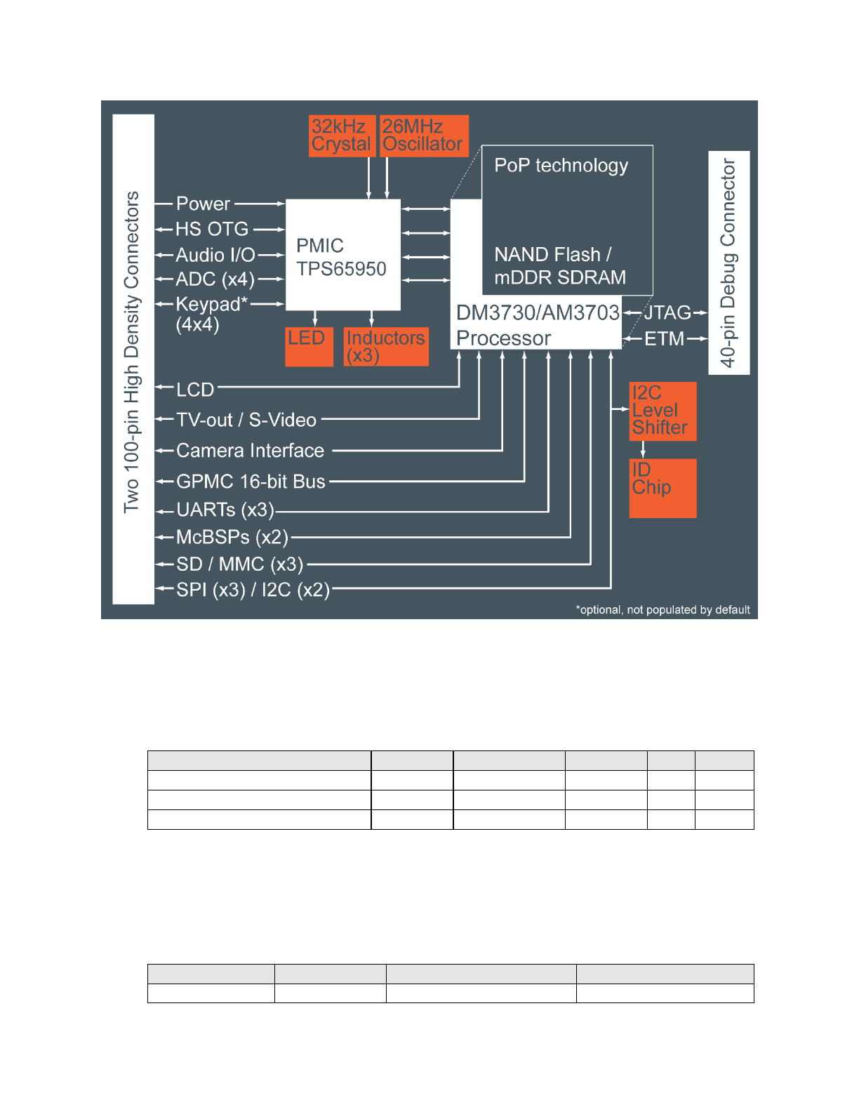
Figure 2.3: DM3730/AM3703 Torpedo SOM Block Diagram
2.3 Mechanical Specifications
Table 2.1: Mechanical Characteristics of SOM
Parameter
Min
Typical
Max
Unit
Notes
Dimensions
—
15.0 x 27.0 x 3.8
—
mm
—
Weight
—
1.96
—
Grams
1
Connector Insertion/Removal
—
30
—
Cycles
—
Table Notes:
1. May vary depending on SOM configuration.
The Torpedo SOM connects to a PCB baseboard through two 100-pin board-to-board (BTB)
socket connectors.
Table 2.2: Baseboard Mating Connectors
Ref Designator
Manufacturer
Torpedo Connector P/N
Mating Connector P/N
J1, J2
Hirose
DF40C-100DP-0.4V(51)
DF40C-100DS-0.4V(51)

DM3730/AM3703 Torpedo SOM Hardware Specification
PN 1020034 Rev 1 Logic PD, Inc. All Rights Reserved. 7
PRELIMINARY DOCUMENTATION—SUBJECT TO CHANGE WITHOUT NOTICE
2.3.1 DM3730/AM3703 Torpedo SOM Mechanical Drawings
Please see Appendix A for mechanical drawings of the DM3730/AM3703 Torpedo SOM and
recommended baseboard footprint layout.
2.3.2 Example Torpedo SOM Retention Methods
Please see Appendix B for mechanical drawings of the example retention methods for the
Torpedo SOM.
2.4 Temperature Specifications
Table 2.3: Temperature Characteristics of SOM
Parameter
Min
Typical
Max
Unit
Notes
Commercial Operating Temperature
0
25
70
C
1
Industrial Operating Temperature
-40
25
85
C
2
Storage Temperature
-40
25
85
C
—
Table Notes:
1. Junction temperature of the DM3730/AM3703 processor must stay below 90C.
2. Junction temperature of the DM3730/AM3703 processor must stay below 105C.

DM3730/AM3703 Torpedo SOM Hardware Specification
PN 1020034 Rev 1 Logic PD, Inc. All Rights Reserved. 8
PRELIMINARY DOCUMENTATION—SUBJECT TO CHANGE WITHOUT NOTICE
3 Electrical Specification
Table 3.1: Absolute Maximum Ratings
Parameter
Symbol
Rating
Unit
DC Main Battery Input Voltage
MAIN_BATTERY
0.0 to 4.5
V
DC USB1_VBUS Input Voltage
USB1_VBUS
0.0 to 7.0
V
RTC Backup Battery Voltage
BACKUP_BATT
0.0 to 3.3
V
NOTE: These stress ratings are only for transient conditions. Operation at, or beyond, absolute
maximum rating conditions may affect reliability and cause permanent damage to the Torpedo
SOM and its components.
Table 3.2: Recommended Operating Conditions
Parameter
Min
Typical
Max
Unit
Notes
DC Main Battery Input Voltage
2.7*
(see note 3)
3.3
4.5
V
3
DC Main Battery Active Current, LoLo
(Main Battery Voltage=3.64V)
—
TBD
—
mA
—
DC Main Battery Active Current,
WinCE
—
TBD
—
mA
—
DC USB1_VBUS Input Voltage
4.4
5.0
7.0
V
—
DC RTC Backup Battery Voltage
1.8
3.2
3.3
V
—
Input Signal High Voltage
0.65 x VREF
—
VREF
V
2, 4
Input Signal Low Voltage
-0.3
—
0.35 x VREF
V
2, 4
Output Signal High Voltage
VREF - 0.2
—
VREF
V
2, 4
Output Signal Low Voltage
GND
—
0.2
V
4
Table Notes:
1. General note: CPU power rails are sequenced on the SOM.
2. VREF represents the peripheral I/O supply reference for the specific CPU voltage rail.
3. 2.7V is the minimum threshold for the battery at which the device will turn OFF. However, the
minimum voltage at which the device will power ON (if PWRON does not have a switch and
is connected to MAIN_BATTERY) is 3.2V ±100mV, assuming battery plug-in as the device
switch on event. If PWRON has a switch then 3.2V is the minimum for the device to turn ON.
4. The exact minimum and maximum values depend on the specific pin being referenced.
Please refer to TI’s DM3730, DM3725 Digital Media Processors Datasheet and TPS65950
Data Manual for exact values.

DM3730/AM3703 Torpedo SOM Hardware Specification
PN 1020034 Rev 1 Logic PD, Inc. All Rights Reserved. 9
PRELIMINARY DOCUMENTATION—SUBJECT TO CHANGE WITHOUT NOTICE
4 Peripheral Specification
4.1 Clocks
The DM3730/AM3703 processors require an oscillator and crystal to enable proper internal
timing. A 26.000 MHz oscillator is used to generate many of the processor’s internal clocks via a
series of Phase Lock Loops (PLLs) and signal dividers. To generate the core CPU clock, the
26.000 MHz signal is run through a Digital PLL controlled by the PRCM registers. Divisors are
used to divide down the internal bus frequency to set the LCD, memory controller, camera
interface, etc.
IMPORTANT NOTE: Please see TI’s AM/DM37x TRM for additional information about processor
clocking.
The second required crystal runs at 32.768 kHz and is connected directly to the TPS65950 PMIC.
The 32.768 kHz clock is used for PMIC and CPU start-up and as a reference clock for the Real
Time Clock (RTC) Module.
The CPU’s microcontroller core clock speed is initialized by software on the Torpedo SOM. The
SDRAM bus speed is set at 200 MHz in LogicLoader. Other clock speeds, such as core speed
and specific serial baud rates, can be supported and modified in software for specific user
applications.
The Torpedo SOM provides an external bus clock, uP_BUS_CLK. This clock is driven by the
GPMC_CLK pin.
Table 4.1: Processor Clock Specifications
DM3730/AM3703 Processor
Signal Name
Torpedo SOM
Net Name
Default Software Value
in LogicLoader
CORE
N/A
Up to 1 GHz
SDRC_CLK
N/A
200 MHz
GPMC_CLK
uP_BUS_CLK
Not configured
4.2 Memory
4.2.1 Package on Package Memory (Mobile DDR and NAND)
The DM3730/AM3703 processors use Package on Package (PoP) technology to stack BGA
memory devices on top of the CPU BGA. The processors use a 32-bit memory bus to interface to
mobile DDR (mDDR) SDRAM and a 16-bit memory bus to interface to NAND.
Logic PD’s default memory configuration on the Torpedo SOM is 256 MB mDDR and 512 MB
NAND.
4.2.2 External Memory
It is possible to expand the system’s non-volatile storage capability by adding external flash ICs,
SD memory, CompactFlash, or NAND flash. Please contact Logic PD
8
for other possible
peripheral designs.
8
http://support.logicpd.com/support/askaquestion.php

DM3730/AM3703 Torpedo SOM Hardware Specification
PN 1020034 Rev 1 Logic PD, Inc. All Rights Reserved. 10
PRELIMINARY DOCUMENTATION—SUBJECT TO CHANGE WITHOUT NOTICE
4.3 Audio Codec
The DM3730/AM3703 processors have multiple Multi-channel Buffered Serial Port (McBSP)
interfaces that support PCM and I2S formats. Both PCM and I2S serial paths drive the built-in
TPS65950 audio codec. From the TPS65950 PMIC, the outputs are CODEC_OUTL and
CODEC_OUTR; these signals are available from the expansion connectors.
The codec in the TPS65950 PMIC performs up to full-duplex codec functions and supports
variable sample rates from 8–96k samples per second. See the ―Audio‖ chapter in TI’s TPS65950
TRM for more information.
NOTE: The Torpedo SOM also offers alternate serial interfaces for other codec devices. If you
are looking for a different codec option, Logic PD has previously interfaced different high-
performance audio codecs into other SOMs. Contact Logic PD for assistance in selecting an
appropriate audio codec for your application.
4.4 Display Interface
The DM3730/AM3703 processors have a built-in LCD controller supporting STN, color STN, and
TFT panels at a resolution of up to HD 720p, 1280 x 720 x 24-bit color. See TI’s AM/DM37x TRM
for additional information on the integrated LCD controller.
The signals from the DM3730/AM3703 LCD controller are organized by bit and color and can be
interfaced through the SOM J1 and J2 connectors (see Section 7). Logic PD has written drivers
for panels of different types and sizes. Please contact Logic PD before selecting a panel for your
application.
IMPORTANT NOTE: Using the internal graphics controller will affect processor performance.
Selecting display resolutions and color bits per pixel will vary processor busload.
4.5 Serial Interfaces
The Torpedo SOM comes with the following serial channels: UARTA, UARTB, UARTC, three SPI
ports, two MCBSP, and two I2C ports. If additional serial channels are required, please contact
Logic PD for reference designs. Please see TI’s AM/DM37x TRM for additional information
regarding serial communications.
4.5.1 UARTA
UARTA has been configured as the main Torpedo SOM serial port based on the processor
UART1. It is an asynchronous 16C750-compatible UART. This UART provides a high-speed
serial interface that uses 64 byte First In / First Out (FIFO) and is capable of sending and
receiving serial data simultaneously. The signals from the Torpedo SOM are 1.8V Transistor-
Transistor Logic (TTL) level signals, not RS232 level signals. The end-product design must
provide an external RS232 transceiver for RS232 applications. Logic PD has provided an
example reference design in the Torpedo Launcher 2 Baseboard Schematics. When choosing an
RS232 transceiver, the designer should keep in mind cost, availability, ESD protection, and data
rates.
The UARTA baud rate is set to a default 115.2 Kbits/sec, though it supports most common serial
baud rates.

DM3730/AM3703 Torpedo SOM Hardware Specification
PN 1020034 Rev 1 Logic PD, Inc. All Rights Reserved. 11
PRELIMINARY DOCUMENTATION—SUBJECT TO CHANGE WITHOUT NOTICE
4.5.2 UARTB
Serial Port UARTB (processor UART3) is an asynchronous 16C750-compatible UART. This
UART is a high-speed serial interface that uses FIFO and is capable of sending and receiving
serial data simultaneously. The signals from the Torpedo SOM are 1.8V TTL level signals, not
RS232 level signals. The UARTB baud rate can also be set to most common serial baud rates.
4.5.3 UARTC
Serial port UARTC (processor UART2) is an asynchronous 16C750-compatible UART. This
UART is a high-speed serial interface that uses FIFO and is capable of sending and receiving
serial data simultaneously. The signals from the Torpedo SOM are 1.8V TTL level signals, not
RS232 level signals. The UARTC baud rate can also be set to most common serial baud rates.
4.5.4 McSPI
The Torpedo SOM provides three external SPI ports with multiple chip selects. Additional SPI
ports are available through different resistor populations. Please see Table 7.1 for more
information.
4.5.5 I2C
The Torpedo SOM supports two dedicated external I2C ports. The clock and data signals for the
I2C2 and I2C3 ports have 4.7K ohm pull-up resistors. Please see TI’s AM/DM37x TRM for
additional information.
4.5.5.1 Reserved I2C Addresses
The Torpedo SOM contains a product ID chip that connects to the I2C bus. Logic PD software
uses this product ID chip to determine hardware version information. As a result, the 7-bit I2C
addresses listed below are used by the product ID chip and must be avoided in custom designs:
101 1000
101 1001
101 1010
101 1011
101 1100
101 1101
4.6 USB Interface
The Torpedo SOM supports one USB 2.0 OTG port, which can function as a host or device/client.
The port can operate at up to 480 Mbit/sec. The USB controller for the OTG port is internal to the
processor; an external PHY built into the TPS65950 PMIC supports the OTG port. For more
information on using the OTG interfaces, please see TI’s AM/DM37x TRM.
IMPORTANT NOTE: In order to correctly implement USB on the Torpedo SOM, additional
impedance matching circuitry may be required on the USB1_D+ and USB1_D- signals before
they can be used. USB 2.0 requirements specify the signals must be routed as differential pairs
with 90 ohm differential impedance. Refer to the USB 2.0 Specification for detailed information.

DM3730/AM3703 Torpedo SOM Hardware Specification
PN 1020034 Rev 1 Logic PD, Inc. All Rights Reserved. 12
PRELIMINARY DOCUMENTATION—SUBJECT TO CHANGE WITHOUT NOTICE
4.7 General Purpose I/O
Logic PD designed the Torpedo SOM to be flexible and provide multiple options for analog and
digital GPIO. There are numerous digital GPIO pins on the Torpedo SOM that interface to the
DM3730/AM3703 processor and TPS65950 PMIC; please see Section 7 for more information. If
certain peripherals are not desired, such as the LCD controller, chip selects, IRQs, or UARTs,
then more GPIO pins become available.
DESIGN NOTE: Due to buffer strength, an external serial resistor must be connected to the BGA
balls where GPIO_120 through GPIO_127 and GPIO_129 are muxed with MMC/SIM signals. See
Section 25.2 in TI’s DM3730, DM3725 Digital Media Processors TRM (SPRUGN4K) for additional
information.
4.8 Expansion/Feature Options
The Torpedo SOM was designed for expansion and a variable feature set, providing all the
necessary control signals and bus signals to expand the user’s design. It is possible for a user to
expand the Torpedo SOM’s functionality even further by adding host bus devices. Some features
that are implemented on the DM3730/AM3703 processors, but are not discussed herein, include:
RTC, pulse width modulation (PWM), Secure Digital, MMC cards, SDIO cards, graphics
accelerator, DSP codecs, Image Processing Unit, 1wire interface, and the debug module. See
TI’s AM/DM37x TRM and Logic PD’s Torpedo SOM Schematics for more details. Logic PD has
experience implementing additional options, including other audio codecs, Ethernet ICs,
co-processors, and components on SOMs. Please contact Logic PD for potential reference
designs before selecting your peripherals.
DESIGN NOTE: Due to buffer strength, an external serial resistor must be connected to the BGA
balls where GPIO_120 through GPIO_127 and GPIO_129 are muxed with MMC/SIM signals. See
Section 25.2 in TI’s DM3730, DM3725 Digital Media Processors TRM (SPRUGN4K) for additional
information.

DM3730/AM3703 Torpedo SOM Hardware Specification
PN 1020034 Rev 1 Logic PD, Inc. All Rights Reserved. 13
PRELIMINARY DOCUMENTATION—SUBJECT TO CHANGE WITHOUT NOTICE
5 System Integration
5.1 Configuration
The Torpedo SOM was designed to meet multiple applications for users with specific design and
budget requirements. As a result, this Torpedo SOM supports a variety of embedded operating
systems and hardware configurations. Please contact Logic PD Sales if you have additional
hardware configurations to meet your specific application needs.
5.2 Resets
The Torpedo SOM has a reset input (MSTR_nRST) and a reset output (SYS_nRESWARM).
External devices can drive MSTR_nRST low to assert reset to the product. The Torpedo SOM
uses SYS_nRESWARM to indicate to other devices that the Torpedo SOM is in reset.
5.2.1 Master Reset (MSTR_nRST)—Reset Input
Logic PD suggests that custom designs implementing the Torpedo SOM use the MSTR_nRST
signal as the ―pin-hole‖ reset used in commercial embedded systems. The MSTR_nRST triggers
a power-on-reset event to the processor and resets the entire CPU.
IMPORTANT NOTE: MSTR_nRST does not reset the TPS65950 PMIC; the TPS65950 is only
reset by removing power from the SOM.
IMPORTANT NOTE: Any custom reset circuit design should guard the assertion of the reset lines
during a low power state so as to prevent power-up in a low or bad power condition. (Powering up
in a low or bad power condition will cause data corruption and, possibly, temporary system
lockup); see Section 5.6 ―Power Management‖ for further details. Either one of the following two
conditions will cause a system-wide reset: power on the MSTR_nRST signal or a low pulse on
the MSTR_nRST signal.
Low Pulse on MSTR_nRST Signal:
A low pulse on the MSTR_nRST signal, asserted by an external source (for example, the reset
button on the custom design application) will bring MSTR_nRST low until the assertion source is
de-asserted. There is no delay beyond the de-assertion of the external MSTR_nRST signal
source, so the custom design must ensure that the assertion time is sufficient for all related
peripherals.
Logic PD suggests that for any external assertion source that triggers the MSTR_nRST signal,
analog or digital, de-bouncing should be used to generate a clean, one-shot reset signal.
5.2.2 Torpedo SOM Reset (SYS_nRESWARM)—Reset output
All hardware peripherals should connect their hardware-reset pin to the SYS_nRESWARM signal
on the SOM’s J2 connector. Internally, all Torpedo SOM peripheral hardware reset pins are
connected to the SYS_nRESWARM net.
5.3 Interrupts
The DM3730/AM3703 processors incorporate the ARM Cortex-A8 interrupt controller which
provides many inter-system interrupt sources and destinations. Most external GPIO signals can

DM3730/AM3703 Torpedo SOM Hardware Specification
PN 1020034 Rev 1 Logic PD, Inc. All Rights Reserved. 14
PRELIMINARY DOCUMENTATION—SUBJECT TO CHANGE WITHOUT NOTICE
also be configured as interrupt inputs by configuring their pin control registers. Logic PD BSPs
setup and process all onboard system and external Torpedo SOM interrupt sources. Refer to TI’s
AM/DM37x TRM for additional information on using interrupts.
5.4 JTAG Debugger Interface
The JTAG connection to the Torpedo SOM allows recovery of corrupted flash memory, real-time
application debug, and DSP development (on the DM3730 processor). There are several third-
party JTAG debuggers available for TI microcontrollers. The following signals make up the JTAG
interface to the DM3730/AM3703 processor: TDI, TMS, TCK, TDO, nTRST, RTCK, EMU0, and
EMU1. These signals are routed to reference designator J5 on the SOM.
IMPORTANT NOTE: When laying out the 20-pin connector, realize that it may not be numbered
as a standard 20-pin 0.1‖ insulation displacement connector (IDC) through-hole connector. See
the ETM Adapter Board reference design for further details. Each JTAG tool vendor may define
the 20-pin IDC connector pin-out differently.
5.5 ETM Adapter Interface
The Embedded Trace Macrocell (ETM) interface signals are available through connector J5 on
the Torpedo SOM. Logic PD developed an adapter board—included with the Zoom Torpedo
Development Kit—that converts the available signals on J5 to the standard Mictor connector
interface used by most common third-party ETM tool providers. The connector supports
ETM_D[15:0], ETM_CLK, ETM_CTL, and the JTAG signals listed in Section 5.4.
5.6 Power Management
5.6.1 System Power Supplies
In order to ensure a flexible design, the Torpedo SOM has the following power areas:
MAIN_BATTERY and BACKUP_BATT. All power areas are inputs to the Torpedo SOM. The
module also provides VIO_1V8 as a reference voltage. It may be used to supply up to 200 mA of
power, but it is recommended to use an external supply.
5.6.1.1 MAIN_BATTERY
The MAIN_BATTERY input is the main source of power for the Torpedo SOM. This input expects
a voltage within typical single lithium-ion battery limits which generally operate from 2.7V to 4.2V.
The TPS65950 power management controller takes the MAIN_BATTERY rail input and creates
all onboard voltages. If the design is required to maintain RAM contents in a critical power
situation (e.g., low battery, loss of power), the MAIN_BATTERY supply should be maintained
above the minimum level at all costs (see Section 3) unless experiencing power down or critical
power conditions.
5.6.1.2 BACKUP_BATT
The BACKUP_BATT power rail is used to power the onboard TPS65950 PMIC, power
management state machine, and RTC circuit when MAIN_BATTERY is not present. Always
power this rail to maintain the clock and power state of the product. A lithium-ion coin cell typically
supplies power to this rail. The TPS65950 PMIC overrides this input when MAIN_BATTERY is
applied.

DM3730/AM3703 Torpedo SOM Hardware Specification
PN 1020034 Rev 1 Logic PD, Inc. All Rights Reserved. 15
PRELIMINARY DOCUMENTATION—SUBJECT TO CHANGE WITHOUT NOTICE
5.6.2 System Power Management
Good power management design is important in any system development and embedded system
design is no exception. In embedded system design, power management is typically one of the
most complicated areas due to the dramatic effect it has on product cost, performance, usability,
and overall customer satisfaction. Many factors affect a power-efficient hardware design: power
supply selection (efficiency), clocking design, IC and component selection, etc. The Torpedo
SOM was designed with these aspects in mind while also providing maximum flexibility in
software and system integration.
On the Torpedo SOM there are many different software configurations that drastically affect
power consumption: microcontroller core clock frequency, bus clock frequency, peripheral clocks,
bus modes, power management states; peripheral power states and modes; product user
scenarios; interrupt handling; and display settings (resolution, backlight, refresh, bits per pixel,
etc). These settings are typically initialized in the start-up software routines and may be modified
later in the operating system and application software. Information for these items can be found in
the appropriate documents such as the LogicLoader User Guide or the specific BSP manual.
5.6.2.1 T2_REGEN
T2_REGEN is an open drain output from the TPS65950 PMIC. It can be used to control power for
external power ICs or LDOs. Please see the TPS65950 TRM for more information.
5.6.3 Processor
The DM3730/AM3703 processor’s power management scheme was designed for the cellular
handset market, which means the static and dynamic power consumption has very flexible
controls allowing designers to tweak the processor to minimize end-product power consumption.
Logic PD software BSPs take advantage of Dynamic Power Switching and SmartReflex Adaptive
Voltage Control to maximize power savings.
5.6.3.1 Run State
Run is the normal operating state for the Torpedo SOM in which oscillator outputs and all clocks
are hardware enabled. The DM3730/AM3703 processor can enter Run mode from any state. A
Standby-to-Run transition occurs on any valid wakeup event, such as the assertion of any
enabled interrupt signal. All required power supplies are active in this state. Please see TI’s
AM/DM37x TRM for further information.
5.6.3.2 Suspend State
Suspend is the hardware power-down state for the Torpedo SOM, allowing for lower power
consumption. The Suspend state is designed to reduce power consumption while the
DM3730/AM3703 processor is waiting for an event, such as a keyboard input. In Logic PD BSPs,
the Suspend state is entered through software commands. All power supplies remain active and
system context is retained. An internal or external wakeup event can cause the processor to
transition back to Run mode. Please see TI’s AM/DM37x TRM for further information.
5.6.3.3 Standby State
Standby is the lowest power state for the Torpedo SOM. This state is entered in Logic PD BSPs
through software commands. The DM3730/AM3730 processor is put into the lowest power state
and all clocks are stopped. The MAIN_BATTERY power rail should be maintained if the low-

DM3730/AM3703 Torpedo SOM Hardware Specification
PN 1020034 Rev 1 Logic PD, Inc. All Rights Reserved. 16
PRELIMINARY DOCUMENTATION—SUBJECT TO CHANGE WITHOUT NOTICE
power DDR SDRAM contents wish to be retained. Internal or external wakeup events can cause
a return to the Run state.
5.7 Boot Modes
The DM3730/AM3703 processor provides the option of booting from multiple sources. The boot
mode is controlled by the SYS_BOOT pins of the processor. SYS_BOOT0, SYS_BOOT1 and
SYS_BOOT3-SYS_BOOT5 are available off-board through the SOM’s J1 and J2 connectors.
Please see TI’s AM/DM37x TRM for further information. Common boot options are shown in
Table 5.1 below.
NOTE: The SYS_BOOT pins of the processor are shared with the parallel display interface. Take
care to ensure the boot strapping does not interfere with the display operation; also, the display
must not interfere with the SYS_BOOT pins during reset.
Table 5.1: Signals for Multiple Boot Sources
DM3730/AM3703 Processor Pins
Boot Method
Default
SYS_BOOT[6:0] =1101111
USB, UART3, MMC1, NAND
Alternate
SYS_BOOT[6:0] =1001111
NAND, USB, UART3, MMC1
Alternate
SYS_BOOT[6:0] =1001110
XIPwait, DOC, USB, UART3, MMC1
Alternate
SYS_BOOT[6:0] =1000110
MMC1, USB
5.8 ESD Considerations
The Torpedo SOM was designed to interface to a customer’s baseboard, while remaining low
cost and adaptable to many different applications. The Torpedo SOM does not provide any
onboard ESD protection circuitry—this must be provided by the product it is used in. Logic PD
has extensive experience in designing products with ESD requirements. Please contact Logic PD
if you need any assistance in ESD design considerations.

DM3730/AM3703 Torpedo SOM Hardware Specification
PN 1020034 Rev 1 Logic PD, Inc. All Rights Reserved. 17
PRELIMINARY DOCUMENTATION—SUBJECT TO CHANGE WITHOUT NOTICE
6 Memory & I/O Mapping
On the DM3730/AM3703 processor, all address mapping for the GPMC chip select signals is
listed below. Mapped ―Chip Select‖ signals for the processor are available as outputs and are
assigned as described in Table 6.1.
Table 6.1: Chip Select Signals
Chip Select
Device/Feature
Notes
nCS0
POP NAND
Boot chip select for PoP NAND device.
nCS1
uP_nCS1
Available for use by an off-board external device
nCS2
uP_nCS2
Available for use by an off-board external device
nCS3
uP_nCS3
Available for use by an off-board external device
nCS4
uP_nCS4
Available for use by an off-board external device
nCS5
uP_nCS5
Available for use by an off-board external device
nCS6
uP_nCS6
Available for use by an off-board external device
NOTE: Memory addresses for chip selects on the Torpedo SOM are configurable by software;
therefore, precise address locations cannot be provided.

DM3730/AM3703 Torpedo SOM Hardware Specification
PN 1020034 Rev 1 Logic PD, Inc. All Rights Reserved. 18
PRELIMINARY DOCUMENTATION—SUBJECT TO CHANGE WITHOUT NOTICE
7 Pin Descriptions & Functions
IMPORTANT NOTE: The following pin descriptions and states are provided for the default pin
usage. Many of the signals defined in the connector tables can be configured as input or
outputs—most GPIOs on the DM3730/AM3703 processor can be configured as either inputs or
outputs—and have different functions. It is critical to review all signals in the final design (both
electrical and software) to verify the necessary configuration (external pull-ups/pull-downs).
IMPORTANT NOTE: Please pay special attention to the reference voltage used to power each
signal in the table below, especially when used as a GPIO. Not all power rails coming out of the
TPS65950 PMIC are on by default and may need to be enabled through software. Reference
voltages for DM3730/AM3703 processor signals can be found in Table 2-1 of TI’s DM3730,
DM3725 Digital Media Processors Datasheet or AM3715, AM3703 Sitara ARM Microprocessor
Datasheet.
7.1 J1 Connector 100-Pin Descriptions
J1
Pin#
Signal Name
BGA Ball#
Processor Signal
I/O
Voltage
Description
1
uP_nWE
F4
GPMC_nWE
O
1.8V
Low indicates processor is writing.
High indicates processor is
reading. (See notes 1 & 2)
2
CODEC_OUTL
B4 (PMIC)
HSOL (PMIC)
O
max 2.7V
Left channel headset out.
3
VMMC1
K25
C2 (PMIC)
VDDS_MMC1
VMMC1.OUT (PMIC)
O
3.0V
(configurable)
MMC/SD1 interface voltage
reference output.
4
CODEC_INR
G1 (PMIC)
AUXR (PMIC)
I
max 2.7V
Auxiliary right channel line in.
5
PWRON
A11 (PMIC)
PWRON (PMIC)
I
Max 4.5V
(MAIN_BATTERY)
Active low. Software can use this
signal as an interrupt to transition
to RUN state from lower power
states. Software is required for
proper operation. This signal has a
4.7K pull up.
6
CODEC_INL
F1 (PMIC)
AUXL (PMIC)
I
max 2.7V
Auxiliary left channel line in.
7
uP_A9
L3
GPMC_A9/
SYS_nDMAREQ2/
GPIO_42
O
1.8V
Processor GPMC bus address bit
9.
8
MIC_IN
E3 (PMIC)
HSMIC.P (PMIC)
I
max 2.7V
Microphone input.
9
uP_nCS0
G4
GPMC_nCS0
O
1.8V
uP_nCS0 is used by the PoP
NAND flash device. This signal
MUST be left unconnected, unless
the PoP chip does not contain
NAND. (See note 1)
10
CODEC_OUTR
B5 (PMIC)
HSOR (PMIC)
O
max 2.7V
Right channel headset out.
11
uP_nCS1
H3
GPMC_nCS1/GPIO_52
O
1.8V
External chip select available for
customer use.
12
DGND
(See
Schematic)
(See Schematic)
I
GND
Ground. Connect to digital ground.
13
uP_A8
M3
GPMC_A8/GPIO_41
O
1.8V
Processor GPMC bus address bit
8.
14
MAIN_BATTERY
(See
Schematic)
(See Schematic)
I
max 4.5V
External power source input. This
signal should be driven directly by
a single cell lithium-ion battery or a
fixed regulated power source.

DM3730/AM3703 Torpedo SOM Hardware Specification
PN 1020034 Rev 1 Logic PD, Inc. All Rights Reserved. 19
PRELIMINARY DOCUMENTATION—SUBJECT TO CHANGE WITHOUT NOTICE
J1
Pin#
Signal Name
BGA Ball#
Processor Signal
I/O
Voltage
Description
15
uP_nOE
G2
GPMC_nOE
O
1.8V
Active low. Used to indicate
processor is reading from external
devices. (See notes 1 & 2)
16
MAIN_BATTERY
(See
Schematic)
(See Schematic)
I
max 4.5V
External power source input. This
signal should be driven directly by
a single cell lithium-ion battery or a
fixed regulated power source.
17
DGND
(See
Schematic)
(See Schematic)
I
GND
Ground. Connect to digital ground.
18
MAIN_BATTERY
(See
Schematic)
(See Schematic)
I
max 4.5V
External power source input. This
signal should be driven directly by
a single cell lithium-ion battery or a
fixed regulated power source.
19
uP_BUS_CLK
T4
GPMC_CLK/GPIO_59
O
1.8V
Processor bus clock. Frequency
varies based on software setup.
Note: uP_BUS_CLK is only active
on bus transactions, it does not run
continuously. See TI's AM/DM37x
TRM and datasheets for additional
information.
20
MAIN_BATTERY
(See
Schematic)
(See Schematic)
I
max 4.5V
External power source input. This
signal should be driven directly by
a single cell lithium-ion battery or a
fixed regulated power source.
21
uP_nBE1
U3
GPMC_nBE1/GPIO_61
O
1.8V
Processor bus Byte Lane Enable 1
bits [15:8].
22
DGND
(See
Schematic)
(See Schematic)
I
GND
Ground. Connect to digital ground.
23
uP_nADV_ALE
F3
GPMC_nADV_ALE
O
1.8V
Processor GPMC address valid or
address latch enable signal. (See
notes 1 & 2)
24
BACKUP_BATT
M14 (PMIC)
BKBAT (PMIC)
I
1.8V-3.3V
External input that supplies power
to the onboard power management
controller and RTC interface. This
signal should be powered by a
coin-cell type battery or an always-
on power source.
25
uP_nBE0
G3
GPMC_nBE0_CLE/
GPIO_60
O
1.8V
Processor bus Byte Lane Enable 0
bits [7:0]. (See notes 1 & 2)
26
uP_nWAIT
M8
GPMC_WAIT0
I
1.8V
Active low. Processor bus
GPMC_WAIT0 signal. Used to
extend bus transactions beyond
programmed wait states. The
external device signals completion
of the cycle by deasserting the
uP_nWAIT signal. This signal is
connected to the PoP NAND flash
R/B signal. (See notes 1 & 2)
27
DGND
(See
Schematic)
(See Schematic)
I
GND
Ground. Connect to digital ground.
28
uP_nCS6
P8
GPMC_nCS6/
SYS_nDMAREQ3/
McBSP4_DX/
GPT11_PWM_EVT/
GPIO_57
O
1.8V
External chip select available for
customer use.

DM3730/AM3703 Torpedo SOM Hardware Specification
PN 1020034 Rev 1 Logic PD, Inc. All Rights Reserved. 20
PRELIMINARY DOCUMENTATION—SUBJECT TO CHANGE WITHOUT NOTICE
J1
Pin#
Signal Name
BGA Ball#
Processor Signal
I/O
Voltage
Description
29
uP_D8
H2
GPMC_D8/GPIO_44
I/O
1.8V
Processor GPMC bus data bit 8.
(See notes 1 & 2)
30
uP_DREQ0
J8
AG11
GPMC_WAIT3/
SYS_nDMAREQ1/
UART4_RX/GPIO_65
POP_INT0_FT
I
1.8V
DMA Request signal for DMA4.
Connected to SYS_nDMAREQ1 of
the DM3730. Note: This signal is
shared with the PoP NAND chip’s
LOCK pin. This signal should be
left floating at power-on to avoid
conflict. (See notes 1 & 2)
31
uP_D9
K2
GPMC_D9/GPIO_45
I/O
1.8V
Processor GPMC bus data bit 9.
(See notes 1 & 2)
32
uP_nCS5
R8
GPMC_nCS5/
SYS_nDMAREQ2/
McBSP4_DR/
GPT10_PWM_EVT/
GPIO_56
O
1.8V
External chip select available for
customer use.
33
uP_D2
L2
GPMC_D2
I/O
1.8V
Processor GPMC bus data bit 2.
(See notes 1 & 2)
34
uP_nCS4
T8
GPMC_nCS4/
SYS_nDMAREQ1/
McBSP4_CLKX/
GPT9_PWM_EVT/
GPIO_55
O
1.8V
External chip select available for
customer use.
35
uP_D0
K1
GPMC_D0
I/O
1.8V
Processor GPMC bus data bit 0.
(See notes 1 & 2)
36
uP_nCS3
U8
GPMC_nCS3/
SYS_nDMAREQ0/
GPIO_54
O
1.8V
External chip select available for
customer use.
37
uP_D1
L1
GPMC_D1
I/O
1.8V
Processor GPMC bus data bit 1.
(See notes 1 & 2)
38
uP_A10
K3
GPMC_A10/
SYS_nDMAREQ3/
GPIO_43
O
1.8V
Processor GPMC bus address bit
10.
39
uP_D3
P2
GPMC_D3
I/O
1.8V
Processor GPMC bus data bit 3.
(See notes 1 & 2)
40
uP_nCS2
V8
GPMC_nCS2/GPIO_53
O
1.8V
External chip select available for
customer use.
41
uP_D12
R2
GPMC_D12/GPIO_48
I/O
1.8V
Processor GPMC bus data bit 12.
(See notes 1 & 2)
42
uP_A4
K4
GPMC_A4/GPIO_37
O
1.8V
Processor GPMC bus address bit
4.
43
uP_D10
P1
GPMC_D10/GPIO_46
I/O
1.8V
Processor GPMC bus data bit 10.
(See notes 1 & 2)
44
uP_A3
L4
GPMC_A3/GPIO_36
O
1.8V
Processor GPMC bus address bit
3.
45
uP_D11
R1
GPMC_D11/GPIO_47
I/O
1.8V
Processor GPMC bus data bit 11.
(See notes 1 & 2)
46
uP_A2
M4
GPMC_A2/GPIO_35
O
1.8V
Processor GPMC bus address bit
2.
47
uP_D13
T2
GPMC_D13/GPIO_49
I/O
1.8V
Processor GPMC bus data bit 13.
(See notes 1 & 2)
48
uP_A1
N4
GPMC_A1/GPIO_34
O
1.8V
Processor GPMC bus address bit
1.

DM3730/AM3703 Torpedo SOM Hardware Specification
PN 1020034 Rev 1 Logic PD, Inc. All Rights Reserved. 21
PRELIMINARY DOCUMENTATION—SUBJECT TO CHANGE WITHOUT NOTICE
J1
Pin#
Signal Name
BGA Ball#
Processor Signal
I/O
Voltage
Description
49
uP_D4
T1
GPMC_D4
I/O
1.8V
Processor GPMC bus data bit 4.
(See notes 1 & 2)
50
uP_A7
N3
GPMC_A7/GPIO_40
O
1.8V
Processor GPMC bus address bit
7.
51
MCSPI2_CS1
V3
McSPI2_CS1/
GPT8_PWM_EVT/
HSUSB2_TLL_DATA3/
USUSB2_DATA3/
MM2_TXEN_N/
GPIO_182
O
1.8V
McSPI2 interface chip select 1
output.
52
uP_A6
R3
GPMC_A6/GPIO_39
O
1.8V
Processor GPMC bus address bit
6.
53
uP_D6
V2
GPMC_D6
I/O
1.8V
Processor GPMC bus data bit 6.
(See notes 1 & 2)
54
uP_A5
T3
GPMC_A5/GPIO_38
O
1.8V
Processor GPMC bus address bit
5.
55
uP_D7
W2
GPMC_D7
I/O
1.8V
Processor GPMC bus data bit 7.
(See notes 1 & 2)
56
MCSPI2_SOMI
Y3
McSPI2_SOMI/
GPT10_PWM_EVT/
HSUSB2_TLL_DATA5/
HSUSB2_DATA5/
GPIO_180
I
1.8V
McSPI2 interface receive input.
57
uP_D5
V1
GPMC_D5
I/O
1.8V
Processor GPMC bus data bit 5.
(See notes 1 & 2)
58
MCSPI2_CS0
Y4
McSPI2_CS0/
GPT11_PWM_EVT/
HSUSB2_TLL_DATA6/
HSUSB2_DATA6/
GPIO_181
O
1.8V
McSPI2 interface chip select 0
output.
59
uP_D14
W1
GPMC_D14/GPIO_50
I/O
1.8V
Processor GPMC bus data bit 14.
(See notes 1 & 2)
60
MCSPI1_SOMI
AA4
McSPI1_SOMI/
MMC2_DAT6/GPIO_173
I
1.8V
McSPI1 interface receive input.
61
DGND
(See
Schematic)
(See Schematic)
I
GND
Ground. Connect to digital ground.
62
MCBSP4_DR
AD1
McBSP4_DR/
SSI1_FLAG_RX/
HSUSB3_TLL_DATA0/
MM3_RXRCV/
GPIO_153
I
1.8V
McBSP4 interface receive input.
63
uP_D15
Y1
GPMC_D15/GPIO_51
I/O
1.8V
Processor GPMC bus data bit 15.
(See notes 1 & 2)
64
MCSPI1_CLK
AB3
McSPI1_CLK/
MMC2_DAT4GPIO_171
O
1.8V
McSPI1 serial clock signal.
65
MCSPI2_SIMO
Y2
McSPI2_SIMO/
GPT9_PWM_EVT/
HSUSB2_TLL_DATA4/
HSUSB2_DATA4/
GPIO_179
O
1.8V
McSPI2 interface transmit output.
66
MCSPI1_SIMO
AB4
McSPI1_SIMO/
MMC2_DAT5/GPIO_172
O
1.8V
McSPI1 interface transmit output.

DM3730/AM3703 Torpedo SOM Hardware Specification
PN 1020034 Rev 1 Logic PD, Inc. All Rights Reserved. 22
PRELIMINARY DOCUMENTATION—SUBJECT TO CHANGE WITHOUT NOTICE
J1
Pin#
Signal Name
BGA Ball#
Processor Signal
I/O
Voltage
Description
67
MCSPI2_CLK
AA3
McSPI2_CLK/
HSUSB2_TLL_DATA7/
HSUSB2_DATA7/
GPIO_178
O
1.8V
McSPI2 serial clock signal.
68
uP_UARTA_CTS
W8
UART1_CTS/
SSI1_RDY_TX/
HSUSB3_TLL_CLK/
GPIO_150
I
1.8V
Clear To Send signal for UART1.
69
MCSPI1_CS1
AC3
McSPI1_CS1/
ADPLLV2D_DITHERING
_EN2/
MMC3_CMD/GPIO_175
O
1.8V
McSPI1 interface chip select 1
output.
70
uP_UARTA_RX
Y8
UART1_RX/
MCBSP1_CLKR/
MCSPI4_CLK/
GPIO_151
I
1.8V
Data Receive signal for UART1.
71
MCSPI1_CS0
AC2
McSPI1_CS0/
MMC2_DAT7/GPIO_174
O
1.8V
McSPI1 interface chip select 0
output.
72
uP_UARTA_TX
AA8
UART1_TX/
SSI1_DAT_TX/
GPIO_148
O
1.8V
Data Transmit signal for UART1.
73
LCD_PANEL_PWR
AC1
McBSP4_FSX/
SSI1_WAKE/
HSUSB3_TLL_DATA3/
MM3_TXEN_n/
GPIO_155
O
1.8V
LCD Panel Power signal.
74
uP_UARTA_RTS
AA9
UART1_RTS/
SSI1_FLAG_TX/
GPIO_149
O
1.8V
Ready To Send signal for UART1.
75
LCD_BACKLIGHT_PWR
AD2
McBSP4_DX/
SSI1_RDY_RX//
HSUSB3_TLL_DATA2/
MM3_TXDAT/GPIO_154
O
1.8V
LCD Backlight Power signal. Active
High.
76
R90 Populated (default):
ADCIN0 (CONFIG11)
H4 (PMIC)
ADCIN0 (PMIC)
I
max 1.5V
Analog to digital converter input.
Connected to TPS65950 ADCIN0.
Tie to DGND when not used.
R91 Populated:
CSI_D8 (CONFIG11)
K27 (PMIC)
CAM_D8/GPIO_107
I
1.8V
Camera Sensor Interface Data bit
8. This signal may also be used as
GPI; output signaling is not
supported.
77
MCBSP3_DR
T15 (PMIC)
PCM.VDX (PMIC)
I
1.8V
McBSP3 interface receive input.
78
R90 Populated (default):
ADCIN1 (CONFIG10)
J3 (PMIC)
ADCIN1 (PMIC)
I
max 1.5V
Analog to digital converter input.
Connected to TPS65950 ADCIN1.
Tie to DGND when not used.
R91 Populated:
CSI_D9 (CONFIG10)
L27
CAM_D9/GPIO_108
I
1.8V
Camera Sensor Interface Data bit
9. This signal may also be used as
GPI; output signaling is not
supported.
79
MCBSP3_DX
T2 (PMIC)
AF6
PCM.VDR (PMIC)
McBSP3_DX/
UART21_CTS/
HSUSB3_TLL_DATA4/
GPIO_140
O
1.8V
McBSP3 interface transmit output.

DM3730/AM3703 Torpedo SOM Hardware Specification
PN 1020034 Rev 1 Logic PD, Inc. All Rights Reserved. 23
PRELIMINARY DOCUMENTATION—SUBJECT TO CHANGE WITHOUT NOTICE
J1
Pin#
Signal Name
BGA Ball#
Processor Signal
I/O
Voltage
Description
80
R90 Populated (default):
ADCIN2 (CONFIG9)
G3 (PMIC)
ADCIN2 (PMIC)
I
max 2.5V
Analog to digital converter input.
Connected to TPS65950 ADCIN2.
Tie to DGND when not used.
R91 Populated:
CSI_D10 (CONFIG9)
B25
CAM_D10/SSI2_WAKE/
GPIO_109
I
1.8V
Camera Sensor Interface Data bit
10.
81
MCBSP3_FSX
R16 (PMIC)
AE5
PCM.VFS (PMIC)
McBSP3_FSX/
UART2_RX/
HSUSB3_TLL_DATA7/
GPIO_143
I/O
1.8V
McBSP3 transmit frame
synchronization.
82
R90 Populated (default):
ADCIN3 (CONFIG8)
P11 (PMIC)
ADCIN3 (PMIC)
I
max 2.5V
Analog to digital converter input.
Connected to TPS65950 ADCIN3.
Tie to DGND when not used.
R91 Populated:
CSI_D11 (CONFIG8)
C26
CAM_D11/GPIO_110
I
1.8V
Camera Sensor Interface Data bit
11.
83
MCBSP3_CLKX
R1 (PMIC)
AF5
PCM.VCK (PMIC)
McBSP3_CLKX/
UART2_TX/
HSUSB3_TLL_DATA6/
GPIO_142
O
1.8V
McBSP3 transmit clock output.
84
SD2_DATA0
AH5
MMC2_DAT0/
McSPI3_SOMI/
GPIO_132
I/O
1.8V
MMC/SD2 Data 0 signal. This
signal requires a 10K pull-up to
VIO_1V8.
85
DGND
(See
Schematic)
(See Schematic)
I
GND
Ground. Connect to digital ground.
86
R86 Populated (default):
LCD_D17 (CONFIG1)
H27
DSS_D17/GPIO_87
O
1.8V
LCD data bit when operating in
24 bpp color mode. Please
reference the AM/DM37x TRM for
LCD bus mapping.
R87 Populated:
MCSPI1_CS2
(CONFIG1)
AB1
McSPI1_CS2/
MMC3_CLK/
GPIO_176
O
1.8V
McSPI1 interface chip select 2
output.
87
R86 Populated (default):
LCD_D23
(CONFIG2/SYS_BOOT6)
AF21
SYS_BOOT6/DSS_D23/
GPIO_8
O
1.8V
LCD data bit when operating in
24 bpp color mode. Please
reference the AM/DM37x TRM for
LCD bus mapping. Must be left
floating during boot-up, unless the
boot order is to be modified. This
signal has a 4.7K pull-up on the
SOM.
R87 Populated:
SD3_CLK (CONFIG2)
AF10
ETK_CLK/
McBSP5_CLKX/
MMC3_CLK/
HSUSB1_STP/
MM1_RXDP/
HSUSB1_TLL_STP/
GPIO_12
O
1.8V
MMC/SD3 Clock signal.
88
R86 Populated (default):
MCSPI3_CLK
(CONFIG3)
AE13
ETK_D3/McSPI3_CLK/
MMC3_DAT3/
HSUSB1_DATA7/
HSUSB1_TLL_DATA7/
GPIO_17
O
1.8V
McSPI3 serial clock signal.
R87 Populated:
MCSPI1_CS3
(CONFIG3)
AB2
McSPI1_CS3/
HSUSB2_TLL_DATA2/
MM2_TXDAT/GPIO_177
O
1.8V
McSPI1 interface chip select 3
output.

DM3730/AM3703 Torpedo SOM Hardware Specification
PN 1020034 Rev 1 Logic PD, Inc. All Rights Reserved. 24
PRELIMINARY DOCUMENTATION—SUBJECT TO CHANGE WITHOUT NOTICE
J1
Pin#
Signal Name
BGA Ball#
Processor Signal
I/O
Voltage
Description
89
SD2_CLK
AE2
MMC2_CLK/
McSPI3_CLK/GPIO_130
O
1.8V
MMC/SD2 Clock signal.
90
R96 Populated (default):
SD3_DATA3
(CONFIG23)
AE3
MMC2_DAT7/
MMC2_CLKIN/
MMC3_DAT3/
HSUSB3_TLL_NXT/
MM3_RXDM/GPIO_139
I/O
1.8V
MMC/SD3 Data 3 signal. This
signal requires a 10K pull-up to
VIO_1V8.
R97 Populated:
MCSPI3_SOMI
(CONFIG23)
AG12
ETK_D1/McSPI3_SOMI/
HSUSB1_DATA1/
MM1_TXSE0/
HSUSB1_TLL_DATA1/
GPIO_15
I
1.8V
McSPI3 interface receive input.
91
SD2_DATA3
AF4
MMC2_DAT3/
McSPI3_CS0/GPIO_135
I/O
1.8V
MMC/SD2 Data 3 signal. This
signal requires a 10K pull-up to
VIO_1V8.
92
R96 Populated (default):
SD3_DATA2
(CONFIG22)
AF3
MMC2_DAT6/
MMC2_DIR_CMD/
CAM_SHUTTER/
MMC3_DAT2/
HSUSB3_TLL_DIR/
GPIO_138
I/O
1.8V
MMC/SD3 Data 2 signal. This
signal requires a 10K pull-up to
VIO_1V8.
R97 Populated:
MCSPI3_SIMO
(CONFIG22)
AF11
ETK_D0/McSPI3_SIMO/
MMC3_DAT4/
HSUSB1_DATA0/
MM1_RXRCV/
HSUSB1_TLL_DATA0/
GPIO_14
O
1.8V
McSPI3 interface transmit output.
93
SD2_DATA2
AG4
MMC2_DAT2/
McSPI3_CS1/GPIO_134
I/O
1.8V
MMC/SD2 Data 2 signal. This
signal requires a 10K pull-up to
VIO_1V8.
94
R96 Populated (default):
SD3_DATA1
(CONFIG21)
AH3
MMC2_DAT5/
MMC2_DIR_DAT1/
CAM_GLOBAL_RESET/
MMC3_DAT1/
HSUSB3_TLL_STP/
MM3_RXDP/GPIO_137
I/O
1.8V
MMC/SD3 Data 1 signal. This
signal requires a 10K pull-up to
VIO_1V8.
R97 Populated:
MCSPI3_CS0
(CONFIG21)
AH12
ETK_D2/McSPI3_CS0/
HSUSB1_DATA2/
MM1_TXDAT/
HSUSB1_TLL_DATA2/
GPIO_16
O
1.8V
McSPI3 interface chip select 0
output.
95
SD2_DATA1
AH4
MMC2_DAT1/GPIO_133
I/O
1.8V
MMC/SD2 Data 1 signal. This
signal requires a 10K pull-up to
VIO_1V8.
96
R96 Populated (default):
SD3_DATA0
(CONFIG20)
AE4
MMC2_DAT4/
MMC2_DIR_DAT0/
MMC3_DAT0/GPIO_136
I/O
1.8V
MMC/SD3 Data 0 signal. This
signal requires a 10K pull-up to
VIO_1V8.
R97 Populated:
MCSPI3_CS1
(CONFIG20)
AH14
ETK_D7/McSPI3_CS1/
MMC3_DAT7/
HSUSB1_DATA3/
MM1_TXEN_n/
HSUSB1_TLL_DATA3/
GPIO_21
O
1.8V
McSPI3 interface chip select 1
output.
97
SD2_CMD
AG5
MMC2_CMD/
McSPI3_SIMO/
GPIO_131
I/O
1.8V
MMC/SD2 Command signal. This
signal requires a 10K pull-up to
VIO_1V8.

DM3730/AM3703 Torpedo SOM Hardware Specification
PN 1020034 Rev 1 Logic PD, Inc. All Rights Reserved. 25
PRELIMINARY DOCUMENTATION—SUBJECT TO CHANGE WITHOUT NOTICE
J1
Pin#
Signal Name
BGA Ball#
Processor Signal
I/O
Voltage
Description
98
uP_IODIR
N8
GPMC_nCS7/
GPMC_IODIR/
McBSP4_FSX/
GPT8_PWM_EVT/
GPIO_58
O
1.8V
When high, external buffers should
drive data from external devices
towards the Torpedo SOM
(Torpedo SOM is reading). When
low, external buffers should drive
data from the Torpedo SOM
towards external devices (Torpedo
SOM is writing).
99
R86 Populated (default):
LCD_D16 (CONFIG0)
G25
DSS_D16/GPIO_86
O
1.8V
LCD data bit when operating in
24 bpp color mode. Please
reference the AM/DM37x TRM for
LCD bus mapping.
R87 Populated:
SD3_CMD (CONFIG0)
AE10
ETK_CTL/MMC3_CMD/
HSUSB1_CLK/
HSUSB1_TLL_CLK/
GPIO_13
O
1.8V
MMC/SD3 Command signal. This
signal requires a 10K pull-up to
VIO_1V8.
100
DGND
(See
Schematic)
(See Schematic)
I
GND
Ground. Connect to digital ground.
NOTES:
1. Use caution when considering these signals for alternative functions as they may connect to
the top package-on-package BGA footprint.
2. When using package-on-package memories with 16-bit NAND memory, these signals
present an additional load on the GPMC bus which must be accounted for when calculating
overall bus load.
7.2 J2 Connector 100-Pin Descriptions
J2
Pin#
Signal Name
Ball BGA #
Processor Signal
I/O
Voltage
Description
1
DGND
(See
Schematic)
(See Schematic)
I
GND
Ground. Connect to digital ground.
2
DGND
(See
Schematic)
(See Schematic)
I
GND
Ground. Connect to digital ground.
3
USB1_D+
T10 (PMIC)
DP/UART3.RXD (PMIC)
I/O
Variable
(see note 1)
USB OTG port 1 I/O data plus
signal. Route as differential pair
with USB1_D-. Follow USB 2.0
routing guidelines. Route pair with
90 ohms differential impedance.
4
VIO_1V8
(See
Schematic)
(See Schematic)
O
1.8V
Voltage reference output created
on Torpedo SOM.
5
USB1_D-
T11 (PMIC)
DN/UART3.TXD (PMIC)
I/O
Variable
(see note 1)
USB OTG port 1 I/O data minus
signal. Route as differential pair
with USB1_D+. Follow USB 2.0
routing guidelines. Route pair with
90 ohms differential impedance.
6
SYS_nRESWARM
AG13
AF24
B13 (PMIC)
POP_RESET_RP_FT
SYS_nRESWARM/
GPIO_30
NRESWARM (PMIC)
O
1.8V
Active low. Reset output from the
CPU that drives all onboard reset
inputs. This signal should be used
to drive reset inputs on external
chips that require similar timing to
the onboard devices. The
SYS_nRESWARM signal has a
4.7K pull up to VIO_1V8.
7
VIO_1V8
(See
Schematic)
(See Schematic)
O
1.8V
Voltage reference output created
on Torpedo SOM.

DM3730/AM3703 Torpedo SOM Hardware Specification
PN 1020034 Rev 1 Logic PD, Inc. All Rights Reserved. 26
PRELIMINARY DOCUMENTATION—SUBJECT TO CHANGE WITHOUT NOTICE
J2
Pin#
Signal Name
Ball BGA #
Processor Signal
I/O
Voltage
Description
8
BT_PCM_DR
C3 (PMIC)
GPIO.16/BT.PCMVDR/
DIG.MIC.CLK0 (PMIC)
I/O
1.8V
TPS65950 GPIO available to user.
Connected to TPS65950 GPIO.16.
9
USB1_ID
R11 (PMIC)
ID (PMIC)
I/O
5.0V
Tie to pin 4 of a USB 2.0 OTG
compliant connector. This signal
negotiates host/device operation
with an external USB product. See
Torpedo Launcher Baseboard
design for reference components.
10
BT_PCM_DX
C5 (PMIC)
GPIO.17/BT.PCM.VDX/
DIG.MIC.CLK1 (PMIC)
I/O
1.8V
TPS65950 GPIO available to user.
Connected to TPS65950 GPIO.17.
11
USB1_VBUS
R8 (PMIC)
VBUS (PMIC)
I/O
5.0V
Ties to pin 1 of a USB 2.0 OTG
compliant connector. This signal
indicates to the USB controller that
an external USB Host has been
connected or can provide power to
USB Device peripherals. See
Torpedo Launcher Baseboard
design for reference components.
12
LCD_HSYNC
D26
DSS_HSYNC/GPIO_67
O
1.8V
LCD Horizontal Sync signal.
13
USB1_VBUS
R8 (PMIC)
VBUS (PMIC)
I/O
5.0V
Ties to pin 1 of a USB 2.0 OTG
compliant connector. This signal
indicates to the USB controller that
an external USB Host has been
connected or can provide power to
USB Device peripherals. See
Torpedo Launcher Baseboard
design for reference components.
14
LCD_VSYNC
D27
DSS_VSYNC/GPIO_68
O
1.8V
LCD Vertical Sync Signal.
15
TWL_32K_CLK_OUT
N10 (PMIC)
AE25
32KCLKOUT (PMIC)
32KCLKOUT
O
1.8V
TPS65950 PMIC 32kHz clock
output.
16
LCD_MDISP
E27
DSS_ACBIAS/GPIO_69
O
1.8V
LCD MDISP signal.
17
T2_REGEN
A10 (PMIC)
REGEN (PMIC)
O
Max 4.5V
(MAIN_BATTERY)
Active high. External LDO enable
signal generated by the TPS65950.
18
LCD_D6 (G1)
E26
DSS_D6/UART1_TX/
GPIO_76
O
1.8V
LCD G1 data bit when operating in
16 bpp 5:6:5 color mode. Please
reference the AM/DM37x TRM for
24-bit LCD bus mapping.
19
RFU
NA
NA
I/O
NA
Reserved for future use. Do not
connect.
20
LCD_D20 (SYS_BOOT3)
AF18
SYS_BOOT3/
DSS_D20/GPIO_5
O
1.8V
LCD data bit when operating in
24 bpp color mode. Please
reference the AM/DM37x TRM for
LCD bus mapping. Must be left
floating during boot-up, unless the
boot order is to be modified. This
signal has a 4.7K pull-up on the
SOM.
21
RFU
NA
NA
I/O
NA
Reserved for future use. Do not
connect.
22
LCD_D9 (G4)
G26
DSS_D9/
UART3_TX_IRTX/
GPIO_79
O
1.8V
LCD G4 data bit when operating in
16 bpp 5:6:5 color mode. Please
reference the AM/DM37x TRM for
24-bit LCD bus mapping.
23
RFU
NA
NA
I/O
NA
Reserved for future use. Do not
connect.

DM3730/AM3703 Torpedo SOM Hardware Specification
PN 1020034 Rev 1 Logic PD, Inc. All Rights Reserved. 27
PRELIMINARY DOCUMENTATION—SUBJECT TO CHANGE WITHOUT NOTICE
J2
Pin#
Signal Name
Ball BGA #
Processor Signal
I/O
Voltage
Description
24
LCD_D8 (G3)
F27
DSS_D8/
UART3_RX_IRRX/
GPIO_78
O
1.8V
LCD G3 data bit when operating in
16 bpp 5:6:5 color mode. Please
reference the AM/DM37x TRM for
24-bit LCD bus mapping.
25
RFU
NA
NA
I/O
NA
Reserved for future use. Do not
connect.
26
LCD_D7 (G2)
F28
DSS_D7/UART1_RX/
GPIO_77
O
1.8V
LCD G2 data bit when operating in
16 bpp 5:6:5 color mode. Please
reference the AM/DM37x TRM for
24-bit LCD bus mapping.
27
DGND
(See
schematic)
(See schematic)
I
GND
Ground. Connect to digital ground.
28
LCD_DCLK
D28
DSS_PCLK/GPIO_66
O
1.8V
LCD Data Clock output.
29
CSI_D5
A25
CAM_D5/
SSI2_RDY_RX/
GPIO_104
I
1.8V
Camera Sensor Interface Data bit
5.
30
DGND
(See
schematic)
(See schematic)
I
GND
Ground. Connect to digital ground.
31
CSI_D2
B24
CAM_D2/
SSI2_RDY_TX/
GPIO_101
I
1.8V
Camera Sensor Interface Data bit
2.
32
SD1_CLK
N28
MMC1_CLK/MS_CLK/
GPIO_120
O
3.0V (VMMC1)
MMC/SD1 Clock signal.
33
CSI_D3
C24
CAM_D3/
SSI2_DAT_RX/
GPIO_102
I
1.8V
Camera Sensor Interface Data bit
3.
34
LCD_D19 (SYS_BOOT1)
AG26
SYS_BOOT1/
DSS_D19/GPIO_3
O
1.8V
LCD data bit when operating in
24 bpp color mode. Please
reference the AM/DM37x TRM for
LCD bus mapping. Must be left
floating during boot-up, unless the
boot order is to be modified. This
signal has a 4.7K pull-up on the
SOM.
35
CSI_D4
D24
CAM_D4/
SSI2_FLAG_RX/
GPIO_103
I
1.8V
Camera Sensor Interface Data bit
4.
36
LCD_D18 (SYS_BOOT0)
AH26
SYS_BOOT0/
DSS_D18/GPIO_2
O
1.8V
LCD data bit when operating in
24 bpp color mode. Please
reference the AM/DM37x TRM for
LCD bus mapping. Must be left
floating during boot-up, unless the
boot order is to be modified. This
signal has a 4.7K pull-up on the
SOM. This signal is also connected
to J2 pin 100.
37
uP_UARTB_CTS
H18
UART3_CTS_RCTX/
GPIO_163
I
1.8V
Clear To Send signal for UART3.
38
BATT_LINE
J25
HDQ_SIO/
SYS_ALTCLK/
I2C2_SCCBE/
I2C3_SCCBE/
GPIO_170
I/O
1.8V
Bi-directional battery management
ONEWIRE interface. This signal
has a 4.7K pull-up to VIO_1V8.
39
uP_UARTB_RTS
H19
UART3_RTS_SD/
GPIO_164
O
1.8V
Ready To Send signal for UART3.

DM3730/AM3703 Torpedo SOM Hardware Specification
PN 1020034 Rev 1 Logic PD, Inc. All Rights Reserved. 28
PRELIMINARY DOCUMENTATION—SUBJECT TO CHANGE WITHOUT NOTICE
J2
Pin#
Signal Name
Ball BGA #
Processor Signal
I/O
Voltage
Description
40
LCD_D21 (SYS_BOOT4)
AF19
SYS_BOOT4/
MMC2_DIR_DAT2/
DSS_D21/GPIO_6
O
1.8V
LCD data bit when operating in
24 bpp color mode. Please
reference the AM/DM37x TRM for
LCD bus mapping. Must be left
floating during boot-up, unless the
boot order is to be modified. This
signal has a 4.7K pull-down on the
SOM.
41
uP_UARTB_RX
H20
UART3_RX_IRRX/
GPIO_165
I
1.8V
Serial Data Receive signal for
UART3.
42
SD1_CMD
M27
MMC1_CMD/MS_BS/
GPIO_121
I/O
3.0V (VMMC1)
MMC/SD1 Command signal. This
signal requires a 10K pull-up to
VMMC1.
43
uP_UARTB_TX
H21
UART3_TX_IRTX/
GPIO_166
O
1.8V
Serial Data Transmit signal for
UART3.
44
SD1_DATA2
N25
MMC1_DAT2/
MS_DAT2/GPIO_124
I/O
3.0V (VMMC1)
MMC/SD1 Data 2 signal. This
signal requires a 10K pull-up to
VMMC1.
45
MCSPI4_CS0
K26
McBSP1_FSX/
McSPI4_CS0/
McBSP_FSX/
GPIO_161
O
1.8V
McSPI4 interface chip select 0
output.
46
SD1_DATA1
N26
MMC1_DAT1/
MS_DAT1/GPIO_123
I/O
3.0V (VMMC1)
MMC/SD1 Data 1 signal. This
signal requires a 10K pull-up to
VMMC1.
47
MCBSP2_DX
K4 (PMIC)
M21
I2S.DIN/TDM.DIN
(PMIC)
McBSP2_DX/
GPIO_119
O
1.8V
McBSP2 interface transmit output.
48
SD1_DATA0
N27
MMC1_DAT0/
MS_DAT0/GPIO_122
I/O
3.0V (VMMC1)
MMC/SD1 Data 0 signal. This
signal requires a 10K pull-up to
VMMC1.
49
MCBSP2_CLKX
L3 (PMIC)
N21
I2S.CLK/TDM.CLK
(PMIC)
McBSP2_CLKX/
GPIO_117
O
1.8V
McBSP2 transmit clock output.
50
SD1_DATA3
P28
MMC1_DAT3/
MS_DAT3/GPIO_125
I/O
3.0V (VMMC1)
MMC/SD1 Data 3 signal. This
signal requires a 10K pull-up to
VMMC1.
51
MCBSP2_FSX
K6 (PMIC)
P21
I2S.SYNC/TDM.SYNC
(PMIC)
McBSP2_FSX/
GPIO_116
I/O
1.8V
McBSP2 transmit frame
synchronization.
52
CSI_FLD
C23
CAM_FLD/
CAM_GLOBAL_RESET
/GPIO_98
I/O
1.8V
Camera Sensor Interface field
identification.
53
MCBSP2_DR
K3 (PMIC)
R21
I2S.DOUT/TDM.DOUT
(PMIC)
McBSP2_DR/
GPIO_118
I
1.8V
McBSP2 interface receive input.
54
uP_GPIO_127
P26
SIM_CLK/GPIO_127
I/O
1.8V
Processor GPIO 127. (see note 2)
55
R92 Populated:
KEY_ROW3
(CONFIG15)
K7 (PMIC)
KPD.R3 (PMIC)
I/O
1.8V
Keypad Row 3 signal.

DM3730/AM3703 Torpedo SOM Hardware Specification
PN 1020034 Rev 1 Logic PD, Inc. All Rights Reserved. 29
PRELIMINARY DOCUMENTATION—SUBJECT TO CHANGE WITHOUT NOTICE
J2
Pin#
Signal Name
Ball BGA #
Processor Signal
I/O
Voltage
Description
R93 Populated (default):
CSI_D7 (CONFIG15)
L28
CAM_D7/GPIO_106
I
1.8V
Camera Sensor Interface Data bit
7. This signal may also be used as
GPI; output signaling is not
supported.
56
uP_GPIO_128
R27
SIM_PWRCTRL/
GPIO_128
I/O
1.8V
Processor GPIO 128.
57
R92 Populated:
KEY_ROW2
(CONFIG14)
L8 (PMIC)
KPD.R2 (PMIC)
I/O
1.8V
Keypad Row 2 signal.
R93 Populated (default):
CSI_D6 (CONFIG14)
K28
CAM_D6/GPIO_105
I
1.8V
Camera Sensor Interface Data bit
6. This signal may also be used as
GPI; output signaling is not
supported.
58
uP_GPIO_129
R25
SIM_RST/GPIO_129
I/O
1.8V
Processor GPIO 129.
59
DGND
(See
schematic)
(See schematic)
I
GND
Ground. Connect to digital ground.
60
TV_OUT2
W28
CVIDEO2_OUT
O
1.8V (VDAC)
Analog TV_OUT2.
61
R92 Populated:
KEY_ROW1
(CONFIG13)
K8 (PMIC)
KPD.R1 (PMIC)
I/O
1.8V
Keypad Row 1 signal.
R93 Populated (default):
CAM_WEN (CONFIG13)
B23
CAM_WEN/
CAM_SHUTTER/
GPIO_167
I
1.8V
Camera Sensor Write Enable.
62
DGND
(See
schematic)
(See schematic)
I
GND
Ground. Connect to digital ground.
63
R92 Populated:
KEY_ROW0
(CONFIG12)
K9 (PMIC)
KPD.R0 (PMIC)
I/O
1.8V
Keypad Row 0 signal.
R93 Populated (default):
CSI_HSYNC
(CONFIG12)
A24
CAM_HS/
SSI2_DAT_TX/
GPIO_94
I/O
1.8V
Camera Sensor Interface
Horizontal Sync signal.
64
TV_OUT1
Y28
CVIDEO1_OUT
O
1.8V (VDAC)
Analog TV_OUT1.
65
R94 populated:
KEY_COL3 (CONFIG19)
F7 (PMIC)
KPD.C3 (PMIC)
I/O
1.8V
Keypad Column 3 signal.
R95 Populated (default):
CSI_VSYNC
(CONFIG19)
A23
CAM_VS/
SSI2_FLAG_TX/
GPIO_95
I/O
1.8V
Camera Sensor Interface Vertical
Sync signal.
66
LCD_D14 (R4)
AA28
DSS_D14/SDI_DAT3N/
GPIO_84
O
1.8V
LCD R4 data bit when operating in
16 bpp 5:6:5 color mode. Please
reference the AM/DM37x TRM for
24-bit LCD bus mapping.
67
R94 Populated:
KEY_COL2 (CONFIG18)
G6 (PMIC)
KPD.C2 (PMIC)
I/O
1.8V
Keypad Column 2 signal.
R95 Populated (default):
CSI_PCLK (CONFIG18)
C27
CAM_PCLK_GPIO_97
I
1.8V
Camera Sensor Interface Pixel
Clock signal.
68
LCD_D13 (R3)
AB27
DSS_D13/SDI_DAT2P/
GPIO_83
O
1.8V
LCD R3 data bit when operating in
16 bpp 5:6:5 color mode. Please
reference the AM/DM37x TRM for
24-bit LCD bus mapping.
69
R94 Populated:
KEY_COL1 (CONFIG17)
H7 (PMIC)
KPD.C1 (PMIC)
I/O
1.8V
Keypad Column 1 signal.
R95 Populated (default):
CSI_XCLKB
(CONFIG17)
B26
CAM_XCLKB/
GPIO_111
O
1.8V
Camera Sensor Clock Output b.

DM3730/AM3703 Torpedo SOM Hardware Specification
PN 1020034 Rev 1 Logic PD, Inc. All Rights Reserved. 30
PRELIMINARY DOCUMENTATION—SUBJECT TO CHANGE WITHOUT NOTICE
J2
Pin#
Signal Name
Ball BGA #
Processor Signal
I/O
Voltage
Description
70
LCD_D12 (R2)
AB28
DSS_D12/SDI_DAT2N/
GPIO_82
O
1.8V
LCD R2 data bit when operating in
16 bpp 5:6:5 color mode. Please
reference the AM/DM37x TRM for
24-bit LCD bus mapping.
71
R94 Populated:
KEY_COL0 (CONFIG16)
G8 (PMIC)
KPD.C0 (PMIC)
I/O
1.8V
Keypad Column 0 signal.
R95 Populated (default):
CSI_XCLKA
(CONFIG16)
C25
CAM_XCLKA/GPIO_96
O
1.8V
Camera Sensor Clock Output a.
72
uP_UARTC_TX
AA25
UART2_TX/
MCBSP3_CLKX/
GPT11_PWM_EVT/
GPIO_146
O
1.8V
Serial Data Transmit signal for
UART2.
73
R88 Populated:
MCBSP5_DX
(CONFIG7)
AF13
ETK_D6/McBSP5_DX/
MMC3_DAT2/
HSUSB1_DATA6/
HSUSB1_TLL_DATA6/
GPIO_20
O
1.8V
McBSP5 interface transmit output.
R89 Populated (default):
MCSPI4_SOMI
(CONFIG7)
U21
McBSP1_DR/
McSPI4_SOMI/
McBSP3_DR/
GPIO_159
I
1.8V
McSPI4 interface receive input.
74
uP_UARTC_RTS
AB25
UART2_RTS/
MCBSP3_DR/
GPT10_PWM_EVT/
GPIO_145
O
1.8V
Ready To Send signal for UART2.
75
R88 Populated:
MCBSP5_FSX
(CONFIG6)
AH9
ETK_D5/McBSP5_FSX/
MMC3_DAT1/
HSUSB1_DATA5/
HSUSB1_TLL_DATA5/
GPIO_19
I/O
1.8V
McBSP5 transmit frame
synchronization.
R89 Populated (default):
MCSPI4_SIMO
(CONFIG6)
V21
McBSP1_DX/
McSPI4_SIMO/
McBSP3_DX/
GPIO_158
O
1.8V
McSPI4 interface transmit output.
76
uP_UARTC_CTS
AB26
UART2_CTS/
MCBSP3_DX/
GPT9_PWM_EVT/
GPIO_144
I
1.8V
Clear To Send signal for UART2.
77
R88 Populated:
MCBSP5_DR
(CONFIG5)
AE11
ETK_D4/McBSP5_DR/
MMC3_DAT0/
HSUSB1_DATA4/
HSUSB1_TLL_DATA4/
GPIO_18
I
1.8V
McBSP5 interface receive input.
R89 Populated (default):
MCSPI4_CLK
(CONFIG5)
Y21
McBSP1_CLKR/
McSPI4_CLK/
SIM_CD/GPIO_156
O
1.8V
McSPI4 serial clock signal.
78
LCD_D15 (R5)
AA27
DSS_D15/SDI_DAT3P/
GPIO_85
O
1.8V
LCD R5 data bit when operating in
16 bpp 5:6:5 color mode. Please
reference the AM/DM37x TRM for
24-bit LCD bus mapping.
79
LCD_D2 (B3)
E28
DSS_D20/SDI_DEN/
McSPI3_SOMI/
DSS_D2/GPIO_90
O
1.8V
LCD B3 data bit when operating in
16 bpp 5:6:5 color mode. Please
reference the AM/DM37x TRM for
24-bit LCD bus mapping.

DM3730/AM3703 Torpedo SOM Hardware Specification
PN 1020034 Rev 1 Logic PD, Inc. All Rights Reserved. 31
PRELIMINARY DOCUMENTATION—SUBJECT TO CHANGE WITHOUT NOTICE
J2
Pin#
Signal Name
Ball BGA #
Processor Signal
I/O
Voltage
Description
80
LCD_D22 (SYS_BOOT5)
AE21
SYS_BOOT5/
MMC2_DIR_DAT3/
DSS_D22/GPIO_7
O
1.8V
LCD data bit when operating in
24 bpp color mode. Please
reference the AM/DM37x TRM for
LCD bus mapping. Must be left
floating during boot-up, unless the
boot order is to be modified. This
signal has a 4.7K pull-up on the
SOM. This signal is also connected
to pin J2.89.
81
LCD_D3 (B4)
J26
DSS_D21/SDI_STP/
McSPI3_CS0/
DSS_D3/GPIO_91
O
1.8V
LCD B4 data bit when operating in
16 bpp 5:6:5 color mode. Please
reference the AM/DM37x TRM for
24-bit LCD bus mapping.
82
LCD_D10 (G5)
AD28
DSS_D10/SDI_DAT1N/
GPIO_80
O
1.8V
LCD G5 data bit when operating in
16 bpp 5:6:5 color mode. Please
reference the AM/DM37x TRM for
24-bit LCD bus mapping.
83
LCD_D1 (B2)
H25
DSS_D19/SDI_HSYNC/
McSPI3_SIMO/
DSS_D1/GPIO_89
O
1.8V
LCD B2 data bit when operating in
16 bpp 5:6:5 color mode. Please
reference the AM/DM37x TRM for
24-bit LCD bus mapping.
84
LCD_D11 (R1)
AD27
DSS_D11/
SDI_DAT1P/GPIO_81
O
1.8V
LCD R1 data bit when operating in
16 bpp 5:6:5 color mode. Please
reference the AM/DM37x TRM for
24-bit LCD bus mapping.
85
CSI_D0
AG17
CAM_D0/CSI2_DX2/
GPIO_99
I
1.8V (VAUX4)
(see note 3)
Camera Sensor Interface Data bit
0. This signal may also be used as
GPI; output signaling is not
supported. Note: The VAUX4
supply is off by default and must be
enabled by software.
86
uP_UARTC_RX
AD25
UART2_RX/
MCBSP3_FSX/
GPT8_PWM_EVT/
GPIO_147
I
1.8V
Serial Data Receive signal for
UART2.
87
CSI_D1
AH17
CAM_D1/CSI2_DY2/
GPIO_100
I
1.8V (VAUX4)
(see note 3)
Camera Sensor Interface Data bit
1. This signal may also be used as
GPI; output signaling is not
supported. Note: The VAUX4
supply is off by default and must be
enabled by software.
88
uP_CLKOUT1_26MHz
AG25
SYS_CLKOUT1/
GPIO_10
O
1.8V
Processor SYS_CLKOUT1.
89
SYS_BOOT5 (LCD_22)
AE21
SYS_BOOT5/
MMC2_DIR_DAT3/
DSS_D22/GPIO_7
I/O
1.8V
Processor SYS_BOOT5. Must be
left floating during boot up, unless
the boot order is to be modified.
This signal has a 4.7K pull-up on
the SOM. See Table 5.1 for more
information. This signal is also
connected to pin J2.80.
90
DGND
(See
schematic)
(See schematic)
I
GND
Ground. Connect to digital ground.
91
uP_I2C2_SDA
AE15
I2C2_SDA/GPIO_183
I/O
1.8V
I2C channel 2 data signal. This
signal has a 4.7K pull-up to the
reference voltage onboard.

DM3730/AM3703 Torpedo SOM Hardware Specification
PN 1020034 Rev 1 Logic PD, Inc. All Rights Reserved. 32
PRELIMINARY DOCUMENTATION—SUBJECT TO CHANGE WITHOUT NOTICE
J2
Pin#
Signal Name
Ball BGA #
Processor Signal
I/O
Voltage
Description
92
MSTR_nRST
AH25
SYS_nRESPWRON
I
1.8V
Active low. External reset input to
the Torpedo SOM. This signal
should be used to reset all devices
on the Torpedo SOM including the
CPU.
93
uP_I2C2_SCL
AF15
I2C2_SCL/GPIO_168
I/O
1.8V
I2C channel 2 clock signal. This
signal has a 4.7K pull-up to the
reference voltage onboard.
94
LCD_D4 (B5)
AC27
DSS_D22/SDI_CLKP/
McSPI3_CS1/DSS_D4/
GPIO_92
O
1.8V
LCD B5 data bit when operating in
16 bpp 5:6:5 color mode. Please
reference the AM/DM37x TRM for
24-bit LCD bus mapping.
95
uP_I2C3_SCL
AF14
3
I2C3_SCL/GPIO_184
SCL1
I/O
1.8V
I2C channel 3 Clock signal. This
signal has a 4.7K ohm pull-up on
the SOM.
96
LCD_D5 (G0)
AC28
DSS_D23/SDI_CLKN/
DSS_D5/GPIO_93
O
1.8V
LCD G0 data bit when operating in
16 bpp 5:6:5 color mode. Please
reference the AM/DM37x TRM for
24-bit LCD bus mapping.
97
uP_I2C3_SDA
4
SDA1
I/O
1.8V
I2C channel 3 Data signal. This
signal has a 4.7K ohm pull-up on
the SOM.
98
LCD_D0 (B1)
H26
DSS_D18/SDI_VSYNC/
McSPI3_CLK/DSS_D0/
GPIO_88
O
1.8V
LCD B1 data bit when operating in
16 bpp 5:6:5 color mode. Please
reference the AM/DM37x TRM for
24-bit LCD bus mapping.
99
DGND
(See
schematic)
(See schematic)
I
GND
Ground. Connect to digital ground.
100
SYS_BOOT0 (LCD_D18)
U8
GPMC_nCS3/
SYS_nDMAREQ0/
GPIO_54
I/O
1.8V
Processor SYS_BOOT0. Must be
left floating during boot-up, unless
the boot order is to be modified.
This signal has a 4.7K pull-up on
the SOM. See Table 5.1 for more
information. This signal is also
connected to pin J2.36.
NOTES:
1. USB voltage levels follow the USB specification and depend on the USB operating speed.
Please see the USB specification for more information.
2. This signal is used as card detect on the Torpedo Development Kit and is recognized as such
by Logic PD software. If using the Torpedo SOM on a custom baseboard that uses an SD
card socket without card detect, this signal must be grounded.
3. This signal is on the DM3730/AM3703 processor’s VDDS_ CSIPHY2 power rail. On the
Torpedo SOM, this rail is powered by the TPS65950’s VAUX4 power supply which is not
enabled by default; therefore, the signal will not function until this power supply is turned on.
Also, this signal is only available as an input when configured as a GPIO.
7.3 Configurable Pins
Several pins are configurable to allow for maximum customization of the Torpedo SOM feature-
set. However, tradeoffs must be considered. Table 7.1 gives some examples of features that are
gained and lost through customization; this is not an exhaustive list.
DM3730/AM3703 Torpedo SOM Hardware Specification
PN 1020034 Rev 1 Logic PD, Inc. All Rights Reserved. 33
PRELIMINARY DOCUMENTATION—SUBJECT TO CHANGE WITHOUT NOTICE
Table 7.1: Feature Gain/Loss through Customization
Resistor Population
Gain
Loss
R92, R94
4x4 Keypad
Camera Interface control signals
R91, R93, R95
12-bit Camera Interface
ADC, 4x4 Keypad
R86
24-bit LCD
SD3, McSPI1 extra CS
R87
SD3, McSPI1 extra CS
24-bit LCD
R88
McBSP5
McSPI4
R89
McSPI4
McBSP5
R90
ADC
Camera interface data8-data11
R97, R86
McSPI3 (with clock)
SD3
R96, R87
SD3
McSPI3
NOTE: Resistor populations other than the default require a custom model number to be created
through Logic PD’s NPI process. Please contact Logic PD’s sales team for more information:
product.sales@logicpd.com
Table 7.2 provides a list of all the configurable pins on the J1 and J2 expansion connectors. The
information below is the same as what appears in the complete pin description tables in Sections
7.1 and 7.2.
Table 7.2: Configurable J1 and J2 Connector Pins
Pin#
Signal Name
BGA Ball#
Processor Signal
I/O
Voltage
Description
J1.76
R90 Populated
(default):
ADCIN0 (CONFIG11)
H4 (PMIC)
ADCIN0 (PMIC)
I
max 1.5V
Analog to digital converter input.
Connected to TPS65950 ADCIN0.
Tie to DGND when not used.
R91 Populated:
CSI_D8 (CONFIG11)
K27 (PMIC)
CAM_D8/GPIO_107
I
1.8V
Camera Sensor Interface Data bit
8. This signal may also be used as
GPI; output signaling is not
supported.
J1.78
R90 Populated
(default):
ADCIN1 (CONFIG10)
J3 (PMIC)
ADCIN1 (PMIC)
I
max 1.5V
Analog to digital converter input.
Connected to TPS65950 ADCIN1.
Tie to DGND when not used.
R91 Populated:
CSI_D9 (CONFIG10)
L27
CAM_D9/GPIO_108
I
1.8V
Camera Sensor Interface Data bit
9. This signal may also be used as
GPI; output signaling is not
supported.
J1.80
R90 Populated
(default):
ADCIN2 (CONFIG9)
G3 (PMIC)
ADCIN2 (PMIC)
I
max 2.5V
Analog to digital converter input.
Connected to TPS65950 ADCIN2.
Tie to DGND when not used.
R91 Populated:
CSI_D10 (CONFIG9)
B25
CAM_D10/SSI2_WAKE/
GPIO_109
I
1.8V
Camera Sensor Interface Data bit
10.
J1.82
R90 Populated
(default):
ADCIN3 (CONFIG8)
P11 (PMIC)
ADCIN3 (PMIC)
I
max 2.5V
Analog to digital converter input.
Connected to TPS65950 ADCIN3.
Tie to DGND when not used.
R91 Populated:
CSI_D11 (CONFIG8)
C26
CAM_D11/GPIO_110
I
1.8V
Camera Sensor Interface Data bit
11.
J1.86
R86 Populated
(default):
LCD_D17 (CONFIG1)
H27
DSS_D17/GPIO_87
O
1.8V
LCD data bit when operating in
24 bpp color mode. Please
reference the AM/DM37x TRM for
LCD bus mapping.

DM3730/AM3703 Torpedo SOM Hardware Specification
PN 1020034 Rev 1 Logic PD, Inc. All Rights Reserved. 34
PRELIMINARY DOCUMENTATION—SUBJECT TO CHANGE WITHOUT NOTICE
Pin#
Signal Name
BGA Ball#
Processor Signal
I/O
Voltage
Description
R87 Populated:
MCSPI1_CS2
(CONFIG1)
AB1
McSPI1_CS2/
MMC3_CLK/
GPIO_176
O
1.8V
McSPI1 interface chip select 2
output.
J1.87
R86 Populated
(default):
LCD_D23
(CONFIG2/SYS_BOO
T6)
AF21
SYS_BOOT6/DSS_D23/
GPIO_8
O
1.8V
LCD data bit when operating in
24 bpp color mode. Please
reference the AM/DM37x TRM for
LCD bus mapping. Must be left
floating during boot-up, unless the
boot order is to be modified. This
signal has a 4.7K pull-up on the
SOM.
R87 Populated:
SD3_CLK (CONFIG2)
AF10
ETK_CLK/
McBSP5_CLKX/
MMC3_CLK/
HSUSB1_STP/
MM1_RXDP/
HSUSB1_TLL_STP/
GPIO_12
O
1.8V
MMC/SD3 Clock signal.
J1.88
R86 Populated
(default):
MCSPI3_CLK
(CONFIG3)
AE13
ETK_D3/McSPI3_CLK/
MMC3_DAT3/
HSUSB1_DATA7/
HSUSB1_TLL_DATA7/
GPIO_17
O
1.8V
McSPI3 serial clock signal.
R87 Populated:
MCSPI1_CS3
(CONFIG3)
AB2
McSPI1_CS3/
HSUSB2_TLL_DATA2/
MM2_TXDAT/GPIO_177
O
1.8V
McSPI1 interface chip select 3
output.
J1.90
R96 Populated
(default):
SD3_DATA3
(CONFIG23)
AE3
MMC2_DAT7/
MMC2_CLKIN/
MMC3_DAT3/
HSUSB3_TLL_NXT/
MM3_RXDM/GPIO_139
I/O
1.8V
MMC/SD3 Data 3 signal. This
signal requires a 10K pull-up to
VIO_1V8.
R97 Populated:
MCSPI3_SOMI
(CONFIG23)
AG12
ETK_D1/McSPI3_SOMI/
HSUSB1_DATA1/
MM1_TXSE0/
HSUSB1_TLL_DATA1/
GPIO_15
I
1.8V
McSPI3 interface receive input.
J1.92
R96 Populated
(default):
SD3_DATA2
(CONFIG22)
AF3
MMC2_DAT6/
MMC2_DIR_CMD/
CAM_SHUTTER/
MMC3_DAT2/
HSUSB3_TLL_DIR/
GPIO_138
I/O
1.8V
MMC/SD3 Data 2 signal. This
signal requires a 10K pull-up to
VIO_1V8.
R97 Populated:
MCSPI3_SIMO
(CONFIG22)
AF11
ETK_D0/McSPI3_SIMO/
MMC3_DAT4/
HSUSB1_DATA0/
MM1_RXRCV/
HSUSB1_TLL_DATA0/
GPIO_14
O
1.8V
McSPI3 interface transmit output.
J1.94
R96 Populated
(default):
SD3_DATA1
(CONFIG21)
AH3
MMC2_DAT5/
MMC2_DIR_DAT1/
CAM_GLOBAL_RESET/
MMC3_DAT1/
HSUSB3_TLL_STP/
MM3_RXDP/GPIO_137
I/O
1.8V
MMC/SD3 Data 1 signal. This
signal requires a 10K pull-up to
VIO_1V8.

DM3730/AM3703 Torpedo SOM Hardware Specification
PN 1020034 Rev 1 Logic PD, Inc. All Rights Reserved. 35
PRELIMINARY DOCUMENTATION—SUBJECT TO CHANGE WITHOUT NOTICE
Pin#
Signal Name
BGA Ball#
Processor Signal
I/O
Voltage
Description
R97 Populated:
MCSPI3_CS0
(CONFIG21)
AH12
ETK_D2/McSPI3_CS0/
HSUSB1_DATA2/
MM1_TXDAT/
HSUSB1_TLL_DATA2/
GPIO_16
O
1.8V
McSPI3 interface chip select 0
output.
J1.96
R96 Populated
(default):
SD3_DATA0
(CONFIG20)
AE4
MMC2_DAT4/
MMC2_DIR_DAT0/
MMC3_DAT0/GPIO_136
I/O
1.8V
MMC/SD3 Data 0 signal. This
signal requires a 10K pull-up to
VIO_1V8.
R97 Populated:
MCSPI3_CS1
(CONFIG20)
AH14
ETK_D7/McSPI3_CS1/
MMC3_DAT7/
HSUSB1_DATA3/
MM1_TXEN_n/
HSUSB1_TLL_DATA3/
GPIO_21
O
1.8V
McSPI3 interface chip select 1
output.
J1.99
R86 Populated
(default):
LCD_D16 (CONFIG0)
G25
DSS_D16/GPIO_86
O
1.8V
LCD data bit when operating in
24 bpp color mode. Please
reference the AM/DM37x TRM for
LCD bus mapping.
R87 Populated:
SD3_CMD
(CONFIG0)
AE10
ETK_CTL/MMC3_CMD/
HSUSB1_CLK/
HSUSB1_TLL_CLK/
GPIO_13
O
1.8V
MMC/SD3 Command signal. This
signal requires a 10K pull-up to
VIO_1V8.
J2.55
R92 Populated:
KEY_ROW3
(CONFIG15)
K7 (PMIC)
KPD.R3 (PMIC)
I/O
1.8V
Keypad Row 3 signal.
R93 Populated
(default):
CSI_D7 (CONFIG15)
L28
CAM_D7/GPIO_106
I
1.8V
Camera Sensor Interface Data bit
7. This signal may also be used as
GPI; output signaling is not
supported.
J2.57
R92 Populated:
KEY_ROW2
(CONFIG14)
L8 (PMIC)
KPD.R2 (PMIC)
I/O
1.8V
Keypad Row 2 signal.
R93 Populated
(default):
CSI_D6 (CONFIG14)
K28
CAM_D6/GPIO_105
I
1.8V
Camera Sensor Interface Data bit
6. This signal may also be used as
GPI; output signaling is not
supported.
J2.61
R92 Populated:
KEY_ROW1
(CONFIG13)
K8 (PMIC)
KPD.R1 (PMIC)
I/O
1.8V
Keypad Row 1 signal.
R93 Populated
(default):
CAM_WEN
(CONFIG13)
B23
CAM_WEN/
CAM_SHUTTER/
GPIO_167
I
1.8V
Camera Sensor Write Enable.
J2.63
R92 Populated:
KEY_ROW0
(CONFIG12)
K9 (PMIC)
KPD.R0 (PMIC)
I/O
1.8V
Keypad Row 0 signal.
R93 Populated
(default):
CSI_HSYNC
(CONFIG12)
A24
CAM_HS/
SSI2_DAT_TX/
GPIO_94
I/O
1.8V
Camera Sensor Interface
Horizontal Sync signal.
J2.65
R94 populated:
KEY_COL3
(CONFIG19)
F7 (PMIC)
KPD.C3 (PMIC)
I/O
1.8V
Keypad Column 3 signal.

DM3730/AM3703 Torpedo SOM Hardware Specification
PN 1020034 Rev 1 Logic PD, Inc. All Rights Reserved. 36
PRELIMINARY DOCUMENTATION—SUBJECT TO CHANGE WITHOUT NOTICE
Pin#
Signal Name
BGA Ball#
Processor Signal
I/O
Voltage
Description
R95 Populated
(default):
CSI_VSYNC
(CONFIG19)
A23
CAM_VS/
SSI2_FLAG_TX/
GPIO_95
I/O
1.8V
Camera Sensor Interface Vertical
Sync signal.
J2.67
R94 Populated:
KEY_COL2
(CONFIG18)
G6 (PMIC)
KPD.C2 (PMIC)
I/O
1.8V
Keypad Column 2 signal.
R95 Populated
(default):
CSI_PCLK
(CONFIG18)
C27
CAM_PCLK_GPIO_97
I
1.8V
Camera Sensor Interface Pixel
Clock signal.
J2.69
R94 Populated:
KEY_COL1
(CONFIG17)
H7 (PMIC)
KPD.C1 (PMIC)
I/O
1.8V
Keypad Column 1 signal.
R95 Populated
(default):
CSI_XCLKB
(CONFIG17)
B26
CAM_XCLKB/
GPIO_111
O
1.8V
Camera Sensor Clock Output b.
J2.71
R94 Populated:
KEY_COL0
(CONFIG16)
G8 (PMIC)
KPD.C0 (PMIC)
I/O
1.8V
Keypad Column 0 signal.
R95 Populated
(default):
CSI_XCLKA
(CONFIG16)
C25
CAM_XCLKA/GPIO_96
O
1.8V
Camera Sensor Clock Output a.
J2.73
R88 Populated:
MCBSP5_DX
(CONFIG7)
AF13
ETK_D6/McBSP5_DX/
MMC3_DAT2/
HSUSB1_DATA6/
HSUSB1_TLL_DATA6/
GPIO_20
O
1.8V
McBSP5 interface transmit output.
R89 Populated
(default):
MCSPI4_SOMI
(CONFIG7)
U21
McBSP1_DR/
McSPI4_SOMI/
McBSP3_DR/
GPIO_159
I
1.8V
McSPI4 interface receive input.
J2.75
R88 Populated:
MCBSP5_FSX
(CONFIG6)
AH9
ETK_D5/McBSP5_FSX/
MMC3_DAT1/
HSUSB1_DATA5/
HSUSB1_TLL_DATA5/
GPIO_19
I/O
1.8V
McBSP5 transmit frame
synchronization.
R89 Populated
(default):
MCSPI4_SIMO
(CONFIG6)
V21
McBSP1_DX/
McSPI4_SIMO/
McBSP3_DX/
GPIO_158
O
1.8V
McSPI4 interface transmit output.
J2.77
R88 Populated:
MCBSP5_DR
(CONFIG5)
AE11
ETK_D4/McBSP5_DR/
MMC3_DAT0/
HSUSB1_DATA4/
HSUSB1_TLL_DATA4/
GPIO_18
I
1.8V
McBSP5 interface receive input.
R89 Populated
(default):
MCSPI4_CLK
(CONFIG5)
Y21
McBSP1_CLKR/
McSPI4_CLK/
SIM_CD/GPIO_156
O
1.8V
McSPI4 serial clock signal.
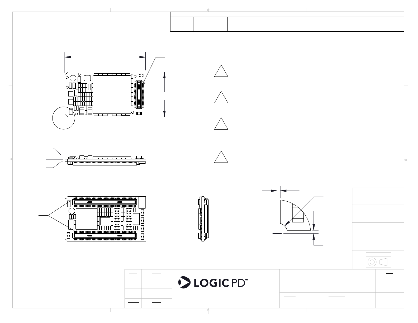
15.0
27.0
A
PIN 1
0
1.5
MAX
0.8
PIN 1
R
1.2
0.4
0.4
DETAIL A
SCALE 6 : 1
TOP
BOTTOM
NOTES:
1. DO NOT SCALE DRAWING
2.
DO NOT PLACE ANY COMPONENTS WITHIN
LAYOUT AREA OF SOM
3.
BASEBOARD CONNECTOR SPECIFICATION:
HIROSE DF40C-100DS-0.4V
4.
IF USING THE ETM DEBUG BOARD DURING
DEVELOPMENT, VERIFY COMPONENT HEIGHT
CONSTRAINTS IN SPECIFIED AREA
5.
PANEL VESTIGES ON ALL FOUR EDGES.
PLEASE DO NOT PLACE COMPONENTS DIRECTLY
ALIGNED WITH EDGE OF SOM
REVISIONS
REV.
PCB NUMBER
DESCRIPTION
DATE
D
1013993,
1017857
UPDATED FOR AM3703 & DM3730 MODELS, ADDED ETM DIMENSIONS
06.21.11
MANF
PMH
MGR
KAG
ENG
NWR
CHECK
06.21.11
DATE
DATE
06.21.11
DATE
06.21.11
DATE
411 WASHINGTON AVE. SUITE 400 MINNEAPOLIS, MN 55401
T : 612.672.9495 F : 612.672.9489 I : WWW.LOGICPD.COM
1 OF 2
SHEET
REV
D
AM3703, DM3730 &
OMAP35X TORPEDO SOM
DWG NO
2:1
SCALE
SIZE
A
1012857
TITLE
± 0.5
± 0.2
± 0.1
± 1°
X
X.X
X.XX
X°
TOLERANCES UNLESS
OTHERWISE SPECIFIED
ALL DIMENSIONS
ARE IN MILLIMETERS
UNLESS OTHERWISE
SPECIFIED
THIS DRAWING PREPARED
IN ACCORDANCE WITH
ASME Y14.5-2000
THIRD ANGLE PROJECTION
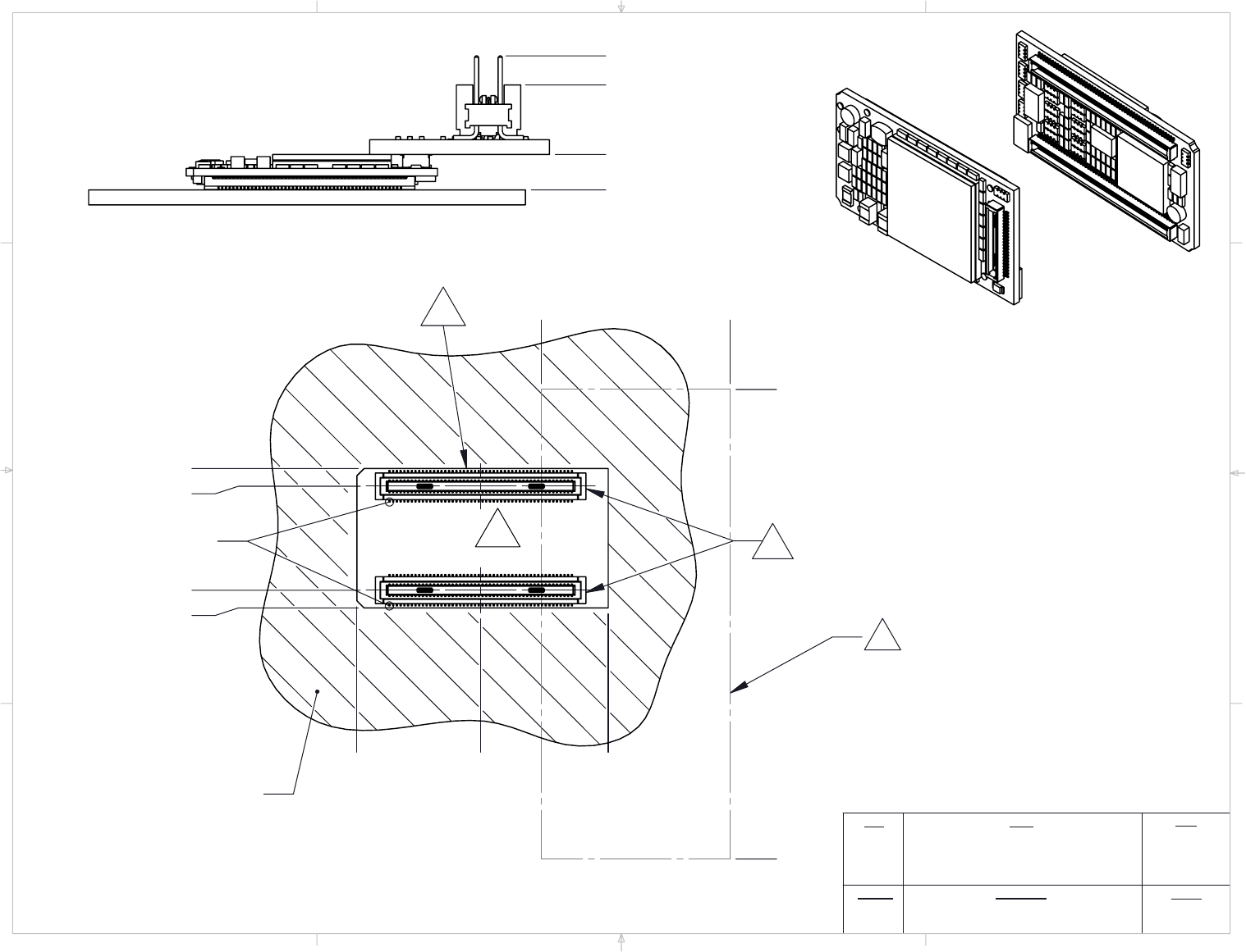
SHEET
REV
DWG NO
SCALE
SIZE
TITLE
2 OF 2
D
AM3703, DM3730 &
OMAP35X TORPEDO SOM
2:1
A
1012857
0
11.3
14.4
MAX
3.8
0.00
11.18
28.9
21.6
2X
0.00
6.5
26.8
13.3
13.7
13.1
1.9
PIN 1
3
J2
REPRESENTATIVE PCB
J1
4
ETM DEBUG BOARD OUTLINE
FOR HEIGHT CONSTRAINTS
5
ISOMETRIC VIEWS
FOR REFERENCE ONLY
TOP
BOTTOM
RECOMMENDED KEEPOUT AREA AND BASEBOARD FOOTPRINT
ETM DEBUG BOARD HEIGHT CONSTRAINTS
2
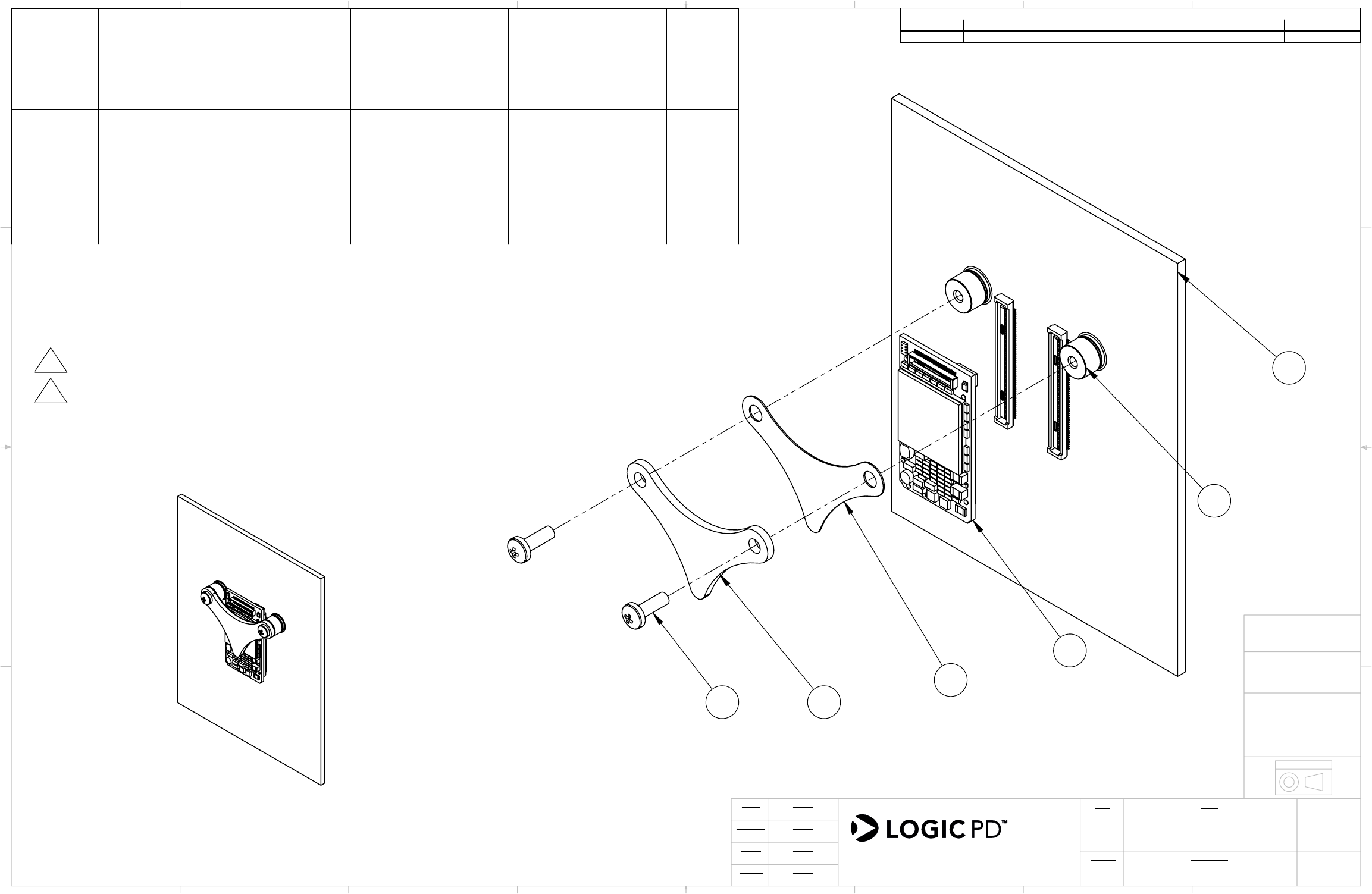
1
2
4
35
6
NOTES:
1. THIS IS THE RECOMMENDED RETENTION METHOD IF USING THE LOGIC PD CLIP
2. DO NOT SCALE DRAWING
3.
DO NOT PLACE COMPONENTS WITHIN LAYOUT AREA OF SOM AND CLIP
4.
BASEBOARD CONNECTOR SPECIFICATION: HIROSE DF40C-100DS-0.4V
REVISIONS
REV.
DESCRIPTION
DATE
C
UPDATED BOM, EXPLODED VIEW, SHEET FORMAT
06.21.11
ITEM NO.
DESCRIPTION
MANUFACTURER
PART NUMBER
QTY.
1
REPRESENTATIVE PCB
N/A N/A
1
2
AM3703, DM3730 & OMAP35X
TORPEDO SOM
LOGIC PD
DEPENDANT ON
CONFIGURATION
1
3
CLIP, SOM RETENTION PLATE
LOGIC PD
LPD-SOM-CLIP1
1
4
CLIP, SOM RETENTION PLATE
THERMAL PAD
LOGIC PD
LPD-SOM-CLIP1-
THPAD
1
5
MACHINE SCREW, M2 X 0.4,
6MM LENGTH
N/A N/A
2
6
SURFACE MOUNT STANDOFF,
4MM HEIGHT
PEM
SMTSO-M2-4
2
D
C
B
A
A
B
C
D
1
2
3
4
5
6
7
8
8
7
6
5
4
3
2
1
MANF
PMH
MGR
KAG
ENG
NWR
CHECK
06.21.11
DATE
DATE
06.21.11
DATE
06.21.11
DATE
411 WASHINGTON AVE. SUITE 400 MINNEAPOLIS, MN 55401
T : 612.672.9495 F : 612.672.9489 I : WWW.LOGICPD.COM
1 OF 2
SHEET
REV
C
TORPEDO RETENTION SYSTEM
- CLIP
DWG NO
2:1
SCALE
SIZE
B
1014553
TITLE
± 0.5
± 0.2
± 0.1
± 1°
X
X.X
X.XX
X°
TOLERANCES UNLESS
OTHERWISE SPECIFIED
ALL DIMENSIONS
ARE IN MILLIMETERS
UNLESS OTHERWISE
SPECIFIED
THIS DRAWING PREPARED
IN ACCORDANCE WITH
ASME Y14.5-2000
THIRD ANGLE PROJECTION
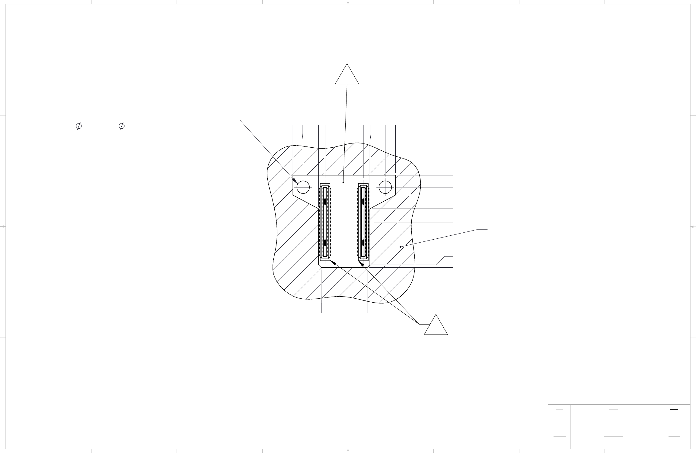
SHEET
REV
DWG NO
SCALE
SIZE
TITLE
2 OF 2
C
TORPEDO RETENTION SYSTEM-
CLIP
2:1
B
1014553
0.0
6.4
9.4
11.18
17.6
20.6
1.1
13.1
1.9
0.0
2X
3.9
2X
12.5
13.3
2X
7.9
2X
10.2
13.7
12.3
4
3
FOR SMT SO-M2-4 STANDOFF
2X
3.7 WITH
6.2 SOLDER PAD REQUIRED
PLATING THRU HOLE NOT REQUIRED
REPRESENTATIVE PCB
RECOMMENDED BASEBOARD FOOTPRINT AND KEEPOUT AREA
D
C
B
A
A
B
C
D
1
2
3
4
5
6
7
8
8
7
6
5
4
3
2
1
THIRD ANGLE PROJECTION
2
NOTES:
1. THE TORPEDO CAN BE RETAINED IN PLACE BY THE SURROUNDING ENCLOSURE.
REPRESENTATIVE ENCLOSURE
2.
REVISIONS
REV.
ECO NUMBER
DESCRIPTION
DATE
A
-
INITIAL RELEASE
09.28.09
MGR DATE
THIS DRAWING PREPARED
IN ACCORDANCE WITH
ASME Y14.5-2000
ALL DIMENSIONS
ARE IN MILLIMETERS
UNLESS OTHERWISE
SPECIFIED
X ± 0.5
X.X ± 0.2
X.XX ± 0.1
X° ± 1°
TOLERANCES UNLESS
OTHERWISE SPECIFIED
Torpedo Retention System -
In Housing
1014554
AA
09.28.09
09.28.09
NWR
DATE
DATE
CHECK
ENG
1 OF 1
1:1
SIZE
SCALE SHEET
REV
DWG NO
TITLE
MANF
09.28.09
DATE
KAG
PMH

THIRD ANGLE PROJECTION
NOTES:
1. BASED ON TESTING A LIMITED NUMBER OF SAMPLES, THE TORPEDO
REQUIRES 10 LBS OF EXTRACTION FORCE AFTER 1 INSERTION CYCLE.
AFTER 30 INSERTION AND EXTRACTION CYCLES, THIS IS REDUCED TO 6 LBS.
REVISIONS
REV.
ECO NUMBER
DESCRIPTION
DATE
A
-
INITIAL RELEASE
09.28.09
MGR DATE
THIS DRAWING PREPARED
IN ACCORDANCE WITH
ASME Y14.5-2000
ALL DIMENSIONS
ARE IN MILLIMETERS
UNLESS OTHERWISE
SPECIFIED
X ± 0.5
X.X ± 0.2
X.XX ± 0.1
X° ± 1°
TOLERANCES UNLESS
OTHERWISE SPECIFIED
Torpedo Retention System
- None
1014552
AA
09.28.09
09.28.09
NWR
DATE
DATE
CHECK
ENG
1 OF 1
2:1
SIZE
SCALE SHEET
REV
DWG NO
TITLE
MANF
09.28.09
DATE
KAG
PMH
