Cover.p65 LT 2240 2220 40 3020 50 Service Manual
User Manual: LT-2240
Open the PDF directly: View PDF ![]() .
.
Page Count: 56
MITSUBISHI DIGITAL ELECTRONICS AMERICA, INC.
9351 Jeronimo Road, Irvine, CA 92618-1904
Copyright © 2004 Mitsubishi Digital Electronics America, Inc.
All Rights Reserved
CAUTION:
Before servicing this chassis, it is important that the service person read the "SAFETY PRECAUTIONS" and
"PRODUCT SAFETY NOTICE" contained in this manual.
MITSUBISHI ELECTRIC
Service
Manual
2003-2004
SPECIFICATIONS
LIQUID CRYSTAL DISPLAY TELEVISION
• Power : [LT-2220, LT-2240] AC ADAPTOR
In - AC 120V, 60Hz; Out - 20VDC 6.0A
: [LT-3020, LT-3040, LT-3050] 120V, 60Hz, 2.2A
• LCD Panel : Resolution - 1280X768
: Pixel Pitch - [LT-2220, LT-2240] 0.375mm
[LT-3020, LT-3040, LT-3050] 0.5025mm
• Analog Inputs : VHF/UHF 75Ω unbalanced
: Two A/V Inputs (Composite or S-Video)
L-R Audio
: Two Component Video Inputs (480i/480p/
720p/1080i) L-R Audio
: PC Input - 60Hz (VGA,S-VGA,XGA,W-XGA)
: PC Audio - 3.5mm Mini-Jack
•Digital Input : MonitorLink™/DVI (Video Sources Only)
L-R Audio (Analog)
: MonitorLink™ Control/RS-232C
•Audio Outputs : L-R Audio Output (Fixed/Variable)
: Headphone Jack (Variable) 3.5mm
• Tuning : NTSC 181Channel Analog Cable
• Frequency Range : VHF 54 ~ 470MHz
UHF 470 ~ 806MHz
• Speakers : [LT-2220, LT-2240]
Left & Right (2 X 2.3W) Sub (3.4W)
: [LT-3020, LT-3040, LT-3050]
Left & Right (2 X 3.5W) Sub (6W)
LT-2220
LT-2240
LT-3020
LT-3040
LT-3050
• Weight and dimensions shown are approximate.
• Design specifications are subject to change without notice.
With Stand: Height Width Depth Weight
[LT-22XX] 20-1/4" 22-3/4" 11-7/8" 36.6 lbs
[LT-30XX] 25-3/8" 29-3/4" 11-7/8" 54.3 lbs
W/O Stand: Height Width Depth Weight
[LT-22XX] 18-5/8" 22-3/4" 4" 19.8 lbs
[LT-30XX] 23-1/4" 29-3/4" 5" 37.5 lbs
• Weight / Cabinet Dimensions

MODELS: LT-2220 / LT-2240 / LT-3020 / LT-3040 / LT-3050
Page 3
INTRODUCTION .................................................................................................................................. 5
PRODUCT SAFETY NOTICE ............................................................................................................... 5
SAFETY PRECAUTIONS ..................................................................................................................... 5
DISASSEMBLY
LT-22XX ............................................................................................................................................. 7
LT-30XX ........................................................................................................................................... 13
ELECTRICAL ADJUSTMENTS
Initial Setup .................................................................................................................................... 21
CIRCUIT EXPLANATIONS & BLOCK DIAGRAMS
Circuit Explanations ....................................................................................................................... 23
Block Diagrams.............................................................................................................................. 29
TEST POINT LOCATIONS AND DESCRIPTIONS
PWB-SET Test Point Locations and Description ............................................................................ 33
PWB-MAIN Test Point Locations and Description .......................................................................... 35
TROUBLESHOOTING
LT-22XX Power Troubleshooting ...................................................................................................... 37
LT-30XX Power Troubleshooting ...................................................................................................... 39
Video Troubleshooting .................................................................................................................... 41
Audio Troubleshooting .................................................................................................................... 51
Remote Control & Front Switch Troubleshooting ............................................................................ 53
REPLACEMENT PARTS
Replacement Parts List .................................................................................................................. 55
INTERCONNECT WIRING DIAGRAM
CONTENTS

Page 4
MODELS: LT-2220 / LT-2240 / LT-3020 / LT-3040 / LT-3050
Page 5
PRODUCT SAFETY NOTICE
Many electrical and mechanical parts in television receivers have special safety related characteristics. These
characteristics are often not evident from visual inspection nor can the protection afforded by them necessarily be
obtained by using replacement components rated for higher voltage, wattage, etc.
Replacement parts which have special safety characteristics are identified in this service manual.
The replacement for any safety part should be identical in value and characteristics.
SAFETY PRECAUTIONS
NOTICE: Observe all cautions and safety related notes located inside the receiver cabinet and on the
receiver chassis.
WARNING:
1. Operation of this receiver outside the cabinet or with the cover removed presents a shock hazard
from the receiver's power supplies. Work on the receiver should not be attempted by anyone who is
not thoroughly familiar with the precautions necessary when working on high voltage equipment.
2. Do not install, remove or handle the LCD panel in any manner unless shatterproof goggles are
worn. People not so equipped should be kept away while the panel is being handled. Keep
the panel away from the body while handling.
3. When service is required, observe the original lead dress. Where a short-circuit has occurred, replace
those components that indicate evidence of overheating.
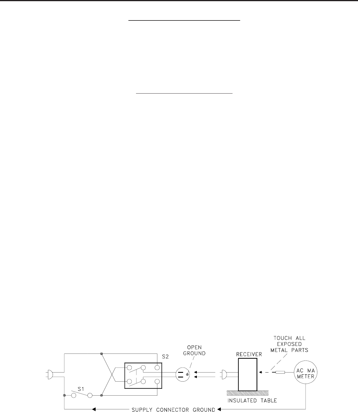
Leakage current check
Before returning the receiver to the customer, leakage current should be measured using following methods.
1. Cold Check
With the alternating current (AC) plug removed from the AC source, place a jumper across the two AC plug
prongs. Connect one lead of an ohm meter to the AC plug and touch the other lead to each exposed metal part
(i.e. antennas, handle bracket, metal cabinet, screw heads, metal overlay, control shafts, etc.), particularly any
exposed metal part that has a return path to the chassis. The resistance of the exposed metal parts having a
return path to the chassis should be a minimum of 1Mega Ohm. Any resistance below this value indicates
an abnormal condition and requires corrective action.
2. Hot Check ...Use the circuit shown below to perform the hot check test.
1. Keep switch S1 open and connect the receiver to the measuring circuit. Immediately after
connection, and with the switching devices of the receiver in their operating positions, measure
the leakage current for both positions of switch S2.
2. Close switch S1, energizing the receiver. Immediately after closing switch S1, and with the
switching devices of the receiver in their operating positions, measure the leakage current for both
positions of switch S2. Repeat the current measurements of items 1 and 2 after the receiver has
reached thermal stabilization. The leakage current must not exceed 0.5 milliampere (mA).
MODELS: LT-2220 / LT-2240 / LT-3020 / LT-3040 / LT-3050

Page 6
MODELS: LT-2220 / LT-2240 / LT-3020 / LT-3040 / LT-3050
Page 7
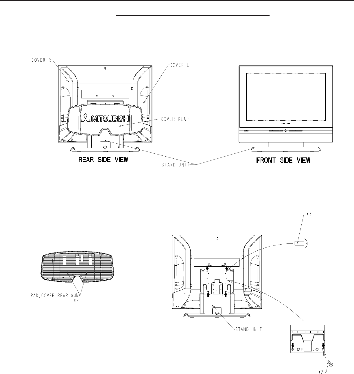
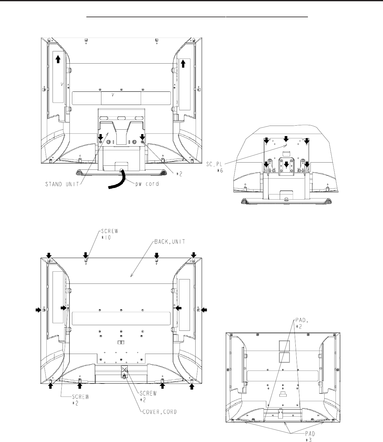
Remove the screws and components in the quantities indicated.
Reassemble in reverse order.
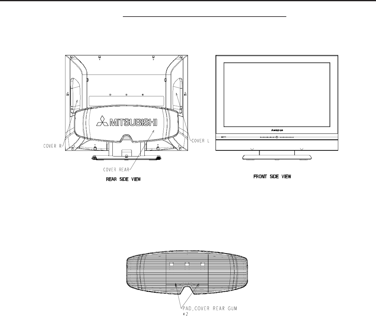
DISASSEMBLY PROCEDURE (LT-22XX)
1. COVER, REAR 2. STAND UNIT
MODELS: LT-2220 / LT-2240 / LT-3020 / LT-3040 / LT-3050
Page 8
3. BACK UNIT
4. BACK COVER
DISASSEMBLY PROCEDURE (LT-22XX) CONTINUED
MODELS: LT-2220 / LT-2240 / LT-3020 / LT-3040 / LT-3050
Page 9
5. PWB-SET
6. PWB-MAIN
DISASSEMBLY PROCEDURE (LT-22XX0) CONTINUED
MODELS: LT-2220 / LT-2240 / LT-3020 / LT-3040 / LT-3050
Page 10
7. CHASSIS BASE
DISASSEMBLY PROCEDURE (LT-22XX) CONTINUED
MODELS: LT-2220 / LT-2240 / LT-3020 / LT-3040 / LT-3050
Page 11
8. LCD
9. PANEL
DISASSEMBLY PROCEDURE (LT-22XX) CONTINUED
MODELS: LT-2220 / LT-2240 / LT-3020 / LT-3040 / LT-3050
Page 12
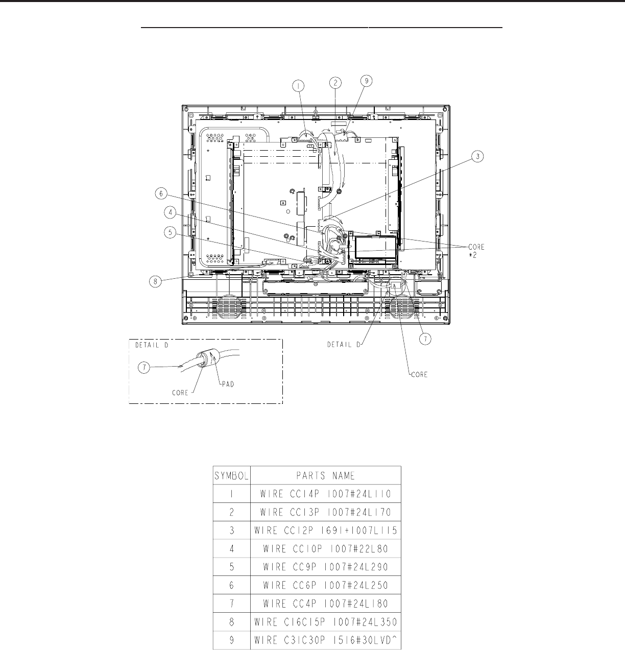
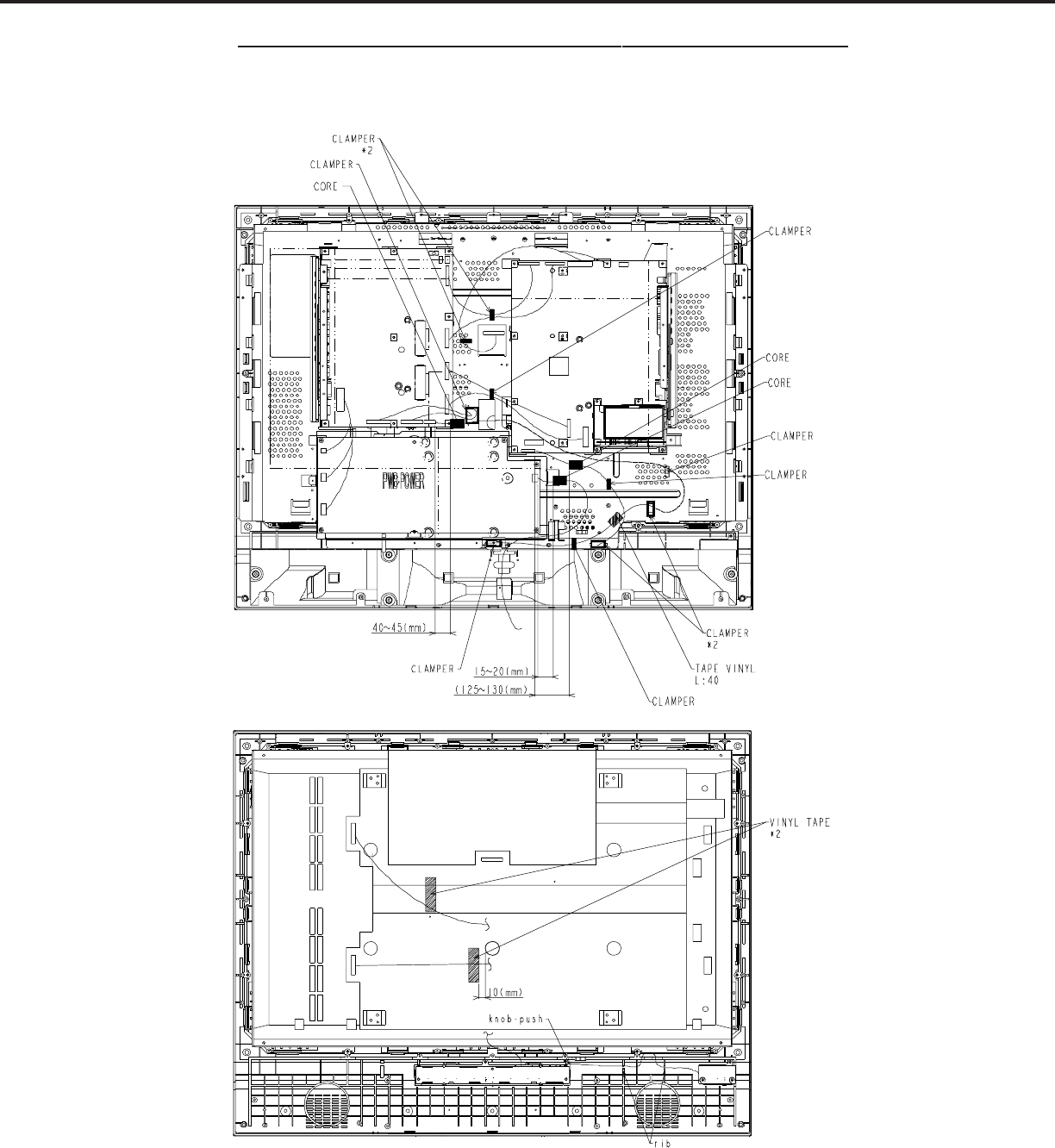
WIRING HARNESS LOCATIONS
DISASSEMBLY PROCEDURE (LT-22XX) CONTINUED
MODELS: LT-2220 / LT-2240 / LT-3020 / LT-3040 / LT-3050
Page 13
DISASSEMBLY PROCEDURE (LT-30XX)
Remove the screws and components in the quantities indicated.
Reassemble in reverse order.
1. COVER, REAR
MODELS: LT-2220 / LT-2240 / LT-3020 / LT-3040 / LT-3050
Page 14
DISASSEMBLY PROCEDURE (LT-30XX) CONTINUED
3. BACK COVER
2. STAND UNIT
MODELS: LT-2220 / LT-2240 / LT-3020 / LT-3040 / LT-3050
Page 15
DISASSEMBLY PROCEDURE (LT-30XX) CONTINUED
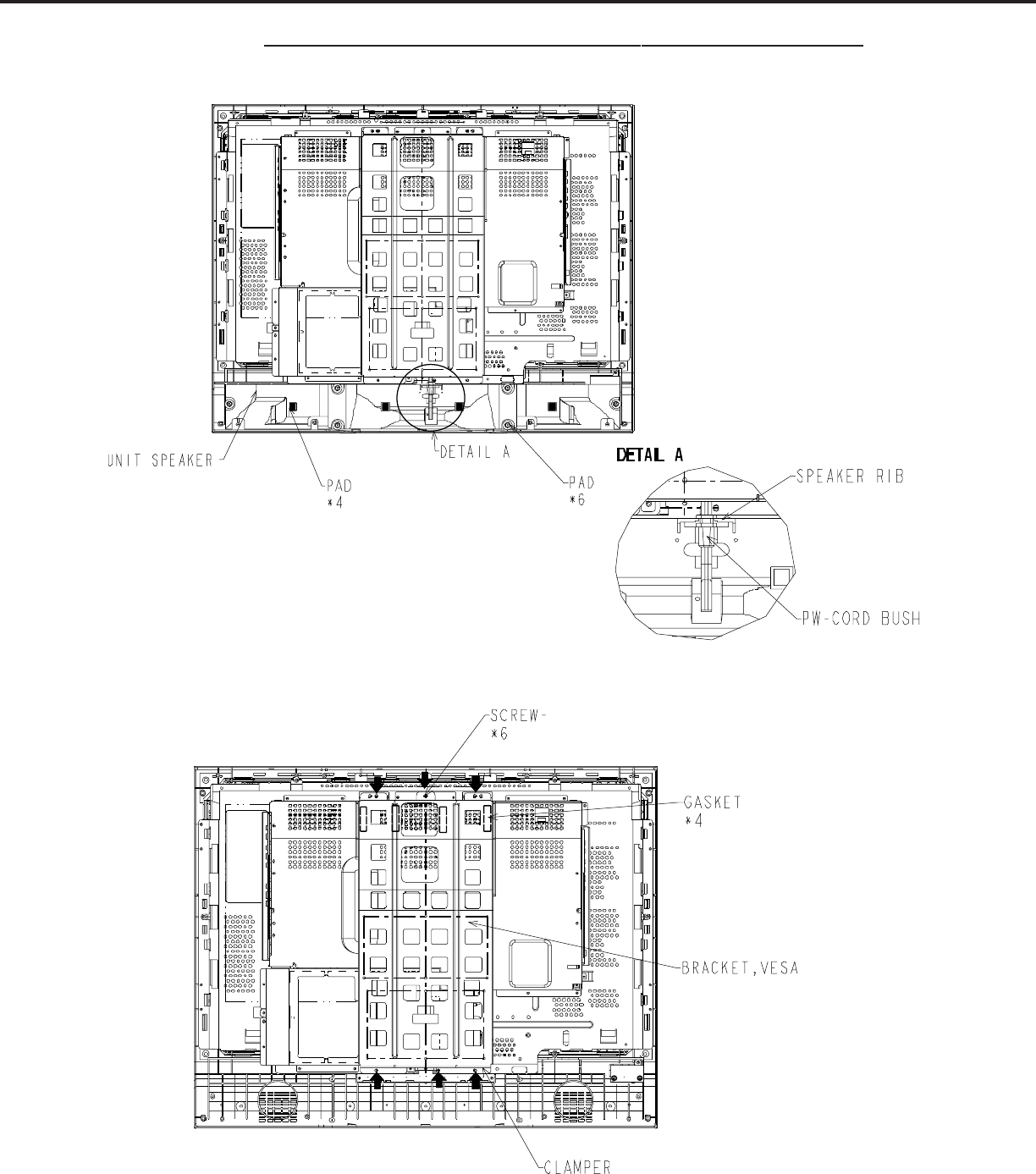
5. BRACKET, VESA
4. UNIT SPEAKER
MODELS: LT-2220 / LT-2240 / LT-3020 / LT-3040 / LT-3050
Page 16
DISASSEMBLY PROCEDURE (LT-30XX) CONTINUED
6. SHIELD, POWER & SHIELD, CASE
7. COVER, TERMINAL, LEFT & RIGHT
MODELS: LT-2220 / LT-2240 / LT-3020 / LT-3040 / LT-3050
Page 17
DISASSEMBLY PROCEDURE (LT-30XX) CONTINUED
8. ASSY-PWB-MAIN/ASSY-PWB-SET/UNIT-POWER
MODELS: LT-2220 / LT-2240 / LT-3020 / LT-3040 / LT-3050
Page 18
DISASSEMBLY PROCEDURE (LT-30XX) CONTINUED
9. CHASSIS, REAR
MODELS: LT-2220 / LT-2240 / LT-3020 / LT-3040 / LT-3050
Page 19
DISASSEMBLY PROCEDURE (LT-30XX) CONTINUED
10. BRACKET T/B/LCD PANEL
11. BEZEL
MODELS: LT-2220 / LT-2240 / LT-3020 / LT-3040 / LT-3050
Page 20
DISASSEMBLY PROCEDURE (LT-30XX) CONTINUED
WIRING HARNESS LOCATIONS
MODELS: LT-2220 / LT-2240 / LT-3020 / LT-3040 / LT-3050
Page 21
Initial Setup
A. Option Menu Setup
Follow the steps below for the initial set-up:
1. Select the "MENU" display by pressing the "MENU" button once.
2. Press the number buttons "2", "0", "7", "0" in sequence to select the "OPTION MENU" display.
3. Press the "ADJUSTpq" buttons to select "INITIAL."
4. Press "ENTER."
NOTE: At this time channel 3 is automatically selected and all Menu and Audio/Video user setting are set
to the defaults shown in the chart below.
B. Default Settings
MENU-2-0-7-0
OPTION MENU
Initial
Power Restore :OFF
DTV Port :Auto
Direct Key Mode :OFF
Memorize channels
ANT-A - Air
V-Chip Start Time 12:00AM TV Speakers (Internal) On
Language (idioma) English V-Chip Stop Time 12:00AM Audio Output Variable
Front Button Lock Off Lock by Time Off AUDIO SETTINGS
Lock Time N/A Bass 31
Clock Setting Manual Unlock Time N/A Treble 31
Clock Time - - : - - - - Balance 31
Set Day Sunday Video Mute On Sub-Woofer Level 31
Black Enhancement On Surround Off
Closed Captions On if Mute PC Power Save On TV Listen To Stereo
CC Background Gray Level Sound Off
Timer Off VIDEO SETTINGS
Antenna ANT-A Set Time - - : - - - - Contrast 31
Channel 3Set Day Sunday Brightness 31
Memory Deleted Sharpness 31
Name N/A Auto Color Correction Off Color 31
SQV N/A Tint 31
Magenta 31 Color Temp High
V-Chip Off Red 31 Video Noise Standard
TV Rating TV-PG Yellow 31 Film Mode (Auto) On
FV- Fantasy Violence Allow Green 31 Back Light 63
D-Sexual Dialog Allow Cyan 31 PC/DVI H-Position 31
L-Adult Language Allow Blue 31 PC/DVI V-Position 31
S-Sexual Situations Allow PC Video Clock 31
V-Violence Allow PC Fine Detail 31
Programs Not Rated Allow PC H-Resolution 31
Movie Rating PG PC V-Resolution 31
ADVANCED FEATURES
TIMER
COLOR BALANCE
CAPTIONS
CHANNEL EDIT
V-CHIP-LOCK
MANUAL COLOR ADJUST
AUDIO/VIDEO
MAIN MENU DEFAULT SETTINGS
SETUP
CLOCK
V-CHIP LOCK By Time
MODELS: LT-2220 / LT-2240 / LT-3020 / LT-3040 / LT-3050

Page 22
MODELS: LT-2220 / LT-2240 / LT-3020 / LT-3040 / LT-3050

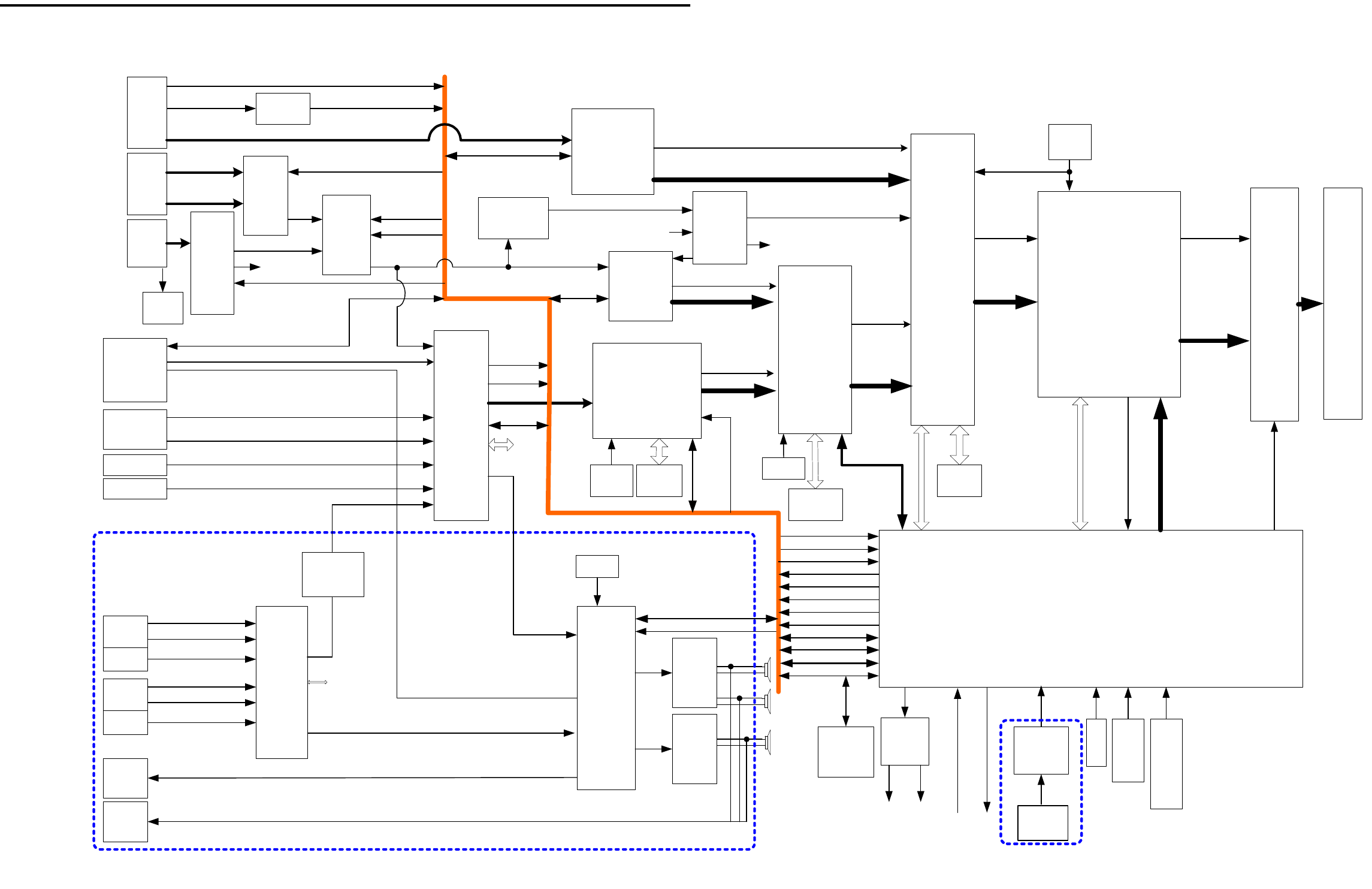
Circuit Explanations
1. Video circuits
This section explains the video circuitry of models LT-2220/LT3020. Both models have almost the same
circuits. The explanation corresponds to the various inputs (PC, TV, VIDEO, Component, DVI).
The HD input has realized high definition with the resolution of WXGA.
(Refer to the LT-2220 / LT-3020 Video block diagram, for the flow of video signals.)
1-1. Video input circuit
1-1-1. PC Input video circuit
For PC input, video is inputted into IC400 of the signal processing IC via the following IC’s.
(A) IC2A3 : Analog-to-digital conversion IC (AD9883AKST-110 : Analog devices)
The video signal (R, G, B) of PC input is changed into a digital signal (8 bits each) from an analog
signal. Besides digital conversion, this IC has the functions below:
- Contrast adjustment for PC
- brightness adjustment for PC
This IC is controlled by register control of IC 2A3 via 3.3V IIC-bus.
(B) IC2A2 : Inverting IC with Schmidt trigger (74LCX14 : Fairchild)
Input IC for Horizontal and Vertical sync signals from the PC input.
In case of noise on the leading and trailing edges or low amplitude of the sync signals outputted from a
PC, it is necessary to modify the waveform.
Improper waveforms are corrected by this IC in the following manner.
- Noise on the leading/trailing edge : Rise-time and fall-time is carried out early.
- Waveform is noisy : False triggering prevented by the Schmidt circuit.
- Low Amplitude : If voltage threshold is satisfied, it will output at 3.3V.
Since the IC is an inverter, it will let it pass twice and has united polarity.
1-1-2. Component and DVI Input circuit.
For Component and DVI inputs, video is inputted into IC400, signal processing IC, via the following IC’s.
(C)IC204 : Analog-switch IC (BA7657 : Rohm)
In this IC, one of the 2 component signal inputs (Y, Cb, Cr) is chosen by the select signal. Select
signal CTL is controlled by the MCU.
Page 23
MODELS: LT-2220 / LT-2240 / LT-3020 / LT-3040 / LT-3050

(D)IC2J1 : TMDS receiver IC with HDCP (Sii907B : SiliconImage)
In this IC, the input signal is processed based on EIA-861A. Inputs from a TMDS-Interface are
converted into a RGB analog signal. HDCP and HDTV resolutions are supported.
When no DVI signal is input, it changes to standby mode automatically and power consumption is
lowered. The LCD panel specification is for input signals whose vertical sync signal is 60Hz. The
outputs of this IC include separate horizontal and vertical sync signals.
(E)IC201 : Analog-switch IC with LPF (SM5301A : NPC)
In this IC, the component signal (Y, Cb, Cr) from IC204 or DVI signal (R,G,B) from IC2J1 is chosen
by the select signal and outputted.
Select signal MUXSEL is controlled by the MCU.
(F) IC202 : Sync separate IC (LM1881M : National Semiconductor)
Used for Component input.
This IC separates the composite H and V sync signal from the composite video signal
The composite sync signal is sent to IC203 (Sync select IC).
(G) IC203 : Sync select IC (HD74LV157: Hitachi)
In this IC, the composite sync signal from IC202(for component) or Separate sync signal from
IC2J1(for DVI) is chosen by the select signal and outputted.
Select signal MUXSEL is controlled by the MCU.
The output from this IC is sent to IC400 (Signal processor IC) in order to remove the
vertical sync signal and output the separated horizontal sync signal. The horizontal sync signal is
then routed to IC205 (Analog-to-digital conversion IC).
(H) IC205 : Analog-to-digital conversion IC (AD9883AKST-110 : Analog devices)
The Component video (YCbCr / RGB) or DVI inut is converted into a digital signal (8 bits
each) from an analog signal. Besides digital conversion this IC performs the following:
- Contrast adjustment for Component or DVI
- brightness adjustment for Component or DVI
This IC is controlled by register control of IC 205 via 3.3V IIC-bus.
This IC’s output is sent to IC500.
Page 24
MODELS: LT-2220 / LT-2240 / LT-3020 / LT-3040 / LT-3050

(I) IC500 : Interlace-to-Progressive conversion IC ( gm6015 : Genesis)
This IC performs the following functions to all input signals except the PC input.
- Motion adaptive De-interlacer for SD (480i) signals.
- Scaling
- PIP / POP control for AV input combinations.
- Color / tint control
- 3 dimension Noise reduction.
- Adaptive Film mode
- Sync Separation for Composite sync.(for component only)
A format change to the input signal is also made by this IC.
Control is performed in 5-line serial communication from the MCU.
1-1-3. VIDEO and TV input circuitry
For VIDEO and TV inputs, the signal is applied to IC400, signal processing IC, via the following ICs.
(J)IC701 : Analog-switch IC (CXA2089 : SONY)
In this IC, the composite signal (CVBS) from video1/2 input or composite signal (S-video) from
video1/2 input is chosen by register control of IC 701 via 5V IIC-bus.
(K)IC702 : Buffer IC with LPF ( MM1566AF : Mitsumi)
IC701 reduces the high frequency noise ingredient of the video signal.
(L)IC100 : Analog-switch IC (CXA2069 : SONY)
In this IC, the composite signal (CVBS / S-video) from the video1/2 inputs or the composite signal
(CVBS) from the TV input is selected by register control of IC 100 via 5V IIC-bus.
It is also selected and sent to IC300 for CCD use.
(M)IC601 : Digital decoder IC with 3D Y/C separation (uPC64011 : NEC)
This IC converts the analog video signal (S-VIDEO/CVBS) from IC100 into a digital signal.
Besides digital conversion this IC also has the following functions.
- 3 dimension Y/C separation for CVBS
- Contrast adjustment.
- Brightness adjustment.
- FIELD signal generation.
- PLL (Phase-Locked Loop) : referential clock generation.
- Sync signal generation
This IC is controlled by register control of IC 601 via 3.3V IIC-bus.
This IC’s output is sent to IC400.
(The output format is YPbPr and WXGA. Thw Vertical frequency is 60Hz.)
Page 25
MODELS: LT-2220 / LT-2240 / LT-3020 / LT-3040 / LT-3050

1-2. Signal processor circuit
(N)IC400 : Signal processor IC ( M66473FP : Mitsubishi)
This IC has the functions below.
- Scaling for PC
- PIP/POP control for PC and AV combination
- Picture enhancement
- Auto setup for PC
- Colorsync function
- Frequency measurement / distinction
- Sync separation for component CS
- Color space conversion ( YPbPr à RGB )
- Gamma correction
This IC is controlled by register control of IC 400 via 5-lines serial communication.
This IC’s output is sent to IC4A0.
(The output format is RGB and WXGA, and Vertical frequency is 60Hz.)
(O)IC4A0 : OSD mixing IC ( M66617FP : Mitsubishi)
This IC combines the picture signal outputted from IC400, the OSD signal outputted from the
MCU and the signal detected by CCD.
V-CHIP function is also controlled by this IC.
This IC is controlled by register control of IC 4A0 via serial communication.
The IC’s output is sent to IC4A1.
1-3. Output signal circuit
(P)IC4A1 : LVDS transmitter IC ( THC63LVDM83R : Thine)
This IC converts 28bits of TTL/CMOS data into LVDS data stream.
In 28 bits, 24-bits digital video signal, horizontal sync signal, vertical sync signal, an enable
signal and a clock signal for the LCD panel are included.
A phase-locked transmit clock is transmitted in parallel with the data streams over a fifth LVDS link.
This IC’s output is sent to the LCD panel.
Page 26
MODELS: LT-2220 / LT-2240 / LT-3020 / LT-3040 / LT-3050

2. Audio circuits
The audio circuits and speaker system of LT-22XX/LT30XX basically have the same circuits, except the Vcc
applied to the audio amplifier is different.
The specifications are as follows.
- High Power (LT-22XX : 8W ,LT-30XX: 12W)
- 2.1ch Sub woofer speaker system
- Impedance : 8 +/-1.2 ohms ( LT-22XX / LT-30XX )
- Compact and high performance sound enclosure box.
- Minimization of vibration noise
Refer to the LT-22XX / LT-30XX Audio block diagram.
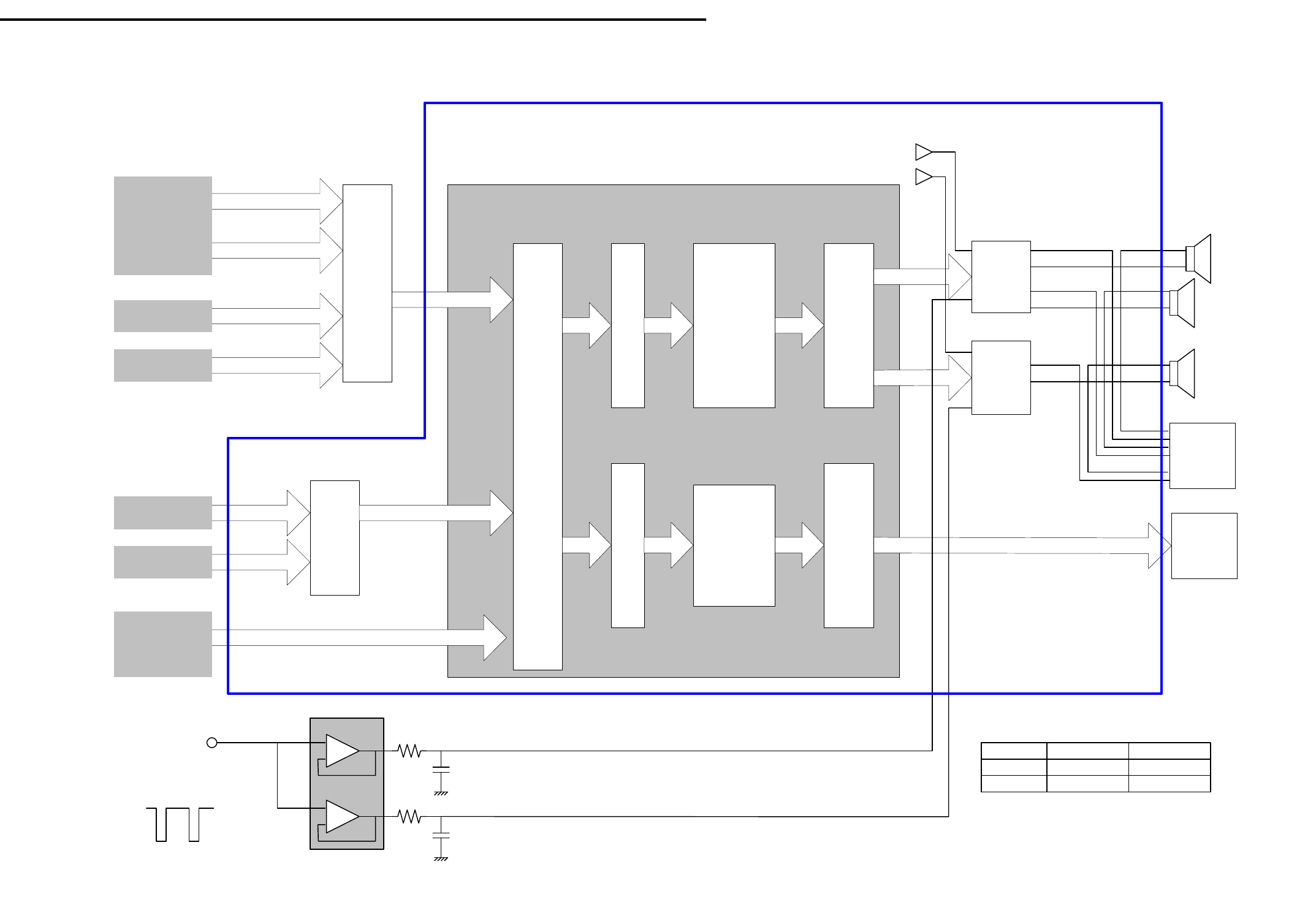
2-1 Audio input mixing circuits
The audio input block consist of 2 AV-SW, IC701(CXA2089) on SUB-PWB and IC100(CXA2069) on
MAIN-PWB. Audio inputs for VIDEO1 and VIDEO2 are connected to IC701. Other external audio Inputs
(Component1/2 and DVI and PC) are connected to IC100. Their output is connected to IC710 (Audio
Processor : MSP3440G ) of Scart1 / Scrat2 input port.
TV broadcasting audio(SIF) is also connected to IC710’s IF Input port. Input sources are selected by register
control of IC 701/IC100/IC710 via 5V IIC-bus.
2-2 Audio processor IC
MSP3440G is used as the main audio processor.
This IC’s functions are as follows.
- De modulator (SAP/Stereo)
- Sub-woofer output
- Volume control
- Tone control
- Surround
- L/R mixing
- Audio line output
Both models have the following audio controls on the users menu: Bass, Treble, Balance, Surround, Listen
to, Level Sound, Sub Woofer, Audio Out Fixed/Variable.
Audio adjustment of all controls except volume is performed by this IC.
(Refer to the “Owner’s guide” for a full explanation of each control.)
2-3 Audio amplifiers and speakers
These models use 2pcs of 2-CH BTL type audio amplifier AN7522.
One piece is for main audio, and one more piece is for the sub-woofer.
Amplifier +B voltage and the input circuits are slightly different by model. ( Refer to table 1).
Page 27
MODELS: LT-2220 / LT-2240 / LT-3020 / LT-3040 / LT-3050
Table 1: Amp supply voltage(+B)
LT-22XX LT-30XX
AMPVCC(for main) 7.5V 9V
SAMPVCC(for Sub Woofer) 9V 12V
Volume control is controlled by fading Volume1 /Volume2 DC signal to the amplifier Pin(#9).
Although the audio signals outputted from amplifier is sent to the SPEAKER, between the amplifier and
SPEAKER is a headphone terminal. If a headphone is connected, the audio signal to SPEAKER will be
interrupted and the audio signal will be sent to the headphone terminal.
3. Power circuit
Refer the LT-2220 / LT-3020 Power circuit block for the following.
The LT-2220 power supply is supplied from an AC adapter.
The LT-3020 power supply is supplied from a power supply board.
The LT-2220 has one connector for the inverter connection, the LT-3020 has two connectors.
Except for that, the circuit composition of the power supply is almost the same.
There are power supplies that are “always on” and “ON/OFF” with a control signal, as follows.
Power source
signal Voltage [V ] “always on” or
“ON/OFF” Control
signal Note
20V 20 always on - “22 only
24V 24 ON/OFF ON_24V “30 only
8.5V 8.5 always on - “30 only
A12V 12 ON/OFF Psave2
A9V 9 ON/OFF Psave2
A8V 8 always on -
AMPVCC “30 : 9
“22 :7.5 ON/OFF Psave3
SAMPVCC “30 : 12
“22 :9 ON/OFF Psave3
S5V 5 always on -
SW5V 5 ON/OFF Psave1
A30V 30 ON/OFF Psave1
S3.3V 3.3 always on -
4.5V 4.5 always on -
D3.3V 3.3 ON/OFF Psave1
A3.3V 3.3 ON/OFF Psave1
AD3.3V 3.3 always on -
D1.9V 1.9 ON/OFF Psave1
D2.5V 2.5 ON/OFF Psave1
1.5V 1.5 ON/OFF Psave1
Page 28
MODELS: LT-2220 / LT-2240 / LT-3020 / LT-3040 / LT-3050
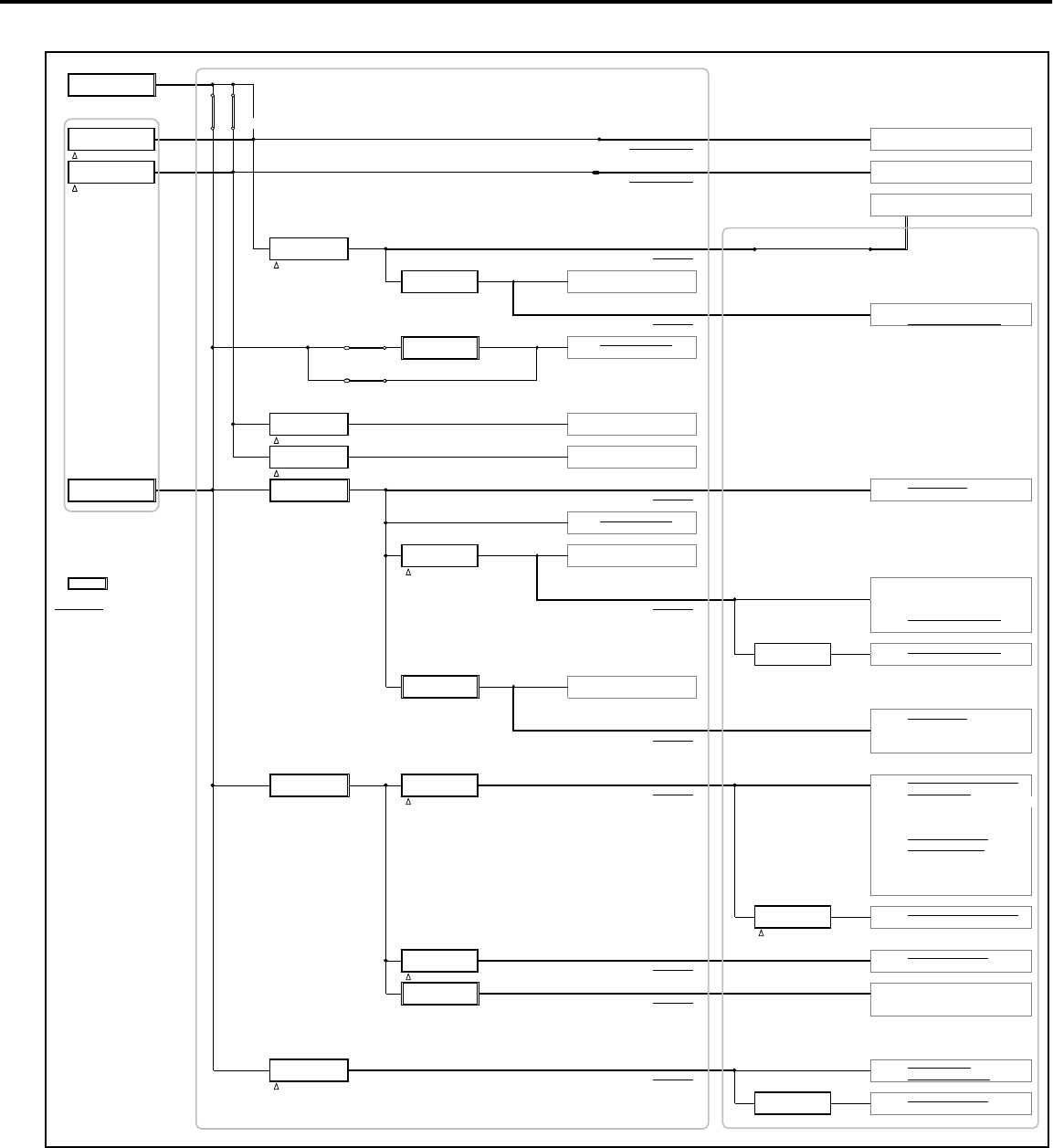
IC400
URANUS
SCALER
PiP/PoP
3.3V
1.9V
IC100
AV SW
CXA2069
9V
add=92H
IC500
gm6015
3D-I/P
PiP/PoP
3.3V
2.5V
CVBS
IC204
SW
BA7657
5V
IC205
AD9883A
A/D
3.3V
add=9AH
IC2A3
AD9883A
A/D(PC)
3.3V
add=98H
24bit
Port 0
Port 1
Y for CCD2
CCDMAIN
BLOCK DIAGRAM of LT-22XX/LT-30XX(except Power)
IC401
16M
SDRAM
IC4A0
M66617FP
OSD MIX
ENMA?
3.3V
2.5V
IC701
AV SW
CXA2089
9V
add=90H
IC710
MSP3440
Audio
Processor
8V
5V
add=80H
TV MPX IC712
AMP
AN7522
IC4A1
LVDS
3.3V
PC_DDC
IC2A1
DDC_EEP
3.3V
PC_H,VIC2A2
74LCX14
3.3V
IC300
CPU M306V7
5V
3.3V
IC501
64M
SDRAM
IC202
SYNC SEP
LM1881M
IC2J1
SiI907B
TMDS
HDCP
3.3V
MonLink
IC8X0
RS322
ADM3311
3.3V
IC711
AMP
AN7522
L
R
Woofer
IC601
16M
SDRAM
H,V,DE,CLK
OSD-MIX
H,V,CLK/RST
PDWN
CCIR601
H,V,DE,CLK
R,G,B
H,V,DE,CLK
Field
R,G,B
H,V,CLK
14.318
MHz5BUS
IC601
UPD64011
3D-YC
DECODER
3.3V/1.5V
add=B8H
3.3V IIC
H,V,DE,CLK
R,G,B
Y,Cb/
Pb,Cr/Pr
18.432
MHz
5V IIC
IC201
SW
SM5301
5V
CVBS/Y/C
RSTB
SYNC
H,V,CLK
24.576
MHz
MUXSEL
CTL
BUS
TU IIC
3.3V IIC
IC305
OPAMP
LMV324
5V
Volume 1/2
VRF
IC490
20MHz
PC_H,V
RESETQ
SWLED
Analog RGB
YPbPr/
YCbCrIC203
SW
74LV157
3.3V
DVI H,V
DVI H,V
RESET/PSAVE1
SW LR2
SW LR1
PWB-
SET(SUB)
CVBS/SY/SC
CCDSUB
IC2J2
E-DDC
3.3V
LCD Panel
PC_H,V
MPX
BUS
5V IIC
5V IIC
YUV/R,G,B
IC702
MM1566AF
BUFFER
SYNC
COMPOSIT_H2
MAIN
L/R Out
Sub
Woofer
Out
Input 1
J703 AUDIO L/R
Input 1
J704 S-Video
CVBS
Input 2
J701 AUDIO L/R
Input 2
J702 S-Video
Audio
Out
J705
Head
Phone
J706
PC
J2A1
(Dsub15)
Component1
/2
J201
Conponent 1
(VIDEO)
Conponent 2
(VIDEO)
DVI HD
(J2J0)
PC AUDIO
J103 L/R
DVI AUDIO
J102
Conponent
AUDIO
J201
L/R
Component 2 L/R
Component 1 L/R
TV
TU1A0
TUNER
30V
5V
add=C0H
CCD_Main
CCD_Sub
Analog RGB
MUXSEL
VRF/CTL
PC_DDC
Psave 1/2/3
Reset/RSB
RESETQ
3.3V IIC
3.3V IIC
5V IIC
TU IIC
16bit24bit
16MHz
IC303
64K EEP
3.3V
IC301
RESET M51957
3.3V
Page 29
MODELS: LT-2220 / LT-2240 / LT-3020 / LT-3040 / LT-3050
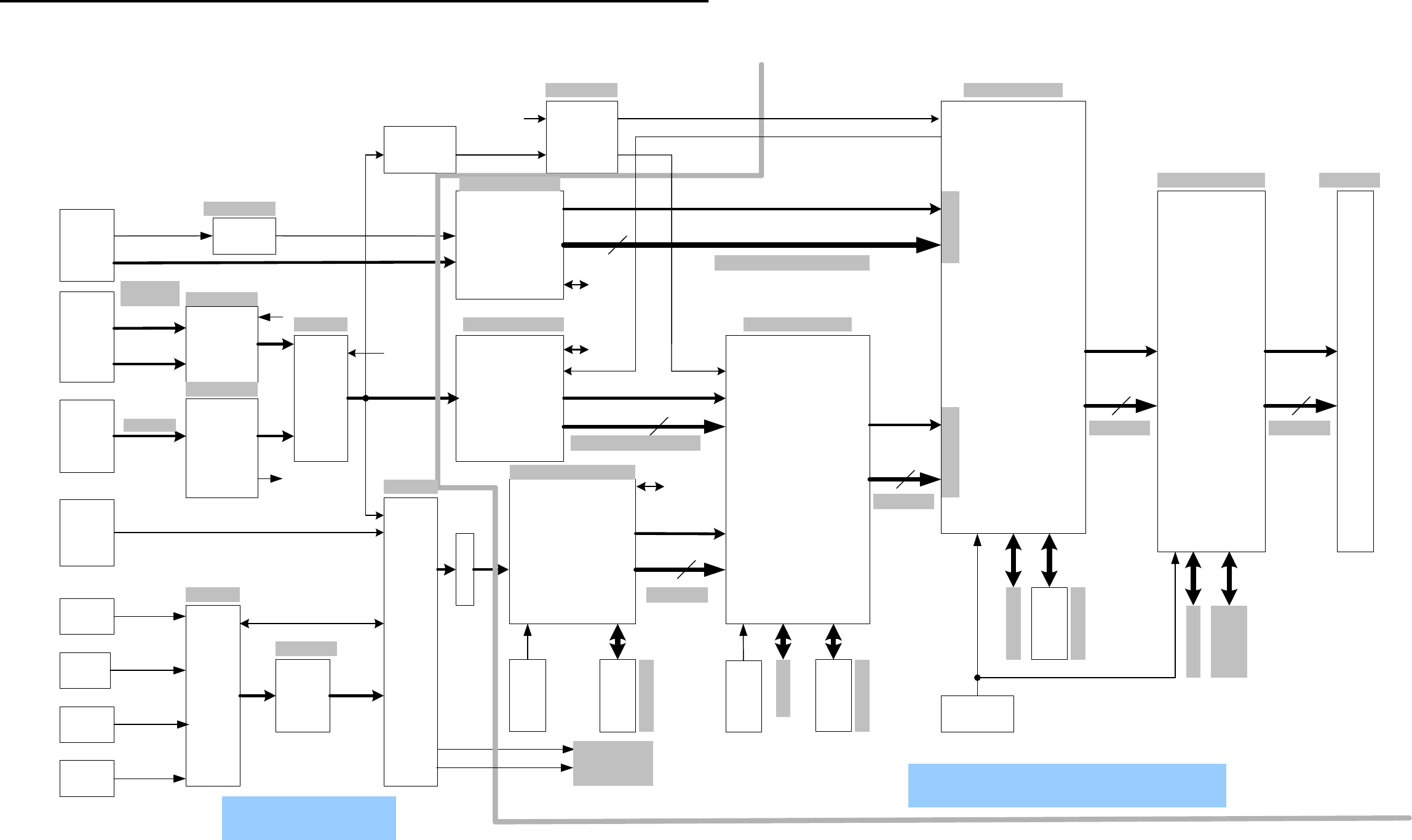
POWER CIRCUIT BLOCK DIAGRAM FOR LT-22XX / LT30XX
20V "22 Only 5A
Adaptor SEB150P2
JP JP
"22 "22
OnlyOnly
24V (1) "30 Only 3A "22: 3A "30: 2.8A (2.5A) INVERTER
PWB-POWER (2.7A) TO INVERTER
ON_24V
24V (2) "30 Only 3.8A "30: 2.8A (2.5A) INVERTER "30 Only
PWB-POWER (3.5A) TO INVERTER
ON_24V LCD PANEL
"30: 0.9A
A12V IC860 "22: 0.8A A12V
PQ1CY1032Z TO MAIN
PSAVE2
A9V IC8K0 0.15A IC701 AV-SW CXA2089
BA178M09FP
A9V IC100 AV-SW CXA2069
TO MAIN TC1A0 TUNER 115VF045AR
"22 Only A8V IC8J0 0.015A IC710 MPX MSP3440G
BA178M08FP
"30 Only
"30: 9V 1.4A
AMPVCC IC870 "22: 7.5V 1.2A IC712 MAIN AMP AN7522F
PQ1CY1032Z
PSAVE3 "30: 12V 0.95A
SAMPVCCIC880 "22: 9V 0.6A IC711 SUB AMP AN7522F
PQ1CY1032Z
PSAVE3
8.5V "30 Only 1.2A S5V IC850 0.6A S5V IC300 MPU M306V7
PWB-POWER PQ1CY1032Z TO MAIN IC2A1 EEPROM 24LC21TSW
IC710 MPX MSP3440G
SW5V IC8E0 0.4A IC702 MM 1556AF
CPH6311
PSAVE1
: Power source is IC305 LMV324MTX
always ON A5V IC201 AV-SW SM5301A
: use several TO MAIN IC204 AV-SW BA7657F
power sources TC1A0 TUNER 115VF045AR
IC202 LM1881MX
A30V IC180 0.005A TC1A0 TUNER 115VF045AR
LA7995M
S3.3V IC8F0 0.05A IC8X0 ADM3311EARS
SI3033LSA
IC300 MPU M306V7
S3.3V IC301 RESET IC M51957
TO MAIN IC303 EEPROM 24LC64T-I
IC2A2 74LCX14
4.5V IC840 1.2A D3.3V IC8N0 0.5A D3.3V IC400 Scaler Uranus M66473FP
PQ1CY1032Z SI3033LSA TO MAIN IC500 3D I/P gm6015
PSAVE1 IC501 DRAM64 K4S643232F-TC60
IC401 DRAM16 IC42S1600-7T *2
IC602 DRAM16 IC42S1600-7T *2
IC601 3D Y/C UPD64011
IC4A0 ENMA M66617FP
IC4A1 LVDS THC63LVDM83R
IC4A4 74LCX74MTCX
IC4A2 74LCX04MTCX
IC490 DSO751SV 20MHz
D1.9V IC402 0.27A IC400 Scaler Uranus M66473FP
SI3018KS
PSAVE1
A3.3V IC8M0 0.04A A3.3V IC601 3D Y/C UPD64011
SI3033LSA TO MAIN IC203 HD74LV157
PSAVE1
AD3.3V IC8Y0 0.24A AD3.3V IC205 A/D AD9883
SI3033LSA TO MAIN IC2A3 A/D AD9883
IC2J1 DVI SiI907B
D2.5V IC830 0.8A D2.5V IC500 3D I/P gm6015
PQ1CY1032Z TO MAIN IC4A0 ENMA2 M66617FP
PSAVE1
1.5V IC600 0.06A IC601 3D Y/C UPD64011
SI3012KS
DEVICE IC
PWB-SET(SUB)
PWB-MAIN
POWER-UNIT
"30 Only
AC-Adaptor "22
Only
Page 30
MODELS: LT-2220 / LT-2240 / LT-3020 / LT-3040 / LT-3050
IC400
M66473FP
(URANUS)
- Scaler for PC
- PiP/PoP control for
PC and AV combination
- Picture Enhancement
- Auto Setup
- Colorsync adjustment
- Sync Separation
for component CS
- Gamma
IC100
AV SW( CXA2069 )
9V
IC500
gm6015
- Motion adaptive
De- interlacer
- PiP/PoP control for
AV input Combination
- Color / Tint adjustment
-3D Noise Reduction
-Scaler for AV Input
-Sync Separation for
Composite Sync
CVBS
IC204
BA7657
AV-SWIC205
AD9883A
ADC(for COMP/DVI)
Black level / contrast
control for
Component / DVI
IC2A3
AD9883A
ADC(for PC)
Black level / contrast
control for PC
OSD Mix
between
IC300
Y for CCD2
CCDMAIN
PC& Video BLOCK DIAGRAM for LT-22XX/LT-30XX
IC401
16M SDRAM
IC4A0
M66617FP
(ENMA II)
- OSD MIX
IC701(AV SW)
CXA2089
9V
IC4A1 LVDS Tx
PC_H,VIC2A2
74LCX14
IC501
64M SDRAM
IC202
SYNC SEP
LM1881M
IC2J1
SiI907B
- TMDS-Rx
- HDCP Dec
- DAC
IC601
16M SDRAM
14.318MHz
IC601
uPD64011
-3D-YC
-DECODER
-Black level / contrast
control for TV /VIDEO
input
IC201
AV-SW
-LPF
CVBS/
SVideo
24.576MHz
MUXSEL
CTL
VRF
IC490
20MHz
Analog
RGB
YPbPr/
YCbCr
IC203
sync SW
74LV157
CCDSUB
PC_H,V
IC702
MM1566AF
BUFFER
Input 1
J703
Input 1
J704 S-Video
CVBS
Input 2
J701
Input 2
J702 S-Video
PC
J2A1
(Dsub15)
Component1/2
J201
YpbPr/
YCbCr
MONITOR-
LINK
(J2J0)
TV
TU1A0
TUNER
30V
5V
add=C0H
Analog RGB
TMDS
Conponent 2
Conponent 1
CVBS/
SVideo
YUV16
YUV/RGB24
H/V/CLK/FIELD
H/V/CLK
To
IC300
(M602V7)
24
YCbCr/
YPbPr
24
WXGA60
480i
480i/480p/720p/1080i
VGA/SVGA/XGA/WXGA
H/V/CLK
RGB
H/V/CLK
Field
Port1Port0
RGB
24
WXGA60
H/V/CLK
RGB
24
WXGA60
H/V/CLK
LPF
YPbPr/
RGB
DVI HV
DVI H/V
Composite Sync
Composite H
Composite H2
HS_out
3.3V IIC
3.3V IIC
3.3V IIC
5V IIC
CPU Bus
CPU Bus
CPU Bus
Vcc=D3.3V/D2.5V
Vcc=D3.3V/1.9V
Vcc=D3.3V
Vcc=D3.3V/D2.5VVcc=AD3.3V
Vcc=AD3.3V
Vcc=AD3.3V
Vcc=A5V
Vcc=A5V
Vcc=S3.3V
Vcc=A9V
Vcc=A5V
Vcc=A9VVcc=A3.3V/A1.5V/D1.5
Vcc=D3.3V
Vcc=D3.3V
Vcc=D3.3V
Vcc=A3.3V
Digital Circuit
Analog
Page 31
MODELS: LT-2220 / LT-2240 / LT-3020 / LT-3040 / LT-3050
IC305
AUDIO Bloc k Diagram for LT-22XX/LT-30XX
IC100
AV-SW
CXA2069
IC701
AV-SW
CXA2089
Component 1
Audio
(J201)
Component 2
Audio
(J201)
DVI-AUDIO
(J102)
PC-AUDIO
(J103)
VIDEO 1
VIDEO 2
IC710 MSP3440g
MPX
from TU1A0
SIF output
IC711
AN7522
IC712
AN7522
MAIN Out
Woofer out
Speaker -L
Input
source
Select
ADC
Main Audio
Processor
Core
-De modulator
-Volume
-Tone control
-Surround
-L/R-Mix
(for Woofer out)
- or others
ADC
DAC
SUB
auduo
processor
-Volume
Audio line output
DAC
J706
Head
Phone
Jack
MAIN_L_P
SUB_P
AMPVCC
SAMPVCC
MAIN_L_N
MAIN_R_P
MAIN_R_NSpeaker -R
Speaker -
Woofer
Volume1
from
IC300
#24
+
-
+
-
Volume control for MAIN
Amp
Volume control for SUB Amp
0.02Vdc to 1.15VdcAMPVCC
SAMPVCC
LT-2220 LT-3020
7.5V
9V9V
12V
Table: Supplied voltage to Amp +B
J705
PWB-MAINPWB-SET(SUB)
PWB-MAIN
SUB_N
0V
3.3V
Page 32
MODELS: LT-2220 / LT-2240 / LT-3020 / LT-3040 / LT-3050
TEST POINT LOCATIONS AND DESCRIPTIONS
Test points, locations and descriptions are shown below.
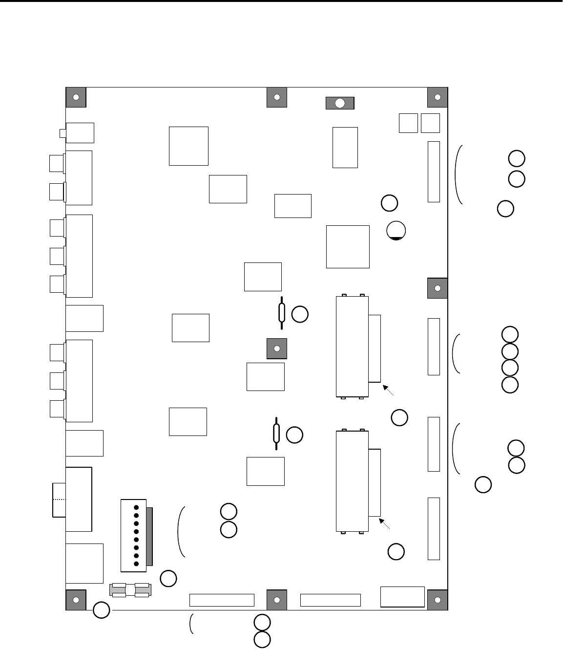
(1) PWB-SET (SUB)
Test Point Location Description Note
1 Pin1 of J800 J801(Fuse-clip) 20Vdc from AC-ADAPTOR 22inches only
2 F800 J802(Fuse-clip) 20Vdc behind the fuse F800 22inches only
3 INV-SW Pin12 of J821 Used to control inverter ON/OFF. (0V :
OFF , 5Vdc : ON)
4 BRIGHT Pin14 of J821 Used for brightness control of
inverter. (PWM control)
(Max : 5Vdc, Min : thin pulse)
5 24V Pin4, 6 of J810 24Vdc from Power-unit. 30inches only
6 8.5V Pin2 of J810 8.5Vdc from Power-unit. 30inches only
7 IN_24V Pin8 of J810 3.3Vdc.
Used for ON/OFF control of the power
supply from the POWER-UNIT.
30inches only
8 Psave1 Pin5 of J712 ON/OFF control signal of D3.3V, A3.3A.
(0V : OFF , 3.3Vdc : ON)
9 A8V (+) of C733 8Vdc.
Used to supply power to IC710.
10 AMPVCC Pin1 of IC711 7~9Vdc.
Used to supply power to IC711.
11 SAMPVCC Pin1 of IC712 8~12Vdc.
Used to supply power to IC712.
12 Psave2 Pin6 of J712 ON/OFF control signal of A9V, A8V
A5A. (0V : OFF , 3.3Vdc : ON)
13 Psave3 Pin7 of J712 ON/OFF control signal of AMPVCC,
SAMPVCC. (0V : OFF , 3.3Vdc : ON)
14 MPX Pin8 of J710 Analog video signal from TV input.
Voltage level is 1.0Vp-p (Typical)
15 SW_L Pin10 of J710 Audio L signal for PC or Monitorlink or
Component input.
16 SW_R Pin12 of J710 Audio R signal for PC or Monitorlink or
Component input.
17 5V_SDA 5 of J711 Serial port data I/O for IC of 5V power
supply.
18 5V_SCL 6 of J711 Serial port data clock for IC of 5V
power supply.
19 MPX_RST Pin10 of J711 Reset signal of IC710.
(0V : reset)
20 F880 F880 7~9Vdc.
Power supply fuse for IC711.
21 F870 F870 8~12Vdc.
Power supply fuse for IC712.
Page 33
MODELS: LT-2220 / LT-2240 / LT-3020 / LT-3040 / LT-3050
IC701
AV-SW
IC710
SOUND-
PRO
CESSOR
J8A0(XH10)
J715(PH6)
Radiator
IC711(IC-AMP)
Radiator
IC712(IC-AMP)
J710(PH-12)
J702
S1J704
S2
J800
DC-IN
IC702
LPF
J810
(
VH-8P)
J820(PH-15)J821(PH-16)
J712(PH-13)J711(PH-14)
IC860
DC
-DC
J8T0
XH3
IC8X0
RS-232C
J703
VIDEO2/AUDIO2
RL
Y
J8X0
RS232CJ705
Line Out
R
L
J701
VIDEO1/AUDIO1
RLY
J8T1
XH3
J706
HP
IC880
DC
-DC
IC870
DC
-DC
IC850
DC
-DC
IC840
DC
-DC
IC830
DC
-DC
J801 J802
14
1
F800
12 : INV-SW
14 : BRIGHT
16
1
1
810
1
13
1
12
1
5 : Psave1
(+) of C733
1
12
1
12
1 of IC712
1 of IC711
6 : Psave2
7 : Psave3
8 : MPX
10 : SW_L
12 : SW_R
4 : ON_24V
PWB-SET(SUB)
1
2
3
4
2 : 8.5V
4 : 24V
6 : 24V
5
6
7
8
12
13
11
10
9
14
15
16
5 : 5V_SDA
6 : 5V_SCL18
17
10 : MPX_RST
19
F880
20
F870
21
Page 34
MODELS: LT-2220 / LT-2240 / LT-3020 / LT-3040 / LT-3050
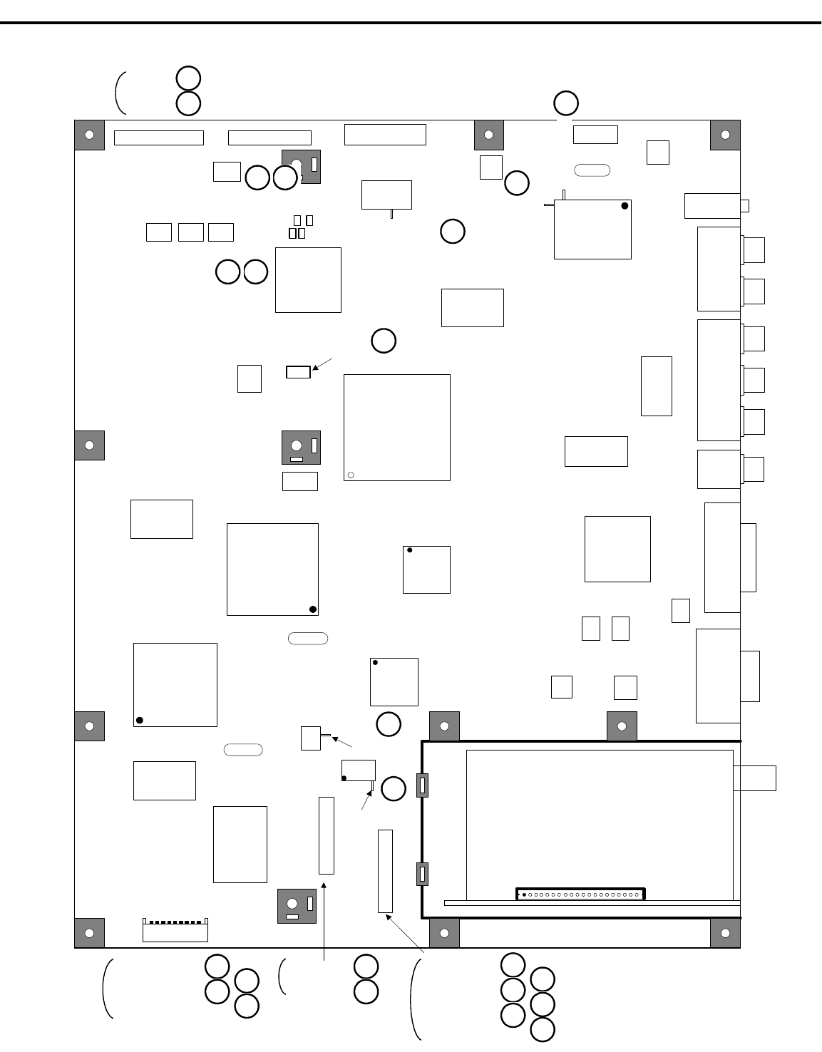
(2) PWB-MAIN
Test Point Location Description Note
1 S5V Pin12 of J303 5Vdc(always on ).
Power supply voltage for MCU, etc.
2 S3.3V Pin13 of J303 3.3Vdc(always on ).
Power supply voltage for MCU, etc.
3 D3.3V Pin7 of J190 3.3Vdc.
Power supply for IC300, IC4A0, IC4A1
etc.
4 A5V Pin1 of J190 5Vdc.
Power supply for IC204, IC201 etc.
5 A3.3V Pin5 of J190 3.3Vdc.
Power supply for IC203, etc.
6 D2.5V Pin8 of J190 2.5Vdc.
Power supply for IC500.
7 AD3.3V Pin6 of J190 3.3Vdc.
Power supply for IC2A3, IC205, IC2J1,
etc.
8 D1.9V L400 1.9Vdc.
Power supply for IC500.
9 Digital_G7 14 of IC4A1 3.3Vdc.
MSB of green digital video signal to
LCD panel.
10 QHS
-27 of IC4A1 R4H6 Horizontal sync signal to LCD panel
11 QVS
-28 of IC4A1 R4H5 Vertical sync signal to LCD panel
12 QCLK
-31 of IC4A1 R4H3 Clock signal to LCD panel
13 QDE
-30 of IC4A1 R4H4 Data_Enable signal to LCD panel
14 A9V 10 of J190 9Vdc.
Power supply for IC100.
15 30V Pin7 of IC180 30Vdc.
Power supply for TU1A0.
16 A1.5V,
D1.5V Pin3 of IC600 1.5Vdc.
Power supply for IC601.
17 TU_SDA Pin31 of IC300 Serial port data I/O for TU1A0.
18 TU_SCL Pin28 of IC300 Serial port data clock forTU1A0.
19 S3.3V(RMC) Pin1 of J301 3.3Vdc(always on ).
Power supply for IR receiver and front
switches, etc.
20 RMC Pin2 of J301 Data signal from IR receiver.
This data is sent to MCU.
21 KEY1 Pin4 of J301 Data signal from front switch.
This data is sent to MCU.
22 KEY2 Pin5 of J301 Data signal from front switch.
This data is sent to MCU.
23 V_OUT Pin2 of J110 Analog video signal from VIDEO 1&2
inputs. (Composite video)
24 SY_OUT Pin4 of J110 Analog video signal from VIDEO 1&2
inputs. (S-video)
Page 35
MODELS: LT-2220 / LT-2240 / LT-3020 / LT-3040 / LT-3050
IC400
GRAPHIC
& SCALER
IC204
VIDEO-SW
IC4A0
IC-OSD
IC4A1
LVDS-Tx
IC501
SDRAM64
IC201
VIDEO-SW
IC2A3
A/D-C
IC300
MCU
IC401
SDRAM16
IC205
A/D-C
J302
MCUWR
J190(XH-10)
J4A0
IC602
SDRAM16
J2J0
MONITOR-LINK
J103
PC-AUDIO
J110(PH-12)
J101
COMPONENT-
AUDIO(1and2)
RL
J201
COMPONENT(1and2)
PrPbY
J2A1
PC(D-sub)
J300(PH-13)J303(PH-14)
IC100
AV-SW
J102
MONITOR
-LINK
-AUDIO
L/R
IC500
3D-I/ P
gm6015
IC601
DECODER
with 3D-Y/C
IC4A2
04
IC4A3
08 IC4A4
74
IC2A2
14
IC202
1881
IC2J2
EEP
IC2A1
EEP
IC301
RST
IC305
LM324
IC303
EEP
TUNER
J301(PH-9)
IC203
157
IC600
3012
IC180
LA7995
IC490
20M
16MHz
14.318M
24.576M
IC402
3018
IC2J1
TMDS-Rx
1 9
L400 (D1.9V)
1 20
J180
3 of IC600
7 of IC180
28 of IC300
31 of IC300
PWB-MAIN
1
13 : S3.3V
12 : S5V2
5 : A3.3V
1 : A5V
7 : D3.3V
6 : AD3.3V
10 : A9V
8 : D2.5V
4
75
3
614
8
14 of IC4A19
R4H5
R4H3
R4H6
R4H4
1310
1211
15
16
18
17
2 : RMC
1 : S3.3V(RMC)
5 : KEY2
4 : KEY119
21 20
22
2 : V_OUT
4 : SY_OUT23
24
Page 36
MODELS: LT-2220 / LT-2240 / LT-3020 / LT-3040 / LT-3050
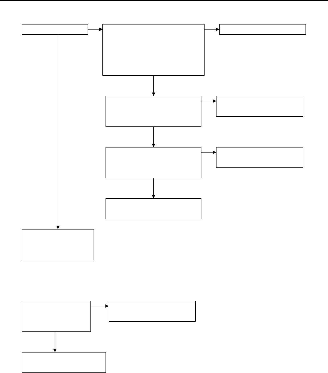
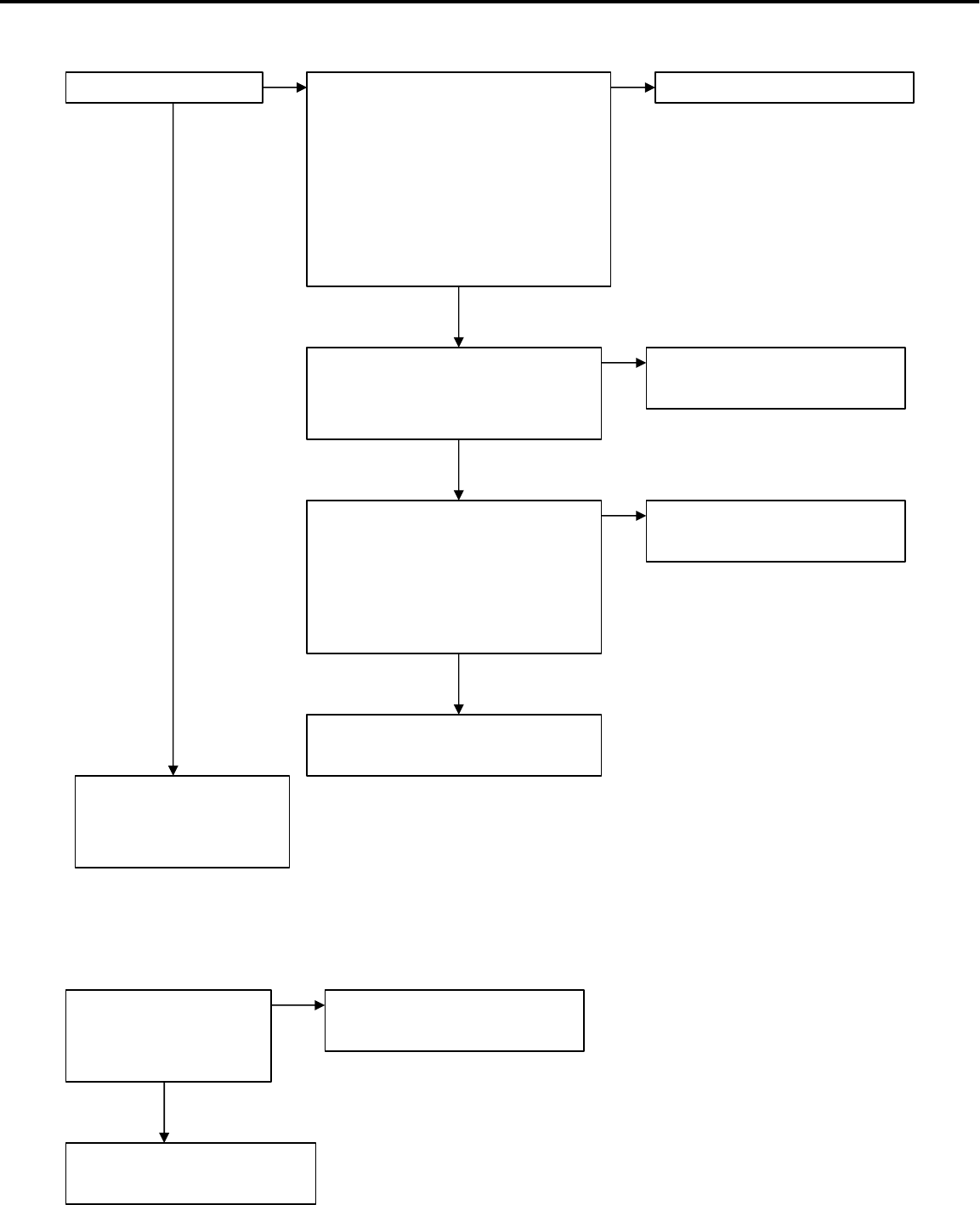
1. Power failure
1.1 In case of LT-22XX
(1)POWER is turned off.
Connect the Power plug and turn on the main Power switch (Front switch or remote control).
Is the POWER LED lit? Is the power plug connected
to the wall outlet correctly?
YES
·To “Flashing in green”(2)
·To “Flashing in amber”(3)
Poor power plug connection.
NO NO
Is the 20V DC available before
the fuse F800?
(Observing point : J801)
*Voltage range of 20V :18~21V
NO The AC-ADAPTOR is out of
order.
YES
Is 20V DC available behind
the fuse F800?
(Observing point : J802)
*Voltage range of 20V :18~21V
NO Fuse F800 have blown out. If
the fuse are replaced and it
blows out again, the AC-
ADAPTOR is out of order.
YES
Is the S5V and S3.3V, AD3.3V output
available at Pin12(S5V) and Pin13
(S3.3V) of J303 and at Pin6 of J190
(PH connector)?
NO Power supply circuit
which generates S5V
and S3V and AD3.3V in
the PWB-SUB(SET) is
out of order.
YES
IC300 and peripheral circuits
are out of order.(PWB-MAIN)
CN Pin No. Voltage
S5V J303 12 5Vdc
S3.3V J303 13 3.3Vdc
AD3.3V J190 6 3.3Vdc
YES
YES
Is all harness connected
correctly?
All harness connects
correctly.
NO
Page 37
MODELS: LT-2220 / LT-2240 / LT-3020 / LT-3040 / LT-3050
(2)Flashing in green.
(3)Flashing in Amber.
Is the back-light on?
YES
NO
Is the INV-SW output 5V-level
at Pin12 of the J821 connector?
(PH connector)
Is the BRIGHT output about 5V
level at Pin14 of the J821
connector? (PH connector)
YES
NO
NO
IC300 and peripheral circuits
are out of order.(PWB-MAIN)
YES
Is the following harness connected?
-Between PWB-SUB(SET) and
INVERTER (J821-INVERTER)
-Between back-lights and
INVERTER
YES
NO Poor harness connection.
Inverter or back-light of LCD-
panel are out of order.
Skip to “2. No picture
displayed and picture
errors.”
If POWER switch is
pushed, does LED
become green?
NO
YES
IC300 and peripheral circuits
are out of order.(PWB-MAIN)
IC300 and peripheral circuits
are out of order.(PWB-MAIN)
Skip to the above-mentioned
“(2) Flashing in green” .
Page 38
MODELS: LT-2220 / LT-2240 / LT-3020 / LT-3040 / LT-3050
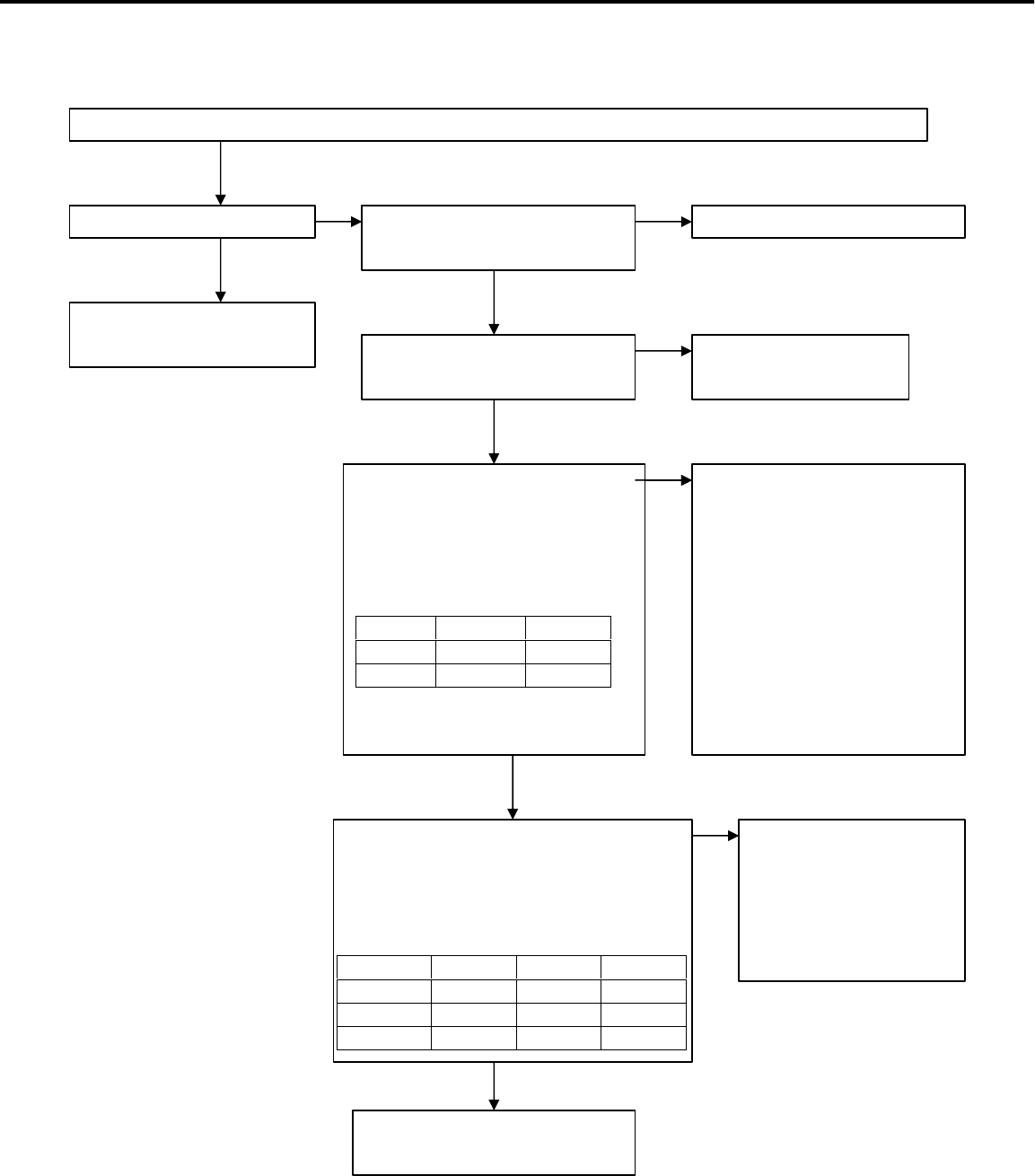
1.2 In case of LT-30XX
(1)POWER is turned off.
Connect the Power plug and turn on the main Power switch (Front switch or remote switch).
Is the POWER LED lit? Is the power plug connected
to the wall outlet correctly?
YES
·To “Flashing in green”(2)
·To “Flashing in amber”(3)
Poor power plug connection.
NO NO
YES
Is the 24V and 8.5V output
available at Pin2(8.5V) and
Pins 4, 6(24V) of the J810
connector? (VH connector)?
*Voltage range of 8.5V :8.1~8.8V
*Voltage range of 24V :22~26V
NO Is the IN_24V output
3Vdc at Pin8(24V) of the J810
connector? (VH connector)
If not outputting, IC300 or its
Periphral circuits is out of
order.(PWB-MAIN)
If outputting, Power unit is
out of order.
YES
YES
IC300 and peripheral circuits
are out of order.(PWB-MAIN)
Pin No. Voltage
8.5V 2 8.5Vdc
24V 4, 6 24Vdc
YES
Is all harness connected
correctly?
All harness connects
correctly.
Is the S5V and S3.3V, AD3.3V output
available at Pin12(S5V) and Pin13
(S3.3V) of J303 and at Pin6 of J190
(PH connector)?
NO Power supply circuit
which generates S5V
and S3V and AD3.3V in
the PWB-SUB(SET) is
out of order.
CN Pin No. Voltage
S5V J303 12 5Vdc
S3.3V J303 13 3.3Vdc
AD3.3V J190 6 3.3Vdc
Page 39
MODELS: LT-2220 / LT-2240 / LT-3020 / LT-3040 / LT-3050
(2)Flashing in green.
(3)Flashing in Amber.
Is the back-light on?
YES
NO
Is the INV-SW output 5V-level
at each Pin12 of the J821 and
J820 connector? (PH connector)
Is the BRIGHT output about 12V
level at each Pin14 of the J821
and J820 connector?
(PH connector)
*Voltage range : 10~14V
YES
NO
NO
IC300 and peripheral circuits
are out of order.(PWB-MAIN)
YES
Is the following two harness
connected?
-Between PWB-SUB(SET) and
INVERTER (J821-INVERTER)
(J820-INVERTER)
-Between back-lights and
INVERTER YES
NO Poor harness connection.
Inverter or back-light of LCD-
panel are out of order.
If POWER switch is
pushed, does LED
become green?
Skip to the above-mentioned
“(2) Flashing in green” .
NO
YES
IC300 and peripheral circuits
are out of order.(PWB-MAIN)
IC300 and peripheral circuits
are out of order.(PWB-MAIN)
Skip to “2. No picture
displayed and picture
errors.”
Page 40
MODELS: LT-2220 / LT-2240 / LT-3020 / LT-3040 / LT-3050
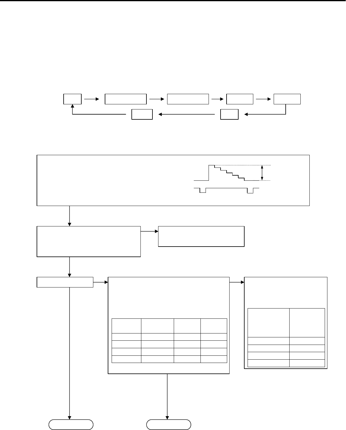
2. No picture displayed and picture errors (It applies both LT-30XX and LT-22XX)
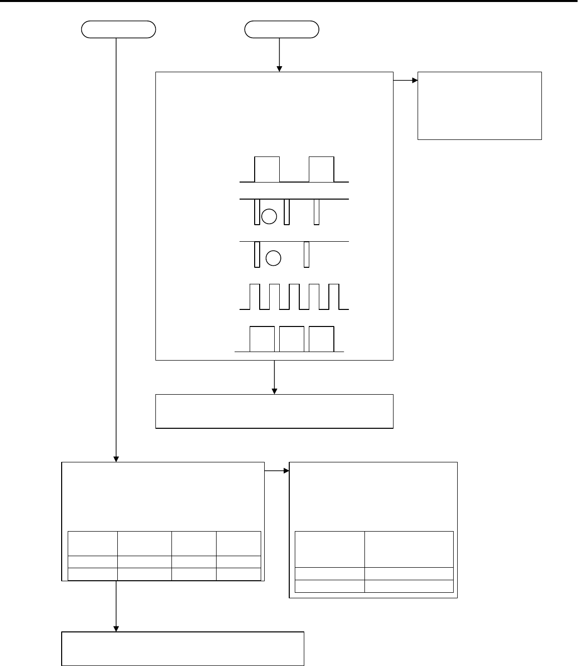
Note ) It applies when there is no screen display or an unusual screen is outputted, although
power supply is turned on and the back light is turned on.
Before checking, perform the initial setup. (Input before the initial setup is channel 3 of TV.)
*Input source changes in following order with DEVICE UP button of remote control or
DEVICE
button of front switch.
2-1. No picture displayed and picture errors of PC signal.
Is all harness connected correctly?
(especially between PWB-MAIN
and LCD PANEL (J4A0-LCD))
NO Poor harness connection or
defective cable.
YES
Is OSD available? Problem is in IC300 or IC4A0 or IC4A1
(and peripheral circuits). Are the
specified voltages available at the
connectors below?
NO
YES
Enter an input of WXGA(60Hz) gray scale
in D-sub connector(J2A1), and select PC INPUT.
(Push the device UP button 5 times.)
And then, perform AV reset by front switch.
The video level inputs above 0.7Vp-p.
TV Component1 Component2 Input1 Input2
DVI PC
NO
CN
Name Pin No. Voltage
S5V J303 12 5Vdc
S3.3V J303 13 3.3Vdc
D3.3V J190 7 3.3Vdc
Psave1* J712 5 3.3Vdc
* control signal of D3.3V
Problem is in the following
circuit (and peripheral
circuits) .
Voltage with
problem PWB
including
the circuit
in problem
S5V SET(SUB)
S3.3V SET(SUB)
D3.3V SET(SUB)
Psave1 MAIN
YES
2-1-2 (P*)
0.7Vp-p
2-1-1 (P*)
Page 41
MODELS: LT-2220 / LT-2240 / LT-3020 / LT-3040 / LT-3050
Problem is in IC2A3 or IC400
(and peripheral circuits). Are the
specified voltages available at the
connectors below?
LCD-module or IC4A1(PWB-MAIN) are out of
order.
IC2A3 or IC400 (and peripheral circuits) are out
of order.(PWB-MAIN)
CN
Name Pin No. Voltage
AD3.3V J190 6 3.3Vdc
D1.9V L400 - 1.9Vdc
NO When the shown voltage is in
problem, PWB including the power
supply circuit(and peripheral
circuits) is the following.
Voltage with
problem PWB including
the circuit in
problem
AD3.3V SET(SUB)
D1.9V MAIN
Is the digital video signal available at pin 14(G_7)
of IC4A1, and control signals of 3Vp-p available at
pins 27(HS : R4H6) and 28(VS : R4H5) and
31(CLK : R4H3) and 30(DE : R4H4) of IC4A1 ?
27 of IC4A1
28 of IC4A1
(f=60Hz)
3Vp-p
3Vp-p
H
V
14 of IC4A1
(MSB of Green) 3Vp-p
31 of IC4A1
(f=70MHz) 3Vp-p
(f=48KHz)
2-1-2 (P*) 2-1-1 (P*)
30 of IC4A1
3Vp-p
(f=48KHz)
YES
NO IC300 or IC4A0 (and
peripheral circuits) are
out of order. (PWB-
MAIN)
YES
Page 42
MODELS: LT-2220 / LT-2240 / LT-3020 / LT-3040 / LT-3050
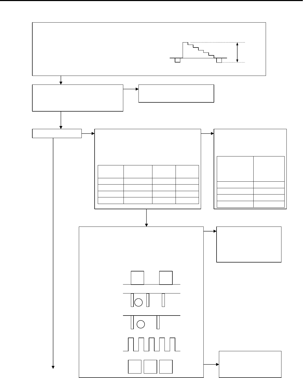
2-2. No picture displayed and picture errors of Component signal.
Enter an input of D1(480i) gray scale in J201
connector, and select COMPONENT1 (or2) INPUT.
(Push the device UP button once.: twice in the case
of COMPONENT2)
And then, perform AV reset by front switch.
The video level inputs about 1.0Vp-p.
YES
Is OSD available? NO
YES
Problem is in IC300 or IC4A0 or IC4A1
(and peripheral circuits). Are the
specified voltages available at the
connectors below?
NO
CN
Name Pin No. Voltage
S5V J303 12 5Vdc
S3.3V J303 13 3.3Vdc
D3.3V J190 7 3.3Vdc
Psave1* J712 5 3.3Vdc
*control signal of D3.3V
YES
Problem is in the following
circuit (and peripheral
circuits) .
Voltage with
problem PWB
including
the circuit
in problem
S5V SET(SUB)
S3.3V SET(SUB)
D3.3V SET(SUB)
Psave1 MAIN
1.0Vp-p
Is all harness connected correctly?
(especially between PWB-MAIN
and LCD PANEL (J4A0-LCD))
NO Poor harness connection or
defective cable.
Is the digital video signal available at pin 14(G_7)
of IC4A1, and control signals of 3Vp-p available at
pins 27(HS : R4H6) and 28(VS : R4H5) and
31(CLK : R4H3) and 30(DE : R4H4) of IC4A1 ?
27 of IC4A1
28 of IC4A1
(f=60Hz)
3Vp-p
3Vp-p
H
V
14 of IC4A1
(MSB of Green) 3Vp-p
31 of IC4A1
(f=70MHz) 3Vp-p
(f=48KHz)
30 of IC4A1
3Vp-p
(f=48KHz)
IC300 or IC4A0 (and
peripheral circuits) are
out of order. (PWB-
MAIN)
NO
LCD-module or IC4A1
(PWB-MAIN) are out of
order.
YES
Page 43
MODELS: LT-2220 / LT-2240 / LT-3020 / LT-3040 / LT-3050
Problem is in IC204 or IC201 or IC205 or
IC500 or IC400 (and peripheral circuits).
Are the specified voltages available at the
connectors below?
IC204 or IC201 orIC205 or IC500 or IC400 (and
peripheral circuits) are out of order.(PWB-MAIN)
CN
Name Pin No. Voltage
A5V J190 1 5Vdc
A3.3V J190 5 3.3Vdc
D2.5V J190 8 2.5Vdc
D1.9V L400 - 1.9Vdc
AD3.3V J190 6 3.3Vdc
NO
When the shown voltage is in
problem, PWB including the power
supply circuit(and peripheral
circuits) is the following.
Voltage with
problem PWB including
the circuit in
problem
A5V SET(SUB)
A3.3V SET(SUB)
D2.5V SET(SUB)
D1.9V MAIN
AD3.3V SET(SUB)
2-2-1 (P*)
2-2-1(P*)
YES
Page 44
MODELS: LT-2220 / LT-2240 / LT-3020 / LT-3040 / LT-3050
2-3. No picture displayed and picture errors of DVI signal.
Enter an input of D2(480p) gray scale
in J2J0 connector, and select DVI INPUT.
(Push the device UP button 6 times)
And then, perform AV reset by front switch.
The video level inputs above 0.7Vp-p.
YES
Is OSD available? NO
YES
Problem is in IC300 or IC4A0 or IC4A1
(and peripheral circuits). Are the
specified voltages available at the
connectors below?
NO
CN
Name Pin No. Voltage
S5V J303 12 5Vdc
S3.3V J303 13 3.3Vdc
D3.3V J190 7 3.3Vdc
Psave1* J712 5 3.3Vdc
*control signal of D3.3V
YES
Problem is in the following
circuit (and peripheral
circuits) .
Voltage with
problem PWB
including
the circuit
in problem
S5V SET(SUB)
S3.3V SET(SUB)
D3.3V SET(SUB)
Psave1 MAIN
0.7Vp-p
Is all harness connected correctly?
(especially between PWB-MAIN
and LCD PANEL (J4A0-LCD))
NO Poor harness connection or
defective cable.
Is the digital video signal available at pin 14(G_7)
of IC4A1, and control signals of 3Vp-p available at
pins 27(HS : R4H6) and 28(VS : R4H5) and
31(CLK : R4H3) and 30(DE : R4H4) of IC4A1 ?
27 of IC4A1
28 of IC4A1
(f=60Hz)
3Vp-p
3Vp-p
H
V
14 of IC4A1
(MSB of Green) 3Vp-p
31 of IC4A1
(f=70MHz) 3Vp-p
(f=48KHz)
30 of IC4A1
3Vp-p
IC300 or IC4A0 (and
peripheral circuits) are
out of order. (PWB-
MAIN)
NO
LCD-module or IC4A1
(PWB-MAIN) are out of
order.
YES
Page 45
MODELS: LT-2220 / LT-2240 / LT-3020 / LT-3040 / LT-3050
IC2J1 or IC201 or IC205 or IC500 or IC400(and
peripheral circuits) are out of order. (PWB-MAIN)
Problem is in IC2J1 or IC201 or IC205 or
IC500 or IC400 (and peripheral circuits).
Are the specified voltages available at the
connectors below?
CN
Name Pin No. Voltage
A5V J190 1 5Vdc
A3.3V J190 5 3.3Vdc
D2.5V J190 8 2.5Vdc
D1.9V L400 - 1.9Vdc
AD3.3V J190 6 3.3Vdc
NO When the shown voltage is in
problem, PWB including the power
supply circuit(and peripheral
circuits) is the following.
Voltage with
problem PWB including
the circuit in
problem
A5V SET(SUB)
A3.3V SET(SUB)
D2.5V SET(SUB)
D1.9V MAIN
AD3.3V SET(SUB)
(f=48KHz)
2-3-1 (P*)
2-3-1 (P*)
YES
Page 46
MODELS: LT-2220 / LT-2240 / LT-3020 / LT-3040 / LT-3050

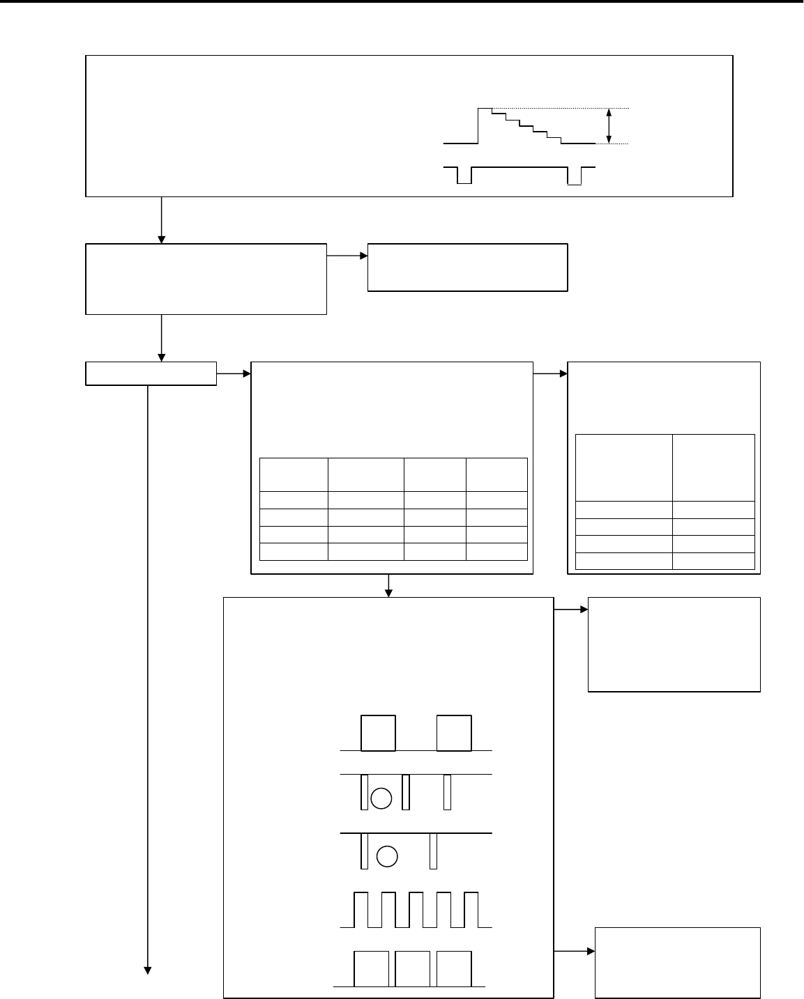
2-4. No picture displayed and picture errors of VIDEO signal.
Enter an input of NTSC gray scale
in J2J0 connector, and select VIDEO1 (or 2) INPUT.
(Push the device UP button 3 times :
4 times in case of VIDEO2)
And then, perform AV reset by front switch.
The video level inputs about 1.0Vp-p.
YES
Is OSD available? NO Problem is in IC300 or IC4A0 or IC4A1
(and peripheral circuits). Are the
specified voltages available at the
connectors below?
NO
CN
Name Pin No. Voltage
S5V J303 12 5Vdc
S3.3V J303 13 3.3Vdc
D3.3V J190 7 3.3Vdc
Psave1* J712 5 3.3Vdc
*control signal of D3.3V
YES
Problem is in the following
circuit (and peripheral
circuits) .
Voltage with
problem PWB
including
the circuit
in problem
S5V SET(SUB)
S3.3V SET(SUB)
D3.3V SET(SUB)
Psave1 MAIN
1.0Vp-p
Is all harness connected correctly?
(especially between PWB-MAIN
and LCD PANEL (J4A0-LCD))
NO Poor harness connection or
defective cable.
Is the digital video signal available at pin 14(G_7)
of IC4A1, and control signals of 3Vp-p available at
pins 27(HS : R4H6) and 28(VS : R4H5) and
31(CLK : R4H3) and 30(DE : R4H4) of IC4A1 ?
27 of IC4A1
28 of IC4A1
(f=60Hz)
3Vp-p
3Vp-p
H
V
14 of IC4A1
(MSB of Green) 3Vp-p
31 of IC4A1
(f=70MHz) 3Vp-p
(f=48KHz)
30 of IC4A1
3Vp-p
IC300 or IC4A0 (and
peripheral circuits) are
out of order. (PWB-
MAIN)
LCD-module or IC4A1
(PWB-MAIN) are out of
order.
YES
YES
Page 47
MODELS: LT-2220 / LT-2240 / LT-3020 / LT-3040 / LT-3050
IC100 or IC601 or IC500 or IC400(and peripheral
circuits) are out of order.(PWB-MAIN)
Problem is in IC100 or IC601 or IC500 or
IC400 (and peripheral circuits).
Are the specified voltages available at the
connectors below?
CN
Name Pin No. Voltage
A9V J190 10 9Vdc
A1.5V IC600 3 1.5Vdc
D1.5V IC600 3 1.5Vdc
A3.3V J190 5 3.3Vdc
D2.5V J190 8 2.5Vdc
D1.9V L400 - 1.9Vdc
AD3.3V J190 6 3.3Vdc
NO
When the shown voltage is in
problem, PWB including the power
supply circuit (and peripheral
circuits) is the following.
Voltage
with
problem
PWB including
the circuit in
problem
A9V SET(SUB)
A1.5V MAIN
D1.5V MAIN
A3.3V SET(SUB)
D2.5V SET(SUB)
D1.9V MAIN
AD3.3V SET(SUB)
YES
2-4-1 (P*)
2-4-1 (P*)
YES
(f=48KHz)
Is the signal of 1.0Vp-p available at pin 2(V_out)
of J110,or pin 4 (SY_out) of J110?
Pin2 of J110
Pin4 of J110 1.0Vp-p
YES
NO IC701 or IC702 (PWB-
SET(SUB)) are out of order.
Page 48
MODELS: LT-2220 / LT-2240 / LT-3020 / LT-3040 / LT-3050
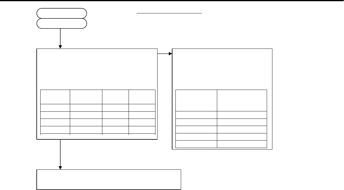
2-5. No picture displayed and picture errors of TV signal.
Enter an input of NTSC gray scale
in TU1A0 (TUNER), and select TV INPUT.
(It may not push the device button after initial
setup. Adjust the channel of TV with the
channel of a signal source.)
And then, perform AV reset by front switch.
YES
Is OSD available? NO Problem is in IC300 or IC4A0 or IC4A1
(and peripheral circuits). Are the
specified voltages available at the
connectors below?
NO
CN
Name Pin No. Voltage
S5V J303 12 5Vdc
S3.3V J303 13 3.3Vdc
D3.3V J190 7 3.3Vdc
Psave1* J712 5 3.3Vdc
YES
Problem is in the following
circuit (and peripheral
circuits) .
Voltage with
problem PWB
including
the circuit
in problem
S5V SET(SUB)
S3.3V SET(SUB)
D3.3V SET(SUB)
Psave1 MAIN
YES
1.0Vp-p
Is all harness connected correctly?
(especially between PWB-MAIN
and LCD PANEL (J4A0-LCD))
NO Poor harness connection or
defective cable.
Is the digital video signal available at pin 14(G_7)
of IC4A1, and control signals of 3Vp-p available at
pins 27(HS : R4H6) and 28(VS : R4H5) and
31(CLK : R4H3) and 30(DE : R4H4) of IC4A1 ?
27 of IC4A1
28 of IC4A1
(f=60Hz)
3Vp-p
3Vp-p
H
V
14 of IC4A1
(MSB of Green) 3Vp-p
31 of IC4A1
(f=70MHz) 3Vp-p
(f=48KHz)
30 of IC4A1
(f=48KHz)
IC300 or IC4A0 (and
peripheral circuits) are
out of order. (PWB-
MAIN)
LCD-module or IC4A1
(PWB-MAIN) are out of
order.
YES
Page 49
MODELS: LT-2220 / LT-2240 / LT-3020 / LT-3040 / LT-3050
TU1A0 or IC100 or IC601 or IC500 or IC400 (and
peripheral circuits) are out of order. (PWB-MAIN)
Problem is in IC100 or IC601 or IC500 or
IC400 (and peripheral circuits).
Are the specified voltages available at the
connectors below?
CN
Name Pin No. Voltage
30V IC180 7 30Vdc
A9V J190 10 9Vdc
A1.5V IC600 3 1.5Vdc
D1.5V IC600 3 1.5Vdc
A3.3V J190 5 3.3Vdc
D2.5V J190 8 2.5Vdc
D1.9V L400 - 1.9Vdc
AD3.3V J190 6 3.3Vdc
NO When the shown voltage is in
problem, PWB including the power
supply circuit (and peripheral
circuits) is the following.
Voltage with
problem PWB including
the circuit in
problem
30V MAIN
A9V SET(SUB)
A1.5V MAIN
D1.5V MAIN
A3.3V SET(SUB)
D2.5V SET(SUB)
D1.9V MAIN
AD3.3V SET(SUB)
3Vp-p
2-5-1 (P*)
2-5-1 (P*)
YES
Page 50
MODELS: LT-2220 / LT-2240 / LT-3020 / LT-3040 / LT-3050
3. No audio output generated.(It applies both LT-30XX and LT-22XX)
Notes) This model is enabled to set up an audio input terminal for each video input terminal. No
audio output is available unless the input terminal of displayed pictures (example:VIDEO1)
coincides with that of audio (example:PC). Therefore, analysis for troubleshooting should be
carried out after the displayed video input terminal (example:VIDEO1) has been made to coincide
with the input terminal according to the instruction manual.
Enter a signal input AUDIO in.
Is “TV speakers” setting on?
Raise volume level. And MUTE is turned off. Volume level is not 0. And MUTE is off.
YES
NO
“TV speakers” setting is on.
NO
YES
In case of TV input, is “Listen To:” setting set
to Stereo or Mono?
NO
YES
“Listen To :” setting is set to Stereo
or Mono.
Are the specified voltages available at the
pins below? (Power source check)
NO
CN
Name Pin No. Voltage
S5V J303 12 5Vdc
A5V J8A0 1 5Vdc
A9V J8A0 10 9Vdc
A8V C733 - 8Vdc
AMPVCC IC711 1 7~9Vdc
SAMPVCC IC712 1 8~12V
dc
Psave2* J712 6 3Vdc
Psave3** J712 7 3Vdc
*control signal of A9V, A8V, A5V
** control signal of AMPVCC, SAMPVCC
Problem is in the following
circuit (and peripheral
circuits) .
Voltage with
problem PWB
including
the circuit
in problem
S5V SET(SUB)
A5V SET(SUB)
A9V SET(SUB)
A8V SET(SUB)
AMPVCC SET(SUB)
SAMPVCC SET(SUB)
Psave2 MAIN
Psave3 MAIN
YES
Is voltage the same before and behind F870
and F880?
NO It replaces the PWB-SET(SUB).
(Fuse have blown out. )
YES
Page 51
MODELS: LT-2220 / LT-2240 / LT-3020 / LT-3040 / LT-3050
v
YES
Is the signal below available at pins 5, 6 of
J711 (control signals of IC701 and IC710 and
IC100 ) and 10 of J711 (control signals of
IC710) and 28, 31 of IC300 (control signals of
TU1A0) ?
5, 6 of J711,
28, 31 of IC300 3Vp-p
IC300 (and peripheral circuits)
are out of order.(PWB-MAIN)
NO
3Vdc 10 of J711
YES
3-A (P*)
3-A (P*)
Is sound signal outputted correctly at the
pins 10, 12 ,8 of J710 connector?
?It checks that a certain signal is outputting
in the voltage range of 1V.
NO
YES
IC100 (and peripheral circuits)
are out of order.(PWB- SET(SUB))
IC701 and IC710 and IC711 and IC712 (and
peripheral circuits) are out of order.
(PWB-MAIN)
Page 52
MODELS: LT-2220 / LT-2240 / LT-3020 / LT-3040 / LT-3050
4. Other faults.(It applies both LT-30XX and LT-22XX)
Notes) It considers the case where there are problems except 1, 2, 3.
4-1. Remote control is not effective.
4-2. Front switch is not effective.
After checking the polarity of batteries, has
it loaded correctly?
Does it use within 20 feet?
Load the batteries, making sure the
polarities (-) and (+) are correct.
Regarding as the slide switch at the top of
the remote, does it set as “TV”?
YES
NO
NO
YES
YES
YES
NO
It sets the slide switch as “TV”.
it uses within 20 feet.
It does not operate, even if it exchanges for
new batteries.
NO It exchanges on new batteries.
Is the following harness connected correctly?
·Between PWB-MAIN and PWB-CONT
(J301-J0A1)
NO Poor harness connection or
defective cable.
YES
When it pushes the front switch, is the signal
below available at pins 1, 4, 5 of J301
(remote control and front switch use) ?
3Vp-p only when switch is not pushed.
0V only when switch is pushed.
YES
IC300 (and peripheral circuits) are out of order.(PWB-MAIN)
NO
3Vdc 1
4, 5 :
YES
When it pushes the remote switch, is the
signal below available at pins 1, 2, of J301
(remote switch use) ?
NO
3Vdc 1
2:
Skip to “4-2 front switch is not effective”.
3Vp-p
Problem is in the following
PWB (and peripheral circuits).
Pin with
problem PWB
including
the circuit
in problem
2 of J301 CONT
1 of J301 MAIN
Problem is in the following
PWB (and peripheral circuits).
Pin with
problem PWB
including
the circuit
in problem
4, 5 of J301 CONT
1 of J301 MAIN
Page 53
MODELS: LT-2220 / LT-2240 / LT-3020 / LT-3040 / LT-3050
MODELS: LT-2220 / LT-2240 / LT-3020 / LT-3040 / LT-3050
Page 54
Part Number Description Part Number Description
7A930032 AC-ADAPTER (SEB150P2-20.0B) 7A930032 AC-ADAPTER (SEB150P2-20.0B)
25327981 BACK-UNIT (CABINET-BACK LT2220/2240) 25327981 BACK-UNIT (CABINET-BACK LT2220/2240)
08LA10AE BEZEL (INCLUDES INNER BEZEL & PLATE) 08LA10AE BEZEL (INCLUDES INNER BEZEL & PLATE)
25327921 BEZEL-INNER (LC-T2220) 25327973 BEZEL-UNIT (LC-T2240 GRY)
25327971 BEZEL-UNIT (LC-T2220 GRY) 79PQ6640 CORD-POWER (1.9M 2P BLK)
7A081023 CORD-POWER (1.9M 2P BLK) 25435861 COVER-LEFT
25435861 COVER-LEFT 25435911 COVER-REAR (CLEAR)
25435911 COVER-REAR (CLEAR) 25435851 COVER-RIGHT
25435851 COVER-RIGHT 25435881 COVER-TERMINAL LEFT
25435881 COVER-TERMINAL LEFT 25435871 COVER-TERMINAL RIGHT
25435871 COVER-TERMINAL RIGHT 3A684064 LCD (LC56XWC8V-02) T/A REQ
3A684043 LCD (AA220TA01) T/A REQUIRED 3A681009 LED (SML78420C)
3A681009 LED (SML78420C) PWB-CONTROL LT2240 PWB-CONTROL/LED T/A REQUIRED
PWB-CONTROL LT2220 PWB-CONTROL/LED T/A REQUIRED 8BL63M15 PWB-MAIN (LT-2240) T/A REQUIRED
8BL61M12 PWB-MAIN (LT-2220) T/A REQUIRED PWB-SUB LT2240 PWB-SUB T/A REQUIRED
PWB-SUB LT2220 PWB-SUB T/A REQUIRED PWB-TUNER LT2240 PWB-TUNER
PWB-TUNER LT2220 PWB-TUNER T/A REQUIRED 79PQ6596 REMOTE
7A930037 REMOTE(EUR7616Z20/Z2A) 3A290003 REMOTE-RECEIVER (GP1UD263XK)
3A290003 REMOTE-RECEIVER (GP1UD263XK) 7A930033 SPEAKER-UNIT(ST-220-1)
7A930033 SPEAKER-UNIT(ST-220-1) 25261691 STAND-UNIT (GREY)
25261691 STAND-UNIT (GREY) 7A930029 TUNER (115V VF045AR)
7A930029 TUNER (115V VF045AR) 79PQ6630 UNIT-INVERTER (J191007.01)
7A930030 UNIT-INVERTER (J191007.00)
Part Number Description Part Number Description
25327961 BACK-UNIT 25327961 BACK-UNIT
08LB10AE BEZEL (INCLUDES INNER BEZEL & PLATE) 08LB10AE BEZEL (INCLUDES INNER BEZEL & PLATE)
25327891 BEZEL-INNER (LC-T3020) 25327952 BEZEL-UNIT
7A081022 CORD-POWER (2.0M 2P BLK) 7A392043 CABLE-ANT(BLACK RF-RF)
25435841 COVER-CORD 79PQ6612 CORD-POWER(2.0M 2P BLK)
25435861 COVER-LEFT 25435841 COVER-CORD
25435831 COVER-REAR 25435861 COVER-LEFT
25435851 COVER-RIGHT 25435831 COVER-REAR
25435881 COVER-TERMINAL LEFT 25435851 COVER-RIGHT
25435871 COVER-TERMINAL RIGHT 25435881 COVER-TERMINAL LEFT
25327951 FRONT-CABINET (W/BUTTONS LT-3020) 25435921 COVER-TERMINAL RIGHT
3A684029-M LCD (LC300W01 A3 LGPL) T/A REQ 3A684029-M LCD (LC300W01 A3 LGPL) T/A REQ
3A681009 LED (SML78420C) 3A681009 LED (SML78420C)
25620101 PLATE (COSMETIC LC-T3020) 7A930031 POWER-UNIT (HS210N2J)(T/A REQ)
7A930031 POWER-UNIT (HS210N2J)(T/A REQ) PWB-CONTROL LT3040 PWB-CONTROL/LED T/A REQUIRED
PWB-CONTROL LT3020 PWB-CONTROL/LED T/A REQUIRED 8BL73M15 PWB-MAIN (LT-3040) T/A REQUIRED
8BL71M12 PWB-MAIN (LT-3020) T/A REQUIRED PWB-SUB LT3040 PWB-SUB T/A REQUIRED
PWB-SUB LT3020 PWB-SUB T/A REQUIRED PWB-TUNER LT3040 PWB-TUNER T/A REQUIRED
PWB-TUNER LT3020 PWB-TUNER T/A REQUIRED 79PQ6596 REMOTE
7A930037 REMOTE(EUR7616Z20/Z2A) 3A290003 REMOTE-RECEIVER (GP1UD263XK)
3A290003 REMOTE-RECEIVER (GP1UD263XK) 7A930034 SPEAKER-UNIT(ST-300-1)
7A930034 SPEAKER-UNIT(ST-300-1) 25261681 STAND-UNIT (GREY)
25261681 STAND-UNIT (GREY) 7A930029 TUNER (115V VF045AR)
7A930029 TUNER (115V VF045AR)
LT-2240 PARTS LISTLT-2220 PARTS LIST
LT-3020 PARTS LIST LT-3040 PARTS LIST
Page 55
MODELS: LT-2220 / LT-2240 / LT-3020 / LT-3040 / LT-3050
Part Number Description
08LB20AE BEZEL (INCLUDES INNER BEZEL & PLATE)
3A684029-M LCD (LC300W01 A3 LGPL) T/A REQ
8BL72M15 PWB-MAIN (LT-3050) T/A REQUIRED
25327961 BACK-UNIT
25327952 BEZEL-UNIT
7A392043 CABLE-ANT(BLACK RF-RF)
79PQ6612 CORD-POWER(2.0M 2P BLK)
25435841 COVER-CORD
25435861 COVER-LEFT
25435831 COVER-REAR
25435851 COVER-RIGHT
25435881 COVER-TERMINAL LEFT
25435921 COVER-TERMINAL RIGHT
3A681009 LED (SML78420C)
7A930031 POWER-UNIT (HS210N2J)(T/A REQ)
PWB-CONTROL LT3050 PWB-CONTROL/LED T/A REQUIRED
PWB-SUB LT3050 PWB-SUB T/A REQUIRED
PWB-TUNER LT3050 PWB-TUNER T/A REQUIRED
79PQ6618 REMOTE
3A290003 REMOTE-RECEIVER (GP1UD263XK)
7A930034 SPEAKER-UNIT(ST-300-1)
25261681 STAND-UNIT (GREY)
7A930029 TUNER (115V VF045AR)
LT-3050 PARTS LIST