Service Manual LX7500R
User Manual: LX7500R
Open the PDF directly: View PDF ![]() .
.
Page Count: 181 [warning: Documents this large are best viewed by clicking the View PDF Link!]

TABLE OF CONTENTS
Technical specification..........................................................2
Location of printed circuit boards..........................................4
Warnings & Safety ................................................................5
Brief Operating Instructions ..................................................6
Dismantling Instructions......................................................15
Service hints .......................................................................22
Diagnostic Software............................................................23
Block Diagrams...................................................................61
Wiring Diagram ...................................................................65
Exploded Views ..................................................................66
Circuit Diagrams and PWB Layouts
Switched Mode Power Supply............................................69
Auxiliary Supply board ........................................................73
Display/Control board .........................................................75
Standby board ....................................................................76
Tray light boards left/right ...................................................76
Combi board .......................................................................78
Amplifier board....................................................................87
Loudspeaker Socket board.................................................92
Analog Video (AV) board....................................................93
µP Sub board (CECO) ......................................................101
Digital board......................................................................105
Alignments ........................................................................117
Circuit- and IC descriptions...............................................120
Abbreviations A/V-, Digital board......................................148
Spare parts list..................................................................150
Revision list.......................................................................181
Version 1.1
LX7500R/01/04/05
Published by MS 0448 Service Audio Printed in The Netherlands Subject to modification ©3103 785 25301
DVD+RW Receiver
CLASS 1
LASER PRODUCT
©Copyright 2004 Philips Consumer Electronics B.V. Eindhoven, The Netherlands
All rights reserved. No part of this publication may be reproduced, stored in a retrieval
system or transmitted, in any form or by any means, electronic, mechanical, photocopying,
or otherwise without the prior permission of Philips.
For servicing the DVD+RW Basic Engine we refer to
Service Manual 3122 785 14850
DVD+RW Basic Engine VAD8041
Only designated workshops can perform these repairs!

TECHNICAL SPECIFICATION
General:
Mains voltage :230V ±10% for EU versions
:120V ±10% for USA version
Mains frequency :50 Hz - 60Hz
Power consumption mains :100 W
Power consumption standby :≤20 W
Power consumption low power stand-by :≤5.5 W
TV Tuner
Test equipment:Fluke 54200 TV Signal generator
Test streams:PAL BG Philips Standard test pattern
System: PAL B/G, PAL D/K, SECAM L/L’, PAL I
RF - Loop Through:
Frequency range :45 MHz - 860 MHz
Gain: (ANT IN - ANT OUT) :-6 dB to 0dB
Radio Interference:
input voltage /3 tone method (+40 dB min) :no limit
Receiver:
PLL tuning with AFC for optimum reception
Frequency range :45.25 MHz - 857 MHz
Sensitivity at 40 dB S/N :≤60dBmV at 75W (video unweighted)
Video Performance:
Channel : 25 / 503,25 MHz,
Test pattern : PAL BG PHILIPS standard test pattern
RF Level :74 dBV
Measured on SCART 1
Frequency response :0 - 4.00 MHz +0-4dB
Group delay ( 0.1 MHz - 4.4 MHz ) :0 nsec ± 150nsec
Audio Performance:
Audio Performance Analogue - HiFi:
Frequency response at SCART 1
(L+R) output :100 Hz - 12 kHz / 0± 3dB
S/N according to DIN 45405, 7, 1967 and PHILIPS standard test
pattern video signal :FM: ≥50dB
AM ≥45dB, unweighted
Harmonic distortion (1 kHz, ± 25 kHz deviation) :FM ≤1.5%
AM ≤2%
Audio Performance NICAM:
Frequency response at SCART 1
(L+R) output :40 Hz - 15 kHz 0 ± 3dB
S/N according to DIN 45405, 7, 1967 and PHILIPS standard test
pattern video signal :≥60 dB unweighted
Harmonic distortion (1 kHz) :≤0.5 %
Tuning
Automatic Search Tuning
scanning time without antenna :typ. 3 min. PAL
stop level (vision carrier) :≥37dBmV
Maximum tuning error of a recalled program :± 62.5 kHz
Maximum tuning error during operation :± 100 kHz
Tuning Principle
automatic B,G, I, DK and L/L’detection
manual selection in "STORE" mode
Audio Tuner
Frequency range FM :87.5 MHz - 108 MHz
AM :531 kHz – 1602 kHz (EU)
530 kHz – 1700 kHz (USA)
Sensitivity at 26 dB S/N FM :≤5µV
AM :≤3250µV/m
IF FM :10.7MHz
AM :450kHz
Harmonic distortion
FM (RF=1mV, ∆f=75kHz) : ≤3% (1% typ.)
AM (RF=50mV/m, m=80%) : ≤5% (4% typ.)
Analogue Inputs
SCART 1 (Connected to TV)
Pin Signals:
1 Audio R 1.8V RMS
2 Audio R
3 Audio L 1.8V RMS
4 Audio GND
5 Blue/Chroma GND
6 Audio L
7 Blue out/ Chroma in: 0.7Vpp ± 0.1V into 75 Ohm (*)
8 Function switch <2V = TV
>4.5V / <7V = asp. ratio 16:9 DVD
>9.5V / <12V = asp. ratio 4:3 DVD
9 Green GND
10 P50 control
11 Green 0.7Vpp ± 0.1V into 75 Ohm (*)
12 Nc
13 Red/Chroma GND
14 fast switch GND
15 Red out/ Chroma out 0.7Vpp ± 0.1V into 75 Ohm (*)
± 3dB 0.3Vpp Chroma (burst)
16 fast switch RGB/ CVBS or Y <0.4V into 75 Ohm = CVBS
>1V / <3V into 75 Ohm = RGB
17 Y/CVBS GND OUT
18 Y/CVBS GND IN
19 CVBS/Y 1Vpp ± 0.1V into 75 Ohm (*)
20 CVBS/Y
21 Shield
SCART 2 (Connected to AUX)
Pin Signals:
1 Audio R 1.8V RMS
2 Audio R
3 Audio L 1.8V RMS
4 Audio GND
5 Blue/Chroma GND
6 Audio L
7 Blue in/ Chroma out ± 3dB 0.3Vpp Chroma (burst)
8 Function switch
9 Green GND
10 P50 control
11 Green
12 Nc
13 Red/Chroma GND
14 fast switch GND
15 Red in/ Chroma in
16 fast switch RGB/ CVBS or Y
17 CVBS GND OUT
18 CVBS GND IN
19 CVBS/Y/RGB sync 1Vpp ± 0.1V into 75 Ohm (*)
20 CVBS/Y
21 Shield
(*) for 100% white
Audio/Video Front Input Connectors
Audio
Input voltage : 2 Vrms
Input impedance : >10kW
Video - Cinch
Input voltage : 1 Vpp ± 3dB
Input impedance : 75 W
EN 2 1. LX7500R Technical specification

Video - YC (Hosiden)
Input voltage Y :1Vpp ± 3dB
Input impedance Y :75 W
Input voltage C :burst 300 mVpp ± 3 dB
Input impedance C :75 Ohm
Video Performance
All outputs loaded with 75 Ohm
SNR measurements over full bandwidth without weighting.
SCART (RGB)
SNR : > -65 dB on all outputs
Bandwidth : 4.8 MHz ± 2dB
Audio Performance CD
Cinch Output Rear
Output voltage 2 channel mode :1.8Vrms ± 2dB
Channel unbalance (1kHz) :<1dB
Crosstalk 1kHz :<-85dB
Crosstalk 20Hz-20kHz :<-70dB
Frequency response 20Hz- 20kHz :±0.5dB max
Signal to noise ratio :>80 dB
Dynamic range 1kHz :>75dB
Dynamic range 20Hz-20kHz :>70dB
Distortion and noise 1kHz :<-70dB
Distortion and noise 20Hz-20kHz :<-55dB
Intermodulation distortion :<-77dB
Mute :>95dB
Outband attenuation :>40dB above 30kHz
Scart Audio
Output voltage 2 channel mode :1.4Vrms ± 2dB
Channel unbalance (1kHz) :<1dB
Crosstalk 1kHz :<-85dB
Crosstalk 20Hz-20kHz :<-70dB
Frequency response 20Hz- 20kHz :± 0.5dB max
Signal to noise ratio :>80 dB
Dynamic range 1kHz :>75dB
Dynamic range 20Hz-20kHz :>70dB
Distortion and noise 1kHz :<-70dB
Distortion and noise 20Hz-20kHz :<-55dB
Intermodulation distortion :<-70dB
Mute (spin-up, pause, access) :>85dB
Outband attenuation :>40dB above 25kHz
Digital Output
Coaxial
CDDA/ LPCM (incl MPEG1) :according IEC958
MPEG2, AC3 audio :according IEC1937
DTS :according IEC1937, amendment 1
Digital Video Input (IEEE 1394)
Applicable Standards
Implementation according:
IEEE Std 1394-1995
IEC 61883 - Part 1
IEC 61883 - Part 2 SD-DVCR (02-01-1997)
Specification of consumer use digital VCR’s using 6.3 mm magnetic
tape - dec.1994
Mechanical connection according: Annex A of 61883-1
P50 System Control
Via SCART pin no. 10
Power Amplifier
Power stage protection : temperature and short circuit
Output power (1kHz, 10% distortion)
European versions : 100W rms at 3Ω(one channel driven)
USA version : 75W rms at 3Ω(FTC rated)
Frequency response
Subwoofer : 35Hz - 150Hz -5dB
Center, L, R, SL, SR
: 150Hz - 20.000Hz ±3dB
Distortion : ≤0,7% at 1 kHz and 1W output power
Channel difference : ≤2dB at 1 kHz and 1W output power
Channel crosstalk : ≤-45dB at 250Hz - 10kHz
Signal/Noise ratio : ≥80dB (A-weighted)
Headphone
3.5mm stereo jack, 8 - 600 Ohm
Output level : typ.15mW at 32Ω
Frequency response : 30Hz - 20.000 Hz -5dB
Distortion : ≤0.1% at 1 kHz and 1mW output
Channel difference : ≤1,5dB at 1 kHz
Channel crosstalk : ≤-30dB at 1kHz
Signal/Noise ratio : ≥75dB (A-weighted)
Dimensions and Weight
Height of feet :10mm
Apparatus tray closed :WxDxH :435 x 335 x 81mm
Weight without packaging :appr. 5.4 kg (main set)
appr. 24.5 kg (speaker boxes)
Weight in packaging :appr. 36.7 kg
Laser Output Power & Wavelength
DVD
Output power during reading :0.8mW
Output power during writing :20mW
Wavelength :660nm
CD
Output power :0.3mW
Wavelength :780nm
EN 31.LX7500RTechnical specification
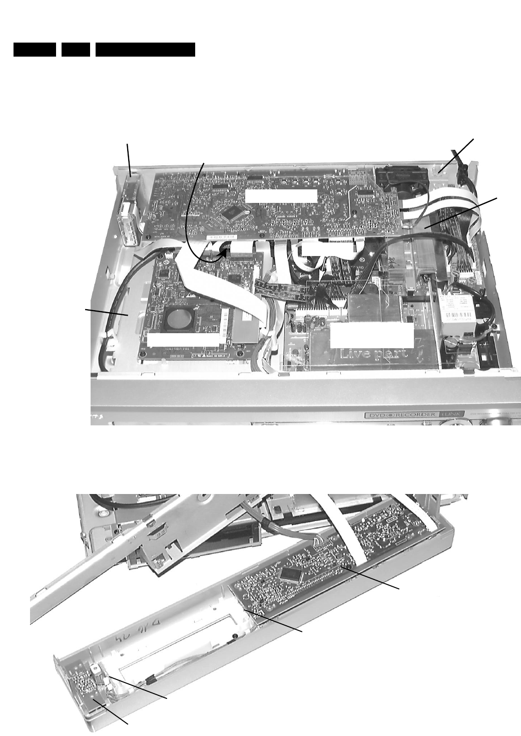
EN 4 1. LX7500R Location of printed boards
top cover removed
Combi Board
AV Board
below Combi Board
DVD+RW
Basic Engine
AV3.5
Amplifier
Board
Aux Supply
Switched Mode
Power Supply
Digital Board
Audio Tuner LS Sockets
LOCATION OF PRINTED BOARDS
figure 1
Display / Control
Board
Standby Board
Tray light left
Board
Tray light right
Board
figure 2
EN 52.LX7500RSafety Information
© WARNING
All ICs and many other semiconductors are susceptible to
electrostatic discharges (ESD). Careless handling during
repair can reduce life drastically.
When repairing, make sure that you are connected with the
same potential as the mass of the set via a wristband with
resistance. Keep components and tools at this potential.
f ATTENTION
Tous les IC et beaucoup d´autres semi-conducteurs sont
sensibles aux décharges statiques (ESD). Leur longévite
pourrait être considérablement écourtée par le fait qu´aucune
précaution nést prise à leur manipulation.
Lors de réparations, s´assurer de bien être relié au même
potentiel que la masse de l´appareil et enfileer le bracelet
serti d´une résistance de sécurité.
Veiller à ce que les composants ainsi que les outils que l´on
utilise soient également à ce potentiel.
d WARNUNG
Alle ICs und viele andere Halbleiter sind empfindlich
gegenüber elektrostatischen Entladungen (ESD).
Unsorgfältige Behandlung im Reparaturfall kann die
Lebensdauer drastisch reduzieren.
Sorgen Sie dafür, daß Sie im Reparaturfall über ein Puls-
armband mit Widerstand mit dem Massepotential des
Gerätes verbunden sind.
Halten Sie Bauteile und Hilfsmittel ebenfalls auf diesem
Potential.
ñ WAARSCHUWING
Alle IC´s en vele andere halfgeleiders zijn gevoelig voor
electrostatische ontladingen (ESD).
Onzorgvuldig behandelen tijdens reparatie kan de levensduur
drastisch doen vermindern. Zorg ervoor dat u tijdens reparatie
via een polsband met weerstand verbonden bent met hetzelfde
potentiaal als de massa van het apparaat.
Houd componenten en hulpmiddelen ook op ditzelfde potentiaal.
i AVVERTIMENTO
Tutti IC e parecchi semi-conduttori sono sensibili alle scariche
statiche (ESD).
La loro longevità potrebbe essere fortemente ridatta in caso di
non osservazione della più grande cauzione alla loro
manipolazione. Durante le riparationi occorre quindi essere
collegato allo stesso potenziale che quello della massa
delápparecchio tramite un braccialetto a resistenza.
Assicurarsi che i componenti e anche gli utensili con quali si
lavora siano anche a questo potenziale.
©
Safety regulations require that the set has to be restored to its
original condition and parts which are identical with
those specified be used. Replace safety components
only by components identical to the original ones.
Safety components are marked by the symbol
i
Le norme di sicurezza estigono che l´apparecchio venga
rimesso nelle condizioni originali e che siano utilizzati i
pezzi di ricambiago identici a quelli specificati.
Componenty di sicurezza sono marcati con
ñ
Veiligheidsbepalingen vereisen, dat het apparaat in zijn
oorspronkeliijke toestand wordt teruggebracht en dat
onderdelen, identiek aan de gespecificeerde, worden toegepast.
De Veiligheidsonderdelen zijn aangeduid met het symbool
s Varning !
Osynlig laserstrålning när apparaten är öppnad och
spärren är urkopplad. Betrakta ej strålen.
∂ Advarsel !
Usynlig laserstråling ved åbning når sikkerhedsafbrydere
er ude af funktion. Undgå udsaettelse for stråling.
ß Varoitus !
Avatussa laitteessa ja suojalukituksen ohitettaessa olet alttiina
näkymättömälle laserisäteilylle. Älä katso säteeseen !
f
"Pour votre sécurite, ces documents doivent être utilisés par
des spécialistes agréés, seuls habilités à réparer votre
appareil en panne".
050704
ESD
SAFETY
d
Bei jeder Reparatur sind die geltenden Sicherheitsvor-
schriften zu beachten. Der Originalzustand des Gerätes
darf nicht verändert werden. Für Reparaturen sind Bauteile
gleicher Spezifikation zu verwenden. Für Sicherheitsbauteile
sind Originalersatzteile zu verwenden.
Sicherheitsbauteile sind durch das Symbol markiert.
f
Les normes de sécurité exigent que l`appareil soit remis
à l`état d`origine et que soient utilisées les pièces de
rechange identiques à celles spécifiées.
Les composants de sécurité sont marqués
CLASS 1
LASER PRODUCT
©
DANGER: Invisible laser radiation when open.
©
After servicing and before returning the set to customer
perform a leakage current measurement test from all
exposed metal parts to earth ground, to assure no
shock hazard exists.
The leakage current must not exceed 0.5mA.
AVOID DIRECT EXPOSURE TO BEAM.
©
AVAILABLE ESD PROTECTION EQUIPMENT :
KIT ESD3 (small tablemat, wristband, connection box, 4822 310 10671
extension cable and earth cable)
wristband tester 4822 344 13999
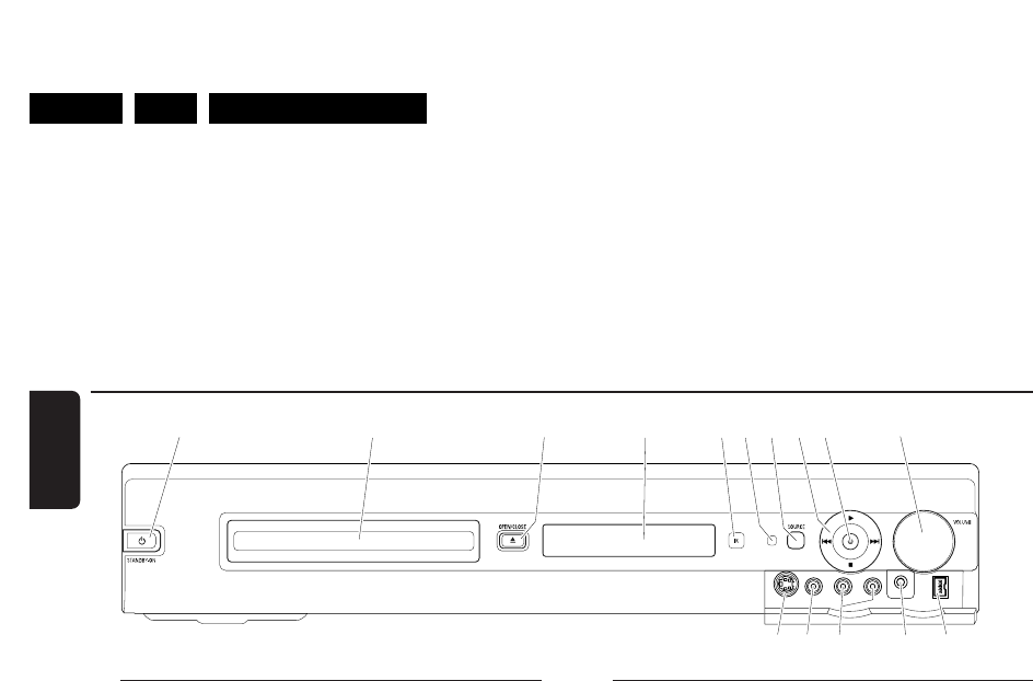
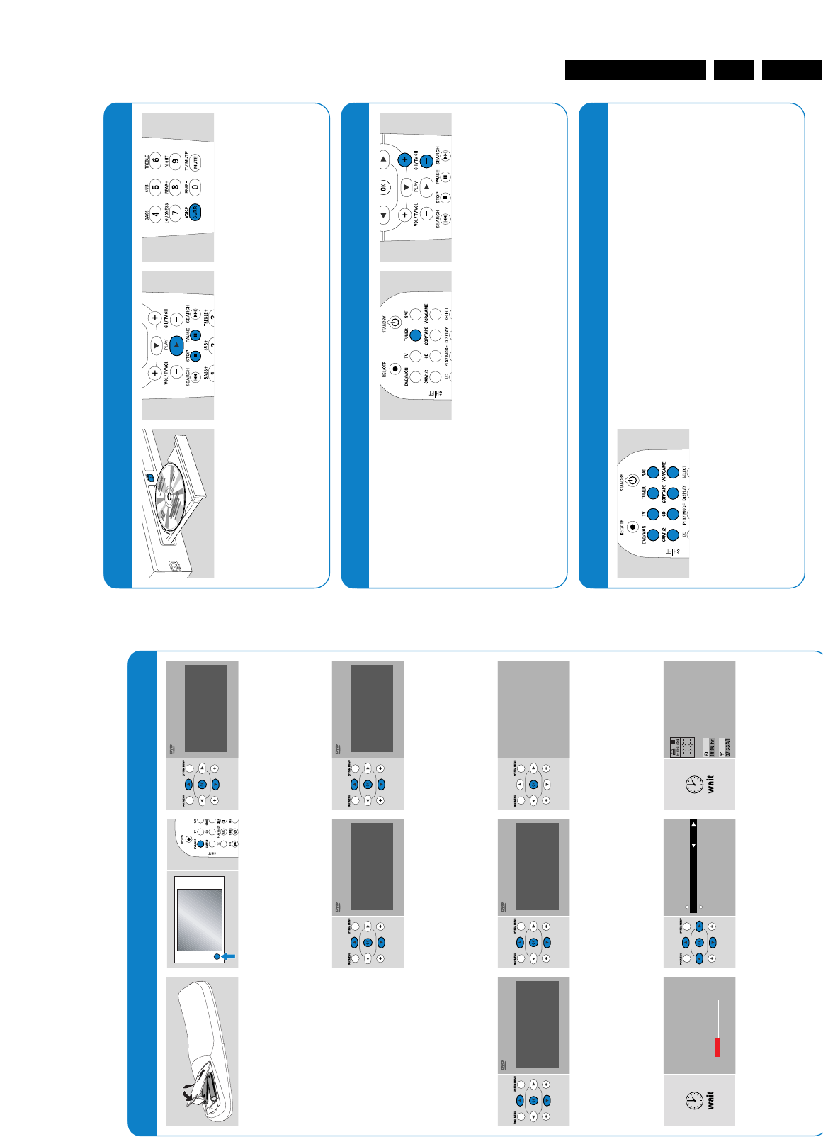
EN 6 3. LX7500R Brief Operating Instructions
Controls on the front
12STANDBY·ON
switches the set on or to standby.
2DVD recorder drawer
3OPEN/CLOSE /
opens/closes the DVD recorder drawer.
4display
5SOURCE
selects a source.
6IR sensor
7Standby LED
82
starts playback
¢
DVD: skips to the beginning of the next chapter/title/track
of the inser ted disc , searches forwards.
TUNER: skips to the next preset radio station.
9
stops playback or recording.
4
DVD: skips to the beginning of the current or previous
chapter/title/track of the inserted disc , searches backwards.
TUNER: skips to the previous preset radio station.
9RECORD
star ts recording a TV channel or from an exter nal video
source (while recording the button will be illuminated).
0VOLUME
adjusts the volume .
Connections on the front
!CAM 1 / S-VIDEO
connect to the S-video output of your Hi-8 or S-VHS
camcorder .
@CAM 1 / VIDEO
connect to the video (CVBS) output of y our camcorder .
#CAM 1 / AUDIOL/R
connect to the audio output of your camcorder .
$PHONES
3.5 mm headphone sock et
%CAM 2 / DV IN
connect to the i.LINK output of your Digital Video (D V) or
Digital 8 camcorder .
Controls and connections
10
English
$ %
@#
!
123
4 56789 0
BRIEF OPERATING INSTRUCTIONS
The following excerpt of the Owner´s Manual serves as a very short introduction to the set.
The complete Owners Manual can be downloaded in several languages from the Internet site of
Philips Customer Care Center: www.p4c.philips.com
EN 73.LX7500RBrief Operating Instructions
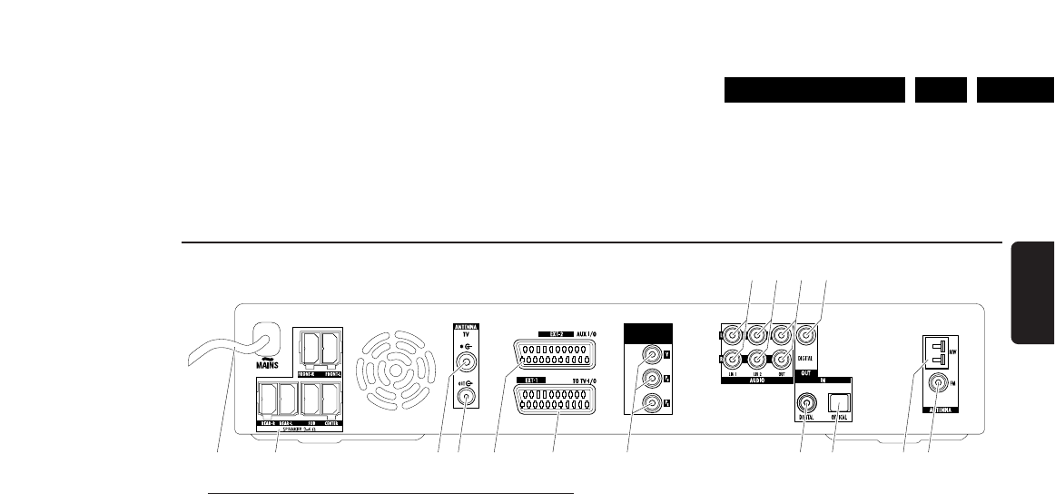
Connections on the rear
1 MAINS ~
After all other connections have been made ,
connect the mains lead to the wall socket.
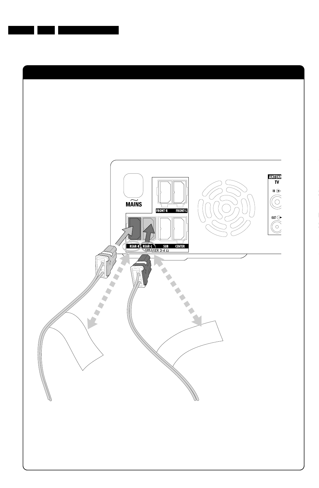
2 FRONT-R, FRONT-L,
REAR-R, REAR-L, SUB, CENTER
connect the supplied speakers.
3 TV ANTENNA / IN
connect the TV antenna.
4 TV ANTENNA / OUT
connect to the TV antenna input of your TV .
5 EXT-2 AUX I/O
connect to the Scart sock et of external video equipment.
6 EXT-1 TO TV-I/O
connect to the Scart socket of the TV.
7 FOR PLAYBACK /
VIDEO OUT COMPONENT Y P
BP
R
connect to the Component Video or Progressive Scan input
of your TV.
8 AUDIO/ LIN1 L/R
connect to the analogue audio output of external
equipment (e. g. tape deck, CD changer , …).
9 AUDIO/ LIN2 L/R
connect to the analogue audio output of external
equipment (e . g. tape deck, CD changer , …).
0 AUDIO /OUT L/R
connect to the analogue audio input of external equipment
(e. g. tape deck, …).
! OUT / DIGITAL
connect to the digital coaxial input of digital equipment.
@ IN / DIGITAL
connect to the digital coaxial output of digital equipment.
# IN / OPTICAL
connect to the digital optical output of digital equipment.
$ ANTENNA / MW
connect the MW antenna.
% ANTENNA / FM
connect the FM antenna.
Before star ting with the connections, make sure all
equipment you want to connect as well as the DVD
recorder system are disconnected from the mains
supply.
Controls and connections
11
English
VIDEO OUT COMPONENT
FOR PLA
YBACK
1111111 1 1 11
1 1 1
%$#@731 4 5 62
8 9 0 !
EN 8 3. LX7500R Brief Operating Instructions
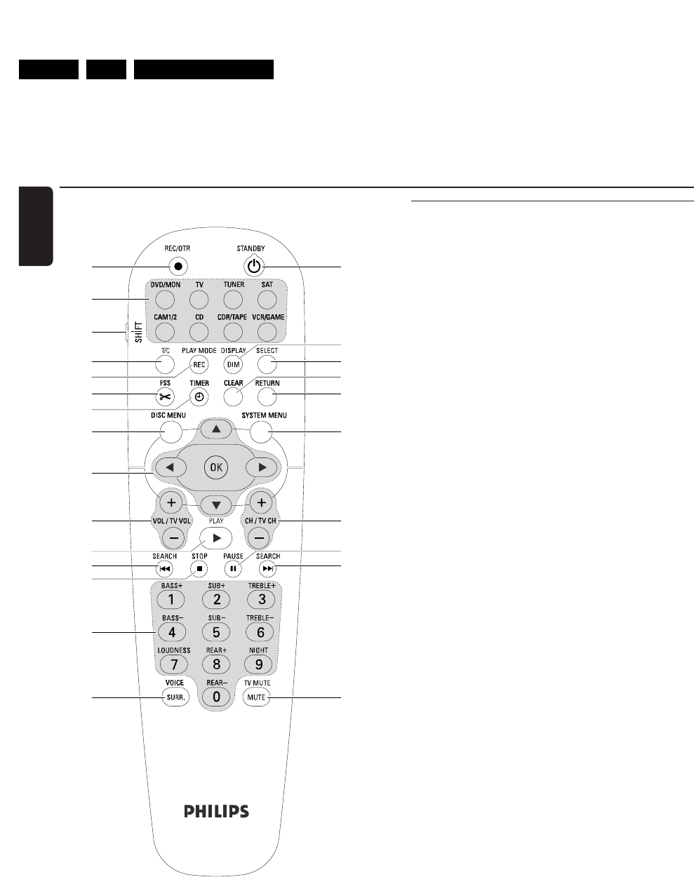
Remote control buttons
1 REC/OTR
starts recording the TV channel or the video source
selected on the DVD recorder system.
2 STANDBY 2
switches the DVD recorder system to standby .
3 DVD/MON
switches between the disc in the tray and the TV channel
selected on the DVD recorder system.
TV
plays the sound of the TV on the DVD recorder system.
TUNER
selects the r adio tuner , selects the waveband and switches
between FM stereo and FM mono .
SAT
selects a connected satellite receiver.
CAM 1/2
switches between the camcorder inputs on the front.
CD
selects a connected CD player.
CDR/TAPE
switches between a connected CD recorder and tape deck
or similar .
VCR/GAME
switches between a connected VCR and game console .
4 SHIFT
press and hold to select secondary functions of the remote
controls b uttons with blue labelling.
5 T/C
switches on the title/chapter selection for discs.
6 REC / PLAY MODE
selects different playback modes like REPEAT or SHUFFLE.
While you press and hold SHIFT : selects a recording mode.
7 DIM / DISPLAY
selects various display information.
While you press and hold SHIFT : dims the display.
8 SELECT
selects menu options,
switches between upper and lower case characters.
Remote control
8
English
2
8
7
¡
@
!
$
&
™
*
∞
1
3
4
5
6
0
9
#
%
^
(
)
≤
£

EN 93.LX7500RBrief Operating Instructions
9 FSS(Favorite Scene Selection)
enters the “Favorite Scene Selection”menu for editing titles.
0 TIMER
enters the timer menu to program recordings.
! CLEAR
clears an entry,e.g.in the timer menu.
@ RETURN
returns to the previous menu on a (Super) Video CD.
# DISC MENU
enters the disc menu.
$ SYSTEM MENU
DVD:enters the system menu of the DVD recorder
system.
TV:enters the system menu of your Philips TV.
% 3,4,1,2
move up,down ,left or right in a menu.
OK
confirms menu options.
^ VOL / TV VOL +, –
adjusts the volume of the DVD recorder system.
While you press and hold SHIFT: adjusts the volume on a
Philips TV.
& CH / TV CH +, –
DVD/MON:selects a TV channel on the DVD recorder
system.
TUNER:selects a preset radio station.
While you press and hold SHIFT:selects a TV channel on a
Philips TV.
* PLAY 2
starts playback,closes the disc tray.
( SEARCH 4
skips to the beginning of the current or previous
chapter/title/track,searches backwards,
tunes to a radio station with a lower frequency.
) STOP 9
stops playback or recording,
press and hold to open/close the disc tray.
¡ PAUSE ;
pauses playback or recording,
advances to next still picture.
™ SEARCH ¢
skips to the beginning of the next chapter/title/track,
searches forwards,
tunes to a radio station with a higher frequency.
£ 0–9 to key in numbers 0–9 and characters (see page 7).
While you press and hold SHIFT:adjust bass,treble and the
volume of the rear speakers and of the subwoofer.Switch
loudness and Night mode on/off.
SURR. / VOICE
selects the different surround modes.
While you press and hold SHIFT:switches ClearVoice on or
off.
MUTE / TV MUTE
mutes the sound of the DVD recorder system.
While you press and hold SHIFT:mutes the sound on a
Philips TV.
Remote control
9
English
EN 10 3. LX7500R Brief Operating Instructions
Quick use guide LX7500R
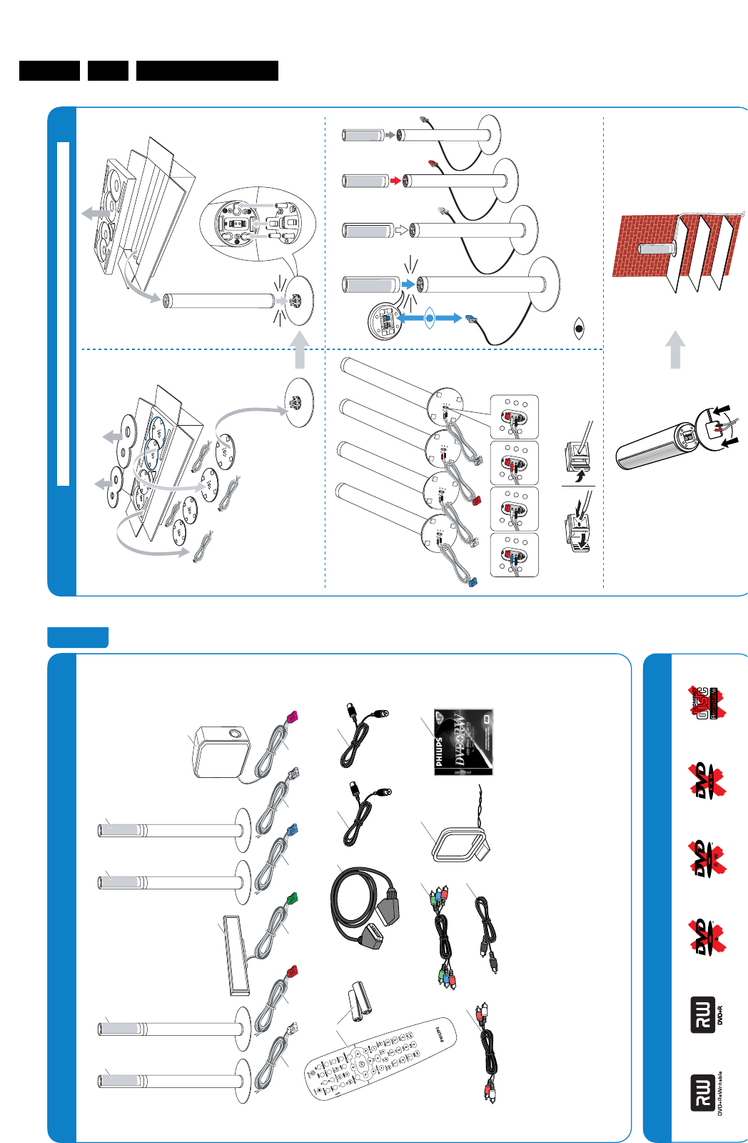
Speakers
click
FRONT-L
REAR-L FRONT-R REAR-R
click
Match colours!
1
34
2
or
Supplied accessories
1 1 1 1
2
1
4 5 6
!
0
9
8
@
7
3 3 3 3 3 3
LX7500R Quick use guide
English
Discs for recording
Your DVD recorder system is delivered with
1 2 front, 1 centre and 2 rear speakers (see page 2)
2 1 subwoofer
3 6 speaker cables
4 1 remote control with 2 AA batteries
5 1 Scart cable
6 1 TV antenna cable
7 1 FM antenna cable
8 1 cinch audio cable (red and white plugs)
9 1 digital audio cab le (black plugs)
0 1 Component Video cable (red, green and blue plugs)
! 1 MW loop antenna
@ 1 blank Philips DVD+RW disc
page 2 valid for loudspeaker boxes with different connector colours
EN 113.LX7500RBrief Operating Instructions
Quick use guide LX7500R
Speakers
click
FRONT-L
REAR-L FRONT-R REAR-R
click
1
34
2
or
page 2 valid for 4 identical loudspeaker boxes
with red/black coloured connectors
3
Speakers
Connections User manual:see pages 12–16
VIDEO OUT COMPONENT
FOR PLAYBACK
Fr ont left Fr ont right
Center
Subw oofer
Rear left Rear right
Fr ont left
Fr ont right
Center
Subw oofer
Rear left Rear right
After finishing all other connections connect
the mains cable to the wall socket.
FM
antenna
cable
TV
antenna
cable
EN 12 3. LX7500R Brief Operating Instructions
R
E
A
R
-
R
R
E
A
R
-
L
Attention – Atención – Achtung – Let op – Attenzione
Viktigt – Vigtig – Huomio – Atenção
Addendum LX7500R
3103 605 2285.1 VieChr0441
EN 133.LX7500RBrief Operating Instructions
Initial installation
1Insert the batteries into the remote
control.
2Switch on your TV.
3Press D VD/MON to switch on the
DVD recorder system.
IS TV ON? will be displayed on the
DVD recorder system.
4Press 4,3to select the language in which
the display messages should appear on
the TV screen. Next, press OK.
If the pre vious menu does not appear, set the
TV to the cor rect audio/video channel for the
DVD recorder system. Such channels may be
called AUX or AUXILIARY IN,AUDIO/VIDEO
or A/V IN, EXT1, EXT2 or EXTERNAL IN, etc .
These channels are often near channel 00.
5Press 4,3to select the language in which
a DVD should pref erably be pla yed. Next,
press OK.
6Press 4,3to select the language in which
subtitles should prefer abl y be displayed.
Next, press OK.
7Press 4,3to select the screen f ormat.
This setting will have an effect onl y with
DVDs supporting different screen formats.
Next, press OK.
8Press 4,3to select the country where
you use the DVD recorder system. Next,
press OK.
9Mak e sure the TV antenna or cable TV
system is connected to the DVD recorder
system. Next, press OK .
→ →The D VD recorder system will search
for available TV channels. This may take
sever al minutes.
10 Check the time and date . If necessar y ,
use 4,3,1,2to set the time/date
cor rectly. Next, press OK.
The TV screen will tur n blank f or about
1/2 minute. Next, the DVD screen will
appear .
The DVD recorder system is ready for
use!
ON TV
English
Español
Français
Italiano
Deutsch
Menu Language
Press OK to continue
Audio language
English
Español
Français
Italiano
Deutsch
Press OK to continue
Subtitle language
English
Español
Français
Italiano
Deutsch
Press OK to continue
TV shape
4:3 letterbox
4:3 panscan
16:9
Press OK to continue
Country
Austria
Belgium
Denmark
Finland
France
Press OK to continue
If you have connected
the aerial -
press OK
To continue
Press OK
Searching for TV channels
12 Channels found
Please wait
Installation
Autom. search Autom. search complete
48 Channels found
Time 18:03
Year 2004
Month 03
Date 25
To continue
Press OK
Autom. Search
LX7500R Quick use guide
5
Playing a disc
Playing a radio station
Selecting a source
1Press and hold D VD/MON for 1 second.
2Press OPEN/CLOSE / on the set to
open the drawer.
3Insert a disc (pr inted side up) in the tray.
4Press OPEN/CLOSE / on the set to
close the drawer.
5If pla yback does not start automatically,
press PLAY 2 to star t playback.
0 To inter rupt pla yback press PAUSE ; .
0 To resume playback press PLAY 2 .
6To stop playback, press STOP 9 .
0 To select one of the a vailable surround
modes, press SURR. repeatedl y. The
selected surround mode will be displa yed
on the D VD recorder system.
Mak e sure the FM radio antenna is
connected to the D VD recorder system.
When you press TUNER for the first time ,
the DVD recorder system will search for
radio stations automaticall y .The search will
take a couple of minutes.
1Press and hold TUNER f or 1 second to
select the r adio tuner .
2Press CH + or CH –repeatedly to skip to
a preset radio station.
Or use 0–9 to enter the n umber of a
preset radio station. To enter a preset
number with two digits, press 0–9 twice
within 2 seconds.
With the “source b uttons” you select what
you want to play and what to record.
Press and hold a source button for
1 second to select a source .
DVD selects the disc inserted into the
DVD recorder system (D VD ,DVD+RW,
DVD+R, Video CD , Super Video CD ,
Audio CD , MP3-CD). Pla yback will start
automatically or a menu/inf ormation
screen will appear on the TV screen.
MON (“Monitor”) sho ws the TV channels
stored in the D VD recorder system. Press
CH + or CH–to select the TV channel
which y ou wish to record.
TV plays the sound of your televison set
on the speak ers of the DVD recorder
system.
SAT, CAM1/2, CD, CDR/TAPE,
VCR/GAME select connected equipment
(satellite receiver, CD player or similar).
With SAT, CAM1/2, VCR/GAME select
the video equipment from which you wish
to record. E. g. To record a satellite
progr amme , first select SAT , then press
REC/OTR.
EN 14 3. LX7500R Brief Operating Instructions
Quick use guide LX7500R
Recording aTV programme
Selecting a recording mode
1Switch your TV set on. If necessar y set the
TV to the cor rect audio/video channel f or
the DVD recorder system. Such channels
may be called AUX or AUXILIAR Y IN,
AUDIO/VIDEO or A/V IN, EXT1, EXT2
or EXTERNAL IN, etc .These channels are
often near channel 00.
2Inser t a DVD+RW or DVD+R disc on
which y ou want to record into the tr ay.
3Press DVD/MON to see the TV channel
cur rentl y selected on the DVD recorder
system.
4Press CH+ or CH–to select the
TV channel (progr amme n umber) which
you wish to record.
5Keep REC/O TR pressed until
SAFE RECOis displa yed on the DVD
recorder system.
Recording star ts at the end of all
existing recordings.
Note f or DVD+RWs: If you press REC/OTR
briefly , the recording will star t at the position
where you stopped playback. Pre vious
recordings may be o verwr itten.
0To inter rupt recording press PAUSE ;.
0To resume recording press PA USE ; again.
6Press STOP 9to stop recording.
The recording mode deter mines the
picture quality of a recording and the
maxim um time available for recording on a
disc .
1Press and hold DVD/MON for 1 second.
2Press STOP 9to stop playback or
recording.
3While you press and hold SHIFT , press
REC / PLAY MODE repeatedly to select
the recording mode .
ON TV
mode quality recording
time
M1 better than DVD 1 hour
M2 DVD 2 hours
M2x better than S-VHS 2 1⁄2hours
M3 S-VHS 3 hours
M4 better than VHS 4 hour s
M6 VHS 6 hours
M8 VHS (longplay) 8 hours
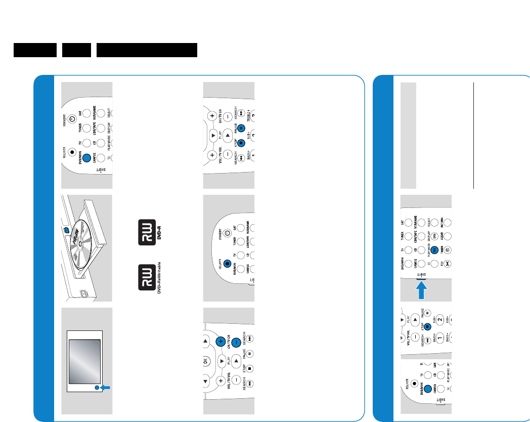
W
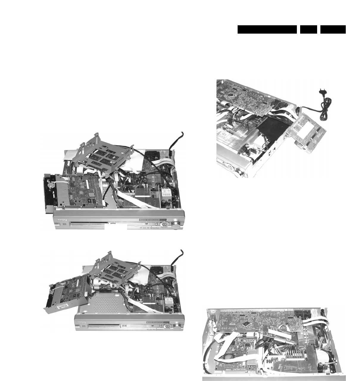
DISMANTLING INSTRUCTIONS
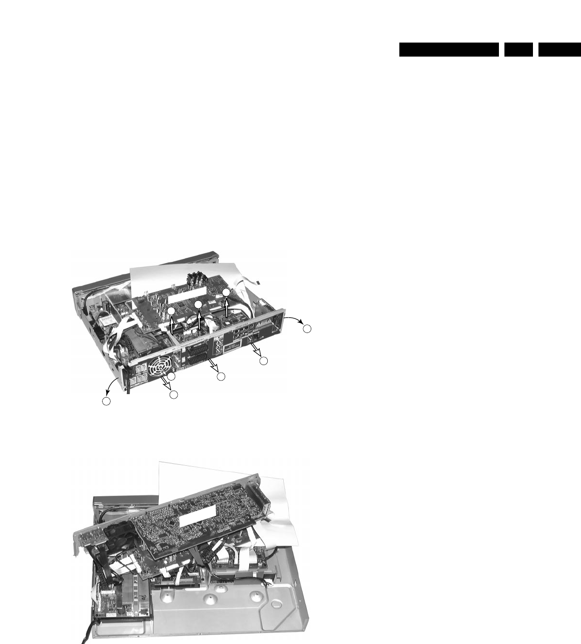
EN 154.LX7500RDismantling Instructions
Dismantling the
Top Cover
picture 1
• Remove 9 screws as shown in picture 1.
• Release side walls on bottom and raise top cover
upwards.
Manual
Opening the Tray
In case the loader is defect or cannot be opened electrically, proceed
as follows:
• The tray can be released by means of screwdriver.
The locking slider of the tray can be accessed through a slot on
the bottom side of the set. To prevent dust coming into the drive
this slot is covered by an adhesive tape on the cabinet of the drive
(see picture 4).
Push through this adhesive tape and move the white pin of the
slider to the left side (see picture 5). The tray will move out a bit
and is now released.
• Pull the tray out.
Make sure that a new adhesive tape has been applied to the
drive when the repair is finished!
picture 4
picture 5
!
CABLE TIE MAINS CORD
!
FIXATION OF CABLES
8004, 8012, 8016
!
FIXATION OF CABLES
8012, 8016
Details of correct
Wire Routing
picture 2
picture 3
!FIXATION CABLE 8041IN CATCH OF AIRGUIDE FOIL Dismantling the Tray Cover
To dismantle the ornamental cover the tray has to be moved out first.
This can either be done by actuating the Open/Close key or
manually. To release the tray manually proceed as described above.
Take the ornamental cover on the bottom side and press it upwards
while supporting the tray. The cover will automatically be tilted a bit.
In turn the catches become released.
picture 6
To fulfil safety requirements cables must not touch the large cooling
plate (high potential) of the Switched Mode Power Supply.
After repair it has therefore to be made sure that all cables are fixed
according the instructions shown in pictures 2 and 3.
sheet of
paper
for isolation
release cables
EN 16 4. LX7500R Dismantling Instructions
picture 8
picture 9
picture 10
picture 11
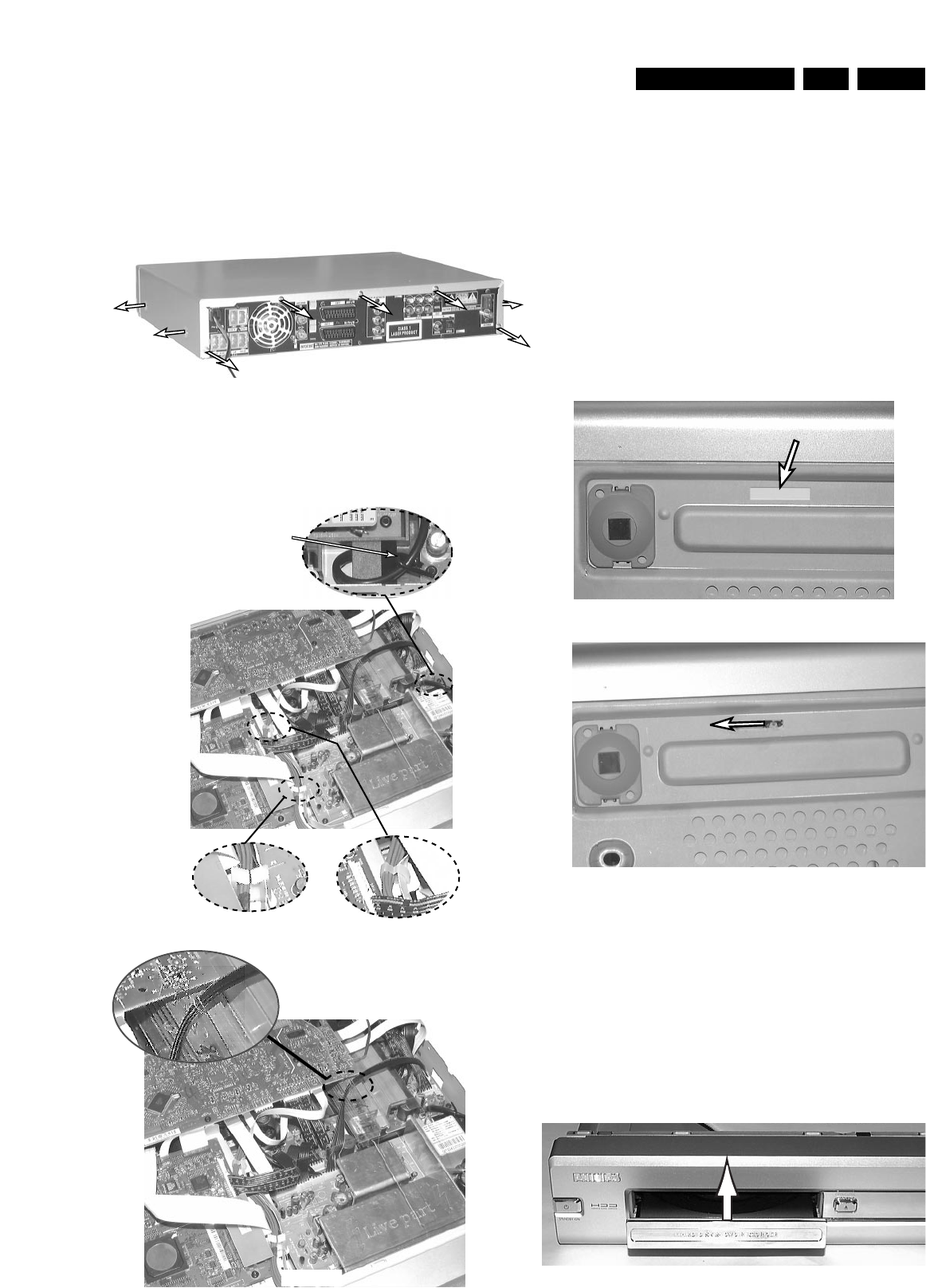
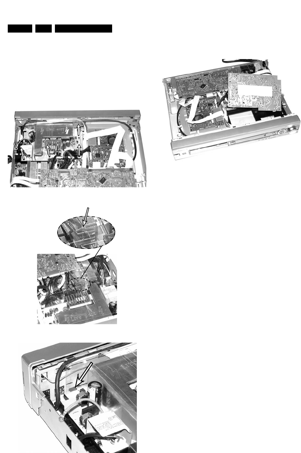
Dismantling the
Digital Board
• Dismantle Top Cover as described before.
• Loosen 4 screws to dismantle Digital Board (see picture 7).
• To get access to the bottom side, the board can be put to a
service position as shown in picture 8.
Digital Board
sheet of
paper
for
isolation
picture 7
Dismantling the
DVD Basic Engine
• Dismantle the ornamental cover of the tray first (see picture 6).
• Dismantle Top Cover as described before.
• Loosen 6 screws as shown in picture 9.
• Release cables from cable catches.
• Lift metal frame-Digital Board assembly on the rear side to get the
catch hook free from the IDE socket board. (see picture 10).
If necessary bend Combi Board up to get support lugs free.
• Pull the complete assembly out and put it to a rest position as
shown in picture 11.
EN 174.LX7500RDismantling Instructions
Dismantling the
DVD Basic Engine
(continued)
paper
for
isolation
picture 12
paper
for
isolation
picture 13
Dismantling the
Amplifier Board
• Remove 4 screws.
• Turn the Amplifier Board out of the set and put it in service
position as shown in picture 14.
Amplifier
Board
picture 14
Aux supply
picture 15
• Now the head of the last screw on the right side has become free
and the screw can be removed.
• Pull off power supply cable from the Basic Engine (rear left).
• Lift Basic Engine at the rear and move it backwards until it
becomes free at the front.
Note: the available space is very tight as the Basic Engine has to
be moved against cables and sockets located on the AV Board.
Slightly lifting Combi Board together with the Basic Engine will
make it easier.
• Turn Basic Engine out at front side and put it to a proper service
position as shown in pictures 12 and 13.
Dismantling the
Auxiliary supply Board
• Remove 1 screw.
• Lift the board on the left side to get it free from the catch on the
right side.
• Turn the Auxiliary supply Board out of the set and put it in
service position as shown in picture 15.
If necessary, the one or the other cable has to be plugged off.
EN 18 4. LX7500R Dismantling Instructions
SMPS
picture 19
Dismantling the
Switched Mode Power Supply Board
• Remove 4 screws as shown in picture 16 and loosen the ground
wire from the cabinet.
• Disengage catch of the airguide foils (see picture 17).
• Lift the unit on the rear side and move it backwards to release the
board from the catches on the front side (see picture 18).
• Pull the whole unit on the front side up - take care of cables routed
between front and the plastic foil! - and turn it to service position as
shown in picture 19.
picture 17
picture 18
picture 16
EN 194.LX7500RDismantling Instructions
Dismantling the
Front panel assembly
• Dismantle the ornamental cover of the tray first (see picture 6).
• Loosen 3 screws to bottom cabinet as shown in picture 20.
• Release catches on both sides (see picture 21) and move the
front panel out.
• Put the panel in rest position as shown in picture 22.
To get access to the printed boards the metal plate has to be
removed →
• Loosen 9 screws as shown in picture 22.
• Pull up the metal frame and move it backwards along cables fed
through.
• Put the metal frame to rest position as shown in picture 23.
→Display Board and Standby Board are now accessible on the
copperside.
Picture 24 shows service position for the component side of the
Display Board.
111
picture 20
3
2
picture 21
49x
picture 22
picture 23
picture 24
EN 20 4. LX7500R Dismantling Instructions
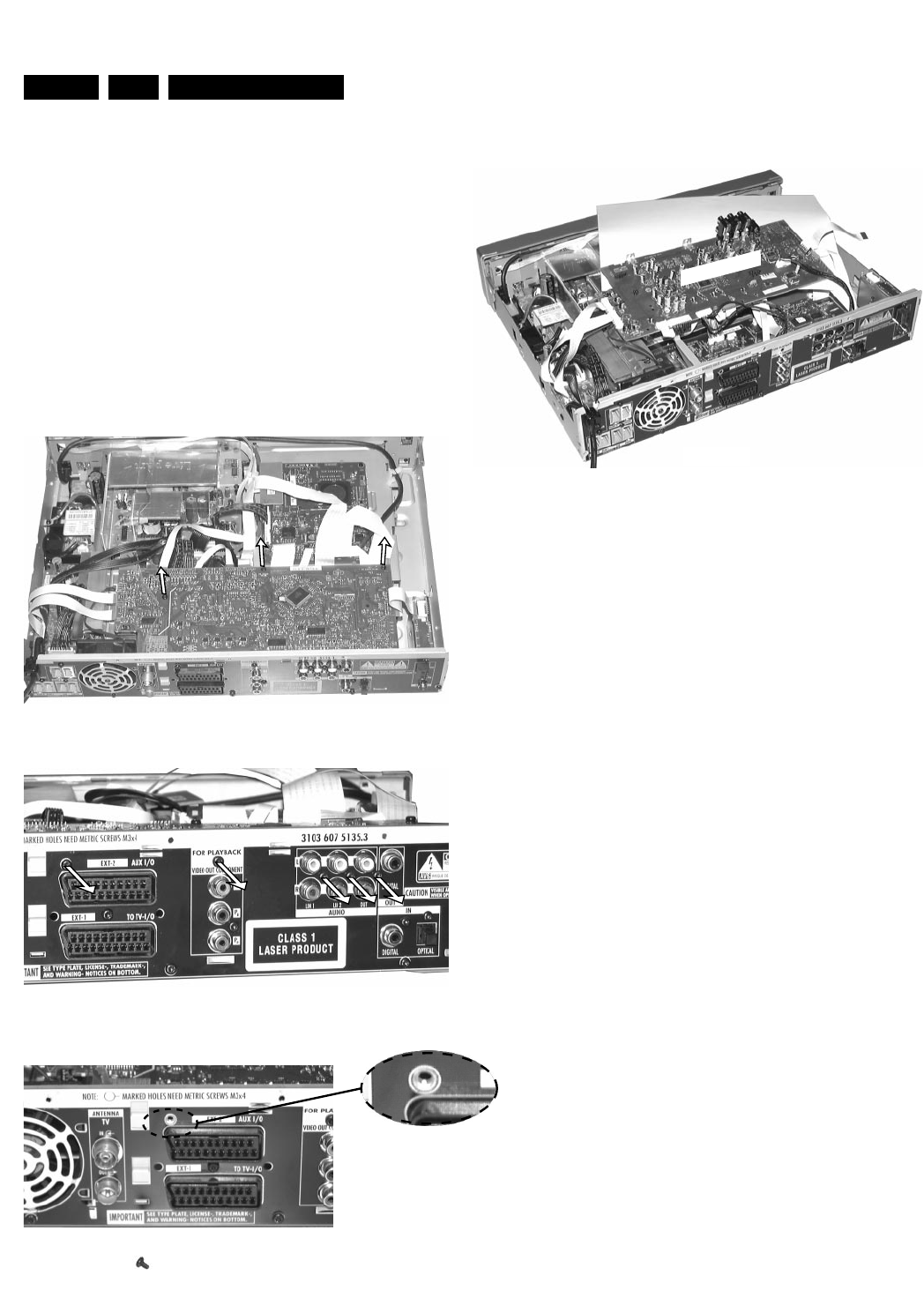
Combi Board
sheet of paper
for isolation
picture 28
picture 25
picture 26
picture 27
Dismantling the
Combi Board
• Loosen 8 screws as shown in pictures 25 and 26.
Note: The Combi Board is fixed with metal screws M3x4 and
plastite screws 3x8. The metal screws are indicated with a text on
the printed board and with a white ring on the rear plate → see
picture 27.
• Move the board frontwards to release the sockets from the rear
plate.
• Turn Combi Board up to service position as shown in picture 28.
The length of some cables might be marginal. We recommend to
disconnect cables to the Audio Tuner and the Amplifier Board
before turning the Combi Board and re-connect them when the
board is in the service position.
Also release cables to front from the cable catch and move them
to max. free length at the Combi Board.
EN 214.LX7500RDismantling Instructions
Combi Board
sheet of paper
for isolation
2
4
4
2
11
1
3loosen only
2
picture 29
AV Board
sheet of paper
for isolation
picture 30
Dismantling the
Analog Video Board
• Dismantle Combi Board and put it to rest (service) position as
described before.
The AV Board can now be accessed on the component side.
To get access to the copper side:
• Loosen 3 screws 1- see picture 29.
• Re-mount Combi Board and fix it provisionally with 1 screw.
• Loosen 3 screws 2- see picture 29.
• Loosen 1 screws 3a few turns to loosen the fan - see picture 29.
• Release catches 4 on both sides of the rear cabinet and move it
backwards until rear cabinet becomes free from bottom cabinet.
• Turn the whole unit AV Board - Combi Board up to service
position as shown in picture 30.

EN 22 5. LX7500R Service hints
SERVICE TOOLS
TORX T10 screwdriver with shaftlength 150mm.....4822 395 50423
TORX screwdriver set SBC 163.............................4822 295 50145
Audio signal disc SBC 429 ....................................4822 397 30184
Playability test disc SBC444..................................4822 397 30245
Test disc 5 (disc without errors) +
Test disc 5A (disc with dropout errors, black spots and fingerprints)
SBC 426/426A....................................4822 397 30096
Burn in test disc (65 min. 1kHz signal at -30dB level
without "pause")..................................4822 397 30155
DEMO MODE
The DEMO MODE displays various features of the set
and will start automatically when no key has been
pressed for several minutes or during Standby mode.
The Demo mode will automatically be switched off after
the first installation of the set.
The Demo mode can be switched on/off again via the
System Menu of the set:
Press
System Menu
on the remote control.
Select A→w→Standby →Low power
Normal
Demo mode
Sub chassis 8 test disc CD....................................7104 099 28362
MPTD printed test disc CVP02.18A.......................7104 099 91691
MPTD printed test disc CVP02.18C ......................7104 099 97941
Burn in test disc DL LVP04.15...............................7104 099 91041
MPTD thin test disc CVP02.60...............................7104 099 97931
NLT 01.00 link test disc DVDROM settings..........7104 099 98502
Blank DVD+RW disc RICOH ..................................7104 099 98582
Blank DVD+R disc RICOH......................................7104 099 94001
LEAD FREE PRODUCED SET
This set is manufactured with lead-free
production technology. This is also indicated by
the PHILIPS-lead-free logo you find on the
printed boards.
The set is produced with lead-free solder-alloy as well as
with lead-free sub-parts. It can be considered as lead-free.
Due to this fact some rules have to be respected by the
workshop during a repair:
• Use only lead-free soldering-tin Philips SAC305 with order
code 0622 149 00106. If lead-free solder-paste is required,
please contact the manufacturer of your solder-equipment.
• Use only adequate solder tools applicable for lead-free
soldering-tin.
• Adjust your solder tool so that a temperature around 217°
– 220° is reached at the solder joint.
• Do not mix lead-free soldering-tin with leaded soldering-tin.
This would lead to unreliable solder joints.
• On our website http://www.atyourservice.ce.philips.com
you find more information to
– aspects of lead-free technology
– BGA-de-/soldering, heating-profiles of BGAs used in
Philips-sets, and others.
EN 235.LX7500RDiagnostic Software
N
Y
SELECT TEST
START TEST
The display shows
next or previous
test of the test menu.
Set version
SW version Combi board µP
SW version Front board µP
Quartz test
Temperature test
EEPROM test
EEPROM format
Display test
Key test
Audio TUNER test
Audio test
I2C test Combi board
LX7500R EU
COMBI SW VXX
FRONT SW VXX
QUARTZ
NTC
EEPROM
EP FORMAT
DISPLAY
KEY TEST
TUNER
AUD TEST
IIC TEST
S or T
button
pressed?
Y
S or T
button
pressed?
TEST Display
shows
S
T
Select test
SERVICE TESTS
APPARATUS
servtest LX7500R sh 1, 181004
N
N
Y
Start
actual selected test. For detailed description of the various tests
see next pages.
PLAY
button
pressed?
Test menu
SERVICE TESTPROGRAM
OVERVIEW ALL TESTS
VXX
S
*To leave Service Testprogram plug mains cord off.
stands for Service mode
EU stands for European version
of Combi board.
NAFT stands for USA version
of Combi board.
To check versions of the DVD+RW software use OSD.
stands for Version number of the software
used in Combi board µP 7107
respectively Front board µP 7103
To enter Service
Testprogram hold
Open/Close & Source
button
depressed while
plugging mainscord in.
S-LX7500R EU
The display shows
the version of the set.
END-USER DIAGNOSTICS
(DVD+RW module)
To enter
END-USER DIAGNOSTICS
hold
PLAY & NEXT
button
depressed
while plugging mainscord in.
VIRGIN MODE
(DVD+RW module)
To reset the set to
Virgin Mode
hold
STANDBY
button
depressed
while plugging mainscord in.
DEMO MODE
To switch Demo Mode on/off
use
System Menu
TOGGLE VIDEO MODE
To toggle Video Mode
(interlace/progressive scan)
hold
S
button depressed
while plugging mainscord in.
for USA version only
for USA version only
FORCED DOWNLOAD
OF OLDER SOFTWARE VERSION
To enable loading of
an older software version hold
Open/Close
& RECORD
buttons
depressed
while plugging mainscord in.
TOGGLE
MODULATOR CHANNEL
To toggle Modulator Channel
(channel 3/4) hold
T
button depressed
while plugging mainscord in.
For detailed description of the
End-User Diagnostic see page 29 ff.
DEMO MODE
The DEMO MODE displays various features of the set
and will start automatically when no key has been
pressed for several minutes or during Standby mode.
The Demo mode will automatically be switched off after
the first installation of the set.
The Demo mode can be switched on/off again via the
System Menu of the set:
Press
System Menu
on the remote control.
Select A → w → Standby →Low power
Normal
Demo mode
EN 24 5. LX7500R Diagnostic Software
servtest LX7500R sh 2, 041004
Y
QUARTZ TEST
Display shows
5859,375±175Hz can be
measurured
on
(pin 18 of µP 7107).
STOP
button
pressed? N
Y
Press
PLAY
button.
Tact frequency
µ
P 7107
(divided 12MHz)
f0
12 MHZ
Back to main menu.
The Quartz test allows a quick check of the oscillator of the
Combi board µP without any influence to the oscillator circuitry
by the test equipment.
The factory can check if the correct quartz has been
assembled.
A 50% duty pulse of the divided oscillator frequency is put on
pin 18 of the µP.
The test signal can best be measured on the junction
3072/3111 →
TEMPERATURE TEST
The temperature test is used to check the NTC resistors which
measure various temperatures to control the speed of the the
set fan.
NTC Front: sensor for ambient temperature, located on
Display board.
NTC Amp(lifier): sensor for the temperature of the heatsink on
the Power Amplifier board.
The signals NTC_Front and NTC_Amp are compared with a
special algorithm and result in the control signal Set_Fan_Ctrl
which controls the speed of the set fan.
In each test step of the temperature test the speed of the set
fan can be set in four steps.
f0
FRONT XX
Display shows
XX = value in ˚C
S or T
button
pressed?
N
YY
Switch speed of set fan
to next/previous step.
Display shows
for 2s.
x= 1, 2, 3, 4
x= 1, 2, 3, 4
FAN SPE ED X
Press
PLAY
button.
TEMPERATURE
TEST
NN
Y
PLAY
button
pressed?
Display shows
XX = value in ˚C
N
Y
PLAY
button
pressed?
Back to main menu.
STOP
button
pressed?
S or T
button
pressed?
N
YY
Switch speed of set fan
to next/previous step.
Display shows
for 2s.
N
Back to main menu.
STOP
button
pressed?
AMPLIFIER XX
FAN SPE ED X
Press
S or T
button
and select
QUARTZ
Press
S or T
button
and select
NTC
EN 255.LX7500RDiagnostic Software
servtest LX7500R sh 3, 051004
Press
PLAY
button.
Y
DISPLAY TEST
Back to main menu.
fig. 1
fig. 2
PLAY
button
pressed?
NN
Y
Y
Y
N
Display shows all
segments and flags
for checking open circuits.
All LEDs are switched on.
See figure 1.
Display shows figure 2.
All alternate pins (2, 4, ..)
of the µP display control pins
are activated
for checking short circuits.
See figure 2.
PLAY
button
pressed?
STOP
button
pressed?
PASS
Y
EEPROM TEST
Display shows
ERR
Display shows
Test pattern is written to
address 1
and
read back again
STOP
button
pressed?
Test ok?
N
Y
N
Y
Press
PLAY
button.
Back to main menu.
Back to main menu.
Y
FORMAT EEPROM
Display shows
for 2s.
EEPROM is cleared and
default values are stored.
NEW
Press
PLAY
button.
The test checks writing and reading of data to EEPROM 7108 on Combi board.
A test pattern is written to the first location in the EEPROM.
PASS is displayed when the test pattern is read back correctly, else ERR.
Each software module using the EEPROM is forced to write the
default values in its part of the EEPROM.
This test should only be used to clear the EEPROM in case
of a µP-"hangup".
The DISPLAY test is intended to check the driver circuits
and the LEDs for open- or short-circuits.
Press
S or T
button
and select
EEPROM
Press
S or T
button
and select
DISPLAY
Press
S or T
button
and select
EP FORMAT
EN 26 5. LX7500R Diagnostic Software
servtest LX7500R sh 4, 091004
Y
AUDIO TUNER
TEST
Press
PLAY
button.
N
Y
EUR USA
Exit
Service Testprogram.
Display shows
version of the Audio tuner
(Combi board setting)
as long as any key will
be pressed.
else
POWER
switched off?
Service Preset-frequencies
acc. table 2 are copied
to the RAM.
Tuner is normal working
except for the
PROGRAM
and
AUTOPROGRAM
functions.
EUROPE
FM/MW
USA
FM/AM
table 2
table 3
REGION
Key
NEXT T
PREV S
STOP 9
PLAY 2
OPEN/CLOSE
manual tuning + auto search
manual tuning + auto search
preset down
preset up
band switch (FM stereo, FM mono, AM)
Function
PRESET
1
2
3
4
5
6
7
8
87,5 MHz
The Audio tuner test is intended to read out the tuner version selected by the Combi board µP.
The correct tuner version is defined by the version detection resistor 3052 mounted on
the Combi board. 3052 mounted = USA version without RDS.
The stored preset frequencies serve as provision for other tuner modules only.
108 MHz
531 kHz
1602 kHz
558 kHz
1494 kHz
98 MHz
87,5 MHz
98,6 MHz 98,6 MHz
108 MHz
560 kHz
1500 kHz
98 MHz
530 kHz
1700 kHz
/22/25/29 /37
SERVICE PRESET FREQUENCIES
USAEUR
Y
KEY TEST
Press
PLAY
button.
STOP
button
pressed?
N
Y
KEY - -
Back to main menu.
X=5 stands for RC5 code
X=6 stands for RC6 code
CC stands for the command code
SS stands for the system code
NEXT T
PREVIOUS S
KEY KEY CODE
2
3
4
5
6 (exit)
7
8
SOURCE
RECORD
STOP
PLAY/PAUSE
STANDBY/ON 1
OPEN/CLOSE
KEY CODES
table 1
Display shows
Numbers acc. table 1
are indicated as long as a
button is held depressed.
If a button is pressed
on the Remote Control
RCX CC SS is shown.
Press
S or T
button
and select
KEY TEST
Press
S or T button
and select TUNER
EN 275.LX7500RDiagnostic Software
STEP
AUD TEST 1
AUD TEST 2
AUD TEST 3
AUD TEST 4
AUD TEST 5
AUD TEST 6
AUD TEST 7
AUD TEST 8
AUD TEST 9
AUD TEST 10
AUD TEST 11
AUD TEST 12
AUD TEST 13
Tuner and DVD module are not switched on in these steps.
To check the inputs a signal has to be fed directly to Combi board, connectors 1202
respectively 1205 or 1701.
In all test steps with digital input signal (2, 3, 4, 10 and 11) NO SIGNAL will be shown on the display when the
SPDIF in/out IC 7603 does not recognize any signal.
Line in 1 any Line out,
Amplifiers
Line out,
Amplifiers
Line out,
Amplifiers
Line out
Line out
Headph. out
Dig out,
Amplifiers
Dig out
Amplifiers
Amplifiers
Amplifiers
10 (-33dB)Audio settings DPL2 Music
DPL2 MusicOpt. in1) AC3/5.1/63Hz/
FS/Subw only
AC3/5.1/
10kHz/FS
AC3/5.1/
10kHz/FS
AC3/5.1/
10kHz/FS
AC3/5.1/
10kHz/FS
20 (-20dB)Dig. out, Amplifiers
Muting
Coax in, Line out
Line in 1, Dig. out
Ext. 1, Line out
Ext. 1, Headph. out
Tuner input
DVD in
Treble
Line in 2, Amplifiers
DPL2 Music0dB FS
0dB FS DPL2 Music
DPL2 Music
DPL2 Music
-6dB FS
-6dB FS
-6dB FS
-10dB
-10dB
-12dB FS
Stereo
Stereo
Stereo
Stereo
Stereo
Stereo
Stereo
Coax in1) 40 (0dB)
transistor mute
Coax in1) 40 (0dB)
Line in 1 1kHz 1Vrms
1kHz/50Hz 1Vrms
40 (0dB)
Line in 2 34 (-6dB)
Ext. 11) 1kHz 1Vrms 40 (0dB)
Ext. 21) 1kHz 1Vrms 40 (0dB)
TUNER1) 1kHz 150mVrms 40 (0dB)
DVD in1) 30 (-10dB)
30 (-10dB)
treble 5 (+10dB)
DVD in1)
0 (-87dB)
transistor mute
Front in
(/17 only)
Ext. 3
(/17 only) 0 (-87dB)
INPUT Input Signal OUTPUT Level VOLUME
Tested
function Speaker
setting
1)
Display shows
Sound ICs are set
acc. table 4
Switch to next step
acc. table 4
AUD TEST XX
Y
STOP
button
pressed?
N
Y
Switch to previous step
acc. table 4
T
button
pressed?
S
button
pressed?
N
Y
N
Y
COMBI BOARD
AUDIO TEST
Press
PLAY
button.
Back to main menu.
stands for the number
of the test step acc.
table 4.
XX
The AUDIO TEST is derived from a factory test defined to
test the Combi board as stand alone test object.
During the relevant test steps the Audio tuner and the
DVD module are not switched on.
Input signals have therefore to be fed in directly at the
dedicated sockets on the Combi board.
The defined input signals stated in table 4 are intended for
quantitative measurements of the different software settings.
For a quick test in repair workshops it is recommended
to use test step 1.
Test step 1 produces output on 6 channels.
This allows either a simple check of the signal path from
Line in 1-socket to Line out-socket and the headphone
amplifier or a complete check of all 6 channels inclusive
the power amplifiers.
At the beginning of the Audio test the user settings are set
to following default values:
Volume: 10 (-33dB)
Bass/Treble: flat
Loudness: off
Clear Voice: off
Bass ALC: on
All speaker outputs: ∆ Volume 0dB
During test step1 manual setting of the sound parameters is
possible. When test step 1 is left the default values will be
restored.
Press
S or T
button
and select AUD TEST
servtest LX7500R sh 5, 111004
TEST STEPS
COMBI BOARD AUDIO TEST
EN 28 5. LX7500R Diagnostic Software
servtest LX7500R sh 6, 111004
Y
COMBI BOARD
I
2
C TEST
Display shows
IIC XXXX FAIL
IIC TEST PASS
Display shows
Test register is written to
the first/next IC to be tested
and
read back again
STOP
button
pressed?
Test ok?
All ICs tested?
N
Y
N
N
Y
Y
N
Press
PLAY
button.
Back to main menu.
STOP
button
pressed?
Y
Back to main menu.
stands for item number of the failed IC.
The selector / sound processor ICs 7207, 7214 and 7303 are passive ICs
which do not feed back via the IIC bus. The functionality of these ICs can
therefore not be tested with the IIC Test. For testing these ICs use the
AUDIO TEST.
7405 CODEC
7505 DSP
7603 SPDIF IC
XXXX
Press
S or T
button
and select IIC TEST
Diagnostic Software EN 29LX7500R 5.
5. Diagnostic Software
Due to the complexity of the DVD recorder, the time to find a
defect in the recorder can become long. To reduce this time,
the recorder has been equipped with Diagnostic and Service
software (DS). The DS offers functionality to diagnose the
DVDR hardware and tests the following:
• Interconnections between components
• Accessibility of components
• Functionality of the audio and video paths
This functionality can be accessed via several interfaces:
1. End user/Dealer script interface
2. Command Interface
5.1 End User/Dealer Script Interface
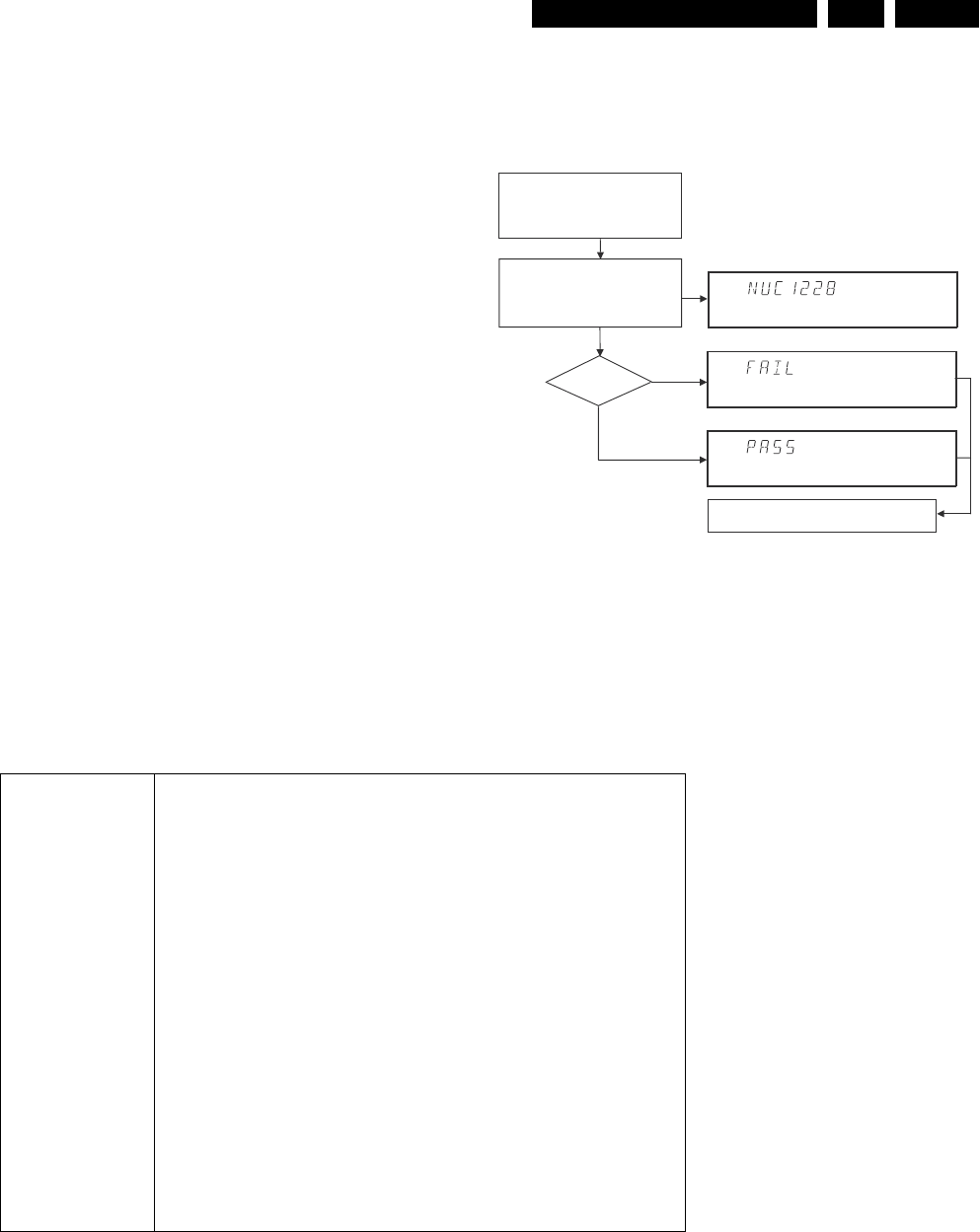
5.1.1 Description
The End user/Dealer script interface gives a diagnosis on a
stand alone DVD recorder. During this mode, a number of
hardware tests (nuclei) are automatically executed to check if
the recorder is faulty. The diagnosis is simply a "fail" or "pass"
message. If the message "FAIL" appears on the display, there
is apparently a failure in the recorder. If the message "PASS"
appears, the nuclei in this mode have been executed
successfully. There can be still a failure in the recorder
because the nuclei in this mode don't cover the complete
functionality of the recorder.
5.1.2 Structure
Figure 5-1
The End use/Dealer script executes all diagnostic nuclei that
do not need any user interaction and are meaningful on a
standalone DVD recorder.
5.1.3 Contents
Unplug the mains cord
Hold Open/Close & Source
depressed while plugging in
the mains cord
During the test, the display shows
the number of the test currently
running
SET O.K.?
YES
NO
To exit DEALER SCRIPT, unplug the mains cord
MS 13016_001
300904
Included tests: 1.DS_ANAB_COMMUNICATIONECHO_NUC
2.DS_DCB_COMMUNICATIONECHO_NUC 3.
DS_BROM_COMMUNICATION_NUC 4.
DS_SYS_SETTINGSDISPLAY_NUC 5.
DS_CHR_DEVTYPEGET_NUC6. DS_CHR_INT_PIC_NUC7.
DS_CHR_DMA_NUC8. DS_BROM_WRITEREAD_NUC9.
DS_NVRAM_COMMUNICATION_NUC10.
DS_NVRAM_WRITEREAD_NUC11.
DS_SDRAM_WRITEREADFAST_NUC12.
DS_FLASH_WRITEREAD_NUC13.DS_FLASH_CHECKSUMPROGRAM_
NUC14.DS_SYS_HARDWAREVERSIONGET_NUC15.
DS_VIP_DEVTYPEGET_NUC16. DS_VIP_COMMUNICATION_NUC17.
DS_DVIO_LINKDEVTYPEGET_NUC18.
DS_DVIO_PHYDEVTYPEGET_NUC19.
DS_DVIO_LINKCOMMUNICATION_NUC20.
DS_DVIO_PHYCOMMUNICATION_NUC21.DS_PSCAN_COMMUNICATI
ONDENC_NUC22.DS_PSCAN_COMMUNICATIONDEINTERLACER_NU
C23.
DS_BE_COMMUNICATIONECHO_NUC24.DS_ANAB_COMMUNICATIO
NIICNVRAM_NUC25.DS_ANAB_COMMUNICATIONIICTUNER_NUC26.D
S_ANAB_COMMUNICATIONIICSOUNDPROCESSOR_NUC27.DS_ANA
B_COMMUNICATIONIICAVSELECTOR_NUC28.
DS_ANAB_CHECKSUMPROGRAM_NUC
Diagnostic Software
EN 30 LX7500R5.
5.2 Virgin mode
If you want that the recorder starts up in Virgin mode, follow this
procedure:
• Unplug the recorder
• plug the recorder again while you keep the STAND BY/ON
key pressed
• the set starts up in Virgin mode.
5.3 Command Mode Interface
5.3.1 Nuclei Numeration
Each nucleus has a unique number of four digits. This number
is the input of the command mode.
Figure 5-2
The following groups are defined for Digital Board Chrysalis:
5.3.2 Error Handling
Each nucleus returns an error code. This code contains six
numerals, which means:
Figure 5-3
The nucleus group numbers and nucleus numbers are the
same as above.
5.3.3 Command Mode Interface
Set-Up Physical Interface Components
Hardware required:
•Service PC
• one free COM port on the Service PC
• special cable to connect DVD recorder to Service PC
The service PC must have a terminal emulation program (e.g.
Hyperterminal) installed and must have a free COM port (e.g.
COM1). Activate the terminal emulation program and check
that the port settings for the free COM port are: 19200 bps, 8
data bits, no parity, 1 stop bit and no flow control. The free COM
port must be connected via a special cable to the RS232 port
of the DVD recorder. This special cable will also connect the
test pin, which is available on the connector, to ground (i.e.
activate test pin).
Code number of PC interface cable: 3122 785 90017
Activation Digital Board Chrysalis
1. Pull the mains cord from the recorder and reconnect it
again (reboot).
2. The next welcome message will appear on the PC:
Startup screen
Figure 5-4
Now, the prompt 'DS:>' will appear. The diagnostic software is
now ready to receive commands. The commands that can be
given are the numbers of the nuclei. If you see above shown
screen, continue with paragraph 'Nuclei Codes'.
1. It is possible that the next messages will appear when
starting the DVD+RW for the first time
Group number Group name
0 Basic / Scripts
1 Chrysalis
2 Boot EEPROM
3NVRAM
4SDRAM
5Flash
6 Video Input Processor
7DVIO
8 Progressive Scan
9 Basic Engine
10 Display and Control Board
11 Analogue Board
12 System
[ XX YY ]
Nucleus number
Nucleus group num
CL 0653215
[ XX YY ZZ ]
Error code
Nucleus number
Nucleus group nu
m
CL 0653215
Diagnostic Software EN 31LX7500R 5.
Error messages startup
Figure 5-5
Error messages D&S program
Figure 5-6
In these cases, the boot EEPROM of the Chrysalis Digital
Board does not contain the required string with the hardware
information. To update the Digital Board with the correct string,
nucleus 1226 must be executed. See next section ’Diversity
String Input’.
There can also be the next error message.
Figure 5-7
Enter "Y" to program a safe string. With this automatically
generated string the board will work in principle but it has to be
checked if all board settings were detected correctly.
Diversity String Input
1. Execute nucleus 1226 to enter the string. Please see
adjustment instructions in chapter 8 for details
Nucleus 1226 execution with string
Figure 5-8
1. To check if the hardware info is filled correctly, you can
execute nucleus 1228.
Nucleus 1228 info example
Figure 5-9
1. Exit the ’Terminal’ program.
1. Reboot the DVD recorder to allow the software to start.
Command overview Digital Board Chrysalis
Below you will find an overview of the nuclei, their numbers,
and their error codes. This overview is preliminary and subject
to modifications.
Diagnostic Software
EN 32 LX7500R5.
Chrysalis (CHR)
Nucleus Name DS_CHR_DevTypeGet
Nucleus Number 100
Description Sends the device ID and the module ids and revisions of the PNX7100 (Chrysalis) to the
stdout port.
User Input None
Example DS:> 100
Device ID 7100
Codec ID PNX7100_MF2
F-BCU (0x0102) 1.0 INTC (0x011d) 1.0 PCI-XIO(0x0113) 1.0
SIF(0x013b) 1.0 EJTAG (0x0104) 0.0 S-BCU (0x0102) 1.0
BOOT (0x010a) 1.0 CONFIG (0x013f) 1.0 RESET (0x0123) 1.0
DEBUG (0x0116) 0.0 UART0 (0x0107) 0.1 UART1 (0x0107) 0.1
UART2 (0x0107) 0.1 UART3 (0x0107) 0.1 I2C0 (0x0105) 0.1
I2C1 (0x0105) 0.1 GPIO (0x013c) 1.0 SYNC (0x013a) 1.0
DISP0 (0xa015) 0.1 DISP1 (0xa00f) 0.0 OSD (0x0136) 0.1
SPU (0xa00e) 0.0 MIXER (0x0137) 1.0 DENC (0x0138) 0.1
CCIR (0x0139) 1.0 VDEC (0x0133) 0.1 PARSER (0xa00d) 0.0
DV (0xa00c) 0.0 BEI (0xa00a) 0.0 IDE (0xa009) 0.0
SGDX (0xa008)0.0 BYTE (0xa00b) 0.0 OUTPUT (0xa003) 0.0
ACOMP (0xa000) 0.0 VFE (0xa001) 0.0 VCOMP (0xa002) 0.0
SCR (0x0000) 0.0 SIFF (0xa011) 0.0 WMD (0xa010) 0.0
AUDIO0 (0xa015) 0.1 AUDIO1 (0xa00f) 0.0 PSCAN (0xa018) 0.0
010000:
Test OK @
Nucleus Name DS_CHR_TestImageOn
Nucleus Number 101
Description Generates a test-image of a selected video standard on selected video output on the digital
board. When no input is given, the default values will be used. Use nucleus
DS_ANAB_VideoRouting to route the video signal on the analogue board output
User Input The user has to decide which test image, video standard and video output must be used:
Test image id:
0 VERTICAL_COLOURBAR (default)
1 HORIZONTAL_COLOURBAR
2 WHITE
3 YELLOW
4 CYAN
5 GREEN
6 MAGENTA
7 RED
8 BLUE
9 BLACK
10 GRAY
Video standard:
PAL (default)
NTSC
Video output:
ALL CVBS and YC and RGB (default)
CVBS
YC
RGB
YUV
PSCAN progressive scan
Example DS:> 101
010100:
Test OK @
DS:> 101 0 pal cvbs
010100:
Test OK @
DS:> 101 4 ntsc yc
010100:
Test OK @
Nucleus Name DS_CHR_TestImageOff
Nucleus Number 102
Description Switches the test-image off.
User Input None
Diagnostic Software EN 33LX7500R 5.
Example DS:> 102
010200:
Test OK @
Nucleus Name DS_CHR_SineOn
Nucleus Number 103
Description Generate an audio sine signal on the audio output of the digital board. Note: Left channel
6kHz, right channel 12 kHz sine. Make sure to route the signal first.
User Input None
Example DS:> 103
010300:
Test OK @
Nucleus Name DS_CHR_SineOff
Nucleus Number 104
Description Stop generating the audio sine signal
User Input None
Example DS:> 104
010400:
Test OK @
Nucleus Name DS_CHR_SineBurst
Nucleus Number 105
Description Generate an audio sine signal on the audio output of the digital board for 4 seconds.
Note: Left channel 6kHz, right channel 12 kHz sine with some known hick-ups
User Input None
Example DS:> 105
010500:
Test OK @
Nucleus Name DS_CHR_MuteOn
Nucleus Number 106
Description Mute the audio outputs of the digital board
User Input None
Example DS:> 106
010600:
Test OK @
Nucleus Name DS_CHR_MuteOff
Nucleus Number 107
Description De-mute the audio outputs of the digital board
User Input None
Example DS:> 107
010700:
Test OK @
Nucleus Name DS_CHR_DvLedOn
Nucleus Number 108
Description Check the connection to the DV-LED on the digital board by switching it on
User Input None
Example DS:> 108
010800:
Test OK @
Nucleus Name DS_CHR_DvLedOff
Nucleus Number 109
Description Switch off the DV-LED on the digital board
User Input None
Example DS:> 109
010900:
Test OK @
Diagnostic Software
EN 34 LX7500R5.
Boot EEPROM (BROM)
Nucleus Name DS_CHR_MacroVisionOn
Nucleus Number 110
Description Turn on MacroVision.
User Input None
Example DS:> 110
011000:
Test OK @
Nucleus Name DS_CHR_MacroVisionOff
Nucleus Number 111
Description Turn off MacroVision.
User Input None
Example DS:> 111
011100:
Test OK @
Nucleus Name DS_CHR_Peek
Nucleus Number 112
Description Peek a value on a specified address
User Input The address to peek on
Example DS:> 112 0xa0700000
011200: Value read = 0x000001BD
Test OK @
Nucleus Name DS_CHR_Poke
Nucleus Number 113
Description Poke a value on a specified address
User Input The address to poke and the value: <address><value>
Example DS:> 113 0xa0700000 0xaabbccdd
011300:
Test OK @
Nucleus Name DS_CHR_INT_PICInterrupts
Nucleus Number 114
Description Test all interrupts of the priority interrupt controller
User Input -
Example DS:> 114
011400:
Test OK @
Nucleus Name DS_CHR_DMA_TestDMA
Nucleus Number 115
Description Test the memory to memory DMA transfer
User Input -
Example DS:> 115
011500:
Test OK @
Nucleus Name DS_BROM_Communication
Nucleus Number 200
Description Check the communication between the IIC controller of the Chrysalis and the boot
EEPROM
User Input None
Example DS:> 200
020000:
Test OK @
Nucleus Name DS_BROM_WriteRead
Nucleus Number 201
Description Check whether the Boot EEPROM can be written to and read from
User Input None
Diagnostic Software EN 35LX7500R 5.
NVRAM
SDRAM
Example DS:> 201
020100:
Test OK @
Nucleus Name DS_NVRAM_Communication
Nucleus Number 300
Description Check the communication between the IIC controller of the Chrysalis and the EEPROM
User Input None
Example DS:> 300
030000:
Test OK @
Nucleus Name DS_NVRAM_WriteRead
Nucleus Number 301
Description Check whether the EEPROM can be written to and read from
User Input None
Example DS:> 301
030100:
Test OK @
Nucleus Name DS_NVRAM_Clear
Nucleus Number 302
Description Make the EEPROM empty, containing all zeroes.
User Input None
Example DS:> 302
030200:
Test OK @
Nucleus Name DS_NVRAM_Modify
Nucleus Number 303
Description Modifies one or more locations in NVRAM and updates the checksum of the section
modified
User Input 1. The location that must be modified
i.e. "ALL" "BOOT" "DIAGNOSTICS" "DOWNLOAD" "CONFIG" "RECORDER" or no
string if an offset from the base address of the NVRAM is required
2. The offset and data which to put on the selected location
<offset> <length> <data>
Example DS:> 303 DIAGNOSTICS 5 1 0x5a
030300:Section is modified successfully
Test OK @
Nucleus Name DS_NVRAM_Read
Nucleus Number 304
Description Read out one or more locations in the NVRAM
User Input 1. The location which must be read
i.e. "ALL" "BOOT" "DIAGNOSTICS" "DOWN LOAD" "CONFIG" "RECORDER" or no
string if an offset from the base address of the NVRAM is required
2. The offset and number of bytes to read
<offset> <length>
Example 304 DIAGNOSTICS 0 6
030400: Value read = 0x00 0x00 0x00 0x00 0x00 0x5A
Test OK @
Nucleus Name DS_SDRAM_WriteRead
Nucleus Number 400
Description Check all data lines, address lines and memory locations of the SDRAM
User Input None
Example DS:> 400
040000:
Test OK @
Nucleus Name DS_SDRAM_WriteReadFast
Nucleus Number 401
Diagnostic Software
EN 36 LX7500R5.
FLASH
Description Check all data lines and address lines of the SDRAM
User Input None
Example DS:> 401
040100:
Test OK @
Nucleus Name DS_SDRAM_Write
Nucleus Number 402
Description Write to a specific memory address
User Input 1. The location that must be modified
( SDRAM starts at address 0xA0000000 )
2. The value to put on the selected location
Example DS:> 402 0xa1000010 0xad112222
040200:
Test OK @
Nucleus Name DS_SDRAM_Read
Nucleus Number 403
Description Read from a specific memory address
User Input The location from which the data must be read
( SDRAM starts at address 0xA0000000 )
Example DS:> 403 0xa1000010
040300: Value read = 0xAD112222
Test OK @
Nucleus Name DS_FLASH_DevTypeGet
Nucleus Number 500
Description Get the device (revision) type information of the FLASH IC. (manufacturer and device ID)
User Input None
Example DS:> 500
050000: Found FLASH memory:
Manufacturer ID: 0x01
Device ID : 0x01
Test OK @
Nucleus Name DS_FLASH_WriteRead
Nucleus Number 501
Description Check whether the FLASH can be written to and read from
User Input None
Example DS:> 501
050100:
Test OK @
Nucleus Name DS_FLASH_Read
Nucleus Number 502
Description Read from a specific memory address in FLASH
User Input The location from which data must be read
( FLASH starts at address 0xB8000000 )
Example DS:> 502 0xb8000000
050200: Value read = 0x3C08A000
Test OK @
Nucleus Name DS_FLASH_ChecksumProgram
Nucleus Number 503
Description Check the checksum of the application partitions by recalculating and comparing partition
checksums
User Input None
Example DS:> 503
050300:
BootCode checksum is: 0xBABE5B6F, which is correct
Diagnostics checksum is : 0xBABEBAFF, which is correct
Download checksum is: 0xBABEEDBF, which is correct
Application checksum is : 0xBABE8EEC, which is correct
Test OK @
Diagnostic Software EN 37LX7500R 5.
Video Input Processor (VIP)
Nucleus Name DS_FLASH_CalculateChecksum
Nucleus Number 504
Description Calculate the checksum over all memory addresses. Used to check entire FLASH contents
User Input None
Example DS:> 504
050400: The Checksum = 0xBABE30A4
Test OK @
Nucleus Name DS_FLASH_CalculateChecksumFast
Nucleus Number 505
Description Calculate a checksum over a selected number of address locations
User Input None
Example DS:> 505
050500: The Checksum = 0xBABEB064
Test OK @
Nucleus Name DS_VIP_DevTypeGet
Nucleus Number 600
Description Get the device (revision) type information of the VIP IC
User Input None
Example DS:> 600
060000: Found SAA7118
Test OK @
Nucleus Name DS_VIP_Communication
Nucleus Number 601
Description Check the communication between the IIC controller of the chrysalis and the VIP IC
User Input None
Example DS:> 601
060100:
Test OK @
Nucleus Name DS_VIP_ClockOutputOn
Nucleus Number 602
Description Switch the clock output on
User Input None
Example DS:> 602
060200:
Test OK @
Nucleus Name DS_VIP_ClockOutputOff
Nucleus Number 603
Description Switch the clock output off
User Input None
Example DS:> 603
060300:
Test OK @
Nucleus Name DS_VIP_SelectInput
Nucleus Number 604
Description Select an input video path to be switched to the analogue output pin (AOUT) of the VIP
User Input The input to select, see table below.
1 CVBS_Y_IN_A
2 CVBS_OUT_B
3 CVBS_Y_IN_B
4 CVBS_Y_IN_C
6 C_IN
8 G_IN
9 Y_IN
13 B_IN
14 U_IN
18 R_IN
19 V_IN
Diagnostic Software
EN 38 LX7500R5.
Digital Video Input Output (DVIO)
Example DS:> 604 1
060400:
Test OK @
Nucleus Name DS_DVIO_LinkDevTypeGet
Nucleus Number 700
Description Get the device (revision) type information of the 1394 Link layer IC
User Input None
Example DS:> 700
070000: Device type of the link layer IC: ffc00301
Test OK @
Nucleus Name DS_DVIO_PhyDevTypeGet
Nucleus Number 701
Description Get the device (revision) type information of the 1394 Physical layer IC
User Input None
Example DS:> 701
070100:
Device type of the phy layer IC: 0
Test OK @
Nucleus Name DS_DVIO_LinkCommunication
Nucleus Number 702
Description Check the accessibility of the 1394 Link layer IC by writing to and reading from a specific
address
User Input None
Example DS:> 702
070200:
Test OK @
Nucleus Name DS_DVIO_PhyCommunication
Nucleus Number 703
Description Check the accessibility of the 1394 Physical layer IC by writing to and reading from a
specific address
User Input None
Example DS:> 703
070300:
Test OK @
Nucleus Name DS_DVIO_Routing
Nucleus Number 704
Description Route a DV stream containing an audio and video signal through the physical and link layer
ICs to the Chrysalis
User Input None, test works for both NTSC and PAL
Example DS:> 704
070400:
Test OK @
Nucleus Name DS_DVIO_DetectNode
Nucleus Number 705
Description Check whether a DV node can be detected by the hardware
User Input None, test works for both NTSC and PAL
Example DS:> 705
070500:
Test OK @
Nucleus Name DS_DVIO_DetectStream
Nucleus Number 706
Description Check whether a DV stream can be detected by the hardware
User Input None, test works for both NTSC and PAL
Example DS:> 706
070600:
Test OK @
Diagnostic Software EN 39LX7500R 5.
Progressive Scan (PSCAN)
Nucleus Name DS_PSCAN_CommunicationDenc
Nucleus Number 801
Description Check the communication between the IIC controller of the chrysalis and the progressive
scan DENC-IC
User Input None
Example DS:> 801
080100:
Test OK @
Nucleus Name DS_PSCAN_TestImageOn
Nucleus Number 802
Description Generate the test images that are present on the progressive scan IC.
User Input In case of ADV7196:
When no input is given “HATCH” is the default
-“HATCH”
-“FRAME”
Remark:
“HATCH” is a crosshatch test pattern (horizontal and vertical white lines are displayed
against a black background)
“FRAME” is a uniform coloured frame/field test pattern (default white).
In case of FLI2300: Nothing.
Example DS:> 802 HATCH
080200:
Test OK @
Nucleus Name DS_PSCAN_TestImageOff
Nucleus Number 803
Description Switch off the generated test image
User Input None
Example DS:> 803
080300:
Test OK @
Nucleus Name DS_PSCAN_TestImageColourSettingsSet
Nucleus Number 804
Description Set the colour of the hatch- or the frame- field to a different value than the default white
User Input A colour string of one of the next non-case sensitive strings ( WHITE, BLACK, RED,
GREEN, BLUE, YELLOW, CYAN, MAGENTA ) or Y Cr Cb (hexa-) decimal values.
Example DS:> 804 yellow
080400:
Test OK @
DS:> 804 0x6a 0xde 0xca
080400:
Test OK @
Nucleus Name DS_PSCAN_TestImageColourSettingsGet
Nucleus Number 805
Description Get the colour settings of the hatch- or the frame- field.
User Input None
Example DS:> 805
080500: Colour Y Cr Cb values: 0xD2 0x92 0x10
Test OK @
Nucleus Name DS_PSCAN_Routing
Nucleus Number 806
Description Route a video signal from the host processor through the progressive scan ICs to the
progressive scan output of the set.
Note: to route the progressive scan to the output of the set, first call nucleus 1112 with
parameter 0 (video routing on analogue board).
User Input None
Example DS:> 806
080600:
Test OK @
Diagnostic Software
EN 40 LX7500R5.
Basic Engine (BE)
Nucleus Name DS_PSCAN_DevTypeGetDeinterlacer
Nucleus Number 807
Description Get the device (revision) type information of the progressive scan deinterlacer.
User Input None
Example DS:> 807
080700:
Chip name : 2300
Chip version : 1
Test OK @
Nucleus Name DS_PSCAN_CommunicationDeinterlacer
Nucleus Number 808
Description Check the communication between the IIC controller of the chrysalis and the progressive
scan Deinterlacer-IC
User Input None
Example DS:> 808
080800:
Test OK @
Nucleus Name DS_BE_CommunicationEcho
Nucleus Number 900
Description Check the communication between the digital board and the basic engine by issuing an
echo command over the S2B interface
User Input None
Example DS:> 900
090000:
Test OK @
Nucleus Name DS_BE_Reset
Nucleus Number 901
Description Reset the basic engine
User Input None
Example DS:> 901
090100:
Test OK @
Nucleus Name DS_BE_VersionGet
Nucleus Number 903
Description Get the version of the basic engine and that of the optical unit
User Input None
Example DS:> 903
090300: BE version = 20.09.18 Optical unit version = 3C.00.09.41.08
Test OK @
Nucleus Name DS_BE_GetSelftestResult
Nucleus Number 902
Description Return the self-test results through the service port
User Input None
Example DS:> 902
090200:
Test OK @
Nucleus Name DS_BE_TrayOut
Nucleus Number 904
Description Open the tray of the basic engine
User Input None
Example DS:> 904
090400:
Test OK @
Nucleus Name DS_BE_TrayIn
Nucleus Number 905
Description Close the tray of the basic engine
Diagnostic Software EN 41LX7500R 5.
User Input None
Example DS:> 905
090500:
Test OK @
Nucleus Name DS_BE_WriteReadDvdRw
Nucleus Number 906
Description Write data to and read data from a DVD+RW disc through the basic engine for verification
of the writing
User Input None
Example DS:> 906
090600: Testing on sector 0x5dbe0: OK
Test OK @
Nucleus Name DS_BE_WriteReadDvdR
Nucleus Number 907
Description Write data to and read data from a DVD+R disc through the basic engine for verification of
the writing
User Input None
Example DS:> 907
090700: Testing on sector 0x36210: OK
Test OK @
Nucleus Name DS_BE_StatisticalInformationGet
Nucleus Number 908
Description Retrieve the statistical information from the basic engine
User Input None
Example DS:> 908
Total time the power power on (HR:MIN) 0: 0h
Total time of reading CDROM discs (HR:MIN) 0: 0h
Total time of reading high DVD SL discs (HR:MIN) 0: 0h
Total time of reading other DVD SL discs (HR:MIN) 0: 0h
Total time of reading high DVD DL siscs (HR:MIN) 0: 0h
Total time of reading other DVD DL discs (HR:MIN) 0: 0h
Total time of reading high DVD+R discs (HR:MIN) 0: 0h
Total time of reading other DVD+R discs (HR:MIN) 0: 0h
Total time of reading high DVD+RW discs (HR:MIN) 0: 0h
Total time of reading other DVD+RW discs (HR:MIN) 1: 0h
Total time of writing DVD+R discs in 2HRS mode (HR:MIN) 0: 0h
Total time of writing DVD+R discs in 4HRS mode (HR:MIN) 0: 0h
Total time of writing DVD+R discs in 6HRS mode (HR:MIN) 0: 2h
Total time of writing DVD+RW discs in 2HRS mode (HR:MIN) 0: 0h
Total time of writing DVD+RW discs in 4HRS mode (HR:MIN) 0: 3h
Total time of writing DVD+RW discs in 6HRS mode (HR:MIN) 0: 0h
090800:
Test OK @
Nucleus Name DS_BE_StatisticalInformationReSet
Nucleus Number 909
Description Reset the statistical information in the basic engine
User Input None
Example DS:> 909
090900:
Test OK @
Nucleus Name DS_BE_ErrorLogGet
Nucleus Number 910
Description Get the error log from the basic engine
User Input None
Example DS:> 910
Momentary errors (0-9): 0x21 0x00 0x00 0x20 0x00 0x00 0x00 0x00 0x00 0x00
Cumulative errors (1-9): 0x00 0x80 0x20 0x00 0x00 0x00 0x00 0x00 0x00
Software fatal assert : 256 cpowermanager.cpp
091000:
Test OK @
Diagnostic Software
EN 42 LX7500R5.
Nucleus Name DS_BE_ErrorLogReset
Nucleus Number 911
Description Reset the error log in the basic engine
User Input None
Example DS:> 911
091100:
Test OK @
Nucleus Name DS_BE_JitterOptimise
Nucleus Number 912
Description Perform jitter optimisation:A formatted DVD must be loaded into the engine before
executing this nucleus
User Input none
Example DS:> 912
Test OK @
Nucleus Name DS_BE_FocusOn
Nucleus Number 913
Description Put the laser of the BE into focus
User Input None
Example DS:> 913
091300:
Test OK @
Nucleus Name DS_BE_FocusOff
Nucleus Number 914
Description Turn off putting the laser of the BE into focus
User Input None
Example DS:> 914
091400:
Test OK @
Nucleus Name DS_BE_MotorOn
Nucleus Number 915
Description Turn on the turntable motor
User Input None
Example DS:> 915
091500:
Test OK @
Nucleus Name DS_BE_MotorOff
Nucleus Number 916
Description Turn off the turntable motor
User Input None
Example DS:> 916
091600:
Test OK @
Nucleus Name DS_BE_RadialOn
Nucleus Number 917
Description Close the radial loop
User Input A formatted DVD must be loaded into the engine before executing this nucleus
Example DS:> 917
091700:
Test OK @
Nucleus Name DS_BE_RadialOff
Nucleus Number 918
Description Open the radial loop
User Input None
Example DS:> 918
091800:
Test OK @
Diagnostic Software EN 43LX7500R 5.
Nucleus Name DS_BE_RadialCalibration
Nucleus Number 919
Description Calibrate the radial loop
User Input A formatted DVD must be loaded into the engine before executing this nucleus
Example DS:> 919
091900:
Test OK @
Nucleus Name DS_BE_Tilt
Nucleus Number 920
Description Test the tilt mechanism control loop, or allow its proper functioning to be
measured.Before executing this nucleus a disc must be loaded into the recorder
User Input None
Example DS:> 920
092000:
Tilt sensor bathtub: (71,-12,145)(68,-12,135)(62,-10,120)(56,-92,97)(50,-75,86)
(44,-59,80)(41,-52,80)(35,-37,86)(29,-22,86)
(23,-7,92)(17,8,111)(11,23,135)(8,31,138)(5,39,158)
Test OK @
Nucleus Name DS_BE_CheckDisc
Nucleus Number 921
Description Check whether there is a disc inside the BE
User Input None
Example DS:> 921
092100: A DVD+Rewritable is loaded (disc is empty or partially recorded)
Test OK @
DS:> 921
092100: No Disc is loaded
Test OK @
Nucleus Name DS_BE_SledgeMotor
Nucleus Number 922
Description Send the sledge to its home position, then to the middle of the disc, and then to the
end.
User Input None
Example DS:> 922
092200:
Test OK @
Nucleus Name DS_BE_ReadTocInfo
Nucleus Number 924
Description Read the TOC from the disc. This gives a good indication if the BE works properly..
User Input None
Example DS:> 924
092400:
TOC info [hex] = 91 3A 0C
Test OK@
DS:> 924
092403:
The BE returned: 0x10 #{no_disc_error} No disc is detected
Error@
DS:> 924
092403: The BE returned: 0x1e #{illegal_medium_error} Engine unable to handle
current disc. Probably illegal medium.
Error @
Nucleus Name DS_BE_DiscErase
Nucleus Number 925
Description Perform a DC-erase on a DVD+RW disc.
User Input None
Diagnostic Software
EN 44 LX7500R5.
Display and Control Board (DCB)
Example DS:> 925
The entirely disc will be erased.
Are you sure you want this?[y/n]
092500:
Test OK @
Nucleus Name DS_BE_RegionCodeSet
Nucleus Number 928
Description Set the region code in the AV3.
User Input Region code
Example DS:> 928 1
092800:
Test OK @
DS:> 928
This nucleus is not supported by the engine
092800:
Test OK @
Nucleus Name DS_BE_RegionCodeGet
Nucleus Number 929
Description Read the region code from the AV3.
User Input None
Example DS:> 929
092900: DVD region 1
Test OK @
DS:> 929This nucleus is not supported by the engine
092900:
Test OK @
Nucleus Name DS_BE_RegionCounterReset
Nucleus Number 930
Description Reset the region counter in the AV3.
User Input None
Example DS:> 930
093000:
Test OK @
DS:> 930 This nucleus is not supported by the engine
093000:
Test OK @
Nucleus Name DS_BE_AdjustLaserControl
Nucleus Number 931
Description Adjust the DVD-M (with the OPU) with PCBA. (So adjusts the two PCBS to each other)
User Input None
Execution Time 30 seconds
Example DS:> 931
093100:
Test OK @
Nucleus Name DS_DCB_CommunicationEcho
Nucleus Number 1000
Description Check the communication between the digital board and the DCB by issuing an echo
command
User Input None
Example DS:> 1000
100000:
Test OK @
Nucleus Name DS_DCB_VersionGet
Nucleus Number 1001
Description Get the version of the DCB
Diagnostic Software EN 45LX7500R 5.
Analogue Board (ANAB)
User Input None
Example DS:> 1001100100: DCB version: 13Test OK @
Nucleus Name DS_DCB_LightDisplay
Nucleus Number 1002
Description Light the entire display of the DCB, and clear the display after confirmation.User
confirmation is necessary.
User Input None
Example DS:> 1002
100200:
Test OK @
Nucleus Name DS_DCB_Keyboard
Nucleus Number 1004
Description Check all keys of the keyboard by confirming the key-code displayed of each key.
User Input None
Example DS:> 1004
100400:
Test OK @
Nucleus Name DS_DCB_RemoteControl
Nucleus Number 1005
Description Check the interface between the remote control and the DCB by checking the key-
code displayed
User Input None
Example DS:> 1005
100500:
Test OK @
Nucleus Name DS_DCB_Led
Nucleus Number 1006
Description Switch the record LED on, and after confirmation off.
The user confirms by pressing the REC key, STOP key, or the PLAY key on the local
keyboard. The PLAY key confirms that the LED is on and the REC key
User Input None
Example DS:> 1006
100600:
Test OK @
Nucleus Name DS_ANAB_CommunicationEcho
Nucleus Number 1100
Description Check the communication between the digital board and the analogue board by
issuing some echo string.
User Input None
Example DS:> 1100
110000: Hello Analogue Board
Test OK @
Nucleus Name DS_ANAB_CommunicationIicNvram
Nucleus Number 1101
Description Check the communication between the digital board and the NVRAM on the analogue
board.
User Input None
Example DS:> 1101
110100:
Test OK @
Nucleus Name DS_ANAB_CommunicationIicTuner
Nucleus Number 1102
Description Check the communication between the digital board and the tuner on the analogue
board
User Input None
Diagnostic Software
EN 46 LX7500R5.
Example DS:> 1102
110200:
Test OK @
Nucleus Name DS_ANAB_CommunicationIicDataSlicer
Nucleus Number 1103
Description Check the communication between the digital board and the data slicer on the
analogue board
User Input None
Example DS:> 1103
110300:
Test OK @
Nucleus Name DS_ANAB_CommunicationIicSoundProcessor
Nucleus Number 1104
Description Check the communication between the digital board and the sound processor on the
analogue board
User Input None
Example DS:> 1104
110400:
Test OK @
Nucleus Name DS_ANAB_CommunicationIicAVSelector
Nucleus Number 1105
Description Check the communication between the digital board and the A/V-selector on the
analogue board
User Input None
Example DS:> 1105
110500:
Test OK @
Nucleus Name DS_ANAB_HardwareVersionGet
Nucleus Number 1106
Description Get the hardware version of the analogue board
User Input None
Example DS:> 1106
110600: Analogue hardware version : 11
Test OK @
Nucleus Name DS_ANAB_SoftwareVersionBootGet
Nucleus Number 1107
Description Get the software version of the boot software of the analogue board
User Input None
Example DS:> 1107
110700: Bootcode application version : 11.00.11
Test OK @
Nucleus Name DS_ANAB_SoftwareVersionDownloadGet
Nucleus Number 1108
Description Get the software version of the download software of the analogue board
User Input None
Example DS:> 1108
110800: Download application version : 11.00.06
Test OK @
Nucleus Name DS_ANAB_SoftwareVersionApplGet
Nucleus Number 1109
Description Get the software version of the application software of the analogue board
User Input None
Example DS:> 1109
110900: Recorder application version : 11.00.23
Test OK @
Diagnostic Software EN 47LX7500R 5.
Video routing paths (Europe)
Video routing paths (NAFTA)
Nucleus Name DS_ANAB_SoftwareVersionDiagnosticsGet
Nucleus Number 1110
Description Get the software version of the diagnostic software of the analogue board
User Input None
Example DS:> 1110
111000: Diagnostics application version : 11.00.13
Test OK @
Nucleus Name DS_ANAB_ChecksumProgram
Nucleus Number 1111
Description Check the checksum of the several partitions by recalculating and comparing partition
checksums
User Input None
Example DS:> 1111
BootCode checksum is: 0xBABE6240, which is correct
Diagnostics checksum is : 0xBABEBEAD, which is correct
Download checksum is: 0xBABEA6B7, which is correct
Application checksum is : 0xBABEB277, which is correct
111100:
Test OK @
Nucleus Name DS_ANAB_VideoRouting
Nucleus Number 1112
Description Perform the routing of the video paths on the analogue board
User Input The user has to input the correct parameter for the routing (see table ’video routing’
below).
Example DS:> 1112
00111200:
Test OK @
Path ID Description
0 Input signal is VIDEO(CVBS) from digital board and will be re-routed back to the digital
board.
1 Input signal is from FRONT VIDEO(CVBS) IN and will be routed to the digital board.
2 No Routing.
3 Input signal is from FRONT S-VIDEO(Y/C) and will be routed to the digital board.
4 No Routing.
5 Input signal is CVBS from SCART1 and will be routed to the digital board.
6 Input signal is CVBS from SCART2 and will be routed to the digital board.
7 Input Signal is CVBS from Digital Board and it will be routed to Scart1 and Scart2.
8 Input signal is VIDEO(CVBS) from ANTENNA IN and will be routed to SCART2.
9 Input signal is VIDEO(CVBS) from SCART1 and will be routed to SCART2.
10 Input signal is VIDEO(CVBS) from SCART2 and will be routed to SCART1.
11 Signal path is routed Fast Blank from Scart2 pin16 and will be routed SCART1 pin16
12 Input Signal is YC from Digital Board and it will be routed to SCART1.
13
14 No Routing.
15 Input Signal is CVBS from TUNER and it will be routed to Digital .
16 No Routing.
17 Input Signal is routed from digital board YC to REAR S-VIDEO(YC) OUT
18 Signal path is routed from digital board RGB to RGB SCART1 and from digital board
CVBS to digital board CVBS.
19 No Routing.
20 Input RGB Signal is routed from Digital Board to SCART1(RGB),Input CVBS Signal
from Digital Board to Digital Board and Fast Blanking Signal from SCART2 to
SCART1.
21 Input Y/C Signal from Digital Board is routed to Rear Y/C Connector and Input Y/C
Signal from Front Y/C connector is routed to Digital Board.
Path ID Description
0 No Routing.
1 Input signal is from FRONT VIDEO(CVBS) IN and will be routed to the digital board.This
routing is same as the above path id.
Diagnostic Software
EN 48 LX7500R5.
Audio routing paths (Europe)
Audio routing paths (NAFTA)
2 Input signal is from REAR VIDEO(CVBS) IN and will be routed to the digital board.
3 Input signal is from FRONT S-VIDEO(Y/C) IN and the signal received will be routed to the
digital board.
4 Input signal is from REAR S-VIDEO(Y/C) IN and will be routed to the digital board.
5 No Routing.
6 No routing.
7 No routing.
8 Input signal is VIDEO(CVBS) from TUNER and will be routed to Y Pin of Rear Y/C
Connector.This will give only black/White Picture .
9 Input signal is from YUV IN and will be routed to YUV OUT.This is possible only if Digital
Board routes back YUV signal received back to the Analogue board(DENC)
10 No routing.
11 No routing.
12 No Routing.
13 No Routing.
14 No Routing.
15 Input CVBS Signal from Tuner is routed to Digital Board..
16 No Routing.
17 No Routing.
18 Input Signal from CVBS Rear In is routed to Digital Board. This is the same as path ID 02.
19 Input Y/C signal from Digital Board is routed to Y/C Rear Out Connector and Input signal from
Y/C Front In Connector is routed to Y/C Digital Board.
20 Y/C signal from Digital Board is routed to Y/C Rear Out Connector and Input signal from Y/
C Rear In Connector is routed to Y/C Digital Board.
23 The Video signal received from the Digital board will be output on Modulator channel 3.
24 The Video signal received from the Digital board will be output on Modulator channel 4.
Nucleus Name DS_ANAB_AudioRouting
Nucleus Number 1113
Description Perform the routing of the audio paths on the analogue board
User Input The user has to input the correct parameter for the routing (see table ’audio routing’
below)
Example DS:> 1113
00111300:
Test OK @
Path ID Description
0 Input signal is from FRONT AUDIO IN and will be routed to the digital board.
1 Input signal is from FRONT AUDIO IN and will be routed to the digital board.
2 No Routing.
3 Input signal is AUDIO from SCART1 and will be routed to the digital board.
4 Input signal is AUDIO from SCART2 and will be routed to the digital board.
5 No routing.
6 No routing.
7 Input Audio signal is from the digital Board and it will be routed to the SCART1 and SCART2
8 Input AUDIO signal from TUNER and will be routed to SCART2.
9 Input signal is AUDIO from SCART1 and will be routed to SCART2.
10 Input audio signal from SCART2 is routed to SCART1.
11 Input Audio signal is routed from DVIO to SCART2.
12
13 No Routing.
14 Input is Audio Signal from DVIO and it will be routed to Digital Board.
15 Input is Audio Signal from TUNER and it will be routed to Digital Board..
16 No routing.
17 No Routing.
18 Input signal is from FRONT AUDIO IN and will be routed to SCART2.
21 Input signal is from FRONT AUDIO IN and will be routed to the digital board.
Path ID Description
0 No Routing.
1 Input signal is from FRONT AUDIO IN and will be routed to the digital board.
2 Input signal is from REAR AUDIO IN 2 and will be routed to the digital board.
Diagnostic Software EN 49LX7500R 5.
3 Input Audio Signal is routed from FRONT Cinch In to Digital Board.(This is same as path ID
01)
4 Input Signal is from Rear Cinch In1 and it will be routed to Digital Board..
5 No routing.
6 No routing.
7 No routing.
8 No Routing.
9 No routing.
10 No Routing.
11 No Routing.
12 No Routing.
13 Input Signal is from Digital Board and it will be routed to the digital board.
14 No routing.
15 Input is Audio Signal from TUNER and it will be routed to Digital Board.
16 Input signal is AUDIO from dvio board and will be routed to Digital Board.
17 No routing.
18 No routing.
19 No routing.
20 Input signal is from REAR AUDIO IN 2 and will be routed to the digital board.
21 Input signal is from REAR AUDIO IN 1 and will be routed to the digital board.
22 Input signal is from REAR AUDIO IN 1 and will be routed to the digital board.
23 The Audio signal received from the Digital board will be outputted on Modulator channel 3.
24 The Audio signal received from the Digital board will be outputted on Modulator channel 4.
Nucleus Name DS_ANAB_SelectTunerChannel
Nucleus Number 1114
Description Set the tuner to receive a valid audio and video signal
User Input <Frequency*16> <video standard id>Tuner frequency: to tune the tuner to e.g. 216
MHz, this parameter must be 3456. (Since 216*16 = 3456. This is to avoid the decimal
points to the parameter list.)Video standard id: The table below shows which video
standards are possible
Video standard id Europe NAFTA
163248648096112 PAL_BG NTSC
PAL_I Invalid
PAL_DK Invalid
SEC_L Invalid
SEC_LS Invalid
SEC_BG Invalid
SEC_DK Invalid
Example DS:> 1114 3456 16
111400:
Test OK @
Nucleus Name DS_ANAB_IICWriteRead
Nucleus Number 1115
Description Perform an IIC write and read action on the analogue board
User Input Writing:
[<W>|<w>] [I2C address] [number of data bytes to write]
with
<data[0]...data[n]> Max 16 data bytes (n < 16).
Reading:
[<R>|<r>] [I2C address] [number of data bytes to read]
Max 16 data bytes (n < 16).
Example DS:> 1115 w 0x94 2 0x06 0x02
111500:
Test OK @
Nucleus Name DS_ANAB_ClockAdjust
Nucleus Number 1116
Description Set the clock to the value passed through in the YYYY MM DD HH MM SS format
User Input <YYYY> <MM> <DD> <HH> <MM> <SS>
Example DS:> 1116 2002 11 11 11 11 11
111600:
Test OK @
Diagnostic Software
EN 50 LX7500R5.
Frequency download string format
Nucleus Name DS_ANAB_ClockReference
Nucleus Number 1117
Description Generate a 1 kHz signal on pin 7 (INT) of the clock IC
User Input None
Example DS:> 1117
111700:
Test OK @
Nucleus Name DS_ANAB_ClockCorrection
Nucleus Number 1118
Description Store the clock IC correction value in NVRAM
User Input The correction value for the clock
Example DS:> 1118 1000023
111800:
Test OK @
Nucleus Name DS_ANAB_TunerAFCReferenceVoltage
Nucleus Number 1119
Description Store the reference voltage for the tuner in NVRAM
User Input The reference voltage, between 0 and 255
Example DS:> 1119
5111900:
Test OK @
Nucleus Name DS_ANAB_TunerFrequencyDownload
Nucleus Number 1120
Description Store the frequency table in NVRAM. The frequency table is passed through the error-
string provided to the nucleus.
User Input See frequency table
Example DS:> 1120 2233 00 02 4E45442031
112000:
Test OK @
Nucleus Name DS_ANAB_StoreExternalPresets
Nucleus Number 1121
Description Store the external presets in NVRAM
User Input None
Example DS:> 1121
112100:
Test OK @
Nucleus Name DS_ANAB_BargraphLevelAdjust
Nucleus Number 1122
Description Measure the audio signal corresponding to 0dB per channel and store it as correction
value in NVRAM
User Input none
Example DS:> 1122
112200:
Test OK @
Format description remarks
X(XXX) Preset number
VVWW VV: Channel numberWW :
Channel offset
Diagnostic Software EN 51LX7500R 5.
System (SYS)
ZZ Byte containing 8 bit fields for
TRUE/FALSE :
BIT 0: Decoder
BIT 1: Modulation
BIT 2: NICAM
SAP
BIT 3: Satpreset
BIT 4: Presetdefined
Channelpreferred
BIT 5: ExtPreset
BIT 6: NameManuallyChanged
BIT 7: ChannelPreset
NICAM/stereo bit for Europe
SAP/stereo bit for NAFTA
Preset defined bit is only used for Europe. For NAFTA,
renamed as channelpreferred to indicate if a channel is
preferred or not.
TRUE if preset is defined from P50 as extern [TGA]
HH HfSystemFineTuning HfS: 4 bit, FT: -4,...,4
IIJJKKLLMM Netname Range: A,..,Z,0,..,9,_,.. Netname length exists for Europe
only.
‘II’ is the HEX-value for the first character, ‘JJ’ for the
second, Ö
The message string of (DS_MessageDef *msgString) should be in the format:
“X(XXX)_VVWW_ZZ_HH_IIJJKKLLMM”.
Here will be ‘X(XXX)’ a decimal value in the range of 0 to 255.
V, W, Z, H, I, J, K, L, M are hex values with out the prefix ‘0x’ (in the range 0... 9,A ... F)
“ _” Denotes a space character.
Remarks:
CHANNEL_SYSTEM is for NAFTA.
PRESET_SYSTEM is for Europe.
Nucleus Name DS_SYS_HardwareVersionGet
Nucleus Number 1200
Description Get the hardware version and type of the digital board
User Input None
Example DS:> 1200
120000: Hardware ID = 00
The (PIO-pins) Digital Board ID = 2
Test OK @
DS:>
Nucleus Name DS_SYS_SoftwareVersionBootGet
Nucleus Number 1201
Description Get the version of the boot software on the digital board
User Input None
Example DS:> 1201
120100: Software Boot Version = 0001T
est OK @
Nucleus Name DS_SYS_SoftwareVersionDownloadGet
Nucleus Number 1202
Description Get the version of the download software on the digital board
User Input None
Example DS:> 1202
120200: Software Download Version = 0001
Test OK @
Nucleus Name DS_SYS_SoftwareVersionApplGet
Nucleus Number 1203
Description Get the version of the application software on the digital board
User Input None
Example DS:> 1203
120300: Software Application Version = 0001
Test OK @
Nucleus Name DS_SYS_SoftwareVersionDiagnosticsGet
Nucleus Number 1204
Description Get the version of the diagnostics software on the digital board
User Input None
Diagnostic Software
EN 52 LX7500R5.
Example DS:> 1204
120400: Software Diagnostics Version = 0001
Test OK @
Nucleus Name DS_SYS_EepromUpload
Nucleus Number 1205
Description Upload the contents of the NVRAM on the analogue board or the digital board to the
service PC, by using the X-modem protocol
User Input Choose one of the following parameters for the nucleus:1. Upload the contents
of the NVRAM of the digital board2. Upload the contents of the NVRAM of the
analogue boardChoose in the terminal on the control PC -> transfer -> receive file.
Select X-modem protocol. Then click receive in the dialogue and fill in the file name
in which you want to store the data.
120503 Something went wrong while transferring the data.
120504 User cancelled the upload.
Example DS:> 1205
1120500:
Test OK @
Nucleus Name DS_SYS_EepromDownload
Nucleus Number 1206
Description Download a file with the contents of the NVRAM for the analogue board or the digital
board from the service PC to the recorder, by using the X-modem protocol
User Input Choose one of the following parameters for the nucleus:1. Download the
contents of the NVRAM of the digital board2. Download the contents of the
NVRAM of the analogue boardChoose in the terminal of the control PC -> transfer -
> send file. Select X-modem protocol. Then choose a file with the Browse button in
the dialogue and click on send.
Example DS:> 1206
1120600:
Test OK @
Nucleus Name DS_SYS_DvIdNumberSet
Nucleus Number 1207
Description Set the IEEE 1394 unique IDThe unique ID to be set.
User Input None
Example DS:> 1207
1234567890 120700:
Test OK @
Nucleus Name DS_SYS_DvIdNumberGet
Nucleus Number 1208
Description Get the IEEE1394 ID
User Input None
Example DS:> 1208
120800: The DvIdNumber is: 0x0C22384E5A
Test OK @
Nucleus Name DS_SYS_IicWrite
Nucleus Number 1209
Description Perform an IIC write action on the digital board
User Input The user input the number of bytes to write followed by these bytes:
<BusID><Slave address to write to><number of bytes to write><d1><d2><..><dx>
Where the bus ID is either 0 (normally used) or 1
Example DS:> 1209 0 0xa0 1 0x6
120900: 1 Bytes written
Test OK @
Nucleus Name DS_SYS_IicRead
Nucleus Number 1210
Description Perform an IIC read action on the digital board
User Input The user inputs the number of bytes to read and the address to read them from:
<BusID><Slave address to read from><Number of bytes to read>Where the bus ID
is either 0 (normally used) or 1
Diagnostic Software EN 53LX7500R 5.
Example DS:> 1210 0 0xa0 1
121000: Value read =0x06T
est OK @
Nucleus Name DS_SYS_UartWrite
Nucleus Number 1211
Description Perform an UART write action on the digital board on a specified UART
User Input The user inputs the UART to write to, the number of bytes and the bytes to be written
to the UART.
1=UART port 1 : not used
2=UART port 2 : Bit Engine
3=UART port 3 : Analogue board
<UartNr><Number of bytes to write><d1><d2><..><dx>
Example DS:> 1211 2 2 0xd1 0x01
121100:
Test OK @
Nucleus Name DS_SYS_UartRead
Nucleus Number 1212
Description Perform an UART read action on the digital board on a specified UART
User Input The user inputs the UART to read from.
1=UART port 1 : not used
2=UART port 2 : Bit Engine
3=UART port 3 : Analogue board
<UartNr >
Example DS:> 1212 2
121200: The value that was read is: 0x50 0xD1 0x00
Test OK @
Nucleus Name DS_SYS_VideoLoopThroughStart
Nucleus Number 1213
Description The video signal, which is confirm the user input, is routed from the input to the
output. Input is set with the routing nucleus 1112. All outputs are enabled.
User Input <vipInput> <VideoOutput> <VideoStandard>
1. vipInput (CVBS, YC, YUV, RGB).
2. VideoOutput (YUV, RGB).
3. VideoStandard (PAL, NTSC).
Example DS:> 1213 CVBS RGB PAL
121300:
Test OK @
Nucleus Name DS_SYS_VideoLoopThroughStop
Nucleus Number 1214
Description Stop routing the video input to all the outputs.
User Input -
Example DS:> 1214
121400:
Test OK @
Nucleus Name DS_SYS_VideoLoop
Nucleus Number 1215
Description Note: Before executing this nucleus the user must route the video signal on the
analog board with nucleus DS_ANAB_VideoRouting(1112 ).
User Input Video input of the digital board:
- CVBS
- YC
- YUV
- RGB
- TEST (The video output will be routed to the video input on the digital board.)
Video standard:
- PAL
- NTSC
When no input is given, the nucleus will take TEST for video input and PAL for video
standard.
Diagnostic Software
EN 54 LX7500R5.
Example DS:> 1215 cvbs ntsc
121500:
Test OK @
DS:> 1215 cvbs pal
121508: The VideoInputProcessor cannot detect a sync-signal.
Error @
DS:> 1215 yuv ntsc
121511:
Error in luminance signal(Y)
Error in chrominance signal(U)
Error in chrominance signal(V)
Error @
Nucleus Name DS_SYS_AudioLoop
Nucleus Number 1216
Description The user first needs to select how the audio path must be routed on the analogue
board (FRS_DS_ANAB_AUDIO_VIDEO_ROUTING) and/or digital board before
calling this nucleus. The user also has to route the audio outputs back to the inputs
by means of cables. In this nucleus the Chrysalis generates an audio sine signal
with a specific signature and sends it to the output of the digital board
(FRS_DS_CHR_SINE). The Chrysalis encodes the audio signal to MPEG I layer II
and after this the signature of the signal will be checked.
User Input None
Example DS:> 1216 121600: Test OK @
Nucleus Name DS_SYS_SlashVersionSet
Nucleus Number 1217
Description Set the slash version of the system
User Input The slash version
Example DS:> 1217
82121700:
Test OK @
Nucleus Name DS_SYS_SlashVersionGet
Nucleus Number 1218
Description Get the slash version of the system
User Input None
Example DS:> 1218
121800: The slash version is: 82
Test OK @
Nucleus Name DS_SYS_Virginize
Nucleus Number 1219
Description (Re-) Virginize the recorder. User data in the NVRAM of the analogue board is
cleared
Example DS:> 1219
121900:
Test OK @
Nucleus Name DS_SYS_VirginModeOn
Nucleus Number 1220
Description Turn on the virgin mode functionality (e.g. the auto channel search upon start-up)
User Input None
Example DS:> 1220
122000:
Test OK @
Nucleus Name DS_SYS_VirginModeOff
Nucleus Number 1221
Description Turn off the virgin mode functionality (e.g. the auto channel search upon start-up)
User Input None
Example DS:> 1221
122100:
Test OK @
Diagnostic Software EN 55LX7500R 5.
Nucleus Name DS_SYS_DisplayFatalOn
Nucleus Number 1223
Description Turn on the display-fatal functionality which displays debug-information on the
display when encountering a fatal error condition from which could not be recovered
automatically
User Input None
Example DS:> 1223
122300:
Test OK @
Nucleus Name DS_SYS_DisplayFatalOff
Nucleus Number 1224
Description Turn off the display-fatal functionality which displays debug-information on the
display when encountering a fatal error condition from which could not be recovered
automatically
User Input None
Example DS:> 1224122400:Test OK @
Nucleus Name DS_SYS_DisplayFatalGet
Nucleus Number 1225
Description Get the display-fatal flag of the recorder
User Input None
Example DS:> 1225
122500:
Test OK @
Nucleus Name DS_SYS_SettingsSet
Nucleus Number 1226
Description Programs the digital board settings into the boot EEPROM on the digital board.
User Input A large hexadecimal value that represents the digital board settings obtained from
the DbString.exe program or from a reference set.
Example DS:> 1226 646961677473746201010200010101010101000020080000
122600:
Test OK @
Nucleus Name DS_SYS_SettingsDisplay
Nucleus Number 1228
Description Show the settings that are programmed in the BROM on the digital board.
User Input None.
Example DS:> 1228
Settings ID: 6D7920626F61726400020300010101020101000020080000
Board name: my board
Hardware ID: 0
Codec IC: PNX7100_MF2
Video Input Processor IC: SAA7118
Progressive Scan Deinterlacer IC: None
Progressive Scan Denc IC: ADV7196
I-Link physical layer circuit IC: PDI1394P25
I-Link link layer circuit IC: PDI1394P40
Audio clock: Clock scheme 1
Bit engine connector: available
IDE connector 1: available
IDE connector 2: not available
PCI connector: not available
RAM size 32MByte
ROM size (NOR FLASH bank 1) 8MByte
ROM size (NOR FLASH bank 2) Not available
ROM size (NAND FLASH) Not available
Bit Engine: AV 2.0
122800:
Test OK @
Nucleus Name DS_SYS_SettingsGet
Nucleus Number 1229
Description Get the digital board diversity settings string that is programmed in the BROM on the
digital board.
User Input None.

Diagnostic Software
EN 56 LX7500R5.
Example DS:> 1229
122900: 6D7920626F61726400020300010101020101000020080000
Test OK @
Nucleus Name DS_SYS_AudioLoopThroughStart
Nucleus Number 1230
Description Description: The audio input is routed from the an input to all outputs. Input is set with
the routing nucleus 1113. All outputs are enabled.
User Input None.
Example DS:> 1230
123000:
Test OK @
Nucleus Name DS_SYS_AudioLoopThroughStop
Nucleus Number 1231
Description Stop routing the audio input to all the outputs
User Input -
Example DS:> 1231
123100:
Test OK @
Nucleus Name DS_SYS_SettingsHwIdSet
Nucleus Number 1232
Description Double check whether stored HW-string equals actual HW as far as we can
automatically detect this. An automatic and a manual mode is supported.
User Input - ‘manual’ or ‘MANUAL’ to enter manual mode
- default is automatic mode where the nucleus stops upon and reports the first
encountered error
Example DS:> 1233
123300:
Test OK @
DS:> 1233 manual
123300:
Test OK @
DS:> 1233
123301:Hardware ID mismatch: in HW-Diversity string:99, actual in FLASH:0
Error @
DS:> 1233 manual
Hardware ID mismatch! in HW-Diversity string:99, actual in FLASH:0
Enter the correct HW ID of the digital board.
> 0
The HW-diversity string has been modified by you. Settings:
Board name: DIAG
Hardware ID: 0
Codec IC: PNX7100_MF3
Video Input Processor IC: SAA7118
Progressive Scan Deinterlacer IC: None
Progressive Scan Denc IC: ADV7196
I-Link physical layer circuit IC: PDI1394P25
I-Link link layer circuit IC: PDI1394P40
Audio clock: Clock scheme 1
Bit engine connector: available
IDE connector 1: available
IDE connector 2: not available
PCI connector: not available
RAM size 32MByte
ROM size (NOR FLASH bank 1) 8MByte
ROM size (NOR FLASH bank 2) Not available
ROM size (NAND FLASH) Not available
Is it OK to program this inthe new HW-diversity string? ([y]es/[n]o):y
Diversity HW-string programmed successfully.
123300:
Test OK @
DS:>
Diagnostic Software EN 57LX7500R 5.
Script
Nucleus Name DS_SYS_SettingsDoubleCheck
Nucleus Number 1233
Description This nucleus sets the HW-Id in the HW-diversity string
User Input - <HW-ID> - The hardware ID to set
-No input - The user will be asked for the ID
Example DS:> 1232
Enter the new HW ID of the digital board (Currently equals 21)
Enter a value between 0 and 99:
> 22
The HW ID will be set to: 22. Is that correct? ([Y/N]):y
123200:
Test OK @
DS:> 1232
Enter the new HW ID of the digital board (Currently equals 22)
Enter a value between 0 and 99:
>
The HW ID will be set to: 0. Is that correct? ([Y/N]):N
123202: Setting the HW ID was aborted by the user.
Error @
DS:> 1232 99
123200:
Test OK @
Nucleus Name DS_IH_ScriptHandler
Nucleus Number Script
Description
Included tests: 1. DS_ANAB_COMMUNICATIONECHO_NUC
2. DS_DCB_COMMUNICATIONECHO_NUC
3. DS_BROM_COMMUNICATION_NUC
4. DS_SYS_SETTINGSDISPLAY_NUC
5. DS_CHR_DEVTYPEGET_NUC
6. DS_CHR_INT_PIC_NUC
7. DS_CHR_DMA_NUC
8. DS_BROM_WRITEREAD_NUC
9. DS_NVRAM_COMMUNICATION_NUC
10. DS_NVRAM_WRITEREAD_NUC
11. DS_SDRAM_WRITEREADFAST_NUC
12. DS_FLASH_WRITEREAD_NUC
13. DS_FLASH_CHECKSUMPROGRAM_NUC
14. DS_SYS_HARDWAREVERSIONGET_NUC
15. DS_VIP_DEVTYPEGET_NUC
16. DS_VIP_COMMUNICATION_NUC
17. DS_DVIO_LINKDEVTYPEGET_NUC
18. DS_DVIO_PHYDEVTYPEGET_NUC
19. DS_DVIO_LINKCOMMUNICATION_NUC
20. DS_DVIO_PHYCOMMUNICATION_NUC
21. DS_PSCAN_COMMUNICATIONDENC_NUC
22. DS_PSCAN_COMMUNICATIONDEINTERLACER_NUC
23. DS_BE_COMMUNICATIONECHO_NUC
24. DS_ANAB_COMMUNICATIONIICNVRAM_NUC
25. DS_ANAB_COMMUNICATIONIICTUNER_NUC
26. DS_ANAB_COMMUNICATIONIICSOUNDPROCESSOR_NUC
27. DS_ANAB_COMMUNICATIONIICAVSELECTOR_NUC
28. DS_ANAB_CHECKSUMPROGRAM_NUC
User Input None

Diagnostic Software
EN 58 LX7500R5.
Example DS:> script
Executing User/Dealer script.
Busy executing NUC1100 1-28
Hello Analogue Board
Busy executing NUC1000 2-28
Busy executing NUC200 3-28
Busy executing NUC1228 4-28
Settings ID: 4C4541440D00000000030300010101020101000020080000
Board name: LEAD
Hardware ID: 0
Codec IC: PNX7100_MF3
Video Input Processor IC: SAA7118
Progressive Scan Deinterlacer IC: None
Progressive Scan Denc IC: ADV7196
I-Link physical layer circuit IC: PDI1394P25
I-Link link layer circuit IC: PDI1394P40
Audio clock: Clock scheme 1
Bit engine connector: available
IDE connector 1: available
IDE connector 2: not available
PCI connector: not available
RAM size 32MByte
ROM size (NOR FLASH bank 1) 8MByte
ROM size (NOR FLASH bank 2) Not available
ROM size (NAND FLASH) Not available
Bit Engine: AV 2.0
Busy executing NUC100 5-28
Device ID 7100
Codec ID PNX7100_MF3
F-BCU (0x0102) 1.0 INTC (0x011d) 1.0 PCI-XIO(0x0113) 1.0
SIF (0x013b) 1.0 EJTAG (0x0104) 0.0 S-BCU (0x0102) 1.0
BOOT (0x010a) 1.0 CONFIG (0x013f) 1.0 RESET (0x0123) 1.0
DEBUG (0x0116) 0.0 UART0 (0x0107) 0.1 UART1 (0x0107) 0.1
UART2 (0x0107) 0.1 UART3 (0x0107) 0.1 I2C0 (0x0105) 0.1
I2C1 (0x0105) 0.1 GPIO (0x013c) 1.0 SYNC (0x013a) 1.0
DISP0 (0xa015) 0.2 DISP1 (0xa00f) 0.0 OSD (0x0136) 0.1
SPU (0xa00e) 0.0 MIXER (0x0137) 1.0 DENC (0x0138) 0.1
CCIR (0x0139) 1.0 VDEC (0x0133) 0.1 PARSER (0xa00d) 0.0
DV (0xa00c) 0.0 BEI (0xa00a) 0.0 IDE (0xa009) 0.0
SGDX (0xa008) 0.0 BYTE (0xa00b) 0.0 OUTPUT (0xa003) 0.0
ACOMP (0xa000) 0.0 VFE (0xa001) 0.0 VCOMP (0xa002) 0.0
SCR (0x0000) 0.0 SIFF (0xa011) 0.0 WMD (0xa010) 0.0
AUDIO0 (0xa015) 0.2 AUDIO1 (0xa00f) 0.0 PSCAN (0xa018) 0.0
Busy executing NUC114 6-28
Busy executing NUC115 7-28
Busy executing NUC201 8-28
Busy executing NUC300 9-28
Busy executing NUC301 10-28
Busy executing NUC401 11-28
Busy executing NUC501 12-28
Busy executing NUC503 13-28
BootCode checksum is: 0xBABEB432, which is correct
Diagnostics checksum is: 0xBABED22B, which is correct
Download checksum is: 0xBABE025F, which is correct
Application checksum is: 0xBABE2825, which is correct
Busy executing NUC1200 14-28
Hardware ID = 00
Busy executing NUC600 15-28
Found SAA7118

Diagnostic Software EN 59LX7500R 5.
Example Busy executing NUC601 16-28
Busy executing NUC700 17-28
Device type of the link layer IC: ffc00301
Busy executing NUC701 18-28
Device type of the phy layer IC: 0
Busy executing NUC702 19-28
Busy executing NUC703 20-28
Busy executing NUC801 21-28
Busy executing NUC808 22-28
The IIC acknowledge was not received, which is correct
Busy executing NUC900 23-28
Busy executing NUC1101 24-28
Busy executing NUC1102 25-28
Busy executing NUC1104 26-28
Busy executing NUC1105 27-28
Busy executing NUC1111 28-28
BootCode checksum is: 0xBABE6240, which is correct
Diagnostics checksum is: 0xBABEDC9A, which is correct
Download checksum is: 0xBABEA6B7, which is correct
Application checksum is: 0xBABE5968, which is correct
PASS
DS:>

Diagnostic Software
EN 60 LX7500R5.
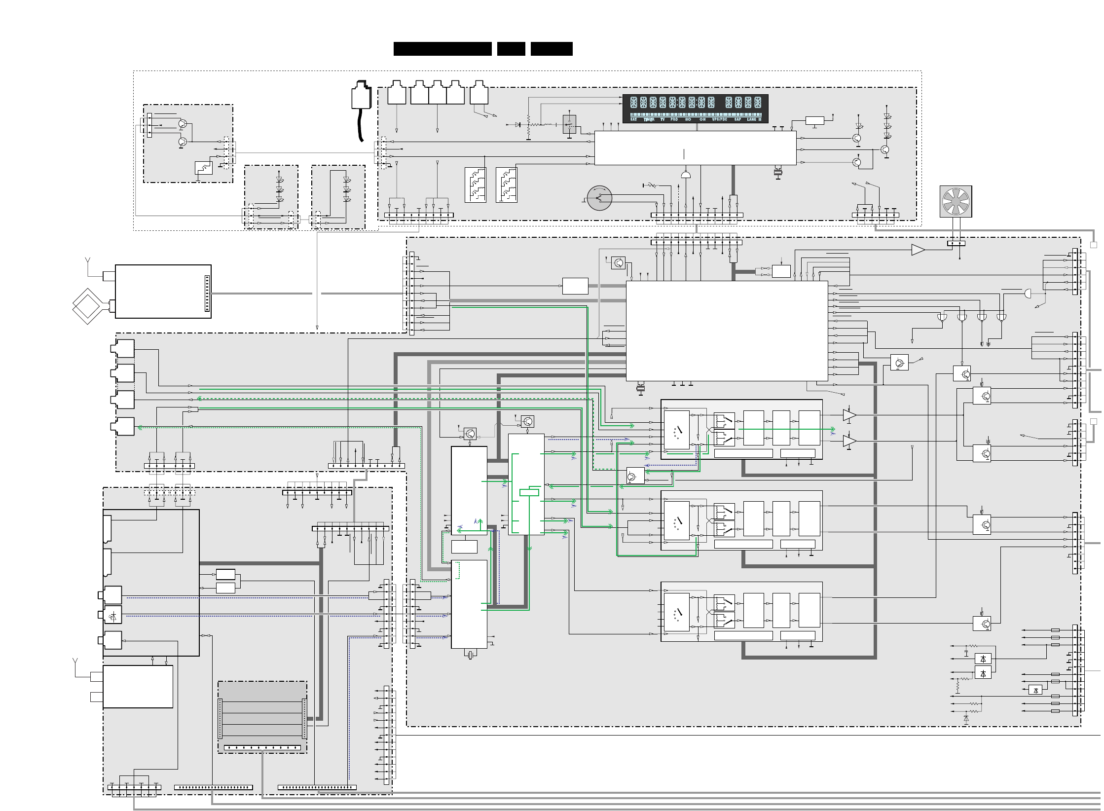
EN 616.LX7500RBlock & Wiring Diagrams
BLOCK DIAGRAM 1
Block diagram 1 LX7500R, 251104
DIGITAL
IN
coax
ANALOG IN 1
ANALOG IN 2
INPUT/OUTPUT PROCESSING
&
SOURCE SELECTION
DAOUT
1951
1940-1
1940-2
7581
OPT. IN
1949
COMP.
VIDEO
OUT
1952
1
9
1950
1943
13
101
1900 22
21
1
19471946
COMPONENT VIDEO OUT
122
1942 19
1953
13
AIN1R
AIN1L
AIN2L
AIN2R
1934
13
1
17
AV BOARD
(Analog Video Board)
for details see
separate block diagram
AINFR
AINFL
CVBSFIN
NC
CFIN
YFIN
Y
PB
PR
5V
5V_OPT
5N
5N_STBY
5V_STBY
33V_STBY
12V_STBY
3V3
IPFAIL
ION
STBY
AUDIO I2SVIDEO
ANALOG AUDIO / VIDEO
ADC
DAC
TV OUT
TV TUNER
CENTRAL CONTROLLER
SUB BOARD
P50
CLOCK & BACKUP
CONTROL µP
1986
110
5V_STBY
SCL_CECO
SDA_CECO
INT_CECO
IPOR_DC
CECO_RST
NTC_FRONT
12V_STBY
I2C BUS
I2C BUS
I2C BUS
1100 112
1202
TU_SD
NC
1
11
1300
10
1
1018
1
8
1302
1
6
1020
1
6
9V_TUNER
TU_RDS
+5V
+5V_STBY
+12V_STBY
VGNSTBY
TU_RIGHT
DOWNMIX_L, R
TU_CE
TU_DI
TU_CLOCK
DIG_IN
OPTICAL_IN
TU_LEFT
TU_stereo
MUX_L, R
DOWNMIX_L, R
DAC_L
LINE 1
LINE 2
DAC_R
I2C BUS
SOURCE
SELECTOR VOLUME I
SUR
SUR SOUND VOLUME II
7207
Source Selector & Soundprocessor
L, R FRONT SPEAKERS
I2C BUS
AF_I2C_SDA, SCL1
I2C Control
5, 24
12
17
7, 22 13, 14, 15 1 27 28
6, 23
4, 25
3, 26
8
21
Power Supply
+9V2
SOURCE
SELECTOR VOLUME I
SUR
SUR SOUND VOLUME II
7303
Source Selector & Soundprocessor
SUBWOOFER&CENTER SPEAKER
I2C Control
6, 23
12
17
7, 22 13, 14, 15 1 27 28
8
21
Power Supply
+9V2
AF_I2C_SDA, SCL2
3, 26
5, 24
4, 25
DAC_CENTRE
LINE_L, R
DAC_L, R
DI_I2C_SDA
DI_I2C_SCL
AF_I2C_SDA
AF_I2C_SCL1
MUTE_SW
AF_I2C_SCL2
AF_I2C_SCL3
TEMP
Rotary A
Rotary B
INT
POR_DC
ADC_IN_L, R
NTC_Amp
AMP_LEFT
HP_DET
HP_DET
HP_RIGHT
HP_LEFT
AMP_RIGHT
LR_AMP_ON
AMP_CENTRE
AMP_SR
AMP_SL
AMP_SUB
NC
NC
SUR_ON
FREQU_HOP
AMP_ERR
MUX_L, R
DAC_SL, R
MUTE
XMUTE_ALL
MuteHP
SET_FAN_CTRL
MuteHP
MuteCentre
MUTE_ALL
MUTE_SW
(MUTE LINE)
MUTE_LINE
IPFAIL
IPFAIL
IPFAIL
MUTE AMPL.
INV_ON
PDN_MUTE
SUR_ON
3, 26
5, 24
I2C BUS
SOURCE
SELECTOR VOLUME I
SUR
SUR SOUND VOLUME II
7214
Source Selector & Soundprocessor
SURROUND SPEAKERS
I2C Control
4, 25
6, 23
12
17
7, 22 13, 14, 15 1 27 28
8
21
Power Supply
+9V2
AF_I2C_SDA, SCL3
DAC_SL
DAC_SR
AMP_ON
POWER_ON
STBY
7204-1
NJM4556AM
+HP
L
R
L
R
7204-2
NJM4556AM
+HP
CENTRE
SUB
MUTE
MUTE
MUTE
MUTE
7301
7206
7211
7210
1200-3
LINE OUT
1200-2
1200-1
LINE IN1
LINE IN2
1702
DIGITAL
OUT
coax
AIN1R
AIN1L
AIN2L
AIN2R
LINE_IN1
ANALOG_IN1
DAC_SUB
DAC_CENTER
ANALOG_IN2
TUNER L, R
LINE_IN2
LINE_OUT
SPDIF
1205 61
DAC_SUB
7201
7108
EEPROM
CLOCK
GENERATOR
+µP
5
6
8
DI_I2C_SDA
DI_I2C_CLK
I2C BUS
RESET
RESET
+µP
RDS
DECODER
SAA6581T
7109
+µP
+µP
NTC_Amp
LR_CSub_ON
LR_CSub_ON
FREQU_HOP
1022
230
FAN
+12V_A
21
FAN CONTROL
AMP_ERR
IPFAIL
INV_ON
AMP_ON
POWER_ON
STBY
1102 110
IPOR_DC
NC
NTC_FRONT
NTC_FRONT
INT_CECO
CECO_RST
12V_STBY
SCL
SDA
IPOR_DC
DSP_RST
INT_CECO
CECO_RST
1024
1810
1
12
+5VSTBY
3V3STBY
+µP
HPREF
5NSTBY
VGNSTBY
+12V_A
9V_TUNER
+HP
+9V2
-5V_A
+5V_A
+5V
+3V3
1025
1030
1026
1029
1028
1023
1097
!8x
!
LM2931
7308 7501
+
+1V25
1701
1
9
SPDIF
7603
7505
DSP_RST
CODEC_
RST
CODEC_
RST
7405
I2S BUS
I2S BUS I2C BUS
I2S BUS
+3V3
+1V25
+3V3 +5V_A
+3V3
LD1086D
RESET
+3V3
RESET
+3V3
MUTE
7107
MICRO PROCESSOR
TMP88CU74F
10
25
26
33
2
14
3, 4
56
35
54
59
53
61
23, 24
62
64
50
75
52
34
57
12
5
6
11
45, 46
43
41
42
36,16
VAREF
VDD
VKK
VASS
40
39
38
78
VSS
7
58
70
AK4112A
SPDIF
RECEIVER
12
14
4
13
11
12
1, 3
2, 10
CODEC
12
DSP
45
69
47
I2C BUS
SIGNAL PATH "ANALOG IN"
SIGNAL PATH "DIGITAL IN"
PROC.
DIGITAL
VIDEO IN
IEEE1394
to
DIGITAL Board
1203
DISPLAY/CONTROL BOARD
1910 121
+5VSTBY
VGNSTBY VKK
+12VSTBY
DI_I2C_SDA
DI_I2C_SCL
TEMP
INT
POR_DC
7110
7104
1110
Rotary B
Rotary A
8 MHz
+5VSTBY
+5VSTBY
+12VSTBY
COMBI BOARD
I2C BUS
7103
MICRO PROCESSOR
TMP87CH74F
VDD
VKK
VKK
VKK
INT0
VSS
VASS
VAREF
14
69
40
39
7
8
9
1017
12 MHz
15
RESET10
38
78
VOLUME
1111 NTC
AMBIENT TEMP.
STAND BY
FLASH
6104
7105
12
11
19
45
1
FIL1
FIL2
36
37
RECORD
6103
6102
6101
+5V_STBY +5V_STBY
+5V_STBY
+5V_STBY
7107
31
2
IR EYE
7112
3
1911
TRAY_LED
KEY 1
KEY 2
4
1
KEY MATRIXKEY MATRIX
+12VSTBY
HP_RIGHT
HP_LEFT
HP_DET
1920 1923
from 1924
1921
AUDIO L
AUDIO R
CVBS
S-VIDEO
1922
1924
to Headphone socket
19
AINFR
AINFL
CVBSFIN
NC
CFIN
YFIN
AV FRONT CONNECTORS
(CAM 1)
HEAD-
PHONE
p
16
1600
24.576 MHz
8
9
AM-FRAME AERIAL
FM
AUDIO TUNER
TRAY LIGHT left TRAY LIGHT right
STAND BY BOARD
1930
4
1
1931
1
3
1940
1
3
1941
2
1
1950
2
1
+12VSTBY
6402
6401
6400
+5V_STBY
6402
6401
6400
7300
7301
TRAY_LED
TRAY_LED 1
TRAY_LED 2
1130
STANDBY - ON
+12VSTBY
+12VSTBY
TRAY_LED 1
TRAY_LED 2 TRAY_LED 2
7100
8020
to sheet 2, 1900 Dig. board
to sheet 2, 1300 AUX. Supply board
to sheet 2, 1104Dig. board
to sheet 2, 1904 Dig. board
to sheet 2, 1704 Dig. board
to sheet 2
AUX. Supply
board, 1305
to sheet 2
AUX. Supply
board, 1304
to sheet 2
AMPLIFIER
board , 1302
to sheet 2
AMPLIFIER
board , 1331
FRONT PANEL
F
F
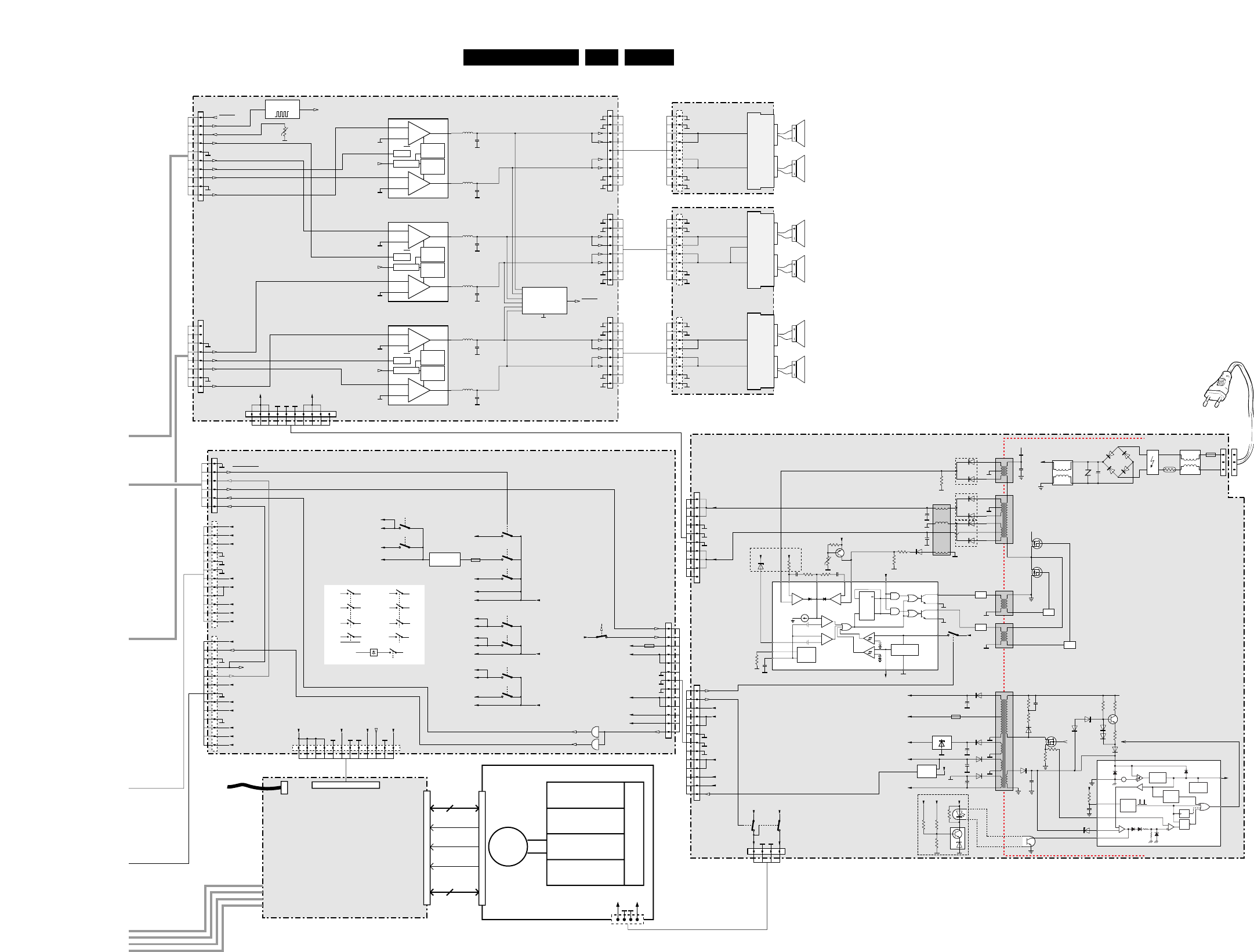
EN 626.LX7500RBlock & Wiring Diagrams
Block diagram 2 LX7500R, 221104
F1 J1
L1A
EMI FILTERVDR1
VDR2 L1B
TH1
10Ω NTC 3
1
3
1
!
F2
!
!!
!
!
!
!
!
!
!
!
!
+
+
L3A
EMI FILTER
L3B
Z8 R51
L4A
+ AMP
– AMP
-
+
+
+
+
T1
T4
L12
AB
AB
C
D
E
L11
Q1
Q2
ϕ
ϕ
-
!
!
T2
C
D
H
G
F
E
-
AB
D14
D10
D20
C9
C7
+
C1
+
C27
J1
1
10 NC
+ AMP
NTC
+ 12V
+ 12V
+ 12V
+ 12V
+ 5V
+ AMP
OVER-VOLTAGE
DETECTION VOLTAGE SENSE
PRIMARY CURRENT LIMITATION
+ 12V
+12V
6
5
4Deadtime
Control
Oscillator
0.12V
0.7V
0.7mA
+
-
-
+
-
+
+
-
DQ
Ck
-
+
+
-
3.5V
4.9V
13
Reference
Regulator
Q2
Q1
8
9
11
10
12
VCC
16 15 3 2 1
12
14 7
Feedback
PWM
Ref. Output
Ref1
Gnd
UV
Lockout
Flip-
Flop
Output Control
Error Amp 1Error Amp 2
Deadtime
Comparator
PWM
Comparator Q
TL494CN
U1
+ 5V
+ 33V
-5V
-28V
Ref2
Ref2
Ref1
Q15
C26
SNUBBER
NETWORK
R38/
R74
R75/
R100
R34/
R67
CURRENT
SENSE
LOW VOLTAGE
DETECTION
D17 Q9
TEMP.
HEATSINK H3
J3
J4
1
13
-28V
IP_FAIL
+33V
+12V
AMP_ON
-5V
IDE_OFF
+5V
+12V0
+5V0
SWITCHED MODE POWER SUPPLY
-
-
-
ϕ
ϕ
Internal
Bias
Vref
Good
Logic
OSC
5-V REF
Error
Amplifier PWM
Latch
Current-
Sense
Comparator
34V nom TL3842
U2
V
CC
GND
RT/CT
VFB
COMP
ISENSE
7
5
4
2
1
3
8
10
REF
OUT
+
–
UVLO
EN
2R
R V1
S
R
T†
+
–
L4B
L4D
+ 5V
+ 5V
-
-
U3
reference
regulation
PC1-A
PC1-B
PRIMARY
D7
+
+
+
C16
C38
D2
D8
C41
D36
1
2
3
POWER
FAIL
DET.
14
AUXILIARY SUPPLY BOARD
1301
1
13
1300
1
13
1305
1
12 AMP_ON
IDE_OFF
+5V_STBY 7301
7310
7302
7308
7300
7303
7305
7322
7306
7309
+12V_DIGI
-28V
+33V_STBY
+12V
-5V_STBY
+5V_STBY
1307
F1.0A
!
IP_FAIL
IP_FAIL_AV
IP_FAIL_COMBI
1304
1
6
IP_FAIL_COMBI
INV_ON
AMP_ON
POWER_ON
STANDBY
1303 112
+3V3_DIGI
+12V_DIGI
+12V_STBY
+3V3_AV
+5V_AV
-5V_AV
+5V_A
+5V_COMBI
+12V_A
-5V_A
-5V_STBY
+5V_STBY
+33V_STBY
+5V_STBY
-5V_STBY
-28V
+5V_DIGI
INV_ON
-5V_DIGI
IP_FAIL_AV
INV_ON
+3V3_COMBI
STANDBY
+12V+12V
+12V_STBY
+12V_DIGI
INV_ON
+12V_A
+12V_A
+33V_STBY
+3V3
+3V3_COMBI
+12V_DIGI
+3V3_DIGI
+3V3_AV
DC/DC
CONVERTER
+5V_STBY
+5V_STBY
+5V_A
+12V_A
+5V_AV
+5V_DIGI +12V_DIGI
+5V_COMBI
-5V_STBY
-5V_STBY
-5V_A
+12V_A
-5V_AV
-5V_DIGI +12V_DIGI
1306
F2A
!
1302
7100
1
10
1306
9
1
1331
1
10
ERROR
FREQU_HOP
NTC_AMP
AMP_LEFT
SUR_ON
L/R ON
AMP_CENTRE
CLOCK FRONT SPEAKERS
CENTRE SPEAKER + SUBWOOFER
SURROUND SPEAKERS
AMP_RIGHT
CSUB_ON
AMP_SR
AMP_SUB
NC
NC
NC
AMP_SL
CLOCK
CLOCK
CLOCK
CLOCK
GENERATOR
NTC TEMPERATURE
HEATSINK
Front Left
Front Left
Front Right
Front Right
Subwoofer
Subwoofer
Centre
Centre
Surround Right
Surround Left
Surround Right
Surround Left
+
-
-
+
MODE
PWM
MODULATOR
PWM
MODULATOR
OSCILLATOR
ON / OFF
9
16
21
8
6
7
5
4
TDA8920/TDA8924
7200
+
-
-
+
MODE
PWM
MODULATOR
PWM
MODULATOR
OSCILLATOR
ON / OFF
9
16
21
8
6
7
5
4
TDA8920/TDA8924
7300
+
-
-
+
MODE
PWM
MODULATOR
PWM
MODULATOR
OSCILLATOR
ON / OFF
9
16
21
8
6
7
5
4
TDA8920/TDA8924
AMPLIFIER BOARD LS SOCKET BOARD 2
LS SOCKET BOARD 1
1309
110
Vdd Vss
NC
1308
8
1
1307
ERROR
to 1302/9
8
1
1925
9
1
1935
8
1
1936
8
1
DC
DETECTION
BE_FAN
RESETN_BE
BE_LOADN
S2B
FRONT-END I2S
DVD & RW ENGINE
TRAY CONTROL
SERVO
READ
WRITE
DISC
7
DATA
&
CONTROL
LASER
1600
1102
1500
+5V
+12V
5
DIGITAL BOARD
for details see
separate block diagram
1203
8020
from sheet 1
IEEE1394
from sheet 1
1018 COMBI board
from sheet 1
1300 COMBI board
from sheet 1
1020 COMBI board
from sheet 1, 1900 A/V board
from sheet 1
1934 A/V board
from sheet 1
1810 COMBI board
from sheet 1, 1986 uP sub- board
from sheet 1, 1947 A/V board
from sheet 1, 1946 A/V board
to 1900 Dig. board
to 1104 Dig. board
to 1904 Dig. board
to 1704 Dig. board
INOUT
+3V3 +12V
+33V_STBY
+12V+12V_DIGI
+12V_DIGI
INV_ON
+5V_STBY+5V_AV
+5V_DIGI
-5V_STBY-5V_AV
-5V_DIGI
+12V+12V_A
+12V_A
+5V_STBY
+5V_A
+5V_COMBI
-5V_STBY
-5V_A
+3V3+3V3_AV
+3V3_DIGI
POWER_ON
+3V3+3V3_COMBI
BLOCK DIAGRAM 2
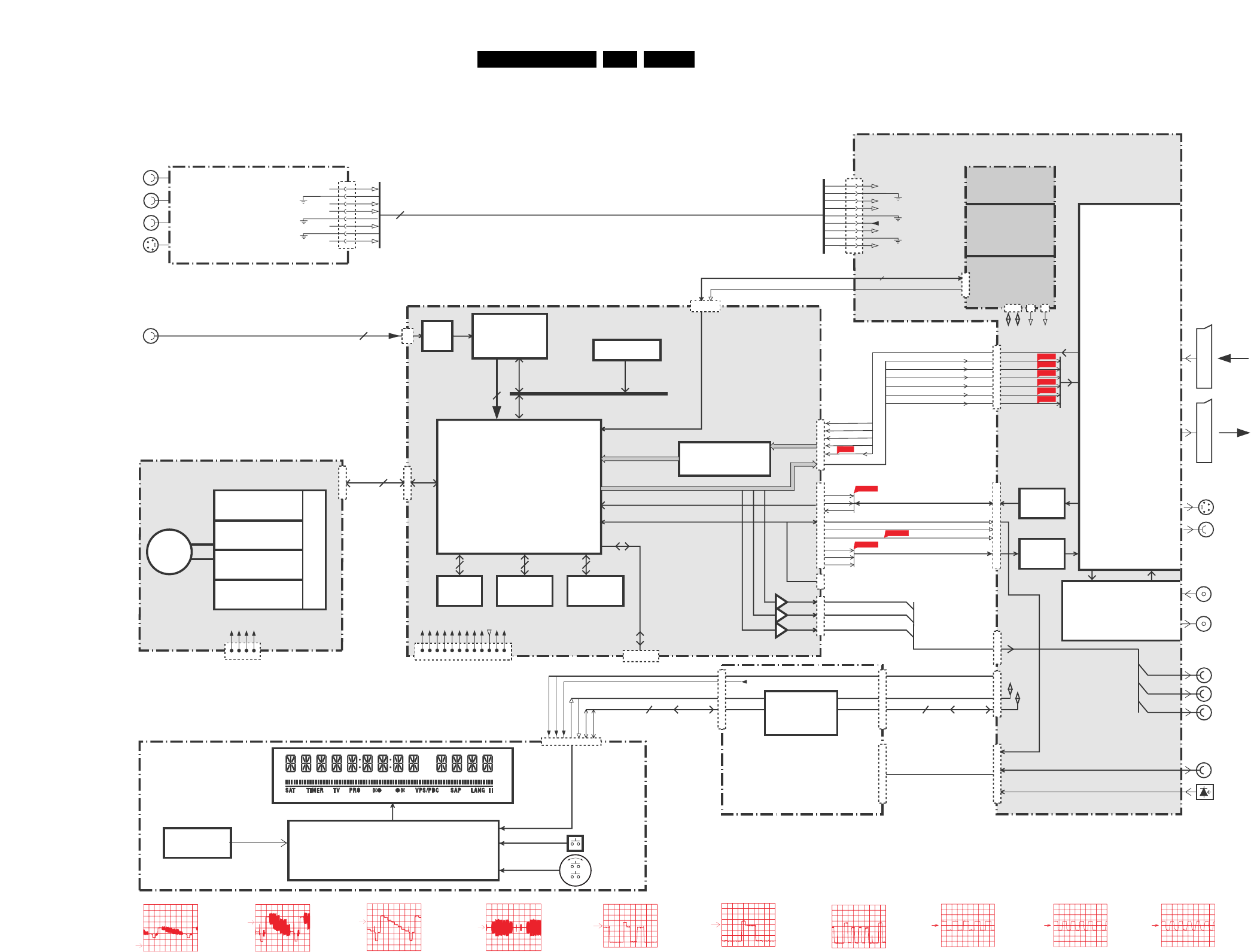
EN 636.LX7500RBlock & Wiring Diagrams
Overall Block Diagram Digital Board Chrysalis
FRONT
Analog input
Digital Video Input
IEEE 1394
UART3: GATEWAY
IRESET_DIG
CVBS-RGB-Y/C
AUDIO PCM I2S
DAOUT
DAOUT
DIG AUDIO IN
OPT AUDIO IN
MUTEN
D_PCMCLK
AUDIO ENCODER I2S
ANALOG AUDIO VIDEO
CVBS_OUT_B
C_OUT_B
Y_OUT_B
V_OUT_B
Y1_OUT_B
U_OUT_B
V_IN
U_IN
Y_IN
C_IN
4
9
DVD+RW ENGINE AV3.5
TRAY CONTROL
SERVO
READ
WRITE
DISC
INFRA RED
EYE
DISPLAY & CONTROL BOARD
PSU
IPOR_DC, INT_CECO
I2C
2
CLOCK &
BACKUP
TV TUNER
INPUT/OUTPUT
PROCESSING &
SOURCE
SELECTION
DAC
CONTROL
uP
P50
ANALOG VIDEO BOARD
LASER
+12Vstby
-Vgnstby
SCL
SDA
INT
POR_DC
5STBY
2
1
AFCRI
AFCLI
CVBSFIN
CFIN
YFIN
3
4
5
7
8
9
1922
1203
1942
1947
1986
1900
1943
1952
1100 1102
1701
1910
6 4 10 7 5 11 12
1900
1104
6
S-VIDEO
CVBS
AUDIO R
AUDIO L
AFCRI
AFCLI
CVBSFIN
8SW
CFIN
YFIN
ADC
1
2
3
4
5
6
7
8
9
12
14
16
18
20
22
1
STANDBY - ON
OPEN/CLOSE
SOURCE
PLAY
STOP
RECORD
NEXT
PREVIOUS
VOLUME
I2C
2
FRONT PROCESSOR
UP SUB BOARD
10
DIGITAL BOARD CHRYSALIS 2.1
COMBI BOARD
SDRAM
FLASH
VIDEO INPUT
PROCESSING
ANALOG VIDEO
DIGITAL AUDIO
DIGITAL AUDIO
RS232
SERVICE
PCI BUS
1500 1103
1904
PSU
1
2
4
6
8
1234567
+3V3
+3V3
+3V3
+3V3
GND
GND
GND
ION
+5V
+12V
8
1
91011
GND
-5V
12
DIG.VIDEO 656
20
21
18
221
7
9
11
12
14
22
20
18
16
14
PHY LINK
2
1901
CHRYSALIS PNX7100
MPEG 2, AC3 CODEC
BOOT
EEPROM USRDATA
EEPROM
I2C I2C
ION STBY
1987
1984
22
Y
Pb
Pr
AUDIO DIGITAL IN
COMPONENT
VIDEO
OUT
ANTENNA INPUT
TV OUT
AUDIO OPTICAL IN
S-VIDEO
SCART II
AUX-
I/O
SCARTI
TO TV
- I/O
CVBS
1946
1102
40
1600-1
PSU
+5V
GND
GND
+12V
1600-2
ATAPI INTERFACE
I2C
I2C, INT
IPOR
1980
IPOR, INT
A_WCLK
A_BCLK
A_DATA
D_DATAO
A_WCLK
A_BCLK
CVBS_Y_IN
A_YCVBS F4709 D_CVBS F4712
D_Y F4714
2V / div AC 10us / div 2V / div AC 200ns / div
AD_WCLK; AE_WCLK AD_BCLK; AE_BCLK
2V / div AC 50ns / div
AD_ACLK
D_C F4716
A: DC, 200mV/Div
10us/Div
D_R F4718 D_G F4720 D_B F4722
A: DC, 500mV/Div
10us/Div A: DC, 200mV/Div
10us/Div
A: DC, 200mV/Div
10us/Div
A: DC, 200mV/Div
10us/Div
A: DC, 200mV/Div
10us/Div A: DC, 200mV/Div
10us/Div
DVD PART LX7500R, 09112004
1704
D_Y
UI
VI
+5VSTBY
COMBI BOARD µP
7107
2
5
8
F4712
F4714
F4716
F4718
F4720
F4722
F4709
AE_xCLK
AD_xCLK
AD_ACLK
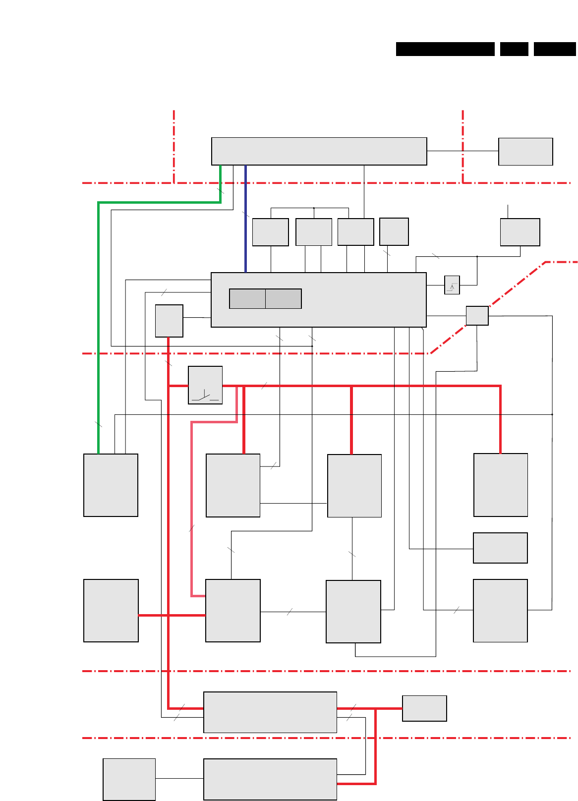
EN 646.LX7500RBlock & Wiring Diagrams
µP-Sub Board
Display Control Board
Combi Board
Analog Board
Digital Board Basic Engine
BE
ext. Latch ext. RAM ext. Flash
int. RAM int. ROM Central-µP
TMP91CW12AF (3,3V Supply)
AD0-AD7
A8-A16
A8-A19
AD0-AD7
AD0-AD7
A0-A7 A0-A7 WE
Digital Board
WE
Reset-IC
P50
=
>1
KILL
AKILL
I2S
IPFAIL
I2S
FBIN
FBIN
IPFAIL
IPOR
Reset
INT only
Sense 3V3STBY
ADC/DAC
(UDA1334BTS
UDA1361TS)
Frontend
Video
Frontend
Audio
(MSP)
DataSlicer
(STV5348)
Follow Me
EEPROM
(M24C16)
IO
Video
(STV6618)
IO
Audio
(HEF IC'S)
Power
Supply
Front µP
TMP87CH74F
Combi µP
TMP88CU74F
Display
I2C
Level
Shifter
I2C 3,3V
I2C 5V
AKILL
I2C
I2C
INT
IPOR_DC INT
POR_DC
Blockdiagram
Control Lines and Bus Systems DVD+RW part
I2C
SWITCH
5SW
I2C_SW
PSS
SB1
SFS_TS
AFC
AGC
A_DATA
D_DATA
A_RDY
D_RDY
IRESET_DIG
PWONSW
WU
WSFI
FBIN
P50
8SC2
STBY
ION
I2C_SW
I2C_SW
I2C_SW
VSA1
ASC1S
VSA2
3
2
5
2
2
2I2C
2
22
2
2
2
8
8
5
5
5
2
5
RSA1
RSA2
SIF1
FOME
INT, IPOR_DC
P50in
P50out
ASC1M for EUROPE only
I2C_SW (for NAFTA only)
2
I2C
(for EUROPE
only)
LEVELSW
For EUROPE only
Blockdiagram Control lines and bus systems LX7500R, 09112004
EEPROM
(M24C02)
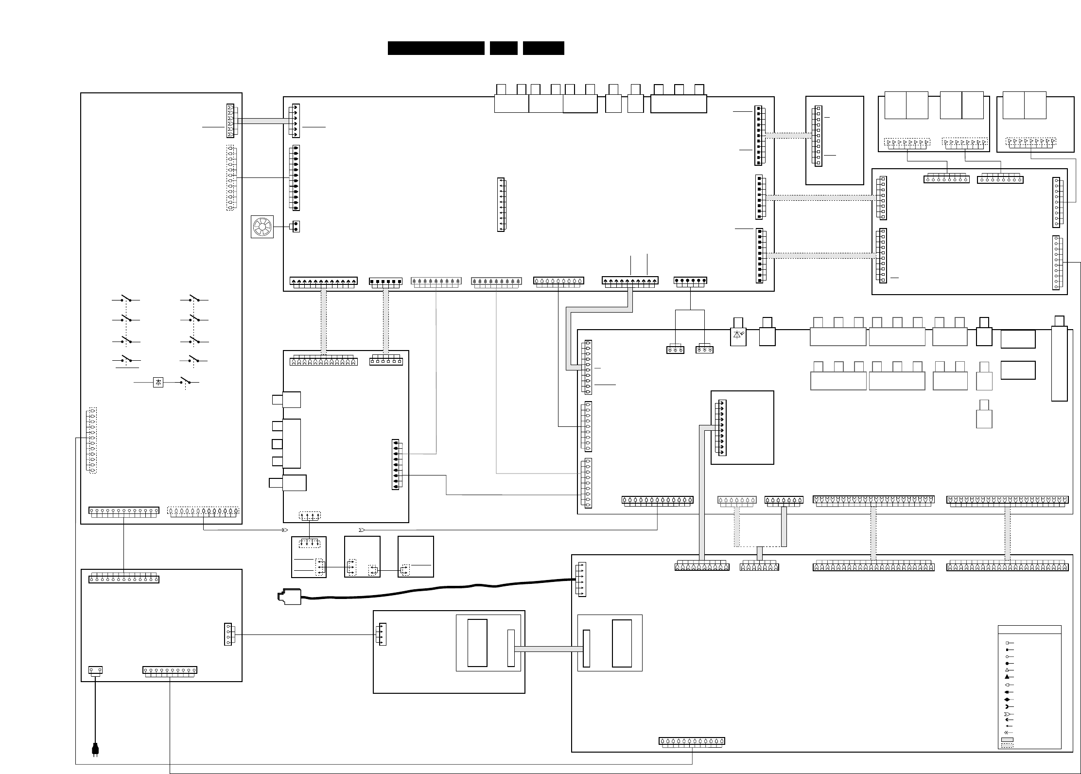
EN 656.LX7500RBlock & Wiring Diagrams
9
1
FRONT BOARD
1
11 11
AINFL
GND_FC
AINFR
GND_FC
CVBSFIN
NC
GND_FC
CFIN
YFIN
6
FFC SIDE ENTRY 1.25
EH TOP ENTRY
EH SIDE ENTRY
DIPMATE
BOARD to BOARD JQ
FFC TOP ENTRY 1.25
LEGEND
PH TOP ENTRY
PH SIDE ENTRY
XH SIDE ENTRY
FLASH TOP ENTRY
FFC TOP ENTRY 1.0
FFC SIDE ENTR
Y 1.0
SPECIAL
HEADER
FFC 1 to 1 (AD)
STANDBY
SWITCH
1911
1930
1931
TRAY LIGHTING
RIGHT
TRAY LIGHTING
LEFT
1940
1941 1950
8025
8026 8024
1924
1922
11
AUDIO TUNER
GND_A
NC
SD
9V_TUNER
RDS
RIGHT
CE
LEFT
DI
Stereo
CLOCK
12VSTBY
GND
ION
STBY
5V
5N
5NSTBY
5VSTBY
33VSTBY
GND
3V3
13
IPFAIL
GND
AV_BOARD
NTC_FRONT
IRESET_DIG
A_DATA
D_DATA
A_RDY
GND
GND
PR
PR
GND
GND
PB
PB
GND
GND
Y
Y
GND
GND
D_RDY
N.C.
WE
(BE_FAN)
FBIN
GND_D
CECO_RST
IPOR_DC
INT
GND
GND
5VSTBY
12VSTBY
SDA
SCL
1
1
1
1
1
1
10
1943
AIN1R
GND
AIN1L
AIN2L
GND
AIN2R 1
1
9
1
AINFL
GND
AINFR
CVBSFIN
GND
NC
GND
CFIN
YFIN
1942
7
7
1
10
1934
Sub µP
OPUS
1986
SPDIF_IN
1951
OPTICAL_IN
7581 E1
TV-TUNER
GND
HP_LEFT
SPDIF_DVD
GND_ALR / GND_HP
GND
HP_RIGHT
5V_OPT
HP_DET
OPTICAL_IN
GND
DIG_IN_-
DIG_IN_+
GND
12
9
9
1
8022
GND
POWER_ON
STBY
IP_FAIL
AMP_ON
INV_ON
COMBI_BOARD
AUX AV
1
8
1
6
1
10
FAN
+12FAN
1
NTC_FRONT
CECO_RST
IPOR_DC
12VSTBY
INT_CECO
GND
GND
NC
SDA
SCL
NC
SurON over 10K
GND_ACS
AMP_SUB
SurON
AMP_SR
GND_AS
AMP_SL
1810
1102
1205
AIN1R
AIN2L
GND
GND
AIN1L
AIN2R
1
1020
1
1
AINFL
AINFL
GND_V
GND_V
AINFR
AINFR
GND_V
GND_V
CVBSFIN
CVBSFIN
GND_V
GND_V
GND_V
GND_V
CFIN
CFIN
YFIN
YFIN
1
11
GND_A
NC
TU_SD
9V_TUNER
TU_RDS
TU_RIGHT
TU_CE
TU_LEFT
TU_DI
TU_Stereo
TU_CLOCK
1202
GND
GND
GND
+12V_A
- 5V_A
+5V_A
+5V
+3V3
+3V3
+5VSTBY
5NSTBY
VGNSTBY
11
10
AMP_ERR
Freq_HOP
NTC_Amp
LR_CSub_on
GND_ACS
AMP_CENTRE
LR_CSub_on
AMP_RIGHT
GND_ALR
AMP_LEFT
1300
1018
1701
1302
1403
9
1
GND_D
CLOCK
GND_D
MODE_SELECT
GND_D
DATA_OUT
GND_D
DATA_IN
GND_D
TEST_RESET
1
1601
JTAG Interface
SPDIF
SVHS
1702
1400
OUT
OUT
9
1
GND
SPDIF_DVD
GND
5V_OPT
OPTICAL_IN
GND
DIG_IN_-
DIG_IN_+
GND
1940-1
1
1
22
22
GND
D_WCLK
GND
GND
A_YCVBS
D_BCLK
GND
GND
A_C
A_PCMCLK
GND
GND
A_G
A_DAT
GND
GND
A_B
A_WCLK
GND
A_BCLK
A_R
GND
D_CVBS
D_DATAO
GND
GND
D_Y
D_PCMCLK
GND
GND
D_C
D_IKILL
D_G
NC
GND
DAOUT
D_B
GND
GND
NC
D_R
NC
GND
NC
1900
1947
HP_LEFT
GND_ALR / GND_HP
HP_RIGHT
HP_DET
1
10
(TrNTC)TEMP
Vss
Vss
Vss
GND_D
GND_D
GND_D
Vdd
Vdd
Vdd
1
1
10
1
9
9
1
8
1
1
1
8
8
8
LS Socket Board 1 LS Socket Board 2
SVHS IN
Headphone
Audio IN
L
R
1949
For /17 only For /17 only For /17 only For /01/04/05 only For /01/04/05 only
For /01/04/05 only
For /17 only For /17 only For /17 only For /17 only
COMP.
VIDEO
OUT
REAR IN
YUV
REAR IN 1
LRCVBS
1941-C
LR
REAR IN 2
1941-B 1941-A
E2
SCART
1940-2
1949
SVHS
OUT
1948
For /17 only
SVHS
IN
REAR OUT
YUV
REAR OUT 1
LRCVBS
1944-C
LR
REAR OUT 2
1944-B 1944-A
OUT
LRCVBS
1402
NC
GND_ACS
SUBW
SurON
SUR_
R
GND_AS
SUR_L
ERR
FREQ_HOP
TEMP
CSub_on
GND_ACS
CENTRE
LR_on
RIGHT
GND_ALR
LEFT
AMPLIFIER BOARD
1935
1936
1925
1930 1931 1920
Easy Conn. Easy Conn.
Easy Conn.
8038
8042 / shielded
8012 (only used in /01)
8031/ shielded (only used in /17)
8006 / shielded (only used in /17)
1200
1921
1923
CVBS IN
1920
8018
8019
8017
1
L
L
GND_L
GND_L
NC
R
R
GND_R
GND_R
LR
Center Sub
GND_S
GND_S
SUBw
SUBw
GND_C
GND_C
CENTER
CENTER
SL SR
GND_SR
GND_SR
SR
SR
GND_SL
GND_SL
SL
SL
1946
1946
1952
8036
1302
1331 1306
1307
1308
1309
1
1401
1022
1
1
3103 308 9446.
3103 308 9426.
RotaryB
RotaryA
TEMP
VGNSTBY
POR_DC
12VSTBY
12VSTBY
12VSTBY
12VSTBY
TRAY_LED2
TRAY_LED2
TRAY_LED1
KEY 1
GND
TRAY_LED
INT
GND
GND
5VSTBY
DI_12C_SDA
DI_12C_SCL
1
11
12
1910
RotaryB
RotaryA
TEMP
VGNSTBY
POR_DC
12VSTBY
INT
GND
GND
5VSTBY
DI_12C_SDA
DI_12C_SCL
1
12
1100
3103 308 9503.
3103 308 9439.
3103 308 9427.
3103 308 9422.
3103 601 0031.
3103 308 9491.
3103 308 9431.
3103 308 9428.
3103 308 9423. 3103 308 9425.
3103 308 9424.
3103 601 0018.
3103 601 0016.
3103 601 0017.
GND
8
GND
GND
GND
GND
6
1950
1953
wiring diagram LX7500R, 181104
WIRING DIAGRAM LX7500R
FAN
8004 / BD
8016 / BD
8005 / AD
8010 / BD for /17
8039 / AD for /01
3103 308 9435.
3103 308 9489.
SCART
FFC 1 to n (BD)
1
1
4
J4
J3
J2
J1
1301
1305
1304
1300
1303
SWITCHED MODE
POWER SUPPLY
Mains
13
VH
10
INOUT
+3V3 +12V
+33V_STBY
+12V+12V_DIGI
+12V_DIGI
INV_ON
+5V_STBY+5V_AV
+5V_DIGI
-5V_STBY-5V_AV
-5V_DIGI
+12V+12V_A
+12V_A
+5V_STBY
+5V_A
+5V_COMBI
-5V_STBY
-5V_A
+3V3+3V3_AV
+3V3_DIGI
POWER_ON
+3V3+3V3_COMBI
GND
GND
GND
+12V_A
- 5V_A
+5V_A
+5V_COMBI
+3V3_COMBI
+3V3_COMBI
+5V_STBY
-5V_STBY
-28V
IPFAIL
-28V
+33V_STBY
+12V
+12V
GND
GND
GND
+5V_STBY
+5V_STBY
-5V_STBY
IDE_OFF
AMP_ON
IPFAIL
-28V
+33V
+12V
+12V
GND
GND
GND
+5V
+5V
-5V
IDE_OFF
AMP_ON
8002
11
13
13
1
12
1
1
6
GND
POWER_ON
STANDBY
IP_FAIL
AMP_ON
INV_ON
+12V_DIGI
GND
+3V3_DIGI
+3V3_DIGI
+3V3_DIGI
+3V3_DIGI
GND
GND
+5V_DIGI
INV_ON
GND
-5V_DIGI
12
1
+12V0
GND
GND
+5V0
13
1
NC
-AMP
-AMP
-AMP
GND_D
GND_D
GND_D
+AMP
+AMP
+AMP
8041
8000
+5V_AV
+3V3_AV
+12V_STBY
IP_FAIL_AV
GND
INV_ON
STANDBY
-5V_AV
-5V_STBY
+5V_STBY
+33V_STBY
GND
GND
3103 308 9420.
3103 308 9418.
3103 308 9488.
8033 /IEC_2422 070 98231
8034 /UL_2422 070 98235
8034 /UK_2422 070 98236
AUXILIARY SUPPLY
BOARD
3103 308 9440.
8032 / AD
3139 110 3591.
8013 / BD
3103 308 9438.
8015 / BD
3103 308 9437.
8014/ BD
DIGITAL_BOARD
+12V
GND
+3V3
+3V3
+3V3
+3V3
GND
GND
+5V
ION
GND
-5V
12
1
6
1
8001
"Chrysalis"
1
1
22
22
DVD/RW Engine
IDE Adaptor
IDE to 40p_FFC 0,5P IDE Adaptor
IDE to 40p_FFC 0,5P
GND
D_WCLK
IRESET_DIG
GND
GND
A_DA
TA
A_YCVBS
D_BCLK
D_DATA
GND
GND
A_RDY
GND
PR
GND
PB
GND
Y
GND
A_C
A_PCMCLK
D_RDY
GND
GND
NC
A_YG
A_DATA
WE
GND
GND
(BE_FAN)
A_UB
A_WCLK
FBIN
GND
A_BCLK
GND_D
A_VR
GND
D_CVBS
D_DATAO
GND
GND
D_Y
D_PCMCLK
GND
GND
D_C
D_IKILL
D_YG
NC
GND
DAOUT
D_UB
GND
GND
NC
D_VR
NC
GND
NC
1
1
10
7
1900
1203
1704
1500
1104
1904
40
40 40
40
1
1
1
4
1
1
+12V
GND
GND
+5V
PC_Con.
Fire Wire
8020
3103 308 9441.
3103 308 9419.
3103 308 9434.
3103 308 9490.
8040 / AD 0,5mm
8009 / AD
3103 308 9433.
8008 / BD
3103 308 9432.
8007 / BD
DIGITAL
VIDEO IN
IEEE1394
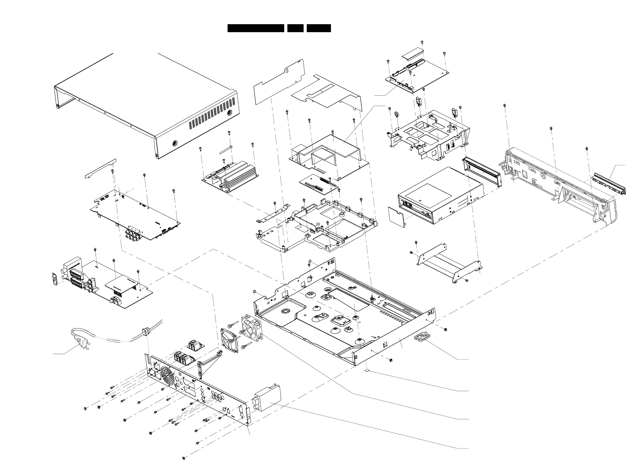
EN 666.LX7500RExploded Views
1108
SWITCHED MODE
POWER SUPPLY
Mains cord 215 fixed with
cable clamp 231
217 226
228
231
211
216
208
227
205
201-1
207
1109
230
210
1106
215
1108
201-2
2x
201-3
2x
233
232
4x
M3x4
4x
Pl. 3x8
4x
M3x4
2x
M3x4
2x
M3x4
2x
M3x4
3x
M3x8
4x
M3x4
3x
M3x4
3x
M3x4
3x
M3x6 washer
4x
M3x6 washer
5x
M3x6
4x
M3x4
M3x4
Pl.3x8
4x
Pl.3x8
11x
Pl.3x8
206
229
219
2x
204
202
214
101
!
1106
DIGITAL BOARD
1107
AMPLIFIER BOARD
1104
IDE ADAPTER
1103
AUX. SUPPLY BOARD
air guide foil
1101
COMBI BOARD
1102
AV BOARD
µP SUB BOARD
1104
IDE ADAPTER
1110
BASIC ENGINE
VAD8041/01
AUDIO TUNER
air guide foil
air guide foil
1005
1005
LS SOCKET
BOARDS
EV set LX7500R, 200904
Pl.3x8
EXPLODED VIEW / apparatus
MECHANICAL PARTSLIST
201-2 3103 604 00622 FOOT, RUBBER
201-3 3103 607 50491 FOOT ASSY
210 3103 607 90941
ORNAMENTAL COVER, TRAY LX7500R
215 !2422 070 98231 MAIN SCORD, IEC
215 !2422 070 98236 MAINS CORD, UK
230 3103 607 10051 FAN 60X60X20
1109 2422 542 90137 RADIO TUNER MODULE, EU
Only those parts of which a service code number is stated
are normal service parts.
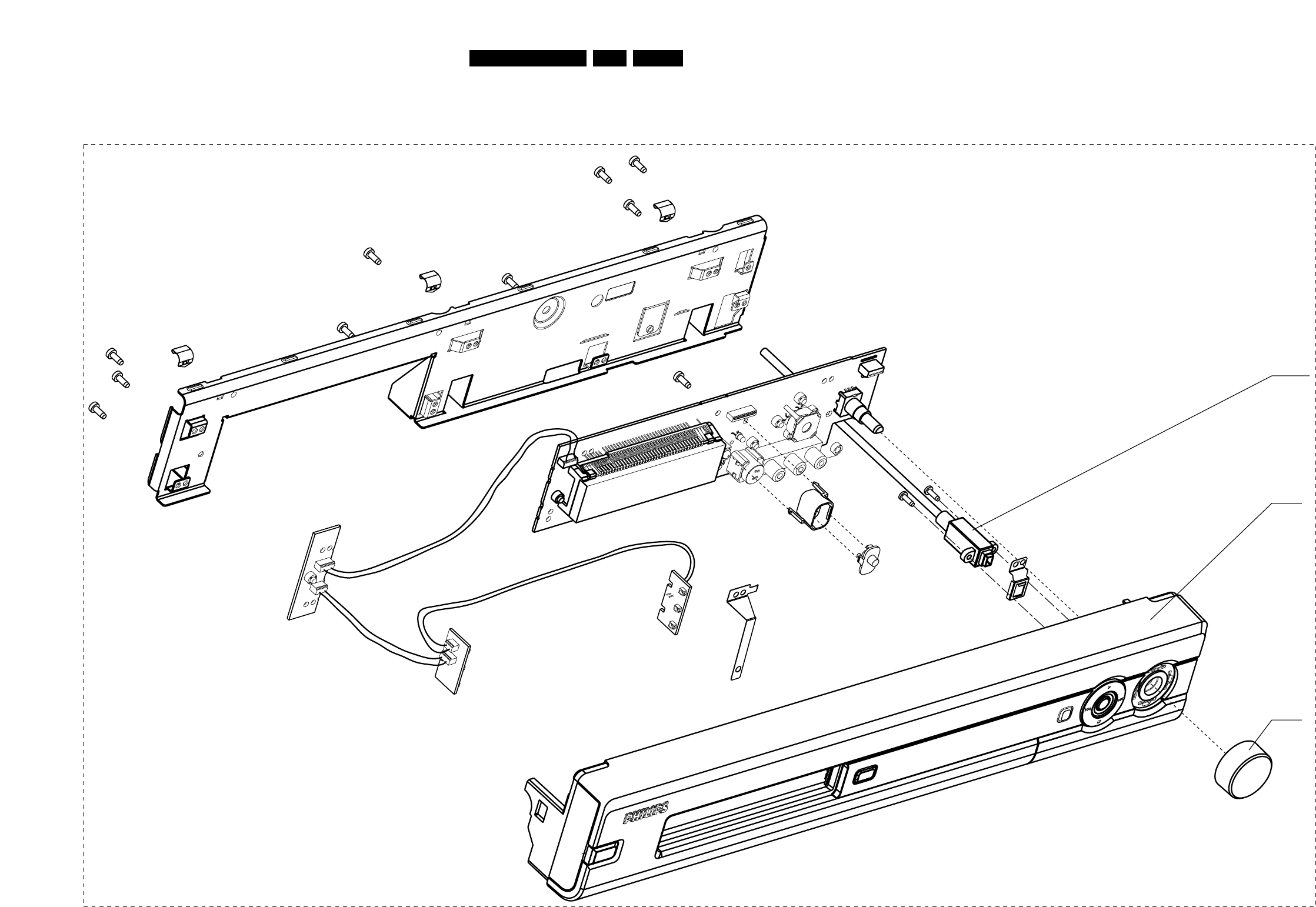
155
105
159
157
104
156
3x
8020
101
FRONT COMPLETE
Pl. 2,5x8
2x
Pl. 3x8
Pl. 3x8
9x
106
102
1001
DISPLAY BOARD
1001
STANDBY BOARD
1001
TRAY LIGHT BOARD
left
1001
TRAY LIGHT BOARD
right
EV2 front complete LX7500R, 270904
EN 677.LX7500RExploded Views
EXPLODED VIEW / Front assembly
MECHANICAL PARTSLIST
102 3103 607 90861 FRONT ASSY MECH. LX7500/01/04
102 3103 607 90981 FRONT ASSY MECH. LX7500/05
106 3103 607 51321 KNOB VOLUME
8020 3103 308 94411 FIREWIRE CABLE, 650mm, EEE1394
Only those parts of which a service code number is stated
are normal service parts.
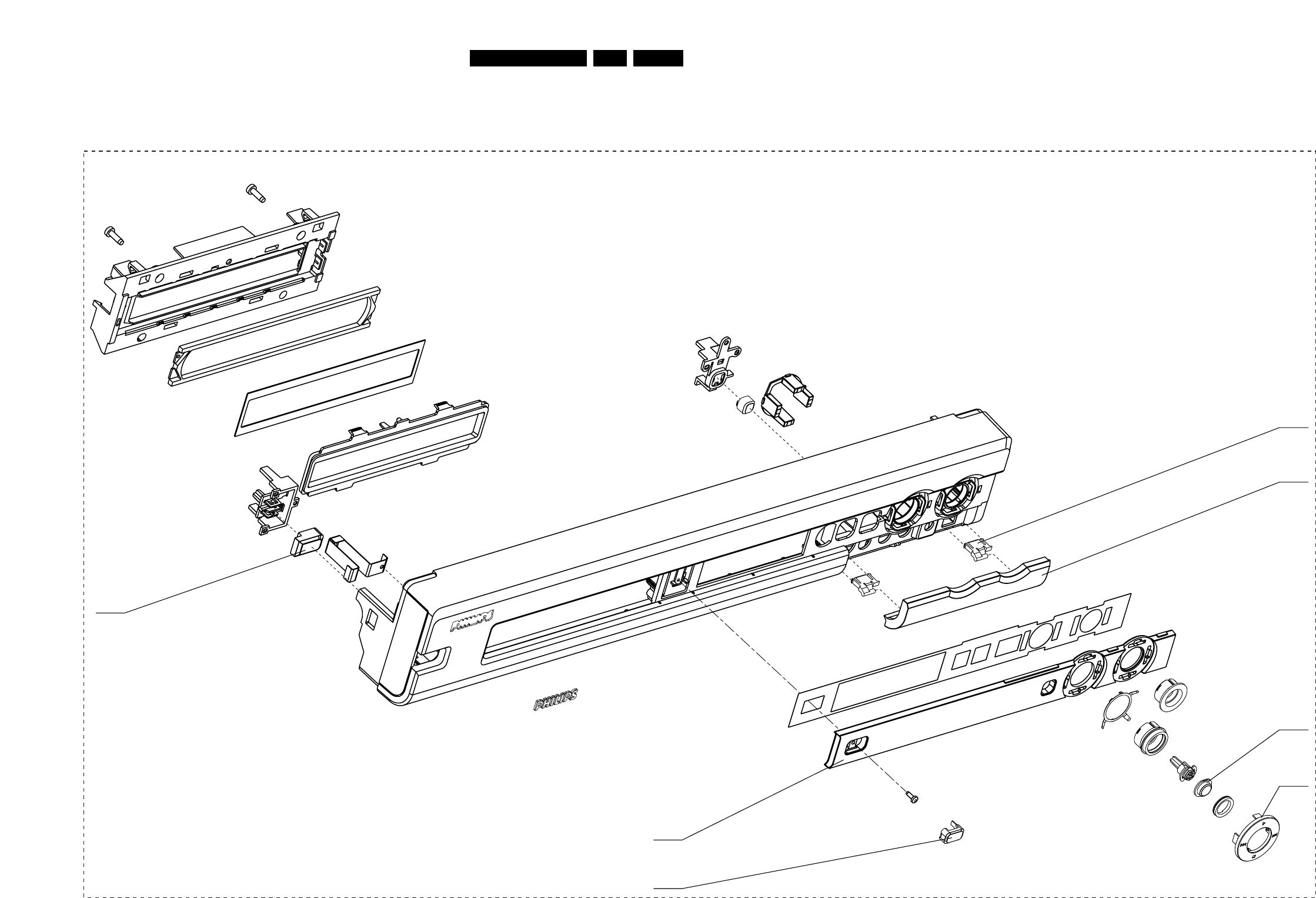
EN 687.LX7500RExploded Views
117
118
121
122
103
132
140
145
139
110
135
136
137
114
115
116
134
102
MECH. FRONT ASSEMBLY
Pl. 3x10
2x
119
120
111
113
126
133
2x
Pl. 2x6
124
EV3 front assy mech. LX7500R, 280904
EXPLODED VIEW / Front assembly
MECHANICAL PARTSLIST
111 3103 607 50341 BUTTON CAP, STANDBY
113 3103 607 50361 BUTTON CAP, OPEN CLOSE
119 3103 607 50411 BUTTON CAP, RECORD
120 3103 607 51311 WINDOW DISPLAY
124 3103 607 51101 RING, KEYS PLAY-STOP-REW-FFW
126 3103 607 51391 DOOR FRONT, LX7500/01/04
126 3103 607 51421 DOOR FRONT, LX7500/05
133 3103 604 00441 HINGE, DOOR FRONT
Only those parts of which a service code number is stated
are normal service parts.
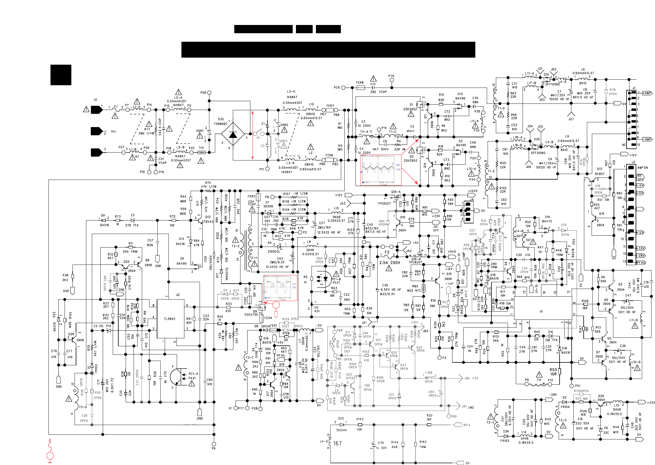
EN 697.LX7500RCircuit Diagrams and PWB Layouts
SMPS "AC6191"
Drawing 1
Switched Mode Power Supply
FOR ORIENTATION ONLY
1
0V
TL494CN (MOTOROLA)
Pulse with modulator
SMPS LX7500R, 221104
(original status 080904)
PWM
GND
VOLTAGE SENSE
+27,6V
-27,6V
0V
5V
0V
12,3V
33,6V
-27,7
3,7V
4,8V
-5,2V
5,2V
307V
12,3V
5V
EVM
V
DC voltages measured in Stop mode
with no audio output.
...V
GND
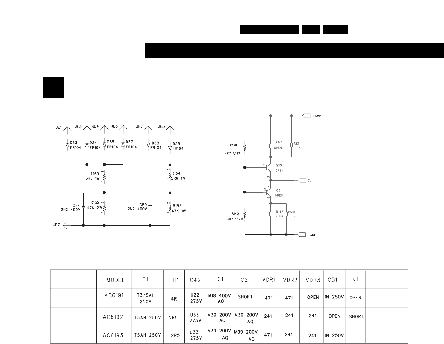
EN 707.LX7500RCircuit Diagrams and PWB Layouts
SMPS "AC6191"
Drawing 2
SMPS AC6191 (LX7500R), 221104
original status 080904
Switched Mode Power Supply
FOR ORIENTATION ONLY
2
230V
120V
120/230V
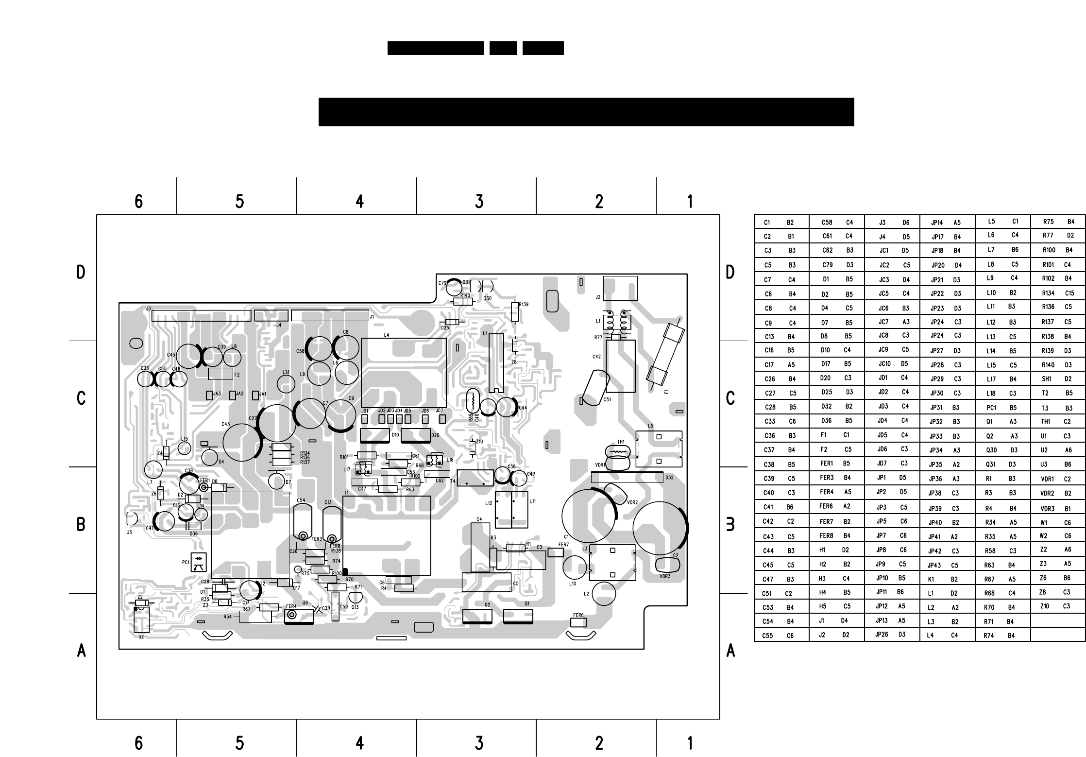
EN 717.LX7500RCircuit Diagrams and PWB Layouts
SWITCHED MODE POWER SUPPLY / component side view
SMPS AC6191 (LX7500R), 150904
original status 080904
Switched Mode Power Supply
FOR ORIENTATION ONLY
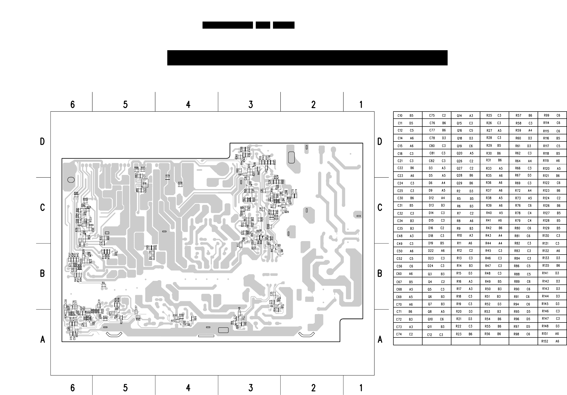
EN 727.LX7500RCircuit Diagrams and PWB Layouts
SWITCHED MODE POWER SUPPLY / copper side view
SMPS AC6191 (LX7500R), 150904
original status 080904
Switched Mode Power Supply
FOR ORIENTATION ONLY
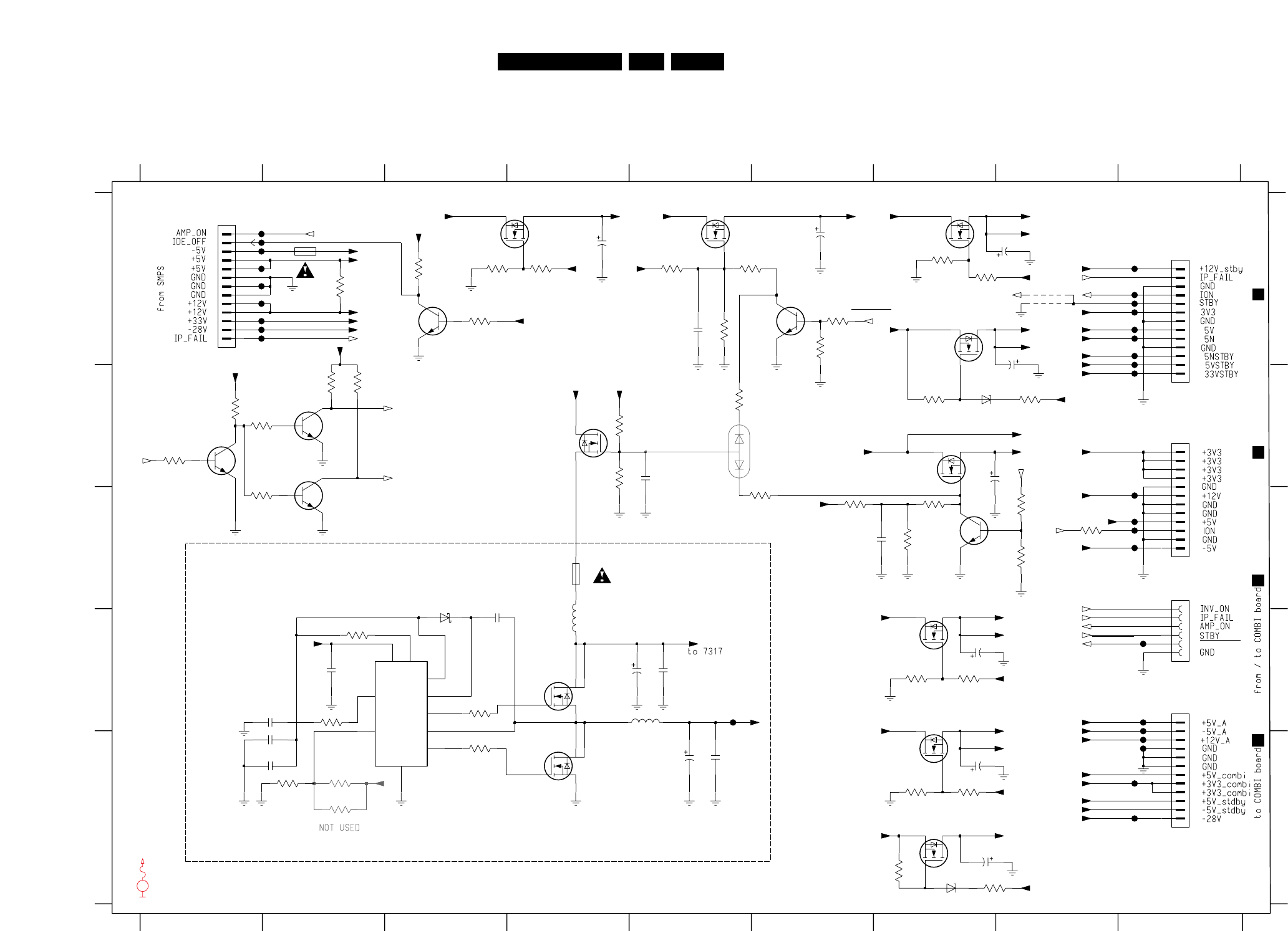
EN 737.LX7500RCircuit Diagrams and PWB Layouts
VL
VIN VCC
BST
DH
LXFB
DL
GND
COMP|EN
B
C
D
E
A
B
C
D
E
1300 A9
1301 A1
1303 B9
1304 C9
1305 D9
123456789
123456789
A
1306 C4
1307 A2
2300 D2
2301 D3
2302 D4
2303 E1
2304 D5
2305 A4
2306 A6
2307 A8
2308 A8
2309 B7
2312 E7
2313 E5
2314 E5
2315 D2
2316 E2
2317 C5
2318 A5
2319 C7
3300 A7
3301 A7
3302 A3
3303 A3
3304 B7
3305 B8
3306 C6
3307 C8
3308 C7
3309 C8
3310 C8
3311 A5
3312 A6
3313 D7
3314 D7
3315 A5
2310 D7
2311 E7
3316 A6
3317 E7
3318 E7
3319 A3
3320 A4
3321 E7
3322 E7
3323 E2
3324 E2
3325 D2
3326 D3
3333 B1
3334 B1
3335 C1
3336 A2
3337 B4
3338 C4
3339 A5
3340 B5
3341 C5
3342 C7
4000 A8
4001 A8
5300 D5
5301 D4
6300 B7
6301 E7
6304 D3
6305 B5
7300 A8
7301 A3
7302 A8
7303 B7
7304 C7
7305 A5
7306 C7
AUX SUPPLY BOARD
3327 E3
3328 D2
3329 E2
3330 B2
3331 B2
3332 B1
7307 A6
7308 D7
7309 A4
7310 E7
7311-1 E4
7311-2 D4
7317 D3
7319 B2
7320 C2
7321 B1
7322 B4
F300 A2
F301 A2
F302 A2
F303 A2
F304 A1
F305 A1
F306 A1
F310 B9
F311 A9
F312 A9
F313 A9
F314 A9
F315 A9
F316 A9
F317 A9
F318 C9
F319 C9
F320 C9
F321 C9
F322 E5
F323 D9
F324 E9
F325 E9
F326 E9
F327 E9
F328 E9
F329 D9
220K
3338
F307 A1
F308 A1
F309 B9
4K7
3322
220K
3315
22R
3327
3326
22R
1u0
2301
F304
PMV60EN
7306
3310
10K
4
5
6
7
8
9
1
10
11
12
13
2
3
1301
B13B-EH-A
2313
2m2 10V
2302
1m0 16V
F325
3303
10K
3300
10K
3320
2K7
F308 F313
2315
1u0
3341
100R
3340
100R
150K
3337
BAW56W
6305
PMV60EN
7322
220R
3336
7320
BC847BW
7319
BC847BW
10K
3333
2303
1u0
3321
4K7
2306
10u 16V
2
3
4
5
6
7
8
9
PH-B
PH-B
1300
1
10
11
12
13
F307
1K5
3318
7308
PMV60EN
4000
150K
3311
7307
BC847BW
100n
2319
2318
100n
100n
2317
3342 100R
10n
100R
3339
2300
3308
220K
7300PMV60EN
3301
1K5
PMV60EN
7310
3314
2K7
3307
10K
F326
15u
5300
1306
2A F
2311
10u16V
F329
10u
5301
8
34
5
MAX1967EUB
7317
10
1
9
6
2
7
F319
F301
F320
F324
F300
F310
F309
3K3
3324
F312
2309
10u 16V
3323
1K0
F302
F316
F315
F317
12
2
3
4
5
6
7
8
9
1303
1
10
11
6301
BZX384-C6V8
4K7
3304
10K
3317
1u0
2304
3331
10K
7305
PMV60EN
10K
3309
5
6
4
3
7311-2
STS8DNF3LL
3335
10K
3306 150K
F 1.0A
1307
06FMN-STK-A
1
1020
2
3
4
5
6
1304
F311
7309
PMV60EN
4001
2316
1u0
3329
68K
F303
BC847BW
7304
F323
F328
F318
3313
10K
F327
68K
3328
2308
10u 16V
10R 3325
2307
10u16V
F321
F314
F322
3302
1K0
7301
BC847BW
2
1
7302PMV60EN
STS8DNF3LL
7311-1
7
8
3305
4K7
10K
3319
F306
2314
1u0
F305
16V10u
2305
10K
3312
3316
10K
10K
3330
10K
3332
100K
3334
7321
BC847BW
2310
10u16V
2
3
4
5
6
7
8
9
1305
PH-B
1
10
11
12
PMV60EN 7303
2312
10u 16V
BZX384-C6V8
6300
BAT54 COL
6304
IP_FAIL
+5V_stdby
+5V_stdby
+12V_DCDC
-5V_stdby
+12V
+12V +33V_stdby
+33V_stdby
+3V3_combi
+3V3
+3V3_digi
+3V3
+12V_DCDC
-5V_stdby
STANDBY
IP_FAIL_AV
IP_FAIL _COMBI
+12V_stdby
+5V_AV
+5V_digi
-5V_AV
-5V_digi
+5V_stdby
+12V_digi
INV_ON
+3V3 +3V3_digi
+3V3_AV
+12V_digi
+5V_stdby
+12V_A
-5V_A
-5V_stdby
+12V_A
+12V +12V_A
+33V_stdby
POWER_ON
+3V3
+12V_A
+5V_A
+5V_combi
+5V_digi
IP_FAIL_COMBI
STANDBY
POWER_ON POWER_ON
AMP_ON
-5V_A
-5V_stdby
-28V
+12V +12V_digi
+5V_stdby
AMP_ON
+33V_stdby
-28V
IP_FAIL
+5V_stdby
INV_ON
+12V_digi
+12V_digi
+3V3_combi
+5V_combi
+12V_A
+5V_stdby
+5V_A
INV_ON
+12V_digi
-5V_digi
+12V_stdby
+33V_stdby
+5V_stdby
-5V_stdby
+5V_AV
-5V_AV
+3V3_AV
IP_FAIL_AV
INV_ON
# for provision only
1
1810
1
J3
3V3 SWITCHED MODE REGULATOR
to/from AV BOARD 1934
4
to/from DIGITAL BORD 1500
5
AUX SUPPLY BOARD LX7500R, 241104
4,9V
-5,1V
5V
12,4V
33,2V
-28V
3,6V
0,7V
9,7V
3,3V 3,3V
12,4V 12,4V 5V
-5,4V
0,2V
7V
12,4V
12,4V
20,1V
0V
3,3V 3,3V
9,8V
5V
-5,4V
0,1V
7V
-5,4V
5V
10,5V
-5,4V
10,8V
5V
20V
20V
0V
0V
0,6V
0V
0V
0V
5V
5V
0/4,7V
12,4V
5V
0,2V
0V
3,3V
5V
5V
34V
-5,4V
-5,3V
3,3V
12,4V
-5,3V
5V
0,2/2,6V
0,2/2,6V
4,8V
4,9V
0V
5V
5V
5V
-5,4V
-28,8V
3,3V
-5,3V
12,4V
1,7V
12,3V 5V
5V
4,7V
3,3V
3,3V
3,5V
12,2V
12,2V
8,4V
4,7V
3,3V
3,5V
3,3V
12,4V
12,4V
20,1V
EVM
V
DC voltages measured in Stop mode
with no audio output.
...V
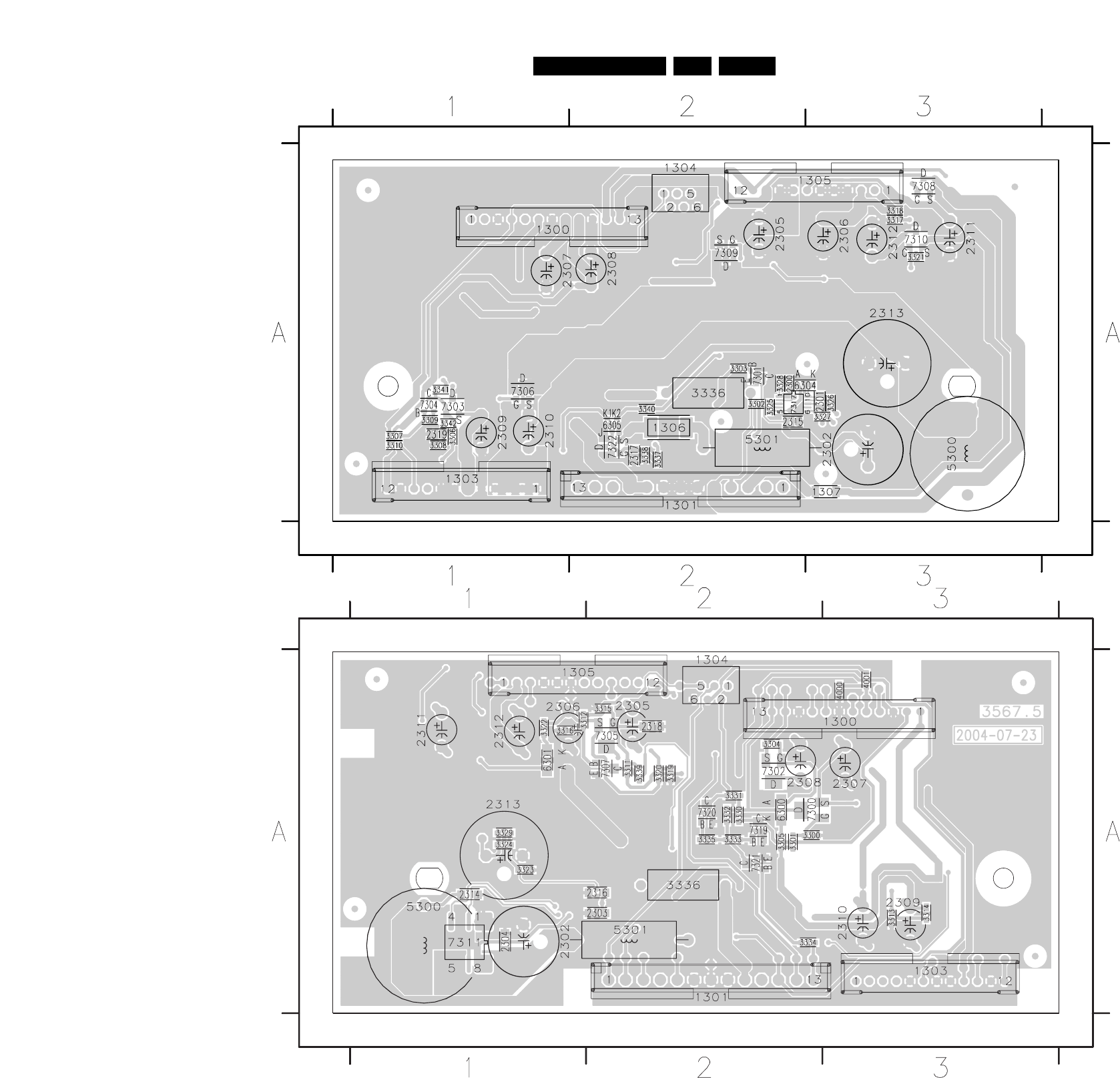
EN 747.LX7500RCircuit Diagrams and PWB Layouts
AUX. SUPPLY BOARD / component side view
Aux. supply LX7500, 221104
1300 A1
1301 A2
1303 A1
1304 A2
1305 A3
1306 A2
1307 A3
2300 A2
2301 A3
2302 A3
2305 A2
2306 A3
2307 A1
2308 A2
2309 A1
2310 A1
2311 A3
2312 A3
2313 A3
2315 A2
2317 A2
2319 A1
3302 A2
3303 A2
3306 A1
3307 A1
3308 A1
3309 A1
3310 A1
3317 A3
3318 A3
3321 A3
3325 A2
3326 A3
3327 A3
3328 A2
3336 A2
3337 A2
3338 A2
3340 A2
3341 A1
3342 A1
5300 A3
5301 A2
6304 A2
6305 A2
7301 A2
7303 A1
7304 A1
7306 A1
7308 A3
7309 A2
7310 A3
7317 A2
7322 A2
AUX. SUPPLY BOARD / copper side view
Aux. supply LX7500, 221104
2303 A2
2304 A1
2314 A1
2316 A2
2318 A2
3300 A2
3301 A2
3304 A2
3305 A2
3311 A2
3312 A1
3313 A3
3314 A3
3315 A2
3316 A1
3319 A2
3320 A2
3322 A1
3323 A1
3324 A1
3329 A1
3330 A2
3331 A2
3332 A2
3333 A2
3334 A2
3335 A2
3339 A2
4000 A3
4001 A3
6300 A2
6301 A1
7300 A2
7302 A2
7305 A2
7307 A2
7311 A1
7319 A2
7320 A2
7321 A2
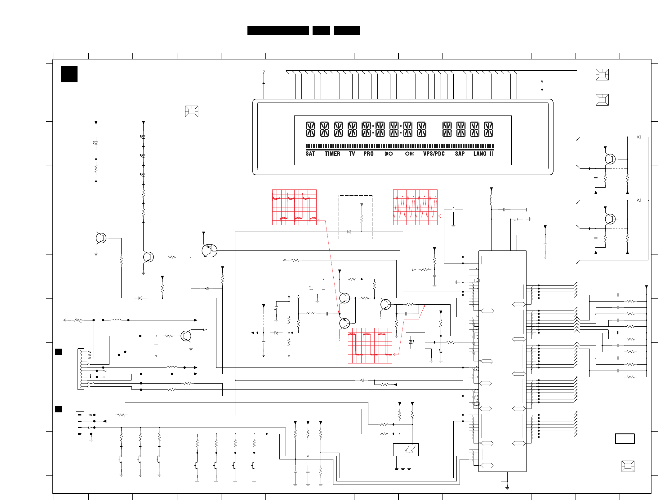
EN 757.LX7500RCircuit Diagrams and PWB Layouts
-T
13
12
11
10
7
INT0
INT1
TC2
DVO
TEST
VKK
VDD
VAREF
14
13
12
11
10
9
8
23
16
21
20
19
18
17
P4<0:7>
AIN
P5<0:3>
PD<0:4>
V3
P6<0:7>
V
P7<0:7>
V
P8<0:7>
V
P9<0:7>
V
SO1
5
6
7
6
5
4
3
2
1
0
15
VSS
PDO
2
1XTAL
P0<0:7>
PPG
PWM
TC4
TC1
SCK0
0
1
2
3
4
5
6
SI1
SCK1
RESET
VASS
INT3
INT2
INT4
INT5
XTIN
XTOUT
SCL
SDA
22
TC3
P1<0:7>
STOP
P2<0:2>
SI0
SO0
P3<0:2>
AIN
31
30
29
28
27
26
25
24
2
3
4
I134 F12
I135 F12
OPEN/CLOSE
I173 H10
F1504 I1
I100 E12
I101 E12
I177 A5
I144 F10
I145 H8
I146 I8
I189 B2
I190 C3
50V
I170 I5
I171 I5
I172 I4
KEY 1
12VSTBY
SOURCE
I159 F7
I160 E8
I161 E8
I162 F8
7105 E3
7106 E7
7107 F9
I167 I3
I168 I2
I136 F12
I155 E10
TRAY_LED
NEXT
PLAY
I127 G12
I128 G12
I129 F12
I130 F12
I131 F12
I132 F12
I133 F12
3162 I8
3163 H8
4100 C13
I183 B3
I152 I6
I143 F9
I105 I12
I106 I12
I156 E10
I199 H10
RotaryA
RotaryB
I191 C2
I192 C3
I184 G10
Dummy
3127 C14
3128 D14
3130 I2
I174 G10
I175 D13
7112 D4
9101 F5
I118 G12
I178 A12
I179 I4
I182 B3
I122 G12
I123 G12
I176 B13
I116 H12
I117 H12
I166 I3
GND
F1408 G3
F1409 G2
F1410 H3
F1411 G2
F1412 G2
F1501 H1
F1502 H1
F1503 H1
3103 I4
3104 I5
3105 I5
I137 H10
I142 F10
I104 E12
5101 F2
5103 G3
I107 H12
I147 F10
I150 E10
I151 E10
I111 H12
I112 H12
I194 D3
PREV
50V
not used
6110 D7
6111 E4
6112 E3
7100 A5
7101 B13
7102 D13
7103 E11
7104 F4
GND
2110 E6
not used
7110 D2
3136 C2
3137 C3
F102 G3
I119 G12
I120 G12
I121 G12
F1402 F2
F1403 F3
I124 G12
I163 F8
I165 F10
not used
3148 F14
3149 F14
3150 F14
3151 G14
3152 G14
3153 G14
3160 H8
3161 H9
1110 C10
1111 I8
1160 I5
I102 E12
I103 E12
5100 C11
3110 I3
3111 F3
5104 F7
I108 H12
I109 H12
I110 H12
6103 C3
6104 B2
I113 H12
I157 F5
I158 F6
REC
+12VSTBY
3121 F9
3122 F6
3123 F6
3124 F8
3125 E8
3126 E9
7108 F7
7109 E8
3134 F1
2114 F9
2115 F5
3139 D3
F103 F2
F104 G4
F1401 F1
3143 H2
3144 E4
F1404 G2
I125 G12
I126 G12
2125 G13
2126 G13
3100 C13
3101 D13
3102 I6
12 3
4101 D13
4199 I14
3108 I3
1168 I3
1169 I5
3112 F10
6100 F6
6101 B3
6102 B3
3116 E7
3117 E9
6105 B14
I114 H12
I115 H12
GND
STOP
from/to Combi board 1100
5VSTBY
B
3132 I7
3133 I7
2113 F7
56
2116 G9
3140 G8
3141 E3
3142 D8
2120 F13
2121 F13
3145 E3
F1405 G1
F1407 G2
ZL
Standby
Record
IR EYE
Rotary Encoder
VOLUME
VGNSTBY
3106 I4
3107 I6
1167 I4
78
1170 I3
3113 E6
3114 G4
3115 H3
2101 C11
2102 D11
3118 E8
6106 C14
6109 G8
not used
23
C
D
E
C
D
E
2111 E7
2112 E9
4
I
A
7
2117 F6
2118 E13
2119 F13
11 12
2122 G13
3146 E2
3147 F14
0206 A13
0210 A3
to STBY board 1930
not used
4
0211 A1
0803 I14
1165 I4
1166 I2
69
1910 G1
1911 H1
2100 I6
13 14
2103 I6
3119 F6
3120 F9
10 11
1
2104 D12
2107 G3
12
H
I
0005 A13
F
G
B
8910
F
G
13
2123 C13
2124 D13
H
14
A
VKK
VKK
I135
5
GND
+5VSTBY
I120
22u
2116
I146
HOLDER FTD ASSY
0206
GND
I126
GND
3136
270R
7101
VGNSTBY
SENSOR AMBIENT
TEMPERATURE
BC847BW
+5VSTBY
7110
BC847BW
6112
BAS316
LIGHT CHAMBER RECORD
0210
I162
3132
1K0
5101
1K0
3163
BLM18H
3162
1K0
F1502
F1501
GND
22K
I103
3151
F1405
I100
I182
+5VSTBY
6109
BAS316
6106
BAS316
47K
3141
BZX384-C6V8
6100
3122
GND
I199
10K
GND
I175
47n
2101
100R
3126
I112
F1504
I157
3130
I165
1K0
I124
22u 16V
I191
1
VS 3
I102
2102
TSOP4836ZC1
7107
GND 2
OUT
+5VSTBY
GND
4100
I108
GND
F104
GND
9101
I163
F1412
2115
47n
F1411
I145
GND
7102
BC847BW
I189
GND
VKK
F1407
3146
3117
10K
3
4
GND
22K
DA
1911
1
2
270R
3137
I177
I115
3145
1166
10K
EVQ11L05R
+5VSTBY
F1401
GNDGND
I107
100p
2126
I151
47K
I106
3108
F103
22K
3100
100p
2118
I159
+12VSTBY
I136
VKK
7104
IPOR
BC847BW
I121
680n
2113
3118
330R
VKK
10n
2103
I178
1160
EVQ11L05R
2124
100p
I132
BC337-25
7106
I118
GND
I137
2107
6103
LTL-1MHHR
2122
100p
1165
EVQ11L05R
I134
I110
330R
3116
I183
I161
I194
6104
LTL-1MHHR
GND
+5VSTBY
22K
3152
I128
9
10K
2322640
3134
11
12
2
3
4
5
6
7
8
12FMN-BTK-A
1910
1
10
10K
3140
BC847BW
7105
3107
I131
2K2
GND
GND
GND
+5VSTBY
VKK
7112
PDTA124EU
2104
100n
3104
1K0
3120
4K7
2100
10n
+12VSTBY
220R
3110
I105
GND
I117
100R
3115
8M0
1
I114
9
8
1110
EFOMC
74
75
76
77
10
13
39
38
40 78
7
64
65
66
67
68
69
70
71
72
73
53
54
55
56
57
58
59
60
61
62
63
42
43
44
45
46
47
48
49
50
51
52
29
30
31
32
33
34
35
36
37
41
21
22
14
12
11
23
24
25
26
27
28
2
3
4
5
6
15
16
17
18
19
20
TMP87CH74F
7103
MC
Φ
79
80
1
+5VSTBY
3125
470R
I130
3101
22K
22K
3153
GND
100K
3128
EVQ11L05R
I113
3149
1167
F102
22K
4K7
3161
F1408
3160
4K7
GND
I133
+5VSTBY
2117
5104
100u
I119
22u
I184
47K
3106
EVQ11L05R
1169
BLM18H
5103
I172
F1404
22K
3150
+5VSTBY
I192
3121
220R
F1409
I101
GND
7109
BC847BW
I111
I158
I156
6111
BAS316
I109
I166
GND
+5VSTBY
LTL-1MHHR
6102
3105
1K0
3113
GND
I104
1K0
3148
22K
F1410
+5VSTBY
VKK
+5VSTBY
+5VSTBY
1K0
3143
I171
10u
2110
2119
100p
6110
BAS316
GND
I170
3
B
2
C
4
5
F1403
EC12
1111
1
A
3133
1K0
2123
I168
GND
100p
I150
22K
3147
2114
GND
P16
21
P17
22
P18
6
P2
7
P3
8
P4
9
P5
10
P6
11
P7
12
P8
13
P9
1n0
26
G2
27
G3
28
G4
29
G5
30
G6
31
G7
32
G8
33
G9
5
P1
14
P10
15
P11
16
P12
17
P13
18
P14
19
P15
20 23 24 34 35 36 37 38 39 40 411
F1
45
F2
25
G1
6101
LTL-1MHHR
7100
BJ900GNK
+12VSTBY
3142
10K
GND
2111
47n
EVQ11L05R
GND
1170
EVQ11L05R
1168
+5VSTBY
I190
I152
I176
6105
BAS316
2K2
3102
7108
BC327-25
GND
3127
100K
I122
VGNSTBY
GND
+5VSTBY
I167
100p
2125
GND
10u
5100
F1503
I173
I129
GND
100p
2120
4199
I155
4101
GND
0005
PROTECTION FOIL
BARCODE
0303
3123
470R
220R
1K0
3112
3103
100R
3114
+5VSTBY
2112
220n
22K
3111
I143
I160
10K
3124
3139
270R
F1402
3144
10K
I116
100p
2121
470R
I123
3119
I125
GND
I179
+12VSTBY
TEMP
POR_DC
INTINT
DI_I"C_SDA
DI_I"C_SCL
I127
V0
V2
G8
G2
G1
IPOR
FIL1
G6
G5
G4
G3
P20
P19
P18
P17
P16
P15
P14
P1
P2
P3
P4
P5
P6
P7
P8
P10
P11
P9
P12
P13
G1
G2
G3
G4
G5
G6
G7
G8_9
V2
V0
P27
P26
P25
P24
P23
P22
P21
P11
P12
P13
P18
P17
P16
P15
G4
G5
G6
G7
G1
G9
P14
P1
P2
P3
P4
P5
P6
P7
P8
P9
P10
P27
P26
P25
P24
P23
P22
P21
P20
P19
G8_9
G8
G2
G3
FIL2
G9
FIL1
FIL2
INT
FRONT PANEL
DISPLAY / CONTROL BOARD
1
13
to 3126
to 1910
from 3113
from 7104
A: DC, 2 V/Div, 10us/Div
7106/7108-Emitter
A: DC, 1 V/Div, 10us/Div
IC7103-19
A: DC, 1 V/Div, 100ns/Div
IC7103-8
Display board .6 LX7500R, 221104
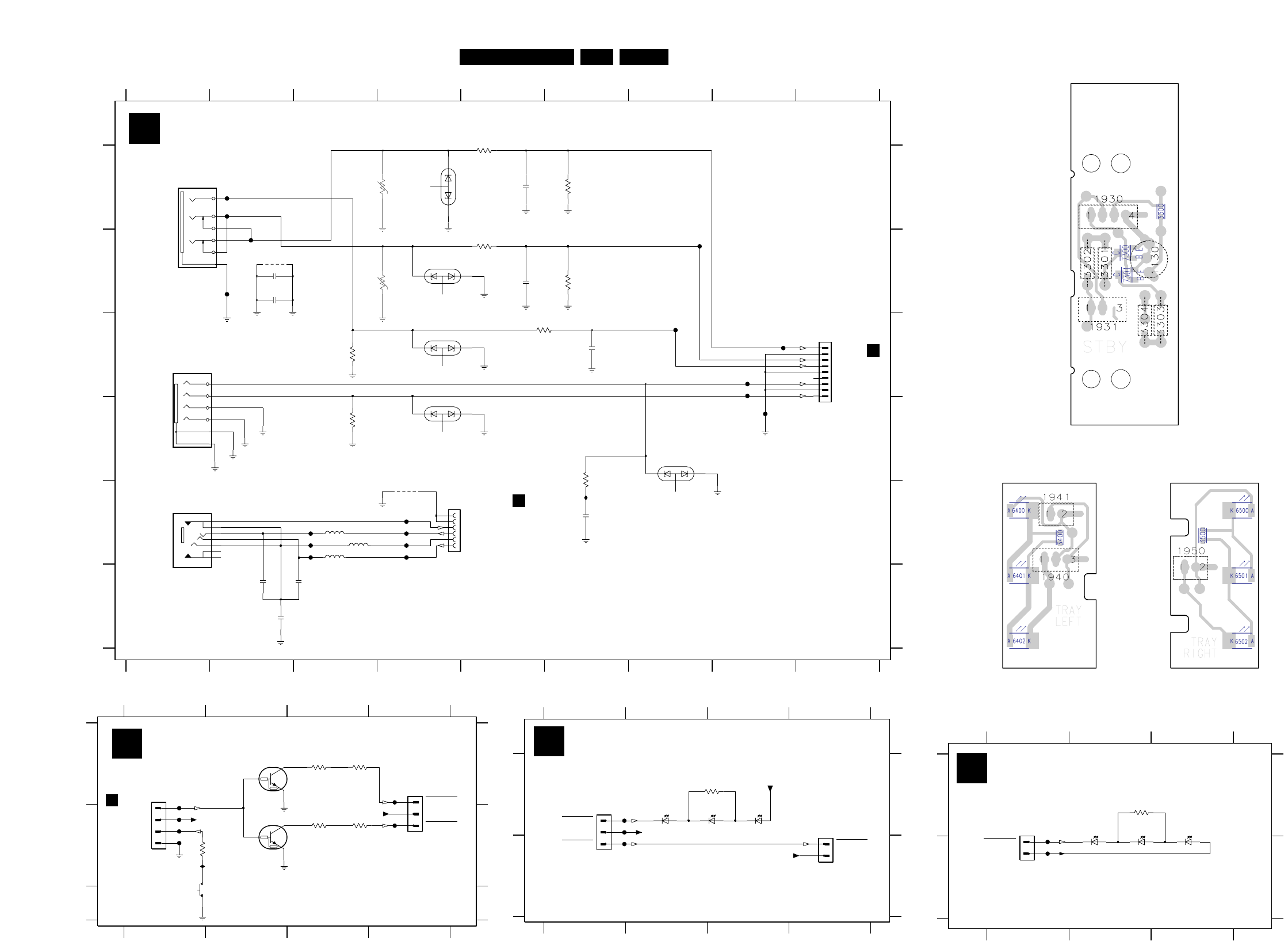
EN 767.LX7500RCircuit Diagrams and PWB Layouts
VV
CVBSFIN
2207 F3
2208 F2
3200 A5
3201 A6
not used
F2213 E4
F2214 E4
F2215 E4
AINF R
AINF L
F1003 A2
not used
GND_FC
AL/MONO
S-CONN
C
4567
3202 B5
YFIN
3206 D3
HP_RIGHT
6203 D4
6204 D7
F1001 B2
HEADPHONE
HP_DET
GND
GND
CFIN
A
B
C
D
1921 D1
2200 A5
F1006 A2
F1101 C8
F1103 B7
HP_LEFT
HP_GND
F2216 E4
I201 E6
F2210 E3
F2211 E3
F2212 E3
CINCH
AR
123
B
1920 B1
89
1
3203 B6
3204 C5
3
3207 D6
3208 A3
3209 B3
6200 A4
6201 B4
6202 C4
NC
CVBS
7
1922 C9
1923 E1
1924 E4
C
F1002 B2
E
2201 B5
2105 B2
2106 B2
2202 E6
2203 C6
F1104 C7
F1105 D8
F1107 C8
F1109 C8
GND_FC
E
F
A
Y
F
2206 F2
GND_FC
89
3205 C3
F2214
not used
not used
456
4129 E4
5201 E3
4198 B2
5202 E3
5203 E3
2
not used
D
F2213
100n
2202
4129
5201
GND_FC
5202
F2211
3209
SIOV-CN0805M4CCG3
F1109
3208
SIOV-CN0805M4CCG3
F1107
3
4
5
6
7
8
9
GND_FC
S9B-PH
1922
1
2
F1105
4
2
5
3
GND_FC
F1001
GND_FC
JPJ1127
1920
1
6
GND_FC
F1006
F1103
GND
75R
3207
5203
2201
330p
F1003
6201
DF3A6.8FUT1 6.8V
GND_FC
GND_FC
1M0
3201
2106
1n0
3203
1M0
3202
1K0
GND_FC
GND_FC
GND_FC
1
2
3
4
5
6
GND_FC
GND_FC
YKF51
1921
2208
1n0
I201
2207
22n
22n
2206
2203
47p
F2216
GND_FC
F2215
6.8V
F1101
DF3A6.8FUT1
6202
1
2
3
4
5
6
GND
F2212
06FE-BT-VK-N
1924
330p
2200
1K0
3200
GND_FC
GND_FC
F1104
F1002
GND_FC
GND_FC
75R
3205
1n0
2105
GND_FC
4198
4
5
F2210
GND
TC38-103-01
6
7
1
2
3
1923
GND_FC
DF3A6.8FUT1
6204
6.8V
3206
75R
6.8V
6.8V
DF3A6.8FUT1
6200
3204
68R
6203
DF3A6.8FUT1
GND_FC
GND_FC
GND_FC
FRONT PANEL
DISPLAY / CONTROL BOARD
2
from/to Combi board
Audio Processing 2 1302
3
to Analog board 1942
2
AV FRONT CONNECTORS
Display board .6 LX7500R, 230904
A
B
C
F3004 B1 F3101 A4
F3103 B4 I300 B13303 B3
GND
+12VSTBY
F3001 A1
F3002 B1 F3003 B1
123
23
1130 C1
1930 A1
4
A
B
C
to TRAY LIGHT LEFT 1940
1931 A4
3300 B1 3301 A3
3302 A3
+12VSTBY
3304 B3 7300 A3
7301 B3
(not used)
STANDBY . ON
(not used)
4
1
7301
PDTC124EU
1
2
3
7300
PDTC124EU
GND
GND
DA
1931
F3103
F3002
F3101
F3003
I300
F3004
+12VSTBY
1130
EVQ11L05R
1
2
3
4
GND
GND
+12VSTBY
1930
DA
3303
270R
3304
270R
3301
270R
3302
270R
F3001
3300
4K7
KEY1 TRAY_LED2
TRAY_LED1
Tray_Led
FRONT PANEL
STANDBY BOARD
3
from/to Display board 1911
1
Display board .6 LX7500R, 240904
3
A
4
6401 A3
+12VSTBY
to TRAY LIGHT BOARD right 1950
1941 B4
4
1
A
B
1940 A1
3
+12VSTBY
2
3400 A3 6400 A3
12
F4002 A1F4001 A1
TRAY_LED2
6402 A2
from STANDBY board 1911
3400
680R
B
F4003 B1
3
+12VSTBY
F4003
1940
DA
1
2
F4002
1
2
F4001
1941
DA
LST670LST670
6401 64006402
LST670
TRAY_LED1
TRAY_LED2
FRONT PANEL
TRAY LIGHT left BOARD
4
+12VSTBY
+12VSTBY
FRONT board .6 LX7500R, 240904
6501 A2 6502 A2 F5002 B1
not used
B
from TRAY LIGHT left BOARD 1941
A
B
A
1
6500 A31950 A1
123
23
F5001 B13500 A2
680R
3500
F5001
F5002
6502
LST670
6501
LST670
6500
LST670
DA
1950
1
2
TRAY_LED2
+12VSTBY
FRONT PANEL
TRAY LIGHT right BOARD
5
FRONT board .6 LX7500R, 230904
STANDBY BOARD / copper side view
Standby board LX7500R .6, 240904
TRAY LIGHT left BOARD
copper side view
tray light left board LX7500R .6, 240904
TRAY LIGHT right BOARD
copper side view
tray light right board LX7500R .6, 240904
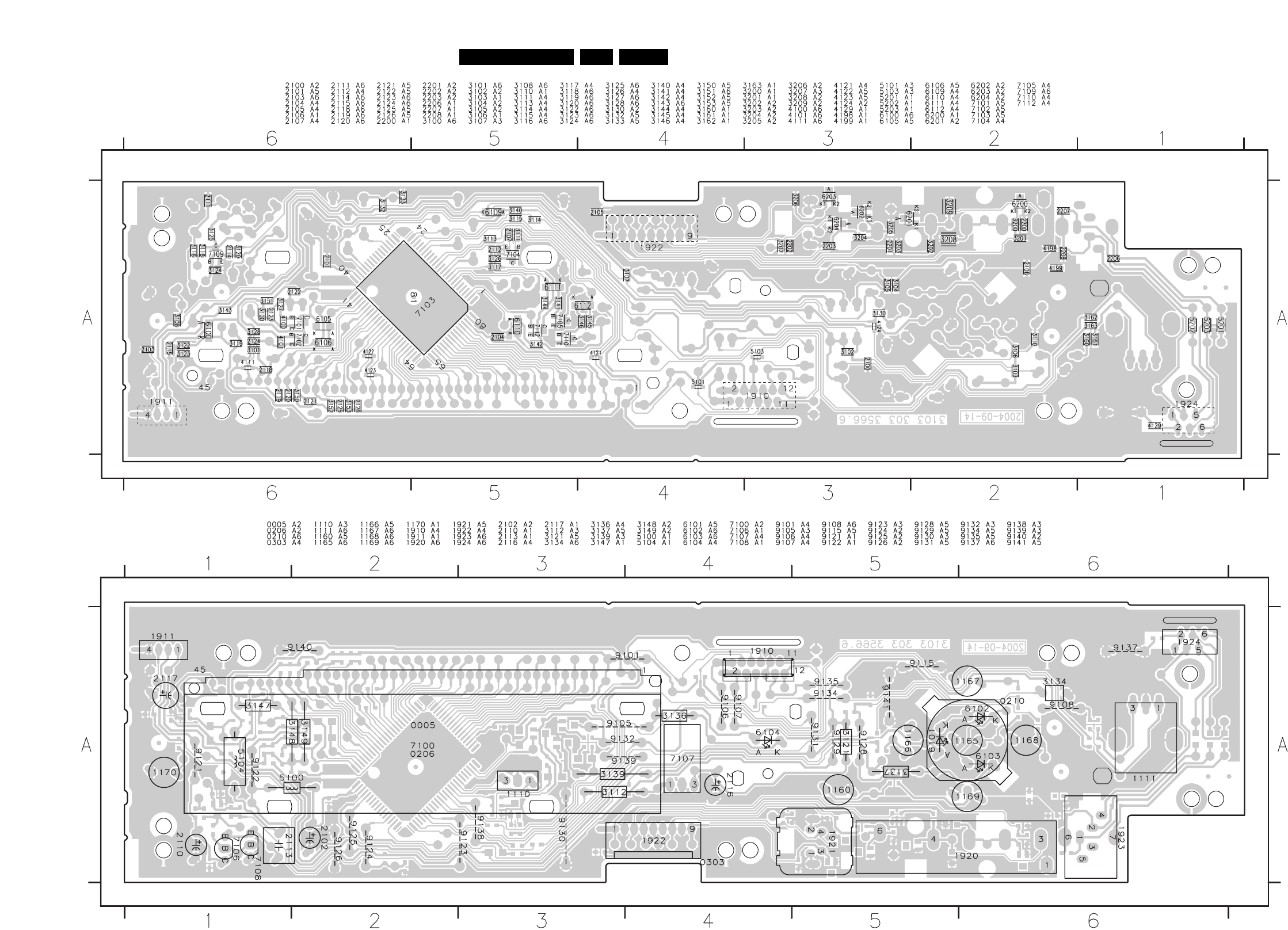
EN 777.LX7500RCircuit Diagrams and PWB Layouts
DISPLAY/CONTROL BOARD / copper side view
Front Display board LX7500R .6, 240904
to COMBI board
to STBY board
to AV board
to COMBI board
REC
STOP
PLAY
SOURCE
STANDBY
IR EYE
S-VIDEO IN
HEADPHONE
VOLUME
CVBS L
AUDIO
R
OPEN/CLOSE
PREV NEXT
to STBY board
to AV board
to COMBI board
to COMBI board
DISPLAY/CONTROL BOARD / component side view
Front Display board LX7500R .6, 240904
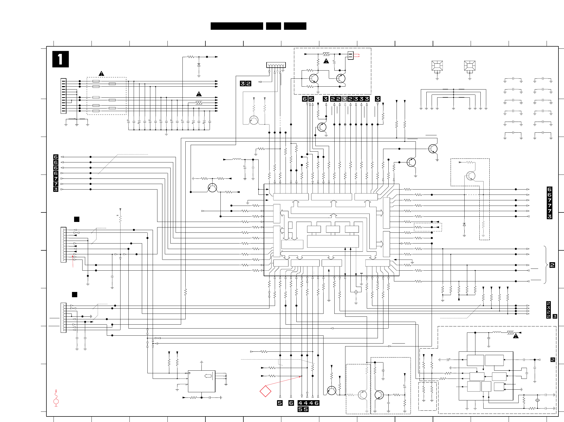
EN 787.LX7500RCircuit Diagrams and PWB Layouts
SCL
ADR
0
1
2SDA
WC
V16
VDD
sink o.drain
V25
V26
V27
V28
-RESET
TEST
XTOUT
XTIN
-STOP
-INT0
-INT1
drain
P6-P9 source open drain
source open
drain 80k p.d. 80k pull
down
P04
P05
P06
P07
80k pull down 80k pull down 80k pull down
V4
V5
V6
V7
V8
V9
V10
V11
V12
V13
V14
V15
CPU
VFT driver circuit (automatic display)
8-Bit A/D
Converter
8-Bit Input/Output
(tri-state)
P0
V17
V18
V19
V20
V21
V22
V29
V30
V31
V32
V33
V34
V35
V36
VKK
-SCK1
SI1
SO1
P03
PD
VSS
VAREF
VASS
XOUT
XIN
P5
TC2
-DV0
-SCKO
AIN0
AIN1
AIN2
AIN3
AIN4
P1 (tri state)
8-Bit Input/Output
P4
sink o.
3-B. I/O P3
AIN5
AIN6
AIN7
AIN10
AIN11
AIN12
AIN13
V0
V1
V2
V3
TC4
Counter
Program
ROM RAM
8-Bit h. break. v.
(tri-state)
8-Bit Input/Output
SCA
SCL
INT4
INT2
TC1
V23
V24
output port with latchoutput port with latch out w. latchP8
out. port w. latch P9
8-Bit h. breakdown v.
8-Bit high breakdown voltage8-Bit high breakdown v.
5-Bit h. breakd. v.
out w. latch
( tristate ) 8-Bit I/O P2
P7P6
4-Bit In/Output
(tri-state)
RESET
POW SUPPL
COMP
BANDPASS
TEST
CTRL
SIGNAL
QUALITY CLK
&
OSC
&
CLOCKED
(8th ORDER)
VSSA
DEM
RDS/RBDS
57 Khz
DET
I
A
B
C
D
E
G
H
I
0002 A11
0003 A11
1017 G8
1019 I13
1020 A6
1022 A8
1023 A2
1024 B2
1025 B1
1026 B2
1027 A1
1028 A1
1029 A1
1030 B1
1100 E1
1102 G1
1810 A1
2000 A8
2001 A13
2002 A13
POR_DC
12VSTBY
Reset
+5V
5VSTBY
DI_I2C_SDA
12345678910111213
1234567891011
F
13
A
B
C
D
E
F
G
H
Fan Control
2003 A13
2004 A13
2005 B13
2006 B13
2007 B13
2008 B13
2009 B13
2010 B13
2011 B2
2012 B3
2013 B3
2014 B3
2015 B3
2016 B3
2017 B3
2018 B3
2019 B4
2020 B4
2021 B4
SCL
VGNSTBY
2022 B4
2023 B4
2024 B4
2025 B4
2026 B5
2027 C5
2028 C6
2029 F2
2030 H1
2031 H1
2032 H12
2033 H11
2034 H13
2035 I13
2036 I9
2037 I13
2038 I10
2039 I13
2040 I5
2041 I9
12
2042 I13
2053 B13
2054 B13
3000 A8
3001 A7
3002 A7
3003 A7
3004 B6
3005 B6
3006 B7
3007 B9
3008 B9
3009 B10
3010 A4
3011 C7
3012 C7
3013 B5
3014 C7
3015 C7
3016 C7
SDA
3017 C8
3018 C8
3019 C8
3020 C9
3021 C9
3022 C9
3023 C6
3024 C9
3025 D6
3026 D6
3027 D7
3028 D7
3029 D8
3030 D8
3031 D8
3032 D8
3033 D9
3034 D9
3035 D9
3036 D4
3037 D5
3038 D10
3039 D5
3040 D10
to Front/Display
1910
INT
DI_I2C_SCL
I2C bus to front µP
GND
3041 D10
3042 D6
3043 D10
3044 D6
3045 D10
3046 E6
3047 E10
3048 E2
3049 E6
3050 E10
3051 E6
3052 E10
3053 E6
3054 E10
3055 E6
3056 E10
3057 E6
3058 E10
3059 F6
3060 F10
SET_FAN_CTRL
3061 F6
3062 F10
3063 F6
3064 F6
3065 F10
3066 F6
3067 F10
3068 F10
3069 F6
3070 F6
3071 F7
3072 F7
3073 I7
3074 F8
3075 F8
3076 F9
3077 F9
3078 F9
3079 G11
3080 G11
RotaryB
GND
3081 G11
3082 G11
3083 G11
3084 G3
3085 G7
3086 G7
3087 G7
3088 G6
3089 G7
3090 G8
3091 G9
3092 G9
3093 G12
3094 G12
3095 G12
3096 G12
3097 H13
CONTROL PART
+3V3
IPOR_DC
GND
INT_CECO
3098 H3
3099 H4
3100 I10
3101 I11
3102 I9
3103 I9
3104 I11
3105 I8
3106 I11
3107 I6
3108 I8
3109 I10
3110 I11
3111 I6
GND
AMP_ON
INV_ON
1943
COMBI BOARD
-28V
3112 I8
3113 I10
3114 I4
3115 I13
3116 I10
3117 I13
3120 C11
3121 E12
3122 H6
3126 C6
4100 B6
4102 D12
to Fan
POWER_ON
+12V_A
from AUX Supply 1305
+5V_A
NTC_FRONT
GND
5100 C5
5101 H12
6100 A4
6101 E11
7100 A8
7101 A8
7102 B6
7103 B8
7104 C11
7105 C10
7106 D5
7107 D10
7108 I5
RotaryA
5VSTBY
5NSTBY
7109 H13
7110 I8
7111 I9
7112 I9
7113 D12
F100 G7
F101 G7
F102 H9
F103 G13
F104 G13
F105 G1
F106 G1
F110 A8
F111 A8
F112 A1
F113 A1
F114 A1
F115 A8
F116 A1
F117 B1
F118 B1
12VSTBY
NC
F119 B1
F120 B1
F121 B8
F122 B8
F123 B7
F124 B8
F125 B8
F126 B8
F127 B8
F128 B9
F129 B9
F130 B9
F131 B9
F132 B6
F133 B6
F134 B6
F135 B7
F136 B7
F137 A5
F138 C10
GND
-5V_A
EEPROM
from AUX Supply 1304
F139 C7
F140 C1
F141 C7
F142 C7
F143 C8
F144 C6
F145 C9
F146 C1
F147 C10
F148 C7
F149 C1
F150 C7
F151 C7
F152 C1
F153 D1
F154 D1
F155 D1
F156 D13
F157 D4
F158 D10
CECO_RST
F159 D13
F160 D5
F161 D13
F162 D5
F163 D13
F164 E13
F165 E5
F166 E10
F167 E10
F168 E3
F169 E10
F170 E10
F171 E3
F172 E3
F173 E10
F174 E2
F175 E13
F176 F3
F177 F13
F178 F2
F179 F13
F180 F2
F181 F13
F182 F1
F183 F13
RDS Decoder
to AV Board
+3V3
TEMP
GND
F184 G2
F185 G2
F186 G2
F187 G2
F188 H2
F189 H12
F190 I4
F191 G13
F192 H13
F193 G13
F194 H6
F195 H7
F196 H7
F197 H7
F198 I7
F199 H7
to 3044, 3122 and
10K
7105
BC857BW
3009
100R
D
GND_V
F136
3070
F179
470R
3030
3100
10K
3020
470R
D
D
D
D
1K0
3026
D
2041
10n
F172
F182
3019
D
10K
3014
470R
470R
3120
D
GND_ALR
DD
DIG
7113
BC847BW
3060
D
1019
HC-49/U-S
1K0
3075
1K0
4M332
DIG
100R
3077
100n
2001
F128
1030 800mAF
100n2012
25V100u
2011
SCN
3
6
5
8
4
7
F111
(256x8)
Φ
EEPROM
7108
M24C02-WMN6
1
2
3083
10K
3038
10K
3082
GND_ALR
1K0
3066
1K0
3042
470R
10K
3093
3076
100R
3094
10K
3007
10K
DIG
F167
1K0
3015
F103
10K
3101
3456
F106
06FMN-STK-A
1020
12
D
3126
1K0
SCN
1K0
3041
3043
1K0
3079
10K
F155
D
F183
10R
3000
3059
1K0
F186
7101
BC327-25
F116
F171
BC847BW
7104
2u2
5101
2037
560p
100n
2005
1K0
3051
F160
3018
470R
F148
10K
3109
F147
D
F169
4K7
3050
3054
1K0
2K2
3117
3116
100K
47p
2035
4K7
3052 version
recognition
3052 assembled
for /37 only
3081
10K
D
F149
F105
F146
100n
2031
F170
3046
470R
3071
3073
1K0
1K0
F145
10K
3107
GND_ACS
3035
470R
F168
F162
ADIG
100R
3091
3092
100R
F177
F193
GND_ALR
2040
F190 100n
100R
3114
BC847BW
7112
3027
1K0
D
D
3023
100R
7106
LEVEL SHIFT
LEVEL SHIFT
BC847BW
D
3104
1K0
F131
1K0
3045
D
F122
100R
3089
10K
3096
3029
1K0
D
D
3110
10K
F174
3068
1K0
1
10
2
3
4
5
6
7
8
9
10FNM-STK-A
1102
3022
10K
D
74
75
76
77
78
79
8
80
9
F130
60 61 62 63 64
65
66
67
68
69
7
70
71
72
73
46 47 48 49
5
50 51 52 53 54 55 56 57 58 59
6
32
33
34
35
36
37
38
39
4
40
41 42 43 44 45
19 2
2021222324
25
26
27
28
29
3
30
31
TMP88CU74F
7107
1
101112131415161718
12M
1017
BC847BW
7110
100R
3088
10K
3008
2038
470n 50V
3037
100K
BC857BW
7103
F184
F180
3084
F178
3028
100R
D
1K0
D
AD
F166
3036
1M0
F135
1023 F800mA
GND_AS
F191
F197
F198
F154
3040
1K5
F153
3006
3106
10K
3016
1K0
1K0
D
3111
10K
3072
100R
3053
1K5
100n
2022
5
6
7
8
9
F156
1100
12FMN-STK-A
1
10
11
12
2
3
4
3103
1K0
3021
470R
470R
3033
5100
2u2
500mA1024
1K0
3047
2014 100n
7111
option
option
1K0
3102
BC857BW
F164
100n
2032
3013
2R2
1K0
3064
3057
1K5
470R
3044
47p
2042
35V10u
2000
1K0
3001
8K2
3002
2007
100n
1K0
3067
3056
1K0
1K0
3087
0002
BRACKET
25V100u
2017
BRACKET
0003
1n0
2029
3017
10K
D
3074
100R
F199
F195
3012
10K
D
F141
F152
DIG
3099
10K
3005
47K
F140
D
10K
3098
D
F133
2033
2u2 50V
100n
2008
25V47u
2021
3097
3R3
D
F127
470R
3032
M
3048
10K
F126
F129
AD
DGND_A
F139
D
F137
F150
F151
18K
3011
F123
100K
D
F112
3004
7102
BC847BW
47K
3108
2025
3061
50V 10u
3063
1K0
1K0
10V
2027
100u
2006
100n
F143
1K0
3078
470R
3034
F165
1029
D
2028
100n
F800mA
6101
BZX384-C3V3
3085
D
SCN
1K0
100K
3112
F194
F196
F102
3024
F101
F189
10K
2034
1202
1202
560p
M
F187
EH-S
1022
1
2
F134
100n
2004
2002
100n
3086
100R
1K5
3003
QUAL1
RDCL16
RDDA2
SCOUT 8
10 SYNC
15TCON
5
VDDAVDDD
12
3 VREF
6
VSSAVSSD
11
AD
7109
SAA6581T
CIN 7
MODE 9
MPX 4
OSCI
13
OSCO
14
2003
100n
F173
1K5
3055
2019
100u 25V
2016
100n
2053
100n
F125
1K0
3065
F1.0A1026
3010
F114 DSCN
1K0
F121
5
6
7
8
9
AD
1810
S12B-PH-K
1
10
11
12
2
3
4
F115
F157
3062
1K0
D
F113
10K
3121
4100
100n
2009
BC847BW
7100
2023
47u25V
100n
2024
220K
3115
GND_A
GND_A
D
F138
F110
1025 1.0AF
82p
2039
SCN
F185
GND_V
SCN
1K0
D
F124
F158
3025
D
F161
6100
BZX384-C3V3
10K
3080
100K
3105
SCN
F132
F119
F117
F118
D
F181
GND_V
F192
GND_A
DIG SCN
2054
100n
D
F176
2010
100n
F142
F120
F144
F100
D
F188
1K0
3122
10n
2036
4102
2015
100u 25V
D
2013 100u25V
1028 F1.6A
1027
8x
F1.0A
F159
470R
3049
3039
47K
D
3058
1K0
2020
100n
3031
470R
F163
F175
D
2030
100n
2026
100n
D
100R
3069
D
3113
220K
D
100n
2018
3095
10K
100R
3090
SCN
F104
+3V3
SPDIF_PDN
IPFAIL
from 1020
VGNSTBY
+12V_A
+3V3
+uP
AF_I2C_SCL1
+uP
+uP
+uP
DI_I2C_SCL
IPFAIL
IPFAI
from 1020
L
+5V
5VSTBY
5NSTBY
DI_I2C_SDA
3V3STBY
reset front µP
reset front µP
+uP
IPOR_R
STBY
+12V_A
+5V_A
-5V_A
+5V
5VSTBY
AB04_I2C_SDA
AB04_I2C_SCL
AMP_ERR
5VSTBY
5VSTBY
SPDIF_ERF
SPDIF_FS96
SPDIF_AUTO_DETECT
3V3STBY
+uP3V3STBY
+5V
Freq_HOP
ASEL_YC2_0
WS_OUT
VIDEO_SEL
SPDIF_SEL
+5V_A
+uP
3V3STBY
DSP_INT
DSP_RST
SPDIF_CDTI
SPDIF_CCLK communication SPDIF receiver
SPDIF_CSN
CODEC_SDA
CODEC_SCL
SPDIF_CDTO
CODEC_INT CODEC_RST
+5V
+5V
+uP +uP
12VSTBY
VGNSTBY
+uP
+5V_A
TU_Stereo
TU_DI
TU_SD
TU_CE
TU_CLOCK
HP_DET
+5V +5V +5V
+uP +uP
NTC_Amp
TU_RDS
MuteCentre
SurON
LR_CSub_on
MuteHP
HighpassOFF
MuteAll
MuteLine
WSIN_2
WSIN_F
+uP
+uP
12VSTBY
AF_I2C_SCL2
AF_I2C_SCL3
AF_I2C_SDA
+5V
I2C bus AV sub µP
I2C bus
CODEC & DSP
1
2
# for provision only
Combi board LX7500R, 181004
/01/04/05 only
/37 only
I2C bus Sound Processors
INT_CECO
CECO_RST
#
#
#
LEVEL SHIFT
EVM
V
DC voltages measured in Stop mode
with no audio output.
...V
f0
5V
5V
3,3V
3,1V
0,8V
0,1V 0,2V
0,2V
4,8V
0,7V 2,6V
3,2V
4,2V
2,9V
0V
8,5V
(speed 2)
4,9V 0V
5V
-5,4V
-28,8V
-5,3V
12,4V
4V
2,2V
2,5V 2,3V
2,6V
2,6V
0V
4,8V
1,6V
4,9V
2,7V
4,2V
1V
12,4V
5V
4V
4V
0V
0V
2,4V
-28,6V
0V
5V
4,9V
4,9V
12,4V
5V
4,9V
5V 1V 1V
2,6V
2,6V
2,6V
5,2V
5,2V 5,2V
5,2V
0V
2,1V
2,1V
5V
4,9V
4,8V
4,7V
4,8V
2,7V
4,2V
4,2V
0V
0V
0,5V
0,1V
0,1V
0,1V
0,2V
0V
0V
0V
0V
4,5V
4,9V
3,2V
3,2V
0V
0V
0V
0V
0,5V
0,5V
0,5V
0,5V
0V
0V
0V
0V
0V
4,9V
4,9V
4,9V
4,9V
4,9V
3,7V
0V
0V
0V
0V
0V
0V
0V
4,2V
4,9V
4,9V
1V
0V
0V
0V
0V
5V
4,9V
0,1V
4,9V
1,5V
0,4V
5V
5V
5V
5V
5V
5V
0V
5V
typ. 2,4V at 25°C
(measured via
Service Testprogram -
Temp. Test)
voltages measured in
Service Testprogram -Temp. Test
fan set to speed 2
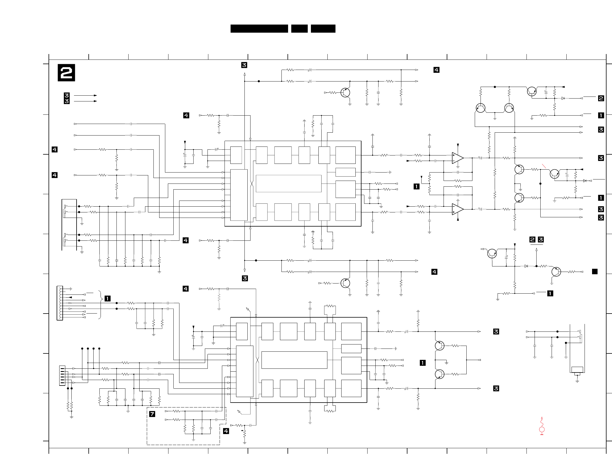
EN 797.LX7500RCircuit Diagrams and PWB Layouts
VOLUME I
RIGHT
SUR.
SOURCE
SUPPLY
POWER
SELECTOR
TREBLE
LEFT
VOLUME II
LOGIC
LEFT
REC
IIC BUS
BASS ALC
BASS
LEFT
VOLUME I
LEFT
SUR.
TREBLE
RIGHT
VOLUME II
RIGHT
BASS
RIGHT
VOLUME I
RIGHT
SUR.
SOURCE
SUPPLY
POWER
SELECTOR
TREBLE
LEFT
VOLUME II
LOGIC
LEFT
REC
IIC BUS
BASS ALC
BASS
LEFT
VOLUME I
LEFT
SUR.
TREBLE
RIGHT
VOLUME II
RIGHT
BASS
RIGHT
F218 E13
F219 F2
F220 F2
F221 G13
F222 G13
F223 G13
F224 G1
F225 G1
F226 G2
F227 G2
F228 H1
F229 H1
3307 I5
6200 A13
7206 C13
7207 B8
7208 D12
7210 E12
7211 E13
7212 F8
7213 G10
7214 F8
7215 H10
F210 A6
F211 A12
F212 C13
3278 G11
to Audio Tuner
Line Out
F213 D1
F214 D1
F215 D1
F216 E1
F217 E6
3288 I1
3289 I10
3290 I2
3291 I2
3292 I3
3293 I3
3294 I4
3295 I8
3296 I4
3297 I5
3299 I4
3306 I4
6201 C14
6202 E12
7200 A8
7201 A13
7202 B11
7203 A12
7204-1 B11
7204-2 D11
7205 C12
3263 F9
3267 F9
3268 F12
3269 F5
3270 F5
3271 F2
3272 F8
3273 F2
3274 G3
3275 G3
3276 G10
3277 G9
3279 H2
3280 H9
3281 H2
3282 H9
3283 H2
3284 H2
3285 H11
3286 H9
3287 I1
3242 D9
3243 D10
3244 D12
3245 D1
3246 E2
3247 E5
3248 E7
3249 E5
3251 E12
3252 E2
3253 E2
3254 E3
to AV board
3255 E3
3256 E7
3257 E9
3258 E13
3259 E7
3260 E14
3261 F12
3262 F7
3221 C12
3222 C10
3223 C13
3224 C12
3225 C2
3226 C14
3227 C10
3228 C11
3229 C9
3230 C2
3231 C11
3232 C9
Line 2
1953
3233 C10
3234 C14
3235 D12
3236 D13
3237 D13
3238 D1
3239 D10
3240 D12
3241 D2
3201 A7
3202 A9
3203 A8
3204 A8
3205 A9
3206 A11
3207 A12
3208 A13
3209 A13
3210 A5
3211 B13
3212 B5
2330 G9
2331 G5
3213 B7
3214 B12
3215 B2
3216 B12
3217 B12
3218 C9
3219 B10
3220 C2
2341 H3
2342 H9
2343 H9
2344 H9
2345 I9
2346 I2
2347 I2
2348 I3
2349 I3
2350 I5
2351 I7
2352 I5
2290 D9
2353 I6
2354 I4
2355 I5
3200 A7
2318 E2
2319 E3
2320 E3
2321 E7
2322 E7
2323 F9
2324 F5
2325 F3
2326 F3
2327 F7
2328 G3
2329 G3
2332 G9
2333 G4
2334 G4
2335 G13
2336 G13
2337 G9
2338 H3
2339 H3
2340 H3
2233 C11
2234 C3
2235 C14
2236 C11
2237 D9
2238 D9
2258 D2
2259 D10
2286 D11
2287 D3
2289 D9
B
C
D
E
F
G
H
I
A
B
2291 D10
2292 E3
2293 E7
2298 E3
2299 E5
2300 E7
2301 E8
2302 E12
2303 E2
Line 1
2228 C10
2229 C9
1234567
1950
COMBI BOARD
AUDIO PROCESSING 1
34567891011121314
A
1200-4 H14
1202 F1
1205 H1
2200 A7
2201 A7
2202 A9
2203 A13
2204 B5
2205 B3
2206 B7
C
D
E
F
G
2216 B9
2217 C11
L/R FRONT SPEAKERS
SURROUND SPEAKERS
8 9 10 11 12 13 14
12
H
I
1200-1 D1
1200-2 D1
1200-3 G14
2207 B8
2208 B7
2209 B3
2210 B9
2211 B10
2212 B3
2213 B5
2214 C4
2215 C4
7213
BC817-25
F215
GND_ALR
470n
2204
470n
2352
3226
10K
F216
GND_A
27K
3254
3262
2K2
MUTE
10K
3261
100K
3260
GND_ALR
470R
3256
GND_ALR
47u
100K
3267
GND_ALR
16V
2333
F229
F227
F224
2348
SCN
2327
220p
3281
4n7
4K7
2207
1K0
3280
100n
220n
2206
7208
F223
BC817-25
3268
BC817-25
10K
7203
10K
3230
47p
2236
6K8
3213
3212
10K
27K
220R
3242
3290
470n
2287
2334
100n
SCN
22n
2301
3248
2300
220n
6K8
GND_ALR
GND_AS
3247
10R3287
4K7
470n
2298
2228
3223
1K0
GND_ALR
100p
3246
7
22
12
17
14
15
9
20
1
4K7
18
27
13
28
3
26
4
25
5
24
6
23
8
21
2
TDA7468
7214
16
10
19
11
2201
50V 4u7
470R
3201
4u750V
2200
470n2325
2K2
3215
2211
1n0
3222
2209
22K
470n
220p
2319
3253
27K
3206
F228
3205
1K0
100K
4K7
3251
3207
1K0
GND_ALR
F222
4u7
2322
D
GND_ALR
50V
2205
470n
2355
470p
GND_A
2354
470p
3306
27K
2326
3273 470n
3272
1K0
2342
1K0
47p
470n
GND_ALR
47R
2337
9
3214
1
10
11
2
3
4
5
6
7
8
11FE-ST-VK-N
1202
3224
47R
5
6
GND_ALR
D
1205
S6B-EH
1
2
3
4
47R
3216
47u
2213
2212 16V
470n
470p
10K
3249
47K
2323
F225
3263
GND_ALR
GND_AS
GND_AS
100R
3259
470p
2202
GND_A
10 11
GND_ALR
2K2
3203
3285
1200-4
LPR6520-A530
GROUND
1K0
47p
2343
27K
3299
BC857BW
7210
F212
4n7 4n7
22082293
GND_AS
3240
330R
2286
10V 100u
7204-2
5
6
7
84
22
12
17
14
15
9
20
1
NJM4556AM
27
13
28
3
26
4
25
5
24
6
23
8
21
2
7
TDA7468
7207
16
10
19
11
18
470p
D
BC817-25
7205
470n
2328
4K7 2350
3294
3293
27K
7212
BC847BW
10K
3220
1K03219
BC857BW
7206
3271 1K0
10K
3241
GND_AS
3270 #
GND_A
4K7
2353
470n
3297
470R
F219
3252
2318
220p
2303
27K
220p
4K7
3296
1K0
3258
3257
470R
27K
3292
BAS316
6202
2320
3284
4K7
220p
2340
470n
4K7
F220
3283
470n
2234
2K2
3225
2214
16V47u
3295
3232
SCN
GND_ALR
1K0
1K0
F217
3243 1K0
F226
3204
4u750V
47K
F218
GND_ALR
2321
GND_A
470n
2299
BAS316
6200
GND_A
7202
BC817-25
SCN
47u
2332
16V
47p
2237
3218
D
2215
22n
220R
GND_ALR
4n7
2351
470n
2338
220p
220p
2347
F211
2346
3229
100R
1K0
27K
3286
GND_ALR
3228
2K2
3289
1n0
2345
10R3288
3275
3274
39K
39K
3279
4K7
4
6
5
1200-2
LPR6520-A530
LPR6520-A530
47u16V
2344
10K
3307
100R
47u 16V
2331
3277
2K2
3276
2330
1n0
470p
2335
2336
470p
1K0
3278
1200-3
7
9
8
LPR6520-A530
3282
1K0
47p
2238
4K7
3245
3217
150R
2229
470n
F210
470n2216
2289
470n
3211
10K
3236
3221
1K0
330R
1
84
100u10V
2217
NJM4556AM
7204-1
3
2
6K8
SCN
1n0
3227
2210
7200
BC847BW
7201
BC857BW
4K7
3210
3209
10K15K
3208
GND_ALR
2203
35V4u7
GND_AS
GND_HP
4u7 50V
2302
3234
15K
6K8
3233
3291
27K
2324
GND_AS
3269 470n
470R
D
3202
470R
GND_AS
470n
2339
GND_AS
GND_AS
470n
2292
27K
3255
470n
2341
GND_A
7211
BC857BW
GND_A
GND_AS
4K7
7215
BC817-25
3238
2233
47p
GND_ALR
100R
3200
GND_AS
GND_ALR
GND_AS
GND_A
D
GND_ALR
F221
GND_A
F214
GND_ALR
10K
220p
2349
3237
2291
GND_AS
1n0
150R
1n0
2290
3231
3244
GND_ALR
27K 6201
BAS316
1
3
2
1200-1
4u7 35V
2235
F213 2259
SC N
3239
100p
470n 22K
2258
3235
2329
470p
47R
AIN2L
+HP
HPREF
from 7214
AIN2R
AIN1L
AIN1R
AIN2L
AIN2R
AIN1L
AIN1R
MUX_R
to 2209
MUX_L
to 2205
LINE_RIGHT
ADC_IN_R
to 1200-3
to 1200-3
MUTE_SW
(Line Mute)
MUTE_SW
MUTE_SW
from 7210
MUTE
MUTE
MUTE HEADPHONE
from 7210
DAC_R
DAC_L
EXT3R
/37 only
EXT3L
+HP
+HP
SEL_L
SEL_R
TU_CLOCK
R
L
TU_Stereo
TU_DI
TU_CE
TU_RDS
9V_TUNER
TU_SD
5VSTBY
LINE_LEFT
ADC_IN_L
MuteLine
DAC_SL
DAC_SR
LINE_RIGHT
LINE_LEFT
IPFAIL
XMUTE_ALL
PDN_MUTE
from 3258
from 3258
PDN_MUTE
PDN_MUTE
MUX_L
MUX_R
5VSTBY
MuteAll
DOWNMIX_L
DOWNMIX_R
+9V2
AMP_SL
1301
1301
AMP_SR
AF_I2C_SCL3
AF_I2C_SDA
XMUTE_ALL
+9V2
AF_I2C_SCL1
AF_I2C_SDA
HPREF
HPREF
HPREF
AMP_LEFT
AMP_RIGHT
HP_LEFT
HP_RIGHT
5VSTBY
MuteHP
1
# for provision only
Combi board LX7500R, 181004
EVM
V
DC voltages measured in Stop mode
with no audio output.
...V
4,6V
12,3V
5,8V
9,1V
4,6V
4,6V
4,6V
4,6V
4,6V
4,6V
4,6V
4,6V
4,6V 4,6V 4,6V 4,6V 4,6V
0V
0V
5V
5V
4V
4,6V
5,8V
5,8V
5,8V
5,8V
12,3V
0V 5V
4,8V
4,7V
4,8V
4,9V
12,3V
0V 0V
0V 0/4,8V[MUTE]
0/4,8V[MUTE]
5V
4,9/4,3V[MUTE] 4,8V
0V
0V
0V
0/4,9V[MUTE] 5V
4,9/4,3V[MUTE]
0V/0,7 [MUTE]
5,8V
5,8V
5,8V
5,8V
4,6V4,6V
4,6V
4,6V
4,6V
9,1V
4,6V
4,6V
4,6V
4,6V
4,6V
4,6V
4,6V
4,6V
4,6V 4,6V 4,6V 4,6V 4,6V
4,6V
0V
5V
5V
4V
4,6V
0V
0V -2,8/0,7V[MUTE]
0V
0V 0/0,7V[MUTE]
4,6V4,6V
4,6V
4,6V
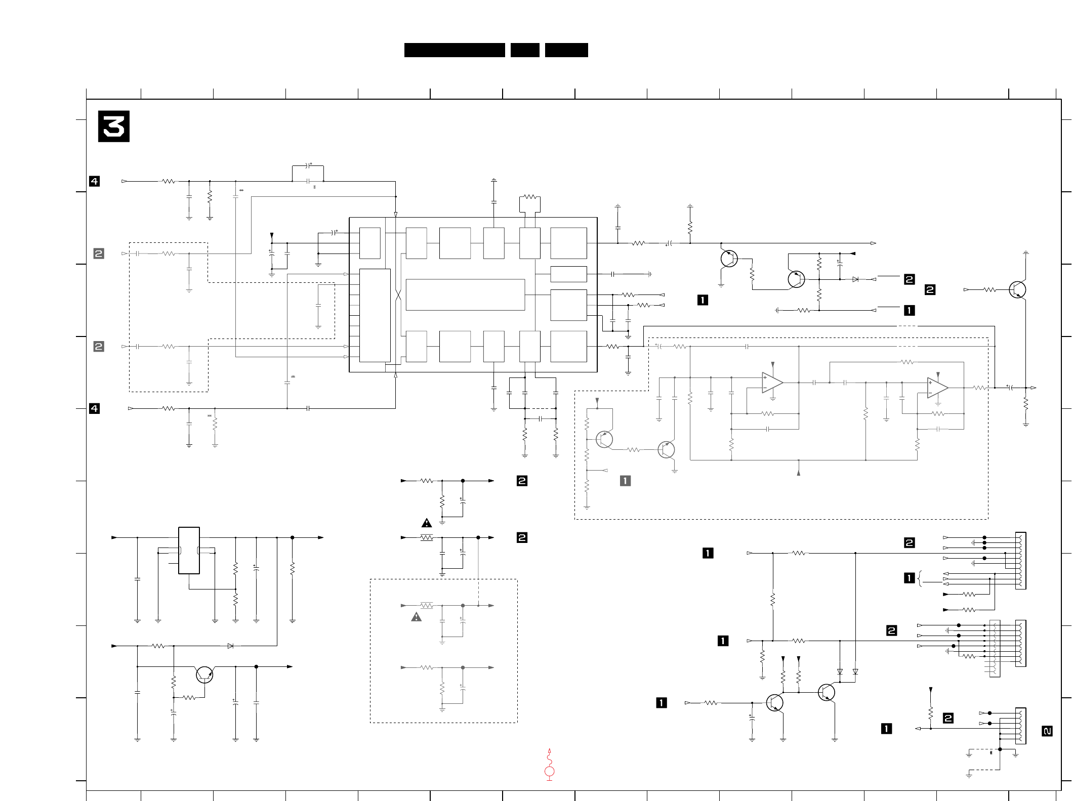
EN 807.LX7500RCircuit Diagrams and PWB Layouts
VOLUME I
RIGHT
SUR.
SOURCE
SUPPLY
POWER
SELECTOR
TREBLE
LEFT
VOLUME II
LOGIC
LEFT
REC
IIC BUS
BASS ALC
BASS
LEFT
VOLUME I
LEFT
SUR.
TREBLE
RIGHT
VOLUME II
RIGHT
BASS
RIGHT
INHIB
IN OUT
ADJ
GND
AUDIO PROCESSING 2
F313 F13
F314 F13
F315 G13
F316 G6
F317 G13
F318 H13
F319 H13
F320 H6
F321 H3
F322 I13
F323 E6
F324 I13
F325 I13
6303 H11
7300 B10
7301 C10
7302 C14
7303 B4
7304-1 D10
7304-2 D13
7306 E8
7307 E9
7308 F2
7309 H2
7310 H11
7311 I10
F310 F4
F311 F6
F312 F13
3443 H2
3444 H6
3445 H2
3446 I12
3447 F5
3448 F6
3449 H10
provision, backup for DSP bass management
3450 I9
3451 H11
3452 F11
3453 G10
3454 H10
3455 H11
4300 C12
4301 D12
4302 D7
4303 G6
4304 I13
4305 I13
6300 C11
6301 H3
6302 H11
3421 E10
3422 E11
3423 E13
3424 E2
3425 E8
3426 E7
3427 E7
1302
3428 E10
3429 E12
3430 E8
3431 E8
3432 F8
3433 F5
3434 G3
3435 G4
3436 G3
3437 G5
3438 G13
3439 G13
3440 H2
3441 H13
3442 H5
3411 C8
3412 C11
3413 D2
3414 D8
3415 D9
3416 D12
3417 D13
1331
3418 D9
3419 D14
3420 D2
2450 I2
2451 F6
2452 I10
2453 A4
3400 A2
3401 B2
3402 B7
3403 B9
3404 B8
3405 B2
3406 B11
3407 C10
3408 C13
3409 C8
3410 C11
2434 D12
2435 E4
2436 E7
2437 E2
2438 E10
2439 E13
2440 F6
provision, backup for DSP bass management
to Amplifier
1924
to Front board
2441 F6
2442 G3
2443 G1
2444 G6
2445 G6
2446 H6
2447 H1
2448 I3
2449 I3
I
A
B
C
D
E
F
2412 C8
2413 C4
2414 C8
2415 C8
2416 D1
2417 D9
2418 D10
2419 D8
2420 D2
2421 D4
2422 D11
2423 D11
2424 D6
2425 D14
2426 D7
2427 D7
2428 D7
2429 D9
2430 D10
2431 D9
2432 D9
2433 D12
1
12
234567891011121314
A
B
C
D
E
F
G
H
COMBI BOARD
34567891011121314
to Amplifier
G
H
I
1018 H14
1300 F14
1301 G13
1302 I14
2400 A4
2401 B2
2402 B3
2403 B6
2404 B8
2405 B4
2406 B9
2407 B1
2408 B3
2409 B3
2410 B11
2411 C2
provision, backup for DSP bass management
2434
100p
SUBWOOFER & CENTER SPEAKERS
2438
10n
D
7304-2
LM833D5
6
7
84
GND_A
GND_ACS
GND_ACS
3436
180K
GND_ACS
GND_ACS
4n7
2403
GND_ACS
D
4K7
3405
6300
BC857BW
7301 BAS316
3425
4K7
F312
2447
2n2
470R
3400
2448
47u 16V
2401
470p
1K0
3411
SCN
3403
2K2
GND_ACS
DD
10K
3446
22n
1K0
2409
GND_ACS
3402
4301
4
5
6
2424
4n7
1302
06FE-ST-VK-N
1
2
3
D
GND_ACS
GND_A
7311
BC847BW
2427
SCN
BC847BW
470n
7307
2453
470n 50V
2425
47u16V
BC857BW
7306
1K0
3408 BC817-25
7302
10K
3449
20
1
GND_ACS
25
5
24
6
23
8
21
2
7
22
12
17
14
15
9
7303
TDA7468
16
10
19
11
18
27
13
28
3
26
4
F317
3415
33K
GND_ACS
GND_A
470n
2416
2421
470n
3407
1K0
F323
16V100u
2446
2442
47u 16V
3438
10K
F316
3433
10R
22R
3437
3444
8K2
3442
4K7
3K3
2436
3426
470n
2417
2u250V
F310
4303
GND_ACS
2
3
4
5
6
7
8
9
4302
1300
FE-ST-VK-NA
1
10
2449
22n
F324
3413
4K7
GND_ALR
330n
2420
GND_A
7309
BC847B
3414
100R
100R
3404
6
2
3
8
5
1
7308
LM2931D-R
4
7
GND_ACS
120n
2418
F320
3451
1K5
3416
F311
F315
10K
3406
10K
1n0
F319
2419 1n0
2404
10K
3430
GND_A
220n
2423
3428
100K
2408
47u 16V
10K
3432
4305
2412
470n
47p
2415
2414
47p
4K7
3447
470n
2402
GND_ACS
3417
100R
2426
470n
7
8
GND_A
SCN
1018
08FE-ST-VK-N
1
2
3
4
5
6
GND_A
3453
8K2
GND_ACS
3434
27K
3443
47R
2K2
3423
2407
470n
F322
GND_ACS
F321
2K2
3419
SCN
2431
18n
3
2
1
84
2441
220u 25V
LM833D
7304-1
3435
1K0
2443
100n
GND_ACS
2428
56n
3410
15K
GND_A
3409
1K0
GND_ALR
16V 47u
2406
100p
2430
2400
470n
2410
4u7 50V
3
4
5
6
7
8
9
FE-ST-VK-NA
1301
1
10
2
6301
3452
1K5
BAS316
2422
220n
2411
330n
F313
2450
100u 16V
3455
10K
3431
10K
2405
47u 16V
2M2
GND_ACS
3418
10K
3401
GND_ACS
470R
3420
2451
100u 10V
GND_ACS
10u
2452
220K
3450
16V
GND_ACS
3445
220R
GND_ALR
GND_AS
SCN
4304
10K
3412
D
GND_ACS
GND_ACS
3454
10K
8K2
3448
3441 10K
SCN
2429
100p
10K
3439
F314
GND_ACS
470n
2435
SCN
GND_ACS
3422
22K
2432
15n
470p
2437
3440
470R
GND_HP
2440
22n
F318
2413
1n0
3427
5K6
4300
BC847BW
7310
10n
2439
10K
3429
7300
BC817-25
GND_ACS
GND_ACS
2444
BAS316
6303
22n
6302
BAS316
16V100u
2445
3424
10K
F325
100p
2433
3421
2K2
GND_A
AMP_SR
AMP_SL
HP_DET
SurON
5VSTBY
5VSTBY
5VSTBY
GND_ACS
HPREF
9V_TUNER
+9V2
HP_RIGHT
HP_LEFT
IPFAIL
MUTE AMPLIFIERS
+5V
LR_CSub_on
AMP_SUB
9V_TUNER
SUB_REF
+SUB
+SUB
AMP_ERR
AMP_LEFT
AMP_RIGHT
AMP_CENTRE
from 2406
from 2425
Freq_HOP
+5V
NTC_Amp
PDN_MUTE
AMP_SUB
XMUTE_ALL
+5V_A
HighpassOFF
+12V_A
+9V2
+12V_A
+HP
+12V_A
+12V_A
SUB_REF
9V_TUNER
+SUB
AMP_CENTRE
to 1300
to 1301
AF_I2C_SCL2
AF_I2C_SDA
DAC_Center
DAC_SUB
5VSTBY
MuteCentre
SEL_L
SEL_R
Combi board LX7500R, 181004
# for provision only
MUTE
MUTE
#
EVM
V
DC voltages measured in Stop mode
with no audio output.
...V
4,6V
4,6V
4,6V
4,6V
4,6V
4,6V
0V
0,7V
5V
5V
4,3V 4,3V 4,9V
1,5V
0/0,7V[MUTE]
0V
4,6V
4,6V
4,6V
4,6V
4,6V
4,6V
4,6V
4,6V
4,6V
4,6V
4,6V
4,6V
4,6V
4,6V
4,6V
4,6V
9,1V
5V
5V
0V
9,2V 5,8V
12,3V
12,4V
12,4V
7,8V
9,2V 9,2V
9,2V
9,2V12,4V
12,4V
9,9V
0,6V 0V
4,4V
4,4V 4,4V
4,4V
3,8V
4,4V
5V
3,8V
0,9V
0V
0V
0V
0V
0V
0V
0V
0V
0V
0V
4,4V
2,4V(25°C)
5V
6,2V
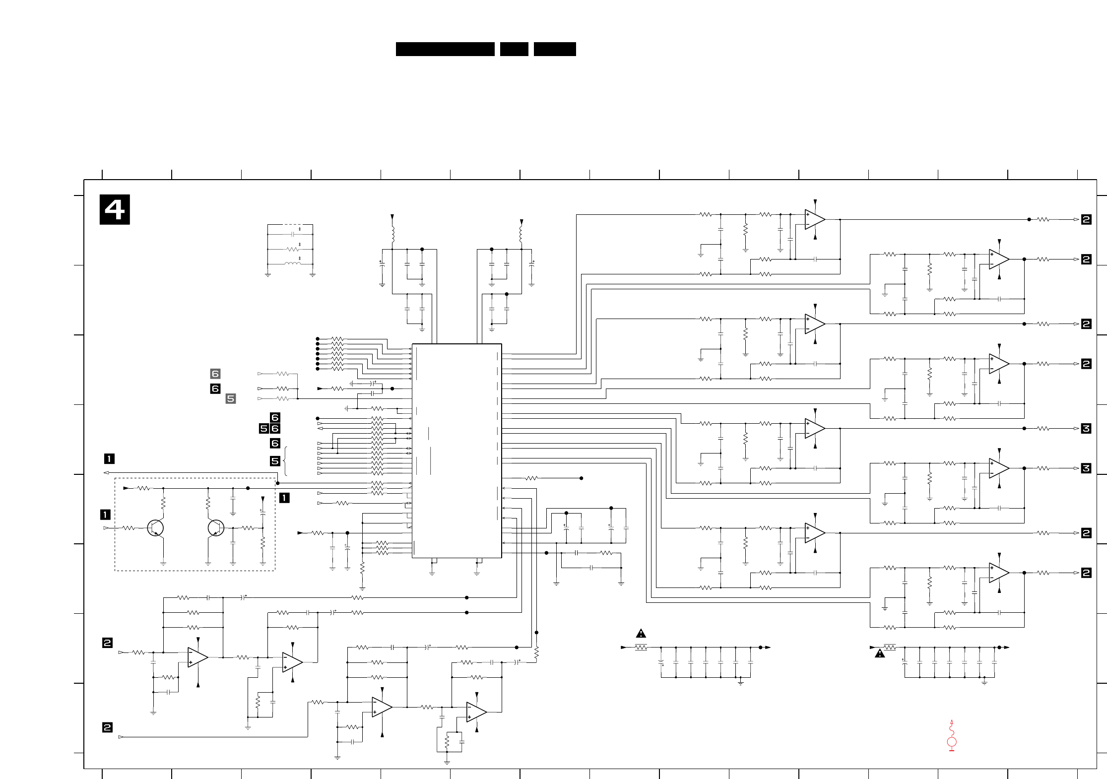
EN 817.LX7500RCircuit Diagrams and PWB Layouts
-
+
-
+
REFGND
LPFLT
AOUTB1
AOUTA1
CCLK
CDOUT
CDIN
CS
-
FILT+
VQ
MUTEC
-
+
-
VLC
AD0
AD1
SCL
RST
SDOUT
3
2
1
LRCK
SCLK
VA
2
RMCK
2
1
1
0
OMCK
GPO
ADCIN
ADC
DAC
SDIN
AINR
AINL
AOUTB4
AOUTA4
AOUTB3
AOUTA3
AOUTB2
AOUTA2
AGNDDGND
+
-
+
-
+
-
+
-
+
-
+
+
NC
SDA
INT
4
SCLK
LRCK
VD
VLS
3
4
5
6
2508 A5
2509 A6
2510 A6
2511 A7
2512 B12
2513 B13
2514 B13
2515 B12
2516 B13
1234
8 9 10 11 12
H
2454 H6
2455 H4
2456 H3
2457 H1
2500 A9
2501 A10
2502 A3
2503 A10
2504 A9
2505 A11
2506 A4
2507 A5 2517 B5
2518 B5
567891011121314
1234567
Reset
13 14
A
B
C
D
E
F
G
H
A
B
C
D
E
F
G
2549 E2
2550 E9
2551 E10
2519 B6
2520 B6
2521 B9
2522 B10
2523 C10
2524 C9
2525 C11
2526 C12
2527 C13
2528 C5
2529 C13
2530 C4
2531 C12
2532 D13
2533 D9
2534 D10
2535 D10
2569 G5
2570 G1
2571 G6
2572 G6
2573 G9
2574 G9
2575 G9
2536 D9
2537 D11
2538 E12
2539 E13
2540 E13
2541 E2
2542 E12
2543 E13
2544 E3
2545 E7
2546 E7
2547 E8
2548 E8
3501 A10
3502 A14
3503 A10
2552 F4
2553 F4
2554 F7
2555 F10
2556 F8
2557 F9
2558 F11
2559 F12
2560 F13
2561 F13
2562 F2
2563 F3
2564 F3
2565 F4
2566 F12
2567 G13
2568 G5
CODEC
COMBI BOARD
3524 C4
2576 G9
2577 G9
2578 G10
2579 G10
2580 G12
2581 G12
2582 G12
2583 G13
2584 G13
2585 G13
2586 G13
2587 G3
2588 H4
2589 H5
3123 C3
3124 C3
3500 A9 3542 D13
3504 A3
3505 A12
3508 A13
3510 A10
3511 A14
3512 B12
3513 B9
3514 B10
3515 B13
3516 B12
3517 B13
3518 B9
3519 B10
3520 B14
3521 B10
3522 C4
3523 C4
3560 D14
3561 E4
3562 E7
3525 C4
3526 C4
3527 C12
3528 C13
3529 C4
3530 C10
3531 C14
3532 C4
3533 C12
3534 C9
3535 C10
3536 C4
3537 C3
3538 D13
3539 D4
3540 D4
3541 D12
Connect close to CODEC
3580 E4
3581 E14
3582 E3
3583 E4
3584 E10
3543 D4
3544 D9
3545 D10
3546 D4
3547 D14
3548 D4
3549 D4
3550 D10
3551 D4
3552 D4
3553 D4
3554 D4
3555 D4
3556 D12
3557 D13
3558 D4
3559 D10
3602 G12
3603 G13
3604 G6
3605 G8
3606 G12
3607 G1
3563 E12
3564 E4
3565 E9
3566 E10
3567 E1
3568 E4
3569 E4
3570 E1
3571 E2
3572 E4
3573 E13
3574 E12
3575 E13
3576 E1
3577 E3
3578 E9
3579 E10
5401 A6
5404 A3
7400-1 A11
7400-2 A13
7402-1 B11
7402-2 C13
3585 E4
3586 F4
3587 F8
3588 F4
3589 F12
3590 F13
3591 F10
3592 F14
3593 F12
3594 F9
3595 F10
3596 F4
3597 F2
3598 F4
3599 G13
3600 G2
3601 G3
F417 C3
F418 C3
F419 C3
F420 C3
F421 C14
F422 C3
F423 C3
F424 C3
F425 C5
3608 G7
3609 G3
3610 G4
3611 G1
3612 H3
3613 G4
3614 G6
3615 H4
3616 H5
3617 H4
3618 H5
3619 F2
3620 F3
3621 G4
3622 G6
4401 A3
5400 A5
F429 E3
F430 E8
F431 E3
F432 E8
F433 E7
F434 E4
F435 F7
F436 F14
F437 F6
F438 F6
F439 G6
F440 G10
F441 G13
F446 G7
7404-1 D11
7404-2 D13
7405 C5
7408 E1
7409 E2
7410-1 E11
7410-2 F13
7412-1 G3
7412-2 G2
7414-1 H5
7414-2 H6
F410 A14
F411 A5
F412 A6
F413 A14
F415 B6
F416 B14
GND_ACS
F426 D3
F427 D14
F428 D14
330p
3K3
3505
3540
2525
10K
100n
2520
3538
3K9
100K
3582
GND_A
GND_AC S
2543
330p
BC847BW
7409
3556
3K3
3534
3K3
3602
3K3
3514
3K9
GND_A S
GND_A
2511
47u 16V
3K9
3503
100n
2507
D
3
2
1
84
7404-1
LM833D
84
100R3568
7400-2
LM833D
5
6
7
3K9
3563
F422
D
5401
3K9
3557
GND_ALR
GND_A
330p
2513
2586
100n
100n
2579
2501
330p
2500
1n5
2589
3618
3K3 100p
2550
1n5
330p
2505
GND_ALR
GND_A S
3500
3K3
GND_AS
F426
F415
D
1n5
2559
F435
F446
3515
F427
3K9
LM833D
7400-1
3
2
1
84
F424
100p
2568
3611
3K3
2556
680p
2554
2n7
3593
3K9
5400
3
2
1
84
7402-1
LM833D
F418
50V10u
2547
3572
100R
3569 100R
330p
2522
50V470n
2544
3610
4K7
3K3
3594
3560
220R
1n5
2542
3K9
D
50V
3573
2565
4u7
3K9
3603
10K3525
2517
100n
10K3523
41
4
51
6
53
17
38
49
50
54
59
19
55
12
7
8
24
18
48
47
46
45
44
43
42
11
39
21
20
3
2
1
64
63
62
5
52
33
28
29
22
23
35
34
31
30
27
26
25
40
15
16
14
13
36
37
32
7405
CS42418-C
Q
CODEC
Φ
10
9
58
57
60
61
56
GND_ALR
100R3586
3K3
3513
50V4u7
2572
3K3
3541
2567
330p
2566
1n5
3583 100R
100R
3536
F419
F433
GND_AS
3508
3K9
GND_ALR
3595
3K9
3502
220R
1n5
2512
LM833D
7404-2
5
6
7
84
10n
GND_AS
2509
2540 470p
3598
220R
3596
220R
330p
2558
GND_AS
GND_ACS
330p
2532
10K
3607
2529 470p
470p
F423
2523
3524 10K
2503 470p
F438
330p
2560
3558
GND_ALR
10R
3570
1K0
F416
DD
3519
3K9
3592
220R
3581
220R
GND_A
3547
220R
3520
220R
2569
4u7 50V
5404
3591
3K9
LM833D
7410-1
3
2
1
84
F412
3550
3K9
F439
2536
1n5
3K9
3533
100R3585
47u
2506
GND_A
3587
10K
16V
330p
2571
3511
220R
100n
2576
F429
100n
2575
3K9
3K9
3599
3K3
3512
GND_ALR
3565
2526
1n5
GND_A
2510
100n
GND_A
3608
220R
3604
220R
1n5
2521
3612
3K3
100p
2570
4
GND_ALR
3K9
3579
LM833D
7412-1
3
2
1
8
1n5
2531
D
470p
2535
3K9
3530
3537 100R
3521
3K9
10R
10R
3548
3546
F436
GND_ALR
100n
2583
100n
100n
2582
2584
D
GND_ALR
470p
2514
D
3615
10K
470p
2555
50V4u7
2563
3578
3K3
GND_AC S
D
2562
100p
2564
330p
2516
330p
2537
330p
330p
D
3597
2539
4K7
3616
3K3
2528
10u 16V
100n
2530
2541
10n
100n
2581
10R
GND_ALR
3549
3601
3K3
3K3
3609 10R
3605
F434
F425
3580
100R
2578
100n
5
6
7
84
3R3
7414-2
LM833D
D
3606
3K3
3617
3542
3K9
100R
3543
82K
3600
1n5
2557
F430
3K3
3518
3K9
3584
2524
1n5
GND_ALR
2580
25V100u
1n5
2533
84
F428
LM833D
7402-2
5
6
7
F441
GND_ACS
2519
GND_ALR
10n
10n
2549
220K
3577
3555 10R
3K3
3614
GND_A
GND_ALR
5
6
7
84
D
7412-2
LM833D
GND_ALR
3K3
3589
3545
3K9
3559
F431
3K9
3564 100R
2527
330p
10K
2553
3522
16V10u
F432
F410
3561 10R
3K9
3528
2585
2502
100n
100n
3504
100R
2561 470p
3590
3K9
2518
10n
3501
3527
3K3
3K9
BC847BW
7408
1n5
2504
330p
2534
25V
2573
100u
84
3K9
3566
7410-2
LM833D
5
6
7
2588
100p
356210K
100p
2456
2551
330p
GND_ALR
100p
2455
100p
2457
10R
3554
10n
2508
3510
3K9
F417
3532 10K
10K3529
3526 10K
100R
3588
1K0
3622
1K0
3621
1K0
3620
3619
2545
1K0
3K9
16V100u
3575
2548
100n
100n
2546
D
1K0
3571
3551 100R
3K9
3535
3613
82K
100p
2454
100R
3123
2538
1n5
3K3
3544
D
F437
F411
10R
3552
3553 10R
3576
100K
F413
3K3
3574
100R
3124
3531
220R
4401
2574
100n
100n
2577
F421
GND_A
F420
3K9
3517
3
2
1
84
GND_ALR
LM833D
7414-1
3567
47K
F440
2552
100n
GND_ACS
1K03539
2515
1n5
2587
100p
3516
3K3
+OP_DAC
CODEC_INT
DAC_L
DAC_R
DAC_SL
DAC_SR
DAC_Center
DAC_SUB
DOWNMIX_L
DOWNMIX_R
SPDIF_MCLK01
SPDIF_MCLK02
-OP_DAC
+OP_DAC
+OP_DAC
-OP_DAC
+3V3
+5V
ADC_IN_L
+5V_A +OP_DAC
+OP_DAC
-OP_DAC
-OP_DAC
+OP_DAC
IIS_OUT_BCLK_RC
IIS_OUT_WS_RC
-OP_DAC
-5V_A
+3V3
+5V_A
+3V3
+OP_DAC
-OP_DAC
+OP_DAC
-OP_DAC
+OP_DAC
-OP_DAC
+OP_DAC
-OP_DAC
+OP_DAC
-OP_DAC
+OP_DAC
-OP_DAC
+OP_DAC
-OP_DAC
IIS_OUT_BCLK
IIS_OUT_WS
DSP_CLK
ADC_IN_R
CODEC_RST
IIS_OUT_SDA4
IIS_OUT_SDA3
IIS_OUT_SDA2
IIS_OUT_SDA1
IIS_IN_SDA1
+5V
CODEC_SCL
CODEC_SDA
-OP_DAC
# for provision only
Combi board LX7500R, 221104
EVM
V
DC voltages measured in Stop mode
with no audio output.
...V
5V
5V 5V
3,3V
0V 0V
-5,2V
1,5V
1,5V
5V
-5,2V
-5,2V -5,2V
2,7V
4,8V
4,8V
2,7V
2,7V
2,7V
2,7V
2,7V
2,7V
2,7V
2,7V
2,7V
2,7V
2,7V
2,7V
2,7V
2,7V
2,7V
2,7V
2,7V
5V
1,5V
1,5V
1,5V
1,5V
1,5V
1,5V
5V
5V 5V
1,5V
5V
-5,2V
1,5V
1,5V
5V
-5,2V
1,5V
1,5V
5V
-5,2V
1,5V
1,5V
5V
-5,2V
1,5V
1,5V
5V
-5,2V
1,5V
1,5V
5V
-5,2V
1,5V
1,5V
5V
-5,2V
1,5V
1,5V
5V
-5,2V
1,5V
-5,3V -5,2V 5V 5V
5V
1,6V
1,6V
3,2V
3,3V
3,3V
5V
5V
1,2V
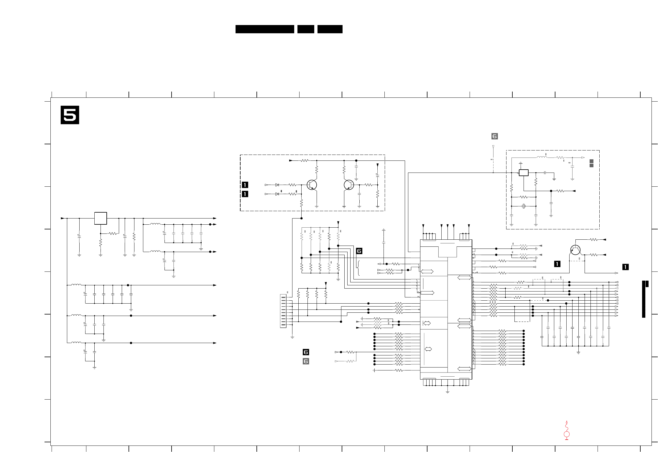
EN 827.LX7500RCircuit Diagrams and PWB Layouts
C
SDI<0:3>
PE<0:11>
SDI<0:3>
SCL
SDA
HA2
HA0
PD<1:0>
IRQ<A:D>
PF
CORE_VDD
DPA
PLL_VDD
IO_VDD
CORE_GND
DPA
IO_GND PLL_GND
CLOCK
SPDIF
INTERRUPTS
JTAG
TIMER
SCAN ESAI_1
SDO4
ESAI
SHI
GPIO
PC<0:11>
MOD
TIO
6
7
TDI
HCKT
FST
SCKT
HCKR
FSR
SCKR
0
1
2
3
4
5
8
SCAN
10
9
NMI_PINIT
EXTAL
ADO
ACI
A
B
D
RESET
SDO5
TMS
TDO
TCLK
1
0
HREQ
SCK
MISO
SS
MOSI
SDO4
SDO5
HCKT
FST
SCKT
HCKR
FSR
SCKR
SDO0
SDO1
SDO2
SDO3
SDO0
SDO1
SDO2
SDO3
NC
1
IN OUT
ADJ
A
B
C
D
1
1
DSP
COMBI BOARD
E
F
G
H
32
E
F
G
H
1500 C12
1601 E6
2045 B12
2700 B13
2701 C12
2702 C11
2703 C12
2704 D1
2705 D2
2706 B8
2707 B8
2708 C8
2710 E2
2711 E2
2712 E2
2713 E2
2714 E2
2715 F1
234567891011121314
RESET
2733 F14
2734 F14
2735 F13
2737 F13
2738 F13
4567891011121314
A
B
C
D
2709 E1
3712 D7
3713 D7
3714 D7
2716 F2
2717 F2
2718 F1
2719 F2
2720 D3
2721 D3
2722 D4
2723 D4
2724 D4
2725 D3
2726 D3
2727 F13
2728 F13
2729 F13
2731 D8
2732 F13
TEST DATA IN
2739 F12
2740 F12
2741 F12
3119 B12
3700 B13
3701 D8
3702 D7
3703 D7
3704 D7
3705 D7
3706 C12
3707 C13
3708 C12
3709 D3
3710 D8
3711 D7
Interface
3746 E7
3747 E7
3715 F11
3716 F11
3717 G11
3718 B7
3719 F11
3720 F11
3721 G11
3722 G11
3723 D13
3724 B8
3725 B7
3726 D13
3727 B8
3728 B6
3729 F11
3730 C8
3764 E11
3765 E11
TEST MODE SELECT
3731 C6
3732 F11
3733 F11
3734 D11
3735 C7
3736 D12
3737 D12
3738 D11
3739 F11
3740 D11
3741 D12
3742 F11
3743 D12
3744 E9
3745 E7
JTAG
3748 E7
3749 D9
3750 E9
3751 D9
3752 E9
3753 E9
3754 E9
3755 E12
3756 E11
3757 E12
3758 E11
3759 F9
3760 F9
3761 F9
3762 F9
3763 E12
TEST DATA OUT
TEST RESET
7500 B12
7501 C2
7502 D13
7503 B8
7504 B7
7505 D11
3766 G9
3767 E11
3768 G9
3769 E11
3770 G9
3771 E11
3772 E11
3773 E11
3774 F9
3775 F9
3776 F9
3777 F9
3778 F9
3779 E11
3780 E11
3781 F8
TEST CLOCK
3782 F9
3783 F9
3784 F9
3852 D2
3853 D2
3854 G8
4101 E12
4500 B11
4501 D13
4502 E12
4503 E13
4504 F12
5102 B12
5500 E1
5501 E1
5502 F1
5503 C3
5504 D3
6500 B6
6501 C6 F544 G8
F545 E13
F546 E12
F547 G8
F548 C4
F549 D4
F510 C12
F511 D8
F512 D7
F513 D7
F514 D7
F515 D7
F516 F12
F517 F12
F518 F12
F519 F12
F520 G12
F521 G12
F522 G12
F523 B8
F524 F12
F525 F12
F526 F12
F527 D11
F528 C7
F529 F12
F530 D11
F531 F12
F532 E2
F533 E8
F534 D9
F535 F7
F536 E8
F537 E9
F538 E8
F539 E3
F540 F9
F541 F9
F542 E13
F543 F3
F550 E13
F551 E12
F552 E12
F553 E12
F554 E12
F555 G8
F556 F7
F557 F8
F558 F8
F559 F8
F560 F8
F561 F8
F562 F8
F563 F8
F564 E13
F565 E13
Clock Generator
377110R F546
D
3702
10K
100R 3778
D
F526
10p
2045
5102
3760100R
47K
3718
7504
BC847BW
3728
100K
3725
1K0
1K0
3724
DD
100K
3730
3735
100K
100R 3721
F510
F539
F532
2717
1n0
F543
50V10u
2725
10R 3779
10R
F511
5503
3773
100K
3723
3706
180R
10K
3768
100R 3761
F537
D
376910R
100R
3700
BC847BW
7502
10K
3703
F530 3741 100R
100R3737
100K
3731
D
2709
5500
10V100u
F518
F514
10K
3705
100n
2712
2711
100n
F556
100R
3749
3742100R
D
3715100R
3757100R
10R 3780
100R 3720
F564
D
D
10R 3765
4101
3734
100R
377210R
D
F559
3717100R
9
D
4501
1
10
2
3
4
5
6
7
8
27
33
1601
147279-2
57
1
58
80
59
37
32
31
30
26
63
77
62
36
7
54
6
55
5
56
4
21
40 39
43 44
42 41
47
22
76
46
19
18
23
13
14
15
16
10
11
9
17
25
64
75
51
50
49
48
35
34
72
67
73
66
38
2
20
24
65
74
3
68
8
29
52
71
45
78
61
79
60
70
69
12
28
53
2704
10u 50V
7505
DSPA56371AF180
DSP
Φ
F512
3762100R
100n
2710
3854
100R
3740
100R
2734
47p
2713
2728
47p
100n
3727
D
D
220K
1M0
3708
50V470n
2707
10n
2708
1K0
3709
F527
4500
F536
D
F558
F538
F533
3754
F535
100R
47p
2740
D
F548
47p
2741
10R 3763
3714
10K
F524
2733
100R 3759
47p
F529
3748
10K
47p
2732
10p
2729
10p
2735
10K
3747
F545
F550
D
F531
F528
4502 4503
100R 3744
F557
3777100R
D
F517
3775100R
F554
D
F562
F541
2723
100n
100R
3781
100R 3719
100n
2714
2702
18p
100R 3739
3774100R
3776100R
100R3743
D
47p
2737
F542
100R 3752
376410R
2721
100n
100n
2724
100n
2722
10K
3745
D
3716100R
2727
47p
F549
BAS316
6501
F547
F519
3733100R
F520
100R 3732
D47K
3726
D
F515
2726
100n
5504
F565
3758
D
100R
3710
10K
F551
D
D
F552
100R 3782
100R 3756 3755100R
100R 3722
3853
100K
3852
10R
4504
100R 3753
D
47p
2739
100n
47p
2738
2701
3707
100R
3746
10K
5501
100R
3738
F553
7503
2
F516
BC847BW
7501
LD1086D2T
1
3
3766100R
10K
3711
F525
F521
F523
F522
2700
D
10p
10K
3701
50V10u
2705
3750100R
F560
F563
F561
10R 3767
6500
BAS316
100R
3119
7500
74AHC1G04GW
2
3
1
5
4
F544
3783100R
F555
F540
1500
24M576
3736 100R
3729100R
100R 3751
100R 3770
10K
3713 3704
10K
3712
10K
100R 3784
F534
2706
10n
47p
2731
2703
18p
D
F513
2720
100u 10V
2718
10u 50V
D
100n
2719
D
5502
50V10u
2715
2716
100n
IIS_OUT_SDA3
IIS_OUT_BCLK_RC
+3V3
+3V3_PLLP
+3V3_PLLA
+3V3_IO
+3V3_PLLP
+1V25_PLLD
+3V3_PLLA
+3V3_IO
+1V25_CORE
SPDIF_DSP
IIS_OUT_WS_R C
SPDIF_MCLK02
SPDIF_MCLK01
CODEC_RST
DSP_CLK
+3V3
IIS_IN_SDA1
IIS_IN_SPDIF
IIS_OUT_SDA4
IIS_OUT_SDA2
IIS_OUT_SDA1
IIS_OUT_WS
IIS_OUT_BCLK
SPDIF_MCLK02
SPDIF_MCLK01
+1V25
SPDIF_ERF_3V3
SPDIF_MCLK01
SPDIF_ERF
+3V3
DSP_RST
CODEC_SCL
CODEC_SDA
+3V3
+3V3
+1V25_CORE
+1V25_PLLD
+3V 3
+5V
+3V3
DSP_INT
+3V3_IO
+3V3_IO
+3V3_IO
+3V3_IO
# for provision only
Combi board LX7500R, 221104
4 6
46
6
6
6
4
4
4
4
4
4
4
4
6
EVM
V
DC voltages measured in Stop mode
with no audio output.
...V
3,3V 1,25V
1,24V
3,3V
3,3V
3,3V 3,3V
3,3V
3,3V
3,3V
3,3V
3,3V
1,25V
1,24V
0V 0V
3,3V
3,3V
1,25V
3,3V
5V
1,5V
1,4V
3V
3,3V
3,2V
5V
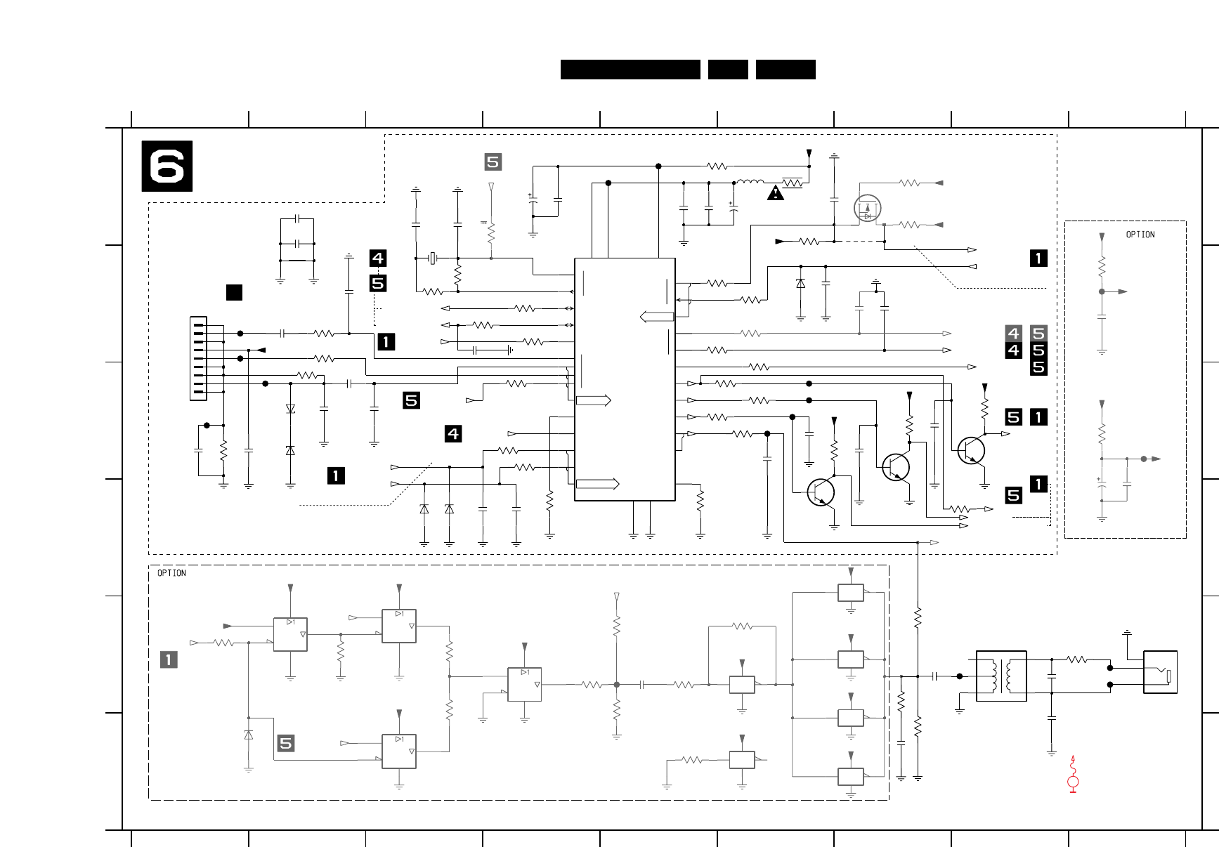
EN 837.LX7500RCircuit Diagrams and PWB Layouts
EN
1
1
EN
1
1
1
EN
1
AUTO
V
R
DIR
DVSS
PDN
1
CCLK
CSN
DAUX
P-S
4
3
2
O
XTAL
RX
DIF <0:2>
OCKS <0:1>
I
I
CDT
CM <0:1>
MCK0
TX
LRCK
BICK
Φ
FS96
ERF
SDTO
2
1
DVDD
TVDD
AVDD
O
AVSS
EN
F624 E9
F625 C1
6601 C2
6602 F2
6603 B6
6604 D3
GND
GND
6605 D3
7601 A7
7603 B4
7605 C8
7611-3 E3
7611-4 E4
F610 A5
F611 A5
F612 B9
F613 B1
F614 C1
F615 C6
F616 C6
F617 C2
F618 C6
F619 C6
3827 C7
3828 C6
3829 C9
3830 C1
SPDIF IN/OUT
GND
F620 C9
F621 E9
F622 E5
F623 E8
3844 E4
3845 E5
3846 E7
3847 E3
3848 E5
3849 E5
3850 F7
3851 E7
4601 A7
5600 E8
5601 A6
6600 C2
2827 B7
2828 B7
3118 F5
3125 D8
SPDIF_DVD
3800 A5
3801 A6
3802 A7
7606 D7
7607 D6
7609-1 E6
7609-2 D7
7609-3 E7
7609-4 E7
7609-5 F7
7609-6 F6
7611-1 F3
7611-2 E2
3814 B2
3815 B6
3816 B4
3817 B5
3818 B2
3819 C6
3820 C2
3821 C4
3822 C5
3823 C6
3825 C8
3826 C5
2808 A2
2809 B2
2810 B9
2811 B2
GND
3832 C4
3833 C6
3834 C4
3836 D4
3837 D5
3839 E6
3840 E1
3841 E2
3842 E3
3843 E9
2815 C1
2816 C2
2817 C6
2818 D9
2819 D9
2820 E7
2821 E8
2822 E5
2823 F8
2824 F7
2825 B6
2826 B4
C
D
E
F
3803 A7
3804 A4
3805 A4
3807 B9
3808 B3
3809 B5
3810 B3
3811 B6
3812 B4
3813 B3
2049 C7
2050 C7
2051 D4
2052 D3
2800 A4
2801 A4
2802 A2
2803 A5
2804 A5
2805 A6
2806 A3
2807 A3
3456
SPDIF Receiver
2812 C2
2813 C2
2814 C3
789
A
B
2046 A6
2048 C6
DIG_IN_+
OPTICAL_IN
5V_OPT
SPDIF out
123456789
12
DIG_IN_-
A
B
C
D
E
F
1600 B3
1701 B1
1702 E9
COMBI BOARD
100R
3812
100n
2815
18K
3837
F624
F623 F621
10K
3803
BSH111
7601
F616
5601
180R
3848
1n0
2824
470p
2814
100n
2812
2800
47u 16V
100R
3118
5
7
4
14
6
74LVC125AD
7611-2
18p
2806
3
714
4
74LVU04D
7609-2
470p
2813
3821
100R
100n
2801
5
714
6
7609-3
74LVU04D
100R
3844
2818
10u 50V
7
13
14
11
SCN
74LVC125AD
7611-4
12
4K7
3840
BZX384-C3V3
6602
100R
3804
100R
3836
3841
10K
F620
2810
100n
F611
F610
2K2
3839
3822 10K
3801
2R2
2046
18p
4601
F625
F622
100R
3819
3813
100R
9
714
8
11
714
10
74LVU04D
7609-4
14
12 7609-5
74LVU04D
74LVU04D
7609-6
13
7
18p
2052
2051
18p
F617
2
1
DIG
DIG
DIGDIG
DIG
DIG
DIG
DIG
DIG DIG DIG
DIG
DIG
DIG
DIG
DIG
DIG
DIGDIGDIG
DIG
DIGDIGDIGDIG
DIGDIGDIGDIG
DIG
DIGDIG
DIG
DIG
DIG DIG
DIG
DIG
DIG
DIG
DIG DIG
DIG
1702
YKC21-3394
3
6604
BZX384-C3V3
150p
2821
BZX384-C3V3
6605
100R
3811
6601
BZX384-C3V9
ADIG
100R3125
DIG
3834
100R
10K
3825
ADIG
16V47u
2805
100R
3814
F613
10R
3830
2817
47p
100R
3817
10K
3823
F612
2825
18p
1
714
2
3827
10K
7609-1
74LVU04D
2808
100n
560R
3846
10K
3833
DIG
3809
100R
18p
2049
2826
10p
2828
10p
10p
2827
100n
2803
100R
3800
2804
100n
9
7
10
14
8
2809
470p
74LVC125AD
7611-3
3842
470R
10K
3805
F615
3829
220R
2823
100n
100n
2819
3802
10K
BZX384-C3V9
6600
3815
100R
100R
3816
100n
2802
3843
39R
SCN
100n
2820
3820 75R
F619
2816
100n
470R
3845
1
2
3
4
5
6
7
8
9
6
1701
from AV board
1952
B9B-PH-K
23
25
26
16
7
8
11
20
3
4
5
22
12
13
14
1
2
18
17
19
24
AK4112A
7603
15
9
10
21
28
27
1M0
3808
3810
100R
6603
BZX384-C3V3
3828
D
100R
6
2050
18p
5600
6RG
1
2
34
2048
18p
F614
3850
470R 10R
BC847BW
7605
3851
3849
100R
470R
3847
100R
3807
3826
10K
2811
100n
470R
3818
1600
24M576
18p
2807
3
7611-1
74LVC125AD
2
7
1
14
ADIG
BC847BW
7607
DIG
100R
3832
F618
100n
2822
SPDIF_MCLK01
IIS_OUT_BCLK_RC
+3V3
7606
BC847BW
IIS_IN_SDA1
DSP_CLK
SPDIF_CDTI
SPDIF_CCLK
SPDIF_CSN
SPDIF_DSP
SPDIF_DAI
SPDIF_ERF_3V3
+3V3
+3V3
SPDIF_MCLK02
SPDIF_ERF
+5V
+3V3_SEL
+3V3_SEL +3V3_SEL
+3V3_SEL
+5V_BUFF
+5V_BUFF
+5V_BUFF
+5V_BUFF
+5V_BUFF
+5V_BUFF
SPDIF_DSP
+3V3_SEL
IIS_IN_SPDIF
+5V
SPDIF_CDTO
SPDIF_DAI
to 3849, 7611-9
SPDIF_AUTO_DETECT
+5V
+5V
SPDIF_FS96
IIS_OUT_WS_RC
SPDIF_PDN
+5V
+3V3
+3V3_SEL
SPDIF_SEL
+5V_BUFF
+5V
# for provision only Combi board LX7500R, 221104
8
communication Control µP
communication Control µP
EVM
V
DC voltages measured in Stop mode
with no audio output.
...V
0,4V
2,7V
2,7V
0V
0V
0V
3,3V
3,3V
2,8V
1,7V
1,7V
1,6V
1,2V
1,2V
0V
0V
0V
0V
0V
5V
5V
4,7V
3,8V
3,3V
3,3V
2,6V
3,4V
1,3V
1,3V
1,6V
2,8V
2,5V
2,9V
2,8V
0V
0V
5V
3,4V
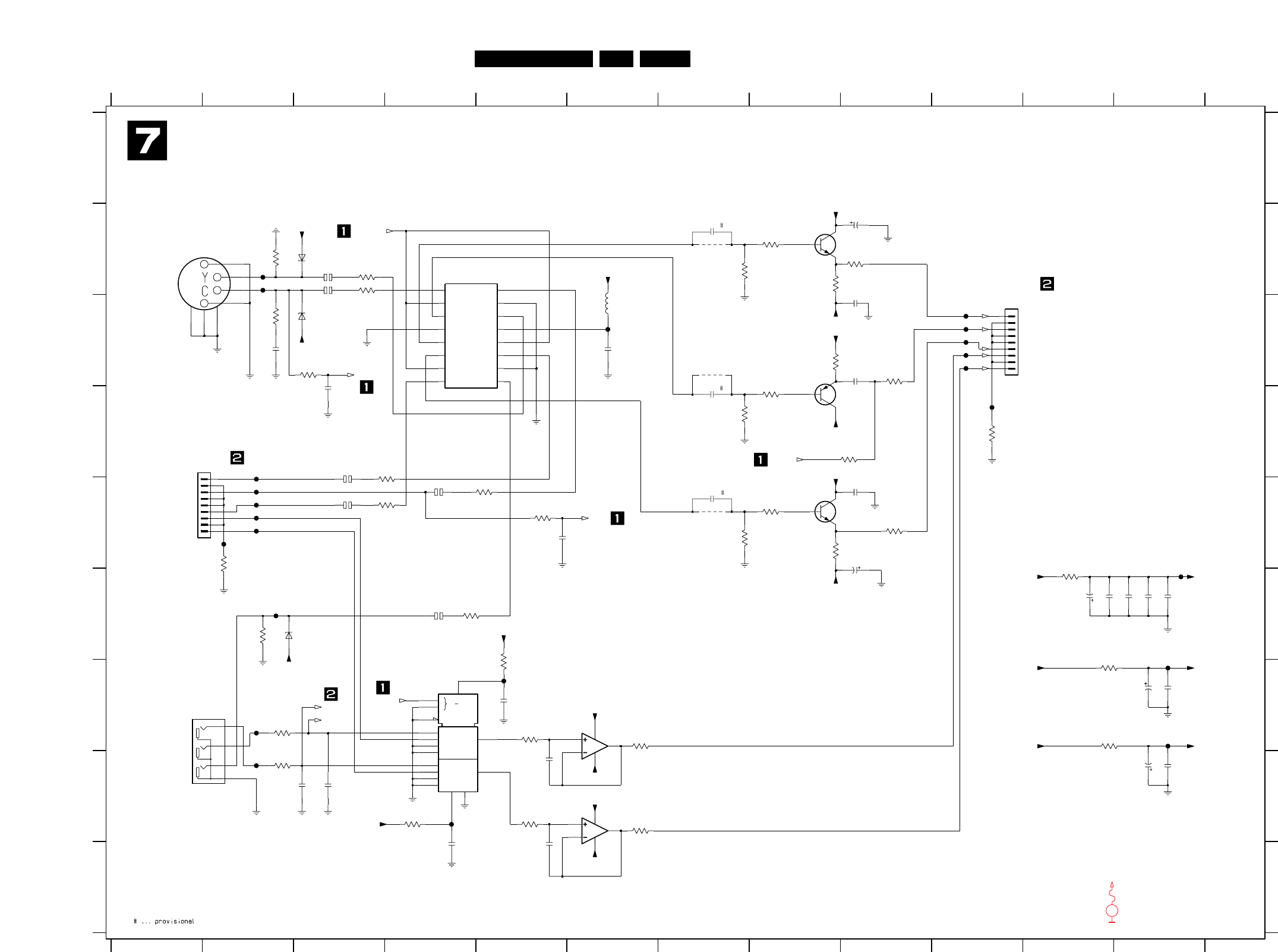
EN 847.LX7500RCircuit Diagrams and PWB Layouts
G4
0
3
2
VDD
VEE VSS
1
0
3
2
1
4X0
3
0
1
EXT. VIDEO IN
SELECTOR
CFIN
CVBSFIN
7901 B4
7902 D8
7903 E8
7904 G4
F710 B2
F711 B2
F712 C10
F713 C10
F714 C10
F715 C10
F716 C10
F717 E2
F718 E2
F719 E2
F720 E2
F721 E2
F722 F2
F723 F12
F724 G12
F725 G2
F726 H2
F727 G12
F728 D10
VIDEO SWITCHING
For non scart version only
3931 G6
3932 H2
3933 G11
3934 H4
3935 H5
3936 H6
4900 B7
4901 C7
4902 E7
5900 C6
6900 B3
6901 C3
6902 F2
7705-1 G6
7705-2 H6
7900 B8
3910 C9
3911 D10
3912 D8
3913 D7
3914 D9
3915 D4
3916 E5
3917 E4
3918 E8
3919 E5
3920 E9
3921 E7
3922 E2
3923 E8
3924 F4
3925 F11
CFIN
Audio R
3926 F2
3927 G5
3928 G11
3929 G2
3930 G5
2928 H12
2929 I4
2930 I5
3900 B8
3901 B2
3902 B9
3903 B7
3904 B3
3905 B8
3906 B3
3907 C2
3908 C8
3909 C3
S-Video
CVBS
2921 G5
2922 G12
2923 G12
2924 H5
2925 H3
2926 H3
2927 H12
from Front
2905 C6
2906 C9
2907 D3
2908 D7
2909 E3
2910 E4
2911 E9
2912 E7
2913 E3
2914 E5
2915 F4
2916 F11
2917 F11
2918 F12
2919 F12
2920 F12
1942
Audio L
VIDEO SWITCH
COMBI BOARD
9 101112
A
B
C
D
E
F
U10 C6
U11 E2
1400 B2
1401 C10
1402 G2
1403 D2
2043 B9
2044 E9
2900 B7
2901 B3
2902 B3
2903 C9
2904 C2
to AV board
8 9 10 11 12
12345678
YFIN
CVBSFIN
1234567
YFIN
G
H
I
A
B
C
D
E
F
G
H
I
U8 H4
U9 G5
AINFL
AINFR
AINFL
AINFR
EXT. AUDIO IN
SELECTOR
F721
150R
3916
68R
3900
3902
150R
100n
2911
10u16V
2915
GND_V
SCN
150R
3912
1K0
3935
SCN
F727
2930
330p 330p
2924
1u0
2908
3907
75R
2902 16V10u
GND_V
100n
2921
100R
3927
2903
100n
GND_V
100n
2919
GND_V
GND_V
2904
100n
F722
F711
10R
F713
3911
SCN
SCN
3928
100R
330R
F725
3923
3930
GND_V
1K0
1K0
3929
F718
BC847BW
7903
1
2
3
4
7
5
6
TCS7927-24-401
1400
SCN
F728
4900
U11
F724
F712
47K
1IN1B
11
IN2A
14
IN2B
8IN3A 9
IN3B
3OUT1
5OUT2
6OUT3
13
V+
3909
NJM2285M
7901
2CTL1
12
CTL2
7CTL3
15
GND1
4GND2
10
GND3
16
IN1A
2918
100n
330R
3908
2044
22u 16V
2043
22u16V
4901
1u0
100n
2912
F716
2906
F715
3925
1K0
3905
330R
2929
100n
6901
BZX384-C12
16V 10u
2909
3915
GND_V
GND
GND
GND
GND
10K
150R
7900
3921
BC847BW
150R
3917
3924
150R
68R
3920
F717
3926
75R
56R
3910
3906
GND_V
150R
100R
3933
7902
BC857BW
2900
10K
1u0
100n
3913
F710
2920
100n
2928
GND_V
3931
470R
3918
150R
F719
GND_
V
150R3904
F726
F720
3914
4K7
84
3903
10K
7705-2
LM833D
5
6
7
16V 10u
SCN
2923
2916
100n
2914
100n
5
6
7
8
9
S9B-PH-SM3-TB-A
1403
1
2
3
4
10R
BZX384-C12
3922
6900
3901
75R
47u25V
2927
2910
10u16V
2926
470p
5900
10u
SC
N
SCN
1K0
3932
GND_V
470p
2925
SCN
6
7
8
9
6902
BZX384-C12
B9B-PH-SM3-TBT
1401
1
2
3
4
5
GND_V
GND_V
2
3
4
1
LPR6520
1402
3919
47K
2922
GND_V
25V47u
84
LM833D
7705-1
3
2
1
5
15
2
11
4
13
3
10
9
6
16
7
8
12
1
14
GND_V
HEF4052B
MDX
7904
3934
F714
100R
2907
100n
470R
F723
3936
2913
GND_V
GND_FC
GND_FC
GND_FC
GND_FC
GND_V
16V 10u
2905
100n
U9
U10
GND_V
U8
SCN
GND_V
4902
2917
100n
2901 10u 16V 5VSTBY
+OP35VSTBY
WSIN_F
-OP3
+OP3
5VSTBY
5NSTBY
ASEL_YC2_0
5NESD5NSTBY
5NESD
-OP3 +OP3
5NSTBY
VIDEO_SEL
WSIN_2
5NESD
5NESD
5NSTBY
5VSTBY
5VSTBY
5NSTBY
5VSTBY
5NSTBY
-OP3
EXT3L
EXT3R
WS_OUT
# for provision only
Combi board LX7500R, 081004
EVM
V
DC voltages measured in Stop mode
with no audio output.
...V
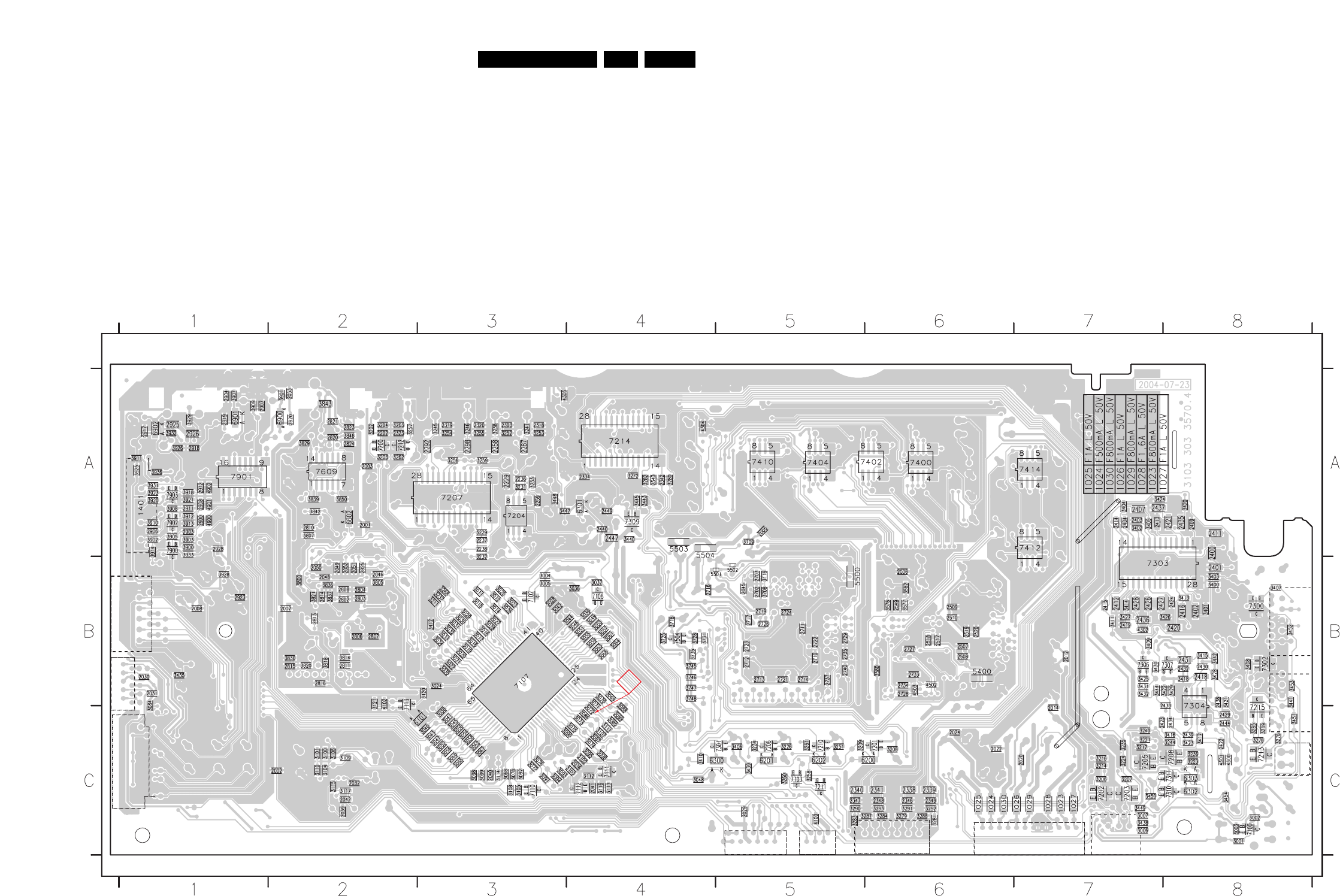
EN 857.LX7500RCircuit Diagrams and PWB Layouts
COMBI BOARD / copper side view
Combi board LX7500R .4 , 071004
SOURCE SEL.
SOUND PROC. IC
SUBWOOFER/
CENTER
SOURCE SEL.
SOUND PROC. IC
SURROUND
SOURCE SEL.
SOUND PROC. IC
FRONT L /R
EXT. VIDEO IN
SELECTOR
µP
1023 C7
1024 C6
1025 C6
1026 C7
1027 C7
1028 C7
1029 C7
1030 C6
2001 A2
2002 C2
2003 A2
2005 A5
2006 B6
2007 B2
2008 B1
2012 B7
2014 C7
2020 C7
2022 C6
2024 C6
2028 B3
2029 C5
2030 B1
2031 B1
2032 C2
2036 C4
2039 C2
2040 C3
2041 C4
2042 C2
2045 B5
2046 B2
2048 B2
2049 B2
2050 B2
2051 B2
2052 B2
2053 A2
2202 A2
2229 A3
2236 A3
2237 A3
2238 A3
2258 A3
2259 A3
2287 A3
2292 A3
2298 A3
2303 A3
2318 A3
2319 A3
2320 A3
2323 A2
2334 A4
2338 C6
2339 C6
2340 C5
2341 C6
2342 A4
2343 A4
2346 C6
2347 C5
2348 C6
2349 C6
2400 A8
2401 B8
2402 B8
2403 A7
2404 A7
2407 A7
2409 A8
2411 A8
2412 B7
2413 A7
2414 A7
2415 B7
2416 B8
2418 B8
2419 B7
2420 B8
2421 A8
2422 C8
2423 C7
2424 B8
2426 B7
2427 B7
2428 B7
2429 C8
2430 B8
2431 B8
2432 B8
2433 B8
2434 C8
2435 A8
2436 B7
2437 A7
2438 B8
2439 C8
2440 A4
2444 C8
2447 A4
2449 A4
2507 B6
2508 B6
2509 B6
2510 B6
2517 B6
2518 B6
2519 B6
2520 B6
2549 B6
2702 B5
2703 B5
2710 B5
2711 B5
2712 B5
2713 B5
2714 B5
2716 B4
2717 B5
2719 B5
2721 B5
2722 B5
2723 B5
2724 B5
2726 B5
2727 B6
2728 B6
2729 B5
2733 B6
2734 B6
2735 B5
2737 B5
2740 B5
2802 B2
2803 B2
2804 B2
2806 B2
2807 B2
2808 B2
2810 A2
2811 B2
2813 B2
2814 B2
2815 B2
2816 B2
2820 A2
2821 A2
2823 A2
2824 A2
2825 B2
2900 A1
2903 A1
2904 A1
2906 A1
2907 A1
2908 A1
2911 A1
2912 A1
2917 A1
2918 A1
2919 A1
2920 A2
2923 B1
2925 A1
2926 A1
2928 A1
3001 C8
3002 C8
3003 C8
3004 B3
3005 B3
3006 C7
3007 C7
3011 B3
3012 B3
3014 B3
3015 B3
3016 B3
3017 B3
3018 B3
3019 B3
3020 B3
3021 B3
3022 B3
3023 B3
3024 B3
3025 B3
3026 B3
3027 B3
3028 B3
3029 B3
3030 B3
3031 B3
3032 B3
3033 B3
3034 B3
3035 B3
3036 B4
3037 B4
3038 C3
3039 B4
3040 C3
3041 C3
3042 B3
3043 C3
3044 B4
3045 C3
3046 B4
3047 C3
3048 C4
3049 B4
3050 C3
3051 B4
3052 C3
3053 B4
3054 C3
3055 B4
3056 C3
3057 B4
3058 C3
3059 B4
3060 C3
3061 B4
3062 C3
3063 B4
3064 B4
3065 C3
3066 B4
3067 C3
3068 C3
3069 B4
3070 B4
3071 B4
3072 C4
3073 C4
3074 C4
3075 C4
3076 C3
3077 C3
3078 C3
3084 B1
3085 C4
3086 C4
3087 C4
3088 C4
3089 C4
3090 C4
3091 C3
3092 C3
3093 C3
3094 C3
3095 C4
3096 C4
3098 C3
3099 C3
3100 C2
3101 C2
3102 C4
3103 C4
3104 C2
3105 C3
3106 C2
3107 C4
3108 C3
3109 C2
3110 C2
3111 C4
3112 C4
3113 C4
3114 C3
3115 C2
3116 C4
3117 C2
3119 B5
3120 B3
3121 B2
3202 A2
3203 A2
3204 A2
3206 C7
3207 C7
3208 C6
3209 C5
3211 B3
3214 C7
3216 C7
3217 C7
3221 C7
3223 C8
3224 C7
3226 C5
3229 A3
3231 A3
3232 B3
3233 A3
3234 C5
3235 C7
3236 C8
3237 B3
3238 A3
3240 C7
3241 A3
3244 C8
3245 A3
3246 A3
3251 C5
3252 A3
3253 A3
3254 A3
3255 A3
3256 A3
3257 A2
3258 C5
3259 A3
3260 C5
3261 C5
3262 A2
3263 A2
3268 B3
3272 A4
3276 C8
3278 C8
3279 C6
3280 A4
3281 C6
3282 A4
3283 C5
3284 C6
3285 C8
3287 C6
3288 C6
3289 C8
3290 C5
3291 C6
3292 C6
3293 C6
3400 B8
3401 B8
3402 A7
3403 B8
3404 A7
3405 A7
3406 C5
3407 B8
3408 B8
3409 B7
3410 C4
3411 B7
3412 B3
3413 B8
3414 B7
3415 B8
3416 C8
3417 C8
3418 B8
3420 A8
3421 B8
3422 B8
3423 C8
3424 A7
3425 B7
3426 B8
3427 B7
3428 B8
3429 B8
3430 B7
3431 B7
3432 B7
3435 B1
3438 C7
3439 C5
3440 A4
3441 B8
3442 B8
3443 A4
3444 B7
3445 A4
3447 A3
3448 A3
3449 C7
3450 C7
3451 C8
3452 B8
3453 B8
3454 C8
3576 B6
3577 B6
3580 B6
3582 B6
3708 B5
3709 A5
3718 B4
3725 B4
3728 B4
3731 B4
3735 B4
3745 B4
3746 B4
3747 B4
3748 B4
3800 B2
3805 B2
3807 A2
3814 B2
3818 B2
3820 B2
3821 B2
3829 A2
3830 B2
3836 B2
3837 B2
3839 A2
3842 A2
3843 A2
3846 A2
3850 A2
3900 A1
3901 A2
3902 A1
3903 A1
3905 A1
3907 A1
3908 A1
3909 A1
3910 A1
3911 A1
3912 A1
3913 A1
3914 A1
3918 A1
3920 A1
3921 A1
3923 A1
3925 A1
3926 A1
3928 B1
3929 A1
3931 A1
3932 A1
3933 A1
3936 A1
4100 C5
4102 B2
4300 C8
4301 C8
4302 B7
4304 A4
4305 A3
4502 B6
4503 B6
4900 A1
4901 A1
4902 A1
5400 B6
5500 B5
5501 B5
5502 B5
5503 A4
5504 A4
6101 C3
6200 C6
6201 C5
6202 C5
6300 C5
6301 A4
6302 C8
6303 C8
6602 A2
6900 A2
6901 A1
6902 A1
7100 C8
7102 B3
7103 C5
7106 B4
7107 B3
7110 C3
7111 C4
7112 C4
7113 B2
7200 A2
7201 C6
7202 C7
7203 C7
7204 A3
7205 C7
7206 C5
7207 A3
7208 C8
7210 C5
7211 C5
7212 A2
7213 C8
7214 A4
7215 C8
7300 B8
7301 C5
7302 B8
7303 B7
7304 B8
7306 B7
7307 B8
7309 A4
7310 C8
7311 C8
7400 A6
7402 A6
7404 A5
7410 A5
7412 A7
7414 A7
7504 B4
7609 A2
7900 A1
7901 A1
7902 A1
7903 A1
19
111
910
10
2
19 21202
1102
111 122 1
16
25612 1 15 26
1100 1020
1205 1810
11
21
2
9
10
7
8
1022 1018 1300
2
1302
1403
This assembly drawing shows a summary of all possible versions.
For components used in a specific version see schematic diagram respectively partslist.
f0
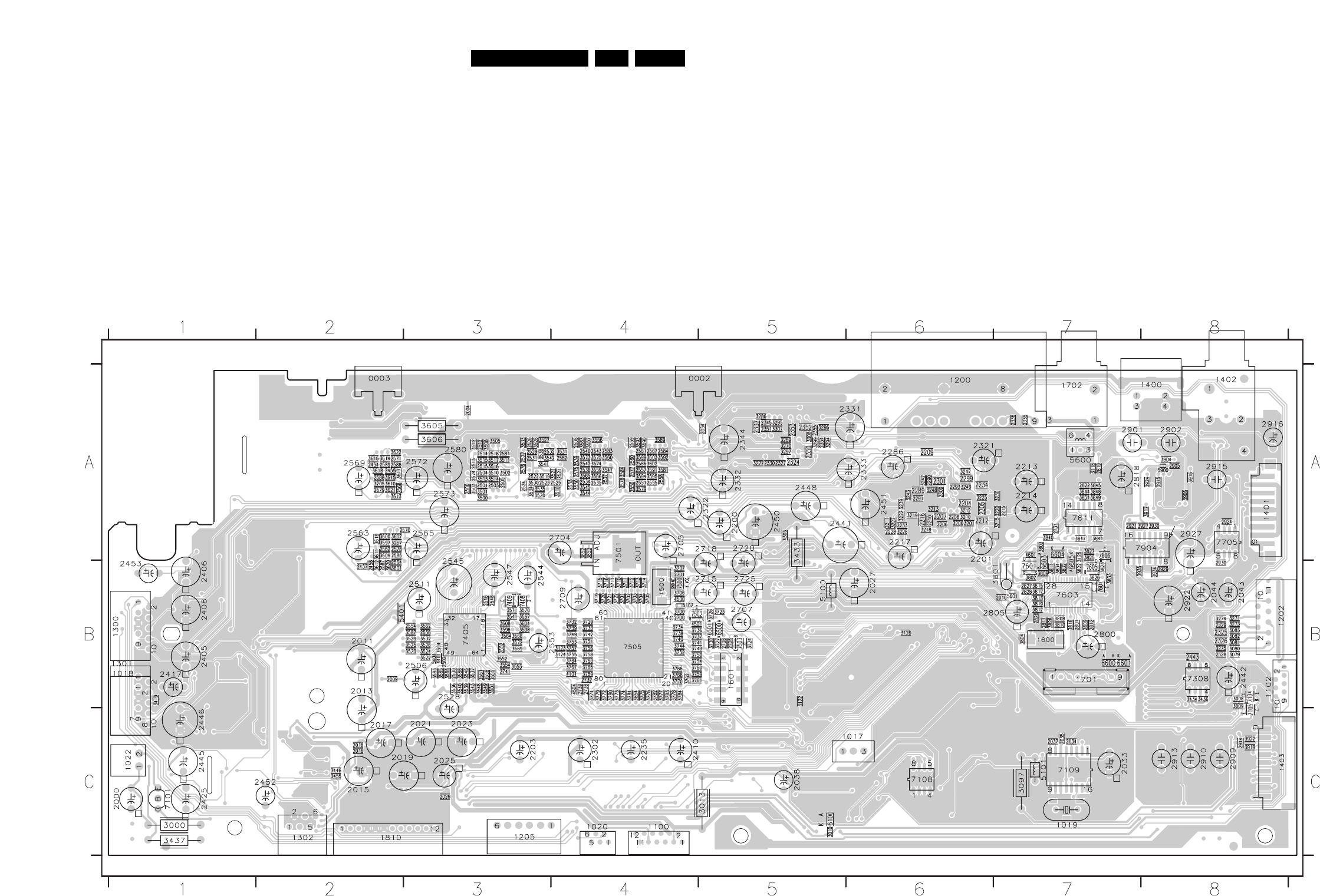
EN 867.LX7500RCircuit Diagrams and PWB Layouts
CODEC
DSP
SPDIF
RECEIVER
AUDIO LINE IN/OUT DIGITAL OUT
S-VIDEO IN
CVBS
LINE IN
RDS DECODER
EXT. AUDIO
SELECTOR
COMBI BOARD / component side view
Combi board LX7500R .4 , 081004
JTAG
INTERFACE
to Amplifier board
1302
to Amplifier board
1331
to Front board
1924 to Front board
1910
to Front board
1922
to AV board 1943
to AV board 1942
to Audio tuner
to Aux supply board
1305 to Aux supply board
1304
to AV board
1950 & 1953
to AV board
1952
FAN
0002 A5
0003 A2
1017 C6
1018 B1
1019 C7
1020 C4
1022 C1
1100 C4
1102 B8
1200 A6
1202 B8
1205 C3
1300 B1
1301 B1
1302 C2
1400 A8
1401 A8
1402 A8
1403 C8
1500 B4
1600 B7
1601 B5
1701 B7
1702 A7
1810 C2
2000 C1
2004 A3
2009 B2
2010 B7
2011 B2
2013 C2
2015 C2
2016 C2
2017 C2
2018 C2
2019 C3
2021 C3
2023 C3
2025 C3
2026 C3
2027 B6
2033 C7
2034 C7
2035 C7
2037 C7
2038 C5
2043 B8
2044 B8
2054 A5
2200 A5
2201 A6
2203 C3
2204 A6
2205 A6
2206 A6
2207 A6
2208 A6
2209 A6
2210 A6
2211 A6
2212 A6
2213 A7
2214 A7
2215 A7
2216 A6
2217 A6
2228 A6
2233 A6
2234 A6
2235 C4
2286 A6
2289 A6
2290 A6
2291 A6
2293 A6
2299 A6
2300 A6
2301 A6
2302 C4
2321 A6
2322 A5
2324 A5
2325 B8
2326 B8
2327 A5
2328 B8
2329 B8
2330 A5
2331 A6
2332 A5
2333 A6
2335 A7
2336 A7
2337 A5
2344 A5
2345 A5
2350 A5
2351 A5
2352 A5
2353 A5
2354 A5
2355 A5
2405 B1
2406 B1
2408 B1
2410 C4
2417 B1
2425 C1
2441 A5
2442 B8
2443 B8
2445 C1
2446 C1
2448 A5
2450 A5
2451 A6
2452 C2
2453 B1
2454 A2
2455 A2
2456 B2
2457 B2
2500 A3
2501 A3
2502 B3
2503 A3
2504 A3
2505 A3
2506 B3
2511 B3
2512 A3
2513 A3
2514 A3
2515 A3
2516 A3
2521 A4
2522 A3
2523 A3
2524 A3
2525 A4
2526 A3
2527 A3
2528 B3
2529 A3
2530 B3
2531 A3
2532 A3
2533 A4
2534 A4
2535 A4
2536 A4
2537 A4
2538 A4
2539 A4
2540 A4
2541 B3
2542 A4
2543 A4
2544 B3
2545 B3
2546 B3
2547 B3
2548 B3
2550 A4
2551 A4
2552 B3
2553 B4
2554 B3
2555 A4
2556 B3
2557 A4
2558 A4
2559 A4
2560 A4
2561 A4
2562 A2
2563 A2
2564 B2
2565 A3
2566 A4
2567 A4
2568 A2
2569 A2
2570 A3
2571 A2
2572 A3
2573 A3
2574 A3
2575 A4
2576 A3
2577 A4
2578 A2
2579 A2
2580 A3
2581 A3
2582 A4
2583 A4
2584 A4
2585 A2
2586 A2
2587 B2
2588 A2
2589 A2
2700 B4
2701 B4
2704 A4
2705 A4
2706 B5
2707 B5
2708 B5
2709 B4
2715 B5
2718 A5
2720 A5
2725 B5
2731 A7
2732 B4
2738 B4
2739 B4
2741 B3
2800 B7
2801 B7
2805 B7
2809 B7
2812 B7
2817 B7
2818 A7
2819 A7
2822 A7
2826 B7
2827 B7
2828 B7
2901 A7
2902 A8
2905 A8
2909 C8
2910 C8
2913 C8
2914 C8
2915 A8
2916 A8
2921 A7
2922 B8
2924 A8
2927 A8
2929 B8
2930 B8
3000 C1
3008 B8
3009 B8
3010 C5
3013 C5
3079 B8
3080 B8
3081 B8
3082 B8
3083 B8
3097 C7
3118 A7
3122 B5
3123 B4
3124 B4
3125 A7
3126 B6
3200 A6
3201 A6
3205 A2
3210 A6
3212 A6
3213 A6
3215 A7
3218 A6
3219 A6
3220 A7
3222 A6
3225 A6
3227 A6
3228 A6
3230 A7
3239 A6
3242 A6
3243 A6
3247 A6
3248 A6
3249 A6
3267 A2
3269 A5
3270 A5
3271 B8
3273 B8
3274 B8
3275 B8
3277 A5
3286 A5
3294 A5
3295 A5
3296 A5
3297 A5
3299 A5
3306 A5
3307 A5
3419 B1
3433 A5
3434 B8
3436 B8
3437 C1
3446 C2
3455 C2
3500 A3
3501 A3
3502 A3
3503 A3
3504 B3
3505 A3
3508 A3
3510 A3
3511 A3
3512 A3
3513 A3
3514 A3
3515 A3
3516 A3
3517 A3
3518 A4
3519 A3
3520 A3
3521 A4
3522 B3
3523 B3
3524 B3
3525 B3
3526 B3
3527 A3
3528 A3
3529 B3
3530 A3
3531 A4
3532 B3
3533 A3
3534 A3
3535 A3
3536 B3
3537 B3
3538 A3
3539 B3
3540 B3
3541 A3
3542 A3
3543 B3
3544 A4
3545 A4
3546 B3
3547 A4
3548 B3
3549 B3
3550 A4
3551 B3
3552 B3
3553 B3
3554 B3
3555 B3
3556 A4
3557 A4
3558 B3
3559 A4
3560 A4
3561 B3
3562 B3
3563 A4
3564 B3
3565 A4
3566 A4
3567 B3
3568 B3
3569 B3
3570 B3
3571 B3
3572 B3
3573 A4
3574 A4
3575 A4
3578 A4
3579 A4
3581 A4
3583 B3
3584 A4
3585 B3
3586 B3
3587 B3
3588 B3
3589 A4
3590 A4
3591 A4
3592 A4
3593 A4
3594 A4
3595 A4
3596 B3
3597 A2
3598 B3
3599 A4
3600 A2
3601 B2
3602 A4
3603 A4
3604 B3
3605 A3
3606 A3
3607 A2
3608 B3
3609 A2
3610 A2
3611 A2
3612 B2
3613 A2
3614 A2
3615 A2
3616 A2
3617 A2
3618 A2
3619 A2
3620 B2
3621 A2
3622 A2
3700 B4
3701 B4
3702 B4
3703 B4
3704 B4
3705 B4
3706 B4
3707 B4
3710 B4
3711 B4
3712 B4
3713 B4
3714 B4
3715 B4
3716 B4
3717 B4
3719 B4
3720 B4
3721 B4
3722 B4
3723 B5
3724 B5
3726 B5
3727 B5
3729 B4
3730 B5
3732 B4
3733 B4
3734 B4
3736 B4
3737 B4
3738 B4
3739 B4
3740 B4
3741 B4
3742 B4
3743 B4
3744 B4
3749 B4
3750 B4
3751 B4
3752 B4
3753 B4
3754 B4
3755 B4
3756 B4
3757 B4
3758 B4
3759 B4
3760 B4
3761 B4
3762 B4
3763 B4
3764 B4
3765 B4
3766 B4
3767 B4
3768 B4
3769 B4
3770 B4
3771 B4
3772 B4
3773 B4
3774 B4
3775 B4
3776 B4
3777 B4
3778 B4
3779 B4
3780 B4
3781 B4
3782 B4
3783 B4
3784 B4
3801 B7
3802 B7
3803 A7
3804 B7
3808 B7
3809 B7
3810 B7
3811 B7
3812 B7
3813 B7
3815 B7
3816 B7
3817 B7
3819 B7
3822 B7
3823 B7
3825 A7
3826 B7
3827 A7
3828 B7
3832 B7
3833 B7
3834 B7
3840 A7
3841 A7
3844 A7
3845 A7
3847 A7
3848 A7
3849 A7
3851 A7
3852 A4
3853 A4
3854 B4
3904 A8
3906 A8
3915 A8
3916 A8
3917 A8
3919 C8
3922 C8
3924 A8
3927 A8
3930 A8
3934 B8
3935 B7
4101 B4
4303 A5
4401 B3
4500 B4
4501 B4
4504 B4
4601 A7
5100 B5
5101 C7
5102 B4
5401 B2
5404 B3
5600 A7
5601 B7
5900 A8
6100 C5
6500 B5
6501 B5
6600 B7
6601 B7
6603 B7
6604 A7
6605 B7
7101 C1
7104 B8
7105 C8
7108 C6
7109 C7
7308 B8
7405 B3
7408 B3
7409 B3
7500 B4
7501 A4
7502 B4
7503 B5
7505 B4
7601 B7
7603 B7
7605 B7
7606 A7
7607 B7
7611 A7
7705 A8
7904 A8
This assembly drawing shows a summary of all possible versions.
For components used in a specific version see schematic diagram respectively partslist.
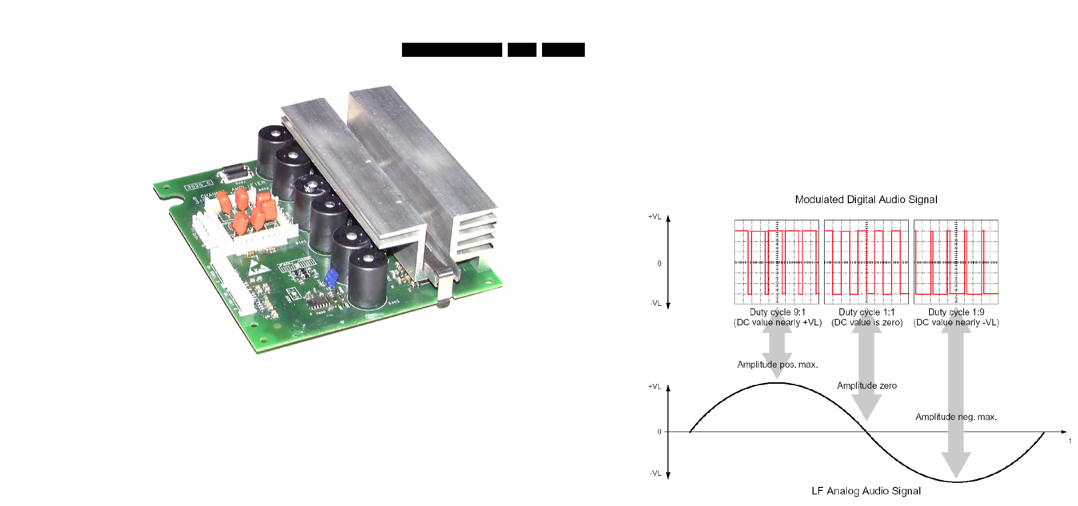
EN 877.LX7500RCircuit Diagrams and PWB Layouts
6-channel class-D amplifier
Basic operation of a class-D amplifier
Basically, the output stage of a class-D amplifier outputs a continuous square wave swinging between positive and negative power supplies
with a fixed frequency (“clock” frequency) far beyond the audible range. The duty cycle of this square wave is modulated with the audio signal.
The output is followed by a low-pass filter which eliminates the clock frequency and allows only the audio signal going to the speaker. See
simplified drawing below.
Compared to a conventional power amplifier the benefits of the Class-D amplifier are:
• higher effiency
• lower power dissipation
• smaller heatsink required
• smaller mains transformer required
The main disadvantage of this concept is:
• The amplifier is operating with a high-frequency square wave at high amplitude and currents. This requires special precautions to prevent
excessive electromagnetic ratiation (EMC).
6 - channel AMPLIFIER BOARD
PWR307 (6x 100W SE)
TABLE OF CONTENT
Class D amplifier circuit description . . . . . . . . . . . . . . . . . . . . . . . . . .87
Exploded view & mechanical parts . . . . . . . . . . . . . . . . . . . . . . . . . .88
Schematic diagram . . . . . . . . . . . . . . . . . . . . . . . . . . . . . . . . . . . . . .89
Assembly drawing, componentside view . . . . . . . . . . . . . . . . . . . . . .90
Assembly drawing, copperside view . . . . . . . . . . . . . . . . . . . . . . . . .91
Loudspeaker sockets . . . . . . . . . . . . . . . . . . . . . . . . . . . . . . . . . . . .92
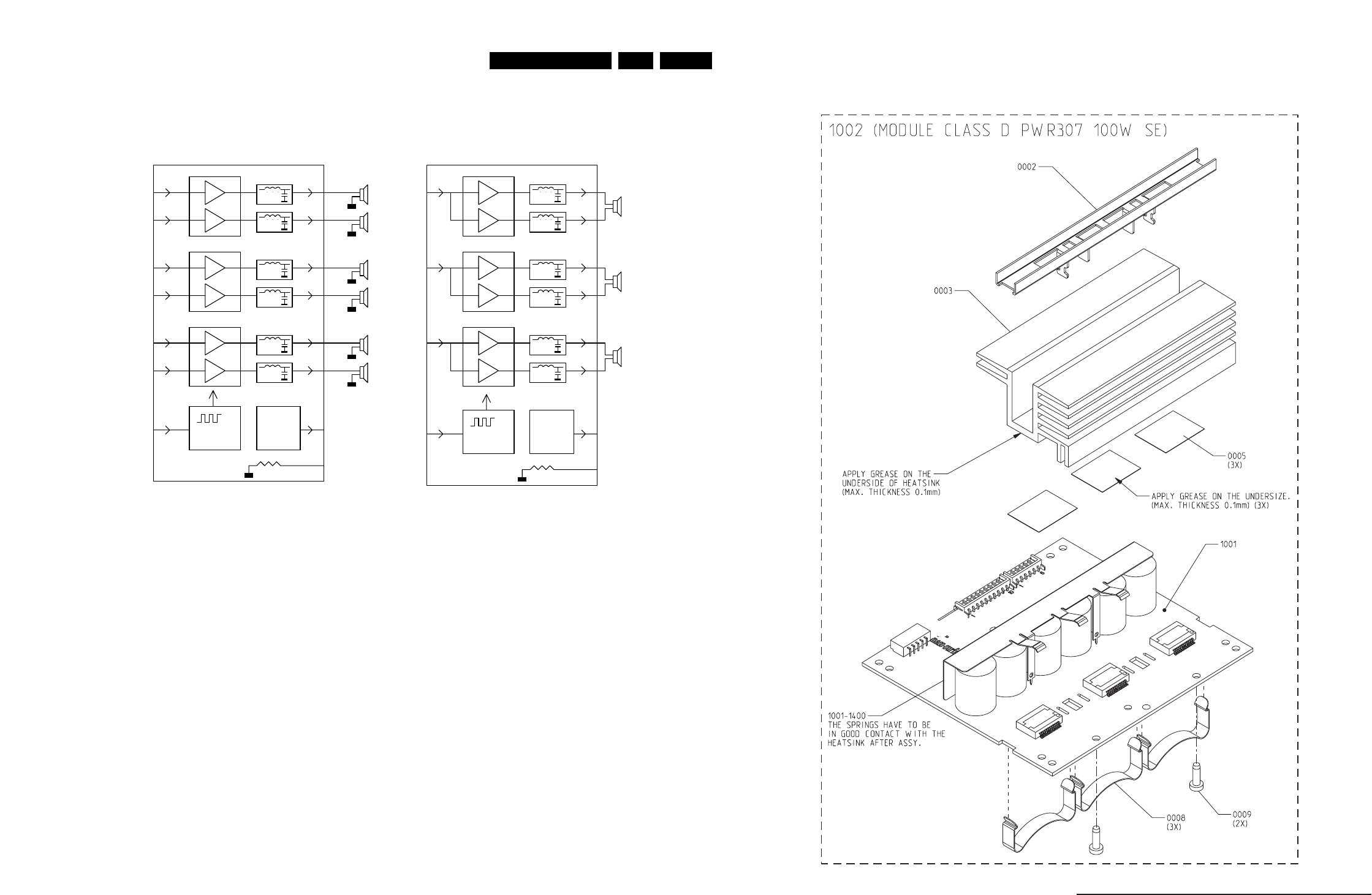
EN 887.LX7500RCircuit Diagrams and PWB Layouts
Block diagram and operation
clock
generator
output 1
output 2
output 3
output 4
output 5
output 6
input 1
input 2
input 3
input 4
input 5
input 6
freq_hop
301.35 / 350 kHz
DC
detection err
temp
NTC
TDA8920/TDA8924
TDA8920/TDA8924
TDA8920/TDA8924
output 1
input 1
TDA8920
SINGLE ENDED 6 x 75W/100W BRIDGE 3 x 100W
+
-
input 2
TDA8920
+
-
input 3
TDA8920
+
-
clock
generator
freq_hop
301.35 / 350 kHz
DC
detection err
temp
NTC
output 2
output 3
• clock oscillator
The clock frequency is generated around IC7600. Using 2 extra transistors (7602 and 7608) and 2 ceramic resonators it can be operated at
2 frequencies: 602.7kHz and 700kHz. The frequency is selected by the signal “FREQ_HOP” coming from connector 1302 pin 9.
When FREQ_HOP is low, the output of 7600-1 will be high. This switches transistor 7602 on, and connects resonator 1600 (602.7kHz) to inverter
7600-3. Similarly, when FREQ_HOP is high, resonator 1601 is connected to 7600-3.
The output frequency is divided by two by IC7607, resulting in 301.35kHz or 350kHz.
The purpose of a selectable clock frequency is related to the disturbance of the tuner which is built-in together with this amplifier. In MW, the
software of the set microprocessor will select the other clock frequency in case the amplifier clock interferes with the tuned station.
• Class-D amplifier TDA8920/TDA8924 and low-pass filter
The TDA892x is a two channel audio power amplifier using class-D technology. The audio input signal is converted into a digital Pulse Width
Modulated (PWM) signal via an analog input stage and PWM modulator. It is then fed to the power stage which outputs a high power PWM
signal which switches between the main supply lines.
The TDA892x is followed by a 2nd-order low-pass filter. It has a cut-off frequency around 50kHz and converts the PWM signal into analog audio
signal across the loudspeaker.
The TDA892x has a temperature protection and a current limiter built-in.
Furthermore, via the mode input, the IC can be put in active-, mute- and standby mode.
- Active mode (amplifier fully operational) with output signal.
- Mute mode; the amplifiers are operational, but the audio signal is muted.
- Standby mode; with a very low supply current, the output stage is switched off.
• DC-detection
The DC-detection circuit monitors all 6 outputs for DC. Whenever one or more outputs contain DC for more than 1 second, the circuit will be
activated. A positive voltage will activate transistor 7710 and pin 10 of connector 1302 will be pulled down. In case of a negative voltage, transistor
7716 will be activated, which in turn activates 7710. The set microprocessor will take further action.
MECHANICAL PARTS LIST & SCREWS
8 4822 492 11735 SPRING, TRANSISTOR
9 - D2.3 x 8
Note: Only the parts mentioned in this list are normal service
spare parts.
MECHANICAL EXPLODED VIEW
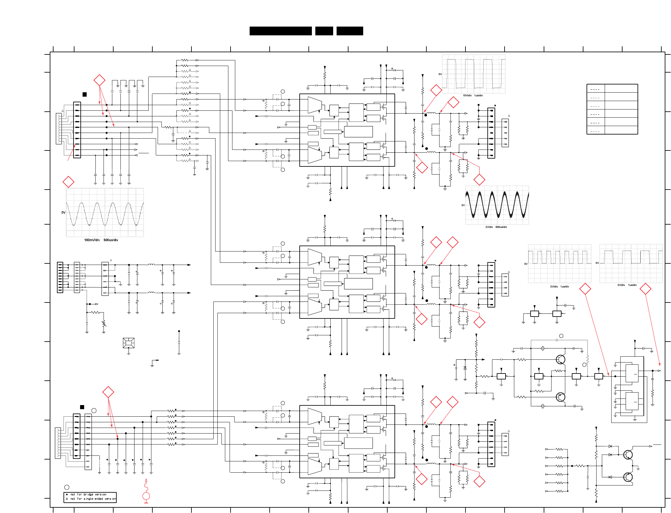
EN 897.LX7500RCircuit Diagrams and PWB Layouts
4138 B7
4338 J7
MUTE
MUTE
REL1
SW1
EN1
REL2
SW2
EN2
VDDP2
VSSP1
-T
MUTE
MUTE
REL1
SW1
EN1
REL2
SW2
EN2
VDDP2
VSSP1
MUTE
MUTE
REL1
SW1
EN1
REL2
SW2
EN2
VDDP2
VSSP1
F140 C2
F141 F3
F142 F2
F143 K3
F109 C12
F111 C2
F112 C12
F113 C15
F114 C2
1318 G12
1400 H3
1600 I13
1601 J13
F115 E15
F116 F2
F117 F3
F118 F2
F119 F3
F120 F12
F121 G12
F122 G12
F123 H19
F124 H3
F125 I18
F126 I3
F127 I3
F128 K12
F129 K12
F130 K12
F131 L15
F132 I2
F133 H12
F134 D12
F135 L12
F139 B12
3456789
I
J
K
L
1301 C1
1302 B2
1303 K2
1304 G2
1305 K1
1306 B12
1307 K12
1308 F12
1320 I 4
1309 G1
1312 G2
1316 C12
1317 K12
12
A
10 11 12 13 14 15 16
123456789
2101 B8
2102 B8
10 11 12 13 14 15 16
B
C
D
E
F
G
H
I
J
K
L
A
B
C
D
E
F
G
H
2104 B9
2105 B9
2106 A10
2107 B10
2108 B10
2111 B10
2114 B10
2115 C10
2116 C11
2117 C11
2118 C11
2120 C10
2122 C10
2123 D11
2124 D11
2125 D11
2126 D10
2127 D10
2128 D9
2129 D8
2130 D8
2131 D7
2132 D7
2133 C7
2134 C6
2135 C6
2136 B7
2137 B7
2138 B7
2201 F8
2202 F8
2204 F9
2205 F9
2206 E10
2207 F10
2208 F10
2211 F10
2214 F10
2215 G10
2216 G11
2217 G11
2218 G11
2331 L7
2332 L7
2333 K7
2220 G10
2222 G10
2224 H11
2223 H11
2225 H11
2226 H10
2227 H10
2228 H9
2229 H8
2230 H8
2231 H7
2232 H7
2233 G7
2234 G6
2235 G6
2236 F7
2237 F7
2238 F7
2301 J8
2302 J8
2304 J9
2305 J9
2306 I10
2416 L3
2417 L3
2418 L2
2419 H2
2420 D3
2421 L2
2422 L3
2423 I 4
2307 J10
2308 J10
2311 J10
2314 J10
2315 K10
2316 K11
2317 K11
2318 K11
2320 K10
2322 K10
2323 L11
2324 L11
2325 L11
2326 L10
2327 L10
2328 L9
2329 L8
2330 L8
2334 K6
2335 K6
2336 J7
2337 J7
2338 K7
2400 I3
2401 G4
2402 G4
2403 G3
2404 G4
2405 G4
2406 G3
2407 G3
2408 B2
2409 B3
2410 B3
2411 D3
2412 D2
2413 D2
2414 D2
2415 L3
3301 K10
3302 K10
3303 K11
3304 L11
3305 L10
3306 L6
2425 B3
2500 C4
2501 D5
2502 D4
2600 H14
2601 H14
2602 I13
2603 I14
2604 I16
2605 I12
2606 J12
2607 J14
2608 I16
2700 L15
2611 I11
3100 B10
3101 C10
3102 C10
3103 C11
3104 D11
3105 D10
3106 D6
3107 B8
3108 B6
3109 E8
3151 C11
3152 D11
3153 C11
3154 D11
3200 F10
3201 G10
3202 G10
3203 G11
3204 H11
3600 I12
3601 I12
3602 I13
3603 H17
3307 J8
3308 J6
3309 M8
3351 K11
3352 L11
3353 K11
3354 L11
3400 B4
3401 B4
3402 C4
3403 C4
3404 C4
3405 C4
3406 C4
3407 C4
3408 D4
3409 D4
3410 K4
3411 J4
3412 K4
3413 K4
3414 A4
3415 A4
3416 A4
4337 J7
4400 C4
4410 L2
5102 B11
5103 C11
5202 F11
5203 G11
5302 K11
3417 B4
3418 B4
3419 B4
3420 H2
3421 B4
3422 H2
3423 B4
3424 J4
3425 K4
3426 K4
6600 I12
6713 K15
6714 K15
3604 I12
3605 I14
3606 I15
3607 J12
3608 J13
3609 J13
3610 J16
3700 K14
3701 K14
3703 K15
3709 L14
3712 L14
3713 K15
3716 L14
3718 L14
3721 L14
3722 L15
4133 C7
4137 B7
4238 F7
4232 H7
4332 L7
4132 D7
4233 G7
4237 F7
4333 L7
4512 C15
4511 B15
4521 C15
4522 C15
4501 B15
4502 B15
7710 K16
7716 L16
F100 B2
F102 B2
F103 B2
F104 B12
F105 C2
F106 C2
F108 C2
5303 L11
5400 G3
5401 G3
6715 L15
7100 B7
7200 F7
7300 J7
7600-1 I12
7600-2 I14
7600-3 I13
7600-4 H14
7600-5 I15
7600-6 H13
7602 I14
7607 J16
7608 J14
2117
220n
35V
220R
3404
2404
470u
2214
560p
1n0
2425
2326
560p
1n0
2418
F114
3
4
5
6
7
8
9
1309
B10B-EH-A
1
10
2
3405
3403
5K6
5K6
3402
5K6
5R6
3205
F106
330p
2331
100n
6713
BAS316
3106
2102
2302
100n
47K
2408
1n0
F130
2220
470n
2316
2419
100n
15n
2136
330p
5R6
3301
1
2
3
4
5
1316
EH-B
2216
470n
1n0
2410
100n
2500
100n
1n0
2409
2130
2106
22u
15n
2111
330p
2402
35V470u
2131
F111
6714
3713
10K
BAS316
5R6
3201
100n
2227
100n
2201
3300
5R6
5302
1
22u
4400
220R
10R
3408
3109
100n
2107
5K6
3411
22R
31033304
1
2
3
4
5
6
7
8
22R
1307
F102
22R
3204
2335
7716
BC857B
2330
100n
68p
2125
470n
3303
22R
F112
22R
3104
100n
2129
100n
2128
5400
2207
100n
F129
560p
2114
2322
560p
560p
2314
5K6
5K6
3401
3400
2230
100n
2328
100n
2108
100n
2407
470u35V
2416
1n0
560p
2315
2222
560p
100n
2229
F134
VDDP2 23
VSSA1
VSSA2
VSSD
VSSP1
VSSP2
PROT
SGND1
SGND2
STABI
SUB|VSSD
VDDA1 10
VDDA2 3
VDDP1 14
IN1+
IN1-
IN2+
IN2-
MODE
OSC
OUT1 16
OUT2 21
HIGH
HIGH
DRIVER
DRIVER
DRIVER
DRIVER
HAND-
HAND-
SHAKE
SHAKE
CTRL &
CTRL &
TEMP SENSOR
CURRENT PROT
MOD
MOD
PWM
PWM
MANAGER
INP
INP
STAGE
15
BOOT1
BOOT2 22
STAGE
OSC
MODE
STABI
LOW
LOW
F124
+A
AMP_LEFT
GND
AMP_RIGHT
L/R_ON
AMP_CENTRE
GND
CSUB_ON
NTC_AMP
GND
AMP_SR
AMP_SL
SUR_ON
AMP_SUB
GND
+A
-A
-A
GND
GND
7
8
9
100n
2304
EH-B
1306
1
2
3
4
5
6
14
VDDP1
23
VDDP2
12 VSSA1
VSSA2
24 VSSD
VSSP1
17
VSSP2
OUT2
PROT
SGND1
SGND2
STABI
SUB|VSSD
19
10
VDDA1
3
VDDA2
BOOT2
IN1+
IN1-
IN2+
IN2-
MODE
OSC
16
OUT1
21
STABI
MODE
OSC
STAGE
STAGE
INP
INP
BOOT1 15
22
MANAGER
PWM
PWM
MOD
MOD
CURRENT PROT
TEMP SENSOR
CTRL &
CTRL &
SHAKE
SHAKE
HAND-
HAND-
DRIVER
DRIVER
DRIVER
DRIVER
HIGH
HIGH
LOW
LOW 3712
47K
100n
23082301
100n
3415
5K6
3102
5R6
F108
10K
3722
F122
100n
2104
2105
100n
10K
F100
3420
3309
10R
470n
2225
EH-B
1
2
3
4
1318
3200
5R6
2231
330p
7710
BC847B
10R
3209
3419
5K6
2228
100n
1n0
2411
4
5
6
7
8
9
F128
10FE-ST-VK-N
1305
1
10
2
3
F133
F135
220n
2224
2120
15n
220R
3409
47K
3208
F109
2700
10u
3709
47K
3701
47K
2226
560p
470n
2116
680n
2118
680n
2123
680n
2218
680n
2223
680n
2318
680n
2323
560p
2115
F116
100n
2205
F103
100n
2307
1
2
3
4
F117
1317
100n
2208
2417
1n0
2414
1n0
3718
47K
47K
3206
22u
5103
1
5102
1
3422
100R
22u
330p
2236
3105
5R6
F131
BAS316
6x100W amplifier LX7500R, 210904
6715
3302
5R6
3107
10R
5K6
3410
10
2
3
4
5
6
7
8
9
1301
FE-ST-VK-NA
1
22u
5202
1
5401
F118
3100
5R6
1
2
3
4
5
6
1312( )
SXXB-EH-A
15n
2211
100n
2204
3413
5K6
2215
560p
F121
5K6
3421
F104
5R6
3202
2127
100n
2420
1n0
F140
3423
5K6
3307
10R
3703
47K
3716
47K
100n
2202
F120
3417
5K6
F119
1n0
2415
47K
3306
220n
2217
3207
10K
3721
10R
2306
22u
2234
2206
22u
220n
5R6
3101
3k9
3151
3k9
3153
3k9
3152
3k9
3154
2327
2422
1n0
100n
2421
4410
1n0
22R
3203
F139
100n
2101
2423
100n
SCREENCOVER
from Power Supply
J1
to LS socket
to LS socket
to LS socket
NTC
Temperature sensor
heatsink
1400
1320
RT-01T
100n
2336
330p
12 VSSA1
1VSSA2
24 VSSD
17 VSSP1
20 VSSP2
2305
11 SGND1
2SGND2
18 STABI
SUB|VSSD
19
12
1
24
17
20
19
1
20
10
VDDA1
3
VDDA2
14
VDDP1
23
VDDP2
IN1-
5IN2+
4IN2-
6MODE
7OSC
16
OUT1
21
OUT2
13 PROT
TDA8920/TDA8924
STABI
MODE
OSC
STAGE
STAGE
INP
INP
MANAGER
PWM
PWM
MOD
MOD
CURRENT PROT
BOOT1 15
22
BOOT2
8IN1+
9
11
2
18
5
4
6
7
13
8
9
11
2
18
5
4
6
7
13
8
9
CTRL &
CTRL &
SHAKE
SHAKE
HAND-
HAND-
DRIVER
DRIVER
DRIVER
DRIVER
HIGH
HIGH
LOW
LOW
2325
470n
7100
TDA8920/TDA8924
7200
TDA8920/TDA8924
7300
TEMP SENSOR
F127
F126
5303
1
22u
5K6
3418
68p
2235
F143
F142
F141
1n0
2412
1308
EH-B
EH-B
EH-B
1
2
3
4
5
6
7
8
3700
47K
1302
FE-BT-VK-N
1
10
2
3
4
5
6
7
8
9
2334
470u 35V
2401
220n
F132
3426
5K6
5K6
3424
100n
2400
220n
2317
220n
2124
3305
3414
5R6
5K6
100n
2329
15n
2311
220n
2324
FE-BT-VK-N
FE-BT-VK-N
13031331
1
10
2
3
4
5
6
7
8
1
2
3
4
5
6
7
8
9
2320
15n
4138
EH-S
1304
3425
5K6
560p
2122
2405
35V470u
1n0
2413
2403
100n
3406
220n
2134
5K6
68p
2135
35V470u
2406
3416
5K6
3308
47K
5203
1
47K
3108
F105
22u
220R
560p
3412
2126
5K6
3407
ERROR
from 7710
FREQ_HOP
TEMP
from 3422
TEMP
to 1302
OUT_4
OUT_5
OUT_6
OUT_2
INPUT_6
INPUT_3
INPUT_6N
INPUT_5
INPUT_4N
INPUT_6N
INPUT_3
INPUT_5
INPUT_1N
Vdd
Vss
Vss
Vdd
Vss
Vdd
OUT_1
OUT_3
INPUT_1
INPUT_2N
INPUT_4N
INPUT_5N
INPUT_6
INPUT_2
MODE_12
MODE_34
MODE_34
MODE_56
INPUT_4
INPUT_5N
MODE_56
INPUT_1N
Vss
Vdd
INPUT_3N
INPUT_4
INPUT_5N
INPUT_6
ERROR
to 1302
Vdd
Vss
Vdd
Vss
VssVss
Vss
VssVss
Vss
OUT_1
OUT_3
OUT_4
OUT_5
OUT_6
OUT_2
Vss
Vss
Vss
Vss
INPUT_2
INPUT_3N
INPUT_4
INPUT_3N
INPUT_6N
Vdd
Vdd
Vss
Vss
VddVdd
Vss Vss Vss
INPUT_3
INPUT_4N
Vss
Vdd
Vdd
Vss
Vss
Vss
MODE_56
CLOCK
from 7607
CLOCK
from 7607
CLOCK
from 7607
Vss
VddVdd
Vss Vss Vss
INPUT_5
INPUT_2
INPUT_2N
VddVdd
Vss VssVss
Vdd
Vss
Vss
Vss
MODE_12
INPUT_1
MODE_34
DC DETECTION
POWER SUPPLY
AMPLIFIER 1
FRONT L/R SPEAKERS
AMPLIFIER BOARD
AMPLIFIER 3
L
SUB
WOOFER
CENTER
RIGHT
LEFT
R
SURROUND SPEAKERS
AMPLIFIER 2
CENTER SPEAKER + SUBWOOFER
*
*
from COMBI board
1018
3
from COMBI board
1300
3
3209 I8
3300 J10
3205 H10
3206 H6
3207 F8
3208 F6
3254 H11
3251 G11
3252 H11
3253 G11
10K
3603
33p
2601
1600
5V
11
1 1
11
O1
O2
3608
1M
100K
3606 3
714
4
7600-2
74HCU04D
100K
3609
2605
470p
100n
2604
5
714
6
7600-3
74HCU04D
3602
100K
820R 820R
3601
6K8
3605
F125
700K
1601
2608
100p
12
BZX384-C5V6
6600
74HCU04D
7600-6
13
714
1n0
1K0
2606
3607
2600
100n
F123
14
8
7600-4
74HCU04D
9
7
10K
3604
BC847B
7602
7608
BC857B
602K7
74HCU04D
7600-5
11
714
10
3600
2607
100p
1
714
2
74HCU04D
7600-1
2603
100p100p
2602
8
SD2
14
7
HEF4013BT
4
CD1
10
CD2
3
CP1
11
CP2
5
D1
9
D2
1
O1
2
13
O2
12
6
SD1
7607
3610
22R
CLOCK
5V
Vdd
5V
FREQ_HOP
from 1302
5V 5V 5V 5V
5V
CLOCK GENERATOR
10u
2611
100n
2501
100n
2502
p
pfor provision only
470n
2138
470n
2137
4137 p
p
4132
470n
2132
470n
2133
4133 p
p
4238
470n
2238
470n
2237
4237 p
p
4232
470n
2232
470n
2233
4233 p
p
4338
470n
2338
470n
2337
4337 p
p
4332
470n
2332
470n
2333
4333 p
p
3k9
3251
3k9
3253
3k9
3252
3k9
3254
3k9
3351
3k9
3353
3k9
3352
3k9
3354
p
p
4502
4521
TDA8920
4ch output
Single Ended
TDA8924
Diversity identification jumpers
6ch output
Bridge Tied Load
4522
4501
4512
4511
A
A
B
B
C
C
B
B
C
B
B
C
A
C
D E
C
4,2V
2,5V
2,9V
2,5V
2,3V
-19,8V
0V
0V
2,8V
0V
4,4V
4,4V
4,4V
2,4V
2,4V
5,3V
+28,5V
-28V
-28V
-28V
-28V
-28V
0V
-15V
-17,7V
0V
0V
0V
4,2V
2,6V
+28V +28V +28V
-28V
-28V
-28V
-28V
-28V
0V
-15V
-17,7V
0V
0V
0V
4,2V
2,6V
+28V +28V +28V
-28V
-28V
-28V
-28V
-28V
0V
-15V
-17,7V
0V
0V
0V
4,2V
2,6V
+28V +28V +28V
-28,5V
typ. 2,4V at 25°C
(measured via
Service Testprogram -
Temp. Test)
EVM
V
DC voltages measured in Stop mode
with no audio output.
...V
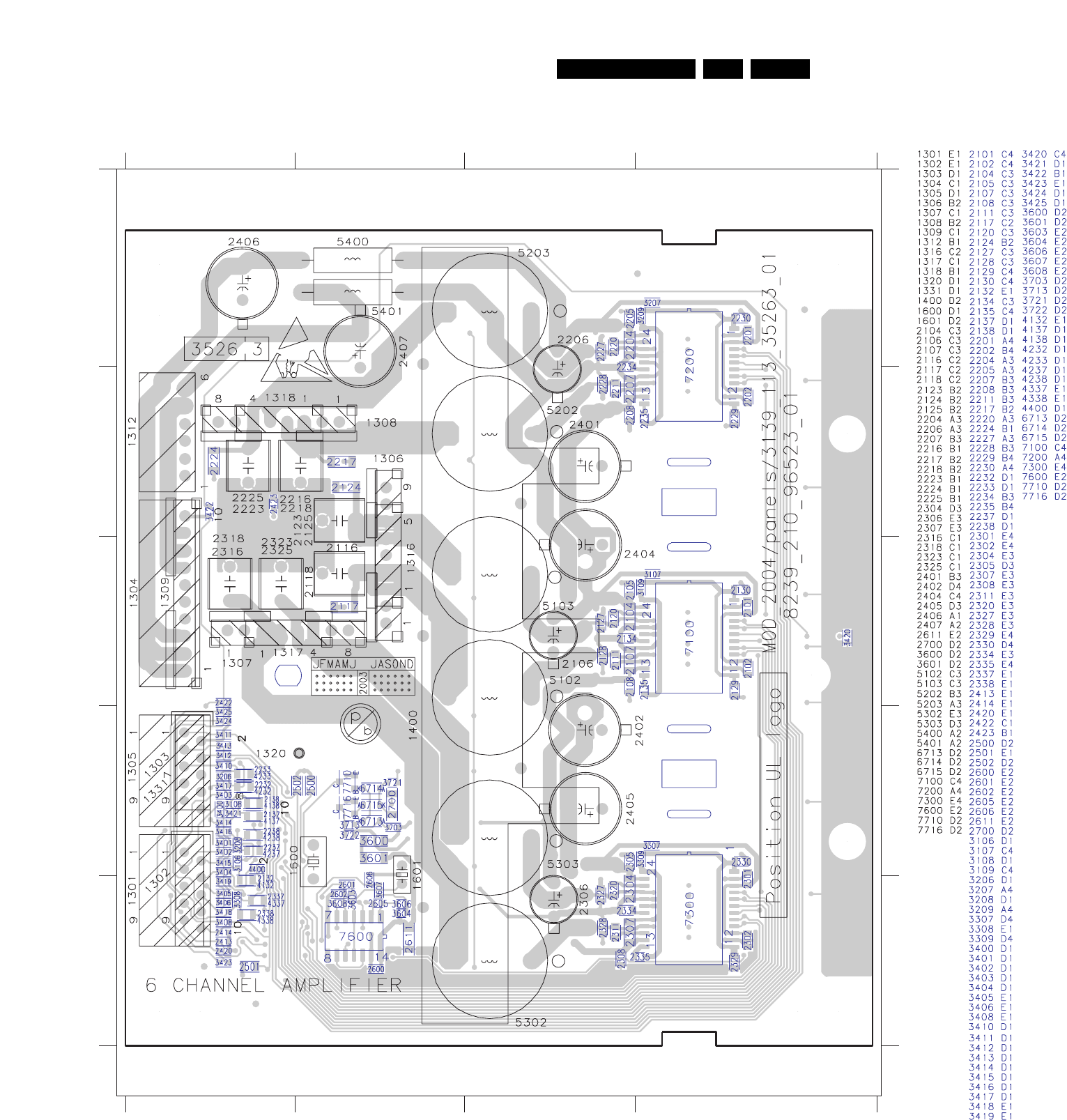
EN 907.LX7500RCircuit Diagrams and PWB Layouts
wired components
3139 113 3526 pt3 dd wk0345
This assembly drawing shows a summary of all possible versions.
For components used in a specific version see schematic diagram and respective parts list.
AMPLIFIER BOARD /
component side view
SMDs
SMDs
A
12 3 4
12 3 4
B
C
D
E
A
B
C
D
E
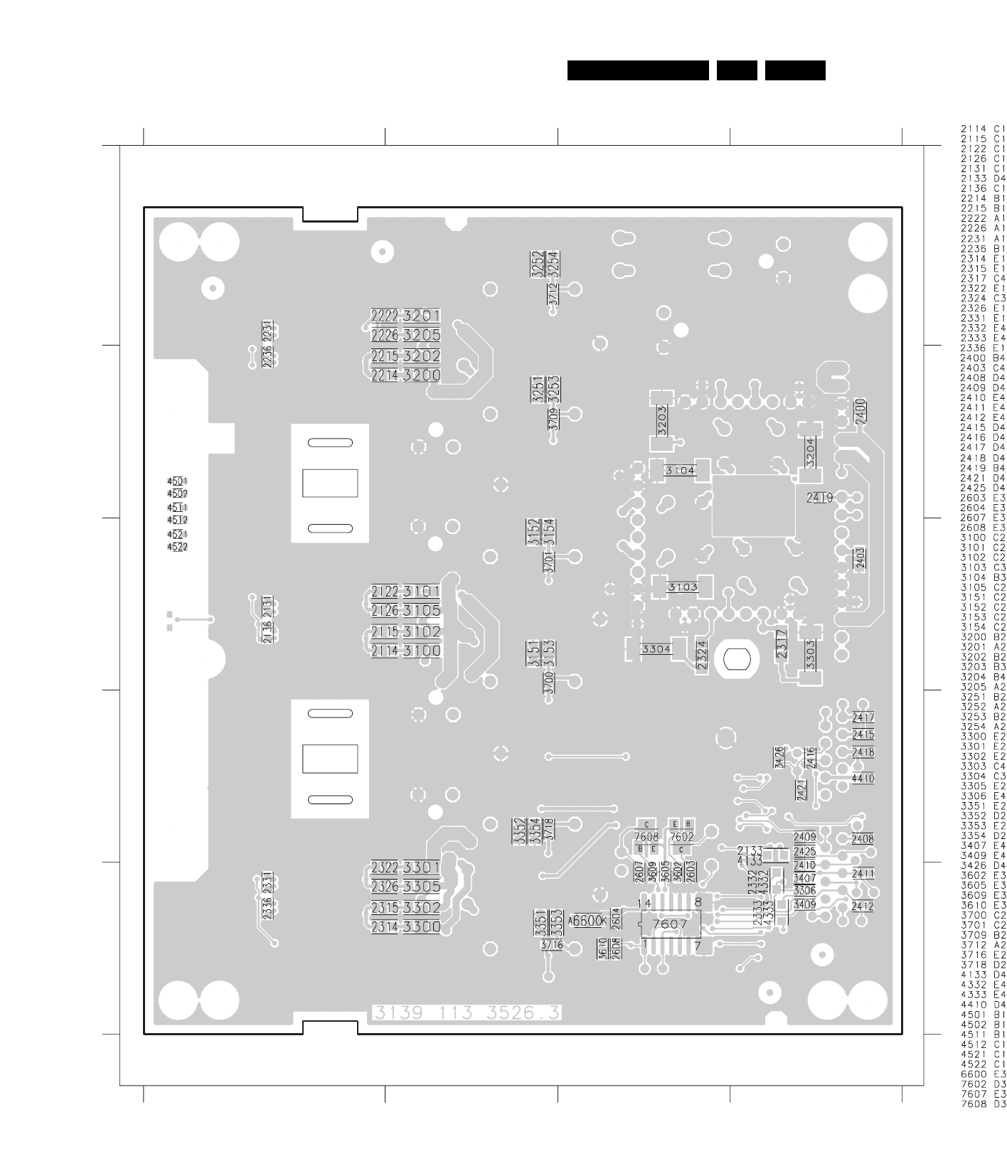
EN 917.LX7500RCircuit Diagrams and PWB Layouts
This assembly drawing shows a summary of all possible versions.
For components used in a specific version see schematic diagram and respective parts list. 3139 113 3526 pt3 dd wk0345
AMPLIFIER BOARD /
copper side view
A
1234
1234
B
C
D
E
A
B
C
D
E
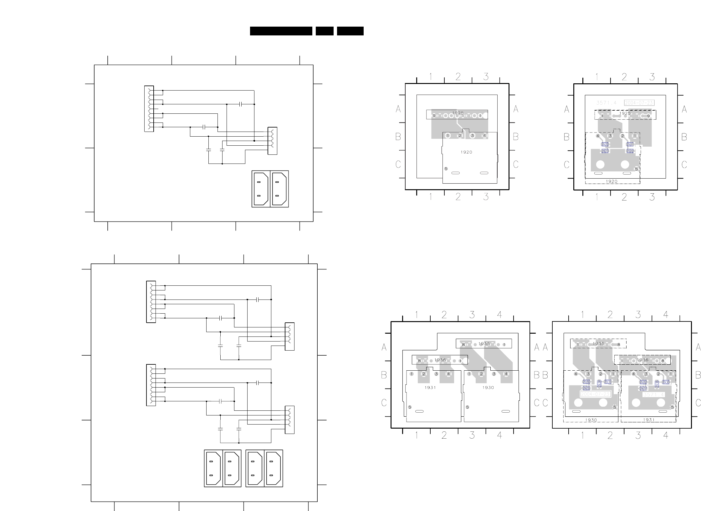
EN 927.LX7500RCircuit Diagrams and PWB Layouts
3
A
B
A
B
1920 A3
12
+
L
-
1925 A1
-
+
-
1
2
+
-
3
GND R
1306
from Power amp
R
L
+
2920 A3 2921 A2 2922 B2 2923 B2
red
GND L
R
L
3
12
4
R
2923
100n
White
2921
100n
2922
2920
33n
33n
2
3
4
5
6
7
8
9
4
5
WH09D-1
1925
1
LQR3215-0002F
1920
1
2
3
L/R Front Loudspeaker Sockets
front LS socket board LX7500R, 210904
LS SOCKET BOARD / component side view
2934 A2
-
2930 A3
2931 A2 2932 B3
2933 B2
4
3
+
-
+
C
C
Green
2935 A2 2936 C2
2937 C2
23
SL
SR
-
+
4
3
+
-
+
+
-
Center
SUB
1
231
SL
Blue SUB
Purple
GND C
SUB
GND SUB
1308
SL
from Power amp.
SR
GND SL
A
B
C
A
B
C
1930 A3
1931 B3 1935 A1
1936 B1
GND SR
1307
from Power amp.
-
2937
+
-
2
1
+
-
2
1
SR
Grey
2936
100n
100n
2935
100n
2934
1
2
3
4
5
100n
LQR3215-0102F
1931
2932
33n
2931
33n
6
7
8
33n
2930
1936
WH08D-1
1
2
3
4
5
2
3
4
5
6
7
8
WH08D-1
1935
1
5
33n
2933
1930
LQR3215-0402F
1
2
3
4
L/R Satellite, Center and Sub-Woofer Loudspeaker Sockets
satellite, center and sub-woofer LS socket board LX7500R, 210904
LS SOCKET BOARD / copper side view
LS SOCKET BOARD / component side view
LS SOCKET BOARD / copper side view
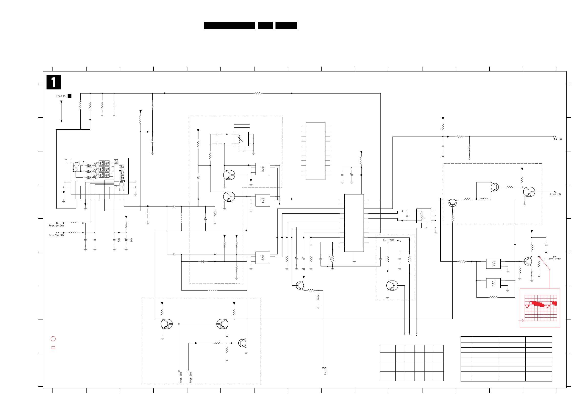
EN 937.LX7500RCircuit Diagrams and PWB Layouts
CDEC
VCO1
VCO2
VDE_EM
QSS
TAGC
STD
LADJ
CBL
VP
CVBS
AF
AFCSF1
VIF2
VIF1
GND
TOP
TPLL
CSAGC
CVAGC
FMIN
CDE_EM
SF2
O
GND
I
I
O2IGND
O1
GND
O
GND
I
I
O2IGND
O1
GND
I
O2ISWI
O1
GND
VIF1
GND
TOP
TPLL
CSAGC
CVAGC
FMIN
CDE_EM
CDEC
VCO1
VCO2
VDE_EM
QSS
TAGC
SF2
NC
VP
CVBS
AF
AFCSF1
VIF2
M
LL
H
M
H
PLL
TDA9817 TDA9817 --
TPS 6,0 MHz
I701 B2
I702 B6
I709 E9
I711 E8
I712 E8
I715 E1
I716 E1
1704
5V
0
0
--
2737 E15
270R
3702 A2
3703 A2
3704 E3
3705 C14
3710 F10
B/G
3720 F8
3724 F9
3725 B13
3726 C5
3728 D13
3730 D5
3731 F13
7710
330R
1
270R
0
I704 C5
I706 E6
I707 D8
I708 D7
I739 H6
I742 D5
I743 E7
I744 E7
I745 A8
I717 F10
I721 F11
I723 F15
I724 E14
I725 F13
--
--
0R
3733 G4
L D/K
H
I
A
B
2740 F7
2741 F4
2742 F11
3701 A7
G
H
I
1701 C7
1702 E7 3711 A3
3714 B12
3715 B13
3716 B5
0
3732 E15 I726 E8
delete for MSTD
I733 E2
I734 E1
I735 E1
45678
I746 E11
I748 D11
I749 D12
AGC-ADJUST
3717 D12
14
E
F
G
4567
C
D
E
F
12 13 14 15
A
1703 D7
1704 F14
1705 C1 I751 D13
from IOV
delete for MSTD
1
1
I
2720 B3
2721 B5
2722 F8
2723 F8
123
2729 C9
2730 E8
2731 D11
2732 E3
2733 E2
91011
G3956M
--
MULTISTD (/39)
0R
12 13 15
123
1
8 9 10 11
3737 E6
3738 E6
3739 F8
3740 F11
3741 D14
B
C
D
TDA9818
1703
PSS
TPS 5,5 MHz
low leakage
L’
*
1706 F14
2713 A2
2719 B5 3745 H5
3746 H6
3758 G6
4700 D4
2724 B12
2725 D3
2727 F10
2728 C9 5705 B3
5709 C10
5710 B6
5711 D12
5713 D13
2734 D4
2735 E1
2736 E2
for MSTD only
3734 F15
3735 F14
3736 F15 6705 F5
7701 G11
7702 D14
7704 C6
3742 F6
3743 G8
3744 G8
0
7709
not used
PAL I (/07)
AFC-ADJUST
4701 G5
5701 E1
5702 E1
5704 A1 7713 D12
7714 H6
7716 D14
7717 G8
F701 D1
5714 G14
6703 C5
6704 D5
for MSTD only
PAL BG (/01)
1
* VERSION TABLE
G3956M
F710 D3
F713 H5
SB1 1
for MSTD only
7705 D6
7706 H6
7709 B10
4701
--
from IOV
--
3731
TPS 5,5 MHz
I727 E7
I728 E11
I729 E5
I730 F57710 D11
7711 E14
7712 H4
placed on some pos. as 7710
Pos.
to MSP
*
F702 C10
F703 C6
F704 A4
4700 0R --
1706
F707 D1
F708 B12
F709 C6
0
1
for PAL-I only
for MSTD only
N750
*
K3953M
*
SFS_TS
0
40,4-ADJUST
*
0R
I731 H4
I732 B3 I754 D13
1
4K7
3716
I742
220p
2719
I731
470R
3702
3717
4K7
I711
PDTC124EU
7704
F710
2730
220n
220R
3704
2u2
2732
7701
PDTC124EU
2
13
I744
TPSRD
1706
6M0
I716
I704
7706
PDTC124EU
I708
I724
I701
5SW
I728
F701
6704
BA591
5SW
2K2
3737
3731
270R
F703
18
19
9
1
2
21
I730
13
20
7
12
23
24
3
14
22
6
8
17
15
11
10
5
4
16
TDA9818T
7709
Φ
5702
47u
2737
I702
6u8
6705
BA591
5705
100R
3728
3734
2K7
18K
3714
I729
5704
7714
BC847BW
100n
2727
3743
56K
22K
3724
3739
5K6
2720
100u
33VSTBY
I754
4K7
3730
5SW
PDTC124EU
7705
33K
3711
3736
330R
3746
F709
5K6
1n0
2741
100R
3726
5M5
TPSRA
1704
2
13
3740
680R
I749
5SW
2723
470p
15u
5713
10K
3715
2740
2u2
100n
2733
I735
I706
2734
1n0
3
1
2
5
4
1703
OFWG3956M
38M9
I712
5SW
3705
10K
F708
2742
1n0
I748
I746
F713
4700
5SW
I707
BA591
6703
5
4
150K
3703
OFWK9656M
38M9
3
1
2
BC857BW
7716
1702
15u
I721
5714
I751
2u2
2722
5SW
I709
I725
22p
2725
I739
3742
4K7
1
2
5
4
F704
1701
OFWK3953M
38M9
3
I727
PDTC124EU
7702
I715
I723
I726
5SW
4K7
3741
5701
2728
10n
F702
5SW
7711
BC857BW
3758
10K
3710
5K6
2
21
3720
330R
15
12
23
24
14
22
6
18
19
9
1
17
11
10
5
4
16
13
20
3
7
Φ
7710
TDA9817T
8
22u
2713
5SW
3744
100K
3735
3K3
5SW
3725
8K2
I734
2729
10u
2731
8p2
3701
680R
I733
I743
2736
27p
F707
3733
4K7
15
MT4
6
NC1
4
SCL
5
SDA
2
TU
VS
7
VST
98
1
AGC
3
AS
IF1
11
IF2|NC2
10
12 MT1
13 MT2
14
MT3
78
UV1316-MK3 1705
ADC
7KMY 5711
1
2
34
6
4701
7717
BC847CW
120p
2721
I732
7712
PDTC124EU
100n
2724
1K0
3732
I717
I745
8
5709
6u8
5710
7KMY
1
2
34
6
7
3745
5K6
27p
2735
5SW
BC857BW
7713
3738
6K8
SIF1
SB1
SFS_TS
SDASW
SCLSW
5SW
SB1
SB1
AGC
VFV
AFC
PSS
ANALOG BOARD
Frontend Video (FV)
A/V board LX7500R, 231104
4
OSCILLOGRAMS
..
..V MEASURED IN RECORD MODE
..V MEASURED IN PLAYBACK MODE
2V
3,5V0,7V
3,3V
0,9V
2,8V
3,2V
3,3V
2,5V
3V
3,2V
3,1V
2,7V
5,2V
2,7V
2V
0V
VFV I723
A: DC, 500mV/Div
10us/Div
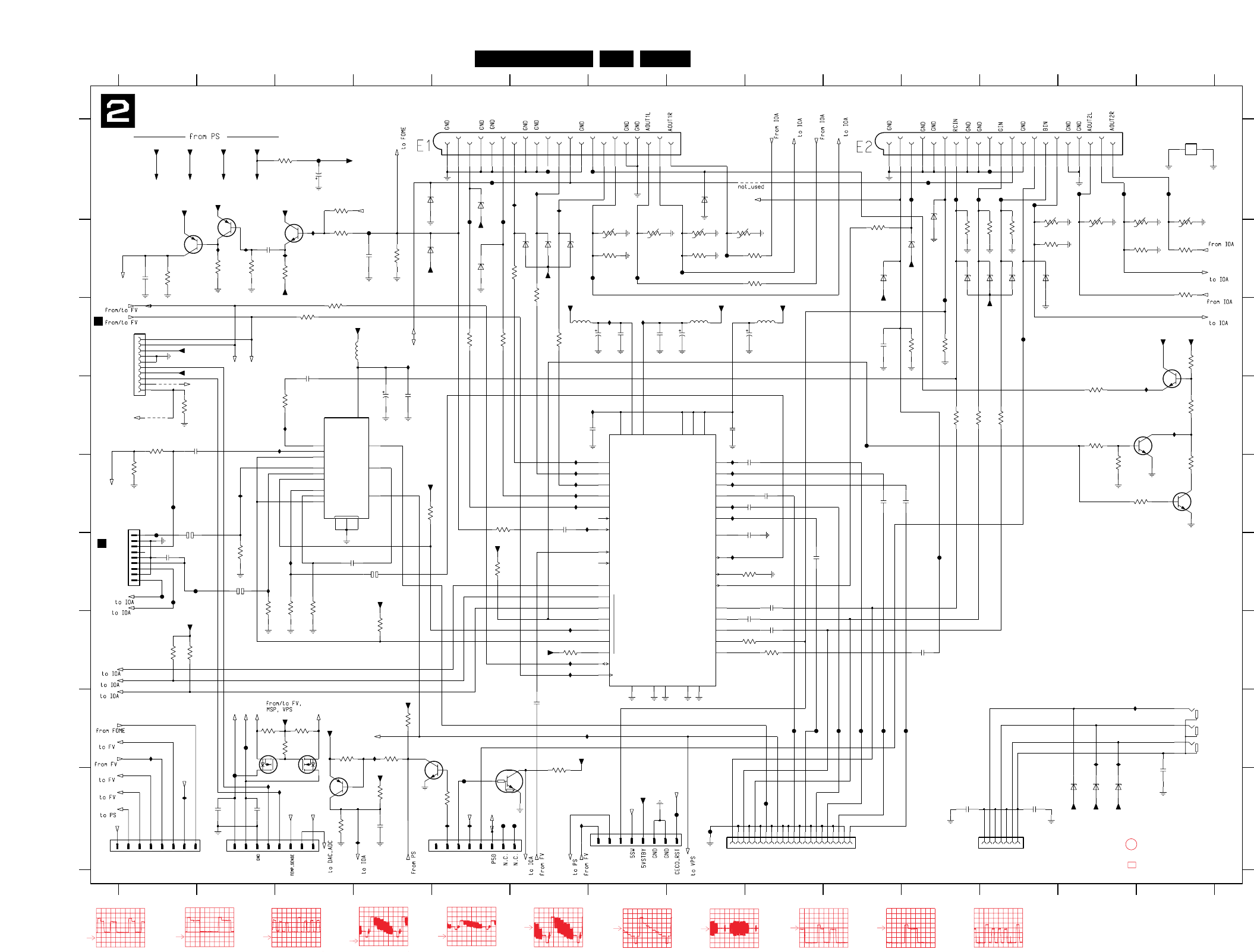
EN 947.LX7500RCircuit Diagrams and PWB Layouts
V V
VV
V
VCC
GND
V
GNDB
Y|CVBSIN-AUX
Y|CVBSIN-TV
CIN-TV
GND1
DIGOUT
FBIN-AUX
B|PBIN-AUX
G|YIN-AUX
R|PR|CIN-AUX
Y|CVBSOUT-AUX
COUT-AUX
Y|CVBSOUT-REC
DECV
YIN-ENC
CIN-ENC
CVBSIN-ENC
B|PBIN-ENC
G|YIN-ENC
R|PR|CIN-ENC
VCCB3
VCCB2
VCCB1
VCCB-REC
VCC
VDD
SCL
SDA
Y|CVBSIN-TUN
6
5
4
3
2
1
GNDD
CIN-TUN
C-GATE
Y|CVBSOUT-TV
FBOUT-TV
B|PBOUT-TV
G|YOUT-TV
R|PR|COUT-TV
GNDB-REC
GND2
V
V
1945-2
I469 G6
I470 G6
I476 F8
I478 E8
I479 E8
I481 E8
I482 E8
I483 E8
I486 H13
GND
GND
GND
TEMP_SENSE
from / toCOMBI board 1102
5VSTBY
I416 F3
I417 E2
I418 H1
I419 I1
I420 I6
I424 I5
I428 I3
I429 I2
I433 H13
not used
1%
not used
from / to Digital Board
I467 D14
I468 G6
F5208 C12
F5210 A11
F5211 A12
F5213 A12
F5215 A11
F5216 C11
F5219 A11
F5220 F11
F913 D10
I341 A13
I402 D14
I405 H6
I406 B2
GND
PR
PB
Y
PSCAN
to Digital Board
not used
I414 D7
I415 F2
F4718 H10
F4720 H10
F4721 I8
F4722 H11
F499 A3
F5101 B8
F5102 B8
F5103 B7
F5106 B6
F5108 A7
F5110 A5
F5113 A6
F5116 B5
F5119 B5
F5120 B4
GND
I437 H13
I453 H4
I454 I5
I456 C7
I457 C7
I458 A6
I459 A6
I460 A5
I461 E6
I462 E6
I464 E6
I465 E6
I466 E6
CFIN
GND
CVBSFIN
GND
F360 E6
F401 I2
F402 H2
F403 I8
F404 I5
F405 I6
F412 I5
F4203 E1
I407 B2
I408 B3
I409 B3
I411 D3
N.C.
from/to uP Board
1%
I412 D3
I413 C4
F4714 H10
F4716 H10
6422 A11
6423 A8
6424 B10
6427 I13
6428 I13
6429 I13
7004 D7
7401 A2
7402 B3
7403 B1
7404 I4
7405 D14
7407 E14
7409 D14
7411 D3
F5201 A14
F5202 A13
F5206 A12
F5207 A12
GND
4401 A9
4402 D1
4403 D1
5401 C4
5402 C9
5403 C6
5406 C8
6401 B4
6402 B6
6403 B6
6404 B6
6409 A4
6414 B5
6415 B11
6416 B12
F4205 F2
F4207 F1
F4209 F1
F4210 E1
1%
F4505 I3
F4707 I9
F4712 H9
3469 B14
3470 B12
3471 B7
3472 B8
3475 B9
3476 B9
3477 B14
3478 B14
3481 F2
3482 F2
3483 F3
3484 F3
3489 E1
3490 D3
3491 D11
7412 H5
7419 H2
7420 H3
7421 H5
GND
not used
GND
3442 D13
3445 E5
3446 B3
3447 A3
3451 I5
3452 G9
3453 D1
3454 A3
3455 E4
3458 H2
3459 G4
3460 H3
3461 A14
3462 A14
3463 A13
6417 B12
6418 B12
6419 B11
6420 A5
1%
3468 B8
not used
YFIN
IPOR_DC
INT
3424 E14
3426 E13
3427 C11
3428 E14
3429 D1
3492 D11
3493 D12
3494 G9
3955 H6
3439 F5
3440 H3
3405 B2
3406 B2
3407 B3
3408 B1
3409 B6
3410 C6
3411 B10
3412 C5
3413 B6
3414 C5
3415 H4
3416 H4
3417 C11
3418 I3
3419 I4
3464 A12
3465 B7
3466 B7
3467 B8
from/to uP Board
1%
PR
2438 F9
2439 E9
2440 E9
2441 E10
2446 H6
2449 F1
2450 B2
2451 I14
2452 I11
2453 I12
2459 D1
3431 G6
3432 C3
3433 C3
3437 G1
CECO_RST
3438 G1
3403 B12
3404 B4
2410 C3
2411 D7
2412 I2
2413 C7
2414 C7
2415 C10
2416 G11
2417 F4
2418 F9
2419 E6
2421 E1
2423 G9
2427 G9
2428 F2
2433 E9
3420 F9
3421 C14
3422 D13
3423 D14
12VSTBY
SCL
GND
GND
GND
PB
from/to uP Board
not used
SDA
1945-3
2464 A3
3400 H3
3401 B11
3402 B12
2408 F3
2409 D8
9 1011121314
A
B
C
D
E
F
G
H
I
2434 C8
2435 C7
2436 E11
2437 E9
GND
GND
GND
GND
GND
GND
34567891011121314
123
E
F
1945-4
8
G
H
I
1940-1 A8
1940-2 A13
1940-3 A14
1942 E1
1943 C1
1945-1 I2
1946 I11
1947 I8
1949 H14
2401 B4
2402 B1
2403 D4
A
B
C
D
N.C.
from/to uP Board
GND
not used
12
not used
4567
not used
Y
2404 D4
2405 C8
2406 I4
2407 I2
not used
from / to front 1922
3417
75R
2403
47u
1u0
2427
2437
1u0
F4205
I456
100R
3433
I406
2410
1u0
BC847BW
7407
16
22K
3419
150R
3491
3469
100K
I460
10u
5401
10K
3451
2421
10u
5NESD
F5219
3401
75R
2436
1u0
F5210
150R
3490
10K
3455
1u0
2408
2415
100p
3464
BZX384-C12
6404
5
6
7
8
9
150R
3452
1942
B9B-PH-K
1
2
3
4
9
6417
BZX384-C12
6424
BZX384-C12
100K
3400
3445
150R
23
7401
BC857BW
I462
3454
1K0
4403
12VSTBY
100n
2450
F5106
3403
75R
I454
2440
1u0
F5116
12VSTBY
F5103
3481
1M0
5402
10u
3
BC847BW
7409
2
3460
4K7
3421
27K
1K0
3415
I459
75R
3427
4402
3410
75R
47K
3429
28
1u0
2446
BSH111
7420
5NSTBY
47u
2405
I402
I482
F5215
I407
3447
47K
F5201
3423
390R
F4721
F4716
F4722
F5208
F412
2401
100p
10u
F5202
2428
F5102
I483
5SW
F499
3463
3409
75R
3489
82K
20
F5113
F913
10u
5406
5VSTBY
4401
I478
3461
I486
3467
5NESD
2406
10n
5NESD
5VSTBY
3468
1u0
2419
F4707
5VSTBY
3472
100K
29
2
3
4
1
F4714
LPR6520-G000G
1949
3482
1M0
5NESD
15
2439
100n
5
OUT2
6
OUT3
13
I464
4
10
16 IN1A
1IN1B
11 IN2A
14 IN2B
8IN3A
9IN3B
3
OUT1
Φ
3-CHANNEL
VIDEO SWITCH
2CTL1
12 CTL2
7CTL3
15
I468
7411
NJM2285M
6420
BZX384-C12
7402
BC847BW
F4210
4
F5206
7405
BC847BW
4K7
3458
3955
10K
BZX384-C6V8
6414
6415
BZX384-C12
7412
PDTC124EU
1M0
3483
7419
BSH111
I461
2414
100n
GND
I412
F5119
I469
I476
150R
3492
F4209
100n
2404
3465
6427
BZX384-C12
I453
150R
3494
7A
8A
9A
100R
3475
19A
2A
20A
21A
3A
4A
5A
6A
10A
11A
12A
13A
14A
15A
16A
17A
18A
11
1940-1
1A
I414
I466
100K
3470
3426
33K
BZX384-C6V8
6409
22
3
4
5
6
7
8
9
6403
BZX384-C12
13
14
15
16
17
18
19
2
20
21
1
10
11
12
47K
3446
1947
22FMN-BTRK-A
3453
10K
5NESD
3484
1M0
BZX384-C12
6416
I417
1u0
2418
F5120
24
100K
3471
5VSTBY
2416
1u0
BZX384-C12
6402
32
75R
3414
100K
3418
2434
47u
I408
6423
BZX384-C12
3440
10K
2412
F5108
1u0
2459
5NESD
100n
2411
26
I424
3422
820R
BC857BW
7404
F4718
F4203
12VSTBY
I428
5NESD
I481
F5213
F4720
I465
F402
10K
3438
68p
2449
12VSTBY
10
3406
220K
3407
3K3
6429
BZX384-C12
75R
3402
5VSTBY
47n
150R
3493
2433
F5216
5VSTBY
F360 / I463
2402
100n
F4712
3408
3K9
17
7421
BC847BW
19
1
41
25
21
33
931
37
38
820 24 30 3236
7
35
34
312 2622 39
15
1029
17
40
23
4
5
42
44
2
14
16
18
Φ
VIDEO SWITCH
MATRIX
13
1127
28
6
43
I411
7004
STV6618
75R
3413
3437
10K
3412
75R
3442
150K
5NSTBY
3459
10K
7
8
9
F5110
1
10
2
3
4
5
6
1943
10FMN-BTK-A
7
BZX384-C12
6428
BC857BW
7403
I419
5VSTBY
10u
2464
22
31
BZX384-C3V9
6422
1945-1
1
3428
100K
5VSTBY
2417
10u
3405
22K
I433
1u0
2438
14
3416
4K7
3476
100R
5NESD
I418
75R
3411
MT2
1940-3
MT1 MT2
5VSTBY
12
035 0 8081 90
100R
3477
5NSTBY
BZX384-C12
3424
33K
6419
19
5VSTBY
2407
F403 100n
2435
3466
3439
10K
F5211
25
100R
3478
4K7
3431
5
I416
3462
30
5NESD
10u
5403
18
F5207
I437
I458
I405
5SW
6401
BZX384-C12
2413
47u
I409
F404
5VSTBY
5VSTBY
3432
100R
6
5VSTBY
I415
I457
F5220
F5101
I429
75R
3404
5NESD
I479
100n
2452
100n
2453
27
21
13
I467
I470
5SW
5VSTBY
F4505
2441
1u0 21B
3B
4B
5B
6B
7B
8B
9B
12B
13B
14B
15B
16B
17B
18B
19B
2B
20B
1B
10B
11B
3420
150R
1940-2
F401
F405
5VSTBY
BZX384-C12
6418
5VSTBY
8
100n
2451
5VSTBY
F4207
I341
I420
I413
1u0
2423
1
2
3
4
5
6
7
100n
2409
D_CVBS
D_Y
1946
07FMN-BTRK-A
A_C
A_YCVBS
A_YCVBS
A_YCVBS
SCL
SCL
SDA
SDA
IPOR_DC
D_B
D_G
IPFAIL
AFC
AFC
STBY
STBY
FBIN
FBIN
8SC1
INT
CECO_RST
CECO_RST
5NSTBY
AOUT2L
AIN2L
AIN2L
AIN2R
AIN2R
A_B
A_G
A_R
YCVBSIN2
YCVBSIN2
PWONSW
A_YCVBS
A_YCVBS
KILL
ASC1M
WU
WU
8SC2
8SC2
FOME
FOME
5SW
PSS
AGC
AGC
SB1
SB1
WSFI
WSFI
SCL
SCL
SDA
SDA
TEMP_SENSE
PWONSW
ASC1S
P50
12VSTBY
12VSTBY
ION
ION
SFS_TS
SFS_TS
PSS
AKILL
YCVBSOUT1
IASC1M
AINFL
AINFR
AINFR
P50
P50
WU
AOUT1R
AIN1R
AIN1R
AOUT2R
AOUT1L
TEMP_SENSE
SCLSW
SDASW
AINFL
VSA1
VSA2
WSFI
CVBSIN1
CVBSIN1
5SW
VFV
D_C
D_R
YCVBSIN2
AIN1L
AIN1L
BOUT
GOUT
RCOUT
FBOUT
CVBSOUT2
12VSTBY5VSTBY
ANALOG BOARD
In/Out Video (IOV)
A/V board LX7500R, 231104
1
2
OSCILLOGRAMS
..
..V MEASURED IN RECORD MODE
..V MEASURED IN PLAYBACK MODE
A:
DC, 500mV/Div
10us/Div
A: DC, 200mV/Div
10us/Div
D_CVBS F4712
A: DC, 200mV/Div
10us/Div
A: DC, 200mV/Div
10us/Div
A: DC, 200mV/Div
10us/Div
A: DC, 200mV/Div
10us/Div
A_CVBS I405
D_Y F4714 D_C F4716 D_R F4718 D_G F4720
A: DC, 200mV/Div
10us/Div
D_B F4722
I465
I461 I462 I463
A: DC, 500mV/Div
10us/Div
A: DC , 500mV/Div
10us/Div A: DC , 500mV/Div
10us/Div A: DC
10us/Div
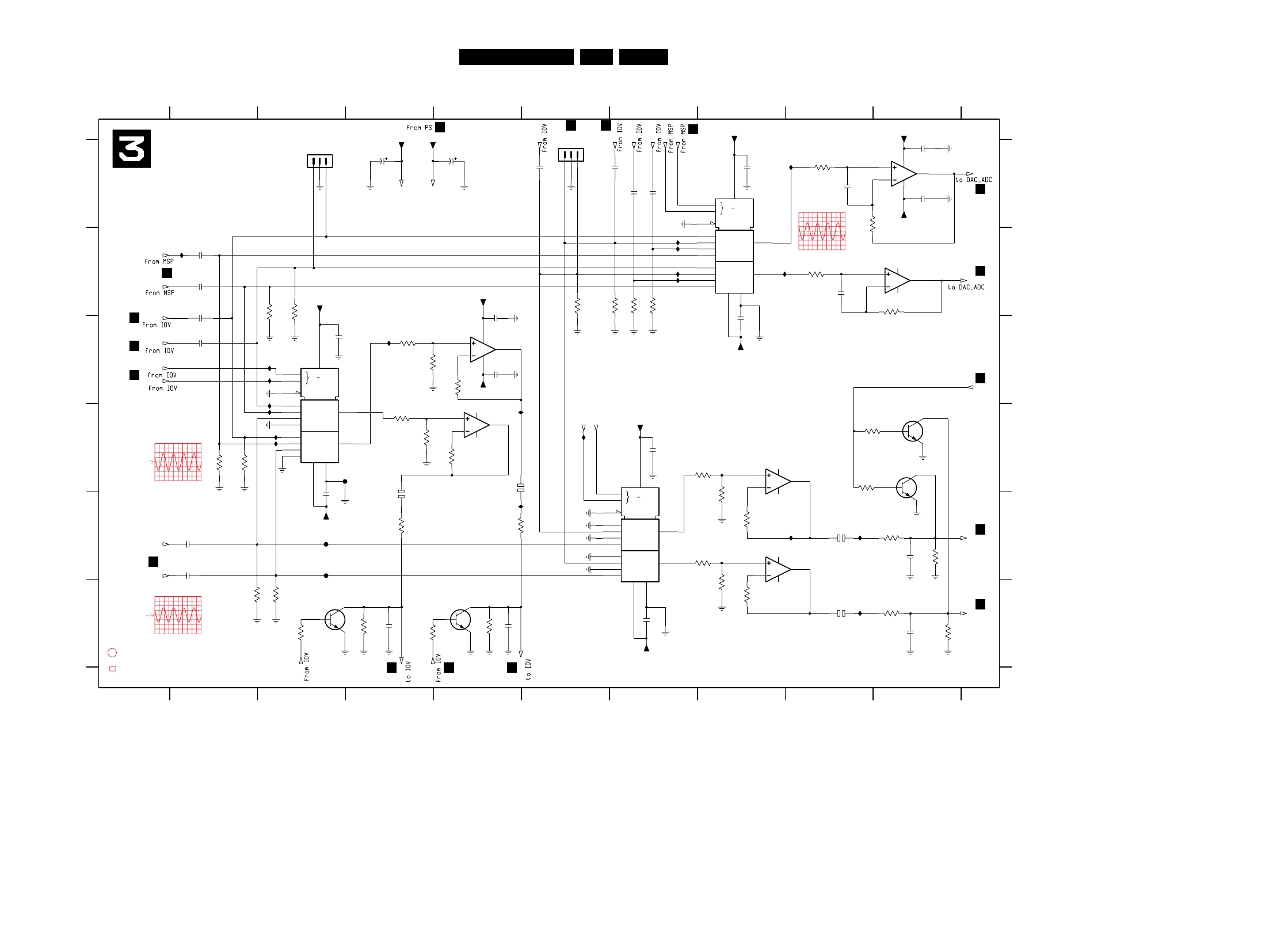
EN 957.LX7500RCircuit Diagrams and PWB Layouts
G4
0
3
2
VDD
VEE VSS
1
0
3
2
1
4X0
3
0
1
G4
0
3
2
VDD
VEE VSS
1
0
3
2
1
4X0
3
0
1
G4
0
3
2
VDD
VEE VSS
1
0
3
2
1
4X0
3
0
1
7502-1 C4
7502-2 D4
7502-3 D7
7502-4 E8
7503 C2
7504 D6
3518 F7
not used
from IOV
I506 C2
I508 D4
I511 C3
I513 B6
I514 B6
I515 B6
3530 F3
AIN2L
AIN2R
3524 F9
3525 E9
3526 E7
3527 E9
3528 F2
3529 F3
2536 F6
from DAC_ADC
7505-1 B9
AIN1R
I517 B7
I518 A8
3512 A8
3513 D4
3514 D1
3515 E7
3516 B2
3517 D8
2516 E3
I528 B1
I532 E4
I535 F8
I539 E8
I540 E8
7509 F2
7511 F4
F501 E2
F502 E2
F504 D2
I501 C2
I502 D2
I503 D2
I516 B6
2526 E8
2527 E9
2530 A9
2531 B8
2532 A8
2535 D6
9
1234567
3531 F4
3532 C3
3533 D3
3534 D1
3535 C3
3536 D3
3537 E7
2510 A3
2511 D4
2512 C7
2513 E1
2514 C4
2515 E1
B
C
D
E
F
1950 A2
1953 A5
2501 A5
I521 D5
7505-2 A8
7506 E9
7508 D9
3519 D8
3520 E3
3521 E4
I504 D2
I505 C2
45678
AIN1L
89
A
to IOV
not used
3502 B8
3503 B5
3504 B6
3505 B6
3506 B6
3507 F2
3508 C4
3509 A8
3538 F7
7501 A7
to IOV
C
D
E
F
A
2502 A7
2503 C2
2504 C1
2505 B1
123
from IOV
not used
2517 F4
2518 E2
2519 A4
2520 F3
2521 A9
2522 F8
2523 F9
3522 F9
3523 D7
from DAC_ADC
B
not used
not used
2508 A6
2509 B4
3501 B9
not used
from IOV
2506 A6
2507 A6
3510 B2
3511 F1
2
11
4
13
3
2524 B1
2525 B1
9
6
16
7
8
12
1
14
5
15
MDX
7501
HEF4052B
10
1u0
2506
5NSTBY
3537
3K9
100K
3534
3530
820R
1K0
3512
2521
100n
220R
3525
2522
100u 16V
I528
4
13
3
7506
BC817-25W
6
16
78
12
1
14
5
15
2
11
MDX
HEF4052B
7504
10
9
2527
1n0
100u
100K
3506
2516
I513
3513
1K0
3529
4K7
7502-2
MC330795
6
7
1
2
3
EH
1950
3
2
1
3K9
3536
MC33078D
7505-1
2524
1u0
5NSTBY
3527
820R
3507
100K
1n0
2523
I540
2526
100u 16V
2507
1u0
5NSTBY
I517
2513
1u0
2501
1u0
220R
I514
3522
1n0
2517
3517
4K7
2510
100u 6.3V
5VSTBY
3518
1K0
12
1
14
5
15
2
11
4
13
3
7503
MDX
10
9
6
16
78
I503
HEF4052B
I518
7502-3
MC33079
10
9
8
5VSTBY
3509
1K0
7511
BC817-25W
2518
100n
100K
3516
820R
3524
3
2
1
4
11
F501
7502-1
MC33079
3533
1K0
I539
3535
3K9
2530
100n
I515
1K0
3515
I532
1K0
3502
5NSTBY
BC817-25W
7508
2505
1u0
100u
100p
2531
2511
I501
I511
2502
100n
3520
220R
I535
1u0
2508
4K7
3528
I508
1K0
3523
2520
1n0
BC817-25W
7509
5VSTBY
100n
2509
I516
5VSTBY
5NSTBY
2535
100n
2536
100n
14
2532
100p
7502-4
MC3307912
13
3521
220R
2519
100u 6.3V
100K
3505
100K
3514
6
7
8
4
MC33078D
7505-2
5
3K9
3538
2514
100n
4K7
3519
I502
I506
I505
820R
3531
100n
2512
I504
3501
1K0
1u0
2504
100n
2503
100K
3503
I521
5VSTBY
3532
1K0
1K0
3508
3511
100K
3504
100K
1u0
2525
F502
F504
5VSTBY
3510
100K
2515
1u0
3526
1K0
2
3
EH
1953
1
ALADC
5NSTBY
VSA1
VSA2
AOUT1L
AOUT1R
AKILL
ARADC
IASC1M
5NSTBY5VSTBY
ALDAC
ASC1S
AOUT2L
AOUT2R
AIN2L
AINFR
AKILL
AKILL
ARDAC
AFEL
AFER
AIN1R
AIN1L
AIN2R
RSA2
RSA1
AINFL
ANALOG BOARD
In/Out Audio (IOA)
A/V board LX7500R, 231104
5
2
2
2
9
2 2
9
9
2
2
2
4
2 2 2
5
OSCILLOGRAMS
..
..V MEASURED IN RECORD MODE
..V MEASURED IN PLAYBACK MODE
I517/I518
A: DC, 500mV/Div
500us/Div
A: DC, 500mV/Div
500us/Div
F501/F502
A: DC, 500mV/Div
500us/Div
I502/I504
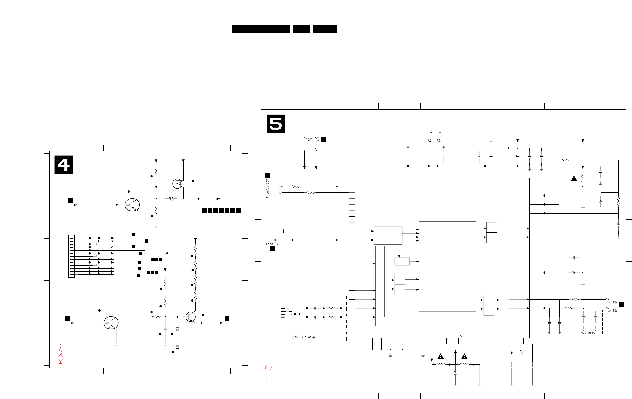
EN 967.
LX7500R
Circuit Diagrams and PWB Layouts
to DAC_ADC
to DAC_ADC
to IOV, IOA, FV
to DAC_ADC,
to FV
AIO, DIGIO
F358 C1
F381 C1
4300 C3
4301 C3 F383 C1
F384 C2
I346 A3
I347 D4
I349 D3
I352 C1
I353 A4
I354 B2
to IOV, FACO
VPS, DIGIO, IOA, MSP
from IOV
E
1934 B1 F331 C2
F333 C1
F346 C2
F347 C1
F348 C2
F350 C1
F351 C2
F352 E4
F353 C1
F354 C1
from IOV
to IOV
to MSP
from IOV
3373 D4
34
6314 E3
6320 E3
7308 A2
7319 D4
7320 A3
7321 D1
F301 C1
F302 C2
F322 B1
F325 B2
to IOV, FACO, FOME, FV
12
not used
1234
A
B
E
A
B
C
D
C
D
2332 A3
2334 E3
3327 A3
3329 B3
3348 D3
3349 C4
3355 D3
3362 D3
3371 C4
3372 C4
I354
to IOV, DAC_ADC
5NSTBY
4301
I352
33VSTBY
STBY
F333
2u2
2332
F302F301
F354
13
2
3
4
5
6
7
8
9
F351
1934
B13P-PH-K
1
10
11
12
F322
PDTC124EU
7321
4300
I353
1M0
3327
7308
PDTC124EU
12VSTBY
5VSTBY
6314
BZX384-C8V2
F353
IPFAIL
F358
3371
47R
F348
680R
3348
3355
47R
12VSTBY
F350
I347
F383
7319
BC847BW
F384
5V
F346
F381
F347
F331
3362
680R
3V3
7320
SI2306DS
33VSTBY
F325
12VSTBY
33R
3373
I346
5SW
3372
33R
5VSTBY
5N
47R
3349
ION
F352
I349
100n
2334
8SW
6320
BAS316
3329
2M2
STBY
STBY
ANALOG BOARD
Power Supply (PS)
A/V board LX7500R, 241104
2
1235678
25
2
2
2
123
1
9
9
93 8 9
from AUX SUPPLY board 1300
12,4V
5V
0,2V
0V
3,3V
5V
5V
34V
-5,4V
-5,3V
EVM
V
DC voltages measured in Stop mode
with no audio output.
...V
LOUDSPEAKER L D/A
D/A
I2SL/R
HEADPHONE R
IDENT
NC
SCART
LOUDSPEAKER R
A/D
D/A
DEMODULATOR
S1...4
FM1
FM2
I2SL/R
NICAM B
NICAM A
SCART-L
HEADPHONE L
IDENT
LOUDSPEAKER
A/D
D/A
SCART-L
SCART-R
DFP
SCART-R
Switching Facilities
GND
I615 B2
2600 A6
2601 A6
QFP44
2602 A7
I608 C2
D
12
2626 E2
E
I613 F6
D
E
F
A
F
1600 F7
DVAR
6
2604 A9
I603 A6
3603 B2
7600 A3
F6001 E1
I604 A7
I605 B7
3607 E2
I607 C1
B
C
1960 E1
I609 D7
I610 F7
I611 F7
I612 F5
I624 A5
I614 B7
24
3612 E8
45
167
I616 B2
I617 B7
5600 A8
2619 E9
2620 F7
F6002 E1
F6004 E1
I601 A7
I602 A4
3602 B9
A
3606 E2
C
3611 D8
2618 E9
I625 A5
3
I620 E2
I623 E7
78
I630 E2
I631 E2
89
2611 A7
from DV - Board
2603 A7
GND
35
2612 D8
2616 E8
2610 C8
DVAL
2627 E2
3600 A8
3601 B1
2605 F5
2606 B8
2608 C9
2609 C2
2621 F7
2623 F6
4601 A5
B
5601 F5
5602 F6
6600 B9
2616
1n0
2617 E8
I621 E2
2607 C2
9
I621
I602
F6004
4n7
2619
5SW
10u
2602
3611
100R
I620
I617
I631
F6001
I625
I613
3607
1K0
I612
10n
2601
5SW
I630
I611
I614
5600
10u
I609
2623
100n
I607
4601
3602
4K7
I608
I615
3p3
2621
2620
3p3
2u2
2627
50V
2603
100n
1
2
3
4
1600
18M432
5SW
1960
B4B-PH-K
I601
10u
2600
1n0
2617
4n7
2618
2609
56p
I605
56p
2607
5602
10u
I624
100n
2606
100R
3612
10u
5601
6600
BAS316
F6002
10n
2604
I623
2611
47u
I616
5SW1
8SW
2626
2u2 50V
8SW
5SW1
3601
100R
STBYQ
4
TESTEN
7
TP
29
VREF1
25
VREF2
42
VREFTOP
5
XTAL_IN
6
XTAL_OUT
32
22
RESETQ
40 SC1_IN_L
41 SC1_IN_R
31
SC1_OUT_L
30
SC1_OUT_R
37 SC2_IN_L
38 SC2_IN_R
11
14 I2S_CL
17 I2S_DA_IN1
21 I2S_DA_IN2
16 I2S_DA_OUT
15 I2S_WS
43 MONO_IN
23 24 28
DACM_L
26
DACM_R
20
DVSS
19
DVSUP
9
D_CTR_IO0
8
D_CTR_IO1
12 I2C_CL
13 I2C_DA
AHVSS
33
AHVSUP
2ANA_IN+
3ANA_IN-
39
ASG
44
AVSS
1
AVSUP
34
CAPL_M
27
MSP3415G
7408 18
ADR_CL
10
ADR_SEL
36
AGNDC
35
2608
10u
1K0
3606
I604
I610
10u
2605
100R
3603
10K
3600
10n
2610
I603
4u7
2612
AFEL
AFER
RSA2
RSA1
SDASW
SCLSW
SIF1
5SW
8SW
ANALOG BOARD
Multi Sound Processing (MSP)
A/V board LX7500R, 241104
4
2
3
1
OSCILLOGRAMS
..
..V MEASURED IN RECORD MODE
..V MEASURED IN PLAYBACK MODE
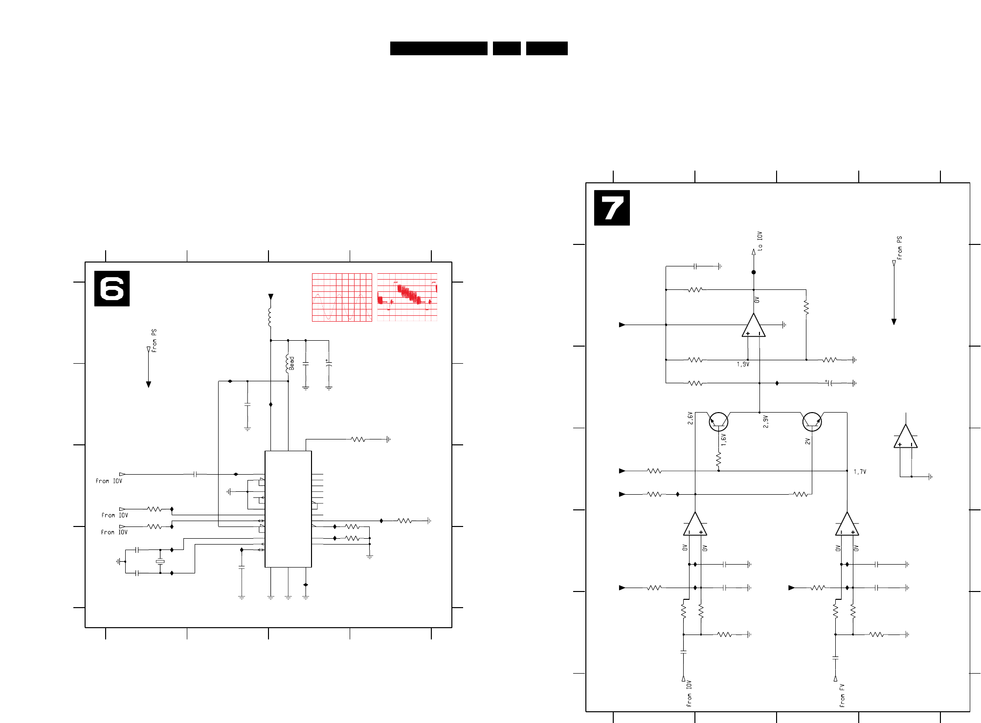
EN 977.LX7500RCircuit Diagrams and PWB Layouts
REF
SL
LFB
TV
EVEN
VDDD RGB
CBLK
XTO
RESERVED
TEST
VDDA
XTI
MA
POL
STTV
FFB
SCL
SDA
VCR
CVBS
DV
L23
Y
ODD
COR_
BLAN
B
G
R
VSSA VSSD VSSO
3
1234
1
1990 D1
2932 B3
2933 B3 3931 C4
3932 C4 I989 C2
2
I990 C3
4
A
B
C
D
A
B
C
D
2934 C2
2935 D2
2936 D1
2937 D1
2938 B2 I991 D2
3933 D4
3934 C1
3935 C1
3936 B4
5931 A2
5932 B3
7931 B2
I987 B3
I988 C4 I992 D3
I993 B2
I994 D1
I995 D1
I996 D3
I997 C1
I998 D1
100n
2932
47K
3931
3933
47K
47K
3932
23
1516
17
5
27
21
322
26 725
24
19
6
9
18
2
14
4
8
20
11
7931
DECODER
Φ
10
12
28
13
1
100n
STV5348D
5SW
2934
I996
10u
5931
10K
3936
I987
2938
100n
5932
I988
I992
I990
I997
I998
I995
I993
I994
I991
I989
100R
3934
2937
22p
22p
2936
L1101-95264-0E1
1990
13M875
2935
100n
3935
100R
2933
47u
5SW
A_YCVBS
SCLSW
SDASW
5SW
ANALOG BOARD
VPS
A/V board LX7500R, 221104
A: DC, 1 V/Div
20ns/Div
I994
A: DC, 200mV/Div
10us/Div
I989
1
2945 D2
4
3950 A3
1
E
2940 A2
2941 B3
3944 E3
D
3
4
3946 E2 7932 B2
D
3938 C1 3941 D3 I959 D3
A
3942 E1
3943 E22942 D2 3947 E4
3948 A1 3953 B22947 E3
3937 C1
3940 D1
3939 C3
3945 E32944 D4 3951 B2
2
I952 B3
I956 D2
I957 D2
3952 B3
A
B
7933 B3
7934-A A2
2946 E1
3
7934-B B4
7934-C C2
7934-D D3
F950 A2
3954 C2
B
C
2943 D4
I955 C1
C
2
5SW 5SW
E
I958 D3
3947
33K
22K
3951
2946
1u0
2942
2n2
2K2
3937
3948
4K7
15K
3952
5SW
100K
3950
33K
3946
5SW
3943
33K
I959
33K
3944
7934-4
LM339D
7
6
1
9
8
14
LM339D
7934-1
100n
2940
F950
10u
2941
33K
3945
4K7
3953
1u0
2947
3942
33K
5SW 5SW
4K7
3954
2K2
3938
10M
3941
2945
180p
I956 I958
2n2
2944
180p
2943
12
I957
LM339D
7934-3
5
4
2
3
3939
4K7
BC847BW
7933
3940
10M
LM339D
7934-2
11
10
13
7932
BC847BW
I952
5SW
CVBSIN1
I955
VFV
FOME
ANALOG BOARD
Follow Me (FOME)
A/V board LX7500R, 231104
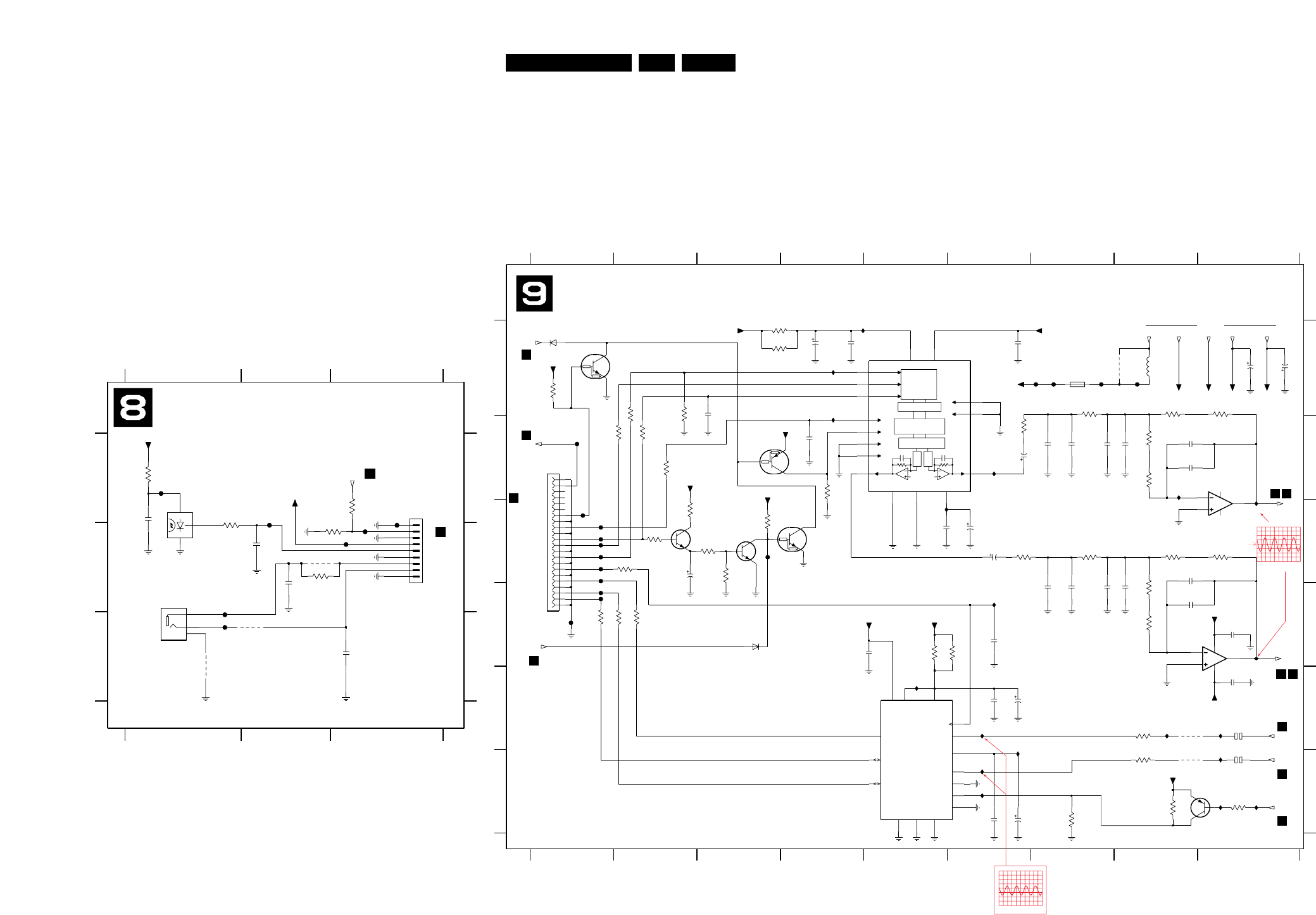
EN 987.LX7500RCircuit Diagrams and PWB Layouts
DIGITAL
DAC
DE-EMPHASIS
INTERPOLATION
DAC
NOISE SHAPER
FILTER
INTERFACE
DAC
DATAO
BCK
WS
VSSAVSSD
VDDD
VINR
SFOR
VINL
MSSEL
VREF
VRN
VDDAVRP
SYSCLK
PWON
F010 C9
3054 C9
4003 F8
4004 E8
4006 A8
5001 A8
6001 A1
6003 D3
7001 A6
I032 F6
I033 B6
I036 F9
from IOA
I020 F9
I021 F9
I022 F6
I028 E8
I030 E9
F0001 D1
F0002 D1
F0003 D1
F0005 C1
F0007 C1
F0009 C1
F0011 C1
F0012 C1
5%
3029 D8
3030 D8
3034 F8
3035 F9
F0014 C1
F0016 C1
F0021 B1
F005 C3
F006 A8
F007 A7
F008 A7
F011 D9
I002 A4
I003 A4
I006 A4
I008 B8
I011 C5
I013 E5
I014 E6
I015 D6
I018 E6
3053 C8
5%
3013 B2
7002-1 B9
7002-2 D8
7003 B3
7004 A1
7005 E4
7006 F9
7008 C2
not used
7010 C4
not used
5%
5%
1%
3039 F8
3041 E8
3043 D2
3044 C3
3045 C3
3046 C2
3047 C3
F009 A7
3052 A9
1%
5%
2034 D7
2035 B8
2036 D8
2037 B7
2038 B8
2039 D8
2040 D7
3001 A3
3014 B4
3015 D5
3017 D6
3018 C2
3019 D2
3020 D1
3024 C6
7009 C3
3027 C7
1%
from PS
not used
1%
1%
45678 9
12
1% 1%
3048 C2
3012 B8
from PS
NP0
NP0
from IOV
Bead
to DIGIO
from IOV
2029 E9
2031 C2
2033 B7
2003 A6
2004 A9
2005 A9
2006 A3
2007 B6
2008 B7
2009 C5
2010 C6
3002 A3
3003 A2
3004 A2
3005 B2
3006 B2
3007 B6
3008 A1
3026 F7
3010 A8
from IOA
from / to Digital Board 1900
1%
123
45678 9
A
C
D
E
F
A
B
3011 B8
B
not used
2020 F6
2022 B4
2023 F9
2024 B8
2025 D7
2026 C8
1900 B1
2001 A4
2002 A4
C
D
E
F
1001 A7
3009 A7
2013 E6
2014 E6
2015 D4
2016 D6
2018 D9
2019 F6
to IOA, IOV
to IOA, IOV
5%
not used
2011 C6
2012 E9
3
I015
7007
PDTC124EU
I036
2034
470p
100K
3010
2R2
3002
5VSTBY
14 VOL 16
VOR
12
VREF-DAC
15
VSSA
5
VSSD
2WS
DEEM
8MUTE
10 PCS
11
SFOR0
7
SFOR1
6SYSCLK
13
VDDA
4
VDDD
7001
UDA1334BTS
1BCK
3DATAI
9
4K7
3009
4004
4n7
2039
100n
2003
10K
3039
I028
5N
7009
BC847BW
F010
F009
3V3DD
22R
3043
5001
3V3DD
2001
47u
3004
22R
F0007
3019
22R
2038
4n7
2R2
3015
1n0
2008
2010
47u
10K
3044
3001
2R2
10K
3003
F0009
47u
2020
3046
470R
7008
BC847BW
F006
47K
3034
3008
4K7
F005
F0005
F0003
5V
I022
I006
5VSTBY
3047
100K
4
5
15
10
12
I014
14
7
6
8
16
9
1
3
2
UDA1361TS
7005
ADC
Φ
24-BIT AUDIO
11
13
2040
4n7
3013
22R
2009
3V3DD
100n
5N
F0014
100n
2018
7010
PDTC124EU
5
6
7
8
4
3048
100R
MC33078D
7002-2
22R
3018
5V
2011
10u25V
2R2
3029
1R0
3017 I011
2002
100n
3V3DD
47u
2004
I013
3041
10K
3024
47K
2012
100n
I003
3
21
8
9
MC33078D
7002-1
19
2
20
21
22
3
4
5
6
7
1
10
11
12
13
14
15
16
17
18
1900
22FMN-BTRK-A 3V3DD
I002
22R
3006
470p
2033
2015
100n
5NSTBY
100u
2013
2036
10p
7003
PDTA124EU
F0012
2025
1n0
F011
F0016
47u
2023
7006
BC857BW
BAS316
6003
4003
100u
2005
47K
3007
47p
2016
3053
100K
3V3DD
I032
10K
3035
2007
I033
10u
I030
3V3DD
3005
22R
2026
27p
I021
F0021
I018
10p
2035
47u
4n7
2037
2029
27p
2024
3026
47K
I008
6001
BAS316
F0001
1R0
3011
F007
330R
3030
3027
4K7
3V3DD
F0011
2006
47p
3V3DD
3K3
3054
3K3
3052
100n
2014
10K
3014
I020
F0002
3012
330R
3045
100K
2031
2u2
22R
3020
100n
2019
398(MP)
1001
125mA
F008
4006
47p
2022
D_DATA0
D_PCMCLK
GND
GND
GND
GND
GND
GND
GND
GND
DAOUT
DAOUT
A_DAT
ARADC
D_IKILL
5V 5N
ALADC
ARDAC
ALDAC
ION
5NSTBY5VSTBY
A_PCMCLK
IPFAIL
A_WCLK
PWONSW
D_BCLK
D_WCLK
A_BCLK
3V3
ANALOG BOARD
Audio Converter (DAC_ADC)
A/V board LX7500R, 231104
4
8
8
2
23
2
2
3
3
3
A: DC, 500mV/Div
500us/Div
I014/I032
ARDAC/ALDAC F010/F011
A: DC, 500mV/Div
500us/Div
VCC
GND
F556 B3
F557 B32582 B2 2583 B2
2584 C3 3584 B3
3585 A3 3586 A1
3587 A1 3588 B2
4582 B2 4583 C2
4584 C1 7581 A1
F551 B1 F552 C1
F553 A2 F554 A1
F555 A3
OPTICAL IN
IN
123
123
A
B
C
A
B
C
1951 B1
1952 A3 2581 A1
DIGITAL
2
3
4
5
6
7
8
9
from DAC_ADC
2
B9B-PH-K
1952
1
YKC21-3416
1951
1
3
5V_Opt
3587
1R0
3586
47R
1
3
F552
7581
GP1FA550RZ
2
F553
2581
100n
F551
4583
75R
3584
F554
5V_Opt
F556
F555
330R
3585
100n
2582
10R
3588
F557
4582
100p
2584
100p
2583
4584
DAOUT
to COMBI board 1701
ANALOG BOARD
Digital In/Out (DIGIO)
A/V board LX7500R, 231104
9
6
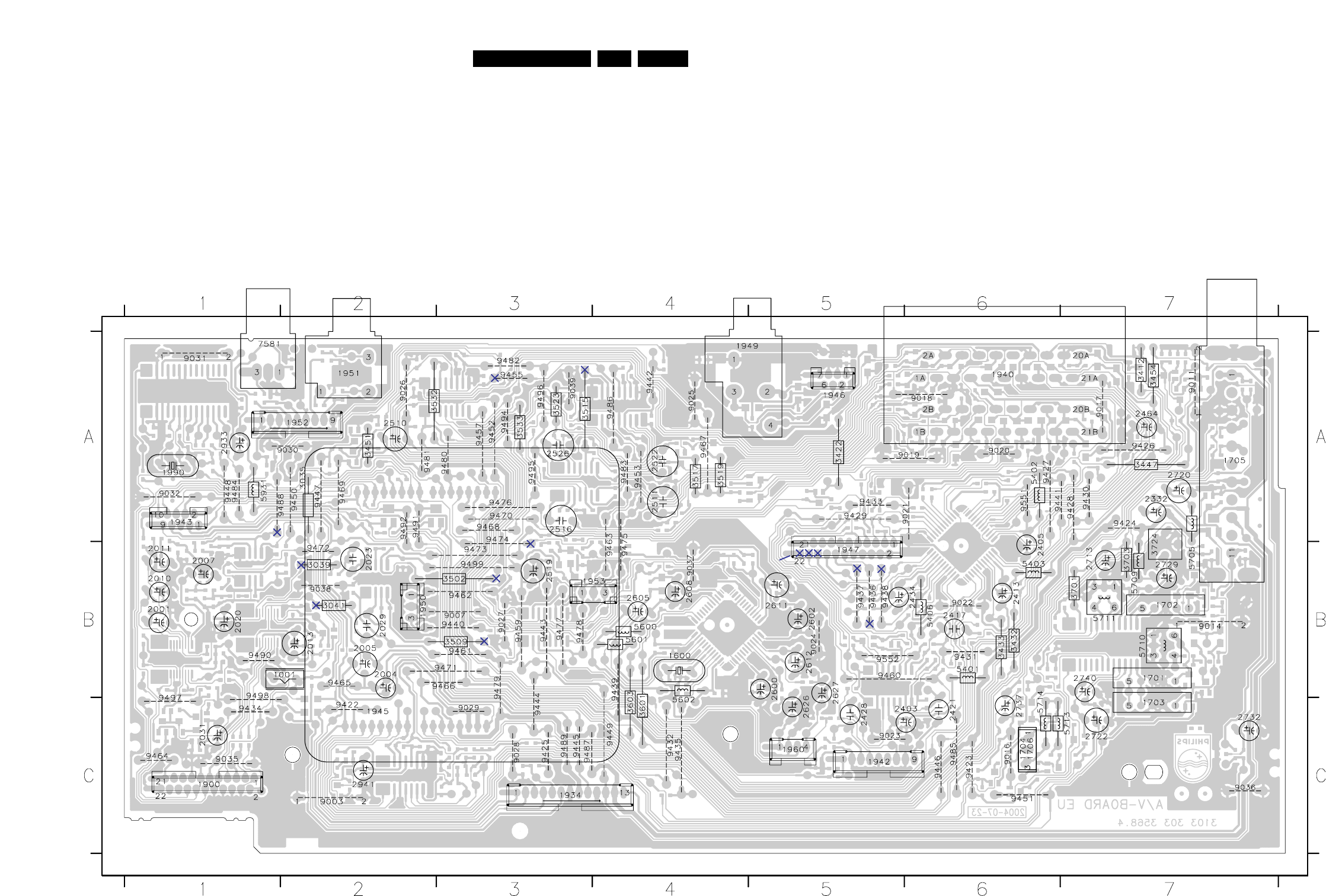
EN 997.LX7500RCircuit Diagrams and PWB Layouts
ANALOG BOARD / component side view
1001 B2
1600 B4
1701 B7
1702 B7
1703 C7
1704 C6
1705 A7
1706 C6
1900 C1
1934 C3
1940 A6
1942 C5
1943 A1
1945 C2
1946 A5
1947 B5
1949 A4
1950 B2
1951 A2
1952 A2
1953 B4
1960 C5
1990 A1
2001 B1
2004 B2
2005 B2
2007 B1
2010 B1
2011 B1
2013 B2
2020 B1
2023 B2
2029 B2
2031 C1
2332 A7
2403 C6
2405 B6
2413 B6
2417 B6
2421 C6
2428 C5
2434 B6
2464 A7
2510 A2
2511 A4
2516 A3
2519 B3
2522 A4
2526 A3
2600 B5
2602 B5
2605 B4
2608 B4
2611 B5
2612 B5
2626 C5
2627 B5
2713 B7
2720 A7
2722 C7
2729 B7
2732 C7
2737 C6
2740 B7
2933 A1
2941 C2
3035 A2
3039 B2
3041 B2
3412 A7
3422 A5
3432 B6
3433 B6
3447 A7
3451 A2
3454 A7
3502 B3
3509 B3
3515 A3
3517 A4
3519 A4
3523 A3
3532 A2
3533 A3
3601 C4
3603 C4
3701 B7
3703 B7
3724 B7
5401 B6
5402 A6
5403 B6
5406 B6
5600 B4
5601 B4
5602 C4
5705 B7
5709 B7
5710 B7
5711 B7
5713 C7
5714 C6
5931 A1
7581 A1
9003 C2
9007 B3
9011 A7
9014 B7
9016 C6
9017 A7
9018 A6
9019 A6
9020 A6
9021 A6
9022 B6
9023 C5
9024 B5
9025 A4
9026 A2
9027 B3
9028 C3
9029 C3
9030 A2
9031 A1
9032 A1
9035 C1
9036 C7
9037 B4
9038 B2
9039 A3
9422 C2
9423 C6
9424 A7
9425 C3
9426 A7
9427 A6
9428 A7
9429 A5
9430 A7
9431 B6
9432 C4
9433 A5
9434 C1
9435 C4
9436 B5
9437 B5
9438 B5
9439 B4
9440 B3
9441 A6
9442 A4
9443 B3
9444 C3
9445 C3
9446 C6
9447 A2
9448 A1
9449 C4
9450 A2
9451 C6
9452 A3
9453 A4
9455 A3
9457 A3
9459 B3
9460 B5
9461 B3
9462 B3
9463 B4
9464 C1
9465 B2
9466 B3
9467 A4
9468 A3
9469 A2
9470 A3
9471 B3
9472 B2
9473 B3
9474 A3
9475 B4
9476 A3
9477 B3
9478 B3
9479 B3
9480 A3
9481 A2
9482 A3
9483 A4
9484 A1
9485 C6
9486 A4
9487 C3
9488 A2
9489 C3
9490 B1
9491 A2
9492 A2
9494 A3
9495 A3
9496 A3
9497 C1
9498 C1
9499 B3
9551 A6
9552 B5
This assembly drawing shows a summary of all possible versions.
For components used in a specific version see schematic diagram respectively partslist.
A/V board LX7500R .4, 231104
OPT DIG
COMP.
VIDEO
PR
PB
Y
SCART
TV TUNER
DIGITAL BOARD 1904
COMBI BOARD
1205
COMBI BOARD
1205
DIGITAL BOARD 1900
DIGITAL BOARD 1704
COMBI BOARD 1102
AUX SUPPLY BOARD 1300
FRONT/DISPLAY BOARD 1922
COMBI BOARD 1701
I405
F4712
F4716
F4714
F4722 pin 22
F4720 pin 20
F4718 pin 18
I517
I518
F501
F502
F011
I032
I014
F 011 A1
F 501 A3
F 502 A3
F4712 B5
F4714 B5
F4716 B5
F4718 B5
F4720 B5
F4722 B5
I 014 B2
I 032 B2
I 405 B 3
I 517 B3
I 518 B3
TEST POINTS
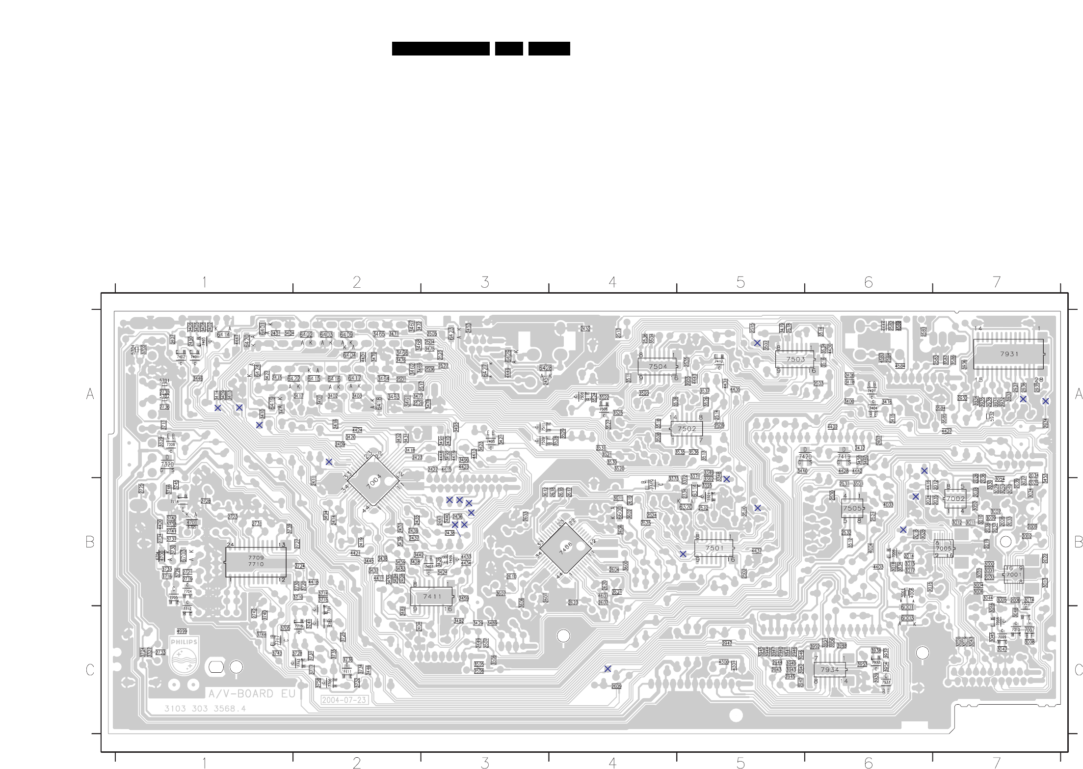
EN 1007.LX7500RCircuit Diagrams and PWB Layouts
ANALOG BOARD / copper side view
2002 B7
2003 B7
2006 B7
2008 B7
2009 B7
2012 B7
2014 B6
2015 B6
2016 B6
2018 B7
2019 B7
2022 B7
2024 B6
2025 B7
2026 B7
2033 B7
2034 A7
2035 B7
2036 B7
2037 B7
2038 B7
2039 B7
2040 B7
2334 B5
2401 A1
2402 A1
2404 C2
2406 A6
2407 A6
2408 B2
2409 A2
2410 A3
2411 B2
2412 A6
2414 B2
2415 A1
2416 A2
2418 A2
2419 B2
2423 A2
2427 A3
2433 B2
2435 B2
2436 B3
2437 B2
2438 B3
2439 B2
2440 B3
2441 B3
2446 C2
2449 C3
2450 A1
2451 A3
2452 A4
2453 A3
2459 B3
2501 A2
2502 B5
2503 A6
2504 A3
2505 A3
2506 A3
2507 C3
2508 C3
2509 A5
2512 B5
2513 A4
2514 A5
2515 A5
2517 A3
2518 A5
2520 A2
2521 B6
2523 A3
2524 B4
2525 B4
2527 A3
2530 B6
2531 B6
2532 B6
2535 A5
2536 A4
2581 A6
2582 A6
2583 A7
2584 A6
2601 B3
2603 B3
2604 B4
2606 B4
2607 B4
2609 C4
2610 B3
2616 B4
2617 B4
2618 B4
2619 B4
2620 B4
2621 B4
2623 B4
2719 B1
2721 B1
2723 B1
2724 B2
2725 B1
2727 B2
2728 B1
2730 B2
2731 B1
2733 C1
2734 B1
2735 A1
2736 A1
2741 B1
2742 C1
2932 A7
2934 A7
2935 A7
2936 A7
2937 A7
2938 A7
2940 C5
2942 C5
2943 C5
2944 C5
2945 C5
2946 C5
2947 C5
3001 B7
3002 B7
3003 B7
3004 B7
3005 B7
3006 B7
3007 B7
3008 C7
3009 B7
3010 B7
3011 B7
3012 B7
3013 B7
3014 B7
3015 B6
3017 B6
3018 B6
3019 C7
3020 C7
3024 B7
3026 B6
3027 B7
3029 B7
3030 B7
3034 B6
3043 C7
3044 B7
3045 C7
3046 C7
3047 C7
3048 C7
3052 B7
3053 B7
3054 B7
3327 C1
3329 A1
3348 A5
3349 A5
3355 B5
3362 B5
3371 A5
3372 B5
3373 B4
3400 A6
3401 A2
3402 A2
3403 A2
3404 A1
3405 A1
3406 A1
3407 A1
3408 A1
3409 A1
3410 A1
3411 A1
3413 A1
3414 A1
3415 A6
3416 A6
3417 A2
3418 A6
3419 A5
3420 A2
3421 A3
3423 A3
3424 B3
3426 B3
3427 A1
3428 B2
3429 C3
3431 A2
3437 B2
3438 B2
3439 B2
3440 A5
3442 B2
3445 B2
3446 A1
3452 A2
3453 B7
3455 B2
3458 A6
3459 B2
3460 A6
3461 A2
3462 A2
3463 A2
3464 A2
3465 A2
3466 A2
3467 A2
3468 A2
3469 A2
3470 A2
3471 A2
3472 A2
3475 A3
3476 A2
3477 A2
3478 A3
3481 C2
3482 C3
3483 B2
3484 B2
3489 C3
3490 A3
3491 A3
3492 A3
3493 A3
3494 B2
3501 B6
3503 A4
3504 A4
3505 C3
3506 C3
3507 A5
3508 A4
3510 B5
3511 A4
3512 B6
3513 A5
3514 A6
3516 A6
3518 A4
3520 A4
3521 A4
3522 A4
3524 A4
3525 A4
3526 A5
3527 A4
3528 A4
3529 A4
3530 A4
3531 A4
3534 A6
3535 A5
3536 A5
3537 A5
3538 A4
3584 A7
3585 A7
3586 A7
3587 A7
3588 A6
3600 B4
3602 B4
3606 B3
3607 B3
3611 B4
3612 B3
3702 A1
3704 C1
3705 C1
3710 B2
3711 A1
3714 B2
3715 B2
3716 B1
3717 C2
3720 B2
3725 C2
3726 B1
3728 C2
3730 B1
3731 C2
3732 C2
3733 B1
3734 C2
3735 C2
3736 C2
3737 B1
3738 B1
3739 B1
3740 C1
3741 C2
3742 B1
3743 C1
3744 C1
3745 B1
3746 B1
3758 C2
3931 A7
3932 A7
3933 A7
3934 A7
3935 A7
3936 A7
3937 C6
3938 C6
3939 C6
3940 C5
3941 C5
3942 C5
3943 C5
3944 C5
3945 C5
3946 C5
3947 C5
3948 C6
3950 C6
3951 C6
3952 C6
3953 C6
3954 C6
3955 A5
4003 B6
4004 B6
4006 B6
4300 C5
4301 C5
4401 A2
4402 A6
4403 B6
4411 B2
4413 A3
4415 A3
4416 B6
4418 B2
4419 A3
4420 B1
4421 B2
4423 A3
4424 A2
4427 A7
4428 A6
4430 A6
4431 A5
4433 B3
4434 B3
4435 A5
4437 B5
4442 A6
4443 A5
4444 A6
4447 A1
4448 A3
4449 A3
4582 A6
4583 A6
4584 A6
4601 B4
4700 B1
4701 B1
4999 C1
5001 B6
5701 A1
5702 A1
5704 A1
5932 A7
6001 C6
6003 C6
6314 B5
6320 B5
6401 A1
6402 A2
6403 A2
6404 A2
6409 A2
6414 A1
6415 A2
6416 A2
6417 A2
6418 A2
6419 A1
6420 A1
6422 A2
6423 A3
6424 A1
6427 A3
6428 A3
6429 A3
6600 B4
6703 B1
6704 B1
6705 B1
7001 B7
7002 B7
7003 B7
7004 B2
7005 B7
7006 B6
7007 C7
7008 C7
7009 C7
7010 C7
7308 A1
7319 B4
7320 A1
7321 B5
7401 A1
7402 A1
7403 A1
7404 A6
7405 A3
7407 B3
7408 B4
7409 B3
7411 B3
7412 A5
7419 A6
7420 A6
7421 A6
7501 B5
7502 A5
7503 A5
7504 A4
7505 B6
7506 A4
7508 A4
7509 A3
7511 A4
7701 C2
7702 C2
7704 B1
7705 B1
7706 C2
7709 B1
7710 B1
7711 C2
7712 C1
7713 C1
7714 B1
7716 C2
7717 C1
7931 A7
7932 C6
7933 C6
7934 C6
This assembly drawing shows a summary of all possible versions.
For components used in a specific version see schematic diagram respectively partslist. A/V board LX7500R .4, 231104
I723
I465 I462
I463
F360
I461
I405
F4712
F4716
F4714
F4718
F4722
F4720
I502
I517
F501
I994 I989
F010
I032
I014
F 010 A7
F 360 A1
F 501 A5
F4712 B3
F4714 B3
F4716 B3
F4718 B3
F4720 B3
F4722 B3
I 014 B6
I 032 B6
I 405 A5
I 461 A2
I 462 A1
I 463 A1
I 465 A1
I 502 B5
I 517 B5
I 723 C4
I 989 A7
I 994 A7
TEST POINTS
1221
22
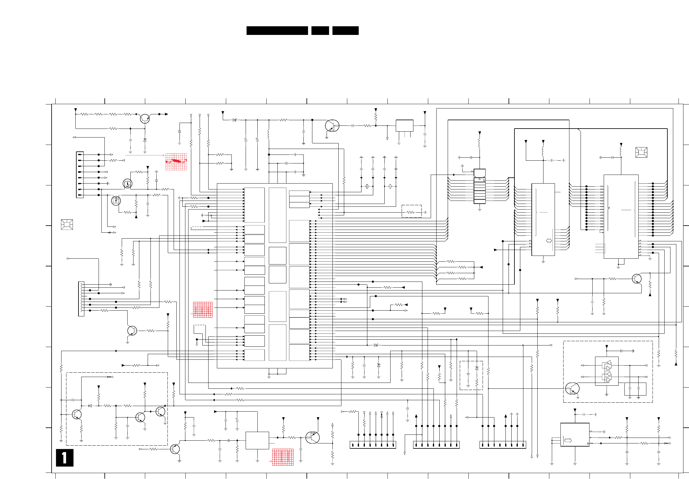
EN 1017.LX7500RCircuit Diagrams and PWB Layouts
EN
C1
1D
18
16
RB
4
3
2
CE
7
6
WE
RP
1
0
BYTE
3
NC
5
8
9
10
11
12
13
14
15
A-1
10
4
9
8
7
6
0
8M-1
0A
D
5
11
2
1
17
OE
12
13
14
15
CSYNC
VSYNC
VIN
GND VCC
15
0
CE1
NC
14
13
11
DQ
16
7
128K-1
0
A
12
CE2
OE
WE
10
9
8
7
6
5
4
3
2
1
0
SCL
ADR
0
1
2 SDA
WC
SIO/UART
( SIO1 )
INTERFACE
( SBI )
8-BIT TIMER
( TMRA1 )
8-BIT TIMER
( TMRA2 )
8-BIT TIMER
( TMRA3 )
8-BIT TIMER
( TMRA4 )
8-BIT TIMER
( TMRA5 )
8-BIT TIMER
( TMRA6 )
8-BIT TIMER
( TMRA7 )
CLOCK DOUBLER
L-OSC
PORT 6
PORT A
CS/WAIT
CONTROLLER
( 4-BLOCK )
INTERRUPT
CONTROLLER
16-BIT TIMER
( TMRB0 )
16-BIT TIMER
( TMRB1 )
PORT 1
PORT 0
CLOCK GEAR
H-OSC
10-BIT 8-CH
A/D
CONVERTER
SIO/UART/IrDA
( SIO0 )
SERIAL BUS
8-BIT TIMER
( TMRA0 )
128KB ROM
4KB RAM
CPU
WATCH
DOG TIMER
( WDT )
REAL-
CLOCK
TIMER
( RTC )
PORT 3
PORT 2
delete for NAFTA
to FACO
to E2
12 13 14 15
12
to E13
to I12
C
D
E
F
G
H
I
0606 B15
0803 C1
1801 B8
1805 B9
1980 B1
1984 I11
1986 E1
1987 I9
1988 I8
2800 A9
A
B
C
D
E
F
1 2345
Bead
SDASW
from / to IOV
to B2
from H8
67891011
2809 B14
2810 B3
2811 C3
2812 E14
2813 B8
2814 B9
34567
for P50 only
from G3
to F3
100R for CHRYSALIS 3V3
Bead
ASC1M
100R for CHRYSALIS 3V3
8 9 10 11 12 13 14 15
2828 H13
2829 H5
2830 H4
2831 H9
2832 G8
2833 G14
G
H
I
A
B
from H10
from E2
CLOCK_ADJ
not used
2801 B8
2802 B8
2803 B6
2804 B6
2805 B6
2806 B11
2807 A8
2808 B13
3812 C2
3813 G15
3814 H10
3815 G10
3816 C2
3817 F10
2815 H1
2816 A5
2817 G10
2818 H2
2819 A5
from/to G2
Bead
to H3
from FACO
from / to IOV
N.C.
2820 A6
2821 A3
2822 A2
2823 I4
2824 I5
2825 I6
2826 I14
2827 I15
3831 G11
3832 G1
3833 G11
3834 G9
3835 G9
3836 H10
2834 H14
2835 H15
2836 H4
3800 E3
3801 A8
PWONSW
not used
to G13
to KUCO
3802 E2
3803 F2
3804 B2
3805 C3
3806 B3
3807 D10
3808 D10
3809 E10
3810 E10
3811 C3
3852 G12
3854 G5
3855 A8
3856 F3
3857 G2
3858 G9
3818 F11
3819 G15
3820 H5
3821 E14
3822 E15
GNDD
N.C.
from H11
to A4
from D2
3823 E14
3824 I7
3825 E8
3826 H8
3827 B2
3828 F13
3829 A4
3830 G12
3874 C4
3875 C4
3876 F12
3877 H3
3878 H8
3879 E3
3837 B4
3838 H5
3839 H1
3840 H3
3841 H2
FLASH_TOSHIBA
from/to Digital Board
3842 H2
3843 I1
3844 I1
3845 A4
3846 A4
3847 B7
3848 C9
3849 H2
3850 B4
3851 E9
5803 A11
5804 A6
6800 H1
6801 A2
6802 A5
6803 G11
3860 G10
3861 H2
3862 A6
3863 A1
3864 A1
EXT_DL
from / to IOV
3865 A2
3866 A2
3867 A2
3868 F3
3869 I4
3870 I5
3871 I6
3872 I6
3873 I7
7815 H3
7816 A3
7817 F2
7818 H6
7819 I3
7821 C2
3880 I3
3881 D2
3882 D2
3884 I14
3885 I15
from / to IOV
to B2
SCLSW
from/to H8
3886 I15
3887 I14
3888 F2
3889 G8
4801 F4
4802 C4
5801 B12
5802 B14
F804 C14
F805 C14
F806 C14
F807 C14
F808 C14
F809 C14
6804 G8
6805 F8
7801 B11
7802 A7
7803 B12
not used
7804 B4
7805 B14
7806 A9
7807 E15
7808 H13
7810 G14
7811 H13
7813 H1
7814 H2
F823 C15
F824 C15
F825 C15
F826 C15
F827 C15
F828 C15
7822 B2
7825 H5
F8001 C1
F8002 C1
F8003 B1
to FACO
from/to D2
F8004 B1
F8005 B1
F8006 B1
F8007 B1
F8008 B1
F801 E12
F802 D11
F803 D11 F839 D15
F840 E8
F8401 H11
F8402 H11
F8403 H11
F8405 H11
F810 C14
F811 C14
F812 C14
F813 C14
F814 C14
from F9
to H8
PCB-Test
from I12
F815 C14
F816 C14
F817 C14
F818 D14
F819 D14
F820 B15
F821 C15
F822 C15
F8604 E1
F8606 E1
F8607 E2
F8608 E1
F8609 F2
F8610 F1F829 C15
F830 C15
F831 C15
F832 C15
F833 C15
Bead
from A9
from E7
to H13
to H8
not used
from B2
for EU+EPG only
F834 C15
F835 D15
F836 D15
F837 D15
F838 D15
F8804 I8
F8805 I8
F8806 I8
F8807 I8
F8808 I9
I801 B8F8406 H12
F8407 H12
F841 F8
F842 F8
F843 F4
from/to H15
not used
F844 D15
F845 D15
F846 A7
F847 A3
F848 E8
F849 B6
F850 C4
F851 C4
F852 E8
F8603 E1 I815 H3
I816 A2
I817 I5
I818 I6
I819 I14
I820 I14
F8701 H9
F8702 H9
F8703 H9
F8704 H10
F8705 H10
N. C.
THG
WSRI/
KILL
to A4
not used
F8706 I10
F8707 H10
F8708 H10
F8802 I8
F8803 I8 I821 D4
I822 D4
I823 H2
I824 H3
I825 G7
I802 B8
I803 B8
I804 B9
I805 F10
I806 G5
from I7
not used
from H8
from B2
to A4
I807 H4
I808 H4
I809 A8
I810 B10
I811 E7
I812 E7
I813 A2
I814 G2
2833
100n
F8610
3V3STBY
GNDD
3871
10K
10K
3816
100n
2805
5VSTBY
GNDD
GNDD
15p
2802
12
20
5801
10
GND
11
1
19
18
17
16
15
14
13
74LVC573
7801
2
3
4
5
6
7
8
9
27K
3839
F820
GNDD
10K
3822
3V3STBY
I821
GNDD
F806
I824
3V3STBY
5VSTBY
F825
5VSTBY
2K7
3818
GNDD
GNDD
3V3STBY
4K7
3886
47p
2832
11
100u
2819
9
10
13
14 28
15
12
37
27
VSS1
46
VSS2
41
43
45
33
35
38
40
42
44
30
32
19
18
8
7
47
26
29
31
34
36
39 3
2
1
48
17
16
23
22
21
20
1Mx8/512Kx16
EPROM
25
24
6
5
4
I813
M29W800DT-70N6
7805
F852
3V3STBY
3842
220K
2821
GNDD
GNDD
10n
7822
BSH111
3863
GNDD
3803
1K0
4R7
GNDD
BC847BW
7816
3823
100K
2822
100n
3847
10K
22K
3802
4802
F8003
3821
10K
0606
SOFTWARE
F828
5VSTBY
GNDD
4801
2806
100n
3V3STBY
5VSTBY
GNDD
I823
10K
3814
GNDD
3V3STBY
F8803
GNDD
5VSTBY
BAT254
6805
3873
4K7
BAS316
F8707
6800
2814
10p
F8002
GNDD
5802
3811
100R
I815
3
5
14
F833
7825
LA7213
2
GNDD
F810
GNDD
F849
F822
F8001
F817
7817
BC847BW
GNDD
GNDD
2820
10n
F8608
I807
F826
3856
10K
3881
47K
GNDD
100n
2803
PMBT2369
7807
GNDD
GNDD
33K
3846
F8808
GNDD
3838
1K0
3882
47K
I822
F804
2M2
3861
3800
22K
6804
BAT254
I825
F847
GNDD
F8604
F807
1K0
3835
6802
BAT254
GNDD
4R7
3866
3V3STBY
F829
GNDD
GNDD
F848
2830
100n
F8805
3807
100K
3858
100K
3
4
5
6
7
8
3857
10K
3V3STBY_R
C36
1988
1
2
GNDD
F8702
F813
PDTC124EU
F801
I802
7802
22K
3806
3830
1K0
7821
3860
2K2
F821
BSH111
F8401
BC847BW
7813
3854
1K0
F832
I811
3809
100K
3V3STBY
3868
10K
5VSTBY
3827
1K0
3V3STBY
3869
330R
100K
3841
2827
100p
2829
10u
I801
100p
2826
3878
1K0
4R7
3864
F803
2809
100n
3V3STBY
F843
F841
F827
1K0
3824
I818
F8007
3851
10K
2801
15p
GNDD
220R
3844
2817
100n
GNDD
3V3STBY
3V3STBY_R
3884
100R
GNDD
7814
BC847BW
F819
2825
100p
3848
10K
220n
2807
29
I804
14
15
17
18
19
20
21
1
24
VCC
32
16
9
8
7
6
5
27
26
22
30
13
CY62128VLL-70SC
12
11
23
25
4
28
3
31
2
10 128Kx8
RAM
7803
10n
2831
F8701
GNDD
6
7
8
5803
C36
1980
1
2
3
4
5
F8607
I806
GNDD
5VSTBY
220m
2816
GNDD
100n
2800
100R
3805
3V3STBY
1
10
2
3
4
5
6
7
8
9
GNDD
1986
10FMN-SMT-A-TF
3888
470R
F840
I808
3865
4R7
6803
BAT254
F837
3832
33K
2823
1n0
F835
7815
BC847BW
F834
100R
3836
3V3STBY
10K
3804
3867
75R
3829
10K
GNDD
1
2
3
4
5
6
7
8
1987
C36
F808
3833
1K0
F8006
32K768
1805
DT-38
GNDD
F816
GNDD
F818
3813
10K
GNDD
F845
12K
3837
F8406
F85110K
3875
GND
3
INP 2
NC1
4
NC2
5
OUTP
1
VSS
4
7
7806
NCP301LSN30
7808
M24C16-MN6
1
2
3
6
5
8
GNDD
(2Kx8)
Φ
EEPROM
GNDD
3V3STBY
F8706
GNDD
GNDD
GNDD
2828
100n
3V3STBY
F823
5VSTBY
GNDD
3862
10K
3834
1K0
1K0
3826
GNDD
GNDD
GNDD
7818
PDTA124EU
I820
GNDD
F842
I810
3850
18K
F8802
F8806
I805
10n
2812
2804
100n
GNDD
1
2
3
4
5
6
7
8
4K7
3840
C36
1984
3825
10K
5804
18K
3815
3V3STBY
2824
1u0
GNDD
10p
2810
F814
3V3STBY
3812
22K
F802
2811
10p
1K0
3820
100K
3810
F824
3V3STBY
F8405
F8402
GNDD
F811
GNDD
3828
10K
3849
47K
F844
F831
X2
GNDD
P96|XT1
32P97|XT2
PA4 39
PA5 40
41PA6
PA7 42
71RD_|P30
30RESET_
RW_|P36 77
87SCOUT|P64
100 VREFH
1 VREFL
74WAIT_|P33
72WR_|P31
28X1
26
P74|TA5OUT
P75|TA7OUT9
10 P80|TB0IN0|INT5
P81|TB0IN1|INT611
12 P82|TB0OUT0
P83|TB0OUT113
14 P84|TB1IN0|INT7
P85|TB1IN1|INT815
16 P86|TB1OUT0
P87|TB1OUT117
18 P90|TXD0
19 P91|RXD0
20 P92|SCLK0|CTS0_
21 P93|TXD1
22 P94|RXD1
23 P95|SCLK1|CTS1_
31
P22|A18|A2
66P23|A19|A3
67P24|A20|A4
68P25|A21|A5
69P26|A22|A6
70P27|A23|A7
78P37
P60|SCK83
P61|SO|SDA84
P62|SI|SCL85
88P65
P66 90
4 P70|TA0IN
P71|TA1OUT5
6 P72|TA3OUT
P73|TA4IN7
8
47P03|AD3
48P04|AD4
49P05|AD5
50P06|AD6
51P07|AD7
52P10|AD8|A8
53P11|AD9|A9
54P12|AD10|A10
55P13|AD11|A11
56P14|AD12|A12
57P15|AD13|A13
58P16|AD14|A14
59P17|AD15|A15
60P20|A16|A0
61P21|A17|A1
65
DVCC3
64
91
DVSS1
27
DVSS2 DVSS3
62
EMU0 33
34EMU1
73HWR_|P32
86INT0|P63
INT1|PA0 35
36INT2|PA1
INT3|PA2 37
38INT4|PA3
NMI_ 63
44P00|AD0
45P01|AD1
46P02|AD2
AN3|ADTRG_|P53
96 AN4|P54
97 AN5|P55
98 AN6|P56
99 AN7|P57
3 AVCC
2 AVSS
BUSAK_|P35 76
BUSRQ_|P34 75
CS0_|P40 79
80CS1_|P41
81CS2_|P42
CS3_|P43 82
89
DVCC1
25
DVCC2
TMP91CW12AF/LIRP1
7804
43ALE
24AM0
29AM1
92 AN0|P50
93 AN1|P51
94 AN2|P52
95
GNDD
GNDD
5VSTBY
F839
0803
BARCODE
2813
10p
F846
3V3STBY
F836
I812
F830
F809
I817
I809
220p
2818
3V3STBY
12VSTBY
3817
2K7
I816 3855
470R
3V3STBY
10p
2835
10K
3876
GNDD
F8603
GNDD
F8606
BC857BW
7819
3877
1K0
3880
100R
I819
GNDD
3V3STBY
GNDD
6801
BZX384-C3V9
F8703
100n
2808
F850
33K
3843
F8407
F8708
10K
3819
GNDD
GNDD
2815
220p
F8804
1K0
3845
F8704
GNDD
2834
10p
I814
3V3STBY
GNDD
F8807
F812
100R
3885
F8609
F815
3V3STBY
GNDD
F805
2836
100n
3870
100K
F838
I803
GNDD
100K
3808
GNDD
24M576
1801
CX-11F
3879
1K0
F8705
10K
3852
F8403
F8005
3872
10K
GNDD
PDTC124EU
7811
VCC
18K
3889
5EN
4
GND
1
NC
2 SCL0 7SCL1
3 SDA0 6SDA1
8
GNDD
PCA9515ADP
7810
3887
4K7
F8008
3831
1K0
10K
3874
F8004
GNDD
10K
3801
SCLSW
SDASW
ION
ION
A_YCVBS
GNDD
WE WE
A_DATA
D_DATA
A_RDY
D_RDY
IRESET_DIG
AD(0)
AD(1)
AD(2)
AD(3)
AD(4)
A(2)
SDA
P50 P50
SDA
SCL
A(10)
CS2_
CS2_
RD_
RD_
RD_
RY|BY_
RY|BY_
FBIN FBIN
BE_FAN
BE_FAN
A(11)
A(12)
A(13)
A(14)
A(15)
A(16)
A(17)
A(18)
A(19)
A(3)
A(4)
A(5)
A(6)
A(7)
A(8)
A(9)
PSS
P50
SDASW
SCLSW
WR_
WR_
A(7)
AD(7)
A(0:7)
A(0)
A(1)
A(2)
A(3)
A(4)
A(5)
A(6)
CS0_
CS0_
A(1)
A(2)
IPOR
SYNC
INT
AD(0)
AD(1)
AD(2)
AD(3)
AD(4)
AD(5)
AD(6)
FOME
WSFI WSFI
SB1
AGC
SFS_TS
12VSTBY
FAN_OFF
AD(7)
AD(6)
AD(5)
AD(4)
AD(3)
AD(2)
A(0)
AD(1)
AD(0)
5VSTBY
GNDD
GNDD
IPOR
IPOR
SCL
SDA
SDA
SCL
SCL
AFC
SYNC
INT
INT
IPOR_DC
IPOR_DC
TEMP_SENSE
TEMP_SENSE
GNDD
A_YCVBS A_YCVBS
8SC2
8SC2
WU
WU
KILL
KILL
STBY
FBIN
FBIN
LEVELSW
WE
BOOT
IPOR_DC
PWONSW
LEVELSW
PWONSW
LEVELSW
A(11)
A(10)
A(9)
A(8)
AD(7)
AD(6)
AD(5)
AD(4)
AD(3)
AD(2)
AD(1)
AD(0)
ALE
ALE
8SC2
WSFI
AD(0:7)
A(16)
A(15)
A(14)
A(13)
A(12)
A(11)
A(10)
A(9)
A(8)
A(8:19)
WU
A(19)
A(18)
A(17)
A(16)
A(15)
A(14)
A(13)
A(12)
AD(5)
AD(6)
AD(7)
A(0)
A(1)
A(3)
A(4)
A(5)
A(6)
A(7)
A(16)
A(17)
A(18)
A(19)
µP Sub board LX7500R, 231104
3V
5.1V
4.5V
4.3V
3.5V
0.3V
3.3V
0V
3.5V
4.2V
4.7V
A: DC, 500mV/Div
10us/Div
A: DC, 1 V/Div
20us/Div
A_CVBS F8008
I818
A: DC, 500mV/Div
10us/Div
SYNC F843
uP Sub Board: Central Controller (CECO)
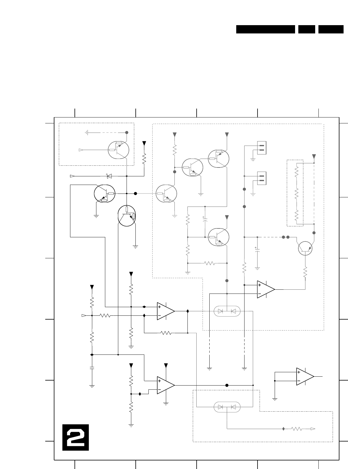
EN 1027.LX7500RCircuit Diagrams and PWB Layouts
D
E
A
B
C
D
E
A
delete for SET FAN
1%
3913 B2
3922 C1
3923 E1
not used
1%
3914 C4
3915 C3
B
C
GNDD
from CECO
1902 A4
2911 D1
2912 B3
2913 B3
4901 A1
4902 D3
4903 D3
4904 B4
3916 D1
3917 C1
not used
7903 A1
7904 A3
3918 B2
1901 A4
to FAN
to CECO
4
not used
from CECO
7910 B3
F901 A3
F902 B3
3919 C1
3920 E1
3921 E4 F910 E3
I903 C2
3924 A2
3925 D1
3926 A2
3927 D2
3928 C3
3929 A4
3930 A4
3931 A4
3932 B4
3933 B4
3934 A4
not used
6901 E3
6902 A1
6903 C3
7902-1 C2
7902-2 D2
7902-3 C4
7902-4 D4
7905 A3
7906 A1
7907 A2
7908 B1
7909 B4
1234
123
I904 C2
I905 C2
I906 E2
I907 E4
I908 D1
1%
F903 B4
F904 B4
F905 A1
F906 A2
F907 A2
F908 B4
F909 C3
from CECO
for SET FAN only
MOT
delete for SET FAN
to FAN
7910
PDTC124EU
GNDD
MOT
not used
F901
BAV70W
6901
3923
10K
I904
4904
7902-1
3
2
1
GNDD
GNDD
LM324D
10
9
8
1K0
3914
LM324D
7902-3
18K
12VSTBY
3928
GNDD
1K0
3915
4903
GNDD
F903
F902
7905
PDTC124EU
1K0
3918
GNDD
5VSTBY
3V3STBY
6902
BAT254
10K
3924
F904
7903
PDTC124EU
4K7
3926
7908
PDTC124EU
100u
2912
1
2
GNDD
GNDD
GNDD
1902
S2B-EH
7904
PDTA124EU
I908
PDTC124EU
7907
BC636
7909
3919
33K
BAV70W
6903
S2B-EH
1901
1
2
3920
5K6
27K
3916
I907
22R
12VSTBY
3933
3932
3931 3929
3934
22R
GNDD
33K
3927
12VSTBY
7906
PDTC124EU
GNDD
GNDD
12VSTBY
GNDD
GNDD
I906
2913
100u
3913
1K0
12VSTBY
I905
12VSTBY
3922
1K0
3925
10K
I903
3921
470R
F909
F908
F910
F907
F905
F906
22R
3930
4901
3917
36K
4902
LM324D
7902-4
12
13
14
5
6
7
4
11
1n0
2911
LM324D
7902-2 GNDD
GNDD
TEMP_SENSE
12VSTBY
GNDD
ION
BE_FAN
FAN_OFF
µP Sub board LX7500R, 231104
uP Sub Board: Fan Control (FACO)
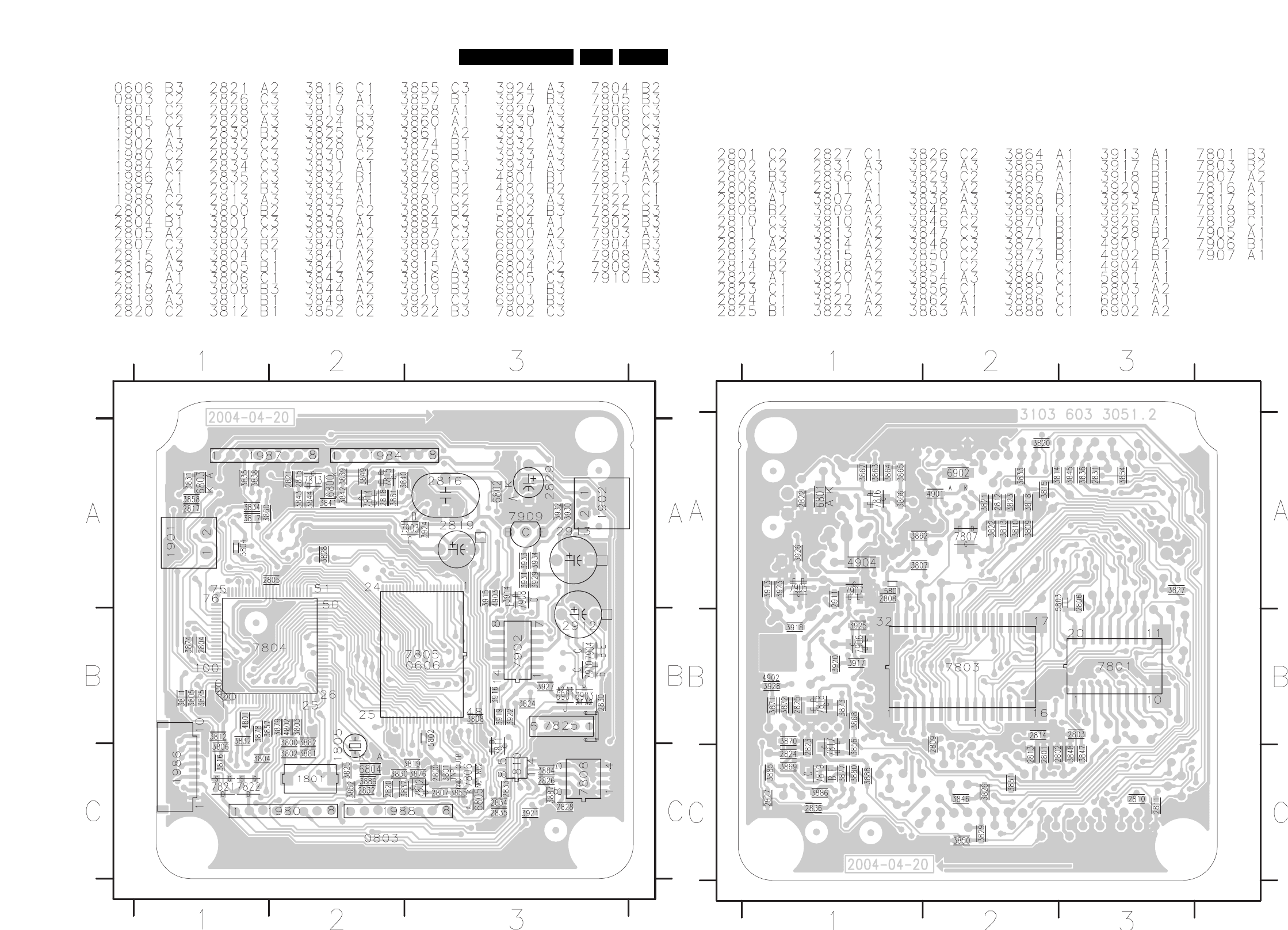
EN 1037.LX7500RCircuit Diagrams and PWB Layouts
uP Sub Board: (top view) uP Sub Board: (bottom view)
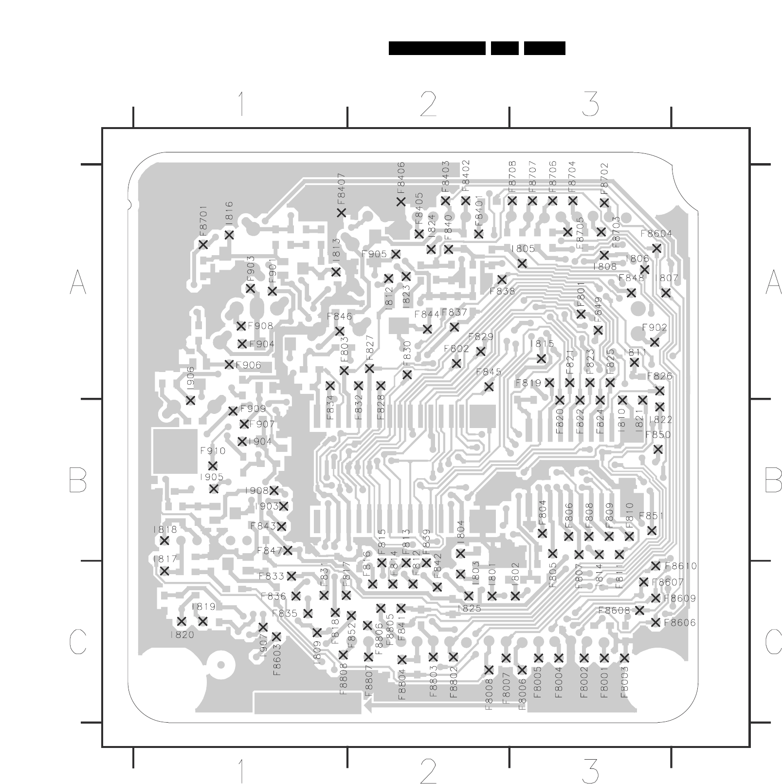
EN 1047.LX7500RCircuit Diagrams and PWB Layouts
F8001 C3
F8002 C3
F8003 C3
F8004 C3
F8005 C3
F8006 C3
F8007 C2
F8008 C2
F801 A3
F802 A2
F803 A1
F804 B3
F805 B3
F807 B3
F812 C2
F813 C2
F814 C2
F815 C2
F816 C2
F817 C1
F818 C1
F819 A3
F820 B3
F821 A3
F822 B3
F823 A3
F824 B3
F825 A3
F826 A3
F827 A2
F828 A2
F829 A2
F830 A2
F831 C1
F832 A2
F833 C1
F834 A1
F835 C1
F836 C1
F837 A2
F838 A2
F839 C2
F840 A2
F8401 A2
F8402 A2
F8403 A2
F8406 A2
F8407 A1
F841 C2
F842 C2
F843 B1
F844 A2
F845 A2
F846 A1
F847 B1
F848 A3
F849 A3
F850 B3
F851 B3
F852 C2
F8603 C1
F8604 A3
F8606 C3
F8607 C3
F8608 C3
F8609 C3
F8610 C3
F8701 A1
F8702 A3
F8703 A3
F8704 A3
F8705 A3
F8706 A3
F8707 A3
F8708 A3
F8802 C2
F8803 C2
F8804 C2
F8805 C2
F8806 C2
F8807 C2
F8808 C1
F901 A1
F902 A3
F903 A1
F904 A1
F905 A2
F906 A1
F907 B1
F908 A1
F909 B1
F910 B1
I801 C2
I802 C3
I803 C2
I804 B2
I805 A3
I806 A3
I807 A3
I808 A3
I809 C1
I810 B3
I811 A3
I812 A2
I813 A1
I814 B3
I815 A3
I816 A1
I817 C1
I818 B1
I819 C1
I820 C1
I821 B3
I822 B3
I823 A2
I824 A2
I825 C2
I903 B1
I904 B1
I905 B1
I906 B1
I907 C1
I908 B1
TR 06058_001
250203
TESTPOINT OVERVIEW
uP Sub Board
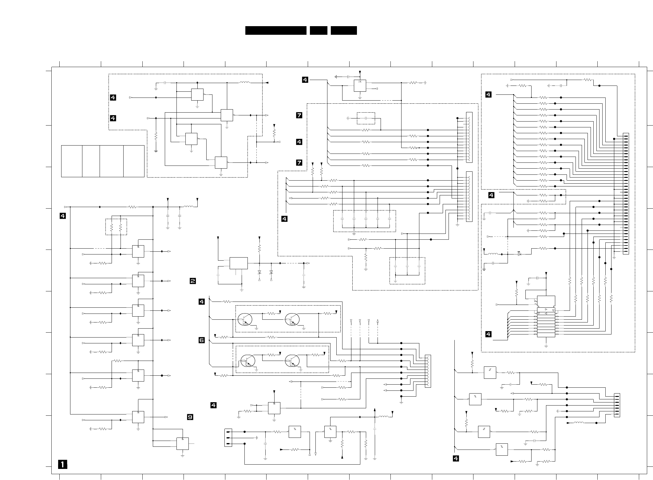
EN 1057.LX7500RCircuit Diagrams and PWB Layouts
&
G3
1
2
3EN2
3EN1
&
&
&
2107 D8
2108 A7
2109 E9
2110 E9
2111 E9
2112 H11
2113 E6
2114 E12
ANALOG BOARD
A
B
C
D
0
for AV2 only
not used
not used
2119 I12
2120 I8
not used
2102 D7
2103 D3
2104 D8
2105 D8
2106 D8
5 6 7 8 9 1011121314
1
2116 E11
1106 I5
2100 A8
2101 E4
not used
NORFLASH
1
for UART 3V3 only
not used
1
not for UART 3V3 or I2C
not used
1
12 13
E
F
G
H
I
1100 A10
1102 B14
1103 H14
1104 G9
1105 B10
0
not used
1234
not used
2124 I5
2125 D3
2127 A3
234567891011
3092 I12
3093 I12
3094 E8
3095 C2
3096 H5
3097 I8
3098 I7
3099 I8
3100 A12
14
A
B
C
D
E
F
G
H
I
not used
XIO_SEL0
0
TRUTH TABLE
for I2C only
3111 B9
3112 A12
3113 B6
3114 D5
3115 B8
3116 A12
3117 I2
3118 B12
3119 A9
3120 B12
2128 D11
2129 A13
3080 H7
3081 H7
3082 G10
3085 C7
3086 C7
3088 I6
3090 G2
3091 H2
NANDFLASH
not used
1
0
3131 C7
3132 F5
3133 C12
3134 G4
3135 C12
3136 C7
3101 A13
3102 B9
3103 A12
3104 B8
3105 B8
3106 A12
3107 B9
3108 A12
3109 B8
3110 A12
for UART 3V3 only
1
MPIO24
for I2C only
for I2C only
3147 E13
3149 F13
3150 I6
3152 D8
3154 D12
3156 D12
3157 D8
3159 E13
3161 D12
3121 F6
3122 B12
3123 F7
3124 B12
3125 G6
3126 B12
3127 G7
3128 B12
3129 G4
3130 B12
1
not used
1
not used
not for I2C
3176 B3
3178 F14
3180 D12
3184 F2
3185 G11
3186 H12
3187 G2
3137 G6
3138 C12
3139 C7
3140 C7
3141 C7
3142 G7
3143 C12
3144 G7
3145 C12
3146 F11
1
IDE1 Only
1
1
not for UART 3V3 or I2C
not used
4117 E6
4118 F8
4119 F8
4121 H6
4122 B5
4123 B5
4124 D11
4125 D11
5100 C4
5102 E11
5103 I13
3162 E2
3163 D2
3164 D12
3165 D2
3167 F13
3168 D12
3170 E13
3172 F13
3173 E2
3175 E14
for I2C only
not for I2C
not used
not used
for I2C only
not for I2C
for I2C only
not for I2C
3189 H12
3191 H11
3192 H12
3195 I10
3197 I12
3199 I12
4101 A8
4110 F8
4111 H7
4113 F8
not used
0
4115 D1
4116 G5
7108 G6
7109 E12
7111-1 G11
7111-2 I11
7111-3 H11
7111-4 I11
7111-5 I6
7111-6 I7
F0001 B9
F0003 B9
F0005 B9
5104 H8
5108 A5
6100 E5
6101 E6
6103 E11
7100 F5
7101 F6
7102-1 A4
7102-2 A5
7102-3 B4
NAND / NOR FLASH
not used
not used
F0209 B13
F0210 B12
F0211 B13
F0212 B12
F0213 B13
F0214 B12
F0215 B13
F0216 C12
F0217 C13
F0218 C12
F0221 C13
7102-4 B5
7103 A8
7104-1 H2
7104-2 I3
7104-3 D2
7104-4 E2
7105 G5
7106 E5
7107-1 F2
7107-2 F2
not used
F0238 E14
not used
7107-3 G2
7107-4 H5
F0305 H13
F0306 H13
F0307 I13
F0401 H9
F0402 H9
F0403 H9
F0404 H9
F0405 G9
F0406 G9
F0407 G9
F0408 G9
F0007 B9
F0009 B9
F0011 B9
F0015 A10
F0201 A14
F0202 B14
F0203 A13
F0204 A12
F0205 A13
F0206 A12
not used
not used
0
F0207 A13
F0208 A12
F0603 I5
F936 G3
I100 E6
I102 E6
I103 A3
I104 A3
I105 A5
F0223 C14
F0225 C13
F0227 D14
F0229 D13
F0231 D14
F0233 D13
F0234 D13
F0235 D13
F0236 E13
F0237 E14
I115 A4
I116 E11
I117 H8
I119 E2
I120 E2
I121 F2
F0239 D12
F0301 H13
F0302 H13
F0303 H13
F0304 H13
10
delete for 5139
I106 B5
I108 D3
I109 E3
I110 F3
I111 G3
I112 C3
I114 C1
F0409 G9
F0410 G9
F0501 C10
F0503 D9
F0506 D9
F0508 B9
F0509 C9
F0510 C9
F0511 C9
F0512 C9
I122 G2
I123 I2
I124 H2
F0514 C9
F0601 I5
7111-5
74HCT14D
11
714
F0304
47R
F0238
3140
74LVC08AD
12
13
714
11
7104-4
F0218
22R
3147
1
2
7
14
3
7102-1
74LVC00AD
4K7
3125
82R3143
220R3180
4
74HCT14D
7111-2
3
714
4K7
3127
F0009
F0005
22R
3159
2103
100n
33R3120
2112
1n5
4K7
3129
47R
3141
100n
2127
714
8
74LVC08AD 7107-3
9
10
33R
3167
3195
100K
4122
1n5
2119
I110
I119
3115
1R0
F0514
3126 33R
4119
I100
F0307
F0306
F0509
10p
2109
F0213
100R
3150
4118
F0511
47R
3139
F0203
F0202
4K7
3121
3081
100R
10K
3097
33R3133
10K
3119
3156 4K7
F0207
5108
3110 33R
F0236
3134
4K7
39
4
40
5
6
7
8
9
3
30
31
32
33
34
35
36
37
38
2
20
21
22
23
24
25
26
27
28
29
10
11
12
13
14
15
16
17
18
19
IDE1
1-440090-4
1102
1
F0208
6K8
3192
TLMH3100
6103
3095
4K7
I120
100n
2125
74HCT14D
1
714
2
7111-1
F0205
F0206
I104
33R3108
F0601
33R3135
3176
4K7
F0209
3163
4K7
14
15
2
3
4
5
6
7
8
9
1
10
11
12
13
FMN-BMT
1100
3130 33R
3168 4K7
3170
33R
F0229
4121
3100
10K
I103
6101
1PS76SB10
3186
10K
I121
I115
5103
F0011
10p
2128
I123
F0408
F0512
2100
10p
F0405
33R
3175
3138 33R
3109
1R0
10p
2105
F0210
4K7
3114
10K
3157
47R
I124
3199
3149
22R
F0406
4113
3118 33R
4K7
3096
14
6
F0410
7104-2
74LVC08AD
4
5
7
33R
3101
F0216
33R3128
100n
4111
2120
F0217
3105
1R0
47R
3131
4K7
3165
100K
3086
3185
2106
10p
100R
4
5
7
14
6
7102-2
74LVC00AD
3103 33R
4110
F0231
1
10
19
20
8
9
18
17
16
15
14
13
12
11
2
3
4
5
6
7
3154 82R
7109
74LVC245APW
100R
3080
F0510
9
10
714
8
14
3
74LVC08AD
7104-3
74LVC08AD
7104-1
1
2
7
I111
11
4K7
3091
7107-4
74LVC08AD
12
13
714
F0001
5102
6
F0234
7107-2
74LVC08AD
4
5
714
10K
6K8
3099
3189
4K7
3094
100n
2116
F0403
3132
100R
4125
4124
F0508
F0227
3085
100K
F0204
F0201
F0407
6100
1PS76SB10
F0212
3137
100R
CD
5
GND
3
INP
2
4
NC
OUTP 1
NCP303LSN29
7106
1R0
3102
F0237
F0409
F0235
F0223
33R3106
F0211
F936
22n
2101
5104
10K
3164
I102
4101
4K7
3184
SD-71308
1106
1
2
3
I116
33R3122
I122
3092
100K
1
2
714
3
7107-1
74LVC08AD
PDTC124EU
7101
I117
5100
F0221
82R3161
1R0
3107
I109
3090
4K7
8
9
47R
3136
11
12
13
14
15
2
3
4
5
6
7
FMN-BMT
1105
1
10
100n
2108
F0501
3197
F0007
100R
14
12
3173
4K7
74HCT14D
7111-6
13
7
3123
4K7
2104
F0215
10p
4K7
3162
F0302
F0305
I106
I112
2111
10p
F0239
I108
4115
F0603
3178
33R
F0015
33R
3172
3117
4K7
10p
2107
3152
47R
3142
100R
9
10
7
14
8
74LVC00AD
7102-3
5K6
3145
100K
F0003
4117
3191
2129
470p
F0225
F0402
F0506
3082
PDTC124EU
7100
100K
1R0
3111
7108
PDTC124EU
2110
10p
F0301
PDTC124EU
7105
3104
47R
12
13
7
14
11
7102-4
74LVC00AD
3116 33R
3088
100K
3124 33R
3113
10K
F0503
100K
3098
F0233
3144
100R
4116
7103
1
2
35
4
74LVC1G32GW
2114
100n
10K
3146
1103
1
2
3
4
5
6
7
3093
B7B-PH-SM3
Service
6K8
1n5
6
F0401
2124
5
714
F0303
F0404
7111-3
74HCT14D
I105
33R3112
2113
470p
4K7
3187
2102
10p
4123
8
F0214
74HCT14D
7111-4
9
714
I114
2
3
4
5
6
7
8
9
FMN
1104
1
10
IDE1_DIOWn
IDE1_DIORn
IDE1_DMACKn
IDE1_DA1
IDE1_DA0
IDE1_DA2
IDE1_CS0n
IDE1_CS1n
IDE1_CTL
+3V3
+3V3
MPIO22_PCI_RESETn
+5V
CTS3
RTS3
+3V3
+3V3
RESET_IDE1n
MPIO17_ANA_WE_LV
IDE1_CTL
IDE1_IORDY
BE_FAN
MPIO4
+3V3
MPIO31_SERVICE_MODE_FAST
+3V3_RES
BE_V4
BE_BCLK
ANA_WE
+3V3_RES
+5V
TXD3
+5V
+5V
BE_SYNC
BE_FAN
+3V3
IDE1_IRQ
IDE1_IORDY
XIO_SEL0
MPIO1_BE_IRQn
VIP_FB
RTS0
RXD0
TXD0
UART0
+5V
-5V
-5V
MPIO6_BE_DLOAD
MPIO19_CTL_SERVICE
+3V3
+3V3
+5V_SERV
CTS0
PNX7100_SYS_RESETn
MPIO13_IDE1_RESETn
TXD1
RXD1
+5V_SERV
+3V3+3V3
VDD_PNX_PAD
RESET_BEn
RESET_PROGSCANn
RESET_1394n
RESET_IDE1n
ANALOG_RESETn
VIP_RESETn
MPIO20_FURORE_RESETn
MPIO16_PROGSCAN_RESETn
MPIO15_BE_RESETn
MPIO14_IEEE1394_RESETn
ION
SDA0
SCL0
BE_DATA_RD
BE_WCLK
BE_FLAG
RESETn
ANALOG_RESETn
IRESET_DIG
MPIO6_BE_DLOAD
BE_DATA
PNX7100_RESETn
IRESET_DIG
EJTAG_RESETn
XIO_SEL0
-5V
+3V3
+3V3
RTS2
TXD2
UART2
RXD3
UART3
+5V
XIO_SEL_NANDFLASH
XIO_SEL_NORFLASH
MPIO24_SEL_NOR_NAND
IDE1_DD(15)
IDE1_DD(15:0)
IDE1_DMARQ
RESET_IDE1n
+3V3
BE_DATA_WR
RXD2
MPIO1_BE_IRQn
CTS2
RESET_BEn
+3V3 +3V3
IDE1_DD(7)
IDE1_DD(8)
IDE1_DD(6)
IDE1_DD(9)
IDE1_DD(5)
IDE1_DD(10)
IDE1_DD(4)
IDE1_DD(11)
IDE1_DD(3)
IDE1_DD(12)
IDE1_DD(2)
IDE1_DD(13)
IDE1_DD(1)
IDE1_DD(14)
IDE1_DD(0)
DIGITAL BOARD Chrysalis PPS E4 AV3+
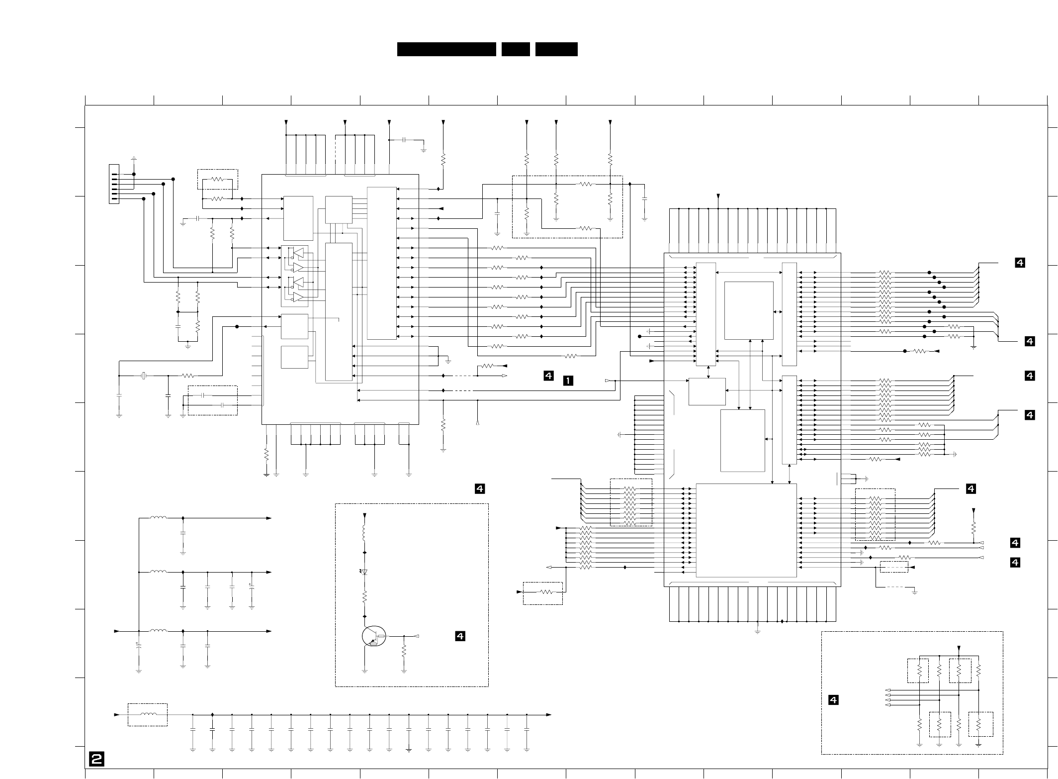
EN 1067.LX7500RCircuit Diagrams and PWB Layouts
TESTPIN
GND
VDD
RESERVED
DVDDAVDD
NC
PLLGNDDGNDAGND
DECODER/
BIAS DATA
INTERFACE
LINK
RECEIVED
CONTROL
STATE
MACHINE
LOGIC
TRANSMIT
CLOCK
PLL
XTAL OSC.
ENCODER
DATA
GENERATOR
CURRENT
AND
VOLTAGE
TEST1
TEST0
C|LKON
ISO_
LPS
CPS
PLLVDD
R0
R1
TPBIAS0
TPA0+
TESTM
TPA0-
TPB0+
TPB0-
XI
XO
TIMER
ARBITR’N
AND
PD
RESET_
CNA
PC2
PC1
PC0
D7
D6
D5
D4
D3
D2
D1
D0
CTL1
CTL0
LREQ
SYSCLK
1%
F212 C13
F213 C13
F214 C13
F215 C13
F216 D13
F217 C13
I213 D6
I214 D6
I215 A6
I201 F2
I211 B7
I227 C7
not used
BOARD_ID
1%
for DV_IN only
I225 C7
5201 F5
always present
5203 H2
5204 I1
6200 G4
7200 A5
7201 B12
7202 H5
F1201 B1
F1202 A1
F1203 A1
F1205 A2
I216 B6
I217 A8
I218 C7
I219 C7
I220 G12
I221 G12
I222 C7
I223 G12
I224 G8
F210 C13
I226 C7
1%
3289 H13
3290 I13
3291 I13
3292 I13
3293 I13
3294 F12
3295 F12
3296 F12
3297 F8
I200 H4
3299 F8
I202 G2
I203 H2
I204 I2
I205 H11
I206 G4
I207 A3
I208 B3
I209 B3
I210 C2
4204 G12
I212 C7
5200 F2
3265 G8
5202 G2
3267 G8
3268 G8
3269 G8
3270 G12
3271 G12
3272 G13
3273 G8
3274 F12
3275 G5
F1204 A2
3277 F12
F200 D12
F201 C9
F203 C3
F204 C13
F205 C13
F206 C13
F207 C13
F208 C13
F209 C13
3287 H13
F211 C13
not used
not used
3245 D6
3246 E12
3247 E12
3248 D8
3249 E12
3250 E12
3251 E12
3298 F8
3253 D2
3315 F8
3316 F8
3317 F8
3318 F8
3319 F8
3320 F13
4201 D6
4202 D6
4203 G12
3263 F8
4205 A4
not used
not used
3266 G8
3223 B6
3224 C12
3225 C7
3226 C12
3227 C12
3228 C6
3229 C12
3230 D13
3231 C7
3276 G7
3233 C2
3278 F12
3279 F12
3280 A7
3281 A7
3282 A8
3283 A2
3284 A8
3285 A6
3286 H13
3243 D12
3288 H13
1%
not used
3204 D6
3205 A2
3206 B7
3207 B8
3252 E12
3209 B8
3254 E12
3255 E13
3256 E13
3257 E13
3258 E13
3259 E13
3260 F12
3261 E3
3262 F8
3219 D13
3264 F8
3221 C12
220R FOR C2
220R FOR C2
220R FOR C2
220R FOR C2
220R FOR C2
LINK
3222 C12
22R FOR C2
2226 I5
2227 I5
3232 C2
2229 I5
3234 C6
3235 C13
3236 C7
3237 D12
3238 C6
3239 D12
3240 C2
3241 D12
3242 C7
3200 E6
3244 D12
3203 H5
1%
1%
2206 G3
2207 F2
3208 B7
2210 G2
3210 C12
3211 C12
3212 B2
3213 B3
3214 C12
3215 C12
3216 B6
3217 C12
3218 C12
2223 I4
3220 B7
2225 I4
345678
2228 I5
10
2230 I6
2231 I6
2232 I6
2233 I7
2234 I7
2235 A5
2236 G3
2237 B9
2238 B6
3202 F12
G
12345
2209 G2
7
2212 H1
2214 H2
2215 H2
2217 I2
2218 I2
2219 I3
2220 I3
2221 I3
2222 I3
2224 I4
H
I
A
B
C
D
E
F
9
H
11 12 13 14
A
B
C
D
E
1201 D1
F
PHY
allways present
not used
not used
not used
I
1203 A1
6 8 9 1011121314
12
2200 B2
2201 C2
2202 D1
2203 D2
2204 D2
2205 D2
F211
G
1203
SR
1
2
3
4
5
678
3205
6K34 I208
100n
2209
33R3222
1R0
3209
3288
4K7
I216
I221
100R3272
3237
100n
2231
33R
3317 100R
I213
F203
100n
2222
100R3319
4K73250
I204
3259 4K7
82R3224
33R3243
3297 100R
3245
10R
I211
3221 33R
33R3211
2233
100n
100u
2212
3270 100R
I201
2229
100n
4K7 3267
10K
3283
10K
3206
33R3214
F209
2223
100n
F210
F208
I205
F206
I226
100n
2226
I206
330R
3275
3233
56R
10K
3219
100n
2219
4K7
3286
F1203
12p
2203
100n
2218
10R
3236
2202
F217
12p
I207
33R3251
2227
100n
3293
4K7
F1202
2205
100n
3298 100R
3274 100R
4204
1R0
3261
I218
I219
10R
3242
I215
10R
3231
56R
3232
33R3254
4K73256
3320
10K
F204
3225
10R
F1204
3255 4K7
3277 100R
PDTC144EU
7202
I225
F207
2217
100n
33R3229
32664K7
4201
10R
3228
10R
3248
3215 33R
2237
100n
2235
1n0
I220
100n
3291
4K7
2214
33R3241
100R3318
100n
2234
TLMH3100
6200
33R3226 10K
3235
4K7 3263
2220
100n
3294 100R
5K1
3240
I224
100R3315
10R
3285
33R3217
4203
100n
2224
10R
3234
100n
2230
270p
2201
100n
2215
F1201
2232
100n
3249 33R
100R3278
5201
I222
3200
10K
4K7
3287
4K7
3289
22K3257
33R 3273
3203
10K
3218 33R
F200
I217
3253
1R0
61
70
I203
107
113
120
132
138
12
18
24
35
44
54
SCLK88
162
263
364
6
78
84
90
95
3
51
4
52
5
58
6
59
7
72
8
71
9
104
RESET_42
11
66
67 12
13
68
14
105
15
129
16
144
17
130
2
50
PHYD280
79 PHYD3
PHYD4
76
PHYD5
75
PHYD674
PHYD773
1
49
10
65
LINKON92
LPS91
LREQ
87
PD48
PHYCTL0
86
PHYCTL185
PHYD082
PHYD1
81
38 HIFINT_ HIFMUX 46
40
HIFRD_
36HIFSC_
HIFWAIT
41
37
HIFWR_
ISON
93
39
HIFD10
8
HIFD117
HIFD124
HIFD133
HIFD142
HIFD151
HIFD810
HIFD99
22
21 HIFAD1
HIFAD2
20
HIFAD319
HIFAD416
HIFAD515
HIFAD614
HIFAD713
HIFALE
32
31
HIFA2
HIFA3 30
HIFA4 29
HIFA5 28
HIFA6 27
HIFA7 26
HIFA8 25
HIFAD0
17
23
34
43
53
60
69
HIF16BIT 45
HIFA0 33
HIFA1
5
77
83
89
94
106
112
119
131
137
11
AV2FSYNC 125
143
AV2READY
AV2SY 126
AV2SYNC 128
AV2VALID 127
CLK5055
CYCLEIN56
CYCLEOUT57
AV2D3 136
139
AV2D4
AV2D5 140
AV2D6 141
142
AV2D7
AV2ENDPCK 123
AV2ERR0|LTLEND 121
122
AV2ERR1|DATINV
AV1READY 118
AV1SY 101
AV1SYNC 103
AV1VALID 102
124
AV2CLK
AV2D0 133
AV2D1 134
AV2D2 135
AV1D4 114
AV1D5 115
116
AV1D6
AV1D7 117
AV1ENDPCK 98
96
AV1ERR0
AV1ERR1 97
AV1FSYNC 100
STATUS
CONTROL
REGISTERS
AND
1394MODE47
AV1CLK 99
AV1D0 108
109
AV1D1
AV1D2 110
AV1D3 111
TRANSMITTER / RECEIVER
AV2 TRANSMITTER / RECEIVER
AV1
PDI1394L40
7201
LINK
CORE
AND
4205
ASYNC
RECEIVER
8-BIT
TRANSMITTER
MEMORY
PACKETS
12KB BUFFER
INTERFACE
ISOCH & ASYNC
3258 22K
I223
100n
2210
F214
4K7 3269
100R3260
28
27
37
36
35
34
38
59
60
22
14
5758
56
40
41
53
2
29
1
54
55
16
43
44
45
46
47
20
21
13
17186364
25266162
23
15
4
5
19
6
7
8
9
10
11
12
484950
3031425152
3
24
7200
PDI1394P25
PDI1394P25
323339
33R3246
F213
2200
1u0
100R3271
3239 33R
4202
2204
100n
5202
24M576
1201
CX-11F
5204
4K7
3292
3280
10K
3284
1R0
I214
100n
2221
100R3299
2228
100n
32684K7
3238
10R
100R3279
3282
10K
10R
3220
100R3202
3216
10R
3230 10K
F212
2236
4u7 35V
3276
100n
2238
1K0
32644K7
5203
F1205
3244 33R
F215
100n
2206
I227
2207
100n
3252 33R
100n
2225
10K
3204
3295 100R
3210 33R
100R3296
10K
3207
32624K7
F205
33R3247
5200
56R
3212
4K7 3265
I210
I202
100R
I209
3316
3290
4K7
3227 33R
56R
3213
3223
10R
3208
10K
3281
10K
I200
F201 F216
I212
L_D(5)
L_FSYNC
L_VAL
L_SYNC
+3V3_LINK
MPIO2_1394_IRQn
L_D(1)
MPIO23_1394_LED
PCI_AD(31:0)
PCI_AD(0)
PCI_AD(1)
L_D(2)
L_CLK
L_D_CTL
MPIO9_BOARD_ID_0
MPIO10_BOARD_ID_1
MPIO11_BOARD_ID_2
MPIO12_BOARD_ID_3
MPIO21_1394_POWERDOWN
+3V3_IEEE_D
MPIO8_1394_CNA
RESET_1394n
+3V3_LINK
+3V3_IEEE_D
PCI_AD(31:0)
+3V3_IEEE_D
+3V3_IEEE_PLL
+3V3_IEEE_A
+3V3
MX_D(5)
MX_D(6)
MX_D(7)
MX_D(7:0)
MX_VAL
MX_SYNC
MX_CLK
+3V3_LINK
AV1SY
AV1ENDPCK
+5V
MX_D_CTL
+3V3_LINK
+3V3_LINK
AV2ENDPCK
AV2FSYNC
MX_D(0)
MX_D(1)
MX_D(2)
MX_D(3)
MX_D(4)
+3V3_IEEE_D
+3V3_IEEE_D
+3V3_IEEE_PLL
+3V3_LINK
L_D(7:0)
L_D(7)
L_D(6)
L_D(4)
L_D(3)
L_D(0)
+3V3_IEEE_A +3V3_IEEE_D
+3V3_IEEE_D +3V3_LINK
+3V3_LINK
+3V3
+3V3
PCI_AD(6)
PCI_AD(7)
PCI_AD(8)
+3V3_LINK
PCI_CBE(1)
PCI_CBE(2)
XIO_SEL1
PCI_AD(24)
PCI_AD(25)
PCI_AD(26)
PCI_AD(27)
PCI_AD(28)
PCI_AD(29)
PCI_AD(30)
PCI_AD(31)
+3V3_LINK
PCI_AD(2)
PCI_AD(3)
PCI_AD(4)
PCI_AD(5)
DIGITAL BOARD Chrysalis PPS E4 AV3+
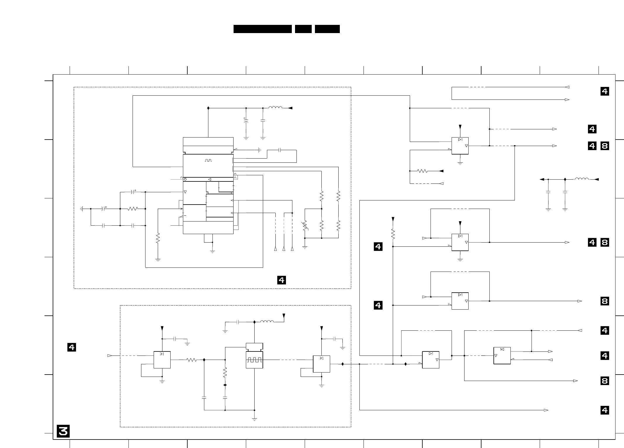
EN 1077.LX7500RCircuit Diagrams and PWB Layouts
EN
EN
EN
-T
Af
EN
EN5 Z3
=1
=1
1&
1
G
6
6
M6
RX Z4
R4
3
RX
CX
5
S
S
EN
EN
2301 A4
2302 B2
2303 C1
2304 B4
2305 C1
2306 C2
8
7300-1 C7
7
7300-3 E6
7305 E2
1%
12 6
not used
15
E
F
C
D D
E
4303 C4
4304 A7
4305 A8
1%
I303 E5
4309 C4
not used
4311 E6
9
I305 F7
not used
not used
67
A
B B
C
F
2300 A3
5300 A4
5301 E4
5302 F7
3300 C2
3301 B5
3302 B5
7300-4 E8
7301 A2
7302 A7
3306 C5
4316 E8
3308 E3
7300-2 D7
I301 E4
7303 E5
7304 E3
not used
not used
not used
4300 E8
4301 C4
4302 E7
234
4306 E1
4307 E4
4308 B6
8
4310 B8
A
I304 F3
4313 D7
I306 E6
not used
2307 E3
2308 F7
4315 E7
2310 F7
2311 E5
2312 E2
not used
3303 C2
3304 C4
3305 C5
3
3307 B6
4
I300 A3
5
I302 E3
3309 F3
3310 E3
3311 C6
4312 C7
9
4314 A7
not used
not used
2309 F3
4304
100n
2310
4316
4315
1K0
3308
1R0
3306
5K6
3305
I301
4314
7304
27M
2
1
4
3
FXO-35F
4311
56R
3300
4313
2300
4u7
4308
4306
3310
1K0
5302
4310
2305
100n
74LVC125AD
7300-3
9
7
10
14
8
I305
100n
2309
15K
3302
2307
100n
14
3
4309
7300-1
74LVC125AD
2
7
1
12
7
13
14
11
I300
7300-4
74LVC125AD
4312
I304
100n
2311
I302
4305
4301
10K
3311
3309
100n
2303
4u7
3304
4K7
7303
74LVC1G32
1
2
35
4
5300
10K
3307
33p
2304
4300
7300-2
5
7
4
14
6
74LVC125AD
4303
1
5
4
220n
2306
7302
2
3
7305
74LVC1G32
1
2
35
4
74LVC1G125
100n
2301
2308
100n
3303
220K
2u2
2302
4
I306
8
5
2
13
11
12
15
14
16
9
[PLL]
74HCT9046AD
7301
6
7
3
10
1
I303
4307
5301
4302
2312
100n
3301
11K
SCKE_IN
SCK012_OUT
SCK3_OUT
FSCLKE_IN_PNX
FSCLKE_IN_PNX
WSE_IN
MPIO25_ADC_FSCLKE_OE
+3V3
VDD_PLL_BUF
PLL_OUT
FSCLKE_IN
VDD_PLL_BUF
MPIO25_ADC_FSCLKE_OE
FSCLK3_OUT
PLL_OUT
VDD_PLL_BUF
VDD_PLL_BUF
+5V
MPIO25_ADC_FSCLKE_OE
SCK012_OUT
SCKE_IN
+3V3
+5V
+5V
VDD_PLL_BUF
FSCLK012_OUT
MPIO26_ADC_FWSCLK012_OE
WS012_OUT
DIGITAL BOARD Chrysalis PPS E4 AV3+
EN 1087.LX7500R
Circuit Diagrams and PWB Layouts
I2C
1394 INDIGITAL VIDEO INTERFACEANALOG VIDEOPROG SCAN
PIOS TEST GENERAL DIGITAL AUDIO INTERFACE UARTS
IDE BE-1 SDRAM
PCI/XIO1394 OUT
G3
1
2
3EN2
3EN1
3456 B10
not used
3852 H2
3853 G2
3860 D2
3861 D2
3862 D2
3482 D10
3483 D11
3454 B10
3455 B11
3457 B11
3458 B10
3459 B11
3473 C11
3474 D10
3445 A11
3462 C10
3493 E10
3494 E11
3495 E11
3496 F10
3497 I4
3468 C10
3469 C11
3444 A10
13 14
A
2412 H13
3475 D11
3476 D10
3827 E1
B
1401 I5
2400 A9
2401 A9
2402 A9
2403 A12
2404 H12
2405 H13
2406 H13
34567
2429 I14
2430 I5
2431 I6
2432 H1
2433 I7
not used
*
789
not used
SDRAM
12
3460 C10
3491 E10
11 12 13 14
1
C
D
E
F
G
H
I
1400 C14
3416 B14
3417 B14
3418 B14
3419 B14
3420 C14
B
C
10 11 12
G
H
I
A
2413 H13
X
not used
2415 H14
2416 H14
2417 H14
2418 I12
2419 I13
2407 H13
2408 H12
2409 H12
2410 H13
2411 H13
2425 I13
2426 I14
2427 I14
2428 I14
not used
not used
3431 E13
3432 E13
3433 F1
2435 A9
2436 I6
not used
3402 A14
3403 A14
3404 A14
3405 A12
3406 A12
8910
EJTAG pitch 1.27 mm
X
23456
3412 A14
3413 B14
3414 B14
3415 B14
3831
3421 C14
3422 C14
D
E
F
3426 C13
3427 C13
3428 C13
3429 D13
3430 E13
2414 H14
1%
2420 I12
2421 I12
2422 I13
2423 I13
2424 I13
3451 B11
3434 F1
3435 F1
3021 I1
3400 A14
3401 A14
3439 G13
3440 G13
3441 I5
3442 A10
3443 A11
not used
only for C1
3407 A12
3408 A12
3409 A14
3410 A14
3411 A14
not used
UART1: DEV ONLY
UART0: DEBUG / SERVICE
3463 C11
3464 C10
3465 C11
3466 C10
3467 C11
-
3423 C14
3424 C13
3425 C13
3446 A10
3447 B11
3448 B10
3449 B11
3450 B10
3478 D10
3479 D11
3480 D10
3481 D11
3452 B10
3453 B11
3436 F13
3437 F13
3438 F13
3487 D11
3488 E10
3489 E10
3490 E11
3461 C11
only for C2
3492 E11
4404 I2
4405 I2
4406 I2
4407 I2
3498 G1
3499 G1
3470 C10
3471 C11
3472 C10
3823 E1
3824 E1
3825 E1
3826 E1
3477 D11
3828 A1
3829 A1
3830 B1
3831 B1
3832 B1
3839 I1
3840 G1
3850 G1
3851 H2
F1401 C14
F1402 C14
F1403 C14
F1405 D14
F1407 D14
3863 D2
3864 D2
3484 D10
3485 D11
3486 D10
3868 I6
3869 I6
4401 I5
4402 I4
4403 I2
I406 E10
I407 I6
I408 I6
I409 I7
I410 I7
5400 A13
5401 G12
3820 E1
3821 E1
3822 E1
5405 I12
5406 I12
7400 A2
7401 H1
7402 I6
3823
-
3833 B1
3834 B1
3835 B1
3837 I1
3838 I1
*
7403 I5
I427 A14
I428 B14
I429 B14
I430 B14
I431 B14
F1409 D14
F1411 E14
3865 D2
3866 D2
3867 D2
F1419 F14
F1421 F14
F1423 F14
F1425 G14
F1427 G14
I441 I7
*
I402 I1
I403 I4
I404 E10
I405 E10
F405 I5
F406 I6
I400 I3
I401 I3
UART2: S2B (BASIC ENGINE)
5402 H12
5403 H1
5404 I7
I422 A14
I411 I7
I412 I7
I413 A12
I420 A14
I416 I13
I417 I12
I418 A14
I419 A14
I432 B14
I433 B14
I434 B14
I435 C14
I436 C14
64 MB
32 MB
UART3: GATEWAY (ANALOG BOARD)
I423 A14
I424 A14
I425 A14
I426 A14
F400 A12
F401 A12
F402 A8
F403 C1
F404 C1
F1413 E14
F1415 E14
F1417 E14
for 5139 only I421 A14
I437 C14
I438 A12
I439 A12
I440 F11
I414 G13
I415 H12
5402
3497
100K
4K7
3410
4K7
3409
F1402
10u
F1425
2404
100n
2417
3451 22R
F1411
3492 22R
I441
3432 33R
33R
3431
3493 22R
10K 3427
3449 22R
3421
F400
3407
4K7
3K3
3K3
3408
3461 22R I435
F1407
I405
3820 4K7
3439 33R
I432
I434
I433
3423 4K7
10K
3424
2416
100n
100n
2415
4K7
D9
XIO-SEL2
AF9 XTAL-IN
AF10 XTAL-OUT
Y-CVBS
N1
3415
M23 VDDP7
D12 VDDP8
D11 VDDP9
M1 VREF
F3 VS-IN
T2 VS-OUT
H25
WE0 J24
WE1
AD16 WS012-OUT
WS3-OUT
AE14
AE11 WSE-IN
AD12 WSK-IN
A20
XIO-A25 D19
XIO-ACK
B8
XIO-SEL0
C8
XIO-SEL1
AD19 TXD3
P4
VDDC1 R4
VDDC2
AC14
VDDC3
AC15
VDDC4
T23 VDDC5
R23 VDDC6
D15 VDDC7
D14 VDDC8
D13 VDDC9
M4
VDDP1 N4
VDDP2
AC12
VDDP3
AC13
VDDP4
P23 VDDP5
N23 VDDP6
F25
SDRAM-DATA5 G23
SDRAM-DATA6 G25
SDRAM-DATA7 G26
SDRAM-DATA8 G24
SDRAM-DATA9
AE16 SPDIF-OUT
AF13 SPDIF1-IN
AE13 SPDIF2-IN
AD10 SYS-RESETN
AD8 TCK
AC9 TDI
AE8 TMS
AD9 TRST
AD17 TXD0
AF17 TXD1
AD18 TXD2
V23
SDRAM-DATA19
D26
SDRAM-DATA2
V25
SDRAM-DATA20 W23
SDRAM-DATA21 W25
SDRAM-DATA22 Y26
SDRAM-DATA23 W26
SDRAM-DATA24 W24
SDRAM-DATA25 V26
SDRAM-DATA26 V24
SDRAM-DATA27 U26
SDRAM-DATA28 U24
SDRAM-DATA29
E25
SDRAM-DATA3
T26
SDRAM-DATA30 T24
SDRAM-DATA31
F23
SDRAM-DATA4
N25
SDRAM-ADDR5 M26
SDRAM-ADDR6 M24
SDRAM-ADDR7 L25
SDRAM-ADDR8 L23
SDRAM-ADDR9
C25
SDRAM-DATA0 D24
SDRAM-DATA1
F26
SDRAM-DATA10 F24
SDRAM-DATA11 E26
SDRAM-DATA12 E24
SDRAM-DATA13 D25
SDRAM-DATA14 C26
SDRAM-DATA15 T25
SDRAM-DATA16 U23
SDRAM-DATA17 U25
SDRAM-DATA18
AF14 SD3-OUT
A25
SDA0
B25
SDA1
AF11 SDE-IN
AE12 SDK-IN
N26
SDRAM-ADDR0 P25
SDRAM-ADDR1
N24
SDRAM-ADDR10 L24
SDRAM-ADDR11 K23
SDRAM-ADDR12 L26
SDRAM-ADDR13 M25
SDRAM-ADDR14
R24
SDRAM-ADDR2 P26
SDRAM-ADDR3 P24
SDRAM-ADDR4
M2 RSET
AF18 RTS2
AF19 RTS3
AC17 RXD0
AE17 RXD1
AC18 RXD2
RXD3
AC19
AC16 SCK012-OUT
AD14 SCK3-OUT
AD11 SCKE-IN
A26
SCL0
B26
SCL1
AF16 SD0-OUT
AD15 SD1-OUT
AE15 SD2-OUT
H2 PROGC-OUT5
H1 PROGC-OUT6
G1 PROGC-OUT7
J4 PROGY-OUT0
K1 PROGY-OUT1
K2 PROGY-OUT2
K3 PROGY-OUT3
K4 PROGY-OUT4
L1 PROGY-OUT5
L2 PROGY-OUT6
L3 PROGY-OUT7
P3 R-CVBS
J23
RAS0 J26
RAS1
AE9 RESETN
K24
RP
AF4 PIO30
AF5 PIO31
Y1 PIO4
Y2 PIO5
Y3 PIO6
Y4 PIO7
AA1 PIO8
AA2 PIO9
AE10 PLL-OUT
AE3 POIO24
L4 PROG-OUT-CLK
J3 PROGC-OUT0
J2 PROGC-OUT1
J1 PROGC-OUT2
H4 PROGC-OUT3
H3 PROGC-OUT4
AC2 PIO16
AC3 PIO17
AD1 PIO18
AD2 PIO19
W3 PIO2
AD3 PIO20
AD4 PIO21
AE1 PIO22
AE2 PIO23
AE4 PIO25
AE5 PIO26
AF1 PIO27
AF2 PIO28
AF3 PIO29
W4 PIO3
A15
PCI-STOP
C15
PCI-TRDY
AC8 PCST0-0
AF7 PCST0-1
AE7 PCST0-2
AE6 PCST1-0
AD6 PCST1-1
AD5 PCST1-2
W1 PIO0
W2 PIO1
AA3 PIO10
AA4 PIO11
AB1 PIO12
AB2 PIO13
AB3 PIO14
AC1 PIO15
PCI-CBE3
A24
PCI-CLK
A16
PCI-DEVSEL
B16
PCI-FRAME
A22
PCI-GNT
B24
PCI-GNTA
C24
PCI-GNTB
D18
PCI-IDSEL
C22
PCI-INTA
C16
PCI-IRDY
B14
PCI-PAR
B15
PCI-PERR
A23
PCI-REQ
B23
PCI-REQA
C23
PCI-REQB
C14
PCI-SERR
A21
PCI-AD27
D20
PCI-AD28
C21
PCI-AD29
C9
PCI-AD3
B21
PCI-AD30
B22
PCI-AD31
A10
PCI-AD4
B10
PCI-AD5
C10
PCI-AD6
D10
PCI-AD7
B11
PCI-AD8
C11
PCI-AD9
A11
PCI-CBE0
A14
PCI-CBE1
A17
PCI-CBE2
C19
C12
PCI-AD12
A13
PCI-AD13
B13
PCI-AD14
C13
PCI-AD15
D16
PCI-AD16
C17
PCI-AD17
B17
PCI-AD18
A18
PCI-AD19
B9
PCI-AD2
D17
PCI-AD20
C18
PCI-AD21
B18
PCI-AD22
A19
PCI-AD23
B19
PCI-AD24
C20
PCI-AD25
B20
PCI-AD26
C1 L-VAL
A5
MX-CLK
A6
MX-D0
B6
MX-D1
C6
MX-D2
A7
MX-D3
B7
MX-D4
C7
MX-D5
D7
MX-D6
D8
MX-D7
C5
MX-SYNC
B5
MX-VAL
A8
PCI-AD0
A9
PCI-AD1
A12
PCI-AD10
B12
PCI-AD11
ITU-OUT3
U1 ITU-OUT4
U2 ITU-OUT5
U3 ITU-OUT6
U4 ITU-OUT7
A1 L-CLK
B2 L-D0
C2 L-D1
A3 L-D2
B3 L-D3
C3 L-D4
A4 L-D5
B4 L-D6
C4 L-D7
B1 L-FSYNC
A2 L-SYNC
IDUMP1
G2 ITU-IN-CLK
G4 ITU-IN-FID
G3 ITU-IN-VAL
D3 ITU-IN0
D2 ITU-IN1
E2 ITU-IN2
D1 ITU-IN3
ITU-IN4
E3
E1 ITU-IN5
F4 ITU-IN6
F1 ITU-IN7
T4 ITU-OUT-CLK
V1 ITU-OUT0
V2 ITU-OUT1
V3 ITU-OUT2
V4
AB24
IDE-DD15
AD23
IDE-DD2 AF23
IDE-DD3 AE22
IDE-DD4 AD21
IDE-DD5 AF21
IDE-DD6 AF20
IDE-DD7 AE20
IDE-DD8 AE21
IDE-DD9
AD25 IDE-DIOR
AE25 IDE-DIOW
AB25 IDE-DMACK
AF25 IDE-DMARQ
AC25 IDE-IORDY
N2 IDUMP0
R1
GND|TCK-PALM
F2 HS-IN
T3 HS-OUT
K26
HSCKB
AC26 IDE-CS0
AB26 IDE-CS1
AE26 IDE-DA0
AF26 IDE-DA1
AD26 IDE-DA2
AC24
IDE-DD0 AE24
IDE-DD1
AF22
IDE-DD10 AD22
IDE-DD11 AE23
IDE-DD12 AF24
IDE-DD13 AD24
IDE-DD14
GND42
M14 GND43
L15 GND44
L14 GND45
N13 GND46
M13 GND47
M12 GND48
L13 GND49
GND5 N11
L12 GND50
D6 GND51
D5 GND52
N12
GND6
P11
GND7 P12
GND8 R11
GND9
AC7
GND28
T16 GND29
L11
GND3
R16 GND30
P16 GND31
P15 GND32
N16 GND33
N15 GND34
GND35
M16
M15 GND36
L16 GND37
E23 GND38
D23 GND39
M11
GND4
D22 GND40
D21 GND41
N14
GND13
AC5
GND14
AC6
GND15
P13
GND16
R13
GND17
T12
GND18
T13
GND19
E4
GND2
GND20 P14
R14
GND21
R15
GND22
T14
GND23
T15
GND24
AC21
GND25
AC22
GND26
AC23 GND27
AB23
DQM0 H24
DQM1 R26
DQM2 R25
DQM3
AD7 DSU-CLK
AF8 DSU-TPC0
AF6 DSU-TPC1
AD20 DTR3
FSCLK012-OUT
AF15
AD13 FSCLK3-OUT
AF12 FSCLKE-IN
R2 G
D4
GND1
R12
GND10 T11
GND11 AB4
GND12 AC4
B
AA23
BE-BCLK AA26
BE-DATI Y25
BE-DATO AA24
BE-FLAG AA25
BE-SYNC Y23
BE-V4 Y24
BE-WCLK
C-CVBS
N3
H26
CAS0 J25
CAS1
K25
CKE
AE18 CTS2
AE19 CTS3
P2 CVBS
AC20 DCD3
H23
PNX7100E
7400
AC11
AVDD-CLK
M3 AVDD0
P1 AVDD1
R3 AVDD2
AC10
AVSS-CLK
T1
4K7
3829
I413
4406
4407
4405
3489
342610K
22R
F1409
F1405
3494 22R
4K7
3414
4K7
3413
3487 22R
3851
10K
I436
3490 22R
33R
3496
3433 1K2
4401
I417
I416
2
1
4
3
7402
FXO-34FL
22R
3445
3447
VDD_PNX_PAD
22R
3862 22R
4K7
3835
3479 22R
I407
F1403
F1401
100n
2419
2418
10u
3863 22R
22R
3860 22R
3481
3850
10K
3498
10K
3499
10K
3861 22R
10K
3853
3827 4K7
4K7
4K7
3825
3821
3823
3826 4K7
4K7
3828 4K7
3833 4K7
5401
3474 22R
3457
3471
22R
22R
22R
3467 22R
3469
3488 22R
3486 22R
15p
2430 +3V3
5404
3491 22R
3473 22R
I440
4402
22R
3444
I403
3442 22R
I402
F404
4K73824
3822 4K7
3443
3456
22R
22R
3834 4K7
3866 22R
F1415
I411
3455 22R
3480 22R
22R
3476
100p2402
2401 100p
100p2400
3K3
3405
3406
3K3
22R
3463 22R
3465
100n
2414
2413
100n
F406
I419
3484 22R
VDD_PNX_PLL
3466 22R
3460
22R
22R
2407
100n
3458
I421
4K7
I422
3830
22R
3446
100n
2429
100n
2428
2427
100n
I431
+1V8
VDD_PNX_ANA
I430
I415
3404 4K7
4K7
3403
22R
3475
3831 4K7
4K7
3832
VDD_PNX_PAD
F1417
I439
5400
22R
3478
2435 100p
4K7
3417
3416 4K7
VDD_PNX_CORE
F403
100n
2425
VDD_PNX_CORE
10K
3852
F1419
5405
I420
F1427
I424
I418
I406
22R
3482
22R
4404
3485
22R
3483
100n
2406
3419 4K7
10K
2410 3425
100n
100n
2409
VDD_PNX_PAD
2408
10u
4403
+3V3
VDD_PNX_PAD
342810K
I414
22R
3477
10K
3021
I400
I404
3472 22R
15R
3435
3434 15R
2436
33p
3441
330R
F1413
2405
I438
2411 100n
100n
100n
100n
2422
2421
2426
100n
10K
10K
3837
3838
I412
I401
3422 4K7
2433
I429
100n
3840 10K
3865 22R
3864 22R
+3V3
F405
3839
3430 33R
22R
3468
10K
+3V3
2403
100n
3869
4K7
VDD_PNX_CORE
VDD_PNX_PLL
VDD_PNX_CORE
2424
100n
100n
2423
F402
22R
3453
F1423
F1421
26
27
28
3
4
5
6
7
8
9
11
12
13
14
15
16
17
18
19
2
20
21
22
23
24
25
1400
STL21
1
10
4K7
+3V3
3420
100n
2432
22R
3495
VDD_PNX_PAD 33R
3429
I409
I408
3437
3438 33R
33R
33R
3436
3868
1K2
2412
BC847BW
7403
100n
3454 22R
3452 22R
3464
22R
3450
22R
22R
3462
VDD_PNX_ANA
5406
I428
VDD_PNX_PAD
3867 22R
VDD_PNX_CORE
I426
I427
4K7
10u
3418
2420
I425
5403
15p
+3V3
I423
I410
2431
VDD_PNX_PAD
4M
1401
HC-49/S
13
12
11
1
10
19
20
5
6
7
8
9
18
17
16
15
14
7401
2
3
4
F401
74LVC245APW
4K7
3400
I437
3448 22R
+3V3
3459 22R
3402
3401 4K7
4K7
3412 4K7
33R
3440
3411 4K7
SD3_OUT
ITU_OUT(0:7)
UART0
UART1
22R
3470
PCI_AD(25)
PCI_AD(24)
PCI_AD(27)
PCI_AD(26)
PCI_AD(29)
PCI_AD(28)
PCI_AD(30)
PCI_AD(31)
PCI_AD(31:0)
PNX7100_XTAL_IN
+3V3_7402
+3V3_7402
SD2_OUT
SD1_OUT
PCI_AD(8)
PCI_AD(9)
PCI_AD(10)
PCI_AD(11)
PCI_AD(12)
PCI_AD(13)
PCI_AD(14)
PCI_AD(15)
PCI_AD(17)
PCI_AD(16)
PCI_AD(19)
PCI_AD(18)
PCI_AD(21)
PCI_AD(20)
PCI_AD(23)
PCI_AD(22)
MX_D(2)
MX_D(3)
MX_D(4)
MX_D(5)
MX_D(6)
MX_D(7)
MX_D(7:0)
PCI_AD(0)
PCI_AD(1)
PCI_AD(2)
PCI_AD(3)
PCI_AD(4)
PCI_AD(5)
PCI_AD(6)
PCI_AD(7)
SD0_OUT
WS3_OUT
SCK3_OUT
FSCLK3_OUT
SDE_IN
WSE_IN
SCKE_IN
PNX7100_XTAL_OUT
XIO_A25
MX_CLK
MX_SYNC
MX_VAL
MX_D(0)
MX_D(1)
L_D(6)
L_D(7)
L_D(7:0)
PNX7100_ITU_IN_VAL
PNX7100_ITU_IN_CLK
PNX7100_ITU_IN_FID
PNX7100_VS_IN
PNX7100_HS_IN
SPDIF_OUT
WS012_OUT
FSCLK012_OUT
SD3_OUT
SD2_OUT
SD1_OUT
ITU_IN(6)
ITU_IN(5)
ITU_IN(4)
ITU_IN(3)
ITU_IN(2)
ITU_IN(1)
ITU_IN(0)
L_D(0)
L_D(1)
L_D(2)
L_D(3)
L_D(4)
L_D(5)
PROGY_OUT(1)
PROGY_OUT(0)
ITU_OUT(7)
ITU_OUT(6)
ITU_OUT(5)
ITU_OUT(4)
ITU_OUT(3)
ITU_OUT(2)
ITU_OUT(1)
ITU_OUT(0)
ITU_IN(7:0)
ITU_IN(7)
PROGC_OUT(3)
PROGC_OUT(2)
PROGC_OUT(1)
PROGC_OUT(0)
PROGY_OUT(7:0)
PROGY_OUT(7)
PROGY_OUT(6)
PROGY_OUT(5)
PROGY_OUT(4)
PROGY_OUT(3)
PROGY_OUT(2)
SDRAM_ADDR(8)
SDRAM_ADDR(7)
SDRAM_ADDR(6)
SDRAM_ADDR(5)
SDRAM_ADDR(4)
SDRAM_ADDR(3)
SDRAM_ADDR(2)
SDRAM_ADDR(1)
SDRAM_ADDR(0)
SDRAM_ADDR(14:0)
PROGC_OUT(7:0)
PROGC_OUT(7)
PROGC_OUT(6)
PROGC_OUT(5)
PROGC_OUT(4)
SDRAM_DATA(8)
SDRAM_DATA(7)
SDRAM_DATA(6)
SDRAM_DATA(31:0)
SDRAM_DATA(5)
SDRAM_DATA(4)
SDRAM_DATA(3)
SDRAM_DATA(2)
SDRAM_DATA(1)
SDRAM_DATA(0)
SDRAM_ADDR(14)
SDRAM_ADDR(13)
SDRAM_ADDR(12)
SDRAM_ADDR(11)
SDRAM_ADDR(10)
SDRAM_ADDR(9)
SDRAM_DATA(24)
SDRAM_DATA(23)
SDRAM_DATA(22)
SDRAM_DATA(21)
SDRAM_DATA(20)
SDRAM_DATA(19)
SDRAM_DATA(18)
SDRAM_DATA(17)
SDRAM_DATA(16)
SDRAM_DATA(15)
SDRAM_DATA(14)
SDRAM_DATA(13)
SDRAM_DATA(12)
SDRAM_DATA(11)
SDRAM_DATA(10)
SDRAM_DATA(9)
IDE1_DD(7)
IDE1_DD(6)
IDE1_DD(15:0)
IDE1_DD(5)
IDE1_DD(4)
IDE1_DD(3)
IDE1_DD(2)
IDE1_DD(1)
IDE1_DD(0)
IDE1_DD(14)
SDRAM_DATA(31)
SDRAM_DATA(30)
SDRAM_DATA(29)
SDRAM_DATA(28)
SDRAM_DATA(27)
SDRAM_DATA(26)
SDRAM_DATA(25)
PCI_REQA
PCI_REQ
PCI_INTA
PCI_GNT
PCI_STOP
PCI_SERR
PCI_PERR
PCI_IRDY
PCI_TRDY
PCI_FRAME
PCI_DEVSEL
PCI_CBE(3)
PCI_CBE(2)
PCI_CBE(1)
PCI_CBE(0)
IDE1_DD(15)
IDE1_DD(13)
IDE1_DD(12)
IDE1_DD(11)
IDE1_DD(10)
IDE1_DD(9)
IDE1_DD(8)
BE_V4
BE_SYNC
BE_FLAG
BE_DATA_WR
BE_DATA_RD
BE_BCLK
BE_DATA
SCL0
SDA0
SDA1
SCL1
IIC1
IIC0
PCI_CON
PCI_GNTB
PCI_REQB
PCI_GNTA
RXD3
RTS3
DTR3
DCD3
HSCKB
CKE
WE(0)
RAS(0)
DQM(3)
DQM(2)
DQM(1)
DQM(0)
CAS(0)
SDRAM_CTRL
BE_WCLK
UART1
UART0
UART2
UART3
RXD0
TXD0
RXD1
TXD1
CTS2
RTS2
RXD2
TXD2
CTS3
TXD3
PCI_GNTA
PCI_REQB
PCI_GNTB
IDE1_DA1
IDE1_DA2
IDE1_DIOWn
IDE1_DIORn
IDE1_IORDY
IDE1_DMACKn
IDE1_DMARQ
IDE1_DA0
IDE1_CS1n
IDE1_CS0n
IDE1_CTL
PCI_CBE(3)
PCI_DEVSEL
PCI_FRAME
PCI_IRDY
PCI_PERR
PCI_SERR
PCI_STOP
PCI_GNT
PCI_INTA
PCI_REQ
PCI_REQA
SDA1
SCL1
SDA0
SCL0
RTS0 RTS1
PCI_PAR
PCI_CLK
PCI_IDSEL
PCI_TRDY
PCI_IDSEL
PCI_CBE(1)
PCI_CBE(2)
L_FSYNC
L_SYNC
L_CLK
PNX7100_ITU_OUT_CLK
CVBS_OUT
C_OUT
Y_OUT
R_OUT
B_OUT
G_OUT
CTS0
L_D_CTL
MX_D_CTL
DIGITAL_AUDIO
VIDEO_OUT
PCI_CBE(0)
PCI_PAR
+3V3
PNX7100_PCST1(0)
PNX7100_DSU_TPC1
PNX7100_DSU_CLK
PNX7100_PCST0(2)
PNX7100_PCST0(1)
PNX7100_PCST0(0)
L_VAL
MPIO1_BE_IRQn
SCK012_OUT
SPDIF_COAX_IN
SPDIF_OPT_IN
XIO_ACK
XIO_SEL2
XIO_SEL1
XIO_SEL0
MPIO19_CTL_SERVICE
MPIO5_VIP_ERROR
IDE1_IRQ
CTS1
SCK3_OUT
FSCLK3_OUT
ITU_OUT(0)
ITU_OUT(7)
ITU_OUT(6)
ITU_OUT(5)
ITU_OUT(4)
ITU_OUT(3)
ITU_OUT(2)
ITU_OUT(1)
ITU_OUT(0:7)
MPIO10_BOARD_ID_1
MPIO8_1394_CNA
MPIO7_MUTE_LVn
MPIO6_BE_DLOAD
MPIO3_FURORE_IRQn
MPIO18_IDE2_RESETn
MPIO17_ANA_WE_LV
MPIO16_PROGSCAN_RESETn
MPIO15_BE_RESETn
MPIO14_IEEE1394_RESETn
MPIO13_IDE1_RESETn
MPIO12_BOARD_ID_3
MPIO11_BOARD_ID_2
MPIO9_BOARD_ID_0
WS3_OUT
PROG_OUT_CLK
PLL_OUT
MPIO2_1394_IRQn
MPIO25_ADC_FSCLKE_OE
MPIO24_SEL_NOR_NAND
MPIO23_1394_LED
MPIO22_PCI_RESETn
MPIO21_1394_POWERDOWN
MPIO20_FURORE_RESETn
PNX7100_RESETn
FSCLKE_IN_PNX
PNX7100_PCST1(2)
PNX7100_PCST1(1)
PNX7100_TDO_DSU_TPC0
EJTAG_RESETn
PNX7100_TCK
PNX7100_TMS
PNX7100_TDI
PNX7100_TRST
PNX7100_VS_OUT
PNX7100_HS_OUT
CTS1
CTS0
MPIO19_CTL_SERVICE
PNX7100_SYS_RESETn
MPIO4
MPIO31_SERVICE_MODE_FAST
PNX7100_DSU_CLK
PNX7100_TDO_DSU_TPC0
PNX7100_DSU_TPC1
PNX7100_PCST0(0)
PNX7100_PCST0(1)
PNX7100_PCST0(2)
PNX7100_PCST1(0)
PNX7100_PCST1(1)
PNX7100_PCST1(2)
PNX7100_TCK
PNX7100_TDI
PNX7100_TMS
PNX7100_TRST
IDE1_IRQ
MPIO26_ADC_FWSCLK012_OE
A: DC, 1 V/Div, 5ms/Div
VS_IN
A: DC, 2 V/Div, 10us/Div
HS_IN
A: DC, 1 V/Div, 50ns/Div
IC7402 pin 3, F405
DIGITAL BOARD Chrysalis PPS E4 AV3+
EN 1097.LX7500RCircuit Diagrams and PWB Layouts
GATE-H
PWRGD
VFB
VCC
COMP
GATE-L
PGDELAY
GND
1503 E4
1504 E5
1505 C2
1506 A4
1507 D2
3503 C4
3504 C5
4500 D2
5501 A5
5502 A3
from Aux. SUPPLY BOARD 1303
A
B
C
D
E
1500 C1
1501 E4
1502 E4
F1501 C2
F1502 C1
F1505 D2
F1506 D2
F1509 D2
F1510 D2
F1512 E2
F501 A4
I500 B3
I502 A3
2512 A5
2514 A3
2515 B2
2516 B6
2518 C3
2519 C3
2521 D3
2524 D3
2525 E3
2526 E3
2527 B4
SLF 10145
I505 A5
I507 B6
5503 B5
I509 C2
7501 A3
I510 C3
I508 C2
7500-2 B5
I511 D2
1%
F500 A4
F502 D2
I512 D3
I501 B3
I503 B4
I504 C4
1%
1K5 1% FOR C3
7500-1 A5
234567
1234567
A
B
C
D
E
I506 B5
I510
1
not used
I505
2514
100n
I500
100n
2524
1504
I506
F502
F1502
F1000mA
1507
I507
F1509
10u
5503
10n
2527
2516
100u
78
2
1
STS5DNF20V
7500-1
1505
1000mA F
4500
5501
3504
1K3
470n
2515
1503
100u
2512
2518
100p
F501
I504
F1000mA
1506
F1505
100n
2525
5502
I508
I511
F1510
7
F1501
4
5
6
8
3
2
1
7501
NCP1571D
I501
100n
2519
F1512
3503
1K5
F1506
I502
I503 7500-2
STS5DNF20V 56
4
3
100n
2526
F500
I509
1502
I512
100n
2521
7
8
9
1501
1
10
11
12
2
3
4
5
6
B12B-PH-SM3-TBT
1500
+1V8
+12V
+5V
ION
-5V
+12V
+3V3
Digital board LX7500R, 241104
A: DC, 2 V/Div, 1us/Div
IC7501 pin 6
A: DC, 2 V/Div, 1us/Div
IC7501 pin 5
DIGITAL BOARD Chrysalis PPS E4 AV3+
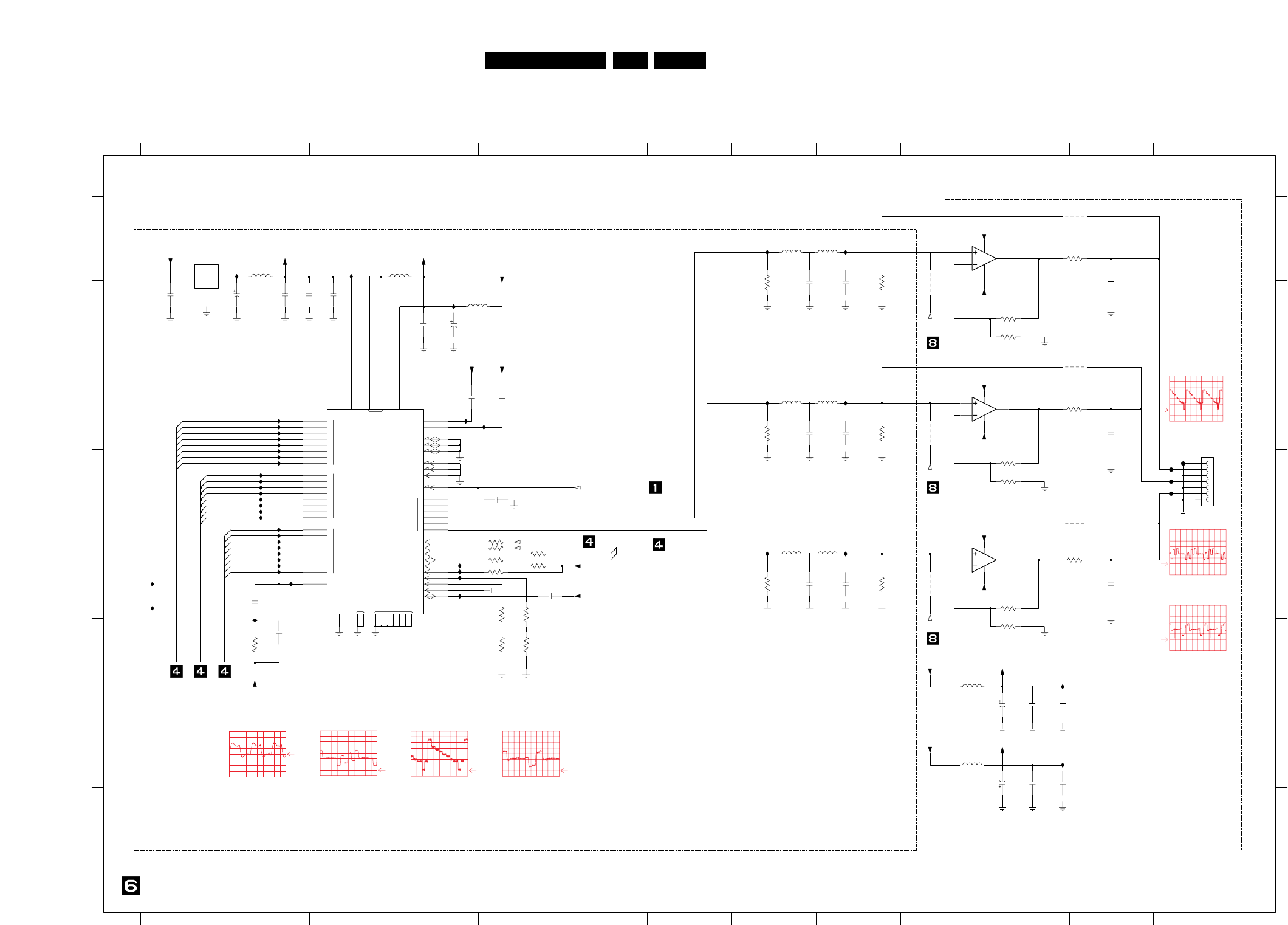
EN 1107.LX7500RCircuit Diagrams and PWB Layouts
2
3
4
5
6
7
0
1
2
3
4
5
6
7
EXT_LF
VAA
SCLK
CLKIN_B
CLKIN_A
F
E
D
C
B
A
RESET
P_BLANK
P_VSYNC
P_HSYNC
S_BLANK
S_VSYNC
S_HSYNC
COMP2
COMP1
AGND
0
2
1
RSET2
RTC_SCR_TR
VREF
3
4
5
6
7
0
1
S
C
Y
VDD VDD_IO
DAC
GND_IO
DGND
RSET1
ALSB
I2C
SDA
COM
OUTIN
2705 C5
2706 B2
2707 B3
1%
not used
for Prog Scan only
I704 D2
PB
I726 C8
I727 C9
I728 E8
I729 E9
I730 C2
I731 C2
1%
7702-2 E11
I738 A3
I739 E4
I740 E4
I742 C5
I743 A2
I744 F2
3731 E5
3732 E5
4701 B10
Y
456789
not used
E
F
G
345678
H
1704 D13
2700 B4
2701 G11
2703 D5
2704 B4
1%
for YUV or PROG_6dB only
1%
D
E
F
G
H
A
1%
23
1%
10 11 12 13
12
2721 E9
2722 E12
2723 E5
2725 C4
2726 G11
2727 G11
2709 B8
2710 B9
2711 B12
1%
for Prog Scan or YUV interlaced only
1%
for YUV or PROG_6dB only
for YUV or PROG_6dB only PR
1%
12 13
A
B
C
3700 E5
3701 E5
3702 E5
3703 A12
3705 B9
3706 B11
1%
1
not used
not used
3713 C9
3714 D11
3716 D11
2712 G11
2715 C8
2716 C9
2717 C12
2720 E8
3725 F5
3726 F5
3727 E5
3728 F2
3729 E5
3730 E5
91011
1%
not used
for YUV int only
4702 C10
4703 E10
4728 A12
not used
2731 B2
2732 B2
2733 E2
2734 F2
5706 C9
5707 E8
5709 E9
5711 F10
5712 G10
5713 A2
B
C
D
1%
not used
1%
3717 C8
3718 E12
3721 E9
3722 E8
3723 E11
3724 F11
7703 C3
7704 A1
F1701 D13
F1702 D13
F1704 D13
F1706 D13
2728 G11
2729 G11
2730 B1
I707 E2
I708 E2
I709 E2
I710 E2
I711 D2
I7119 E4
4729 C12
4730 D12
5700 B4
5701 A8
5703 A9
5704 C8
I718 D2
I720 E4
I721 C4
I722 E2
I723 E1
I724 A8
3707 B11
3709 B8
3710 C12
1%
I705 E2
I706 E2
I745 F11
I746 G11
1%
ANALOG BOARD
I712 D2
I713 D2
I714 D2
I715 D2
I716 D2
I717 D2
1%
for YUV int only
5714 A4
7701 A11
7702-1 C11
for YUV int only
1%
I725 A9
I732 C2
I733 C2
I734 C2
I735 C2
I736 D2
I737 D2
I700 B4
I701 E1
I703 D2
2703
1n0
2705
100n
2701
100n
3723
1K0
100n
2726
7702-2
AD8092AR
5
6
7
8
4
3705
300R
3716
1K0
2727
100n
I721
I706
I727
4u7
5712
5711
4u7
2730
100n
3729
10R
3730
10R
I745
I746
2707
100n
I707
100R
3701
F1701
7
8
9
12
13
50
49
41
10
56
1
46
4
5
6
54
55
58
59
60
61
62
22
21
48
52
64
19
25
23
24
33
47
35
31
53
38
37
11
57
34
2
3
14
15
51
28
29
30
32
63
45
36
44
43
42
39
40
20
16
17
18
26
27
Φ
VIDEO
ENCODER
ADV7302A
7703
4u7
2729
3728
680R
I729
5701
6u8
6u8
5704
I726
2709
6p8
2731
4u7 35V
2723
100n
2732
100n
3732 33R
I713
I716
I709
5713
3709
300R
5714
I7119
3725
750R
F1702
2
4u7
2700
AD8091ART
7701
3
4
1
5
AD8092AR
3
2
1
8
4
7702-1
I700 5700
2716
18p
2706
I724
100n
I710
2711
220p
I732
I730
I731
3713
300R
3724
1K0
5703
2u2
I728
33R3727
4729
1K0
3707
2733
3n9
2734
820p
I717
I703
3714
1K0
2728
4u7
I714
3710
75R
I705
100n
2725
I738
3721
300R
2721
18p
2717
220p
5706
2u2
I704
I722
750R
I720
3726
4K7
I701
2
13
3731
I743
LF25CDT
7704
I744
2u2
I723
5709
4728
F1704
2704
100n
I715
I740
I739
I725
I742
6p8
2720
3722
300R
I712
4730
4703
3700 100R
2722
220p
3706
1K0
2
3
4
5
6
7
100n
2712
1704
FMN-BMT
PSCAN
1
4K7
4701
3702
4702
2715
6p8
I736
I737
I735
I733
I734
18p
2710
5707
6u8
3703
75R
F1706
I711
I708
75R
3718
300R
I718
+2V5
SDA0
SCL0
IIC0
3717
ITU_OUT(5)
ITU_OUT(4)
ITU_OUT(3)
ITU_OUT(2)
ITU_OUT(1)
ITU_OUT(0)
ITU_OUT(7)
ITU_OUT(7:0)
PNX7100_ITU_OUT_CLK
+2V5
VDD_IO
VDD_IO
ITU_OUT(6)
PROGC_OUT(5)
PROGC_OUT(6)
PROGC_OUT(7)
+3V3
+3V3
+2V5
+2V5
RESET_PROGSCANn
PROGY_OUT(7)
PROGY_OUT(6)
PROGY_OUT(5)
PROGY_OUT(4)
PROGY_OUT(3)
PROGY_OUT(2)
PROGY_OUT(1)
PROGY_OUT(0)
PROGC_OUT(7:0)
PROGC_OUT(4)
PROGC_OUT(3)
PROGC_OUT(2)
PROGC_OUT(1)
PROGC_OUT(0)
D_YUIVI
+2V5
+5V
-5V_PS
+5V_PS
+5V_PS
+5V_PS
-5V -5V_PS
PROG_OUT_CLK
PROGY_OUT(7:0)
-5V_PS
-5V_PS
+5V_PS
A: DC, 200mV/Div, 5us/Div
IC7703 pin 36
A: DC, 200mV/Div, 5us/Div
0V
IC7703 pin 34
A: DC, 200mV/Div, 5us/Div
IC7703 pin 32
A: DC, 2 V/Div, 10ns/Div
IC7703 pin 25
A: DC, 500mV/Div
10us/Div
Y 1704-2
A: DC, 500mV/Div
10us/Div
PB 1704-4
A: DC, 500mV/Div
10us/Div
PR 1704-6
DIGITAL BOARD Chrysalis PPS E4 AV3+
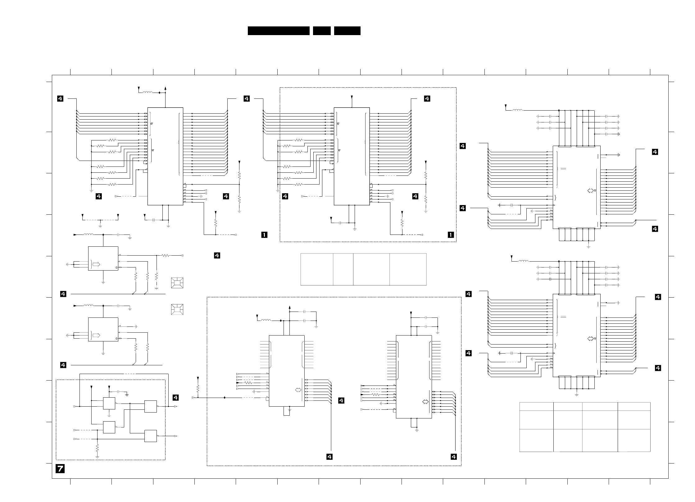
EN 1117.LX7500RCircuit Diagrams and PWB Layouts
7
1
6
BY
RY
D
GND
ALE
NC NC
WP
WE
RE 5
CLE
3
4
8
2
CE
7
1
6
B
R
D
GND
ALE
NC NC
WP
WE
RE 5
CLE
3
4
8
2
CE
SCL
ADR
0
1
2SDA
WC
OE
3
2
1
0
13
2
1
14
WE
BYTE
5
15
16
4
RY
8
10
6
5
RES
15
7
A
21
17
20
11
WP
ACC
18
19
3
4
BY
A-1
6
CE
12
11
10
9
8
7
12
14
D
D
13
9
0
7
6
5
4
3
2
15
14
11
10
9
8
D
0
1
2
3
4
5
6
7
8
9
10
VSS
VDDQ
4M-1
DQM
VDD
VSSQ
0
A
BA
1
12
H
0
WE
L
NC
CAS
RAS
CS
CKE
CLK
11
1
0
13
12
7
1
6
BY
RY
D
GND
ALE
NC NC
WP
WE
RE 5
CLE
3
4
8
2
CE
2
NC
D
0
1
2
3
4
5
6
7
8
9
10
VSS
VDDQ
2M-1
DQM
VDD
VSSQ
0
A
BA
1
6
H
0
WE
L
1
CAS
RAS
7
5
4
3
2
15
14
11
10
CS
CKE
CLK
11
1
0
13
12
9
8
&
SCL
ADR
0
1
2SDA
WC
&
0
9
OE
3
2
1
0
13
2
1
14
WE
BYTE
5
15
16
4
RY
8
10
6
5
RES
15
7
A
17
20
11
WP
ACC
18
19
3
4
BY
A-1
6
CE
12
11
10
9
8
7
12
14
D
D
13
NC
7
6
5
4
3
2
15
14
11
10
9
8
D
0
1
2
3
4
5
6
7
8
9
10
VSS
VDDQ
4M-1
DQM
VDD
VSSQ
0
A
BA
1
12
H
0
WE
L
NC
CAS
RAS
CS
CKE
CLK
11
1
0
13
12
OE
3
2
1
0
13
2
1
14
WE
BYTE
5
15
16
4
RY
8
10
6
5
RES
15
7
A
21
17
20
11
WP
ACC
18
19
3
4
BY
A-1
6
CE
12
11
10
9
8
7
12
14
D
D
13
9
0
&
2
NC
D
0
1
2
3
4
5
6
7
8
9
10
VSS
VDDQ
2M-1
DQM
VDD
VSSQ
0
A
BA
1
6
H
0
WE
L
1
CAS
RAS
7
5
4
3
2
15
14
11
10
CS
CKE
CLK
11
1
0
13
12
9
8
&
0
9
OE
3
2
1
0
13
2
1
14
WE
BYTE
5
15
16
4
RY
8
10
6
5
RES
15
7
A
17
20
11
WP
ACC
18
19
3
4
BY
A-1
6
CE
12
11
10
9
8
7
12
14
D
D
13
NC
11 12
2832 F2
2833 D2
2834 D7
23
2811 A13
not used
not used
0
XIO_SEL_NORFLASH
6
8
4
8 Mbyte NOR FLASH
1
1
13 14
A
B
7809 F1
7810 D1
1
I804 E12
NOR FLASH
XIO_SEL_NORFLASH_H
5803 A2
5804 E11
I805 A3
I806 H4
XIO_SEL_NORFLASH_L
7803-4 I2
7812, 7813
*
DEVICE
0
not used
not used
7806 F8
7807 A3
7808 E12
7811 A8
7812 B12
NAND
I801 D1
I802 A12
I803 F6
4819 H5
APPLICATION
#
not used
Only for 7805
4822 G2
5802 A11
4805 H8
4806 H8
5805 F5
5808 F1
not used
7803-1 H1
7803-2 H1
7803-3 H2
4817 G5
*
PCI_AD(23)
not used
0
Only for 7807
7804 B12
7805 A8
for BOARD with
*
0
3819 C9
3836 G2
7813 E12
7814 F8
I800 F1
32 Mbyte SDRAM
4818 G5
3849 D4
#
#
#
CHRY BOOT
0
4802 D1
4803 D1
4804 C2
3805 G2
4807 H8
4808 I1
5809 D1
7801 A3
7802 F5
4814 D9
4815 C11
4816 G11
3814 B1
TRUTH TABLE - NORFLASH SELECTION
1
0
2814 C11
2818 F6
not used
1
4 Mbyte NOR FLASH
3816 C5
3817 C5
3818 C9
2827 F9
2828 F9
3841 B6
3842 B6
3846 C6
3847 C6
3848 D8
3804 H5
1
8 9 10 11
3854 D3
3855 E3
4800 C4
4801 C8
F
G
3806 E2
3807 E2
4809 I1
4812 C6
4813 D4
3811 B2
3812 B1
3813 B2
G
7804, 7808
SDRAM
7807
not used
2819 F6
not used
not used
3815 B2
2824 E12
2825 E13
2826 E13
910
2829 G11
2830 D3
3843 B6
3844 B6
3845 B6
2836 H2
3801 I1
3802 H8
57 12
1
C
D
E
H
I
3808 H4
3809 C2
3810 C1
D
E
F
2812 B13
NOR
7801
not used
0605 E3
0609 F3
2806 A12
2807 A13
1
2820 E12
2821 E13
2822 E12
2823 E13
67
not used
1
64 Mbyte SDRAM
A
B
C
H
I
DEVICE
not used
NOR
NAND FLASH
1
NAND
1
2808 A12
2345 13 14
1
2809 A13
2810 A12
not used
19
3842
10K
11
14
15
8
7
12
37
13
36
18
38
39
40
45
46
47
48
3
4
5
10
23
24
25
26
27
28
33
2
34
35
31
32
41
42
43
44
1
20
21
22
128-MBIT/64Mx8
EEPROM
Φ
17
9
16
6
29
30
7806
TC58128AFTI
3846
10K
I804
3808
4K7
15
16
42
41
23
44
1
22
4
5
36
37
38
7
39
8
9
10
13
14
25
26
27
6
17
28
29
30
31
32
35
8-BIT SERIAL
Φ
EEPROM
3
43
2
40
18
19
20
21
24
7802
TC58V64AFTI
100n2824
3844
10K
100n2812
10K
3841
100n2809
3813
10K
37
2746
11
14
45
33
35
38
40
42
44
30
32
28
12
15
7
47
26
29
31
34
36
39
41
43
9
23
10
13
22
21
20
19
18
8
25
24
6
5
4
3
2
1
48
17
16
AM29DL640G-70EI
7805
ROM
(4Mx16)
[FLASH]
100n
2836
84
7
4802
EEPROM
Φ
(8Kx8)
1
2
3
6
5
M24C64-WMN6
7810
2821 100n
100n2811
37
13
36
18
19
3
4
5
10
11
14
15
8
7
12
33
2
34
35
38
39
40
45
46
47
48
1
20
21
22
23
24
25
26
27
28
9
16
6
29
30
31
32
41
42
43
44
Φ
EEPROM
128-MBIT/64Mx8
TC58256AFTI
7814
17
I801
43
49
28
41
54
6
12
46
52
16
44
39
15
40
18
1
14
27
3
9
48
50
51
53
5
7
8
10
11
13
42
20
21
17
37
38
19
2
4
45
47
22
35
36
25
26
29
30
31
32
33
34
7813
MT48LC16M16A2
4M X 16 X 4
DRAM
Φ
23
24
100n
2819
5802
3809
10K
10K
3843
3818
4K7 4K7
3819
5809
2822 100n
100R
3807
28
41
54
6
12
46
52
16
40
36
18
1
14
27
3
9
43
49
53
5
7
8
10
11
13
42
44
39
15
17
37
38
19
2
4
45
47
48
50
51
25
26
29
30
31
32
33
34
20
21
7808
2M X 16 X 4
DRAM
Φ
23
24
22
35
MT48LC8M16A2TG
3
6
5
84
7
100n
2827
7809
M24C64-WMN6
EEPROM
Φ
(8Kx8)
1
2
2828
100n
I800
7
14
8
74LVC00AD
7803-3
9
10
3811
10K
22K
3855
5804
2830
100n
10K
3812
4K7
3816
100n2810
100n2825
10p
4812
2814
4
5
7
14
6
7803-2
74LVC00AD
4806
100n
I805
2808
46
11
14
4818
40
42
44
30
32
13
28
12
15
37
27
29
31
34
36
39
41
43
45
33
35
38
10
22
21
20
19
18
8
7
47
26
5
4
3
2
1
48
17
16
9
23
(2Mx16)
ROM
AM29DL324GB-70EI
25
24
6
7811
100R
3805
10K
3847
2820 100n
4822
5808
3848
10K
100n
2833
4814
100n2823
14
11
7803-4
74LVC00AD
12
13
7
32
28
12
15
37
2746
11
14
39
41
43
45
33
35
38
40
42
44
30
19
18
8
7
47
26
29
31
34
36
1
48
17
16
9
23
10
13
22
21
20
25
24
6
5
4
3
2
7807
AM29DL640G-70EI
ROM
(4Mx16)
[FLASH]
54
6
12
46
52
16
18
1
14
27
3
9
43
49
28
41
5
7
8
10
11
13
42
44
39
15
40
38
19
2
4
45
47
48
50
51
53
26
29
30
31
32
33
34
20
21
17
37
MT48LC16M16A2
7812
4M X 16 X 4
23
24
22
35
36
25
DRAM
Φ
4801
3801
10K
10K
3814
2829 10p
4805
2832
100n
2826 100n
4819 4K73802
5805 I803
0605
SOFTWARE
3804 4K7
3836
100R
4800
3815
10K
I806
4807
3806
100R
10K
3810
10K
3849
4816
4815
4817
2818
100n
15
37
2746
11
14
33
35
38
40
42
44
30
32
13
28
12
47
26
29
31
34
36
39
41
43
45
16
9
23
10
22
21
20
19
18
8
7
24
6
5
4
3
2
1
48
17
[FLASH]
(2Mx16)
ROM
AM29DL324GB-70EI
7801
25
1
2
7
14
3
74LVC00AD
7803-1
28
41
54
6
12
46
52
16
10K
3845
36
18
1
14
27
3
9
43
49
53
5
7
8
10
11
13
42
44
39
15
40
37
38
19
2
4
45
47
48
50
51
25
26
29
30
31
32
33
34
20
21
17
Φ
DRAM
7804
2M X 16 X 4
23
24
22
35
5803
MT48LC8M16A2TG
3817
4K7
0609 SOFTWARE
100n2807
4808
I802
4813
100n
2834
2806 100n
4804
2K2
3854
4809
4803
PCI_AD(10)
XIO_SEL_NORFLASH_L
PCI_CBE(2)
VDD_NOR
PCI_CBE(1)
MPIO19_CTL_SERVICE
XIO_SEL_NORFLASH
PCI_AD(1)
PCI_AD(2)
PCI_AD(11)
PCI_AD(12)
PCI_AD(13)
PCI_AD(14)
PCI_AD(15)
PCI_AD(16)
PCI_AD(17)
PCI_AD(18)
PCI_AD(19)
PCI_AD(20)
PCI_AD(3)
PCI_AD(21)
PCI_AD(4)
PCI_AD(5)
PCI_AD(6)
PCI_AD(7)
PCI_AD(8)
PCI_AD(9)
XIO_ACK
PCI_CBE(1)
VDD_NAND
PCI_CBE(2)
PCI_AD(25)
PCI_AD(24)
XIO_SEL_NANDFLASH
PCI_AD(31)
PCI_AD(30)
PCI_AD(29)
PCI_AD(28)
PCI_AD(27)
PCI_AD(26)
PCI_AD(31:0)
PCI_AD(0)
PCI_AD(22)
PCI_AD(23)
VDD_NOR
PCI_AD(24)
PCI_AD(25)
PCI_AD(26)
PCI_AD(27)
PCI_AD(28)
PCI_AD(29)
PCI_AD(30)
PCI_AD(31)
VDD_NAND
PCI_AD(1)
VDD_NANDVDD_NOR
XIO_ACK
+3V3
VDD_NAND
PCI_AD(1)
PCI_AD(0)
SDRAM_DATA(13)
SDRAM_DATA(14)
SDRAM_DATA(15)
SDRAM_DATA(2)
SDRAM_DATA(3)
SDRAM_DATA(4)
SDRAM_DATA(5)
SDRAM_DATA(6)
SDRAM_DATA(7)
SDRAM_DATA(8)
SDRAM_DATA(9)
DQM(1)
DQM(0)
SDRAM_DATA(20)
SDRAM_DATA(21)
SDRAM_DATA(22)
SDRAM_DATA(23)
SDRAM_DATA(24)
SDRAM_DATA(25)
DQM(3)
DQM(2)
SDRAM_DATA(0)
SDRAM_DATA(1)
SDRAM_DATA(10)
SDRAM_DATA(11)
SDRAM_DATA(12)
PCI_AD(14)
PCI_AD(13)
PCI_AD(12)
PCI_AD(11)
PCI_AD(2)
PCI_AD(1)
SDRAM_DATA(16)
SDRAM_DATA(17)
SDRAM_DATA(26)
SDRAM_DATA(27)
SDRAM_DATA(28)
SDRAM_DATA(29)
SDRAM_DATA(30)
SDRAM_DATA(31)
SDRAM_DATA(18)
SDRAM_DATA(19)
PCI_AD(9)
PCI_AD(8)
PCI_AD(7)
PCI_AD(6)
PCI_AD(5)
PCI_AD(4)
PCI_AD(21)
PCI_AD(3)
PCI_AD(20)
PCI_AD(19)
PCI_AD(18)
PCI_AD(17)
PCI_AD(16)
PCI_AD(15)
SDRAM_ADDR(14:0)
SDRAM_DATA(31:0)
SDRAM_CTRL
PCI_AD(24)
PCI_AD(25)
PCI_AD(26)
PCI_AD(27)
PCI_AD(28)
PCI_AD(29)
PCI_AD(30)
PCI_AD(31)
PCI_AD(0)
PCI_CBE(1)
VDD_NOR
PCI_CBE(2)
XIO_SEL_NORFLASH_H
PCI_AD(10)
PNX7100_RESETn
XIO_SEL_NORFLASH_H
XIO_SEL_NORFLASH_L
VDD_NOR
PCI_CBE(1)
PCI_AD(31:0)
PCI_AD(22)
SDRAM_CTRL
SDRAM_ADDR(12)
SDRAM_DATA(31:0)
SDRAM_ADDR(10)
SDRAM_ADDR(11)
SDRAM_ADDR(9)
VDD_NAND
PCI_AD(26)
PCI_AD(31:0)
VDD_NOR
PCI_AD(0)
PCI_AD(31)
PCI_AD(31:0) PCI_AD(31:0)
VDD_NOR
PCI_AD(22)
PNX7100_RESETn
VDD_NOR
SDRAM_ADDR(12)
PCI_CBE(2)
PCI_AD(31:0)
XIO_ACK XIO_ACK
VDD_NORVDD_NOR
SCL1
IIC1
SCL0
IIC0
SDA0
+3V3
PCI_AD(28)
PCI_AD(29)
PCI_AD(30)
VDD_NOR
+3V3
PCI_AD(24)
PCI_AD(25)
PCI_AD(27)
SDRAM_ADDR(5)
SDRAM_ADDR(4)
SDRAM_ADDR(7)
SDRAM_ADDR(6)
SDRAM_ADDR(9)
SDRAM_ADDR(8)
SDRAM_ADDR(11)
SDRAM_ADDR(10)
+3V3
XIO_SEL_NANDFLASH
+3V3
+3V3
+3V3
SDA1
RAS(0)
WE(0)
CKE
SDRAM_CTRL
HSCKB
SDRAM_ADDR(14)
SDRAM_ADDR(13)
SDRAM_ADDR(14:0)
SDRAM_ADDR(1)
SDRAM_ADDR(0)
SDRAM_ADDR(3)
SDRAM_ADDR(2)
SDRAM_ADDR(13)
SDRAM_ADDR(1)
SDRAM_ADDR(0)
SDRAM_ADDR(3)
SDRAM_ADDR(2)
SDRAM_ADDR(5)
SDRAM_ADDR(4)
SDRAM_ADDR(7)
SDRAM_ADDR(6)
SDRAM_ADDR(8)
CKE
CAS(0)
HSCKB
RAS(0)
WE(0)
SDRAM_CTRL
SDRAM_ADDR(14)
CAS(0)
DIGITAL BOARD Chrysalis PPS E4 AV3+
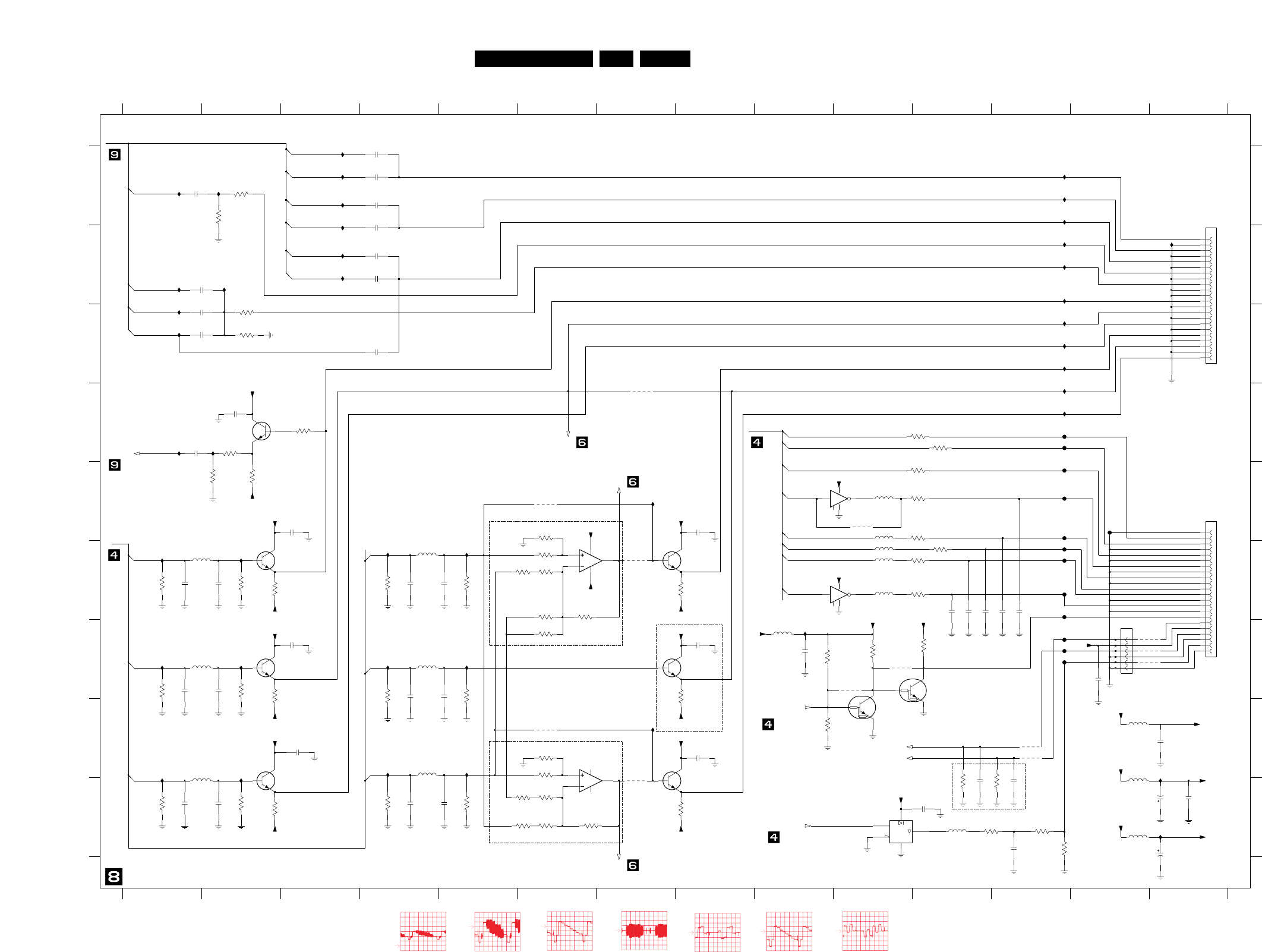
EN 1127.LX7500RCircuit Diagrams and PWB Layouts
NC
EN
NC
3903 I11
3904 I12
3905 C2
3906 C2
5914 F10
5915 F10
5916 H13
7900 E9
7901 F9
7902 G11
I916 D12
I917 D12
I918 G9
I919 H14
1%
1%
1%
1%
only for NAFTA_C1 or YUV interlaced
for 2004 only
2926 G1
3918 F1
2924 G3
2925 G8
I936
1%
2914 F1
2915 F2
2916 F4
2917 F5
1234567
1%
7 8 9 10 11 12 13 14
A
2937 I4
2938 D2
2939 I14
2940 I14
VIP_ANALOG_VIDEO_INPUT
1%
not used
1%
not used
1%
B
ANALOG BOARD INTERFACE AUDIO IN/OUT
8 9 10 11 12
C
D D
E
2908 C1
2909 C1
2910 I12
2911 D1
2912 E3
2913 E8
3913 E11
3914 E11
3915 G10
3916 F11
1%
F
G
H
I
1900 E14
1901 G13
1904 A14
2036 I5
1%
not used
2931 I14
2932 C4
2933 H3
2934 H8
2935 I1
2936 I2
3932 I4
3933 I8
3934 F2
3935 F5
1%
delete for NAFTA_C1
not used
1%
1%
2046 G12
E
only for
1%
I
A
B
C
3907 D3
3908 D2
3909 D11
3910 D11
3911 E2
3912 E2
3953 I6
3954 I6
3955 I12
3956 I12
only for EU or NAFTA&C3
1%
1%
1%
2918 G11
2919 G11
2920 I11
2921 G12
2922 G11
13
only for
3456
3926 G2
3927 G4
3928 G8
3929 I11
3930 I1
3931 I2
5902 H13
5903 I13
5904 I11
5905 E10
1%
delete for I2C
delete for 2004
1%
ANALOG BOARD INTERFACE VIDEO IN/OUT
2941 I11
2942 I12
2900 A4
F
G
H
2927 G2
2928 G4
2929 G5
2930 H14
4908 G13
4909 G13
4910 G13
4911 E10
4912 G10
5901 G9
F1918 E12
F1920 D12
F1921 D12
F1922 E13
1%
only for NAFTA & C1
1%
1%
1%
3917 F11
2923 G9
14
12
3922 F11
3923 G11
3924 G1
3925 H9
F1907 F12
F1909 F12
F1911 F12
F1912 F12
F1914 E12
F1916 E12
I932 C1
I933 D1
I934 A3
I935 A3
I936 A3
NAFTA&C1
not used
delete for NAFTA_C1
only for NAFTA_C1 or YUV interlaced
1%
3939 I5
3087 E11
3901 A2
3902 A2
3943 F6
3944 F6
3945 F6
3946 F6
I910 A12
I911 A12
I912 B12
I913 C12
I914 C12
I915 C12
I943 E7
I944 H7
NAFTA&C1
not used
1%
I904 H2
I905 F1
I906 G1
I907 H1
7907 F2
7908 G2
4900 H12
3919 F2
3920 F4
3921 F8
4904 E6
4905 F7
4906 H6
4907 I7
I926 H5
I927 A2
I928 B2
I929 A1
I930 B1
I931 C1
I908 A12
I909 B14
7910-1 F6
7910-2 H6
7911 I2
7912 I8
F1902 G12
F1903 G12
F1904 G12
I925 H4
1%
I900 B12
I901 B12
5906 E10
3940 G9
3941 E6
3942 F6
1%
1%
delete for 2004
delete for 2004
delete for 2004
for I2C only
I902 F2
I903 G2
5907 F4
5908 F1
5909 F10
5910 G1
5911 G4
5912 H1
5913 H4
for IOE only
delete for IOE
I937 A3
I938 B3
I939 B3
I940 D2
I920 I14
I921 F4
I922 F5
I923 G4
I924 G5
7909 G8
4901 H12
4902 G10
4903 D7
DAIO
1%
3936 G2
3937 G5
3938 I2
2943 G13
2901 A4
2902 A1
2903 A4
2904 A4
2905 B4
2906 B4
2907 B1
3947 G6
3948 H6
3949 H6
3950 I6
3951 I6
3952 I6
7903 I10
7904 D2
7905 H10
7906 F8
100n
2940
I934
I939
1K0
3946
F1922
750R
3948
22n
2911
1K2
3952
2
3
1
5
4
74LVC1G04GW
7900
3924
75R
270p
2915
2931
I944
4u7
I940
I943
100R
3907
4912
I915
2906
100n
I920
F1921
7905
PDTC124EU
75R
3932
3941
750R
2934
100n
3944
1K0
5K6
3954
2922 68p
100n
2924
1K0
3931
4
3
2
1
8
I904
7910-1
AD8092AR
2928
270p
F1902
10n
2943
100n
2912
100n
I921
2933
75R
3930
1R0
3955
270p
2937
4910
5
6
7
84
AD8092AR
7910-2
3910
68R
4906
3934
F1909
75R
4K7
3947
3928
1K0
100n
2905
I932
270p
2916
2923
100n
47R
3087
75R
3920
I927
5909
5912
I912
F1904
1u5
I918
F1918
75R
F1912
3936
7904
BC847B
180R
3901
I923
F1920
100n
2907
2046
100n
2920
22p
1K5
3950
2930
100n
I916
3904
100K
22p
2942
20
21
22
3
4
5
6
7
8
9
11
12
13
14
15
16
17
18
19
2
FMN-BMT
1904
1
10
4K7
3953
3929
56R
I930
4905
I903
F1911
4901
3919
1K0
3940
10K
F1914
I907
1u5
5910
I913
1K0
3926
4903
3922
68R
47R
3916
22K
3923
5915
5914
5906
5907
1u5
150p
2910
100n
2932
2913
100n
3938
75R
I924
3915
4K7
3914
68R
I937
I905
2941
22p
5901
2938
100n
75R
3937
2926
270p
BC847B
7912
3927
75R
4900
3912
I926
2K2
100n
2904
2903
100n
I909
F1903 3
4
5
6
7
8
9
13
14
15
16
17
18
19
2
20
21
22
1900
FMN-BMT
1
10
11
12
I917
3917
47R
BC847B
7906
I929
I922
3935
75R
I925
7909
BC847B
5905
I938
270p
2935
2939
4u7
I931
F1916
I902
1u5
5911
1K5
3942
4904
7907
BC847B
4909
I935
I911
3939
75R
3905
4908
180R
2936
270p
3909
68R
4907
1u5
5908
2925
100n
3925
10K
3949
1K5
3945
4K7
3918
75R
560R
3911
I919
100R
3956
22R
3913
100n
2909
I900
560R
560R
3902
2929
3906
3
1
5
4
270p
7903
74HCT1G125GW
2
5916
1K0
3921
2901
100n
100n
2902
I906 2
3
4
5
6
FMN-BMT
1901
1
3951
1K5
22p2919
5903
4u7
2917
270p
6K8
3943
3908
100n
2900
180R
2914
270p
4
2036
270p
7901
2
3
1
5
2918
74LVC1G04GW
22p
I914
4902
100K
3903
PDTC124EU
7902
2908
I910
100n
7911
BC847B
22p
BC847B
7908
2921
5913
1u5
5904
I928
270p
2927
I933
1K0
3933
5902
4u7
F1907
I901
I908
4911
D_WCLK
WS012_OUT
D_BCLK
SCK012_OUT
D_KILL
MPIO7_MUTE_LVn
DAOUT
A_PCMCLK
DIGITAL_AUDIO
3V3_I2S
FSCLK012_OUT
D_DATA0
D_PCMCLK
SD0_OUT
C_IN_VIP
CVBS_Y_IN_A
C_OUT
Y_OUT
CVBS_OUT
-5V_Buffer
-5V_Buffer
-5V_Buffer
+5V_Buffer
+5V_Buffer
+5V_Buffer
VI
-5V_Buffer
+5V_Buffer
UI
A_YG
D_C
D_Y
D_Y
D_CVBS
VIDEO_OUT
CVBS_OUT_B_VIP
+5V_Buffer
-5V_Buffer
CVBS_Y_IN_C
CVBS_Y_IN_B
R_IN_VIP
V_IN_VIP
B_IN_VIP
U_IN_VIP
G_IN_VIP
Y_IN_VIP
A_C
A_YCVBS
WSE_IN
SDE_IN
+3V3
3V3_I2S
3V3_I2S
A_VR
A_UB
SPDIF_COAX_IN
SPDIF_OPT_IN
VDD_125
+5V
VDD_125
+5V
VDD_125
FSCLKE_IN
SCKE_IN
-5V_Buffer
-5V_Buffer
-5V_Buffer
D_VR
+5V_Buffer
D_YG
+5V_Buffer
D_UB
+5V_Buffer
G_OUT
B_OUT
SPDIF_OUT
-5V
-5V_Buffer
+5V_Buffer
+5V
A_DATA
A_WCLK
A_BCLK
R_OUT
A: DC, 500mV/Div
10us/Div
A_YCVBS 1904-14
A: DC, 200mV/Div
10us/Div
D_YCVBS 1904-11
A: DC, 200mV/Div
10us/Div
D_Y 1904-9
A: DC, 200mV/Div
10us/Div
D_C 1904-7
A: DC, 200mV/Div
10us/Div
D_VR 1904-5
A: DC, 200mV/Div
10us/Div
D_YG 1904-3
A: DC, 200mV/Div
10us/Div
D_UB 1904-1
DIGITAL BOARD Chrysalis PPS E4 AV3+
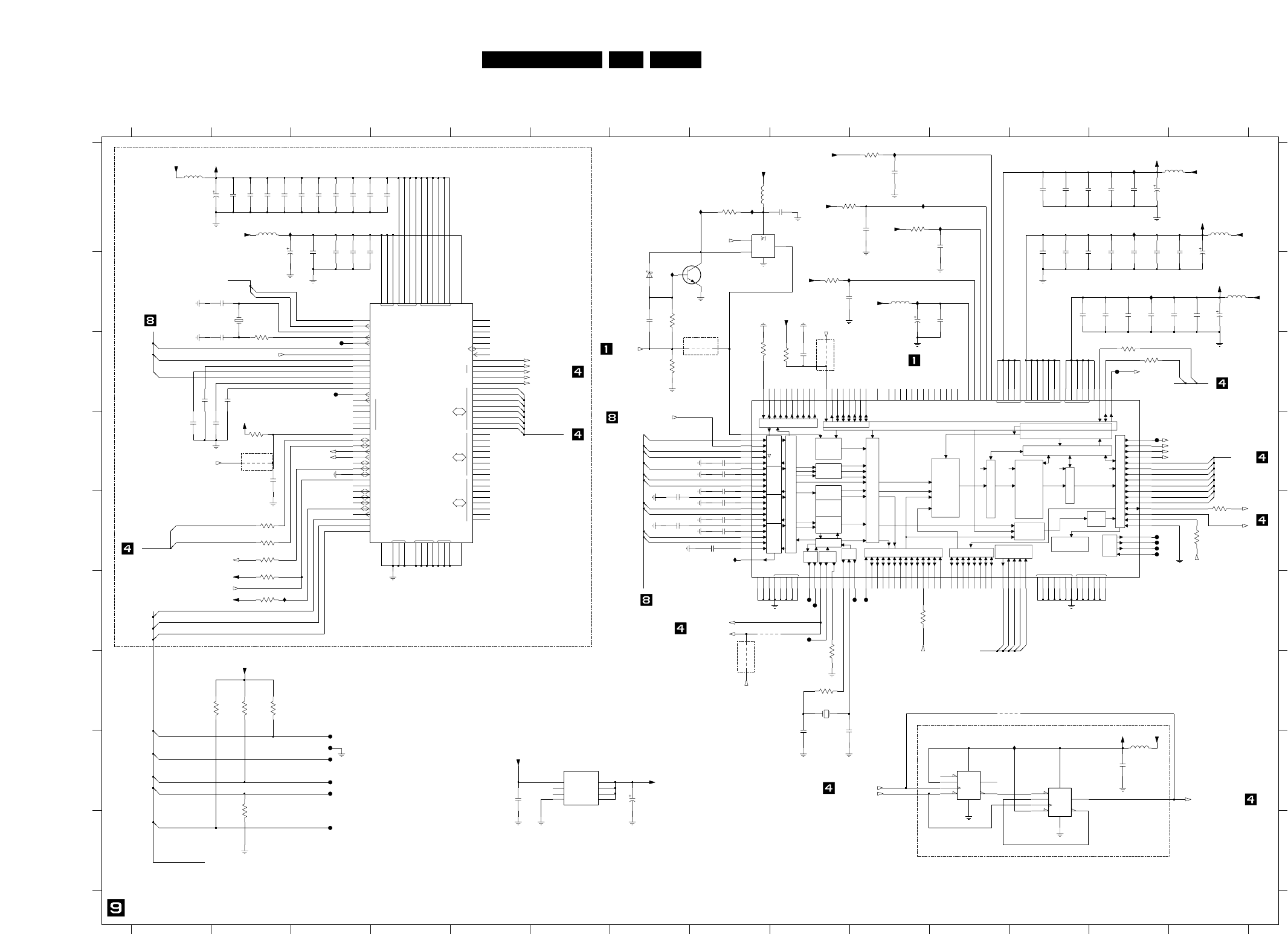
EN 1137.LX7500RCircuit Diagrams and PWB Layouts
3
2
R3
C1
1D
S2
3
2
R3
C1
1D
S2
NC
GND
IN VOUT
NC VOUT
VOUT
VOUT
Y
AUDIO
COMP
DELAY
SWITCH
FAST
VIDEO
DECODER OUTPUT CONTROL
BOUNDARY
SCAN
OUTPUT FORMATTER I-PORT
1ST TASK IIC REG MAP SCALER
SCALER EVENT CONTROLLER
VIDEO/TEXT
ARBITER
RAW S
Y
S
C
CLK GPO XTAL
S
S
Y
CR
CB
CB
CR
YCBCR
YCBCR
YCBCRS
CBCR
CBCR
RAW
BCS-SCALER
VDDA VDDE VDDI
VSSA VSSE VSSI
IIC REGISTER MAP
R
COMB
PROC
CHROM
PROC
CLK
H-PORTX-PORT
2ST TASK IIC REG MAP SCALER
SYNC
PROC
LUM
FIL
ANALOG INPUT CONTROL
AD-PORT CONTROL
ANALOG1
+ ADC1
TEXT
FIFO
VBI DATA
SLICER
ANALOG1
+ ADC1
VIDEO FIFO
VERTICAL SCALING
HORIZONTAL FINE-
(PHASE-) SCALING
LINE FIFO BUFFER
FIR-PREFILTER
PRESCALER
ANALOG1
+ ADC1
ANALOG1
+ ADC1
G
B
HPD
XPD
VDDA VDDE VDDI VXDD
TEST
VSSA
AGND VSSE VSSI VXSS
IGP
IPD
RTCO
RTS1
IDQ
AMXCLK
ALRCLK
ASCLK
AMCLK
RESON
LLC2
LLC
2
3
4
5
CE
SCL
SDA
RTS0
7
6
5
4
3
2
1
0
TDI
1
0
AOUT
AI2D
AI1D
AI24
AI23
AI22
AI21
AI12
AI11
XTOUT
XTALO
XTALI
TDO
ICLK
ITRI
ITRDY
XTRI
XRV
XRH
XCLK
XDQ
XRDY
TRSTN
TCK
TMS
IGPH
0
1
IGPV
7
6
5
4
3
2
1
0
7
6
5
4
3
2
1
0
4
H
6
I
8
1000 B2
10
1001 G9
2000 B3
VIP ANALOG
2001 B3
2002 B3
2003 B4
2004 A2
2005 A2
2006 A2
2007 A2
2008 A3
2009 A3
2010 A3
2011 A3
2012 A3
2013 A4
F009 F9
F011 D13
F013 H3
F015 H3
F017 H3
F018 I3
F019 C3
I001 E8
I002 A10
I003 A13
I004 A10
I005 A11
I006 A13
I007 B13
I008 B10
I009 B9
5009 B10
I010 A8
5011 H13
I011 A8
7001 H6
I012 B7
7003 B7
I013 F2
7005 B3
I014 A2
I015 H12
VIDEO INPUT
7008-1 H11
7008-2 H12
7112 F2
F001 F10
F002 F10
F003 C13
F004 E13
F005 E13
F006 E13
F007 E13
F008 F9
3018 I2
F010 C3
3020 F2
F012 F9
3023 A10
F014 H3
3025 A10
F016 H3
4001 F8
4002 G8
4003 C9
4004 D2
4005 G11
4007 C8
5001 A14
5002 A2
5003 A1
5005 A14
5008 B14
2071 E8
5010 A8
3001 E2
6000 B7
3003 C9
7002 A8
3005 C13
7004 C8
3007 C2
not used
3008 C13
3009 C7
3010 E14
3011 F10
3012 G9
3013 G9
3014 E2
3015 G2
3016 G2
3017 G2
2052 D8
3019 E14
2054 D8
3022 D2
2056 E8
3024 A9
2058 E8
3026 B9
2060 H9
2061 A9
2062 H13
2063 D7
2064 E8
2065 E7
2066 C9
2067 H5
2030 B13
3000 A8
2032 B14
3002 E2
2034 C2
3004 B7
2037 B9
3006 C8
2039 B13
not used
not used
2040 B13
2041 B13
2042 B14
2043 B14
2044 B14
2045 B2
2047 D2
2048 B7
2049 B10
2050 B11
2051 C2
2014 H7
2053 D8
2016 A12
2055 D1
2018 A12
2057 C1
2020 A13
2059 H9
2022 A13
not used
2023 B2
2024 A1
2025 D2
2026 A10
2027 B12
2028 B12
2029 B13
H
2031 B13
A
2033 B14
C
2035 A11
E
2038 B12
G
not used
not used
not used
3
2015 A10
5
2017 A12
7
2019 A13
9
2021 B12
11 12 13 14
A
B
C
D
E
F
G
I
B
1
D
3
F
567891011121314
12
24
100n
2011
CX-11F
1000
24M576
2013
100n
100n
2012
I008
100n
2021
F014
2022
4u7
5001
F012
3019
4K7
24M576
1001
CX-11F
2063 100n
5009
2051
18p
22R
3014
2029
100n
100n2065
2047
1n0
5005
14
I005
3
1
2
7
45
6
SN74HC74D
7008-1
2042
100n
1PS76SB10
6000
2058 100n
2006
100n
4u7
2023
7112
10K
680R
3004
100n
2019
100R
3001
F013
I012
2028
100n
10 9
8
14
100n
2026
7008-2
11
13
12
7
SN74HC74D
10K
3011
100n
2041
5008
I014
4003
2067
100n
F006
I013
F015
2066
1n0
4K7
3022 F011
1R0
3013
I010
F005
F009
3000
680R
I011
5010
2005
100n
F008
2035
100n
2015
100n
100R
3025
I015
2059
33p
10R
3007
4002
3024
100R
2054 100n
3010
22R
3009
1K0
2001
100n
100n
2037
4007
F002
F010
I003
10K
3020
4005
100n2052
3002
100R
2064
F017
100n
F016
100R
3008
F001
47u
2014
2045
18p
100n
2034
2038
100n
2016
100n
5011
100n
2031
5003
10K
3017
100n
2003
100n
2017
2020
100n
100n
2018
I007
100n
2043
4004
100n
2000
1
4
5
8
2
3
6
7
7001
LD1117D33
3003
4K7
F007
100n
2040
I001
100n
2055
2057
100n
2044
4u7
3016
10K
2062
100n
4u7
2033
F004
4001
100n
3006
2K2
100n
2032
2030
100n2053
I009
F019
I004
2002
100n
4u7
2049
7
6
4
80
90
89
87
86
85
84
82
81
96
92
91
50
76
100
38
63
88
85
94
95
33
43
58
68
83
93
24
15
9
26
79
99
97
23
17
11
1
25
51
75
35
31
32
98
3
2
44
73
74
77
78
57
56
55
54
42
47
28
29
30
36
34
45
46
48
49
53
52
62
61
60
59
22
39
27 72
71
70
69
67
66
65
64
20
18
19
16
14
12
10
13
40
37
41
VIDEO DECODER
PAL/NTSC/SECAM
Φ
SAA7114H
7005
21
100n
2007
3018
10K
10K
3015
100R
3023
1
2
35
4
7002
74LVC1G32GW
XTRI
100n
2004
XPD6
C11 XPD7
A6 XRDY
C7 XRH
D8 XRV
A3 XTAL
B4 XTALI
A2 XTOUT
B11
XCLK
B7 XDQ
A8 XPD0
B8 XPD1
A9 XPD2
B9 XPD3
A10 XPD4
B10 XPD5
A11
L11
D7
D10
F11
J11
L5
L9
B3
VXDD
A4 VXSS
A7
M2
J4
H3
E4
C1
D5
D9
D11
G11
L4
L8
H12
M4
M8
M11
C8
C10
F12
J12
M5
M9
L1
VDDA1A
H4
J1
VDDA2A
F4
G2
VDDA3A
D4
E2
VDDA4A
C5
C9
D12
C14TEST2
A13TEST3
B12TEST4
A12TEST5
D6 TMS
C6 TRSTN
M3
K4
L10 RTCO
N9SCL
P10SDA
B6 TCK
B5 TDI
A5 TDO
P13TEST0
D13TEST1
C4
RES5 C12
RES6 C13
RES7 N1
RES8 N2
RES9
P5RESON
M10 RST0
N10 RST1
N3
RES10 N13
RES11 N14
RES12 P2
RES13
B13
RES2 B14
RES3 C3
RES4
K12IGPH
K14IGPV
P9INT_A
N12ITRDY
L12ITRI
P4 LLC
N5 LLC2
B2
RES1
H14IDP3
H13IDP4
J14IDP5
J13IDP6
K11IDP7
L13IDQ
L14IGP0
K13IGP1
E14 HPD4
F13 HPD5
F14 HPD6
G13 HPD7
M14ICLK
G14IDP0
G12IDP1
H11IDP2
N4CE
N6CLKEXT
P3
EXMCLR
M13 FSW
D14 HPD0
E11 HPD1
E13 HPD2
E12 HPD3
F3 A|33
G1 A|34
F1 A|3D
B1 A|41
D2 A|42
D1 A|43
E1 A|44
D3 A|4D
K3 A|1D
G4 A|21
G3 A|22
H2 A|23
J3 A|24
H1 A|2D
E3 A|31
F2 A|32
P11AMCLK
M12AMXCLK
M1 AOUT
N11ASCLK
J2 A|11
K1 A|12
K2 A|13
L3 A|14
P7ADP4
N7ADP5
L6ADP6
M6ADP7
P6ADP8
C2 AGND
L2 AGNDA
P12ALRCLK
SAA7118E
7004
N8ADP0
P8ADP1
M7ADP2
L7ADP3
I006
100n
4u7
2024
2050
BC847B
7003
2009
100n
3012
4K7
2071 100n
I002
33p
2060
2025
100n
3026
100R
2039
100n
2027
100n
F018
3005
100R
150p
2048
5002
2061
100n
F003
2010
100n
2008
100n
+3V3
VIP_IGP1
JTAG_VIP_TRSTn
JTAG_VIP_TDO
JTAG_VIP
100n2056
+3V3_VIP
B_IN_VIP
U_IN_VIP
JTAG_VIP
JTAG_VIP_TDI
JTAG_VIP_TDO
VDD_7005
SDA0
VDD_7005
VDDE_7118
VDD_7008
+3V3_VIP
+5V
VIP_INTA
VDDI_7118
+3V3
VDD_7005
VIP_ERROR
PNX7100_VS_IN
VIP_FID
VIP_RESETn
VIP_RESETn
VDDA4A_7118
VDDA2A_7118
+3V3_VIP
JTAG_VIP_TMS
JTAG_VIP_TDI
JTAG_VIP_TMS
JTAG_VIP_TCK
JTAG_VIP_TRSTn
PNX7100_ITU_IN_VAL
PNX7100_HS_IN
PNX7100_VS_IN
VIP_FID
PNX7100_ITU_IN_CLK
ITRDY
VIP_IGP1
MPIO5_VIP_ERROR
VDDA1A_7118
VDDA3A_7118
VDDA_7118
VDDE_7118
VIP_FB
+3V3
JTAG_VIP_TCK
CVBS_Y_IN_B
CVBS_Y_IN_B
CVBS_OUT_B_VIP
C_IN_VIP
+3V3
PNX7100_ITU_IN_FID
VIP_ANALOG_VIDEO_INPUT
ITU_IN(2)
ITU_IN(1)
ITU_IN(0)
JTAG_VIP
JTAG_VIP_TCK
JTAG_VIP_TDI
JTAG_VIP_TDO
JTAG_VIP_TMS
JTAG_VIP_TRSTn
VIP_FID
IIC0
PNX7100_HS_IN
PNX7100_VS_IN
PNX7100_ITU_IN_CLK
PNX7100_ITU_IN_VAL
ITU_IN(0)
ITU_IN(1)
ITU_IN(2)
ITU_IN(3)
ITU_IN(4)
ITU_IN(5)
ITU_IN(6)
ITU_IN(7)
ITU_IN(7:0)
ITU_IN(7:0)
ITU_IN(7)
ITU_IN(6)
ITU_IN(5)
ITU_IN(4)
ITU_IN(3)
VDD_7005
SCL0
+3V3
+3V3
VDDI_7118
+3V3_VIP
+3V3_VIP
VIP_ERROR
VIP_RTS1
G_IN_VIP
Y_IN_VIP
R_IN_VIP
V_IN_VIP
VIP_INTA
VDDX_7118
+3V3_VIP
+3V3_VIP
+3V3
CVBS_Y_IN_A
CVBS_Y_IN_B
CVBS_Y_IN_C
C_IN_VIP
SDA0
SCL0
CVBS_OUT_B_VIP
VIP_IGP1
VDDE_7118
DIGITAL BOARD Chrysalis PPS E4 AV3+
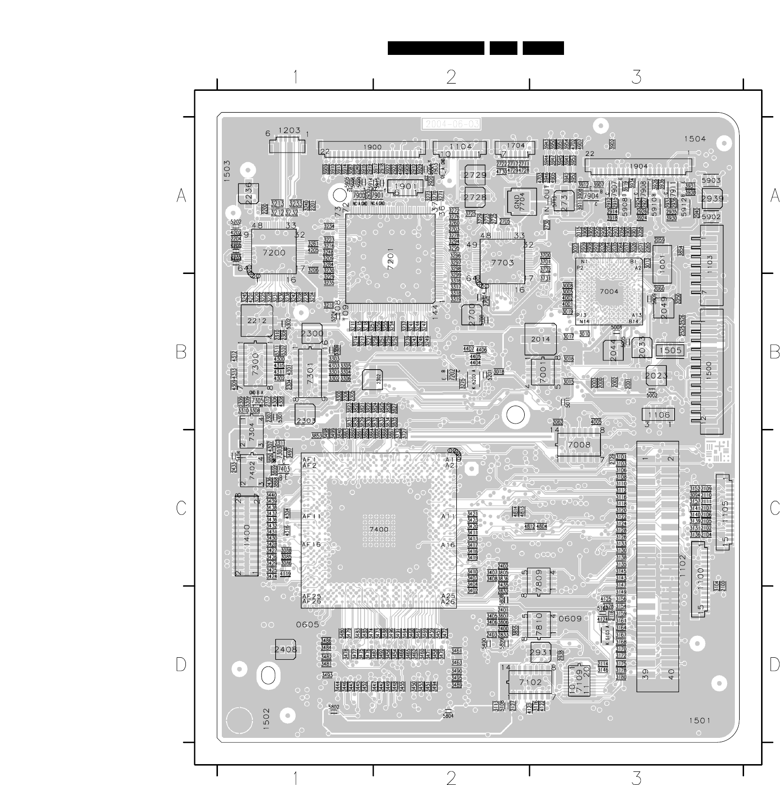
EN 1147.LX7500RCircuit Diagrams and PWB Layouts
0605 D1
0609 D3
1001 A3
1100 C3
1102 C3
1103 A3
1104 A2
1105 C3
1106 B3
1203 A1
1400 C1
1500 B3
1505 B3
1704 A2
1900 A1
1901 A2
1904 A3
2000 B3
2001 B3
2002 B3
2003 B3
2014 B3
2015 A3
2023 B3
2026 A3
2033 B3
2035 A3
2037 A3
2044 B3
2046 A1
2049 B3
2050 B3
2054 A3
2056 A3
2058 A3
2059 A3
2060 B3
2062 B3
2064 A3
2065 A3
2071 A3
2100 D3
2102 C3
2104 C3
2105 C3
2106 C3
2107 C3
2109 C3
2110 C3
2111 C3
2114 D3
2116 D3
2127 D2
2128 D3
2129 C3
2200 A1
2201 A1
2204 A1
2205 A1
2212 B1
2235 A1
2236 A1
2238 B1
2300 B1
2301 B1
2302 B2
2303 B1
2304 B1
2305 B1
2306 B1
2307 B1
2308 B1
2309 B1
2310 B1
2311 C1
2312 B1
2400 D2
2401 D2
2402 C2
2403 D2
2408 D1
2433 C1
2435 C2
2436 C1
2525 B3
2526 B3
2700 B2
2703 A2
2704 B2
2705 A2
2711 A2
2717 A2
2722 A2
2723 A2
2725 A2
2728 A2
2729 A2
2730 A3
2731 A3
2832 D2
2833 D2
2900 A3
2901 A3
2903 A3
2904 A3
2905 A3
2906 A3
2907 A3
2908 A3
2909 A3
2910 A2
2912 A3
2914 A3
2915 A3
2918 A2
2919 A1
2920 A2
2922 A2
2924 A3
2926 A3
2927 A3
2930 A1
2931 D3
2933 A3
2935 A3
2936 A3
2938 D3
2939 A3
2940 A3
3005 B3
3008 B3
3010 B3
3013 A3
3015 B3
3016 B3
3017 B3
3018 B2
3019 B3
3023 A3
3026 A3
3085 C1
3086 C1
3087 A1
3088 C1
3094 C3
3101 C3
3103 C3
3104 D3
3106 C3
3108 C3
3110 C3
3112 C3
3113 D2
3116 C3
3118 C3
3120 C3
3122 C3
3124 C3
3126 C3
3128 C3
3130 C3
3131 C3
3133 C3
3135 C3
3136 C3
3138 C3
3139 C3
3140 C3
3141 C3
3143 C3
3145 C3
3146 D3
3147 C3
3149 D3
3152 C3
3154 D3
3156 D3
3157 C3
3159 D3
3161 D3
3164 D3
3167 D3
3168 D3
3170 D3
3172 D3
3175 D3
3176 D3
3178 D3
3180 D3
3204 B1
3206 A1
3208 B1
3209 A1
3210 B1
3211 B1
3212 A1
3213 A1
3214 B1
3215 B1
3216 A1
3217 B1
3218 B1
3220 B1
3221 B1
3223 A1
3225 B1
3228 B1
3229 B1
3230 A1
3231 B1
3232 A1
3233 A1
3234 A1
3235 B1
3236 B1
3237 B2
3238 B1
3239 B2
3240 A1
3241 B2
3242 B1
3243 B2
3244 B2
3245 B1
3246 B2
3247 B2
3248 A1
3249 B2
3251 B2
3252 B2
3254 B2
3255 B2
3256 B2
3257 B1
3258 B2
3259 B2
3260 A2
3261 A1
3270 A2
3271 A2
3272 A2
3273 A2
3275 B2
3276 A2
3278 A2
3284 A1
3294 A2
3295 A2
3296 A2
3297 A2
3298 A2
3299 B2
3300 B1
3301 B1
3302 B1
3303 B1
3304 B1
3305 B1
3306 B1
3307 B1
3308 B1
3309 B1
3310 B1
3311 B1
3316 B2
3317 B2
3318 B2
3319 B2
3402 D2
3403 C2
3404 C2
3405 D2
3406 D2
3407 C2
3408 C2
3410 C2
3411 C2
3413 C2
3416 C2
3417 C2
3419 C2
3420 C2
3421 C2
3423 C2
3424 C1
3425 C1
3426 C1
3427 C1
3428 C1
3429 C1
3430 C1
3431 C1
3432 C1
3436 C1
3437 C1
3438 C1
3439 C1
3440 C1
3442 D2
3443 D1
3444 D1
3445 D1
3446 D1
3447 D2
3448 D2
3449 D2
3450 D2
3451 D2
3452 D1
3453 D2
3454 D2
3455 D2
3456 D2
3457 D2
3458 D2
3459 D2
3460 D2
3461 D2
3462 D2
3463 D2
3464 D2
3465 D2
3466 D2
3467 D2
3468 D2
3469 D2
3470 D2
3471 D2
3472 D2
3473 D2
3474 D1
3475 D1
3476 D1
3477 D1
3478 D1
3479 D1
3480 D1
3481 D1
3482 D1
3483 D1
3484 D1
3485 D1
3486 D1
3487 D2
3488 D2
3489 D2
3490 D2
3491 D2
3492 D2
3493 D1
3494 D2
3495 D2
3496 D2
3497 C1
3498 C1
3499 C1
3700 A3
3701 A3
3702 A3
3725 A2
3727 C2
3729 A2
3731 B3
3732 C2
3805 C2
3806 D2
3807 D2
3820 B1
3821 B1
3822 B1
3823 B1
3824 B2
3825 B2
3826 B2
3827 B2
3828 B1
3829 B1
3830 B1
3831 B1
3832 B2
3833 B2
3834 B2
3835 B2
3836 C2
3840 C1
3850 C1
3853 C1
3854 A3
3855 D2
3860 C1
3861 C1
3862 C1
3863 C1
3864 C1
3865 C2
3866 C2
3867 C2
3868 C1
3869 C1
3902 A3
3905 A3
3906 A3
3907 A3
3908 A3
3909 A1
3910 A1
3911 A3
3912 A3
3913 A1
3914 A1
3916 A1
3917 A2
3918 A3
3919 A3
3922 A2
3924 A3
3926 A3
3929 A2
3930 A3
3931 A3
3934 A3
3936 A3
3938 A3
3941 A3
3942 A3
3943 A3
3944 A3
3945 A3
3946 A3
3947 A3
3950 A3
3951 A3
3952 A3
3953 A3
3954 A3
4001 B3
4002 B3
4005 B3
4119 C1
4122 D3
4123 D2
4124 D3
4125 D3
4201 B1
4202 A1
4205 A1
4300 B1
4301 B1
4302 B1
4303 B1
4304 C1
4306 B1
4307 C1
4308 B1
4309 B1
4311 B1
4312 B1
4313 B1
4315 B1
4316 C1
4404 B2
4405 B2
4406 B2
4407 B2
4702 A3
4703 A3
4728 A2
4729 A2
4730 A2
4804 C3
4812 C3
4813 C2
4814 C2
4905 A3
4907 A3
4908 A2
4909 A2
5002 B3
5005 B3
5008 B3
5009 B3
5011 B3
5102 D3
5108 D2
5200 A1
5201 B2
5202 A1
5203 A1
5204 B1
5300 B1
5301 B1
5302 B1
5400 D2
5404 C1
5700 B2
5713 A3
5714 B2
5802 D1
5804 D2
5808 D2
5809 D2
5902 A3
5903 A3
5904 A2
5905 A1
5906 A1
5908 A3
5909 A1
5910 A3
5912 A3
5914 A1
5915 A2
6103 D3
6200 B2
7001 B3
7004 B3
7008 C3
7102 D3
7109 D3
7200 A1
7201 A2
7202 B2
7300 B1
7301 B1
7303 C1
7304 C1
7305 B1
7400 C2
7402 C1
7403 C1
7703 A2
7704 A2
7809 C3
7810 D3
7900 A1
7901 A2
7903 A2
7904 A3
7907 A3
7908 A3
7911 A3
DIGITAL BOARD Chrysalis PPS E4 AV3 plus / top view
Digi board Chrysalis LX7500R, 191004
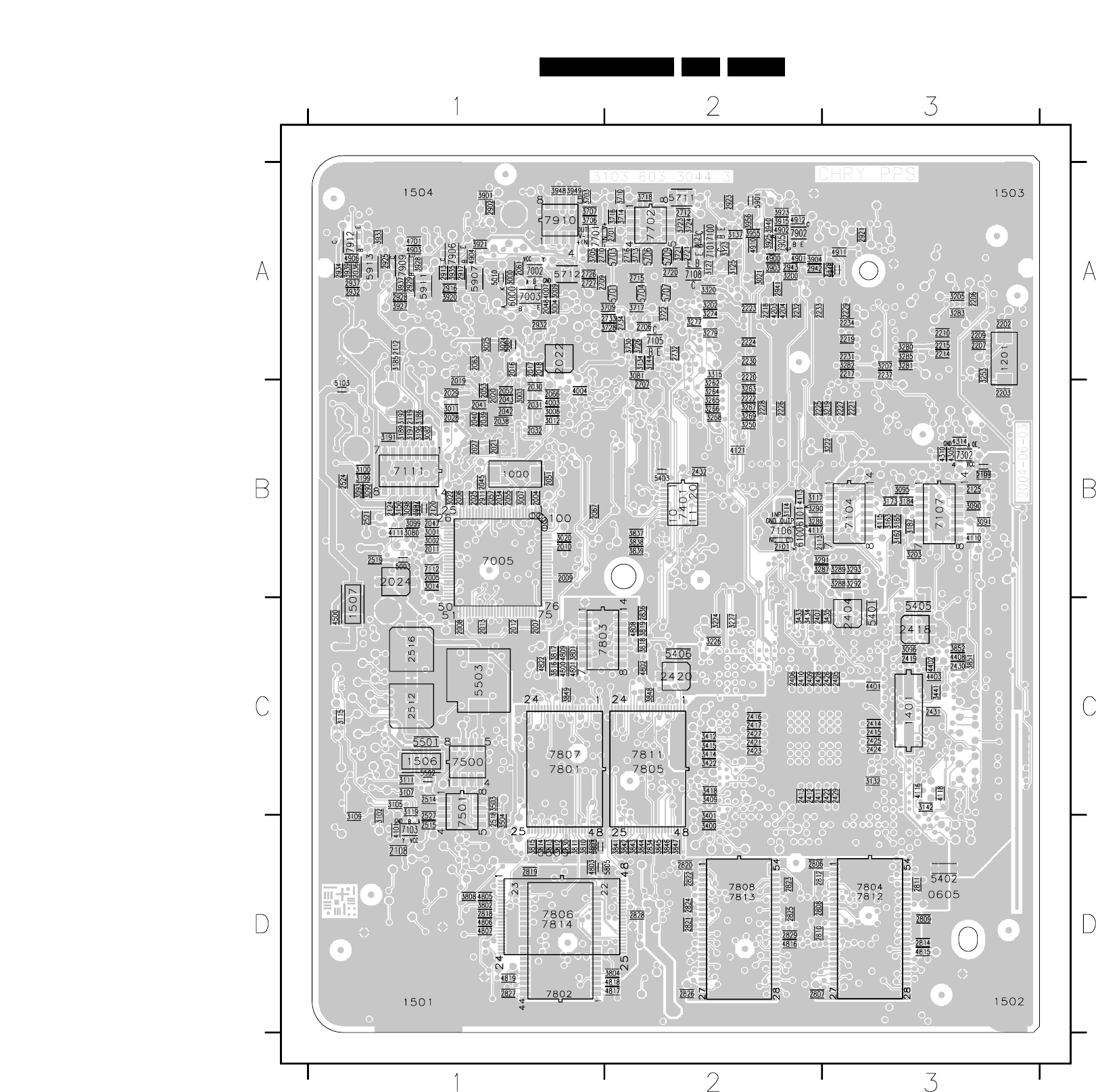
EN 1157.LX7500RCircuit Diagrams and PWB Layouts
1000 B1
1201 A3
1401 C3
1506 C1
1507 C1
2004 B1
2005 B1
2006 B1
2007 C1
2008 C1
2009 B1
2010 B1
2011 B1
2012 C1
2013 C1
2016 A1
2017 A1
2018 A1
2019 B1
2020 B1
2021 B1
2022 A1
2024 B1
2025 B1
2027 B1
2028 B1
2029 B1
2030 B1
2031 B1
2032 B1
2034 B1
2036 A1
2038 B1
2039 B1
2040 B1
2041 B1
2042 B1
2043 B1
2045 B1
2047 B1
2048 A1
2051 B1
2052 B1
2053 B1
2055 B1
2057 B1
2061 A1
2063 A1
2066 B1
2067 B1
2101 B2
2103 B3
2108 D1
2112 A1
2113 B2
2119 B1
2120 B1
2124 B1
2125 B3
2202 A3
2203 B3
2206 A3
2207 A3
2209 A3
2210 A3
2214 A3
2215 A3
2217 A3
2218 A2
2219 A3
2220 A2
2221 B3
2222 B2
2223 A2
2224 A2
2225 B2
2226 B2
2227 B3
2228 B2
2229 A3
2230 A2
2231 A3
2232 A2
2233 A2
2234 A3
2237 A3
2404 C3
2405 C3
2406 C2
2407 C2
2409 C2
2410 C2
2411 C2
2412 C2
2413 C2
2414 C3
2415 C3
2416 C2
2417 C2
2418 C3
2419 C3
2420 C2
2421 C2
2422 C3
2423 C2
2424 C3
2425 C3
2426 C3
2427 C2
2428 C2
2429 C3
2430 C3
2431 C3
2432 B2
2512 C1
2514 C1
2515 D1
2516 C1
2518 D1
2519 B1
2521 B1
2524 B1
2527 D1
2701 A2
2706 A2
2707 B2
2709 A1
2710 A1
2712 A2
2715 A2
2716 A2
2720 A2
2721 A2
2726 A1
2727 A1
2732 A2
2733 A2
2734 A2
2806 D2
2807 D2
2808 D2
2809 D3
2810 D2
2811 D3
2812 D2
2814 D3
2818 D1
2819 D1
2820 D2
2821 D2
2822 D2
2823 D2
2824 D2
2825 D2
2826 D2
2827 D1
2828 D2
2829 D2
2830 D1
2834 D2
2836 C2
2902 A1
2911 B1
2913 A1
2916 A1
2917 A1
2921 A3
2923 A2
2925 A1
2928 A1
2929 A1
2932 A1
2934 A1
2937 A1
2941 A2
2942 A2
2943 A2
3000 A1
3001 B1
3002 B1
3003 B1
3004 A1
3006 B1
3007 B1
3009 A1
3011 B1
3012 B1
3014 B1
3020 B1
3021 A2
3022 B1
3024 A1
3025 A1
3080 B1
3081 A2
3082 B1
3090 B3
3091 B3
3092 B1
3093 B1
3095 B3
3096 C3
3097 B1
3098 B1
3099 B1
3100 B1
3102 D1
3105 C1
3107 C1
3109 D1
3111 C1
3114 B2
3115 C1
3117 B2
3119 C1
3121 A2
3123 A2
3125 A2
3127 A2
3129 A3
3132 C3
3134 A2
3137 A2
3142 C3
3144 A2
3150 B1
3162 B3
3163 B3
3165 B3
3173 B3
3184 B3
3185 A1
3186 B1
3187 B3
3189 B1
3191 B1
3192 B1
3195 B1
3197 B1
3199 B1
3200 A2
3202 A2
3203 B3
3205 A3
3207 A3
3219 B3
3222 B3
3224 C2
3226 C2
3227 C2
3250 B2
3253 A3
3262 B2
3263 B2
3264 B2
3265 B2
3266 B2
3267 B2
3268 B2
3269 B2
3274 A2
3277 A2
3279 A2
3280 A3
3281 A3
3282 A3
3283 A3
3285 A3
3286 B2
3287 B2
3288 B3
3289 B3
3290 B2
3291 B2
3292 B3
3293 B3
3315 A2
3320 A2
3400 D2
3401 D2
3409 C2
3412 C2
3414 C2
3415 C2
3418 C2
3422 C2
3433 C2
3434 C2
3435 C3
3441 C3
3503 C1
3504 D1
3703 A1
3705 A1
3706 A1
3707 A1
3709 A2
3710 A2
3713 A2
3714 A2
3716 A2
3717 A2
3718 A2
3721 A2
3722 A2
3723 A2
3724 A2
3726 A2
3728 A2
3730 A2
3801 C1
3802 D1
3804 D2
3808 D1
3809 D1
3810 D1
3811 D1
3812 D1
3813 D1
3814 D1
3815 D1
3816 C1
3817 C1
3818 C2
3819 C2
3837 B2
3838 B2
3839 B2
3841 D2
3842 D2
3843 D2
3844 D2
3845 D2
3846 D2
3847 D2
3848 C2
3849 C1
3851 C3
3852 C3
3901 A1
3903 A2
3904 A2
3915 A2
3920 A1
3921 A1
3923 A2
3925 A2
3927 A1
3928 A1
3932 A1
3933 A1
3935 A1
3937 A1
3939 A1
3940 A2
3948 A1
3949 A1
3955 A2
3956 A2
4003 B1
4004 B1
4007 A1
4101 D1
4110 B3
4111 B1
4113 B2
4115 B3
4116 C3
4117 B2
4118 C3
4121 B2
4203 A2
4204 A2
4305 B3
4310 B3
4314 B3
4401 C3
4402 C3
4403 C3
4408 C3
4500 C1
4701 A1
4800 C1
4801 C1
4802 C2
4803 D1
4805 D1
4806 D1
4807 D1
4808 C2
4809 C1
4815 D3
4816 D2
4817 D2
4818 D2
4819 D1
4822 C1
4900 A2
4901 A2
4902 A2
4903 A1
4904 A1
4906 A1
4910 A2
4911 A3
4912 A2
5001 A1
5003 B1
5010 A1
5100 B3
5103 B1
5104 B1
5401 C3
5402 D3
5403 B2
5405 C3
5406 C2
5501 C1
5502 C1
5503 C1
5701 A2
5703 A2
5704 A2
5706 A2
5707 A2
5709 A2
5711 A2
5712 A1
5803 D1
5805 D2
5901 A2
5907 A1
5911 A1
5913 A1
5916 A3
6000 A1
6100 B2
6101 B2
7002 A1
7003 A1
7005 B1
7100 A2
7101 A2
7103 D1
7104 B3
7105 A2
7106 B2
7107 B3
7108 A2
7111 B1
7112 B1
7302 B3
7401 B2
7500 C1
7501 C1
7701 A1
7702 A2
7801 C1
7802 D1
7803 C1
7804 D3
7805 C2
7806 D1
7807 C1
7808 D2
7811 C2
7812 D3
7813 D2
7814 D1
7902 A2
7905 A2
7906 A1
7909 A1
7910 A1
7912 A1
DIGITAL BOARD Chrysalis PPS E4 AV3 plus / bottom view
Digi board Chrysalis LX7500R, 191004
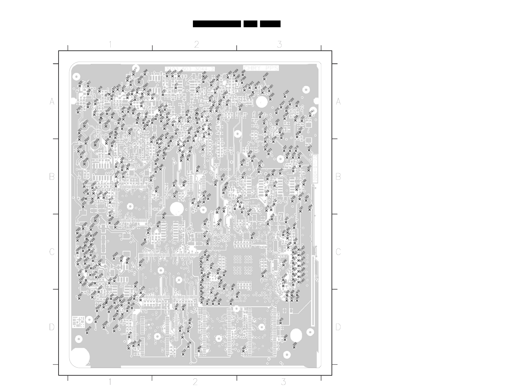
EN 1167.LX7500RCircuit Diagrams and PWB Layouts
F0001 C1
F0003 C1
F0005 C1
F0007 D1
F0009 D1
F001 A1
F0011 D1
F0015 D1
F002 B1
F003 B2
F004 B2
F005 B2
F006 B2
F007 B2
F008 B1
F009 B2
F010 B1
F011 C1
F012 B1
F013 B2
F014 A2
F015 B2
F016 B1
F017 B2
F018 B2
F019 B1
F0201 C1
F0202 A1
F0203 C1
F0204 C1
F0205 C1
F0206 C1
F0207 C1
F0208 C1
F0209 C1
F0210 C1
F0211 C1
F0212 C1
F0213 C1
F0214 C1
F0215 C1
F0216 C1
F0217 C1
F0218 D1
F0221 D1
F0223 D1
F0225 D1
F0227 D1
F0229 D1
F0231 D1
F0233 D1
F0234 D1
F0235 D1
F0236 D1
F0237 D1
F0238 D1
F0239 D1
F0301 A1
F0302 A1
F0303 A1
F0304 B1
F0305 C1
F0306 B1
F0307 B1
F0401 A2
F0402 A2
F0403 A2
F0404 A2
F0405 B1
F0406 C3
F0407 C3
F0408 A2
F0409 C3
F0410 B3
F0501 A1
F0503 C1
F0506 C1
F0508 C1
F0509 C1
F0510 C1
F0511 C1
F0512 C1
F0514 C1
F0601 B1
F0603 B1
F1201 A3
F1202 A3
F1203 B1
F1204 A3
F1205 A3
F1401 C3
F1402 C3
F1403 C3
F1405 C3
F1407 C3
F1409 C3
F1411 B3
F1413 C3
F1415 C3
F1417 C3
F1419 C3
F1421 C3
F1423 C3
F1425 C3
F1427 C3
F1501 B1
F1502 B1
F1505 A3
F1506 B1
F1509 C1
F1510 B1
F1512 A1
F1701 D1
F1702 A2
F1704 A2
F1706 A2
F1902 A2
F1903 A2
F1904 A2
F1907 A2
F1909 A3
F1911 A3
F1912 A3
F1914 A3
F1916 A3
F1918 A3
F1920 A3
F1921 A3
F1922 D1
F200 B3
F201 A3
F203 A3
F204 B3
F205 C2
F206 B3
F207 B2
F208 B2
F209 B2
F210 B3
F211 B3
F212 B3
F213 B3
F214 C2
F215 C2
F216 B3
F217 B3
F400 D2
F401 D2
F402 C2
F403 C3
F404 C3
F405 C3
F406 C3
F500 C1
F501 C1
F502 C1
F936 B3
I001 A1
I002 A1
I003 B2
I004 A1
I005 A1
I006 B1
I007 B1
I008 B1
I009 A1
I010 A1
I011 A1
I012 A2
I013 B2
I014 B1
I015 C1
I100 B2
I102 C3
I103 D2
I104 D2
I105 D1
I106 C2
I108 B3
I109 A2
I110 B3
I111 A2
I112 B3
I114 B3
I115 D2
I116 D1
I117 B1
I119 B3
I120 B3
I121 B3
I122 B3
I123 B3
I124 B3
I200 B2
I201 A3
I202 A3
I203 A3
I204 A2
I205 D3
I206 B2
I207 A3
I208 A3
I209 A3
I210 A3
I211 A3
I212 B3
I213 B3
I214 A3
I215 A3
I216 B3
I217 A3
I218 B3
I219 B3
I220 A2
I221 A2
I222 A3
I223 A2
I224 A2
I225 B3
I226 B3
I227 B3
I300 B3
I301 B3
I302 B3
I303 C3
I304 B3
I305 B3
I306 B3
I400 C3
I401 C3
I402 B2
I403 C3
I404 D3
I405 D2
I406 C2
I407 D3
I408 D3
I409 D3
I410 D3
I411 D3
I412 D3
I413 D2
I414 C3
I415 D3
I416 C3
I417 C2
I418 D2
I419 D2
I420 D2
I421 C2
I422 D2
I423 C2
I424 C2
I425 C2
I426 C2
I427 C2
I428 C2
I429 C2
I430 C2
I431 C2
I432 C2
I433 D2
I434 D1
I435 D1
I436 C2
I437 C2
I438 D2
I439 D2
I440 D3
I441 C3
I441 C4
I500 D1
I501 A1
I502 C1
I503 D1
I504 C1
I505 C1
I506 C1
I507 D1
I508 B1
I509 B1
I510 B3
I511 B1
I512 B1
I700 A2
I701 A2
I703 B2
I704 B2
I705 B2
I706 B2
I707 B2
I708 B2
I709 B2
I710 B2
I711 B2
I7119 A2
I712 B2
I713 A2
I714 A2
I715 A2
I716 A2
I717 A2
I718 A2
I720 A2
I721 A2
I722 A2
I723 A2
I724 A2
I725 A2
I726 A2
I727 A2
I728 A2
I729 A2
I730 B2
I731 B2
I732 B2
I733 B2
I734 B2
I735 B3
I736 B3
I737 B2
I738 A2
I739 B2
I740 B2
I742 A2
I743 A2
I743 A5
I744 A2
I744 A5
I745 A2
I745 A5
I746 A2
I746 A5
I800 D2
I801 D2
I802 D3
I803 D2
I804 D2
I805 C2
I806 D1
I900 A1
I901 A1
I902 A1
I903 A1
I904 A1
I905 A1
I906 A1
I907 A1
I908 A1
I909 A3
I910 A1
I911 A1
I912 A1
I913 A1
I914 A1
I915 A1
I916 A1
I917 A1
I918 A2
I919 A1
I920 A1
I921 B2
I922 A1
I923 A1
I924 A1
I925 A1
I926 A1
I927 A1
I928 A2
I929 B1
I930 A1
I931 B1
I932 A1
I933 B1
I934 A1
I935 A1
I936 A1
I937 A1
I938 A1
I939 A1
I940 B2
I940 B5
I943 A1
I943 A6
I944 A1
I944 A6
TR 19001_001
250504
DIGITAL BOARD / TESTPOINT OVERVIEW
Alignments EN 117LX7500R 8.
8. Alignments
8.1 Alignment Instructions Analog Board
Figure 8-1
TP ADJ. MODE INPUT
Frequency-
Counter
Disc
R3054
Pin 2 of
Con.1911
(FMRV)
3,800MHz
±10kHz
DISC MEAS.EQ.
MEAS.EQ.
MEAS.EQ.
MEAS.EQ.
SPEC.
TUNER
component
adjustment Specification
Measuring
equipment
measuring
equipment
Test equipment:
1. Dual-trace oscilloscope
Voltage range : 0.001 ~ 50 V/div
Frequency : DC ~ 50 MHz
Probe : 10:1, 1:1
2. DVM (Digital voltmeter)
3. Frequency counter
4. Sinus generator
Sinus : 0 ~ 50 MHz
5. Test pattern generator
How to read the adjustment procedures:
Front End (FV)
Service tasks after replacement of IC 7710, coil L5710 and L5711:
1 AFC Adjustment:
Purpose:
Storage in NVRAM via command mode interface of DSW:
Correct adjustment of demodulator AFC - circuit
After adjustment, the AFC reference value has to be stored in the NVRAM.
This reference value is 256 * measured voltage/Ucc. Ucc is 5.0V.
Store the reference value via command 732 , followed by the ref. value.
Example: DD:> 732 128
Symptom, if incorrectly set:
Bad or disturbed TV channel reception.
PAL - AFC adjustment [5711]:
2 HF - AGC adjustment [3724]:
Service tasks after replacement of IC 7710:
Purpose:
Set amplifier control.
Symptom, if incorrectly set:
Picture jitter if input level is too low and picture distortion
if input level is too high.
TP ADJ. MODE INPUT
DC Voltmeter
Frequ. Generator
TUNER 38,9MHz 500mVpp
at Tuner 1705, Pin 11
(F710, IF-out)
2,5V ±0,1V
DISC
DISC
DISC
SPEC.
L5711
IC 7710
Pin 17
(F708)
TP ADJ. MODE INPUT
5mV(74dBµV)
on aerial input
PAL white picture,
audio IF on,
no modulation
SPEC.
R3707
Oscilloscope
Video Pattern
Generator
500mVpp +/-0.5dB
(use a 10:1 probe )
Set tuned to
channel 25
503.25 MHz
Tuner
1705
Pin 11
(F710,
IF-out)
3 Attenuating the 40.4 MHz [5710]:
(SECAM only)
Service tasks after replacement of coil 5710:
Purpose:
To attenuate the band I carrier rests.
Symptom, if incorrectly set:
Bad picture quality when the filter attenuates the picture
carrier (38.9MHz).
If the adjustment is correct the signal at pin 1 of OFW [1701] must be
smaller than the input signal amplitude by at least 6 dB.
TP ADJ. MODE INPUT
L5710
Oscilloscope,
Sinus Generator,
Counter
adjust minimum
amplitude
TUNER
OFW
1701
Pin 1
(F709)
40.4 MHz, 200mVrms
at Tuner 1705, Pin 11
(F710, IF-out)
SPEC.

Alignments
EN 118 LX7500R8.
8.2 Reprogramming Procedure of NVM on the
Microprocessor Sub PCB
The NVM, item 7808, on the Microprocessor Sub board
contains the following factory settings:
1. Clock correction factor
2. AFC reference value
3. Slash version
The settings 1,2 and 3 are stored in the NVM during the
production of the analogue board.
The slash version is stored at the end of the production line of
the set.
In case of failure, the NVM must be replaced by an empty
device. By way of commands via the Diagnostic Software or via
ComPair, the factory settings must be restored in the NVM.
8.2.1 Clock Correction Adjustment
To guarantee an exact function of the real time clock, an
adjustment of the clock frequency is possibe. The adjustment
value is stored in the NVM.
Procedure:
• put the set in service command mode
• execute command 1117 to initiate that a signal with 32768
Hz is available on pin 3 of connector 1988
example:
DD:>1117
• measure the frequency fmeas of the Clock Crystal with an
accuracy of 0.1 Hz.
• Calculate the parameter to be entered: 32768/fmeas * 106
• Normally the parameter must be between 999902 and
1000097. If the parameter and therefore the frequency of
the crystal is outside this range, the crystal must be
replaced.
• Execute command 1118 with the parameter as input
example:
DD:>1118 1000023
8.2.2 AFC Reference Voltage Tuner
This function stores the reference voltage for the tuner in the
NVM. Before this value can be stored, the AFC adjustment,
described in the adjustment instructions of the analogue board,
must be carried out.
Procedure:
• Adjust AFC circuit
• Calculate the reference value
• Execute command 1119 and use the calculated reference
value as parameter example: DD:>1119 128
8.2.3 Slash Version
The slash version is stored with command 1217, followed by
the slash version as parameter.
The slash versions used in LX7500R are the following:
• LX7500R/01: 35
• LX7500R/05: 36
• LX7500R/04: 39
• LX7500R/69: 40
Example:
DD:>1217 35
Reset of Slash Version
Use command 1115 to reset the analogue board to the default
setting.
Procedure:
• Put the set in DSW command mode
• Execute command 1115 with the following parameters:
DD:> 1115 w 0xAE 2 0xD0 0x00
• Leave the DSW command mode and start up the set in
application mode
No background is visible on the TV screen. The analogue
board is ready to accept the appropriate slash version
8.3 Rework Procedure IEEE Unique Number
8.3.1 Scope:
The procedure describes how to upgrade sets with a unique
number after repair. This unique number is stored in the
NVRAM (item 7809) of the digital board at the end of the
production line.
This procedure is only valid or necessary when:
• The digital board is replaced
• NVRAM on the digital board is replaced
• NVRAM is cleared
In all other cases the repaired set retains its unique number.
The procedure defines several means to re-assure the unique
number depending on the possibilities of repair or the state the
faulty set is in.
8.3.2 Handling:
State of original (defective) board:
1. The digital board starts up in Diagnostics Mode: follow
procedure A to retrieve the valid unique number
2. The digital board does NOT start up in Diagnostics Mode:
follow procedure B.
8.3.3 Procedure A
1. Connect defective digital board to PC via serial cable (3122
785 90017)
2. start up hyper terminal or any other serial terminal via the
correct settings (DSW command mode interface)
3. read out existing unique number via nucleus 1208
example:
DD:> 1208
120800: DV Unique ID = 00D7A1FC6C Test OK @
4. note read out
5. program new digital board via nucleus 1207
example:
DD:> 1207 00D7A1FC6C 120700: Test OK @
The set has now the original unique number
8.3.4 Procedure B
1. Note the serial number of the set example:
VN050136130156
– VN = production centre (VN....Szekesfehervar).
According to UAW-500: V=22 and N=14

Alignments EN 119LX7500R 8.
– 05 = change code (this is not used for this calculation)
– 01 = YEAR
– 36 = Production WEEK
– 130156 = Lot and SERIAL number
2. Calculate the unique number: this number always exists
out of 10 hexadecimal numbers.
3. First 5 numbers: First we calculate a decimal number
according to the formula below:
35828*YEAR + 676* WEEK + 26*V + N+ 8788
The figures are fixed, YEAR + WEEK + factory code ( V+
N) are variable
Example: 35828*01+676*36+26*22+14+8788 = 69538
(decimal)
Then we translate the decimal number to a hexadecimal
number. example: 69538 (decimal)= 10FA2 (hex)
4. Last 5 numbers: The last 5 numbers exist out of the Lot and
SERIAL number according formula below:
serial nr + 1 * 100000
Example: 130156 + 100000 = 230156 (decimal)
230156 (decimal) = 3830C (hex)
5. Program new digital board via nucleus or 1207. Therefore
we use the 10 hexadecimal numbers we calculated above:
example:
>1207 10D7A3830C
12700: Test OK @
The set has now its original unique number
8.4 Alignments after replacing the Boot EEPROM
7810
The NVM, item 7810, on the Digitalt Board Chrysalis contains
the “Diversity String” that tells the software during startup which
hardware version is present.
The setting is stored in the NVM during the production of the
Digital Board Chrysalis
In case of a fault the NVM must be replaced by a programmed
device containing the boot script.
Via the Diagnostic Software the Diversity String is stored with
command 1226, followed by the Diversity String as parameter.
The diversity strings used in HDRW720/0x are the following:
ChrysalisString
Board
Type
CHRY F EF3_AV3 44424849179020014546335
F4156330034030300000101020001010040080800
Example:
DD:> 1226 44424849179020014546335F41
56330034030300000101020001010040080800
122600
Test OK @
With command 1228 the settings can be displayed.

Circuit-, IC descriptions and list of abbreviations
EN 120 LX7500R9.
9. Circuit-, IC descriptions and list of abbreviations
9.1 Display Board
9.1.1 Microcontroller
The core element of the Display Control unit is the
microcontroller TMP87CH74AF [7103]. The TMP87CH74AF is
an 8 bit microcontroller fitted with 32kB ROM and 1kB RAM. It
requires 5V supply and is responsible for the following
functions:
– Interface to Central Controller-P
– Evaluation of the keyboard matrix
– Decoding the remote control commands from the infra-red
receiver
– Activation and control of the local display
– Heater voltage generation
The 8 MHz resonator (Pos. 1110) generates the system clock.
The reset is generated by the CC-P via “POR_DC”-signal
where the transistor [7104] is used as a level-shifter from 3V3
to 5V.
9.1.2 Interface to the Central Control µP
The communication to the main microcontroller (CC) on the P-
Sub-PCB is done via Combi board microcontroller 7107, where
the TMP87CH74AF acts in slave-mode.
An additional wire (“INT”-line) to the I2C interface is used to
signal the Central controller that data are ready, e.g. when a
key has been pressed.
9.1.3 Evaluation of the keyboard matrix
There are 8 different keys on the display board. A resistor
network is used to generate a specific direct voltage value,
depending on the pressed key. Via the resistors 3107 and 3102
on the analog/digital (A/D) ports (7103 pin 36 and 37) the
evaluation is done.
9.1.4 IR receiver and signal evaluation
The IR receiver [7107] contains a selectively controlled
amplifier as well as a photo-diode. The photo-diode changes
the received infra red transmission (approx. 940nm) to
electrical pulses, which are then amplified and demodulated.
On the output of the IR receiver [7107], a pulse sequence with
TTL-level, which corresponds to the envelope curve of the
received IR remote control command, can be measured. This
pulse sequence is fed into the controller for further processing
via port TC1 [7103, pin20].
9.1.5 Vacuum Fluorescence Display
The VFD “BJ900GNK” [POS 7100] is fully controlled by the
microcontroller. The µC also includes the driving stages. Only
two additional drivers [POS 7101 and 7102] are necessary for
the grids 8 and 9 because of their large size.
9.1.6 VFD Heater Voltage Generator
The circuit around POS [7106, 7108 and 7109] is used to
generate a proper AC-Voltage for the filament of the VFD. For
this the microcontroller generates an appropriate rectangular
signal with 50% duty-cycle and a frequency of 30 kHz at pin 19.
Pos. [5104] and [2113] are acting as a resonance-circuit. Via
Zener-Diode (POS[6100]) and resistors [3119, 3122 and 3123]
the two heater-pins of the VFD (“FIL1” and “FIL2”) are clamped
so that the grids and segments can be fully switched off.
9.1.7 REC-LED
The REC-LED-ring is made with 3 red LED, controlled via pin
3 (only for flashing) and pin 12 for on/off switching, of the
microcontroller. The POS [7105] is used as a driver for the led.
9.1.8 STANDBY-LED
The STANDBY led is a red led and controlled from the pin 14
from the microcontroller. The POS [7110] is used as a driver for
the led.
9.1.9 TRAY-LED
There are 6 leds (chip) necessary to illuminate the tray, these
6 leds are located on a little sub-pcb connected over a 4 pin
connector POS [1911] from the DC-print. The leds are
controlled from pin 11 of the microcontroller.
9.2 Microcontroller Sub Board (UP SUB Board)
9.2.1 General
This small PCB is directly soldered in on top of the Analogue-
Board.
It is used with no diversity in all three different basic versions
(Europe, NAFTA and APAC-Pal). Only the software being
loaded into the external Flash-memory is not the same.
9.2.2 Microcontroller
The main part of the Sub-PCB is the central controller (CC) µP
[7804] TMP91CW12AF, which is a 16-bit CPU with 128kBROM
and 4kB RAM.
It works with a 3V3 supply and a system clock of 24,576MHz
[1801].
The 3V3-supply is made out of the “5VSTBY” by the circuit
around [7816].
After connecting the set to the mains (power-up) the IC [7806]
generates a reset pulse. This signal (“IPOR”) is directly fed to
first priority interrupt input (pin 63) for power fail detection and
also to the Reset-Input of the CC (Pin30) via [7802], which is
necessary to generate a reset only during power-up. In case of
power fail pin 30 of the CC must be kept high (3V3).
The internal memory of the CC is too small for all necessary
demands. Therefore an external Flash-ROM [7805] with
1MByte in size and a RAM [7803] with 128kByte are
necessary. Both parts are connected to the µP via a parallel
address-/data-bus. The lower eight bus-lines (AD0 to AD7) are
multiplexed by [7801] and the “ALE”-signal of the CC.
For updating of the software the external Flash-ROM can be
reprogrammed by the µP. During this process [7807] is
switched on by the “WE”-signal.
When no mains is connected, the CC is supplied via Gold-Cap
[2816] during the power backup period. The diode [6802]
prevents unwanted current consumption of other components.
The internal ROM of the µP holds the program code for the
Real-Time-Clock. Only the microprocessor is supplied by the
backup cell, not the external memories and the µP operates in
a low frequency mode with the clock crystal [1805] only (32.768
kHz). To adjust the clock the frequency can be measured at pin
87 of the µP in a special test-mode.
9.2.3 Control-Interfaces
The CC is communicating with the digital board via a serial
connection, which operates at a speed of 19,4 kbit/s
(“D_DATA”-, “A_DATA”, “D_RDY”- and “A_RDY”-signal on

Circuit-, IC descriptions and list of abbreviations EN 121LX7500R 9.
[1986]). By generating a high level on pin 16 of the CC the
digital PCB can be reset (inverter [7817] in between).
Most of the other parts are controlled by the µP via I2C-bus
(“SDA”- and “SCL”-signal). The FETs [7821] and [7822] are
used for adaptation of the 3V3-level on CC-side to the
components supplied with 5V.
The CC can also reset the display-board-µP by pulling pin 39
to high.
The transistor [7819] acts as a level shifter for the “INT”-signal.
In the European sets a bi-directional interface is established
between the recording unit and the TV device at pin 10 of the
Scart (“P50”-line/Easy Link). The processing is done via pin 14
(output) and pin 38 (input) of the CC and the circuit around
[7813], [7814] and [7815].
9.2.4 EEPROM
The EEPROM M24C16 [7808] is an electrical erasable and
programmable, non-volatile memory. The EEPROM stores
data specific to the device, such as the AFC-reference value of
the Europe IF-part, the clock-correction-factor, etc. It is
accessed by the µP via the I2C-bus.
9.2.5 Sync Separator
To detect whether a video signal is available or not a separate
IC [7825] is used to extract the sync information out of the video
signal that is also routed to the digital board for recording.
While on the input a low-pass-filter ([2823] and [3869]) limits
the bandwidth an additional filter (circuit
around [7818]) on the output avoids distortions. Afterwards the
sync-signal is routed to pin11 of the CC.
9.3 Analog board Europe
9.3.1 General
This PCB consists out of the following parts:
– Frontend (Audio & Video)
– Input-/Output-switching
– Audio ADC- & DAC-processing
– VPS/PDC- and Text-Data slicer
– Analog Follow-Me Circuit
All functional groups are either controlled via I2C-bus or via
separate signal lines by the Central-Controller on the µP-Sub-
Board. This sub board is directly soldered in onto the analog
PCB. During Stand-By mode of the set, several parts are not
supplied (Tuner, MSP, ...). The microprocessor is running and
maintains the clock of the set.
To avoid bus blockades the I2C-bus (“SCLSW” & “SDASW”) to/
from these units is decoupled via transistors [7419], [7420]
from the general bus (“SCL” & “SDA”).
9.3.2 Frontend
This unit is designed to support two basic versions, which are
distinguished by a different assembly variant only (one for
multistandard and the second for Pal-I only) and comprises the
following parts:
• Tuner UV1316K [1705]
• IF amplifier & video demodulator IC TDA 9818/9817 [7710]
• Sound processor MSP3415G [7600]
Tuner and IF selection
The Tuner [1705] converts the RF-signal coming from the
antenna input to an IF-signal. The tuner is fully controlled via
I2C-bus of the CC-µP. [1705] is also equipped with a “passive-
loop-through” between antenna-in and -out to save power in
stand-by of the set, when the complete part is not supplied.
The IF frequency of the video carrier is 38.9 MHz for all
systems except SECAM L' (34,0 MHz).
A quasi-split audio system is used. Separate surface-wave
filters (SAW) are required. [1701], [1703] for video, [1702] for
audio. [1701] is switched into the signal path for DK/I-SECAM
L/L' reception, if the signal “SFS_TS” is “high”. In this case the
switches [7704], [7705] are open and the diode [6703] is
conducting. [1703] is switched into the signal path for BG
reception (“SFS_TS” is “low”). Then the switch [7712] is open
and the diode [6704] is conducting. For DK/I-SECAM L/L'
reception, an additional circuit for suppressing the audio carrier
of the adjacent channel is used. This circuitry is adjusted by coil
[5710] for maximum suppression at 40.4MHz.
IF demodulator
The signal from the tuner and IF-selection circuit is processed
by the demodulator IC TDA 9818/9817 [7710]. The signal
“PSS” to pin 3 switches between demodulation of positive
(SECAM only) or negative modulated video carriers. A QSS-
audio-IF signal SIF1 is generated for demodulation in the
sound processor [7600]. The audio-IF carrier is selected in the
audio SAW filter [1702]. This filter is switched for SECAM L’. If
the signal “SB1” is “high”, the switch [7714] is closed and the
diode [6705] is not conducting. For all other standards the
diode [6705] is conducting and the switch [7714] is open. The
output signal of this SAW filter is firstly processed in the TDA
9818. Audio carriers are converted from the tuner IF level to the
audio IF position and further processed in the audio
demodulator [7600]. The AFC coil [5711] on the TDA 9818/
9817 is adjusted so that when a frequency of 38.90 MHz is
supplied to the IF output of the tuner, the AFC voltage on pin
17 of [7710] is 2.5V. The setting of the picture carrier frequency
for SECAM L in the TDA 9818 is achieved by connecting pin 7
of the IC via a resistor [3710] to ground. The switch [7701] and
the signal “SB1" do this. The HF-AGC is set using the
potentiometer [3724] so that, with a sufficiently large antenna
input signal (74 dBµV), the voltage at the IF output of the tuner
[1705] pin 11 is 500 mVpp. This setting must be carried out
when the audio carrier is switched off. The demodulated video
signal appears on pin 16 of [7710]. The AGC voltage at pin 4 is
used to determine the antenna signal strength after a buffer
[7717] with the signal “AGC” and an analog input port of the
CC-P. The trap [1704] reduces the sound carrier remainders in
the video for BG standards. The trap [1706] works in the same
way for the Pal-I standard only. For all other standards the
switch [7713] is closed via [7706] and “SFS_TS”-line set “high"
to bypass this trap. In these cases the selectivity of the SAW
filter [1701] is sufficient. The coil [5713] for non-BG standards
realizes a frequency response correction. This correction is not
desired for SECAM L' and therefore short-circuited by [7716]
(signal SB1 is “high” and [7702] has on-status). The
demodulated video signal “VFV” is available after the buffer
and limiting stage for noise peaks [7711]. The FM-PLL
demodulator function of TDA 9818 is not necessary and
therefore deactivated by the resistor [3739].
Audio demodulator
The sound demodulation is done by the MSP3415 [7600],
which is also fully controlled via I2C-bus by the CC-P
(determination of bandwidth, amplitude, standard, ...).The
audio signals are available at pin 30 and pin 31 of [7600] and
fed as “AFER”- & “AFEL”-line to the audio-I/O for further
processing.
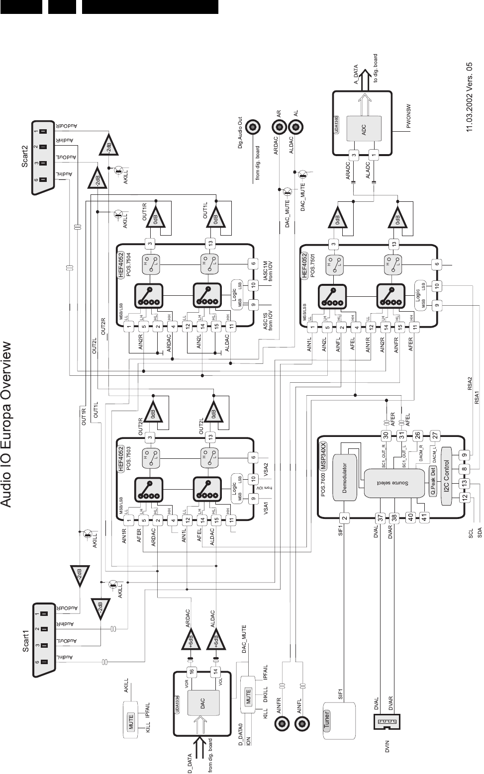
Circuit-, IC descriptions and list of abbreviations
EN 122 LX7500R9.
9.3.3 Audio routing
TR 01055_001
170502

Circuit-, IC descriptions and list of abbreviations EN 123LX7500R 9.
The processing of audio is always done in stereo (e.g. separate
left- and right-channel) and the complete switching is realized
by using HEF4052, which is a dual four-to-one multiplexer. In
principle there are three independent selectors:
a) Scart 1-Output-Path:
Pos [7504] is used to select either Scart 2-Input (“AIN2L”/
”AIN2R”) or the signal directly from the audio DAC [7004]
(“ALDAC”/”ARDAC”) as the output source for Scart 1
(“AOUT1L”/”AOUT1R”).
The control is done by means of the lines “ASC1S” coming from
[7408] (IC [7408] acts as a port expander for the CC-P) and
“IASC1M”, which is directly coming from the CC. Pos [7412] is
used for level adaptation (3V3 to 5V) for the “IASC1M”-signal.
b) Scart 2-Output-Path:
Pos [7503] selects between Scart 1-Input (“AIN1L”/”AIN1R”),
signals from the internal frontend (“AFEL”/”AFER”) via MSP
[7600] or audio directly from the DAC [7004] (“ALDAC”/
”ARDAC”). The outputs of this switch are routed to Scart 2
(“AOUT2L”/AOUT2R”). This switch is controlled via “VSA1”-
and “VSA2”-line. These lines come from [7408] that is acting as
a port expander for the CC-P.
c) Record-Path:
Pos [7501] selects either signals from Scart 1 (“AIN1L”/
”AIN1R”) or Scart 2 (“AIN2L”/”AIN2R”) or Cinch-Front (“AINFL”/
”AINFR”) or the MSP [7600] (“AFEL”/”AFER”) and routes to the
audio ADC [7007] (“ALADC”/”ARADC”) for record purposes.
The switch is controlled via “RSA1”- and “RSA2”-signals.
These signals come from the MSP [7600], which acts as a port
expander of the CC-P. As there can also exist a fifth input in
case of DV-In is present the corresponding analog audio
signals from the DVIO-board are firstly routed via extra cable
and connector [1960] to the MSP. The MSP acts as a
preselector between audio from internal frontend or the DV-
Input.
Each of these three selectors ([7501], [7503] & [7504]) has a
separate Op-Amp on the output for level-adaptation-,
performance- and line-driving-reasons. [7505-A & -B] for
record, [7502-C & -D] for Scart 1-Output and [7502-A & -B]
respectively for Scart 2. Every audio output line on the two
Scart connectors can be “killed” (muted) by an extra transistors
([7506], [7508], [7509] &[7511]), which can be activated by the
“AKILL”-line. This signal is generated by the circuit around
[7404]/[7421] and is a combination of the “KILL”- from the CC-
P and the “IPFAIL” of the power-supply-unit.
d) Line-Out-Path:
see chapter 9.3.5
e) Digital Audio Output-Path without IOE-Print:
Additionally to analog audio the set is also equipped with a
digital output via cinch plug [1951]. The signal is generated on
the dig. board and routed via audio interface cable and
connector [1900] to the Ana-PCB. Here the “DAOUT”-line first
passes a 6-fold inverter [7580] being used as a driver and for
performance reasons (noise reduction, jitter, etc.). Afterwards
a transformer [5580] is necessary to achieve the correct level
and also to have a floating output with isolated ground before
the signal is fed via [3580] to cinch plug [1951]. The capacitor
[2580] performs an AC-coupling between connector- and set-
ground.
f) Digital Audio Output-Path with IOE-Print:
In case of usage of the IOE-print the digital audio signals (input
and output) are directly routed from digital board via interface
cable to plug [1920] on the IOE-print. The “DAOUT”-line is
splitted into two signals, one for cinch out and one for optical
out. The signal to cinch out first passes a 5-fold inverter [7250]
being used as a driver and for performance reasons (noise
reduction, jitter, etc.). Afterwards a transformer [5250] is
necessary to achieve the correct level and also to have a
floating output with isolated ground before the signal is fed via
[3259] to the cinch plug [1925] (or [1926-B] in case of option
“DIGITAL IN”). The capacitors [2256] and [2266] perform an
AC-coupling between connector- and set-ground. The second
“DAOUT”-signal is fed directly via [3264] to the optical out
transmitter [6255].
g) Digital Audio Input-Path with IOE-Print:
There are two possibilities for a digital audio input signal in case
of option “DIGITAL IN”. One is the signal from the optical
receiver [6259], which is routed via [3269] directly to plug
[1920]. The second is the signal from the cinch plug [1926-A].
This signal then passes an inverting amplifier [7250-6] and is
then routed via [2253] to the plug [1920].
9.3.4 Audio ADC/DAC
a) PCBs with AD1852 [7004]:
The conversion of analog audio signals from the record-
selector [7501] in the I/O (“ALADC”- & “ARADC”) is done via
UDA1361TS [7007]. This IC can process input signals up to
2Vrms by using external resistors [3047], [3053] in series to the
input pins. As the level from the DVIO-Board is only 1Vrms a
6dB step can be performed by setting pin 7 of [7007] to 3,3V via
[7008] and the “PWONSW”-line controlled by the CC-P to use
the whole dynamic range of the ADC. All required clock signals
are generated on the dig. board and only the audio data
(“A_DAT”-line) are routed from Ana- to Dig.-PCB for further
processing.
The transformation of dig. audio back into the analog domain is
done by AD1852 [7004]. All necessary clock signals are
coming from the dig. board and dig. audio data (“D_DATA0”-
line) are converted into analog signals, which are available at
pin 17/16 and pin 12/13 of [7004] as symmetrical signals.
Afterwards an Op-Amp. [7003] (line driver & converting to
unsymmetrical signal, gain = 1), which is also working as low-
pass-filter to increase signal performance (noise,
distortions,...), is passed. Then both signals (“ALDAC” &
“ARDAC”) are directly routed to the rear cinch output and also
used in the audio-I/O for further processing. The DAC has also
a mute possibility, which can be activated by setting pin 23 to
5V via [7001]. This mute is controlled either by the dig. board
(“D_IKLL”-line) or the “IPFAIL”-signal from power-supply-unit
(in this case it’s the combination of “A_KILL” and “IPFAIL”).
If the DAC is muted externally via pin 23 or if there are no audio
data available (e.g. “D_DATA0”-line zero), the output pins 8
and 22 of the DAC change to high (+ 5V). These two signals
are then combined with diode pos. 6006. After decoupling via
[7009] the signal “DAC_MUTE” is used as mute signal for the
mute transistors [7415], [7416] for cinch rear out.
b) PCBs with UDA1334BTS [7001]:
The conversion of analog audio signals from the record-
selector [7501] in the I/O (“ALADC”- & “ARADC”) is done via
UDA1361TS [7005]. This IC can process input signals up to
2Vrms by using external resistors [3039], [3041] in series to the
input pins. As the level from the DVIO-Board is only 1Vrms a
6dB step can be performed by setting pin 7 of [7005] to 3,3V via
[7006] and the “PWONSW”-line controlled by the CC-P to use
the whole dynamic range of the ADC. All required clock signals
are generated on the dig. board and only the audio data
(“A_DAT”-line) are routed from Ana- to Dig.-PCB for further
processing.
The transformation of dig. audio back into the analog domain is
done by UDA1334BTS [7001]. All necessary clock signals are
coming from the dig. board and dig. audio data (“D_DATA0”-
line) are converted into analog signals, which are available at
pin 14 and pin 16 of [7001]. Afterwards an Op-Amp. [7002] (line
driver & level adaptation, gain = 2) which is also working as
low-pass-filter to increase signal performance (noise,
distortions,...), is passed. Then both signals (“ALDAC” &
“ARDAC”) are directly routed to the rear cinch output and also
used in the audio-I/O for further processing. The DAC has also
a mute possibility, which can be activated by setting pin 8 to
3,3V via [7003]. This mute is controlled either by the dig. board

Circuit-, IC descriptions and list of abbreviations
EN 124 LX7500R9.
(“D_IKLL”-line) or the “IPFAIL”-signal from power-supply-unit
(in this case it’s the combination of “A_KILL” and “IPFAIL”).
In addition to that the DAC [7001] and the cinch outputs can be
killed (muted) in case of “digital silence” by the circuit around
[7008], [7009] and [7010], when no audio data are available
(e.g. “D_DATA0”-line zero).
This function can be also activated via the “ION”-line (set to
high during any stand-by mode). To avoid signal distortions
(clipping) the mute transistors for cinch rear out [7415], [7416]
are decoupled via [7011].
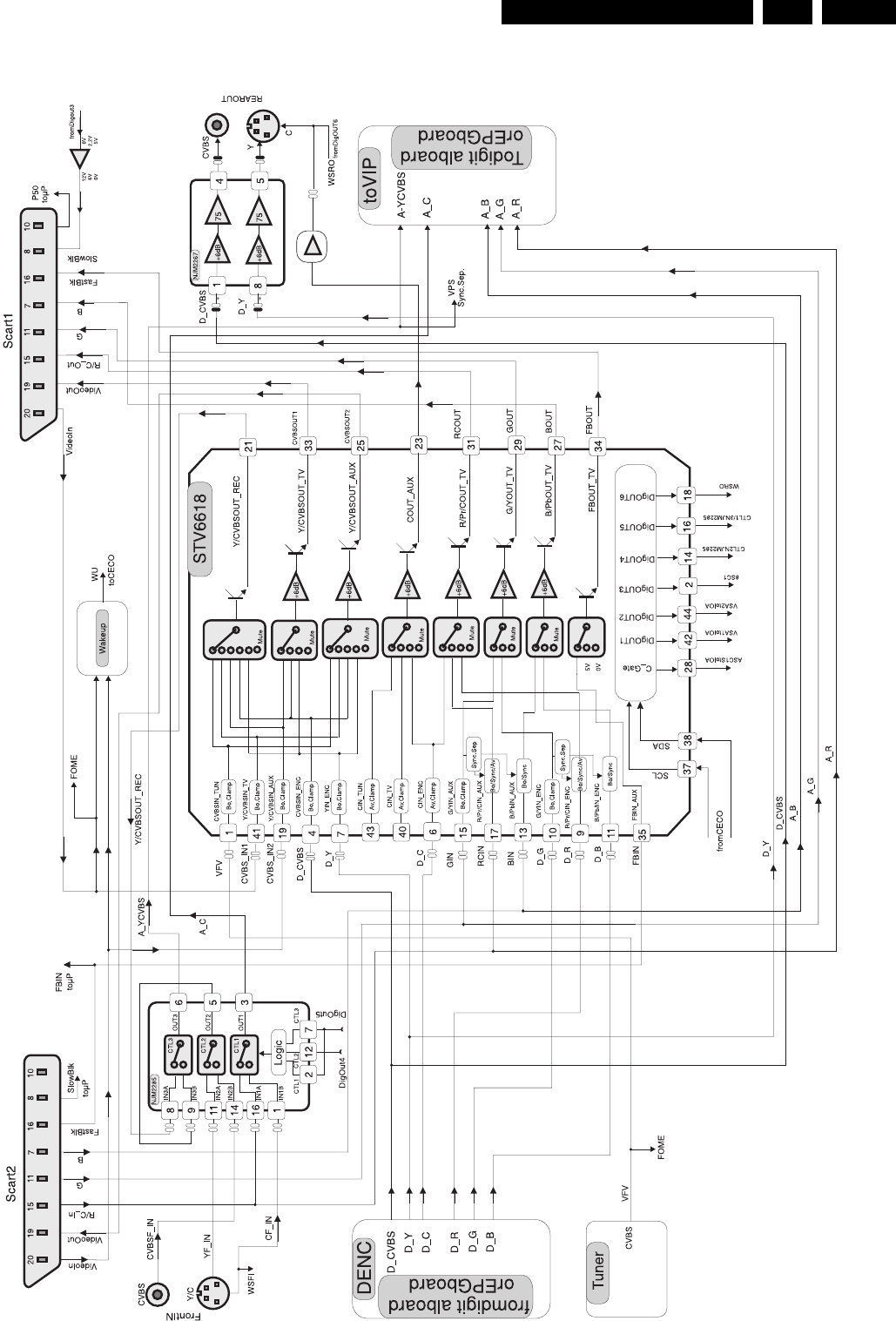
Circuit-, IC descriptions and list of abbreviations EN 125LX7500R 9.
9.3.5 Video-routing
Figure 9-1
Video IO Europe

Circuit-, IC descriptions and list of abbreviations
EN 126 LX7500R9.
The Video-I/O-switching is basically realized by the matrix
switch STV6618 [7408], which is controlled via I2C-bus by the
CC. All used outputs excluding pin 21 (Y/CVBS-REC) have a 6
dB-amplification and a 75 Ohms driver-stage inside. This IC
includes also several digital outputs, which are used for
switching purposes on the analog board. The record selector
inside the switch selects between the CVBS from frontend
(“VFV”), the input from Scart 1 (“YCVBSIN1”) or the signal from
Scart 2 (“YCVBSIN2”). Afterwards the signal passes another
switch [7411] in which a selection between signals from the
front or the preselected ones are done. The output signals of
[7411] are fed as “A_YCVBS”- and “A_C”-line to the digital
board for further processing.
To reduce the number of external presets there exists only one
preset for CVBS- and Y/C-front. The set automatically detects
between the two inputs depending on the presence of a video
signal (sync separator-circuit on µP-sub-board) where Y/C has
higher priority.
The R/G/B-inputs and the Fast-Blanking-line from Scart 2 are
routed over the optional EPG board to the digital PCB. Also all
other video signal from the analog board are routed through the
EPG board if present. These signals are also available on the
corresponding input-pins of the STV6618 to enable a loop-
through in AV-Standby. In this mode the set has to behave like
a cable between the two Scart-connectors. AV-Standby is
activated either by a “high” level on pin 8 of Scart 2 (“active
device is present”) or by the “WU”-line (wake up). This signal is
generated out of the circuit around [7401], [7402] & [7403] and
will become “high” if there is a signal on pin 20 of Scart 1- or
Scart 2. The detection of the input level on pin 8 of Scart 2
(“8SC2”) is done via an analog input of the CC-P (less than 2V
means inactive; 4,5V to 7V determines a source with 16:9
picture-ratio and greater than 9,5V is an active 4:3 source).
All signals from the digital board (“D_R”, “D_G”, “D_B”, D_C”,
“D_Y” and “D_CVBS” are routed to the proper inputs of the
STV6618 for amplification and driving purpose before they can
be seen on the appropriate Scart outputs. In case of EPG the
signals from the digital board are routed through the EPG
board where the selection between digital board video or EPG
OSD is taken.
The “D_CVBS”- and the “D_Y”-line are passing a 6 dB-
amplifier and driver-IC [7410] and are then routed to the CVBS-
Cinch and Y/C-out rear. The chroma signal for this Y/C out is
coming from the STV6618 - which makes the 6 dB-
amplification - and a driver [7406] in between.
The detection of the picture ratio information on the Y/C-input
front is made by measuring the DC-level on the Chroma signal
via analog input of the CC-P (“WSFI”-line). In case the level is
higher than 3,5V the input signal is a 16:9 source. If the level is
lower than 2,4V the picture ratio is 4:3.
For generation of the appropriate DC-voltage on the Y/C-out
rear the “WSRO”-line is controlled via pin 18 of [7408] by the
CC-P (Pin 18 set to low means 4:3, pin 18 set to high
determines 16:9).
The control of the switching voltage (Pin 8 of Scart 1) is done
via 3-level-pin (nr.2) of the STV6618 [7408] and the transistors
[7405], [7407] & [7409]. A “low” on pin 2 of [7408] causes
around 11V on pin 8-Scart 1 (e.g. source with 4:3 picture-ratio
active). Medium level (2,5V) on pin 2 of the STV6618
generates medium level (approx. 6V) on pin 8-Scart 1 (e.g.
active source with 16:9) and a “high” on pin 2 of the STV6618
pushes pin 8-Scart 1 to “low” (e.g. inactive).
9.3.6 VPS/PDC- and Text-Dataslicer
For extraction of relevant information out of the video signal
(time controlled recording, net-name-identification, time- &
date- download) the STV5348 [7931] is used. Data transfer to/
from the CC is fully done via I2C-bus and the input signal for
decoding is the same as the one being routed to the digital
board for recording purposes (“A_YCVBS”-line).
9.3.7 Analog Follow-Me
This circuit compares the video signal from the internal
frontend (“VFV”) of the recorder with that one of the connected
TV-set (“CVBS1”). The TV set delivers the signal via Scart-
cable. A comparator [7934] and several additional parts
([7932], [7933], ...) are used to compare the two video signals.
In case of both input signals are equal the output-line of this
circuit (“FOME”) is set to low. Detection is made via an input
port of the CC-P.
9.4 Analog board NAFTA- & APAC-Pal- version
9.4.1 Frontend NAFTA
[1701] demodulates the video signal from the antenna input.
Tuner and IF-demodulator are in one unit. Also a modulator is
included in that part. The audio- and video-signal to the
modulator are the ones from the selected input or the playback
path of the set (“AMCO”- and “D_CVBS”-line). The control of
the tuner is fully done via I2C-bus by the CC-P. Via the “MSW”-
signal and [7701] the modulator is switched on and off. In
opposite to this the antenna loop-through is opened or closed.
In the APAC-Pal version POS [1700] is used with the difference
that it demodulates only PAL- instead of NTSC-signals and has
also no modulator. The “CSW_SSW” line switches the
modulator between CH3 or CH4 in the NTSC-version.
To achieve optimal tuning the “AFC”-signal is detected by the
CC via an analog input; [3701], [3702] and [3703] are used for
level adaptation (5V to 3V3). Pos [7700] is a driver for the video
signal.
The sound demodulation is realized by the MSP34x5 [7600],
which is also fully controlled via I2C-bus by the CC-P
(determination of bandwidth, amplitude, standard, ...). The
audio signals are available at pin 30 and pin 31 of [7600] and
fed as “AFER”- & “AFEL”-line to the audio-I/O for further
processing. As this PCB is used for different regions (NAFTA
and APAC) either MSP3425 or MSP3415 are assembled.
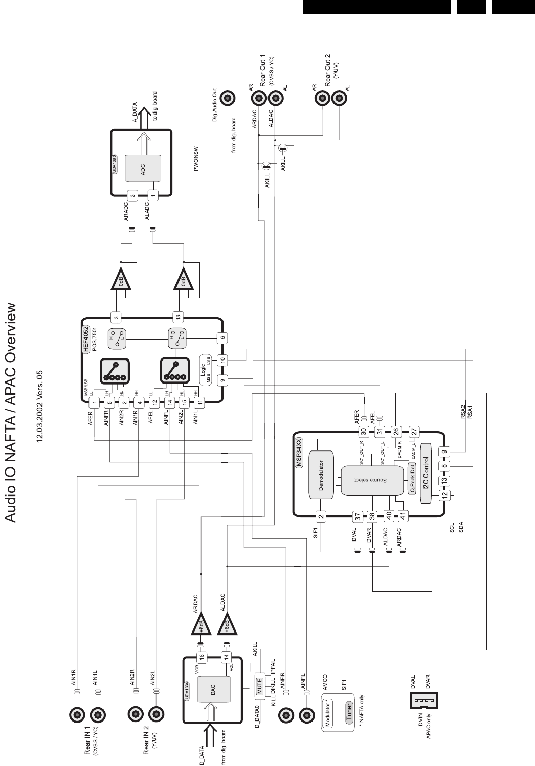
Circuit-, IC descriptions and list of abbreviations EN 127LX7500R 9.
9.4.2 Audio routing
Figure 9-2
TR 01057_001
170502

Circuit-, IC descriptions and list of abbreviations
EN 128 LX7500R9.
The sound processing is always done in stereo (that means
separate left- and right-channel).
a) Record-Path:
The complete selection of the audio signal for recording is done
by a HEF4052 [7501], which is a dual four-to-one multiplexer.
The input lines for the selector [7501] are coming either from
MSP [7600] (“AFEL”/”AFER”) or cinch rear in 1 (“AIN1L”/
”AIN1R”) or cinch rear in 2 (“AIN2L”/”AIN2R”) or the cinch in
front (“AINFL”/AINFR”). The [7501] is controlled via “RSA1”-
and “RSA2”-signals coming from the MSP [7600]. The MSP
acts as a port expander of the CC-P. The Op-Amp on the
output [7504] is necessary for performance reasons and acts
also as a driver. The selected signals “ARADC” and “ALADC”
are directly fed to the Audio-ADC.
As there can exist also a fifth input in case of DV-In is present
the corresponding analog audio signals from the DVIO-board
are firstly routed via extra cable and connector [1960] to the
MSP, which acts as a preselector between audio from internal
frontend or the DV-Input.
b) Line-Out-Path:
see chapter 9.4.3
c) Digital Audio Output-Path without IOE-Print:
Additionally to analog audio the set is also equipped with a
digital output via cinch plug [1951]. The signal is generated on
the dig. board and routed via audio interface cable and
connector [1900] to the Ana-PCB. Here the “DAOUT”-line first
passes a 6-fold inverter [7580] being used as a driver and for
performance reasons (noise reduction, jitter, etc.). Afterwards
a transformer [5580] is necessary to achieve the correct level
and also to have a floating output with isolated ground before
the signal is fed via [3580] to cinch plug [1951]. The capacitors
[2580], [2582] and [2583] perform an AC-coupling between
connector- and set-ground.
d) Digital Audio Output-Path with IOE-Print:
see chapter 9.3.4.f
e) Digital Audio Input-Path with IOE-Print:
see chapter 9.3.4.g
9.4.3 Audio ADC/DAC
The conversion of analog audio signals from the record-
selector [7501] in the I/O (“ALADC”- & “ARADC”) is done via
UDA1361TS [7005]. This IC can process input signals up to
2Vrms by using an external resistor [3039], [3041] in series to
the input pins. As the level from the DVIO-Board is only 1Vrms
a 6dB step can be performed by setting pin 7 of [7005] to 3,3V
via [7006] and “PWONSW”-line controlled by the CC-P to use
the whole dynamic range of the ADC. All required clock signals
are generated on the dig. board and only the audio data
(“A_DAT”-line) are routed from Ana- to Dig.-PCB for further
processing.
The transformation of dig. audio back to the analog domain is
done by UDA1334BTS [7001]. All necessary clock signals are
coming from the dig. board and dig. audio data (“D_DATA0”-
line) are converted into analog signals, which are available at
pin 14 and pin 16 of [7001]. Afterwards an Op-Amp. [7002] (line
driver & level adaptation) which also works as a low-pass-filter
to increase signal performance (noise, distortions,...) is
passed. Then both signals (“ALDAC” & “ARDAC”) are directly
routed to the rear cinch output. The DAC has also a mute
possibility, which can be activated by setting pin 8 to 3,3V via
[7003]. This mute is controlled either by the dig. board
(“D_IKLL”-line) or the “IPFAIL”-signal from power-supply-unit.
In addition to that the DAC [7001] and the cinch outputs can be
killed (muted) in case of “digital silence” by the circuit around
[7008], [7009] and [7010], when no audio data are available
(e.g. “D_DATA0”-line zero).
The signals from the audio DAC part (“ARDAC”/”ALDAC”) are
directly routed to both cinch rear outputs, which are connected
in parallel. To avoid plops and any other audible noise on the
output there is a mute-stage implemented [7509], [7511] for
each channel. The activation is done via “AKILL”-line, which is
a combination of the “KILL” from CC-P, “DAC_MUTE” from
DAC-part and “IPFAIL” from the power-supply-unit. The circuit
around [6430], [6431], [7430] and [7404] generates this signal.
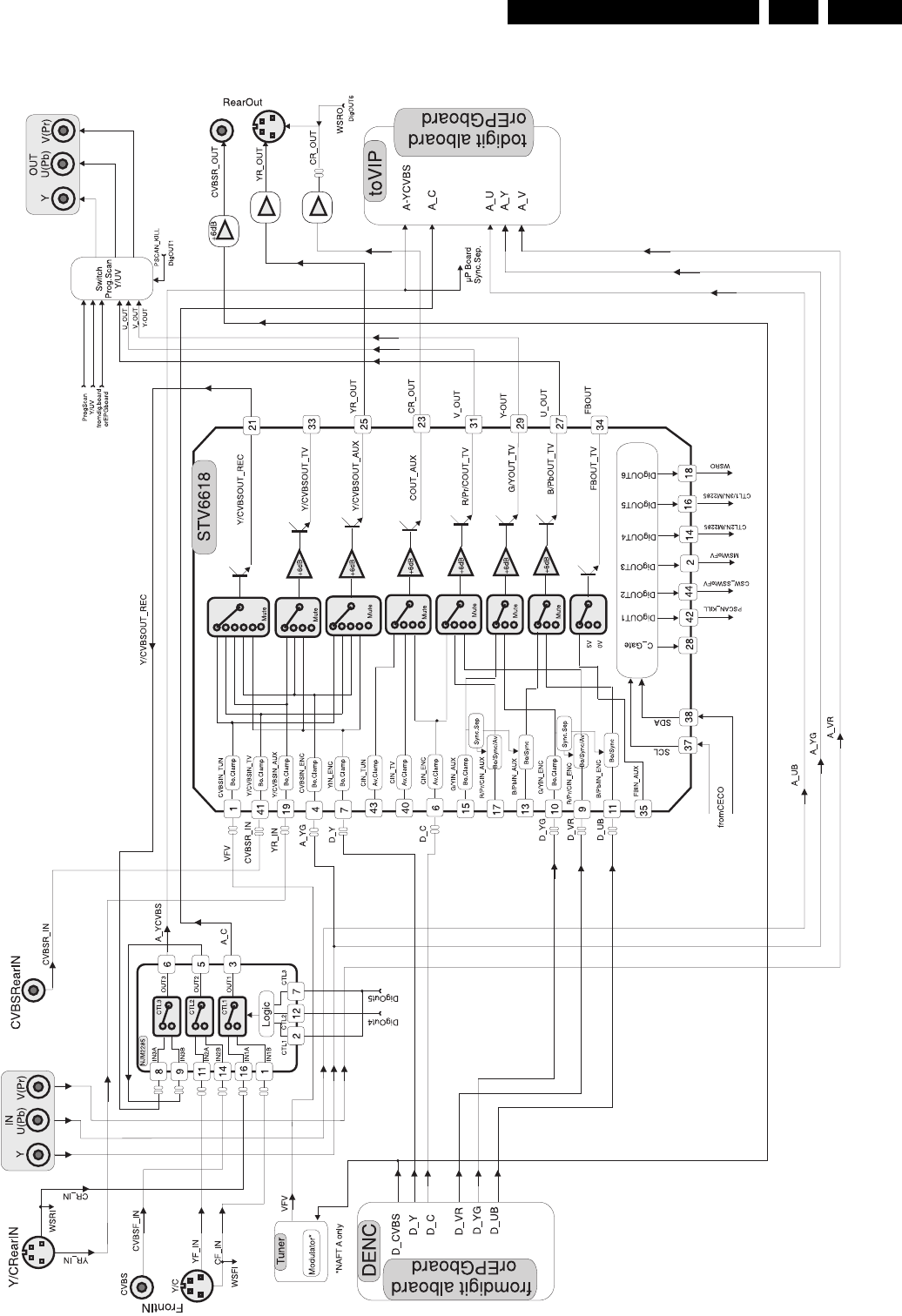
Circuit-, IC descriptions and list of abbreviations EN 129LX7500R 9.
9.4.4 Video-routing
Figure 9-3
Video IO Nafta
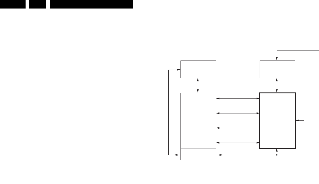
Circuit-, IC descriptions and list of abbreviations
EN 130 LX7500R9.
The Video-I/O-switching is basically realized by the matrix
switch STV6618 [7408], which is controlled via I2C-bus by the
CC. All used outputs excluding pin 21 (Y/CVBS-REC) have a
6dB-amplification and a 75 Ohms-driver-stage inside. This IC
also includes several digital outputs, which are used for
switching purposes on the analog board. The record selector
inside the switch selects between the CVBS from frontend, the
CVBS from Cinch-Rear or Y from the S-Video-input rear.
Afterwards the signal passes another switch [7411] in which a
selection between signals from the front or the preselected
ones is done. The output signals of [7411] are fed as
“A_YCVBS”- and “A_C”-line to the digital board for further
processing.
To reduce the number of external presets there is only one
station for CVBS or Y/C (front and rear). The set automatically
detects between the two inputs depending on the presence of
a video signal (sync separator-circuit on µP-sub-board) where
Y/C has higher priority.
The Y/U/V-inputs are routed over the optional EPG board to the
digital PCB. Only the Y-line has to be present additionally on
pin 4 of [7408] for video recognition. Also all other video signal
from the analog board are routed through the EPG board if
present.
The signals “D_C” and “D_Y” are fed through [7408] (6dB
amplification) and via [7406], [7409] used as driver to the S-
Video output connector. The “D_CVBS” line is directly routed to
the modulator and via the circuit around [7431] and [7432]
amplified by 6dB before it is fed to the CVBS output plug. In
case of EPG the signals from the digital board are routet
through the EPG board where the selection between digital
board video or EPG OSD is taken.
The Y/U/V signals from the digital board are also passing
[7408] for 6dB amplification and driving purpose.
To achieve optimal picture quality the set is equipped with a
simple progressive scan function based on a so-called line
doubler. The complete generation of the signal is done on the
digital board and via a separate cable and connector [1946] the
corresponding Y/U/V lines are routed to the analog PCB. Also
the YUVprogressive signals are switchable to EPG OSD on the
EPG board if implemented. As there is only one Y/U/V output
available a switching between interlaced and progressive
output is necessary. While the transistors [7421], [7422],
[7424], [7425], [7427] and [7428] are used as driver for Y/U/V
progressive, [7423], [7426] and [7429] together with [7405] are
necessary for killing these signals via pin 42 of [7408] in case
the interlaced is selected (“PSCAN_KILL”-line set to low). If
progressive output is active the pins 27, 29 and 31 of [7408] are
set to high impedance and “PSCAN_KILL” is also high (e.g.
5V).
The detection of the picture ratio information on the Y/C inputs
(rear or front) is done by measuring the DC-level on the
Chroma signal via an analog input of the CC-P (“WSRI”- and
“WSFI”-line). In case the level is higher than 3,5V the input
signal is a 16:9 source, if the level is lower than 2,4V the picture
ratio is 4:3.
For generation of the appropriate DC-voltage on the Y/C output
the “WSRO”-line is controlled via pin18 of [7408] by the CC-P
(Pin 18 set to low means 4:3, pin 18 set to high determines
16:9).
During Stand-By there is also no loop-through of any input to
any output performed.
9.5 Digital Board Chrysalis F
9.5.1 Introduction
Block diagram 2nd generation DVD recorder
Figure 9-4
This 2nd generation Digital Board is based on the highly
integrated 'Chrysalis' IC. Its predecessors, the 'Empire' and
'Empress' based boards, had two PWBs mounted on top of
each other (due to separate DVIO board). For this new
generation, all functionality is now available on one PWB in one
BGA IC (Ball Grid Array) i.s.o. four VLSI ICs.
The board encodes and multiplexes analogue video and digital
uncompressed audio (I2S) into an MPEG2 stream. This
MPEG2 stream is formatted, to be recorded by the DVD+RW
engine. In playback, the board will decode the MPEG2 stream
into analogue and digital audio and into analogue video. In
addition, a DV stream can be received via IEEE1394 (i-Link),
and transformed to MPEG2 format.
There are versions foreseen, to generate a progressive scan
analogue video output. In the standard Chrysalis board, the
progressive video output is generated by the PNX7100. In the
Chrysalis 'F' it is generated by the Faroudja FLi2301.
The Chrysalis Digital board is pin compatible with the Empress
digital board in terms of A/V IO, BE interface, Power Supply,
and Service interface. For functional enhancements, several
connectors are added:IDE connector (HDD, AV3, PCMCIA,
etc.).
ANALOG BOARD
CONTROL
VIDEO IN/OUT
DISPLAY &
CONTROL BOARD BASIC ENGINE
POWER SUPPLY
DIGITAL BOARD DV IN
AUDIO IN/OUT
2FH VIDEO OUTPUT
CONTROL
CL 36532004_001.eps
140203
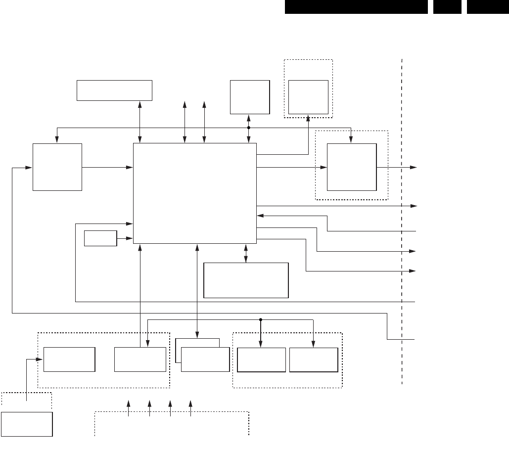
Circuit-, IC descriptions and list of abbreviations EN 131LX7500R 9.
9.5.2 Record Mode
Block diagram Chrysalis Digital Board
Figure 9-5
Video Part
The analogue video input signals CVBS, YC, and YUV/RGB
(RGB for EURO and YUV for USA), are routed via the analogue
board to connector 1904 and sent to IC7004 (SAA7118, Video
Input Processor).
The digital video input signals are routed from the DV-In
connector (item 1200) via ICs 7200 (1394 PHY) and 7201
(1394 LINK) to IC7400 (PNX7100, Chrysalis).
The multistandard Video Input Processor (VIP, IC7400)
encodes the analogue video to digital video stream (CCIR656
format). It provides filtering of the analogue signals and
separation of luminance and chrominance by a comb filter. The
output stream, named ITU_IN(7:0), is then routed to the
Chrysalis IC (PNX7100). This IC encodes and decodes the
digital video stream into/from MPEG2 format.
Audio Part
I2S audio is sent from the analog board to the Chrysalis IC via
connector 1900. The Chrysalis compresses the I2S audio data
into an MPEG1-L2/AC3 audio stream.
Front-end I2S
IC7400 (Chrysalis) interfaces directly to the Basic Engine (BE)
via connectors 1100 (clock and data) and 1105 (control). For
future use (with AV3 BE module, HDD, or card reader) it also
interfaces to an IDE bus via connector 1102 .
It buffers the data streams that are coming from (or going to)
these hardware modules.
In the Chrysalis, the video MPEG2 stream and the audio AC3
stream are multiplexed into an I2S stream. The serial data are
sent to the Basic Engine for recording.
Front-end IDE Interface
IC7400 (Chrysalis) interfaces directly to the Basic Engine (BE)
IDE bus via connector 1102.
Via connector 1101 it connects to the hard disk.
The normal recording is always done on the hard disk. Only
archiving and playback is done with optical disk.
9.5.3 Playback Mode
During playback, the serial data from the Basic Engine is going
directly to the PNX7100 via the serial front-end I2S interface.
The PNX7100 is an MPEG CoDec and has the following
outputs:
• To the analogue board: analogue video RGB, YC, CVBS
on connector 1904.
• I2S audio (PCM format) on connector 1900.
• SPDIF audio (digital audio output) on connector 1904.
• Progressive video on connector 1704.
• Communication gateway (RS232) on connector 1104.
(1) analogue CVBS / YC and RGB/YUV
(2) analogue CVBS, YC, RGB/YUV
(3) 2X16Mx16 can be mounted instead of
2x8Mx16 if necessary
SDRAM
2 X 8Mx16(3)
IDE CONNECTOR
TO/FROM BE AV3
HDD, PCMCIA
BE AV2
UART I2S I2C
EEPROM
64Kbit
VIP
SAA7118/19
1394
PID1394P25
I2C
EEPROM
64Kbit
OPTIONAL
CHRYSALIS
PNX7100
7400
7703
2FH DENC
OPTIONAL
2FH YUV
VIDEO
1FH VIDEO
OUT(2)
DIG. AUDIO IN
OPT. & COAX
DIG. AUDIO OUT
I2S AUDIO OUT
I2S AUDIO IN
1FH VIDEO IN(1)
I2C 0I2C 0
I2C 1
7004
I2C0
CCIR656
CLOCK
7200
1200
OPTIONAL OPTIONAL
7201
-5V
FROM POWER SUPPLY
5V 12V3V3
XIO_1 XIO_0 XIO_0 XIO_0
1394
PID1394L40
1394
CONNECTOR
NORFLASH
4Mx8 NORFLASH
4Mx8 NANDFLASH
8Mx8
CL 36532004_003.eps
140203
7804/7812
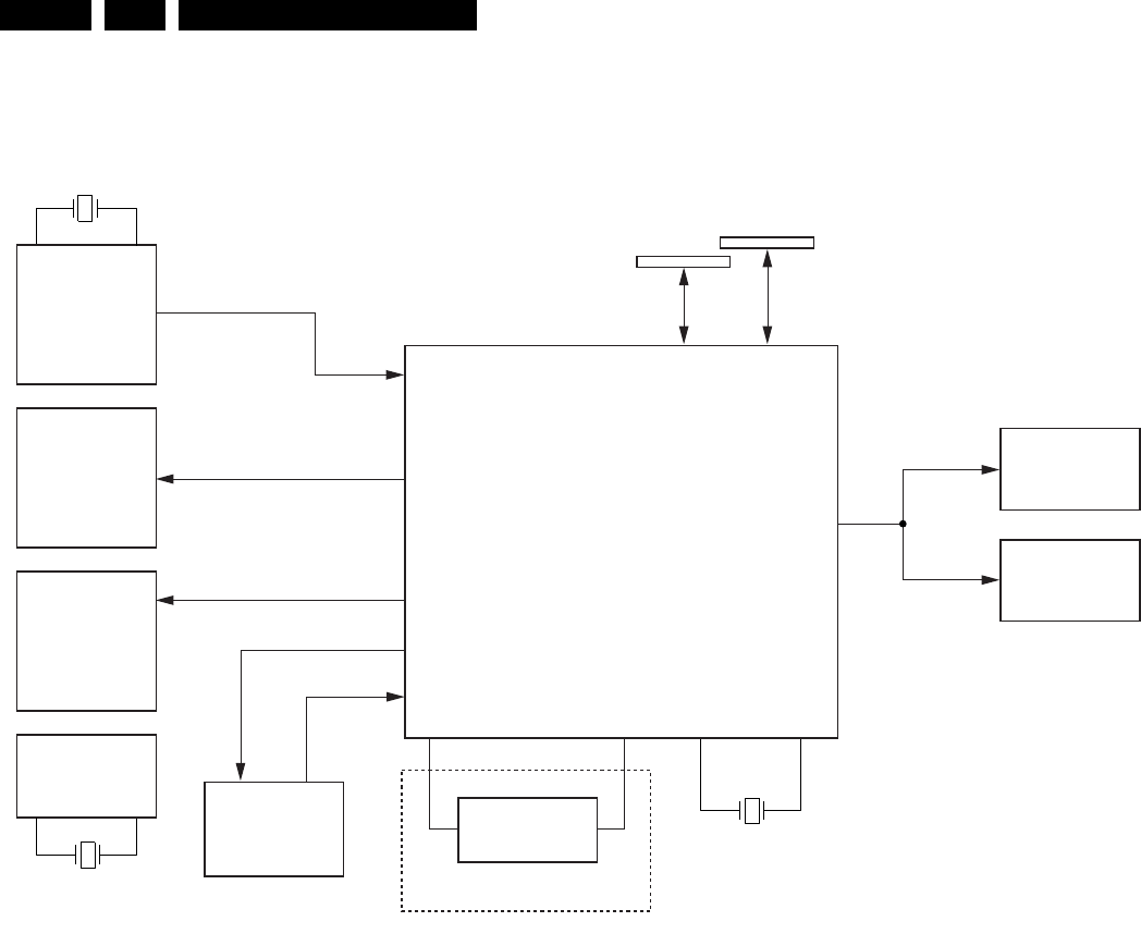
Circuit-, IC descriptions and list of abbreviations
EN 132 LX7500R9.
9.5.4 Clock Distribution
Clock distribution on Chrysalis board
Figure 9-6
The PNX7100 has a complex clock system, which is needed to
support the processes running at different frequencies such as
video decoding, audio decoding or peripheral I/O devices etc.
To ensure a synchronous initialisation of all the registers and
state machines, all the PLLs are switched to their default
frequency and the reset sequence is run at 4 MHz. Then when
the booting control unit is correctly initialized and once it has
captured all the booting parameters, it sets the PLLs to its
functional frequency to allow the modules to run at their
nominal frequencies. Thanks to a clock blocking mechanism,
the frequency switching is glitch free.
System clocks:
• PNX7100 (IC7400, pins AF9 and AF10) : 4 MHz provided
by the xtal oscillator 7402.
• SAA7118 (IC7004, pins A3 and B4): 24.576 MHz provided
by xtal 1001.
• ADV7196 (IC7703, pin 25): 27 MHz provided by PNX7100.
• SDRAM (IC7804 and 7808, pin 38): 133 MHz provided by
the PNX7100.
• 1394-LINK (IC7201, pin 88): 49.152 MHz provided by
1394-PHY.
• 1394-PHY (IC7200, pins 59 and 60): 24.576 MHz provided
by xtal 1201.
9.5.5 Power Supply
The Digital Board is not powered in standby mode. The control
signal 'ION' (Inverse On), coming from the analogue board, will
enable the PSU, and power the digital board.
• ION = High: the digital board is in powered down standby
mode.
• ION = Low: the power supply to the digital board is
enabled.
The 3V3, +5V, -5V, and +12V come from the PSU, while the
1V8 core voltage is generated on the board by a low voltage
buck controller (item 7501). It provides the control for a DC-DC
power solution producing an 1.8V output voltage over a wide
current range. The NCP1570-based solution is powered from
12 V with the output derived from the 3V3 supply. It contains all
required circuitry for a synchronous NFET (IC7500-1 and -2)
buck regulator.
9.5.6 Memory
Several memories are used on the Chrysalis Digital Board:
• EEPROM IC7810: this memory contains all the necessary
boot parameters of the board.
• EEPROM IC7809: this memory contains all the necessary
parameters for the application.
• FLASH IC7807(05/11): this memory contains the
application-, diagnosis-, and service software.
VIP7118
7004
ADV7196
CHRYSALIS
PNX7100
7703
7400
SDRAM
BE INTERFACE
7804
133MHz
SDRAM
7812
1394 LINK
7201
AUDIO PLL 27 MHz
Osc.
7300
OPTIONAL
1394 PHY
24.576 MHz
24.576 MHz
7200
4 MHz
CL 36532004_004.eps
140203
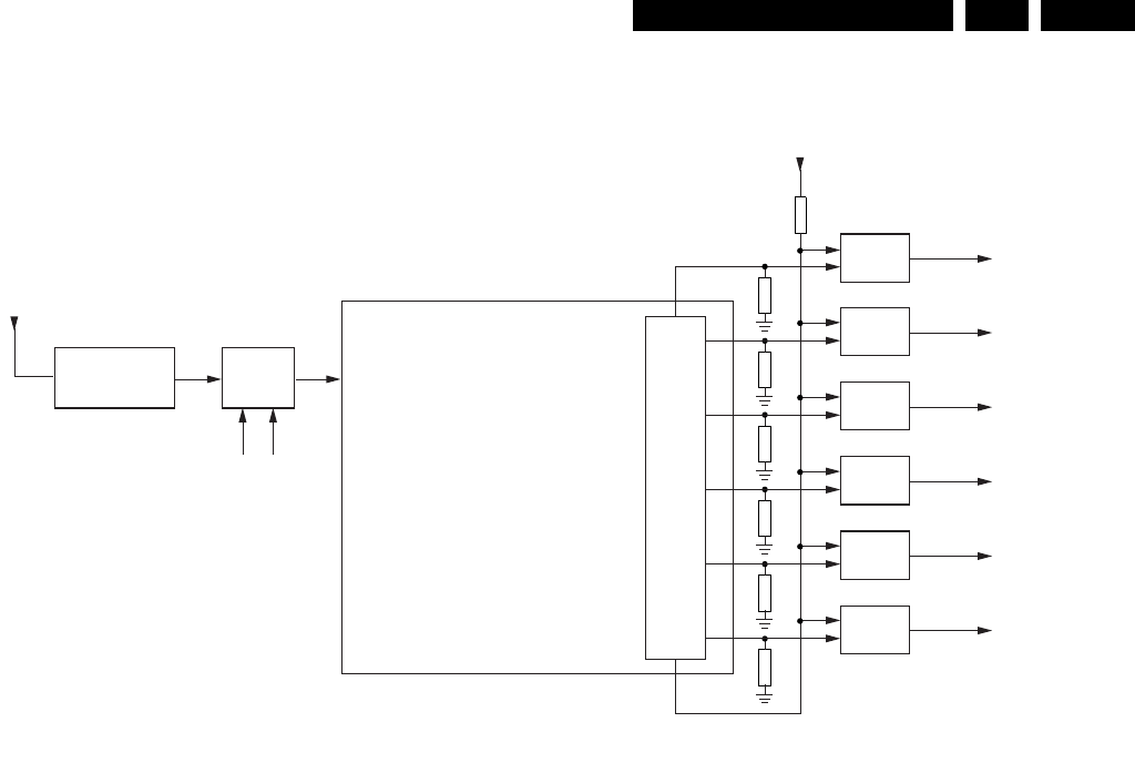
Circuit-, IC descriptions and list of abbreviations EN 133LX7500R 9.
9.5.7 Reset
Reset concept Chrysalis board
Figure 9-7
The voltage detector NCP303LSN29 (IC7600) provides the
reset signal PNX7100_RESETn (active ’low’) with the correct
timing behavior. This circuitry functions as a Power-On Reset
(POR) module, which detects the minimum functional voltage
that is needed by the device. It also detects any voltage drop.
When the power voltage is outside the nominal range, a reset
signal is generated by the POR module and fed to the reset
module which controls the individual reset of the different
peripherals and processing units.
There are two control lines which can overrule this reset signal:
• IRESET_DIG (controlled by the microprocessor on the
Analogue Board).
• EJTAG_RESETn (only for production).
They can pull the output of the NCP303LSN29 (item 7106)
down via a shottky diode.
So when the output signal PNX7100_RESETn is 'low', the
board will reset. When this signal is 'high', the board is up and
running.
The PNX7100_SYS_RESETn is a general enabling signal for
the different reset lines. All other reset lines are directly driven
from Chrysalis port pins (e.g. MPIO13_IDE1_RESETn). All
reset lines are logically connected via 74LVC08D (item 7104)
and (item 7107) AND-gates. If both reset signals are low, all
other external devices are initialised.
9.5.8 I2C Bus
The PNX7100 is the master of the I2C bus (during reset,
external I2C masters are allowed). The following ICs are
controlled by the I2C bus:
• IC7809.
• IC7810 NVRAMs.
• IC7004 VIP.
• IC7700 FLI2301 Video De-interlacer Line Doubler (for
Chrysalis-F boards).
• IC7703 ADV7196 Video Enc (for progressive scan done by
Chrysalis).
9.5.9 I/O Connectors
AIO Connector (item 1900)
The Audio In/Out (AIO) connector is used to interchange digital
audio signals between Analog- and Digital Board.
DAIO Connector (item 1901)
The Digital Audio In/Out (DAIO) connector is used to
interchange digital audio (SPDIF) signals between the IOE-
Board and the Digital Board.
VIO Connector (item 1904)
The Video In/Out (VIO) connector is used to interchange
analogue video signals between Analog- and Digital-Board.
9.5.10 Progressive Scan
Introduction
There are two versions foreseen, to generate a progressive
scan analogue video output:
• In the standard Chrysalis board, the 'low end' progressive
video output is generated by the PNX7100.
• In the Chrysalis 'F', the 'high end' progressive output is
generated by the Faroudja FLI2301. This IC offers
additionaly DCDi, upscaling to HDTV, and picture
enhancement.
Description
The progressive scan part is integrated in the Digital Board and
built around the FLI2301 de-interlace/line doubler (7701). This
I2C controlled de-interlace uses a 64Mbit SDRAM (32bit x 2M)
to perform high quality de-interlacing (meshing). The de-
interlace gets its digital YUV input data from the PNX7100
(7400). The format of the digital YUV input to the Fli2301 is
CCIR656 with separated Hsync, Vsync, and odd/even signal
running on 27MHz.
CHRYSALIS
PNX7100
7400
GPIO
7104-3
&
Reset_IDEn
PNX7100_Resetn
PNX7100_SYS_Resetn
7106
3V3
>1
EJTAG_Resetn
IResetDig
NCP303
7104-4
&
Reset_1394n
7107-1
&
Reset_BEn
7107-2
&
Reset_PSn
7107-3
&
Analog_Resetn
7104-1
&
VIP_Resetn
3V3
CL 36532004_005.eps
140203

Circuit-, IC descriptions and list of abbreviations
EN 134 LX7500R9.
9.6 Service UART Interface
Logic IC 74HCT14D (item 7111) is used to make a level
conversion from microprocessor (LVTTL) to +/-5V (compatible
with most RS232 interfaces) and vice versa. The control line
MPIO19_CTL_SERVICE is used to activate service and
diagnostic SW at start up procedure. The connectivity is
provided via an external service tool.
9.7 I/O Extension Board
This board feeds the internal S/PDIF signal from the Digital
board to an optical and/or digital out connector. For European
players, also an YUV output is present on this board.
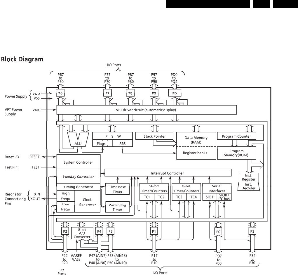
Circuit-, IC descriptions and list of abbreviations EN 135LX7500R 9.
9.8 IC Descriptions
9.8.1 Display Board
IC 7103 TMP87CH74F Display Board, Front Microprocessor
Figure 9-8
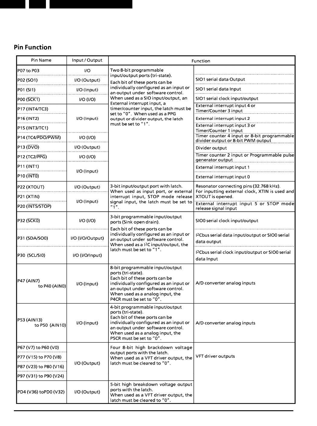
Circuit-, IC descriptions and list of abbreviations
EN 136 LX7500R9.
Figure 9-9
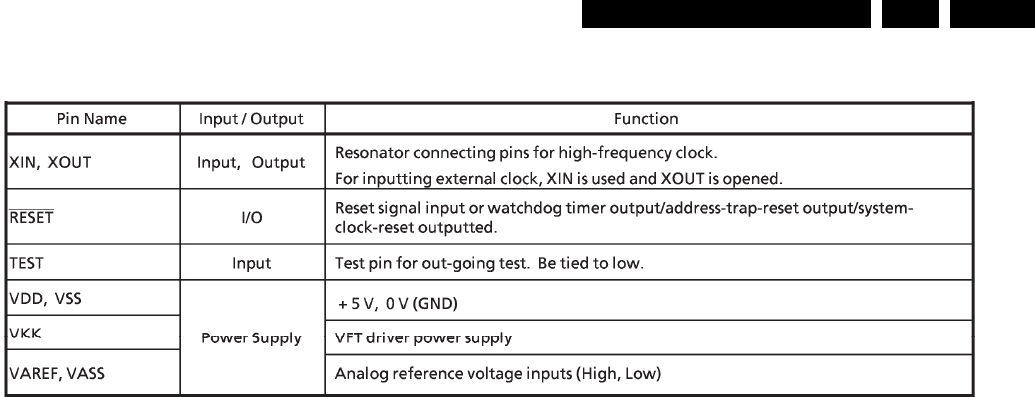
Circuit-, IC descriptions and list of abbreviations EN 137LX7500R 9.
Figure 9-10

Circuit-, IC descriptions and list of abbreviations
EN 138 LX7500R9.
9.8.2 IC’s Analog Board
IC7408: STV6618 Analog Board, Video Switch Matrix
1.2 Pin Description
Pin No. Symbol Description
1 Y/CVBSIN_TUN Y/CVBS Input from Tuner
2 DIGOUT3 Digital Output Pin 3
3 GND1 Ground Supply 1 for Video Inputs
4 CVBSIN_ENC CVBS Input from Encoder
5 DECV Video decoupling capacitor
6 CIN_ENC Chroma Input from Encoder
7 YIN_ENC Y Input from Encoder
8VCC +5 V Power Supply for Video Inputs
9 R/PR/CIN_ENC Red or Pr or Chroma Input from Encoder
10 G/YIN_ENC Green or Y Input from Encoder
11 B/PBIN_ENC Blue or Pb Input from Encoder
12 GND2 Ground Supply 2 for Video Inputs
13 B/PBIN_AUX Blue or Pb Input from Auxiliary (SCART2 or external Cinch)
14 DIGOUT4 Digital Output Pin 4
15 G/YIN_AUX Green or Y Input from Auxiliary (SCART2 or external Cinch)
16 DIGOUT5 Digital Output Pin 5
17 R/PR/CIN_AUX Red or Pr or Chroma input from Auxiliary (SCART2 or external Cinch)
18 DIGOUT6 Digital Output Pin 6
19 Y/CVBSIN_AUX Y/CVBS Input from Auxiliary (SCART2 or external Cinch)
20 VCCB_REC Video Output Recorder Buffer Supply Pin
21 Y/CVBSOUT_REC Y/CVBS Output to Recorder
22 GNDB_REC Ground Supply for Recorder Buffer
23 COUT_AUX Chroma Output to Auxiliary (SCART2 or external Cinch)
24 VCCB1 Video Output Buffer Supply Pin
25 Y/CVBSOUT_AUX Y/CVBS Output to Auxiliary (SCART2 or external Cinch)
26 GNDB Ground Supply for Video Buffer
27 B/PBOUT_TV Blue or Pb Output to TV (SCART1 or external Cinch)
28 C_GATE External Transistor Command for Bidirectinnal B/C SCART I/O
29 G/YOUT_TV Green or Y Output to TV (SCART1 or external Cinch)
30 VCCB2 Video Buffer
31 R/PR/COUT_TV Red or Pr or Chroma Output to TV (SCART1 or external Cinch)
32 VCCB3 Video Output Buffer Supply Pin
33 Y/CVBSOUT_TV Y/CVBS Output to TV (SCART1 or external Cinch)
34 FBOUT_TV Fast Blanking Output to TV (SCART1)
35 FBIN_AUX Fast Blanking Input from Auxiliary (SCART2)
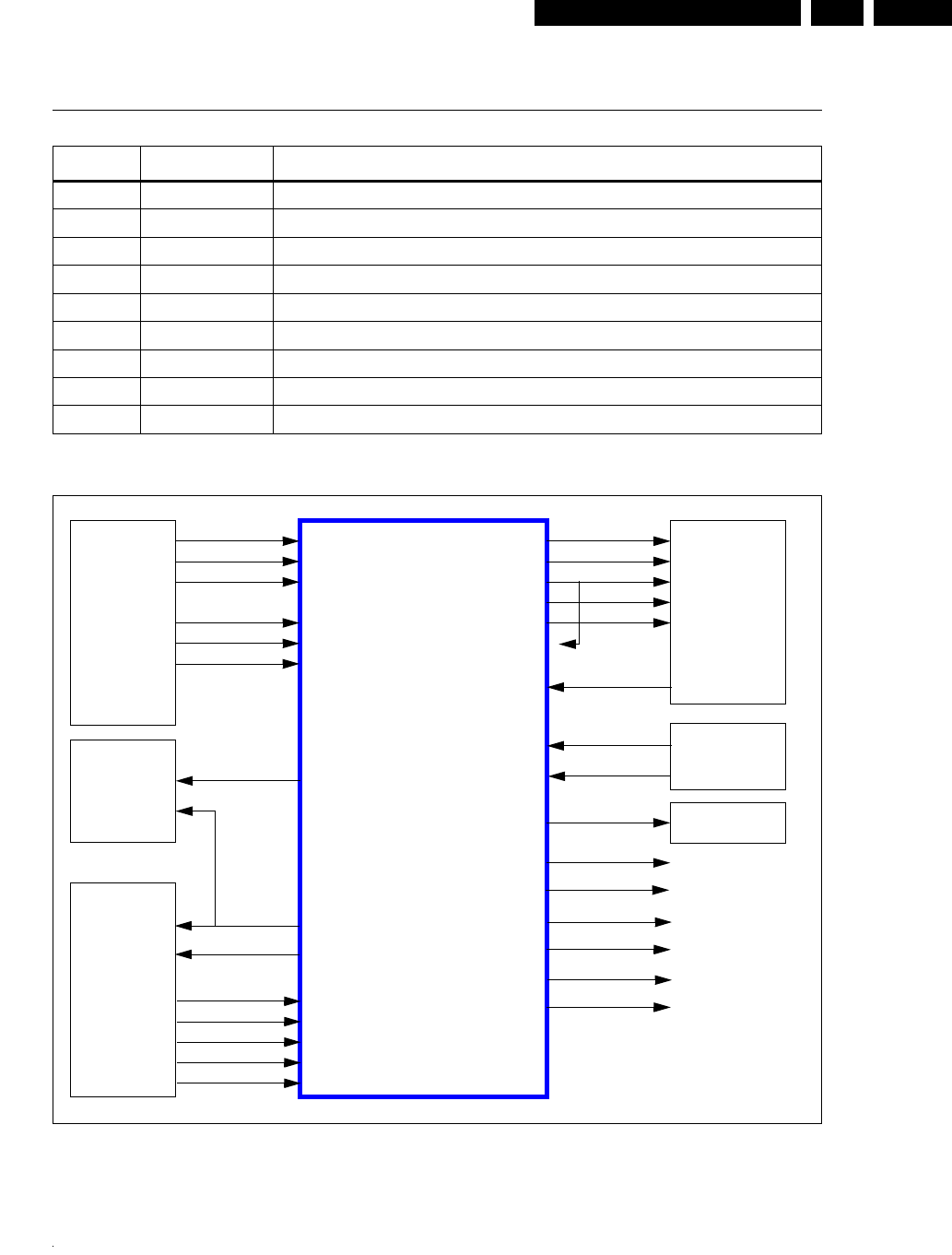
Circuit-, IC descriptions and list of abbreviations EN 139LX7500R 9.
36 VDD +5 V Digital Power Supply
37 SCL I²C Bus Clock
38 SDA I²C Bus Data
39 GNDD Digital Ground Supply
40 CIN_TV Chroma Input from TV (SCART1 or external Cinch)
41 Y/CVBSIN_TV Y/CVBS Input from TV (SCART1 or external Cinch)
42 DIGOUT1 Digital Output Pin 1
43 CIN_TUN Chroma Input from Tuner
44 DIGOUT2 Digital Output Pin 2
Figure 2: STV6618 Input/Output Diagram
Pin No. Symbol Description
SCART1
TV
R/PR/COUT_TV
G/YOUT_TV
B/PBOUT_TV
FBOUT_TV
Y/CVBSOUT_TV
Y/CVBSIN_TV
Tuner
Y/CVBSIN_TUN
Encoder
R/PR/CIN_ENC
G/YIN_ENC
B/PBIN_ENC
CVBSIN_ENC
CIN_ENC
YIN_ENC
Recorder
Y/CVBS_REC
SCART2
R/PR/CIN_AUX
G/YIN_AUX
B/PB_AUX
FBIN_AUX
Y/CVBSIN_AUX
COUT_AUX
COUT_REC
CIN_TV
Transistor
C_GATE
STV6618
(TQFP 44)
DIGOUT1
DIGOUT2
Y/CVBSOUT_AUX
CIN_TUN
DIGOUT3
DIGOUT4
DIGOUT5
DIGOUT6
(Auxiliary)
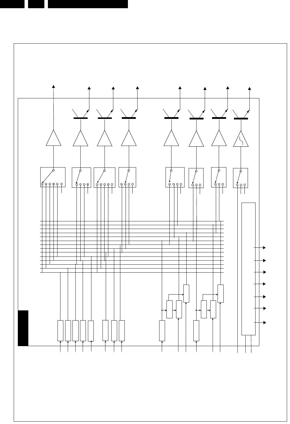
Circuit-, IC descriptions and list of abbreviations
EN 140 LX7500R9.
Figure 3: STV6618 Block Diagram
Sync Sep
Bo. Clamp
Y/CVBSIN_TUN
Y/CVBSIN_TV
Y/CVBSIN_AUX
CVBSIN_ENC
Bo. Clamp
G/YIN_AUX
R/PR/CIN_AUX
B/PBIN_AUX
Sync Sep
Bo. Clamp
G/YIN_ENC
R/PR/CIN_ENC
B/PBIN_ENC
YIN_ENC
CIN_TV
CIN_ENC
mute
0 dB
Y/CVBSOUT_REC
Y/CVBSIN_TUN
Y/CVBSIN_TV
Y/CVBSIN_AUX
CVBSIN_ENC
YIN_ENC
CIN_TV
CIN_ENC
G/YIN_ENC
G/YIN_AUX
R/Pr/CIN_AUX
B/PbIN_AUX
R/Pr/CIN_ENC
B/PbIN_ENC
STV6618
Recorder
mute
6 dB
Y/CVBSOUT_TV
SCART1
mute
6 dB
Y/CVBSOUT_AUX
SCART2
mute
6 dB
R/Pr/COUT_TV
mute 6 dB
G/YOUT_TV
SCART1
SCART1
mute
6 dB
B/PbOUT_TV
SCART1
Y/CVBS_TUN
Y/CVBS_TV
Y/CVBS_AUX
CVBSIN_ENC
YIN_ENC
CIN_TV
CIN_ENC
G/YIN_ENC
G/YIN_AUX
R/Pr/CIN_AUX
B/PbIN_AUX
R/Pr/CIN_ENC
B/PbIN_ENC
FBOUT_TV
SCL
FBIN_AUX
0v
5v
SDA
C_GATE
I²C Bus
Bo. Clamp
Bo. Clamp
Bo. Clamp
Bo. Clamp
Av. Clamp
Av. Clamp
Bot/sync/av.
Bo/Sync
Bot/sync
Bot/sync/av.
CVBSIN_TUN
Y/CVBSIN_TV
Y/CVBSIN_AUX
CVBSIN_ENC
YIN_ENC
mute
6 dB
COUT_AUX
Y/CVBSIN_AUX
CVBSIN_ENC
YIN_ENC
CVBSIN_TUN
Y/CVBSIN_TV
CVBSIN_ENC
YIN_ENC
CIN__TV
CIN_ENC
CIN_ENC
R/Pr/CIN_AUX
R/Pr/CIN_ENC
G/YIN_AUX
G/YIN_ENC
B/PbIN_AUX
B/PbIN_ENC
FBIN_AUX
CIN_TUN
Av. Clamp
CIN_TUN CIN_TUN
CIN__TUN
DIGOUT1
DIGOUT2
DIGOUT3
DIGOUT4
DIGOUT5
DIGOUT6
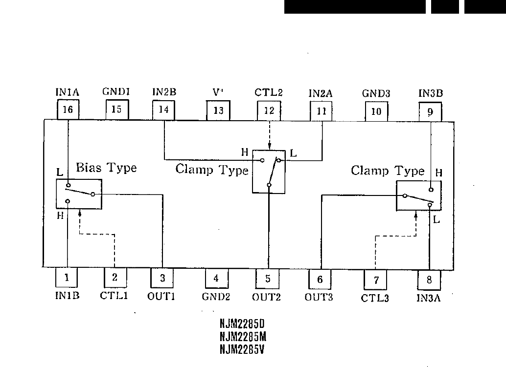
Circuit-, IC descriptions and list of abbreviations EN 141LX7500R 9.
IC7411: NJM2285 Analog Board, Video Switch
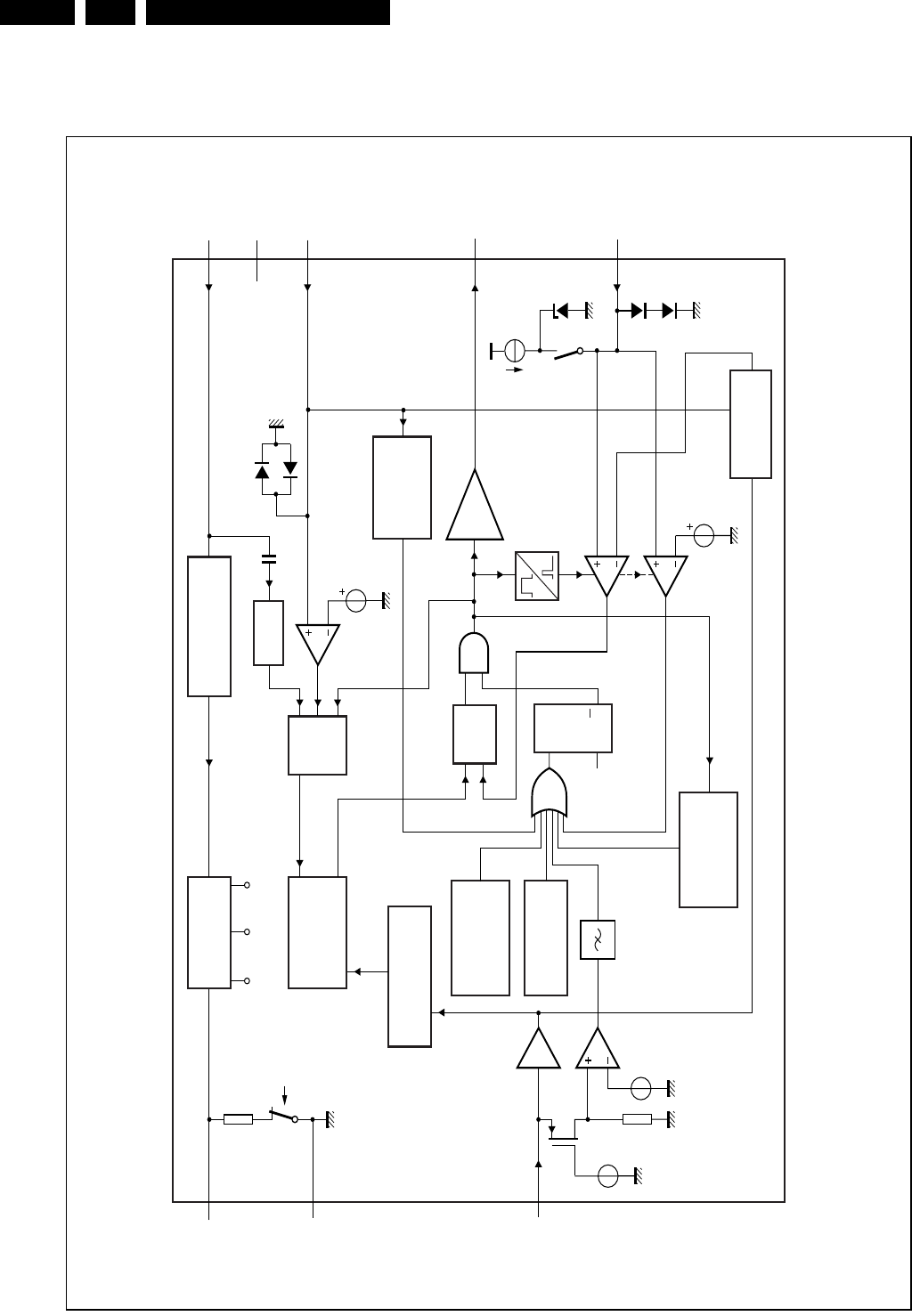
Circuit-, IC descriptions and list of abbreviations
EN 142 LX7500R9.
IC7313 TEA 1507 Analog Board, Power Supply Control
BLOCK DIAGRAM
a
ndbook, full pagewidth
SUPPLY
MANAGEMENT
internal
supply UVLO start
M-level
VCC 1
2
3
GND
S1
CTRL
FREQUENCY
CONTROL
VOLTAGE
CONTROLLED
OSCILLATOR LOGIC
LOGIC
OVER-
VOLTAGE
PROTECTION
OVERPOWER
PROTECTION
short
winding
soft
start
S2
OVER-
TEMPERATURE
PROTECTION
SQ
R
UVLO Q
MAXIMUM
ON-TIME
PROTECTION
POWER-ON
RESET
−1
VALLEY
TEA1507
100 mV
clamp
DRIVER
START-UP
CURRENT SOURCE
0.75 V
0.5 V
5Isense
6DRIVER
MGU230
4DEM
8DRAIN
7HVS
n.c.
OCP
LEB
blank
Iss
2.5 V
burst
detect
Fig.2 Block diagram.
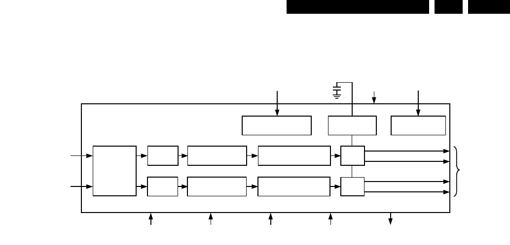
Circuit-, IC descriptions and list of abbreviations EN 143LX7500R 9.
IC7404: AD1582 Analog Board, Digital/Analogue Converter
FUNCTIONAL BLOCK DIAGRAM
SERIAL
DATA
INTERFACE
8 3 F
S
INTERPOLATOR
SERIAL CONTROL
INTERFACE AUTO-CLOCK
DIVIDE CIRCUIT
VOLUME
MUTE
CONTROL DATA
INPUT
32
DIGITAL
SUPPLY CLOCK
IN
ANALOG
OUTPUTS
22
ZERO
FLAG
ANALOG
SUPPLY
DE-EMPHASISMUTE
RESET
2
SERIAL
MODE
16-/18-/20-/24-BIT
DIGITAL
DATA INPUT
AD1852
MULTIBIT SIGMA-
DELTA MODULATOR
ATTEN/
MUTE
DAC
MULTIBIT SIGMA-
DELTA MODULATOR
8 3 F
S
INTERPOLATION
ATTEN/
MUTE
VOLTAGE
REFERENCE
DAC
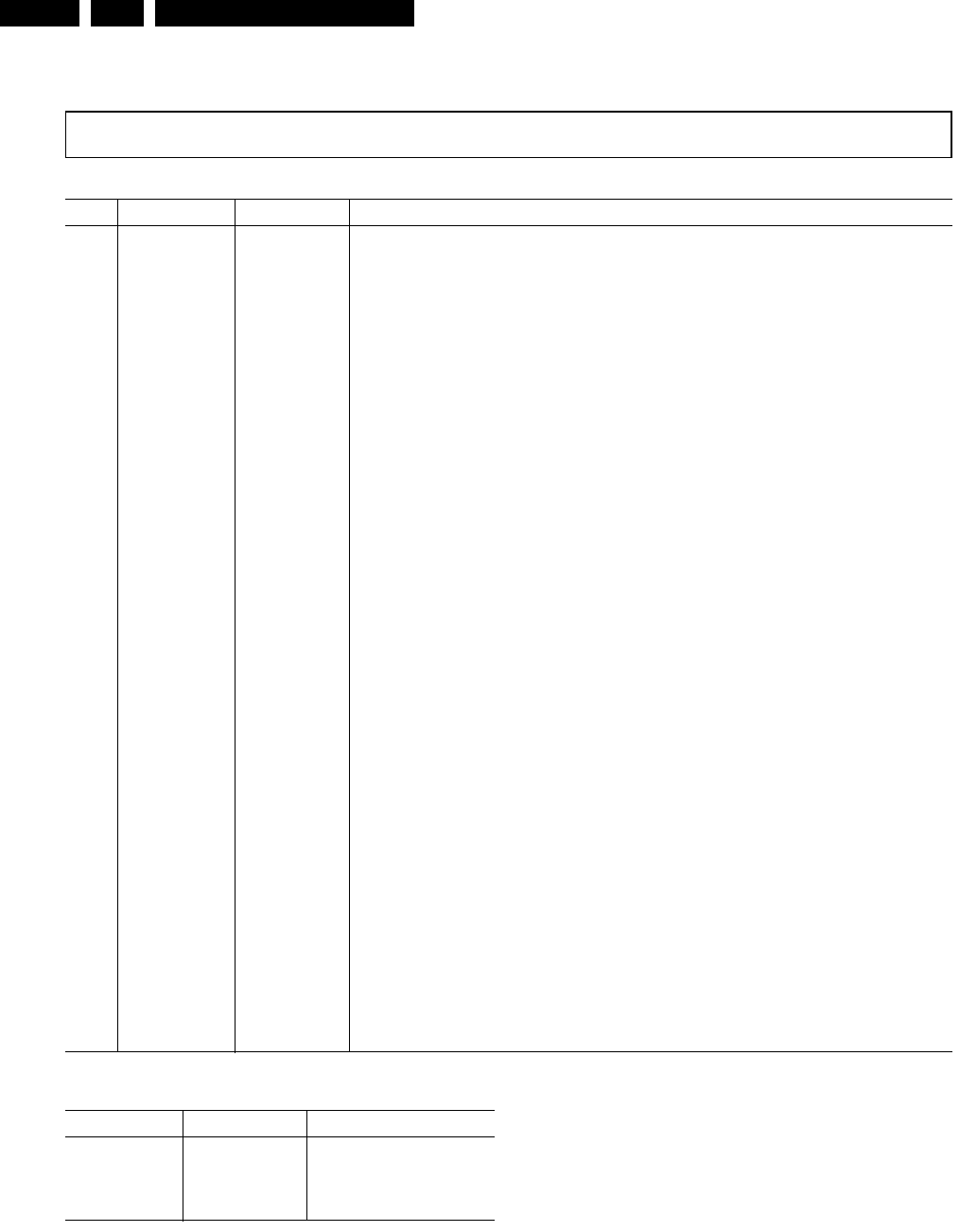
Circuit-, IC descriptions and list of abbreviations
EN 144 LX7500R9.
AD1852
PIN FUNCTION DESCRIPTIONS
Pin Input/Output Pin Name Description
1 I DGND Digital Ground.
2 I MCLK Master Clock Input. Connect to an external clock source at either 256 F
S
, 384 F
S
,
512 F
S
, 768 F
S
, or 1024 F
S
.
3 I CLATCH Latch Input for Control Data. This input is rising-edge sensitive.
4 I CCLK Control Clock Input for Control Data. Control input data must be valid on the rising
edge of CCLK. CCLK may be continuous or gated.
5 I CDATA Serial Control Input, MSB first, containing 16 bits of unsigned data per channel. Used
for specifying channel-specific attenuation and mute.
6 NC No Connect.
7 I 192/48 Selects 48 kHz (LO) or 192 kHz Sample Frequency.
8 O ZEROR Right Channel Zero Flag Output. This pin goes HI when Right Channel has no signal
input for more than 1024 LR Clock Cycles.
9 I DEEMP De-Emphasis. Digital de-emphasis is enabled when this input signal is HI. This is used
to impose a 50 µs/15 µs response characteristic on the output audio spectrum at an
assumed 44.1 kHz sample rate. Curves for 32 kHz and 48 kHz sample rates may be
selected via SPI control register.
10 I 96/48 Selects 48 kHz (LO) or 96 kHz Sample Frequency.
11, 15 I AGND Analog Ground.
12 O OUTR+ Right Channel Positive Line Level Analog Output.
13 O OUTR– Right Channel Negative Line Level Analog Output.
14 O FILTR Voltage Reference Filter Capacitor Connection. Bypass and decouple the voltage refer-
ence with parallel 10 µF and 0.1 µF capacitors to the AGND.
16 O OUTL– Left Channel Negative Line Level Analog Output.
17 O OUTL+ Left Channel Positive Line Level Analog Output.
18 I AVDD Analog Power Supply. Connect to Analog 5 V Supply.
19 FILTB Filter Capacitor Connection. Connect 10µF capacitor to AGND (Pin 15).
20 I IDPM1 Input Serial Data Port Mode Control One. With IDPM0, defines 1 of 4 serial modes.
21 I IDPM0 Input Serial Data Port Mode Control Zero. With IDPM1, defines 1 of 4 serial modes.
22 O ZEROL Left Channel Zero Flag Output. This pin goes HI when Left Channel has no signal
input for more than 1024 LR Clock Cycles.
23 I MUTE Mute. Assert HI to mute both stereo analog outputs. Deassert LO for normal operation.
24 I RESET Reset. The AD1852 is reset on the rising edge of this signal. The serial control port
registers are reset to the default values. Connect HI for normal operation.
25 I L/RCLK Left/Right Clock Input for Input Data. Must run continuously.
26 I BCLK Bit Clock Input for Input Data. Need not run continuously; may be gated or used in a
burst fashion.
27 I SDATA Serial Input, MSB first, containing two channels of 16, 18, 20, and 24 bits of twos
complement data per channel.
28 I DVDD Digital Power Supply Connect to digital 5 V supply.
Table I. Serial Data Input Mode
IDPM1 (Pin 20) IDPM0 (Pin 21) Serial Data Input Format
0 0 Right-Justified
01I
2
S-Compatible
1 0 Left-Justified
1 1 DSP
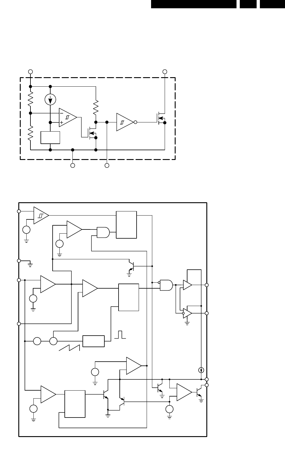
Circuit-, IC descriptions and list of abbreviations EN 145LX7500R 9.
9.8.3 ICs Digital Board Chrysalis
IC7106 NCP303LSN29, Digital Board 2.1 Chrysalis, Reset Circuit
IC7501 NCP1570D, Digital Board 2.1 Chrysalis, DC/DC Converter Control
NCP303LSNxxT1
Open Drain Output Configuration
V
ref
2 Input
3Gnd 5C
D
R
D
1 Reset Output
NCP1570
Figure 2. Block Diagram
–
+
UVLO COMP
–
+
–
+
–
+
Fault Latch
Set Dominant
+
–0.25 V
Error Amp
–R
S
Q
PWM Latch
Reset Dominant
PWM COMP
+ΣOSC
Art Ramp
80%, 200 kHz
0.525 V
+
–8.5 V/7.5 V
+
–0.985 V
S
R
Q
VCC
GND
VFB
COMP
GATE(H)
GATE(L)
PGDELAY
PWRGD
Non
Overlap
VCC
+
–0.89 V/0.69 V
+
–
+
–
0.25 V
S
R
Q
PGDELAY Latch
Set Dominant
–
+
+
–3.3 V
12 µA
+
–
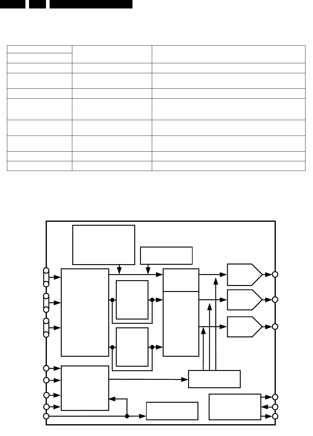
Circuit-, IC descriptions and list of abbreviations
EN 146 LX7500R9.
IC7703 ADV7196A, Digital Board 2.1 Chrysalis, Progressive Scan Video Encoder
PACKAGE PIN DESCRIPTION
PACKAGE PIN #
SO–8 PIN SYMBOL FUNCTION
1 VCC Power supply input.
2 PWRGD Open collector output goes low when VFB is out of regulation. User
must externally limit current into this pin to less than 20 mA.
3 PGDELAY External capacitor programs PWRGD low–to–high transition delay.
4 COMP Error amp output. PWM comparator reference input. A capacitor to
LGND provides error amp compensation and Soft Start. Pulling pin
< 0.45 locks gate outputs to a zero percent duty cycle state.
5 GATE(H) High–side switch FET driver pin. Capable of delivering peak currents
of 1.5 A.
6 GATE(L) Low–side synchronous FET driver pin. Capable of delivering peak
currents of 1.5 A.
7 VFB Error amplifier and PWM comparator input.
8 GND Power supply return.
FUNCTIONAL BLOCK DIAGRAM
CGMS
MACROVISION
SHARPNESS
FILTER CONTROL
AND
ADAPTIVE
FILTER CONTROL
TEST PATTERN
GENERATOR
AND
DELAY
AND
GAMMA
CORRECTION
Y0–Y9
Cr0–Cr9
Cb0–Cb9
CHROMA
4:2:2
TO
4:4:4
(SSAF) 2 INTER-
POLATION
TIMING
GENERATOR
SYNC
GENERATOR
I
2
C MPU
PORT
CLKIN
HORIZONTAL
SYNC
VERTICAL
SYNC
BLANKING
RESET
ADV7196A
DAC CONTROL
BLOCK
DAC A (Y)
DAC B
DAC C
V
REF
RESET
COMP
11-BIT+
SYNC
DAC
11-BIT
DAC
11-BIT
DAC
LUMA
SSAF
CHROMA
4:2:2
TO
4:4:4
(SSAF)
Circuit-, IC descriptions and list of abbreviations EN 147LX7500R 9.
ADV7196A
PIN FUNCTION DESCRIPTIONS
Pin Mnemonic Input/Output Function
1, 12 V
DD
P Digital Power Supply
2–11 Y0–Y9 I 10-Bit Progressive Scan/HDTV Input Port for Y Data. Input for G data when
RGB data is input.
13, 52 GND G Digital Ground
14–23 Cr0–Cr9 I
1
0-Bit Progressive Scan/HDTV Input Port for Color Data in 4:4:4 Input Mode.
In 4:2:2 mode this input port is not used. Input port for R data when RGB data
is input.
24, 35 V
AA
P Analog Power Supply
25 CLKIN I Pixel Clock Input. Requires a 27 MHz reference clock for standard operation in
Progressive Scan Mode or a 74.25 MHz (74.1758 MHz) reference clock in
HDTV mode.
26, 33 AGND G Analog Ground
27 DV I Video Blanking Control Signal Input
28 VSYNC/ IVSYNC, Vertical Sync Control Signal Input or TSYNC Input Control Signal in
TSYNC Async Timing Mode
29 HSYNC/ IHSYNC, Horizontal
Sync Control Signal Input or SYNC Input Control Signal in
SYNC
Async Timing Mode
30 SCL I MPU Port Serial Interface Clock Input
31 SDA I/O MPU Port Serial Data Input/Output
32 DAC C O Color Component Analog Output of Input Data on Cb/Cr9–0 Input Pins
34 DAC A O Y Analog Output
36 DAC B O Color Component Analog Output of Input Data on Cr9–Cr0 Input Pins
37 COMP O Compensation Pin for DACs. Connect 0.1 µF capacitor from COMP pin to V
AA
.
38 R
SET
I A 2470 Ω resistor (for input ranges 64–940 and 64–960; output standards
EIA-770.1–EIA-770.3) must be connected from this pin to ground and is used to
control the amplitudes of the DAC outputs. For input ranges 0–1023 (output
standards RS-170, RS-343A) the R
SET
value must be 2820 Ω.
39 V
REF
I/O Optional External Voltage Reference Input for DACs or Voltage Reference
Output (1.235 V)
40 RESET I This input resets the on-chip timing generator and sets the ADV7196A into
Default Register setting. Reset is an active low signal.
41 ALSB I TTL Address Input. This signal sets up the LSB of the MPU address. When this
pin is tied high, the I
2
C filter is activated which reduces noise on the I
2
C interface.
When this pin is tied low, the input bandwidth on the I
2
C interface is increased.
42–51 Cb/Cr9–0 I
1
0-Bit Progressive Scan/HDTV Input Port for Color Data. In 4:2:2 mode the
multiplexed CrCb data must be input on these pins. Input port for B data when
RGB is input.

Circuit-, IC descriptions and list of abbreviations
EN 148 LX7500R9.
9.9 List of Abbreviations
Analog Board
+5VSTBY Permanent Supply 5V
8SC2 Pin8 Scart2 (only for Europe)
A_DATA Data from Analog- to Digital-Board
(UART-Communication)
A_RDY Analog-board ready (status
information to digital-board)
A18 - A19 Parallel Address Bus (CC - Flash-
ROM and S-RAM)
A8 - A17 Parallel Address Bus (CC - Flash-
ROM and S-RAM)
AD0 - AD7 Parallel Address Bus (CC - Flash-
ROM and S-RAM)
AFC Automatic Frequency Control
AFEL Audio Frontend Left
AFER Audio Frontend Right
AGC / WSRI Automatic Gain Control (for Europe),
Wide Screen Rear In (for NTSC)
AINFL Audio In Front Left
AINFR Audio In Front Right
AKILL Audio Kill Signal
ALADC Audio Left to ADC
ALDAC Audio Left from DAC
ALE Address Latch Enable
AM0 Adress-mode 0
AM1 Adress-mode 1
ARADC Audio Right to ADC
ARDAC Audio Right from DAC
ASCC1 Audio Scart 1 Mute (System Clock
Output for Real time Clock-
Adjustment)
AVCC Power Supply for A/D-converter
AVSS GND-Pin for A/D-converter
CFIN Chroma Front In
CS0_ Chip Select 0 (CC - S-RAM)
CS2_ Chip Select 2 (CC - Flash-ROM)
CVBSFIN Video Front In
D_DATA Data from Digital- to Analog-Board
(UART-Communication)
D_RDY Digital-board ready (status information
from digital-board)
DAC_MUTE Mute Signal for DAC
DAOUT Digital Audio Out
DVAL Audio from Digital Video In Left
DVAR Audio from Digital Video In Right
DVCC1 Power Supply Pin
DVCC2 Power Supply Pin
DVCC3 Power Supply Pin
DVSS1 GND Pin
DVSS2 GND Pin
DVSS3 GND Pin
FAN_OFF Fan for Basic engine
FBIN Fast Blanking input
FOME FOllow ME Status line (matching
signals yes/no; only for Europe)
G1…10 DISPLAY GRID
INT Interrupt OUT for the CC
INT Interrupt – line from Display Print
ION Inverse ON-Line
IPFAIL Inverse Power Fail Detection
IPOR Inverse Power On Reset
IRESET Inverse Reset Input
K1 Key-Input-Line
K2 Key-Input-Line
KILL Signal from IR-Receiver
P50 IN P50 INput-line (only for Europe)
P50 OUT P50 OUTput-line (only for Europe)
POR_DC Power On Reset for Display Control
Print (Ext_DL)
PSS Output Enable ReaD (CC - Flash-
ROM and S-RAM)
PWM_FIL Control line for Filament Voltage
Generation
PWONSW Amplifier Switch Audio A/D Converter
RD_ Pal/Secam-Select
RECLED Control Signal for REC-LED
RESET_DIG Reset Line to Digital Board
RP_ Inverse Reset line to Flash-ROM
RSA1/2 Record Selector 1/2
RY/BY_ Ready/Busy – input line (from Flash-
ROM)
SIF1 Sound intermediate frequency
SB1 Secam Band 1 (PCB-Test entrance)
SCL IC-Bus
SCLSW Switched I2C-Bus
SDA IC-Bus
SDASW Switched I2C-Bus
SFS_TS SAW Filter Select Trap Select
STBY Standby-Line (Flash_Toshiba)
SYNC Video Sync input
TEMP_SENSE Temperature Sense Line
VER HW-version input
VFV Video from Frontend
VKK VFT Driver Power Supply
VREFH Pin for Reference-voltage input to A/D-
converter
VREFL Pin for Reference-voltage input to A/D-
converter
VS1/2 View Selector 1/2
WR_ Write Enable (CC - Flash-ROM and S-
RAM)
WSFI Wide Screen Signalling Front In
WU Wake Up
X1 Oscillator Pin
X12 Oscillator Pin
XIN Oscillator Pin
XOUT Oscillator Pin
XT1 Low Frequency Oscillator Pin
XT2 Low Frequency Oscillator Pin
YFIN Luminance Front In
Digital Board Chrysalis
ADC Analog to Digital Converter
DAC Digital to Analog Converter
DENC Digital (Video) Encoder (Video DAC)
DV Digital Video (Camcorder)
EF Emitter Follower
OSD On-Screen Display
VIP Video Input Processor (Video ADC)
2Fh Progressive scan video
2V5 +2V5 Power supply for Link+Codec
IC7431
3V3 +3V3 Power supply
3V3_A +3V3 Analog power supply for PHY
IC7400
3V3_D +3V3 Digital power supply for PHY
IC7400
3V3_DLY +3V3 Power supply for IC7500
3V3_LINK +3V3 Power supply for Link+Codec
IC7431
3V3_F +3V3 Power supply for optional Flash
memory IC7432
3V3_RAM +3V3 Power supply for SDRAM
IC7430
3V3_uP +3V3 Power supply for Micro-
controller IC7802
3V3_32kHz +3V3 Power supply for audio format
adaptation circuitry IC7507 and
IC7508
3V3_AC +3V3 Power supply for audio system
clock generator IC7605 and IC7606
+5V +5V Power supply
5V_PLL +5V Power supply for VCO of audio
PLL IC7604
A (1:17) Flash address lines of uPD72893

Circuit-, IC descriptions and list of abbreviations EN 149LX7500R 9.
A_MUTE Audio Mute
ABCK Audio Bit Clock
AD (1:10) Address bus lines for Host I/F of
Link+Codec IC7431
AEMP1 PCM1 emphasis ON/OFF for PCM1
output
AFS1 Audio sampling frequency indication
signal
ALRCLK Audio Word Select
AMCLK44 11.2896MHz (=256 * 44.1 kHz) audio
master clock signal for 44.1 kHz audio
AMCLK48 12.288MHz (=256 * 48 kHz) audio
master clock signal for 32 kHz and 48
kHz audio
APWM PWM signal for audio PLL
ASIC Application Specific Integrated Circuit
BUFENn_AUD Buffer Enable Audio
BUFENn_VID Buffer Enable Video
CLK27M_CON 27MHz Clock to Digital Board
CS Parallel interface chip select input of
Link+Codec IC7431
CTL (0:1) Link interface control lines
CTSN Clear to Send
D (0:15) Flash data lines of Link+Codec
IC7431
DCDi Directional Correlational
Deinterlacing. Circuitry that reduces
jaggies on diagonal edges when
deinterlacing video-sourced material.
DV_STATUS Interrupt pin for reading DV-status
HS_CLK Video clock input of Link+Codec
IC7431
INT Interrupt request output of Link+Codec
IC7431 (input to Micro-Controller)
IOR Parallel interface IO read control input
of Link+Codec IC7431
ISPN In System Programming signal (used
for programming IC7802)
LKON Link-on signal outputLPSLink power
status inputLREQLink request input
MA (0:10) SDRAM address lines of Link+Codec
IC7431
MCAS SDRAM column address strobe signal
MCLK SDRAM clock signal
MD (0:15) SDRAM data lines of Link+Codec
IC7431
MRAS SDRAM row-address strobe signal
MWE SDRAM write enable signal
PCM1 Audio Serial Data Output of
Link+Codec IC7431
PCM1_NEW ’MSB justified’ to I2S converted audio
serial data; audio serial data input of
audio DAC UDA1334A
PD (0:15) Data bus lines for Host I/F of
Link+Codec IC7431
PHY_D (0:7) Data bus connection between PHY
and LINK device
RESETn DVIO board reset
RESET_FM Reset signal driven by Flashmaster
programming device
RESTB Reset input of Link+Codec IC7431
RTSN Request to Send
RWZ Parallel interface read/write control
input of Link+Codec IC7431
RXD Receive Data
SCLK Link control output clock
TXD Transmit Data
VPP +10V switchable programming voltage
of microcontroller
YUV (0:7) Digital Video
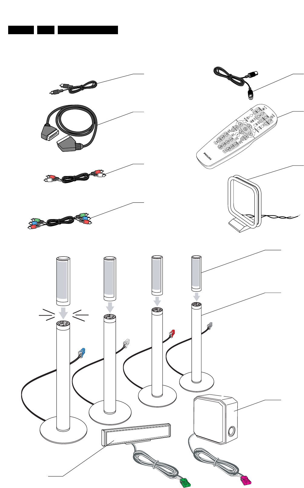
EN 150 10. LX7500R Spare Parts List
322
317 327
330
325
328
331
323
338 4x
338-1
339-1 341-1
338-2
338-4
338-3
340 4x
341
339
click
accessories LX7500R, 201004
ACCESSORIES

see also Exploded View drawings pages 66, 67, 68 and 150
MECHANICAL PARTS
–––––––––––––––––––––––––––––––––––––––––––––––––––––
102 3103 607 90861 FRONT ASSY MECH. LX7500/01/04
102 3103 607 90981 FRONT ASSY MECH. LX7500/05
106 3103 607 51321 KNOB VOLUME
111 3103 607 50341 BUTTON CAP, STANDBY
113 3103 607 50361 BUTTON CAP, OPEN CLOSE
119 3103 607 50411 BUTTON CAP, RECORD
120 3103 607 51311 WINDOW DISPLAY
124 3103 607 51101 RING, KEYS PLAY-STOP-REW-FFW
126 3103 607 51391 DOOR FRONT, LX7500/01/04
126 3103 607 51421 DOOR FRONT, LX7500/05
133 3103 604 00441 HINGE, DOOR FRONT
201-2 3103 604 00622 FOOT, RUBBER
201-3 3103 607 50491 FOOT ASSY
210 3103 607 90941
ORNAMENTAL COVER, TRAY LX7500R
215 !2422 070 98231 MAIN SCORD, IEC
215 !2422 070 98236 MAINS CORD, UK
230 3103 607 10051 FAN 60X60X20
ACCESSORIES
–––––––––––––––––––––––––––––––––––––––––––––––––––––
317 3103 308 92540 DIGITAL OUT CABLE, 75Ω
322 2422 076 00532 SCART CABLE, 21P
323 3103 308 92610 AUDIO CABLE STEREO CINCH 1.5m
325 2422 076 00374
CABLE CINCH/CINCH 1M5 GN/BU/RD
327 4822 320 50377 TV ANTENNA CABLE
328 3128 147 16432 REMOTE CONTROL, RC19046015/01
330 4822 320 50377 TV ANTENNA CABLE
331 2422 549 45813 LOOP ANTENNA, AM
338 9965 000 26097 SATELLITE BOX LX7500
339 3103 607 90961 CENTER BOX LX7500
340 3103 607 90971
ALUM. STAND FOR SATELL. SPEAKERS
341 3103 607 91031 SUBWOOFER
MISCELLANEOUS
–––––––––––––––––––––––––––––––––––––––––––––––––––––
1106 3103 608 51732 CHRYS. BOARD PPS E4_AV3_PLUS
1108 !2722 171 00139 SMPS AC6191 B, 230V
1109 2422 542 90137 RADIO TUNER MODULE, EU
8004 3103 308 95031 FLEXFOIL CABLE, 12P, 350mm, BD
8005 3103 308 94311 FLEXFOIL CABLE, 10P, 120mm, AD
8007 3103 308 94321 FLEXFOIL CABLE, 22P, 180mm, BD
8008 3103 308 94331 FLEXFOIL CABLE, 22P, 180mm, BD
8009 3103 308 94341 FLEXFOIL CABLE, 10P, 180mm, AD
8013 3139 110 35911 FLEXFOIL CABLE, 11P, 100mm, BD
8014 3103 308 94371 FLEXFOIL CABLE, 10P, 140mm, BD
8015 3103 308 94381 FLEXFOIL CABLE, 8P, 140mm, BD
8016 3103 308 94391 FLEXFOIL CABLE, 6P, 520mm, BD
8020 3103 308 94411 FIREWIRE CABLE, 650mm, EEE1394
8032 3103 308 94401 FLEXFOIL CABLE, 6P, 120mm, AD
8039 3103 308 94891 FLEXFOIL CABLE, 7P, 200mm, AD
8040 3103 308 94901 FLEXFOIL CABLE, 40P, 220mm, BD
338-1 9965 000 26175 LS-CABLE 2P 5M WHITE CON. FR-L
338-2 9965 000 26176 LS-CABLE 2P 5M RED CONN. FR-R
338-3 9965 000 26177 LS-CABLE 2P 15M BLUE REAR-L
338-4 9965 000 26178 LS-CABLE 2P 15M GREY REAR-R
EN 15110.LX7500RSpare Parts List

AUXILIARY SUPPLY BOARD
MISCELLANEOUS
–––––––––––––––––––––––––––––––––––––––––––––––––––––
1304 2422 025 17897 FFC-CONNECTOR, 6P, SIDE ENTRY
1306 !2422 086 00618 FUSE SMD, F 2A, 125V UL
1307©!2422 086 11104 FUSE SMD, F 1A, 50V UL
CAPACITORS
–––––––––––––––––––––––––––––––––––––––––––––––––––––
2300 © 3198 017 31030 10nF 10% 50V
2301 © 2022 552 05679 1µF 10% 16V
2302 2020 021 91506 1000µF 20% 16V
2303 © 2022 552 05679 1µF 10% 16V
2304 © 2022 552 05679 1µF 10% 16V
2305 3198 028 21090 10µF 20% 16V
2306 3198 028 21090 10µF 20% 16V
2307 3198 028 21090 10µF 20% 16V
2308 3198 028 21090 10µF 20% 16V
2309 3198 028 21090 10µF 20% 16V
2310 3198 028 21090 10µF 20% 16V
2311 3198 028 21090 10µF 20% 16V
2312 3198 028 21090 10µF 20% 16V
2313 2020 021 91668 2200µF 20% 10V
2314 © 2022 552 05679 1µF 10% 16V
2315 © 2022 552 05679 1µF 10% 16V
2316 © 2022 552 05679 1µF 10% 16V
2317 © 2222 580 15649 100nF 10% 50V
2318 © 2222 580 15649 100nF 10% 50V
2319 © 2222 580 15649 100nF 10% 50V
RESISTORS
–––––––––––––––––––––––––––––––––––––––––––––––––––––
3300 © 3198 021 31030 10kΩ5% 0,06W
3301 © 3198 021 31520 1,5kΩ5% 0,06W
3302 © 3198 021 31020 1kΩ5% 0,06W
3303 © 3198 021 31030 10kΩ5% 0,06W
3304 © 3198 021 34720 4,7kΩ5% 0,06W
3305 © 3198 021 34720 4,7kΩ5% 0,06W
3306 © 3198 021 31540 150kΩ5% 0,06W
3307 © 3198 021 31030 10kΩ5% 0,06W
3308 © 3198 021 32240 220kΩ5% 0,06W
3309 © 3198 021 31030 10kΩ5% 0,06W
3310 © 3198 021 31030 10kΩ5% 0,06W
3311 © 3198 021 31540 150kΩ5% 0,06W
3312 © 3198 021 31030 10kΩ5% 0,06W
3313 © 3198 021 31030 10kΩ5% 0,06W
3314 © 3198 021 32720 2,7kΩ5% 0,06W
3315 © 3198 021 32240 220kΩ5% 0,06W
3316 © 3198 021 31030 10kΩ5% 0,06W
3317 © 3198 021 31030 10kΩ5% 0,06W
3318 © 3198 021 31520 1,5kΩ5% 0,06W
3319 © 3198 021 31030 10kΩ5% 0,06W
3320 © 3198 021 32720 2,7kΩ5% 0,06W
3321 © 3198 021 34720 4,7kΩ5% 0,06W
3322 © 3198 021 34720 4,7kΩ5% 0,06W
3323 © 3198 021 31020 1kΩ5% 0,06W
3324 © 3198 021 33320 3,3kΩ5% 0,06W
3325 © 3198 021 31090 10Ω5% 0,06W
3326 © 3198 021 32290 22Ω5% 0,06W
3327 © 3198 021 32290 22Ω5% 0,06W
3328 © 3198 021 36830 68kΩ5% 0,06W
3329 © 3198 021 36830 68kΩ5% 0,06W
3330 © 3198 021 31030 10kΩ5% 0,06W
3331 © 3198 021 31030 10kΩ5% 0,06W
3332 © 3198 021 31030 10kΩ5% 0,06W
3333 © 3198 021 31030 10kΩ5% 0,06W
3334 © 3198 021 31040 100kΩ5% 0,06W
3335 © 3198 021 31030 10kΩ5% 0,06W
3336 3198 012 12210 220Ω5% 1W
RESISTORS
–––––––––––––––––––––––––––––––––––––––––––––––––––––
3337 © 3198 021 31540 150kΩ5% 0,06W
3338 © 3198 021 32240 220kΩ5% 0,06W
3339 © 3198 021 31010 100Ω5% 0,06W
3340 © 3198 021 31010 100Ω5% 0,06W
3341 © 3198 021 31010 100Ω5% 0,06W
3342 © 3198 021 31010 100Ω5% 0,06W
4000 © 3198 021 90030 CHIP JUMPER 0603
4001 © 3198 021 90030 CHIP JUMPER 0603
COILS
–––––––––––––––––––––––––––––––––––––––––––––––––––––
5300 2422 536 00625 15µH, 20%
5301 4822 157 71736 10µH, 5%
DIODES
–––––––––––––––––––––––––––––––––––––––––––––––––––––
6300 © 4822 130 11416 BZX384-C6V8
6301 © 4822 130 11416 BZX384-C6V8
6304 © 4822 130 80622 BAS316
TRANSISTORS
–––––––––––––––––––––––––––––––––––––––––––––––––––––
7300 © 9340 575 20215 PMV60EN
7301 © 3198 010 42310 BC847BW
7302 © 9340 575 20215 PMV60EN
7303 © 9340 575 20215 PMV60EN
7304 © 3198 010 42310 BC847BW
7305 © 9340 575 20215 PMV60EN
7306 © 9340 575 20215 PMV60EN
7307 © 3198 010 42310 BC847BW
7308 © 9340 575 20215 PMV60EN
7309 © 9340 575 20215 PMV60EN
7310 © 9340 575 20215 PMV60EN
7311 © 9322 207 91668 STS8DNF3LL
7319 © 3198 010 42310 BC847BW
7320 © 3198 010 42310 BC847BW
7321 © 3198 010 42310 BC847BW
7322 © 9340 575 20215 PMV60EN
INTEGRATED CIRCUITS
–––––––––––––––––––––––––––––––––––––––––––––––––––––
7317 © 9322 211 76668 MAX1967EUB+
Note:
Components printed in grey colour are considered
as standard spareparts and thus not available on
service stock.
Code numbers are published for orientation only.
EN 152 10. LX7500R Spare Parts List

FRONT BOARDS
Display Board, Standby Board, Tray Light Boards
MISCELLANEOUS
–––––––––––––––––––––––––––––––––––––––––––––––––––––
1111 2422 129 16708 ROTARY ENCODER
1130 4822 276 13732 SWITCH, TACT
1160 4822 276 13732 SWITCH, TACT
1165 4822 276 13732 SWITCH, TACT
1166 4822 276 13732 SWITCH, TACT
1167 4822 276 13732 SWITCH, TACT
1168 4822 276 13732 SWITCH, TACT
1169 4822 276 13732 SWITCH, TACT
1170 4822 276 13732 SWITCH, TACT
1910 2422 025 18209
FFC-CONNECTOR, 12P, SIDE ENTRY
1920 2422 026 05301 SOCKET, CINCH, 3P, FJPJ1127 B
1921 2422 026 05307 SOCKET, S-VIDEO
1923 2422 026 05059 HEADPHONE SOCKET, 3,5mm, JACK
1924 4822 267 10731 FFC-CONNECTOR, 6P, TOP ENTRY
7100 2722 171 07736 DISPLAY, BJ900GNK
7107 9322 185 95667 TSOP4836ZC1, IR EYE
CAPACITORS
–––––––––––––––––––––––––––––––––––––––––––––––––––––
2100 © 3198 017 31030 10nF 10% 50V
2101 © 3198 017 34730 47nF 10% 16V
2102 3198 029 22290 22µF 20% 16V
2103 © 3198 017 31030 10nF 10% 50V
2104 © 2238 586 59812 100nF 10% 50V
2110 3198 029 31090 10µF 20% 25V
2111 © 3198 017 34730 47nF 10% 16V
2112 © 3198 017 42240 220nF 20% 16V
2113 3198 014 06840 680nF 10% 50V
2114 © 3198 017 31020 1nF 10% 50V
2115 © 3198 024 44730 47nF 5% 50V
2116 3198 029 22290 22µF 20% 16V
2117 2020 021 91529 22µF 20% 50V
2118 © 3198 016 31010 100pF 5% 50V
2119 © 3198 016 31010 100pF 5% 50V
2120 © 3198 016 31010 100pF 5% 50V
2121 © 3198 016 31010 100pF 5% 50V
2122 © 3198 016 31010 100pF 5% 50V
2123 © 3198 016 31010 100pF 5% 50V
2124 © 3198 016 31010 100pF 5% 50V
2125 © 3198 016 31010 100pF 5% 50V
2126 © 3198 016 31010 100pF 5% 50V
2200 © 3198 016 33310 330pF NP0 50V
2201 © 3198 016 33310 330pF NP0 50V
2202 © 3198 017 31040 100nF 10% 16V
2206 © 3198 017 32230 22nF 10% 25V
2207 © 3198 017 32230 22nF 10% 25V
2208 © 3198 017 31020 1nF 10% 50V
RESISTORS
–––––––––––––––––––––––––––––––––––––––––––––––––––––
3100 © 3198 021 32230 22kΩ5% 0,06W
3101 © 3198 021 32230 22kΩ5% 0,06W
3102 © 3198 021 32220 2,2kΩ5% 0,06W
3103 © 3198 021 32210 220Ω5% 0,06W
3104 © 3198 021 34720 4,7kΩ5% 0,06W
3105 © 3198 021 31020 1kΩ5% 0,06W
3106 © 3198 021 34730 47kΩ5% 0,06W
3107 © 3198 021 32220 2,2kΩ5% 0,06W
3108 © 3198 021 34730 47kΩ5% 0,06W
3110 © 3198 021 32210 220Ω5% 0,06W
3111 © 3198 021 32230 22kΩ5% 0,06W
3112 3198 011 01020 1kΩ5% 0,2W
3113 © 3198 021 31020 1kΩ5% 0,06W
3114 © 3198 021 31010 100Ω5% 0,06W
3115 © 3198 021 31010 100Ω5% 0,06W
RESISTORS
–––––––––––––––––––––––––––––––––––––––––––––––––––––
3116 © 3198 021 33310 330Ω5% 0,06W
3117 © 3198 021 31030 10kΩ5% 0,06W
3118 © 3198 021 33310 330Ω5% 0,06W
3119 © 3198 021 34710 470Ω5% 0,06W
3120 © 3198 021 31020 1kΩ5% 0,06W
3121 3198 011 02210 220Ω5% 0,16W
3122 © 3198 021 31030 10kΩ5% 0,06W
3123 © 3198 021 34710 470Ω5% 0,06W
3124 © 3198 021 31030 10kΩ5% 0,06W
3125 © 3198 021 34710 470Ω5% 0,06W
3126 © 3198 021 31010 100Ω5% 0,06W
3127 © 3198 021 31040 100kΩ5% 0,06W
3128 © 3198 021 31040 100kΩ5% 0,06W
3130 © 3198 021 31020 1kΩ5% 0,06W
3132 © 3198 021 31020 1kΩ5% 0,06W
3134 4822 117 12063 10kΩ5% NTC
3136 3198 011 02710 270Ω5% 0,16W
3137 3198 011 02710 270Ω5% 0,16W
3139 3198 011 02710 270Ω5% 0,16W
3140 © 3198 021 31030 10kΩ5% 0,06W
3141 © 3198 021 34730 47kΩ5% 0,06W
3143 © 3198 021 31020 1kΩ5% 0,06W
3144 © 3198 021 31030 10kΩ5% 0,06W
3145 © 3198 021 31030 10kΩ5% 0,06W
3146 © 3198 021 32230 22kΩ5% 0,06W
3147 3198 011 02230 22kΩ5% 0,2W
3148 3198 011 02230 22kΩ5% 0,2W
3149 3198 011 02230 22kΩ5% 0,2W
3150 © 3198 021 32230 22kΩ5% 0,06W
3151 © 3198 021 32230 22kΩ5% 0,06W
3152 © 3198 021 32230 22kΩ5% 0,06W
3153 © 3198 021 32230 22kΩ5% 0,06W
3160 © 3198 021 34720 4,7kΩ5% 0,06W
3161 © 3198 021 34720 4,7kΩ5% 0,06W
3162 © 3198 021 31020 1kΩ5% 0,06W
3163 © 3198 021 31020 1kΩ5% 0,06W
3200 © 3198 021 31020 1kΩ5% 0,06W
3201 © 3198 021 31050 1MΩ5% 0,06W
3202 © 3198 021 31020 1kΩ5% 0,06W
3203 © 3198 021 31050 1MΩ5% 0,06W
3204 © 3198 021 36890 68Ω5% 0,06W
3205 © 3198 021 37590 75Ω5% 0,06W
3206 © 3198 021 37590 75Ω5% 0,06W
3207 © 3198 021 37590 75Ω5% 0,06W
3300 © 3198 021 34720 4,7kΩ5% 0,06W
3301 3198 011 02710 270Ω5% 0,16W
3302 3198 011 02710 270Ω5% 0,16W
3303 3198 011 02710 270Ω5% 0,16W
3304 3198 011 02710 270Ω5% 0,16W
3400 © 3198 021 36810 680Ω5% 0,06W
3500 © 3198 021 36810 680Ω5% 0,06W
4111 © 3198 021 90030 CHIP JUMPER 0603
4121 © 3198 021 90030 CHIP JUMPER 0603
4122 © 3198 021 90030 CHIP JUMPER 0603
4123 © 3198 021 90030 CHIP JUMPER 0603
4124 © 3198 021 90030 CHIP JUMPER 0603
4129 © 3198 021 90030 CHIP JUMPER 0603
4198 © 3198 021 90030 CHIP JUMPER 0603
4199 © 3198 021 90030 CHIP JUMPER 0603
COILS
–––––––––––––––––––––––––––––––––––––––––––––––––––––
1110 4822 242 82114 RESONATOR, 8MHZ
5100 4822 157 11706 10µH, 5%
5101 © 2422 549 44607 FERRITE BEAD
EN 15310.LX7500RSpare Parts List

COILS
–––––––––––––––––––––––––––––––––––––––––––––––––––––
5103 © 2422 549 44607 FERRITE BEAD
5104 4822 157 50964 100µH, 10%
5201 © 2422 549 44197 FILTER 100MHz
5202 © 2422 549 44197 FILTER 100MHz
5203 © 2422 549 44197 FILTER 100MHz
DIODES
–––––––––––––––––––––––––––––––––––––––––––––––––––––
6100 © 4822 130 11416 BZX384-C6V8
6101 © 9322 190 44676 LTL-1MHHR
6102 © 9322 190 44676 LTL-1MHHR
6103 © 9322 190 44676 LTL-1MHHR
6104 © 9322 190 44676 LTL-1MHHR
6105 © 4822 130 11397 BAS316
6106 © 4822 130 11397 BAS316
6109 © 4822 130 11397 BAS316
6111 © 4822 130 11397 BAS316
6112 © 4822 130 11397 BAS316
6200 © 9322 146 61685 DF3A6.8FU
6201 © 9322 146 61685 DF3A6.8FU
6202 © 9322 146 61685 DF3A6.8FU
6203 © 9322 146 61685 DF3A6.8FU
6204 © 9322 146 61685 DF3A6.8FU
6400 © 9322 203 48685 LTST-T670KRK
6401 © 9322 203 48685 LTST-T670KRK
6402 © 9322 203 48685 LTST-T670KRK
6500 © 9322 203 48685 LTST-T670KRK
6501 © 9322 203 48685 LTST-T670KRK
6502 © 9322 203 48685 LTST-T670KRK
TRANSISTORS
–––––––––––––––––––––––––––––––––––––––––––––––––––––
7101 © 3198 010 42310 BC847BW
7102 © 3198 010 42310 BC847BW
7104 © 3198 010 42310 BC847BW
7105 © 3198 010 42310 BC847BW
7106 4822 130 40981 BC337-25
7108 4822 130 41246 BC327-25
7109 © 3198 010 42310 BC847BW
7110 © 3198 010 42310 BC847BW
7112 © 4822 130 60854 PDTA124EU
7300 © 4822 130 61553 PDTC124EU
7301 © 4822 130 61553 PDTC124EU
INTEGRATED CIRCUITS
–––––––––––––––––––––––––––––––––––––––––––––––––––––
7103 © 3103 165 13731 TMP87CH74F/LDCP1
COMBI BOARD
MISCELLANEOUS
–––––––––––––––––––––––––––––––––––––––––––––––––––––
1018 4822 265 11535 FFC-CONNECTOR, 8P, SIDE ENTRY
1020 2422 025 17897 FFC-CONNECTOR, 6P, SIDE ENTRY
1023©!2422 086 11091 FUSE, F 800MA, 50V UL
1024©!2422 086 11092 FUSE, 500mA, 50V UL
1025©!2422 086 11104 FUSE SM, F 1A, 50V UL
1026©!2422 086 11104 FUSE SM, F 1A, 50V UL
1027©!2422 086 11104 FUSE SM, F 1A, 50V UL
1028©!2422 086 00654 FUSE, F 1.6A, 50V UL
1029©!2422 086 11091 FUSE, F 800MA, 50V UL
1030©!2422 086 11091 FUSE, F 800MA, 50V UL
1100 2422 025 18013
FFC-CONNECTOR, 12P, SIDE ENTRY
1102 2422 025 15907
FFC-CONNECTOR, 10P, SIDE ENTRY
1200 2422 026 05441 CINCH SOCKET 6 FOLD
1202 2422 025 14541
FFC-CONNECTOR, 11P, SIDE ENTRY
1300 4822 265 11208
FFC-CONNECTOR, 10P, SIDE ENTRY
1302 4822 265 11207 FFC-CONNECTOR, 6P, SIDE ENTRY
1702 4822 267 31729 CINCH SOCKET, BLACK
CAPACITORS
–––––––––––––––––––––––––––––––––––––––––––––––––––––
2000 3198 028 41090 10µF 20% 35V
2001 © 3198 017 31040 100nF 10% 16V
2002 © 3198 017 31040 100nF 10% 16V
2003 © 3198 017 31040 100nF 10% 16V
2004 © 3198 017 31040 100nF 10% 16V
2005 © 3198 017 31040 100nF 10% 16V
2006 © 3198 017 31040 100nF 10% 16V
2007 © 3198 017 31040 100nF 10% 16V
2008 © 3198 017 31040 100nF 10% 16V
2009 © 3198 017 31040 100nF 10% 16V
2010 © 3198 017 31040 100nF 10% 16V
2011 3198 037 31010 100µF 20% 25V
2012 © 3198 017 31040 100nF 10% 16V
2013 3198 037 31010 100µF 20% 25V
2014 © 3198 017 31040 100nF 10% 16V
2015 3198 037 31010 100µF 20% 25V
2016 © 3198 017 31040 100nF 10% 16V
2017 3198 037 31010 100µF 20% 25V
2018 © 3198 017 31040 100nF 10% 16V
2019 3198 037 31010 100µF 20% 25V
2020 © 3198 017 31040 100nF 10% 16V
2021 3198 037 34790 47µF 20% 25V
2022 © 3198 017 31040 100nF 10% 16V
2023 3198 037 34790 47µF 20% 25V
2024 © 3198 017 31040 100nF 10% 16V
2025 3198 037 51090 10µF 20% 50V
2026 © 3198 017 31040 100nF 10% 16V
2027 3198 037 11010 100µF 20% 10V
2028 © 3198 017 31040 100nF 10% 16V
2029 © 3198 017 31020 1nF 10% 50V
2030 © 3198 017 31040 100nF 10% 16V
2031 © 3198 017 31040 100nF 10% 16V
2032 © 3198 017 31040 100nF 10% 16V
2033 3198 037 52280 2,2µF 20% 50V
2034 © 3198 016 35610 47pF 5% 50V
2035 © 3198 016 34790 47pF 5% 50V
2036 © 3198 017 31030 10nF 10% 50V
2037 © 3198 016 35610 47pF 5% 50V
2038 3198 028 54770 0,47µF 20% 50V
2039 © 3198 016 38290 82pF NP0 50V
2040 © 3198 017 31040 100nF 10% 16V
2041 © 3198 017 31030 10nF 10% 50V
2042 © 3198 016 34790 47pF 5% 50V
2045 © 3198 016 31090 10pF NP0 50V
Note:
Components printed in grey colour are considered
as standard spareparts and thus not available on
service stock.
Code numbers are published for orientation only.
EN 154 10. LX7500R Spare Parts List

CAPACITORS
–––––––––––––––––––––––––––––––––––––––––––––––––––––
2046 © 3198 016 31890 18pF NP0 50V
2048 © 3198 016 31890 18pF NP0 50V
2049 © 3198 016 31890 18pF NP0 50V
2050 © 3198 016 31890 18pF NP0 50V
2051 © 3198 016 31890 18pF NP0 50V
2052 © 3198 016 31890 18pF NP0 50V
2053 © 3198 017 31040 100nF 10% 16V
2054 © 3198 017 31040 100nF 10% 16V
2200 3198 037 54780 4,7µF 20% 50V
2201 3198 037 54780 4,7µF 20% 50V
2202 © 3198 017 34710 470pF 20% 50V
2203 3198 028 44780 4,7µF 20% 35V
2204 © 2222 780 15658 470nF 10% 16V
2204 © 2022 552 05742 470nF 10% 16V
2205 © 2222 780 15658 470nF 10% 16V
2205 © 2022 552 05742 470nF 10% 16V
2206 © 3198 017 32240 220nF 10% 10V
2207 © 3198 017 01040 100nF 20% 16V
2208 © 3198 017 34720 4,7nF 50V
2209 © 2222 780 15658 470nF 10% 16V
2209 © 2022 552 05742 470nF 10% 16V
2210 © 3198 017 31020 1nF 10% 50V
2211 © 3198 017 31020 1nF 10% 50V
2212 © 2222 780 15658 470nF 10% 16V
2212 © 2022 552 05742 470nF 10% 16V
2213 2020 021 91804 47µF 20% 16V
2214 2020 021 91804 47µF 20% 16V
2215 © 3198 017 32230 22nF 10% 25V
2216 © 2222 780 15658 470nF 10% 16V
2216 © 2022 552 05742 470nF 10% 16V
2217 2020 021 91527 100µF 20% 10V
2228 © 3198 016 31010 100pF 5% 50V
2229 © 2222 780 15658 470nF 10% 16V
2229 © 2022 552 05742 470nF 10% 16V
2233 © 3198 016 34790 47pF 5% 50V
2234 © 2022 552 05742 470nF 10% 16V
2234 © 2222 780 15658 470nF 10% 16V
2235 3198 028 44780 4,7µF 20% 35V
2236 © 3198 016 34790 47pF 5% 50V
2237 © 3198 016 34790 47pF 5% 50V
2238 © 3198 016 34790 47pF 5% 50V
2258 © 2222 780 15658 470nF 10% 16V
2258 © 2022 552 05742 470nF 10% 16V
2259 © 3198 016 31010 100pF 5% 50V
2286 2020 021 91527 100µF 20% 10V
2287 © 2222 780 15658 470nF 10% 16V
2287 © 2022 552 05742 470nF 10% 16V
2289 © 2222 780 15658 470nF 10% 16V
2289 © 2022 552 05742 470nF 10% 16V
2290 © 3198 017 31020 1nF 10% 50V
2291 © 3198 017 31020 1nF 10% 50V
2292 © 2022 552 05742 470nF 10% 16V
2292 © 2222 780 15658 470nF 10% 16V
2293 © 3198 017 34720 4,7nF 50V
2298 © 2222 780 15658 470nF 10% 16V
2298 © 2022 552 05742 470nF 10% 16V
2299 © 2222 780 15658 470nF 10% 16V
2299 © 2022 552 05742 470nF 10% 16V
2300 © 3198 017 32240 220nF 10% 10V
2301 © 3198 017 01040 100nF 20% 16V
2302 3198 037 54780 4,7µF 20% 50V
2303 © 3198 016 32210 220pF NP0 50V
2318 © 3198 016 32210 220pF NP0 50V
2319 © 3198 016 32210 220pF NP0 50V
CAPACITORS
–––––––––––––––––––––––––––––––––––––––––––––––––––––
2320 © 3198 016 32210 220pF NP0 50V
2321 3198 037 54780 4,7µF 20% 50V
2322 3198 037 54780 4,7µF 20% 50V
2323 © 3198 017 34710 470pF 20% 50V
2324 © 2022 552 05742 470nF 10% 16V
2324 © 2222 780 15658 470nF 10% 16V
2325 © 2222 780 15658 470nF 10% 16V
2325 © 2022 552 05742 470nF 10% 16V
2326 © 2022 552 05742 470nF 10% 16V
2326 © 2222 780 15658 470nF 10% 16V
2327 © 3198 017 34720 4,7nF 50V
2328 © 3198 017 34710 470pF 20% 50V
2329 © 3198 017 34710 470pF 20% 50V
2330 © 3198 017 31020 1nF 10% 50V
2331 3198 028 24790 47µ 20% 16V
2332 2020 021 91804 47µF 20% 16V
2333 2020 021 91804 47µF 20% 16V
2334 © 3198 017 32230 22nF 10% 25V
2335 © 2238 586 55618 470pF 10% 50V
2336 © 2238 586 55618 470pF 10% 50V
2337 © 2222 780 15658 470nF 10% 16V
2337 © 2022 552 05742 470nF 10% 16V
2338 © 2022 552 05742 470nF 10% 16V
2338 © 2222 780 15658 470nF 10% 16V
2339 © 2222 780 15658 470nF 10% 16V
2339 © 2022 552 05742 470nF 10% 16V
2340 © 2022 552 05742 470nF 10% 16V
2340 © 2222 780 15658 470nF 10% 16V
2341 © 2022 552 05742 470nF 10% 16V
2341 © 2222 780 15658 470nF 10% 16V
2342 © 3198 016 34790 47pF 5% 50V
2343 © 3198 016 34790 47pF 5% 50V
2344 3198 028 24790 47µ 20% 16V
2345 © 3198 017 31020 1nF 10% 50V
2346 © 3198 016 32210 220pF NP0 50V
2347 © 3198 016 32210 220pF NP0 50V
2348 © 3198 016 32210 220pF NP0 50V
2349 © 3198 016 32210 220pF NP0 50V
2350 © 2022 552 05742 470nF 10% 16V
2350 © 2222 780 15658 470nF 10% 16V
2351 © 3198 017 34720 4,7nF 50V
2352 © 2222 780 15658 470nF 10% 16V
2352 © 2022 552 05742 470nF 10% 16V
2353 © 2222 780 15658 470nF 10% 16V
2353 © 2022 552 05742 470nF 10% 16V
2354 © 3198 017 34710 470pF 20% 50V
2355 © 3198 017 34710 470pF 20% 50V
2401 © 3198 017 04710 470pF 20% 50V
2402 © 2222 780 15658 470nF 10% 16V
2402 © 2022 552 05742 470nF 10% 16V
2403 © 3198 017 34720 4,7nF 50V
2404 © 3198 017 31020 1nF 10% 50V
2405 3198 028 24790 47µ 20% 16V
2406 3198 028 24790 47µ 20% 16V
2408 3198 028 24790 47µ 20% 16V
2409 © 3198 017 32230 22nF 10% 25V
2410 3198 037 54780 4,7µF 20% 50V
2412 © 2022 552 05742 470nF 10% 16V
2412 © 2222 780 15658 470nF 10% 16V
2414 © 3198 016 34790 47pF 5% 50V
2415 © 3198 016 34790 47pF 5% 50V
2419 © 3198 017 31020 1nF 10% 50V
2421 © 2022 552 05742 470nF 10% 16V
2421 © 2222 780 15658 470nF 10% 16V
EN 15510.LX7500RSpare Parts List COMBI BOARD

CAPACITORS
–––––––––––––––––––––––––––––––––––––––––––––––––––––
2424 © 3198 017 34720 4,7nF 50V
2425 3198 028 24790 47µ 20% 16V
2426 © 2022 552 05742 470nF 10% 16V
2426 © 2222 780 15658 470nF 10% 16V
2427 © 2022 552 05742 470nF 10% 16V
2427 © 2222 780 15658 470nF 10% 16V
2428 © 2022 552 05429 56nF 10% 50V
2435 © 2022 552 05742 470nF 10% 16V
2435 © 2222 780 15658 470nF 10% 16V
2436 © 2222 780 15658 470nF 10% 16V
2436 © 2022 552 05742 470nF 10% 16V
2437 © 3198 017 04710 470pF 20% 50V
2440 © 3198 017 32230 22nF 10% 25V
2441 3198 037 32210 220µF 20% 25V
2442 2020 021 91804 47µF 20% 16V
2443 © 3198 017 01040 100nF 20% 16V
2447 © 3198 017 02220 2,2nF 20% 50V
2448 3198 028 24790 47µ 20% 16V
2449 © 3198 017 32230 22nF 10% 25V
2450 3198 028 21010 100µF 20% 16V
2451 3198 037 11010 100µF 20% 10V
2452 3198 028 21090 10µF 20% 16V
2453 3198 028 54770 0,47µF 20% 50V
2454 © 3198 016 31010 100pF 5% 50V
2455 © 3198 016 31010 100pF 5% 50V
2456 © 3198 016 31010 100pF 5% 50V
2457 © 3198 016 31010 100pF 5% 50V
2500 © 3198 017 31520 1,5nF 20% 50V
2501 © 3198 017 33310 330pF 20% 50V
2503 © 2238 586 55618 470pF 10% 50V
2504 © 3198 017 31520 1,5nF 20% 50V
2505 © 3198 017 33310 330pF 20% 50V
2506 2020 021 91804 47µF 20% 16V
2507 © 3198 017 31040 100nF 10% 16V
2508 © 3198 017 31030 10nF 10% 50V
2509 © 3198 017 31030 10nF 10% 50V
2510 © 3198 017 31040 100nF 10% 16V
2511 2020 021 91804 47µF 20% 16V
2512 © 3198 017 31520 1,5nF 20% 50V
2513 © 3198 017 33310 330pF 20% 50V
2514 © 2238 586 55618 470pF 10% 50V
2515 © 3198 017 31520 1,5nF 20% 50V
2516 © 3198 017 33310 330pF 20% 50V
2517 © 3198 017 31040 100nF 10% 16V
2518 © 3198 017 31030 10nF 10% 50V
2519 © 3198 017 31030 10nF 10% 50V
2520 © 3198 017 31040 100nF 10% 16V
2521 © 3198 017 31520 1,5nF 20% 50V
2522 © 3198 017 33310 330pF 20% 50V
2523 © 2238 586 55618 470pF 10% 50V
2524 © 3198 017 31520 1,5nF 20% 50V
2525 © 3198 017 33310 330pF 20% 50V
2526 © 3198 017 31520 1,5nF 20% 50V
2527 © 3198 017 33310 330pF 20% 50V
2528 3198 028 21090 10µF 20% 16V
2529 © 2238 586 55618 470pF 10% 50V
2530 © 2022 552 05638 100nF 10% 16V
2531 © 3198 017 31520 1,5nF 20% 50V
2532 © 3198 017 33310 330pF 20% 50V
2533 © 3198 017 31520 1,5nF 20% 50V
2534 © 3198 017 33310 330pF 20% 50V
2535 © 2238 586 55618 470pF 10% 50V
2536 © 3198 017 31520 1,5nF 20% 50V
2537 © 3198 017 33310 330pF 20% 50V
CAPACITORS
–––––––––––––––––––––––––––––––––––––––––––––––––––––
2538 © 3198 017 31520 1,5nF 20% 50V
2539 © 3198 017 33310 330pF 20% 50V
2540 © 2238 586 55618 470pF 10% 50V
2541 © 3198 017 31030 10nF 10% 50V
2542 © 3198 017 31520 1,5nF 20% 50V
2543 © 3198 017 33310 330pF 20% 50V
2544 3198 028 54770 0,47µF 20% 50V
2545 3198 028 21010 100µF 20% 16V
2546 © 2022 552 05638 100nF 10% 16V
2547 3198 037 51090 10µF 20% 50V
2548 © 2022 552 05638 100nF 10% 16V
2549 © 3198 017 31030 10nF 10% 50V
2550 © 3198 017 31520 1,5nF 20% 50V
2551 © 3198 017 33310 330pF 20% 50V
2552 © 2022 552 05638 100nF 10% 16V
2553 3198 028 21090 10µF 20% 16V
2554 © 2020 552 96137 2,7nF 10% 50V
2555 © 2238 586 55618 470pF 10% 50V
2556 © 3198 017 36810 680pF 50V
2557 © 3198 017 31520 1,5nF 20% 50V
2558 © 3198 017 33310 330pF 20% 50V
2559 © 3198 017 31520 1,5nF 20% 50V
2560 © 3198 017 33310 330pF 20% 50V
2561 © 2238 586 55618 470pF 10% 50V
2562 © 3198 016 31010 100pF 5% 50V
2563 3198 037 54780 4,7µF 20% 50V
2564 © 3198 017 33310 330pF 20% 50V
2565 3198 037 54780 4,7µF 20% 50V
2566 © 3198 017 31520 1,5nF 20% 50V
2567 © 3198 017 33310 330pF 20% 50V
2568 © 3198 016 31010 100pF 5% 50V
2569 3198 037 54780 4,7µF 20% 50V
2570 © 3198 016 31010 100pF 5% 50V
2571 © 3198 017 33310 330pF 20% 50V
2572 3198 037 54780 4,7µF 20% 50V
2573 3198 037 31010 100µF 20% 25V
2574 © 3198 017 31040 100nF 10% 16V
2575 © 3198 017 31040 100nF 10% 16V
2576 © 3198 017 31040 100nF 10% 16V
2577 © 3198 017 31040 100nF 10% 16V
2578 © 3198 017 31040 100nF 10% 16V
2579 © 3198 017 31040 100nF 10% 16V
2580 3198 037 31010 100µF 20% 25V
2581 © 3198 017 31040 100nF 10% 16V
2582 © 3198 017 31040 100nF 10% 16V
2583 © 3198 017 31040 100nF 10% 16V
2584 © 3198 017 31040 100nF 10% 16V
2585 © 3198 017 31040 100nF 10% 16V
2586 © 3198 017 31040 100nF 10% 16V
2587 © 3198 016 31010 100pF 5% 50V
2588 © 3198 016 31010 100pF 5% 50V
2589 © 3198 016 31010 100pF 5% 50V
2700 © 3198 016 31090 10pF NP0 50V
2701 © 3198 017 31040 100nF 10% 16V
2702 © 3198 016 31890 18pF NP0 50V
2703 © 3198 016 31890 18pF NP0 50V
2704 3198 037 51090 10µF 20% 50V
2705 3198 037 51090 10µF 20% 50V
2706 © 3198 017 31030 10nF 10% 50V
2707 3198 028 54770 0,47µF 20% 50V
2708 © 3198 017 31030 10nF 10% 50V
2709 3198 025 11010 100µF 20% 10V
2710 © 3198 017 31040 100nF 10% 16V
2711 © 3198 017 31040 100nF 10% 16V
EN 156 10. LX7500R Spare Parts List COMBI BOARD

CAPACITORS
–––––––––––––––––––––––––––––––––––––––––––––––––––––
2712 © 3198 017 31040 100nF 10% 16V
2713 © 3198 017 31040 100nF 10% 16V
2714 © 3198 017 31040 100nF 10% 16V
2715 3198 037 51090 10µF 20% 50V
2716 © 3198 017 31040 100nF 10% 16V
2717 © 3198 017 31020 1nF 10% 50V
2718 3198 037 51090 10µF 20% 50V
2719 © 3198 017 31040 100nF 10% 16V
2720 3198 025 11010 100µF 20% 10V
2721 © 3198 017 31040 100nF 10% 16V
2722 © 3198 017 31040 100nF 10% 16V
2723 © 3198 017 31040 100nF 10% 16V
2724 © 3198 017 31040 100nF 10% 16V
2725 3198 037 51090 10µF 20% 50V
2726 © 3198 017 31040 100nF 10% 16V
2727 © 3198 016 34790 47pF 5% 50V
2728 © 3198 016 34790 47pF 5% 50V
2731 © 3198 016 34790 47pF 5% 50V
2732 © 3198 016 34790 47pF 5% 50V
2733 © 3198 016 34790 47pF 5% 50V
2734 © 3198 016 34790 47pF 5% 50V
2737 © 3198 016 34790 47pF 5% 50V
2738 © 3198 016 34790 47pF 5% 50V
2739 © 3198 016 34790 47pF 5% 50V
2740 © 3198 016 34790 47pF 5% 50V
2741 © 3198 016 34790 47pF 5% 50V
2800 2020 021 91804 47µF 20% 16V
2801 © 3198 017 31040 100nF 10% 16V
2802 © 3198 017 31040 100nF 10% 16V
2803 © 3198 017 31040 100nF 10% 16V
2804 © 3198 017 31040 100nF 10% 16V
2805 2020 021 91804 47µF 20% 16V
2806 © 3198 016 31890 18pF NP0 50V
2807 © 3198 016 31890 18pF NP0 50V
2808 © 3198 017 31040 100nF 10% 16V
2809 © 3198 016 34710 470pF 5% 50V
2811 © 2022 552 05638 100nF 10% 16V
2812 © 2022 552 05638 100nF 10% 16V
2813 © 3198 016 34710 470pF 5% 50V
2814 © 3198 016 34710 470pF 5% 50V
2815 © 3198 017 31040 100nF 10% 16V
2816 © 3198 017 31040 100nF 10% 16V
2817 © 3198 016 34790 47pF 5% 50V
2820 © 3198 017 31040 100nF 10% 16V
2821 © 3198 016 31510 150pF NP0 50V
2823 © 3198 017 31040 100nF 10% 16V
2825 © 3198 016 31890 18pF NP0 50V
2826 © 3198 016 31090 10pF NP0 50V
2828 © 3198 016 31090 10pF NP0 50V
RESISTORS
–––––––––––––––––––––––––––––––––––––––––––––––––––––
3000 !4822 052 10109 10Ω5% 0,33W NFR
3001 © 3198 021 31020 1kΩ5% 0,06W
3002 © 3198 021 38220 8,2kΩ5% 0,06W
3003 © 3198 021 31520 1,5kΩ5% 0,06W
3004 © 3198 021 31040 100kΩ5% 0,06W
3005 © 3198 021 34730 47kΩ5% 0,06W
3006 © 3198 021 31030 10kΩ5% 0,06W
3007 © 3198 021 31030 10kΩ5% 0,06W
3008 © 3198 021 31030 10kΩ5% 0,06W
3009 © 3198 021 31030 10kΩ5% 0,06W
3010 © 3198 021 31020 1kΩ5% 0,06W
3011 © 3198 021 31830 18kΩ5% 0,06W
3012 © 3198 021 31030 10kΩ5% 0,06W
RESISTORS
–––––––––––––––––––––––––––––––––––––––––––––––––––––
3013 !4822 052 10228 2,2Ω5% 0,33W NFR
3014 © 3198 021 31030 10kΩ5% 0,06W
3015 © 3198 021 31020 1kΩ5% 0,06W
3016 © 3198 021 31020 1kΩ5% 0,06W
3017 © 3198 021 31030 10kΩ5% 0,06W
3018 © 3198 021 34710 470Ω5% 0,06W
3019 © 3198 021 34710 470Ω5% 0,06W
3020 © 3198 021 34710 470Ω5% 0,06W
3021 © 3198 021 34710 470Ω5% 0,06W
3022 © 3198 021 31030 10kΩ5% 0,06W
3023 © 3198 021 31010 100Ω5% 0,06W
3024 © 3198 021 31030 10kΩ5% 0,06W
3025 © 3198 021 31020 1kΩ5% 0,06W
3026 © 3198 021 31020 1kΩ5% 0,06W
3027 © 3198 021 31020 1kΩ5% 0,06W
3028 © 3198 021 31020 1kΩ5% 0,06W
3029 © 3198 021 31020 1kΩ5% 0,06W
3030 © 3198 021 34710 470Ω5% 0,06W
3031 © 3198 021 34710 470Ω5% 0,06W
3032 © 3198 021 34710 470Ω5% 0,06W
3033 © 3198 021 34710 470Ω5% 0,06W
3034 © 3198 021 34710 470Ω5% 0,06W
3035 © 3198 021 34710 470Ω5% 0,06W
3036 © 3198 021 31050 1MΩ5% 0,06W
3037 © 3198 021 31040 100kΩ5% 0,06W
3038 © 3198 021 31020 1kΩ5% 0,06W
3039 © 3198 021 34730 47kΩ5% 0,06W
3040 © 3198 021 31520 1,5kΩ5% 0,06W
3041 © 3198 021 31020 1kΩ5% 0,06W
3042 © 3198 021 34710 470Ω5% 0,06W
3043 © 3198 021 31020 1kΩ5% 0,06W
3044 © 3198 021 34710 470Ω5% 0,06W
3045 © 3198 021 31020 1kΩ5% 0,06W
3046 © 3198 021 34710 470Ω5% 0,06W
3047 © 3198 021 31020 1kΩ5% 0,06W
3049 © 3198 021 34710 470Ω5% 0,06W
3050 © 3198 021 34720 4,7kΩ5% 0,06W
3051 © 3198 021 31020 1kΩ5% 0,06W
3053 © 3198 021 31520 1,5kΩ5% 0,06W
3054 © 3198 021 31020 1kΩ5% 0,06W
3055 © 3198 021 31520 1,5kΩ5% 0,06W
3056 © 3198 021 31020 1kΩ5% 0,06W
3057 © 3198 021 31520 1,5kΩ5% 0,06W
3058 © 3198 021 31020 1kΩ5% 0,06W
3059 © 3198 021 31020 1kΩ5% 0,06W
3060 © 3198 021 31020 1kΩ5% 0,06W
3061 © 3198 021 31020 1kΩ5% 0,06W
3062 © 3198 021 31020 1kΩ5% 0,06W
3063 © 3198 021 31020 1kΩ5% 0,06W
3064 © 3198 021 31020 1kΩ5% 0,06W
3065 © 3198 021 31020 1kΩ5% 0,06W
3066 © 3198 021 31020 1kΩ5% 0,06W
3067 © 3198 021 31020 1kΩ5% 0,06W
3068 © 3198 021 31020 1kΩ5% 0,06W
3069 © 3198 021 31010 100Ω5% 0,06W
3070 © 3198 021 31010 100Ω5% 0,06W
3071 © 3198 021 31020 1kΩ5% 0,06W
3072 © 3198 021 31010 100Ω5% 0,06W
3074 © 3198 021 31010 100Ω5% 0,06W
3075 © 3198 021 31020 1kΩ5% 0,06W
3076 © 3198 021 31010 100Ω5% 0,06W
3077 © 3198 021 31010 100Ω5% 0,06W
3078 © 3198 021 31020 1kΩ5% 0,06W
3079 © 3198 021 31030 10kΩ5% 0,06W
EN 15710.LX7500RSpare Parts List COMBI BOARD

RESISTORS
–––––––––––––––––––––––––––––––––––––––––––––––––––––
3080 © 3198 021 31030 10kΩ5% 0,06W
3081 © 3198 021 31030 10kΩ5% 0,06W
3082 © 3198 021 31030 10kΩ5% 0,06W
3083 © 3198 021 31030 10kΩ5% 0,06W
3084 © 3198 021 31010 100Ω5% 0,06W
3085 © 3198 021 31020 1kΩ5% 0,06W
3086 © 3198 021 31010 100Ω5% 0,06W
3087 © 3198 021 31020 1kΩ5% 0,06W
3088 © 3198 021 31010 100Ω5% 0,06W
3089 © 3198 021 31010 100Ω5% 0,06W
3090 © 3198 021 31010 100Ω5% 0,06W
3091 © 3198 021 31010 100Ω5% 0,06W
3092 © 3198 021 31010 100Ω5% 0,06W
3093 © 3198 021 31030 10kΩ5% 0,06W
3094 © 3198 021 31030 10kΩ5% 0,06W
3095 © 3198 021 31030 10kΩ5% 0,06W
3096 © 3198 021 31030 10kΩ5% 0,06W
3097 !4822 052 10338 3,3Ω5% 0,33W NFR
3098 © 3198 021 31030 10kΩ5% 0,06W
3099 © 3198 021 31030 10kΩ5% 0,06W
3100 © 3198 021 31030 10kΩ5% 0,06W
3101 © 3198 021 31030 10kΩ5% 0,06W
3103 © 3198 021 31020 1kΩ5% 0,06W
3104 © 3198 021 31020 1kΩ5% 0,06W
3105 © 3198 021 31040 100kΩ5% 0,06W
3106 © 3198 021 31020 1kΩ5% 0,06W
3107 © 3198 021 31030 10kΩ5% 0,06W
3108 © 3198 021 34720 4,7kΩ5% 0,06W
3111 © 3198 021 31030 10kΩ5% 0,06W
3113 © 3198 021 32240 220kΩ5% 0,06W
3114 © 3198 021 31010 100Ω5% 0,06W
3115 © 3198 021 32240 220kΩ5% 0,06W
3116 © 3198 021 31040 100kΩ5% 0,06W
3117 © 3198 021 32220 2,2kΩ5% 0,06W
3119 © 3198 021 31010 100Ω5% 0,06W
3122 © 3198 021 31020 1kΩ5% 0,06W
3123 © 3198 021 31010 100Ω5% 0,06W
3125 © 3198 021 31010 100Ω5% 0,06W
3126 © 3198 021 31020 1kΩ5% 0,06W
3200 © 3198 021 31010 100Ω5% 0,06W
3201 © 3198 021 34710 470Ω5% 0,06W
3202 © 3198 021 34710 470Ω5% 0,06W
3203 © 3198 021 32220 2,2kΩ5% 0,06W
3204 © 3198 021 34730 47kΩ5% 0,06W
3205 © 3198 021 31040 100kΩ5% 0,06W
3206 © 3198 021 31020 1kΩ5% 0,06W
3207 © 3198 021 31020 1kΩ5% 0,06W
3208 © 3198 021 31030 10kΩ5% 0,06W
3209 © 3198 021 31530 15kΩ5% 0,06W
3210 © 3198 021 34720 4,7kΩ5% 0,06W
3211 © 3198 021 31030 10kΩ5% 0,06W
3212 © 3198 021 31030 10kΩ5% 0,06W
3213 © 3198 021 36820 6,8kΩ5% 0,06W
3214 © 3198 021 34790 47Ω5% 0,06W
3215 © 3198 021 32220 2,2kΩ5% 0,06W
3216 © 3198 021 34790 47Ω5% 0,06W
3217 © 3198 021 31510 150Ω5% 0,06W
3218 © 3198 021 32210 220Ω5% 0,06W
3219 © 3198 021 31020 1kΩ5% 0,06W
3220 © 3198 021 31030 10kΩ5% 0,06W
3221 © 3198 021 33310 330Ω5% 0,06W
3222 © 3198 021 32230 22kΩ5% 0,06W
3223 © 3198 021 31020 1kΩ5% 0,06W
3224 © 3198 021 34790 47Ω5% 0,06W
RESISTORS
–––––––––––––––––––––––––––––––––––––––––––––––––––––
3225 © 3198 021 32220 2,2kΩ5% 0,06W
3226 © 3198 021 31030 10kΩ5% 0,06W
3227 © 3198 021 36820 6,8kΩ5% 0,06W
3228 © 3198 021 32730 27kΩ5% 0,06W
3229 © 3198 021 31020 1kΩ5% 0,06W
3230 © 3198 021 31030 10kΩ5% 0,06W
3231 © 3198 021 32730 27kΩ5% 0,06W
3232 © 3198 021 31020 1kΩ5% 0,06W
3233 © 3198 021 36820 6,8kΩ5% 0,06W
3234 © 3198 021 31530 15kΩ5% 0,06W
3235 © 3198 021 34790 47Ω5% 0,06W
3236 © 3198 021 31020 1kΩ5% 0,06W
3237 © 3198 021 31030 10kΩ5% 0,06W
3238 © 3198 021 34720 4,7kΩ5% 0,06W
3239 © 3198 021 32230 22kΩ5% 0,06W
3240 © 3198 021 33310 330Ω5% 0,06W
3241 © 3198 021 34720 4,7kΩ5% 0,06W
3242 © 3198 021 32210 220Ω5% 0,06W
3243 © 3198 021 31020 1kΩ5% 0,06W
3244 © 3198 021 31510 150Ω5% 0,06W
3245 © 3198 021 34720 4,7kΩ5% 0,06W
3246 © 3198 021 34720 4,7kΩ5% 0,06W
3247 © 3198 021 34720 4,7kΩ5% 0,06W
3248 © 3198 021 36820 6,8kΩ5% 0,06W
3249 © 3198 021 31030 10kΩ5% 0,06W
3251 © 3198 021 34720 4,7kΩ5% 0,06W
3252 © 3198 021 32730 27kΩ5% 0,06W
3253 © 3198 021 32730 27kΩ5% 0,06W
3254 © 3198 021 32730 27kΩ5% 0,06W
3255 © 3198 021 32730 27kΩ5% 0,06W
3256 © 3198 021 34710 470Ω5% 0,06W
3257 © 3198 021 34710 470Ω5% 0,06W
3258 © 3198 021 31020 1kΩ5% 0,06W
3259 © 3198 021 31010 100Ω5% 0,06W
3260 © 3198 021 31040 100kΩ5% 0,06W
3261 © 3198 021 31030 10kΩ5% 0,06W
3262 © 3198 021 32220 2,2kΩ5% 0,06W
3263 © 3198 021 34730 47kΩ5% 0,06W
3267 © 3198 021 31040 100kΩ5% 0,06W
3268 © 3198 021 31030 10kΩ5% 0,06W
3269 © 3198 021 34710 470Ω5% 0,06W
3271 © 3198 021 31020 1kΩ5% 0,06W
3272 © 3198 021 31020 1kΩ5% 0,06W
3273 © 3198 021 31020 1kΩ5% 0,06W
3274 © 3198 021 33930 39kΩ5% 0,06W
3275 © 3198 021 33930 39kΩ5% 0,06W
3276 © 3198 021 32220 2,2kΩ5% 0,06W
3277 © 3198 021 31010 100Ω5% 0,06W
3278 © 3198 021 31020 1kΩ5% 0,06W
3279 © 3198 021 34720 4,7kΩ5% 0,06W
3280 © 3198 021 31020 1kΩ5% 0,06W
3281 © 3198 021 34720 4,7kΩ5% 0,06W
3282 © 3198 021 31020 1kΩ5% 0,06W
3283 © 3198 021 34720 4,7kΩ5% 0,06W
3284 © 3198 021 34720 4,7kΩ5% 0,06W
3285 © 3198 021 31020 1kΩ5% 0,06W
3286 © 3198 021 31010 100Ω5% 0,06W
3287 © 3198 021 31090 10Ω5% 0,06W
3288 © 3198 021 31090 10Ω5% 0,06W
3289 © 3198 021 32220 2,2kΩ5% 0,06W
3290 © 3198 021 32730 27kΩ5% 0,06W
3291 © 3198 021 32730 27kΩ5% 0,06W
3292 © 3198 021 32730 27kΩ5% 0,06W
3293 © 3198 021 32730 27kΩ5% 0,06W
EN 158 10. LX7500R Spare Parts List COMBI BOARD

RESISTORS
–––––––––––––––––––––––––––––––––––––––––––––––––––––
3294 © 3198 021 34720 4,7kΩ5% 0,06W
3295 © 3198 021 31020 1kΩ5% 0,06W
3296 © 3198 021 34720 4,7kΩ5% 0,06W
3297 © 3198 021 34710 470Ω5% 0,06W
3299 © 3198 021 32730 27kΩ5% 0,06W
3306 © 3198 021 32730 27kΩ5% 0,06W
3400 © 3198 021 34710 470Ω5% 0,06W
3401 © 3198 021 31030 10kΩ5% 0,06W
3402 © 3198 021 31020 1kΩ5% 0,06W
3403 © 3198 021 32220 2,2kΩ5% 0,06W
3404 © 3198 021 31010 100Ω5% 0,06W
3406 © 3198 021 31030 10kΩ5% 0,06W
3407 © 3198 021 31020 1kΩ5% 0,06W
3408 © 3198 021 31020 1kΩ5% 0,06W
3409 © 3198 021 31020 1kΩ5% 0,06W
3410 © 3198 021 31530 15kΩ5% 0,06W
3411 © 3198 021 31020 1kΩ5% 0,06W
3412 © 3198 021 31030 10kΩ5% 0,06W
3414 © 3198 021 31010 100Ω5% 0,06W
3419 © 3198 021 32220 2,2kΩ5% 0,06W
3420 © 3198 021 34710 470Ω5% 0,06W
3424 © 3198 021 31030 10kΩ5% 0,06W
3426 © 3198 021 33320 3,3kΩ5% 0,06W
3433 !4822 052 10109 10Ω5% 0,33W NFR
3434 © 2322 704 62703 27kΩ1% 0,06W
3435 © 3198 021 31020 1kΩ5% 0,06W
3436 © 2322 704 61804 180kΩ1% 0,06W
3438 © 3198 021 31030 10kΩ5% 0,06W
3439 © 3198 021 31030 10kΩ5% 0,06W
3440 © 3198 021 34710 470Ω5% 0,06W
3441 © 3198 021 31030 10kΩ5% 0,06W
3443 © 3198 021 34790 47Ω5% 0,06W
3445 © 3198 021 32210 220Ω5% 0,06W
3446 © 3198 021 31030 10kΩ5% 0,06W
3447 © 3198 021 34720 4,7kΩ5% 0,06W
3448 © 3198 021 38220 8,2kΩ5% 0,06W
3449 © 3198 021 31030 10kΩ5% 0,06W
3450 © 3198 021 32240 220kΩ5% 0,06W
3451 © 3198 021 31520 1,5kΩ5% 0,06W
3452 © 3198 021 31520 1,5kΩ5% 0,06W
3453 © 3198 021 38220 8,2kΩ5% 0,06W
3454 © 3198 021 31030 10kΩ5% 0,06W
3455 © 3198 021 31030 10kΩ5% 0,06W
3500 © 3198 021 33320 3,3kΩ5% 0,06W
3501 © 3198 021 33920 3,9kΩ5% 0,06W
3502 © 3198 021 32210 220Ω5% 0,06W
3503 © 3198 021 33920 3,9kΩ5% 0,06W
3505 © 3198 021 33320 3,3kΩ5% 0,06W
3508 © 3198 021 33920 3,9kΩ5% 0,06W
3510 © 3198 021 33920 3,9kΩ5% 0,06W
3511 © 3198 021 32210 220Ω5% 0,06W
3512 © 3198 021 33920 3,9kΩ5% 0,06W
3513 © 3198 021 33320 3,3kΩ5% 0,06W
3514 © 3198 021 33920 3,9kΩ5% 0,06W
3515 © 3198 021 33920 3,9kΩ5% 0,06W
3516 © 3198 021 33320 3,3kΩ5% 0,06W
3517 © 3198 021 33920 3,9kΩ5% 0,06W
3518 © 3198 021 33320 3,3kΩ5% 0,06W
3519 © 3198 021 33920 3,9kΩ5% 0,06W
3520 © 3198 021 32210 220Ω5% 0,06W
3521 © 3198 021 33920 3,9kΩ5% 0,06W
3522 © 3198 021 31030 10kΩ5% 0,06W
3523 © 3198 021 31030 10kΩ5% 0,06W
3524 © 3198 021 31030 10kΩ5% 0,06W
RESISTORS
–––––––––––––––––––––––––––––––––––––––––––––––––––––
3525 © 3198 021 31030 10kΩ5% 0,06W
3526 © 3198 021 31030 10kΩ5% 0,06W
3527 © 3198 021 33320 3,3kΩ5% 0,06W
3528 © 3198 021 33920 3,9kΩ5% 0,06W
3529 © 3198 021 31030 10kΩ5% 0,06W
3530 © 3198 021 33920 3,9kΩ5% 0,06W
3531 © 3198 021 32210 220Ω5% 0,06W
3532 © 3198 021 31030 10kΩ5% 0,06W
3533 © 3198 021 33920 3,9kΩ5% 0,06W
3534 © 3198 021 33320 3,3kΩ5% 0,06W
3535 © 3198 021 33920 3,9kΩ5% 0,06W
3536 © 3198 021 31010 100Ω5% 0,06W
3538 © 3198 021 33920 3,9kΩ5% 0,06W
3539 © 3198 021 31020 1kΩ5% 0,06W
3540 © 3198 021 31030 10kΩ5% 0,06W
3541 © 3198 021 33320 3,3kΩ5% 0,06W
3542 © 3198 021 33920 3,9kΩ5% 0,06W
3543 © 3198 021 31010 100Ω5% 0,06W
3544 © 3198 021 33320 3,3kΩ5% 0,06W
3545 © 3198 021 33920 3,9kΩ5% 0,06W
3546 © 3198 021 31090 10Ω5% 0,06W
3547 © 3198 021 32210 220Ω5% 0,06W
3550 © 3198 021 33920 3,9kΩ5% 0,06W
3551 © 3198 021 31010 100Ω5% 0,06W
3552 © 3198 021 31090 10Ω5% 0,06W
3553 © 3198 021 31090 10Ω5% 0,06W
3554 © 3198 021 31090 10Ω5% 0,06W
3555 © 3198 021 31090 10Ω5% 0,06W
3556 © 3198 021 33320 3,3kΩ5% 0,06W
3557 © 3198 021 33920 3,9kΩ5% 0,06W
3558 © 3198 021 31090 10Ω5% 0,06W
3559 © 3198 021 33920 3,9kΩ5% 0,06W
3560 © 3198 021 32210 220Ω5% 0,06W
3561 © 3198 021 31090 10Ω5% 0,06W
3562 © 3198 021 31030 10kΩ5% 0,06W
3563 © 3198 021 33920 3,9kΩ5% 0,06W
3564 © 3198 021 31010 100Ω5% 0,06W
3565 © 3198 021 33320 3,3kΩ5% 0,06W
3566 © 3198 021 33920 3,9kΩ5% 0,06W
3567 © 3198 021 34730 47kΩ5% 0,06W
3568 © 3198 021 31010 100Ω5% 0,06W
3569 © 3198 021 31010 100Ω5% 0,06W
3570 © 3198 021 31020 1kΩ5% 0,06W
3571 © 3198 021 31020 1kΩ5% 0,06W
3572 © 3198 021 31010 100Ω5% 0,06W
3573 © 3198 021 33920 3,9kΩ5% 0,06W
3574 © 3198 021 33320 3,3kΩ5% 0,06W
3575 © 3198 021 33920 3,9kΩ5% 0,06W
3576 © 3198 021 31040 100kΩ5% 0,06W
3577 © 3198 021 32240 220kΩ5% 0,06W
3578 © 3198 021 33320 3,3kΩ5% 0,06W
3579 © 3198 021 33920 3,9kΩ5% 0,06W
3580 © 3198 021 31010 100Ω5% 0,06W
3581 © 3198 021 32210 220Ω5% 0,06W
3582 © 3198 021 31040 100kΩ5% 0,06W
3583 © 3198 021 31010 100Ω5% 0,06W
3584 © 3198 021 33920 3,9kΩ5% 0,06W
3585 © 3198 021 31010 100Ω5% 0,06W
3586 © 3198 021 31010 100Ω5% 0,06W
3587 © 3198 021 31030 10kΩ5% 0,06W
3588 © 3198 021 31010 100Ω5% 0,06W
3589 © 3198 021 33320 3,3kΩ5% 0,06W
3590 © 3198 021 33920 3,9kΩ5% 0,06W
3591 © 3198 021 33920 3,9kΩ5% 0,06W
EN 15910.LX7500RSpare Parts List COMBI BOARD

RESISTORS
–––––––––––––––––––––––––––––––––––––––––––––––––––––
3592 © 3198 021 32210 220Ω5% 0,06W
3593 © 3198 021 33920 3,9kΩ5% 0,06W
3594 © 3198 021 33320 3,3kΩ5% 0,06W
3595 © 3198 021 33920 3,9kΩ5% 0,06W
3596 © 3198 021 32210 220Ω5% 0,06W
3597 © 3198 021 34720 4,7kΩ5% 0,06W
3598 © 3198 021 32210 220Ω5% 0,06W
3599 © 3198 021 33920 3,9kΩ5% 0,06W
3600 © 3198 021 38230 82kΩ5% 0,06W
3601 © 3198 021 33320 3,3kΩ5% 0,06W
3602 © 3198 021 33320 3,3kΩ5% 0,06W
3603 © 3198 021 33920 3,9kΩ5% 0,06W
3604 © 3198 021 32210 220Ω5% 0,06W
3605 !4822 052 10109 10Ω5% 0,33W NFR
3606 !4822 052 10338 3,3Ω5% 0,33W NFR
3607 © 3198 021 31030 10kΩ5% 0,06W
3608 © 3198 021 32210 220Ω5% 0,06W
3609 © 3198 021 33320 3,3kΩ5% 0,06W
3610 © 3198 021 34720 4,7kΩ5% 0,06W
3611 © 3198 021 33320 3,3kΩ5% 0,06W
3612 © 3198 021 33320 3,3kΩ5% 0,06W
3613 © 3198 021 38230 82kΩ5% 0,06W
3614 © 3198 021 33320 3,3kΩ5% 0,06W
3615 © 3198 021 31030 10kΩ5% 0,06W
3616 © 3198 021 33320 3,3kΩ5% 0,06W
3617 © 3198 021 33320 3,3kΩ5% 0,06W
3618 © 3198 021 33320 3,3kΩ5% 0,06W
3619 © 3198 021 31020 1kΩ5% 0,06W
3620 © 3198 021 31020 1kΩ5% 0,06W
3621 © 3198 021 31020 1kΩ5% 0,06W
3622 © 3198 021 31020 1kΩ5% 0,06W
3702 © 3198 021 31030 10kΩ5% 0,06W
3706 © 3198 021 31810 180Ω5% 0,06W
3707 © 3198 021 31010 100Ω5% 0,06W
3708 © 3198 021 31050 1MΩ5% 0,06W
3709 © 3198 021 31020 1kΩ5% 0,06W
3710 © 3198 021 31030 10kΩ5% 0,06W
3712 © 3198 021 31030 10kΩ5% 0,06W
3713 © 3198 021 31030 10kΩ5% 0,06W
3714 © 3198 021 31030 10kΩ5% 0,06W
3715 © 3198 021 31010 100Ω5% 0,06W
3716 © 3198 021 31010 100Ω5% 0,06W
3717 © 3198 021 31010 100Ω5% 0,06W
3718 © 3198 021 34730 47kΩ5% 0,06W
3719 © 3198 021 31010 100Ω5% 0,06W
3720 © 3198 021 31010 100Ω5% 0,06W
3721 © 3198 021 31010 100Ω5% 0,06W
3722 © 3198 021 31010 100Ω5% 0,06W
3723 © 3198 021 31040 100kΩ5% 0,06W
3724 © 3198 021 31020 1kΩ5% 0,06W
3725 © 3198 021 31020 1kΩ5% 0,06W
3726 © 3198 021 34730 47kΩ5% 0,06W
3727 © 3198 021 32240 220kΩ5% 0,06W
3728 © 3198 021 31040 100kΩ5% 0,06W
3729 © 3198 021 31010 100Ω5% 0,06W
3730 © 3198 021 31040 100kΩ5% 0,06W
3732 © 3198 021 31010 100Ω5% 0,06W
3733 © 3198 021 31010 100Ω5% 0,06W
3734 © 3198 021 31010 100Ω5% 0,06W
3735 © 3198 021 31040 100kΩ5% 0,06W
3737 © 3198 021 31010 100Ω5% 0,06W
3738 © 3198 021 31010 100Ω5% 0,06W
3739 © 3198 021 31010 100Ω5% 0,06W
3740 © 3198 021 31010 100Ω5% 0,06W
RESISTORS
–––––––––––––––––––––––––––––––––––––––––––––––––––––
3742 © 3198 021 31010 100Ω5% 0,06W
3743 © 3198 021 31010 100Ω5% 0,06W
3744 © 3198 021 31010 100Ω5% 0,06W
3745 © 3198 021 31030 10kΩ5% 0,06W
3746 © 3198 021 31030 10kΩ5% 0,06W
3747 © 3198 021 31030 10kΩ5% 0,06W
3748 © 3198 021 31030 10kΩ5% 0,06W
3749 © 3198 021 31010 100Ω5% 0,06W
3750 © 3198 021 31010 100Ω5% 0,06W
3752 © 3198 021 31010 100Ω5% 0,06W
3753 © 3198 021 31010 100Ω5% 0,06W
3754 © 3198 021 31010 100Ω5% 0,06W
3756 © 3198 021 31010 100Ω5% 0,06W
3757 © 3198 021 31010 100Ω5% 0,06W
3758 © 3198 021 31010 100Ω5% 0,06W
3759 © 3198 021 31010 100Ω5% 0,06W
3762 © 3198 021 31010 100Ω5% 0,06W
3763 © 3198 021 31090 10Ω5% 0,06W
3764 © 3198 021 31090 10Ω5% 0,06W
3765 © 3198 021 31090 10Ω5% 0,06W
3766 © 3198 021 31010 100Ω5% 0,06W
3767 © 3198 021 31090 10Ω5% 0,06W
3768 © 3198 021 31030 10kΩ5% 0,06W
3769 © 3198 021 31090 10Ω5% 0,06W
3770 © 3198 021 31010 100Ω5% 0,06W
3771 © 3198 021 31090 10Ω5% 0,06W
3772 © 3198 021 31090 10Ω5% 0,06W
3773 © 3198 021 31090 10Ω5% 0,06W
3774 © 3198 021 31010 100Ω5% 0,06W
3775 © 3198 021 31010 100Ω5% 0,06W
3776 © 3198 021 31010 100Ω5% 0,06W
3777 © 3198 021 31010 100Ω5% 0,06W
3778 © 3198 021 31010 100Ω5% 0,06W
3780 © 3198 021 31090 10Ω5% 0,06W
3781 © 3198 021 31010 100Ω5% 0,06W
3782 © 3198 021 31010 100Ω5% 0,06W
3783 © 3198 021 31010 100Ω5% 0,06W
3784 © 3198 021 31010 100Ω5% 0,06W
3800 © 3198 021 31010 100Ω5% 0,06W
3801 !4822 052 10228 2,2Ω5% 0,33W NFR
3808 © 3198 021 31050 1MΩ5% 0,06W
3809 © 3198 021 31010 100Ω5% 0,06W
3810 © 3198 021 31010 100Ω5% 0,06W
3811 © 3198 021 31010 100Ω5% 0,06W
3812 © 3198 021 31010 100Ω5% 0,06W
3813 © 3198 021 31010 100Ω5% 0,06W
3814 © 3198 021 31010 100Ω5% 0,06W
3816 © 3198 021 31010 100Ω5% 0,06W
3817 © 3198 021 31010 100Ω5% 0,06W
3818 © 3198 021 34710 470Ω5% 0,06W
3819 © 3198 021 31010 100Ω5% 0,06W
3820 © 3198 021 37590 75Ω5% 0,06W
3821 © 3198 021 34710 470Ω5% 0,06W
3822 © 3198 021 31030 10kΩ5% 0,06W
3823 © 3198 021 31030 10kΩ5% 0,06W
3825 © 3198 021 31030 10kΩ5% 0,06W
3826 © 3198 021 31030 10kΩ5% 0,06W
3827 © 3198 021 31030 10kΩ5% 0,06W
3828 © 3198 021 31010 100Ω5% 0,06W
3830 © 3198 021 31090 10Ω5% 0,06W
3832 © 3198 021 31010 100Ω5% 0,06W
3833 © 3198 021 31030 10kΩ5% 0,06W
3834 © 3198 021 31010 100Ω5% 0,06W
3836 © 3198 021 31010 100Ω5% 0,06W
EN 160 10. LX7500R Spare Parts List COMBI BOARD

RESISTORS
–––––––––––––––––––––––––––––––––––––––––––––––––––––
3837 © 2322 704 61803 18kΩ1% 0,06W
3839 © 3198 021 32220 2,2kΩ5% 0,06W
3843 © 2322 730 61399 39Ω5% 0,06W
3850 © 3198 021 34710 470Ω5% 0,06W
3851 © 3198 021 31090 10Ω5% 0,06W
3852 © 3198 021 31090 10Ω5% 0,06W
3853 © 3198 021 31040 100kΩ5% 0,06W
4100 © 3198 021 90030 CHIP JUMPER 0603
4102 © 3198 021 90030 CHIP JUMPER 0603
4300 © 3198 021 90030 CHIP JUMPER 0603
4302 © 3198 021 90030 CHIP JUMPER 0603
4303 © 3198 021 90030 CHIP JUMPER 0603
4305 © 3198 021 90030 CHIP JUMPER 0603
4401 © 3198 021 90030 CHIP JUMPER 0603
4501 © 3198 021 90030 CHIP JUMPER 0603
4504 © 3198 021 90030 CHIP JUMPER 0603
4601 © 3198 021 90030 CHIP JUMPER 0603
COILS
–––––––––––––––––––––––––––––––––––––––––––––––––––––
1017 5322 242 73686 CERAMIC RESONATOR, 12MHZ
1019 2422 543 01254 XTAL 4,332MHz
1500 © 2422 543 01425 XTAL 24.576MHZ
1600 © 2422 543 01425 XTAL 24.576MHZ
5100 2422 535 94686 2,7µH
5101 2422 535 94686 2,7µH
5400 © 2422 549 44919 FILTER, 600Ωat 100MHZ
5401 © 2422 549 44919 FILTER, 600Ωat 100MHZ
5500 © 2422 549 44919 FILTER, 600Ωat 100MHZ
5501 © 2422 549 43062 FILTER 100MHz
5502 © 2422 549 43062 FILTER 100MHz
5503 © 2422 549 44919 FILTER, 600Ωat 100MHZ
5504 © 2422 549 44919 FILTER, 600Ωat 100MHZ
5600 2422 536 00019 TRANSFORMER, DIGITAL OUT
5601 © 2422 549 43062 FILTER, 600Ωat 100MHZ
DIODES
–––––––––––––––––––––––––––––––––––––––––––––––––––––
6100 © 4822 130 10838 BZX384-C3V3
6101 © 4822 130 10838 BZX384-C3V3
6200 © 4822 130 11397 BAS316
6201 © 4822 130 11397 BAS316
6202 © 4822 130 11397 BAS316
6300 © 4822 130 11397 BAS316
6301 © 4822 130 11397 BAS316
6302 © 4822 130 11397 BAS316
6303 © 4822 130 11397 BAS316
6500 © 4822 130 11397 BAS316
6600 © 4822 130 11564 BZX384-C3V9
6601 © 4822 130 11564 BZX384-C3V9
6603 © 4822 130 10838 BZX384-C3V3
6604 © 4822 130 10838 BZX384-C3V3
6605 © 4822 130 10838 BZX384-C3V3
TRANSISTORS
–––––––––––––––––––––––––––––––––––––––––––––––––––––
7100 © 3198 010 42310 BC847BW
7101 4822 130 41246 BC327-25
7102 © 3198 010 42310 BC847BW
7103 © 3198 010 42320 BC857BW
7104 © 3198 010 42310 BC847BW
7105 © 3198 010 42320 BC857BW
7106 © 3198 010 42310 BC847BW
7110 © 3198 010 42310 BC847BW
7112 © 3198 010 42310 BC847BW
7200 © 3198 010 42310 BC847BW
7201 © 3198 010 42320 BC857BW
TRANSISTORS
–––––––––––––––––––––––––––––––––––––––––––––––––––––
7202 © 4822 130 42804 BC817-25
7203 © 4822 130 42804 BC817-25
7205 © 4822 130 42804 BC817-25
7206 © 3198 010 42320 BC857BW
7208 © 4822 130 42804 BC817-25
7210 © 3198 010 42320 BC857BW
7211 © 3198 010 42320 BC857BW
7212 © 3198 010 42310 BC847BW
7213 © 4822 130 42804 BC817-25
7215 © 4822 130 42804 BC817-25
7300 © 4822 130 42804 BC817-25
7301 © 3198 010 42320 BC857BW
7302 © 4822 130 42804 BC817-25
7309 © 5322 130 60159 BC847B
7310 © 3198 010 42310 BC847BW
7311 © 3198 010 42310 BC847BW
7408 © 3198 010 42310 BC847BW
7409 © 3198 010 42310 BC847BW
7502 © 3198 010 42310 BC847BW
7503 © 3198 010 42310 BC847BW
7504 © 3198 010 42310 BC847BW
7605 © 3198 010 42310 BC847BW
7606 © 3198 010 42310 BC847BW
7607 © 3198 010 42310 BC847BW
INTEGRATED CIRCUITS
–––––––––––––––––––––––––––––––––––––––––––––––––––––
7107 © 9965 000 26213 TMP88PU74YF-V92
7108 © 9322 206 24668 M24C02-WMN6P
7109 © 9352 686 05118 SAA6581T, RDS DECODER IC
7204 © 4822 209 31378 NJM4556AM
7207 © 9322 150 74668 TDA7468D, SOURCE SEL. & SOUND
7214 © 9322 150 74668 TDA7468D, SOURCE SEL. & SOUND
7303 © 9322 150 74668 TDA7468D, SOURCE SEL. & SOUND
7308 © 9322 186 70668 LM2931D
7400 © 4822 209 30095 LM833D
7402 © 4822 209 30095 LM833D
7404 © 4822 209 30095 LM833D
7405 © 9322 203 36668 CS42418-CQ
7410 © 4822 209 30095 LM833D
7412 © 4822 209 30095 LM833D
7414 © 4822 209 30095 LM833D
7500 © 9352 627 53165 74AHC1G04GW
7501 © 9322 187 22668 LD1086D2T
7505 © 9322 211 80671 DSPA56371AF180
7603 © 9965 000 17380 AK4112BVF
Note:
Components printed in grey colour are considered
as standard spareparts and thus not available on
service stock.
Code numbers are published for orientation only.
EN 16110.LX7500RSpare Parts List COMBI BOARD

AMPLIFIER BOARD
MECHANICAL PARTS
–––––––––––––––––––––––––––––––––––––––––––––––––––––
0008 3104 211 29861 SPRING, TRANSISTOR
MISCELLANEOUS
–––––––––––––––––––––––––––––––––––––––––––––––––––––
1302 4822 267 10729 FFC-CONNECTOR, 10P, TOP ENTRY
1331 4822 265 11515 FFC-CONNECTOR, 8P, TOP ENTRY
CAPACITORS
–––––––––––––––––––––––––––––––––––––––––––––––––––––
2101 © 2222 580 15649 100nF 10% 50V
2102 © 2222 580 15649 100nF 10% 50V
2104 2222 601 55649 100nF 10% 100V
2105 © 2222 580 15649 100nF 10% 50V
2106 2020 021 91431 22µF 20% 100V
2107 2222 601 55649 100nF 10% 100V
2108 © 2222 580 15649 100nF 10% 50V
2111 © 4822 126 13188 15nF 5% 63V
2114 © 2238 600 15619 560pF 10% 100V
2115 © 2238 600 15619 560pF 10% 100V
2117 2222 601 55649 100nF 10% 100V
2118 5322 121 42498 680nF 5% 63V
2120 © 4822 126 13188 15nF 5% 63V
2122 © 2238 600 15619 560pF 10% 100V
2123 5322 121 42498 680nF 5% 63V
2124 2222 601 55649 100nF 10% 100V
2126 © 2238 600 15619 560pF 10% 100V
2127 © 2222 580 15649 100nF 10% 50V
2128 © 2222 580 15649 100nF 10% 50V
2129 © 2222 580 15649 100nF 10% 50V
2130 © 2222 580 15649 100nF 10% 50V
2131 © 4822 126 14241 330pF 50V
2132 © 4822 126 14583 470nF 10% 16V
2133 © 4822 126 14583 470nF 10% 16V
2134 © 2238 780 55654 220nF 10% 16V
2135 © 4822 126 14221 68pF 5% 50V
2136 © 4822 126 14241 330pF 50V
2137 © 4822 126 14583 470nF 10% 16V
2138 © 4822 126 14583 470nF 10% 16V
2201 © 2222 580 15649 100nF 10% 50V
2202 © 2222 580 15649 100nF 10% 50V
2204 2222 601 55649 100nF 10% 100V
2205 © 2222 580 15649 100nF 10% 50V
2206 2020 021 91431 22µF 20% 100V
2207 2222 601 55649 100nF 10% 100V
2208 © 2222 580 15649 100nF 10% 50V
2211 © 4822 126 13188 15nF 5% 63V
2214 © 2238 600 15619 560pF 10% 100V
2215 © 2238 600 15619 560pF 10% 100V
2217 2222 601 55649 100nF 10% 100V
2218 5322 121 42498 680nF 5% 63V
2220 © 4822 126 13188 15nF 5% 63V
2222 © 2238 600 15619 560pF 10% 100V
2223 5322 121 42498 680nF 5% 63V
2224 2222 601 55649 100nF 10% 100V
2226 © 2238 600 15619 560pF 10% 100V
2227 © 2222 580 15649 100nF 10% 50V
2228 © 2222 580 15649 100nF 10% 50V
2229 © 2222 580 15649 100nF 10% 50V
2230 © 2222 580 15649 100nF 10% 50V
2231 © 4822 126 14241 330pF 50V
2232 © 4822 126 14583 470nF 10% 16V
2233 © 4822 126 14583 470nF 10% 16V
2234 © 2238 780 55654 220nF 10% 16V
2235 © 4822 126 14221 68pF 5% 50V
2236 © 4822 126 14241 330pF 50V
2237 © 4822 126 14583 470nF 10% 16V
2238 © 4822 126 14583 470nF 10% 16V
2301 © 2222 580 15649 100nF 10% 50V
2302 © 2222 580 15649 100nF 10% 50V
CAPACITORS
–––––––––––––––––––––––––––––––––––––––––––––––––––––
2304 2222 601 55649 100nF 10% 100V
2305 © 2222 580 15649 100nF 10% 50V
2306 2020 021 91431 22µF 20% 100V
2307 2222 601 55649 100nF 10% 100V
2308 © 2222 580 15649 100nF 10% 50V
2311 © 4822 126 13188 15nF 5% 63V
2314 © 2238 600 15619 560pF 10% 100V
2315 © 2238 600 15619 560pF 10% 100V
2317 2222 601 55649 100nF 10% 100V
2318 5322 121 42498 680nF 5% 63V
2320 © 4822 126 13188 15nF 5% 63V
2322 © 2238 600 15619 560pF 10% 100V
2323 5322 121 42498 680nF 5% 63V
2324 2222 601 55649 100nF 10% 100V
2326 © 2238 600 15619 560pF 10% 100V
2327 © 2222 580 15649 100nF 10% 50V
2328 © 2222 580 15649 100nF 10% 50V
2329 © 2222 580 15649 100nF 10% 50V
2330 © 2222 580 15649 100nF 10% 50V
2331 © 4822 126 14241 330pF 50V
2332 © 4822 126 14583 470nF 10% 16V
2333 © 4822 126 14583 470nF 10% 16V
2334 © 2238 780 55654 220nF 10% 16V
2335 © 4822 126 14221 68pF 5% 50V
2336 © 4822 126 14241 330pF 50V
2337 © 4822 126 14583 470nF 10% 16V
2338 © 4822 126 14583 470nF 10% 16V
2400 © 2222 580 15649 100nF 10% 50V
2401 3198 038 44710 470µF 20% 35V
2402 3198 038 44710 470µF 20% 35V
2403 © 2222 580 15649 100nF 10% 50V
2404 3198 038 44710 470µF 20% 35V
2405 3198 038 44710 470µF 20% 35V
2406 4822 123 14026 470µF 20% 35V
2407 4822 123 14026 470µF 20% 35V
2408 © 5322 126 11578 1nF 10% 63V
2409 © 5322 126 11578 1nF 10% 63V
2410 © 5322 126 11578 1nF 10% 63V
2411 © 5322 126 11578 1nF 10% 63V
2412 © 5322 126 11578 1nF 10% 63V
2413 © 5322 126 11578 1nF 10% 63V
2414 © 5322 126 11578 1nF 10% 63V
2415 © 5322 126 11578 1nF 10% 63V
2416 © 5322 126 11578 1nF 10% 63V
2417 © 5322 126 11578 1nF 10% 63V
2418 © 5322 126 11578 1nF 10% 63V
2419 © 2238 586 59812 100nF 10% 50V
2420 © 5322 126 11578 1nF 10% 63V
2421 © 5322 126 11578 1nF 10% 63V
2422 © 5322 126 11578 1nF 10% 63V
2423 © 2238 586 59812 100nF 10% 50V
2425 © 5322 126 11578 1nF 10% 63V
2500 © 4822 126 14585 100nF 10% 50V
2501 © 4822 126 14585 100nF 10% 50V
2502 © 4822 126 14585 100nF 10% 50V
2600 © 2238 586 59812 100nF 10% 50V
2602 © 2020 552 94427 100pF 5% 50V
2603 © 2020 552 94427 100pF 5% 50V
2604 © 2238 586 59812 100nF 10% 50V
2605 © 4822 126 13881 470pF 5% 50V
2606 © 5322 126 11578 1nF 10% 63V
2607 © 2020 552 94427 100pF 5% 50V
2608 © 2020 552 94427 100pF 5% 50V
2611 © 2020 552 96507 10µF 20% 10V
EN 162 10. LX7500R Spare Parts List

CAPACITORS
–––––––––––––––––––––––––––––––––––––––––––––––––––––
2700 © 2020 552 96507 10µF 20% 10V
RESISTORS
–––––––––––––––––––––––––––––––––––––––––––––––––––––
3100 © 4822 051 10568 5,6Ω5% 0,25W
3101 © 4822 051 10568 5,6Ω5% 0,25W
3102 © 4822 051 10568 5,6Ω5% 0,25W
3103 © 2322 762 60229 22Ω5% 0,25W
3104 © 2322 762 60229 22Ω5% 0,25W
3105 © 4822 051 10568 5,6Ω5% 0,25W
3107 © 4822 051 30109 10Ω5% 0,06W
3109 © 4822 051 30109 10Ω5% 0,06W
3200 © 4822 051 10568 5,6Ω5% 0,25W
3201 © 4822 051 10568 5,6Ω5% 0,25W
3202 © 4822 051 10568 5,6Ω5% 0,25W
3203 © 2322 762 60229 22Ω5% 0,25W
3204 © 2322 762 60229 22Ω5% 0,25W
3205 © 4822 051 10568 5,6Ω5% 0,25W
3207 © 4822 051 30109 10Ω5% 0,06W
3209 © 4822 051 30109 10Ω5% 0,06W
3300 © 4822 051 10568 5,6Ω5% 0,25W
3301 © 4822 051 10568 5,6Ω5% 0,25W
3302 © 4822 051 10568 5,6Ω5% 0,25W
3303 © 2322 762 60229 22Ω5% 0,25W
3304 © 2322 762 60229 22Ω5% 0,25W
3305 © 4822 051 10568 5,6Ω5% 0,25W
3307 © 4822 051 30109 10Ω5% 0,06W
3309 © 4822 051 30109 10Ω5% 0,06W
3401 © 4822 051 30562 5,6kΩ5% 0,06W
3404 © 4822 051 30221 220Ω5% 0,06W
3405 © 4822 051 30562 5,6kΩ5% 0,06W
3408 © 4822 051 30221 220Ω5% 0,06W
3410 © 4822 051 30562 5,6kΩ5% 0,06W
3411 © 4822 051 30562 5,6kΩ5% 0,06W
3412 © 4822 051 30221 220Ω5% 0,06W
3413 © 4822 051 30562 5,6kΩ5% 0,06W
3414 © 4822 051 30562 5,6kΩ5% 0,06W
3415 © 4822 051 30562 5,6kΩ5% 0,06W
3420 © 2322 615 33103 10kΩ5% NTC
3421 © 4822 051 30562 5,6kΩ5% 0,06W
3422 © 4822 051 30101 100Ω5% 0,06W
3423 © 4822 051 30562 5,6kΩ5% 0,06W
3424 © 4822 051 30562 5,6kΩ5% 0,06W
3425 © 4822 051 30562 5,6kΩ5% 0,06W
3426 © 4822 051 30562 5,6kΩ5% 0,06W
3600 © 4822 051 10821 820Ω2% 0,25W
3601 © 4822 051 10821 820Ω2% 0,25W
3602 © 4822 117 13632 100kΩ1% 0,06W
3604 © 4822 051 30103 10kΩ5% 0,06W
3605 © 4822 051 30682 6,8kΩ5% 0,06W
3606 © 4822 117 13632 100kΩ1% 0,06W
3607 © 4822 051 30102 1kΩ5% 0,06W
3608 © 4822 051 30105 1MΩ5% 0,06W
3609 © 4822 117 13632 100kΩ1% 0,06W
3610 © 9965 000 23109 22Ω5% 0,06W
3700 © 4822 117 12925 47kΩ1% 0,06W
3701 © 4822 117 12925 47kΩ1% 0,06W
3703 © 4822 117 12925 47kΩ1% 0,06W
3709 © 4822 117 12925 47kΩ1% 0,06W
3712 © 4822 117 12925 47kΩ1% 0,06W
3713 © 4822 051 30103 10kΩ5% 0,06W
3716 © 4822 117 12925 47kΩ1% 0,06W
3718 © 4822 117 12925 47kΩ1% 0,06W
3721 © 4822 051 30103 10kΩ5% 0,06W
RESISTORS
–––––––––––––––––––––––––––––––––––––––––––––––––––––
3722 © 4822 051 30103 10kΩ5% 0,06W
4410 © 4822 051 30008 CHIP JUMPER 0603
4501 © 4822 051 30008 CHIP JUMPER 0603
4512 © 4822 051 30008 CHIP JUMPER 0603
4521 © 4822 051 30008 CHIP JUMPER 0603
COILS
–––––––––––––––––––––––––––––––––––––––––––––––––––––
1600 2422 540 98514 CER. RESONATOR 602kHz
1601 2422 540 98568 CER. RESONATOR 700kHz
5102 2422 536 00625 15µH, 20%
5103 2422 536 00625 15µH, 20%
5202 2422 536 00625 15µH, 20%
5203 2422 536 00625 15µH, 20%
5302 2422 536 00625 15µH, 20%
5303 2422 536 00625 15µH, 20%
5400 4822 157 11411 FERRITE BEAD
5401 4822 157 11411 FERRITE BEAD
DIODES
–––––––––––––––––––––––––––––––––––––––––––––––––––––
6600 © 3198 020 55680 BZX384-C5V6
6713 © 4822 130 11397 BAS316
6714 © 4822 130 11397 BAS316
6715 © 4822 130 11397 BAS316
TRANSISTORS
–––––––––––––––––––––––––––––––––––––––––––––––––––––
7602 © 5322 130 60159 BC846B
7608 © 4822 130 60373 BC856B
7710 © 5322 130 60159 BC846B
7716 © 4822 130 60373 BC856B
INTEGRATED CIRCUITS
–––––––––––––––––––––––––––––––––––––––––––––––––––––
7100 © 9352 719 94518 TDA8924TH/N1
7200 © 9352 719 94518 TDA8924TH/N1
7300 © 9352 719 94518 TDA8924TH/N1
7600 © 5322 209 11517 PC74HCU04T, HEX INVERTER IC
7607 © 5322 209 14477 HEF4013BT
Note:
Components printed in grey colour are considered
as standard spareparts and thus not available on
service stock.
Code numbers are published for orientation only.
EN 16310.LX7500RSpare Parts List AMPLIFIER BOARD

AV BOARD /01 (EU)
MISCELLANEOUS
–––––––––––––––––––––––––––––––––––––––––––––––––––––
1001 !2422 086 10919 FUSE 125mA 65V MP13
1705 3139 147 17001 TV TUNER UV1316MK3
1705 3139 147 17751 TUNER UV1316MK3
1900 4822 265 11154 FFC-CON., 22P, TOP ENTRY
1940 2422 025 18316 SCART SOCKET
1940 2422 033 00334 SCART SOCKET
1943 4822 267 11031 FFC-CONNECTOR, 10P, TOP ENTRY
1946 2422 025 17367 FFC-CONNECTOR, 7P, TOP ENTRY
1947 4822 265 11154 FFC-CON., 22P, TOP ENTRY
1949 2422 026 05628 CINCH SOCKET, 3-FOLD, GR/BL/RD
1951 4822 267 31729 CINCH SOCKET, BLACK
7581 9322 203 28667
OPTICAL IN CONNECT. GP1FA553RZ
7581 9322 155 48687
OPTICAL IN CONNECT. GP1FA550RZ
CAPACITORS
–––––––––––––––––––––––––––––––––––––––––––––––––––––
2001 3198 029 04790 47µF 20% 6,3V
2002 © 3198 023 41040 100nF 10% 25V
2003 © 3198 023 41040 100nF 10% 25V
2004 3198 029 04790 47µF 20% 6,3V
2005 3198 029 01010 100µF 20% 6,3V
2006 © 3198 016 34790 47pF 5% 50V
2007 3198 029 31090 10µF 20% 25V
2008 © 3198 016 31020 1nF 5% 25V
2009 © 3198 023 41040 100nF 10% 25V
2010 3198 029 04790 47µF 20% 6,3V
2011 3198 029 31090 10µF 20% 25V
2012 © 3198 023 41040 100nF 10% 25V
2013 3198 029 01010 100µF 20% 6,3V
2014 © 3198 023 41040 100nF 10% 25V
2015 © 3198 023 41040 100nF 10% 25V
2018 © 3198 023 41040 100nF 10% 25V
2019 © 3198 023 41040 100nF 10% 25V
2020 3198 029 04790 47µF 20% 6,3V
2023 2020 009 90094 47µF 20% 16V
2024 © 3198 016 32790 27pF NP0 50V
2025 © 3198 016 31020 1nF 5% 25V
2026 © 3198 016 32790 27pF NP0 50V
2029 2020 009 90094 47µF 20% 16V
2031 3198 029 52280 2,2µF 20% 50V
2033 © 3198 016 34710 470pF 5% 50V
2034 © 3198 016 34710 470pF 5% 50V
2037 © 2022 552 05457 4,7nF 5% 50V
2038 © 2022 552 05457 4,7nF 5% 50V
2039 © 2022 552 05457 4,7nF 5% 50V
2040 © 2022 552 05457 4,7nF 5% 50V
2332 3198 029 52280 2,2µF 20% 50V
2334 © 3198 023 41040 100nF 10% 25V
2402 © 3198 017 31040 100nF 10% 16V
2403 3198 029 04790 47µF 20% 6,3V
2404 © 3198 023 41040 100nF 10% 25V
2405 3198 029 04790 47µF 20% 6,3V
2406 © 3198 017 31030 10nF 10% 50V
2407 © 3198 016 31090 10pF NP0 50V
2408 © 3198 017 41050 1µF 20% 10V
2409 © 3198 023 41040 100nF 10% 25V
2410 © 3198 017 41050 1µF 20% 10V
2411 © 3198 023 41040 100nF 10% 25V
2412 © 3198 016 31090 10pF NP0 50V
2413 3198 029 04790 47µF 20% 6,3V
2414 © 3198 023 41040 100nF 10% 25V
2416 © 3198 017 41050 1µF 20% 10V
2417 2020 009 90074 10µF 20% 16V
2418 © 3198 017 41050 1µF 20% 10V
2419 © 3198 017 41050 1µF 20% 10V
CAPACITORS
–––––––––––––––––––––––––––––––––––––––––––––––––––––
2421 2020 009 90074 10µF 20% 16V
2423 © 3198 017 41050 1µF 20% 10V
2427 © 3198 017 41050 1µF 20% 10V
2428 2020 009 90074 10µF 20% 16V
2433 © 3198 017 34730 47nF 10% 16V
2434 3198 029 04790 47µF 20% 6,3V
2435 © 3198 023 41040 100nF 10% 25V
2436 © 3198 017 41050 1µF 20% 10V
2437 © 3198 017 41050 1µF 20% 10V
2438 © 3198 017 41050 1µF 20% 10V
2439 © 3198 017 31040 100nF 10% 16V
2440 © 3198 017 41050 1µF 20% 10V
2441 © 3198 017 41050 1µF 20% 10V
2446 © 3198 017 41050 1µF 20% 10V
2449 © 3198 016 36890 68pF 10% 50V
2450 © 3198 017 31040 100nF 10% 16V
2451 © 3198 023 41040 100nF 10% 25V
2452 © 3198 023 41040 100nF 10% 25V
2453 © 3198 023 41040 100nF 10% 25V
2459 © 3198 017 41050 1µF 20% 10V
2464 3198 029 31090 10µF 20% 25V
2501 © 3198 017 41050 1µF 20% 10V
2502 © 3198 023 41040 100nF 10% 25V
2503 © 3198 023 41040 100nF 10% 25V
2504 © 3198 017 41050 1µF 20% 10V
2505 © 3198 017 41050 1µF 20% 10V
2506 © 3198 017 41050 1µF 20% 10V
2507 © 3198 017 41050 1µF 20% 10V
2508 © 3198 017 41050 1µF 20% 10V
2509 © 3198 023 41040 100nF 10% 25V
2510 3198 029 01010 100µF 20% 6,3V
2511 2020 009 90097 100µF 20% 16V
2512 © 3198 023 41040 100nF 10% 25V
2513 © 2020 552 96807 1µF 10% 10V
2514 © 3198 023 41040 100nF 10% 25V
2515 © 2020 552 96807 1µF 10% 10V
2516 2020 009 90097 100µF 20% 16V
2517 © 3198 017 31020 1nF 10% 50V
2518 © 3198 023 41040 100nF 10% 25V
2519 3198 029 01010 100µF 20% 6,3V
2520 © 3198 017 31020 1nF 10% 50V
2521 © 3198 023 41040 100nF 10% 25V
2522 2020 009 90097 100µF 20% 16V
2523 © 3198 017 31020 1nF 10% 50V
2524 © 3198 017 41050 1µF 20% 10V
2525 © 3198 017 41050 1µF 20% 10V
2526 2020 009 90097 100µF 20% 16V
2527 © 3198 017 31020 1nF 10% 50V
2530 © 3198 023 41040 100nF 10% 25V
2535 © 3198 023 41040 100nF 10% 25V
2536 © 3198 023 41040 100nF 10% 25V
2581 © 3198 017 31040 100nF 10% 16V
2582 © 3198 023 41040 100nF 10% 25V
2583 © 3198 016 31010 100pF 5% 50V
2584 © 3198 016 31010 100pF 5% 50V
2600 3198 029 31090 10µF 20% 25V
2601 © 3198 017 31030 10nF 10% 50V
2602 3198 029 31090 10µF 20% 25V
2603 © 3198 023 41040 100nF 10% 25V
2604 © 3198 017 31030 10nF 10% 50V
2605 3198 029 31090 10µF 20% 25V
2606 © 3198 023 41040 100nF 10% 25V
2607 © 3198 016 35690 56pF NP0 50V
2608 3198 029 31090 10µF 20% 25V
EN 164 10. LX7500R Spare Parts List

CAPACITORS
–––––––––––––––––––––––––––––––––––––––––––––––––––––
2609 © 3198 016 35690 56pF NP0 50V
2610 © 3198 017 31030 10nF 10% 50V
2611 3198 029 24790 47µf 20% 16V
2612 3198 029 54780 4,7µF 20% 16V
2616 © 3198 017 31020 1nF 10% 50V
2617 © 3198 017 31020 1nF 10% 50V
2620 © 3198 016 33380 3,3pF 10% 50V
2621 © 3198 016 33380 3,3pF 10% 50V
2623 © 3198 023 41040 100nF 10% 25V
2626 3198 029 52280 2,2µF 20% 50V
2627 3198 029 52280 2,2µF 20% 50V
2713 3198 029 22290 22µF 20% 16V
2719 © 3198 016 32210 220pF NP0 50V
2720 3198 029 01010 100µF 20% 6,3V
2721 © 3198 016 31210 120pF NP0 50V
2722 2020 021 91355 2,2µF 20% 50V
2723 © 3198 016 34710 470pF 5% 50V
2724 © 3198 023 41040 100nF 10% 25V
2727 © 3198 023 41040 100nF 10% 25V
2728 © 3198 017 31030 10nF 10% 50V
2729 3198 029 31090 10µF 20% 25V
2730 © 3198 017 42240 220nF 20% 16V
2731 © 2020 552 94523 8,2pF 5% 50V
2732 3198 029 52280 2,2µF 20% 50V
2733 © 2238 586 59812 100nF 10% 50V
2734 © 3198 017 31020 1nF 10% 50V
2735 © 3198 016 32790 27pF NP0 50V
2736 © 3198 016 32790 27pF NP0 50V
2737 3198 029 04790 47µF 20% 6,3V
2740 3198 029 52280 2,2µF 20% 50V
2741 © 3198 017 31020 1nF 10% 50V
2742 © 3198 017 31020 1nF 10% 50V
2932 © 3198 023 41040 100nF 10% 25V
2933 3198 029 04790 47µF 20% 6,3V
2934 © 3198 023 41040 100nF 10% 25V
2935 © 3198 023 41040 100nF 10% 25V
2936 © 3198 016 32290 22pF 5% 50V
2937 © 3198 016 32290 22pF 5% 50V
2938 © 3198 023 41040 100nF 10% 25V
2940 © 3198 023 41040 100nF 10% 25V
2941 3198 029 31090 10µF 20% 25V
2942 © 3198 017 32220 2,2nF 10% 50V
2943 © 3198 016 31810 180pF NP0 50V
2944 © 3198 017 32220 2,2nF 10% 50V
2945 © 3198 016 31810 180pF NP0 50V
2946 © 3198 017 41050 1µF 20% 10V
2947 © 3198 017 41050 1µF 20% 10V
RESISTORS
–––––––––––––––––––––––––––––––––––––––––––––––––––––
3001 © 3198 021 32280 2,2Ω5% 0,06W
3002 © 3198 021 32280 2,2Ω5% 0,06W
3003 © 3198 021 31030 10kΩ5% 0,06W
3004 © 3198 021 32290 22Ω5% 0,06W
3005 © 3198 021 32290 22Ω5% 0,06W
3006 © 3198 021 32290 22Ω5% 0,06W
3007 © 2322 704 64703 47kΩ1% 0,06W
3008 © 3198 021 34720 4,7kΩ5% 0,06W
3009 © 2322 704 64702 4,7kΩ1% 0,06W
3010 © 2322 704 61004 100kΩ1% 0,06W
3011 © 3198 021 31080 1Ω5% 0,06W
3012 © 2322 704 63301 330Ω1% 0,06W
3013 © 3198 021 32290 22Ω5% 0,06W
3014 © 3198 021 31030 10kΩ5% 0,06W
3015 © 3198 021 32280 2,2Ω5% 0,06W
RESISTORS
–––––––––––––––––––––––––––––––––––––––––––––––––––––
3017 © 3198 021 32280 2,2Ω5% 0,06W
3018 © 3198 021 32290 22Ω5% 0,06W
3019 © 3198 021 32290 22Ω5% 0,06W
3020 © 3198 021 32290 22Ω5% 0,06W
3024 © 2322 704 64703 47kΩ1% 0,06W
3026 © 3198 021 34730 47kΩ5% 0,06W
3027 © 2322 704 64702 4,7kΩ1% 0,06W
3029 © 3198 021 31080 1Ω5% 0,06W
3030 © 2322 704 63301 330Ω1% 0,06W
3034 © 3198 021 34730 47kΩ5% 0,06W
3035 3198 011 01030 10kΩ5% 0,16W
3039 3198 011 01030 10kΩ5% 0,16W
3041 3198 011 01030 10kΩ5% 0,16W
3043 © 3198 021 32290 22Ω5% 0,06W
3044 © 3198 021 31030 10kΩ5% 0,06W
3045 © 3198 021 31040 100kΩ5% 0,06W
3046 © 3198 021 34710 470Ω5% 0,06W
3047 © 3198 021 31040 100kΩ5% 0,06W
3048 © 3198 021 31010 100Ω5% 0,06W
3052 © 3198 021 33320 3,3kΩ5% 0,06W
3053 © 2322 704 61004 100kΩ1% 0,06W
3054 © 3198 021 33320 3,3kΩ5% 0,06W
3327 © 3198 021 31050 1MΩ5% 0,06W
3329 © 3198 021 32250 2,2MΩ5% 0,06W
3348 © 3198 021 36810 680Ω5% 0,06W
3349 © 3198 021 34790 47Ω5% 0,06W
3355 © 3198 021 34790 47Ω5% 0,06W
3362 © 3198 021 36810 680Ω5% 0,06W
3371 © 3198 021 34790 47Ω5% 0,06W
3372 © 3198 021 33390 33Ω5% 0,06W
3373 © 3198 021 33390 33Ω5% 0,06W
3401 © 2322 704 67509 75Ω1% 0,06W
3402 © 2322 704 67509 75Ω1% 0,06W
3403 © 2322 704 67509 75Ω1% 0,06W
3404 © 3198 021 37590 75Ω5% 0,06W
3405 © 3198 021 32230 22kΩ5% 0,06W
3406 © 3198 021 32240 220kΩ5% 0,06W
3407 © 3198 021 33320 3,3kΩ5% 0,06W
3408 © 3198 021 33920 3,9kΩ5% 0,06W
3409 © 2322 704 67509 75Ω1% 0,06W
3410 © 2322 704 67509 75Ω1% 0,06W
3411 © 3198 021 37590 75Ω5% 0,06W
3412 3198 011 07590 75Ω5% 0,25W
3413 © 3198 021 37590 75Ω5% 0,06W
3414 © 3198 021 37590 75Ω5% 0,06W
3415 © 3198 021 31020 1kΩ5% 0,06W
3416 © 3198 021 34720 4,7kΩ5% 0,06W
3417 © 3198 021 37590 75Ω5% 0,06W
3418 © 3198 021 31040 100kΩ5% 0,06W
3419 © 3198 021 32230 22kΩ5% 0,06W
3420 © 3198 021 31510 150Ω5% 0,06W
3421 © 3198 021 32730 27kΩ5% 0,06W
3422 3198 011 08210 820Ω5% 0,2W
3423 © 3198 021 33910 390Ω5% 0,06W
3424 © 3198 021 33330 33kΩ5% 0,06W
3426 © 3198 021 33330 33kΩ5% 0,06W
3427 © 3198 021 37590 75Ω5% 0,06W
3428 © 3198 021 31040 100kΩ5% 0,06W
3429 © 3198 021 34730 47kΩ5% 0,06W
3431 © 2120 108 94172 4,7kΩ5% 0,06W
3432 3198 011 01010 100Ω5% 0,2W
3433 3198 011 01010 100Ω5% 0,2W
3437 © 3198 021 31030 10kΩ5% 0,06W
3438 © 3198 021 31030 10kΩ5% 0,06W
EN 16510.LX7500RSpare Parts List AV BOARD /01 (EU)

RESISTORS
–––––––––––––––––––––––––––––––––––––––––––––––––––––
3439 © 3198 021 31030 10kΩ5% 0,06W
3440 © 3198 021 31030 10kΩ5% 0,06W
3442 © 3198 021 31540 150kΩ5% 0,06W
3445 © 3198 021 31510 150Ω5% 0,06W
3446 © 3198 021 34730 47kΩ5% 0,06W
3447 3198 011 04730 47kΩ5% 0,2W
3451 3198 011 01030 10kΩ5% 0,16W
3452 © 3198 021 31510 150Ω5% 0,06W
3454 3198 011 01020 1kΩ5% 0,2W
3455 © 3198 021 31030 10kΩ5% 0,06W
3458 © 3198 021 34720 4,7kΩ5% 0,06W
3459 © 3198 021 31030 10kΩ5% 0,06W
3460 © 3198 021 34720 4,7kΩ5% 0,06W
3461©!2122 551 00031 VDR 1MA/6V4
3461©!2322 574 10402 VDR 1MA/6V4
3462©!2122 551 00031 VDR 1MA/6V4
3462©!2322 574 10402 VDR 1MA/6V4
3463©!2322 574 10402 VDR 1MA/6V4
3463©!2122 551 00031 VDR 1MA/6V4
3464©!2322 574 10402 VDR 1MA/6V4
3464©!2122 551 00031 VDR 1MA/6V4
3465©!2122 551 00031 VDR 1MA/6V4
3465©!2322 574 10402 VDR 1MA/6V4
3466©!2322 574 10402 VDR 1MA/6V4
3466©!2122 551 00031 VDR 1MA/6V4
3467©!2122 551 00031 VDR 1MA/6V4
3467©!2322 574 10402 VDR 1MA/6V4
3468©!2322 574 10402 VDR 1MA/6V4
3468©!2122 551 00031 VDR 1MA/6V4
3469 © 3198 021 31040 100kΩ5% 0,06W
3470 © 3198 021 31040 100kΩ5% 0,06W
3471 © 3198 021 31040 100kΩ5% 0,06W
3472 © 3198 021 31040 100kΩ5% 0,06W
3475 © 3198 021 31010 100Ω5% 0,06W
3476 © 3198 021 31010 100Ω5% 0,06W
3477 © 3198 021 31010 100Ω5% 0,06W
3478 © 3198 021 31010 100Ω5% 0,06W
3489 © 3198 021 38230 82kΩ5% 0,06W
3490 © 3198 021 31510 150Ω5% 0,06W
3491 © 3198 021 31510 150Ω5% 0,06W
3492 © 3198 021 31510 150Ω5% 0,06W
3493 © 3198 021 31510 150Ω5% 0,06W
3494 © 3198 021 31510 150Ω5% 0,06W
3501 © 3198 021 31020 1kΩ5% 0,06W
3502 3198 011 01020 1kΩ5% 0,2W
3503 © 3198 021 31040 100kΩ5% 0,06W
3504 © 3198 021 31040 100kΩ5% 0,06W
3505 © 3198 021 31040 100kΩ5% 0,06W
3506 © 3198 021 31040 100kΩ5% 0,06W
3507 © 3198 021 31040 100kΩ5% 0,06W
3508 © 3198 021 31020 1kΩ5% 0,06W
3509 3198 011 01020 1kΩ5% 0,2W
3510 © 3198 021 31040 100kΩ5% 0,06W
3511 © 3198 021 31040 100kΩ5% 0,06W
3512 © 3198 021 31020 1kΩ5% 0,06W
3513 © 3198 021 31020 1kΩ5% 0,06W
3514 © 3198 021 31040 100kΩ5% 0,06W
3515 3198 011 01020 1kΩ5% 0,2W
3516 © 3198 021 31040 100kΩ5% 0,06W
3517 3198 011 04720 4,7kΩ5% 0,2W
3518 © 3198 021 31020 1kΩ5% 0,06W
3519 3198 011 04720 4,7kΩ5% 0,2W
3520 © 3198 021 32210 220Ω5% 0,06W
3521 © 3198 021 32210 220Ω5% 0,06W
RESISTORS
–––––––––––––––––––––––––––––––––––––––––––––––––––––
3522 © 3198 021 32210 220Ω5% 0,06W
3523 3198 011 01020 1kΩ5% 0,2W
3524 © 3198 021 38210 820Ω5% 0,06W
3525 © 3198 021 32210 220Ω5% 0,06W
3526 © 3198 021 31020 1kΩ5% 0,06W
3527 © 3198 021 38210 820Ω5% 0,06W
3528 © 3198 021 34720 4,7kΩ5% 0,06W
3529 © 3198 021 34720 4,7kΩ5% 0,06W
3530 © 3198 021 38210 820Ω5% 0,06W
3531 © 3198 021 38210 820Ω5% 0,06W
3532 3198 011 01020 1kΩ5% 0,2W
3533 3198 011 01020 1kΩ5% 0,2W
3534 © 3198 021 31040 100kΩ5% 0,06W
3584 © 3198 021 37590 75Ω5% 0,06W
3585 © 3198 021 33310 330Ω5% 0,06W
3586 © 3198 021 34790 47Ω5% 0,06W
3587 © 3198 021 31080 1Ω5% 0,06W
3588 © 3198 021 31090 10Ω5% 0,06W
3600 © 3198 021 31030 10kΩ5% 0,06W
3601 3198 011 01010 100Ω5% 0,2W
3602 © 2120 108 94172 4,7kΩ5% 0,06W
3603 3198 011 01010 100Ω5% 0,2W
3606 © 3198 021 31020 1kΩ5% 0,06W
3607 © 3198 021 31020 1kΩ5% 0,06W
3611 © 3198 021 31010 100Ω5% 0,06W
3612 © 3198 021 31010 100Ω5% 0,06W
3701 3198 011 06810 680Ω5% 0,2W
3702 © 3198 021 34710 470Ω5% 0,06W
3703 3198 011 01540 150kΩ5% 0,2W
3704 © 3198 021 32210 220Ω5% 0,06W
3705 © 3198 021 31030 10kΩ5% 0,06W
3710 © 3198 021 35620 5,6kΩ5% 0,06W
3711 © 3198 021 33330 33kΩ5% 0,06W
3714 © 3198 021 31830 18kΩ5%0,06W
3715 © 3198 021 31030 10kΩ5% 0,06W
3716 © 3198 021 34720 4,7kΩ5% 0,06W
3717 © 3198 021 34720 4,7kΩ5% 0,06W
3720 © 3198 021 33310 330Ω5% 0,06W
3724 2120 368 90124 TRIMPOT. 22kΩLIN.
3725 © 3198 021 38220 8,2kΩ5% 0,06W
3726 © 3198 021 31010 100Ω5% 0,06W
3728 © 3198 021 31010 100Ω5% 0,06W
3730 © 3198 021 34720 4,7kΩ5% 0,06W
3731 © 3198 021 32710 270Ω5% 0,06W
3732 © 3198 021 31020 1kΩ5% 0,06W
3733 © 3198 021 34720 4,7kΩ5% 0,06W
3734 © 3198 021 32720 2,7kΩ5% 0,06W
3735 © 3198 021 33320 3,3kΩ5% 0,06W
3736 © 3198 021 33310 330Ω5% 0,06W
3737 © 3198 021 32220 2,2kΩ5% 0,06W
3738 © 3198 021 36820 6,8kΩ5% 0,06W
3739 © 3198 021 35620 5,6kΩ5% 0,06W
3740 © 3198 021 36810 680Ω5% 0,06W
3741 © 3198 021 34720 4,7kΩ5% 0,06W
3742 © 3198 021 34720 4,7kΩ5% 0,06W
3743 © 3198 021 35630 56kΩ5% 0,06W
3744 © 3198 021 31040 100kΩ5% 0,06W
3745 © 3198 021 35620 5,6kΩ5% 0,06W
3746 © 3198 021 35620 5,6kΩ5% 0,06W
3758 © 3198 021 31030 10kΩ5% 0,06W
3931 © 3198 021 34730 47kΩ5% 0,06W
3932 © 3198 021 34730 47kΩ5% 0,06W
3933 © 3198 021 34730 47kΩ5% 0,06W
3934 © 3198 021 31010 100Ω5% 0,06W
EN 166 10. LX7500R Spare Parts List AV BOARD /01 (EU)

RESISTORS
–––––––––––––––––––––––––––––––––––––––––––––––––––––
3935 © 3198 021 31010 100Ω5% 0,06W
3936 © 3198 021 31030 10kΩ5% 0,06W
3937 © 3198 021 32220 2,2kΩ5% 0,06W
3938 © 3198 021 32220 2,2kΩ5% 0,06W
3939 © 3198 021 34720 4,7kΩ5% 0,06W
3940 © 3198 021 31060 10MΩ5% 0,06W
3941 © 3198 021 31060 10MΩ5% 0,06W
3942 © 3198 021 33330 33kΩ5% 0,06W
3943 © 3198 021 33330 33kΩ5% 0,06W
3944 © 3198 021 33330 33kΩ5% 0,06W
3945 © 3198 021 33330 33kΩ5% 0,06W
3946 © 3198 021 33330 33kΩ5% 0,06W
3947 © 3198 021 33330 33kΩ5% 0,06W
3948 © 3198 021 34720 4,7kΩ5% 0,06W
3950 © 3198 021 31040 100kΩ5% 0,06W
3951 © 3198 021 32230 22kΩ5% 0,06W
3952 © 3198 021 32730 27kΩ5% 0,06W
3953 © 3198 021 34720 4,7kΩ5% 0,06W
3954 © 3198 021 34720 4,7kΩ5% 0,06W
3955 © 3198 021 31030 10kΩ5% 0,06W
4003 © 3198 021 90030 CHIP JUMPER 0603
4004 © 3198 021 90030 CHIP JUMPER 0603
4301 © 3198 021 90030 CHIP JUMPER 0603
4402 © 3198 021 90030 CHIP JUMPER 0603
4403 © 3198 021 90030 CHIP JUMPER 0603
4411 © 3198 021 90030 CHIP JUMPER 0603
4413 © 3198 021 90030 CHIP JUMPER 0603
4415 © 3198 021 90030 CHIP JUMPER 0603
4416 © 3198 021 90030 CHIP JUMPER 0603
4418 © 3198 021 90030 CHIP JUMPER 0603
4419 © 3198 021 90030 CHIP JUMPER 0603
4420 © 3198 021 90030 CHIP JUMPER 0603
4421 © 3198 021 90030 CHIP JUMPER 0603
4423 © 3198 021 90030 CHIP JUMPER 0603
4424 © 3198 021 90030 CHIP JUMPER 0603
4427 © 3198 021 90030 CHIP JUMPER 0603
4428 © 3198 021 90030 CHIP JUMPER 0603
4430 © 3198 021 90030 CHIP JUMPER 0603
4431 © 3198 021 90030 CHIP JUMPER 0603
4433 © 3198 021 90030 CHIP JUMPER 0603
4434 © 3198 021 90030 CHIP JUMPER 0603
4435 © 3198 021 90030 CHIP JUMPER 0603
4437 © 3198 021 90030 CHIP JUMPER 0603
4442 © 3198 021 90030 CHIP JUMPER 0603
4443 © 3198 021 90030 CHIP JUMPER 0603
4444 © 3198 021 90030 CHIP JUMPER 0603
4447 © 3198 021 90030 CHIP JUMPER 0603
4448 © 3198 021 90030 CHIP JUMPER 0603
4449 © 3198 021 90030 CHIP JUMPER 0603
4583 © 3198 021 90030 CHIP JUMPER 0603
4584 © 3198 021 90030 CHIP JUMPER 0603
4601 © 3198 021 90030 CHIP JUMPER 0603
4999 © 3198 021 90030 CHIP JUMPER 0603
COILS
–––––––––––––––––––––––––––––––––––––––––––––––––––––
1600 4822 242 10434 X-TAL, 18.432MHZ
1701 4822 242 81436 FILTER, 38.9MHZ, OFWK3953M
1702 2422 549 44341 FILTER OFWK9656M
1703 4822 242 10307 FILTER 38.9MHZ, OFWG3956M
1704 2422 549 44611 FILTER 5,5MHz
1990 4822 242 73552 XTAL, 13.875MHZ
5001 © 2422 549 43062 FILTER 100MHz
5401 4822 157 11706 10µH, 5%
5402 4822 157 11706 10µH, 5%
COILS
–––––––––––––––––––––––––––––––––––––––––––––––––––––
5403 4822 157 11706 10µH, 5%
5406 4822 157 11706 10µH, 5%
5600 !4822 157 11706 10µH, 5%
5601 !4822 157 11706 10µH, 5%
5602 !4822 157 11706 10µH, 5%
5701 © 2422 549 43062 FILTER 100MHz
5702 © 2422 549 43062 FILTER 100MHz
5705 4822 157 11139 6,8µH, 5%
5709 4822 157 11139 6,8µH, 5%
5710 2422 549 44162 COIL VARIABLE
5711 2422 549 45833 COIL, VARIABLE
5713 4822 157 11747 15µH, 5%
5714 4822 157 11747 15µH, 5%
5931 4822 157 11706 10µH, 5%
5932 © 2422 549 43062 FILTER 100MHz
DIODES
–––––––––––––––––––––––––––––––––––––––––––––––––––––
6001 © 4822 130 11397 BAS316
6003 © 4822 130 11397 BAS316
6314 © 4822 130 10837 BZX384-C8V2
6320 © 4822 130 11397 BAS316
6401 © 9340 548 61115 BZX384-C12
6402 © 9340 548 61115 BZX384-C12
6403 © 9340 548 61115 BZX384-C12
6404 © 9340 548 61115 BZX384-C12
6409 © 4822 130 11416 BZX384-C6V8
6414 © 4822 130 11416 BZX384-C6V8
6415 © 9340 548 61115 BZX384-C12
6416 © 9340 548 61115 BZX384-C12
6417 © 9340 548 61115 BZX384-C12
6418 © 9340 548 61115 BZX384-C12
6419 © 9340 548 61115 BZX384-C12
6420 © 9340 548 61115 BZX384-C12
6422 © 4822 130 11564 BZX384-C3V9
6423 © 9340 548 61115 BZX384-C12
6424 © 9340 548 61115 BZX384-C12
6427 © 9340 548 61115 BZX384-C12
6428 © 9340 548 61115 BZX384-C12
6429 © 9340 548 61115 BZX384-C12
6600 © 4822 130 11397 BAS316
6703 © 9340 552 30115 BA591
6704 © 9340 552 30115 BA591
6705 © 9340 552 30115 BA591
TRANSISTORS
–––––––––––––––––––––––––––––––––––––––––––––––––––––
7003 © 4822 130 60854 PDTA124EU
7006 © 3198 010 42320 BC857BW
7007 © 4822 130 61553 PDTC124EU
7008 © 3198 010 42310 BC847BW
7009 © 3198 010 42310 BC847BW
7010 © 4822 130 61553 PDTC124EU
7308 © 4822 130 61553 PDTC124EU
7319 © 3198 010 42310 BC847BW
7320 © 9322 163 75685 SI2306DS
7321 © 4822 130 61553 PDTC124EU
7401 © 3198 010 42320 BC857BW
7402 © 3198 010 42310 BC847BW
7403 © 3198 010 42320 BC857BW
7404 © 3198 010 42320 BC857BW
7405 © 3198 010 42310 BC847BW
7407 © 3198 010 42310 BC847BW
7409 © 3198 010 42310 BC847BW
7412 © 4822 130 61553 PDTC124EU
7421 © 3198 010 42310 BC847BW
EN 16710.LX7500RSpare Parts List AV BOARD /01 (EU)

TRANSISTORS
–––––––––––––––––––––––––––––––––––––––––––––––––––––
7506 © 9340 219 30115 BC817-25W
7508 © 9340 219 30115 BC817-25W
7509 © 9340 219 30115 BC817-25W
7511 © 9340 219 30115 BC817-25W
7701 © 4822 130 61553 PDTC124EU
7702 © 4822 130 61553 PDTC124EU
7704 © 4822 130 61553 PDTC124EU
7705 © 4822 130 61553 PDTC124EU
7706 © 4822 130 61553 PDTC124EU
7711 © 3198 010 42320 BC857BW
7712 © 4822 130 61553 PDTC124EU
7713 © 3198 010 42320 BC857BW
7714 © 3198 010 42310 BC847BW
7716 © 3198 010 42320 BC857BW
7717 © 9340 217 80115 BC847CW
7932 © 3198 010 42310 BC847BW
7933 © 3198 010 42310 BC847BW
INTEGRATED CIRCUITS
–––––––––––––––––––––––––––––––––––––––––––––––––––––
7001 © 9352 668 47118 UDA1334BTS/N2
7002 © 4822 209 62312 MC33078D
7004 © 9322 173 41668 ST6618
7005 © 9352 670 99118 UDA1361TS/N1
7408 © 9322 186 87668 MSP3415G-QG-B8V3
7411 © 9322 179 71668 NJM2285M
7419 © 9340 560 36235 BSH111
7420 © 9340 560 36235 BSH111
7501 © 5322 209 11102 HEF4052BT
7502 © 4822 209 32071 MC33079D
7503 © 5322 209 11102 HEF4052BT
7504 © 5322 209 11102 HEF4052BT
7505 © 4822 209 62312 MC33078D
7709 © 9352 606 11118 TDA9818T/V1
7931 © 4822 209 17505 STV5348D
7934 © 4822 209 60177 LM339D
A/V BOARD /05 (GB)
MISCELLANEOUS
–––––––––––––––––––––––––––––––––––––––––––––––––––––
1001 !2422 086 10919 FUSE 125mA 65V MP13
1705 3139 147 17751 TUNER UV1316MK3
1705 3139 147 17001 TV TUNER UV1316MK3
1900 4822 265 11154 FFC-CONNECTOR, 22P, TOP ENTRY
1940 2422 033 00334 SCART SOCKET
1940 2422 025 18316 SCART SOCKET
1943 4822 267 11031 FFC-CONNECTOR, 10P, TOP ENTRY
1946 2422 025 17367 FFC-CONNECTOR, 7P, TOP ENTRY
1947 4822 265 11154 FFC-CONNECTOR, 22P, TOP ENTRY
1949 2422 026 05628 CINCH SOCKET, 3-FOLD, GR/BL/RD
1951 4822 267 31729 CINCH SOCKET, BLACK
7581 9322 203 28667
OPTICAL IN CONNECT. GP1FA553RZ
7581 9322 155 48687
OPTICAL IN CONNECT. GP1FA550RZ
CAPACITORS
–––––––––––––––––––––––––––––––––––––––––––––––––––––
2001 3198 029 04790 47µF 20% 6,3V
2002 © 3198 023 41040 100nF 10% 25V
2003 © 3198 023 41040 100nF 10% 25V
2004 3198 029 04790 47µF 20% 6,3V
2005 3198 029 01010 100µF 20% 6,3V
2006 © 3198 016 34790 47pF 5% 50V
2007 3198 029 31090 10µF 20% 25V
2008 © 3198 016 31020 1nF 5% 25V
2009 © 3198 023 41040 100nF 10% 25V
2010 3198 029 04790 47µF 20% 6,3V
2011 3198 029 31090 10µF 20% 25V
2012 © 3198 023 41040 100nF 10% 25V
2013 3198 029 01010 100µF 20% 6,3V
2014 © 3198 023 41040 100nF 10% 25V
2015 © 3198 023 41040 100nF 10% 25V
2018 © 3198 023 41040 100nF 10% 25V
2019 © 3198 023 41040 100nF 10% 25V
2020 3198 029 04790 47µF 20% 6,3V
2023 2020 009 90094 47µF 20% 16V
2024 © 3198 016 32790 27pF NP0 50V
2025 © 3198 016 31020 1nF 5% 25V
2026 © 3198 016 32790 27pF NP0 50V
2029 2020 009 90094 47µF 20% 16V
2031 3198 029 52280 2,2µF 20% 50V
2033 © 3198 016 34710 470pF 5% 50V
2034 © 3198 016 34710 470pF 5% 50V
2037 © 2022 552 05457 4,7nF 5% 50V
2038 © 2022 552 05457 4,7nF 5% 50V
2039 © 2022 552 05457 4,7nF 5% 50V
2040 © 2022 552 05457 4,7nF 5% 50V
2332 3198 029 52280 2,2µF 20% 50V
2334 © 3198 023 41040 100nF 10% 25V
2402 © 3198 017 31040 100nF 10% 16V
2403 3198 029 04790 47µF 20% 6,3V
2404 © 3198 023 41040 100nF 10% 25V
2405 3198 029 04790 47µF 20% 6,3V
2406 © 3198 017 31030 10nF 10% 50V
2407 © 3198 016 31090 10pF NP0 50V
2408 © 3198 017 41050 1µF 20% 10V
2409 © 3198 023 41040 100nF 10% 25V
2410 © 3198 017 41050 1µF 20% 10V
2411 © 3198 023 41040 100nF 10% 25V
2412 © 3198 016 31090 10pF NP0 50V
2413 3198 029 04790 47µF 20% 6,3V
2414 © 3198 023 41040 100nF 10% 25V
2416 © 3198 017 41050 1µF 20% 10V
2417 2020 009 90074 10µF 20% 16V
2418 © 3198 017 41050 1µF 20% 10V
2419 © 3198 017 41050 1µF 20% 10V
Note:
Components printed in grey colour are considered
as standard spareparts and thus not available on
service stock.
Code numbers are published for orientation only.
EN 168 10. LX7500R Spare Parts List

CAPACITORS
–––––––––––––––––––––––––––––––––––––––––––––––––––––
2421 2020 009 90074 10µF 20% 16V
2423 © 3198 017 41050 1µF 20% 10V
2427 © 3198 017 41050 1µF 20% 10V
2428 2020 009 90074 10µF 20% 16V
2433 © 3198 017 34730 47nF 10% 16V
2434 3198 029 04790 47µF 20% 6,3V
2435 © 3198 023 41040 100nF 10% 25V
2436 © 3198 017 41050 1µF 20% 10V
2437 © 3198 017 41050 1µF 20% 10V
2438 © 3198 017 41050 1µF 20% 10V
2439 © 3198 017 31040 100nF 10% 16V
2440 © 3198 017 41050 1µF 20% 10V
2441 © 3198 017 41050 1µF 20% 10V
2446 © 3198 017 41050 1µF 20% 10V
2449 © 3198 016 36890 68pF 10% 50V
2450 © 3198 017 31040 100nF 10% 16V
2451 © 3198 023 41040 100nF 10% 25V
2452 © 3198 023 41040 100nF 10% 25V
2453 © 3198 023 41040 100nF 10% 25V
2459 © 3198 017 41050 1µF 20% 10V
2464 3198 029 31090 10µF 20% 25V
2501 © 3198 017 41050 1µF 20% 10V
2502 © 3198 023 41040 100nF 10% 25V
2503 © 3198 023 41040 100nF 10% 25V
2504 © 3198 017 41050 1µF 20% 10V
2505 © 3198 017 41050 1µF 20% 10V
2506 © 3198 017 41050 1µF 20% 10V
2507 © 3198 017 41050 1µF 20% 10V
2508 © 3198 017 41050 1µF 20% 10V
2509 © 3198 023 41040 100nF 10% 25V
2510 3198 029 01010 100µF 20% 6,3V
2511 2020 009 90097 100µF 20% 16V
2512 © 3198 023 41040 100nF 10% 25V
2513 © 2020 552 96807 1µF 10% 10V
2514 © 3198 023 41040 100nF 10% 25V
2515 © 2020 552 96807 1µF 10% 10V
2516 2020 009 90097 100µF 20% 16V
2517 © 3198 017 31020 1nF 10% 50V
2518 © 3198 023 41040 100nF 10% 25V
2519 3198 029 01010 100µF 20% 6,3V
2520 © 3198 017 31020 1nF 10% 50V
2521 © 3198 023 41040 100nF 10% 25V
2522 2020 009 90097 100µF 20% 16V
2523 © 3198 017 31020 1nF 10% 50V
2524 © 3198 017 41050 1µF 20% 10V
2525 © 3198 017 41050 1µF 20% 10V
2526 2020 009 90097 100µF 20% 16V
2527 © 3198 017 31020 1nF 10% 50V
2530 © 3198 023 41040 100nF 10% 25V
2535 © 3198 023 41040 100nF 10% 25V
2536 © 3198 023 41040 100nF 10% 25V
2581 © 3198 017 31040 100nF 10% 16V
2582 © 3198 023 41040 100nF 10% 25V
2583 © 3198 016 31010 100pF 5% 50V
2584 © 3198 016 31010 100pF 5% 50V
2600 3198 029 31090 10µF 20% 25V
2601 © 3198 017 31030 10nF 10% 50V
2602 3198 029 31090 10µF 20% 25V
2603 © 3198 023 41040 100nF 10% 25V
2604 © 3198 017 31030 10nF 10% 50V
2605 3198 029 31090 10µF 20% 25V
2606 © 3198 023 41040 100nF 10% 25V
2607 © 3198 016 35690 56pF NP0 50V
2608 3198 029 31090 10µF 20% 25V
CAPACITORS
–––––––––––––––––––––––––––––––––––––––––––––––––––––
2609 © 3198 016 35690 56pF NP0 50V
2610 © 3198 017 31030 10nF 10% 50V
2611 3198 029 24790 47µf 20% 16V
2612 3198 029 54780 4,7µF 20% 16V
2616 © 3198 017 31020 1nF 10% 50V
2617 © 3198 017 31020 1nF 10% 50V
2620 © 3198 016 33380 3,3pF 10% 50V
2621 © 3198 016 33380 3,3pF 10% 50V
2623 © 3198 023 41040 100nF 10% 25V
2626 3198 029 52280 2,2µF 20% 50V
2627 3198 029 52280 2,2µF 20% 50V
2713 3198 029 22290 22µF 20% 16V
2720 3198 029 01010 100µF 20% 6,3V
2722 2020 021 91355 2,2µF 20% 50V
2723 © 3198 016 34710 470pF 5% 50V
2724 © 3198 023 41040 100nF 10% 25V
2725 © 3198 016 32290 22pF 5% 50V
2728 © 3198 017 31030 10nF 10% 50V
2729 3198 029 31090 10µF 20% 25V
2730 © 3198 017 42240 220nF 20% 16V
2731 © 2020 552 94523 8,2pF 5% 50V
2732 3198 029 52280 2,2µF 20% 50V
2733 © 2238 586 59812 100nF 10% 50V
2734 © 3198 017 31020 1nF 10% 50V
2735 © 3198 016 32790 27pF NP0 50V
2736 © 3198 016 32790 27pF NP0 50V
2737 3198 029 04790 47µF 20% 6,3V
2740 3198 029 52280 2,2µF 20% 50V
2741 © 3198 017 31020 1nF 10% 50V
2932 © 3198 023 41040 100nF 10% 25V
2933 3198 029 04790 47µF 20% 6,3V
2934 © 3198 023 41040 100nF 10% 25V
2935 © 3198 023 41040 100nF 10% 25V
2936 © 3198 016 32290 22pF 5% 50V
2937 © 3198 016 32290 22pF 5% 50V
2938 © 3198 023 41040 100nF 10% 25V
2940 © 3198 023 41040 100nF 10% 25V
2941 3198 029 31090 10µF 20% 25V
2942 © 3198 017 32220 2,2nF 10% 50V
2943 © 3198 016 31810 180pF NP0 50V
2944 © 3198 017 32220 2,2nF 10% 50V
2945 © 3198 016 31810 180pF NP0 50V
2946 © 3198 017 41050 1µF 20% 10V
2947 © 3198 017 41050 1µF 20% 10V
RESISTORS
–––––––––––––––––––––––––––––––––––––––––––––––––––––
3001 © 3198 021 32280 2,2Ω5% 0,06W
3002 © 3198 021 32280 2,2Ω5% 0,06W
3003 © 3198 021 31030 10kΩ5% 0,06W
3004 © 3198 021 32290 22Ω5% 0,06W
3005 © 3198 021 32290 22Ω5% 0,06W
3006 © 3198 021 32290 22Ω5% 0,06W
3007 © 2322 704 64703 47kΩ1% 0,06W
3008 © 3198 021 34720 4,7kΩ5% 0,06W
3009 © 2322 704 64702 4,7kΩ1% 0,06W
3010 © 2322 704 61004 100kΩ1% 0,06W
3011 © 3198 021 31080 1Ω5% 0,06W
3012 © 2322 704 63301 330Ω1% 0,06W
3013 © 3198 021 32290 22Ω5% 0,06W
3014 © 3198 021 31030 10kΩ5% 0,06W
3015 © 3198 021 32280 2,2Ω5% 0,06W
3017 © 3198 021 32280 2,2Ω5% 0,06W
3018 © 3198 021 32290 22Ω5% 0,06W
3019 © 3198 021 32290 22Ω5% 0,06W
EN 16910.LX7500RSpare Parts List AV BOARD /05 (UK)

RESISTORS
–––––––––––––––––––––––––––––––––––––––––––––––––––––
3020 © 3198 021 32290 22Ω5% 0,06W
3024 © 2322 704 64703 47kΩ1% 0,06W
3026 © 3198 021 34730 47kΩ5% 0,06W
3027 © 2322 704 64702 4,7kΩ1% 0,06W
3029 © 3198 021 31080 1Ω5% 0,06W
3030 © 2322 704 63301 330Ω1% 0,06W
3034 © 3198 021 34730 47kΩ5% 0,06W
3035 3198 011 01030 10kΩ5% 0,16W
3039 3198 011 01030 10kΩ5% 0,16W
3041 3198 011 01030 10kΩ5% 0,16W
3043 © 3198 021 32290 22Ω5% 0,06W
3044 © 3198 021 31030 10kΩ5% 0,06W
3045 © 3198 021 31040 100kΩ5% 0,06W
3046 © 3198 021 34710 470Ω5% 0,06W
3047 © 3198 021 31040 100kΩ5% 0,06W
3048 © 3198 021 31010 100Ω5% 0,06W
3052 © 3198 021 33320 3,3kΩ5% 0,06W
3053 © 2322 704 61004 100kΩ1% 0,06W
3054 © 3198 021 33320 3,3kΩ5% 0,06W
3327 © 3198 021 31050 1MΩ5% 0,06W
3329 © 3198 021 32250 2,2MΩ5% 0,06W
3348 © 3198 021 36810 680Ω5% 0,06W
3349 © 3198 021 34790 47Ω5% 0,06W
3355 © 3198 021 34790 47Ω5% 0,06W
3362 © 3198 021 36810 680Ω5% 0,06W
3371 © 3198 021 34790 47Ω5% 0,06W
3372 © 3198 021 33390 33Ω5% 0,06W
3373 © 3198 021 33390 33Ω5% 0,06W
3401 © 2322 704 67509 75Ω1% 0,06W
3402 © 2322 704 67509 75Ω1% 0,06W
3403 © 2322 704 67509 75Ω1% 0,06W
3404 © 3198 021 37590 75Ω5% 0,06W
3405 © 3198 021 32230 22kΩ5% 0,06W
3406 © 3198 021 32240 220kΩ5% 0,06W
3407 © 3198 021 33320 3,3kΩ5% 0,06W
3408 © 3198 021 33920 3,9kΩ5% 0,06W
3409 © 2322 704 67509 75Ω1% 0,06W
3410 © 2322 704 67509 75Ω1% 0,06W
3411 © 3198 021 37590 75Ω5% 0,06W
3412 3198 011 07590 75Ω5% 0,25W
3413 © 3198 021 37590 75Ω5% 0,06W
3414 © 3198 021 37590 75Ω5% 0,06W
3415 © 3198 021 31020 1kΩ5% 0,06W
3416 © 3198 021 34720 4,7kΩ5% 0,06W
3417 © 3198 021 37590 75Ω5% 0,06W
3418 © 3198 021 31040 100kΩ5% 0,06W
3419 © 3198 021 32230 22kΩ5% 0,06W
3420 © 3198 021 31510 150Ω5% 0,06W
3421 © 3198 021 32730 27kΩ5% 0,06W
3422 3198 011 08210 820Ω5% 0,2W
3423 © 3198 021 33910 390Ω5% 0,06W
3424 © 3198 021 33330 33kΩ5% 0,06W
3426 © 3198 021 33330 33kΩ5% 0,06W
3427 © 3198 021 37590 75Ω5% 0,06W
3428 © 3198 021 31040 100kΩ5% 0,06W
3429 © 3198 021 34730 47kΩ5% 0,06W
3431 © 2120 108 94172 4,7kΩ5% 0,06W
3432 3198 011 01010 100Ω5% 0,2W
3433 3198 011 01010 100Ω5% 0,2W
3437 © 3198 021 31030 10kΩ5% 0,06W
3438 © 3198 021 31030 10kΩ5% 0,06W
3439 © 3198 021 31030 10kΩ5% 0,06W
3440 © 3198 021 31030 10kΩ5% 0,06W
3442 © 3198 021 31540 150kΩ5% 0,06W
RESISTORS
–––––––––––––––––––––––––––––––––––––––––––––––––––––
3445 © 3198 021 31510 150Ω5% 0,06W
3446 © 3198 021 34730 47kΩ5% 0,06W
3447 3198 011 04730 47kΩ5% 0,2W
3451 3198 011 01030 10kΩ5% 0,16W
3452 © 3198 021 31510 150Ω5% 0,06W
3454 3198 011 01020 1kΩ5% 0,2W
3455 © 3198 021 31030 10kΩ5% 0,06W
3458 © 3198 021 34720 4,7kΩ5% 0,06W
3459 © 3198 021 31030 10kΩ5% 0,06W
3460 © 3198 021 34720 4,7kΩ5% 0,06W
3461©!2122 551 00031 VDR 1MA/6V4
3461©!2322 574 10402 VDR 1MA/6V4
3462©!2122 551 00031 VDR 1MA/6V4
3462©!2322 574 10402 VDR 1MA/6V4
3463©!2322 574 10402 VDR 1MA/6V4
3463©!2122 551 00031 VDR 1MA/6V4
3464©!2322 574 10402 VDR 1MA/6V4
3464©!2122 551 00031 VDR 1MA/6V4
3465©!2122 551 00031 VDR 1MA/6V4
3465©!2322 574 10402 VDR 1MA/6V4
3466©!2322 574 10402 VDR 1MA/6V4
3466©!2122 551 00031 VDR 1MA/6V4
3467©!2122 551 00031 VDR 1MA/6V4
3467©!2322 574 10402 VDR 1MA/6V4
3468©!2322 574 10402 VDR 1MA/6V4
3468©!2122 551 00031 VDR 1MA/6V4
3469 © 3198 021 31040 100kΩ5% 0,06W
3470 © 3198 021 31040 100kΩ5% 0,06W
3471 © 3198 021 31040 100kΩ5% 0,06W
3472 © 3198 021 31040 100kΩ5% 0,06W
3475 © 3198 021 31010 100Ω5% 0,06W
3476 © 3198 021 31010 100Ω5% 0,06W
3477 © 3198 021 31010 100Ω5% 0,06W
3478 © 3198 021 31010 100Ω5% 0,06W
3489 © 3198 021 38230 82kΩ5% 0,06W
3490 © 3198 021 31510 150Ω5% 0,06W
3491 © 3198 021 31510 150Ω5% 0,06W
3492 © 3198 021 31510 150Ω5% 0,06W
3493 © 3198 021 31510 150Ω5% 0,06W
3494 © 3198 021 31510 150Ω5% 0,06W
3501 © 3198 021 31020 1kΩ5% 0,06W
3502 3198 011 01020 1kΩ5% 0,2W
3503 © 3198 021 31040 100kΩ5% 0,06W
3504 © 3198 021 31040 100kΩ5% 0,06W
3505 © 3198 021 31040 100kΩ5% 0,06W
3506 © 3198 021 31040 100kΩ5% 0,06W
3507 © 3198 021 31040 100kΩ5% 0,06W
3508 © 3198 021 31020 1kΩ5% 0,06W
3509 3198 011 01020 1kΩ5% 0,2W
3510 © 3198 021 31040 100kΩ5% 0,06W
3511 © 3198 021 31040 100kΩ5% 0,06W
3512 © 3198 021 31020 1kΩ5% 0,06W
3513 © 3198 021 31020 1kΩ5% 0,06W
3514 © 3198 021 31040 100kΩ5% 0,06W
3515 3198 011 01020 1kΩ5% 0,2W
3516 © 3198 021 31040 100kΩ5% 0,06W
3517 3198 011 04720 4,7kΩ5% 0,2W
3518 © 3198 021 31020 1kΩ5% 0,06W
3519 3198 011 04720 4,7kΩ5% 0,2W
3520 © 3198 021 32210 220Ω5% 0,06W
3521 © 3198 021 32210 220Ω5% 0,06W
3522 © 3198 021 32210 220Ω5% 0,06W
3523 3198 011 01020 1kΩ5% 0,2W
3524 © 3198 021 38210 820Ω5% 0,06W
EN 170 10. LX7500R Spare Parts List AV BOARD /05 (UK)

RESISTORS
–––––––––––––––––––––––––––––––––––––––––––––––––––––
3525 © 3198 021 32210 220Ω5% 0,06W
3526 © 3198 021 31020 1kΩ5% 0,06W
3527 © 3198 021 38210 820Ω5% 0,06W
3528 © 3198 021 34720 4,7kΩ5% 0,06W
3529 © 3198 021 34720 4,7kΩ5% 0,06W
3530 © 3198 021 38210 820Ω5% 0,06W
3531 © 3198 021 38210 820Ω5% 0,06W
3532 3198 011 01020 1kΩ5% 0,2W
3533 3198 011 01020 1kΩ5% 0,2W
3534 © 3198 021 31040 100kΩ5% 0,06W
3584 © 3198 021 37590 75Ω5% 0,06W
3585 © 3198 021 33310 330Ω5% 0,06W
3586 © 3198 021 34790 47Ω5% 0,06W
3587 © 3198 021 31080 1Ω5% 0,06W
3588 © 3198 021 31090 10Ω5% 0,06W
3600 © 3198 021 31030 10kΩ5% 0,06W
3601 3198 011 01010 100Ω5% 0,2W
3602 © 2120 108 94172 4,7kΩ5% 0,06W
3603 3198 011 01010 100Ω5% 0,2W
3606 © 3198 021 31020 1kΩ5% 0,06W
3607 © 3198 021 31020 1kΩ5% 0,06W
3611 © 3198 021 31010 100Ω5% 0,06W
3612 © 3198 021 31010 100Ω5% 0,06W
3701 3198 011 06810 680Ω5% 0,2W
3702 © 3198 021 34710 470Ω5% 0,06W
3703 3198 011 01540 150kΩ5% 0,2W
3704 © 3198 021 32210 220Ω5% 0,06W
3711 © 3198 021 33330 33kΩ5% 0,06W
3714 © 3198 021 31830 18kΩ5%0,06W
3715 © 3198 021 31030 10kΩ5% 0,06W
3720 © 3198 021 33310 330Ω5% 0,06W
3724 2120 368 90124 TRIMPOT. 22kΩLIN.
3725 © 3198 021 38220 8,2kΩ5% 0,06W
3731 © 3198 021 33310 330Ω5% 0,06W
3732 © 3198 021 31020 1kΩ5% 0,06W
3734 © 3198 021 32720 2,7kΩ5% 0,06W
3735 © 3198 021 33320 3,3kΩ5% 0,06W
3736 © 3198 021 33310 330Ω5% 0,06W
3739 © 3198 021 35620 5,6kΩ5% 0,06W
3743 © 3198 021 35630 56kΩ5% 0,06W
3744 © 3198 021 31040 100kΩ5% 0,06W
3931 © 3198 021 34730 47kΩ5% 0,06W
3932 © 3198 021 34730 47kΩ5% 0,06W
3933 © 3198 021 34730 47kΩ5% 0,06W
3934 © 3198 021 31010 100Ω5% 0,06W
3935 © 3198 021 31010 100Ω5% 0,06W
3936 © 3198 021 31030 10kΩ5% 0,06W
3937 © 3198 021 32220 2,2kΩ5% 0,06W
3938 © 3198 021 32220 2,2kΩ5% 0,06W
3939 © 3198 021 34720 4,7kΩ5% 0,06W
3940 © 3198 021 31060 10MΩ5% 0,06W
3941 © 3198 021 31060 10MΩ5% 0,06W
3942 © 3198 021 33330 33kΩ5% 0,06W
3943 © 3198 021 33330 33kΩ5% 0,06W
3944 © 3198 021 33330 33kΩ5% 0,06W
3945 © 3198 021 33330 33kΩ5% 0,06W
3946 © 3198 021 33330 33kΩ5% 0,06W
3947 © 3198 021 33330 33kΩ5% 0,06W
3948 © 3198 021 34720 4,7kΩ5% 0,06W
3950 © 3198 021 31040 100kΩ5% 0,06W
3951 © 3198 021 32230 22kΩ5% 0,06W
3952 © 3198 021 32730 27kΩ5% 0,06W
3953 © 3198 021 34720 4,7kΩ5% 0,06W
3954 © 3198 021 34720 4,7kΩ5% 0,06W
RESISTORS
–––––––––––––––––––––––––––––––––––––––––––––––––––––
3955 © 3198 021 31030 10kΩ5% 0,06W
4003 © 3198 021 90030 CHIP JUMPER 0603
4004 © 3198 021 90030 CHIP JUMPER 0603
4301 © 3198 021 90030 CHIP JUMPER 0603
4402 © 3198 021 90030 CHIP JUMPER 0603
4403 © 3198 021 90030 CHIP JUMPER 0603
4411 © 3198 021 90030 CHIP JUMPER 0603
4413 © 3198 021 90030 CHIP JUMPER 0603
4415 © 3198 021 90030 CHIP JUMPER 0603
4416 © 3198 021 90030 CHIP JUMPER 0603
4418 © 3198 021 90030 CHIP JUMPER 0603
4419 © 3198 021 90030 CHIP JUMPER 0603
4420 © 3198 021 90030 CHIP JUMPER 0603
4421 © 3198 021 90030 CHIP JUMPER 0603
4423 © 3198 021 90030 CHIP JUMPER 0603
4424 © 3198 021 90030 CHIP JUMPER 0603
4427 © 3198 021 90030 CHIP JUMPER 0603
4428 © 3198 021 90030 CHIP JUMPER 0603
4430 © 3198 021 90030 CHIP JUMPER 0603
4431 © 3198 021 90030 CHIP JUMPER 0603
4433 © 3198 021 90030 CHIP JUMPER 0603
4434 © 3198 021 90030 CHIP JUMPER 0603
4435 © 3198 021 90030 CHIP JUMPER 0603
4437 © 3198 021 90030 CHIP JUMPER 0603
4442 © 3198 021 90030 CHIP JUMPER 0603
4443 © 3198 021 90030 CHIP JUMPER 0603
4444 © 3198 021 90030 CHIP JUMPER 0603
4447 © 3198 021 90030 CHIP JUMPER 0603
4448 © 3198 021 90030 CHIP JUMPER 0603
4449 © 3198 021 90030 CHIP JUMPER 0603
4583 © 3198 021 90030 CHIP JUMPER 0603
4584 © 3198 021 90030 CHIP JUMPER 0603
4601 © 3198 021 90030 CHIP JUMPER 0603
4700 © 3198 021 90030 CHIP JUMPER 0603
4701 © 3198 021 90030 CHIP JUMPER 0603
4999 © 3198 021 90030 CHIP JUMPER 0603
COILS
–––––––––––––––––––––––––––––––––––––––––––––––––––––
1600 4822 242 10434 RESONATOR 18,432MHz
1702 2422 549 44341 FILTER OFWK9656M
1703 4822 242 81436 FILTER, 38.9MHZ, OFWK3953M
1706 4822 242 81572 FILTER, 6MHZ, TPSR*MBQ2
1990 4822 242 73552 RESONATOR 13,875MHz
5001 © 2422 549 43062 COIL 100MHZ, 600Ω
5401 4822 157 11706 10µH, 5%
5402 4822 157 11706 10µH, 5%
5403 4822 157 11706 10µH, 5%
5406 4822 157 11706 10µH, 5%
5600 !4822 157 11706 10µH, 5%
5601 !4822 157 11706 10µH, 5%
5602 !4822 157 11706 10µH, 5%
5701 © 2422 549 43062 COIL 100MHZ, 600Ω
5702 © 2422 549 43062 COIL 100MHZ, 600Ω
5705 4822 157 11139 6,8µH, 5%
5709 4822 157 11139 6,8µH, 5%
5711 2422 549 45833 COIL, VARIABLE
5714 4822 157 11747 15µH, 5%
5931 4822 157 11706 10µH, 5%
5932 © 2422 549 43062 COIL 100MHZ, 600Ω
EN 17110.LX7500RSpare Parts List AV BOARD /05 (UK)

DIODES
–––––––––––––––––––––––––––––––––––––––––––––––––––––
6001 © 4822 130 11397 BAS316
6003 © 4822 130 11397 BAS316
6314 © 4822 130 10837 UDZS8.2B
6320 © 4822 130 11397 BAS316
6401 © 9340 548 61115 PDZ12B
6402 © 9340 548 61115 PDZ12B
6403 © 9340 548 61115 PDZ12B
6404 © 9340 548 61115 PDZ12B
6409 © 4822 130 11416 PDZ6.8B
6414 © 4822 130 11416 PDZ6.8B
6415 © 9340 548 61115 PDZ12B
6416 © 9340 548 61115 PDZ12B
6417 © 9340 548 61115 PDZ12B
6418 © 9340 548 61115 PDZ12B
6419 © 9340 548 61115 PDZ12B
6420 © 9340 548 61115 PDZ12B
6422 © 4822 130 11564 BZX384-C3V9
6423 © 9340 548 61115 PDZ12B
6424 © 9340 548 61115 PDZ12B
6427 © 9340 548 61115 PDZ12B
6428 © 9340 548 61115 PDZ12B
6429 © 9340 548 61115 PDZ12B
6600 © 4822 130 11397 BAS316
TRANSISTORS
–––––––––––––––––––––––––––––––––––––––––––––––––––––
7003 © 4822 130 60854 PDTA124EU-W
7006 © 3198 010 42320 BC857BW
7007 © 4822 130 61553 PDTC124EU
7008 © 3198 010 42310 BC847BW
7009 © 3198 010 42310 BC847BW
7010 © 4822 130 61553 PDTC124EU
7308 © 4822 130 61553 PDTC124EU
7319 © 3198 010 42310 BC847BW
7320 © 9322 163 75685 SI2306DS
7321 © 4822 130 61553 PDTC124EU
7401 © 3198 010 42320 BC857BW
7402 © 3198 010 42310 BC847BW
7403 © 3198 010 42320 BC857BW
7404 © 3198 010 42320 BC857BW
7405 © 3198 010 42310 BC847BW
7407 © 3198 010 42310 BC847BW
7409 © 3198 010 42310 BC847BW
7412 © 4822 130 61553 PDTC124EU
7421 © 3198 010 42310 BC847BW
7506 © 9340 219 30115 BC817-25W
7508 © 9340 219 30115 BC817-25W
7509 © 9340 219 30115 BC817-25W
7511 © 9340 219 30115 BC817-25W
7711 © 3198 010 42320 BC857BW
7717 © 9340 217 80115 BC847CW
7932 © 3198 010 42310 BC847BW
7933 © 3198 010 42310 BC847BW
INTEGRATED CIRCUITS
–––––––––––––––––––––––––––––––––––––––––––––––––––––
7001 © 9352 668 47118 UDA1334BTS/N2
7002 © 4822 209 62312 MC33078
7004 © 9322 173 41668 ST6618
7005 © 9352 670 99118 UDA1361TS/N1
7408 © 9322 186 87668 MSP3415G-QG-B8V3
7411 © 9322 179 71668 NJM2285M
7419 © 9340 560 36235 BSH111
7420 © 9340 560 36235 BSH111
7501 5322 209 11102 HEF4052BT
7502 © 4822 209 32071 MC33079D
INTEGRATED CIRCUITS
–––––––––––––––––––––––––––––––––––––––––––––––––––––
7503 5322 209 11102 HEF4052BT
7504 5322 209 11102 HEF4052BT
7505 © 4822 209 62312 MC33078
7710 © 9352 621 13118 TDA9817T/V1
7931 © 4822 209 17505 STV5348D, VPS DECODER
7934 © 4822 209 60177 LM339D, 4X OPAMP
Note:
Components printed in grey colour are considered
as standard spareparts and thus not available on
service stock.
Code numbers are published for orientation only.
EN 172 10. LX7500R Spare Parts List AV BOARD /05 (UK)

sub µP BOARD
MISCELLANEOUS
–––––––––––––––––––––––––––––––––––––––––––––––––––––
1986 2422 025 16677
FFC-CONNECTOR, 10P, SIDE ENTRY
CAPACITORS
–––––––––––––––––––––––––––––––––––––––––––––––––––––
2800 © 3198 023 41040 100nF 10% 25V
2801 © 3198 016 31590 15pF 5% 50V
2802 © 3198 016 31590 15pF 5% 50V
2803 © 3198 023 41040 100nF 10% 25V
2804 © 3198 023 41040 100nF 10% 25V
2805 © 3198 023 41040 100nF 10% 25V
2806 © 3198 023 41040 100nF 10% 25V
2807 © 3198 017 32240 220nF 10% 10V
2808 © 3198 023 41040 100nF 10% 25V
2809 © 3198 023 41040 100nF 10% 25V
2810 © 3198 016 31090 10pF NP0 50V
2811 © 3198 016 31090 10pF NP0 50V
2812 © 3198 017 31030 10nF 10% 50V
2813 © 3198 016 31090 10pF NP0 50V
2814 © 3198 016 31090 10pF NP0 50V
2815 © 3198 016 32210 220pF NP0 50V
2816 4822 124 11968 220mF 20% 5,5V
2817 © 3198 023 41040 100nF 10% 25V
2818 © 3198 016 32210 220pF NP0 50V
2819 3198 029 01010 100µF 20% 6,3V
2820 © 3198 017 31030 10nF 10% 50V
2821 © 3198 017 31030 10nF 10% 50V
2822 © 3198 023 41040 100nF 10% 25V
2823 © 3198 017 31020 1nF 10% 50V
2824 © 3198 017 41050 1µF 20% 10V
2825 © 3198 016 31010 100pF 5% 50V
2828 © 3198 023 41040 100nF 10% 25V
2829 3198 029 31090 10µF 20% 25V
2830 © 3198 023 41040 100nF 10% 25V
2831 © 3198 017 31030 10nF 10% 50V
2836 © 3198 023 41040 100nF 10% 25V
RESISTORS
–––––––––––––––––––––––––––––––––––––––––––––––––––––
3800 © 3198 021 31010 100Ω5% 0,06W
3801 © 3198 021 31030 10kΩ5% 0,06W
3802 © 3198 021 31010 100Ω5% 0,06W
3803 © 3198 021 31020 1kΩ5% 0,06W
3804 © 3198 021 31030 10kΩ5% 0,06W
3805 © 3198 021 31010 100Ω5% 0,06W
3806 © 3198 021 32230 22kΩ5% 0,06W
3807 © 3198 021 31040 100kΩ5% 0,06W
3808 © 3198 021 31040 100kΩ5% 0,06W
3809 © 3198 021 31040 100kΩ5% 0,06W
3810 © 3198 021 31040 100kΩ5% 0,06W
3811 © 3198 021 31010 100Ω5% 0,06W
3812 © 3198 021 32230 22kΩ5% 0,06W
3813 © 3198 021 31030 10kΩ5% 0,06W
3814 © 3198 021 31030 10kΩ5% 0,06W
3815 © 3198 021 31830 18kΩ5% 0,06W
3816 © 3198 021 31030 10kΩ5% 0,06W
3817 © 3198 021 32720 2,7kΩ5% 0,06W
3818 © 3198 021 32720 2,7kΩ5% 0,06W
3819 © 3198 021 31030 10kΩ5% 0,06W
3820 © 3198 021 31020 1kΩ5% 0,06W
3821 © 3198 021 31030 10kΩ5% 0,06W
3822 © 3198 021 31030 10kΩ5% 0,06W
3823 © 3198 021 31040 100kΩ5% 0,06W
3824 © 3198 021 31020 1kΩ5% 0,06W
3825 © 3198 021 31030 10kΩ5% 0,06W
3826 © 3198 021 31020 1kΩ5% 0,06W
RESISTORS
–––––––––––––––––––––––––––––––––––––––––––––––––––––
3827 © 3198 021 31020 1kΩ5% 0,06W
3828 © 3198 021 31030 10kΩ5% 0,06W
3829 © 3198 021 31030 10kΩ5% 0,06W
3830 © 3198 021 31020 1kΩ5% 0,06W
3831 © 3198 021 31020 1kΩ5% 0,06W
3832 © 3198 021 33330 33kΩ5% 0,06W
3833 © 3198 021 31020 1kΩ5% 0,06W
3834 © 3198 021 31020 1kΩ5% 0,06W
3835 © 3198 021 31020 1kΩ5% 0,06W
3836 © 3198 021 31010 100Ω5% 0,06W
3837 © 3198 021 31230 12kΩ5% 0,06W
3838 © 3198 021 31020 1kΩ5% 0,06W
3839 © 3198 021 32730 27kΩ5% 0,06W
3840 © 3198 021 34720 4,7kΩ5% 0,06W
3841 © 3198 021 31040 100kΩ5% 0,06W
3842 © 3198 021 32240 220kΩ5% 0,06W
3843 © 3198 021 33330 33kΩ5% 0,06W
3844 © 3198 021 32210 220Ω5% 0,06W
3845 © 3198 021 31020 1kΩ5% 0,06W
3846 © 3198 021 33330 33kΩ5% 0,06W
3847 © 3198 021 31030 10kΩ5% 0,06W
3849 © 3198 021 34730 47kΩ5% 0,06W
3850 © 3198 021 31830 18kΩ5% 0,06W
3851 © 3198 021 31030 10kΩ5% 0,06W
3852 © 3198 021 31030 10kΩ5% 0,06W
3854 © 3198 021 31020 1kΩ5% 0,06W
3855 © 3198 021 34710 470Ω5% 0,06W
3856 © 3198 021 31030 10kΩ5% 0,06W
3857 © 3198 021 31030 10kΩ5% 0,06W
3858 © 3198 021 31040 100kΩ5% 0,06W
3860 © 3198 021 32220 2,2kΩ5% 0,06W
3861 © 3198 021 32250 2,2MΩ5% 0,06W
3862 © 3198 021 31030 10kΩ5% 0,06W
3863 © 3198 021 34780 4,7Ω5% 0,06W
3864 © 3198 021 34780 4,7Ω5% 0,06W
3865 © 3198 021 34780 4,7Ω5% 0,06W
3866 © 3198 021 34780 4,7Ω5% 0,06W
3867 © 3198 021 37590 75Ω5% 0,06W
3868 © 3198 021 31030 10kΩ5% 0,06W
3869 © 3198 021 33310 330Ω5% 0,06W
3870 © 3198 021 31040 100kΩ5% 0,06W
3871 © 3198 021 31030 10kΩ5% 0,06W
3872 © 3198 021 31030 10kΩ5% 0,06W
3873 © 3198 021 34720 4,7kΩ5% 0,06W
3874 © 3198 021 31030 10kΩ5% 0,06W
3875 © 3198 021 31030 10kΩ5% 0,06W
3876 © 3198 021 31030 10kΩ5% 0,06W
3877 © 3198 021 31020 1kΩ5% 0,06W
3878 © 3198 021 31020 1kΩ5% 0,06W
3879 © 3198 021 31020 1kΩ5% 0,06W
3880 © 3198 021 31010 100Ω5% 0,06W
3881 © 3198 021 34730 47kΩ5% 0,06W
3882 © 3198 021 34730 47kΩ5% 0,06W
3884 © 3198 021 31010 100Ω5% 0,06W
3885 © 3198 021 31010 100Ω5% 0,06W
3886 © 3198 021 34720 4,7kΩ5% 0,06W
3887 © 3198 021 34720 4,7kΩ5% 0,06W
3888 © 3198 021 34710 470Ω5% 0,06W
3889 © 3198 021 31830 18kΩ5% 0,06W
3916 © 3198 021 32730 27kΩ5% 0,06W
3917 © 2322 704 63603 36kΩ1% 0,06W
3919 © 2120 108 93058 33kΩ1% 0,06W
3920 © 3198 021 35620 5,6kΩ5% 0,06W
3922 © 3198 021 31020 1kΩ5% 0,06W
EN 17310.LX7500RSpare Parts List

RESISTORS
–––––––––––––––––––––––––––––––––––––––––––––––––––––
3923 © 3198 021 31030 10kΩ5% 0,06W
3924 © 3198 021 31030 10kΩ5% 0,06W
3925 © 2322 704 61003 10kΩ1% 0,06W
3927 © 3198 021 33330 33kΩ5% 0,06W
4902 © 3198 021 90030 CHIP JUMPER 0603
4903 © 3198 021 90030 CHIP JUMPER 0603
COILS
–––––––––––––––––––––––––––––––––––––––––––––––––––––
1801 © 2422 543 01368 XTAL 24.576MHZ
1801 2422 543 01115 RESONATOR 24M576 CX-11F
1805 4822 242 70938 XTAL 32.768kHz
5801 © 2422 549 44607 FERRITE BEAD
5802 © 2422 549 44607 FERRITE BEAD
5803 © 2422 549 44607 FERRITE BEAD
5804 © 2422 549 44607 FERRITE BEAD
DIODES
–––––––––––––––––––––––––––––––––––––––––––––––––––––
6800 © 4822 130 11397 BAS316
6801 © 4822 130 11564 UDZ3.9B
6802 © 4822 130 10654 BAT254
6803 © 4822 130 10654 BAT254
6804 © 4822 130 10654 BAT254
6805 © 4822 130 10654 BAT254
6902 © 4822 130 10654 BAT254
TRANSISTORS
–––––––––––––––––––––––––––––––––––––––––––––––––––––
7802 © 4822 130 61553 DTC124EU
7807 © 4822 209 73852 PMBT2369
7813 © 3198 010 42310 BC847BW
7814 © 3198 010 42310 BC847BW
7815 © 3198 010 42310 BC847BW
7816 © 3198 010 42310 BC847BW
7817 © 3198 010 42310 BC847BW
7818 © 4822 130 60854 DTA124EU
7819 © 3198 010 42320 BC857BW
7906 © 4822 130 61553 DTC124EU
7908 © 4822 130 61553 DTC124EU
INTEGRATED CIRCUITS
–––––––––––––––––––––––––––––––––––––––––––––––––––––
7801 © 9352 190 00118 74LVC573AD, SHIFT REGISTER
7803 © 9322 186 16668 CY62128VLL-70SC, 128K RAM
7803 © 9322 202 01668 M68AW127BM-70MC6
7804 © 3103 165 13721 TMP91CW12AF/LIRP1, CECO
7805 © 9965 000 26212 M29W800DT-70N6
7806 © 9322 163 26685 NCP301LSN30, RESET IC
7808 © 9322 130 40668 M24C16-WMN6
7808 © 4822 209 16907 M24C16-MN6
7821 © 9340 560 36235 BSH111
7822 © 9340 560 36235 BSH111
7825 © 9322 181 92682 LA7213
7902 © 4822 209 63709 LM324D
DIGITAL BOARD
MISCELLANEOUS
–––––––––––––––––––––––––––––––––––––––––––––––––––––
1102 2422 025 18185 FFC-CONNECTOR, 40P, TOP ENTRY
1103 2422 025 17104 FFC-CONNECTOR, 7P, TOP ENTRY
1104 2422 025 16729 FFC-CONNECTOR, 10P, TOP ENTRY
1203 2422 025 17955 FFC-CONNECTOR, 6P, TOP ENTRY
1400 2422 025 18219 FFC-CONNECTOR, 28P, TOP ENTRY
1500 2422 025 17441 CONNECTOR, 12P, TOP ENTRY
1505©!2422 086 11087 FUSE, F 1A, 125V UL
1506©!2422 086 11087 FUSE, F 1A, 125V UL
1507©!2422 086 11087 FUSE, F 1A, 125V UL
1704 2422 025 16794 FFC-CONNECTOR, 7P, TOP ENTRY
1900 2422 025 16389 FFC-CONNECTOR, 22P, TOP ENTRY
1904 2422 025 16389 FFC-CONNECTOR, 22P, TOP ENTRY
CAPACITORS
–––––––––––––––––––––––––––––––––––––––––––––––––––––
2014 © 3198 030 44790 47µF 20% 16V
2015 © 3198 017 31040 100nF 10% 16V
2016 © 3198 017 31040 100nF 10% 16V
2017 © 3198 017 31040 100nF 10% 16V
2018 © 3198 017 31040 100nF 10% 16V
2019 © 3198 017 31040 100nF 10% 16V
2020 © 3198 017 31040 100nF 10% 16V
2021 © 3198 017 31040 100nF 10% 16V
2022 © 3198 030 74780 4,7µF 20% 35V
2026 © 3198 017 31040 100nF 10% 16V
2027 © 3198 017 31040 100nF 10% 16V
2028 © 3198 017 31040 100nF 10% 16V
2029 © 3198 017 31040 100nF 10% 16V
2030 © 3198 017 31040 100nF 10% 16V
2031 © 3198 017 31040 100nF 10% 16V
2032 © 3198 017 31040 100nF 10% 16V
2033 © 3198 030 74780 4,7µF 20% 35V
2035 © 3198 017 31040 100nF 10% 16V
2036 © 3198 016 32710 270pF 10% 50V
2037 © 3198 017 31040 100nF 10% 16V
2038 © 3198 017 31040 100nF 10% 16V
2039 © 3198 017 31040 100nF 10% 16V
2040 © 3198 017 31040 100nF 10% 16V
2041 © 3198 017 31040 100nF 10% 16V
2042 © 3198 017 31040 100nF 10% 16V
2043 © 3198 017 31040 100nF 10% 16V
2044 © 3198 030 74780 4,7µF 20% 35V
2046 © 3198 016 32290 22pF 5% 50V
2048 © 3198 016 31510 150pF NP0 50V
2049 © 3198 030 74780 4,7µF 20% 35V
2050 © 3198 017 31040 100nF 10% 16V
2052 © 3198 017 31040 100nF 10% 16V
2053 © 3198 017 31040 100nF 10% 16V
2054 © 3198 017 31040 100nF 10% 16V
2056 © 3198 017 31040 100nF 10% 16V
2058 © 3198 017 31040 100nF 10% 16V
2059 © 3198 016 33390 33pF 50V
2060 © 3198 016 33390 33pF 50V
2061 © 3198 017 31040 100nF 10% 16V
2063 © 3198 017 31040 100nF 10% 16V
2064 © 3198 017 31040 100nF 10% 16V
2065 © 3198 017 31040 100nF 10% 16V
2066 © 3198 016 31020 1nF 5% 25V
2067 © 3198 017 31040 100nF 10% 16V
2071 © 3198 017 31040 100nF 10% 16V
2101 © 3198 017 32230 22nF 10% 25V
2103 © 3198 017 31040 100nF 10% 16V
2108 © 3198 017 01040 100nF 20% 16V
2112 © 3198 017 31520 1,5nF 20% 50V
2113 © 3198 016 34710 470pF 5% 50V
2114 © 3198 017 31040 100nF 10% 16V
2119 © 3198 017 31520 1,5nF 20% 50V
2120 © 3198 017 31040 100nF 10% 16V
Note:
Components printed in grey colour are considered
as standard spareparts and thus not available on
service stock.
Code numbers are published for orientation only.
EN 174 10. LX7500R Spare Parts List

CAPACITORS
–––––––––––––––––––––––––––––––––––––––––––––––––––––
2125 © 3198 017 31040 100nF 10% 16V
2129 © 3198 016 34710 470pF 5% 50V
2200 © 3198 017 41050 1µF 20% 10V
2201 © 3198 016 32710 270pF 10% 50V
2202 © 3198 016 31290 12pF NP0 50V
2203 © 3198 016 31290 12pF NP0 50V
2206 © 3198 017 31040 100nF 10% 16V
2207 © 3198 017 31040 100nF 10% 16V
2209 © 3198 017 31040 100nF 10% 16V
2210 © 3198 017 31040 100nF 10% 16V
2212 © 3198 030 41010 100µF 20% 16V
2214 © 3198 017 31040 100nF 10% 16V
2215 © 3198 017 31040 100nF 10% 16V
2217 © 3198 017 31040 100nF 10% 16V
2218 © 3198 017 31040 100nF 10% 16V
2219 © 3198 017 31040 100nF 10% 16V
2220 © 3198 017 31040 100nF 10% 16V
2221 © 3198 017 31040 100nF 10% 16V
2222 © 3198 017 31040 100nF 10% 16V
2223 © 3198 017 31040 100nF 10% 16V
2224 © 3198 017 31040 100nF 10% 16V
2225 © 3198 017 31040 100nF 10% 16V
2226 © 3198 017 31040 100nF 10% 16V
2227 © 3198 017 31040 100nF 10% 16V
2228 © 3198 017 31040 100nF 10% 16V
2229 © 3198 017 31040 100nF 10% 16V
2230 © 3198 017 31040 100nF 10% 16V
2231 © 3198 017 31040 100nF 10% 16V
2232 © 3198 017 31040 100nF 10% 16V
2233 © 3198 017 31040 100nF 10% 16V
2234 © 3198 017 31040 100nF 10% 16V
2235 © 3198 016 31020 1nF 5% 25V
2236 © 3198 030 74780 4,7µF 20% 35V
2237 © 3198 017 31040 100nF 10% 16V
2238 © 3198 017 31040 100nF 10% 16V
2308 © 3198 017 31040 100nF 10% 16V
2310 © 3198 017 31040 100nF 10% 16V
2403 © 3198 017 31040 100nF 10% 16V
2404 © 3198 030 41090 10µF 20% 16V
2405 © 3198 017 31040 100nF 10% 16V
2406 © 3198 017 31040 100nF 10% 16V
2407 © 3198 017 31040 100nF 10% 16V
2408 © 3198 030 41090 10µF 20% 16V
2409 © 3198 017 31040 100nF 10% 16V
2410 © 3198 017 31040 100nF 10% 16V
2411 © 3198 017 31040 100nF 10% 16V
2412 © 3198 017 31040 100nF 10% 16V
2413 © 3198 017 31040 100nF 10% 16V
2414 © 3198 017 31040 100nF 10% 16V
2415 © 3198 017 31040 100nF 10% 16V
2416 © 3198 017 31040 100nF 10% 16V
2417 © 3198 017 31040 100nF 10% 16V
2418 © 3198 030 41090 10µF 20% 16V
2419 © 3198 017 31040 100nF 10% 16V
2420 © 3198 030 41090 10µF 20% 16V
2421 © 3198 017 31040 100nF 10% 16V
2422 © 3198 017 31040 100nF 10% 16V
2423 © 3198 017 31040 100nF 10% 16V
2424 © 3198 017 31040 100nF 10% 16V
2425 © 3198 017 31040 100nF 10% 16V
2426 © 3198 017 31040 100nF 10% 16V
2427 © 3198 017 31040 100nF 10% 16V
2428 © 3198 017 31040 100nF 10% 16V
2429 © 3198 017 31040 100nF 10% 16V
CAPACITORS
–––––––––––––––––––––––––––––––––––––––––––––––––––––
2433 © 3198 017 31040 100nF 10% 16V
2436 © 3198 016 33390 33pF 50V
2512 © 2020 021 91672 100µF 20% 6,3V
2512 © 2020 021 91857 100µF 20% 6,3V
2514 © 3198 017 31040 100nF 10% 16V
2515 © 3198 017 44740 470nF 20% 10V
2516 © 2020 021 91672 100µF 20% 6,3V
2516 © 2020 021 91857 100µF 20% 6,3V
2518 © 3198 016 31010 100pF 5% 50V
2519 © 3198 017 31040 100nF 10% 16V
2521 © 3198 017 31040 100nF 10% 16V
2524 © 3198 017 31040 100nF 10% 16V
2525 © 3198 017 31040 100nF 10% 16V
2526 © 3198 017 31040 100nF 10% 16V
2527 © 3198 017 31030 10nF 10% 50V
2700 © 3198 030 74780 4,7µF 20% 35V
2701 © 3198 017 31040 100nF 10% 16V
2703 © 3198 016 31020 1nF 5% 25V
2704 © 3198 017 31040 100nF 10% 16V
2705 © 3198 017 31040 100nF 10% 16V
2706 © 3198 017 31040 100nF 10% 16V
2707 © 3198 017 31040 100nF 10% 16V
2709 © 3198 016 36880 6,8pF NP0 50V
2710 © 3198 016 33390 33pF 50V
2712 © 3198 017 31040 100nF 10% 16V
2715 © 3198 016 36880 6,8pF NP0 50V
2716 © 3198 016 33390 33pF 50V
2720 © 3198 016 36880 6,8pF NP0 50V
2721 © 3198 016 33390 33pF 50V
2723 © 3198 017 31040 100nF 10% 16V
2725 © 3198 017 31040 100nF 10% 16V
2726 © 3198 017 31040 100nF 10% 16V
2727 © 3198 017 31040 100nF 10% 16V
2728 © 3198 030 74780 4,7µF 20% 35V
2729 © 3198 030 74780 4,7µF 20% 35V
2730 © 3198 017 31040 100nF 10% 16V
2731 © 3198 030 74780 4,7µF 20% 35V
2732 © 3198 017 31040 100nF 10% 16V
2733 © 2238 586 15631 3,9nF 10% 50V
2734 © 3198 016 38210 820pF 10% 25V
2806 © 3198 017 31040 100nF 10% 16V
2807 © 3198 017 31040 100nF 10% 16V
2808 © 3198 017 31040 100nF 10% 16V
2809 © 3198 017 31040 100nF 10% 16V
2810 © 3198 017 31040 100nF 10% 16V
2811 © 3198 017 31040 100nF 10% 16V
2812 © 3198 017 31040 100nF 10% 16V
2820 © 3198 017 31040 100nF 10% 16V
2821 © 3198 017 31040 100nF 10% 16V
2822 © 3198 017 31040 100nF 10% 16V
2823 © 3198 017 31040 100nF 10% 16V
2824 © 3198 017 31040 100nF 10% 16V
2825 © 3198 017 31040 100nF 10% 16V
2826 © 3198 017 31040 100nF 10% 16V
2832 © 3198 017 31040 100nF 10% 16V
2833 © 3198 017 31040 100nF 10% 16V
2834 © 3198 017 31040 100nF 10% 16V
2900 © 3198 017 31040 100nF 10% 16V
2901 © 3198 017 31040 100nF 10% 16V
2902 © 3198 017 31040 100nF 10% 16V
2903 © 3198 017 31040 100nF 10% 16V
2904 © 3198 017 31040 100nF 10% 16V
2905 © 3198 017 31040 100nF 10% 16V
2906 © 3198 017 31040 100nF 10% 16V
EN 17510.LX7500RSpare Parts List DIGITAL BOARD

CAPACITORS
–––––––––––––––––––––––––––––––––––––––––––––––––––––
2907 © 3198 017 31040 100nF 10% 16V
2908 © 3198 017 31040 100nF 10% 16V
2909 © 3198 017 31040 100nF 10% 16V
2910 © 3198 016 31510 150pF NP0 50V
2911 © 3198 017 32230 22nF 10% 25V
2912 © 3198 017 31040 100nF 10% 16V
2913 © 3198 017 31040 100nF 10% 16V
2914 © 3198 016 32710 270pF 10% 50V
2915 © 3198 016 32710 270pF 10% 50V
2916 © 3198 016 32710 270pF 10% 50V
2917 © 3198 016 32710 270pF 10% 50V
2918 © 3198 016 32290 22pF 5% 50V
2919 © 3198 016 32290 22pF 5% 50V
2920 © 3198 017 31040 100nF 10% 16V
2921 © 3198 016 32290 22pF 5% 50V
2922 © 3198 016 36890 68pF 10% 50V
2924 © 3198 017 31040 100nF 10% 16V
2925 © 3198 017 31040 100nF 10% 16V
2926 © 3198 016 32710 270pF 10% 50V
2927 © 3198 016 32710 270pF 10% 50V
2928 © 3198 016 32710 270pF 10% 50V
2929 © 3198 016 32710 270pF 10% 50V
2930 © 3198 017 31040 100nF 10% 16V
2931 © 3198 030 74780 4,7µF 20% 35V
2933 © 3198 017 31040 100nF 10% 16V
2934 © 3198 017 31040 100nF 10% 16V
2935 © 3198 016 32710 270pF 10% 50V
2936 © 3198 016 32710 270pF 10% 50V
2937 © 3198 016 32710 270pF 10% 50V
2938 © 3198 017 31040 100nF 10% 16V
2939 © 3198 030 74780 4,7µF 20% 35V
2940 © 3198 017 31040 100nF 10% 16V
2943 © 3198 017 31030 10nF 10% 50V
RESISTORS
–––––––––––––––––––––––––––––––––––––––––––––––––––––
3000 © 3198 021 36810 680Ω5% 0,06W
3003 © 3198 021 34720 4,7kΩ5% 0,06W
3004 © 3198 021 36810 680Ω5% 0,06W
3005 © 3198 021 31010 100Ω5% 0,06W
3006 © 3198 021 32220 2,2kΩ5% 0,06W
3008 © 3198 021 31010 100Ω5% 0,06W
3009 © 3198 021 31020 1kΩ5% 0,06W
3010 © 3198 021 32290 22Ω5% 0,06W
3011 © 3198 021 31030 10kΩ5% 0,06W
3012 © 3198 021 34720 4,7kΩ5% 0,06W
3013 © 3198 021 31080 1Ω5% 0,06W
3015 © 3198 021 31030 10kΩ5% 0,06W
3016 © 3198 021 31030 10kΩ5% 0,06W
3017 © 3198 021 31030 10kΩ5% 0,06W
3018 © 3198 021 31030 10kΩ5% 0,06W
3019 © 3198 021 34720 4,7kΩ5% 0,06W
3023 © 3198 021 31010 100Ω5% 0,06W
3024 © 3198 021 31010 100Ω5% 0,06W
3025 © 3198 021 31010 100Ω5% 0,06W
3026 © 3198 021 31010 100Ω5% 0,06W
3082 © 3198 021 31040 100kΩ5% 0,06W
3087 © 3198 021 34790 47Ω5% 0,06W
3088 © 3198 021 31040 100kΩ5% 0,06W
3090 © 3198 021 34720 4,7kΩ5% 0,06W
3092 © 3198 021 31040 100kΩ5% 0,06W
3093 © 3198 021 36820 6,8kΩ5% 0,06W
3095 © 3198 021 34720 4,7kΩ5% 0,06W
3096 © 3198 021 34720 4,7kΩ5% 0,06W
3098 © 3198 021 31040 100kΩ5% 0,06W
RESISTORS
–––––––––––––––––––––––––––––––––––––––––––––––––––––
3100 © 3198 021 31030 10kΩ5% 0,06W
3101 © 3198 021 33390 33Ω5% 0,06W
3103 © 3198 021 33390 33Ω5% 0,06W
3106 © 3198 021 33390 33Ω5% 0,06W
3108 © 3198 021 33390 33Ω5% 0,06W
3110 © 3198 021 33390 33Ω5% 0,06W
3112 © 3198 021 33390 33Ω5% 0,06W
3113 © 3198 021 31030 10kΩ5% 0,06W
3114 © 3198 021 34720 4,7kΩ5% 0,06W
3116 © 3198 021 33390 33Ω5% 0,06W
3117 © 3198 021 34720 4,7kΩ5% 0,06W
3118 © 3198 021 33390 33Ω5% 0,06W
3119 © 3198 021 31030 10kΩ5% 0,06W
3120 © 3198 021 33390 33Ω5% 0,06W
3122 © 3198 021 33390 33Ω5% 0,06W
3124 © 3198 021 33390 33Ω5% 0,06W
3126 © 3198 021 33390 33Ω5% 0,06W
3128 © 3198 021 33390 33Ω5% 0,06W
3130 © 3198 021 33390 33Ω5% 0,06W
3132 © 3198 021 31010 100Ω5% 0,06W
3133 © 3198 021 33390 33Ω5% 0,06W
3135 © 3198 021 33390 33Ω5% 0,06W
3137 © 3198 021 31010 100Ω5% 0,06W
3138 © 3198 021 33390 33Ω5% 0,06W
3142 © 3198 021 31010 100Ω5% 0,06W
3143 © 2322 702 60829 82Ω5%
3144 © 3198 021 31010 100Ω5% 0,06W
3145 © 3198 021 35620 5,6kΩ5% 0,06W
3147 © 3198 021 34790 47Ω5% 0,06W
3149 © 3198 021 34790 47Ω5% 0,06W
3154 © 2322 702 60829 82Ω5%
3156 © 3198 021 34720 4,7kΩ5% 0,06W
3159 © 3198 021 34790 47Ω5% 0,06W
3161 © 2322 702 60829 82Ω5%
3162 © 3198 021 34720 4,7kΩ5% 0,06W
3164 © 3198 021 31030 10kΩ5% 0,06W
3167 © 3198 021 34790 47Ω5% 0,06W
3170 © 3198 021 34790 47Ω5% 0,06W
3172 © 3198 021 34790 47Ω5% 0,06W
3173 © 3198 021 34720 4,7kΩ5% 0,06W
3175 © 3198 021 34790 47Ω5% 0,06W
3178 © 3198 021 34790 47Ω5% 0,06W
3184 © 3198 021 34720 4,7kΩ5% 0,06W
3185 © 3198 021 31010 100Ω5% 0,06W
3186 © 3198 021 31030 10kΩ5% 0,06W
3187 © 3198 021 34720 4,7kΩ5% 0,06W
3189 © 3198 021 31030 10kΩ5% 0,06W
3191 © 3198 021 31040 100kΩ5% 0,06W
3192 © 3198 021 36820 6,8kΩ5% 0,06W
3195 © 3198 021 31040 100kΩ5% 0,06W
3197 © 3198 021 31010 100Ω5% 0,06W
3199 © 3198 021 31030 10kΩ5% 0,06W
3200 © 3198 021 31030 10kΩ5% 0,06W
3202 © 3198 021 32210 220Ω5% 0,06W
3204 © 3198 021 31030 10kΩ5% 0,06W
3205 © 2322 704 66342 6,3kΩNP0 0,06W
3210 © 3198 021 33390 33Ω5% 0,06W
3211 © 3198 021 33390 33Ω5% 0,06W
3212 © 2322 734 65609 56Ω1% 0,06W
3213 © 2322 734 65609 56Ω1% 0,06W
3214 © 3198 021 33390 33Ω5% 0,06W
3215 © 3198 021 33390 33Ω5% 0,06W
3216 © 3198 021 31090 10Ω5% 0,06W
3217 © 3198 021 33390 33Ω5% 0,06W
EN 176 10. LX7500R Spare Parts List DIGITAL BOARD

RESISTORS
–––––––––––––––––––––––––––––––––––––––––––––––––––––
3218 © 3198 021 33390 33Ω5% 0,06W
3219 © 3198 021 31030 10kΩ5% 0,06W
3220 © 3198 021 31090 10Ω5% 0,06W
3221 © 3198 021 33390 33Ω5% 0,06W
3222 © 3198 021 33390 33Ω5% 0,06W
3223 © 3198 021 31090 10Ω5% 0,06W
3224 © 2322 702 60829 82Ω5%
3225 © 3198 021 31090 10Ω5% 0,06W
3226 © 3198 021 33390 33Ω5% 0,06W
3227 © 3198 021 33390 33Ω5% 0,06W
3228 © 3198 021 31090 10Ω5% 0,06W
3229 © 3198 021 33390 33Ω5% 0,06W
3230 © 3198 021 31030 10kΩ5% 0,06W
3231 © 3198 021 31090 10Ω5% 0,06W
3232 © 2322 734 65609 56Ω1% 0,06W
3233 © 2322 734 65609 56Ω1% 0,06W
3234 © 3198 021 31090 10Ω5% 0,06W
3235 © 3198 021 31030 10kΩ5% 0,06W
3236 © 3198 021 31090 10Ω5% 0,06W
3237 © 3198 021 33390 33Ω5% 0,06W
3238 © 3198 021 31090 10Ω5% 0,06W
3239 © 3198 021 33390 33Ω5% 0,06W
3240 © 2322 704 65102 5,1kΩ1% 0,06W
3241 © 3198 021 33390 33Ω5% 0,06W
3242 © 3198 021 31090 10Ω5% 0,06W
3243 © 3198 021 33390 33Ω5% 0,06W
3244 © 3198 021 33390 33Ω5% 0,06W
3245 © 3198 021 31090 10Ω5% 0,06W
3246 © 3198 021 33390 33Ω5% 0,06W
3247 © 3198 021 33390 33Ω5% 0,06W
3248 © 3198 021 32290 22Ω5% 0,06W
3249 © 3198 021 33390 33Ω5% 0,06W
3250 © 3198 021 34720 4,7kΩ5% 0,06W
3251 © 3198 021 33390 33Ω5% 0,06W
3252 © 3198 021 33390 33Ω5% 0,06W
3253 © 3198 021 31080 1Ω5% 0,06W
3254 © 3198 021 33390 33Ω5% 0,06W
3255 © 3198 021 34720 4,7kΩ5% 0,06W
3256 © 3198 021 34720 4,7kΩ5% 0,06W
3257 © 3198 021 32230 22kΩ5% 0,06W
3258 © 3198 021 32230 22kΩ5% 0,06W
3259 © 3198 021 34720 4,7kΩ5% 0,06W
3260 © 3198 021 32210 220Ω5% 0,06W
3261 © 3198 021 31080 1Ω5% 0,06W
3262 © 3198 021 34720 4,7kΩ5% 0,06W
3263 © 3198 021 34720 4,7kΩ5% 0,06W
3264 © 3198 021 34720 4,7kΩ5% 0,06W
3265 © 3198 021 34720 4,7kΩ5% 0,06W
3266 © 3198 021 34720 4,7kΩ5% 0,06W
3267 © 3198 021 34720 4,7kΩ5% 0,06W
3268 © 3198 021 34720 4,7kΩ5% 0,06W
3269 © 3198 021 34720 4,7kΩ5% 0,06W
3270 © 3198 021 32210 220Ω5% 0,06W
3271 © 3198 021 32210 220Ω5% 0,06W
3272 © 3198 021 32210 220Ω5% 0,06W
3273 © 3198 021 33390 33Ω5% 0,06W
3274 © 3198 021 32210 220Ω5% 0,06W
3276 © 3198 021 31020 1kΩ5% 0,06W
3277 © 3198 021 32210 220Ω5% 0,06W
3278 © 3198 021 32210 220Ω5% 0,06W
3279 © 3198 021 32210 220Ω5% 0,06W
3280 © 3198 021 31030 10kΩ5% 0,06W
3281 © 3198 021 31030 10kΩ5% 0,06W
3282 © 3198 021 31030 10kΩ5% 0,06W
RESISTORS
–––––––––––––––––––––––––––––––––––––––––––––––––––––
3285 © 3198 021 31090 10Ω5% 0,06W
3287 © 3198 021 34720 4,7kΩ5% 0,06W
3289 © 3198 021 34720 4,7kΩ5% 0,06W
3290 © 3198 021 34720 4,7kΩ5% 0,06W
3292 © 3198 021 34720 4,7kΩ5% 0,06W
3294 © 3198 021 32210 220Ω5% 0,06W
3295 © 3198 021 32210 220Ω5% 0,06W
3296 © 3198 021 32210 220Ω5% 0,06W
3297 © 3198 021 32210 220Ω5% 0,06W
3298 © 3198 021 32210 220Ω5% 0,06W
3299 © 3198 021 32210 220Ω5% 0,06W
3307 © 3198 021 31030 10kΩ5% 0,06W
3311 © 3198 021 31030 10kΩ5% 0,06W
3315 © 3198 021 32210 220Ω5% 0,06W
3316 © 3198 021 32210 220Ω5% 0,06W
3317 © 3198 021 32210 220Ω5% 0,06W
3318 © 3198 021 32210 220Ω5% 0,06W
3319 © 3198 021 32210 220Ω5% 0,06W
3320 © 3198 021 31030 10kΩ5% 0,06W
3400 © 3198 021 34720 4,7kΩ5% 0,06W
3401 © 3198 021 34720 4,7kΩ5% 0,06W
3402 © 3198 021 34720 4,7kΩ5% 0,06W
3403 © 3198 021 34720 4,7kΩ5% 0,06W
3404 © 3198 021 34720 4,7kΩ5% 0,06W
3405 © 3198 021 33320 3,3kΩ5% 0,06W
3406 © 3198 021 33320 3,3kΩ5% 0,06W
3407 © 3198 021 33320 3,3kΩ5% 0,06W
3408 © 3198 021 33320 3,3kΩ5% 0,06W
3409 © 3198 021 34720 4,7kΩ5% 0,06W
3410 © 3198 021 34720 4,7kΩ5% 0,06W
3411 © 3198 021 34720 4,7kΩ5% 0,06W
3412 © 3198 021 34720 4,7kΩ5% 0,06W
3413 © 3198 021 34720 4,7kΩ5% 0,06W
3414 © 3198 021 34720 4,7kΩ5% 0,06W
3415 © 3198 021 34720 4,7kΩ5% 0,06W
3416 © 3198 021 34720 4,7kΩ5% 0,06W
3417 © 3198 021 34720 4,7kΩ5% 0,06W
3418 © 3198 021 34720 4,7kΩ5% 0,06W
3419 © 3198 021 34720 4,7kΩ5% 0,06W
3420 © 3198 021 34720 4,7kΩ5% 0,06W
3421 © 3198 021 34720 4,7kΩ5% 0,06W
3422 © 3198 021 34720 4,7kΩ5% 0,06W
3423 © 3198 021 34720 4,7kΩ5% 0,06W
3424 © 3198 021 31030 10kΩ5% 0,06W
3425 © 3198 021 31030 10kΩ5% 0,06W
3426 © 3198 021 31030 10kΩ5% 0,06W
3427 © 3198 021 31030 10kΩ5% 0,06W
3428 © 3198 021 31030 10kΩ5% 0,06W
3429 © 3198 021 33390 33Ω5% 0,06W
3430 © 3198 021 33390 33Ω5% 0,06W
3431 © 3198 021 33390 33Ω5% 0,06W
3432 © 3198 021 33390 33Ω5% 0,06W
3433 © 2322 704 61202 1,2kΩ1% 0,06W
3434 © 3198 021 31590 15Ω5% 0,06W
3435 © 3198 021 31590 15Ω5% 0,06W
3436 © 3198 021 33390 33Ω5% 0,06W
3437 © 3198 021 33390 33Ω5% 0,06W
3438 © 3198 021 33390 33Ω5% 0,06W
3439 © 3198 021 33390 33Ω5% 0,06W
3440 © 3198 021 33390 33Ω5% 0,06W
3441 © 3198 021 33310 330Ω5% 0,06W
3442 © 3198 021 32290 22Ω5% 0,06W
3443 © 3198 021 32290 22Ω5% 0,06W
3444 © 3198 021 32290 22Ω5% 0,06W
EN 17710.LX7500RSpare Parts List DIGITAL BOARD

RESISTORS
–––––––––––––––––––––––––––––––––––––––––––––––––––––
3445 © 3198 021 32290 22Ω5% 0,06W
3446 © 3198 021 32290 22Ω5% 0,06W
3447 © 3198 021 32290 22Ω5% 0,06W
3448 © 3198 021 32290 22Ω5% 0,06W
3449 © 3198 021 32290 22Ω5% 0,06W
3450 © 3198 021 32290 22Ω5% 0,06W
3451 © 3198 021 32290 22Ω5% 0,06W
3452 © 3198 021 32290 22Ω5% 0,06W
3453 © 3198 021 32290 22Ω5% 0,06W
3454 © 3198 021 32290 22Ω5% 0,06W
3455 © 3198 021 32290 22Ω5% 0,06W
3456 © 3198 021 32290 22Ω5% 0,06W
3457 © 3198 021 32290 22Ω5% 0,06W
3458 © 3198 021 32290 22Ω5% 0,06W
3459 © 3198 021 32290 22Ω5% 0,06W
3460 © 3198 021 32290 22Ω5% 0,06W
3461 © 3198 021 32290 22Ω5% 0,06W
3462 © 3198 021 32290 22Ω5% 0,06W
3463 © 3198 021 32290 22Ω5% 0,06W
3464 © 3198 021 32290 22Ω5% 0,06W
3465 © 3198 021 32290 22Ω5% 0,06W
3466 © 3198 021 32290 22Ω5% 0,06W
3467 © 3198 021 32290 22Ω5% 0,06W
3468 © 3198 021 32290 22Ω5% 0,06W
3469 © 3198 021 32290 22Ω5% 0,06W
3470 © 3198 021 32290 22Ω5% 0,06W
3471 © 3198 021 32290 22Ω5% 0,06W
3472 © 3198 021 32290 22Ω5% 0,06W
3473 © 3198 021 32290 22Ω5% 0,06W
3474 © 3198 021 32290 22Ω5% 0,06W
3475 © 3198 021 32290 22Ω5% 0,06W
3476 © 3198 021 32290 22Ω5% 0,06W
3477 © 3198 021 32290 22Ω5% 0,06W
3478 © 3198 021 32290 22Ω5% 0,06W
3479 © 3198 021 32290 22Ω5% 0,06W
3480 © 3198 021 32290 22Ω5% 0,06W
3481 © 3198 021 32290 22Ω5% 0,06W
3482 © 3198 021 32290 22Ω5% 0,06W
3483 © 3198 021 32290 22Ω5% 0,06W
3484 © 3198 021 32290 22Ω5% 0,06W
3485 © 3198 021 32290 22Ω5% 0,06W
3486 © 3198 021 32290 22Ω5% 0,06W
3487 © 3198 021 32290 22Ω5% 0,06W
3488 © 3198 021 32290 22Ω5% 0,06W
3489 © 3198 021 32290 22Ω5% 0,06W
3490 © 3198 021 32290 22Ω5% 0,06W
3491 © 3198 021 32290 22Ω5% 0,06W
3492 © 3198 021 32290 22Ω5% 0,06W
3493 © 3198 021 32290 22Ω5% 0,06W
3494 © 3198 021 32290 22Ω5% 0,06W
3495 © 3198 021 32290 22Ω5% 0,06W
3496 © 3198 021 33390 33Ω5% 0,06W
3497 © 3198 021 31040 100kΩ5% 0,06W
3498 © 3198 021 31030 10kΩ5% 0,06W
3499 © 3198 021 31030 10kΩ5% 0,06W
3503 © 2322 704 61502 1,5kΩ1% 0,06W
3504 © 2322 704 61502 1,5kΩ1% 0,06W
3700 © 3198 021 31010 100Ω5% 0,06W
3701 © 3198 021 31010 100Ω5% 0,06W
3702 © 3198 021 34720 4,7kΩ5% 0,06W
3703 © 2322 704 67509 75Ω1% 0,06W
3705 © 2322 704 63001 300Ω1% 0,06W
3706 © 2322 704 61002 1kΩ1% 0,06W
3707 © 2322 704 61002 1kΩ1% 0,06W
RESISTORS
–––––––––––––––––––––––––––––––––––––––––––––––––––––
3709 © 2322 704 63001 300Ω1% 0,06W
3710 © 2322 704 67509 75Ω1% 0,06W
3713 © 2322 704 63001 300Ω1% 0,06W
3714 © 2322 704 61002 1kΩ1% 0,06W
3716 © 2322 704 61002 1kΩ1% 0,06W
3717 © 2322 704 63001 300Ω1% 0,06W
3718 © 2322 704 67509 75Ω1% 0,06W
3721 © 2322 704 63001 300Ω1% 0,06W
3722 © 2322 704 63001 300Ω1% 0,06W
3723 © 2322 704 61002 1kΩ1% 0,06W
3724 © 2322 704 61002 1kΩ1% 0,06W
3725 © 2322 704 87501 750Ω1% 0,06W
3726 © 2322 704 87501 750Ω1% 0,06W
3727 © 3198 021 33390 33Ω5% 0,06W
3728 © 3198 021 36810 680Ω5% 0,06W
3729 © 3198 021 31090 10Ω5% 0,06W
3730 © 3198 021 31090 10Ω5% 0,06W
3731 © 3198 021 34720 4,7kΩ5% 0,06W
3732 © 3198 021 33390 33Ω5% 0,06W
3805 © 3198 021 31010 100Ω5% 0,06W
3806 © 3198 021 31010 100Ω5% 0,06W
3807 © 3198 021 31010 100Ω5% 0,06W
3808 © 3198 021 34720 4,7kΩ5% 0,06W
3809 © 3198 021 31030 10kΩ5% 0,06W
3810 © 3198 021 31030 10kΩ5% 0,06W
3811 © 3198 021 31030 10kΩ5% 0,06W
3812 © 3198 021 31030 10kΩ5% 0,06W
3813 © 3198 021 31030 10kΩ5% 0,06W
3814 © 3198 021 31030 10kΩ5% 0,06W
3815 © 3198 021 31030 10kΩ5% 0,06W
3817 © 3198 021 34720 4,7kΩ5% 0,06W
3820 © 3198 021 34720 4,7kΩ5% 0,06W
3821 © 3198 021 34720 4,7kΩ5% 0,06W
3822 © 3198 021 34720 4,7kΩ5% 0,06W
3823 © 3198 021 34720 4,7kΩ5% 0,06W
3825 © 3198 021 34720 4,7kΩ5% 0,06W
3826 © 3198 021 34720 4,7kΩ5% 0,06W
3827 © 3198 021 34720 4,7kΩ5% 0,06W
3832 © 3198 021 34720 4,7kΩ5% 0,06W
3836 © 3198 021 31010 100Ω5% 0,06W
3840 © 3198 021 31030 10kΩ5% 0,06W
3849 © 3198 021 31030 10kΩ5% 0,06W
3850 © 3198 021 31030 10kΩ5% 0,06W
3851 © 3198 021 31030 10kΩ5% 0,06W
3852 © 3198 021 31030 10kΩ5% 0,06W
3854 © 3198 021 32220 2,2kΩ5% 0,06W
3855 © 3198 021 32230 22kΩ5% 0,06W
3860 © 3198 021 32290 22Ω5% 0,06W
3861 © 3198 021 32290 22Ω5% 0,06W
3862 © 3198 021 32290 22Ω5% 0,06W
3863 © 3198 021 32290 22Ω5% 0,06W
3864 © 3198 021 32290 22Ω5% 0,06W
3865 © 3198 021 32290 22Ω5% 0,06W
3866 © 3198 021 32290 22Ω5% 0,06W
3867 © 3198 021 32290 22Ω5% 0,06W
3868 © 3198 021 31220 1,2kΩ5% 0,06W
3869 © 3198 021 34720 4,7kΩ5% 0,06W
3901 © 2322 704 61801 180Ω1% 0,06W
3902 © 2322 704 65601 560Ω1% 0,06W
3905 © 2322 704 61801 180Ω1% 0,06W
3906 © 2322 704 65601 560Ω1% 0,06W
3907 © 3198 021 31010 100Ω5% 0,06W
3908 © 3198 021 31810 180Ω5% 0,06W
3909 © 3198 021 36890 68Ω5% 0,06W
EN 178 10. LX7500R Spare Parts List DIGITAL BOARD

RESISTORS
–––––––––––––––––––––––––––––––––––––––––––––––––––––
3910 © 3198 021 36890 68Ω5% 0,06W
3911 © 3198 021 35610 560Ω5% 0,06W
3912 © 3198 021 32220 2,2kΩ5% 0,06W
3913 © 3198 021 32290 22Ω5% 0,06W
3914 © 3198 021 36890 68Ω5% 0,06W
3916 © 3198 021 34790 47Ω5% 0,06W
3917 © 3198 021 34790 47Ω5% 0,06W
3918 © 2322 704 67509 75Ω1% 0,06W
3919 © 3198 021 31020 1kΩ5% 0,06W
3920 © 2322 704 67509 75Ω1% 0,06W
3921 © 3198 021 31020 1kΩ5% 0,06W
3922 © 3198 021 36890 68Ω5% 0,06W
3924 © 2322 704 67509 75Ω1% 0,06W
3925 © 3198 021 31030 10kΩ5% 0,06W
3926 © 3198 021 31020 1kΩ5% 0,06W
3927 © 2322 704 67509 75Ω1% 0,06W
3928 © 3198 021 31020 1kΩ5% 0,06W
3929 © 2322 704 65609 56Ω1% 0,06W
3930 © 2322 704 67509 75Ω1% 0,06W
3931 © 3198 021 31020 1kΩ5% 0,06W
3932 © 2322 704 67509 75Ω1% 0,06W
3933 © 3198 021 31020 1kΩ5% 0,06W
3934 © 2322 704 67509 75Ω1% 0,06W
3935 © 2322 704 67509 75Ω1% 0,06W
3936 © 2322 704 67509 75Ω1% 0,06W
3937 © 2322 704 67509 75Ω1% 0,06W
3938 © 2322 704 67509 75Ω1% 0,06W
3939 © 2322 704 67509 75Ω1% 0,06W
3955 © 3198 021 31080 1Ω5% 0,06W
4001 © 3198 021 90030 CHIP JUMPER 0603
4005 © 3198 021 90030 CHIP JUMPER 0603
4111 © 3198 021 90030 CHIP JUMPER 0603
4113 © 3198 021 90030 CHIP JUMPER 0603
4115 © 3198 021 90030 CHIP JUMPER 0603
4117 © 3198 021 90030 CHIP JUMPER 0603
4123 © 3198 021 90030 CHIP JUMPER 0603
4125 © 3198 021 90030 CHIP JUMPER 0603
4201 © 3198 021 90030 CHIP JUMPER 0603
4202 © 3198 021 90030 CHIP JUMPER 0603
4204 © 3198 021 90030 CHIP JUMPER 0603
4205 © 3198 021 90030 CHIP JUMPER 0603
4308 © 3198 021 90030 CHIP JUMPER 0603
4311 © 3198 021 90030 CHIP JUMPER 0603
4315 © 3198 021 90030 CHIP JUMPER 0603
4316 © 3198 021 90030 CHIP JUMPER 0603
4401 © 3198 021 90030 CHIP JUMPER 0603
4402 © 3198 021 90030 CHIP JUMPER 0603
4404 © 3198 021 90030 CHIP JUMPER 0603
4406 © 3198 021 90030 CHIP JUMPER 0603
4407 © 3198 021 90030 CHIP JUMPER 0603
4803 © 3198 021 90030 CHIP JUMPER 0603
4815 © 3198 021 90030 CHIP JUMPER 0603
4816 © 3198 021 90030 CHIP JUMPER 0603
4822 © 3198 021 90030 CHIP JUMPER 0603
4900 © 3198 021 90030 CHIP JUMPER 0603
4901 © 3198 021 90030 CHIP JUMPER 0603
4902 © 3198 021 90030 CHIP JUMPER 0603
4904 © 3198 021 90030 CHIP JUMPER 0603
4906 © 3198 021 90030 CHIP JUMPER 0603
4910 © 3198 021 90030 CHIP JUMPER 0603
Note:
Components printed in grey colour are considered
as standard spareparts and thus not available on
service stock.
Code numbers are published for orientation only.
EN 17910.LX7500RSpare Parts List DIGITAL BOARD

COILS
–––––––––––––––––––––––––––––––––––––––––––––––––––––
1001 © 2422 543 89017 XTAL 24.576MHZ
1001 © 2422 543 01422 XTAL 24.576MHZ
1201 2422 543 01115 RESONATOR 24M576 CX-11F
1201 © 2422 543 01368 XTAL 24.576MHZ
5001 © 4822 157 11499 FILTER 100MHz
5005 © 4822 157 11499 FILTER 100MHz
5008 © 4822 157 11499 FILTER 100MHz
5009 © 4822 157 11499 FILTER 100MHz
5010 © 4822 157 11499 FILTER 100MHz
5100 © 4822 157 11499 FILTER 100MHz
5103 © 4822 157 11499 FILTER 100MHz
5104 © 4822 157 11499 FILTER 100MHz
5200 © 4822 157 11499 FILTER 100MHz
5202 © 4822 157 11499 FILTER 100MHz
5203 © 4822 157 11499 FILTER 100MHz
5204 © 4822 157 11499 FILTER 100MHz
5302 © 4822 157 11499 FILTER 100MHz
5400 © 4822 157 11499 FILTER 100MHz
5401 © 4822 157 11717 BML31P500SPT
5402 © 4822 157 11717 BML31P500SPT
5404 © 4822 157 11499 FILTER 100MHz
5405 © 4822 157 11717 BML31P500SPT
5406 © 4822 157 11717 BML31P500SPT
5501 © 4822 157 11717 BML31P500SPT
5502 © 4822 157 11499 FILTER 100MHz
5503 © 2422 535 94995 10µH, 20%
5700 © 4822 157 11499 FILTER 100MHz
5701 © 4822 157 10586 2,2µH, 10%
5703 © 4822 157 10586 2,2µH, 10%
5704 © 4822 157 10586 2,2µH, 10%
5706 © 4822 157 10586 2,2µH, 10%
5707 © 4822 157 10586 2,2µH, 10%
5709 © 4822 157 10586 2,2µH, 10%
5711 © 4822 157 70649 4,7µH, 5%
5712 © 4822 157 70649 4,7µH, 5%
5713 © 4822 157 11499 FILTER 100MHz
5802 © 4822 157 11499 FILTER 100MHz
5803 © 4822 157 11499 FILTER 100MHz
5804 © 4822 157 11499 FILTER 100MHz
5808 © 4822 157 11499 FILTER 100MHz
5809 © 4822 157 11499 FILTER 100MHz
5901 © 4822 157 11499 FILTER 100MHz
5902 © 4822 157 70649 4,7µH, 5%
5903 © 4822 157 70649 4,7µH, 5%
5904 © 3198 018 90050 BEAD, 1kΩat 100MHZ
5905 © 2422 549 45634 BEAD, 60Ωat 100MHZ
5906 © 2422 549 45634 BEAD, 60Ωat 100MHZ
5907 © 3198 018 41580 1,5µH, 5%
5908 © 3198 018 41580 1,5µH, 5%
5909 © 2422 549 45634 BEAD, 60Ωat 100MHZ
5910 © 3198 018 41580 1,5µH, 5%
5911 © 3198 018 41580 1,5µH, 5%
5912 © 3198 018 41580 1,5µH, 5%
5913 © 3198 018 41580 1,5µH, 5%
5914 © 2422 549 45634 BEAD, 60Ωat 100MHZ
5915 © 2422 549 45634 BEAD, 60Ωat 100MHZ
5916 © 4822 157 11499 FILTER 100MHz
7402 © 2722 171 08819 XTAL 4MHZ, FXO34FL
DIODES
–––––––––––––––––––––––––––––––––––––––––––––––––––––
6000 © 4822 130 11528 1PS76SB10
6100 © 4822 130 11528 1PS76SB10
6101 © 4822 130 11528 1PS76SB10
TRANSISTORS
–––––––––––––––––––––––––––––––––––––––––––––––––––––
7003 © 5322 130 60159 BC846B
7403 © 3198 010 42310 BC847BW
7500 © 9322 188 69668 STS5DNF20V
7902 © 4822 130 61553 DTC124EU
7904 © 5322 130 60159 BC847B
7906 © 5322 130 60159 BC847B
7907 © 5322 130 60159 BC847B
7908 © 5322 130 60159 BC847B
7909 © 5322 130 60159 BC847B
7911 © 5322 130 60159 BC847B
7912 © 5322 130 60159 BC847B
INTEGRATED CIRCUITS
–––––––––––––––––––––––––––––––––––––––––––––––––––––
7001 © 9322 116 74668 LD1117D33
7002 © 9352 683 81115 74LVC1G32GW
7004 © 9352 673 95518 SAA7118E/V1
7103 © 9352 683 81115 74LVC1G32GW
7104 © 9352 500 20118 74LVC08AD
7106 © 9322 191 99685 NCP303LSN29
7107 © 9352 500 20118 74LVC08AD
7109 © 9352 115 40118 74LVC245APW
7111 © 5322 209 71568 PC74HCT14D
7200 © 9352 683 02157 PDI1394P25BD
7201 © 9352 682 52557 PDI1394L40
7300 © 9352 317 00118 74LVC125AD
7400 © 9352 745 77557 PNX7100EH/C3
7501 © 9322 207 93668 NCP1571D
7701 © 9322 200 00685 AD8091ART
7702 © 9322 205 55668 AD8092AR
7703 © 9322 190 09671 ADV7302AKST
7704 © 9322 142 88668 LF25CDT
7801 © 9965 000 26236 AM29DL324GB-70EI
7804 © 9322 182 03668 MT48LC8M16A2TG-75
7808 © 9322 182 03668 MT48LC8M16A2TG-75
7809 © 9322 130 41668 M24C64, EEPROM
7810 © 9965 000 18099 M24C64, EEPROM
7900 © 9352 684 56115 74LVC1G04GW
7901 © 9352 684 56115 74LVC1G04GW
7903 © 9352 456 80115 74HCT1G125GW
Note:
Components printed in grey colour are considered
as standard spareparts and thus not available on
service stock.
Code numbers are published for orientation only.
EN 180 10. LX7500R Spare Parts List DIGITAL BOARD

REVISION LIST
SERVICE MANUAL 3103 785 25300
First edition with still missing/incomplete information (Block Diagrams, partslist without 4822... code numbers)
SERVICE MANUAL 3103 785 25301
- Block Diagrams completed/corrected
- Minor updates added to several schematic diagrams
- A/V Board: Oscillograms added to schematic diagrams
Test points added to assembly drawings
- Partslist updated
EN 18111.LX7500RRevision List
