Lab4 Instructions
Lab4_Instructions
Lab4_Instructions
User Manual:
Open the PDF directly: View PDF ![]() .
.
Page Count: 11

Page 1 of 11
DEPARTMENT OF ELECTRICAL AND COMPUTER ENGINEERING
UNIVERSITY OF BRITISH COLUMBIA
CPEN 311 – Digital Systems Design
Winter 2018 Term 2
Lab 4: Memory, Scheduling, and Decryption
Overview
This lab was originally written by Prof. Steve Wilton for CPEN311 in Summer 2015 Term 2 and perhaps also used
for earlier terms. It is essentially unchanged from Prof. Wilton's lab except that I have changed the grading
scheme.
Additionally, and read this carefully, for this lab and for this lab only, I am allowing you to work in groups of 2
(group MUST be formed people from the same lab section - otherwise it will be a logistical nightmare for the
TAs). However, if you do decide to work in groups of 2, there is a price for this, as follows: You must implement
the lab using modular design with multiple FSMs that communicate with each other using the start-finish protocol
or another standardized protocol that you can explain and justify. I recommend doing this anyway, always, even if
you are working alone. But for those working in groups of 2, this is mandatory.
Prof. Wilton solved this lab using just one FSM that he incrementally made more capable. I solved it using the
modular FSM approach which resulted in 5 FSMs being written. Both approaches are valid as long as the FSMs
are built reliably. If you choose to solve this lab as a 1-person lab group like other labs, then you are free to choose
your implementation method. If you are part of a 2-person group, this means that you must choose the modular
FSM approach in order to be able to efficiently divide the work among team members. I am doing this because I
want to promote modular design, standardized protocols between FSMs, and team design as part of this course.
In this lab, you will get experience creating a design that contains several on-chip memories. The circuit you will
create is an RC4 Decryption circuit. RC4 is a popular stream cypher, and until recently was widely used in
encrypting web traffic among other uses. RC4 has now been deemed insecure and has been replaced by several
variants. Still, RC4 is an important algorithm and provides a good vehicle for studying digital circuits that made
extensive use of on-chip memory. It also provides a basis for implementing some of these variants that are more
secure.
In this lab, you will first design an RC4 decryption circuit. The secret key will be obtained from a bank of
switches on your board, and the encrypted message will be given to you as a ROM initialization file. In Task 1
and 2, you will build the basic decryption circuit. In Task 3, you will extend this to build an RC4 cracking circuit;
the circuit will implement a ‘brute-force’ attack on RC4 by cycling through the entire keyspace and stopping when
a successful decryption is performed. Those of you that want to go further can consider building multiple
functional units, each of which cycles through a portion of the keyspace in parallel for faster cracking (Bonus
Task).
Do not be fooled by the complexity of this lab. Although it is more complicated than previous labs, we are still
talking about an algorithm that can be expressed in a flowchart (or, in the case of the modular FSM approach,
multiple flowcharts). You already know from the lectures and Lab 2 how to reliably convert any proper FSM
flowchart to an FSM. In essence, therefore, this is not fundamentally different from Lab 2 except that the
algorithm and flowcharts will be much more complicated.
Page 2 of 11
Background: RC4 Decryption
This section describes the RC4 decryption algorithm. You can find more information by doing a Google Search,
but the information here should be sufficient to complete this lab. Interestingly, the same algorithm is used for
both encryption and decryption, but we will only use it for decryption in this lab.
RC4 is a stream cipher. Based on a key, the algorithm generates a series of bytes. Each byte is XOR’ed with one
byte of a message to produce the decoded text.
The basic RC4 algorithm is shown on the following page:
Page 3 of 11
// Input:
// secret_key [] : array of bytes that represent the secret key. In our implementation,
// we will assume a key of 24 bits, meaning this array is 3 bytes long
// encrypted_input []: array of bytes that represent the encrypted message. In our
// implementation, we will assume the input message is 32 bytes
// Output:
// decrypted _output []: array of bytes that represent the decrypted result. This will
// always be the same length as encrypted_input [].
// initialize s array. You will build this in Task 1
for i = 0 to 255 {
s[i] = i;
}
// shuffle the array based on the secret key. You will build this in Task 2
j = 0
for i = 0 to 255 {
j = (j + s[i] + secret_key[i mod keylength] ) mod 256 //keylength is 3 in our impl.
swap values of s[i] and s[j]
}
// compute one byte per character in the encrypted message. You will build this in Task 2
i = 0, j=0
for k = 0 to message_length-1 { // message_length is 32 in our implementation
i = (i+1) mod 256
j = (j+s[i]) mod 256
swap values of s[i] and s[j]
f = s[ (s[i]+s[j]) mod 256 ]
decrypted_output[k] = f xor encrypted_input[k] // 8 bit wide XOR function
}
However, if you define the variables i, j, and f as 8-bit registers, and since s[i] and s[j] are also 8-bit numbers, then
due to the "automatic" modulo-256 that we get by having an 8-bit number, we can drop all the "mod 256" and
simply write:
// initialize s array. You will build this in Task 1
for i = 0 to 255 {
s[i] = i;
}
// shuffle the array based on the secret key. You will build this in Task 2
j = 0
for i = 0 to 255 {
j = (j + s[i] + secret_key[i mod keylength] ) //keylength is 3 in our impl.
swap values of s[i] and s[j]
}
// compute one byte per character in the encrypted message. You will build this in Task 2
i = 0, j=0
for k = 0 to message_length-1 { // message_length is 32 in our implementation
i = i+1
j = j+s[i]
swap values of s[i] and s[j]
f = s[ (s[i]+s[j]) ]
decrypted_output[k] = f xor encrypted_input[k] // 8 bit wide XOR function
}
This is a significant simplification since the modulo operations could be synthesized by the compiler using
divisions, which we know takes up a lot of resources.
Page 4 of 11
The length of the secret key can vary in different applications, but is typically 40 bits (8 bytes). In our
implementation, we will assume a 24 bit (3 byte) key. We are using a smaller key to ensure that you can “crack”
the implementation in Task 3 in a reasonable amount of time. Note that in the second loop above, secret_key[0]
refers to the first byte of the key, secret_key[1] refers to the second byte of the secret key, and secret_key[2] refers
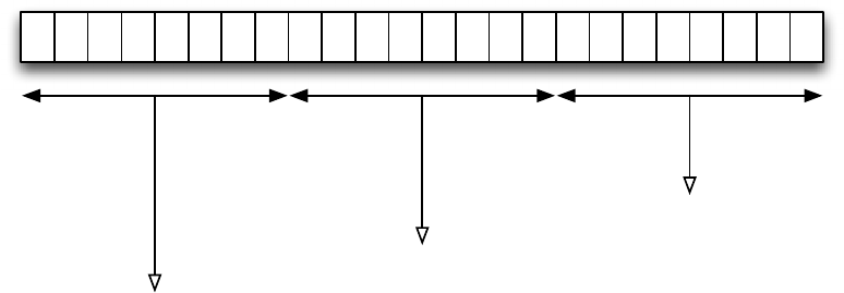
to the third byte of the secret key. This is illustrated below; in this example, the 24-bit secret key is
000000110101111100111100 = x035F3C. The diagram shows how each of secret_key[0], secret_key[1], and
secret_key[2] are found.
secret_key[0] = 00111011 = x03 = 3
000000110101111100111100
secret_key[1] = 01011111 = x5F = 95
secret_key[2] = 00111100 = x3C = 60
The encrypted message (the input) consists of 32 bytes, and in the above pseudo-code, encrypted_input[k] refers
to the kth byte in the encrypted input. The decrypted message (the output) will also be 32 bytes; in the above
pseudo-code, decrypted_output[k] refers to the kth byte in the encrypted output.
Page 5 of 11
Task 1: Creating a memory, instantiating it, and writing to it (20% of functionality)
To get started, download the template and open the Quartus project. In this task, you will get started by creating a
RAM using the Megafunction Wizard, creating circuitry to fill the memory, and observing the memory contents
using the In-System Memory Content Editor.
a) Creating a RAM block using the Wizard
(If you have a DE2 and are using Quartus 13.0sp1) Choose Tools->MegaWizard Plug In Manager. Choose
to create a new custom megafunction variation. In the left panel, expand Memory Compiler, and choose RAM:
1-Port.
(If you have a DE1-SoC and are using Quartus 14.1) Choose Tools->IP Catalog. In the IP Catalog, select
Basic Functions->On Chip Memory->RAM: 1-Port.
Create an output file called s_memory.vhd in your project directory and hit next. In the next few panels,
customize your Megafunction as indicated below.
How wide should the ‘q’ output bus be? 8 bits
How many 8-bit words of memory? 256 words
What should the memory block type be? M4K (DE2), or M10K (DE1-SoC)
What clocking method would you like to use? Single clock
Which ports should be registered: Make sure ‘q’ output port is unselected
Create one clock enable signal… : do not select
Create an ‘aclr’ asynchronous clear… : do not select
Create a ‘rden’ read enable… : do not select
(DE1-SoC only) What should the q output be…: New Data
Do you want to specify the initial contents? No
Allow In-System Memory Content Editor to capture and update.. Select this option
The ‘Instance ID’ of this RAM is S
Generate netlist: do not select
Output files: select s_memory.cmp (VHDL Component declaration file)
Do you want to add the Quartus II File to the project? Yes
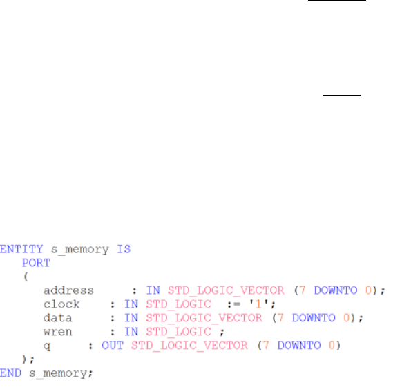
When you finish this, you will find the file s_memory.qip in your project file list. Click on the triangle beside
s_memory.qip to expand, and you will see s_memory.vhd. Open this file and examine it. Near the top of your
file, you will find the Entity declaration for s_memory, which will look something like this:
Be sure your declaration matches the above. This is the entity you will include as a component in your design.
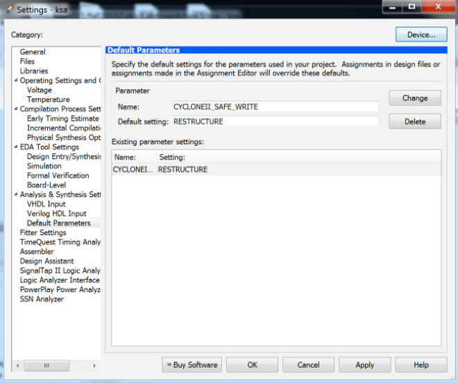
b) Setting Assignment (if you are using a DE1-SoC, skip this step)
Because you are going to use the In-System Memory Content Editor, you must make one additional setting in your
project. Choose Assignments->Settings and open Analysis And Synthesis Settings->Default Parameters.
Page 6 of 11
Type the parameter name CYCLONEII_SAFE_WRITE and assign the value RESTRUCTURE as shown in the
following diagram (be sure to spell it exactly right). Click ADD and then OK.
c) Creating a VHDL module that writes to your memory
Look at the top-level file ksa.vhd. You are to add code to implement the following algorithm (this is the very first
part of RC4).
for i = 0 to 255 {
s[i] = i;
}
If you see a message something like
“Error (15684): M4K memory block WYSIWYG primitive
"s_memory:u0|altsyncram:altsyncram_component|altsyncram_5ee1:auto_generated|altsyncram_l2a2:alts
yncram1|ram_block3a1" utilizes the dual-port dual-clock mode. However, this mode is not supported in
Cyclone II device family in this version of Quartus II software. Please refer to the Cyclone II FPGA
Family Errata Sheet for more information on this feature.
Then it is probably because you either forgot step (b) above, or else mistyped the name or default setting. Open
the settings again and verify that it is correct. Be sure your design compiles without errors before going on.
d) Running your code.
Program your design and run it as usual. The circuit will fill the on-chip memory with the numbers 0-255. To
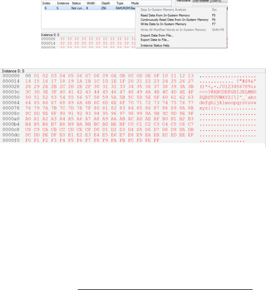
examine the contents of the memory, you can choose Tools->In System Memory Content Editor (while your
circuit is running). This will open a window that shows the memory contents. In the instance manager window
(left) you should see a list of memories in your design (in this case, it is only S). Right click S, and choose Read
Data from In-System Memory.
Page 7 of 11
This memory contents will be read and displayed. You should see something like:
As you can see, the memory has been filled. Each location i contains the value i. Be sure that your program has
filled the memory as expected. You will use the In-System Memory Content Editor to help you debug your lab in
Task 2, so be sure you are able to get this working before moving on.
Task 2: Building a Single Decryption Core (40% of functionality)
In this task, you are to continue your design from Task 1 to implement a single decryption core. Given a 24 bit
key, and an encrypted message in a ROM, your algorithm will decrypt the message and store the result in another
memory. You will then use the In-System Memory Content Editor to read the result to ensure the encryption
occurred as expected.
As shown below, your system will consist of three memories and a state machine/datapath. The initial encrypted
message is stored in a 32-word ROM (which you will initialize using a .mif file when you compile the design).
The result is stored in a 32-word RAM (which you can examine using the In-System Memory Content Editor after
the decryption is complete. In addition, you will use a 256x8 bit S memory (the same memory you used in Task
2). The secret key is set using the slider switches. Note that the secret key should be 24 bits long, but you only
have 18 slider switches on the DE2 board (and only 10 on the DE1-SoC board). For this task only (not Task 3),
you can hardwire the upper 14 bits of the secret key to 0.
The diagram below shows the design of your system. Although it shows bits 23-18 of the key are “0” and the
switches are used for bits 17-0, you should set bits 23-10 to “0” and just use bits 9-0 from the switches.
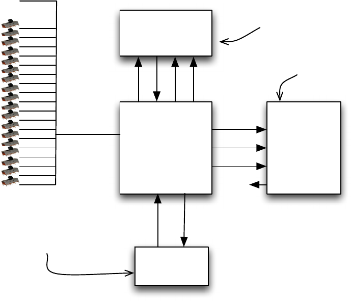
Page 8 of 11
Encrypted
Message
32x8 ROM
Decrypted
Message
RAM
32x8
Working Memory
RAM (S)
(256x8)
Your
State Machine/
Datapath
address_d
data_d
wren_d
q_d
address
data
wen
qq_m
address_m
secret_key
(24 bits)
"000000"
bit 0
SW(0)
SW(1)
SW(2)
SW(3)
SW(4)
SW(5)
SW(6)
SW(7)
SW(8)
SW(9)
SW(10)
SW(11)
SW(12)
SW(13)
SW(14)
SW(15)
SW(16)
SW(17)
bit 1
bit 2
bit 3
bit 4
bit 5
bit 6
bit 7
bit 8
bit 9
bit 10
bit 11
bit 12
bit 13
bit 14
bit 15
bit 16
bit 17
bits 18-23
The encrypted message we
give you goes here (the input)
The result
goes here
Working memory
Task 2a) Second Loop in algorithm
Starting with your Task 2 code, add hardware to implement the second loop from the algorithm on the second page
of this handout. That is, add code to implement the following (remember what I said about being able to omit
the "mod 256" operation in the "Background" section if you define the relevant quantities as 8-bit wide.
However you still need to implement "i mod keylength". The Verilog keyword for mod is "%")
j = 0
for i = 0 to 255 {
j = (j + s[i] + secret_key[i mod keylength] ) mod 256 //keylength is 3 in our impl.
swap values of s[i] and s[j]
}
This code does not use the encoded message ROM or the decoded message RAM (you will add that in part b
below). Test your code as follows. Set the secret key to 00000000 00000010 01001001 = x000249 (remember
you can set the lower order 10 bits of secret key using the slider switches as in the above diagram) and examine
the s array using the in-system memory content editor as before. Note that in this example secret_key [0] = 0x0,
secret_key [1] = 0x2, secret_key[2] = 0x49. Do not mix up the order of these or you will not get the right results!
You should see the following. If you do, your code is likely correct; if not, you have some debugging to do.
Don’t move on until you have this right.
Page 9 of 11
Task 2b) Rest of algorithm
Now you will complete the rest of the algorithm (the third for loop in the pseudo-code on Page 2 of this handout).
This will require adding two memories: one to store the encrypted message (this could be a ROM since the
message to decrypt will be compiled with your hardware) and one to store the decrypted message (this could be a
RAM since your circuit must write the result to it). To create the ROM and RAM, it is suggested that you use the
MegaWizard Plug In Manager (as you did for Task 2).
When creating a ROM using the MegaWizard Plug-In Manager (Quartus 13.0) or IP Library (Quartus 14.1), you
will have the ability to indicate an initialization file name. Use the name message.mif. There are example
message.mif files included in your project directory (under the folder secret_messages); you will need to make
sure this file is in your working directory before you create your component with the MegaWizard Plug In
Manager. During compilation, the contents in this file is then read (notice: it is read at compile time), and is used
as the initial contents of the memory. There are several other settings you will need to specify in the MegaWizard
Plug In Manager; you should know enough now that you can figure out what to use for each of these settings.
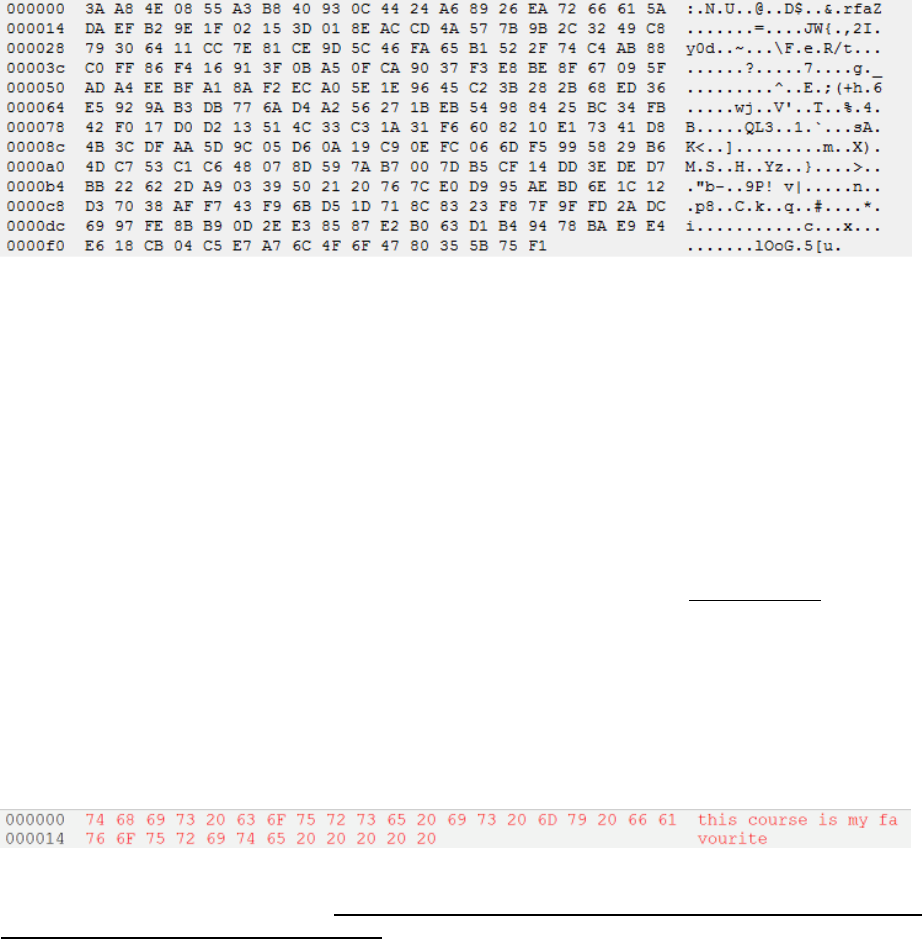
Test your design. If you decrypt the first message (in secret_messages/msg_1_for_task2b) (with secret key
00000000 00000010 01001001 = x000249) you should see the following if you use the In System Memory
Content editor to view the contents of the Decrypted Message RAM after your algorithm completes (note: not the
s memory; that will continue to contain pseudo-random bytes). As you can see, the decrypted message is an
ASCII string that you can read.
Check the other messages in the folder (they each have their own secret key). For each, you will need to replace
message.mif in your working directory. Due to a bug in Quartus II, you must also delete the db directory in
your working directory before recompiling (the db directory acts as a cache, and caches your most recent
message.mif file). Remember that the contents of the initial memory contents file is read at compile time, not run
time. Of course, the slider switches are read at run-time. Be sure to use the slider switches to set the appropriate
secret key (each of the three messages has its own secret key).
Common error: Watch out for a warning such as:
Critical Warning (127003): Can't find Memory Initialization File or Hexadecimal (Intel-Format) File
./db/message_mod.mif -- setting all initial values to 0
If you see this warning, it did not find your message.mif file during compilation. Make sure it is in your project
directory, and that you specified it properly when you made your component.
When you can read all the message, you can move on to Task 3. Be sure to back up your code; if you don’t get
Task 3 working, you can get part marks for demoing what you have here.

Page 10 of 11
Task 3: Cracking RC-4 (40% of functionality)
In this task, you are going to modify your design from Task 2 to “crack” a message that has been encrypted using
RC4. In this case, you have the encrypted message, but you do not know the key. You will implement a brute-
force algorithm which cycles through all possible keys. For each key, if the result string is a readable message,
then you will assume the string is correct. More precisely, your circuit will search through the key space until it
finds a result in which, for every character in the decoded output, the character is in the range [97,122]
(corresponding to the characters ‘a’ to ‘z’) or the value 32 (which is a space). All characters in the correct output
will either be a lower case letter or a space; the correct message will contain no upper character letters or
punctuation. Note that it is not enough that just one character is a lower case letter or space; all 32 characters in the
decoded output must be lower case letters or a space before you deem it correct. Of course, there is a chance that
even though a key leads to an ASCII string, the string is not actually correct, but if you work out the math you will
see that the odds of this are extremely low.
Prof. Wilton's implementation of this Task takes about 10 minutes to cycle through the entire key space (I haven't
timed my solution over the entire key space, but it will likely take longer since my solution is slower than Prof.
Wilton's). To make your life easier in the lab, I will tell you that, for every test case we will give you, the two most
significant bits in the correct key are 0. This reduces the size of the keyspace you have to search, meaning you
should be able to search the entire keyspace in a few minutes.
When your circuit finds a correct message, it should put the message in the result RAM and enter an endless loop
in which it does nothing. You can use the In System Memory Content editor to view the output to make sure it is
correct. You should also turn on an LED to indicate that the search has complete. If you search the entire
keyspace and do not find a correct message, then you should turn on a different LED.
The key that is being considered should be displayed on the HEX displays. The project contains a module in
SevenSegmentDisplayDecoder.v which can be used for this purpose. The input to this module is a 4-bit value, and
the output is a 7-bit value which is used to drive the 7-segment display on the DE2/DE1-SoC board. Since your
key is 24 bits, it will require 6 digits of display. Use HEX0 to HEX5. As your design quickly searches through
the keyspace, the HEX displays should be updated in real time, and show the key that is currently being
considered.
There are encoded messages available within the project directory, in the secret_messages/msg_*_for_task3
folders. You can test your design on these messages; you should be able to “crack” each test case. For your
demonstration, the TA will give you a new encoded message that you have never seen before, so make sure your
design works before demoing!
Challenge Task: Multi-Core Cracking (this qualifies for the full 15% Creativity Bonus)
In the challenge task, you will accelerate the keyspace search by using multiple instantiations of the decryption
circuit (core) in Task 3, and using each one to search a subset of the keyspace simultaneously. For example, if you
have two cores, one core could search all even keys and one could search all odd keys. If you have 4 cores, each
could search ¼ of the search space. When one unit finds a correct message, all units should stop.
For the challenge task, modify your design so that it contains at least four decryption cores that operate
simultaneously.
Page 11 of 11
Marking: What to demo depends on how far you get.
If you get the challenge task done, demo that, and explain to the TA how you parallelized the code across multiple
cores. The TA will likely give you a new encrypted message for you to solve. If your implementation is
successful, you do not need to demo Tasks 2 or 3.
If you get Task 3 done, but not the challenge task, demo a working Task 3. The TA will likely give you a new
encrypted message for you to solve. In this works, you do not need to demo Task 2.
If you only get Task 2 done, demo that. If you have Task 2 plus parts of Task 3 done (but not a complete working
system), demo Task 2 and show the TA what you have for Task 3 for possible part marks.
If you only get Task 1 done, demo that. If you have Task 1 plus parts of Task 2 done (but not a complete working
system), demo Task 1 and show the TA what you have for Task 2 for possible part marks.
If you didn’t get Task 1 done, show the TA what you have for possible part marks.
Specific grading requirements for this lab
To receive full points for simulation, you need to simulate all FSMs that you write, and demonstrate/explain those
simulations to the TA.
Do not forget the rules of good design:
- Always design while thinking about the hardware
implementation
- Use simple structures
- Incremental design and test
- Modular design: divide the work, work in
parallel in the group
- Use the RTL viewer
- Verification and test: Use simulations,
LEDs, 7-segments, SignalTap, LCD scope (or
SignalTap equivalent)
- Write Clean, Neat, and Legible code
- Give meaningful names to variables, use comments
- Go over and understand the warnings given by
Quartus during compilation
- The circuit should be correct by design, not just
by simulation.
- The code should be verifiable by inspection
- Design in a modular fashion, always thinking
about future reutilization of the module.
- Re-use proven modules, instead of re-inventing
the wheel all the time
