LinkIt 2523 HDK V11 User's Guide Link It Users
LinkIt_2523_HDK_Users_Guide
LinkIt_2523_HDK_Users_Guide
User Manual:
Open the PDF directly: View PDF ![]() .
.
Page Count: 88
- 1. Introduction
- 2. Get Started with the HDK
- 3. Hardware Description
- 4. Hardware Configuration
- 4.1. Microcontroller unit
- 4.2. Power
- 4.3. Jumpers
- 4.4. LEDs
- 4.5. Buttons
- 4.6. GPIO
- 4.7. LCM
- 4.8. Audio
- 4.9. Speech
- 4.10. MSDC
- 4.11. Camera
- 4.12. USB
- 4.13. GNSS (LinkIt 2523G only)
- 4.14. Bluetooth and Bluetooth Low Energy
- 4.15. Debugging
- 4.16. Connectors
- 4.16.1. UART pin header
- 4.16.2. I2C pin header
- 4.16.3. Battery connector CON2102
- 4.16.4. Push-Push micro SD tray CON4101
- 4.16.5. RTC battery connector BAT5201
- 4.16.6. OMTP standard audio connector CON6001
- 4.16.7. Serial display connector CON6102
- 4.16.8. Camera daughterboard connector CON6201
- 4.16.9. Sensor daughterboard connector CON6301
- 4.16.10. USB 2.0 high speed connector
- 4.16.11. CMSIS-DAP USB 1.1 full speed connector
- 4.16.12. MK20 JTAG connector
- 4.16.13. eMMC / micro SD holder jumpers
- 4.16.14. JTAG connector CON9002
- 4.16.15. SMA connectors
- 4.16.16. External component connectivity support
- 5. Schematics (V11)
- 6. Layout (V11)
- 7. LinkIt 2523 HDK’s BOM (V11)
- 8. Appendix A: Acronyms and Abbreviations

LinkIt 2523 HDK v11 User's Guide
Version: 1.1
Release date: 4 November 2016
© 2015 - 2016 MediaTek Inc.
This document contains information that is proprietary to MediaTek Inc. (“MediaTek”) and/or its licensor(s). MediaTek cannot grant you
permission for any material that is owned by third parties. You may only use or reproduce this document if you have agreed to and been
bound by the applicable license agreement with MediaTek (“License Agreement”) and been granted explicit permission within the License
Agreement (“Permitted User”). If you are not a Permitted User, please cease any access or use of this document immediately. Any
unauthorized use, reproduction or disclosure of this document in whole or in part is strictly prohibited. THIS DOCUMENT IS PROVIDED ON AN
“AS-IS” BASIS ONLY. MEDIATEK EXPRESSLY DISCLAIMS ANY AND ALL WARRANTIES OF ANY KIND AND SHALL IN NO EVENT BE LIABLE FOR ANY
CLAIMS RELATING TO OR ARISING OUT OF THIS DOCUMENT OR ANY USE OR INABILITY TO USE THEREOF. Specifications contained herein are
subject to change without notice.

LinkIt 2523 HDK v11 User's Guide
© 2015 - 2016 MediaTek Inc. Page i of v
This document contains information that is proprietary to MediaTek Inc. (“MediaTek”) and/or its licensor(s).
Any unauthorized use, reproduction or disclosure of this document in whole or in part is strictly prohibited.
Document Revision History
Revision Date Description
1.0 2 September 2016 Initial release. This document is for LinkIt 2523 HDK v11.
1.1 4 November 2016 • Updated introduction to include top and bottom views of the
LinkIt 2523 HDK v11.
• Updated the section for Bluetooth and Bluetooth Low Energy.
• Updated the schematic and the BOM list.

LinkIt 2523 HDK v11 User's Guide
© 2015 - 2016 MediaTek Inc. Page ii of v
This document contains information that is proprietary to MediaTek Inc. (“MediaTek”) and/or its licensor(s).
Any unauthorized use, reproduction or disclosure of this document in whole or in part is strictly prohibited.
Table of contents
1. Introduction ........................................................................................................................................ 1
2. Get Started with the HDK .................................................................................................................... 3
2.1. Installing the LinkIt 2523 HDK drivers on Microsoft Windows ........................................................... 3
2.2. Downloading the project image using the LinkIt 2523 HDK as a removable storage ......................... 6
3. Hardware Description ......................................................................................................................... 7
4. Hardware Configuration .................................................................................................................... 10
4.1. Microcontroller unit ......................................................................................................................... 10
4.2. Power ................................................................................................................................................ 10
4.3. Jumpers ............................................................................................................................................ 16
4.4. LEDs .................................................................................................................................................. 18
4.5. Buttons ............................................................................................................................................. 20
4.6. GPIO .................................................................................................................................................. 21
4.7. LCM ................................................................................................................................................... 22
4.8. Audio ................................................................................................................................................ 25
4.9. Speech .............................................................................................................................................. 25
4.10. MSDC ................................................................................................................................................ 25
4.11. Camera ............................................................................................................................................. 27
4.12. USB ................................................................................................................................................... 29
4.13. GNSS (LinkIt 2523G only) .................................................................................................................. 30
4.14. Bluetooth and Bluetooth Low Energy............................................................................................... 30
4.15. Debugging ......................................................................................................................................... 32
4.16. Connectors ........................................................................................................................................ 34
5. Schematics (V11) ............................................................................................................................... 49
6. Layout (V11)...................................................................................................................................... 71
7. LinkIt 2523 HDK’s BOM (V11) ............................................................................................................ 75
8. Appendix A: Acronyms and Abbreviations ......................................................................................... 82

LinkIt 2523 HDK v11 User's Guide
© 2015 - 2016 MediaTek Inc. Page iii of v
This document contains information that is proprietary to MediaTek Inc. (“MediaTek”) and/or its licensor(s).
Any unauthorized use, reproduction or disclosure of this document in whole or in part is strictly prohibited.
Lists of tables and figures
Table 1. Power input jumpers ............................................................................................................................... 10
Table 2. GPIO voltage level customization with jumper and pin (illustrated) settings ......................................... 11
Table 3. Enabling the active GPS antenna on HDK with jumper pin settings (illustrated) .................................... 13
Table 4. PSRAM power source selection jumpers ................................................................................................. 14
Table 5. Serial flash I/O power source selection jumper ...................................................................................... 15
Table 6. Analog I/O power source selection jumper ............................................................................................. 15
Table 7. LinkIt 2523 HDK jumper index ................................................................................................................. 16
Table 8. The LED indicators ................................................................................................................................... 18
Table 9. Buttons and corresponding keypad functionality ................................................................................... 20
Table 10. LinkIt 2523 board’s eFuse jumper pin settings (illustrated) .................................................................. 22
Table 11. LinkIt 2523 board’s RTC jumper pin settings ......................................................................................... 22
Table 12. LCM backlight source selection settings (illustrated) ............................................................................ 23
Table 13. LinkIt 2523 HDK display peripheral jumper pin settings (illustrated) .................................................... 24
Table 14. Jumper settings (illustrated) for storage options .................................................................................. 25
Table 15. Jumper pin settings (illustrated) for camera and sensor daughterboards ............................................ 28
Table 16. Jumper pin settings (illustrated) for Bluetooth ..................................................................................... 31
Table 17. Resistor selections ................................................................................................................................. 33
Table 18. Battery connector CON2101 (see Figure 18) ......................................................................................... 34
Table 19. Micro-SD tray ........................................................................................................................................ 35
Table 20. OMTP Audio jack connector .................................................................................................................. 35
Table 21. LCM serial display daughterboard connector ....................................................................................... 36
Table 22. Serial camera daughterboard connector CON6201 .............................................................................. 37
Table 23. Sensor daughterboard connector CON6301 ......................................................................................... 38
Table 24.The HDK’s high speed USB 2.0 connector .............................................................................................. 39
Table 25. CMSIS-DAP USB full speed connector ................................................................................................... 40
Table 26. MK20 JTAG connector pin definition ..................................................................................................... 41
Table 27. eMMC/micro SD jumpers ...................................................................................................................... 41
Table 28. JTAG connector CON9002 ..................................................................................................................... 41
Table 29. GPIO pin functionalities ......................................................................................................................... 43
Table 30. LinkIt 2523 HDK bill of materials ........................................................................................................... 75
Table 31. Acronyms and abbreviations ................................................................................................................. 82
Figure 1. Top view of the LinkIt 2523 HDK v11 ....................................................................................................... 1
Figure 2. Bottom view of the LinkIt 2523 HDK v11 ................................................................................................. 2
Figure 3. USB connectors on the LinkIt 2523 development board ......................................................................... 3
Figure 4. Device COM port for debugging on your PC ............................................................................................ 4
Figure 5. Device COM port for logging on your PC ................................................................................................. 5
Figure 6. A typical USB to UART converter.............................................................................................................. 5
Figure 7. LinkIt 2523 HDK connected as removable disk storage ........................................................................... 6
Figure 8. LinkIt 2523 HDK’s top view....................................................................................................................... 8
Figure 9. LinkIt 2523 HDK’s bottom view ................................................................................................................ 9

LinkIt 2523 HDK v11 User's Guide
© 2015 - 2016 MediaTek Inc. Page iv of v
This document contains information that is proprietary to MediaTek Inc. (“MediaTek”) and/or its licensor(s).
Any unauthorized use, reproduction or disclosure of this document in whole or in part is strictly prohibited.
Figure 10. The positions of jumpers J1105, J1110 to J1112. J1114, resistors R4101, R1113, GPDAC test point TP1101
and micro SD cardholder ...................................................................................................................................... 12
Figure 11. The jumper positions for J5201 and J5202, J1106, J1108, J1109 ......................................................... 14
Figure 12. LED positions for LED2001, LED2003 and LED6601 ............................................................................. 19
Figure 13. LED positions for LED9201, LED9206 and LED9209 ............................................................................. 20
Figure 14. The positions of buttons, strap pin resistors, jumpers J1102 to J1104 ................................................ 21
Figure 15. LCM display module and backlight jumper locations .......................................................................... 23
Figure 16. Jumpers J1001 to J1006 for storage options ........................................................................................ 27
Figure 17. Jumper pin locations of J1007 to J1012, J1015 .................................................................................... 28
Figure 18. Positions of J1101 and Bluetooth antenna path selection from J5001 to J5004, U1101, CON2101 and
resistor R5005 ....................................................................................................................................................... 31
Figure 19. The positions of UART and I2C pin header for debugging facilitation ................................................. 34
Figure 20. Micro-SD card holder CON4101 ........................................................................................................... 35
Figure 21. Serial LCM daughterboard’s connector and I2C pull-up resistors (R1002, R1003) ............................. 36
Figure 22. Serial camera daughterboard CON6201 .............................................................................................. 37
Figure 23. The position of the camera daughterboard pin headers ..................................................................... 37
Figure 24. High-speed USB2.0 connector ............................................................................................................. 39
Figure 25. CMSIS-DAP USB 1.1 full speed connector ............................................................................................ 39
Figure 26. MK20 JTAG connector, sensor daughterboard connector and PSRAM power switch J1113 .............. 40
Figure 27. JTAG connector CON9002 pin definition ............................................................................................. 42
Figure 28. LinkIt 2523 HDK extension connectors ................................................................................................ 43
Figure 29. Block diagram ....................................................................................................................................... 50
Figure 30. I2C ID .................................................................................................................................................... 51
Figure 31. PMU_SPEC ............................................................................................................................................ 52
Figure 32. BB MT2523G BB ................................................................................................................................... 53
Figure 33. BB_MT2523G_ABB ............................................................................................................................... 54
Figure 34. POWER_COMMON_LDO ...................................................................................................................... 55
Figure 35. POWER_Charging ................................................................................................................................. 56
Figure 36. MEMORY_eMMC ................................................................................................................................. 57
Figure 37. MEMORY_SD Card ............................................................................................................................... 58
Figure 38. CONNECTIVITY_BT_MT2523G .............................................................................................................. 59
Figure 39. CONNECTIVITY_GPS_MT2523G ........................................................................................................... 60
Figure 40. PERI_Audio_IO ..................................................................................................................................... 61
Figure 41. PERI_LCD_Capacitive touch panel ........................................................................................................ 62
Figure 42. PERI_CAMERA ...................................................................................................................................... 63
Figure 43. PERI_SENSOR_DTB_IO ......................................................................................................................... 64
Figure 44. PERI_USB .............................................................................................................................................. 65
Figure 45. PERI_KEY .............................................................................................................................................. 66
Figure 46. PERI_SWD ............................................................................................................................................. 67
Figure 47. DEBUG_IO ............................................................................................................................................ 68
Figure 48. POWER INDICATOR .............................................................................................................................. 69
Figure 49. LCM ...................................................................................................................................................... 70
Figure 50. LinkIt 2523 HDK layout (Layer 1) .......................................................................................................... 71
Figure 51. LinkIt 2523 HDK layout (Layer 2) .......................................................................................................... 72

LinkIt 2523 HDK v11 User's Guide
© 2015 - 2016 MediaTek Inc. Page v of v
This document contains information that is proprietary to MediaTek Inc. (“MediaTek”) and/or its licensor(s).
Any unauthorized use, reproduction or disclosure of this document in whole or in part is strictly prohibited.
Figure 52. LinkIt 2523 HDK layout (Layer 3) .......................................................................................................... 73
Figure 53. LinkIt 2523 HDK layout (Layer 4) .......................................................................................................... 74

LinkIt 2523 HDK v11 User's Guide
© 2015 - 2016 MediaTek Inc. Page 1 of 82
This document contains information that is proprietary to MediaTek Inc. (“MediaTek”) and/or its licensor(s).
Any unauthorized use, reproduction or disclosure of this document in whole or in part is strictly prohibited.
1. Introduction
MediaTek LinkIt™ 2523 hardware development kit (HDK) by SAC is a fully functional development platform for
RTOS for IoT and Wearable applications powered by MediaTek MT2523G, an ARM Cortex-M4 core-based
microcontroller unit (MCU). The HDK has rich connectivity features and interfaces such as SPI, I2S, PCM, UART,
ADC, PWM, JTAG and clock out generators.
The LinkIt 2523 HDK enables application development, prototyping and evaluation using sensors, Bluetooth,
Bluetooth low energy, GNSS, audio (speech, headset and speaker), MIPI, serial, camera serial interface, keypad,
battery management, micro SD and eMMC portable storage support and high speed USB 2.0. The LinkIt 2523 HDK
also has built-in antenna that is able to receive Bluetooth (compatibility with up to 4.0 and higher versions), and
GNSS (GPS, GLONASS and BeiDou) signals. In addition, the USB to serial wire debug (SWD) converter and JTAG
feature provides convenient development and debugging.
The LinkIt 2523 HDK supports OpenSDA to provide more streamlined development to debug and flash the binary
code.
This user’s guide covers MT2523G and MT2523D integrated chipsets. The functions and pin assignments from both
chipsets are identical, except the MT2523D doesn’t support GNSS communication.
The user manual guides you through the following.
• Describing the hardware features of the LinkIt 2523 HDK.
• Configuring the LinkIt 2523 HDK with specific pin and jumper assignments.
• Providing the hardware schematics for more detailed configuration and reference design.
• Listing bill of materials (BOM) for the LinkIt 2523 HDK.
Front and back views of the LinkIt 2523 HDK version 11 are presented in Figure 1 and Figure 2, respectively.
Figure 1. Top view of the LinkIt 2523 HDK v11

LinkIt 2523 HDK v11 User's Guide
© 2015 - 2016 MediaTek Inc. Page 2 of 82
This document contains information that is proprietary to MediaTek Inc. (“MediaTek”) and/or its licensor(s).
Any unauthorized use, reproduction or disclosure of this document in whole or in part is strictly prohibited.
Figure 2. Bottom view of the LinkIt 2523 HDK v11

LinkIt 2523 HDK v11 User's Guide
© 2015 - 2016 MediaTek Inc. Page 3 of 82
This document contains information that is proprietary to MediaTek Inc. (“MediaTek”) and/or its licensor(s).
Any unauthorized use, reproduction or disclosure of this document in whole or in part is strictly prohibited.
2. Get Started with the HDK
This section provides details on how to configure the HDK and install the required peripheral drivers for the full
operation of the development platform.
Before commencing the application development, set the jumpers for the camera daughterboard, as shown in
Figure 3.
Figure 3. USB connectors on the LinkIt 2523 development board
The 2523 USB can be used for powering up the board and downloading the binary with LinkIt 2523 Flash Tool.
The MK20 USB can be used for debugging with GDB and downloading the binary using Keil IDE. To learn more
about 2523 USB COM port driver, see section 2.3, “Installing the USB driver” of MT2523 Flash Tool Users Guide.
2.1. Installing the LinkIt 2523 HDK drivers on Microsoft Windows
Install mbed serial port driver to use the USB serial port on Windows OS for debugging:
1) Download and install the Windows serial port driver from here.
2) Connect the board to the computer through 2523 USB and the MK20 USB.
3) Open Windows Control Panel, click System and:
• On Windows 7 and 8, click Device Manager.
• On Windows XP, click the Hardware tab and then Device Manager.
4) In Device Manager, navigate to Ports (COM & LPT) (see Figure 4).
Jumpers for the Camera
Daughterboard
2523 USB
MK20 USB
System
Power
3 2 1

LinkIt 2523 HDK v11 User's Guide
© 2015 - 2016 MediaTek Inc. Page 4 of 82
This document contains information that is proprietary to MediaTek Inc. (“MediaTek”) and/or its licensor(s).
Any unauthorized use, reproduction or disclosure of this document in whole or in part is strictly prohibited.
A new COM device should appear under Ports (COM & LPT), as shown in Figure 4. Note the COMx port
number of the mbed Serial Port. Use this port to send and receive data to and from the LinkIt 2523 HDK.
Figure 4. Device COM port for debugging on your PC
To install a USB to UART driver, such as prolific USB to UART converter:
1) Connect a USB to UART cable to PC, such as USB to Serial/UART Bridge Controller (Integrated crystal/OTP).
A new unknown device will be detected on Microsoft Windows system, if the device driver wasn’t setup
before.
2) Download and install the USB to UART cable driver from Prolific. After the driver is installed, unknown
device will be changed to Prolific USB-to-Serial Comm Port.
3) Open Windows Control Panel, click System.
• On Windows 7 and 8, click Device Manager.
• On Windows XP, click the Hardware tab and then Device Manager.
4) In Device Manager, navigate to Ports (COM & LPT) (see Figure 5). A new COM device should appear.
Note the COMx port number of the Prolific USB-to-Serial Comm Port. The COM port can now be used
to receive system logs through the UART interface on the LinkIt 2523 HDK.

LinkIt 2523 HDK v11 User's Guide
© 2015 - 2016 MediaTek Inc. Page 5 of 82
This document contains information that is proprietary to MediaTek Inc. (“MediaTek”) and/or its licensor(s).
Any unauthorized use, reproduction or disclosure of this document in whole or in part is strictly prohibited.
Figure 5. Device COM port for logging on your PC
A typical USB to UART converter is shown in Figure 6. The USB connector should be connected to the PC. The jump
wires (count of four) should be connected to the UART interface on the LinkIt 2523 HDK. Connect the black wire to
the GND, the white wire to the RX and the green wire to the TX and no need to connect the red wire. Once the
converter is connected, the system logs will display on the serial monitor tool, such as Tera Terminal. Figure 19
shows the UART port connector location.
Figure 6. A typical USB to UART converter
LinkIt 2523 HDK v11 User's Guide
© 2015 - 2016 MediaTek Inc. Page 6 of 82
This document contains information that is proprietary to MediaTek Inc. (“MediaTek”) and/or its licensor(s).
Any unauthorized use, reproduction or disclosure of this document in whole or in part is strictly prohibited.
2.2. Downloading the project image using the LinkIt 2523 HDK as a
removable storage
To update the FreeRTOS image only (example project image: iot_sdk_demo.bin) use the LinkIt 2523 HDK as a
removable disk drive according to the following steps:
1) Connect the LinkIt 2523 HDK to your PC with a micro-USB cable to the MK20 USB connector.
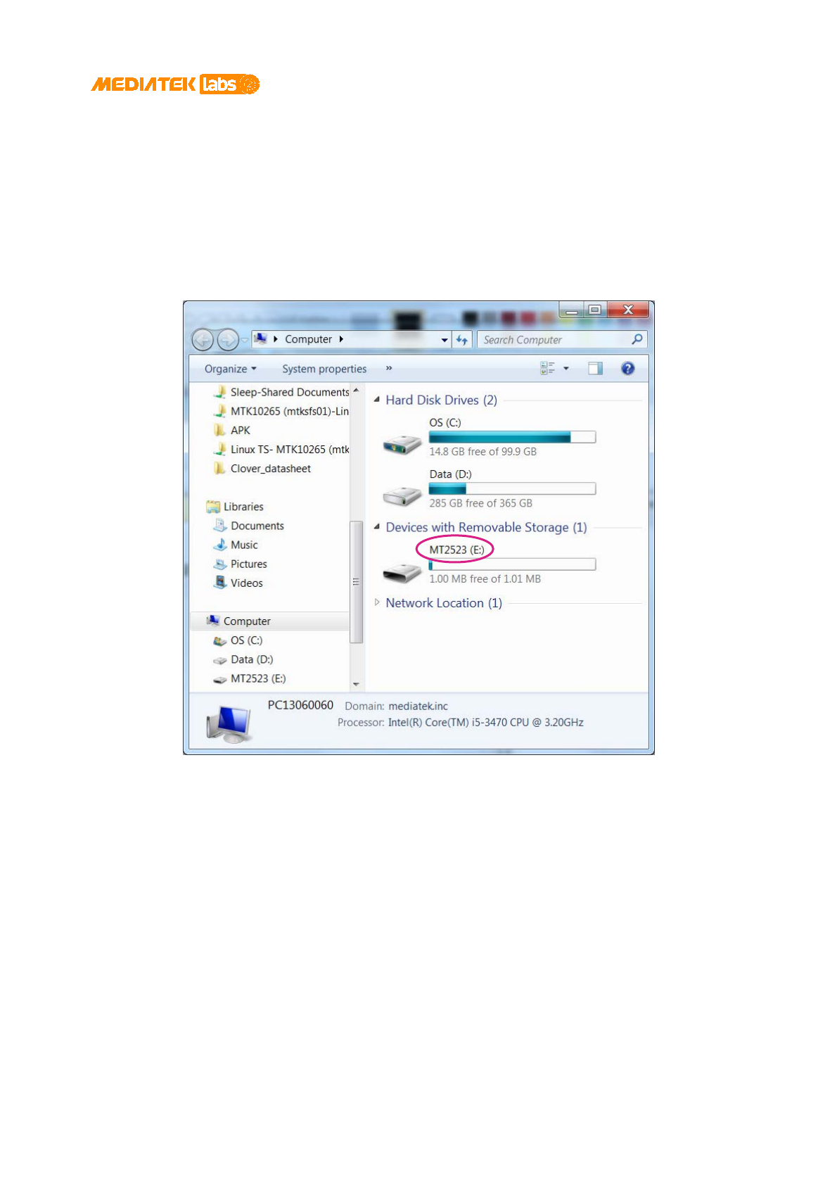
2) Navigate to Computer on your PC to check if a new mass storage named MT2523 is available
under Devices with Removable Storage, as shown in Figure 7.
Figure 7. LinkIt 2523 HDK connected as removable disk storage
3) Open the MT2523 removable storage, then drag and drop the project image, such as
iot_sdk_demo.bin, from the original image folder to update the image on the HDK’s flash.

LinkIt 2523 HDK v11 User's Guide
© 2015 - 2016 MediaTek Inc. Page 7 of 82
This document contains information that is proprietary to MediaTek Inc. (“MediaTek”) and/or its licensor(s).
Any unauthorized use, reproduction or disclosure of this document in whole or in part is strictly prohibited.
3. Hardware Description
LinkIt 2523 HDK provides connections between the system on chip (SOC) and the peripherals, such as micro SD
card, eMMC, MIPI LCM, serial LCM, touch panel, serial camera, sensor daughterboard, GNSS, Bluetooth, audio
speech and high speed USB 2.0.
The top and bottom layout views (Figure 8 and Figure 9, respectively) show the positions of the peripherals on the
development board. Some of the peripheral interfaces are mutually exclusive. The eMMC and the micro SD, for
example, cannot be used at the same time, as the corresponding pins can only be assigned to one function at a
time.
The LinkIt 2523 HDK provides the following features for application development.
• ARM Cortex-M4 core-based MT2523G microcontroller.
• Internal 160kB SRAM and 4MB PSRAM.
• Internal 4MB serial flash.
• Rich interfaces.
• Three I2Cs.
• Four master SPIs and a slave SPI.
• One master I2S and one slave I2S.
• One PCM interface that supports master.
• Four sets of UARTs. The first set of UART is directly configured through pin headers, the other three sets
are software configurable.
• Five 12-bit ADCs.
• Six PWMs by alternative voltage level.
• Two SDMMCs.
• JTAG debugging support.
• Five sets of clock outputs.
• Peripherals.
• One serial camera interface supporting up to 3-bit mode image capture.
• Two display modes supporting serial interface and MIPI with the resolution of up to 320*320 pixels.
• Keypad supported to simulate buttons, such as volume up or down, backward and enter.
• Onboard speaker, onboard analog microphone and audio jack appliance.
• User-friendly customization.
• Supports Bluetooth (2.4GHz) and GNSS onboard antenna connectivity and an SMA connector for
dedicated antenna connectivity.
• Supports 2-wire SWD interface for debugging purposes.
• Headers for convenient and accurate current measurement.

LinkIt 2523 HDK v11 User's Guide
© 2015 - 2016 MediaTek Inc. Page 8 of 82
This document contains information that is proprietary to MediaTek Inc. (“MediaTek”) and/or its licensor(s).
Any unauthorized use, reproduction or disclosure of this document in whole or in part is strictly prohibited.
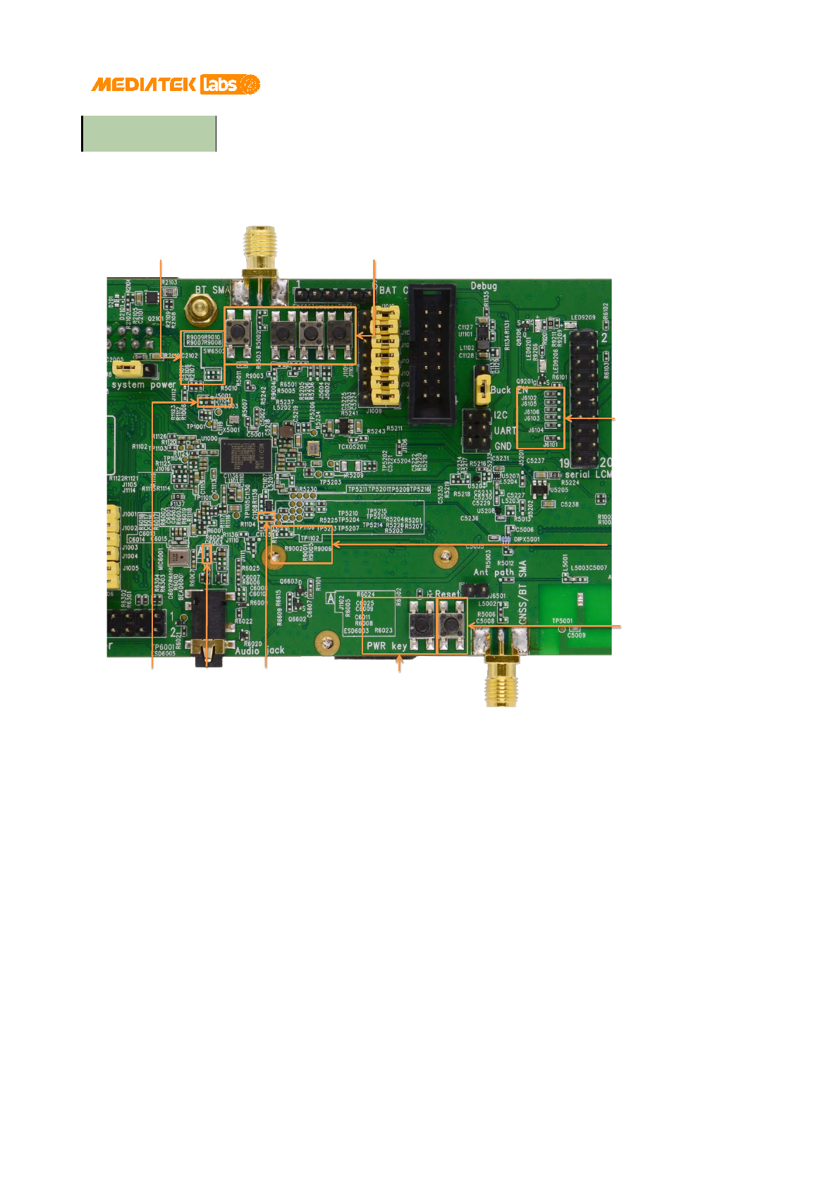
Figure 8. LinkIt 2523 HDK’s top view
BT SMA
(SMA 5002)
R9023
Analog
Microphone
(MIC6001)
GNSS/BT SMA
(SMA 5001)
Analog Jack

LinkIt 2523 HDK v11 User's Guide
© 2015 - 2016 MediaTek Inc. Page 9 of 82
This document contains information that is proprietary to MediaTek Inc. (“MediaTek”) and/or its licensor(s).
Any unauthorized use, reproduction or disclosure of this document in whole or in part is strictly prohibited.
Figure 9. LinkIt 2523 HDK’s bottom view
For more details on the HDK schematics see chapter 5, “Schematics”.
GNSS RTC
Battery
R9017 to R9021
2523 JTAG (CON9002)
Connector
Speaker with
Housing
R4005

LinkIt 2523 HDK v11 User's Guide
© 2015 - 2016 MediaTek Inc. Page 10 of 82
This document contains information that is proprietary to MediaTek Inc. (“MediaTek”) and/or its licensor(s).
Any unauthorized use, reproduction or disclosure of this document in whole or in part is strictly prohibited.
4. Hardware Configuration
4.1. Microcontroller unit
The LinkIt 2523 HDK is powered by MediaTek MT2523G SOC, designed for IoT applications and equipped with
flexible pin assignments for custom applications.
MT2523G SOC is an ARM Cortex-M4 core-based architecture with built-in Bluetooth and Bluetooth Low Energy
connectivity support, GNSS, audio interface, internal PSRAM and flash storage. The LinkIt 2523 HDK provides
peripheral support for the I2C, SPI, UART, ADC, PWM, clock generator, audio and SDMMC interfaces.
LinkIt 2523 platform featured applications include but are not limited to industrial applications and automation,
medical signal processing applications, such as sports physiological signal recording, long term medical data
recording, home automation applications, tracking and safety applications using GNSS.
4.2. Power
This section describes the power source options for the LinkIt 2523 HDK. The HDK can operate powered by USB or
a battery. To charge the battery, the USB cable has to be connected. The board can enter to sleep mode using the
PSRAM memory. The sleep mode can be enabled or disabled by the software.
The LinkIt 2523 HDK also enables GPIO voltage setting configuration based on the supported components. It also
can supply power to the storage, such as micro SD or eMMC. The HDK supports an active GNSS antenna that
requires a power input, see section 4.2.4, “Powering on an active GPS antenna”.
4.2.1. Powering up with the USB
Connect a micro USB cable directly to 2523 USB or MK20 USB (see Figure 3) to supply power to the HDK. Set the
jumper J2001 (system power) to pin 1 and pin 2, to charge the battery using a USB connector. To boot up the
system without a battery, apply the jumper settings, as shown in Table 1. The jumper J2001 (system power)
location is marked in Figure 3, it’s assigned for the power rail source. The main power traces through jumper J2001
to the system.
For the battery criteria of LinkIt 2523 HDK, the capacity between 30mAh to 500mAh is recommended; charging
voltage from USB connector with tolerance between 4.15V to 7V is acceptable. The LinkIt 2523 HDK also supports
powering on the battery with power key, where the system power jumper setting is the same as to charge the
battery.
Table 1. Power input jumpers
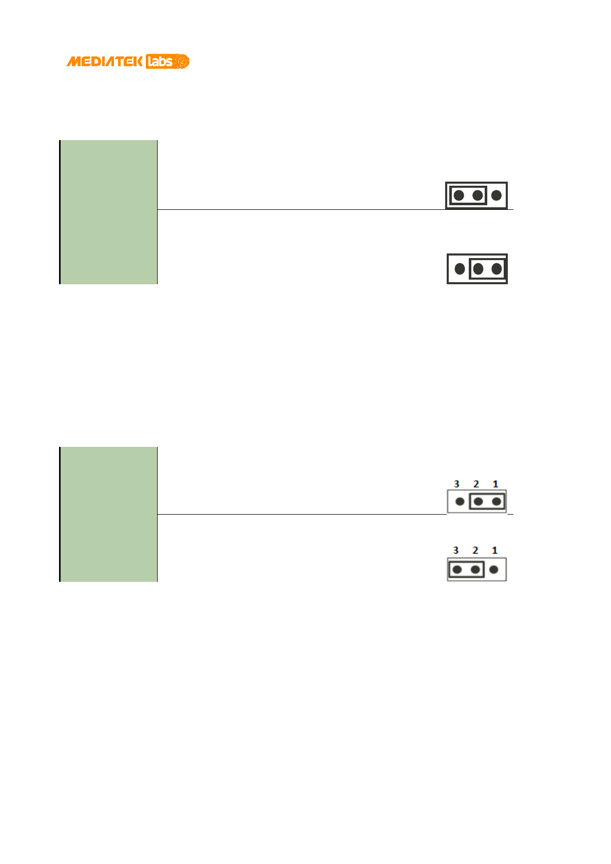
Power path switch Set the jumper J2001 pins to assign the power source from 2523 USB connector
or MK20 USB connector, as shown below.
Set the jumper J2001 pins to get the power source from battery connector
CON2101 (see Figure 18), as shown below.

LinkIt 2523 HDK v11 User's Guide
© 2015 - 2016 MediaTek Inc. Page 11 of 82
This document contains information that is proprietary to MediaTek Inc. (“MediaTek”) and/or its licensor(s).
Any unauthorized use, reproduction or disclosure of this document in whole or in part is strictly prohibited.
4.2.2. Power source for digital I/O
LinkIt 2523 HDK supplies power to devices with different voltage support. GPIO voltage level customization is
shown in Table 2. Jumper and resistor positions are specified in Figure 10 and Figure 11.
Table 2. GPIO voltage level customization with jumper and pin (illustrated) settings
Power rail
DVDD_VIO_A voltage
Set the jumper J1106 pins with 0Ω resistor to assign the power rail DVDD_VIO_A
to VIO28, as shown below.
Set the jumper J1106 pins with 0Ω resistor to assign the power rail DVDD_VIO_A
to VIO18, as shown below.
Power rail
DVDD_VIO_C voltage
Set the jumper J1108 pins with 0Ω resistor to assign the power rail
DVDD_VIO_C
to VIO28, as shown below.
Set the jumper J1108 pins with 0Ω resistor to assign the power rail
DVDD_VIO_C
to VIO18, as shown below.
Power rail
DVDD_GPO voltage
Set the jumper J1109 pins with 0Ω resistor to assign the power rail DVDD_GPO to
VIO28, as shown below.
Set the jumper J1109 pins with 0Ω resistor to assign the power rail DVDD_GPO to
VIO18, as shown below.
Power rail
DVDD18_VIO18
voltage selection
Set the jumper J1110 pins with 0Ω resistor to assign the power
rail DVDD18_VIO18 to VIO28, as shown below.
Set the jumper J1110 pins with 0Ω resistor to assign the power
rail DVDD18_VIO18 to VIO18, as shown below.
Power rail Set the jumper J1111 pins with 0Ω resistor to assign the power rail
DVDD_VMC
to
VIO28, as shown below.
1 2 3
1 2 3
1 2 3
1 2 3
1 2 3
1 2 3
1 2 3
1 2 3

LinkIt 2523 HDK v11 User's Guide
© 2015 - 2016 MediaTek Inc. Page 12 of 82
This document contains information that is proprietary to MediaTek Inc. (“MediaTek”) and/or its licensor(s).
Any unauthorized use, reproduction or disclosure of this document in whole or in part is strictly prohibited.
DVDD_VMC voltage
Set the jumper J1111 pins with 0Ω resistor to assign the power rail
DVDD_VMC
to
VIO18, as shown below.
Remove the jumper J1111 with 0Ω resistor to select the power rail DVDD_VMC
connected with VMC while the 0Ω resistor R1113 is mounted. Mount the 0Ω
resistors R1113 and R4101, to use micro SD storage.
Figure 10. The positions of jumpers J1105, J1110 to J1112. J1114, resistors R4101, R1113, GPDAC test point
TP1101 and micro SD cardholder
J1112
Micro SD
Cardholder
3
2
1
1 2 3
R4101 J1105
J1114
J1111
R1113
J1110
1 2 3
1
2
3
TP1101
1 2 3
1 2 3

LinkIt 2523 HDK v11 User's Guide
© 2015 - 2016 MediaTek Inc. Page 13 of 82
This document contains information that is proprietary to MediaTek Inc. (“MediaTek”) and/or its licensor(s).
Any unauthorized use, reproduction or disclosure of this document in whole or in part is strictly prohibited.
4.2.3. Powering on the eMMC or micro SD
The LinkIt 2523 HDK supports eMMC and micro SD card for storage. The HDK operates with either eMMC or micro
SD card (see Figure 10) enabled but not both at the same time.
4.2.4. Powering on an active GPS antenna
The active GPS antenna on LinkIt 2523 HDK can be either software controlled or hardware activated. Table 3
provides details on how to determine if the antenna is activated by direct power supply or by software control.
Adjust the jumpers J5201 and J5202 to change the settings. The jumper locations are shown in Figure 10 and
Figure 11.
Table 3. Enabling the active GPS antenna on HDK with jumper pin settings (illustrated)
Low noise amplifier
activation control
(should be synchronized
with J5202)
Set the jumper J5201 pins with 0Ω resistor to enable the active GPS
antenna using the power rail, as shown below.
Set the jumper J5201 pins with 0Ω resistor to enable the active GPS
antenna controlled by software settings, as shown below.
Active antenna power
supply (should be
synchronized with J5201)
Set the jumper J5202 pins with 0Ω resistor to supply power and enable
the active GPS antenna using the power rail, as shown below.
Set the jumper J5202 pins with 0Ω resistor to supply power and enable
the active GPS antenna controlled by software settings, as shown below.
1 2 3
1 2 3
1 2 3
1 2 3

LinkIt 2523 HDK v11 User's Guide
© 2015 - 2016 MediaTek Inc. Page 14 of 82
This document contains information that is proprietary to MediaTek Inc. (“MediaTek”) and/or its licensor(s).
Any unauthorized use, reproduction or disclosure of this document in whole or in part is strictly prohibited.
Figure 11. The jumper positions for J5201 and J5202, J1106, J1108, J1109
4.2.5. The LCM backlight power source ISINK
The current sink for LCM backlight is the pin named ISINK. The current and voltage settings are configurable.
If the current sink is active, LED9209 is powered on to indicate the backlight is enabled. More details can be found
in Table 8, Figure 12 and Figure 13.
4.2.6. PSRAM power source
The PSRAM power source can be set to either always powered on or could be controlled by user-defined settings.
Table 4 provides the jumper settings for each of the methods. The jumpers J1105 (see Figure 10) and J1113 (see
Figure 26) can be adjusted for PSRAM power source.
Table 4. PSRAM power source selection jumpers
PSRAM power supply J1105
(Should be synchronized
with J1113)
Connect the jumper J1105 pins with 0Ω resistor to set the power source
from VSWXM, as shown below.
J1108 J1106 J5201
J5202
J1109
1
2
3
3
2
1
1
2
3
3
2
1
1 2 3

LinkIt 2523 HDK v11 User's Guide
© 2015 - 2016 MediaTek Inc. Page 15 of 82
This document contains information that is proprietary to MediaTek Inc. (“MediaTek”) and/or its licensor(s).
Any unauthorized use, reproduction or disclosure of this document in whole or in part is strictly prohibited.
Connect the jumper J1105 pins with 0Ω resistor to set the power source
from VIO18, as shown below.
PSRAM power supply J1113
(Should be synchronized
with J1105)
Connect the jumper J1113 pins to set the power source from VIO18, as
shown below.
Connect the jumper J1113 pins to set the power source from VSWXM, as
shown below.
4.2.7. Serial flash I/O power source
Table 5 provides two different settings to power up the serial flash.
Table 5. Serial flash I/O power source selection jumper
Serial flash I/O
power supply J1112
Connect the jumper J1112 (see Figure 10) pins with 0Ω resistor to set the power
source from VIO18, as shown below.
Connect the jumper J1112 (see Figure 10) pins with 0Ω resistor to set the power
source from VSF, as shown below.
4.2.8. Analog I/O power selection
Table 6 provides two different settings to power up the analog I/O.
Table 6. Analog I/O power source selection jumper
Analog I/O power
supply J1114
Connect the jumper J1114 (see Figure 10) pins with 0Ω resistor to set the power
source from VA28, as shown below.
Connect the jumper J1114 pins with 0Ω resistor to set the power source from
VIO28, as shown below.
1 2 3
1 2 3
1 2 3
1 2 3
1 2 3
1 2 3
1 2 3

LinkIt 2523 HDK v11 User's Guide
© 2015 - 2016 MediaTek Inc. Page 16 of 82
This document contains information that is proprietary to MediaTek Inc. (“MediaTek”) and/or its licensor(s).
Any unauthorized use, reproduction or disclosure of this document in whole or in part is strictly prohibited.
4.3. Jumpers
The HDK offers flexible jumper settings for customization. Table 7 summarizes the functions associated with
different jumpers.
Table 7. LinkIt 2523 HDK jumper index
Jumpers Purpose Features Type
J1001
J1002
J1003
J1004
J1005
J1006
Storage options
• eMMC
• Micro SD
GPIO selection, see
section 4.10, “MSDC”.
J1007
J1008
J1009
J1010
J1011
J1012
J1015
Daughterboard options
of camera or sensor
• Sensor daughterboard
• Camera daughterboard
GPIO selection, see
section 4.11, “Camera”.
J1101 Selection of external
buck LDO by ROM
control or system boot
• Enable by VIO28
• Enable by EXT_PWREN
Power selection, see
section 4.14, “Bluetooth
and Bluetooth Low
Energy”.
J1102
MT2523 D-die eFuse
options
• Enable by VIO28
• Disable by GND
GPIO selection, see
section 4.6.1, “MT2523
digital die eFuse”.
J1103 32.768kHz XTAL support
(Should be synchronized
with J1104)
• Mount the 32.768kHz XTAL
for power saving operations
• Unmount the 32.768kHz
XTAL for cost reduction
GPIO selection, see
section 4.6.2, “RTC
source ”.
J1104 32.768kHz XTAL support
(Should be synchronized
with J1103)
• Mount the 32.768kHz XTAL
needed by VIO18
• Unmount the 32.768kHz
XTAL by VA18
GPIO selection, see
section 4.6.2, “RTC
source ”.
J1105
Power path for PSRAM
power source (SMT
type)
• VIO18 for PSRAM power
source
• VSWXM for PSRAM power
source
Power selection, see
section 4.2.6, “PSRAM
power source”.
J1106 Power path selection for
DVDD_VIO_A cluster
power source
• VIO18 for DVDD_VIO_A
cluster I/O voltage 1.8V
• VIO28
for DVDD_VIO_A cluster
I/O voltage 2.8V
Power selection, see
section 4.2.2, “Power
source for digital I/O”.
J1108
Power path selection for
DVDD_VIO_C cluster
power source
• VIO18 for DVDD_VIO_C
cluster I/O voltage 1.8V
• VIO28 for DVDD_VIO_C
cluster I/O voltage 2.8V
Power selection, see
section 4.2.2, “Power
source for digital I/O”.
J1109 Power path selection for •
VIO18 for DVDD_GPO cluster Power selection, see

LinkIt 2523 HDK v11 User's Guide
© 2015 - 2016 MediaTek Inc. Page 17 of 82
This document contains information that is proprietary to MediaTek Inc. (“MediaTek”) and/or its licensor(s).
Any unauthorized use, reproduction or disclosure of this document in whole or in part is strictly prohibited.
Jumpers Purpose Features Type
DVDD_GPO cluster
power source
I/O voltage 1.8V
• VIO28 for DVDD_GPO cluster
I/O voltage 2.8V
section 4.2.2, “Power
source for digital I/O”.
J1110 Power path selection for
DVDD18_VIO18 cluster
power source
• VIO18 for DVDD18_VIO18
cluster I/O voltage 1.8V
• VIO28 for DVDD18_VIO18
cluster I/O voltage 2.8V
Power selection, see
section 4.2.2, “Power
source for digital I/O”.
J1111 Power path selection for
DVDD_VMC cluster
power source
• VIO18 for DVDD_VMC cluster
IO voltage 1.8V
• VIO28 for DVDD_VMC cluster
IO voltage 2.8V
Power selection, see
section 4.2.2, “Power
source for digital I/O”.
J1112 Power path selection for
serial flash power source
• VSF for internal serial flash
power source
• VIO18 for internal serial
flash power source
Power selection, see
section 4.2.7, “Serial
flash I/O power source”.
J1113
Power path for PSRAM
power source (Jumper
type)
• VIO18 for PSRAM power
source
• VSWXM for PSRAM power
source
Power selection, see
section 4.2.6, “PSRAM
power source selection
jumpers”.
J1114 Power path for analog
I/O power source
• VIO28 for analog IO power
source
• VA28 for analog IO power
source
Power selection, see
section 4.2.8, “Analog
I/O power selection”.
J2001 Power path selection • VBAT for buck power supply
to system directly
• VBAT_CONN for battery
power supply to system,
also including battery
charging
GPIO selection, see
section 4.2.1, “Powering
up with the USB”.
J5001 External clock 26MHz
signal input support
• Enable using VIO28
• Disable using GND
GPIO selection, see
section 4.14, “Bluetooth
and Bluetooth Low
Energy”.
J5002 Bluetooth mode or BLE
mode selection
• VBT for Bluetooth mode
and BLE modes
• VIO18 for BLE mode only.
Power selection, see
section 4.14, “Bluetooth
and Bluetooth Low
Energy”.
J5003 RF signal path selection
by onboard antenna or
SMA connector
• Select onboard antenna by
connecting pin 1 and pin 2.
• Select SMA connector
antenna by connecting pin 2
and pin 3.
GPIO selection, see
section 4.14, “Bluetooth
and Bluetooth Low
Energy”.
J5004 Bluetooth mode
selection or external
buck cost reduction
• VBT for both of Bluetooth
mode and BLE mode
• VIO18 for external buck
LDO cost reduction
Power selection, see
section 4.14, “Bluetooth
and Bluetooth Low
Energy”.

LinkIt 2523 HDK v11 User's Guide
© 2015 - 2016 MediaTek Inc. Page 18 of 82
This document contains information that is proprietary to MediaTek Inc. (“MediaTek”) and/or its licensor(s).
Any unauthorized use, reproduction or disclosure of this document in whole or in part is strictly prohibited.
Jumpers Purpose Features Type
J5201 Active GPS antenna
control
• Controlled by power
rail GPS_VTCXO_SW
• Software control by net TX2
Power selection, see
section 4.2.4, “Powering
on an active GPS
antenna”.
J5202 Active GPS antenna
power source
• Controlled by power
rail GPS_VTCXO_SW
• Software control by
external buck LDO
Power selection, see
section 4.2.4, “Powering
on an active GPS
antenna”.
J6101
J6102
J6103
J6104
J6105
J6106
Display output by serial
jumpers or high speed
connector
• Select serial pin header by
connecting pin 2 and pin 3.
• Select MIPI display LCM
connecting pin 1 and pin 2.
GPIO selection, see
section 4.7, “LCM”.
R9001
R9002
R9007
R9008
Disable JTAG
interface when
R9002 and R9008
are mounted
Switch of JTAG interface
enable/disable on
keypad and camera
clusters
• Select JTAG interface enable
on keypad cluster if R9002
and R9007 are mounted.
• Select JTAG interface on
camera cluster is enabled if
R9001 and R9007 are
mounted.
Strap pin selection, see
section 4.15,
“Debugging”.
4.4. LEDs
The LED indicators (see Figure 12 and Figure 13) on the HDK are listed in Table 8.
Table 8. The LED indicators
USB power source
indicator
LED2001 indicates if the power is supplied to both LinkIt 2523 HDK and CMSIS-
DAP using USB connectors.
Buck power
indicator
LED2003 indicates if the power source is from the USB cable and the buck is
enabled.
CMSIS-DAP power
indicator
LED6601 indicates if the CMSIS-DAP power is on. This LED is not mounted on the
HDK v1.1. It can be soldered, if necessary.
eMMC/micro SD
power indicator
LED9201 indicates if the micro SD or eMMC power rail is enabled.
Core power
indicator
LED9206 indicates if the main power rail for LinkIt 2523 HDK core operates
successfully.
Display current sink
indicator
The only amber indicator LED9209 indicates if the backlight of the display panel is
on.

LinkIt 2523 HDK v11 User's Guide
© 2015 - 2016 MediaTek Inc. Page 19 of 82
This document contains information that is proprietary to MediaTek Inc. (“MediaTek”) and/or its licensor(s).
Any unauthorized use, reproduction or disclosure of this document in whole or in part is strictly prohibited.
Figure 12. LED positions for LED2001, LED2003 and LED6601
LED2001 LED6601 LED2003

LinkIt 2523 HDK v11 User's Guide
© 2015 - 2016 MediaTek Inc. Page 20 of 82
This document contains information that is proprietary to MediaTek Inc. (“MediaTek”) and/or its licensor(s).
Any unauthorized use, reproduction or disclosure of this document in whole or in part is strictly prohibited.
Figure 13. LED positions for LED9201, LED9206 and LED9209
4.5. Buttons
The LinkIt 2523 HDK has four buttons that could support keypad functionality. To improve the pin usage on the
development board, the buttons could be designed with double key feature, as shown in Table 9.
The JTAG debug feature is assigned to the same set of pins as the buttons on the HDK. The pins are SW6502,
SW6503, SW6504 and SW6505 and they will be disabled when JTAG feature is enabled using one of the resistors
R9001 and R9007. The pin locations are shown in Figure 14.
To enable button or keypad functions on the HDK:
• Remove 10kΩ resistor from R9001.
• Mount 10kΩ resistor to R9002.
• Set GPIO 18, GPIO 20 and GPIO 22 to keypad function using the Easy PinMux Tool (EPT).
Table 9. Buttons and corresponding keypad functionality
System reset Push Reset to reset the HDK.
Power on Push PWR key to power on the HDK with a battery. There is no need to press this
button, if the system is powered on with a USB cable as it will automatically turn
on.
Volume up SW6502 button is assigned to control the volume up function.
Volume down SW6503 button is assigned to control the volume down function.
Enter SW6504 button is assigned to simulate ENTER key similar to the keypad.
LED9201 LED9209
LED9206
LinkIt 2523 HDK v11 User's Guide
© 2015 - 2016 MediaTek Inc. Page 21 of 82
This document contains information that is proprietary to MediaTek Inc. (“MediaTek”) and/or its licensor(s).
Any unauthorized use, reproduction or disclosure of this document in whole or in part is strictly prohibited.
Back SW6505 button is assigned to simulate BACK key similar to the keypad.
Figure 14. The positions of buttons, strap pin resistors, jumpers J1102 to J1104
4.6. GPIO
LinkIt 2523 GPIOs provide the following internal states: digital high and digital low, input and output. The pin
configuration is stored under project\mt2523_hdk\template\ept_config folder and the Easy PinMux Tool
is under PC_tool_Win folder. To learn more about the software registers and GPIO functionality, refer to the
LinkIt 2523 API Reference Manual.
MT2523 digital die eFuse, MT2523 real-time clock (RTC) source selection and pins assigned for user applications
are GPIO features that could be customized in user-defined applications.
4.6.1. MT2523 digital die eFuse
The MT2523 digital die eFuse function can be enabled to protect the binary image stored on the HDK, as shown
in
Table 10 and Figure 14.
Left to right
R9009, R9010
R9007, R9008
Left to right
SW6502, SW6503
SW6504, SW6505
Left to right
R9002, R9001
R9005, R9006
Top to bottom
J6102
J6105
J6106
J6103
J6104
J6101
Power Key
Reset
J1102
J1104 J1103
3 2 1
3 2 1
LinkIt 2523 HDK v11 User's Guide
© 2015 - 2016 MediaTek Inc. Page 22 of 82
This document contains information that is proprietary to MediaTek Inc. (“MediaTek”) and/or its licensor(s).
Any unauthorized use, reproduction or disclosure of this document in whole or in part is strictly prohibited.
Table 10. LinkIt 2523 board’s eFuse jumper pin settings (illustrated)
Enable or disable
eFuse
Set the jumper J1102 with 0Ω resistor to GND to disable the eFuse setting on the
HDK, as shown below.
Set the jumper J1102 with 0Ω resistor to power rail VIO28 to enable the eFuse
setting on the HDK, as shown below.
4.6.2. RTC source
The RTC source can be provided using either an internal or an external clock. Connect the jumper J1103 pin 2 and
pin 3 to provide 32.786kHz internal clock signal for BOM cost saving setting. Connect jumper J1103 pin 1 and pin 2
to select the clock source generated by external XTAL or built-in oscillator. Jumper J1104 should be synchronized
with the jumper J1103.
Set the jumper J1104 pins 1 and pin 2 to apply power saving mode, if 32.768kHz XTAL is mounted. Connect jumper
J1104 pins 2 and pin 3 for XTAL cost reduction. Table 11 provides details on how to configure the RTC jumper
settings for the HDK. The pin, jumper and resistor locations can be found in Figure 14.
Table 11. LinkIt 2523 board’s RTC jumper pin settings
Enable or disable
32.768kHz XTAL
Set the jumpers J1103 and J1104 with 0Ω resistors to supply 32.768kHz clock by
XTAL, as shown below.
Set the jumpers J1103 and J1104 with 0Ω resistors to supply 32.768kHz internal
clock, as shown below.
4.6.3. Pins reserved for user-defined applications
The camera and sensor daughterboard pin headers can be configured in user-defined applications. In addition,
LinkIt 2523 HDK provides two sets of two-pin header jumpers for I2C, UART, EINT and GPIO pins that are software
configurable using the EPT (see Figure 19). Pin assignment tables to implement multi-mode selections can be
found in sections 4.16.1, “UART ” and 4.16.2, “I2C ”.
4.7. LCM
The LinkIt 2523 HDK supports two types of display topology: MIPI DSI and serial. The MIPI interface provides a
maximum resolution of display of up to 320*320 pixels and it’s a hyper RGB 1.63 inch AMOLED display. The serial
1 2 3
1 2 3

LinkIt 2523 HDK v11 User's Guide
© 2015 - 2016 MediaTek Inc. Page 23 of 82
This document contains information that is proprietary to MediaTek Inc. (“MediaTek”) and/or its licensor(s).
Any unauthorized use, reproduction or disclosure of this document in whole or in part is strictly prohibited.
interface is a 240*240 pixel graphical RGB 1.6 inch thin film transistor LCD. The connector CON6102 on the HDK is
reserved for the serial display LCM.
The HDK supports only one display LCM at a time. The capacitive touch screen is enabled on both displays.
The onboard MIPI LCM or CON6102 supports touch panel connected to the I2C interface. The pin definition of the
connectors can be found in Table 13, with the path selection resistor locations shown in Figure 14. Resistors J6101
to J6106 are designed for onboard LCM and serial pin header switching. Table 13 presents jumper settings for
different use case scenarios.
For MIPI LCM display, users should connect the connectors CON501 and CON502 (located behind CON501 on the
back of the board) for touch and display functions; for serial display, the set of CON401 and CON402 should be
used.
Jumpers J401 and J402 enable the current sink, and jumpers J201, J202, J203 are reserved for external current sink
IC to power up the serial display backlight. Only one type of backlight source is needed at a time. All descriptions of
backlight source jumpers and path selections are shown in Table 12.
Figure 15. LCM display module and backlight jumper locations
Table 12. LCM backlight source selection settings (illustrated)
LCM backlight boost
source
Set the jumpers J201, J202 and J203 to activate the external current sink IC for
backlight. Remove the jumpers J401 and J402.
Remove the jumpers J201, J202 and J203 to deactivate current IC and set
jumpers J401 and J402 for backlight source through the current sink path.
CON501
J201
Up: J203
Down: J202
CON402
Left: J402
Right: J401
CON401

LinkIt 2523 HDK v11 User's Guide
© 2015 - 2016 MediaTek Inc. Page 24 of 82
This document contains information that is proprietary to MediaTek Inc. (“MediaTek”) and/or its licensor(s).
Any unauthorized use, reproduction or disclosure of this document in whole or in part is strictly prohibited.
LCM current sink source Set the jumpers J401, J402 to activate the current sink and remove jumpers
J201, J202 and J203 to disable the external current sink IC.
Remove the jumpers J401, J402 to deactivate the current sink and set jumpers
J201, J202 and J203 to activate the external current sink IC.
Table 13. LinkIt 2523 HDK display peripheral jumper pin settings (illustrated)
LCM display reset Set the jumper J6101 with 0Ω resistor to connect the LCM reset signal to
onboard LCM, as shown below.
Set the jumper J6101 with 0Ω resistor to connect the LCM reset signal to serial
pin header, as shown below.
LCM display chip select Set the jumper J6102 with 0Ω resistor to connect the LCM SCE signal to
onboard LCM, as shown below.
Set the jumper J6102 with 0Ω resistor to connect the LCM SCE signal to
serial pin header, as shown below.
LCM display clock
Set the jumper J6103 with 0Ω resistor to connect the LCM SCK signal to
onboard LCM, as shown below.
Set the jumper J6103 with 0Ω resistor to connect the LCM SCK signal to serial
pin header, as shown below.
LCM display tearing Set the jumper J6104 with 0Ω resistor to connect the LCM PTE signal to
onboard LCM, as shown below.
1 2 3
1 2 3
1 2 3
1 2 3
1 2 3
1 2 3

LinkIt 2523 HDK v11 User's Guide
© 2015 - 2016 MediaTek Inc. Page 25 of 82
This document contains information that is proprietary to MediaTek Inc. (“MediaTek”) and/or its licensor(s).
Any unauthorized use, reproduction or disclosure of this document in whole or in part is strictly prohibited.
Set the jumper J6104 with 0Ω resistor to connect the LCM PTE signal to serial
pin header, as shown below.
LCM display data Set the jumper J6105 with 0Ω resistor to connect the LCM SDA signal to
onboard LCM, as shown below.
Set the jumper J6105 with 0Ω resistor to connect the LCM SDA signal to serial
pin header, as shown below.
LCM display address Set the jumper J6106 with 0Ω resistor to connect the LCM SA0 signal to
onboard LCM, as shown below.
Set the jumper J6106 with 0Ω resistor to connect the LCM SA0 signal to serial
pin header, as shown below.
4.8. Audio
The LinkIt 2523 HDK is equipped with a loud speaker to enable audio playback. To enable the speaker, configure
the GPIO45 as an output using the Easy PinMux Tool. The LinkIt 2523 HDK also supports full duplex to develop
audio receive and speak at the same time for real-time development. The HDK is using the I2S interface with
master and slave with a sampling rate of 48Hz and bit width of up to 16 bits for stereo.
4.9. Speech
There is one analog microphone on the LinkIt 2523 HDK for audio recording. The audio jack also supports the
OMTP standard for recording. The locations of the microphone and audio jack are shown in Figure 8.
4.10. MSDC
The LinkIt 2523 HDK supports any micro SD card of FAT32 format to read and write data. The micro-SD card plug-
in is detected at GPIO10 with various voltage levels. To power on the eMMC, the power rail should be connected
to the power rail VMC, which means DVDD33_VMC should be connected to VMC using R1113.
The eMMC feature is shared with micro SD card by configuring the pin jumper settings, see Table 14 and Figure 16.
Table 14. Jumper settings (illustrated) for storage options
Storage data line 0
Set the jumper J1001 pins to assign the storage data line 0 to micro SD, as shown
1 2 3
1 2 3
1 2 3
1 2 3
1 2 3
1 2 3

LinkIt 2523 HDK v11 User's Guide
© 2015 - 2016 MediaTek Inc. Page 26 of 82
This document contains information that is proprietary to MediaTek Inc. (“MediaTek”) and/or its licensor(s).
Any unauthorized use, reproduction or disclosure of this document in whole or in part is strictly prohibited.
below.
Set the jumper J1001 pins to assign the storage data line 0 to eMMC, as shown
below.
Storage data line 1
Set the jumper J1002 pins to assign the storage data line 1 to micro SD, as shown
below.
Set the jumper J1002 pins to assign the storage data line 1 to eMMC, as shown
below.
Storage data line 2 Set the jumper J1003 pins to assign the storage data line 2 to micro SD, as shown
below.
Set the jumper J1003 pins to assign the storage data line 2 to eMMC, as shown
below.
Storage data line 3 Set the jumper J1004 pins to assign the storage data line 3 to micro SD, as shown
below.
Set the jumper J1004 pins to assign the storage data line 3 to eMMC, as shown
below.
Storage clock line
Set the jumper J1005 pins to assign the storage clock line to micro SD, as shown
below.
Set the jumper J1005 pins to assign the storage clock line to eMMC, as shown
below.
Storage command
Set the jumper J1006 pins to assign the storage command line to micro SD, as
1 2 3
1 2 3
1 2 3
1 2 3
1 2 3
1 2 3
1 2 3
1 2 3
1 2 3
1 2 3

LinkIt 2523 HDK v11 User's Guide
© 2015 - 2016 MediaTek Inc. Page 27 of 82
This document contains information that is proprietary to MediaTek Inc. (“MediaTek”) and/or its licensor(s).
Any unauthorized use, reproduction or disclosure of this document in whole or in part is strictly prohibited.
line shown below.
Set the jumper J1006 pins to assign the storage command line to eMMC, as shown
below.
Figure 16. Jumpers J1001 to J1006 for storage options
4.11. Camera
Connect the camera daughterboard (see Figure 23) to the camera connector to enable the camera. The sensor
daughterboard features are shared with camera using a jumper (see Table 15 and Figure 17). The LinkIt 2523 HDK
supports serial interface cameras.
Top to Bottom
J1001
J1002
J1003
J1004
J1005
J1006
1 2 3
1 2 3
1 2 3

LinkIt 2523 HDK v11 User's Guide
© 2015 - 2016 MediaTek Inc. Page 28 of 82
This document contains information that is proprietary to MediaTek Inc. (“MediaTek”) and/or its licensor(s).
Any unauthorized use, reproduction or disclosure of this document in whole or in part is strictly prohibited.
Figure 17. Jumper pin locations of J1007 to J1012, J1015
Table 15. Jumper pin settings (illustrated) for camera and sensor daughterboards
Top to Bottom
J1010
J1008
J1007
J1011
J1015
J1012
J1009
3 2 1
Camera power down or
sensor daughterboard chip
select
Set the jumper J1007 to connect the sensor daughterboard using SPI chip
select, as shown below.
Set the jumper J1007 to connect camera daughterboard using camera
power down, as shown below.
Camera reset or sensor
board power down
Set the jumper J1008 to connect the sensor daughterboard using the GPIO,
as shown below.
Set the jumper J1008 to connect the camera daughterboard using the
camera reset, as shown below.
Camera data line 1 or
sensor daughterboard
data output
Set the jumper J1009 to connect the sensor daughterboard using the SPI
data output, as shown below.
Set the jumper J1009 to connect the camera daughterboard using data line

LinkIt 2523 HDK v11 User's Guide
© 2015 - 2016 MediaTek Inc. Page 29 of 82
This document contains information that is proprietary to MediaTek Inc. (“MediaTek”) and/or its licensor(s).
Any unauthorized use, reproduction or disclosure of this document in whole or in part is strictly prohibited.
4.12.
US
B
LinkI
t
2523
HDK
has
two
USB
conn
ector
s, 25
23
USB
see
secti
on
4.16.
10,
“USB
2.0
high
spee
d
conn
ector”
and
MK
20
USB
see
secti
on
4.16.
11,
“CM
SIS-
DAP
USB
1.1
full
spee
d
conn
ector
”, as shown in Figure 3. The 2523 USB connector is used to flash the board with the LinkIt 2523 Flash Tool.
The MK20 USB is for CMSIS-DAP USB and serial port communication and setting up the board as a mass storage
device. The CMSIS-DAP is the debugging user interface for embedded devices. The mass storage is for flashing the
LinkIt 2523 using the SWD interface. The user can drag and drop the LinkIt 2523 binary file and the FreeRTOS
1, as shown below.
Camera data line 0 or
sensor daughterboard
clock
Set the jumper J1010 to connect the sensor daughterboard using the SPI
clock, as shown below.
Set the jumper J1010 to connect the camera daughterboard using data line
0, as shown below.
Camera pixel clock input
or sensor daughterboard
data input
Set the jumper J1011 to connect the sensor daughterboard using the SPI
data input, as shown below.
Set the jumper J1011 to the camera daughterboard using pixel clock input,
as shown below.
Camera pixel clock output
or sensor daughterboard
reset
Set the jumper J1012 to connect the sensor daughterboard connection
using the GPIO, as shown below.
Set the jumper J1012 to connect the camera daughterboard using the
camera pixel clock output or data line 0, as shown below.
Camera pixel clock output
/ camera data line 2
Set the jumper J1015 to connect the camera daughterboard using the
camera pixel clock output, as shown below.
Set the jumper J1015 to connect the camera daughterboard using the
camera data line 2, as shown below.
1 2 3
1 2 3

LinkIt 2523 HDK v11 User's Guide
© 2015 - 2016 MediaTek Inc. Page 30 of 82
This document contains information that is proprietary to MediaTek Inc. (“MediaTek”) and/or its licensor(s).
Any unauthorized use, reproduction or disclosure of this document in whole or in part is strictly prohibited.
binary file to the HDK operating as a mass storage device to flash the image directly. The serial port also supports
UART2 connectivity on the LinkIt 2523 HDK.
The maximum charging current is 1.5A at 5V DC for the LinkIt 2523 HDK’s internal charger. The USB power source
is passing through the jumper J2001 on the HDK.
4.13. GNSS (LinkIt 2523G only)
The LinkIt 2523G HDK is equipped with multi-GNSS chip with a built-in multiband onboard antenna with an
operating range of 1.5GHz-2.4GHz. Set the jumper J5003 to receive Bluetooth, Bluetooth Low Energy and GNSS
signal by an onboard antenna or SMA connector. It’s convenient to use the onboard antenna for direct line of sight
signals, where the environment conditions are clear for satellite visibility and location estimation. It’s
recommended to use the passive onboard antenna for the satellite signals with signal-noise-ratio (SNR) greater
than 40dB. If users would like to validate the satellite performance, please connect external antenna to the
GNSS/BT SMA header shown in Figure 8.
The HDK supports GPS, GLONASS, BeiDou, Galileo, QZSS and SBAS standards with optimized power consumption
and extended battery life. Onboard antenna and SMA connector path settings are described in section 4.14,
“Bluetooth and Bluetooth Low Energy”.
4.14. Bluetooth and Bluetooth Low Energy
The LinkIt 2523 HDK supports Bluetooth 4.2 for Bluetooth core specification updates to provide an improved speed
and reliable data transfer. The transfer speed is up to 2.5 times faster and the protocol stack size is smaller.
Bluetooth 4.2 also consumes less power. It’s backward compatible with Bluetooth 4.0 and 4.1 and has adopted
Bluetooth core versions starting from 1.1 with Bluetooth BR/EDR.
There are three options to power up the HDK with Bluetooth, Bluetooth LE and external buck power supply. The
data transfer is through an onboard antenna or an external antenna with an SMA connector. The SMA connector
SMA5002 could be connected with an external antenna cable for Bluetooth and Bluetooth LE signal strength
validation.
Some of the jumpers are designed to switch between the RF signal and Bluetooth mode. Details on switching
between the modes are presented in Table 16 with the jumpers shown in Figure 18.

LinkIt 2523 HDK v11 User's Guide
© 2015 - 2016 MediaTek Inc. Page 31 of 82
This document contains information that is proprietary to MediaTek Inc. (“MediaTek”) and/or its licensor(s).
Any unauthorized use, reproduction or disclosure of this document in whole or in part is strictly prohibited.
Figure 18. Positions of J1101 and Bluetooth antenna path selection from J5001 to J5004, U1101, CON2101 and
resistor R5005
Table 16. Jumper pin settings (illustrated) for Bluetooth
Bluetooth external
buck activated
Connect the jumper J1101 pin 1 and pin 2 to set the external buck U1101
enabled by power rail VIO28, as shown below.
Connect the jumper J1101 pin 1 and pin 2 to set the external buck U1101
enabled by ROM, as shown below.
Bluetooth external Connect the jumper J5001 pins with 0Ω resistor to set the Bluetooth clock to
the clock signal generated by 26MHz XTAL, as shown below.
BAT CON (CON2101)
Connector
U1101 J1101
J5001
1 2 3 1
2
3
1
2
3
Left: J5004
Right: J5002
J5003
3 2 1
R5005
1 2 3
1 2 3

LinkIt 2523 HDK v11 User's Guide
© 2015 - 2016 MediaTek Inc. Page 32 of 82
This document contains information that is proprietary to MediaTek Inc. (“MediaTek”) and/or its licensor(s).
Any unauthorized use, reproduction or disclosure of this document in whole or in part is strictly prohibited.
clock source
Connect the jumper J5001 pins with 0Ω resistor to set the Bluetooth clock to
an external clock source, as shown below.
Bluetooth power input Connect the jumper J5002 pins with 0Ω resistor to set the Bluetooth main
power source to VBT, as shown below.
Connect the jumper J5002 pins with 0Ω resistor to set the Bluetooth main
power source to VIO18, as shown below.
Bluetooth antenna
path
Connect the jumper J5003 pins with 0Ω resistor to select the antenna signal
uplink and downlink paths on an onboard antenna, as shown below.
Connect the jumper J5003 pins with 0Ω resistor to select the antenna signal
uplink and downlink path using SMA connector, as shown below.
Bluetooth I/O power
input
Connect the jumper J5004 pins with 0Ω resistor to set the Bluetooth I/O power
source to VBT, as shown below.
Connect the jumper J5004 pins with 0Ω resistor to set the Bluetooth I/O power
source to VIO18, as shown below.
Mount the 0Ω resistor R5005 and disconnect the jumper J5004 with 0Ω
resistor to set the Bluetooth main power source to external buck LDO for low
power consumption.
4.15. Debugging
To enable debugging on the LinkIt 2523 HDK, activate the JTAG interface using Easy PinMux Tool. Switch from the
camera operation mode to debugging mode using JTAG interface by replacing the output pins in a range from GPIO
24 to GPIO 28 in Easy PinMux Tool from camera function to JTAG interface. The debugging log can be captured
1 2 3
1 2 3
1 2 3
1 2 3
1 2 3
1 2 3
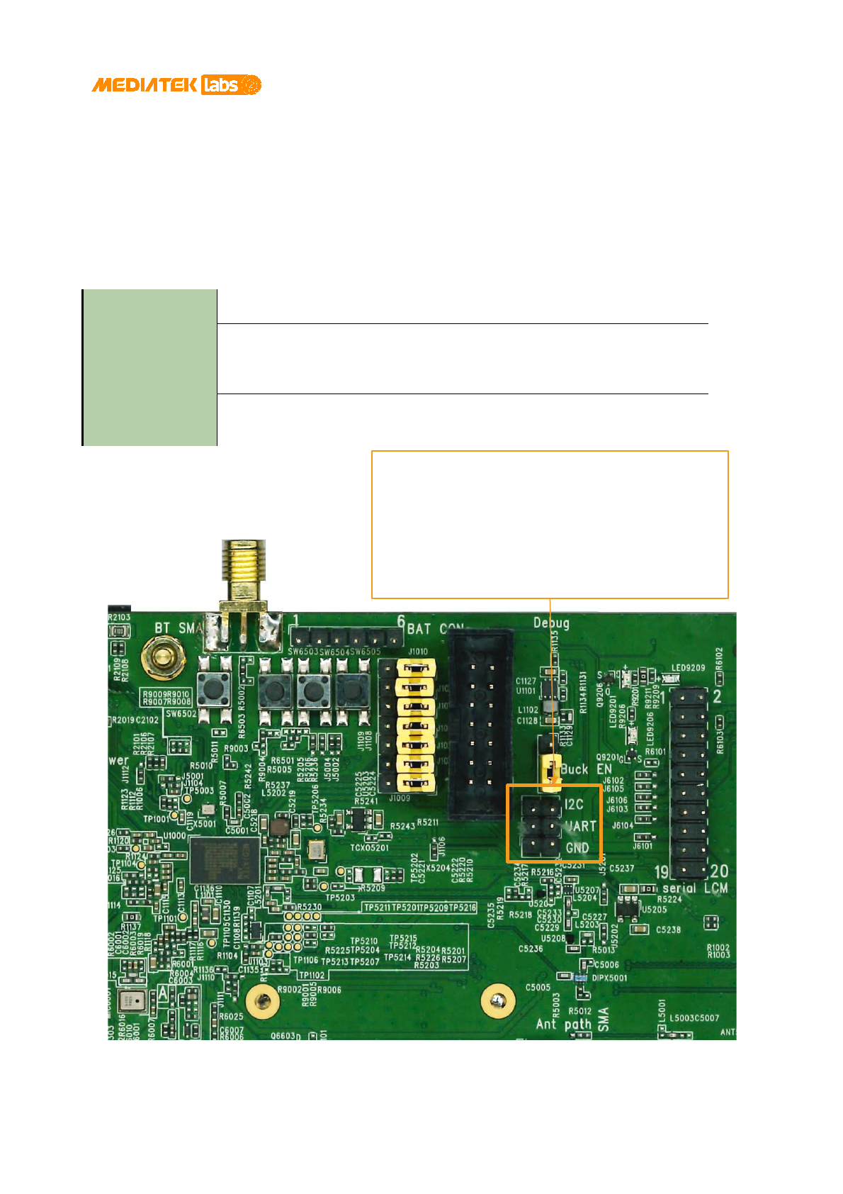
LinkIt 2523 HDK v11 User's Guide
© 2015 - 2016 MediaTek Inc. Page 33 of 82
This document contains information that is proprietary to MediaTek Inc. (“MediaTek”) and/or its licensor(s).
Any unauthorized use, reproduction or disclosure of this document in whole or in part is strictly prohibited.
through the same jumpers, if the JTAG interface is activated. To capture logs by JTAG formal pin assignment
connector, mount 0Ω resistors on footprint R9016, R9017, R9018, R9019, R9020, R9021 and R9023, then the
connector CON9002 will be ready for JTAG signal transmission.
Resistors from R9001, R9002, R9007 and R9008 are the strap pins to adjust the feature settings, such as JTAG
debug interface output cluster, as shown in Table 17. LinkIt 2523 HDK also provides the I2C and UART pin headers
to receive system log or connect to external components directly, as shown in Figure 19. Both Figure 14 and Figure
19 provide the detailed locations of the pins.
Table 17. Resistor selections
JTAG function
activated
Mount 10kΩ resistors R9002 and R9008 to deactivate the JTAG signals.
Mount 10kΩ resistors R9001 and R9007 to activate the JTAG signals through the
GPIO pins in a range from GPIO 24 to GPIO 28 to interface the camera pin
headers.
Mount 10kΩ resistors R9001 and R9008 to activate the JTAG signals through the
GPIO of keypad cluster. Apply this setting to activate the MK20 JTAG connector.
Left to Right
I2C pins –SCL0, SDA0
UART pins –UTXD0, URXD0
GND pins –GND, GND

LinkIt 2523 HDK v11 User's Guide
© 2015 - 2016 MediaTek Inc. Page 34 of 82
This document contains information that is proprietary to MediaTek Inc. (“MediaTek”) and/or its licensor(s).
Any unauthorized use, reproduction or disclosure of this document in whole or in part is strictly prohibited.
Figure 19. The positions of UART and I2C pin header for debugging facilitation
4.16. Connectors
The LinkIt 2523 HDK supports connectors to capture a signal, plug-in an external component, update an image and
more. This section provides details and pin definitions for the connectors.
4.16.1. UART pin header
The UART pin header is reserved for user applications that can be configured for different modes, such as UART,
GPIO and EINT (see Figure 19).
4.16.2. I2C pin header
The I2C pin header is reserved for user applications that can be configured for different modes, such as GPIO and
I2C (see Figure 19).
Note, the pull-up resistors are needed for the I2C interface to provide the sufficient driving power to the I2C clock
and data lines. The two pull-up resistors R1003 and R1002 are already installed for the I2C interface, as shown in
Figure 21.
4.16.3. Battery connector CON2102
The pin configuration of the battery connector CON2101 is shown in Table 18.
Table 18. Battery connector CON2101 (see Figure 18)
Pin number Description Pin number Description
1 VBAT 2 VBAT
3 NC 4 NTC
5
GND
6
NC
4.16.4. Push-Push micro SD tray CON4101
The push-push micro SD tray is able to read micro SD card directly to conveniently provide data from the storage.
Connector details are shown in Table 19. The connector location is shown in Figure 10 and the schematic view is in
Figure 20.

LinkIt 2523 HDK v11 User's Guide
© 2015 - 2016 MediaTek Inc. Page 35 of 82
This document contains information that is proprietary to MediaTek Inc. (“MediaTek”) and/or its licensor(s).
Any unauthorized use, reproduction or disclosure of this document in whole or in part is strictly prohibited.
Figure 20. Micro-SD card holder CON4101
Table 19. Micro-SD tray
Pin number Description Pin number Description
1
Data 2
2
Data 3
3 CMD 4 VDD
5 CLK 6 GND
7
Data 0
8
Data 1
9 GND 10 GND
11
GND
12
GND
13 GND 14 GND
15
Card detect
4.16.5. RTC battery connector BAT5201
The coin battery connector is located at the bottom of the LinkIt 2523 HDK. The RTC saves the satellite information
even when the system is powered off, see Figure 9.
4.16.6. OMTP standard audio connector CON6001
Audio jack pin assignment follows the OMTP standard and supports audio playback and microphone features. It
enables to record speech and playback using the Audio Jack (see Figure 8), as described in Table 20.
Table 20. OMTP Audio jack connector
Pin number Description Pin number Description
1 GND 2 MIC
3
Headset left
4
Headset right
5 Headset plug-in detection 6 NC
4.16.7. Serial display connector CON6102
CON6102 connector is mounted for external serial interface LCM daughterboard, as shown in Figure 21 and
described in Table 21. You can only operate one LCM display at a time, make sure to change the signal path by
resistors J6101 to J6106.

LinkIt 2523 HDK v11 User's Guide
© 2015 - 2016 MediaTek Inc. Page 36 of 82
This document contains information that is proprietary to MediaTek Inc. (“MediaTek”) and/or its licensor(s).
Any unauthorized use, reproduction or disclosure of this document in whole or in part is strictly prohibited.
Figure 21. Serial LCM daughterboard’s connector and I2C pull-up resistors (R1002, R1003)
Table 21. LCM serial display daughterboard connector
Pin number Description Pin number Description
1
LCM backlight current sink
2
VIO18
3
LCM backlight PWM
4
VIO28
5 LPTE 6 VIO28
7
LSDA
8
I2C_SCL
9 LSA0 10 I2C_SDA
11
LSCK
12
GND
13 LSCE_B 14 Touch panel EINT
15 LSRSTB 16 Touch panel reset pin
17
VBAT
18
GND
19 VBAT 20 GND
Serial LCM
(CON6102)
Up: R1002
Down: R1003
LCM Display Path Selection
J6101 to J6106

LinkIt 2523 HDK v11 User's Guide
© 2015 - 2016 MediaTek Inc. Page 37 of 82
This document contains information that is proprietary to MediaTek Inc. (“MediaTek”) and/or its licensor(s).
Any unauthorized use, reproduction or disclosure of this document in whole or in part is strictly prohibited.
4.16.8. Camera daughterboard connector CON6201
Connect the camera daughterboard to connector CON6201 (see Figure 22 and Figure 23) to capture images. The
direction of camera module is to the left, which means the camera module on daughterboard should be toward
USB connectors. The pin assignments can be customized for user-defined applications (see Table 22), if no camera
daughterboard is available.
Figure 22. Serial camera daughterboard CON6201
Figure 23. The position of the camera daughterboard pin headers
Table 22. Serial camera daughterboard connector CON6201
Pin
number
GPI
O #
Power
domai
n
Descri
ption
Flexible
mode1
Flexible
mode2
Flexible
mode3
Flexible
mode4
Flexible
mode5
Flexible
mode6
Flexible
mode8
Flexible
mode9
1 VBAT VBAT
2 24 DVDD_
VIO_A
CMRS
T
GPIO LSRSTB CLKO EINT GPCOU
NTER
JTDI MC1_D
A3
3 VCAMA VCAM
A
4 25 DVDD_
VIO_A
CMPD
N
GPIO LSCK1 DAICLK MA_SPI
2_CS
MA_SPI
3_CS
JTMS MC1_D
A2
SLV_SPI
0_CS
5 GND
6
29
DVDD_
CMCS
GPIO
LPTE
CMCSD
EINT
CON6201
1 2
13 14

LinkIt 2523 HDK v11 User's Guide
© 2015 - 2016 MediaTek Inc. Page 38 of 82
This document contains information that is proprietary to MediaTek Inc. (“MediaTek”) and/or its licensor(s).
Any unauthorized use, reproduction or disclosure of this document in whole or in part is strictly prohibited.
Pin
number
GPI
O #
Power
domai
n
Descri
ption
Flexible
mode1
Flexible
mode2
Flexible
mode3
Flexible
mode4
Flexible
mode5
Flexible
mode6
Flexible
mode8
Flexible
mode9
VIO_A
K
2
7 37 DVDD_
VIO_A
I2C_S
DA0
GPIO I2C_SDA
1
8 28 DVDD_
VIO_A
CMMC
LK
GPIO LSA0DA
1
DAISYN
C
MA_SPI
2_MISO
MA_SPI
3_MISO
JTDO MC1_D
A0
SLV_SPI
0_MISO
9 36 DVDD_
VIO_A
I2C_SC
L0
GPIO I2C_SCL
1
10 29 DVDD_
VIO_A
CMCS
D2
GPIO LPTE CMCSK EINT
11 GND
12 27 DVDD_
VIO_A
CMCS
D1
GPIO LSDA1 DAIPCM
OUT
MA_SPI
2_MOSI
MA_SPI
3_MOSI
JTRSTB MC1_CK SLV_SPI
0_MOSI
13 GND
14 26 DVDD_
VIO_A
CMCS
D0
GPIO LSCE_B1 DAIPCM
IN
MA_SPI
2_SCK
MA_SPI
3_SCK
JTCK MC1_C
M0
SLV_SPI
0_SCK
4.16.9. Sensor daughterboard connector CON6301
Connect the sensor daughterboard to CON6301. The pin assignments can be customized in user-defined
applications, if sensor daughterboard is unplugged, as described in Table 23 and Figure 26.
Table 23. Sensor daughterboard connector CON6301
Pin
number
GPI
O #
Power
domain
Descript
ion
Flexibl
e
mode
1
Flexible
mode2
Flexible
mode3
Flexible
mode4
Flexible
mode5
Flexible
mode6
Flexible
mode8
Flexible
mode9
1 VBAT VBAT
2
VA28
VA28
3 VIO28 VIO28
4
VIO18
VIO18
5 GND
6
GND
7 37 DVDD_
VIO_A
I2C_SDA
0
GPIO EINT MC1_D
A3
8 28 DVDD_
VIO_A
MA_SPI
3_MISO
CMMC
LK
GPIO LSA0DA
1
DAISYN
C
MA_SPI
2_MISO
JTDO MC1_D
A0
SLV_SPI
0_MISO
9 36 DVDD_
VIO_A
I2C_SCL
0
GPIO EINT MC1_D
A2
10 27 DVDD_
VIO_A
MA_SPI
3_MOSI
CMCS
D1
GPIO LSDA1 DAIPCM
OUT
MA_SPI
2_MOSI
JTRSTB MC1_CK SLV_SPI
0_MOSI
11 GND
12 26 DVDD_
VIO_A
MA_SPI
3_SCK
CMCS
D0
GPIO LSCE_B1 DAIPCM
IN
MA_SPI
2_SCK
JTCK MC1_C
M0
SLV_SPI
0_SCK
13 48 DVDD_
GPO
MA_SPI
3_CS1
GPO
14 25 DVDD_
VIO_A
MA_SPI
3_CS0
CMPD
N
GPIO LSCK1 DAICLK MA_SPI
2_CS
JTMS MC1_D
A2
SLV_SPI
0_CS
15 4 DVDD_
VIO_A
EINT GPIO URXD1 MC1_CK MA_SPI
0_CS
SLA_ED
IDO
16
GND
17 5 DVDD_
VIO_A
EINT GPIO UTXD1 MC1_C
M0
MA_SPI
0_SCK
SLA_ED
IDI
18 7 DVDD_
VIO_A
EINT GPIO UTXD2 MC1_D
A1
MA_SPI
0_MISO
SLA_ED
ICK

LinkIt 2523 HDK v11 User's Guide
© 2015 - 2016 MediaTek Inc. Page 39 of 82
This document contains information that is proprietary to MediaTek Inc. (“MediaTek”) and/or its licensor(s).
Any unauthorized use, reproduction or disclosure of this document in whole or in part is strictly prohibited.
Pin
number
GPI
O #
Power
domain
Descript
ion
Flexibl
e
mode
1
Flexible
mode2
Flexible
mode3
Flexible
mode4
Flexible
mode5
Flexible
mode6
Flexible
mode8
Flexible
mode9
19 6 DVDD_
VIO_A
EINT GPIO URXD2 MC1_D
A0
MA_SPI
0_MOSI
SLA_ED
IWS
20 29 DVDD_
VIO_A
EINT CMCS
K
GPIO LPTE CMCSD
2
MC1_D
A1
BT_RGPI
O2
21 13 DVDD_
VIO_C
SEN_32
K_BB
GPIO EINT CLKO MA_EDI
WS
MA_SPI
1_MOSI
PWM2 SLA_EDI
WS
22 24 DVDD_
VIO_A
GPIO EINT MC1_D
A1
SLA_EDI
CK
UTXD2 BT_BUC
K_EN_H
W
MA_SPI
0_MISO
23
GND
24 GND
4.16.10. USB 2.0 high speed connector
The 2523 USB connector (see Figure 3 and Figure 24) follows USB 2.0 high-speed standard to communicate with
other compatible devices. It’s used for charging and system power supply. The 5V power rail is also connected
with MK20 USB. The connector pins are described in Table 24.
Figure 24. High-speed USB2.0 connector
Table 24.The HDK’s high speed USB 2.0 connector
Pin number Description Pin number Description
1
VUSB_BB
2
D-
3 D+ 4 NC
5
GND
-
-
4.16.11. CMSIS-DAP USB 1.1 full speed connector
Apply the MK20 USB connector (see Figure 25 and Figure 26) to update the binary on the HDK using CMSIS-DAP
without other tools. The HDK operates as a removable mass storage, if the MK20 USB is used for connecting the
device to the PC.
Figure 25. CMSIS-DAP USB 1.1 full speed connector
The connector pin details are described in Table 25.

LinkIt 2523 HDK v11 User's Guide
© 2015 - 2016 MediaTek Inc. Page 40 of 82
This document contains information that is proprietary to MediaTek Inc. (“MediaTek”) and/or its licensor(s).
Any unauthorized use, reproduction or disclosure of this document in whole or in part is strictly prohibited.
Table 25. CMSIS-DAP USB full speed connector
Pin number Description Pin number Description
1 VUSB_DAP 2 D-
3
D+
4
NC
5
GND
-
-
4.16.12. MK20 JTAG connector
MK20 JTAG connector is used to provide a factory update of the MK20 bootloader (see Figure 26 and
Table 26). No further modification can be applied.
Figure 26. MK20 JTAG connector, sensor daughterboard connector and PSRAM power switch J1113
The connector pin details are described in
MK20 JTAG
J1113
1 2 3
Sensor

LinkIt 2523 HDK v11 User's Guide
© 2015 - 2016 MediaTek Inc. Page 41 of 82
This document contains information that is proprietary to MediaTek Inc. (“MediaTek”) and/or its licensor(s).
Any unauthorized use, reproduction or disclosure of this document in whole or in part is strictly prohibited.
Table 26.
Table 26. MK20 JTAG connector pin definition
Pin number Description Pin number Description
1
VIO28
2
VIO28
3
SDA_JTAG_TRST
4
GND
5 SDA_JTAG_TDI 6 GND
7
SDA_JTAG_TMS
8
GND
9
SDA_JTAG_TCLK
10
GND
11
-
12
GND
13 SDA_JTAG_TDO 14 GND
15 - 16 GND
17
-
18
GND
19 - 20 GND
4.16.13. eMMC / micro SD holder jumpers
There are six jumpers (J1001 to J1006) (see Figure 16) dedicated for eMMC or micro SD card, as shown in Table 27.
If the assigned jumpers are idle, they can be customized for other applications. Use only the middle pin of those
jumpers. The pins are sorted from up to down starting from 1 to 6.
Table 27. eMMC/micro SD jumpers
Pin
order
from
upside
GPI
O #
Descr
iption
Flexible
mode0
Flexible
mode1
Flexible
mode2
Flexible
mode3
Flexible
mode4
Flexible
mode5
Flexible
mode6
Flexible
mode9
1 32 MCD
A0
GPIO32 SLV_SPI0
_CS
EINT13 PWM2 DAISYNC MC0_D
A0
MA_SPI
3_B_CS
2 33 MCD
A1
GPIO33 SLV_SPI0
_SCK
EINT14 PWM3 DAIPCMI
N
MC0_D
A1
MA_SPI
3_B_SC
K
3 34 MCD
A2
GPIO34 SLV_SPI0
_MOSI
EINT15 PWM4 DAICLK MC0_D
A2
MA_SPI
3_B_M
OSI
4 35 MCD
A3
GPIO35 SLV_SPI0
_MISO
EINT3 PWM5 DAIPCM
OUT
MC0_D
A3
CLKO2 MA_SPI
3_B_MI
SO
5 30 MCCK GPIO30 SCL0 EINT11 PWM0 URXD1 MC0_C
K
SCL2
6 31 MCC
M0
GPIO31 SDA0 EINT12 PWM1 UTXD1 MC0_C
M0
SDA2
4.16.14. JTAG connector CON9002
The connector CON9002 provides the standard JTAG connection. CON9002 could be enabled using the resistors
R9011 to R9021 and R9023 (see Figure 9 and Figure 8).
Table 28. JTAG connector CON9002

LinkIt 2523 HDK v11 User's Guide
© 2015 - 2016 MediaTek Inc. Page 42 of 82
This document contains information that is proprietary to MediaTek Inc. (“MediaTek”) and/or its licensor(s).
Any unauthorized use, reproduction or disclosure of this document in whole or in part is strictly prohibited.
Pin number Description Pin number Description
1
DVDD_VIO_A
2
DVDD_VIO_A
3 JTRST 4 GND
5
JTDI
6
GND
7 JTMS 8 GND
9 JTCK 10 GND
11
NC
12
GND
13 JTDO 14 GND
15
SYSRSTB_IN
16
GND
17 NC 18 GND
19
NC
20
GND
Figure 27. JTAG connector CON9002 pin definition
4.16.15. SMA connectors
There are two SMA headers to connect to the external antennas. The GNSS/BT SMA is used to connect to
GNSS/Bluetooth antenna. The BT SMA could be connected to a Bluetooth antenna. The connectors are shown in
Figure 8. To activate the BT SMA connector, move 0Ω resistor from R5010 to R5011.
4.16.16. External component connectivity support
This section provides the detailed pin layout for sensor and daughterboard connectors and GPIO pins, see Figure
28 and Table 29.

LinkIt 2523 HDK v11 User's Guide
© 2015 - 2016 MediaTek Inc. Page 43 of 82
This document contains information that is proprietary to MediaTek Inc. (“MediaTek”) and/or its licensor(s).
Any unauthorized use, reproduction or disclosure of this document in whole or in part is strictly prohibited.
Figure 28. LinkIt 2523 HDK extension connectors
Table 29. GPIO pin functionalities
Right to Left
J1010
J1008
J1007
J1011
J1015
J1012
J1009
Right to Left
J1001 to J1006
Ref
Left
Right
1
GND
GND
2
GPIO24
GPIO14
3
GPIO29
GPIO6
4
GPIO7
GPIO5
5
GND
GPIO4
6
GPIO25
GPO48
7
GPIO26
GND
8
GPIO27
GPIO36
9
GPIO28
GPIO37
10
GND
GND
11
VIO18
VIO28
12
VA28
VBAT
R1L1
R12L12
Ref
GPIO #
J1001
GPIO32
J1002
GPIO33
J1003
GPIO34
J1004
GPIO35
J1005
GPIO30
J1006
GPIO31
Ref
GPIO #
J1010
GPIO26
J1008
GPIO24
J1007
GPIO25
J1011
GPIO28
J1015
GPIO29
J1012
GPIO29
J1009
GPIO27
CON6102
19
20
1
2
Sensor
Ref
GPIO #
GPIO #
Ref
1
ISINK
VIO18
2
3
LCM_B
LPWM
VIO28
4
5
GPIO43
VIO28
6
7
GPIO41
GPIO36
8
9
GPIO42
GPIO37
10
11
GPIO40
GND
12
13
GPIO39
GPIO15
14
15
GPIO38
GPO47
16
17
VBAT
GND
18
19
VBAT
GND
20
Pin alias Name Direction Description
GPIO4 MC[1]_CK O MSDC clock, output
GPIO[4] I/O General purpose input, output
SLA_EDIDO O Slave I2S data output
EINT[3] I External interrupt
URXD[1] I UART receive port, input

LinkIt 2523 HDK v11 User's Guide
© 2015 - 2016 MediaTek Inc. Page 44 of 82
This document contains information that is proprietary to MediaTek Inc. (“MediaTek”) and/or its licensor(s).
Any unauthorized use, reproduction or disclosure of this document in whole or in part is strictly prohibited.
MA_SPI[0]_CS O SPI master chip select
GPIO5 MC[1]_CM0 O MSDC command, output
GPIO[5] I/O General purpose input, output
SLA_EDIDI I Slave I2S data input
EINT[4] I External interrupt
UTXD[1] O UART transmit port, output
MA_SPI[0]_SCK O SPI master clock output
GPIO6 MC[1]_DA0 I/O MSDC data input, output
GPIO[6] I/O General purpose input, output
SLA_EDIWS I Slave I2S frame clock input
EINT[5] I External interrupt
URXD[2] I UART receive port, input
MA_SPI[0]_MOSI O SPI master MOSI
GPIO7 MC[1]_DA1 I/O MSDC data input, output
GPIO[7] I/O General purpose input, output
SLA_EDICK I Slave I2S bit clock input
EINT[6] I External interrupt
UTXD[2] O UART transmit port, output
MA_SPI[0]_MISO I SPI master MISO
BT_BUCK_EN_HW O External buck enable pin, output
GPIO14 EINT[12] I External interrupt
CLKO[4] O Clock output
MA_EDICK O Master I2S bit clock output
GPIO[14] I/O General purpose input, output
PWM[3] O Pulse width modulation in 3.3V
MA_SPI[1]_MISO I SPI master MISO
SLA_EDICK I Slave I2S bit clock output
GPIO24 CMRST O Serial camera reset, output
LSRSTB O Serial display reset, output
CLKO[1] O Clock output
GPIO[24] I/O General purpose input, output
EINT[9] I External interrupt
GPCOUNTER_0 I General interrupt counter, input
JTDI I JTAG data input
MC[1]_DA3 I/O MSDC data input, output
GPIO25 CMPDN O Serial camera power down, output
LSCK1 O Serial display clock, output
DAICLK O Digital audio interface clock, output
GPIO[26] I/O General purpose input, output
MA_SPI[2]_CS O SPI master chip select

LinkIt 2523 HDK v11 User's Guide
© 2015 - 2016 MediaTek Inc. Page 45 of 82
This document contains information that is proprietary to MediaTek Inc. (“MediaTek”) and/or its licensor(s).
Any unauthorized use, reproduction or disclosure of this document in whole or in part is strictly prohibited.
MA_SPI[3]_CS O SPI master chip select
JTMS O JTAG mode selection, input
MC[1]_DA2 I/O MSDC data input, output
SLV_SPI[0]_CS I SPI slave chip select
GPIO26 CMCSD0 I Camera sensor data 0, input
LSCE_B1 O Serial display chip select, output
DAIPCMIN I Digital audio interface data input
GPIO[26] I/O General purpose input, output
MA_SPI[2]_SCK O SPI master clock output
MA_SPI[3]_SCK O SPI master clock output
JTCK O JTAG clock output
MC[1]_CM0 O MSDC command, output
SLV_SPI[0]_SCK I SPI slave clock input
GPIO27 CMCSD1 I Camera sensor data 1, input
LSDA1 O Serial display data, output
DAIPCMOUT O Digital audio interface data output
GPIO[27] I/O General purpose input, output
MA_SPI[2]_MOSI O SPI master data output
MA_SPI[3]_MOSI O SPI master data output
JTRSTB O JTAG clock reset, output
MC[1]_CK O MSDC clock output
SLV_SPI[0]_MOSI I SPI slave data input
GPIO28 CMMCLK O Camera main clock, output
LSA0DA1 O Serial display address, output
DAISYNC O DAI frame synchronization output
GPIO[28] I/O General purpose input, output
MA_SPI[2]_MISO I SPI master data input
MA_SPI[3]_MISO I SPI master data input
JTDO O JTAG data output
MC[1]_DA0 I/O MSDC data input, output
SLV_SPI[0]_MISO O SPI slave data output
GPIO29 CMCSK I Camera sensor clock, input
LPTE O Serial display tearing signal, output
CMCSD2 I Camera sensor data 2, input
GPIO[29] I/O General purpose input, output
EINT[10] I External interrupt
MC[1]_DA1 I/O MSDC data input, output
GPIO30 SCL[0] O I2C clock output
EINT[11] I External interrupt

LinkIt 2523 HDK v11 User's Guide
© 2015 - 2016 MediaTek Inc. Page 46 of 82
This document contains information that is proprietary to MediaTek Inc. (“MediaTek”) and/or its licensor(s).
Any unauthorized use, reproduction or disclosure of this document in whole or in part is strictly prohibited.
URXD[1] I UART receive port, input
MC[0]_CK O MSDC clock, output
GPIO[30] I/O General purpose input, output
SCL[2] O I2C clock output
PWM[0] O Pulse width modulation
GPIO31 SDA[0] I/O I2C data input, output
EINT[12] I External interrupt
UTXD[1] O UART transmit port, output
MC[0]_CM0 O MSDC command, output
GPIO[31] I/O General purpose input, output
SDA[2] I/O I2C data input, output
PWM[1] O Pulse width modulation
GPIO32 SLV_SPI[0]_CS I SPI slave chip select
EINT[13] I External interrupt
GPIO[32] I/O General purpose input, output
PWM[2] O Pulse width modulation
DAISYNC O DAI frame synchronization output
MC[0]_DA0 I/O MSDC data input, output
MA_SPI[3]_CS O SPI master chip select
GPIO33 SLV_SPI0_SCK I SPI slave clock input
EINT[14] I External interrupt
GPIO[33] I/O General purpose input, output
PWM[3] O Pulse width modulation
DAIPCMIN I Digital audio interface data input
MC[0]_DA1 I/O MSDC data input, output
MA_SPI[3]_SCK O SPI master clock output
GPIO34 SLV_SPI0_MOSI I SPI slave data input
EINT[15] I External interrupt
GPIO[34] I/O General purpose input, output
PWM[4] O Pulse-width-modulated output
DAICLK O Digital audio interface clock, output
MC[0]_DA2 I/O MSDC data input, output
MA_SPI[3]_MOSI O SPI master data output
GPIO35 SLV_SPI0_MISO O SPI slave data output
EINT[3] I External interrupt
GPIO[35] I/O General purpose input, output
PWM[5] O Pulse-width-modulated output
DAIPCMOUT O Digital audio interface data output
MC[0]_DA3 I/O MSDC data input, output
MA_SPI[3]_MISO I SPI master data input

LinkIt 2523 HDK v11 User's Guide
© 2015 - 2016 MediaTek Inc. Page 47 of 82
This document contains information that is proprietary to MediaTek Inc. (“MediaTek”) and/or its licensor(s).
Any unauthorized use, reproduction or disclosure of this document in whole or in part is strictly prohibited.
CLKO[2] O Clock output
GPIO36 SCL[0] O I2C clock output
GPIO[36] I/O General purpose input, output
SCL[1] O I2C clock output
GPIO37 SDA[0] I/O I2C data input, output
GPIO[37] I/O General purpose input, output
SDA[1] I/O I2C data input, output
GPIO38 LSRSTB O Serial display reset, output
CMRST O Serial camera reset, output
GPIO[38] I/O General purpose input, output
CLKO[3] O Clock output
SFSWP O Serial Flash write protect
SCL[1] O I2C clock output
GPIO39 LSCE_B0 O Serial display chip select, output
CMCSD0 I Camera sensor data 0, input
GPIO[39] I/O General purpose input, output
CLKO[4] O Clock output
SFSCS0 O Serial Flash chip select 0
SCL[1] O I2C clock output
MA_SPI[2]_CS O SPI master chip select
EINT[4] I External interrupt
GPIO40 LSCK0 O Serial display clock, output
CMPDN O Serial camera power down, output
GPIO[40] I/O General purpose input, output
SFSHOLD O Serial Flash data hold
MA_SPI[2]_SCK O SPI master clock output
GPIO41 LSDA0 O Serial display data, output
CMCSD1 I Camera sensor data 1, input
GPIO[41] I/O General purpose input, output
SFSCK O Serial Flash clock
SDA[1] I/O I2C data input, output
MA_SPI[2]_MOSI O SPI master data output
EINT[4] I External interrupt
GPIO42 LSA0DA0 O Serial display interface address, output
LSCE1_B0 O Serial display chip select, output
GPIO[42] I/O General purpose input, output
CMMCLK O Camera main clock, output
SFSOUT I Serial Flash data output
CLKO[5] O Clock output

LinkIt 2523 HDK v11 User's Guide
© 2015 - 2016 MediaTek Inc. Page 48 of 82
This document contains information that is proprietary to MediaTek Inc. (“MediaTek”) and/or its licensor(s).
Any unauthorized use, reproduction or disclosure of this document in whole or in part is strictly prohibited.
MA_SPI[2]_MISO I SPI master data input
GPIO43 LPTE O Serial display tearing signal, output
CMCSK I Camera sensor clock, input
GPIO[43] I/O General purpose input, output
CMCSD2 I Camera sensor data 2, input
SFSIN I Serial Flash data input
SDA[1] I/O I2C data input, output
EINT[6] I External interrupt

LinkIt 2523 HDK v11 User's Guide
© 2015 - 2016 MediaTek Inc.
Page 49 of 82
This document contains information that is proprietary to MediaTek Inc. (“MediaTek”) and/or its licensor(s).
Any unauthorized use, reproduction or disclosure of this document in whole or in part is strictly prohibited.
5. Schematics (V11)
GPS
BT
LNA DiplexerSAW
Connectivity ANT
Reset
Title
Size
Date: Sheet of
MediaTek HDK MT2523G
01_Block Diagram
C
199Thursday , March 31, 2016
MK20DX128
Project : MT2523
REF_SCH TOP LEVEL
UART
SWD
AU_VIN1
Analog MIC
Audio Jack
HP_OUT
eMMC
Audio
Speech
Charger
RTC 32K
Battery
UART
SDIO
SDIO
UART
Debug port
MT2523G
JTAG
USB HS Micro USB
USB HS
HSP_OUT
AU_VIN0
Camera IF
Camera DTB
CAM (Serial)
26M_BB
32K_BB
I2C
LCM+CTP DTB
VB AT
BJT
XTAL
Serial Display serial
interface
I2C
VBUS
I2C
Sensors DTB
I2C
SPI
EINT
PMU
SPI
MIPI
Class-D
SPK Amp.
SPK_OUT
EINT
Micro SD
UART
JTAG
Bluetooth
SDIO
SWD

LinkIt 2523 HDK v11 User's Guide
© 2015 - 2016 MediaTek Inc.
Page 50 of 82
This document contains information that is proprietary to MediaTek Inc. (“MediaTek”) and/or its licensor(s).
Any unauthorized use, reproduction or disclosure of this document in whole or in part is strictly prohibited.
Figure 29. Block diagram
Title
Size
Date: Sheet of
MediaTek HDK MT2523G
02_I2C_ID_Overview
C
299Thursday , March 31, 2016
I2C Spec.
400 Kbps
I2C
Rear Camera Rear camera (GC0310) I2C address: 0X21 (Write:0x42, Read:0x43)
Yes.
Function
I2C0
I2C Slave Address (7-bit mode)
400 Kbps
Budgeted Timing
Touch IC Yes. TP (GT9137) I2C address: 0X24 (Write:0x28, Read:0x29)

LinkIt 2523 HDK v11 User's Guide
© 2015 - 2016 MediaTek Inc.
Page 51 of 82
This document contains information that is proprietary to MediaTek Inc. (“MediaTek”) and/or its licensor(s).
Any unauthorized use, reproduction or disclosure of this document in whole or in part is strictly prohibited.
Figure 30. I2C ID
Title
Size
Date: Sheet of
MediaTek HDK MT2523G
04_PMU_SPEC
C
499Thursday , March 31, 2016
20
I_max(mA)
VIO28
VIO18
150
2.8/1.8
2.8
2.8
100
150
Analog LDO VA28
VCAMA
230
100
2.8
1.8
3.3
1.8/2.8/3/3.3
2.5
VUSB
VMC
VIBR
1.8
1.86/3.0/3.3
VA18
VSF
200
Digital LDO
1.8 5
Driver ISINK
Digital LDO
0.6~1.3
VDIG18
100
150
200
80
Vout(V)
Vcore
VBT
1.3/1.5/1.8/2/
2.5/2.8/3/3.3
Buck
1X(96mA;48mA/0.25V)
Vcore 0.6~1.3

LinkIt 2523 HDK v11 User's Guide
© 2015 - 2016 MediaTek Inc.
Page 52 of 82
This document contains information that is proprietary to MediaTek Inc. (“MediaTek”) and/or its licensor(s).
Any unauthorized use, reproduction or disclosure of this document in whole or in part is strictly prohibited.
Figure 31. PMU_SPEC
Note: 10-1
J1018
HEADER 2X1(W/O JMP)
1 2
CMCSK_CAM
UTXD0
URXD0
MCCK
MCCM0
MCDA0
MCDA1
MCDA2
MCDA3
URXD0 UTXD0SDA0 SCL0
Selection of CAM and sensor DTB
Note: 10-3
Note: 10-4
Note: 10-4
Note: 10-4
Title
Size
Date: Sheet of
MediaTek HDK MT2523G
10_BB_MT2523G_BB
C
10 99Thursday , March 31, 2016
SPK_AMP_PDN
SYS CTL
SCL0
SDA0
U305_EINT_CONN [ 63,93]
U304_EINT_CONN [ 63,93]
U302_EINT_CONN [ 63,93]
U303_EINT_CONN [ 63,93]
Note: 10-5
EAR_EINT [60, 93]
MCINS [41,93]
SEN_32K_BB [ 63]
GPIO_A0 [63,93]
GPIO_A1 [63,93]
GPIO_A2 [63,93]
GPIO_A3 [63,93]
GPIO_A4 [41,93]
GPIO_A5 [60,93]
Note 10-1: Jumper selection for microSD or eMMC;
Schematic design notice of "10_BB_MT2523G_BB" page.
Note 10-3: Jumper selection for Camera or sensor DTB;
Dedicate pins for GPS function are fixed; Note 10-4:
Optional schematic for external flashNote 10-5:
R1004 should be closed to Larkspur ball out position
Note 10-2:
please don't change this design to other appliance.
also flexible pin mux feature for user appliance.
also flexible pin mux feature for user appliance.
MCDA0
MCDA1
MCDA2
MCDA3
MCCK
MCCM0
J1005
1
3
2
R1002
R / 4.7 / K / 0402
12
J1006
1
3
2
J1011
1
3
2
J1007
1
3
2
R1003
R / 4.7 / K / 0402
12
R1006 R / 0 / ohm / 0402 / NC
J1012
1
3
2
J1013
HEADER 2X1(W/O JMP)
12
J1014
HEADER 2X1(W/O JMP)
12
J1001
1
3
2
R1004
R / 5.1 / K / 0402 / 1%
12
J1008
1
3
2
TP1001
NC
1
J1002
1
3
2
R1010
R / 1.8 / K / 0402 / 1%
R0402
12
J1009
1
3
2
J1003
1
3
2
J1016
R / 0 / ohm / 0402-3P(1-2)
1
2
3
J1015
1
3
2
J1010
1
3
2
J1004
1
3
2
USB_VRT
LCMMSDC
CAMERA GPIO_B
UARTI2CGPIO_AUSBADC
SYS_CTL
MT2523 BB
GPO
GPIO_C
GND
U1000-1
MT2523G
MCCK
P10
MCCM0
N13
MCDA0
P12
LSCE_B
K13
LSRSTB
K14
LSCK
L13
LSDA
L12
LSA0
L14
LPTE
M15
CMPDN B18
CMRST B17
CMCSD1 A19
CMCSD0 B16
CMMCLK B19
CMCSK A18
GPIO_B2 B13
GPIO_B1 D10
GPIO_B3 E10
GPIO_B4 D9
URXD0 B8
UTXD0 B7
GPIO_A0 C18
USB_DM E3
USB_DP D3
GPIO_A1 B15
SCL0 E14
SDA0 E13
GPIO_B5 C10
GPIO_B0 E11
AUXADCIN_0 N8
GPIO_A2 D15
GPIO_A3 D16
GPIO_A4 C15
GPIO_A5 D17
MCDA1
N12
MCDA2
N11
MCDA3
N10
TESTMODE
B2
SRCLKENAI
C6
TCP
J5
TCN
H5
AVDD28_MIPI
F3
AVSS28_MIPI
E4
USB_VRT E6
TVR T
J4 AUXADCIN_1 M12
AUXADCIN_2 M8
AUXADCIN_3 M11
AUXADCIN_4 L8
TDP
G4
TDN
F4
GPO_0 L10
GPO_1 A6
GPO_2 B20
GPO_3 B6
GPIO_C4 A15
GPIO_C3 B10
GPIO_C2 D13
GPIO_C1 C13
GPIO_C0 D14
GND
F15
GND
J14
GND
H14
GND
G14
GND
F14
GND
J13
GND
H13
GND
G13
GND
F13
GND
J12
GND
J15
GND
H15
GND
G15
GND
H12
GND
G12
GND
F12
GND
H11
GND
G11
GND
F11
GND
K15
DVDD_VIO_A
VSWMP
VIO28
SCL0 [61,62,63]
SDA0 [61,62,63]
TDP[61]
TDN[61]
TCP[61]
TCN[61]
MA_SPI3_B_CS1 [63,90]
MSDC0_CMD [40]
MSDC0_C LK [40]
MSDC0_DAT3 [40]
Selection of
eMMC and micro SD
MSDC0_DAT2 [40]
MSDC0_DAT1 [40]
MSDC0_DAT0 [40]
EXT_PWREN [11]
LCM_BLPWM [ 61,90]
USB_DM [64]
USB_DP [64]
SWD_CLK_TGTMCU [66]
SWD_DIO_TGTMCU [66]
UART2_RX_MK [66]
UAR T2_TX_MK [66]
GPS_32K_BB [52]
GPS_HRST_B [90]
TP_RST [61]
MCCK_J [41]
MCCM0 _J [41]
MCDA3_J [ 41]
MCDA2_J [ 41]
MCDA1_J [ 41]
MCDA0_J [ 41]
CMMCL K_J[62,90]
CMCSD0_J[62,90]
CMCSD1_J[62,90]
CMRS T_J[62,90]
CMPDN_J[62,90]
MA_SPI3_B_CS0[63]
MA_SPI3_B_SCK[63]
MA_SPI3_B_MOSI[63]
U303_RSTN_CONN[63]
U303_PD_CONN[ 63]
UTXD3_GPS [52]
KROW1 [65]
KCOL2 [65]
CMCSK_J[62]
CMCSD2_J[62]
GPS_EINT [52]
TP_EINT [61]
MA_SPI3_B_MISO[63]
URXD3_GPS [52]
KCOL0 [65,90]
GPS_LDO_EN [52]
SPK_AMP_PDN[60]
LSCE_B_LC M[61]
LSRSTB_LCM[ 61]
LSDA_LC M[ 61]
LSA0_LCM[61]
LPTE_LCM[61]
LSCK_LC M[61,90]
MC_RST [40]
CMCSK
TVR T
CMCSK_CAM
Note: 10-2
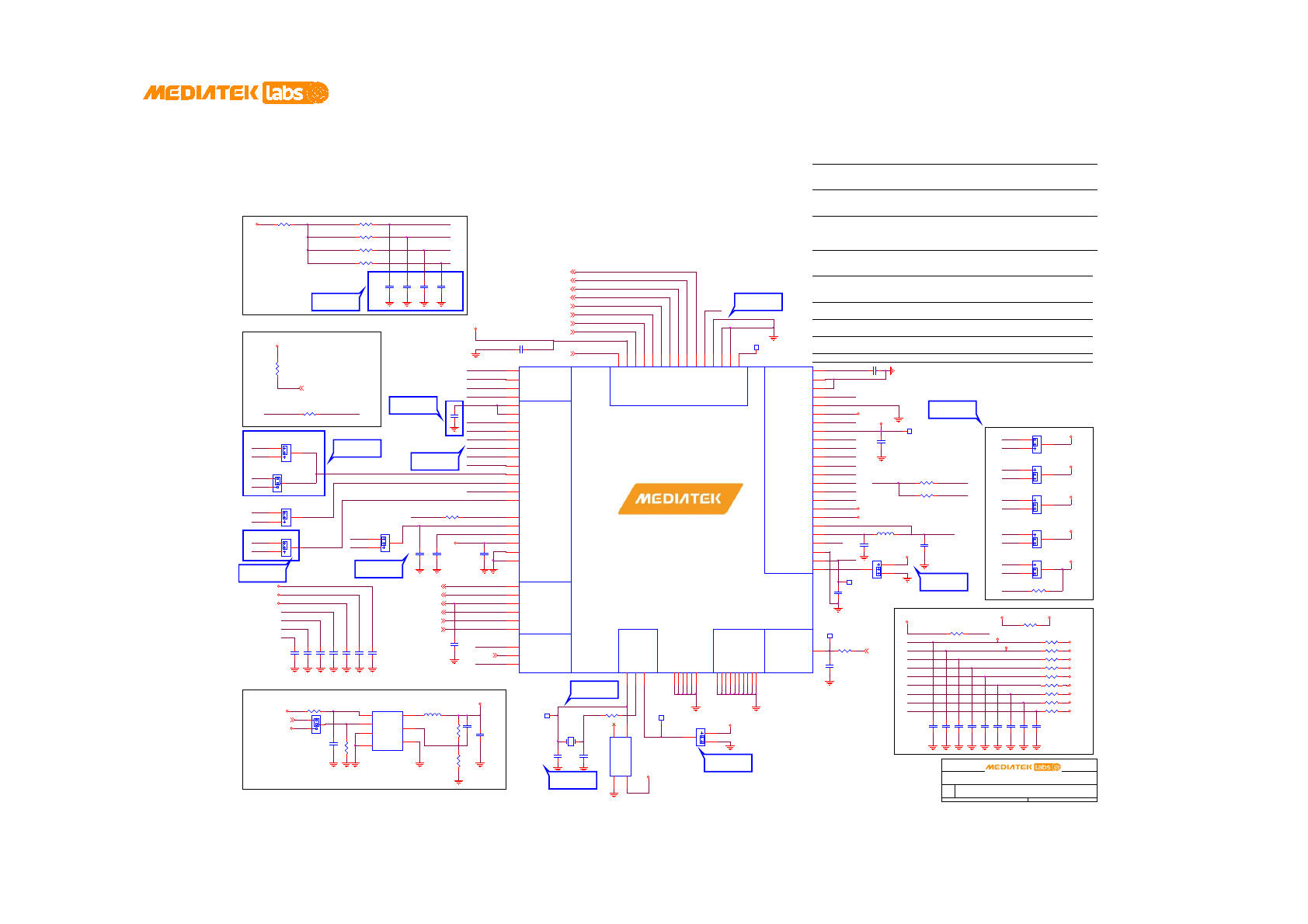
LinkIt 2523 HDK v11 User's Guide
© 2015 - 2016 MediaTek Inc.
Page 53 of 82
This document contains information that is proprietary to MediaTek Inc. (“MediaTek”) and/or its licensor(s).
Any unauthorized use, reproduction or disclosure of this document in whole or in part is strictly prohibited.
Figure 32. BB MT2523G BB
R1116
R / 1 / ohm / 0402
12
R1117
R / 0 / ohm / 0402
1 2
R1115
R / 0 / ohm / 0402
12
J1106
R / 0 / ohm / 0402-3P(1-2)
1
2
3
R1114
R / 0 / ohm / 0402
12
J1111
R / 0 / ohm / 0402-3P(1-2)
1
2
3
J1110
R / 0 / ohm / 0402-3P(1-2)
1
2
3
Note: 11-1
C1139
C / 2.2 / uF / 0402
2 1
R1113
R / 0 / ohm / 0402 / N C
1 2
C1138
C / 1 / uF / 0402
2 1
C1137
C / 1 / uF / 0402
2 1
J1109
R / 0 / ohm / 0402-3P(1-2)
1
2
3
C1140
C / 2.2 / uF / 0402
2 1
VIO28
VIO18
VIO18
VIO28
J1108
R / 0 / ohm / 0402-3P(1-2)
1
2
3
VIO18
VBAT_LDOS2
VBAT_LDOS1
VBAT IN
VIO18
VIO18
VIO28
VIO28
VBAT_VCORE
VBAT_BUCK_CTRL
VBAT
VMC
VIO28
DVDD_VIO_C
DVDD_GPO
DVDD18_VIO18
R1137
R / 0 / ohm / 0603
12
DVDD_VIO_A
DVDD33_VMC
DVDD18_VSWXM
C1112
C / 1 / uF / 0402
2 1
C1122
C / 1 / uF / 0402
2 1
R1124
R / 0 / ohm / 0402
12
R1122
R / 0 / ohm / 0402
12
TP1101
1
Note 11-4:
Note 11-3: This jumper could be switched for efuse function workable.
C1127 C / 4.7 / uF / 0603
2 1
Selection of 32.768 KHz crystal mounted:
This jumper could be switched for 32.768KHz crystal mounted
Users are able to adjust IO cluster power source by design;
Schematic design notice of "11_BB_MT2523G_ABB" page.
Those capacitors must be closed Larkspur ball out placement
Note 11-1:
Note 11-2:
R1139
R / 0 / ohm / 0402
1 2
Note 11-5: This jumper could be switched for PSRAM power saving
Note 11-6:
Note 11-7:
This test point is used for DCXO calibration
Note 11-8:
without battery.
VRTC: 32.768 KHz crystal is not existed
GND: 32.768 KHz crystal is existed
Total capacitor value at VBAT must larger than 28.4uF for D L
AVSS28_ABB ball L5 and K5 connected first, then connected
R1120
R / 0 / ohm / 0402
1 2
VSWXM: Switch off power supply in suspend mode
VIO18: 32.768KHz crystal existed
VA18: 32.768KHz crystal less
No burning eFUSE case: Pin FSOURCE_D is tied to GND .
Pin FSOURCE_D connected to VEFUSE
Burning eFUSE case is needed:
to C1109 GND side by point directly which without any branch.
Active eMMC should unmount R1113 and mount J1111.
VIO18: Default setting
J1101
1
3
2
DVDD_VIO_B should be connected to 2.8V power only
Note 11-9:
Note: 11-9
C1132C / 1 / uF / 0402
21
VDIG18
POWER INVBAT IN
AUDIO
LED DRV
PMU LDO
System
Control
MT2523 ABB
RTC
CHARGER
GND
U1000-2
MT2523G
ISINK D1
VIO18 L3
VIBR H1
VCORE_LDO N1
VMC E2
AU_HPL N2
AU_HPR M2
AU_VIN0_P P3
AU_VIN0_N P2
AU_VIN1_P N4
AU_VIN1_N N3
VDDK
H3
AU_MICBIAS0 N5
VSF E1
AVSS28_ABB L5
VIO28 K2
VA18 K3
VBAT_LDOS2
F1
VBAT_LDOS1
L1
VCORE_BUCK P7
VCAMA G1
VBAT_VCORE
P6
VA28 H2
GND_VCORE P9
VUSB33 J1
VSWMP K1
VSWDP L2
VCORE_FB N6
VBAT_BUCK_CTRL
N7
VREF B5
VBATSW F2
VSWXM M1
VBT C3
FSOURCE_A L9
VCDT
A4
BATON
C2
CHRLDO
D2
VDRV
B1
BATSNS
A2
ISENSE
A3
PWRKEY
C5
XIN
N15
XOUT
P15
AVSS28_HP L6
RTC_XOSC32_ENB
N16
AUD_VREF M4
SYSRSTB_IN
L7
ACCDET M5
VDDK
K11
FSOURCE_D M9
AVSS28_ABB K5
AU_HSP K6
AU_HSN K7
AVDD18_DCXO
C7
AVDD18_AUXADC
B3
AVDD33_USB
C4
AVDD_RTC
N14
AVDD28_ABB
M3
DVDD18_VIO18
K9
DVDD_GPO
A8
DVDD_VIO_A
D21
DVDD_VIO_B
D8
DVDD_VIO_C
A16
DVDD_VSF
E15
DVDD33_VMC
P13
AVSS_PMU
E7
AVSS_PMU
E8
AVSS_PMU
F7
AVSS_PMU
H8
AVSS_PMU
J8
AVSS_PMU
J9
AVSS_DCXO
E9
AVSS_VREF B4
AVSS_VREF L4
DVDD18_VSWXM
K12
RESETB_OUT
L11
GND
G9
GND
J10
GND
F9
GND
H10
GND
F8
GND
H9
GND
G8
GND
G10
GND
F10
GND
K10
GPDAC M6
AVSS33_USB
D4
DVDD_VIO_B
M14
VDIG18 N9
VSF_23
VCORE_FB
VCORE
VMC_23
VIO28_LD O
VIO18_LD O
VUSB33_23
VBT_LDO
VCAMA_LDO
VA18_LDO
VBATSW
VA28_LDO
R1104
R / 0 / ohm / 0402
12
C1114
C / 4.7 / uF / 0603
2 1
C1110
C / 10 / uF / 0603
2 1
R1102
R / 0 / ohm / 0402
12
C1115
C / 10 / uF / 0603
2 1
R1131 R / 100 / K / 0402
12
C1113
C / 1 / uF / 0402
2 1
C1105 C / 2.2 / uF / 0402 / NC
2 1
R1133
R / 430 / K / 0402
12
C1125
C / 1 / uF / 0402
2 1
R1125
R / 0 / ohm / 0402
1 2
R1119
R / 0 / ohm / 0402
12
C1124
C / 1 / uF / 0402
2
1
R1118
R / 0 / ohm / 0402
12
C1107/C1108 mounted when 32K co-clock with GNSS function
VIO28
VIO18
C1126
C / 1 / uF / 0402
2 1
R1135
R / 0 / ohm / 0402
12
C1106
C / 1 / uF / 0402
2 1
C1116
C / 10 / uF / 0402
2 1
VDDK
C1130
C / 10 / uF / 0603
2 1
R1121
R / 0 / ohm / 0402
1 2
R1123
R / 0 / ohm / 0402
12
VIO18_LD O
C1120
C / 2.2 / uF / 0402
2 1
Note: 11-3
VIO28_LD O
X1101
X / 32 / KHz / SC-20S / 7pF
1 2
C1134
C / 100 / nF / 0402
2 1
C1102
C / 1 / uF / 0402
2 1
DVDD_VSF
C1117
C / 2.2 / uF / 0402 / NC
2 1
C1107
C / 10 / pF / 0402
2 1
R1134
R / 360 / K / 0402
12
C1121
C / 1 / uF / 0402
2 1
L1102
PL / MAKK2016T2R2M
12
J1103
R / 0 / ohm / 0402-3P(1-2)
1
2
3
C1129
C / 22 / pF / 0402
2 1
C1108
C / 10 / pF / 0402
2 1
J1102
R / 0 / ohm / 0402-3P(1-2)
1
2
3
R1103
R / 0 / ohm / 0402
12
TP1102
1
C1128
C / 10 / uF / 0603
2 1
C1118
C / 1 / uF / 0402
2 1
C1133
C / 100 / nF / 0402 / N C
2 1
TP1105
1
R1126
R / 0 / ohm / 0402
1 2
C1119
C / 2.2 / uF / 0402
2 1
C1123
C / 1 / uF / 0402
2 1
C1103
C / 1 / uF / 0402
2 1
TP1104
1
TP1103
1
U1101
U / TPS62560
SW 1
FB 3
Vin
5
EN
4
GND
6
MOD E
2
THER PAD 7
VR TC
AU_MICBIAS0
VUSB33
VMC
VSF
VA28
VBT
VA18
VIO28
VCAMA
AVDD_BTRF_ext
VBAT
VSWXM
VSWMP
VSWDP
VIO28
VIBR
VSWDP
VSWXM
VSWMP
L1101
PL / MBKK1608T1R0M / SMD1608
12
VR TC
VCORE
VDIG18
AU_HPR[60]
AU_HPL[60]
CHRLDO[21]
VCDT[21]
VDRV[21]
VBAT_VCORE
VBAT_LDOS1
VBAT_BUCK_CTRL
VBAT_LDOS2
AU_VIN1_N[ 60]
BATON[21]
AU_VIN1_P[60]
DVDD_IO power
source selection
AU_HSN[60]
AU_HSP[60]
AU_VIN0_P[60]
AU_VIN0_N[ 60]
BATSNS[21]
ISENSE[21]
PWRKEY[ 65]
ACCDET[ 60]
EXT_PWREN[ 10]
ISINK [61,92]
XIN
XOUT
RTC_XOSC32_ENB
Title
Size
Date: Sheet of
MediaTek HDK MT2523G
11_BB_MT2523_ABB
C
11 99Friday , June 24, 2016
DVDD18_VIO18
VIO18_LD O
PMU LDO
VDDK
RESETB_OUT
Note: 11-6
VMC_23
R1101
R / 1 / K / 0402 / NC
12
R1136
R / 0 / ohm / 0402 / N C
SYSRSTB_IN [66, 90]
VIO18
System reset button
SYSRSTB_IN RESETB_OUT
VUSB33_23
Note: 11-2
Note: 11-1
R1106
R / 0 / ohm / 0402
1 2
R1105
R / 0 / ohm / 0402 / N C
12
VDDK
VCORE
VCORE_FB
VIO28_LD O
VSF_23
Note: 11-8
VA28_LDO
VA18_LDO
VBT_LDO
VCAMA_LDO
C1136
C / 2.2 / nF / 0402 / X5R
2 1
SYSRSTB_IN
Note: 11-7
U6606
VTCXO / SiT1533AI-H4-D14-32768 / N C
1NC
GND
2
CLKOUT 3
VRTC
4
VREF
VR TC
R1112
R / 0 / ohm / 0402
1 2
VR TC
VIO28
DVDD_VIO_A
DVDD_GPO
VUSB33
C1135
C / 100 / nF / 0402
2 1
Note: 11-5
VSWXM
VIO18
J1105
R / 0 / ohm / 0402-3P(1-2) / N C
1
2
3
VIO18
J1113
CON3/SMD/P2.54/C111400/B/ACMELUX
1
3
2
VSWXM
J1112
R / 0 / ohm / 0402-3P(1-2)
1
2
3
VSF
VIO18
J1104
R / 0 / ohm / 0402-3P(1-2)
1
2
3
VA18
VIO28
VA28
VIO18
J1114
R / 0 / ohm / 0402-3P(1-2)
1
2
3
C1109
C / 2.2 / uF / 0402
2 1
C1131
C / 1 / uF / 0402
2 1
Note: 11-4 Note: 11-7
DVDD33_VMC
DVDD_VSF
AVDD18_AUXADC
VA18
AVDD18_DCXO
DVDD18_VSWXM
DVDD_VIO_C
VIO28
Vin = 2.5V ~ 5.5V
Vout = 0.6 x (1+Ra/Rb)
1.32V / 20mA (max)
Ext. Buck for BT AVDD13
CHRLDO
VDRV
ISENSE
VCDT
BATON
BATSNS
VREF
VBATSW
Note: 11-8
TP1106
1
AVDD18_DCXO
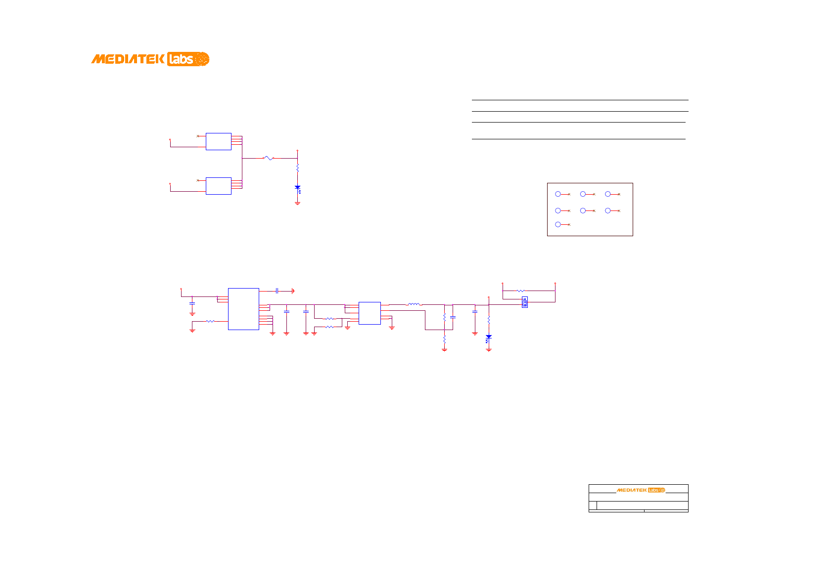
LinkIt 2523 HDK v11 User's Guide
© 2015 - 2016 MediaTek Inc.
Page 54 of 82
This document contains information that is proprietary to MediaTek Inc. (“MediaTek”) and/or its licensor(s).
Any unauthorized use, reproduction or disclosure of this document in whole or in part is strictly prohibited.
Figure 33. BB_MT2523G_ABB
J2001
1
3
2
VBAT_CONN
R2019 R / 1 / K / 0603
12
VBAT
Note 20-1: Users must connect CON6401 for total system power supply
DC 5V supply
60mils
Schematic design notice of "20_POWER_COMMON_LDO" page.
60mils
AD_IN_SW
AD_IN_FB
Vout = 0.6 x (1+Ra/Rb) = 3.96V
External LDO are option components
Note 20-2:
60mils
60mils
VBUS_SY S
60mils
FD and Hole
Remove R1118, R1119, C1114 change to 10uF when applying external LDO
Title
Size
Date: Sheet of
MediaTek HDK MT2523G
20_POWER_COMMON_LDO
C
20 99Monday, Oct ober 24, 2016
H2007
STAND
HOLE/PTH/R6D3.5
H2006
STAND
HOLE/PTH/R6D3.5
C2001
C / 1 / uF / 0603 / 50V
21
H2001
STAND
HOLE/PTH/R6D3.5
C2006
C / 22 / pF / 0402
2 1
LED2003
LED / CL190Y G
1
2
H2005
STAND
HOLE/PTH/R6D3.5
R2005
R / 510 / K / 0402
1
2
R2006
R / 91 / K / 0402
1
2
R2003
R / 1 / K / 0402
12
H2004
STAND
HOLE/PTH/R6D3.5
R2004
R / 1 / K / 0402 / NC
1 2
R2002
R / 0 / ohm / 0402
12R2018
R / 1.58 / K / 0402
12
L2001
PL / MEKK2520T1R0M
1 2
U2004
U / TPS62065
SW 2
FB 4
PVIN
8
AVIN
7
PGND 1
MOD E
6
THER PAD
9AGND 3
EN
5
H2003
STAND
HOLE/PTH/R6D3.5
R2001
R / 2.2 / K / 0402
12
F2001 2A FUSE
FUSE/DIP/SMD
C2002
C / 1 / uF / 0402
2 1
C2004
C / 10 / uF / 0603
21
LED2001
LED / CL190Y G
12
C2005
C / 22 / uF / 0603
2 1
C2003
C / 2.2 / uF / 0402
21
U2001
U / SS2003M
ANODE
3
CATHODE 5
CATHODE 1
CATHODE 2
NC
4
CATHODE 6
U2002
U / SS2003M
ANODE
3
CATHODE 5
CATHODE 1
CATHODE 2
NC
4
CATHODE 6
U2003
U / TPD1S514-1
VBUS_CON
C3
EN#
A1 GND B4
GND C1
VBUS_SY S A2
VBUS_SY S A3
VBUS_POWER B1
VBUS_SY S B2
VBUS_CON
C2
GND A4
GND C4
VBUS_CON
B3
H2002
STAND
HOLE/PTH/R6D3.5
AD_IN
VBUS
VUSB_DAP
VUSB_BB
VBUS
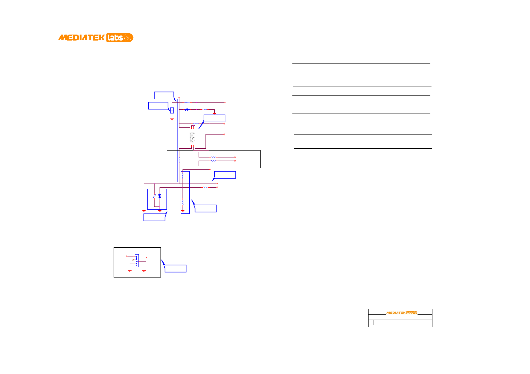
LinkIt 2523 HDK v11 User's Guide
© 2015 - 2016 MediaTek Inc.
Page 55 of 82
This document contains information that is proprietary to MediaTek Inc. (“MediaTek”) and/or its licensor(s).
Any unauthorized use, reproduction or disclosure of this document in whole or in part is strictly prohibited.
Figure 34. POWER_COMMON_LDO
R2109
R / 0 / ohm / 0402
1 2
Differential
NTC
Rsense
4mil
BATTERY
CONNECTOR
4mil
Note: 21-2
Note: 21-1
Note: 21-5
Note: 21-4
Note: 21-3
Note: 21-6
Note 21-1:
Before you select BJT , please take power dissipation into consideration. Note 21-3:
Note 21-4: 60mils from battery connector to MT2523 chip
1. Close to Battery Connector. (Rsense (R2103) <10mm)
Capacitor rating depends on Phone OVP spec.Note 21-2:
Schematic design notice of "21_Power_Charging" page.
Based on your system level design , if better ESD performance is needed
Note 21-5: L style pin header for battery sub board plug in
Note: 21-7
Note 21-7: Thermal protection : battery with NTC
Note 21-6:
NTC
Title
Size
Date: Sheet of
MediaTek HDK MT2523G
21_POWER_Charging
C
21 99Friday , June 24, 2016
Please place ESD2101 closed by R1137.
on your system, please refer to ESD performance enhance proposal.
Refer to MT6385 design notice.
3. Star connection from R2103 to BAT Connector
-> U2101's C -> R2103 -> VBAT)
2. Main path should be 40mil. (VBUS -> U2101's E,
BATTERY DTB
VCDT rating: 1.268V
60mils
(2) if battery NTC is 47kohm; R2106=61.9K (+/-1%)
(1) if battery NTC is 10kohm; R2106=16.9K (+/-1%)
C2102
C / 22 / uF / 0603
2 1
R2103
R / 0.1 / ohm / 0805 / 1%
R0805
12
Q2101
Q / PNMT6N1-LB
E1
B2
D3
S
4G
5C
6C
7
D8
R2101
R / 1 / K / 0402
1 2
C2101
C / 1 / uF / 0603 / 50V
2 1
R2108
R / 0 / ohm / 0402
1 2
R2105
R / 1.5 / K / 0402
1 2
ESD2101
ESD / AZ5825-01F
12
ESD2102
ESD / AZ5725-01F
12
R2104
R / 330 / K / 0402 / 1%
1 2
R2107
NTC / NTCG103JF103FT / 0402
12
R2106
R / 16.9 / K / 0402 / 1%
1 2
CON2101
5
4
6
2
3
1
R2102
R / 39 / K / 0402 / 1%
1 2
VBUS
VBAT_CONN
VBAT_CONN
VBAT_CONN
VA18
VDRV [11]
VCDT
[11]
ISENSE [11]
BATON [11]
CHRLDO [11]
BATSNS [11]
D2101
D/NZ9F5V6ST5G
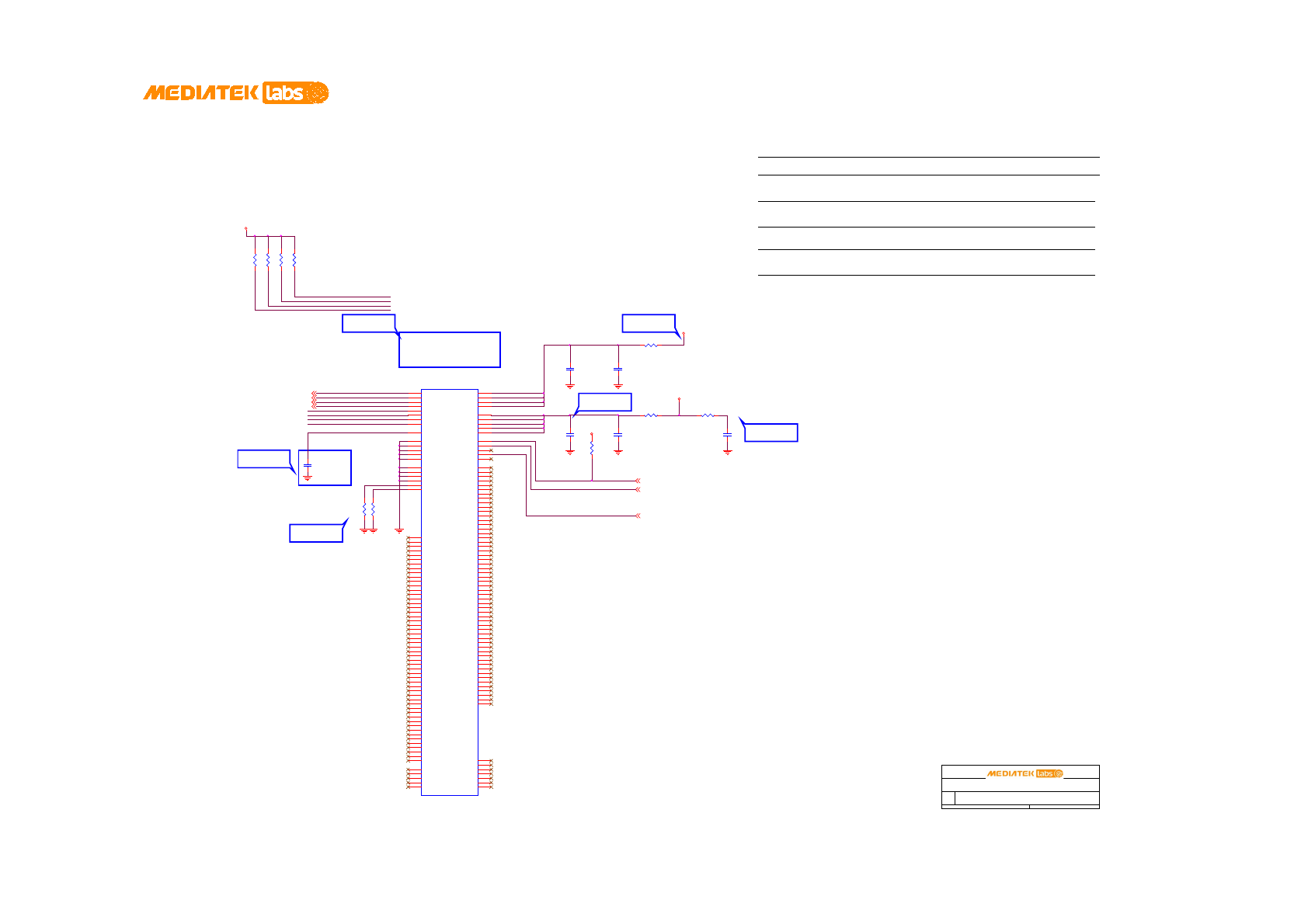
LinkIt 2523 HDK v11 User's Guide
© 2015 - 2016 MediaTek Inc.
Page 56 of 82
This document contains information that is proprietary to MediaTek Inc. (“MediaTek”) and/or its licensor(s).
Any unauthorized use, reproduction or disclosure of this document in whole or in part is strictly prohibited.
Figure 35. POWER_Charging
C4005
C / 4.7 / uF / 0402
2 1
R4010
R / 0 / ohm / 0402
12
MSDC0_DAT5
MSDC0_DAT6
MSDC0_DAT7
MSDC0_DAT4
153 ball eMMC
R4009
R / 0 / ohm / 0402 / N C
1
2
MSDC0_DAT5
MSDC0_DAT4
MSDC0_DAT7
MSDC0_DAT6
VIO18
Title
Size
Date: Sheet of
MediaTek HDK MT2523G
40_Memory_eMMC
C
40 99Thursday , March 31, 2016
eMMC is an optional componentNote 40-5:
Note: 40-5
Schematic design notice of "40_MEMORY_eMMC" page.
Note 40-1:
C4003 need to be placed near by eMMCNote 40-3:
For eMMC 5.0, connect eMMC's A6 & J5 pin to GND.
Please refer eMMC datasheet for the recommendation of
Note 40-2:
Note: 40-3
Note: 40-1
Note: 40-2
R4004
R / 10 / K / 0402 / NC
12
C4004
C / 100 / nF / 0402
2 1
R4008
R / 0 / ohm / 0402
12
U4001
U / 153 eMMC / THGBMBG5D1KBAI L
DAT0
A3
DAT1
A4
DAT2
A5
DAT3
B2
DAT4
B3
DAT5
B4
DAT6
B5
DAT7
B6
VDDI
C2
VSSQ
C4
VCCQ C6
VCC E6
VSS
E7
VCC F5
VSS
G5
VSS
H10
VCC J10
RST K5
VSS
K8
VCC K9
VCCQ M4
CMD M5
CLK M6
VSSQ
N2
VCCQ N4
VSSQ
N5
VCCQ P3
VSSQ
P4
VCCQ P5
VSSQ
P6 A1 INDEX / NC D4
NC
A1
NC
A2
VSS
A6
RFU A7
NC
A8
NC
A9
NC
A10
NC
A11
NC
A12
NC
A13
NC
A14
NC
B1
NC
B7
NC
B8
NC
B9
NC
B10
NC
B11
NC
B12
NC
B13
NC
B14
NC
C1
NC
C3
NC C5
NC C7
NC C8
NC C9
NC C10
NC C11
NC C12
NC C13
NC C14
NC D1
NC D2
NC D3
NC D12
NC D13
NC D14
NC E1
NC E2
NC E3
RFU E5
RFU E8
RFU E9
RFU E10
NC E12
NC E13
NC E14
NC F1
NC F2
NC F3
RFU F10
NC F12
NC F13
NC F14
NC G1
NC G2
RFU G3
RFU
G10
NC G12
NC G13
NC G14
NC
H1
NC
H2
NC
H3
DSL H5
NC
H12
NC
H13
NC
H14
NC J1
NC J2
NC J3
VSS
J5
NC J12
NC J13
NC J14
NC
K1
NC
K2
NC
K3
RFU
K6 RFU
K7 RFU
K10
NC
K12
NC
K13
NC
K14
NC L1
NC L2
NC L3
NC L12
NC L13
NC L14
NC
M1
NC
M2
NC
M3
NC
M7
NC
M8
NC
M9
NC
M10
NC
M11
NC
M12
NC
M13
NC
M14
NC N1
NC N3
NC N6
NC N7
NC N8
NC N9
NC N10
NC N11
NC N12
NC N13
NC N14
NC
P1
NC
P2
NC
P7
NC
P8
NC
P9
RFU
P10
NC
P11
NC
P12
NC
P13
NC
P14
R4009 and R4010 co-layout for path selection only on one time
R4007
R / 0 / ohm / 0402
12
R4005
R / 0 / ohm / 0402 / N C
12
C4002
C / 4.7 / uF / 0402
21
C4001
C / 2.2 / uF / 0402
2 1
R4001
R / 10 / K / 0402 / NC
1
2
R4006
R / 10 / K / 0402 / NC
12
C4003
C / 100 / nF / 0402
2 1
R4002
R / 10 / K / 0402 / NC
1
2
R4003
R / 10 / K / 0402 / NC
12
C4006
C / 100 / nF / 0402
2 1
VMC
VIO18
MSDC0_CMD [10]
MC_RST [10]
MSDC0_C LK [10]
MSDC0_DAT1[10]
MSDC0_DAT0[10]
MSDC0_DAT2[10]
MSDC0_DAT3[10]
Note: 40-4
R4005 and R4009 must be removed when micro SD feature activeNote 40-4:
Note: 40-4
VCC/VCCQ/VDDI bypass capacitors values.
For eMMC 4.5, check eMMC's A6 & J5 is no connection (NC).
VIO18

LinkIt 2523 HDK v11 User's Guide
© 2015 - 2016 MediaTek Inc.
Page 57 of 82
This document contains information that is proprietary to MediaTek Inc. (“MediaTek”) and/or its licensor(s).
Any unauthorized use, reproduction or disclosure of this document in whole or in part is strictly prohibited.
Figure 36. MEMORY_eMMC
VMC
Title
Size
Date: Sheet of
MediaTek HDK MT2523G
41_MEMORY_SD Card
C
41 99Thursday , March 31, 2016
MSDC interface
Schematic design notice of "41_MEMORY_SD Card" page.
These ESD diodes are optional for better ESD and RF de-sense performance.
Note 41-1:
Note: 41-1 Note: 41-1
Note: 41-2
Note 41-2: R4101 must be removed when eMMC feature active
R4102
R / 10 / K / 0402 / NC
1 2
ESD4101 ESD5451NKM / NC
AK
R4103
R / 10 / K / 0402 / NC
1 2
ESD4102 ESD5451NKM / NC
A K
ESD4103 ESD5451NKM / NC
A K
CON4101
CON / 12 / TA-M017-012-07-811
MICROSD/8P/ SMD/TA-M017-012-07-811
DATA2
1
CD/DATA3
2
CMD
3
VDD
4
CLK
5
VSS
6
DATA0
7
DATA1
8
CD 12
SWPIO 9
VCCSWP 10
GND 11
GND 13
GND 14
GND 15
GND 16
GND 17
GND 18
GND 19
ESD4104 ESD5451NKM / NC
A K
ESD4107 ESD5451NKM / NC
A K
R4104
R / 10 / K / 0402 / NC
1 2
ESD4105 ESD5451NKM / NC
A K
ESD4106 ESD5451NKM / NC
AK
C4101
C / 1 / uF / 0402
2 1
ESD4108 ESD5451NKM / NC
A K
R4101
R / 0 / ohm / 0402
12
ESD4109 ESD5451NKM / NC
A K
VMC
MCINS [10,93]
MCDA1_J[10]
MCDA0_J[10]
MCDA3_J[10]
MCDA2_J[10]
MCCM0 _J[10]
MCCK_J[10]
(The C load of Diodes on trace should be less than 15pF)
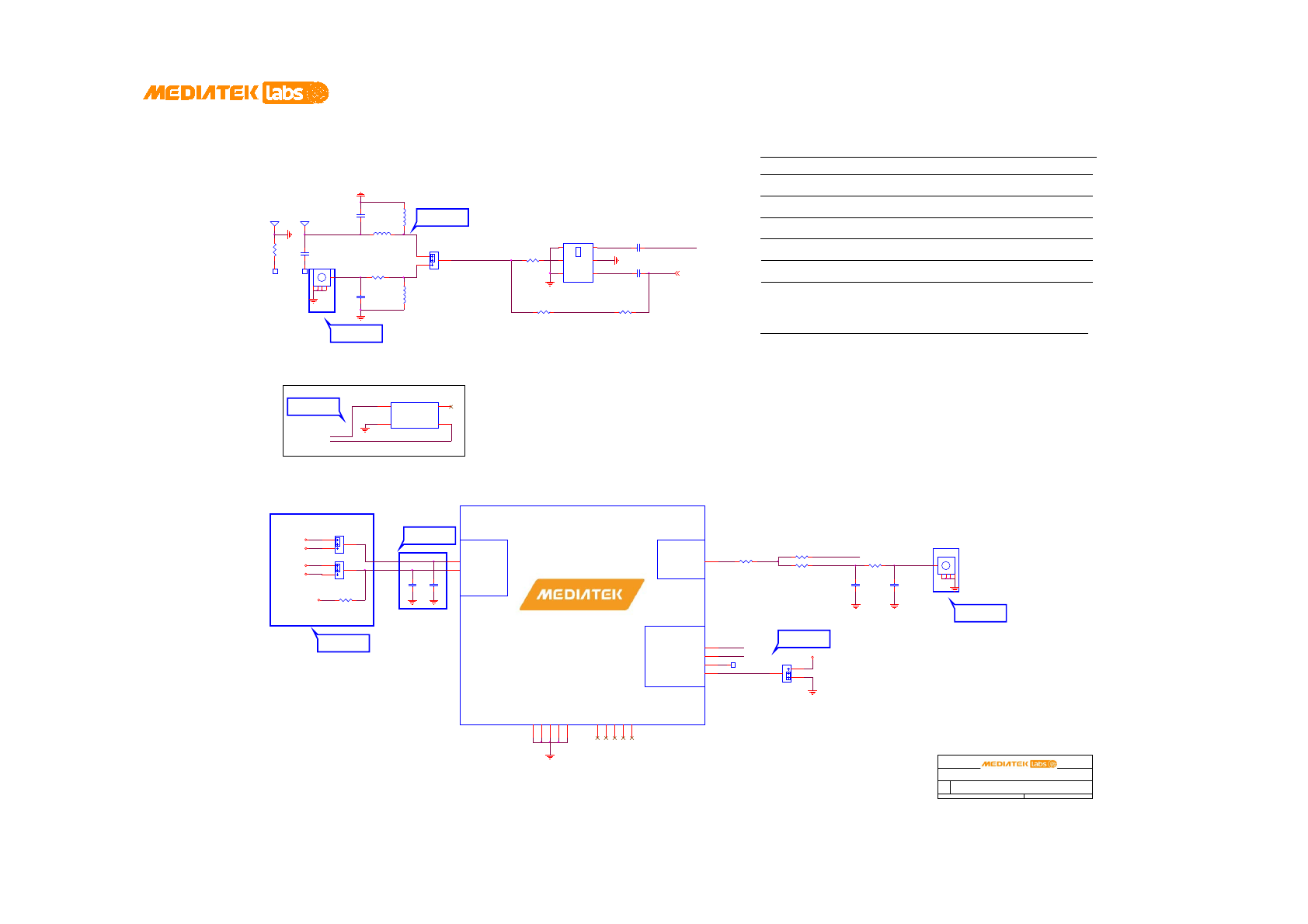
LinkIt 2523 HDK v11 User's Guide
© 2015 - 2016 MediaTek Inc.
Page 58 of 82
This document contains information that is proprietary to MediaTek Inc. (“MediaTek”) and/or its licensor(s).
Any unauthorized use, reproduction or disclosure of this document in whole or in part is strictly prohibited.
Figure 37. MEMORY_SD Card
R5012
R / 0 / ohm / 0402 / N C
1
2
R5013
R / 0 / ohm / 0402 / N C
12
AVDD13_BTRF
R5005
R / 0 / ohm / 0402 / N C
12
AVDD_BTRF_ext
J5004 connected to VIO18 for external buck LDO cost reduction
Note 50-6: J5002 connected to VBT for dual mode of Bluetooth and BLE modes
Note 50-7: SMA 5001 SMA5002 are optional components
J5005 connected to AVDD_BTRF_ext for power saving
J5002 connected to VIO18 for BLE mode
J5004 connected to VBT for dual mode of Bluetooth and BLE modes
BT_ANT
R5010
R / 0 / ohm / 0402
12
R5011
R / 0 / ohm / 0402 / N C
12
BT_ANT
Note: 50-6
Note: 50-7
Note: 50-7
Title
Size
Date: Sheet of
MediaTek HDK MT2523G
50_CONNECTIVITY_BT_MT2523G
C
50 99Thursday , March 31, 2016
26MHz crystal
XTA L 2
XTA L 1
XTA L 2
XTA L 1
R5002, C5003 and C5004 are reserved for BT antenna matching tuning
Note 50-1:
Schematic design notice of "50_CONNECTIVITY_BT_MT2523G" page.
Note 50-2: 26MHz crystal must be placed near by Larkspur ball out position
These capacitors should be placed near by ball out position
Note 50-3:
Note: 50-4
Note: 50-5
Note: 50-2
R5007
R / 0 / ohm / 0402
1 2
R5009
R / 0 / ohm / 0402 / N C
12
C5002
C / 100 / nF / 0402
2 1
TP5002
NC
1
BT
26M & CLK
BUFFER
MT2523 BT
POWER IN
U1000-3
MT2523G
XTA L 1 A9
XTA L 2 A10
FREF C8
BT_LNA A12
AVDD13_BTRF
A13
EXT_CLK_SEL A11
AVSS_BT
C11
AVSS_BT
B12
AVDD_VBT
A14
AVSS_BT
C12
AVSS_BT
D12
AVSS_BT
E12
DUMMY_NET
A1
DUMMY_NET
A22
DUMMY_NET
P1
DUMMY_NET
P22
DUMMY_NET
P5
SMA5001
SMA-1.66MM
1
2
3
4
5
C5006
C / 18 / pF / 0402
2
1
R5002
R / 0 / ohm / 0402
12
C5005
C / 18 / pF / 0402
2
1
C5003
C / NC / 0402
21
R5003
R / 0 / ohm / 0402
1
2
TP5001
NC
1
C5001
C / 2.2 / pF / 0402
2 1
C5004
C / NC / 0402
2 1
ANT5002
ANT sprint
Feed 1
R5006
R / 0 / ohm / 0402
1 2
J5002
R / 0 / ohm / 0402-3P(1-2)
1
2
3
J5001
R / 0 / ohm / 0402-3P(1-2)
1
2
3
L5002
NC
12
J5004
R / 0 / ohm / 0402-3P(1-2)
1
2
3
C5008
C / NC / 0402
2 1
DIPX5001
DP1608-V1524C A
DIPLEXER/6P/SMD/DP1608
WiFi 1
GND 2
GPS 3
GND
4
ANT
5
GND
6
ANT5001
ANT sprint
Feed 1
J5003
R / 0 / ohm / 0402-3P(1-2)
1
2
3
X5001
X / 26 / MHz / 8Q26000008
Hot2
1
GND
2HOT 3
NC 4
L5001
NC
1 2
SMA5002
SMA-1.66MM
1
2
3
4
5
C5007
C / NC / 0402
21
VIO18
The impedence of traces about diplexer should be 50 ohmNote 50-5:
Note 50-4: J5001 should keep low for clock is generated by crystal;
VBT
VIO18
VBT
VIO18
CLK_SEL
50 Ohm impedence
50 Ohm impedence
50 Ohm impedence
50 Ohm impedence
GPS_diplexer_input [ 52]
TP5003
C5009
C / 3.6 / pF / 0402 / GJM1555C1H3R6WB01D
2 1
L5003
L / 6.8 / nH / LQG15HS6N 8H02D
1
2
J5006 is set for single Bluetooth performance measurement.
Pull high if clock signal is injected from net XTAL1.
AVDD_VBT
Note: 50-1
50 Ohm impedence

LinkIt 2523 HDK v11 User's Guide
© 2015 - 2016 MediaTek Inc.
Page 59 of 82
This document contains information that is proprietary to MediaTek Inc. (“MediaTek”) and/or its licensor(s).
Any unauthorized use, reproduction or disclosure of this document in whole or in part is strictly prohibited.
Figure 38. CONNECTIVITY_BT_MT2523G
GNSS_VBAT
R5243
R / 0 / ohm / 0402 / N C
12
Note: 52-18
R5224 R / 0 / ohm / 0603
1
2
GNSS_VBAT
VBAT
Note: 52-8
Note: 52-14
External buck 3.3V LDO
Note 52-18:GPS HOT re-start feature
No support:
BAT5201=NC, R5211=NC, R5243=NC, R5234=0ohm
Support:
Support and Power optimization
X5204=NC, C5222=NC, C5221=NC, R5210=120K, R5220=91K
BAT5201=NC, R5211=NC, R5243=0ohm, R5234=NC
X5204=NC, C5222=NC, C5221=NC, R5210=120K, R5220=91K
BAT5201=ML621S, R5211=1K, R5243=NC, R5234=0 ohm
X5204=FC-135, C5222=22pF, C5221=22pF, R5210=NC, R5220=NC
GNSS_VBAT for pin GPS_VRTC_4V3 should be provided between 2.0V to 4.3V.
GPS_VDDIO
Carkit_input
SCK1
Title
Size
Date: Sheet of
MediaTek HDK MT2523G
52_CONNECTIVITY_GPS_MT3333
C
52 99Monday , May 30, 2016
JDI
JCK
JMS
JRST
GPS_VTLDO_2V8
SCS1
External buck 3.3V LDO
VGPS_MAIN
GPS_VRTC_1V1
JDO
GPS_DCV
GPS_VREF
GPS_VTCXO_SW
GPS_DCV_FB
JRCK
GPS_VTCXO_SW
GPS_VTCXO_SW
50 Ohm
VGPS_MAIN
GPS_RTC_XOUT
GPS_RFIN
TCXO
GPS_RTC_XIN
TX2
Schematic design notice of "52_CONNECTIVITY_GPS_MT2523G" page.
Note 52-1:
AVSS43_DCV should be connected to C5218 GND net first,
Note 52-3:
Both of pin AVDD43_VBAT and AVDD43_DCV voltage should be keeped
C5214 is close to G1 ball (AVDD28_TLDO)Note 52-2:
Buck Mode : L5202 = 1uH, R5205 = 0 ohm , R5206 = NC
Note 52-4:
Note 52-5: Recommend to select 3V coin battery for leakage consideration.
Note: 52-1
Note: 52-1
Note: 52-2
Note: 52-3
Note: 52-4
Note: 52-5
U5204/C5221/C5222 could be removed, R5210 = 0 ohm,
Note 52-6:
Note: 52-6
Note: 52-7
Note 52-7: VTCXO voltage selection
Note 52-8: RF clock selection
Note: 52-9
IO Voltage Selection
Note 52-9:
Host interface selection
Note 52-10:
Note: 52-10
Note: 52-12
Note: 52-11
Note 52-11:C5201 is close to U5201 VCC
50 Ohm
Carkit_input
Note: 52-15
Note: 52-13
RTC XT AL
TCXO layout please refer to MTK TCXO layout rule.
In order to keep good GPS clock stability,Note 52-12:
Note 52-15:
Note 52-14:Main Input Voltage Requirement and External LDOs Selection
output voltage drop-down period.
discharge function and confirm the voltage drop-down curve to keep long
[1] Please choose one voltage source without built-in output high-speed
GPS_VTCXO_SW Note for external active antenna, Note 52-16:
matching value depends on LNA selected
GPS_VTCXO_SW is 1.8V or 2.8V base on TCXO selection.
The voltage drop must can't be lower than 3.1V.
output voltage drop-down period (>1ms from 2.7V to 0.5V).
function, such as Torex XC6210/XC6215/XC6221 series to keep long
[2] Please choose external LDOs without output high-speed discharge
C5203, C5206 and L5201 are reserved for LNA matchingNote 52-13:
Otherwise, please using external power supply.
Please ensure external active antenna is operating at this range.
Please refer the QVL to select LNA componentNote 52-17:
the QVL to select TCXO component
MT2523 support 16.368MHz&26MHz TCXO, please refer
Note: 52-17
Note: 52-16
GPS_DCV_1V8
GPS_DCV_1V8
GPS_CORE1V1
GPS_VTLDO_2V8
C5218
C / 4.7 / uF / 0603
2 1
TP5205
NC
1
L5203
L / 22 / nH / 0402 / NC
12
C5216
C / 1 / uF / 0402
2
1
R5211 R / 1 / K / 0402 / NC
TP5201
NC
1
C5224
C / 4.7 / uF / 0603
2 1
R5235
R / 0 / ohm / 0402
12
TP5207
NC
1
TP5210
NC
1
C5214
C / 1 / uF / 0402
2 1
R5241
R / 0 / ohm / 0402
1
2
C5237
C / 4.7 / uF / 0603
2 1
TP5215
NC
1
C5226
C / 1 / uF / 0402
21
U5205
U / XC6210A332MR
IN
1
GND
2
EN
3BYP 4
OUT 5
C5233
C / 0402 / NC
2 1
U5207
U / BGA725L6
GND 1
VCC 2
AO 3
GNDRF
4
AI
5
PON
6
+
BAT5201 ML621S / NC
R5237
R / 0 / ohm / 0402
12
R5230
R / 0 / ohm / 0402
12
R5238R / 0 / ohm / 0402
12
TP5203
NC
1
X5204
X / FC-135 32.768KH Z 12. 5pF
IN1 1
IN2 2
C5219
C / 4.7 / uF / 0603
2 1
C5236
C / 18 / pF / 0402
21
L5202
L / 1 / uH / 0806
L/IND/SMD/LQM2MPN1R0NG0
R5207
R / 10 / K / 0402 / NC
C5229
C / 18 / pF / 0402
21
C5221
C / 22 / pF / 0402
R5210 R / 120 / K / 0402 / N C
1
2
C5227
C / 22 / pF / 0402
2
1
J5202
R / 0 / ohm / 0402-3P(1-2)
1
2
3
R5206
R / 0 / ohm / 0402 / N C
R5236
R / 0 / ohm / 0402
12R5203 R / 10 / K / 0402 / N C
C5209
C / 4.7 / nF / 0402
2
1
R5209
R / 10 / K / 0402 / NC
C5211 C / 1 / uF / 0402
21
L5204
L / 5.6 / nH / 0402
12
TP5214
NC
1
R5219
R / 0 / ohm / 0402
12
C5210 C / 1 / uF / 0402
21
U5203
U / XC6210A332MR
IN
1
GND
2
EN
3BYP 4
OUT 5
J5201
R / 0 / ohm / 0402-3P(1-2)
1
2
3
TP5206
NC
1
C5213 C / 4.7 / nF / 0402
2
1
C5232
C / 0402 / NC
2 1
TP5204 NC
1
C5235
C / 0402 / NC
2 1
TP5216
NC
1
C5234
C / 0402 / NC
2 1
C5207
C / 1 / nF / 0402
12
R5218
R / 0 / ohm / 0402 / N C
12
R5217
R / 0 / ohm / 0402 / N C
12
C5222
C / 22 / pF / 0402
TP5213
NC
1
C5203
NC
12
C5238
C / 4.7 / uF / 0603
2 1
VGPS_MAIN
R5216
R / 0 / ohm / 0402
12
C5212 C / 2.2 / uF / 0402
2
1
TP5211
NC
1
R5240
R / 0 / ohm / 0402
1
2
R5226
R / 0 / ohm / 0402
R5205
R / 0 / ohm / 0402
C5201
C / 1 / uF / 0402
2 1
GPS_DCV_1V8
R5208
R / 10 / K / 0402
R5225
R / 0 / ohm / 0402
U5206
U / EPOCOS_B8313
IN
1
G
2
G
3
OUT 4
G
5
R5220 R / 91 / K / 0402 / N C
1
2
R5228
R / 0 / ohm / 0402
1
2
R5204 R / 10 / K / 0402 / N C
R5232
R / 0 / ohm / 0402
12
TP5208
NC
1
TP5202 NC
1
R5239
R / 0 / ohm / 0402
1
2
C5215
C / 1 / uF / 0402
21
R5201
R / 0 / ohm / 0402
R5234
R / 0 / ohm / 0402
12
C5230
C / 0402 / NC
2 1
U5208
U / EPOCOS_B8313
IN
1
G
2
G
3
OUT 4
G
5
C5208
C / 4.7 / nF / 0402
2
1
TP5209
NC
1
TX2
R5227
R / 0 / ohm / 0402
1 2
C5220
C / 1 / uF / 0402
2 1
MT2523G
U1000-4
MT2523G
GPS_32K_OUT
E17
GPS_AVDD43_RTC
D19
GPS_AVDD11_RTC
F21
GPS_XIN
K21
GPS_XOUT
K22
GPS_TX0
M16
GPS_RX0
M18
GPS_TX1
E16
GPS_RX1
G20
GPS_TX2
J18
GPS_RX2
L18
GPS_SCK1
K17
GPS_SCS1_
P17
GPS_VREF
H22
GPS_AVDD_TCXO_SW
F22
GPS_AVDD 28_TLDO
E22
GPS_AVSS43_MISC
G21
GPS_AVDD 28_CLDO
D22
GPS_AVDD 11_CLDO
B22
GPS_AVSS11_CLDO
C22
GPS_AVDD43_DCV
B21
GPS_AVSS43_DCV
A21
GPS_DCV
C21
GPS_DCV_FB
C20
GPS_HRST_B M21
GPS_XTEST M19
GPS_EINT0 N19
GPS_EINT1 N20
GPS_DVDD11_COR E2 L19
GPS_DVDD11_COR E1 G18
GPS_DVSS28_IO J17
GPS_DVDD28_IO1 H 20
GPS_DVDD28_IO2 P20
GPS_DVDD28_SF J20
GPS_JRCK L17
GPS_JDO P18
GPS_JDI K16
GPS_JCK G19
GPS_JMS N18
GPS_JRST_ N17
GPS_RFIN N22
GPS_AVDD18_RXFE M 22
GPS_T1P L20
GPS_OSC F20
GPS_AVDD18_CM L22
GPS_T1N L21
GPS_AVDD43_VBAT
G22
GPS_FORCE_ON
D20
GPS_DVSS11_CORE J16
GPS_DVSS11_CORE F17
GPS_DVSS11_CORE F16
GPS_DVSS11_CORE F18
GPS_DVSS11_CORE G16
GPS_DVSS11_CORE G17
GPS_DVSS11_CORE H16
GPS_DVSS11_CORE H17
GPS_DVSS11_CORE C19
GPS_AVSS_RF P21
GPS_DVSS28_SF J21
C5223
C / 2.2 / uF / 0402
2 1
L5201
L / 1.2 / nH / 0402
TP5212
NC
1
C5231
C / 1 / uF / 0402
2
1
TCXO5201
TCXO / 26 / MHz
VCC 4
OUT
3
GND
2NC 1
C5206
C / 1 / pF / 0402
C5217
C / 1 / uF / 0402
2 1
C5225
C / 4.7 / uF / 0603
2 1
GPS_VANT
GNSS_VBAT
GNSS_VBAT
GPS_VTCXO_SW
GPS_32K_BB[ 10]
GPS_LDO_EN[10]
GPS_diplexer_input[50]
URXD3_GPS
[10]
UTXD3_GPS
[10]
between 3.1V to 4.3V (VGPS_MAIN)
VGPS_MAIN
then connect to reference GND.
LDO Mode : L5202 = 0 ohm , R5205 = NC , R5206 = 0 ohm
Pin GPS_VRTC_4V3 should be provided between 2.0V to 4.3V.
GPS_VRTC_4V3 should be kept (always alive voltage source).
Or change C5220 to 0 ohm and feed 1.1V (always alive voltage
source) into GPS_VRTC_1V1.
2.8V TCXO: TLDO 2.8V : R5209 = NC
1.8V TCXO: SMPS 1.8V : R5209 = 10K
16.368MHZ TCXO : R5207 = NC , R5208 = NC
26MHZ TCXO : R5207 = NC , R5208 = 10K
2.8V IO : R5201= 0 , R5202 = NC (IO voltage is GPS_VTLDO)
1.8V IO : R5201 = NC , R5202 = 0 (IO voltage is GPS_DCV_1V8)
UART : R5203 = NC , R5204 = NC (I/F : TX0 , RX0)
SPI : R5203 = NC , R5204 = 10K
I2C : R5203 = 10K , R5204 = 10K
GPS_CORE1V1
GPS_DCV_1V8
GPS_EINT
[10] R5242R / 0 / ohm / 0402
1
2
GPS_VANT
GPS_VTLDO_2V8
GPS_VTCXO_SW
VGPS_MAIN
TX2

LinkIt 2523 HDK v11 User's Guide
© 2015 - 2016 MediaTek Inc.
Page 60 of 82
This document contains information that is proprietary to MediaTek Inc. (“MediaTek”) and/or its licensor(s).
Any unauthorized use, reproduction or disclosure of this document in whole or in part is strictly prohibited.
Figure 39. CONNECTIVITY_GPS_MT2523G
Note: 60-2
The gain of class-D amplifier is set to 12dB (4V/V); Note 60-2:
Note: 60-3
Note: 60-3
AMIC
Note 60-3: ESD diodes are for ehnhacement proposal; also could be cost reduction.
Note: 60-3
Note: 60-3
C6017 C / 1 / uF / 0402
2 1
C6004
C / 33 / pF / 0402 / N C
R6005 R / 100 / ohm / 0402
ESD6006
ESD5Z5.0T1G
AK
ESD6004ESD5Z5.0T1G
AK
C6021
C / 100 / nF / 0402
21
C6010
C / 33 / pF / 0402 / N C
BEAD6001
L / BLM15AG100SN1 / 0402
2 1
R6014
R / 0 / ohm / 0402
1 2
R6016
R / 0 / ohm / 0402
12
C6001 C / 100 / nF / 0402
TP6001
NC
1
C6006
C / 100 / pF / 0402 / N C
C6009
C / 33 / pF / 0402 / N C
R6008
R / 470 / ohm / 0402
R6015
R / 0 / ohm / 0402
1 2
TP6003
MIC6001
MIC / SPU0410HR5H-PB
FILTER/SMD/SPU0410HR5H-PB
OUT 4
GND
2GND 3
VDD
1
C6018
C / 100 / nF / 0402
21
C6003
C / 33 / pF / 0402 / N C
ESD6001
ESD5451N KM / NC
A K
R6019
R / 0 / ohm / 0402
1 2
TP6004
R6004
R / 1 / K / 0402
C6025
C / 22 / uF / 0402
C6007
C / 22 / uF / 0402
C6014
C / 33 / pF / 0402
2 1
C6019
C / 4.7 / uF / 0402 / X5R
21
R6013
R / 300 / K / 0402 / NC
1
2
C6024
C / 33 / pF / 0402
2 1
R6017
R / 0 / ohm / 0402 / N C
1 2
C6015
C / 33 / pF / 0402
2 1
ESD6002
ESD5451N KM / NC
AK
C6005 C / 4.7 / uF / 0603
R6007
R / 470 / K / 0402
1 2
R6010
R / 47 / K / 0402
1 2
R6009
R / 470 / ohm / 0402
U6001
U / TPA2010D1
VDD
B1
IN+
A1
IN-
C1
SHUNTDOWN
C2
PVDD B2
GND A2
GND B3
VO- A3
VO+ C3
XMI C
R6018
R / 0 / ohm / 0402 / N C
1 2
C6012
C / 100 / nF / 0402
2 1
ESD6005ESD5Z5.0T1G
AK
R6020
R / 0 / ohm / 0402
12
CON6001
JACK_CON/ 5P/EJ -3699M-GP
AUDIOJAC K/5P/ SMD/EJ-3699M-GP
1
2
3
5
4
C6013
C / 100 / pF / 0402
2 1
C6011
C / 33 / pF / 0402 / N C
R6006 R / 100 / ohm / 0402
ESD6003ESD5Z5.0T1G
AK
R6011
R / 75 / K / 0402
1 2
C6016 C / 1 / uF / 0402
2 1
R6003
R / 0 / ohm / 0402 / N C
1 2
R6012
R / 75 / K / 0402
12
R6001
R / 1.5 / K / 0402
C6023
C / 100 / pF / 0402
21
C6022
C / 33 / pF / 0402
2 1
C6008
C / 33 / pF / 0402 / N C
C6002 C / 100 / nF / 0402
R6002
R / 0 / ohm / 0402 / N C
1 2
C6020
C / 100 / nF / 0402
21
AU_MICBIAS0
VIO28
AU_MICBIAS0
VBAT
EAR_EINT[10,93]
AU_HPR[11]
AU_HPL[11]
AU_HSP[11]
AU_HSN[11]
SPK_AMP_PDN[ 10]
AU_VIN0_N [11]
AU_VIN0_P [11]
AU_VIN1_N[11]
ACCDET[ 11]
AU_VIN1_P[11]
Speaker is an optional componentNote 60-4:
Note: 60-4
Title
Size
Date: Sheet of
MediaTek HDK MT2523G
60_PERI_Audio_IO
C
60 99Thursday , March 31, 2016
SPK1
SPK / 2403-260-00071-190-EN
SPEAKER/ SMD/2403-260-00071/WS3330
1
2
AU_SPKN
AU_SPKP
AU_SPK_N
AU_SPK_P
Speaker
R6021
R / 0 / ohm / 0402
1 2
R6022
R / 0 / ohm / 0402
1 2
R6023
R / 0 / ohm / 0402
1 2
Schematic design notice of "60_PERI_Audio_IO" page.
Note 60-1:
JACK_GND
Note: 60-1
Note: 60-1
The GND of headset microphone and Headset earphone
In shielding
XMIC_SLT
XMP3_R_SLT
XMP3_L
XMP3_R
XMI C
XMP3_R
R6024
R / 0 / ohm / 0402
1 2
R6025
R / 0 / ohm / 0402
1 2
XMP3_L
Headset earphone
Headset microphone
default open
XMP3_L_SLT
JACK_GND
EAR_EINT_1
should be connected together first, then connected to main GND.
SHORT6001
SHORT / NC-MMD-L6-4MIL
12

LinkIt 2523 HDK v11 User's Guide
© 2015 - 2016 MediaTek Inc.
Page 61 of 82
This document contains information that is proprietary to MediaTek Inc. (“MediaTek”) and/or its licensor(s).
Any unauthorized use, reproduction or disclosure of this document in whole or in part is strictly prohibited.
Figure 40. PERI_Audio_IO
R6101
R / 0 / ohm / 0402 / N C
LCM_BLPWM_J
R6102
R / 0 / ohm / 0402
R6103
R / 0 / ohm / 0402 VI O28
VIO18
Title
Size
Date: Sheet of
MediaTek HDK MT2523G
61_PERI_LCD_CTP
C
61 99Friday , J une 24, 2016
Note 61-1: High speed connector is an optional component
J6101
R / 0 / ohm / 0402-3P(1-2)
1
2
3
J6102
R / 0 / ohm / 0402-3P(1-2)
1
2
3
CON6102
1 2
43
5 6
87
910
1211
1413
15 16
18
20
17
19
J6103
R / 0 / ohm / 0402-3P(1-2)
1
2
3
LSRSTB_JP
LSRSTB_HS
LSCE_B_H S
LSCE_B_J P
LPTE_JP
LSCK_H S
LSCK_JP
LSDA_H S
LSDA_JP
LPTE_HS
LSA0_HS
LSA0_JP
LCM_BLPWM_J
LPTE_JP
LSDA_JP
LSA0_JP
LSCK_JP
LSCE_B_J P
LSRSTB_JP
J6104
R / 0 / ohm / 0402-3P(1-2)
1
2
3
J6105
R / 0 / ohm / 0402-3P(1-2)
1
2
3
J6106
R / 0 / ohm / 0402-3P(1-2)
1
2
3
VBAT
LCM_BLPWM[10, 90]
LPTE_LCM[10]
LSDA_LC M[ 10]
LSCK_LC M[10,90]
LSRSTB_LCM[ 10]
LSCE_B_LC M[10]
LSA0_LCM[10]
TP_RST [10,61]
ISINK[11,61,92]
TP_EINT [10,61]
SCL0 [10,61,62, 63]
SDA0 [10,61,62, 63]
SCL0 TP_SCL [94]
SDA0 TP_SDA [94]
TP_EINT TP_EINT[94]
LPTE_HS LPTE [94]
LSRSTB_HS LSRSTB [94]
TP_RST TP_RST [94]
ISINK ISINK [94]
LSCK_H S LSCK [94]
LSDA_H S LSDA [94]
LSA0 [94]
LSA0_HS
LSCE_B_H S LSCE_B [94]
LCM_BLPWM_J PWM_EN[94]

LinkIt 2523 HDK v11 User's Guide
© 2015 - 2016 MediaTek Inc.
Page 62 of 82
This document contains information that is proprietary to MediaTek Inc. (“MediaTek”) and/or its licensor(s).
Any unauthorized use, reproduction or disclosure of this document in whole or in part is strictly prohibited.
Figure 41. PERI_LCD_Capacitive touch panel
CMCSK_J [10]
CMCSD1_J [10,90]
CMCSD0_J [10,90]
CMMC LK_J [10,90]
CMCSD2_J [10]
CMR ST_J [10,90]
CMPDN_J [10,90]
VCAMA VBAT
SDA0[10,61,63]
SCL0[10,61,63]
Title
Size
Date: Sheet of
MediaTek HDK MT2523G
62_PERI_CAMERA
C
62 99Thursday , March 31, 2016
CON6201
HE7X2 MALE_TOP
DIP7X2/P2.54
+
1
+
3
+
5
+
7
+
9
+
11
+
13
+2
+4
+6
+8
+10
+12
+14

LinkIt 2523 HDK v11 User's Guide
© 2015 - 2016 MediaTek Inc.
Page 63 of 82
This document contains information that is proprietary to MediaTek Inc. (“MediaTek”) and/or its licensor(s).
Any unauthorized use, reproduction or disclosure of this document in whole or in part is strictly prohibited.
Figure 42. PERI_CAMERA
Title
Size
Date: Sheet of
MediaTek HDK MT2523G
63_PERI_SENSOR_DTB
C
63 99Friday , June 24, 2016
CON6301
1 2
43
5 6
87
910
12
11
1413
15 16
18
20
17
19
21
23
22
24
R6301
R / 0 / ohm / 0402
1 2 R6302
R / 0 / ohm / 0402
1 2
R6303
R / 0 / ohm / 0402
1 2
VBAT
VIO28 VIO18
SDA0[10,61,62] MA_SPI3_B_MISO [ 10]
SCL0[10,61,62] MA_SPI3_B_MOSI [10]
MA_SPI3_B_CS0 [10]
MA_SPI3_B_SCK [10]
U303_EINT_CONN [10,93]
U303_PD_CONN [10]
U303_RSTN_CONN [10]
MA_SPI3_B_CS1[10,90]
U304_EINT_CONN[10,93]
U305_EINT_CONN[10,93]
U302_EINT_CONN[10,93]
SEN_32K_BB[10]
R6304
R / 0 / ohm / 0402
1 2 VA28

LinkIt 2523 HDK v11 User's Guide
© 2015 - 2016 MediaTek Inc.
Page 64 of 82
This document contains information that is proprietary to MediaTek Inc. (“MediaTek”) and/or its licensor(s).
Any unauthorized use, reproduction or disclosure of this document in whole or in part is strictly prohibited.
Figure 43. PERI_SENSOR_DTB_IO
Title
Size
Date: Sheet of
MediaTek HDK MT2523G
64_PERI_USB
C
64 99Thursday , March 31, 2016
USB_DP[ 10]
USB_DM[10]
VUSB_BB
CON6401
Proconn_8791-N 005-M1A0
VUSB
1
D-
2
D+
3
ID
4
GND
5.6
.7
.8
.9
.10
.11
ESD6402
ESD / AZ5825-01F
12
ESD6401
ESD / AZ5315-02F
D2 1
D1 2
D3
3
USB
This ESD components are optional for better ESD performance.
Note 64-1:
Schematic design notice of "64_PERI_USB" page.
Note: 64-1
The C load of these diodes must smaller than 3pf and close to USB jack.

LinkIt 2523 HDK v11 User's Guide
© 2015 - 2016 MediaTek Inc.
Page 65 of 82
This document contains information that is proprietary to MediaTek Inc. (“MediaTek”) and/or its licensor(s).
Any unauthorized use, reproduction or disclosure of this document in whole or in part is strictly prohibited.
Figure 44. PERI_USB
PWRKEY
Title
Size
Date: Sheet of
MediaTek HDK MT2523G
65_PERI_Key
C
65 99Thursday , March 31, 2016
SW6501
KSW (DJT-1109S-2)
12
43
ESD6501
ESD5451N KM / NC
A K
R6502
R / 1 / K / 0402
12
PWRKEY[11]
ESD6503 ESD / ESD5311NKM /NC
12
ESD6505 ESD / AZ5325-01F /N C
12
KEYPAD
SW6502
KSW (DJT-1109S-2)
12
43
SW6503
KSW (DJT-1109S-2)
12
4
3
R6501
R / 20 / K / 0402
1
2
R6503
R / 20 / K / 0402
12
SW6504
KSW (DJT-1109S-2)
12
4
3
KCOL0[10, 90]
SW6505
KSW (DJT-1109S-2)
12
4
3
KROW1[10]
KCOL2[ 10]
ESD6502 ESD / ESD5311NKM /NC
12
ESD6504 ESD / AZ5325-01F /N C
12
Note 65-1: This ESD diode D6501 must be closed by power button SW6301
Note: 65-1
Schematic design notice of "65_PERI_KEY" page.
J6501
HEADER 2X1(W/O JMP)
12

LinkIt 2523 HDK v11 User's Guide
© 2015 - 2016 MediaTek Inc.
Page 66 of 82
This document contains information that is proprietary to MediaTek Inc. (“MediaTek”) and/or its licensor(s).
Any unauthorized use, reproduction or disclosure of this document in whole or in part is strictly prohibited.
Figure 45. PERI_KEY
SW6601
KSW (DJT-1109S-2)
1
2
43
C6606
C / 1 / uF / 0603 / 50V
2 1
R6605
R / 0 / ohm / 0402
12
VIO28_MK
VIO28_MK
R6616
R / 0 / ohm / 0402 / N C
12
R6618
R / 0 / ohm / 0402
12
Title
Size
Date: Sheet of
MediaTek HDK MT2523G
66_PERI_SWD
C
66 99Thursday , March 31, 2016
Schematic design notice of "66_PERI_SWD" page.
Replace to bead 330ohm@100MHz 1.5A if power noise impact existedNote 66-1:
Note: 66-1
SDA_JTAG_TCLK
SDA_JTAG_TRST
SDA_JTAG_TDI
SDA_JTAG_TMS
SDA_JTAG_TDO
MK20 JTAG connector
X6601
X / 8 / MHz / ABM3B-8.000MHZ-18-B2-T
IN
1
GND
2OUT 3
GND 4
RESETB_TGT2V8
For RESETB LVS
LED6601
LED / CL190Y G / N C
12
TP6610NC 1
TP6604
NC
1
CON6602
HE10X2 RA HOUSING
+
1
+
3
+
5
+
7
+
9
+
11
+
13
+
15
+
17
+
19
+2
+4
+6
+8
+10
+12
+14
+16
+18
+20
VIO28
Q6602
Q / SSM3K15AMFV
2 3
1
ESD6601 ESD / AZ5825-01F
12
VIO28_MK
R6615
R / 510 / K / 0402
12
U6601
U / MK20DX128VFM5
VDDA
7
VSSA
8
VBAT
11
VREGIN
6
VOUT33
5
USB0_D M
4
USB0_D P
3
EXTAL32
10
RESET#
19
VSS1
2
EPAD
33
VDD1
1
XTA L
9
JTAG_TCLK/SWD_CLK/EZP_CLK/TSI0_CH1/PTA0/UART0_CTS#/UART0_COL#/FTM0_CH5 12
JTAG_TDI/EZP_DI/TSI0_CH2/PTA1/UART0_RX/FTM0_CH6 13
JTAG_TDO/TRACE_SWO/EZP_DO/TSI0_CH3/PTA2/UART0_TX/FTM0_CH7 14
JTAG_TMS/SWD_DIO/TSI0_CH4/PTA3/UART0_RTS#/FTM0_CH0 15
NMI#/EZP_CS#/TSI0_CH5/PTA4/FTM0_CH1 16
EXTAL/PTA18/FTM0_FLT2/FTM_CLKIN 0 17
XTAL/PTA19/FTM1_FLT0/FTM_CLKIN 1/LPTMR0_ALT1 18
ADC0_SE8/TSI0_CH0/PTB0/I2C0_SCL/FTM1_CH0/FTM1_QD_PHA 20
ADC0_SE9/TSI0_CH6/PTB1/I2C0_SDA/FTM1_CH1/FTM1_QD_PHB 21
ADC0_SE15/TSI0_CH14/PTC1/SPI0_PCS3/UART1_RTS#/FTM0_CH0/I2S0_TXD0 22
ADC0_SE4B/CMP1_IN0/TSI0_CH15/PTC2/SPI0_PCS2/UART1_CTS#/FTM0_CH1/I2S0_TX_FS 23
CMP1_IN1/PTC3/SPI0_PCS1/UART1_RX/FTM0_CH2/CLKOUT/I2S0_TX_BCLK 24
PTC4/SPI0_PCS0/UART1_TX/FTM0_CH3/CMP1_OUT 25
PTC5/SPI 0_SCK/LPTMR0_ALT2/I2S0_R XD0/CMP0_OUT 26
CMP0_IN0/PTC6/SPI0_SOUT/PDB0_EXTRG/I2S0_RX_BCLK/I2S0_MCLK 27
CMP0_IN1/PTC7/SPI0_SIN/USB_SOF_OUT/I2S0_RX_FS 28
PTD4/SPI0_PCS1/UART0_RTS#/FTM0_CH4/EWM_IN 29
ADC0_SE6B/PTD5/SPI0_PCS2/UART0_CTS#/UART0_COL#/FTM0_CH5/EWM_OUT# 30
ADC0_SE7b/PTD6/SPI0_PCS3/UART0_RX/FTM0_CH6/FTM0_FLT0 31
PTD7/CMT_IRO/UART0_TX/FTM0_CH7/FTM0_FLT1 32
R6625
R / 0 / ohm / 0603
1 2
R6607
R / 6.6 / K / 0402 / NC
12
R6603R / 33 / ohm / 0402
12
TP6606NC 1
R6611
R / 10 / K / 0402
12
R6617
R / 5.1 / K / 0402
12
C6601
C / 18 / pF / 0402
2 1
R6609
R / 10 / K / 0402
12
CON6601
Proconn_8791-N 005-M1A0
VUSB 1
D- 2
D+ 3
ID 4
GND 5
.
6.
7.
8.
9.
10 .
11
U6605
U / ATMEL AT45DB161E-SHD2B-T / N C
SI
1
SCK
2GND 7
SO 8
RST_B
3
CS_B
4
VCC 6
WP_B 5
TP6612
NC
1
R6619
R / 0 / ohm / 0402
R6622
R / 0 / ohm / 0402
R6621 R / 0 / ohm / 0402
Q6603
Q / SSM3K15AMFV
2 3
1
R6606
R / 5.1 / K / 0402 / NC
12
ESD6602
ESD / AZ5315-02F
D2 1
D1 2
D3
3
C6602
C / 18 / pF / 0402
2 1
TP6607
NC
1
TP6603NC 1
R6620 R / 0 / ohm / 0402
TP6611NC 1
C6607
C / 1 / uF / 0402
2 1
TP6609NC 1
C6605
C / 2.2 / uF / 0603
21
R6614
R / 0 / ohm / 0402
12
TP6601
NC
1
R6623
R / 0 / ohm / 0402
R6602R / 33 / ohm / 0402
12
U / NXP 74LVC125A
U6604
1OE#
1
1A
2
1Y
3
2OE#
4
2A
53OE# 10
4Y 11
4A 12
4OE# 13
VCC 14
2Y
6
GND
7
3A 9
3Y 8
GND 15
C6604
C / 1 / uF / 0402
2 1
TP6602NC 1
R / 470 / ohm / 0402 / N C
R6608
R6604
R / 10 / K / 0402
12
R6610
R / 10 / K / 0402
12
TP6608NC 1
TP6605NC 1
VIO28_MK VIO28_MK
VIO28_MK
VIO28_MK
VIO28_MK
VUSB_DAP
VBUS
VUSB_DAP
VIO28_MK
VIO28_MK
VIO28_MK
SYSRSTB_IN [11, 90]
UART2_RX_MK [10]
UAR T2_TX_MK [10]
SWD_CLK_TGTMCU [10]
SWD_DIO_TGTMCU [10]
RESETB_TGT2V8
Buffer for SWD input/output
SDA_SWD_OE_B
SDA_SPI0_SIN
SDA_SPI0_CS
SDA_SPI0_RST_B
SDA_SPI0_SCK
SDA_SPI0_SOUT
WP_B
SDA_JTAG_TRST
SPI FLASH MEMORY
SDA_JTAG_TCLK
SDA_SWD_EN
SDA_JTAG_TMS
SDA_JTAG_TDO
SDA_JTAG_TDI
SDA_SPI0_CS
SDA_SPI0_RST_B
SDA_SPI0_SIN
SDA_SPI0_SOUT
SDA_SPI0_SCK
SDA_SWD_OE_B
SDA_SPI0_SOUT
SDA_SWD_EN
SDA_SPI0_SCK
SDA_SWD_EN
SDA_SPI0_SIN
SWD_DIO_TGTMCU_R
SWD_DIO_TGTMCU_R
C6608
C / 100 / nF / 0402 / N C
21
R6624
R / 10 / K / 0402 / NC
1
2
WP_B

LinkIt 2523 HDK v11 User's Guide
© 2015 - 2016 MediaTek Inc.
Page 67 of 82
This document contains information that is proprietary to MediaTek Inc. (“MediaTek”) and/or its licensor(s).
Any unauthorized use, reproduction or disclosure of this document in whole or in part is strictly prohibited.
Figure 46. PERI_SWD
DVDD_VIO_A
CON9002
HE10X2 RA HOUSING
+
1
+
3
+
5
+
7
+
9
+
11
+
13
+
15
+
17
+
19
+2
+4
+6
+8
+10
+12
+14
+16
+18
+20
R9016
R / 5.1 / K / 0402 / NC
1
2
R9017 R / 0 / ohm / 0402 / NC
1 2
R9018 R / 0 / ohm / 0402 / NC
1 2
R9019 R / 0 / ohm / 0402 / NC
1 2
R9020 R / 0 / ohm / 0402 / NC
1 2
R9021 R / 0 / ohm / 0402 / NC
1 2
CMPDN_J[10,62]
CMRS T_J[ 10,62]
CMCSD1_J[10,62]
CMMCL K_J[ 10,62]
CMCSD0_J[10,62]
Title
Size
Date: Sheet of
MediaTek HDK MT2523G
90_DEBUG_IO
C
90 99Thursday , March 31, 2016
HW trap
R9003
R / 10 / K / 0402 / NC
1
2
R9008
R / 10 / K / 0402
12
R9004
R / 10 / K / 0402 / NC
12
R9009
R / 10 / K / 0402 / NC
12
R9005
R / 10 / K / 0402 / NC
12
R9010
R / 10 / K / 0402 / NC
12
R9006
R / 10 / K / 0402 / NC
1
2
R9001
R / 10 / K / 0402
12
R9002
R / 10 / K / 0402 / NC
1
2
R9007
R / 10 / K / 0402 / NC
12
DVDD18_VIO18 VI O28
DVDD_GPO
DVDD18_VIO18
KCOL0[ 10,65]
DVDD_GPO
LCM_BLPWM[10,61]
GPS_HRST_B[10]
LSCK_LC M[10, 61]
MA_SPI3_B_CS1[10,63]
MCU JTAG Trapping
The sequence is (GPS_HRST_B, LCM_BLPWM)
Low: Normal mode, High: Test mode
Low: 1.86V, High: 3V
Keep low for image download, keep high for normal boot.
(Low, Low): no JTAG; (Low, High): JTAG at keypad; (High, High): JTAG at CAM
Note 90-1:
Net KCOL0 is the trap pin of USB download.
Note 90-3: This trap pin is used to adjust serial flash voltage.
One of JTAG trap pin, selection combination with note 90-2
Note 90-2:
Schematic design notice of "90_Debug_IO" page.
This trap pin is used to adjust system into system level test or not.Note 90-4:
Note: 90-1
Note: 90-4Note: 90-2
Note: 90-3
R9023 R / 0 / ohm / 0402 / NC
1 2
SYSRSTB_IN[ 11,66]

LinkIt 2523 HDK v11 User's Guide
© 2015 - 2016 MediaTek Inc.
Page 68 of 82
This document contains information that is proprietary to MediaTek Inc. (“MediaTek”) and/or its licensor(s).
Any unauthorized use, reproduction or disclosure of this document in whole or in part is strictly prohibited.
Figure 47. DEBUG_IO
Title
Size
Date: Sheet of
MediaTek HDK MT2523G
92_POWER INDICATOR
C
92 99Thursday , March 31, 2016
R / 0 / ohm / 0603
R9211
Q / SSM3K37MFV
Q9201
2 3
1
LED9201
LED / CL190Y G
12
LED9209
LED / LAL296-P1R2-Z
1
2
Q / SSM3K15AMFV
Q9206
2 3
1
R9201
R / 1.58 / K / 0402
12
R9206
R / 1.58 / K / 0402
12
LED9206
LED / CL190Y G
1
2
R / 180 / ohm / 0402
R9209
VBAT
VCORE
VMC
ISINK [11,61]
VBAT
Power Indicator

LinkIt 2523 HDK v11 User's Guide
© 2015 - 2016 MediaTek Inc.
Page 69 of 82
This document contains information that is proprietary to MediaTek Inc. (“MediaTek”) and/or its licensor(s).
Any unauthorized use, reproduction or disclosure of this document in whole or in part is strictly prohibited.
Figure 48. POWER INDICATOR
TCP
R101
R / 0 / ohm / 0402
1 2
R102
R / 0 / ohm / 0402
1 2
TCN
R103
R / 0 / ohm / 0402
1 2
R104
R / 0 / ohm / 0402
1 2
TDP
TDN
SCL0 TP_SCL [94]
SDA0
TP_EINT TP_SDA [94]
TP_EINT[ 94]
LPTE_HS
LSRSTB_HS
LPTE [ 94]
LSRSTB [94]
TP_RST
ISINK TP_RST [94]
ISINK [94]
LSCK_HS
LSDA_HS LSC K [94]
LSDA [94]
LSA0_HS
LSCE_B_HS LSA0 [ 94]
LSCE_B [94]
LCM_BLPWM PWM_EN[94]
TP IC:ITE7258
R401
R / 4.7 / K / 0402 / NC
12
VIO28
R402
R / 4.7 / K / 0402 / NC
12
TP_SDA
TP_SCL
VIO28VIO28
VIO18
LPTE
LSA0
VIO28
TR-TFT 240 x 240 LCM
Goodix+Truly CTP (at TOP)
LSCK
LSRSTB
LSCE_B
LSDA
Model :Truly 1.6" Square
Driver : ST7789H2-G4
Spec : 240 X 240
Interface : Serial
Touch panel : Truly
Backlight types: 1S3P (3 LEDs)
C403
C / 100 / nF / 0402
21
C401
C / 100 / nF / 0402
2 1
Note: 4-1
TP IC:GT9137
LEDK[2,3]
TP412
1
IM0
R404 0R
1
2
3
VIO18
R405 0R
1
2
3
IM1
VBAT
VIO18
IM1
IM0
C402
C / 2. 2 / uF / 0402
C0402
2 1
D401
ESD / PESD 5V0V1BL / NC
1
2
CON401
CON / 24 / OK-03F024-04
LEDK
1
LEDK
2
GND
3
GND
4
FMARK
5
SDA
6
WR
7
RS
8
CS
9
RESET
10
IOVCC
11
IOVCC
12
VCC
13
VCC
14
GND
15
GND
16
NC
17
NC
18
NC
19
IM1
20
IM0
21
NC
22
LEDA
23
LEDA
24
R403
R / NC / 0402
12
D402
ESD / PESD 5V0V1BL / NC
12
CON402
CON / 10 / OK-20F010-04
VDD
1
SCL
2
SDA
3
EINT
4
RESET
5
GND
6
GND
7
GND
9
GND
10
NC
8
D403
ESD / PESD 5V0V1BL / NC
12
D404
ESD / PESD 5V0V1BL / NC
12
D405
ESD / PESD 5V0V1BL / NC
12
TP_SCL[1,3, 5]
TP_EINT[1,3,5]
TP_SDA[1,3, 5]
TP_RST[1, 3,5]
LEDA[2,3]
J402
1 2
LSDA
LSA0
LSRSTB
LSCK
LSCE_B [1]
LPTE
U501
U / TPS65631W
SWP
1
PGND
2
OU TP
3
FBS
4
AGND
5
PVIN 10
AVIN 9
SWN 8
OU TN 7
CTRL 6
GND 11
LSCE_B
LSDA [1]
LPTE [ 1,5]
LSRSTB [1,3, 5]
LSCK [1]
AMOLED Power
LSA0 [1]
TP402
1
TP404
1
TP403
1
TP401
1
TP405
1
IM1=0,IM0=1 (3SPI)
IM1=1,IM0=0 (4SPI)
TP406
1
TP407 1
TP408 1
J401
1 2
TP409 1
TP410 1
ISINK[1,3]
R204
R / 3. 3 / ohm / 0402
12
J201
12
PWM_EN[1] LEDK [3, 4]
J203
1 2
VBAT
Note: 2-1
J202
1 2
LEDA[3,4]
Rset=200/Imax
L201 PL / 10 / uH / L-NR 3012
C201
C / 470 / nF / 0402
21
C204
C / 10 / uF / 0603
21
U201
U / KTD2898 / TDFN22-6
CTRL
1
VIN
2
VOUT
3
FB 4
GND 5
LX 6
EP
7
LCM Backlight LED Driver
MTP
MTP
Note: 1-3
TCP_AMOLED [5]
TCN_AMOLED [5]
TDP_AMOLED [5]
TDN_AMOLED [5]
1. For MTK Internal development and verification.(EVB:WS3308)
2. CON101,CON102 can support display MIPI and Serial I/F at the same time.
Note 1-1:
R101,R102,R103,R104 is for selecting TR-TFT LCM or AMOLED.
Note 1-2:
Schematic design notice of "01_CONNECTOR" page.
Title
Size
Date: Sheet of
MTK Confidential
94_MIPI_AMOLED_CTP
D
94 99Monday, October 24, 2016
Note 1-3:
JP101 only support serial LCM I/F.
C502
C / 1 / uF / 0402
2 1
C503
C / 1 / uF / 0402
2 1
CON502
AXE510124
1
1
3
3
5
5
7
7
9
910 10
88
66
44
22
11
11
14
14
12 12
13 13
VIO28
CON501
CON / 24 / AXE520127
1
111 11
2
212 12
3
313 13
4
414 14
5
515 15
6
616 16
20 20
10
10 19 19
9
918 18
8
817 17
7
7
24
24
22
22 21 21
23 23
C501
C / 1 / uF / 0402
2 1
VIO18
AVDD
R501
R / 0 / ohm / 0402
1 2
AVEE
VIO28
VIO28
TDN_AMOLED [1]
TDP_AMOLED [1]
TCN_AMOLED [1]
TCP_AMOLED [1]
SWIRE[ 5]
LPTE[1,4]
LSRSTB[1,3, 4]
TP_SCL [1,3, 4]
TP_SDA[1,3, 4]
TP_RST[1, 3,4]
TP_EINT[1,3,4]
Model :AUO
Driver : RM69032
Spec : 320 X 320
Interface : MIPI DSI, 1-Lane
Touch panel : N/A
3D Display : N/A
AMOLED
ITE+Jinfu CTP (at Bottom)
L502
PL / 10 / uH / L-NR 3012
SWIRE [5]
L501
PL / 10 / uH / L-NR 3012
C507
C / 10 / uF / 0402 / 6.3V
21
C505
C / 10 / uF / 0402 / 6.3V
2 1
C506
C / 10 / uF / 0402 / 6.3V
2 1
VBAT
AVEE
AVDD 20%
C504
C / 100 / nF / 0402
21
20%
25V
R502
R / 0 / ohm / 0402
12
GND_POW ER GND_SI GNAL
TCP [ 10 94]
TDN [ 10 94]
TDP [ 10 94]
TCN [ 10 94]

LinkIt 2523 HDK v11 User's Guide
© 2015 - 2016 MediaTek Inc.
Page 70 of 82
This document contains information that is proprietary to MediaTek Inc. (“MediaTek”) and/or its licensor(s).
Any unauthorized use, reproduction or disclosure of this document in whole or in part is strictly prohibited.
Figure 49. LCM

LinkIt 2523 HDK v11 User's Guide
© 2015 - 2016 MediaTek Inc.
Page 71 of 82
This document contains information that is proprietary to MediaTek Inc. (“MediaTek”) and/or its licensor(s).
Any unauthorized use, reproduction or disclosure of this document in whole or in part is strictly prohibited.
6. Layout (V11)
Figure 50. LinkIt 2523 HDK layout (Layer 1)

LinkIt 2523 HDK v11 User's Guide
© 2015 - 2016 MediaTek Inc.
Page 72 of 82
This document contains information that is proprietary to MediaTek Inc. (“MediaTek”) and/or its licensor(s).
Any unauthorized use, reproduction or disclosure of this document in whole or in part is strictly prohibited.
Figure 51. LinkIt 2523 HDK layout (Layer 2)

LinkIt 2523 HDK v11 User's Guide
© 2015 - 2016 MediaTek Inc.
Page 73 of 82
This document contains information that is proprietary to MediaTek Inc. (“MediaTek”) and/or its licensor(s).
Any unauthorized use, reproduction or disclosure of this document in whole or in part is strictly prohibited.
Figure 52. LinkIt 2523 HDK layout (Layer 3)

LinkIt 2523 HDK v11 User's Guide
© 2015 - 2016 MediaTek Inc.
Page 74 of 82
This document contains information that is proprietary to MediaTek Inc. (“MediaTek”) and/or its licensor(s).
Any unauthorized use, reproduction or disclosure of this document in whole or in part is strictly prohibited.
Figure 53. LinkIt 2523 HDK layout (Layer 4)

LinkIt 2523 HDK v11 User's Guide
© 2015 - 2016 MediaTek Inc. Page 75 of 82
This document contains information that is proprietary to MediaTek Inc. (“MediaTek”) and/or its licensor(s).
Any unauthorized use, reproduction or disclosure of this document in whole or in part is strictly prohibited.
7. LinkIt 2523 HDK’s BOM (V11)
Table 30 shows the bill of material details of the HDK. Users can refer this table to understand the components
used on the HDK as well as to customize and change parts as needed.
Table 30. LinkIt 2523 HDK bill of materials
Ite
m
Quantity Reference Part PCB Footprint Manufacturer
1 2 ANT5001,ANT5002 ANT sprint PAD/SMD/2.3X1.0
2 1 BAT5201 ML621S C0.22F3.3V/SMD/
EN-RL
Panasonic
3 1 BEAD6001 L / BLM15AG100SN1 /
0402
BEAD0402 Murata
4 1 CON2101 HEAD_6P DIP6/P2.54 PIN CHIH
5 1 CON401 CON / 24 / OK-03F024-
04
CON12X4/SMD/F/
OK-03F024-
04/WS3287
OCN
6 1 CON402 CON / 10 / OK-20F010-
04
CON5X2/SMD/P0.
4/F/OK-20F010-
04/WS3287
OCN
7 1 CON4101 CON / 12 / TA-M017-
012-07-811
MICROSD/8P/SM
D/TA-M017-012-
07-811
Smart-conn
7
1
CON501
CON / 24 / AXE520127
CON10X2/SMD/P
0.4/F/AXE520127
/WS3287
Panasonic
8 1 CON502 AXE510124 CON5X2/SMD/P0.
4/F/AXE510124/
WS3287
Panasonic
9 1 CON6001 JACK_CON/5P/EJ-
3699M-GP
AUDIOJACK/5P/S
MD/EJ-3699M-GP
Dian Jin
10 1 CON6101 QTH-060-01-FDA (120
pin)
QTH-060-01-F-D-
A
SAMTEC
11
1
CON6102
JUMPER 10x2
DIP/P2.54
DIP10X2/P2.54
PIN CHIH
12
1
CON6201
HE7X2 MALE_TOP
DIP7X2/P2.54
PIN CHIH
13 1 CON6301 JUMPER 12x2
DIP/P2.54
DIP12X2/P2.54 PIN CHIH
14 2 CON6401,CON6601 Proconn_8791-N005-
M1A0
MICROUSB/5P/S
MD/P0.65/R/879
1-N005-M1A0
Proconn
15 2 CON6602,CON9002 HE10X2 RA HOUSING JP10X2/P2.54/R PIN CHIH
16
1
CON9001
CON / 40 / AXT640124
/ NC
Panasonic
17
1
C201
C / 470 / nF / 0402
C0402
18 35 C501,C502,C503,C1102,
C1103,C1106,C1112,C1113,
C1118,C1121,C1122,C1123,
C1124,C1125,C1126,C1131,
C1132,C1137,C1138,C2002,
C / 1 / uF / 0402 C0402

LinkIt 2523 HDK v11 User's Guide
© 2015 - 2016 MediaTek Inc. Page 76 of 82
This document contains information that is proprietary to MediaTek Inc. (“MediaTek”) and/or its licensor(s).
Any unauthorized use, reproduction or disclosure of this document in whole or in part is strictly prohibited.
Ite
m
Quantity Reference Part PCB Footprint Manufacturer
C4101,C5201,C5210,C5211,
C5214,C5215,C5216,C5217,
C5220,C5226,C5231,C6016,
C6017,C6604,C6607
19 2 C1105,C1117 C / 2.2 / uF / 0402 / NC C0402
20 2 C1107,C1108 C / 10 / pF / 0402 C0402
21 10 C402,C1109,C1119,C1120,
C1139,1140,C2003,C4001,
C5212,C5223
C / 2.2 / uF / 0402 C0402
22 6 C204,C1110,C1115,C1128,
C1130,C2004
C / 10 / uF / 0603 C0603
23 9 C1114,C1127,C5218,C5219,
C5224,C5225,C5237,C5238,
C6005
C / 4.7 / uF / 0603 C0603
24 4 C505,C506,C507,C1116 C / 10 / uF / 0402 C0402
25 3 C1129,C2006,C5227 C / 22 / pF / 0402 C0402
26 2 C1133,C6608 C / 100 / nF / 0402 / NC C0402
27 16 C401,C403,C504,C1134,
C1135,C4003,C4004,C4006,
C5002,C6001,C6002,C6012,
C6018,C6020,C6021,C9001
C / 100 / nF / 0402 C0402
28 1 C1136 C / 2.2 / nF / 0402 /
X5R
C0402
29 3 C2001,C2101,C6606 C / 1 / uF / 0603 / 50V C0603
30
2
C2005,C2102
C / 22 / uF / 0603
C0603
31 2 C4002,C4005 C / 4.7 / uF / 0402 C0402
32
1
C5001
C / 2.2 / pF / 0402
C0402
33 4 C5003,C5004,C5007,C5008 C / NC / 0402 C0402
34
6
C5005,C5006,C5229,C5236,
C6601,C6602
C / 18 / pF / 0402
C0402
35
1
C5009
C / 3.6 / pF / 0402 /
GJM1555C1H3R6WB01
D
C0402
Murata
36
45
TP1001,TP1101,TP1102,
TP1103,TP1104,TP1105,
TP1106,TP5001,L5001,
TP5002,L5002,TP5003,
TP5201,TP5202,TP5203,
C5203,TP5204,TP5205,
TP5206,TP5207,TP5208,
TP5209,TP5210,TP5211,
TP5212,TP5213,TP5214,
TP5215,TP5216,TP6001,
TP6003,TP6004,TP6601,
TP6602,TP6603,TP6604,
TP6605,TP6606,TP6607,
TP6608,TP6609,TP6610,
TP6611,TP6612,TP9001
NC
TP30MIL
37 1 C5206 C / 1 / pF / 0402 C0402

LinkIt 2523 HDK v11 User's Guide
© 2015 - 2016 MediaTek Inc. Page 77 of 82
This document contains information that is proprietary to MediaTek Inc. (“MediaTek”) and/or its licensor(s).
Any unauthorized use, reproduction or disclosure of this document in whole or in part is strictly prohibited.
Ite
m
Quantity Reference Part PCB Footprint Manufacturer
38 1 C5207 C / 1 / nF / 0402 C0402
39 3 C5208,C5209,C5213 C / 4.7 / nF / 0402 C0402
40 2 C5221,C5222 C / 22 / pF / 0402 C0402
41 1 C5228 C / 220 / nF / 0402 C0402
42 5 C5230,C5232,C5233,C5234,
C5235
C / 0402 / NC C0402
43 6 C6003,C6004,C6008,C6009,
C6010,C6011
C / 33 / pF / 0402 / NC C0402
44 1 C6006 C / 100 / pF / 0402 / NC C0402
45 2 C6007,C6025 C / 22 / uF / 0402 C0402
46 2 C6013,C6023 C / 100 / pF / 0402 C0402
47 4 C6014,C6015,C6022,C6024 C / 33 / pF / 0402 C0402
48
1
C6019
C / 4.7 / uF / 0402 /
X5R
C0402
49
1
C6605
C / 2.2 / uF / 0603
C0603
50 1 DIPX5001 DP1608-V1524CA DIPLEXER/6P/SM
D/DP1608
Advanced
Ceramic
51 3 ESD2101,ESD6402,ESD6601 ESD / AZ5825-01F VR0402 Amazing
Microelectronic
52 1 ESD2102 ESD / AZ5725-01F VR0402 Amazing
Microelectronic
53 12 ESD4101,ESD4102,ESD4103,
ESD4104,ESD4105,ESD4106,
ESD4107,ESD4108,ESD4109,
ESD6001,ESD6002,ESD6501
ESD5451NKM / NC SOD923/SMD/AK TY
Semiconductor
54 4 ESD6003,ESD6004,ESD6005,
ESD6006
ESD5Z5.0T1G SOD523/ESD5Z2.5
T1
ON
Semiconductor
55 2 ESD6401,ESD6602 ESD / AZ5315-02F ESD/SMD/AZ5315
-02F
Amazing
Microelectronic
56 2 ESD6502,ESD6503 ESD / ESD5311NKM
/NC
VR0402 TY
Semiconductor
57 2 ESD6504,ESD6505 ESD / AZ5325-01F /NC VR0402 Amazing
Microelectronic
58 1 F2001 2A FUSE FUSE/DIP/SMD PAN HAO
59 5 H2001,H2002,H2003,H2004,
H2005
STAND HOLE/PTH/R6D3.
5
60 15 J1001,J1002,J1003,J1004,
J1005,J1006,J1007,J1008,
J1009,J1010,J1011,J1012,
J1015,J1101,J2001
JMP_3P(2-3) DIP3/P2.54
61
7
J201,J202,J203,J1013,
J1014,J1018,J6501
HEADER 2X1(W/O JMP)
DIP2/P2.54
62 2 J401,J402 HEADER 2X1(W JMP) DIP2/P2.54
63 23 R404,R405,J1016,J1102,
J1103,J1104,J1106,J1108,
J1109,J1110,J1111,J1112,
J1114,J5001,J5002,J5003,
J5004,J5201,J5202,J6101,
R / 0 / ohm / 0402-
3P(1-2)
R0402/(1-2)

LinkIt 2523 HDK v11 User's Guide
© 2015 - 2016 MediaTek Inc. Page 78 of 82
This document contains information that is proprietary to MediaTek Inc. (“MediaTek”) and/or its licensor(s).
Any unauthorized use, reproduction or disclosure of this document in whole or in part is strictly prohibited.
Ite
m
Quantity Reference Part PCB Footprint Manufacturer
J6102,J6103,J6104,J6105,
J6106
64 1 J1105 R / 0 / ohm / 0402-
3P(1-2) / NC
R0402/(1-2)
65 1 J1113 CON3/SMD/P2.54/C11
1400/B/ACMELUX
CON3/SMD/P2.54
/C111400/B/ACM
ELUX
ACMELUX
66 4 LED2001,LED2003,LED9201,
LED9206
LED / CL190YG LED190 CITIZEN
ELECTRONIC
67 1 LED6601 LED / CL190YG / NC LED190 CITIZEN
ELECTRONIC
68
1
LED9209
LED / LAL296-P1R2-Z
LED190
OSRAM
69 3 L201,L501,L502 PL / 10 / uH / L-NR3012 L-NR3012 Taiyo Yuden
70
1
L1101
PL / MBKK1608T1R0M
/ SMD1608
L/IND/SMD/MBKK
1608
Taiyo Yuden
71
1
L1102
PL / MAKK2016T2R2M
L/IND/SMD/MAK
K2016
Taiyo Yuden
72 1 L2001 PL / MEKK2520T1R0M L/IND/SMD/2520 Taiyo Yuden
73 1 L5003 L / 6.8 / nH /
LQG15HS6N8H02D
L0402 Murata
74 1 L5201 L / 1.2 / nH / 0402 L0402
75 1 L5202 L / 1 / uH / 0806 L/IND/SMD/0402
1 L5203 L / 22 / nH / 0402 / NC L/IND/SMD/LQM
2MPN1R0NG0
76 1 L5204 L / 5.6 / nH / 0402 L0402
77 1 MIC6001 MIC / SPU0410HR5H-
PB
L0402 Knowles
78 1 Q2101 Q / PNMT6N1-LB FILTER/SMD/SPU
0410HR5H-PB
Prisemi
79 3 Q6602,Q6603,Q9206 Q / SSM3K15AMFV DFN6/SMD/P0.65
/PNMT6N1-LB
Toshiba
80 1 Q9201 Q / SSM3K37MFV 2-
1L1B/SMD/SSM3
K35MFV
Toshiba
81 1 R204 R / 3.3 / ohm / 0402 R0402
81 2 R1002,R1003 R / 4.7 / K / 0402 2-
1L1B/SMD/SSM3
K35MFV
82 1 R1004 R / 5.1 / K / 0402 / 1% R0402
83 32 R1006,R1105,R1113,R1136,
R4005,R4009,R5005,R5009,
R5011,R5012,R5013,R5206,
R5217,R5218,R5243,R6002,
R6003,R6017,R6018,R6101,
R6616,R9011,R9012,R9013,
R9014,R9015,R9017,R9018,
R9019,R9020,R9021,R9023
R / 0 / ohm / 0402 / NC R0402
84 1 R1010 R / 1.8 / K / 0402 / 1% R0402
85 2 R1101,R2004,R5211 R / 1 / K / 0402 / NC R0402

LinkIt 2523 HDK v11 User's Guide
© 2015 - 2016 MediaTek Inc. Page 79 of 82
This document contains information that is proprietary to MediaTek Inc. (“MediaTek”) and/or its licensor(s).
Any unauthorized use, reproduction or disclosure of this document in whole or in part is strictly prohibited.
Ite
m
Quantity Reference Part PCB Footprint Manufacturer
86 77 R501,R502,R1102,R1103,
R1104,R1106,R1112,R1114,
R1115,R1117,R1118,R1119,
R1120,R1121,R1122,R1123,
R1124,R1125,R1126,R1135,
R1139,R2002,R2108,R2109,
R4007,R4008,R4010,R4101,
R5002,R5003,R5006,R5007,
R5010,R5201,R5205,R5216,
R5219,R5225,R5226,R5227,
R5228,R5230,R5232,R5233,
R5234,R5235,R5236,R5237,
R5238,R5239,R5240,R5241,
R5242,R6014,R6015,R6016,
R6019,R6020,R6021,R6022,
R6023,R6024,R6025,R6102,
R6103,R6301,R6302,R6303,
R6304,R6605,R6614,R6618,
R6619,R6620,R6621,R6622,
R6623
R / 0 / ohm / 0402 R0402
87
1
R1116
R / 1 / ohm / 0402
R0402
88 1 R1131 R / 100 / K / 0402 R0402
89 1 R1133 R / 430 / K / 0402 R0402
90 1 R1134 R / 360 / K / 0402 R0402
91
4
R1137,R5224,R6625,R9211
R / 0 / ohm / 0603
R0603
92 1 R2001 R / 2.2 / K / 0402 R0402
93
1
R2003
R / 1 / K / 0402
R0402
94 2 R2005,R6615 R / 510 / K / 0402 R0402
95 1 R2006 R / 91 / K / 0402 R0402
96 3 R2018,R9201,R9206 R / 1.58 / K / 0402 R0402
97 1 R2019 R / 1 / K / 0603 R0603
98 3 R2101,R5211,R6004,R6502 R / 1 / K / 0402 R0402
99
1
R2102
R / 39 / K / 0402 / 1%
R0402
100 1 R2103 R / 0.056 / ohm / 0805
/ 1%
R0805
101 1 R2104 R / 330 / K / 0402 / 1% R0402
102 2 R2105,R6001 R / 1.5 / K / 0402 R0402
103 1 R2106 R / 16.9 / K / 0402 / 1% R0402
104 1 R2107 NTC / NTCG103JF103FT
/ 0402
R0402 TDK
105 21 R4001,R4002,R4003,R4004,
R4006,R4102,R4103,R4104,
R5203,R5204,R5207,R5209,
R6624,R9002,R9003,R9004,
R9005,R9006,R9007,R9009,
R9010
R / 10 / K / 0402 / NC R0402
106 1 R5210 R / 120 / K / 0402 / NC R0402

LinkIt 2523 HDK v11 User's Guide
© 2015 - 2016 MediaTek Inc. Page 80 of 82
This document contains information that is proprietary to MediaTek Inc. (“MediaTek”) and/or its licensor(s).
Any unauthorized use, reproduction or disclosure of this document in whole or in part is strictly prohibited.
Ite
m
Quantity Reference Part PCB Footprint Manufacturer
107 1 R5220 R / 91 / K / 0402 / NC R0402
108 2 R6005,R6006 R / 100 / ohm / 0402 R0402
109 1 R6007 R / 470 / K / 0402 R0402
110 2 R6008,R6009 R / 470 / ohm /0402 R0402
111 1 R6010 R / 47 / K / 0402 R0402
112 2 R6011,R6012 R / 75 / K / 0402 R0402
113 1 R6013 R / 300 / K / 0402 / NC R0402
114 2 R6501,R6503 R / 20 / K / 0402 R0402
115 2 R6602,R6603 R / 33 / ohm / 0402 R0402
116 7 R5208,R6604,R6609,R6610,
R6611,R9001,R9008
R / 10 / K / 0402 R0402
117 3 R6606,R9016,R9022 R / 5.1 / K / 0402 / NC R0402
118 1 R6607 R / 6.6 / K / 0402 / NC R0402
119 1 R6608 R / 470 / ohm / 0402 /
NC
R0402
120 1 R6617 R / 5.1 / K / 0402 R0402
115 1 R9209 R / 180 / ohm / 0402 R0402
116 1 SHORT6001 SHORT / NC-MMD-L6-
4MIL
NC-4MIL
117 2 SMA5001,SMA5002 SMA-1.66MM SMA1 PIN CHIH
118
1
SPK1
SPK / 2403-260-00071-
190-EN
SPEAKER/SMD/24
03-260-
00071/WS3330
EDOM
119 6 SW6501,SW6502,SW6503,
SW6504,SW6505,SW6601
KSW (DJT-1109S-2) SW/4P/SMD/SHO
WMAN
DJ TECH
120
1
TCXO5201
TCXO / 26 / MHz /
7L26002009
TCXO/SMD/2.5X2.
0/IT2205BE
TXC
121
1
U201
U / KTD2898 / TDFN22-
6
TDFN22/6P/SMD/
P0.65/KTD2898
Kinetic
122 1 U501 U / TPS65631W SON10/SMD/P0.5
/TPS65631W
Texas
Instruments
123 1 U1000 MT2523G MT2523G/TFBGA
246/P0.4/B0.25/9
.2X6.0
MediaTek
124
1
U1101
U / TPS62560
SON6/SMD/P0.65
/TPS62560
Texas
Instruments
125 2 U2001,U2002 U / SS2003M SOT-
363/6P/SMD/P0.6
5/SS2003M
ON
Semiconductor
126
1
U2003
U / TPD1S514-1
DSBGA12/P0.4/B0
.225/TPD1S514
Texas
Instruments
127 1 U2004 U / TPS62065 WSON8/SMD/P0.
5/TPS62060
Texas
Instruments
128 1 U4001 U / 153 eMMC /
THGBMBG5D1KBAIL
FBGA153/P0.5/B0
.27/11.5X13/SKHY
NIX
Toshiba
129 2 U5203,U5205 U / XC6210A332MR SOT23-5 Torex

LinkIt 2523 HDK v11 User's Guide
© 2015 - 2016 MediaTek Inc. Page 81 of 82
This document contains information that is proprietary to MediaTek Inc. (“MediaTek”) and/or its licensor(s).
Any unauthorized use, reproduction or disclosure of this document in whole or in part is strictly prohibited.
Ite
m
Quantity Reference Part PCB Footprint Manufacturer
Semiconductor
130 2 U5206,U5208 U / EPOCOS_B8313 SAW/SMD/1.05X1
.35
TDK
131 1 U5207 U / BGA725L6 TSLP6/SMD/P0.4/
BGA725L6/S
Infineon
Technologies
132 1 U6001 U / TPA2010D1 WCSP9/SMD/P0.5
/B0.27/TPA2010D
1
Texas
Instruments
133 1 U6601 U / MK20DX128VFM5 QFN32/SMD/P0.5
/98ARE10566D
Freescale
134 1 U6604 U / NXP 74LVC125A DHVQFN14/SMD/
P0.5/74LVC125A
NXP
135 1 U6605 U / ATMEL
AT45DB161E-SHD2B-T /
NC
SOIC8/SMD ATMEL
136 1 U6606 TCXO / SiT1533AI-H4-
D14-32768 / NC
SIT1533AI-SMD-
32768
Si-Time
137 1 X1101 X / 32 / KHz / SC-20S /
7pF
CRYSTAL/SMD/C
M8V-T1A
Seiko
Instruments
138 1 X5001 X / 26 / MHz /
8Q26000008
CRYS/SMD/D1.6X
1.2/8Q26000008
TXC
139 1 X5204 X / FC-135 32.768KHZ
12.5pF
RTC/SMD/2P/3.2X
1.5
EPSON
140 1 X6601 X / 8 / MHz / ABM3B-
8.000MHZ-18-B2-T
CRYS/SMD/5X3.2/
ABM3B-
8.000MHZ-22-B2-
T
ABRACON

LinkIt 2523 HDK v11 User's Guide
© 2015 - 2016 MediaTek Inc. Page 82 of 82
This document contains information that is proprietary to MediaTek Inc. (“MediaTek”) and/or its licensor(s).
Any unauthorized use, reproduction or disclosure of this document in whole or in part is strictly prohibited.
8. Appendix A: Acronyms and Abbreviations
The acronyms and abbreviations used in this user manual are listed in Table 31.
Table 31. Acronyms and abbreviations
Acronym Description Acronym Description
ADC
Analog-to-Digital Converter
BT
Bluetooth
BLE Bluetooth Low Energy CLKO Clock out
CMSIS-
DAP
Cortex® Microcontroller Software
Interface Standard Debug Access Port
CTP Capacitive Touch Panel
eFuse Electronic Fuses EINT External interrupt
GPIO
General Purpose I/O
GPS
Global Positioning System
HDK Hardware Development Kit I2C Inter-Integrated Circuit
I2S Integrated Interchip Sound ISINK LCM backlight current sink source
JTAG
Joint Test Action Group
MIPI
Mobile Industry Processor Interface
MSDC Mass Storage Device Class NC Not connected
NTC
Negative Temperature Coefficient
OMTP
Open Mobile Terminal Platform
PCM
Pulse-code modulation
PSRAM
Pseudo Static Random Access Memory
RTC Real Time Counter SDMMC Secure Digital Multimedia Card
SPI
Serial Peripheral Interface Bus
SWD
Serial Wire Debug
TFT Thin-Film Transistor USB Universal Serial Bus
VIO18
The power rail of digital LDO output 1.8V
VIO28
The power rail of digital LDO output 2.8V.
VSF The power rail of digital LDO output for
the serial flash
VA28 The power rail of analog LDO output 2.8V.
VA18 The power rail of analog LDO output 1.8V. VBT The power rail of analog LDO output for
Bluetooth.
VCAMA
The power rail of analog LDO output for
camera.
VUSB33
The power rail of digital LDO output for USB.
VMC
The power rail of digital LDO output for
eMMC.
VBAT
The main power rail for battery charging and
system operating power source.
