MAX1000 User Guide
User Manual:
Open the PDF directly: View PDF ![]() .
.
Page Count: 74
MAX1000
User Guide
Please read the legal disclaimer at the end of this document.
Revision 1.0

MAX1000 User Guide www.arrow.com
Page | 2 July 2017
Table of Contents
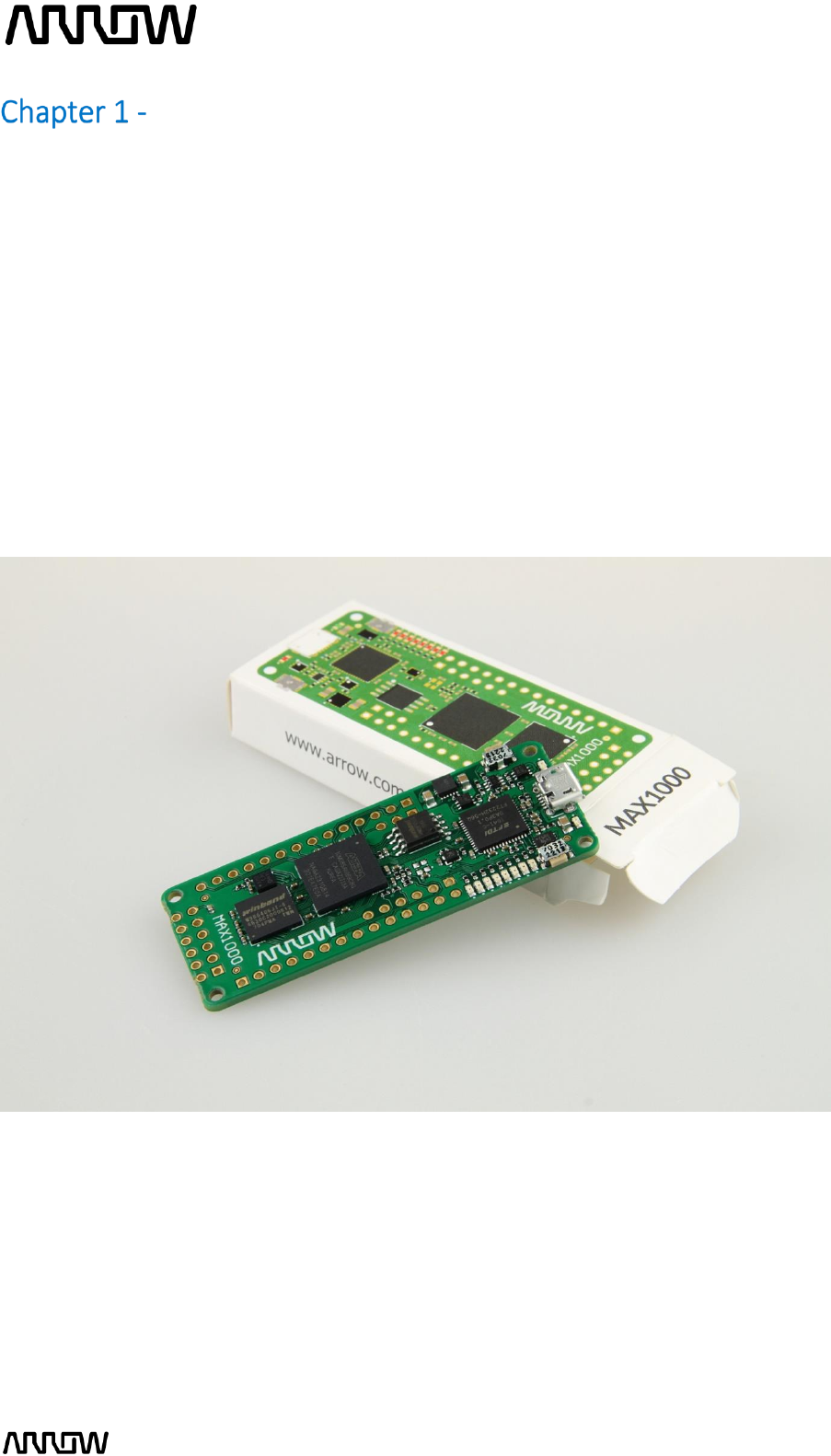
MAX1000 IoT / Maker Board ................................................................................ 5
1.1 About Arrow MAX1000 Board .......................................................................................... 5
1.2 Useful Links ....................................................................................................................... 6
1.3 Getting Help ...................................................................................................................... 6
Introduction to the MAX1000 Board ..................................................................... 7
2.1 Layout and Components ................................................................................................... 7
2.2 Block Diagram ................................................................................................................... 8
Connections and Peripherals of the MAX1000 Board .......................................... 10
3.1 Board Status Elements .................................................................................................... 10
3.2 Clock Circuitry ................................................................................................................. 10
3.3 Peripherals Connected to the FPGA ............................................................................... 11
3.3.1 LEDs ......................................................................................................................... 11
3.3.2 Push Buttons ........................................................................................................... 12
3.3.3 Accelerometer ......................................................................................................... 13
3.3.4 SDRAM Memory ...................................................................................................... 14
3.3.5 Flash Memory ......................................................................................................... 15
3.3.6 User I/O ................................................................................................................... 16
3.3.7 Arduino MKR Connectors ........................................................................................ 16
3.3.8 PMOD Connector .................................................................................................... 18
3.3.9 Communication and Configuration ......................................................................... 19
3.3.10 Power Tree .............................................................................................................. 21
Software and Driver Installation ......................................................................... 22
4.1 Installing Quartus Prime Software (Windows) ............................................................... 22
4.2 Installing Arrow USB Programmer2 (Windows) ............................................................. 24
4.3 Installing Quartus Prime Software (Linux) ...................................................................... 26
4.4 Installing Arrow USB Programmer2 (Linux) .................................................................... 28
New Project with MAX1000................................................................................ 30
5.1 Creating a new Blinky Project with MAX1000 ................................................................ 30
5.2 Building a Blinky Project with MAX1000 ........................................................................ 35
5.2.1 Block Diagram ......................................................................................................... 35
5.2.2 Components of the Design ...................................................................................... 35
5.2.3 Catalog IP ................................................................................................................ 36
5.2.4 Create and Configure the PLL ................................................................................. 37

MAX1000 User Guide www.arrow.com
Page | 3 July 2017
5.2.5 Create and Configure the Counter .......................................................................... 41
5.2.6 Create and Configure the Multiplexer .................................................................... 44
5.2.7 Adding the Components to the Schematic ............................................................. 47
5.2.8 Connecting the Components .................................................................................. 49
5.2.9 Analysis and Synthesis ............................................................................................ 55
5.2.10 Adding Timing Constraints ...................................................................................... 55
5.2.11 Pinning Assignments ............................................................................................... 58
5.2.12 Compiling the Design .............................................................................................. 61
5.2.13 Reading the Compilation Report ............................................................................. 63
Configuring the MAX1000 .................................................................................. 64
6.1 Configure the FPGA in JTAG Mode ................................................................................. 64
6.2 Internal Configuration .................................................................................................... 69
Common Issues and Fixes ................................................................................... 71
Appendix ........................................................................................................... 72
7.1 Revision History .............................................................................................................. 72
7.2 Legal Disclaimer .............................................................................................................. 73

MAX1000 User Guide www.arrow.com
Page | 4 July 2017
Table of Figures
Figure 1 - MAX1000 Board (top view) .............................................................................................. 7
Figure 2 - MAX1000 Block Diagram ................................................................................................. 8
Figure 3 – Position of Indication LEDs ............................................................................................ 10
Figure 4 – MAX1000 Clock Tree ..................................................................................................... 10
Figure 5 – LED Connections ............................................................................................................ 11
Figure 6 – Button Debouncing ....................................................................................................... 12
Figure 7 – Button Connections....................................................................................................... 12
Figure 8 – Accelerometer Connections .......................................................................................... 13
Figure 9 – SDRAM Connections ..................................................................................................... 14
Figure 10 – Flash Connections ....................................................................................................... 15
Figure 11 - User I/O Connections ................................................................................................... 16
Figure 12 - Arduino MKR Header Connections .............................................................................. 16
Figure 13 – PMOD Header Connections ........................................................................................ 18
Figure 14 – UART Connections ....................................................................................................... 19
Figure 15 – JTAG Connections ........................................................................................................ 20
Figure 16 – Power Tree Connections ............................................................................................. 21
MAX1000 User Guide www.arrow.com
Page | 5 July 2017
MAX1000 IoT / Maker Board
1.1 About Arrow MAX1000 Board
The MAX1000 is a customizable IoT / Maker Board ready for evaluation, development and/or use
in a product. It is built around the Intel MAX10 FPGA, which is the industry’s first single chip, non-
volatile programmable logic device (PLDs) to integrate the optimal set of system components.
Users can now leverage the power of tremendous re-configurability paired with a high-
performance, low-power FPGA system. Providing internally stored dual images with self-
configuration, comprehensive design protection features, integrated ADCs and hardware to
implement the Nios II 32-bit microcontroller IP, MAX10 devices are ideal solution for system
management, protocol bridging, communication control planes, industrial, automotive and
consumer applications. The MAX1000 is equipped with an Arrow USB Programmer2, SDRAM,
flash memory, accelerometer sensor and PMOD/ADRUINO MKR connectors making it a fully
featured plug and play solution without any additional costs.
The MAX1000 board contains all the tools needed to use the board in conjunction with a
computer that runs a 64-bit Linux / Microsoft Windows 7 operating system or later.

MAX1000 User Guide www.arrow.com
Page | 6 July 2017
1.2 Useful Links
A set of useful links that can be used to get relevant information about the MAX1000 or the
MAX10 FPGA.
MAX1000 at Arrow Shop
MAX1000 at Trenz Electronic Shop
Intel MAX10 Webpage
MAX1000 Wiki Page
1.3 Getting Help
Here are the addresses where you can get help if you encounter any problems:
Arrow Electronics
In Person
Arrow EMEA
+ 49 (0) 6102 5030 0
Online
https://arrow.com
Trenz Electronic GmbH
https://www.trenz-electronic.de/en/
MAX1000 User Guide www.arrow.com
Page | 7 July 2017
Introduction to the MAX1000 Board
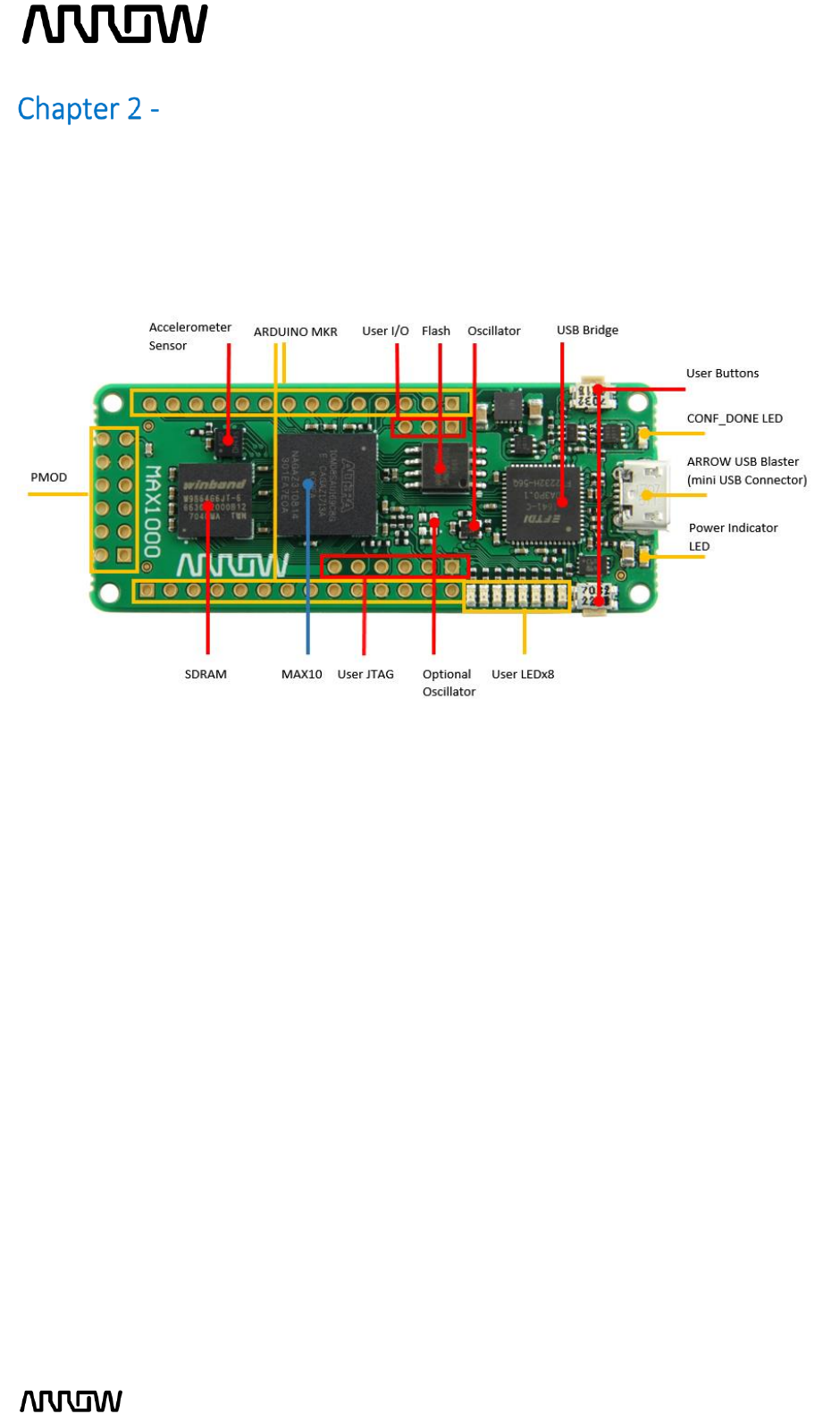
2.1 Layout and Components
Figure 1 shows a top view of the board. It depicts the layout of the board and indicates the location
of the various connectors and key components.
The following are available on the MAX1000 board:
Intel MAX®10 10M08SAU169C8G device
Arrow USB Programmer2 on-board for programming; JTAG Mode
64MBit SDRAM (16-bit data bus)
64Mbit Flash Memory
One 12MHz MEMS Oscillator
One optional MEMS Oscillator of preferred frequency
Eight red user LEDs
Two board indication LEDs
Two user buttons
One 3-axis accelerometer
One 12-pin PMOD header
One Arduino MKR header
One User JTAG header
One User I/O header
Figure 1 - MAX1000 Board (top view)
MAX1000 User Guide www.arrow.com
Page | 8 July 2017
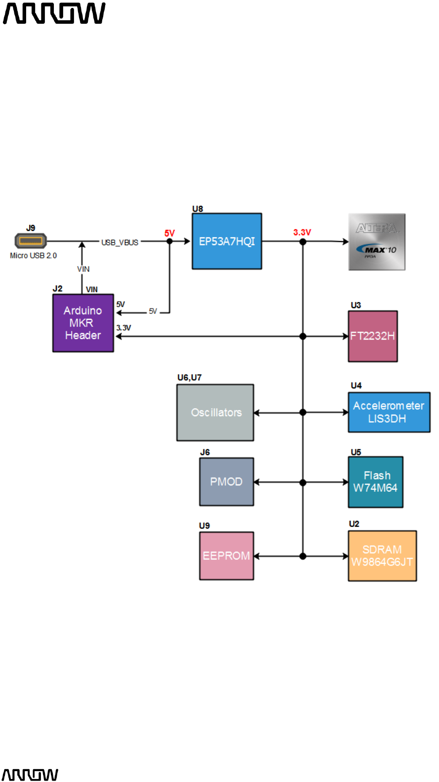
2.2 Block Diagram
Figure 2 represents the block diagram of the board. All the connections are established through
the MAX 10 FPGA device to provide maximum flexibility for users. Users can configure the FPGA
to implement any system design.
FPGA Device
Available MAX10 Devices for the MAX1000
Resources
Device
10M02
10M04
10M08
10M16
Logic Elements (LE) (K)
2
4
8
16
M9K Memory (K)
108
189
378
549
User Flash (K)
96
1248
1376
2368
Internal Configuration Image
1
2
2
2
ADC
-
1
1
1
PLLs
2
2
2
4
Configuration and Debug
On-board Arrow USB Programmer2 (mini-USB type B connector)
Memory Devices
64MBit to 128 MBit external flash memory
64MBit to 256 MBit external SDRAM memory
Figure 2 - MAX1000 Block Diagram

MAX1000 User Guide www.arrow.com
Page | 9 July 2017
Headers
PMOD Header
Arduino MKR Header
User JTAG Header
User I/O Header
Buttons and Indicators
2 x side-buttons
8 x red user LEDs
2 x board indication LEDs
Sensors
One 3-axis accelerometer
Power
Recommended external supply voltage range: +5.0 V (nominal)
Recommended I/O signal voltage range: 0/0 to +3.3 V
MAX1000 User Guide www.arrow.com
Page | 10 July 2017
Connections and Peripherals of the MAX1000 Board
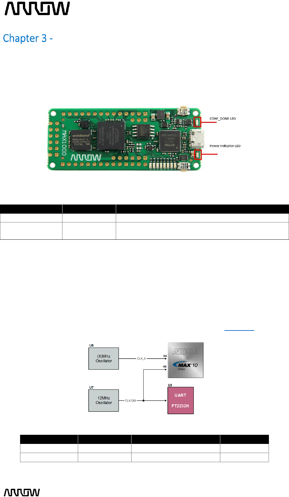
3.1 Board Status Elements
In addition to the 8 LEDs that the FPGA can control, there are 2 additional LEDs which can indicate
the status of the board.
Board Reference
LED Name
Description
D1
3.3V
On when 3.3V power is active
D10
CONF_DONE
On when configuration data was loaded to MAX10 device
without error
3.2 Clock Circuitry
All the external clocks of the system can be seen in Figure 4. The default clock (CLK12M) is at
12 MHz and is connected and driving the FPGA’s user logic and the Arrow USB Programmer2.
There is an optional slot of another clock (CLK_X) to add another preferred clock source to the
FPGA. Both clocks are driving PLL1/PLL3, which are able to drive the ADC clock.
For more information on clocks and PLLs of the MAX10, please refer to this document.
Board Reference
FPGA Pin No.
Description
I/O Standard
CLK12M
PIN_H6
12MHz clock input
3.3 V
CLK_X
PIN_G5
Optional clock input
3.3 V
Figure 3 – Position of Indication LEDs
Figure 4 – MAX1000 Clock Tree

MAX1000 User Guide www.arrow.com
Page | 11 July 2017
3.3 Peripherals Connected to the FPGA
3.3.1 LEDs
There are eight red user-controllable LEDs connected to the FPGA. Each LED is driven directly and
individually by the MAX10 FPGA; driving its associated pin to a high logic level for on or low logic
level for off.
Board Reference
FPGA Pin No.
I/O Standard
LED1
PIN_A8
3.3 V
LED2
PIN_A9
3.3 V
LED3
PIN_A11
3.3 V
LED4
PIN_A10
3.3 V
LED5
PIN_B10
3.3 V
LED6
PIN_C9
3.3 V
LED7
PIN_C10
3.3 V
LED8
PIN_D8
3.3 V
Figure 5 – LED Connections
MAX1000 User Guide www.arrow.com
Page | 12 July 2017
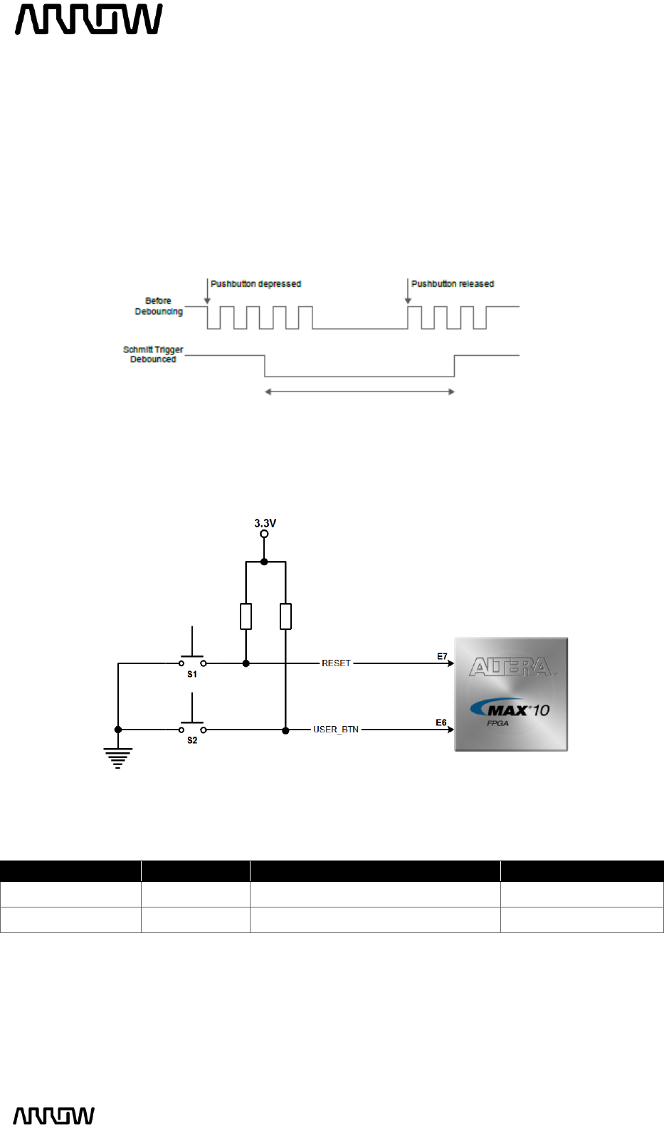
3.3.2 Push Buttons
The board has two push buttons connected to the FPGA. MAX10 devices support Schmitt trigger
input on all I/O pins. A Schmitt trigger feature introduces hysteresis to the input signal for
improved noise immunity, especially for signal with slow edge rate and acts as switch debouncer.
Push buttons drive their associated pins low logic level when pressed and high logic level when
released.
Board Reference
FPGA Pin No.
Description
I/O Standard
RESET
PIN_E7
Dual-function Pin: GPIO or nCONFIG
3.3 V Schmitt Triger
USER_BTN
PIN_E6
User button
3.3 V Schmitt Triger
Figure 6 – Button Debouncing
Figure 7 – Button Connections
MAX1000 User Guide www.arrow.com
Page | 13 July 2017
3.3.3 Accelerometer
The board comes with a digital accelerometer (LIS3DH), commonly known as the G-Sensor. This
G-Sensor is a small, thin, ultra-low power consumption, 3-axis accelerometer with digital I2C/SPI
serial interface, standard output. The LIS3DH has user-selectable full scales of +/-2g, +/-4g, +/-8g,
+/-16g and it is capable of measuring accelerations with output data rates from 1 Hz to 5 kHz. The
supplied power to the board (coming either from micro-USB connection or user Vin) can be
monitored through the ADC channel 3 of the accelerometer.
Board Reference
FPGA Pin No.
Description*
I/O Standard
SEN_INT1
PIN_J5
Interrupt 1
3.3 V
SEN_INT2
PIN_L4
Interrupt 2
3.3 V
SEN_SDI
PIN_J7
Data In (MOSI)
3.3 V
SEN_SDO
PIN_K5
Data Out (MISO)
3.3 V
SEN_SPC
PIN_J6
Clock
3.3 V
SEN_CS
PIN_L5
Chip Select
3.3 V
*For SPI connection
Figure 8 – Accelerometer Connections
MAX1000 User Guide www.arrow.com
Page | 14 July 2017
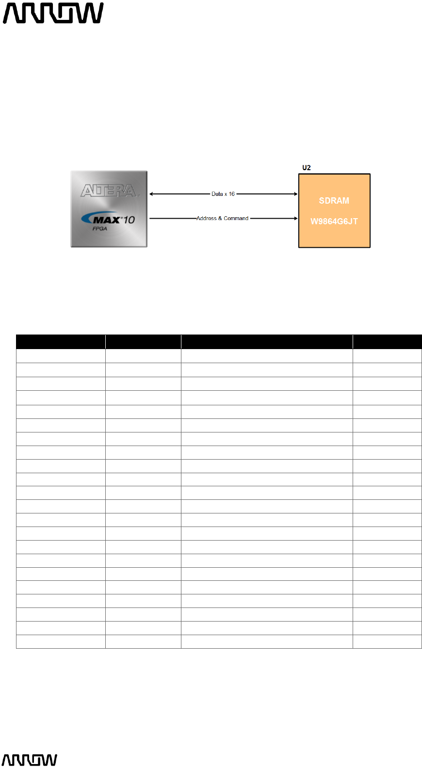
3.3.4 SDRAM Memory
The MAX1000 board supports 64 MBit (default version) or up to 256 MBit (customized version)
SDRAM which can operate up to 166 MHz clock frequency. Below are the connections and pinning
of the SDRAM used in the MAX1000.
Board Reference
FPGA Pin No.
Description
I/O Standard
A0
PIN_K6
SDRAM Address [0]
3.3 V
A1
PIN_M5
SDRAM Address [1]
3.3 V
A2
PIN_N5
SDRAM Address [2]
3.3 V
A3
PIN_J8
SDRAM Address [3]
3.3 V
A4
PIN_N10
SDRAM Address [4]
3.3 V
A5
PIN_M11
SDRAM Address [5]
3.3 V
A6
PIN_N9
SDRAM Address [6]
3.3 V
A7
PIN_L10
SDRAM Address [7]
3.3 V
A8
PIN_M13
SDRAM Address [8]
3.3 V
A9
PIN_N8
SDRAM Address [9]
3.3 V
A10
PIN_N4
SDRAM Address [10]
3.3 V
A11
PIN_M10
SDRAM Address [11]
3.3 V
A12
PIN_L11
SDRAM Address [12]
3.3 V
A13
PIN_M12
SDRAM Address [13]
3.3 V
BA0
PIN_N6
SDRAM Bank Address [0]
3.3 V
BA1
PIN_K8
SDRAM Bank Address [1]
3.3 V
CLK
PIN_M9
SDRAM Input Clock
3.3 V
CKE
PIN_M8
SDRAM Clock Enable
3.3 V
RAS
PIN_M7
SDRAM Row Address Strobe
3.3 V
CAS
PIN_N7
SDRAM Column Address Strobe
3.3 V
WE
PIN_K7
SDRAM Write Enable
3.3 V
CS
PIN_M4
SDRAM Chip Select
3.3 V
Figure 9 – SDRAM Connections
MAX1000 User Guide www.arrow.com
Page | 15 July 2017
Board Reference
FPGA Pin No.
Description
I/O Standard
DQ0
PIN_D11
SDRAM Data[0]
3.3 V
DQ1
PIN_G10
SDRAM Data [1]
3.3 V
DQ2
PIN_F10
SDRAM Data [2]
3.3 V
DQ3
PIN_F9
SDRAM Data [3]
3.3 V
DQ4
PIN_E10
SDRAM Data [4]
3.3 V
DQ5
PIN_D9
SDRAM Data [5]
3.3 V
DQ6
PIN_G9
SDRAM Data [6]
3.3 V
DQ7
PIN_F8
SDRAM Data [7]
3.3 V
DQ8
PIN_F13
SDRAM Data [8]
3.3 V
DQ9
PIN_E12
SDRAM Data [9]
3.3 V
DQ10
PIN_E13
SDRAM Data [10]
3.3 V
DQ11
PIN_D12
SDRAM Data [11]
3.3 V
DQ12
PIN_C12
SDRAM Data [12]
3.3 V
DQ13
PIN_B12
SDRAM Data [13]
3.3 V
DQ14
PIN_B13
SDRAM Data [14]
3.3 V
DQ15
PIN_A12
SDRAM Data [15]
3.3 V
DQM0
PIN_E9
SDRAM Lower Data Mask
3.3 V
DQM1
PIN_F12
SDRAM Upper Data Mask
3.3 V
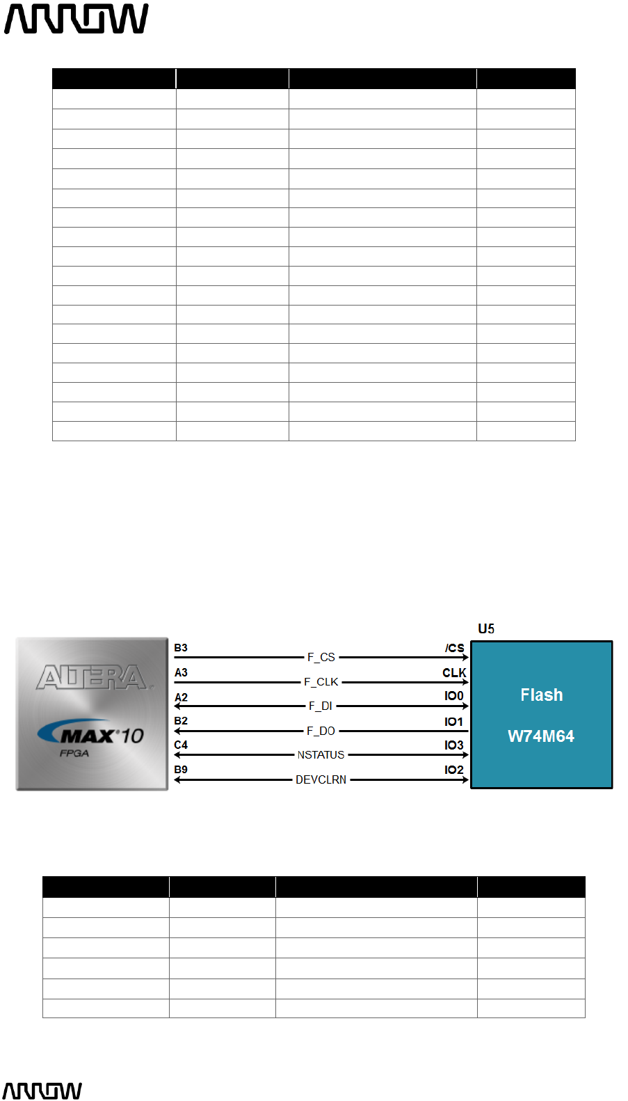
3.3.5 Flash Memory
The MAX1000 board supports up to 128 MBit of serial flash memory that can be used for user
data and programming non-volatile storage. Single SPI interface is supported that can reach up to
104 MHz SPI performance. Device offers unique advanced security features that could benefit
greatly end node security applications.
Board Reference
FPGA Pin No.
Description
I/O Standard
F_CS
PIN_B3
Flash Chip Select
3.3 V
F_CLK
PIN_A3
Flash Clock Input
3.3 V
F_DI
PIN_A2
Flash Data Input Input (IO0)
3.3 V
F_DO
PIN_B2
Flash Data Input Output (IO1)
3.3 V
NSTATUS
PIN_C4
NSTATUS
3.3 V
DEVCLRN
PIN_B9
DEVLCLRN
3.3 V
Figure 10 – Flash Connections

MAX1000 User Guide www.arrow.com
Page | 16 July 2017
3.3.6 User I/O
The MAX1000 board has two pins that can be connected to the board and take analogue inputs.
Those two pins are connected to the ADC block of the MAX10 and can measure up to 3.6V. This
12-bit SAR ADC can reach 1 MSPS and has single ended capabilities.
For more information on the ADCs of the MAX10, please refer to this document.
Note: If you use bank 1A for ADC, you cannot use the bank for GPIO.
Board Reference
FPGA Pin No.
Description
AIN
PIN_D2
Dedicated analogue input pin
AIN7
PIN_B1
Dual function pin
3.3.7 Arduino MKR Connectors
The MAX1000 board offers connectivity to Arduino MKR compatible shields that could also
alternatively be used as GPIOs. The MKR connectors offer up to 7 analogue inputs and 15 digital
I/Os. There is also an option to use or not use the 4.7k Ohm pull-up resistor lines for
communication interfaces.
Figure 11 - User I/O Connections
Figure 12 - Arduino MKR Header Connections
MAX1000 User Guide www.arrow.com
Page | 17 July 2017
Note: If you use bank 1A for ADC, you cannot use the bank for GPIO (includes all AIN[0..7] pins)
Board Reference
FPGA Pin No.
Description
MKR Header/Pin
I/O Standard
AREF
PIN_D3
Analogue Reference
J1 / 1
N/A
AIN0
PIN_E1
Analogue In Channel 8 of
ADC or GPIO
J1 / 2
3.3 V
AIN1
PIN_C2
Analogue In Channel 2 of
ADC or GPIO
J1 / 3
3.3 V
AIN2
PIN_C1
Analogue In Channel 5 of
ADC or GPIO
J1 / 4
3.3 V
AIN3
PIN_D1
Analogue In Channel 1 of
ADC or GPIO
J1 / 5
3.3 V
AIN4
PIN_E3
Analogue In Channel 3 of
ADC or GPIO
J1 / 6
3.3 V
AIN5
PIN_F1
Analogue In Channel 7 of
ADC or GPIO
J1 / 7
3.3 V
AIN6
PIN_E4
Analogue In Channel 4 of
ADC or GPIO
J1 / 8
3.3 V
D0
PIN_H8
Digital In[0]
J1 / 9
3.3 V
D1
PIN_K10
Digital In[1]
J1 / 10
3.3 V
D2
PIN_H5
Digital In[2]
J1 / 11
3.3 V
D3
PIN_H4
Digital In[3]
J1 / 12
3.3 V
D4
PIN_J1
Digital In[4]
J1 / 13
3.3 V
D5
PIN_J2
Digital In[5]
J1 / 14
3.3 V
D6
PIN_L12
Digital In[6]
J2 / 1
3.3 V
D7
PIN_J12
Digital In[7]
J2 / 2
3.3 V
D8
PIN_J13
Digital In[8]
J2 / 3
3.3 V
D9
PIN_K11
Digital In[9]
J2 / 4
3.3 V
D10
PIN_K12
Digital In[10]
J2 / 5
3.3 V
D11
PIN_J10
Digital In[11]
J2 / 6
3.3 V
D12
PIN_H10
Digital In[12]
J2 / 7
3.3 V
D13
PIN_H13
Digital In[13]
J2 / 8
3.3 V
D14
PIN_G12
Digital In[14]
J2 / 9
3.3 V
D11_R
PIN_B11
Digital In[11] with pull-up
resistor
J2 / 6
3.3 V
D12_R
PIN_G13
Digital In[12] with pull-up
resistor
J2 / 7
3.3 V
RESET
N/A
Connected to system
reset of the board
J2 / 10
N/A
GND
N/A
Ground output to the
connector
J2 / 11
N/A
3.3V
N/A
3.3V power to the
connector
J2 / 12
N/A
VIN
N/A
User power into to the
MAX1000
J2 / 13
N/A
5V
N/A
5V power to the
connector
J2 / 14
N/A
*Can only choose one, hence same name pinning
MAX1000 User Guide www.arrow.com
Page | 18 July 2017
3.3.8 PMOD Connector
The MAX1000 board offers connectivity to PMOD compatible connectors (2x6-pin or 1x12-pin),
making it possible to add a big variety of sensors or ICs to the system. Below is the connection
schematic and pinning information.
Figure 13 – PMOD Header Connections
Board Reference
FPGA Pin No.
Description
I/O
Standard
PIO_01
PIN_M3
PMOD Pin 1
3.3 V
PIO_02
PIN_L3
PMOD Pin 2
3.3 V
PIO_03
PIN_M2
PMOD Pin 3
3.3 V
PIO_04
PIN_M1
PMOD Pin 4
3.3 V
PIO_05
PIN_N3
PMOD Pin 5
3.3 V
PIO_06
PIN_N2
PMOD Pin 6
3.3 V
PIO_07
PIN_K2
PMOD Pin 7
3.3 V
PIO_08
PIN_K1
PMOD Pin 8
3.3 V
GND
N/A
Ground
N/A
3.3V
N/A
3.3 V Power to PMOD
3.3 V
MAX1000 User Guide www.arrow.com
Page | 19 July 2017
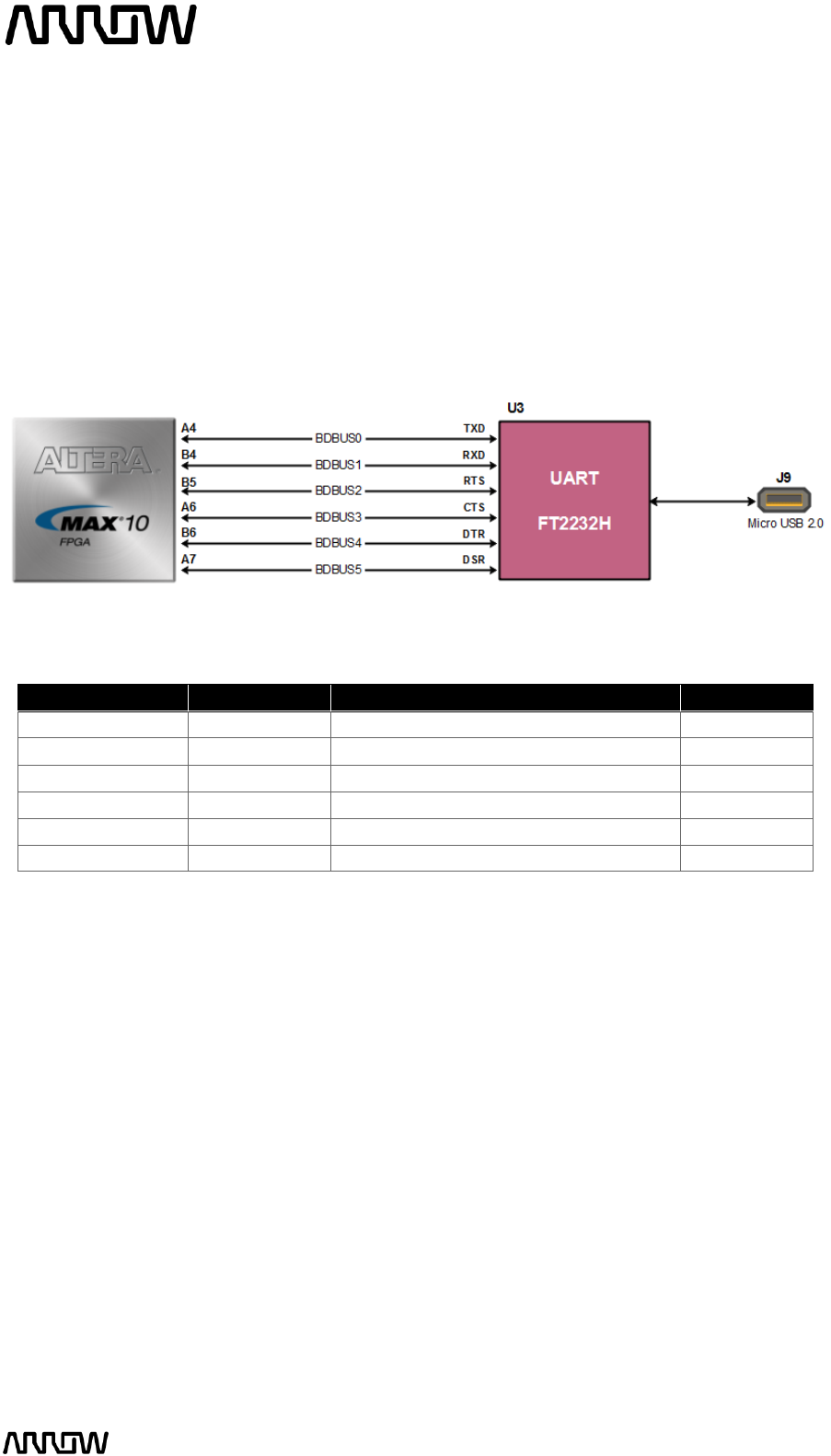
3.3.9 Communication and Configuration
The MAX1000 board uses a single chip to perform configuration of the device and USB to UART
communications, having each described below.
3.3.9.1 UART Communication
UART to USB communication supports USB 2.0 High Speed (up to 480 Mb/s) independently of
other protocols used in the chip like JTAG. Below is the connection schematic and pinning
information.
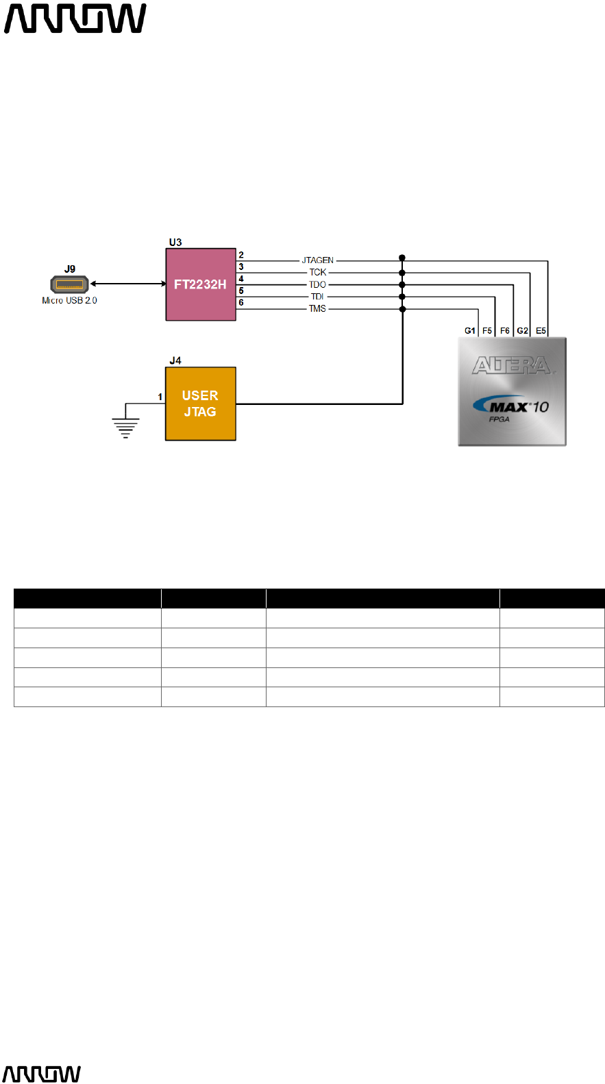
3.3.9.2 JTAG Chain Configuration
There are two types of configuration methods supported by MAX1000:
1. JTAG Configuration: configuration using JTAG ports. JTAG configuration scheme allows you to
directly configure the device core through JTAG pins (TDI, TDO, TMS and TCK pins). The
Quartus Prime software automatically generates a .sof that can be downloaded to the MAX10
with a download cable through the Quartus Prime Programmer.
2. Internal Configuration: configuration using internal flash. Before internal configuration, you
need to program the configuration data .pof into the configuration flash memory (CFM) which
provides non-volatile storage for the bit stream. The information is retained within CFM even
if the MAX1000 is turned off. When the board is powered on, the configuration data in the
CFM is automatically loaded into the MAX10 FPGA.
Board Reference
FPGA Pin No.
Description
I/O Standard
BDBUS0
PIN_A4
Transmitter output of FT2232H (Tx)
3.3 V
BDBUS1
PIN_B4
Receiver input of FT2232H (Rx)
3.3 V
BDBUS2
PIN_B5
Ready To Send handshake output (RTS)
3.3 V
BDBUS3
PIN_A6
Clear To Send handshake input (CTS)
3.3 V
BDBUS4
PIN_B6
Data Transmit Ready (DTR)
3.3 V
BDBUS5
PIN_A7
Data Set Ready (DSR)
3.3 V
Figure 14 – UART Connections
MAX1000 User Guide www.arrow.com
Page | 20 July 2017
The FPGA device can be configured through JTAG interface on MAX1000, but the JTAG chain must
form a closed loop, which allows Quartus Prime programmer to detect the FPGA device.
MAX1000 offers two ways of configuring your board.
1) Through the on-board Arrow USB Programmer2
2) Pins for connecting user’s preferred JTAG interface
Board Reference
FPGA Pin No.
Description
I/O Standard
JTAGEN
PIN_E5
Dual Function: JTAG Pin Sharing
3.3 V
TCK
PIN_G2
Test Interface Clock
3.3 V
TDO
PIN_F6
Test Data Out
3.3 V
TDI
PIN_F5
Test Data In
3.3 V
TMS
PIN_G1
Test Mode Select
3.3 V
For detailed information about how to configure the MAX10 device, please refer to Chapter 6.
Figure 15 – JTAG Connections
MAX1000 User Guide www.arrow.com
Page | 21 July 2017
3.3.10 Power Tree
The MAX1000 is powered by Enpirion’s buck regulator, which provides high efficiency up to 1A
with integrated magnetics, switches, control, and compensation. As seen from the diagram
below, the board can be powered either by a micro-USB connection, or by user input voltage from
the Arduino MKR header (takes precedence over the USB bus). All devices are powered by 3.3V
voltage line and the 5V and 3.3V lines are fed back to the Arduino header to power that
connection if needed.
Figure 16 – Power Tree Connections
MAX1000 User Guide www.arrow.com
Page | 22 July 2017
Software and Driver Installation
Firstly it is required to create your myAltera Account if you don’t own one already. It is required
to download the software. Below are guides for installing the software and drivers for Windows
and Linux operating systems.
4.1 Installing Quartus Prime Software (Windows)
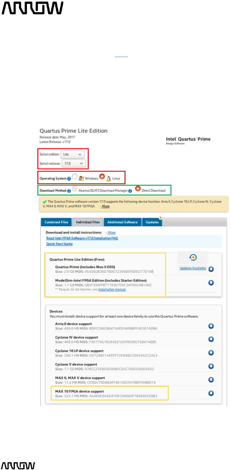
4.1.1 Go to the Intel Download Centre: Link.
4.1.2 Select Windows as the operating system (highlighted in red).
4.1.3 Select Release 17.0, or your preferred version (highlighted in red).
4.1.4 Select the following files from the “Individual Files” tab to be downloaded (highlighted in
yellow):
- Quartus Prime Lite Edition (Free)
- ModelSim-Altera Edition (includes Starter Edition)
- MAX10 FPGA device support
4.1.5 Click “Download Selected Files” to begin the download and save them in the same
folder.
MAX1000 User Guide www.arrow.com
Page | 23 July 2017
Note: In case of browser issues using Akamai DLM3 Manager, you can alternative download the
above files using the “Direct Download” (highlighted in green).
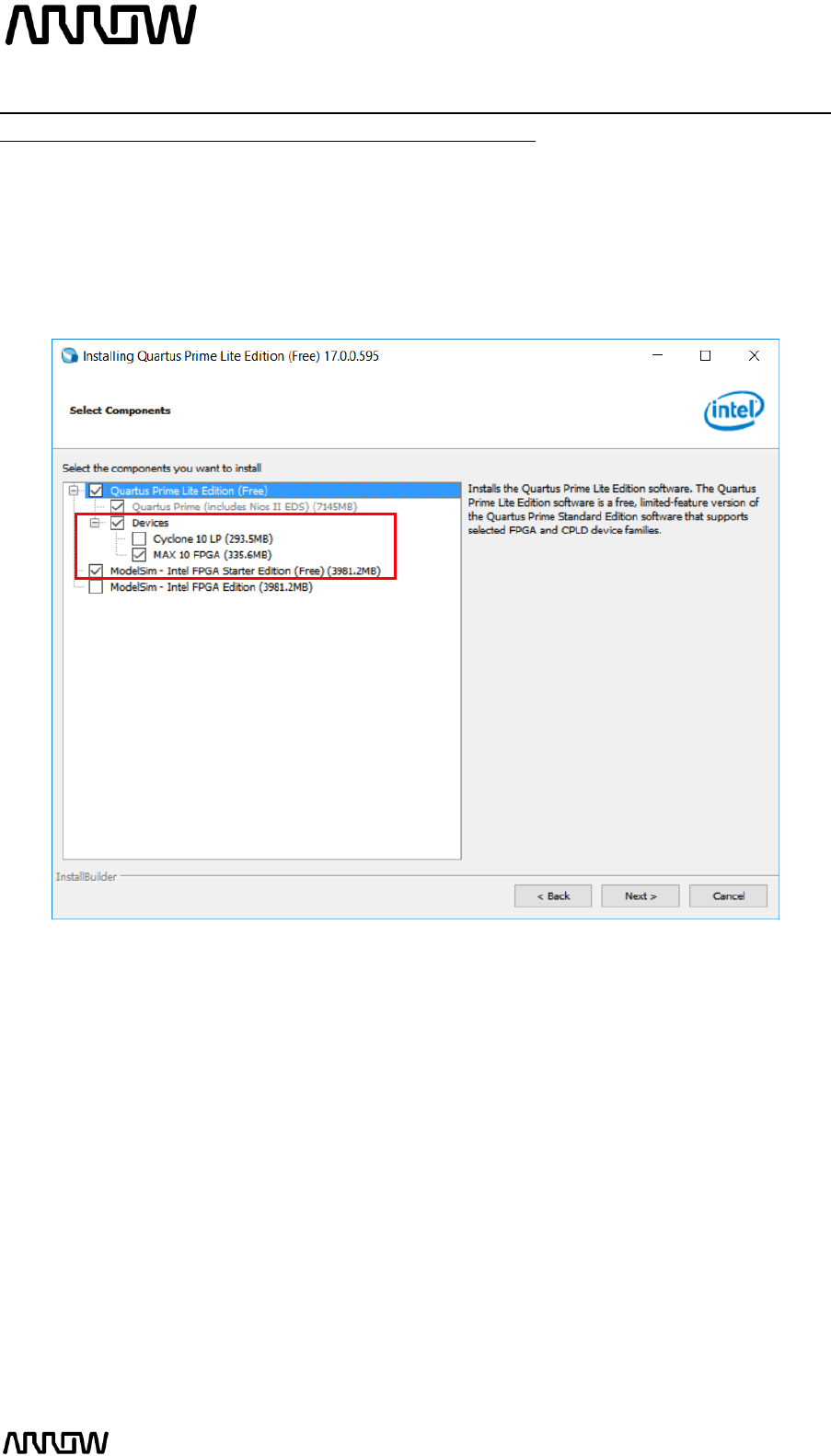
4.1.6 After the download is finished, run the Quartus Prime installer.
4.1.7 When prompted to select the components, the installer will detect automatically the
MAX10 device support and ModelSim packages when they are in the same folder. Make
sure these components are selected:
4.1.9 Finish the installation of the Quartus Lite and proceeded to the next section to install Arrow
USB Programmer2 to be able to connect to the MAX1000 board.
MAX1000 User Guide www.arrow.com
Page | 24 July 2017
4.2 Installing Arrow USB Programmer2 (Windows)
The MAX1000 board uses version 2 of the Arrow USB Programmer2 programming solution, that
is an FTDI FT2232H Hi-Speed USB controller plus a programmer DLL. Since this FTDI USB controller
is a very common standard device, usually no specific drivers are needed to make the MAX1000
work.
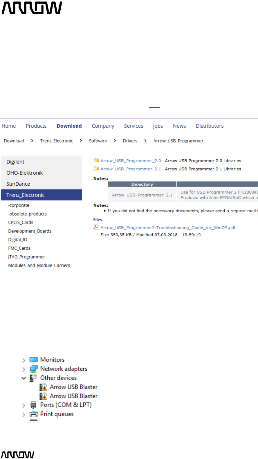
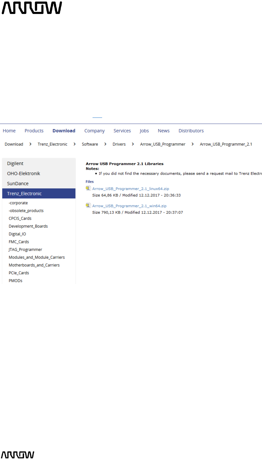
4.2.1 Download the appropriate version of Arrow USB Programmer2 for MAX1000 from Trenz
Electronic Wiki page or alternatively this direct link.
4.2.2 After downloading the file, run the installer to install the Arrow USB Programmer2. The
setup executable installs the programmer DLL and adds some keys to the registry of the
PC.
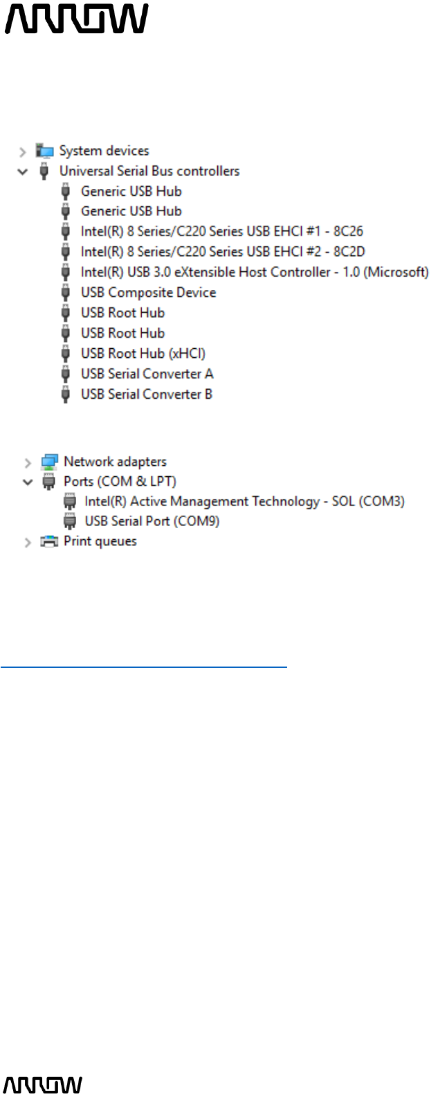
4.2.3 After connecting the MAX1000 board to the PC, two unknown devices might appear in
the “Other devices” section of device manager of the PC.
MAX1000 User Guide www.arrow.com
Page | 25 July 2017
Windows usually automatically finds the appropriate drivers for these devices. After some time,
the “Other devices” section should be empty. Instead, two USB Serial Converters should be listed
in the section “USB Serial Bus controllers”:
Furthermore, a USB Serial Port should be listed in the “Ports (COM & LPT)” section.
Note: The number of the port will most probably be different from the one shown here.
In case Windows does not automatically find the appropriate drivers go to
http://www.ftdichip.com/Drivers/D2XX.htm to download the setup executable to install the
required drivers.
MAX1000 User Guide www.arrow.com
Page | 26 July 2017
4.3 Installing Quartus Prime Software (Linux)
4.3.1 Go to the Intel Download Centre: Link.
4.3.2 Select Linux as the operating system (highlighted in red).
4.3.3 Select Release 17.0, or your preferred version (highlighted in red).
4.3.4 Select the following files to be downloaded from the “Individual Files” tab (highlighted in
yellow):
- Quartus Prime (Includes Nios II EDS)
- ModelSim-Intel FPGA Edition (includes Starter Edition)
- MAX10 FPGA device support
MAX1000 User Guide www.arrow.com
Page | 27 July 2017
4.3.5 Download the selected files and store them into the same folder.
For example, the Downloads folder under the home of the current user ~/Downloads:
Quartus Prime Lite edition: ~/Downloads/QuartusLiteSetup-17.0.0.595-linux.run
ModelSim-Intel FPGA Edition: ~/Downloads/ModelSimSetup-17.0.0.595-linux.run
MAX10 device support package for Quartus: ~/Downloads/max10-17.0.0.595.qdz
Run Intel Quartus installer. Open a terminal and navigate through the folder where the
installers are downloaded:
$ cd ~/Downloads
Make sure the installer has execution permissions. If you have a different version of
Quartus Software, please match the name of the file:
$ chmod +x QuartusLiteSetup-17.0.0.595-linux.run
Run the installer:
$ ./QuartusLiteSetup-17.0.0.595-linux.run
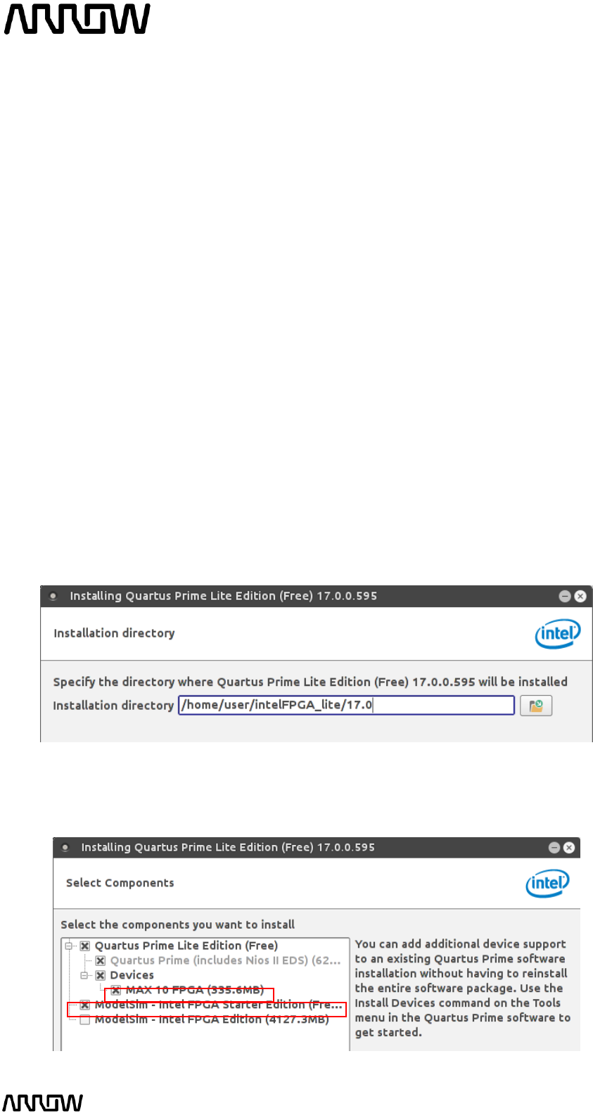
4.3.6 Follow the steps through the installation assistant. When prompted the destination
folder, you can choose a path within your home directory, so you don’t need additional
permissions:
4.3.7 The installer will detect automatically the MAX10 device support and ModelSim
packages when they are located in the same folder. Make sure these components are
selected:
MAX1000 User Guide www.arrow.com
Page | 28 July 2017
4.3.8 Continue through the installation assistant until the process has finished. Now you can
run Quartus Lite.
To connect with the MAX1000 board you need to install additional Arrow USB Programmer2
drivers as explained in the next section.
4.4 Installing Arrow USB Programmer2 (Linux)
4.4.1 Download the Arrow USB Programmer2 Driver for Linux from Trenz Electronic Wiki page
or alternatively this direct link.
4.4.2 You can download the files in a temporal folder such as the Downloads folder under the
home of the current user ~/Downloads:
- Udev USB rules: ~/Downloads/51-usbProgrammer2.rules
- Default configuration file: ~/Downloads/arrow_usb_Programmer2.conf:
- Plugin for Quartus Prime: ~/Downloads/libjtag_hw_arrow.so:
4.4.3 Open a terminal and navigate through your Downloads folder:
$ cd ~/Downloads
4.4.4 Install udev USB rules:
$ sudo cp 51-usbProgrammer2.rules /etc/udev/rules.d/

MAX1000 User Guide www.arrow.com
Page | 29 July 2017
4.4.5 Make sure your linux user belongs to the plugdev group:
$ sudo useradd -G plugdev <your linux username>
4.4.6 Install default configuration file:
$ sudo cp arrow_usb_Programmer2.conf /etc/
4.4.7 Install the Quartus Prime plugin:
Use the directory quartus/linux64 under the installation path selected on step 4.3.6.
$ cp libjtag_hw_arrow.so <Quartus Path>/quartus/linux64

MAX1000 User Guide www.arrow.com
Page | 30 July 2017
New Project with MAX1000
5.1 Creating a new Blinky Project with MAX1000
5.1.1 Launch Quartus Prime Lite Edition from the Start Menu.
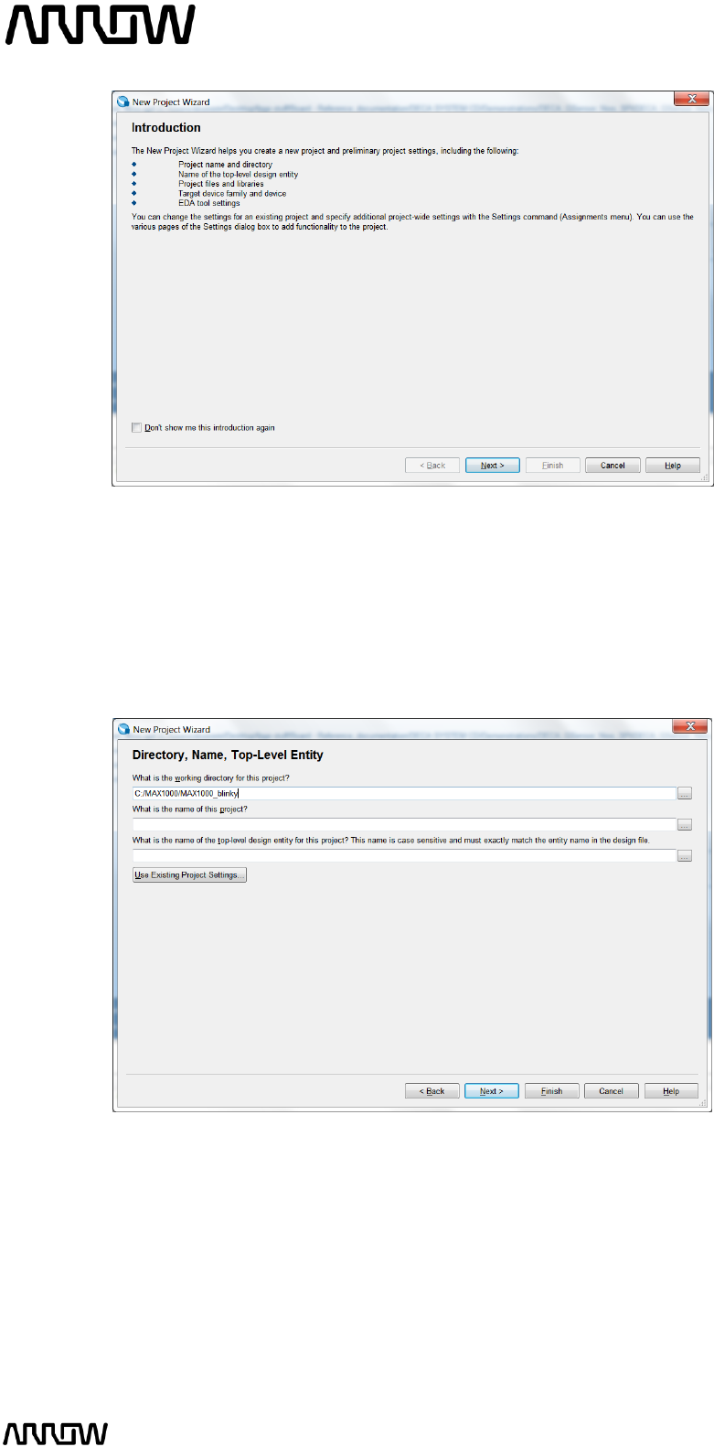
5.1.2 In the Quartus Prime tool, create a new project: File -> New Project Wizard.
The New Project Wizard walks you through the project settings, such as the name, directories,
files, directories, device family and other settings. These settings can be changed later if needed.
MAX1000 User Guide www.arrow.com
Page | 31 July 2017
5.1.3 Click “Next”.
5.1.4 Browse in the project directory and choose a preferred location for the new project. Then
create new folder named MAX1000_blinky. This will be the folder containing all the
project files.
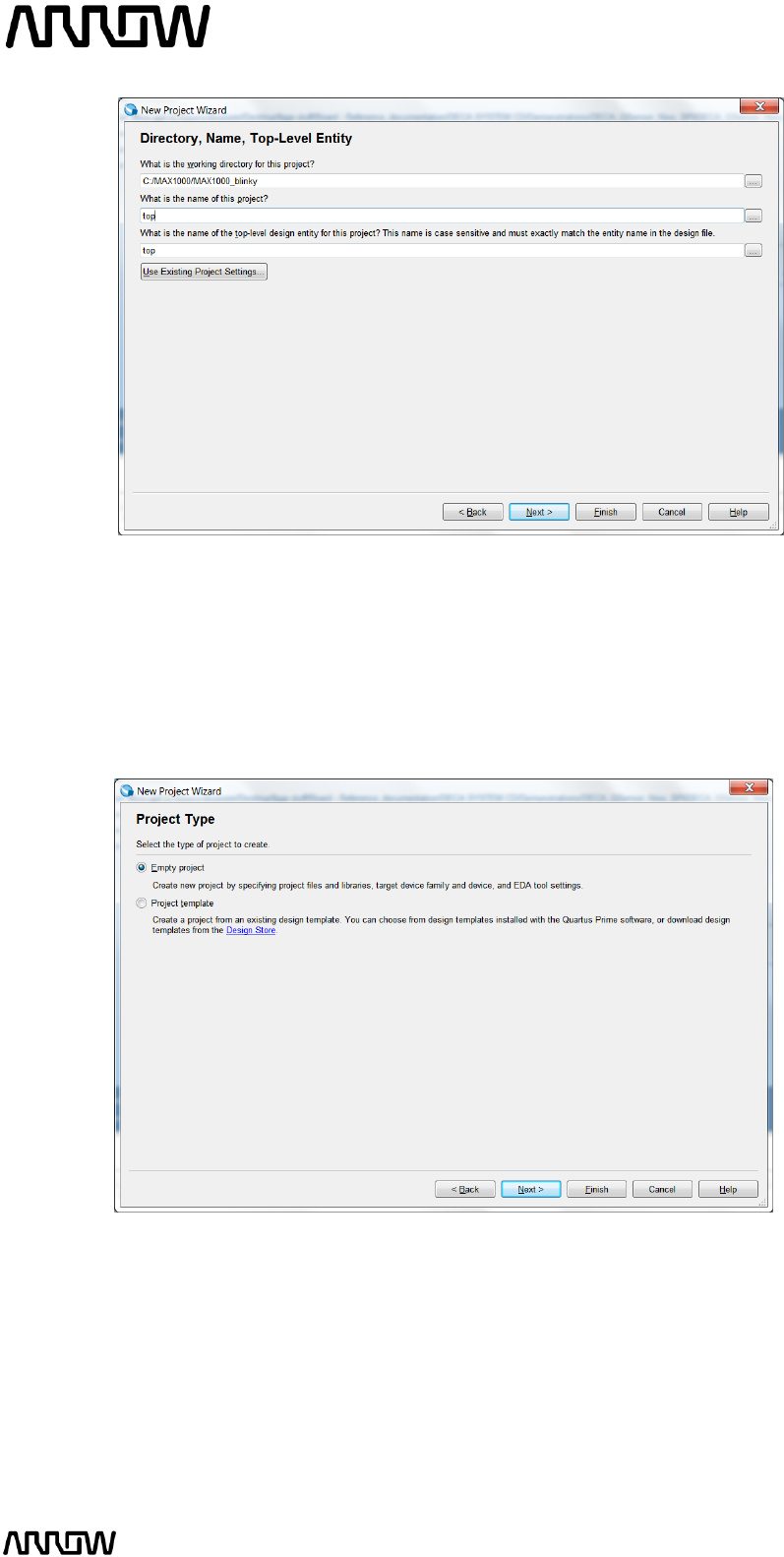
5.1.5 Enter the project name: “top”.
MAX1000 User Guide www.arrow.com
Page | 32 July 2017
5.1.6 Click “Next”.
5.1.7 Project Type
In this page you choose the Project Type. In this tutorial, a new project will be created, and thus
the default settings of empty project should be selected.
5.1.8 Click “Next”.
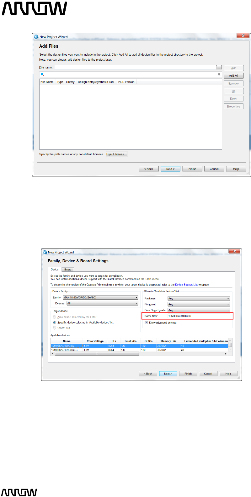
5.1.9 Add Project Files
The Add File window will appear. For this tutorial, new design files will be created so no files will
be added. For other designs, files could be added here.
MAX1000 User Guide www.arrow.com
Page | 33 July 2017
5.1.10 Click “Next”.
5.1.11 Select the Device Part Number of the MAX1000 Board
In the Family and Device Settings, use the pull down menu to select the family as MAX10. Then in
the Name Filter enter 10M08SAU169C8G.
Rather than entering the exact part number, the pull-down menus can be used to select the
correct family, package, pin count, and speed grade. Quartus Prime will use these settings to
compile the design, and also provide the programming file that you will use later to program the
device.
5.1.12 Click “Next”.
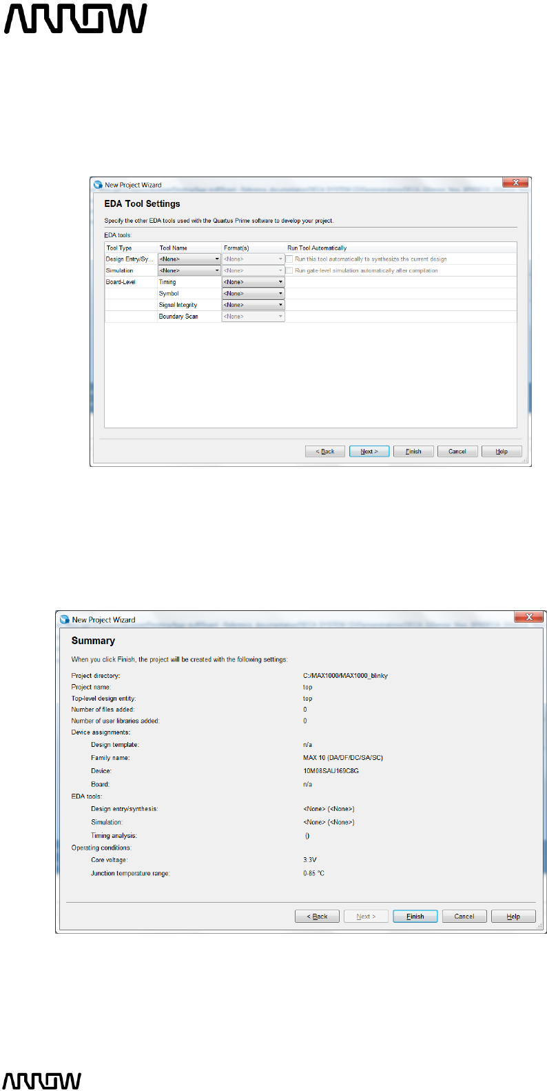
5.1.13 EDA Tool Settings
MAX1000 User Guide www.arrow.com
Page | 34 July 2017
In the EDA tool Settings window, disable any EDA tools, if there are any present. EDA tools are
third party tools that work with Quartus Prime for design entry, simulation, verification and
board-level timing. For this tutorial, no EDA software will be used, as only Quartus Prime will be
used.
5.1.14 Click “Next”.
5.1.15 Project Summary Page
This is the Summary Page that showing the settings Quartus Prime will use for this Project. Those
settings can be changed if required at a later time.
5.1.16 Click “Finish”.
MAX1000 User Guide www.arrow.com
Page | 35 July 2017
5.2 Building a Blinky Project with MAX1000
Overview: In this section you will create the components to a design, make connections, set the
pins and compile a project. The goal is to go through the design process of a simple blinky project,
where the toggle speed of the LEDs could be controlled by one of the pushbuttons of the
MAX1000.
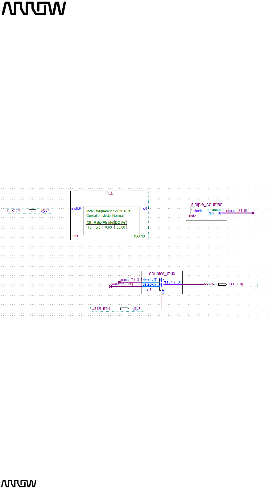
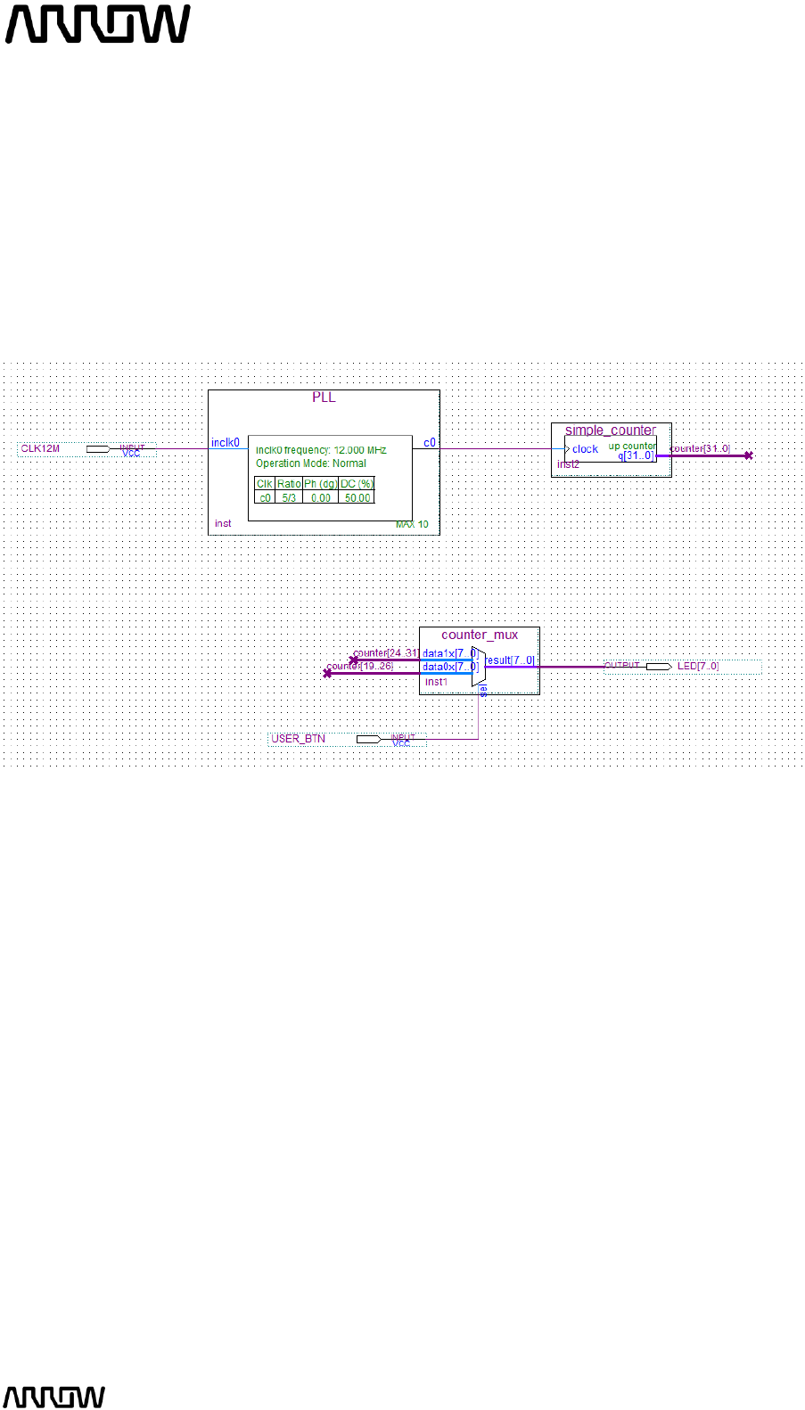
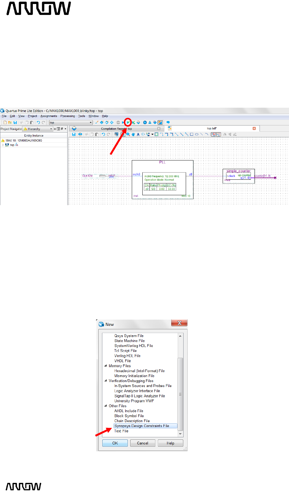
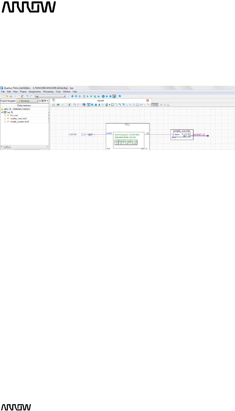
5.2.1 Block Diagram
The final system that will be built with the following steps will look as follows when complete:
5.2.2 Components of the Design
There are three components in the system: a PLL, a counter and a mux. The components, in the
following steps, will be built separately and then connected together. A user push button on the
board controls the mux. The mux in turn control which of the counter outputs (slow counting or
fast counting) will be shown on the LEDs. There are different ways to create components, such as
RTL or schematic. In this lab, schematics will be used. There are also different ways for entering
schematics such as Qsys and IP Catalog. This lab will focus on the IP Catalog.
MAX1000 User Guide www.arrow.com
Page | 36 July 2017
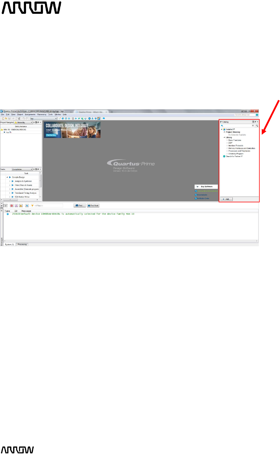
5.2.3 Catalog IP
The IP Catalog allows you to create and modify design files with custom variations. The IP Catalog
window is open by default when you open Quartus Prime. If it’s not present, you can open it by
going to the tab Tool IP Catalog.
3.4.4 Create a PLL
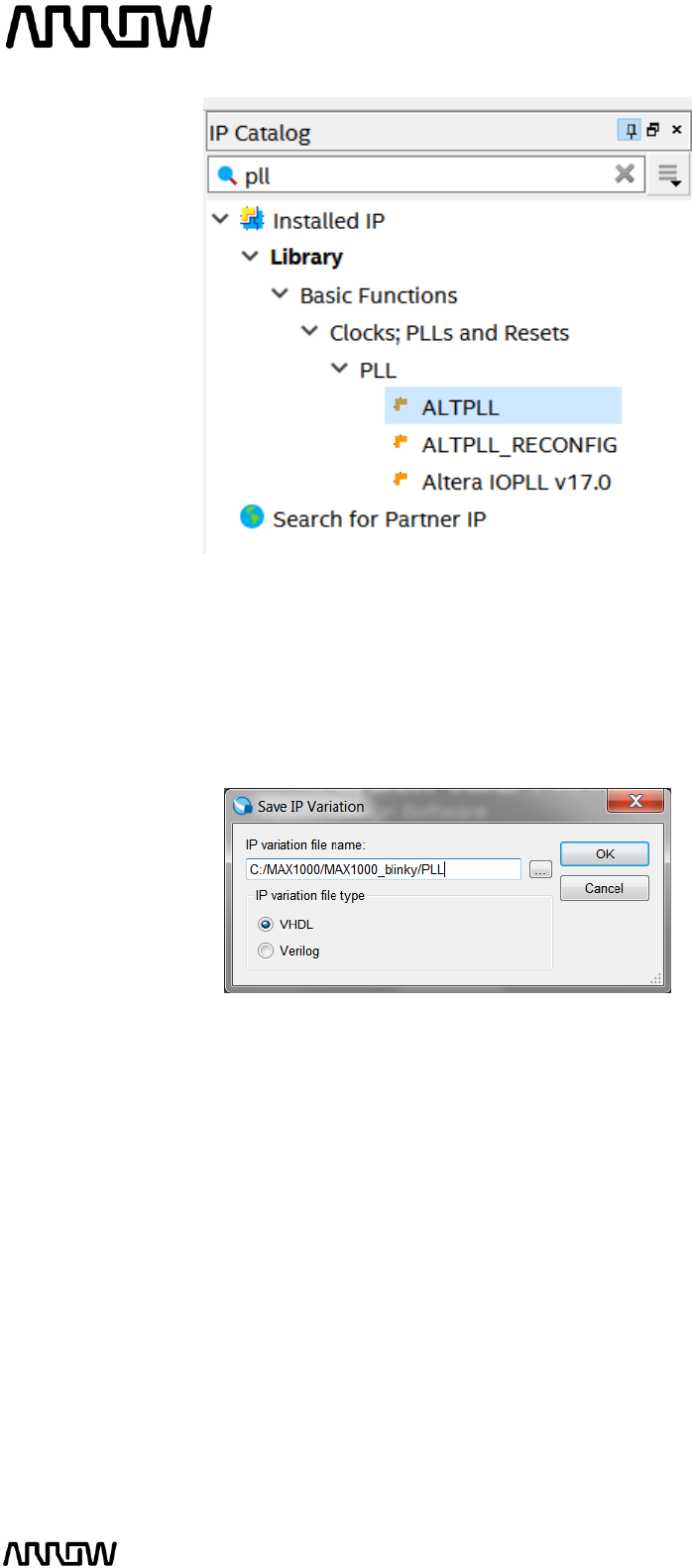
In the IP Catalog, browse for ALTPLL, via: Basic Functions Clocks; PLLs and Resets PLL or type
in the search field for “PLL”.
5.2.3.1 In the Search bar of the IP Catalog, type “pll” and select ALTPLL which stands for Altera
Phase Locked Loop.
MAX1000 User Guide www.arrow.com
Page | 37 July 2017
5.2.3.2 Click “Add”.
When the Save IP Variation window appears, enter the file name variation as PLL and select VHDL
(Verilog can be used as well). Both Verilog and VHDL schematics will be created.
5.2.3.3 Click “OK”.
5.2.4 Create and Configure the PLL
The next step is to configure the PLL component that we just named.
5.2.4.1 Enter the PLL reference clock frequency to match the clock input on the MAX1000 Board.
Since we have a 12 MHz coming into the FPGA, the inclk input will be 12 MHz.
The setting should look like this:
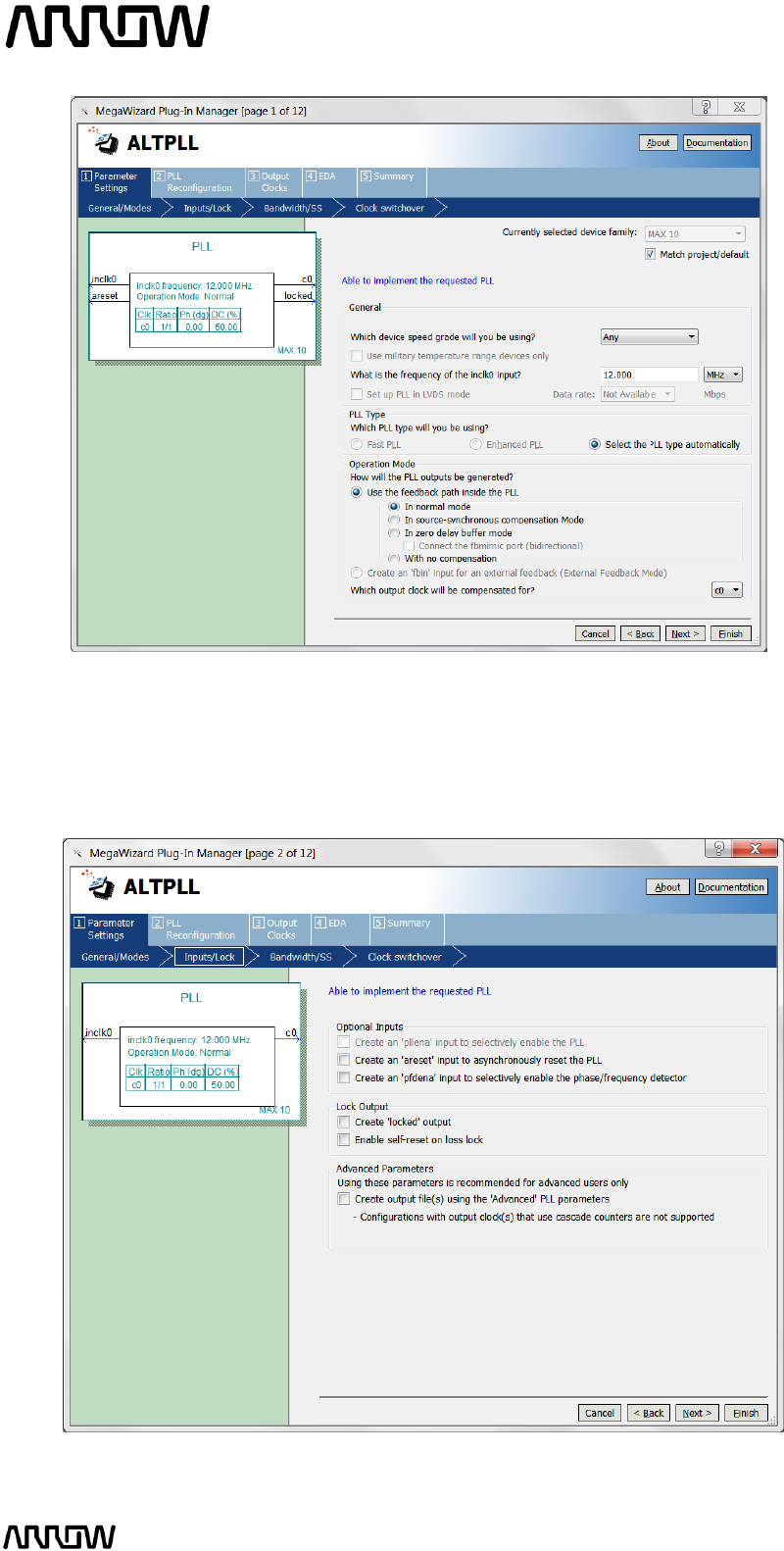
MAX1000 User Guide www.arrow.com
Page | 38 July 2017
5.2.4.2 Click “Next”.
5.2.4.3 Simplify the PLL, by disabling areset and locked outputs.
The setting should look like this:
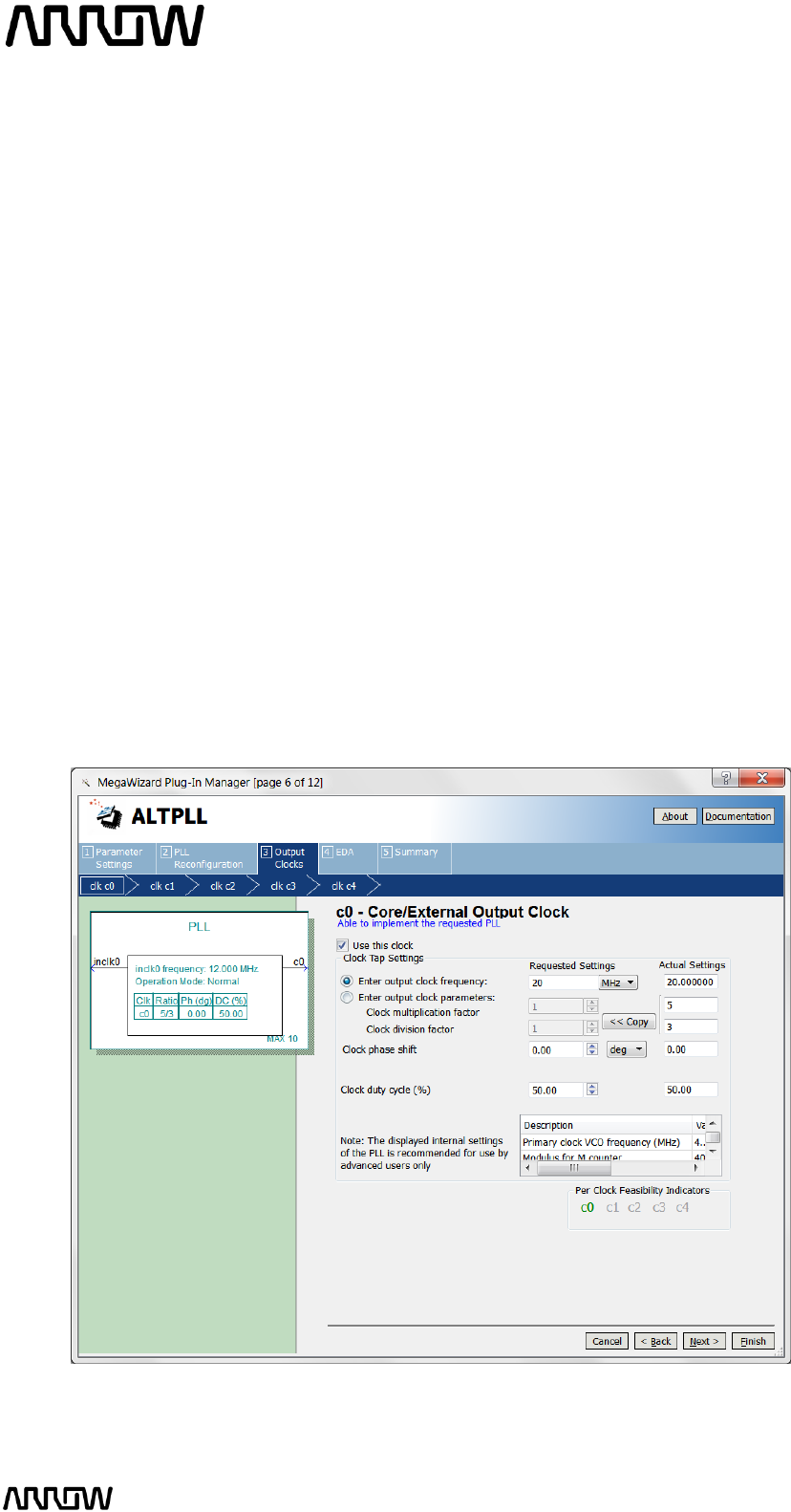
MAX1000 User Guide www.arrow.com
Page | 39 July 2017
5.2.4.4 Click “Next”.
5.2.4.5 Continue to select Next to go through the various options (e.g. Pages 3 to Pages 5), but
leaving the default options as they are. The page numbers can be seen on the top of the
window.
5.2.4.6 On page 6, (c0-Core/External Output Clock) select “Enter output clock frequency” and set
the requested setting to 20 MHz, leave the rest as default. For simplification, there is one
input to the PLL (12 MHz), and one output of the PLL (20 MHz)
The setting should look like this:
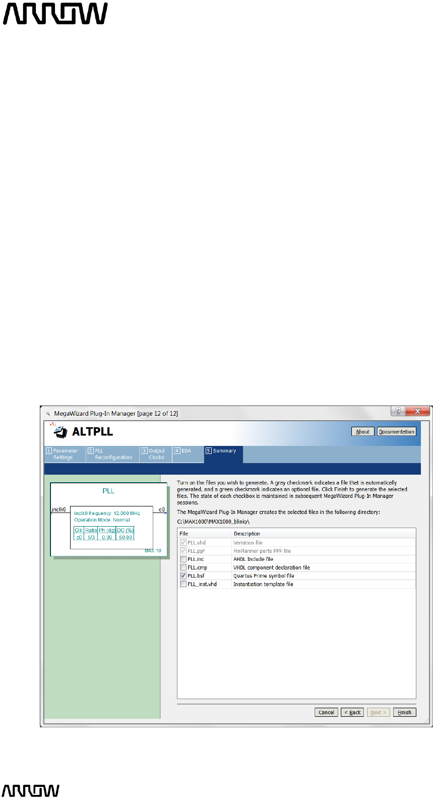
MAX1000 User Guide www.arrow.com
Page | 40 July 2017
5.2.4.7 Click “Next”.
5.2.4.8 Click “Next” for pages 7 to 11, as default settings are to be used.
5.2.4.9 On page 12 there is a list of output files that will be generated. Since the design will be
done in a schematic, you will need to select PLL.bsf checkbox. The .bsf file provides a
symbol that can be used in the schematic design we will be creating later.
The setting should look like this:
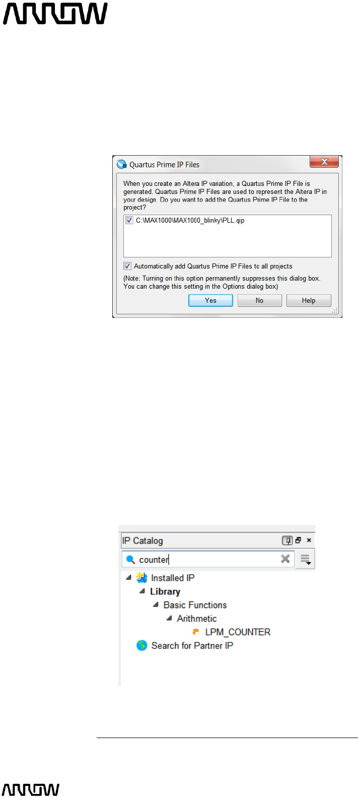
MAX1000 User Guide www.arrow.com
Page | 41 July 2017
5.2.4.10 Click “Finish”.
The PLL (1st component) will now be created.
5.2.4.11 If this is the first time that you are using this version of Quartus Prime, you might see a
pop-up Window for Quartus Prime IP Files, that asks if the tool should add IP files
automatically after generating them.
5.2.4.12 Select “Automatically add Quartus Prime IP Files to all projects.
5.2.4.13 Click “Yes” to allow all of the IP to automatically be added to the project, and so that
this message will not be seen for other designs.
5.2.5 Create and Configure the Counter
The next step is to create the counter which will drive the LEDs on the MAX1000 board.
5.2.5.1 To create this counter, select the IP Catalog and expand the Basics Arithmetic and
select the LPM_COUNTER or type “counter” in the search field.
Note: LPM stands for Library of Parameterized Modules
MAX1000 User Guide www.arrow.com
Page | 42 July 2017
5.2.5.2 Click “Add”.
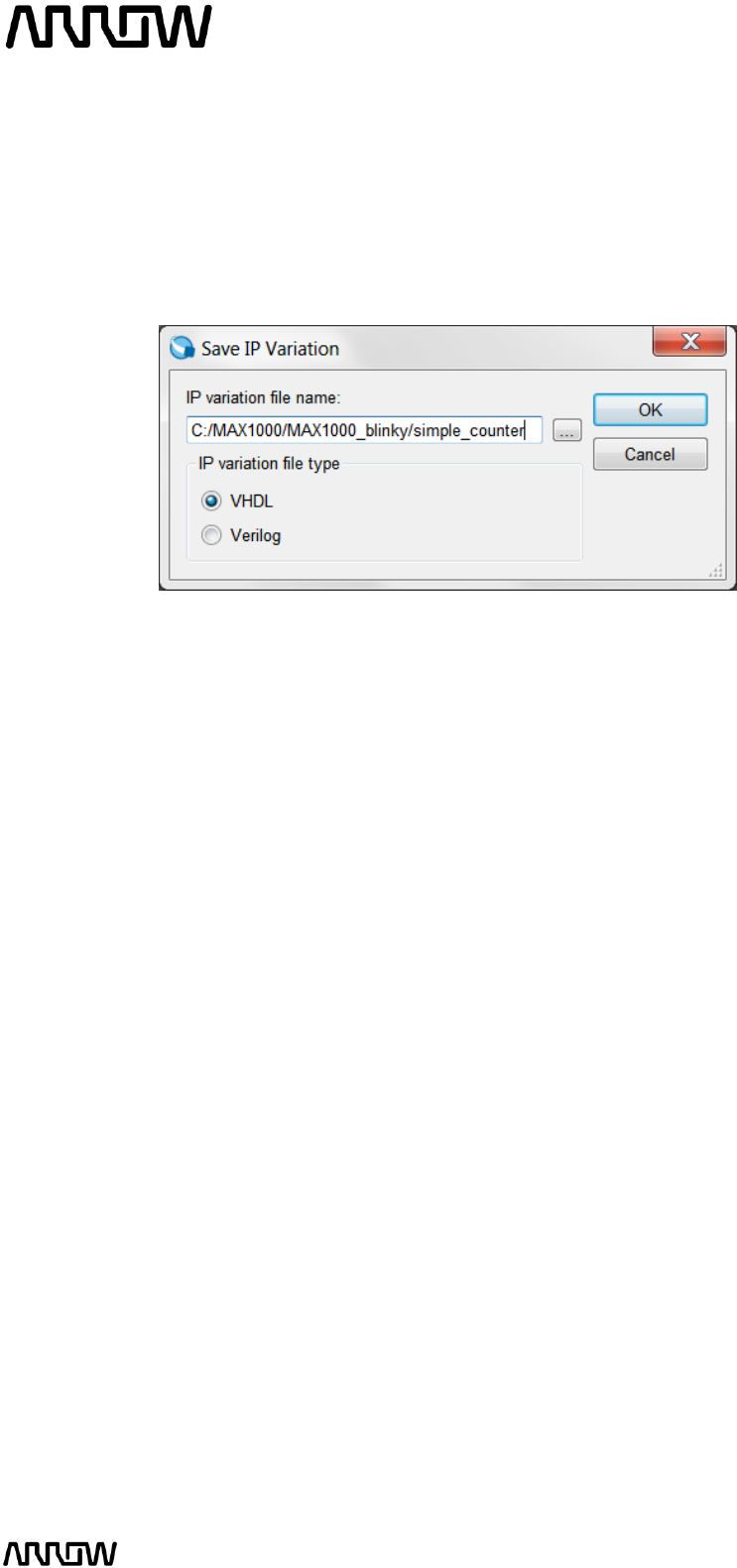
5.2.5.3 When the Save IP Variation pop up appears, enter “simple_counter” and select VHDL as
below:
5.2.5.4 Click “OK”.
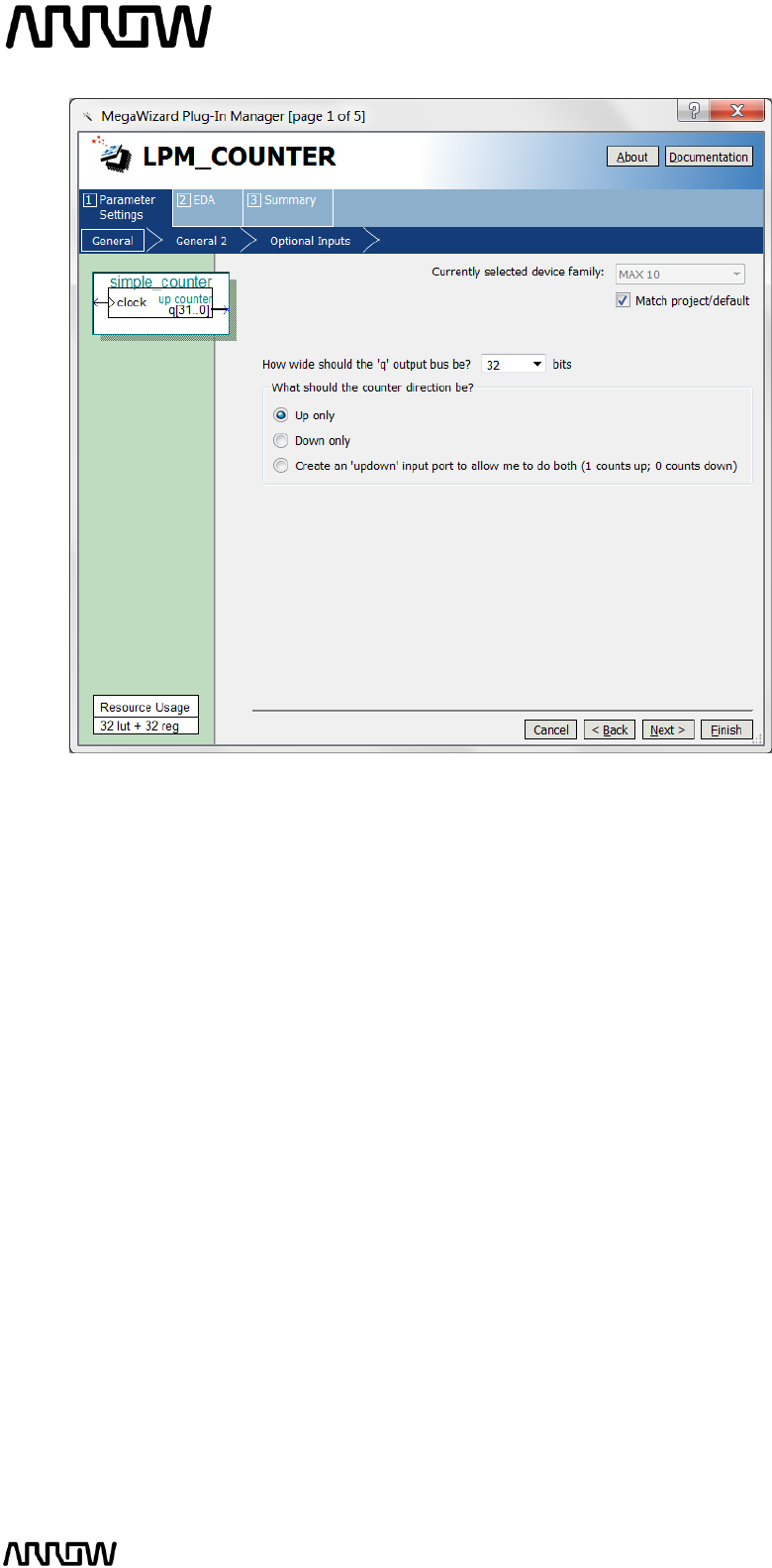
5.2.5.5 The next step is to increase the size of the counter to a number of bits large enough to
divide down the clock so we can see the LEDs toggling.
5.2.5.6 Change this number to 32.
5.2.5.7 Let the counter to be Up only, so the LEDs will show the counters counting up.
The setting should look like this:
MAX1000 User Guide www.arrow.com
Page | 43 July 2017
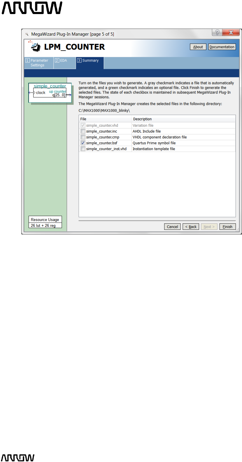
5.2.5.8 Select “Next” until reaching Page 5.
Select simple_counter.bsf checkbox to generate a symbol for our schematic design.
The screen should look like this now:
MAX1000 User Guide www.arrow.com
Page | 44 July 2017
5.2.5.9 Click “Finish”.
The counter is now created.
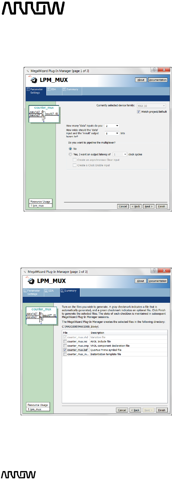
5.2.6 Create and Configure the Multiplexer
MAX1000 User Guide www.arrow.com
Page | 45 July 2017
The next step is to create a mux component. This mux will be used along with a push button on
the MAX1000 board to control the speed of the counter, where the counter outputs will be seen
on the LEDs.
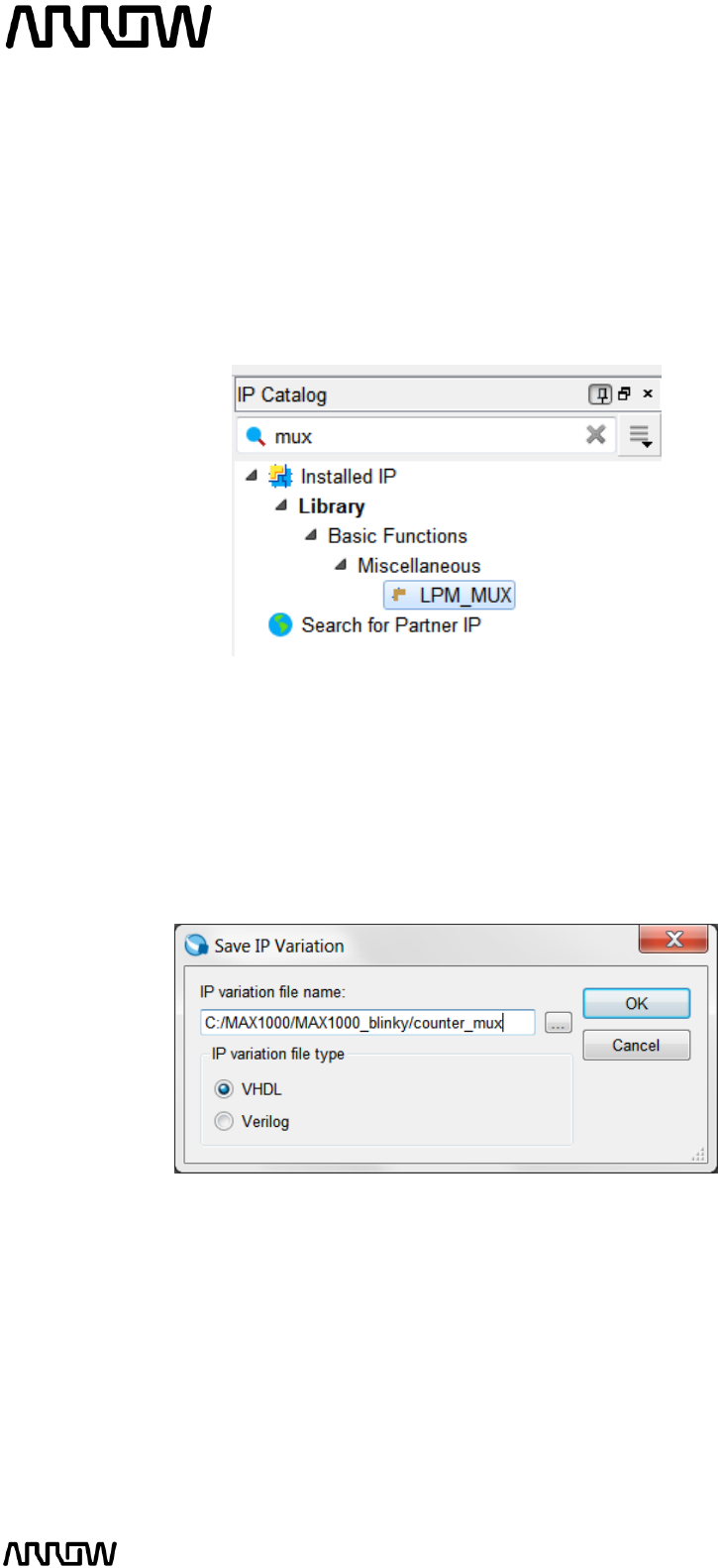
5.2.6.1 To create this mux, select IP Catalog and expand Basic Functions Miscellaneous and
select LPM_MUX or type mux in the search field.
5.2.6.2 Click “Add”.
5.2.6.3 In the Save IP Variation, enter the name of the counter_mux and the file type to be VHDL.
5.2.6.4 Click “OK”.
MAX1000 User Guide www.arrow.com
Page | 46 July 2017
5.2.6.5 Select 2 data inputs and the width of the input and output buses to be 8 bits. The reason
for 8 bits is that there are 8 LEDs to be toggled (showing count values).
The screen should look like this now:
5.2.6.6 Click “Next” until Page 3.
5.2.6.7 Select counter_mux.bsf checkbox to generate a symbol for our schematic design.
The view of this now looks like:
5.2.6.8 Click “Finish”.
MAX1000 User Guide www.arrow.com
Page | 47 July 2017
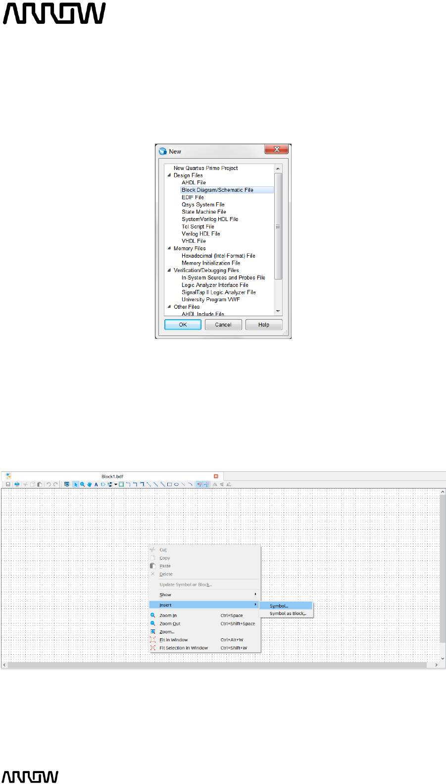
5.2.7 Adding the Components to the Schematic
The next step would be to connect all three components together.
5.2.7.1 To do so, select File menu, then select New and select Block Diagram/Schematic File.
5.2.7.2 Click “OK”.
A new schematic will be created, where the components can be added.
5.2.7.3 Right click on the schematic page, and select Insert Symbol… as seen below.
MAX1000 User Guide www.arrow.com
Page | 48 July 2017
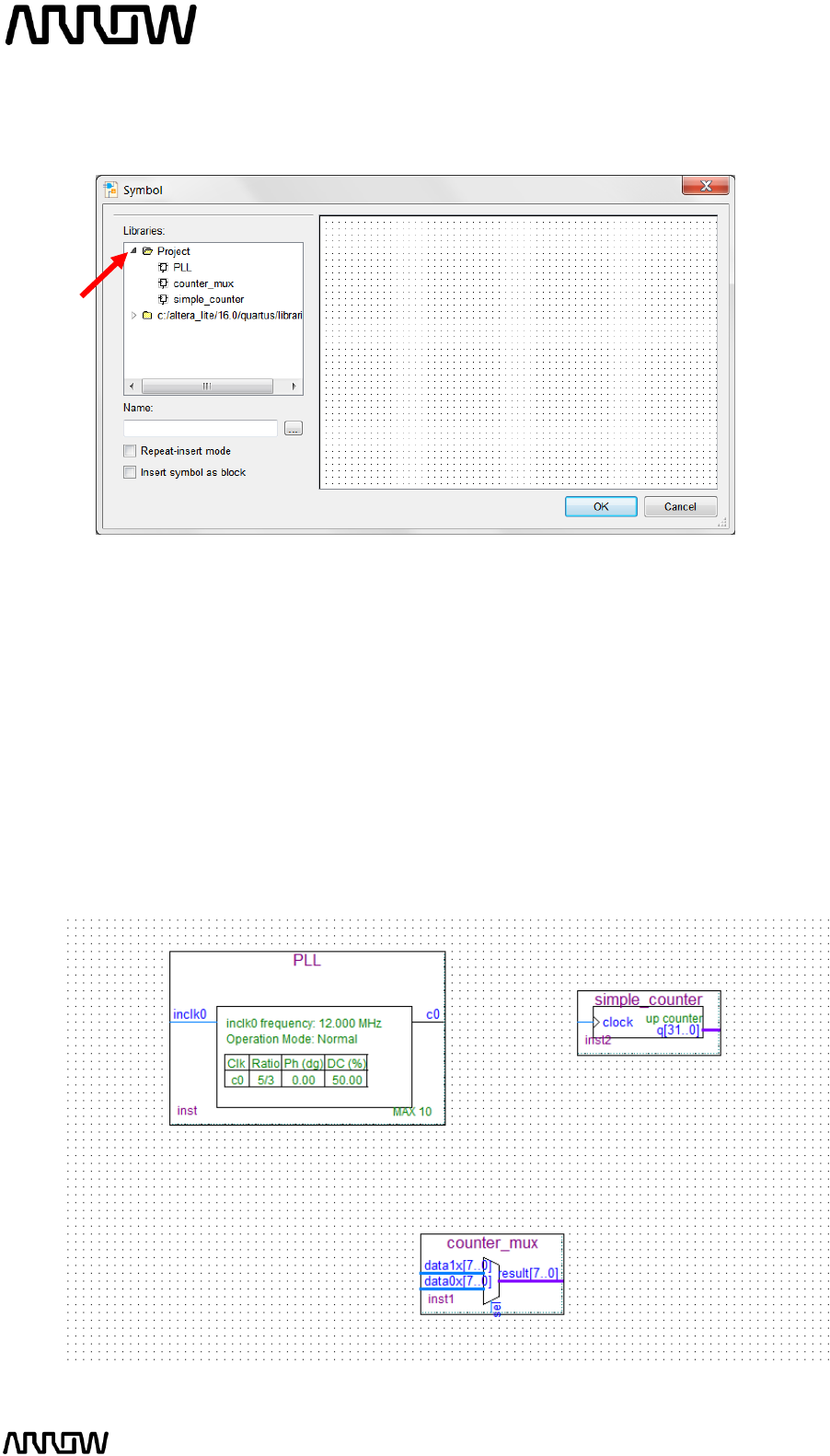
5.2.7.4 In the new window, expand “Project” and the three components that were created can
now be seen.
5.2.7.5 Select “PLL”.
5.2.7.6 Click “OK”.
The PLL component can be added now by left clicking on the schematic page.
5.2.7.7 Just like in the steps from 5.7.2.3 to 5.2.7.6, do the same for counter_mux and
simple_counter to add them to the schematic page. The order of adding the components
does not matter, as the connections between them will happen in the following steps.
5.2.7.8 After adding three components, your schematic should look similar to the following. To
place them similarly, simply drag the components to the appropriate locations.
MAX1000 User Guide www.arrow.com
Page | 49 July 2017
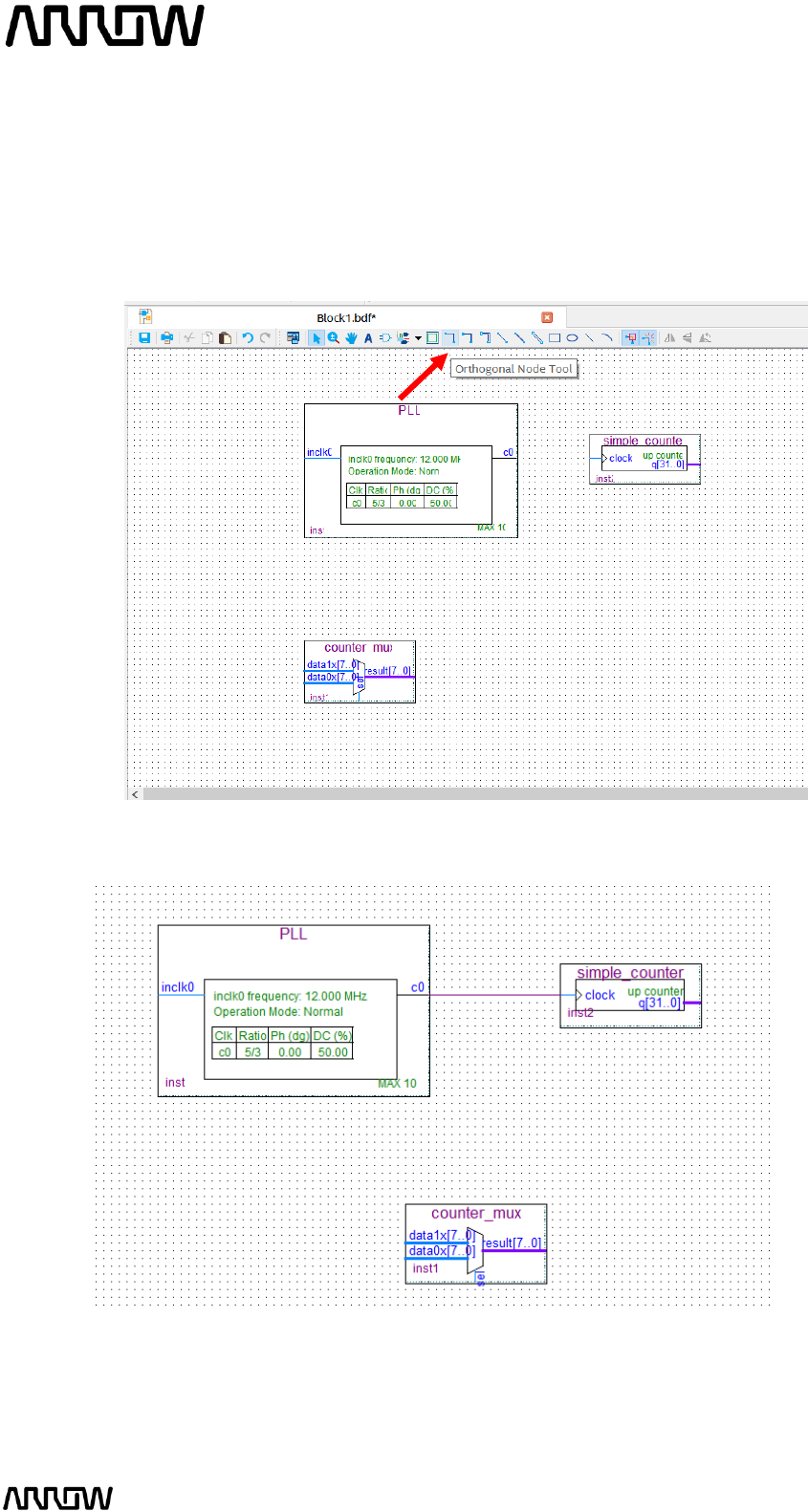
5.2.8 Connecting the Components
Next step is to make the proper connections between the three components we just added to the
schematic.
5.2.8.1 Select the “Node Tool”.
5.2.8.2 Connect the c0 of the PLL to the simple_counter as shown below:
This will mean that a single signal (c0) is connected to the simple_counter (clock).
MAX1000 User Guide www.arrow.com
Page | 50 July 2017
5.2.8.3 Select the “Bus Tool”.
5.2.8.4 Using the bus tool create a connection coming out of the simple_counter and one
connection for each of the inputs of the counter_mux as show below.
MAX1000 User Guide www.arrow.com
Page | 51 July 2017
5.2.8.5 Right click on the output bus of the simple counter that you just created and select
“Properties”.
Set the name of the bus to: counter[31..0]
The view of the “Bus Properties” should look like this:
5.2.8.6 Do the same for input buses of the mux:
Name the top bus input: data1x[7..0] counter[24..31]
Name the bottom bus input: data0x[7..0] counter[19..26]
Schematic should look like this:
MAX1000 User Guide www.arrow.com
Page | 52 July 2017
5.2.8.7 Add inputs to the schematic
Click on the “Pin Tool” as show below and select “Input”.
5.2.8.8 Add one input pin for inclk0 of the PLL.
Add one input pin for sel of counter_mux.
Your schematic should look like this:
5.2.8.9 Rename the pin_name1 to CLK12M by double clicking its current name. This is going to
be the clock signal coming into the FPGA.
MAX1000 User Guide www.arrow.com
Page | 53 July 2017
5.2.8.10 Rename the pin_name2 to USER_BTN by double clicking its current name. This is going
to be the user button of the MAX1000 board to select the mux.
5.2.8.11 Using the “Node Tool” connect:
CLK12M inclk0 (of the PLL component)
USER_BTN sel (of the counter_mux component)
Your schematic should look like this now:
5.2.8.12 Add the outputs to the schematic
Click on the “Pin Tool” as before, but this time select “Output”.
MAX1000 User Guide www.arrow.com
Page | 54 July 2017
5.2.8.13 Add one output pin for the LEDs.
5.2.8.14 Rename the pin to LED[7..0].
5.2.8.15 Using the “Bus Tool”, make the connection between counter_mux component and
output pin:
result[7..0] LED[7..0]
The final schematic should look like the following:
Looking at the schematic, even though the buses are not connected together by wires, the names
of counter tell Quartus Prime to connect the signals together. Overall, the user button will toggle
between displaying higher 8 bits of the counter and 8 lower bits of the counter. The signals of the
counter that are not connected will not be used by Quartus Prime.
5.2.8.16 Save your design
Open the File Menu and select “Save”. Save it as top.bdf
MAX1000 User Guide www.arrow.com
Page | 55 July 2017
5.2.9 Analysis and Synthesis
The next step is to run Analysis and Synthesis to ensure that there is no errors in the design.
To run Analysis and synthesis open Processing Start Analysis and Synthesis
or from clicking the button on the top toolbar as seen below:
There should be no errors. If there are errors, they should be fixed before continuing and Analysis
and Synthesis run again.
5.2.10 Adding Timing Constraints
Timing Constraints tell the Quartus what are the timing requirements for this design. Timing
Constraints are required in every CPLD/FPGA design.
To add the timing constraints, select File New and under the “Other File” section, select
“Synopsys Design Constraints File” and select “OK”.

MAX1000 User Guide www.arrow.com
Page | 56 July 2017
Type or copy the following lines into this new file:
#create input clock which is 12MHz
create_clock -name CLK12M -period 83.333 [get_ports {CLK12M}]
#derive PLL clocks
derive_pll_clocks
#derive clock uncertainty
derive_clock_uncertainty
#set false path
set_false_path -from [get_ports {USER_BTN}]
set_false_path -from * -to [get_ports {LED*}]
5.2.10.1 The first line “create_clock” tells Quartus Prime that the clock, CLK12M is 83.333 ns
(12 MHz). It also assigns the CLK12M to a pin (port) in the .sdc format.
5.2.10.2 The second line “derive_pll_clocks” tells the software to look if there are any PLLs,
and if so, automatically derive the clock multiplication/division of the outputs of the
PLL even if they are used internally within the CPLD/FPGA.
5.2.10.3 The third line “derive_clock_uncertainty” tells the software to automatically
determine the internal clock uncertainty. No clock is ideal, and thus there will be
some internal jitter within the FPGA associated with it.
5.2.10.4 The fourth and fifth line “set_false_path” tells the software to not do any timing
optimization to the stated paths/pins. The I/Os of this design are trivial, so they can
be ignored in the Timing Analysis.
5.2.10.5 Use File Save to save it as top.sdc.
MAX1000 User Guide www.arrow.com
Page | 57 July 2017
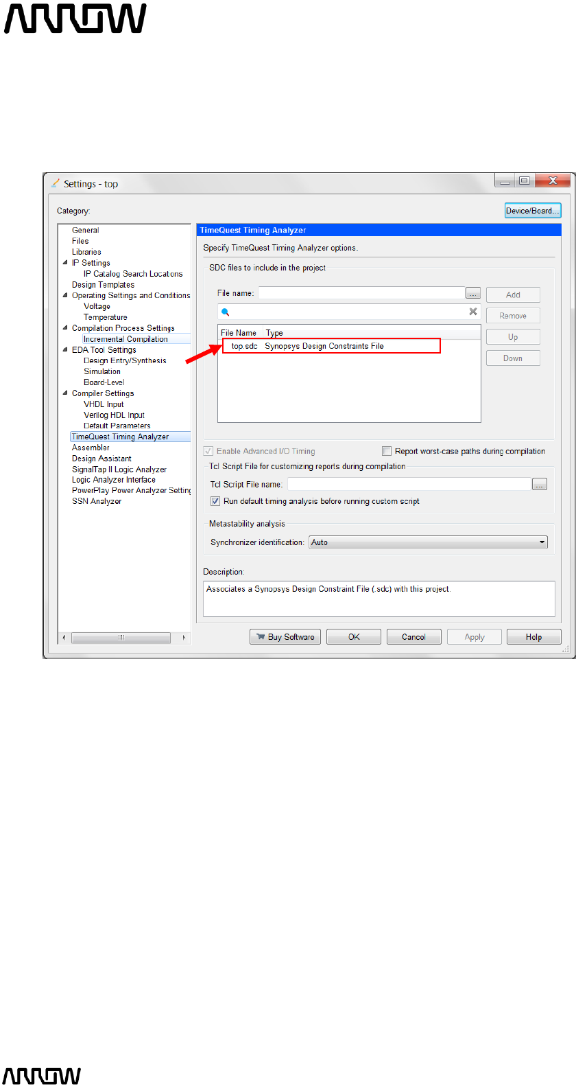
5.2.10.6 Ensure that the file is added to the Project: Assignments Settings and select
“Timequest Timing Analyzer”. The top.sdc should have been already added by
default. If it is not, it will need to be added manually.
MAX1000 User Guide www.arrow.com
Page | 58 July 2017
5.2.11 Pinning Assignments
Before the design can be downloaded to the FPGA, pin assignments that match the hardware on
the board are needed. There are different ways to do this such as the Pin Planner, Assignment
Editor, and text files.
The following steps will show one of these ways, the Pin Planner. Since there are only 10 pins that
need to be assigned, the Pin Planner can be used. If many pins are needed, other ways can be
used such as the Quartus Assignment Editor, or by importing constraints from a text file or
spreadsheet.
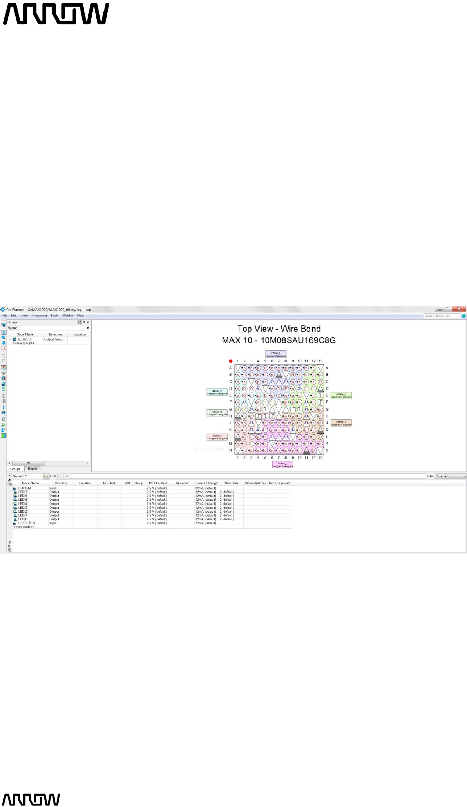
5.2.11.1 Open the Pin Planner: Assignments Pin Planner.
A new window will open as seen below:
5.2.11.2 To make pin assignments, select the CLK12M (node name) on the bottom portion and
drag and drop it to pin H6 of the Top View of the FPGA or alternatively set the Location
field of the CLK12M to PIN_H6.
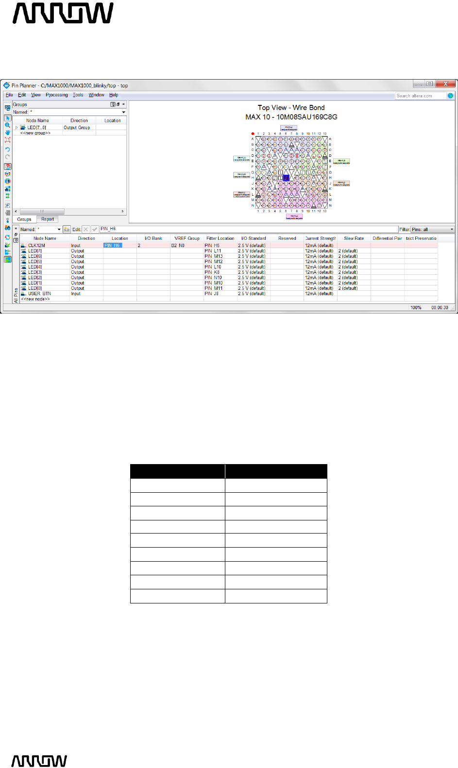
MAX1000 User Guide www.arrow.com
Page | 59 July 2017
The window should now look like this:
Note that the Location of the CLK12M is now set to Location PIN_H6 (as seen in blue colour in the
top view of the FPGA).
5.2.11.3 The other pins need to be assigned as well. Just like previously set all the pins to their
appropriate locations using the table below, by either drag and drop or writing
manually the location.
Node Name
Pin Location
LED[7]
PIN_D8
LED[6]
PIN_C10
LED[5]
PIN_C9
LED[4]
PIN_B10
LED[3]
PIN_A10
LED[2]
PIN_A11
LED[1]
PIN_A9
LED[0]
PIN_A8
USER_BTN
PIN_E6
MAX1000 User Guide www.arrow.com
Page | 60 July 2017
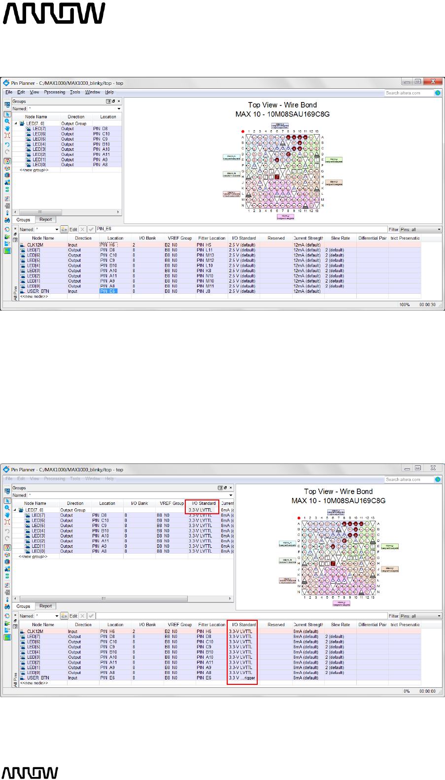
5.2.11.4 Now the Pin Planner should look like this after assigning all the pin locations.
The specific pins are now selected, but the I/O standards now need to be set as well. The button,
LEDS, and clock pins are the same I/O standard for MAX1000 since all banks and peripherals are
powered by 3.3V. The USER_BTN is a 3.3 V Schmitt Trigger, the LEDs and clock pins are 3.3-V
LVTTL. These I/O standards can be set in the Pin Planner, by selecting the I/O Standard. Select
the I/O standard either from the “All Pins” tab or the “Groups” tab, and change the 2.5V (default)
to the specific I/O standard.
5.2.11.5 The Pin Planner should now look like this:
5.2.11.6 Close the Pin Planner. The settings are automatically saved.
MAX1000 User Guide www.arrow.com
Page | 61 July 2017
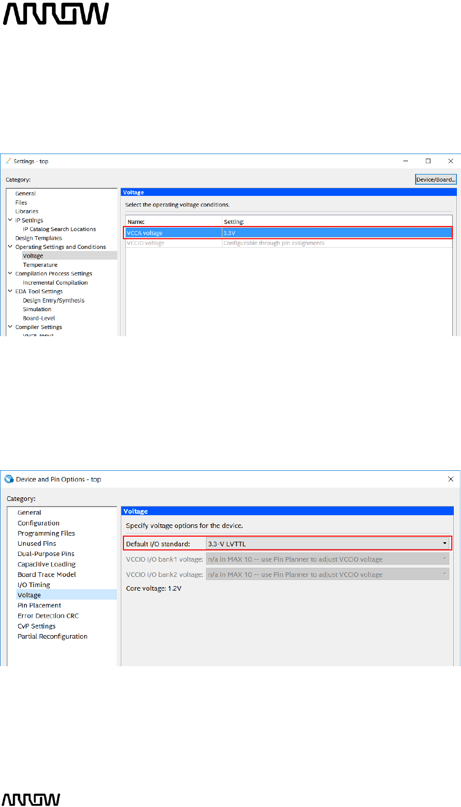
5.2.12 Compiling the Design
5.2.12.1 First, make sure that the operating conditions of the device are set correctly.
Open Settings Operating Settings and Conditions Voltage and set VCCA voltage to “3.3V”
and press “Apply” and “OK”.
5.2.12.2 You can also set the default I/O Standard which can eliminate some design warning
and save you time from setting the standard for some pins manually.
Open Assignments Device Device and Pin Options Voltage and set Default I/O Standard
to “3.3-V LVTTL” and press “OK” to all the windows.
MAX1000 User Guide www.arrow.com
Page | 62 July 2017
5.2.12.3 The next step is to compile and complete the design. This step will verify that there are
no errors, create internal databases, and create programming files that will be used in
the next steps.
To compile the design, select Processing Start Compilation or through the button as show
below:
If there are errors, they will need to be resolved and re-compiled before the design can be
programmed to the board. When Compiling finishes and there are no errors, there will be a
message at the bottom of the window that states: Full Compilation was successful and a 100%
indication along with the compile time in the right bottom corner.

MAX1000 User Guide www.arrow.com
Page | 63 July 2017
5.2.13 Reading the Compilation Report
After successfully compiling the design, a Compilation Report should appear as shown above:
This report is very useful with a lot of information about the design. Last message state that the
design was fully constrained, Timing Analysis and compilation successful, but there is more to it:
In the Flow Summary, it can be seen how many logic elements the whole design took, along
with total PLLs, registers, pins, etc.
In Analysis and Synthesis, more detailed information about the resources used can be seen in
Resource Usage Summary, as well how many LEs were used for each component in Resource
Utilization by Entity.
In the Fitter, more detailed information about the pins and their banks can be seen. For
example if we used the RESET_BTN (PIN_E7), we could have issues since it is configured as a
secondary function, which can be seen in Fitter Resource Section Dual Purpose and
Dedicated Pins, which would require to disable in the settings.
TimeQuest Timing Analyzer shows various timing information concerning the design, as well
as if the design has met the timing requirements. In this case timing requirements were met,
but in other cases that requirements might not be met, could be solved by going over the
information provided in the reports inside this folder. Most notable reports in this folder are:
the maximum frequency the design can achieve, setup and hold slack, unconstrained paths in
case they were missed, etc.
MAX1000 User Guide www.arrow.com
Page | 64 July 2017
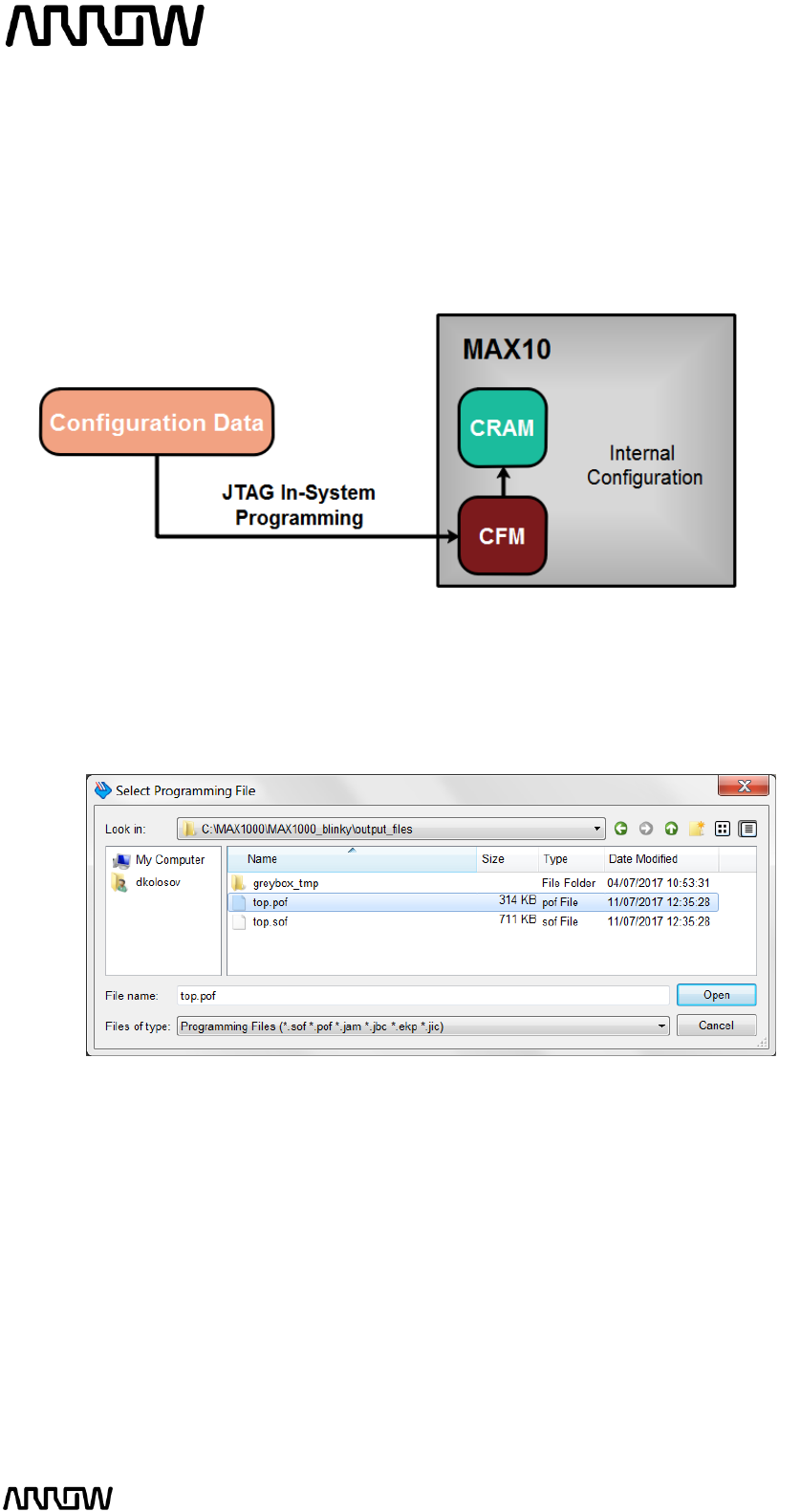
Configuring the MAX1000
After successfully compiling your project, there should new files generated. In case of MAX10
devices, two type of files are generated due to the architecture of the device, .sof and .pof. In
other device architectures, only the .sof file is generated automatically.
Note: Difference between .pof and .sof files
sof: is for the direct volatile configuration, which programs the FPGA fabric directly (SRAM cells).
Configuration is lost on power off.
pof: is for non-volatile programming, which program the either an external configuration devices
or in MAX10 case, itself as it is a non-volatile FPGA.
6.1 Configure the FPGA in JTAG Mode
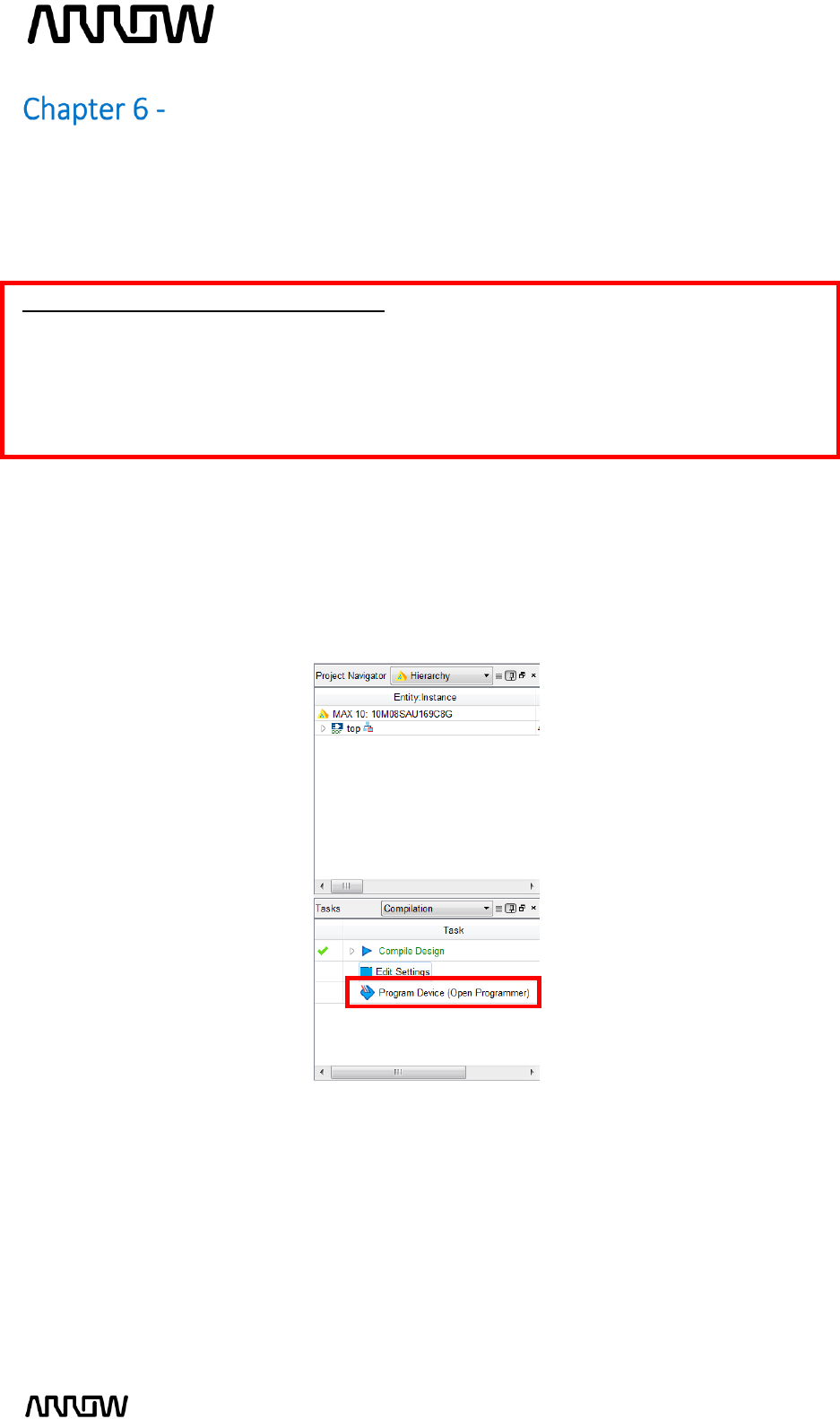
6.1.1 Open the Quartus Prime Programmer from Tools Programmer or double-click on
Program Device (Open Programmer) from the Tasks pane. Since the MAX1000 is not
connected yet, the Programmer should show a blank configuration.
MAX1000 User Guide www.arrow.com
Page | 65 July 2017
6.1.2 After opening the program this should be the view of the new window:
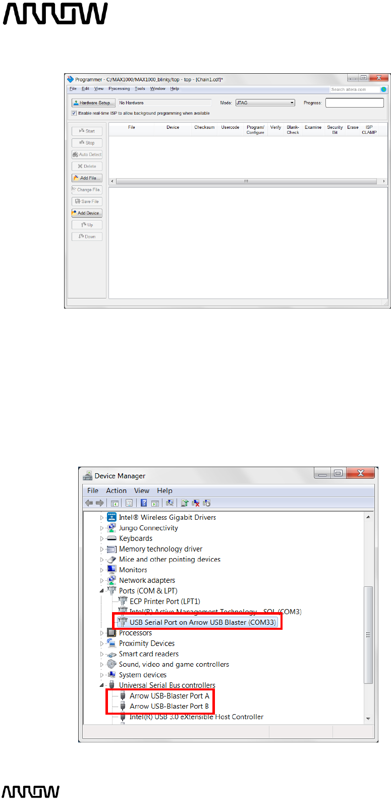
6.1.3 Connect your MAX1000 board to your PC using a USB cable. The Arrow USB Programmer2
driver software should already be installed, if not please refer to Chapter 4.2 (Windows
based operating system) or 4.4 (Linux based operating system) for installing the drivers.
After plugging in the MAX1000, the green LED should also light up indicating power on, along with
a brief flash of the red LED CONF_DONE.
In the Window's Device Manager should display the following entries that are highlighted in red.
MAX1000 User Guide www.arrow.com
Page | 66 July 2017
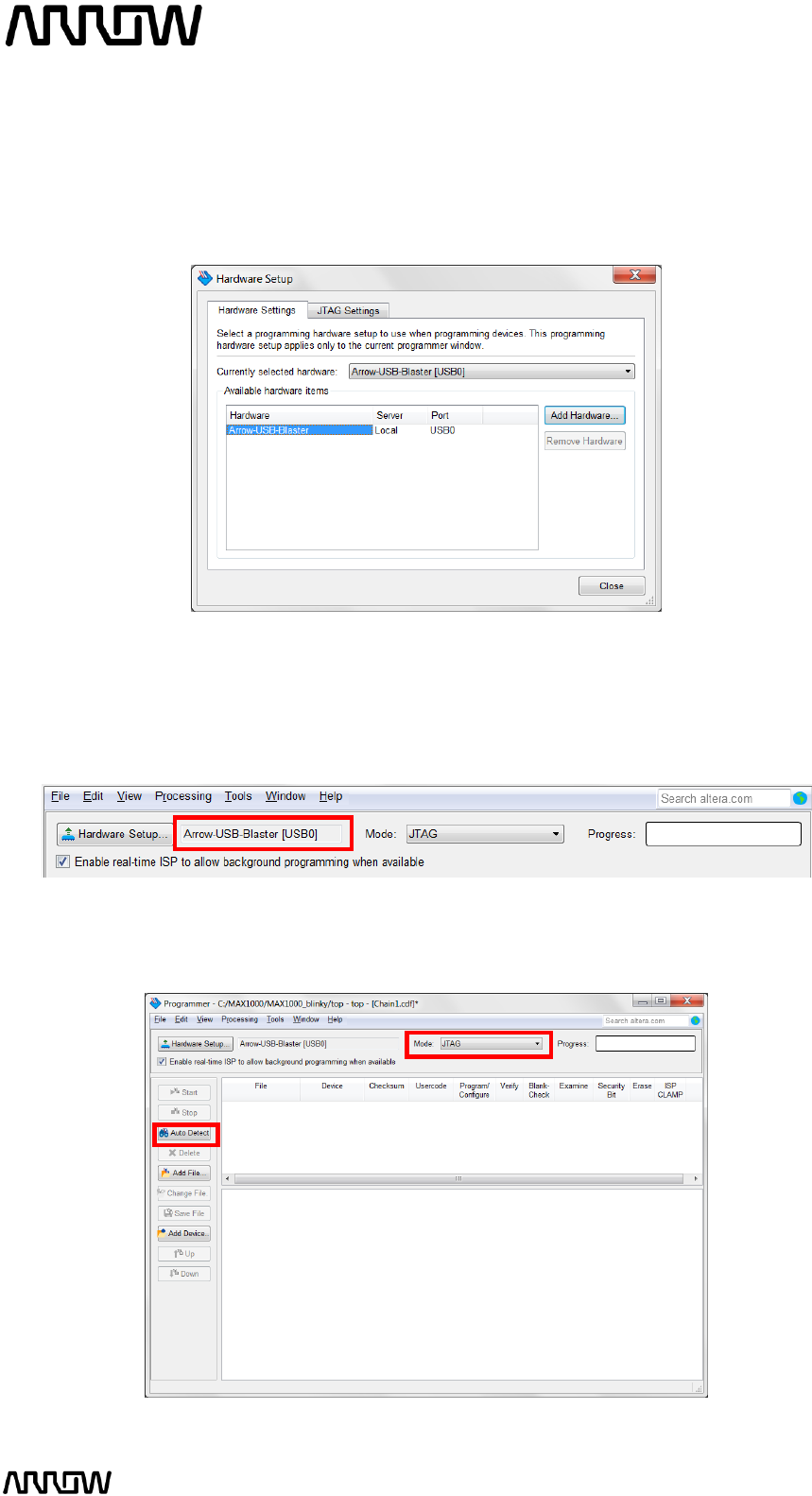
6.1.4 In the Programmer window, click Hardware Setup and double-click the ARROW-USB-
PROGRAMMER2 entry in the Hardware Settings tab (you should only be able to see this
Arrow USB Programmer2 if MAX1000 is connected to the PC). The “Currently selected
hardware” drop-down should now show ARROW-USB-PROGRAMMER2 [USB-0].
Depending on your PC, the USB port number may vary.
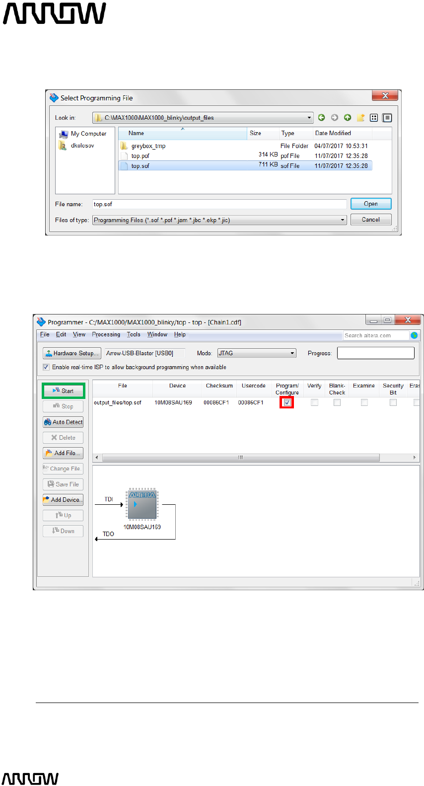
6.1.5 Click “Close”.
6.1.6 The Programmer window should now have a Hardware Setup such as:
6.1.7 Click “Auto Detect” on the left side of the Programme window and make sure the Mode
is JTAG.
MAX1000 User Guide www.arrow.com
Page | 67 July 2017
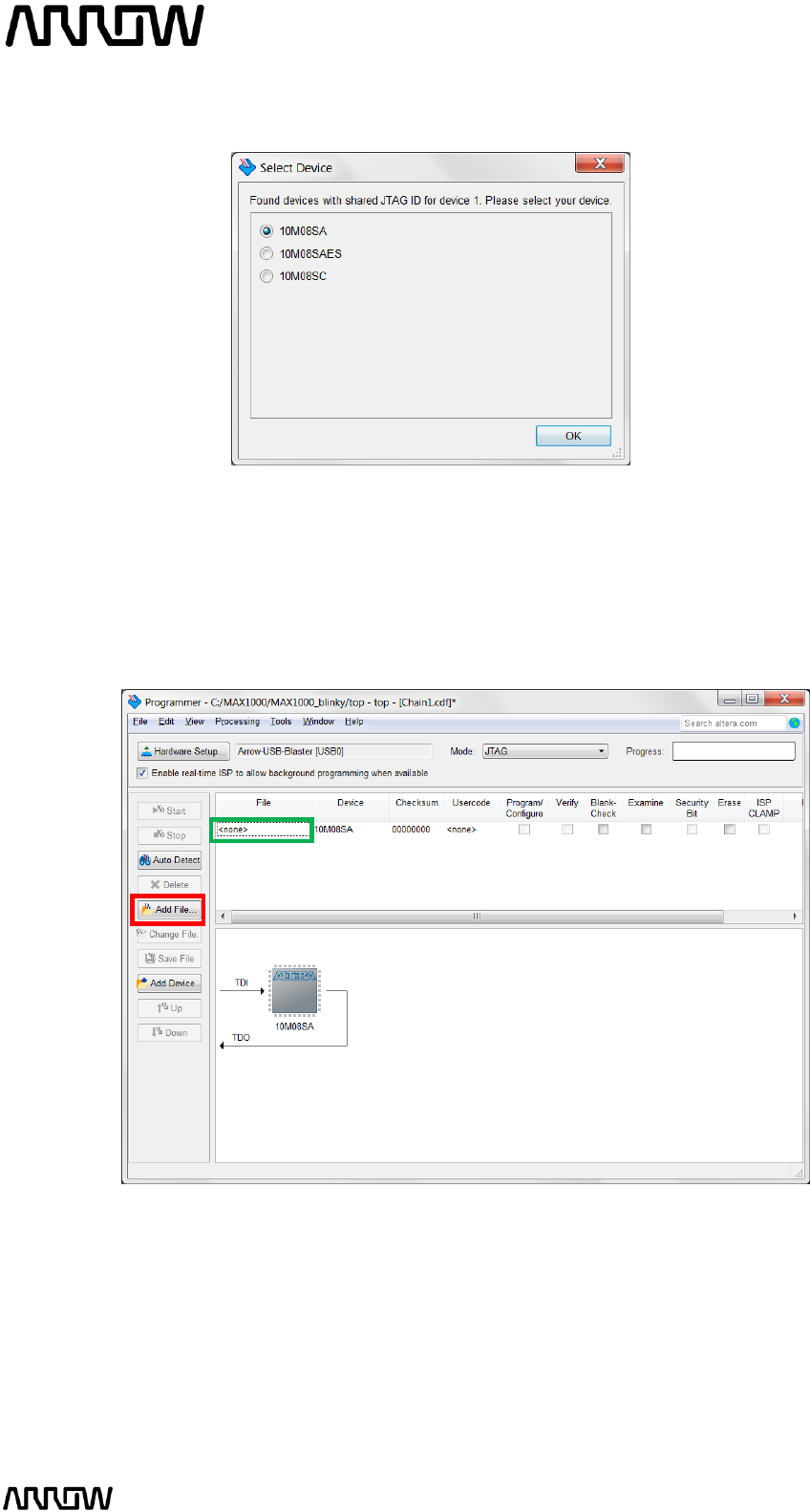
6.1.8 Select your device and click OK. In this case its “10M08SA”
6.1.9 To choose the programming file, you can either click “Add File..” on the right side of the
Programmer window (highlighted in red) or double-click <none> below the File tab
(highlighted in green).
MAX1000 User Guide www.arrow.com
Page | 68 July 2017
6.1.10 In either case, navigate to: <project_directory>/output_files/ in your compilation
directory. Select and open the top.sof file.
6.1.11 Click “Open”.
6.1.12 The Programmer window should look like this now:
6.1.13 Make sure the Program/Configure checkbox is checked (highlighted in red above) and
click “Start” (highlighted in green above) to program the MAX1000. You should see the
CONF_DONE LED toggle briefly to indicate that the configuration is complete and the
Progress bar should reach 100% (Successful). The design is now programmed to the FPGA.
Note: that turning off and then on the FPGA will result into losing its configuration.
MAX1000 User Guide www.arrow.com
Page | 69 July 2017
6.2 Internal Configuration
The configuration data to be written to CFM will be part of the programmer object file (.pof). This
configuration data is automatically loaded from the CFM into the MAX10 device when the board
is powered up.
6.2.1 Going back to step 6.1.10, instead of choosing the .sof file, choose the .pof file.
6.2.2 Click “Open”.
MAX1000 User Guide www.arrow.com
Page | 70 July 2017
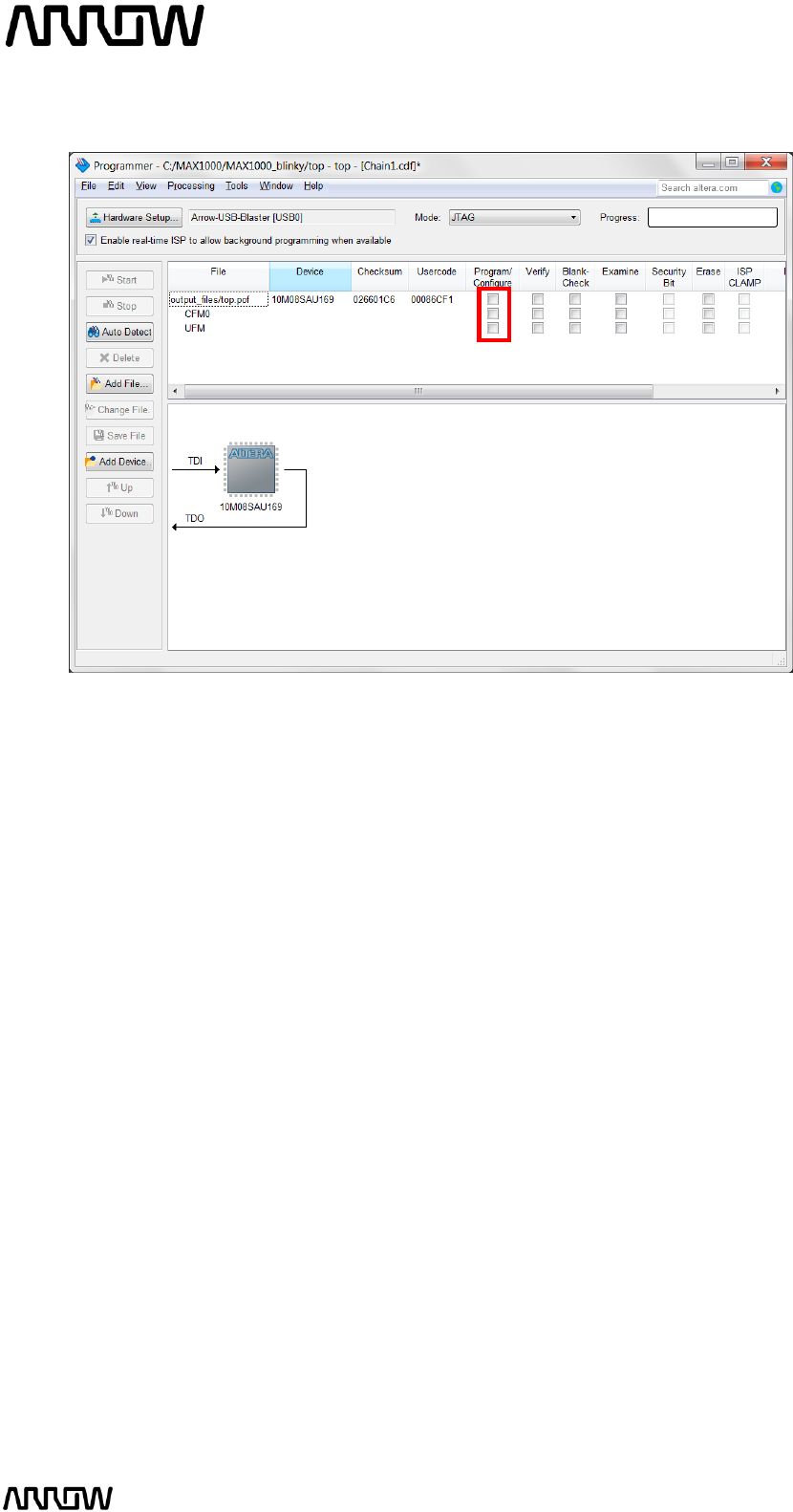
6.2.3 The window should look like this:
Select all the checkboxes under the Program/Configure for CFM0 and UFM (highlighted in red
above).
6.2.4 Click “Start” to configure MAX10. The programming could take a while.
6.2.5 When the programming is finished, the MAX1000 should be able to keep its configuration
data even after powered off.
6.3 Testing the Design
Does not matter which way the MAX1000 was configured, the results should be the same for both
methods, with the only difference being if configuration is retained after power off.
On the board by default, the LEDS should now toggle in a slow counting sequence.
Push and hold the USER_BTN to see that the LEDs will now toggle in a very fast counting sequence.
USER_BTN is on the side of the LEDs.
Releasing the USER_BTN, will make the LEDs toggle at a slower rate as before.
MAX1000 User Guide www.arrow.com
Page | 71 July 2017
Common Issues and Fixes
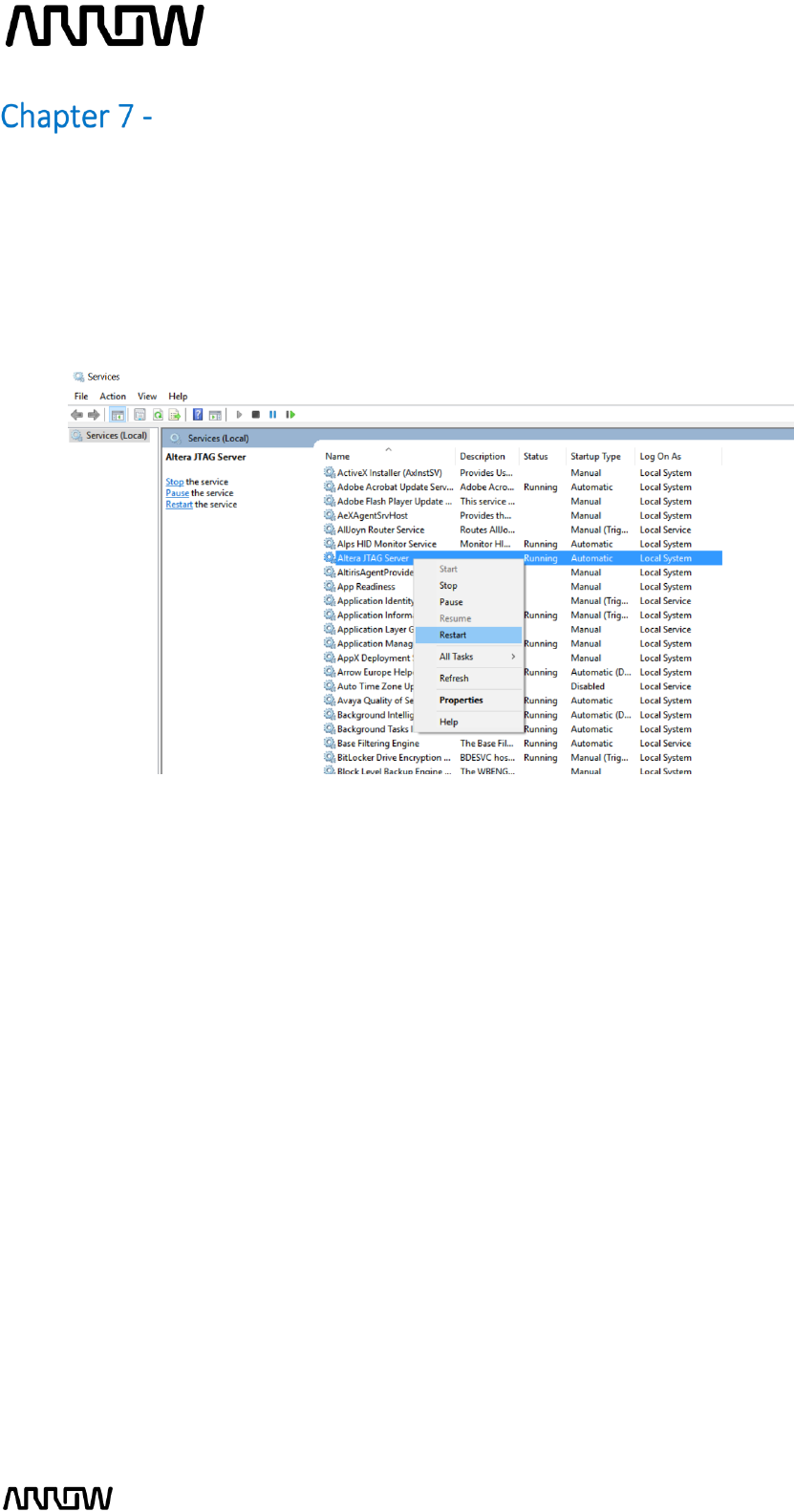
1) Issue: In some rare cases when using Windows 10 operating system, the programmer
DLL is not properly loaded/unloaded, causing the Quartus Programmer to not detect the
Arrow USB Programmer2.
Solution: Restart the Altera JTAG Server using the Services application of Windows.

MAX1000 User Guide www.arrow.com
Page | 72 July 2017
Appendix
7.1 Revision History
Version
Change Log
Date of Change
V1.0
Initial Version
11/07/2017

MAX1000 User Guide www.arrow.com
Page | 73 July 2017
7.2 Legal Disclaimer
ARROW ELECTRONICS
EVALUATION BOARD LICENSE AGREEMENT
By using this evaluation board or kit (together with all related software, firmware, components, and
documentation provided by Arrow, “Evaluation Board”), You (“You”) are agreeing to be bound by the terms and
conditions of this Evaluation Board License Agreement (“Agreement”). Do not use the Evaluation Board until
You have read and agreed to this Agreement. Your use of the Evaluation Board constitutes Your acceptance of
this Agreement.
PURPOSE
The purpose of this evaluation board is solely intended for evaluation purposes. Any use of the Board beyond
these purposes is on your own risk. Furthermore, according the applicable law, the offering Arrow entity
explicitly does not warrant, guarantee or provide any remedies to you with regard to the board.
LICENSE
Arrow grants You a non-exclusive, limited right to use the enclosed Evaluation Board offering limited features
only for Your evaluation and testing purposes in a research and development setting. Usage in a live environment
is prohibited. The Evaluation Board shall not be, in any case, directly or indirectly assembled as a part in any
production of Yours as it is solely developed to serve evaluation purposes and has no direct function and is not
a finished product.
EVALUATION BOARD STATUS
The Evaluation Board offers limited features allowing You only to evaluate and test purposes. The Evaluation
Board is not intended for consumer or household use. You are not authorized to use the Evaluation Board in any
production system, and it may not be offered for sale or lease, or sold, leased or otherwise distributed for
commercial purposes.
OWNERSHIP AND COPYRIGHT
Title to the Evaluation Board remains with Arrow and/or its licensors. This Agreement does not involve any
transfer of intellectual property rights (“IPR) for evaluation board. You may not remove any copyright or other
proprietary rights notices without prior written authorization from Arrow or it licensors.
RESTRICTIONS AND WARNINGS
Before You handle or use the Evaluation Board, You shall comply with all such warnings and other instructions
and employ reasonable safety precautions in using the Evaluation Board. Failure to do so may result in death,
personal injury, or property damage.
You shall not use the Evaluation Board in any safety critical or functional safety testing, including but not limited
to testing of life supporting, military or nuclear applications. Arrow expressly disclaims any responsibility for
such usage which shall be made at Your sole risk.
WARRANTY
Arrow warrants that it has the right to provide the evaluation board to you. This warranty is provided by Arrow
in lieu of all other warranties, written or oral, statutory, express or implied, including any warranty as to
merchantability, non-infringement, fitness for any particular purpose, or uninterrupted or error-free operation,
all of which are expressly disclaimed. The evaluation board is provided “as is” without any other rights or
warranties, directly or indirectly.
You warrant to Arrow that the evaluation board is used only by electronics experts who understand the dangers
of handling and using such items, you assume all responsibility and liability for any improper or unsafe handling
or use of the evaluation board by you, your employees, affiliates, contractors, and designees.

MAX1000 User Guide www.arrow.com
Page | 74 July 2017
LIMITATION OF LIABILITIES
In no event shall Arrow be liable to you, whether in contract, tort (including negligence), strict liability, or any
other legal theory, for any direct, indirect, special, consequential, incidental, punitive, or exemplary damages
with respect to any matters relating to this agreement. In no event shall arrow’s liability arising out of this
agreement in the aggregate exceed the amount paid by you under this agreement for the purchase of the
evaluation board.
IDENTIFICATION
You shall, at Your expense, defend Arrow and its Affiliates and Licensors against a claim or action brought by a
third party for infringement or misappropriation of any patent, copyright, trade secret or other intellectual
property right of a third party to the extent resulting from (1) Your combination of the Evaluation Board with
any other component, system, software, or firmware, (2) Your modification of the Evaluation Board, or (3) Your
use of the Evaluation Board in a manner not permitted under this Agreement. You shall indemnify Arrow and its
Affiliates and Licensors against and pay any resulting costs and damages finally awarded against Arrow and its
Affiliates and Licensors or agreed to in any settlement, provided that You have sole control of the defense and
settlement of the claim or action, and Arrow cooperates in the defense and furnishes all related evidence under
its control at Your expense. Arrow will be entitled to participate in the defense of such claim or action and to
employ counsel at its own expense.
RECYCLING
The Evaluation Board is not to be disposed as an urban waste. At the end of its life cycle, differentiated waste
collection must be followed, as stated in the directive 2002/96/EC. In all the countries belonging to the European
Union (EU Dir. 2002/96/EC) and those following differentiated recycling, the Evaluation Board is subject to
differentiated recycling at the end of its life cycle, therefore: It is forbidden to dispose the Evaluation Board as
an undifferentiated waste or with other domestic wastes. Consult the local authorities for more information on
the proper disposal channels. An incorrect Evaluation Board disposal may cause damage to the environment and
is punishable by the law.
