MC80F0308 ABOV SEMICONDUCTOR
User Manual: MC80F0308-ABOV SEMICONDUCTOR - powered by h5ai v0.28.1 (s://larsjung.de/h5ai/)
Open the PDF directly: View PDF ![]() .
.
Page Count: 138 [warning: Documents this large are best viewed by clicking the View PDF Link!]

ABOV SEMICONDUCTOR
8-BIT SINGLE-CHIP MICROCONTROLLERS
MC80F0304/0308/0316
MC80C0304/0308/0316
User’s Manual (Ver. 2.12)

Version 2.12
Published by
FAE Team
©2006 ABOV Semiconductor Co., Ltd. All right reserved.
Additional information of this manual may be served by ABOV Semiconductor offices in Korea or Distributors and Representatives.
ABOV Semiconductor reserves the right to make changes to any information here in at any time without notice.
The information, diagrams and other data in this manual are correct and reliable; however, ABOV Semiconductor is in no way responsible
for any violations of patents or other rights of the third party generated by the use of this manual.

MC80F0304/08/16
November 4, 2011 Ver 2.12 3
REVISION HISTORY
VERSION 2.12 (November 4, 2011) This Book
Logo is changed.
The dimensions of 28 SOP package outline drawing is fixed.
VERSION 2.11 (May 14, 2008)
Corrected Stack End Address to 0100H at Figure 8-4 on page 34.
Corrected the address of PU2 to 00FEH at Figure 8-1 on page 38.
Corrected the bit name of TM1to T1CK1,T1CK0,T1CN and T1ST at Figure 13-17 on page 75.
Corrected the PWM1HR to T1PWHR at Figure 13-20 on page 77.
Corrected the initial value of WDT Timer to “Enable” at Figure 20-1 on page 110.
VERSION 2.10 (April 4, 2008)
Updated the description for Figure 14-4 A/D Converter Control & Result Register on page 80.
The format of Instruction Set and Revision History was renewed.
Fixed some errata.
VERSION 2.02 (SEP 28, 2007) This book
Fix error in description and diagram of 8 bit event counter.
VERSION 2.01 (MAY 5, 2007)
Fix error in figure 9-2 : change R04, R07 and EC0,EC1 of PSR1 to R05, R06 and T0O, T2O (page 38)
Fix pin number error of 28 pin package in Table 5-2. (page 9)
VERSION 2.0 (MAR. 2007)
Add TVDD parameter specification and change TPOR in DC Electrical Characteristics.
Note for configuration option is added and fix some errata.
VERSION 1.92 (JAN. 2007)
Mask Order Sheet is updated
VERSION 1.91 (NOV. 2006)
Fix some errata in Section 13.6 PWM mode.
VERSION 1.9 (SEP. 2006)
Add 32 SOP package type.
VERSION 1.81 (AUG. 2006)
Fix some errata in Figure 18-2 and Figure 18-3.
VERSION 1.8 (JUL. 2006)
Correct Interrupts Sequence and example codes in Chapter 18.
Mask Order Sheet is updated

MC80F0304/08/16
4 November 4, 2011 Ver 2.12
Delete chapter 15.3.
Fix some errata.
VERSION 1.7 (JUN. 2006)
Correct the description of TM1 in Figure13-1.
fXIN/2, fXIN/8 and timer0 clock instead of fXIN/4, fXIN/16 and timer2 clock are selected when T1CK[1..0] is “01b”, “10b”,
“11b” respectively.
VERSION 1.6 (MAY.2006)
Update notification in Chapter 26.3 Hardware Conditions to Enter the ISP Mode. (Condition to enter ISP in case of using
RESET pin as input pin)
Correct the schematic of ISP configuration and Reference ISP Board circuit.
Add chapters about sequence to enter ISP/User mode and ACK mode and update chapters 26.3 to chapter 26.6
Fix some font error in chapter 25. Emulator Board Setting.
VERSION 1.5 (APR. 2006)
Update Typical Characteristics
VERSION 1.4 (APR. 2006)
Correct SIO Block diagram, Timing and usage.
VERSION 1.3 (MAR. 2006)
The company name, MagnaChip Semiconductor Ltd. changed to ABOV Semiconductor Co.,Ltd..
Add 28 SOP package type.
VERSION 1.2 (OCT. 2005)
Add notification that the DAA, DAS decimal adjust instructions are not supported.
VERSION 1.1 (JUN. 2005)
Add Pb free package
VERSION 1.0 (MAY. 2005)
Fix some errata.
VERSION 0.1 (MAR. 2005)
First Edition.

MC80F0304/08/16
November 4, 2011 Ver 2.12 5
Table of Contents
1. OVERVIEW.........................................................7
Description .........................................................7
Features .............................................................7
Development Tools ............................................8
Ordering Information ........................................9
2. BLOCK DIAGRAM ...........................................10
3. PIN ASSIGNMENT ...........................................11
4. PACKAGE DRAWING .....................................12
5. PIN FUNCTION ................................................16
6. PORT STRUCTURES ......................................18
7. ELECTRICAL CHARACE TERISTICS ............22
Absolute Maximum Ratings .............................22
Recommended Operating Conditions ..............22
A/D Converter Characteristics .........................22
DC Electrical Characteristics ...........................23
AC Characteristics ...........................................24
Typical Characteristics (MC80F0304/08/16) ....24
Typical Characteristics (MC80C0304/08/16) ...28
8. MEMORY ORGANIZATION .............................32
Registers ..........................................................32
Program Memory .............................................34
Data Memory ..................................................37
Addressing Mode .............................................41
9. I/O PORTS........................................................46
R0 and R0IO register .......................................46
R1 and R1IO register .......................................47
R2 and R2IO register .......................................48
R3 and R3IO register .......................................49
10.CLOCK GENERATOR .....................................51
Oscillation Circuit ............................................51
11.BASIC INTERVAL TIMER................................53
12.WATCHDOG TIMER ........................................55
13.TIMER/EVENT COUNTER ...............................58
8-bit Timer / Counter Mode ..............................61
16-bit Timer / Counter Mode ............................65
8-bit Compare Output (16-bit) ..........................67
8-bit Capture Mode ..........................................67
16-bit Capture Mode ........................................72
PWM Mode ......................................................74
14.ANALOG TO DIGITAL CONVERTER .............78
15.SERIAL INPUT/OUTPUT (SIO)........................81
Transmission/Receiving Timing ...................... 82
The usage of Serial I/O ................................... 83
16.UNIVERSAL ASYNCHRONOUS RECEIVER/
TRANSMITTER (UART) .................................. 85
UART Serial Interface Functions ..................... 85
Serial Interface Configuration .......................... 86
Communication operation ............................... 89
Relationship between main clock and baud rate .
90
17.BUZZER FUNCTION ....................................... 92
18.INTERRUPTS .................................................. 94
Interrupt Sequence .......................................... 96
BRK Interrupt .................................................. 98
Multi Interrupt .................................................. 98
External Interrupt ............................................. 99
19.POWER SAVING OPERATION .................... 102
Sleep Mode ................................................... 102
Stop Mode ..................................................... 103
Stop Mode at Internal RC-Oscillated Watchdog
Timer Mode ................................................... 106
Minimizing Current Consumption .................. 107
20.RESET ........................................................... 110
21.POWER FAIL PROCESSOR......................... 112
22.COUNTERMEASURE OF NOISE ................. 114
Oscillation Noise Protector ............................ 114
Oscillation Fail Processor .............................. 115
23.DEVICE CONFIGURATION AREA ............... 116
24.MASK OPTION (MC80C0304/08/16) ............ 117
25.EMULATOR EVA. BOARD SETTING ......... 118
DIP Switch and VR Setting ........................... 119
26.IN-SYSTEM PROGRAMMING (ISP) ............. 121
Getting Started / Installation .......................... 121
Basic ISP S/W Information ............................ 121
Hardware Conditions to Enter the ISP Mode 122
Sequence to enter ISP mode/user mode ...... 124
ACK mode ..................................................... 124
Reference ISP Circuit Diagram and ABOV Sup-
plied ISP Board ............................................. 124
A. INSTRUCTION.................................................. ii
Terminology List ................................................ii
Instruction Map ................................................. iii
Instruction Set ..................................................iv

MC80F0304/08/16
6 November 4, 2011 Ver 2.12
B. MASK ORDER SHEET(MC80C0304)...............x
C. MASK ORDER SHEET(MC80C0308) ..............xi
D. MASK ORDER SHEET(MC80C0316) ............ xii

MC80F0304/08/16
November 4, 2011 Ver 2.12 7
MC80F0304/0308/0316
MC80C0304/0308/0316
CMOS SINGLE-CHIP 8-BIT MICROCONTROLLER
WITH 10-BIT A/D CONVERTER AND UART
1. OVERVIEW
1.1 Description
The MC80F0304/0308/0316 is advanced CMOS 8-bit microcontroller with 4K/8K/16K bytes of FLASH. This is a powerful microcontrol-
ler which provides a highly flexible and cost effective solution to many embedded control applications. This provides the following features
: 4K/8K/16K bytes of FLASH, 512 bytes of RAM, 8/16-bit timer/counter, watchdog timer, 10-bit A/D converter, 8-bit Serial Input/Output,
UART, buzzer driving port, 10-bit PWM output and on-chip oscillator and clock circuitry. It also has ONP, noise filter, PFD for improving
noise immunity. In addition, the MC80F0304/0308/0316 supports power saving modes to reduce power consumption.
This document explaines the base MC80F0316, the other’s eliminated functions are same as below table.
1.2 Features
• 4K/8K/16K Bytes On-chip ROM
• FLASH Memory
- Endurance : 1000 cycles
- Data retention time : 10 years
• 512 Bytes On-chip Data RAM
(Included stack memory)
• Minimum Instruction Execution Time:
- 333ns at 12MHz (NOP instruction)
• Programmable I/O pins
(LED direct driving can be a source and sink)
- MC80F0316B : 30(29)
- MC80F0316D32 : 30(29)
- MC80F0316G : 26(25)
- MC80F0316D : 26(25)
• One 8-bit Basic Interval Timer
• Four 8-bit Timer/counters
(or two 16-bit Timer/counter)
• One Watchdog timer
• Two 10-bit High Speed PWM Outputs
• 10-bit A/D converter : 16 channels
• Two 8-bit Serial Communication Interface
- One Serial I/O and one UART
• One Buzzer Driving port
- 488Hz ~ 250kHz@4MHz
• Four External Interrupt input ports
• On-chip POR (Power on Reset)
• Thirteen Interrupt sources
- External input : 4
- Timer : 6
- A/D Conversion : 1
- Serial Interface : 1
- UART : 1
• Built in Noise Immunity Circuit
- Noise filter
- PFD (Power fail detector)
- ONP (Oscillation Noise Protector)
• Power Down Mode
- Stop mode
- Sleep mode
- RC-WDT mode
• Operating Voltage & Frequency
Device Name FLASH
Size RAM ADC I/O PORT Package
FLASH MASK ROM
MC80F0304B/08B/16B MC80C0304B/08B/16B
4K/8K/16K 512B 16 channel
30 port 32 PDIP
MC80F0304D32/
08D32/16D32
MC80C0304D32/
08D32/16D32 30 port 32 SOP
MC80F0304G/08G/16G MC80C0304G/08G/16G 26 port 28 SKDIP
MC80F0304D/08D/16D MC80C0304D/08D/16D 26 port 28 SOP

MC80F0304/08/16
8 November 4, 2011 Ver 2.12
- 2. 7 V ~ 5. 5 V (a t 1 ~ 8M H z) : FL A SH
- 2.0V ~ 5.5V (at 1 ~ 4.2MHz) : MASK
- 4.5V ~ 5.5V (at 1 ~ 12MHz) : FLASH,MASK
• Operating Temperature : -40°C ~ 85°C
• Oscillator Type
- Crystal
- Ceramic resonator
- External RC Oscillator (C can be omitted)
- Internal Oscillator (4MHz/2MHz)
• Package
- 28SKDIP, 28SOP, 32PDIP
- Avalilable Pb free package
1.3 Development Tools
The MC80F0304/0308/0316 is supported by a full-featured mac-
ro assembler, an in-circuit emulator CHOICE-Dr.TM and OTP
programmers. There are two different type of programmers such
as single type and gang type. Macro assembler operates under the
MS-Windows 95 and upversioned Windows OS.
Please contact sales part of ABOV semiconductor.
Software
- MS-Windows based assembler
- MS-Windows based Debugger
- HMS800 C compiler
Hardware
(Emulator)
- CHOICE-Dr.
- CHOICE-Dr. EVA80C0x B/D
FLASH Writer
- CHOICE - SIGMA I/II (Single writer)
- PGM Plus III (Single writer)
- Standalone GANG4 I/II (Gang writer)
PGMplus III ( Single Writer )
Choice-Dr. (Emulator)
Standalone Gang4 II ( Gang Writer )

MC80F0304/08/16
November 4, 2011 Ver 2.12 9
1.4 Ordering Information
Pb free package:
The “P” Suffix will be added at the original part number.
For example; MC80F0316G(Normal package), MC80F0316G P(Pb free package)
Device name MASK ROM FLASH ROM RAM Package
MASK version
MC80C0316B
MC80C0316D32
MC80C0316G
MC80C0316D
16K bytes
16K bytes
16K bytes
16K bytes
-
512bytes
32PDIP
32SOP
28SKDIP
28SOP
MC80C0308B
MC80C0308D32
MC80C0308G
MC80C0308D
8K bytes
8K bytes
8K bytes
8K bytes
512bytes
32PDIP
32SOP
28SKDIP
28SOP
MC80C0304B
MC80C0304D32
MC80C0404G
MC80C0304D
4K bytes
4K bytes
4K bytes
4K bytes
512bytes
32PDIP
32SOP
28SKDIP
28SOP
FLASH version
MC80F0316B
MC80F0316D32
MC80F0316G
MC80F0316D
-
16K bytes
16K bytes
16K bytes
16K bytes
512bytes
32PDIP
32SOP
28SKDIP
28SOP
MC80F0308B
MC80F0308D32
MC80F0308G
MC80F0308D
8K bytes
8K bytes
8K bytes
8K bytes
512bytes
32PDIP
32SOP
28SKDIP
28SOP
MC80F0304B
MC80F0304D32
MC80F0304G
MC80F0304D
4K bytes
4K bytes
4K bytes
4K bytes
512bytes
32PDIP
32SOP
28SKDIP
28SOP
MC80F0304/08/16
10 November 4, 2011 Ver 2.12
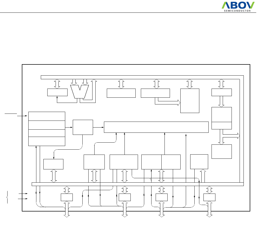
2. BLOCK DIAGRAM
ALU Accumulator Stack Pointer
Interrupt Controller
Data
Memory
10-bit
Converter
A/D
8-bit
Counter
Timer/
Program
Memory
Data Table
PC
8-bit Basic
Timer
Interval
Watch-dog
Timer
Instruction
R0 R1
Buzzer
Driver
PSW
System controller
Timing generator
System
Clock Controller
Clock Generator
RESET
R00 / INT3 / SCK
R01 / AN1 / SI
R02 / AN2 / SOUT
R03 / AN3 / INT2
R04 / AN4 / EC0 / RXD
R05 / AN5 / T0O / TXD
R06 / AN6 / T2O / ACLK
R07 / AN7 / EC1
R10 / AN0 / Avref / PWM1O
R11 / INT0 / PWM3O
R12 / INT1 / BUZO
R13
R14
VDD
VSS
Power
Supply
Decoder
High
PWM
Speed
R3
XOUT / R34
SIO/UART
R31 / AN14
R32 / AN15
XIN / R33
R2
R20
R21
R22
R23 / AN9
R24 / AN10
R25 / AN11
R26 / AN12
R27
R15
R16
R17 / AN8
MC80F0304/08/16
November 4, 2011 Ver 2.12 11
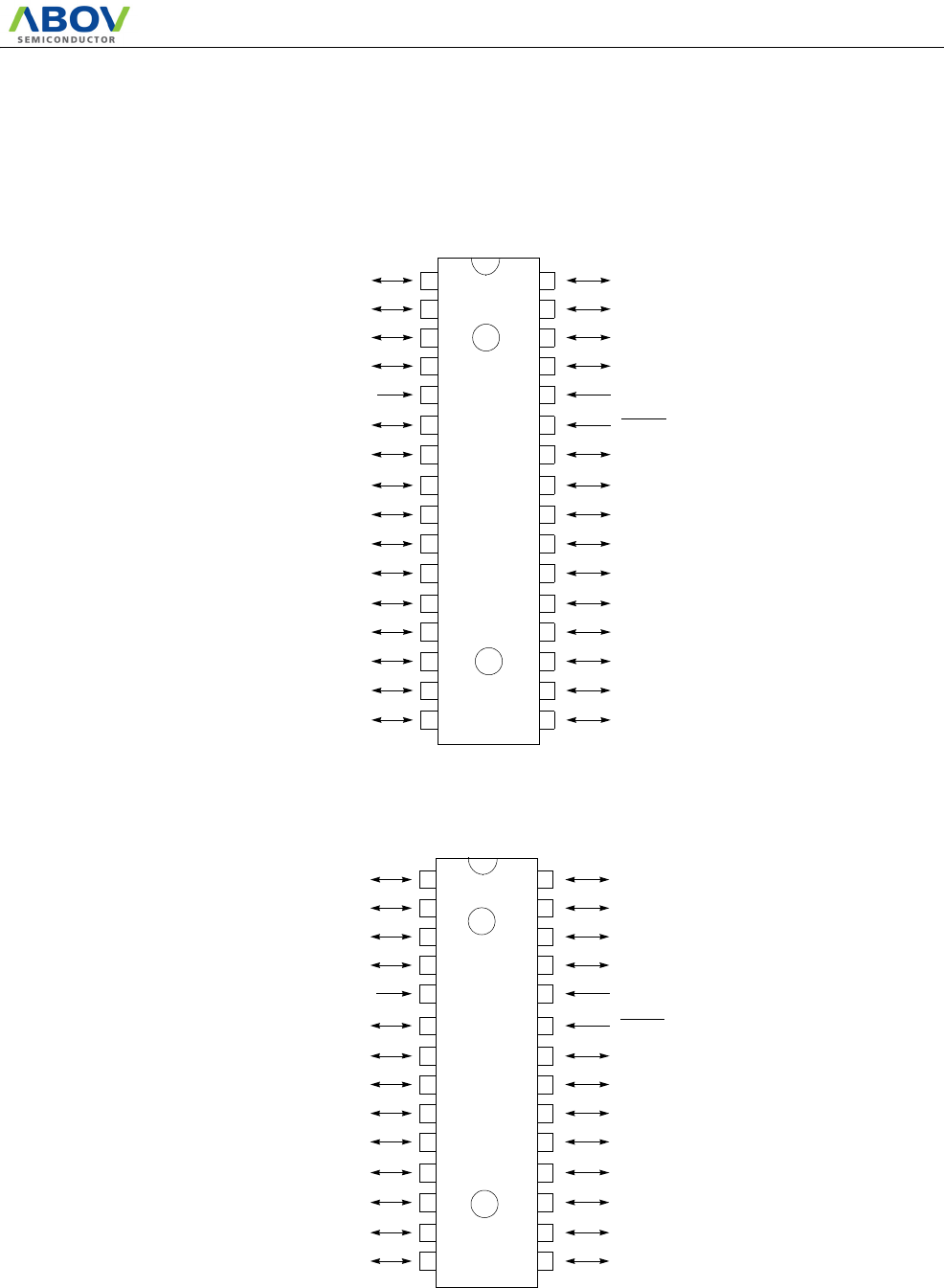
3. PIN ASSIGNMENT
2
3
4
5
6
7
8
27
26
25
24
23
22
21
128
9
10
11
12
13
14
20
19
18
17
16
15
R02 / AN2 / SOUT
R01 / AN1 / SI
R00 / INT3 / SCK
VSS
RESET / R35
XOUT / R34
XIN / R33
R32 / AN15
R31 / AN14
R05 / AN5 / T0O / TXD
R06 / AN6 / T2O / ACLK
R07 / AN7 / EC1
VDD
R10 / AN0 / AVREF / PWM1O
R11 / INT0 / PWM3O
32PDIP
2
3
4
5
6
7
8
9
10
31
30
29
28
27
26
25
24
23
R12 / INT1 / BUZO
R13
R14
R03 / AN3 / INT2R04/AN4 / EC0 / RXD 132
R02 / AN2 / SOUT
R01 / AN1 / SI
R00 / INT3 / SCK
VSS
RESET / R35
XOUT / R34
XIN / R33
R05 / AN5 / T0O / TXD
R06 / AN6 / T2O / ACLK
R07 / AN7 / EC1
VDD
R10 / AN0 / AVREF / PWM1O
R11 / INT0 / PWM3O
R12 / INT1 / BUZO
R03 / AN3 / INT2R04 / AN4 / EC0 / RXD
28 SKDIP/ SOP
11
12
13
14
15
16
22
21
20
19
18
17
R15
R16
R17 / AN8
R20
R21
R22
R13
R14
R15
R17 / AN8
R23 / AN9
R30 / AN13
R27
R26 / AN12
R25 / AN11
R24 / AN10
R23 / AN9
R16
R32 / AN15
R31 / AN14
R30 / AN13
R26 / AN12
R25 / AN11
R24 / AN10
MC80F0304/08/16
12 November 4, 2011 Ver 2.12
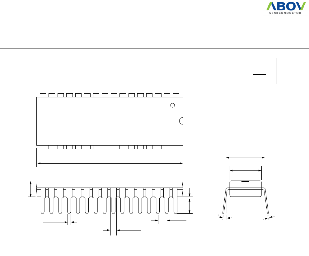
4. PACKAGE DRAWING
1.375
0.015
0.045
TYP 0.100
TYP 0.300
0.300
0.014
0 ~ 15°
MAX 0.180
MIN 0.020
0.120
28 SKINNY DIP unit: inch
MAX
MIN
1.355
0.021
0.140
0.055
0.008
0.275
MC80F0304/08/16
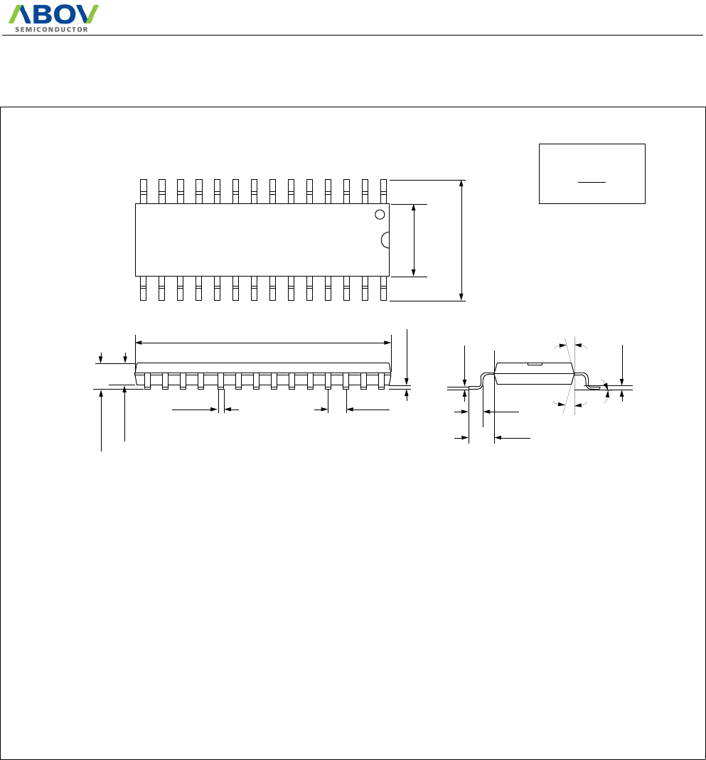
November 4, 2011 Ver 2.12 13
7.501 BSC
10.30 BSC
0.3121.27 BSC 0.40
28 SOP
17.901 BSC
0.5121.27
unit: millimetres
MAX
MIN
0.334
0.204
2.05 MIN
2.65 MAX
0.30 MAX3
1.40 REF
0.25 BSC
SEATING PLANE
GAUGE PLANE
5 ~ 15°
5 ~ 15°
0 ~ 8°
1. 17.90 dimension does not include mold FLASH, protrusions or gate burrs.
2. This dimensions apply to the flat section of the lead between 0.10 to 0.25 mm from the lead tip.
3. This is defined as the vertical distance from the seating plane to the lowers point on the package body
4. This dimensions apply to the flat section of the lead between 0.10 to 0.25 mm from the lead tip.
Mold FLASH, protrusions or gate burrs shall not exceed 0.15mm per end.
7.50 dimension does not include interlead FLASH or protrusion.
Interlead FLASH or protrusion shall not exceed 0.25mm per side.
The package top may be smaller than the package bottom.
17.90 and 7.50 dimensions are determined at the outermost extremes of the plastic body exclusive of mold FLASH.
Tie bar burrs, gate burrs and interlead FLASH, but including any mismatch between the top and bottom of the plastic body.
Dimension does not include dambar protrusion.
Allowable dambar protrusion shall be 0.10 mm total in excess of the dimension maximum material condition.
The dambar may not be located on the lower radius of the foot.
excluding the thermal enhancemet on cavity down package configurations.
MC80F0304/08/16
14 November 4, 2011 Ver 2.12
1.665
0.015
0.045
TYP 0.100
TYP 0.600
0.550
0.012
0 ~ 15°
MAX 0.190
MIN 0.015
0.120
1.645
0.022
0.140
0.065
0.008
0.530
32 PDIP
unit: inch
MAX
MIN
MC80F0304/08/16
November 4, 2011 Ver 2.12 15
7.45
10.20
21.30
2.55
0.35 TYP 1.27
0.20 MIN
0 ~ 8°
0.55
32 SOP
10.60
7.55
21.20
2.35
0.45
0.95
unit: milimeter
MAX
MIN
TYP 0.40
MC80F0304/08/16
16 November 4, 2011 Ver 2.12
5. PIN FUNCTION
VDD: Supply voltage.
VSS: Circuit ground.
RESET: Reset the MCU.
XIN: Input to the inverting oscillator amplifier and input to the in-
ternal main clock operating circuit.
XOUT: Output from the inverting oscillator amplifier.
R00~R07: R0 is an 8-bit, CMOS, bidirectional I/O port. R0 pins
can be used as outputs or inputs according to “1” or “0” written
the their Port Direction Register(R0IO).
In addition, R0 serves the functions of the various special features
in Table 5-1 .
R10~R17: R1 is an 8-bit, CMOS, bidirectional I/O port. R1 pins
can be used as outputs or inputs according to “1” or “0” written
the their Port Direction Register (R1IO).
R1 serves the functions of the various following special features
in Table 5-2
R20~R27 : R2 is an 8-bit, CMOS, bidirectional I/O port. R2 pins
can be used as outputs or inputs according to “1” or “0” written
the their Port Direction Register(R2IO)
In addition, R2 serves the functions of the various special features
in Table 5-3 .
R31~R35: R3 is a 6-bit, CMOS, bidirectional I/O port. R3 pins
can be used as outputs or inputs according to “1” or “0” written
the their Port Direction Register (R3IO).
R3 serves the functions of the serial interface following special
features in Table 5-4 .
Port pin Alternate function
R00
R01
R02
R03
R04
R05
R06
R07
INT3 ( External Interrupt Input Port3 )
SCK ( SPI CLK )
AN1 ( Analog Input Port 1 )
SI (SPI Serial Data Input )
AN2 ( Analog Input Port 2 )
SOUT ( SPI Serial Data Output )
AN3 ( Analog Input Port 3 )
INT2 ( External Interrupt Input Port2 )
AN4 ( Analog Input Port 4 )
EC0 ( Event Counter Input Source 0 )
RXD ( UART Data Input )
AN5 ( Analog Input Port 5 )
T0O (Timer0 Clock Output )
TXD ( UART Data Output )
AN6 ( Analog Input Port 6 )
T2O (Timer2 Clock Output )
ACLK ( UART Clock Input )
AN7 ( Analog Input Port 7 )
EC1 ( Event Counter Input Source 1 )
Table 5-1 R0 Port
Port pin Alternate function
R10
R11
R12
R13
R14
R15
R16
R17
AN0 ( Analog Input Port 0 )
AVref ( External Analog Reference Pin )
PWM1O ( PWM1 Output )
INT0 ( External Interrupt Input Port 0 )
PWM3O ( PWM3 Output )
INT1 ( External Interrupt Input Port 1 )
BUZ ( Buzzer Driving Output Port )
-
-
-
-
AN8( Analog Input Port 8 )
Table 5-2 R1 Port
Port pin Alternate function
R20
R21
R22
R23
R24
R25
R26
R27
-
-
-
AN9 ( Analog Input Port 9 )
AN10 ( Analog Input Port 10 )
AN11 ( Analog Input Port 11 )
AN12 ( Analog Input Port 12 )
-
Table 5-3 R2 Port
Port pin Alternate function
R30
R31
R32
R33
R34
R35
AN13 ( Analog Input Port 13)
AN14 ( Analog Input Port 14 )
AN15 ( Analog Input Port 15 )
XIN ( Oscillation Input )
XOUT ( Oscillation Output )
RESETB ( Reset input port )
Table 5-4 R3 Port
MC80F0304/08/16
November 4, 2011 Ver 2.12 17
PIN NAME
Pin No.
In/Out
Function
32 28 First Second Third Forth
VDD 55 -Supply voltage
VSS 28 24 -Circuit ground
RESET (R35) 27 23 I Reset signal input Input only port - -
XIN (R33) 25 21 IOscillation Input Normal I/O Port - -
XOUT (R34) 26 22 O Oscillation Output Normal I/O Port - -
R00 (INT3/SCK) 29 25 I/O
Normal I/O Ports
External Interrupt 3 SPI clock Input -
R01 (AN1/SI) 30 26 I/O Analog Input Port 1 SPI Data Input -
R02 (AN2/SOUT) 31 27 I/O Analog Input Port 2 SPI Data Output -
R03 (AN3/INT2) 32 28 I/O Analog Input Port 3 External Interrupt2 -
R04 (AN4/EC0/RXD) 1 1 I/O Analog Input Port 4 Event Counter UART RX
R05 (AN5/T0O/TXD) 2 2 I/O Analog Input Port 5 Timer0 Output UART TX
R06 (AN6/T2O/ACLK) 3 3 I/O Analog Input Port 6 Timer2 Output UART Clock
R07 (AN7/EC1) 4 4 I/O Analog Input Port 7 Event Counter -
R10 (AN0/AVref/PWM1O) 6 6 I/O Analog Input Port 0 Analog Reference PWM 1 output
R11 (INT0/PWM3O) 7 7 I/O External Interrupt 0 PWM 3 output -
R12 (INT1/BUZO) 8 8 I/O External Interrupt 1 Buzzer Driving
Output
-
R13 9 9 I/O ---
R14 10 10 I/O ---
R15 11 11 I/O ---
R16 12 12 I/O ---
R17 13 13 I/O Analog Input Port 8 - -
R20 14 - I/O ---
R21 15 - I/O ---
R22 16 - I/O ---
R23 17 14 I/O Analog Input Port 9 - -
R24 18 15 I/O Analog Input Port 10 - -
R25 19 16 I/O Analog Input Port 11 - -
R26 20 17 I/O Analog Input Port 12 - -
R27 21 - I/O ---
R30(AN13) 22 18 I/O Analog Input Port 13 - -
R31 (AN14) 23 19 I/O Analog Input Port 14 - -
R32 (AN15) 24 20 I/O Analog Input Port 15 - -
Table 5-5 Pin Description
MC80F0304/08/16
18 November 4, 2011 Ver 2.12
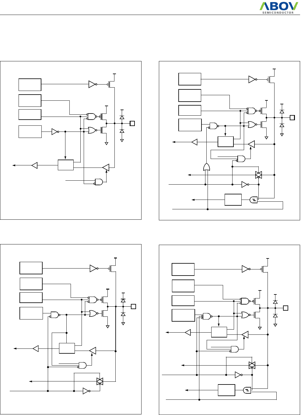
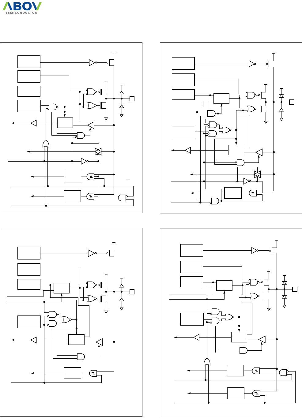
6. PORT STRUCTURES
R13~R16,R20~R22,R27
R17,R30~R32,R23~R26(AN8 ~ AN15)
R01 (AN1 / SI)
R03 (AN3 / INT2), R07 (AN7 / EC1)
VDD
VSS
Pin
Data Reg.
Direction
Reg.
Pull-up
Tr.
Pull-up
Reg.
MUX
VDD
Data Bus
VDD
VSS
Open Drain
Reg.
RD
RD
AN[15:14]
ADEN & ADS[3:0] (ADCM)
VDD
VSS
Pin
Data Reg.
Direction
Reg.
Pull-up
Tr.
Pull-up
Reg.
MUX
VDD
Data Bus
VDD
VSS
Open Drain
Reg.
SI
SI_EN (SIOM)
Noise
Filter
RD
AN[1]
ADEN & ADS[3:0]
VDD
VSS
Pin
Data Reg.
Direction
Reg.
Pull-up
Tr.
Pull-up
Reg.
MUX
VDD
Data Bus
VDD
VSS
Open Drain
Reg.
(ADCM)
INT2, EC1
INT2E (PSR0.2), EC1E (PSR0.5)
Noise
Filter
RD
AN[3, 7]
ADEN & ADS[3:0]
VDD
VSS
Pin
Data Reg.
Direction
Reg.
Pull-up
Tr.
Pull-up
Reg.
MUX
VDD
Data Bus
VDD
VSS
Open Drain
Reg.
(ADCM)
MC80F0304/08/16
November 4, 2011 Ver 2.12 19
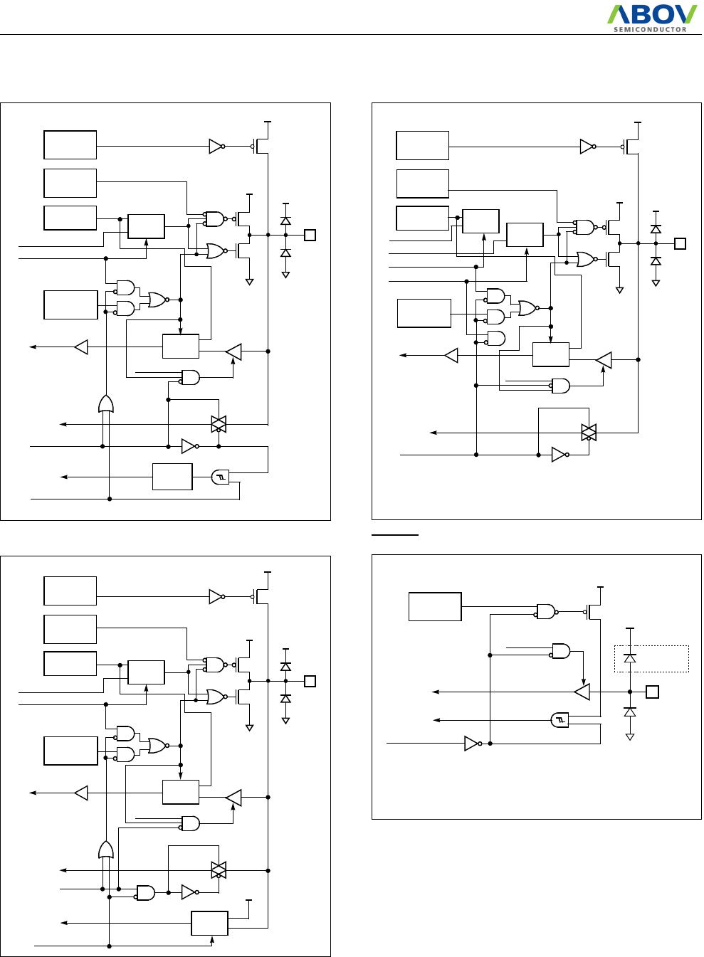
R04 (AN4 / EC0 / RXD)
R11 (INT0 / PWM3O), R12 (INT1 / BUZO)
R02 (AN2 / SOUT)
R00 (INT3 / SCK)
EC0
EC0E (PSR0)
Noise
Filter
RD
AN[1]
ADEN & ADS[3:0]
VDD
VSS
Pin
Data Reg.
Direction
Reg.
Pull-up
Tr.
Pull-up
Reg.
MUX
VDD
Data Bus
VDD
VSS
Open Drain
Reg.
(ADCM)
RXD
RXE (ASIMR)
Noise
Filter
INT0,INT1
INT0E(PSR0.0)
Noise
Filter
RD
VDD
VSS
Pin
Data Reg.
Direction
Reg.
Pull-up
Tr.
Pull-up
Reg.
MUX
VDD
Data Bus
VDD
VSS
Open Drain
Reg.
INT1E(PSR0.1)
MUX
PWM3OE(PSR0.7)
BUZOE(PSR1.2)
PWM3O, BUZO
SOUT(SI)
SO_OUT_EN (SIOM)
Noise
Filter
RD
VDD
VSS
Pin
Data Reg.
Direction
Reg.
Pull-up
Tr.
Pull-up
Reg.
MUX
VDD
Data Bus
VDD
VSS
Open Drain
Reg.
MUX
SO_EN(SIOM)
SOUT
AN[2]
ADEN & ADS[3:0]
(ADCM)
SCK
SCK_EN(SIOM)
Noise
Filter
RD
VDD
VSS
Pin
Data Reg.
Direction
Reg.
Pull-up
Tr.
Pull-up
Reg.
MUX
VDD
Data Bus
VDD
VSS
Open Drain
Reg.
MUX
SCKO_EN(SIOM)
SCK
INT3
INT3E(PSR0.3)
Noise
Filter
MC80F0304/08/16
20 November 4, 2011 Ver 2.12
R06 (AN6 / T2O / ACLK)
R10 (AN0 / AVREF / PWM1O)
R05 (AN5 / T0O / TXD)
RESET
AN[6]
ADEN & ADS[3:0]
RD
VDD
VSS
Pin
Data Reg.
Direction
Reg.
Pull-up
Tr.
Pull-up
Reg.
MUX
VDD
Data Bus
VDD
VSS
Open Drain
Reg.
MUX
T2OE(PSR1.1)
T2O
ACLK
TPS[2:0](BRGCR[6:4])
Noise
Filter
(ADCM)
AN[0]
ADEN & ADS[3:0]
RD
VDD
VSS
Pin
Data Reg.
Direction
Reg.
Pull-up
Tr.
Pull-up
Reg.
MUX
VDD
Data Bus
VDD
VSS
Open Drain
Reg.
MUX
PWM1OE(PSR0.6)
PWM1O
ADC Reference
AVREFS(PSR1.3)
(ADCM)
MUX
VDD
Voltage Input
AN[5]
ADEN & ADS[3:0]
RD
VDD
VSS
Pin
Data Reg.
Direction
Reg.
Pull-up
Tr.
Pull-up
Reg.
MUX
VDD
Data Bus
VDD
VSS
Open Drain
Reg.
MUX
T0OE(PSR1.0)
TXD
(ADCM)
MUX
T0O
TXE(ASIMR.7)
Pin
VDD
VSS
Data Bus
Mask only
Pull-up
Tr.
Pull-up
Reg.
VDD
RD
Internal Reset
Reset Disable
(Configuration option bit)
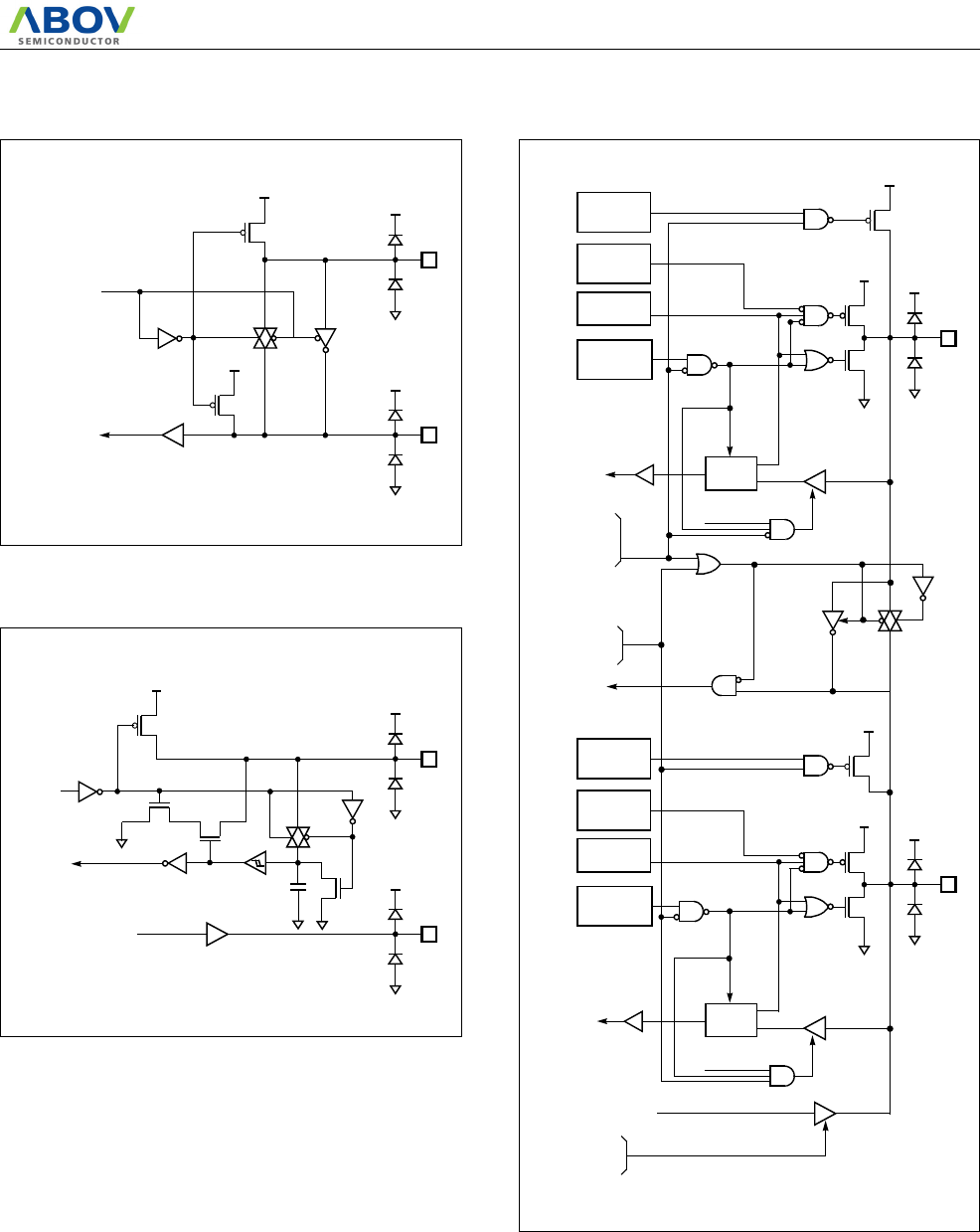
MC80F0304/08/16
November 4, 2011 Ver 2.12 21
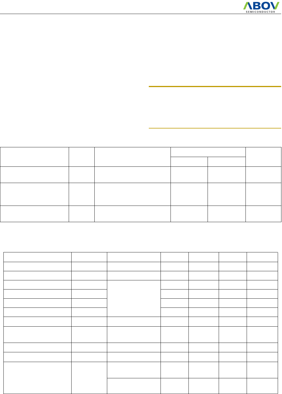
XIN, XOUT (Crystal or Ceramic Resonator)
XIN, XOUT (External RC or R oscillation)
R33 (XIN), R34 (XOUT)
VDD
VSS
VDD
VSS
VDD
VDD
STOP
MAIN
CLOCK
XIN
XOUT
XIN
VDD
VSS
XOUT
VDD
VSS
VDD
STOP
MAIN
CLOCK
fXIN ÷ 4
RD
VDD
VSS
Data Reg.
Direction
Reg.
Pull-up
Tr.
Pull-up
Reg.
MUX
VDD
Data Bus
VDD
VSS
Open Drain
Reg.
RD
VDD
VSS
XOUT
Data Reg.
Direction
Reg.
Pull-up
Tr.
Pull-up
Reg.
MUX
VDD
Data Bus
VDD
VSS
Open Drain
Reg.
System Clock ÷ 4
IN4MCLKXO
IN2MCLKCO
EXRCXO
CLOCK option
(Configuration option bit)
IN4MCLKXO
IN2MCLKXO
CLOCK option
(Configuration
option bit)
/ R34
XIN
/ R33
Main Clock
(to ONP Block)
IN4MCLK
IN2MCLK
IN4MCLK
IN2MCLK
EXRC
MC80F0304/08/16
22 November 4, 2011 Ver 2.12
7. ELECTRICAL CHARACE TERISTICS
7.1 Absolute Maximum Ratings
Supply voltage........................................................ -0.3 to +6.0 V
Storage Temperature .............................................-65 to +150 °C
Voltage on any pin with respect to Ground (VSS)
..........................................................................-0.3 to VDD+0.3V
Maximum current out of VSS pin.....................................200 mA
Maximum current into VDD pin.......................................100 mA
Maximum current sunk by (IOL per I/O Pin) .....................20 mA
Maximum output current sourced by (IOH per I/O Pin)
............................................................................................10 mA
Maximum current (ΣIOL) .................................................160 mA
Maximum current (ΣIOH)...................................................80 mA
Note: Stresses above those listed under “Absolute Maximum
Ratings” may cause permanent damage to the device. This is a
stress rating only and functional operation of the device at any oth-
er conditions above those indicated in the operational sections of
this specification is not implied. Exposure to absolute maximum
rating conditions for extended periods may affect device reliability.
7.2 Recommended Operating Conditions
7.3 A/D Converter Characteristics
(Ta=-40~85°C, VSS=0V, VDD=2.7~5.5V @fXIN=8MHz)
Parameter Symbol Condition
Specifications
Unit
Min. Max.
Supply Voltage VDD
fXIN=1~12MHz
fXIN=1~8MHz
4.5
2.7
5.5
5.5 V
Operating Frequency fXIN
VDD=4.5~5.5V
VDD=2.7~5.5V(MC80F03XXX)
VDD=2.0~5.5V(MC80C03XXX)
1
1
1
12
8
4.2
MHz
Operating Temperature TOPR
VDD =2.7~5.5V(MC80F03XXX)
VDD =2.0~5.5V(MC80C03XXX) -40 85 °C
Parameter Symbol Conditions Min. Typ. Max. Unit
Resolution - - 10 - BIT
Overall Accuracy - - - - ±3LSB
Integral Linearity Error ILE
VDD = AVREF = 5V
CPU Clock = 10MHz
VSS = 0V
-−±3LSB
Differential Linearity Error DLE - −±3LSB
Offset Error of Top EOT - ±1±3LSB
Offset Error of Bottom EOB - ±0.5 ±3LSB
Conversion Time TCONV -13--μS
Analog Input Voltage VAIN -VSS -VDD
(AVREF)V
Analog Reference Voltage AVREF -TBD-
VDD V
Analog Input Current IAIN VDD = AVREF = 5V --10μA
Analog Block Current IAVDD
VDD = AVREF = 5V
VDD = AVREF = 3V
-
-
1
0.5
3
1.5 mA
VDD = AVREF = 5V
power down mode - 100 500 nA
MC80F0304/08/16
November 4, 2011 Ver 2.12 23
7.4 DC Electrical Characteristics
(TA=-40~85°C, VDD=5.0V, VSS=0V),
Parameter Symbol Pin Condition
Specifications
Unit
Min. Typ. Max.
Input High Voltage
VIH1 XIN, RESET 0.8 VDD -VDD
V
VIH2 Hysteresis Input10.8 VDD -VDD
VIH3 Normal Input 0.7 VDD -VDD
Input Low Voltage
VIL1 XIN, RESET 0-
0.2 VDD
V
VIL2 Hysteresis Input10-
0.2 VDD
VIL3 Normal Input 0 - 0.3 VDD
Output High Voltage VOH All Output Port VDD=5V, IOH=-5mA VDD -1 --V
Output Low Voltage VOL All Output Port VDD=5V, IOL=10mA --1V
Input Pull-up Current IPNormal Input VDD=5V -60 - -150 μA
Input High
Leakage Current
IIH1 All Pins (except XIN)V
DD=5V --5μA
IIH2 XIN VDD=5V -1220μA
Input Low
Leakage Current
IIL1 All Pins (except XIN)V
DD=5V -5 - - μA
IIL2 XIN VDD=5V -20 -12 - μA
Hysteresis | VT | Hysteresis Input1VDD=5V 0.5 - - V
PFD Voltage VPFD VDD 2.4 2.9 3.4 V
POR Voltage2VPOR VDD 2.2 2.7 3.2 V
POR Start Voltage2VSTART VDD --1.9V
POR Rising Time2TPOR VDD --40ms/V
VDD Rising Time2TVDD VDD --40ms/V
Internal RC WDT
Period TRCWDT XOUT VDD=5.5V 36 - 90 μS
Operating Current IDD VDD VDD=5.5V, fXIN=12MHz --15mA
Sleep Mode Current ISLEEP VDD VDD=5.5V, fXIN=12MHz --4.5mA
RCWDT Mode Cur-
rent at Stop Mode IRCWDT VDD VDD=5.5V --50μA
Stop Mode Current ISTOP VDD VDD=5.5V, fXIN=12MHz --5μA
Internal Oscillation
Frequency fIN_CLK XOUT VDD=5V 345MHz
RESET Input Noise
Cancel Time TRST_NC RESET VDD=5V 1.5 1.8 μs
External RC2
Oscillator Frequency
fRC-OSC fXOUT = fRC-OSC ÷ 4 VDD=5.5V
R=30kΩ, C=10pF 2.2 MHz
fR-OSC fXOUT = fR-OSC ÷ 4V
DD=5.5V, R=30kΩ1.6 MHz
1. Hysteresis Input: INT0 ~INT3(R11,R12,R03,R00),SIO(R00,R01,R02),UART(R04,R06),EC0,EC1
2. These parameters are presented for design guidance only and not tested or guaranteed.
MC80F0304/08/16
24 November 4, 2011 Ver 2.12
7.5 AC Characteristics
(TA=-40~+85°C, VDD=5V±10%, VSS=0V)
Figure 7-1 Timing Chart
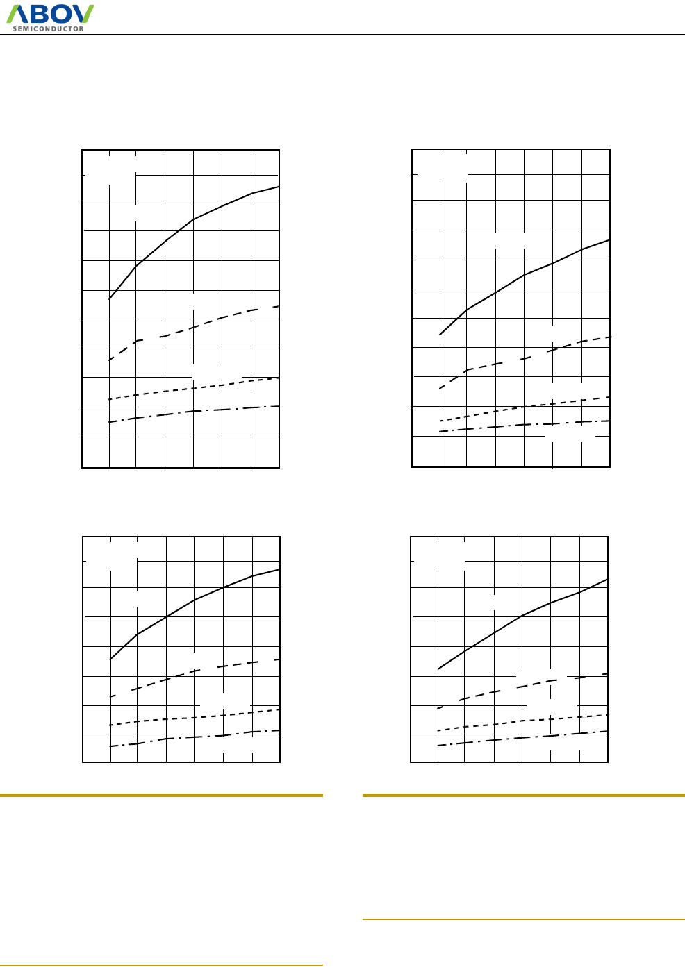
7.6 Typical Characteristics (MC80F0304/08/16)
These graphs and tables provided in this section are for design
guidance only and are not tested or guaranteed.
In some graphs or tables the data presented are out-
side specified operating range (e.g. outside specified
VDD range). This is for information only and devices
are guaranteed to operate properly only within the
specified range.
The data presented in this section is a statistical summary of data
collected on units from different lots over a period of time. “Typ-
ical” represents the mean of the distribution while “max” or
“min” represents (mean + 3σ) and (mean − 3σ) respectively
where σ is standard deviation
Parameter Symbol Pins
Specifications
Unit
Min. Typ. Max.
Operating Frequency fCP XIN 1-8MHz
External Clock Pulse Width tCPW XIN 50 - - nS
External Clock Transition Time tRCP,tFCP XIN --20nS
Oscillation Stabilizing Time tST XIN, XOUT --20mS
External Input Pulse Width tEPW INT0, INT1, INT2, INT3
EC0, EC1 2--
tSYS
RESET Input Width tRST RESET 8--
tSYS
tRCP tFCP
XIN
INT0, INT1
INT2,
0.5V
VDD-0.5V
0.2VDD
RESET
0.2VDD
0.8VDD
EC0,
tRST
tEPW
tEPW
1/fCP
tCPW tCPW
tSYS
INT3
EC1
MC80F0304/08/16
November 4, 2011 Ver 2.12 25
Ta= 25°C
Ta=25°C
IDD−VDD
10
6
4
2
0
(mA)
IDD
2345
6
VDD
(V)
Normal Operation
8
6
4
2
0
(MHz)
fXIN
23456
VDD
(V)
Operating Area
fXIN=12MHz
10
ISLEEP−VDD
2.0
1.5
1.0
0.5
0
(mA)
IDD
2345
6
VDD
(V)
SLEEP Mode
IRCWDT−VDD
20
15
10
5
0
(μA)
IDD
2345
6
VDD
(V)
RC-WDT in Stop Mode
Ta=25°C
fXIN = 12MHz
Ta=25°C
ISTOP−VDD
2
1.5
1
0.5
0
(μA)
IDD
2345
VDD
(V)
STOP Mode
Ta=25°C
TRCWDT = 50uS
12
14
16
8
12
MC80F0304/08/16
26 November 4, 2011 Ver 2.12
IOL−VOL, VDD=5V
20
15
10
5
0
(mA)
IOL
VOL
(V)
IOH−VOH, VDD=5V
-20
-15
-10
-5
0
(mA)
IOH
3.5 4 4.5 5
VOH
(V)
0.5 1 1.5 2
fXIN=4MHz
VDD−VIH1
4
3
2
1
0
(V)
VIH1
2345
6
VDD
(V)
VDD−VIH2
4
3
2
1
0
(V)
VIH2
2345
6
VDD
(V)
Ta=25°C
f
XIN
=4kHz
Ta=25°C
1
XIN, RESET Hysteresis input
-25°C
85°C
25°C
-25°C
85°C
25°C
VDD−VIH3
4
3
2
1
0
(V)
VIH3
2345
6
VDD
(V)
f
XIN
=4kHz
Ta=25°C
Normal input
fXIN=4MHz
VDD−VIL1
4
3
2
1
0
(V)
VIL1
2345
6
VDD
(V)
VDD−VIL2
4
3
2
1
0
(V)
VIL2
2345
6
VDD
(V)
Ta=25°C
f
XIN
=4kHz
Ta=25°C
1
XIN, RESET Hysteresis input VDD−VIL3
4
3
2
1
0
(V)
VIL3
2345
6
VDD
(V)
f
XIN
=4kHz
Ta=25°C
Normal input
MC80F0304/08/16
November 4, 2011 Ver 2.12 27
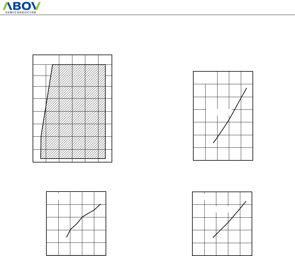
Note: The external RC oscillation frequencies shown in
above are provided for design guidance only and not tested
or guaranteed. The user needs to take into account that the
external RC oscillation frequencies generated by the same
circuit design may be not the same. Because there are vari-
ations in the resistance and capacitance due to the toler-
ance of external R and C components. The parasitic
capacitance difference due to the different wiring length
and layout may change the external RC oscillation frequen-
cies.
Note: The external RC oscillation frequencies of the
MC80F0304/0308/0316 may be different from that of the
MC80C0304/0308/0316. There may be the difference be-
tween package types(PDIP, SOP, SKDIP). The user should
modify the value of R and C components to get the proper
frequency in exchanging Flash device to Mask device or
one package type to another package type.
Typical RC Oscillator
Frequency vs VDD
Typical RC Oscillator
Frequency vs VDD
Typical RC Oscillator
Frequency vs VDD
Typical RC Oscillator
Frequency vs VDD
4
3
2
1
0
(MHz)
FOSC
2.5 3.0 3.5 4.0 4.5
VDD
(V)
5
5.0 5.5
R = 4.7K
R = 10K
R = 20K
R = 30K
Ta = 25°C
No Cap
10
9
8
7
6
4
3
2
1
0
(MHz)
FOSC
2.5 3.0 3.5 4.0 4.5
VDD
(V)
5
5.0 5.5
R = 4.7K
R = 10K
R = 20K
R = 30K
10
9
8
7
6
Ta = 25°C
CEXT = 10pF
1
0
(MHz)
FOSC
2.5 3.0 3.5 4.0 4.5
VDD
(V)
2
5.0 5.5
R = 4.7K
R = 10K
R = 20K
R = 30K
Ta = 25°C
CEXT = 20pF
7
6
5
4
3
1
0
(MHz)
FOSC
2.5 3.0 3.5 4.0 4.5
VDD
(V)
2
5.0 5.5
R = 4.7K
R = 20K
R = 30K
Ta = 25°C
CEXT = 30pF
7
6
5
4
3R = 10K

MC80F0304/08/16
28 November 4, 2011 Ver 2.12
Note: The internal 4MHz oscillation frequencies shown in
above are provided for design guidance only and not tested
or guaranteed. The user needs to take into account that the
internal oscillation of the MC80F0308 may show different
frequency with sample by sample, voltage and tempera-
ture. The internal oscillation can be used only in timing in-
sensitive application.
7.7 Typical Characteristics (MC80C0304/08/16)
These graphs and tables provided in this section are for design
guidance only and are not tested or guaranteed.
In some graphs or tables the data presented are out-
side specified operating range (e.g. outside specified
VDD range). This is for information only and devices
are guaranteed to operate properly only within the
specified range.
The data presented in this section is a statistical summary of data
collected on units from different lots over a period of time. “Typ-
ical” represents the mean of the distribution while “max” or
“min” represents (mean + 3σ) and (mean − 3σ) respectively
where σ is standard deviation
Typical Internal 4MHz
Frequency vs VDD
3
(MHz)
FOSC
2.5 3.0 3.5 4.0 4.5
VDD
(V)
3.5
5.0 5.5
Ta = 25°C
4.5
4
MC80F0304/08/16
November 4, 2011 Ver 2.12 29
Ta= 25°C
Ta=25°C
IDD−VDD
4
3
2
7
(mA)
IDD
2345
6
VDD
(V)
Normal Operation
8
6
4
2
0
(MHz)
fXIN
23456
VDD
(V)
Operating Area
fXIN=12MHz
10
ISLEEP−VDD
2.0
1.5
1.0
0.5
0
(mA)
IDD
2345
6
VDD
(V)
SLEEP Mode
Ta=25°C
fXIN = 12MHz
ISTOP−VDD
0.8
0.6
0.4
0.2
0
(μA)
IDD
2345
VDD
(V)
STOP Mode
Ta=25°C
12
14
16
6
5

MC80F0304/08/16
30 November 4, 2011 Ver 2.12
IOL−VOL, VDD=5V
20
15
10
5
0
(mA)
IOL
VOL
(V)
IOH−VOH, VDD=5V
-20
-15
-10
-5
0
(mA)
IOH
3.5 4 4.5 5
VOH
(V)
0.5 1 1.5 2
fXIN=4MHz
VDD−VIH1
4
3
2
1
0
(V)
VIH1
2345
6
VDD
(V)
VDD−VIH2
4
3
2
1
0
(V)
VIH2
2345
6
VDD
(V)
Ta=25°C
f
XIN
=4kHz
Ta=25°C
1
XIN, RESET Hysteresis input
-25°C
85°C
25°C
-25°C
85°C
25°C
VDD−VIH3
4
3
2
1
0
(V)
VIH3
2345
6
VDD
(V)
f
XIN
=4kHz
Ta=25°C
Normal input
fXIN=4MHz
VDD−VIL1
4
3
2
1
0
(V)
VIL1
2345
6
VDD
(V)
VDD−VIL2
4
3
2
1
0
(V)
VIL2
2345
6
VDD
(V)
Ta=25°C
f
XIN
=4kHz
Ta=25°C
1
XIN, RESET Hysteresis input VDD−VIL3
4
3
2
1
0
(V)
VIL3
2345
6
VDD
(V)
f
XIN
=4kHz
Ta=25°C
Normal input

MC80F0304/08/16
November 4, 2011 Ver 2.12 31
Note: The internal 4MHz oscillation frequencies shown in
above are provided for design guidance only and not tested
or guaranteed. The user needs to take into account that the
internal oscillation of the MC80C0104 or MC80C0204 may
show different frequency with sample by sample, voltage
and temperature. The internal oscillation can be used only
in timing insensitive application.
Typical Internal 4MHz
Frequency vs VDD
3.5
(MHz)
FOSC
2.5 3.0 3.5 4.0 4.5
VDD
(V)
4
5.0 5.5
Ta = 25°C
5
4.5
MC80F0304/08/16
32 November 4, 2011 Ver 2.12
8. MEMORY ORGANIZATION
The MC80F0304/0308/0316 has separate address spaces for Pro-
gram memory and Data Memory. 4K bytes program memory can
only be read, not written to.
Data memory can be read and written to up to 256 bytes including
the stack area.
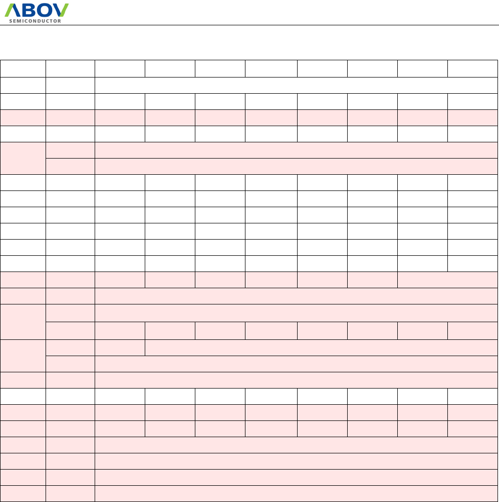
8.1 Registers
This device has six registers that are the Program Counter (PC),
a Accumulator (A), two index registers (X, Y), the Stack Pointer
(SP), and the Program Status Word (PSW). The Program Counter
consists of 16-bit register.
Figure 8-1 Configuration of Registers
Accumulator: The Accumulator is the 8-bit general purpose reg-
ister, used for data operation such as transfer, temporary saving,
and conditional judgement, etc.
The Accumulator can be used as a 16-bit register with Y Register
as shown below.
Figure 8-2 Configuration of YA 16-bit Register
X, Y Registers: In the addressing mode which uses these index
registers, the register contents are added to the specified address,
which becomes the actual address. These modes are extremely ef-
fective for referencing subroutine tables and memory tables. The
index registers also have increment, decrement, comparison and
data transfer functions, and they can be used as simple accumula-
tors.
Stack Pointer: The Stack Pointer is an 8-bit register used for oc-
currence interrupts and calling out subroutines. Stack Pointer
identifies the location in the stack to be accessed (save or restore).
Generally, SP is automatically updated when a subroutine call is
executed or an interrupt is accepted. However, if it is used in ex-
cess of the stack area permitted by the data memory allocating
configuration, the user-processed data may be lost.
The stack can be located at any position within 1C0H to 1FFH of
the internal data memory. The SP is not initialized by hardware,
requiring to write the initial value (the location with which the use
of the stack starts) by using the initialization routine. Normally,
the initial value of “FFH” is used.
Note: The Stack Pointer must be initialized by software be-
cause its value is undefined after Reset.
Example: To initialize the SP
LDX #0FFH
TXSP ; SP ← FFH
Program Counter: The Program Counter is a 16-bit wide which
consists of two 8-bit registers, PCH and PCL. This counter indi-
cates the address of the next instruction to be executed. In reset
state, the program counter has reset routine address (PCH:0FFH,
PCL:0FEH).
Program Status Word: The Program Status Word (PSW) con-
tains several bits that reflect the current state of the CPU. The
PSW is described in Figure 8-3 . It contains the Negative flag, the
Overflow flag, the Break flag the Half Carry (for BCD opera-
tion), the Interrupt enable flag, the Zero flag, and the Carry flag.
[Carry flag C]
This flag stores any carry or borrow from the ALU of CPU after
an arithmetic operation and is also changed by the Shift Instruc-
tion or Rotate Instruction.
[Zero flag Z]
This flag is set when the result of an arithmetic operation or data
transfer is “0” and is cleared by any other result.
ACCUMULATOR
X REGISTER
Y REGISTER
STACK POINTER
PROGRAM COUNTER
PROGRAM STATUS WORD
X
A
SP
Y
PCL
PSW
PCH
Two 8-bit Registers can be used as a “YA” 16-bit Register
Y
A
Y A
SP
01H
Stack Address (1C0H ~ 1FFH)
Bit 15 Bit 087
Hardware fixed
C0H~FFH
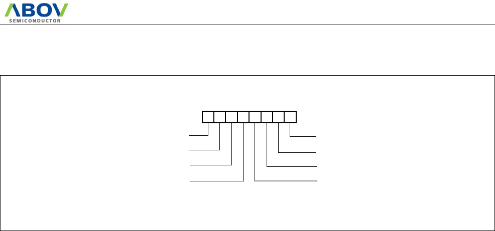
MC80F0304/08/16
November 4, 2011 Ver 2.12 33
Figure 8-3 PSW (Program Status Word) Register
[Interrupt disable flag I]
This flag enables/disables all interrupts except interrupt caused
by Reset or software BRK instruction. All interrupts are disabled
when cleared to “0”. This flag immediately becomes “0” when an
interrupt is served. It is set by the EI instruction and cleared by
the DI instruction.
[Half carry flag H]
After operation, this is set when there is a carry from bit 3 of ALU
or there is no borrow from bit 4 of ALU. This bit can not be set
or cleared except CLRV instruction with Overflow flag (V).
[Break flag B]
This flag is set by software BRK instruction to distinguish BRK
from TCALL instruction with the same vector address.
[Direct page flag G]
This flag assigns RAM page for direct addressing mode. In the di-
rect addressing mode, addressing area is from zero page 00H to
0FFH when this flag is "0". If it is set to "1", addressing area is
assigned 100H to 1FFH. It is set by SETG instruction and cleared
by CLRG.
[Overflow flag V]
This flag is set to “1” when an overflow occurs as the result of an
arithmetic operation involving signs. An overflow occurs when
the result of an addition or subtraction exceeds +127(7FH) or -
128(80H). The CLRV instruction clears the overflow flag. There
is no set instruction. When the BIT instruction is executed, bit 6
of memory is copied to this flag.
[Negative flag N]
This flag is set to match the sign bit (bit 7) status of the result of
a data or arithmetic operation. When the BIT instruction is exe-
cuted, bit 7 of memory is copied to this flag.
N
NEGATIVE FLAG
V G B H I Z C
MSB LSB
RESET VALUE: 00H
PSW
OVERFLOW FLAG
BRK FLAG
CARRY FLAG RECEIVES
ZERO FLAG
INTERRUPT ENABLE FLAG
CARRY OUT
HALF CARRY FLAG RECEIVES
CARRY OUT FROM BIT 1 OF
ADDITION OPERLANDS
SELECT DIRECT PAGE
when G=1, page is selected to “page 1”
MC80F0304/08/16
34 November 4, 2011 Ver 2.12
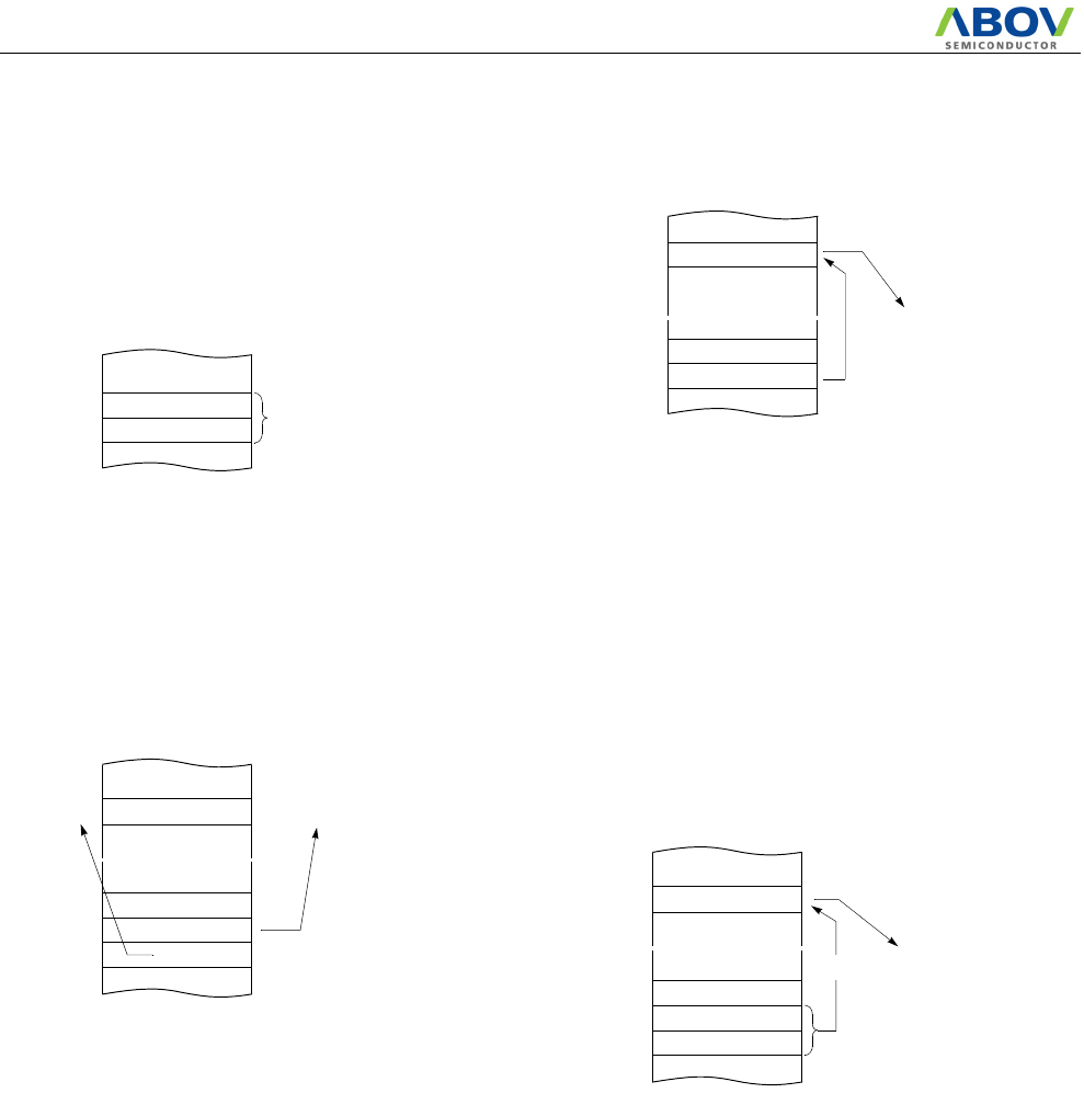
Figure 8-4 Stack Operation
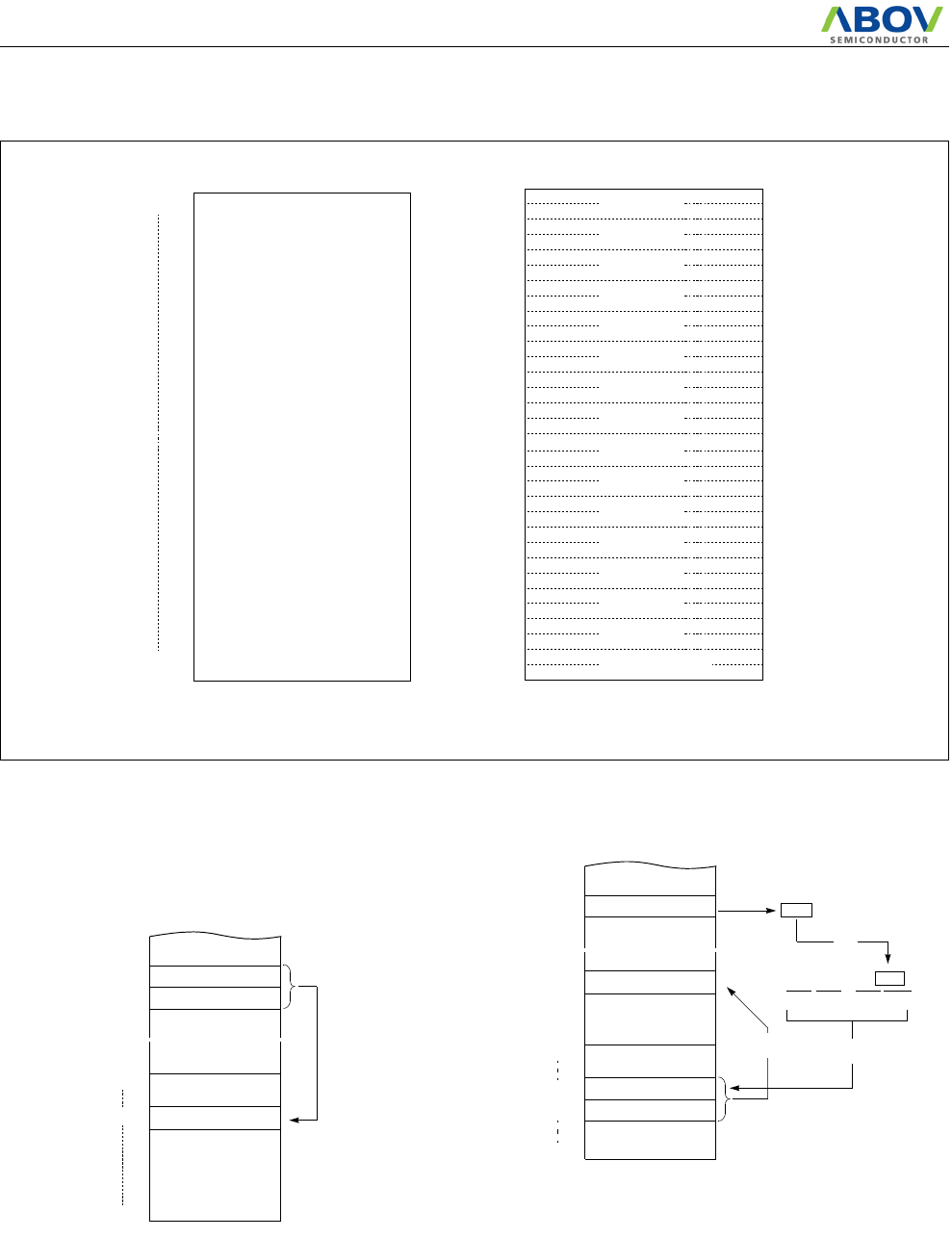
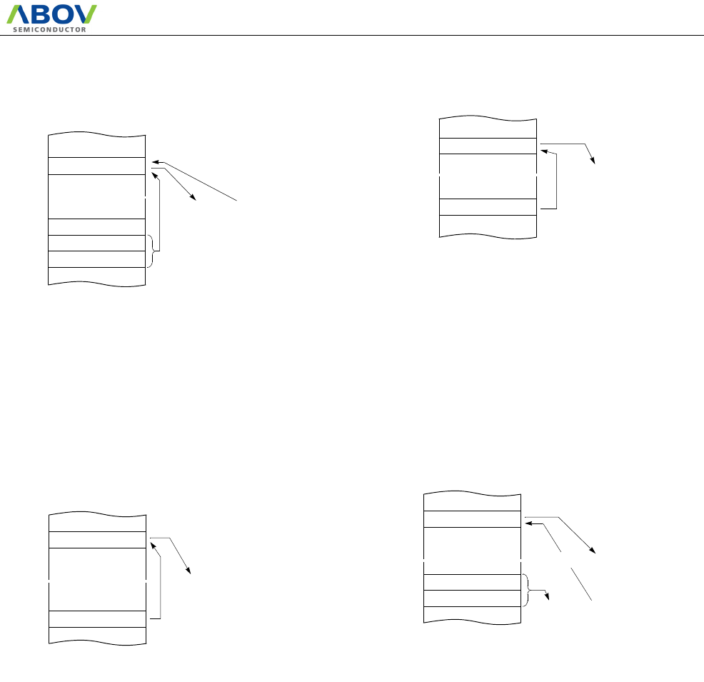
8.2 Program Memory
A 16-bit program counter is capable of addressing up to 64K
bytes, but this device has 4K/8K/16K bytes program memory
space only physically implemented. Accessing a location above
FFFFH will cause a wrap-around to 0000H.
Figure 8-5 , shows a map of Program Memory. After reset, the
CPU begins execution from reset vector which is stored in ad-
dress FFFEH and FFFFH as shown in Figure 8-6 .
As shown in Figure 8-5 , each area is assigned a fixed location in
Program Memory. Program Memory area contains the user pro-
gram
Figure 8-5 Program Memory Map
Page Call (PCALL) area contains subroutine program to reduce
At execution of
a CALL/TCALL/PCALL
PCL
PCH
01FC
SP after
execution
SP before
execution
01FD
01FD
01FE
01FF
01FF
Push
down
At acceptance
of interrupt
PCL
PCH
01FC
01FC
01FD
01FE
01FF
01FF
Push
down
PSW
At execution
of RET instruction
PCL
PCH
01FC
01FF
01FD
01FE
01FF
01FD
Pop
up
At execution
of RET instruction
PCL
PCH
01FC
01FF
01FD
01FE
01FF
01FC
Pop
up
PSW
0100H
01FFH
Stack
depth
At execution
of PUSH instruction
A
01FC
01FE
01FD
01FE
01FF
01FF
Push
down
SP after
execution
SP before
execution
PUSH A (X,Y,PSW)
At execution
of POP instruction
A
01FC
01FF
01FD
01FE
01FF
01FE
Pop
up
POP A (X,Y,PSW)
Interrupt
Vector Area
FEFFH
FF00H
FFC0H
FFDFH
FFE0H
FFFFH
PCALL area
C000H
TCALL area
8K ROM
4K ROM
16K ROM
E000H
F000H
MC80F0304/08/16
November 4, 2011 Ver 2.12 35
program byte length by using 2 bytes PCALL instead of 3 bytes
CALL instruction. If it is frequently called, it is more useful to
save program byte length.
Table Call (TCALL) causes the CPU to jump to each TCALL ad-
dress, where it commences the execution of the service routine.
The Table Call service area spaces 2-byte for every TCALL:
0FFC0H for TCALL15, 0FFC2H for TCALL14, etc., as shown in
Figure 8-7 .
Example: Usage of TCALL
The interrupt causes the CPU to jump to specific location, where
it commences the execution of the service routine. The External
interrupt 0, for example, is assigned to location 0FFFCH. The in-
terrupt service locations spaces 2-byte interval: 0FFFAH and
0FFFBH for External Interrupt 1, 0FFFCH and 0FFFDH for Ex-
ternal Interrupt 0, etc.
Any area from 0FF00H to 0FFFFH, if it is not going to be used,
its service location is available as general purpose Program Mem-
ory.
Figure 8-6 Interrupt Vector Area
LDA #5
TCALL 0FH ;
1BYTE INSTRUCTION
:;
INSTEAD OF 3 BYTES
:;
NORMAL CALL
;
;TABLE CALL ROUTINE
;
FUNC_A: LDA LRG0
RET
;
FUNC_B: LDA LRG1
RET
;
;TABLE CALL ADD. AREA
;
ORG 0FFC0H ;
TCALL ADDRESS AREA
DW FUNC_A
DW FUNC_B
1
2
0FFE0H
E2
Address Vector Area Memory
E4
E6
E8
EA
EC
EE
F0
F2
F4
F6
F8
FA
FC
FE
Basic Interval Timer
Watchdog Timer Interrupt
A/D Converter
-
External Interrupt 3
Serial Input/Output (SIO)
External Interrupt 1
External Interrupt 0
RESET
External Interrupt 2
Timer/Counter 3 Interrupt
Timer/Counter 0 Interrupt
UART Rx interrupt
UART Tx interrupt
Timer/Counter 1 Interrupt
Timer/Counter 2 Interrupt
MC80F0304/08/16
36 November 4, 2011 Ver 2.12
Figure 8-7 PCALL and TCALL Memory Area
PCALL→ rel
4F35 PCALL 35H
TCALL→ n
4A TCALL 4
Example: The usage software example of Vector address
0FFC0H
C1
Address Program Memory
C2
C3
C4
C5
C6
C7
C8
0FF00H
Address PCALL Area Memory
0FFFFH
PCALL Area
(256 Bytes)
* means that the BRK software interrupt is using
same address with TCALL0.
NOTE:
TCALL 15
TCALL 14
TCALL 13
TCALL 12
TCALL 11
TCALL 10
TCALL 9
TCALL 8
TCALL 7
TCALL 6
TCALL 5
TCALL 4
TCALL 3
TCALL 2
TCALL 1
TCALL 0 / BRK *
C9
CA
CB
CC
CD
CE
CF
D0
D1
D2
D3
D4
D5
D6
D7
D8
D9
DA
DB
DC
DD
DE
DF
4F
~
~~
~
NEXT
35
0FF35H
0FF00H
0FFFFH
11111111 11010110
01001010
PC:
FH FH DH 6H
4A
~
~~
~
25
0FFD6H
0FF00H
0FFFFH
D1
NEXT
0FFD7H
þ
À
Ã
0D125H
Reverse
MC80F0304/08/16
November 4, 2011 Ver 2.12 37
8.3 Data Memory
Figure 8-8 shows the internal Data Memory space available.
Data Memory is divided into three groups, a user RAM, control
registers, and Stack memory.
Figure 8-8 Data Memory Map
User Memory
The MC80F0304/0308/0316 has 512 × 8 bits for the user memory
(RAM). RAM pages are selected by RPR (See Figure 8-9 ).
Note: After setting RPR(RAM Page Select Register), be
sure to execute SETG instruction. When executing CLRG
instruction, be selected PAGE0 regardless of RPR.
Control Registers
The control registers are used by the CPU and Peripheral function
blocks for controlling the desired operation of the device. There-
fore these registers contain control and status bits for the interrupt
system, the timer/ counters, analog to digital converters and I/O
ports. The control registers are in address range of 0C0H to 0FFH.
Note that unoccupied addresses may not be implemented on the
chip. Read accesses to these addresses will in general return ran-
dom data, and write accesses will have an indeterminate effect.
More detailed informations of each register are explained in each
peripheral section.
Note: Write only registers can not be accessed by bit ma-
nipulation instruction. Do not use read-modify-write instruc-
tion. Use byte manipulation instruction, for example “LDM”.
Example; To write at CKCTLR
LDM CKCTLR,#0AH ;Divide ratio(÷32)
Stack Area
The stack provides the area where the return address is saved be-
fore a jump is performed during the processing routine at the ex-
ecution of a subroutine call instruction or the acceptance of an
interrupt.
When returning from the processing routine, executing the sub-
routine return instruction [RET] restores the contents of the pro-
gram counter from the stack; executing the interrupt return
instruction [RETI] restores the contents of the program counter
and flags.
The save/restore locations in the stack are determined by the
stack pointed (SP). The SP is automatically decreased after the
saving, and increased before the restoring. This means the value
of the SP indicates the stack location number for the next save.
Refer to Figure 8-4 on page 34.
Figure 8-9 RPR(RAM Page Select Register)
User Memory
Control
Registers
0000H
00BFH
00C0H
PAGE0
PAGE1
(When “G-flag=0”,
this page0 is selected)
User Memory
00FFH
0100H
023FH
(192Bytes)
(64Bytes)
01FFH
0200H
User Memory
Stack Area
PAGE2
System clock source select
000 : PAGE0
001 : PAGE1
INITIAL VALUE: ---- -000B
ADDRESS: 0E1H
RPR
010 : PAGE2
011 : Not used
-
76543210
--
R/W R/W R/W
RPR2
-- RPR1 RPR0
100 : Not used
-
others : Setting prohibited

MC80F0304/08/16
38 November 4, 2011 Ver 2.12
Address Register Name Symbol R/W Initial Value Addressing
Mode
76543210
00C0 R0 port data register R0 R/W 00000000 byte, bit1
00C1 R0 port I/O direction register R0IO W 00000000 byte2
00C2 R1 port data register R1 R/W 00000000 byte, bit
00C3 R1 port I/O direction register R1IO W 00000000 byte
00C4 R2 port data register R2 R/W 00000000 byte, bit
00C5 R2 port I/O direction register R2IO W 00000000 byte
00C6 R3 port data register R3 R/W - -000000 byte, bit
00C7 R3 port I/O direction register R3IO W - -000000 byte
00C8 Port 0 Open Drain Selection Register R0OD W 00000000 byte
00C9 Port 1 Open Drain Selection Register R1OD W 00000000 byte
00CA Port 2 Open Drain Selection Register R2OD W 00000000 byte
00CB Port 3 Open Drain Selection Register R3OD W - -000000 byte
00D0 Timer 0 mode control register TM0 R/W - - 000000 byte, bit
00D1
Timer 0 register T0 R 00000000
byteTimer 0 data register TDR0 W 11111111
Timer 0 capture data register CDR0 R 0 0 0 0 0000
00D2 Timer 1 mode control register TM1 R/W 00000000 byte, bit
00D3
Timer 1 data register TDR1 W 11111111 byte
Timer 1 PWM period register T1PPR W 11111111 byte
00D4
Timer 1 register T1 R 00000000
byte
Timer 1 capture data register CDR1 R 0 0 0 0 0000
Timer 1 PWM duty register T1PDR R/W 00000000 byte
00D5 Timer 1 PWM high register T1PWHR W - - - -0000 bit
00D6 Timer 2 mode control register TM2 R/W - - 000000 byte, bit
00D7
Timer 2 register T2 R 00000000
byteTimer 2 data register TDR2 W 11111111
Timer 2 capture data register CDR2 R 0 0 0 0 0000
00D8 Timer 3 mode control register TM3 R/W 00000000 byte, bit
00D9
Timer 3 data register TDR3 W 11111111
byte
Timer 3 PWM period register T3PPR W 11111111
00DA
Timer 3 register T3 R 00000000
byteTimer 3 PWM duty register T3PDR R/W 00000000
Timer 3 capture data register CDR3 R 0 0 0 0 0000
Table 8-1 Control Registers

MC80F0304/08/16
November 4, 2011 Ver 2.12 39
00DB Timer 3 PWM high register T3PWHR W - - - -0000 byte
00E0 Buzzer driver register BUZR W 11111111 byte
00E1 RAM page selection register RPR R/W - - - - - 0 0 0 byte, bit
00E2 SIO mode control register SIOM R/W 00000001 byte, bit
00E3 SIO data shift register SIOR R/W Undefined byte, bit
00E6 UART mode register ASIMR R/W 0 0 0 0 - 0 0 - byte, bit
00E7 UART status register ASISR R - - - - - 0 0 0 byte
00E8 UART Baud rate generator control register BRGCR R/W - 0 0 1 0000 byte, bit
00E9
UART Receive buffer register RXBR R 00000000
byte
UART Transmit shift register TXSR W 11111111
00EA Interrupt enable register high IENH R/W 00000000 byte, bit
00EB Interrupt enable register low IENL R/W 00000000 byte, bit
00EC Interrupt request register high IRQH R/W 0 0 0 0 0000 byte, bit
00ED Interrupt request register low IRQL R/W 0 0 0 0 0000 byte, bit
00EE Interrupt edge selection register IEDS R/W 00000000 byte, bit
00EF A/D converter mode control register ADCM R/W 00000001 byte, bit
00F0 A/D converter result high register ADCRH R(W) 0 1 0 Undefined byte
00F1 A/D converter result low register ADCRL R Undefined byte
00F2
Basic interval timer register BITR R Undefined
byte
Clock control register CKCTLR W 0-010111
00F4
Watch dog timer register WDTR W 01111111
byte
Watch dog timer data register WDTDR R Undefined
00F5 Stop & sleep mode control register SSCR W 00000000 byte
00F7 PFD control register PFDR R/W - - - - - 0 0 0 byte, bit
00F8 Port selection register 0 PSR0 W 00000000 byte
00F9 Port selection register 1 PSR1 W - - - - 0000 byte
00FC Pull-up selection register 0 PU0 W 00000000 byte
00FD Pull-up selection register 1 PU1 W 00000000 byte
00FE pull-up selection register 2 PU2 W 00000000 byte
00FF Pull-up selection register 3 PU3 W - - 000000 byte
Address Register Name Symbol R/W Initial Value Addressing
Mode
76543210
Table 8-1 Control Registers

MC80F0304/08/16
40 November 4, 2011 Ver 2.12
The ‘byte’ means registers are controlled by only byte manipulation instruction. Do not use bit manipulation
1. The ‘byte, bit’ means registers are controlled by both bit and byte manipulation instruction.
2.
instruction such as SET1, CLR1 etc. If bit manipulation instruction is used on these registers,
content of other seven bits are may varied to unwanted value.
*The mark of ‘-’ means this bit location is reserved.
Caution) The R/W register except T1PDR and T3PDR are both can be byte and bit manipulated.
Address Name Bit 7 Bit 6 Bit 5 Bit 4 Bit 3 Bit 2 Bit 1 Bit 0
0C0H R0 R0 Port Data Register
0C1H R0IO R0 Port Direction Register
0C2H R1 R1 Port Data Register
0C3H R1IO R1 Port Direction Register
0C4H R2 R2 Port Data Register
0C5H R2IO R2Port Data Register
0C6H R3 R3 Port Data Register
0C7H R3IO R3 Port Direction Register
0C8H R0OD R0 Open Drain Selection Register
0C9H R1OD R1 Open Drain Selection Register
0CAH R2OD R2 Open Drain Selection Register
0CBH R3OD R3 Open Drain Selection Register
0D0H TM0 - - CAP0 T0CK2 T0CK1 T0CK0 T0CN T0ST
0D1H T0/TDR0/
CDR0 Timer0 Register / Timer0 Data Register / Timer0 Capture Data Register
0D2H TM1 T1_POL T1_16BIT PWM1E CAP1 T1CK1 T1CK0 T1CN T1ST
0D3H TDR1/
T1PPR Timer1 Data Register / Timer1 PWM Period Register
0D4H T1/CDR1 Timer1 Register / Timer1 Capture Data Register
0D5H PWM1HR -- - - Timer1 PWM High Register
0D6H TM2 - - CAP2 T2CK2 T2CK1 T2CK0 T2CN T2ST
0D7H T2/TDR2/
CDR2 Timer2 Register / Timer2 Data Register / Timer2 Capture Data Register
0D8H TM3 T3_POL T3_16BIT PWM3E CAP3 T3CK1 T3CK0 T3CN T3ST
0D9H TDR3/
T3PPR Timer3 Data Register / Timer3 PWM Period Register
0DAH T3/CDR3/
T3PDR Timer3 Register / Timer3 Capture Data Register / Timer3 PWM Duty Register
0DBH PWM3HR -- - - Timer3 PWM High Register
0E0H BUZR BUCK1 BUCK0 BUR5 BUR4 BUR3 BUR2 BUR1 BUR0
0E1H RPR - - - - - RPR2 RPR1 RPR0
0E2H SIOM POL IOSW SM1 SM0 SCK1 SCK0 SIOST SIOSF
Table 8-2 Control Register Function Description
MC80F0304/08/16
November 4, 2011 Ver 2.12 41
8.4 Addressing Mode
The MC8 series MCU uses six addressing modes;
• Register addressing
• Immediate addressing
• Direct page addressing
• Absolute addressing
• Indexed addressing
• Register-indirect addressing
Register Addressing
Register addressing accesses the A, X, Y, C and PSW.
0E3H SIOR SIO Data Shift Register
0E6H ASIMR TXE RXE PS01 PS00 - SL0 ISRM -
0E7H ASISR - - - - - PE0 FE0 OVE0
0E8H BRGCR0 - TPS02 TPS01 TPS00 MLD03 MLD02 MLD01 MLD00
0E9H RXR UART Receive Buffer Register
TXR UART Transmit Shift Register
0EAH IENH INT0E INT1E INT2E INT3E RXE TXE SIOE T0E
0EBH IENL T1E T2E T3E - ADCE WDTE WTE BITE
0ECH IRQH INT0IF INT1IF INT2IF INT3IF RXIF TXIF SIOIF T0IF
0EDH IRQL T1IF T2IF T3IF T4IF ADCIF WDTIF WTIF BITIF
0EEH IEDS IED3H IED3L IED2H IED2L IED1H IED1L IED0H IED0L
0EFH ADCM ADEN ADCK ADS3 ADS2 ADS1 ADS0 ADST ADSF
0F0H ADCRH PSSEL1 PSSEL0 ADC8 - - - ADC Result Reg. High
0F1H ADCRL ADC Result Register Low
0F2H BITR1Basic Interval Timer Data Register
CKCTLR1ADRST -RCWDT WDTON BTCL BTS2 BTS1 BTS0
0F4H WDTR WDTCL 7-bit Watchdog Timer Register
WDTDR Watchdog Timer Data Register (Counter Register)
0F5H SSCR Stop & Sleep Mode Control Register
0F7H PFDR - - - - - PFDEN PFDM PFDS
0F8H PSR0 PWM3O PWM1O EC1E EC0E INT3E INT2E INT1E INT0E
0F9H PSR1 - - - - XTEN BUZO T2O T0O
0FCH PU0 R0 Pull-up Selection Register
0FDH PU1 R1 Pull-up Selection Register
0FEH PU2 R2 Pull-up Selection Register
0FFH PU3 R3 Pull-up Selection Register
1. The register BITR and CKCTLR are located at same address. Address ECH is read as BITR, written to CKCTLR.
Caution) The registers of dark-shaded area can not be accessed by bit manipulation instruction such as "SET1, CLR1", but should be
accessed by register operation instruction such as "LDM dp,#imm".
Address Name Bit 7 Bit 6 Bit 5 Bit 4 Bit 3 Bit 2 Bit 1 Bit 0
Table 8-2 Control Register Function Description
MC80F0304/08/16
42 November 4, 2011 Ver 2.12
Immediate Addressing → #imm
In this mode, second byte (operand) is accessed as a data imme-
diately.
Example:
0435 ADC #35H
When G-flag is 1, then RAM address is defined by 16-bit address
which is composed of 8-bit RAM paging register (RPR) and 8-bit
immediate data.
Example: G=1
E45535 LDM 35H,#55H
Direct Page Addressing → dp
In this mode, a address is specified within direct page.
Example; G=0
C535 LDA 35H ;A ←RAM[35H]
Absolute Addressing → !abs
Absolute addressing sets corresponding memory data to Data, i.e.
second byte (Operand I) of command becomes lower level ad-
dress and third byte (Operand II) becomes upper level address.
With 3 bytes command, it is possible to access to whole memory
area.
ADC, AND, CMP, CMPX, CMPY, EOR, LDA, LDX, LDY, OR,
SBC, STA, STX, STY
Example;
0735F0 ADC !0F035H ;A ←ROM[0F035H]
The operation within data memory (RAM)
ASL, BIT, DEC, INC, LSR, ROL, ROR
Example; Addressing accesses the address 0135H regardless of
G-flag.
35 A+35H+C → A
04
MEMORY
E4
0F100H
data ← 55H
~
~~
~
data
0135H
þ
35
0F102H
55
0F101H
À
data
35
35H
0E551H
data → A
À
þ
~
~~
~
C5
0E550H
07
0F100H
~
~~
~
data
0F035H
þ
F0
0F102H
35
0F101H
À
A+data+C → A
address: 0F035
MC80F0304/08/16
November 4, 2011 Ver 2.12 43
983501 INC !0135H ;A ←ROM[135H]
Indexed Addressing
X indexed direct page (no offset) → {X}
In this mode, a address is specified by the X register.
ADC, AND, CMP, EOR, LDA, OR, SBC, STA, XMA
Example; X=15H, G=1
D4 LDA {X} ;ACC←RAM[X].
X indexed direct page, auto increment→ {X}+
In this mode, a address is specified within direct page by the X
register and the content of X is increased by 1.
LDA, STA
Example; G=0, X=35H
DB LDA {X}+
X indexed direct page (8 bit offset) → dp+X
This address value is the second byte (Operand) of command plus
the data of X-register. And it assigns the memory in Direct page.
ADC, AND, CMP, EOR, LDA, LDY, OR, SBC, STA STY,
XMA, ASL, DEC, INC, LSR, ROL, ROR
Example; G=0, X=0F5H
C645 LDA 45H+X
Y indexed direct page (8 bit offset) → dp+Y
This address value is the second byte (Operand) of command plus
the data of Y-register, which assigns Memory in Direct page.
This is same with above (2). Use Y register instead of X.
Y indexed absolute → !abs+Y
Sets the value of 16-bit absolute address plus Y-register data as
Memory.This addressing mode can specify memory in whole ar-
ea.
Example; Y=55H
98
0F100H
~
~~
~
data
135H
þ
01
0F102H
35
0F101H
À
data+1 → data
Ã
address: 0135
data
D4
115H
0E550H
data → A
À
þ
~
~~
~
data
DB
35H
data → A
À
þ
~
~~
~36H → X
data
45
3AH
0E551H
data → A
À
þ
~
~~
~
C6
0E550H
45H+0F5H=13AH
Ã
MC80F0304/08/16
44 November 4, 2011 Ver 2.12
D500FA LDA !0FA00H+Y
Indirect Addressing
Direct page indirect → [dp]
Assigns data address to use for accomplishing command which
sets memory data (or pair memory) by Operand.
Also index can be used with Index register X,Y.
JMP, CALL
Example; G=0
3F35 JMP [35H]
X indexed indirect → [dp+X]
Processes memory data as Data, assigned by 16-bit pair memory
which is determined by pair data [dp+X+1][dp+X] Operand plus
X-register data in Direct page.
ADC, AND, CMP, EOR, LDA, OR, SBC, STA
Example; G=0, X=10H
1625 ADC [25H+X]
Y indexed indirect → [dp]+Y
Processes memory data as Data, assigned by the data [dp+1][dp]
of 16-bit pair memory paired by Operand in Direct page plus Y-
register data.
ADC, AND, CMP, EOR, LDA, OR, SBC, STA
Example; G=0, Y=10H
1725 ADC [25H]+Y
Absolute indirect → [!abs]
The program jumps to address specified by 16-bit absolute ad-
dress.
JMP
Example; G=0
D5
0F100H
data → A
þ
~
~~
~
data
0FA55H
0FA00H+55H=0FA55H
Ã
FA
0F102H
00
0F101H
À
0A
35H
jump to
þ
~
~~
~
35
0FA00H
E3
36H
À
3F
0E30AH NEXT
~
~~
~
address 0E30AH
05
35H
0E005H
~
~~
~
25
0FA00H
E0
36H
16
0E005H data
~
~~
~
à A + data + C → A
25 + X(10) = 35H
þ
À
05
25H
0E005H + Y(10)
þ
~
~~
~
25
0FA00H
E0
26H
À
17
0E015H data
~
~~
~
Ã
= 0E015H
A + data + C → A

MC80F0304/08/16
November 4, 2011 Ver 2.12 45
1F25E0 JMP [!0C025H]
25
0E025H
jump to
~
~~
~
E0
0FA00H
E7
0E026H
À
25
0E725H NEXT
~
~~
~
1F
PROGRAM MEMORY
þaddress 0E30AH
MC80F0304/08/16
46 November 4, 2011 Ver 2.12
9. I/O PORTS
The MC80F0304/0308/0316 has three ports (R0, R1 and R3).
These ports pins may be multiplexed with an alternate function
for the peripheral features on the device. All port can drive max-
imum 20mA of high current in output low state, so it can directly
drive LED device.
All pins have data direction registers which can define these ports
as output or input. A “1” in the port direction register configure
the corresponding port pin as output. Conversely, write “0” to the
corresponding bit to specify it as input pin. For example, to use
the even numbered bit of R0 as output ports and the odd num-
bered bits as input ports, write “55H” to address 0C1H (R0 port
direction register) during initial setting as shown in Figure 9-1 .
All the port direction registers in the MC80F0304/0308/0316
have 0 written to them by reset function. On the other hand, its
initial status is input.
Figure 9-1 Example of port I/O assignment
9.1 R0 and R0IO register
R0 is an 8-bit CMOS bidirectional I/O port (address 0C0H). Each
I/O pin can independently used as an input or an output through
the R0IO register (address 0C1H). When R00 through R07 pins
are used as input ports, an on-chip pull-up resistor can be connect-
ed to them in 1-bit units with a pull-up selection register 0 (PU0).
Each I/O pin of R0 port can be used to open drain output port by
setting the corresponding bit of the open drain selection register
0 (R0OD).
Figure 9-2 R0 Port Register
In addition, Port R0 is multiplexed with various alternate func-
tions. The port selection register PSR0 (address 0F8H) and PSR1
(address 0F9H) control the selection of alternate functions such as
external interrupt 3 (INT3), external interrupt 2 (INT2), event
I: INPUT PORT
WRITE “55H” TO PORT R0 DIRECTION REGISTER
01010101
IOIOIOIO
R0 data
R1 data
R0 direction
R1 direction
0C0H
0C1H
0C2H
0C3H
76543210
BIT
76543210
PORT
O: OUTPUT PORT
R0 Data Register
R0
ADDRESS: 0C0H
RESET VALUE: 00H
R07 R06 R05 R04 R03 R02 R01 R00
Port Direction
R0 Direction Register
R0IO
ADDRESS: 0C1H
RESET VALUE: 00H
0: Input
1: Output
Input / Output data
R0 Pull-up
PU0
ADDRESS: 0FCH
RESET VALUE: 00H
Selection Register
0: Disable
1: Enable
Pull-up Resister Selection
R0 Open Drain
R0OD
ADDRESS: 0C8H
RESET VALUE: 00H
Selection Register
0: Disable
1: Enable
Open Drain Resister Selection
PSR0
ADDRESS: 0F8H
RESET VALUE: 0000 0000B
INT2E
Port / INT Selection
0: R11, R12, R03, R00
1: INT0, INT1,INT2, INT3
INT0EINT1EINT3E
PWM3OE
EC0EEC1E
Port / EC Selection
0: R04, R07
1: EC0, EC1
Port / PWM Selection
0: R10, R11
1: PWM1O, PWM3O
PWM1OE
PSR1
ADDRESS: 0F9H
RESET VALUE: ---- 0000B
BUZOE
R12/BUZO Selection
0: R12 port (Turn off buzzer)
1: BUZO port (Turn on buzzer)
T0OE
T2OE
AVREFS
- - -
-
Port / TO Selection
0: R05, R06
1: T0O, T2O
R10 / AVREF Selection
0: R10 port
1: AVREF port

MC80F0304/08/16
November 4, 2011 Ver 2.12 47
counter input 0 (EC0), timer 0 output (T0O), timer 2 output
(T2O) and event counter input 1 (EC1). When the alternate func-
tion is selected by writing “1” in the corresponding bit of PSR0
or PSR1, port pin can be used as a corresponding alternate fea-
tures regardless of the direction register R0IO.
The ADC input channel 1~7 (AN1~AN7), SIO data input (SI),
SIO data output (SOUT) and UART data input (RXD), UART
data output (TXD) and UART clock input (ACLK) can be select-
ed by setting ADCM(00EFH), SIOM(00E2H) and
ASIMR(00E6H) register to enable the corresponding peripheral
operation and select operation mode.
9.2 R1 and R1IO register
R1 is a 5-bit CMOS bidirectional I/O port (address 0C2H). Each
I/O pin can independently used as an input or an output through
the R1IO register (address 0C3H). When R10 through R17 pins
are used as input ports, an on-chip pull-up resistor can be connect-
ed to them in 1-bit units with a pull-up selection register 1 (PU1).
Each I/O pin of R1 port can be used to open drain output port by
setting the corresponding bit of the open drain selection register
1 (R1OD).
In addition, Port R1 is multiplexed with various alternate func-
tions. The port selection register PSR0 (address 0F8H) and PSR1
(address 0F9H) control the selection of alternate functions such as
Analog reference voltage input (AVREF), external interrupt 0
(INT0), external interrupt 1 (INT1), PWM 1 output (PWM1O),
PWM 3 output (PWM3O) and buzzer output (BUZO). When the
alternate function is selected by writing “1” in the corresponding
bit of PSR0 or PSR1, port pin can be used as a corresponding al-
ternate features regardless of the direction register R1IO.
The ADC input channel 0 (AN0) and channel 8(AN8) can be se-
lected by setting ADCM(00EFH) register to enable ADC and se-
lect channel 0 and channel 8 .
Port Pin Alternate Function
R00-
R01
R02
R03
R04
R05
R06
R07
INT3 (External interrupt 3)
SCK (SIO clock input/output)
AN1(ADC Input channel 1)
SI (SIO data input)I
AN2 (ADC Input channel 2)
SOUT (SIO data output)
AN3 (ADC Input channel 3)
INT2 (External interrupt 2)
AN4 (ADC Input channel 4)
EC0 (Event counter input 0)
RXD (UART data input)
AN5 (ADC Input channel 5)
T0O (Timer output 0)
TXD (UART data output)
AN6 (ADC Input channel 6)
T2O (Timer output 2)
ACLK (UART clock input)
AN7 (ADC Input channel 7)
EC1 (Event counter input 1)
Port Pin Alternate Function
R10
R11
R12
R13
R14
R15
R16
R17
AN0 (ADC input channel 0)
AVREF (Analog reference voltage)
PWM1O (PWM 1 output)
INT0 (External Interrupt 0)
PWM3O (PWM 3 output)
INT1 (External Interrupt 1)
BUZO (Buzzer output)
-
-
-
-
AN8
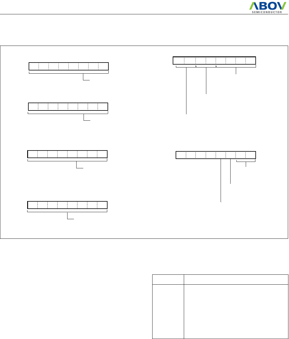
MC80F0304/08/16
48 November 4, 2011 Ver 2.12
Figure 9-3 R1 Port Register
9.3 R2 and R2IO register
R2 is an 8-bit CMOS bidirectional I/O port (address 0C4H). Each
I/O pin can independently used as an input or an output through
the R3IO register (address 0C5H). When R20 through R27 pins
are used as input ports, an on-chip pull-up resistor can be connect-
ed to them in 1-bit units with a pull-up selection register 2 (PU2).
R20 through R27 pins can be used to open drain output port by
setting the corresponding bit of the open drain selection register
2 (R2OD).
In addition, Port R2 is multiplexed with alternate functions. R23
R24,R25,and R26 can be used as ADC input channel 9 to 12 by
setting ADCM to enable ADC and select channel 9 to 12.
R1 Data Register
R1
ADDRESS: 0C2H
RESET VALUE: 00H
R17
R16
R15
R14 R13 R12 R11 R10
Port Direction
R1 Direction Register
R1IO
ADDRESS: 0C3H
RESET VALUE: 00H
0: Input
1: Output
Input / Output data
R1 Pull-up
PU1
ADDRESS: 0FDH
RESET VALUE: 00H
Selection Register
0: Disable
1: Enable
Pull-up Resister Selection
R1 Open Drain
R1OD
ADDRESS: 0C9H
RESET VALUE: 00H
Selection Register
0: Disable
1: Enable
Open Drain Resister Selection
PSR0
ADDRESS: 0F8H
RESET VALUE: 0000 0000B
INT2E
Port / INT Selection
0: R11, R12, R03, R00
1: INT0, INT1,INT2, INT3
INT0EINT1EINT3E
PWM3OE
EC0EEC1E
Port / EC Selection
0: R04, R07
1: EC0, EC1
Port / PWM Selection
0: R10, R11
1: PWM1O, PWM3O
PWM1OE
PSR1
ADDRESS: 0F9H
RESET VALUE: ---- 0000B
BUZOE
R12/BUZO Selection
0: R12 port (Turn off buzzer)
1: BUZO port (Turn on buzzer)
T0OE
T2OE
AVREFS
- - -
-
Port / TO Selection
0: R04, R07
1: EC0, EC1
R10 / AVREF Selection
0: R10 port
1: AVREF port
Port Pin Alternate Function
R20
R21
R22
R23
R24
R25
R26
R27
-
-
-
AN9 (ADC input channel 9)
AN10 (ADC input channel 10)
AN11 (ADC input channel 11)
AN12 (ADC input channel 12)
-
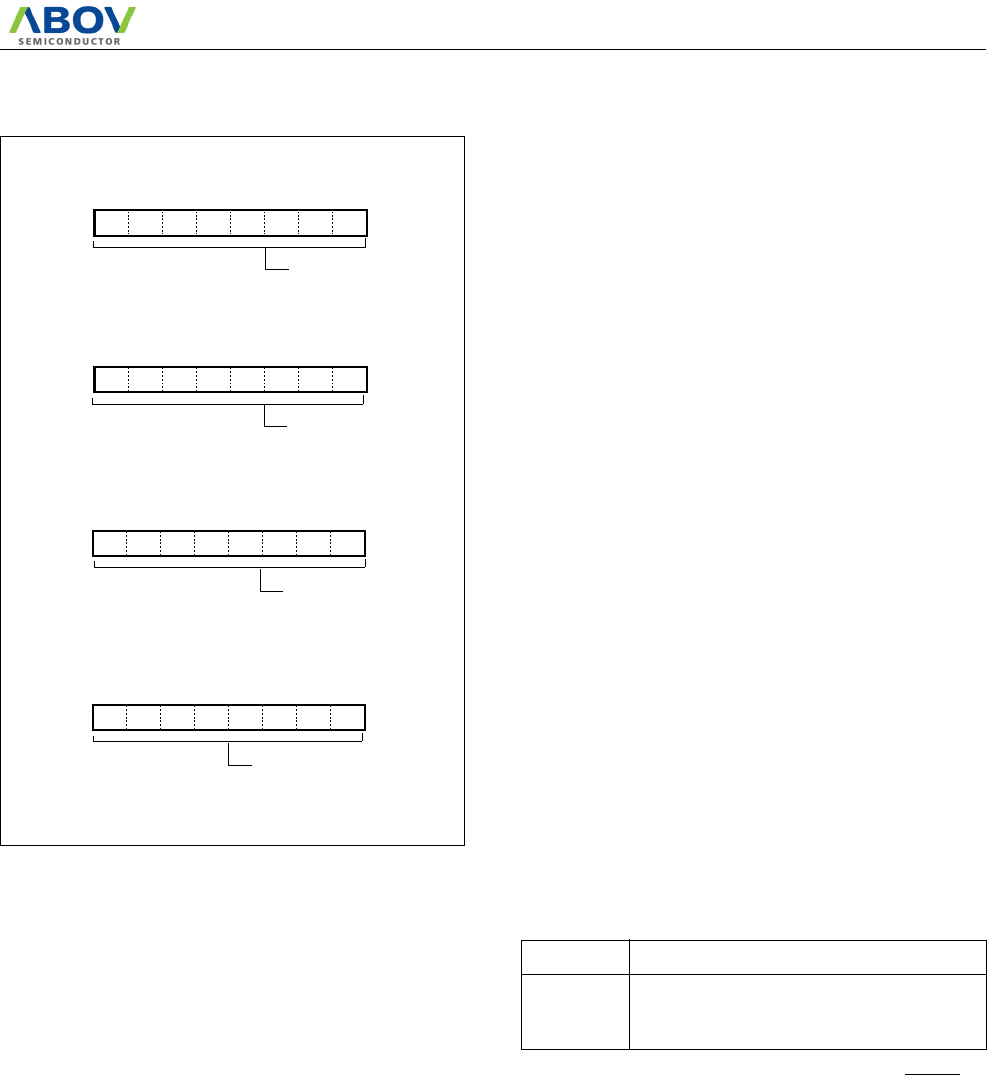
MC80F0304/08/16
November 4, 2011 Ver 2.12 49
9.4 R3 and R3IO register
R3 is a 6-bit CMOS bidirectional I/O port (address 0C6H). Each
I/O pin (except R35) can independently used as an input or an
output through the R3IO register (address 0C7H). R35 is an input
only port. When R30 through R35 pins are used as input ports, an
on-chip pull-up resistor can be connected to them in 1-bit units
with a pull-up selection register 3 (PU3). R30 through R34 pins
can be used to open drain output port by setting the corresponding
bit of the open drain selection register 1 (R3OD).
In addition, Port R3 is multiplexed with alternate functions. R30
R31,and R32 can be used as ADC input channel 13,14 and 15 by
setting ADCM to enable ADC and select channel 13,14 and 15.
R33, R34 and R35 is multiplexd with XIN, XOUT, and RESET pin
.
R2 Data Register
R2
ADDRESS: 0C4H
RESET VALUE: 00H
R25 R24 R23 R22 R21
Port Direction
R2 Direction Register
R2IO
ADDRESS: 0C5H
RESET VALUE: 00H
0: Input
1: Output
Input / Output data
R2 Pull-up
PU2
ADDRESS: 0FEH
RESET VALUE: 00H
Selection Register
0: Disable
1: Enable
Pull-up Resister Selection
R2 Open Drain
R2OD
ADDRESS: 0CAH
RESET VALUE: 00H
Selection Register
0: Disable
1: Enable
Open Drain Resister Selection
R27 R26 R20
Port Pin Alternate Function
R30
R31
R32
AN13 (ADC input channel 13)
AN14 (ADC input channel 14)
AN15 (ADC input channel 15)
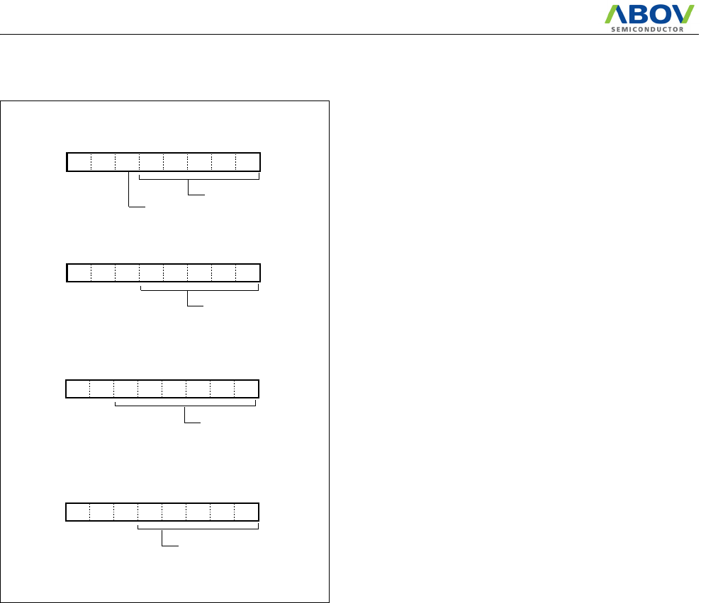
MC80F0304/08/16
50 November 4, 2011 Ver 2.12
R3 Data Register
R3
ADDRESS: 0C6H
RESET VALUE: 00H
- - R35 R34 R33 R32 R31 R30
Port Direction
R3 Direction Register
R3IO
ADDRESS: 0C7H
RESET VALUE: 00H
0: Input
1: Output
Input / Output data
- - -
Input data
R3 Pull-up
PU3
ADDRESS: 0FDH
RESET VALUE: 00H
Selection Register
0: Disable
1: Enable
Pull-up Resister Selection
- -
R3 Open Drain
R3OD
ADDRESS: 0CBH
RESET VALUE: ---0 000-B
Selection Register
0: Disable
1: Enable
Open Drain Resister Selection
MC80F0304/08/16
November 4, 2011 Ver 2.12 51
10. CLOCK GENERATOR
As shown in Figure 10-1 , the clock generator produces the basic
clock pulses which provide the system clock to be supplied to the
CPU and the peripheral hardware. It contains main-frequency
clock oscillator. The system clock operation can be easily ob-
tained by attaching a crystal or a ceramic resonator between the
XIN and XOUT pin, respectively. The system clock can also be ob-
tained from the external oscillator. In this case, it is necessary to
input a external clock signal to the XIN pin and open the XOUT
pin. There are no requirements on the duty cycle of the external
clock signal, since the input to the internal clocking circuitry is
through a divide-by-two flip-flop, but minimum and maximum
high and low times specified on the data sheet must be observed.
To the peripheral block, the clock among the not-divided original
clock, clocks divided by 1, 2, 4,..., up to 4096 can be provided.
Peripheral clock is enabled or disabled by STOP instruction. The
peripheral clock is controlled by clock control register
(CKCTLR). See "11. BASIC INTERVAL TIMER" on page 53
for details.
Figure 10-1 Block Diagram of Clock Generator
10.1 Oscillation Circuit
XIN and XOUT are the input and output, respectively, a inverting
amplifier which can be set for use as an on-chip oscillator, as
shown in Figure 10-2 .
Figure 10-2 Oscillator Connections
Note: When using a system clock oscillator, carry out wiring in
the broken line area in Figure 10-2 to prevent any effects from wir-
ing capacities.
- Minimize the wiring length.
- Do not allow wiring to intersect with other signal conductors.
- Do not allow wiring to come near changing high current.
- Set the potential of the grounding position of the oscillator capac-
itor to that of VSS. Do not ground to any ground pattern where high
current is present.
- Do not fetch signals from the oscillator.
Internal
PRESCALER
÷1
Peripheral clock
÷2÷4÷8÷16 ÷128 ÷256 ÷512 ÷1024÷32 ÷64
PS0 PS1 PS2 PS3 PS4 PS5 PS6 PS7 PS8 PS9 PS10
fEX (Hz) PS0 PS3PS2 PS4PS1 PS10PS9PS5 PS6 PS7
4M
Frequency
period
4M 1M 500K 250K2M 125K 62.5K
250n 500n 1u 2u 4u 8u 16u 32u 64u 256u128u
3.906K7.183K15.63K31.25K
PS8
÷2048 ÷4096
PS12PS11
1.953K 976
512u 1.024m
Main OSC
SLEEP
fEX system clock
PS12PS11
XIN
Clock Pulse
Generator
(÷2)
Stop
OSC
Circuit
XOUT
STOP
INOSC
ONP
Circuit
MUX
INOSC
fXIN
INCLK
Int OSC
Circuit
INOSC
INOSC (IN4MCLK/IN2MCLK/
7 ~ 3 2 ~ 0
Configuration Option Register (20FFH)
IN4MCLKXO/IN2MCLKXO)
Xout
Xin
Vss
C1
C2
MC80F0304/08/16
52 November 4, 2011 Ver 2.12
n addition, see Figure 10-3 for the layout of the crystal.
Figure 10-3 Layout of Oscillator PCB circuit
To drive the device from an external clock source, Xout should
be left unconnected while Xin is driven as shown in Figure 10-4
. There are no requirements on the duty cycle of the external clock
signal, since the input to the internal clocking circuitry is through
a divide-by-two flip-flop, but minimum and maximum high and
low times specified on the data sheet must be observed.
Oscillation circuit is designed to be used either with a ceramic
resonator or crystal oscillator. Since each crystal and ceramic res-
onator have their own characteristics, the user should consult the
crystal manufacturer for appropriate values of external compo-
nents.
Figure 10-4 External Clock Connections
In addition, the MC80F0304/0308/0316 has an ability for the ex-
ternal RC oscillated operation. It offers additional cost savings
for timing insensitive applications. The RC oscillator frequency
is a function of the supply voltage, the external resistor (REXT)
and capacitor (CEXT) values, and the operating temperature.
The user needs to take into account variation due to tolerance of
external R and C components used.
Figure 10-1 shows how the RC combination is connected to the
MC80F0304/0308/0316. External capacitor (CEXT) can be omit-
ted for more cost saving. However, the characteristics of external
R only oscillation are more variable than external RC oscillation.
Figure 10-1 RC Oscillator Connections
Figure 10-2 R Oscillator Connections
To use the RC oscillation , the CLK option of the configuration
bits (20FFH) should be set to “EXRC or EXRCXO”.
The oscillator frequency, divided by 4, is output from the Xout
pin, and can be used for test purpose or to synchronize other logic.
In addition to external crystal/resonator and external RC/R oscil-
lation, the MC80F0304/0308/0316 provides the internal 4MHz or
2MHz oscillation. The internal 4MHz/2MHz oscillation needs no
external parts.
To use the internal 4MHz/2MHz oscillation, the CLK option of
the configuration bits should be set to “IN4MCLK”,
“IN2MCLK”, “IN4MCLKXO” or “IN2MCLKXO”. For detail
description on the configuration bits, refer to "23.. DEVICE
CONFIGURATION AREA" on page 116
XOUT
XIN
Xout
Xin
Vss
OPEN
External
Clock
Source
XOUT
XIN
Vdd
CEXT
fXIN÷4
REXT
Cint ≈ 6pF
XOUT
XIN
VDD
fXIN÷4
REXT
CINT ≈ 6pF
MC80F0304/08/16
November 4, 2011 Ver 2.12 53
11. BASIC INTERVAL TIMER
The MC80F0304/0308/0316 has one 8-bit Basic Interval Timer
that is free-run and can not stop. Block diagram is shown in Fig-
ure 11-1 . In addition, the Basic Interval Timer generates the time
base for watchdog timer counting. It also provides a Basic inter-
val timer interrupt (BITIF).
The 8-bit Basic interval timer register (BITR) is increased every
internal count pulse which is divided by prescaler. Since prescal-
er has divided ratio by 8 to 1024, the count rate is 1/8 to 1/1024
of the oscillator frequency. As the count overflow from FFH to
00H, this overflow causes the interrupt to be generated.
The Basic Interval Timer is controlled by the clock control regis-
ter (CKCTLR) shown in Figure 11-2. If the RCWDT bit is set to
“1”, the clock source of the BITR is changed to the internal RC
oscillation.
When write "1" to bit BTCL of CKCTLR, BITR register is
cleared to "0" and restart to count-up. The bit BTCL becomes "0"
after one machine cycle by hardware.
If the STOP instruction executed after writing "1" to bit RCWDT
of CKCTLR, it goes into the internal RC oscillated watchdog tim-
er mode. In this mode, all of the block is halted except the internal
RC oscillator, Basic Interval Timer and Watchdog Timer. More
detail informations are explained in Power Saving Function. The
bit WDTON decides Watchdog Timer or the normal 7-bit timer.
Source clock can be selected by lower 3 bits of CKCTLR.
BITR and CKCTLR are located at same address, and address
0F2H is read as a BITR, and written to CKCTLR.
Note: All control bits of Basic interval timer are in CKCTLR reg-
ister which is located at same address of BITR (address ECH). Ad-
dress ECH is read as BITR, written to CKCTLR. Therefore, the
CKCTLR can not be accessed by bit manipulation instruction.
Figure 11-1 Block Diagram of Basic Interval Timer
MUX
Basic Interval
BITR
Select Input clock 3
Basic Interval Timer
source
clock
8-bit up-counter
BCK[2:0] BTCL
÷1024
÷512
÷256
÷128
÷64
÷32
÷16
÷8
To Watchdog timer (WDTCK)
CKCTLR
clear
overflow
Internal bus line
clock control register
[0F2H]
[0F2H]
BITIF
Read
XIN PIN
Prescaler
Timer Interrupt
Internal RC OSC
RCWDT
1
0
RCWDT
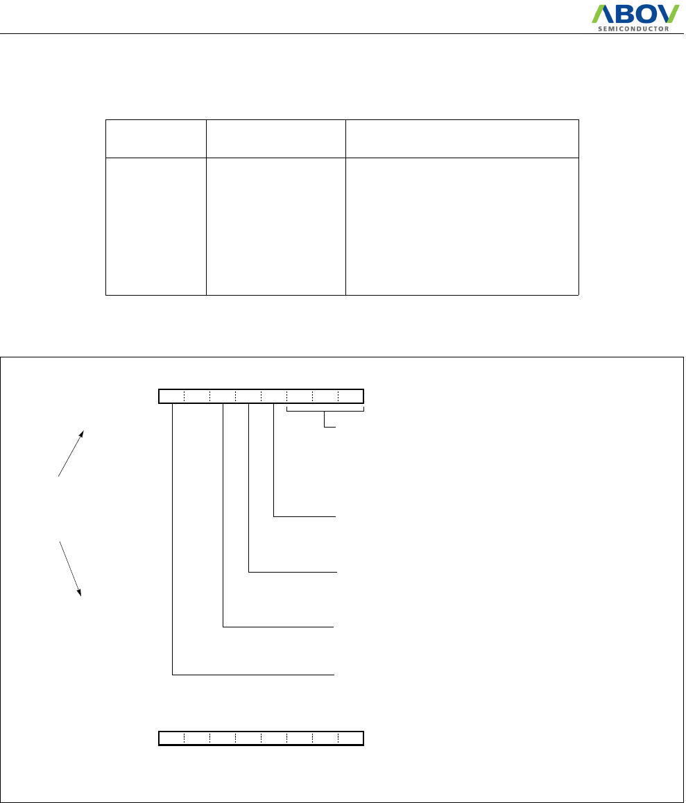
MC80F0304/08/16
54 November 4, 2011 Ver 2.12
Table 11-1 Basic Interval Timer Interrupt Period
Figure 11-2 BITR: Basic Interval Timer Mode Register
Example 1:
Interrupt request flag is generated every 4.096ms at 4MHz.
:
LDM CKCTLR,#1BH
SET1 BITE
EI
:
Example 2:
Interrupt request flag is generated every 4.096ms at 8MHz.
:
LDM CKCTLR,#1CH
SET1 BITE
EI
:
CKCTLR
[2:0] Source clock Interrupt (overflow) Period (ms)
@ fXIN = 8MHz
000
001
010
011
100
101
110
111
fXIN÷8
fXIN÷16
fXIN÷32
fXIN÷64
fXIN÷128
fXIN÷256
fXIN÷512
fXIN÷1024
0.256
0.512
1.024
2.048
4.096
8.192
16.384
32.768
BTCL
76543210
RCWDT
-
ADRST
BTS1
Basic Interval Timer source clock select
000: fXIN ÷ 8
001: fXIN ÷ 16
010: fXIN ÷ 32
011: fXIN ÷ 64
100: fXIN ÷ 128
101: fXIN ÷ 256
110: fXIN ÷ 512
111: fXIN ÷ 1024
Clear bit
0: Normal operation (free-run)
1: Clear 8-bit counter (BITR) to “0”. This bit becomes 0 automatically
INITIAL VALUE: 0-01 0111B
ADDRESS: 0F2H
after one machine cycle, and starts counting.
CKCTLR
INITIAL VALUE: Undefined
ADDRESS: 0F2H
BITR
Both register are in same address,
when write, to be a CKCTLR,
when read, to be a BITR.
Caution:
8-BIT FREE-RUN BINARY COUNTER
WDTON
BTS0BTS2
BTCL
BTCL
76543210
Watchdog timer Enable bit
0: Operate as 7-bit Timer
See the section “Watchdog Timer”.
Address Trap Reset Selection
0: Enable Address Fail Reset
1: Disable Address Fail Reset
1: Enable Watchdog Timer operation
0: Disable Internal RC Watchdog Timer
1: Enable Internal RC Watchdog Timer
RC Watchdog Selection bit
MC80F0304/08/16
November 4, 2011 Ver 2.12 55
12. WATCHDOG TIMER
The watchdog timer rapidly detects the CPU malfunction such as
endless looping caused by noise or the like, and resumes the CPU
to the normal state. The watchdog timer signal for detecting mal-
function can be selected either a reset CPU or a interrupt request.
When the watchdog timer is not being used for malfunction de-
tection, it can be used as a timer to generate an interrupt at fixed
intervals.
The watchdog timer has two types of clock source. The first type
is an on-chip RC oscillator which does not require any external
components. This RC oscillator is separate from the external os-
cillator of the XIN pin. It means that the watchdog timer will run,
even if the clock on the XIN pin of the device has been stopped,
for example, by entering the STOP mode. The other type is a
prescaled system clock.
The watchdog timer consists of 7-bit binary counter and the
watchdog timer data register. When the value of 7-bit binary
counter is equal to the lower 7 bits of WDTR, the interrupt re-
quest flag is generated. This can be used as Watchdog timer inter-
rupt or reset the CPU in accordance with the bit WDTON.
Note: Because the watchdog timer counter is enabled after clear-
ing Basic Interval Timer, after the bit WDTON set to "1", maximum
error of timer is depend on prescaler ratio of Basic Interval Timer.
The 7-bit binary counter is cleared by setting WDTCL(bit7 of
WDTR) and the WDTCL is cleared automatically after 1 machine
cycle.
The RC oscillated watchdog timer is activated by setting the bit
RCWDT as shown below.
LDM CKCTLR,#3FH; enable the RC-OSC WDT
LDM WDTR,#0FFH ; set the WDT period
LDM SSCR, #5AH ;ready for STOP mode
STOP ; enter the STOP mode
NOP
NOP ; RC-OSC WDT running
:
The RC-WDT oscillation period is vary with temperature, VDD
and process variations from part to part (approximately,
33~100uS). The following equation shows the RCWDT oscillat-
ed watchdog timer time-out.
T
RCWDT
=CLK
RCWDT
×2
8
×
WDTR + (CLK
RCWDT
×2
8)
/2
where, CLK
RCWDT
= 33~100uS
In addition, this watchdog timer can be used as a simple 7-bit tim-
er by interrupt WDTIF. The interval of watchdog timer interrupt
is decided by Basic Interval Timer. Interval equation is as below.
TWDT = (WDTR+1)
×
Interval of BIT
Figure 12-1 Block Diagram of Watchdog Timer
Watchdog Timer Control
Figure 12-2 shows the watchdog timer control register. The
watchdog timer is automatically disabled after reset.
The CPU malfunction is detected during setting of the detection
to reset CPU
BASIC INTERVAL TIMER Count
enable
Watchdog
7-bit compare data
comparator
Watchdog Timer interrupt
clear
clear
WDTIF
Counter (7-bit)
WDTCL
“0”
“1”
WDTON in CKCTLR [0F2H]
OVERFLOW
Watchdog Timer
Register
WDTR
Internal bus line
7
[0F4H]
source
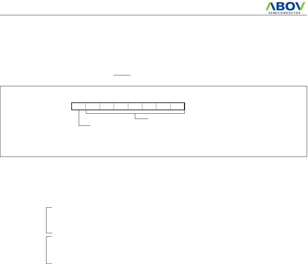
MC80F0304/08/16
56 November 4, 2011 Ver 2.12
time, selecting of output, and clearing of the binary counter.
Clearing the binary counter is repeated within the detection time.
If the malfunction occurs for any cause, the watchdog timer out-
put will become active at the rising overflow from the binary
counters unless the binary counter is cleared. At this time, when
WDTON=1, a reset is generated, which drives the RESET pin to
low to reset the internal hardware. When WDTON=0, a watchdog
timer interrupt (WDTIF) is generated. The WDTON bit is in reg-
ister CLKCTLR.
The watchdog timer temporarily stops counting in the STOP
mode, and when the STOP mode is released, it automatically re-
starts (continues counting).
Figure 12-2 WDTR: Watchdog Timer Control Register
Example: Sets the watchdog timer detection time to 1 sec. at 4.194304MHz
Enable and Disable Watchdog
Watchdog timer is enabled by setting WDTON (bit 4 in
CKCTLR) to “1”. WDTON is initialized to “0” during reset and
it should be set to “1” to operate after reset is released.
Example: Enables watchdog timer for Reset
:
LDM CKCTLR,#xxx1_xxxxB;WDTON ← 1
:
:
The watchdog timer is disabled by clearing bit 4 (WDTON) of
CKCTLR. The watchdog timer is halted in STOP mode and re-
starts automatically after STOP mode is released.
Watchdog Timer Interrupt
The watchdog timer can be also used as a simple 7-bit timer by
clearing bit4 of CKCTLR to “0”. The interval of watchdog timer
interrupt is decided by Basic Interval Timer. Interval equation is
shown as below.
TWDT = (WDTR+1)
×
Interval of BIT
The stack pointer (SP) should be initialized before using the
watchdog timer output as an interrupt source.
Example: 7-bit timer interrupt set up.
LDM CKCTLR,#xxx0_xxxxB;WDTON ←0
LDM WDTR,#8FH ;WDTCL ←1
:
76543210
WDTCL
Clear count flag
0: Free-run count
INITIAL VALUE: 0111 1111B
ADDRESS: 0F4H
WDTR
WW WW
1: When the WDTCL is set to “1”, binary counter
is cleared to “0”. And the WDTCL becomes “0” automatically
after one machine cycle. Counter count up again.
7-bit compare data
WWWW
LDM CKCTLR,#3FH ;Select 1/1024 clock source, WDTON ← 1, Clear Counter
LDM WDTR,#08FH
LDM WDTR,#08FH ;Clear counter
:
:
:
:
LDM WDTR,#08FH ;Clear counter
:
:
:
:
LDM WDTR,#08FH ;Clear counter
Within WDT
detection time
Within WDT
detection time
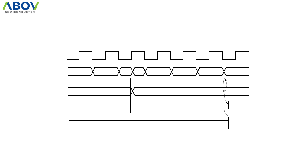
MC80F0304/08/16
November 4, 2011 Ver 2.12 57
Figure 12-3 Watchdog timer Timing
If the watchdog timer output becomes active, a reset is generated,
which drives the RESET pin low to reset the internal hardware.
The main clock oscillator also turns on when a watchdog timer re-
set is generated in sub clock mode.
2
3
n
Source clock
Binary-counter
WDTR
WDTIF interrupt
WDTR ← “1000_0011B”
10
Match
Detect
Counter
Clear
1230
BIT overflow
3
WDT reset reset
Counter
Clear
MC80F0304/08/16
58 November 4, 2011 Ver 2.12
13. TIMER/EVENT COUNTER
The MC80F0304/0308/0316 has Four Timer/Counter registers.
Each module can generate an interrupt to indicate that an event
has occurred (i.e. timer match).
Timer 0 and Timer 1 are can be used either two 8-bit Timer/
Counter or one 16-bit Timer/Counter with combine them. Also
Timer 2 and Timer 3 are same. Timer 4 is 16-bit Timer/Counter.
In the “timer” function, the register is increased every internal
clock input. Thus, one can think of it as counting internal clock
input. Since a least clock consists of 2 and most clock consists of
2048 oscillator periods, the count rate is 1/2 to 1/2048 of the os-
cillator frequency.
In the “counter” function, the register is increased in response to
a 0-to-1 (rising edge) transition at its corresponding external input
pin, EC0 or EC1.
In addition the “capture” function, the register is increased in re-
sponse external or internal clock sources same with timer or
counter function. When external clock edge input, the count reg-
ister is captured into Timer data register correspondingly. When
external clock edge input, the count register is captured into cap-
ture data register CDRx.
Timer 0 and Timer 1 is shared with "PWM" function and "Com-
pare output" function. It has six operating modes: "8-bit timer/
counter", "16-bit timer/counter", "8-bit capture", "16-bit cap-
ture", "8-bit compare output", and "10-bit PWM" which are se-
lected by bit in Timer mode register TM0 and TM1 as shown in
Table 13-1, Figure 13-1 .
Timer 2 and Timer 3 is shared with "PWM" function and "Com-
pare output" function. It has six operating modes: "8-bit timer/
counter", "16-bit timer/counter", "8-bit capture", "16-bit cap-
ture", "8-bit compare output", and "10-bit PWM" which are se-
lected by bit in Timer mode register TM2 and TM3 as shown in
Table 13-2, Figure 13-2 .
Table 13-1 Operation Modes of Timer 0, 1
16BIT CAP0 CAP1 PWM1E T0CK
[2:0]
T1CK
[1:0] PWM1O TIMER 0 TIMER 1
0 0 0 0 XXX XX 0 8-bit Timer 8-bit Timer
0 0 1 0 111 XX 0 8-bit Event counter 8-bit Capture
0 1 0 0 XXX XX 1 8-bit Capture (internal clock) 8-bit Compare Output
0 X 0 1 XXX XX 1 8-bit Timer/Counter 10-bit PWM
1 0 0 0 XXX 11 0 16-bit Timer
1 0 0 0 111 11 0 16-bit Event counter
1 1 1 0 XXX 11 0 16-bit Capture (internal clock)
1. X means the value of “0” or “1” corresponds to user operation.
16BIT CAP2 CAP3 PWM3E T2CK
[2:0]
T3CK
[1:0] PWM3O TIMER 2 TIMER 3
0 0 0 0 XXX XX 0 8-bit Timer 8-bit Timer
0 0 1 0 111 XX 0 8-bit Event counter 8-bit Capture
0 1 0 0 XXX XX 1 8-bit Capture (internal clock) 8-bit Compare Output
0 X 0 1 XXX XX 1 8-bit Timer/Counter 10-bit PWM
1 0 0 0 XXX 11 0 16-bit Timer
1 0 0 0 111 11 0 16-bit Event counter
1 1 1 0 XXX 11 0 16-bit Capture (internal clock)
Table 13-2 Operating Modes of Timer 2, 3
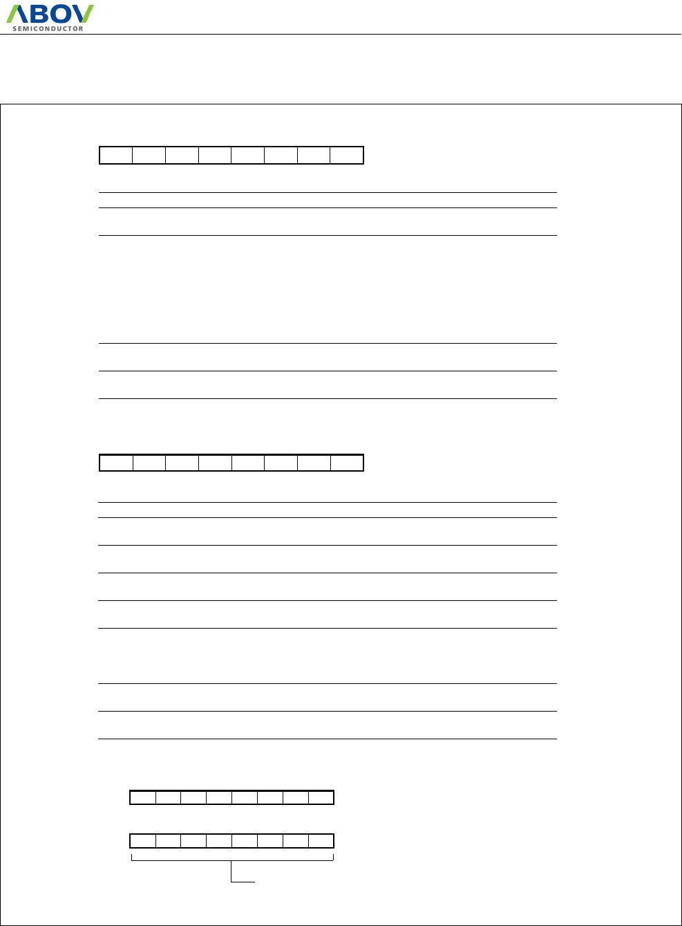
MC80F0304/08/16
November 4, 2011 Ver 2.12 59
Figure 13-1 TM0, TM1 Registers
BTCL
76543210
16BITPOL T1CN INITIAL VALUE: 00H
ADDRESS: 0D2H
TM1 T1STT1CK0T1CK1PWM1E CAP1
Bit Name Bit Position Description
POL TM1.7 0: PWM Duty Active Low
1: PWM Duty Active High
16BIT TM1.6 0: 8-bit Mode
1: 16-bit Mode
PWM1E TM1.5 0: Disable PWM
1: Enable PWM
CAP1 TM1.4 0: Timer/Counter mode
1: Capture mode selection flag
T1CK1
T1CK0
TM1.3
TM1.2
00: 8-bit Timer, Clock source is fXIN
01: 8-bit Timer, Clock source is fXIN ÷ 2
10: 8-bit Timer, Clock source is fXIN ÷ 8
11: 8-bit Timer, Clock source is Using the Timer 0 Clock
T1CN TM1.1 0: Timer count pause
1: Timer count start
T1ST TM1.0 0: When cleared, stop the counting.
1: When set, Timer 0 Count Register is cleared and start again.
BTCL
543210
-- T0CN
INITIAL VALUE: --00 0000
B
ADDRESS: 0D0
H
TM0
T0STT0CK0T0CK1CAP0 T0CK2
Bit Name Bit Position Description
CAP0 TM0.5 0: Timer/Counter mode
1: Capture mode selection flag
T0CK2
T0CK1
T0CK0
TM0.4
TM0.3
TM0.2
000: 8-bit Timer, Clock source is fXIN ÷ 2
001: 8-bit Timer, Clock source is fXIN ÷ 4
010: 8-bit Timer, Clock source is fXIN ÷ 8
011: 8-bit Timer, Clock source is fXIN ÷ 32
100: 8-bit Timer, Clock source is fXIN ÷ 128
101: 8-bit Timer, Clock source is fXIN ÷ 512
110: 8-bit Timer, Clock source is fXIN ÷ 2048
111: EC0 (External clock)
T0CN TM0.1 0: Timer count pause
1: Timer count start
T0ST TM0.0 0: When cleared, stop the counting.
1: When set, Timer 0 Count Register is cleared and start again.
76543210
INITIAL VALUE: 0FFH
ADDRESS: 0D1H
TDR0
Read: Count value read
Write: Compare data write
R/W R/W R/W R/W R/W R/W R/W R/W
R/W R/W R/W R/W R/W R/W R/W R/W
R/W R/W R/W R/W R/W R/W
76543210
INITIAL VALUE: 0FFH
ADDRESS: 0D3H
TDR1
R/W R/W R/W R/W R/W R/W R/W R/W
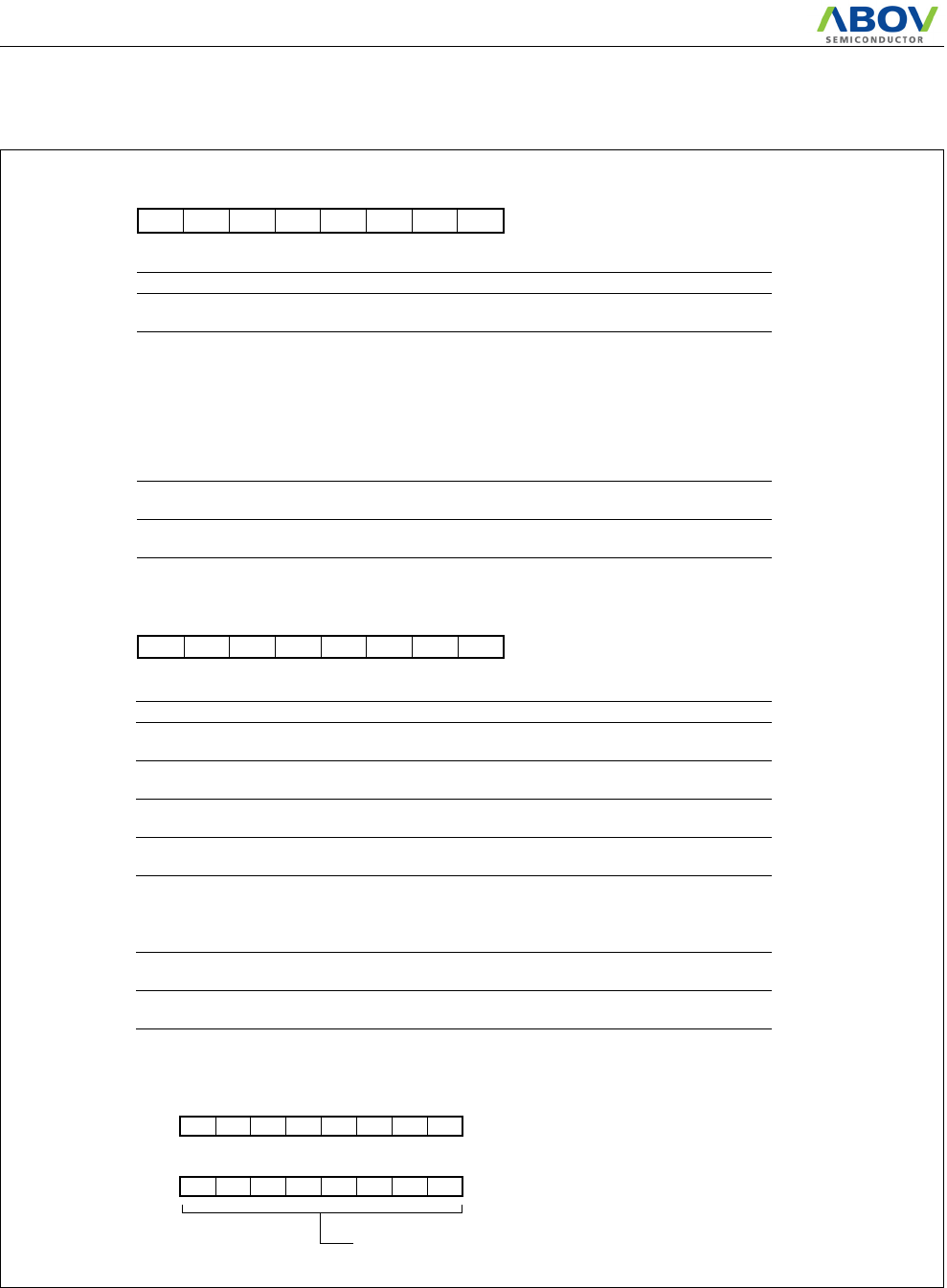
MC80F0304/08/16
60 November 4, 2011 Ver 2.12
Figure 13-2 TM2, TM3 Registers
BTCL
76543210
16BITPOL T3CN INITIAL VALUE: 00H
ADDRESS: 0D8H
TM3 T3STT3CK0T3CK1PWM3E CAP3
Bit Name Bit Position Description
POL TM3.7 0: PWM Duty Active Low
1: PWM Duty Active High
16BIT TM3.6 0: 8-bit Mode
1: 16-bit Mode
PWM3E TM3.5 0: Disable PWM
1: Enable PWM
CAP3 TM3.4 0: Timer/Counter mode
1: Capture mode selection flag
T3CK1
T3CK0
TM3.3
TM3.2
00: 8-bit Timer, Clock source is fXIN
01: 8-bit Timer, Clock source is fXIN ÷ 4
10: 8-bit Timer, Clock source is fXIN ÷ 16
11: 8-bit Timer, Clock source is Using the Timer 2 Clock
T3CN TM3.1 0: Timer count pause
1: Timer count start
T3ST TM3.0 0: When cleared, stop the counting.
1: When set, Timer 0 Count Register is cleared and start again.
BTCL
543210
-- T2CN
INITIAL VALUE: --00 0000
B
ADDRESS: 0D6
H
TM2
T2STT2CK0T2CK1CAP2 T2CK2
Bit Name Bit Position Description
CAP2 TM2.5 0: Timer/Counter mode
1: Capture mode selection flag
T2CK2
T2CK1
T2CK0
TM2.4
TM2.3
TM2.2
000: 8-bit Timer, Clock source is fXIN ÷ 2
001: 8-bit Timer, Clock source is fXIN ÷ 4
010: 8-bit Timer, Clock source is fXIN ÷ 8
011: 8-bit Timer, Clock source is fXIN ÷ 16
100: 8-bit Timer, Clock source is fXIN ÷ 64
101: 8-bit Timer, Clock source is fXIN ÷ 256
110: 8-bit Timer, Clock source is fXIN ÷ 1024
111: EC1 (External clock)
T2CN TM2.1 0: Timer count pause
1: Timer count start
T2ST TM2.0 0: When cleared, stop the counting.
1: When set, Timer 0 Count Register is cleared and start again.
76543210
INITIAL VALUE: 0FFH
ADDRESS: 0D7H
TDR2
Read: Count value read
Write: Compare data write
R/W R/W R/W R/W R/W R/W R/W R/W
R/W R/W R/W R/W R/W R/W R/W R/W
R/W R/W R/W R/W R/W R/W
76543210
INITIAL VALUE: 0FFH
ADDRESS: 0D9H
TDR3
R/W R/W R/W R/W R/W R/W R/W R/W
MC80F0304/08/16
November 4, 2011 Ver 2.12 61
13.1 8-bit Timer / Counter Mode
The MC80F0304/0308/0316 has four 8-bit Timer/Counters, Tim-
er 0, Timer 1, Timer 2, Timer 3. The Timer 0, Timer 1 are shown
in Figure 13-3 and Timer 2, Timer 3 are shown in Figure 13-4 .
The “timer” or “counter” function is selected by control registers
TM0, TM1, TM2, TM3 as shown in Figure 13-1 . To use as an 8-
bit timer/counter mode, bit CAP0, CAP1, CAP2, or CAP3 of
TMx should be cleared to “0” and 16BIT and PWM1E or
PWM3E of TM1 or TM3 should be cleared to "0" (Figure 13-3 ).
These timers have each 8-bit count register and data register. The
count register is increased by every internal or external clock in-
put. The internal clock has a prescaler divide ratio option of 1, 2,
4, 8, 16, 32, 64, 128, 256, 512, 1024, 2048 or external clock (se-
lected by control bits TxCK0, TxCK1, TxCK2 of register TMx).
Figure 13-3 8-bit Timer/Counter 0, 1
EC0 PIN
÷ 2
÷ 4
÷ 8
XIN PIN
MUX
Prescaler
clear
0: Stop
1: Clear and start
T0ST
T0CK[2:0]
111
000
001
010
T0CN
MUX
T1IF
clear
0: Stop
1: Clear and start
T1ST
T1CK[1:0]
11
00
01
TIMER 1
INTERRUPT
÷ 1
÷ 2
÷ 8
TDR0 (8-bit)
TDR1 (8-bit)
T1 (8-bit)
T0 (8-bit)
Comparator
Comparator
TIMER 0
TIMER 1
BTCL
76543210
--T0CN
INITIAL VALUE: --00 0000B
ADDRESS: 0D0H
TM0 T0STT0CK0T0CK1CAP0 T0CK2
-- XXXX
X means don’t care
÷ 32
÷ 128
÷ 512
÷ 2048
011
100
101
110
T0IF TIMER 0
INTERRUPT
T1CN
10
INITIAL VALUE: 00H
ADDRESS: 0D2H
TM1
X means don’t care
0X
BTCL
76543210
16BITPOL T1CN T1STT1CK0T1CK1PWM1E CAP1
X0 X XXX
00
EDGE
DETECTOR
F/F
R05 / T0O
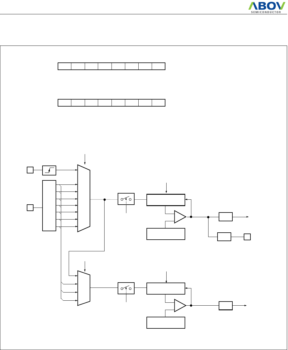
MC80F0304/08/16
62 November 4, 2011 Ver 2.12
Figure 13-4 8-bit Timer/Counter 2, 3
EC1 PIN
÷ 2
÷ 4
÷ 8
XIN PIN
MUX
Prescaler
clear
0: Stop
1: Clear and start
T2ST
T2CK[2:0]
111
000
001
010
T2CN
MUX
T3IF
clear
0: Stop
1: Clear and start
T3ST
T3CK[1:0]
11
00
01
TIMER 3
INTERRUPT
÷ 1
÷ 4
÷ 16
TDR2 (8-bit)
TDR3 (8-bit)
T3 (8-bit)
T2 (8-bit)
Comparator
Comparator
TIMER 2
TIMER 3
BTCL
76543210
--T2CN
INITIAL VALUE: --000000B
ADDRESS: 0D6H
TM2 T2STT2CK0T2CK1CAP2 T2CK2
-- XXXX
X means don’t care
÷ 16
÷ 64
÷ 256
÷ 1024
011
100
101
110
T2IF TIMER 2
INTERRUPT
T3CN
10
INITIAL VALUE: 00H
ADDRESS: 0D8H
TM3
X means don’t care
0X
BTCL
76543210
16BITPOL T3CN T3STT3CK0T3CK1PWM3E CAP3
X0 X XXX
00
EDGE
DETECTOR
F/F
R06 / T2O

MC80F0304/08/16
November 4, 2011 Ver 2.12 63
Example 1:
Timer0 = 2ms 8-bit timer mode at 4MHz
Timer1 = 0.5ms 8-bit timer mode at 4MHz
Timer2 = 1ms 8-bit timer mode at 4MHz
Timer3 = 1ms 8-bit timer mode at 4MHz
LDM TDR0,#249
LDM TDR1,#249
LDM TDR2,#249
LDM TDR3,#249
LDM TM0,#0000_1111B
LDM TM1,#0000_1011B
LDM TM2,#0000_1111B
LDM TM3,#0000_1011B
SET1 T0E
SET1 T1E
SET1 T2E
SET1 T3E
EI
Example 2:
Timer0 = 8-bit event counter mode
Timer1 = 0.5ms 8-bit timer mode at 4MHz
Timer2 = 8-bit event counter mode
Timer3 = 1ms 8-bit timer mode at 4MHz
LDM TDR0,#249
LDM TDR1,#249
LDM TDR2,#249
LDM TDR3,#249
LDM TM0,#0001_1111B
LDM TM1,#0000_1011B
LDM TM2,#0001_1111B
LDM TM3,#0000_1011B
SET1 T0E
SET1 T1E
SET1 T2E
SET1 T3E
EI
These timers have each 8-bit count register and data register. The
count register is increased by every internal or external clock in-
put. The internal clock has a prescaler divide ratio option of 2, 4,
8, 32, 128, 512, 2048 selected by control bits T0CK[2:0] of reg-
ister TM0 or 1, 2, 8 selected by control bits T1CK[1:0] of register
TM1, or 2, 4, 8, 16, 64, 256, 1024 selected by control bits
T2CK[2:0] of register TM2, or 1, 4, 16 selected by control bits
T3CK[1:0] of register TM3. In the Timer 0, timer register T0 in-
creases from 00H until it matches TDR0 and then reset to 00H.
The match output of Timer 0 generates Timer 0 interrupt (latched
in T0IF bit).
In counter function, the counter is increased every 0-to-1 (rising
edge) transition of EC0 pin. In order to use counter function, the
bit EC0 of the Port Selection Register (PSR0.4) is set to "1". The
Timer 0 can be used as a counter by pin EC0 input, but Timer 1
can not. Likewise, In order to use Timer2 as counter function, the
bit EC1 of the Port Selection Register (PSR0.5) is set to "1". The
Timer 2 can be used as a counter by pin EC1 input, but Timer 3
can not.
8-bit Timer Mode
In the timer mode, the internal clock is used for counting up.
Thus, you can think of it as counting internal clock input. The
contents of TDRn are compared with the contents of up-counter,
Tn. If match is found, a timer n interrupt (TnIF) is generated and
the up-counter is cleared to 0. Counting up is resumed after the
up-counter is cleared.
As the value of TDRn is changeable by software, time interval is
set as you want.
Figure 13-5 Timer Mode Timing Chart
0n-2 2
0
n3
n-1
n
Source clock
Up-counter
TDR1
T1IF interrupt
Start count
123 1 4
Match
Detect Counter
Clear
~
~
~
~~
~~
~~
~

MC80F0304/08/16
64 November 4, 2011 Ver 2.12
Figure 13-6 Timer Count Example
8-bit Event Counter Mode
In this mode, counting up is started by an external trigger. This
trigger means rising edge of the EC0 or EC1 pin input. Source
clock is used as an internal clock selected with timer mode regis-
ter TM0 or TM2. The contents of timer data register TDRn (n =
0,1,2,3) are compared with the contents of the up-counter Tn. If a
match is found, an timer interrupt request flag TnIF is generated,
and the counter is cleared to “0”. The counter is restart and count
up continuously by every rising edge of the EC0 or EC1 pin input.
The maximum frequency applied to the EC0 or EC1 pin is fXIN/
2 [Hz].
In order to use event counter function, the bit 4, 5 of the Port Se-
lection Register PSR0(address 0F8H) is required to be set to “1”.
After reset, the value of timer data register TDRn is initialized to
"0", The interval period of Timer is calculated as below equation.
Figure 13-7 Event Counter Mode Timing Chart
~
~
Timer 0 (T0IF)
Interrupt
TDR0
TIME
Occur interrupt Occur interrupt Occur interrupt
Interrupt period
up-count
~
~
~
~
0
1
2
3
4
5
6
7A
7C
Count Pulse
= 8 μs x (124+1)
7B
MATCH
Example: Make 1ms interrupt using by Timer0 at 4MHz
LDM TM0,#0FH ; divide by 32
LDM TDR0,#124 ; 8us x (124+1)= 1ms
SET1 T0E ; Enable Timer 0 Interrupt
EI ; Enable Master Interrupt
Period
When
TDR0 = 124D = 7CH
fXIN = 4 MHz
INTERRUPT PERIOD =
4 × 10⁶ Hz
1× 32 × (124+1) = 1 ms
TM0 = 0000 1111B (8-bit Timer mode, Prescaler divide ratio = 32)
8 μs
(TDR0 = T0)
7C
0
Period (sec) 1
f
XIN
----------- 2 Divide Ratio (TDRn+1) ×××=
0121
0n 2
~
~
~
~~
~
n-1
n
~
~~
~~
~
EC0 pin input
Up-counter
TDR0
T1IF interrupt
Start count
MC80F0304/08/16
November 4, 2011 Ver 2.12 65
Figure 13-8 Count Operation of Timer / Event counter
13.2 16-bit Timer / Counter Mode
The Timer register is being run with all 16 bits. A 16-bit timer/
counter register T0, T1 are incremented from 0000H until it
matches TDR0, TDR1 and then resets to 0000H. The match out-
put generates Timer 0 interrupt.
The clock source of the Timer 0 is selected either internal or ex-
ternal clock by bit T0CK[2:0]. In 16-bit mode, the bits
T1CK[1:0] and 16BIT of TM1 should be set to "1" respectively
as shown in Figure 13-9 .
Likewise, A 16-bit timer/counter register T2, T3 are incremented
from 0000H until it matches TDR2, TDR3 and then resets to
0000H. The match output generates Timer 2 interrupt.
The clock source of the Timer 2 is selected either internal or ex-
ternal clock by bit T2CK[2:0]. In 16-bit mode, the bits
T3CK[1:0] and 16BIT of TM3 should be set to "1" respectively
as shown in Figure 13-10 .
Even if the Timer 0 (including Timer 1) is used as a 16-bit timer,
the Timer 2 and Timer 3 can still be used as either two 8-bit timer
or one 16-bit timer by setting the TM3. Reversely, even if the
Timer 2 (including Timer 3) is used as a 16-bit timer, the Timer
0 and Timer 1 can still be used as 8-bit timer independently.
Timer 1 (T1IF)
Interrupt
TDR1
TIME
Occur interrupt Occur interrupt
stop
clear & start
disable enable
Start & Stop
T1ST
T1CN
Control count
up-count
~
~
~
~
T1ST = 0
T1ST = 1
T1CN = 0
T1CN = 1
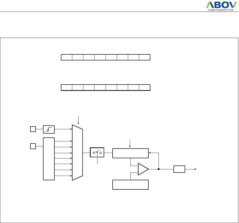
MC80F0304/08/16
66 November 4, 2011 Ver 2.12
Figure 13-9 16-bit Timer/Counter for Timer 0, 1
clear
0: Stop
1: Clear and start
T0ST
T0CN
TDR1 + TDR0
Comparator
TIMER 0 + TIMER 1 → TIMER 0 (16-bit)
Higher byte Lower byte
(16-bit)
COMPARE DATA
T1 + T0
(16-bit)
(Not Timer 1 interrupt)
EDGE
BTCL
76543210
--T0CN
INITIAL VALUE: --00 0000B
ADDRESS: 0D0H
TM0 T0STT0CK0T0CK1CAP0 T0CK2
-- XXXX
X means don’t care
INITIAL VALUE: 00H
ADDRESS: 0D2H
TM1
X means don’t care
0X
BTCL
76543210
16BITPOL T1CN T1STT1CK0T1CK1PWM1E CAP1
X1 X X11
00
EC0 PIN
÷ 2
÷ 4
÷ 8
XIN PIN
MUX
Prescaler
T0CK[2:0]
111
000
001
010
÷ 32
÷ 128
÷ 512
÷ 2048
011
100
101
110
DETECTOR
T0IF TIMER 0
INTERRUPT
MC80F0304/08/16
November 4, 2011 Ver 2.12 67
Figure 13-10 16-bit Timer/Counter for Timer 2, 3
13.3 8-bit Compare Output (16-bit)
The MC80F0304/0308/0316 has Timer Compare Output func-
tion. To pulse out, the timer match can goes to port pin( T0O or
T2O) as shown in Figure 13-3 or Figure 13-4 . Thus, pulse out is
generated by the timer match. These operation is implemented to
pin, R05/AN5//T0O/TXD or R06/AN6/T2O/ACK.
In this mode, the bit T0OE or T2OE bit of Port Selection register1
(PSR1.0 or PSR1.1) should be set to "1". This pin output the sig-
nal having a 50 : 50 duty square wave, and output frequency is
same as below equation.
13.4 8-bit Capture Mode
The Timer 0 capture mode is set by bit CAP0 of timer mode reg-
ister TM0 (bit CAP1 of timer mode register TM1 for Timer 1) as
shown in Figure 13-11 . Likewise, the Timer 2 capture mode is
set by bit CAP2 of timer mode register TM2 (bit CAP3 of timer
mode register TM3 for Timer 3) as shown in Figure 13-12 .
The Timer/Counter register is increased in response internal or
external input. This counting function is same with normal timer
mode, and Timer interrupt is generated when timer register T0
(T1, T2, T3) increases and matches TDR0 (TDR1, TDR2,
TDR3).
This timer interrupt in capture mode is very useful when the pulse
width of captured signal is more wider than the maximum period
clear
0: Stop
1: Clear and start
T2ST
T2CN
TDR3 + TDR2
Comparator
TIMER 2 + TIMER 3 → TIMER 2 (16-bit)
Higher byte Lower byte
(16-bit)
COMPARE DATA
T3 + T2
(16-bit)
(Not Timer 3 interrupt)
EDGE
BTCL
76543210
--T2CN
INITIAL VALUE: --000000B
ADDRESS: 0D6H
TM2 T2STT2CK0T2CK1CAP2 T2CK2
-- XXXX
X means don’t care
INITIAL VALUE: 00H
ADDRESS: 0D8H
TM3
X means don’t care
0X
BTCL
76543210
16BITPOL T3CN T3STT3CK0T3CK1PWM3E CAP3
X1 X X11
00
EC1 PIN
÷ 2
÷ 4
÷ 8
XIN PIN
MUX
Prescaler
T2CK[2:0]
111
000
001
010
÷ 16
÷ 64
÷ 256
÷ 1024
011
100
101
110
DETECTOR
T2IF TIMER 2
INTERRUPT
f
COMP
Oscillation Frequency
2 Prescaler Value
TDR
1)+(××
-------------------------------------------------------------------------------------------=
MC80F0304/08/16
68 November 4, 2011 Ver 2.12
of Timer.
For example, in Figure 13-14 , the pulse width of captured signal
is wider than the timer data value (FFH) over 2 times. When ex-
ternal interrupt is occurred, the captured value (13H) is more little
than wanted value. It can be obtained correct value by counting
the number of timer overflow occurrence.
Timer/Counter still does the above, but with the added feature
that a edge transition at external input INTx pin causes the current
value in the Timer x register (T0,T1,T2,T3), to be captured into
registers CDRx (CDR0, CDR1, CDR2, CDR3), respectively. Af-
ter captured, Timer x register is cleared and restarts by hardware.
It has three transition modes: "falling edge", "rising edge", "both
edge" which are selected by interrupt edge selection register
IEDS. Refer to “18.4 External Interrupt” on page 99. In addition,
the transition at INTn pin generate an interrupt.
Note: The CDRn and TDRn are in same address.In the capture
mode, reading operation is read the CDRn, not TDRn because
path is opened to the CDRn.
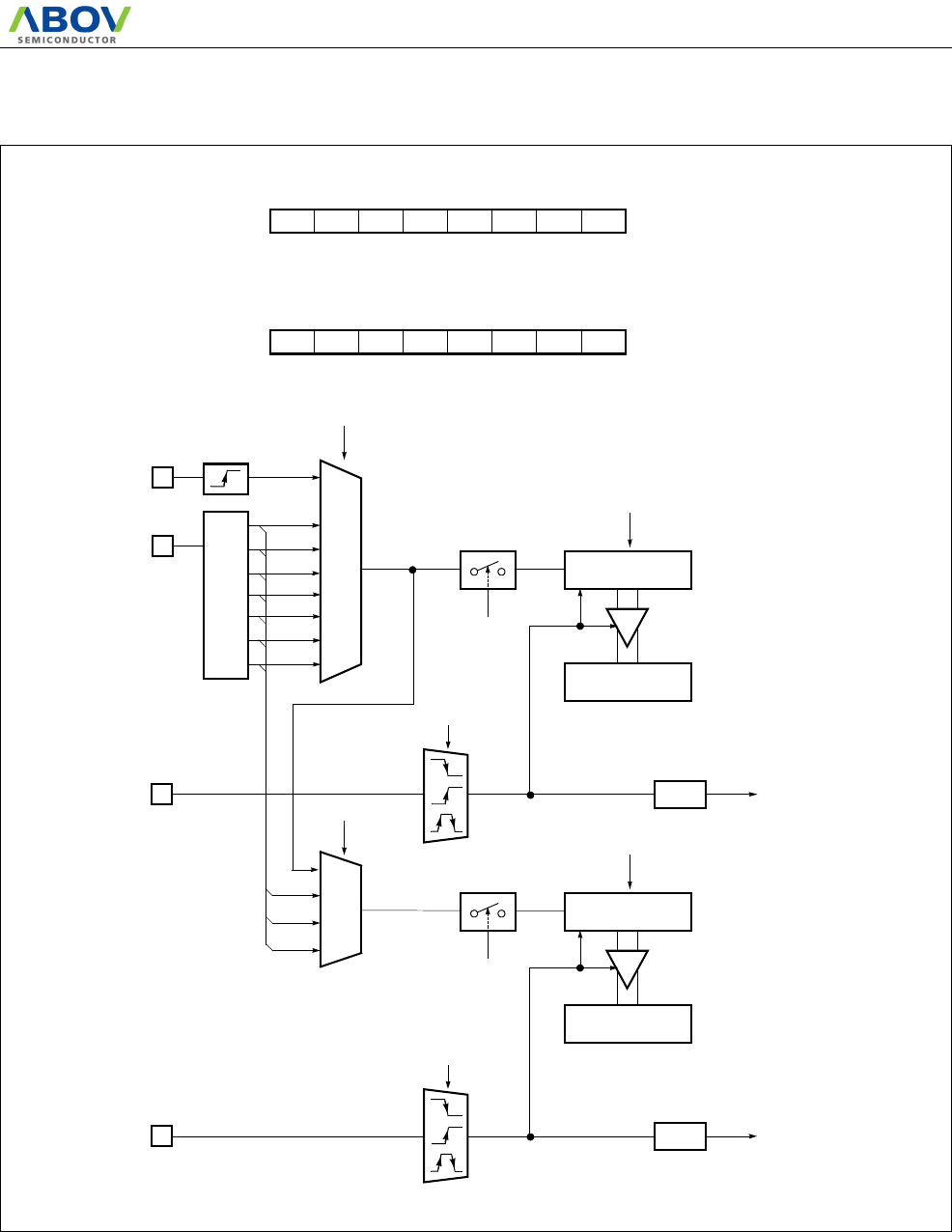
MC80F0304/08/16
November 4, 2011 Ver 2.12 69
Figure 13-11 8-bit Capture Mode for Timer 0, 1
INT0IF
0: Stop
1: Clear and start
T0ST
INT0
INTERRUPT
T0CN
CDR0 (8-bit)
T0 (8-bit)
“01”
“10”
“11”
Capture
IEDS[1:0]
EC0 PIN
÷ 2
÷ 4
÷ 8
XIN PIN
MUX
Prescaler
T0CK[2:0]
111
000
001
010
MUX
T1CK[1:0]
11
00
01
÷ 1
÷ 2
÷ 8
÷ 32
÷ 128
÷ 512
÷ 2048
011
100
101
110
10
INT0 PIN
INT1IF
0: Stop
1: Clear and start
T1ST
INT1
INTERRUPT
T1CN
CDR1 (8-bit)
T1 (8-bit)
“01”
“10”
“11”
Capture
IEDS[3:2]
INT1 PIN
BTCL
76543210
--T0CN
INITIAL VALUE: --00 0000B
ADDRESS: 0D0H
TM0 T0STT0CK0T0CK1CAP0 T0CK2
-- XXXX
X means don’t care
INITIAL VALUE: 00H
ADDRESS: 0D2H
TM1
X means don’t care
1X
BTCL
76543210
16BITPOL T1CN T1STT1CK0T1CK1PWM1E CAP1
X0 X XXX
01
Edge
Detector
clear
clear
MC80F0304/08/16
70 November 4, 2011 Ver 2.12
Figure 13-12 8-bit Capture Mode for Timer 2, 3
INT2IF
0: Stop
1: Clear and start
T2ST
INT2
INTERRUPT
T2CN
CDR2 (8-bit)
T2 (8-bit)
“01”
“10”
“11”
Capture
IEDS[5:4]
EC1 PIN
÷ 2
÷ 4
÷ 8
XIN PIN
MUX
Prescaler
T2CK[2:0]
111
000
001
010
MUX
T3CK[1:0]
11
00
01
÷ 1
÷ 4
÷ 16
÷ 16
÷ 64
÷ 256
÷ 1024
011
100
101
110
10
INT2 PIN
INT3IF
0: Stop
1: Clear and start
T3ST
INT3
INTERRUPT
T3CN
CDR3 (8-bit)
T3 (8-bit)
“01”
“10”
“11”
Capture
IEDS[7:6]
INT3 PIN
BTCL
76543210
--T2CN
INITIAL VALUE: --00 0000B
ADDRESS: 0D6H
TM2 T2STT2CK0T2CK1CAP2 T2CK2
-- XXXX
X means don’t care
INITIAL VALUE: 00H
ADDRESS: 0D8H
TM3
X means don’t care
1X
BTCL
76543210
16BITPOL T3CN T3STT3CK0T3CK1PWM3E CAP3
X0 X XXX
01
Edge
Detector
clear
clear
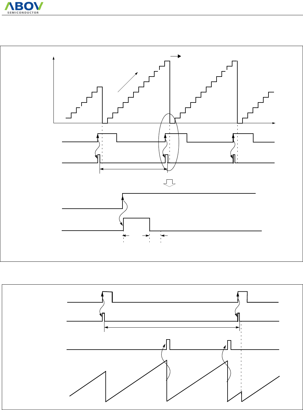
MC80F0304/08/16
November 4, 2011 Ver 2.12 71
Figure 13-13 Input Capture Operation of Timer 0 Capture mode
Figure 13-14 Excess Timer Overflow in Capture Mode
~
~
Ext. INT0 Pin
Interrupt Request
T0
TIME
up-count
~
~
~
~
0
1
2
3
4
5
6
7
8
9
n
n-1
Capture
( Timer Stop )
Clear & Start
Interrupt Interval Period
Delay
( INT0IF )
Ext. INT0 Pin
Interrupt Request
( INT0IF )
This value is loaded to CDR0
20nS 5nS
Interrupt Interval Period=01H+FFH +01H+FFH +01H+13H=214H
FFHFFH
Ext. INT0 Pin
Interrupt Request
( INT0IF )
00H00H
Interrupt Request
( T0IF )
T0
13H
MC80F0304/08/16
72 November 4, 2011 Ver 2.12
13.5 16-bit Capture Mode
16-bit capture mode is the same as 8-bit capture, except that the
Timer register is being run will 16 bits. The clock source of the
Timer 0 is selected either internal or external clock by bit
T0CK[2:0]. In 16-bit mode, the bits T1CK1, T1CK0, CAP1 and
16BIT of TM1 should be set to "1" respectively as shown in Fig-
ure 13-15 .
The clock source of the Timer 2 is selected either internal or ex-
ternal clock by bit T2CK[2:0]. In 16-bit mode, the bits
T3CK1,T3CK0, CAP3 and 16BIT of TM3 should be set to "1" re-
spectively as shown in Figure 13-16 .
Figure 13-15 16-bit Capture Mode of Timer 0, 1
0: Stop
1: Clear and start
T0ST
T0CN
Capture
CDR1 + CDR0
Higher byte Lower byte
(16-bit)
CAPTURE DATA
T1 + T0
(16-bit)
INT0IF INT0
INTERRUPT
“01”
“10”
“11”
IEDS[1:0]
EC0 PIN
÷ 2
÷ 4
÷ 8
XIN PIN
MUX
Prescaler
T0CK[2:0]
111
000
001
010
÷ 32
÷ 128
÷ 512
÷ 2048
011
100
101
110
INT0 PIN
BTCL
76543210
--T0CN
INITIAL VALUE: --00 0000B
ADDRESS: 0D0H
TM0 T0STT0CK0T0CK1CAP0 T0CK2
-- XXXX
X means don’t care
INITIAL VALUE: 00H
ADDRESS: 0D2H
TM1
X means don’t care
1X
BTCL
76543210
16BITPOL T1CN T1STT1CK0T1CK1PWM1E CAP1
X1 X X11
01
Edge
Detector
clear
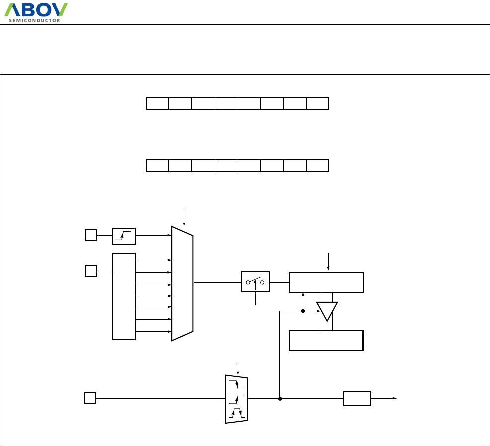
MC80F0304/08/16
November 4, 2011 Ver 2.12 73
Figure 13-16 16-bit Capture Mode of Timer 2, 3
Example 1:
Timer0 = 16-bit timer mode, 0.5s at 4MHz
LDM TM0,#0000_1111B;8uS
LDM TM1,#0100_1100B;16bit Mode
LDM TDR0,#<62499 ;8uS X 62500
LDM TDR1,#>62499 ;=0.5s
SET1 T0E
EI
:
:
Example 2:
Timer0 = 16-bit event counter mode
LDM PSR0,#0001_0000B;EC0 Set
LDM TM0,#0001_1111B;CounterMode
LDM TM1,#0100_1100B;16bit Mode
LDM TDR0,#<0FFH ;
LDM TDR1,#>0FFH ;
SET1 T0E
EI
:
:
Example 3:
Timer0 = 16-bit capture mode
LDM PSR0,#0000_0001B;INT0 set
LDM TM0,#0010_1111B;CaptureMode
LDM TM1,#0100_1100B;16bit Mode
LDM TDR0,#<0FFH ;
LDM TDR1,#>0FFH ;
LDM IEDS,#01H;Falling Edge
SET1 T0E
EI
:
:
0: Stop
1: Clear and start
T2ST
T2CN
Capture
CDR3 + CDR2
Higher byte Lower byte
(16-bit)
CAPTURE DATA
T3 + T2
(16-bit)
INT2IF INT2
INTERRUPT
“01”
“10”
“11”
IEDS[5:4]
EC1 PIN
÷ 2
÷ 4
÷ 8
XIN PIN
MUX
Prescaler
T2CK[2:0]
111
000
001
010
÷ 16
÷ 64
÷ 256
÷ 1024
011
100
101
110
INT2 PIN
BTCL
76543210
--T2CN
INITIAL VALUE: --00 0000B
ADDRESS: 0D6H
TM2 T2STT2CK0T2CK1CAP2 T2CK2
-- XXXX
X means don’t care
INITIAL VALUE: 00H
ADDRESS: 0D8H
TM3
X means don’t care
1X
BTCL
76543210
16BITPOL T3CN T3STT3CK0T3CK1PWM3E CAP3
X1 X X11
01
Edge
Detector
clear
MC80F0304/08/16
74 November 4, 2011 Ver 2.12
13.6 PWM Mode
The MC80F0304/0308/0316 has high speed PWM (Pulse Width
Modulation) functions which shared with Timer1 or Timer3.
In PWM mode, R10 / PWM1O or R11 / PWM3O pin output up
to a 10-bit resolution PWM output. These pins should be config-
ured as a PWM output by setting "1" bit PWM1OE and
PWM3OE in PSR0 register.
The period of the PWM1 output is determined by the T1PPR (T1
PWM Period Register) and T1PWHR[3:2] (bit3,2 of T1 PWM
High Register) and the duty of the PWM output is determined by
the T1PDR (T1 PWM Duty Register) and T1PWHR[1:0] (bit1,0
of T1 PWM High Register).
The period of the PWM3 output is determined by the T3PPR (T3
PWM Period Register) and T3PWHR[3:2] (bit3,2 of T3 PWM
High Register) and the duty of the PWM output is determined by
the T3PDR (T3 PWM Duty Register) and T3PWHR[1:0] (bit1,0
of T3 PWM High Register).
The user writes the lower 8-bit period value to the T1(3)PPR( and
the higher 2-bit period value to the T1(3)PWHR[3:2]. And writes
duty value to the T1(3)PDR and the T1(3)PWHR[1:0] same way.
The T1(3)PDR is configured as a double buffering for glitchless
PWM output. In Figure 13-18 , the duty data is transferred from
the master to the slave when the period data matched to the count-
ed value. (i.e. at the beginning of next duty cycle)
PWM1(3) Period = [PWM1(3)HR[3:2]T1(3)PPR] X
Source Clock
PWM1(3) Duty = [PWM3HR[1:0]T1(3)PDR] X Source
Clock
The relation of frequency and resolution is in inverse proportion.
Table 13-3 shows the relation of PWM frequency vs. resolution.
If it needed more higher frequency of PWM, it should be reduced
resolution.
The bit POL of TM1 or TM3 decides the polarity of duty cycle.
If the duty value is set same to the period value, the PWM output
is determined by the bit POL (1: High, 0: Low). And if the duty
value is set to "00H", the PWM output is determined by the bit
POL (1: Low, 0: High).
It can be changed duty value when the PWM output. However the
changed duty value is output after the current period is over. And
it can be maintained the duty value at present output when
changed only period value shown as Figure 13-20 . As it were, the
absolute duty time is not changed in varying frequency. But the
changed period value must greater than the duty value.
Note: If changing the Timer1 to PWM function, it should be stop
the timer clock firstly, and then set period and duty register value.
If user writes register values while timer is in operation, these reg-
ister could be set with certain values.
Ex) Sample Program @4MHz 2uS
LDM TM1,#1010_1000b ; Set Clock & PWM3E
LDM T1PPR,#199 ; Period :400uS=2uSX(199+1)
LDM T1PDR,#99 ; Duty:200uS=2uSX(99+1)
LDM PWM1HR,00H
LDM TM1,#1010_1011b ; Start timer1
Resolution
Frequency
T1CK[1:0]
= 00(250nS)
T1CK[1:0]
= 01(500nS)
T1CK[1:0]
= 10(2uS)
10-bit 3.9kHz 0.98kHz 0.49kHz
9-bit 7.8kHz 1.95kHz 0.97kHz
8-bit 15.6kHz 3.90kHz 1.95kHz
7-bit 31.2kHz 7.81kHz 3.90kHz
Table 13-3 PWM Frequency vs. Resolution at 4MHz
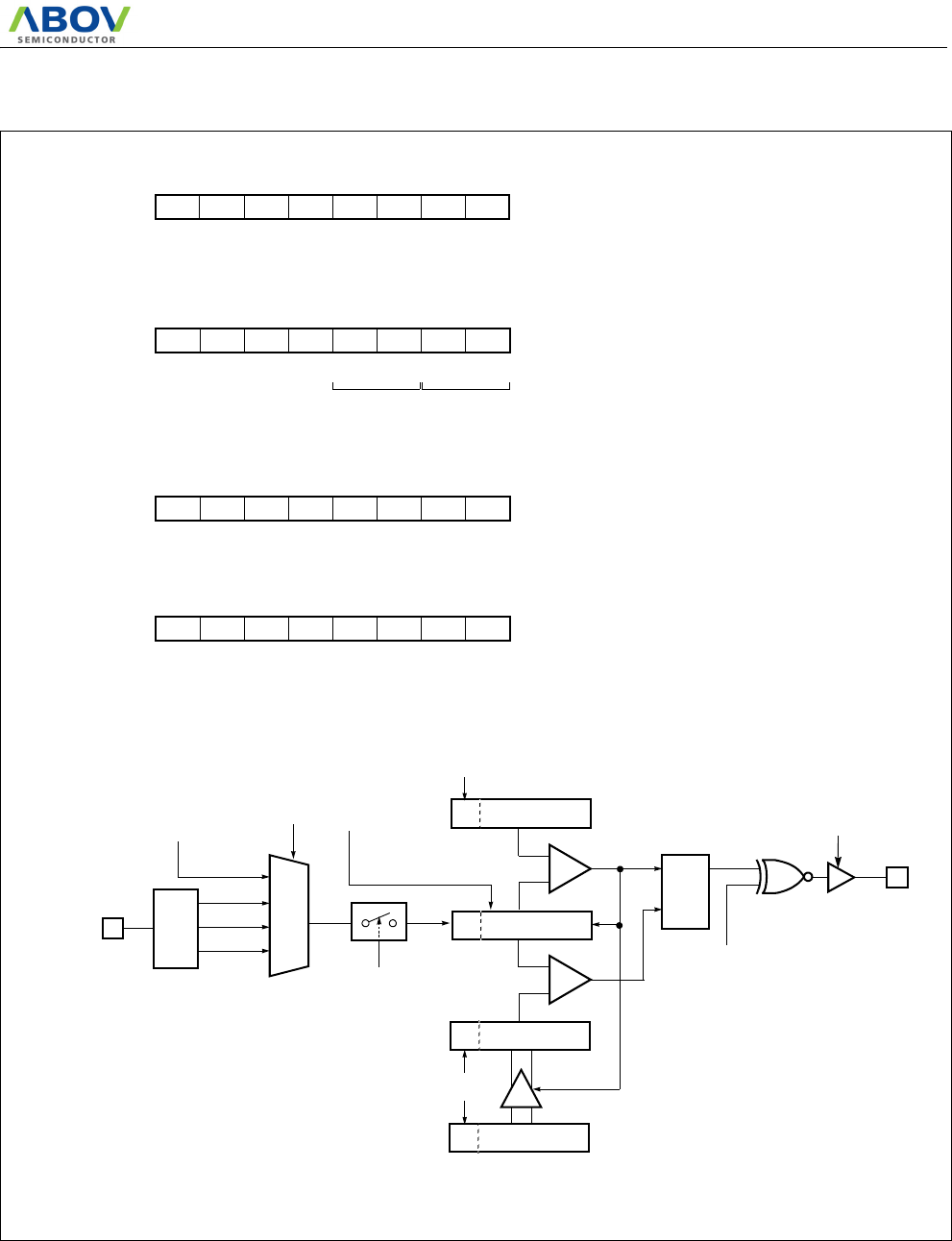
MC80F0304/08/16
November 4, 2011 Ver 2.12 75
Figure 13-17 PWM1 Mode
T1ST
0 : Stop
1 : Clear and Start
Clear
SQ
R
POL
PWM1OE
[PSR0.6]
Period High Duty High
Bit Manipulation Not Available
INITIAL VALUE: 00H
ADDRESS: 0D2H
TM1 BTCL
76543210
16BITPOL T1CN T1STT1CK0T1CK1PWM1E CAP3
X0 X XXX
10
R/W R/W R/W R/W R/W R/W R/W R/W
INITIAL VALUE: ---- 0000B
ADDRESS: 0D5H
T1PWHR
X:The value "0" or "1" corresponding your operation.
BTCL
76543210
--
T1PWHR1 T1PWHR0T1PWHR2T1PWHR3
--
-- XXXX
--
- - - -WWWW
INITIAL VALUE: 0FFH
ADDRESS: 0D3H
T1PPR BTCL
76543210
WWWWWWWW
INITIAL VALUE: 00H
ADDRESS: 0D4H
T1PDR BTCL
76543210
R/W R/W R/W R/W R/W R/W R/W R/W
X:The value "0" or "1" corresponding your operation.
T1PDR(8-bit)
T1PDR(8-bit)
T1PWHR[1:0]
Slave
Master
T1PPR(8-bit)
T1PWHR[3:2]
Comparator
T1CN
÷ 1
÷ 2
÷ 8
XIN PIN
MUX
Prescaler
00
01
10
T1CK[1:0]
T0 clock source
[T0CK]
T1(8-bit)
2-bit
Comparator
R10 / PWM1O PIN
11
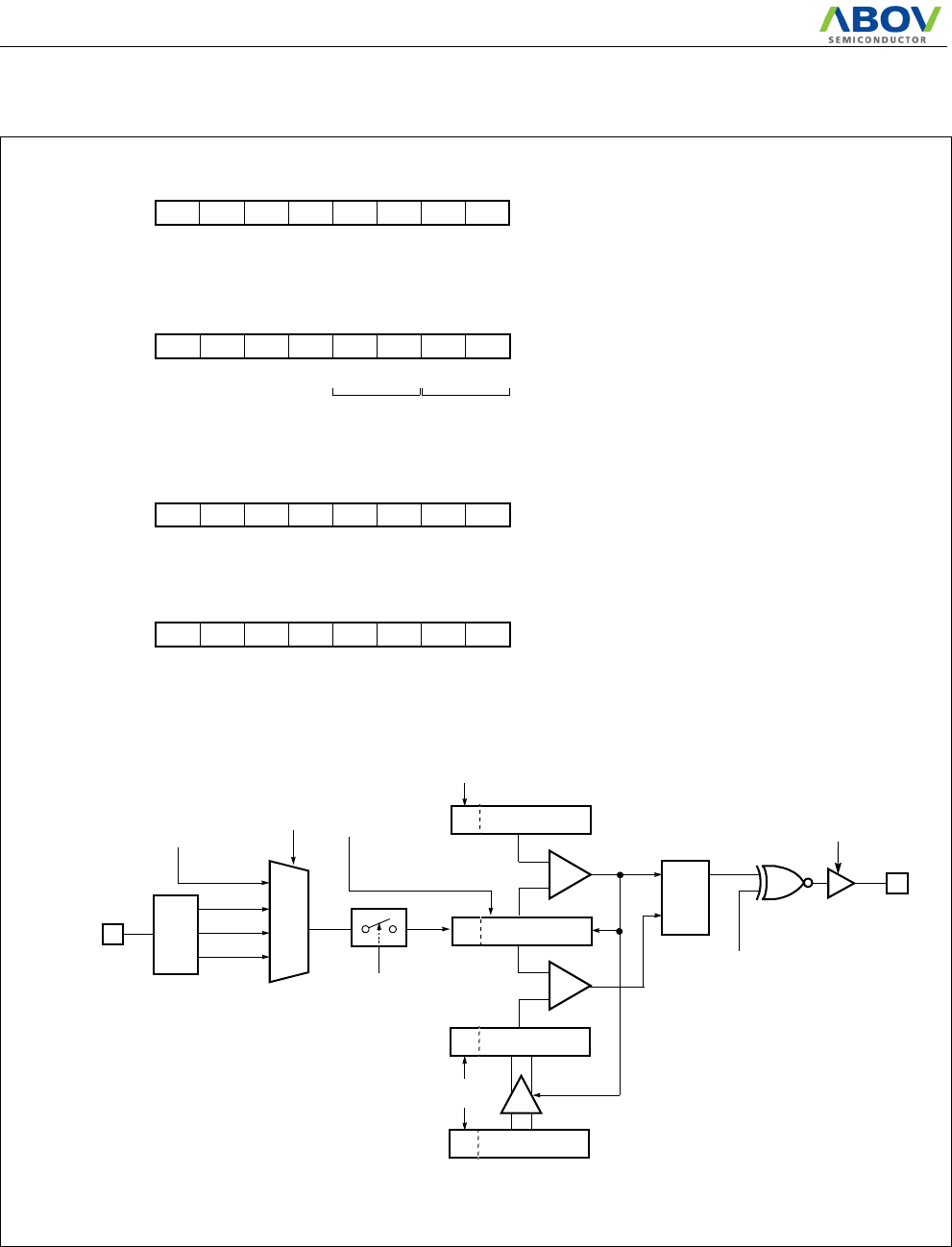
MC80F0304/08/16
76 November 4, 2011 Ver 2.12
Figure 13-18 PWM3 Mode
T3ST
0 : Stop
1 : Clear and Start
Clear
SQ
R
POL
PWM3O
[PSR0.7]
Period High Duty High
Bit Manipulation Not Available
INITIAL VALUE: 00H
ADDRESS: 0D8H
TM3 BTCL
76543210
16BITPOL T3CN T3STT3CK0T3CK1PWM3E CAP3
X0 X XXX
10
R/W R/W R/W R/W R/W R/W R/W R/W
INITIAL VALUE: ---- 0000B
ADDRESS: 0DBH
T3PWHR
X:The value "0" or "1" corresponding your operation.
BTCL
76543210
--
T3PWHR1 T3PWHR0T3PWHR2T3PWHR3
--
-- XXXX
--
- - - -WWWW
INITIAL VALUE: 0FFH
ADDRESS: 0D9H
T3PPR BTCL
76543210
WWWWWWWW
INITIAL VALUE: 00H
ADDRESS: 0DAH
T3PDR BTCL
76543210
R/W R/W R/W R/W R/W R/W R/W R/W
X:The value "0" or "1" corresponding your operation.
T3PDR(8-bit)
T3PDR(8-bit)
T3PWHR[1:0]
Slave
Master
T3PPR(8-bit)
T3PWHR[3:2]
Comparator
T3CN
÷ 1
÷ 4
÷ 16
XIN PIN
MUX
Prescaler
00
01
10
T3CK[1:0]
T2 clock source
[T2CK]
T3(8-bit)
2-bit
Comparator
R11 / PWM3O PIN
11
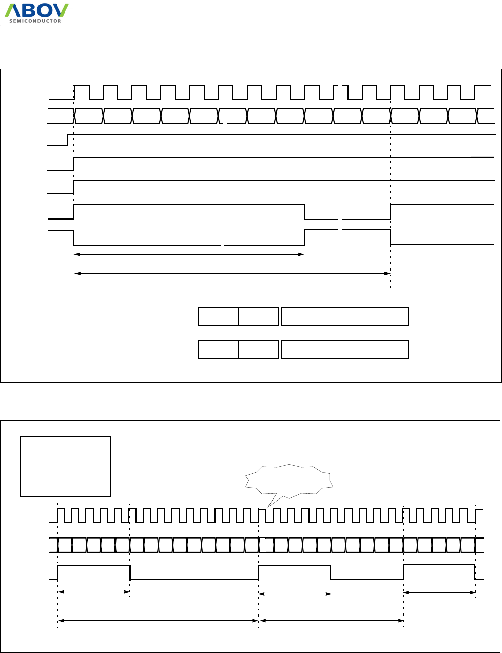
MC80F0304/08/16
November 4, 2011 Ver 2.12 77
Figure 13-19 Example of PWM1 at 4MHz
Figure 13-20 Example of Changing the PWM1 Period in Absolute Duty Cycle (@4MHz)
Source
T1
PWM1O
~
~~
~
~
~
01 02 03 04 7E 7F 80 01 02
~
~~
~
~
~
~
~
~
~
~
~
~
~
[POL=1]
PWM1O
[POL=0]
Duty Cycle [ (1+7Fh) x 250nS = 32uS ]
Period Cycle [ (3FFh+1) x 250nS = 256uS, 3.9KHz ]
T1PWHR = 0CH
T1PPR = FFH
T1PDR = 7FH
T1CK[1:0] = 00 ( XIN ) T1PWHR3 T1PWHR2
T1PWHR1 T1PWHR0
T1PPR (8-bit)
T1PDR (8-bit)
Period
Duty
1 1 FFH
00 7FH
00
clock
PWM1E
~
~
T1ST
~
~
T1CN
~
~
00 3FF
Source
T1
PWM1O
POL=1
Duty Cycle
Period Cycle [ (1+0Dh) x 2uS = 28uS, 35.5KHz ]
T1PWHR = 00H
T1PPR = 0DH
T1PDR = 04H
T1CK[1:0] = 10 ( 2us )
01 02 03 04 05 07 08 0A 0B 0C 0D 00 01 02 03 04 05 06 07 08 09 00 01 02 0306 09 04
[ (04h+1) x 2uS = 10uS ]
Duty Cycle
[ (04h+1) x 2uS = 10uS ]
Period Cycle [ (1+09h) x 2uS = 20uS, 50KHz ]
Duty Cycle
[ (04h+1) x 2uS = 10uS ]
Write T1PPR to 09H
clock
00
MC80F0304/08/16
78 November 4, 2011 Ver 2.12
14. ANALOG TO DIGITAL CONVERTER
The analog-to-digital converter (A/D) allows conversion of an
analog input signal to a corresponding 10-bit digital value. The A/
D module has sixteen analog inputs, which are multiplexed into
one sample and hold. The output of the sample and hold is the in-
put into the converter, which generates the result via successive
approximation.
The analog reference voltage is selected to VDD or AVref by set-
ting of the bit AVREFS in PSR1 register. If external analog ref-
erence AVref is selected, the analog input channel 0 (AN0)
should not be selected to use. Because this pin is used to an analog
reference of A/D converter.
The A/D module has three registers which are the control register
ADCM and A/D result register ADCRH and ADCRL. The AD-
CRH[7:6] is used as ADC clock source selection bits too. The
register ADCM, shown in Figure 14-4 , controls the operation of
the A/D converter module. The port pins can be configured as an-
alog inputs or digital I/O.
It is selected for the corresponding channel to be converted by
setting ADS[3:0]. The A/D port is set to analog input port by
ADEN and ADS[3:0] regardless of port I/O direction register.
The port unselected by ADS[3:0] operates as normal port.
Figure 14-1 A/D Converter Operation Flow
How to Use A/D Converter
The processing of conversion is start when the start bit ADST is
set to “1”. After one cycle, it is cleared by hardware. The register
ADCRH and ADCRL contains the results of the A/D conversion.
When the conversion is completed, the result is loaded into the
ADCRH and ADCRL, the A/D conversion status bit ADSF is set
to “1”, and the A/D interrupt flag ADCIF is set. See Figure 14-1
for operation flow.
The block diagram of the A/D module is shown in Figure 14-3 .
The A/D status bit ADSF is set automatically when A/D conver-
sion is completed, cleared when A/D conversion is in process.
The conversion time takes 13 times of conversion source clock.
The conversion source clock should selected for the conversion
time being more than 25μs.
A/D Converter Cautions
(1) Input range of AN0 ~ AN15
The input voltage of A/D input pins should be within the specifi-
cation range. In particular, if a voltage above VDD (or AVref) or
below VSS is input (even if within the absolute maximum rating
range), the conversion value for that channel can not be indeter-
minate. The conversion values of the other channels may also be
affected.
(2) Noise countermeasures
In order to maintain 10-bit resolution, attention must be paid to
noise on pins VDD (or AVref) and analog input pins (AN0 ~
AN15). Since the effect increases in proportion to the output im-
pedance of the analog input source, it is recommended in some
cases that a capacitor be connected externally as shown in Figure
14-2 in order to reduce noise. The capacitance is user-selectable
and appropriately determined according to the target system.
Figure 14-2 Analog Input Pin Connecting Capacitor
(3) I/O operation
The analog input pins AN0 ~ AN15 also have function as input/
output port pins. When A/D conversion is performed with any
pin, be sure not to execute a PORT input instruction with the se-
lected pin while conversion is in progress, as this may reduce the
conversion resolution.
Also, if digital pulses are applied to a pin adjacent to the pin in the
process of A/D conversion, the expected A/D conversion value
ADSF = 1
YES
NO
Enable A/D Converter
A/D Input Channel Select
Conversion Source Clock Select
A/D Start (ADST = 1)
NOP
Read ADCR
AN0~AN15
Analog
Input
0~1000pF
User Selectable
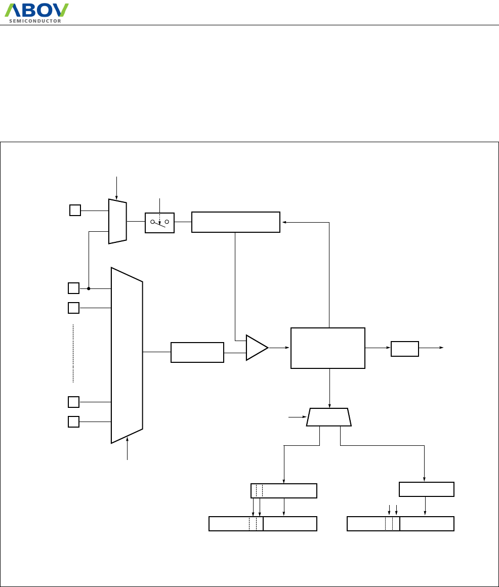
MC80F0304/08/16
November 4, 2011 Ver 2.12 79
may not be obtainable due to coupling noise. Therefore, avoid ap-
plying pulses to pins adjacent to the pin undergoing A/D conver-
sion.
(4) AVDD pin input impedance
A series resistor string of approximately 5KΩ is connected be-
tween the AVREF pin and the VSS pin. Therefore, if the output im-
pedance of the analog power source is high, this will result in
parallel connection to the series resistor string between the
AVREF pin and the VSS pin, and there will be a large analog sup-
ply voltage error
Figure 14-3 A/D Block Diagram
AN0 / AVREF
Sample & Hold
AN1
AN14
Successive
Approximation ADCIF
ADC Result Register
ADC
INTERRUPT
MUX
Resistor Ladder Circuit
VDD
ADS[3:0] (ADCM[5:2])
Circuit
ADEN
ADC Result Register
ADC8 01
2389
01
ADCRL (8-bit)
10-bit ADCR
ADCRH
00
ADCRL (8-bit)ADCRH
ADCR (10-bit)
89
10-bit ADCR
10-bit Mode 8-bit Mode
01
01
AN15
AVREFS (PSR1.3)
The conversion time takes 13 times of conversion source clock.
The conversion source clock should selected for the conversion
time being more than 25μs
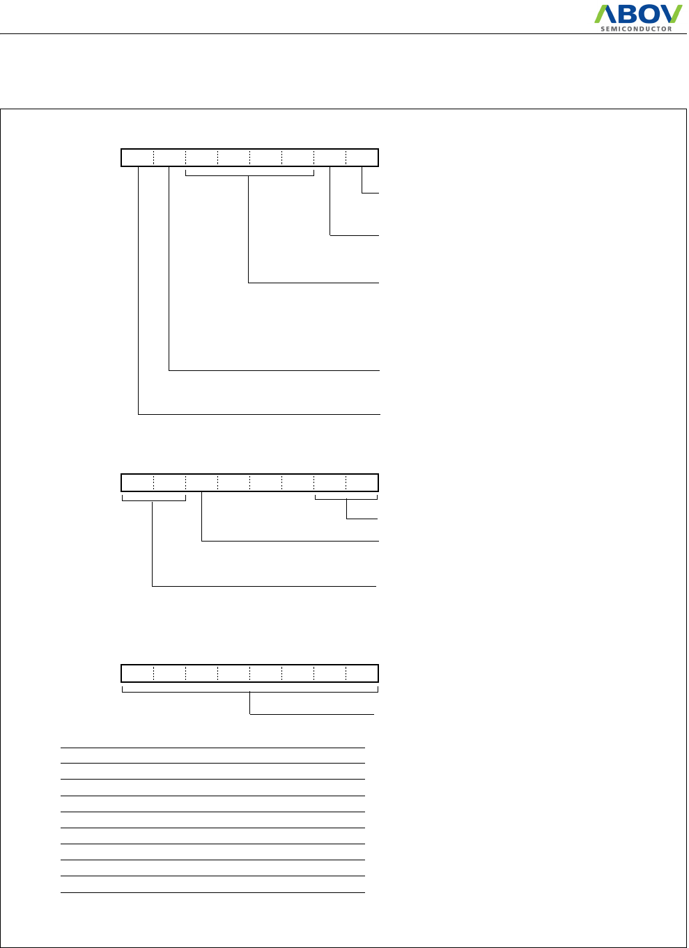
MC80F0304/08/16
80 November 4, 2011 Ver 2.12
Figure 14-4 A/D Converter Control & Result Register
BTCL
76543210
ADEN ADST
A/D status bit
Analog input channel select
INITIAL VALUE: 0000 0001B
ADDRESS: 0EFH
ADCM ADSF
A/D converter Clock Source Divide Ratio Selection bit
0: Clock Source fPS
1: Clock Source fPS ÷ 2
R/W R/W R/W R/W R/W R
0000: Channel 0 (AN0)
0001: Channel 1 (AN1)
0010: Channel 2 (AN2)
0011: Channel 3 (AN3)
0110: Channel 6 (AN6)
0111: Channel 7 (AN7)
1000: Channel 8 (AN8)
0: A/D conversion is in progress
1: A/D conversion is completed
A/D start bit
Setting this bit starts an A/D conversion.
After one cycle, bit is cleared to “0” by hardware.
ADS1 ADS0 ADS3 ADS2
ADCK
1001: Channel 9 (AN9)
A/D converter Enable bit
0: A/D converter module turn off and current is not flow.
1: Enable A/D converter
INITIAL VALUE: Undefined
ADDRESS: 0F1H
ADCRL
A/D Conversion Low Data
R/W R/W
BTCL
76543210
PSSEL1
ADCRH - -ADC8 -
PSSEL0
INITIAL VALUE: 010- ----B
ADDRESS: 0F0H
A/D Conversion High Data
A/D Conversion Clock (fPS) Source Selection
00: fXIN ÷ 4
01: fXIN ÷ 8
10: fXIN ÷ 16
11: fXIN ÷ 32
BTCL
76543210
- - -RR
WW
RRRRRR
RR
ADCK PSSEL1 PSSEL0 PS Clock Selection
00 0PS = f
XIN ÷ 4
00 1PS = f
XIN ÷ 8
01 0PS = f
XIN ÷ 16
01 1PS = f
XIN ÷ 32
10 0PS = f
XIN ÷ 8
10 1PS = f
XIN ÷ 16
11 0PS = f
XIN ÷ 32
11 1PS = f
XIN ÷ 64
Conversion Time = TPS x 13
ADC 8-bit Mode select bit
0: 10-bit Mode
1: 8-bit Mode
W
0100: Channel 4 (AN4)
0101: Channel 5 (AN5)
1010: Channel 10 (AN10)
~ 1101: Not available
1011: Channel 11 (AN11)
1100: Channel 12 (AN12)
1101: Channel 13 (AN13)
1110: Channel 14 (AN14)
1111: Channel 15 (AN15)
PS : Conversion Source Clock
* The conversion time takes 13 times of conversion source clock.
The conversion source clock should selected for the conversion time being more than 25μs.
MC80F0304/08/16
November 4, 2011 Ver 2.12 81
15. SERIAL INPUT/OUTPUT (SIO)
The serial Input/Output is used to transmit/receive 8-bit data se-
rially. The Serial Input/Output (SIO) module is a serial interface
useful for communicating with other peripheral of microcontrol-
ler devices. These peripheral devices may be serial EEPROMs,
shift registers, display drivers, A/D converters, etc. This SIO is 8-
bit clock synchronous type and consists of serial I/O data register,
serial I/O mode register, clock selection circuit, octal counter and
control circuit as illustrated in Figure 15-1 . The SO pin is de-
signed to input and output. So the Serial I/O(SIO) can be operated
with minimum two pin. Pin R00/SCK, R01/SI, and R02/SO pins
are controlled by the Serial Mode Register. The contents of the
Serial I/O data register can be written into or read out by software.
The data in the Serial Data Register can be shifted synchronously
with the transfer clock signal.
Figure 15-1 SIO Block Diagram
÷ 4
÷ 16
XIN PIN
Prescaler
MUX
SCK[1:0]
00
01
10
11
SCK PIN
SIO
Shift
Input shift register
SIOR
Clock
Clock Octal
Serial communication
Interrupt
SIOIF
Internal Bus
Counter
SCK[1:0]
“11”
overflow
not “11”
Timer0
Overflow
SI PIN
IOSW
SO PIN SOUT
IOSW
CONTROL
CIRCUIT
“0”
“1”
POL
1
0
Start
SIOST
clear
SM0
(3-bit)
SIOSF
Complete
MC80F0304/08/16
82 November 4, 2011 Ver 2.12
Serial I/O Mode Register (SIOM) controls serial I/O function.
According to SCK1 and SCK0, the internal clock or external
clock can be selected.
Serial I/O Data Register (SIOR) is an 8-bit shift register. First
LSB is send or is received first.
Figure 15-2 SIO Control Register
15.1 Transmission/Receiving Timing
The serial transmission is started by setting SIOST(bit1 of SIOM)
to “1”. After one cycle of SCK, SIOST and SIOSF(bit 0 of SIOM)
is cleared automatically to “0”. At the default state of POL bit
clear, the serial output data from 8-bit shift register is output at
falling edge of SCLK, and input data is latched at rising edge of
SCLK pin (Refer to Figure 15-3 ). When transmission clock is
counted 8 times, serial I/O counter is cleared as ‘0”. Transmission
clock is halted in “H” state and serial I/O interrupt (SIOIF) oc-
curred. SIOSF is set to “1” automatically.
BTCL
76543210
IOSWPOL SIOST
Serial transmission Clock selection
INITIAL VALUE: 0000 0001B
ADDRESS: 0E2H
SIOM
Serial Input Pin Selection bit
0: SI Pin Selection
1: SO Pin Selection
R/W R/W R/W R/W R/W R
00: fXIN ÷ 4
01: fXIN ÷ 16
10: TMR0OV(Timer0 Overflow)
11: External Clock
Serial transmission start bit
Setting this bit starts an Serial transmission.
After one cycle, bit is cleared to “0” by hardware.
SCK1 SCK0 SM1 SM0
R/W
Serial transmission Operation Mode
00: Normal Port(R00,R01,R02)
01: Sending Mode(SCK,R01,SO)
10: Receiving Mode(SCK,SI,R02)
11: Sending & Receiving Mode(SCK,SI,SO)
INITIAL VALUE: Undefined
ADDRESS: 0E3H
SIOR BTCL
76543210
R/W R/W R/W R/W R/W R/W
R/W R/W
Sending Data at Sending Mode
Receiving Data at Receiving Mode
Serial Clock Polarity Selection bit
0: Data Transmission at Falling Edge
Received Data Latch at Rising Edge
1: Data Transmission at Rising Edge
Received Data Latch at Falling Edge
R/W
SIOSF
Serial transmission status bit
0: Serial transmission is in progress
1: Serial transmission is completed
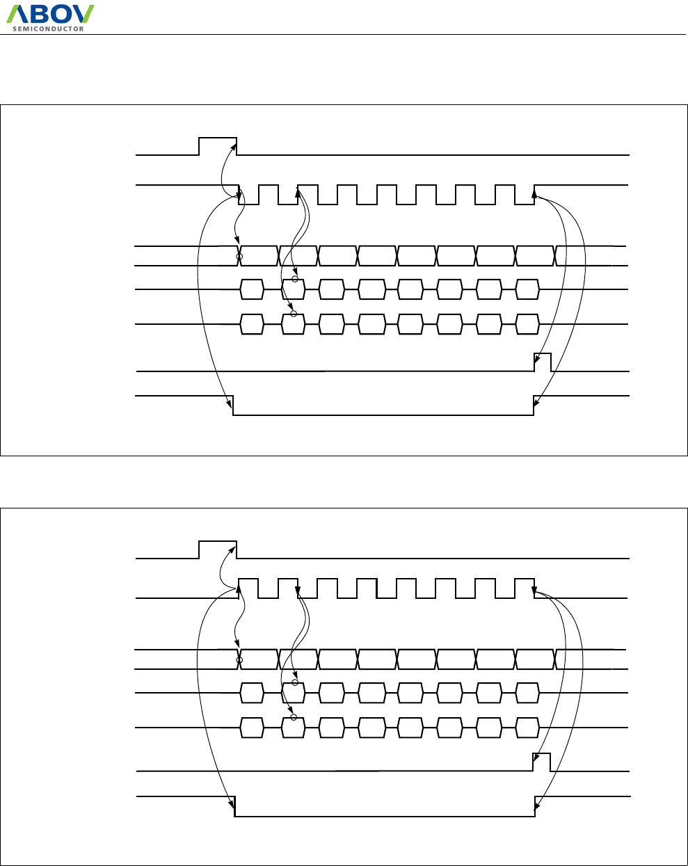
MC80F0304/08/16
November 4, 2011 Ver 2.12 83
Figure 15-3 Serial I/O Timing Diagram at POL=0
Figure 15-4 Serial I/O Timing Diagram at POL=1
15.2 The usage of Serial I/O
1. Select transmission/receiving mode. 2. In case of sending mode, write data to be send to SIOR.
D1 D2 D3 D4 D6 D7D0 D5
D1 D2 D3 D4 D6 D7D0 D5
SIOST
SCK [R00]
(POL=0)
SO [R02]
SI [R01]
SIOIF
(SIO Int. Req)
(IOSW=0)
D1 D2 D3 D4 D6 D7D0 D5
IOSWIN [R02]
(IOSW=1)
SIOSF
(SIO Status)
D1 D2 D3 D4 D6 D7D0 D5
D1 D2 D3 D4 D6 D7D0 D5
SIOST
SCK [R00]
(POL=1)
SO [R02]
SI [R01]
SIOIF
(SIO Int. Req)
(IOSW=0)
D1 D2 D3 D4 D6 D7D0 D5
IOSWIN [R02]
(IOSW=1)
SIOSF
(SIO Status)

MC80F0304/08/16
84 November 4, 2011 Ver 2.12
3. Set SIOST to “1” to start serial transmission.
4. The SIO interrupt is generated at the completion of SIO
and SIOIF is set to “1”.
5. In case of receiving mode, the received data is acquired
by reading the SIOR.
6. When using polling method, the completion of 1 byte
serial communication can be checked by reading
SIOST and SIOSF. As shown in example code, wait un-
til SIOST is changed to “0” and then wait the SIOSF is
changed to “1” for completion check. Note: When external clock is used, the frequency should be less
than 1MHz and recommended duty is 50%. If both transmission
mode is selected and transmission is performed simultaneously,
error may be occur.
LDM SIOR,#0AAh ;set tx data
LDM SIOM,#0011_1100b;set SIO mode
NOP
LDM SIOM,#0011_1110b;SIO Start
NOP
SIO_WAIT:
NOP
BBS SIOST,SIO_WAIT ;wait first edge
BBC SIOSF,SIO_WAIT ;wait complete
MC80F0304/08/16
November 4, 2011 Ver 2.12 85
16. UNIVERSAL ASYNCHRONOUS RECEIVER/TRANSMITTER (UART)
16.1 UART Serial Interface Functions
The Universal Asynchronous Receiver / Transmitter (UART) en-
ables full-duplex operation wherein one byte of data after the start
bit is transmitted and received. The on-chip baud rate generator
dedicated to UART enables communications using a wide range
of selectable baud rates. In addition, a baud rate can also be de-
fined by dividing clocks input to the ACLK pin.
The UART driver consists of RXR, TXR, ASIMR, ASISR and
BRGCR register. Universal asynchronous serial I/O mode
(UART) can be selected by ASIMR register. Figure 16-1 shows
a block diagram of the UART driver.
Figure 16-1 UART Block Diagram
(ASISR)
Transmit Shift Register
Internal Data Bus
TxD PIN
RxD PIN
TxE
RxE
ACLK PIN
fXIN ÷2 ~ fXIN÷128
(TXR)
Transmit Controller
(Parity Addition)
Receive Buffer Register
(RXR)
Receive Shift Register
(RX)
Receive Controller
(Parity Check)
Baud Rate
Generator
210
PE FE OVE
INT_TX
(UART tramsmit interrupt)
INT_RX
(UART receive interrupt)
MC80F0304/08/16
86 November 4, 2011 Ver 2.12
Figure 16-2 Baud Rate Generator Block Diagram
16.2 Serial Interface Configuration
The UART interface consists of the following hardware.
Transmit shift register (TXR)
This is the register for setting transmit data. Data written to TXR
is transmitted as serial data. When the data length is set as 7 bit,
bit 0 to 6 of the data written to TXR are transferred as transmit
data. Writing data to TXR starts the transmit operation.
TXR can be written by an 8 bit memory manipulation instruction.
It cannot be read. The RESET input sets TXR to 0FFH.
Receive buffer register (RXR)
This register is used to hold receive data. When one byte of data
is received, one byte of new receive data is transferred from the
receive shift register (RXSR). When the data length is set as 7
bits, receive data is sent to bits 0 to 6 of RXR. In this case, the
MSB of RXR always becomes 0.
RXR can be read by an 8 bit memory manipulation instruction. It
cannot be written. The RESET input sets RXR to 00H.
Receive shift register
This register converts serial data input via the RXD pin to paral-
leled data. When one byte of data is received at this register can-
not be manipulated directly by a program.
Asynchronous serial interface mode register
(ASIMR)
This is an 8 bit register that controls UART serial transfer opera-
tion. ASIMR is set by a 1 bit or 8 bit memory manipulation in-
truction. The RESET input sets ASIMR to 0000_-00-B. Figure
16-3 shows the format of ASIMR The RXD / R04 and TXD /
R05 pin function selection is shown in Table 16-2.
Note: Do not switch the operation mode until the current serial
transmit/receive operation has stopped.
MUX
RECEIVE
RxE
Tx_Clock
Rx_Clock
TxE
SEND
5-bit counter
Decoder
5-bit counter
match
match
(BRGCR)
-TPS2 TPS1 TPS0 MDL3 MDL2 MDL1 MDL0
ACLK PIN
fXIN÷2 ~ fXIN÷128
Internal Data Bus
÷2
(Divider)
÷2
(Divider)
Item Configuration
Register
Transmit shift register (TXR)
Receive buffer register (RXR)
Receive shift register
Control
register
Serial interface mode register (ASIMR)
Serial interface status register (ASISR)
Baud rate generator control register (BRGCR)
Table 16-1 Serial Interface Configuration
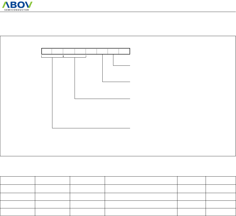
MC80F0304/08/16
November 4, 2011 Ver 2.12 87
Figure 16-3 Asynchronous Serial Interface Mode register (ASIMR) Format
BTCL
76543210
RXETXE ISRM
UART Stop Bit Length for Specification for Transmit Data bit
INITIAL VALUE: 0000 -00-B
ADDRESS: 0E6H
ASIMR -
R/W R/W - R/W R/W -
0: 1 bit
1: 2 bit
UART Receive interrupt request is issued when an error occurs bit
- SL PS1 PS0
R/W
UART Parity Bit Specification bit
00: No parity
01: Zero parity always added during transmission.
10: Odd parity
11: Even parity
UART Tx/Rx Enable bit
R/W
0: Receive Completion Interrupt Control When Error occurs
1: Receive completion interrupt request is not issued when an error occur
No parity detection during reception (parity errors do not occur)
00: Not used UART
01: UART Receive only Mode
10: UART Transmit only Mode
11: UART Receive & Transmit Mode
TXE (ASIMR.7) RXE(ASIMR.6) EC0(PSR0.4) Operation Mode RXD/R04 TXD/R05
00
X1Operation Stop R04 R05
0 1 0 UART mode (Receive only) RXD R05
1 0 X UART mode (Transmit only) R04 TXD
1 1 0 UART mode (Transmit and receive) RXD TXD
Table 16-2 UART mode and RXD/TXD pin function
1. X:The value "0" or "1" corresponding your operation
MC80F0304/08/16
88 November 4, 2011 Ver 2.12
Asynchronous serial interface status register (ASISR)
When a receive error occurs during UART mode, this register in-
dicates the type of error. ASISR can be read by an 8 bit memory
manipulation instruction. The RESET input sets ASISR to ----_-
000B. Figure 16-4 shows the format of ASISR.
Figure 16-4 Asynchronous Serial Interface Status Register (ASISR) Format
BTCL
76543210
-- FE
UART Frame Error Flag
INITIAL VALUE: ---- -000B
ADDRESS: 0E7H
ASISR OVE
RRR
0: No Frame error
1: Framing errorNote1 (stop bit not detected)
UART Parity Error Flag
- PE - -
UART Overrun Error Flag
0: No overrun error
1: Overrun errorNote2
0: No parity error
1: Parity error (Transmit data parity not matched)
Note 1. Even if a stop bit length is set to 2 bits by setting bit2(SL) in
ASIMR, stop bit detection during a recive operation only applies
to a stop bit length of 1bit.
2. Be sure to read the contents of the receive buffer register(RXR)
when an overrun error has occurred.
Until the contents of RXR are read, futher overrun errors will
occur when receiving data.
(Next receive operation was completed before data was read
from receive buffer register (RXR))
MC80F0304/08/16
November 4, 2011 Ver 2.12 89
Baud rate generator control register (BRGCR)
This register sets the serial clock for serial interface. BRGCR is
set by an 8 bit memory manipulation instruction. The RESET in-
put sets BRGCR to -001_0000B.
Figure 16-5 shows the format of BRGCR.
Figure 16-5 Baud Rate Generator Control Register (BRGCR) Format
16.3 Communication operation
The transmit operation is enabled when bit 7 (TXE) of the asyn-
chronous serial interface mode register (ASIMR) is set to 1. The
transmit operation is started when transmit data is written to the
transmit shift register (TXR). The timing of the transmit comple-
tion interrupt request is shown in Figure 16-6 .
The receive operation is enabled when bit 6 (RXE) of the asyn-
chronous serial interface mode register (ASIMR) is set to 1, and
input via the RxD pin is sampled. The serial clock specified by
ASIMR is used to sample the RxD pin. Once reception of one
data frame is completed, a receive completion interrupt request
(INT_RX) occurs. Even if an error has occurred, the receive data
in which the error occurred is still transferred to RXR. When
ASIMR bit 1 (ISRM) is cleared to 0 upon occurrence of an error,
and INT_RX occurs. When ISRM bit is set to 1, INT_RX does
not occur in case of error occurrence. Figure 16-6 shows the tim-
ing of the asynchronous serial interface receive completion inter-
BTCL
76543210
TPS2- MDL1 INITIAL VALUE: -001 0000B
ADDRESS: 0E8H
BRGCR MDL0
R/W R/W R/W R/W R/W R/W
MDL3 MDL2TPS1 TPS0
R/W
UART Source Clock Selection for 5 bit count
000: ACLK
001: fXIN ÷ 2
010: fXIN ÷ 4
011: fXIN ÷ 8
100: fXIN ÷ 16
101: fXIN ÷ 32
110: fXIN ÷ 64
111: fXIN ÷ 128
UART Input Clock Selection
0000: fSCK ÷ 16
0001: fSCK ÷ 17
0010: fSCK ÷ 18
0011: fSCK ÷ 19
0100: fSCK ÷ 20
0101: fSCK ÷ 21
0110: fSCK ÷ 22
0111: fSCK ÷ 23
1000: fSCK ÷ 24
1001: fSCK ÷ 25
1010: fSCK ÷ 26
1011: fSCK ÷ 27
1100: fSCK ÷ 28
1101: fSCK ÷ 29
1110: fSCK ÷ 30
1111: Setting prohibited
1. fSCK : Source clock for 5 bit counter
Remarks
Writing to BRGCR during a communication operation may cause abnormal output from the baud rate generator and
disable further communication operations. Therefore, do not write to BRGCR during a communication operation.
Caution
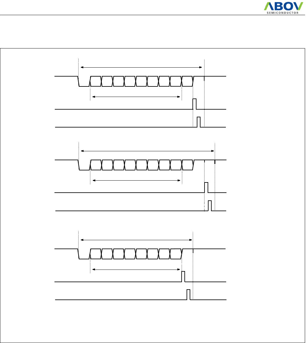
MC80F0304/08/16
90 November 4, 2011 Ver 2.12
rupt request.
Figure 16-6 UART data format and interrupt timing diagram
16.4 Relationship between main clock and baud rate
The transmit/receive clock that is used to generate the baud rate
is obtained by dividing the main system clock. Transmit/Receive
clock generation for baud rate is made by using main system
clock which is divided. The baud rate generated from the main
D0 D1
TxD
TX
D2
RxD D4D3 D6D5 D7 Parity
INTERRUPT
Stop
1 data frame
character bits
1 data frame consists of following bits.
- Start bit : 1 bit
- Character bits : 8 bits
- Parity bit : Even parity, Odd parity, Zero parity, No parity
- Stop bit(s) : 1 bit or 2 bits
RX
INTERRUPT
Start
1. Stop bit Length : 1 bit
D0 D1
TxD
TX
D2
RxD D4D3 D6D5 D7 Parity
INTERRUPT
Stop
1 data frame
character bits
RX
INTERRUPT
Start
2. Stop bit Length : 2 bit
D0 D1
TxD
TX
D2
RxD D4D3 D6D5 D7
INTERRUPT
1 data frame
character bits
RX
INTERRUPT
Start
3. Stop bit Length : 1 bit, No parity
Stop
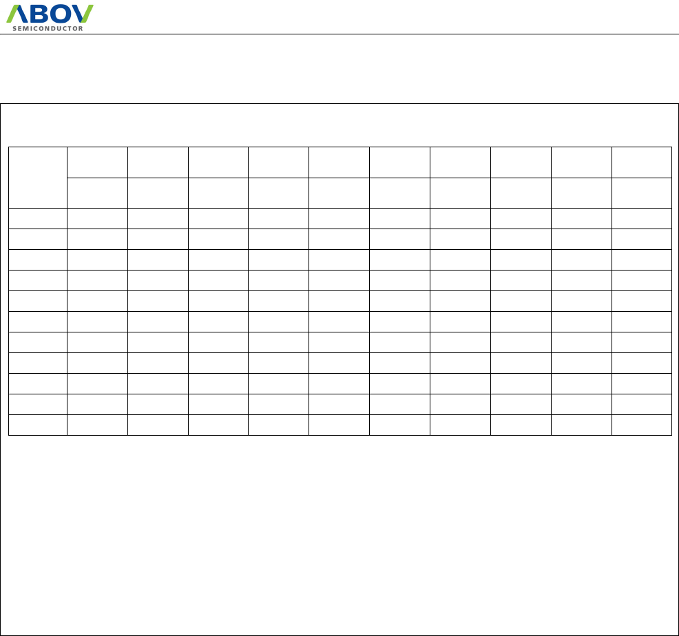
MC80F0304/08/16
November 4, 2011 Ver 2.12 91
system clock is determined according to the following formula.
Figure 16-7 Relationship between main clock and Baud Rate
Baud Rate
(bps)
fXIN=11.05
92M fXIN=10.0M fXIN=8.0M fXIN=4.0M fXIN=2.0M
BRGCR ERR(%) BRGCR ERR(%) BRGCR ERR(%) BRGCR ERR
(%) BRGCR ERR(%)
600 - - - - - - 7AH 0.16 6AH 0.16
1200 - - - - 7AH 0.16 6AH 0.16 5AH 0.16
2400 72H 0.00 70H 1.73 6AH 0.16 5AH 0.16 4AH 0.16
4800 62H 0.00 60H 1.73 5AH 0.16 4AH 0.16 3AH 0.16
9600 52H 0.00 50H 1.73 4AH 0.16 3AH 0.16 2AH 0.16
19200 42H 0.00 40H 1.73 3AH 0.16 2AH 0.16 1AH 0.16
31250 36H 0.53 34H 0.00 30H 0.00 20H 0.00 10H 0.00
38400 32H 0.00 30H 1.73 2AH 0.16 1AH 0.16 - -
57600 28H 0.00 26H 1.35 21H 2.11 11H 2.12 - -
76800 22H 0.00 20H 1.73 1AH 0.16 - - - -
115200 18H 0.00 16H 1.36 11H 2.12 - - - -
2. fSCK : Source clock for 5 bit counter
3. n : Value set via TPS0 to TPS2 ( 0 ≤ n ≤ 7 )
4. k : Source clock for 5 bit counter ( 0 ≤ k ≤ 14 )
Remarks 1. fXIN : Main system clock oscillation frequency
When ACLK is selected as the source clock of the 5-bit counter,
substitute the input clock frequency to ACLK pin for in the above expression.
Baud Rate = fXIN ÷ ( 2n+1(k+16) )
MC80F0304/08/16
92 November 4, 2011 Ver 2.12
17. BUZZER FUNCTION
The buzzer driver block consists of 6-bit binary counter, buzzer
register BUZR, and clock source selector. It generates square-
wave which has very wide range frequency (488Hz ~ 250kHz at
fXIN= 4MHz) by user software.
A 50% duty pulse can be output to R12 / BUZO pin to use for pi-
ezo-electric buzzer drive. Pin R12 is assigned for output port of
Buzzer driver by setting the bit 2 of PSR1(address 0F9H) to “1”.
For PSR1 register, refer to Figure 17-2 .
Example: 5kHz output at 4MHz.
LDM BUZR,#0011_0001B
LDM PSR1,#XXXX_X1XXB
X means don’t care
The bit 0 to 5 of BUZR determines output frequency for buzzer
driving.
Equation of frequency calculation is shown below.
fBUZ: Buzzer frequency
fXIN: Oscillator frequency
Divide Ratio: Prescaler divide ratio by BUCK[1:0]
BUR: Lower 6-bit value of BUZR. Buzzer period value.
The frequency of output signal is controlled by the buzzer control
register BUZR. The bit 0 to bit 5 of BUZR determine output fre-
quency for buzzer driving.
Figure 17-1 Block Diagram of Buzzer Driver
Figure 17-2 Buzzer Register & PSR1
f
BUZ
f
XIN
2
DivideRatio BUR
1+()××
---------------------------------------------------------------------------------=
Prescaler
÷ 8
÷ 32
÷ 16
÷ 64
BUR
R12/BUZO PIN
PSR1
Internal bus line
R12 port data
XIN PIN
2
6
[0E0H]
[0F9H]
0
1
F/F
Comparator
Compare data
6-BIT BINARY
MUX
00
01
10
11
Port selection register 1
MUX
BUZO
COUNTER
BUR[5:0]
BUZR
ADDRESS: 0E0H
RESET VALUE: 0FFH
WWWW WW
Source clock select
00: fXIN ÷ 8
01: fXIN ÷ 16
10: fXIN ÷ 32
11: fXIN ÷ 64
Buzzer Period Data
WW
BUCK1 BUCK0 PSR1
ADDRESS: 0F9H
RESET VALUE: ---- 0000B
BUZO
R12 / BUZO Selection
0: R12 port (Turn off buzzer)
1: BUZO port (Turn on buzzer)
-
-
-
- - -
-
MC80F0304/08/16
November 4, 2011 Ver 2.12 93
The 6-bit counter is cleared and starts the counting by writing sig-
nal at BUZR register. It is incremental from 00H until it matches
6-bit BUR value.
When main-frequency is 4MHz, buzzer frequency is shown as
below Table 17-1.
BUR
[5:0]
BUR[7:6] BUR
[5:0]
BUR[7:6]
00 01 10 11 00 01 10 11
00
01
02
03
04
05
06
07
250.000
125.000
83.333
62.500
50.000
41.667
35.714
31.250
125.000
62.500
41.667
31.250
25.000
20.833
17.857
15.625
62.500
31.250
20.833
15.625
12.500
10.417
8.929
7.813
31.250
15.625
10.417
7.813
6.250
5.208
4.464
3.906
20
21
22
23
24
25
26
27
7.576
7.353
7.143
6.944
6.757
6.579
6.410
6.250
3.788
3.676
3.571
3.472
3.378
3.289
3.205
3.125
1.894
1.838
1.786
1.736
1.689
1.645
1.603
1.563
0.947
0.919
0.893
0.868
0.845
0.822
0.801
0.781
08
09
0A
0B
0C
0D
0E
0F
27.778
25.000
22.727
20.833
19.231
17.857
16.667
15.625
13.889
12.500
11.364
10.417
9.615
8.929
8.333
7.813
6.944
6.250
5.682
5.208
4.808
4.464
4.167
3.906
3.472
3.125
2.841
2.604
2.404
2.232
2.083
1.953
28
29
2A
2B
2C
2D
2E
2F
6.098
5.952
5.814
5.682
5.556
5.435
5.319
5.208
3.049
2.976
2.907
2.841
2.778
2.717
2.660
2.604
1.524
1.488
1.453
1.420
1.389
1.359
1.330
1.302
0.762
0.744
0.727
0.710
0.694
0.679
0.665
0.651
10
11
12
13
14
15
16
17
14.706
13.889
13.158
12.500
11.905
11.364
10.870
10.417
7.353
6.944
6.579
6.250
5.952
5.682
5.435
5.208
3.676
3.472
3.289
3.125
2.976
2.841
2.717
2.604
1.838
1.736
1.645
1.563
1.488
1.420
1.359
1.302
30
31
32
33
34
35
36
37
5.102
5.000
4.902
4.808
4.717
4.630
4.545
4.464
2.551
2.500
2.451
2.404
2.358
2.315
2.273
2.232
1.276
1.250
1.225
1.202
1.179
1.157
1.136
1.116
0.638
0.625
0.613
0.601
0.590
0.579
0.568
0.558
18
19
1A
1B
1C
1D
1E
1F
10.000
9.615
9.259
8.929
8.621
8.333
8.065
7.813
5.000
4.808
4.630
4.464
4.310
4.167
4.032
3.906
2.500
2.404
2.315
2.232
2.155
2.083
2.016
1.953
1.250
1.202
1.157
1.116
1.078
1.042
1.008
0.977
38
39
3A
3B
3C
3D
3E
3F
4.386
4.310
4.237
4.167
4.098
4.032
3.968
3.907
2.193
2.155
2.119
2.083
2.049
2.016
1.984
1.953
1.096
1.078
1.059
1.042
1.025
1.008
0.992
0.977
0.548
0.539
0.530
0.521
0.512
0.504
0.496
0.488
Table 17-1 buzzer frequency (kHz unit)
MC80F0304/08/16
94 November 4, 2011 Ver 2.12
18. INTERRUPTS
The MC80F0304/0308/0316 interrupt circuits consist of Interrupt
enable register (IENH, IENL), Interrupt request flags of IRQH,
IRQL, Priority circuit, and Master enable flag (“I” flag of PSW).
Fifteen interrupt sources are provided. The configuration of inter-
rupt circuit is shown in Figure 18-1 and interrupt priority is
shown in Table 18-1.
The External Interrupts INT0 ~ INT3 each can be transition-acti-
vated (1-to-0 or 0-to-1 transition) by selection IEDS register.
The flags that actually generate these interrupts are bit INT0IF,
INT1IF, INT2IF and INT3IF in register IRQH. When an external
interrupt is generated, the generated flag is cleared by the hard-
ware when the service routine is vectored to only if the interrupt
was transition-activated.
The Timer 0 ~ Timer 3 Interrupts are generated by T0IF, T1IF,
T2IF and T3IF which is set by a match in their respective timer/
counter register.
The Basic Interval Timer Interrupt is generated by BITIF which
is set by an overflow in the timer register.
The AD converter Interrupt is generated by ADCIF which is set
by finishing the analog to digital conversion.
The Watchdog timer is generated by WDTIF which is set by a
match in Watchdog timer register.
Figure 18-1 Block Diagram of Interrupt
The Basic Interval Timer Interrupt is generated by BITIF which
is set by a overflow in the timer counter register.
UART Rx
INT2
INT1
INT0 INT0IF
IENH Interrupt Enable
Interrupt Enable
IRQH
IRQL
Internal bus line
Register (Lower byte)
Internal bus line
Register (Higher byte)
Release STOP/SLEEP
To CPU
Interrupt Master
Enable Flag
I-flag
IENL
Priority Control
I-flag is in PSW, it is cleared by “DI”, set by
“EI” instruction. When it goes interrupt service,
I-flag is cleared by hardware, thus any other
interrupt are inhibited. When interrupt service is
completed by “RETI” instruction, I-flag is set to
“1” by hardware.
[0EAH]
[0ECH]
[0EDH]
INT1IF
INT2IF
INT3IF
UARTRIF
T0IF
SIOIF
INT3
UART Tx
Timer 0
Serial
UARTTIF
Timer 1 T1IF
T3IF
Timer 2
Timer 3
T2IF
A/D Converter ADCIF
BITIF
Watchdog Timer
BIT
WDTIF
[0EBH]
Communication
Interrupt
Vector
Address
Generator
MC80F0304/08/16
November 4, 2011 Ver 2.12 95
The UART receive or transmit interrupts are generated by UAR-
TRIF or UARTTIF are set by completion of UART data recep-
tion or transmission.
The SIO interrupt is generated by SIOIF which is set by comple-
tion of SIO data reception or transmission.
The interrupts are controlled by the interrupt master enable flag
I-flag (bit 2 of PSW on Figure 8-3 ), the interrupt enable register
(IENH, IENL), and the interrupt request flags (in IRQH and
IRQL) except Power-on reset and software BRK interrupt. The
Table 18-1 shows the Interrupt priority.
Vector addresses are shown in Figure 8-6 . Interrupt enable reg-
isters are shown in Figure 18-2 . These registers are composed of
interrupt enable flags of each interrupt source and these flags de-
termines whether an interrupt will be accepted or not. When en-
able flag is “0”, a corresponding interrupt source is prohibited.
Note that PSW contains also a master enable bit, I-flag, which
disables all interrupts at once.
Figure 18-2 Interrupt Enable Flag Register
Reset/Interrupt Symbol Priority
Hardware Reset
External Interrupt 0
External Interrupt 1
External Interrupt 2
External Interrupt 3
UART Rx Interrupt
UART Tx Interrupt
Serial Input/Output
Timer/Counter 0
Timer/Counter 1
Timer/Counter 2
Timer/Counter 3
ADC Interrupt
Watchdog Timer
Basic Interval Timer
RESET
INT0
INT1
INT2
INT3
INT_RX
INT_TX
SIO
Timer 0
Timer 1
Timer 2
Timer 3
ADC
WDT
BIT
1
2
3
4
5
6
7
8
9
10
11
12
13
14
15
Table 18-1 Interrupt Priority
INT3E
R/W
INT0E
Timer/Counter 0 interrupt enable flag
INITIAL VALUE: 0000 0000B
ADDRESS: 0EAH
IENH INT1E
MSB LSB
SIOE T0E
UARTRE
INT2E
R/W R/W
Serial Communication interrupt enable flag
UART Tx interrupt enable flag
External interrupt 3 enable flag
UART Rx interrupt enable flag
R/W R/WR/W R/W R/W
External interrupt 2 enable flag
External interrupt 1 enable flag
External interrupt 0 enable flag
R/W
T1E INITIAL VALUE: 000- 00-0B
ADDRESS: 0EBH
IENL T2E
MSB
R/W
Timer/Counter 3 interrupt enable flag
R/W R/W
Timer/Counter 2 interrupt enable flag
Timer/Counter 1 interrupt enable flag
LSB
R/W
ADCE WDTE
R/WR/W R/W
T3E - - BITE
Basic Interval Timer interrupt enable flag
Watchdog timer interrupt enable flag
A/D Converter interrupt enable flag
UARTTE

MC80F0304/08/16
96 November 4, 2011 Ver 2.12
Figure 18-3 Interrupt Request Flag Register
18.1 Interrupt Sequence
An interrupt request is held until the interrupt is accepted or the
interrupt latch is cleared to “0” by a reset or an instruction. Inter-
rupt acceptance sequence requires 8 cycles of fXIN (2μs at fX-
IN=4MHz) after the completion of the current instruction
execution. The interrupt service task is terminated upon execu-
tion of an interrupt return instruction [RETI].
Interrupt acceptance
1. The interrupt master enable flag (I-flag) is cleared to
“0” to temporarily disable the acceptance of any follow-
ing maskable interrupts. When a non-maskable inter-
rupt is accepted, the acceptance of any following
interrupts is temporarily disabled.
2. The contents of the program counter (return address)
and the program status word are saved (pushed) onto the
stack area. The stack pointer decreases 3 times.
3. The entry address of the interrupt service program is
read from the vector table address and the entry address
is loaded to the program counter.
4. The instruction stored at the entry address of the inter-
INT3IF
R/W
INT0IF
Timer/Counter 0 interrupt request flag
INITIAL VALUE: 0000 0000B
ADDRESS: 0ECH
IRQH INT1IF
MSB LSB
SIOIF T0IF
UARTRIF UARTTIF
INT2IF
R/W R/W
Serial Communication interrupt request flag
UART Tx interrupt request flag
External interrupt 3 request flag
UART Rx interrupt request flag
R/W R/WR/W R/W R/W
External interrupt 2 request flag
External interrupt 1 request flag
External interrupt 0 request flag
R/W
T1IF INITIAL VALUE: 000- 00-0B
ADDRESS: 0EDH
IRQL T2IF
MSB
-
Timer/Counter 3 interrupt request flag
R/W R/W
Timer/Counter 2 interrupt request flag
Timer/Counter 1 interrupt request flag
LSB
-
ADCIF WDTIF
R/WR/W R/W
T3IF - - BITIF
Basic Interval Timer interrupt request flag
Watchdog timer interrupt request flag
A/D Converter interrupt request flag
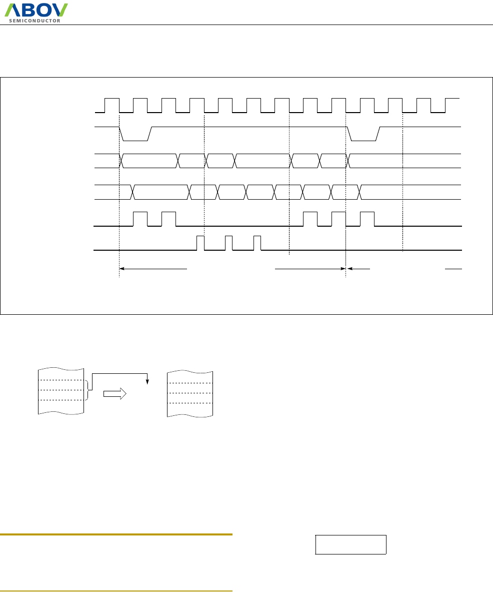
MC80F0304/08/16
November 4, 2011 Ver 2.12 97
rupt service program is executed.
Figure 18-4 Timing chart of Interrupt Acceptance and Interrupt Return Instruction
A interrupt request is not accepted until the I-flag is set to “1”
even if a requested interrupt has higher priority than that of the
current interrupt being serviced.
When nested interrupt service is required, the I-flag should be set
to “1” by “EI” instruction in the interrupt service program. In this
case, acceptable interrupt sources are selectively enabled by the
individual interrupt enable flags.
Clearing Interrupt Request Flag
The Interrupt Request flag may not cleared itself during interrupt
acceptance processing. After interrupt acceptance, it should be
cleard as shown in interrupt service routine.
Note: The MC80F0316 and HMS87C1416B is similar in
function, but the interrupt processing method is different.
When replacing the HMS87C1416B to MC80F0316, clear-
ing interrupt request flag should be added.
Example: Clearing Interrupt Request Flag
Saving/Restoring General-purpose Register
During interrupt acceptance processing, the program counter and
the program status word are automatically saved on the stack, but
accumulator and other registers are not saved itself. These regis-
ters are saved by the software if necessary. Also, when multiple
interrupt services are nested, it is necessary to avoid using the
same data memory area for saving registers.
The following method is used to save/restore the general-purpose
registers.
V.L.
System clock
Address Bus PC SP SP-1 SP-2 V.H. New PC
V.L.
Data Bus Not used PCH PCL PSW ADL OP codeADH
Instruction Fetch
Internal Read
Internal Write
Interrupt Processing Step Interrupt Service Task
V.L. and V.H. are vector addresses.
ADL and ADH are start addresses of interrupt service routine as vector contents.
Basic Interval Timer
012H
0E3H
0FFE0H
0FFE1H
0EH
2EH
0E312H
0E313H
Entry Address
Correspondence between vector table address for BIT interrupt
and the entry address of the interrupt service program.
Vector Table Address
T1_INT: CLR1 T1IF ;CLEAR T1 REQUEST
interrupt processing
RETI ;RETURN
MC80F0304/08/16
98 November 4, 2011 Ver 2.12
Example: Register save using push and pop instructions
General-purpose register save/restore using push and pop instruc-
tions;
18.2 BRK Interrupt
Software interrupt can be invoked by BRK instruction, which has
the lowest priority order.
Interrupt vector address of BRK is shared with the vector of
TCALL 0 (Refer to Program Memory Section). When BRK inter-
rupt is generated, B-flag of PSW is set to distinguish BRK from
TCALL 0.
Each processing step is determined by B-flag as shown in Figure
18-5 .
Figure 18-5 Execution of BRK/TCALL0
18.3 Multi Interrupt
If two requests of different priority levels are received simulta-
neously, the request of higher priority level is serviced. If re-
quests of the interrupt are received at the same time
simultaneously, an internal polling sequence determines by hard-
ware which request is serviced. However, multiple processing
through software for special features is possible. Generally when
an interrupt is accepted, the I-flag is cleared to disable any further
interrupt. But as user sets I-flag in interrupt routine, some further
INTxx: CLR1 INTxxIF
PUSH A
PUSH X
PUSH Y
;CLEAR REQUEST.
;SAVE ACC.
;SAVE X REG.
;SAVE Y REG.
interrupt processing
POP Y
POP X
POP A
RETI
;RESTORE Y REG.
;RESTORE X REG.
;RESTORE ACC.
;RETURN
B-FLAG
BRK
INTERRUPT
ROUTINE
RETI
TCALL0
ROUTINE
RET
BRK or
TCALL0
=0
=1
MC80F0304/08/16
November 4, 2011 Ver 2.12 99
interrupt can be serviced even if certain interrupt is in progress.
Figure 18-6 Execution of Multi Interrupt
Example: During Timer1 interrupt is in progress, INT0 interrupt
serviced without any suspend.
TIMER1: CLR1 T1IF ;Clear Timer1 Request
PUSH A
PUSH X
PUSH Y
LDM IENH,#80H ;Enable INT0 only
LDM IENL,#0 ;Disable other int.
EI ;Enable Interrupt
:
:
:
:
:
:
LDM IENH,#0FFH ;Enable all interrupts
LDM IENL,#0FFH
POP Y
POP X
POP A
RETI
18.4 External Interrupt
The external interrupt on INT0, INT1, INT2 and INT3 pins are
edge triggered depending on the edge selection register IEDS (ad-
dress 0EEH) as shown in Figure 18-7 .
The edge detection of external interrupt has three transition acti-
vated mode: rising edge, falling edge, and both edge.
enable INT0
TIMER 1
service
INT0
service
Main Program
service
Occur
TIMER1 interrupt Occur
INT0
EI
disable other
enable INT0
enable other
In this example, the INT0 interrupt can be serviced without any
pending, even TIMER1 is in progress.
Because of re-setting the interrupt enable registers IENH,IENL
and master enable “EI” in the TIMER1 routine.
MC80F0304/08/16
100 November 4, 2011 Ver 2.12
Figure 18-7 External Interrupt Block Diagram
INT0 ~ INT3 are multiplexed with general I/O ports (R11, R12,
R03, R00). To use as an external interrupt pin, the bit of port se-
lection register PSR0 should be set to “1” correspondingly.
Example: To use as an INT0 and INT2
:
;**** Set external interrupt port as pull-up state.
LDM PU1,#0000_0101B
;
;**** Set port as an external interrupt port
LDM PSR0,#0000_0101B
;
;**** Set Falling-edge Detection
LDM IEDS,#0001_0001B
:
Response Time
The INT0 ~ INT3 edge are latched into INT0IF ~ INT3IF at every
machine cycle. The values are not actually polled by the circuitry
until the next machine cycle. If a request is active and conditions
are right for it to be acknowledged, a hardware subroutine call to
the requested service routine will be the next instruction to be ex-
ecuted. The DIV itself takes twelve cycles. Thus, a minimum of
twelve complete machine cycles elapse between activation of an
external interrupt request and the beginning of execution of the
first instruction of the service routine.
Figure 18-8 shows interrupt response timings.
Figure 18-8 Interrupt Response Timing Diagram
INT0IF
INT0 pin INT0 INTERRUPT
INT1IF
INT1 pin INT1 INTERRUPT
INT2IF
INT2 pin INT2 INTERRUPT
IEDS
[0EEH]
INT3IF
INT3 pin INT3 INTERRUPT
Edge selection
Register
2 2 2 2
01
10
11
01
10
11
01
10
11
01
10
11
Interrupt
goes
active
Interrupt
latched Interrupt
processing
Interrupt
routine
8 fXIN
max. 12 fXIN
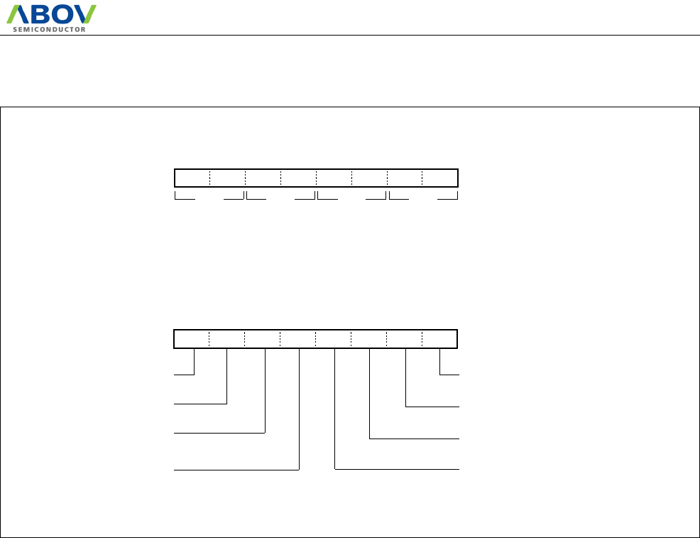
MC80F0304/08/16
November 4, 2011 Ver 2.12 101
Figure 18-9 IEDS register and Port Selection Register PSR0
BTCL
WWWWWWWW
EC1EPWM1O
PWM3O
INT1E
0: R11
1: INT0
INITIAL VALUE: 00H
ADDRESS: 0F8H
PSR0 EC0E INT0EINT2EINT3E
0: R12
1: INT1
0: R03
1: INT2
0: R00
1: INT3
0: R11
1: PWM3O
0: R07
1: EC1
0: R04
1: EC0
LSBMSB
BTCL
WWWWWWWW
IED2HIED3LIED3H IED0H INITIAL VALUE: 00H
ADDRESS: 0EEH
IEDS IED2L IED0LIED1LIED1H
LSBMSB
Edge selection register
00: Reserved
01: Falling (1-to-0 transition)
10: Rising (0-to-1 transition)
11: Both (Rising & Falling)
INT0
INT1INT2INT3
0: R10
1: PWM1O
MC80F0304/08/16
102 November 4, 2011 Ver 2.12
19. POWER SAVING OPERATION
The MC80F0304/0308/0316 has two power-down modes. In
power-down mode, power consumption is reduced considerably.
For applications where power consumption is a critical factor, de-
vice provides two kinds of power saving functions, STOP mode
and SLEEP mode. Table 19-1 shows the status of each Power
Saving Mode. SLEEP mode is entered by the SSCR register to
“0Fh”., and STOP mode is entered by STOP instruction after the
SSCR register to “5Ah”.
19.1 Sleep Mode
In this mode, the internal oscillation circuits remain active.
Oscillation continues and peripherals are operate normally but
CPU stops. Movement of all peripherals is shown in Table 19-1.
SLEEP mode is entered by setting the SSCR register to “0Fh”. It
is released by Reset or interrupt. To be released by interrupt, in-
terrupt should be enabled before SLEEP mode.
Figure 19-1 STOP and SLEEP Control Register
Release the SLEEP mode
The exit from SLEEP mode is hardware reset or all interrupts.
Reset re-defines all the Control registers but does not change the
on-chip RAM. Interrupts allow both on-chip RAM and Control
registers to retain their values.
If I-flag = 1, the normal interrupt response takes place. If I-flag =
0, the chip will resume execution starting with the instruction fol-
lowing the SLEEP instruction. It will not vector to interrupt ser-
vice routine. (refer to Figure 19-4 )
When exit from SLEEP mode by reset, enough oscillation stabi-
lizing time is required to normal operation. Figure 19-3 shows
the timing diagram. When released from the SLEEP mode, the
Basic interval timer is activated on wake-up. It is increased from
00H until FFH. The count overflow is set to start normal opera-
tion. Therefore, before SLEEP instruction, user must be set its
relevant prescaler divide ratio to have long enough time (more
than 20msec). This guarantees that oscillator has started and sta-
bilized. By interrupts, exit from SLEEP mode is shown in Figure
19-2 . By reset, exit from SLEEP mode is shown in Figure 19-3 .
76543210
INITIAL VALUE: 0000 0000B
ADDRESS: 0F5H
SSCR
W
Power Down Control
5AH: STOP mode
0FH: SLEEP mode
W W W W W W W
NOTE :
To get into STOP mode, SSCR must be set to 5AH just before STOP instruction execution.
At STOP mode, Stop & Sleep Control Register (SSCR) value is cleared automatically when released.
To get into SLEEP mode, SSCR must be set to 0FH.
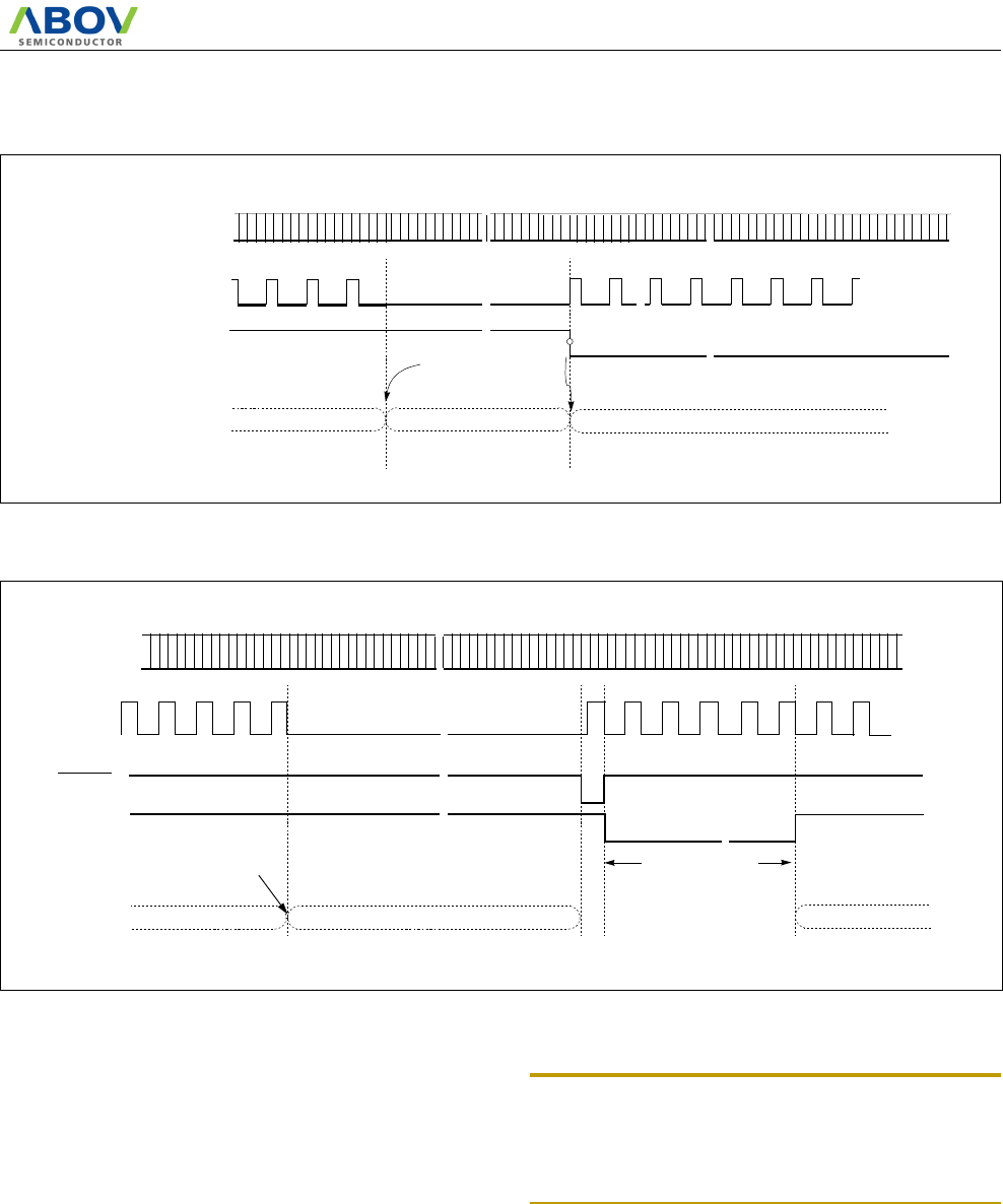
MC80F0304/08/16
November 4, 2011 Ver 2.12 103
.
Figure 19-2 SLEEP Mode Release Timing by External Interrupt
Figure 19-3 Timing of SLEEP Mode Release by Reset
19.2 Stop Mode
In the Stop mode, the main oscillator, system clock and peripher-
al clock is stopped, but RC-oscillated watchdog timer continue to
operate. With the clock frozen, all functions are stopped, but the
on-chip RAM and Control registers are held. The port pins out the
values held by their respective port data register, port direction
registers. Oscillator stops and the systems internal operations are
all held up.
• The states of the RAM, registers, and latches valid
immediately before the system is put in the STOP
state are all held.
• The program counter stop the address of the
instruction to be executed after the instruction
"STOP" which starts the STOP operating mode.
Note: The Stop mode is activated by execution of STOP instruc-
tion after setting the SSCR to “5AH”. (This register should be writ-
ten by byte operation. If this register is set by bit manipulation
instruction, for example "set1" or "clr1" instruction, it may be undes-
ired operation)
In the Stop mode of operation, VDD can be reduced to minimize
power consumption. Care must be taken, however, to ensure that
VDD is not reduced before the Stop mode is invoked, and that
VDD is restored to its normal operating level, before the Stop
mode is terminated.
The reset should not be activated before VDD is restored to its
normal operating level, and must be held active long enough to
allow the oscillator to restart and stabilize.
Oscillator
(XIN pin)
~
~
Normal Operation SLEEP Operation
~
~
~
~~
~
~
~
External Interrupt
Internal Clock
SLEEP Instruction
Executed
~
~
Normal Operation
~
~
~
~
~
~
SLEEP Instruction Stabilization Time
tST = 65.5mS @4MHz
Internal
~
~
~
~
~
~
RESET
RESET
Oscillator
(XIN pin)
~
~
CPU
Clock
~
~~
~
Execution
Normal Operation SLEEP Operation Normal Operation
MC80F0304/08/16
104 November 4, 2011 Ver 2.12
Note: After STOP instruction, at least two or more NOP instruc-
tion should be written.
Ex) LDM CKCTLR,#0FH ;more than 20ms
LDM SSCR,#5AH
STOP
NOP ;for stabilization time
NOP ;for stabilization time
In the STOP operation, the dissipation of the power associated
with the oscillator and the internal hardware is lowered; however,
the power dissipation associated with the pin interface (depend-
ing on the external circuitry and program) is not directly deter-
mined by the hardware operation of the STOP feature. This point
should be little current flows when the input level is stable at the
power voltage level (VDD/VSS); however, when the input level
gets higher than the power voltage level (by approximately 0.3 to
0.5V), a current begins to flow. Therefore, if cutting off the out-
put transistor at an I/O port puts the pin signal into the high-im-
pedance state, a current flow across the ports input transistor,
requiring to fix the level by pull-up or other means.
Release the STOP mode
The source for exit from STOP mode is hardware reset, external
interrupt, Timer(EC0,1), Watch Timer, WDT, SIO or UART.
When releasing from the STOP mode by the SIO(ext.clock), the
SIOR has dummy data and the SIOST bit should be cleard after
release from the STOP mode.
Reset re-defines all the Control registers but does not change the
on-chip RAM. External interrupts allow both on-chip RAM and
Control registers to retain their values.
If I-flag = 1, the normal interrupt response takes place. If I-flag =
0, the chip will resume execution starting with the instruction fol-
lowing the STOP instruction. It will not vector to interrupt service
routine. (refer to Figure 19-4 )
When exit from Stop mode by external interrupt, enough oscilla-
tion stabilizing time is required to normal operation. Figure 19-5
shows the timing diagram. When released from the Stop mode,
the Basic interval timer is activated on wake-up. It is increased
from 00H until FFH. The count overflow is set to start normal op-
eration. Therefore, before STOP instruction, user must be set its
relevant prescaler divide ratio to have long enough time (more
than 20msec). This guarantees that oscillator has started and sta-
bilized.
By reset, exit from Stop mode is shown in Figure 19-6 .
Peripheral STOP Mode SLEEP Mode
CPU Stop Stop
RAM Retain Retain
Basic Interval Timer Halted Operates Continuously
Watchdog Timer Stop (Only operates in RC-WDT mode) Stop
Timer/Counter Halted (Only when the event counter mode
is enabled, timer operates normally) Operates Continuously
Buzzer, ADC Stop Stop
SIO Only operate with external clock Only operate with external clock
UART Only operate with external clock Only operate with external clock
Oscillator Stop (XIN=L, XOUT=H) Oscillation
I/O Ports Retain Retain
Control Registers Retain Retain
Internal Circuit Stop mode Sleep mode
Prescaler Retain Active
Address Data Bus Retain Retain
Release Source
Reset, Timer(EC0,1), SIO, UART0(using
ACLK0), UART1(using ACLK1)
Watch Timer (RC-WDT mode),
Watchdog Timer (RC-WDT mode),
External Interrupt
Reset, All Interrupts
Table 19-1 Peripheral Operation During Power Saving Mode
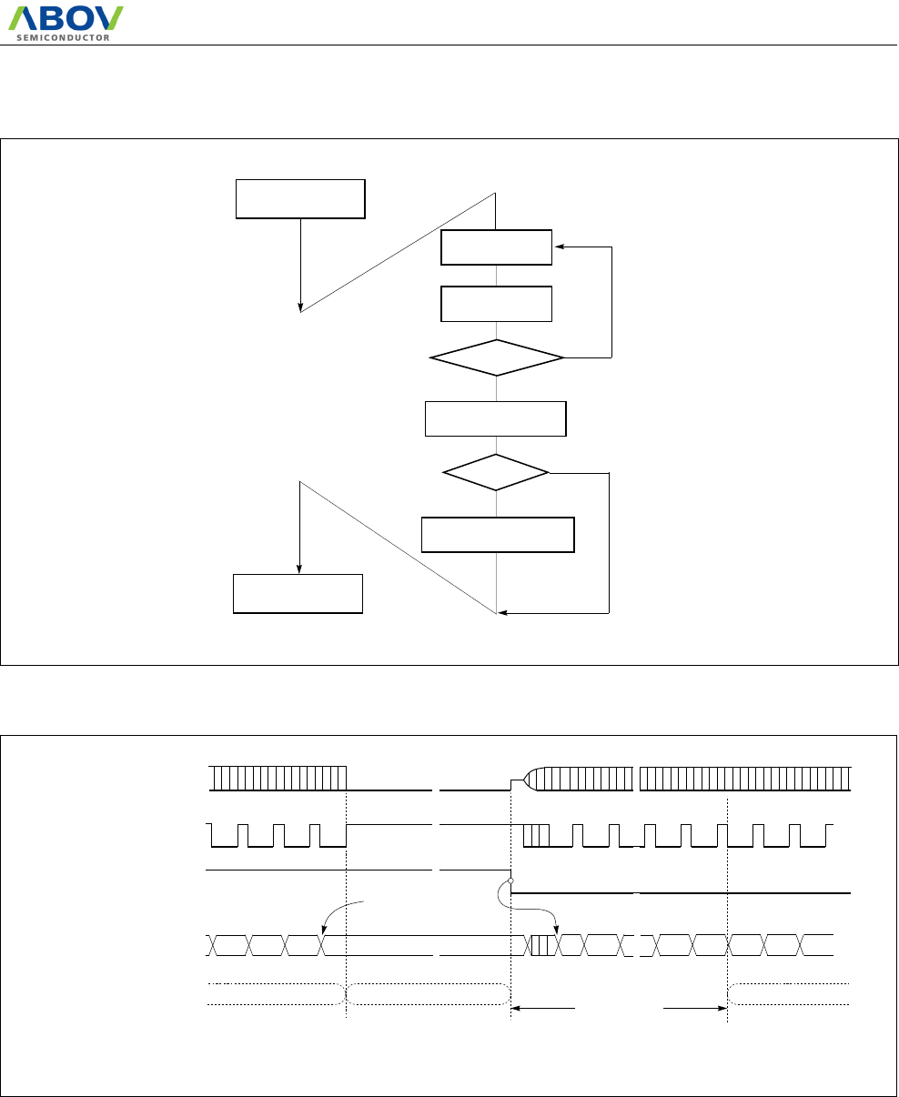
MC80F0304/08/16
November 4, 2011 Ver 2.12 105
Figure 19-4 STOP Releasing Flow by Interrupts
.
Figure 19-5 STOP Mode Release Timing by External Interrupt
IENH or IENL ?
=0
=1
STOP
INSTRUCTION
STOP Mode
Interrupt Request
STOP Mode Release
I-FLAG
=1
Interrupt Service Routine
Next
INSTRUCTION
=0
Master Interrupt
Enable Bit PSW[2]
Corresponding Interrupt
Enable Bit (IENH, IENL)
Before executing Stop instruction, Basic Interval Timer must be set
Oscillator
(XIN pin)
~
~
n0
BIT Counter n+1 n+2 n+3
~
~
Normal Operation Stop Operation Normal Operation
1FE FF 012
~
~
~
~
~
~
tST > 20ms
~
~
~
~
External Interrupt
Internal Clock
Clear
STOP Instruction
Executed
~
~~
~
~
~
properly by software to get stabilization time which is longer than 20ms.
by software
~
~
Stabilization Time
MC80F0304/08/16
106 November 4, 2011 Ver 2.12
Figure 19-6 Timing of STOP Mode Release by Reset
19.3 Stop Mode at Internal RC-Oscillated Watchdog Timer Mode
In the Internal RC-Oscillated Watchdog Timer mode, the on-chip
oscillator is stopped. But internal RC oscillation circuit is oscil-
lated in this mode. The on-chip RAM and Control registers are
held. The port pins out the values held by their respective port
data register, port direction registers.
The Internal RC-Oscillated Watchdog Timer mode is activated
by execution of STOP instruction after setting the bit RCWDT of
CKCTLR to "1". (This register should be written by byte opera-
tion. If this register is set by bit manipulation instruction, for ex-
ample "set1" or "clr1" instruction, it may be undesired operation)
Note: Caution: After STOP instruction, at least two or more NOP
instruction should be written
Ex) LDM WDTR,#1111_1111B
LDM CKCTLR,#0010_1110B
LDM SSCR,#0101_1010B
STOP
NOP ;for stabilization time
NOP ;for stabilization time
The exit from Internal RC-Oscillated Watchdog Timer mode is
hardware reset or external interrupt or watchdog timer interrupt
(at RC-watchdog timer mode). Reset re-defines all the Control
registers but does not change the on-chip RAM. External inter-
rupts allow both on-chip RAM and Control registers to retain
their values.
If I-flag = 1, the normal interrupt response takes place. In this
case, if the bit WDTON of CKCTLR is set to "0" and the bit
WDTE of IENH is set to "1", the device will execute the watch-
dog timer interrupt service routine(Figure 8-6 ). However, if the
bit WDTON of CKCTLR is set to "1", the device will generate
the internal Reset signal and execute the reset processing(Figure
19-8 ). If I-flag = 0, the chip will resume execution starting with
the instruction following the STOP instruction. It will not vector
to interrupt service routine.(refer to Figure 19-4 )
When exit from Stop mode at Internal RC-Oscillated Watchdog
Timer mode by external interrupt, the oscillation stabilization
time is required to normal operation. Figure 19-7 shows the tim-
ing diagram. When release the Internal RC-Oscillated Watchdog
Timer mode, the basic interval timer is activated on wake-up. It
is increased from 00H until FFH. The count overflow is set to start
normal operation. Therefore, before STOP instruction, user must
be set its relevant prescaler divide ratio to have long enough time
(more than 20msec). This guarantees that oscillator has started
and stabilized. By reset, exit from internal RC-Oscillated Watch-
dog Timer mode is shown in Figure 19-8 .
~
~
STOP Mode
Time can not be control by software
Oscillator
(XI pin)
~
~~
~
~
~
STOP Instruction Execution
Stabilization Time
tST = 65.5mS @4MHz
Internal
Clock
Internal
~
~
~
~
~
~
~
~
~
~
RESET
RESET
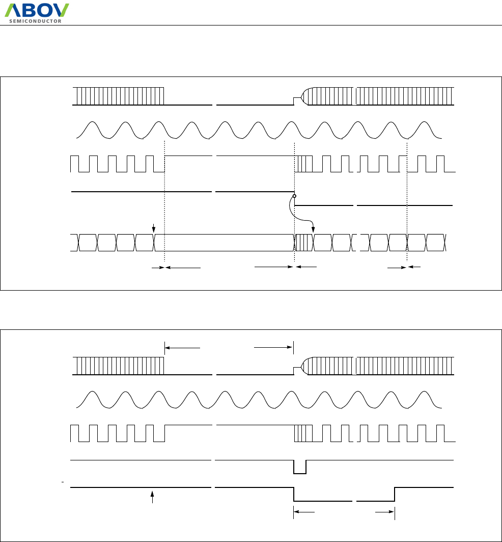
MC80F0304/08/16
November 4, 2011 Ver 2.12 107
Figure 19-7 Stop Mode Release at Internal RC-WDT Mode by External Interrupt or WDT Interrupt
Figure 19-8 Internal RC-WDT Mode Releasing by Reset
19.4 Minimizing Current Consumption
The Stop mode is designed to reduce power consumption. To
minimize current drawn during Stop mode, the user should turn-
off output drivers that are sourcing or sinking current, if it is prac-
~
~
STOP mode Normal Operation
Oscillator
(XIN pin)
~
~~
~
N+1NN+2 00 01 FE FF 00 00
N-1
N-2
~
~~
~
~
~
~
~~
~
Clear Basic Interval Timer
STOP Instruction Execution
Normal Operation Stabilization Time
tST > 20mS
Internal
Clock
External
Interrupt
BIT
Counter
~
~
Internal
RC Clock
( or WDT Interrupt )
at RC-WDT Mode
~
~
Oscillator
(XIN pin)
~
~
~
~
~
~~
~
Internal
Clock
Internal
RC Clock
Time can not be control by software
~
~
STOP Instruction Execution
Stabilization Time
tST = 65.5mS @4MHz
Internal
~
~
~
~
~
~
RESET by WDT
RESET
RESET
RCWDT Mode
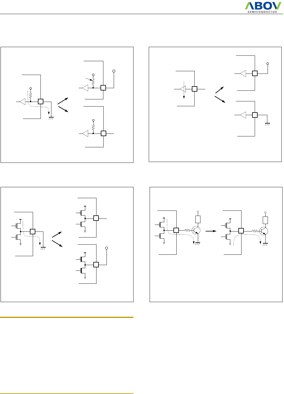
MC80F0304/08/16
108 November 4, 2011 Ver 2.12
tical.
Figure 19-9 Application Example of Unused Input Port
Figure 19-10 Application Example of Unused Output Port
Note: In the STOP operation, the power dissipation associated
with the oscillator and the internal hardware is lowered; however,
the power dissipation associated with the pin interface (depending
on the external circuitry and program) is not directly determined by
the hardware operation of the STOP feature. This point should be
little current flows when the input level is stable at the power volt-
age level (VDD/VSS); however, when the input level becomes high-
er than the power voltage level (by approximately 0.3V), a current
begins to flow. Therefore, if cutting off the output transistor at an I/
O port puts the pin signal into the high-impedance state, a current
flow across the ports input transistor, requiring it to fix the level by
pull-up or other means.
It should be set properly in order that current flow through port
doesn't exist.
First consider the port setting to input mode. Be sure that there is
no current flow after considering its relationship with external
circuit. In input mode, the pin impedance viewing from external
MCU is very high that the current doesn’t flow.
But input voltage level should be VSS or VDD. Be careful that if
unspecified voltage, i.e. if uncertain voltage level (not VSS or
VDD) is applied to input pin, there can be little current (max. 1mA
at around 2V) flow.
If it is not appropriate to set as an input mode, then set to output
mode considering there is no current flow. The port setting to
INPUT PIN
VDD
GND
i
VDD
X
Weak pull-up current flows
VDD
internal
pull-up
INPUT PIN
i
VDD
X
Very weak current flows
VDD
O
O
OPEN
OPEN
i=0
O
i=0
O
GND
When port is configured as an input, input level should
be closed to 0V or 5V to avoid power consumption.
OUTPUT PIN
GND
i
In the left case, much current flows from port to GND.
X
ON
OFF
OUTPUT PIN
GND
i
In the left case, Tr. base current flows from port to GND.
i=0
X
OFF
ON
VDD
L
ON
OFF
OPEN
GND
VDD
L
ON
OFF
To avoid power consumption, there should be low output
ON
OFF
O
O
VDD
O
to the port .

MC80F0304/08/16
November 4, 2011 Ver 2.12 109
High or Low is decided by considering its relationship with exter-
nal circuit. For example, if there is external pull-up resistor then
it is set to output mode, i.e. to High, and if there is external pull-
down register, it is set to low.
MC80F0304/08/16
110 November 4, 2011 Ver 2.12
20. RESET
The MC80F0304/0308/0316 supports various kinds of reset as
below.
• Power-On Reset (POR)
• RESET (external reset circuitry)
• Watchdog Timer Timeout Reset
• Power-Fail Detection (PFD) Reset
• Address Fail Reset
Figure 20-1 RESET Block Diagram
The on-chip POR circuit holds down the device in RESET until
VDD has reached a high enough level for proper operation. It will
eliminate external components such as reset IC or external resis-
tor and capacitor for external reset circuit. In addition that the RE-
SET pin can be used to normal input port R35 by setting “POR”
and “R35EN” bit Configuration Area(20FFH) in the Flash pro-
gramming. When the device starts normal operation, its operating
parmeters (voltage, frequency, temperature...etc) must be met.
.Table 20-1 shows on-chip hardware initialization by reset action.
Table 20-1 Initializing Internal Status by Reset Action
The reset input is the RESET pin, which is the input to a Schmitt
Trigger. A reset in accomplished by holding the RESET pin low
for at least 8 oscillator periods, within the operating voltage range
and oscillation stable, it is applied, and the internal state is initial-
ized. After reset, 65.5ms (at 4 MHz) add with 7 oscillator periods
are required to start execution as shown in Figure 20-3 .
Internal RAM is not affected by reset. When VDD is turned on,
the RAM content is indeterminate. Therefore, this RAM should
be initialized before read or tested it.
When the RESET pin input goes to high, the reset operation is re-
leased and the program execution starts at the vector address
stored at addresses FFFEH - FFFFH.
A connection for simple power-on-reset is shown in Figure 20-2 .
Figure 20-2 Simple Power-on-Reset Circuit
POR
(Power-On Reset)
Address Fail reset
PFD
(Power-Fail Detection)
WDT
(WDT Timeout Reset)
S
R
Q
BIT
Internal
RESET
RESET
Clear
Overflow
Noise Canceller
On-chip Hardware Initial Value On-chip Hardware Initial Value
Program counter (PC) (FFFFH) - (FFFEH)Peripheral clock Off
RAM page register (RPR) 0 Watchdog timer Enable
G-flag (G) 0 Control registers Refer to Table 8-1 on page 38
Operation mode Main-frequency clock Power fail detector Disable
7036P
VCC
10uF
+
10kΩ
to the RESET pin
MC80F0304/08/16
November 4, 2011 Ver 2.12 111
Figure 20-3 Timing Diagram after Reset
The Address Fail Reset is the function to reset the system by
checking code access of abnormal and unwished address caused
by erroneous program code itself or external noise, which could
not be returned to normal operation and would become malfunc-
tion state. If the CPU tries to fetch the instruction from ineffective
code area or RAM area, the address fail reset is occurred. Please
refer to Figure 11-2 for setting address fail option.
MAIN PROGRAM
Oscillator
(XIN pin)
??FFFE FFFF
Stabilization Time
tST =65.5mS at 4MHz
RESET
ADDRESS
DATA
1234567
?? Start
??? FE
?ADL ADH OP
BUS
BUS
Reset Process Step
~
~~
~~
~~
~~
~
~
~
tST = x 256
fXIN ÷1024
1
MC80F0304/08/16
112 November 4, 2011 Ver 2.12
21. POWER FAIL PROCESSOR
The MC80F0304/0308/0316 has an on-chip power fail detection
circuitry to immunize against power noise. A configuration reg-
ister, PFDR, can enable or disable the power fail detect circuitry.
Whenever VDD falls close to or below power fail voltage for
100ns, the power fail situation may reset or freeze MCU accord-
ing to PFDM bit of PFDR. Refer to “Figure 21-1 Power Fail Volt-
age Detector Register” on page 112.
In the in-circuit emulator, power fail function is not implemented
and user can not experiment with it. Therefore, after final devel-
opment of user program, this function may be experimented or
evaluated.
Figure 21-1 Power Fail Voltage Detector Register
Figure 21-2 Example S/W of Reset flow by Power fail
PFDM
76543210
PFDS INITIAL VALUE: ---- -000B
ADDRESS: 0F7H
PFDR
R/W R/W R/W
PFDEN
PFD Operation Mode
0 : MCU will be frozen by power fail detection
1 : MCU will be reset by power fail detection
PFD Enable Bit
0: Power fail detection disable
1: Power fail detection enable
Power Fail Status
0: Normal operate
1: Set to “1” if power fail is detected
* Cautions : Be sure to set bits 3 through 7 to “0”.
-----
Function
Execution
Initialize RAM Data
PFDS =1
NO
RESET VECTOR
Initialize All Ports
Initialize Registers
RAM Clear
YES
Skip the
initial routine
PFDS = 0
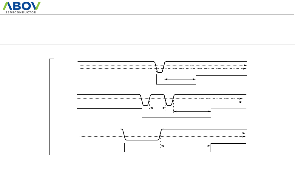
MC80F0304/08/16
November 4, 2011 Ver 2.12 113
Figure 21-3 Power Fail Processor Situations (at 4MHz operation)
Internal
RESET
Internal
RESET
Internal
RESET
VDD
VDD
VDD
VPFDMAX
VPFDMIN
VPFDMAX
VPFDMIN
VPFDMAX
VPFDMIN
65.5mS
65.5mS
t < 65.5mS
65.5mS
When PFDM = 1
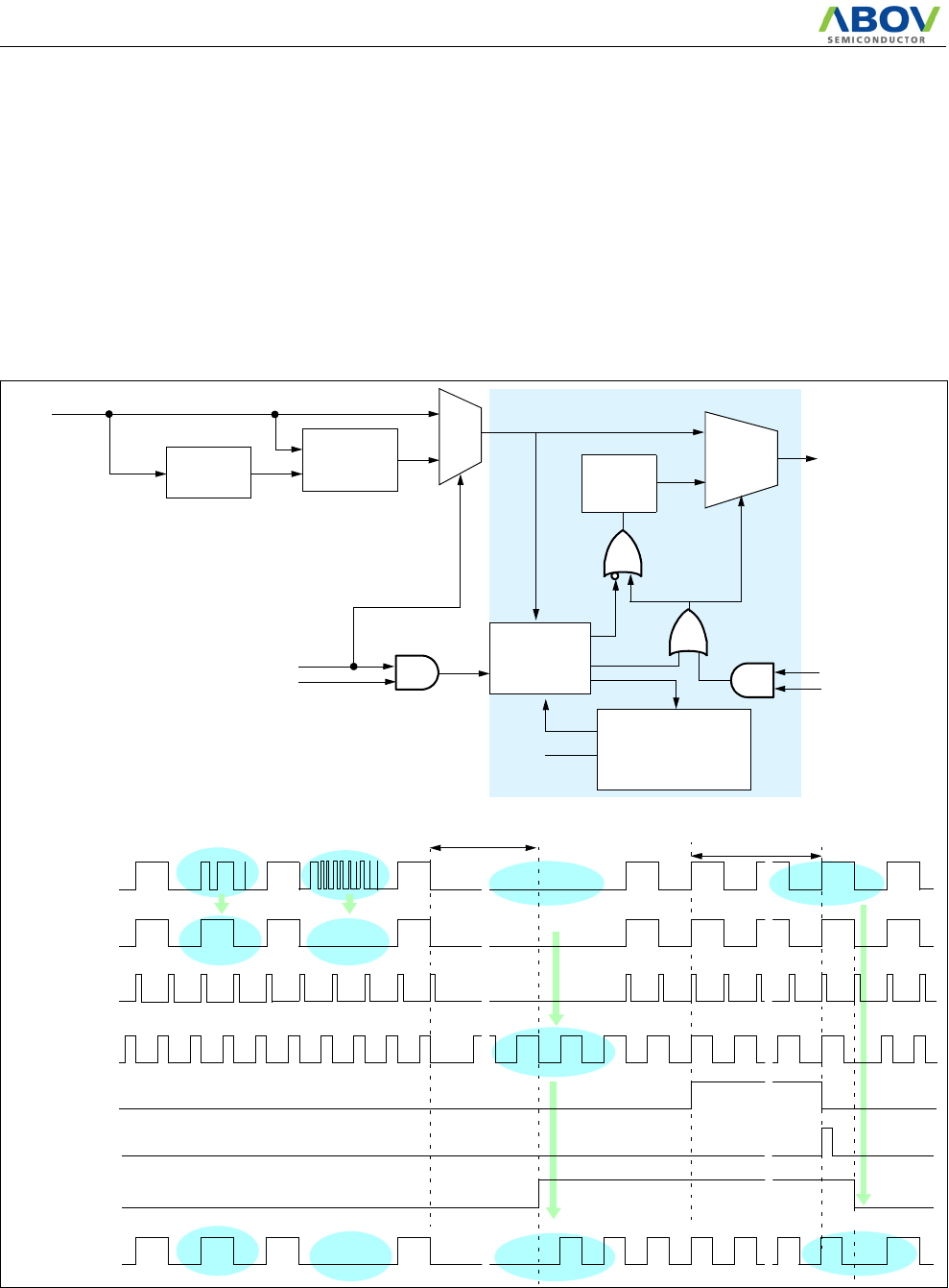
MC80F0304/08/16
114 November 4, 2011 Ver 2.12
22. COUNTERMEASURE OF NOISE
22.1 Oscillation Noise Protector
The Oscillation Noise Protector (ONP) is used to supply stable
internal system clock by excluding the noise which could be en-
tered into oscillator and recovery the oscillation fail. This func-
tion could be enabled or disabled by the “ONP” bit of the Device
configuration area (20FFH) for the MC80F0304/0308/0316,
“ONP” option bits MASK option.
The ONP function is like below.
- Recovery the oscillation wave crushed or loss caused
by high frequency noise.
- Change system clock to the internal oscillation clock
when the high frequency noise is continuing.
- Change system clock to the internal oscillation clock
when the XIN/XOUT is shorted or opened, the main
oscillation is stopped except by stop instruction and
the low frequency noise is entered.
Figure 22-1 Block Diagram of ONP & OFP and Respective Wave Forms
LF Noise
HF Noise
Canceller
HF Noise
Observer
Mux CLK
Changer
Internal
OSC
OFP
OFP
o/f
CK
PS10
FINTERNAL
INT_CLK
XIN_NF
XIN
ONP
IN4(2)MCLK(XO)
(8-Bit counter)
en
ONP
OFP en
en
0
0
1
1
S
S
ONPb = 0
LF_on = 1
IN_CLK = 0
CLK_CHG
XIN_NF
INT_CLK reset
INT_CLK
OFP_EN
CHG_END
CLK_CHG
fINTERNAL
~
~
~
~
~
~
~
~~
~~
~
~
~~
~
~
~~
~~
~
High Frq. Noise
XIN
~
~
~
~
Noise Cancel
INT_CLK 8 periods
(250ns × 8 =2us)
Low Frq. Noise or
Oscillation Fail
Clock Change Start(XIN to INT_CLK)
PS10(INT_CLK/512) 256 periods
(250ns × 512 × 256 =33 ms)
Clock Change End(INT_CLK to XIN))
Observer

MC80F0304/08/16
November 4, 2011 Ver 2.12 115
22.2 Oscillation Fail Processor
The oscillation fail processor (OFP) can change the clock source
from external to internal oscillator when the oscillation fail oc-
cured. This function could be enabled or disabled by the “OFP”
bit of the Device Configuration Area (MASK option for
MC80F0304/0308/0316).
And this function can recover the external clock source when the
external clock is recovered to normal state.
IN4(2)MCLK/CLKXO(XO) Option
The “IN4MCLK(XO)”, “IN2MCLK(XO)” bit of the Device
Configuration Area (MASK option for MC80F0304/0308/0316)
enables the function to operate the device by using the internal os-
cillator clock in ONP block as system clock. There is no need to
connect the x-tal, resonator, RC and R externally. The user only
to connect the XIN pin to VDD. After selecting the this option, the
period of internal oscillator clock could be checked by XOUT out-
putting clock divided the internal oscillator clock by 4.
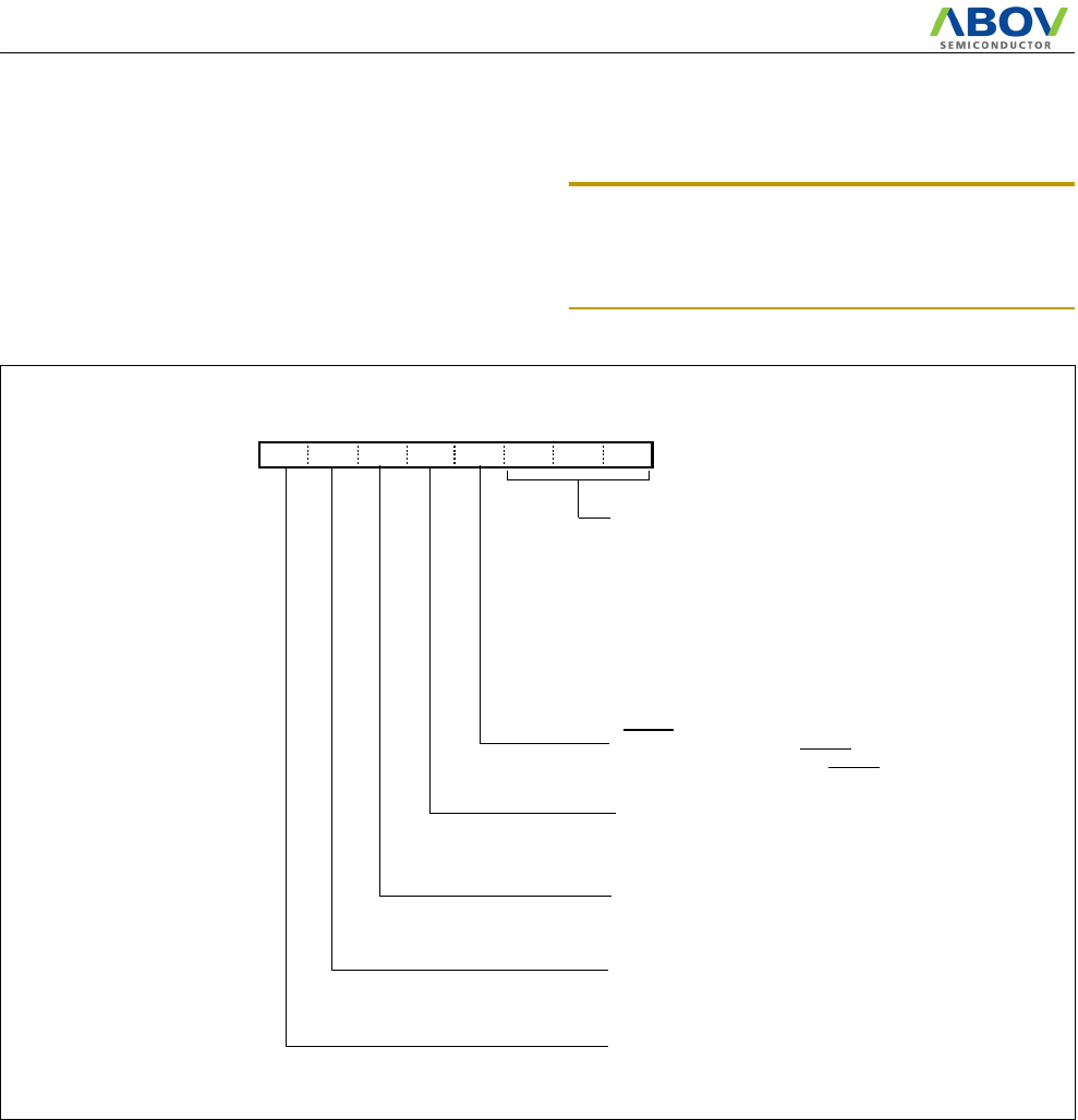
MC80F0304/08/16
116 November 4, 2011 Ver 2.12
23. DEVICE CONFIGURATION AREA
The Device Configuration Area can be programmed or left un-
programmed to select device configuration such as POR, ONP,
CLK option and security bit. This area is not accessible during
normal execution but is readable and writable during FLASH
program / verify mode.
Note: The Configuration Option may not be read exactly
when VDD rising time is very slow. It is recommended to
adjust the VDD rising time faster than 40ms/V (200ms from
0V to 5V).
Figure 23-1 Device Configuration Area
76543210
INITIAL VALUE: 00H
ADDRESS: 20FFH
Configuration Option Bits
Oscillation confuguration
000 : IN4MCLK (Internal 4MHz Oscillation & R33/R34 Enable)
001 : IN2MCLK (Internal 2MHz Oscillation & R33/R34 Enable)
CLK2ONP OFP LOCK POR R35EN CLK1 CLK0
010 : EXRC (External R/RC Oscillation & R34 Enable)
011 : X-tal (Crystal or Resonator Oscillation)
100 : IN4MCLKXO (internal 4MHz Oscillation & R33 Enable
& XOUT = fSYS ÷ 4)
101 : IN2MCLKXO (internal 2MHz Oscillation & R33 Enable
& XOUT = fSYS ÷ 4)
110 : EXRCXO (External R/RC Oscillation & XOUT = fSYS ÷ 4)
111 : Prohibited
RESET/R35 Port configuration
0 : R35 Port Disable (Use RESET)
1 : R35 Port Ensable (Disable RESET)
POR Use
0 : Disable POR Reset
1 : Ensable POR Reset
Security Bit
0 : Enable reading User Code
1 : Disable reading User Code
OFP use
0 : Disable OFP (Clock Changer)
1 : Enable OFP (Clock Changer)
ONP disable
0 : Enable ONP (Enable OFP, Internal 4MHz/2MHz oscillation)
1 : Disable ONP (Disable OFP, Internal 4MHz/2MHz oscillation)
MC80F0304/08/16
November 4, 2011 Ver 2.12 117
24. MASK OPTION (MC80C0304/08/16)
The MC80C0304/08/16 has several MASK option which config-
ures the package type or use of some special features of the de-
vice. The MASK option of the MASK order sheet should be
checked to select device configuration such as package type, Os-
cillation selection, oscillation noise protector, oscillation fail pro-
tector, internal 4MHz, amount of noise to be cancelled.
Table 24-1 MASK options
Option Check Operation Remark
MASK
Option
Package 28 SKDIP 28 SKDIP type package select
32 PDIP 32 PDIP type package select
ONP Yes ONP Enable OSC Noise Protector(ONP)
Operation En/Disable Bit
No ONP Disable
OFP
Yes Enables Oscillation Fail Processor (ONP clock
changer) Change the Inter clock when
oscillation failed
No Disables Oscillation Fail Processor (ONP clock
changer )
POR Yes Enables POR To select Power-on Reset
No Disables POR
R35EN Yes R35 port Enable (Disable RESET)To use R35 port as nomarl input
port
No R35 port Disable (Use RESET)
CLK
option
Crystal Crystal Oscillation
To select Oscillation Type
EXRC External R/RC oscillation & R33 Enable
IN4MCLK Internal 4MHz Oscillation & R33/R34 Enable
IN2MCLK Internal 2MHz Oscillation & R33/R34 Enable
EXRCXO External R/RC oscillation & R33 Enable
XOUT Pin : System clock ÷ 4
IN4MCLKXO Internal 4MHz Oscillation & R33 Enable
XOUT Pin : System clock ÷ 4
IN2MCLKXO Internal 2MHz Oscillation & R33 Enable
XOUT Pin : System clock ÷ 4
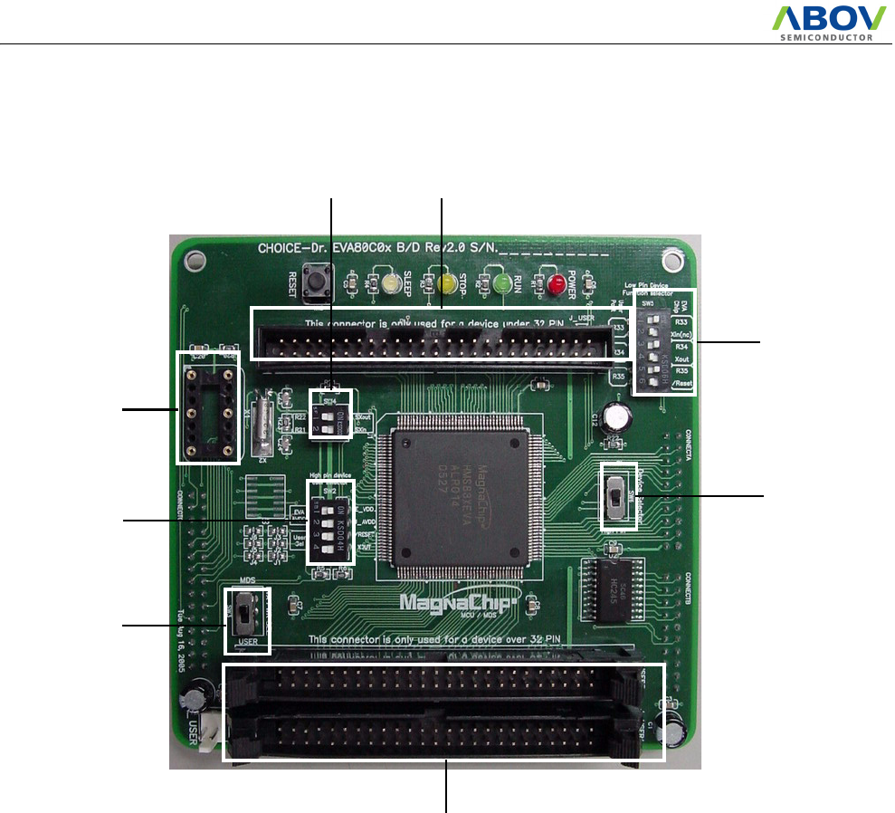
MC80F0304/08/16
118 November 4, 2011 Ver 2.12
25. EMULATOR EVA. BOARD SETTING
À
þ
Ã
Õ
Œ
œ
–
—

MC80F0304/08/16
November 4, 2011 Ver 2.12 119
25.1 DIP Switch and VR Setting
Before execute the user program, keep in your mind the below configuration
DIP S/W Description ON/OFF Setting
- This connector is only used for a device over 32 PIN. For the MC80F0224/MC80F0448
- This connector is only used for a device under 32 PIN. For the MC80F0316.
SW2
1
2
AVDD pin select switch
These switches select the AVDD source.
ON & OFF : Use Eva. VDD
OFF & ON : Use User AVDD
3 This switch select the /Reset source.
Normally OFF.
EVA. chip can be reset by external user tar-
get board.
ON : Reset is available by either user target
system board or Emulator RESET switch.
OFF : Reset the MCU by Emulator RESET
switch. Does not work from user target
board.
4 This switch select the Xout signal on/off.
Normally OFF.
MCU XOUT pin is disconnected internally
in the Emulator. Some circumstance user
may connect this circuit.
ON : Output XOUT signal
OFF : Disconnect circuit
SW3 1
This switch select Eva. B/D Power supply source.
Normally MDS.
This switch select Eva. B/D Power supply
source.
SW4 1
2
This switch select the R22 or SXOUT.
This switch select the R21 or SXIN.
These switchs select the Normal I/O
port(off) or Sub-Clock (on).
It is reserved for the MC80F0448.
ON : SXOUT, SXIN
OFF : R22, R21
Don’t care (MC80F0224/MC80F0448).
SW5
1
2These switches select the R33 or XIN This switch select the Normal I/O
port(on&off) or special function
select(off&on).
It is reserved for the MC80F0316.
ON & OFF : R33,R34,R35 Port selected.
OFF & ON : XOUT, XIN , /Reset selected.
Don’t care (MC80F0224/MC80F0448).
3
4These switches select the R34 or XOUT
5
6These switches select the R35 or /Reset
- This is External oscillation socket(CAN Type. OSC) This is for External Clock(CAN Type.
OSC).
þ
À
Ã
ON
OFF
OFF
ON
Use Eva. VDD Use User’s AVDD
Õ
Use MDS Power
MDS
USER
MDS
USER
Use User’s Power
Œ
œ
–

MC80F0304/08/16
120 November 4, 2011 Ver 2.12
SW6 1
Eva. select switch
Must be OFF position.
ON : For the MC80F0224/MC80F0448.
OFF : For the MC80F0316.
DIP S/W Description ON/OFF Setting
—ON
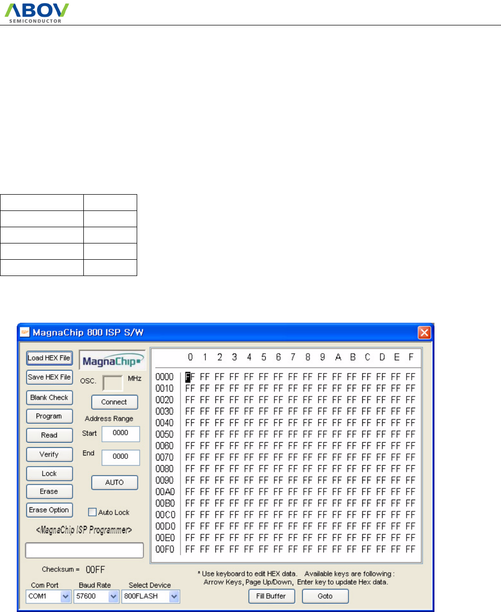
MC80F0304/08/16
November 4, 2011 Ver 2.12 121
26. IN-SYSTEM PROGRAMMING (ISP)
26.1 Getting Started / Installation
The following section details the procedure for accomplishing the
installation procedure.
1. Connect the serial(RS-232C) cable between a target
board and the COM1 serial port of your PC.
2. Configure the COM1 serial port of your PC as follow-
ing.
3. Turn your target B/D power switch ON. Your target B/
D must be configured to enter the ISP mode.
4. Run the MagnaChip ISP software.
5. Press the Reset Button in the ISP S/W. If the status win-
dows shows a message as "Connected", all the condi-
tions for ISP are provided.
26.2 Basic ISP S/W Information
Baudrate 115,200
Data bit 8
Parity No
Stop bit 1
Flow control No

MC80F0304/08/16
122 November 4, 2011 Ver 2.12
26.3 Hardware Conditions to Enter the ISP Mode
The boot loader can be executed by holding ALEB high, RST/
VPP as +9V, and ACLK(optional) with OSC. 1.8432MHz. The
ISP function uses following pins: TxD, RxD, ALEB, ACLK and
RST/VPP.
Note: If POR and R35 are enabled, Vdd and Vpp should
be turned on simultaneously to enter ISP mode.
Normal sequence above can not enter ISP mode when
POR and R35 options are enabled.
Please follow below sequence instead of normal one.
1) Power off a target system.
2) Configure a target system as ISP mode.
3) Attach a ISP B/D into a target system.
4) Run the ISP S/W
Function Description
Load HEX File Load the data from the selected file storage into the memory buffer.
Save HEX File Save the current data in your memory buffer to a disk storage by using the Intel Motorolla HEX
format.
Erase Erase the data in your target MCU before programming it.
Blank Check Verify whether or not a device is in an erased or unprogrammed state.
Program This button enables you to place new data from the memory buffer into the target device.
Read Read the data in the target MCU into the buffer for examination. The checksum will be displayed
on the checksum box.
Verify Assures that data in the device matches data in the memory buffer. If your device is secured, a
verification error is detected.
Lock Secures devices so that their content can no longer be examined or modified.
Erase Option -
AUTO Erase & Program & Verify
Auto Lock If selected with check mark, the security locking is performed after erasure.
Connect Connect a MCU in your target Board with displaying as “Connected” in the status box. Users have
to press this button at least one time to initialize a target MCU for entering the ISP mode. If failed
to enter the ISP mode, all the buttons are unavailable. And, after entering successfully, the
Connect button will be unavailable.
Edit Buffer Modify the data in the selected address in your buffer memory
Fill Buffer Fill the selected area with a data.
Goto Display the selected page.
OSC. ______ MHz Enter your target system’s oscillator value with discarding below point.
Start ______ Starting address
End ______ End address
Checksum Display the checksum(Hexdecimal) after reading the target device.
Com Port Select serial port.
Baud Rate Select UART baud rate.
Select Device Select target device.
Page Up Key Display the previous page of your memory buffer.
Page Down Key Display the higher page than the current location.
Table 1. ISP Function Description
MC80F0304/08/16
November 4, 2011 Ver 2.12 123
5) Select target MCU - It makes condition to make Vpp to
turn on when Vdd is turned on.
6) Power on a target system. : At this point, ISP mode is en-
tered because the Vdd and Vpp are turned on simulta-
neously.
VDD
RESET
XIN
XOUT
VSS
R05 / TxD
R04 / RxD
R05 / ACLK
R10
ISP Configuration
MCU TxD
MCU RxD
High(1)
VDD(+5V)
+9V
2
3
4
5
6
7
8
27
26
25
24
23
22
21
128
9
10
11
12
13
14
20
19
18
17
16
15
2MHz~12MHz
ACLK_CLK
ALE
X-TAL
RESET/VPP
RST/VPP
Tx Data1
Rx Data1
ACLK4
VDD(+5V)
ISP Board
VSS
User target reset circuitry
ISP_VPP
RST/VPP
47KΩ3(optional)
1. If other signals affect UART communiction in ISP mode, disconnect these pins by using a jumper or a switch.
2. The ALEB can be shared with other function. Toggle the port between ISP and user mode.
3. The pull down resister is optional. If user set to ISP Mode without connection ISP board, the Vpp/Reset Port is in floating state.
The pull down resistor is for blocking this undefined state.
4. Refer to the section 26.5 explaining the auto bua drate and ACK mode.
Do not power on a application B/D in ISP mode without connecting a ISP board.
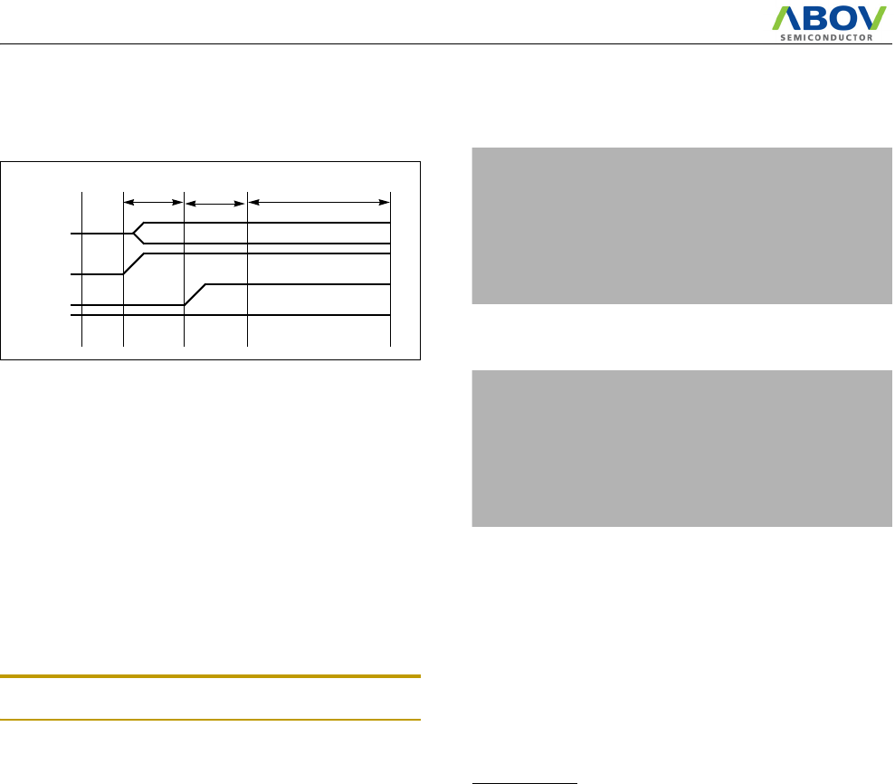
MC80F0304/08/16
124 November 4, 2011 Ver 2.12
26.4 Sequence to enter ISP mode/user mode
Figure 26-1 Timing diagram to enter the ISP mode
Sequence to enter ISP mode from user mode.
(If POR and R35 are enabled, the sequnence “Run the ISP S/
W”should be followed by the sequence “Power on a target sys-
tem” as shown in NOTE of chapter 26.3)
S
Sequence to enter user mode from ISP mode.
26.5 ACK mode
The ISP S/W can not detect user system clock. Users have to en-
ter a user system clock. This mode is only used when failed to de-
tect user system clock automatically.
Note: Need to connect the ACK pin to ISP B/D.
26.6 Reference ISP Circuit Diagram and ABOV Supplied ISP Board
The ISP software and hardware circuit diagram are provided at www.abov.co.kr . To get a ISP B/D, contact to sales department.
VPP
ALEB
VDD
XIN 2 ~ 12MHz
ISP modeReset
logic high
min.10us 64ms@4MHz
1. Power off a target system.
2. Configure a target system as ISP mode.
3. Attach a ISP B/D into a target system.
4. Power on a target system.
5. Run the ISP S/W.
1. Close the ISP S/W..
2. Power off a target system.
3. Configure a target system as user mode
4. Detach a ISP B/D from a target system.
5. Power on.
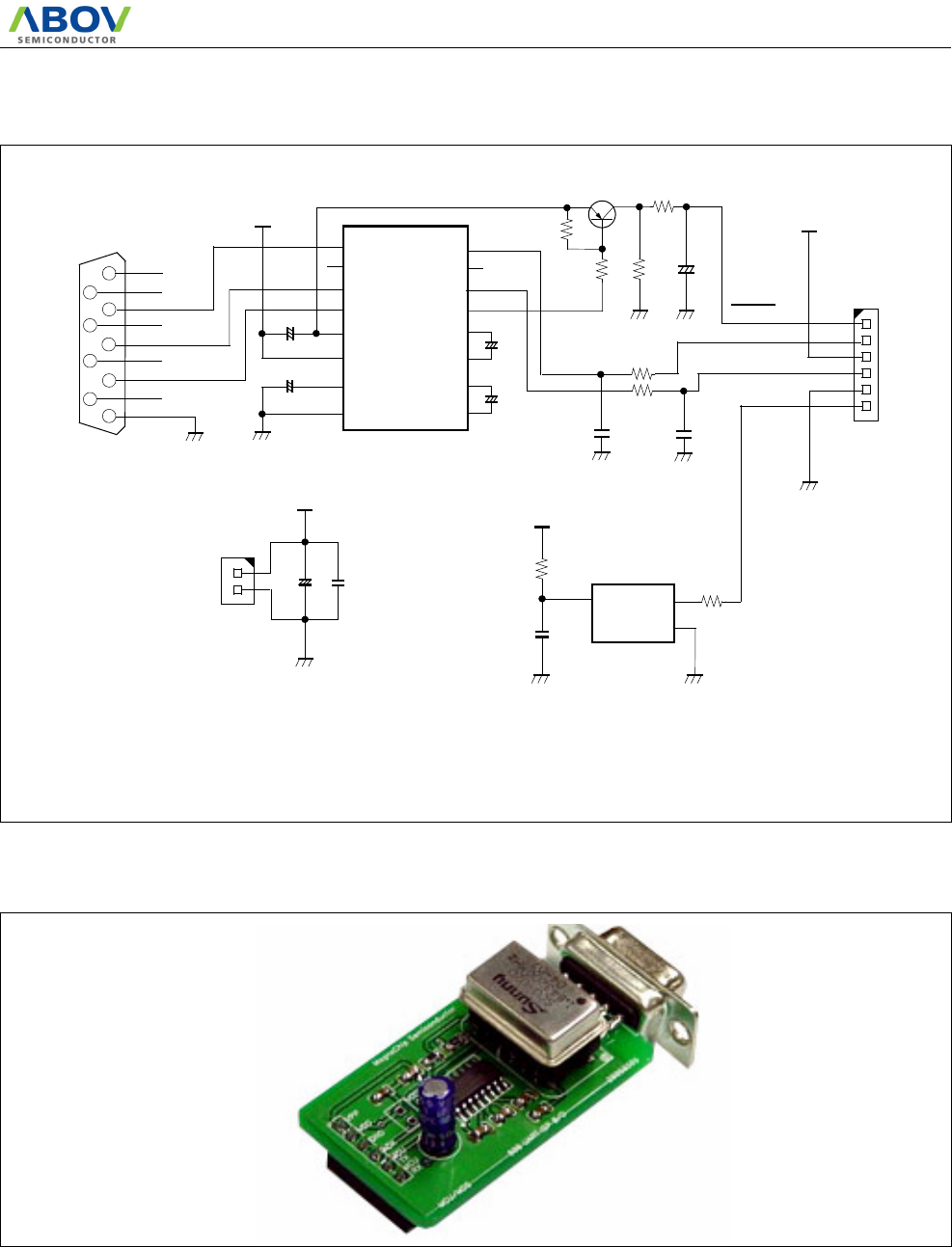
MC80F0304/08/16
November 4, 2011 Ver 2.12 125
The following circuit diagram is for reference use.
Figure 26-2 Reference ISP Circuit Diagram
T1IN
T2IN
R1OUT
R2OUT
C1+
C1-
C2+
C2-
T1OUT
T2OUT
R1IN
R2IN
V+
VCC
V-
GND
CON1
Female DB9
J2
VSS
J3
External VDD
RESET/VPP
MCU_TxD
MCU_RxD
10uF/16V
0.1uF
MAX232
ACLK_CLK
Vcc Out
Gnd
OSC
X1
1.8432MHz
22Ω0.1uF
22Ω
The ragne of VDD must be from 4.5 to 5.5V and ISP function is not supported under 2MHz system clock.
If the user supplied VDD is out of range, the external power is needed instead of the target system VDD.
VDD(+5V)
VSS
VDD(+5V)
VSS
14
7
13
8
2
16
6
15
11
10
12
9
1
3
4
5
VSS
1
2
3
4
5
VDD(+5V)
6
1uF
1uF
1uF
1uF
* VPP : VDD + 4V
* VDD : +4.5 ~ +5.5V
From PC
To MCU
GND
TxD
RxD
+
+
++
+
For the ISP operation, power consumption required is minimum 30mA.
VDD
VSS
DTR
VSS VSS
+
10uF/35V
100Ω
1kΩ
8.2kΩ
10kΩ
2N2907
VSS
VSS
VDD(+5V)
5
4
3
2
1
9
8
7
6
22Ω
22Ω
VSS VSS
100pF
100pF
Figure 26-3 ISP board supplied by ABOV

MC80F0304/08/16
126 November 4, 2011 Ver 2.12

MC80F0304/08/16
November 4, 2011 Ver 2.12 i
APPENDIX
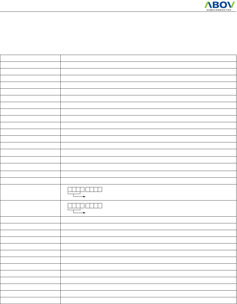
MC80F0304/08/16
ii November 4, 2011 Ver 2.12
A. INSTRUCTION
A.1 Terminology List
Terminology Description
A Accumulator
X X - register
Y Y - register
PSW Program Status Word
#imm 8-bit Immediate data
dp Direct Page Offset Address
!abs Absolute Address
[ ] Indirect expression
{ } Register Indirect expression
{ }+ Register Indirect expression, after that, Register auto-increment
.bit Bit Position
A.bit Bit Position of Accumulator
dp.bit Bit Position of Direct Page Memory
M.bit Bit Position of Memory Data (000H~0FFFH)
rel Relative Addressing Data
upage U-page (0FF00H~0FFFFH) Offset Address
n Table CALL Number (0~15)
+Addition
x
Upper Nibble Expression in Opcode
y
Upper Nibble Expression in Opcode
−Subtraction
×Multiplication
/ Division
( ) Contents Expression
∧AND
∨OR
⊕Exclusive OR
~NOT
←Assignment / Transfer / Shift Left
→Shift Right
↔Exchange
= Equal
≠Not Equal
0
Bit Position
1
Bit Position

MC80F0304/08/16
November 4, 2011 Ver 2.12 iii
A.2 Instruction Map
LOW
HIGH
00000
00
00001
01
00010
02
00011
03
00100
04
00101
05
00110
06
00111
07
01000
08
01001
09
01010
0A
01011
0B
01100
0C
01101
0D
01110
0E
01111
0F
000 - SET1
dp.bit
BBS
A.bit,rel
BBS
dp.bit,rel
ADC
#imm
ADC
dp
ADC
dp+X
ADC
!abs
ASL
A
ASL
dp
TCALL
0
SETA1
.bit
BIT
dp
POP
A
PUSH
ABRK
001 CLRC “ “ “ SBC
#imm
SBC
dp
SBC
dp+X
SBC
!abs
ROL
A
ROL
dp
TCALL
2
CLRA1
.bit
COM
dp
POP
X
PUSH
X
BRA
rel
010 CLRG “ “ “ CMP
#imm
CMP
dp
CMP
dp+X
CMP
!abs
LSR
A
LSR
dp
TCALL
4
NOT1
M.bit
TST
dp
POP
Y
PUSH
Y
PCALL
Upage
011 DI“““
OR
#imm
OR
dp
OR
dp+X
OR
!abs
ROR
A
ROR
dp
TCALL
6
OR1
OR1B
CMPX
dp
POP
PSW
PUSH
PSW RET
100 CLRV “ “ “ AND
#imm
AND
dp
AND
dp+X
AND
!abs
INC
A
INC
dp
TCALL
8
AND1
AND1B
CMPY
dp
CBNE
dp+X TXSP INC
X
101 SETC“““
EOR
#imm
EOR
dp
EOR
dp+X
EOR
!abs
DEC
A
DEC
dp
TCALL
10
EOR1
EOR1B
DBNE
dp
XMA
dp+X TSPX DEC
X
110 SETG “ “ “ LDA
#imm
LDA
dp
LDA
dp+X
LDA
!abs TXA LDY
dp
TCALL
12
LDC
LDCB
LDX
dp
LDX
dp+Y XCN DAS
(N/A)
111 EI“““
LDM
dp,#imm
STA
dp
STA
dp+X
STA
!abs TAX STY
dp
TCALL
14
STC
M.bit
STX
dp
STX
dp+Y XAX STOP
LOW
HIGH
10000
10
10001
11
10010
12
10011
13
10100
14
10101
15
10110
16
10111
17
11000
18
11001
19
11010
1A
11011
1B
11100
1C
11101
1D
11110
1E
11111
1F
000 BPL
rel
CLR1
dp.bit
BBC
A.bit,rel
BBC
dp.bit,rel
ADC
{X}
ADC
!abs+Y
ADC
[dp+X]
ADC
[dp]+Y
ASL
!abs
ASL
dp+X
TCALL
1
JMP
!abs
BIT
!abs
ADDW
dp
LDX
#imm
JMP
[!abs]
001 BVC
rel “““
SBC
{X}
SBC
!abs+Y
SBC
[dp+X]
SBC
[dp]+Y
ROL
!abs
ROL
dp+X
TCALL
3
CALL
!abs
TEST
!abs
SUBW
dp
LDY
#imm
JMP
[dp]
010 BCC
rel “““
CMP
{X}
CMP
!abs+Y
CMP
[dp+X]
CMP
[dp]+Y
LSR
!abs
LSR
dp+X
TCALL
5MUL TCLR1
!abs
CMPW
dp
CMPX
#imm
CALL
[dp]
011 BNE
rel “““
OR
{X}
OR
!abs+Y
OR
[dp+X]
OR
[dp]+Y
ROR
!abs
ROR
dp+X
TCALL
7
DBNE
Y
CMPX
!abs
LDYA
dp
CMPY
#imm RETI
100 BMI
rel “““
AND
{X}
AND
!abs+Y
AND
[dp+X]
AND
[dp]+Y
INC
!abs
INC
dp+X
TCALL
9DIV CMPY
!abs
INCW
dp
INC
YTAY
101 BVS
rel “““
EOR
{X}
EOR
!abs+Y
EOR
[dp+X]
EOR
[dp]+Y
DEC
!abs
DEC
dp+X
TCALL
11
XMA
{X}
XMA
dp
DECW
dp
DEC
YTYA
110 BCS
rel “““
LDA
{X}
LDA
!abs+Y
LDA
[dp+X]
LDA
[dp]+Y
LDY
!abs
LDY
dp+X
TCALL
13
LDA
{X}+
LDX
!abs
STYA
dp XAY DAA
(N/A)
111 BEQ
rel “““
STA
{X}
STA
!abs+Y
STA
[dp+X]
STA
[dp]+Y
STY
!abs
STY
dp+X
TCALL
15
STA
{X}+
STX
!abs
CBNE
dp XYX NOP
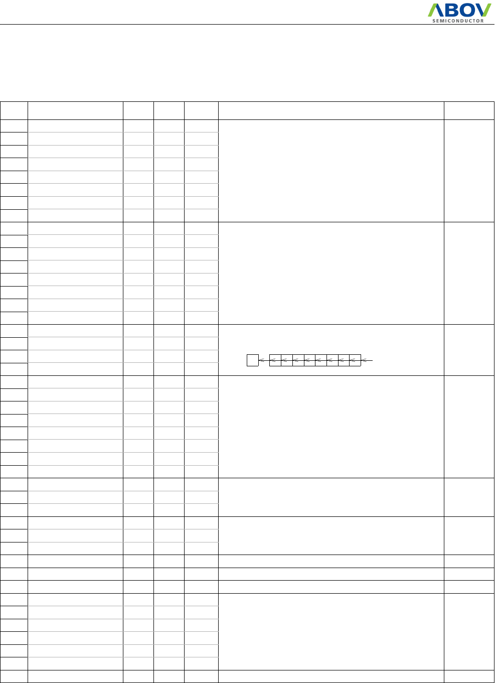
MC80F0304/08/16
iv November 4, 2011 Ver 2.12
A.3 Instruction Set
Arithmetic / Logic Operation
NO. MNEMONIC OP
CODE
BYTE
NO
CYCLE
NO OPERATION FLAG
NVGBHIZC
1 ADC #imm 04 2 2
Add with carry.
A ← ( A ) + ( M ) + C NV--H-ZC
2ADC dp 05 2 3
3 ADC dp + X 06 2 4
4 ADC !abs 07 3 4
5 ADC !abs + Y 15 3 5
6 ADC [ dp + X ] 16 2 6
7 ADC [ dp ] + Y 17 2 6
8ADC { X } 14 1 3
9 AND #imm 84 2 2
Logical AND
A ← ( A ) ∧ ( M ) N-----Z-
10 AND dp 85 2 3
11 AND dp + X 86 2 4
12 AND !abs 87 3 4
13 AND !abs + Y 95 3 5
14 AND [ dp + X ] 96 2 6
15 AND [ dp ] + Y 97 2 6
16 AND { X } 94 1 3
17 ASL A 08 1 2 Arithmetic shift left
N-----ZC
18 ASL dp 09 2 4
19 ASL dp + X 19 2 5
20 ASL !abs 18 3 5
21 CMP #imm 44 2 2
Compare accumulator contents with memory contents
( A ) - ( M ) N-----ZC
22 CMP dp 45 2 3
23 CMP dp + X 46 2 4
24 CMP !abs 47 3 4
25 CMP !abs + Y 55 3 5
26 CMP [ dp + X ] 56 2 6
27 CMP [ dp ] + Y 57 2 6
28 CMP { X } 54 1 3
29 CMPX #imm 5E 2 2
Compare X contents with memory contents
( X ) - ( M ) N-----ZC30 CMPX dp 6C 2 3
31 CMPX !abs 7C 3 4
32 CMPY #imm 7E 2 2
Compare Y contents with memory contents
( Y ) - ( M ) N-----ZC33 CMPY dp 8C 2 3
34 CMPY !abs 9C 3 4
35 COM dp 2C 2 4 1’S Complement : ( dp ) ← ~( dp ) N-----Z-
36 DAA - - - Unsupported -
37 DAS - - - Unsupported -
38 DEC A A8 1 2
Decrement
M ← ( M ) - 1 N-----Z-
39 DEC dp A9 2 4
40 DEC dp + X B9 2 5
41 DEC !abs B8 3 5
42 DEC X AF 1 2
43 DEC Y BE 1 2
44 DIV 9B 1 12 Divide : YA / X Q: A, R: Y NV--H-Z-
0
“0”
C 7654321
MC80F0304/08/16
November 4, 2011 Ver 2.12 v
45 EOR #imm A4 2 2
Exclusive OR
A ← ( A ) ⊕ ( M ) N-----Z-
46 EOR dp A5 2 3
47 EOR dp + X A6 2 4
48 EOR !abs A7 3 4
49 EOR !abs + Y B5 3 5
50 EOR [ dp + X ] B6 2 6
51 EOR [ dp ] + Y B7 2 6
52 EOR { X } B4 1 3
53 INC A 88 1 2
Increment
M ← ( M ) + 1 N-----Z-
54 INC dp 89 2 4
55 INC dp + X 99 2 5
56 INC !abs 98 3 5
57 INC X 8F 1 2
58 INC Y 9E 1 2
59 LSR A 48 1 2 Logical shift right
N-----ZC
60 LSR dp 49 2 4
61 LSR dp + X 59 2 5
62 LSR !abs 58 3 5
63 MUL 5B 1 9 Multiply : YA ← Y × AN-----Z-
64 OR #imm 64 2 2
Logical OR
A ← ( A ) ∨ ( M ) N-----Z-
65 OR dp 65 2 3
66 OR dp + X 66 2 4
67 OR !abs 67 3 4
68 OR !abs + Y 75 3 5
69 OR [ dp + X ] 76 2 6
70 OR [ dp ] + Y 77 2 6
71 OR { X } 74 1 3
72 ROL A 28 1 2 Rotate left through carry
N-----ZC
73 ROL dp 29 2 4
74 ROL dp + X 39 2 5
75 ROL !abs 38 3 5
76 ROR A 68 1 2 Rotate right through carry
N-----ZC
77 ROR dp 69 2 4
78 ROR dp + X 79 2 5
79 ROR !abs 78 3 5
80 SBC #imm 24 2 2
Subtract with carry
A ← ( A ) - ( M ) - ~( C ) NV--HZC
81 SBC dp 25 2 3
82 SBC dp + X 26 2 4
83 SBC !abs 27 3 4
84 SBC !abs + Y 35 3 5
85 SBC [ dp + X ] 36 2 6
86 SBC [ dp ] + Y 37 2 6
87 SBC { X } 34 1 3
88 TST dp 4C 2 3 Test memory contents for negative or zero
( dp ) - 00HN-----Z-
89 XCN CE 1 5 Exchange nibbles within the accumulator
A7~A4 ↔ A3~A0N-----Z-
NO. MNEMONIC OP
CODE
BYTE
NO
CYCLE
NO OPERATION FLAG
NVGBHIZC
0
“0”
C7654321
0C 7654321
0C7654321

MC80F0304/08/16
vi November 4, 2011 Ver 2.12
Register / Memory Operation
NO. MNEMONIC OP
CODE
BYTE
NO
CYCLE
NO OPERATION FLAG
NVGBHIZC
1LDA #imm C4 2 2
Load accumulator
A ← ( M ) N-----Z-
2LDA dp C5 2 3
3 LDA dp + X C6 2 4
4 LDA !abs C7 3 4
5 LDA !abs + Y D5 3 5
6 LDA [ dp + X ] D6 2 6
7 LDA [ dp ] + Y D7 2 6
8LDA { X } D4 1 3
9 LDA { X }+ DB 1 4 X- register auto-increment : A ← ( M ) , X ← X + 1
10 LDM dp,#imm E4 3 5 Load memory with immediate data : ( M ) ← imm --------
11 LDX #imm 1E 2 2
Load X-register
X ← ( M ) N-----Z-
12 LDX dp CC 2 3
13 LDX dp + Y CD 2 4
14 LDX !abs DC 3 4
15 LDY #imm 3E 2 2
Load Y-register
Y ← ( M ) N-----Z-
16 LDY dp C9 2 3
17 LDY dp + X D9 2 4
18 LDY !abs D8 3 4
19 STA dp E5 2 4
Store accumulator contents in memory
( M ) ← A --------
20 STA dp + X E6 2 5
21 STA !abs E7 3 5
22 STA !abs + Y F5 3 6
23 STA [ dp + X ] F6 2 7
24 STA [ dp ] + Y F7 2 7
25 STA { X } F4 1 4
26 STA { X }+ FB 1 4 X- register auto-increment : ( M ) ← A, X ← X + 1
27 STX dp EC 2 4
Store X-register contents in memory
( M ) ← X --------
28 STX dp + Y ED 2 5
29 STX !abs FC 3 5
30 STY dp E9 2 4
Store Y-register contents in memory
( M ) ← Y --------
31 STY dp + X F9 2 5
32 STY !abs F8 3 5
33 TAX E8 1 2 Transfer accumulator contents to X-register : X ← A N-----Z-
34 TAY 9F 1 2 Transfer accumulator contents to Y-register : Y ← A N-----Z-
35 TSPX AE 1 2 Transfer stack-pointer contents to X-register : X ← sp N-----Z-
36 TXA C8 1 2 Transfer X-register contents to accumulator: A ← X N-----Z-
37 TXSP 8E 1 2 Transfer X-register contents to stack-pointer: sp ← X N-----Z-
38 TYA BF 1 2 Transfer Y-register contents to accumulator: A ← Y N-----Z-
39 XAX EE 1 4 Exchange X-register contents with accumulator :X ↔ A --------
40 XAY DE 1 4 Exchange Y-register contents with accumulator :Y ↔ A --------
41 XMA dp BC 2 5 Exchange memory contents with accumulator
N-----Z-
42 XMA dp+X AD 2 6 ( M ) ↔ A
43 XMA {X} BB 1 5
44 XYX FE 1 4 Exchange X-register contents with Y-register : X ↔ Y--------
MC80F0304/08/16
November 4, 2011 Ver 2.12 vii
16-BIT Operation
Bit Manipulation
NO. MNEMONIC OP
CODE
BYTE
NO
CYCLE
NO OPERATION FLAG
NVGBHIZC
1 ADDW dp 1D 2 5 16-Bits add without carry
YA ← ( YA ) + ( dp +1 ) ( dp ) NV--H-ZC
2CMPW dp 5D 2 4 Compare YA contents with memory pair contents : (YA) −
(dp+1)(dp) N-----ZC
3 DECW dp BD 2 6 Decrement memory pair
( dp+1)( dp) ← ( dp+1) ( dp) - 1 N-----Z-
4 INCW dp 9D 2 6 Increment memory pair
( dp+1) ( dp) ← ( dp+1) ( dp ) + 1 N-----Z-
5LDYA dp 7D 2 5 Load YA
YA ← ( dp +1 ) ( dp ) N-----Z-
6STYA dp DD 2 5 Store YA
( dp +1 ) ( dp ) ← YA --------
7SUBW dp 3D 2 5 16-Bits substact without carry
YA ← ( YA ) - ( dp +1) ( dp) NV--H-ZC
NO. MNEMONIC OP
CODE
BYTE
NO
CYCLE
NO OPERATION FLAG
NVGBHIZC
1AND1 M.bit 8B 3 4 Bit AND C-flag : C ← ( C ) ∧ ( M .bit ) -------C
2AND1B M.bit 8B 3 4 Bit AND C-flag and NOT : C ← ( C ) ∧ ~( M .bit ) -------C
3BIT dp 0C 2 4 Bit test A with memory :
Z ← ( A ) ∧ ( M ) , N ← ( M7 ) , V ← ( M6 )MM----Z-
4BIT !abs 1C 3 5
5CLR1 dp.bit y1 2 4 Clear bit : ( M.bit ) ← “0” --------
6CLRA1 A.bit 2B 2 2 Clear A bit : ( A.bit )← “0” --------
7CLRC 20 1 2 Clear C-flag : C ← “0” -------0
8CLRG 40 1 2 Clear G-flag : G ← “0” --0-----
9CLRV 80 1 2 Clear V-flag : V ← “0” -0--0---
10 EOR1 M.bit AB 3 5 Bit exclusive-OR C-flag : C ← ( C ) ⊕ ( M .bit ) -------C
11 EOR1B M.bit AB 3 5 Bit exclusive-OR C-flag and NOT : C ← ( C ) ⊕ ~(M .bit) -------C
12 LDC M.bit CB 3 4 Load C-flag : C ← ( M .bit ) -------C
13 LDCB M.bit CB 3 4 Load C-flag with NOT : C ← ~( M .bit ) -------C
14 NOT1 M.bit 4B 3 5 Bit complement : ( M .bit ) ← ~( M .bit ) --------
15 OR1 M.bit 6B 3 5 Bit OR C-flag : C ← ( C ) ∨ ( M .bit ) -------C
16 OR1B M.bit 6B 3 5 Bit OR C-flag and NOT : C ← ( C ) ∨ ~( M .bit ) -------C
17 SET1 dp.bit x1 2 4 Set bit : ( M.bit ) ← “1” --------
18 SETA1 A.bit 0B 2 2 Set A bit : ( A.bit ) ← “1” --------
19 SETC A0 1 2 Set C-flag : C ← “1” -------1
20 SETG C0 1 2 Set G-flag : G ← “1” --1-----
21 STC M.bit EB 3 6 Store C-flag : ( M .bit ) ← C --------
22 TCLR1 !abs 5C 3 6 Test and clear bits with A :
A - ( M ) , ( M ) ← ( M ) ∧ ~( A ) N-----Z-
23 TSET1 !abs 3C 3 6 Test and set bits with A :
A - ( M ) , ( M ) ← ( M ) ∨ ( A ) N-----Z-

MC80F0304/08/16
viii November 4, 2011 Ver 2.12
Branch / Jump Operation
NO. MNEMONIC OP
CODE
BYTE
NO
CYCLE
NO OPERATION FLAG
NVGBHIZC
1BBC A.bit,rel y2 2 4/6 Branch if bit clear :
if ( bit ) = 0 , then pc ← ( pc ) + rel --------
2BBC dp.bit,rel y3 3 5/7
3BBS A.bit,rel x2 2 4/6 Branch if bit set :
if ( bit ) = 1 , then pc ← ( pc ) + rel --------
4BBS dp.bit,rel x3 3 5/7
5BCC rel 5022/4
Branch if carry bit clear
if ( C ) = 0 , then pc ← ( pc ) + rel --------
6BCS rel D0 2 2/4 Branch if carry bit set
if ( C ) = 1 , then pc ← ( pc ) + rel --------
7BEQ rel F0 2 2/4 Branch if equal
if ( Z ) = 1 , then pc ← ( pc ) + rel --------
8BMI rel 9022/4
Branch if minus
if ( N ) = 1 , then pc ← ( pc ) + rel --------
9BNE rel 7022/4
Branch if not equal
if ( Z ) = 0 , then pc ← ( pc ) + rel --------
10 BPL rel 1022/4
Branch if minus
if ( N ) = 0 , then pc ← ( pc ) + rel --------
11 BRA rel 2F 2 4 Branch always
pc ← ( pc ) + rel --------
12 BVC rel 3022/4
Branch if overflow bit clear
if (V) = 0 , then pc ← ( pc) + rel --------
13 BVS rel B0 2 2/4 Branch if overflow bit set
if (V) = 1 , then pc ← ( pc ) + rel --------
14 CALL !abs 3B 3 8 Subroutine call
M( sp)←( pcH ), sp←sp - 1, M(sp)← (pcL), sp ←sp - 1,
if !abs, pc← abs ; if [dp], pcL← ( dp ), pcH← ( dp+1 ) .
--------
15 CALL [dp] 5F 2 8
16 CBNE dp,rel FD 3 5/7 Compare and branch if not equal :
if ( A ) ≠ ( M ) , then pc ← ( pc ) + rel. --------
17 CBNE dp+X,rel 8D 3 6/8
18 DBNE dp,rel AC 3 5/7 Decrement and branch if not equal :
if ( M ) ≠ 0 , then pc ← ( pc ) + rel. --------
19 DBNE Y,rel 7B 2 4/6
20 JMP !abs 1B 3 3
Unconditional jump
pc ← jump address --------
21 JMP [!abs] 1F 3 5
22 JMP [dp] 3F 2 4
23 PCALL upage 4F 2 6
U-page call
M(sp) ←( pcH ), sp ←sp - 1, M(sp) ← ( pcL ),
sp ← sp - 1, pcL ← ( upage ), pcH ← ”0FFH” .
--------
24 TCALL n nA 1 8
Table call : (sp) ←( pcH ), sp ← sp - 1,
M(sp) ← ( pcL ),sp ← sp - 1,
pcL ← (Table vector L), pcH ← (Table vector H)
--------

MC80F0304/08/16
November 4, 2011 Ver 2.12 ix
Control Operation & Etc.
NO. MNEMONIC OP
CODE
BYTE
NO
CYCLE
NO OPERATION FLAG
NVGBHIZC
1BRK 0F 1 8
Software interrupt : B ← ”1”, M(sp) ← (pcH), sp ←sp-1,
M(s) ← (pcL), sp ← sp - 1, M(sp) ← (PSW), sp ← sp -1,
pcL ← ( 0FFDEH ) , pcH ← ( 0FFDFH) .
---1-0--
2DI 60 1 3 Disable interrupts : I ← “0” -----0--
3EI E0 1 3 Enable interrupts : I ← “1” -----1--
4NOP FF 1 2 No operation --------
5POP A 0D 1 4 sp ← sp + 1, A ← M( sp )
sp ← sp + 1, X ← M( sp )
sp ← sp + 1, Y ← M( sp )
sp ← sp + 1, PSW ← M( sp )
--------
6POP X 2D 1 4
7POP Y 4D 1 4
8POP PSW 6D 1 4 restored
9PUSH A 0E 1 4 M( sp ) ← A , sp ← sp - 1
M( sp ) ← X , sp ← sp - 1
M( sp ) ← Y , sp ← sp - 1
M( sp ) ← PSW , sp ← sp - 1
--------
10 PUSH X 2E 1 4
11 PUSH Y 4E 1 4
12 PUSH PSW 6E 1 4
13 RET 6F 1 5 Return from subroutine
sp ← sp +1, pcL ← M( sp ), sp ← sp +1, pcH ← M( sp ) --------
14 RETI 7F 1 6
Return from interrupt
sp ← sp +1, PSW ← M( sp ), sp ← sp + 1,
pcL ← M( sp ), sp ← sp + 1, pcH ← M( sp )
restored
15 STOP EF 1 3 Stop mode ( halt CPU, stop oscillator ) --------

B. MASK ORDER SHEET(MC80C0304)
1. Customer Information
Company Name
2. Device Information
Application
Order Date
YYYY MM DD
Tel: Fax:
Name &
Signature:
Customer should write inside thick line box.
E-mail:
04-NOV-2011
MASK ORDER & VERIFICATION SHEET
MC80C0304-MC
28SKDIP 28SOP
Set “00H” in
this area
0000H
F000H
FFFFH
.OTP file data
EFFFH
Mask Data File Name: ( .OTP)
Check Sum: ( )
POR Use Yes No
Notice : Unused user
ROM area should
be filled with “00H”
Crystal
IN4M IN4MXO
IN2M IN2MXO
EXRC EXRCXO
32PDIP 32SOP
Package
If POR is Yes No
“Yes”,
R35
Use
If POR is No
“No”,
R35
Use
ROM Size 4K 8K 16K
ONP Use Yes No
If ONP is
Yes No
“Yes”,
OFP
Use
CLK
Use
Crystal
EXRC EXRCXO
If ONP is
“No”, CLK
Use
3. Marking Specification
(Please check mark into )
YYWW KOREA
MC80C0304
B, G, D or D32
-MC
Work Week
YYWW KOREA
Customer’s logo
Customer logo is not required.
Customer’s part number
If the customer logo must be used in the special mark,
please submit a clean original of the logo.
ROM Code Number
4. Delivery Schedule
Customer Sample
Date
YYYY MM DD
Risk Order
Quantity ABOV Confirmation
pcs
pcs
5. ROM Code Verification
Verification Date:
Check Sum:
Tel: Fax:
Signature:
No
OFP
Use
Name &
E-mail:
B, G, D or D32
B:PDIP
G:SKDIP
D:SOP
D32:32SOP
P:Pb Free
P:Pb Free
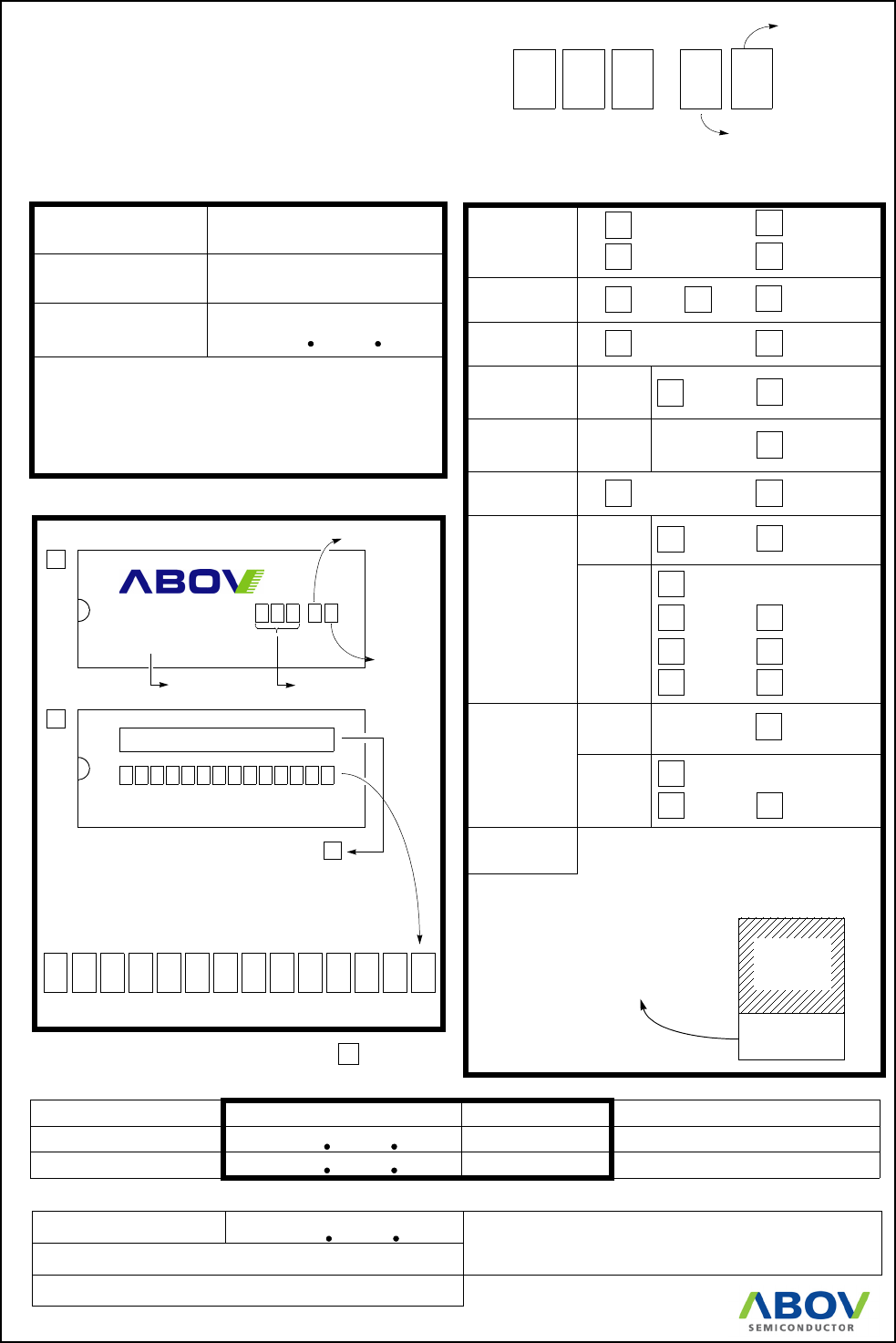
C. MASK ORDER SHEET(MC80C0308)
1. Customer Information
Company Name
2. Device Information
Application
Order Date
YYYY MM DD
Tel: Fax:
Name &
Signature:
Customer should write inside thick line box.
E-mail:
04-NOV-2011
MASK ORDER & VERIFICATION SHEET
MC80C0308-MC
28SKDIP 28SOP
Set “00H” in
this area
0000H
F000H
FFFFH
.OTP file data
EFFFH
Mask Data File Name: ( .OTP)
Check Sum: ( )
POR Use Yes No
Notice : Unused user
ROM area should
be filled with “00H”
Crystal
IN4M IN4MXO
IN2M IN2MXO
EXRC EXRCXO
32PDIP 32SOP
Package
If POR is Yes No
“Yes”,
R35
Use
If POR is No
“No”,
R35
Use
ROM Size 4K 8K 16K
ONP Use Yes No
If ONP is
Yes No
“Yes”,
OFP
Use
CLK
Use
Crystal
EXRC EXRCXO
If ONP is
“No”, CLK
Use
3. Marking Specification
(Please check mark into )
YYWW KOREA
MC80C0308
B, G, D or D32
-MC
Work Week
YYWW KOREA
Customer’s logo
Customer logo is not required.
Customer’s part number
If the customer logo must be used in the special mark,
please submit a clean original of the logo.
ROM Code Number
4. Delivery Schedule
Customer Sample
Date
YYYY MM DD
Risk Order
Quantity ABOV Confirmation
pcs
pcs
5. ROM Code Verification
Verification Date:
Check Sum:
Tel: Fax:
Signature:
No
OFP
Use
Name &
E-mail:
B, G, D or D32
B:PDIP
G:SKDIP
D:SOP
D32:32SOP
P:Pb Free
P:Pb Free
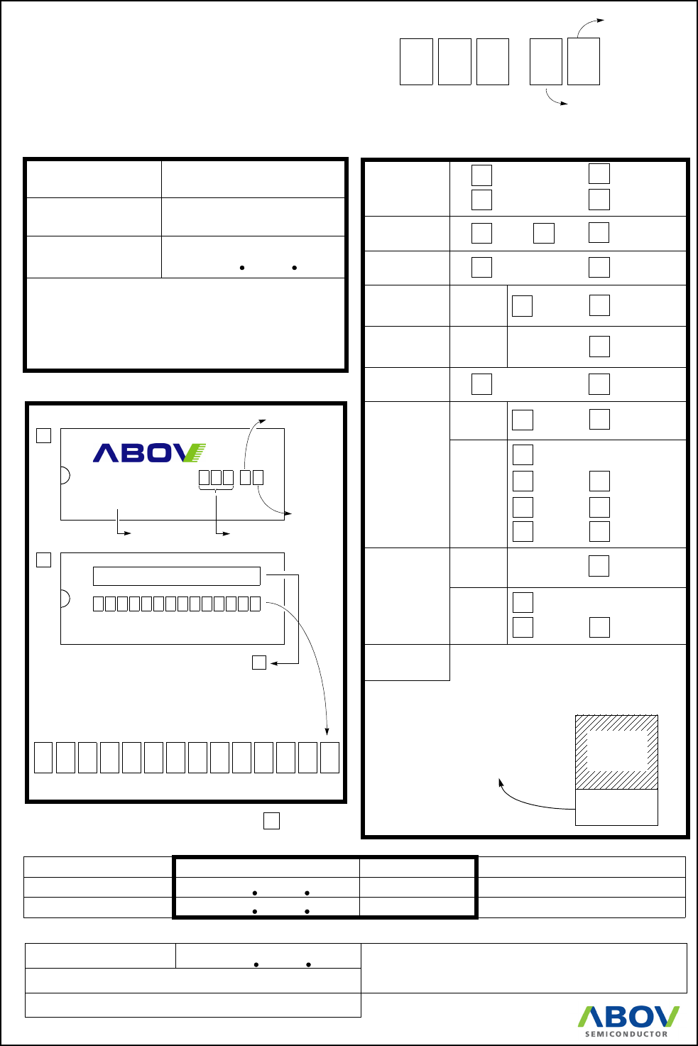
D. MASK ORDER SHEET(MC80C0316)
1. Customer Information
Company Name
2. Device Information
Application
Order Date
YYYY MM DD
Tel: Fax:
Name &
Signature:
Customer should write inside thick line box.
E-mail:
04-NOV-2011
MASK ORDER & VERIFICATION SHEET
MC80C0316-MC
28SKDIP 28SOP
Set “00H” in
this area
0000H
F000H
FFFFH
.OTP file data
EFFFH
Mask Data File Name: ( .OTP)
Check Sum: ( )
POR Use Yes No
Notice : Unused user
ROM area should
be filled with “00H”
Crystal
IN4M IN4MXO
IN2M IN2MXO
EXRC EXRCXO
32PDIP 32SOP
Package
If POR is Yes No
“Yes”,
R35
Use
If POR is No
“No”,
R35
Use
ROM Size 4K 8K 16K
ONP Use Yes No
If ONP is
Yes No
“Yes”,
OFP
Use
CLK
Use
Crystal
EXRC EXRCXO
If ONP is
“No”, CLK
Use
3. Marking Specification
(Please check mark into )
YYWW KOREA
MC80C0316
B, G, D or D32
-MC
Work Week
YYWW KOREA
Customer’s logo
Customer logo is not required.
Customer’s part number
If the customer logo must be used in the special mark,
please submit a clean original of the logo.
ROM Code Number
4. Delivery Schedule
Customer Sample
Date
YYYY MM DD
Risk Order
Quantity ABOV Confirmation
pcs
pcs
5. ROM Code Verification
Verification Date:
Check Sum:
Tel: Fax:
Signature:
No
OFP
Use
Name &
E-mail:
B, G, D or D32
B:PDIP
G:SKDIP
D:SOP
D32:32SOP
P:Pb Free
P:Pb Free
