MCF52211 Reference Manual Addendum Cold Fire MCF52211RM
User Manual: ColdFire MCF52211
Open the PDF directly: View PDF ![]() .
.
Page Count: 569 [warning: Documents this large are best viewed by clicking the View PDF Link!]
- MCF52211_RMAD_binder
- MCF52211RMAD
- MCF52211RM_REV3
- Chapter 1 Overview
- 1.1 Introduction
- 1.2 MCF52211 Family Configurations
- 1.3 Block Diagram
- 1.4 Part Numbers and Packaging
- 1.5 Features
- 1.5.1 V2 Core Overview
- 1.5.2 Integrated Debug Module
- 1.5.3 JTAG
- 1.5.4 On-Chip Memories
- 1.5.5 Power Management
- 1.5.6 USB On-The-Go Controller
- 1.5.7 UARTs
- 1.5.8 I2C Bus
- 1.5.9 QSPI
- 1.5.10 Fast ADC
- 1.5.11 DMA Timers (DTIM0-DTIM3)
- 1.5.12 General Purpose Timer (GPT)
- 1.5.13 Periodic Interrupt Timers (PIT0 and PIT1)
- 1.5.14 Real-Time Clock (RTC)
- 1.5.15 Pulse-Width Modulation (PWM) Timers
- 1.5.16 Software Watchdog Timer
- 1.5.17 Backup Watchdog Timer
- 1.5.18 Phase-Locked Loop (PLL)
- 1.5.19 Interrupt Controller (INTC)
- 1.5.20 DMA Controller
- 1.5.21 Reset
- 1.5.22 GPIO
- 1.6 Memory Map Overview
- Chapter 2 Signal Descriptions
- 2.1 Introduction
- 2.2 Overview
- 2.3 Pin Functions
- 2.4 Reset Signals
- 2.5 PLL and Clock Signals
- 2.6 Mode Selection
- 2.7 External Interrupt Signals
- 2.8 Queued Serial Peripheral Interface (QSPI)
- 2.9 I2C I/O Signals
- 2.10 UART Module Signals
- 2.11 DMA Timer Signals
- 2.12 ADC Signals
- 2.13 General Purpose Timer Signals
- 2.14 Pulse-Width Modulator Signals
- 2.15 Debug Support Signals
- 2.16 EzPort Signal Descriptions
- 2.17 Power and Ground Pins
- Chapter 3 ColdFire Core
- Chapter 4 Multiply-Accumulate Unit (MAC)
- Chapter 5 Static RAM (SRAM)
- Chapter 6 Clock Module
- Chapter 7 Backup Watchdog Timer (BWT) Module
- Chapter 8 Power Management
- Chapter 9 Chip Configuration Module (CCM)
- Chapter 10 Reset Controller Module
- Chapter 11 Real-Time Clock
- 11.1 Introduction
- 11.2 Memory Map/Register Definition
- 11.2.1 RTC Hours and Minutes Counter Register (HOURMIN)
- 11.2.2 RTC Seconds Counter Register (SECONDS)
- 11.2.3 RTC Hours and Minutes Alarm Register (ALRM_HM)
- 11.2.4 RTC Seconds Alarm Register (ALRM_SEC)
- 11.2.5 RTC Control Register (RTCCTL)
- 11.2.6 RTC Interrupt Status Register (RTCISR)
- 11.2.7 RTC Interrupt Enable Register (RTCIENR)
- 11.2.8 RTC Stopwatch Minutes Register (STPWCH)
- 11.2.9 RTC Days Counter Register (DAYS)
- 11.2.10 RTC Day Alarm Register (ALRM_DAY)
- 11.2.11 RTC General Oscillator Count Registers (RTCGOCU and RTCGOCL)
- 11.3 Functional Description
- 11.4 Initialization/Application Information
- Chapter 12 System Control Module (SCM)
- Chapter 13 General Purpose I/O Module
- Chapter 14 Interrupt Controller Module
- 14.1 68K/ColdFire Interrupt Architecture Overview
- 14.2 Memory Map
- 14.3 Register Descriptions
- 14.3.1 Interrupt Pending Registers (IPRHn, IPRLn)
- 14.3.2 Interrupt Mask Registers (IMRHn, IMRLn)
- 14.3.3 Interrupt Force Registers (INTFRCHn, INTFRCLn)
- 14.3.4 Interrupt Request Level Register (IRLRn)
- 14.3.5 Interrupt Acknowledge Level and Priority Register (IACKLPRn)
- 14.3.6 Interrupt Control Registers (ICRnx)
- 14.3.7 Software and Level m IACK Registers (SWIACKn, LmIACKn)
- 14.3.8 Global Level m IACK Registers (GLmIACK)
- 14.4 Low-Power Wakeup Operation
- Chapter 15 Universal Serial Bus, OTG Capable Controller
- Chapter 16 Edge Port Module (EPORT)
- Chapter 17 DMA Controller Module
- Chapter 18 ColdFire Flash Module (CFM)
- Chapter 19 EzPort
- Chapter 20 Programmable Interrupt Timers (PIT0-PIT1)
- Chapter 21 General Purpose Timer Module (GPT)
- 21.1 Introduction
- 21.2 Features
- 21.3 Block Diagram
- 21.4 Low-Power Mode Operation
- 21.5 Signal Description
- 21.6 Memory Map and Registers
- 21.6.1 GPT Input Capture/Output Compare Select Register (GPTIOS)
- 21.6.2 GPT Compare Force Register (GPCFORC)
- 21.6.3 GPT Output Compare 3 Mask Register (GPTOC3M)
- 21.6.4 GPT Output Compare 3 Data Register (GPTOC3D)
- 21.6.5 GPT Counter Register (GPTCNT)
- 21.6.6 GPT System Control Register 1 (GPTSCR1)
- 21.6.7 GPT Toggle-On-Overflow Register (GPTTOV)
- 21.6.8 GPT Control Register 1 (GPTCTL1)
- 21.6.9 GPT Control Register 2 (GPTCTL2)
- 21.6.10 GPT Interrupt Enable Register (GPTIE)
- 21.6.11 GPT System Control Register 2 (GPTSCR2)
- 21.6.12 GPT Flag Register 1 (GPTFLG1)
- 21.6.13 GPT Flag Register 2 (GPTFLG2)
- 21.6.14 GPT Channel Registers (GPTCn)
- 21.6.15 Pulse Accumulator Control Register (GPTPACTL)
- 21.6.16 Pulse Accumulator Flag Register (GPTPAFLG)
- 21.6.17 Pulse Accumulator Counter Register (GPTPACNT)
- 21.6.18 GPT Port Data Register (GPTPORT)
- 21.6.19 GPT Port Data Direction Register (GPTDDR)
- 21.7 Functional Description
- 21.8 Reset
- 21.9 Interrupts
- Chapter 22 DMA Timers (DTIM0-DTIM3)
- Chapter 23 Queued Serial Peripheral Interface (QSPI)
- Chapter 24 UART Modules
- 24.1 Introduction
- 24.2 External Signal Description
- 24.3 Memory Map/Register Definition
- 24.3.1 UART Mode Registers 1 (UMR1n)
- 24.3.2 UART Mode Register 2 (UMR2n)
- 24.3.3 UART Status Registers (USRn)
- 24.3.4 UART Clock Select Registers (UCSRn)
- 24.3.5 UART Command Registers (UCRn)
- 24.3.6 UART Receive Buffers (URBn)
- 24.3.7 UART Transmit Buffers (UTBn)
- 24.3.8 UART Input Port Change Registers (UIPCRn)
- 24.3.9 UART Auxiliary Control Register (UACRn)
- 24.3.10 UART Interrupt Status/Mask Registers (UISRn/UIMRn)
- 24.3.11 UART Baud Rate Generator Registers (UBG1n/UBG2n)
- 24.3.12 UART Input Port Register (UIPn)
- 24.3.13 UART Output Port Command Registers (UOP1n/UOP0n)
- 24.4 Functional Description
- 24.5 Initialization/Application Information
- Chapter 25 I2C Interface
- Chapter 26 Analog-to-Digital Converter (ADC)
- 26.1 Introduction
- 26.2 Features
- 26.3 Block Diagram
- 26.4 Memory Map and Register Definition
- 26.4.1 Control 1 Register (CTRL1)
- 26.4.2 Control 2 Register (CTRL2)
- 26.4.3 Zero Crossing Control Register (ADZCC)
- 26.4.4 Channel List 1 and 2 Registers (ADLST1 and ADLST2)
- 26.4.5 Sample Disable Register (ADSDIS)
- 26.4.6 Status Register (ADSTAT)
- 26.4.7 Limit Status Register (ADLSTAT)
- 26.4.8 Zero Crossing Status Register (ADZCSTAT)
- 26.4.9 Result Registers (ADRSLTn)
- 26.4.10 Low and High Limit Registers (ADLLMTn and ADHLMTn)
- 26.4.11 Offset Registers (ADOFSn)
- 26.4.12 Power Control Register (POWER)
- 26.4.13 Voltage Reference Register (CAL)
- 26.5 Functional Description
- 26.5.1 Input MUX Function
- 26.5.2 ADC Sample Conversion
- 26.5.3 ADC Data Processing
- 26.5.4 Sequential vs. Parallel Sampling
- 26.5.5 Scan Sequencing
- 26.5.6 Scan Configuration and Control
- 26.5.7 Interrupt Sources
- 26.5.8 Power Management
- 26.5.9 ADC Clock
- 26.5.10 Voltage Reference Pins VREFH and VREFL
- 26.5.11 Supply Pins VDDA and VSSA
- Chapter 27 Pulse-Width Modulation (PWM) Module
- 27.1 Introduction
- 27.2 Memory Map/Register Definition
- 27.2.1 PWM Enable Register (PWME)
- 27.2.2 PWM Polarity Register (PWMPOL)
- 27.2.3 PWM Clock Select Register (PWMCLK)
- 27.2.4 PWM Prescale Clock Select Register (PWMPRCLK)
- 27.2.5 PWM Center Align Enable Register (PWMCAE)
- 27.2.6 PWM Control Register (PWMCTL)
- 27.2.7 PWM Scale A Register (PWMSCLA)
- 27.2.8 PWM Scale B Register (PWMSCLB)
- 27.2.9 PWM Channel Counter Registers (PWMCNTn)
- 27.2.10 PWM Channel Period Registers (PWMPERn)
- 27.2.11 PWM Channel Duty Registers (PWMDTYn)
- 27.2.12 PWM Shutdown Register (PWMSDN)
- 27.3 Functional Description
- Chapter 28 Debug Module
- 28.1 Introduction
- 28.2 Signal Descriptions
- 28.3 Memory Map/Register Definition
- 28.3.1 Shared Debug Resources
- 28.3.2 Configuration/Status Register (CSR)
- 28.3.3 BDM Address Attribute Register (BAAR)
- 28.3.4 Address Attribute Trigger Register (AATR)
- 28.3.5 Trigger Definition Register (TDR)
- 28.3.6 Program Counter Breakpoint/Mask Registers (PBR0-3, PBMR)
- 28.3.7 Address Breakpoint Registers (ABLR, ABHR)
- 28.3.8 Data Breakpoint and Mask Registers (DBR, DBMR)
- 28.4 Functional Description
- Chapter 29 IEEE 1149.1 Test Access Port (JTAG)
- Appendix A Register Memory Map Quick Reference
- Appendix B Revision History
- Chapter 1 Overview

© Freescale Semiconductor, Inc., 2012. All rights reserved.
Freescale MCF52211RM
Rev. 3.1, 05/2012
This is the MCF52211 Reference Manual set consisting of the following files:
• MCF52211 Reference Manual Addendum, Rev 2
• MCF52211 Reference Manual, Rev 3
MCF52211 Reference Manual
Addendum
by: Automotive and Industrial Solutions Gruop

Freescale
Reference Manual Addendum
MCF52211RMAD
Rev. 2, 05/2012
Contents
© Freescale, Inc., 2012. All rights reserved.
This addendum document describes corrections to the
MCF52211 Reference Manual, order number
MCF52211RM. For convenience, the addenda items are
grouped by revision. Please check our website at
http://www.freescale.com/coldfire for the latest updates.
The current available version of the MCF52211
Reference Manual is Revision 3.
1 Addendum for Revision 3 . . . . . . . . . . . . . . . . . . . . . . . . 2
2 Addendum for Revision 1 . . . . . . . . . . . . . . . . . . . . . . . . 3
3 Revision History. . . . . . . . . . . . . . . . . . . . . . . . . . . . . . . . 4
MCF52211 Reference Manual
Addendum
by: Automotive and Industrial Solutions Gruop
MCF52211 Reference Manual Addendum, Rev. 2
Addendum for Revision 3
Freescale Semiconductor2
1 Addendum for Revision 3
Table 1. MCF52211 Reference Manual Rev 3 Addendum
Location Description
Chapter “Clock
Module”/Section
“Block
Diagram”/Figure
“Clock Module Block
Diagram”
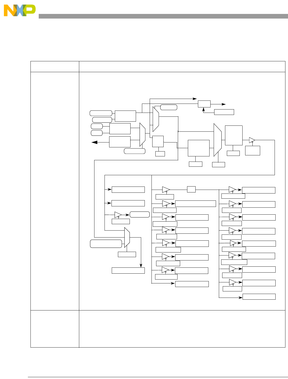
Update the Figure “Clock Module Block Diagram”.In the previous figure it was shown that the USB
clock is sourced directly from the MHz oscillator. The figure is improved as shown below:
Chapter “Universal
Serial Bus, OTG
CapableController”/
Table 15-35
“USB_CTRL Field
Descriptions”
In Table 15-35 “USB_CTRL Field Description” Field “CLK_SRC” change the description from “01
External OSC or EXTAL pin” to “01 PLL Bypass Clock”.
PPMRH[11]
CFM
PPMRH[9]
PWM
PPMRH[8]
GPT
PPMRH[7]
ADC
PPMRH[1]
Edge Port
PPMRH[0]
GPIO / Ports
CLKOUT
PPMRL[17]
Interrupt Controller
PPMRL[16:13]
DMA Timers
PPMRL[10]
QSPI
PPMRL[9:8]
I2Cs
PPMRL[7:5]
UARTs
DMA
ColdFire V2
BDM
PITs
DISCLK
PPMRL[1]
2
System Clock (fsys)
USB_CTRL
USB
USB_ALT_CLK
EXTAL
CLKMOD1 CLKSRC
PLL
Low
Power
Divider
LPD[3:0]
Ref Clock
0
1
ADC auto-standby Clk1
STOP
Pre-
Divider
CCHR
ON-CHIP
0
1
kHz
MHz
OSCILLA-
XTAL
OSCSEL02
1
0
RTC_EXTAL
RTC_XTAL
RTC_Clk
1
OSCSEL1
PLL Bypass Clock
BWT_Clk
1
RTC
DIV
RTCGOCNT
PPMRH[14]
RTC
BWT
WDOG
PPMRH[4:3]
PPMRL[4]

Addendum for Revision 1
MCF52211 Reference Manual Addendum, Rev. 2
Freescale Semiconductor 3
2 Addendum for Revision 1
Table 2. MCF52211 Reference Manual Rev 1 Addendum
Location Description
Throughout Formatting, layout, spelling, and grammar corrections.
Table 2-1 / Page 2-3 Synchronized the table in the reference manual and the device data sheet.
Table 6-4 / Page 6-6 Corrected the CCHR reset value (was 0x04, is 0x05).
Figure 6-12 / Page 6-19 Deleted the RS resistor.
Chapter 8 Deleted references to nonexistent FlexCAN module.
Chapter 11 Added information about the RTC general oscillator count registers, RTCGOCU and RTCGOCL.
Figure 11-13 Corrected the code example for initializing the RTC.
Section 12.5.4 / Page 12-7 Updated the section to reflect the fact that the CWT does not cause a hardware reset.
Table 12-6 / Page 12-8 In the CWCR[CWRI] field description, changed “The interrupt level for the CWT is programmed
in the interrupt control register 7 (ICR7)...” to “The interrupt level for the CWT is programmed in
the interrupt control register 8 (ICR8)...”.
Section 12.7.3.1 / Page 12-14 • Rewrote the introductory text describing the MPR (removing erroneous reference to a fast
Ethernet controller).
• Corrected the MPR reset value (was 0x11, is 0x1).
Table 12-15 / Page 12-18 Deleted reference to nonexistent FlexCAN module.
Section 14-1 / Page 14-2 Deleted the sentence beginning with “For many peripheral devices...”.
Table 14-2 / Page 14-5 Deleted the entry for the (nonexistent) GSWIACK register.
Section 14.3.8 / Page 14-16 Deleted references to the (nonexistent) GSWIACK register.
Table 15-4 / Page 15-10 Corrected the acronym for the SOF threshold register (was OSOF_THLDL, is SOF_THLD).
Table 15-35 / Page 15-31 Corrected the descriptions of USB_CTRL[PDE] (when this bit is cleared, weak pulldowns are
disabled; when this bit is set, weak pulldowns are enabled).
Section 17.4 / Page 17-12 Deleted the sentence “BCRn decrements when an address transfer write completes for a
single-address access (DCRn[SAA] = 0), or when SAA equals 1.”
Figure 24-6 / Page 24-9 Added a note to clarify the UCSRn reset values.
Figure 24-20 / Page 24-21 • Corrected the label of the top signal (was UnTXD, is UnRXD).
• Corrected the text in the footnote (was TXRTS, is RXRTS).
Figure 24-23 / Page 24-24 Corrected the UnTXD label (was “Input”, is “Output”).
Figure 24-24 / Page 24-25 • Corrected a label on the bottom row (was UMR1n[PT]=2, is UMR1n[PT]=1).
• Deleted duplicate UMR1n[PM]=11 label.
Section 24.5.1.2 / Page 24-27 Added example DMA configuration steps.
Section 27.3.2.5.1 / Page
27-18
Corrected the numerical values in the left-aligned example.
Section 27.3.2.6.1 / Page
27-20
Corrected the numerical values in the center-aligned example.
Appendix A • Corrected the acronym for the SOF threshold register (was OSOF_THLDL, is SOF_THLD).
• Deleted the entry for the (nonexistent) GSWIACK register.
• Added entries for the RTCGOCU and RTCGOCL registers.

MCF52211 Reference Manual Addendum, Rev. 2
Revision History
Freescale Semiconductor4
3 Revision History
Table 3 provides a revision history for this document.
Table 3. Revision History
Rev. Number Substantive Changes Date of Release
1 Initial release, incorporating corrections listed in Ta bl e 2 . 06/2007
2 Incorporated changes in “Clock Module” as listed in Ta bl e 1 . 05/2012

Document Number: MCF52211RMAD
Rev. 2
05/2012
How to Reach Us:
Home Page:
www.freescale.com
Web Support:
http://www.freescale.com/support
USA/Europe or Locations Not Listed:
Freescale Semiconductor, Inc.
Technical Information Center, EL516
2100 East Elliot Road
Tempe, Arizona 85284
+1-800-521-6274 or +1-480-768-2130
www.freescale.com/support
Europe, Middle East, and Africa:
Freescale Halbleiter Deutschland GmbH
Technical Information Center
Schatzbogen 7
81829 Muenchen, Germany
+44 1296 380 456 (English)
+46 8 52200080 (English)
+49 89 92103 559 (German)
+33 1 69 35 48 48 (French)
www.freescale.com/support
Japan:
Freescale Semiconductor Japan Ltd.
Headquarters
ARCO Tower 15F
1-8-1, Shimo-Meguro, Meguro-ku,
Tokyo 153-0064
Japan
0120 191014 or +81 3 5437 9125
support.japan@freescale.com
Asia/Pacific:
Freescale Semiconductor Hong Kong Ltd.
Technical Information Center
2 Dai King Street
Tai Po Industrial Estate
Tai Po, N.T., Hong Kong
+800 2666 8080
support.asia@freescale.com
For Literature Requests Only:
Freescale Semiconductor Literature Distribution Center
P.O. Box 5405
Denver, Colorado 80217
1-800-441-2447 or 303-675-2140
Fax: 303-675-2150
LDCForFreescaleSemiconductor@hibbertgroup.com
Information in this document is provided solely to enable system and software
implementers to use Freescale Semiconductor products. There are no express or
implied copyright licenses granted hereunder to design or fabricate any integrated
circuits or integrated circuits based on the information in this document.
Freescale Semiconductor reserves the right to make changes without further notice to
any products herein. Freescale Semiconductor makes no warranty, representation or
guarantee regarding the suitability of its products for any particular purpose, nor does
Freescale Semiconductor assume any liability arising out of the application or use of any
product or circuit, and specifically disclaims any and all liability, including without
limitation consequential or incidental damages. “Typical” parameters that may be
provided in Freescale Semiconductor data sheets and/or specifications can and do vary
in different applications and actual performance may vary over time. All operating
parameters, including “Typicals”, must be validated for each customer application by
customer’s technical experts. Freescale Semiconductor does not convey any license
under its patent rights nor the rights of others. Freescale Semiconductor products are
not designed, intended, or authorized for use as components in systems intended for
surgical implant into the body, or other applications intended to support or sustain life,
or for any other application in which the failure of the Freescale Semiconductor product
could create a situation where personal injury or death may occur. Should Buyer
purchase or use Freescale Semiconductor products for any such unintended or
unauthorized application, Buyer shall indemnify and hold Freescale Semiconductor and
its officers, employees, subsidiaries, affiliates, and distributors harmless against all
claims, costs, damages, and expenses, and reasonable attorney fees arising out of,
directly or indirectly, any claim of personal injury or death associated with such
unintended or unauthorized use, even if such claim alleges that Freescale
Semiconductor was negligent regarding the design or manufacture of the part.
RoHS-compliant and/or Pb-free versions of Freescale products have the functionality
and electrical characteristics as their non-RoHS-compliant and/or non-Pb-free
counterparts. For further information, see http://www.freescale.com or contact your
Freescale sales representative.
For information on Freescale’s Environmental Products program, go to
http://www.freescale.com/epp.
Freescale™ and the Freescale logo are trademarks of Freescale Semiconductor, Inc.
All other product or service names are the property of their respective owners.
© Freescale Semiconductor, Inc. 2012. All rights reserved.

MCF52211 ColdFire® Integrated
Microcontroller Reference Manual
Devices Supported:
MCF52210
MCF52211
MCF52212
MCF52213
Document Number: MCF52211RM
Rev. 3
03/2011

How to Reach Us:
Home Page:
http://www.freescale.com
Web Support:
Http://www.freescale.com/support
USA/Europe or Locations Not Listed:
Freescale Semiconductor
Technical Information Center, EL516
2100East Elliot Road
Tempe, Arizona 85284
+1-800-521-6274 or +1-480-768-2130
www.freescale.com/support
Europe, Middle East, and Africa:
Freescale Halbleiter Deutschland GmbH
Technical Information Center
Schatzbogen 7
81829 Muenchen, Germany
+44 1296 380 456 (English)
+46 8 52200080 (English)
+49 89 92103 559 (German)
+33 1 69 35 48 48 (French)
www.freescale.com/support
Japan:
Technical Information Center
Freescale Semiconductor Japan Ltd.
Headquarters
ARCO Tower 15F
1-8-1, Shimo-Meguro, Meguro-ku,
Tokyo 153-0064, Japan
0120 191014 or +81 3 5437 9125
support.japan@freescale.com
Asia/Pacific:
Freescale Semiconductor China Ltd.
Exchange Building 23F
No. 118 Jianguo Road
Chaoyang District
Beijing 100022
China
+86 10 5879 8000
support.asia@freescale.com
For Literature Requests Only:
Freescale Semiconductor Literature Distribution Center
1-800-441-2447 or +1-303-675-2140
Fax: +1-303-675-2150
LDCForFreescaleSemiconductor@hibbertgroup.com
Information in this document is provided solely to enable system and
software implementers to use Freescale Semiconductor products. There are
no express or implied copyright licenses granted hereunder to design or
fabricate any integrated circuits or integrated circuits based on the
information in this document.
Freescale Semiconductor reserves the right to make changes without further
notice to any products herein. Freescale Semiconductor makes no warranty,
representation or guarantee regarding the suitability of its products for any
particular purpose, nor does Freescale Semiconductor assume any liability
arising out of the application or use of any product or circuit, and specifically
disclaims any and all liability, including without limitation consequential or
incidental damages. “Typical” parameters that may be provided in Freescale
Semiconductor data sheets and/or specifications can and do vary in different
applications and actual performance may vary over time. All operating
parameters, including “Typicals”, must be validated for each customer
application by customer’s technical experts. Freescale Semiconductor does
not convey any license under its patent rights nor the rights of others.
Freescale Semiconductor products are not designed, intended, or authorized
for use as components in systems intended for surgical implant into the body,
or other applications intended to support or sustain life, or for any other
application in which the failure of the Freescale Semiconductor product could
create a situation where personal injury or death may occur. Should Buyer
purchase or use Freescale Semiconductor products for any such unintended
or unauthorized application, Buyer shall indemnify and hold Freescale
Semiconductor and its officers, employees, subsidiaries, affiliates, and
distributors harmless against all claims, costs, damages, and expenses, and
reasonable attorney fees arising out of, directly or indirectly, any claim of
personal injury or death associated with such unintended or unauthorized
use, even if such claim alleges that Freescale Semiconductor was negligent
regarding the design or manufacture of the part.
Freescale™ and the Freescale logo are trademarks of Freescale
Semiconductor, Inc. All other product or service names are the property of their
respective owners.
© Freescale Semiconductor, Inc. 2011. All rights reserved.
MCF52211RM
Rev. 3
03/2011

Freescale Semiconductor i
Chapter 1
Overview
1.1 Introduction . . . . . . . . . . . . . . . . . . . . . . . . . . . . . . . . . . . . . . . . . . . . . . . . . . . . . . . . . . . . . . . . . 1-1
1.2 MCF52211 Family Configurations . . . . . . . . . . . . . . . . . . . . . . . . . . . . . . . . . . . . . . . . . . . . . . . 1-2
1.3 Block Diagram . . . . . . . . . . . . . . . . . . . . . . . . . . . . . . . . . . . . . . . . . . . . . . . . . . . . . . . . . . . . . . . 1-3
1.4 Part Numbers and Packaging . . . . . . . . . . . . . . . . . . . . . . . . . . . . . . . . . . . . . . . . . . . . . . . . . . . . 1-4
1.5 Features . . . . . . . . . . . . . . . . . . . . . . . . . . . . . . . . . . . . . . . . . . . . . . . . . . . . . . . . . . . . . . . . . . . . 1-4
1.5.1 V2 Core Overview . . . . . . . . . . . . . . . . . . . . . . . . . . . . . . . . . . . . . . . . . . . . . . . . . . . . . 1-8
1.5.2 Integrated Debug Module . . . . . . . . . . . . . . . . . . . . . . . . . . . . . . . . . . . . . . . . . . . . . . . 1-9
1.5.3 JTAG . . . . . . . . . . . . . . . . . . . . . . . . . . . . . . . . . . . . . . . . . . . . . . . . . . . . . . . . . . . . . . . 1-9
1.5.4 On-Chip Memories . . . . . . . . . . . . . . . . . . . . . . . . . . . . . . . . . . . . . . . . . . . . . . . . . . . 1-10
1.5.5 Power Management . . . . . . . . . . . . . . . . . . . . . . . . . . . . . . . . . . . . . . . . . . . . . . . . . . . 1-10
1.5.6 USB On-The-Go Controller . . . . . . . . . . . . . . . . . . . . . . . . . . . . . . . . . . . . . . . . . . . . . 1-10
1.5.7 UARTs . . . . . . . . . . . . . . . . . . . . . . . . . . . . . . . . . . . . . . . . . . . . . . . . . . . . . . . . . . . . . 1-11
1.5.8 I2C Bus . . . . . . . . . . . . . . . . . . . . . . . . . . . . . . . . . . . . . . . . . . . . . . . . . . . . . . . . . . . . . 1-11
1.5.9 QSPI . . . . . . . . . . . . . . . . . . . . . . . . . . . . . . . . . . . . . . . . . . . . . . . . . . . . . . . . . . . . . . . 1-11
1.5.10 Fast ADC . . . . . . . . . . . . . . . . . . . . . . . . . . . . . . . . . . . . . . . . . . . . . . . . . . . . . . . . . . . 1-11
1.5.11 DMA Timers (DTIM0–DTIM3) . . . . . . . . . . . . . . . . . . . . . . . . . . . . . . . . . . . . . . . . . 1-11
1.5.12 General Purpose Timer (GPT) . . . . . . . . . . . . . . . . . . . . . . . . . . . . . . . . . . . . . . . . . . . 1-12
1.5.13 Periodic Interrupt Timers (PIT0 and PIT1) . . . . . . . . . . . . . . . . . . . . . . . . . . . . . . . . . 1-12
1.5.14 Real-Time Clock (RTC) . . . . . . . . . . . . . . . . . . . . . . . . . . . . . . . . . . . . . . . . . . . . . . . . 1-12
1.5.15 Pulse-Width Modulation (PWM) Timers . . . . . . . . . . . . . . . . . . . . . . . . . . . . . . . . . . . 1-12
1.5.16 Software Watchdog Timer . . . . . . . . . . . . . . . . . . . . . . . . . . . . . . . . . . . . . . . . . . . . . . 1-12
1.5.17 Backup Watchdog Timer . . . . . . . . . . . . . . . . . . . . . . . . . . . . . . . . . . . . . . . . . . . . . . . 1-13
1.5.18 Phase-Locked Loop (PLL) . . . . . . . . . . . . . . . . . . . . . . . . . . . . . . . . . . . . . . . . . . . . . . 1-13
1.5.19 Interrupt Controller (INTC) . . . . . . . . . . . . . . . . . . . . . . . . . . . . . . . . . . . . . . . . . . . . . 1-13
1.5.20 DMA Controller . . . . . . . . . . . . . . . . . . . . . . . . . . . . . . . . . . . . . . . . . . . . . . . . . . . . . . 1-13
1.5.21 Reset . . . . . . . . . . . . . . . . . . . . . . . . . . . . . . . . . . . . . . . . . . . . . . . . . . . . . . . . . . . . . . . 1-13
1.5.22 GPIO . . . . . . . . . . . . . . . . . . . . . . . . . . . . . . . . . . . . . . . . . . . . . . . . . . . . . . . . . . . . . . 1-14
1.6 Memory Map Overview . . . . . . . . . . . . . . . . . . . . . . . . . . . . . . . . . . . . . . . . . . . . . . . . . . . . . . . 1-14
Chapter 2
Signal Descriptions
2.1 Introduction . . . . . . . . . . . . . . . . . . . . . . . . . . . . . . . . . . . . . . . . . . . . . . . . . . . . . . . . . . . . . . . . . 2-1
2.2 Overview . . . . . . . . . . . . . . . . . . . . . . . . . . . . . . . . . . . . . . . . . . . . . . . . . . . . . . . . . . . . . . . . . . . 2-1
2.3 Pin Functions . . . . . . . . . . . . . . . . . . . . . . . . . . . . . . . . . . . . . . . . . . . . . . . . . . . . . . . . . . . . . . . . 2-2
2.4 Reset Signals . . . . . . . . . . . . . . . . . . . . . . . . . . . . . . . . . . . . . . . . . . . . . . . . . . . . . . . . . . . . . . . . 2-8
2.5 PLL and Clock Signals . . . . . . . . . . . . . . . . . . . . . . . . . . . . . . . . . . . . . . . . . . . . . . . . . . . . . . . . . 2-8
2.6 Mode Selection . . . . . . . . . . . . . . . . . . . . . . . . . . . . . . . . . . . . . . . . . . . . . . . . . . . . . . . . . . . . . . . 2-8
2.7 External Interrupt Signals . . . . . . . . . . . . . . . . . . . . . . . . . . . . . . . . . . . . . . . . . . . . . . . . . . . . . . . 2-8
2.8 Queued Serial Peripheral Interface (QSPI) . . . . . . . . . . . . . . . . . . . . . . . . . . . . . . . . . . . . . . . . . 2-9
2.9 I2C I/O Signals . . . . . . . . . . . . . . . . . . . . . . . . . . . . . . . . . . . . . . . . . . . . . . . . . . . . . . . . . . . . . . . 2-9
2.10 UART Module Signals . . . . . . . . . . . . . . . . . . . . . . . . . . . . . . . . . . . . . . . . . . . . . . . . . . . . . . . . . 2-9
2.11 DMA Timer Signals . . . . . . . . . . . . . . . . . . . . . . . . . . . . . . . . . . . . . . . . . . . . . . . . . . . . . . . . . . 2-10
MCF52211 ColdFire® Integrated Microcontroller Reference Manual, Rev. 3

Freescale Semiconductor ii
2.12 ADC Signals . . . . . . . . . . . . . . . . . . . . . . . . . . . . . . . . . . . . . . . . . . . . . . . . . . . . . . . . . . . . . . . . 2-10
2.13 General Purpose Timer Signals . . . . . . . . . . . . . . . . . . . . . . . . . . . . . . . . . . . . . . . . . . . . . . . . . 2-10
2.14 Pulse-Width Modulator Signals . . . . . . . . . . . . . . . . . . . . . . . . . . . . . . . . . . . . . . . . . . . . . . . . . 2-11
2.15 Debug Support Signals . . . . . . . . . . . . . . . . . . . . . . . . . . . . . . . . . . . . . . . . . . . . . . . . . . . . . . . . 2-11
2.16 EzPort Signal Descriptions . . . . . . . . . . . . . . . . . . . . . . . . . . . . . . . . . . . . . . . . . . . . . . . . . . . . . 2-12
2.17 Power and Ground Pins . . . . . . . . . . . . . . . . . . . . . . . . . . . . . . . . . . . . . . . . . . . . . . . . . . . . . . . 2-12
Chapter 3
ColdFire Core
3.1 Introduction . . . . . . . . . . . . . . . . . . . . . . . . . . . . . . . . . . . . . . . . . . . . . . . . . . . . . . . . . . . . . . . . . 3-1
3.1.1 Overview . . . . . . . . . . . . . . . . . . . . . . . . . . . . . . . . . . . . . . . . . . . . . . . . . . . . . . . . . . . . 3-1
3.2 Memory Map/Register Description . . . . . . . . . . . . . . . . . . . . . . . . . . . . . . . . . . . . . . . . . . . . . . . 3-2
3.2.1 Data Registers (D0–D7) . . . . . . . . . . . . . . . . . . . . . . . . . . . . . . . . . . . . . . . . . . . . . . . . . 3-4
3.2.2 Address Registers (A0–A6) . . . . . . . . . . . . . . . . . . . . . . . . . . . . . . . . . . . . . . . . . . . . . . 3-4
3.2.3 Supervisor/User Stack Pointers (A7 and OTHER_A7) . . . . . . . . . . . . . . . . . . . . . . . . . 3-4
3.2.4 Condition Code Register (CCR) . . . . . . . . . . . . . . . . . . . . . . . . . . . . . . . . . . . . . . . . . . 3-5
3.2.5 Program Counter (PC) . . . . . . . . . . . . . . . . . . . . . . . . . . . . . . . . . . . . . . . . . . . . . . . . . . 3-6
3.2.6 Vector Base Register (VBR) . . . . . . . . . . . . . . . . . . . . . . . . . . . . . . . . . . . . . . . . . . . . . 3-6
3.2.7 Status Register (SR) . . . . . . . . . . . . . . . . . . . . . . . . . . . . . . . . . . . . . . . . . . . . . . . . . . . . 3-7
3.2.8 Memory Base Address Registers (RAMBAR, FLASHBAR) . . . . . . . . . . . . . . . . . . . . 3-8
3.3 Functional Description . . . . . . . . . . . . . . . . . . . . . . . . . . . . . . . . . . . . . . . . . . . . . . . . . . . . . . . . . 3-8
3.3.1 Version 2 ColdFire Microarchitecture . . . . . . . . . . . . . . . . . . . . . . . . . . . . . . . . . . . . . . 3-8
3.3.2 Instruction Set Architecture (ISA_A+) . . . . . . . . . . . . . . . . . . . . . . . . . . . . . . . . . . . . 3-13
3.3.3 Exception Processing Overview . . . . . . . . . . . . . . . . . . . . . . . . . . . . . . . . . . . . . . . . . 3-14
3.3.4 Processor Exceptions . . . . . . . . . . . . . . . . . . . . . . . . . . . . . . . . . . . . . . . . . . . . . . . . . . 3-17
3.3.5 Instruction Execution Timing . . . . . . . . . . . . . . . . . . . . . . . . . . . . . . . . . . . . . . . . . . . 3-24
Chapter 4
Multiply-Accumulate Unit (MAC)
4.1 Introduction . . . . . . . . . . . . . . . . . . . . . . . . . . . . . . . . . . . . . . . . . . . . . . . . . . . . . . . . . . . . . . . . . 4-2
4.1.1 Overview . . . . . . . . . . . . . . . . . . . . . . . . . . . . . . . . . . . . . . . . . . . . . . . . . . . . . . . . . . . . 4-2
4.2 Memory Map/Register Definition . . . . . . . . . . . . . . . . . . . . . . . . . . . . . . . . . . . . . . . . . . . . . . . . 4-3
4.2.1 MAC Status Register (MACSR) . . . . . . . . . . . . . . . . . . . . . . . . . . . . . . . . . . . . . . . . . . 4-3
4.2.2 Mask Register (MASK) . . . . . . . . . . . . . . . . . . . . . . . . . . . . . . . . . . . . . . . . . . . . . . . . . 4-5
4.2.3 Accumulator Register (ACC) . . . . . . . . . . . . . . . . . . . . . . . . . . . . . . . . . . . . . . . . . . . . 4-6
4.3 Functional Description . . . . . . . . . . . . . . . . . . . . . . . . . . . . . . . . . . . . . . . . . . . . . . . . . . . . . . . . . 4-7
4.3.1 Fractional Operation Mode . . . . . . . . . . . . . . . . . . . . . . . . . . . . . . . . . . . . . . . . . . . . . . 4-8
4.3.2 MAC Instruction Set Summary . . . . . . . . . . . . . . . . . . . . . . . . . . . . . . . . . . . . . . . . . . . 4-9
4.3.3 MAC Instruction Execution Times . . . . . . . . . . . . . . . . . . . . . . . . . . . . . . . . . . . . . . . 4-10
4.3.4 Data Representation . . . . . . . . . . . . . . . . . . . . . . . . . . . . . . . . . . . . . . . . . . . . . . . . . . . 4-10
4.3.5 MAC Opcodes . . . . . . . . . . . . . . . . . . . . . . . . . . . . . . . . . . . . . . . . . . . . . . . . . . . . . . . 4-10
MCF52211 ColdFire® Integrated Microcontroller Reference Manual, Rev. 3

Freescale Semiconductor iii
Chapter 5
Static RAM (SRAM)
5.1 Introduction . . . . . . . . . . . . . . . . . . . . . . . . . . . . . . . . . . . . . . . . . . . . . . . . . . . . . . . . . . . . . . . . . 5-1
5.1.1 Overview . . . . . . . . . . . . . . . . . . . . . . . . . . . . . . . . . . . . . . . . . . . . . . . . . . . . . . . . . . . . 5-1
5.1.2 Features . . . . . . . . . . . . . . . . . . . . . . . . . . . . . . . . . . . . . . . . . . . . . . . . . . . . . . . . . . . . . 5-1
5.2 Memory Map/Register Description . . . . . . . . . . . . . . . . . . . . . . . . . . . . . . . . . . . . . . . . . . . . . . . 5-1
5.2.1 SRAM Base Address Register (RAMBAR) . . . . . . . . . . . . . . . . . . . . . . . . . . . . . . . . . 5-2
5.3 Initialization/Application Information . . . . . . . . . . . . . . . . . . . . . . . . . . . . . . . . . . . . . . . . . . . . . 5-3
5.3.1 SRAM Initialization Code . . . . . . . . . . . . . . . . . . . . . . . . . . . . . . . . . . . . . . . . . . . . . . . 5-4
5.3.2 Power Management . . . . . . . . . . . . . . . . . . . . . . . . . . . . . . . . . . . . . . . . . . . . . . . . . . . . 5-4
Chapter 6
Clock Module
6.1 Introduction . . . . . . . . . . . . . . . . . . . . . . . . . . . . . . . . . . . . . . . . . . . . . . . . . . . . . . . . . . . . . . . . . 6-1
6.2 Features . . . . . . . . . . . . . . . . . . . . . . . . . . . . . . . . . . . . . . . . . . . . . . . . . . . . . . . . . . . . . . . . . . . . 6-1
6.3 Modes of Operation . . . . . . . . . . . . . . . . . . . . . . . . . . . . . . . . . . . . . . . . . . . . . . . . . . . . . . . . . . . 6-1
6.3.1 Backup Watchdog Timer Mode . . . . . . . . . . . . . . . . . . . . . . . . . . . . . . . . . . . . . . . . . . . 6-2
6.3.2 RTC Mode . . . . . . . . . . . . . . . . . . . . . . . . . . . . . . . . . . . . . . . . . . . . . . . . . . . . . . . . . . . 6-2
6.3.3 Normal PLL Mode . . . . . . . . . . . . . . . . . . . . . . . . . . . . . . . . . . . . . . . . . . . . . . . . . . . . . 6-2
6.3.4 External Clock Mode . . . . . . . . . . . . . . . . . . . . . . . . . . . . . . . . . . . . . . . . . . . . . . . . . . . 6-2
6.4 Low-Power Mode Operation . . . . . . . . . . . . . . . . . . . . . . . . . . . . . . . . . . . . . . . . . . . . . . . . . . . . 6-2
6.5 Block Diagram . . . . . . . . . . . . . . . . . . . . . . . . . . . . . . . . . . . . . . . . . . . . . . . . . . . . . . . . . . . . . . . 6-3
6.6 Signal Descriptions . . . . . . . . . . . . . . . . . . . . . . . . . . . . . . . . . . . . . . . . . . . . . . . . . . . . . . . . . . . 6-5
6.6.1 EXTAL . . . . . . . . . . . . . . . . . . . . . . . . . . . . . . . . . . . . . . . . . . . . . . . . . . . . . . . . . . . . . . 6-5
6.6.2 XTAL . . . . . . . . . . . . . . . . . . . . . . . . . . . . . . . . . . . . . . . . . . . . . . . . . . . . . . . . . . . . . . . 6-5
6.6.3 CLKOUT . . . . . . . . . . . . . . . . . . . . . . . . . . . . . . . . . . . . . . . . . . . . . . . . . . . . . . . . . . . . 6-5
6.6.4 CLKMOD[1:0] . . . . . . . . . . . . . . . . . . . . . . . . . . . . . . . . . . . . . . . . . . . . . . . . . . . . . . . 6-5
6.6.5 RSTO . . . . . . . . . . . . . . . . . . . . . . . . . . . . . . . . . . . . . . . . . . . . . . . . . . . . . . . . . . . . . . . 6-6
6.7 Memory Map and Registers . . . . . . . . . . . . . . . . . . . . . . . . . . . . . . . . . . . . . . . . . . . . . . . . . . . . . 6-6
6.7.1 Register Descriptions . . . . . . . . . . . . . . . . . . . . . . . . . . . . . . . . . . . . . . . . . . . . . . . . . . . 6-7
6.8 Functional Description . . . . . . . . . . . . . . . . . . . . . . . . . . . . . . . . . . . . . . . . . . . . . . . . . . . . . . . . 6-17
6.8.1 System Clock Modes . . . . . . . . . . . . . . . . . . . . . . . . . . . . . . . . . . . . . . . . . . . . . . . . . . 6-17
6.8.2 Clock Operation During Reset . . . . . . . . . . . . . . . . . . . . . . . . . . . . . . . . . . . . . . . . . . . 6-17
6.8.3 System Clock Generation . . . . . . . . . . . . . . . . . . . . . . . . . . . . . . . . . . . . . . . . . . . . . . 6-18
6.8.4 PLL Operation . . . . . . . . . . . . . . . . . . . . . . . . . . . . . . . . . . . . . . . . . . . . . . . . . . . . . . . 6-18
Chapter 7
Backup Watchdog Timer (BWT) Module
7.1 Introduction . . . . . . . . . . . . . . . . . . . . . . . . . . . . . . . . . . . . . . . . . . . . . . . . . . . . . . . . . . . . . . . . . 7-1
7.1.1 Overview . . . . . . . . . . . . . . . . . . . . . . . . . . . . . . . . . . . . . . . . . . . . . . . . . . . . . . . . . . . . 7-1
7.1.2 Modes of Operation . . . . . . . . . . . . . . . . . . . . . . . . . . . . . . . . . . . . . . . . . . . . . . . . . . . . 7-1
7.2 Memory Map and Register Definition . . . . . . . . . . . . . . . . . . . . . . . . . . . . . . . . . . . . . . . . . . . . . 7-2
7.2.1 Memory Map . . . . . . . . . . . . . . . . . . . . . . . . . . . . . . . . . . . . . . . . . . . . . . . . . . . . . . . . . 7-2
7.2.2 Register Descriptions . . . . . . . . . . . . . . . . . . . . . . . . . . . . . . . . . . . . . . . . . . . . . . . . . . . 7-3
MCF52211 ColdFire® Integrated Microcontroller Reference Manual, Rev. 3

Freescale Semiconductor iv
7.3 Functional Description . . . . . . . . . . . . . . . . . . . . . . . . . . . . . . . . . . . . . . . . . . . . . . . . . . . . . . . . . 7-6
Chapter 8
Power Management
8.1 Introduction . . . . . . . . . . . . . . . . . . . . . . . . . . . . . . . . . . . . . . . . . . . . . . . . . . . . . . . . . . . . . . . . . 8-1
8.1.1 Features . . . . . . . . . . . . . . . . . . . . . . . . . . . . . . . . . . . . . . . . . . . . . . . . . . . . . . . . . . . . . 8-1
8.2 Memory Map/Register Definition . . . . . . . . . . . . . . . . . . . . . . . . . . . . . . . . . . . . . . . . . . . . . . . . 8-1
8.2.1 Peripheral Power Management Registers (PPMRH, PPMRL) . . . . . . . . . . . . . . . . . . . 8-2
8.2.2 Low-Power Interrupt Control Register (LPICR) . . . . . . . . . . . . . . . . . . . . . . . . . . . . . . 8-5
8.2.3 Peripheral Power Management Set Register (PPMRS) . . . . . . . . . . . . . . . . . . . . . . . . . 8-7
8.2.4 Peripheral Power Management Clear Register (PPMRC) . . . . . . . . . . . . . . . . . . . . . . . 8-7
8.2.5 Low-Power Control Register (LPCR) . . . . . . . . . . . . . . . . . . . . . . . . . . . . . . . . . . . . . . 8-8
8.3 IPS Bus Timeout Monitor . . . . . . . . . . . . . . . . . . . . . . . . . . . . . . . . . . . . . . . . . . . . . . . . . . . . . . 8-9
8.4 Functional Description . . . . . . . . . . . . . . . . . . . . . . . . . . . . . . . . . . . . . . . . . . . . . . . . . . . . . . . . 8-10
8.4.1 Low-Power Modes . . . . . . . . . . . . . . . . . . . . . . . . . . . . . . . . . . . . . . . . . . . . . . . . . . . . 8-10
8.4.2 Peripheral Behavior in Low-Power Modes . . . . . . . . . . . . . . . . . . . . . . . . . . . . . . . . . 8-12
8.4.3 Summary of Peripheral State During Low-Power Modes . . . . . . . . . . . . . . . . . . . . . . 8-15
Chapter 9
Chip Configuration Module (CCM)
9.1 Introduction . . . . . . . . . . . . . . . . . . . . . . . . . . . . . . . . . . . . . . . . . . . . . . . . . . . . . . . . . . . . . . . . . 9-1
9.1.1 Features . . . . . . . . . . . . . . . . . . . . . . . . . . . . . . . . . . . . . . . . . . . . . . . . . . . . . . . . . . . . . 9-1
9.2 External Signal Descriptions . . . . . . . . . . . . . . . . . . . . . . . . . . . . . . . . . . . . . . . . . . . . . . . . . . . . 9-1
9.2.1 RCON . . . . . . . . . . . . . . . . . . . . . . . . . . . . . . . . . . . . . . . . . . . . . . . . . . . . . . . . . . . . . . 9-2
9.2.2 CLKMOD[1:0] . . . . . . . . . . . . . . . . . . . . . . . . . . . . . . . . . . . . . . . . . . . . . . . . . . . . . . . 9-2
9.2.3 JTAG_EN . . . . . . . . . . . . . . . . . . . . . . . . . . . . . . . . . . . . . . . . . . . . . . . . . . . . . . . . . . . . 9-2
9.2.4 TEST . . . . . . . . . . . . . . . . . . . . . . . . . . . . . . . . . . . . . . . . . . . . . . . . . . . . . . . . . . . . . . . 9-2
9.3 Memory Map/Register Definition . . . . . . . . . . . . . . . . . . . . . . . . . . . . . . . . . . . . . . . . . . . . . . . . 9-2
9.3.1 Programming Model . . . . . . . . . . . . . . . . . . . . . . . . . . . . . . . . . . . . . . . . . . . . . . . . . . . 9-2
9.3.2 Memory Map . . . . . . . . . . . . . . . . . . . . . . . . . . . . . . . . . . . . . . . . . . . . . . . . . . . . . . . . . 9-3
9.3.3 Register Descriptions . . . . . . . . . . . . . . . . . . . . . . . . . . . . . . . . . . . . . . . . . . . . . . . . . . . 9-3
Chapter 10
Reset Controller Module
10.1 Introduction . . . . . . . . . . . . . . . . . . . . . . . . . . . . . . . . . . . . . . . . . . . . . . . . . . . . . . . . . . . . . . . . 10-1
10.2 Features . . . . . . . . . . . . . . . . . . . . . . . . . . . . . . . . . . . . . . . . . . . . . . . . . . . . . . . . . . . . . . . . . . . 10-1
10.3 Block Diagram . . . . . . . . . . . . . . . . . . . . . . . . . . . . . . . . . . . . . . . . . . . . . . . . . . . . . . . . . . . . . . 10-1
10.4 Signals . . . . . . . . . . . . . . . . . . . . . . . . . . . . . . . . . . . . . . . . . . . . . . . . . . . . . . . . . . . . . . . . . . . . 10-2
10.4.1 RSTI . . . . . . . . . . . . . . . . . . . . . . . . . . . . . . . . . . . . . . . . . . . . . . . . . . . . . . . . . . . . . . . 10-2
10.4.2 RSTO . . . . . . . . . . . . . . . . . . . . . . . . . . . . . . . . . . . . . . . . . . . . . . . . . . . . . . . . . . . . . . 10-2
10.5 Memory Map and Registers . . . . . . . . . . . . . . . . . . . . . . . . . . . . . . . . . . . . . . . . . . . . . . . . . . . . 10-2
10.5.1 Reset Control Register (RCR) . . . . . . . . . . . . . . . . . . . . . . . . . . . . . . . . . . . . . . . . . . . 10-3
10.5.2 Reset Status Register (RSR) . . . . . . . . . . . . . . . . . . . . . . . . . . . . . . . . . . . . . . . . . . . . 10-4
10.6 Functional Description . . . . . . . . . . . . . . . . . . . . . . . . . . . . . . . . . . . . . . . . . . . . . . . . . . . . . . . . 10-5
MCF52211 ColdFire® Integrated Microcontroller Reference Manual, Rev. 3

Freescale Semiconductor v
10.6.1 Reset Sources . . . . . . . . . . . . . . . . . . . . . . . . . . . . . . . . . . . . . . . . . . . . . . . . . . . . . . . . 10-5
10.6.2 Reset Control Flow . . . . . . . . . . . . . . . . . . . . . . . . . . . . . . . . . . . . . . . . . . . . . . . . . . . 10-6
10.6.3 Concurrent Resets . . . . . . . . . . . . . . . . . . . . . . . . . . . . . . . . . . . . . . . . . . . . . . . . . . . . 10-8
Chapter 11
Real-Time Clock
11.1 Introduction . . . . . . . . . . . . . . . . . . . . . . . . . . . . . . . . . . . . . . . . . . . . . . . . . . . . . . . . . . . . . . . . 11-1
11.1.1 Overview . . . . . . . . . . . . . . . . . . . . . . . . . . . . . . . . . . . . . . . . . . . . . . . . . . . . . . . . . . . 11-1
11.1.2 Features . . . . . . . . . . . . . . . . . . . . . . . . . . . . . . . . . . . . . . . . . . . . . . . . . . . . . . . . . . . . 11-1
11.1.3 Modes of Operation . . . . . . . . . . . . . . . . . . . . . . . . . . . . . . . . . . . . . . . . . . . . . . . . . . . 11-2
11.2 Memory Map/Register Definition . . . . . . . . . . . . . . . . . . . . . . . . . . . . . . . . . . . . . . . . . . . . . . . 11-2
11.2.1 RTC Hours and Minutes Counter Register (HOURMIN) . . . . . . . . . . . . . . . . . . . . . . 11-3
11.2.2 RTC Seconds Counter Register (SECONDS) . . . . . . . . . . . . . . . . . . . . . . . . . . . . . . . 11-3
11.2.3 RTC Hours and Minutes Alarm Register (ALRM_HM) . . . . . . . . . . . . . . . . . . . . . . . 11-4
11.2.4 RTC Seconds Alarm Register (ALRM_SEC) . . . . . . . . . . . . . . . . . . . . . . . . . . . . . . . 11-5
11.2.5 RTC Control Register (RTCCTL) . . . . . . . . . . . . . . . . . . . . . . . . . . . . . . . . . . . . . . . . 11-5
11.2.6 RTC Interrupt Status Register (RTCISR) . . . . . . . . . . . . . . . . . . . . . . . . . . . . . . . . . . 11-6
11.2.7 RTC Interrupt Enable Register (RTCIENR) . . . . . . . . . . . . . . . . . . . . . . . . . . . . . . . . 11-8
11.2.8 RTC Stopwatch Minutes Register (STPWCH) . . . . . . . . . . . . . . . . . . . . . . . . . . . . . . 11-9
11.2.9 RTC Days Counter Register (DAYS) . . . . . . . . . . . . . . . . . . . . . . . . . . . . . . . . . . . . . 11-9
11.2.10RTC Day Alarm Register (ALRM_DAY) . . . . . . . . . . . . . . . . . . . . . . . . . . . . . . . . . 11-10
11.2.11RTC General Oscillator Count Registers (RTCGOCU and RTCGOCL) . . . . . . . . . .11-11
11.3 Functional Description . . . . . . . . . . . . . . . . . . . . . . . . . . . . . . . . . . . . . . . . . . . . . . . . . . . . . . . 11-12
11.3.1 Prescaler and Counter . . . . . . . . . . . . . . . . . . . . . . . . . . . . . . . . . . . . . . . . . . . . . . . . 11-12
11.3.2 Alarm . . . . . . . . . . . . . . . . . . . . . . . . . . . . . . . . . . . . . . . . . . . . . . . . . . . . . . . . . . . . . 11-12
11.3.3 Minute Stopwatch . . . . . . . . . . . . . . . . . . . . . . . . . . . . . . . . . . . . . . . . . . . . . . . . . . . 11-13
11.4 Initialization/Application Information . . . . . . . . . . . . . . . . . . . . . . . . . . . . . . . . . . . . . . . . . . . 11-13
11.4.1 RTC Register Access Protocol . . . . . . . . . . . . . . . . . . . . . . . . . . . . . . . . . . . . . . . . . . 11-13
11.4.2 Flow Chart of RTC Operation . . . . . . . . . . . . . . . . . . . . . . . . . . . . . . . . . . . . . . . . . . 11-13
11.4.3 Code Example for Initializing the Real-Time Clock . . . . . . . . . . . . . . . . . . . . . . . . . 11-14
Chapter 12
System Control Module (SCM)
12.1 Introduction . . . . . . . . . . . . . . . . . . . . . . . . . . . . . . . . . . . . . . . . . . . . . . . . . . . . . . . . . . . . . . . . 12-1
12.2 Overview . . . . . . . . . . . . . . . . . . . . . . . . . . . . . . . . . . . . . . . . . . . . . . . . . . . . . . . . . . . . . . . . . . 12-1
12.3 Features . . . . . . . . . . . . . . . . . . . . . . . . . . . . . . . . . . . . . . . . . . . . . . . . . . . . . . . . . . . . . . . . . . . 12-1
12.4 Memory Map and Register Definition . . . . . . . . . . . . . . . . . . . . . . . . . . . . . . . . . . . . . . . . . . . . 12-2
12.5 Register Descriptions . . . . . . . . . . . . . . . . . . . . . . . . . . . . . . . . . . . . . . . . . . . . . . . . . . . . . . . . . 12-3
12.5.1 Internal Peripheral System Base Address Register (IPSBAR) . . . . . . . . . . . . . . . . . . 12-3
12.5.2 Memory Base Address Register (RAMBAR) . . . . . . . . . . . . . . . . . . . . . . . . . . . . . . . 12-4
12.5.3 Core Reset Status Register (CRSR) . . . . . . . . . . . . . . . . . . . . . . . . . . . . . . . . . . . . . . . 12-6
12.5.4 Core Watchdog Control Register (CWCR) . . . . . . . . . . . . . . . . . . . . . . . . . . . . . . . . . 12-7
12.5.5 Core Watchdog Service Register (CWSR) . . . . . . . . . . . . . . . . . . . . . . . . . . . . . . . . . 12-8
12.6 Internal Bus Arbitration . . . . . . . . . . . . . . . . . . . . . . . . . . . . . . . . . . . . . . . . . . . . . . . . . . . . . . . 12-9
MCF52211 ColdFire® Integrated Microcontroller Reference Manual, Rev. 3

Freescale Semiconductor vi
12.6.1 Overview . . . . . . . . . . . . . . . . . . . . . . . . . . . . . . . . . . . . . . . . . . . . . . . . . . . . . . . . . . . 12-9
12.6.2 Arbitration Algorithms . . . . . . . . . . . . . . . . . . . . . . . . . . . . . . . . . . . . . . . . . . . . . . . 12-10
12.6.3 Bus Master Park Register (MPARK) . . . . . . . . . . . . . . . . . . . . . . . . . . . . . . . . . . . . . 12-10
12.7 System Access Control Unit (SACU) . . . . . . . . . . . . . . . . . . . . . . . . . . . . . . . . . . . . . . . . . . . 12-12
12.7.1 Overview . . . . . . . . . . . . . . . . . . . . . . . . . . . . . . . . . . . . . . . . . . . . . . . . . . . . . . . . . . 12-12
12.7.2 Features . . . . . . . . . . . . . . . . . . . . . . . . . . . . . . . . . . . . . . . . . . . . . . . . . . . . . . . . . . . 12-12
12.7.3 Memory Map/Register Definition . . . . . . . . . . . . . . . . . . . . . . . . . . . . . . . . . . . . . . . 12-13
Chapter 13
General Purpose I/O Module
13.1 Introduction . . . . . . . . . . . . . . . . . . . . . . . . . . . . . . . . . . . . . . . . . . . . . . . . . . . . . . . . . . . . . . . . 13-1
13.2 Overview . . . . . . . . . . . . . . . . . . . . . . . . . . . . . . . . . . . . . . . . . . . . . . . . . . . . . . . . . . . . . . . . . . 13-2
13.3 Features . . . . . . . . . . . . . . . . . . . . . . . . . . . . . . . . . . . . . . . . . . . . . . . . . . . . . . . . . . . . . . . . . . . 13-2
13.4 Signal Descriptions . . . . . . . . . . . . . . . . . . . . . . . . . . . . . . . . . . . . . . . . . . . . . . . . . . . . . . . . . . 13-2
13.5 Memory Map/Register Definition . . . . . . . . . . . . . . . . . . . . . . . . . . . . . . . . . . . . . . . . . . . . . . . 13-2
13.5.1 Ports Memory Map . . . . . . . . . . . . . . . . . . . . . . . . . . . . . . . . . . . . . . . . . . . . . . . . . . . 13-2
13.6 Register Descriptions . . . . . . . . . . . . . . . . . . . . . . . . . . . . . . . . . . . . . . . . . . . . . . . . . . . . . . . . . 13-4
13.6.1 Port Output Data Registers (PORTn) . . . . . . . . . . . . . . . . . . . . . . . . . . . . . . . . . . . . . . 13-4
13.6.2 Port Data Direction Registers (DDRn) . . . . . . . . . . . . . . . . . . . . . . . . . . . . . . . . . . . . 13-5
13.6.3 Port Pin Data/Set Data Registers (PORTnP/SETn) . . . . . . . . . . . . . . . . . . . . . . . . . . . 13-7
13.6.4 Port Clear Output Data Registers (CLRn) . . . . . . . . . . . . . . . . . . . . . . . . . . . . . . . . . . 13-9
13.6.5 Pin Assignment Registers . . . . . . . . . . . . . . . . . . . . . . . . . . . . . . . . . . . . . . . . . . . . . 13-10
13.6.6 Pad Control Registers . . . . . . . . . . . . . . . . . . . . . . . . . . . . . . . . . . . . . . . . . . . . . . . . 13-13
13.7 Ports Interrupts . . . . . . . . . . . . . . . . . . . . . . . . . . . . . . . . . . . . . . . . . . . . . . . . . . . . . . . . . . . . . 13-15
Chapter 14
Interrupt Controller Module
14.1 68K/ColdFire Interrupt Architecture Overview . . . . . . . . . . . . . . . . . . . . . . . . . . . . . . . . . . . . . 14-1
14.1.1 Interrupt Controller Theory of Operation . . . . . . . . . . . . . . . . . . . . . . . . . . . . . . . . . . 14-2
14.2 Memory Map . . . . . . . . . . . . . . . . . . . . . . . . . . . . . . . . . . . . . . . . . . . . . . . . . . . . . . . . . . . . . . . 14-4
14.3 Register Descriptions . . . . . . . . . . . . . . . . . . . . . . . . . . . . . . . . . . . . . . . . . . . . . . . . . . . . . . . . . 14-5
14.3.1 Interrupt Pending Registers (IPRHn, IPRLn) . . . . . . . . . . . . . . . . . . . . . . . . . . . . . . . 14-5
14.3.2 Interrupt Mask Registers (IMRHn, IMRLn) . . . . . . . . . . . . . . . . . . . . . . . . . . . . . . . . 14-6
14.3.3 Interrupt Force Registers (INTFRCHn, INTFRCLn) . . . . . . . . . . . . . . . . . . . . . . . . . 14-8
14.3.4 Interrupt Request Level Register (IRLRn) . . . . . . . . . . . . . . . . . . . . . . . . . . . . . . . . . 14-8
14.3.5 Interrupt Acknowledge Level and Priority Register (IACKLPRn) . . . . . . . . . . . . . . . 14-9
14.3.6 Interrupt Control Registers (ICRnx) . . . . . . . . . . . . . . . . . . . . . . . . . . . . . . . . . . . . . 14-10
14.3.7 Software and Level m IACK Registers (SWIACKn, LmIACKn) . . . . . . . . . . . . . . . 14-11
14.3.8 Global Level m IACK Registers (GLmIACK) . . . . . . . . . . . . . . . . . . . . . . . . . . . . . 14-12
14.4 Low-Power Wakeup Operation . . . . . . . . . . . . . . . . . . . . . . . . . . . . . . . . . . . . . . . . . . . . . . . . 14-15
Chapter 15
Universal Serial Bus, OTG Capable Controller
15.1 Introduction . . . . . . . . . . . . . . . . . . . . . . . . . . . . . . . . . . . . . . . . . . . . . . . . . . . . . . . . . . . . . . . . 15-1
MCF52211 ColdFire® Integrated Microcontroller Reference Manual, Rev. 3

Freescale Semiconductor vii
15.1.1 USB . . . . . . . . . . . . . . . . . . . . . . . . . . . . . . . . . . . . . . . . . . . . . . . . . . . . . . . . . . . . . . . 15-1
15.1.2 USB On-The-Go . . . . . . . . . . . . . . . . . . . . . . . . . . . . . . . . . . . . . . . . . . . . . . . . . . . . . 15-3
15.1.3 USB-FS Features . . . . . . . . . . . . . . . . . . . . . . . . . . . . . . . . . . . . . . . . . . . . . . . . . . . . . 15-4
15.2 Functional Description . . . . . . . . . . . . . . . . . . . . . . . . . . . . . . . . . . . . . . . . . . . . . . . . . . . . . . . . 15-4
15.2.1 Data Structures . . . . . . . . . . . . . . . . . . . . . . . . . . . . . . . . . . . . . . . . . . . . . . . . . . . . . . . 15-4
15.3 Programmers Interface . . . . . . . . . . . . . . . . . . . . . . . . . . . . . . . . . . . . . . . . . . . . . . . . . . . . . . . . 15-4
15.3.1 Buffer Descriptor Table . . . . . . . . . . . . . . . . . . . . . . . . . . . . . . . . . . . . . . . . . . . . . . . . 15-4
15.3.2 Rx vs. Tx as a USB Target Device or USB Host . . . . . . . . . . . . . . . . . . . . . . . . . . . . . 15-5
15.3.3 Addressing Buffer Descriptor Table Entries . . . . . . . . . . . . . . . . . . . . . . . . . . . . . . . . 15-5
15.3.4 Buffer Descriptor Formats . . . . . . . . . . . . . . . . . . . . . . . . . . . . . . . . . . . . . . . . . . . . . . 15-6
15.3.5 USB Transaction . . . . . . . . . . . . . . . . . . . . . . . . . . . . . . . . . . . . . . . . . . . . . . . . . . . . . 15-8
15.4 Memory Map/Register Definitions . . . . . . . . . . . . . . . . . . . . . . . . . . . . . . . . . . . . . . . . . . . . . . 15-9
15.4.1 Capability Registers . . . . . . . . . . . . . . . . . . . . . . . . . . . . . . . . . . . . . . . . . . . . . . . . . . 15-10
15.5 OTG and Host Mode Operation . . . . . . . . . . . . . . . . . . . . . . . . . . . . . . . . . . . . . . . . . . . . . . . . 15-33
15.6 Host Mode Operation Examples . . . . . . . . . . . . . . . . . . . . . . . . . . . . . . . . . . . . . . . . . . . . . . . 15-33
15.7 On-The-Go Operation . . . . . . . . . . . . . . . . . . . . . . . . . . . . . . . . . . . . . . . . . . . . . . . . . . . . . . . 15-35
15.7.1 OTG Dual Role A Device Operation . . . . . . . . . . . . . . . . . . . . . . . . . . . . . . . . . . . . . 15-36
15.7.2 OTG Dual Role B Device Operation . . . . . . . . . . . . . . . . . . . . . . . . . . . . . . . . . . . . . 15-37
15.7.3 Power . . . . . . . . . . . . . . . . . . . . . . . . . . . . . . . . . . . . . . . . . . . . . . . . . . . . . . . . . . . . . 15-38
15.7.4 USB Suspend State . . . . . . . . . . . . . . . . . . . . . . . . . . . . . . . . . . . . . . . . . . . . . . . . . . 15-39
Chapter 16
Edge Port Module (EPORT)
16.1 Introduction . . . . . . . . . . . . . . . . . . . . . . . . . . . . . . . . . . . . . . . . . . . . . . . . . . . . . . . . . . . . . . . . 16-1
16.2 Low-Power Mode Operation . . . . . . . . . . . . . . . . . . . . . . . . . . . . . . . . . . . . . . . . . . . . . . . . . . . 16-2
16.3 Signal Descriptions . . . . . . . . . . . . . . . . . . . . . . . . . . . . . . . . . . . . . . . . . . . . . . . . . . . . . . . . . . 16-2
16.4 Memory Map/Register Definition . . . . . . . . . . . . . . . . . . . . . . . . . . . . . . . . . . . . . . . . . . . . . . . 16-2
16.4.1 EPORT Pin Assignment Register (EPPAR) . . . . . . . . . . . . . . . . . . . . . . . . . . . . . . . . . 16-3
16.4.2 EPORT Data Direction Register (EPDDR) . . . . . . . . . . . . . . . . . . . . . . . . . . . . . . . . . 16-4
16.4.3 Edge Port Interrupt Enable Register (EPIER) . . . . . . . . . . . . . . . . . . . . . . . . . . . . . . . 16-4
16.4.4 Edge Port Data Register (EPDR) . . . . . . . . . . . . . . . . . . . . . . . . . . . . . . . . . . . . . . . . . 16-5
16.4.5 Edge Port Pin Data Register (EPPDR) . . . . . . . . . . . . . . . . . . . . . . . . . . . . . . . . . . . . 16-5
16.4.6 Edge Port Flag Register (EPFR) . . . . . . . . . . . . . . . . . . . . . . . . . . . . . . . . . . . . . . . . . 16-6
Chapter 17
DMA Controller Module
17.1 Introduction . . . . . . . . . . . . . . . . . . . . . . . . . . . . . . . . . . . . . . . . . . . . . . . . . . . . . . . . . . . . . . . . 17-1
17.1.1 Overview . . . . . . . . . . . . . . . . . . . . . . . . . . . . . . . . . . . . . . . . . . . . . . . . . . . . . . . . . . . 17-1
17.1.2 Features . . . . . . . . . . . . . . . . . . . . . . . . . . . . . . . . . . . . . . . . . . . . . . . . . . . . . . . . . . . . 17-2
17.2 DMA Transfer Overview . . . . . . . . . . . . . . . . . . . . . . . . . . . . . . . . . . . . . . . . . . . . . . . . . . . . . . 17-3
17.3 Memory Map/Register Definition . . . . . . . . . . . . . . . . . . . . . . . . . . . . . . . . . . . . . . . . . . . . . . . 17-3
17.3.1 DMA Request Control (DMAREQC) . . . . . . . . . . . . . . . . . . . . . . . . . . . . . . . . . . . . . 17-4
17.3.2 Source Address Registers (SARn) . . . . . . . . . . . . . . . . . . . . . . . . . . . . . . . . . . . . . . . . 17-5
17.3.3 Destination Address Registers (DARn) . . . . . . . . . . . . . . . . . . . . . . . . . . . . . . . . . . . . 17-6
MCF52211 ColdFire® Integrated Microcontroller Reference Manual, Rev. 3

Freescale Semiconductor viii
17.3.4 Byte Count Registers (BCRn) and DMA Status Registers (DSRn) . . . . . . . . . . . . . . 17-6
17.3.5 DMA Control Registers (DCRn) . . . . . . . . . . . . . . . . . . . . . . . . . . . . . . . . . . . . . . . . . 17-8
17.4 Functional Description . . . . . . . . . . . . . . . . . . . . . . . . . . . . . . . . . . . . . . . . . . . . . . . . . . . . . . . 17-11
17.4.1 Transfer Requests (Cycle-Steal and Continuous Modes) . . . . . . . . . . . . . . . . . . . . . 17-12
17.4.2 Dual-Address Data Transfer Mode . . . . . . . . . . . . . . . . . . . . . . . . . . . . . . . . . . . . . . 17-12
17.4.3 Channel Initialization and Startup . . . . . . . . . . . . . . . . . . . . . . . . . . . . . . . . . . . . . . . 17-13
17.4.4 Data Transfer . . . . . . . . . . . . . . . . . . . . . . . . . . . . . . . . . . . . . . . . . . . . . . . . . . . . . . . 17-14
17.4.5 Termination . . . . . . . . . . . . . . . . . . . . . . . . . . . . . . . . . . . . . . . . . . . . . . . . . . . . . . . . 17-15
Chapter 18
ColdFire Flash Module (CFM)
18.1 Introduction . . . . . . . . . . . . . . . . . . . . . . . . . . . . . . . . . . . . . . . . . . . . . . . . . . . . . . . . . . . . . . . . 18-1
18.1.1 Overview . . . . . . . . . . . . . . . . . . . . . . . . . . . . . . . . . . . . . . . . . . . . . . . . . . . . . . . . . . . 18-1
18.1.2 Features . . . . . . . . . . . . . . . . . . . . . . . . . . . . . . . . . . . . . . . . . . . . . . . . . . . . . . . . . . . . 18-2
18.2 External Signal Description . . . . . . . . . . . . . . . . . . . . . . . . . . . . . . . . . . . . . . . . . . . . . . . . . . . . 18-3
18.3 Memory Map and Register Definition . . . . . . . . . . . . . . . . . . . . . . . . . . . . . . . . . . . . . . . . . . . . 18-3
18.3.1 Memory Map . . . . . . . . . . . . . . . . . . . . . . . . . . . . . . . . . . . . . . . . . . . . . . . . . . . . . . . . 18-3
18.3.2 Flash Base Address Register (FLASHBAR) . . . . . . . . . . . . . . . . . . . . . . . . . . . . . . . . 18-4
18.3.3 Register Descriptions . . . . . . . . . . . . . . . . . . . . . . . . . . . . . . . . . . . . . . . . . . . . . . . . . . 18-7
18.4 Functional Description . . . . . . . . . . . . . . . . . . . . . . . . . . . . . . . . . . . . . . . . . . . . . . . . . . . . . . . 18-16
18.4.1 General . . . . . . . . . . . . . . . . . . . . . . . . . . . . . . . . . . . . . . . . . . . . . . . . . . . . . . . . . . . . 18-16
18.4.2 Flash Normal Mode . . . . . . . . . . . . . . . . . . . . . . . . . . . . . . . . . . . . . . . . . . . . . . . . . . 18-16
18.4.3 Flash Security Operation . . . . . . . . . . . . . . . . . . . . . . . . . . . . . . . . . . . . . . . . . . . . . . 18-30
Chapter 19
EzPort
19.1 Features . . . . . . . . . . . . . . . . . . . . . . . . . . . . . . . . . . . . . . . . . . . . . . . . . . . . . . . . . . . . . . . . . . . 19-1
19.2 Modes of Operation . . . . . . . . . . . . . . . . . . . . . . . . . . . . . . . . . . . . . . . . . . . . . . . . . . . . . . . . . . 19-1
19.3 External Signal Description . . . . . . . . . . . . . . . . . . . . . . . . . . . . . . . . . . . . . . . . . . . . . . . . . . . . 19-2
19.3.1 Overview . . . . . . . . . . . . . . . . . . . . . . . . . . . . . . . . . . . . . . . . . . . . . . . . . . . . . . . . . . . 19-2
19.3.2 Detailed Signal Descriptions . . . . . . . . . . . . . . . . . . . . . . . . . . . . . . . . . . . . . . . . . . . . 19-2
19.4 Command Definition . . . . . . . . . . . . . . . . . . . . . . . . . . . . . . . . . . . . . . . . . . . . . . . . . . . . . . . . . 19-3
19.4.1 Command Descriptions . . . . . . . . . . . . . . . . . . . . . . . . . . . . . . . . . . . . . . . . . . . . . . . . 19-4
19.5 Functional Description . . . . . . . . . . . . . . . . . . . . . . . . . . . . . . . . . . . . . . . . . . . . . . . . . . . . . . . . 19-7
19.6 Initialization/Application Information . . . . . . . . . . . . . . . . . . . . . . . . . . . . . . . . . . . . . . . . . . . . 19-8
Chapter 20
Programmable Interrupt Timers (PIT0–PIT1)
20.1 Introduction . . . . . . . . . . . . . . . . . . . . . . . . . . . . . . . . . . . . . . . . . . . . . . . . . . . . . . . . . . . . . . . . 20-1
20.1.1 Overview . . . . . . . . . . . . . . . . . . . . . . . . . . . . . . . . . . . . . . . . . . . . . . . . . . . . . . . . . . . 20-1
20.1.2 Block Diagram . . . . . . . . . . . . . . . . . . . . . . . . . . . . . . . . . . . . . . . . . . . . . . . . . . . . . . . 20-1
20.1.3 Low-Power Mode Operation . . . . . . . . . . . . . . . . . . . . . . . . . . . . . . . . . . . . . . . . . . . . 20-1
20.2 Memory Map/Register Definition . . . . . . . . . . . . . . . . . . . . . . . . . . . . . . . . . . . . . . . . . . . . . . . 20-2
20.2.1 PIT Control and Status Register (PCSRn) . . . . . . . . . . . . . . . . . . . . . . . . . . . . . . . . . . 20-3
MCF52211 ColdFire® Integrated Microcontroller Reference Manual, Rev. 3

Freescale Semiconductor ix
20.2.2 PIT Modulus Register (PMRn) . . . . . . . . . . . . . . . . . . . . . . . . . . . . . . . . . . . . . . . . . . 20-4
20.2.3 PIT Count Register (PCNTRn) . . . . . . . . . . . . . . . . . . . . . . . . . . . . . . . . . . . . . . . . . . 20-5
20.3 Functional Description . . . . . . . . . . . . . . . . . . . . . . . . . . . . . . . . . . . . . . . . . . . . . . . . . . . . . . . . 20-5
20.3.1 Set-and-Forget Timer Operation . . . . . . . . . . . . . . . . . . . . . . . . . . . . . . . . . . . . . . . . . 20-5
20.3.2 Free-Running Timer Operation . . . . . . . . . . . . . . . . . . . . . . . . . . . . . . . . . . . . . . . . . . 20-6
20.3.3 Timeout Specifications . . . . . . . . . . . . . . . . . . . . . . . . . . . . . . . . . . . . . . . . . . . . . . . . 20-6
20.3.4 Interrupt Operation . . . . . . . . . . . . . . . . . . . . . . . . . . . . . . . . . . . . . . . . . . . . . . . . . . . 20-6
Chapter 21
General Purpose Timer Module (GPT)
21.1 Introduction . . . . . . . . . . . . . . . . . . . . . . . . . . . . . . . . . . . . . . . . . . . . . . . . . . . . . . . . . . . . . . . . 21-1
21.2 Features . . . . . . . . . . . . . . . . . . . . . . . . . . . . . . . . . . . . . . . . . . . . . . . . . . . . . . . . . . . . . . . . . . . 21-1
21.3 Block Diagram . . . . . . . . . . . . . . . . . . . . . . . . . . . . . . . . . . . . . . . . . . . . . . . . . . . . . . . . . . . . . . 21-2
21.4 Low-Power Mode Operation . . . . . . . . . . . . . . . . . . . . . . . . . . . . . . . . . . . . . . . . . . . . . . . . . . . 21-3
21.5 Signal Description . . . . . . . . . . . . . . . . . . . . . . . . . . . . . . . . . . . . . . . . . . . . . . . . . . . . . . . . . . . 21-3
21.5.1 GPT[2:0] . . . . . . . . . . . . . . . . . . . . . . . . . . . . . . . . . . . . . . . . . . . . . . . . . . . . . . . . . . . 21-3
21.5.2 GPT3 . . . . . . . . . . . . . . . . . . . . . . . . . . . . . . . . . . . . . . . . . . . . . . . . . . . . . . . . . . . . . . 21-3
21.6 Memory Map and Registers . . . . . . . . . . . . . . . . . . . . . . . . . . . . . . . . . . . . . . . . . . . . . . . . . . . . 21-3
21.6.1 GPT Input Capture/Output Compare Select Register (GPTIOS) . . . . . . . . . . . . . . . . . 21-5
21.6.2 GPT Compare Force Register (GPCFORC) . . . . . . . . . . . . . . . . . . . . . . . . . . . . . . . . 21-5
21.6.3 GPT Output Compare 3 Mask Register (GPTOC3M) . . . . . . . . . . . . . . . . . . . . . . . . . 21-6
21.6.4 GPT Output Compare 3 Data Register (GPTOC3D) . . . . . . . . . . . . . . . . . . . . . . . . . . 21-7
21.6.5 GPT Counter Register (GPTCNT) . . . . . . . . . . . . . . . . . . . . . . . . . . . . . . . . . . . . . . . . 21-7
21.6.6 GPT System Control Register 1 (GPTSCR1) . . . . . . . . . . . . . . . . . . . . . . . . . . . . . . . 21-8
21.6.7 GPT Toggle-On-Overflow Register (GPTTOV) . . . . . . . . . . . . . . . . . . . . . . . . . . . . . 21-9
21.6.8 GPT Control Register 1 (GPTCTL1) . . . . . . . . . . . . . . . . . . . . . . . . . . . . . . . . . . . . . . 21-9
21.6.9 GPT Control Register 2 (GPTCTL2) . . . . . . . . . . . . . . . . . . . . . . . . . . . . . . . . . . . . . 21-10
21.6.10GPT Interrupt Enable Register (GPTIE) . . . . . . . . . . . . . . . . . . . . . . . . . . . . . . . . . . 21-10
21.6.11GPT System Control Register 2 (GPTSCR2) . . . . . . . . . . . . . . . . . . . . . . . . . . . . . . 21-11
21.6.12GPT Flag Register 1 (GPTFLG1) . . . . . . . . . . . . . . . . . . . . . . . . . . . . . . . . . . . . . . . 21-12
21.6.13GPT Flag Register 2 (GPTFLG2) . . . . . . . . . . . . . . . . . . . . . . . . . . . . . . . . . . . . . . . 21-12
21.6.14GPT Channel Registers (GPTCn) . . . . . . . . . . . . . . . . . . . . . . . . . . . . . . . . . . . . . . . 21-13
21.6.15Pulse Accumulator Control Register (GPTPACTL) . . . . . . . . . . . . . . . . . . . . . . . . . 21-13
21.6.16Pulse Accumulator Flag Register (GPTPAFLG) . . . . . . . . . . . . . . . . . . . . . . . . . . . . 21-14
21.6.17Pulse Accumulator Counter Register (GPTPACNT) . . . . . . . . . . . . . . . . . . . . . . . . . 21-15
21.6.18GPT Port Data Register (GPTPORT) . . . . . . . . . . . . . . . . . . . . . . . . . . . . . . . . . . . . . 21-16
21.6.19GPT Port Data Direction Register (GPTDDR) . . . . . . . . . . . . . . . . . . . . . . . . . . . . . 21-16
21.7 Functional Description . . . . . . . . . . . . . . . . . . . . . . . . . . . . . . . . . . . . . . . . . . . . . . . . . . . . . . . 21-16
21.7.1 Prescaler . . . . . . . . . . . . . . . . . . . . . . . . . . . . . . . . . . . . . . . . . . . . . . . . . . . . . . . . . . . 21-17
21.7.2 Input Capture . . . . . . . . . . . . . . . . . . . . . . . . . . . . . . . . . . . . . . . . . . . . . . . . . . . . . . . 21-17
21.7.3 Output Compare . . . . . . . . . . . . . . . . . . . . . . . . . . . . . . . . . . . . . . . . . . . . . . . . . . . . . 21-17
21.7.4 Pulse Accumulator . . . . . . . . . . . . . . . . . . . . . . . . . . . . . . . . . . . . . . . . . . . . . . . . . . . 21-18
21.7.5 Event Counter Mode . . . . . . . . . . . . . . . . . . . . . . . . . . . . . . . . . . . . . . . . . . . . . . . . . 21-18
21.7.6 Gated Time Accumulation Mode . . . . . . . . . . . . . . . . . . . . . . . . . . . . . . . . . . . . . . . . 21-18
21.7.7 General-Purpose I/O Ports . . . . . . . . . . . . . . . . . . . . . . . . . . . . . . . . . . . . . . . . . . . . . 21-19
MCF52211 ColdFire® Integrated Microcontroller Reference Manual, Rev. 3

Freescale Semiconductor x
21.8 Reset . . . . . . . . . . . . . . . . . . . . . . . . . . . . . . . . . . . . . . . . . . . . . . . . . . . . . . . . . . . . . . . . . . . . . 21-21
21.9 Interrupts . . . . . . . . . . . . . . . . . . . . . . . . . . . . . . . . . . . . . . . . . . . . . . . . . . . . . . . . . . . . . . . . . 21-21
21.9.1 GPT Channel Interrupts (CnF) . . . . . . . . . . . . . . . . . . . . . . . . . . . . . . . . . . . . . . . . . . 21-21
21.9.2 Pulse Accumulator Overflow (PAOVF) . . . . . . . . . . . . . . . . . . . . . . . . . . . . . . . . . . 21-21
21.9.3 Pulse Accumulator Input (PAIF) . . . . . . . . . . . . . . . . . . . . . . . . . . . . . . . . . . . . . . . . 21-21
21.9.4 Timer Overflow (TOF) . . . . . . . . . . . . . . . . . . . . . . . . . . . . . . . . . . . . . . . . . . . . . . . 21-22
Chapter 22
DMA Timers (DTIM0–DTIM3)
22.1 Introduction . . . . . . . . . . . . . . . . . . . . . . . . . . . . . . . . . . . . . . . . . . . . . . . . . . . . . . . . . . . . . . . . 22-1
22.1.1 Overview . . . . . . . . . . . . . . . . . . . . . . . . . . . . . . . . . . . . . . . . . . . . . . . . . . . . . . . . . . . 22-1
22.1.2 Features . . . . . . . . . . . . . . . . . . . . . . . . . . . . . . . . . . . . . . . . . . . . . . . . . . . . . . . . . . . . 22-2
22.2 Memory Map/Register Definition . . . . . . . . . . . . . . . . . . . . . . . . . . . . . . . . . . . . . . . . . . . . . . . 22-3
22.2.1 DMA Timer Mode Registers (DTMRn) . . . . . . . . . . . . . . . . . . . . . . . . . . . . . . . . . . . 22-3
22.2.2 DMA Timer Extended Mode Registers (DTXMRn) . . . . . . . . . . . . . . . . . . . . . . . . . . 22-5
22.2.3 DMA Timer Event Registers (DTERn) . . . . . . . . . . . . . . . . . . . . . . . . . . . . . . . . . . . . 22-5
22.2.4 DMA Timer Reference Registers (DTRRn) . . . . . . . . . . . . . . . . . . . . . . . . . . . . . . . . 22-7
22.2.5 DMA Timer Capture Registers (DTCRn) . . . . . . . . . . . . . . . . . . . . . . . . . . . . . . . . . . 22-7
22.2.6 DMA Timer Counters (DTCNn) . . . . . . . . . . . . . . . . . . . . . . . . . . . . . . . . . . . . . . . . . 22-8
22.3 Functional Description . . . . . . . . . . . . . . . . . . . . . . . . . . . . . . . . . . . . . . . . . . . . . . . . . . . . . . . . 22-8
22.3.1 Prescaler . . . . . . . . . . . . . . . . . . . . . . . . . . . . . . . . . . . . . . . . . . . . . . . . . . . . . . . . . . . . 22-8
22.3.2 Capture Mode . . . . . . . . . . . . . . . . . . . . . . . . . . . . . . . . . . . . . . . . . . . . . . . . . . . . . . . 22-8
22.3.3 Reference Compare . . . . . . . . . . . . . . . . . . . . . . . . . . . . . . . . . . . . . . . . . . . . . . . . . . . 22-8
22.3.4 Output Mode . . . . . . . . . . . . . . . . . . . . . . . . . . . . . . . . . . . . . . . . . . . . . . . . . . . . . . . . 22-9
22.4 Initialization/Application Information . . . . . . . . . . . . . . . . . . . . . . . . . . . . . . . . . . . . . . . . . . . . 22-9
22.4.1 Code Example . . . . . . . . . . . . . . . . . . . . . . . . . . . . . . . . . . . . . . . . . . . . . . . . . . . . . . . 22-9
22.4.2 Calculating Time-Out Values . . . . . . . . . . . . . . . . . . . . . . . . . . . . . . . . . . . . . . . . . . . 22-10
Chapter 23
Queued Serial Peripheral Interface (QSPI)
23.1 Introduction . . . . . . . . . . . . . . . . . . . . . . . . . . . . . . . . . . . . . . . . . . . . . . . . . . . . . . . . . . . . . . . . 23-1
23.1.1 Block Diagram . . . . . . . . . . . . . . . . . . . . . . . . . . . . . . . . . . . . . . . . . . . . . . . . . . . . . . . 23-1
23.1.2 Overview . . . . . . . . . . . . . . . . . . . . . . . . . . . . . . . . . . . . . . . . . . . . . . . . . . . . . . . . . . . 23-2
23.1.3 Features . . . . . . . . . . . . . . . . . . . . . . . . . . . . . . . . . . . . . . . . . . . . . . . . . . . . . . . . . . . . 23-2
23.1.4 Modes of Operation . . . . . . . . . . . . . . . . . . . . . . . . . . . . . . . . . . . . . . . . . . . . . . . . . . . 23-2
23.2 External Signal Description . . . . . . . . . . . . . . . . . . . . . . . . . . . . . . . . . . . . . . . . . . . . . . . . . . . . 23-2
23.3 Memory Map/Register Definition . . . . . . . . . . . . . . . . . . . . . . . . . . . . . . . . . . . . . . . . . . . . . . . 23-3
23.3.1 QSPI Mode Register (QMR) . . . . . . . . . . . . . . . . . . . . . . . . . . . . . . . . . . . . . . . . . . . . 23-3
23.3.2 QSPI Delay Register (QDLYR) . . . . . . . . . . . . . . . . . . . . . . . . . . . . . . . . . . . . . . . . . . 23-5
23.3.3 QSPI Wrap Register (QWR) . . . . . . . . . . . . . . . . . . . . . . . . . . . . . . . . . . . . . . . . . . . . 23-6
23.3.4 QSPI Interrupt Register (QIR) . . . . . . . . . . . . . . . . . . . . . . . . . . . . . . . . . . . . . . . . . . . 23-6
23.3.5 QSPI Address Register (QAR) . . . . . . . . . . . . . . . . . . . . . . . . . . . . . . . . . . . . . . . . . . 23-7
23.3.6 QSPI Data Register (QDR) . . . . . . . . . . . . . . . . . . . . . . . . . . . . . . . . . . . . . . . . . . . . . 23-8
23.3.7 Command RAM Registers (QCR0–QCR15) . . . . . . . . . . . . . . . . . . . . . . . . . . . . . . . . 23-8
MCF52211 ColdFire® Integrated Microcontroller Reference Manual, Rev. 3

Freescale Semiconductor xi
23.4 Functional Description . . . . . . . . . . . . . . . . . . . . . . . . . . . . . . . . . . . . . . . . . . . . . . . . . . . . . . . . 23-9
23.4.1 QSPI RAM . . . . . . . . . . . . . . . . . . . . . . . . . . . . . . . . . . . . . . . . . . . . . . . . . . . . . . . . . 23-11
23.4.2 Baud Rate Selection . . . . . . . . . . . . . . . . . . . . . . . . . . . . . . . . . . . . . . . . . . . . . . . . . . 23-12
23.4.3 Transfer Delays . . . . . . . . . . . . . . . . . . . . . . . . . . . . . . . . . . . . . . . . . . . . . . . . . . . . . 23-13
23.4.4 Transfer Length . . . . . . . . . . . . . . . . . . . . . . . . . . . . . . . . . . . . . . . . . . . . . . . . . . . . . 23-14
23.4.5 Data Transfer . . . . . . . . . . . . . . . . . . . . . . . . . . . . . . . . . . . . . . . . . . . . . . . . . . . . . . . 23-14
23.5 Initialization/Application Information . . . . . . . . . . . . . . . . . . . . . . . . . . . . . . . . . . . . . . . . . . . 23-15
Chapter 24
UART Modules
24.1 Introduction . . . . . . . . . . . . . . . . . . . . . . . . . . . . . . . . . . . . . . . . . . . . . . . . . . . . . . . . . . . . . . . . 24-1
24.1.1 Overview . . . . . . . . . . . . . . . . . . . . . . . . . . . . . . . . . . . . . . . . . . . . . . . . . . . . . . . . . . . 24-1
24.1.2 Features . . . . . . . . . . . . . . . . . . . . . . . . . . . . . . . . . . . . . . . . . . . . . . . . . . . . . . . . . . . . 24-2
24.2 External Signal Description . . . . . . . . . . . . . . . . . . . . . . . . . . . . . . . . . . . . . . . . . . . . . . . . . . . . 24-3
24.3 Memory Map/Register Definition . . . . . . . . . . . . . . . . . . . . . . . . . . . . . . . . . . . . . . . . . . . . . . . 24-3
24.3.1 UART Mode Registers 1 (UMR1n) . . . . . . . . . . . . . . . . . . . . . . . . . . . . . . . . . . . . . . . 24-5
24.3.2 UART Mode Register 2 (UMR2n) . . . . . . . . . . . . . . . . . . . . . . . . . . . . . . . . . . . . . . . 24-6
24.3.3 UART Status Registers (USRn) . . . . . . . . . . . . . . . . . . . . . . . . . . . . . . . . . . . . . . . . . . 24-8
24.3.4 UART Clock Select Registers (UCSRn) . . . . . . . . . . . . . . . . . . . . . . . . . . . . . . . . . . . 24-9
24.3.5 UART Command Registers (UCRn) . . . . . . . . . . . . . . . . . . . . . . . . . . . . . . . . . . . . . . 24-9
24.3.6 UART Receive Buffers (URBn) . . . . . . . . . . . . . . . . . . . . . . . . . . . . . . . . . . . . . . . . 24-11
24.3.7 UART Transmit Buffers (UTBn) . . . . . . . . . . . . . . . . . . . . . . . . . . . . . . . . . . . . . . . . 24-12
24.3.8 UART Input Port Change Registers (UIPCRn) . . . . . . . . . . . . . . . . . . . . . . . . . . . . . 24-12
24.3.9 UART Auxiliary Control Register (UACRn) . . . . . . . . . . . . . . . . . . . . . . . . . . . . . . 24-13
24.3.10UART Interrupt Status/Mask Registers (UISRn/UIMRn) . . . . . . . . . . . . . . . . . . . . . 24-13
24.3.11UART Baud Rate Generator Registers (UBG1n/UBG2n) . . . . . . . . . . . . . . . . . . . . . 24-15
24.3.12UART Input Port Register (UIPn) . . . . . . . . . . . . . . . . . . . . . . . . . . . . . . . . . . . . . . . 24-15
24.3.13UART Output Port Command Registers (UOP1n/UOP0n) . . . . . . . . . . . . . . . . . . . . 24-16
24.4 Functional Description . . . . . . . . . . . . . . . . . . . . . . . . . . . . . . . . . . . . . . . . . . . . . . . . . . . . . . . 24-16
24.4.1 Transmitter/Receiver Clock Source . . . . . . . . . . . . . . . . . . . . . . . . . . . . . . . . . . . . . . 24-16
24.4.2 Transmitter and Receiver Operating Modes . . . . . . . . . . . . . . . . . . . . . . . . . . . . . . . 24-18
24.4.3 Looping Modes . . . . . . . . . . . . . . . . . . . . . . . . . . . . . . . . . . . . . . . . . . . . . . . . . . . . . 24-22
24.4.4 Multidrop Mode . . . . . . . . . . . . . . . . . . . . . . . . . . . . . . . . . . . . . . . . . . . . . . . . . . . . . 24-24
24.4.5 Bus Operation . . . . . . . . . . . . . . . . . . . . . . . . . . . . . . . . . . . . . . . . . . . . . . . . . . . . . . 24-26
24.5 Initialization/Application Information . . . . . . . . . . . . . . . . . . . . . . . . . . . . . . . . . . . . . . . . . . . 24-26
24.5.1 Interrupt and DMA Request Initialization . . . . . . . . . . . . . . . . . . . . . . . . . . . . . . . . . 24-26
24.5.2 UART Module Initialization Sequence . . . . . . . . . . . . . . . . . . . . . . . . . . . . . . . . . . . 24-29
Chapter 25
I2C Interface
25.1 Introduction . . . . . . . . . . . . . . . . . . . . . . . . . . . . . . . . . . . . . . . . . . . . . . . . . . . . . . . . . . . . . . . . 25-1
25.1.1 Block Diagram . . . . . . . . . . . . . . . . . . . . . . . . . . . . . . . . . . . . . . . . . . . . . . . . . . . . . . . 25-2
25.1.2 Overview . . . . . . . . . . . . . . . . . . . . . . . . . . . . . . . . . . . . . . . . . . . . . . . . . . . . . . . . . . . 25-2
25.1.3 Features . . . . . . . . . . . . . . . . . . . . . . . . . . . . . . . . . . . . . . . . . . . . . . . . . . . . . . . . . . . . 25-3
MCF52211 ColdFire® Integrated Microcontroller Reference Manual, Rev. 3

Freescale Semiconductor xii
25.2 Memory Map/Register Definition . . . . . . . . . . . . . . . . . . . . . . . . . . . . . . . . . . . . . . . . . . . . . . . 25-3
25.2.1 I2C Address Register (I2ADRn) . . . . . . . . . . . . . . . . . . . . . . . . . . . . . . . . . . . . . . . . . 25-4
25.2.2 I2C Frequency Divider Register (I2FDRn) . . . . . . . . . . . . . . . . . . . . . . . . . . . . . . . . . 25-4
25.2.3 I2C Control Register (I2CRn) . . . . . . . . . . . . . . . . . . . . . . . . . . . . . . . . . . . . . . . . . . . 25-5
25.2.4 I2C Status Register (I2SRn) . . . . . . . . . . . . . . . . . . . . . . . . . . . . . . . . . . . . . . . . . . . . . 25-6
25.2.5 I2C Data I/O Register (I2DRn) . . . . . . . . . . . . . . . . . . . . . . . . . . . . . . . . . . . . . . . . . . 25-7
25.3 Functional Description . . . . . . . . . . . . . . . . . . . . . . . . . . . . . . . . . . . . . . . . . . . . . . . . . . . . . . . . 25-8
25.3.1 START Signal . . . . . . . . . . . . . . . . . . . . . . . . . . . . . . . . . . . . . . . . . . . . . . . . . . . . . . . 25-8
25.3.2 Slave Address Transmission . . . . . . . . . . . . . . . . . . . . . . . . . . . . . . . . . . . . . . . . . . . . 25-9
25.3.3 Data Transfer . . . . . . . . . . . . . . . . . . . . . . . . . . . . . . . . . . . . . . . . . . . . . . . . . . . . . . . . 25-9
25.3.4 Acknowledge . . . . . . . . . . . . . . . . . . . . . . . . . . . . . . . . . . . . . . . . . . . . . . . . . . . . . . . 25-10
25.3.5 STOP Signal . . . . . . . . . . . . . . . . . . . . . . . . . . . . . . . . . . . . . . . . . . . . . . . . . . . . . . . . 25-10
25.3.6 Repeated START . . . . . . . . . . . . . . . . . . . . . . . . . . . . . . . . . . . . . . . . . . . . . . . . . . . . 25-10
25.3.7 Clock Synchronization and Arbitration . . . . . . . . . . . . . . . . . . . . . . . . . . . . . . . . . . . 25-12
25.3.8 Handshaking and Clock Stretching . . . . . . . . . . . . . . . . . . . . . . . . . . . . . . . . . . . . . . 25-13
25.4 Initialization/Application Information . . . . . . . . . . . . . . . . . . . . . . . . . . . . . . . . . . . . . . . . . . . 25-13
25.4.1 Initialization Sequence . . . . . . . . . . . . . . . . . . . . . . . . . . . . . . . . . . . . . . . . . . . . . . . . 25-13
25.4.2 Generation of START . . . . . . . . . . . . . . . . . . . . . . . . . . . . . . . . . . . . . . . . . . . . . . . . 25-13
25.4.3 Post-Transfer Software Response . . . . . . . . . . . . . . . . . . . . . . . . . . . . . . . . . . . . . . . 25-14
25.4.4 Generation of STOP . . . . . . . . . . . . . . . . . . . . . . . . . . . . . . . . . . . . . . . . . . . . . . . . . . 25-14
25.4.5 Generation of Repeated START . . . . . . . . . . . . . . . . . . . . . . . . . . . . . . . . . . . . . . . . 25-15
25.4.6 Slave Mode . . . . . . . . . . . . . . . . . . . . . . . . . . . . . . . . . . . . . . . . . . . . . . . . . . . . . . . . 25-15
25.4.7 Arbitration Lost . . . . . . . . . . . . . . . . . . . . . . . . . . . . . . . . . . . . . . . . . . . . . . . . . . . . . 25-15
Chapter 26
Analog-to-Digital Converter (ADC)
26.1 Introduction . . . . . . . . . . . . . . . . . . . . . . . . . . . . . . . . . . . . . . . . . . . . . . . . . . . . . . . . . . . . . . . . 26-1
26.2 Features . . . . . . . . . . . . . . . . . . . . . . . . . . . . . . . . . . . . . . . . . . . . . . . . . . . . . . . . . . . . . . . . . . . 26-1
26.3 Block Diagram . . . . . . . . . . . . . . . . . . . . . . . . . . . . . . . . . . . . . . . . . . . . . . . . . . . . . . . . . . . . . . 26-2
26.4 Memory Map and Register Definition . . . . . . . . . . . . . . . . . . . . . . . . . . . . . . . . . . . . . . . . . . . . 26-2
26.4.1 Control 1 Register (CTRL1) . . . . . . . . . . . . . . . . . . . . . . . . . . . . . . . . . . . . . . . . . . . . 26-3
26.4.2 Control 2 Register (CTRL2) . . . . . . . . . . . . . . . . . . . . . . . . . . . . . . . . . . . . . . . . . . . . 26-5
26.4.3 Zero Crossing Control Register (ADZCC) . . . . . . . . . . . . . . . . . . . . . . . . . . . . . . . . . 26-8
26.4.4 Channel List 1 and 2 Registers (ADLST1 and ADLST2) . . . . . . . . . . . . . . . . . . . . . . 26-8
26.4.5 Sample Disable Register (ADSDIS) . . . . . . . . . . . . . . . . . . . . . . . . . . . . . . . . . . . . . 26-10
26.4.6 Status Register (ADSTAT) . . . . . . . . . . . . . . . . . . . . . . . . . . . . . . . . . . . . . . . . . . . . . 26-11
26.4.7 Limit Status Register (ADLSTAT) . . . . . . . . . . . . . . . . . . . . . . . . . . . . . . . . . . . . . . 26-13
26.4.8 Zero Crossing Status Register (ADZCSTAT) . . . . . . . . . . . . . . . . . . . . . . . . . . . . . . 26-14
26.4.9 Result Registers (ADRSLTn) . . . . . . . . . . . . . . . . . . . . . . . . . . . . . . . . . . . . . . . . . . . 26-14
26.4.10Low and High Limit Registers (ADLLMTn and ADHLMTn) . . . . . . . . . . . . . . . . . 26-15
26.4.11Offset Registers (ADOFSn) . . . . . . . . . . . . . . . . . . . . . . . . . . . . . . . . . . . . . . . . . . . . 26-17
26.4.12Power Control Register (POWER) . . . . . . . . . . . . . . . . . . . . . . . . . . . . . . . . . . . . . . 26-17
26.4.13Voltage Reference Register (CAL) . . . . . . . . . . . . . . . . . . . . . . . . . . . . . . . . . . . . . . 26-20
26.5 Functional Description . . . . . . . . . . . . . . . . . . . . . . . . . . . . . . . . . . . . . . . . . . . . . . . . . . . . . . . 26-21
26.5.1 Input MUX Function . . . . . . . . . . . . . . . . . . . . . . . . . . . . . . . . . . . . . . . . . . . . . . . . . 26-23
MCF52211 ColdFire® Integrated Microcontroller Reference Manual, Rev. 3

Freescale Semiconductor xiii
26.5.2 ADC Sample Conversion . . . . . . . . . . . . . . . . . . . . . . . . . . . . . . . . . . . . . . . . . . . . . . 26-25
26.5.3 ADC Data Processing . . . . . . . . . . . . . . . . . . . . . . . . . . . . . . . . . . . . . . . . . . . . . . . . 26-27
26.5.4 Sequential vs. Parallel Sampling . . . . . . . . . . . . . . . . . . . . . . . . . . . . . . . . . . . . . . . . 26-28
26.5.5 Scan Sequencing . . . . . . . . . . . . . . . . . . . . . . . . . . . . . . . . . . . . . . . . . . . . . . . . . . . . 26-29
26.5.6 Scan Configuration and Control . . . . . . . . . . . . . . . . . . . . . . . . . . . . . . . . . . . . . . . . 26-30
26.5.7 Interrupt Sources . . . . . . . . . . . . . . . . . . . . . . . . . . . . . . . . . . . . . . . . . . . . . . . . . . . . 26-32
26.5.8 Power Management . . . . . . . . . . . . . . . . . . . . . . . . . . . . . . . . . . . . . . . . . . . . . . . . . . 26-32
26.5.9 ADC Clock . . . . . . . . . . . . . . . . . . . . . . . . . . . . . . . . . . . . . . . . . . . . . . . . . . . . . . . . 26-34
26.5.10Voltage Reference Pins VREFH and VREFL . . . . . . . . . . . . . . . . . . . . . . . . . . . . . . 26-37
26.5.11Supply Pins VDDA and VSSA . . . . . . . . . . . . . . . . . . . . . . . . . . . . . . . . . . . . . . . . . 26-38
Chapter 27
Pulse-Width Modulation (PWM) Module
27.1 Introduction . . . . . . . . . . . . . . . . . . . . . . . . . . . . . . . . . . . . . . . . . . . . . . . . . . . . . . . . . . . . . . . . 27-1
27.1.1 Overview . . . . . . . . . . . . . . . . . . . . . . . . . . . . . . . . . . . . . . . . . . . . . . . . . . . . . . . . . . . 27-1
27.2 Memory Map/Register Definition . . . . . . . . . . . . . . . . . . . . . . . . . . . . . . . . . . . . . . . . . . . . . . . 27-2
27.2.1 PWM Enable Register (PWME) . . . . . . . . . . . . . . . . . . . . . . . . . . . . . . . . . . . . . . . . . 27-3
27.2.2 PWM Polarity Register (PWMPOL) . . . . . . . . . . . . . . . . . . . . . . . . . . . . . . . . . . . . . . 27-4
27.2.3 PWM Clock Select Register (PWMCLK) . . . . . . . . . . . . . . . . . . . . . . . . . . . . . . . . . . 27-4
27.2.4 PWM Prescale Clock Select Register (PWMPRCLK) . . . . . . . . . . . . . . . . . . . . . . . . 27-5
27.2.5 PWM Center Align Enable Register (PWMCAE) . . . . . . . . . . . . . . . . . . . . . . . . . . . 27-6
27.2.6 PWM Control Register (PWMCTL) . . . . . . . . . . . . . . . . . . . . . . . . . . . . . . . . . . . . . . 27-7
27.2.7 PWM Scale A Register (PWMSCLA) . . . . . . . . . . . . . . . . . . . . . . . . . . . . . . . . . . . . . 27-8
27.2.8 PWM Scale B Register (PWMSCLB) . . . . . . . . . . . . . . . . . . . . . . . . . . . . . . . . . . . . . 27-9
27.2.9 PWM Channel Counter Registers (PWMCNTn) . . . . . . . . . . . . . . . . . . . . . . . . . . . . . 27-9
27.2.10PWM Channel Period Registers (PWMPERn) . . . . . . . . . . . . . . . . . . . . . . . . . . . . . 27-10
27.2.11PWM Channel Duty Registers (PWMDTYn) . . . . . . . . . . . . . . . . . . . . . . . . . . . . . . 27-11
27.2.12PWM Shutdown Register (PWMSDN) . . . . . . . . . . . . . . . . . . . . . . . . . . . . . . . . . . . 27-12
27.3 Functional Description . . . . . . . . . . . . . . . . . . . . . . . . . . . . . . . . . . . . . . . . . . . . . . . . . . . . . . . 27-13
27.3.1 PWM Clock Select . . . . . . . . . . . . . . . . . . . . . . . . . . . . . . . . . . . . . . . . . . . . . . . . . . . 27-13
27.3.2 PWM Channel Timers . . . . . . . . . . . . . . . . . . . . . . . . . . . . . . . . . . . . . . . . . . . . . . . . 27-15
Chapter 28
Debug Module
28.1 Introduction . . . . . . . . . . . . . . . . . . . . . . . . . . . . . . . . . . . . . . . . . . . . . . . . . . . . . . . . . . . . . . . . 28-2
28.1.1 Block Diagram . . . . . . . . . . . . . . . . . . . . . . . . . . . . . . . . . . . . . . . . . . . . . . . . . . . . . . . 28-2
28.1.2 Overview . . . . . . . . . . . . . . . . . . . . . . . . . . . . . . . . . . . . . . . . . . . . . . . . . . . . . . . . . . . 28-2
28.2 Signal Descriptions . . . . . . . . . . . . . . . . . . . . . . . . . . . . . . . . . . . . . . . . . . . . . . . . . . . . . . . . . . 28-3
28.3 Memory Map/Register Definition . . . . . . . . . . . . . . . . . . . . . . . . . . . . . . . . . . . . . . . . . . . . . . . 28-4
28.3.1 Shared Debug Resources . . . . . . . . . . . . . . . . . . . . . . . . . . . . . . . . . . . . . . . . . . . . . . . 28-5
28.3.2 Configuration/Status Register (CSR) . . . . . . . . . . . . . . . . . . . . . . . . . . . . . . . . . . . . . . 28-6
28.3.3 BDM Address Attribute Register (BAAR) . . . . . . . . . . . . . . . . . . . . . . . . . . . . . . . . . 28-9
28.3.4 Address Attribute Trigger Register (AATR) . . . . . . . . . . . . . . . . . . . . . . . . . . . . . . . 28-10
28.3.5 Trigger Definition Register (TDR) . . . . . . . . . . . . . . . . . . . . . . . . . . . . . . . . . . . . . . 28-11
MCF52211 ColdFire® Integrated Microcontroller Reference Manual, Rev. 3

Freescale Semiconductor xiv
28.3.6 Program Counter Breakpoint/Mask Registers (PBR0–3, PBMR) . . . . . . . . . . . . . . . 28-14
28.3.7 Address Breakpoint Registers (ABLR, ABHR) . . . . . . . . . . . . . . . . . . . . . . . . . . . . 28-16
28.3.8 Data Breakpoint and Mask Registers (DBR, DBMR) . . . . . . . . . . . . . . . . . . . . . . . . 28-17
28.4 Functional Description . . . . . . . . . . . . . . . . . . . . . . . . . . . . . . . . . . . . . . . . . . . . . . . . . . . . . . . 28-18
28.4.1 Background Debug Mode (BDM) . . . . . . . . . . . . . . . . . . . . . . . . . . . . . . . . . . . . . . . 28-18
28.4.2 Real-Time Debug Support . . . . . . . . . . . . . . . . . . . . . . . . . . . . . . . . . . . . . . . . . . . . . 28-39
28.4.3 Concurrent BDM and Processor Operation . . . . . . . . . . . . . . . . . . . . . . . . . . . . . . . . 28-41
28.4.4 Real-Time Trace Support . . . . . . . . . . . . . . . . . . . . . . . . . . . . . . . . . . . . . . . . . . . . . . 28-41
28.4.5 Processor Status, Debug Data Definition . . . . . . . . . . . . . . . . . . . . . . . . . . . . . . . . . . 28-44
28.4.6 Freescale-Recommended BDM Pinout . . . . . . . . . . . . . . . . . . . . . . . . . . . . . . . . . . . 28-50
Chapter 29
IEEE 1149.1 Test Access Port (JTAG)
29.1 Introduction . . . . . . . . . . . . . . . . . . . . . . . . . . . . . . . . . . . . . . . . . . . . . . . . . . . . . . . . . . . . . . . . 29-1
29.1.1 Block Diagram . . . . . . . . . . . . . . . . . . . . . . . . . . . . . . . . . . . . . . . . . . . . . . . . . . . . . . . 29-1
29.1.2 Features . . . . . . . . . . . . . . . . . . . . . . . . . . . . . . . . . . . . . . . . . . . . . . . . . . . . . . . . . . . . 29-2
29.1.3 Modes of Operation . . . . . . . . . . . . . . . . . . . . . . . . . . . . . . . . . . . . . . . . . . . . . . . . . . . 29-2
29.2 External Signal Description . . . . . . . . . . . . . . . . . . . . . . . . . . . . . . . . . . . . . . . . . . . . . . . . . . . . 29-2
29.2.1 JTAG Enable (JTAG_EN) . . . . . . . . . . . . . . . . . . . . . . . . . . . . . . . . . . . . . . . . . . . . . . 29-2
29.2.2 Test Clock Input (TCLK) . . . . . . . . . . . . . . . . . . . . . . . . . . . . . . . . . . . . . . . . . . . . . . . 29-3
29.2.3 Test Mode Select/Breakpoint (TMS/BKPT) . . . . . . . . . . . . . . . . . . . . . . . . . . . . . . . . 29-3
29.2.4 Test Data Input/Development Serial Input (TDI/DSI) . . . . . . . . . . . . . . . . . . . . . . . . . 29-3
29.2.5 Test Reset/Development Serial Clock (TRST/DSCLK) . . . . . . . . . . . . . . . . . . . . . . . 29-4
29.2.6 Test Data Output/Development Serial Output (TDO/DSO) . . . . . . . . . . . . . . . . . . . . 29-4
29.3 Memory Map/Register Definition . . . . . . . . . . . . . . . . . . . . . . . . . . . . . . . . . . . . . . . . . . . . . . . 29-4
29.3.1 Instruction Shift Register (IR) . . . . . . . . . . . . . . . . . . . . . . . . . . . . . . . . . . . . . . . . . . . 29-4
29.3.2 IDCODE Register . . . . . . . . . . . . . . . . . . . . . . . . . . . . . . . . . . . . . . . . . . . . . . . . . . . . 29-5
29.3.3 Bypass Register . . . . . . . . . . . . . . . . . . . . . . . . . . . . . . . . . . . . . . . . . . . . . . . . . . . . . . 29-5
29.3.4 JTAG_CFM_CLKDIV Register . . . . . . . . . . . . . . . . . . . . . . . . . . . . . . . . . . . . . . . . . 29-5
29.3.5 TEST_CTRL Register . . . . . . . . . . . . . . . . . . . . . . . . . . . . . . . . . . . . . . . . . . . . . . . . . 29-5
29.3.6 Boundary Scan Register . . . . . . . . . . . . . . . . . . . . . . . . . . . . . . . . . . . . . . . . . . . . . . . . 29-6
29.4 Functional Description . . . . . . . . . . . . . . . . . . . . . . . . . . . . . . . . . . . . . . . . . . . . . . . . . . . . . . . . 29-6
29.4.1 JTAG Module . . . . . . . . . . . . . . . . . . . . . . . . . . . . . . . . . . . . . . . . . . . . . . . . . . . . . . . . 29-6
29.4.2 TAP Controller . . . . . . . . . . . . . . . . . . . . . . . . . . . . . . . . . . . . . . . . . . . . . . . . . . . . . . . 29-6
29.4.3 JTAG Instructions . . . . . . . . . . . . . . . . . . . . . . . . . . . . . . . . . . . . . . . . . . . . . . . . . . . . 29-7
29.5 Initialization/Application Information . . . . . . . . . . . . . . . . . . . . . . . . . . . . . . . . . . . . . . . . . . . 29-10
29.5.1 Restrictions . . . . . . . . . . . . . . . . . . . . . . . . . . . . . . . . . . . . . . . . . . . . . . . . . . . . . . . . 29-10
29.5.2 Nonscan Chain Operation . . . . . . . . . . . . . . . . . . . . . . . . . . . . . . . . . . . . . . . . . . . . . 29-10
B.1 Changes in Rev. 3 . . . . . . . . . . . . . . . . . . . . . . . . . . . . . . . . . . . . . . . . . . . . . . . . . . . . . . . . . . . . 31-1
B.2 Changes between Rev. 1 and Rev. 2 . . . . . . . . . . . . . . . . . . . . . . . . . . . . . . . . . . . . . . . . . . . . . 31-1
B.3 Changes between Rev. 0 and Rev. 1 . . . . . . . . . . . . . . . . . . . . . . . . . . . . . . . . . . . . . . . . . . . . . 31-2
MCF52211 ColdFire® Integrated Microcontroller Reference Manual, Rev. 3

Freescale Semiconductor 1-1
Chapter 1
Overview
1.1 Introduction
This chapter provides an overview of the major features and functional components of the MCF52211
family of microcontrollers. The differences between these parts are summarized in Table 1-1. This
document is written from the perspective of the MCF52211.
The MCF52211 represents a family of highly integrated 32-bit reduced instruction set computing (RISC)
microcontrollers based on the V2 ColdFire® microarchitecture. Featuring up to 16 Kbytes of internal
SRAM and up to 128 Kbytes of flash memory, four 32-bit timers with DMA request capability, a 4-channel
DMA controller, two I2C™ modules, up to 3 UARTs and a queued SPI, the MCF52211 family has been
designed for general-purpose industrial control applications.
This 32-bit device is based on the Version 2 (V2) ColdFire reduced instruction set computing (RISC) core
with a multiply-accumulate unit (MAC) and divider providing 76 Dhrystone 2.1 MIPS at a frequency up
to 80 MHz from internal flash. On-chip modules include the following:
• V2 ColdFire core with multiply-accumulate unit (MAC)
• Up to 16 Kbytes of internal SRAM
• Up to 128 Kbytes of on-chip flash memory
• Universal Serial Bus On-The-Go (USB OTG) full speed/low speed host and device controller
• Up to three universal asynchronous receiver/transmitters (UARTs)
• Two inter-integrated circuit (I2C) bus controllers
• 12-bit analog-to-digital converter (ADC)
• Real-time clock
• Queued serial peripheral interface (QSPI) module
• Four-channel, 32-bit direct memory access (DMA) controller
• Four-channel, 32-bit general purpose timers with optional DMA support
• Two 16-bit periodic interrupt timers (PITs)
• Programmable software watchdog timer
• Backup watchdog timer
• Interrupt controller capable of handling up to 63 interrupt sources
• Clock module with 8 MHz on-chip relaxation oscillator and integrated phase-locked loop (PLL)
To locate any published errata or updates for this document, refer to the ColdFire products website at
http://www.freescale.com/coldfire.
MCF52211 ColdFire® Integrated Microcontroller Reference Manual, Rev. 3

Overview
Freescale Semiconductor 1-2
1.2 MCF52211 Family Configurations
Table 1-1. MCF52211 Family Configurations
Module 52210 52211 52212 52213
Version 2 ColdFire Core with MAC (Multiply-Accumulate
Unit)
System Clock 66, 80 MHz 50 MHz
Performance (Dhrystone 2.1 MIPS) up to 76 up to 46
Flash / Static RAM (SRAM) 64/16 Kbytes 128/16 Kbytes 64/8 Kbytes 128/8 Kbytes
Interrupt Controller (INTC)
Fast Analog-to-Digital Converter (ADC)
USB On-The-Go (USB OTG)
Four-channel Direct-Memory Access (DMA)
Software Watchdog Timer (WDT)
Secondary Watchdog Timer
Two-channel Periodic Interrupt Timer (PIT) 2 2 2 2
Four-Channel General Purpose Timer (GPT)
32-bit DMA Timers 4 4 4 4
QSPI
UART(s) 2 3 2 2
I2C2222
Eight/Four-channel 8/16-bit PWM Timer
General Purpose I/O Module (GPIO)
Chip Configuration and Reset Controller Module
Background Debug Mode (BDM)
JTAG - IEEE 1149.1 Test Access Port1
1The full debug/trace interface is available only on the 100-pin packages. A reduced debug interface is bonded on smaller
packages.
Package 64 LQFP/QFN
81 MAPBGA
64 LQFP/QFN
81 MAPBGA
100 LQFP
64 LQFP 64 LQFP
MCF52211 ColdFire® Integrated Microcontroller Reference Manual, Rev. 3
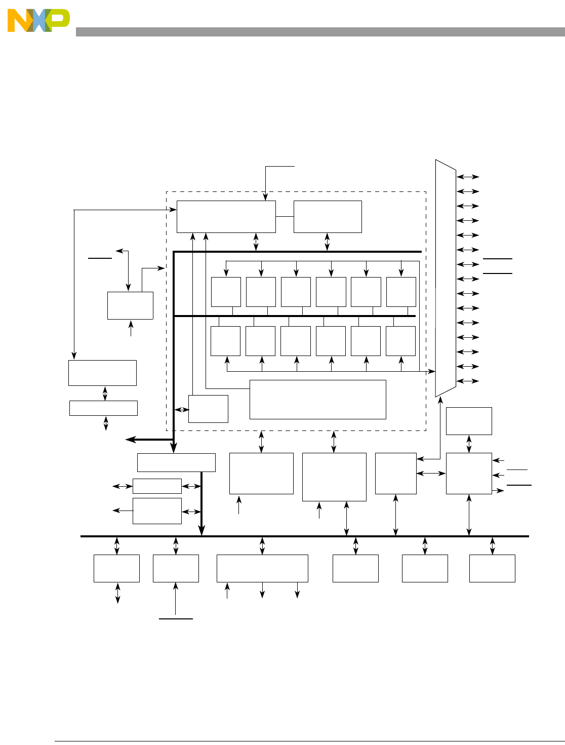
Overview
1-3 Freescale Semiconductor
1.3 Block Diagram
The superset device in the MCF52211 family comes in a 100-lead low-profile quad flat package (LQFP).
Figure 1-1 shows a top-level block diagram of the MCF52211.
Figure 1-1. MCF52211 Block Diagram
Arbiter Interrupt
Controller
UART
0QSPI
UART
1UART
2I2C
V2 ColdFire CPU
4 CH
JTAG
TAP
16 Kbytes
SRAM
(2K32)2
128 Kbytes
Flash
(16K16)4
PORTS CIM_IBO RSTI
RSTO
ADC
AN[7:0]
PLL OCO
CLKGEN
Edge
Port
TIM
EXTAL XTAL CLKOUT
PIT0 PIT1 PWM
IRQ[7:1]
PMM
VSTBY
PADI – Pin Muxing
AN
Slave Mode Access
(CIM_IBO/EzPort)
M3
TMS
TDI
TDO
TRST
TCLK
JTAG_EN
DMA
M2 M0
Watch
Dog
TMR
0RTC
TMR
1TMR
2TMR
3I2C
DDATA
QSPI
SDAn
SCLn
UTXDn
URXDn
URTSn
UCTSn
PWMn
DTINn/DTOUTn
GPT
RCON_B
ALLPST
PST
BDM
PORT
IPS Bus Gasket
Watchdog
CIM_IBO
CFM
VPP
CLKMOD
GPT[3:0]
Backup
USB
On-The-Go
USB TCVR
USBD+
USBD-
M1
MCF52211 ColdFire® Integrated Microcontroller Reference Manual, Rev. 3

Overview
Freescale Semiconductor 1-4
1.4 Part Numbers and Packaging
Table 1-8 summarizes the features of the MCF52211 product family. Several speed/package options are
available to match cost- or performance-sensitive applications.
1.5 Features
The MCF52211 family includes the following features:
• Version 2 ColdFire variable-length RISC processor core
— Static operation
— 32-bit address and data paths on-chip
— Up to 80 MHz processor core frequency
— 40 MHz and 33 MHz off-platform bus frequency
— Sixteen general-purpose, 32-bit data and address registers
— Implements ColdFire ISA_A with extensions to support the user stack pointer register and four
new instructions for improved bit processing (ISA_A+)
— Multiply-Accumulate (MAC) unit with 32-bit accumulator to support 1616 32 or
3232 32 operations
• System debug support
— Real-time trace for determining dynamic execution path
— Background debug mode (BDM) for in-circuit debugging (DEBUG_B+)
Table 1-2. Orderable Part Number Summary
Freescale Part
Number Description Speed
(MHz)
Flash/SRAM
(Kbytes) Package Temp range
(C)
MCF52210CAE66 MCF52210 Microcontroller, 2 UARTs 66 64 / 16 64 LQFP -40 to +85
MCF52210CEP66 MCF52210 Microcontroller, 2 UARTs 66 64 / 16 64 QFN -40 to +85
MCF52210CVM66 MCF52210 Microcontroller, 2 UARTs 66 64 / 16 81 MAPBGA -40 to +85
MCF52210CVM80 MCF52210 Microcontroller, 2 UARTs 80 64 / 16 81 MAPBGA -40 to +85
MCF52211CAE66 MCF52211 Microcontroller, 3 UARTs 66 128 / 16 64 LQFP -40 to +85
MCF52211CAF80 MCF52211 Microcontroller, 3 UARTs 80 128 / 16 100 LQFP -40 to +85
MCF52211CEP66 MCF52211 Microcontroller, 3 UARTs 66 128 / 16 64 QFN -40 to +85
MCF52211CVM66 MCF52211 Microcontroller, 3 UARTs 66 128 / 16 81 MAPBGA -40 to +85
MCF52211CVM80 MCF52211 Microcontroller, 3 UARTs 80 128 / 16 81 MAPBGA -40 to +85
MCF52212CAE50 MCF52212 Microcontroller, 2 UARTs 50 64 / 8 64 LQFP -40 to +85
MCF52212AE50 MCF52212 Microcontroller, 2 UARTs 50 64 / 8 64 LQFP 0 to +70
MCF52213CAE50 MCF52213 Microcontroller, 2 UARTs 50 128 / 8 64 LQFP -40 to +85
MCF52213AE50 MCF52213 Microcontroller, 2 UARTs 50 128 / 8 64 LQFP 0 to +70
MCF52211 ColdFire® Integrated Microcontroller Reference Manual, Rev. 3

Overview
1-5 Freescale Semiconductor
— Real-time debug support, with six hardware breakpoints (4 PC, 1 address and 1 data)
configurable into a 1- or 2-level trigger
• On-chip memories
— Up to 16-Kbyte dual-ported SRAM on CPU internal bus, supporting core and DMA access
with standby power supply support
— Up to 128 Kbytes of interleaved flash memory supporting 2-1-1-1 accesses
• Power management
— Fully static operation with processor sleep and whole chip stop modes
— Rapid response to interrupts from the low-power sleep mode (wake-up feature)
— Clock enable/disable for each peripheral when not used (except backup watchdog timer)
— Software controlled disable of external clock output for low-power consumption
• Universal Serial Bus On-The-Go (USB OTG) dual-mode host and device controller
— Full-speed / low-speed host controller
— USB 1.1 and 2.0 compliant full-speed / low speed device controller
— 16 bidirectional end points
— DMA or FIFO data stream interfaces
— Low power consumption
— OTG protocol logic
• Three universal asynchronous/synchronous receiver transmitters (UARTs)
— 16-bit divider for clock generation
— Interrupt control logic with maskable interrupts
— DMA support
— Data formats can be 5, 6, 7 or 8 bits with even, odd, or no parity
— Up to two stop bits in 1/16 increments
— Error-detection capabilities
— Modem support includes request-to-send (RTS) and clear-to-send (CTS) lines for two UARTs
— Transmit and receive FIFO buffers
•Two I
2C modules
— Interchip bus interface for EEPROMs, LCD controllers, A/D converters, and keypads
— Fully compatible with industry-standard I2C bus
— Master and slave modes support multiple masters
— Automatic interrupt generation with programmable level
• Queued serial peripheral interface (QSPI)
— Full-duplex, three-wire synchronous transfers
— Up to four chip selects available
— Master mode operation only
— Programmable bit rates up to half the CPU clock frequency
— Up to 16 pre-programmed transfers
MCF52211 ColdFire® Integrated Microcontroller Reference Manual, Rev. 3

Overview
Freescale Semiconductor 1-6
• Fast analog-to-digital converter (ADC)
— Eight analog input channels
— 12-bit resolution
— Minimum 1.125 s conversion time
— Simultaneous sampling of two channels for motor control applications
— Single-scan or continuous operation
— Optional interrupts on conversion complete, zero crossing (sign change), or under/over
low/high limit
— Unused analog channels can be used as digital I/O
• Four 32-bit timers with DMA support
— 12.5 ns resolution at 80 MHz
— Programmable sources for clock input, including an external clock option
— Programmable prescaler
— Input capture capability with programmable trigger edge on input pin
— Output compare with programmable mode for the output pin
— Free run and restart modes
— Maskable interrupts on input capture or output compare
— DMA trigger capability on input capture or output compare
• Four-channel general purpose timer
— 16-bit architecture
— Programmable prescaler
— Output pulse-widths variable from microseconds to seconds
— Single 16-bit input pulse accumulator
— Toggle-on-overflow feature for pulse-width modulator (PWM) generation
— One dual-mode pulse accumulation channel
• Pulse-width modulation timer
— Support for PCM mode (resulting in superior signal quality compared to conventional PWM)
— Operates as eight channels with 8-bit resolution or four channels with 16-bit resolution
— Programmable period and duty cycle
— Programmable enable/disable for each channel
— Software selectable polarity for each channel
— Period and duty cycle are double buffered. Change takes effect when the end of the current
period is reached (PWM counter reaches zero) or when the channel is disabled.
— Programmable center or left aligned outputs on individual channels
— Four clock sources (A, B, SA, and SB) provide for a wide range of frequencies
— Emergency shutdown
• Two periodic interrupt timers (PITs)
— 16-bit counter
MCF52211 ColdFire® Integrated Microcontroller Reference Manual, Rev. 3

Overview
1-7 Freescale Semiconductor
— Selectable as free running or count down
• Real-Time Clock (RTC)
— Maintains system time-of-day clock
— Provides stopwatch and alarm interrupt functions
• Software watchdog timer
— 32-bit counter
— Low-power mode support
• Backup watchdog timer (BWT)
— Independent timer that can be used to help software recover from runaway code
— 16-bit counter
— Low-power mode support
• Clock generation features
— Crystal, on-chip trimmed relaxation oscillator, or external oscillator reference options
— Trimmed relaxation oscillator
— Pre-divider capable of dividing the clock source frequency into the PLL reference frequency
range
— System can be clocked from PLL or directly from crystal oscillator or relaxation oscillator
— Low power modes supported
—2
n (0 n15) low-power divider for extremely low frequency operation
• Interrupt controller
— Uniquely programmable vectors for all interrupt sources
— Fully programmable level and priority for all peripheral interrupt sources
— Seven external interrupt signals with fixed level and priority
— Unique vector number for each interrupt source
— Ability to mask any individual interrupt source or all interrupt sources (global mask-all)
— Support for hardware and software interrupt acknowledge (IACK) cycles
— Combinatorial path to provide wake-up from low-power modes
• DMA controller
— Four fully programmable channels
— Dual-address transfer support with 8-, 16-, and 32-bit data capability, along with support for
16-byte (432-bit) burst transfers
— Source/destination address pointers that can increment or remain constant
— 24-bit byte transfer counter per channel
— Auto-alignment transfers supported for efficient block movement
— Bursting and cycle-steal support
— Software-programmable DMA requests for the UARTs (3) and 32-bit timers (4)
•Reset
— Separate reset in and reset out signals
MCF52211 ColdFire® Integrated Microcontroller Reference Manual, Rev. 3

Overview
Freescale Semiconductor 1-8
— Seven sources of reset:
– Power-on reset (POR)
– External
– Software
– Watchdog
– Loss of clock / loss of lock
– Low-voltage detection (LVD)
–JTAG
— Status flag indication of source of last reset
• Chip configuration module (CCM)
— System configuration during reset
— Selects one of six clock modes
— Configures output pad drive strength
— Unique part identification number and part revision number
• General purpose I/O interface
— Up to 56 bits of general purpose I/O
— Bit manipulation supported via set/clear functions
— Programmable drive strengths
— Unused peripheral pins may be used as extra GPIO
• JTAG support for system level board testing
1.5.1 V2 Core Overview
The version 2 ColdFire processor core is comprised of two separate pipelines decoupled by an instruction
buffer. The two-stage instruction fetch pipeline (IFP) is responsible for instruction-address generation and
instruction fetch. The instruction buffer is a first-in-first-out (FIFO) buffer that holds prefetched
instructions awaiting execution in the operand execution pipeline (OEP). The OEP includes two pipeline
stages. The first stage decodes instructions and selects operands (DSOC); the second stage (AGEX)
performs instruction execution and calculates operand effective addresses, if needed.
The V2 core implements the ColdFire instruction set architecture revision A+ with support for a separate
user stack pointer register and four new instructions to assist in bit processing. Additionally, the core
includes the multiply-accumulate (MAC) unit for improved signal processing capabilities. The MAC
implements a three-stage arithmetic pipeline, optimized for 16x16 bit operations, with support for one
32-bit accumulator. Supported operands include 16- and 32-bit signed and unsigned integers, signed
fractional operands, and a complete set of instructions to process these data types. The MAC provides
support for execution of DSP operations within the context of a single processor at a minimal hardware
cost.
MCF52211 ColdFire® Integrated Microcontroller Reference Manual, Rev. 3

Overview
1-9 Freescale Semiconductor
1.5.2 Integrated Debug Module
The ColdFire processor core debug interface is provided to support system debugging with low-cost debug
and emulator development tools. Through a standard debug interface, access to debug information and
real-time tracing capability is provided on 100-lead packages. This allows the processor and system to be
debugged at full speed without the need for costly in-circuit emulators.
The on-chip breakpoint resources include a total of nine programmable 32-bit registers: an address and an
address mask register, a data and a data mask register, four PC registers, and one PC mask register. These
registers can be accessed through the dedicated debug serial communication channel or from the
processor’s supervisor mode programming model. The breakpoint registers can be configured to generate
triggers by combining the address, data, and PC conditions in a variety of single- or dual-level definitions.
The trigger event can be programmed to generate a processor halt or initiate a debug interrupt exception.
This device implements revision B+ of the ColdFire Debug Architecture.
The processor’s interrupt servicing options during emulator mode allow real-time critical interrupt service
routines to be serviced while processing a debug interrupt event. This ensures the system continues to
operate even during debugging.
To support program trace, the V2 debug module provides processor status (PST[3:0]) and debug data
(DDATA[3:0]) ports. These buses and the PSTCLK output provide execution status, captured operand
data, and branch target addresses defining processor activity at the CPU’s clock rate. The device includes
a new debug signal, ALLPST. This signal is the logical AND of the processor status (PST[3:0]) signals
and is useful for detecting when the processor is in a halted state (PST[3:0] = 1111).
The full debug/trace interface is available only on the 100-pin packages. However, every product features
the dedicated debug serial communication channel (DSI, DSO, DSCLK) and the ALLPST signal.
1.5.3 JTAG
The processor supports circuit board test strategies based on the Test Technology Committee of IEEE and
the Joint Test Action Group (JTAG). The test logic includes a test access port (TAP) consisting of a 16-state
controller, an instruction register, and three test registers (a 1-bit bypass register, a 256-bit boundary-scan
register, and a 32-bit ID register). The boundary scan register links the device’s pins into one shift register.
Test logic, implemented using static logic design, is independent of the device system logic.
The device implementation can:
• Perform boundary-scan operations to test circuit board electrical continuity
• Sample system pins during operation and transparently shift out the result in the boundary scan
register
• Bypass the device for a given circuit board test by effectively reducing the boundary-scan register
to a single bit
• Disable the output drive to pins during circuit-board testing
• Drive output pins to stable levels
MCF52211 ColdFire® Integrated Microcontroller Reference Manual, Rev. 3

Overview
Freescale Semiconductor 1-10
1.5.4 On-Chip Memories
1.5.4.1 SRAM
The dual-ported SRAM module provides a general-purpose 8- or 16-Kbyte memory block that the
ColdFire core can access in a single cycle. The location of the memory block can be set to any 8- or
16-Kbyte boundary within the 4-Gbyte address space. This memory is ideal for storing critical code or data
structures and for use as the system stack. Because the SRAM module is physically connected to the
processor's high-speed local bus, it can quickly service core-initiated accesses or memory-referencing
commands from the debug module.
The SRAM module is also accessible by the DMA. The dual-ported nature of the SRAM makes it ideal
for implementing applications with double-buffer schemes, where the processor and a DMA device
operate in alternate regions of the SRAM to maximize system performance.
1.5.4.2 Flash Memory
The ColdFire flash module (CFM) is a non-volatile memory (NVM) module that connects to the
processor’s high-speed local bus. The CFM is constructed with up to four banks of 16-Kbyte16-bit flash
memory arrays to generate up to 128 Kbytes of 32-bit flash memory. These electrically erasable and
programmable arrays serve as non-volatile program and data memory. The flash memory is ideal for
program and data storage for single-chip applications, allowing for field reprogramming without requiring
an external high voltage source. The CFM interfaces to the ColdFire core through an optimized read-only
memory controller that supports interleaved accesses from the 2-cycle flash memory arrays. A backdoor
mapping of the flash memory is used for all program, erase, and verify operations, as well as providing a
read datapath for the DMA. Flash memory may also be programmed via the EzPort, which is a serial flash
memory programming interface that allows the flash memory to be read, erased and programmed by an
external controller in a format compatible with most SPI bus flash memory chips.
1.5.5 Power Management
The device incorporates several low-power modes of operation entered under program control and exited
by several external trigger events. An integrated power-on reset (POR) circuit monitors the input supply
and forces an MCU reset as the supply voltage rises. The low voltage detector (LVD) monitors the supply
voltage and is configurable to force a reset or interrupt condition if it falls below the LVD trip point. The
RAM standby switch provides power to RAM when the supply voltage to the chip falls below the standby
battery voltage.
1.5.6 USB On-The-Go Controller
The device includes a Universal Serial Bus On-The-Go (USB OTG) dual-mode controller. USB is a
popular standard for connecting peripherals and portable consumer electronic devices such as digital
cameras and handheld computers to host PCs. The OTG supplement to the USB specification extends USB
to peer-to-peer application, enabling devices to connect directly to each other without the need for a PC.
The dual-mode controller on the device can act as a USB OTG host and as a USB device. It also supports
full-speed and low-speed modes.
MCF52211 ColdFire® Integrated Microcontroller Reference Manual, Rev. 3

Overview
1-11 Freescale Semiconductor
1.5.7 UARTs
The device has three full-duplex UARTs that function independently. The three UARTs can be clocked by
the system bus clock, eliminating the need for an external clock source. On smaller packages, the third
UART is multiplexed with other digital I/O functions.
1.5.8 I2C Bus
The processor includes two I2C modules. The I2C bus is an industry-standard, two-wire, bidirectional
serial bus that provides a simple, efficient method of data exchange and minimizes the interconnection
between devices. This bus is suitable for applications requiring occasional communications over a short
distance between many devices.
1.5.9 QSPI
The queued serial peripheral interface (QSPI) provides a synchronous serial peripheral interface with
queued transfer capability. It allows up to 16 transfers to be queued at once, minimizing the need for CPU
intervention between transfers.
1.5.10 Fast ADC
The fast ADC consists of an eight-channel input select multiplexer and two independent sample and hold
(S/H) circuits feeding separate 12-bit ADCs. The two separate converters store their results in accessible
buffers for further processing.
The ADC can be configured to perform a single scan and halt, a scan when triggered, or a programmed
scan sequence repeatedly until manually stopped.
The ADC can be configured for sequential or simultaneous conversion. When configured for sequential
conversions, up to eight channels can be sampled and stored in any order specified by the channel list
register. Both ADCs may be required during a scan, depending on the inputs to be sampled.
During a simultaneous conversion, both S/H circuits are used to capture two different channels at the same
time. This configuration requires that a single channel may not be sampled by both S/H circuits
simultaneously.
Optional interrupts can be generated at the end of the scan sequence if a channel is out of range (measures
below the low threshold limit or above the high threshold limit set in the limit registers) or at several
different zero crossing conditions.
1.5.11 DMA Timers (DTIM0–DTIM3)
There are four independent, DMA transfer capable 32-bit timers (DTIM0, DTIM1, DTIM2, and DTIM3)
on the device. Each module incorporates a 32-bit timer with a separate register set for configuration and
control. The timers can be configured to operate from the system clock or from an external clock source
using one of the DTINn signals. If the system clock is selected, it can be divided by 16 or 1. The input
clock is further divided by a user-programmable 8-bit prescaler that clocks the actual timer counter register
MCF52211 ColdFire® Integrated Microcontroller Reference Manual, Rev. 3

Overview
Freescale Semiconductor 1-12
(TCRn). Each of these timers can be configured for input capture or reference (output) compare mode.
Timer events may optionally cause interrupt requests or DMA transfers.
1.5.12 General Purpose Timer (GPT)
The general purpose timer (GPT) is a four-channel timer module consisting of a 16-bit programmable
counter driven by a seven-stage programmable prescaler. Each of the four channels can be configured for
input capture or output compare. Additionally, channel three, can be configured as a pulse accumulator.
A timer overflow function allows software to extend the timing capability of the system beyond the 16-bit
range of the counter. The input capture and output compare functions allow simultaneous input waveform
measurements and output waveform generation. The input capture function can capture the time of a
selected transition edge. The output compare function can generate output waveforms and timer software
delays. The 16-bit pulse accumulator can operate as a simple event counter or a gated time accumulator.
1.5.13 Periodic Interrupt Timers (PIT0 and PIT1)
The two periodic interrupt timers (PIT0 and PIT1) are 16-bit timers that provide interrupts at regular
intervals with minimal processor intervention. Each timer can count down from the value written in its PIT
modulus register or it can be a free-running down-counter.
1.5.14 Real-Time Clock (RTC)
The Real-Time Clock (RTC) module maintains the system (time-of-day) clock and provides stopwatch,
alarm, and interrupt functions. It includes full clock features: seconds, minutes, hours, days and supports
a host of time-of-day interrupt functions along with an alarm interrupt.
1.5.15 Pulse-Width Modulation (PWM) Timers
The device has an 8-channel, 8-bit PWM timer. Each channel has a programmable period and duty cycle
as well as a dedicated counter. Each of the modulators can create independent continuous waveforms with
software-selectable duty rates from 0% to 100%. The timer supports PCM mode, which results in superior
signal quality when compared to that of a conventional PWM. The PWM outputs have programmable
polarity, and can be programmed as left aligned outputs or center aligned outputs. For higher period and
duty cycle resolution, each pair of adjacent channels ([7:6], [5:4], [3:2], and [1:0]) can be concatenated to
form a single 16-bit channel. The module can, therefore, be configured to support 8/0, 6/1, 4/2, 2/3, or 0/4
8-/16-bit channels.
1.5.16 Software Watchdog Timer
The watchdog timer is a 32-bit timer that facilitates recovery from runaway code. The watchdog counter
is a free-running down-counter that generates a reset on underflow. To prevent a reset, software must
periodically restart the countdown.
MCF52211 ColdFire® Integrated Microcontroller Reference Manual, Rev. 3

Overview
1-13 Freescale Semiconductor
1.5.17 Backup Watchdog Timer
The backup watchdog timer is an independent 16-bit timer that, like the software watchdog timer,
facilitates recovery from runaway code. This timer is a free-running down-counter that generates a reset
on underflow. To prevent a reset, software must periodically restart the countdown. The backup watchdog
timer can be clocked by either the relaxation oscillator or the system clock.
1.5.18 Phase-Locked Loop (PLL)
The clock module contains a crystal oscillator, 8 MHz on-chip relaxation oscillator (OCO), phase-locked
loop (PLL), reduced frequency divider (RFD), low-power divider status/control registers, and control
logic. To improve noise immunity, the PLL, crystal oscillator, and relaxation oscillator have their own
power supply inputs: VDDPLL and VSSPLL. All other circuits are powered by the normal supply pins,
VDD and VSS.
1.5.19 Interrupt Controller (INTC)
The device has a single interrupt controller that supports up to 63 interrupt sources. There are 56
programmable sources, 49 of which are assigned to unique peripheral interrupt requests. The remaining
seven sources are unassigned and may be used for software interrupt requests.
1.5.20 DMA Controller
The direct memory access (DMA) controller provides an efficient way to move blocks of data with
minimal processor intervention. It has four channels that allow byte, word, longword, or 16-byte burst line
transfers. These transfers are triggered by software explicitly setting a DCRn[START] bit or by the
occurrence of certain UART or DMA timer events.
1.5.21 Reset
The reset controller determines the source of reset, asserts the appropriate reset signals to the system, and
keeps track of what caused the last reset. There are seven sources of reset:
• External reset input
• Power-on reset (POR)
• Watchdog timer
• Phase locked-loop (PLL) loss of lock / loss of clock
• Software
• Low-voltage detector (LVD)
•JTAG
Control of the LVD and its associated reset and interrupt are managed by the reset controller. Other
registers provide status flags indicating the last source of reset and a control bit for software assertion of
the RSTO pin.
MCF52211 ColdFire® Integrated Microcontroller Reference Manual, Rev. 3

Overview
Freescale Semiconductor 1-14
1.5.22 GPIO
Nearly all pins on the device have general purpose I/O capability and are grouped into 8-bit ports. Some
ports do not use all eight bits. Each port has registers that configure, monitor, and control the port pin.
1.6 Memory Map Overview
Refer to Appendix A, “Register Memory Map Quick Reference” for module memory map details
MCF52211 ColdFire® Integrated Microcontroller Reference Manual, Rev. 3

Freescale Semiconductor 2-1
Chapter 2
Signal Descriptions
2.1 Introduction
This chapter describes signals implemented on this device and includes an alphabetical listing of signals
that characterizes each signal as an input or output, defines its state at reset, and identifies whether a
pull-up resistor should be used.
NOTE
The terms assertion and negation are used to avoid confusion when dealing
with a mixture of active-low and active-high signals. The term asserted
indicates that a signal is active, independent of the voltage level. The term
negated indicates that a signal is inactive.
Active-low signals, such as SRAS and TA, are indicated with an overbar.
2.2 Overview
Figure 2-1 shows the block diagram of the device with the signal interface.
MCF52211 ColdFire® Integrated Microcontroller Reference Manual, Rev. 3
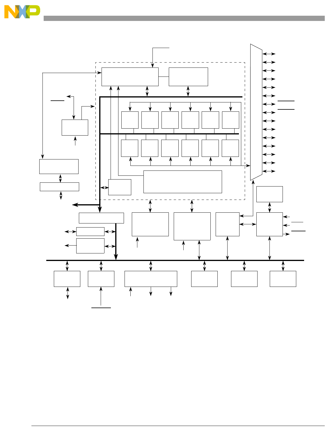
Signal Descriptions
2-2 Freescale Semiconductor
Figure 2-1. Block Diagram with Signal Interfaces
2.3 Pin Functions
Arbiter Interrupt
Controller
UART
0QSPI
UART
1UART
2I2C
V2 ColdFire CPU
4 CH
JTAG
TAP
16 Kbytes
SRAM
(2K32)2
128 Kbytes
Flash
(16K16)4
PORTS CIM_IBO RSTI
RSTO
ADC
AN[7:0]
PLL OCO
CLKGEN
Edge
Port
TIM
EXTAL XTAL CLKOUT
PIT0 PIT1 PWM
IRQ[7:1]
PMM
VSTBY
PADI – Pin Muxing
AN
Slave Mode Access
(CIM_IBO/EzPort)
M3
TMS
TDI
TDO
TRST
TCLK
JTAG_EN
DMA
M2 M0
Watch
Dog
TMR
0RTC
TMR
1TMR
2TMR
3I2C
DDATA
QSPI
SDAn
SCLn
UTXDn
URXDn
URTSn
UCTSn
PWMn
DTINn/DTOUTn
GPT
RCON_B
ALLPST
PST
BDM
PORT
IPS Bus Gasket
Watchdog
CIM_IBO
CFM
VPP
CLKMOD
GPT[3:0]
Backup
USB
On-The-Go
USB TCVR
USBD+
USBD-
M1
MCF52211 ColdFire® Integrated Microcontroller Reference Manual, Rev. 3

Signal Descriptions
Freescale Semiconductor 2-3
Table 2-1. Pin Functions by Primary and Alternate Purpose
Pin
Group
Primary
Function
Secondary
Function
Tertiary
Function
Quaternary
Function
Drive
Strength /
Control1
Slew Rate /
Control1
Pull-up /
Pull-down2
Pin on
100 LQFP
Pin on 81
MAPBGA
Pin on 64
LQFP/QFN
ADC AN7 — — GPIO Low FAST — 51 H9 33
AN6 — — GPIO Low FAST — 52 G9 34
AN5 — — GPIO Low FAST — 53 G8 35
AN4 — — GPIO Low FAST — 54 F9 36
AN3 — — GPIO Low FAST — 46 G7 28
AN2 — — GPIO Low FAST — 45 G6 27
AN1 — — GPIO Low FAST — 44 H6 26
AN0 — — GPIO Low FAST — 43 J6 25
SYNCA3— — —N/AN/A————
SYNCB3— — —N/AN/A————
VDDA — — — N/A N/A — 50 H8 32
VSSA — — — N/A N/A — 47 H7, J9 29
VRH — — — N/A N/A — 49 J8 31
VRL — — — N/A N/A — 48 J7 30
Clock
Generation
EXTAL — — — N/A N/A — 73 B9 47
XTAL — — — N/A N/A — 72 C9 46
VDDPLL — — — N/A N/A — 74 B8 48
VSSPLL — — — N/A N/A — 71 C8 45
Debug Data ALLPST — — — High FAST — 86 A6 55
DDATA[3:0] — — GPIO High FAST — 84,83,78,77 — —
PST[3:0] — — GPIO High FAST — 70,69,66,65 — —
I2C SCL USB_DMI UTXD2 GPIO PDSR[0] PSRR[0] pull-up410 E1 8
SDA USB_DPI URXD2 GPIO PDSR[0] PSRR[0] pull-up411 E2 9
MCF52211 ColdFire® Integrated Microcontroller Reference Manual, Rev. 3

2-4 Freescale Semiconductor
Signal Descriptions
Interrupts IRQ7 — —GPIOLowFAST—95C458
IRQ6 — — GPIO Low FAST — 94 B4 —
IRQ5 — — GPIO Low FAST — 91 A4 —
IRQ4 — —GPIOLowFAST—90C557
IRQ3 — — GPIO Low FAST — 89 A5 —
IRQ2 — — GPIO Low FAST — 88 B5 —
IRQ1 SYNCA USB_ALT_C
LK
GPIO High FAST pull-up487 C6 56
JTAG/BDM JTAG_EN — — — N/A N/A pull-down 26 J2 17
TCLK/
PSTCLK
CLKOUT — — High FAST pull-up564 C7 44
TDI/DSI — — — N/A N/A pull-up579 B7 50
TDO/DSO— — —HighFAST—80A751
TMS
/BKPT
— — — N/A N/A pull-up576 A8 49
TRST
/DSCLK
— — — N/A N/A pull-up585 B6 54
Mode
Selection6
CLKMOD0 — — — N/A N/A pull-down640 G5 24
CLKMOD1 — — — N/A N/A pull-down639 H5 —
RCON/
EZPCS
— — — N/A N/A pull-up 21 G3 16
Table 2-1. Pin Functions by Primary and Alternate Purpose (continued)
Pin
Group
Primary
Function
Secondary
Function
Tertiary
Function
Quaternary
Function
Drive
Strength /
Control1
Slew Rate /
Control1
Pull-up /
Pull-down2
Pin on
100 LQFP
Pin on 81
MAPBGA
Pin on 64
LQFP/QFN
MCF52211 ColdFire® Integrated Microcontroller Reference Manual, Rev. 3

Signal Descriptions
Freescale Semiconductor 2-5
QSPI QSPI_DIN/
EZPD
— URXD1 GPIO PDSR[2] PSRR[2] — 16 F3 12
QSPI_DOUT
/EZPQ
— UTXD1 GPIO PDSR[1] PSRR[1] — 17 G1 13
QSPI_CLK/
EZPCK
SCL URTS1 GPIO PDSR[3] PSRR[3] pull-up818 G2 14
QSPI_CS3 SYNCA — GPIO PDSR[7] PSRR[7] pull-up/pull-
down7
12 F1 —
QSPI_CS2 — — GPIO PDSR[6] PSRR[6] pull-up/pull-
down7
13 F2 —
QSPI_CS1 — — GPIO PDSR[5] PSRR[5] — 19 H2 —
QSPI_CS0 SDA UCTS1 GPIO PDSR[4] PSRR[4] pull-up820 H1 15
Reset9RSTI — — — N/A N/A pull-up996 A3 59
RSTO — — —highFAST—97B360
Test TEST — — — N/A N/A pull-down 5 C2 3
Timers, 16-bit GPT3 — PWM7 GPIO PDSR[23] PSRR[23] pull-up10 63 D7 —
GPT2 — PWM5 GPIO PDSR[22] PSRR[22] pull-up10 58 E8 —
GPT1 — PWM3 GPIO PDSR[21] PSRR[21] pull-up10 33 J4 —
GPT0 — PWM1 GPIO PDSR[20] PSRR[20] pull-up10 38 J5 —
Timers, 32-bit DTIN3 DTOUT3 PWM6 GPIO PDSR[19] PSRR[19] — 32 H3 19
DTIN2 DTOUT2 PWM4 GPIO PDSR[18] PSRR[18] — 31 J3 18
DTIN1 DTOUT1 PWM2 GPIO PDSR[17] PSRR[17] — 37 G4 23
DTIN0 DTOUT0 PWM0 GPIO PDSR[16] PSRR[16] — 36 H4 22
UART 0 UCTS0 — — GPIO PDSR[11] PSRR[11] — 6 C1 4
URTS0 — — GPIO PDSR[10] PSRR[10] — 9 D3 7
URXD0 RTC_EXTAL — GPIO PDSR[9] PSRR[9] — 7 D1 5
UTXD0 RTC_XTAL — GPIO PDSR[8] PSRR[8] — 8 D2 6
Table 2-1. Pin Functions by Primary and Alternate Purpose (continued)
Pin
Group
Primary
Function
Secondary
Function
Tertiary
Function
Quaternary
Function
Drive
Strength /
Control1
Slew Rate /
Control1
Pull-up /
Pull-down2
Pin on
100 LQFP
Pin on 81
MAPBGA
Pin on 64
LQFP/QFN
MCF52211 ColdFire® Integrated Microcontroller Reference Manual, Rev. 3

2-6 Freescale Semiconductor
Signal Descriptions
UART 1 UCTS1 SYNCA URXD2 GPIO PDSR[15] PSRR[15] — 98 C3 61
URTS1 SYNCB UTXD2 GPIO PDSR[14] PSRR[14] — 4 B1 2
URXD1 — — GPIO PDSR[13] PSRR[13] — 100 B2 63
UTXD1 — — GPIO PDSR[12] PSRR[12] — 99 A2 62
UART 2 UCTS2 — — GPIO PDSR[27] PSRR[27] — 27 — —
URTS2 — — GPIO PDSR[26] PSRR[26] — 30 — —
URXD2 — — GPIO PDSR[25] PSRR[25] — 28 — —
UTXD2 — — GPIO PDSR[24] PSRR[24] — 29 — —
VSTBY VSTBY — — — N/A N/A — 55 F8 37
USB VDDUSB — — — N/A N/A — 62 D8 43
VSSUSB — — — N/A N/A — 59 F7 40
USB_DM — — — N/A N/A — 61 D9 42
USB_DP — — — N/A N/A — 60 E9 41
VDD VDD — — — N/A N/A — 1,2,14,22,
23,34,41,
57,68,81,93
D5,E3–E7,
F5
1,10,20,39,
52
VSS VSS — — — N/A N/A — 3,15,24,25,
35,42,56,
67,75,82,92
A1,A9,D4,D
6,F4,F6,J1
11,21,38,
53,64
1The PDSR and PSSR registers are described in the General Purpose I/O chapter. All programmable signals default to 2 mA drive and FAST slew rate in
normal (single-chip) mode.
2All signals have a pull-up in GPIO mode.
3These signals are multiplexed on other pins.
4For primary and GPIO functions only.
5Only when JTAG mode is enabled.
6CLKMOD0 and CLKMOD1 have internal pull-down resistors; however, the use of external resistors is very strongly recommended.
7When these pins are configured for USB signals, they should use the USB transceiver’s internal pull-up/pull-down resistors (see the description of the
OTG_CTRL register). If these pins are not configured for USB signals, each pin should be pulled down externally using a 10 k resistor.
8For secondary and GPIO functions only.
9RSTI has an internal pull-up resistor; however, the use of an external resistor is very strongly recommended.
10 For GPIO function. Primary Function has pull-up control within the GPT module.
Table 2-1. Pin Functions by Primary and Alternate Purpose (continued)
Pin
Group
Primary
Function
Secondary
Function
Tertiary
Function
Quaternary
Function
Drive
Strength /
Control1
Slew Rate /
Control1
Pull-up /
Pull-down2
Pin on
100 LQFP
Pin on 81
MAPBGA
Pin on 64
LQFP/QFN
MCF52211 ColdFire® Integrated Microcontroller Reference Manual, Rev. 3

Signal Descriptions
Freescale Semiconductor 2-7
2.4 Reset Signals
Table 2-2 describes signals that are used to reset the chip or as a reset indication.
2.5 PLL and Clock Signals
Table 2-3 describes signals that are used to support the on-chip clock generation circuitry.
2.6 Mode Selection
Table 2-4 describes signals used in mode selection, Table 6-3 describes particular clocking modes.
2.7 External Interrupt Signals
Table 2-5 describes the external interrupt signals.
Table 2-2. Reset Signals
Signal Name Abbreviation Function I/O
Reset In RSTI Primary reset input to the device. Asserting RSTI immediately resets
the CPU and peripherals.
I
Reset Out RSTO Driven low for 512 CPU clocks after the reset source has deasserted
and PLL locked.
O
Table 2-3. PLL and Clock Signals
Signal Name Abbreviation Function I/O
External Clock In EXTAL Crystal oscillator or external clock input except when the on-chip
relaxation oscillator is used.
I
Crystal XTAL Crystal oscillator output except when CLKMOD0=0, then sampled as
part of the clockmode selection mechanism.
O
Clock Out CLKOUT This output signal reflects the internal system clock. O
Table 2-4. Mode Selection Signals
Signal Name Abbreviation Function I/O
Clock Mode Selection CLKMOD[1:0] Selects the clock boot mode. I
Reset Configuration RCON The serial flash programming mode is entered by asserting the
RCON pin (with the TEST pin negated) as the chip comes out of
reset. During this mode, the EzPort has access to the flash memory
which can be programmed from an external device.
Test TEST Reserved for factory testing only and in normal modes of operation
should be connected to VSS to prevent unintentional activation of
test functions.
I
MCF52211 ColdFire® Integrated Microcontroller Reference Manual, Rev. 3

Signal Descriptions
2-8 Freescale Semiconductor
2.8 Queued Serial Peripheral Interface (QSPI)
Table 2-6 describes the QSPI signals.
2.9 I2C I/O Signals
Table 2-7 describes the I2C serial interface module signals.
2.10 UART Module Signals
Table 2-8 describes the UART module signals.
Table 2-5. External Interrupt Signals
Signal Name Abbreviation Function I/O
External Interrupts IRQ[7:1] External interrupt sources. I
Table 2-6. Queued Serial Peripheral Interface (QSPI) Signals
Signal Name Abbreviation Function I/O
QSPI Synchronous
Serial Output
QSPI_DOUT Provides the serial data from the QSPI and can be programmed to be
driven on the rising or falling edge of QSPI_CLK.
O
QSPI Synchronous
Serial Data Input
QSPI_DIN Provides the serial data to the QSPI and can be programmed to be
sampled on the rising or falling edge of QSPI_CLK.
I
QSPI Serial Clock QSPI_CLK Provides the serial clock from the QSPI. The polarity and phase of
QSPI_CLK are programmable.
O
Synchronous Peripheral
Chip Selects
QSPI_CS[3:0] QSPI peripheral chip selects that can be programmed to be active
high or low.
O
Table 2-7. I2C I/O Signals
Signal Name Abbreviation Function I/O
Serial Clock SCLnOpen-drain clock signal for the for the I2C interface. It is driven by the
I2C module when the bus is in master mode or it becomes the clock
input when the I2C is in slave mode.
I/O
Serial Data SDAnOpen-drain signal that serves as the data input/output for the I2C
interface.
I/O
Table 2-8. UART Module Signals
Signal Name Abbreviation Function I/O
Transmit Serial Data Output UTXDnTransmitter serial data outputs for the UART modules. The output is
held high (mark condition) when the transmitter is disabled, idle, or in
the local loopback mode. Data is shifted out, LSB first, on this pin at
the falling edge of the serial clock source.
O
Receive Serial Data Input URXDnReceiver serial data inputs for the UART modules. Data is received on
this pin LSB first. When the UART clock is stopped for power-down
mode, any transition on this pin restarts it.
I
MCF52211 ColdFire® Integrated Microcontroller Reference Manual, Rev. 3

Signal Descriptions
Freescale Semiconductor 2-9
2.11 DMA Timer Signals
Table 2-9 describes the signals of the four DMA timer modules.
2.12 ADC Signals
Table 2-10 describes the signals of the analog-to-digital converter.
2.13 General Purpose Timer Signals
Table 2-11 describes the general purpose timer signals.
Clear-to-Send UCTSnIndicate to the UART modules that they can begin data transmission. I
Request-to-Send URTSnAutomatic request-to-send outputs from the UART modules. This
signal can also be configured to be asserted and negated as a
function of the RxFIFO level.
O
Table 2-9. DMA Timer Signals
Signal Name Abbreviation Function I/O
DMA Timer Input DTINnEvent input to the DMA timer modules. I
DMA Timer Output DTOUTnProgrammable output from the DMA timer modules. O
Table 2-10. ADC Signals
Signal Name Abbreviation Function I/O
Analog Inputs AN[7:0] Inputs to the ADC. I
Analog Reference VRH Reference voltage high and low inputs. I
VRL I
Analog Supply VDDA Isolate the ADC circuitry from power supply noise —
VSSA —
Table 2-11. GPT Signals
Signal Name Abbreviation Function I/O
General Purpose Timer
Input/Output
GPT[3:0] Inputs to or outputs from the general purpose timer module I/O
Table 2-8. UART Module Signals (continued)
Signal Name Abbreviation Function I/O
MCF52211 ColdFire® Integrated Microcontroller Reference Manual, Rev. 3

Signal Descriptions
2-10 Freescale Semiconductor
2.14 Pulse-Width Modulator Signals
Table 2-12 describes the PWM signals.
2.15 Debug Support Signals
The signals in Table 2-13 are used as the interface to the on-chip JTAG controller and also to interface to
the BDM logic.
Table 2-12. PWM Signals
Signal Name Abbreviation Function I/O
PWM Output Channels PWM[7:0] Pulse-width modulated output for PWM channels O
Table 2-13. Debug Support Signals
Signal Name Abbreviation Function I/O
JTAG Enable JTAG_EN Select between debug module and JTAG signals at reset I
Test Reset TRST This active-low signal is used to initialize the JTAG logic
asynchronously.
I
Test Clock TCLK Used to synchronize the JTAG logic. I
Test Mode Select TMS Used to sequence the JTAG state machine. TMS is sampled on the
rising edge of TCLK.
I
Test Data Input TDI Serial input for test instructions and data. TDI is sampled on the rising
edge of TCLK.
I
Test Data Output TDO Serial output for test instructions and data. TDO is three-stateable and
is actively driven in the shift-IR and shift-DR controller states. TDO
changes on the falling edge of TCLK.
O
Development Serial
Clock
DSCLK Development Serial Clock. Internally synchronized input. (The logic
level on DSCLK is validated if it has the same value on two
consecutive rising bus clock edges.) Clocks the serial communication
port to the debug module during packet transfers. Maximum frequency
is PSTCLK/5. At the synchronized rising edge of DSCLK, the data
input on DSI is sampled and DSO changes state.
I
Breakpoint BKPT Breakpoint. Input used to request a manual breakpoint. Assertion of
BKPT puts the processor into a halted state after the current
instruction completes. Halt status is reflected on processor status
signals as the value 0xF.
I
Development Serial
Input
DSI Development Serial Input. Internally synchronized input that provides
data input for the serial communication port to the debug module after
the DSCLK has been seen as high (logic 1).
I
Development Serial
Output
DSO Development Serial Output. Provides serial output communication for
debug module responses. DSO is registered internally. The output is
delayed from the validation of DSCLK high.
O
MCF52211 ColdFire® Integrated Microcontroller Reference Manual, Rev. 3

Signal Descriptions
Freescale Semiconductor 2-11
2.16 EzPort Signal Descriptions
Table 2-14 contains a list of EzPort external signals
2.17 Power and Ground Pins
The pins described in Table 2-15 provide system power and ground to the chip. Multiple pins are provided
for adequate current capability. All power supply pins must have adequate decoupling (bypass
capacitance) for high-frequency noise suppression.
Debug Data DDATA[3:0] Debug data. Displays captured processor data and breakpoint status.
The CLKOUT signal can be used by the development system to know
when to sample DDATA[3:0].
O
Processor Status Clock PSTCLK Processor Status Clock. Delayed version of the processor clock. Its
rising edge appears in the center of valid PST and DDATA output.
PSTCLK indicates when the development system should sample PST
and DDATA values.
If real-time trace is not used, setting CSR[PCD] keeps PSTCLK, and
PST and DDATA outputs from toggling without disabling triggers.
Non-quiescent operation can be reenabled by clearing CSR[PCD],
although the external development systems must resynchronize with
the PST and DDATA outputs.
PSTCLK starts clocking only when the first non-zero PST value (0xC,
0xD, or 0xF) occurs during system reset exception processing.
O
Processor Status
Outputs
PST[3:0] Indicate core status. Debug mode timing is synchronous with the
processor clock; status is unrelated to the current bus transfer. The
CLKOUT signal can be used by the development system to know
when to sample PST[3:0].
O
All Processor Status
Outputs
ALLPST Logical AND of PST[3.0] O
Table 2-14. EzPort Signal Descriptions
Signal Name Abbreviation Function I/O
EzPort Clock EZPCK Shift clock for EzPort transfers I
EzPort Chip Select EZPCS Chip select for signaling the start and end of
serial transfers
I
EzPort Serial Data In EZPD EZPD is sampled on the rising edge of EZPCK I
EzPort Serial Data Out EZPQ EZPQ transitions on the falling edge of EZPCK O
Table 2-13. Debug Support Signals (continued)
Signal Name Abbreviation Function I/O
MCF52211 ColdFire® Integrated Microcontroller Reference Manual, Rev. 3

Signal Descriptions
2-12 Freescale Semiconductor
Table 2-15. Power and Ground Pins
Signal Name Abbreviation Function I/O
PLL Analog Supply VDDPLL,
VSSPLL
Dedicated power supply signals to isolate the sensitive PLL analog
circuitry from the normal levels of noise present on the digital power
supply.
I
Positive Supply VDD These pins supply positive power to the core logic. I
Ground VSS This pin is the negative supply (ground) to the chip.
MCF52211 ColdFire® Integrated Microcontroller Reference Manual, Rev. 3
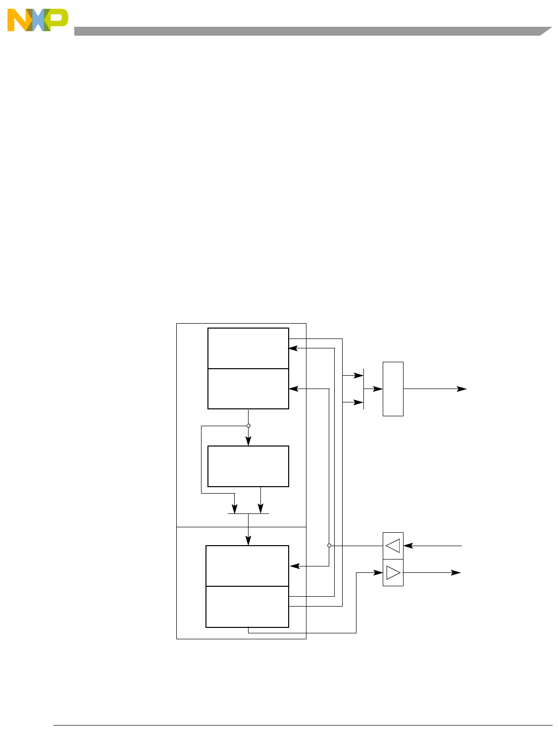
Freescale Semiconductor 3-1
Chapter 3
ColdFire Core
3.1 Introduction
This section describes the organization of the Version 2 (V2) ColdFire® processor core and an overview
of the program-visible registers. For detailed information on instructions, see the ISA_A+ definition in the
ColdFire Family Programmer’s Reference Manual.
3.1.1 Overview
As with all ColdFire cores, the V2 ColdFire core is comprised of two separate pipelines decoupled by an
instruction buffer.
Figure 3-1. V2 ColdFire Core Pipelines
The instruction fetch pipeline (IFP) is a two-stage pipeline for prefetching instructions. The prefetched
instruction stream is then gated into the two-stage operand execution pipeline (OEP), that decodes the
Instruction
Instruction
FIFO
Decode & Select,
Address
IAG
IC
IB
DSOC
AGEX
Instruction Buffer
Address
Generation
Fetch Cycle
Generation,
Execute
Operand Fetch
Instruction
Operand
Pipeline
Execution
Fetch
Pipeline
Address [ :0]
31
Read Data[31:0]
Write Data[31:0]
MCF52211 ColdFire® Integrated Microcontroller Reference Manual, Rev. 3

ColdFire Core
3-2 Freescale Semiconductor
instruction, fetches the required operands, and then executes the required function. Because the IFP and
OEP pipelines are decoupled by an instruction buffer serving as a FIFO queue, the IFP is able to prefetch
instructions in advance of their actual use by the OEP thereby minimizing time stalled waiting for
instructions.
The V2 ColdFire core pipeline stages include the following:
• Two-stage instruction fetch pipeline (IFP) (plus optional instruction buffer stage)
— Instruction address generation (IAG) — Calculates the next prefetch address
— Instruction fetch cycle (IC)—Initiates prefetch on the processor’s local bus
— Instruction buffer (IB) — Optional buffer stage minimizes fetch latency effects using FIFO
queue
• Two-stage operand execution pipeline (OEP)
— Decode and select/operand fetch cycle (DSOC)—Decodes instructions and fetches the
required components for effective address calculation, or the operand fetch cycle
— Address generation/execute cycle (AGEX)—Calculates operand address or executes the
instruction
When the instruction buffer is empty, opcodes are loaded directly from the IC cycle into the operand
execution pipeline. If the buffer is not empty, the IFP stores the contents of the fetched instruction in the
IB until it is required by the OEP.
For register-to-register and register-to-memory store operations, the instruction passes through both OEP
stages once. For memory-to-register and read-modify-write memory operations, an instruction is
effectively staged through the OEP twice; the first time to calculate the effective address and initiate the
operand fetch on the processor’s local bus, and the second time to complete the operand reference and
perform the required function defined by the instruction.
The resulting pipeline and local bus structure allow the V2 ColdFire core to deliver sustained high
performance across a variety of demanding embedded applications.
3.2 Memory Map/Register Description
The following sections describe the processor registers in the user and supervisor programming models.
The programming model is selected based on the processor privilege level (user mode or supervisor mode)
as defined by the S bit of the status register (SR). Table 3-1 lists the processor registers.
The user-programming model consists of the following registers:
• 16 general-purpose 32-bit registers (D0–D7, A0–A7)
• 32-bit program counter (PC)
• 8-bit condition code register (CCR)
• MAC registers
— One 32-bit accumulator (ACC) register
— One 16-bit mask register (MASK)
— 8-bit Status register (MACSR)
(described fully in Chapter 4, “Multiply-Accumulate Unit (MAC)”)
MCF52211 ColdFire® Integrated Microcontroller Reference Manual, Rev. 3

ColdFire Core
Freescale Semiconductor 3-3
The supervisor programming model is to be used only by system control software to implement restricted
operating system functions, I/O control, and memory management. All accesses that affect the control
features of ColdFire processors are in the supervisor programming model, that consists of registers
available in user mode as well as the following control registers:
• 16-bit status register (SR)
• 32-bit supervisor stack pointer (SSP)
• 32-bit vector base register (VBR)
Table 3-1. ColdFire Core Programming Model
BDM1Register Width
(bits) Access Reset Value Written with
MOVEC Section/Page
Supervisor/User Access Registers
Load: 0x080
Store: 0x180
Data Register 0 (D0) 32 R/W 0xCF20_0 No 3.2.1/3-4
Load: 0x081
Store: 0x181
Data Register 1 (D1) 32 R/W 0x10A0_1070 No 3.2.1/3-4
Load: 0x082–7
Store: 0x182–7
Data Register 2–7 (D2–D7) 32 R/W Undefined No 3.2.1/3-4
Load: 0x088–8E
Store: 0x188–8E
Address Register 0–6 (A0–A6) 32 R/W Undefined No 3.2.2/3-4
Load: 0x08F
Store: 0x18F
Supervisor/User A7 Stack Pointer (A7) 32 R/W Undefined No 3.2.3/3-4
0x804 MAC Status Register (MACSR) R/W 0x00 No 4.2.1/4-3
0x805 MAC Address Mask Register (MASK) R/W 0xFFFF No 4.2.2/4-5
0x806 MAC Accumulator (ACC) 32 R/W Undefined No 4.2.3/4-6
0x80E Condition Code Register (CCR) 8 R/W Undefined No 3.2.4/3-5
0x80F Program Counter (PC) 32 R/W Contents of
location
0x0000_0004
No 3.2.5/3-6
Supervisor Access Only Registers
0x800 User/Supervisor A7 Stack Pointer
(OTHER_A7)
32 R/W Contents of
location
0x0000_0000
No 3.2.3/3-4
0x801 Vector Base Register (VBR) 32 R/W 0x0000_0000 Yes 3.2.6/3-6
0x80E Status Register (SR) 16 R/W 0x27-- No 3.2.7/3-7
0xC04 Flash Base Address Register
(FLASHBAR)
32 R/W 0x0000_0000 Yes 3.2.8/3-8
• Two 32-bit memory base address registers (RAMBAR, FLASHBAR)
MCF52211 ColdFire® Integrated Microcontroller Reference Manual, Rev. 3

ColdFire Core
3-4 Freescale Semiconductor
3.2.1 Data Registers (D0–D7)
D0–D7 data registers are for bit (1-bit), byte (8-bit), word (16-bit) and longword (32-bit) operations; they
can also be used as index registers.
NOTE
Registers D0 and D1 contain hardware configuration details after reset. See
Section 3.3.4.15, “Reset Exception” for more details.
3.2.2 Address Registers (A0–A6)
These registers can be used as software stack pointers, index registers, or base address registers. They can
also be used for word and longword operations.
3.2.3 Supervisor/User Stack Pointers (A7 and OTHER_A7)
The ColdFire architecture supports two independent stack pointer (A7) registers—the supervisor stack
pointer (SSP) and the user stack pointer (USP). The hardware implementation of these two
0xC05 RAM Base Address Register (RAMBAR) 32 R/W See Section Yes 3.2.8/3-8
1The values listed in this column represent the Rc field used when accessing the core registers via the BDM port. For more
information see Chapter 28, “Debug Module”.
BDM: Load: 0x080 + n; n = 0-7 (Dn)
Store: 0x180 + n; n = 0-7 (Dn)
Access: User read/write
BDM read/write
313029282726252423222120191817161514131211109876543210
RData
W
Reset
(D2-D7) ––––––––––––––––––––––––––––––––
Reset
(D0, D1) See Section 3.3.4.15, “Reset Exception”
Figure 3-2. Data Registers (D0–D7)
BDM: Load: 0x088 + n; n =0–6 (An)
Store: 0x188 + n; n =0–6 (An)
Access: User read/write
BDM read/write
313029282726252423222120191817161514131211109876543210
R
Address
W
Reset––––––––––––––––––––––––––––––––
Figure 3-3. Address Registers (A0–A6)
Table 3-1. ColdFire Core Programming Model (continued)
BDM1Register Width
(bits) Access Reset Value Written with
MOVEC Section/Page
MCF52211 ColdFire® Integrated Microcontroller Reference Manual, Rev. 3

ColdFire Core
Freescale Semiconductor 3-5
program-visible 32-bit registers does not identify one as the SSP and the other as the USP. Instead, the
hardware uses one 32-bit register as the active A7 and the other as OTHER_A7. Thus, the register contents
are a function of the processor operation mode, as shown in the following:
if SR[S] = 1
then A7 = Supervisor Stack Pointer
OTHER_A7 = User Stack Pointer
else A7 = User Stack Pointer
OTHER_A7 = Supervisor Stack Pointer
The BDM programming model supports direct reads and writes to the (active) A7 and OTHER_A7. It is
the responsibility of the external development system to determine, based on the setting of SR[S], the
mapping of A7 and OTHER_A7 to the two program-visible definitions (SSP and USP).
To support dual stack pointers, the following two supervisor instructions are included in the ColdFire
instruction set architecture to load/store the USP:
move.l Ay,USP;move to USP
move.l USP,Ax;move from USP
These instructions are described in the ColdFire Family Programmer’s Reference Manual. All other
instruction references to the stack pointer, explicit or implicit, access the active A7 register.
NOTE
The USP must be initialized using the move.l Ay,USP instruction before any
entry into user mode.
The SSP is loaded during reset exception processing with the contents of
location 0x0000_0000.
3.2.4 Condition Code Register (CCR)
The CCR is the LSB of the processor status register (SR). Bits 4–0 act as indicator flags for results
generated by processor operations. The extend bit (X) is also an input operand during multiprecision
arithmetic computations.
NOTE
The CCR register must be explicitly loaded after reset and before any
compare (CMP), Bcc, or Scc instructions are executed.
BDM: Load: 0x08F (A7)
Store: 0x18F (A7)
0x800 (OTHER_A7)
Access: A7: User or BDM read/write
OTHER_A7: Supervisor or BDM read/write
313029282726252423222120191817161514131211109876543210
R
Address
W
Reset––––––––––––––––––––––––––––––––
Figure 3-4. Stack Pointer Registers (A7 and OTHER_A7)
MCF52211 ColdFire® Integrated Microcontroller Reference Manual, Rev. 3

ColdFire Core
3-6 Freescale Semiconductor
3.2.5 Program Counter (PC)
The PC contains the currently executing instruction address. During instruction execution and exception
processing, the processor automatically increments PC contents or places a new value in the PC. The PC
is a base address for PC-relative operand addressing.
The PC is initially loaded during reset exception processing with the contents at location 0x0000_0004.
3.2.6 Vector Base Register (VBR)
The VBR contains the base address of the exception vector table in the memory. To access the vector table,
the displacement of an exception vector is added to the value in VBR. The lower 20 bits of the VBR are
BDM: LSB of Status Register (SR) Access: User read/write
BDM read/write
76543210
R 0 0 0
X N Z V C
W
Reset:0 0 0 —————
Figure 3-5. Condition Code Register (CCR)
Table 3-2. CCR Field Descriptions
Field Description
7–5 Reserved, must be cleared.
4
X
Extend condition code bit. Set to the C-bit value for arithmetic operations; otherwise not affected or set to a specified
result.
3
N
Negative condition code bit. Set if most significant bit of the result is set; otherwise cleared.
2
Z
Zero condition code bit. Set if result equals zero; otherwise cleared.
1
V
Overflow condition code bit. Set if an arithmetic overflow occurs implying the result cannot be represented in operand
size; otherwise cleared.
0
C
Carry condition code bit. Set if a carry out of the operand msb occurs for an addition or if a borrow occurs in a
subtraction; otherwise cleared.
BDM: 0x80F (PC) Access: User read/write
BDM read/write
313029282726252423222120191817161514131211109876543210
R
Address
W
Reset––––––––––––––––––––––––––––––––
Figure 3-6. Program Counter Register (PC)
MCF52211 ColdFire® Integrated Microcontroller Reference Manual, Rev. 3

ColdFire Core
Freescale Semiconductor 3-7
not implemented by ColdFire processors. They are assumed to be zero, forcing the table to be aligned on
a 1 MB boundary.
3.2.7 Status Register (SR)
The SR stores the processor status and includes the CCR, the interrupt priority mask, and other control
bits. In supervisor mode, software can access the entire SR. In user mode, only the lower 8 bits (CCR) are
accessible. The control bits indicate the following states for the processor: trace mode (T bit), supervisor
or user mode (S bit), and master or interrupt state (M bit). All defined bits in the SR have read/write access
when in supervisor mode.
NOTE
The lower byte of the SR (the CCR) must be loaded explicitly after reset and
before any compare (CMP), Bcc, or Scc instructions execute.
BDM: 0x801 (VBR) Access: Supervisor read/write
BDM read/write
313029282726252423222120191817161514131211109876543210
R
Base Address
00000000000000000 0 00
W
Reset00000000000000000000000000000000
Figure 3-7. Vector Base Register (VBR)
BDM: 0x80E (SR) Access: Supervisor read/write
BDM read/write
System Byte Condition Code Register (CCR)
1514131211109876543210
RT0S M 0I000X N ZVC
W
Reset00100111000—————
Figure 3-8. Status Register (SR)
Table 3-3. SR Field Descriptions
Field Description
15
T
Trace enable. When set, the processor performs a trace exception after every instruction.
14 Reserved, must be cleared.
13
S
Supervisor/user state.
0User mode
1 Supervisor mode
12
M
Master/interrupt state. Bit is cleared by an interrupt exception and software can set it during execution of the RTE or
move to SR instructions.
11 Reserved, must be cleared.
MCF52211 ColdFire® Integrated Microcontroller Reference Manual, Rev. 3
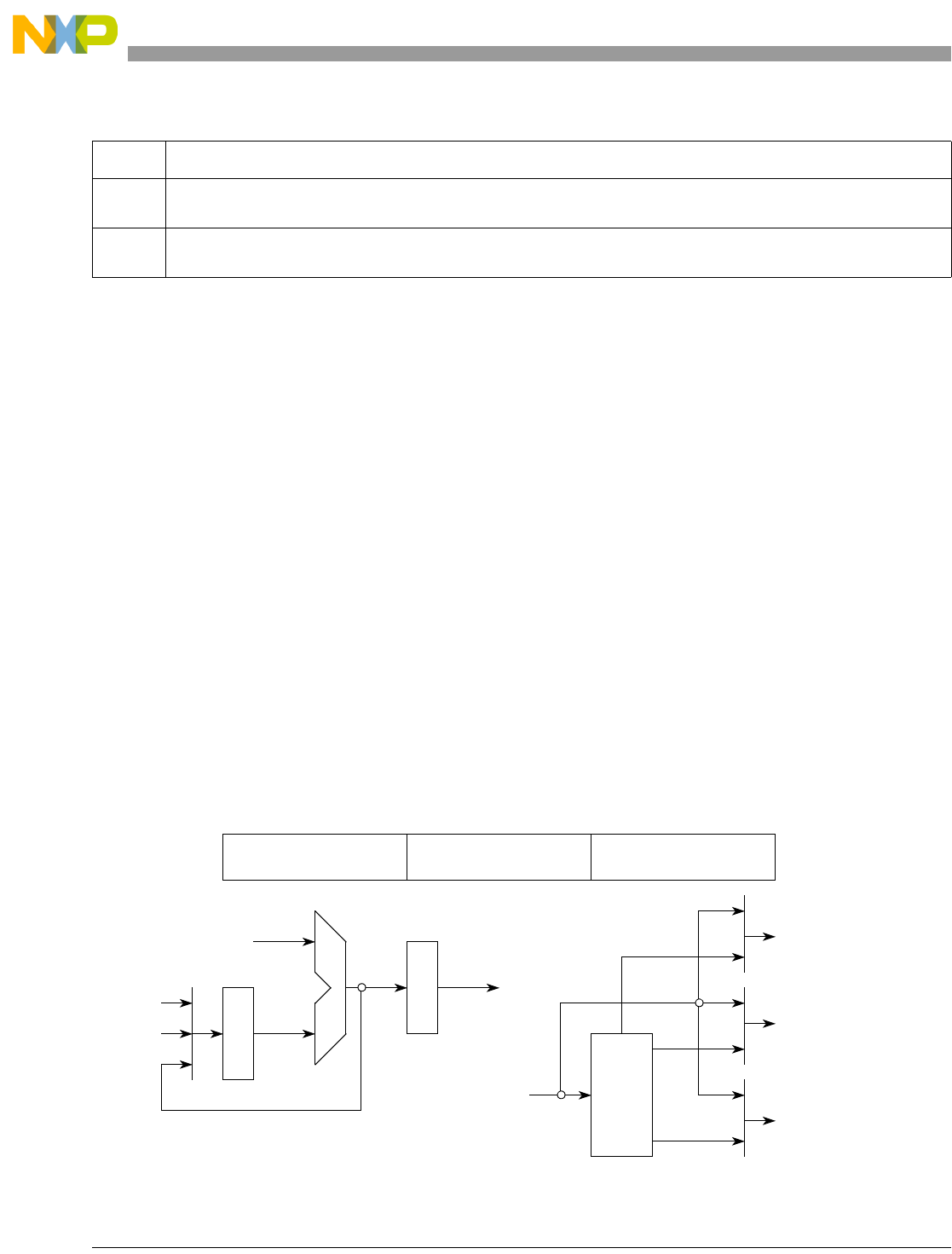
ColdFire Core
3-8 Freescale Semiconductor
3.3 Functional Description
3.3.1 Version 2 ColdFire Microarchitecture
From the block diagram in Figure 3-1, the non-Harvard architecture of the processor is readily apparent.
The processor interfaces to the local memory subsystem via a single 32-bit address and two unidirectional
32-bit data buses. This structure minimizes the core size without compromising performance to a large
degree.
A more detailed view of the hardware structure within the two pipelines is presented in Figure 3-9 and
Figure 3-10 below. In these diagrams, the internal structure of the instruction fetch and operand execution
pipelines is shown:
Figure 3-9. Version 2 ColdFire Processor Instruction Fetch Pipeline Diagram
10–8
I
Interrupt level mask. Defines current interrupt level. Interrupt requests are inhibited for all priority levels less than or
equal to current level, except edge-sensitive level 7 requests, which cannot be masked.
7–0
CCR
Refer to Section 3.2.4, “Condition Code Register (CCR)”.
Table 3-3. SR Field Descriptions (continued)
Field Description
3.2.8 Memory Base Address Registers (RAMBAR, FLASHBAR)
The memory base address registers are used to specify the base address of the internal SRAM and flash
modules and indicate the types of references mapped to each. Each base address register includes a base
address, write-protect bit, address space mask bits, and an enable bit. FLASHBAR determines the base
address of the on-chip flash, and RAMBAR determines the base address of the on-chip RAM. For more
information, refer to Section 5.2.1, “SRAM Base Address Register (RAMBAR)” and Section 18.3.2,
“Flash Base Address Register (FLASHBAR)”.
IAG IC IB
Core Bus
Address
Core Bus
Read Data
Opword
Extension 1
Extension 2
FIFO
IB
+4
MCF52211 ColdFire® Integrated Microcontroller Reference Manual, Rev. 3
ColdFire Core
Freescale Semiconductor 3-9
Figure 3-10. Version 2 ColdFire Processor Operand Execution Pipeline Diagram
The instruction fetch pipeline prefetches instructions from local memory using a two-stage structure. For
sequential prefetches, the next instruction address is generated by adding four to the last prefetch address.
This function is performed during the IAG stage and the resulting prefetch address gated onto the core bus
(if there are no pending operand memory accesses assigned a higher priority). After the prefetch address
is driven onto the core bus, the instruction fetch cycle accesses the appropriate local memory and returns
the instruction read data back to the IFP during the cycle. If the accessed data is not present in a local
memory (e.g., an instruction cache miss, or an external access cycle is required), the IFP is stalled in the
IC stage until the referenced data is available. As the prefetch data arrives in the IFP, it can be loaded into
the FIFO instruction buffer or gated directly into the OEP.
The V2 design uses a simple static conditional branch prediction algorithm (forward-assumed as
not-taken, backward-assumed as taken), and all change-of-flow operations are calculated by the OEP and
the target instruction address fed back to the IFP.
The IFP and OEP are decoupled by the FIFO instruction buffer, allowing instruction prefetching to occur
with the available core bus bandwidth not used for operand memory accesses. For the V2 design, the
instruction buffer contains three 32-bit locations.
Consider the operation of the OEP for three basic classes of non-branch instructions:
• Register-to-register:
op Ry,Rx
• Embedded load:
op <mem>y,Rx
• Register-to-memory (store)
move Ry,<mem>x
For simple register-to-register instructions, the first stage of the OEP performs the instruction decode and
fetching of the required register operands (OC) from the dual-ported register file, while the actual
DSOC AGEX
Opword
Extension 1
Extension 2
Core Bus
Read Data
Core Bus
Address
Core Bus
Write Data
RGF
MCF52211 ColdFire® Integrated Microcontroller Reference Manual, Rev. 3
ColdFire Core
3-10 Freescale Semiconductor
instruction execution is performed in the second stage (EX) in one of the execute engines (e.g., ALU,
barrel shifter, divider, EMAC). There are no operand memory accesses associated with this class of
instructions, and the execution time is typically a single machine cycle. See Figure 3-11.
Figure 3-11. V2 OEP Register-to-Register
For memory-to-register (embedded-load) instructions, the instruction is effectively staged through the
OEP twice with a basic execution time of three cycles. First, the instruction is decoded and the components
of the operand address (base register from the RGF and displacement) are selected (DS). Second, the
operand effective address is generated using the ALU execute engine (AG). Third, the memory read
operand is fetched from the core bus, while any required register operand is simultaneously fetched (OC)
from the RGF. Finally, in the fourth cycle, the instruction is executed (EX). The heavily-used 32-bit load
instruction (move.l <mem>y,Rx) is optimized to support a two-cycle execution time. The following example
in Figure 3-12 shows an effective address of the form <ea>y = (d16,Ay), i.e., a 16-bit signed displacement
added to a base register Ay.
Operand Execution Pipeline
DSOC AGEX
Opword
Extension 1
Extension 2
Core Bus
Read Data
Core Bus
Address
Core Bus
Write
Data
new Rx
Rx
Ry
RGF
MCF52211 ColdFire® Integrated Microcontroller Reference Manual, Rev. 3
ColdFire Core
Freescale Semiconductor 3-11
Figure 3-12. V2 OEP Embedded-Load Part 1
Figure 3-13. V2 OEP Embedded-Load Part 2
For register-to-memory (store) operations, the stage functions (DS/OC, AG/EX) are effectively performed
simultaneously allowing single-cycle execution. See Figure 3-14 where the effective address is of the form
<ea>x = (d16,Ax), i.e., a 16-bit signed displacement added to a base register Ax.
Operand Execution Pipeline
DSOC AGEX
Opword
Extension 1
Extension 2
Core Bus
Read Data
Core Bus
Address
Core Bus
Write
RGF
Data
Ay
d16
<ea>y
Operand Execution Pipeline
DSOC AGEX
Opword
Extension 1
Extension 2
Core Bus
Read Data
Core Bus
Address
Core Bus
Write
RGF
Data
Rx new Rx
<mem>y
MCF52211 ColdFire® Integrated Microcontroller Reference Manual, Rev. 3
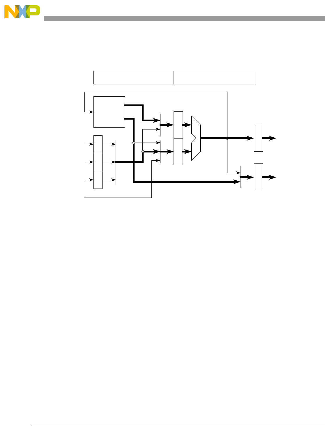
ColdFire Core
3-12 Freescale Semiconductor
For read-modify-write instructions, the pipeline effectively combines an embedded-load with a store
operation for a three-cycle execution time.
Figure 3-14. V2 OEP Register-to-Memory
The pipeline timing diagrams of Figure 3-15 depict the execution templates for these three classes of
instructions. In these diagrams, the x-axis represents time, and the various instruction operations are shown
progressing down the operand execution pipeline.
Operand Execution Pipeline
DSOC AGEX
Opword
Extension 1
Extension 2
Core Bus
Read Data
Core Bus
Address
Core Bus
Write
RGF
Data
Ax
d16
Ry <ea>x
MCF52211 ColdFire® Integrated Microcontroller Reference Manual, Rev. 3
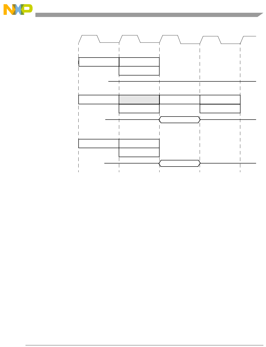
ColdFire Core
Freescale Semiconductor 3-13
Figure 3-15. V2 OEP Pipeline Execution Templates
3.3.2 Instruction Set Architecture (ISA_A+)
The original ColdFire instruction set architecture (ISA_A) was derived from the M68000 family opcodes
based on extensive analysis of embedded application code. The ISA was optimized for code compiled
from high-level languages where the dominant operand size was the 32-bit integer declaration. This
approach minimized processor complexity and cost, while providing excellent performance for compiled
applications.
After the initial ColdFire compilers were created, developers noted there were certain ISA additions that
would enhance code density and overall performance. Additionally, as users implemented ColdFire-based
designs into a wide range of embedded systems, they found certain frequently-used instruction sequences
that could be improved by the creation of additional instructions.
The original ISA definition minimized support for instructions referencing byte- and word-sized operands.
Full support for the move byte and move word instructions was provided, but the only other opcodes
supporting these data types are CLR (clear) and TST (test). A set of instruction enhancements has been
implemented in subsequent ISA revisions, ISA_B and ISA_C. The added opcodes primarily addressed
three areas:
1. Enhanced support for byte and word-sized operands
2. Enhanced support for position-independent code
3. Miscellaneous instruction additions to address new functionality
Core clock
Register-to-Register
Core Bus
Embedded-Load
Core Bus
Register-to-Memory
op read
Core Bus op write
OEP.DSOC OC next
OEP.AGEX EX
OEP.DSOC DS OC next
OEP.AGEX EXAG
OEP.DSOC DSOC next
OEP.AGEX AGEX
(Store)
MCF52211 ColdFire® Integrated Microcontroller Reference Manual, Rev. 3

ColdFire Core
3-14 Freescale Semiconductor
Table 3-4 summarizes the instructions added to revision ISA_A to form revision ISA_A+. For more details
see the ColdFire Family Programmer’s Reference Manual.
3.3.3 Exception Processing Overview
Exception processing for ColdFire processors is streamlined for performance. The ColdFire processors
differ from the M68000 family because they include:
• A simplified exception vector table
• Reduced relocation capabilities using the vector-base register
• A single exception stack frame format
All ColdFire processors use an instruction restart exception model. However, Version 2 ColdFire
processors require more software support to recover from certain access errors. See Section 3.3.4.1,
“Access Error Exception” for details.
Exception processing includes all actions from fault condition detection to the initiation of fetch for first
handler instruction. Exception processing is comprised of four major steps:
1. The processor makes an internal copy of the SR and then enters supervisor mode by setting the S
bit and disabling trace mode by clearing the T bit. The interrupt exception also forces the M bit to
be cleared and the interrupt priority mask to set to current interrupt request level.
Table 3-4. Instruction Enhancements over Revision ISA_A
Instruction Description
BITREV The contents of the destination data register are bit-reversed; new Dn[31] equals old Dn[0], new
Dn[30] equals old Dn[1],..., new Dn[0] equals old Dn[31].
BYTEREV The contents of the destination data register are byte-reversed; new Dn[31:24] equals old
Dn[7:0],..., new Dn[7:0] equals old Dn[31:24].
FF1 The data register, Dn, is scanned, beginning from the most-significant bit (Dn[31]) and ending
with the least-significant bit (Dn[0]), searching for the first set bit. The data register is then
loaded with the offset count from bit 31 where the first set bit appears.
Move from USP USP Destination register
Move to USP Source register USP
STLDSR Pushes the contents of the status register onto the stack and then reloads the status register
with the immediate data value.
2. The processor determines the exception vector number. For all faults except interrupts, the
processor performs this calculation based on exception type. For interrupts, the processor
performs an interrupt-acknowledge (IACK) bus cycle to obtain the vector number from the
interrupt controller. The IACK cycle is mapped to special locations within the interrupt
controller’s address space with the interrupt level encoded in the address.
MCF52211 ColdFire® Integrated Microcontroller Reference Manual, Rev. 3

ColdFire Core
Freescale Semiconductor 3-15
3. The processor saves the current context by creating an exception stack frame on the system stack.
The exception stack frame is created at a 0-modulo-4 address on top of the system stack pointed to
by the supervisor stack pointer (SSP). As shown in Figure 3-16, the processor uses a simplified
fixed-length stack frame for all exceptions. The exception type determines whether the program
counter placed in the exception stack frame defines the location of the faulting instruction (fault)
or the address of the next instruction to be executed (next).
4. The processor calculates the address of the first instruction of the exception handler. By definition,
the exception vector table is aligned on a 1 MB boundary. This instruction address is generated by
fetching an exception vector from the table located at the address defined in the vector base register.
The index into the exception table is calculated as (4 vector number). After the exception vector
has been fetched, the vector contents determine the address of the first instruction of the desired
handler. After the instruction fetch for the first opcode of the handler has initiated, exception
processing terminates and normal instruction processing continues in the handler.
The table contains 256 exception vectors; the first 64 are defined for the core and the remaining 192 are
device-specific peripheral interrupt vectors. See Chapter 14, “Interrupt Controller Module” for details on
the device-specific interrupt sources.
Table 3-5. Exception Vector Assignments
Vector
Number(s)
Vector
Offset (Hex)
Stacked
Program
Counter
Assignment
0 0x000 — Initial supervisor stack pointer
1 0x004 — Initial program counter
2 0x008 Fault Access error
3 0x00C Fault Address error
4 0x010 Fault Illegal instruction
5 0x014 Fault Divide by zero
6–7 0x018–0x01C — Reserved
8 0x020 Fault Privilege violation
9 0x024 Next Trace
10 0x028 Fault Unimplemented line-A opcode
11 0x02C Fault Unimplemented line-F opcode
12 0x030 Next Debug interrupt
13 0x034 — Reserved
14 0x038 Fault Format error
15–23 0x03C–0x05C — Reserved
24 0x060 Next Spurious interrupt
25–31 0x064–0x07C — Reserved
All ColdFire processors support a 1024-byte vector table aligned on any 1 Mbyte address boundary (see
Table 3-5).
MCF52211 ColdFire® Integrated Microcontroller Reference Manual, Rev. 3

ColdFire Core
3-16 Freescale Semiconductor
All ColdFire processors inhibit interrupt sampling during the first instruction of all exception handlers.
This allows any handler to disable interrupts effectively, if necessary, by raising the interrupt mask level
contained in the status register. In addition, the ISA_A+ architecture includes an instruction (STLDSR)
that stores the current interrupt mask level and loads a value into the SR. This instruction is specifically
intended for use as the first instruction of an interrupt service routine that services multiple interrupt
requests with different interrupt levels. For more details, see ColdFire Family Programmer’s Reference
Manual.
3.3.3.1 Exception Stack Frame Definition
Figure 3-16 shows exception stack frame. The first longword contains the 16-bit format/vector word (F/V)
and the 16-bit status register, and the second longword contains the 32-bit program counter address.
The 16-bit format/vector word contains three unique fields:
• A 4-bit format field at the top of the system stack is always written with a value of 4, 5, 6, or 7 by
the processor, indicating a two-longword frame format. See Table 3-6.
• There is a 4-bit fault status field, FS[3:0], at the top of the system stack. This field is defined for
access and address errors only and written as zeros for all other exceptions. See Table 3-7.
32–47 0x080–0x0BC Next Trap # 0-15 instructions
48–63 0x0C0–0x0FC — Reserved
64–255 0x100–0x3FC Next Device-specific interrupts
1Fault refers to the PC of the instruction that caused the exception. Next refers to the PC
of the instruction that follows the instruction that caused the fault.
313029282726252423222120191817161514131211109876543210
SSP Format FS[3:2] Vector FS[1:0] Status Register
+ 0x4 Program Counter
Figure 3-16. Exception Stack Frame Form
Table 3-6. Format Field Encodings
Original SSP @ Time
of Exception, Bits 1:0
SSP @ 1st
Instruction of
Handler
Format Field
00 Original SSP - 8 0100
01 Original SSP - 9 0101
10 Original SSP - 10 0110
11 Original SSP - 11 0111
Table 3-5. Exception Vector Assignments (continued)
Vector
Number(s)
Vector
Offset (Hex)
Stacked
Program
Counter
Assignment
MCF52211 ColdFire® Integrated Microcontroller Reference Manual, Rev. 3

ColdFire Core
Freescale Semiconductor 3-17
• The 8-bit vector number, vector[7:0], defines the exception type and is calculated by the processor
for all internal faults and represents the value supplied by the interrupt controller in case of an
interrupt. See Table 3-5.
3.3.4 Processor Exceptions
3.3.4.1 Access Error Exception
The exact processor response to an access error depends on the memory reference being performed. For
an instruction fetch, the processor postpones the error reporting until the faulted reference is needed by an
instruction for execution. Therefore, faults during instruction prefetches followed by a change of
instruction flow do not generate an exception. When the processor attempts to execute an instruction with
a faulted opword and/or extension words, the access error is signaled and the instruction is aborted. For
this type of exception, the programming model has not been altered by the instruction generating the access
error.
If the access error occurs on an operand read, the processor immediately aborts the current instruction’s
execution and initiates exception processing. In this situation, any address register updates attributable to
the auto-addressing modes, (for example, (An)+,-(An)), have already been performed, so the programming
model contains the updated An value. In addition, if an access error occurs during a MOVEM instruction
loading from memory, any registers already updated before the fault occurs contain the operands from
memory.
The V2 ColdFire processor uses an imprecise reporting mechanism for access errors on operand writes.
Because the actual write cycle may be decoupled from the processor’s issuing of the operation, the
signaling of an access error appears to be decoupled from the instruction that generated the write.
Accordingly, the PC contained in the exception stack frame merely represents the location in the program
when the access error was signaled. All programming model updates associated with the write instruction
are completed. The NOP instruction can collect access errors for writes. This instruction delays its
Table 3-7. Fault Status Encodings
FS[3:0] Definition
00xx Reserved
0100 Error on instruction fetch
0101 Reserved
011x Reserved
1000 Error on operand write
1001 Attempted write to write-protected space
101x Reserved
1100 Error on operand read
1101 Reserved
111x Reserved
MCF52211 ColdFire® Integrated Microcontroller Reference Manual, Rev. 3

ColdFire Core
3-18 Freescale Semiconductor
execution until all previous operations, including all pending write operations, are complete. If any
previous write terminates with an access error, it is guaranteed to be reported on the NOP instruction.
3.3.4.2 Address Error Exception
Any attempted execution transferring control to an odd instruction address (if bit 0 of the target address is
set) results in an address error exception.
Any attempted use of a word-sized index register (Xn.w) or a scale factor of eight on an indexed effective
addressing mode generates an address error, as does an attempted execution of a full-format indexed
addressing mode, which is defined by bit 8 of extension word 1 being set.
If an address error occurs on a JSR instruction, the Version 2 ColdFire processor calculates the target
address then the return address is pushed onto the stack. If an address error occurs on an RTS instruction,
the Version 2 ColdFire processor overwrites the faulting return PC with the address error stack frame.
3.3.4.3 Illegal Instruction Exception
The ColdFire variable-length instruction set architecture supports three instruction sizes: 16, 32, or 48 bits.
The first instruction word is known as the operation word (or opword), while the optional words are known
as extension word 1 and extension word 2. The opword is further subdivided into three sections: the upper
four bits segment the entire ISA into 16 instruction lines, the next 6 bits define the operation mode
(opmode), and the low-order 6 bits define the effective address. See Figure 3-17. The opword line
definition is shown in Table 3-8.
Figure 3-17. ColdFire Instruction Operation Word (Opword) Format
1514131211109876543210
Line OpMode Effective Address
Mode Register
Table 3-8. ColdFire Opword Line Definition
Opword[Line] Instruction Class
0x0 Bit manipulation, Arithmetic and Logical Immediate
0x1 Move Byte
0x2 Move Long
0x3 Move Word
0x4 Miscellaneous
0x5 Add (ADDQ) and Subtract Quick (SUBQ), Set according to Condition Codes (Scc)
0x6 PC-relative change-of-flow instructions
Conditional (Bcc) and unconditional (BRA) branches, subroutine calls (BSR)
0x7 Move Quick (MOVEQ), Move with sign extension (MVS) and zero fill (MVZ)
0x8 Logical OR (OR)
0x9 Subtract (SUB), Subtract Extended (SUBX)
MCF52211 ColdFire® Integrated Microcontroller Reference Manual, Rev. 3

ColdFire Core
Freescale Semiconductor 3-19
In the original M68000 ISA definition, lines A and F were effectively reserved for user-defined operations
(line A) and co-processor instructions (line F). Accordingly, there are two unique exception vectors
associated with illegal opwords in these two lines.
Any attempted execution of an illegal 16-bit opcode (except for line-A and line-F opcodes) generates an
illegal instruction exception (vector 4). Additionally, any attempted execution of any non-MAC line-A and
most line-F opcodes generate their unique exception types, vector numbers 10 and 11, respectively.
ColdFire cores do not provide illegal instruction detection on the extension words on any instruction,
including MOVEC.
3.3.4.4 Divide-By-Zero
Attempting to divide by zero causes an exception (vector 5, offset equal 0x014).
3.3.4.5 Privilege Violation
The attempted execution of a supervisor mode instruction while in user mode generates a privilege
violation exception. See ColdFire Programmer’s Reference Manual for a list of supervisor-mode
instructions.
There is one special case involving the HALT instruction. Normally, this opcode is a supervisor mode
instruction, but if the debug module's CSR[UHE] is set, then this instruction can be also be executed in
user mode for debugging purposes.
3.3.4.6 Trace Exception
To aid in program development, all ColdFire processors provide an instruction-by-instruction tracing
capability. While in trace mode, indicated by setting of the SR[T] bit, the completion of an instruction
execution (for all but the stop instruction) signals a trace exception. This functionality allows a debugger
to monitor program execution.
The stop instruction has the following effects:
1. The instruction before the stop executes and then generates a trace exception. In the exception stack
frame, the PC points to the stop opcode.
2. When the trace handler is exited, the stop instruction executes, loading the SR with the immediate
operand from the instruction.
0xA MAC, Move 3-bit Quick (MOV3Q)
0xB Compare (CMP), Exclusive-OR (EOR)
0xC Logical AND (AND), Multiply Word (MUL)
0xD Add (ADD), Add Extended (ADDX)
0xE Arithmetic and logical shifts (ASL, ASR, LSL, LSR)
0xF Cache Push (CPUSHL), Write DDATA (WDDATA), Write Debug (WDEBUG)
Table 3-8. ColdFire Opword Line Definition (continued)
Opword[Line] Instruction Class
MCF52211 ColdFire® Integrated Microcontroller Reference Manual, Rev. 3

ColdFire Core
3-20 Freescale Semiconductor
3. The processor then generates a trace exception. The PC in the exception stack frame points to the
instruction after the stop, and the SR reflects the value loaded in the previous step.
If the processor is not in trace mode and executes a stop instruction where the immediate operand sets
SR[T], hardware loads the SR and generates a trace exception. The PC in the exception stack frame points
to the instruction after the stop, and the SR reflects the value loaded in step 2.
Because ColdFire processors do not support any hardware stacking of multiple exceptions, it is the
responsibility of the operating system to check for trace mode after processing other exception types. As
an example, consider a TRAP instruction execution while in trace mode. The processor initiates the trap
exception and then passes control to the corresponding handler. If the system requires that a trace exception
be processed, it is the responsibility of the trap exception handler to check for this condition (SR[T] in the
exception stack frame set) and pass control to the trace handler before returning from the original
exception.
3.3.4.7 Unimplemented Line-A Opcode
A line-A opcode is defined when bits 15-12 of the opword are 0b1010. This exception is generated by the
attempted execution of an undefined line-A opcode.
3.3.4.8 Unimplemented Line-F Opcode
A line-F opcode is defined when bits 15-12 of the opword are 0b1111. This exception is generated when
attempting to execute an undefined line-F opcode.
3.3.4.9 Debug Interrupt
See Chapter 28, “Debug Module,” for a detailed explanation of this exception, which is generated in
response to a hardware breakpoint register trigger. The processor does not generate an IACK cycle, but
rather calculates the vector number internally (vector number 12). Additionally, SR[M,I] are unaffected by
the interrupt.
3.3.4.10 RTE and Format Error Exception
When an RTE instruction is executed, the processor first examines the 4-bit format field to validate the
frame type. For a ColdFire core, any attempted RTE execution (where the format is not equal to {4,5,6,7})
generates a format error. The exception stack frame for the format error is created without disturbing the
original RTE frame and the stacked PC pointing to the RTE instruction.
The selection of the format value provides some limited debug support for porting code from M68000
applications. On M68000 family processors, the SR was located at the top of the stack. On those
processors, bit 30 of the longword addressed by the system stack pointer is typically zero. Thus, if an RTE
is attempted using this old format, it generates a format error on a ColdFire processor.
If the format field defines a valid type, the processor: (1) reloads the SR operand, (2) fetches the second
longword operand, (3) adjusts the stack pointer by adding the format value to the auto-incremented address
after the fetch of the first longword, and then (4) transfers control to the instruction address defined by the
second longword operand within the stack frame.
MCF52211 ColdFire® Integrated Microcontroller Reference Manual, Rev. 3

ColdFire Core
Freescale Semiconductor 3-21
3.3.4.11 TRAP Instruction Exception
The TRAP #n instruction always forces an exception as part of its execution and is useful for implementing
system calls. The TRAP instruction may be used to change from user to supervisor mode.
3.3.4.12 Unsupported Instruction Exception
If execution of a valid instruction is attempted but the required hardware is not present in the processor, an
unsupported instruction exception is generated. The instruction functionality can then be emulated in the
exception handler, if desired.
All ColdFire cores record the processor hardware configuration in the D0 register immediately after the
negation of RESET. See Section 3.3.4.15, “Reset Exception,” for details.
3.3.4.13 Interrupt Exception
Interrupt exception processing includes interrupt recognition and the fetch of the appropriate vector from
the interrupt controller using an IACK cycle. See Chapter 14, “Interrupt Controller Module,” for details
on the interrupt controller.
3.3.4.14 Fault-on-Fault Halt
If a ColdFire processor encounters any type of fault during the exception processing of another fault, the
processor immediately halts execution with the catastrophic fault-on-fault condition. A reset is required to
to exit this state.
3.3.4.15 Reset Exception
Asserting the reset input signal (RESET) to the processor causes a reset exception. The reset exception has
the highest priority of any exception; it provides for system initialization and recovery from catastrophic
failure. Reset also aborts any processing in progress when the reset input is recognized. Processing cannot
be recovered.
The reset exception places the processor in the supervisor mode by setting the SR[S] bit and disables
tracing by clearing the SR[T] bit. This exception also clears the SR[M] bit and sets the processor’s SR[I]
field to the highest level (level 7, 0b111). Next, the VBR is initialized to zero (0x0000_0000). The control
registers specifying the operation of any memories (e.g., cache and/or RAM modules) connected directly
to the processor are disabled.
NOTE
Other implementation-specific registers are also affected. Refer to each
module in this reference manual for details on these registers.
After the processor is granted the bus, it performs two longword read-bus cycles. The first longword at
address 0x0000_0000 is loaded into the supervisor stack pointer and the second longword at address
0x0000_0004 is loaded into the program counter. After the initial instruction is fetched from memory,
program execution begins at the address in the PC. If an access error or address error occurs before the first
instruction is executed, the processor enters the fault-on-fault state.
MCF52211 ColdFire® Integrated Microcontroller Reference Manual, Rev. 3

ColdFire Core
3-22 Freescale Semiconductor
ColdFire processors load hardware configuration information into the D0 and D1 general-purpose
registers after system reset. The hardware configuration information is loaded immediately after the
reset-in signal is negated. This allows an emulator to read out the contents of these registers via the BDM
to determine the hardware configuration.
Information loaded into D0 defines the processor hardware configuration as shown in Figure 3-18.
BDM: Load: 0x080 (D0)
Store: 0x180 (D0)
Access: User read-only
BDM read-only
31 30 29 28 27 26 25 24 23 22 21 20 19 18 17 16
RPF VER REV
W
Reset1100111100100000
15 14 13 12 11 10 9 8 7 6 5 4 3 2 1 0
RMAC DIVEMACFPU0000 ISA DEBUG
W
Reset1100000010001001
Figure 3-18. D0 Hardware Configuration Info
Table 3-9. D0 Hardware Configuration Info Field Description
Field Description
31–24
PF
Processor family. This field is fixed to a hex value of 0xCF indicating a ColdFire core is present.
23–20
VER
ColdFire core version number. Defines the hardware microarchitecture version of ColdFire core.
0001 V1 ColdFire core
0010 V2 ColdFire core (This is the value used for this device.)
0011 V3 ColdFire core
0100 V4 ColdFire core
0101 V5 ColdFire core
Else Reserved for future use
19–16
REV
Processor revision number. The default is 0b0000.
15
MAC
MAC present. This bit signals if the optional multiply-accumulate (MAC) execution engine is present in processor core.
0 MAC execute engine not present in core.
1 MAC execute engine is present in core.
14
DIV
Divide present. This bit signals if the hardware divider (DIV) is present in the processor core.
0 Divide execute engine not present in core.
1 Divide execute engine is present in core.
13
EMAC
EMAC present. This bit signals if the optional enhanced multiply-accumulate (EMAC) execution engine is present in
processor core.
0 EMAC execute engine not present in core. (This is the value used for this device.)
1 EMAC execute engine is present in core.
12
FPU
FPU present. This bit signals if the optional floating-point (FPU) execution engine is present in processor core.
0 FPU execute engine not present in core. (This is the value used for this device.)
1 FPU execute engine is present in core.
(This is the value used for this device.)
(This is the value used for this device.)
MCF52211 ColdFire® Integrated Microcontroller Reference Manual, Rev. 3

ColdFire Core
Freescale Semiconductor 3-23
Information loaded into D1 defines the local memory hardware configuration as shown in the figure below.
11–8 Reserved.
7–4
ISA
ISA revision. Defines the instruction-set architecture (ISA) revision level implemented in ColdFire processor core.
0000 ISA_A
0001 ISA_B
0010 ISA_C
1000 ISA_A+ (This is the value used for this device.)
Else Reserved
3–0
DEBUG
Debug module revision number. Defines revision level of the debug module used in the ColdFire processor core.
0000 DEBUG_A
0001 DEBUG_B
0010 DEBUG_C
0011 DEBUG_D
0100 DEBUG_E
1001 DEBUG_B+ (This is the value used for this device.)
1011 DEBUG_D+
1111 DEBUG_D+PST Buffer
Else Reserved
BDM: Load: 0x1 (D1)
Store: 0x1 (D1)
Access: User read-only
BDM read-only
31 30 29 28 27 26 25 24 23 22 21 20 19 18 17 16
R CLSZ CCAS CCSZ FLASHSZ 0 0 0
W
Reset0001000010100000
1514131211109876543210
RMBSZ UCAS 0000 SRAMSZ 000
W
Reset0001000001110000
Figure 3-19. D1 Hardware Configuration Info
Table 3-10. D1 Hardware Configuration Information Field Description
Field Description
31–30
CLSZ
Cache line size. This field is fixed to a hex value of 0x0 indicating a 16-byte cache line size.
29–28
CCAS
Configurable cache associativity.
00 Four-way
01 Direct mapped (This is the value used for this device)
Else Reserved for future use
Table 3-9. D0 Hardware Configuration Info Field Description (continued)
Field Description
MCF52211 ColdFire® Integrated Microcontroller Reference Manual, Rev. 3

ColdFire Core
3-24 Freescale Semiconductor
3.3.5 Instruction Execution Timing
This section presents processor instruction execution times in terms of processor-core clock cycles. The
number of operand references for each instruction is enclosed in parentheses following the number of
processor clock cycles. Each timing entry is presented as C(R/W) where:
•C is the number of processor clock cycles, including all applicable operand fetches and writes, and
all internal core cycles required to complete the instruction execution.
27–24
CCSZ
Configurable cache size. Indicates the amount of instruction/data cache.The cache configuration options available
are 50% instruction/50% data, 100% instruction, or 100% data, and are specified in the CACR register.
0000 No configurable cache (This is the value used for this device)
0001 512 B configurable cache
0010 1 KB configurable cache
0011 2 KB configurable cache
0100 4 KB configurable cache
0101 8 KB configurable cache
0110 16 KB configurable cache
0111 32 KB configurable cache
Else Reserved
23–19
FLASHSZ
Flash bank size.
00000-01110 No flash
10000 64 KB flash
10010 128 KB flash
10011 96 KB flash
10100 256 KB flash (This is the value used for this device)
10110 512 KB flash
Else Reserved for future use
18–16 Reserved
15–14
MBSZ
Bus size. Defines the width of the ColdFire master bus datapath.
00 32-bit system bus datapath (This is the value used for this device)
01 64-bit system bus datapath
Else Reserved
13–8 Reserved, resets to 0b01_0000
7–3
SRAMSZ
SRAM bank size.
00000 No SRAM
00010 512 bytes
00100 1 KB
00110 2 KB
01000 4 KB
01010 8 KB
01100 16 KB
01111 24 KB
01110 32 KB (This is the value used for this device)
10000 64 KB
10010 128 KB
Else Reserved for future use
2–0 Reserved.
Table 3-10. D1 Hardware Configuration Information Field Description (continued)
Field Description
MCF52211 ColdFire® Integrated Microcontroller Reference Manual, Rev. 3

ColdFire Core
Freescale Semiconductor 3-25
• R/W is the number of operand reads (R) and writes (W) required by the instruction. An operation
performing a read-modify-write function is denoted as (1/1).
This section includes the assumptions concerning the timing values and the execution time details.
3.3.5.1 Timing Assumptions
For the timing data presented in this section, these assumptions apply:
1. The OEP is loaded with the opword and all required extension words at the beginning of each
instruction execution. This implies that the OEP does not wait for the IFP to supply opwords and/or
extension words.
2. The OEP does not experience any sequence-related pipeline stalls. The most common example of
stall involves consecutive store operations, excluding the MOVEM instruction. For all STORE
operations (except MOVEM), certain hardware resources within the processor are marked as busy
for two clock cycles after the final decode and select/operand fetch cycle (DSOC) of the store
instruction. If a subsequent STORE instruction is encountered within this 2-cycle window, it is
stalled until the resource again becomes available. Thus, the maximum pipeline stall involving
consecutive STORE operations is two cycles. The MOVEM instruction uses a different set of
resources and this stall does not apply.
3. The OEP completes all memory accesses without any stall conditions caused by the memory itself.
Thus, the timing details provided in this section assume that an infinite zero-wait state memory is
attached to the processor core.
4. All operand data accesses are aligned on the same byte boundary as the operand size; for example,
16-bit operands aligned on 0-modulo-2 addresses, 32-bit operands aligned on 0-modulo-4
addresses.
The processor core decomposes misaligned operand references into a series of aligned accesses as
shown in Table 3-11.
3.3.5.2 MOVE Instruction Execution Times
Table 3-12 lists execution times for MOVE.{B,W} instructions; Table 3-13 lists timings for MOVE.L.
NOTE
For all tables in this section, the execution time of any instruction using the
PC-relative effective addressing modes is the same for the comparable
An-relative mode.
Table 3-11. Misaligned Operand References
address[1:0] Size Bus
Operations
Additional
C(R/W)
01 or 11 Word Byte, Byte 2(1/0) if read
1(0/1) if write
01 or 11 Long Byte, Word,
Byte
3(2/0) if read
2(0/2) if write
10 Long Word, Word 2(1/0) if read
1(0/1) if write
MCF52211 ColdFire® Integrated Microcontroller Reference Manual, Rev. 3

ColdFire Core
3-26 Freescale Semiconductor
The nomenclature xxx.wl refers to both forms of absolute addressing, xxx.w
and xxx.l.
ET with {<ea> = (d16,PC)} equals ET with {<ea> = (d16,An)}
ET with {<ea> = (d8,PC,Xi*SF)} equals ET with {<ea> = (d8,An,Xi*SF)}
Table 3-12. MOVE Byte and Word Execution Times
Source
Destination
Rx (Ax) (Ax)+ -(Ax) (d16,Ax) (d8,Ax,Xi*SF) xxx.wl
Dy 1(0/0) 1(0/1) 1(0/1) 1(0/1) 1(0/1) 2(0/1) 1(0/1)
Ay 1(0/0) 1(0/1) 1(0/1) 1(0/1) 1(0/1) 2(0/1) 1(0/1)
(Ay) 3(1/0) 3(1/1) 3(1/1) 3(1/1) 3(1/1) 4(1/1)) 3(1/1)
(Ay)+ 3(1/0) 3(1/1) 3(1/1) 3(1/1) 3(1/1) 4(1/1)) 3(1/1)
-(Ay) 3(1/0) 3(1/1) 3(1/1) 3(1/1) 3(1/1) 4(1/1)) 3(1/1)
(d16,Ay) 3(1/0) 3(1/1) 3(1/1) 3(1/1) 3(1/1) — —
(d8,Ay,Xi*SF) 4(1/0) 4(1/1) 4(1/1) 4(1/1) — — —
xxx.w 3(1/0) 3(1/1) 3(1/1) 3(1/1) — — —
xxx.l 3(1/0) 3(1/1) 3(1/1) 3(1/1) — — —
(d16,PC) 3(1/0) 3(1/1) 3(1/1) 3(1/1) 3(1/1) — —
(d8,PC,Xi*SF) 4(1/0) 4(1/1) 4(1/1) 4(1/1)) — — —
#xxx 1(0/0) 3(0/1) 3(0/1) 3(0/1) — — —
Table 3-13. MOVE Long Execution Times
Source
Destination
Rx (Ax) (Ax)+ -(Ax) (d16,Ax) (d8,Ax,Xi*SF) xxx.wl
Dy 1(0/0) 1(0/1) 1(0/1) 1(0/1) 1(0/1) 2(0/1) 1(0/1)
Ay 1(0/0) 1(0/1) 1(0/1) 1(0/1) 1(0/1) 2(0/1) 1(0/1)
(Ay) 2(1/0) 2(1/1) 2(1/1) 2(1/1) 2(1/1) 3(1/1) 2(1/1)
(Ay)+ 2(1/0) 2(1/1) 2(1/1) 2(1/1) 2(1/1) 3(1/1) 2(1/1)
-(Ay) 2(1/0) 2(1/1) 2(1/1) 2(1/1) 2(1/1) 3(1/1) 2(1/1)
(d16,Ay) 2(1/0) 2(1/1) 2(1/1) 2(1/1) 2(1/1) — —
(d8,Ay,Xi*SF) 3(1/0) 3(1/1) 3(1/1) 3(1/1) — — —
xxx.w 2(1/0) 2(1/1) 2(1/1) 2(1/1) — — —
xxx.l 2(1/0) 2(1/1) 2(1/1) 2(1/1) — — —
(d16,PC) 2(1/0) 2(1/1) 2(1/1) 2(1/1) 2(1/1) — —
(d8,PC,Xi*SF) 3(1/0) 3(1/1) 3(1/1) 3(1/1) — — —
#xxx 1(0/0) 2(0/1) 2(0/1) 2(0/1) — — —
MCF52211 ColdFire® Integrated Microcontroller Reference Manual, Rev. 3

ColdFire Core
Freescale Semiconductor 3-27
3.3.5.3 Standard One Operand Instruction Execution Times
3.3.5.4 Standard Two Operand Instruction Execution Times
Table 3-14. One Operand Instruction Execution Times
Opcode <EA>
Effective Address
Rn (An) (An)+ -(An) (d16,An) (d8,An,Xn*SF) xxx.wl #xxx
BITREVDx1(0/0)———— — ——
BYTEREVDx1(0/0)———— — ——
CLR.B <ea> 1(0/0) 1(0/1) 1(0/1) 1(0/1) 1(0/1) 2(0/1) 1(0/1) —
CLR.W <ea> 1(0/0) 1(0/1) 1(0/1) 1(0/1) 1(0/1) 2(0/1) 1(0/1) —
CLR.L <ea> 1(0/0) 1(0/1) 1(0/1) 1(0/1) 1(0/1) 2(0/1) 1(0/1) —
EXT.WDx1(0/0)———— — ——
EXT.LDx1(0/0)———— — ——
EXTB.LDx1(0/0)———— — ——
FF1Dx1(0/0)———— — ——
NEG.LDx1(0/0)———— — ——
NEGX.LDx1(0/0)———— — ——
NOT.LDx1(0/0)———— — ——
SCCDx1(0/0)———— — ——
SWAPDx1(0/0)———— — ——
TST.B <ea> 1(0/0) 3(1/0) 3(1/0) 3(1/0) 3(1/0) 4(1/0) 3(1/0) 1(0/0)
TST.W <ea> 1(0/0) 3(1/0) 3(1/0) 3(1/0) 3(1/0) 4(1/0) 3(1/0) 1(0/0)
TST.L <ea> 1(0/0) 2(1/0) 2(1/0) 2(1/0) 2(1/0) 3(1/0) 2(1/0) 1(0/0)
Table 3-15. Two Operand Instruction Execution Times
Opcode <EA>
Effective Address
Rn (An) (An)+ -(An) (d16,An)
(d16,PC)
(d8,An,Xn*SF)
(d8,PC,Xn*SF) xxx.wl #xxx
ADD.L <ea>,Rx 1(0/0) 3(1/0) 3(1/0) 3(1/0) 3(1/0) 4(1/0) 3(1/0) 1(0/0)
ADD.L Dy,<ea> — 3(1/1) 3(1/1) 3(1/1) 3(1/1) 4(1/1) 3(1/1) —
ADDI.L #imm,Dx 1(0/0) — — — — — — —
ADDQ.L #imm,<ea> 1(0/0) 3(1/1) 3(1/1) 3(1/1) 3(1/1) 4(1/1) 3(1/1) —
ADDX.L Dy,Dx 1(0/0) — — — — — — —
AND.L <ea>,Rx 1(0/0) 3(1/0) 3(1/0) 3(1/0) 3(1/0) 4(1/0) 3(1/0) 1(0/0)
AND.L Dy,<ea> — 3(1/1) 3(1/1) 3(1/1) 3(1/1) 4(1/1) 3(1/1) —
ANDI.L #imm,Dx 1(0/0) — — — — — — —
MCF52211 ColdFire® Integrated Microcontroller Reference Manual, Rev. 3

ColdFire Core
3-28 Freescale Semiconductor
ASL.L <ea>,Dx 1(0/0) — — — — — — 1(0/0)
ASR.L <ea>,Dx 1(0/0) — — — — — — 1(0/0)
BCHG Dy,<ea> 2(0/0) 4(1/1) 4(1/1) 4(1/1) 4(1/1) 5(1/1) 4(1/1) —
BCHG #imm,<ea> 2(0/0) 4(1/1) 4(1/1) 4(1/1) 4(1/1) — — —
BCLR Dy,<ea> 2(0/0) 4(1/1) 4(1/1) 4(1/1) 4(1/1) 5(1/1) 4(1/1) —
BCLR #imm,<ea> 2(0/0) 4(1/1) 4(1/1) 4(1/1) 4(1/1) — — —
BSET Dy,<ea> 2(0/0) 4(1/1) 4(1/1) 4(1/1) 4(1/1) 5(1/1) 4(1/1) —
BSET #imm,<ea> 2(0/0) 4(1/1) 4(1/1) 4(1/1) 4(1/1) — — —
BTST Dy,<ea> 2(0/0) 3(1/0) 3(1/0) 3(1/0) 3(1/0) 4(1/0) 3(1/0) —
BTST #imm,<ea> 1(0/0) 3(1/0) 3(1/0) 3(1/0) 3(1/0) — — —
CMP.L <ea>,Rx 1(0/0) 3(1/0) 3(1/0) 3(1/0) 3(1/0) 4(1/0) 3(1/0) 1(0/0)
CMPI.L #imm,Dx 1(0/0) — — — — — — —
DIVS.W <ea>,Dx 20(0/0) 23(1/0) 23(1/0) 23(1/0) 23(1/0) 24(1/0) 23(1/0) 20(0/0)
DIVU.W <ea>,Dx 20(0/0) 23(1/0) 23(1/0) 23(1/0) 23(1/0) 24(1/0) 23(1/0) 20(0/0)
DIVS.L <ea>,Dx 35(0/0) 38(1/0) 38(1/0) 38(1/0) 38(1/0) — — —
DIVU.L <ea>,Dx 35(0/0) 38(1/0) 38(1/0) 38(1/0) 38(1/0) — — —
EOR.L Dy,<ea> 1(0/0) 3(1/1) 3(1/1) 3(1/1) 3(1/1) 4(1/1) 3(1/1) —
EORI.L #imm,Dx 1(0/0) — — — — — — —
LEA <ea>,Ax — 1(0/0) — — 1(0/0) 2(0/0) 1(0/0) —
LSL.L <ea>,Dx 1(0/0) — — — — — — 1(0/0)
LSR.L <ea>,Dx 1(0/0) — — — — — — 1(0/0)
MOVEQ.L #imm,Dx — — — — — — — 1(0/0)
OR.L <ea>,Rx 1(0/0) 3(1/0) 3(1/0) 3(1/0) 3(1/0) 4(1/0) 3(1/0) 1(0/0)
OR.L Dy,<ea> — 3(1/1) 3(1/1) 3(1/1) 3(1/1) 4(1/1) 3(1/1) —
ORI.L #imm,Dx 1(0/0) — — — — — — —
REMS.L <ea>,Dx 35(0/0) 38(1/0) 38(1/0) 38(1/0) 38(1/0) — — —
REMU.L <ea>,Dx 35(0/0) 38(1/0) 38(1/0) 38(1/0) 38(1/0) — — —
SUB.L <ea>,Rx 1(0/0) 3(1/0) 3(1/0) 3(1/0) 3(1/0) 4(1/0) 3(1/0) 1(0/0)
SUB.L Dy,<ea> — 3(1/1) 3(1/1) 3(1/1) 3(1/1) 4(1/1) 3(1/1) —
SUBI.L #imm,Dx 1(0/0) — — — — — — —
SUBQ.L #imm,<ea> 1(0/0) 3(1/1) 3(1/1) 3(1/1) 3(1/1) 4(1/1) 3(1/1) —
SUBX.L Dy,Dx 1(0/0) — — — — — — —
Table 3-15. Two Operand Instruction Execution Times (continued)
Opcode <EA>
Effective Address
Rn (An) (An)+ -(An) (d16,An)
(d16,PC)
(d8,An,Xn*SF)
(d8,PC,Xn*SF) xxx.wl #xxx
MCF52211 ColdFire® Integrated Microcontroller Reference Manual, Rev. 3

ColdFire Core
Freescale Semiconductor 3-29
3.3.5.5 Miscellaneous Instruction Execution Times
Table 3-16. Miscellaneous Instruction Execution Times
Opcode <EA>
Effective Address
Rn (An) (An)+ -(An) (d16,An) (d8,An,Xn*SF) xxx.wl #xxx
CPUSHL (Ax) — 11(0/1) — — — — — —
LINK.W Ay,#imm 2(0/1) — — — — — — —
MOVE.L Ay,USP 3(0/0) — — — — — — —
MOVE.L USP,Ax 3(0/0) — — — — — — —
MOVE.W CCR,Dx 1(0/0) — — — — — — —
MOVE.W <ea>,CCR 1(0/0) — — — — — — 1(0/0)
MOVE.W SR,Dx 1(0/0) — — — — — — —
MOVE.W <ea>,SR 7(0/0) — — — — — — 7(0/0) 2
MOVEC Ry,Rc 9(0/1) — — — — — — —
MOVEM.L <ea>, and
list
—1+n(n/0)— —1+n(n/0) — — —
MOVEM.L and
list,<ea>
—1+n(0/n)— —1+n(0/n) — — —
NOP 3(0/0)———— — ——
PEA <ea> — 2(0/1) — — 2(0/1) 43(0/1) 52(0/1) —
PULSE 1(0/0)———— — ——
STLDSR#imm————— — —5(0/1)
STOP#imm————— — —3(0/0)
3
TRAP#imm————— — —15(1/2)
TPF 1(0/0)———— — ——
TPF.W 1(0/0)———— — ——
TPF.L 1(0/0)———— — ——
UNLK Ax 2(1/0) — — — — — — —
WDDATA <ea> — 3(1/0) 3(1/0) 3(1/0) 3(1/0) 4(1/0) 3(1/0) —
WDEBUG<ea> —5(2/0)— —5(2/0) — — —
1The n is the number of registers moved by the MOVEM opcode.
2If a MOVE.W #imm,SR instruction is executed and imm[13] equals 1, the execution time is 1(0/0).
3The execution time for STOP is the time required until the processor begins sampling continuously for interrupts.
4PEA execution times are the same for (d16,PC).
5PEA execution times are the same for (d8,PC,Xn*SF).
MCF52211 ColdFire® Integrated Microcontroller Reference Manual, Rev. 3

ColdFire Core
3-30 Freescale Semiconductor
3.3.5.6 MAC Instruction Execution Times
3.3.5.7 Branch Instruction Execution Times
Table 3-17. MAC Instruction Execution Times
Opcode <EA>
Effective Address
Rn (An) (An)+ -(An) (d16,An) (d8,An,
Xn*SF) xxx.wl #xxx
MAC.L Ry, Rx 3(0/0) — — — — — — —
MAC.L Ry, Rx, <ea>, Rw — (1/0) (1/0) (1/0) (1/0)1———
MAC.W Ry, Rx 1(0/0) — — — — — — —
MAC.W Ry, Rx, <ea>, Rw — (1/0) (1/0) (1/0) (1/0)1
1Effective address of (d16,PC) not supported
———
MOVE.L <ea>y, Racc 1(0/0) — — — — — — 1(0/0)
MOVE.L <ea>y, MACSR 2(0/0) — — — — — — 2(0/0)
MOVE.L <ea>y, Rmask 1(0/0) — — — — — — 1(0/0)
MOVE.L Racc, <ea>x 1(0/0)2
2Storing the accumulator requires one additional processor clock cycle when rounding is performed
——— — ———
MOVE.L MACSR, <ea>x 1(0/0) — — — — — — —
MOVE.L Rmask, <ea>x 1(0/0) — — — — — — —
MSAC.L Ry, Rx 3(0/0) — — — — — — —
MSAC.W Ry, Rx 1(0/0) — — — — — — —
MSAC.L Ry, Rx, <ea>, Rw — (1/0) (1/0) (1/0) (1/0)1———
MSAC.W Ry, Rx, <ea>, Rw — (1/0) (1/0) (1/0) (1/0)1———
MULS.L <ea>y, Dx 5(0/0) (1/0) (1/0) (1/0) (1/0) — — —
MULS.W <ea>y, Dx 3(0/0) (1/0) (1/0) (1/0) (1/0) (1/0) (1/0) 3(0/0)
MULU.L <ea>y, Dx 5(0/0) (1/0) (1/0) (1/0) (1/0) — — —
MULU.W <ea>y, Dx 3(0/0) (1/0) (1/0) (1/0) (1/0) (1/0) (1/0) 3(0/0)
Table 3-18. General Branch Instruction Execution Times
Opcode <EA>
Effective Address
Rn (An) (An)+ -(An) (d16,An)
(d16,PC)
(d8,An,Xi*SF)
(d8,PC,Xi*SF) xxx.wl #xxx
BRA — — — — 2(0/1) — — —
BSR — — — — 3(0/1) — — —
JMP <ea> — 3(0/0) — — 3(0/0) 4(0/0) 3(0/0) —
MCF52211 ColdFire® Integrated Microcontroller Reference Manual, Rev. 3

ColdFire Core
Freescale Semiconductor 3-31
JSR <ea> — 3(0/1) — — 3(0/1) 4(0/1) 3(0/1) —
RTE — — 10(2/0) — — — — —
RTS ——5(1/0)—————
Table 3-19. Bcc Instruction Execution Times
Opcode Forward
Taken
Forward
Not Taken
Backward
Taken
Backward
Not Taken
Bcc 3(0/0) 1(0/0) 2(0/0) 3(0/0)
Table 3-18. General Branch Instruction Execution Times (continued)
Opcode <EA>
Effective Address
Rn (An) (An)+ -(An) (d16,An)
(d16,PC)
(d8,An,Xi*SF)
(d8,PC,Xi*SF) xxx.wl #xxx
MCF52211 ColdFire® Integrated Microcontroller Reference Manual, Rev. 3
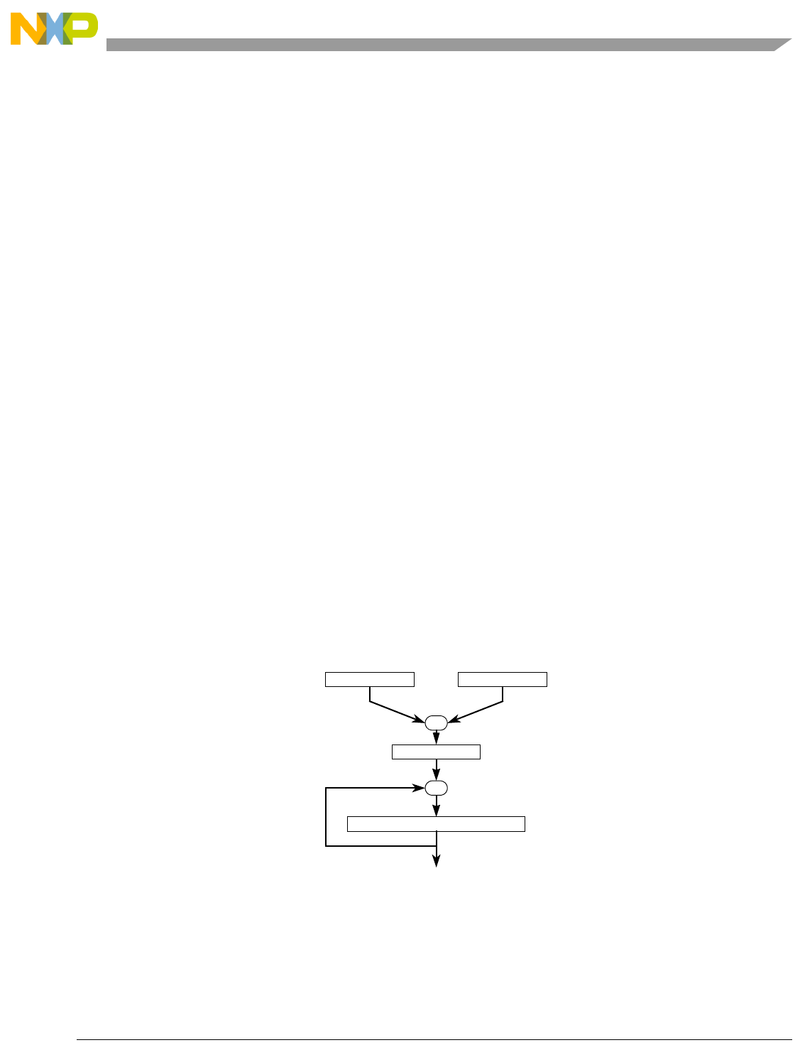
Freescale Semiconductor 4-2
Chapter 4
Multiply-Accumulate Unit (MAC)
4.1 Introduction
This chapter describes the functionality, microarchitecture, and performance of the multiply-accumulate
(MAC) unit in the ColdFire family of processors.
4.1.1 Overview
The MAC design provides a set of DSP operations that can improve the performance of embedded code
while supporting the integer multiply instructions of the baseline ColdFire architecture.
The MAC provides functionality in three related areas:
1. Signed and unsigned integer multiplication
2. Multiply-accumulate operations supporting signed and unsigned integer operands as well as
signed, fixed-point, and fractional operands
3. Miscellaneous register operations
The MAC features a three-stage execution pipeline optimized for 16-bit operands, with a 16x16 multiply
array and a single 32-bit accumulator.
The three areas of functionality are addressed in detail in following sections. The logic required to support
this functionality is contained in a MAC module (Figure 4-1).
Figure 4-1. Multiply-Accumulate Functionality Diagram
4.1.1.1 Introduction to the MAC
The MAC is an extension of the basic multiplier in most microprocessors. It is typically implemented in
hardware within an architecture and supports rapid execution of signal processing algorithms in fewer
X
+/-
Operand Y Operand X
Shift 0,1,-1
Accumulator(s)
MCF52211 ColdFire® Integrated Microcontroller Reference Manual, Rev. 3

Multiply-Accumulate Unit (MAC)
4-3 Freescale Semiconductor
cycles than comparable non-MAC architectures. For example, small digital filters can tolerate some
variance in an algorithm’s execution time, but larger, more complicated algorithms such as orthogonal
transforms may have more demanding speed requirements beyond scope of any processor architecture and
may require full DSP implementation.
To balance speed, size, and functionality, the ColdFire MAC is optimized for a small set of operations that
involve multiplication and cumulative additions. Specifically, the multiplier array is optimized for
single-cycle pipelined operations with a possible accumulation after product generation. This functionality
is common in many signal processing applications. The ColdFire core architecture is also modified to
allow an operand to be fetched in parallel with a multiply, increasing overall performance for certain DSP
operations.
Consider a typical filtering operation where the filter is defined as in Equation 4-1.
Eqn. 4-1
Here, the output y(i) is determined by past output values and past input values. This is the general form of
an infinite impulse response (IIR) filter. A finite impulse response (FIR) filter can be obtained by setting
coefficients a(k) to zero. In either case, the operations involved in computing such a filter are multiplies
and product summing. To show this point, reduce Equation 4-1 to a simple, four-tap FIR filter, shown in
Equation 4-2, in which the accumulated sum is a past data values and coefficients sum.
Eqn. 4-2
4.2 Memory Map/Register Definition
The following table and sections explain the MAC registers:
4.2.1 MAC Status Register (MACSR)
The MAC status register (MACSR) contains a 4-bit operational mode field and condition flags.
Operational mode bits control whether operands are signed or unsigned and whether they are treated as
integers or fractions. These bits also control the overflow/saturation mode and the way in which rounding
is performed. Negative, zero, and overflow condition flags are also provided.
Table 4-1. MAC Memory Map
BDM1Register Width
(bits) Access Reset Value Section/Page
0x804 MAC Status Register (MACSR) 8 R/W 0x00 4.2.1/4-3
0x805 MAC Address Mask Register (MASK) 16 R/W 0xFFFF 4.2.2/4-5
0x806 Accumulator (ACC) 32 R/W Undefined 4.2.3/4-6
1The values listed in this column represent the Rc field used when accessing the core registers via the BDM port. For more
information see Chapter 28, “Debug Module.”
yi akyi k–
k1=
N1–
bkxi k–
k0=
N1–
+=
yi bkxi k–
k0=
3
b0xi b1xi 1–b2xi 2–b3xi 3–+++==
MCF52211 ColdFire® Integrated Microcontroller Reference Manual, Rev. 3

Multiply-Accumulate Unit (MAC)
Freescale Semiconductor 4-4
BDM: 0x4 (MACSR) Access: Supervisor read/write
BDM read/write
76543210
R
OMC S/U F/I R/T N Z VC
W
Reset:00000000
Figure 4-2. MAC Status Register (MACSR)
Table 4-2. MACSR Field Descriptions
Field Description
7
OMC
Overflow saturation mode. Enables or disables saturation mode on overflow. If set, the accumulator is set
to the appropriate constant (see S/U field description) on any operation that overflows the accumulator.
After saturation, the accumulator remains unaffected by any other MAC or MSAC instructions until the
overflow bit is cleared or the accumulator is directly loaded.
6
S/U
Signed/unsigned operations.
In integer mode:
S/U determines whether operations performed are signed or unsigned. It also determines the accumulator
value during saturation, if enabled.
0 Signed numbers. On overflow, if OMC is enabled, the accumulator saturates to the most positive
(0x7FFF_FFFF) or the most negative (0x8000_0000) number, depending on the instruction and the
product value that overflowed.
1 Unsigned numbers. On overflow, if OMC is enabled, the accumulator saturates to the smallest value
(0x0000_0000) or the largest value (0xFFFF_FFFF), depending on the instruction.
In fractional mode:
S/U controls rounding while storing the accumulator to a general-purpose register.
0 Move accumulator without rounding to a 16-bit value. Accumulator is moved to a general-purpose
register as a 32-bit value.
1 The accumulator is rounded to a 16-bit value using the round-to-nearest (even) method when moved to
a general-purpose register. See Section 4.3.1.1, “Rounding”. The resulting 16-bit value is stored in the
lower word of the destination register. The upper word is zero-filled. This rounding procedure does not
affect the accumulator value.
5
F/I
Fractional/integer mode. Determines whether input operands are treated as fractions or integers.
0 Integers can be represented in signed or unsigned notation, depending on the value of S/U.
1 Fractions are represented in signed, fixed-point, two’s complement notation. Values range from -1 to
1-2
-15 for 16-bit fractions and -1 to 1 - 2-31 for 32-bit fractions. See Section 4.3.4, “Data
Representation."
4
R/T
Round/truncate mode. Controls rounding procedure for MSAC.L instructions when in fractional mode.
0 Truncate. The product’s lsbs are dropped before it is combined with the accumulator.
1 Round-to-nearest (even). The 64-bit product of two 32-bit, fractional operands is rounded to the nearest
32-bit value. If the low-order 32 bits equal 0x8000_0000, the upper 32 bits are rounded to the nearest
even (lsb = 0) value. See Section 4.3.1.1, “Rounding”.
3
N
Negative. Set if the msb of the result is set, otherwise cleared. N is affected only by MAC, MSAC, and load
operations; it is not affected by MULS and MULU instructions.
2
Z
Zero. Set if the result equals zero, otherwise cleared. This bit is affected only by MAC, MSAC, and load
operations; it is not affected by MULS and MULU instructions.
MCF52211 ColdFire® Integrated Microcontroller Reference Manual, Rev. 3

Multiply-Accumulate Unit (MAC)
4-5 Freescale Semiconductor
Table 4-3 summarizes the interaction of the MACSR[S/U,F/I,R/T] control bits.
4.2.2 Mask Register (MASK)
The MASK register performs a simple AND with the operand address for MAC instructions. The
processor calculates the normal operand address and, if enabled, that address is then ANDed with
{0xFFFF, MASK[15:0]} to form the final address. Therefore, with certain MASK bits cleared, the operand
address can be constrained to a certain memory region. This is used primarily to implement circular queues
with the (An)+ addressing mode.
This minimizes the addressing support required for filtering, convolution, or any routine that implements
a data array as a circular queue. For MAC + MOVE operations, the MASK contents can optionally be
included in all memory effective address calculations. The syntax is as follows:
mac.sz Ry,RxSF,<ea>y&,Rw
The & operator enables the MASK use and causes bit 5 of the extension word to be set. The exact
algorithm for the use of MASK is:
1
V
Overflow. Set if an arithmetic overflow occurs, implying that the result cannot be represented in the operand
size. After set, V remains set until the accumulator register is loaded with a new value or MACSR is directly
loaded. MULS and MULU instructions do not change this value.
0 Carry. This field is always zero.
Table 4-3. Summary of S/U, F/I, and R/T Control Bits
S/U F/I R/T Operational Modes
0 0 x Signed, integer
0 1 0 Signed, fractional
Truncate on MAC.L and MSAC.L
No round on accumulator stores
0 1 1 Signed, fractional
Round on MAC.L and MSAC.L
No round on accumulator stores
1 0 x Unsigned, integer
1 1 0 Signed, fractional
Truncate on MAC.L and MSAC.L
Round-to-16-bits on accumulator stores
1 1 1 Signed, fractional
Round on MAC.L and MSAC.L
Round-to-16-bits on accumulator stores
Table 4-2. MACSR Field Descriptions (continued)
Field Description
MCF52211 ColdFire® Integrated Microcontroller Reference Manual, Rev. 3

Multiply-Accumulate Unit (MAC)
Freescale Semiconductor 4-6
if extension word, bit [5] = 1, the MASK bit, then
if <ea> = (An)
oa = An & {0xFFFF, MASK}
if <ea> = (An)+
oa = An
An = (An + 4) & {0xFFFF, MASK}
if <ea> =-(An)
oa = (An - 4) & {0xFFFF, MASK}
An = (An - 4) & {0xFFFF, MASK}
if <ea> = (d16,An)
oa = (An + se_d16) & {0xFFFF0x, MASK}
Here, oa is the calculated operand address and se_d16 is a sign-extended 16-bit displacement. For
auto-addressing modes of post-increment and pre-decrement, the updated An value calculation is also
shown.
Use of the post-increment addressing mode, {(An)+} with the MASK is suggested for circular queue
implementations.
4.2.3 Accumulator Register (ACC)
The accumulator register store 32-bits of the MAC operation result.
Figure 4-4. Accumulator Register (ACC)
BDM: 0x5 (MASK) Access: User read/write
BDM read/write
1514131211109876543210
R
MASK
W
Reset1111111111111111
Figure 4-3. Mask Register (MASK)
Table 4-4. MASK Field Descriptions
Field Description
15–0
MASK
Performs a simple AND with the operand address for MAC instructions.
BDM: 0x806 (ACC) Access: User read/write
BDM read/write
313029282726252423222120191817161514131211109876543210
RAccumulator
W
Reset––––––––––––––––––––––––––––––––
MCF52211 ColdFire® Integrated Microcontroller Reference Manual, Rev. 3

Multiply-Accumulate Unit (MAC)
4-7 Freescale Semiconductor
4.3 Functional Description
The MAC speeds execution of ColdFire integer-multiply instructions (MULS and MULU) and provides
additional functionality for multiply-accumulate operations. By executing MULS and MULU in the MAC,
execution times are minimized and deterministic compared to the 2-bit/cycle algorithm with early
termination that the OEP normally uses if no MAC hardware is present.
The added MAC instructions to the ColdFire ISA provide for the multiplication of two numbers, followed
by the addition or subtraction of the product to or from the value in the accumulator. Optionally, the
product may be shifted left or right by 1 bit before addition or subtraction. Hardware support for saturation
arithmetic can be enabled to minimize software overhead when dealing with potential overflow conditions.
Multiply-accumulate operations support 16- or 32-bit input operands in these formats:
• Signed integers
• Unsigned integers
• Signed, fixed-point, fractional numbers
The MAC is optimized for 16-bit multiplications to keep the area consumption low. Two 16-bit operands
produce a 32-bit product. Longword operations are performed by reusing the 16-bit multiplier array at the
expense of a small amount of extra control logic. Again, the product of two 32-bit operands is a 32-bit
result. For longword integer operations, only the least significant 32 bits of the product are calculated. For
fractional operations, the entire 64-bit product is calculated and then truncated or rounded to a 32-bit result
using the round-to-nearest (even) method.
Because the multiplier array is implemented in a three-stage pipeline, MAC instructions have an effective
issue rate of 1 cycle for word operations, 3 cycles for longword integer operations, and 4 cycles for 32-bit
fractional operations.
All arithmetic operations use register-based input operands, and summed values are stored in the
accumulator. Therefore, an additional MOVE instruction is needed to store data in a general-purpose
register.
The need to move large amounts of data presents an obstacle to obtaining high throughput rates in DSP
engines. Existing ColdFire instructions can accommodate these requirements. A MOVEM instruction can
efficiently move large data blocks by generating line-sized burst references. The ability to load an operand
simultaneously from memory into a register and execute a MAC instruction makes some DSP operations
such as filtering and convolution more manageable.
The programming model includes a mask register (MASK), which can optionally be used to generate an
operand address during MAC + MOVE instructions. The register application with auto-increment
addressing mode supports efficient implementation of circular data queues for memory operands.
Table 4-5. ACC Field Descriptions
Field Description
31–0
Accumulator
Store 32-bits of the result of the MAC operation.
MCF52211 ColdFire® Integrated Microcontroller Reference Manual, Rev. 3

Multiply-Accumulate Unit (MAC)
Freescale Semiconductor 4-8
4.3.1 Fractional Operation Mode
This section describes behavior when the fractional mode is used (MACSR[F/I] is set).
4.3.1.1 Rounding
When the processor is in fractional mode, there are two operations during which rounding can occur:
1. The 32-bit accumulator is moved into a general purpose register. If MACSR[S/U] is cleared, the
accumulator is stored as is in the destination register; if it is set, the 32-bit value is rounded to a
16-bit value using the round-to-nearest (even) method. The resulting 16-bit number is stored in the
lower word of the destination register. The upper word is zero-filled. The accumulator value is
unaffected by this rounding procedure.
2. Execution of a MAC (or MSAC) instruction with 32-bit operands. If MACSR[R/T] is zero,
multiplying two 32-bit numbers creates a 64-bit product truncated to the upper 32 bits; otherwise,
it is rounded using round-to-nearest (even) method.
To understand the round-to-nearest-even method, consider the following example involving the rounding
of a 32-bit number, R0, to a 16-bit number. Using this method, the 32-bit number is rounded to the closest
16-bit number possible. Let the high-order 16 bits of R0 be named R0.U and the low-order 16 bits be R0.L.
• If R0.L is less than 0x8000, the result is truncated to the value of R0.U.
• If R0.L is greater than 0x8000, the upper word is incremented (rounded up).
• If R0.L is 0x8000, R0 is half-way between two 16-bit numbers. In this case, rounding is based on
the lsb of R0.U, so the result is always even (lsb = 0).
— If the lsb of R0.U equals 1 and R0.L equals 0x8000, the number is rounded up.
— If the lsb of R0.U equals 0 and R0.L equals 0x8000, the number is rounded down.
This method minimizes rounding bias and creates as statistically correct an answer as possible.
The rounding algorithm is summarized in the following pseudocode:
if R0.L < 0x8000
then Result = R0.U
else if R0.L > 0x8000
then Result = R0.U + 1
else if lsb of R0.U = 0 /* R0.L = 0x8000 */
then Result = R0.U
else Result = R0.U + 1
The round-to-nearest-even technique is also known as convergent rounding.
4.3.1.2 Saving and Restoring the MAC Programming Model
The presence of rounding logic in the MAC output datapath requires special care during the MAC’s
save/restore process. In particular, any result rounding modes must be disabled during the save/restore
process so the exact bit-wise contents of the MAC registers are accessed. Consider the memory structure
containing the MAC programming model:
struct macState {
int acc;
int mask;
MCF52211 ColdFire® Integrated Microcontroller Reference Manual, Rev. 3

Multiply-Accumulate Unit (MAC)
4-9 Freescale Semiconductor
int macsr;
} macState;
The following assembly language routine shows the proper sequence for a correct MAC state save. This
code assumes all Dn and An registers are available for use, and the memory location of the state save is
defined by A7.
MAC_state_save:
move.l macsr,d7 ; save the macsr
clr.l d0 ; zero the register to ...
move.l d0,macsr ; disable rounding in the macsr
move.l acc,d5 ; save the accumulator
move.l mask,d6 ; save the address mask
movem.l #0x00e0,(a7) ; move the state to memory
This code performs the MAC state restore:
MAC_state_restore:
movem.l (a7),#0x00e0; restore the state from memory
move.l #0,macsr ; disable rounding in the macsr
move.l d5,acc ; restore the accumulator
move.l d6,mask ; restore the address mask
move.l d7,macsr ; restore the macsr
Executing this sequence type can correctly save and restore the exact state of the MAC programming
model.
4.3.1.3 MULS/MULU
MULS and MULU are unaffected by fractional-mode operation; operands remain assumed to be integers.
4.3.1.4 Scale Factor in MAC or MSAC Instructions
The scale factor is ignored while the MAC is in fractional mode.
4.3.2 MAC Instruction Set Summary
Table 4-6 summarizes MAC unit instructions.
Table 4-6. MAC Instruction Summary
Command Mnemonic Description
Multiply Signed muls <ea>y,Dx Multiplies two signed operands yielding a signed result
Multiply Unsigned mulu <ea>y,Dx Multiplies two unsigned operands yielding an unsigned result
Multiply Accumulate mac Ry,RxSF
msac Ry,RxSF
Multiplies two operands, then adds/subtracts the product
to/from the accumulator
Multiply Accumulate
with Load
mac Ry,RxSF,Rw
msac Ry,RxSF,Rw
Multiplies two operands, combines the product to the
accumulator while loading a register with the memory
operand
Load Accumulator move.l {Ry,#imm},ACC Loads the accumulator with a 32-bit operand
Store Accumulator move.l ACC,Rx Writes the contents of the accumulator to a CPU register
MCF52211 ColdFire® Integrated Microcontroller Reference Manual, Rev. 3

Multiply-Accumulate Unit (MAC)
Freescale Semiconductor 4-10
4.3.3 MAC Instruction Execution Times
The instruction execution times for the MAC can be found in Section 3.3.5.6, “MAC Instruction Execution
Times”.
4.3.4 Data Representation
MACSR[S/U,F/I] selects one of the following three modes, where each mode defines a unique operand
type:
1. Two’s complement signed integer: In this format, an N-bit operand value lies in the range -2(N-1)
< operand < 2(N-1) - 1. The binary point is right of the lsb.
2. Unsigned integer: In this format, an N-bit operand value lies in the range 0 < operand < 2N - 1. The
binary point is right of the lsb.
3. Two’s complement, signed fractional: In an N-bit number, the first bit is the sign bit. The remaining
bits signify the first N-1 bits after the binary point. Given an N-bit number, aN-1aN-2aN-3... a2a1a0,
its value is given by the equation in Equation 4-3.
Eqn. 4-3
This format can represent numbers in the range -1 < operand < 1-2
-(N-1).
For words and longwords, the largest negative number that can be represented is -1, whose internal
representation is 0x8000 and 0x8000_0000, respectively. The largest positive word is 0x7FFF or (1 - 2-15);
the most positive longword is 0x7FFF_FFFF or (1 - 2-31). Thus, the number range for these signed
fractional numbers is [-1.0, ..., 1.0].
4.3.5 MAC Opcodes
MAC opcodes are described in the ColdFire Programmer’s Reference Manual.
Remember the following:
• Unless otherwise noted, the value of MACSR[N,Z] is based on the result of the final operation that
involves the product and the accumulator.
• The overflow (V) flag is managed differently. It is set if the complete product cannot be represented
as a 32-bit value (this applies to 32 32 integer operations only) or if the combination of the
Load MACSR move.l {Ry,#imm},MACSR Writes a value to MACSR
Store MACSR move.l MACSR,Rx Write the contents of MACSR to a CPU register
Store MACSR to CCR move.l MACSR,CCR Write the contents of MACSR to the CCR
Load MAC Mask Reg move.l {Ry,#imm},MASK Writes a value to the MASK register
Store MAC Mask Reg move.l MASK,Rx Writes the contents of the MASK to a CPU register
Table 4-6. MAC Instruction Summary (continued)
Command Mnemonic Description
value 1 aN1–
–2
i1N–+–ai
i0=
N2–
+=
MCF52211 ColdFire® Integrated Microcontroller Reference Manual, Rev. 3

Multiply-Accumulate Unit (MAC)
4-11 Freescale Semiconductor
product with the accumulator cannot be represented in the given number of bits. This indicator is
treated as a sticky flag, meaning after set, it remains set until the accumulator or the MACSR is
directly loaded. See Section 4.2.1, “MAC Status Register (MACSR)”.
• The optional 1-bit shift of the product is specified using the notation {<< | >>} SF, where <<1
indicates a left shift and >>1 indicates a right shift. The shift is performed before the product is
added to or subtracted from the accumulator. Without this operator, the product is not shifted. If the
MAC is in fractional mode (MACSR[F/I] is set), SF is ignored and no shift is performed. Because
a product can overflow, the following guidelines are implemented:
— For unsigned word and longword operations, a zero is shifted into the product on right shifts.
— For signed, word operations, the sign bit is shifted into the product on right shifts unless the
product is zero. For signed, longword operations, the sign bit is shifted into the product unless
an overflow occurs or the product is zero, in which case a zero is shifted in.
— For all left shifts, a zero is inserted into the lsb position.
The following pseudocode explains basic MAC or MSAC instruction functionality. This example is
presented as a case statement covering the three basic operating modes with signed integers, unsigned
integers, and signed fractionals. Throughout this example, a comma-separated list in curly brackets, {},
indicates a concatenation operation.
switch (MACSR[6:5]) /* MACSR[S/U, F/I] */
{
case 0: /* signed integers */
if (MACSR.OMC == 0 || MACSR.V == 0)
then {
MACSR.V = 0
/* select the input operands */
if (sz == word)
then {if (U/Ly == 1)
then operandY[31:0] = {sign-extended Ry[31], Ry[31:16]}
else operandY[31:0] = {sign-extended Ry[15], Ry[15:0]}
if (U/Lx == 1)
then operandX[31:0] = {sign-extended Rx[31], Rx[31:16]}
else operandX[31:0] = {sign-extended Rx[15], Rx[15:0]}
}
else {operandY[31:0] = Ry[31:0]
operandX[31:0] = Rx[31:0]
}
/* perform the multiply */
product[63:0] = operandY[31:0] * operandX[31:0]
/* check for product overflow */
if ((product[63:31] != 0x0000_0000_0) && (product[63:31] != 0xffff_ffff_1))
then { /* product overflow */
MACSR.V = 1
if (inst == MSAC && MACSR.OMC == 1)
then if (product[63] == 1)
then result[31:0] = 0x7fff_ffff
else result[31:0] = 0x8000_0000
else if (MACSR.OMC == 1)
then /* overflowed MAC,
saturationMode enabled */
if (product[63] == 1)
MCF52211 ColdFire® Integrated Microcontroller Reference Manual, Rev. 3

Multiply-Accumulate Unit (MAC)
Freescale Semiconductor 4-12
then result[31:0] = 0x8000_0000
else result[31:0] = 0x7fff_ffff
}
/* scale product before combining with accumulator */
switch (SF) /* 2-bit scale factor */
{
case 0: /* no scaling specified */
break;
case 1: /* SF = “<< 1” */
if (product[31] ^ product[30])
then {MACSR.V = 1
if (inst == MSAC && MACSR.OMC == 1)
then if (product[63] == 1)
then result[31:0] = 0x7fff_ffff
else result[31:0] = 0x8000_0000
else if (MACSR.OMC == 1)
then /* overflowed MAC,
saturationMode enabled */
if (product[63] == 1)
then result[31:0] = 0x8000_0000
else result[31:0] = 0x7fff_ffff
}
else product[31:0] = {product[30:0], 0}
break;
case 2: /* reserved encoding */
break;
case 3: /* SF = “>> 1” */
if (MACSR.OMC == 0 || MACSR.V = 0)
then product[31:0] = {product[31], product[31:1]}
break;
}
/* combine with accumulator */
if (MACSR.V == 0)
then {if (inst == MSAC)
then result[31:0] = acc[31:0] - product[31:0]
else result[31:0] = acc[31:0] + product[31:0]
}
/* check for accumulation overflow */
if (accumulationOverflow == 1)
then {MACSR.V = 1
if (MACSR.OMC == 1)
then /* accumulation overflow,
saturationMode enabled */
if (result[31] == 1)
then result[31:0] = 0x7fff_ffff
else result[31:0] = 0x8000_0000
}
/* transfer the result to the accumulator */
acc[31:0] = result[31:0]
MACSR.N = result[31]
if (result[31:0] == 0x0000_0000)
then MACSR.Z = 1
else MACSR.Z = 0
MCF52211 ColdFire® Integrated Microcontroller Reference Manual, Rev. 3

Multiply-Accumulate Unit (MAC)
4-13 Freescale Semiconductor
}
break;
case 1:
case 3: /* signed fractionals */
if (MACSR.OMC == 0 || MACSR.V == 0)
then {
MACSR.V = 0
if (sz == word)
then {if (U/Ly == 1)
then operandY[31:0] = {Ry[31:16], 0x0000}
else operandY[31:0] = {Ry[15:0], 0x0000}
if (U/Lx == 1)
then operandX[31:0] = {Rx[31:16], 0x0000}
else operandX[31:0] = {Rx[15:0], 0x0000}
}
else {operandY[31:0] = Ry[31:0]
operandX[31:0] = Rx[31:0]
}
/* perform the multiply */
product[63:0] = (operandY[31:0] * operandX[31:0]) << 1
/* check for product rounding */
if (MACSR.R/T == 1)
then { /* perform convergent rounding */
if (product[31:0] > 0x8000_0000)
then product[63:32] = product[63:32] + 1
else if ((product[31:0] == 0x8000_0000) && (product[32] == 1))
then product[63:32] = product[63:32] + 1
}
/* combine with accumulator */
if (inst == MSAC)
then result[31:0] = acc[31:0] - product[63:32]
else result[31:0] = acc[31:0] + product[63:32]
/* check for accumulation overflow */
if (accumulationOverflow == 1)
then {MACSR.V = 1
if (MACSR.OMC == 1)
then /* accumulation overflow,
saturationMode enabled */
if (result[31] == 1)
then result[31:0] = 0x7fff_ffff
else result[31:0] = 0x8000_0000
}
/* transfer the result to the accumulator */
acc[31:0] = result[31:0]
MACSR.N = result[31]
if (result[31:0] == 0x0000_0000)
then MACSR.Z = 1
else MACSR.Z = 0
}
break;
MCF52211 ColdFire® Integrated Microcontroller Reference Manual, Rev. 3

Multiply-Accumulate Unit (MAC)
Freescale Semiconductor 4-14
case 2: /* unsigned integers */
if (MACSR.OMC == 0 || MACSR.V == 0)
then {
MACSR.V = 0
/* select the input operands */
if (sz == word)
then {if (U/Ly == 1)
then operandY[31:0] = {0x0000, Ry[31:16]}
else operandY[31:0] = {0x0000, Ry[15:0]}
if (U/Lx == 1)
then operandX[31:0] = {0x0000, Rx[31:16]}
else operandX[31:0] = {0x0000, Rx[15:0]}
}
else {operandY[31:0] = Ry[31:0]
operandX[31:0] = Rx[31:0]
}
/* perform the multiply */
product[63:0] = operandY[31:0] * operandX[31:0]
/* check for product overflow */
if (product[63:32] != 0x0000_0000)
then { /* product overflow */
MACSR.V = 1
if (inst == MSAC && MACSR.OMC == 1)
then result[31:0] = 0x0000_0000
else if (MACSR.OMC == 1)
then /* overflowed MAC,
saturationMode enabled */
result[31:0] = 0xffff_ffff
}
/* scale product before combining with accumulator */
switch (SF) /* 2-bit scale factor */
{
case 0: /* no scaling specified */
break;
case 1: /* SF = “<< 1” */
if (product[31] == 1)
then {MACSR.V = 1
if (inst == MSAC && MACSR.OMC == 1)
then result[31:0] = 0x0000_0000
else if (MACSR.OMC == 1)
then /* overflowed MAC,
saturationMode enabled */
result[31:0] = 0xffff_ffff
}
else product[31:0] = {product[30:0], 0}
break;
case 2: /* reserved encoding */
break;
case 3: /* SF = “>> 1” */
product[31:0] = {0, product[31:1]}
break;
}
/* combine with accumulator */
MCF52211 ColdFire® Integrated Microcontroller Reference Manual, Rev. 3

Multiply-Accumulate Unit (MAC)
4-15 Freescale Semiconductor
if (MACSR.V == 0)
then {if (inst == MSAC)
then result[31:0] = acc[31:0] - product[31:0]
else result[31:0] = acc[31:0] + product[31:0]
}
/* check for accumulation overflow */
if (accumulationOverflow == 1)
then {MACSR.V = 1
if (inst == MSAC && MACSR.OMC == 1)
then result[31:0] = 0x0000_0000
else if (MACSR.OMC == 1)
then /* overflowed MAC,
saturationMode enabled */
result[31:0] = 0xffff_ffff
}
/* transfer the result to the accumulator */
acc[31:0] = result[31:0]
MACSR.N = result[31]
if (result[31:0] == 0x0000_0000)
then MACSR.Z = 1
else MACSR.Z = 0
}
break;}
MCF52211 ColdFire® Integrated Microcontroller Reference Manual, Rev. 3

Freescale Semiconductor 5-1
Chapter 5
Static RAM (SRAM)
5.1 Introduction
This chapter describes the on-chip static RAM (SRAM) implementation, including general operations,
configuration, and initialization. It also provides information and examples showing how to minimize
power consumption when using the SRAM.
5.1.1 Overview
The SRAM module provides a general-purpose memory block that the ColdFire processor can access in a
single cycle. The location of the memory block can be specified to any 0-modulo-16K address. The
memory is ideal for storing critical code or data structures or for use as the system stack. Because the
SRAM module is physically connected to the processor's high-speed local bus, it can service
processor-initiated accesses or memory-referencing commands from the debug module.
The SRAM is dual-ported to provide access. The SRAM is partitioned into two physical memory arrays
to allow simultaneous access to arrays by the processor core and another bus master. For more information
see Chapter 12, “System Control Module (SCM).”
5.1.2 Features
The major features includes:
• One 16 Kbyte SRAM
• Single-cycle access
• Physically located on the processor's high-speed local bus
• Memory location programmable on any 0-modulo-16 Kbyte address
• Byte, word, and longword address capabilities
5.2 Memory Map/Register Description
The SRAM programming model shown in Table 5-1 includes a description of the SRAM base address
register (RAMBAR), SRAM initialization, and power management.
MCF52211 ColdFire® Integrated Microcontroller Reference Manual, Rev. 3

Static RAM (SRAM)
5-2 Freescale Semiconductor
5.2.1 SRAM Base Address Register (RAMBAR)
The configuration information in the SRAM base-address register (RAMBAR) controls the operation of
the SRAM module.
• The RAMBAR holds the SRAM base address. The MOVEC instruction provides write-only access
to this register.
• The RAMBAR can be read or written from the debug module.
• All undefined bits in the register are reserved. These bits are ignored during writes to the
RAMBAR and return zeroes when read from the debug module.
• A reset clears the RAMBAR’s valid bit. This invalidates the processor port to the SRAM (The
RAMBAR must be initialized before the core can access the SRAM.) All other bits are unaffected.
The RAMBAR contains several control fields. These fields are shown in Figure 5-1.
Table 5-1. SRAM Programming Model
Rc[11:0]1
1The values listed in this column represent the Rc field used when accessing the core registers via the BDM port. For more
information see Chapter 28, “Debug Module.”
Register Width
(bits) Access Reset Value Written
w/ MOVEC Section/Page
Supervisor Access Only Registers
0xC05 RAM Base Address Register (RAMBAR) 32 R/W See Section Yes 5.2.1/5-2
Rc[11:0]: 0x0C05 (RAMBAR) Access: User write-only
Debug read/write
31 30 29 28 27 26 25 24 23 22 21 20 19 18 17 16 15 14 13 12 11 10 9 8 7 6 5 4 3 2 1 0
RBA 0 0 PRIU PRIL SPV WP 0 0 C/I SC SD UC UD V
W
ResetUUUUUUUUUUUUUUUUUU0 0 0 0 0 U 0 0 U U U U U 0
Figure 5-1. SRAM Base Address Register (RAMBAR)
Table 5-2. RAMBAR Field Descriptions
Field Description
31–14
BA
Base Address. Defines the 0-modulo-16K base address of the SRAM module. By programming this field,
the SRAM may be located on any 16-Kbyte boundary.
13–12 Reserved, must be cleared.
MCF52211 ColdFire® Integrated Microcontroller Reference Manual, Rev. 3

Static RAM (SRAM)
Freescale Semiconductor 5-3
5.3 Initialization/Application Information
After a hardware reset, the SRAM module contents are undefined. The valid bit of the RAMBAR is
cleared, disabling the processor port into the memory. If the SRAM requires initialization with instructions
or data, perform the following steps:
1. Load the RAMBAR, mapping the SRAM module to the desired location within the address space.
11–10
PRIU
PRIL
Priority Bit. PRIU determines if DMA/USB or CPU has priority in the upper 8K bank of memory. PRIL
determines if DMA/USB or CPU has priority in the lower 8K bank of memory. If a bit is set, the CPU has
priority. If a bit is cleared, DMA/USB has priority. Priority is determined according to the following table:
Note: The recommended setting (maximum performance) for the priority bits is 00.
9
SPV
Secondary port valid. Allows access by DMA, USB .
0 DMA, USB access to memory is disabled.
1 DMA, USB access to memory is enabled.
Note: The SPV bit in the second RAMBAR register must also be set to allow dual port access to the SRAM.
For more information, see Section 12.5.2, “Memory Base Address Register (RAMBAR).”
8
WP
Write Protect. Allows only read accesses to the SRAM. When this bit is set, any attempted write access
from the core generates an access error exception to the ColdFire processor core.
0 Allows core read and write accesses to the SRAM module
1 Allows only core read accesses to the SRAM module
Note: This bit does not affect non-core write accesses.
7–6 Reserved, must be cleared.
5–1
C/I, SC, SD, UC,
UD
Address Space Masks (ASn). These five bit fields allow types of accesses to be masked or inhibited from
accessing the SRAM module. The address space mask bits are:
C/I = CPU space/interrupt acknowledge cycle mask
SC = Supervisor code address space mask
SD = Supervisor data address space mask
UC = User code address space mask
UD = User data address space mask
For each address space bit:
0 An access to the SRAM module can occur for this address space
1 Disable this address space from the SRAM module. If a reference using this address space is made, it
is inhibited from accessing the SRAM module and is processed like any other non-SRAM reference.
These bits are useful for power management as detailed in Section 5.3.2, “Power Management.” In most
applications, the C/I bit is set
0
V
Valid. When set, this bit enables the SRAM module; otherwise, the module is disabled. A hardware reset
clears this bit.
0 Contents of RAMBAR are not valid
1 Contents of RAMBAR are valid
Table 5-2. RAMBAR Field Descriptions (continued)
Field Description
PRIU,PRIL Upper Bank Priority Lower Bank Priority
00 DMA/USB /USB
01 /USB CPU
10 CPU /USB
11 CPU CPU
MCF52211 ColdFire® Integrated Microcontroller Reference Manual, Rev. 3

Static RAM (SRAM)
5-4 Freescale Semiconductor
2. Read the source data and write it to the SRAM. Various instructions support this function,
including memory-to-memory move instructions, or the MOVEM opcode. The MOVEM
instruction is optimized to generate line-sized burst fetches on 0-modulo-16 addresses, so this
opcode generally provides maximum performance.
3. After the data loads into the SRAM, it may be appropriate to load a revised value into the
RAMBAR with a new set of attributes. These attributes consist of the write-protect and address
space mask fields.
The ColdFire processor or an external debugger using the debug module can perform these initialization
functions.
5.3.1 SRAM Initialization Code
The following code segment describes how to initialize the SRAM. The code sets the base address of the
SRAM at 0x2000_0000 and initializes the SRAM to zeros.
RAMBASE EQU 0x20000000 ;set this variable to 0x20000000
RAMVALID EQU 0x00000001
move.l #RAMBASE+RAMVALID,D0 ;load RAMBASE + valid bit into D0.
movec.l D0, RAMBAR ;load RAMBAR and enable SRAM
The following loop initializes the entire SRAM to zero:
lea.l RAMBASE,A0 ;load pointer to SRAM
move.l #4096,D0 ;load loop counter into D0 (SRAM size/4)
SRAM_INIT_LOOP:
clr.l (A0)+ ;clear 4 bytes of SRAM
clr.l (A0)+ ;clear 4 bytes of SRAM
clr.l (A0)+ ;clear 4 bytes of SRAM
clr.l (A0)+ ;clear 4 bytes of SRAM
subq.l #4,D0 ;decrement loop counter
bne.b SRAM_INIT_LOOP ;if done, then exit; else continue looping
5.3.2 Power Management
If the SRAM is used only for data operands, setting the ASn bits associated with instruction fetches can
decrease power dissipation. Additionally, if the SRAM contains only instructions, masking operand
accesses can reduce power dissipation. Table 5-3 shows examples of typical RAMBAR settings.
Table 5-3. Typical RAMBAR Setting Examples
Data Contained in SRAM RAMBAR[7:0]
Instruction Only 0x2B
Data Only 0x35
Instructions and Data 0x21
MCF52211 ColdFire® Integrated Microcontroller Reference Manual, Rev. 3

Freescale Semiconductor 6-1
Chapter 6
Clock Module
6.1 Introduction
The clock module allows the device to be configured for one of several clocking methods. Clocking modes
include internal phase-locked loop (PLL) clocking with an external clock reference or an external crystal
reference supported by an internal crystal amplifier. The PLL can also be disabled and an external
oscillator can be used to clock the device directly. The clock module contains the following:
• Crystal amplifier and oscillator (OSC)
• Phase-locked loop (PLL)
• Reduced frequency divider (RFD)
• Status and control registers
• Control logic
• Real-time clock (RTC) oscillator
6.2 Features
Features of the clock module include the following:
• Crystal, on-chip relaxation oscillator, or external oscillator reference options
• Trimmed relaxation oscillator
• Pre-divider capable of dividing the clock source frequency into the PLL reference frequency range
• External RTC/backup oscillator (nominal frequency 32.768 kHz)
• System can be clocked from PLL or directly from crystal oscillator or relaxation oscillator
• Support for low-power modes
• Separate clock out signal
•2
n (0 n15) low-power divider for extremely low frequency operation
6.3 Modes of Operation
The clock module can be operated in backup watchdog timer mode, RTC mode, normal PLL mode
(default) or external clock mode (PLL disabled).
MCF52211 ColdFire® Integrated Microcontroller Reference Manual, Rev. 3

Clock Module
6-2 Freescale Semiconductor
6.3.1 Backup Watchdog Timer Mode
In this mode, the backup watchdog timer is disabled after POR (power on reset), and the clock input to this
timer is the system clock. The selection of the clock source for the secondary watchdog timer module can
occur only once per POR. Thus, if the relaxation oscillator is selected as the timer’s input source,
subsequent attempts to select the relaxation oscillator as the system clock’s source are blocked until the
next POR. If the relaxation oscillator was already selected as the system clock’s source and is subsequently
selected as the timer’s input source, the system and the timer can use the oscillator as the source.
6.3.2 RTC Mode
A dedicated RTC oscillator can be selected to run the RTC circuitry. In normal operation, this oscillator is
powered by the VDDPLL and VSSPLL pins. When the part is shut down, this oscillator is powered by the
VSTBY pin. The nominal expected frequency for the RTC oscillator is 32.768 kHz, but can range from
32 kHz to 38.4 kHz.
6.3.3 Normal PLL Mode
In normal PLL mode, the PLL is fully programmable. It can synthesize frequencies ranging from 1x to 18x
the reference frequency and has a post divider capable of reducing this synthesized frequency without
disturbing the PLL. The PLL reference can be a crystal oscillator or an external clock.
6.3.4 External Clock Mode
In external clock mode, the PLL is bypassed, and the external clock is applied to EXTAL. The resulting
operating frequency is equal to the external clock frequency.
6.4 Low-Power Mode Operation
This subsection describes the operation of the clock module in low-power and halted modes of operation.
Low-power modes are described in Chapter 6, “Clock Module.” Table 6-1 shows the clock module
operation in low-power modes.
Table 6-1. Clock Module Operation in Low-power Modes
In wait and doze modes, the system clocks to the peripherals are enabled and the clocks to the CPU and
SRAM are stopped. Each module can disable its clock locally at the module level.
Low-power Mode Clock Operation Mode Exit
Wait Clocks sent to peripheral modules only Exit not caused by clock module, but normal
clocking resumes upon mode exit
Doze Clocks sent to peripheral modules only Exit not caused by clock module, but normal
clocking resumes upon mode exit
Stop All system clocks disabled Exit not caused by clock module, but clock
sources are re-enabled and normal clocking
resumes upon mode exit
Halted Normal Exit not caused by clock module
MCF52211 ColdFire® Integrated Microcontroller Reference Manual, Rev. 3

Clock Module
Freescale Semiconductor 6-3
In stop mode, all system clocks are disabled. There are several options for enabling or disabling the PLL
or crystal oscillator in stop mode, compromising between stop mode current and wakeup recovery time.
The PLL can be disabled in stop mode, but requires a wakeup period before it can relock. The oscillator
can also be disabled during stop mode, but requires a wakeup period to restart.
When the PLL is enabled in stop mode (STPMD[1:0]), the external CLKOUT signal can support systems
using CLKOUT as the clock source.
There is also a fast wakeup option for quickly enabling the system clocks during stop recovery. This
eliminates the wakeup recovery time but at the risk of sending a potentially unstable clock to the system.
To prevent a non-locked PLL frequency overshoot when using the fast wakeup option, change the RFD
divisor to the current RFD value plus one before entering stop mode.
In external clock mode, there are no wakeup periods for oscillator startup or PLL lock.
6.5 Block Diagram
Figure 6-1 shows a block diagram of the entire clock module.
MCF52211 ColdFire® Integrated Microcontroller Reference Manual, Rev. 3
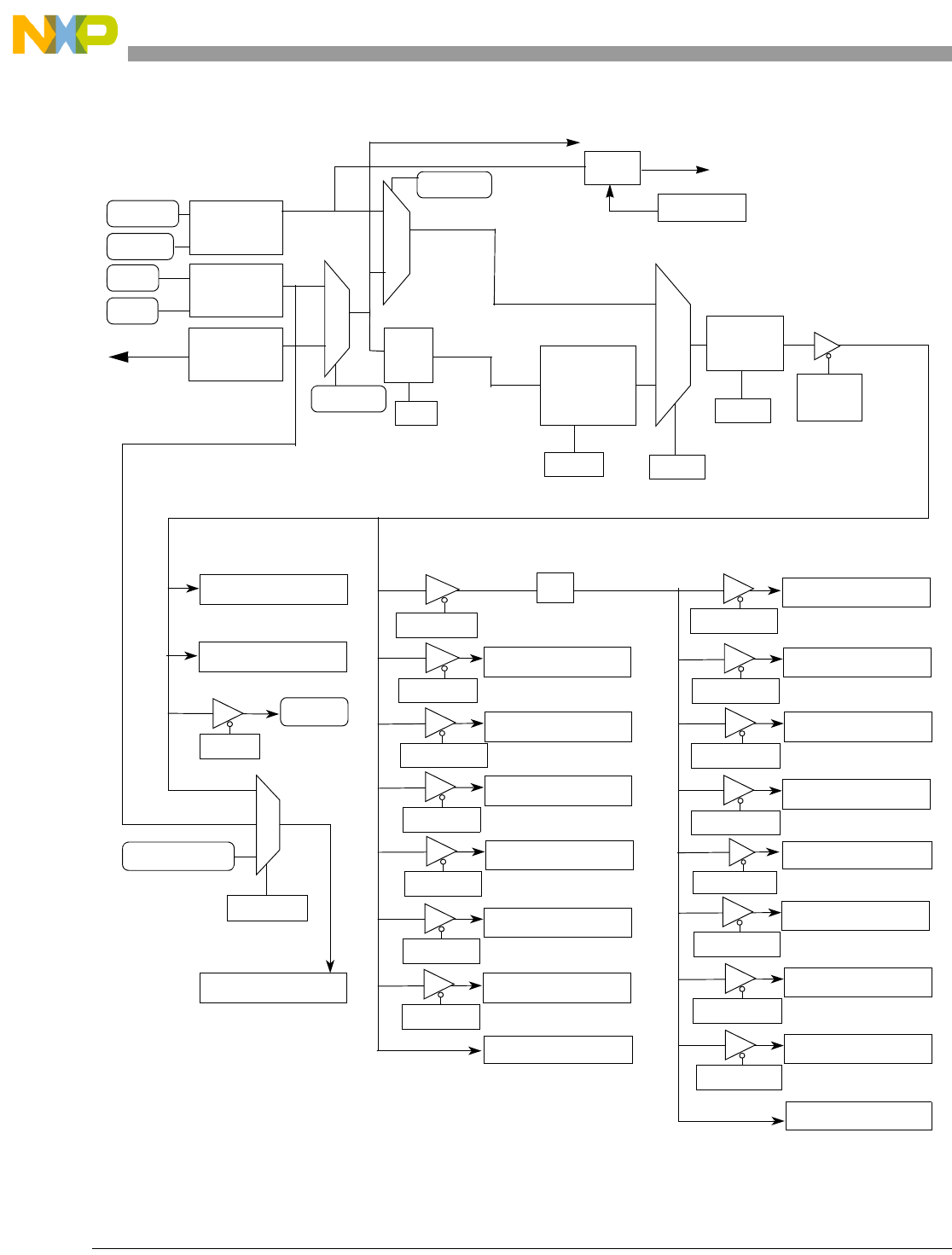
Clock Module
6-4 Freescale Semiconductor
1These clocks are alternate clocks available to their respective modules.
2OSCSEL0 is loaded from CLKMOD0 at reset.
Figure 6-1. Clock Module Block Diagram
PPMRH[11]
CFM
PPMRH[9]
PWM
PPMRH[8]
GPT
PPMRH[7]
ADC
PPMRH[4:3]
PPMRH[1]
Edge Port
PPMRH[0]
GPIO / Ports
CLKOUT
PPMRL[17]
Interrupt Controller
PPMRL[16:13]
DMA Timers
PPMRL[10]
QSPI
PPMRL[9:8]
I2Cs
PPMRL[7:5]
UARTs
PPMRL[4]
DMA
ColdFire V2 Core
BDM
PITs
DISCLK
PPMRL[1]
2
System Clock (fsys)
USB_CTRL
USB
USB_ALT_CLK
See note
below
EXTAL
CLKMOD1 CLKSRC
PLL
Low Power
Divider
LPD[3:0]
Ref Clock
0
1
ADC auto-standby Clk1
STOP
MODE
Pre-
Divider
CCHR
ON-CHIP 8 MHz
OSCILLATOR
0
1
kHz
OSCILLATOR
MHz
OSCILLATOR
XTAL
OSCSEL02
1
0
RTC_EXTAL
RTC_XTAL
RTC_Clk
1
OSCSEL1
PLL Bypass Clock
BWT_Clk
1
RTC
DIV
RTCGOCNT
PPMRH[14]
RTC
BWT
WDOG
MCF52211 ColdFire® Integrated Microcontroller Reference Manual, Rev. 3

Clock Module
Freescale Semiconductor 6-5
6.6 Signal Descriptions
The clock module signals are summarized in Table 6-2 and a brief description follows. For more detailed
information, refer to Chapter 2, “Signal Descriptions.”
6.6.1 EXTAL
This input is driven by an external clock except when used as a connection to the external crystal when
using the internal oscillator.
6.6.2 XTAL
This output is an internal oscillator connection to the external crystal. If CLKMOD0 is driven low during
reset, XTAL is sampled to determine clocking mode.
6.6.3 CLKOUT
This output reflects the internal system clock.
6.6.4 CLKMOD[1:0]
These inputs are used to select the clock mode during chip configuration as described in Table 6-3.
Table 6-2. Signal Properties
Name Function
EXTAL Oscillator or clock input
XTAL Oscillator output
CLKOUT System clock output
CLKMOD[1:0] Clock mode select inputs
RSTO Reset signal from reset controller
Table 6-3. Clocking Modes
CLKMOD[1:0] XTAL Clocking Mode
00 0 PLL disabled, clock driven by external oscillator
00 1 PLL disabled, clock driven by on-chip oscillator
01 N/A PLL disabled, clock driven by external crystal
10 0 PLL in normal mode, clock driven by external oscillator1
10 1 Reserved2
11 N/A PLL in normal mode, clock driven by external crystal1
MCF52211 ColdFire® Integrated Microcontroller Reference Manual, Rev. 3

Clock Module
6-6 Freescale Semiconductor
6.6.5 RSTO
The RSTO pin is asserted by one of the following:
• Internal system reset signal
• FRCRSTOUT bit in the reset control status register (RCR); see Section 11.5.1, “Reset Control
Register (RCR).”
6.7 Memory Map and Registers
The clock module programming model shown in Table 6-4 consists of registers that define clock operation
and status as well as additional peripheral power management registers.
1The PLL pre-divider (CCHR+1) reset value is 6 and the PLL input reference range is 2–10 MHz, so in order
to boot with the PLL enabled, the external clock or crystal frequency needs to be greater than 12 MHz.
MCF5221x devices cannot boot with PLL enabled from an external clock or crystal oscillator with frequency
less than 12 MHz. This constraint does not apply to booting with PLL disabled.
2Cannot boot from the Internal 8MHz Relaxation oscillator with the PLL enabled. See note 1. Thus this mode
has been removed from the table.
Table 6-4. Clock Module Memory Map
IPSBAR
Offset1
1Addresses not assigned to a register and undefined register bits are reserved for expansion.
Register Width
(bits) Access Reset Value Section/Page
Supervisor Mode Access Only
0x12_0000 Synthesizer Control Register (SYNCR) 16 R/W 0x1002 6.7.1.1/6-7
0x12_0002 Synthesizer Status Register (SYNSR) 8 R 0x00 6.7.1.2/6-9
0x12_0004 Relaxation Oscillator Control Register (ROCR) 16 R/W See note2
2The reset value for ROCR is loaded during reset from the flash information row (bits [9:0]). The bits reset to 0b10_0000_0000
during Power-On Reset.
6.7.1.3/6-11
0x12_0007 Low Power Divider Register (LPDR) 8 R/W 0x00 6.7.1.4/6-11
0x12_0008 Clock Control High Register (CCHR) 8 R/W 0x05 6.7.1.5/6-12
0x12_0009 Clock Control Low Register (CCLR) 8 R/W See note3
3CCLR reset state determined during reset configuration.
6.7.1.6/6-12
0x12_000A Oscillator Control High Register (OCHR) 8 R/W See note4
4OCHR reset state determined during reset configuration.
6.7.1.7/6-13
0x12_000B Oscillator Control Low Register (OCLR) 8 R/W See note5
5OCLR reset state determined during reset configuration.
6.7.1.8/6-14
0x12_0012 Real Time Clock Control Register (RTCCR) 8 R/W 0x00 6.7.1.9/6-15
0x12_0013 Backup Watchdog Timer Control Register (BWCR) 8 R/W 0x006
6The contents of BWCR are reset only during Power-On Reset; they are preserved during a warm reset.
6.7.1.10/6-16
0x00_000C Peripheral Power Management Register High (PPMRH)732 R/W 0x00 10.2.1/10-2
0x00_0018 Peripheral Power Management Register Low (PPMRL)732 R/W 0x01 10.2.1/10-2
MCF52211 ColdFire® Integrated Microcontroller Reference Manual, Rev. 3

Clock Module
Freescale Semiconductor 6-7
6.7.1 Register Descriptions
This subsection provides a description of the clock module registers.
6.7.1.1 Synthesizer Control Register (SYNCR)
7See Section 8.2.1, “Peripheral Power Management Registers (PPMRH, PPMRL).”
IPSBAR
Offset: 0x12_0000 (SYNCR)
Access: Supervisor read/write
15 14 13 12 11 10 9 8
RLOLRE MFD2 MFD1 MFD0 LOCRE RFD2 RFD1 RFD0
W
Reset 0 0 0 1 0 0 0 0
76 5 4 3 2 10
RLOCEN DISCLK FWKUP — — CLKSRC1
1The reset value of PLLEN and CLKSRC depend on the value of CLKMOD1 during reset (set to 1 if PLL is
enabled when the device emerges from reset).
PLLMODE PLLEN1
W
Reset 0 0 0 0 0 0 1 0
Figure 6-2. Synthesizer Control Register (SYNCR)
Table 6-5. SYNCR Field Descriptions
Field Description
15
LOLRE
Loss-of-lock reset enable. Determines how the system manages a loss-of-lock indication. When operating
in normal mode, the PLL must be locked before setting the LOLRE bit. Otherwise, reset is immediately
asserted. To prevent an immediate reset, the LOLRE bit must be cleared before writing the MFD[2:0] bits
or entering stop mode with the PLL disabled.
0 No reset on loss of lock
1 Reset on loss of lock
Note: In external clock mode, the LOLRE bit has no effect.
MCF52211 ColdFire® Integrated Microcontroller Reference Manual, Rev. 3
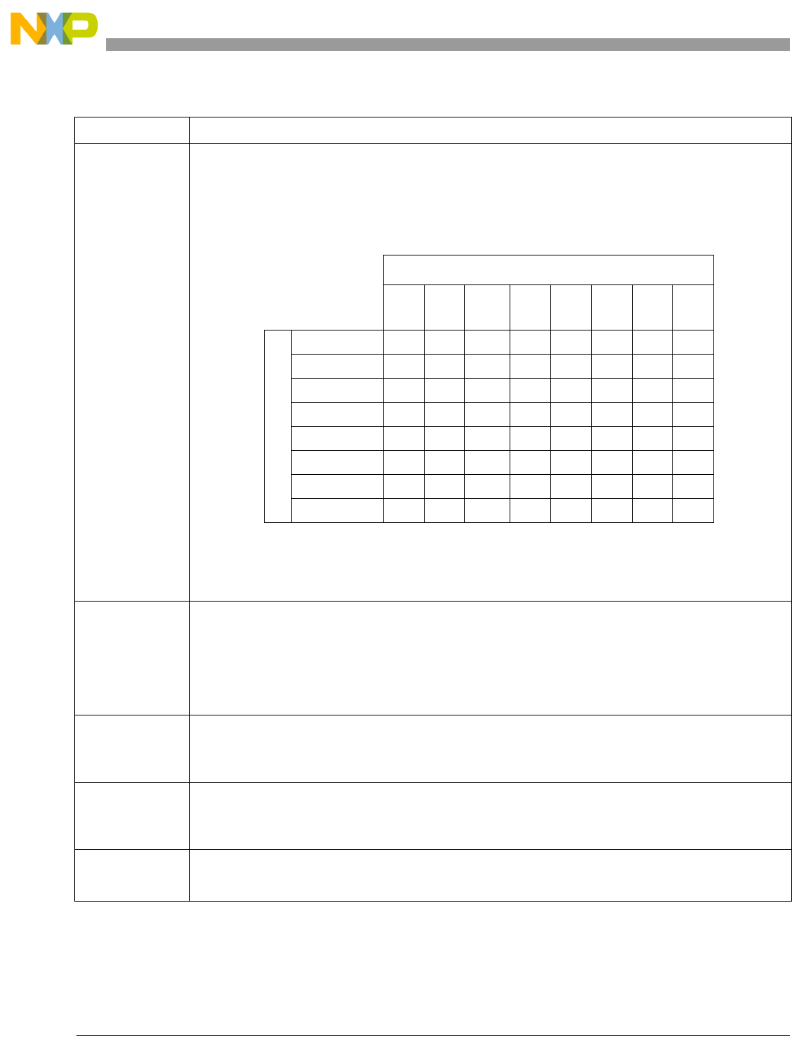
Clock Module
6-8 Freescale Semiconductor
14–12
MFD
Multiplication Factor Divider. Contain the binary value of the divider in the PLL feedback loop. The MFD[2:0]
value is the multiplication factor applied to the reference frequency. When MFD[2:0] are changed or the PLL
is disabled in stop mode, the PLL loses lock.
Note: In external clock mode, the MFD[2:0] bits have no effect.
11
LOCRE
Loss-of-clock reset enable. Determines how the system manages a loss-of-clock condition. When the
LOCEN bit is clear, LOCRE has no effect. If the LOCS flag in SYNSR indicates a loss-of-clock condition,
setting the LOCRE bit causes an immediate reset. To prevent an immediate reset, the LOCRE bit must be
cleared before entering stop mode with the PLL disabled.
0 No reset on loss-of-clock
1 Reset on loss-of-clock
Note: In external clock mode, the LOCRE bit has no effect.
10–8
RFD
Reduced frequency divider field. The binary value written to RFD[2:0] is the PLL frequency divisor; see
table in MFD bit description. Changing RFD[2:0] does not affect the PLL or cause a relock delay. Changes
in clock frequency are synchronized to the next falling edge of the current system clock. To avoid surpassing
the allowable system operating frequency, write to RFD[2:0] only when the LOCK bit is set.
7
LOCEN
Enables the loss-of-clock function. LOCEN does not affect the loss-of-lock function.
0 Loss-of-clock function disabled
1 Loss-of-clock function enabled
Note: In external clock mode, the LOCEN bit has no effect.
6
DISCLK
Disable CLKOUT determines whether CLKOUT is driven. Setting the DISCLK bit holds CLKOUT low.
0 CLKOUT enabled
1 CLKOUT disabled
Table 6-5. SYNCR Field Descriptions (continued)
Field Description
The following table shows the system frequency multiplier of the reference
frequency1 in normal PLL mode.
1fsys = fref 2(MFD + 2) / 2RFD; fref 2(MFD + 2) Max_Spec) MHz, fsys
(Max_Spec) MHz
MFD[2:0]
0002
(4x)
2MFD = 000 not valid for fref < 3 MHz
0013
(6x)
3Default value out of reset
010
(8x)
011
(10x)
100
(12x)
101
(14x)
110
(16x)
111
(18x)
RFD[2:0]
0003 (1) 4 638 1012141618
001 (2) 23 4 56789
010 (4) 1 3/2 2 5/2 3 7/2 4 9/2
011 (8) 1/2 3/4 1 5/4 3/2 7/4 2 9/4
100 (16) 1/4 3/8 1/2 5/8 3/4 7/8 1 9/8
101 (32) 1/8 3/16 1/4 5/16 3/8 7/16 1/2 9/16
110 (64) 1/16 3/32 1/8 5/32 3/16 7/32 1/4 9/32
111 (128) 1/32 3/64 1/16 5/64 3/32 7/64 1/8 9/64
MCF52211 ColdFire® Integrated Microcontroller Reference Manual, Rev. 3

Clock Module
Freescale Semiconductor 6-9
6.7.1.2 Synthesizer Status Register (SYNSR)
The SYNSR is a read-only register that can be read at any time. Writing to the SYNSR has no effect and
terminates the cycle normally.
5
FWKUP
Fast wakeup. Determines when the system clocks are enabled during wakeup from stop mode.
0 System clocks enabled only when PLL is locked or operating normally
1 System clocks enabled on wakeup regardless of PLL lock status
Note: When FWKUP = 0, if the PLL or oscillator is enabled and unintentionally lost in stop mode, the PLL
wakes up in self-clocked mode or reference clock mode depending on the clock that was lost. In
external clock mode, the FWKUP bit has no effect on the wakeup sequence.
4–3
—
Reserved, must be cleared.
2
CLKSRC
Clock Source. Determines whether the PLL output clock or the PLL reference clock is to drive the system
clock. This bit is ignored when the PLL is disabled, in which case the PLL reference clock drives the system
clock. Having this separate bit allows the PLL to first be enabled, and then the system clock can be switched
to the PLL output clock only after the PLL has locked. When disabling the PLL, the clock can be switched
before disabling the PLL so that a smooth transfer is ensured.
0) PLLreference clock (input clock) drives the system clock.
1) PLL output clock drives the system clock (provided the PLL is enabled).
1
PLLMODE
Determines the operating mode of the PLL. This bit should only be changed after reset with the PLL
disabled. For this device, this bit must be set to 1.
0) Reserved, do not use
1) PLL operates in normal mode
0
PLLEN
Enables and disables the PLL. If the PLL is enabled out of reset, the chip does not leave the reset state until
the PLL is locked and the system clock is driven by the PLL output clock. Use the CLKSRC control bit to
switch the system clock between the PLL output clock and PLL bypass clock after the PLL is enabled.
0) PLL is disabled
1) PLL is enabled
IPSBAR
Offset: 0x12_0002 (SYNSR)
Access: Supervisor read/write
76543210
REXTOSC OCOSC CRYOSC LOCKS LOCK LOCS — —
W
Reset: See note 1 See note 2 See note 2 0 0 0
Note: 1. Reset state determined during reset configuration.
2. See the LOCKS and LOCK bit descriptions.
Figure 6-3. Synthesizer Status Register (SYNSR)
Table 6-5. SYNCR Field Descriptions (continued)
Field Description
MCF52211 ColdFire® Integrated Microcontroller Reference Manual, Rev. 3

Clock Module
6-10 Freescale Semiconductor
Table 6-6. SYNSR Field Descriptions
Field Description
7
EXTOSC
Indicates if an external oscillator is providing the reference clock source
0) Reference clock is not external oscillator
1 Reference clock is external oscillator
6
OCOSC
Indicates if the on-chip oscillator is providing the reference clock source.
0 Reference clock is not on-chip oscillator
1 Reference clock is on-chip oscillator
5
CRYOSC
Indicates if an external crystal is providing the reference clock source
0 Reference clock is not external crystal
1 Crystal clock reference
4
LOCKS
Sticky indication of PLL lock status.
0 PLL loss of lock since last system reset or MFD change or currently not locked due to exit from STOP
with FWKUP set
1 No unintentional PLL loss of lock since last system reset or MFD change
The lock detect function sets the LOCKS bit when the PLL achieves lock after:
• A system reset
• A write to SYNCR that changes the MFD[2:0] bits
When the PLL loses lock, LOCKS is cleared. When the PLL relocks, LOCKS remains cleared until one of
the two listed events occurs.
In stop mode, if the PLL is intentionally disabled, then the LOCKS bit reflects the value prior to entering stop
mode. However, if FWKUP is set, then LOCKS is cleared until the PLL regains lock. after lock is regained,
the LOCKS bit reflects the value prior to entering stop mode. Furthermore, reading the LOCKS bit at the
same time that the PLL loses lock does not return the current loss of lock condition.
In external clock mode, LOCKS remains cleared after reset. In normal PLL mode, LOCKS is set after reset.
3
LOCK
Set when the PLL is locked. PLL lock occurs when the synthesized frequency is within approximately 0.75%
of the programmed frequency. The PLL loses lock when a frequency deviation of greater than approximately
1.5% occurs. Reading the LOCK flag at the same time that the PLL loses lock or acquires lock does not
return the current condition of the PLL. The power-on reset circuit uses the LOCK bit as a condition for
releasing reset.
If operating in external clock mode, LOCK remains cleared after reset.
0 PLL not locked
1 PLL locked
2
LOCS
Sticky indication of whether a loss-of-clock condition has occurred at any time since exiting reset in normal
PLL mode.
• LOCS = 0 when the system clocks are operating normally.
• LOCS = 1 when system clocks have failed due to a reference failure or PLL failure.
After entering stop mode with FWKUP set and the PLL and oscillator intentionally disabled
(STPMD[1:0] = 11), the PLL exits stop mode in the SCM while the oscillator starts up. During this time,
LOCS is temporarily set regardless of LOCEN. It is cleared after the oscillator comes up and the PLL is
attempting to lock.
If a read of the LOCS flag and a loss-of-clock condition occur simultaneously, the flag does not reflect the
current loss-of-clock condition.
A loss-of-clock condition can be detected only if LOCEN = 1 or the oscillator has not yet returned from exit
from stop mode with FWKUP = 1.
0 Loss-of-clock not detected since exiting reset
1 Loss-of-clock detected since exiting reset or oscillator not yet recovered from exit from stop mode with
FWKUP = 1
Note: The LOCS flag is always 0 in external clock mode.
1–0 Reserved, must be cleared.
MCF52211 ColdFire® Integrated Microcontroller Reference Manual, Rev. 3

Clock Module
Freescale Semiconductor 6-11
6.7.1.3 Relaxation Oscillator Control Register (ROCR)
The ROCR is used to trim the frequency of the on-chip oscillator. Setting one of the TRIM bits engages
its associated bypass capacitance, which increases or decreases the period of the output frequency. The
largest capacitance, and thus the biggest frequency step (40%), is associated with TRIM9. The lowest
capacitance, and thus the smallest frequency step (0.8%), is associated with TRIM0. The tuning steps are
binary-weighted in terms of signal period, not frequency. The module was designed such that the
approximate middle of the tuning range is 8 MHz.
6.7.1.4 Low-Power Divider Register (LPDR)
The LPDR contains a 4-bit field that divides down the system clock (regardless if the reference clock or
PLL clock is driving the system clock) by a factor of 2n (where n is a number from 0 to 15 represented by
the 4 bit field). The clock change takes effect with the next rising edge of the system clock.
IPSBAR
Offset: 0x12_0004 (ROCR)
Access: Supervisor read/write
15 14 13 12 11 10 9 8
R——————TRIM9TRIM8
W
Reset000000See note
1
1Loaded during reset from the flash information row (bits [9:0]).
See note 1
76543210
R TRIM7 TRIM6 TRIM5 TRIM4 TRIM3 TRIM2 TRIM1 TRIM0
W
Reset See note 1 See note 1 See note 1 See note 1 See note 1 See note 1 See note 1 See note 1
Figure 6-4. Relaxation Oscillator Control Register (ROCR)
Table 6-7. ROCR Field Descriptions
Field Description
15–10
—
Reserved, must be cleared.
9–0
TRIM
10-bit trim value used to trim the frequency of the on-chip oscillator.
IPSBAR
Offset: 0x12_0007 (LPDR)
Access: Supervisor read/write
76543210
R————
LPD3 LPD2 LPD1 LPD0
W
Reset:00000000
Figure 6-5. Low-Power Divider Register (LPDR)
MCF52211 ColdFire® Integrated Microcontroller Reference Manual, Rev. 3

Clock Module
6-12 Freescale Semiconductor
6.7.1.5 Clock Control High Register (CCHR)
The CCHR sets the pre-division factor, which divides down the PLL input clock by 1 (CCHR[2:0] = 000)
to 8 (CCHR[2:0] =111). This allows an external oscillator or crystal of more than 10 MHz to be used with
the PLL. The division factor should be set to generate an input clock for the PLL, refer to the device
datasheet for crystal oscillator frequency range in normal PLL mode. When CCHR[2:0] are changed or
the PLL is disabled in stop mode, the PLL loses lock.
6.7.1.6 Clock Control Low Register (CCLR)
The CCLR selects the clock source for the PLL input/bypass clock. The two possible sources are the
external oscillator (in external crystal or external oscillator mode) and the relaxation oscillator. When
switching clock sources, the module ensures that the changeover does not cause spurious glitches in the
system clock, and that the crystal and the relaxation oscillator remain enabled for the duration of the
changeover.
When switching the clock source to the relaxation oscillator, OCHR[OCOEN] should be set before
OSCSEL is set. Similarly, when switching the clock source to the external oscillator, OCLR[OSCEN]
should be set before OSCSEL is cleared.
Table 6-8. LPDR Field Descriptions
Field Description
7–4 Reserved, must be cleared.
3–0
LPD
Low-Power Divider. This field is used to divide down the system clock by a factor of 2LPD.
IPSBAR
Offset: 0x12_0008 (CCHR)
Access: Supervisor read/write
76543210
R—————
CCHR2 CCHR1 CCHR0
W
Reset:00000101
Figure 6-6. Clock Control High Register (CCHR)
Table 6-9. CCHR Field Descriptions
Field Description
7–3 Reserved, must be cleared.
2–0
CCHR
Clock Control High Register. This field is used to divide down the system clock by a factor of CCHR+1.
MCF52211 ColdFire® Integrated Microcontroller Reference Manual, Rev. 3

Clock Module
Freescale Semiconductor 6-13
6.7.1.7 Oscillator Control High Register (OCHR)
The OCHR is used to enable and configure the relaxation oscillator.
IPSBAR
Offset: 0x12_0009 (CCLR)
Access: Supervisor read/write
76543210
R————— — OSCSEL1 OSCSEL0
W
Reset:0000000See note
1
1The OSCSEL reset state is determined during reset configuration.
Figure 6-7. Clock Control Low Register (CCLR)
Table 6-10. CCLR Field Descriptions
Field Description
7–1 Reserved, must be cleared.
1
OSCSEL1
Oscillator Select 1 bit. This bit works in conjunction with the OSCSEL0 bit to select the clock source for the
PLL input/bypass clock, as shown in Ta b l e 6 - 1 1 .
0 PLL input/bypass clock comes from the external oscillator.
1 PLL input/bypass clock comes from the relaxation oscillator.
Note: When switching clock sources, the module ensures that, during the changeover, no spurious glitches
occur in the system clock, and that the crystal and relaxation oscillators remain enabled.
0
OSCSEL0
Oscillator Select 0 bit. This bit works in conjunction with the OSCSEL1 bit to select the clock source for the
PLL input/bypass clock, as shown in Ta b l e 6 - 1 1 .
0 PLL input/bypass clock comes from the primary oscillator.
1 PLL input/bypass clock comes from the relaxation oscillator.
Note: When switching clock sources, the module ensures that, during the changeover, no spurious glitches
occur in the system clock, and that the crystal and relaxation oscillators remain enabled.
Table 6-11. CCLR[OSCSEL1] and CCLR[OSCSEL0] Settings
OSCSEL1 OSCSEL0 Source of PLL input/bypass clock
0 0 Primary oscillator (default)
0 1 Relaxation oscillator
10
Secondary oscillator
11
MCF52211 ColdFire® Integrated Microcontroller Reference Manual, Rev. 3

Clock Module
6-14 Freescale Semiconductor
6.7.1.8 Oscillator Control Low Register (OCLR)
The OCLR is used to enable and configure the external oscillator.
IPSBAR
Offset: 0x12_000A (OCHR)
Access: Supervisor read/write
76543210
R
OCOEN STBY
——————
W
Reset: See note1
1The OCOEN reset state is determined during reset configuration.
0000000
Figure 6-8. Oscillator Control High Register (OCHR)
Table 6-12. OCHR Field Descriptions
Field Description
7
OCOEN
On-chip Oscillator Enable bit. This bit enables the relaxation oscillator.
0 Relaxation oscillator is disabled.
1 Relaxation oscillator is enabled.
Note: When switching the clock source to the relaxation oscillator, this bit should be set before
CCLR[OSCSEL] is set.
6
STBY
Relaxation oscillator standby. This bit configures the relaxation oscillator for Standby mode with the output
clock running at 400 kHz.
0 Relaxation oscillator is running in normal mode with an output clock of 8 MHz.
1 Relaxation oscillator is running in standby mode with an output clock of 400 kHz.
5–0 Reserved, must be cleared.
IPSBAR
Offset: 0x12_000B (OCLR)
Access: Supervisor read/write
76543210
R
OSCEN REFS LPEN RANGE
————
W
Reset: See note1
1The OSCEN and REFS reset states are determined during reset configuration.
See note 1110000
Figure 6-9. Oscillator Control Low Register (OCLR)
MCF52211 ColdFire® Integrated Microcontroller Reference Manual, Rev. 3

Clock Module
Freescale Semiconductor 6-15
6.7.1.9 Real-Time Clock Control Register (RTCCR)
The RTCCR is used to configure the RTC oscillator.
Table 6-13. OCLR Field Descriptions
Field Description
7
OSCEN
External Oscillator Enable bit. This bit enables the crystal oscillator in external crystal or external oscillator
mode.
0 External oscillator is disabled.
1 External oscillator is enabled.
Note: When switching the clock source to the external oscillator, this bit should be set before
CCLR[OSCSEL] is cleared.
6
REFS
Reference Source bit. This bit configures the external oscillator for operation with an external crystal or
external oscillator.
0 External oscillator is running in external oscillator mode.
1 External oscillator is running in external crystal mode.
5
LPEN
Low-Power Enable bit. This bit configures the external oscillator to run in low-power mode when using an
external crystal.
0 External oscillator runs in normal-power mode.
1 External oscillator runs in low-power mode.
4
RANGE
Range bit. This bit configures the external oscillator to run with different frequency crystals.
0 Support external crystal of 32 kHz.
1 Support external crystal in the range of 1 MHz to 16 MHz.
3–0 Reserved, must be cleared.
IPSBAR
Offset: 0x12_0012 (RTCCR)
Access: Supervisor read/write
76543210
R — — —
OSCEN KHZEN REFS LPEN RTCSEL
W
Reset:00000000
Figure 6-10. Real-Time Clock Control Register (RTCCR)
Table 6-14. RTCCR Field Descriptions
Field Description
7–5 Reserved, must be cleared.
4
OSCEN
RTC Oscillator Enable bit. This bit enables the RTC oscillator.
0 RTC oscillator is disabled.
1 RTC oscillator is enabled.
3
KHZEN
The KHZEN bit selects the operating frequency range of the oscillator
0 Oscillator operates in the kHz range.
1 Oscillator operates in the MHz range.
MCF52211 ColdFire® Integrated Microcontroller Reference Manual, Rev. 3

Clock Module
6-16 Freescale Semiconductor
6.7.1.10 Backup Watchdog Timer Control Register (BWCR)
The BWCR is used to configure the interaction between the clock module and the Backup Watchdog Timer
module (see Chapter 7, “Backup Watchdog Timer (BWT) Module”).
NOTE
The BWCR is a write-once register. The contents of this register are
preserved during a warm reset. This register is reset only by a Power-on
Reset event.
2
REFS
Reference Source bit. This bit configures the RTC oscillator for operation with an external crystal or external
oscillator.
0 RTC oscillator is running in external oscillator mode.
1 RTC oscillator is running in external crystal mode.
1
LPEN
Low-Power Enable bit. This bit configures the RTC oscillator to run in low-power mode when using an
external crystal.
0 RTC oscillator runs in normal-power mode.
1 RTC oscillator runs in low-power mode.
0
RTCSEL
RTC source selection bit. This bit configures the source of the RTC clock.
0 Source is the system clock.
1 Source is the RTC oscillator.
IPSBAR
Offset: 0x12_0013 (BWCR)
Access: Supervisor read/write
76543210
R——————
BWDSTOP BWDSEL
W
Reset1:
1The BWCR is reset to these values only after a Power-On Reset. The register contents are preserved during a warm
reset.
00000000
Figure 6-11. Backup Watchdog Timer Control Register (BWCR)
Table 6-15. BWCR Field Descriptions
Field Description
7–2 Reserved, must be cleared.
Table 6-14. RTCCR Field Descriptions (continued)
Field Description
MCF52211 ColdFire® Integrated Microcontroller Reference Manual, Rev. 3

Clock Module
Freescale Semiconductor 6-17
6.8 Functional Description
This section provides a functional description of the clock module.
6.8.1 System Clock Modes
The system clock source and PLL mode (enabled/disabled) are determined during reset (see Table 11-5).
The values of CLKMOD[1:0] (and XTAL if CLKMOD0 does not equal 1) are latched during reset and are
of no importance after reset is negated. If CLKMOD1 or CLKMOD0 change during a reset other than
power-on reset, the internal clocks may glitch as the system clock source is changed between external
clock mode and PLL clock mode. When CLKMOD1 or CLKMOD0 is changed in reset, an immediate
loss-of-lock condition occurs.
Table 6-16 shows the clock out frequency to clock in frequency relationships for the possible system clock
modes.
The external clock is divided by two internally to produce the system clocks.
6.8.2 Clock Operation During Reset
In external clock mode, the system is static and does not recognize reset until a clock is generated from the
reference clock source selected by the CLKMOD pins (see Section 6.6.4, “CLKMOD[1:0]).
In PLL mode, the PLL operates in self-clocked mode (SCM) during reset until the input reference clock
to the PLL begins operating within the limits given in the electrical specifications.
1
BWDSTOP
This bit determines whether the relaxation oscillator input to the BWT is stopped during Stop mode
operation.
0 The relaxation oscillator input to the BWT is stopped when the device enters Stop mode. When the
device leaves Stop mode, the relaxation oscillator input to the BWT is restored.
1 The relaxation oscillator input continues to be provided to the BWT when the device enters Stop mode.
0
BWDSEL
BWT clock source selection bit. This bit determines the source of the BWT clock.
0 The source for the BWT is half the system frequency, fsys/2.
1 The source for the BWT is the relaxation oscillator. After this value is selected, CCLR[OSCSEL0] can no
longer be set.
Table 6-16. Clock Out and Clock In Relationships
System Clock Mode PLL Options1
1fref = input reference frequency
fsys = CLKOUT frequency
MFD ranges from 0 to 7.
RFD ranges from 0 to 7.
Normal PLL clock mode fsys = fref 2(MFD + 2)/2RFD
External clock mode fsys = fref
Table 6-15. BWCR Field Descriptions (continued)
Field Description
MCF52211 ColdFire® Integrated Microcontroller Reference Manual, Rev. 3

Clock Module
6-18 Freescale Semiconductor
If a PLL failure causes a reset, the system enters reset using the reference clock. Then the system clock
source changes to the PLL operating in SCM. If SCM is not functional, the system becomes static.
Alternately, if SYNCR[LOCEN] is cleared when the PLL fails, the system becomes static. If external reset
is asserted, the system cannot enter reset unless the PLL is capable of operating in SCM.
6.8.3 System Clock Generation
In normal PLL clock mode, the default system frequency is six times the reference frequency after reset.
The RFD[2:0] and MFD[2:0] bits in the SYNCR select the frequency multiplier. The LPD[3:0] field in the
LPDR register provides additional settings for dividing down the system clock (including when the PLL
is disabled) for low-power operation.
When programming the PLL, do not exceed the maximum system clock frequency listed in the electrical
specifications. Use this procedure to accommodate the frequency overshoot that occurs when the MFD bits
are changed:
1. Determine the appropriate value for the MFD and RFD fields in the SYNCR. The amount of jitter
in the system clocks can be minimized by selecting the maximum MFD factor that can be paired
with an RFD factor to provide the required frequency.
2. Write a value of 1 + RFD (from step 1) to the RFD field of the SYNCR.
3. Write the MFD value from step 1 to the SYNCR.
4. Monitor the LOCK flag in SYNSR. When the PLL achieves lock, write the RFD value from step
1 to the RFD field of the SYNCR. This changes the system clocks frequency to the required
frequency.
NOTE
Keep the maximum system clock frequency below the limit given in the
electrical characteristics.
6.8.4 PLL Operation
In PLL mode, the PLL synthesizes the system clocks. The PLL can multiply the reference clock frequency
by 4x to 18x, provided that the system clock frequency remains within the range listed in electrical
specifications. For example, if the reference frequency is 2 MHz, the PLL can synthesize frequencies of
8 MHz to 36 MHz. In addition, the RFD can reduce the system frequency by dividing the output of the
PLL. The RFD is not in the feedback loop of the PLL, so changing the RFD divisor does not affect PLL
operation.
Figure 6-12 shows the external support circuitry for the crystal oscillator with example component values.
Actual component values depend on crystal specifications.
The following subsections describe each major block of the PLL. Refer to Figure 6-12 to see how these
functional sub-blocks interact.
MCF52211 ColdFire® Integrated Microcontroller Reference Manual, Rev. 3
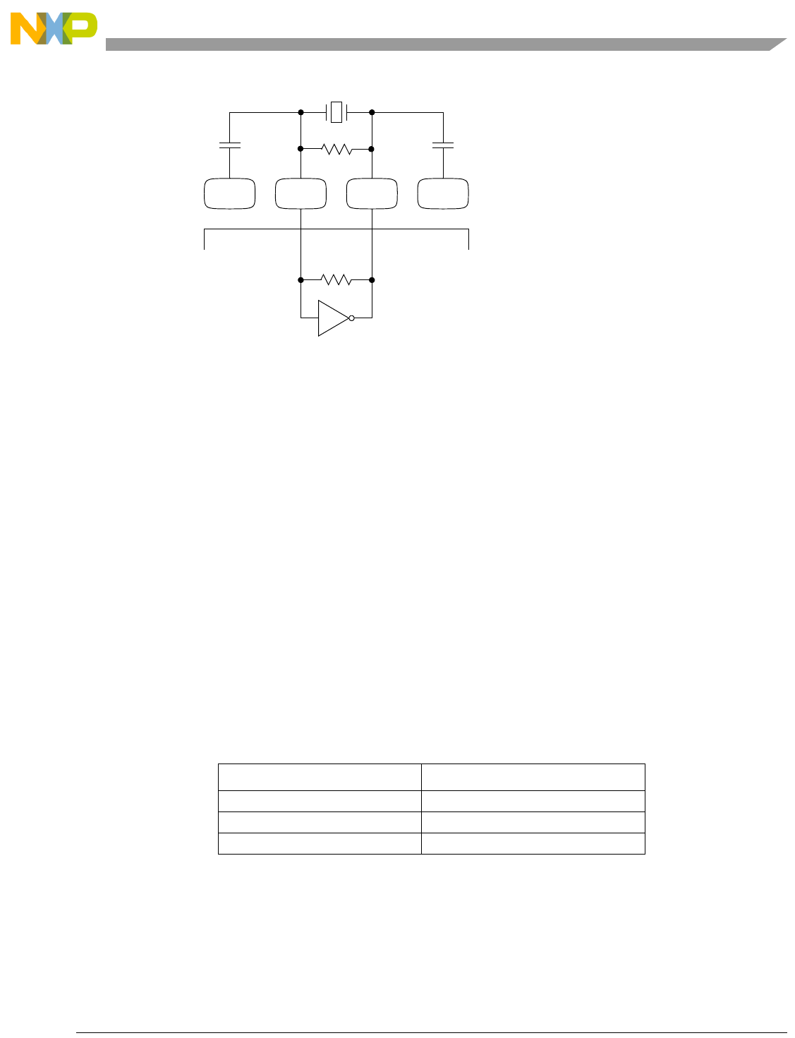
Clock Module
Freescale Semiconductor 6-19
Figure 6-12. Crystal Oscillator Example
6.8.4.1 Phase and Frequency Detector (PFD)
The PFD is a dual-latch phase-frequency detector. It compares the phase and frequency of the reference
and feedback clocks. The reference clock comes from the crystal oscillator or an external clock source.
The feedback clock comes from the following:
• VCO output divided by the MFD in normal PLL mode
When the frequency of the feedback clock equals the frequency of the reference clock, the PLL is
frequency-locked. If the falling edge of the feedback clock lags the falling edge of the reference clock, the
PFD pulses the UP signal. If the falling edge of the feedback clock leads the falling edge of the reference
clock, the PFD pulses the DOWN signal. The width of these pulses relative to the reference clock depends
on how much the two clocks lead or lag each other. After phase lock is achieved, the PFD continues to
pulse the UP and DOWN signals for very short durations during each reference clock cycle. These short
pulses continually update the PLL and prevent the frequency drift phenomenon known as dead-banding.
6.8.4.2 Charge Pump/Loop Filter
In normal mode the current magnitude of the charge pump varies with the MFD as shown in Table 6-17.
The UP and DOWN signals from the PFD control whether the charge pump applies or removes charge,
respectively, from the loop filter. The filter is integrated on the chip.
Table 6-17. Charge Pump Current and MFD in Normal Mode Operation
Charge Pump Current MFD
1x 0MFD < 2
2x 2MFD < 6
4x 6MFD
VSSPLL VSSPLL
EXTAL XTAL
RF
C1 C2
ON-CHIP
CRYSTAL CONFIGURATION
C1 = C2 = 18 pF
RF = 1 M
R1
R1 = 1 M
MCF52211 ColdFire® Integrated Microcontroller Reference Manual, Rev. 3

Clock Module
6-20 Freescale Semiconductor
6.8.4.3 Voltage Control Output (VCO)
The voltage across the loop filter controls the frequency of the VCO output. The frequency-to-voltage
relationship (VCO gain) is positive, and the output frequency is four times the target system frequency.
6.8.4.4 Multiplication Factor Divider (MFD)
The MFD divides the output of the VCO and feeds it back to the PFD. The PFD controls the VCO
frequency via the charge pump and loop filter such that the reference and feedback clocks have the same
frequency and phase. Thus, the frequency of the input to the MFD, which is also the output of the VCO,
is the reference frequency multiplied by the same amount that the MFD divides by. For example, if the
MFD divides the VCO frequency by six, the PLL is frequency locked when the VCO frequency is six times
the reference frequency. The presence of the MFD in the loop allows the PLL to perform frequency
multiplication, or synthesis.
6.8.4.5 PLL Lock Detection
The lock detect logic monitors the reference frequency and the PLL feedback frequency to determine when
frequency lock is achieved. Phase lock is inferred by the frequency relationship, but is not guaranteed. The
LOCK flag in the SYNSR reflects the PLL lock status. A sticky lock flag, LOCKS, is also provided.
The lock detect function uses two counters: one is clocked by the reference, and the other is clocked by
the PLL feedback. When the reference counter has counted N cycles, its count is compared to that of the
feedback counter. If the feedback counter has also counted N cycles, the process is repeated for N + K
counts. Then, if the two counters continue to match, the lock criteria is relaxed by 1/2 and the system is
notified that the PLL has achieved frequency lock.
After lock is detected, the lock circuit continues to monitor the reference and feedback frequencies using
the alternate count and compare process. If the counters do not match at any comparison time, then the
LOCK flag is cleared to indicate that the PLL has lost lock. At this point, the lock criteria is tightened and
the lock detect process is repeated.
The alternate count sequences prevent false lock detects due to frequency aliasing while the PLL tries to
lock. Alternating between tight and relaxed lock criteria prevents the lock detect function from randomly
toggling between locked and non-locked status due to phase sensitivities. Figure 6-13 shows the sequence
for detecting locked and non-locked conditions.
In external clock mode, the PLL is disabled and cannot lock.
MCF52211 ColdFire® Integrated Microcontroller Reference Manual, Rev. 3

Clock Module
Freescale Semiconductor 6-21
Figure 6-13. Lock Detect Sequence
6.8.4.6 PLL Loss of Lock Conditions
After the PLL acquires lock after reset, the LOCK and LOCKS flags are set. If the MFD is changed, or if
an unexpected loss of lock condition occurs, the LOCK and LOCKS flags are negated. While the PLL is
in the non-locked condition, the system clocks continue to be sourced from the PLL as the PLL attempts
to relock. Consequently, during the relocking process, the system clocks frequency is not well defined and
may exceed the maximum system frequency, violating the system clock timing specifications.
However, after the PLL has relocked, the LOCK flag is set. The LOCKS flag remains cleared if the loss
of lock was unexpected. The LOCKS flag is set when the loss of lock is caused by changing MFD. If the
PLL is intentionally disabled during stop mode, then after exit from stop mode, the LOCKS flag reflects
the value prior to entering stop mode after lock is regained.
6.8.4.7 PLL Loss of Lock Reset
If the LOLRE bit in the SYNCR is set, a loss of lock condition asserts reset. Reset reinitializes the LOCK
and LOCKS flags. Therefore, software must read the LOL bit in the reset status register (RSR) to
determine if a loss of lock caused the reset. See Section 11.5.2, “Reset Status Register (RSR).”
To exit reset in PLL mode, the reference must be present, and the PLL must achieve lock.
In external clock mode, the PLL cannot lock. Therefore, a loss of lock condition cannot occur, and the
LOLRE bit has no effect.
Count N
Reference Cycles
and Compare
Number of Feedback
Cycles Elapsed
Start
with Tight Lock
Criteria Feedback Count
Loss of Lock Detected
Set Tight Lock Criteria
and Notify System of Loss
of Lock Condition
Count N + K
Reference Cycles
and Compare Number
of Feedback Cycles
Elapsed
Lock Detected.
Set Relaxed Lock
Condition and Notify
System of Lock
Condition
Reference Count
Reference Count =
Feedback Count = N
In Same Count/Compare Sequence
Reference Count = Feedback Count = N + K
In Same Count/Compare Sequence
Reference Count
Feedback Count
MCF52211 ColdFire® Integrated Microcontroller Reference Manual, Rev. 3

Clock Module
6-22 Freescale Semiconductor
6.8.4.8 Loss of Clock Detection
The LOCEN bit in the SYNCR enables the loss of clock detection circuit to monitor the input clocks to
the phase and frequency detector (PFD). When the reference or feedback clock frequency falls below the
minimum frequency, the loss of clock circuit sets the sticky LOCS flag in the SYNSR.
NOTE
In external clock mode, the loss of clock circuit is disabled.
6.8.4.9 Loss of Clock Reset
The clock module can assert a reset when a loss of clock or loss of lock occurs. When a loss-of-clock
condition is recognized, reset is asserted if the LOCRE bit in SYNCR is set. The LOCS bit in SYNSR is
cleared after reset. Therefore, the LOC bit must be read in RSR to determine that a loss of clock condition
occurred. LOCRE has no effect in external clock mode.
To exit reset in PLL mode, the reference must be present, and the PLL must acquire lock.
Reset initializes the clock module registers to a known startup state as described in Section 6.7, “Memory
Map and Registers.”
6.8.4.10 Alternate Clock Selection
Depending on which clock source fails, the loss-of-clock circuit switches the system clocks source to the
remaining operational clock. The alternate clock source generates the system clocks until reset is asserted.
As Table 6-18 shows, if the reference fails, the PLL goes out of lock and into self-clocked mode (SCM).
The PLL remains in SCM until the next reset. When the PLL is operating in SCM, the system frequency
depends on the value in the RFD field. The SCM system frequency stated in electrical specifications
assumes that the RFD has been programmed to binary 000. If the loss-of-clock condition is due to PLL
failure, the PLL reference becomes the system clocks source until the next reset, even if the PLL regains
and relocks.
A special loss-of-clock condition occurs when the reference and the PLL fail. The failures may be
simultaneous, or the PLL may fail first. In either case, the reference clock failure takes priority and the
PLL attempts to operate in SCM. If successful, the PLL remains in SCM until the next reset. If the PLL
cannot operate in SCM, the system remains static until the next reset. The reference and the PLL must be
functioning properly to exit reset.
Table 6-18. Loss of Clock Summary
Clock
Mode
System Clock Source
Before Failure
Reference Failure Alternate Clock
Selected by LOC Circuit1 Until Reset
1The LOC circuit monitors the reference and feedback inputs to the PFD. See Figure 6-12.
PLL Failure Alternate Clock
Selected by LOC Circuit Until Reset
PLL PLL PLL self-clocked mode PLL reference
External External clock None NA
MCF52211 ColdFire® Integrated Microcontroller Reference Manual, Rev. 3

Clock Module
Freescale Semiconductor 6-23
6.8.4.11 Loss of Clock in Stop Mode
Table 6-19 shows the resulting actions for a loss of clock in stop mode when the device is being clocked
by the various clocking methods.
Table 6-19. Stop Mode Operation
MODE
In
LOCEN
LOCRE
LOLRE
PLL
OSC
FWKUP
Expected
PLL
Action at
Stop
PLL Action
During Stop
MODE
Out
LOCKSS
LOCK
LOCS
Comments
EXT X X X X X X — — EXT 0 0 0
Lose reference
clock
Stuck — — —
NRM 0 0 0 Off Off 0 Lose lock,
f.b. clock,
reference
clock
Regain NRM ‘LK 1 ‘LC
No regain Stuck — — —
NRM X 0 0 Off Off 1 Lose lock,
f.b. clock,
reference
clock
Regain clocks, but
don’t regain lock
SCM–>
unstable
NRM
0–>‘LK 0–>1 1–>‘LC Block LOCS and
LOCKS until
clock and lock
respectively
regain; enter
SCM regardless
of LOCEN bit
until reference
regained
No reference
clock regain
SCM–> 0–> 0–> 1–> Block LOCS and
LOCKS until
clock and lock
respectively
regain; enter
SCM regardless
of LOCEN bit
No f.b. clock
regain
Stuck — — —
NRM 0 0 0 Off On 0 Lose lock Regain NRM ‘LK 1 ‘LC Block LOCKS
from being
cleared
Lose reference
clock or no lock
regain
Stuck — — —
Lose reference
clock,
regain
NRM ‘LK 1 ‘LC Block LOCKS
from being
cleared
MCF52211 ColdFire® Integrated Microcontroller Reference Manual, Rev. 3

Clock Module
6-24 Freescale Semiconductor
NRM 0 0 0 Off On 1 Lose lock No lock regain Unstable
NRM
0–>‘LK 0–>1 ‘LC Block LOCKS
until lock
regained
Lose reference
clock or no f.b.
clock regain
Stuck — — —
Lose reference
clock, regain
Unstable
NRM
0–>‘LK 0–>1 ‘LC LOCS not set
because
LOCEN = 0
NRM 0 0 0 On On 0 — — NRM ‘LK 1 ‘LC
Lose lock or clock Stuck — — —
Lose lock, regain NRM 0 1 ‘LC
Lose clock and
lock, regain
NRM 0 1 ‘LC LOCS not set
because
LOCEN = 0
NRM 0 0 0 On On 1 — — NRM ‘LK 1 ‘LC
Lose lock Unstable
NRM
00–>1‘LC
Lose lock, regain NRM 0 1 ‘LC
Lose clock Stuck — — —
Lose clock, regain
without lock
Unstable
NRM
00–>1‘LC
Lose clock, regain
with lock
NRM 0 1 ‘LC
NRM X X 1 Off X X Lose lock,
f.b. clock,
reference
clock
RESET RESET — — — Reset
immediately
NRM 0 0 1 On On X — — NRM ‘LK 1 ‘LC
Lose lock or clock RESET — — — Reset
immediately
NRM 1 0 0 Off Off 0 Lose lock,
f.b. clock,
reference
clock
Regain NRM ‘LK 1 ‘LC REF not entered
during stop;
SCM entered
during stop only
during oscillator
startup
No regain Stuck — — —
Table 6-19. Stop Mode Operation (continued)
MODE
In
LOCEN
LOCRE
LOLRE
PLL
OSC
FWKUP
Expected
PLL
Action at
Stop
PLL Action
During Stop
MODE
Out
LOCKSS
LOCK
LOCS
Comments
MCF52211 ColdFire® Integrated Microcontroller Reference Manual, Rev. 3

Clock Module
Freescale Semiconductor 6-25
NRM 1 0 0 Off On 0 Lose lock,
f.b. clock
Regain NRM ‘LK 1 ‘LC REF mode not
entered during
stop
No f.b. clock or
lock regain
Stuck — — —
Lose reference
clock
SCM 0 0 1 Wakeup without
lock
NRM 1 0 0 Off On 1 Lose lock,
f.b. clock
Regain f.b. clock Unstable
NRM
0–>‘LK 0–>1 ‘LC REF mode not
entered during
stop
No f.b. clock
regain
Stuck — — —
Lose reference
clock
SCM 0 0 1 Wakeup without
lock
NRM 1 0 0 On On 0 — — NRM ‘LK 1 ‘LC
Lose reference
clock
SCM 0 0 1 Wakeup without
lock
Lose f.b. clock REF 0 X 1 Wakeup without
lock
Lose lock Stuck — — —
Lose lock, regain NRM 0 1 ‘LC
NRM 1 0 0 On On 1 — — NRM ‘LK 1 ‘LC
Lose reference
clock
SCM 0 0 1 Wakeup without
lock
Lose f.b. clock REF 0 X 1 Wakeup without
lock
Lose lock Unstable
NRM
00–>1‘LC
NRM 1 0 1 On On X — — NRM ‘LK 1 ‘LC
Lose lock or clock RESET — — — Reset
immediately
NRM 1 1 X Off X X Lose lock,
f.b. clock,
reference
clock
RESET RESET — — — Reset
immediately
Table 6-19. Stop Mode Operation (continued)
MODE
In
LOCEN
LOCRE
LOLRE
PLL
OSC
FWKUP
Expected
PLL
Action at
Stop
PLL Action
During Stop
MODE
Out
LOCKSS
LOCK
LOCS
Comments
MCF52211 ColdFire® Integrated Microcontroller Reference Manual, Rev. 3

Clock Module
6-26 Freescale Semiconductor
NRM 1 1 0 On On 0 — — NRM ‘LK 1 ‘LC
Lose clock RESET — — — Reset
immediately
Lose lock Stuck — — —
Lose lock, regain NRM 0 1 ‘LC
NRM 1 1 0 On On 1 — — NRM ‘LK 1 ‘LC
Lose clock RESET — — — Reset
immediately
Lose lock Unstable
NRM
00–>1‘LC
Lose lock, regain NRM 0 1 ‘LC
NRM 1 1 1 On On X — — NRM ‘LK 1 ‘LC
Lose clock or lock RESET — — — Reset
immediately
REF 1 0 0 X X X — — REF 0 X 1
Lose reference
clock
Stuck — — —
SCM 100OffX0PLL
disabled
Regain SCM SCM 0 0 1 Wakeup without
lock
SCM 100OffX1PLL
disabled
Regain SCM SCM 0 0 1
SCM 1 0 0 On On 0 — — SCM 0 0 1 Wakeup without
lock
Lose reference
clock
SCM
Table 6-19. Stop Mode Operation (continued)
MODE
In
LOCEN
LOCRE
LOLRE
PLL
OSC
FWKUP
Expected
PLL
Action at
Stop
PLL Action
During Stop
MODE
Out
LOCKSS
LOCK
LOCS
Comments
MCF52211 ColdFire® Integrated Microcontroller Reference Manual, Rev. 3

Clock Module
Freescale Semiconductor 6-27
SCM 1 0 0 On On 1 — — SCM 0 0 1
Lose reference
clock
SCM
Note:
PLL = PLL enabled during STOP mode. PLL = On when STPMD[1:0] = 00 or 01
OSC = oscillator enabled during STOP mode. Oscillator is on when STPMD[1:0] = 00, 01, or 10
MODES
NRM = normal PLL crystal clock reference or normal PLL external reference mode. During normal external reference mode,
the oscillator is never enabled. Therefore, during these modes, refer to the OSC = On case regardless of STPMD values.
EXT = external clock mode
REF = PLL reference mode due to losing PLL clock or lock from NRM mode
SCM = PLL self-clocked mode due to losing reference clock from NRM mode
RESET = immediate reset
LOCKS
‘LK -= expecting previous value of LOCKS before entering stop
0–>‘LK = current value is 0 until lock is regained which then is the previous value before entering stop
0–> = current value is 0 until lock is regained but lock is never expected to regain
LOCS
‘LC = expecting previous value of LOCS before entering stop
1–>‘LC = current value is 1 until clock is regained which then is the previous value before entering stop
1–> = current value is 1 until clock is regained but CLK is never expected to regain
Table 6-19. Stop Mode Operation (continued)
MODE
In
LOCEN
LOCRE
LOLRE
PLL
OSC
FWKUP
Expected
PLL
Action at
Stop
PLL Action
During Stop
MODE
Out
LOCKSS
LOCK
LOCS
Comments
MCF52211 ColdFire® Integrated Microcontroller Reference Manual, Rev. 3
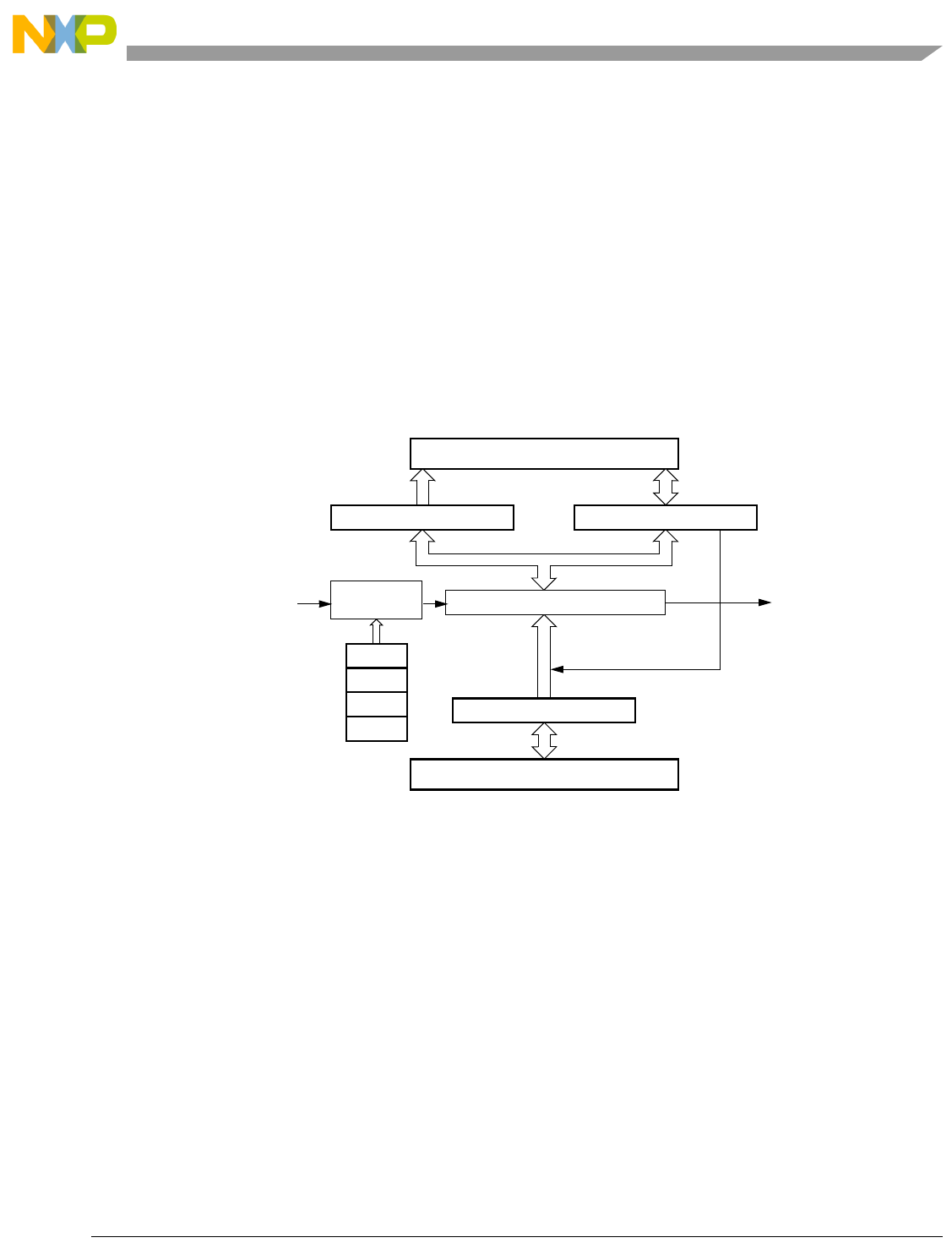
Freescale Semiconductor 7-1
Chapter 7
Backup Watchdog Timer (BWT) Module
7.1 Introduction
The Backup Watchdog Timer (BWT) module is used to help software recover from runaway code. This
section presents the modes of operation, register information, and functional description of the BWT. A
block diagram of the BWT is shown in Figure 7-1.
Figure 7-1. Backup Watchdog Timer Block Diagram
7.1.1 Overview
The BWT is a 16-bit timer that is useful in helping software to recover from runaway code. It incorporates
a free-running up-counter that generates a warm reset on underflow. To prevent a reset, software must
periodically restart the countdown by writing a special set of values to a register in the BWT. This periodic
writing process is referred to as servicing the BWT.
The clock source for the BWT can come from the relaxation oscillator or the system clock (see
Section 6.7.1.10, “Backup Watchdog Timer Control Register (BWCR)”).
7.1.2 Modes of Operation
This section describes the operation of the BWT in low-power modes of operation. These modes are
described in Chapter 10, “Power Management”.
16-bit WMR
16-bit Watchdog Counter
Count = 0
BWT Divide by Reset
Clock
IPBUS
4096
16-bit WCNTR 16-bit WSR
IPBUS
Load Counter
EN
WAIT
DOZE
HALTED
Source
MCF52211 ColdFire® Integrated Microcontroller Reference Manual, Rev. 3

Backup Watchdog Timer (BWT) Module
7-2 Freescale Semiconductor
7.1.2.1 Wait Mode
The functionality of the BWT in Wait mode depends on the value of WCR[WAIT].
When WCR[WAIT]=1, the BWT stops when the device enters Wait mode. When the device leaves Wait
mode, the BWT resumes from the state it was in when it stopped.
When WCR[WAIT]=0, the BWT continues to operate normally when the device enters Wait mode.
7.1.2.2 Doze Mode
The functionality of the BWT in Doze mode depends on the value of WCR[DOZE].
When WCR[DOZE]=1, the BWT stops when the device enters Doze mode. When the device leaves Doze
mode, the BWT resumes from the state it was in when it stopped.
When WCR[DOZE]=0, the BWT continues to operate normally when the device enters Doze mode.
7.1.2.3 Stop Mode
The functionality of the BWT in Stop mode depends on the value of WCR[STOP].
When WCR[STOP]=1, the BWT stops when the device enters Stop mode. When the device leaves Stop
mode, the BWT resumes from the state it was in when it stopped.
When WCR[STOP]=0, the BWT continues to operate normally when the device enters Stop mode.
7.2 Memory Map and Register Definition
The backup watchdog timer programming model includes registers in the BWT and clock modules. The
registers used to configure the BWT are read-always/write once, and their contents are preserved during a
warm reset. Only a Power-On Reset resets these registers to their default values.
7.2.1 Memory Map
Table 7-1. BWT Memory Map
IPSBAR
Offset1
1Addresses not assigned to a register and undefined register bits are reserved for expansion.
Register Width
(bits) Access Reset Value Section/Page
0x14_0000 Backup Watchdog Timer Control Register (WCR) 8 R/W2
2WCR and WMR are read-always/write-once, and cannot be changed until the next Power-On Reset event.
0x02 7.2.2.1/7-3
0x14_0002 Backup Watchdog Timer Modulus Register (WMR) 16 R/W20xFFFF 7.2.2.2/7-4
0x14_0004 Backup Watchdog Timer Count Register (WCNTR) 16 R 0xFFFF 7.2.2.3/7-4
0x14_0006 Backup Watchdog Timer Service Register (WSR) 16 R/W 0x00 7.2.2.4/7-5
0x12_0013 Clock Module Backup Watchdog Timer Control Register
(BWCR)3
3This read-always/write-once register is part of the Clock Module; see Section 6.7.1.10, “Backup Watchdog Timer Control
Register (BWCR),” for a detailed description.
8R/W
30x02 6.7.1.10/6-16
MCF52211 ColdFire® Integrated Microcontroller Reference Manual, Rev. 3

Backup Watchdog Timer (BWT) Module
Freescale Semiconductor 7-3
7.2.2 Register Descriptions
7.2.2.1 Backup Watchdog Timer Control Register (WCR)
The WCR, shown in Figure 7-2, configures the operation of the BWT. It is a read-always/write-once
register; after the register is written, the contents cannot be changed until the next Power-On Reset event
occurs.
This register must be written as a whole.
NOTE
To ensure that the BWT is properly enabled, the software must write a value
to the WMR (see Section 7.2.2.2, “Backup Watchdog Timer Modulus
Register (WMR)”) prior to writing to the WCR.
IPSBAR
Offset: 0x14_0000 (WCR)
Access: Supervisor read/write
1514131211109876543210
R00000000000
STOP WAIT DOZE 1EN
W
Reset1
1After Power-On Reset; the register contents are preserved during warm resets.
0000000000000010
Figure 7-2. Backup Watchdog Timer Control Register (WCR)
Table 7-2. WCR Field Descriptions
Field Description
15–5 Reserved, should read 0. Writes have no effect and terminate without transfer error exception.
4
STOP
Stop Mode bit. This read-always/write-once bit controls the function of the BWT in Stop mode.
0 BWT continues to operate when the device enters Stop mode as long as the BWT is provided with a clock.
1 BWT stops when the device enters Stop mode.
3
WAIT
Wait Mode bit. This read-always/write-once bit controls the function of the BWT in Wait mode.
0 BWT continues to operate when the device enters Wait mode.
1 BWT stops when the device enters Wait mode.
2
DOZE
Doze Mode bit. This read-always/write-once bit controls the function of the BWT in Doze mode.
0 BWT continues to operate when the device enters Doze mode.
1 BWT stops when the device enters Doze mode.
1 Reserved, should read 1.
0
EN
BWT Enable bit. This read-always/write-once bit enables the BWT.
0 BWT is disabled.
1 BWT is enabled.
MCF52211 ColdFire® Integrated Microcontroller Reference Manual, Rev. 3

Backup Watchdog Timer (BWT) Module
7-4 Freescale Semiconductor
7.2.2.2 Backup Watchdog Timer Modulus Register (WMR)
The WMR, shown in Figure 7-3, contains the value (modulus) that is loaded into the BWT count register
(WCNTR) when the BWT is serviced. This value effectively corresponds to the BWT’s timeout period.
The software must service the timer within this period to avoid a reset. The timeout period is a function of
the WMR, the period of the BWT’s input clock, and the device operating mode, as shown in the equation
in Table 7-3.
The WMR is a read-always/write-once register; after the register is written, the contents cannot be changed
until the next Power-On Reset event occurs.
NOTE
To ensure that the BWT is properly enabled, the software must write a value
to the WMR prior to writing to the WCR.
7.2.2.3 Backup Watchdog Timer Count Register (WCNTR)
The WCNTR, shown in Figure 7-4, reflects the current value in the BWT counter. This counter is reset to
the value in WMR when the BWT is serviced.
WCNTR should be read as a whole; reading it with two 8-bit reads may not return the correct value.
Writing to WCNTR has no effect and results in a normal write cycle termination.
IPSBAR
Offset: 0x14_0002 (WMR)
Access: Supervisor read/write
1514131211109876543210
RWM
W
Reset1
1After Power-On Reset; the register contents are preserved during warm resets.
1111111111111111
Figure 7-3. Backup Watchdog Timer Modulus Register (WMR)
Table 7-3. WMR Field Descriptions
Field Description
15–0
WM
BWT modulus. This value is loaded into the BWT count register (WCNTR) when the BWT is serviced. It thus
corresponds to the BWT’s timeout period. The actual timeout period is given by the following equations:
Device in Stop/Wait/Doze mode:
Device not in Stop/Wait/Doze mode:
where T is the timeout period and is the period of the BWT’s input clock.
TWM1+4096 16+=
TWM1+4096 4+=
MCF52211 ColdFire® Integrated Microcontroller Reference Manual, Rev. 3

Backup Watchdog Timer (BWT) Module
Freescale Semiconductor 7-5
7.2.2.4 Backup Watchdog Timer Service Register (WSR)
The WSR is shown in Figure 7-5, and is used to instruct the BWT to reset its internal counter to the value
in WMR[WM]. This is known as servicing the BWT. To do so, the software must write the two values
0x5555 and 0xAAAA, in that order, to WSR. These two write operations must be completed before the
BWT timeout period is reached (i.e., WCNTR[WC] reaches zero). If these operations are not completed
before the end of the timeout period, the BWT asserts a system reset.
The software can execute other instructions between the two write instructions required to service the
BWT (0x5555 and 0xAAAA). All instructions, however, must be completed before the timeout period is
reached to prevent a reset.
Writing any values other than 0x5555 or 0xAAAA to the WSR resets the servicing sequence. The software
must then begin the sequence again (writing 0x5555 and 0xAAAA to WSR) to service the BWT.
This register must be written as a whole.
IPSBAR
Offset: 0x14_0004 (WCNTR)
Access: Supervisor read/write
1514131211109876543210
RWC
W
Reset1111111111111111
Figure 7-4. Backup Watchdog Timer Count Register (WCNTR)
Table 7-4. WCNTR Field Descriptions
Field Description
15–0
WC
BWT counter. This field reflects the current value in the BWT counter.
IPSBAR
Offset: 0x14_0006 (WSR)
Access: Supervisor read/write
1514131211109876543210
RWS
W
Reset0000000000000000
Figure 7-5. Backup Watchdog Timer Service Register (WSR)
Table 7-5. WSR Field Descriptions
Field Description
15–0
WS
BWT service field. To service the BWT, the software must write the values 0x5555 and 0xAAAA, in that order, to this
field before the BWT timeout period is reached.
MCF52211 ColdFire® Integrated Microcontroller Reference Manual, Rev. 3

Backup Watchdog Timer (BWT) Module
7-6 Freescale Semiconductor
7.3 Functional Description
When the BWT is properly enabled, it loads the value in WMR[WM] into WCNTR[WC] and begins to
decrement WCNTR[WC]. If WCNTR[WC] reaches zero, the BWT asserts a system reset. To prevent this
reset, the BWT requires the software to write 0x5555 and 0xAAAA, in that order, to the WSR. This
procedure, referred to as servicing the BWT, reinitializes the value of WCNTR[WC] to the value in
WMR[WM]. This logic helps guard against runaway code.
The following procedure summarizes how to enable and service the BWT properly.
1. Select the desired clock source for the BWT from within the clock module (see Chapter 6, “Clock
Module”).
2. Write to the BWCR (see Section 6.7.1.10, “Backup Watchdog Timer Control Register (BWCR)”)
with the proper values for the chosen clock source.
3. Determine the desired timeout period for the BWT, and write it to the WMR. This step is
recommended even if the default values are acceptable, to lock the register against accidental
writes by runaway code.
4. Write to the WCR with WCR[EN]=1 and the WAIT, DOZE, and STOP bits configured as desired.
5. To prevent a reset, service the BWT by writing 0x5555 and 0xAAAA, in that order, to the WSR
before the timeout period is reached.
MCF52211 ColdFire® Integrated Microcontroller Reference Manual, Rev. 3

Freescale Semiconductor 8-1
Chapter 8
Power Management
8.1 Introduction
This chapter explains the low-power operation of the MCF52211.
8.1.1 Features
The following features support low-power operation.
• Four modes of operation: run, wait, doze, and stop
• Ability to shut down most peripherals independently
• Ability to shut down the external CLKOUT pin
8.2 Memory Map/Register Definition
The power management programming model consists of registers from the SCM and CCM memory space,
as shown in Table 8-1.
Table 8-1. Power Management Memory Map
IPSBAR
Offset1
1Addresses not assigned to a register and undefined register bits are reserved for expansion.
Register Width
(bits) Access Reset Value Section/Page
0x11_0004 Chip Configuration Register (CCR)2
2The CCR is described in the Chip Configuration Module. It is shown here only to warn against accidental writes to this register
when accessing the LPCR.
16 R 0x1 9.3.3.1/9-3
0x11_0007 Low-Power Control Register (LPCR) 8 R/W 0x2 8.2.5/8-8
0x00_000C Peripheral Power Management Register High (PPMRH) 32 R/W 0x0 8.2.1/8-2
0x00_0010 Core Reset Status Register (CRSR)3
3The CRSR, CWCR, and CWSR are described in the System Control Module. They are shown here only to warn against
accidental writes to these registers when accessing the LPICR.
8R/W 12.5.3/12-6
0x00_0011 Core Watchdog Control Register (CWCR)38R/W 0x0 12.5.4/12-7
0x00_0012 Low-Power Interrupt Control Register (LPICR) 8 R/W 0x0 8.2.2/8-5
0x00_0013 Core Watchdog Service Register (CWSR)38R/W 12.5.5/12-8
0x00_0018 Peripheral Power Management Register Low (PPMRL) 32 R/W 0x8 8.2.1.1/8-4
0x00_0021 Peripheral Power Management Set Register (PPMRS) 8 W 0x0 8.2.3/8-7
0x00_0022 Peripheral Power Management Clear Register (PPMRC) 32 R/W 0x0 8.2.4/8-7
MCF52211 ColdFire® Integrated Microcontroller Reference Manual, Rev. 3

Power Management
8-2 Freescale Semiconductor
8.2.1 Peripheral Power Management Registers (PPMRH, PPMRL)
The PPMRH and PPMRL registers provide a bit map for controlling the generation of the module clocks
for each decoded address space associated with the IPS controller. The PPMRx provides a unique control
bit for each of these address spaces that defines whether the module clock for the given space is enabled
or disabled.
NOTE
It is software’s responsibility to appropriately disable module clocks using
the PPMRx only when a module is completely unused or quiescent.
Because the operation of the IPS controller and the system control module (SCM) are fundamental to the
operation of the system, the clocks for these three modules cannot be disabled.
The individual bits of the PPMRx can be modified using a read-modify-write to this register directly or
indirectly through writes to the PPMRS and PPMRC registers to set/clear individual bits.
See Figure 8-1 and Table 8-2 for the PPMRH definition.
IPSBAR
Offset: 0x000C (PPMRH)
Access: read/write
31 30 29 28 27 26 25 24
R 0 0 0 0 0 000
W
Reset 0 0 0 0 0 0 0 0
23 22 21 20 19 18 17 16
R0 0 0 0 0000
W
Reset 0 0 0 0 0 0 0 0
15 14 13 12 11 10 9 8
R 0 CDRTC 00
CDCFM 0CDPWM CDGPT
W
Reset 0 0 0 0 0 0 0 0
76 5 43210
RCDADC 00
CDPIT1 CDPIT0 0CDEPORT CDPORTS
W
Reset 0 0 0 0 0 0 0 0
Figure 8-1. Peripheral Power Management Register High (PPMRH)
Table 8-2. PPMRH Field Descriptions
Field Description
31–12 Reserved, should be cleared.
14
CDRTC
Disable clock to the RTC Module
0 RTC module clock is enabled
1 RTC module clock is disabled
MCF52211 ColdFire® Integrated Microcontroller Reference Manual, Rev. 3

Power Management
Freescale Semiconductor 8-3
11
CDCFM
Disable clock to the CFM (Common Flash Module)
0 CFM module clock is enabled
1 CFM module clock is disabled
10 Reserved, should be cleared.
9
CDPWM
Disable clock to the PWM module.
0 PWM module clock is enabled
1 PWM module clock is disabled
8
CDGPT
Disable clock to the 16 bit general purpose timer module (GPT).
0 ICOC module clock is enabled
1 ICOC module clock is disabled
7
CDADC
Disable clock to the ADC module.
0 ADC module clock is enabled
1 ADC module clock is disabled
6–5 Reserved, should be cleared.
4
CDPIT1
Disable clock to the PIT1 module.
0 PIT0 module clock is enabled
1 PIT1 module clock is disabled
3
CDPIT0
Disable clock to the PIT0 module.
0 PIT0 module clock is enabled
1 PIT0 module clock is disabled
2 Reserved, should be cleared.
1
CDEPORT
Disable clock to the EPORT module.
0 EPORT module clock is enabled
1 EPORT module clock is disabled
0
CDPORTS
Disable clock to the Ports module.
0 Ports module clock is enabled
1 Ports module clock is disabled
Table 8-2. PPMRH Field Descriptions (continued)
Field Description
MCF52211 ColdFire® Integrated Microcontroller Reference Manual, Rev. 3

Power Management
8-4 Freescale Semiconductor
8.2.1.1 Peripheral Power Management Register Low (PPMRL)
IPSBAR
Offset: 0x0018 (PPMRL)
Access: read/write
31 30 29 28 27 26 25 24
R 0 0 0 0 0 000
W
Reset 0 0 0 0 0 0 0 0
23 22 21 20 19 18 17 16
R0 0 0 0 0 0 CDINTC0 CDTMR3
W
Reset 0 0 0 0 0 0 0 0
15 14 13 12 11 10 9 8
RCDTMR2 CDTMR1 CDTMR0 00
CDQSPI CDI2C1 CDI2C0
W
Reset 0 0 0 0 0 0 0 0
76 5 43210
RCDUART2 CDUART1 CDUART0 CDDMA 10CDG 0
W
Reset 0 0 0 0 1000
Figure 8-2. Peripheral Power Management Register Low (PPMRL)
Table 8-3. PPMRL Field Descriptions
Field Description
31–18 Reserved, should be cleared.
17
CDINTC0
Disable clock to the INTC0 module.
0 INTC0 module clock is enabled
1 INTC0 module clock is disabled
16
CDTMR3
Disable clock to the DTIM3 module.
0 TMR3 module clock is enabled
1 TMR3 module clock is disabled
15
CDTMR2
Disable clock to the DTIM2 module.
0 TMR2 module clock is enabled
1 TMR2 module clock is disabled
14
CDTMR1
Disable clock to the DTIM1 module.
0 TMR1 module clock is enabled
1 TMR1 module clock is disabled
13
CDTMR0
Disable clock to the DTIM0 module.
0 TMR0 module clock is enabled
1 TMR0 module clock is disabled
12–11 Reserved, should be cleared.
MCF52211 ColdFire® Integrated Microcontroller Reference Manual, Rev. 3

Power Management
Freescale Semiconductor 8-5
8.2.2 Low-Power Interrupt Control Register (LPICR)
Implementation of low-power stop mode and exit from a low-power mode via an interrupt require
communication between the CPU and logic associated with the interrupt controller. The LPICR is an 8-bit
register that enables entry into low-power stop mode, and includes the setting of the interrupt level needed
to exit a low-power mode.
NOTE
The setting of the low-power mode select (LPMD) field in the power
management module’s low-power control register (LPCR) determines
which low-power mode the device enters when a STOP instruction is issued.
If this field is set to enter stop mode, then the ENBSTOP bit in the LPICR
must also be set.
10
CDQSPI
Disable clock to the QSPI module.
0 QSPI module clock is enabled
1 QSPI module clock is disabled
9
CDI2C
Disable clock to the I2C1 module.
0 I2C1 module clock is enabled
1 I2C1 module clock is disabled
8
CDI2C
Disable clock to the I2C0 module.
0 I2C0 module clock is enabled
1 I2C0 module clock is disabled
7
CDUART2
Disable clock to the UART2 module.
0 UART1 module clock is enabled
1 UART2 module clock is disabled
6
CDUART1
Disable clock to the UART1 module.
0 UART1 module clock is enabled
1 UART1 module clock is disabled
5
CDUART0
Disable clock to the UART0 module.
0 UART0 module clock is enabled
1 UART0 module clock is disabled
4
CDDMA
Disable clock to the DMA module.
0 DMA module clock is enabled
1 DMA module clock is disabled
3 Reserved, should be set.
2 Reserved, should be cleared.
1
CDG
Disable clock to the Global off-platform modules.
0 Global off-platform module clocks are enabled
1 Global off-platform module clocks are disabled
0 Reserved, should be cleared.
Table 8-3. PPMRL Field Descriptions (continued)
Field Description
MCF52211 ColdFire® Integrated Microcontroller Reference Manual, Rev. 3

Power Management
8-6 Freescale Semiconductor
The following is the sequence of operations needed to enable this functionality:
1. The LPICR is programmed, setting the ENBSTOP bit (if stop mode is the desired low-power
mode) and loading the appropriate interrupt priority level.
2. At the appropriate time, the processor executes the privileged STOP instruction. After the
processor has stopped execution, it asserts a specific Processor Status (PST) encoding. Issuing the
STOP instruction when the LPICR[ENBSTOP] bit is set causes the SCM to enter stop mode.
3. The entry into a low-power mode is processed by the low-power mode control logic, and the
appropriate clocks (usually those related to the high-speed processor core) are disabled.
4. After entering the low-power mode, the interrupt controller enables a combinational logic path
which evaluates any unmasked interrupt requests. The device waits for an event to generate an
interrupt request with a priority level greater than the value programmed in
LPICR[XLPM_IPL[2:0]].
NOTE
Only a fixed (external) interrupt can bring a device out of stop mode. To exit
from other low-power modes, such as doze or wait, fixed or programmable
interrupts may be used; however, the module generating the interrupt must
be enabled in that particular low-power mode.
5. After an appropriately high interrupt request level arrives, the interrupt controller signals its
presence, and the SCM responds by asserting the request to exit low-power mode.
6. The low-power mode control logic senses the request signal and re-enables the appropriate clocks.
7. With the processor clocks enabled, the core processes the pending interrupt request.
IPSBAR
Offset: 0x0012 (LPICR)
Access: read/write
7 6543210
R
ENBSTOP XLPM_IPL
0000
W
Reset: 0 0 0 0 0 0 0 0
Figure 8-3. Low-Power Interrupt Control Register (LPICR)
Table 8-4. LPICR Field Description
Field Description
7
ENBSTOP
Enable low-power stop mode.
0 Low-power stop mode disabled
1 Low-power stop mode enabled. After the core is stopped and the signal to enter stop mode is asserted,
processor clocks can be disabled.
6–4
XLPM_IPL
Exit low-power mode interrupt priority level. This field defines the interrupt priority level needed to exit the
low-power mode.Refer to Ta b l e 8 - 5 .
3–0 Reserved, should be cleared.
MCF52211 ColdFire® Integrated Microcontroller Reference Manual, Rev. 3
Power Management
Freescale Semiconductor 8-7
8.2.3 Peripheral Power Management Set Register (PPMRS)
The PPMRS register provides a simple memory-mapped mechanism to set a given bit in the PPMRx
registers to disable the clock for a given IPS module without the need to perform a read-modify-write on
the PPMR. The data value on a register write causes the corresponding bit in the PPMRx register to be set.
A data value of 64 to 127 provides a global set function, forcing the entire contents of the PPMRx to be
set, disabling all IPS module clocks. Reads of this register return all zeroes. See Figure 8-4 and Table 8-6
for the PPMRS definition.
8.2.4 Peripheral Power Management Clear Register (PPMRC)
The PPMRC register provides a simple memory-mapped mechanism to clear a given bit in the PPMRx
registers to enable the clock for a given IPS module without the need to perform a read-modify-write on
the PPMRx. The data value on a register write causes the corresponding bit in the PPMRx register to be
cleared. A data value of 64 to 127 provides a global clear function, forcing the entire contents of the
PPMRx to be zeroed, enabling all IPS module clocks. In the event on simultaneous writes of the PPMRS
Table 8-5. XLPM_IPL Settings
XLPM_IPL[2:0] Interrupts Level Needed to Exit Low-Power Mode
000 Any interrupt request exits low-power mode
001 Interrupt request levels 2–7 exit low-power mode
010 Interrupt request levels 3–7 exit low-power mode
011 Interrupt request levels 4–7 exit low-power mode
100 Interrupt request levels 5–7 exit low-power mode
101 Interrupt request levels 6–7 exit low-power mode
11x Interrupt request level 7 exits low-power mode
IPSBAR
Offset: 0x0021 (PPMRS)
Access: write-only
7 6543210
R 0
WPPMRS
Reset: 0 0 0 0 0 0 0 0
Figure 8-4. Peripheral Power Management Set Register (PPMRS)
Table 8-6. PPMRS Field Descriptions
Field Description
7 Reserved, should be cleared.
6–0
PPMRS
Set Module Clock Disable
0–63 Set corresponding bit in PPMRx, disabling the module clock
64–127 Set all bits in PPMRx, disabling all the module clocks
MCF52211 ColdFire® Integrated Microcontroller Reference Manual, Rev. 3

Power Management
8-8 Freescale Semiconductor
and PPMRC, the write to the PPMRC takes priority. Reads of this register return all zeroes. See Figure 8-5
and Table 8-7 for the PPMRC definition.
8.2.5 Low-Power Control Register (LPCR)
The LPCR controls chip operation and module operation during low-power modes. It specifies the
low-power mode entered when the STOP instruction is issued, and controls clock activity in this
low-power mode.
IPSBAR
Offset: 0x0022 (PPMRC)
Access: write-only
7 6543210
R 0
WPPMRC
Reset: 0 0 0 0 0 0 0 0
Figure 8-5. Peripheral Power Management Clear Register (PPMRC)
Table 8-7. PPMRC Field Descriptions
Field Description
7 Reserved, should be cleared.
6–0
PPMRC
Clear Module Clock Disable
0–63 Clear corresponding bit in PPMRx, enabling the module clock
64–127 Clear all bits in PPMRx, enabling all the module clocks
IPSBAR
Offset: 0x11_0007 (LPCR)
Access: read/write
76543210
R
LPMD
0
STPMD
0
LVDS E
0
W
Reset:00000010
Figure 8-6. Low-Power Control Register (LPCR)
MCF52211 ColdFire® Integrated Microcontroller Reference Manual, Rev. 3

Power Management
Freescale Semiconductor 8-9
8.3 IPS Bus Timeout Monitor
The IPS controller implements a bus timeout monitor to ensure that every IPS bus cycle is properly
terminated within a programmed period of time. The monitor continually checks for termination of each
IPS bus cycle and completes the cycle if there is no response when the programmed monitor cycle count
is reached. The error termination is propagated onto the system bus and eventually back to the ColdFire
Core.
The monitor can be programmed from 8–1024 system bus cycles under control of the IPS Bus Monitor
Timeout Register (IPSBMT). The timeout value must be selected so that it is larger than the response time
of the slowest IPS peripheral device. The bus timeout monitor begins counting on the initial assertion of
any IPS module enable and continues to count until the bus cycle is terminated via the negation of
ips_xfr_wait. If the programmed timeout value is reached before a termination, the bus monitor completes
Table 8-8. LPCR Field Descriptions
Field Description
7–6
LPMD
Low-power mode select. Used to select the low-power mode the chip enters after the ColdFire CPU executes the
STOP instruction. These bits must be written prior to instruction execution for them to take effect. The LPMD[1:0]
bits are readable and writable in all modes. Below illustrates the four different power modes that can be configured
with the LPMD bit field.
Note: If LPCR[LPMD] is cleared, the device stops executing code upon issue of a STOP instruction. However, no
clocks are disabled.
5 Reserved, should be cleared.
4–3
STPMD
CLKOUT stop mode. This field controls CLKOUT operation during stop mode.
2 Reserved, should be cleared.
1
LVDS E
LVD Standby Enable bit. This bit controls whether the PMM enters VREG Standby Mode (LVD disabled) or VREG
Pseudo-Standby (LVD enabled) mode when the PMM receives a power down request. This bit has no
effect if RCR[LVDE] is cleared (see Section 10.5.1, “Reset Control Register (RCR)”).
0 VREG Standby mode (LVD disabled on power down request).
1 VREG Pseudo-Standby mode (LVD enabled on power down request).
0 Reserved, should be cleared.
LPMD[1:0] Mode
11 STOP
10 WAIT
01 DOZE
00 RUN
Operation During Stop Mode
STPMD[1:0] System Clocks CLKOUT PLL OSC PMM
00 Disabled Enabled Enabled Enabled Enabled
01 Disabled Disabled Enabled Enabled Enabled
10 Disabled Disabled Disabled Enabled Enabled
11 Disabled Disabled Disabled Disabled Low Power Option
MCF52211 ColdFire® Integrated Microcontroller Reference Manual, Rev. 3

Power Management
8-10 Freescale Semiconductor
the cycle with an error termination. At reset, the IPSBMT is enabled with a maximum timeout value. See
Figure 8-7 and Table 8-9 for the IPSBMT definition.
8.4 Functional Description
The functions and characteristics of the low-power modes, and how each module is affected by, or affects
these modes are discussed in this section.
8.4.1 Low-Power Modes
The system enters a low-power mode by executing a STOP instruction. Which mode the device actually
enters (stop, wait, or doze) depends on what is programmed in LPCR[LPMD]. Entry into any of these
modes idles the CPU with no cycles active, powers down the system and stops all internal clocks
appropriately. During stop mode, the system clock is stopped low.
For entry into stop mode, the LPICR[ENBSTOP] bit must be set before a STOP instruction is issued.
IPSBAR
Offset: 0x0023 (IPSBMT)
Access: read/write
31 30 29 28 27 26 25 24 23 22 21 20 19 18 17 16
R000000000 0 000000
W
Reset000000000 0 0000 0 0
15 14 13 12 11 10 9 8 7 6 5 4 3 2 1 0
R 0 00000000 000
BME BMT
W
Reset000000000 0 0010 0 0
Figure 8-7. IPS Bus Timeout Monitor (IPSBMT) Register
Table 8-9. IPSBMT Field Description
Field Description
15–4 Reserved, should be cleared.
3
BME
Bus Timeout Monitor Enable
0 The bus timeout monitor is disabled.
1 The bus timeout monitor is enabled.
2–0
BMT[2:0]
Bus Monitor Timeout. This field selects the timeout period (measured in system bus clock cycles) for the bus
monitor.
000 1024 cycles
001 512 cycles
010 256 cycles
011 128 cycles
100 64 cycles
101 32 cycles
110 16 cycles
111 8 cycles
MCF52211 ColdFire® Integrated Microcontroller Reference Manual, Rev. 3

Power Management
Freescale Semiconductor 8-11
A wakeup event is required to exit a low-power mode and return to run mode. Wakeup events consist of
any of these conditions:
• Any type of reset
• Any valid, enabled interrupt request
Exiting from low-power mode via an interrupt request requires:
• An interrupt request whose priority is higher than the value programmed in the XLPM_IPL field
of the LPICR.
• An interrupt request whose priority higher than the value programmed in the interrupt priority
mask (I) field of the core’s status register.
• An interrupt request from a source which is not masked in the interrupt controller’s interrupt mask
register.
• An interrupt request which has been enabled at the module of the interrupt’s origin.
8.4.1.1 Run Mode
Run mode is the normal system operating mode. Current consumption in this mode is related directly to
the system clock frequency.
8.4.1.2 Wait Mode
Wait mode is intended to be used to stop only the CPU and memory clocks until a wakeup event is
detected. In this mode, peripherals may be programmed to continue operating and can generate interrupts,
which cause the CPU to exit from wait mode.
8.4.1.3 Doze Mode
Doze mode affects the CPU in the same manner as wait mode, except that each peripheral defines
individual operational characteristics in doze mode. Peripherals which continue to run and have the
capability of producing interrupts may cause the CPU to exit the doze mode and return to run mode.
Peripherals that are stopped restart operation on exit from doze mode as defined for each peripheral.
8.4.1.4 Stop Mode
Stop mode affects the CPU in the same manner as the wait and doze modes, except that all clocks to the
system are stopped and the peripherals cease operation.
Stop mode must be entered in a controlled manner to ensure that any current operation is properly
terminated. When exiting stop mode, most peripherals retain their pre-stop status and resume operation.
The following subsections specify the operation of each module while in and when exiting low-power
modes.
8.4.1.5 Peripheral Shut Down
Most peripherals may be disabled by software to cease internal clock generation and remain in a static
state. Each peripheral has its own specific disabling sequence (refer to each peripheral description for
MCF52211 ColdFire® Integrated Microcontroller Reference Manual, Rev. 3

Power Management
8-12 Freescale Semiconductor
further details). A peripheral may be disabled at any time and remains disabled during any low-power
mode of operation.
8.4.2 Peripheral Behavior in Low-Power Modes
8.4.2.1 ColdFire Core
The ColdFire core is disabled during any low-power mode. No recovery time is required when exiting any
low-power mode.
8.4.2.2 Static Random-Access Memory (SRAM)
SRAM is disabled during any low-power mode. No recovery time is required when exiting any low-power
mode.
8.4.2.3 System Control Module (SCM)
The SCM’s core watchdog timer can bring the device out of all low-power modes except stop mode. In
stop mode, all clocks stop, and the core watchdog does not operate.
When enabled, the core watchdog can bring the device out of wait and doze modes via a core watchdog
interrupt. This system setup must meet the conditions specified in Section 8.4.1, “Low-Power Modes” for
the core watchdog interrupt to bring the device out of waite and doze modes.
8.4.2.4 DMA Controller (DMA0–DMA3)
In wait and doze modes, the DMA controller is capable of bringing the device out of a low-power mode
by generating an interrupt upon completion of a transfer or an error condition. The completion of transfer
interrupt is generated when DMA interrupts are enabled by the setting of the DCR[INT] bit, and an
interrupt is generated when the DSR[DONE] bit is set. The interrupt upon error condition is generated
when the DCR[INT] bit is set, and an interrupt is generated when the CE, BES, or BED bit in the DSR
becomes set.
The DMA controller is stopped in stop mode and thus cannot cause an exit from this low-power mode.
8.4.2.5 UART Modules (UART0, UART1, and UART2)
In wait and doze modes, the UART may generate an interrupt to exit the low-power modes.
• Clearing the transmit enable bit (TE) or the receiver enable bit (RE) disables UART functions.
• The UARTs are unaffected by wait mode and may generate an interrupt to exit this mode.
In stop mode, the UARTs stop immediately and freeze their operation, register values, state machines, and
external pins. During this mode, the UART clocks are shut down. Coming out of stop mode returns the
UARTs to operation from the state prior to the low-power mode entry.
MCF52211 ColdFire® Integrated Microcontroller Reference Manual, Rev. 3

Power Management
Freescale Semiconductor 8-13
8.4.2.6 I2C Module
When the I2C Module is enabled by the setting of the I2CR[IEN] bit and when the device is not in stop
mode, the I2C module is operable and may generate an interrupt to bring the device out of a low-power
mode. For an interrupt to occur, the I2CR[IIE] bit must be set to enable interrupts, and the setting of the
I2SR[IIF] generates the interrupt signal to the CPU and interrupt controller. The setting of I2SR[IIF]
signifies the completion of one byte transfer or the reception of a calling address matching its own
specified address when in slave receive mode.
In stop mode, the I2C Module stops immediately and freezes operation, register values, and external pins.
Upon exiting stop mode, the I2C resumes operation unless stop mode was exited by reset.
8.4.2.7 Queued Serial Peripheral Interface (QSPI)
In wait and doze modes, the queued serial peripheral interface (QSPI) may generate an interrupt to exit the
low-power modes.
• Clearing the QSPI enable bit (SPE) disables the QSPI function.
• The QSPI is unaffected by wait mode and may generate an interrupt to exit this mode.
In stop mode, the QSPI stops immediately and freezes operation, register values, state machines, and
external pins. During this mode, the QSPI clocks are shut down. Coming out of stop mode returns the QSPI
to operation from the state prior to the low-power mode entry.
8.4.2.8 DMA Timers (DTIM0–DTIM3)
In wait and doze modes, the DMA timers may generate an interrupt to exit a low-power mode. This
interrupt can be generated when the DMA Timer is in input capture mode or reference compare mode.
In input capture mode, where the capture enable (CE) field of the timer mode register (DTMR) has a
non-zero value and the DMA enable (DMAEN) bit of the DMA timer extended mode register (DTXMR)
is cleared, an interrupt is issued upon a captured input. In reference compare mode, where the output
reference request interrupt enable (ORRI) bit of DTMR is set and the DTXMR[DMAEN] bit is cleared,
an interrupt is issued when the timer counter reaches the reference value.
DMA timer operation is disabled in stop mode, but the DMA timer is unaffected by the wait or doze modes
and may generate an interrupt to exit these modes. Upon exiting stop mode, the timer resumes operation
unless stop mode was exited by reset.
8.4.2.9 Interrupt Controllers (INTC0, INTC1)
The interrupt controller is not affected by any of the low-power modes. All logic between the input sources
and generating the interrupt to the processor is combinational to allow the ability to wake up the CPU
processor during low-power stop mode when all system clocks are stopped.
An interrupt request causes the CPU to exit a low-power mode only if that interrupt’s priority level is at or
above the level programmed in the interrupt priority mask field of the CPU’s status register (SR). The
interrupt must also be enabled in the interrupt controller’s interrupt mask register as well as at the module
from which the interrupt request would originate.
MCF52211 ColdFire® Integrated Microcontroller Reference Manual, Rev. 3

Power Management
8-14 Freescale Semiconductor
8.4.2.10 I/O Ports
The I/O ports are unaffected by entry into a low-power mode. These pins may impact low-power current
draw if they are configured as outputs and are sourcing current to an external load. If low-power mode is
exited by a reset, the state of the I/O pins reverts to their default direction settings.
8.4.2.11 Reset Controller
A power-on reset (POR) always causes a chip reset and exit from any low-power mode.
In wait and doze modes, asserting the external RESET pin for at least four clocks causes an external reset
that resets the chip and exit any low-power modes.
In stop mode, the RESET pin synchronization is disabled and asserting the external RESET pin
asynchronously generates an internal reset and exit any low-power modes. Registers lose current values
and must be reconfigured from reset state if needed.
If the phase lock loop (PLL) in the clock module is active and if the appropriate (LOCRE, LOLRE) bits
in the synthesizer control register are set, then any loss-of-clock or loss-of-lock resets the chip and exit any
low-power modes.
This device contains two watchdog timers:
• If the backup watchdog timer (BWT) is enabled during wait, doze, or stop modes, then a watchdog
timer timeout generates a reset to exit these low-power modes.
• The watchdog timer in the SCM is only able to request an interrupt, so a reset request must be
performed in software.
When the CPU is inactive, a software reset cannot be generated to exit any low-power mode.
8.4.2.12 Chip Configuration Module
The Chip Configuration Module is unaffected by entry into a low-power mode. If low-power mode is
exited by a reset, chip configuration may be executed if configured to do so.
8.4.2.13 Clock Module
In wait and doze modes, the clocks to the CPU, flash, and SRAM are stopped and the system clocks to the
peripherals are enabled. Each module may disable the module clocks locally at the module level. In stop
mode, all clocks to the system are stopped.
During stop mode, the PLL continues to run. The external CLKOUT signal may be enabled or disabled
when the device enters stop mode, depending on the LPCR[STPMD] bit settings.The external CLKOUT
output pin may be disabled to lower power consumption via the SYNCR[DISCLK] bit. The external
CLKOUT pin function is enabled by default at reset.
8.4.2.14 Edge Port
In wait and doze modes, the edge port continues to operate normally and may be configured to generate
interrupts (an edge transition or low level on an external pin) to exit the low-power modes.
MCF52211 ColdFire® Integrated Microcontroller Reference Manual, Rev. 3

Power Management
Freescale Semiconductor 8-15
In stop mode, there is no system clock available to perform the edge detect function. Thus, only the level
detect logic is active (if configured) to allow any low level on the external interrupt pin to generate an
interrupt (if enabled) to exit the stop mode.
8.4.2.15 Programmable Interrupt Timers (PIT0–PIT1)
In stop mode (or in doze mode, if so programmed), the programmable interrupt timer (PIT) ceases
operation, and freezes at the current value. When exiting these modes, the PIT resumes operation from the
stopped value. It is the responsibility of software to avoid erroneous operation.
When not stopped, the PIT may generate an interrupt to exit the low-power modes.
8.4.2.16 PWM Module
The PWM module is user programmable as to how it behaves when the device enters wait mode
(PWMCTL[PSWAI]) and doze mode (PWMCTL[PFRZ]). If either of these bits are set, the PWM input
clock to the prescaler is disabled during the respective low-power mode.
In stop mode the input clock is disabled and PWM generation is halted.
8.4.2.17 BDM
Entering halt mode via the BDM port (by asserting the external BKPT pin) causes the CPU to exit any
low-power mode.
8.4.2.18 JTAG
The JTAG (Joint Test Action Group) controller logic is clocked using the TCLK input and is not affected
by the system clock. The JTAG cannot generate an event to cause the CPU to exit any low-power mode.
Toggling TCLK during any low-power mode increases the system current consumption.
8.4.3 Summary of Peripheral State During Low-Power Modes
The functionality of each of the peripherals and CPU during the various low-power modes is summarized
in Table 8-10. The status of each peripheral during a given mode refers to the condition the peripheral
automatically assumes when the STOP instruction is executed and the LPCR[LPMD] field is set for the
particular low-power mode. Individual peripherals may be disabled by programming its dedicated control
bits. The wakeup capability field refers to the ability of an interrupt or reset by that peripheral to force the
CPU into run mode.
Table 8-10. CPU and Peripherals in Low-Power Modes
Module
Peripheral Status1 / Wakeup Capability
Wait Mode Doze Mode Stop Mode
CPU Stopped N/A Stopped N/A Stopped N/A
SRAM Stopped N/A Stopped N/A Stopped N/A
Flash Stopped N/A Stopped N/A Stopped N/A
MCF52211 ColdFire® Integrated Microcontroller Reference Manual, Rev. 3

Power Management
8-16 Freescale Semiconductor
System Control Module Enabled Reset Enabled Reset Stopped N/A
DMA Controller Enabled Yes Enabled Yes Stopped N/A
UART0, UART1 and UART2 Enabled Interrupt Enabled Interrupt Stopped N/A
I2C Module Enabled Interrupt Enabled Interrupt Stopped N/A
QSPI Enabled Interrupt Enabled Interrupt Stopped N/A
DMA Timers Enabled Interrupt Enabled Interrupt Stopped N/A
Interrupt Controller Enabled Interrupt Enabled Interrupt Enabled Interrupt
I/O Ports Enabled N/A Enabled N/A Enabled N/A
Reset Controller Enabled Reset Enabled Reset Enabled Reset
Chip Configuration Module Enabled N/A Enabled N/A Stopped N/A
Power Management Enabled N/A Enabled N/A Stopped N/A
Clock Module Enabled Interrupt Enabled Interrupt Enabled Interrupt
Edge port Enabled Interrupt Enabled Interrupt Stopped Interrupt
Programmable Interrupt Timers Enabled Interrupt Program Interrupt Stopped N/A
ADC Enabled Interrupt Program Interrupt Stopped N/A
General Purpose Timer Enabled Interrupt Enabled Interrupt Stopped N/A
PWM Program N/A Program N/A Stopped N/A
BDM Enabled Yes2Enabled Yes2Enabled Yes2
JTAG Enabled N/A Enabled N/A Enabled N/A
1Program Indicates that the peripheral function during the low-power mode is dependent on programmable bits in the
peripheral register map.
2The BDM logic is clocked by a separate TCLK clock. Entering halt mode via the BDM port exits any low-power mode.
Upon exit from halt mode, the previous low-power mode is re-entered and changes made in halt mode remains in effect.
Table 8-10. CPU and Peripherals in Low-Power Modes (continued)
Module
Peripheral Status1 / Wakeup Capability
Wait Mode Doze Mode Stop Mode
MCF52211 ColdFire® Integrated Microcontroller Reference Manual, Rev. 3

Freescale Semiconductor 9-1
Chapter 9
Chip Configuration Module (CCM)
9.1 Introduction
This chapter describes the various operating configurations of the device. It also provides a description of
signals used by the CCM and a programming model.
9.1.1 Features
The chip configuration for the MCF52211 is determined by the chip configuration module (CCM). The
configuration options selectable at reset are:
• Operating Mode
— Serial flash programming mode (EzPort mode)
— Single-chip mode
• Clock Reference
— External oscillator
— External crystal
— On-chip 8 MHz oscillator
• Phase-locked look (PLL)
• BDM or JTAG mode
9.2 External Signal Descriptions
Table 9-1 provides an overview of the CCM signals.
Table 9-1. Signal Properties
Name Function Reset State1
1The use of external pull-up/down resistors is highly recommended.
RCON Reset configuration select Internal weak pull-up device
CLKMOD[1:0] Clock mode select2
2Refer to Chapter 6, “Clock Module” for more information.
—
JTAG_EN JTAG or BDM mode selection Internal weak pull-down device
TEST Test mode selection Internal weak pull-down device
MCF52211 ColdFire® Integrated Microcontroller Reference Manual, Rev. 3

Chip Configuration Module (CCM)
9-2 Freescale Semiconductor
9.2.1 RCON
The serial flash programming mode is entered by asserting the RCON pin (with the TEST pin negated) as
the chip comes out of reset. While the device is in this mode, the EzPort has access to the flash memory,
which allows it to be programmed from an external device.
9.2.2 CLKMOD[1:0]
The state of the CLKMOD[1:0] pins during reset determines the clock mode after reset. Refer to Chapter 6,
“Clock Module” for more information.
9.2.3 JTAG_EN
The JTAG_EN signal is used to select between debug module (JTAG_EN = 0) and JTAG (JTAG_EN = 1)
modes at reset.
9.2.4 TEST
Reserved for factory testing only. In normal modes of operation, this pin must be connected to VSS to
avoid unintentional activation of test functions.
9.3 Memory Map/Register Definition
This subsection provides a description of the memory map and registers.
9.3.1 Programming Model
The CCM programming model consists of these registers:
• The chip configuration register (CCR) controls the main chip configuration.
• The reset configuration register (RCON) indicates the default chip configuration.
• The chip identification register (CIR) contains a unique part number.
Table 9-2. Write-Once Bits Read/Write Accessibility
Configuration Read/Write Access
All configurations Read-always
Debug operation Write-always
MCF52211 ColdFire® Integrated Microcontroller Reference Manual, Rev. 3

Chip Configuration Module (CCM)
Freescale Semiconductor 9-3
9.3.2 Memory Map
9.3.3 Register Descriptions
The following section describes the CCM registers.
9.3.3.1 Chip Configuration Register (CCR)
Table 9-3. Chip Configuration Module Memory Map
IPSBAR
Offset1
1Addresses not assigned to a register and undefined register bits are reserved for expansion.
Register Width
(bits) Access Reset Value Section/Page
Supervisor Mode Access Only
0x11_0004 Chip Configuration Register (CCR) 16 R 0x0001 9.3.3.1/9-3
0x11_0007 Low-Power Control Register (LPCR)2
2See Chapter 8, “Power Management” for a description of the LPCR. It is shown here only to warn against accidental writes
to this register.
8 R/W 0x00 8.2.5/8-8
0x11_0008 Reset Configuration Register (RCON) 16 R 0x0000 9.3.3.2/9-4
0x11_000A Chip Identification Register (CIR) 16 R See note3
3The reset value for the CIR is device-dependent.
9.3.3.3/9-4
0x11_0010 Unimplemented4
4Accessing an unimplemented address has no effect other than causing a cycle termination transfer error.
—
IPSBAR
Offset:
0x11_0004 (CCR) Access: Supervisor read-only
15 14 13 12 11 10 9 8 7 6 5 4 3 2 1 0
R0 0 0 0 0 Mode 0 0 0 0 0000
W
Reset0 0 0 0 011000 0 00 0 0 1
Figure 9-1. Chip Configuration Register (CCR)
Table 9-4. CCR Field Descriptions
Field Description
15–11 Reserved, should be cleared.
10-8
Mode
Chip configuration mode. This read-only field reflects the configuration selected at reset.
111 Reserved
110 Single Chip Mode
101 EzPort Mode
100 Reserved
0xx Reserved
7–0 Reserved, should be cleared.
MCF52211 ColdFire® Integrated Microcontroller Reference Manual, Rev. 3

Chip Configuration Module (CCM)
9-4 Freescale Semiconductor
9.3.3.2 Reset Configuration Register (RCON)
At reset, RCON determines the default operation of certain chip functions. All default functions defined
by the RCON values can only be overridden during reset configuration if the external RCON pin is
asserted. RCON is a read-only register.
9.3.3.3 Chip Identification Register (CIR)
IPSBAR
Offset:
0x11_0008 (RCON) Access: Supervisor read-only
15 14 13 12 11 10 9 8 7 6 5 4 3 2 1 0
R0 0 0 0 0 00000RLOAD0000MODE
W
Reset0000000000000000
Figure 9-2. Reset Configuration Register (RCON)
Table 9-5. RCON Field Descriptions
Field Description
15–6 Reserved, should be cleared.
5
RLOAD
Pad Driver Load. This read-only field reflects the reset value of the pin drive strength register. If booting into EzPort
mode, all pins default to high drive strength. In single-chip mode, all PDSR controlled pins default to low drive
strength,
0 Single-chip mode. All PDSR bits reset to 0 (low drive strength).
1 EzPort mode. All PDSR bits reset to 1 (high drive strength).
4–1 Reserved, should be cleared.
0
MODE
Chip Configuration Mode. Reflects the default chip configuration mode.
0 Single-chip mode (This is the value used for the MCF52211.)
1 Reserved.
The default mode cannot be overridden during reset configuration.
IPSBAR
Offset:
0x11_000A (CIR) Access: read-only
15 14 13 12 11 10 9 8 7 6 5 4 3 2 1 0
RPIN PRN
W
Reset1––––––––––––––––
1The reset value is device-dependent.
Figure 9-3. Chip Identification Register (CIR)
MCF52211 ColdFire® Integrated Microcontroller Reference Manual, Rev. 3

Chip Configuration Module (CCM)
Freescale Semiconductor 9-5
Table 9-6. CIR Field Description
Field Description
15–6
PIN
Part identification number. Contains a unique identification number for the device.
5–0
PRN
Part revision number. This number is increased by one for each new full-layer mask set of this part. The
revision numbers are assigned in chronological order, beginning with zero.
MCF52211 ColdFire® Integrated Microcontroller Reference Manual, Rev. 3

Freescale Semiconductor 10-1
Chapter 10
Reset Controller Module
10.1 Introduction
The reset controller is provided to determine the cause of reset, assert the appropriate reset signals to the
system, and keep a history of what caused the reset. The low voltage detection module, which generates
low-voltage detect (LVD) interrupts and resets, is implemented within the reset controller module.
10.2 Features
Module features include the following:
• Seven sources of reset:
— External reset input
— Power-on reset (POR)
— Watchdog timer
— Phase locked-loop (PLL) loss of lock
— PLL loss of clock
— Software
— Low-voltage detector (LVD)
• Software-assertable RSTO pin independent of chip reset state
• Software-readable status flags indicating the cause of the last reset
• LVD control and status bits for setup and use of LVD reset or interrupt
10.3 Block Diagram
Figure 10-1 illustrates the reset controller and is explained in the following sections.
MCF52211 ColdFire® Integrated Microcontroller Reference Manual, Rev. 3
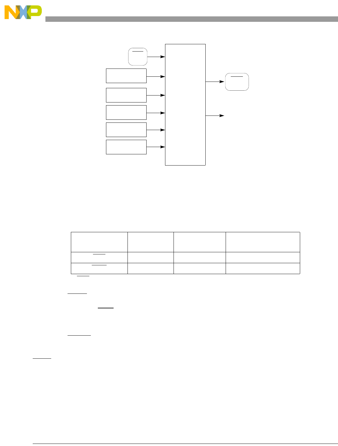
Reset Controller Module
10-2 Freescale Semiconductor
Figure 10-1. Reset Controller Block Diagram
10.4 Signals
Table 10-1 provides a summary of the reset controller signal properties. The signals are described in the
following sections.
10.4.1 RSTI
Asserting the external RSTI for at least four rising CLKOUT edges causes the external reset request to be
recognized and latched.
10.4.2 RSTO
This active-low output signal is driven low when the internal reset controller module resets the chip. When
RSTO is active, the user can drive override options on the data bus.
10.5 Memory Map and Registers
The reset controller programming model consists of these registers:
• Reset control register (RCR)—selects reset controller functions
• Reset status register (RSR)—reflects the state of the last reset source
Table 10-1. Reset Controller Signal Properties
Name Direction Input
Hysteresis
Input
Synchronization
RSTI IYes Yes
1
1RSTI is always synchronized except when in low-power stop mode.
RSTO O— —
Power-On
Reset
PLL
Loss of Clock
PLL
Loss of Lock
Software
Reset
LVD
Detect
RSTI
Pin
Reset
Controller
RSTO
Pin
To Internal Resets
MCF52211 ColdFire® Integrated Microcontroller Reference Manual, Rev. 3

Reset Controller Module
Freescale Semiconductor 10-3
See Table 10-2 for the memory map and the following paragraphs for a description of the registers.
10.5.1 Reset Control Register (RCR)
The RCR allows software control for requesting a reset, independently asserting the external RSTO pin,
and controlling low-voltage detect (LVD) functions.
Table 10-2. Reset Controller Memory Map
IPSBAR
Offset1
1Addresses not assigned to a register and undefined register bits are reserved for expansion.
Register Width
(bits) Access Reset Value Section/Page
0x11_0000 Reset Control Register (RCR) 8 R/W 0x05 10.5.1/10-3
0x11_0001 Reset Status Register (RSR) 8 R 10.5.2/10-4
IPSBAR
Offset:
0x11_0000 (RCR) Access: User read/write
76543210
R
SOFTRST FRCRSTOU
T
0
LVDF LV D IE LVD R E
0
LVDE
W
Reset:00000101
Figure 10-2. Reset Control Register (RCR)
Table 10-3. RCR Field Descriptions
Field Description
7
SOFTRST
Allows software to request a reset. The reset caused by setting this bit clears this bit.
1 Software reset request
0 No software reset request
6
FRCRSTOUT
Allows software to assert or negate the external RSTO pin.
1 Assert RSTO pin
0 Negate RSTO pin
CAUTION: External logic driving reset configuration data during reset needs to be considered when asserting
the RSTO pin when setting FRCRSTOUT.
5
—
Reserved, should be cleared.
4
LVDF
LVD flag. Indicates the low-voltage detect status if LVDE is set. Write a 1 to clear the LVDF bit.
1 Low voltage has been detected
0 Low voltage has not been detected
NOTE: The setting of this flag causes an LVD interrupt if LVDE and LVDIE bits are set and LVDRE is cleared
when the supply voltage VDD drops below VDD (minimum). The vector for this interrupt is shared with INT0 of
the EPORT module. Interrupt arbitration in the interrupt service routine is necessary if both of these interrupts
are enabled. Also, LVDF is not cleared at reset; however, it always initializes to a zero because the part does
not come out of reset while in a low-power state (LVDE/LVDRE bits are enabled out of reset).
3
LVDI E
LVD interrupt enable. Controls the LVD interrupt if LVDE is set. This bit has no effect if the LVDE bit is a logic 0.
1 LVD interrupt enabled
0 LVD interrupt disabled
MCF52211 ColdFire® Integrated Microcontroller Reference Manual, Rev. 3

Reset Controller Module
10-4 Freescale Semiconductor
10.5.2 Reset Status Register (RSR)
The RSR contains a status bit for every reset source. When reset is entered, the cause of the reset condition
is latched, along with a value of 0 for the other reset sources that were not pending at the time of the reset
condition. These values are then reflected in RSR. One or more status bits may be set at the same time.
The cause of any subsequent reset is also recorded in the register, overwriting status from the previous reset
condition.
RSR can be read at any time. Writing to RSR has no effect.
2
LVDRE
LVD reset enable. Controls the LVD reset if LVDE is set. This bit has no effect if the LVDE bit is a logic 0. LVD
reset has priority over LVD interrupt, if both are enabled.
1 LVD reset enabled
0 LVD reset disabled
1
—
Reserved, should be cleared.
0
LVDE
Controls whether the LVD is enabled.
1 LVD is enabled
0LVD is disabled
IPSBAR
Offset:
0x11_0001 (RSR) Access: User read-only
76543210
RWDR_ASY
NC LVD SOFT 0POR EXT LOC LOL
W
Reset: Reset Dependent
Figure 10-3. Reset Status Register (RSR)
Table 10-4. RSR Field Descriptions
Field Description
7
WDR_ASYNC
Backup watchdog timer reset flag. This bit indicates whether the last reset was caused by a watchdog timer
timeout.
1 Last reset was caused by a backup watchdog timer timeout
0 Last reset was not caused by a backup watchdog timer timeout
6
LVD
Low voltage detect. Indicates that the last reset state was caused by an LVD reset.
1 Last reset state was caused by an LVD reset
0 Last reset state was not caused by an LVD reset
5
SOFT
Software reset flag. Indicates that the last reset was caused by software.
1 Last reset caused by software
0 Last reset not caused by software
4 Reserved, should be cleared.
Table 10-3. RCR Field Descriptions (continued)
Field Description
MCF52211 ColdFire® Integrated Microcontroller Reference Manual, Rev. 3

Reset Controller Module
Freescale Semiconductor 10-5
10.6 Functional Description
10.6.1 Reset Sources
Table 10-5 defines the sources of reset and the signals driven by the reset controller.
To protect data integrity, a synchronous reset source is not acted upon by the reset control logic until the
end of the current bus cycle. Reset is then asserted on the next rising edge of the system clock after the
cycle is terminated. When the reset control logic must synchronize reset to the end of the bus cycle, the
internal bus monitor is automatically enabled regardless of the BME bit state in the chip configuration
register (CCR). Then, if the current bus cycle is not terminated normally, the bus monitor terminates the
cycle based on the length of time programmed in the BMT field of the CCR.
Internal byte, word, or longword writes are guaranteed to complete without data corruption when a
synchronous reset occurs. External writes, including longword writes to 16-bit ports, are also guaranteed
to complete.
Asynchronous reset sources usually indicate a catastrophic failure. Therefore, the reset control logic does
not wait for the current bus cycle to complete. Reset is asserted immediately to the system.
3
POR
Power-on reset flag. Indicates that the last reset was caused by a power-on reset.
1 Last reset caused by power-on reset
0 Last reset not caused by power-on reset
2
EXT
External reset flag. Indicates that the last reset was caused by an external device asserting the external RSTI pin.
1 Last reset state caused by external reset
0 Last reset not caused by external reset
1
LOC
Loss-of-clock reset flag. Indicates that the last reset state was caused by a PLL loss of clock.
1 Last reset caused by loss of clock
0 Last reset not caused by loss of clock
0
LOL
Loss-of-lock reset flag. Indicates that the last reset state was caused by a PLL loss of lock.
1 Last reset caused by a loss of lock
0 Last reset not caused by loss of lock
Table 10-5. Reset Source Summary
Source Type
Power on Asynchronous
External RSTI pin (not stop mode) Synchronous
External RSTI pin (during stop mode) Asynchronous
Loss-of-clock Asynchronous
Loss-of-lock Asynchronous
Software Synchronous
LVD reset Asynchronous
Table 10-4. RSR Field Descriptions (continued)
Field Description
MCF52211 ColdFire® Integrated Microcontroller Reference Manual, Rev. 3

Reset Controller Module
10-6 Freescale Semiconductor
10.6.1.1 Power-On Reset
At power up, the reset controller asserts RSTO. RSTO continues to be asserted until VDD has reached a
minimum acceptable level and, if PLL clock mode is selected, until the PLL achieves phase lock. Then
after approximately another 512 cycles, RSTO is negated and the part begins operation.
10.6.1.2 External Reset
Asserting the external RSTI for at least four rising CLKOUT edges causes the external reset request to be
recognized and latched. The bus monitor is enabled and the current bus cycle is completed. The reset
controller asserts RSTO for approximately 512 cycles after RSTI is negated and the PLL has acquired lock.
The part then exits reset and begins operation.
In low-power stop mode, the system clocks are stopped. Asserting the external RSTI in stop mode causes
an external reset to be recognized.
10.6.1.3 Loss-of-Clock Reset
This reset condition occurs in PLL clock mode when the LOCRE bit in the SYNCR is set and the PLL
reference or the PLL itself fails. The reset controller asserts RSTO for approximately 512 cycles after the
PLL has acquired lock. The device then exits reset and begins operation.
10.6.1.4 Loss-of-Lock Reset
This reset condition occurs in PLL clock mode when the LOLRE bit in the SYNCR is set and the PLL
loses lock. The reset controller asserts RSTO for approximately 512 cycles after the PLL has acquired
lock. The device then exits reset and resumes operation.
10.6.1.5 Software Reset
A software reset occurs when the SOFTRST bit is set. If the RSTI is negated and the PLL has acquired
lock, the reset controller asserts RSTO for approximately 512 cycles. Then the device exits reset and
resumes operation.
10.6.1.6 LVD Reset
The LVD reset occurs when the supply input voltage, VDD, drops below VLVD (minimum).
10.6.2 Reset Control Flow
The reset logic control flow is shown in Figure 10-4. In this figure, the control state boxes have been
numbered, and these numbers are referred to (within parentheses) in the flow description that follows. All
cycle counts given are approximate.
MCF52211 ColdFire® Integrated Microcontroller Reference Manual, Rev. 3
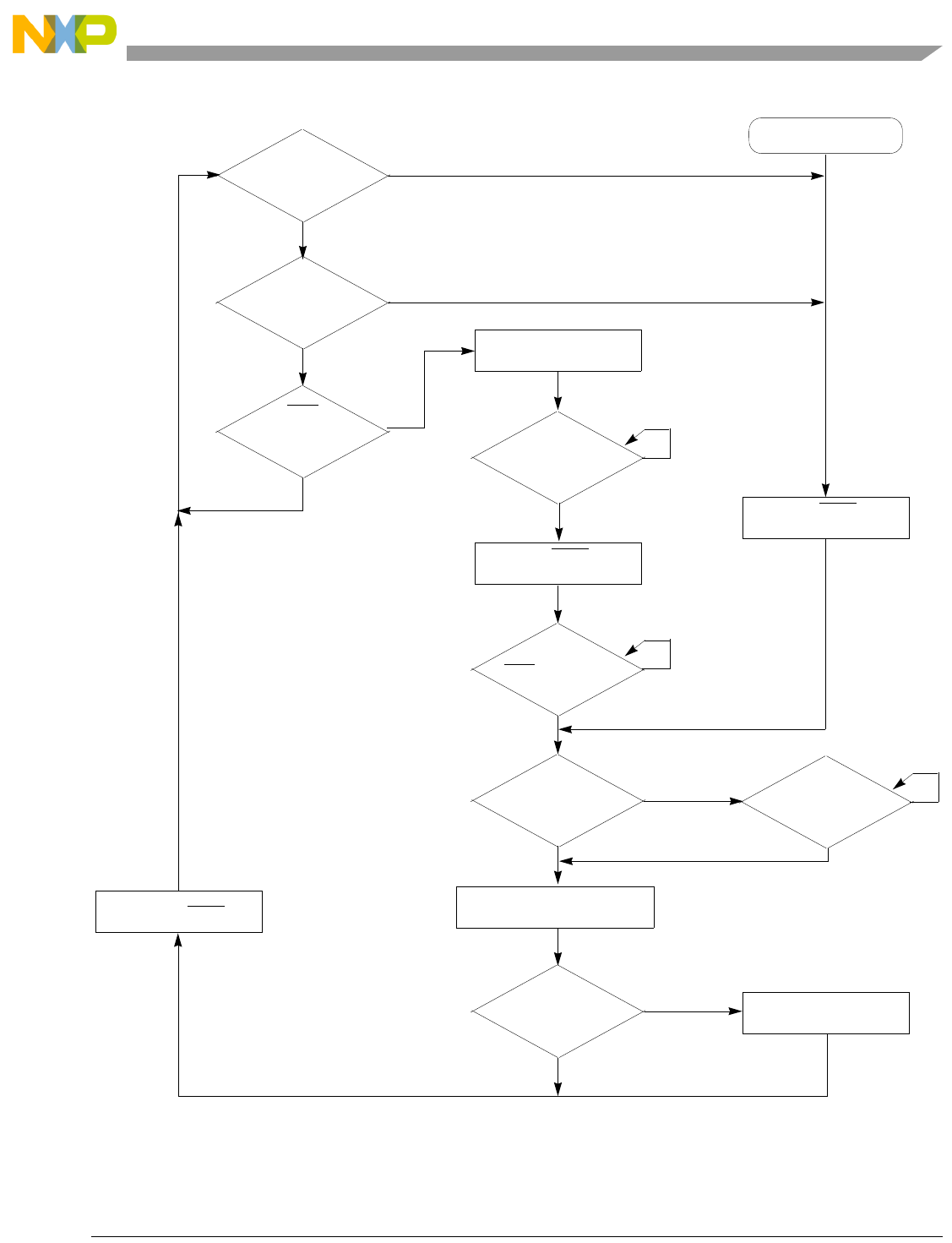
Reset Controller Module
Freescale Semiconductor 10-7
Figure 10-4. Reset Control Flow
RSTI
PIN OR WD TIMEOUT
OR SW RESET?
LOSS OF CLOCK?
LOSS OF LOCK?
RSTI NEGATED?
PLL MODE?
BUS CYCLE
COMPLETE?
RCON ASSERTED?
PLL LOCKED?
ENABLE BUS MONITOR
ASSERT RSTO AND
LATCH RESET STATUS
WAIT 512 CLKOUT CYCLES
LATCH CONFIGURATION
NEGATE RSTO
POR OR LVD
ASSERT RSTO AND
LATCH RESET STATUS
N
N
N
Y
Y
Y
1
2
3
N
N
N
0
5
6
7
8
9
10
11
Y
Y
N
N
Y
Y
12
4
9A
11A
Y
MCF52211 ColdFire® Integrated Microcontroller Reference Manual, Rev. 3

Reset Controller Module
10-8 Freescale Semiconductor
10.6.2.1 Synchronous Reset Requests
In this discussion, the references in parentheses refer to the state numbers in Figure 10-4. All cycle counts
given are approximate.
If the external RSTI signal is asserted by an external device for at least four rising CLKOUT edges (3) and
if software requests a reset, the reset control logic latches the reset request internally and enables the bus
monitor (5). When the current bus cycle is completed (6), RSTO is asserted (7). The reset control logic
waits until the RSTI signal is negated (8) and for the PLL to attain lock (9, 9A) before waiting 512
CLKOUT cycles (1). The reset control logic may latch the configuration according to the RCON signal
level (11, 11A) before negating RSTO (12).
If the external RSTI signal is asserted by an external device for at least four rising CLKOUT edges during
the 512 count (10) or during the wait for PLL lock (9A), the reset flow switches to (8) and waits for the
RSTI signal to be negated before continuing.
10.6.2.2 Internal Reset Request
If reset is asserted by an asynchronous internal reset source, such as loss of clock (1) or loss of lock (2),
the reset control logic asserts RSTO (4). The reset control logic waits for the PLL to attain lock (9, 9A)
before waiting 512 CLKOUT cycles (1). Then the reset control logic may latch the configuration
according to the RCON pin level (11, 11A) before negating RSTO (12).
If loss of lock occurs during the 512 count (10), the reset flow switches to (9A) and waits for the PLL to
lock before continuing.
10.6.2.3 Power-On Reset/Low-Voltage Detect Reset
When the reset sequence is initiated by power-on reset (0), the same reset sequence is followed as for the
other asynchronous reset sources.
10.6.3 Concurrent Resets
This section describes the concurrent resets. As in the previous discussion, references in parentheses refer
to the state numbers in Figure 10-4.
10.6.3.1 Reset Flow
If a power-on reset or low-voltage detect condition is detected during any reset sequence, the reset
sequence starts immediately (0).
If the external RSTI pin is asserted for at least four rising CLKOUT edges while waiting for PLL lock or
the 512 cycles, the external reset is recognized. Reset processing switches to wait for the external RSTI
pin to negate (8).
If a loss-of-clock or loss-of-lock condition is detected while waiting for the current bus cycle to complete
(5, 6) for an external reset request, the cycle is terminated. The reset status bits are latched (7) and reset
processing waits for the external RSTI pin to negate (8).
MCF52211 ColdFire® Integrated Microcontroller Reference Manual, Rev. 3

Reset Controller Module
Freescale Semiconductor 10-9
If a loss-of-clock or loss-of-lock condition is detected during the 512 cycle wait, the reset sequence
continues after a PLL lock (9, 9A).
10.6.3.2 Reset Status Flags
For a POR reset, the POR and LVD bits in the RSR are set, and the SOFT, WDR_ASYNC, EXT, LOC,
and LOL bits are cleared even if another type of reset condition is detected during the reset sequence for
the POR.
If a loss-of-clock or loss-of-lock condition is detected while waiting for the current bus cycle to complete
(5, 6) for an external reset request, the EXT, WDR_ASYNC, and/or SOFT bits along with the LOC and/or
LOL bits are set.
If the RSR bits are latched (7) during the EXT, WDR_ASYNC, and/or SOFT reset sequence with no other
reset conditions detected, only the EXT, WDR_ASYNC, and/or SOFT bits are set.
If the RSR bits are latched (4) during the internal reset sequence with the RSTI pin not asserted and no
SOFT or WDR_ASYNC event, then the LOC and/or LOL bits are the only bits set.
For a LVD reset, the LVD bit in the RSR is set, and the SOFT, WDR_ASYNC, EXT, LOC, and LOL bits
are cleared to 0, even if another type of reset condition is detected during the reset sequence for LVD.
MCF52211 ColdFire® Integrated Microcontroller Reference Manual, Rev. 3
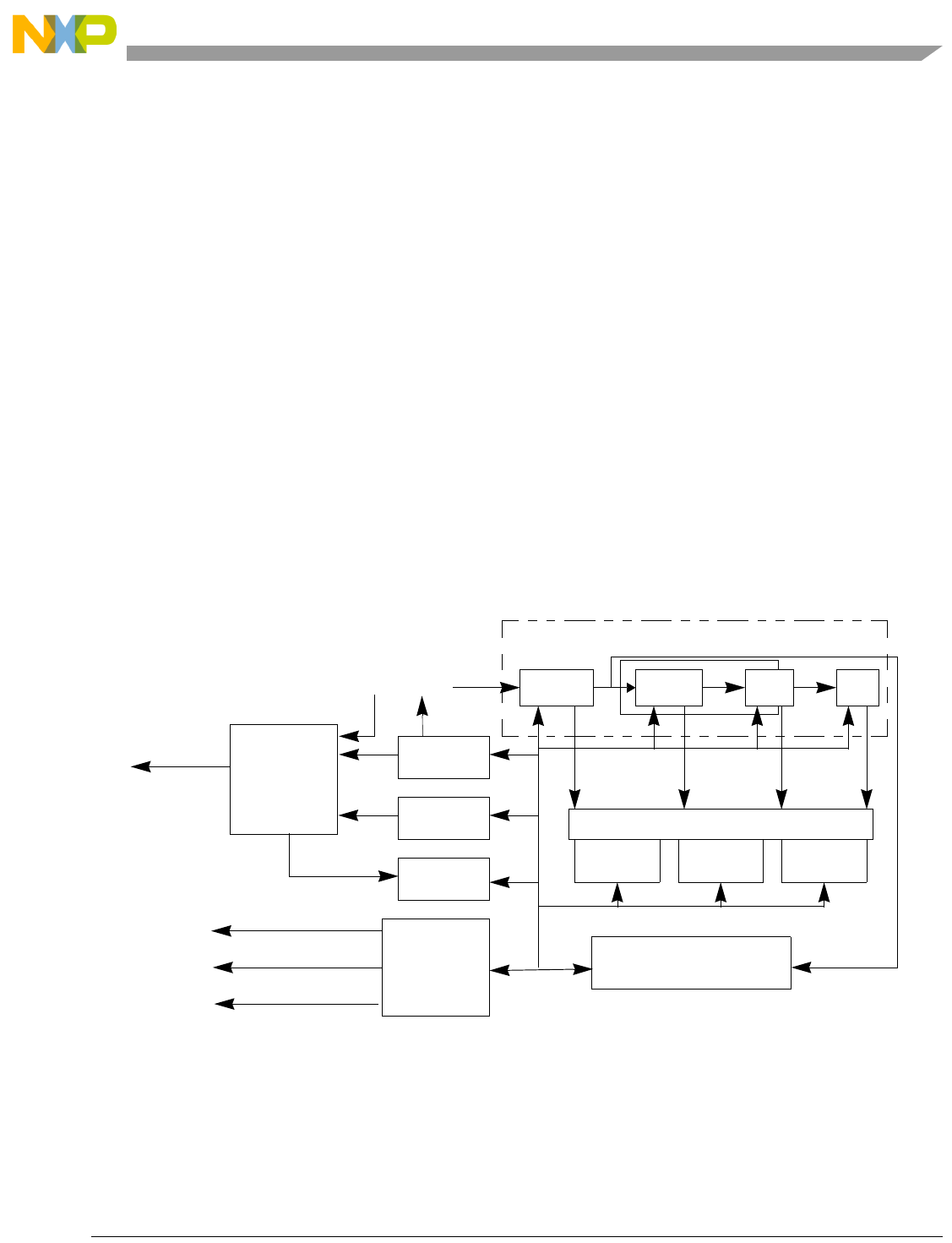
Freescale Semiconductor 11-1
Chapter 11
Real-Time Clock
11.1 Introduction
This section discusses how to operate and program the real-time clock (RTC) module that maintains the
system clock, provides stopwatch, alarm, and interrupt functions, and supports the following features.
11.1.1 Overview
Figure 11-1 is a block diagram of the Real-Time Clock (RTC) module. It consists of the following blocks:
• Time-of-day (TOD) clock counter
•Alarm
• Minute stopwatch
• Associated control and bus interface hardware
Figure 11-1. Real-Time Clock Block Diagram
11.1.2 Features
The RTC module includes the following features:
• Full clock—days, hours, minutes, seconds
SECOND MINUTE
INTERRUPT
CONTROL
INTERRUPT
ENABLE
CLOCK
CONTROL
INTERRUPT
STATUS
ALARM COMPARATOR
SECOND
LATCH
MINUTE
LATCH
HOUR
LATCH
DATA
BUS CONTROL
ADDRESS
MINUTE STOPWATCH
1 PPM
IPBUS
DECODE
HOUR DAY
TOD CLOCK
1 Hz Input CLock
1 PPH 1 PPD
RTC_INT
MCF52211 ColdFire® Integrated Microcontroller Reference Manual, Rev. 3

Real-Time Clock
Freescale Semiconductor 11-2
• Minute countdown timer with interrupt
• Programmable daily alarm with interrupt
• Once-per-day, once-per-hour, once-per-minute, and once-per-second interrupts
11.1.3 Modes of Operation
The incoming 1 Hz signal is used to increment the seconds, minutes, hours, and days TOD counters. The
alarm functions, when enabled, generate RTC interrupts when the TOD settings reach programmed values.
The sampling timer generates fixed-frequency interrupts, and the minute stopwatch allows for efficient
interrupts on minute boundaries.
• Counter
The counter portion of the RTC module consists of four groups of counters that are physically
located in three registers:
— The 6-bit seconds counter is located in the SECONDS register
— The 6-bit minutes counter and the 5-bit hours counter are located in the HOURMIN register
— The 16-bit day counter is located in the DAYR register
•Alarm
There are three alarm registers that mirror the three counter registers. An alarm is set by accessing
the real-time clock alarm registers (ALRM_HM, ALRM_SEC, and DAYALARM) and loading the
exact time that the alarm should generate an interrupt. When the TOD clock value and the alarm
value coincide, an interrupt occurs one half second later.
• Minute Stopwatch
The minute stopwatch performs a countdown with a one minute resolution. It can be used to
generate an interrupt on a minute boundary.
11.2 Memory Map/Register Definition
The RTC module includes 10 32-bit registers. Table 11-1 summarizes these registers and their addresses.
Table 11-1. RTC Module Register Memory Map
IPSBAR Offset Use Access
0x0 RTC Hours and Minutes Counter Register (HOURMIN) read/write
0x4 RTC Seconds Counter Register (SECONDS) read/write
0x8 RTC Hours and Minutes Alarm Register (ALRM_HM) read/write
0xC RTC Seconds Alarm Register (ALRM_SEC) read/write
0x0 RTC Control Register (RTCCTL) read/write
0x4 RTC Interrupt Status Register (RTCISR) read/write
0x8 RTC Interrupt Enable Register (RTCIENR) read/write
0xC Stopwatch Minutes Register (STPWCH) read/write
0x0 RTC Days Counter Register (DAYS) read/write
MCF52211 ColdFire® Integrated Microcontroller Reference Manual, Rev. 3
Real-Time Clock
11-3 Freescale Semiconductor
11.2.1 RTC Hours and Minutes Counter Register (HOURMIN)
The real-time clock hours and minutes counter register (HOURMIN) is used to program the hours and
minutes for the TOD clock. It can be read or written at any time. After a write, the time changes to the new
value. A power-on reset (POR) sets the RTC to the reset values shown in Figure 11-2.
Figure 11-2. RTC Hours and Minutes Counter Register (HOURMIN)
11.2.2 RTC Seconds Counter Register (SECONDS)
The real-time clock seconds register (SECONDS) is used to program the seconds for the TOD clock. It
can be read or written at any time. After a write, the time changes to the new value. A power-on reset
(POR) sets the RTC to the reset values shown in Figure 11-3.
0x4 RTC Day Alarm Register (ALRM_DAY) read/write
0x0 Reserved —
0x4 RTC General Oscillator Count Upper Register (RTCGOCU) read/write
0x8 RTC General Oscillator Count Lower Register (RTCGOCL) read/write
IPSBAR
Offset: 0x0 (HOURMIN)
Access: User read/write
31 30 29 28 27 26 25 24 23 22 21 20 19 18 17 16
R 0 0 0 0 0 0 0 0 0 0 0 0 0 0 0 0
W
Reset1
1
0000000000000000
15 14 13 12 11 10 9 8 7 6 5 4 3 2 1 0
R 0 0 0 HOURS 0 0 MINUTES
W
Reset1000?????00??????
Table 11-2. HOURMIN Field Descriptions
Field Description
31–13 Reserved, should be cleared.
12–8
HOURS
Hour setting; can be set to any value between 0 and 23.
7–6 Reserved, should be cleared.
5–0
MINUTES
Minutes setting; can be set to any value between 0 and 59.
Table 11-1. RTC Module Register Memory Map (continued)
IPSBAR Offset Use Access
MCF52211 ColdFire® Integrated Microcontroller Reference Manual, Rev. 3

Real-Time Clock
Freescale Semiconductor 11-4
11.2.3 RTC Hours and Minutes Alarm Register (ALRM_HM)
The real-time clock hours and minutes alarm (ALRM_HM) register is used to configure the hours and
minutes setting for the alarm. The alarm settings can be read or written at any time.
IPSBAR
Offset: 0x4 (SECONDS)
Access: User read/write
31 30 29 28 27 26 25 24 23 22 21 20 19 18 17 16
R 0 0 0 0 0 0 0 0 0 0 0 0 0 0 0 0
W
Reset1
1
0000000000000000
15 14 13 12 11 10 9 8 7 6 5 4 3 2 1 0
R0000000000
SECONDS
W
Reset10000000000??????
Figure 11-3. RTC Seconds Counter Register (SECONDS)
Table 11-3. SECONDS Field Descriptions
Field Description
31–6 Reserved, should be cleared.
5–0
SECONDS
Seconds setting; can be set to any value between 0 and 59.
IPSBAR
Offset: 0x8 (ALRM_HM)
Access: User read/write
31 30 29 28 27 26 25 24 23 22 21 20 19 18 17 16
R 0 0 0 0 0 0 0 0 0 0 0 0 0 0 0 0
W
Reset0000000000000000
15 14 13 12 11 10 9 8 7 6 5 4 3 2 1 0
R 0 0 0
HOURS
0 0
MINUTES
W
Reset0000000000000000
Figure 11-4. RTC Hours and Minutes Alarm Register (ALRM_HM)
MCF52211 ColdFire® Integrated Microcontroller Reference Manual, Rev. 3

Real-Time Clock
11-5 Freescale Semiconductor
11.2.4 RTC Seconds Alarm Register (ALRM_SEC)
The real-time clock seconds alarm (ALRM_SEC) register is used to configure the seconds setting for the
alarm. The alarm settings can be read or written at any time.
11.2.5 RTC Control Register (RTCCTL)
The real-time clock control (RTCCTL) register is used to enable the real-time clock module and specify
the reference frequency information for the prescaler.
Table 11-4. ALRM_HM Field Descriptions
Field Description
31–13 Reserved, should be cleared.
12–8
HOURS
Alarm hour setting; can be set to any value between 0 and 23.
7–6 Reserved, should be cleared.
5–0
MINUTES
Alarm minute setting; can be set to any value between 0 and 59.
IPSBAR
Offset: 0xC (ALRM_SEC)
Access: User read/write
31 30 29 28 27 26 25 24 23 22 21 20 19 18 17 16
R 0 0 0 0 0 0 0 0 0 0 0 0 0 0 0 0
W
Reset0000000000000000
15 14 13 12 11 10 9 8 7 6 5 4 3 2 1 0
R0000000000
SECONDS
W
Reset0000000000000000
Figure 11-5. RTC Seconds Alarm Register (ALRM_SEC)
Table 11-5. ALRM_SEC Field Descriptions
Field Description
31–6 Reserved, should be cleared.
5–0
SECONDS
Alarm seconds setting; can be set to any value between 0 and 59.
MCF52211 ColdFire® Integrated Microcontroller Reference Manual, Rev. 3

Real-Time Clock
Freescale Semiconductor 11-6
11.2.6 RTC Interrupt Status Register (RTCISR)
The real-time clock interrupt status register (RTCISR) indicates the status of the various real-time clock
interrupts. When an event of the types included in this register occurs, then the bit is set in this register
regardless of its corresponding interrupt enable bit. These bits are cleared by writing a 1 to them; this also
clears the interrupt. Interrupts may occur while the system clock is idle or in sleep mode.
IPSBAR
Offset: 0x0 (RTCCTL)
Access: User read/write
31 30 29 28 27 26 25 24 23 22 21 20 19 18 17 16
R 0 0 0 0 0 0 0 0 0 0 0 0 0 0 0 0
W
Reset0000000000000000
15 14 13 12 11 10 9 8 7 6 5 4 3 2 1 0
R00000000
EN
0 0 0 0 0 0
SWR
W
Reset0000000010000000
Figure 11-6. RTC Control Register (RTCCTL)
Table 11-6. RTCCTL Field Descriptions
Field Description
31–8 Reserved, should be cleared.
7
EN
RTC Enables/Disable bit. This bit enables/disables the RTC. The software reset bit (SWR) has no effect on this bit.
Bit description
0 Disable the real-time clock
1 Enable the real-time clock
6–1 Reserved, should be cleared.
0
SWR
Software Reset bit. This bit resets the RTC to its default state. However, a software reset has no effect on the EN bit.
0 No effect
1 Reset the module to its default state
MCF52211 ColdFire® Integrated Microcontroller Reference Manual, Rev. 3

Real-Time Clock
11-7 Freescale Semiconductor
IPSBAR
Offset: 0x4 (RTCISR)
Access: User read/write
31 30 29 28 27 26 25 24 23 22 21 20 19 18 17 16
R 0 0 0 0 0 0 0 0 0 0 0 0 0 0 0 0
W
Reset0000000000000000
15 14 13 12 11 10 9 8 7 6 5 4 3 2 1 0
R 0 0 0 0 0 0 0 0 0 0
HR 1HZ DAY ALM MIN SW
W
Reset0000000000000000
Figure 11-7. RTC Interrupt Status Register (RTCISR)
Table 11-7. RTCISR Field Descriptions
Field Description
31–6 Reserved, should be cleared.
5
HR
Hour flag bit. This bit indicates whether the hour counter has incremented. If enabled, this bit is set on every
increment of the RTC hour counter.
0 No 1-hour interrupt occurred
1 A 1-hour interrupt has occurred
4
1HZ
1 Hz flag bit. This bit indicates whether the second counter has incremented. If enabled, this bit is set on every
increment of the RTC second counter.
0 No 1 Hz interrupt occurred
1 A 1 Hz interrupt has occurred
3
DAY
Day flag bit. This bit indicates whether the day counter has incremented. If enabled, this bit is set on every
increment of the RTC day counter.
0 No 24-hour rollover interrupt occurred
1 A 24-hour rollover interrupt has occurred
2
ALM
Alarm flag bit. This bit indicates that the RTC time matches the value in the alarm registers. The alarm
reoccurs every 65536 days. For a single alarm, clear the interrupt enable for this bit in the interrupt service
routine.
0 No alarm interrupt occurred
1 An alarm interrupt has occurred
1
MIN
Minute flag bit. This bit indicates that the minute counter has incremented. If enabled, this bit is set on every
increment of the RTC minute counter.
0 No 1-minute interrupt occurred
1 A 1-minute interrupt has occurred
0
SW
Stopwatch flag bit. This bit indicates that the stopwatch countdown has timed out.
0 The stopwatch did not time out.
1 The stopwatch timed out.
MCF52211 ColdFire® Integrated Microcontroller Reference Manual, Rev. 3

Real-Time Clock
Freescale Semiconductor 11-8
11.2.7 RTC Interrupt Enable Register (RTCIENR)
The real-time clock interrupt enable register (RTCIENR) is used to enable/disable the various real-time
clock interrupts. Masking an interrupt bit has no effect on its corresponding status bit.
IPSBAR
Offset:
0x8 (RTCIENR) Access: User read/write
31 30 29 28 27 26 25 24 23 22 21 20 19 18 17 16
R 0 0 0 0 0 0 0 0 0 0 0 0 0 0 0 0
W
Reset0000000000000000
15 14 13 12 11 10 9 8 7 6 5 4 3 2 1 0
R 0 0 0 0 0 0 0 0 0 0
HR 1HZ DAY ALM MIN SW
W
Reset0000000000000000
Figure 11-8. RTC Interrupt Enable Register (RTCIENR)
Table 11-8. RTCIENR Field Descriptions
Field Description
31-6 Reserved, should be cleared.
5
HR
Hour interrupt enable bit. This bit enables/disables an interrupt when the hour counter of the real-time clock
increments.
0 The 1-hour interrupt id disabled.
1 The 1-hour interrupt is enabled.
4
1HZ
1 Hz interrupt enable bit. This bit enables/disables an interrupt when the second counter of the real-time clock
increments.
0 The 1 Hz interrupt is disabled.
1 The 1 Hz interrupt is enabled.
3
DAY
Day interrupt enable bit. This bit enables/disables an interrupt when the hours counter rolls over from 23 to 0
(midnight rollover).
0 The 24-hour interrupt is disabled.
1 The 24-hour interrupt is enabled.
2
ALM
Alarm interrupt enable bit. This bit enables/disables the alarm interrupt.
0 The alarm interrupt is disabled.
1 The alarm interrupt is enabled.
1
MIN
Minute interrupt enable bit. This bit enables/disables an interrupt when the RTC minute counter increments.
0 The 1-minute interrupt is disabled.
1 The 1-minute interrupt is enabled.
0
SW
Stopwatch interrupt enable; enables/disables the stopwatch interrupt. The stopwatch counts down and
remains at decimal -1 until it is reprogrammed. If this bit is enabled with -1 (decimal) in the STPWCH register,
an interrupt is posted on the next minute tick.
Bit description
1 = Stopwatch interrupt is enabled.
0 = Stopwatch interrupt is disabled.
MCF52211 ColdFire® Integrated Microcontroller Reference Manual, Rev. 3

Real-Time Clock
11-9 Freescale Semiconductor
11.2.8 RTC Stopwatch Minutes Register (STPWCH)
The stopwatch minutes (STPWCH) register contains the current stopwatch countdown value. When the
minute counter of the TOD clock increments, the value in this register decrements.
11.2.9 RTC Days Counter Register (DAYS)
The real-time clock days counter register (DAYS) is used to program the day for the TOD clock. When the
HOUR field of the HOURMIN register rolls over from 23 to 00, the day counter increments. It can be read
or written at any time. After a write, the time changes to the new value. This register cannot be reset
because the real-time clock is always enabled at reset. Only 16-bit accesses to this register are allowed.
IPSBAR
Offset: 0xC (STPWCH)
Access: User read/write
31 30 29 28 27 26 25 24 23 22 21 20 19 18 17 16
R 0 0 0 0 0 0 0 0 0 0 0 0 0 0 0 0
W
Reset0000000000000000
15 14 13 12 11 10 9 8 7 6 5 4 3 2 1 0
R 0 0 0 0 0 0 0 0 0 0
CNT
W
Reset0000000000111111
Figure 11-9. RTC Stopwatch Minutes Register (STPWCH)
Table 11-9. STPWCH Field Descriptions
Field Description
31–6 Reserved, should be cleared.
5–0
CNT
Stopwatch count. This field contains the stopwatch countdown value.
Note: The stopwatch counter is decremented by the minute (MIN) tick output from the real-time clock, so the
average tolerance of the count is 0.5 minutes. For better accuracy, enable the stopwatch by polling the
MIN bit of the RTCISR register or by polling the minute interrupt service routine.
MCF52211 ColdFire® Integrated Microcontroller Reference Manual, Rev. 3

Real-Time Clock
Freescale Semiconductor 11-10
11.2.10 RTC Day Alarm Register (ALRM_DAY)
The real-time clock day alarm (ALRM_DAY) register is used to configure the day for the alarm. The alarm
settings can be read or written at any time.
IPSBAR
Offset: 0x0 (DAYS)
Access: User read/write
31 30 29 28 27 26 25 24 23 22 21 20 19 18 17 16
R 0 0 0 0 0 0 0 0 0 0 0 0 0 0 0 0
W
Reset0000000000000000
15 14 13 12 11 10 9 8 7 6 5 4 3 2 1 0
R
DAYS
W
Reset????????????????
Figure 11-10. RTC Days Counter Register (DAYS)
Table 11-10. DAYS Field Descriptions
Field Description
31–16 Reserved, should be cleared.
15–0
DAYS
Day Setting. This field indicates the current day count, and can be set to any value between 0 and 65535.
IPSBAR
Offset: 0x4 (ALRM_DAY)
Access: User read/write
31 30 29 28 27 26 25 24 23 22 21 20 19 18 17 16
R 0 0 0 0 0 0 0 0 0 0 0 0 0 0 0 0
W
Reset0000000000000000
15 14 13 12 11 10 9 8 7 6 5 4 3 2 1 0
R
DAYSAL
W
Reset0000000000000000
Figure 11-11. RTC Day Alarm Register (ALRM_DAY)
MCF52211 ColdFire® Integrated Microcontroller Reference Manual, Rev. 3

Real-Time Clock
11-11 Freescale Semiconductor
11.2.11 RTC General Oscillator Count Registers (RTCGOCU and RTCGOCL)
The real-time clock general oscillator count registers (RTCGOCU and RTCGOCL) contain the upper and
lower 16 bits of a 32-bit field, RTCGOCNT. This field is used to control the 1 Hz clock and the sampling
clock as described in Section 11.3, “Functional Description”.
Table 11-11. ALRM_DAY Field Descriptions
Field Description
31–16 Reserved, should be cleared.
15–0
DAYSAL
Day Setting of the Alarm. This field can be set to any value between 0 and 65535.
IPSBAR
Offset: 0x4 (RTCGOCU)
Access: User read/write
15 14 13 12 11 10 9 8 7 6 5 4 3 2 1 0
R
RTCGOCNT[31:16]
W
Reset0000000000000000
Figure 11-12. RTC General Oscillator Count Upper Register (RTCGOCU)
Table 11-12. RTCGOCU Field Descriptions
Field Description
15–0
RTCGOCNT[31:16]
RTC general oscillator count, bits 31:16. This field is used to control the 1 Hz clock and the sampling
clock as described in Section 11.3, “Functional Description”.
IPSBAR
Offset: 0x8 (RTCGOCL)
Access: User read/write
15 14 13 12 11 10 9 8 7 6 5 4 3 2 1 0
R
RTCGOCNT[15:0]
W
Reset0000000000000000
Figure 11-13. RTC General Oscillator Count Lower Register (RTCGOCL)
Table 11-13. RTCGOCL Field Descriptions
Field Description
15–0
RTCGOCNT[15:0]
RTC general oscillator count, bits 15:0. This field is used to control the 1 Hz clock and the sampling clock
as described in Section 11.3, “Functional Description”.
MCF52211 ColdFire® Integrated Microcontroller Reference Manual, Rev. 3

Real-Time Clock
Freescale Semiconductor 11-12
11.3 Functional Description
The RTC uses a supplied 1 Hz signal to increment the seconds, minutes, hours, and days TOD counters.
The alarm functions, when enabled, generate RTC interrupts when the TOD settings reach programmed
values. The minute stopwatch allows for efficient interrupts on minute boundaries.
The 1 Hz clock and the sampling clock are affected by the value of RTCGOCNT (see Section 11.2.11,
“RTC General Oscillator Count Registers (RTCGOCU and RTCGOCL)”) as follows:
• The 1 Hz clock is the input clock divided by RTCGOCNT[31:0].
• The sampling clock is the input clock divided by RTCGOCNT[31:9].
• If RTCGOCNT equals 0x0, the 1 Hz clock is shut down completely.
Table 11-14 presents several examples of this functionality.
11.3.1 Prescaler and Counter
A 1 Hz clock is supplied to the RTC. This 1 Hz clock drives the RTC’s counters. The counter portion of
the RTC module consists of four groups of counters that are physically located in three registers:
• The 6-bit seconds counter is located in the SECONDS register
• The 6-bit minutes counter and the 5-bit hours counter are located in the HOURMIN register
• The 16-bit day counter is located in the DAYR register
These counters cover a 24-hour clock over 65536 days. All three registers can be read or written at any
time.
Interrupts signal when each of the four counters increments, and can be used to indicate when a counter
rolls over. For example, each tick of the seconds counter causes the 1HZ interrupt flag to be set. When the
seconds counter rolls from 59 to 00, the minute counter increments and the MIN interrupt flag is set. The
same is true for the minute counter with the HR signal, and the hour counter with the DAY signal.
11.3.2 Alarm
There are three alarm registers that mirror the three counter registers. An alarm is set by accessing the
real-time clock alarm registers (ALRM_HM, ALRM_SEC, and DAYALARM) and loading the exact time
that the alarm should generate an interrupt. If RTCIENR[ALM] is set, when the TOD clock value and the
alarm value coincide, an interrupt occurs one half second later. If the alarm is not disabled, it reoccurs
every 65536 days. If a single alarm is desired, the alarm function must be disabled through RTCIENR.
Table 11-14. Sample RTC parameter values
Sampling clock
frequency
RTCGOCNT[31:0]
value for 1 Hz
Divider output
frequency
RTCGOCNT[31:9]
value for 512 Hz
Output clock
frequency
32.000 kHz 0x1F40
1Hz
0x3E 516.1 Hz
32.768 kHz 0x2000 0x40 512 Hz
38.400 kHz 0x2580 0x4B 512 Hz
48.000 kHz 0x2EE0 0x5D 516.1 Hz
MCF52211 ColdFire® Integrated Microcontroller Reference Manual, Rev. 3

Real-Time Clock
11-13 Freescale Semiconductor
11.3.3 Minute Stopwatch
The minute stopwatch performs a countdown with a one minute resolution. It can be used to generate an
interrupt on a minute boundary. At each minute, the value in the stopwatch is decremented. When the
stopwatch value reaches -1, the interrupt occurs. The value of the register does not change until it is
reprogrammed. The actual delay includes the seconds from setting the stopwatch to the next minute tick.
11.4 Initialization/Application Information
11.4.1 RTC Register Access Protocol
1. Perform dummy read access to a non-RTC address location.
2. Perform dummy read to the targeted RTC address location.
3. Perform actual read or write access to the targeted RTC address location.
Steps 1 and 2 can be combined into one cycle that is a dummy read access to a non-RTC but targeted RTC
address location. Then the protocol is:
1. Perform dummy read access to a non-RTC, targeted RTC address location.
2. Perform actual read or write access to targeted RTC address location.
11.4.2 Flow Chart of RTC Operation
Figure 11-14 shows the flow chart of a typical RTC operation.
MCF52211 ColdFire® Integrated Microcontroller Reference Manual, Rev. 3
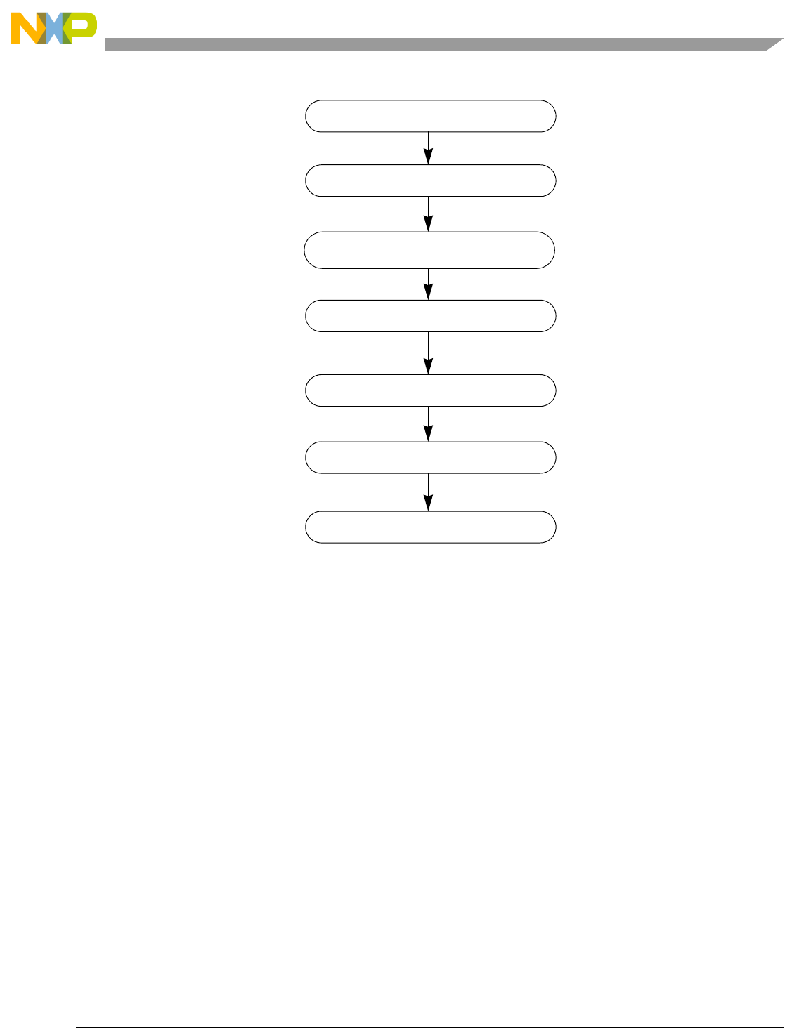
Real-Time Clock
Freescale Semiconductor 11-14
Figure 11-14. Flow Chart of RTC Operation
11.4.3 Code Example for Initializing the Real-Time Clock
Figure 11-15 shows sample code for initializing the RTC.
MCF_CLOCK_RTCCR=0b01010110; //RTCCC
MCF_RTCGOCL = 0x00002000; //32KHz
MCF_CLOCK_RTCCR=0b01010111; //RTCCC
MCF_RTC_HOURMIN = MCF_RTC_HOURMIN_HOURS(((uint32)time_temp % 24));
MCF_RTC_HOURMIN = MCF_RTC_HOURMIN_MINUTES(((uint32)time_temp % 60));
MCF_RTC_SECONDS = MCF_RTC_SECONDS_SECONDS(((uint32)time_temp % 60));
Figure 11-15. Code Example for Initializing the Real-Time Clock
Configure RTC Control Register
Config RTC Days Counter Register
Config RTC Hr/Min Counter Register
Config RTC Alarm Registers
Config RTC Interrupt Enable Reg
Check RTC Interrupt Status Register
Config RTC Seconds Counter Reg
MCF52211 ColdFire® Integrated Microcontroller Reference Manual, Rev. 3

Freescale Semiconductor 12-1
Chapter 12
System Control Module (SCM)
12.1 Introduction
This section details the functionality of the system control module (SCM) that provides the programming
model for the system access control unit (SACU), system bus arbiter, 32-bit core watchdog timer (CWT),
and system control registers and logic. Specifically, the system control includes the internal peripheral
system (IPS) base address register (IPSBAR), the processor’s dual-port RAM base address register
(RAMBAR), and system control registers that include the core watchdog timer control.
12.2 Overview
The SCM provides the control and status for a variety of functions including base addressing and address
space masking for the IPS peripherals and resources (IPSBAR) and the ColdFire core memory spaces
(RAMBAR). The CPU core supports two memory banks, one for the internal SRAM and the other for the
internal flash.
The SACU provides the mechanism needed to implement secure bus transactions to the system address
space.
The programming model for the system bus arbitration resides in the SCM. The SCM sources the
necessary control signals to the arbiter for bus master management.
The CWT provides a means of preventing system lockup due to uncontrolled software loops via a special
software service sequence. If periodic software servicing action does not occur, the CWT times out with a
programmed response (system reset or interrupt) to allow recovery or corrective action to be taken.
12.3 Features
The SCM includes these distinctive features:
• IPS base address register (IPSBAR)
— Base address location for 1-Gbyte peripheral space
— User control bits
• Processor-local memory base address register (RAMBAR)
• System control registers
— Core reset status register (CRSR) indicates type of last reset
— Core watchdog service register (CWSR) services watchdog timer
— Core watchdog control register (CWCR) for watchdog timer control
• System bus master arbitration programming model (MPARK)
MCF52211 ColdFire® Integrated Microcontroller Reference Manual, Rev. 3

System Control Module (SCM)
12-2 Freescale Semiconductor
• System access control unit (SACU) programming model
— Master privilege register (MPR)
— Peripheral access control registers (PACRs)
— Grouped peripheral access control registers (GPACR0, GPACR1)
12.4 Memory Map and Register Definition
The memory map for the SCM registers is shown in Table 12-1. All the registers in the SCM are
memory-mapped as offsets within the 1-Gbyte IPS address space and accesses are controlled to these
registers by the control definitions programmed into the SACU.
Table 12-1. SCM Register Map
IPSBAR
Offset1Register Width
(bits) Access Reset Value Section/Page
0x0000 IPS Base Address Register (IPSBAR) 32 R/W 0x4000_0001 12.5.1/12-3
0x0008 Memory Base Address Register (RAMBAR) 32 R/W 0x00 12.5.2/12-4
0x000C Peripheral Power Management Register High (PPMRH)232 R/W 0x00 8.2.1/8-2
0x0010 Core Reset Status Register (CRSR) 8 R/W See Section 12.5.3/12-6
0x0011 Core Watchdog Control Register (CWCR) 8 R/W 0x00 12.5.4/12-7
0x0012 Low-Power Interrupt Control Register (LPICR) 8 R/W 0x00 8.2.2/8-5
0x0013 Core Watchdog Service Register (CWSR) 8 R/W Uninitialized 12.5.5/12-8
0x0014 DMA Request Control Register (DMAREQC) 32 R/W 0x00 17.3.1/17-4
0x0018 Peripheral Power Management Register Low (PPMRL)232 R/W 0x01 8.2.1.1/8-4
0x001C Default Bus Master Park Register (MPARK) 32 R/W 0x30E1_0000 12.6.3/12-10
0x0020 Master Privilege Register (MPR) 8 R/W 0x03 12.7.3.1/12-14
0x0021 Peripheral Power Management Set Register (PPMRS)28 W 0x00 8.2.3/8-7
0x0022 Peripheral Power Management Clear Register (PPMRC)232 R/W 0x00 8.2.4/8-7
0x0023 IPS Bus Timeout Monitor Register (IPSBMT)2,3 32 R/W 0x08 8.3/8-9
0x0024 Peripheral Access Control Register (PACR0) 8 R/W 0x00 12.7.3.2/12-14
0x0025 Peripheral Access Control Register (PACR1) 8 R/W 0x00 12.7.3.2/12-14
0x0026 Peripheral Access Control Register (PACR2) 8 R/W 0x00 12.7.3.2/12-14
0x0027 Peripheral Access Control Register (PACR3) 8 R/W 0x00 12.7.3.2/12-14
0x0028 Peripheral Access Control Register (PACR4) 8 R/W 0x00 12.7.3.2/12-14
0x0029 Peripheral Access Control Register (PACR5) 8 R/W 0x00 12.7.3.2/12-14
0x002A Peripheral Access Control Register (PACR6) 8 R/W 0x00 12.7.3.2/12-14
0x002B Peripheral Access Control Register (PACR7) 8 R/W 0x00 12.7.3.2/12-14
MCF52211 ColdFire® Integrated Microcontroller Reference Manual, Rev. 3

System Control Module (SCM)
Freescale Semiconductor 12-3
12.5 Register Descriptions
12.5.1 Internal Peripheral System Base Address Register (IPSBAR)
The IPSBAR specifies the base address for the 1-Gbyte memory space associated with the on-chip
peripherals. At reset, the base address is loaded with a default location of 0x4000_0000 and marked as
valid (IPSBAR[V]=1). If desired, the address space associated with the internal modules can be moved by
loading a different value into the IPSBAR at a later time.
0x002C Peripheral Access Control Register (PACR8) 8 R/W 0x00 12.7.3.2/12-14
0x0030 GPACR0 Register 8 R/W 0x00 12.7.3.3/12-16
0x0031 GPACR1 Register 8 R/W 0x00 12.7.3.3/12-16
1Addresses not assigned to a register and undefined register bits are reserved for expansion.
2The PPMRH, LPICR, PMRL, PPMRS, PPMRC, and IPSBMT are described in Chapter 8, “Power Management.”
3Register must be addressed as a byte.
Table 12-2. Accessing as 32-Bit Registers
IPSBAR
Offset [31:24] [23:16] [15:8] [7:0]
0x0000 IPSBAR
0x0004 —
0x0008 RAMBAR
0x000C PPMRH1
1The LPICR is described in Chapter 8, “Power Management.”
0x0010 CRSR CWCR LPICR1CWSR
0x0014 DMAREQC2
2The DMAREQC register is described in Chapter 17, “DMA Controller Module.”
0x0018 PPMRL1
0x001C MPARK
0x0020 MPR PPMRS1PPMRC1IPSBMT1,3
3Register must be addressed as a byte.
0x0024 PACR0 PACR1 PACR2 PACR3
0x0028 PACR4 PACR5 PACR6 PACR7
0x002C PACR8 — — —
0x0030 GPACR0 GPACR1 — —
0x0034 — — — —
0x0038 — — — —
0x003C — — — —
Table 12-1. SCM Register Map (continued)
IPSBAR
Offset1Register Width
(bits) Access Reset Value Section/Page
MCF52211 ColdFire® Integrated Microcontroller Reference Manual, Rev. 3

System Control Module (SCM)
12-4 Freescale Semiconductor
NOTE
Accessing reserved IPSBAR memory space could result in an unterminated
bus cycle that causes the core to hang. Only a hard reset allows the core to
recover from this state. Therefore, all bus accesses to IPSBAR space should
fall within a module’s memory map space.
If an address hits in overlapping memory regions, the following priority is used to determine what memory
is accessed:
1. IPSBAR
2. RAMBAR
NOTE
This is the list of memory access priorities when viewed from the processor
core.
See Figure 12-1 and Table 12-3 for descriptions of the bits in IPSBAR.
12.5.2 Memory Base Address Register (RAMBAR)
The device supports dual-ported local SRAM memory. This processor-local memory can be accessed
directly by the core and/or other system bus masters. Because this memory provides single-cycle accesses
at processor speed, it is ideal for applications where double-buffer schemes can be used to maximize
system-level performance. For example, a DMA channel in a typical double-buffer application (also
IPSBAR
Offset: 0x0000 (IPSBAR)
Access: read/write
31 30 29 28 27 26 25 24 23 22 21 20 19 18 17 16
RBA31 BA30 0000000 0 000000
W
Reset010000000 0 000000
15 14 13 12 11 10 9 8 7 6 5 4 3 2 1 0
R 0 00000000 000000V
W
Reset000000000 0 000001
Figure 12-1. IPS Base Address Register (IPSBAR)
Table 12-3. IPSBAR Field Description
Field Description
31–30
BA
Base address. Defines the base address of the 1-Gbyte internal peripheral space. This is the starting address for the
IPS registers when the valid bit is set.
29–1 Reserved, should be cleared.
0
V
Valid. Enables/disables the IPS Base address region. V is set at reset.
0 IPS Base address is not valid.
1 IPS Base address is valid.
MCF52211 ColdFire® Integrated Microcontroller Reference Manual, Rev. 3

System Control Module (SCM)
Freescale Semiconductor 12-5
known as a ping-pong scheme) may load data into one portion of the dual-ported SRAM while the
processor is manipulating data in another portion of the SRAM. After the processor completes the data
calculations, it begins processing the recently-loaded buffer while the DMA moves out the
recently-calculated data from the other buffer, and reloads the next data block into the recently-freed
memory region. The process repeats with the processor and the DMA ping-ponging between alternate
regions of the dual-ported SRAM.
The device design implements the dual-ported SRAM in the memory space defined by the RAMBAR
register. There are two physical copies of the RAMBAR register: one located in the processor core and
accessible only via the privileged MOVEC instruction at CPU space address 0xC05 and another located
in the SCM at IPSBAR + 0x008. ColdFire core accesses to this memory are controlled by the
processor-local copy of the RAMBAR, while module accesses are enabled by the SCM's RAMBAR.
The physical base address programmed in both copies of the RAMBAR is typically the same value;
however, they can be programmed to different values. By definition, the base address must be a
0-modulo-size value.
The SRAM modules are configured through the RAMBAR shown in Figure 12-2.
• RAMBAR specifies the base address of the SRAM.
• All undefined bits are reserved. These bits are ignored during writes to the RAMBAR and return
zeros when read.
IPSBAR
Offset: 0x0008 (RAMBAR)
Access: read/write
31 30 29 28 27 26 25 24 23 22 21 20 19 18 17 16
RBA
W
Reset000000000 0 000000
15 14 13 12 11 10 9 8 7 6 5 4 3 2 1 0
R 0 00000
BDE 00 0000000
W
Reset000000000 0 000000
Figure 12-2. Memory Base Address Register (RAMBAR)
Table 12-4. RAMBAR Field Description
Field Description
31–16
BA
Base address. Defines the memory module's base address on a 64-Kbyte boundary corresponding to the physical
array location within the 4 Gbyte address space supported by ColdFire.
15–10 Reserved, should be cleared.
9
BDE
Back door enable. Qualifies non-core master module accesses to the memory.
0 Disables non-core master module accesses to the internal SRAM
1 Enables non-core master module accesses to the internal SRAM
Note: The SPV bit in the CPU’s RAMBAR must also be set to allow dual port access to the SRAM. For more
information, see Section 5.2.1, “SRAM Base Address Register (RAMBAR).”
8–0 Reserved, should be cleared.
MCF52211 ColdFire® Integrated Microcontroller Reference Manual, Rev. 3

System Control Module (SCM)
12-6 Freescale Semiconductor
• The back door enable bit, RAMBAR[BDE], is cleared at reset, disabling the module access to the
SRAM.
NOTE
The RAMBAR default value of 0x0000_0000 is invalid. The RAMBAR
located in the processor’s CPU space must be initialized with the valid bit
set before the CPU (or modules) can access the on-chip SRAM (see
Chapter 5, “Static RAM (SRAM),” for more information.
For details on the processor's view of the local SRAM memories, see Section 5.2.1, “SRAM Base Address
Register (RAMBAR).”
12.5.3 Core Reset Status Register (CRSR)
The CRSR contains a bit that indicates the reset source to the CPU. When the EXT bit (bit 7) reads as 1,
an external device driving RSTI has caused the most recent reset. The CRSR is updated by the control logic
when the reset is complete. Only one bit is set at any one time in the CRSR. The register reflects the cause
of the most recent reset. To clear a bit, a logic 1 must be written to the bit location; writing a zero has no
effect. Unused bits are reserved and should not be written.
NOTE
The reset status register (RSR) in the reset controller module provides
indication of all reset sources except the core watchdog timer (see
Chapter 10, “Reset Controller Module”).
IPSBAR
Offset: 0x0010 (CRSR)
Access: read/write
76543210
R
EXT
0 0 00000
W
Reset:See Note0000000
Note: The reset value of EXT depend on the last reset source. All other bits are initialized to zero.
Figure 12-3. Core Reset Status Register (CRSR)
Table 12-5. CRSR Field Descriptions
Field Description
7
EXT
External reset.
1 An external device driving RSTI caused the last reset. Assertion of reset by an external device causes the processor
core to initiate reset exception processing. All registers are forced to their initial state.
6–0 Reserved, should read as 0. Do not write to these locations.
MCF52211 ColdFire® Integrated Microcontroller Reference Manual, Rev. 3

System Control Module (SCM)
Freescale Semiconductor 12-7
12.5.4 Core Watchdog Control Register (CWCR)
The core watchdog timer prevents system lockup if the software becomes trapped in a loop with no
controlled exit. The core watchdog timer can be enabled or disabled through CWCR[CWE]. It is disabled
by default. If enabled, the watchdog timer requires the periodic execution of a core watchdog servicing
sequence. If this periodic servicing action does not occur, the timer times out, resulting in a watchdog timer
interrupt as programmed by CWCR[CWRI]. If the timer times out and the core watchdog transfer
acknowledge enable bit (CWCR[CWTA]) is set, a watchdog timer interrupt is asserted. If a core watchdog
timer interrupt acknowledge cycle has not occurred after another timeout, CWT TA is asserted in an
attempt to allow the interrupt acknowledge cycle to proceed by terminating the bus cycle. The setting of
CWCR[CWTAVAL] indicates that the watchdog timer TA was asserted.
To prevent the core watchdog timer from interrupting, the CWSR must be serviced by performing the
following sequence:
1. Write 0x55 to CWSR.
2. Write 0xAA to CWSR.
Both writes must occur in order before the time-out, but any number of instructions can be executed
between the two writes. This order allows interrupts and exceptions to occur, if necessary, between the two
writes. Caution should be exercised when changing CWCR values after the software watchdog timer has
been enabled with the setting of CWCR[CWE], because it is difficult to determine the state of the core
watchdog timer while it is running. The countdown value is constantly compared with the time-out period
specified by CWCR[CWT]. The following steps must be taken to change CWT:
1. Disable the core watchdog timer by clearing CWCR[CWE].
2. Reset the counter by writing 0x55 and then 0xAA to CWSR.
3. Update CWCR[CWT].
4. Re-enable the core watchdog timer by setting CWCR[CWE]. This step can be performed in step 3.
The CWCR controls the software watchdog timer, time-out periods, and software watchdog timer transfer
acknowledge. The register can be read at any time, but can be written only if the CWT is not pending. At
system reset, the software watchdog timer is disabled.
IPSBAR
Offset: 0x0011 (CWCR)
Access: read/write
76543210
R
CWE CWRI CWT[2:0] CWTA CWTAVAL CWTIF
W
Reset:00000000
Figure 12-4. Core Watchdog Control Register (CWCR)
MCF52211 ColdFire® Integrated Microcontroller Reference Manual, Rev. 3

System Control Module (SCM)
12-8 Freescale Semiconductor
12.5.5 Core Watchdog Service Register (CWSR)
The software watchdog service sequence must be performed using the CWSR as a data register to prevent
a CWT time-out. The service sequence requires two writes to this data register: first a write of 0x55
followed by a write of 0xAA. Both writes must be performed in this order prior to the CWT time-out, but
any number of instructions or accesses to the CWSR can be executed between the two writes. If the CWT
has already timed out, writing to this register has no effect in negating the CWT interrupt. Figure 12-5
illustrates the CWSR. At system reset, the contents of CWSR are uninitialized.
Table 12-6. CWCR Field Description
Field Description
7
CWE
Core watchdog enable.
0 SWT disabled.
1 SWT enabled.
6
CWRI
Core watchdog interrupt select.
0 If a time-out occurs, the CWT generates an interrupt to the processor core. The interrupt level for the CWT is
programmed in the interrupt control register 8 (ICR8) of INTC0.
1 Reserved. If a one is written undetermined behavior results.
Note: If a core reset is required, the watchdog interrupt should set the soft reset bit in the interrupt controller.
5–3
CWT[2:0]
Core watchdog timing delay. These bits select the timeout period for the CWT as shown in the following table. At
system reset, the CWT field is cleared signaling the minimum time-out period but the watchdog is disabled
(CWCR[CWE] = 0). the following table shows the core watchdog timer delay.
2
CWTA
Core watchdog transfer acknowledge enable.
0 CWTA Transfer acknowledge disabled.
1 CWTA Transfer Acknowledge enabled. After one CWT time-out period of the unacknowledged assertion of the
CWT interrupt, the transfer acknowledge asserts, which allows CWT to terminate a bus cycle and allow the
interrupt acknowledge to occur.
1
CWTAVA
L
Core watchdog transfer acknowledge valid.
0 CWTA Transfer Acknowledge has not occurred.
1 CWTA Transfer Acknowledge has occurred. Write a 1 to clear this flag bit.
0
CWTIF
Core watchdog timer interrupt flag.
0 CWT interrupt has not occurred
1 CWT interrupt has occurred. Write a 1 to clear the interrupt request.
CWT [2:0] CWT Time-Out Period
000 29 Bus clock frequency
001 211 Bus clock frequency
010 213 Bus clock frequency
011 215 Bus clock frequency
100 219 Bus clock frequency
101 223 Bus clock frequency
110 227 Bus clock frequency
111 231 Bus clock frequency
MCF52211 ColdFire® Integrated Microcontroller Reference Manual, Rev. 3
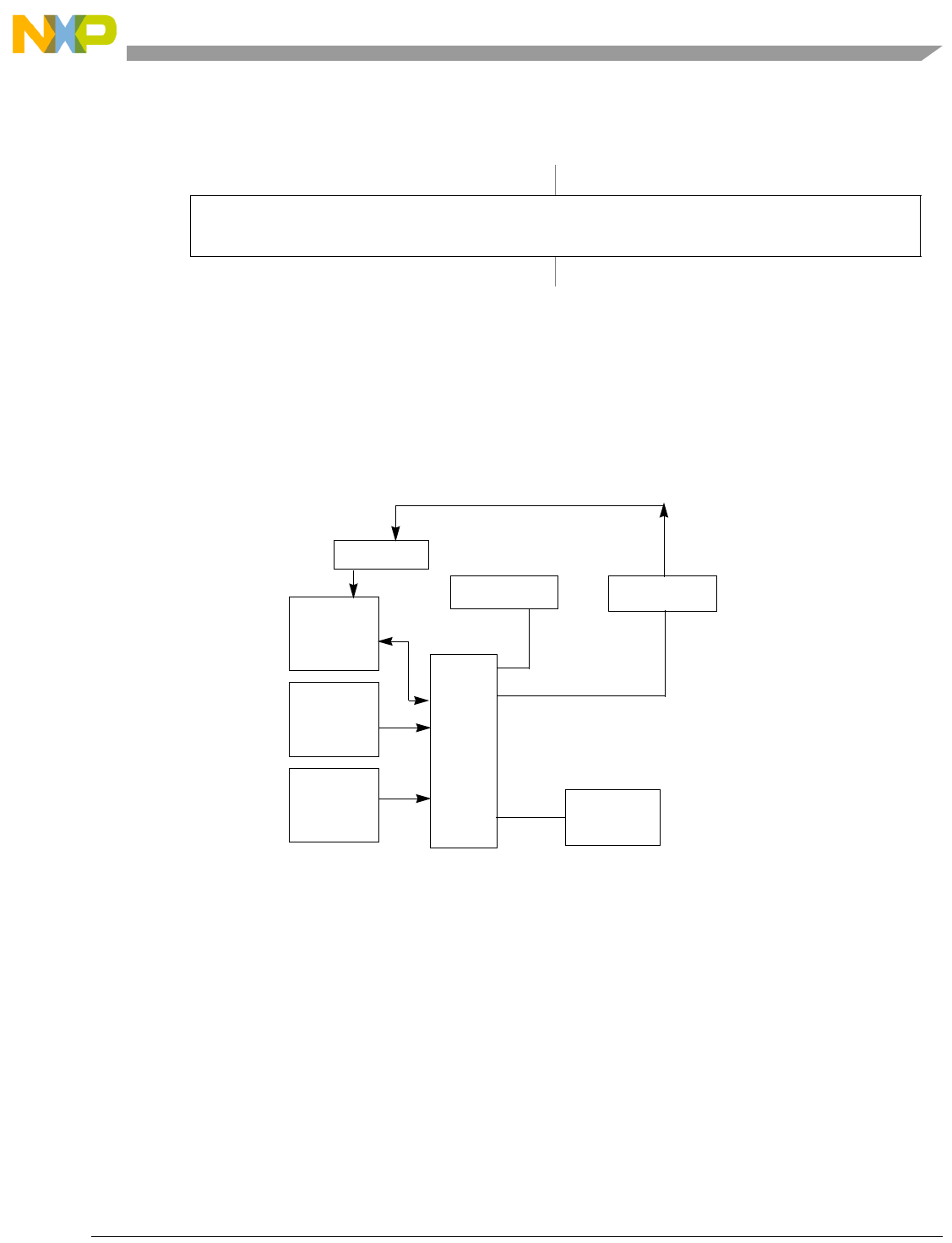
System Control Module (SCM)
Freescale Semiconductor 12-9
12.6 Internal Bus Arbitration
The internal bus arbitration is performed by the on-chip bus arbiter, which containing the arbitration logic
that controls which of up to four MBus masters (M0–M3 in Figure 12-6) has access to the external buses.
The function of the arbitration logic is described in this section.
Figure 12-6. Arbiter Module Functions
12.6.1 Overview
The basic functionality is that of a 2-port, pipelined internal bus arbitration module with the following
attributes:
• The master pointed to by the current arbitration pointer may get on the bus with zero latency if the
address phase is available. All other requesters face at least a one cycle arbitration pipeline delay
to meet bus timing constraints on address phase hold.
• If a requester receives an immediate address phase (that is, it is pointed to by the current arbitration
pointer and the bus address phase is available), it is the current bus master and is ignored by
arbitration. All remaining requesting ports are evaluated by the arbitration algorithm to determine
the next-state arbitration pointer.
IPSBAR
Offset:
0x0013 (CWSR) Access: read/write
76543210
R
CWSR[7:0]
W
Reset: Uninitialized
Figure 12-5. Core Watchdog Service Register (CWSR)
SRAM1
MPARK RAMBAR
CPU
M0
DMA
M2
Internal
M1
Bus
Master Internal
MARB
Modules
Back door to SRAM and flash
MCF52211 ColdFire® Integrated Microcontroller Reference Manual, Rev. 3

System Control Module (SCM)
12-10 Freescale Semiconductor
• There are two arbitration algorithms: fixed and round-robin. Fixed arbitration sets the next-state
arbitration pointer to the highest priority requester. Round-robin arbitration sets the next-state
arbitration pointer to the highest priority requester (calculated by adding a requester's fixed priority
to the current bus master’s fixed priority and then taking this sum modulo the number of possible
bus masters).
• The default priority is DMA (M2) > CPU (M0), where M2 is the highest and M0 the lowest
priority.
• There are two actions for an idle arbitration cycle, leave the current arbitration pointer as is or set
it to the lowest priority requester.
• The anti-lock-out logic for the fixed priority scheme forces the arbitration algorithm to round-robin
if any requester has been held for longer than a specified cycle count.
12.6.2 Arbitration Algorithms
There are two modes of arbitration: fixed and round-robin. This section discusses the differences between
them.
12.6.2.1 Round-Robin Mode
Round-robin arbitration is the default mode after reset. This scheme cycles through the sequence of
masters as specified by MPARK[Mn_PRTY] bits. Upon completion of a transfer, the master is given the
lowest priority and the priority for all other masters is increased by one.
If no masters are requesting, the arbitration unit must park, pointing at one of the masters. There are two
possibilities: park the arbitration unit on the last active master, or park pointing to the highest priority
master. Setting MPARK[PRK_LAST] causes the arbitration pointer to be parked on the highest priority
master. In round-robin mode, programming the timeout enable and lockout bits MPARK[13,11:8] has no
effect on the arbitration.
12.6.2.2 Fixed Mode
In fixed arbitration, the master with highest priority (as specified by the MPARK[Mn_PRTY] bits) wins
the bus. That master relinquishes the bus when all transfers to that master are complete.
If MPARK[TIMEOUT] is set, a counter increments for each master for every cycle it is denied access.
When a counter reaches the limit set by MPARK[LCKOUT_TIME], the arbitration algorithm is changed
to round-robin arbitration mode until all locks are cleared. The arbitration then returns to fixed mode and
the highest priority master is granted the bus.
As in round-robin mode, if no masters are requesting, the arbitration pointer parks on the highest priority
master if MPARK[PRK_LAST] is set or parks on the master that last requested the bus if cleared.
12.6.3 Bus Master Park Register (MPARK)
The MPARK controls the operation of the system bus arbitration module. The platform bus master
connections are defined as the following:
MCF52211 ColdFire® Integrated Microcontroller Reference Manual, Rev. 3

System Control Module (SCM)
Freescale Semiconductor 12-11
• Master 2 (M2): 4-channel DMA
• Master 0 (M0): V2 ColdFire Core
IPSBAR
Offset: 0x001C (MPARK)
Access: read/write
31 30 29 28 27 26 25 24 23 22 21 20 19 18 17 16
R 0 0 0 0 0 0 M2_P
_EN
BCR2
4BIT
00
M2_PRTY M0_PRTY 00
W
Reset0 0 1100001 1 1000 01
15 14 13 12 11 10 9 8 7 6 5 4 3 2 1 0
R 0 FIXED TIME
OUT
PRKL
AST LCKOUT_TIME 000000 00
W
Reset0 0 0000000 0 0000 00
Figure 12-7. Default Bus Master Park Register (MPARK)
Table 12-7. MPARK Field Description
Field Description
31–26 Reserved, should be cleared.
25
M2_P_EN
DMA bandwidth control enable
0 disable the use of the DMA's bandwidth control to elevate the priority of its bus requests.
1 enable the use of the DMA's bandwidth control to elevate the priority of its bus requests.
24
BCR24BIT
Enables the use of 24 bit byte count registers in the DMA module
0 DMA BCRs function as 16 bit counters.
1 DMA BCRs function as 24 bit counters.
23–22 Reserved, should be cleared.
21–20
M2_PRTY
Master priority level for master 2 (DMA Controller)
00 fourth (lowest) priority
01 third priority
10 second priority
11 first (highest) priority
19–18
M0_PRTY
Master priority level for master 0 (ColdFire Core)
00 fourth (lowest) priority
01 third priority
10 second priority
11 first (highest) priority
17–16 Reserved, should be cleared.
15 Reserved, should be cleared.
14
FIXED
Fixed or round robin arbitration
0 round robin arbitration
1 fixed arbitration
13
TIMEOUT
Timeout Enable
0 disable count for when a master is locked out by other masters.
1 enable count for when a master is locked out by other masters and allow access when LCKOUT_TIME is
reached.
MCF52211 ColdFire® Integrated Microcontroller Reference Manual, Rev. 3

System Control Module (SCM)
12-12 Freescale Semiconductor
The initial state of the master priorities is M2 > M0. System software should guarantee that the
programmed Mn_PRTY fields are unique, otherwise the hardware defaults to the initial-state priorities.
12.7 System Access Control Unit (SACU)
This section details the functionality of the system access control unit (SACU), which provides the
mechanism needed to implement secure bus transactions to the address space mapped to the internal
modules.
12.7.1 Overview
The SACU supports the traditional model of two privilege levels: supervisor and user. Typically, memory
references with the supervisor attribute have total accessibility to all the resources in the system, while user
mode references cannot access system control and configuration registers. In many systems, the operating
system executes in supervisor mode, while application software executes in user mode.
The SACU further partitions the access control functions into two parts: one control register defines the
privilege level associated with each bus master, and another set of control registers define the access levels
associated with the peripheral modules and memory space.
The SACU’s programming model is physically implemented as part of the system control module (SCM)
with the actual access control logic included as part of the arbitration controller. Each bus transaction
targeted for the IPS space is first checked to see if its privilege rights allow access to the given memory
space. If the privilege rights are correct, the access proceeds on the bus. If the privilege rights are
insufficient for the targeted memory space, the transfer is immediately aborted and terminated with an
exception, and the targeted module is not accessed.
12.7.2 Features
Each bus transfer can be classified by its privilege level and the reference type. The complete set of access
types includes the following:
• Supervisor instruction fetch
• Supervisor operand read
• Supervisor operand write
• User instruction fetch
• User operand read
12
PRKLAST
Park on the last active master or highest priority master if no masters are active
0 park on last active master
1 park on highest priority master
11–8
LCKOUT_TIME
Lock-out Time. Lock-out time for a master being denied the bus.
The lock out time is defined as 2^ LCKOUT_TIME[3:0].
7–0 Reserved, should be cleared.
Table 12-7. MPARK Field Description (continued)
Field Description
MCF52211 ColdFire® Integrated Microcontroller Reference Manual, Rev. 3

System Control Module (SCM)
Freescale Semiconductor 12-13
• User operand write
Instruction fetch accesses are associated with the execute attribute.
It should be noted that while the bus does not implement the concept of reference type (code versus data)
and only supports the user/supervisor privilege level, the reference type attribute is supported by the
system bus. Accordingly, the access checking associated with privilege level and reference type is
performed in the IPS controller using the attributes associated with the reference from the system bus.
The SACU partitions the access control mechanisms into three distinct functions:
• Master privilege register (MPR)
— Allows each bus master to be assigned a privilege level:
– Disable the master’s user/supervisor attribute and force to user mode access
– Enable the master’s user/supervisor attribute
— The reset state provides supervisor privilege to the processor core (bus master 0).
— Input signals allow the non-core bus masters to have their user/supervisor attribute enabled at
reset. This is intended to support the concept of a trusted bus master, and also controls the
ability of a bus master to modify the register state of any of the SACU control registers; that is,
only trusted masters can modify the control registers.
• Peripheral access control registers (PACRs)
— Provide read/write access rights, supervisor/user privilege levels.
— Reset state provides supervisor-only read/write access to these modules.
— Nine 8-bit registers control access to 17 of the on-chip peripheral modules
• Grouped peripheral access control registers (GPACR0, GPACR1)
— Provide read/write/execute access rights, supervisor/user privilege levels.
— One single register (GPACR0) controls access to 14 of the on-chip peripheral modules.
— One register (GPACR1) controls access for IPS reads and writes to the flash module.
— Reset state provides supervisor-only read/write access to each of these peripheral spaces.
12.7.3 Memory Map/Register Definition
The memory map for the SACU program-visible registers within the system control module (SCM) is
shown in Table 12-8. The MPR, PACR, and GPACRs are 8 bits wide.
Table 12-8. SACU Register Memory Map
IPSBAR
Offset [31:28] [27:24] [23:20] [19:16] [15:12] [11:8] [7:4] [3:0]
0x020 MPR PPMRS PPMRC IPSBMT
0x024 PACR0 PACR1 PACR2 PACR3
0x028 PACR4 PACR5 PACR6 PACR7
0x02C PACR8 — — —
0x030 GPACR0 GPACR1 — —
MCF52211 ColdFire® Integrated Microcontroller Reference Manual, Rev. 3

System Control Module (SCM)
12-14 Freescale Semiconductor
12.7.3.1 Master Privilege Register (MPR)
The MPR specifies the access privilege level associated with each bus master in the platform. The register
provides one bit per bus master. Bit 3 is reserved and should be cleared. Bits 2:0 correspond to master 2
(DMA Controller), master 1 (internal bus master), and master 0 (ColdFire core), respectively.
Only trusted bus masters can modify the access control registers. If a non-trusted bus master attempts to
write any of the SACU control registers, the access is aborted with an error termination and the registers
remain unaffected.
The processor core is connected to bus master 0 and is always treated as a trusted bus master. Accordingly,
MPR[0] is forced to 1 at reset.
12.7.3.2 Peripheral Access Control Registers (PACR0–PACR8)
Access to several on-chip peripherals is controlled by shared peripheral access control registers. A single
PACR defines the access level for each of the two modules. These modules only support operand reads
and writes. Each PACR follows the format illustrated in Figure 12-9. For a list of PACRs and the modules
that they control, refer to Table 12-12.
0x034 — — — —
0x038 — — — —
0x03C — — — —
IPSBAR
Offset: 0x0020 (MPR)
Access: read/write
76543210
R 0 0 0 0
MPR[3:0]
W
Reset:00000001
Figure 12-8. Master Privilege Register (MPR)
Table 12-9. MPR[n] Field Descriptions
Field Description
7–4 Reserved. Should be cleared.
3–0
MPR
Each 1-bit field defines the access privilege level of the given bus master n.
0 All bus master accesses are in user mode.
1 All bus master accesses use the sourced user/supervisor attribute.
Note: Bit 3 is reserved and should be cleared.
Table 12-8. SACU Register Memory Map (continued)
IPSBAR
Offset [31:28] [27:24] [23:20] [19:16] [15:12] [11:8] [7:4] [3:0]
MCF52211 ColdFire® Integrated Microcontroller Reference Manual, Rev. 3

System Control Module (SCM)
Freescale Semiconductor 12-15
IPSBAR
Offset:
0x0024 + Offset (PACRn) Access: read/write
76543210
R
LOCK1 ACCESS_CTRL1 LOCK0 ACCESS_CTRL0
W
Reset:00000000
Figure 12-9. Peripheral Access Control Register (PACRn)
Table 12-10. PACR Field Descriptions
Field Description
7
LOCK1
This bit, when set, prevents subsequent writes to ACCESSCTRL1. Any attempted write to the PACR
generates an error termination and the contents of the register are not affected. Only a system reset clears
this flag.
6–4
ACCESS_CTRL1
This 3-bit field defines the access control for the given platform peripheral.
The encodings for this field are shown in Table 12-11.
3
LOCK0
This bit, when set, prevents subsequent writes to ACCESSCTRL0. Any attempted write to the PACR
generates an error termination and the contents of the register are not affected. Only a system reset clears
this flag.
2–0
ACCESS_CTRL0
This 3-bit field defines the access control for the given platform peripheral.
The encodings for this field are shown in Table 12-11.
Table 12-11. PACR ACCESSCTRL Bit Encodings
Bits Supervisor Mode User Mode
000 Read/Write No Access
001 Read No Access
010 Read Read
011 Read No Access
100 Read/Write Read/Write
101 Read/Write Read
110 Read/Write Read/Write
111 No Access No Access
Table 12-12. Peripheral Access Control Registers (PACRs)
IPSBAR Offset Name
Modules Controlled1
ACCESS_CTRL1 ACCESS_CTRL0
0x024 PACR0 SCM —
0x025 PACR1 — DMA
0x026 PACR2 UART0 UART1
MCF52211 ColdFire® Integrated Microcontroller Reference Manual, Rev. 3

System Control Module (SCM)
12-16 Freescale Semiconductor
At reset, these on-chip modules are configured to have only supervisor read/write access capabilities. If an
instruction fetch access to any of these peripheral modules is attempted, the IPS bus cycle is immediately
terminated with an error.
12.7.3.3 Grouped Peripheral Access Control Registers (GPACR0 & GPACR1)
The on-chip peripheral space starting at IPSBAR is subdivided into sixteen 64-Mbyte regions. Each of the
first two regions has a unique access control register associated with it. The other 14 regions are in reserved
space; the access control registers for these regions are not implemented. Bits [29:26] of the address select
the specific GPACRn to be used for a given reference within the IPS address space. These access control
registers are 8 bits wide so that read, write, and execute attributes may be assigned to the given IPS region.
NOTE
The access control for modules with memory space protected by
PACR0–PACR8 are determined by the PACR0–PACR8 settings. The access
control is not affected by GPACR0, even though the modules are mapped in
its 64-Mbyte address space.
0x027 PACR3 UART2 —
0x028 PACR4 I2C QSPI
0x029 PACR5 — —
0x02A PACR6 DTIM0 DTIM1
0x02B PACR7 DTIM2 DTIM3
0x02C PACR8 INTC0 —
1A value of — in these columns indicates that the bits are not associated with any module and are
reserved.
IPSBAR
Offsets:
0x0030 (GPACR0)
0x0031 (GPACR1)
Access: read/write
76543210
R
LOCK
0 0 0
ACCESS_CTRL
W
Reset:00000000
Figure 12-10. GPACR Register
Table 12-12. Peripheral Access Control Registers (PACRs) (continued)
IPSBAR Offset Name
Modules Controlled1
ACCESS_CTRL1 ACCESS_CTRL0
MCF52211 ColdFire® Integrated Microcontroller Reference Manual, Rev. 3

System Control Module (SCM)
Freescale Semiconductor 12-17
At reset, these on-chip modules are configured to have only supervisor read/write access capabilities. Bit
encodings for the ACCESS_CTRL field in the GPACR are shown in Table 12-14. Table 12-15 shows the
memory space protected by the GPACRs and the modules mapped to these spaces.
Table 12-13. Grouped Peripheral Access Control Register (GPACR) Field Descriptions
Field Description
7
LOCK
This bit, after set, prevents subsequent writes to the GPACR. Any attempted write to the GPACR generates
an error termination and the contents of the register are not affected. Only a system reset clears this flag.
6–4 Reserved, should be cleared.
3–0
ACCESS_CTRL
This 4-bit field defines the access control for the given memory region.
The encodings for this field are shown in Table 12-14.
Table 12-14. GPACR ACCESS_CTRL Bit Encodings
Bits Supervisor Mode User Mode
0000 Read / Write No Access
0001 Read No Access
0010 Read Read
0011 Read No Access
0100 Read / Write Read / Write
0101 Read / Write Read
0110 Read / Write Read / Write
0111 No Access No Access
1000 Read / Write / Execute No Access
1001 Read / Execute No Access
1010 Read / Execute Read / Execute
1011 Execute No Access
1100 Read / Write / Execute Read / Write / Execute
1101 Read / Write / Execute Read / Execute
1110 Read / Write Read
1111 Read / Write / Execute Execute
MCF52211 ColdFire® Integrated Microcontroller Reference Manual, Rev. 3

System Control Module (SCM)
12-18 Freescale Semiconductor
Table 12-15. GPACR Address Space
Register Space Protected
(IPSBAR Offset) Modules Protected
GPACR0 0x0000_0000–
0x03FF_FFFF
Ports, CCM, PMM, Reset controller, Clock,
EPORT, WDOG, PIT0–PIT3, QADC, GPTA,
GPTB, FlexCAN, CFM (Control)
GPACR1 0x0400_0000–
0x07FF_FFFF
CFM (Flash module’s backdoor access for
programming or access by a bus master other
than the core)
MCF52211 ColdFire® Integrated Microcontroller Reference Manual, Rev. 3
Freescale Semiconductor 13-1
Chapter 13
General Purpose I/O Module
13.1 Introduction
Many of the pins associated with the external interface may be used for several different functions. When
not used for their primary function, many of the pins may be used as general-purpose digital I/O pins. In
some cases, the pin function is set by the operating mode, and the alternate pin functions are not supported.
The digital I/O pins are grouped into 8-bit ports. Some ports do not use all 8 bits. Each port has registers
that configure, monitor, and control the port pins. Figure 13-1 is a block diagram of the MCF52211 ports.
Figure 13-1. General Purpose I/O Module Block Diagram
DDATA[3:0] / PDD[7:4]
PORT QS
PORT AS
PORT DD
PORT UA
PORT UC
PORT TC
PORT TD
PST[3:0] / PDD[3:0]
SDA0 / PAS[1] / URXD2
SCL0 / PAS[0] / UTXD2
QSPI_CLK / PQS[2] / SCL0 / URTS1
QSPI_DIN / PQS[1] / SDA1 / URXD1
QSPI_DOUT / PQS[0] / SCL1 / UTXD1
DTIN3 / PTC[3] / DTOUT3 / PWM6
DTIN2 / PTC[2] / DTOUT2 / PWM4
DTIN1 / PTC[1] / DTOUT1 / PWM2
DTIN0 / PTC[0] / DTOUT0 / PWM0
UCTS1 / PUB[3] / SYNCA / URXD2
URTS1 / PUB[2] / SYNCB / UTXD2
URXD1 / PUB[1] / SDA1
UTXD1 / PUB[0] / SCL1
UCTS0 / PUA[3]
URTS0 / PUA[2]
URXD0 / PUA[1] / RTC_EXTAL
UTXD0 / PUA[0] / RTC_XTAL
UCTS2 / PUC[3] / SCL1
URTS2 / PUC[2] / SDA1
URXD2 / PUC[1]
UTXD2 / PUC[0]
PWM7 / PTD[3]
PWM5 / PTD[2]
PWM3 / PTD[1]
PWM1 / PTD[0]
PORT TA
GPT[3] / PTA[3] / PWM7
GPT[2] / PTA[2] / PWM5
GPT[1] / PTA[1] / PWM3
GPT[0] / PTA[0] / PWM1
PORT AN
AN0 / PAN[0]
AN1 / PAN[1]
AN2 / PAN[2]
AN3 / PAN[3]
AN4 / PAN[4]
AN5 / PAN[5]
AN6 / PAN[6]
AN7 / PAN[7]
PORT UB
QSPI_CS0 / PQS[3] / SDA0 / UCTS1
PORT NQ
IRQ1 / PNQ[1] / SYNCA / USB_ALT_CLK
IRQ2 / PNQ[2]
IRQ3 / PNQ[3]
IRQ4 / PNQ[4]
IRQ5 / PNQ[5]
IRQ6 / PNQ[6]
IRQ7 / PNQ[7]
QSPI_CS1 / PQS[4]
QSPI_CS2 / PQS[5] / SYNCB
QSPI_CS3 / PQS[6] / SYNCA
MCF52211 ColdFire® Integrated Microcontroller Reference Manual, Rev. 3

General Purpose I/O Module
13-2 Freescale Semiconductor
13.2 Overview
The MCF52211 ports module controls the configuration for the following external pins:
• External bus accesses
• Chip selects
• Debug data
• Processor status
•USB
•I
2C serial control
• QSPI
• UART transmit/receive
• 32-bit DMA timers
13.3 Features
The MCF52211 ports includes these distinctive features:
• Control of primary function use on all ports
• Digital I/O support for all ports; registers for:
— Storing output pin data
— Controlling pin data direction
— Reading current pin state
— Setting and clearing output pin data registers
13.4 Signal Descriptions
Refer to Chapter 2, “Signal Descriptions,” for more detailed information on the different signals and pins.
13.5 Memory Map/Register Definition
13.5.1 Ports Memory Map
Table 13-1 summarizes all the registers in the MCF52211 ports address space.
MCF52211 ColdFire® Integrated Microcontroller Reference Manual, Rev. 3

General Purpose I/O Module
Freescale Semiconductor 13-3
Table 13-1. Registers in the MCF52211 Ports Address Space
Address1
1The register address is the sum of the IPSBAR address and the value in this column.
31–24 23–16 15–8 7–0 Access2
2S/U = supervisor or user mode access. User mode accesses to supervisor-only addresses have no effect and cause a
cycle termination transfer error.
Port Output Data Registers
0x10_0000 Reserved
0x10_0004 Reserved
0x10_0008 PORTNQ Reserved PORTAN PORTAS S/U
0x10_000C PORTQS Reserved PORTTA PORTTC S/U
0x10_0010 PORTTD PORTUA PORTUB PORTUC S/U
0x10_0014 PORTDD Reserved Reserved Reserved S/U
Port Data Direction Registers
0x10_0018 Reserved
0x10_001C Reserved
0x10_0020 DDRNQ Reserved DDRAN DDRAS S/U
0x10_0024 DDRQS Reserved DDRTA DDRTC S/U
0x10_0028 DDRTD DDRUA DDRUB DDRUC S/U
0x10_002C DDRDD Reserved Reserved Reserved S/U
Port Pin Data/Set Data Registers
0x10_0030 Reserved
0x10_0034 Reserved
0x10_0038 PORTNQP/SETNQ Reserved PORTANP/SETAN PORTASP/SETAS S/U
0x10_003C PORTQSP/SETQS Reserved PORTTAP/SETTA PORTTCP/SETTC S/U
0x10_0040 PORTTDP/SETTD PORTUAP/SETUA PORTUBP/SETUB PORTUCP/SETUC S/U
0x10_0044 PORTDDP/SETDD Reserved Reserved Reserved S/U
Port Clear Output Data Registers
0x10_0048 Reserved
0x10_004C Reserved
0x10_0050 CLRNQ Reserved CLRAN CLRAS S/U
0x10_0054 CLRQS Reserved CLRTA CLRTC S/U
0x10_0058 CLRTD CLRUA CLRUB CLRUC S/U
0x10_005C CLRDD Reserved Reserved Reserved S/U
Port Pin Assignment Registers
0x10_0060 Reserved
0x10_0064 Reserved
0x10_0068 PNQPAR PANPAR PASPAR S/U
0x10_006C PQSPAR PTAPAR PTCPAR S/U
0x10_0070 PTDPAR PUAPAR PUBPAR PUCPAR S/U
0x10_0074 PDDPAR Reserved Reserved Reserved S/U
Port Pad Control Registers
0x10_0078 PSRR[31:0] S/U
0x10_007C PDSR[31:0] S/U
MCF52211 ColdFire® Integrated Microcontroller Reference Manual, Rev. 3

General Purpose I/O Module
13-4 Freescale Semiconductor
13.6 Register Descriptions
13.6.1 Port Output Data Registers (PORTn)
The PORTn registers store the data to be driven on the corresponding port n pins when the pins are
configured for digital output.
The PORTn registers with a full 8-bit implementation are shown in Figure 13-2. The remaining PORTn
registers use fewer than 8 bits. Their bit definitions are shown in Figure 13-3, Figure 13-4, Figure 13-5,
and Figure 13-6. The fields are described in Table 13-2, which applies to all PORTn registers.
The PORTn registers are read/write. At reset, all bits in the PORTn registers are set.
Reading a PORTn register returns the current values in the register, not the port n pin values.
PORTn bits can be set by setting the PORTn register, or by setting the corresponding bits in the
PORTnP/SETn register. They can be cleared by clearing the PORTn register, or by clearing the
corresponding bits in the CLRn register.
IPSBAR
Offsets:
0x10_0014 (PORTDD)
0x10_000A (PORTAN)
Access: User read/write
76543210
RPORTn7PORTn6PORTn5PORTn4PORTn3PORTn2PORTn1PORTn0
W
Reset:11111111
Figure 13-2. Port Output Data Registers with Bits 7:0 Implemented (PORTDD, PORTAN)
IPSBAR
Offsets:
0x10_000E (PORTTA)
0x10_000F (PORTTC)
0x10_0010 (PORTTD)
0x10_0011 (PORTUA)
0x10_0012 (PORTUB)
0x10_0013 (PORTUC)
Access: User read/write
76543210
R0 0 0 0 PORTn3PORTn2PORTn1PORTn0
W
Reset:00001111
Figure 13-3. Port Output Data Registers with Bits 3:0 Implemented (PORTTA, PORTTC, PORTDD, PORTUA,
PORTUB, PORTUC)
MCF52211 ColdFire® Integrated Microcontroller Reference Manual, Rev. 3

General Purpose I/O Module
Freescale Semiconductor 13-5
13.6.2 Port Data Direction Registers (DDRn)
The DDRn registers control the direction of the port n pin drivers when the pins are configured for digital
I/O.
The DDRn registers with a full 8-bit implementation are shown in Figure 13-7. The remaining DDRn
registers use fewer than eight bits. Their bit definitions are shown in Figure 13-8, Figure 13-9,
Figure 13-10, and Figure 13-11. The fields are described in Table 13-3, which applies to all DDRn
registers.
The DDRn registers are read/write. At reset, all bits in the DDRn registers are cleared.
IPSBAR
Offset: 0x10_000C (PORTQS)
Access: User read/write
76543210
R0PORTn6PORTn5PORTn4PORTn3PORTn2PORTn1PORTn0
W
Reset:01111111
Figure 13-4. Port QS Output Data Register (PORTQS)
IPSBAR
Offset: 0x10_0008 (PORTNQ)
Access: User read/write
76543210
RPORTn7PORTn6PORTn5PORTn4PORTn3PORTn2PORTn10
W
Reset:11111110
Figure 13-5. Port NQ Output Data Register (PORTNQ)
IPSBAR
Offset: 0x10_000B (PORTAS)
Access: User read/write
76543210
R000000
PORTn1PORTn0
W
Reset:00000011
Figure 13-6. Port AS Output Data Register (PORTAS)
Table 13-2. PORTn Field Descriptions
Field Description
Portnx Data to be driven when the port pin is configured as a digital output.
1 Output is a logic 1
0 Output is a logic 0
MCF52211 ColdFire® Integrated Microcontroller Reference Manual, Rev. 3

General Purpose I/O Module
13-6 Freescale Semiconductor
Setting any bit in a DDRn register configures the corresponding port n pin as an output. Clearing any bit
in a DDRn register configures the corresponding pin as an input.
IPSBAR
Offsets:
0x10_002C (DDRDD)
0x10_0022 (DDRAN)
Access: User read/write
76543210
RDDRn7DDRn6DDRn5DDRn4 DDRn3 DDRn2 DDRn1 DDRn0
W
Reset:00000000
Figure 13-7. Port Data Direction Registers with Bits 7:0 Implemented (DDRDD, DDRAN)
IPSBAR
Offsets:
0x10_0026 (DDRTA)
0x10_0027 (DDRTC)
0x10_0028 (DDRTD)
0x10_0029 (DDRUA)
0x10_002A (DDRUB)
0x10_002B (DDRUC)
Access: User read/write
76543210
R0 0 0 0 DDRn3 DDRn2 DDRn1 DDRn0
W
Reset:00000000
Figure 13-8. Port Data Direction Registers with Bits 3:0 Implemented (DDRTA, DDRTC, DDRTD, DDRUA,
DDRUB, DDRUC)
IPSBAR
Offset: 0x10_0024 (DDRQS)
Access: User read/write
76543210
R0DDRn6DDRn5DDRn4 DDRn3 DDRn2 DDRn1 DDRn0
W
Reset:00000000
Figure 13-9. Port QS Data Direction Register (DDRQS)
IPSBAR
Offset: 0x10_0020 (DDRNQ)
Access: User read/write
76543210
RDDRn7DDRn6DDRn5DDRn4 DDRn3 DDRn2 DDRn10
W
Reset:00000000
Figure 13-10. Port NQ Data Direction Register (DDRNQ)
MCF52211 ColdFire® Integrated Microcontroller Reference Manual, Rev. 3

General Purpose I/O Module
Freescale Semiconductor 13-7
13.6.3 Port Pin Data/Set Data Registers (PORTnP/SETn)
The PORTnP/SETn registers reflect the current pin states and control the setting of output pins when the
pin is configured for digital I/O.
The PORTnP/SETn registers with a full 8-bit implementation are shown in Figure 13-12. The remaining
PORTnP/SETn registers use fewer than eight bits. Their bit definitions are shown in Figure 13-13,
Figure 13-14, Figure 13-15, and Figure 13-16. The fields are described in Table 13-4, which applies to all
PORTnP/SETn registers.
The PORTnP/SETn registers are read/write. At reset, the bits in the PORTnP/SETn registers are set to the
current pin states.
Reading a PORTnP/SETn register returns the current state of the port n pins.
Writing 1s to a PORTnP/SETn register sets the corresponding bits in the PORTn register. Writing 0s has
no effect.
IPSBAR
Offset: 0x10_0023 (DDRAS)
Access: User read/write
76543210
R000000
DDRn1 DDRn0
W
Reset:00000000
Figure 13-11. Port AS Data Direction Register (DDRAS)
Table 13-3. DDRn Field Descriptions
Field Description
DDRnx Sets data direction for port nx pin when the port is configured as a digital output.
1 DDRnx is configured as an output
0 DDRnx is configured as an input
IPSBAR
Offsets:
0x10_0044 (PORTDDP/SETDD)
0x10_003A (PORTANP/SETAN)
Access: User read/write
76543210
RPORTnP7 PORTnP6 PORTnP5 PORTnP4 PORTnP3 PORTnP2 PORTnP1 PORTnP0
W
Reset:11111111
Figure 13-12. Port Pin Data/Set Data Registers with Bits 7:0 Implemented (PORTDD/SETDD,
PORTAN/SETAN)
MCF52211 ColdFire® Integrated Microcontroller Reference Manual, Rev. 3

General Purpose I/O Module
13-8 Freescale Semiconductor
IPSBAR
Offsets:
0x10_003E (PORTTAP/SETTA)
0x10_003F (PORTTCP/SETTC)
0x10_0040 (PORTTDP/SETTD)
0x10_0041 (PORTUAP/SETUA)
0x10_0042 (PORTUBP/SETUB)
0x10_0043 (PORTUCP/SETUC)
Access: User read/write
76543210
R0 0 0 0 PORTnP3 PORTnP2 PORTnP1 PORTnP0
W
Reset:00001111
Figure 13-13. Port Pin Data/Set Data Registers with Bits 3:0 Implemented (PORTTA/SETTA, PORTTC/SETTC,
PORTTD/SETTD, PORTUA/SETUA, PORTUB/SETUB, PORTUC/SETUC)
IPSBAR
Offset: 0x10_003C (PORTQSP/SETQS)
Access: User read/write
76543210
R0PORTnP6 PORTnP5 PORTnP4 PORTnP3 PORTnP2 PORTnP1 PORTnP0
W
Reset:01111111
Figure 13-14. Port QS Pin Data/Set Data Register (PORTQS/SETQS)
IPSBAR
Offset: 0x10_0038 (PORTNQP/SETNQ)
Access: User read/write
76543210
RPORTnP7 PORTnP6 PORTnP5 PORTnP4 PORTnP3 PORTnP2 PORTnP1 0
W
Reset:11111110
Figure 13-15. Port NQ Pin Data/Set Data Register (PORTNQ/SETNQ)
IPSBAR
Offset: 0x10_003B (PORTASP/SETAS)
Access: User read/write
76543210
R000000
PORTnP1 PORTnP0
W
Reset:00000011
Figure 13-16. Port AS Pin Data/Set Data Register (PORTAS/SETAS)
MCF52211 ColdFire® Integrated Microcontroller Reference Manual, Rev. 3

General Purpose I/O Module
Freescale Semiconductor 13-9
13.6.4 Port Clear Output Data Registers (CLRn)
Writing 0s to a CLRn register clears the corresponding bits in the PORTn register. Writing 1s has no effect.
Reading the CLRn register returns 0s.
The CLRn registers with a full 8-bit implementation are shown in Figure 13-17. The remaining DDRn
registers use fewer than eight bits. Their bit definitions are shown in Figure 13-18, Figure 13-19,
Figure 13-20, and Figure 13-21. The fields are described in Table 13-5, which applies to all CLRn
registers.
The CLRn registers are read/write.
Table 13-4. PORTnP/SETn Field Descriptions
Field Description
PortnPx Port nx pin data/set data bits.
1PortnPx pin state is 1 (read); writing a 1 sets the corresponding port nx bit to 1
0PortnPx pin state is 0
IPSBAR
Offsets:
0x10_005C (CLRDD)
0x10_0052 (CLRAN)
Access: User read/write
76543210
RCLRn7CLRn6CLRn5CLRn4CLRn3CLRn2CLRn1CLRn0
W
Reset:00000000
Figure 13-17. Port Clear Output Data Registers with Bits 7:0 Implemented (CLRDD, CLRAN)
IPSBAR
Offsets:
0x10_0056 (CLRTA)
0x10_0057 (CLRTC)
0x10_0058 (CLRTD)
0x10_0059 (CLRUA)
0x10_005A (CLRUB)
0x10_005B (CLRUC)
Access: User read/write
76543210
R0 0 0 0 CLRn3CLRn2CLRn1CLRn0
W
Reset:00000000
Figure 13-18. Port Clear Output Data Registers with Bits 3:0 Implemented (CLRTA, CLRTC, CLRTD, CLRUA,
CLRUB, CLRUC)
MCF52211 ColdFire® Integrated Microcontroller Reference Manual, Rev. 3

General Purpose I/O Module
13-10 Freescale Semiconductor
13.6.5 Pin Assignment Registers
All pin assignment registers are read/write. Refer to Table 2-1 for the different functions assignable to each
pin.
Some signals can be assigned to different pins (see Table 2-1). However, a signal should not be assigned
to more than one pin at the same time. If a signal is assigned to two or more pins simultaneously, the result
is undefined.
IPSBAR
Offset: 0x10_0054 (CLRQS)
Access: User read/write
76543210
R0CLRn6CLRn5CLRn4CLRn3CLRn2CLRn1CLRn0
W
Reset:00000000
Figure 13-19. Port QS Clear Output Data Register (CLRQS)
IPSBAR
Offset: 0x10_0050 (CLRNQ)
Access: User read/write
76543210
RCLRn7CLRn6CLRn5CLRn4CLRn3CLRn2CLRn10
W
Reset:00000000
Figure 13-20. Port NQ Clear Output Data Register (CLRNQ)
IPSBAR
Offset: 0x10_0053 (CLRAS)
Access: User read/write
76543210
R000000
CLRn1CLRn0
W
Reset:00000000
Figure 13-21. Port AS Clear Output Data Register (CLRAS)
Table 13-5. CLRn Field Descriptions
Field Description
CLRnxPortnx pin data/set data bits.
1 Never returned for reads; no effect for writes
0 Always returned for reads; clears corresponding port nx bit for writes
MCF52211 ColdFire® Integrated Microcontroller Reference Manual, Rev. 3

General Purpose I/O Module
Freescale Semiconductor 13-11
13.6.5.1 Dual-Function Pin Assignment Registers
The dual function pin assignment registers allow each pin controlled by each register bit to be configured
for the primary function or the GPIO function. The fields are described in Table 13-6, which applies to all
dual-function registers.
.
13.6.5.2 Quad Function Pin Assignment Registers
The quad function pin assignment registers allow each pin controlled by each register bit to be configured
for the primary, alternate 1 (secondary), alternate 2 (tertiary), and GPIO (quaternary) functions. The fields
are described in Table 13-7, which applies to all quad-function registers.
IPSBAR
Offsets:
0x10_0074 (PDDPAR)
0x10_006A (PANPAR)
Access: User read/write
76543210
RPnPAR7 PnPAR6 PnPAR5 PnPAR4 PnPAR3 PnPAR2 PnPAR1 PnPAR0
W
Reset:00000000
Figure 13-22. Dual-Function Pin Assignment Registers with Bits 7:0 Implemented (PDDPAR, PANPAR)
IPSBAR
Offsets:
0x10_0070 (PTDPAR)
0x10_0073 (PUCPAR)
Access: User read/write
76543210
R0 0 0 0 PnPAR3 PnPAR2 PnPAR1 PnPAR0
W
Reset:00000000
Figure 13-23. Dual-Function Pin Assignment Registers with Bits 3:0 Implemented (PTDPAR, PUCPAR)
Table 13-6. Dual-Function PnPAR Field Descriptions
Field Description
PnPA R x P nPARx pin assignment register bits.
1 Pin assumes the primary function
0 Pin assumes the GPIO function
MCF52211 ColdFire® Integrated Microcontroller Reference Manual, Rev. 3

General Purpose I/O Module
13-12 Freescale Semiconductor
IPSBAR
Offset: 0x10_006C (PQSPAR)
Access: User read/write
15 14 13 12 11 10 9 8
R 0 0 PnPAR6 PnPAR5 PnPAR4
W
Reset00000000
76543210
RPnPAR3 PnPAR2 PnPAR1 PnPAR0
W
Reset00000000
Figure 13-24. Port QS Pin Assignment Register (PQSPAR)
IPSBAR
Offset: 0x10_006B (PASPAR)
Access: User read/write
76543210
R0000 PnPAR1 PnPAR0
W
Reset:00000000
Figure 13-25. Port AS Pin Assignment Register (PASPAR)
IPSBAR
Offsets:
0x10_006E (PTAPAR)
0x10_006F (PTCPAR)
0x10_0070 (PTDPAR)
0x10_0071 (PUAPAR)
0x10_0072 (PUBPAR)
Access: User read/write
76543210
RPnPAR3 PnPAR2 PnPAR1 PnPAR0
W
Reset:00000000
Figure 13-26. Quad-Function Pin Assignment Registers with Bits 7:0 Implemented (PTAPAR, PTCPAR,
PTDPAR, PUAPAR, PUBPAR)
Table 13-7. Quad-Function PnPAR Field Descriptions
Field Description
PnPA R x P nPARx pin assignment register bits.
00 Pin assumes the GPIO function
01 Pin assumes the primary function
10 Pin assumes the alternate 1 function
11 Pin assumes the alternate 2 function
MCF52211 ColdFire® Integrated Microcontroller Reference Manual, Rev. 3

General Purpose I/O Module
Freescale Semiconductor 13-13
13.6.5.3 Port NQ Pin Assignment Register (PNQPAR)
The port NQ pin assignment register (PNQPAR) contains quad-function (for IRQ1) and dual-function pin
assignment controls. Refer to Table 13-6 and Table 13-7 for the encodings for the different fields. The
reset value of the PNQPAR register defaults to the primary function (IRQ) instead of GPIO.
13.6.6 Pad Control Registers
13.6.6.1 Pin Slew Rate Register (PSRR)
The pin slew rate register (PSRR) is read/write. Each bit resets to logic 0 in Single Chip mode (MCF52211
default) and logic 1 in EzPort and FAST mode. The fields are described in Table 13-8.
The slew rate control bits corresponding to each pin/signal are listed in Table 2-1.
IPSBAR
Offset: 0x10_0068 (PNQPAR)
Access: User read/write
15 14 13 12 11 10 9 8
RPNQPAR7 PNQPAR6 PNQPAR5 PNQPAR4
W
Reset010100101
76543210
RPNQPAR3 PNQPAR2 PNQPAR1 00
W
Reset01010100
Figure 13-27. Port NQ Pin Assignment Register (PNQPAR)
MCF52211 ColdFire® Integrated Microcontroller Reference Manual, Rev. 3

General Purpose I/O Module
13-14 Freescale Semiconductor
IPSBAR
Offset: 0x10_0078 (PSRR)
Access: User read/write
31 30 29 28 27 26 25 24
RPSRR31 PSRR30 PSRR29 PSRR28 PSRR27 PSRR26 PSRR25 PSRR24
W
Reset00000000
23 22 21 20 19 18 17 16
RPSRR23 PSRR22 PSRR21 PSRR20 PSRR19 PSRR18 PSRR17 PSRR16
W
Reset00000000
15 14 13 12 11 10 9 8
RPSRR15 PSRR14 PSRR13 PSRR12 PSRR11 PSRR10 PSRR9 PSRR8
W
Reset00000000
76543210
RPSRR7 PSRR6 PSRR5 PSRR4 PSRR3 PSRR2 PSRR1 PSRR0
W
Reset00000000
Figure 13-28. Pin Slew Rate Register (PSRR)
Table 13-8. PSRR Field Descriptions
Field Description
PSRRx PSRRx slew rate register control bits.
1 Pin is configured for slow slew rate (delay is approximately 10 times slower)
0 Pin is configured for fast slew rate
MCF52211 ColdFire® Integrated Microcontroller Reference Manual, Rev. 3

General Purpose I/O Module
Freescale Semiconductor 13-15
13.6.6.2 Pin Drive Strength Register (PDSR)
The pin drive strength register is read/write. Each bit resets to logic 0 in single chip mode (MCF52211
default) and logic 1 in EzPort and FAST mode. The fields are described in Table 13-9.
Refer to Table 2-1 for details of which PDSR bit controls which pin.
.
13.7 Ports Interrupts
The ports module does not generate interrupt requests.
IPSBAR
Offset: 0x10_007C (PDSR)
Access: User read/write
31 30 29 28 27 26 25 24
RPDSR31 PDSR30 PDSR29 PDSR28 PDSR27 PDSR26 PDSR25 PDSR24
W
Reset See note 1
23 22 21 20 19 18 17 16
RPDSR23 PDSR22 PDSR21 PDSR20 PDSR19 PDSR18 PDSR17 PDSR16
W
Reset See note 1
15 14 13 12 11 10 9 8
RPDSR15 PDSR14 PDSR13 PDSR12 PDSR11 PDSR10 PDSR9 PDSR8
W
Reset See note 1
76543210
RPDSR7 PDSR6 PDSR5 PDSR4 PDSR3 PDSR2 PDSR1 PDSR0
W
Reset See note 1
1)Each bit resets to logic 0 in Single Chip mode and logic 1 in EzPort/FAST mode.
Figure 13-29. Pin Drive Strength Register (PDSR)
Table 13-9. PDSR Field Descriptions
Field Description
PDSRx PDSRx pin strength register control bits.
1 Pin is configured for high drive strength (10mA)
0 Pin is configured for low drive strength (2mA)
MCF52211 ColdFire® Integrated Microcontroller Reference Manual, Rev. 3

Freescale Semiconductor 14-1
Chapter 14
Interrupt Controller Module
This section details the functionality for the interrupt controller. The general features of the interrupt
controller include:
• Interrupt sources
— 56 fully-programmable interrupt sources (of which some are reserved)
— 7 fixed-level interrupt sources
• Each of the sources has a unique interrupt control register (ICRnx) to define the software-assigned
levels and priorities within the level
• Unique vector number for each interrupt source
• Ability to mask any individual interrupt source, plus global mask-all capability
• Supports hardware and software interrupt acknowledge cycles
• Wake-up signal from low-power stop modes
The 50 fully-programmable and seven fixed-level interrupt sources for the interrupt controller manage the
complete set of interrupt sources from all of the modules on the device. This section describes how the
interrupt sources are mapped to the interrupt controller logic and how interrupts are serviced.
14.1 68K/ColdFire Interrupt Architecture Overview
Before continuing with the specifics of the interrupt controller, a brief review of the interrupt architecture
of the 68K/ColdFire family is appropriate.
The interrupt architecture of ColdFire is exactly the same as the M68000 family, where there is a 3-bit
encoded interrupt priority level sent from the interrupt controller to the core, providing 7 levels of interrupt
requests. Level 7 represents the highest priority interrupt level, while level 1 is the lowest priority. The
processor samples for active interrupt requests once per instruction by comparing the encoded priority
level against a 3-bit interrupt mask value (I) contained in bits 10:8 of the core’s status register (SR). If the
priority level is greater than the SR[I] field at the sample point, the processor suspends normal instruction
execution and initiates interrupt exception processing. Level 7 interrupts are treated as non-maskable and
edge-sensitive within the processor, while levels 1–6 are treated as level-sensitive and may be masked
depending on the value of the SR[I] field. For correct operation, ColdFire requires that the interrupt source,
after asserted, remains asserted until explicitly disabled by the interrupt service routine.
During the interrupt exception processing, the CPU enters supervisor mode, disables trace mode, and then
fetches an 8-bit vector from the interrupt controller. This byte-sized operand fetch is known as the interrupt
acknowledge (IACK) cycle, with the ColdFire implementation using a special encoding of the transfer
type and transfer modifier attributes to distinguish this data fetch from a normal memory access. The
fetched data provides an index into the exception vector table, which contains 256 addresses, each pointing
MCF52211 ColdFire® Integrated Microcontroller Reference Manual, Rev. 3

Interrupt Controller Module
14-2 Freescale Semiconductor
to the beginning of a specific exception service routine. In particular, vectors 64–255 of the exception
vector table are reserved for user interrupt service routines. The first 64 exception vectors are reserved for
the processor to manage reset, error conditions (access, address), arithmetic faults, system calls, etc. After
the interrupt vector number has been retrieved, the processor continues by creating a stack frame in
memory. For ColdFire, all exception stack frames are 2 longwords in length and contain 32 bits of vector
and status register data, along with the 32-bit program counter value of the instruction that was interrupted
(see Section 3.3.3.1, “Exception Stack Frame Definition,” for more information on the stack frame
format).
After the exception stack frame is stored in memory, the processor accesses the 32-bit pointer from the
exception vector table using the vector number as the offset, and then jumps to that address to begin
execution of the service routine. After the status register is stored in the exception stack frame, the SR[I]
mask field is set to the level of the interrupt being acknowledged, effectively masking that level and all
lower values while in the service routine.
For this device, the processing of the interrupt acknowledge cycle is fundamentally different than previous
68K/ColdFire cores. In the new approach, all IACK cycles are directly managed by the interrupt controller,
so the requesting peripheral device is not accessed during IACK. As a result, the interrupt request must be
explicitly cleared in the peripheral during the interrupt service routine. For more information, see
Section 14.1.1.3, “Interrupt Vector Determination.”
Unlike the M68000 family, all ColdFire processors guarantee that the first instruction of the service routine
is executed before sampling for interrupts is resumed. By making this initial instruction a load of the SR,
interrupts can be safely disabled if required.
During the execution of the service routine, the appropriate actions must be performed on the peripheral
to negate the interrupt request.
For more information on exception processing, perform a keyword search at
http://www.freescale.com/coldfire for “CFPRM,” then click the CFPRM: ColdFire Family Programmer’s
Reference Manual link in the list of search results.
14.1.1 Interrupt Controller Theory of Operation
To support the interrupt architecture of the 68K/ColdFire programming model, the combined 63 interrupt
sources are organized as 7 levels, with each level supporting up to 9 prioritized requests. Consider the
priority structure within a single interrupt level (from highest to lowest priority) as shown in Table 14-1.
Table 14-1. Interrupt Priority Within a Level
ICR[2:0] Priority Interrupt
Sources
111 7 (Highest) 8–63
110 6 8–63
101 5 8–63
100 4 8–63
— Fixed Midpoint Priority 1–7
MCF52211 ColdFire® Integrated Microcontroller Reference Manual, Rev. 3

Interrupt Controller Module
Freescale Semiconductor 14-3
The level and priority is fully programmable for all sources except interrupt sources 1–7. Interrupt source
1–7 (from the edge port module) are fixed at the corresponding level’s midpoint priority. Thus, a maximum
of 8 fully-programmable interrupt sources are mapped into a single interrupt level. The fixed interrupt
source is hardwired to the given level and represents the mid-point of the priority within the level. For the
fully-programmable interrupt sources, the 3-bit level and the 3-bit priority within the level are defined in
the 8-bit interrupt control register (ICRnx).
The operation of the interrupt controller can be broadly partitioned into three activities:
• Recognition
• Prioritization
• Vector determination during IACK
14.1.1.1 Interrupt Recognition
The interrupt controller continuously examines the request sources and the interrupt mask register to
determine if there are active requests. This is the recognition phase.
14.1.1.2 Interrupt Prioritization
As an active request is detected, it is translated into the programmed interrupt level, and the resulting 7-bit
decoded priority level (IRQ[7:1]) is driven out of the interrupt controller.
14.1.1.3 Interrupt Vector Determination
After the core has sampled for pending interrupts and begun interrupt exception processing, it generates
an interrupt acknowledge (IACK) cycle. The IACK transfer is treated as a memory-mapped byte read by
the processor and routed to the appropriate interrupt controller. Next, the interrupt controller extracts the
level being acknowledged from address bits 4:2, determines the highest priority interrupt request active
for that level, and returns the 8-bit interrupt vector for that request to complete the cycle. The 8-bit interrupt
vector is formed using the following algorithm:
vector_number = 64 + interrupt source number
Recall that vector numbers 0–63 are reserved for the ColdFire processor and its internal exceptions. Thus,
the mapping of bit positions to vector numbers is as follows:
if interrupt source 1 is active and acknowledged, then Vector number = 65
if interrupt source 2 is active and acknowledged, then Vector number = 66
011 3 8–63
010 2 8–63
001 1 8–63
000 0 (Lowest) 8–63
Table 14-1. Interrupt Priority Within a Level (continued)
ICR[2:0] Priority Interrupt
Sources
MCF52211 ColdFire® Integrated Microcontroller Reference Manual, Rev. 3

Interrupt Controller Module
14-4 Freescale Semiconductor
...
if interrupt source 8 is active and acknowledged, then Vector number = 72
if interrupt source 9 is active and acknowledged, then Vector number = 73
...
if interrupt source 62 is active and acknowledged, then Vector number = 126
The net effect is a fixed mapping between the bit position within the source to the actual interrupt vector
number.
If there is no active interrupt source for the given level, a special spurious interrupt vector (vector
number = 24) is returned. It is the responsibility of the service routine to manage this error situation.
This protocol implies the interrupting peripheral is not accessed during the acknowledge cycle because the
interrupt controller completely services the acknowledge. This means the interrupt source must be
explicitly disabled in the interrupt service routine. This design provides unique vector capability for all
interrupt requests, regardless of the complexity of the peripheral device.
14.2 Memory Map
The register programming model for the interrupt controllers is memory-mapped to a 256-byte space. In
the following discussion, there are a number of program-visible registers greater than 32 bits. For these
control fields, the physical register is partitioned into two 32-bit values: a register high (the upper
longword, represented by an appended H) and a register low (the lower longword, represented by an
appended L).
The registers and their locations are defined in Table 14-3. The register names include the (zero-based)
interrupt controller number n, which is useful in devices with multiple controllers. This device has only
one interrupt controller; hence, n=0.
Table 14-2. Interrupt Controller Base Addresses
Interrupt Controller Number Base Address
INTC0 IPSBAR + 0xC00
Global IACK Registers Space1
1This address space only contains the L1ACK-L7IACK registers. See Section 14.3.7, “Software and Level m
IACK Registers (SWIACKn, LmIACKn)" for more information
IPSBAR + 0xF00
Table 14-3. Interrupt Controller Memory Map
Address Register Width
(bits) Access Reset Value Section/
Page
Interrupt Controller 0
0x00_0C00 Interrupt Pending Register High (IPRH0) 32 R 0x0000_0000 14.3.1/14-5
0x00_0C04 Interrupt Pending Register Low (IPRL0) 32 R 0x0000_0000 14.3.1/14-5
0x00_0C08 Interrupt Mask Register High (IMRH0) 32 R/W 0xFFFF_FFFF 14.3.2/14-6
0x00_0C0C Interrupt Mask Register Low (IMRL0) 32 R/W 0xFFFF_FFFF 14.3.2/14-6
MCF52211 ColdFire® Integrated Microcontroller Reference Manual, Rev. 3

Interrupt Controller Module
Freescale Semiconductor 14-5
14.3 Register Descriptions
The interrupt controller registers are described in the following sections.
14.3.1 Interrupt Pending Registers (IPRHn, IPRLn)
The IPRHn and IPRLn registers, Figure 14-1 and Figure 14-2, each 32 bits, provide a bit map for each
interrupt request to indicate if there is an active request (1 = active request, 0 = no request) for the given
source. The state of the interrupt mask register does not affect the IPRn. The IPRn is cleared by reset. The
IPRn is a read-only register, so any attempted write to this register is ignored. Bit 0 is not implemented and
reads as a zero.
0x00_0C10 Interrupt Force Register High (INTFRCH0) 32 R/W 0x0000_0000 14.3.3/14-8
0x00_0C14 Interrupt Force Register Low (INTFRCL0) 32 R/W 0x0000_0000 14.3.3/14-8
0x00_0C18 Interrupt Request Level Register (IRLR0) 8 R/W 0x00 14.3.4/14-8
0x00_0C19 Interrupt Acknowledge Level and Priority Register
(IACKLPR0)
8W 0x00 14.3.5/14-9
0x00_0C40 + n
(n=0:63)
Interrupt Control Registers (ICR0n) 8 W 0x00 14.3.6/14-10
0x00_0CE0 Software Interrupt Acknowledge (SWIACK0) 8 R 0x00 14.3.7/14-11
0x00_0CE0 + 4n
(n=1:7)
Level m Interrupt Acknowledge Registers (LmIACK0) 8 R 0x00 14.3.7/14-11
Global IACK Registers
0x00_0F0E0 + 4n
(n=1:7)
Global Level m Interrupt Acknowledge Registers
(GLmIACK)
8R 0x0014.3.8/14-12
IPSBAR
Offset:
0x00_0C00 (IPRH0) Access: User read-only
313029282726252423222120191817161514131211109876543210
RINT[63:32]
W
Reset00000000000000000000000000000000
Figure 14-1. Interrupt Pending Register High (IPRHn)
Table 14-3. Interrupt Controller Memory Map (continued)
Address Register Width
(bits) Access Reset Value Section/
Page
MCF52211 ColdFire® Integrated Microcontroller Reference Manual, Rev. 3
Interrupt Controller Module
14-6 Freescale Semiconductor
14.3.2 Interrupt Mask Registers (IMRHn, IMRLn)
The IMRHn and IMRLn registers are each 32 bits and provide a bit map for each interrupt to allow the
request to be disabled (1 = disable the request, 0 = enable the request). The IMRn is set to all ones by reset,
disabling all interrupt requests. The IMRn can be read and written. A write that sets bit 0 of the IMRLn
forces the other 63 bits to be set, disabling all interrupt sources, and providing a global mask-all capability.
Table 14-4. IPRHn Field Descriptions
Field Description
31–0
INT
Interrupt pending. Each bit corresponds to an interrupt source. The corresponding IMRHn bit determines whether an
interrupt condition can generate an interrupt. At every system clock, the IPRHn samples the signal generated by the
interrupting source. The corresponding IPRHn bit reflects the state of the interrupt signal even if the corresponding
IMRHn bit is set.
0 The corresponding interrupt source does not have an interrupt pending
1 The corresponding interrupt source has an interrupt pending
IPSBAR
Offset:
0x00_0C04 (IPRL0) Access: User read-only
313029282726252423222120191817161514131211109876543210
RINT[31:1] 0
W
Reset00000000000000000000000000000000
Figure 14-2. Interrupt Pending Register Low (IPRLn)
Table 14-5. IPRLn Field Descriptions
Field Description
31–1
INT
Interrupt Pending. Each bit corresponds to an interrupt source. The corresponding IMRLn bit determines whether an
interrupt condition can generate an interrupt. At every system clock, the IPRLn samples the signal generated by the
interrupting source. The corresponding IPRLn bit reflects the state of the interrupt signal even if the corresponding
IMRLn bit is set.
0 The corresponding interrupt source does not have an interrupt pending
1 The corresponding interrupt source has an interrupt pending
0 Reserved, must be cleared.
IPSBAR
Offset:
0x00_0C08 (IMRH0) Access: User read/write
313029282726252423222120191817161514131211109876543210
RINT_MASK[63:32]
W
Reset11111111111111111111111111111111
Figure 14-3. Interrupt Mask Register High (IMRHn)
MCF52211 ColdFire® Integrated Microcontroller Reference Manual, Rev. 3

Interrupt Controller Module
Freescale Semiconductor 14-7
NOTE
A spurious interrupt may occur if an interrupt source is being masked in the
interrupt controller mask register (IMR) or a module’s interrupt mask
register while the interrupt mask in the status register (SR[I]) is set to a value
lower than the interrupt’s level. This is because by the time the status
register acknowledges this interrupt, the interrupt has been masked. A
spurious interrupt is generated because the CPU cannot determine the
interrupt source.
To avoid this situation for interrupts sources with levels 1–6, first write a
higher level interrupt mask to the status register, before setting the mask in
the IMR or the module’s interrupt mask register. After the mask is set, return
the interrupt mask in the status register to its previous value. Because level
7 interrupts cannot be disabled in the status register prior to masking, use of
the IMR or module interrupt mask registers to disable level 7 interrupts is
not recommended.
Table 14-6. IMRHn Field Descriptions
Field Description
31–0
INT_MASK
Interrupt mask. Each bit corresponds to an interrupt source. The corresponding IMRHn bit determines whether an
interrupt condition can generate an interrupt. The corresponding IPRHn bit reflects the state of the interrupt signal
even if the corresponding IMRHn bit is set.
0 The corresponding interrupt source is not masked
1 The corresponding interrupt source is masked
IPSBAR
Offset:
0x00_0C0C (IMRL0) Access: User read/write
31302928272625242322212019181716151413121110987654321 0
RINT_MASK[31:1] MASK
ALL
W
Reset1111111111111111111111111111111 1
Figure 14-4. Interrupt Mask Register Low (IMRLn)
Table 14-7. IMRLn Field Descriptions
Field Description
31–1
INT_MASK
Interrupt mask. Each bit corresponds to an interrupt source. The corresponding IMRLn bit determines whether an
interrupt condition can generate an interrupt. The corresponding IPRLn bit reflects the state of the interrupt signal
even if the corresponding IMRLn bit is set.
0 The corresponding interrupt source is not masked
1 The corresponding interrupt source is masked
0
MASKALL
Mask all interrupts. Setting this bit forces the other 63 bits of the IMRHn and IMRLn to ones, disabling all interrupt
sources, and providing a global mask-all capability.
MCF52211 ColdFire® Integrated Microcontroller Reference Manual, Rev. 3

Interrupt Controller Module
14-8 Freescale Semiconductor
14.3.3 Interrupt Force Registers (INTFRCHn, INTFRCLn)
The INTFRCHn and INTFRCLn registers, each 32 bits, provide a mechanism to allow software generation
of interrupts for each possible source for functional or debug purposes. The system design may reserve one
or more sources to allow software to self-schedule interrupts by forcing one or more of these bits (1 = force
request, 0 = negate request) in the appropriate INTFRCn register. The assertion of an interrupt request via
the INTFRCn register is not affected by the interrupt mask register. The INTFRCn register is cleared by
reset.
14.3.4 Interrupt Request Level Register (IRLRn)
This 7-bit register is updated each machine cycle and represents the current interrupt requests for each
interrupt level, where bit 7 corresponds to level 7, bit 6 to level 6, etc.
IPSBAR
Offset:
0x00_0C10 (INTFRCH0) Access: User read/write
313029282726252423222120191817161514131211109876543210
RINTFRCH[63:32]
W
Reset00000000000000000000000000000000
Figure 14-5. Interrupt Force Register High (INTFRCHn)
Table 14-8. INTFRCHn Field Descriptions
Field Description
31–0
INTFRCH
Interrupt force. Allows software generation of interrupts for each possible source for functional or debug purposes.
0 No interrupt forced on corresponding interrupt source
1 Force an interrupt on the corresponding source
IPSBAR
Offset:
0x00_0C14 (INTFRCL0) Access: User read/write
313029282726252423222120191817161514131211109876543210
RINTFRCL[31:1] 0
W
Reset00000000000000000000000000000000
Figure 14-6. Interrupt Force Register Low (INTFRCLn)
Table 14-9. INTFRCLn Field Descriptions
Field Description
31–1
INTFRCL
Interrupt force. Allows software generation of interrupts for each possible source for functional or debug purposes.
0 No interrupt forced on corresponding interrupt source
1 Force an interrupt on the corresponding source
0 Reserved, must be cleared.
MCF52211 ColdFire® Integrated Microcontroller Reference Manual, Rev. 3

Interrupt Controller Module
Freescale Semiconductor 14-9
14.3.5 Interrupt Acknowledge Level and Priority Register (IACKLPRn)
Each time an IACK is performed, the interrupt controller responds with the vector number of the highest
priority source within the level being acknowledged. In addition to providing the vector number directly
for the byte-sized IACK read, this 8-bit register is also loaded with information about the interrupt level
and priority being acknowledged. This register provides the association between the acknowledged
physical interrupt request number and the programmed interrupt level/priority.
IPSBAR
Offset:
0x00_0C18 (IRLR0) Access: Read-only
76543210
RIRQ[7:1] 0
W
Reset:00000000
Figure 14-7. Interrupt Request Level Register (IRLRn)
Table 14-10. IRLRn Field Descriptions
Field Description
7–1
IRQ
Interrupt requests. Represents the prioritized active interrupts for each level.
0 There are no active interrupts at this level
1 There is an active interrupt at this level
0 Reserved
IPSBAR
Offset:
0x00_0C19 (IACKLPR0) Access: Read-only
76543210
R 0 LEVEL PRI
W
Reset:00000000
Figure 14-8. IACK Level and Priority Register (IACKLPRn)
Table 14-11. IACKLPRn Field Descriptions
Field Description
7 Reserved
MCF52211 ColdFire® Integrated Microcontroller Reference Manual, Rev. 3

Interrupt Controller Module
14-10 Freescale Semiconductor
14.3.6 Interrupt Control Registers (ICRnx)
Each ICRnx, where x = 1, 2,..., 63, specifies the interrupt level (1–7) and the priority within the level (0–7).
As shown in Table 14-12, all ICRnx registers can be read, but only ICRn8 through ICRn63 can be written.
Registers ICRn1 through ICRn7 are read-only because the interrupt levels for IRQ1 through IRQ7 are
hard-coded to their respective source numbers (see Section 14.1.1, “Interrupt Controller Theory of
Operation”). The registers are described in Figure 14-9 and Table 14-13.
It is the responsibility of the software to program the ICRnx registers with unique and non-overlapping
level and priority definitions. Failure to program the ICRnx registers in this manner can result in undefined
behavior. If a specific interrupt request is completely unused, the ICRnx value can remain in its reset (and
disabled) state.
6–4
LEVEL
Interrupt level. Represents the interrupt level of the interrupt currently being acknowledged.
3–0
PRI
Interrupt Priority. Represents the priority within the interrupt level of the interrupt currently being acknowledged.
0 Priority 0
1 Priority 1
2 Priority 2
3 Priority 3
4 Priority 4
5 Priority 5
6 Priority 6
7 Priority 7
8 Mid-point priority associated with the fixed level interrupts only
Table 14-12. ICRnx Register Accessibility
Registers Access
ICRn1 – ICRn7 Read-only
ICRn8 – ICRn63 Read / write
IPSBAR
Offsets: See Table 14-2 for register offsets (ICRnx)
Access: R/W (Read only for ICRn1-ICRn7)
76543210
R 0 0
IL IP
W
Reset:00000000
Note: It is the responsibility of the software to program the ICRnx registers with unique and non-overlapping level
and priority definitions. Failure to program the ICRnx registers in this manner can result in undefined
behavior. If a specific interrupt request is completely unused, the ICRnx value can remain in its reset (and
disabled) state.
Figure 14-9. Interrupt Control Register (ICRnx)
Table 14-11. IACKLPRn Field Descriptions (continued)
Field Description
MCF52211 ColdFire® Integrated Microcontroller Reference Manual, Rev. 3

Interrupt Controller Module
Freescale Semiconductor 14-11
14.3.7 Software and Level m IACK Registers (SWIACKn, LmIACKn)
The eight IACK registers can be explicitly addressed via the CPU, or implicitly addressed via a
processor-generated interrupt acknowledge cycle during exception processing. In either case, the interrupt
controller’s actions are very similar.
When a level-m IACK arrives in the interrupt controller, the controller examines all the currently-active
level m interrupt requests, determines the highest priority within the level, and then responds with the
unique vector number corresponding to that specific interrupt source. The vector number is supplied as the
data for the byte-sized IACK read cycle. In addition to providing the vector number, the interrupt controller
also loads the level and priority number for the level into the IACKLPR register, where it may be retrieved
later.
This interrupt controller design also supports the concept of a software IACK. A software IACK allows
an interrupt service routine to determine if there are other pending interrupts so that the overhead
associated with interrupt exception processing (including machine state save/restore functions) can be
minimized. In general, the software IACK is performed near the end of an interrupt service routine, and if
there are additional active interrupt sources, the current interrupt service routine (ISR) passes control to
the appropriate service routine, but without taking another interrupt exception.
When the interrupt controller receives a software IACK read, it returns the vector number associated with
the highest level, highest priority unmasked interrupt source for that interrupt controller. The IACKLPR
register is also loaded as the software IACK is performed. If there are no active sources, the interrupt
controller returns an all-zero vector as the operand. For this situation, the IACKLPR register is also
cleared.
Table 14-13. ICRnx Field Descriptions
Field Description
7–6 Reserved, must be cleared.
5–3
IL
Interrupt level. Indicates the interrupt level assigned to each interrupt input.
2–0
IP
Interrupt priority. Indicates the interrupt priority for internal modules within the interrupt-level assignment. 0x0
represents the lowest priority and 0x7 represents the highest. For the fixed level interrupt sources, the priority is fixed
at the midpoint for the level, and the IP field always reads as 0x0.
IPSBAR
Offsets:
See Table 14-2 for register offsets
(SWIACKn, LmIACKn)
Access: read-only
76543210
RVECTOR
W
Reset:00000000
Figure 14-10. Software and Level m IACK Registers (SWIACKn, LmIACKn)
MCF52211 ColdFire® Integrated Microcontroller Reference Manual, Rev. 3

Interrupt Controller Module
14-12 Freescale Semiconductor
14.3.8 Global Level m IACK Registers (GLmIACK)
In addition to the software IACK registers (Section 14.3.7, “Software and Level m IACK Registers
(SWIACKn, LmIACKn)”), there are global IACK registers, GLmIACK. (There is no global SWIACK
register.) On devices with multiple interrupt controllers, a read from one of the GLmIACK registers returns
the vector for the highest priority unmasked interrupt within a level for all interrupt controllers. Because
this device has only one interrupt controller, the global registers effectively provide the same information
as the LmIACK registers.
Table 14-14. SWIACKn and LmIACKn Field Descriptions
Field Description
7–0
VECTOR
Vector number. A read from the SWIACK register returns the vector number associated with the highest level,
highest priority unmasked interrupt source. A read from one of the LmIACK registers returns the highest priority
unmasked interrupt source within the level.
IPSBAR
Offsets:
See Table 14-2 for register offsets
(GLmIACK)
Access: read-only
76543210
RVECTOR
W
Reset:00000000
Figure 14-11. Global Level m IACK Registers (GLmIACK)
Table 14-15. GSWIACK and GLmIACK Field Descriptions
Field Description
7–0
VECTOR
Vector number. A read from one of the LmIACK registers returns the vector for the highest priority unmasked
interrupt within a level for all interrupt controllers.
As implemented on the MCF52211, these registers contain the same information as LmIACK.
MCF52211 ColdFire® Integrated Microcontroller Reference Manual, Rev. 3

Interrupt Controller Module
Freescale Semiconductor 14-13
14.3.8.1 Interrupt Sources
Table 14-16 lists the interrupt sources for each interrupt request line.
Table 14-16. Interrupt Source Assignments
Source Module Flag Source Description Flag Clearing Mechanism
0 Not used (Reserved)
1
EPORT
EPF1 Edge port flag 1 Write EPF1 = 1
2 EPF2 Edge port flag 2 Write EPF2 = 1
3 EPF3 Edge port flag 3 Write EPF3 = 1
4 EPF4 Edge port flag 4 Write EPF4 = 1
5 EPF5 Edge port flag 5 Write EPF5 = 1
6 EPF6 Edge port flag 6 Write EPF6 = 1
7 EPF7 Edge port flag 7 Write EPF7 = 1
8 SCM SWTI Software watchdog timeout Cleared when service complete.
9
DMA
DONE DMA Channel 0 transfer complete Write DONE = 1
10 DONE DMA Channel 1 transfer complete Write DONE = 1
11 DONE DMA Channel 2 transfer complete Write DONE = 1
12 DONE DMA Channel 3 transfer complete Write DONE = 1
13 UART0 INT UART0 interrupt Automatically cleared
14 UART1 INT UART1 interrupt Automatically cleared
15 UART2 INT UART2 interrupt Automatically cleared
16 Not used (Reserved)
17 I2C0 IIF I2C interrupt Write IIF = 0
18 QSPI INT QSPI interrupt Write 1 to appropriate QIR bit
19 DTIM0 INT DTIM0 interrupt Write 1 to appropriate DTER0 bit
20 DTIM1 INT DTIM1 interrupt Write 1 to appropriate DTER1 bit
21 DTIM2 INT DTIM2 interrupt Write 1 to appropriate DTER2 bit
22 DTIM3 INT DTIM3 interrupt Write 1 to appropriate DTER3 bit
23 Not used (Reserved)
24 Not used (Reserved)
25 Not used (Reserved)
26 Not used (Reserved)
27 Not used (Reserved)
28 Not used (Reserved)
MCF52211 ColdFire® Integrated Microcontroller Reference Manual, Rev. 3

Interrupt Controller Module
14-14 Freescale Semiconductor
29 Not used (Reserved)
30 Not used (Reserved)
31 Not used (Reserved)
32 Not used (Reserved)
33 Not used (Reserved)
34 Not used (Reserved)
35 Not used (Reserved)
36 Not used (Reserved)
37 Not used (Reserved)
38 Not used (Reserved)
39 Not used (Reserved)
40 Not used (Reserved)
41
GPT
TOF Timer overflow Write TOF = 1 or access TIMCNTH/L if TFFCA = 1
42 PAIF Pulse accumulator input Write PAIF = 1 or access PAC if TFFCA = 1
43 PAOVF Pulse accumulator overflow Write PAOVF = 1 or access PAC if TFFCA = 1
44 C0F Timer channel 0 Write C0F = 1 or access IC/OC if TFFCA = 1
45 C1F Timer channel 1 Write 1 to C1F or access IC/OC if TFFCA = 1
46 C2F Timer channel 2 Write 1 to C2F or access IC/OC if TFFCA = 1
47 C3F Timer channel 3 Write 1 to C3F or access IC/OC if TFFCA = 1
48 PMM LVDF LVD Write LVDF = 1
49
ADC
ADCA ADCA conversion complete Write 1 to EOSI0
50 ADCB ADCB conversion complete Write 1 to EOSI1
51 ADCINT ADC Interrupt Write 1 to ZCI, LLMTI and HLMTI
52 PWM PWM PWM Interrupt Write PWMIF = 1
53 USB USB USB Interrupt See Section 15.4.1.5, “OTG Interrupt Status Register
(OTG_INT_STAT)” and Section 15.4.1.9, “Interrupt
Status Register (INT_STAT)”
54 Not used (Reserved)
55 PIT0 PIF PIT interrupt flag Write PIF = 1 or write PMR
56 PIT1 PIF PIT interrupt flag Write PIF = 1 or write PMR
57 Not Used (Reserved)
58 CFM CBEIF SGFM buffer empty Write CBEIF = 1
Table 14-16. Interrupt Source Assignments (continued)
Source Module Flag Source Description Flag Clearing Mechanism
MCF52211 ColdFire® Integrated Microcontroller Reference Manual, Rev. 3

Interrupt Controller Module
Freescale Semiconductor 14-15
14.4 Low-Power Wakeup Operation
The system control module (SCM) contains an 8-bit low-power interrupt control register (LPICR) used
explicitly for controlling the low-power stop mode. This register must explicitly be programmed by
software to enter low-power mode.
The interrupt controller provides a special combinatorial logic path to provide a special wake-up signal to
exit from the low-power stop mode. This special mode of operation works as follows:
1. LPICR[6:4] is loaded with the specified mask level while the core is in stop mode. LPICR[7] must
be set to enable this mode of operation.
NOTE
The wakeup mask level taken from LPICR[6:4] is adjusted by hardware to
allow a level 7 IRQ to generate a wakeup. That is, the wakeup mask value
used by the interrupt controller must be in the range of 0–6.
2. The processor executes a STOP instruction which places it in stop mode. After the processor is
stopped, each interrupt controller enables a special logic path that evaluates the incoming interrupt
sources in a purely combinatorial path; that is, there are no clocked storage elements. If an active
interrupt request is asserted and the resulting interrupt level is greater than the mask value
contained in LPICR[6:4], then the interrupt controller asserts the wake-up output signal, which is
routed to the SCM and PLL module to re-enable the device’s clock trees and resume processing.
59 CFM CCIF SGFM command complete Cleared automatically
60 CFM PVIF Protection violation Cleared automatically
61 CFM AEIF Access error Cleared automatically
62 I2C1 IIF I2C interrupt Write IIF = 0
63 RTC RTC RTC Interrupt See Section 11.2.6, “RTC Interrupt Status Register
(RTCISR)”
Table 14-16. Interrupt Source Assignments (continued)
Source Module Flag Source Description Flag Clearing Mechanism
MCF52211 ColdFire® Integrated Microcontroller Reference Manual, Rev. 3

Freescale Semiconductor 15-1
Chapter 15
Universal Serial Bus, OTG Capable Controller
NOTE
Portions of Chapter 15, “Universal Serial Bus, OTG Capable Controller,”
relating to the EHCI specification are Copyright © Intel Corporation
1999-2001. The EHCI specification is provided as is with no warranties
whatsoever, including any warranty of merchantability, non-infringement,
fitness for any particular purpose, or any warranty otherwise arising out of
any proposal, specification or sample. Intel disclaims all liability, including
liability for infringement of any proprietary rights, relating to use of
information in the EHCI specification. Intel may make changes to the EHCI
specifications at any time, without notice.
This chapter describes the USB Dual Mode FS/LS Host - FS Device Controller and Universal Serial Bus
(USB) interface, which implements many industry standards. However, it is beyond the scope of this
document to document the intricacies of these standards. Instead, it is left to the reader to refer to the
governing specifications.
The following documents are available from the USB Implementers Forum web page at
http://www.usb.org/developers/docs:
•Universal Serial Bus Specification, Revision 1.1
•On-The-Go Supplement to the USB 2.0 Specification, Revision 1.0a
15.1 Introduction
This section describes the USB Dual-Mode (DM) controller. The OTG implementation in this module
provides limited host functionality as well as device FS solutions for implementing a USB 2.0
full-speed/low-speed compliant peripheral. The OTG implementation supports the On-The-Go (OTG)
addendum to the USB 2.0 Specification. Only one protocol can be active at any time. A negotiation
protocol must be used to switch to a USB host functionality from a USB device. This is known as the
Master Negotiation Protocol (MNP).
15.1.1 USB
The USB is a cable bus that supports data exchange between a host computer and a wide range of
simultaneously accessible peripherals. The attached peripherals share USB bandwidth through a
host-scheduled, token-based protocol. The bus allows peripherals to be attached, configured, used, and
detached while the host and other peripherals are in operation.
MCF52211 ColdFire® Integrated Microcontroller Reference Manual, Rev. 3
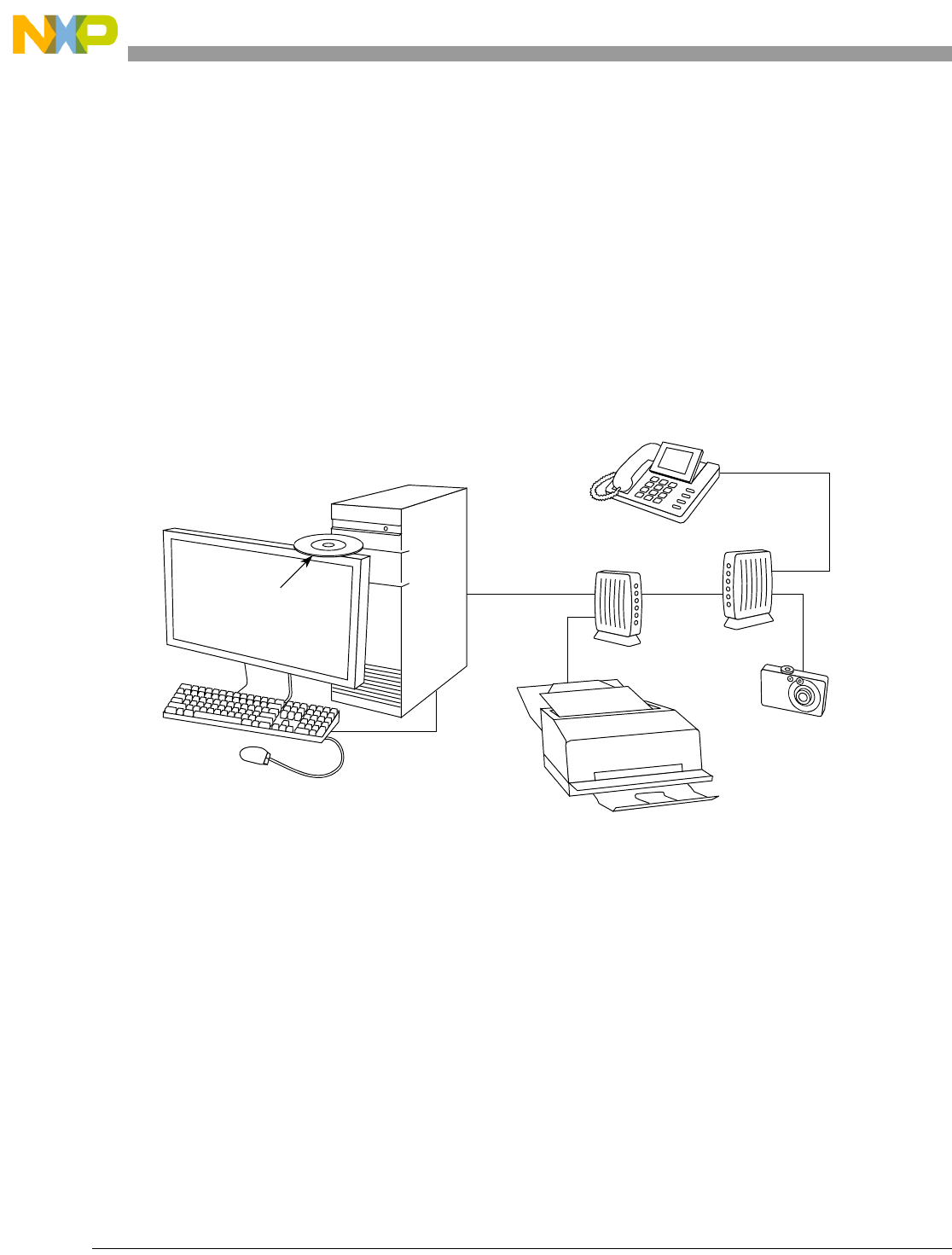
Universal Serial Bus, OTG Capable Controller
15-2 Freescale Semiconductor
USB software provides a uniform view of the system for all application software, hiding implementation
details making application software more portable. It manages the dynamic attach and detach of
peripherals.
There is only one host in any USB system. The USB interface to the host computer system is referred to
as the Host Controller.
There may be multiple USB devices in any system such as joysticks, speakers, printers, etc. USB devices
present a standard USB interface in terms of comprehension, response, and standard capability.
The host initiates transactions to specific peripherals, while the device responds to control transactions.
The device sends and receives data to and from the host using a standard USB data format. USB 2.0
full-speed /low-speed peripherals operate at 12Mb/s or 1.5 MB/s.
For additional information, refer to the USB2.0 specification [2].
Figure 15-1. Example USB 2.0 System Configuration
Host
Software
USB Cable
USB Cable
USB Cables
Host PC
External Hub
USB Cable
External Hub
USB Peripherals
Root
Hub
MCF52211 ColdFire® Integrated Microcontroller Reference Manual, Rev. 3

Universal Serial Bus, OTG Capable Controller
Freescale Semiconductor 15-3
15.1.2 USB On-The-Go
USB (Universal Serial Bus) is a popular standard for connecting peripherals and portable consumer
electronic devices such as digital cameras and hand-held computers to host PCs. The On-The-Go (OTG)
Supplement to the USB Specification extends USB to peer-to-peer application. Using USB OTG
technology consumer electronics, peripherals and portable devices can connect to each other (for example,
a digital camera can connect directly to a printer, or a keyboard can connect to a Personal Digital Assistant)
to exchange data.
With the USB On-The-Go product, you can develop a fully USB-compliant peripheral device that can also
assume the role of a USB host. Software determines the role of the device based on hardware signals, and
then initializes the device in the appropriate mode of operation (host or peripheral) based on how it is
connected. After connecting the devices can negotiate using the OTG protocols to assume the role of host
or peripheral based on the task to be accomplished.
For additional information, refer to the On-The-Go Supplement to the USB 2.0 Specification [3].
Figure 15-2. Example USB 2.0 On-The-Go Configurations
Download Songs
Hot Sync
Swap Songs
Keyboard Input
Print Photos
MCF52211 ColdFire® Integrated Microcontroller Reference Manual, Rev. 3

Universal Serial Bus, OTG Capable Controller
15-4 Freescale Semiconductor
15.1.3 USB-FS Features
• USB 1.1 and 2.0 compliant full-speed device controller
• 16-Bidirectional end points
• DMA or FIFO data stream interfaces
• Low-power consumption
• On-The-Go protocol logic
15.2 Functional Description
The USB-FS 2.0 full-speed/low-speed module communicates with the ColdFire processor core through status and
control registers, and data structures in memory.
15.2.1 Data Structures
The function of the device operation is to transfer a request in the memory image to and from the Universal
Serial Bus. To efficiently manage USB endpoint communications the USB-FS implements a Buffer
Descriptor Table (BDT) in system memory. See Figure 15-3.
15.3 Programmers Interface
15.3.1 Buffer Descriptor Table
To efficiently manage USB endpoint communications the USB-FS implements a Buffer Descriptor Table
(BDT) in system memory. The BDT resides on a 512 byte boundary in system memory and is pointed to
by the BDT Page Registers. Every endpoint direction requires two eight-byte Buffer Descriptor entries.
Therefore, a system with 16 fully bidirectional endpoints would require 512 bytes of system memory to
implement the BDT. The two Buffer Descriptor (BD) entries allows for an EVEN BD and ODD BD entry
for each endpoint direction. This allows the microprocessor to process one BD while the USB-FS is
processing the other BD. Double buffering BDs in this way allows the USB-FS to easily transfer data at
the maximum throughput provided by USB.
The software API intelligently manages buffers for the USB-FS by updating the BDT when needed. This
allows the USB-FS to efficiently manage data transmission and reception, while the microprocessor
performs communication overhead processing and other function dependent applications. Because the
buffers are shared between the microprocessor and the USB-FS a simple semaphore mechanism is used to
distinguish who is allowed to update the BDT and buffers in system memory. A semaphore bit, the OWN
bit, is cleared to 0 when the BD entry is owned by the microprocessor. The microprocessor is allowed read
and write access to the BD entry and the buffer in system memory when the OWN bit is 0. When the OWN
bit is set to 1, the BD entry and the buffer in system memory are owned by the USB-FS. The USB-FS now
has full read and write access and the microprocessor should not modify the BD or its corresponding data
buffer. The BD also contains indirect address pointers to where the actual buffer resides in system memory.
This indirect address mechanism is shown in the following diagram.
MCF52211 ColdFire® Integrated Microcontroller Reference Manual, Rev. 3
Universal Serial Bus, OTG Capable Controller
Freescale Semiconductor 15-5
Figure 15-3. Buffer Descriptor Table
15.3.2 Rx vs. Tx as a USB Target Device or USB Host
The USB-FS core can function as a USB target device (function), or as a USB hosts, and may switch
modes of operation between host and target device under software control. In either mode, USB host or
USB target device, the same data paths and buffer descriptors are used for the transmission and reception
of data. For this reason, a USB-FS core centric nomenclature is used to describe the direction of the data
transfer between the USB-FS core and the USB. Rx or receive is used to describe transfers that move data
from the USB to memory, and Tx, or transmit is used to describe transfers that move data from memory
to the USB. The following table shows how the data direction corresponds to the USB token type in host
and target device applications.
15.3.3 Addressing Buffer Descriptor Table Entries
To access endpoint data via the USB-FS or microprocessor, the addressing mechanism of the Buffer
Descriptor Table must be understood. As stated earlier, the Buffer Descriptor Table occupies up to 512
bytes of system memory. Sixteen bidirectional endpoints can be supported with a full BDT of 512 bytes.
Sixteen bytes are needed for each USB endpoint direction. Applications with less than 16 End Points
require less RAM to implement the BDT. The BDT Page Registers point to the starting location of the
Table 15-1. Data Direction for USB Host
or USB Target
Rx Tx
Device OUT or Setup IN
Host IN Out or Setup
•
•
•
System Memory
Current
Endpoint
BDT
Start of Buffer
•
•
•
End of Buffer
Buffer in Memory
BDT Page
000ODDINEND_POINTBDT_PAGE Registers
MCF52211 ColdFire® Integrated Microcontroller Reference Manual, Rev. 3

Universal Serial Bus, OTG Capable Controller
15-6 Freescale Semiconductor
BDT. The BDT must be located on a 512-byte boundary in system memory. All enabled TX and RX
endpoint BD entries are indexed into the BDT to allow easy access via the USB-FS or ColdFire Core.
When the USB-FS receives a USB token on an enabled endpoint it uses its integrated DMA controller to
interrogate the BDT. The USB-FS must read the corresponding endpoint BD entry and determine if it owns
the BD and corresponding buffer in system memory. To compute the entry point in to the BDT, the
BDT_PAGE registers is concatenated with the current endpoint and the TX and ODD fields to form a
32-bit address. This address mechanism is shown in the following diagrams:
Figure 15-4. BDT Address Calculation
15.3.4 Buffer Descriptor Formats
The Buffer Descriptors (BD) provide endpoint buffer control information for the USB-FS and
microprocessor. The Buffer Descriptors have different meaning based on who is reading the BD in
memory. The USB-FS Controller uses the data stored in the BDs to determine:
• Who owns the buffer in system memory
• Data0 or Data1 PID
• Release Own upon packet completion
• No address increment (FIFO Mode)
• Data toggle synchronization enable
• How much data is to be transmitted or received
• Where the buffer resides in system memory
While the microprocessor uses the data stored in the BDs to determine:
• Who owns the buffer in system memory
• Data0 or Data1 PID
• The received TOKEN PID
• How much data was transmitted or received
• Where the buffer resides in system memory
The format for the BD is shown in the following figure.
31:24 23:16 15:9 8:5 4 3 2:0
BDT_PAGE_03 BDT_PAGE_02 BDT_PAGE_01[7:1] End Point IN ODD 000
Table 15-2. BDT Address Calculation Fields
Field Description
BDT_PAGE BDT_PAGE registers in the Control Register Block
END_POINT END POINT field from the USB TOKEN
TX 1 for an TX transmit transfers and 0 for an RX receive transfers
ODD This bit is maintained within the USB-FS SIE. It corresponds to the buffer currently in use. The buffers are
used in a ping-pong fashion.
MCF52211 ColdFire® Integrated Microcontroller Reference Manual, Rev. 3

Universal Serial Bus, OTG Capable Controller
Freescale Semiconductor 15-7
Figure 15-5. Buffer Descriptor Byte Format
31:26 25:16 15:8 7 6 5 4 3 2 1 0
RSVD BC
(10-Bits) RSVD OWN DATA0/1 KEEP/
TOK_PID[3]
NINC/
TOK_PID[2]
DTS/ 5
TOK_PID[1]
BDT_STALL/
TOK_PID[0] 0 0
Buffer Address (32-Bits)
Table 15-3. Buffer Descriptor Byte Fields
Field Description
31 – 26
RSVD
Reserved
25 – 16
BC[9:0]
The Byte Count bits represent the 10-bit Byte Count. The USB-FS SIE changes this field upon the
completion of a RX transfer with the byte count of the data received.
15 – 8
RSVD
Reserved
7
OWN
If OWN=1 USB-FS has exclusive access to the BD. If OWN=0 the microprocessor has exclusive access to
the BD. This OWN bit determines who currently owns the buffer. The SIE generally writes a 0 to this bit when
it has completed a token, except when KEEP=1. The USB-FS ignores all other fields in the BD when
OWN=0. The microprocessor has access to the entire BD when OWN=0. This byte of the BD should always
be the last byte the microprocessor updates when it initializes a BD. After the BD has been assigned to the
USB-FS, the microprocessor should not change it in any way.
6
DATA0/1
This bit defines if a DATA0 field (DATA0/1=0) or a DATA1 (DATA0/1=1) field was transmitted or received. It is
unchanged by the USB-FS.
5
KEEP/
TOK_PID[3]
If KEEP equals 1, after the OWN bit is set it remains owned by the USB-FS forever. KEEP must equal 0 to
allow the USB-FS to release the BD when a token has been processed. Typically this bit is set to 1 with ISO
endpoints that are feeding a FIFO. The microprocessor is not informed that a token has been processed,
the data is simply transferred to or from the FIFO. The NINC bit is normally also set when KEEP=1 to prevent
address increment. If KEEP=1 this bit is unchanged by the USB-FS, otherwise bit 3 of the current token PID
is written back in to the BD by the USB-FS.
4
NINC/
TOK_PID[2]
The No INCrement bit disables the DMA engine address increment. This forces the DMA engine to read or
write from the same address. This is useful for endpoints when data needs to be read from or written to a
single location such as a FIFO. Typically this bit is set with the KEEP bit for ISO endpoints that are interfacing
to a FIFO. If KEEP=1 this bit is unchanged by the USB-FS, otherwise bit 2 of the current token PID is written
back in to the BD by the USB-FS.
3
DTS/
TOK_PID[1]
Setting this bit enables the USB-FS to perform Data Toggle Synchronization. When this bit is 0 no Data
Toggle Synchronization is performed. If KEEP=1 this bit is unchanged by the USB-FS, otherwise bit 1 of the
current token PID is written back in to the BD by the USB-FS.
2
BDT_STALL
TOK_PID[0]
Setting this bit causes the USB-FS to issue a STALL handshake if a token is received by the SIE that would
use the BDT in this location. The BDT is not consumed by the SIE (the owns bit remains and the rest of the
BDT are unchanged) when a BDT-STALL bit is set.
If KEEP=1 this bit is unchanged by the USB-FS, otherwise bit 0 of the current token PID is written back in
to the BD by the USB-FS
TOK_PID[n] Bits [5:2] can also represent the current token PID. The current token PID is written back in to the BD by the
USB-FS when a transfer completes. The values written back are the token PID values from the USB
specification: 0x1 for an OUT token, 0x9 for and IN token or 0xd for a SETUP token.
In host mode this field is used to report the last returned PID or a transfer status indication. The possible
values returned are: 0x3 DATA0, 0xb DATA1, 0x2 ACK, 0xe STALL, 0xa NAK, 0x0 Bus Timeout, 0xf Data
Error.
MCF52211 ColdFire® Integrated Microcontroller Reference Manual, Rev. 3
Universal Serial Bus, OTG Capable Controller
15-8 Freescale Semiconductor
15.3.5 USB Transaction
When the USB-FS transmits or receives data, it computes the BDT address using the address generation
shown in Table 2. After the BDT has been read and if the OWN bit equals 1, the SIE transfers the data via
the DMA to or from the buffer pointed to by the ADDR field of the BD. When the TOKEN is complete,
the USB-FS updates the BDT and change the OWN bit to 0 if KEEP is 0. The STAT register is updated
and the TOK_DNE interrupt is set. When the microprocessor processes the TOK_DNE interrupt it reads
the status register, this gives the microprocessor all the information it needs to process the endpoint. At
this point, the microprocessor allocates a new BD so additional USB data can be transmitted or received
for that endpoint, and process then the last BD. The following figure shows a time line how a typical USB
token would be processed.
Figure 15-6. USB Token Transaction
The USB has two sources for the DMA overrun error. First, the memory latency on the BVCI initiator
interface may be too high and cause the receive FIFO to overflow. This is predominantly a hardware
performance issue, usually caused by transient memory access issues. Second, the packet received may be
larger than the negotiated MaxPacket size. This would be caused by a software bug.
In the first case, the USB responds with a NAK or Bus Timeout (BTO - See bit 4 in Section 15.4.1.11,
“Error Interrupt Status Register (ERR_STAT)”) as appropriate for the class of transaction. The DMA_ERR
bit is set in the ERR_STAT register of the core for host and device modes of operation. Depending on the
values of the INT_ENB and ERR_ENB register, the core may assert an interrupt to notify the processor of
the DMA error. In device mode, the BDT is not written back nor is the TOK_DNE interrupt triggered
1–0
Reserved
Reserved, should read as zeroes
ADDR[31:0] The Address bits represent the 32 -bit buffer address in system memory. These bits are unchanged by the
USB-FS.
Table 15-3. Buffer Descriptor Byte Fields (continued)
SETUP TOKEN DATA ACK
USB RST SOF
SOF
Interrupt Generated
TOK_DNE
Interrupt Generated
IN TOKEN DATA ACK
TOK_DNE
Interrupt Generated
OUT TOKEN DATA ACK
TOK_DNE
Interrupt Generated
USB_RST
Interrupt Generated
USB Host Function
MCF52211 ColdFire® Integrated Microcontroller Reference Manual, Rev. 3

Universal Serial Bus, OTG Capable Controller
Freescale Semiconductor 15-9
because it is assumed that a second attempt is queued and succeed in the future. For host mode, the
TOK_DNE interrupt fires and the TOK_PID field of the BDT is 1111 to indicate the DMA latency error.
Host mode software can decide to retry or move to another item in its schedule.
In the second case of oversized data packets the USB specification is ambiguous. It assumes correct
software drivers on both sides. The overrun is not due to memory latency but due to a lack of space to put
the excess data. NAKing the packet may cause another retransmission of the already oversized packet data.
In response to oversized packets, the USB core continues ACKing the packet for non-isochronous
transfers. The data written to memory is clipped to the MaxPacket size so as not to corrupt system memory.
The core asserts the DMA_ERR bit of the ERR_STAT register (which could trigger an interrupt, as above)
and a TOK_DNE interrupt fires. The TOK_PID field of the BDT is not 1111 because the DMA_ERR is
not due to latency. The packet length field written back to the BDT is the MaxPacket value that represents
the length of the clipped data actually written to memory. The software can decide an appropriate course
of action from here for future transactions such as stalling the endpoint, canceling the transfer, disabling
the endpoint, etc.
15.4 Memory Map/Register Definitions
This section provides the memory map and detailed descriptions of all USB interface registers. The
memory map of the USB interface is shown in Table 15-4.
Table 15-4. USB Interface Memory Map
Address Register Acronym Bits
USB OTG Registers
IPSBAR + 0x1C_0000 Peripheral ID Register PER_ID 8
IPSBAR + 0x1C_0004 Peripheral ID Complement Register ID_COMP 8
IPSBAR + 0x1C_0008 Peripheral Revision Register REV 8
IPSBAR + 0x1C_000C Peripheral Additional Info Register ADD_INFO 8
IPSBAR + 0x1C_0010 OTG Interrupt Status Register OTG_INT_STAT 8
IPSBAR + 0x1C_0014 OTG Interrupt Control Register OTG_INT_EN 8
IPSBAR + 0x1C_0018 OTG Status Register OTG_STATUS 8
IPSBAR + 0x1C_001C OTG Control Register OTG_CTRL 8
IPSBAR + 0x1C_0080 Interrupt Status Register INT_STAT 8
IPSBAR + 0x1C_0084 Interrupt Enable Register INT_ENB 8
IPSBAR + 0x1C_0088 Error Interrupt Status Register ERR_STAT 8
IPSBAR + 0x1C_008C Error Interrupt Enable Register ERR_ENG 8
IPSBAR + 0x1C_0090 Status Register STAT 8
IPSBAR + 0x1C_0094 Control Register CTL 8
IPSBAR + 0x1C_0098 Address Register ADDR 8
IPSBAR + 0x1C_009C BDT Page Register 1 BDT_PAGE_01 8
IPSBAR + 0x1C_00A0 Frame Number Register Low FRM_NUML 8
MCF52211 ColdFire® Integrated Microcontroller Reference Manual, Rev. 3

Universal Serial Bus, OTG Capable Controller
15-10 Freescale Semiconductor
The following sections provide details about the registers in the USB OTG memory map.
15.4.1 Capability Registers
The capability registers specify the software limits, restrictions, and capabilities of the host/device
controller implementation. Most of these registers are defined by the EHCI specification. Registers that
are not defined by the EHCI specification are noted in their descriptions.
IPSBAR + 0x1C_00A4 Frame Number Register High FRM_NUMH 8
IPSBAR + 0x1C_00A8 Token Register TOKEN 8
IPSBAR + 0x1C_00AC SOF Threshold Register SOF_THLD 8
IPSBAR + 0x1C_00B0 BDT Page Register 2 BDT_PAGE_02 8
IPSBAR + 0x1C_00B4 BDT Page Register 3 BDT_PAGE_03 8
IPSBAR + 0x1C_00C0 Endpoint Control Register 0 ENDPT0 8
IPSBAR + 0x1C_00C4 Endpoint Control Register 1 ENDPT1 8
IPSBAR + 0x1C_00C8 Endpoint Control Register 2 ENDPT2 8
IPSBAR + 0x1C_00CC Endpoint Control Register 3 ENDPT3 8
IPSBAR + 0x1C_00D0 Endpoint Control Register 4 ENDPT4 8
IPSBAR + 0x1C_00D4 Endpoint Control Register 5 ENDPT5 8
IPSBAR + 0x1C_00D8 Endpoint Control Register 6 ENDPT6 8
IPSBAR + 0x1C_00DC Endpoint Control Register 7 ENDPT7 8
IPSBAR + 0x1C_00E0 Endpoint Control Register 8 ENDPT8 8
IPSBAR + 0x1C_00E4 Endpoint Control Register 9 ENDPT9 8
IPSBAR + 0x1C_00E8 Endpoint Control Register 10 ENDPT10 8
IPSBAR + 0x1C_00EC Endpoint Control Register 11 ENDPT11 8
IPSBAR + 0x1C_00F0 Endpoint Control Register 12 ENDPT12 8
IPSBAR + 0x1C_00F4 Endpoint Control Register 13 ENDPT13 8
IPSBAR + 0x1C_00F8 Endpoint Control Register 14 ENDPT14 8
IPSBAR + 0x1C_00FC Endpoint Control Register 15 ENDPT15 8
IPSBAR + 0x1C_0100 USB Control Register USB_CTRL 8
IPSBAR + 0x1C_0104 USB OTG Observe Register USB_OTG_OBSERVE 8
IPSBAR + 0x1C_0108 USB OTG Control Register USB_OTG_CONTROL 8
Table 15-4. USB Interface Memory Map (continued)
Address Register Acronym Bits
MCF52211 ColdFire® Integrated Microcontroller Reference Manual, Rev. 3

Universal Serial Bus, OTG Capable Controller
Freescale Semiconductor 15-11
15.4.1.1 Peripheral ID Register (PER_ID)
The Peripheral ID Register reads back the value of 0x04. This value is defined for the USB Peripheral.
Figure 15-7 shows the PER_ID register.
15.4.1.2 Peripheral ID Complement Register (ID_COMP)
The Peripheral ID Complement Register reads back the complement of the Peripheral ID Register. For the
USB Peripheral, this is the value 0xFB. Figure 15-8 shows the ID_COMP register.
IPSBAR
Offset: 0x1C_0000 (PER_ID) Access: User read-only
7 654 3 210
R 0 0 ID5 ID4 ID3 ID2 ID1 ID0
W
Reset:0 000 0 100
Figure 15-7. Peripheral ID Register (PER_ID)
Table 15-11. PER_ID Field Descriptions
Field Description
7–6 These bits always read zeros
5–0
IDx
Peripheral identification bits. These bits always read 0x04 (00_0100).
IPSBAR
Offset:
0x1C_0004 (ID_COMP) Access: User read-only
7 654 3 210
R 1 1 NID5 NID4 NID3 NID2 NID1 NID0
W
Reset:1 111 1 011
Figure 15-8. Peripheral ID Complement Register
Table 15-12. ID_COMP Field Descriptions
Field Description
7–6 These bits always read ones
5–0
NIDx
Ones complement of peripheral identification bits.
MCF52211 ColdFire® Integrated Microcontroller Reference Manual, Rev. 3

Universal Serial Bus, OTG Capable Controller
15-12 Freescale Semiconductor
15.4.1.3 Peripheral Revision Register (REV)
This register contains the revision number of the USB Module. Figure 15-9 shows the REV register.
15.4.1.4 Peripheral Additional Info Register (ADD_INFO)
The Peripheral Additional info Register reads back the value of the fixed Interrupt Request Level
(IRQ_NUM) along with the Host Enable bit. If set to 1, the Host Enable bit indicates the USB peripheral
is operating in host mode. Figure 15-10 shows the ADD_INFO register.
IPSBAR
Offset:
0x1C_0008 (REV) Access: User read-only
7 654 3 210
R REV7 REV6 REV5 REV4 REV3 REV2 REV1 REV0
W
Reset:0 011 0 011
Figure 15-9. Peripheral Revision Register
Table 15-13. REV Field Descriptions
Field Description
7–0
REVx
REV[7:0] indicate the revision number of the USB Core.
IPSBAR
Offset:
0x1C_000C (ADD_INFO) Access: User read-only
7 654 3 210
R IRQ_NUM 0 0 IEHOST
W
Reset:0 000 0 001
Figure 15-10. Peripheral Additional Info Register
Table 15-14. ADD_INFO Field Descriptions
Field Description
7–3
IRQ_NUM
Assigned Interrupt Request Number.
2–1
Reserved
RESERVED. These bits read back zeros.
0
IEHOST
This bit is set if host mode is enabled.
MCF52211 ColdFire® Integrated Microcontroller Reference Manual, Rev. 3

Universal Serial Bus, OTG Capable Controller
Freescale Semiconductor 15-13
15.4.1.5 OTG Interrupt Status Register (OTG_INT_STAT)
The OTG Interrupt Status Register records changes of the ID sense and VBUS signals. Software can read
this register to determine which event has caused an interrupt. Only bits that have changed since the last
software read are set. Writing a one to a bit clears the associated interrupt. Figure 15-11 shows the
OTG_INT_STAT register.
IPSBAR
Offset:
0x1C_0010 (OTG_INT_STAT) Access: User read/write
7 654 3 210
RID_CHG 1_MSEC LINE_STATE
_CHG
Reserved SESS_VLD
_CHG
B_SESS
_CHG
Reserved A_VBUS
_CHG
W––
Reset: 0 1 1 X 0 0 X 0
Figure 15-11. OTG Interrupt Status Register
Table 15-15. OTG_INT_STAT Field Descriptions
Field Description
7
ID_CHG
This bit is set when a change in the ID Signal from the USB connector is sensed.
6
1_MSEC
This bit is set when the 1 millisecond timer expires. This bit stays asserted until cleared by software. The
interrupt must be serviced every millisecond to avoid losing 1msec counts.
5
LINE_STAT
_CHG
This bit is set when the USB line state changes. The interrupt associated with this bit can be used to detect
Reset, Resume, Connect, and Data Line Pulse signals.
4
Reserved
Reserved
3
SESS_VLD
_CHG
This bit is set when a change in VBUS is detected indicating a session valid or a session no longer valid
2
B_SESS
_CHG
This bit is set when a change in VBUS is detected on a B device.
1
Reserved
Reserved
0
A_VBUS
_CHG
This bit is set when a change in VBUS is detected on an A device.
MCF52211 ColdFire® Integrated Microcontroller Reference Manual, Rev. 3

Universal Serial Bus, OTG Capable Controller
15-14 Freescale Semiconductor
15.4.1.6 OTG Interrupt Control Register (OTG_INT_EN)
The OTG Interrupt Control Register enables the corresponding interrupt status bits defined in the OTG
Interrupt Status Register. Figure 15-12 shows the OTG_INT_EN register.
IPSBAR
Offset:
0x1C_0014 (OTG_INT_EN) Access: User read/write
7 6543210
RID_EN 1_MSEC
_EN
LINE_STATE_
EN
Reserved SESS_VLD
_EN
B_SESS
_EN
Reserved A_VBUS
_EN
W––
Reset: 0 0 0 X 0 0 X 0
Figure 15-12. OTG Interrupt Control Register
Table 15-16. OTG_INT_EN Field Descriptions
Field Description
7
ID_EN
ID interrupt enable
0 The ID interrupt is disabled
1 The ID interrupt is enabled
6
1_MSEC_EN
1 millisecond interrupt enable
0 The 1msec timer interrupt is disabled
1 The 1msec timer interrupt is enabled
5
LINE_STATE
_EN
Line State change interrupt enable
0 The LINE_STAT_CHG interrupt is disabled
1 The LINE_STAT_CHG interrupt is enabled
4 Reserved.
3
SESS_VLD
_EN
Session valid interrupt enable
0 The SESS_VLD_CHG interrupt is disabled
1 The SESS_VLD_CHG interrupt is enabled
2
B_SESS_EN
B Session END interrupt enable
0 The B_SESS_CHG interrupt is disabled
1 The B_SESS_CHG interrupt is enabled
1 Reserved.
0
A_VBUS_EN
A VBUS Valid interrupt enable
0 The A_VBUS_CHG interrupt is disabled
1 The A_VBUS_CHG interrupt is enabled
MCF52211 ColdFire® Integrated Microcontroller Reference Manual, Rev. 3

Universal Serial Bus, OTG Capable Controller
Freescale Semiconductor 15-15
15.4.1.7 Interrupt Status Register (OTG_STAT)
The Interrupt Status Register displays the actual value from the external comparator outputs of the ID pin
and VBUS. Figure 15-13 shows the OTG_STAT register.
IPSBAR
Offset: 0x1C_0018 (OTG_STAT) Access: User read/write
76543210
RID 1_MSEC_EN LINE_STATE
_STABLE
Reserved SESS_VLD B_SESS
_END
Reserved A_VBUS
_VLD
W––
Reset: 0 0 1 X 0 0 X 0
Figure 15-13. Interrupt Status Register
Table 15-17. OTG_STAT Field Descriptions
Field Description
7
ID
Indicates the current state of the ID pin on the USB connector
0 Indicates a Type A cable has been plugged into the USB connector
1 Indicates no cable is attached or a Type B cable has been plugged into the USB connector
6
1_MSEC_EN
This bit is reserved for the 1msec count, but it is not useful to software.
5
LINE_STATE
_STABLE
This bit indicates that the internal signals that control the LINE_STATE_CHG bit (bit 5) of the OTG_INT_STAT
register have been stable for at least 1 millisecond. First read the LINE_STATE_CHG bit, and then read this bit.
If this bit reads as 1, then the value of LINE_STATE_CHG can be considered stable.
0 The LINE_STAT_CHG bit is not yet stable
1 The LINE_STAT_CHG bit has been debounced and is stable
4 Reserved.
3
SESS_VLD
Session Valid
0 The VBUS voltage is below the B session Valid threshold
1 The VBUS voltage is above the B session Valid threshold
2
B_SESS
_END
B Session END
0 The VBUS voltage is above the B session End threshold
1 The VBUS voltage is below the B session End threshold
1 Reserved.
0
A_VBUS
_VLD
A VBUS Valid
0 The VBUS voltage is below the A VBUS Valid threshold
1 The VBUS voltage is above the A VBUS Valid threshold
MCF52211 ColdFire® Integrated Microcontroller Reference Manual, Rev. 3

Universal Serial Bus, OTG Capable Controller
15-16 Freescale Semiconductor
15.4.1.8 OTG Control Register (OTG_CTRL)
The OTG Control Register controls the operation of VBUS and Data Line termination resistors.
Figure 15-14 shows the OTG_CTRL register.
IPSBAR
Offset:
0x1C_001C (OTG_CTRL) Access: User read/write
76543210
RDP_HIGH DP_LOW DM_LOW OTG_EN
W
Reset:00000000
Figure 15-14. OTG Control Register
Table 15-18. OTG_CTRL Field Descriptions
Field Description
7
DP_HIGH
D+ Data Line pull-up resistor enable
0 D+ pull-up resistor is not enabled
1 D+ pull-up resistor is enabled
6
Reserved
Reserved.
5
DP_LOW
D+ Data Line pull-down resistor enable
0 D+ pull-down resistor is not enabled
1 D+ pull-down resistor is enabled
This bit should always be enabled together with bit 4 (DM_LOW)
4
DM_LOW
D- Data Line pull-down resistor enable
0 D- pull-down resistor is not enabled
1 D- pull-down resistor is enabled
This bit should always be enabled together with bit 5 (DP_LOW)
3
Reserved
Reserved.
2
OTG_EN
On-The-Go pull-up/pull-down resistor enable
0 If USB_EN is set and HOST_MODE is clear in the Control Register (CTL), then the D+ Data Line pull-up
resistors are enabled. If HOST_MODE is set the D+ and D- Data Line pull-down resistors are engaged.
1 The pull-up and pull-down controls in this register are used
1
Reserved
Reserved.
0
Reserved
Reserved.
MCF52211 ColdFire® Integrated Microcontroller Reference Manual, Rev. 3

Universal Serial Bus, OTG Capable Controller
Freescale Semiconductor 15-17
15.4.1.9 Interrupt Status Register (INT_STAT)
The Interrupt Status Register contains bits for each of the interrupt sources within the USB Module. Each
of these bits are qualified with their respective interrupt enable bits (see Section 15.4.1.10, “Interrupt
Enable Register (INT_ENB)”). All bits of this register are logically OR’d together along with the OTG
Interrupt Status Register (OTG_STAT) to form a single interrupt source for the ColdFire core. After an
interrupt bit has been set it may only be cleared by writing a one to the respective interrupt bit. This register
contains the value of 0x00 after a reset. Figure 15-15 shows the INT_STAT register.
IPSBAR
Offset:
0x1C_0080 (INT_STAT) Access: User read/write
76543210
RSTALL ATTACH RESUME SLEEP TOK_DNE SOF_TOK ERROR USB_RST
W
Reset:00010000
Figure 15-15. Interrupt Status Register
Table 15-19. INT_STAT Field Descriptions
Field Description
7
STALL
Stall Interrupt
In Target mode this bit is asserted when a STALL handshake is sent by the SIE.
In Host mode this bit is set when the USB Module detects a STALL acknowledge during the handshake phase
of a USB transaction. This interrupt can be use to determine is the last USB transaction was completed
successfully or if it stalled.
6
AT TA C H
Attach Interrupt
This bit is set when the USB Module detects an attach of a USB device. This signal is only valid if
HOST_MODE_EN is true. This interrupt signifies that a peripheral is now present and must be configured.
5
RESUME
This bit is set depending upon the DP/DM signals, and can be used to signal remote wake-up signaling on the
USB bus. When not in suspend mode this interrupt should be disabled.
4
SLEEP
This bit is set when the USB Module detects a constant idle on the USB bus for 3 milliseconds. The sleep timer
is reset by activity on the USB bus.
3
TOK_DNE
This bit is set when the current token being processed has completed. The ColdFire core should immediately
read the STAT register to determine the EndPoint and BD used for this token. Clearing this bit (by writing a one)
causes the STAT register to be cleared or the STAT holding register to be loaded into the STAT register.
2
SOF_TOK
This bit is set when the USB Module receives a Start Of Frame (SOF) token.
In Host mode this bit is set when the SOF threshold is reached, so that software can prepare for the next SOF.
1
ERROR
This bit is set when any of the error conditions within the ERR_STAT register occur. The ColdFire core must
then read the ERR_STAT register to determine the source of the error.
0
USB_RST
This bit is set when the USB Module has decoded a valid USB reset. This informs the Microprocessor that it
should write 0x00 into the address register and enable endpoint 0. USB_RST is set after a USB reset has been
detected for 2.5 microseconds. It is not asserted again until the USB reset condition has been removed and
then reasserted.
MCF52211 ColdFire® Integrated Microcontroller Reference Manual, Rev. 3

Universal Serial Bus, OTG Capable Controller
15-18 Freescale Semiconductor
15.4.1.10 Interrupt Enable Register (INT_ENB)
The Interrupt Enable Register contains enable bits for each of the interrupt sources within the USB
Module. Setting any of these bits enables the respective interrupt source in the INT_STAT register. This
register contains the value of 0x00 after a reset. Figure 15-16 shows the INT_ENB register.
IPSBAR
Offset:
0x1C_0084 (INT_ENB) Access: User read/write
76543210
RSTALL_EN ATTACH_EN RESUME
_EN SLEEP_EN TOK_DNE
_EN
SOF_TOK
_EN
ERROR_E
N
USB_RST
_EN
W
Reset:00000000
Figure 15-16. Interrupt Enable Register
Table 15-20. INT_ENB Field Descriptions
Field Description
7
STALL_EN
STALL Interrupt Enable
0 The STALL interrupt is not enabled
1 The STALL interrupt is enabled
6
AT TAC H _ E N
ATTACH Interrupt Enable
0 The ATTACH interrupt is not enabled
1 The ATTACH interrupt is enabled
5
RESUME_EN
RESUME Interrupt Enable
0 The RESUME interrupt is not enabled
1 The RESUME interrupt is enabled
4
SLEEP_EN
SLEEP Interrupt Enable
0 The SLEEP interrupt is not enabled
1 The SLEEP interrupt is enabled
3
TOK_DNE
_EN
TOK_DNE Interrupt Enable
0 The TOK_DNE interrupt is not enabled
1 The TOK_DNE interrupt is enabled
2
SOF_TOK
_EN
SOF_TOK Interrupt Enable
0 The SOF_TOK interrupt is not enabled
1 The SOF_TOK interrupt is enabled
1
ERROR_EN
ERROR Interrupt Enable
0 The ERROR interrupt is not enabled
1 The ERROR interrupt is enabled
0
USB_RST
_EN
USB_RST Interrupt Enable
0 The USB_RST interrupt is not enabled
1 The USB_RST interrupt is enabled
MCF52211 ColdFire® Integrated Microcontroller Reference Manual, Rev. 3

Universal Serial Bus, OTG Capable Controller
Freescale Semiconductor 15-19
15.4.1.11 Error Interrupt Status Register (ERR_STAT)
The Error Interrupt Status Register contains enable bits for each of the error sources within the USB
Module. Each of these bits are qualified with their respective error enable bits (see Section 15.4.1.12,
“Error Interrupt Enable Register (ERR_ENB)”). All bits of this Register are logically OR’d together and
the result placed in the ERROR bit of the INT_STAT register. After an interrupt bit has been set it may
only be cleared by writing a one to the respective interrupt bit. Each bit is set as soon as the error conditions
is detected. Therefore, the interrupt does not typically correspond with the end of a token being processed.
This register contains the value of 0x00 after a reset. Figure 15-17 shows the ERR_STAT register.
IPSBAR
Offset: 0x1C_0088 (ERR_STAT) Access: User read/write
76543210
RBTS_ERR Reserved DMA_ERR BTO_ERR DFN8 CRC16 CRC5_EOF PID_ERR
W–
Reset:00000000
Figure 15-17. Error Interrupt Status Register
Table 15-21. ERR_STAT Field Descriptions
Field Description
7
BTS_ERR
This bit is set when a bit stuff error is detected. If set, the corresponding packet is rejected due to the error.
6 Reserved
5
DMA_ERR
This bit is set if the USB Module has requested a DMA access to read a new BDT but has not been given the
bus before it needs to receive or transmit data. If processing a TX transfer this would cause a transmit data
underflow condition. If processing a RX transfer this would cause a receive data overflow condition. This
interrupt is useful when developing device arbitration hardware for the microprocessor and the USB Module to
minimize bus request and bus grant latency.
This bit is also set if a data packet to or from the host is larger than the buffer size allocated in the BDT. In this
case the data packet is truncated as it is put into buffer memory.
4
BTO_ERR
This bit is set when a bus turnaround timeout error occurs. The USB Module contains a bus turnaround timer
that keeps track of the amount of time elapsed between the token and data phases of a SETUP or OUT TOKEN
or the data and handshake phases of a IN TOKEN. If more than 16 bit times are counted from the previous
EOP before a transition from IDLE, a bus turnaround timeout error occurs.
3
DFN8
This bit is set if the data field received was not 8 bits in length. USB Specification 1.0 requires that data fields
be an integral number of bytes. If the data field was not an integral number of bytes, this bit is set.
2
CRC16
This bit is set when a data packet is rejected due to a CRC16 error.
1
CRC5_EOF
This error interrupt has two functions.
When the USB Module is operating in peripheral mode (HOST_MODE_EN=0), this interrupt detects CRC5
errors in the token packets generated by the host. If set the token packet was rejected due to a CRC5 error.
When the USB Module is operating in host mode (HOST_MODE_EN=1), this interrupt detects End Of Frame
(EOF) error conditions. This occurs when the USB Module is transmitting or receiving data and the SOF counter
reaches zero. This interrupt is useful when developing USB packet scheduling software to ensure that no USB
transactions cross the start of the next frame.
0
PID_ERR
This bit is set when the PID check field fails.
MCF52211 ColdFire® Integrated Microcontroller Reference Manual, Rev. 3

Universal Serial Bus, OTG Capable Controller
15-20 Freescale Semiconductor
15.4.1.12 Error Interrupt Enable Register (ERR_ENB)
The Error Interrupt Enable Register contains enable bits for each of the error interrupt sources within the
USB Module. Setting any of these bits enables the respective interrupt source in the ERR_STAT register.
Each bit is set as soon as the error conditions is detected. Therefore, the interrupt does not typically
correspond with the end of a token being processed. This register contains the value of 0x00 after a reset.
Figure 15-18 shows the ERR_ENB register.
IPSBAR
Offset:
0x1C_008C (ERR_ENB)
Access: User read/write
76543210
RBTS_ERR
_EN
Reserved DMA_ERR
_EN
BTO_ERR
_EN DFN8_EN CRC16_EN CRC5_EOF
_EN
PID_ERR
_EN
W–
Reset:00000000
Figure 15-18. Error Interrupt Enable Register
Table 15-22. ERR_ENB Field Descriptions
Field Description
7
BTS_ERR
_EN
BTS_ERR Interrupt Enable
0 The BTS_ERR interrupt is not enabled
1 The BTS_ERR interrupt is enabled
6 Reserved
5
DMA_ERR
_EN
DMA_ERR Interrupt Enable
0 The DMA_ERR interrupt is not enabled
1 The DMA_ERR interrupt is enabled
4
BTO_ERR
_EN
BTO_ERR Interrupt Enable
0 The BTO_ERR interrupt is not enabled
1 The BTO_ERR interrupt is enabled
3
DFN8_EN
DFN8 Interrupt Enable
0 The DFN8 interrupt is not enabled
1 The DFN8 interrupt is enabled
2
CRC16_EN
CRC16 Interrupt Enable
0 The CRC16 interrupt is not enabled
1 The CRC16 interrupt is enabled
1
CRC5_EOF
_EN
CRC5/EOF Interrupt Enable
0 The CRC5/EOF interrupt is not enabled
1 The CRC5/EOF interrupt is enabled
0
PID_ERR
_EN
PID_ERR Interrupt Enable
0 The PID_ERR interrupt is not enabled
1 The PID_ERR interrupt is enabled
MCF52211 ColdFire® Integrated Microcontroller Reference Manual, Rev. 3

Universal Serial Bus, OTG Capable Controller
Freescale Semiconductor 15-21
15.4.1.13 Status Register (STAT)
The Status Register reports the transaction status within the USB Module. When the ColdFire core has
received a TOK_DNE interrupt the Status Register should be read to determine the status of the previous
endpoint communication. The data in the status register is valid when the TOK_DNE interrupt bit is
asserted. The STAT register is actually a read window into a status FIFO maintained by the USB Module.
When the USB Module uses a BD, it updates the Status Register. If another USB transaction is performed
before the TOK_DNE interrupt is serviced, the USB Module stores the status of the next transaction in the
STAT FIFO. Thus the STAT register is actually a four byte FIFO that allows the ColdFire core to process
one transaction while the SIE is processing the next transaction. Clearing the TOK_DNE bit in the
INT_STAT register causes the SIE to update the STAT register with the contents of the next STAT value.
If the data in the STAT holding register is valid, the SIE immediately reasserts to TOK_DNE interrupt.
Figure 15-19 shows the STAT register.
IPSBAR
Offset:
0x1C_0090 (STAT) Access: User read-only
76543210
R ENDP TX ODD Reserved Reserved
W
Reset:00000000
Figure 15-19. Status Register
Table 15-23. STAT Field Descriptions
Field Description
7 - 5
ENDP[3:0]
This four-bit field encodes the endpoint address that received or transmitted the previous token. This allows the
ColdFire core to determine which BDT entry was updated by the last USB transaction.
3
TX
Transmit Indicator
0 The most recent transaction was a Receive operation
1 The most recent transaction was a Transmit operation
2
ODD
this bit is set if the last Buffer Descriptor updated was in the odd bank of the BDT.
1 - 0 Reserved
MCF52211 ColdFire® Integrated Microcontroller Reference Manual, Rev. 3

Universal Serial Bus, OTG Capable Controller
15-22 Freescale Semiconductor
15.4.1.14 Control Register (CTL)
The Control Register provides various control and configuration information for the USB Module.
Figure 15-20 shows the CTL register.
IPSBAR
Offset:
0x1C_0094 (CTL) Access: User read/write
76 5 43210
RJSTATE SE0 TXSUSPEND/
TOKENBUSY RESET HOST_
MODE_EN RESUME ODD_RST USB_EN/
SOF_EN
W
Reset:11 0 00000
Figure 15-20. Control Register
Table 15-24. CTL Field Descriptions
Field Description
7
JSTATE
Live USB differential receiver JSTATE signal. The polarity of this signal is affected by the current state of
LS_EN (See)
6
SE0
Live USB Single Ended Zero signal
5
TXSUSPEND/
TOKENBUSY
When the USB Module is in Host mode TOKEN_BUSY is set when the USB Module is busy executing a USB
token and no more token commands should be written to the Token Register. Software should check this bit
before writing any tokens to the Token Register to ensure that token commands are not lost.
In Target mode TXD_SUSPEND is set when the SIE has disabled packet transmission and reception.
Clearing this bit allows the SIE to continue token processing. This bit is set by the SIE when a Setup Token
is received allowing software to dequeue any pending packet transactions in the BDT before resuming token
processing.
4
RESET
Setting this bit enables the USB Module to generate USB reset signaling. This allows the USB Module to
reset USB peripherals. This control signal is only valid in Host mode (HOST_MODE_EN=1). Software must
set RESET to 1 for the required amount of time and then clear it to 0 to end reset signaling. For more
information on RESET signaling see Section 7.1.4.3 of the USB specification version 1.0.
3
HOST_
MODE_EN
When set to 1, this bit enables the USB Module to operate in Host mode. In host mode, the USB module
performs USB transactions under the programmed control of the host processor.
2
RESUME
When set to 1 this bit enables the USB Module to execute resume signaling. This allows the USB Module to
perform remote wake-up. Software must set RESUME to 1 for the required amount of time and then clear it
to 0. If the HOST_MODE_EN bit is set, the USB module appends a Low Speed End of Packet to the Resume
signaling when the RESUME bit is cleared. For more information on RESUME signaling see Section 7.1.4.5
of the USB specification version 1.0.
1
ODD_RST
Setting this bit to 1 resets all the BDT ODD ping/pong bits to 0, which then specifies the EVEN BDT bank.
0
USB_EN/
SOF_EN
USB Enable
0 The USB Module is disabled
1 The USB Module is enabled.
Setting this bit causes the SIE to reset all of its ODD bits to the BDTs. Therefore, setting this bit resets much
of the logic in the SIE. When host mode is enabled, clearing this bit causes the SIE to stop sending SOF
tokens.
MCF52211 ColdFire® Integrated Microcontroller Reference Manual, Rev. 3

Universal Serial Bus, OTG Capable Controller
Freescale Semiconductor 15-23
15.4.1.15 Address Register (ADDR)
The Address Register holds the unique USB address that the USB Module decodes when in Peripheral
mode (HOST_MODE_EN=0). When operating in Host mode (HOST_MODE_EN=1) the USB Module
transmits this address with a TOKEN packet. This enables the USB Module to uniquely address an USB
peripheral. In either mode, the USB_EN bit within the control register must be set. The Address Register
is reset to 0x00 after the reset input becomes active or the USB Module decodes a USB reset signal. This
action initializes the Address Register to decode address 0x00 as required by the USB specification.
Figure 15-21 shows the ADDR register.
IPSBAR
Offset: 0x1C_0098 (ADDR) Access: User read/write
76543210
RLS_EN ADDR
W
Reset:00000000
Figure 15-21. ADDR Register
Table 15-25. ADDR Field Descriptions
Field Description
7
LS_EN
Low Speed Enable bit. This bit informs the USB Module that the next token command written to the token
register must be performed at low speed. This enables the USB Module to perform the necessary preamble
required for low-speed data transmissions.
6–0
ADDR
USB address. This 7-bit value defines the USB address that the USB Module decodes in peripheral mode, or
transmit when in host mode.
MCF52211 ColdFire® Integrated Microcontroller Reference Manual, Rev. 3

Universal Serial Bus, OTG Capable Controller
15-24 Freescale Semiconductor
15.4.1.16 BDT Page Register 1 (BDT_PAGE_01)
The Buffer Descriptor Table Page Register 1 contains an 8-bit value used to compute the address where
the current Buffer Descriptor Table (BDT) resides in system memory. Figure 15-22 shows the BDT Page
Register 1.
IPSBAR
Offset:
0x1C_009C (BDT_PAGE_01) Access: User read/write
76543210
RBDT_BA15 BDT_BA14 BDT_BA13 BDT_BA12 BDT_BA11 BDT_BA10 BDT_BA9 NOT USED
W
Reset:00000000
Figure 15-22. BDT_PAGE_01 Register
Table 15-26. BDT_PAGE_01 Field Descriptions
Field Description
7 – 1
BDT_
BA[15:8]
This 7 bit field provides address bits 15 through 9 of the BDT base address, which defines where the Buffer
Descriptor Table resides in system memory.
0
NOT USED
This bit is always zero. The 32-bit BDT Base Address is always aligned on 512 byte boundaries in memory.
MCF52211 ColdFire® Integrated Microcontroller Reference Manual, Rev. 3

Universal Serial Bus, OTG Capable Controller
Freescale Semiconductor 15-25
15.4.1.17 Frame Number Register Low/High (FRM_NUML, FRM_NUMH)
The Frame Number Register Low contains an 8-bit value used to compute the address where the current
Buffer Descriptor Table (BDT) resides in system memory. Figure 15-23 shows the FRM_NUML Register.
IPSBAR
Offset:
0x1C_00A0 (FRM_NUML) Access: User read-only
76543210
R FRM7 FRM6 FRM5 FRM4 FRM3 FRM2 FRM1 FRM0
W
Reset:00000000
Figure 15-23. FRM_NUML Register
Table 15-27. FRM_NUML Field Descriptions
Field Description
7–0
FRM[7:0]
These 8 bits represent the low-order bits of the11-bit Frame Number
IPSBAR
Offset:
0x1C_00A4 (FRM_NUMH)
Access: User read-only
76543210
R 0 0 0 0 0 FRM10 FRM9 FRM8
W
Reset:00000000
Figure 15-24. FRM_NUMH Register
Table 15-28. FRM_NUMH Field Descriptions
Field Description
2–0
FRM[10:8]
These 3 bits represent the high-order bits of the11-bit Frame Number
7–3
NOT USED
This bits always read zero.
MCF52211 ColdFire® Integrated Microcontroller Reference Manual, Rev. 3

Universal Serial Bus, OTG Capable Controller
15-26 Freescale Semiconductor
15.4.1.18 Token Register (TOKEN)
The Token Register is used to perform USB transactions when in host mode (HOST_MODE_EN=1).
When the ColdFire core processor wishes to execute a USB transaction to a peripheral, it writes the
TOKEN type and endpoint to this register. After this register has been written, the USB module begins the
specified USB transaction to the address contained in the address register. The ColdFire core should
always check that the TOKEN_BUSY bit in the control register is not set before performing a write to the
Token Register. This ensures token commands are not overwritten before they can be executed. The
address register and endpoint control register 0 are also used when performing a token command and
therefore must also be written before the Token Register. The address register is used to correctly select
the USB peripheral address transmitted by the token command. The endpoint control register determines
the handshake and retry policies used during the transfer. Figure 15-25 shows the TOKEN Register.
IPSBAR
Offset:
0x1C_00A8 (TOKEN) Access: User read/write
76543210
RTOKEN_PID TOKEN_ENDPT
W
Reset:00000000
Figure 15-25. TOKEN Register
Table 15-29. TOKEN Field Descriptions
Field Description
7 – 4
TOKEN
_ENDPT
This 4 bit field holds the Endpoint address for the token command. The four bit value written must be a valid
endpoint.
3 – 0
TOKEN_PID
This 4-bit field contains the token type executed by the USB Module.
Valid tokens are:
TOKEN_PID=0001 OUT Token USB Module performs an OUT (TX) transaction
TOKEN_PID=1001 IN Token USB Module performs an In (RX) transaction
TOKEN_PID=1101 SETUP Token USB Module performs a SETUP (TX) transaction
MCF52211 ColdFire® Integrated Microcontroller Reference Manual, Rev. 3

Universal Serial Bus, OTG Capable Controller
Freescale Semiconductor 15-27
15.4.1.19 SOF Threshold Register (SOF_THLD)
The SOF Threshold Register is used only in Hosts mode (HOST_MODE_EN=1). When in Host mode, the
14-bit SOF counter counts the interval between SOF frames. The SOF must be transmitted every 1msec
so the SOF counter is loaded with a value of 12000. When the SOF counter reaches zero, a Start Of Frame
(SOF) token is transmitted. The SOF threshold register is used to program the number of USB byte times
before the SOF to stop initiating token packet transactions. This register must be set to a value that ensures
that other packets are not actively being transmitted when the SOF time counts to zero. When the SOF
counter reaches the threshold value, no more tokens are transmitted until after the SOF ha been
transmitted. The value programmed into the threshold register must reserve enough time to ensure the
worst case transaction completes. In general the worst case transaction is a IN token followed by a data
packet from the target followed by the response from the host. The actual time required is a function of the
maximum packet size on the bus. Typical values for the SOF threshold are: 64-byte packets=74; 32-byte
packets=42; 16-byte packets=26; 8-byte packets=18. Figure 15-26 shows the SOF_THLD Register.
IPSBAR
Offset:
0x1C_00AC (SOF_THLD) Access: User read/write
76543210
RCNT7 CNT6 CNT5 CNT4 CNT3 CNT2 CNT1 CNT0
W
Reset:00000000
Figure 15-26. SOF_THLD Register
Table 15-30. SOF_THLD Field Descriptions
Field Description
7 – 0
CNT[7:0]
This 8 bit field represents the SOF count threshold in byte times.
MCF52211 ColdFire® Integrated Microcontroller Reference Manual, Rev. 3

Universal Serial Bus, OTG Capable Controller
15-28 Freescale Semiconductor
15.4.1.20 BDT Page Register 2 (BDT_PAGE_02)
The Buffer Descriptor Table Page Register 2 contains an 8-bit value used to compute the address where
the current Buffer Descriptor Table (BDT) resides in system memory. See Section 15.4.1.16, “BDT Page
Register 1 (BDT_PAGE_01)” for more information on the format of the Buffer Descriptor Table.
Figure 15-27 shows the BDT Page Register 2.
15.4.1.21 BDT Page Register 3 (BDT_PAGE_03)
The Buffer Descriptor Table Page Register 3 contains an 8-bit value used to compute the address where
the current Buffer Descriptor Table (BDT) resides in system memory. See Section 15.4.1.16, “BDT Page
Register 1 (BDT_PAGE_01)” for more information on the format of the Buffer Descriptor Table.
Figure 15-28 shows the BDT Page Register 3.
IPSBAR
Offset: 0x1C_00B0 (BDT_PAGE_02) Access: User read/write
76543210
RBDT_BA23 BDT_BA22 BDT_BA21 BDT_BA20 BDT_BA19 BDT_BA18 BDT_BA17 BDT_BA16
W
Reset:00000000
Figure 15-27. BDT_PAGE_02 Register
Table 15-31. BDT_PAGE_02 Field Descriptions
Field Description
7 – 0
BDT_
BA[23:16]
This 8 bit field provides address bits 23 through 16 of the BDT base address, which defines where the Buffer
Descriptor Table resides in system memory.
IPSBAR
Offset: 0x1C_00B4 (BDT_PAGE_03)
Access: User read/write
76543210
RBDT_BA31 BDT_BA30 BDT_BA29 BDT_BA28 BDT_BA27 BDT_BA26 BDT_BA25 BDT_BA24
W
Reset:00000000
Figure 15-28. BDT_PAGE_03 Register
Table 15-32. BDT_PAGE_03 Field Descriptions
Field Description
7 – 0
BDT_
BA[31:24]
This 8 bit field provides address bits 31through 24 of the BDT base address, which defines where the Buffer
Descriptor Table resides in system memory.
MCF52211 ColdFire® Integrated Microcontroller Reference Manual, Rev. 3

Universal Serial Bus, OTG Capable Controller
Freescale Semiconductor 15-29
15.4.1.22 Endpoint Control Registers 0 – 15 (ENDPT0–15)
The Endpoint Control Registers contain the endpoint control bits for each of the 16 endpoints available
within the USB Module for a decoded address. The format for these registers is shown in the following
figure. Endpoint 0 (ENDPT0) is associated with control pipe 0, which is required for all USB functions.
Therefore, after a USB_RST interrupt occurs the ColdFire core should set the ENDPT0 register to contain
0x0D.
In Host mode ENDPT0 is used to determine the handshake, retry and low speed characteristics of the host
transfer. For Host mode control, bulk and interrupt transfers the EP_HSHK bit should be set to 1. Fort
Isochronous transfers it should be set to 0. Common values to use for ENDPT0 in host mode are 0x4D for
Control, Bulk, and Interrupt transfers, and 0x4C for Isochronous transfers.
Figure 15-29 shows the Endpoint Control Registers.
IPSBAR
Offsets:
0x1C_00C0 (ENDPT0)
0x1C_00C4 (ENDPT1)
0x1C_00C8 (ENDPT2)
0x1C_00CC (ENDPT3)
0x1C_00D0 (ENDPT4)
0x1C_00D4 (ENDPT5)
0x1C_00D8 (ENDPT6)
0x1C_00DC (ENDPT7)
0x1C_00E0 (ENDPT8)
0x1C_00E4 (ENDPT9)
0x1C_00E8 (ENDPT10)
0x1C_00EC (ENDPT11)
0x1C_00F0 (ENDPT12)
0x1C_00F4 (ENDPT13)
0x1C_00F8 (ENDPT14)
0x1C_00FC (ENDPT15)
Access: User read/write
76543210
RHOST_WO
_HUB RETRY_DIS 0EP_CTL
_DIS
EP_RX
_EN
EP_TX
_EN EP_STALL EP_HSHK
W
Reset:00000000
Figure 15-29. Endpoint Control Registers
MCF52211 ColdFire® Integrated Microcontroller Reference Manual, Rev. 3

Universal Serial Bus, OTG Capable Controller
15-30 Freescale Semiconductor
Table 15-33. Endpoint Control Registers Field Descriptions
Field Description
7
HOST_WO
_HUB
This is a Host mode only bit and is only present in the control register for endpoint 0 (ENDPT0). When set this
bit allows the host to communicate to a directly connected low speed device. When cleared, the host produces
the PRE_PID then switch to low speed signaling when sending a token to a low speed device as required to
communicate with a low speed device through a hub.
6
RETRY_DIS
This is a Host mode only bit and is only present in the control register for endpoint 0 (ENDPT0). When set this
bit causes the host to not retry NAK’ed (Negative Acknowledgement) transactions. When a transaction is
NAKed, the BDT PID field is updated with the NAK PID, and the TOKEN_DNE interrupt is set. When this bit is
cleared NAKed transactions is retried in hardware. This bit must be set when the host is attempting to poll an
interrupt endpoint.
5 Reserved
4
EP_CTL_DIS
This bit, when set, disables control (SETUP) transfers. When cleared, control transfers are enabled. This
applies if and only if the EP_RX_EN and EP_TX_EN bits are also set. SeeTable 15-34
3
EP_RX_EN
This bit, when set, enables the endpoint for RX transfers. SeeTable 15-34
2
EP_TX_EN
This bit, when set, enables the endpoint for TX transfers. SeeTable 15-34
1
EP_STALL
When set this bit indicates that the endpoint is called. This bit has priority over all other control bits in the
EndPoint Enable Register, but it is only valid if EP_TX_EN=1 or EP_RX_EN=1. Any access to this endpoint
causes the USB Module to return a STALL handshake. After an endpoint is stalled it requires intervention from
the Host Controller.
0
EP_HSHK
When set this bet enables an endpoint to perform handshaking during a transaction to this endpoint. This bit is
generally set unless the endpoint is Isochronous.
Table 15-34. Endpoint Direction and Control
EPL_CTL_DIS EP_RX_EN EP_TX_EN Endpoint Enable / Direction Control
X 0 0 Disable Endpoint
X 0 1 Enable Endpoint for TX transfers only
X 1 0 Enable Endpoint for RX transfers only
1 1 1 Enable Endpoint for RX and TX transfers
0 1 1 Enable Endpoint for RX and TX as well as control (SETUP) transfers
MCF52211 ColdFire® Integrated Microcontroller Reference Manual, Rev. 3

Universal Serial Bus, OTG Capable Controller
Freescale Semiconductor 15-31
15.4.1.23 USB Control Register (USB_CTRL)
15.4.1.24 USB OTG Observe Register (USB_OTG_OBSERVE)
IPSBAR
Offset:
0x1C_0100 (USB_CTRL) Access: User read/write
76543210
RSUSP PDE ———— CLK_SRC
W
Reset:11000011
Figure 15-30. USB Control Register
Table 15-35. USB_CTRL Field Descriptions
Field Description
7
SUSP
Places the USB transceiver into the suspend state.
0 USB transceiver is not in suspend state.
1 USB transceiver is in suspend state.
6
PDE
Enables the non-functional weak pulldowns on the USB transceiver
0 Weak pulldowns are disabled on D+ and D–
1 Weak pulldowns are enabled on D+ and D–
5 –2 Reserved
1-0
CLK_SRC
Determines the clock source for the USB 48 MHz clock
00 USB_ALT_CLK pin (External clock that can feed in from PTG0)
01 External OSC on EXTAL pin
10 Reserved
11 System clock source (MCGPLLSCLK)
IPSBAR
Offset:
0x1C_0104 (USB_OTG_OBSERVE)
Access: User read/write
76543210
RDP_PU DP_PD 0DM_PD ———1
W—
Reset:00000000
Figure 15-31. USB OTG Observe Register
MCF52211 ColdFire® Integrated Microcontroller Reference Manual, Rev. 3

Universal Serial Bus, OTG Capable Controller
15-32 Freescale Semiconductor
15.4.1.25 USB OTG Control Register (USB_OTG_CONTROL)
Table 15-36. USB_OTG_OBSERVE Field Descriptions
Field Description
7
DP_PU
Provides observability of the D+ Pull Up signal output from the USB OTG module. This bit is useful when
interfacing to an external OTG control module via a serial interface.
0 D+ pullup disabled.
1 D+ pullup enabled.
6
DP_PD
Provides observability of the D+ Pull Down signal output from the USB OTG module. Useful when interfacing
to an external OTG control module via a serial interface.
0 D+ pulldown disabled.
1 D+ pulldown enabled.
5
Reserved
Reserved. Should always read zero.
4
DM_PD
Provides observability of the D+ Pull Down signal output from the USB OTG module. Useful when interfacing
to an external OTG control module via a serial interface.
0 D+ pulldown disabled.
1 D+ pulldown enabled.
3-0
Reserved
Reserved
IPSBAR
Offset: 0x1C_0108 (USB_OTG_CONTROL)
Access: User read/write
76543210
R— — —DPPULLUP_
NONOTG ID VBUSVLD SESSVLD SESSEND
W
Reset:00000000
Figure 15-32. USB OTG Control Register
Table 15-37. USB_OTG_CONTROL Field Descriptions
Field Description
7 — 5 Reserved
4
DPPULLUP_
NONOTG
Provides control of the DP PULLUP in the USB OTG module, if USB is configured in non-OTG device mode.
0 DP Pull up in non-OTG device mode is not enabled.
1 DP Pull up in non-OTG device mode is enabled.
3
ID
Provides control of the USB ID signal into the USB OTG module if a pin has not been configured for this
function. Useful when interfacing to an external OTG control module via a serial interface.
0 USB ID input is negated.
1 USB ID input is asserted.
2
VBUSVLD
Provides control of the VBUS Valid signal into the USB OTG module if a pin has not been configured for this
function. Useful when interfacing to an external OTG control module via a serial interface.
0 VBUS Valid input is negated.
1 VBUS Valid input is asserted.
MCF52211 ColdFire® Integrated Microcontroller Reference Manual, Rev. 3

Universal Serial Bus, OTG Capable Controller
Freescale Semiconductor 15-33
15.5 OTG and Host Mode Operation
The Host Mode logic allows devices such as digital cameras and palmtop computers to function as a USB
Host Controller. The OTG logic adds an interface to allow the OTG Host Negotiation and Session Request
Protocols (HNP and SRP) to be implemented in software. Host Mode allows a peripheral such as a digital
camera to be connected directly to a USB compliant printer. Digital photos can then be easily printed
without having to upload them to a PC. In the palmtop computer application, a USB compliant
keyboard/mouse can be connected to the palmtop computer with the obvious advantages of easier
interaction.
Host mode is intended for use in handheld-portable devices to allow easy connection to simple HID class
devices such as printers and keyboards. It is NOT intended to perform the functions of a full OHCI or
UHCI compatible host controller found on PC motherboards. The USB-FS is not supported by Windows
98 as a USB host controller. Host mode allows bulk, Isochronous, interrupt and control transfers. Bulk data
transfers are performed at nearly the full USB bus bandwidth. Support is provided for ISO transfers, but
the number of ISO streams that can be practically supported is affected by the interrupt latency of the
processor servicing the token during interrupts from the SIE. Custom drivers must be written to support
Host mode operation.
Setting the HOST_MODE_EN bit in the CTL register enables host Mode. The USB-FS core can only
operate as a peripheral device or in Host Mode. It cannot operate in both modes simultaneously. When
HOST_MODE is enabled, only endpoint zero is used. All other endpoints should be disabled by software.
15.6 Host Mode Operation Examples
The following sections illustrate the steps required to perform USB host functions using the USB-FS core.
The following sections are useful to understand the interaction of the hardware and the software at a
detailed level, but an understanding of the interactions at this level is not required to write host applications
using the API software.
To enable host mode and discover a connected device:
1. Enable Host Mode (CTL[HOST_MODE_EN]=1). Pull down resistors enabled, pull-up disabled.
SOF generation begins. SOF counter loaded with 12,000. Eliminate noise on the USB by disabling
Start of Frame packet generation by writing the USB enable bit to 0 (CTL[USB_EN]=0).
1
SESSVLD
Provides observability of the Session Valid signal output from the USB OTG module. Useful when interfacing
to an external OTG control module via a serial interface.
0 Session Valid input is negated.
1 Session Valid input is asserted.
0
SESSEND
Provides observability of the Session End signal output from the USB OTG module. Useful when interfacing to
an external OTG control module via a serial interface.
0 Session End input is negated.
1 Session End input is asserted.
Table 15-37. USB_OTG_CONTROL Field Descriptions
Field Description
MCF52211 ColdFire® Integrated Microcontroller Reference Manual, Rev. 3

Universal Serial Bus, OTG Capable Controller
15-34 Freescale Semiconductor
2. Enable the ATTACH interrupt (INT_ENB[ATTACH]=1).
3. Wait for ATTACH interrupt (INT_STAT[ATTACH]). Signaled by USB Target pull-up resistor
changing the state of DPLUS or DMINUS from 0 to 1 (SE0 to J or K state).
4. Check the state of the JSTATE and SE0 bits in the control register. If the JSTATE bit is 0 then the
connecting device is low speed. If the connecting device is low speed then set the low speed bit in
the address registers (ADDR[LS_EN]=1) and the host the host without hub bit in endpoint 0
register control (EP_CTL0[HOST_WO_HUB]=1).
5. Enable RESET (CTL[RESET]=1) for 10 ms
6. Enable SOF packet to keep the connected device from going to suspend (CTL[USB_EN=1])
7. Start enumeration by sending a sequence of Chapter 9, device frame work packets to the default
control pipe of the connected device.
To complete a control transaction to a connected device:
1. Complete all steps discover a connected device
2. Set up the endpoint control register for bidirectional control transfers EP_CTL0[4:0] = 0x0d.
3. Place a copy of the device framework setup command in a memory buffer. See Chapter 9 of the
USB 2.0 specification [2] for information on the device framework command set.
4. Initialize current (even or odd) TX EP0 BDT to transfer the 8 bytes of command data for a device
framework command (i.e. a GET DEVICE DESCRIPTOR).
— Set the BDT command word to 0x00080080 – Byte count to 8, own bit to 1
— Set the BDT buffer address field to the start address of the 8 byte command buffer
5. Set the USB device address of the target device in the address register (ADDR[6:0]). After the USB
bus reset, the device USB address is zero. It is set to some other value (usually 1) by the Set
Address device framework command.
6. Write the token register with a SETUP to Endpoint 0 the target device default control pipe
(TOKEN=0xD0). This initiates a setup token on the bus followed by a data packet. The device
handshake is returned in the BDT PID field after the packets complete. When the BDT is written
a token done (INT_STAT[TOK_DNE]) interrupt is asserted. This completes the setup phase of the
setup transaction as referenced in chapter 9 of the USB specification.
7. To initiate the data phase of the setup transaction (i.e., get the data for the GET DEVICE descriptor
command) set up a buffer in memory for the data to be transferred.
8. Initialize the current (even or odd) TX EP0 BDT to transfer the data.
— Set the BDT command word to 0x004000C0 – Byte count to the length of the data buffer in
this case 64, own bit to 1, Data toggle to Data1.
— Set the BDT buffer address field to the start address of the data buffer
9. Write the token register with a IN or OUT token to Endpoint 0 the target device default control
pipe, an IN token for a GET DEVICE DESCRIPTOR command (TOKEN=0x90). This initiates an
IN token on the bus followed by a data packet from the device to the host. When the data packet
completes the BDT is written and a token done (INT_STAT[TOK_DNE]) interrupt is asserted. For
control transfers with a single packet data phase this completes the data phase of the setup
transaction as referenced in chapter 9 of the USB specification.
MCF52211 ColdFire® Integrated Microcontroller Reference Manual, Rev. 3

Universal Serial Bus, OTG Capable Controller
Freescale Semiconductor 15-35
10. To initiate the Status phase of the setup transaction set up a buffer in memory to receive or send the
zero length status phase data packet.
11. Initialize the current (even or odd) TX EP0 BDT to transfer the status data.
— Set the BDT command word to 0x00000080 – Byte count to the length of the data buffer in
this case 0, own bit to 1, Data toggle to Data0.
— Set the BDT buffer address field to the start address of the data buffer
12. Write the token register with a IN or OUT token to Endpoint 0 the target device default control
pipe, an OUT token for a GET DEVICE DESCRIPTOR command (TOKEN=0x10). This initiates
an OUT token on the bus followed by a zero length data packet from the host to the device. When
the data packet completes the BDT is written with the handshake form the device and a token done
(INT_STAT[TOK_DNE]) interrupt is asserted. This completes the data phase of the setup
transaction as referenced in chapter 9 of the USB specification.
To send a Full speed bulk data transfer to a target device:
1. Complete all steps discover a connected device and to configure a connected device. Write the
ADDR register with the address of the target device. Typically, there is only one other device on
the USB bus in host mode so it is expected that the address is 0x01 and should remain constant.
2. Write the ENDPT0 to 0x1D register to enable transmit and receive transfers with handshaking
enabled.
3. Setup the Even TX EP0 BDT to transfer up to 64 bytes.
4. Set the USB device address of the target device in the address register (ADDR[6:0]).
5. Write the TOKEN register with an OUT token to the desired endpoint. The write to this register
triggers the USB-FS transmit state machines to begin transmitting the TOKEN and the data.
6. Setup the Odd TX EP0 BDT to transfer up to 64 bytes.
7. Write the TOKEN register with an OUT token as in step 4. Two Tokens can be queued at a time to
allow the packets to be double buffered to achieve maximum throughput.
8. Wait for the TOK_DNE interrupt. This indicates one of the BDTs has been released back to the
microprocessor and that the transfer has completed. If the target device asserts NAKs, the USB-FS
continues to retry the transfer indefinitely without processor intervention unless the RETRY_DIS
retry disable bit is set in the EP0 control register. If the retry disable bit is set, the handshake (ACK,
NAK, STALL, or ERROR (0xf)) is returned in the BDT PID field. If a stall interrupt occurs, the
pending packet must be dequeued and the error condition in the target device cleared. If a RESET
interrupt occurs (SE0 for more than 2.5us), the target has detached.
9. After the TOK_DNE interrupt occurs, the BDTs can be examined and the next data packet queued
by returning to step 2.
15.7 On-The-Go Operation
The USB-OTG core provides sensors and controls to enable On-The-Go (OTG) operation. These sensors
are used by the OTG API software to implement the Host Negotiation Protocol (HNP) and Session
Request Protocol (SRP). API calls are provided to give access the OTG protocol control signals, and
include the OTG capabilities in the device application. The following state machines show the OTG
operations involved with HNP and SRP protocols from either end of the USB cable.
MCF52211 ColdFire® Integrated Microcontroller Reference Manual, Rev. 3
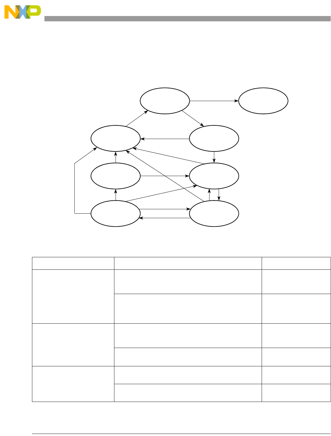
Universal Serial Bus, OTG Capable Controller
15-36 Freescale Semiconductor
15.7.1 OTG Dual Role A Device Operation
A device is considered the A device because of the type of cable attached. If the USB Type A connector
or the USB Type Mini A connector is plugged into the device, he is considered the A device.
A dual role A device operates as the following flow diagram and state description table illustrates.
Figure 15-33. Dual Role A Device Flow Diagram
Table 15-38. State Descriptions for Figure 15-33
State Action Response
A_IDLE If ID Interrupt.
The cable has been un-plugged or a Type B cable has been
attached. The device now acts as a Type B device.
Go to B_IDLE
If the A application wants to use the bus or if the B device is
doing an SRP as indicated by an A_SESS_VLD Interrupt or
Attach or Port Status Change Interrupt check data line for 5
–10 msec pulsing.
Go to A_WAIT_VRISE
Turn on DRV_VBUS
A_WAIT_VRISE If ID Interrupt or if A_VBUS_VLD is false after 100 msec
The cable has been changed or the A device cannot support
the current required from the B device.
Go to A_WAIT_VFALL
Turn off DRV_VBUS
If A_VBUS_VLD interrupt Go to A_WAIT_BCON
A_WAIT_BCON After 200 msec without Attach or ID Interrupt. (This could wait
forever if desired.)
Go to A_WAIT_FALL
Turn off DRV_VBUS
A_VBUS_VLD Interrupt and B device attaches Go to A_HOST
Turn on Host Mode
A_IDLE
A_WAIT_VFALL A_WAIT_VRISE
A_PERIPHERAL
A_SUSPEND
B_IDLE
A_WAIT_BCON
A_HOST
MCF52211 ColdFire® Integrated Microcontroller Reference Manual, Rev. 3
Universal Serial Bus, OTG Capable Controller
Freescale Semiconductor 15-37
15.7.2 OTG Dual Role B Device Operation
A device is considered a B device if it connected to the bus with a USB Type B cable or a USB Type Mini
B cable.
A dual role B device operates as the following flow diagram and state description table illustrates.
Figure 15-34. Dual Role B Device Flow Diagram
A_HOST Enumerate Device determine OTG Support.
If A_VBUS_VLD/ Interrupt or A device is done and doesn’t
think he wants to do something soon or the B device
disconnects
Go to A_WAIT_VFALL
Turn off Host Mode
Turn off DRV_VBUS
If the A device is finished with session or if the A device wants
to allow the B device to take bus.
Go to A_SUSPEND
ID Interrupt or the B device disconnects Go to A_WAIT_BCON
A_SUSPEND
If ID Interrupt, or if 150 msec B disconnect timeout (This
timeout value could be longer) or if A_VBUS_VLD\ Interrupt
Go to A_WAIT_VFALL
Turn off DRV_VBUS
If HNP enabled, and B disconnects in 150 msec then B device
is becoming the host.
Go to A_PERIPHERAL
Turn off Host Mode
If A wants to start another session Go to A_HOST
A_PERIPHERAL If ID Interrupt or if A_VBUS_VLD interrupt Go to A_WAIT_VFALL
Turn off DRV_VBUS.
If 3 –200 msec of Bus Idle Go to A_WAIT_BCON
Turn on Host Mode
A_WAIT_VFALL If ID Interrupt or (A_SESS_VLD/ & b_conn/) Go to A_IDLE
Table 15-38. State Descriptions for Figure 15-33 (continued)
State Action Response
B_IDLE
B_HOST B_SRP_INIT
B_WAIT_ACON
A_IDLE
B_PERIPHERAL
MCF52211 ColdFire® Integrated Microcontroller Reference Manual, Rev. 3

Universal Serial Bus, OTG Capable Controller
15-38 Freescale Semiconductor
15.7.3 Power
The USB-FS core is a fully synchronous static design. The power used by the design is dependant on the
application usage of the core. Applications that transfer more data or cause a greater number of packets to
be sent consumes a greater amount of power.
Because the design is synchronous and static, reducing the transitions on the clock net may conserve
power. This may be done in the following ways.
The first is to reduce the clock frequency to the USB module. The clock frequency may not be reduced
below the minimum recommended operating frequency of the USB module without first disabling the
USB operation and disconnecting (via software disconnect) the USB module from the USB bus.
Alternately, the clock may be shut off to the core to conserve power. Again, this may only be done after
the USB operations on the bus have been disabled and the device has been disconnected from the USB.
Table 15-39. State Descriptions for Figure 15-34
State Action Response
B_IDLE If ID\ Interrupt.
A Type A cable has been plugged in and the device should now
respond as a Type A device.
Go to A_IDLE
If B_SESS_VLD Interrupt.
The A device has turned on VBUS and begins a session.
Go to B_PERIPHERAL
Turn on DP_HIGH
If B application wants the bus and Bus is Idle for 2 ms and the
B_SESS_END bit is set, the B device can perform an SRP.
Go to B_SRP_INIT
Pulse CHRG_VBUS Pulse
DP_HIGH 5-10 ms
B_SRP_INIT If ID\ Interrupt or SRP Done (SRP must be done in less than 100
msecs.)
Go to B_IDLE
B_PERIPHERAL If HNP enabled and the bus is suspended and B wants the bus,
the B device can become the host.
Go to B_WAIT_ACON
Turn off DP_HIGH
B_WAIT_ACON If A connects, an attach interrupt is received Go to B_HOST
Turn on Host Mode
If ID\ Interrupt or B_SESS_VLD/ Interrupt
If the cable changes or if VBUS goes away, the host doesn’t
support us.
Go to B_IDLE
Go to B_IDLE
If 3.125 ms expires or if a Resume occurs Go to B_PERIPHERAL
B_HOST If ID\ Interrupt or B_SESS_VLD\ Interrupt
If the cable changes or if VBUS goes away, the host doesn’t
support us.
Go to B_IDLE
If B application is done or A disconnects Go to B_PERIPHERAL
MCF52211 ColdFire® Integrated Microcontroller Reference Manual, Rev. 3

Universal Serial Bus, OTG Capable Controller
Freescale Semiconductor 15-39
15.7.4 USB Suspend State
USB bus powered devices are required to respond to a 3ms lack of activity on the USB bus by going into
a suspend state. Software is notified of the suspend condition via the transition in the port status and control
register. Optionally, an interrupt can be generated that is controlled by the interrupt enable register. In the
suspend state, a USB device has a maximum USB bus power budget of 500uA. To achieve that level of
power conservation, most of the device circuits need to be switched off. When the clock is disabled to the
USB-FScore all functions are disabled, but all operational states are retained. The transceiver VP and VM
signals can be used to construct a circuit able to detect the resume signaling on the bus and restore the
clocks to the rest of the circuit when the USB host takes the bus out of the suspend state.
MCF52211 ColdFire® Integrated Microcontroller Reference Manual, Rev. 3
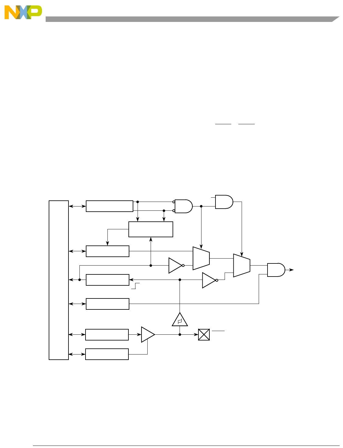
Freescale Semiconductor 16-1
Chapter 16
Edge Port Module (EPORT)
16.1 Introduction
The edge port module (EPORT) has up to eight interrupt pins, IRQ7 – IRQ0. Each pin can be configured
individually as a level-sensitive interrupt pin, an edge-detecting interrupt pin (rising edge, falling edge, or
both), or a general-purpose input/output (I/O) pin.
NOTE
Not all EPORT signals may be output from the device. See Chapter 2,
“Signal Descriptions,” to determine which signals are available.
Figure 16-1. EPORT Block Diagram
NOTE
The GPIO module must be configured to enable the peripheral function of
the appropriate pins (refer to Chapter 13, “General Purpose I/O Module”)
prior to configuring the edge-port module.
Internal Bus
Synchronizer
EPFRn
EPPAR[2n, 2n + 1]
EPIERn
Edge Detect
D0
Stop
Logic
D1
QD0
D1
Q
Mode
To Interrupt
Controller
IRQn pin
Rising Edge
of System Clock
EPPDRn
EPDRn
EPDDRn
MCF52211 ColdFire® Integrated Microcontroller Reference Manual, Rev. 3

Edge Port Module (EPORT)
Freescale Semiconductor 16-2
16.2 Low-Power Mode Operation
This section describes the operation of the EPORT module in low-power modes. For more information on
low-power modes, see Chapter 8, “Power Management”. Table 16-1 shows EPORT-module operation in
low-power modes and describes how this module may exit each mode.
NOTE
The control register (LPCR) in the system control module specifies the
interrupt level at or above what is needed to bring the device out of a
low-power mode.
In wait and doze modes, the EPORT module continues to operate as it does in run mode. It may be
configured to exit the low-power modes by generating an interrupt request on a selected edge or a low level
on an external pin. In stop mode, no clocks are available to perform the edge-detect function. Only the
level-detect logic is active (if configured) to allow any low level on the external interrupt pin to generate
an interrupt (if enabled) to exit stop mode.
NOTE
In stop mode, the input pin synchronizer is bypassed for the level-detect
logic because no clocks are available.
16.3 Signal Descriptions
All EPORT pins default to general-purpose input pins at reset. The pin value is synchronized to the rising
edge of CLKOUT when read from the EPORT pin data register (EPPDR). The values used in the
edge/level detect logic are also synchronized to the rising edge of CLKOUT. These pins use
Schmitt-triggered input buffers with built-in hysteresis designed to decrease the probability of generating
false, edge-triggered interrupts for slow rising and falling input signals.
When a pin is configured as an output, it is driven to a state whose level is determined by the corresponding
bit in the EPORT data register (EPDR). All bits in the EPDR are set at reset.
16.4 Memory Map/Register Definition
This subsection describes the memory map and register structure. Refer to Table 16-2 for a description of
the EPORT memory map.
Table 16-1. Edge Port Module Operation in Low-Power Modes
Low-power Mode EPORT Operation Mode Exit
Wait Normal Any IRQn interrupt at or above level in LPCR
Doze Normal Any IRQn interrupt at or above level in LPCR
Stop Level-sensing only Any IRQn interrupt set for level-sensing at or
above level in LPCR. See note below.
MCF52211 ColdFire® Integrated Microcontroller Reference Manual, Rev. 3

Edge Port Module (EPORT)
16-3 Freescale Semiconductor
16.4.1 EPORT Pin Assignment Register (EPPAR)
The EPORT pin assignment register (EPPAR) controls the function of each pin individually.
Table 16-2. Edge Port Module Memory Map
IPSBAR
Offset Register Width
(bits) Access Reset Value Section/Page
Supervisor Access Only Registers1
1User access to supervisor-only address locations have no effect and result in a bus error.
0x13_0000 EPORT Pin Assignment Register (EPPAR) 16 R/W 0x0000 16.4.1/16-3
0x13_0002 EPORT Data Direction Register (EPDDR) 8 R/W 0x00 16.4.2/16-4
0x13_0003 EPORT Interrupt Enable Register (EPIER) 8 R/W 0x00 16.4.3/16-4
Supervisor/User Access Registers
0x13_0004 EPORT Data Register (EPDR) 8 R/W 0xFF 16.4.4/16-5
0x13_0005 EPORT Pin Data Register (EPPDR) 8 R See Section 16.4.5/16-5
0x13_0006 EPORT Flag Register (EPFR) 8 R/W 0x00 16.4.6/16-6
IPSBAR
Offset:
0x13_0000 (EPPAR) Access: Supervisor read/write
1514131211109876543210
REPPA7 EPPA6 EPPA5 EPPA4 EPPA3 EPPA2 EPPA1 EPPA0
W
Reset0000000000000000
Figure 16-2. EPORT Pin Assignment Register (EPPAR)
Table 16-3. EPPAR Field Descriptions
Field Description
15–0
EPPAn
EPORT pin assignment select fields. The read/write EPPAn fields configure EPORT pins for level detection and rising
and/or falling edge detection.
Pins configured as level-sensitive are active-low (logic 0 on the external pin represents a valid interrupt request).
Level-sensitive interrupt inputs are not latched. To guarantee that a level-sensitive interrupt request is acknowledged,
the interrupt source must keep the signal asserted until acknowledged by software. Level sensitivity must be selected
to bring the device out of stop mode with an IRQn interrupt.
Pins configured as edge-triggered are latched and need not remain asserted for interrupt generation. A pin
configured for edge detection can trigger an interrupt regardless of its configuration as input or output.
Interrupt requests generated in the EPORT module can be masked by the interrupt controller module. EPPAR
functionality is independent of the selected pin direction.
Reset clears the EPPAn fields.
00 Pin IRQn level-sensitive
01 Pin IRQn rising edge triggered
10 Pin IRQn falling edge triggered
11 Pin IRQn falling edge and rising edge triggered
MCF52211 ColdFire® Integrated Microcontroller Reference Manual, Rev. 3

Edge Port Module (EPORT)
Freescale Semiconductor 16-4
16.4.2 EPORT Data Direction Register (EPDDR)
The EPORT data direction register (EPDDR) controls the direction of each one of the pins individually.
16.4.3 Edge Port Interrupt Enable Register (EPIER)
The EPORT interrupt enable register (EPIER) enables interrupt requests for each pin individually.
IPSBAR
Offset:
0x13_0002 (EPDDR) Access: Supervisor read/write
76543210
REPDD7 EPDD6 EPDD5 EPDD4 EPDD3 EPDD2 EPDD1 EPDD0
W
Reset00000000
Figure 16-3. EPORT Data Direction Register (EPDDR)
Table 16-4. EPDDR Field Descriptions
Field Description
7–0
EPDDn
Setting any bit in the EPDDR configures the corresponding pin as an output. Clearing any bit in EPDDR configures
the corresponding pin as an input. Pin direction is independent of the level/edge detection configuration. Reset clears
EPDD7–EPDD0.
To use an EPORT pin as an external interrupt request source, its corresponding bit in EPDDR must be clear.
Software can generate interrupt requests by programming the EPORT data register when the EPDDR selects output.
0 Corresponding EPORT pin configured as input
1 Corresponding EPORT pin configured as output
IPSBAR
Offset:
0x13_0003 (EPIER) Access: User read/write
76543210
R
EPIE7 EPIE6 EPIE5 EPIE4 EPIE3 EPIE2 EPIE1 EPIE0
W
Reset:00000000
Figure 16-4. EPORT Port Interrupt Enable Register (EPIER)
Table 16-5. EPIER Field Descriptions
Field Description
7–0
EPIEn
Edge port interrupt enable bits enable EPORT interrupt requests. If a bit in EPIER is set, EPORT generates an
interrupt request when:
• The corresponding bit in the EPORT flag register (EPFR) is set or later becomes set
• The corresponding pin level is low and the pin is configured for level-sensitive operation
Clearing a bit in EPIER negates any interrupt request from the corresponding EPORT pin. Reset clears
EPIE7–EPIE0.
0 Interrupt requests from corresponding EPORT pin disabled
1 Interrupt requests from corresponding EPORT pin enabled
MCF52211 ColdFire® Integrated Microcontroller Reference Manual, Rev. 3

Edge Port Module (EPORT)
16-5 Freescale Semiconductor
16.4.4 Edge Port Data Register (EPDR)
The EPORT data register (EPDR) holds the data to be driven to the pins.
16.4.5 Edge Port Pin Data Register (EPPDR)
The EPORT pin data register (EPPDR) reflects the current state of the pins.
IPSBAR
Offset:
0x13_0004 (EPDR) Access: User read/write
76543210
R
EPD7 EPD6 EPD5 EPD4 EPD3 EPD2 EPD1 EPD0
W
Reset:11111111
Figure 16-5. EPORT Port Data Register (EPDR)
Table 16-6. EPDR Field Descriptions
Field Description
7–0
EPDn
Edge port data bits. An internal register stores data written to EPDR; if any pin of the port is configured as an output,
the bit stored for that pin is driven onto the pin. Reading EDPR returns the data stored in the register. Reset sets
EPD7 – EPD0.
IPSBAR
Offset:
0x13_0005 (EPPDR) Access: User read-only
76543210
REPPD7 EPPD6 EPPD5 EPPD4 EPPD3 EPPD2 EPPD1 EPPD0
W
Reset: [IRQ7] [IRQ6] [IRQ5] [IRQ4] [IRQ3] [IRQ2] [IRQ1] [IRQ0]
Figure 16-6. EPORT Port Pin Data Register (EPPDR)
Table 16-7. EPPDR Field Descriptions
Field Description
7–0
EPPDn
Edge port pin data bits. The read-only EPPDR reflects the current state of the EPORT pins IRQ7 – IRQ0. Writing to
EPPDR has no effect, and the write cycle terminates normally. Reset does not affect EPPDR.
MCF52211 ColdFire® Integrated Microcontroller Reference Manual, Rev. 3

Edge Port Module (EPORT)
Freescale Semiconductor 16-6
16.4.6 Edge Port Flag Register (EPFR)
The EPORT flag register (EPFR) individually latches EPORT edge events.
IPSBAR
Offset:
0x13_0006 (EPFR) Access: User read/write
7 6543210
REPF7 EPF6 EPF5 EPF4 EPF3 EPF2 EPF1 EPF0
Ww1c w1c w1c w1c w1c w1c w1c w1c
Reset: 0 0 0 0 0 0 0 0
Figure 16-7. EPORT Port Flag Register (EPFR)
Table 16-8. EPFR Field Descriptions
Field Description
7–0
EPFn
Edge port flag bits. When an EPORT pin is configured for edge triggering, its corresponding read/write bit in EPFR
indicates that the selected edge has been detected. Reset clears EPF7 – EPF0.
Bits in this register are set when the selected edge is detected on the corresponding pin. A bit remains set until
cleared by writing a 1 to it. Writing 0 has no effect. If a pin is configured as level-sensitive (EPPARn= 00), pin
transitions do not affect this register.
0 Selected edge for IRQn pin not detected
1 Selected edge for IRQn pin detected
MCF52211 ColdFire® Integrated Microcontroller Reference Manual, Rev. 3

Freescale Semiconductor 17-1
Chapter 17
DMA Controller Module
17.1 Introduction
This chapter describes the direct memory access (DMA) controller module. It provides an overview of the
module and describes in detail its signals and registers. The latter sections of this chapter describe
operations, features, and supported data transfer modes in detail.
NOTE
The designation n is used throughout this section to refer to registers or
signals associated with one of the four identical DMA channels: DMA0,
DMA1, DMA2, or DMA3.
17.1.1 Overview
The DMA controller module enables fast transfers of data, providing an efficient way to move blocks of
data with minimal processor interaction. The DMA module, shown in Figure 17-1, has four channels that
allow byte, word, longword, or 16-byte burst data transfers. Each channel has a dedicated source address
register (SARn), destination address register (DARn), byte count register (BCRn), control register
(DCRn), and status register (DSRn). Transfers are dual address to on-chip devices, such as UART and
GPIOs.
MCF52211 ColdFire® Integrated Microcontroller Reference Manual, Rev. 3
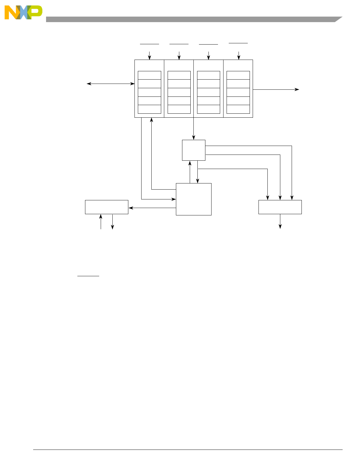
DMA Controller Module
Freescale Semiconductor 17-2
Figure 17-1. DMA Signal Diagram
NOTE
Throughout this chapter, the terms external request and DREQ are used to
refer to a DMA request from one of the on-chip UARTS, DMA timers or
DREQ signals. For details on the connections associated with DMA
request inputs, see Section 17.3.1, “DMA Request Control (DMAREQC).”
17.1.2 Features
The DMA controller module features:
• Four independently programmable DMA controller channels
• Auto-alignment for source or destination accesses
• Dual-address transfers
• Channel arbitration on transfer boundaries
• Data transfers in 8-, 16-, 32-, or 128-bit blocks using a 16-byte buffer
• Continuous-mode or cycle-steal transfers
• Independent transfer widths for source and destination
• Independent source and destination address registers
• Modulo addressing on source and destination addresses
• Automatic channel linking
MUX
Arbitration/
Bus Interface
Data Path Control
Internal
ChannelChannel
MUX
Registered
Data Path
SAR0
DAR0
BCR0
DCR0
DSR0
Channel 0
Interrupts
SAR1
DAR1
BCR1
DCR1
DSR1
Channel 1
SAR2
DAR2
BCR2
DCR2
DSR2
Channel 2
SAR3
DAR3
BCR3
DCR3
DSR3
Channel 3
Bus
Attributes
Current Master Attributes
Write Data Bus
Read Data Bus
System Bus Address
System Bus Size
Channel
Enables
Requests
Bus Signals
Control
Control
DREQ0 DREQ1 DREQ2 DREQ3
MCF52211 ColdFire® Integrated Microcontroller Reference Manual, Rev. 3
DMA Controller Module
17-3 Freescale Semiconductor
17.2 DMA Transfer Overview
The DMA module can move data within system memory (including memory and peripheral devices) with
minimal processor intervention, greatly improving overall system performance. The DMA module
consists of four independent, functionally equivalent channels, so references to DMA in this chapter apply
to any of the channels. It is not possible to implicitly address all four channels at once.
The processor generates DMA requests internally by setting DCR[START]; the UART modules and DMA
timers can generate a DMA request by asserting internal DREQ signals. The processor can program bus
bandwidth for each channel. The channels support cycle-steal and continuous transfer modes; see
Section 17.4.1, “Transfer Requests (Cycle-Steal and Continuous Modes).”
The DMA controller supports dual-address transfers. The DMA channels support up to 32 data bits.
• Dual-address transfers—A dual-address transfer consists of a read followed by a write and is
initiated by an internal request using the START bit or by a peripheral DMA request. Two types of
transfer can occur: a read from a source device or a write to a destination device. See Figure 17-2
for more information.
Figure 17-2. Dual-Address Transfer
Any operation involving the DMA module follows the same three steps:
1. Channel initialization—Channel registers are loaded with control information, address pointers,
and a byte-transfer count.
2. Data transfer—The DMA accepts requests for operand transfers and provides addressing and bus
control for the transfers.
3. Channel termination—Occurs after the operation is finished, successfully or due to an error. The
channel indicates the operation status in the channel’s DSR, described in Section 17.3.4, “Byte
Count Registers (BCRn) and DMA Status Registers (DSRn).”
17.3 Memory Map/Register Definition
This section describes each internal register and its bit assignment. Modifying DMA control registers
during a DMA transfer can result in undefined operation. Table 17-1 shows the mapping of DMA
controller registers.
DMADMA
Memory/
Peripheral
Memory/
Peripheral
Control and Data
Control and Data
MCF52211 ColdFire® Integrated Microcontroller Reference Manual, Rev. 3

DMA Controller Module
Freescale Semiconductor 17-4
17.3.1 DMA Request Control (DMAREQC)
The DMAREQC register provides a software-controlled connection matrix for DMA requests. It logically
routes DMA requests from the DMA timers and UARTs to the four channels of the DMA controller.
Writing to this register determines the exact routing of the DMA request to the four channels of the DMA
modules.
If DCRn[EEXT] is set and the channel is idle, the assertion of the appropriate external DREQn signal
activates channel n.
Table 17-1. DMA Controller Memory Map
IPSBAR
Offset Register Width Access Reset Value Section/Page
0x00_0014 DMA request control register (DMAREQC)1
1Located within the SCM, but listed here for clarity.
32 R/W 0x0000_0000 17.3.1/17-4
0x00_0100
+ n * 0x10
Source address register n (SARn)
where n = 0–3
32 R/W 0x0000_0000 17.3.2/17-5
0x00_0104
+ n * 0x10
Destination address register n (DARn)
where n = 0–3
32 R/W 0x0000_0000 17.3.3/17-6
0x00_0108
+ n * 0x10
DMA status (DSRn) and byte count register n (BCRn)
where n = 0–3
32 R/W 0x0000_0000 17.3.4/17-6
0x00_010C
+ n * 0x10
DMA control register n (DCRn)
where n = 0–3
32 R/W 0x0000_0000 17.3.5/17-8
IPSBAR
Offset: 0x00_0014 (DMAREQC)
Access: read/write
31 30 29 28 27 26 25 24 23 22 21 20 19 18 17 16
R00000000000000 0 0
W
Reset00000000000000 0 0
15 14 13 12 11 10 9 8 7 6 5 4 3 2 1 0
RDMAC3 DMAC2 DMAC1 DMAC0
W
Reset00000000000000 0 0
Figure 17-3. DMA Request Control Register (DMAREQC)
MCF52211 ColdFire® Integrated Microcontroller Reference Manual, Rev. 3

DMA Controller Module
17-5 Freescale Semiconductor
17.3.2 Source Address Registers (SARn)
SARn, shown in Figure 17-4, contains the address from which the DMA controller requests data.
NOTE
The backdoor enable bit must be set in the SCM RAMBAR, as well as the
secondary port valid bit in the core RAMBAR to enable backdoor accesses
from the DMA to SRAM. See Section 14.5.2, “Memory Base Address
Register (RAMBAR)and Section 5.2.1, “SRAM Base Address Register
(RAMBAR),” for more details.
Table 17-2. DMAREQC Field Description
Field Description
15–0
DMACn
DMA channel n. Each four bit field defines the logical connection between the DMA requesters and that DMA
channel. There are ten possible requesters (4 DMA Timers and 6 UARTs). Any request can be routed to any of
the DMA channels. Effectively, the DMAREQC provides a software-controlled routing matrix of the 10 DMA
request signals to the 4 channels of the DMA module. DMAC3 controls DMA channel 3, DMAC2 controls DMA
channel 2, etc.
0100 DMA Timer 0
0101 DMA Timer 1
0110 DMA Timer 2
0111 DMA Timer 3
1000 UART0 Receive
1001 UART1 Receive
1010 UART2 Receive
1100 UART0 Transmit
1101 UART1 Transmit
1110 UART2 Transmit
All other values are reserved and do not generate a DMA request.
IPSBAR
Offset:
0x00_0100 (SAR0)
0x00_0110 (SAR1)
0x00_0120 (SAR2)
0x00_0130 (SAR3)
Access: read/write
31 30 29 28 27 26 25 24 23 22 21 20 19 18 17 16
RSAR
W
Reset00000000000000 0 0
15 14 13 12 11 10 9 8 7 6 5 4 3 2 1 0
RSAR
W
Reset00000000000000 0 0
Figure 17-4. Source Address Registers (SARn)
MCF52211 ColdFire® Integrated Microcontroller Reference Manual, Rev. 3

DMA Controller Module
Freescale Semiconductor 17-6
17.3.3 Destination Address Registers (DARn)
DARn holds the address to which the DMA controller sends data.
17.3.4 Byte Count Registers (BCRn) and DMA Status Registers (DSRn)
The BCRn and DSRn registers are two logical registers that occupy one 32-bit register, as shown in
Figure 17-6. The address used to access both registers is the same; DSRn occupies bits 31–24, and BCRn
occupies bits 23–0. BCRn contains the number of bytes yet to be transferred for a given block. BCRn
decrements on the successful completion of the address transfer of a write transfer. BCRn decrements by
1, 2, 4, or 16 for byte, word, longword, or line accesses, respectively.
The fields of the DSRn register (bits 31–24 in Figure 17-6) are shown in Figure 17-7. In response to an
event, the DMA controller writes to the appropriate DSRn bit. Only a write to DSRn[DONE] results in
action. DSRn[DONE] is set when the block transfer is complete.
IPSBAR
Offset:
0x00_0104 (DAR0)
0x00_0114 (DAR1)
0x00_0124 (DAR2)
0x00_0134 (DAR3)
Access: Read/write
31 30 29 28 27 26 25 24 23 22 21 20 19 18 17 16
RDAR
W
Reset00000000000000 0 0
15 14 13 12 11 10 9 8 7 6 5 4 3 2 1 0
RDAR
W
Reset00000000000000 0 0
Figure 17-5. Destination Address Registers (DARn)
IPSBAR
Offset:
0x00_0108 (BCR0/DSR0)
0x00_0118 (BCR1/DSR1)
0x00_0128 (BCR2/DSR2)
0x00_0138 (BCR3/DSR3)
Access: Read/write
31 30 29 28 27 26 25 24 23 22 21 20 19 18 17 16
R
DSR BCR
W
Reset0000000000000000
1514131211109876543210
R
BCR
W
Reset0000000000000000
Figure 17-6. Byte Count Registers (BCRn) and DMA Status Registers (DSRn)
MCF52211 ColdFire® Integrated Microcontroller Reference Manual, Rev. 3

DMA Controller Module
17-7 Freescale Semiconductor
When a transfer sequence is initiated and BCRn[BCR] is not a multiple of 16, 4, or 2 when the DMA is
configured for line, longword, or word transfers, respectively, DSRn[CE] is set and no transfer occurs.
IPSBAR
Offsets:
0x00_0108 (DSR0)
0x00_0118 (DSR1)
0x00_0128 (DSR2)
0x00_0138 (DSR3)
Access: Read/write
76543210
R 0
CE BES BED
0
REQ BSY DONE
W
Reset:00000000
Figure 17-7. DMA Status Registers (DSRn)
Table 17-3. DSRn Field Descriptions
Field Description
7 Reserved, should be cleared.
6
CE
Configuration error. Occurs when BCR, SAR, or DAR does not match the requested transfer size, or if
BCR equals 0 when the DMA receives a start condition. CE is cleared at hardware reset or by writing a 1 to
DSR[DONE].
0 No configuration error exists.
1 A configuration error has occurred.
5
BES
Bus error on source
0 No bus error occurred.
1 The DMA channel terminated with a bus error during the read portion of a transfer.
4
BED
Bus error on destination
0 No bus error occurred.
1 The DMA channel terminated with a bus error during the write portion of a transfer.
3 Reserved, should be cleared.
2
REQ
Request
0 No request is pending or the channel is currently active. Cleared when the channel is selected.
1 The DMA channel has a transfer remaining and the channel is not selected.
1
BSY
Busy
0 DMA channel is inactive. Cleared when the DMA has finished the last transaction.
1 BSY is set the first time the channel is enabled after a transfer is initiated.
0
DONE
Transactions done. Set when all DMA controller transactions complete, as determined by transfer count or error
conditions. When BCR reaches zero, DONE is set when the final transfer completes successfully. DONE can also
be used to abort a transfer by resetting the status bits. When a transfer completes, software must clear DONE
before reprogramming the DMA.
0 Writing or reading a 0 has no effect.
1 DMA transfer completed. Writing a 1 to this bit clears all DMA status bits and can be used in an interrupt
handler to clear the DMA interrupt and error bits.
MCF52211 ColdFire® Integrated Microcontroller Reference Manual, Rev. 3

DMA Controller Module
Freescale Semiconductor 17-8
17.3.5 DMA Control Registers (DCRn)
The DMA control registers (DCRn) are described in Figure 17-8 and Table 17-4.
IPSBAR
Offsets:
0x00_010C (DCR0)
0x00_011C (DCR1)
0x00_012C (DCR2)
0x00_013C (DCR3)
Access: Read/write
31 30 29 28 27 26 25 24 23 22 21 20 19 18 17 16
R
INT EEXT CS AA BWC
00
SINC SSIZE DINC DSIZE
0
WSTART
Reset00000000 0 000000 0
15141312111098 7 654321 0
R
SMOD DMOD D_REQ
0
LINKCC LCH1 LCH2
W
Reset00000000 0 000000 0
Figure 17-8. DMA Control Registers (DCRn)
Table 17-4. DCRn Field Descriptions
Field Description
31
INT
Interrupt on completion of transfer. Determines whether an interrupt is generated by completing a transfer or by
the occurrence of an error condition.
0 No interrupt is generated.
1 Internal interrupt signal is enabled.
30
EEXT
Enable external request. Care should be taken because a collision can occur between the START bit and DREQn
when EEXT equals 1.
0 External request is ignored.
1 Enables external request to initiate transfer. The internal request (initiated by setting the START bit) is always
enabled.
29
CS
Cycle steal.
0 DMA continuously makes read/write transfers until the BCR decrements to 0.
1 Forces a single read/write transfer per request.
28
AA
Auto-align. AA and SIZE determine whether the source or destination is auto-aligned, that is, transfers are
optimized based on the address and size. See Section 17.4.4.1, “Auto-Alignment.”
0 Auto-align disabled
1 If SSIZE indicates a transfer no smaller than DSIZE, source accesses are auto-aligned; otherwise, destination
accesses are auto-aligned. Source alignment takes precedence over destination alignment. If auto-alignment
is enabled, the appropriate address register increments, regardless of DINC or SINC.
MCF52211 ColdFire® Integrated Microcontroller Reference Manual, Rev. 3

DMA Controller Module
17-9 Freescale Semiconductor
27–25
BWC
Bandwidth control. Indicates the number of bytes in a block transfer. When the byte count reaches a multiple of
the BWC value, the DMA releases the bus.
24–23 Reserved, should be cleared.
22
SINC
Source increment. Controls whether a source address increments after each successful transfer.
0 No change to SAR after a successful transfer.
1 The SAR increments by 1, 2, 4, or 16, as determined by the transfer size.
21–20
SSIZE
Source size. Determines the data size of the source bus cycle for the DMA control module.
00 Longword
01 Byte
10 Word
11 Line (16-byte burst)
19
DINC
Destination increment. Controls whether a destination address increments after each successful transfer.
0 No change to the DAR after a successful transfer.
1 The DAR increments by 1, 2, 4, or 16, depending upon the size of the transfer.
18–17
DSIZE
Destination size. Determines the data size of the destination bus cycle for the DMA controller.
00 Longword
01 Byte
10 Word
11 Line (16-byte burst)
16
START
Start transfer.
0DMA inactive
1 The DMA begins the transfer in accordance to the values in the control registers. START is cleared
automatically after one system clock and is always read as logic 0.
Table 17-4. DCRn Field Descriptions (continued)
Field Description
BWC Number of kilobytes per block
000 DMA has priority and does not negate
its request until transfer completes.
001 16 Kbytes
010 32 Kbytes
011 64 Kbytes
100 128 Kbytes
101 256 Kbytes
110 512 Kbytes
111 1024 Kbytes
MCF52211 ColdFire® Integrated Microcontroller Reference Manual, Rev. 3

DMA Controller Module
Freescale Semiconductor 17-10
15–12
SMOD
Source address modulo. Defines the size of the source data circular buffer used by the DMA Controller. If enabled
(SMOD is non-zero), the buffer base address is located on a boundary of the buffer size. The value of this
boundary is based upon the initial source address (SAR). The base address should be aligned to a 0-modulo-
circular buffer size boundary. Misaligned buffers are not possible. The boundary is forced to the value determined
by the upper address bits in the field selection.
11–8
DMOD
Destination address modulo. Defines the size of the destination data circular buffer used by the DMA Controller.
If enabled (DMOD value is non-zero), the buffer base address is located on a boundary of the buffer size. The
value of this boundary depends on the initial destination address (DAR). The base address should be aligned to
a 0-modulo- circular buffer size boundary. Misaligned buffers are not possible. The boundary is forced to the value
determined by the upper address bits in the field selection.
.
7
D_REQ
Disable request. DMA hardware automatically clears the corresponding DCRn[EEXT] bit when the byte count
register reaches zero.
0 EEXT bit is not affected.
1 EEXT bit is cleared when the BCR is exhausted.
6 Reserved; should be cleared.
Table 17-4. DCRn Field Descriptions (continued)
Field Description
SMOD Circular Buffer Size
0000 Buffer Disabled
0001 16 Bytes
0010 32 Bytes
... ...
1111 256 Kbytes
SMOD Circular Buffer Size
0000 Buffer Disabled
0001 16 Bytes
0010 32 Bytes
... ...
1111 256 Kbytes
DMOD Circular Buffer Size
0000 Buffer Disabled
0001 16 Bytes
0010 32 Bytes
... ...
1111 256 Kbytes
MCF52211 ColdFire® Integrated Microcontroller Reference Manual, Rev. 3

DMA Controller Module
17-11 Freescale Semiconductor
17.4 Functional Description
In the following discussion, the term DMA request implies that DCRn[START or EEXT] is set, followed
by assertion of an internal or external DMA request. The START bit is cleared when the channel begins
an internal access.
Before initiating a dual-address access, the DMA module verifies that DCRn[SSIZE,DSIZE] are
consistent with the source and destination addresses. If they are not consistent, the configuration error bit,
DSRn[CE], is set. If misalignment is detected, no transfer occurs, DSRn[CE] is set, and, depending on the
DCR configuration, an interrupt event is issued. If the auto-align bit, DCRn[AA], is set, error checking is
performed on the appropriate registers.
A read/write transfer reads bytes from the source address and writes them to the destination address. The
number of bytes is the larger of the sizes specified by DCRn[SSIZE] and DCRn[DSIZE]. See 17.3.5,
“DMA Control Registers (DCRn).”
5–4
LINKCC
Link channel control. Allows DMA channels to have their transfers linked. The current DMA channel triggers a
DMA request to the linked channels (LCH1 or LCH2) depending on the condition described by the LINKCC bits.
00 No channel-to-channel linking
01 Perform a link to channel LCH1 after each cycle-steal transfer followed by a link to LCH2 after the BCR
decrements to zero.
10 Perform a link to channel LCH1 after each cycle-steal transfer
11 Perform a link to channel LCH1 after the BCR decrements to zero
If not in cycle steal mode (DCRn[CS]=0) and LINKCC equals 01 or 10, no link to LCH1 occurs.
If LINKCC equals 01, a link to LCH1 is created after each cycle-steal transfer performed by the current DMA
channel is completed. As the last cycle-steal is performed and the BCR reaches zero, then the link to LCH1 is
closed and a link to LCH2 is created.
If the LINKCC field is non-zero, the contents of the bandwidth control field (DCRn[BWC]) are ignored and
effectively forced to zero by the DMA hardware. This is done to prevent any non-zero bandwidth control settings
from allowing channel arbitration while any type of link is to be performed.
3-2
LCH1
Link channel 1. Indicates the DMA channel assigned as link channel 1. The link channel number cannot be the
same as the currently executing channel, and generates a configuration error if this is attempted (DSRn[CE] is
set).
00 DMA Channel 0
01 DMA Channel 1
10 DMA Channel 2
11 DMA Channel 3
1-0
LCH2
Link channel 2. Indicates the DMA channel assigned as link channel 2. The link channel number cannot be the
same as the currently executing channel, and generates a configuration error if this is attempted (DSRn[CE] is
set).
00 DMA Channel 0
01 DMA Channel 1
10 DMA Channel 2
11 DMA Channel 3
Table 17-4. DCRn Field Descriptions (continued)
Field Description
MCF52211 ColdFire® Integrated Microcontroller Reference Manual, Rev. 3

DMA Controller Module
Freescale Semiconductor 17-12
Source and destination address registers (SARn and DARn) can be programmed in the DCRn to increment
at the completion of a successful transfer.
17.4.1 Transfer Requests (Cycle-Steal and Continuous Modes)
The DMA channel supports internal and external requests. A request is issued by setting DCRn[START]
or when a UART or DMA timer asserts a DMA request. Setting DCRn[EEXT] enables recognition of
external DMA requests. Selecting between cycle-steal and continuous modes minimizes bus usage for
internal or external requests.
• Cycle-steal mode (DCRn[CS] = 1)—Only one complete transfer from source to destination occurs
for each request. If DCRn[EEXT] is set, a request can be internal or external. An internal request
is selected by setting DCRn[START]. An external request is initiated by an on-chip peripheral
while DCRn[EEXT] is set.
• Continuous mode (DCRn[CS] = 0)—After an internal or external request, the DMA continuously
transfers data until BCRn reaches zero or a multiple of DCRn[BWC] or until DSRn[DONE] is set.
If BCRn is a multiple of BWC, the DMA request signal is negated until the bus cycle terminates
to allow the internal arbiter to switch masters. DCRn[BWC] equaling 000 specifies the maximum
transfer rate; other values specify a transfer rate limit.
The DMA performs the specified number of transfers, then relinquishes bus control. The DMA
negates its internal bus request on the last transfer before BCRn reaches a multiple of the boundary
specified in BWC. Upon completion, the DMA reasserts its bus request to regain mastership at the
earliest opportunity. The DMA loses bus control for a minimum of one bus cycle.
17.4.2 Dual-Address Data Transfer Mode
Each channel supports dual-address transfers. Dual-address transfers consist of a source data read and a
destination data write. The DMA controller module begins a dual-address transfer sequence during a DMA
request. If no error condition exists, DSRn[REQ] is set.
• Dual-address read—The DMA controller drives the SARn value onto the internal address bus. If
DCRn[SINC] is set, the SARn increments by the appropriate number of bytes upon a successful
read cycle. When the appropriate number of read cycles complete (multiple reads if the destination
size is larger than the source), the DMA initiates the write portion of the transfer.
If a termination error occurs, DSRn[BES, DONE] are set and DMA transactions stop.
• Dual-address write—The DMA controller drives the DARn value onto the address bus. If
DCRn[DINC] is set, DARn increments by the appropriate number of bytes at the completion of a
successful write cycle. BCRn decrements by the appropriate number of bytes. DSRn[DONE] is set
when BCRn reaches zero. If the BCRn is greater than zero, another read/write transfer is initiated.
If the BCRn is a multiple of DCRn[BWC], the DMA request signal is negated until termination of
the bus cycle to allow the internal arbiter to switch masters.
If a termination error occurs, DSRn[BED, DONE] are set and DMA transactions stop.
MCF52211 ColdFire® Integrated Microcontroller Reference Manual, Rev. 3

DMA Controller Module
17-13 Freescale Semiconductor
17.4.3 Channel Initialization and Startup
Before a block transfer starts, channel registers must be initialized with information describing
configuration, request-generation method, and the data block.
17.4.3.1 Channel Prioritization
The four DMA channels are prioritized in ascending order (channel 0 having highest priority and channel
3 having the lowest) or in an order determined by DCRn[BWC]. If the BWC encoding for a DMA channel
is 000, that channel has priority only over the channel immediately preceding it. For example, if
DCR3[BWC] equals 000, DMA channel 3 has priority over DMA channel 2 (assuming
DCR2[BWC] 000), but not over DMA channel 1.
If DCR0[BWC] equals 000 and DCR1[BWC] equals 000, DMA0 continues having priority over DMA1.
In this case, DCR1[BWC] equals 000 does not affect prioritization.
Simultaneous external requests are prioritized in ascending order or in an order determined by each
channel’s DCRn[BWC] bits.
17.4.3.2 Programming the DMA Controller Module
General guidelines for programming the DMA are:
• No mechanism exists within the DMA module itself to prevent writes to control registers during
DMA accesses.
•If the DCRn[BWC] value of sequential channels are equal, the channels are prioritized in
ascending order.
The DMAREQC register is configured to assign peripheral DMA requests to the individual DMA
channels.
The SARn is loaded with the source (read) address. If the transfer is from a peripheral device to memory,
the source address is the location of the peripheral data register. If the transfer is from memory to a
peripheral device or memory, the source address is the starting address of the data block. This can be any
aligned byte address.
The DARn should contain the destination (write) address. If the transfer is from a peripheral device to
memory, or from memory to memory, the DARn is loaded with the starting address of the data block to be
written. If the transfer is from memory to a peripheral device, DARn is loaded with the address of the
peripheral data register. This address can be any aligned byte address.
SARn and DARn change after each cycle depending on DCRn[SSIZE,DSIZE,
SINC,DINC,SMOD,DMOD] and on the starting address. Increment values can be 1, 2, 4, or 16 for byte,
word, longword, or 16-byte line transfers, respectively. If the address register is programmed to remain
unchanged (no count), the register is not incremented after the data transfer.
BCRn[BCR] must be loaded with the number of byte transfers to occur. It is decremented by 1, 2, 4, or 16
at the end of each transfer, depending on the transfer size. DSRn[DONE] must be cleared for channel
startup.
MCF52211 ColdFire® Integrated Microcontroller Reference Manual, Rev. 3

DMA Controller Module
Freescale Semiconductor 17-14
As soon as the channel has been initialized, it is started by writing a one to DCRn[START], or a peripheral
DMA request, depending on the status of DCRn[EEXT]. Programming the channel for internal requests
causes the channel to request the bus and start transferring data immediately. If the channel is programmed
for external request, a peripheral DMA request must be asserted before the channel requests the bus.
Changes to DCRn are effective immediately while the channel is active. To avoid problems with changing
a DMA channel setup, write a one to DSRn[DONE] to stop the DMA channel.
17.4.4 Data Transfer
This section describes auto-alignment and bandwidth control for DMA transfers.
.
17.4.4.1 Auto-Alignment
Auto-alignment allows block transfers to occur at the optimal size based on the address, byte count, and
programmed size. To use this , DCRn[AA] must be set. The source is auto-aligned if DCRn[SSIZE]
indicates a transfer size larger than DCRn[DSIZE]. Source alignment takes precedence over the
destination when the source and destination sizes are equal. Otherwise, the destination is auto-aligned. The
address register chosen for alignment increments regardless of the increment value. Configuration error
checking is performed on registers not chosen for alignment.
If BCRn is greater than 16, the address determines transfer size. Bytes, words, or longwords are transferred
until the address is aligned to the programmed size boundary, at which time accesses begin using the
programmed size.
If BCRn is less than 16 at the start of a transfer, the number of bytes remaining dictates transfer size. For
example, AA equals 1, SARn equals 0x0001, BCRn equals 0x00F0, SSIZE equals 00 (longword), and
DSIZE equals 01 (byte). Because SSIZE > DSIZE, the source is auto-aligned. Error checking is performed
on destination registers. The access sequence is as follows:
1. Read byte from 0x0001—write 1 byte, increment SARn.
2. Read word from 0x0002—write 2 bytes, increment SARn.
3. Read longword from 0x0004—write 4 bytes, increment SARn.
4. Repeat longwords until SARn= 0x00F0.
5. Read byte from 0x00F0—write byte, increment SARn.
If DSIZE is another size, data writes are optimized to write the largest size allowed based on the address,
but not exceeding the configured size.
17.4.4.2 Bandwidth Control
Bandwidth control makes it possible to force the DMA off the bus to allow access to another device.
DCRn[BWC] provides seven levels of block transfer sizes. If the BCRn decrements to a multiple of the
decode of the BWC, the DMA bus request negates until the bus cycle terminates. If a request is pending,
the arbiter may then pass bus mastership to another device. If auto-alignment is enabled,
MCF52211 ColdFire® Integrated Microcontroller Reference Manual, Rev. 3

DMA Controller Module
17-15 Freescale Semiconductor
DCRn[AA] equals 1, the BCRn may skip over the programmed boundary, in which case, the DMA bus
request is not negated.
If BWC equals 000, the request signal remains asserted until BCRn reaches zero. DMA has priority over
the core. In this scheme, the arbiter can always force the DMA to relinquish the bus.
17.4.5 Termination
An unsuccessful transfer can terminate for one of the following reasons:
• Error conditions—When the DMA encounters a read or write cycle that terminates with an error
condition, DSRn[BES] is set for a read and DSRn[BED] is set for a write before the transfer is
halted. If the error occurred in a write cycle, data in the internal holding register is lost.
• Interrupts—If DCRn[INT] is set, the DMA drives the appropriate internal interrupt signal. The
processor can read DSRn to determine whether the transfer terminated successfully or with an
error. DSRn[DONE] is then written with a one to clear the interrupt and the DONE and error bits.
MCF52211 ColdFire® Integrated Microcontroller Reference Manual, Rev. 3

Freescale Semiconductor 18-1
Chapter 18
ColdFire Flash Module (CFM)
18.1 Introduction
18.1.1 Overview
The ColdFire Flash Module (CFM) is a non-volatile memory (NVM) module for integration with a CPU.
The CFM provides 128 Kbytes of 32-bit Flash memory serving as electrically erasable and programmable,
non-volatile memory. The flash memory is ideal for program and data storage for single-chip applications,
allowing for field reprogramming without requiring external programming voltage sources.
The common flash bus interface executes read operations to the flash memory using one or two system
bus cycles to access each flash physical block, with access latency depending on the factory setting of the
CLKSEL bits in the CFMCLKSEL register. Flash physical blocks are interleaved between odd and even
addresses to form a flash logical block. Interleaving allows back-to-back read operations to the flash
memory at an effective access rate of one system bus cycle per word after the initial two-cycle access if
the CLKSEL bits are not set for single cycle access.
It is not possible to read from any flash logical block while the same logical block is being erased,
programmed, or verified. Flash logical blocks are divided into multiple 2-kByte logical pages that can be
erased separately. An erased bit reads 1 and a programmed bit reads 0.
MCF52211 ColdFire® Integrated Microcontroller Reference Manual, Rev. 3
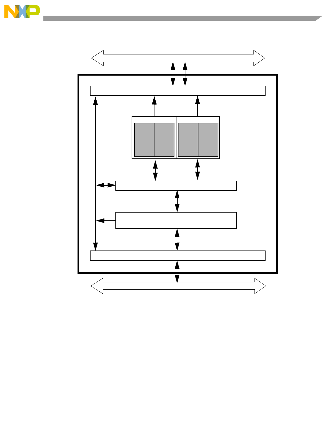
ColdFire Flash Module (CFM)
Freescale Semiconductor 18-2
Figure 18-1. CFM Block Diagram
18.1.2 Features
• 128 Kbytes of 32-bit Flash memory
• Automated program, erase, and verify operations
• Single power supply for program and erase operations
• Software programmable interrupts on command completion, access violations, or protection
violations
• Fast page erase operation
• Fast word program operation
• Protection scheme to prevent accidental program or erase of flash memory
FLASH COMMAND CONTROLLER
FLASH MEMORY CONTROLLER
INTERNAL FLASH BUS INTERFACE
COMMON FLASH BUS
INTERNAL FLASH BUS
COMMON FLASH BUS INTERFACE
ARRAY 0 ARRAY 1
EVEN BLOCK
ARRAY 2 ARRAY 3
ODD BLOCK
EVEN ODD
MCF52211 ColdFire® Integrated Microcontroller Reference Manual, Rev. 3
ColdFire Flash Module (CFM)
18-3 Freescale Semiconductor
• Access restriction control for supervisor/user and data/instruction operations
• Security to prevent unauthorized access to the flash memory
18.2 External Signal Description
The CFM contains no signals that connect off-chip for the end customer.
18.3 Memory Map and Register Definition
This section describes the CFM memory map and registers.
18.3.1 Memory Map
The memory map for the CFM memory is shown in <f-helvetica><st-bold>Figure 18-2.. The starting
address of the flash memory is determined by the flash array base address as defined by the system level
configuration. The flash memory map shows how a pair of 32-bit flash physical blocks (even and odd)
interleave every four bytes to form a contiguous memory space as follows:
Flash Block 0 includes byte addresses (PROGRAM_ARRAY_BASE+0x0000_0000) to
(PROGRAM_ARRAY_BASE+0x0001_FFFF).
Figure 18-2. CFM Flash Memory Map
The CFM has hardware interlocks that protect data from accidental corruption using program or erase
operations. A flexible scheme allows the protection of any combination of flash logical sectors as
described in Section 18.3.3.4, “CFMPROT — CFM Protection Register”. A similar scheme is available to
control supervisor/user and data/instruction access to these flash logical sectors.
Security information that allows the MCU to prevent intrusive access to the flash memory is stored in the
flash configuration field. The flash configuration field is composed of 24 bytes of reserved memory space
within the flash memory, which contains information that determines the CFM protection and access
restriction scheme out of reset. A description of each byte found in the flash configuration field is given in
Table 18-1.
(PROGRAM_ARRAY_BASE + 0x0000_0000)
128kBytes
•
•
•
Configuration Field
(PROGRAM_ARRAY_BASE+0x400) to
(PROGRAM_ARRAY_BASE+0x41A)
BLOCK
0 EVEN
(4Bytes)
BLOCK
0 ODD
(4Bytes)
BLOCK
0 EVEN
(4Bytes)
BLOCK
0 ODD
(4Bytes)
(PROGRAM_ARRAY_BASE + 0x0001_FFFF)
MCF52211 ColdFire® Integrated Microcontroller Reference Manual, Rev. 3

ColdFire Flash Module (CFM)
Freescale Semiconductor 18-4
18.3.2 Flash Base Address Register (FLASHBAR)
The configuration information in the flash base address register (FLASHBAR) controls the operation of
the flash module.
• The FLASHBAR holds the base address of the flash. The MOVEC instruction provides write-only
access to this register.
• The FLASHBAR can be read or written from the debug module in a similar manner.
• All undefined bits in the register are reserved. These bits are ignored during writes to the
FLASHBAR and return zeroes when read from the debug module.
• The FLASHBAR valid bit is programmed according to the chip mode selected at reset (see
Chapter 9, “Chip Configuration Module (CCM)” for more details). All other bits are unaffected.
The FLASHBAR register contains several control fields. These fields are shown in Figure 18-3.
NOTE
The default value of the FLASHBAR is determined by the chip
configuration selected at reset (see Chapter 9, “Chip Configuration Module
(CCM)” for more information).
Table 18-1. CFM Configuration Field
Address Offset
(from PROGRAM_ARRAY_BASE)
Size
(bytes) Description Factory
Default
0x0400 - 0x0407 8 Backdoor Comparison Key 0xFFFF_FFFF_FFFF_FFFF
0x0408 - 0x040B 4 Flash Protection Bytes
(see Section 18.3.3.4, “CFMPROT —
CFM Protection Register”)
0xFFFF_FFFF
0x040C - 0x040F 4 Flash SUPV Access Bytes
(see Section 18.3.3.5, “CFMSACC —
CFM Supervisor Access Register”)
0xFFFF_FFFF
0x0410 - 0x0413 4 Flash DATA Access Bytes
(see Section 18.3.3.6, “CFMDACC —
CFM Data Access Register”)
0xFFFF_FFFF
0x0414 - 0x0417 4 Flash Security Word
(see Section 18.3.3.3, “CFMSEC —
CFM Security Register”)
0xFFFF_FFFF
MCF52211 ColdFire® Integrated Microcontroller Reference Manual, Rev. 3

ColdFire Flash Module (CFM)
18-5 Freescale Semiconductor
NOTE
Flash accesses (reads/writes) by a bus master other than the core (e.g. DMA
controller), or writes to flash by the core during programming must use the
backdoor flash address of IPSBAR plus an offset of 0x0400_0000. For
example, for a DMA transfer from the first location of flash when IPSBAR
is at its default location of 0x4000_0000, the source register would be
loaded with 0x4400_0000. Backdoor access to flash for reads can be made
by the bus master, but it takes two cycles longer than a direct read of the
flash if using its FLASHBAR address.
NOTE
The flash is marked as valid on reset based on the RCON (reset
configuration) pin state. Flash space is valid on reset when booting in
single-chip mode . See Chapter 9, “Chip Configuration Module (CCM)” for
more details. When the default reset configuration is not overridden, the
MCU (by default) boots up in single-chip mode and the flash space is
marked as valid at address 0x0. The flash configuration field is checked
during the reset sequence to see if the flash is secured. If it is, the part always
boots from internal flash because it is marked as valid regardless of what is
done for chip configuration.
Address CPU + 0xC04 (FLASHBAR) Access: User read/write
31 30 29 28 27 26 25 24 23 22 21 20 19 18 17 16
RBA31 BA30 BA29 BA28 BA27 BA26 BA25 BA24 BA23 BA22 BA21 BA20 BA19 000
W
Reset0000000000000000
1514131211109876543210
R0000000WP0
AFS C/I SC SD UC UD V1
1The reset value for the valid bit is determined by the chip mode selected at reset (see Chapter 9, “Chip Configuration Module
(CCM)”).
W
Reset0000000100100000
Figure 18-3. Flash Base Address Register (FLASHBAR)
Table 18-2. FLASHBAR Field Descriptions
Bits Name Description
31–19 BA[31:18] Base Address Field. Defines the 0-modulo-512K base address of the flash module. By
programming this field, the flash may be located on any 512-Kbyte boundary within the processor’s
four gigabyte address space.
18–9 — Reserved, should be cleared.
8 WP Write Protect. Read-only. Allows only read accesses to the flash. This bit is always set and any
attempted write access generates an access error exception to the ColdFire processor core.
0 Allows read and write accesses to the flash module
1 Allows only read accesses to the flash module
MCF52211 ColdFire® Integrated Microcontroller Reference Manual, Rev. 3

ColdFire Flash Module (CFM)
Freescale Semiconductor 18-6
The CFM contains a set of control and status registers located at the register base address as defined by the
system level configuration. A summary of the CFM registers is given in Table 18-3.
7 — Reserved, should be cleared.
6 AFS Address fetch speculation. Performance enhancement to generate speculative flash accesses. to
reduce the effective flash access time from the actual two-cycle array time to a smaller number
approaching one cycle.
0 Speculation enabled
1 Disable speculation
5–1 C/I, SC, SD,
UC, UD
Address Space Masks (ASn).
These five bit fields allow certain types of accesses to be masked or inhibited from accessing the
flash module. The address space mask bits are:
C/I CPU space/interrupt acknowledge cycle mask
SC Supervisor code address space mask
SD Supervisor data address space mask
UC User code address space mask
UD User data address space mask
For each address space bit:
0 An access to the flash module can occur for this address space
1 Disable this address space from the flash module. If a reference using this address space is
made, it is inhibited from accessing the flash module, and is processed like any other non-flash
reference.
These bits are useful for power management as detailed in Chapter 8, “Power Management.”
0 V Valid. When set, this bit enables the flash module; otherwise, the module is disabled.
0 Contents of FLASHBAR are not valid
1 Contents of FLASHBAR are valid
Table 18-3. CFM Register Address Map
IPSBAR Offset
Register Bits
31 - 24 23 - 16 15 - 8 7 - 0
0x1D_0000 CFMMCR CFMCLKD RESERVED1
0x1D_0004 RESERVED1
0x1D_0008 CFMSEC
0x1D_000C RESERVED1
0x1D_0010 CFMPROT
0x1D_0014 CFMSACC
0x1D_0018 CFMDACC
0x1D_001C RESERVED1
0x1D_0020 CFMUSTAT RESERVED1
0x1D_0024 CFMCMD RESERVED1
0x1D_0028 RESERVED1
0x1D_002C RESERVED1
0x1D_0030 RESERVED1
Table 18-2. FLASHBAR Field Descriptions
Bits Name Description
MCF52211 ColdFire® Integrated Microcontroller Reference Manual, Rev. 3

ColdFire Flash Module (CFM)
18-7 Freescale Semiconductor
18.3.3 Register Descriptions
18.3.3.1 CFMMCR — CFM Module Configuration Register
The CFMMCR register is used to configure and control the operation of the internal bus interface.
CFMMCR register bits [10:5] are readable and writable with restrictions, while the remaining bits read 0
and are not writable.
0x1D_0034 RESERVED1
0x1D_0038 RESERVED1
0x1D_003C RESERVED1
0x1D_0040 RESERVED1
0x1D_0044 RESERVED1
0x1D_0048 RESERVED1CFMCLKSEL
1Access to reserved address locations generate a cycle termination transfer error.
IPSBAR
Offset: 0x1D_0000 (CFMMCR)
Access: User read/write
1514131211109876543210
R00000
LOCK PVIE AEIE CBE
IE CCIE KEY
ACC
00000
W
Reset0000000000000000
Figure 18-4. CFM Module Configuration Register (CFMMCR)
Table 18-4. CFMMCR Field Descriptions
Field Description
15-11 Reserved, read as 0
10
LOCK
Write Lock Control. The LOCK bit is always readable and is set once.
0 CFMPROT, CMFSACC, and CFMDACC registers are writable.
1 CFMPROT, CMFSACC, and CFMDACC registers are write-locked.
9
PVIE
Protection Violation interrupt Enable
The PVIE bit is always readable and writable. The PVIE bit enables an interrupt in case the protection
violation flag, PVIOL in the CFMUSTAT register, is set.
0 PVIOL interrupt disabled.
1 An interrupt is requested when the PVIOL flag is set.
8
AEIE
Access Error Interrupt Enable
The AEIE bit is always readable and writable. The AEIE bit enables an interrupt in case the access error
flag, ACCERR in the CFMUSTAT register, is set.
0 ACCERR interrupt disabled.
1 An interrupt is requested when the ACCERR flag is set.
Table 18-3. CFM Register Address Map
IPSBAR Offset
Register Bits
31 - 24 23 - 16 15 - 8 7 - 0
MCF52211 ColdFire® Integrated Microcontroller Reference Manual, Rev. 3

ColdFire Flash Module (CFM)
Freescale Semiconductor 18-8
18.3.3.2 CFMCLKD — CFM Clock Divider Register
The CFMCLKD register is used to control the period of the clock used for timed events in program and
erase algorithms.
All CFMCLKD register bits are readable, while bits [6:0] write once and bit 7 is not writable.
7
CBEIE
Command Buffer Empty Interrupt Enable
The CBEIE bit is always readable and writable. The CBEIE bit enables an interrupt in case the command
buffer empty flag, CBEIF in the CFMUSTAT register, is set.
0 CBEIF interrupt disabled.
1 An interrupt is requested when the CBEIF flag is set.
6
CCIE
Command Complete Interrupt Enable
The CCIE bit is always readable and writable. The CCIE bit enables an interrupt in case the command
completion flag, CCIF in the CFMUSTAT register, is set.
0 CCIF interrupt disabled.
1 An interrupt is requested when the CCIF flag is set.
5
KEYACC
Enable Security Key Writing
The KEYACC bit is readable and only writable if the KEYEN bits in the CFMSEC register are set to enable
backdoor key access.
0 Writes to CFM flash memory are interpreted as the start of a command write sequence.
1 Writes to CFM flash memory are interpreted as keys to release security.
4-0- Reserved, read as 0
IPSBAR
Offset: 0x1D_0002 (CFMCLKD)
Access: User read/write
76543210
RDIVLD
PRDIV8 DIV
W
Reset:00000000
Figure 18-5. CFM Clock Divider Register (CFMCLKD)
Table 18-5. CFMCLKD Field Descriptions
Field Description
7
DIVLD
Clock Divider Loaded
0 CFMCLKD register has not been written.
1 CFMCLKD register has been written to since the last reset.
Table 18-4. CFMMCR Field Descriptions (continued)
Field Description
MCF52211 ColdFire® Integrated Microcontroller Reference Manual, Rev. 3

ColdFire Flash Module (CFM)
18-9 Freescale Semiconductor
18.3.3.3 CFMSEC — CFM Security Register
The CFMSEC register is used to store the flash security word and CFM security state.
CFMSEC register bits [31:30,15:0] are readable, while remaining bits read 0 and all bits are not writable.
6
PRDIV8
Enable Prescaler by 8
0 The internal flash bus clock is directly fed into the clock divider.
1 Enables a prescaler to divide the internal flash bus clock by 8 before feeding into the clock divider.
5-0
DIV
Clock Divider Bits
The combination of PRDIV8 and DIV effectively divides the internal flash bus clock down to a frequency
of 150 KHz - 200 KHz. The internal flash bus clock frequency range is 150 KHz less than the internal flash
bus clock which is less than 102.4 MHz.
The CFMCLKD register bits PRDIV8 and DIV must be set with appropriate values before programming
or erasing the CFM flash memory Section 18.4.2.3.1, “Writing the CFMCLKD Register.”
IPSBAR
Offset: 0x1D_0008 (CFMSEC)
Access: User read/write
31 30 29 28 27 26 25 24 23 22 21 20 19 18 17 16
RKEYEN SEC
STAT 00000000000000
W
Reset F1
1Reset state loaded from flash configuration field during reset.
-2
2Reset state determined by security state of CFM.
00000000000000
15 14 131211109876543210
RSEC
W
Reset F1F1F1F1F1F1F1F1F1F1F1F1F1F1F1F1
Figure 18-6. CFM Security Register (CFMSEC)
Table 18-6. CFMSEC Field Descriptions
Field Description
31
KEYEN
Enable backdoor key access to unlock security
0 Backdoor key access to flash module is disabled.
1 Backdoor key access to flash module is enabled.
30
SECSTAT
Flash memory security status
0 Flash security is disabled.
1 Flash security is enabled.
29-16 Reserved, should read 0
15–0
SEC
Flash memory security bits
The SEC bits define the security state of the MCU as shown in Ta b l e 1 8 - 7 , which defines the single code
that enables the security in the CFM
Table 18-5. CFMCLKD Field Descriptions (continued)
Field Description
MCF52211 ColdFire® Integrated Microcontroller Reference Manual, Rev. 3

ColdFire Flash Module (CFM)
Freescale Semiconductor 18-10
The CFMSEC register is loaded from the flash configuration field in the flash block at offset 0x0414
during the reset sequence, indicated by F in Figure 18-6.
The CFM flash security operation is described in Section 18.4.3, “Flash Security Operation”.
18.3.3.4 CFMPROT — CFM Protection Register
The CFMPROT register defines which flash logical sectors are protected against program and erase
operations.
Figure 18-7. CFM Protection Register (CFMPROT)
All CFMPROT register bits are readable and only writable when LOCK=0.
The flash memory is divided into logical sectors for the purpose of data protection using the CFMPROT
register. The flash memory consists of 32 4kByte sectors as shown in <f-helvetica><st-bold>Figure 18-8..
To change the flash memory protection on a temporary basis, the CFMPROT register should be written
after the LOCK bit in the CFMMCR register has been cleared. To change the flash memory protection
loaded during the reset sequence, the flash logical sector containing the flash configuration field must first
be unprotected, and then the flash protection bytes must be programmed with the desired value.
Table 18-7. CFM Security States
SEC[15:0] Description
0x4AC81
1This value was chosen because it represents the ColdFire HALT instruction, making
it unlikely that a user compiled code accidentally programmed at the security
configuration field location would unintentionally secure the flash memory.
Flash Memory Secured
All other combinations Flash Memory Unsecured
IPSBAR
Offset: 0x1D_0010 (CFMPROT)
Access: User read/write
31 30 29 28 27 26 25 24 23 22 21 20 19 18 17 16
RPROTECT
W
Reset F1
1Reset state loaded from flash configuration field during reset.
F1F1F1F1F1F1F1F1F1F1F1F1F1F1F1
15 14 13 12 11 10 9 8 7 6 5 4 3 2 1 0
RPROTECT
W
Reset F1F1F1F1F1F1F1F1F1F1F1F1F1F1F1F1
MCF52211 ColdFire® Integrated Microcontroller Reference Manual, Rev. 3
ColdFire Flash Module (CFM)
18-11 Freescale Semiconductor
PROTECT[31:0]
Figure 18-8. CFMPROT Protection Diagram
Table 18-8. CFMPROT Field Descriptions
Field Description
31–0
PROTECT
Each flash logical sector can be protected from program and erase operations by setting the
PROTECT[M] bit.
1 Flash logical sector M is protected.
0 Flash logical sector M is not protected.
(PROGRAM_ARRAY_BASE + 0x0000_0000)
(PROGRAM_ARRAY_BASE + 0x0001_FFFF)
SECTOR 0
SECTOR 14
(PROGRAM_ARRAY_BASE + 0x0000_1000)
(PROGRAM_ARRAY_BASE + 0x0000_E000)
PROTECT[31]
PROTECT[0]
(PROGRAM_ARRAY_BASE + 0x0001_F000)
•
•
•
(PROGRAM_ARRAY_BASE + 0x0000_F000)
SECTOR 15
SECTOR 31
SECTOR 17
•
•
•
SECTOR 16
(PROGRAM_ARRAY_BASE + 0x0001_2000)
(PROGRAM_ARRAY_BASE + 0x0001_1000)
(PROGRAM_ARRAY_BASE + 0x0001_0000)
4kBytes
4kBytes
4kBytes
4kBytes
4kBytes
4kBytes
Flash Logical Sectors -
protection defined by CFMPROT
MCF52211 ColdFire® Integrated Microcontroller Reference Manual, Rev. 3

ColdFire Flash Module (CFM)
Freescale Semiconductor 18-12
18.3.3.5 CFMSACC — CFM Supervisor Access Register
The CFMSACC register is used to control supervisor/user access to the flash memory.
Figure 18-9. CFM Supervisor Access Register (CFMSACC)
All CFMSACC register bits are readable and only writable when LOCK is cleared.
To change the flash supervisor access on a temporary basis, the CFMSACC register should be written after
the LOCK bit in the CFMMCR register has been cleared. To change the flash supervisor access loaded
during the reset sequence, the flash logical sector containing the flash configuration field must first be
unprotected, and then the flash supervisor access bytes must be programmed with the desired value. Each
flash logical sector may be mapped into supervisor or unrestricted address space (see
<f-helvetica><st-bold>Figure 18-8. for details on flash sector mapping).
18.3.3.6 CFMDACC — CFM Data Access Register
The CFMDACC register is used to control data/instruction access to the flash memory.
IPSBAR
Offset: 0x1D_0014 (CFMSACC)
Access: User read/write
31 30 29 28 27 26 25 24 23 22 21 20 19 18 17 16
RSUPV
W
Reset F1
1Reset state loaded from flash configuration field during reset.
F1F1F1F1F1F1F1F1F1F1F1F1F1F1F1
1514131211109876543210
RSUPV
W
Reset F1F1F1F1F1F1F1F1F1F1F1F1F1F1F1F1
Table 18-9. CFMSACC Field Descriptions
Field Description
31–0
SUPV
Flash address space assignment for supervisor/user access
0 Flash logical sector M is placed in unrestricted address space.
1 Flash logical sector M is placed in supervisor address space
MCF52211 ColdFire® Integrated Microcontroller Reference Manual, Rev. 3

ColdFire Flash Module (CFM)
18-13 Freescale Semiconductor
Figure 18-10. CFM Data Access Register (CFMDACC)
All CFMDACC register bits are readable and only writable when LOCK is cleared.
To change the flash data access on a temporary basis, the CFMDACC register should be written after the
LOCK bit in the CFMMCR register has been cleared. To change the flash data access loaded during the
reset sequence, the flash logical sector containing the flash configuration field must first be unprotected,
and then the flash data access bytes must be programmed with the desired value. Each flash logical sector
may be mapped into data or both data and instruction address space (see Figure 18-8 for details on flash
sector mapping).
18.3.3.7 CFMUSTAT — CFM User Status Register
The CFMUSTAT register defines the flash command controller status and flash memory access, protection
and verify status.
Figure 18-11. CFM User Status Register (CFMUSTAT)
CFMUSTAT register bits CBEIF, PVIOL, ACCERR, and BLANK are readable and writable while CCIF
is readable but not writable, and remaining bits read 0 and are not writable.
IPSBAR
Offset: 0x1D_0018 (CFMDACC)
Access: User read/write
31 30 29 28 27 26 25 24 23 22 21 20 19 18 17 16
RDACC
W
Reset F1
1Reset state loaded from flash configuration field during reset.
F1F1F1F1F1F1F1F1F1F1F1F1F1F1F1
15 14 13 12 11 10 9 8 7 6 5 4 3 2 1 0
RDACC
W
Reset F1F1F1F1F1F1F1F1F1F1F1F1F1F1F1F1
Table 18-10. CFMDACC Field Descriptions
Field Description
31–0
DACC
Flash memory address space assignment for data/instruction access
0 Flash logical sector M is placed in data and instruction address space.
1 Flash logical sector M is placed in data address space.
IPSBAR
Offset: 0x1D_0020 (CFMUSTAT)
Access: User read/write
76543210
R
CBEIF
CCIF
PVIOL ACCERR
0
BLANK
00
W
Reset:11000000
MCF52211 ColdFire® Integrated Microcontroller Reference Manual, Rev. 3

ColdFire Flash Module (CFM)
Freescale Semiconductor 18-14
The CFMUSTAT register bits CBEIF, CCIF, PVIOL, ACCERR, and BLANK are available as external
signals CFM_STATUS_BITS[7:4,2] on the module boundary.
NOTE
Only one CFMUSTAT register bit can be cleared at a time.
Table 18-11. CFMUSTAT Field Descriptions
Field Description
7
CBEIF
Command Buffer Empty Interrupt Flag
The CBEIF flag, set by the flash command controller, indicates that the address, data, and command
buffers are empty so that a new command write sequence can be started. The CBEIF flag is cleared by
writing a 1 to CBEIF as part of a command write sequence. Writing a 0 to the CBEIF flag has no effect
on CBEIF, but can be used to abort a command write sequence. The CBEIF flag can generate an interrupt
if the CBEIE bit in the CFMMCR register is set.
0 Buffers are full.
1 Buffers are ready to accept a new command write sequence.
6
CCIF
Command Complete Interrupt Flag
The CCIF flag, set by the flash command controller, indicates that there are no more commands pending.
The CCIF flag is cleared by the flash command controller when CBEIF is cleared and sets upon
completion of all active and pending commands. Writing to the CCIF flag has no effect on CCIF. The CCIF
flag can generate an interrupt if the CCIE bit in the CFMMCR register is set.
0 Command in progress.
1 All commands are completed.
5
PVIOL
Protection Violation
The PVIOL flag, set by the flash command controller, indicates an attempt was made to program or erase
an address in a protected flash logical sector. The PVIOL flag is cleared by writing a 1 to PVIOL. Writing
a 0 to the PVIOL flag has no effect on PVIOL. While the PVIOL flag is set, it is not possible to launch a
command or start a command write sequence.
0 No protection violation has been detected.
1 Protection violation has occurred.
4
ACCERR
Access Error
The ACCERR flag, set by the flash command controller, indicates an illegal access was made to the flash
memory or registers caused by an illegal command write sequence. The ACCERR flag is cleared by
writing a 1 to the ACCERR flag. Writing a 0 to the ACCERR flag has no effect on ACCERR. While the
ACCERR flag is set, it is not possible to launch a command or start a command write sequence. See
Section 18.4.2.3.5, “Flash Normal Mode Illegal Operations” for details on what action sets the ACCERR
flag.
0 No access error has been detected.
1 Access error has occurred.
3 Reserved, should read 0
2
BLANK
All flash memory locations or the selected flash logical page have been verified as erased.
The BLANK flag, set by the flash command controller, indicates that a blank check or page erase verify
operation has checked all flash memory locations or the selected flash logical page and found them to be
erased. The BLANK flag is cleared by writing a 1 to BLANK. Writing a 0 to the BLANK flag has no effect
on BLANK.
0 If a blank check or page erase verify command has been executed, and the CCIF flag is set, then a 0
in the BLANK flag indicates that all flash memory locations are not erased or the selected flash logical
page is not erased.
1 All flash memory locations or selected logical page verify as erased.
1 -0 Reserved, should read 0
MCF52211 ColdFire® Integrated Microcontroller Reference Manual, Rev. 3

ColdFire Flash Module (CFM)
18-15 Freescale Semiconductor
18.3.3.8 CFMCMD — CFM Command Register
The CFMCMD register is the flash command register.
Figure 18-12. CFM Command Buffer and Register (CFMCMD)
All CFMCMD register bits are readable and writable except bit 7, which reads zero and is not writable.
18.3.3.9 CFMCLKSEL — CFM Clock Select Register
The CFMCLKSEL register reflects the factory setting for read access latency from the system bus to the
flash block.
IPSBAR
Offset: 0x1D_0024 (CFMCMD)
Access: User read/write
7 6543210
R0
CMD
W
Reset: 0 0 0 0 0 0 0 0
Table 18-12. CFMCMD Field Descriptions
Field Description
7 Reserved, should read 0
6 - 0
CMD
Valid flash memory commands are shown in Table 18-13. Writing a command other than those listed in
Table 18-13 during a command write sequence causes the ACCERR flag in the CFMUSTAT register to
set.
Table 18-13. CFM Flash Memory Commands
CMD[6:0] Description
0x05 Blank Check
0x06 Page Erase Verify
0x20 Word Program
0x40 Page Erase
0x41 Mass Erase
MCF52211 ColdFire® Integrated Microcontroller Reference Manual, Rev. 3

ColdFire Flash Module (CFM)
Freescale Semiconductor 18-16
Figure 18-13. CFM Clock Select Register (CFMCLKSEL)
CFMCLKSEL register bits [1:0] are read-only, while the remaining bits read 0 and are not writable.
18.4 Functional Description
18.4.1 General
The following modes and operations are described in the corresponding sections:
1. Flash normal mode (Section 18.4.2, “Flash Normal Mode”)
a) Read operation (Section 18.4.2.1, “Read Operation”)
b) Write operation (Section 18.4.2.2, “Write Operation”)
c) Program, erase, and verify operations (Section 18.4.2.3, “Program, Erase, and Verify
Operations”)
d) Stop mode (Section 18.4.2.4, “Stop Mode”)
2. Flash security operation (Section 18.4.3, “Flash Security Operation”)
18.4.2 Flash Normal Mode
In flash normal mode, the user can access the CFM registers and the CFM flash memory (see
Section 18.3.1, “Memory Map”).
IPSBAR
Offset: 0x1D_004A(CFMCLKSEL)
Access: User read/write
1514131211109876543210
R00000000000000CLKSEL
W
Reset00000000000000F
1
1Reset state set by factory and is not modifiable.
F1
Table 18-14. CFMCLKSEL Field Descriptions
Field Description
15 - 2 Reserved, should read 0
1 - 0
CLKSEL
Flash Read Access Latency Select
The CLKSEL bits set the read access latency to the flash block. Ta b l e 1 8 - 1 5 describes the setting that
selects between single-cycle and two-cycle flash block read access.
Table 18-15. Clock Select States
CLKSEL[1:0] Description Burst Read Access
2’b10 Single-Cycle Flash Block Read Access 1-1-1-1
All other combinations Two-cycle Flash Block Read Access 2-1-1-1
MCF52211 ColdFire® Integrated Microcontroller Reference Manual, Rev. 3

ColdFire Flash Module (CFM)
18-17 Freescale Semiconductor
18.4.2.1 Read Operation
A valid read operation occurs when a transfer request is initiated, the address is equal to an address within
the valid range of the CFM flash memory space, and the read/write control indicates a read cycle.
18.4.2.2 Write Operation
A valid write operation occurs when a transfer request is initiated, the address is equal to an address within
the valid range of the CFM flash memory space and the read/write control indicates a write cycle. The
action taken on a valid flash array write depends on the subsequent user command issued as part of a valid
command write sequence. Only 32-bit write operations are allowed to the flash memory space. Byte and
half-word write operations to the flash memory space results in a cycle termination transfer error.
18.4.2.3 Program, Erase, and Verify Operations
Write and read operations are used for the program, erase, and verify algorithms described in this section.
These algorithms are controlled by the flash memory controller whose timebase, for program and erase
operations, is derived from the internal flash bus clock via a programmable counter. The command register
as well as the associated address and data registers operate as a buffer and a register (2-stage FIFO), so that
a new command along with the necessary data and address can be stored to the buffer while the previous
command is in progress. This buffering operation provides time optimization when programming more
than one word on a physical row in the flash memory as the high voltage generation can be kept active in
between two programming operations. This saves the time overhead needed for setup of the high voltage
charge pumps. Buffer empty, as well as command completion, is signaled by flags in the CFMUSTAT
register with interrupts generated, if enabled.
The next four sections describe:
• How to write the CFMCLKD register
• Command write sequences used to program, erase, and verify the flash memory
• Valid flash commands
• Errors resulting from illegal command write sequences to the flash memory
18.4.2.3.1 Writing the CFMCLKD Register
Prior to issuing any command, it is necessary to write the CFMCLKD register to divide the internal bus
frequency to within the 150- to 200-kHz range. CFMCLKD[PRDIV8 and DIV] are set as follows:
For bus frequencies greater than 12.8 MHz, the CFMCLKD bit PRDIV8 must be set.
CFMCLKD DIV bit field must be chosen so that the following equation is valid:
If PRDIV8 == 1 then FCLK = input clock / 8, else FCLK = input clock
If (FCLK[KHz] / 200KHz) is integer then DIV = (FCLK[KHz] / 200KHz) - 1,
else DIV = INT (FCLK[KHz] / 200kHz)
Therefore, the clock to the flash block timing control, FCLK, is:
FCLK = (input clock) / (DIV + 1)
150KHz < FCLK <= 200KHz
MCF52211 ColdFire® Integrated Microcontroller Reference Manual, Rev. 3

ColdFire Flash Module (CFM)
Freescale Semiconductor 18-18
For example, if the bus frequency is 33 MHz, CFMCLKD[DIV] should be set to 0x14 and bit PRDIV8 set
to 1. The resulting FCLK is 196.4 KHz. As a result, the flash memory program and erase algorithm timings
are increased over the optimum target by:
(200 - 196.4) / 200 x 100% = 1.78%
Remark: INT(X) means taking the integer part of X
Example: INT(33MHz/8/200KHz) = 20
CAUTION
Programming the flash with bus frequency < 150 KHz should be avoided.
Setting CFMCLKD to a value such that FCLK < 150 KHz can destroy the
flash memory due to overstress. Setting CFMCLKD to a value such that
FCLK > 200 KHz can result in incomplete programming or erasure of the
flash memory array cells.
NOTE
Program and Erase command execution time increases proportionally with
the period of FCLK.
If the CFMCLKD register is written, the DIVLD bit is set automatically. If the DIVLD bit is 0, the
CFMCLKD register has not been written since the last reset. No command can be executed if the
CFMCLKD register has not been written to Section 18.4.2.3.5, “Flash Normal Mode Illegal Operations.”
18.4.2.3.2 Command Write Sequence
The flash command controller is used to supervise the command write sequence to execute blank check,
page erase verify, program, page erase, and mass erase algorithms.
Before starting a command write sequence, the ACCERR and PVIOL flags in the CFMUSTAT register
must be clear and the CBEIF flag should be tested to determine the state of the address, data, and command
buffers. If the CBEIF flag is set, indicating the buffers are empty, a new command write sequence can be
executed.
A command write sequence consists of three steps that must be strictly adhered to, because writes to the
CFM are not permitted between steps. However, flash register and array reads are allowed during a
command write sequence. The basic command write sequence is as follows:
1. Write to one or more addresses in the flash memory.
2. Write a valid command to the CFMCMD register.
3. Clear CBEIF flag by writing a 1 to CBEIF to launch the command.
When the CBEIF flag is cleared, the CCIF flag is cleared on the same bus cycle by the flash command
controller indicating that the command was successfully launched. The CBEIF flag is set again indicating
that the address, data, and command buffers are ready for a new command write sequence to begin. A
buffered command waits for the active command to be completed before being launched. The CCIF flag
in the CFMUSTAT register set upon completion of all active and buffered commands.
A command write sequence can be aborted at anytime prior to clearing the CBEIF flag in the CFMUSTAT
register by writing a 0 to the CBEIF flag. The ACCERR flag in the CFMUSTAT register is set after
MCF52211 ColdFire® Integrated Microcontroller Reference Manual, Rev. 3

ColdFire Flash Module (CFM)
18-19 Freescale Semiconductor
successfully aborting a command write sequence and the ACCERR flag must be cleared prior to starting
a new command write sequence.
18.4.2.3.3 Bus Arbitration During Write Operations
After a command has been successfully launched, the CFM signals the core platform to hold off read
accesses to any active flash physical block until all active and buffered commands have completed
(CCIF=1). A flash write operation from the internal flash bus holds off the Core platform until it is
completed.
18.4.2.3.4 Flash Normal Mode Commands
Table 18-16 summarizes the valid flash normal mode commands.
Blank Check
The blank check operation verifies all flash memory addresses in the CFM are erased.
An example flow to execute the blank check command is shown in Figure 18-14. The blank check
command write sequence is as follows:
1. Write to any flash memory address to start the command write sequence for the blank check
command. The specific address and data written during the blank check command write sequence
is ignored.
2. Write the blank check command, 0x05, to the CFMCMD register.
3. Clear the CBEIF flag by writing a 1 to CBEIF to launch the blank check command.
Because all flash physical blocks are verified simultaneously, the number of internal flash bus cycles
required to execute the blank check operation on a fully erased flash memory is equal to the number of
word addresses in a flash logical block plus 15 internal flash bus cycles as measured from the time the
CBEIF flag is cleared until the CCIF flag is set in the CFMUSTAT register. Upon completion of the blank
check operation (CCIF=1), the BLANK flag sets in the CFMUSTAT register if the entire flash memory is
erased. If any flash memory location is not erased, the blank check operation terminates and the BLANK
flag remains clear.
Table 18-16. CFM Flash Memory Command Description
CFMCMD Meaning Description
0x05 Blank Check Verify that the entire flash memory is erased. If all bits are erased, the BLANK bit sets in
the CFMUSTAT register, Figure 18-11, upon command completion.
0x06 Page Erase
Verify
Verifies that a flash logical page is erased. If the flash logical page is erased, the BLANK
bit sets in the CFMUSTAT register, Figure 18-11, upon command completion.
0x20 Program Program a 32-bit word.
0x40 Page Erase Erase a flash logical page.
0x41 Mass Erase Erase the entire flash memory. All flash memory protection must be disabled.
MCF52211 ColdFire® Integrated Microcontroller Reference Manual, Rev. 3
ColdFire Flash Module (CFM)
Freescale Semiconductor 18-20
Figure 18-14. Example Blank Check Command Flow
Page Erase Verify
The page erase verify operation verifies all memory addresses in a flash logical page are erased.
Write: Register CFMCLKD
Read: Register CFMCLKD
Write: Array Address
Write: Register CFMCMD
Blank Check Command 0x05
Write: Register CFMUSTAT
yes
no
Clear bit CBEIF 0x80
Clock Register
Written
Check
1.
2.
3.
yes
no
Access Error and
Protection Violation
no
and Data
Bit Polling for
Command Completion
Check
Read: Register CFMUSTAT
yes
NOTE: command write sequence
aborted by writing 0x00 to
CFMUSTAT register.
NOTE: command write sequence
aborted by writing 0x00 to
CFMUSTAT register.
EXIT
Read: Register CFMUSTAT
no
START
yes
no
Blank Check
Verify Status
Read: Register CFMUSTAT
yes
EXIT
Flash Memory
Erased
Flash Memory
Not Erased
Check
CCIF
Set?
Bit
BLANK
Set?
Bit
ACCERR/PVIOL
Set?
Bit
CBEIF
Set?
Bit
DIVLD
Set?
Bit
Clear bit ACCERR/PVIOL 0x30
Write: Register CFMUSTAT
Address, Data,
Command
Buffer Empty Check
Clear bit BLANK 0x04
Write: Register CFMUSTAT
MCF52211 ColdFire® Integrated Microcontroller Reference Manual, Rev. 3

ColdFire Flash Module (CFM)
18-21 Freescale Semiconductor
An example flow to execute the page erase verify operation is shown in Figure 18-15. The page erase
verify command write sequence is as follows:
1. Write to any word address in a flash logical page to start the command write sequence for the page
erase verify command. The address written determines the flash logical page to be verified, while
the data written during the page erase verify command write sequence is ignored.
2. Write the page erase verify command, 0x06, to the CFMCMD register.
3. Clear the CBEIF flag by writing a 1 to CBEIF to launch the page erase verify command.
Because the word addresses in even and odd flash blocks are interleaved, pages from adjacent interleaving
flash physical blocks are automatically erase verified at the same time. The number of internal flash bus
cycles required to execute the page erase verify operation on a fully erased flash logical page is equal to
the number of word addresses in a flash logical page plus 15 internal flash bus cycles as measured from
the time the CBEIF flag is cleared until the CCIF flag is set in the CFMUSTAT register.
Upon completion of any page erase verify operation (CCIF=1), the BLANK flag in the CFMUSTAT
register is set if all addresses in the selected flash logical page are verified to be erased. If any address in
the selected flash logical page is not erased, the page erase verify operation terminates and the BLANK
flag remains clear.
MCF52211 ColdFire® Integrated Microcontroller Reference Manual, Rev. 3
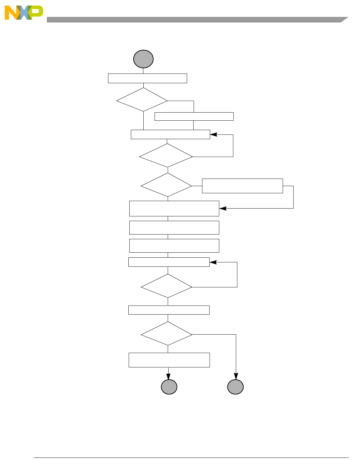
ColdFire Flash Module (CFM)
Freescale Semiconductor 18-22
Figure 18-15. Example Page Erase Verify Command Flow
Program
The operation programs a previously erased address in the flash memory using an embedded algorithm.
Write: Register CFMCLKD
Read: Register CFMCLKD
Write: Logical Page Address
Write: Register CFMCMD
Page Erase Verify Command 0x06
Write: Register CFMUSTAT
yes
no
Clear bit CBEIF 0x80
Clock Register
Written
Check
1.
2.
3.
Clear bit ACCERR/PVIOL 0x30
Write: Register CFMUSTAT
yes
no
Access Error and
Protection Violation
no
and Dummy Data
Bit Polling for
Command Completion
Check
Read: Register CFMUSTAT
yes
NOTE: Command write sequence
aborted by writing 0x00 to
CFMUSTAT register.
NOTE: Command write sequence
aborted by writing 0x00 to
CFMUSTAT register.
Read: Register CFMUSTAT
no
START
yes
Read: Register CFMUSTAT
Check
CCIF
Set?
Bit
ACCERR/PVIOL
Set?
Bit
CBEIF
Set?
Bit
DIVLD
Set?
Bit
Address, Data,
Command
Buffer Empty Check
no
Page Erase
Verify Status
yes
EXIT
Flash Logical Page
Not Erased
BLANK
Set?
Bit
Clear bit BLANK 0x04
Write: Register CFMUSTAT
EXIT
Flash Logical Page
Erased
MCF52211 ColdFire® Integrated Microcontroller Reference Manual, Rev. 3

ColdFire Flash Module (CFM)
18-23 Freescale Semiconductor
An example flow to execute the program operation is shown in Figure 18-16. The program command write
sequence is as follows:
1. Write to a word address in a flash physical block to start the command write sequence for the
program command. The word address written determines the flash physical block address to
program while the data written during the program command write sequence determines the data
stored at that address.
To write to two physical blocks simultaneously, perform the following steps:
a) Write data to even address (where address is a multiple of eight)
b) Write data to odd address (previous address + 4)
c) Write PROGRAM command to CFMCMD
d) Clear CBEIF, by writing a 1 to it
The flash physical block written to in the first array write limits the ability to simultaneously
program in block order only those flash physical blocks that remain.
2. Write the program command, 0x20, to the CFMCMD register.
3. Clear the CBEIF flag by writing a 1 to CBEIF to launch the program command.
If the address to be programmed is in a protected sector of the flash memory, the PVIOL flag in the
CFMUSTAT register sets and the program command does not launch. After the program command has
successfully launched, the CCIF flag in the CFMUSTAT register sets after the program operation has
completed unless a new command write sequence has been buffered.
MCF52211 ColdFire® Integrated Microcontroller Reference Manual, Rev. 3

ColdFire Flash Module (CFM)
Freescale Semiconductor 18-24
Figure 18-16. Example Program Command Flow
Page Erase
The page erase operation erases all memory addresses in a flash logical page using an embedded algorithm.
Write: Register CFMCLKD
Read: Register CFMCLKD
Write: Array Address and
Write: Register CFMCMD
Program Command 0x20
Write: Register CFMUSTAT
yes
no
Clear bit CBEIF 0x80
CBEIF
Set?
Bit yes
Clock Register
Written
Check
1.
2.
3.
no
Protection
Violation Check
Read: Register CFMUSTAT
CCIF
Set?
Bit no
no
Address, Data,
Command
Buffer Empty Check
Next Write?
yes
no
Data
Clear bit PVIOL 0x20
Write: Register CFMUSTAT
yes
PVIOL
Set?
Bit
Bit Polling for
Command
Completion Check
Read: Register CFMUSTAT
yes
NOTE: Command write sequence
aborted by writing 0x00 to
CFMUSTAT register.
NOTE: Command write sequence
aborted by writing 0x00 to
CFMUSTAT register.
EXIT
Read: Register CFMUSTAT
no
CBEIF
Set?
Bit
START
yes
•
DIVLD
Set?
Bit
Change Protection
Clear bit ACCERR/PVIOL 0x30
Write: Register CFMUSTAT
yes
no
Access Error and
Protection Violation ACCERR/PVIOL
Set?
Bit
Check
MCF52211 ColdFire® Integrated Microcontroller Reference Manual, Rev. 3

ColdFire Flash Module (CFM)
18-25 Freescale Semiconductor
An example flow to execute the page erase operation is shown in Figure 18-17. The page erase command
write sequence is as follows:
1. Write to any word address in a flash logical page to start the command write sequence for the page
erase command. The word address written determines the flash logical page to erase while the data
written during the page erase command write sequence is ignored.
2. Write the page erase command, 0x40, to the CFMCMD register.
3. Clear the CBEIF flag by writing a 1 to CBEIF to launch the page erase command.
If the flash logical page to be erased is in a protected sector of the flash memory, the PVIOL flag in the
CFMUSTAT register sets and the page erase command does not launch. After the page erase command has
successfully launched, the CCIF flag in the CFMUSTAT register sets after the page erase operation has
completed, unless a new command write sequence has been buffered.
MCF52211 ColdFire® Integrated Microcontroller Reference Manual, Rev. 3
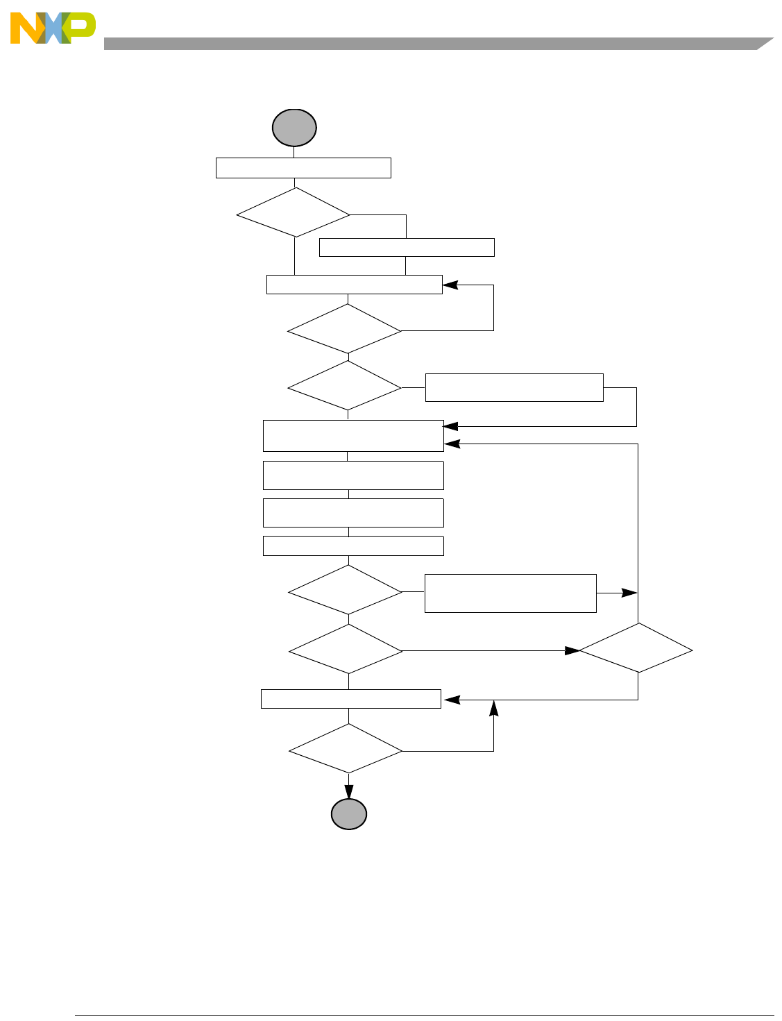
ColdFire Flash Module (CFM)
Freescale Semiconductor 18-26
Figure 18-17. Example Page Erase Command Flow
Mass Erase
The mass erase operation erases all flash memory addresses using an embedded algorithm.
Write: Register CFMCLKD
Read: Register CFMCLKD
Write: Logical Page Address
Write: Register CFMCMD
Page Erase Command 0x40
Write: Register CFMUSTAT
yes
no
Clear bit CBEIF 0x80
CBEIF
Set?
Bit yes
Clock Register
Written
Check
1.
2.
3.
no
Protection
Violation Check
Read: Register CFMUSTAT
CCIF
Set?
Bit no
no
Address, Data,
Command
Buffer Empty Check
Next Write?
yes
no
and Dummy Data
Clear bit PVIOL 0x20
Write: Register CFMUSTAT
yes
PVIOL
Set?
Bit
Bit Polling for
Command
Completion Check
Read: Register CFMUSTAT
yes
NOTE: Command write sequence
aborted by writing 0x00 to
CFMUSTAT register.
NOTE: Command write sequence
aborted by writing 0x00 to
CFMUSTAT register.
EXIT
Read: Register CFMUSTAT
no
CBEIF
Set?
Bit
START
yes
•
DIVLD
Set?
Bit
Change Protection
Clear bit ACCERR/PVIOL 0x30
Write: Register CFMUSTAT
yes
no
Access Error and
Protection Violation ACCERR/PVIOL
Set?
Bit
Check
MCF52211 ColdFire® Integrated Microcontroller Reference Manual, Rev. 3

ColdFire Flash Module (CFM)
18-27 Freescale Semiconductor
An example flow to execute the mass erase command is shown in Figure 18-18. The mass erase command
write sequence is as follows:
1. Write to any flash memory address to start the command write sequence for the mass erase
command. The specific address and data written during the mass erase command write sequence
is ignored.
2. Write the mass erase command, 0x41, to the CFMCMD register.
3. Clear the CBEIF flag by writing a 1 to CBEIF to launch the mass erase command.
If any flash logical sector is protected, the PVIOL flag in the CFMUSTAT register sets during the
command write sequence and the mass erase command does not launch. After the mass erase command
has successfully launched, the CCIF flag in the CFMUSTAT register sets after the mass erase operation
has completed, unless a new command write sequence has been buffered.
MCF52211 ColdFire® Integrated Microcontroller Reference Manual, Rev. 3
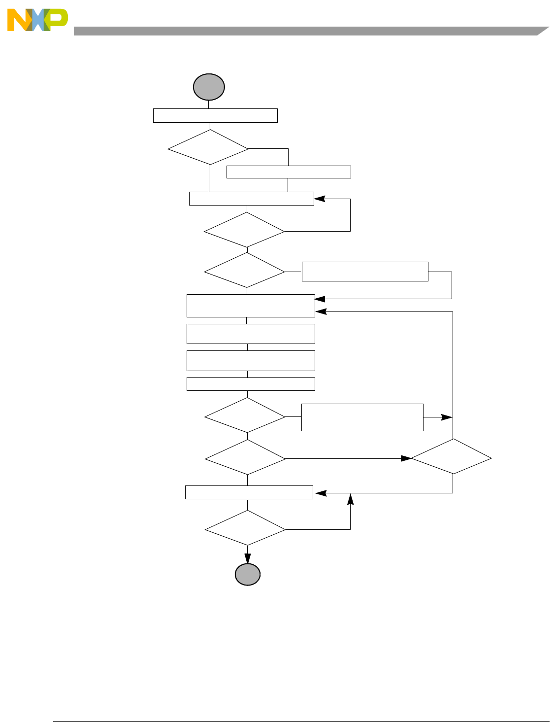
ColdFire Flash Module (CFM)
Freescale Semiconductor 18-28
Figure 18-18. Example Mass Erase Command Flow
Write: Register CFMCLKD
Read: Register CFMCLKD
Write: Array Address and
Write: Register CFMCMD
Mass Erase Command 0x41
Write: Register CFMUSTAT
yes
no
Clear bit CBEIF 0x80
CBEIF
Set?
Bit yes
Clock Register
Written
Check
1.
2.
3.
no
Protection
Violation Check
Read: Register CFMUSTAT
CCIF
Set?
Bit no
no
Address, Data,
Command
Buffer Empty Check
Next Write?
yes
no
Dummy Data
Clear bit PVIOL 0x20
Write: Register CFMUSTAT
yes
PVIOL
Set?
Bit
Bit Polling for
Command
Completion Check
Read: Register CFMUSTAT
yes
NOTE: command write sequence
aborted by writing 0x00 to
CFMUSTAT register.
NOTE: command write sequence
aborted by writing 0x00 to
CFMUSTAT register.
EXIT
Read: Register CFMUSTAT
no
CBEIF
Set?
Bit
START
yes
•
DIVLD
Set?
Bit
Change Protection
Clear bit ACCERR/PVIOL 0x30
Write: Register CFMUSTAT
yes
no
Access Error and
Protection Violation ACCERR/PVIOL
Set?
Bit
Check
MCF52211 ColdFire® Integrated Microcontroller Reference Manual, Rev. 3

ColdFire Flash Module (CFM)
18-29 Freescale Semiconductor
18.4.2.3.5 Flash Normal Mode Illegal Operations
The ACCERR flag is set during the command write sequence if any of the following illegal operations are
performed, causing the command write sequence to immediately abort:
• Writing to the flash memory before initializing CFMCLKD.
• Writing to the flash memory while CBEIF is not set.
• Writing to a flash block with a data size other than 32 bits.
• After writing to the flash even block, writing an additional word to the flash memory during the
flash command write sequence other than the flash odd block.
• Writing an invalid flash normal mode command to the CFMCMD register.
• Writing to any CFM register other than CFMCMD after writing to the flash memory.
• Writing a second command to the CFMCMD register before executing the previously written
command.
• Writing to any CFM register other than CFMUSTAT (to clear CBEIF) after writing to the
command register, CFMCMD.
• The part enters stop mode and any command is in progress. Upon entering STOP mode, any active
command is aborted.
• Aborting a command write sequence by writing a 0 to the CBEIF flag after writing to the flash
memory or after writing a command to the CFMCMD register but before the command is launched.
The PVIOL flag is set during the command write sequence if any of the following illegal operations are
performed, causing the command write sequence to immediately abort:
• Writing a program command if the address to program is in a protected flash logical sector.
• Writing a page erase command if the address to erase is in a protected flash logical sector.
• Writing a mass erase command while any protection is enabled.
If a read operation is attempted on a flash logical block while a command is active on that logical block
(CCIF=0), the read operation returns invalid data and the ACCERR flag in the CFMUSTAT register is not
set.
18.4.2.4 Stop Mode
If a command is active (CCIF=0) when the MCU enters stop mode, the flash command controller and flash
memory controller performs the following:
• The active command is aborted. Therefore, if data was being programmed, it is now lost.
• The high voltage circuitry to the flash arrays is switched off.
• Any buffered command (CBEIF=0)is not executed after the MCU exits stop mode.
• The CCIF and ACCERR flags is set if a command is active when the MCU enters stop mode.
CAUTION
As active commands are immediately aborted when the MCU enters stop
mode, it is strongly recommended not to execute the stop instruction during
program and erase operations.
MCF52211 ColdFire® Integrated Microcontroller Reference Manual, Rev. 3

ColdFire Flash Module (CFM)
Freescale Semiconductor 18-30
If a command is not active (CCIF=1) when the MCU enters stop mode, the ACCERR flag does not set.
18.4.3 Flash Security Operation
The CFM provides security information to the integration module and the rest of the MCU. This security
information is stored within a word in the flash configuration field. This security word is read
automatically after each reset and stored in the CFMSEC register.
NOTE
Enabling flash security disables BDM communications.
In flash normal mode, it is possible to bypass the security via a backdoor access sequence using an 8-byte
long key. Upon successful completion of the backdoor access sequence, the SECSTAT bit in the CFMSEC
register is cleared indicating that the MCU is unsecured.
The CFM may be unsecured by:
• Executing a backdoor access sequence.
• Passing a blank check operation on the flash memory.
• Executing the JTAG lockout recovery sequence.
18.4.3.1 Backdoor Access Sequence
If the KEYEN bits in the CFMSEC register are set to the enabled state, it is possible to bypass security by:
1. Setting the KEYACC bit in the CFMMCR register.
2. Writing the correct 8-byte backdoor comparison key to the flash memory at offset 0x0400 -
0x0407. This operation must be composed of two 32-bit writes to address 0x0400 and 0x0404 in
that order. The two backdoor write cycles can be separated by any number of internal flash bus
cycles.
NOTE
Any attempt to use a key of all zeros or all ones locks the backdoor access
sequence until the CFM is reset.
3. Clearing the KEYACC bit.
4. If all eight bytes written match the flash memory content at offset 0x0400 - 0x0407, security is
bypassed until the next reset.
In the unsecured state, the software has full control of the contents of the 8-byte backdoor comparison key
by programming the bytes at offset 0x0400 - 0x0407 of the flash configuration field. If at any time a key
of all zeroes or all ones is received, the backdoor access sequence is terminated and cannot be successfully
restarted until after the CFM is reset.
The security of the CFM as defined in the flash security word at address offset 0x0414 is not changed by
the executing the backdoor access sequence to unsecure the device. After the next reset sequence, the CFM
is secured again and the same backdoor key is in effect unless the flash configuration field was changed
by program or erase prior to reset. The backdoor access sequence to unsecure the device has no effect on
the program and erase protections defined in the CFM protection register.
MCF52211 ColdFire® Integrated Microcontroller Reference Manual, Rev. 3

ColdFire Flash Module (CFM)
18-31 Freescale Semiconductor
The contents of the flash security word at address offset 0x0414 must be changed by programming that
address when the device is unsecured and the sector containing the flash configuration field is unprotected.
18.4.3.2 Blank Check
A secured CFM can be unsecured by verifying that the entire flash memory is erased. If required, the mass
erase command can be executed on the flash memory. The blank check command must then be executed
on the flash memory. The CFM is unsecured if the blank check operation determines that the entire flash
memory is erased. After the next reset sequence, the security state of the CFM is determined by the flash
security word at address offset 0x0414. For further details on security, see the MCU security specification.
18.4.3.3 JTAG Lockout Recovery
A secured CFM can be unsecured by mass erasing the flash memory via a sequence of JTAG commands,
as specified in the system level security documentation followed by a reset of the MCU.
18.4.3.4 EzPort Lockout Recovery
A secured CFM can also be unsecured by mass erasing the flash memory via the EzPort bulk erase (BE)
command. Doing so clears the flash security (FS) bit in the EzPort status register, after which a reset chip
(RESET) command can be issued to regain access to the device.
MCF52211 ColdFire® Integrated Microcontroller Reference Manual, Rev. 3

Freescale Semiconductor 19-1
Chapter 19
EzPort
The EzPort is a serial programming interface that allows the microcontroller's on-chip flash memory to be
read, erased, and programmed using the command set of industry-standard, SPI-compatible flash memory
devices.
19.1 Features
The EzPort includes the following features:
• Same serial interface as, and subset of, the command set used by industry-standard SPI flash
memories
• Ability to read, erase, and program flash memory
• Reset command to boot the system after flash programming
The EzPort allows the on-chip flash memory to be programmed like industry-standard SPI flash memories.
The EzPort implements the core industry-standard SPI flash commands so that existing code, whether
written for another microcontroller or for automated test equipment, can be used to program, erase, and
verify the on-chip flash under the control of an external device. In essence, the EzPort virtualizes the
on-chip flash by making it mimic the behavior of simple, industry-standard SPI flash devices, thus
eliminating the need to use the background-debug-mode interface to download and run user-developed
flash-programming code.
19.2 Modes of Operation
The EzPort can operate in one of two different modes:
• Enabled—When enabled, the EzPort steals access to the flash memory, preventing access from
other cores or peripherals. The rest of the micro-controller is disabled when the EzPort is enabled
to avoid conflicts.
• Disabled—When the EzPort is disabled, the rest of the micro-controller can access flash memory
as normal.
MCF52211 ColdFire® Integrated Microcontroller Reference Manual, Rev. 3
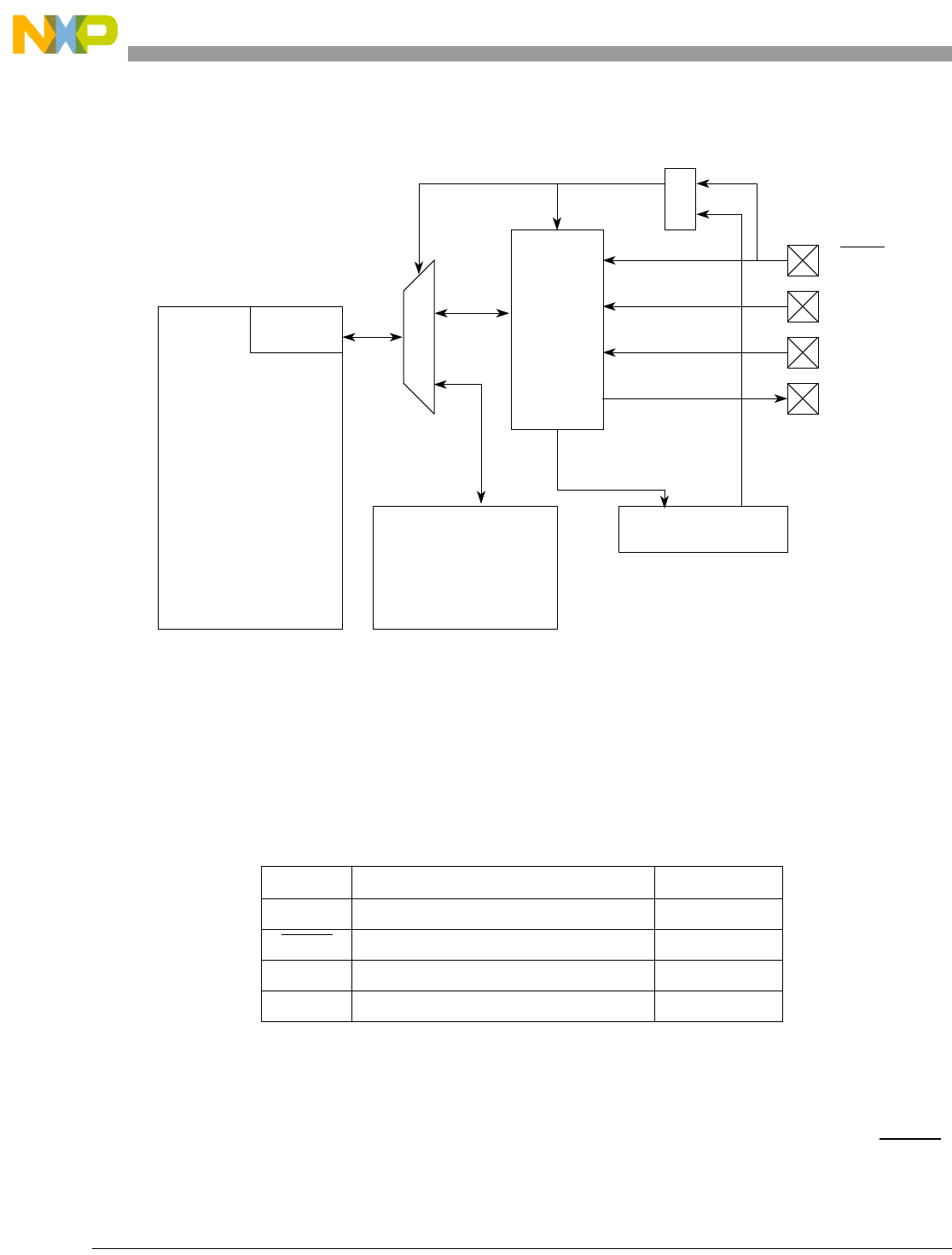
EzPort
19-2 Freescale Semiconductor
Figure 19-1 is a block diagram of the EzPort.
Figure 19-1. EzPort Block Diagram
19.3 External Signal Description
19.3.1 Overview
Table 19-1 contains a list of EzPort external signals.
19.3.2 Detailed Signal Descriptions
19.3.2.1 EZPCK — EzPort Clock
EzPort clock (EZPCK) is the serial clock for data transfers. Serial data in (EZPD) and chip select (EZPCS)
are registered on the rising edge of EZPCK while serial data out (EZPQ) is driven on the falling edge of
Table 19-1. Signal Descriptions
Name Description I/O
EZPCK EzPort Clock Input
EZPCS EzPort Chip Select Input
EZPD EzPort Serial Data In Input
EZPQ EzPort Serial Data Out Output
Flash
Controller EzPort
Flash Memory
Microcontroller
Core
EzPort Enabled
EZPCS
EZPCK
EZPD
EZPQ
G
Reset Controller
Reset
Reset Out
MCF52211 ColdFire® Integrated Microcontroller Reference Manual, Rev. 3

EzPort
Freescale Semiconductor 19-3
EZPCK.The maximum frequency of the EzPort clock is half the system clock frequency for all commands
except when executing the read data command. When executing the Read Data command, the EzPort
clock has a maximum frequency of one eighth the system clock frequency.
19.3.2.2 EZPCS — EzPort Chip Select
EzPort chip select (EZPCS) is the chip select for signalling the start and end of serial transfers. If EZPCS
is asserted during and when the micro-controller’s reset out signal is negated, then EzPort is enabled out
of reset; otherwise it is disabled. After EzPort is enabled, asserting EZPCS commences a serial data
transfer, which continues until EZPCS is negated again. The negation of EZPCS indicates the current
command is finished and resets the EzPort state machine so that it is ready to receive the next command.
19.3.2.3 EZPD — EzPort Serial Data In
EzPort serial data in (EZPD) is the serial data in for data transfers. It is registered on the rising edge of
EZPCK. All commands, addresses, and data are shifted in most significant bit first. When EzPort is driving
output data on EZPQ, the data shifted in EZPD is ignored.
19.3.2.4 EZPQ — EzPort Serial Data Out
EzPort serial data out (EZPQ) is the serial data out for data transfers. It is driven on the falling edge of
EZPCK. It is tri-stated, unless EZPCS is asserted and the EzPort is driving data out. All data is shifted out
most significant bit first.
19.4 Command Definition
The EzPort receives commands from an external device and translates those commands into flash memory
accesses. Table 19-2 lists the supported commands.
Table 19-2. EzPort Commands
Command Description Code Address
Bytes
Dummy
Bytes
Data
Bytes
Compatible
Commands1
1Lists the compatible commands on the ST Microelectronics Serial Flash Memory parts.
WREN Write Enable 0x06 0 0 0 WREN
WRDI Write Disable 0x04 0 0 0 WRDI
RDSR Read Status Register 0x05 0 0 1 RDSR
WRCR Write Config Register 0x01 0 0 1 WRSR
READ Read Data 0x03 3 0 1+ READ
FAST_READ Read Data at High Speed 0x0B 3 1 1+ FAST_READ
PP Page Program 0x02 3 0 4 to 256 PP
SE Sector Erase 0xD8 3 0 0 SE
BE Bulk Erase 0xC7 0 0 0 BE
RESET Reset Chip 0xB9 0 0 0 DP
MCF52211 ColdFire® Integrated Microcontroller Reference Manual, Rev. 3

EzPort
19-4 Freescale Semiconductor
19.4.1 Command Descriptions
19.4.1.1 Write Enable
The Write Enable command sets the write enable register bit in the status register. The write enable bit
must be set for a Write Configuration Register (WRCR), Page Program (PP), Sector Erase (SE), or Bulk
Erase (BE) command to be accepted. The write enable register bit clears on reset, on a Write Disable
command, and at the completion of a write, program, or erase command.
This command should not be used if a write is already in progress.
19.4.1.2 Write Disable
The Write Disable command clears the write enable register bit in the status register.
This command should not be used if a write is already in progress.
19.4.1.3 Read Status Register
The read status register command returns the contents of the EzPort status register.
IPSBAR
Offset:
Access: read/write
7 6543210
RFS WEF CRL WEN WIP
W
Reset: 0/11
1Reset value reflects if flash security is enabled or disabled out of reset.
000 0 000
Figure 19-2. EzPort Status Register
Table 19-3. EzPort Status Register Field Description
Field Descriptions
7
FS
Flash Security. Status flag that indicates if the flash memory is in secure mode. In secure mode, the following
commands are not accepted: Read (READ), Fast Read (FAST_READ), Page Program (PP), Sector Erase
(SE). Secure mode can be exited by performing a Bulk Erase (BE) command, which erases the entire contents
of the flash memory.
0 Flash is not in secure mode.
1 Flash is in secure mode.
6
WEF
Write Error Flag. Status flag that indicates if there has been an error with an erase or program instruction inside
the flash controller due to attempting to program or erase a protected sector, or if there is an error in the flash
memory after performing a Bulk Erase command. The flag clears after a Read Status Register (RDSR)
command.
0 No error on previous erase/program command.
1 Error on previous erase/program command.
MCF52211 ColdFire® Integrated Microcontroller Reference Manual, Rev. 3

EzPort
Freescale Semiconductor 19-5
19.4.1.4 Write Configuration Register
The Write Configuration Command updates the flash controller’s clock configuration register. The clock
configuration register divides down the flash controller’s internal system clock to a 150 kHz to 200 kHz
clock. This register must be initialized before any erase or program commands are issued to the flash
controller.
This command should not be used if the write error flag is set, a write is in progress, or the configuration
register has already been loaded (as it is a write-once register).
5
CRL
Configuration Register Loaded. Status flag that indicates if the configuration register has been loaded. The
configuration register initializes the flash controllers clock configuration register to generate a divided down
clock from the system clock that runs at a frequency of 150 kHz to 200 kHz. This register must be initialized
before any erase or program commands are accepted.
0 Configuration register has not been loaded; erase and program commands are not accepted.
1 Configuration register has been loaded; erase and program commands are accepted.
4–2
—
Reserved, should be cleared.
1
WEN
Write Enable. Control bit that must be set before a Write Configuration Register (WRCR), Page Program (PP),
Sector Erase (SE), or Bulk Erase (BE) command is accepted. Is set by the Write Enable (WREN) command
and cleared by reset or a Write Disable (WRDI) command. It also clears on completion of a write, erase, or
program command.
0 Disables the following write, erase, or program command.
1 Enables the following write, erase, or program command.
0
WIP
Write In Progress. Status flag that sets after a Write Configuration Register (WRCR), Page Program (PP),
Sector Erase (SE), or Bulk Erase (BE) command is accepted and clears after the flash memory erase or
program is completed. Only the Read Status Register (RDSR) command is accepted while a write is in
progress.
0 Write is not in progress. Accept any command.
1 Write is in progress. Only accept RDSR command.
IPSBAR
Offset:
Access: read/write
7 6543210
R
W PRDIV8 DIV[5:0]
Reset: 0 0 0 0 0 0 0 0
Figure 19-3. EzPort Configuration Register
Table 19-3. EzPort Status Register Field Description (continued)
Field Descriptions
MCF52211 ColdFire® Integrated Microcontroller Reference Manual, Rev. 3

EzPort
19-6 Freescale Semiconductor
19.4.1.5 Read Data
The Read Data command returns data from the flash memory, starting at the address specified in the
command word. Data continues being returned for as long as the EzPort chip select (EZPCS) is asserted,
with the address automatically incrementing. When the address reaches the highest flash memory address,
it wraps around to the lowest flash memory address. In this way, the entire contents of the flash memory
can be returned by one command.
For this command to return the correct data, the EzPort Clock (EZPCK) must run at no more than divide
by eight of the internal system clock.
This command should not be used if the write error flag is set, or a write is in progress. This command is
not accepted if flash security is enabled.
19.4.1.6 Read Data at High Speed
This command is identical to the Read Data command, except for the inclusion of a dummy byte following
the address bytes and before the first data byte is returned.
This allows the command to run at any frequency of the EzPort Clock (EZPCK) up to and including half
the internal system clock frequency of the micro-controller.This command should not be used if the write
error flag is set, or a write is in progress. This command is not accepted if flash security is enabled.
19.4.1.7 Page Program
The Page Program command programs locations in flash memory that have previously been erased. The
starting address of the memory to program is sent after the command word and must be a 32-bit aligned
address (the two LSBs must be zero). After every four bytes of data are received by the EzPort, that 32-bit
word is programmed into flash memory with the address automatically incrementing after each write. For
this reason, the number of bytes to program must be a multiple of four. Only a maximum of 256 bytes can
be programmed at a time; when the address reaches the highest address within any given 256-byte space
of memory, it wraps around to the lowest address in that same space.
This command should not be used if the write error flag is set, a write is in progress, the write enable bit
is not set, or the configuration register has not been written.This command is not accepted if flash security
is enabled.
The write error flag sets if there is an attempt to program a protected area of the flash memory.
Table 19-4. EzPort Configuration Register Field Description
Field Descriptions
7
—
Reserved, should be cleared.
6
PRDIV
Enables prescaler divide by 8.
0 The system clock is fed directly into the divider.
1 Enables a prescaler that divides the system clock by 8 before it enters the divider.
5–0
DIV[5:0]
Clock divider field. The combination of PRDIV8 and DIV[5:0] effectively divides the system clock down to a
frequency between 150 kHz and 200 kHz.
MCF52211 ColdFire® Integrated Microcontroller Reference Manual, Rev. 3

EzPort
Freescale Semiconductor 19-7
19.4.1.8 Sector Erase
The Sector Erase command erases the contents of a 2-Kbyte space of flash memory. The 3-byte address
sent after the command byte can be any address within the space to erase.
This command should not be used if the write error flag is set, a write is in progress, the write enable bit
is not set, or the configuration register has not been written. This command is not accepted if flash security
is enabled.
The write error flag sets if there is an attempt to erase a protected area of the flash memory.
19.4.1.9 Bulk Erase
The Bulk Erase command erases the entire contents of flash memory, ignoring any protected sectors or
flash security. The write error flag sets if the Bulk Erase command does not successfully erase the entire
contents of flash memory. Flash security is disabled if the Bulk Erase command is followed by a Reset
Chip command.
This command should not be used if the write error flag is set, a write is in progress, the write enable bit
is not set, or the configuration register has not been written.
19.4.1.10 Reset Chip
The Reset Chip command forces the chip into the reset state. If the EzPort chip select (EZPCS) pin is
asserted at the end of the reset period, EzPort is enabled; otherwise, it is disabled.
This command allows the chip to boot up from flash memory after it has been programmed by an external
source.
This command should not be used if a write is in progress.
19.5 Functional Description
The EzPort provides a simple interface to connect an external device to the flash memory on board a 32
bit microcontroller.
The interface itself is compatible with the SPI interface (with the EzPort operating as a slave) running in
either of the two following modes with data transmitted most significant bit first:
• CPOL = 0, CPHA = 0
• CPOL = 1, CPHA = 1
Commands are issued by the external device to erase, program, or read the contents of the flash memory.
The serial data out from the EzPort is tri-stated unless data is being driven, allowing the signal to be shared
among several different EzPort (or compatible) devices in parallel, provided they have different chip
selects.
MCF52211 ColdFire® Integrated Microcontroller Reference Manual, Rev. 3

EzPort
19-8 Freescale Semiconductor
19.6 Initialization/Application Information
Prior to issuing any program or erase commands, the clock configuration register must be written to set
the flash state machine clock (FCLK). The flash controller module runs at the system clock frequency
divide by 2, but FCLK must be divided down from this frequency to a frequency between 150 kHz and
200 kHz. Use the following procedure to set the PRDIV8 and DIV[5:0] bits in the clock configuration
register.
1. If fSYS is greater than 25.6 MHz, PRDIV8 = 1; otherwise PRDIV8 = 0.
2. Determine DIV[5:0] by using the following equation. Keep only the integer portion of the result
and discard any fraction. Do not round the result.
Eqn. 19-1
3. Therefore, the flash state machine clock is:
Eqn. 19-2
Therefore, for Fsys equaling 66 MHz, writing 0x54 to the clock configuration register sets Fclk to
196.43 kHz, which is a valid frequency for the timing of program and erase operations.
For proper program and erase operations, it is critical to set Fclk between 150 kHz and 200 kHz. Array
damage due to overstress can occur when Fclk is less than 150 kHz. Incomplete programming and erasure
can occur when Fclk is greater than 200 kHz.
DIV Fsys
2x200kHzx 1 PRDIV8x7+
-------------------------------------------------------------------------------
=
Fclk Fsys
2x DIV 1+x 1 PRDIV8x7+
------------------------------------------------------------------------------------
=
MCF52211 ColdFire® Integrated Microcontroller Reference Manual, Rev. 3
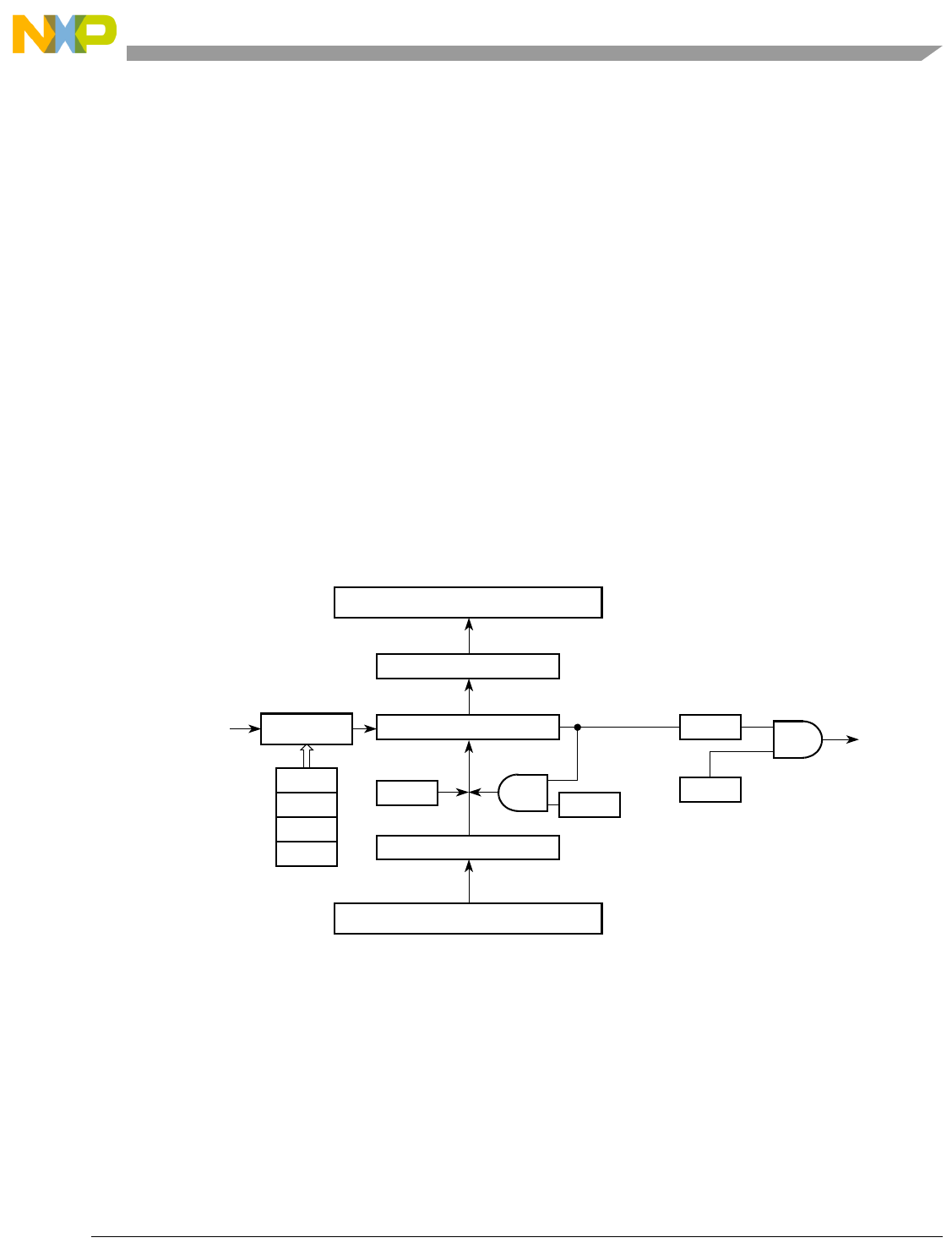
Freescale Semiconductor 20-1
Chapter 20
Programmable Interrupt Timers (PIT0–PIT1)
20.1 Introduction
This chapter describes the operation of the two programmable interrupt timer modules: PIT0–PIT1.
20.1.1 Overview
Each PIT is a 16-bit timer that provides precise interrupts at regular intervals with minimal processor
intervention. The timer can count down from the value written in the modulus register or it can be a
free-running down-counter.
20.1.2 Block Diagram
Figure 20-1. PIT Block Diagram
20.1.3 Low-Power Mode Operation
This subsection describes the operation of the PIT modules in low-power modes and debug mode of
operation. Low-power modes are described in the power management module, Chapter 8, “Power
Management.” Table 20-1 shows the PIT module operation in low-power modes and how it can exit from
each mode.
Internal Bus
Clock (fsys)
16-bit PMRn
16-bit PIT Counter COUNT = 0
Internal Bus
16-bit PCNTRn
Internal Bus
EN OVW
DOZE
DBG
Prescaler
PRE[3:0] RLD
PIF
PIE
Load
Counter
To Interrupt
Controller
MCF52211 ColdFire® Integrated Microcontroller Reference Manual, Rev. 3

Programmable Interrupt Timers (PIT0–PIT1)
20-2 Freescale Semiconductor
NOTE
The low-power interrupt control register (LPICR) in the system control
module specifies the interrupt level at or above which the device can be
brought out of a low-power mode.
In wait mode, the PIT module continues to operate as in run mode and can be configured to exit the
low-power mode by generating an interrupt request. In doze mode with the PCSRn[DOZE] bit set, PIT
module operation stops. In doze mode with the PCSRn[DOZE] bit cleared, doze mode does not affect PIT
operation. When doze mode is exited, PIT continues operating in the state it was in prior to doze mode. In
stop mode, the internal bus clock is absent and PIT module operation stops.
In debug mode with the PCSRn[DBG] bit set, PIT module operation stops. In debug mode with the
PCSRn[DBG] bit cleared, debug mode does not affect PIT operation. When debug mode is exited, the PIT
continues to operate in its pre-debug mode state, but any updates made in debug mode remain.
20.2 Memory Map/Register Definition
This section contains a memory map (see Table 20-2) and describes the register structure for PIT0–PIT1.
Table 20-1. PIT Module Operation in Low-power Modes
Low-power Mode PIT Operation Mode Exit
Wait Normal N/A
Doze Normal if PCSRn[DOZE] cleared,
stopped otherwise
Any interrupt at or above level in LPICR, exit doze
mode if PCSRn[DOZE] is set. Otherwise
interrupt assertion has no effect.
Stop Stopped No
Debug Normal if PCSRn[DBG] cleared,
stopped otherwise
No. Any interrupt is serviced upon normal exit
from debug mode
Table 20-2. Programmable Interrupt Timer Modules Memory Map
IPSBAR Offset
Register Width
(bits) Access1
1Accesses to reserved address locations have no effect and result in a cycle termination transfer error.
Reset Value Section/Page
PIT 0
PIT 1
Supervisor Access Only Registers2
0x15_0000
0x16_0000
PIT Control and Status Register (PCSRn) 16 R/W 0x0000 20.2.1/20-3
0x15_0002
0x16_0002
PIT Modulus Register (PMRn) 16 R/W 0xFFFF 20.2.2/20-4
User/Supervisor Access Registers
0x15_0004
0x16_0004
PIT Count Register (PCNTRn) 16 R 0xFFFF 20.2.3/20-5
MCF52211 ColdFire® Integrated Microcontroller Reference Manual, Rev. 3

Programmable Interrupt Timers (PIT0–PIT1)
Freescale Semiconductor 20-3
20.2.1 PIT Control and Status Register (PCSRn)
The PCSRn registers configure the corresponding timer’s operation.
2User mode accesses to supervisor only addresses have no effect and result in a cycle termination transfer error.
IPSBAR
Offset:
0x15_0000 (PCSR0)
0x16_0000 (PCSR1)
Access: Supervisor
read/write
1514131211109876543210
R0000 PRE 0DOZE DBG OVW PIE PIF RLD EN
Ww1c
Reset0000000000000000
Figure 20-2. PCSRn Register
Table 20-3. PCSRn Field Descriptions
Field Description
15–12 Reserved, must be cleared.
11–8
PRE
Prescaler. The read/write prescaler bits select the internal bus clock divisor to generate the PIT clock. To accurately
predict the timing of the next count, change the PRE[3:0] bits only when the enable bit (EN) is clear. Changing
PRE[3:0] resets the prescaler counter. System reset and the loading of a new value into the counter also reset the
prescaler counter. Setting the EN bit and writing to PRE[3:0] can be done in this same write cycle. Clearing the EN
bit stops the prescaler counter.
7 Reserved, must be cleared.
6
DOZE
Doze Mode Bit. The read/write DOZE bit controls the function of the PIT in doze mode. Reset clears DOZE.
0 PIT function not affected in doze mode
1 PIT function stopped in doze mode. When doze mode is exited, timer operation continues from the state it was in
before entering doze mode.
PRE Internal Bus Clock
Divisor
Decimal
Equivalent
0000 201
0001 212
0010 224
... ... ...
1101 213 8192
1110 214 16384
1111 215 32768
MCF52211 ColdFire® Integrated Microcontroller Reference Manual, Rev. 3

Programmable Interrupt Timers (PIT0–PIT1)
20-4 Freescale Semiconductor
20.2.2 PIT Modulus Register (PMRn)
The 16-bit read/write PMRn contains the timer modulus value loaded into the PIT counter when the count
reaches 0x0000 and the PCSRn[RLD] bit is set.
When the PCSRn[OVW] bit is set, PMRn is transparent, and the value written to PMRn is immediately
loaded into the PIT counter. The prescaler counter is reset (0xFFFF) anytime a new value is loaded into
the PIT counter and also during reset. Reading the PMRn returns the value written in the modulus latch.
Reset initializes PMRn to 0xFFFF.
5
DBG
Debug mode bit. Controls the function of PIT in halted/debug mode. Reset clears DBG. During debug mode, register
read and write accesses function normally. When debug mode is exited, timer operation continues from the state it
was in before entering debug mode, but any updates made in debug mode remain.
0 PIT function not affected in debug mode
1 PIT function stopped in debug mode
Note: Changing the DBG bit from 1 to 0 during debug mode starts the PIT timer. Likewise, changing the DBG bit
from 0 to 1 during debug mode stops the PIT timer.
4
OVW
Overwrite. Enables writing to PMRn to immediately overwrite the value in the PIT counter.
0 Value in PMRn replaces value in PIT counter when count reaches 0x0000.
1 Writing PMRn immediately replaces value in PIT counter.
3
PIE
PIT interrupt enable. This read/write bit enables PIF flag to generate interrupt requests.
0 PIF interrupt requests disabled
1 PIF interrupt requests enabled
2
PIF
PIT interrupt flag. This read/write bit is set when PIT counter reaches 0x0000. Clear PIF by writing a 1 to it or by
writing to PMR. Writing 0 has no effect. Reset clears PIF.
0 PIT count has not reached 0x0000.
1 PIT count has reached 0x0000.
1
RLD
Reload bit. The read/write reload bit enables loading the value of PMRn into PIT counter when the count reaches
0x0000.
0 Counter rolls over to 0xFFFF on count of 0x0000
1 Counter reloaded from PMRn on count of 0x0000
0
EN
PIT enable bit. Enables PIT operation. When PIT is disabled, counter and prescaler are held in a stopped state. This
bit is read anytime, write anytime.
0 PIT disabled
1 PIT enabled
IPSBAR
Offset:
0x15_0002 (PMR0)
0x16_0002 (PMR1)
Access: Supervisor
read/write
1514131211109876543210
RPM
W
Reset1111111111111111
Figure 20-3. PIT Modulus Register (PMRn)
Table 20-3. PCSRn Field Descriptions (continued)
Field Description
MCF52211 ColdFire® Integrated Microcontroller Reference Manual, Rev. 3

Programmable Interrupt Timers (PIT0–PIT1)
Freescale Semiconductor 20-5
20.2.3 PIT Count Register (PCNTRn)
The 16-bit, read-only PCNTRn contains the counter value. Reading the 16-bit counter with two 8-bit reads
is not guaranteed coherent. Writing to PCNTRn has no effect, and write cycles are terminated normally.
20.3 Functional Description
This section describes the PIT functional operation.
20.3.1 Set-and-Forget Timer Operation
This mode of operation is selected when the RLD bit in the PCSR register is set.
When PIT counter reaches a count of 0x0000, PIF flag is set in PCSRn. The value in the modulus register
loads into the counter, and the counter begins decrementing toward 0x0000. If the PCSRn[PIE] bit is set,
the PIF flag issues an interrupt request to the CPU.
When the PCSRn[OVW] bit is set, the counter can be directly initialized by writing to PMRn without
having to wait for the count to reach 0x0000.
Table 20-4. PMRn Field Descriptions
Field Description
15–0
PM
Timer modulus. The value of this register is loaded into the PIT counter when the count reaches zero and the
PCSRn[RLD] bit is set. However, if PCSRn[OVW] is set, the value written to this field is immediately loaded into the
counter. Reading this field returns the value written.
IPSBAR
Offset:
0x15_0004 (PCNTR0)
0x16_0004 (PCNTR1)
Access: User read only
1514131211109876543210
RPC
W
Reset1111111111111111
Figure 20-4. PIT Count Register (PCNTRn)
Table 20-5. PCNTRn Field Descriptions
Field Description
15–0
PC
Counter value. Reading this field with two 8-bit reads is not guaranteed coherent. Writing to PCNTRn has no effect,
and write cycles are terminated normally.
MCF52211 ColdFire® Integrated Microcontroller Reference Manual, Rev. 3
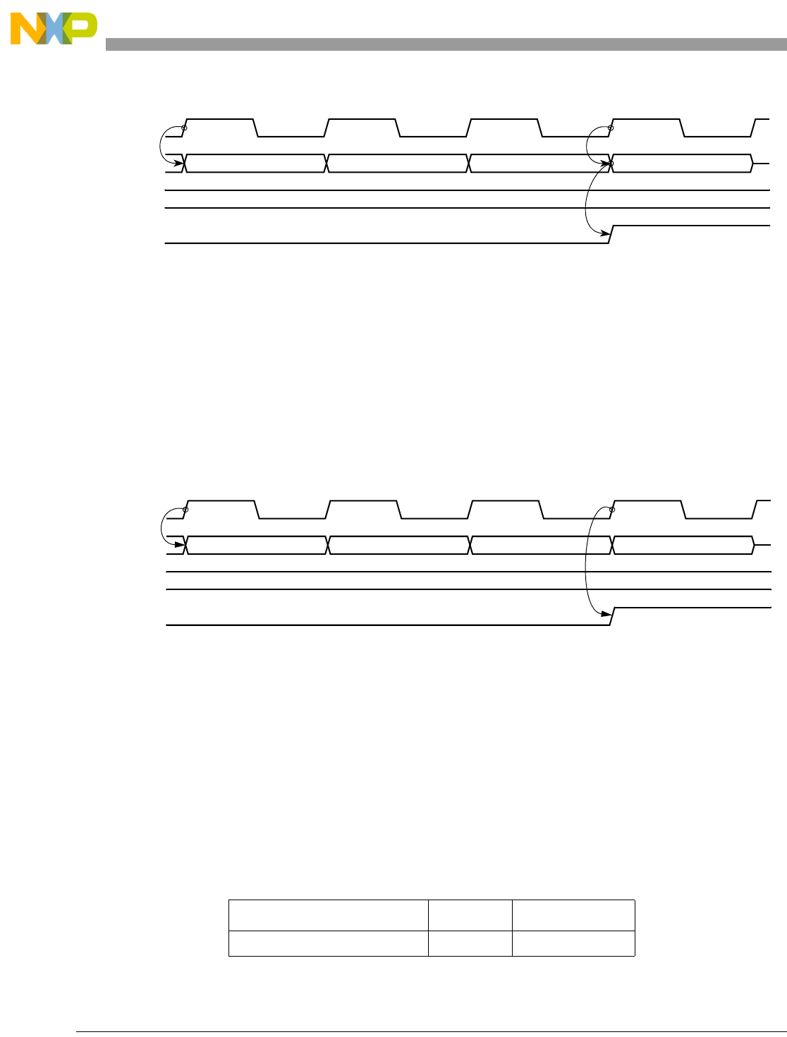
Programmable Interrupt Timers (PIT0–PIT1)
20-6 Freescale Semiconductor
Figure 20-5. Counter Reloading from the Modulus Latch
20.3.2 Free-Running Timer Operation
This mode of operation is selected when the PCSRn[RLD] bit is clear. In this mode, the counter rolls over
from 0x0000 to 0xFFFF without reloading from the modulus latch and continues to decrement.
When the counter reaches a count of 0x0000, PCSRn[PIF] flag is set. If the PCSRn[PIE] bit is set, PIF flag
issues an interrupt request to the CPU.
When the PCSRn[OVW] bit is set, counter can be directly initialized by writing to PMRn without having
to wait for the count to reach 0x0000.
Figure 20-6. Counter in Free-Running Mode
20.3.3 Timeout Specifications
The 16-bit PIT counter and prescaler supports different timeout periods. The prescaler divides the internal
bus clock period as selected by the PCSRn[PRE] bits. The PMRn[PM] bits select the timeout period.
Eqn. 20-1
20.3.4 Interrupt Operation
Table 20-6 shows the interrupt request generated by the PIT.
Table 20-6. PIT Interrupt Requests
Interrupt Request Flag Enable Bit
Timeout PIF PIE
0x0002 0x0001 0x0000 0x0005
0x0005
PIT Clock
Counter
Modulus
PIF
0x0002 0x0001 0x0000 0xFFFF
0x0005
PIT CLOCK
COUNTER
MODULUS
PIF
Timeout period 2PCSRn[PRE] (PMRn[PM] 1)+
fsys
------------------------------------------------------------------------
=
MCF52211 ColdFire® Integrated Microcontroller Reference Manual, Rev. 3

Programmable Interrupt Timers (PIT0–PIT1)
Freescale Semiconductor 20-7
The PIF flag is set when the PIT counter reaches 0x0000. The PIE bit enables the PIF flag to generate
interrupt requests. Clear PIF by writing a 1 to it or by writing to the PMR.
MCF52211 ColdFire® Integrated Microcontroller Reference Manual, Rev. 3

Freescale Semiconductor 21-1
Chapter 21
General Purpose Timer Module (GPT)
21.1 Introduction
This device has one 4-channel general purpose timer module (GPT). It consists of a 16-bit counter driven
by a 7-stage programmable prescaler.
A timer overflow function allows software to extend the timing capability of the system beyond the 16-bit
range of the counter. Each of the four timer channels can be configured for input capture, which can
capture the time of a selected transition edge, or for output compare, which can generate output waveforms
and timer software delays. These functions allow simultaneous input waveform measurements and output
waveform generation.
Additionally, channel 3 can be configured as a 16-bit pulse accumulator that can operate as a simple event
counter or as a gated time accumulator. The pulse accumulator uses the GPT channel 3 input/output pin in
event mode or gated time accumulation mode.
21.2 Features
Features of the general-purpose timer include the following:
• Four 16-bit input capture/output compare channels
• 16-bit architecturef
• Programmable prescaler
• Pulse-widths variable from microseconds to seconds
• Single 16-bit pulse accumulator
• Toggle-on-overflow for pulse-width modulator (PWM) generation
MCF52211 ColdFire® Integrated Microcontroller Reference Manual, Rev. 3
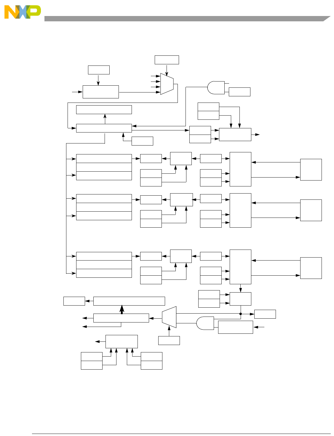
General Purpose Timer Module (GPT)
Freescale Semiconductor 21-2
21.3 Block Diagram
Figure 21-1. GPT Block Diagram
Prescaler
Channel 0
PT0
16-Bit Counter
Internal bus clock
LOGIC
PR[2:0]
Divide-by-64
GPTC0H:GPTC0L
EDGE
DETECT
GPTPACNTH:GPTPACNTL
PA OV F
PEDGE
PA OV I
PA M O D
PA E
16-Bit Comparator
GPTCNTH:GPTCNTL
16-Bit Latch
CHANNEL 1
GPTC1H:GPTC1L
16-Bit Comparator
16-Bit Latch
16-Bit Counter
Interrupt
Logic
TOF
TOI
C0F
C1F
Edge
Detect
PT1
LOGIC
Edge
Detect
CxF
Channel 2
Channel3
GPTC3H:GPTC3L
16-Bit Comparator
16-Bit Latch
C3F
PT3
LOGIC
Edge
Detect
IOS0
IOS1
IOS3
OM:OL0
TOV0
OM:OL1
TOV1
OM:OL3
TOV3
EDG1A
EDG1B
EDG3A
EDG3B
EDG0A
EDG0B
TCRE
Channel 3 Output Compare
PA I F
Clear Counter
PA I F
PA I
Interrupt
Logic
CxI
Interrupt
Request
Interrupt
Request
PA OV F
CH. 3 Compare
CH.3 Capture
CH. 1 Capture
MUX
CLK[1:0]
PA C L K
PACLK/256
PACLK/65536
PAC LK
PACLK/256
PACLK/65536
TE
CH. 1 Compare
CH. 0 Compare
CH. 0 Capture
PA Input
MUX
GPTx0
Pin
GPTx1
Pin
GPTx3
Pin
(fsys/2)
Internal bus clock
(fsys/2)
MCF52211 ColdFire® Integrated Microcontroller Reference Manual, Rev. 3

General Purpose Timer Module (GPT)
21-3 Freescale Semiconductor
21.4 Low-Power Mode Operation
This subsection describes the operation of the general purpose timer module in low-power modes and
halted mode of operation. Low-power modes are described in Chapter 10, “Power Management.”
Table 21-1 shows the general purpose timer module operation in the low-power modes, and shows how
this module may facilitate exit from each mode.
Table 21-1. Watchdog Module Operation in Low-power Modes
General purpose timer operation stops in stop mode. When stop mode is exited, the general purpose timer
continues to operate in its pre-stop mode state.
21.5 Signal Description
Table 21-2 provides an overview of the signal properties.
21.5.1 GPT[2:0]
The GPT[2:0] pins are for channel 2–0 input capture and output compare functions. These pins are
available for general-purpose input/output (I/O) when not configured for timer functions.
21.5.2 GPT3
The GPT3 pin is for channel 3 input capture and output compare functions or for the pulse accumulator
input. This pin is available for general-purpose I/O when not configured for timer functions.
21.6 Memory Map and Registers
Table 21-3 shows the memory map of the GPT module. The base address for GPT is IPSBAR +
0x1A_0000.
Low-power Mode Watchdog Operation Mode Exit
Wait Normal No
Doze Normal No
Stop Stopped No
Halted Normal No
Table 21-2. Signal Properties
Pin
Name
GPTPORT
Register Bit Function Reset State Pull-up
GPT0 PORTTn0 GPT channel 0 IC/OC pin Input Active
GPT1 PORTTn1 GPT channel 1 IC/OC pin Input Active
GPT2 PORTTn2 GPT channel 2 IC/OC pin Input Active
GPT3 PORTTn3 GPT channel 3 IC/OC or PA pin Input Active
MCF52211 ColdFire® Integrated Microcontroller Reference Manual, Rev. 3

General Purpose Timer Module (GPT)
Freescale Semiconductor 21-4
NOTE
Reading reserved or unimplemented locations returns zeros. Writing to
reserved or unimplemented locations has no effect.
Table 21-3. GPT Memory Map
IPSBAR
Offset1Register Width
(bits) Access Reset Value Section/Page
Supervisor Mode Access Only
0x1A_0000 GPT IC/OC Select Register (GPTIOS) 8 R/W 0x00 21.6.1/21-5
0x1A_0001 GPT Compare Force Register (GPTCFORC) 8 R/W 0x00 21.6.2/21-5
0x1A_0002 GPT Output Compare 3 Mask Register (GPTOC3M) 8 R/W 0x00 21.6.3/21-6
0x1A_0003 GPT Output Compare 3 Data Register (GPTOC3D) 8 R/W 0x00 21.6.4/21-7
0x1A_0004 GPT Counter Register High (GPTCNTH)28 R 0x00 21.6.5/21-7
0x1A_0005 GPT Counter Register Low (GPTCNTL)28 R 0x00 21.6.5/21-7
0x1A_0006 GPT System Control Register 1 (GPTSCR1) 8 R/W 0x00 21.6.6/21-8
0x1A_0008 GPT Toggle-on-Overflow Register (GPTTOV) 8 R/W 0x00 21.6.7/21-9
0x1A_0009 GPT Control Register 1 (GPTCTL1) 8 R/W 0x00 21.6.8/21-9
0x1A_000B GPT Control Register 2 (GPTCTL2) 8 R/W 0x00 21.6.9/21-10
0x1A_000C GPT Interrupt Enable Register (GPTIE) 8 R/W 0x00 21.6.10/21-10
0x1A_000D GPT System Control Register 2 (GPTSCR2) 8 R/W 0x00 21.6.11/21-11
0x1A_000E GPT Flag Register 1 (GPTFLG1) 8 R/W 0x00 21.6.12/21-12
0x1A_000F GPT Flag Register 2 (GPTFLG2) 8 R/W 0x00 21.6.13/21-12
0x1A_0010 GPT Channel 0 Register High (GPTC0H)2821.6.14/21-13
0x1A_0011 GPT Channel 0 Register Low (GPTC0L)2821.6.14/21-13
0x1A_0012 GPT Channel 1 Register High (GPTC1H)2821.6.14/21-13
0x1A_0013 GPT Channel 1 Register Low (GPTC1L)2821.6.14/21-13
0x1A_0014 GPT Channel 2 Register High (GPTC2H)2821.6.14/21-13
0x1A_0015 GPT Channel 2 Register Low (GPTC2L)2821.6.14/21-13
0x1A_0016 GPT Channel 3 Register High (GPTC3H)2821.6.14/21-13
0x1A_0017 GPT Channel 3 Register Low (GPTC3L)2821.6.14/21-13
0x1A_0018 Pulse Accumulator Control Register (GPTPACTL) 8 R/W 0x00 21.6.15/21-13
0x1A_0019 Pulse Accumulator Flag Register (GPTPAFLG) 8 R/W 0x00 21.6.16/21-14
0x1A_001A Pulse Accumulator Counter Register High
(GPTPACNTH)2
8R/W 21.6.17/21-15
0x1A_001B Pulse Accumulator Counter Register Low (GPTPACNTL)28R/W 21.6.17/21-15
MCF52211 ColdFire® Integrated Microcontroller Reference Manual, Rev. 3

General Purpose Timer Module (GPT)
21-5 Freescale Semiconductor
21.6.1 GPT Input Capture/Output Compare Select Register (GPTIOS)
21.6.2 GPT Compare Force Register (GPCFORC)
0x1A_001D GPT Port Data Register (GPTPORT) 8 R/W 0x00 21.6.18/21-16
0x1A_001E GPT Port Data Direction Register (GPTDDR) 8 R/W 0x00 21.6.19/21-16
1Addresses not assigned to a register and undefined register bits are reserved for expansion.
2This register is 16 bits wide, and should be read using only word accesses.
IPSBAR
Offset: 0x1A_0000 (GPTIOS)
Access: Supervisor read/write
76543210
R 0 0 0 0
IOS
W
Reset:00000000
Figure 21-2. GPT Input Capture/Output Compare Select Register (GPTIOS)
Table 21-4. GPTIOS Field Descriptions
Field Description
7–4 Reserved, should be cleared.
3–0
IOS
I/O select. The IOS[3:0] bits enable input capture or output compare operation for the corresponding timer channels.
These bits are read anytime (always read 0x00), write anytime.
1 Output compare enabled
0 Input capture enabled
IPSBAR
Offset: 0x1A_0001 (GPCFORC)
Access: Supervisor read/write
76543210
R 0 0 0 0
FOC
W
Reset:00000000
Figure 21-3. GPT Input Compare Force Register (GPCFORC)
Table 21-3. GPT Memory Map (continued)
IPSBAR
Offset1Register Width
(bits) Access Reset Value Section/Page
MCF52211 ColdFire® Integrated Microcontroller Reference Manual, Rev. 3

General Purpose Timer Module (GPT)
Freescale Semiconductor 21-6
NOTE
A successful channel 3 output compare overrides any compare on channels
2:0. For each OC3M bit that is set, the output compare action reflects the
corresponding OC3D bit.
21.6.3 GPT Output Compare 3 Mask Register (GPTOC3M)
Table 21-5. GPTCFORC Field Descriptions
Field Description
7–4 Reserved, should be cleared.
3–0
FOC
Force output compare.Setting an FOC bit causes an immediate output compare on the corresponding channel.
Forcing an output compare does not set the output compare flag. These bits are read anytime, write anytime.
1 Force output compare
0 No effect
IPSBAR
Offset: 0x1A_0002 (GPTOC3M)
Access: Supervisor read/write
76543210
R 0 0 0 0
OC3M
W
Reset:00000000
Figure 21-4. GPT Output Compare 3 Mask Register (GPTOC3M)
Table 21-6. GPTOC3M Field Descriptions
Field Description
7–4 Reserved, should be cleared.
3–0
OC3M
Output compare 3 mask. Setting an OC3M bit configures the corresponding PORTTn pin to be an output. OC3Mn
makes the GPT port pin an output regardless of the data direction bit when the pin is configured for output compare
(IOSx = 1). The OC3Mn bits do not change the state of the PORTTnDDR bits. These bits are read anytime, write
anytime.
1 Corresponding PORTTn pin configured as output
0 No effect
MCF52211 ColdFire® Integrated Microcontroller Reference Manual, Rev. 3

General Purpose Timer Module (GPT)
21-7 Freescale Semiconductor
21.6.4 GPT Output Compare 3 Data Register (GPTOC3D)
NOTE
A successful channel 3 output compare overrides any channel 2:0 compares.
For each OC3M bit that is set, the output compare action reflects the
corresponding OC3D bit.
21.6.5 GPT Counter Register (GPTCNT)
IPSBAR
Offset: 0x1A_0003 (GPTOC3D)
Access: Supervisor read/write
76543210
R 0 0 0 0
OC3D
W
Reset:00000000
Figure 21-5. GPT Output Compare 3 Data Register (GPTOC3D)
Table 21-7. GPTOC3D Field Descriptions
Field Description
7–4 Reserved, should be cleared.
3–0
OC3D
Output compare 3 data. When a successful channel 3 output compare occurs, these bits transfer to the PORTTn
data register if the corresponding OC3Mn bits are set. These bits are read anytime, write anytime.
IPSBAR
Offset: 0x1A_0004 (GPTCNT)
Access: Supervisor read-only
1514131211109876543210
RCNTR
W
Reset0000000000000000
Figure 21-6. GPT Counter Register (GPTCNT)
Table 21-8. GPTCNT Field Descriptions
Field Description
15–0
CNTR
Read-only field that provides the current count of the timer counter. To ensure coherent reading of the timer counter,
such that a timer rollover does not occur between two back-to-back 8-bit reads, it is recommended that only word
(16-bit) accesses be used.
A write to GPTCNT may have an extra cycle on the first count because the write is not synchronized with the
prescaler clock. The write occurs at least one cycle before the synchronization of the prescaler clock.
These bits are read anytime. They should be written to only in test (special) mode; writing to them has no effect in
normal modes.
MCF52211 ColdFire® Integrated Microcontroller Reference Manual, Rev. 3
General Purpose Timer Module (GPT)
Freescale Semiconductor 21-8
21.6.6 GPT System Control Register 1 (GPTSCR1)
Figure 21-8. Fast Clear Flag Logic
IPSBAR
Offset: 0x1A_0006 (GPTSCR1)
Access: Supervisor read/write
76543210
R
GPTEN
0
TFFCA
0000
W
Reset:00000000
Figure 21-7. GPT System Control Register 1 (GPTSCR1)
Table 21-9. GPTSCR1 Field Descriptions
Field Description
7
GPTEN
Enables the general purpose timer. When the timer is disabled, only the registers are accessible. Clearing GPTEN
reduces power consumption. These bits are read anytime, write anytime.
1 GPT enabled
0 GPT and GPT counter disabled
6–5 Reserved, should be cleared.
4
TFFCA
Timer fast flag clear all. Enables fast clearing of the main timer interrupt flag registers (GPTFLG1 and GPTFLG2)
and the PA flag register (GPTPAFLG). TFFCA eliminates the software overhead of a separate clear sequence. See
Figure 21-8.
When TFFCA is set:
• An input capture read or a write to an output compare channel clears the corresponding channel flag, CxF.
• Any access of the GPT count registers (GPTCNTH/L) clears the TOF flag.
• Any access of the PA counter registers (GPTPACNT) clears the PAOVF and PAIF flags in GPTPAFLG.
Writing logic 1s to the flags clears them only when TFFCA is clear.
1 Fast flag clearing
0 Normal flag clearing
3–0 Reserved, should be cleared.
Clear
Write GPTCn Registers
Read GPTCn Registers
TFFCA
Data Bit n
Write GPTFLG1 Register
CnF
CnF Flag
MCF52211 ColdFire® Integrated Microcontroller Reference Manual, Rev. 3

General Purpose Timer Module (GPT)
21-9 Freescale Semiconductor
21.6.7 GPT Toggle-On-Overflow Register (GPTTOV)
21.6.8 GPT Control Register 1 (GPTCTL1)
IPSBAR
Offset: 0x1A_0008 (GPTTOV)
Access: Supervisor read/write
76543210
R 0 0 0 0
TOV
W
Reset:00000000
Figure 21-9. GPT Toggle-On-Overflow Register (GPTTOV)
Table 21-10. GPTTOV Field Description
Field Description
7–4 Reserved, should be cleared.
3–0
TOV
Toggles the output compare pin on overflow for each channel. This only takes effect when in output compare mode.
When set, it takes precedence over forced output compare but not channel 3 override events. These bits are read
anytime, write anytime.
1 Toggle output compare pin on overflow enabled
0 Toggle output compare pin on overflow disabled
IPSBAR
Offset: 0x1A_0009 (GPTCTL1)
Access: Supervisor read/write
76543210
R
OM3 OL3 OM2 OL2 OM1 OL1 OM0 OL0
W
Reset:00000000
Figure 21-10. GPT Control Register 1 (GPTCTL1)
Table 21-11. GPTCL1 Field Descriptions
Field Description
7–0
OMx/OLx
Output mode/output level. Selects the output action to be taken as a result of a successful output compare on each
channel. When OMn or OLn is set and the IOSn bit is set, the pin is an output regardless of the state of the
corresponding DDR bit. These bits are read anytime, write anytime.
00 GPT disconnected from output pin logic
01 Toggle OCn output line
10 Clear OCn output line
11 Set OCn line
Note: Channel 3 shares a pin with the pulse accumulator input pin. To use the PAI input, clear the OM3 and OL3
bits and clear the OC3M3 bit in the output compare 3 mask register.
MCF52211 ColdFire® Integrated Microcontroller Reference Manual, Rev. 3

General Purpose Timer Module (GPT)
Freescale Semiconductor 21-10
21.6.9 GPT Control Register 2 (GPTCTL2)
21.6.10 GPT Interrupt Enable Register (GPTIE)
IPSBAR
Offset: 0x1A_000B (GPTCTL2)
Access: Supervisor read/write
76543210
R
EDG3B EDG3A EDG2B EDG2A EDG1B EDG1A EDG0B EDG0A
W
Reset:00000000
Figure 21-11. GPT Control Register 2(GPTCTL2)
Table 21-12. GPTLCTL2 Field Descriptions
Field Description
7–0
EDGn[B:A]
Input capture edge control. Configures the input capture edge detector circuits for each channel. These bits are
read anytime, write anytime.
00 Input capture disabled
01 Input capture on rising edges only
10 Input capture on falling edges only
11 Input capture on any edge (rising or falling)
IPSBAR
Offset: 0x1A_000C (GPTIE)
Access: Supervisor read/write
76543210
R 0 0 0 0
CI
W
Reset:00000000
Figure 21-12. GPT Interrupt Enable Register (GPTIE)
Table 21-13. GPTIE Field Descriptions
Field Description
7–4 Reserved, should be cleared.
3–0
Cnl
Channel interrupt enable. Enables the C[3:0]F flags in GPT flag register 1 to generate interrupt requests for each
channel. These bits are read anytime, write anytime.
1 Corresponding channel interrupt requests enabled
0 Corresponding channel interrupt requests disabled
MCF52211 ColdFire® Integrated Microcontroller Reference Manual, Rev. 3

General Purpose Timer Module (GPT)
21-11 Freescale Semiconductor
21.6.11 GPT System Control Register 2 (GPTSCR2)
IPSBAR
Offset: 0x1A_000D (GPTSCR2)
Access: Supervisor read/write
76543210
R
TOI
0
PUPT RDPT TCRE PR
W
Reset:00000000
Figure 21-13. GPT System Control Register 2 (GPTSCR2)
Table 21-14. GPTSCR2 Field Descriptions
Field Description
7
TOI
Enables timer overflow interrupt requests.
1 Overflow interrupt requests enabled
0 Overflow interrupt requests disabled
6 Reserved, should be cleared.
5
PUPT
Enables pull-up resistors on the GPT ports when the ports are configured as inputs.
1 Pull-up resistors enabled
0 Pull-up resistors disabled
4
RDPT
GPT drive reduction. Reduces the output driver size.
1 Output drive reduction enabled
0 Output drive reduction disabled
3
TCRE
Enables a counter reset after a channel 3 compare.
1 Counter reset enabled
0 Counter reset disabled
Note: When the GPT channel 3 registers contain 0x0000 and TCRE is set, the GPT counter registers remain at
0x0000 all the time. When the GPT channel 3 registers contain 0xFFFF and TCRE is set, TOF does not get set even
though the GPT counter registers go from 0xFFFF to 0x0000.
2–0
PR
Prescaler bits. Select the prescaler divisor for the GPT counter.
000 Prescaler divisor 1
001 Prescaler divisor 2
010 Prescaler divisor 4
011 Prescaler divisor 8
100 Prescaler divisor 16
101 Prescaler divisor 32
110 Prescaler divisor 64
111 Prescaler divisor 128
Note: The newly selected prescaled clock does not take effect until the next synchronized edge of the prescaled clock
when the clock count transitions to 0x0000.)
MCF52211 ColdFire® Integrated Microcontroller Reference Manual, Rev. 3

General Purpose Timer Module (GPT)
Freescale Semiconductor 21-12
21.6.12 GPT Flag Register 1 (GPTFLG1)
21.6.13 GPT Flag Register 2 (GPTFLG2)
NOTE
When the fast flag clear all bit, GPTSCR1[TFFCA], is set, any access to the
GPT counter registers clears GPT flag register 2.
IPSBAR
Offset: 0x1A_000E (GPTFLG1)
Access: Supervisor read/write
76543210
R 0 0 0 0
CF
W
Reset:00000000
Figure 21-14. GPT Flag Register 1 (GPTFLG1)
Table 21-15. GPTFLG1 Field Descriptions
Field Description
7–4 Reserved, should be cleared.
3–0
CnF
Channel flags. A channel flag is set when an input capture or output compare event occurs. These bits are read
anytime, write anytime (writing 1 clears the flag, writing 0 has no effect).
Note: When the fast flag clear all bit, GPTSCR1[TFFCA], is set, an input capture read or an output compare write
clears the corresponding channel flag. When a channel flag is set, it does not inhibit subsequent output compares
or input captures.
IPSBAR
Offset: 0x1A_000F (GPTFLG2)
Access: Supervisor read/write
76543210
R
TOF
0 0 00000
W
Reset:00000000
Figure 21-15. GPT Flag Register 2 (GPTFLG2)
Table 21-16. GPTFLG2 Field Descriptions
Field Description
7
TOF
Timer overflow flag. Set when the GPT counter rolls over from 0xFFFF to 0x0000. If the TOI bit in GPTSCR2 is also
set, TOF generates an interrupt request. This bit is read anytime, write anytime (writing 1 clears the flag, and writing
0 has no effect).
1 Timer overflow
0 No timer overflow
Note: When the GPT channel 3 registers contain 0xFFFF and TCRE is set, TOF does not get set even though the
GPT counter registers go from 0xFFFF to 0x0000. When TOF is set, it does not inhibit subsequent overflow events.
6–0 Reserved, should be cleared.
MCF52211 ColdFire® Integrated Microcontroller Reference Manual, Rev. 3

General Purpose Timer Module (GPT)
21-13 Freescale Semiconductor
21.6.14 GPT Channel Registers (GPTCn)
21.6.15 Pulse Accumulator Control Register (GPTPACTL)
IPSBAR
Offsets:
0x1A_0010 (GPTC0)
0x1A_0012 (GPTC1)
0x1A_0014 (GPTC2)
0x1A_0016 (GPTC3)
Access: Supervisor
read/write
1514131211109876543210
RCCNT
W
Reset0000000000000000
Figure 21-16. GPT Channel[0:3] Register (GPTCn)
Table 21-17. GPTCn Field Descriptions
Field Description
15–0
CCNT
When a channel is configured for input capture (IOSn = 0), the GPT channel registers latch the value of the
free-running counter when a defined transition occurs on the corresponding input capture pin.
When a channel is configured for output compare (IOSn = 1), the GPT channel registers contain the output compare
value.
To ensure coherent reading of the GPT counter, such that a timer rollover does not occur between back-to-back 8-bit
reads, it is recommended that only word (16-bit) accesses be used. These bits are read anytime, write anytime (for
the output compare channel); writing to the input capture channel has no effect.
IPSBAR
Offset: 0x1A_0018 (GPTPACTL)
Access: Supervisor read/write
76543210
R 0
PA E PA M O D PEDGE CLK PA OV I PA I
W
Reset:00000000
Figure 21-17. Pulse Accumulator Control Register (GPTPACTL)
Table 21-18. GPTPACTL Field Descriptions
Field Description
7 Reserved, should be cleared.
6
PA E
Enables the pulse accumulator.
1 Pulse accumulator enabled
0 Pulse accumulator disabled
Note: The pulse accumulator can operate in event mode even when the GPT enable bit, GPTEN, is clear.
5
PA M O D
Pulse accumulator mode. Selects event counter mode or gated time accumulation mode.
1 Gated time accumulation mode
0 Event counter mode
MCF52211 ColdFire® Integrated Microcontroller Reference Manual, Rev. 3

General Purpose Timer Module (GPT)
Freescale Semiconductor 21-14
21.6.16 Pulse Accumulator Flag Register (GPTPAFLG)
4
PEDGE
Pulse accumulator edge. Selects falling or rising edges on the PAI pin to increment the counter.
In event counter mode (PAMOD = 0):
1 Rising PAI edge increments counter
0 Falling PAI edge increments counter
In gated time accumulation mode (PAMOD = 1):
1 Low PAI input enables divide-by-64 clock to pulse accumulator and trailing rising edge on PAI sets PAIF flag.
0 High PAI input enables divide-by-64 clock to pulse accumulator and trailing falling edge on PAI sets PAIF flag.
Note: The timer prescaler generates the divide-by-64 clock. If the timer is not active, there is no divide-by-64 clock.
To operate in gated time accumulation mode:
1. Apply logic 0 to RSTI pin.
2. Initialize registers for pulse accumulator mode test.
3. Apply appropriate level to PAI pin.
4. Enable GPT.
3–2
CLK
Select the GPT counter input clock. Changing the CLK bits causes an immediate change in the GPT counter clock
input.
00 GPT prescaler clock (When PAE = 0, the GPT prescaler clock is always the GPT counter clock.)
01 PACLK
10 PACLK/256
11 PACLK/65536
1
PAOV I
Pulse accumulator overflow interrupt enable. Enables the PAOVF flag to generate interrupt requests.
1 PAOVF interrupt requests enabled
0 PAOVF interrupt requests disabled
0
PA I
Pulse accumulator input interrupt enable. Enables the PAIF flag to generate interrupt requests.
1 PAIF interrupt requests enabled
0 PAIF interrupt requests disabled
IPSBAR
Offset: 0x1A_0019 (GPTPAFLG)
Access: Supervisor read/write
76543210
R000000
PA OV F PA I F
W
Reset:00000000
Figure 21-18. Pulse Accumulator Flag Register (GPTPAFLG)
Table 21-19. GPTPAFLG Field Descriptions
Field Description
7–2 Reserved, should be cleared.
Table 21-18. GPTPACTL Field Descriptions (continued)
Field Description
MCF52211 ColdFire® Integrated Microcontroller Reference Manual, Rev. 3

General Purpose Timer Module (GPT)
21-15 Freescale Semiconductor
NOTE
When the fast flag clear all enable bit (GPTSCR1[TFFCA]) is set, any
access to the pulse accumulator counter registers clears all the flags in
GPTPAFLG.
21.6.17 Pulse Accumulator Counter Register (GPTPACNT)
1
PA OV F
Pulse accumulator overflow flag. Set when the 16-bit pulse accumulator rolls over from 0xFFFF to 0x0000. If the
GPTPACTL[PAOVI] bit is also set, PAOVF generates an interrupt request. Clear PAOVF by writing a 1 to it. This bit
is read anytime, write anytime. (Writing 1 clears the flag; writing 0 has no effect.)
1 Pulse accumulator overflow
0 No pulse accumulator overflow
0
PA I F
Pulse accumulator input flag. Set when the selected edge is detected at the PAI pin. In event counter mode, the event
edge sets PAIF. In gated time accumulation mode, the trailing edge of the gate signal at the PAI pin sets PAIF. If the
PAI bit in GPTPACTL is also set, PAIF generates an interrupt request. Clear PAIF by writing a 1 to it.
1 Active PAI input
0 No active PAI input
IPSBAR
Offset:
0x1A_001A (GPTPACNT)
Access: Supervisor
read/write
15 14 13 12 11 10 9 8 7 6 5 4 3 2 1 0
RPAC N T
W
Reset0000000000000 0 0 0
Figure 21-19. Pulse Accumulator Counter Register (GPTPACNT)
Table 21-20. GPTPACR Field Descriptions
Field Description
15–0
PACNT
Contains the number of active input edges on the PAI pin since the last reset.
Note: Reading the pulse accumulator counter registers immediately after an active edge on the PAI pin may miss the
last count because the input first has to be synchronized with the bus clock.
To ensure coherent reading of the PA counter, such that the counter does not increment between back-to-back 8-bit
reads, it is recommended that only word (16-bit) accesses be used. These bits are read anytime, write anytime.
Table 21-19. GPTPAFLG Field Descriptions (continued)
Field Description
MCF52211 ColdFire® Integrated Microcontroller Reference Manual, Rev. 3

General Purpose Timer Module (GPT)
Freescale Semiconductor 21-16
21.6.18 GPT Port Data Register (GPTPORT)
21.6.19 GPT Port Data Direction Register (GPTDDR)
21.7 Functional Description
The general purpose timer (GPT) module is a 16-bit, 4-channel timer with input capture and output
compare functions and a pulse accumulator.
IPSBAR
Offset: 0x1A_001D (GPTPORT)
Access: Supervisor read/write
76543210
R 0 0 0 0
PORTT
W
Reset:00000000
Figure 21-20. GPT Port Data Register (GPTPORT)
Table 21-21. GPTPORT Field Descriptions
Field Description
7–4 Reserved, should be cleared.
3–0
PORTT
GPT port input capture/output compare data. Data written to GPTPORT is buffered and drives the pins only when
they are not used in output compare.
Reading an input (DDR bit = 0) reads the pin state; reading an output (DDR bit = 1) reads the latched value. Writing
to a pin configured as a GPT output does not change the pin state. These bits are read anytime (read pin state when
corresponding GPTDDRn bit is 0, read pin driver state when corresponding GPTDDR bit is 1), write anytime.
IPSBAR
Offset: 0x1A_001E (GPTDDR)
Access: Supervisor read/write
76543210
R 0 0 0 0
DDRT
W
Reset:00000000
Figure 21-21. GPT Port Data Direction Register (GPTDDR)
Table 21-22. GPTDDR Field Descriptions
Bit(s) Name Description
7–4 — Reserved, should be cleared.
3–0 DDRT Control the port logic of PORTTn. Reset clears the PORTTn data direction register,
configuring all GPT port pins as inputs. These bits are read anytime, write anytime.
1 Corresponding pin configured as output
0 Corresponding pin configured as input
MCF52211 ColdFire® Integrated Microcontroller Reference Manual, Rev. 3

General Purpose Timer Module (GPT)
21-17 Freescale Semiconductor
21.7.1 Prescaler
The prescaler divides the module clock by 1 or 16. The PR[2:0] bits in GPTSCR2 select the prescaler
divisor.
21.7.2 Input Capture
Clearing an I/O select bit (IOSn) configures channel n as an input capture channel. The input capture
function captures the time at which an external event occurs. When an active edge occurs on the pin of an
input capture channel, the timer transfers the value in the GPT counter into the GPT channel registers
(GPTCn).
The minimum pulse width for the input capture input is greater than two module clocks.
The input capture function does not force data direction. The GPT port data direction register controls the
data direction of an input capture pin. Pin conditions such as rising or falling edges can trigger an input
capture only on a pin configured as an input.
An input capture on channel n sets the CnF flag. The CnI bit enables the CnF flag to generate interrupt
requests.
21.7.3 Output Compare
Setting an I/O select bit (IOSn) configures channel n as an output compare channel. The output compare
function can generate a periodic pulse with a programmable polarity, duration, and frequency. When the
GPT counter reaches the value in the channel registers of an output compare channel, the timer can set,
clear, or toggle the channel pin. An output compare on channel n sets the CnF flag. The CnI bit enables the
CnF flag to generate interrupt requests.
The output mode (OMn) and level bits (OLn) select, set, clear, or toggle on output compare. Clearing OMn
and OLn disconnects the pin from the output logic.
Setting a force output compare bit (FOCn) causes an output compare on channel n. A forced output
compare does not set the channel flag.
A successful output compare on channel 3 overrides output compares on all other output compare
channels. A channel 3 output compare can cause bits in the output compare 3 data register to transfer to
the GPT port data register, depending on the output compare 3 mask register. The output compare 3 mask
register masks the bits in the output compare 3 data register. The GPT counter reset enable bit, TCRE,
enables channel 3 output compares to reset the GPT counter. A channel 3 output compare can reset the
GPT counter even if the OC3/PAI pin is being used as the pulse accumulator input.
An output compare overrides the data direction bit of the output compare pin but does not change the state
of the data direction bit.
Writing to the PORTTn bit of an output compare pin does not affect the pin state. The value written is
stored in an internal latch. When the pin becomes available for general-purpose output, the last value
written to the bit appears at the pin.
MCF52211 ColdFire® Integrated Microcontroller Reference Manual, Rev. 3

General Purpose Timer Module (GPT)
Freescale Semiconductor 21-18
21.7.4 Pulse Accumulator
The pulse accumulator (PA) is a 16-bit counter that can operate in two modes:
• Event counter mode: counts edges of selected polarity on the pulse accumulator input pin, PAI
• Gated time accumulation mode: counts pulses from a divide-by-64 clock
The PA mode bit (PAMOD) selects the mode of operation.
The minimum pulse width for the PAI input is greater than two module clocks.
21.7.5 Event Counter Mode
Clearing the PAMOD bit configures the PA for event counter operation. An active edge on the PAI pin
increments the PA. The PA edge bit (PEDGE) selects falling edges or rising edges to increment the PA.
An active edge on the PAI pin sets the PA input flag (PAIF). The PA input interrupt enable bit (PAI) enables
the PAIF flag to generate interrupt requests.
NOTE
The PAI input and GPT channel 3 use the same pin. To use the PAI input,
disconnect it from the output logic by clearing the channel 3 output mode
and output level bits, OM3 and OL3. Also clear the channel 3 output
compare 3 mask bit (OC3M3).
The PA counter register (GPTPACNT) reflects the number of active input edges on the PAI pin since the
last reset.
The PA overflow flag (PAOVF) is set when the PA rolls over from 0xFFFF to 0x0000. The PA overflow
interrupt enable bit (PAOVI) enables the PAOVF flag to generate interrupt requests.
NOTE
The PA can operate in event counter mode even when the GPT enable bit
(GPTEN) is clear.
21.7.6 Gated Time Accumulation Mode
Setting the PAMOD bit configures the PA for gated time accumulation operation. An active level on the
PAI pin enables a divide-by-64 clock to drive the PA. The PA edge bit (PEDGE) selects low levels or high
levels to enable the divide-by-64 clock.
The trailing edge of the active level at the PAI pin sets the PA input flag (PAIF). The PA input interrupt
enable bit (PAI) enables the PAIF flag to generate interrupt requests.
NOTE
The PAI input and GPT channel 3 use the same pin. To use the PAI input,
disconnect it from the output logic by clearing the channel 3 output mode
(OM3) and output level (OL3) bits. Also clear the channel 3 output compare
mask bit (OC3M3).
MCF52211 ColdFire® Integrated Microcontroller Reference Manual, Rev. 3
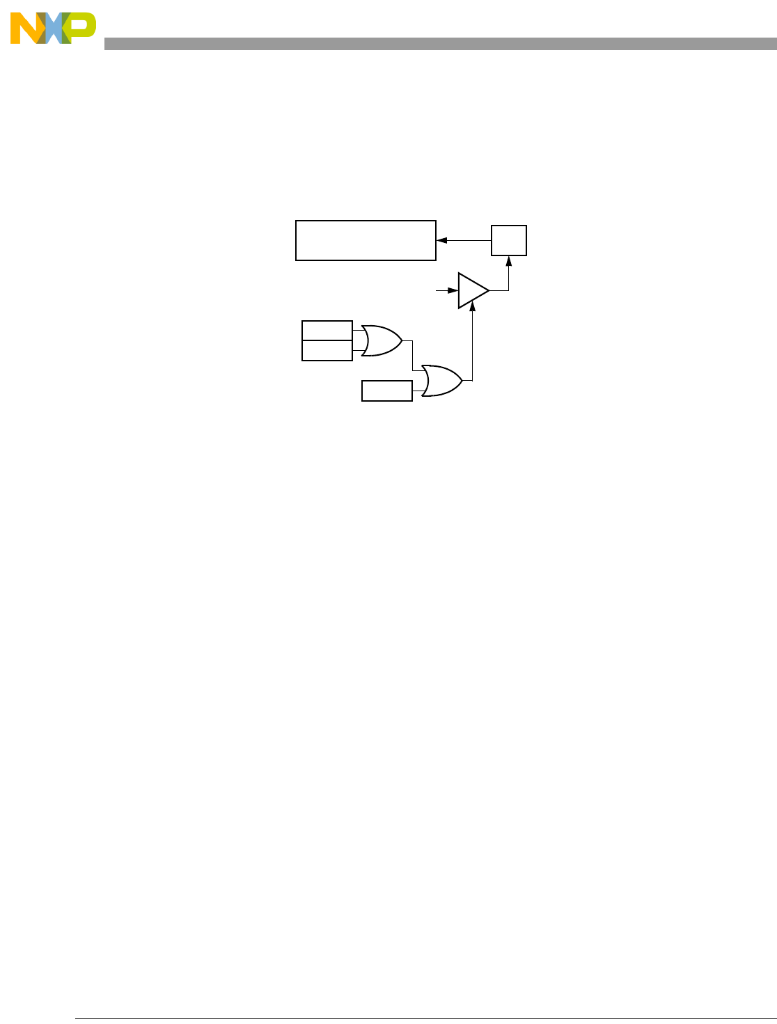
General Purpose Timer Module (GPT)
21-19 Freescale Semiconductor
The PA counter register (GPTPACNT) reflects the number of pulses from the divide-by-64 clock since the
last reset.
NOTE
The GPT prescaler generates the divide-by-64 clock. If the timer is not
active, there is no divide-by-64 clock.
Figure 21-22. Channel 3 Output Compare/Pulse Accumulator Logic
21.7.7 General-Purpose I/O Ports
An I/O pin used by the timer defaults to general-purpose I/O unless an internal function that uses that pin
is enabled.
The PORTTn pins can be configured for an input capture function or an output compare function. The
IOSn bits in the GPT IC/OC select register configure the PORTTn pins as input capture or output compare
pins.
The PORTTn data direction register controls the data direction of an input capture pin. External pin
conditions trigger input captures on input capture pins configured as inputs.
To configure a pin for input capture:
1. Clear the pin’s IOS bit in GPTIOS.
2. Clear the pin’s DDR bit in PORTTnDDR.
3. Write to GPTCTL2 to select the input edge to detect.
PORTTnDDR does not affect the data direction of an output compare pin. The output compare function
overrides the data direction register but does not affect the state of the data direction register.
To configure a pin for output compare:
1. Set the pin’s IOS bit in GPTIOS.
2. Write the output compare value to GPTCn.
3. Clear the pin’s DDR bit in PORTTnDDR.
4. Write to the OMn/OLn bits in GPTCTL1 to select the output action.
Table 21-23 shows how various timer settings affect pin functionality.
Pad
OM3
OL3
Channel 3 Output Compare
Pulse
Accumulator
OC3M3
MCF52211 ColdFire® Integrated Microcontroller Reference Manual, Rev. 3

General Purpose Timer Module (GPT)
Freescale Semiconductor 21-20
Table 21-23. GPT Settings and Pin Functions
GPTEN DDR1
1When DDR sets the pin as input (0), reading the data register returns the state of the pin. When DDR set the pin as output (1),
reading the data register returns the content of the data latch. Pin conditions such as rising or falling edges can trigger an input
capture on a pin configured as an input.
GPTIOS EDGx
[B:A]
OMx/
OLx2
2OMn/OLn bit pairs select the output action to be taken as a result of a successful output compare. When OMn or OLn is set and
the IOSn bit is set, the pin is an output regardless of the state of the corresponding DDR bit.
OC3Mx3
3Setting an OC3M bit configures the corresponding PORTTn pin to be output. OC3Mn makes the PORTTn pin an output
regardless of the data direction bit when the pin is configured for output compare (IOSn = 1). The OC3Mn bits do not change the
state of the PORTTnDDR bits.
Pin
Data
Dir.
Pin
Driven by Pin Function Comments
00X
4
4X = Don’t care
X X X In Ext. Digital input GPT disabled by GPTEN = 0
0 1 X X X X Out Data reg. Digital output GPT disabled by GPTEN = 0
1 0 0 (IC) 0 (IC
disabled)
X 0 In Ext. Digital input Input capture disabled by EDGn
setting
1 1 0 0 X 0 Out Data reg. Digital output Input capture disabled by EDGn
setting
1 0 0 <> 0 X 0 In Ext. IC and digital input Normal settings for input capture
1 1 0 <> 0 X 0 Out Data reg. Digital output Input capture of data driven to output
pin by CPU
1 0 0 <> 0 X 1 In Ext. IC and digital input OC3M setting has no effect because
IOS = 0
1 1 0 <> 0 X 1 Out Data reg. Digital output OC3M setting has no effect because
IOS = 0; input capture of data driven
to output pin by CPU
101 (OC)X
(3) 05
5An output compare overrides the data direction bit of the output compare pin but does not change the state of the data direction
bit. Enabling output compare disables data register drive of the pin.
0 In Ext. Digital input Output compare takes place but
does not affect the pin because of
the OMn/OLn setting
1 1 1 X 0 0 Out Data reg. Digital output Output compare takes place but
does not affect the pin because of
the OMn/OLn setting
1 0 1 X <> 0 0 Out OC action Output compare Pin readable only if DDR = 0(5)
1 1 1 X <> 0 0 Out OC action Output compare Pin driven by OC action(5)
1 0 1 X X 1 Out OC action/
OC3Dn
Output compare
(ch 3)
Pin readable only if DDR = 06
6A successful output compare on channel 3 causes an output value determined by OC3Dn value to temporarily override the output
compare pin state of any other output compare channel.The next OC action for the specific channel continues to be output to the
pin. A channel 3 output compare can cause bits in the output compare 3 data register to transfer to the GPT port data register,
depending on the output compare 3 mask register.
1 1 1 X X 1 Out OC action/
OC3Dn
Output
compare/OC3Dn
(ch 3)
Pin driven by channel OC action and
OC3Dn via channel 3 OC(6)
MCF52211 ColdFire® Integrated Microcontroller Reference Manual, Rev. 3

General Purpose Timer Module (GPT)
21-21 Freescale Semiconductor
21.8 Reset
Reset initializes the GPT registers to a known startup state as described in Section 21.6, “Memory Map
and Registers.”
21.9 Interrupts
Table 21-24 lists the interrupt requests generated by the timer.
21.9.1 GPT Channel Interrupts (CnF)
A channel flag is set when an input capture or output compare event occurs. Clear a channel flag by writing
a 1 to it.
NOTE
When the fast flag clear all bit (GPTSCR1[TFFCA]) is set, an input capture
read or an output compare write clears the corresponding channel flag.
When a channel flag is set, it does not inhibit subsequent output compares
or input captures
21.9.2 Pulse Accumulator Overflow (PAOVF)
PAOVF is set when the 16-bit pulse accumulator rolls over from 0xFFFF to 0x0000. If the PAOVI bit in
GPTPACTL is also set, PAOVF generates an interrupt request. Clear PAOVF by writing a 1 to this flag.
NOTE
When the fast flag clear all enable bit (GPTSCR1[TFFCA]) is set, any
access to the pulse accumulator counter registers clears all the flags in
GPTPAFLG.
21.9.3 Pulse Accumulator Input (PAIF)
PAIF is set when the selected edge is detected at the PAI pin. In event counter mode, the event edge sets
PAIF. In gated time accumulation mode, the trailing edge of the gate signal at the PAI pin sets PAIF. If the
Table 21-24. GPT Interrupt Requests
Interrupt Request Flag Enable Bit
Channel 3 IC/OC C3F C3I
Channel 2 IC/OC C2F C2I
Channel 1 IC/OC C1F C1I
Channel 0 IC/OC C0F C0I
PA overflow PAOVF PAOVI
PA input PAIF PAI
Timer overflow TOF TOI
MCF52211 ColdFire® Integrated Microcontroller Reference Manual, Rev. 3

General Purpose Timer Module (GPT)
Freescale Semiconductor 21-22
PAI bit in GPTPACTL is also set, PAIF generates an interrupt request. Clear PAIF by writing a 1 to this
flag.
NOTE
When the fast flag clear all enable bit (GPTSCR1[TFFCA]) is set, any
access to the pulse accumulator counter registers clears all the flags in
GPTPAFLG.
21.9.4 Timer Overflow (TOF)
TOF is set when the GPT counter rolls over from 0xFFFF to 0x0000. If the GPTSCR2[TOI] bit is also set,
TOF generates an interrupt request. Clear TOF by writing a 1 to this flag.
NOTE
When the GPT channel 3 registers contain 0xFFFF and TCRE is set, TOF
does not get set even though the GPT counter registers go from 0xFFFF to
0x0000.
When the fast flag clear all bit (GPTSCR1[TFFCA]) is set, any access to the
GPT counter registers clears GPT flag register 2.
When TOF is set, it does not inhibit future overflow events.
MCF52211 ColdFire® Integrated Microcontroller Reference Manual, Rev. 3

Freescale Semiconductor 22-1
Chapter 22
DMA Timers (DTIM0–DTIM3)
22.1 Introduction
This chapter describes the configuration and operation of the four direct memory access (DMA) timer
modules (DTIM0, DTIM1, DTIM2, and DTIM3). These 32-bit timers provide input capture and reference
compare capabilities with optional signaling of events using interrupts or DMA triggers. Additionally,
programming examples are included.
NOTE
The designation n appears throughout this section to refer to registers or
signals associated with one of the four identical timer modules: DTIM0,
DTIM1, DTIM2, or DTIM3.
22.1.1 Overview
Each DMA timer module has a separate register set for configuration and control. The timers can be
configured to operate from the internal bus clock (fsys) or from an external clocking source using the
DTINn signal. If the internal bus clock is selected, it can be divided by 16 or 1. The selected clock source
is routed to an 8-bit programmable prescaler that clocks the actual DMA timer counter register (DTCNn).
Using the DTMRn, DTXMRn, DTCRn, and DTRRn registers, the DMA timer may be configured to assert
an output signal, generate an interrupt, or request a DMA transfer on a particular event.
NOTE
The GPIO module must be configured to enable the peripheral function of
the appropriate pins (refer to Chapter 13, “General Purpose I/O Module”)
prior to configuring the DMA Timers.
MCF52211 ColdFire® Integrated Microcontroller Reference Manual, Rev. 3
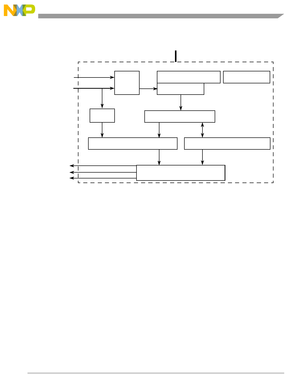
DMA Timers (DTIM0–DTIM3)
Freescale Semiconductor 22-2
Figure 22-1 is a block diagram of one of the four identical timer modules.
Figure 22-1. DMA Timer Block Diagram
22.1.2 Features
Each DMA timer module has:
• Maximum timeout period of 266,548 seconds at 66 MHz (~74 hours)
• 15-ns resolution at 66 MHz
• Programmable sources for the clock input, including external clock
• Programmable prescaler
• Input-capture capability with programmable trigger edge on input pin
• Programmable mode for the output pin on reference compare
• Free run and restart modes
• Programmable interrupt or DMA request on input capture or reference-compare
• Ability to stop the timer from counting when the ColdFire core is halted
DMA Timer
Divider
DMA Timer Mode Register (DTMRn)
Prescaler Mode Bits
DMA Timer Counter Register (DTCNn)
31 0
DMA Timer Reference Register (DTRRn)
31 0
DMA Timer Capture Register (DTCRn)
31 0
DMA Timer Event Register (DTERn)
Capture
Detection
clock
(contains incrementing value)
(reference value for comparison with DTCN)
(indicates capture or when DTCN = DTRRn)
Interrupt Request
Clock
Generator
DMA Timer Extended Mode
Register (DTXMRn)
DMA Request
0
0
15 7
70
Internal Bus Clock
(fsys)
DMA Timer
Internal Bus to/from DMA Timer Registers
(latches DTCN value when triggered byDTINn)
DTOUTn
DTINn
MCF52211 ColdFire® Integrated Microcontroller Reference Manual, Rev. 3

DMA Timers (DTIM0–DTIM3)
22-3 Freescale Semiconductor
22.2 Memory Map/Register Definition
The timer module registers, shown in Table 22-1, can be modified at any time.
22.2.1 DMA Timer Mode Registers (DTMRn)
The DTMRn registers program the prescaler and various timer modes.
Table 22-1. DMA Timer Module Memory Map
IPSBAR Offset
Register Width
(bits) Access Reset Value Section/Page
DMA Timer 0
DMA Timer 1
DMA Timer 2
DMA Timer 3
0x00_0400
0x00_0440
0x00_0480
0x00_04C0
DMA Timer n Mode Register (DTMRn) 16 R/W 0x0000 22.2.1/22-3
0x00_0402
0x00_0442
0x00_0482
0x00_04C2
DMA Timer n Extended Mode Register (DTXMRn) 8 R/W 0x00 22.2.2/22-5
0x00_0403
0x00_0443
0x00_0483
0x00_04C3
DMA Timer n Event Register (DTERn)8R/W0x0022.2.3/22-5
0x00_0404
0x00_0444
0x00_0484
0x00_04C4
DMA Timer n Reference Register (DTRRn) 32 R/W 0xFFFF_FFFF 22.2.4/22-7
0x00_0408
0x00_0448
0x00_0488
0x00_04C8
DMA Timer n Capture Register (DTCRn) 32 R/W 0x0000_0000 22.2.5/22-7
0x00_040C
0x00_044C
0x00_048C
0x00_04CC
DMA Timer n Counter Register (DTCNn) 32 R 0x0000_0000 22.2.6/22-8
IPSBAR
Offset:
0x00_0400 (DTMR0)
0x00_0440 (DTMR1)
0x00_0480 (DTMR2)
0x00_04C0 (DTMR3)
Access: User read/write
1514131211109876543210
RPS CE OM ORRI FRR CLK RST
W
Reset0000000000000000
Figure 22-2. DTMRn Registers
MCF52211 ColdFire® Integrated Microcontroller Reference Manual, Rev. 3

DMA Timers (DTIM0–DTIM3)
Freescale Semiconductor 22-4
Table 22-2. DTMRn Field Descriptions
Field Description
15–8
PS
Prescaler value. Divides the clock input (internal bus clock/(16 or 1) or clock on DTINn)
0x00 1
...
0xFF 256
7–6
CE
Capture edge.
00 Disable capture event output. Timer in reference mode.
01 Capture on rising edge only
10 Capture on falling edge only
11 Capture on any edge
5
OM
Output mode.
0 Active-low pulse for one internal bus clock cycle (15-ns resolution at 66 MHz)
1 Toggle output.
4
ORRI
Output reference request, interrupt enable. If ORRI is set when DTERn[REF] is set, a DMA request or an interrupt
occurs, depending on the value of DTXMRn[DMAEN] (DMA request if set, interrupt if cleared).
0 Disable DMA request or interrupt for reference reached (does not affect DMA request or interrupt on capture
function).
1 Enable DMA request or interrupt upon reaching the reference value.
3
FRR
Free run/restart
0 Free run. Timer count continues incrementing after reaching the reference value.
1 Restart. Timer count is reset immediately after reaching the reference value.
2–1
CLK
Input clock source for the timer. Avoid setting CLK when RST is already set. Doing so causes CLK to zero (stop
counting).
00 Stop count
01 Internal bus clock divided by 1
10 Internal bus clock divided by 16. This clock source is not synchronized with the timer; therefore, successive
time-outs may vary slightly.
11 DTINn pin (falling edge)
0
RST
Reset timer. Performs a software timer reset similar to an external reset, although other register values can be written
while RST is cleared. A transition of RST from 1 to 0 resets register values. The timer counter is not clocked unless
the timer is enabled.
0 Reset timer (software reset)
1 Enable timer
MCF52211 ColdFire® Integrated Microcontroller Reference Manual, Rev. 3

DMA Timers (DTIM0–DTIM3)
22-5 Freescale Semiconductor
22.2.2 DMA Timer Extended Mode Registers (DTXMRn)
The DTXMRn registers program DMA request and increment modes for the timers.
22.2.3 DMA Timer Event Registers (DTERn)
DTERn, shown in Figure 22-4, reports capture or reference events by setting DTERn[CAP] or
DTERn[REF]. This reporting happens regardless of the corresponding DMA request or interrupt enable
values, DTXMRn[DMAEN] and DTMRn[ORRI,CE].
Writing a 1 to DTERn[REF] or DTERn[CAP] clears it (writing a 0 does not affect bit value); both bits can
be cleared at the same time. If configured to generate an interrupt request, clear REF and CAP early in the
interrupt service routine so the timer module can negate the interrupt request signal to the interrupt
controller. If configured to generate a DMA request, processing of the DMA data transfer automatically
clears the REF and CAP flags via the internal DMA ACK signal.
IPSBAR
Offset:
0x00_0402 (DTXMR0)
0x00_0442 (DTXMR1)
0x00_0482 (DTXMR2)
0x00_04C2 (DTXMR3)
Access: User read/write
76543210
R
DMAEN HALTED
00000
MODE16
W
Reset:00000000
Figure 22-3. DTXMRn Registers
Table 22-3. DTXMRn Field Descriptions
Field Description
7
DMAEN
DMA request. Enables DMA request output on counter reference match or capture edge event.
0 DMA request disabled
1 DMA request enabled
6
HALTED
Controls the counter when the core is halted. This allows debug mode to be entered without timer interrupts affecting
the debug flow.
0 Timer function is not affected by core halt.
1 Timer stops counting while the core is halted.
Note: This bit is only applicable in reference compare mode, see Section 22.3.3, “Reference Compare.”
5–1 Reserved, must be cleared.
0
MODE16
Selects the increment mode for the timer. Setting MODE16 is intended to exercise the upper bits of the 32-bit timer
in diagnostic software without requiring the timer to count through its entire dynamic range. When set, the counter’s
upper 16 bits mirror its lower 16 bits. All 32 bits of the counter remain compared to the reference value.
0 Increment timer by 1
1 Increment timer by 65,537
MCF52211 ColdFire® Integrated Microcontroller Reference Manual, Rev. 3

DMA Timers (DTIM0–DTIM3)
Freescale Semiconductor 22-6
IPSBAR
Offset:
0x00_0403 (DTER0)
0x00_0443 (DTER1)
0x00_0483 (DTER2)
0x00_04C3 (DTER3)
Access: User read/write
76543210
R000000REFCAP
Ww1c w1c
Reset:00000000
Figure 22-4. DTERn Registers
Table 22-4. DTERn Field Descriptions
Field Description
7–2 Reserved, must be cleared.
1
REF
Output reference event. The counter value (DTCNn) equals DTRRn. Writing a 1 to REF clears the event condition.
Writing a 0 has no effect.
0
CAP
Capture event. The counter value has been latched into DTCRn. Writing a 1 to CAP clears the event condition.
Writing a 0 has no effect.
REF DTMRn[ORRI] DTXMRn[DMAEN]
0X X No event
1 0 0 No request asserted
1 0 1 No request asserted
1 1 0 Interrupt request asserted
1 1 1 DMA request asserted
CAP DTMRn[CE] DTXMRn
[DMAEN]
0XX X No event
1 00 0 Disable capture event output
1 00 1 Disable capture event output
1 01 0 Capture on rising edge and trigger interrupt
1 01 1 Capture on rising edge and trigger DMA
1 10 0 Capture on falling edge and trigger interrupt
1 10 1 Capture on falling edge and trigger DMA
1 11 0 Capture on any edge and trigger interrupt
1 11 1 Capture on any edge and trigger DMA
MCF52211 ColdFire® Integrated Microcontroller Reference Manual, Rev. 3
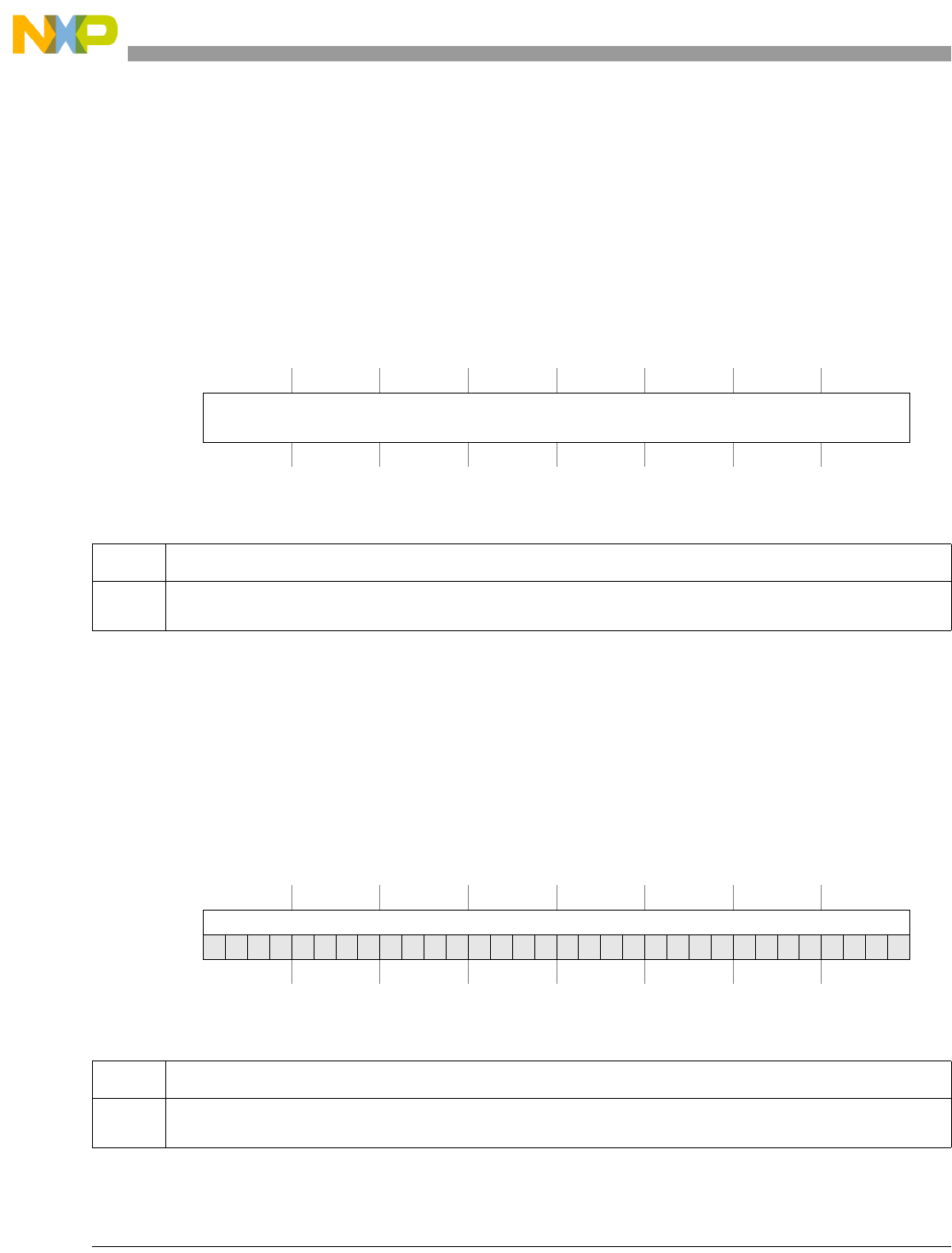
DMA Timers (DTIM0–DTIM3)
22-7 Freescale Semiconductor
22.2.4 DMA Timer Reference Registers (DTRRn)
As part of the output-compare function, each DTRRn contains the reference value compared with the
respective free-running timer counter (DTCNn).
The reference value is matched when DTCNn equals DTRRn. The prescaler indicates that DTCNn should
be incremented again. Therefore, the reference register is matched after DTRRn+ 1 time intervals.
22.2.5 DMA Timer Capture Registers (DTCRn)
Each DTCRn latches the corresponding DTCNn value during a capture operation when an edge occurs on
DTINn, as programmed in DTMRn. The internal bus clock is assumed to be the clock source. DTINn
cannot simultaneously function as a clocking source and as an input capture pin. Indeterminate operation
results if DTINn is set as the clock source when the input capture mode is used.
IPSBAR
Offset:
0x00_0404 (DTRR0)
0x00_0444 (DTRR1)
0x00_0484 (DTRR2)
0x00_04C4 (DTRR3)
Access: User read/write
313029282726252423222120191817161514131211109876543210
RREF (32-bit reference value)
W
Reset11111111111111111111111111111111
Figure 22-5. DTRRn Registers
Table 22-5. DTRRn Field Descriptions
Field Description
31–0
REF
Reference value compared with the respective free-running timer counter (DTCNn) as part of the output-compare
function.
IPSBAR
Offset:
0x00_0408 (DTCR0)
0x00_0448 (DTCR1)
0x00_0488 (DTCR2)
0x00_04C8 (DTCR3)
Access: User read-only
313029282726252423222120191817161514131211109876543210
RCAP (32-bit capture counter value)
W
Reset00000000000000000000000000000000
Figure 22-6. DTCRn Registers
Table 22-6. DTCRn Field Descriptions
Field Description
31–0
CAP
Captures the corresponding DTCNn value during a capture operation when an edge occurs on DTINn, as
programmed in DTMRn.
MCF52211 ColdFire® Integrated Microcontroller Reference Manual, Rev. 3

DMA Timers (DTIM0–DTIM3)
Freescale Semiconductor 22-8
22.2.6 DMA Timer Counters (DTCNn)
The current value of the 32-bit timer counter can be read at anytime without affecting counting. Writes to
DTCNn clear the timer counter. The timer counter increments on the clock source rising edge (internal bus
clock divided by 1, internal bus clock divided by 16, or DTINn).
22.3 Functional Description
22.3.1 Prescaler
The prescaler clock input is selected from the internal bus clock (fsys divided by 1 or 16) or from the
corresponding timer input, DTINn. DTINn is synchronized to the internal bus clock, and the
synchronization delay is between two and three internal bus clocks. The corresponding DTMRn[CLK]
selects the clock input source. A programmable prescaler divides the clock input by values from 1 to 256.
The prescaler output is an input to the 32-bit counter, DTCNn.
22.3.2 Capture Mode
Each DMA timer has a 32-bit timer capture register (DTCRn) that latches the counter value when the
corresponding input capture edge detector senses a defined DTINn transition. The capture edge bits
(DTMRn[CE]) select the type of transition that triggers the capture and sets the timer event register capture
event bit, DTERn[CAP]. If DTERn[CAP] and DTXMRn[DMAEN] are set, a DMA request is asserted. If
DTERn[CAP] is set and DTXMRn[DMAEN] is cleared, an interrupt is asserted.
22.3.3 Reference Compare
Each DMA timer can be configured to count up to a reference value. If the reference value is met,
DTERn[REF] is set.
•If DTMRn[ORRI] is set and DTXMRn[DMAEN] is cleared, an interrupt is asserted.
•If DTMRn[ORRI] and DTXMRn[DMAEN] are set, a DMA request is asserted.
IPSBAR
Offset:
0x00_040C (DTCN0)
0x00_044C (DTCN1)
0x00_048C (DTCN2)
0x00_04CC (DTCN3)
Access: User read/write
313029282726252423222120191817161514131211109876543210
RCNT (32-bit timer counter value count)
W
Reset00000000000000000000000000000000
Figure 22-7. DMA Timer Counters (DTCNn)
Table 22-7. DTCNn Field Descriptions
Field Description
31–0
CNT
Timer counter. Can be read at anytime without affecting counting and any write to this field clears it.
MCF52211 ColdFire® Integrated Microcontroller Reference Manual, Rev. 3

DMA Timers (DTIM0–DTIM3)
22-9 Freescale Semiconductor
If the free run/restart bit (DTMRn[FRR]) is set, a new count starts. If it is clear, the timer keeps running.
22.3.4 Output Mode
When a timer reaches the reference value selected by DTRR, it can send an output signal on DTOUTn.
DTOUTn can be an active-low pulse or a toggle of the current output, as selected by the DTMRn[OM] bit.
22.4 Initialization/Application Information
The general-purpose timer modules typically, but not necessarily, follow this program order:
• The DTMRn and DTXMRn registers are configured for the desired function and behavior.
— Count and compare to a reference value stored in the DTRRn register
— Capture the timer value on an edge detected on DTINn
— Configure DTOUTn output mode
— Increment counter by 1 or by 65,537 (16-bit mode)
— Enable/disable interrupt or DMA request on counter reference match or capture edge
• The DTMRn[CLK] register is configured to select the clock source to be routed to the prescaler.
— Internal bus clock (can be divided by 1 or 16)
—DTINn, the maximum value of DTINn is 1/5 of the internal bus clock, as described in the
device’s electrical characteristics
NOTE
DTINn may not be configured as a clock source when the timer capture
mode is selected or indeterminate operation results.
• The 8-bit DTMRn[PS] prescaler value is set.
• Using DTMRn[RST], counter is cleared and started.
• Timer events are managed with an interrupt service routine, a DMA request, or by a software
polling mechanism.
22.4.1 Code Example
The following code provides an example of how to initialize and use DMA Timer0 for counting time-out
periods.
DTMR0 EQU IPSBARx+0x400 ;Timer0 mode register
DTMR1 EQU IPSBARx+0x440 ;Timer1 mode register
DTRR0 EQU IPSBARx+0x404 ;Timer0 reference register
DTRR1 EQU IPSBARx+0x444 ;Timer1 reference register
DTCR0 EQU IPSBARx+0x408 ;Timer0 capture register
DTCR1 EQU IPSBARx+0x448 ;Timer1 capture register
DTCN0 EQU IPSBARx+0x40C ;Timer0 counter register
DTCN1 EQU IPSBARx+0x44C ;Timer1 counter register
DTER0 EQU IPSBARx+0x403 ;Timer0 event register
DTER1 EQU IPSBARx+0x443 ;Timer1 event register
* TMR0 is defined as: *
*[PS] = 0xFF, divide clock by 256
MCF52211 ColdFire® Integrated Microcontroller Reference Manual, Rev. 3

DMA Timers (DTIM0–DTIM3)
Freescale Semiconductor 22-10
*[CE] = 00 disable capture event output
*[OM] = 0 output=active-low pulse
*[ORRI] = 0, disable ref. match output
*[FRR] = 1, restart mode enabled
*[CLK] = 10, internal bus clock/16
*[RST] = 0, timer0 disabled
move.w #0xFF0C,D0
move.w D0,TMR0
move.l #0x0000,D0;writing to the timer counter with any
move.l DO,TCN0 ;value resets it to zero
move.l #0xAFAF,DO ;set the timer0 reference to be
move.l #D0,TRR0 ;defined as 0xAFAF
The simple example below uses Timer0 to count time-out loops. A time-out occurs when the reference
value, 0xAFAF, is reached.
timer0_ex
clr.l DO
clr.l D1
clr.l D2
move.l #0x0000,D0
move.l D0,TCN0 ;reset the counter to 0x0000
move.b #0x03,D0 ;writing ones to TER0[REF,CAP]
move.b D0,TER0 ;clears the event flags
move.w TMR0,D0 ;save the contents of TMR0 while setting
bset #0,D0 ;the 0 bit. This enables timer 0 and starts counting
move.w D0,TMR0 ;load the value back into the register, setting TMR0[RST]
T0_LOOP
move.b TER0,D1 ;load TER0 and see if
btst #1,D1 ;TER0[REF] has been set
beq T0_LOOP
addi.l #1,D2 ;Increment D2
cmp.l #5,D2 ;Did D2 reach 5? (i.e. timer ref has timed)
beq T0_FINISH ;If so, end timer0 example. Otherwise jump back.
move.b #0x02,D0 ;writing one to TER0[REF] clears the event flag
move.b D0,TER0
jmp T0_LOOP
T0_FINISH
HALT ;End processing. Example is finished
22.4.2 Calculating Time-Out Values
Equation 22-1 determines time-out periods for various reference values:
Eqn. 22-1
When calculating time-out periods, add one to the prescaler to simplify calculating, because
DTMRn[PS] equal to 0x00 yields a prescaler of one, and DTMRn[PS] equal to 0xFF yields a prescaler of
256.
Timeout period 1 clock frequency1 or 16DTMRn[PS] 1+DTRRn[REF] 1+=
MCF52211 ColdFire® Integrated Microcontroller Reference Manual, Rev. 3

DMA Timers (DTIM0–DTIM3)
22-11 Freescale Semiconductor
For example, if a 66-MHz timer clock is divided by 16, DTMRn[PS] equals 0x7F, and the timer is
referenced at 0xFBC5 (64,453 decimal), the time-out period is:
Eqn. 22-2
Timeout period 1
66 106
-------------------- 16 127 1+64453 1+ 2.00 seconds==
MCF52211 ColdFire® Integrated Microcontroller Reference Manual, Rev. 3
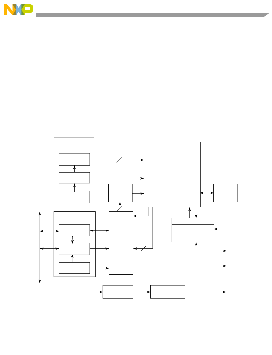
Freescale Semiconductor 23-1
,
Chapter 23
Queued Serial Peripheral Interface (QSPI)
23.1 Introduction
This chapter describes the queued serial peripheral interface (QSPI) module.
23.1.1 Block Diagram
Figure 23-1 illustrates the QSPI module.
Figure 23-1. QSPI Block Diagram
Queue Control
Block
Queue
Pointer
4
Done
Comparator
End Queue
Pointer
Status
Regs
Delay
Counter
Control Logic
Control
Regs
80-byte
QSPI
RAM
Chip
Selects
Command
Divide by 2 Baud Rate
Generator
msb lsb
Logic
Array
QSPI_CLK
QSPI_DIN
8
/16 Bit Shift Reg
.
Rx/Tx Data Reg.
QSPI_DOUT
4
4
Internal Bus
QSPI
Address
Register
QSPI
Data
Register
Internal Bus
Clock (fsys)
QSPI_CS[3:0]
MCF52211 ColdFire® Integrated Microcontroller Reference Manual, Rev. 3

Queued Serial Peripheral Interface (QSPI)
23-2 Freescale Semiconductor
,
23.1.2 Overview
The queued serial peripheral interface module provides a serial peripheral interface with queued transfer
capability. It allows users to queue up to 16 transfers at once, eliminating CPU intervention between
transfers. Transfer RAM in the QSPI is indirectly accessible using address and data registers.
NOTE
The GPIO module must be configured to enable the peripheral function of
the appropriate pins (refer to Chapter 13, “General Purpose I/O Module”)
prior to configuring the QSPI module.
23.1.3 Features
Features include:
• Programmable queue to support up to 16 transfers without user intervention
— 80 bytes of data storage provided
• Supports transfer sizes of 8 to 16 bits in 1-bit increments
• Four peripheral chip-select lines for control of up to 15 devices (All chip selects may not be
available on all devices. See Chapter 2, “Signal Descriptions,” for details on which chip-selects are
pinned-out.)
• Baud rates from 129.4 Kbps to 16.6 Mbps at 66 MHz internal bus frequency
• Programmable delays before and after transfers
• Programmable QSPI clock phase and polarity
• Supports wraparound mode for continuous transfers
23.1.4 Modes of Operation
Because the QSPI module only operates in master mode, the master bit in the QSPI mode register
(QMR[MSTR]) must be set for the QSPI to function properly. If the master bit is not set, QSPI activity is
indeterminate. The QSPI can initiate serial transfers but cannot respond to transfers initiated by other QSPI
masters.
23.2 External Signal Description
The module provides access to as many as 15 devices with a total of seven signals: QSPI_DOUT,
QSPI_DIN, QSPI_CLK, QSPI_CS[3:0].
Peripheral chip-select signals, QSPI_CSn, are used to select an external device as the source or destination
for serial data transfer. Signals are asserted when a command in the queue is executed. More than one
chip-select signal can be asserted simultaneously.
Although QSPI_CSn signals function as simple chip selects in most applications, up to 15 devices can be
selected by decoding them with an external 4-to-16 decoder.
MCF52211 ColdFire® Integrated Microcontroller Reference Manual, Rev. 3

Queued Serial Peripheral Interface (QSPI)
Freescale Semiconductor 23-3
,
23.3 Memory Map/Register Definition
Table 23-2 is the QSPI register memory map. Reading reserved locations returns zeros.
23.3.1 QSPI Mode Register (QMR)
The QMR, shown in Figure 23-2, determines the basic operating modes of the QSPI module. Parameters
such as QSPI_CLK polarity and phase, baud rate, master mode operation, and transfer size are determined
by this register.
NOTE
Because the QSPI does not operate in slave mode, the master mode enable
bit (QMR[MSTR]) must be set for the QSPI module to operate correctly.
NOTE
Because of the implementation of the QSPI module on this device, CPOL
and CPHA may be modified only once, typically during software
initialization. Changing CPOL and CPHA during operation is not
supported.
Table 23-1. QSPI Input and Output Signals and Functions
Signal Name Hi-Z or Actively Driven Function
Data output (QSPI_DOUT) Configurable Serial data output from QSPI
Data input (QSPI_DIN) N/A Serial data input to QSPI
Serial clock (QSPI_CLK) Actively driven Clock output from QSPI
Peripheral chip selects (QSPI_CSn) Actively driven Peripheral selects from QSPI
Table 23-2. QSPI Memory Map
IPSBAR
Offset1
1Addresses not assigned to a register and undefined register bits are reserved for expansion.
Register Width
(bits) Access Reset Value Section/Page
0x00_0340 QSPI Mode Register (QMR) 16 R/W 0x0104 23.3.1/23-3
0x00_0344 QSPI Delay Register (QDLYR) 16 R/W 0x0404 23.3.2/23-5
0x00_0348 QSPI Wrap Register (QWR) 16 R/W2
2See the register description for special cases. Some bits may be read- or write-only.
0x0000 23.3.3/23-6
0x00_034C QSPI Interrupt Register (QIR) 16 R/W20x0000 23.3.4/23-6
0x00_0350 QSPI Address Register (QAR) 16 R/W20x0000 23.3.5/23-7
0x00_0354 QSPI Data Register (QDR) 16 R/W 0x0000 23.3.6/23-8
MCF52211 ColdFire® Integrated Microcontroller Reference Manual, Rev. 3

Queued Serial Peripheral Interface (QSPI)
23-4 Freescale Semiconductor
,
IPSBAR
Offset:
0x00_0340 (QMR) Access: User read/write
1514131211109 876543210
RMSTR 0BITS CPOL CPHA BAUD
W
Reset0 0 00000100000100
Figure 23-2. QSPI Mode Register (QMR)
Table 23-3. QMR Field Descriptions
Field Description
15
MSTR
Master mode enable.
0 Reserved, do not use.
1 The QSPI is in master mode. Must be set for the QSPI module to operate correctly.
14 Reserved, must be cleared.
13–10
BITS
Transfer size. Determines the number of bits to be transferred for each entry in the queue.
9
CPOL
Clock polarity. Defines the clock polarity of QSPI_CLK.
0 The inactive state value of QSPI_CLK is logic level 0.
1 The inactive state value of QSPI_CLK is logic level 1.
8
CPHA
Clock phase. Defines the QSPI_CLK clock-phase.
0 Data captured on the leading edge of QSPI_CLK and changed on the following edge of QSPI_CLK.
1 Data changed on the leading edge of QSPI_CLK and captured on the following edge of QSPI_CLK.
7–0
BAUD
Baud rate divider. The baud rate is selected by writing a value in the range 2–255. A value of zero disables the QSPI.
A value of 1 is an invalid setting. The desired QSPI_CLK baud rate is related to the internal bus clock and
QMR[BAUD] by the following expression:
QMR[BAUD] = fsys/ [desired QSPI_CLK baud rate])
BITS Bits per Transfer
0000 16
0001–0111 Reserved
1000 8
1001 9
1010 10
1011 11
1100 12
1101 13
1110 14
1111 15
MCF52211 ColdFire® Integrated Microcontroller Reference Manual, Rev. 3
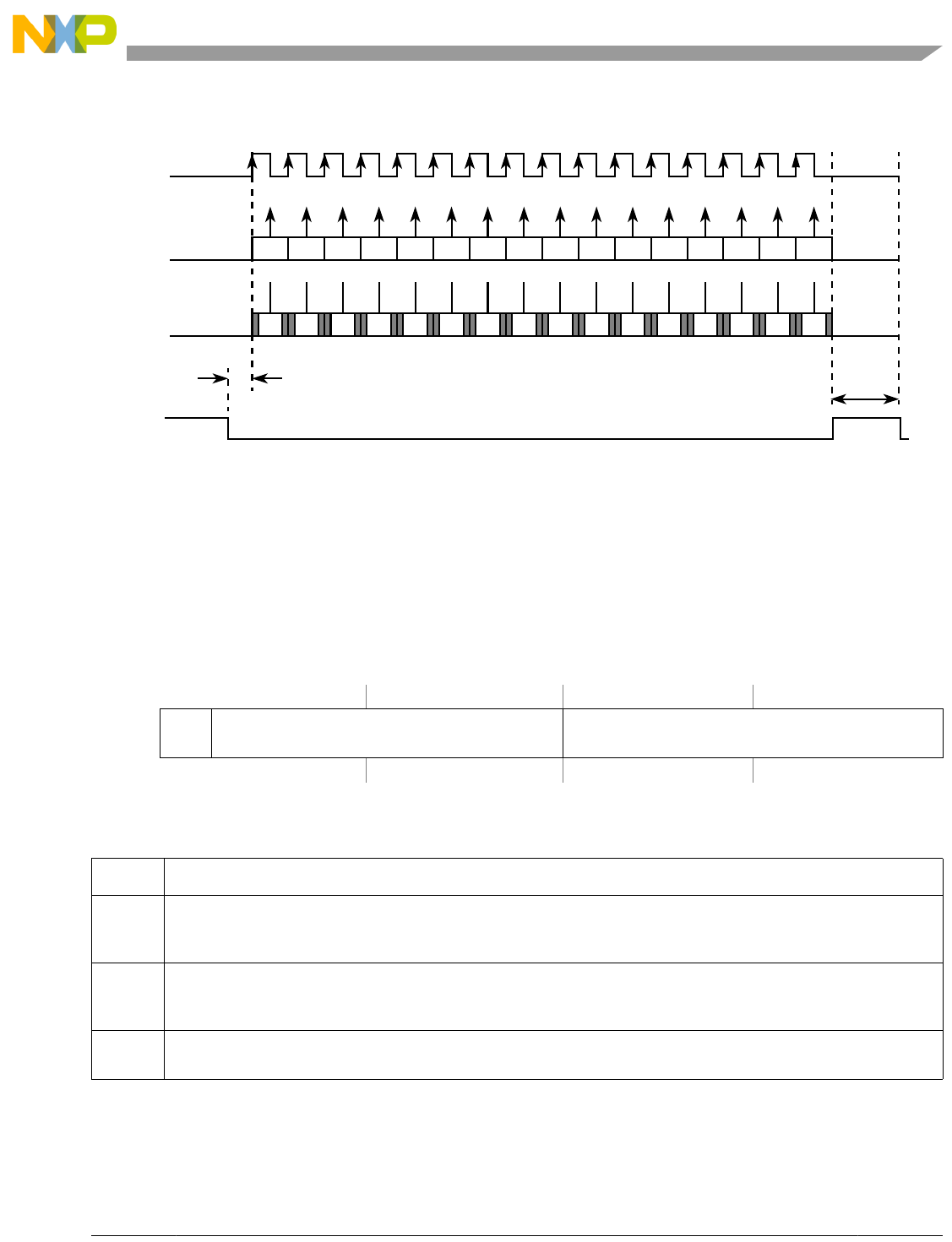
Queued Serial Peripheral Interface (QSPI)
Freescale Semiconductor 23-5
,
Figure 23-3 shows an example of a QSPI clocking and data transfer.
Figure 23-3. QSPI Clocking and Data Transfer Example
23.3.2 QSPI Delay Register (QDLYR)
The QDLYR is used to initiate master mode transfers and to set various delay parameters.
IPSBAR
Offset:
0x00_0344 (QDLYR) Access: User read/write
1514131211109 876543210
RSPE QCD DTL
W
Reset0 0 00010000000100
Figure 23-4. QSPI Delay Register (QDLYR)
Table 23-4. QDLYR Field Descriptions
Field Description
15
SPE
QSPI enable. When set, the QSPI initiates transfers in master mode by executing commands in the command RAM.
The QSPI clears this bit automatically when a transfer completes. The user can also clear this bit to abort transfer
unless QIR[ABRTL] is set. The recommended method for aborting transfers is to set QWR[HALT].
14–8
QCD
QSPI_CLK delay. When the DSCK bit in the command RAM is set this field determines the length of the delay from
assertion of the chip selects to valid QSPI_CLK transition. See Section 23.4.3, “Transfer Delays” for information on
setting this bit field.
7–0
DTL
Delay after transfer. When the DT bit in the command RAM is set this field determines the length of delay after the
serial transfer.
QSPI_CLK
QSPI_DOUT
QSPI_DIN
QSPI_CS
AB
QMR[CPOL] = 0
QMR[CPHA] = 1
QCR[CONT] = 0
Chip selects are active low
A=QDLYR[QCD]
B=QDLYR[DTL]
15 14 13 12 11 10 9 8 7 6 5 4 3 2 1 0
15 14 13 12 11 10 9 8 7 6 5 4 3 2 1 0
msb
MCF52211 ColdFire® Integrated Microcontroller Reference Manual, Rev. 3

Queued Serial Peripheral Interface (QSPI)
23-6 Freescale Semiconductor
,
23.3.3 QSPI Wrap Register (QWR)
The QSPI wrap register provides halt transfer control, wraparound settings, and queue pointer locations.
23.3.4 QSPI Interrupt Register (QIR)
The QIR contains QSPI interrupt enables and status flags.
IPSBAR
Offset:
0x00_0348 (QWR) Access: User read/write
1514 131211109 8 76543210
RHALT WREN WRTO CSIV ENDQP CPTQP NEWQP
W
Reset0 0 0 0000000000000
Figure 23-5. QSPI Wrap Register (QWR)
Table 23-5. QWR Field Descriptions
Field Description
15
HALT
Halt transfers. Assertion of this bit causes the QSPI to stop execution of commands after it has completed execution
of the current command.
14
WREN
Wraparound enable. Enables wraparound mode.
0 Execution stops after executing the command pointed to by QWR[ENDQP].
1 After executing command pointed to by QWR[ENDQP], wrap back to entry zero, or the entry pointed to by
QWR[NEWQP] and continue execution.
13
WRTO
Wraparound location. Determines where the QSPI wraps to in wraparound mode.
0 Wrap to RAM entry zero.
1 Wrap to RAM entry pointed to by QWR[NEWQP].
12
CSIV
QSPI_CS inactive level.
0 QSPI chip select outputs return to zero when not driven from the value in the current command RAM entry during
a transfer (that is, inactive state is 0, chip selects are active high).
1 QSPI chip select outputs return to one when not driven from the value in the current command RAM entry during
a transfer (that is, inactive state is 1, chip selects are active low).
11–8
ENDQP
End of queue pointer. Points to the RAM entry that contains the last transfer description in the queue.
7–4
CPTQP
Completed queue entry pointer. Points to the RAM entry that contains the last command to have been completed.
This field is read only.
3–0
NEWQP
Start of queue pointer. This 4-bit field points to the first entry in the RAM to be executed on initiating a transfer.
IPSBAR
Offset:
0x00_034C (QIR) Access: User read/write
15 141312 11 109876543 210
RWCEFB ABRTB 0ABRTL WCEFE ABRTE 0SPIFE 0 0 0 0 WCEF ABRT 0 SPIF
Ww1c w1c w1c
Reset0 000 0 00000000000
Figure 23-6. QSPI Interrupt Register (QIR)
MCF52211 ColdFire® Integrated Microcontroller Reference Manual, Rev. 3

Queued Serial Peripheral Interface (QSPI)
Freescale Semiconductor 23-7
,
23.3.5 QSPI Address Register (QAR)
The QAR is used to specify the location in the QSPI RAM that read and write operations affect. As shown
in Section 23.4.1, “QSPI RAM”, the transmit RAM is located at addresses 0x0 to 0xF, the receive RAM
is located at 0x10 to 0x1F, and the command RAM is located at 0x20 to 0x2F. (These addresses refer to
the QSPI RAM space, not the device memory map.)
NOTE
A read or write to the QSPI RAM causes QAR to increment. However, the
QAR does not wrap after the last queue entry within each section of the
RAM. The application software must manage address range errors.
Table 23-6. QIR Field Descriptions
Field Description
15
WCEFB
Write collision access error enable. A write collision occurs during a data transfer when the RAM entry containing
the current command is written to by the CPU with the QDR. When this bit is asserted, the write access to QDR
results in an access error.
14
ABRTB
Abort access error enable. An abort occurs when QDLYR[SPE] is cleared during a transfer. When set, an attempt to
clear QDLYR[SPE] during a transfer results in an access error.
13 Reserved, must be cleared.
12
ABRTL
Abort lock-out. When set, QDLYR[SPE] cannot be cleared by writing to the QDLYR. QDLYR[SPE] is only cleared by
the QSPI when a transfer completes.
11
WCEFE
Write collision (WCEF) interrupt enable.
0 Write collision interrupt disabled
1 Write collision interrupt enabled
10
ABRTE
Abort (ABRT) interrupt enable.
0 Abort interrupt disabled
1 Abort interrupt enabled
9 Reserved, must be cleared.
8
SPIFE
QSPI finished (SPIF) interrupt enable.
0 SPIF interrupt disabled
1 SPIF interrupt enabled
7–4 Reserved, must be cleared.
3
WCEF
Write collision error flag. Indicates that an attempt has been made to write to the RAM entry that is currently being
executed. Writing a 1 to this bit (w1c) clears it and writing 0 has no effect.
2
ABRT
Abort flag. Indicates that QDLYR[SPE] has been cleared by the user writing to the QDLYR rather than by completion
of the command queue by the QSPI. Writing a 1 to this bit (w1c) clears it and writing 0 has no effect.
1 Reserved, must be cleared.
0
SPIF
QSPI finished flag. Asserted when the QSPI has completed all the commands in the queue. Set on completion of
the command pointed to by QWR[ENDQP], and on completion of the current command after assertion of
QWR[HALT]. In wraparound mode, this bit is set every time the command pointed to by QWR[ENDQP] is completed.
Writing a 1 to this bit (w1c) clears it and writing 0 has no effect.
MCF52211 ColdFire® Integrated Microcontroller Reference Manual, Rev. 3

Queued Serial Peripheral Interface (QSPI)
23-8 Freescale Semiconductor
,
23.3.6 QSPI Data Register (QDR)
The QDR is used to access QSPI RAM indirectly. The CPU reads and writes all data from and to the QSPI
RAM through this register.
A write to QDR causes data to be written to the RAM entry specified by QAR[ADDR]. This also causes
the value in QAR to increment. Correspondingly, a read at QDR returns the data in the RAM at the address
specified by QAR[ADDR]. This also causes QAR to increment. A read access requires a single wait state.
23.3.7 Command RAM Registers (QCR0–QCR15)
The command RAM is accessed using the upper byte of the QDR; the QSPI cannot modify information in
command RAM. There are 16 bytes in the command RAM. Each byte is divided into two fields. The chip
select field enables external peripherals for transfer. The command field provides transfer operations.
IPSBAR
Offset:
0x00_0350 (QAR) Access: User read/write
15 14 13 12 11 10 9 8 7 6 5 4 3 2 1 0
R0000000000 ADDR
W
Reset0000000000000000
Figure 23-7. QSPI Address Register (QAR)
Table 23-7. QAR Field Descriptions
Field Description
15–6 Reserved, must be cleared.
5–0
ADDR
Address used to read/write the QSPI RAM. Ranges are as follows:
0x00–0x0F Transmit RAM
0x10–0x1F Receive RAM
0x20–0x2F Command RAM
0x30–0x3F Reserved
IPSBAR
Offset:
0x00_0354 (QDR) Access: User read/write
1514131211109876543210
RDATA
W
Reset0000000000000000
Figure 23-8. QSPI Data Register (QDR)
Table 23-8. QDR Field Descriptions
Field Description
15–0
DATA
A write to this field causes data to be written to the QSPI RAM entry specified by QAR[ADDR]. Similarly, a read of
this field returns the data in the QSPI RAM at the address specified by QAR[ADDR]. During command RAM
accesses (QAR[ADDR] = 0x20–0x2F), only the most significant byte of this field is used.
MCF52211 ColdFire® Integrated Microcontroller Reference Manual, Rev. 3

Queued Serial Peripheral Interface (QSPI)
Freescale Semiconductor 23-9
,
NOTE
The command RAM is accessed only using the most significant byte of
QDR and indirect addressing based on QAR[ADDR].
23.4 Functional Description
The QSPI uses a dedicated 80-byte block of static RAM accessible to the module and CPU to perform
queued operations. The RAM is divided into three segments:
• 16 command control bytes (command RAM)
• 32 transmit data bytes (transmit data RAM)
Address: QAR[ADDR] Access: CPU write-only
15 14 13 12 11 10 9 8 7 6 5 4 3 2 1 0
R
WCONTBITSEDTDSCK QSPI_CS 00000000
Reset————————————————
Figure 23-9. Command RAM Registers (QCR0–QCR15)
Table 23-9. QCR0–QCR15 Field Descriptions
Field Description
15
CONT
Continuous.
0 Chip selects return to inactive level defined by QWR[CSIV] when a single word transfer is complete.
1 Chip selects return to inactive level defined by QWR[CSIV] only after the transfer of the queue entries (max of 16
words).
Note: To keep the chip selects asserted for transfers beyond 16 words, the QWR[CSIV] bit must be set to control
the level that the chip selects return to after the first transfer.
14
BITSE
Bits per transfer enable.
0 Eight bits
1 Number of bits set in QMR[BITS]
13
DT
Delay after transfer enable.
0 Default reset value.
1 The QSPI provides a variable delay at the end of serial transfer to facilitate interfacing with peripherals that have
a latency requirement. The delay between transfers is determined by QDLYR[DTL].
12
DSCK
Chip select to QSPI_CLK delay enable.
0 Chip select valid to QSPI_CLK transition is one-half QSPI_CLK period.
1 QDLYR[QCD] specifies the delay from QSPI_CS valid to QSPI_CLK.
11–8
QSPI_CS
Peripheral chip selects. Used to select an external device for serial data transfer. More than one chip select may be
active at once, and more than one device can be connected to each chip select. Bits 11-8 map directly to the
corresponding QSPI_CSn pins. If more than four chip selects are needed, then an external demultiplexor can be
used with the QSPI_CSn pins.
0 Enable chip select.
1 Mask chip select.
Note: Not all chip selects may be available on all device packages. See Chapter 2, “Signal Descriptions,” for details
on which chip selects are pinned-out.
7–0 Reserved, must be cleared.
MCF52211 ColdFire® Integrated Microcontroller Reference Manual, Rev. 3

Queued Serial Peripheral Interface (QSPI)
23-10 Freescale Semiconductor
,
• 32 receive data bytes (receive data RAM)
The RAM is organized so that 1 byte of command control data, 1 word of transmit data, and 1 word of
receive data comprise 1 of the 16 queue entries (0x0–0xF).
NOTE
Throughout ColdFire documentation, the term word is used to designate a
16-bit data unit. The only exceptions to this appear in discussions of serial
communication modules such as QSPI that support variable-length data
units. To simplify these discussions, the functional unit is referred to as a
word regardless of length.
The user initiates QSPI operation by loading a queue of commands in command RAM, writing transmit
data into transmit RAM, and then enabling the QSPI data transfer. The QSPI executes the queued
commands and sets the completion flag in the QSPI interrupt register (QIR[SPIF]) to signal their
completion. As another option, QIR[SPIFE] can be enabled to generate an interrupt.
The QSPI uses four queue pointers. The user can access three of them through fields in QSPI wrap register
(QWR):
• New queue pointer (QWR[NEWQP])—points to the first command in the queue
• Internal queue pointer—points to the command currently being executed
• Completed queue pointer (QWR[CPTQP])—points to the last command executed
• End queue pointer (QWR[ENDQP]) —points to the final command in the queue
The internal pointer is initialized to the same value as QWR[NEWQP]. During normal operation, the
following sequence repeats:
1. The command pointed to by the internal pointer is executed.
2. The value in the internal pointer is copied into QWR[CPTQP].
3. The internal pointer is incremented.
Execution continues at the internal pointer address unless the QWR[NEWQP] value is changed. After each
command is executed, QWR[ENDQP] and QWR[CPTQP] are compared. When a match occurs,
QIR[SPIF] is set and the QSPI stops unless wraparound mode is enabled. Setting QWR[WREN] enables
wraparound mode.
QWR[NEWQP] is cleared at reset. When the QSPI is enabled, execution begins at address 0x0 unless
another value has been written into QWR[NEWQP]. QWR[ENDQP] is cleared at reset but is changed to
show the last queue entry before the QSPI is enabled. QWR[NEWQP] and QWR[ENDQP] can be written
at any time. When the QWR[NEWQP] value changes, the internal pointer value also changes unless a
transfer is in progress, in which case the transfer completes normally. Leaving QWR[NEWQP] and
QWR[ENDQP] set to 0x0 causes a single transfer to occur when the QSPI is enabled.
Data is transferred relative to QSPI_CLK, which can be generated in any one of four combinations of
phase and polarity using QMR[CPHA,CPOL]. Data is transferred with the most significant bit (msb) first.
The number of bits transferred defaults to 8, but can be set to any value between 8 and 16 by writing a
value into the BITSE field of the command RAM (QCR[BITSE]).
MCF52211 ColdFire® Integrated Microcontroller Reference Manual, Rev. 3

Queued Serial Peripheral Interface (QSPI)
Freescale Semiconductor 23-11
,
23.4.1 QSPI RAM
The QSPI contains an 80-byte block of static RAM that can be accessed by the user and the QSPI. This
RAM does not appear in the device memory map, because it can only be accessed by the user indirectly
through the QSPI address register (QAR) and the QSPI data register (QDR). The RAM is divided into
three segments with 16 addresses each:
• Receive data RAM—the initial destination for all incoming data
• Transmit data RAM—a buffer for all out-bound data
• Command RAM—where commands are loaded
The transmit data and command RAM are user write-only. The receive RAM is user read-only.
Figure 23-10 shows the RAM configuration. The RAM contents are undefined immediately after a reset.
The command and data RAM in the QSPI are indirectly accessible with QDR and QAR as 48 separate
locations that comprise 16 words of transmit data, 16 words of receive data, and 16 bytes of commands.
A write to QDR causes data to be written to the RAM entry specified by QAR[ADDR] and causes the
value in QAR to increment. Correspondingly, a read from QDR returns the data in the RAM at the address
specified by QAR[ADDR]. This also causes QAR to increment. A read access requires a single wait state.
23.4.1.1 Receive RAM
Data received by the QSPI is stored in the receive RAM segment located at 0x10 to 0x1F in the QSPI RAM
space. Read this segment to retrieve data from the QSPI. Data words with less than 16 bits are stored in
Relative
Address Register Function
0x00 QTR0 Transmit RAM
0x01 QTR1
... ... 16 bits wide
0x0F QTR15
0x10 QRR0 Receive RAM
0x11 QRR1
... ... 16 bits wide
0x1F QRR15
0x20 QCR0 Command RAM
0x21 QCR1
... ... 8 bits wide
0x2F QCR15
Figure 23-10. QSPI RAM Model
MCF52211 ColdFire® Integrated Microcontroller Reference Manual, Rev. 3

Queued Serial Peripheral Interface (QSPI)
23-12 Freescale Semiconductor
,
the least significant bits of the RAM. Unused bits in a receive queue entry are set to zero upon completion
of the individual queue entry. Receive RAM is not writeable.
QWR[CPTQP] shows which queue entries have been executed. The user can query this field to determine
which locations in receive RAM contain valid data.
23.4.1.2 Transmit RAM
Data to be transmitted by the QSPI is stored in the transmit RAM segment located at addresses 0x0 to 0xF.
The user normally writes 1 word into this segment for each queue command to be executed. The user
cannot read data in the transmit RAM.
Outbound data must be written to transmit RAM in a right-justified format. The unused bits are ignored.
The QSPI copies the data to its data serializer (shift register) for transmission. The data is transmitted most
significant bit first and remains in transmit RAM until overwritten by the user.
23.4.1.3 Command RAM
The CPU writes one byte of control information to this segment for each QSPI command to be executed.
Command RAM, referred to as QCR0–15, is write-only memory from a user’s perspective.
Command RAM consists of 16 bytes, each divided into two fields. The peripheral chip select field controls
the QSPI_CS signal levels for the transfer. The command control field provides transfer options.
A maximum of 16 commands can be in the queue. Queue execution proceeds from the address in
QWR[NEWQP] through the address in QWR[ENDQP].
The QSPI executes a queue of commands defined by the control bits in each command RAM entry that
sequence the following actions:
• Chip-select pins are activated.
• Data is transmitted from the transmit RAM and received into the receive RAM.
• The synchronous transfer clock QSPI_CLK is generated.
Before any data transfers begin, control data must be written to the command RAM, and any out-bound
data must be written to the transmit RAM. Also, the queue pointers must be initialized to the first and last
entries in the command queue.
Data transfer is synchronized with the internally generated QSPI_CLK, whose phase and polarity are
controlled by QMR[CPHA] and QMR[CPOL]. These control bits determine which QSPI_CLK edge is
used to drive outgoing data and to latch incoming data.
23.4.2 Baud Rate Selection
The maximum QSPI clock frequency is one-fourth the clock frequency of the internal bus clock (fsys).
Baud rate is selected by writing a value from 2–255 into QMR[BAUD]. The QSPI uses a prescaler to
derive the QSPI_CLK rate from the internal bus clock divided by two. Table 23-10 shows the QSPI_CLK
frequency as a function of internal bus clock and baud rate.
A baud rate value of zero turns off the QSPI_CLK.
MCF52211 ColdFire® Integrated Microcontroller Reference Manual, Rev. 3

Queued Serial Peripheral Interface (QSPI)
Freescale Semiconductor 23-13
,
The desired QSPI_CLK baud rate is related to the internal bus clock and QMR[BAUD] by the following
expression:
Eqn. 23-1
23.4.3 Transfer Delays
The QSPI supports programmable delays for the QSPI_CS signals before and after a transfer. The time
between QSPI_CS assertion and the leading QSPI_CLK edge, and the time between the end of one transfer
and the beginning of the next, are both independently programmable.
The chip select to clock delay enable bit in the command RAM, QCR[DSCK], enables the programmable
delay period from QSPI_CS assertion until the leading edge of QSPI_CLK. QDLYR[QCD] determines the
period of delay before the leading edge of QSPI_CLK. The following expression determines the actual
delay before the QSPI_CLK leading edge:
Eqn. 23-2
QDLYR[QCD] has a range of 1–127.
When QDLYR[QCD] or QCR[DSCK] equals zero, the standard delay of one-half the QSPI_CLK period
is used.
The command RAM delay after transmit enable bit, QCR[DT], enables the programmable delay period
from the negation of the QSPI_CS signals until the start of the next transfer. The delay after transfer can
be used to provide a peripheral deselect interval. A delay can also be inserted between consecutive
transfers to allow serial A/D converters to complete conversion. There are two transfer delay options: the
user can choose to delay a standard period after serial transfer is complete or can specify a delay period.
Writing a value to QDLYR[DTL] specifies a delay period. QCR[DT] determines whether the standard
delay period (DT = 0) or the specified delay period (DT = 1) is used. The following expression is used to
calculate the delay when DT equals 1:
Eqn. 23-3
Table 23-10. QSPI_CLK Frequency as Function of Internal Bus Clock and Baud Rate
Internal Bus Clock = MHz
QMR [BAUD] QSPI_CLK
216.5MHz
48.25MHz
84.1MHz
16 2.06 MHz
32 1.0 MHz
255 12.9 kHz
QMR[BAUD] fsys
2 [desired QSPI_CLK baud rate]
-----------------------------------------------------------------------------------
=
QSPI_CS-to-QSPI_CLK delay QDLYR[QCD]
fsys
-------------------------------------
=
Delay after transfer 32 QDLYR[DTL]
fsys
------------------------------------------------ (DT = 1)=
MCF52211 ColdFire® Integrated Microcontroller Reference Manual, Rev. 3

Queued Serial Peripheral Interface (QSPI)
23-14 Freescale Semiconductor
,
where QDLYR[DTL] has a range of 1–255. A zero value for DTL causes a delay-after-transfer value of
8192/fsys. Standard delay period (DT = 0) is calculated by the following:
Eqn. 23-4
Adequate delay between transfers must be specified for long data streams because the QSPI module
requires time to load a transmit RAM entry for transfer. Receiving devices need at least the standard delay
between successive transfers. If the internal bus clock is operating at a slower rate, the delay between
transfers must be increased proportionately.
23.4.4 Transfer Length
There are two transfer length options. The user can choose a default value of 8 bits or a programmed value
of 8 to 16 bits. The programmed value must be written into QMR[BITS]. The command RAM bits per
transfer enable field, QCR[BITSE], determines whether the default value (BITSE = 0) or the BITS[3–0]
value (BITSE = 1) is used. QMR[BITS] indicates the required number of bits to be transferred, with the
default value of 16 bits.
23.4.5 Data Transfer
The transfer operation is initiated by setting QDLYR[SPE]. Shortly after QDLYR[SPE] is set, the QSPI
executes the command at the command RAM address pointed to by QWR[NEWQP]. Data at the pointer
address in transmit RAM is loaded into the data serializer and transmitted. Data that is simultaneously
received is stored at the pointer address in receive RAM.
When the proper number of bits has been transferred, the QSPI stores the working queue pointer value in
QWR[CPTQP], increments the working queue pointer, and loads the next data for transfer from the
transmit RAM. The command pointed to by the incremented working queue pointer is executed next
unless a new value has been written to QWR[NEWQP]. If a new queue pointer value is written while a
transfer is in progress, the current transfer is completed normally.
When the CONT bit in the command RAM is set, the QSPI_CSn signals are asserted between transfers.
When CONT is cleared, QSPI_CSn are negated between transfers. The QSPI_CSn signals are not high
impedance.
When the QSPI reaches the end of the queue, it asserts the SPIF flag, QIR[SPIF]. If QIR[SPIFE] is set, an
interrupt request is generated when QIR[SPIF] is asserted. Then the QSPI clears QDLYR[SPE] and stops,
unless wraparound mode is enabled.
Wraparound mode is enabled by setting QWR[WREN]. The queue can wrap to pointer address 0x0, or to
the address specified by QWR[NEWQP], depending on the state of QWR[WRTO].
In wraparound mode, the QSPI cycles through the queue continuously, even while requesting interrupt
service. QDLYR[SPE] is not cleared when the last command in the queue is executed. New receive data
overwrites previously received data in the receive RAM. Each time the end of the queue is reached,
Standard delay after transfer 17
fsys
------- (DT = 0)=
MCF52211 ColdFire® Integrated Microcontroller Reference Manual, Rev. 3

Queued Serial Peripheral Interface (QSPI)
Freescale Semiconductor 23-15
,
QIR[SPIFE] is set. QIR[SPIF] is not automatically reset. If interrupt driven QSPI service is used, the
service routine must clear QIR[SPIF] to abort the current request. Additional interrupt requests during
servicing can be prevented by clearing QIR[SPIFE].
There are two recommended methods of exiting wraparound mode: clearing QWR[WREN] or setting
QWR[HALT]. Exiting wraparound mode by clearing QDLYR[SPE] is not recommended because this may
abort a serial transfer in progress. The QSPI sets SPIF, clears QDLYR[SPE], and stops the first time it
reaches the end of the queue after QWR[WREN] is cleared. After QWR[HALT] is set, the QSPI finishes
the current transfer, then stops executing commands. After the QSPI stops, QDLYR[SPE] can be cleared.
23.5 Initialization/Application Information
The following steps are necessary to set up the QSPI 12-bit data transfers and a QSPI_CLK of 4.125 MHz.
The QSPI RAM is set up for a queue of 16 transfers. All four QSPI_CS signals are used in this example.
1. Write the QMR with 0xB308 to set up 12-bit data words with the data shifted on the falling clock
edge, and a QSPI_CLK frequency of 4.125 MHz (assuming a 66-MHz internal bus clock).
2. Write QDLYR with the desired delays.
3. Write QIR with 0xD00F to enable write collision, abort bus errors, and clear any interrupts.
4. Write QAR with 0x0020 to select the first command RAM entry.
5. Write QDR with 0x7E00, 0x7E00, 0x7E00, 0x7E00, 0x7D00, 0x7D00, 0x7D00, 0x7D00, 0x7B00,
0x7B00, 0x7B00, 0x7B00, 0x7700, 0x7700, 0x7700, and 0x7700 to set up four transfers for each
chip select. The chip selects are active low in this example.
6. Write QAR with 0x0000 to select the first transmit RAM entry.
7. Write QDR with sixteen 12-bit words of data.
8. Write QWR with 0x0F00 to set up a queue beginning at entry 0 and ending at entry 15.
9. Set QDLYR[SPE] to enable the transfers.
10. Wait until the transfers are complete. QIR[SPIF] is set when the transfers are complete.
11. Write QAR with 0x0010 to select the first receive RAM entry.
12. Read QDR to get the received data for each transfer.
13. Repeat steps 5 through 13 to do another transfer.
MCF52211 ColdFire® Integrated Microcontroller Reference Manual, Rev. 3
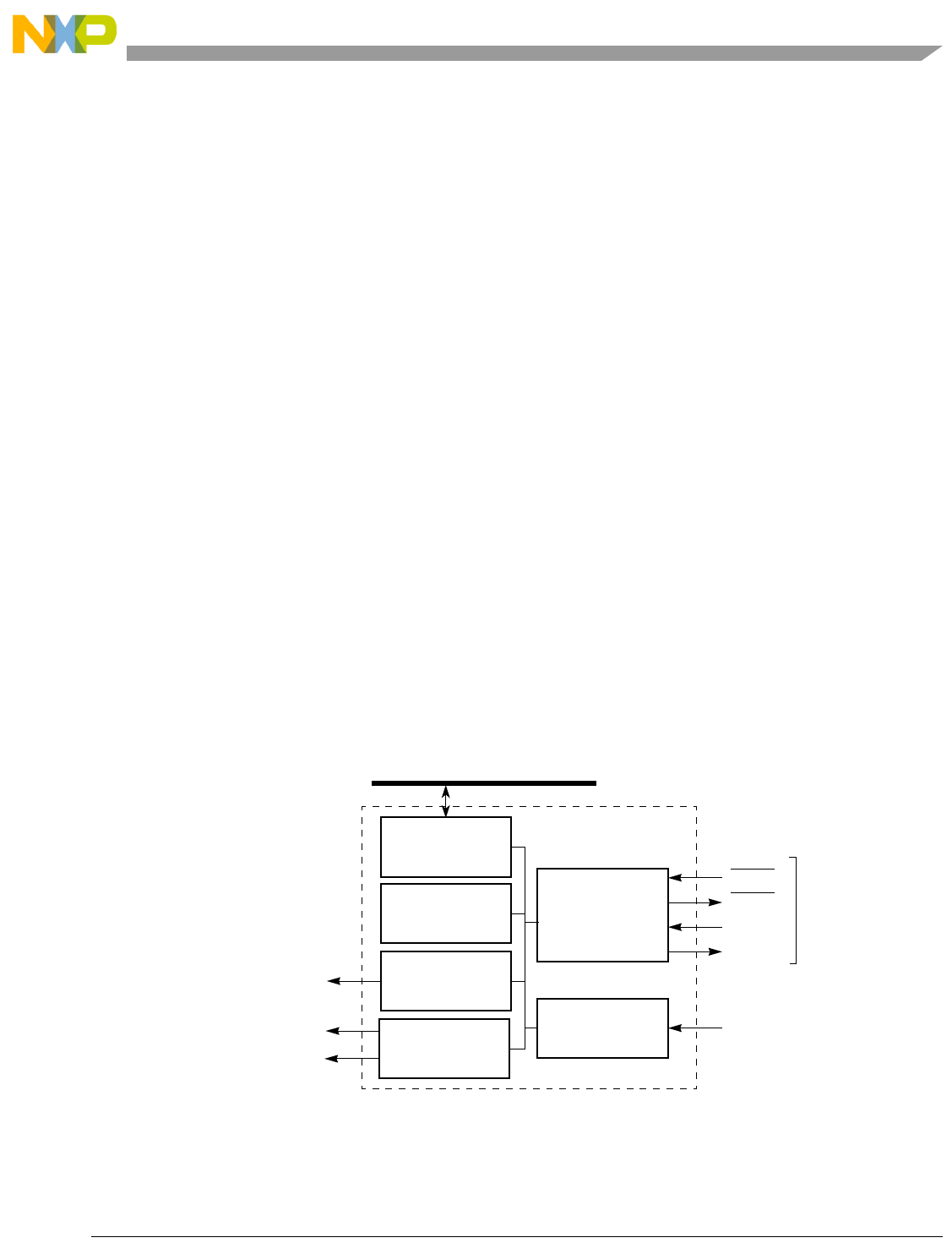
Freescale Semiconductor 24-1
Chapter 24
UART Modules
24.1 Introduction
This chapter describes the use of the three universal asynchronous receiver/transmitters (UARTs) and
includes programming examples.
NOTE
The designation n appears throughout this section to refer to registers or
signals associated with one of the three identical UART modules: UART0,
UART1, or UART2.
24.1.1 Overview
The internal bus clock can clock each of the three independent UARTs, eliminating the need for an external
UART clock. As Figure 24-1 shows, each UART module interfaces directly to the CPU and consists of:
• Serial communication channel
• Programmable clock generation
• Interrupt control logic and DMA request logic
• Internal channel control logic
Figure 24-1. UART Block Diagram
Serial
Interrupt Control
Logic
Internal Channel
Control Logic
Programmable
Clock
Communications
Channel
Generation
UART
Internal Bus Clock (fsys)
or External Clock (DTINn)
DMA Request
Logic
Transmit DMA Request
Receive DMA Request
Interrupt Request
(to Interrupt Controller)
(To DMA Controller)
External Signals
UART Registers
UCTSn
URTSn
URXDn
UTXDn
Internal Bus
MCF52211 ColdFire® Integrated Microcontroller Reference Manual, Rev. 3

UART Modules
24-2 Freescale Semiconductor
NOTE
The DTINn pin can clock UARTn. However, if the timers are operating and
the UART uses DTINn as a clock source, input capture mode is not available
for that timer.
The serial communication channel provides a full-duplex asynchronous/synchronous receiver and
transmitter deriving an operating frequency from the internal bus clock or an external clock using the timer
pin. The transmitter converts parallel data from the CPU to a serial bit stream, inserting appropriate start,
stop, and parity bits. It outputs the resulting stream on the transmitter serial data output (UTXDn). See
Section 24.4.2.1, “Transmitter.”
The receiver converts serial data from the receiver serial data input (URXDn) to parallel format, checks
for a start, stop, and parity bits, or break conditions, and transfers the assembled character onto the bus
during read operations. The receiver may be polled, interrupt driven, or use DMA requests for servicing.
See Section 24.4.2.2, “Receiver.”
NOTE
The GPIO module must be configured to enable the peripheral function of
the appropriate pins (refer to Chapter 13, “General Purpose I/O Module”)
prior to configuring the UART module.
24.1.2 Features
The device contains three independent UART modules with:
• Each clocked by external clock or internal bus clock (eliminates need for an external UART clock)
• Full-duplex asynchronous/synchronous receiver/transmitter
• Quadruple-buffered receiver
• Double-buffered transmitter
• Independently programmable receiver and transmitter clock sources
• Programmable data format:
— 5–8 data bits plus parity
— Odd, even, no parity, or force parity
— One, one-and-a-half, or two stop bits
• Each serial channel programmable to normal (full-duplex), automatic echo, local loopback, or
remote loopback mode
• Automatic wake-up mode for multidrop applications
• Four maskable interrupt conditions
• All three UARTs have DMA request capability
• Parity, framing, and overrun error detection
• False-start bit detection
• Line-break detection and generation
• Detection of breaks originating in the middle of a character
MCF52211 ColdFire® Integrated Microcontroller Reference Manual, Rev. 3

UART Modules
Freescale Semiconductor 24-3
• Start/end break interrupt/status
24.2 External Signal Description
Table 24-1 briefly describes the UART module signals.
Figure 24-2 shows a signal configuration for a UART/RS-232 interface.
Figure 24-2. UART/RS-232 Interface
24.3 Memory Map/Register Definition
This section contains a detailed description of each register and its specific function. Flowcharts in
Section 24.5, “Initialization/Application Information,” describe basic UART module programming.
Writing control bytes into the appropriate registers controls the operation of the UART module.
NOTE
UART registers are accessible only as bytes.
NOTE
Interrupt can mean an interrupt request asserted to the CPU or a DMA
request.
Table 24-1. UART Module External Signals
Signal Description
UTXDnTransmitter Serial Data Output. UTXDn is held high (mark condition) when the transmitter is
disabled, idle, or operating in the local loopback mode. Data is shifted out on UTXDn on the
falling edge of the clock source, with the least significant bit (lsb) sent first.
URXDnReceiver Serial Data Input. Data received on URXDn is sampled on the rising edge of the clock
source, with the lsb received first.
UCTSnClear-to- Send. This input can generate an interrupt on a change of state.
URTSnRequest-to-Send. This output can be programmed to be negated or asserted automatically by
the receiver or the transmitter. When connected to a transmitter’s UCTSn, URTSn can control
serial data flow.
DO2
DI1
DI2
DO1
RS-232 TransceiverUART
URXDn
UTXDn
UCTSn
URTSn
MCF52211 ColdFire® Integrated Microcontroller Reference Manual, Rev. 3

UART Modules
24-4 Freescale Semiconductor
Table 24-2. UART Module Memory Map
Register Width
(bit) Access Reset Value Section/PageUART0
UART1
UART2
0x00
0x0
0x0
UART Mode Registers1 (UMR1n), (UMR2n)
1UMR1n, UMR2n, and UCSRn must be changed only after the receiver/transmitter is issued a software reset command. If
operation is not disabled, undesirable results may occur.
8 R/W 0x00 24.3.1/24-5
24.3.2/24-6
0x04
0x4
0x4
UART Status Register (USRn)8R0x0024.3.3/24-8
UART Clock Select Register1(UCSRn) 8 W See Section 24.3.4/24-9
0x08
0x8
0x8
UART Command Registers (UCRn)8W0x0024.3.5/24-9
0x0C
0xC
0xC
UART Receive Buffers (URBn) 8 R 0xFF 24.3.6/24-11
UART Transmit Buffers (UTBn)8W0x0024.3.7/24-12
0x10
0x0
0x0
UART Input Port Change Register (UIPCRn) 8 R See Section 24.3.8/24-12
UART Auxiliary Control Register (UACRn)8W0x0024.3.9/24-13
0x14
0x4
0x4
UART Interrupt Status Register (UISRn)8R0x0024.3.10/24-13
UART Interrupt Mask Register (UIMRn)8W0x00
0x18
0x8
0x8
UART Baud Rate Generator Register (UBG1n)8W
2
2Reading this register results in undesired effects and possible incorrect transmission or reception of characters. Register
contents may also be changed.
0x00 24.3.11/24-15
0x1C
0xC
0xC
UART Baud Rate Generator Register (UBG2n)8W
20x00 24.3.11/24-15
0x34
0x4
0x4
UART Input Port Register (UIPn) 8 R 0xFF 24.3.12/24-15
0x38
0x8
0x8
UART Output Port Bit Set Command Register (UOP1n)8W
20x00 24.3.13/24-16
0x3C
0xC
0xC
UART Output Port Bit Reset Command Register (UOP0n)8W
20x00 24.3.13/24-16
MCF52211 ColdFire® Integrated Microcontroller Reference Manual, Rev. 3

UART Modules
Freescale Semiconductor 24-5
24.3.1 UART Mode Registers 1 (UMR1n)
The UMR1n registers control UART module configuration. UMR1n can be read or written when the mode
register pointer points to it, at RESET or after a RESET MODE REGISTER POINTER command using
UCRn[MISC]. After UMR1n is read or written, the pointer points to UMR2n.
IPSBAR
Offset:
0x00_0200 (UMR10)
0x00_0240 (UMR11)
0x00_0280 (UMR12)
Access: User read/write1
76543210
R
RXRTS RXIRQ/
FFULL ERR PM PT B/C
W
Reset:00000000
1After UMR1n is read or written, the pointer points to UMR2n
Figure 24-3. UART Mode Registers 1 (UMR1n)
Table 24-3. UMR1n Field Descriptions
Field Description
7
RXRTS
Receiver request-to-send. Allows the URTSn output to control the UCTSn input of the transmitting device to prevent
receiver overrun. If the receiver and transmitter are incorrectly programmed for URTSn control, URTSn control is
disabled for both. Transmitter RTS control is configured in UMR2n[TXRTS].
0 The receiver has no effect on URTSn.
1 When a valid start bit is received, URTSn is negated if the UART's FIFO is full. URTSn is reasserted when the
FIFO has an empty position available.
6
RXIRQ/
FFULL
Receiver interrupt select.
0 RXRDY is the source generating interrupt or DMA requests.
1 FFULL is the source generating interrupt or DMA requests.
5
ERR
Error mode. Configures the FIFO status bits, USRn[RB,FE,PE].
0 Character mode. The USRn values reflect the status of the character at the top of the FIFO. ERR must be 0 for
correct A/D flag information when in multidrop mode.
1 Block mode. The USRn values are the logical OR of the status for all characters reaching the top of the FIFO since
the last RESET ERROR STATUS command for the UART was issued. See Section 24.3.5, “UART Command
Registers (UCRn).”
4–3
PM
Parity mode. Selects the parity or multidrop mode for the UART. The parity bit is added to the transmitted character,
and the receiver performs a parity check on incoming data. The value of PM affects PT, as shown below.
MCF52211 ColdFire® Integrated Microcontroller Reference Manual, Rev. 3

UART Modules
24-6 Freescale Semiconductor
24.3.2 UART Mode Register 2 (UMR2n)
The UMR2n registers control UART module configuration. UMR2n can be read or written when the mode
register pointer points to it, which occurs after any access to UMR1n. UMR2n accesses do not update the
pointer.
2
PT
Parity type. PM and PT together select parity type (PM = 0x) or determine whether a data or address character is
transmitted (PM = 11).
1–0
B/C
Bits per character. Selects the number of data bits per character to be sent. The values shown do not include start,
parity, or stop bits.
00 5 bits
01 6 bits
10 7 bits
11 8 bits
IPSBAR
Offset:
0x00_0200 (UMR20)
0x00_0240 (UMR21)
0x00_0280 (UMR22)
Access: User read/write1
76543210
R
CM TXRTS TXCTS SB
W
Reset:00000000
1After UMR1n is read or written, the pointer points to UMR2n
Figure 24-4. UART Mode Registers 2 (UMR2n)
Table 24-3. UMR1n Field Descriptions (continued)
Field Description
PM Parity Mode Parity Type (PT= 0) Parity Type (PT= 1)
00 With parity Even parity Odd parity
01 Force parity Low parity High parity
10 No parity N/A
11 Multidrop mode Data character Address character
MCF52211 ColdFire® Integrated Microcontroller Reference Manual, Rev. 3

UART Modules
Freescale Semiconductor 24-7
Table 24-4. UMR2n Field Descriptions
Field Description
7–6
CM
Channel mode. Selects a channel mode. Section 24.4.3, “Looping Modes,” describes individual modes.
00 Normal
01 Automatic echo
10 Local loopback
11 Remote loopback
5
TXRTS
Transmitter ready-to-send. Controls negation of URTSn to automatically terminate a message transmission.
Attempting to program a receiver and transmitter in the same UART for URTSn control is not permitted and disables
URTSn control for both.
0 The transmitter has no effect on URTSn.
1 In applications where the transmitter is disabled after transmission completes, setting this bit automatically clears
UOP[RTS] one bit time after any characters in the transmitter shift and holding registers are completely sent,
including the programmed number of stop bits.
4
TXCTS
Transmitter clear-to-send. If TXCTS and TXRTS are set, TXCTS controls the operation of the transmitter.
0 UCTSn has no effect on the transmitter.
1 Enables clear-to-send operation. The transmitter checks the state of UCTSn each time it is ready to send a
character. If UCTSn is asserted, the character is sent; if it is deasserted, the signal UTXDn remains in the high
state and transmission is delayed until UCTSn is asserted. Changes in UCTSn as a character is being sent do
not affect its transmission.
3–0
SB
Stop-bit length control. Selects length of stop bit appended to the transmitted character. Stop-bit lengths of 9/16 to
2 bits are programmable for 6–8 bit characters. Lengths of 1-1/16 to 2 bits are programmable for 5-bit characters. In
all cases, the receiver checks only for a high condition at the center of the first stop-bit position, one bit time after the
last data bit or after the parity bit, if parity is enabled. If an external 1x clock is used for the transmitter, clearing bit 3
selects one stop bit and setting bit 3 selects two stop bits for transmission.
SB 5 Bits 6–8 Bits SB 5–8 Bits
0000 1.063 0.563 1000 1.563
0001 1.125 0.625 1001 1.625
0010 1.188 0.688 1010 1.688
0011 1.250 0.750 1011 1.750
0100 1.313 0.813 1100 1.813
0101 1.375 0.875 1101 1.875
0110 1.438 0.938 1110 1.938
0111 1.500 1.000 1111 2.000
MCF52211 ColdFire® Integrated Microcontroller Reference Manual, Rev. 3

UART Modules
24-8 Freescale Semiconductor
24.3.3 UART Status Registers (USRn)
The USRn registers show the status of the transmitter, the receiver, and the FIFO.
IPSBAR
Offset:
0x00_0204 (USR0)
0x00_0244 (USR1)
0x00_0284 (USR2)
Access: User read-only
76543210
RRB FE PE OE TXEMP TXRDY FFULL RXRDY
W
Reset:00000000
Figure 24-5. UART Status Registers (USRn)
Table 24-5. USRn Field Descriptions
Field Description
7
RB
Received break. The received break circuit detects breaks originating in the middle of a received character. However,
a break in the middle of a character must persist until the end of the next detected character time.
0 No break was received.
1 An all-zero character of the programmed length was received without a stop bit. Only a single FIFO position is
occupied when a break is received. Further entries to the FIFO are inhibited until URXDn returns to the high state
for at least one-half bit time, which equals two successive edges of the UARTclock. RB is valid only when RXRDY
is set.
6
FE
Framing error.
0 No framing error occurred.
1 No stop bit was detected when the corresponding data character in the FIFO was received. The stop-bit check
occurs in the middle of the first stop-bit position. FE is valid only when RXRDY is set.
5
PE
Parity error. Valid only if RXRDY is set.
0 No parity error occurred.
1 If UMR1n[PM] equals 0x (with parity or force parity), the corresponding character in the FIFO was received with
incorrect parity. If UMR1n[PM] equals 11 (multidrop), PE stores the received address or data (A/D) bit. PE is valid
only when RXRDY is set.
4
OE
Overrun error. Indicates whether an overrun occurs.
0 No overrun occurred.
1 One or more characters in the received data stream have been lost. OE is set upon receipt of a new character
when the FIFO is full and a character is already in the shift register waiting for an empty FIFO position. When this
occurs, the character in the receiver shift register and its break detect, framing error status, and parity error, if any,
are lost. The RESET ERROR STATUS command in UCRn clears OE.
3
TEMP
Transmitter empty.
0 The transmit buffer is not empty. A character is shifted out, or the transmitter is disabled. The transmitter is
enabled/disabled by programming UCRn[TC].
1 The transmitter has underrun (the transmitter holding register and transmitter shift registers are empty). This bit
is set after transmission of the last stop bit of a character if there are no characters in the transmitter holding
register awaiting transmission.
2
TXRDY
Transmitter ready.
0 The CPU loaded the transmitter holding register, or the transmitter is disabled.
1 The transmitter holding register is empty and ready for a character. TXRDY is set when a character is sent to the
transmitter shift register or when the transmitter is first enabled. If the transmitter is disabled, characters loaded
into the transmitter holding register are not sent.
MCF52211 ColdFire® Integrated Microcontroller Reference Manual, Rev. 3

UART Modules
Freescale Semiconductor 24-9
24.3.4 UART Clock Select Registers (UCSRn)
The UCSRs select an external clock on the DTIN input (divided by 1 or 16) or a prescaled internal bus
clock as the clocking source for the transmitter and receiver. See Section 24.4.1, “Transmitter/Receiver
Clock Source.” The transmitter and receiver can use different clock sources. To use the internal bus clock
for both, set UCSRn to 0xDD.
24.3.5 UART Command Registers (UCRn)
The UCRs supply commands to the UART. Only multiple commands that do not conflict can be specified
in a single write to a UCRn. For example, RESET TRANSMITTER and ENABLE TRANSMITTER cannot be
specified in one command.
1
FFULL
FIFO full.
0 The FIFO is not full but may hold up to two unread characters.
1 A character was received and the receiver FIFO is now full. Any characters received when the FIFO is full are lost.
0
RXRDY
Receiver ready.
0 The CPU has read the receive buffer and no characters remain in the FIFO after this read.
1 One or more characters were received and are waiting in the receive buffer FIFO.
IPSBAR
Offset:
0x00_0204 (UCSR0)
0x00_0244 (UCSR1)
0x00_0284 (UCSR2)
Access: User write-only
76543210
R
WRCS TCS
Reset: See Note See Note
Note: The RCS and TCS reset values are set so the receiver and transmitter use the prescaled internal bus
clock as their clock source.
Figure 24-6. UART Clock Select Registers (UCSRn)
Table 24-6. UCSRn Field Descriptions
Field Description
7–4
RCS
Receiver clock select. Selects the clock source for the receiver.
1101 Prescaled internal bus clock (fsys)
1110 DTINn divided by 16
1111 DTINn
3–0
TCS
Transmitter clock select. Selects the clock source for the transmitter.
1101 Prescaled internal bus clock (fsys)
1110 DTINn divided by 16
1111 DTINn
Table 24-5. USRn Field Descriptions (continued)
Field Description
MCF52211 ColdFire® Integrated Microcontroller Reference Manual, Rev. 3

UART Modules
24-10 Freescale Semiconductor
Table 24-7 describes UCRn fields and commands. Examples in Section 24.4.2, “Transmitter and Receiver
Operating Modes,” show how these commands are used.
IPSBAR
Offset:
0x00_0208 (UCR0)
0x00_0248 (UCR1)
0x00_0288 (UCR2)
Access: User write-only
76543210
R
W 0 MISC TC RC
Reset:00000000
Figure 24-7. UART Command Registers (UCRn)
Table 24-7. UCRn Field Descriptions
Field Description
7 Reserved, must be cleared.
6–4
MISC
MISC Field (this field selects a single command)
Command Description
000 NO COMMAND —
001 RESET MODE
REGISTER POINTER
Causes the mode register pointer to point to UMR1n.
010 RESET RECEIVER Immediately disables the receiver, clears USRn[FFULL,RXRDY], and reinitializes
the receiver FIFO pointer. No other registers are altered. Because it places the
receiver in a known state, use this command instead of RECEIVER DISABLE when
reconfiguring the receiver.
011 RESET
TRANSMITTER
Immediately disables the transmitter and clears USRn[TXEMP,TXRDY]. No other
registers are altered. Because it places the transmitter in a known state, use this
command instead of TRANSMITTER DISABLE when reconfiguring the transmitter.
100 RESET ERROR
STATUS
Clears USRn[RB,FE,PE,OE]. Also used in block mode to clear all error bits after
a data block is received.
101 RESET BREAK –
CHANGE INTERRUPT
Clears the delta break bit, UISRn[DB].
110 START BREAK Forces UTXDn low. If the transmitter is empty, break may be delayed up to one bit
time. If the transmitter is active, break starts when character transmission
completes. Break is delayed until any character in the transmitter shift register is
sent. Any character in the transmitter holding register is sent after the break.
Transmitter must be enabled for the command to be accepted. This command
ignores the state of UCTSn.
111 STOP BREAK Causes UTXDn to go high (mark) within two bit times. Any characters in the
transmit buffer are sent.
MCF52211 ColdFire® Integrated Microcontroller Reference Manual, Rev. 3

UART Modules
Freescale Semiconductor 24-11
24.3.6 UART Receive Buffers (URBn)
The receive buffers contain one serial shift register and three receiver holding registers, which act as a
FIFO. URXDn is connected to the serial shift register. The CPU reads from the top of the FIFO while the
receiver shifts and updates from the bottom when the shift register is full (see Figure 24-18). RB contains
the character in the receiver.
3–2
TC
Transmit command field. Selects a single transmit command.
1–0
RC
Receive command field. Selects a single receive command.
Table 24-7. UCRn Field Descriptions (continued)
Field Description
Command Description
00 NO ACTION TAKEN Causes the transmitter to stay in its current mode: if the transmitter is enabled, it
remains enabled; if the transmitter is disabled, it remains disabled.
01 TRANSMITTER
ENABLE
Enables operation of the UART’s transmitter. USRn[TXEMP,TXRDY] are set. If the
transmitter is already enabled, this command has no effect.
10 TRANSMITTER
DISABLE
Terminates transmitter operation and clears USRn[TXEMP,TXRDY]. If a character
is being sent when the transmitter is disabled, transmission completes before the
transmitter becomes inactive. If the transmitter is already disabled, the command
has no effect.
11 — Reserved, do not use.
Command Description
00 NO ACTION TAKEN Causes the receiver to stay in its current mode. If the receiver is enabled, it
remains enabled; if disabled, it remains disabled.
01 RECEIVER ENABLE If the UART module is not in multidrop mode (UMR1n[PM] 11), RECEIVER ENABLE
enables the UART's receiver and forces it into search-for-start-bit state. If the
receiver is already enabled, this command has no effect.
10 RECEIVER DISABLE Disables the receiver immediately. Any character being received is lost. The
command does not affect receiver status bits or other control registers. If the
UART module is programmed for local loopback or multidrop mode, the receiver
operates even though this command is selected. If the receiver is already
disabled, the command has no effect.
11 — Reserved, do not use.
MCF52211 ColdFire® Integrated Microcontroller Reference Manual, Rev. 3

UART Modules
24-12 Freescale Semiconductor
24.3.7 UART Transmit Buffers (UTBn)
The transmit buffers consist of the transmitter holding register and the transmitter shift register. The
holding register accepts characters from the bus master if UART’s USRn[TXRDY] is set. A write to the
transmit buffer clears USRn[TXRDY], inhibiting any more characters until the shift register can accept
more data. When the shift register is empty, it checks if the holding register has a valid character to be sent
(TXRDY = 0). If there is a valid character, the shift register loads it and sets USRn[TXRDY] again. Writes
to the transmit buffer when the UART’s TXRDY is cleared and the transmitter is disabled have no effect
on the transmit buffer.
Figure 24-9 shows UTBn. TB contains the character in the transmit buffer.
24.3.8 UART Input Port Change Registers (UIPCRn)
The UIPCRs hold the current state and the change-of-state for UCTSn.
IPSBAR
Offset:
0x00_020C (URB0)
0x00_024C (URB1)
0x00_028C (URB2)
Access: User read-only
76543210
RRB
W
Reset:11111111
Figure 24-8. UART Receive Buffer (URBn)
IPSBAR
Offset:
0x00_020C (UTB0)
0x00_024C (UTB1)
0x00_028C (UTB2)
Access: User write-only
76543210
R
WTB
Reset:00000000
Figure 24-9. UART Transmit Buffer (UTBn)
IPSBAR
Offset:
0x00_0210 (UIPCR0)
0x00_0250 (UIPCR1)
0x00_0290 (UIPCR2)
Access: User read-only
76543210
R 0 0 0 COS 1 1 1 CTS
W
Reset:0000111UCTSn
Figure 24-10. UART Input Port Changed Registers (UIPCRn)
MCF52211 ColdFire® Integrated Microcontroller Reference Manual, Rev. 3

UART Modules
Freescale Semiconductor 24-13
24.3.9 UART Auxiliary Control Register (UACRn)
The UACRs control the input enable.
24.3.10 UART Interrupt Status/Mask Registers (UISRn/UIMRn)
The UISRs provide status for all potential interrupt sources. UISRn contents are masked by UIMRn. If
corresponding UISRn and UIMRn bits are set, internal interrupt output is asserted. If a UIMRn bit is
cleared, state of the corresponding UISRn bit has no effect on the output.
The UISRn and UIMRn registers share the same space in memory. Reading this register provides the user
with interrupt status, while writing controls the mask bits.
Table 24-8. UIPCRn Field Descriptions
Field Description
7–5 Reserved
4
COS
Change of state (high-to-low or low-to-high transition).
0 No change-of-state since the CPU last read UIPCRn. Reading UIPCRn clears UISRn[COS].
1 A change-of-state longer than 25–50 s occurred on the UCTSn input. UACRn can be programmed to generate
an interrupt to the CPU when a change of state is detected.
3–1 Reserved
0
CTS
Current state of clear-to-send. Starting two serial clock periods after reset, CTS reflects the state of UCTSn. If
UCTSn is detected asserted at that time, COS is set, which initiates an interrupt if UACRn[IEC] is enabled.
0 The current state of the UCTSn input is asserted.
1 The current state of the UCTSn input is deasserted.
IPSBAR
Offset:
0x00_0210 (UACR0)
0x00_0250 (UACR1)
0x00_0290 (UACR2)
Access: User write-only
76543210
R
W0000000IEC
Reset:00000000
Figure 24-11. UART Auxiliary Control Registers (UACRn)
Table 24-9. UACRn Field Descriptions
Field Description
7–1 Reserved, must be cleared.
0
IEC
Input enable control.
0 Setting the corresponding UIPCRn bit has no effect on UISRn[COS].
1UISRn[COS] is set and an interrupt is generated when the UIPCRn[COS] is set by an external transition on the
UCTSn input (if UIMRn[COS] = 1).
MCF52211 ColdFire® Integrated Microcontroller Reference Manual, Rev. 3

UART Modules
24-14 Freescale Semiconductor
NOTE
True status is provided in the UISRn regardless of UIMRn settings. UISRn
is cleared when the UART module is reset.
IPSBAR
Offset:
0x00_0214 (UISR0)
0x00_0254 (UISR1)
0x00_0294 (UISR2)
Access: User read/write
76543210
R
(UISRn)COS 0 0 0 0 DB FFULL/
RXRDY TXRDY
W
(UIMRn)COS 0 0 0 0 DB FFULL/
RXRDY TXRDY
Reset:00000000
Figure 24-12. UART Interrupt Status/Mask Registers (UISRn/UIMRn)
Table 24-10. UISRn/UIMRn Field Descriptions
Field Description
7
COS
Change-of-state.
0UIPCRn[COS] is not selected.
1 Change-of-state occurred on UCTSn and was programmed in UACRn[IEC] to cause an interrupt.
6–3 Reserved, must be cleared.
2
DB
Delta break.
0 No new break-change condition to report. Section 24.3.5, “UART Command Registers (UCRn),” describes the
RESET BREAK-CHANGE INTERRUPT command.
1 The receiver detected the beginning or end of a received break.
1
FFULL/
RXRDY
Status of FIFO or receiver, depending on UMR1[FFULL/RXRDY] bit. Duplicate of USRn[FIFO] and USRn[RXRDY]
0
TXRDY
Transmitter ready. This bit is the duplication of USRn[TXRDY].
0 The transmitter holding register was loaded by the CPU or the transmitter is disabled. Characters loaded into the
transmitter holding register when TXRDY is cleared are not sent.
1 The transmitter holding register is empty and ready to be loaded with a character.
UIMRn
[FFULL/RXRDY]
UISRn
[FFULL/RXRDY]
UMR1n[FFULL/RXRDY]
0 (RXRDY) 1 (FIFO)
0 0 Receiver not ready FIFO not full
1 0 Receiver not ready FIFO not full
0 1 Receiver is ready,
Do not interrupt
FIFO is full,
Do not interrupt
1 1 Receiver is ready,
interrupt
FIFO is full,
interrupt
MCF52211 ColdFire® Integrated Microcontroller Reference Manual, Rev. 3

UART Modules
Freescale Semiconductor 24-15
24.3.11 UART Baud Rate Generator Registers (UBG1n/UBG2n)
The UBG1n registers hold the MSB, and the UBG2n registers hold the LSB of the preload value. UBG1n
and UBG2n concatenate to provide a divider to the internal bus clock for transmitter/receiver operation,
as described in Section 24.4.1.2.1, “Internal Bus Clock Baud Rates.”
NOTE
The minimum value loaded on the concatenation of UBG1n with UBG2n is
0x0002. The UBG2n reset value of 0x00 is invalid and must be written to
before the UART transmitter or receiver are enabled. UBG1n and UBG2n
are write-only and cannot be read by the CPU.
24.3.12 UART Input Port Register (UIPn)
The UIPn registers show the current state of the UCTSn input.
IPSBAR
Offset:
0x00_0218 (UBG10)
0x00_0258 (UBG11)
0x00_0298 (UBG12)
Access: User write-only
76543210
R
WDivider MSB
Reset:00000000
Figure 24-13. UART Baud Rate Generator Registers (UBG1n)
IPSBAR
Offset:
0x00_021C (UBG20)
0x00_025C (UBG21)
0x00_029C (UBG22)
Access: User write-only
76543210
R
WDivider LSB
Reset:00000000
Figure 24-14. UART Baud Rate Generator Registers (UBG2n)
IPSBAR
Offset:
0x00_0234 (UIP0)
0x00_0274 (UIP1)
0x00_02B4 (UIP2)
Access: User read-only
76543210
R1111111CTS
W
Reset:11111111
Figure 24-15. UART Input Port Registers (UIPn)
MCF52211 ColdFire® Integrated Microcontroller Reference Manual, Rev. 3

UART Modules
24-16 Freescale Semiconductor
24.3.13 UART Output Port Command Registers (UOP1n/UOP0n)
The URTSn output can be asserted by writing a 1 to UOP1n[RTS] and negated by writing a 1 to
UOP0n[RTS].
24.4 Functional Description
This section describes operation of the clock source generator, transmitter, and receiver.
24.4.1 Transmitter/Receiver Clock Source
The internal bus clock serves as the basic timing reference for the clock source generator logic, which
consists of a clock generator and a programmable 16-bit divider dedicated to each UART. The 16-bit
divider is used to produce standard UART baud rates.
Table 24-11. UIPn Field Descriptions
Field Description
7–1 Reserved
0
CTS
Current state of clear-to-send. The UCTSn value is latched and reflects the state of the input pin when UIPn is read.
Note: This bit has the same function and value as UIPCRn[CTS].
0 The current state of the UCTSn input is logic 0.
1 The current state of the UCTSn input is logic 1.
IPSBAR
Offset:
0x00_0238 (UOP10)
0x00_023C (UOP00)
0x00_0278 (UOP11)
0x00_027C (UOP01)
0x00_02B8 (UOP12)
0x00_02BC (UOP02)
Access: User write-only
76543210
R
W0000000RTS
Reset:00000000
Figure 24-16. UART Output Port Command Registers (UOP1n/UOP0n)
Table 24-12. UOP1n/UOP0n Field Descriptions
Field Description
7–1 Reserved, must be cleared.
0
RTS
Output port output. Controls assertion (UOP1)/negation (UOP0) of URTSn output.
0 Not affected.
1 Asserts URTSn in UOP1. Negates URTSn in UOP0.
MCF52211 ColdFire® Integrated Microcontroller Reference Manual, Rev. 3
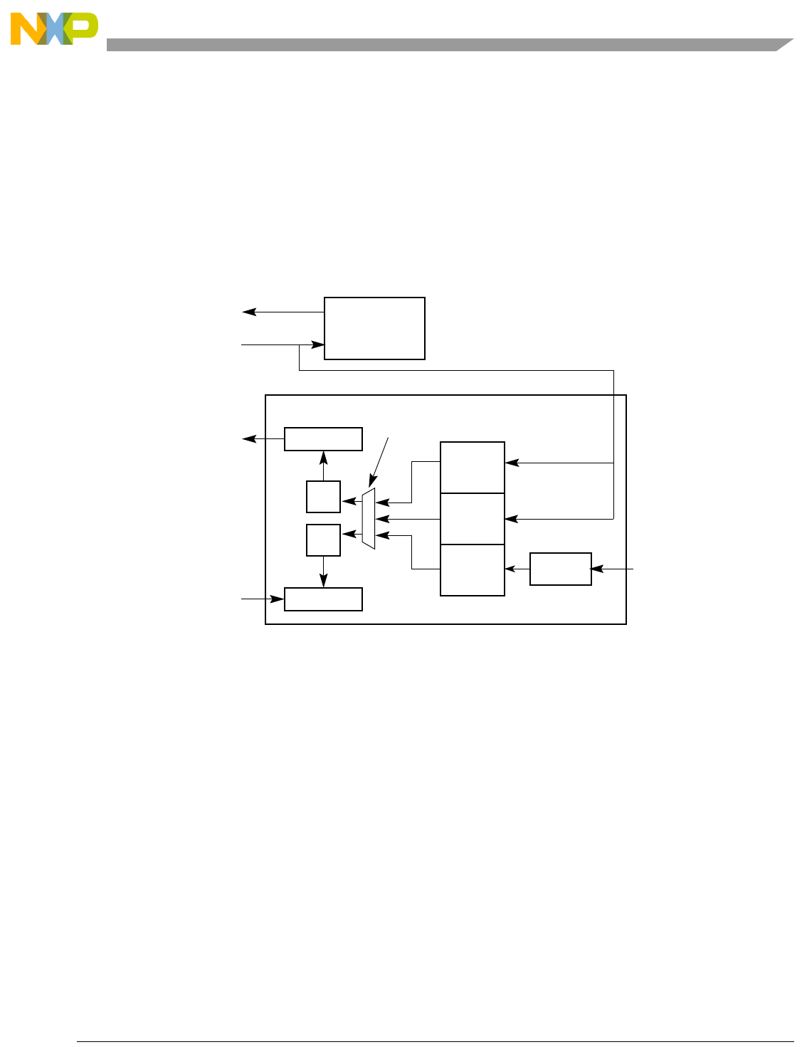
UART Modules
Freescale Semiconductor 24-17
24.4.1.1 Programmable Divider
As Figure 24-17 shows, the UARTn transmitter and receiver can use the following clock sources:
• An external clock signal on the DTINn pin. When not divided, DTINn provides a synchronous
clock; when divided by 16, it is asynchronous.
• The internal bus clock supplies an asynchronous clock source divided by 32 and then divided by
the 16-bit value programmed in UBG1n and UBG2n. See Section 24.3.11, “UART Baud Rate
Generator Registers (UBG1n/UBG2n).”
The choice of DTIN or internal bus clock is programmed in the UCSR.
Figure 24-17. Clocking Source Diagram
NOTE
If DTINn is a clocking source for the timer or UART, that timer module
cannot use DTINn for timer input capture.
24.4.1.2 Calculating Baud Rates
The following sections describe how to calculate baud rates.
24.4.1.2.1 Internal Bus Clock Baud Rates
When the internal bus clock is the UART clocking source, it goes through a divide-by-32 prescaler and
then passes through the 16-bit divider of the concatenated UBG1n and UBG2n registers. The baud-rate
calculation is:
Eqn. 24-1
UART
On-Chip
TIN
1
16
16-bit
Divider 32
TIN
Clocking sources programmed in UCSR
Timer Module
Internal
Tx
Rx
Rx Buffer
Tx Buffer
fsys
Bus Clock
URXDn
UTXDn
DTINn
DTOUTn
Baudrate fsys
32 x Divider
------------------------------------=
MCF52211 ColdFire® Integrated Microcontroller Reference Manual, Rev. 3
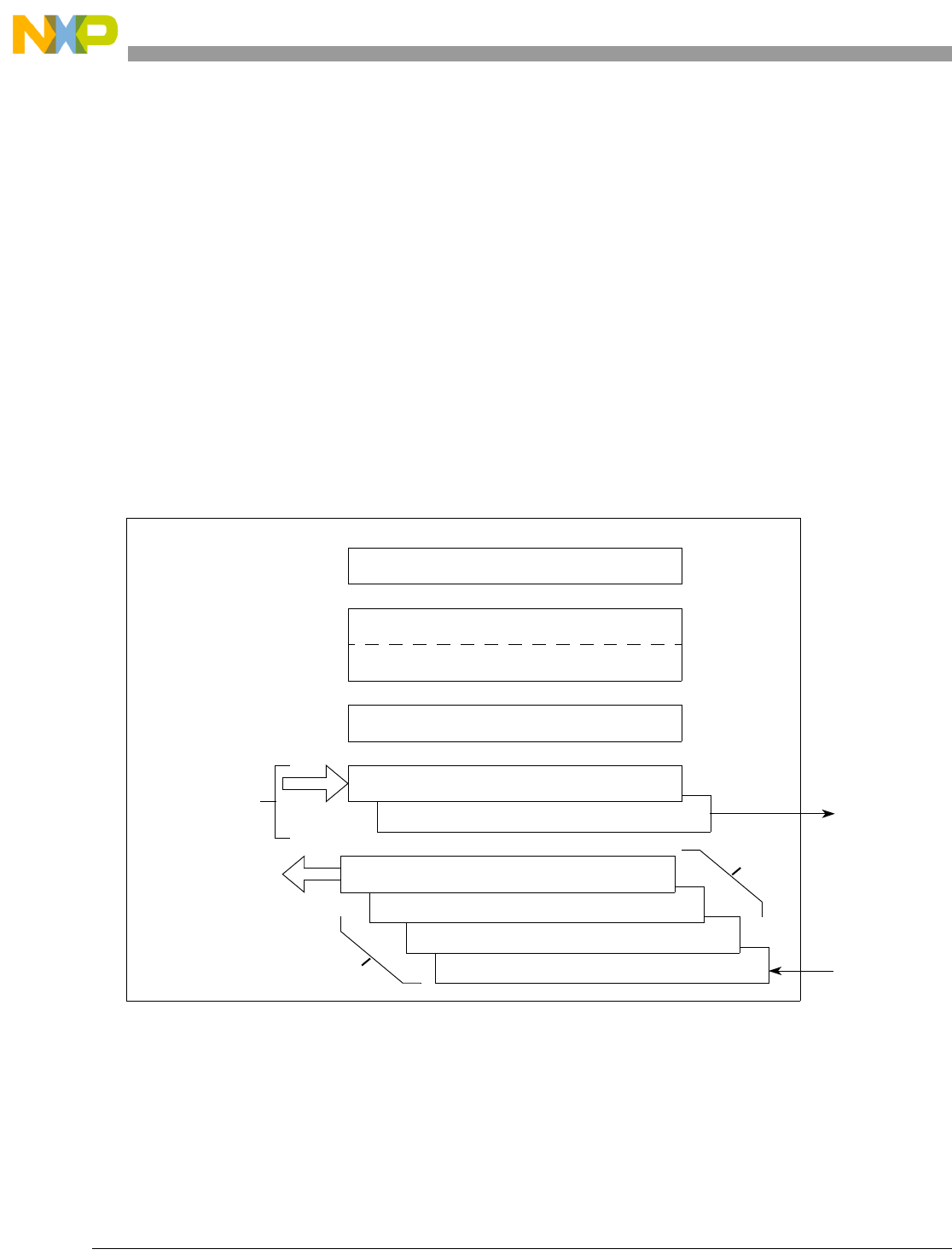
UART Modules
24-18 Freescale Semiconductor
Using a 66-MHz internal bus clock and letting baud rate equal 9600, then
Eqn. 24-2
Therefore, UBG1n equals 0x00 and UBG2n equals 0xD6.
24.4.1.2.2 External Clock
An external source clock (DTINn) passes through a divide-by-1 or 16 prescaler. If fextc is the external clock
frequency, baud rate can be described with this equation:
Eqn. 24-3
24.4.2 Transmitter and Receiver Operating Modes
Figure 24-18 is a functional block diagram of the transmitter and receiver showing the command and
operating registers, which are described generally in the following sections. For detailed descriptions, refer
to Section 24.3, “Memory Map/Register Definition.”
Figure 24-18. Transmitter and Receiver Functional Diagram
24.4.2.1 Transmitter
The transmitter is enabled through the UART command register (UCRn). When it is ready to accept a
character, UART sets USRn[TXRDY]. The transmitter converts parallel data from the CPU to a serial bit
stream on UTXDn. It automatically sends a start bit followed by the programmed number of data bits, an
Divider 66MHz
32 x 9600
-------------------------------215 decimal0x00D6 hexadecimal== =
Baudrate fextc
(16 or 1)
---------------------
=
Receiver Shift Register
UART Command Register (UCRn)W
UART Status Register (USRn)R
Transmitter Shift Register
UART Mode Register 1 (UMR1n)R/W
UART Mode Register 2 (UMR2n)R/W
Transmitter Holding Register W
Receiver Holding Register 3
Receiver Holding Register 2
Receiver Holding Register 1 R
UART Receive
UART
Buffer (URBn)
(4 Registers)
UARTn
External
Interface
Transmit Buffer
(UTBn)
(2 Registers)
FIFO
URXDn
UTXDn
MCF52211 ColdFire® Integrated Microcontroller Reference Manual, Rev. 3

UART Modules
Freescale Semiconductor 24-19
optional parity bit, and the programmed number of stop bits. The lsb is sent first. Data is shifted from the
transmitter output on the falling edge of the clock source.
After the stop bits are sent, if no new character is in the transmitter holding register, the UTXDn output
remains high (mark condition) and the transmitter empty bit (USRn[TXEMP]) is set. Transmission
resumes and TXEMP is cleared when the CPU loads a new character into the UART transmit buffer
(UTBn). If the transmitter receives a disable command, it continues until any character in the transmitter
shift register is completely sent.
If the transmitter is reset through a software command, operation stops immediately (see Section 24.3.5,
“UART Command Registers (UCRn)”). The transmitter is reenabled through the UCRn to resume
operation after a disable or software reset.
If the clear-to-send operation is enabled, UCTSn must be asserted for the character to be transmitted. If
UCTSn is negated in the middle of a transmission, the character in the shift register is sent and UTXDn
remains in mark state until UCTSn is reasserted. If transmitter is forced to send a continuous low condition
by issuing a SEND BREAK command, transmitter ignores the state of UCTSn.
If the transmitter is programmed to automatically negate URTSn when a message transmission completes,
URTSn must be asserted manually before a message is sent. In applications in which the transmitter is
disabled after transmission is complete and URTSn is appropriately programmed, URTSn is negated one
bit time after the character in the shift register is completely transmitted. The transmitter must be manually
reenabled by reasserting URTSn before the next message is sent.
Figure 24-19 shows the functional timing information for the transmitter.
MCF52211 ColdFire® Integrated Microcontroller Reference Manual, Rev. 3
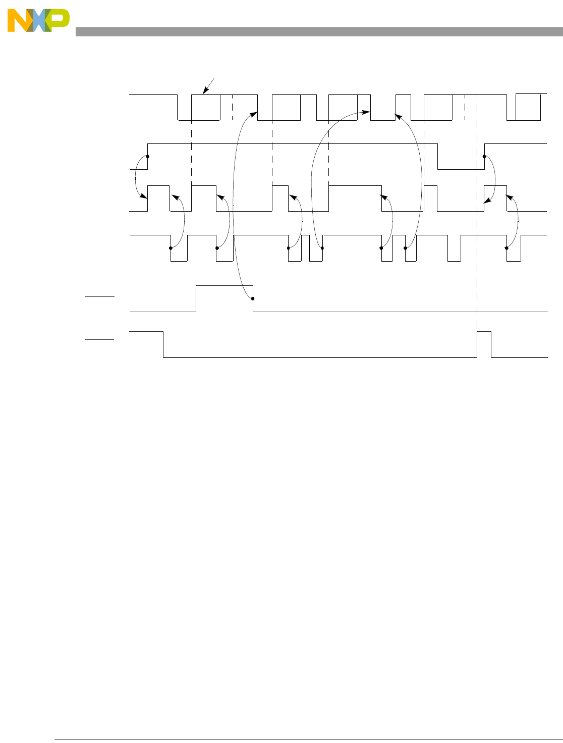
UART Modules
24-20 Freescale Semiconductor
Figure 24-19. Transmitter Timing Diagram
24.4.2.2 Receiver
The receiver is enabled through its UCRn, as described in Section 24.3.5, “UART Command Registers
(UCRn).”
When the receiver detects a high-to-low (mark-to-space) transition of the start bit on URXDn, the state of
URXDn is sampled eight times on the edge of the bit time clock starting one-half clock after the transition
(asynchronous operation) or at the next rising edge of the bit time clock (synchronous operation). If
URXDn is sampled high, start bit is invalid and the search for the valid start bit begins again.
If URXDn remains low, a valid start bit is assumed. The receiver continues sampling the input at one-bit
time intervals at the theoretical center of the bit until the proper number of data bits and parity, if any, is
assembled and one stop bit is detected. Data on the URXDn input is sampled on the rising edge of the
programmed clock source. The lsb is received first. The data then transfers to a receiver holding register
and USRn[RXRDY] is set. If the character is less than 8 bits, the most significant unused bits in the
receiver holding register are cleared.
After the stop bit is detected, receiver immediately looks for the next start bit. However, if a non-zero
character is received without a stop bit (framing error) and URXDn remains low for one-half of the bit
period after the stop bit is sampled, receiver operates as if a new start bit were detected. Parity error,
C1
1
C2 C3 Break C4 C6
Transmitter
Enabled
USRn[TXRDY]
W
2
WWWWWWW
Manually asserted
by
BIT
-
SET
command
Manually
asserted
Start
break
C5
not
transmitted
C6C4 Stop
break
C3C2C1
1
C1 in transmission
3
UMR2n[TXCTS] = 1
1
Cn = transmit characters
2
W = write
4
UMR2n
[TXRTS] = 1
internal
module
select
UTXDn
UCTSn3
URTSn4
MCF52211 ColdFire® Integrated Microcontroller Reference Manual, Rev. 3
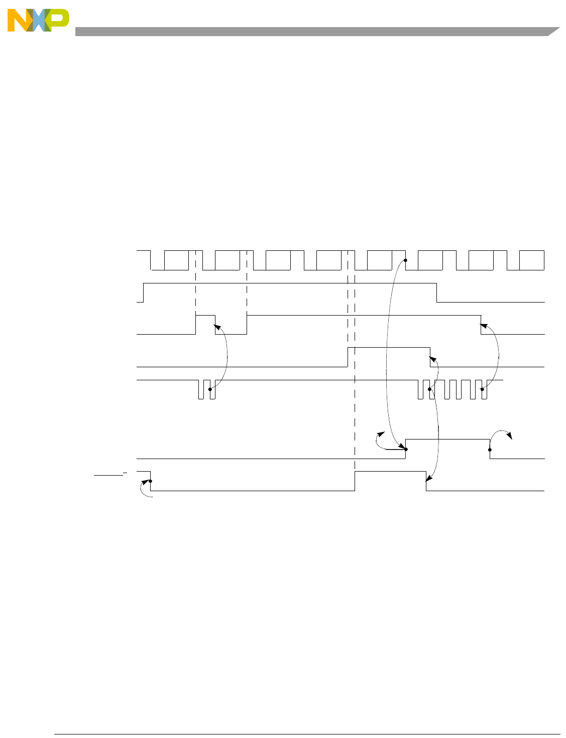
UART Modules
Freescale Semiconductor 24-21
framing error, overrun error, and received break conditions set the respective PE, FE, OE, and RB error
and break flags in the USRn at the received character boundary. They are valid only if USRn[RXRDY] is
set.
If a break condition is detected (URXDn is low for the entire character including the stop bit), a character
of all 0s loads into the receiver holding register and USRn[RB,RXRDY] are set. URXDn must return to a
high condition for at least one-half bit time before a search for the next start bit begins.
The receiver detects the beginning of a break in the middle of a character if the break persists through the
next character time. The receiver places the damaged character in the Rx FIFO and sets the corresponding
USRn error bits and USRn[RXRDY]. Then, if the break lasts until the next character time, the receiver
places an all-zero character into the Rx FIFO and sets USRn[RB,RXRDY].
Figure 24-20 shows receiver functional timing.
Figure 24-20. Receiver Timing Diagram
24.4.2.3 FIFO
The FIFO is used in the UART’s receive buffer logic. The FIFO consists of three receiver holding registers.
The receive buffer consists of the FIFO and a receiver shift register connected to the URXDn (see
Figure 24-18). Data is assembled in the receiver shift register and loaded into the top empty receiver
holding register position of the FIFO. Therefore, data flowing from the receiver to the CPU is
quadruple-buffered.
In addition to the data byte, three status bits—parity error (PE), framing error (FE), and received break
(RB)—are appended to each data character in the FIFO; overrun error (OE) is not appended. By
C1 C2 C4 C6 C7 C8
C3 C5
C6, C7, and C8 is lost
(C2)
Status
Data
(C3)
Status
Data
(C4)
Status
Data
C5 is
lost
Reset by
command
Receiver
Enabled
USRn
[RXRDY]
Overrun
Internal
module
select
USRn
[FFULL]
(C1)
Status
Data
USRn
[OE]
Automatically asserted
when ready to receive
Manually asserted first time,
automatically negated if overrun occurs
UOP0[RTS] = 1
1
UMR2n
[RXRTS] = 1
URXDn
URTSn1
MCF52211 ColdFire® Integrated Microcontroller Reference Manual, Rev. 3

UART Modules
24-22 Freescale Semiconductor
programming the ERR bit in the UART’s mode register (UMR1n), status is provided in character or block
modes.
USRn[RXRDY] is set when at least one character is available to be read by the CPU. A read of the receive
buffer produces an output of data from the top of the FIFO. After the read cycle, the data at the top of the
FIFO and its associated status bits are popped and the receiver shift register can add new data at the bottom
of the FIFO. The FIFO-full status bit (FFULL) is set if all three positions are filled with data. The RXRDY
or FFULL bit can be selected to cause an interrupt and TXRDY or RXRDY can be used to generate a DMA
request.
The two error modes are selected by UMR1n[ERR]:
• In character mode (UMR1n[ERR] = 0), status is given in the USRn for the character at the top of
the FIFO.
• In block mode, the USRn shows a logical OR of all characters reaching the top of the FIFO since
the last RESET ERROR STATUS command. Status is updated as characters reach the top of the
FIFO. Block mode offers a data-reception speed advantage where the software overhead of
error-checking each character cannot be tolerated. However, errors are not detected until the check
is performed at the end of an entire message—the faulting character is not identified.
In either mode, reading the USRn does not affect the FIFO. The FIFO is popped only when the receive
buffer is read. The USRn should be read before reading the receive buffer. If all three receiver holding
registers are full, a new character is held in the receiver shift register until space is available. However, if
a second new character is received, the contents of the character in the receiver shift register is lost, the
FIFOs are unaffected, and USRn[OE] is set when the receiver detects the start bit of the new overrunning
character.
To support flow control, the receiver can be programmed to automatically negate and assert URTSn, in
which case the receiver automatically negates URTSn when a valid start bit is detected and the FIFO is
full. The receiver asserts URTSn when a FIFO position becomes available; therefore, connecting URTSn
to the UCTSn input of the transmitting device can prevent overrun errors.
NOTE
The receiver continues reading characters in the FIFO if the receiver is
disabled. If the receiver is reset, the FIFO, URTSn control, all receiver status
bits, interrupts, and DMA requests are reset. No more characters are
received until the receiver is reenabled.
24.4.3 Looping Modes
The UART can be configured to operate in various looping modes. These modes are useful for local and
remote system diagnostic functions. The modes are described in the following paragraphs and in
Section 24.3, “Memory Map/Register Definition.”
The UART’s transmitter and receiver should be disabled when switching between modes. The selected
mode is activated immediately upon mode selection, regardless of whether a character is being received
or transmitted.
MCF52211 ColdFire® Integrated Microcontroller Reference Manual, Rev. 3
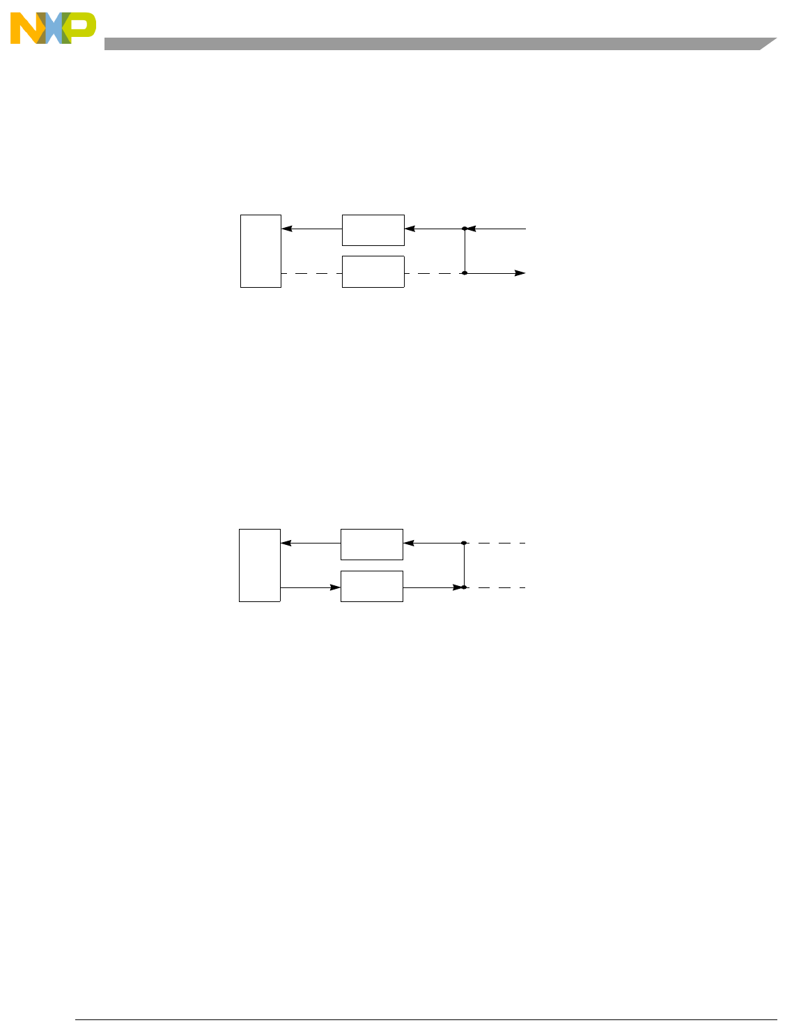
UART Modules
Freescale Semiconductor 24-23
24.4.3.1 Automatic Echo Mode
In automatic echo mode, shown in Figure 24-21, the UART automatically resends received data bit by bit.
The local CPU-to-receiver communication continues normally, but the CPU-to-transmitter link is
disabled. In this mode, received data is clocked on the receiver clock and re-sent on UTXDn. The receiver
must be enabled, but the transmitter need not be.
Figure 24-21. Automatic Echo
Because the transmitter is inactive, USRn[TXEMP,TXRDY] is inactive and data is sent as it is received.
Received parity is checked but not recalculated for transmission. Character framing is also checked, but
stop bits are sent as they are received. A received break is echoed as received until the next valid start bit
is detected.
24.4.3.2 Local Loopback Mode
Figure 24-22 shows how UTXDn and URXDn are internally connected in local loopback mode. This
mode is for testing the operation of a UART by sending data to the transmitter and checking data
assembled by the receiver to ensure proper operations.
Figure 24-22. Local Loopback
Features of this local loopback mode are:
• Transmitter and CPU-to-receiver communications continue normally in this mode.
•URXDn input data is ignored.
•UTXDn is held marking.
• The receiver is clocked by the transmitter clock. The transmitter must be enabled, but the receiver
need not be.
24.4.3.3 Remote Loopback Mode
In remote loopback mode, shown in Figure 24-23, the UART automatically transmits received data bit by
bit on the UTXDn output. The local CPU-to-transmitter link is disabled. This mode is useful in testing
receiver and transmitter operation of a remote UART. For this mode, transmitter uses the receiver clock.
Because the receiver is not active, received data cannot be read by the CPU and all status conditions are
inactive. Received parity is not checked and is not recalculated for transmission. Stop bits are sent as they
are received. A received break is echoed as received until next valid start bit is detected.
Disabled Disabled
Tx
Rx
CPU
URXDn InputURXDn Input
UTXDn Output
CPU
Disabled
Disabled
Tx
Rx URXDn Input
UTXDn Output
MCF52211 ColdFire® Integrated Microcontroller Reference Manual, Rev. 3

UART Modules
24-24 Freescale Semiconductor
Figure 24-23. Remote Loopback
24.4.4 Multidrop Mode
Setting UMR1n[PM] programs the UART to operate in a wake-up mode for multidrop or multiprocessor
applications. In this mode, a master can transmit an address character followed by a block of data
characters targeted for one of up to 256 slave stations.
Although slave stations have their receivers disabled, they continuously monitor the master’s data stream.
When the master sends an address character, the slave receiver notifies its respective CPU by setting
USRn[RXRDY] and generating an interrupt (if programmed to do so). Each slave station CPU then
compares the received address to its station address and enables its receiver if it wishes to receive the
subsequent data characters or block of data from the master station. Unaddressed slave stations continue
monitoring the data stream. Data fields in the data stream are separated by an address character. After a
slave receives a block of data, its CPU disables the receiver and repeats the process. Functional timing
information for multidrop mode is shown in Figure 24-24.
CPU
Disabled
Disabled
Tx
Rx
Disabled
Disabled
UTXDn Output
URXDn Input
MCF52211 ColdFire® Integrated Microcontroller Reference Manual, Rev. 3
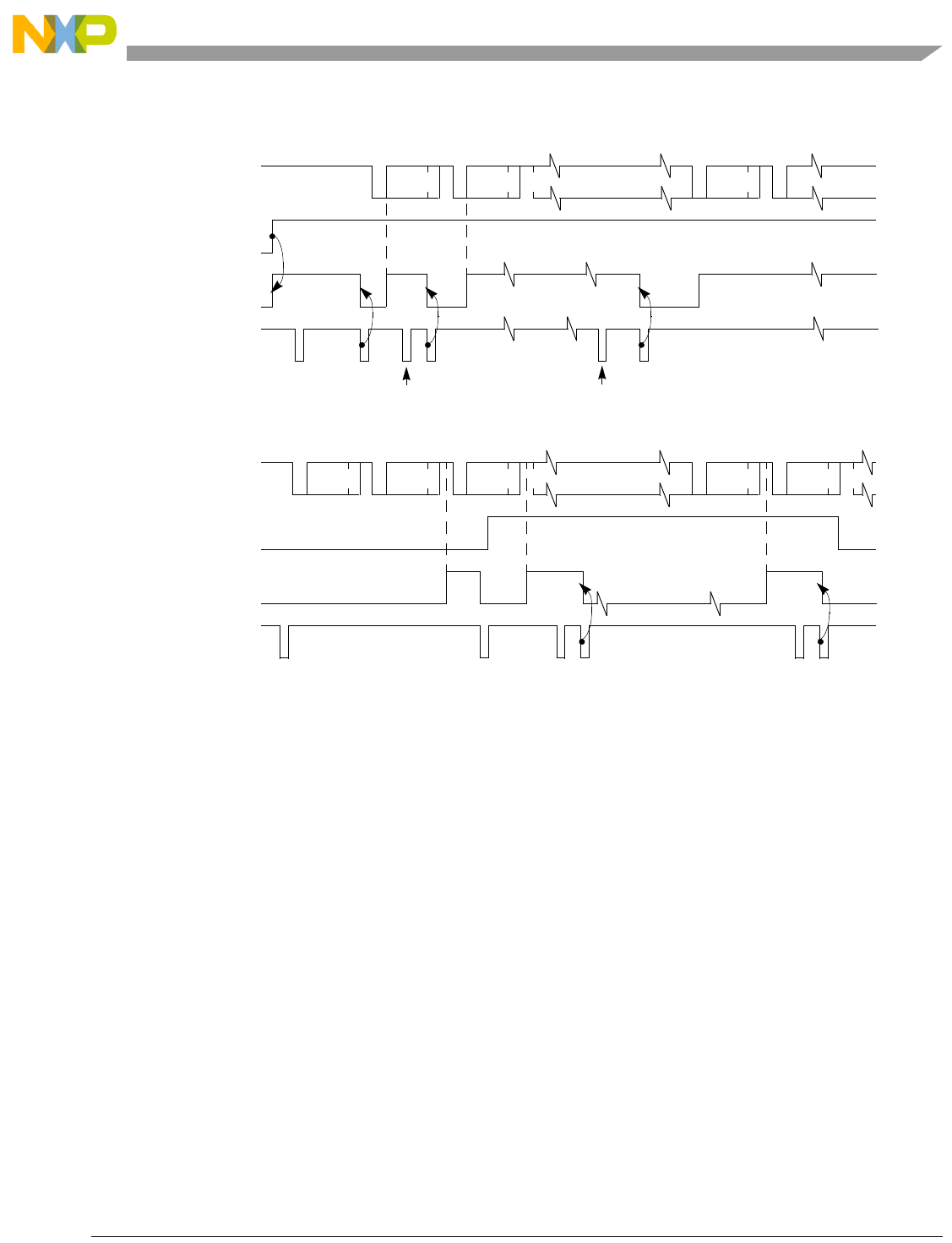
UART Modules
Freescale Semiconductor 24-25
Figure 24-24. Multidrop Mode Timing Diagram
A character sent from the master station consists of a start bit, a programmed number of data bits, an
address/data (A/D) bit flag, and a programmed number of stop bits. A/D equals 1 indicates an address
character; A/D equals 0 indicates a data character. The polarity of A/D is selected through UMR1n[PT].
UMR1n should be programmed before enabling the transmitter and loading the corresponding data bits
into the transmit buffer.
In multidrop mode, the receiver continuously monitors the received data stream, regardless of whether it
is enabled or disabled. If the receiver is disabled, it sets the RXRDY bit and loads the character into the
receiver holding register FIFO provided the received A/D bit is a 1 (address tag). The character is
discarded if the received A/D bit is 0 (data tag). If the receiver is enabled, all received characters are
transferred to the CPU through the receiver holding register during read operations.
In either case, data bits load into the data portion of the FIFO while the A/D bit loads into the status portion
of the FIFO normally used for a parity error (USRn[PE]).
Framing error, overrun error, and break detection operate normally. The A/D bit takes the place of the
parity bit; therefore, parity is neither calculated nor checked. Messages in this mode may continues
containing error detection and correction information. If 8-bit characters are not required, one way to
provide error detection is to use software to calculate parity and append it to the 5-, 6-, or 7-bit character.
ADD1
Transmitter
Enabled
USRn
[TXRDY]
C0 ADD211
internal
module
select
A/D A/D A/D
ADD1
Receiver
Enabled
USRn
[RXRDY]
C0 ADD211
internal
module
select
A/D A/D A/D
0
A/D
0
A/D
(C0)
Status Data
(ADD 2)
Status DataADD 1
Peripheral Station
Master Station
UMR1n[PM] = 11
UMR1n[PM] = 11
UMR1n[PT] = 1
ADD 1
UMR1n[PT] = 0
C0
UMR1n[PT] = 1
ADD 2
UTXDn
URXDn
MCF52211 ColdFire® Integrated Microcontroller Reference Manual, Rev. 3

UART Modules
24-26 Freescale Semiconductor
24.4.5 Bus Operation
This section describes bus operation during read, write, and interrupt acknowledge cycles to the UART
module.
24.4.5.1 Read Cycles
The UART module responds to reads with byte data. Reserved registers return zeros.
24.4.5.2 Write Cycles
The UART module accepts write data as bytes only. Write cycles to read-only or reserved registers
complete normally without an error termination, but data is ignored.
24.5 Initialization/Application Information
The software flowchart, Figure 24-25, consists of:
• UART module initialization—These routines consist of SINIT and CHCHK (See Sheet 1 p. 24-30
and Sheet 2 p. 24-31). Before SINIT is called at system initialization, the calling routine allocates
2 words on the system FIFO. On return to the calling routine, SINIT passes UART status data on
the FIFO. If SINIT finds no errors, the transmitter and receiver are enabled. SINIT calls CHCHK
to perform the checks. When called, SINIT places the UART in local loopback mode and checks
for the following errors:
— Transmitter never ready
— Receiver never ready
— Parity error
— Incorrect character received
• I/O driver routine—This routine (See Sheet 4 p. 24-33 and Sheet 5 p. 24-34) consists of INCH, the
terminal input character routine which gets a character from the receiver, and OUTCH, which
sends a character to the transmitter.
• Interrupt handling—This consists of SIRQ (See Sheet 4 p. 24-33), which is executed after the
UART module generates an interrupt caused by a change-in-break (beginning of a break). SIRQ
then clears the interrupt source, waits for the next change-in-break interrupt (end of break), clears
the interrupt source again, then returns from exception processing to the system monitor.
24.5.1 Interrupt and DMA Request Initialization
24.5.1.1 Setting up the UART to Generate Core Interrupts
The list below provides steps to properly initialize the UART to generate an interrupt request to the
processor’s interrupt controller. See Section 14.3.8.1, “Interrupt Sources,” for details on interrupt
assignments for the UART modules.
1. Initialize the appropriate ICRx register in the interrupt controller.
2. Unmask appropriate bits in IMR in the interrupt controller.
MCF52211 ColdFire® Integrated Microcontroller Reference Manual, Rev. 3

UART Modules
Freescale Semiconductor 24-27
3. Unmask appropriate bits in the core’s status register (SR) to enable interrupts.
4. If TXRDY or RXRDY generates interrupt requests, verify that DMAREQC (in the SCM) does not
also assign the UART’s TXRDY and RXRDY into DMA channels.
5. Initialize interrupts in the UART, see Table 24-13.
24.5.1.2 Setting up the UART to Request DMA Service
The UART is capable of generating two internal DMA request signals: transmit and receive.
The transmit DMA request signal is asserted when the TXRDY (transmitter ready) in the UART interrupt
status register (UISRn[TXRDY]) is set. When the transmit DMA request signal is asserted, the DMA can
initiate a data copy, reading the next character transmitted from memory and writing it into the UART
transmit buffer (UTBn). This allows the DMA channel to stream data from memory to the UART for
transmission without processor intervention. After the entire message has been moved into the UART, the
DMA would typically generate an end-of-data-transfer interrupt request to the CPU. The resulting
interrupt service routine (ISR) could query the UART programming model to determine the
end-of-transmission status.
Similarly, the receive DMA request signal is asserted when the FIFO full or receive ready
(FFULL/RXRDY) flag in the interrupt status register (UISRn[FFULL/RXRDY]) is set. When the receive
DMA request signal is asserted, the DMA can initiate a data move, reading the appropriate characters from
the UART receive buffer (URBn) and storing them in memory. This allows the DMA channel to stream
data from the UART receive buffer into memory without processor intervention. After the entire message
has been moved from the UART, the DMA would typically generate an end-of-data-transfer interrupt
request to the CPU. The resulting interrupt service routine (ISR) should query the UART programming
model to determine the end-of-transmission status. In typical applications, the receive DMA request
should be configured to use RXRDY directly (and not FFULL) to remove any complications related to
retrieving the final characters from the FIFO buffer.
The implementation described in this section allows independent DMA processing of transmit and receive
data while continuing to support interrupt notification to the processor for CTS change-of-state and delta
break error managing.
Table 24-13. UART Interrupts
Register Bit Interrupt
UMR1n6RxIRQ
UIMRn7 Change of State (COS)
UIMRn2 Delta Break
UIMRn1 RxFIFO Full
UIMRn0TXRDY
MCF52211 ColdFire® Integrated Microcontroller Reference Manual, Rev. 3

UART Modules
24-28 Freescale Semiconductor
To configure the UART for DMA requests:
1. Initialize the DMAREQC in the SCM to map the desired UART DMA requests to the desired DMA
channels. For example, setting DMAREQC[7:4] to 1000 maps UART0 receive DMA requests to
DMA channel 1, setting DMAREQC[11:8] to 1101 maps UART1 transmit DMA requests to DMA
channel 2, and so on. It is possible to independently map transmit-based and receive-based UART
DMA requests in the DMAREQC.
2. Disable interrupts using the UIMR register. The appropriate UIMR bits must be cleared so that
interrupt requests are disabled for those conditions for which a DMA request is desired. For
example, to generate transmit DMA requests from UART1, UIMR1[TXRDY] should be cleared.
This prevents TXRDY from generating an interrupt request while a transmit DMA request is
generated.
3. Enable DMA access to the UARTn registers by setting the corresponding PACR register in the
SCM for read/write in supervisor and user modes.
4. Enable DMA access to SRAM by setting the SPV bit in the core RAMBAR, and the BDE bit in
the SCM RAMBAR
5. Initialize the DMA channel. The DMA should be configured for cycle steal mode and a source and
destination size of one byte. This causes a single byte to be transferred for each UART DMA
request. Set the disable request bit (DCRn[D_REQ] to disable external requests when the BCR
reaches zero.
6. For a transmit process:
— Set the DMA SAR register to the address of the source data
—Set DCRn[SINC] to increment the source pointer
— Set DAR to the address if the UART transmit buffer (UTB)
—Clear DCRn[DINC]
— Set BCR to the number of bytes to transmit.
7. For a receive process:
— Set the DMA SAR register to the address of the UART receive buffer (URB)
—Clear DCRn[SINC]
— Set DAR to the address of the source data
—Set DCRn[DINC] to increment the destination pointer
— Set BCR to the number of bytes to transmit.
8. Start the data transfer by setting DCRn[EEXT], which enables the UART channel to issue DMA
requests.
Table 24-14 shows the DMA requests.
Table 24-14. UART DMA Requests
Register Bit DMA Request
UISRn1 Receive DMA request
UISRn0 Transmit DMA request
MCF52211 ColdFire® Integrated Microcontroller Reference Manual, Rev. 3

UART Modules
Freescale Semiconductor 24-29
24.5.2 UART Module Initialization Sequence
The following shows the UART module initialization sequence.
1. UCRn:
a) Reset the receiver and transmitter.
b) Reset the mode pointer (MISC[2–0] = 0b001).
2. UIMRn: Enable the desired interrupt sources.
3. UACRn: Initialize the input enable control (IEC bit).
4. UCSRn: Select the receiver and transmitter clock. Use timer as source if required.
5. UMR1n:
a) If preferred, program operation of receiver ready-to-send (RXRTS bit).
a) Select receiver-ready or FIFO-full notification (RXRDY/FFULL bit).
b) Select character or block error mode (ERR bit).
c) Select parity mode and type (PM and PT bits).
d) Select number of bits per character (B/Cx bits).
6. UMR2n:
a) Select the mode of operation (CM bits).
b) If preferred, program operation of transmitter ready-to-send (TXRTS).
c) If preferred, program operation of clear-to-send (TXCTS bit).
d) Select stop-bit length (SB bits).
7. UCRn: Enable transmitter and/or receiver.
MCF52211 ColdFire® Integrated Microcontroller Reference Manual, Rev. 3
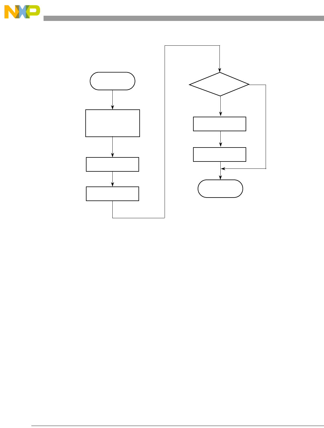
UART Modules
24-30 Freescale Semiconductor
Figure 24-25. UART Mode Programming Flowchart (Sheet 1 of 5)
Serial Module
SINIT
Initiate:
Channel
Interrupts
CHK1
Call CHCHK
Save Channel
Status
Enable
Any
Errors?
Y
N
Enable Receiver
Assert
Request To Send
SINITR
Return
MCF52211 ColdFire® Integrated Microcontroller Reference Manual, Rev. 3
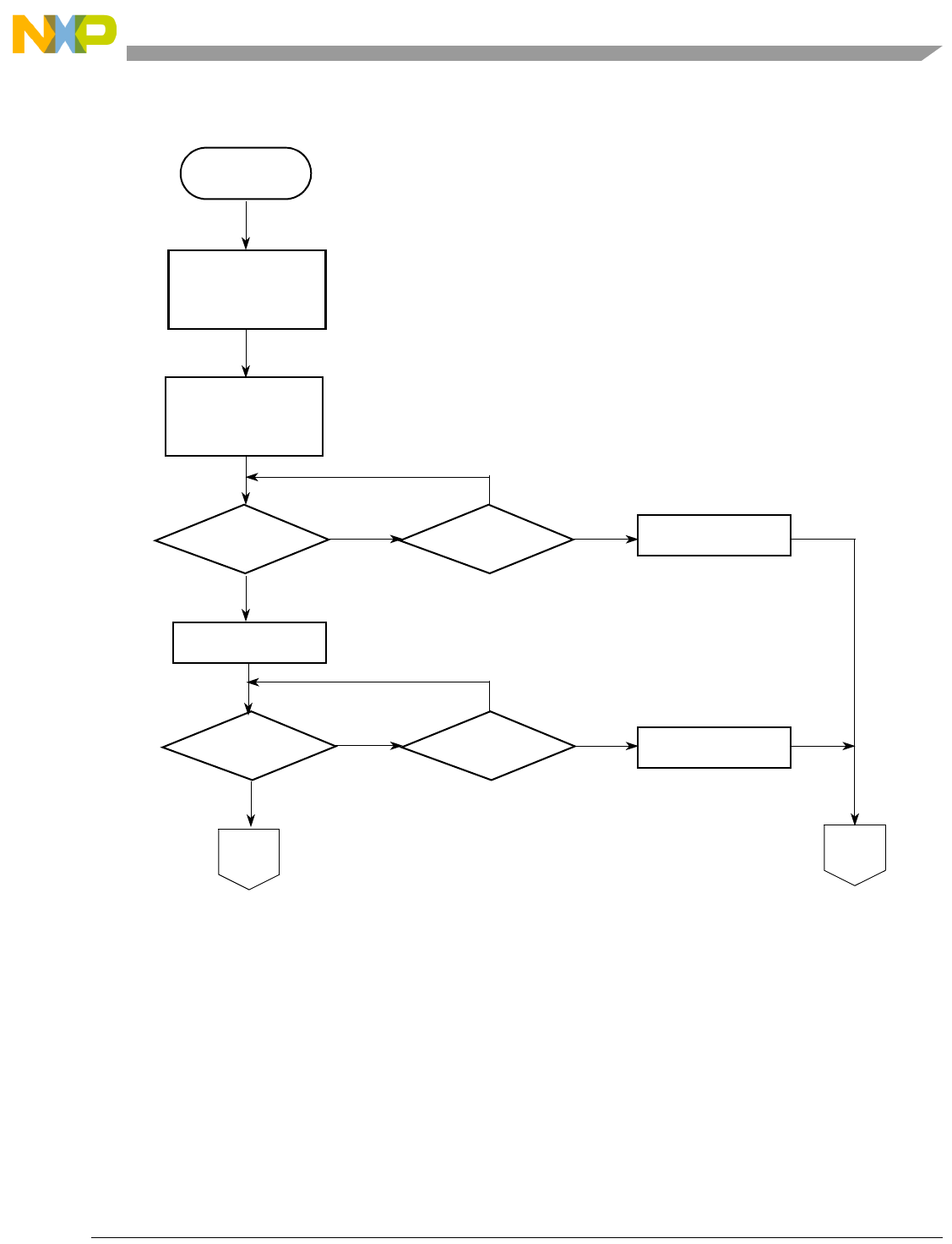
UART Modules
Freescale Semiconductor 24-31
Figure 24-25. UART Mode Programming Flowchart (Sheet 2 of 5)
CHCHK
CHCHK
Place Channel In
Local Loopback
Mode
Enable
Transmitter Clear
Status Word
TxCHK
Is
Transmitter
Ready?
Y
N
SNDCHR
RxCHK
Send Character
To Transmitter
Has
Character Been
Received?
N
Y
A
Waited
Too Long?
N
N
Waited
Too Long?
Y
Y
Set Transmitter-
Never-ready Flag
Set Receiver-
Never-ready Flag
B
MCF52211 ColdFire® Integrated Microcontroller Reference Manual, Rev. 3
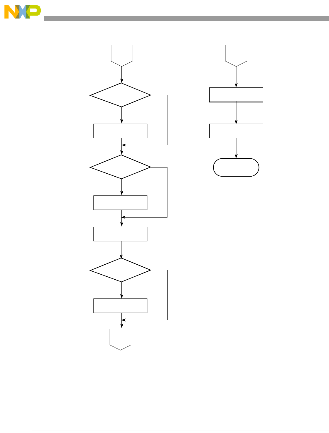
UART Modules
24-32 Freescale Semiconductor
Figure 24-25. UART Mode Programming Flowchart (Sheet 3 of 5)
AB
B
FRCHK
Have
Framing Error?
Set Framing
Error Flag
PRCHK
Have
Parity Error?
Set Parity
Error Flag
Get Character
From Receiver
Same As
Transmitted
Character?
Set Incorrect
Character Flag
N
N
Y
CHRCHK
Y
N
Disable
Transmitter
RSTCHN
Restore
To Original Mode
Return
Y
MCF52211 ColdFire® Integrated Microcontroller Reference Manual, Rev. 3
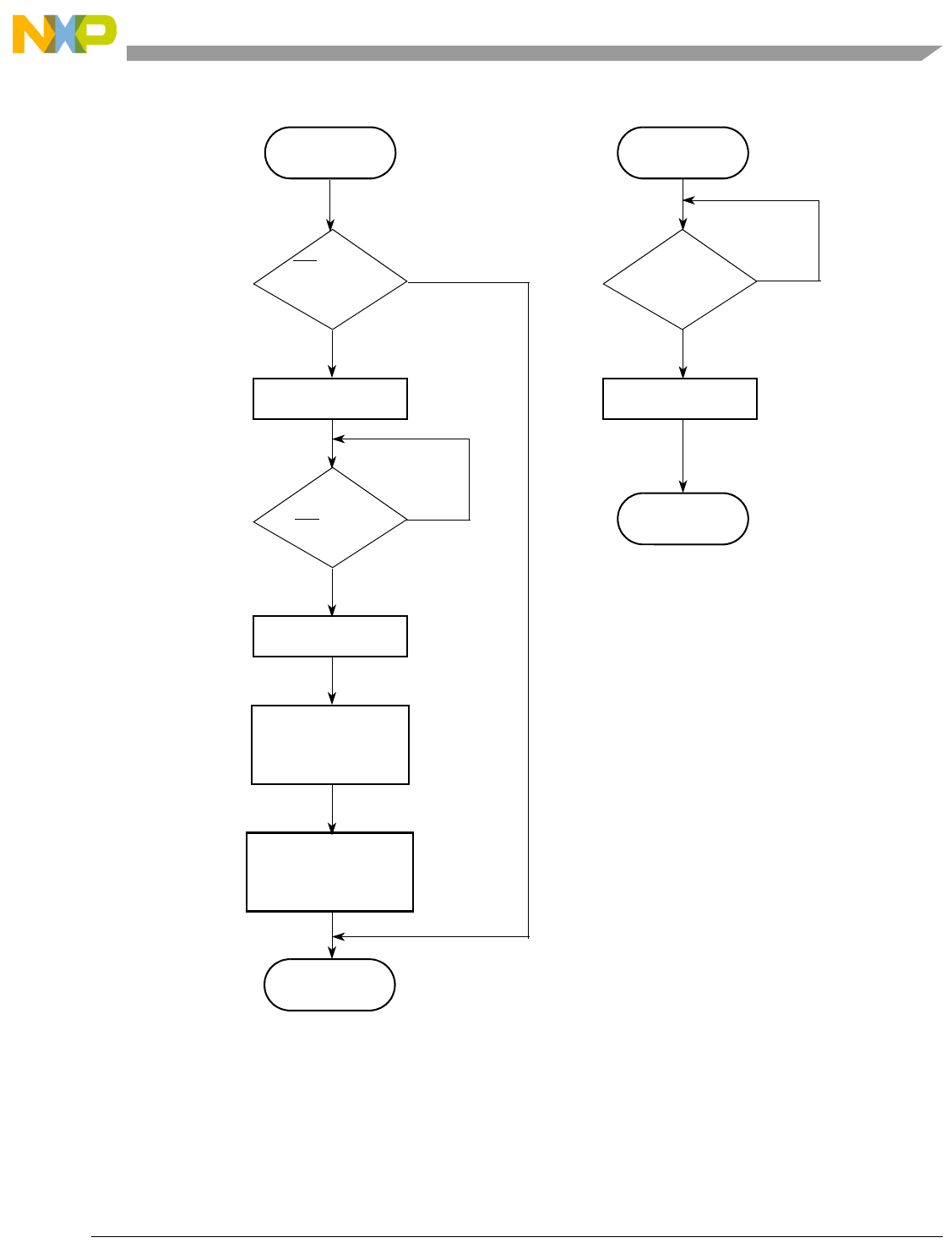
UART Modules
Freescale Semiconductor 24-33
Figure 24-25. UART Mode Programming Flowchart (Sheet 4 of 5)
Was
IRQ Caused
By Beginning
Of A Break?
SIRQ
ABRKI
N
Clear Change-in-
Break Status Bit
ABRKI1
N
Has
End-of-break
IRQ Arrived
Ye t ?
Y
Y
Clear Change-in-
Break Status Bit
Remove Break
Character From
Receiver FIFO
Replace Return
Address On System
Stack And Monitor
Warm Start Address
SIRQR
RTE
N
Y
Does
Channel A
Receiver Have A
Character?
INCH
Place Character
In D0
Return
MCF52211 ColdFire® Integrated Microcontroller Reference Manual, Rev. 3
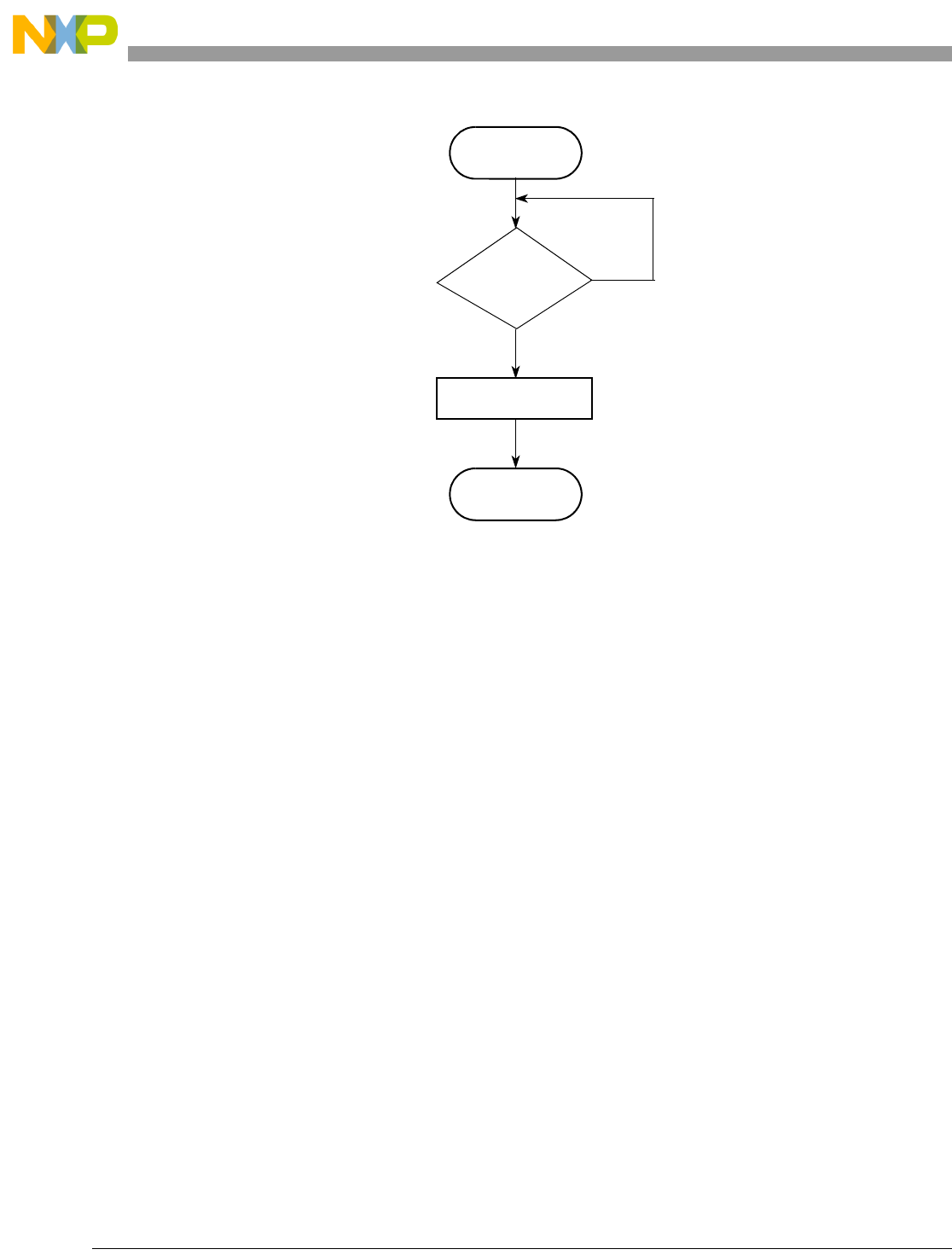
UART Modules
24-34 Freescale Semiconductor
Figure 24-25. UART Mode Programming Flowchart (Sheet 5 of 5)
OUTCH
Is
Transmitter
Ready?
N
Y
Send Character
To Transmitter
Return
MCF52211 ColdFire® Integrated Microcontroller Reference Manual, Rev. 3

Freescale Semiconductor 25-1
Chapter 25
I2C Interface
25.1 Introduction
This chapter describes the I2C module, clock synchronization, and I2C programming model registers. It
also provides extensive programming examples.
NOTE
This device contains two I2C modules, I2C0 and I2C1. The designation ‘n’,
with n= 0 or 1, is used throughout this chapter to refer to registers and
signals associated with the two identical I2C modules.
MCF52211 ColdFire® Integrated Microcontroller Reference Manual, Rev. 3
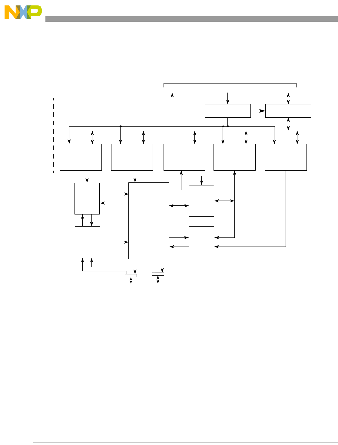
I2C Interface
25-2 Freescale Semiconductor
25.1.1 Block Diagram
Figure 25-1 is a I2C module block diagram, illustrating the interaction of the registers described in
Section 25.2, “Memory Map/Register Definition”.
Figure 25-1. I2C Module Block Diagram
25.1.2 Overview
I2C is a two-wire, bidirectional serial bus that provides a simple, efficient method of data exchange,
minimizing the interconnection between devices. This bus is suitable for applications that require
occasional communication between many devices over a short distance. The flexible I2C bus allows
additional devices to connect to the bus for expansion and system development.
The interface operates up to 100 Kbps with maximum bus loading and timing. The device is capable of
operating at higher baud rates, up to a maximum of the internal bus clock divided by 20, with reduced bus
loading. The maximum communication length and the number of devices connected are limited by a
maximum bus capacitance of 400 pF.
The I2C system is a true multiple-master bus; it uses arbitration and collision detection to prevent data
corruption in the event that multiple devices attempt to control the bus simultaneously. This supports
Address
Compare
In/Out
Data
Shift
Start, Stop,
Input
Sync
Clock
Control
Registers and Slave Interface
Address Decode
I2C Address
Data MUX
AddressIRQ Data
and
Arbitration
Control
Register
Internal Bus
Register
I2C Frequency
Divider Register
I2C Data
I/O Register
I2C Status
Register
I2C Control
Register
I2Cn_SCL I2Cn_SDA
(I2FDRn)(I2CRn)(I2SRn)(I2DRn)(I2ADRn)
MCF52211 ColdFire® Integrated Microcontroller Reference Manual, Rev. 3

I2C Interface
Freescale Semiconductor 25-3
complex applications with multiprocessor control and can be used for rapid testing and alignment of end
products through external connections to an assembly-line computer.
NOTE
The I2C module is compatible with the Philips I2C bus protocol. For
information on system configuration, protocol, and restrictions, see The I2C
Bus Specification, Version 2.1.
NOTE
The GPIO module must be configured to enable the peripheral function of
the appropriate pins (refer to Chapter 13, “General Purpose I/O Module”)
prior to configuring the I2C module.
25.1.3 Features
The I2C module has these key features:
• Compatibility with I2C bus standard version 2.1
• Multiple-master operation
• Software-programmable for one of 50 different serial clock frequencies
• Software-selectable acknowledge bit
• Interrupt-driven, byte-by-byte data transfer
• Arbitration-lost interrupt with automatic mode switching from master to slave
• Calling address identification interrupt
• START and STOP signal generation/detection
• Repeated START signal generation
• Acknowledge bit generation/detection
• Bus-busy detection
25.2 Memory Map/Register Definition
The below table lists the configuration registers used in the I2C interfaces.
Table 25-1. I2C Module Memory Map
IPSBAR
Offset
Register Access Reset Value Section/Page
I2C0
I2C1
0x00_0300
0x00_0380
I2C Address Register (I2ADRn)R/W0x0025.2.1/25-4
0x00_0304
0x00_0384
I2C Frequency Divider Register (I2FDRn)R/W0x0025.2.2/25-4
0x00_0308
0x00_0388
I2C Control Register (I2CRn)R/W0x0025.2.3/25-5
MCF52211 ColdFire® Integrated Microcontroller Reference Manual, Rev. 3

I2C Interface
25-4 Freescale Semiconductor
25.2.1 I2C Address Register (I2ADRn)
I2ADRn holds the address the I2C responds to when addressed as a slave. It is not the address sent on the
bus during the address transfer when the module is performing a master transfer.
25.2.2 I2C Frequency Divider Register (I2FDRn)
The I2FDRn, shown in Figure 25-3, provides a programmable prescaler to configure the I2C clock for
bit-rate selection.
0x00_030C
0x00_038C
I2C Status Register (I2SRn)R/W0x8125.2.4/25-6
0x00_0310
0x00_0390
I2C Data I/O Register (I2DRn)R/W0x0025.2.5/25-7
IPSBAR
Offset:
0x00_0300 (I2ADR0)
0x00_0380 (I2ADR1)
Access: User read/write
76543210
R
ADR
0
W
Reset:00000000
Figure 25-2. I2C Address Register (I2ADRn)
Table 25-2. I2ADRn Field Descriptions
Field Description
7–1
ADR
Slave address. Contains the specific slave address to be used by the I2C module. Slave mode is the default I2C mode
for an address match on the bus.
0 Reserved, must be cleared.
IPSBAR
Offset:
0x00_0304 (I2FDR0)
0x00_0384 (I2FDR1)
Access: User read/write
76543210
R 0 0
IC
W
Reset:00000000
Figure 25-3. I2C Frequency Divider Register (I2FDRn)
Table 25-1. I2C Module Memory Map (continued)
IPSBAR
Offset
Register Access Reset Value Section/Page
I2C0
I2C1
MCF52211 ColdFire® Integrated Microcontroller Reference Manual, Rev. 3

I2C Interface
Freescale Semiconductor 25-5
25.2.3 I2C Control Register (I2CRn)
I2CRn enables the I2C module and the I2C interrupt. It also contains bits that govern operation as a slave
or a master.
Table 25-3. I2FDRn Field Descriptions
Field Description
7–6 Reserved, must be cleared.
5–0
IC
I2C clock rate. Prescales the clock for bit-rate selection. The serial bit clock frequency is equal to the internal bus
clock divided by the divider shown below. Due to potentially slow I2Cn_SCL and I2Cn_SDA rise and fall times, bus
signals are sampled at the prescaler frequency.
IPSBAR
Offset:
0x00_0308 (I2CR0)
0x00_0388 (I2CR1)
Access: User read/write
76543210
R
IEN IIEN MSTA MTX TXAK RSTA
0 0
W
Reset:00000000
Figure 25-4. I2C Control Register (I2CRn)
IC Divider IC Divider IC Divider IC Divider
0x00 28 0x10 288 0x20 20 0x30 160
0x01 30 0x11 320 0x21 22 0x31 192
0x02 34 0x12 384 0x22 24 0x32 224
0x03 40 0x13 480 0x23 26 0x33 256
0x04 44 0x14 576 0x24 28 0x34 320
0x05 48 0x15 640 0x25 32 0x35 384
0x06 56 0x16 768 0x26 36 0x36 448
0x07 68 0x17 960 0x27 40 0x37 512
0x08 80 0x18 1152 0x28 48 0x38 640
0x09 88 0x19 1280 0x29 56 0x39 768
0x0A 104 0x1A 1536 0x2A 64 0x3A 896
0x0B 128 0x1B 1920 0x2B 72 0x3B 1024
0x0C 144 0x1C 2304 0x2C 80 0x3C 1280
0x0D 160 0x1D 2560 0x2D 96 0x3D 1536
0x0E 192 0x1E 3072 0x2E 112 0x3E 1792
0x0F 240 0x1F 3840 0x2F 128 0x3F 2048
MCF52211 ColdFire® Integrated Microcontroller Reference Manual, Rev. 3

I2C Interface
25-6 Freescale Semiconductor
25.2.4 I2C Status Register (I2SRn)
I2SRn contains bits that indicate transaction direction and status.
Table 25-4. I2CRn Field Descriptions
Field Description
7
IEN
I2C enable. Controls the software reset of the entire I2C module. If the module is enabled in the middle of a byte
transfer, slave mode ignores the current bus transfer and starts operating when the next START condition is detected.
Master mode is not aware that the bus is busy; initiating a start cycle may corrupt the current bus cycle, ultimately
causing the current master or the I2C module to lose arbitration, after which bus operation returns to normal.
0The I
2C module is disabled, but registers can be accessed.
1The I
2C module is enabled. This bit must be set before any other I2CRn bits have any effect.
6
IIEN
I2C interrupt enable.
0I
2C module interrupts are disabled, but currently pending interrupt condition is not cleared.
1I
2C module interrupts are enabled. An I2C interrupt occurs if I2SRn[IIF] is also set.
5
MSTA
Master/slave mode select bit. If the master loses arbitration, MSTA is cleared without generating a STOP signal.
0 Slave mode. Changing MSTA from 1 to 0 generates a STOP and selects slave mode.
1 Master mode. Changing MSTA from 0 to 1 signals a START on the bus and selects master mode.
4
MTX
Transmit/receive mode select bit. Selects the direction of master and slave transfers.
0 Receive
1 Transmit. When the device is addressed as a slave, software must set MTX according to I2SRn[SRW]. In master
mode, MTX must be set according to the type of transfer required. Therefore, when the MCU addresses a slave
device, MTX is always 1.
3
TXAK
Transmit acknowledge enable. Specifies the value driven onto I2Cn_SDA during acknowledge cycles for master and
slave receivers. Writing TXAK applies only when the I2C bus is a receiver.
0 An acknowledge signal is sent to the bus at the ninth clock bit after receiving one byte of data.
1 No acknowledge signal response is sent (acknowledge bit = 1).
2
RSTA
Repeat start. Always read as 0. Attempting a repeat start without bus mastership causes loss of arbitration.
0 No repeat start
1 Generates a repeated START condition.
1–0 Reserved, must be cleared.
IPSBAR
Offset:
0x00_030C (I2SR0)
0x00_038C (I2SR1)
Access: User read/write
76543210
R ICF IAAS IBB
IAL
0SRW
IIF
RXAK
W
Reset:10000001
Figure 25-5. I2C Status Register (I2SRn)
MCF52211 ColdFire® Integrated Microcontroller Reference Manual, Rev. 3

I2C Interface
Freescale Semiconductor 25-7
25.2.5 I2C Data I/O Register (I2DRn)
In master-receive mode, reading I2DRn allows a read to occur and for the next data byte to be received. In
slave mode, the same function is available after the I2C has received its slave address.
Table 25-5. I2SRn Field Descriptions
Field Description
7
ICF
I2C Data transferring bit. While one byte of data is transferred, ICF is cleared.
0 Transfer in progress
1 Transfer complete. Set by falling edge of ninth clock of a byte transfer.
6
IAAS
I2C addressed as a slave bit. The CPU is interrupted if I2CRn[IIEN] is set. Next, the CPU must check SRW and set
its TX/RX mode accordingly. Writing to I2CRn clears this bit.
0 Not addressed.
1 Addressed as a slave. Set when its own address (IADR) matches the calling address.
5
IBB
I2C bus busy bit. Indicates the status of the bus.
0 Bus is idle. If a STOP signal is detected, IBB is cleared.
1 Bus is busy. When START is detected, IBB is set.
4
IAL
I2C arbitration lost. Set by hardware in the following circumstances. (IAL must be cleared by software by writing zero
to it.)
•I2Cn_SDA sampled low when the master drives high during an address or data-transmit cycle.
•I2Cn_SDA sampled low when the master drives high during the acknowledge bit of a data-receive cycle.
• A start cycle is attempted when the bus is busy.
• A repeated start cycle is requested in slave mode.
• A stop condition is detected when the master did not request it.
3 Reserved, must be cleared.
2
SRW
Slave read/write. When IAAS is set, SRW indicates the value of the R/W command bit of the calling address sent
from the master. SRW is valid only when a complete transfer has occurred, no other transfers have been initiated,
and the I2C module is a slave and has an address match.
0 Slave receive, master writing to slave.
1 Slave transmit, master reading from slave.
1
IIF
I2C interrupt. Must be cleared by software by writing a 0 in the interrupt routine.
0No I
2C interrupt pending
1 An interrupt is pending, which causes a processor interrupt request (if IIEN = 1). Set when one of the following
occurs:
• Complete one byte transfer (set at the falling edge of the ninth clock)
• Reception of a calling address that matches its own specific address in slave-receive mode
• Arbitration lost
0
RXAK
Received acknowledge. The value of I2Cn_SDA during the acknowledge bit of a bus cycle.
0 An acknowledge signal was received after the completion of 8-bit data transmission on the bus
1 No acknowledge signal was detected at the ninth clock.
MCF52211 ColdFire® Integrated Microcontroller Reference Manual, Rev. 3

I2C Interface
25-8 Freescale Semiconductor
25.3 Functional Description
The I2C module uses a serial data line (I2Cn_SDA) and a serial clock line (I2Cn_SCL) for data transfer.
For I2C compliance, all devices connected to these two signals must have open drain or open collector
outputs. The logic AND function is exercised on both lines with external pull-up resistors.
Out of reset, the I2C default state is as a slave receiver. Therefore, when not programmed to be a master or
responding to a slave transmit address, the I2C module should return to the default slave receiver state. See
Section 25.4.1, “Initialization Sequence,” for exceptions.
Normally, a standard communication is composed of four parts: START signal, slave address transmission,
data transfer, and STOP signal. These are discussed in the following sections.
25.3.1 START Signal
When no other device is bus master (I2Cn_SCL and I2Cn_SDA lines are at logic high), a device can
initiate communication by sending a START signal (see A in Figure 25-7). A START signal is defined as
a high-to-low transition of I2Cn_SDA while I2Cn_SCL is high. This signal denotes the beginning of a data
transfer (each data transfer can be several bytes long) and awakens all slaves.
IPSBAR
Offset:
0x00_0310 (I2DR0)
0x00_0390 (I2DR1)
Access: User read/write
76543210
R
DATA
W
Reset:00000000
Figure 25-6. I2C Data I/O Register (I2DRn)
Table 25-6. I2DRn Field Description
Field Description
7–0
DATA
I2C data. When data is written to this register in master transmit mode, a data transfer is initiated. The most significant
bit is sent first. In master receive mode, reading this register initiates the reception of the next byte of data. In slave
mode, the same functions are available after an address match has occurred.
Note: In master transmit mode, the first byte of data written to I2DRn following assertion of I2CRn[MSTA] is used for
the address transfer and should comprise the calling address (in position D7–D1) concatenated with the
required R/W bit (in position D0). This bit (D0) is not automatically appended by the hardware, software must
provide the appropriate R/W bit.
Note: I2CRn[MSTA] generates a start when a master does not already own the bus. I2CRn[RSTA] generates a start
(restart) without the master first issuing a stop (i.e., the master already owns the bus). To start the read of data,
a dummy read to this register starts the read process from the slave. The next read of the I2DRn register
contains the actual data.
MCF52211 ColdFire® Integrated Microcontroller Reference Manual, Rev. 3
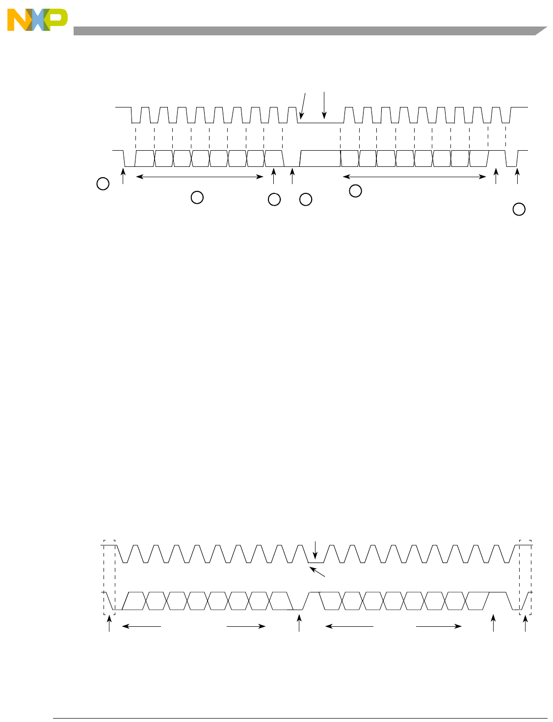
I2C Interface
Freescale Semiconductor 25-9
Figure 25-7. I2C Standard Communication Protocol
25.3.2 Slave Address Transmission
The master sends the slave address in the first byte after the START signal (B). After the seven-bit calling
address, it sends the R/W bit (C), which tells the slave data transfer direction (0 equals write transfer, 1
equals read transfer).
Each slave must have a unique address. An I2C master must not transmit its own slave address; it cannot
be master and slave at the same time.
The slave whose address matches that sent by the master pulls I2Cn_SDA low at the ninth serial clock (D)
to return an acknowledge bit.
25.3.3 Data Transfer
When successful slave addressing is achieved, data transfer can proceed (see E in Figure 25-7) on a
byte-by-byte basis in the direction specified by the R/W bit sent by the calling master.
Data can be changed only while I2Cn_SCL is low and must be held stable while I2Cn_SCL is high, as
Figure 25-7 shows. I2Cn_SCL is pulsed once for each data bit, with the msb being sent first. The receiving
device must acknowledge each byte by pulling I2Cn_SDA low at the ninth clock; therefore, a data byte
transfer takes nine clock pulses. See Figure 25-8.
Figure 25-8. Data Transfer
12345678 123456789 9
AD7 AD6 AD5 AD4 AD3 AD2 AD1 R/W XXX D7 D6 D5 D4 D3 D2 D1 D0
Calling Address R/W ACK
Bit
Data Byte No
ACK
Bit
STOP
Signal
lsbmsblsbmsb
START
Signal
A
BDC
E
F
Interrupt bit set
(Byte complete)
I2Cn_SCL
I2Cn_SDA
I2Cn_SCL held low
while Interrupt is
12345678956784321
Bit6 Bit4 Bit3 Bit2 Bit1Bit5Bit7 Bit0 Bit6 Bit4 Bit3 Bit2 Bit1Bit5 Bit0Bit7
START
Signal
ACK from
Receiver
STOP
No
ACK Bit
Data Byte
Slave Address
R/W
Signal
Interrupt Bit Set
(Byte Complete)
9
I2Cn_SCL
I2Cn_SDA
I2Cn_SCL held low while
Interrupt is serviced
MCF52211 ColdFire® Integrated Microcontroller Reference Manual, Rev. 3
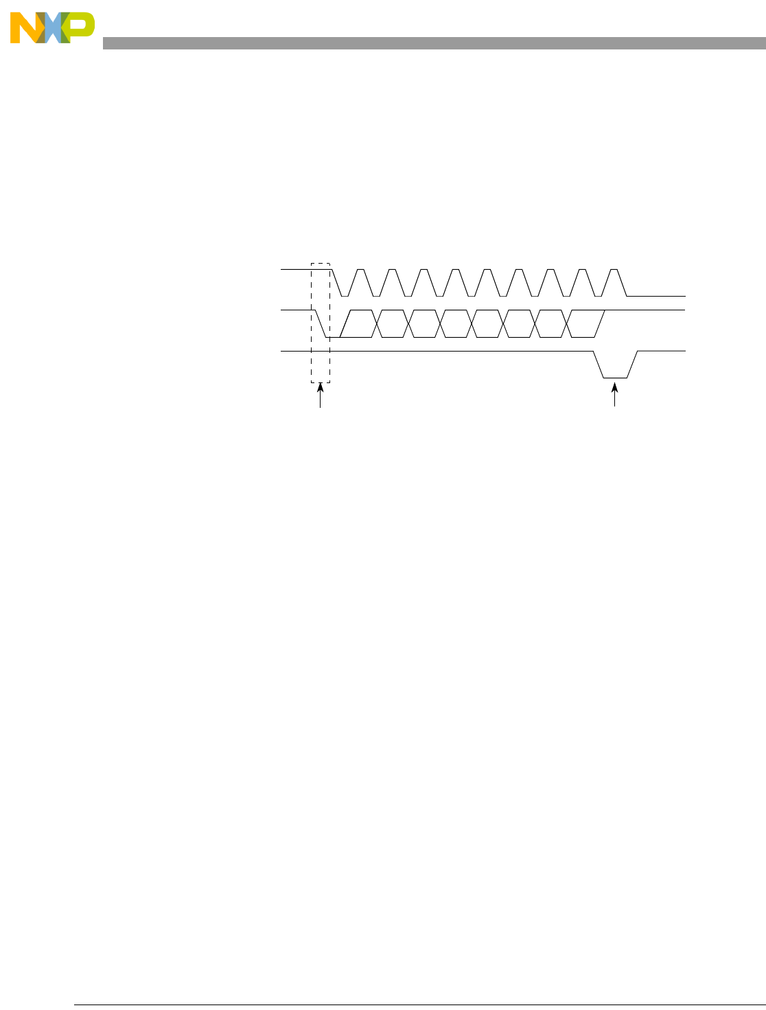
I2C Interface
25-10 Freescale Semiconductor
25.3.4 Acknowledge
The transmitter releases the I2Cn_SDA line high during the acknowledge clock pulse as shown in
Figure 25-9. The receiver pulls down the I2Cn_SDA line during the acknowledge clock pulse so that it
remains stable low during the high period of the clock pulse.
If it does not acknowledge the master, the slave receiver must leave I2Cn_SDA high. The master can then
generate a STOP signal to abort data transfer or generate a START signal (repeated start, shown in
Figure 25-10 and discussed in Section 25.3.6, “Repeated START”) to start a new calling sequence.
Figure 25-9. Acknowledgement by Receiver
If the master receiver does not acknowledge the slave transmitter after a byte transmission, it means
end-of-data to the slave. The slave releases I2Cn_SDA for the master to generate a STOP or START signal
(Figure 25-9).
25.3.5 STOP Signal
The master can terminate communication by generating a STOP signal to free the bus. A STOP signal is
defined as a low-to-high transition of I2Cn_SDA while I2Cn_SCL is at logical high (see F in Figure 25-7).
The master can generate a STOP even if the slave has generated an acknowledgment, at which point the
slave must release the bus. The master may also generate a START signal following a calling address,
without first generating a STOP signal. Refer to Section 25.3.6, “Repeated START.”
25.3.6 Repeated START
A repeated START signal is a START signal generated without first generating a STOP signal to terminate
the communication, as shown in Figure 25-10. The master uses a repeated START to communicate with
another slave or with the same slave in a different mode (transmit/receive mode) without releasing the bus.
567894321
Bit6 Bit4 Bit3 Bit2 Bit1Bit5Bit7 Bit0
START Signal
R/W
ACK
I2Cn_SCL
I2Cn_SDA by Transmitter
I2Cn_SDA by Receiver
MCF52211 ColdFire® Integrated Microcontroller Reference Manual, Rev. 3
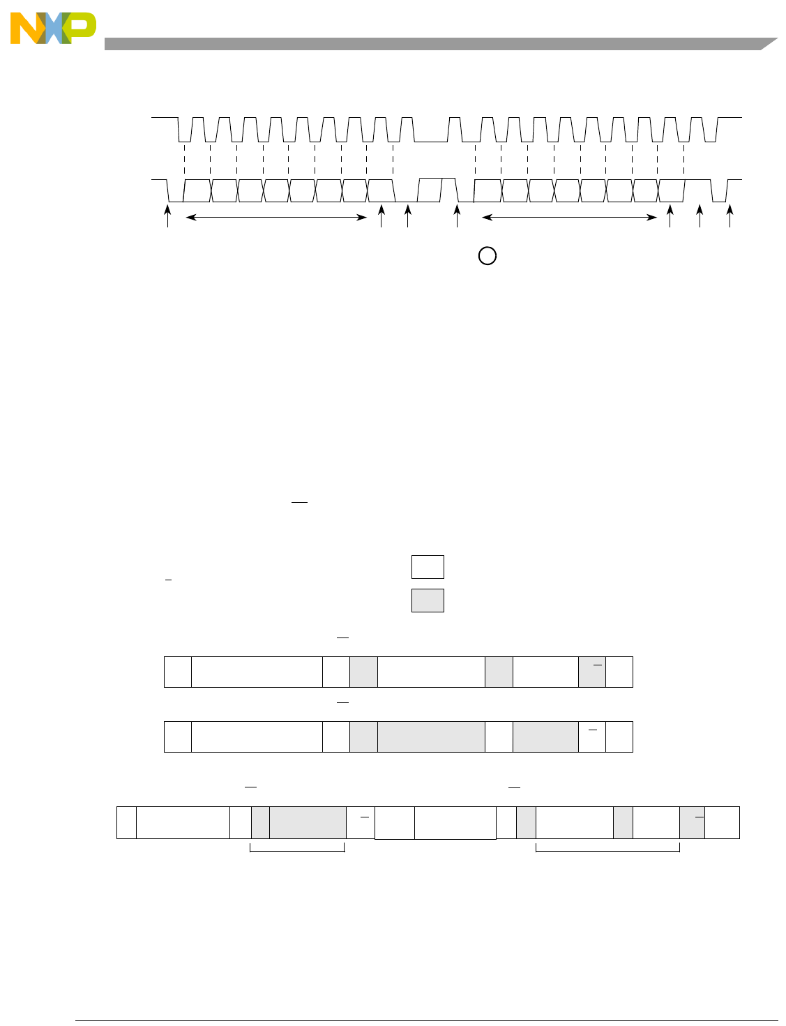
I2C Interface
Freescale Semiconductor 25-11
Figure 25-10. Repeated START
Various combinations of read/write formats are then possible:
• The first example in Figure 25-11 is the case of master-transmitter transmitting to slave-receiver.
The transfer direction is not changed.
• The second example in Figure 25-11 is the master reading the slave immediately after the first byte.
At the moment of the first acknowledge, the master-transmitter becomes a master-receiver and the
slave-receiver becomes slave-transmitter.
• In the third example in Figure 25-11, START condition and slave address are repeated using the
repeated START signal. This is to communicate with same slave in a different mode without
releasing the bus. The master transmits data to the slave first, and then the master reads data from
slave by reversing the R/W bit.
Figure 25-11. Data Transfer, Combined Format
1234567 8 1 2 5 67834
AD7 AD6 AD5 AD4 AD3 AD2 AD1 R/W AD7 AD6 AD5 AD4 AD3 AD2 AD1 R/W
99
XX
New Calling Address R/W No
ACK
Bit
STOP
Signal
Repeated
START
Signal
ACK
Bit
R/W
Calling Address
START
msb lsb msb lsb
Signal
A
I2Cn_SCL
I2Cn_SDA
ST A
7bit Slave Address 0A
Data Data A/A
R/W
SP
From Master to Slave
From Slave to Master
ST A
7bit Slave Address 1AData A
R/W
SP
ST A
1A
Data
R/W
Rept A
7-bit Slave 0A
Data Data A/A
R/W
SP
ST Address
7-bit Slave
Address
Example 1:
Example 2:
Example 3:
Master Reads from Slave Master Writes to Slave
Note: No acknowledge on the last byte
Data
ST = Start
SP = Stop
A = Acknowledge (I2Cn_SDA low)
A = Not Acknowledge (I2Cn_SDA high)
Rept ST = Repeated Start
MCF52211 ColdFire® Integrated Microcontroller Reference Manual, Rev. 3
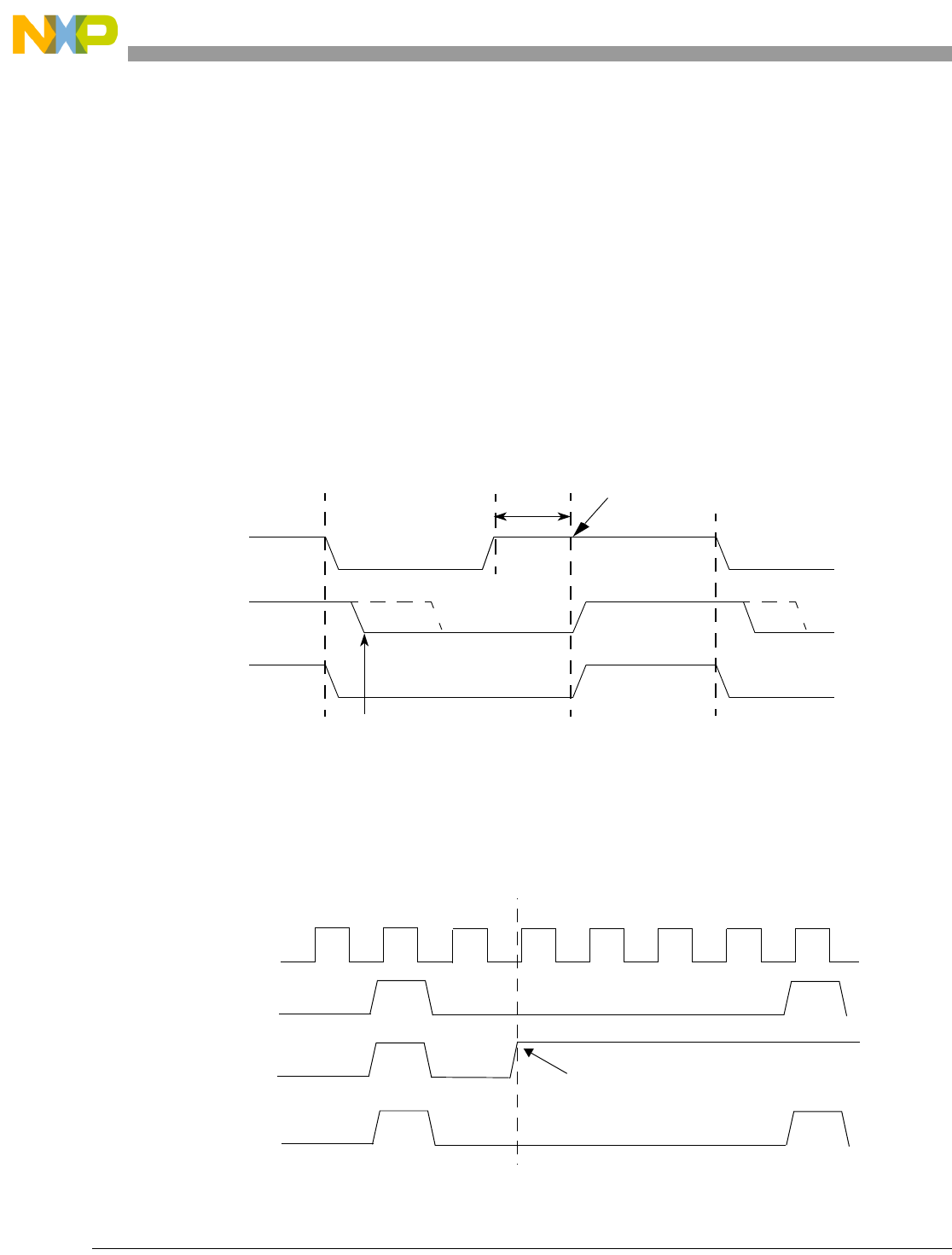
I2C Interface
25-12 Freescale Semiconductor
25.3.7 Clock Synchronization and Arbitration
I2C is a true multi-master bus that allows more than one master connected to it. If two or more master
devices simultaneously request control of the bus, a clock synchronization procedure determines the bus
clock. Because wire-AND logic is performed on the I2Cn_SCL line, a high-to-low transition on the
I2Cn_SCL line affects all the devices connected on the bus. The devices start counting their low period
and after a device’s clock has gone low, it holds the I2Cn_SCL line low until the clock high state is reached.
However, change of low to high in this device’s clock may not change the state of the I2Cn_SCL line if
another device clock remains within its low period. Therefore, synchronized clock I2Cn_SCL is held low
by the device with the longest low period.
Devices with shorter low periods enter a high wait state during this time (see Figure 25-12). When all
devices concerned have counted off their low period, the synchronized clock (I2Cn_SCL) line is released
and pulled high. At this point, the device clocks and the I2Cn_SCL line are synchronized, and the devices
start counting their high periods. The first device to complete its high period pulls the I2Cn_SCL line low
again.
Figure 25-12. Clock Synchronization
A data arbitration procedure determines the relative priority of the contending masters. A bus master loses
arbitration if it transmits logic 1 while another master transmits logic 0. The losing masters immediately
switch over to slave receive mode and stop driving I2Cn_SDA output (see Figure 25-13). In this case,
transition from master to slave mode does not generate a STOP condition. Meanwhile, hardware sets
I2SRn[IAL] to indicate loss of arbitration.
Figure 25-13. Arbitration Procedure
Internal Counter Reset
Wait Start counting high period
I2Cn_SCL1
I2Cn_SCL2
I2Cn_SCL
Master 2 Loses Arbitration,
and becomes slave-receiver
I2Cn_SCL
I2Cn_SDA
by Master1
I2Cn_SDA
by Master2
I2Cn_SDA
MCF52211 ColdFire® Integrated Microcontroller Reference Manual, Rev. 3

I2C Interface
Freescale Semiconductor 25-13
25.3.8 Handshaking and Clock Stretching
The clock synchronization mechanism can acts as a handshake in data transfers. Slave devices can hold
I2Cn_SCL low after completing one byte transfer. In such a case, the clock mechanism halts the bus clock
and forces the master clock into wait states until the slave releases I2Cn_SCL.
Slaves may also slow down the transfer bit rate. After the master has driven I2Cn_SCL low, the slave can
drive I2Cn_SCL low for the required period and then release it. If the slave I2Cn_SCL low period is longer
than the master I2Cn_SCL low period, the resulting I2Cn_SCL bus signal low period is stretched.
25.4 Initialization/Application Information
The following examples show programming for initialization, signaling START, post-transfer software
response, signaling STOP, and generating a repeated START.
25.4.1 Initialization Sequence
Before the interface can transfer serial data, registers must be initialized:
1. Set I2FDRn[IC] to obtain I2Cn_SCL frequency from the system bus clock. See Section 25.2.2,
“I2C Frequency Divider Register (I2FDRn).”
2. Update the I2ADRn to define its slave address.
3. Set I2CRn[IEN] to enable the I2C bus interface system.
4. Modify the I2CRn to select or deselect master/slave mode, transmit/receive mode, and
interrupt-enable or not.
NOTE
If I2SRn[IBB] is set when the I2C bus module is enabled, execute the
following pseudocode sequence before proceeding with normal
initialization code. This issues a STOP command to the slave device,
placing it in idle state as if it were power-cycled on.
I2CRn = 0x0
I2CRn = 0xA0
dummy read of I2DRn
I2SRn = 0x0
I2CRn = 0x0
I2CRn = 0x80 ; re-enable
25.4.2 Generation of START
After completion of the initialization procedure, serial data can be transmitted by selecting the master
transmitter mode. On a multiple-master bus system, I2SRn[IBB] must be tested to determine whether the
serial bus is free. If the bus is free (IBB is cleared), the START signal and the first byte (the slave address)
can be sent. The data written to the data register comprises the address of the desired slave and the lsb
indicates the transfer direction.
The free time between a STOP and the next START condition is built into the hardware that generates the
START cycle. Depending on the relative frequencies of the system clock and the I2Cn_SCL period, the
MCF52211 ColdFire® Integrated Microcontroller Reference Manual, Rev. 3

I2C Interface
25-14 Freescale Semiconductor
processor may need to wait until the I2C is busy after writing the calling address to the I2DRn before
proceeding with the following instructions.
The following example signals START and transmits the first byte of data (slave address):
1. Check I2SRn[IBB]. If it is set, wait until it is clear.
2. After cleared, set to transmit mode by setting I2CRn[MTX].
3. Set master mode by setting I2CRn[MSTA]. This generates a START condition.
4. Transmit the calling address via the I2DRn.
5. Check I2SRn[IBB]. If it is clear, wait until it is set and go to step #1.
25.4.3 Post-Transfer Software Response
Sending or receiving a byte sets the I2SRn[ICF], which indicates one byte communication is finished.
I2SRn[IIF] is also set. An interrupt is generated if the interrupt function is enabled during initialization by
setting I2CRn[IIEN]. Software must first clear I2SRn[IIF] in the interrupt routine. Reading from I2DRn
in receive mode or writing to I2DRn in transmit mode can clear I2SRn[ICF].
Software can service the I2C I/O in the main program by monitoring the IIF bit if the interrupt function is
disabled. Polling should monitor IIF rather than ICF, because that operation is different when arbitration
is lost.
When an interrupt occurs at the end of the address cycle, the master is always in transmit mode; the address
is sent. If master receive mode is required, I2CRn[MTX] should be toggled.
During slave-mode address cycles (I2SRn[IAAS] = 1), I2SRn[SRW] is read to determine the direction of
the next transfer. MTX is programmed accordingly. For slave-mode data cycles (IAAS = 0), SRW is
invalid. MTX should be read to determine the current transfer direction.
The following is an example of a software response by a master transmitter in the interrupt routine (see
Figure 25-14).
1. Clear the I2CRn[IIF] flag.
2. Check if acknowledge has been received, I2SRn[RXAK].
3. If no ACK, end transmission. Else, transmit next byte of data via I2DRn.
25.4.4 Generation of STOP
A data transfer ends when the master signals a STOP, which can occur after all data is sent, as in the
following example.
1. Check if acknowledge has been received, I2SRn[RXAK]. If no ACK, end transmission and go to
step #5.
2. Get value from transmitting counter, TXCNT. If no more data, go to step #5.
3. Transmit next byte of data via I2DRn.
4. Decrement TXCNT and go to step #1
5. Generate a stop condition by clearing I2CRn[MSTA].
MCF52211 ColdFire® Integrated Microcontroller Reference Manual, Rev. 3

I2C Interface
Freescale Semiconductor 25-15
For a master receiver to terminate a data transfer, it must inform the slave transmitter by not
acknowledging the last data byte. This is done by setting I2CRn[TXAK] before reading the next-to-last
byte. Before the last byte is read, a STOP signal must be generated, as in the following example.
1. Decrement RXCNT.
2. If last byte (RXCNT = 0) go to step #4.
3. If next to last byte (RXCNT = 1), set I2CRn[TXAK] to disable ACK and go to step #5.
4. This is last byte, so clear I2CRn[MSTA] to generate a STOP signal.
5. Read data from I2DRn.
6. If there is more data to be read (RXCNT 0), go to step #1 if desired.
25.4.5 Generation of Repeated START
If the master wants the bus after the data transfer, it can signal another START followed by another slave
address without signaling a STOP, as in the following example.
1. Generate a repeated START by setting I2CRn[RSTA].
2. Transmit the calling address via I2DRn.
25.4.6 Slave Mode
In the slave interrupt service routine, software must poll the I2SRn[IAAS] bit to determine if the controller
has received its slave address. If IAAS is set, software must set the transmit/receive mode select bit
(I2CRn[MTX]) according to the I2SRn[SRW]. Writing to I2CRn clears IAAS automatically. The only
time IAAS is read as set is from the interrupt at the end of the address cycle where an address match
occurred; interrupts resulting from subsequent data transfers have IAAS cleared. A data transfer can now
be initiated by writing information to I2DRn for slave transmits, or read from I2DRn in slave-receive
mode. A dummy read of I2DRn in slave/receive mode releases I2Cn_SCL, allowing the master to send
data.
In the slave transmitter routine, I2SRn[RXAK] must be tested before sending the next byte of data. Setting
RXAK means an end-of-data signal from the master receiver, after which software must switch it from
transmitter to receiver mode. Reading I2DRn releases I2Cn_SCL so the master can generate a STOP
signal.
25.4.7 Arbitration Lost
If several devices try to engage the bus at the same time, one becomes master. Hardware immediately
switches devices that lose arbitration to slave receive mode. Data output to I2Cn_SDA stops, but
I2Cn_SCL continues generating until the end of the byte during which arbitration is lost. An interrupt
occurs at the falling edge of the ninth clock of this transfer with I2SRn[IAL] set and
I2CRn[MSTA] cleared.
If a non-master device tries to transmit or execute a START, hardware inhibits the transmission, clears
MSTA without signaling a STOP, generates an interrupt to the CPU, and sets IAL to indicate a failed
MCF52211 ColdFire® Integrated Microcontroller Reference Manual, Rev. 3
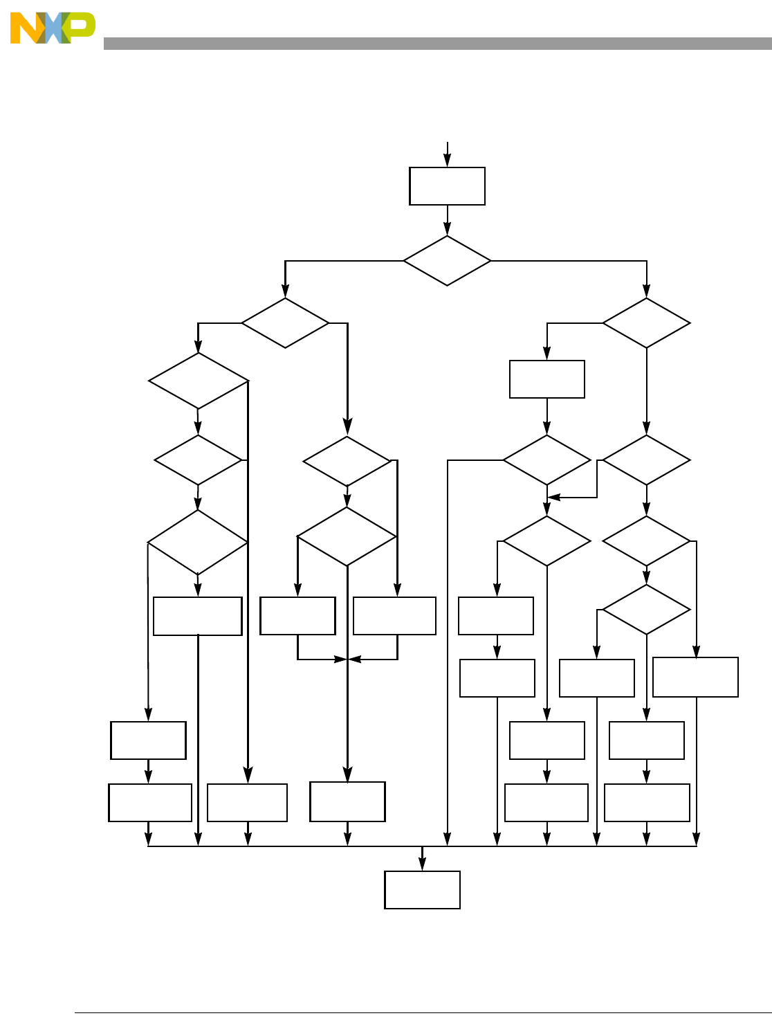
I2C Interface
25-16 Freescale Semiconductor
attempt to engage the bus. When considering these cases, slave service routine should first test IAL and
software should clear it if it is set.
Figure 25-14. Flow-Chart of Typical I2C Interrupt Routine
Clear
Master
Mode?
TX/Rx
?
Last Byte
Transmitted
?
RXAK= 0
?
End of
ADDR Cycle
(Master RX)
?
Write Next
Byte to I2DR
Switch to
Rx Mode
Dummy Read
from I2DR
Generate
STOP Signal
Read Data
from I2DR
And Store
Set TXAK =1 Generate
STOP Signal
2nd Last
Byte to be
Last
Byte to be
?
Arbitration
Lost?
Clear IAL
IAAS=1
?
IAAS=1
?
SRW=1
?Tx/Rx
?
Set TX
Mode
Write Data
to I2DR
Set RX
Mode
Dummy Read
from I2DR
ACK from
Receiver
?
Tx Next
Byte
Read Data
from I2DR
and Store
Switch to
Rx Mode
Dummy Read
from I2DR
RTE
YN
Y
Y
Y
Y
Y
Y
Y
Y
Y
N
N
N
N
N
N
N
N
N
Y
TX RX
RX
TX
(WRITE)
(Read)
N
IIF
Address
Cycle Data
Cycle
Read
Read?
MCF52211 ColdFire® Integrated Microcontroller Reference Manual, Rev. 3

Freescale Semiconductor 26-1
Chapter 26
Analog-to-Digital Converter (ADC)
26.1 Introduction
The analog-to-digital converter (ADC) consists of two separate and complete ADCs, each with their own
sample and hold circuits. The converters share a common voltage reference and common digital control
module.
26.2 Features
The ADC’s characteristics include the following:
• 12-bit resolution
• Maximum ADC clock frequency of 5.0 MHz, 200 ns period
• Sampling rate up to 1.66 million samples per second1
• Single conversion time of 8.5 ADC clock cycles (8.5 200 ns = 1.7 s)
• Additional conversion time of 6 ADC clock cycles (6 200 ns = 1.2 s)
• Eight conversions in 26.5 ADC clocks (26.5 200 ns = 5.3 s) using simultaneous mode
• Ability to simultaneously sample and hold 2 inputs
• Ability to sequentially scan and store up to 8 measurements
• Internal multiplex to select two of 8 inputs
• Power savings modes allow automatic shutdown/startup of all or part of ADC
• Those inputs not selected tolerate injected/sourced current without affecting ADC performance,
supporting operation in noisy industrial environments.
• Optional interrupts at the end of a scan, if an out-of-range limit is exceeded (high or low), or at zero
crossing
• Optional sample correction by subtracting a pre-programmed offset value
• Signed or unsigned result
• Single ended or differential inputs for all input pins with support for an arbitrary mix of input types
1. In loop mode, the time between each conversion is 6 ADC clock cycles (1.2 s at 5.0 MHz). Using simultaneous conversion,
two samples are captured in 1.2 s, providing an overall sample rate of 1.66 million samples per second.
MCF52211 ColdFire® Integrated Microcontroller Reference Manual, Rev. 3
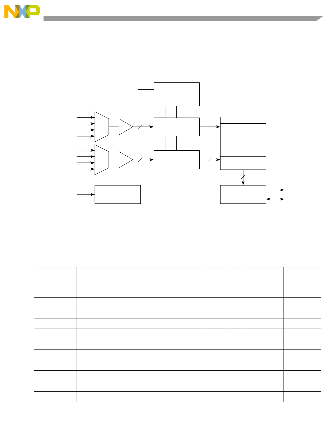
Analog-to-Digital Converter (ADC)
Freescale Semiconductor 26-2
26.3 Block Diagram
The ADC function, shown in Figure 26-1, consists of two four-channel input select functions, interfacing
with two independent Sample and Hold (S/H) circuits, which feed two 12-bit ADCs. The two converters
store their results in a buffer, awaiting further processing.
Figure 26-1. Dual ADC Block Diagram
26.4 Memory Map and Register Definition
This section presents the registers of the ADC module. A summary of these registers is given in
Table 26-1. All ADC registers are supervisor-mode access only.
Table 26-1. ADC Register Summary
IPSBAR Offset1Register Width
(bits) Access Reset Value Section/Page
0x19_0000 Control Register 1 (CTRL1) 16 R/W 0x5005 26.4.1/26-3
0x19_0002 Control Register 2 (CTRL2) 16 R/W 0x0002 26.4.2/26-5
0x19_0004 Zero Crossing Control Register (ADZCC) 16 R/W 0x0000 26.4.3/26-8
0x19_0006 Channel List Register 1 (ADLST1) 16 R/W 0x3210 26.4.4/26-8
0x19_0008 Channel List Register 2 (ADLST2) 16 R/W 0x7654 26.4.4/26-8
0x19_000A Sample Disable Register (ADSDIS) 16 R/W 0x0000 26.4.5/26-10
0x19_000C Status Register (ADSTAT) 16 R/W 0x0000 26.4.6/26-11
0x19_000E Limit Status Register (ADLSTAT) 16 R/W 0x0000 26.4.7/26-13
0x19_0010 Zero Crossing Status Register (ADZCSTAT) 16 R/W 0x0000 26.4.8/26-14
0x19_0012–20 Result Registers 0-7 (ADRSLT0-7) 16 R/W 0x0000 26.4.9/26-14
0x19_0022–30 Low Limit Registers 0-7 (ADLLMT0-7) 16 R/W 0x0000 26.4.10/26-15
IRQ
AN7
AN6
AN5
AN4
Scaling & Cyclic
Converter B
12
AN3
AN2
AN1
AN0
Scaling & Cyclic
Converter A
12
•
•
•
Digital Output
Storage Registers
16
Bus Interface Data
SYNCx Controller
VREFH Voltage
VREFL
Sample/Hold
Reference
Circuit
MUX
MUX
MCF52211 ColdFire® Integrated Microcontroller Reference Manual, Rev. 3

Analog-to-Digital Converter (ADC)
26-3 Freescale Semiconductor
26.4.1 Control 1 Register (CTRL1)
The CTRL1 register, shown in Figure 26-2, is used to configure and control the ADC module. The
associated field descriptions are given in Table 26-2. Please see Section 26.5.6, “Scan Configuration and
Control” for details on the functionality controlled by this register.
0x19_0032–40 High Limit Registers 0-7 (ADHLMT0-7) 16 R/W 0x0000 26.4.10/26-15
0x19_0042–50 Offset Registers 0-7 (ADOFS0-7) 16 R/W 0x0000 26.4.11/26-17
0x19_0052 Power Control Register (POWER) 16 R/W 0x00D7 26.4.12/26-17
0x19_0054 Voltage Reference Register (CAL) 16 R/W 0x0000 26.4.13/26-20
1Addresses not assigned to a register and undefined register bits are reserved for expansion.
IPSBAR
Offset: 0x19_0000 (CTRL1)
Access: read/write
15 14 13 12 11 10 9 8 7 6 5 4 3 2 1 0
R 0 STOP0 SYNC0 EOSI
E0 ZCIE LLMT
IE
HLMT
IE CHNCFG SMODE
WSTART0
Reset0 1 0 1 00000000 0 1 0 1
Figure 26-2. Control 1 Register (CTRL1)
Table 26-2. CTRL1 Field Descriptions
Field Description
15 Reserved, should be cleared.
14
STOP0
Stop Conversion 0 bit. When STOP0 is set, the current scan is stopped and no further scans can start. Any
further SYNC0 input pulses (see the SYNC0 field description) or writes to START0 are ignored until STOP0
is cleared. After the ADC is in stop mode, the result registers can be modified by the processor. Any changes
to the result registers in stop mode are treated as if the analog core supplied the data. Therefore, limit
checking, zero crossing, and associated interrupts can occur if enabled.
0 Normal operation
1 Stop mode
Note: This is not the same as the device’s STOP mode.
13
START0
Start Conversion 0 bit. A scan is started by writing a 1 to this bit. START0 is write-only. Writing 1 to the
START0 bit again is ignored until the end of the current scan. The ADC must be in a stable power
configuration prior to writing to START0 (see Section 26.5.8, “Power Management”).
0 No action
1 Start command is issued
Table 26-1. ADC Register Summary (continued)
IPSBAR Offset1Register Width
(bits) Access Reset Value Section/Page
MCF52211 ColdFire® Integrated Microcontroller Reference Manual, Rev. 3

Analog-to-Digital Converter (ADC)
Freescale Semiconductor 26-4
12
SYNC0
Synchronization 0 Enable bit. When this bit is set, a conversion may be initiated by asserting a positive edge
on the SYNC0 input. Any subsequent SYNC0 input pulses that occur during the scan are ignored. In once
sequential and once parallel scan modes, only the first SYNC0 input pulse is honored. Subsequent SYNC0
input pulses are ignored until SYNC0 input is re-armed by setting SYNC0. This can be done at any time, even
during the execution of the scan. The ADC must be in a stable power configuration prior to writing to START0
(see Section 26.5.8, “Power Management”).
0 Scan is initiated by a write to the START0 bit only
1 Scan is initiated by a SYNC0 input pulse or a write to the START0 bit
11
EOSIE0
End of Scan Interrupt 0 Enable bit. This bit enables an EOSI0 interrupt to be generated upon completion of
the scan. For looping scan modes, the interrupt triggers after the completion of each iteration of the loop.
0 Interrupt disabled
1 Interrupt enabled
10
ZCIE
Zero Crossing Interrupt Enable bit. This bit enables the zero crossing interrupt if the current result value has
a sign change from the previous result as configured by the ADZCC register.
0 Interrupt disabled
1 Interrupt enabled
9
LLMTIE
Low Limit Interrupt Enable bit. This bit enables the low limit exceeded interrupt when the current result value
is less than the low limit register value. The raw result value is compared to ADLLMTn[LLMT] before the offset
register value is subtracted.
0 Interrupt disabled
1 Interrupt enabled
8
HLMTIE
High Limit Interrupt Enable bit. This bit enables the high limit exceeded interrupt if the current result value is
greater than the high limit register value. The raw result value is compared to ADHLMT[HLMT] before the
offset register value is subtracted.
0 Interrupt disabled
1 Interrupt enabled
Table 26-2. CTRL1 Field Descriptions (continued)
Field Description
MCF52211 ColdFire® Integrated Microcontroller Reference Manual, Rev. 3

Analog-to-Digital Converter (ADC)
26-5 Freescale Semiconductor
26.4.2 Control 2 Register (CTRL2)
The structure of the CTRL2 register depends on whether the ADC is operating in sequential or parallel
mode (see Section 26.4.1, “Control 1 Register (CTRL1)”).
26.4.2.1 CTRL2 Under Sequential Scan Modes
7–4
CHNCFG
Channel Configure. This field configures the inputs for single-ended or differential conversions:
2–0
SMODE
Scan Mode Control. This field controls the scan mode of the ADC module. See Section 26.5.6, “Scan
Configuration and Control” for details on each scan mode.
000 Once sequential
001 Once parallel
010 Loop sequential
011 Loop parallel
100 Triggered sequential
101 Triggered parallel (default)
110 Reserved; do not use
111 Reserved; do not use
IPSBAR
Offset:
0x19_0002 (CTRL2)
Access: read/write
15 14 13 12 11 10 9 8 7 6 5 4 3 2 1 0
R 0 0 0 0 0 000000 DIV
W
Reset0 0 0 0 00000000 0 0 1 0
Figure 26-3. Control 2 Register (CTRL2) Under Sequential Scan Modes
Table 26-2. CTRL1 Field Descriptions (continued)
Field Description
CHNCFG Inputs Description
xxx1 AN0–AN1 Configured as differential pair (AN0 is + and AN1 is –)
xxx0 Both configured as single ended inputs
xx1x AN2–AN3 Configured as differential pair (AN2 is + and AN3 is –)
xx0x Both configured as single ended inputs
x1xx AN4–AN5 Configured as differential pair (AN4 is + and AN5 is –)
x0xx Both configured as single ended inputs
1xxx AN6–AN7 Configured as differential pair (AN6 is + and AN7 is –)
0xxx Both configured as single ended inputs
MCF52211 ColdFire® Integrated Microcontroller Reference Manual, Rev. 3

Analog-to-Digital Converter (ADC)
Freescale Semiconductor 26-6
26.4.2.2 CTRL2 Under Parallel Scan Modes
When the ADC operates in a parallel scan mode, the CTRL2 register is used to control the operation of
converter B. The interaction between converters A and B (and hence CTRL1 and CTRL2) is determined
by the CTRL2[SIMULT] bit. By default, CTRL2[SIMULT] equals 1 and converter B operates together
with converter A. In this case, the STOP1, START1, SYNC1, and EOSIE1 bits in the CTRL2 register do
not affect converter B operation. If CTRL2[SIMULT] equals 0, these bits and the SYNC1 input are used
to control the converter B scan. In this case, EOSIE1 enables the EOSI1 interrupt, signaling the end of a
B converter scan. In addition, ADSTAT[CIP1] is used to indicate a converter B scan is active.
Table 26-3. CTRL2 Field Descriptions Under Sequential Scan Modes
Field Description
15–5 Reserved, should be cleared.
4–0
DIV
Clock Divisor Select. This field controls the divider circuit, which generates the ADC clock by dividing the
system clock by 2DIV+1). DIV must be chosen so the ADC clock does not exceed 5.0 MHz. See Table 26-5
for a listing of ADC clock frequency based on the value of DIV for several configurations.
IPSBAR
Offset: 0x19_0002 (CTRL2)
Access: read/write
15 14 13 12 11 10 9 8 7 6 5 4 3 2 1 0
R 0 STOP1 SYNC1 EOSIE1 00000
SIMU
LT DIV
WSTART1
Reset 0 1 0 1 0 0 0 0 0 0 0 0 0 0 1 0
Figure 26-4. Control 2 Register (CTRL2) Under Parallel Scan Modes
Table 26-4. CTRL2 Field Descriptions Under Parallel Scan Modes
Field Description
15 Reserved, should be cleared.
14
STOP1
Stop Conversion 1bit. In parallel-scan modes when SIMULT equaling 0, setting STOP1 stops parallel scans
in the B converter and prevents new scans from starting. Any further SYNC1 input pulses (see the SYNC1
field description) or writes to START1 are ignored until STOP1 is cleared. After the ADC is in stop mode, the
result registers can be modified by the processor. Any changes to the result registers in stop mode are
treated as if the analog core supplied the data. Therefore, limit checking, zero crossing, and associated
interrupts can occur if enabled.
0 Normal operation
1 Stop mode
Note: This is not the same as the device’s STOP mode.
13
START1
Start Conversion 1 bit. In parallel-scan modes when SIMULT equaling 0, a scan by the B converter is started
by writing a 1 to this bit. START1 is write-only. Writing 1 to the START1 bit again is ignored until the end of
the current scan. The ADC must be in a stable power configuration prior to writing to START1 (see
Section 26.5.8, “Power Management”).
0 No action
1 Start command is issued
MCF52211 ColdFire® Integrated Microcontroller Reference Manual, Rev. 3

Analog-to-Digital Converter (ADC)
26-7 Freescale Semiconductor
12
SYNC1
Synchronization 1 Enable bit. In parallel-scan modes when SIMULT equaling 0, setting SYNC1 allows a
conversion to be initiated by asserting a positive edge on the SYNC1 input. Any subsequent SYNC1 input
pulses that occur during the scan are ignored. In once sequential and once parallel scan modes, only the
first SYNC1 input pulse is honored. Subsequent SYNC1 input pulses are ignored until SYNC1 input is
re-armed by setting SYNC1. This can be done at any time, even during the execution of the scan. The ADC
must be in a stable power configuration prior to writing to START0 (see Section 26.5.8, “Power
Management”).
0 Scan is initiated by a write to the START1 bit only
1 Scan is initiated by a SYNC1 input pulse or a write to the START1 bit
11
EOSIE1
End of Scan Interrupt 1 Enable bit. In parallel-scan modes when SIMULT equaling 0, this bit enables an
EOSI1 interrupt to be generated upon completion of the scan. For looping scan modes, the interrupt triggers
after the completion of each iteration of the loop.
0 Interrupt disabled
1 Interrupt enabled
10–6 Reserved, should be cleared.
5
SIMULT
Simultaneous Mode bit. This bit only affects parallel scan modes.
When SIMULT equals 1, parallel scans operate in simultaneous mode. The scans in the A and B converter
operate simultaneously and always result in pairs of simultaneous conversions in the A and B converter.
START0, STOP0, SYNC0, and EOSIE0 control bits and the SYNC0 input are used to start and stop scans
in both converters simultaneously. A scan ends in both converters when either converter encounters a
disabled sample slot. When the parallel scan completes, the EOSI0 triggers if EOSIE0 is set. The CIP0
status bit indicates that a parallel scan is in process.
When SIMULT equals 0, parallel scans in the A and B converters operate independently. The B converter
has its own independent set of the above controls (START1, STOP1, SYNC1, EOSIE1, SYNC1) designed to
control its operation and report its status. Each converter’s scan continues until its sample list is exhausted
(four samples) or a disabled sample is encountered. For looping parallel scan mode, each converter starts
its next iteration as soon as the previous iteration in that converter is complete and continues until the STOP
bit for that converter is asserted.
0 Parallel scans occur independently
1 Parallel scans occur simultaneously (default)
4–0
DIV
Clock Divisor Select. This field controls the divider circuit, which generates the ADC clock by dividing the
system clock by 2DIV+1. DIV must be chosen so the ADC clock does not exceed 5.0 MHz. See Ta bl e 2 6 - 5
for a listing of ADC clock frequency based on the value of DIV for several configurations.
Table 26-5. ADC Clock Frequency for Various Conversion Clock Sources
DIV Divisor
ROSC Standby
400 kHz
ROSC Normal
8MHz
PLL
64 MHz External CLK
200 kHz Sys Clock 4 MHz Sys Clock 32 MHz Sys Clock CLK/2 Sys Clock
00000 2 100 kHz 2.00 MHz 16.0 MHz CLK/4
00001 4 100 kHz 1.00 MHz 8.00 MHz CLK/8
00010 6 100 kHz 500 kHz 5.33 MHz CLK/12
00011 8 100 kHz 250 kHz 4.00 MHz CLK/16
00100 10 100 kHz 125 kHz 3.20 MHz CLK/20
——————
Table 26-4. CTRL2 Field Descriptions Under Parallel Scan Modes (continued)
Field Description
MCF52211 ColdFire® Integrated Microcontroller Reference Manual, Rev. 3

Analog-to-Digital Converter (ADC)
Freescale Semiconductor 26-8
26.4.3 Zero Crossing Control Register (ADZCC)
The ADC zero crossing control (ADZCC) register provides the ability to monitor the selected channels
and determine the direction of zero crossing triggering the optional interrupt. Zero crossing logic monitors
only the sign change between current and previous sample. The ZCE0 bit monitors the sample stored in
ADRSLT0, ZCE1 bit monitors ADRSLT1, and ZCE7 bit monitors ADRSLT7. When the zero crossing is
disabled for a selected result register, sign changes are not monitored or updated in the ADZCSTAT
register.
26.4.4 Channel List 1 and 2 Registers (ADLST1 and ADLST2)
The channel list register contains an ordered list of the analog input channels to be converted when the next
scan is initiated. If all samples are enabled in the ADSDIS register, a sequential scan of inputs proceeds in
order of SAMPLE0 through SAMPLE7. If one of the parallel sampling modes is selected instead, the
converter A sampling order is SAMPLE0-3, and the converter B sampling order is SAMPLE4-7.
In sequential modes, the sample slots are converted in order from SAMPLE0 to SAMPLE7. Analog input
pins can be sampled in any order, including sampling the same input pin more than once.
In parallel modes, converter A processes sample slots SAMPLE0 through SAMPLE3, while converter B
processes sample slots SAMPLE4 through SAMPLE7. Because converter A only has access to analog
inputs AN0 through AN3, sample slots SAMPLE0-3 should only contain binary values between 000 and
011. Likewise, because converter B only has access to analog inputs AN4 through AN7, sample slots
——————
11111 64 100 kHz 62.5 kHz 500 kHz CLK/128
IPSBAR
Offset: 0x19_0004 (ADZCC)
Access: read/write
1514131211109876543210
RZCE7 ZCE6 ZCE5 ZCE4 ZCE3 ZCE2 ZCE1 ZCE0
W
Reset0000000000000000
Figure 26-5. Zero Crossing Control Register (ADZCC)
Table 26-6. ADZCC Field Descriptions
Field Description
15–0
ZCEn
Zero Crossing Enable. For each channel n, setting the ZCEn field allows detection of the indicated zero
crossing condition, provided the corresponding offset register (ADOFSn) has a value offset, 0 < offset <
0x7FF8.
00 Zero crossing disabled
01 Zero crossing enabled for positive to negative sign change
10 Zero crossing enabled for negative to positive sign change
11 Zero crossing enabled for any sign change
Table 26-5. ADC Clock Frequency for Various Conversion Clock Sources (continued)
MCF52211 ColdFire® Integrated Microcontroller Reference Manual, Rev. 3

Analog-to-Digital Converter (ADC)
26-9 Freescale Semiconductor
SAMPLE4-7 should only contain binary values between 100 and 111. No damage occurs if this constraint
is violated, but results are undefined.
When inputs are configured as differential pairs, a reference to either analog input in a differential pair by
a sample slot implies a differential measurement on the pair. The details of single ended and differential
measurement are described in Section 26.5.2.1, “Single-Ended Samples” and Section 26.5.2.2,
“Differential Samples”. Sample slots are disabled using the ADSDIS register.
IPSBAR
Offset: 0x19_0006 (ADLST1)
Access: read/write
1514131211109876543210
RSAMPLE3 SAMPLE2 SAMPLE1 SAMPLE0
W
Reset0011001000010000
Figure 26-6. Channel List 1 Register (ADLST1)
Table 26-7. ADLST1 Field Descriptions
Field Description
15 Reserved, should be cleared.
14–12
SAMPLE3
Sample input channel select 3. The settings for this field are given in Ta b l e 2 6 - 9 .
11 Reserved, should be cleared.
10–8
SAMPLE2
Sample input channel select 2. The settings for this field are given in Ta b l e 2 6 - 9 .
7 Reserved, should be cleared.
6–4
SAMPLE1
Sample input channel select 1. The settings for this field are given in Ta b l e 2 6 - 9 .
3 Reserved, should be cleared.
2–0
SAMPLE0
Sample input channel select 0. The settings for this field are given in Ta b l e 2 6 - 9 .
IPSBAR
Offset: 0x19_0008 (ADLST2)
Access: read/write
1514131211109876543210
RSAMPLE7 SAMPLE6 SAMPLE5 SAMPLE4
W
Reset0111011001010100
Figure 26-7. Channel List 2 Register (ADLST2)
MCF52211 ColdFire® Integrated Microcontroller Reference Manual, Rev. 3

Analog-to-Digital Converter (ADC)
Freescale Semiconductor 26-10
26.4.5 Sample Disable Register (ADSDIS)
This register is an extension to the ADLST1and ADLST2, providing the ability to enable only the desired
samples programmed in the SAMPLE0–SAMPLE7. At reset, all samples are enabled. For example, if in
sequential mode and bit DS5 is set to 1, SAMPLE0 through SAMPLE4 are sampled. However, if in
parallel mode and bits DS5 or DS1 are set to 1, only SAMPLE0 and SAMPLE4 are sampled.
Table 26-8. ADLST2 Field Descriptions
Field Description
15 Reserved, should be cleared.
14–12
SAMPLE7
Sample input channel select 7. The settings for this field are given in Ta b l e 2 6 - 9 .
11 Reserved, should be cleared.
10–8
SAMPLE6
Sample input channel select 6. The settings for this field are given in Ta b l e 2 6 - 9 .
7 Reserved, should be cleared.
6–4
SAMPLE5
Sample input channel select 5. The settings for this field are given in Ta b l e 2 6 - 9 .
3 Reserved, should be cleared.
2–0
SAMPLE4
Sample input channel select 4. The settings for this field are given in Ta b l e 2 6 - 9 .
Table 26-9. ADC Input Conversion for Sample Bits
SAMPLEn[2:0]
ADC Input Pins Selected
Sequential Mode Parallel Mode
n=0,1,2,...,7 n=0,1,2,3
(Conv. A)
n=4,5,6,7
(Conv. B) Single Ended Differential
000 000 AN0 AN0+, AN1–
001 001 AN1
010 010 AN2 AN2+, AN3–
011 011 AN3
100 100 AN4 AN4+, AN5–
101 101 AN5
110 110 AN6 AN6+, AN7–
111 111 AN7
MCF52211 ColdFire® Integrated Microcontroller Reference Manual, Rev. 3

Analog-to-Digital Converter (ADC)
26-11 Freescale Semiconductor
26.4.6 Status Register (ADSTAT)
This register provides the current status of the ADC module. RDYn bits are cleared by reading their
corresponding result (ADRSLTn) registers. The HLMTI and LLMTI bits are cleared by writing 1 to each
asserted bit in the ADC limit status (ADLSTAT) register. Likewise, the ZCI bit is cleared by writing 1 to
each asserted bit in the ADC zero crossing status (ADZCSTAT) register. The EOSIn bits are cleared by
writing 1 to them.
Except for CIP0 and CIP1 all bits in ADSTAT are sticky – after being set, they require some specific action
to be cleared. They are not cleared automatically on the next scan sequence.
IPSBAR
Offset: 0x19_000A (ADSDIS)
Access: read/write
1514131211109876543210
R00000000
DS7 DS6 DS5 DS4 DS3 DS2 DS1 DS0
W
Reset0000000000000000
Figure 26-8. Sample Disable Register (ADSDIS)
Table 26-10. ADSDIS Field Descriptions
Field Description
15–8 Reserved, should be cleared.
7–0
DSn
Disable Sample bits. Setting or clearing DSn enables or disables the corresponding SAMPLEn field.
0 Enable SAMPLEn
1 Disable SAMPLEn and all subsequent samples. Which samples are actually disabled depends on the
conversion mode, sequential/parallel, and the value of SIMULT.
IPSBAR
Offset: 0x19_000C (ADSTAT)
Access: read/write
1514131211109 8 76543210
RCIP0 CIP1 0EOSI1 EOSI0 ZCI LLMTI HLMTI RDY7 RDY6 RDY5 RDY4 RDY3 RDY2 RDY1 RDY0
W
Reset000 0 0 00 0 00000000
Figure 26-9. Status Register (ADSTAT)
MCF52211 ColdFire® Integrated Microcontroller Reference Manual, Rev. 3

Analog-to-Digital Converter (ADC)
Freescale Semiconductor 26-12
Table 26-11. ADSTAT Field Descriptions
Field Description
15
CIP0
Conversion in Progress 0 bit. This bit indicates when a scan is in progress. This bit supports any sequential
scan or parallel scan with SIMULT equaling 1. When executing a parallel scan with SIMULT equaling 0, this
bit services the scan of converter A, and the CIP1 bit services the scan of converter B.
0 Idle state
1 A scan cycle is in progress (the ADC ignores all sync pulses or start commands)
14
CIP1
Conversion in Progress 1 bit. This refers only to a B converter scan in non-simultaneous (SIMULT=0) parallel
scan modes.
0 Idle state
1 A scan cycle is in progress (the ADC ignores all sync pulses or start commands)
13 Reserved, should be cleared.
12
EOSI1
End of Scan Interrupt 1 bit. This bit indicates whether a scan of analog inputs has been completed since the
last read of ADSTAT or a reset. The EOSI1 bit is cleared by writing a 1 to it. This bit cannot be set by software.
In looping scan modes, this interrupt is triggered at the completion of each iteration of the loop. This interrupt
is triggered only by the completion of a B converter scan in non-simultaneous (SIMULT=0) parallel scan
modes. In this case the EOSI0 interrupt is triggered when converter A completes its scan.
0 A scan cycle has not been completed, no end of scan IRQ pending
1 A scan cycle has been completed, end of scan IRQ pending
11
EOSI0
End of Scan Interrupt 0 bit. This bit indicates whether a scan of analog inputs has been completed since the
last read of ADSTAT or a reset. The EOSI0 bit is cleared by writing a 1 to it. This bit cannot be set by software.
EOSI0 is the preferred bit to poll for scan completion if interrupts are not enabled.
In looping scan modes, this interrupt is triggered at the completion of each iteration of a loop.
This interrupt is triggered upon the completion of any sequential scan or parallel scan with
SIMULT equaling 1. When executing parallel scans with SIMULT equaling 0, this interrupt is triggered when
converter A completes its scan while the EOSI1 interrupt services converter B.
0 A scan cycle has not been completed, no end of scan IRQ pending
1 A scan cycle has been completed, end of scan IRQ pending
10
ZCI
Zero Crossing Interrupt bit. This bit is asserted at the completion of an individual conversion experiencing a
zero crossing enabled in the ADC zero crossing control (ADZCC) register. The bit is set as soon as an
enabled zero crossing event occurs rather than at the end of the ADC scan. ZCI is cleared by writing 1 to all
active ADZCSTAT[ZCS] bits.
0 No ZCI interrupt request
1 Zero crossing encountered; IRQ pending if CTRL1[ZCIE] is set
9
LLMTI
Low Limit Interrupt bit. If any low limit register (ADLLMTn) is enabled by having a value other than 0x0, low
limit checking is enabled. This bit is set at the completion of an individual conversion which may or may not
be the end of a scan. It is cleared by writing 1 to all active ADLSTAT[LLS] bits.
0 No low limit interrupt request
1 Low limit exceeded, IRQ pending if CTRL1[LLMTIE] is set
MCF52211 ColdFire® Integrated Microcontroller Reference Manual, Rev. 3

Analog-to-Digital Converter (ADC)
26-13 Freescale Semiconductor
26.4.7 Limit Status Register (ADLSTAT)
The ADC limit status (ADLSTAT) register latches in the result of the comparison between the result of the
sample in the ADRSLTn register and the respective limit register, ADHLMTn or ADLLMTn.
For example, if the result for ADRSLT0 is greater than the value programmed into ADHLMT0, then the
the HLS0 bit is set. An interrupt is generated if CTRL1[HLMTIE] is set.
These bits are sticky—they are not cleared automatically by subsequent conversions. A bit may only be
cleared by writing a 1 to it.
8
HLMTI
High Limit Interrupt bit. If any high limit register (ADHLMTn) is enabled by having a value other than 0x7FF8,
high limit checking is enabled. This bit is set at the completion of an individual conversion which may or may
not be the end of a scan. It is cleared by writing 1 to all active ADLSTAT[HLS] bits.
0 No high limit interrupt request
1 High limit exceeded, IRQ pending if CTRL1[HLMTIE] is set
7–0
RDYn
Ready Sample bits. These bits indicate samples 7-0 are ready to be read. The RDYn bits are set as the
individual channel conversions are completed and stored in a ADRSLTn register. These bits are cleared after
a read from the corresponding ADC results (ADRSLTn) register. If polling the RDYn bits to determine if a
particular sample is executed, care should be taken not to start a new scan until all enabled samples are
completed.
0 Sample not ready or has been read
1 Sample ready to be read
Note: RDYn bits can be cleared when the debugger reads the corresponding results register during a debug
session.
IPSBAR
Offset: 0x19_000E (ADLSTAT)
Access: read/write
1514131211109876543210
RHLS7 HLS6 HLS5 HLS4 HLS3 HLS2 HLS1 HLS0 LLS7 LLS6 LLS5 LLS4 LLS3 LLS2 LLS1 LLS0
W
Reset0000000000000000
Figure 26-10. Limit Status Register (ADLSTAT)
Table 26-12. ADLSTAT Field Descriptions
Field Description
15–8
HLSn
High Limit Status bits. These bits hold the result of a comparison between the sample (stored in ADRSLTn)
and the high-limit value (stored in ADHLMTn).
0 Sample n is less than or equal to the associated high-limit value
1 Sample n is greater than the associated high-limit value
Note: These bits are sticky, and can only be cleared by writing a 1 to them.
7–0
LLSn
Low Limit Status bits. These bits hold the result of a comparison between the sample (stored in ADRSLTn)
and the low-limit value (stored in ADLLMTn).
0 Sample n is greater than or equal to the associated low-limit value
1 Sample n is less than the associated low-limit value
Note: These bits are sticky, and can only be cleared by writing a 1 to them.
Table 26-11. ADSTAT Field Descriptions (continued)
Field Description
MCF52211 ColdFire® Integrated Microcontroller Reference Manual, Rev. 3

Analog-to-Digital Converter (ADC)
Freescale Semiconductor 26-14
26.4.8 Zero Crossing Status Register (ADZCSTAT)
The ADC zero crossing status (ADZCSTAT) register latches in the result of a sign comparison between
the current and previous sample. The type of comparison is controlled by the ADZCC register (see
Section 26.4.3, “Zero Crossing Control Register (ADZCC)”).
For example, if the result for the channel programmed in SAMPLE0 changes sign from the previous
conversion, and the respective ZCE bit in the ADZCC register is set to 0b11 (any edge change), then the
ZCS0 bit is set. An interrupt is generated if CTRL1[ZCIE] is set.
These bits are sticky—they are not cleared automatically by subsequent conversions. A bit may only be
cleared by writing a 1 to it.
26.4.9 Result Registers (ADRSLTn)
The 8 result registers contain the converted results from a scan. The SAMPLEn result is loaded into
ADRSLTn. In a simultaneous parallel scan mode, the first channel pair, designated by SAMPLE0 and
SAMPLE4 in register LIST1/2, is stored in ADRSLT0 and ADRSLT4, respectively.
When writing to this register, only the RSLT portion of the value written is used. This value is modified as
shown in Figure 26-23 and the result of the subtraction is stored. The SEXT bit is only set as a result of
this subtraction and is not directly determined by the value written.
RSLT can be interpreted as a signed integer or a signed fixed point (fractional) number. As a fixed point
number, RSLT can be used directly. If RSLT is interpreted as a signed integer, you have two options:
• Right shift with sign extend (ASR) three places to fit it into the range [0,4095]
• Accept the number as presented in the register, knowing there are missing codes, because the lower
three LSBs are always zero
IPSBAR
Offset: 0x19_0010 (ADZCSTAT)
Access: read/write
1514131211109876543210
R00000000
ZCS7 ZCS6 ZCS5 ZCS4 ZCS3 ZCS2 ZCS1 ZCS0
W
Reset0000000000000000
Figure 26-11. Zero Crossing Status Register (ADZCSTAT)
Table 26-13. ADLSTAT Field Descriptions
Field Description
15–8 Reserved, should be cleared.
7–0
ZCSn
Zero Crossing Status bits. These bits hold the result of a sign comparison between the current and previous
sample. The type of comparison is controlled by the ADZCC register (see Section 26.4.3, “Zero Crossing
Control Register (ADZCC)”).
0 Sample did not change sign, or sign comparison is disabled
1 Sample changed sign
Note: These bits are sticky, and can only be cleared by writing a 1 to them.
MCF52211 ColdFire® Integrated Microcontroller Reference Manual, Rev. 3

Analog-to-Digital Converter (ADC)
26-15 Freescale Semiconductor
Negative results (SEXT = 1) are always presented in twos-complement format. If an application requires
that the result be always positive, the corresponding offset register (ADOFSn) must be set to 0x0.
The interpretation of the numbers programmed into the ADC limit and offset registers (ADLLMTn,
ADHLMTn, and ADOFSn) must match your interpretation of the result register.
26.4.10 Low and High Limit Registers (ADLLMTn and ADHLMTn)
Each ADC sample is compared against the values in the limit registers. The comparison is based upon the
raw conversion value before the offset correction is applied. Refer to Figure 26-23. ADC limit registers
(ADLLMTn and ADHLMTn) correspond to result registers (ADRSLTn). The high limit register is used
for the comparison of result > high limit. The low limit register is used for the comparison of result < low
limit.
Limit checking can be disabled by programming the respective limit register with 0x7FF8 for the high
limit and 0x0000 for the low limit. At reset, limit checking is disabled.
IPSBAR
Offsets:
0x19_0012 (ADRSLT0)
0x19_0014 (ADRSLT1)
0x19_0016 (ADRSLT2)
0x19_0018 (ADRSLT3)
0x19_001A (ADRSLT4)
0x19_001C (ADRSLT5)
0x19_001E (ADRSLT6)
0x19_0020 (ADRSLT7)
Access: read/write
1514131211109876543210
RSEXT RSLT 000
W
Reset0000000000000000
Figure 26-12. Result Registers (ADRSLTn)
Table 26-14. ADRSLTn Field Descriptions
Field Description
15
SEXT
Sign Extend bit.
0 Result is positive
1 Result is negative
Note: If only positive results are required, then the respective offset register (ADOFSn) must be set to 0x0.
14–3
RSLT
Result of the conversion.
2–0 Reserved, should be cleared.
MCF52211 ColdFire® Integrated Microcontroller Reference Manual, Rev. 3

Analog-to-Digital Converter (ADC)
Freescale Semiconductor 26-16
IPSBAR
Offsets:
0x19_0022 (ADLLMT0)
ox19_0024 (ADLLMT1)
0x19_0026 (ADLLMT2)
0x19_0028 (ADLLMT3)
0x19_002A (ADLLMT4)
0x19_002C (ADLLMT5)
0x19_002E (ADLLMT6)
0x19_0030 (ADLLMT7)
Access: read/write
1514131211109876543210
R 0 LLMT 0 0 0
W
Reset0000000000000000
Figure 26-13. Low Limit Registers (ADLLMTn)
Table 26-15. ADLLMTn Field Descriptions
Field Description
15 Reserved, should be cleared.
14–3
LLMT
Low limit.
2–0 Reserved, should be cleared.
IPSBAR
Offset:
0x19_0032 (ADHLMT0)
0x19_0034 (ADHLMT1)
0x19_0036 (ADHLMT2)
0x19_0038 (ADHLMT3)
0x19_003A (ADHLMT4)
0x19_003C (ADHLMT5)
0x19_003E (ADHLMT6)
0x19_0040 (ADHLMT7)
Access: read/write
1514131211109876543210
R 0 HLMT 0 0 0
W
Reset0000000000000000
Figure 26-14. High Limit Registers (ADHLMTn)
Table 26-16. ADHLMTn Field Descriptions
Field Description
15 Reserved, should be cleared.
14–3
HLMT
High limit.
2–0 Reserved, should be cleared.
MCF52211 ColdFire® Integrated Microcontroller Reference Manual, Rev. 3

Analog-to-Digital Converter (ADC)
26-17 Freescale Semiconductor
26.4.11 Offset Registers (ADOFSn)
The values in the offset registers (ADOFSn) are subtracted from the raw ADC values, and the results are
stored in the ADRSLTn registers. To obtain unsigned results, the respective offset register must be
programmed with a value of 0x0 to yield a resulting range of 0x0 to 0x7FF8.
26.4.12 Power Control Register (POWER)
This register controls the power management features of the ADC module. There are manual power-down
control bits for the two ADC converters and the shared voltage reference generator. There are also 5
distinct power modes with related controls:
1. Powered-down state
Each converter and the voltage reference generator can individually be put into a powered down
state. When powered down, the unit consumes no power. Results of scans referencing a powered
down converter are undefined. The voltage reference generator and at least one converter must be
powered up to use the ADC module.
2. Manual power-down controls
Each converter and the voltage reference generator have a manual power control bit capable of
forcing that component into the power down state. Also, each converter and the voltage reference
generator can be powered up/down automatically as part of ADC operation.
3. Idle state
The ADC module is idle when neither of the two converters has a scan in process.
4. Active state
The ADC module is active when at least one of the two converters has a scan in process.
IPSBAR
Offsets:
0x19_0042 (ADOFS0)
0x19_0044 (ADOFS1)
0x19_0046 (ADOFS2)
0x19_0048 (ADOFS3)
0x19_004A (ADOFS4)
0x19_004C (ADOFS5)
0x19_004E (ADOFS6)
0x19_0050 (ADOFS7)
Access: read/write
1514131211109876543210
R 0 OFFSET 0 0 0
W
Reset0000000000000000
Figure 26-15. Offset Registers (ADOFSn)
Table 26-17. ADOFSn Field Descriptions
Field Description
15 Reserved, should be cleared.
14–3
OFFSET
Offset value. This value is subtracted from the raw ADC value, and the result is stored in the respective
ADRSLTn register.
2–0 Reserved, should be cleared.
MCF52211 ColdFire® Integrated Microcontroller Reference Manual, Rev. 3

Analog-to-Digital Converter (ADC)
Freescale Semiconductor 26-18
5. Current mode
• Normal current mode is used to power the converters at clock rates above 100 kHz.
• Standby current mode uses less power and is engaged only when the ADC clock is at 100 kHz. The
current mode active does not affect the number of ADC clock cycles required to do a conversion
or the accuracy of a conversion. The ADC module may change the current mode when idle as part
of the power saving strategy. Both converters are in the same current mode at all times.
In addition to the power modes, there is startup delay:
• Auto power-down and auto standby power modes cause a startup delay when the ADC module
goes between the idle and active states to allow time to switch clocks or power configurations. The
number of ADC clocks used in the startup delay is defined by the PUDELAY field.
See the discussion of power modes in the Functional Description Section 26.5, “Functional Description”
for details of the 5 power modes and how to configure them. See Section 26.5.9, “ADC Clock,” for a more
detailed description of the clocking system and the control of current mode.
IPSBAR
Offset: 0x19_0052 (POWER)
Access: read/write
1514131211109876543210
RASB 0 0 PSTS2 PSTS1 PSTS0 PUDELAY APD PD2 PD1 PD0
W
Reset000 0 0 0 0011010111
Figure 26-16. Power Control Register (POWER)
Table 26-18. POWER Field Descriptions
Field Description
15
ASB
Auto Standby bit. This bit selects auto standby mode. ASB is ignored if APD is set. When the ADC is idle,
auto standby mode selects the standby clock as the ADC clock source and puts the converters into standby
current mode. At the start of any scan, the conversion clock is selected as the ADC clock and a delay of
PUDELAY ADC clock cycles is imposed for current levels to stabilize. After this delay, the ADC initiates the
scan. When the ADC returns to the idle state, the standby clock is again selected and the converters revert
to the standby current state.
0 Auto standby mode disabled
1 Auto standby mode enabled
14–13 Reserved, should be cleared.
12
PSTS2
Voltage Reference Power Status bit.
0 Voltage reference circuit is currently enabled
1 Voltage reference circuit is currently disabled
11
PSTS1
Converter B Power Status bit. This bit is asserted immediately after PD1 is set. It is deasserted PUDELAY
ADC clock cycles after PD1 is cleared if APD is 0. This bit can be read as a status bit to determine when the
ADC is ready for operation. During auto power-down mode, this bit indicates the current powered state of
converter B.
0 ADC converter B is currently enabled
1 ADC converter B is currently disabled
MCF52211 ColdFire® Integrated Microcontroller Reference Manual, Rev. 3

Analog-to-Digital Converter (ADC)
26-19 Freescale Semiconductor
10
PSTS0
Converter A Power Status bit. This bit is asserted immediately after PD0 is set. It is deasserted PUDELAY
ADC clock cycles after PD0 is cleared if APD is 0. This bit can be read as a status bit to determine when the
ADC is ready for operation. During auto power-down mode, this bit indicates the current powered state of
converter A.
0 = ADC converter A is currently enabled
1 = ADC converter A is currently disabled
9–4
PUDELAY
Power-Up Delay. This field determines the number of ADC clock cycles provided to enable an ADC converter
(after clearing PD0 or PD1) before allowing a scan to start. It also determines the number of ADC clock
cycles of delay provided in auto power-down (APD) and auto standby (ASB) modes between when the ADC
goes from the idle to active state and when the scan is allowed to start. The default value is 13 ADC clock
cycles. Accuracy of the initial conversions in a scan is degraded if PUDELAY is too low.
Note: PUDELAY defaults to a value typically sufficient for any power mode. The latency of a scan can be
reduced by reducing PUDELAY to the lowest value for which accuracy is not degraded. Please refer
to the Device Data Sheet for further details.
3
APD
Auto Power-Down Mode bit. Auto power-down mode disables converters when they are not in use for a scan.
APD takes precedence over ASB. When a scan is started in APD mode, a delay of PUDELAY ADC clock
cycles is imposed during which the needed converter(s), if idle, are enabled. The ADC then initiates a scan
equivalent to when APD is not active. When the scan is completed, the converter(s) are disabled again.
0 Auto power-down mode is not active
1 Auto power-down mode is active
Note: If ASB or APD is asserted while a scan is in progress, that scan is unaffected and the ADC waits to
enter its low-power state until after all conversions are complete and both ADCs are idle.
Note: ASB and APD are not useful in looping modes. The continuous nature of scanning means the ADC
can never enter the low-power state.
2
PD2
Power-Down Control for Voltage Reference Circuit bit. This bit controls the power-down of the ADC’s voltage
reference circuit. This circuit is shared by both converters. When PD2 is set, the voltage reference is activated
when PD1 or PD0 are enabled. It is not usually necessary to modify this bit, because disabling
(powering-down) converter A and converter B automatically powers-down the voltage reference.
0 Manually power-up voltage reference circuit
1 Power-down voltage reference circuit is controlled by PD0 and PD1 (default)
Table 26-18. POWER Field Descriptions (continued)
Field Description
MCF52211 ColdFire® Integrated Microcontroller Reference Manual, Rev. 3

Analog-to-Digital Converter (ADC)
Freescale Semiconductor 26-20
26.4.13 Voltage Reference Register (CAL)
In earlier series, this register supported ADC calibration and had a different name. Improvements in ADC
performance have eliminated the need for on-chip calibration support, hence the new name.
1
PD1
Manual Power-Down for Converter B bit. This bit forces Converter B to power-down. Setting PD1
powers-down converter B immediately. The results of a scan using converter B is invalid when PD1 is set.
When PD1 is cleared, converter B is continuously powered-up (APD = 0) or automatically powered-up when
needed (APD = 1).
0 Power-up ADC converter B
1 Power-down ADC converter B
Note: When clearing PD1 in any power mode except auto power-down (APD = 1), wait PUDELAY ADC clock
cycles before initiating a scan to stabilize power levels within the converter. The PSTS1 bit can be
polled to determine when the PUDELAY time has elapsed. Failure to follow this procedure can result
in loss of accuracy of the first two samples.
0
PD0
Manual Power-Down for Converter A bit. This bit forces Converter A to power-down. Setting PD0
powers-down converter A immediately. The results of a scan using converter A is invalid when PD0 is set.
When PD0 is cleared, converter A is continuously powered-up (APD = 0) or automatically powered-up when
needed (APD = 1).
0 = Power-up ADC converter A
1 = Power-down ADC converter A
Note: When clearing PD0 in any power mode except auto power-down (APD = 1), wait PUDELAY ADC clock
cycles before initiating a scan to stabilize power levels within the converter. The PSTS0 bit can be
polled to determine when the PUDELAY time has elapsed. Failure to follow this procedure can result
in loss of accuracy of the first two samples.
IPSBAR
Offset: 0x19_0054 (CAL)
Access: read/write
15 14 13 12 11 10 9 8 7 6 5 4 3 2 1 0
RSEL_VREFH SEL_VREFL 00000000000000
W
Reset 0 0 00000000000000
Figure 26-17. Voltage Reference Register (CAL)
Table 26-19. CAL Field Descriptions
Field Description
15
SEL_VREFH
Select VREFH Source bit. This bit selects the source of the VREFH reference for conversions.
0VRH
1AN2
14
SEL_VREFL
Select VREFL Source bit. This bit selects the source of the VREFL reference for conversions.
0VRL
1AN6
13–0 Reserved, should be cleared.
Table 26-18. POWER Field Descriptions (continued)
Field Description
MCF52211 ColdFire® Integrated Microcontroller Reference Manual, Rev. 3
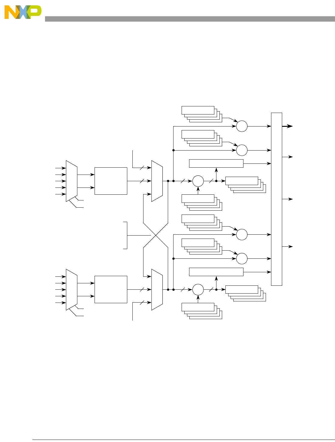
Analog-to-Digital Converter (ADC)
26-21 Freescale Semiconductor
26.5 Functional Description
The ADC’s conversion process is initiated by a sync signal from one of two input pins (SYNCx) or by
writing 1 to a STARTn bit.
Starting a single conversion actually begins a sequence of conversions, or a scan of up to 8 single-ended
or differential samples one at a time in sequential scan mode. The operation of the module in sequential
scan mode is shown in Figure 26-18.
Figure 26-18. Sequential Mode Operation of the ADC
Scan sequence is determined by defining eight sample slots in ADLST1/2 registers, processed in order
SAMPLE0-7 during sequential scan or in order SAMPLE0-3 by converter A and in order SAMPLE4-7 by
converter B in parallel scan. SAMPLE slots may be disabled using the SDIS register.
The following pairs of analog inputs can be configured as a differential pair: AN0-1, AN2-3, AN4-5, and
AN6-7. When configured as a differential pair, a reference to either member of the differential pair by a
sample slot results in a differential measurement using that differential pair.
AN3
AN2
AN1
AN0 V+
VREFL Channel Select
V– ADCA 12
Single-Ended vs
Crossbars allow AN0-3
to be stored in samples 4-7,
or AN4-7 to be stored in
samples 0-3
Differential
12 +
ADOFS[0:3]
13
Zero Crossing Logic
+
–
ADHLMT[4:7]
>
ADRSLT[0:3]
Zero Crossing
or Error Limit
Interrupt
ADLLMT[4:7]
<
12 12 +
ADOFS[4:7]
13
Zero Crossing Logic
+
–
ADRSLT[4:7]
12
AN7
AN6
AN5
AN4 V+
VREFL Channel Select
V– ADCB
Single-Ended vs
Differential
12
ADHLMT[0:3]
>
ADLLMT[0:3]
<
Test Data
(From CPU)
Test Data
(From CPU)
ADC2
ADC1
ADC0
End of
Scan B
Interrupt
End of
Scan A
Interrupt
IRQ Logic
MCF52211 ColdFire® Integrated Microcontroller Reference Manual, Rev. 3

Analog-to-Digital Converter (ADC)
Freescale Semiconductor 26-22
Parallel scan can be simultaneous or non-simultaneous. During simultaneous scan, the scans in the two
converters are done simultaneously and always result in simultaneous pairs of conversions, one by
converter A and one by converter B. The two converters share the same start, stop, sync, end-of-scan
interrupt enable control, and interrupt. Scanning in both converters is terminated when either converter
encounters a disabled sample. In non-simultaneous scan, the parallel scans in the two converters are
achieved independently. The two converters have their own start, stop, sync, end-of-scan interrupt enable
controls, and end-of-scan interrupts. Scanning in either converter terminates only when that converter
encounters a disabled sample in its part of SDIS register (DS0-DS3 for A, DS4-DS7 for B).
Figure 26-19. Parallel Mode Operation of the ADC
The ADC can be configured to perform a single scan and halt, perform a scan when triggered, or perform
the scan sequence repeatedly until manually stopped. The single scan (once mode) differs from the
triggered mode only in that SYNC input signals must be re-armed after each using a once mode scan, and
subsequent SYNC inputs are ignored until the SYNC input is re-armed. This arming can occur anytime
after the SYNC pulse occurs, even while the scan it initiated remains in process.
AN3
AN2
AN1
AN0 V+
VREFL Channel Select
V– ADCA 12
Single-Ended vs
Crossbars do
not operate in
Differential
12 +
ADOFS[0:3]
13
Zero Crossing Logic
+
–
ADHLMT[4:7]
>
ADRSLT[0:3]
Zero Crossing
or Error Limit
Interrupt
ADLLMT[4:7]
<
12 12 +
ADOFS[4:7]
13
Zero Crossing Logic
+
–
ADRSLT[4:7]
12
AN7
AN6
AN5
AN4 V+
VREFL Channel Select
V– ADCB
Single-Ended vs
Differential
12
ADHLMT[0:3]
>
ADLLMT[0:3]
<
Test Data
(From CPU)
Test Data
(From CPU)
ADC2
ADC1
ADC0
End of
Scan B
Interrupt
End of
Scan A
Interrupt
IRQ Logic
this mode
MCF52211 ColdFire® Integrated Microcontroller Reference Manual, Rev. 3

Analog-to-Digital Converter (ADC)
26-23 Freescale Semiconductor
Optional interrupts can be generated at the end of a scan sequence. Interrupts are available simply to
indicate the scan ended, that a sample was out of range, or at several different zero crossing conditions.
Out-of-range is determined by the high and low limit registers.
To understand the operation of the ADC, it is important to understand the feature and limitations of each
of the functional parts.
26.5.1 Input MUX Function
The input MUX function is shown in Figure 26-20. The channel select and single ended vs. differential
switches are indirectly controlled based on settings within the LIST1, LIST2, and SDIS registers, and the
CHNCFG field of the CTRL1 register.
1. MUXing for Sequential mode, single-ended conversions—During each conversion cycle (sample),
any one input of the two muxes can be directed to any ADRSLTn register.
2. MUXing for sequential mode, differential conversions—During any conversion cycle (sample),
either member of a differential pair may be referenced as a SAMPLE, resulting in a differential
measurement on that pair being stored in the corresponding ADRSLTn register.
3. MUXing for parallel mode, single-ended conversions—During any conversion cycle (sample), any
of AN0-AN3 can be directed to ADRSLT0-3 and any of AN4-AN7 can be directed to ADRSLT4-7.
4. MUXing for parallel mode, differential conversions—During any conversion cycle (sample),
either member of differential pair AN0/1 or either member of differential pair AN2/3 can be
referenced as a SAMPLE, resulting in a differential measurement of that pair being stored in one
of the ADRSLT0-3 registers. Likewise, either member of differential pair AN4/5 or either member
of differential pair AN6/7 can be referenced as a SAMPLE, resulting in a differential measurement
of that pair being stored in one of the ADRSLT4-7 registers.
Details of switch operation is shown in Table 26-20. Internally, all measurements are performed
differentially. During single ended measurements, VREFL is used as the negative (-) input voltage, while
the selected analog input is used as the positive (+) input.
Table 26-20. Analog MUX Controls for Each Conversion Mode
Conversion Mode Channel Select Switches Single Ended Differential Switches
Sequential, Single Ended The two 1-of-4 select muxes can be
set for the appropriate input line.
The lower switch selects VREFL for the
V- input of the A/D. The upper switch is
always closed so that any of the four
inputs can get to the V+ A/D input.
Sequential, Differential The channel select switches are
turned on in pairs, providing a dual
1-of-2 select function, such that either
of the two differential channels can be
routed to the A/D input.
The upper switch is open and the
bottom switch selects the differential
channel for the V- input of the A/D.
MCF52211 ColdFire® Integrated Microcontroller Reference Manual, Rev. 3
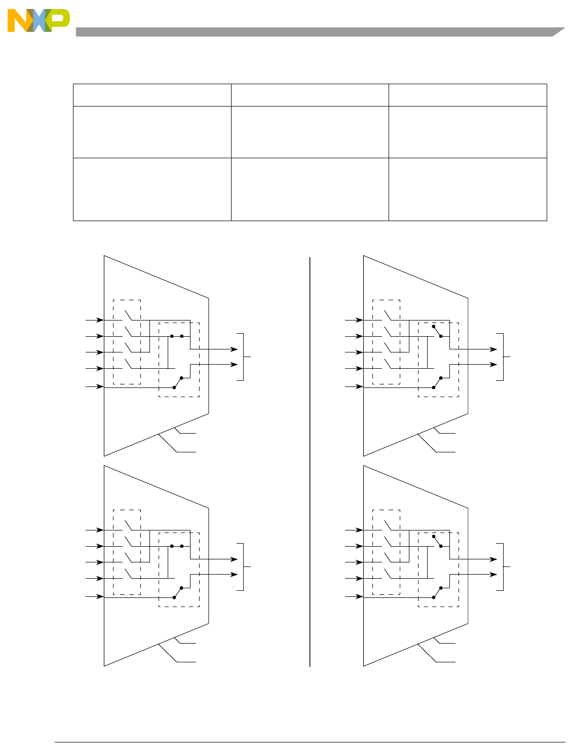
Analog-to-Digital Converter (ADC)
Freescale Semiconductor 26-24
Figure 26-20. Input Select Mux
Parallel, Single Ended The two 1-of-4 select muxes can be
set for the appropriate input line.
The lower switch selects VREFL for the
V- input of the A/D. The upper switch is
always closed so that any of the four
inputs can get to the V+ A/D input.
Parallel, Differential The channel select switches are
turned on in pairs, providing a dual
1-of-2 select function, such that either
of the two differential channels can be
routed to the A/D input.
The upper and lower switches are
open and the middle switch is closed,
providing the differential channel to
the differential input of the A/D.
Table 26-20. Analog MUX Controls for Each Conversion Mode (continued)
Conversion Mode Channel Select Switches Single Ended Differential Switches
AN3
AN2
AN1
AN0
VREFL
V+
V–
Channel
Select
To
Converter A
Single-Ended
Interface
Function
MUX Configuration for Differentialvs
Channel Select
Single-Ended vs
Differential
AN7
AN6
AN5
AN4
VREFL
V+
V–
Channel
Select
To
Converter B
Single-Ended
Interface
Function
AN3
AN2
AN1
AN0
VREFL
V+
V–
Channel
Select
To
Converter A
Differential
Interface
Function
AN7
AN6
AN5
AN4
VREFL
V+
V–
Channel
Select
To
Converter B
Differential
Interface
Function
Channel Select
Single-Ended vs
Differential
Channel Select
Single-Ended vs
Differential
Channel Select
Single-Ended vs
Differential
MUX Configuration for Single-Ended
MCF52211 ColdFire® Integrated Microcontroller Reference Manual, Rev. 3
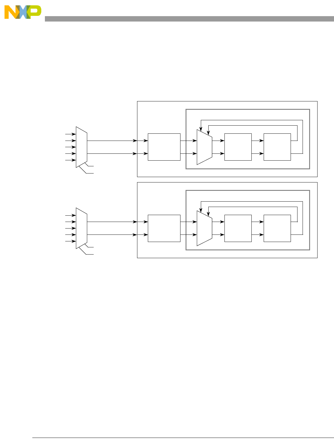
Analog-to-Digital Converter (ADC)
26-25 Freescale Semiconductor
26.5.2 ADC Sample Conversion
The ADC consists of a cyclic, algorithmic architecture using two recursive sub-ranging sections (RSD#1
and RSD#2), shown in Figure 26-21. Each sub-ranging section resolves a single bit for each conversion
clock, resulting in an overall conversion rate of two bits per clock cycle. Each sub-ranging section is
designed to run at a maximum clock speed of 5.0 MHz. Thus a complete 12-bit conversion takes 6 ADC
clocks (1.2 s), not including sample or post processing time.
Figure 26-21. Cyclic ADC — Top Level Block Diagram
The input mode for a given sample is determined by the CHNCFG field of the CTRL1 register. The ADC
has two input modes:
1. Single-ended mode (CHNCFG bit=0)—In single-ended mode, input mux of the ADC selects one
of the analog inputs and directs it to the plus terminal of the A/D core. The minus terminal of the
A/D core is connected to the VREFL reference during this mode. The ADC measures the voltage of
the selected analog input and compares it against the (VREFH - VREFL) reference voltage range.
2. Differential mode (CHNCFG bit = 1)—In differential mode, the ADC measures the voltage
difference between two analog inputs and compares that against the (VREFH - VREFL) voltage
range. The input is selected as an input pair: AN0/1, AN2/3, AN4/5, or AN6/7. In this mode, the
plus terminal of the A/D core is connected to the even analog input, while the minus terminal is
connected to the odd analog input.
A mix and match combination of differential and single-ended configurations may exist.
Examples:
• AN0 and AN1 differential, AN2 and AN3 single-ended
• AN4 and AN5 differential, AN6 and AN7 single-ended
Interface
Function RSD#1
1
RSD#2
2
Cyclic ADC Core
ADCB
MUX
AN3
AN2
AN1
AN0 V+
VREFL Channel Select
V–
Single-Ended vs
Differential
Interface
Function RSD#1
1
RSD#2
2
V+
V–
Cyclic ADC Core
ADCA
AN7
AN6
AN5
AN4 V+
VREFL Channel Select
V–
Single-Ended vs
Differential
V+
V–
MUX
MCF52211 ColdFire® Integrated Microcontroller Reference Manual, Rev. 3

Analog-to-Digital Converter (ADC)
Freescale Semiconductor 26-26
26.5.2.1 Single-Ended Samples
The ADC module performs a ratio metric conversion. For single ended measurements, the digital result is
proportional to the ratio of the analog input to the reference voltage in the following formula:
Single-ended measurements return the max value 32760 when the input is at VREFH, return 0 when the
input is at VREFL, and scale linearly between based on the amount by which the input exceeds VREFL.
26.5.2.2 Differential Samples
For differential measurements, the digital result is proportional to the ratio of the difference in the inputs
to the difference in the reference voltages (VREFH and VREFL). Figure 26-22 shows typical configurations
for differential inputs.
When converting differential measurements, the following formula is useful:
Differential measurements return the max value 32760 (= 4095 8) when the plus () input is VREFH and
the minus ( input is VREFL, return 0 when the plus () input is at VREFL and the minus ( input is at
VREFL, and scale linearly between based on the voltage difference between the two signals.
SingleEndedValue round VIN VREFL–
VREFH VREFL–
----------------------------------------- 4095()8=
VIN = Applied voltage at the input pin
VREFH and VREFL = Voltage at the external reference pins on the device (typically VREFH = VDDA and VREFL
= VSSA)
Note: The 12-bit result is rounded to the nearest LSB.
Note: The ADC is a 12-bit function with 4096 possible states. However, the 12 bits have been left
shifted three bits on the 16-bit data bus so its magnitude, as read from the data bus, is now
32760.
DifferentialValue round VIN1VIN2–
VREFH VREFLO–
-------------------------------------------4095()8=
VIN = Applied voltage at the input pin
VREFH and VREFL = Voltage at the external reference pins on the device (typically VREFH = VDDA and VREFL =
VSSA)
Note: The 12-bit result is rounded to the nearest LSB.
Note: The ADC is a 12-bit function with 4096 possible states. However, the 12 bits have been left
shifted three bits on the 16-bit data bus so its magnitude, as read from the data bus, is now
32760.
MCF52211 ColdFire® Integrated Microcontroller Reference Manual, Rev. 3
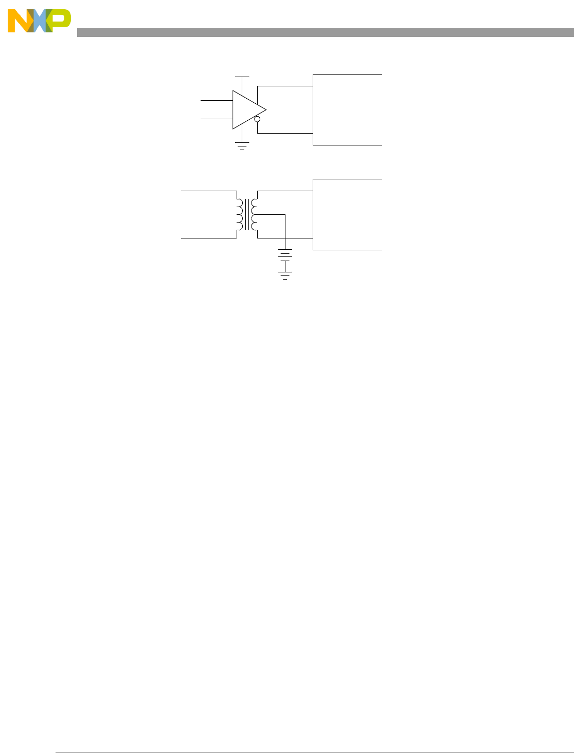
Analog-to-Digital Converter (ADC)
26-27 Freescale Semiconductor
Figure 26-22. Typical Connections for Differential Measurements
26.5.3 ADC Data Processing
As shown in Figure 26-23, the raw result of the ADC conversion process is sent to an adder for offset
correction. The adder subtracts the ADOFSn register value from each sample and the result is stored in the
corresponding result register (ADRSLTn). Concurrent to this the raw ADC value is checked for limit
violations, and the ADRSLTn values are checked for zero-crossing. Appropriate interrupts are asserted, if
enabled.
The sign of the result is calculated from the ADC unsigned result minus the respective offset register. If
the offset register is programmed with a value of zero, the result register value is unsigned and equals the
cyclic converter unsigned result. The range of the result registers (ADRSLTn) is 0x0000–0x7FF8,
assuming the offset (ADOFSn) registers are set to zero.
The processor can write to the result registers when the ADC is in stop mode or powered down. The data
from this write operation is treated as if it came from the ADC analog core; so the limit checking, zero
crossing, and the offset registers function as if in normal mode. For example, if the ADC is stopped and
the processor writes to ADRSLT5, the data written to ADRSLT5 is muxed to the ADC digital logic inputs,
processed, and stored into ADRSLT5, as if the analog core had provided the data. This test data must be
left justified by 3 bits (as shown in the ADRSLT register definition) and does not include the sign bit. The
sign bit (SEXT) is calculated during subtraction of the corresponding ADOFSn offset value.
+
–
AN+
AN–
Differential buffer centers about mid-point
AN+
AN–
VREF/2
Center tap held at (VREFH + VREFL) /2
NOTE: Normally, VREFL is
VREFH Potential
set to VSSA = 0V
MCF52211 ColdFire® Integrated Microcontroller Reference Manual, Rev. 3
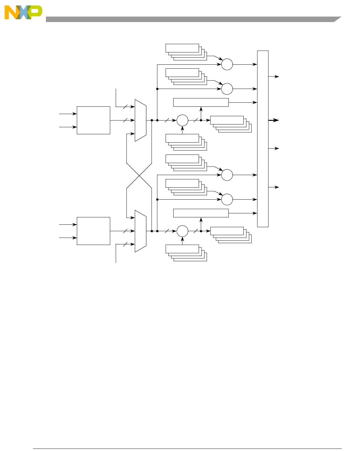
Analog-to-Digital Converter (ADC)
Freescale Semiconductor 26-28
Figure 26-23. Result Register Data Manipulation
26.5.4 Sequential vs. Parallel Sampling
All scan modes make use of the 8 SAMPLE slots in the ADLST1 and ADLST2 registers. These slots are
used to define which single-ended input or differential input pair is measured at each step in a scan
sequence. The SDIS register is used to disable unneeded slots.
Differential measurements are made on input pairs AN0/1, AN2/3, AN4/5, and AN6/7 using the CHNCFG
field of the CTRL1 register. A single ended measurement is made if a SAMPLE slot refers to an input not
configured as a member of a differential pair by CHNCFG. A differential measurement is made if a
SAMPLE slot refers to either member of a differential pair. Refer to the CHNCFG field description in the
CTRL1 register for details of differential and single ended measurement.
Scan modes are sequential or parallel, as defined by the SMODE field of the CTRL1 register. In
sequential scans, up to 8 SAMPLE slots are sampled one at a time in the order SAMPLE 0-7. Each
SAMPLE slot may refer to any of the 8 analog inputs (AN0-7), thus the same input may be referenced by
more than one SAMPLE slot. Scanning is initiated when the START0 bit is written as 1 or, if the SYNC0
V+
V– ADCA 12 12 +
ADOFS[0:3]
13
Zero Crossing Logic
+
–
ADHLMT[4:7]
>
ADRSLT[0:3]
Zero Crossing
or Error Limit
Interrupt
ADLLMT[4:7]
<
12 12 +
ADOFS[4:7]
13
Zero Crossing Logic
+
–
ADRSLT[4:7]
12
V+
V– ADCB
12
ADHLMT[0:3]
>
ADLLMT[0:3]
<
Test Data
(From CPU)
Test Data
(From CPU)
ADC2
ADC1
ADC0
End of
Scan B
Interrupt
End of
Scan A
Interrupt
IRQ Logic
MCF52211 ColdFire® Integrated Microcontroller Reference Manual, Rev. 3

Analog-to-Digital Converter (ADC)
26-29 Freescale Semiconductor
bit is 1, when the SYNC0 input goes high. A scan ends when the first disabled sample slot is encountered
in the SDIS register. Completion of the scan triggers the EOSI0 interrupt if the interrupt is enabled by the
EOSIE0 bit. The START0 bit and SYNC0 input are ignored while a scan is in process. Scanning stops and
cannot be initiated when the STOP0 bit is set.
Parallel scans differ in that converter A collects up to 4 samples (SAMPLE 0-3) in parallel to converter B
collecting up to 4 samples (SAMPLE 4-7). SAMPLEs 0-3 may only reference inputs AN0-3, and
SAMPLEs 4-7 may only reference inputs AN4-7. Within these constraints, any sample may reference any
pin and the same input may be referenced by more than one sample slot.
By default (when SIMULT=1), parallel scans of the converters are initiated together when the START0 bit
is written as 1 or, if the SYNC0 bit is 1, when the SYNC0 input goes high. The scan in both converters
terminates when either converter encounters a disabled sample slot in SDIS. Completion of a scan triggers
the EOSI0 interrupt provided the EOSIE0 interrupt enable is set. Samples are always taken simultaneously
in the A and B converters. Setting the STOP0 bit stops and prevents the initiation of scanning in both
converters.
Setting SIMULT equal to 0 (non-simultaneous mode) causes parallel scanning to operate independently in
the A and B converter. Each converter has its own set of STARTn, STOPn, SYNCn, and EOSIEn control
bits, SYNCn input, EOSIn interrupt, and CIPn status indicators (n = 0 for converter A, n = 1 for converter
B). Although continuing to operate in parallel, the scans in the A and B converter start and stop
independently according to their own controls. They may be simultaneous, phase shifted, or asynchronous,
depending on when scans are initiated on the respective converters. The A and B converter may be of
different length (up to a maximum of four) and each converter’s scan completes when a disabled sample
is encountered in that converters sample list only. STOP0 only stops the A converter, and STOP1 only
stops the B converter. Looping scan modes repeat independently, with the A converter capturing SAMPLE
0-3, and B converter capturing SAMPLE 4-7. In loop modes, each converter independently restarts its scan
after capturing its samples.
26.5.5 Scan Sequencing
Scan modes break down into three types based on how they repeat: once, triggered, or loop. Be certain to
read Section 26.5.4, “Sequential vs. Parallel Sampling” to understand the operation of sequential and
parallel scan modes before proceeding.
During a once mode scan, a single sequential or parallel scan is executed. Once scan modes differ from
triggered scan modes in that they must be re-armed after each use. While all scan modes ignore sync pulses
occurring while a scan is in process, once scan modes continues to ignore sync pulses even after the scan
completes until re-armed. However, re-arming can occur any time, including during the scan, by writing
to a CTRLn register. If operating in a sequential mode or simultaneous parallel, write to the CTRL1
register. If operating in a non-simultaneous parallel mode, re-arm converter A by writing to the CTRL1
register and converter B by writing to the CTRL2 register.
Triggered scan modes are identical to the corresponding once scan modes, except that re-arming of sync
inputs is not necessary.
Loop scan modes automatically restart a scan as soon as the previous scan completes. In the loop
sequential mode, up to 8 samples are captured in each loop, and the next scan starts immediately after the
MCF52211 ColdFire® Integrated Microcontroller Reference Manual, Rev. 3

Analog-to-Digital Converter (ADC)
Freescale Semiconductor 26-30
completion of the previous scan. In loop parallel scan modes, both converters restart together if
SIMULT equals 1 and restart independently if SIMULT equals 0. All subsequent start and sync pulses are
ignored after the scan begins. Scanning can only be terminated by setting a STOPn bit. Use STOP0 in the
CTRL1 register if operating in a sequential or simultaneous parallel mode. If operating in a
non-simultaneous parallel mode, use STOP0 to stop converter A and STOP1 in the CTRL2 register to stop
converter B.
26.5.6 Scan Configuration and Control
The operation of the ADC module is controlled by the CTRL1 and CTRL2 registers. The CTRL1 register
is described in Section 26.4.1, “Control 1 Register (CTRL1)”. The structure of the CTRL2 register
depends on whether the ADC is in sequential-scan or parallel-scan mode (see Section 26.4.2.1, “CTRL2
Under Sequential Scan Modes” and Section 26.4.2.2, “CTRL2 Under Parallel Scan Modes”, respectively).
These are used to set the scan mode, configure channels, and start/stop scans.
The ADC can operate in several sequential or parallel scan modes, as determined by CTRL1[SMODE].
These are summarized in Table 26-21. When the ADC operates in a parallel scan mode, its functionality
can be further controlled by CTRL2[SIMULT].
All scan modes make use of the 8 sample slots defined by the ADLST1 and ADLST2 registers. A scan is
the process of stepping through these sample slots, converting the analog input indicated by that slot, and
storing the result. Slots that are not required may be disabled by writing 1 to the appropriate bits of the
SDIS register.
Input pairs AN0-1, AN2-3, AN4-5, and AN6-7 may be configured as differential pairs using
CTRL1[CHNCFG]. When a slot in ADLSTn refers to either member of a differential pair, a differential
measurement on that pair is made; otherwise, a single-ended measurement is taken on that input. The
details of single-ended and differential measurements are described in Section 26.5.2.1, “Single-Ended
Samples” and Section 26.5.2.2, “Differential Samples”, respectively.
CTRL1[SMODE] determines whether the slots are used to perform a sequential scan of up to 8 samples
or 2 parallel scans up to 4 samples. It also controls how these scans are initiated/terminated and whether
the scans are performed one time or repetitively. For more details, please see Figure 26-18 and
Figure 26-19.
Parallel scans may be simultaneous or non-simultaneous depending on CTRL2[SIMULT]. This bit only
applies to parallel operating modes and is ignored during sequential operating modes. During simultaneous
parallel scans, A and B converters scan synchronously using one set of shared controls (CTRL1 register).
During non-simultaneous scans, the A and B converters operate asynchronously with each converter using
its own independent set of controls (CTRL1 for A and CTRL2 for B). Refer to Section 26.4.2.2, “CTRL2
Under Parallel Scan Modes,” for more information.
MCF52211 ColdFire® Integrated Microcontroller Reference Manual, Rev. 3

Analog-to-Digital Converter (ADC)
26-31 Freescale Semiconductor
Table 26-21. ADC Scan Modes
Scan Mode Description
Once sequential Upon START or an enabled sync signal, samples are taken one at a time starting
with SAMPLE0 until a first disabled sample is encountered. If no disabled sample
is encountered in the ADSDIS register, conversion concludes after SAMPLE7. If
the scan is initiated by a sync signal, only one scan is completed until the
converter is rearmed by writing to the CTRL1 register.
Once parallel Upon START or an armed and enabled sync signal, converter A captures
samples 0-3 and converter B captures samples 4-7. By default
(CTRL2[SIMULT]=1), samples are taken simultaneously (synchronously), and
scanning stops when either converter encounters a disabled sample or both
converters complete all four samples. When SIMULT equals 0, samples are
taken asynchronously, and scanning stops when each converter encounters a
disabled sample in its part of the SDIS register or completes all 4 samples. If the
scan is initiated by a sync signal, only one scan is completed until the converter
is re-armed by writing to the CTRL1 register. (When SIMULT equals 0, the B
converter must be re-armed separately by writing to the CTRL2 register.)
Loop sequential Upon an initial start or enabled sync pulse, up to 8 samples are taken one at a
time until a disabled sample is encountered. The process repeats until the
STOP0 bit is set. While a loop mode is running, any additional start commands
or sync pulses are ignored. If auto standby (POWER[ASB]=1) or auto
power-down (POWER[APD]=1) is the selected power mode control, the
power-up delay defined by PUDELAY is applied only on the first conversion.
Loop parallel Upon an initial start or enabled sync pulse, converter A captures Samples 0-3,
and converter B captures Samples 4-7. Each time a converter completes its
current scan, it immediately restarts its scan sequence. This continues until a
STOPn bit is asserted. While a loop is running, any additional start commands
or sync pulses are ignored. By default (CTRL2[SIMULT]=1), samples are taken
simultaneously (synchronously), and scanning stops when either converter
encounters a disabled sample or both converters complete all four samples.
When SIMULT equals 0, samples are taken asynchronously, and scanning stops
when each converter encounters a disabled sample in its part of the SDIS
register or completes all 4 samples. If auto standby or auto power-down is the
selected power mode control, the power-up delay defined by PUDELAY is
applied only on the first conversion.
Triggered sequential Upon START or an enabled sync signal, samples are taken one at a time starting
with SAMPLE0 until a first disabled sample is encountered. If no disabled sample
is encountered, conversion concludes after SAMPLE7. If external sync is
enabled, new scans are started for each sync pulse that is non-overlapping with
a current scan in progress.
Triggered parallel (default) Upon START or an enabled sync signal, converter A converts Samples 0-3, and
converter B converts Samples 4-7 in parallel. By default (CTRL2[SIMULT]=1),
samples are taken simultaneously (synchronously), and scanning stops when
either converter encounters a disabled sample or both converters complete all
four samples. When CTRL2[SIMULT] equals 0, samples are taken
asynchronously, and scanning stops when each converter encounters a disabled
sample in its part of the ADSDIS register or completes all 4 samples. If external
sync is enabled (SYNC0=1), new scans are started for each sync pulse as long
as the ADC has completed the previous scan (STAT[CIPn]=0).
MCF52211 ColdFire® Integrated Microcontroller Reference Manual, Rev. 3
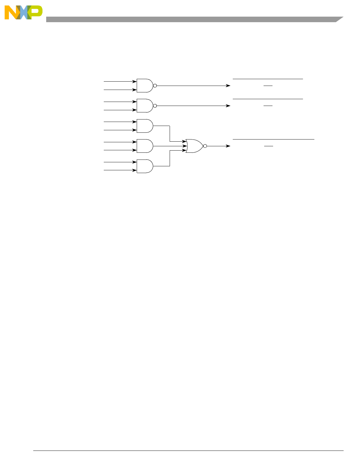
Analog-to-Digital Converter (ADC)
Freescale Semiconductor 26-32
26.5.7 Interrupt Sources
Figure 26-24 illustrates how five interrupt sources are combined into three entries in the interrupt vector
table.
Figure 26-24. ADC Interrupt Sources
26.5.8 Power Management
The five supported power modes are described below. They are in order of highest to lowest power
utilization at the expense of increased conversion latency and/or startup delay. Please see Section 26.5.9,
“ADC Clock,” for details of the various clocks referenced below.
26.5.8.1 Power Management Modes
1. Normal power mode
This mode operates when:
— At least one ADC converter is powered up (PD0 or PD1=0 in the POWER register);
— Auto power-down and auto standby modes are disabled (APD=0, ASB=0 in the POWER
register);
— The ADC’s clock is enabled (ADC=1 in the SIM module’s SIM_PCE register).
In this mode, the ADC uses the conversion clock as the ADC clock source when active or idle. To
minimize conversion latency, it is recommended the conversion clock be configured to 5.0 MHz. No
startup delay (defined by PUDELAY in the POWER register) is imposed.
2. Auto power-down mode
This mode operates when:
— At least one ADC converter is powered up (PD0 or PD1=0 in the POWER register);
— Auto power-down mode is enabled (APD=1 in the POWER register);
— The ADC’s clock is enabled (ADC=1 in the SIM module’s SIM_PCE register).
Auto power-down and standby modes can be used together by setting APD equal to 1 in the above
configuration. This hybrid mode converts at an ADC clock rate of 100 kHz using standby current mode
when active, and gates off the ADC clock and powers down the converters when idle. A startup delay of
EOSI0
EOSIE0
EOSI1
EOSIE1
ZCI
ZCIE
ADC Zero Crossing or Limit Error
LLMTIE
HLMTI
HLTMIE
LLMTI
(ADC_ERR_INT)
ADCB Conversion Complete
(ADC_CC1_INT)
ADCA Conversion Complete
(ADC_CC0_INT)
MCF52211 ColdFire® Integrated Microcontroller Reference Manual, Rev. 3

Analog-to-Digital Converter (ADC)
26-33 Freescale Semiconductor
PUDELAY ADC clock cycles execute at the start of all scans while the ADC engages the conversion clock
and the ADC powers up, stabilizing in the standby current mode. This provides the lowest possible power
configuration for ADC operation.
3. Auto standby mode
This mode operates when:
— At least one ADC converter is powered up (PD0 or PD1=0 in the POWER register);
— Auto power-down is disabled (APD=0 in the POWER register);
— Auto standby is enabled (ASB=1 in the POWER register);
— The ADC’s clock is enabled (ADC=1 in the SIM module’s SIM_PCE register);
— The relaxation oscillator must be enabled for 8-MHz operation or the external oscillator clock
must be running at 8 MHz in this mode.
In auto standby mode, the ADC uses the conversion clock when active and the100 kHz Standby clock
when idle. The standby (low current) state automatically engages when the ADC is idle. The ADC
executes a startup delay of PUDELAY ADC clocks at the start of all scans, allowing the ADC to switch to
the Conversion clock and to revert from standby to normal current mode.
It is recommended the conversion clock be configured at or near 5.0 MHz to minimize conversion latency
when active. In this mode, the ADC uses the conversion clock when active and gates off the conversion
clock and powers down the converters when idle. A startup delay of PUDELAY ADC clocks is executed
at the start of all scans, allowing the ADC to stabilize when switching to normal current mode from a
completely powered off condition. This mode uses less power than normal and more power than auto
standby. It requires more startup latency than auto standby when leaving the idle state to start a scan (higher
PUDELAY value).
4. POWER-DOWN MODE
This mode operates when:
— Both ADC converters are powered down (PD0=PD1=1 in the POWER register);
— The ADC’s clock is disabled (ADC=0 in the SIM module’s SIM_PCE register).
In this configuration, the clock trees to the ADC and all of its analog components are shut down
and the ADC uses no power.
26.5.8.2 Power Management Details
The ADC voltage reference and converters are powered down (PDn=1 in the POWER register) on reset.
Individual converters can be manually powered down when not in use (PD0=1 or PD1=1), and the voltage
reference can be automatically powered down when no converter is in use (PD2=1) or manually powered
up when no converters are powered (PD2=0). When the ADC voltage reference is powered down, output
reference voltages are set to low (VSSA).
A delay of PUDELAY ADC clock cycles is imposed when PD0 or PD1 are cleared to power-up a converter
and when the ADC goes from an idle (neither converter has a scan in process) to an active state when not
operating in normal power mode. The ADC is active when at least one converter has a scan in process. A
device recommends the use of two PUDELAY values: a large value for full power-up and a smaller value
for going from standby current levels to full power-up. The following paragraphs provide an explanation
of how to use PUDELAY when starting the ADC up or changing modes.
MCF52211 ColdFire® Integrated Microcontroller Reference Manual, Rev. 3

Analog-to-Digital Converter (ADC)
Freescale Semiconductor 26-34
When starting up in normal mode, first set PUDELAY to the large power-up value. Next, clear the PD0
and or PD1 bits to power-up the required converters. Poll the status bits (PSTSn in the POWER register)
until all required converters are powered up. Following polling, start scan operations. The value in
PUDELAY provides a power-up delay before scans begin. Because normal mode does not use PUDELAY
at start of scans, no further delays are imposed.
When starting up using auto standby mode, first use the normal mode startup procedure. Before starting
scan operations, set PUDELAY to the smaller value, then set ASB in the POWER register. Auto standby
mode automatically reduces current levels until active and then impose a PUDELAY wait to allow current
levels to rise from standby to normal levels.
When starting up using auto power-down mode, first use the normal mode startup procedure. Before
starting scan operations, set PUDELAY to the large power-up value. Next, set APD in the POWER
register. Finally, clear the PD0 and or PD1 bits for the required converters. Converters remain powered off
until scanning goes active, at which time the large PUDELAY executes as the ADC goes from powered
down to fully powered at the start of the scan.
In auto power-down mode, when the ADC goes from idle to active, a converter is only powered up if it is
required for the scan, as determined by the ADLST1, ADLST2, and SDIS registers.
It is recommended to power-off both converters (PD0=PD1=1 in the POWER register) when
re-configuring clocking or power controls to avoid generating bad samples and ensure proper delays are
applied when powering up or starting scans.
Attempts to start a scan during the PUDELAY time-out are ignored until the appropriate PSTSn bits are
cleared in the POWER register.
Any attempt to use a converter when powered down or with the voltage reference disabled results in
invalid results. It is possible to read ADC result registers after converter power down to see results
calculated before power-down. However, a new scan sequence must be started with a SYNCn pulse or a
write to the STARTn bit before new results are available.
26.5.8.3 ADC STOP Mode of Operation
Any conversion sequence in progress can be stopped by setting the relevant STOPn bit. Any further sync
pulses or writes to the STARTn bit are ignored until the STOPn bit is cleared. In this stop mode, the results
registers can be modified by writes from the processor. Any write to ADRSLTn in the ADC stop mode is
treated as if the analog core supplied the data, so limit checking, zero crossing, and associated interrupts
can occur if enabled.
26.5.9 ADC Clock
26.5.9.1 General
The ADC has two external clock inputs used to drive two clock domains within the ADC module.
MCF52211 ColdFire® Integrated Microcontroller Reference Manual, Rev. 3
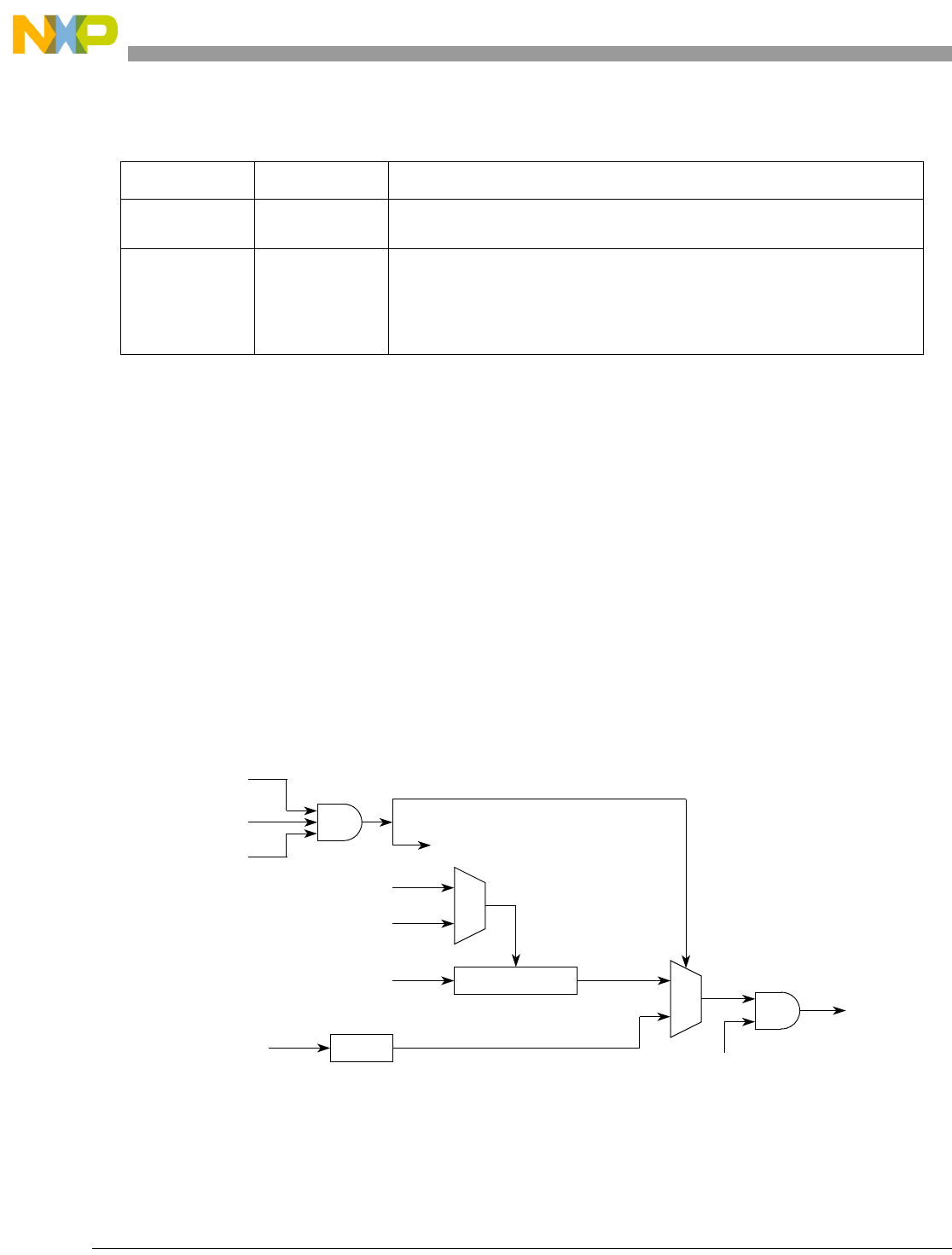
Analog-to-Digital Converter (ADC)
26-35 Freescale Semiconductor
26.5.9.2 Description of Clock Operation
As shown in Figure 26-25, the conversion clock is the primary source for the ADC clock and is always
selected as the ADC clock when conversions are in process. The DIV value in the CTRL2 register should
be configured so the conversion clock frequency falls between 100 kHz and 5.0 MHz. Operating the ADC
at out-of-spec clock frequencies degrades conversion accuracy. Similarly, modifying the parameters affect
clock rates or power modes while the regulators are powered up (PD0=0 or PD1=0) also degrades
conversion accuracy.
The conversion clock ADC uses for sampling is calculated using the IPBus clock and the clock divisor bits
within the CTRL2 register. Please see Section 26.4.1, “Control 1 Register (CTRL1)” or Section 26.4.2,
“Control 2 Register (CTRL2)”. The ADC clock is active 100% of the time while in loop modes, or if power
management is set to normal. It is also active during all ADC power-up for a period of time determined by
the PUDELAY field in the power (POWER) register. After the power-up delay times out, the ADC clock
continues until the completion of the ADCn scan when operating in auto standby or auto power-down
modes.
Figure 26-25. ADC Clock Generation
The oscillator clock feeds an 80:1 divider, generating the auto standby clock. The auto standby clock is
selected as the ADC clock during the auto standby power mode when both converters are idle. The auto
Table 26-22. ADC Clock Summary
Clock input Source Characteristics
Peripheral Clock
(=System Clock)
1/2 Core clock Maximum rate is PLL output divided by 2 if PLL enabled. When PLL disabled,
max rate is oscillator clock divided by 2.
ADC 8MHz Clock Relaxation
Oscillator (8MHz),
Crystal Oscillator
(1-16MHz), or
external Oscillator
Provides 8MHz for auto standby power saving mode.
0
0
1
CTRL2:DIV
(+2 x [DIV+1])
Peripheral (System) Clock
1/2 Core Frequency 0
1
Auto Power-Down
ADC Idle
Disabled (APD=0)
Auto Standby
Enabled (ASB=1)
Standby Current Mode Status
ADC Bit in SIM_PCE
(+80)
Oscillator Clock
(8MHz)
ADC Clock
Auto Standby Clock
(100kHz)
ADC
Conversion
Clock
DIV
MCF52211 ColdFire® Integrated Microcontroller Reference Manual, Rev. 3
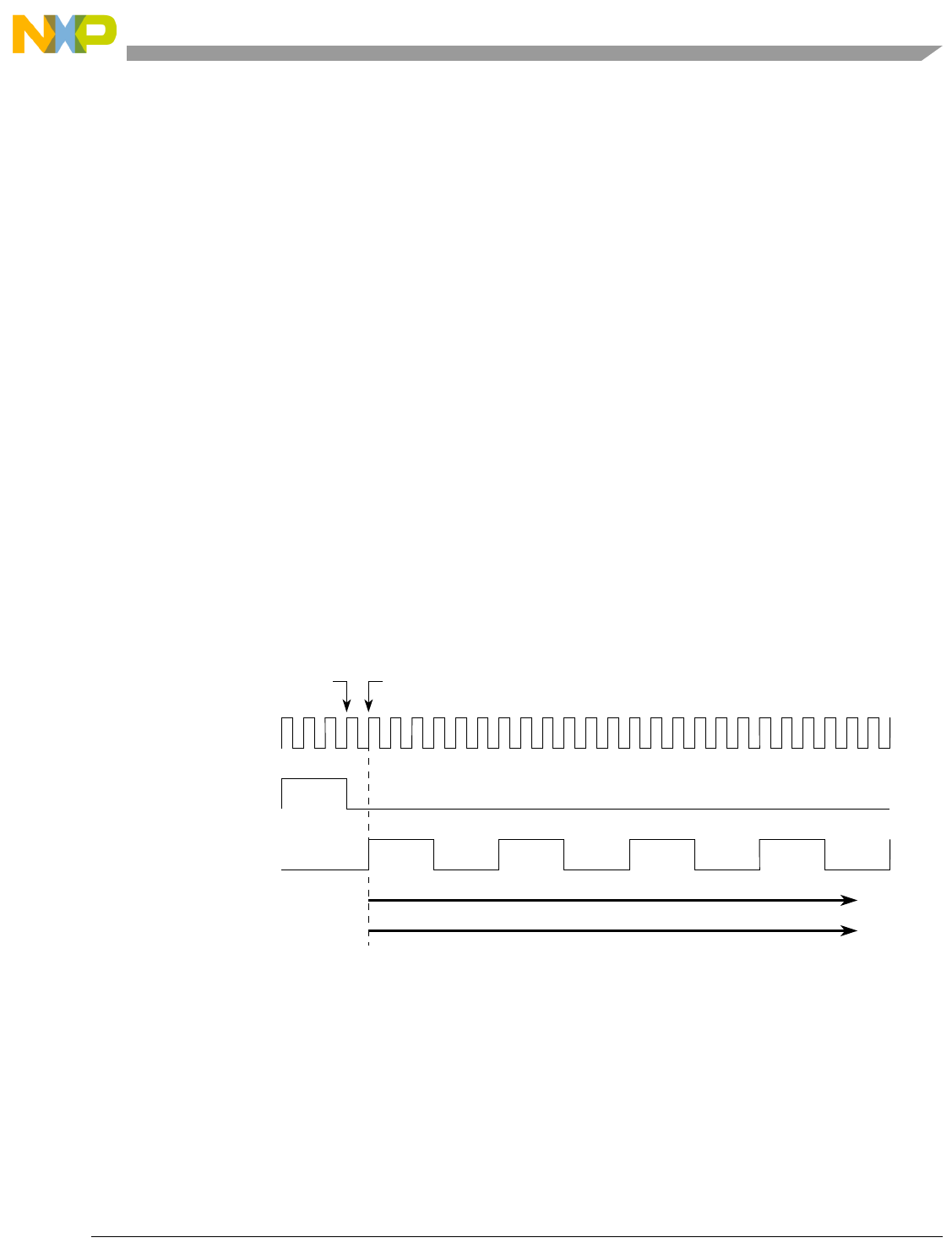
Analog-to-Digital Converter (ADC)
Freescale Semiconductor 26-36
standby power mode requires an 8 MHz oscillator clock from the relaxation oscillator, crystal oscillator,
or external oscillator.
26.5.9.3 ADC Clock Resynchronization at Start of Scan
At the fastest ADC speed, each ADC clock period is 6 system clock periods long. When asserting the start
of a scan, by writing to a STARTn bit or by a SYNCn signal, the ADC clock is re-synchronized to align it
to the system clock. This allows the commanded scan to begin as soon as possible rather than wait up to 5
additional system clocks for the start of the next ADC clock period. This is shown in Figure 26-26 for
sequential and simultaneous parallel modes of operation. In these modes, both ADCs operate off of the
same start signal.
In a parallel scan mode when SIMULT equals 0, both ADCs operate using independent STARTn bits and
SYNCn signals. As shown in Figure 26-27, the first scan started is re-synchronized to the system clock,
but the second scan may wait up to 5 additional system clocks before starting. Also, which converter is
synchronized to the system clock depends on which convert first starts to use the ADC. The case shown
has ADCA synchronized, but one could easily imagine the case where the ADCA start comes after instead
of before the ADCB start. In this case, ADCAs start would be delayed up to 5 additional system clock
periods instead of ADCBs.
If there is a known timing relationship between ADCA and ADCB when operating in a non-simultaneous
parallel mode, then the application can control which ADC starts first and gets the re-synchronized clock.
The application can also control the delay to starting the second ADC scan so that its start signal aligns
with the ADC clock, and the start of the second ADC is not delayed.
Figure 26-26. ADC Clock Resynchronization for
Sequential and Simultaneous Parallel Modes
START0
Asserted ADC Conversion Clock Resynchronized
ADC Scans Start
System Clock
Old ADC Clock
ADC Clock After
Resynchronization
ADCA Scan
ADCB Scan
MCF52211 ColdFire® Integrated Microcontroller Reference Manual, Rev. 3
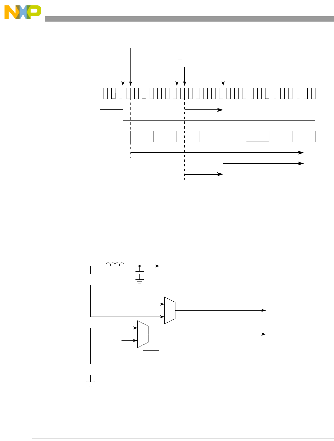
Analog-to-Digital Converter (ADC)
26-37 Freescale Semiconductor
Figure 26-27. ADC Clock Resynchronization for
Non-Simultaneous Parallel Modes
26.5.10 Voltage Reference Pins VREFH and VREFL
The voltage difference between VREFH and VREFL provides the reference voltage that all analog inputs are
measured against. The reference voltage should be provided from a low noise filtered source capable of
providing up to 1mA of reference current.
Figure 26-28. ADC Voltage Reference Circuit
When tying VREFH to the same potential as VDDA, relative measurements are being made with respect to
the amplitude of VDDA. It is imperative that special precautions be taken to assure the voltage applied to
START0
Asserted
System Clock
Old ADC Clock
ADC Clock After
Resynchronization
ADCA Scan
ADCB Scan
ADCB Scan Start
ADCB Scan Should Start Here
START1 Asserted
ADC Conversion Clock Resynchronized
ADCA Scan Start
Delay in start because ADC Clock cannot
be resynchronized: 5 System Clocks
Wait for next rising
edge of ADC
Conversion Clock
VRH
External
Reference
Voltage
V
RL
1.0mH
AN6
SEL_VREFL
VREFH to ADC
VREFL to ADC
SEL_VREFH
AN2
0.1F
MCF52211 ColdFire® Integrated Microcontroller Reference Manual, Rev. 3

Analog-to-Digital Converter (ADC)
Freescale Semiconductor 26-38
VREFH is as noise-free as possible. Any noise residing on the VREFH voltage is directly transferred to the
digital result.
Figure 26-28 illustrates the internal workings of the ADC voltage reference circuit. VREFH must be noise
filtered; a minimum configuration is shown in the figure.
26.5.11 Supply Pins VDDA and VSSA
Dedicated power supply pins are provided for the purposes of reducing noise coupling and to improve
accuracy. The power provided to these pins is suggested to come from a low noise filtered source.
Uncoupling capacitors ought to be connected between VDDA and VSSA.
MCF52211 ColdFire® Integrated Microcontroller Reference Manual, Rev. 3
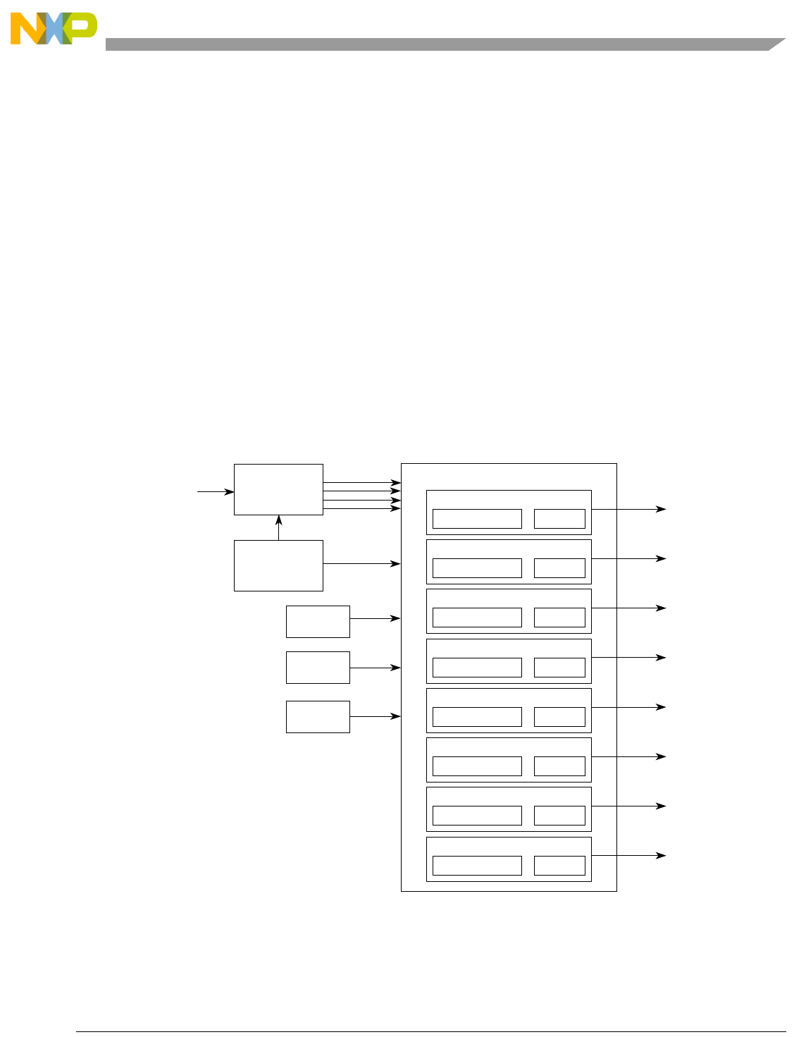
Freescale Semiconductor 27-1
Chapter 27
Pulse-Width Modulation (PWM) Module
27.1 Introduction
This chapter describes the configuration and operation of the pulse-width modulation (PWM) module. It
includes a block diagram, programming model, and functional description.
27.1.1 Overview
The PWM module, shown in Figure 27-1, generates a synchronous series of pulses having programmable
period and duty cycle. With a suitable low-pass filter, the PWM can be used as a digital-to-analog
converter.
Figure 27-1. PWM Block Diagram
Internal Bus
Clock (fsys)
Clock select
PWM Clocks
Period and Duty Counter
Channel 3
Period and Duty Counter
Channel 2
Period and Duty Counter
Channel 1
Period and Duty Counter
Channel 0
PWM Channels
Alignment
Polarity
Control
PWMOUT3
PWMOUT2
PWMOUT1
PWMOUT0
Enable Period and Duty Counter
Channel 5
Period and Duty Counter
Channel 4
PWMOUT5
PWMOUT4
Period and Duty Counter
Channel 7
Period and Duty Counter
Channel 6
PWMOUT7
PWMOUT6
MCF52211 ColdFire® Integrated Microcontroller Reference Manual, Rev. 3

Pulse-Width Modulation (PWM) Module
Freescale Semiconductor 27-2
Main features include the following:
• Double-buffered period and duty cycle
• Left- or center-aligned outputs
• Eight independent PWM modules
• Byte-wide registers provide programmable duty cycle and period control
• Four programmable clock sources
NOTE
The GPIO module must be configured to enable the peripheral function of
the appropriate pins (refer to Chapter 13, “General Purpose I/O Module”)
prior to configuring the PWM module.
27.2 Memory Map/Register Definition
This section describes the registers and control bits in the PWM module. There are eight independent
PWM modules, each with its own control and counter registers. The memory map for the PWM is shown
below.
Table 27-1. PWM Memory Map
IPSBAR Offset1,2
1Addresses not assigned to a register and undefined register bits are reserved for expansion. Write accesses to these
reserved address spaces and reserved register bits have no effect.
2A 32-bit access to any of these registers results in a bus transfer error.
Register Width
(bits) Access Reset Value Section/Page
Supervisor Read/Write Only Access
0x1B_0000 PWM Enable Register (PWME) 8 R/W 0x00 27.2.1/27-3
0x1B_0001 PWM Polarity Register (PWMPOL) 8 R/W 0x00 27.2.2/27-4
0x1B_0002 PWM Clock Select Register (PWMCLK) 8 R/W 0x00 27.2.3/27-4
0x1B_0003 PWM Prescale Clock Select Register (PWMPRCLK) 8 R/W 0x00 27.2.4/27-5
0x1B_0004 PWM Center Align Enable Register (PWMCAE) 8 R/W 0x00 27.2.5/27-6
0x1B_0005 PWM Control Register (PWMCTL) 8 R/W 0x00 27.2.6/27-7
0x1B_0008 PWM Scale A Register (PWMSCLA) 8 R/W 0x00 27.2.7/27-8
0x1B_0009 PWM Scale B Register (PWMSCLB) 8 R/W 0x00 27.2.8/27-9
0x1B_000C + n
n=0–7
PWM Channel n Counter Register (PWMCNTn) 8 R/W 0x00 27.2.9/27-9
0x1B_0014 + n
n=0–7
PWM Channel n Period Register (PWMPERn) 8 R/W 0xFF 27.2.10/27-10
0x1B_001C + n
n=0–7
PWM Channel n Duty Register (PWMDTYn) 8 R/W 0xFF 27.2.11/27-11
0x1B_0024 PWM Shutdown Register (PWMSDN) 8 R/W 0x00 27.2.12/27-12
MCF52211 ColdFire® Integrated Microcontroller Reference Manual, Rev. 3

Pulse-Width Modulation (PWM) Module
27-3 Freescale Semiconductor
27.2.1 PWM Enable Register (PWME)
Each PWM channel has an enable bit (PWMEn) to start its waveform output. While in run mode, if all
eight PWM output channels are disabled (PWME[7:0] = 0), the prescaler counter shuts off for power
savings. See Section 27.3.2.1, “PWM Enable” for more information.
IPSBAR
Offset:
0x1B_0000 (PWME) Access: Supervisor
Read/Write
76543210
R
PWME7 PWME6 PWME5 PWME4 PWME3 PWME2 PWME1 PWME0
W
Reset:00000000
Figure 27-2. PWM Enable Register (PWME)
Table 27-2. PWME Field Descriptions
Field Description
7
PWME7
PWM Channel 7 Enable. In normal mode, if enabled, the PWM signal becomes available at PWMOUT7 when its
corresponding clock source begins its next cycle. When PWMSDN[SDNEN] is set this channel is an input for
emergency shutdown.
0 PWM7 disabled
1 PWM7 enabled
6
PWME6
PWM Channel 6 Output Enable. If enabled, the PWM signal becomes available at PWMOUT6 when its
corresponding clock source begins its next cycle. If PWMCTL[CON67] is set, then this bit has no effect and
PWMOUT6 is disabled.
0 PWM output disabled
1 PWM output enabled
5
PWME5
PWM Channel 5 Output Enable. If enabled, the PWM signal becomes available at PWMOUT5 when its
corresponding clock source begins its next cycle.
0 PWM output disabled
1 PWM output enabled
4
PWME4
PWM Channel 4 Output Enable. If enabled, the PWM signal becomes available at PWMOUT4 when its
corresponding clock source begins its next cycle. If PWMCTL[CON45] is set, then this bit has no effect and
PWMOUT4 is disabled.
0 PWM output disabled
1 PWM output enabled
3
PWME3
PWM Channel 3 Output Enable. If enabled, the PWM signal becomes available at PWMOUT3 when its
corresponding clock source begins its next cycle.
0 PWM output disabled
1 PWM output enabled
2
PWME2
PWM Channel 2 Output Enable. If enabled, the PWM signal becomes available at PWMOUT2 when its
corresponding clock source begins its next cycle. If PWMCTL[CON23] is set, then this bit has no effect and
PWMOUT2 is disabled.
0 PWM output disabled
1 PWM output enabled, if PWMCTL[CON23]=0
MCF52211 ColdFire® Integrated Microcontroller Reference Manual, Rev. 3

Pulse-Width Modulation (PWM) Module
Freescale Semiconductor 27-4
27.2.2 PWM Polarity Register (PWMPOL)
The starting polarity of each PWM channel waveform is determined by the associated PWMPOL[PPOLn]
bit. If the polarity is changed while a PWM signal is being generated, a truncated or stretched pulse can
occur during the transition.
27.2.3 PWM Clock Select Register (PWMCLK)
Each PWM channel has the capability of selecting one of two clocks. For channels0, 1, 4, and 5, the clock
choices are clock A or SA. For channels2, 3, 6, and 7, the choices are clock B or SB. The clock selection
is done with the below PWMCLK[PCLKn] control bits. If a clock select is changed while a PWM signal
is being generated, a truncated or stretched pulse can occur during the transition.
1
PWME1
PWM Channel 1 Output Enable. If enabled, the PWM signal becomes available at PWMOUT1 when its
corresponding clock source begins its next cycle.
0 PWM output disabled
1 PWM output enabled
0
PWME0
PWM Channel 0 Output Enable. If enabled, the PWM signal becomes available at PWMOUT0 when its
corresponding clock source begins its next cycle. If PWMCTL[CON01] is set, then this bit has no effect and
PWMOUT0 is disabled.
0 PWM output disabled
1 PWM output enabled, if PWMCTL[CON01]=0
IPSBAR
Offset:
0x1B_0001 (PWMPOL) Access:
SupervisorRead/Write
76543210
R
PPOL7 PPOL6 PPOL5 PPOL4 PPOL3 PPOL2 PPOL1 PPOL0
W
Reset:00000000
Figure 27-3. PWM Polarity Register (PWMPOL)
Table 27-3. PWMPOL Field Descriptions
Field Description
7–0
PPOLn
PWM Channel n Polarity. The even-numbered channels’ polarity has no effect when the corresponding
PWMCTL[CONn(n+1)] bit is set. For example, if PWMCTL[CON01] equals 1, PWMPOL[PPOL0] has no affect.
0 PWM channel n output is low at the beginning of the period, then goes high when the duty count is reached
1 PWM channel n output is high at the beginning of the period, then goes low when the duty count is reached
Table 27-2. PWME Field Descriptions (continued)
Field Description
MCF52211 ColdFire® Integrated Microcontroller Reference Manual, Rev. 3

Pulse-Width Modulation (PWM) Module
27-5 Freescale Semiconductor
27.2.4 PWM Prescale Clock Select Register (PWMPRCLK)
The PWMPRCLK register selects the prescale clock source for clocks A and B independently. If the clock
prescale is changed while a PWM signal is being generated, a truncated or stretched pulse can occur during
the transition.
IPSBAR
Offset:
0x1B_0002 (PWMCLK) Access: Supervisor
Read/Write
76543210
R
PCLK7 PCLK6 PCLK5 PCLK4 PCLK3 PCLK2 PCLK1 PCLK0
W
Reset:00000000
Figure 27-4. PWM Clock Select Register (PWMCLK)
Table 27-4. PWMCLK Field Descriptions
Field Description
7–0
PCLKn
PWM channel n clock select. Selects between one of two clock sources for each PWM channel. See Section 27.2.4,
“PWM Prescale Clock Select Register (PWMPRCLK)” and Section 27.2.7, “PWM Scale A Register (PWMSCLA)” for
more information on how the different clock rates are generated. The even-numbered channels’ clock select has no
effect when the corresponding PWMCTL[CONn(n+1)] bit is set. For example, if PWMCTL[CON01] equals 1,
PWMCLK[PCLK0] has no affect.
IPSBAR
Offset:
0x1B_0003 (PWMPRCLK) Access:
SupervisorRead/Write
76543210
R 0
PCKB
0
PCKA
W
Reset:00000000
Figure 27-5. PWM Prescale Clock Select Register (PWMPRCLK)
PCLK6 & PCLK7
(PWM6 & PWM7
Clock Source)
PCLK4 & PCLK5
(PWM4 & PWM5
Clock Source)
PCLK2 & PCLK3
(PWM2 & PWM3
Clock Source)
PCLK0 & PCLK1
(PWM0 & PWM1
Clock Source)
0BABA
1SBSASBSA
MCF52211 ColdFire® Integrated Microcontroller Reference Manual, Rev. 3

Pulse-Width Modulation (PWM) Module
Freescale Semiconductor 27-6
27.2.5 PWM Center Align Enable Register (PWMCAE)
The PWMCAE register contains eight control bits for the selection of center-aligned outputs or
left-aligned outputs for each PWM channel. Write these bits only when the corresponding channel is
disabled. See Section 27.3.2.5, “Left-Aligned Outputs” and Section 27.3.2.6, “Center-Aligned Outputs”
for a more detailed description of the PWM output modes.
Table 27-5. PWMPRCLK Field Descriptions
Field Description
7 Reserved, must be cleared.
6–4
PCKB
Clock B prescaler select. These three bits control the rate of Clock B, which can be used for PWM channels2, 3, 6
and 7.
3 Reserved, must be cleared.
2–0
PCKA
Clock A prescaler select. These three bits control the rate of Clock A, which can be used for PWM channels0, 1, 4
and 5.
IPSBAR
Offset:
0x1B_0004 (PWMCAE) Access:
SupervisorRead/Write
76543210
R
CAE7 CAE6 CAE5 CAE4 CAE3 CAE2 CAE1 CAE0
W
Reset:00000000
Figure 27-6. PWM Center Align Enable Register (PWMCAE)
PCKB Clock B Rate
000 Internal bus clock 20
001 Internal bus clock 21
... ...
111 Internal bus clock 27
PCKA Clock A Rate
000 Internal bus clock 20
001 Internal bus clock 21
... ...
111 Internal bus clock 27
MCF52211 ColdFire® Integrated Microcontroller Reference Manual, Rev. 3

Pulse-Width Modulation (PWM) Module
27-7 Freescale Semiconductor
27.2.6 PWM Control Register (PWMCTL)
The PWMCTL register provides various control of the PWM module. Change the CONn(n+1) bits only
when both corresponding channels are disabled. See Section 27.3.2.7, “PWM 16-Bit Functions” for a
more detailed description of the concatenation function.
Table 27-6. PWMCAE Field Descriptions
Field Description
7–0
CAEn
Center align enable for channel n. The even-numbered channels’ center align enable has no effect when the
corresponding PWMCTL[CONn(n+1)] bit is set. For example, if PWMCTL[CON01] equals 1, PWMCAE[CAE0] has
no affect.
0 Channel n operates in left-aligned output mode
1 Channel n operates in center-aligned output mode
IPSBAR
Offset:
0x1B_0005 (PWMCTL) Access:
SupervisorRead/Write
76543210
R
CON67 CON45 CON23 CON01 PSWAI PFRZ
0 0
W
Reset:00000000
Figure 27-7. PWM Control Register (PWMCTL)
Table 27-7. PWMCTL Field Descriptions
Field Description
7
CON67
Concatenates PWM channels 6 and 7 to form one 16-bit PWM channel.
0 Channels 6 and 7 are separate 8-bit PWMs
1 Concatenate PWM 6 and 7. Channel 6 becomes the high order byte and channel 7 the low order byte. PWMOUT7
is the output for this 16-bit PWM signal, and PWMOUT6 is disabled. The channel 7 clock select, polarity, center align
enable, and enable bits control this concatenated output.
6
CON45
Concatenates PWM channels 4 and 5 to form one 16-bit PWM channel.
0 Channels 4 and 5 are separate 8-bit PWMs
1 Concatenate PWM 4 and 5. Channel 4 becomes the high order byte and channel 5 the low order byte. PWMOUT5
is the output for this 16-bit PWM signal, and PWMOUT4 is disabled. The channel 5 clock select, polarity, center align
enable, and enable bits control this concatenated output.
5
CON23
Concatenates PWM channels 2 and 3 to form one 16-bit PWM channel.
0 Channels 2 and 3 are separate 8-bit PWMs
1 Concatenate PWM 2 and 3. Channel 2 becomes the high order byte and channel 3 the low order byte. PWMOUT3
is the output for this 16-bit PWM signal, and PWMOUT2 is disabled. The channel 3 clock select, polarity, center align
enable, and enable bits control this concatenated output.
4
CON01
Concatenates PWM channels 0 and 1 to form one 16-bit PWM channel.
0 Channels 0 and 1 are separate 8-bit PWMs
1 Concatenate PWM 0 and 1. Channel 0 becomes the high order byte and channel 1 the low order byte. PWMOUT1
is the output for this 16-bit PWM signal, and PWMOUT0 is disabled. The channel 1 clock select, polarity, center align
enable, and enable bits control this concatenated output.
MCF52211 ColdFire® Integrated Microcontroller Reference Manual, Rev. 3

Pulse-Width Modulation (PWM) Module
Freescale Semiconductor 27-8
27.2.7 PWM Scale A Register (PWMSCLA)
PWMSCLA is the programmable scale value used in scaling clock A to generate clock SA. Clock SA is
generated with the following equation:
Eqn. 27-1
Any value written to this register causes the scale counter to load the new scale value (PWMSCLA).
3
PSWAI
PWM stops in doze mode. Disables the input clock to the prescaler while in doze mode.
0 Allow the clock to the prescaler while in doze mode
1 Stop the input clock to the prescaler when the core is in doze mode
2
PFRZ
PWM counters stop in debug mode (BKPT asserted).
0 Allow PWM counters to continue while in debug mode
1 Disable PWM input clock to the prescaler when the core is in debug mode. Useful for emulation as it allows the
PWM function to be suspended.
1–0 Reserved, must be cleared.
IPSBAR
Offset:
0x1B_0008 (PWMSCLA) Access:
SupervisorRead/Write
76543210
R
SCALEA
W
Reset:00000000
Figure 27-8. PWM Scale A Register (PWMSCLA)
Table 27-8. PWMSCLA Field Descriptions
Field Description
7–0
SCALEA
Part of divisor used to form Clock SA from Clock A.
Table 27-7. PWMCTL Field Descriptions (continued)
Field Description
Clock SA Clock A
2PWMSCLA
-----------------------------------------
=
SCALEA Value
0x00 256
0x01 1
0x02 2
... ...
0xFF 255
MCF52211 ColdFire® Integrated Microcontroller Reference Manual, Rev. 3

Pulse-Width Modulation (PWM) Module
27-9 Freescale Semiconductor
27.2.8 PWM Scale B Register (PWMSCLB)
PWMSCLB is the programmable scale value used in scaling clock B to generate clock SB. Clock SB is
generated according to the following equation:
Eqn. 27-2
Any value written to this register causes the scale counter to load the new scale value (PWMSCLB).
27.2.9 PWM Channel Counter Registers (PWMCNTn)
Each channel has a dedicated 8-bit up/down counter that runs at the rate of the selected clock source,
PWMCLK[PCLKn]. The user can read the counters at any time without affecting the count or the
operation of the PWM channel. In left-aligned output mode, the counter counts from 0 to the value in the
period register minus 1. In center-aligned output mode, the counter counts from 0 up to the value in the
period register and then back down to 0. Therefore, given the same value in the period register,
center-aligned mode is twice the period of left-aligned mode.
Any value written to the counter causes the counter to reset to 0x00, the counter direction to be set to up
for center-aligned mode, the immediate load of duty and period registers with values from the buffers, and
the output to change according to the polarity bit.
The counter is also cleared at the end of the effective period (see Section 27.3.2.5, “Left-Aligned Outputs”
and Section 27.3.2.6, “Center-Aligned Outputs” for more details). When the channel is disabled
IPSBAR
Offset:
0x1B_0009 (PWMSCLB) Access:
SupervisorRead/Write
76543210
R
SCALEB
W
Reset:00000000
Figure 27-9. PWM Scale B Register (PWMSCLB)
Table 27-9. PWMSCLB Field Descriptions
Field Description
7–0
SCALEB
Divisor used to form Clock SB from Clock B.
Clock SB Clock B
2PWMSCLB
----------------------------------------
=
SCALEB Value
0x00 256
0x01 1
0x02 2
... ...
0xFF 255
MCF52211 ColdFire® Integrated Microcontroller Reference Manual, Rev. 3

Pulse-Width Modulation (PWM) Module
Freescale Semiconductor 27-10
(PWMEn=0), the PWMCNTn register does not count. When a channel is enabled (PWMEn=1), the
associated PWM counter starts at the count in the PWMCNTn register. For more detailed information on
the operation of the counters, refer to Section 27.3.2.4, “PWM Timer Counters.”
27.2.10 PWM Channel Period Registers (PWMPERn)
The PWM period registers determine the period of the associated PWM channel. Refer to Section 27.3.2.3,
“PWM Period and Duty” for more information.
Calculating the output period depends on the output mode (center-aligned has twice the period as
left-aligned mode) as well as PWMPERn. See the below equation:
Eqn. 27-3
For boundary case programming values (e.g. PWMPERn= 0x00), please refer to Section 27.3.2.8, “PWM
Boundary Cases”.
IPSBAR
Offset:
0x1B_000C (PWMCNT0)
0x1B_000D (PWMCNT1)
0x1B_000E (PWMCNT2)
0x1B_000F (PWMCNT3)
0x1B_0010 (PWMCNT4)
0x1B_0011 (PWMCNT5)
0x1B_0012 (PWMCNT6)
0x1B_0013 (PWMCNT7)
Access:
SupervisorRead/Write
76543210
R
COUNT
W
Reset:00000000
Figure 27-10. PWM Counter Registers (PWMCNTn)
Table 27-10. PWMCNTn Field Descriptions
Field Description
7–0
COUNT
Current value of the PWM up counter. Resets to zero when written.
PWMn period Channel clock period PWMCAE CAEn1+PWMPERn=
MCF52211 ColdFire® Integrated Microcontroller Reference Manual, Rev. 3

Pulse-Width Modulation (PWM) Module
27-11 Freescale Semiconductor
27.2.11 PWM Channel Duty Registers (PWMDTYn)
The PWM duty registers determine the duty cycle of the associated PWM channel. To calculate the output
duty cycle (high time as a percentage of period) for a particular channel:
Eqn. 27-4
For boundary case programming values (e.g. PWMDTYn= 0x00 or PWMDTYn>PWMPERn), refer to
Section Section 27.3.2.8, “PWM Boundary Cases”.
IPSBAR
Offset:
0x1B_0014 (PWMPER0)
0x1B_0015 (PWMPER1)
0x1B_0016 (PWMPER2)
0x1B_0017 (PWMPER3)
0x1B_0018 (PWMPER4)
0x1B_0019 (PWMPER5)
0x1B_001A (PWMPER6)
0x1B_001B (PWMPER7)
Access:
SupervisorRead/Write
76543210
R
PERIOD
W
Reset:11111111
Figure 27-11. PWM Period Registers (PWMPERn)
Table 27-11. PWMPERn Field Descriptions
Field Description
7–0
PERIOD
Period counter for the output PWM signal.
If PERIOD equals 0x00, the PWMn output is always high (PPOLn=1) or always low (PPOLn=0). See
Section 27.3.2.8, “PWM Boundary Cases” for other special cases.
IPSBAR
Offset:
0x1B_001C (PWMDTY0)
0x1B_001D (PWMDTY1)
0x1B_001E (PWMDTY2)
0x1B_001F (PWMDTY3)
0x1B_0020 (PWMDTY4)
0x1B_0021 (PWMDTY5)
0x1B_0022 (PWMDTY6)
0x1B_0023 (PWMDTY7)
Access:
SupervisorRead/Write
76543210
R
DUTY
W
Reset:11111111
Figure 27-12. PWM Duty Registers (PWMDTYn)
Duty Cycle 1 PWMPOL PPOLn
PWMDTYn
PWMPERn
------------------------------
––
100%=
MCF52211 ColdFire® Integrated Microcontroller Reference Manual, Rev. 3

Pulse-Width Modulation (PWM) Module
Freescale Semiconductor 27-12
27.2.12 PWM Shutdown Register (PWMSDN)
The PWM shutdown register provides emergency shutdown functionality of the PWM module. The
PWMSDN[7:1] bits are ignored if PWMSDN[SDNEN] is cleared.
Table 27-12. PWMDTYn Field Descriptions
Field Description
7–0
DUTY
Contains the duty value used to determine when a transition occurs on the PWM output signal. When a match occurs
with the corresponding PWMCNTn register, the PWM output toggles.
If DUTY equals 0x00, the PWMn output is always low (PPOLn=1) or always high (PPOLn=0). See Section 27.3.2.8,
“PWM Boundary Cases” for other special cases.
IPSBAR
Offset:
0x1B_0024 (PWMSDN) Access:
SupervisorRead/Write
76543210
RIF
IE
0
LVL
0PWM7IN
PWM7IL SDNEN
Ww1c RESTART
Reset:00000000
Figure 27-13. PWM Shutdown Register (PWMSDN)
Table 27-13. PWMSDN Field Descriptions
Field Description
7
IF
PWM interrupt flag. Any change in state of PWM7IN is flagged by setting this bit. The flag is cleared by writing a 1
to it. Writing 0 has no effect.
0 No change in PWM7IN input
1 Change in PWM7IN input
6
IE
PWM interrupt enable. An interrupt is triggered to the device’s interrupt controller when PWMSDN[IF] is set.
0 Interrupt is disabled
1 Interrupt is enabled
5
RESTART
PWM restart. After setting the RESTART bit, the PWM channels start running after the corresponding counter resets
to zero. Also, if emergency shutdown is cleared (after being set), the PWM outputs restart after the corresponding
counter resets to zero. This bit is self-clearing, so is always read as zero.
4
LVL
PWM shutdown output level. Describes the behavior of the PWM outputs when PWM7IN input is asserted and
PWMSDN[SDNEN] is set.
0 PWM outputs are forced to logic 0
1 PWM outputs are forced to logic 1
3 Reserved, must be cleared.
2
PWM7IN
PWM channel 7 input status. Reflects the current status of the PWMOUT7 pin. Read only.
MCF52211 ColdFire® Integrated Microcontroller Reference Manual, Rev. 3

Pulse-Width Modulation (PWM) Module
27-13 Freescale Semiconductor
27.3 Functional Description
27.3.1 PWM Clock Select
There are four available clocks—clock A, B, SA (scaled A), and SB (scaled B)—all based on the internal
bus clock.
Clock A and B can be programmed to run at 1, 1/2,..., 1/128 times the internal bus clock. Clock SA and
SB use clock A and B respectively as an input and divide it further with a reloadable counter. The rates
available for clock SA and SB are programmable to run at clock A and B divided by 2, 4,..., or 512. Each
PWM channel has the capability of selecting one of two clocks, the prescaled clock (clock A or B) or the
scaled clock (clock SA or SB). The block diagram in Figure 27-14 shows the four different clocks and how
the scaled clocks are created.
1
PWM7IL
PWM channel 7 input polarity. If PWMSDN[SDNEN] is set, this bit sets the active level of the PWM 7 channel
0 PWM 7 input is active low
1 PWN 7 input is active high
0
SDNEN
PWM emergency shutdown enable. If set, the pin associated with PWM channel 7 is forced to input and the
emergency shutdown is enabled.
0 Emergency shutdown is disabled
1 Emergency shutdown is enabled
Table 27-13. PWMSDN Field Descriptions (continued)
Field Description
MCF52211 ColdFire® Integrated Microcontroller Reference Manual, Rev. 3
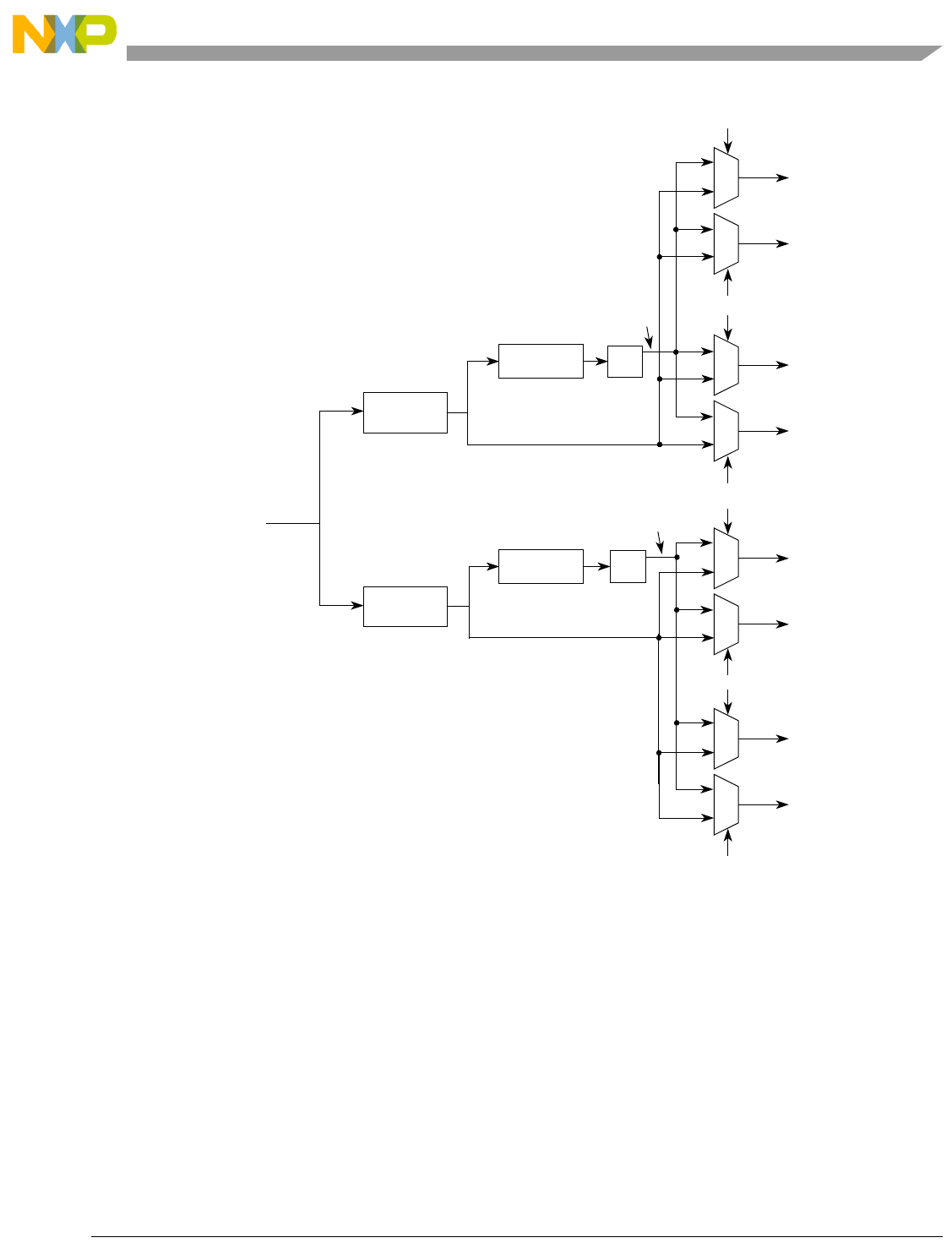
Pulse-Width Modulation (PWM) Module
Freescale Semiconductor 27-14
Figure 27-14. PWM Clock Select Block Diagram
27.3.1.1 Prescaled Clock (A or B)
The internal bus clock is the input clock to the PWM prescaler that can be disabled when the device is in
debug mode by setting the PWMCTL[PFRZ] bit. This is useful for reducing power consumption and for
emulation to freeze the PWM. The input clock is also disabled when all PWM channels are disabled
(PWMEn=0).
Clock A and B are scaled values of the input clock. The value is software selectable for clock A and B and
has options of 1, 1/2,..., or 1/128 times the internal bus clock. The value selected for clock A and B is
determined by the PWMPRCLK[PCKAn] and PWMPRCLK[PCKBn] bits.
Internal Bus
Clock (fsys/)
PWMSCLA 21
0
PCLR4
1
0
PCLR5
PWMPRCLK
PWMSCLB
1
0
PCLR2
1
0
PCLR3
[PCKB]
PWMPRCLK
[PCKA]
Clock A
Clock SA
Clock
Clock B
Clock SB
2
Clock to
PWM4
Clock to
PWM5
Clock to
PWM2
Clock to
PWM3
1
0
PCLR6
1
0
PCLR7
Clock to
PWM6
Clock to
PWM7
1
0
PCLR0
1
0
PCLR1
Clock to
PWM0
Clock to
PWM1
MCF52211 ColdFire® Integrated Microcontroller Reference Manual, Rev. 3

Pulse-Width Modulation (PWM) Module
27-15 Freescale Semiconductor
27.3.1.2 Scaled Clock (SA or SB)
The scaled A (SA) and scaled B (SB) clocks use clock A and B respectively as inputs, divide it further with
a user programmable value, then divide this by 2. The rates available for clock SA are programmable to
run at clock A divided by 2, 4,..., or 512. Similar rates are available for clock SB.
Clock SA equals clock A divided by two times the value in the PWMSCLA register:
Eqn. 27-5
Similarly, clock SB is generated according to the following equation:
Eqn. 27-6
As an example, consider the case in which the user writes 0xFF into the PWMSCLA register. Clock A for
this case is selected to be internal bus clock divided by 4. A pulse occurs at a rate of once every 2554 bus
cycles. Passing this through the divide by two circuit produces a clock signal of the internal bus clock
divided by 2040. Similarly, a value of 0x01 in the PWMSCLA register when clock A is internal bus clock
divided by 4 produces an internal bus clock divided by 8 rate.
Writing to PWMSCLA or PWMSCLB causes the associated 8-bit down counter to be re-loaded.
Otherwise, when changing rates, the counter would have to count down to 0x01 before counting at the
proper rate. Forcing the associated counter to re-load the scale register value every time PWMSCLA or
PWMSCLB is written prevents this.
Writing to the scale registers while channels are operating can cause irregularities in the PWM outputs.
27.3.1.3 Clock Select
Each PWM channel has the capability of selecting one of two clocks. For channels 0, 1, 4, and 5 the clock
choices are clock A or SA. For channels 2, 3, 6 and 7, the choices are clock B or SB. The clock selection
is done with the PWMCLK[PCLKx] control bits.
Changing clock control bits while channels are operating can cause irregularities in the PWM outputs.
27.3.2 PWM Channel Timers
The main part of the PWM module is the actual timers. Each of the timer channels has a counter, a period
register, and a duty register (each are 8-bit). The waveform output period is controlled by a match between
the period register and the value in the counter. The duty is controlled by a match between the duty register
and the counter value and causes the state of the output to change during the period. The starting polarity
of the output is also selectable on a per channel basis. Figure 27-15 shows a block diagram for a PWM
timer.
Clock SA Clock A
2PWMSCLA
-----------------------------------------
=
Clock SB Clock B
2PWMSCLB
----------------------------------------
=
MCF52211 ColdFire® Integrated Microcontroller Reference Manual, Rev. 3
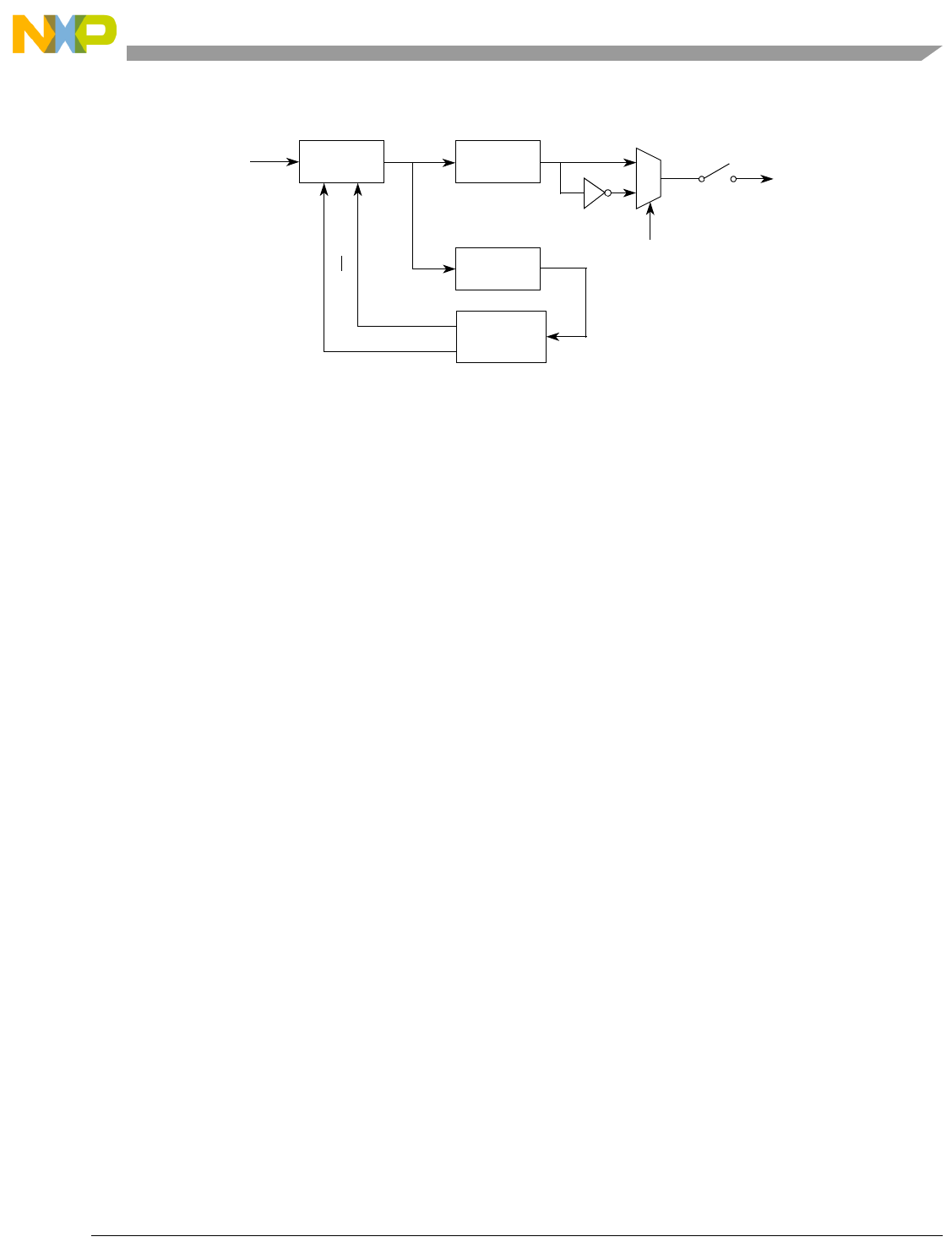
Pulse-Width Modulation (PWM) Module
Freescale Semiconductor 27-16
Figure 27-15. PWM Timer Channel Block Diagram
27.3.2.1 PWM Enable
Each PWM channel has an enable bit (PWMEn) to start its waveform output. When any of the PWMEn
bits are set (PWMEn=1), the associated PWM output signal is enabled immediately. However, the actual
PWM waveform is not available on the associated PWM output until its clock source begins its next cycle;
this is due to the synchronization of PWMEn and the clock source. An exception is when channels are
concatenated. Refer to Section 27.3.2.7, “PWM 16-Bit Functions” for more detail.
The first PWM cycle after enabling the channel can be irregular. When the channel is disabled
(PWMEn=0), the counter for the channel does not count.
27.3.2.2 PWM Polarity
Each channel has a polarity bit to allow starting a waveform cycle with a high or low signal. This is shown
on the block diagram as a mux select. When one of the bits in the PWMPOL register is set, the associated
PWM channel output is high at the beginning of the waveform, then goes low when the duty count is
reached. Conversely, if the polarity bit is zero, the output starts low and then goes high when the duty count
is reached.
27.3.2.3 PWM Period and Duty
Dedicated period and duty registers exist for each channel and are double buffered so that if they change
while the channel is enabled, the change does not take effect until one of the following occurs:
• The effective period ends
• The PWMCNTn register is written (counter resets to 0x00)
• The channel is disabled, PWMEn=0
In this way, the output of the PWM is always the old waveform or the new waveform, not some variation
in between. If the channel is not enabled, writes to the period and duty registers go directly to the latches
as well as the buffer.
A change in duty or period can be forced into effect immediately by writing the new value to the duty
and/or period registers and then writing to the counter. This forces the counter to reset and the new duty
PWMCNTnPWMDTYn
PWMPERn
Up/Down
Reset
PWMCAE = 1
PWMCAE = 0
Clock Source
From Figure 27-14
PPOLn
0
1
PWMOUTn
PWMEn
MCF52211 ColdFire® Integrated Microcontroller Reference Manual, Rev. 3

Pulse-Width Modulation (PWM) Module
27-17 Freescale Semiconductor
and/or period values to be latched. In addition, because the counter is readable, it is possible to know where
the count is with respect to the duty value, and software can be used to make adjustments. When forcing
a new period or duty into effect immediately, an irregular PWM cycle can occur.
Depending on the polarity bit, the duty registers contain the count of the high time or the low time.
27.3.2.4 PWM Timer Counters
Each channel has a dedicated 8-bit up/down counter that runs at the rate of the selected clock source (see
Figure 27-14 for the available clock sources and rates). The counter compares to two registers, a duty
register and a period register, as shown in Figure 27-15. When the PWM counter matches the duty register,
the output flip-flop changes state, causing the PWM waveform to also change state. A match between the
PWM counter and the period register behaves differently depending on what output mode is selected as
shown in Figure 27-15 and described in Section 27.3.2.5, “Left-Aligned Outputs” and Section 27.3.2.6,
“Center-Aligned Outputs.”
Each channel counter can be read at anytime without affecting the count or the operation of the PWM
channel.
Any value written to the counter causes the counter to reset to 0x00, the counter direction to be set to up,
the immediate load of duty and period registers with values from the buffers, and the output to change
according to the polarity bit. When the channel is disabled (PWMEn= 0), the counter stops. When a
channel becomes enabled (PWMEn= 1), the associated PWM counter continues from the count in the
PWMCNTn register. This allows the waveform to continue where it left off when the channel is
re-enabled. When the channel is disabled, writing 0 to the period register causes the counter to reset on the
next selected clock.
NOTE
If the user wants to start a new clean PWM waveform without any history
from the old waveform, the user must write to channel counter
(PWMCNTn) prior to enabling the PWM channel (PWMEn=1).
Generally, writes to the counter are done prior to enabling a channel to start from a known state. However,
writing a counter can also be done while the PWM channel is enabled (counting). The effect is similar to
writing the counter when the channel is disabled, except that the new period is started immediately with
the output set according to the polarity bit. Writing to the counter while the channel is enabled can cause
an irregular PWM cycle to occur.
The counter is cleared at the end of the effective period (see Section 27.3.2.5, “Left-Aligned Outputs” and
Section 27.3.2.6, “Center-Aligned Outputs” for more details).
Table 27-14. PWM Timer Counter Conditions
Counter Clears (0x00) Counter Counts Counter Stops
When PWMCNTn register written to any
value When PWM channel is enabled
(PWMEn= 1). Counts from last value
in PWMCNTn.
When PWM channel is disabled
(PWMEn=0)
Effective period ends
MCF52211 ColdFire® Integrated Microcontroller Reference Manual, Rev. 3
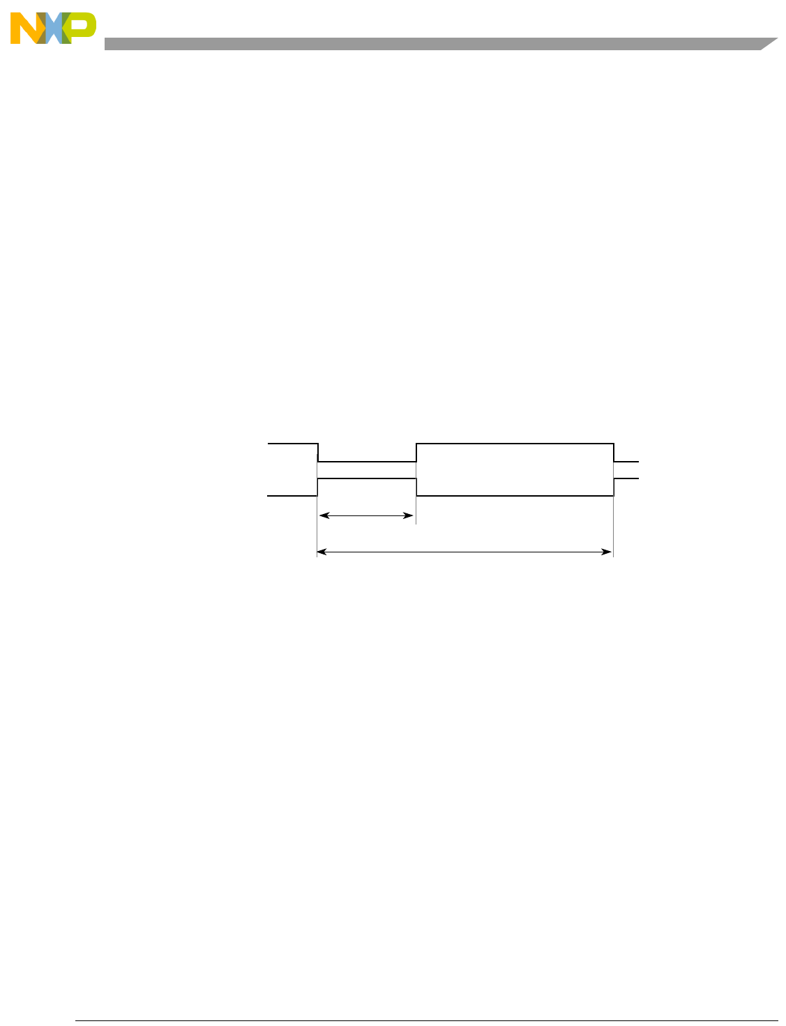
Pulse-Width Modulation (PWM) Module
Freescale Semiconductor 27-18
27.3.2.5 Left-Aligned Outputs
The PWM timer provides the choice of two types of outputs: left- or center-aligned. They are selected with
the PWMCAE[CAEn] bits. If the CAEn bit is cleared, the corresponding PWM output is left-aligned.
In left-aligned output mode, the 8-bit counter is configured as an up counter only. It compares to two
registers, a duty register and a period register, as shown in the block diagram in Figure 27-15. When the
PWM counter matches the duty register, the output flip-flop changes state causing the PWM waveform to
also change state. A match between the PWM counter and the period register resets the counter and the
output flip-flop, as shown in Figure 27-16, as well as performing a load from the double buffer period and
duty register to the associated registers, as described in Figure 27.3.2.3. The counter counts from 0 to the
value in the period register minus 1.
NOTE
Changing the PWM output mode from left-aligned to center-aligned output
(or vice versa) while channels are operating can cause irregularities in the
PWM output. It is recommended to program the output mode before
enabling the PWM channel.
Figure 27-16. PWM Left-Aligned Output Waveform
To calculate the output frequency in left-aligned output mode for a particular channel, take the selected
clock source frequency for the channel (A, B, SA, or SB) and divide it by the value in the period register
for that channel.
Eqn. 27-7
The PWMn duty cycle (high time as a percentage of period) is expressed as:
Eqn. 27-8
27.3.2.5.1 Left-Aligned Output Example
As an example of a left-aligned output, consider the following case:
Clock source = internal bus clock, where internal bus clock = 40 MHz (25 ns period)
PPOLn = 0, PWMPERn = 4, PWMDTYn = 1
PWMn frequency = 40 MHz 4 = 10 MHz
PWMn period = 100 ns
The output waveform generated is below:
PWMDTYn
Period = PWMPERn
PPOLn=0
PPOLn=1
PWMn frequency Clock (A, B, SA, or SB)
PWMPERn
----------------------------------------------------------
=
Duty Cycle 1 PWMPOL PPOLn
PWMDTYn
PWMPERn
-------------------------------
––
100%=
PWMn Duty Cycle 1 1
4
---
–
100% 75%==
MCF52211 ColdFire® Integrated Microcontroller Reference Manual, Rev. 3
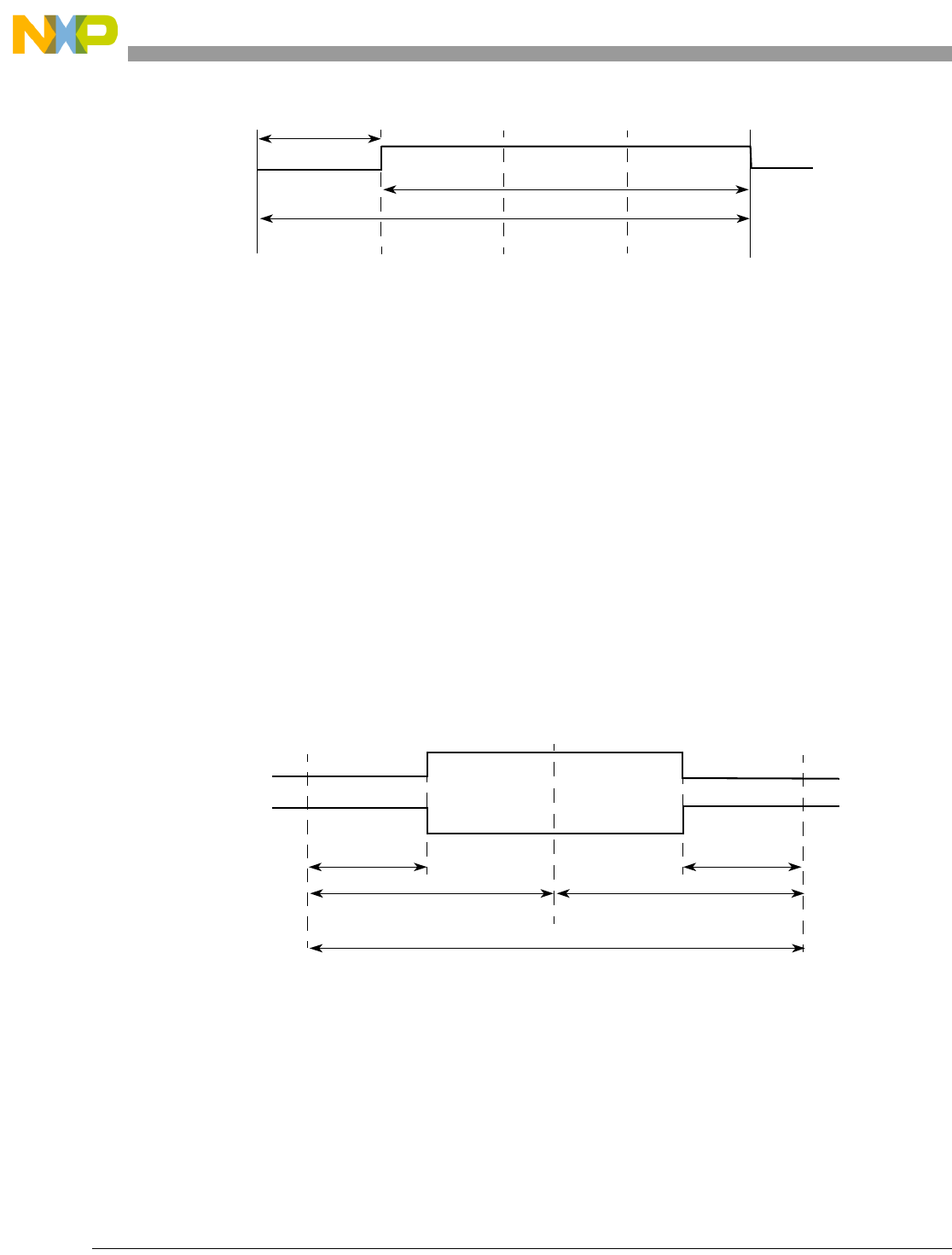
Pulse-Width Modulation (PWM) Module
27-19 Freescale Semiconductor
Figure 27-17. PWM Left-Aligned Output Example Waveform
27.3.2.6 Center-Aligned Outputs
For center-aligned output mode selection, set the PWMCAE[CAEn] bit and the corresponding PWM
output is center-aligned.
The 8-bit counter operates as an up/down counter in this mode and is set to up when the counter is equal
to 0x00. The counter compares to two registers, a duty register and a period register, as shown in the block
diagram in Figure 27-15. When the PWM counter matches the duty register, the output flip-flop changes
state, causing the PWM waveform to also change state. A match between the PWM counter and the period
register changes the counter direction from an up-count to a down-count. When the PWM counter
decrements and matches the duty register again, the output flip-flop changes state causing the PWM output
to also change state. When the PWM counter decrements and reaches zero, the counter direction changes
from a down-count back to an up-count, and a load from the double buffer period and duty registers to the
associated registers is performed as described in Figure 27.3.2.3. The counter counts from 0 up to the value
in the period register and then back down to 0. Thus the effective period is PWMPERn2.
Changing the PWM output mode from left-aligned output to center-aligned output (or vice versa) while
channels are operating can cause irregularities in the PWM output. It is recommended to program the
output mode before enabling the PWM channel.
Figure 27-18. PWM Center-Aligned Output Waveform
To calculate the output frequency in center-aligned output mode for a particular channel, take the selected
clock source frequency for the channel (A, B, SA, or SB) and divide it by twice the value in the period
register for that channel.
Eqn. 27-9
The PWMn duty cycle (high time as a percentage of period) is expressed as:
PERIOD = 100ns
DUTY CYCLE = 75%
E = 25ns
PPOLn=0
PPOLn=1
Period = PWMPERn 2
PWMDTYn
PWMPERnPWMPERn
PWMDTYn
PWMn frequency Clock (A, B, SA, or SB)
2PWMPERn
----------------------------------------------------------
=
MCF52211 ColdFire® Integrated Microcontroller Reference Manual, Rev. 3
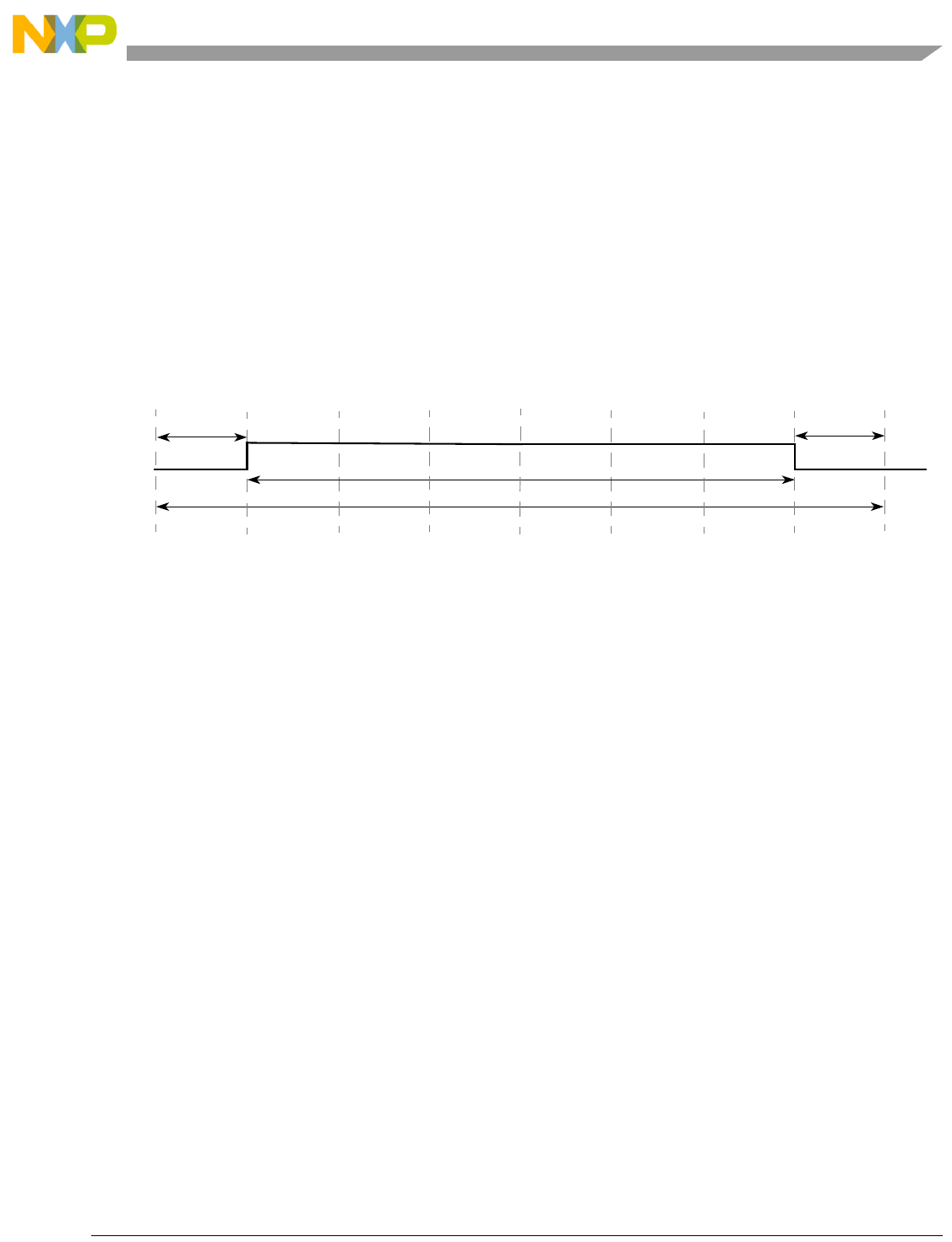
Pulse-Width Modulation (PWM) Module
Freescale Semiconductor 27-20
Eqn. 27-10
27.3.2.6.1 Center-Aligned Output Example
As an example of a center-aligned output, consider the following case:
Clock source = internal bus clock, where internal bus clock = 40 MHz (25 ns period)
PPOLn = 0, PWMPERn = 4, PWMDTYn = 1
PWMn frequency = 40 MHz / (24) = 5 MHz
PWMn period = 200 ns
Shown below is the generated output waveform.
Figure 27-19. PWM Center-Aligned Output Example Waveform
27.3.2.7 PWM 16-Bit Functions
The PWM timer also has the option of generating eight 8-bit channels or four 16-bit channels for greater
PWM resolution. This 16-bit channel option is achieved through the concatenation of two 8-bit channels.
The PWMCTL register contains four concatenation control bits, each used to concatenate a pair of PWM
channels into one 16-bit channel. Channels 0 and 1 are concatenated with the CON01 bit, channels 2 and
3 are concatenated with the CON23 bit, and so on. Change these bits only when both corresponding
channels are disabled.
As shown in Figure 27-20, when channels 2 and 3 are concatenated, channel 2 registers become the high
order bytes of the double byte channel. When channels 0 and 1 are concatenated, channel 0 registers
become the high order bytes of the double byte channel.
When using the 16-bit concatenated mode, the clock source is determined by the low order 8-bit channel
clock select control bits (the odd numbered channel). The resulting PWM is output to the pins of the
corresponding low order 8-bit channel, as shown in Figure 27-20. The polarity of the resulting PWM
output is controlled by the PPOLn bit of the corresponding low order 8-bit channel as well.
After concatenated mode is enabled (PWMCTL[CONnn] bits set), enabling/disabling the corresponding
16-bit PWM channel is controlled by the low order PWMEn bit. In this case, the high order bytes’ PWMEn
bits have no effect, and their corresponding PWM output is disabled.
In concatenated mode, writes to the 16-bit counter by using a 16-bit access or writes to the low or high
order byte of the counter resets the 16-bit counter. Reads of the 16-bit counter must be made by 16-bit
access to maintain data coherency.
Duty Cycle 1 PWMPOL PPOLn
PWMDTYn
PWMPERn
-------------------------------
––
100%=
PWMn Duty Cycle 1 1
4
---
–
100% 75%==
DUTY CYCLE = 75%
E=25ns
PERIOD = 200ns
E = 25ns
MCF52211 ColdFire® Integrated Microcontroller Reference Manual, Rev. 3
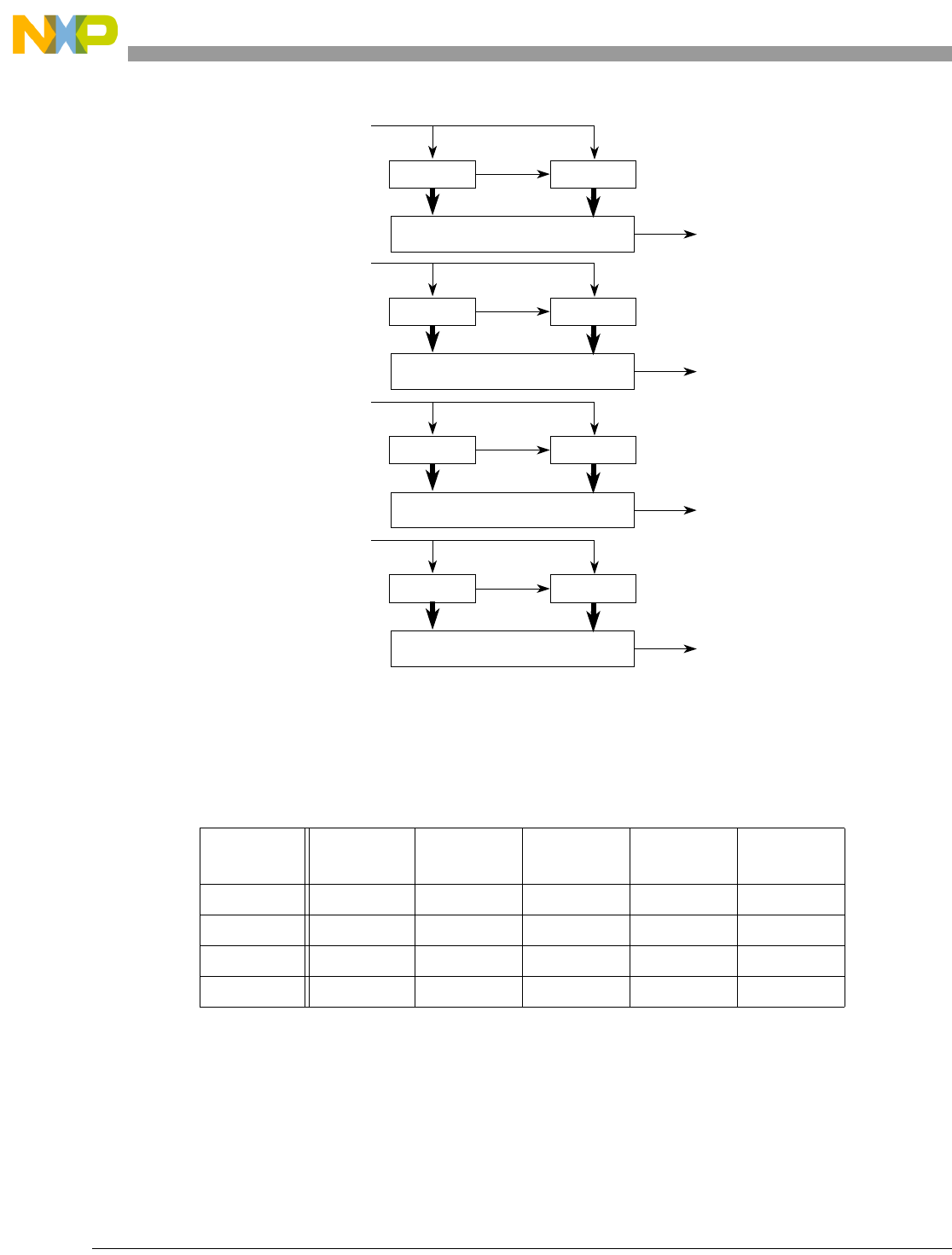
Pulse-Width Modulation (PWM) Module
27-21 Freescale Semiconductor
Figure 27-20. PWM 16-Bit Mode
Left- or center-aligned output mode can be used in concatenated mode and is controlled by the low order
CAEn bit. The high order CAEn bit has no effect. The table shown below is used to summarize which
channels are used to set the various control bits when in 16-bit mode.
Table 27-15. 16-bit Concatenation Mode Summary
CONnn PWMEnPPOLnPCLKnCAEnPWMn
Output
CON67 PWM7 PPOL7 PCLK7 CAE7 PWMOUT7
CON45 PWM5 PPOL5 PCLK5 CAE5 PWMOUT5
CON23 PWME3 PPOL3 PCLK3 CAE3 PWMOUT3
CON01 PWME1 PPOL1 PCLK1 CAE1 PWMOUT1
PWMCNT4
PWMOUT5
High Low
Period/Duty Compare
PWMCNT5
Clock Source 5
PWMCNT2
PWMOUT3
High Low
Period/Duty Compare
PWMCNT3
Clock Source 3
PWMCNT0
PWMOUT1
High Low
Period/Duty Compare
PWMCNT1
Clock Source 1
PWMCNT6
PWMOUT7
High Low
Period/Duty Compare
PWMCNT7
Clock Source 7
MCF52211 ColdFire® Integrated Microcontroller Reference Manual, Rev. 3

Pulse-Width Modulation (PWM) Module
Freescale Semiconductor 27-22
27.3.2.8 PWM Boundary Cases
The following table summarizes the boundary conditions for the PWM regardless of the output mode (left-
or center-aligned) and 8-bit (normal) or 16-bit (concatenation):
Table 27-16. PWM Boundary Cases
PWMDTYnPWMPERnPPOLnPWMn Output
0x00
(indicates no duty)
>0x00 1 Always Low
0x00
(indicates no duty)
>0x00 0 Always High
XX 0x001
(indicates no period)
1Counter = 0x00 and does not count.
1 Always High
XX 0x001
(indicates no period)
0Always Low
PWMPERnXX 1 Always High
PWMPERnXX 0 Always Low
MCF52211 ColdFire® Integrated Microcontroller Reference Manual, Rev. 3
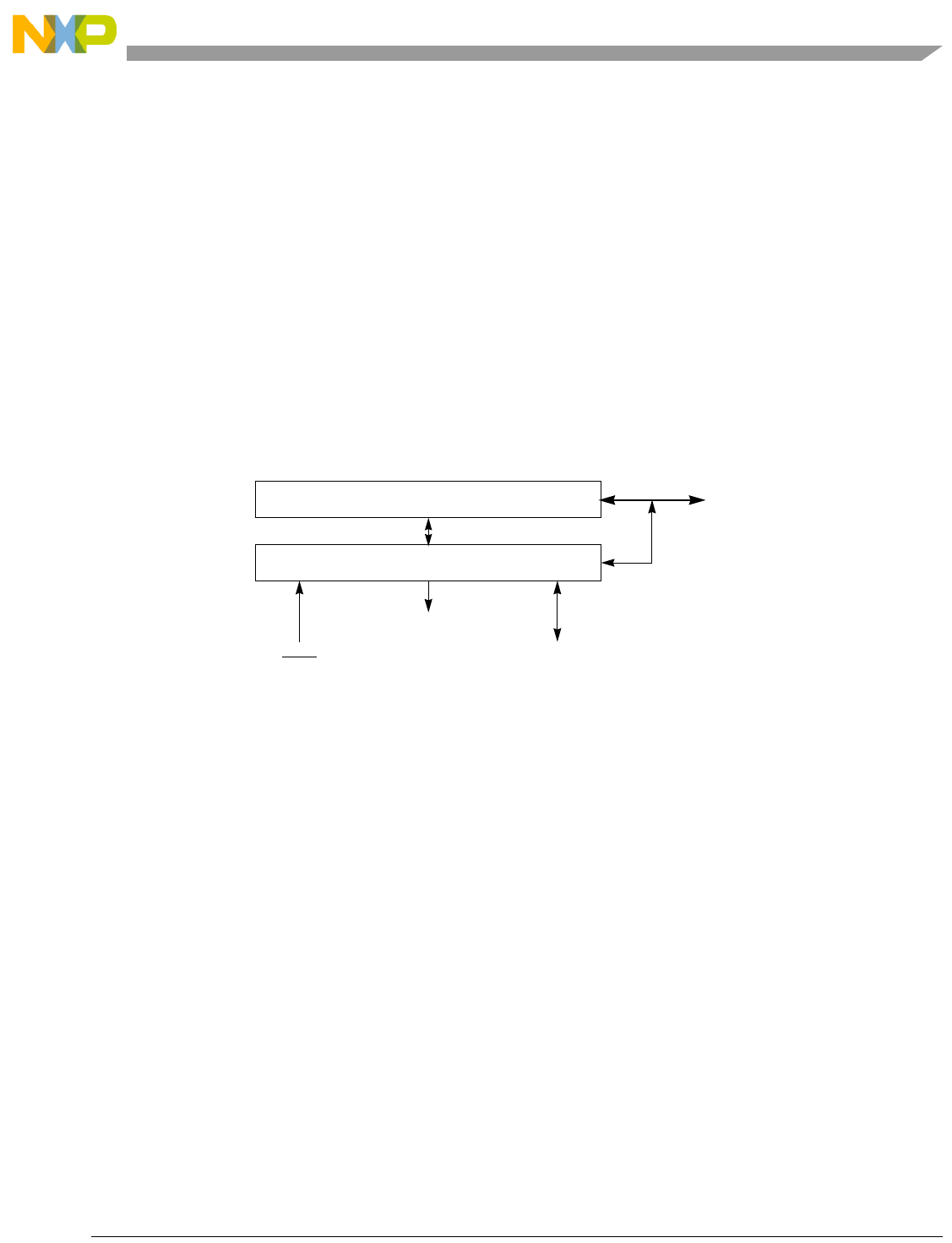
Freescale Semiconductor 28-2
Chapter 28
Debug Module
28.1 Introduction
This chapter describes the revision B+ enhanced hardware debug module.
28.1.1 Block Diagram
The debug module is shown in Figure 28-1.
Figure 28-1. Processor/Debug Module Interface
28.1.2 Overview
Debug support is divided into three areas:
• Real-time trace support—The ability to determine the dynamic execution path through an
application is fundamental for debugging. The ColdFire solution implements an 8-bit parallel
output bus that reports processor execution status and data to an external emulator system. See
Section 28.4.4, “Real-Time Trace Support”.
• Background debug mode (BDM)—Provides low-level debugging in the ColdFire processor
complex. In BDM, the processor complex is halted and a variety of commands can be sent to the
processor to access memory, registers, and peripherals. The external emulator uses a three-pin,
serial, full-duplex channel. See Section 28.4.1, “Background Debug Mode (BDM),” and
Section 28.3, “Memory Map/Register Definition”.
• Real-time debug support—BDM requires the processor to be halted, which many real-time
embedded applications cannot do. Debug interrupts let real-time systems execute a unique service
routine that can quickly save the contents of key registers and variables and return the system to
normal operation. External development systems can access saved data, because the hardware
supports concurrent operation of the processor and BDM-initiated commands. In addition, the
option allows interrupts to occur. See Section 28.4.2, “Real-Time Debug Support”.
ColdFire CPU Core
Debug Module
High-speed
Communication Port
DSCLK, DSI, DSO
Control
BKPT
local bus
Tra ce Po r t
PST[3:0],
DDATA[3:0]
PSTCLK
MCF52211 ColdFire® Integrated Microcontroller Reference Manual, Rev. 3

Debug Module
28-3 Freescale Semiconductor
The first version 2 ColdFire core devices implemented the original debug architecture, now called revision
A. Based on feedback from customers and third-party developers, enhancements have been added to
succeeding generations of ColdFire cores. For revision A, CSR[HRL] is 0. See Section 28.3.2,
“Configuration/Status Register (CSR)”.
Revision B (and B+) of the debug architecture offers more flexibility for configuring the hardware
breakpoint trigger registers and removing the restrictions involving concurrent BDM processing while
hardware breakpoint registers are active. Revision B+ adds three additional PC breakpoint registers. For
revision B, CSR[HRL] is 1, and for revision B+, CSR[HRL] is 0x9.
The following table summarizes the various debug revisions.
28.2 Signal Descriptions
Table 28-2 describes debug module signals. All ColdFire debug signals are unidirectional and related to a
rising edge of the processor core’s clock signal. The standard 26-pin debug connector is shown in
Section 28.4.6, “Freescale-Recommended BDM Pinout”.
Table 28-1. Debug Revision Summary
Revision CSR[HRL] Enhancements
A 0000 — Initial debug revision
B 0001 — BDM command execution does not affect hardware breakpoint logic
Added BDM address attribute register (BAAR)
BKPT configurable interrupt (CSR[BKD])
Level 1 and level 2 triggers on OR condition, in addition to AND
SYNC_PC command to display the processor’s current PC
B+ 1001 — 3 additional PC breakpoint registers PBR1–3
Table 28-2. Debug Module Signals
Signal Description
Development Serial
Clock (DSCLK)
Internally synchronized input. (The logic level on DSCLK is validated if it has the same value on two
consecutive rising bus clock edges.) Clocks the serial communication port to the debug module
during packet transfers. Maximum frequency is 1/5 the processor status clock (PSTCLK). At the
synchronized rising edge of DSCLK, the data input on DSI is sampled and DSO changes state.
Development Serial
Input (DSI)
Internally synchronized input that provides data input for the serial communication port to the debug
module after the DSCLK has been seen as high (logic 1).
Development Serial
Output (DSO)
Provides serial output communication for debug module responses. DSO is registered internally. The
output is delayed from the validation of DSCLK high.
Breakpoint (BKPT) Input requests a manual breakpoint. Assertion of BKPT puts the processor into a halted state after
the current instruction completes. Halt status is reflected on processor status signals (PST[3:0]) as
the value 0xF. If CSR[BKD] is set (disabling normal BKPT functionality), asserting BKPT generates a
debug interrupt exception in the processor.
MCF52211 ColdFire® Integrated Microcontroller Reference Manual, Rev. 3
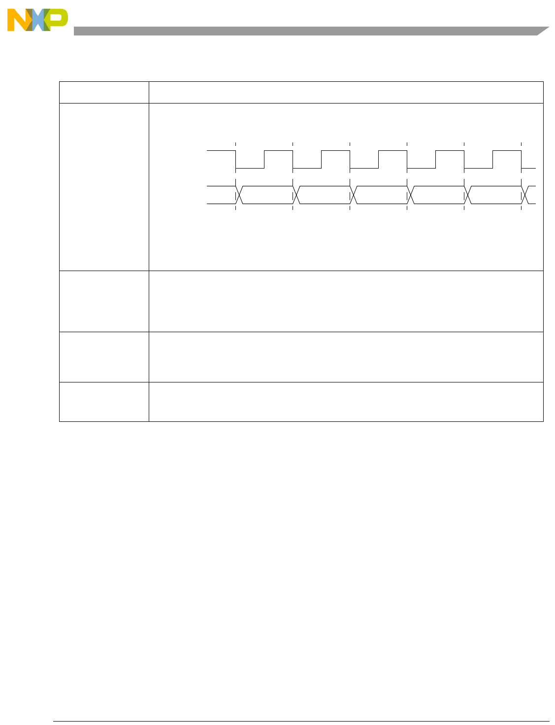
Debug Module
Freescale Semiconductor 28-4
28.3 Memory Map/Register Definition
In addition to the existing BDM commands that provide access to the processor’s registers and the memory
subsystem, the debug module contain a number of registers to support the required functionality. These
registers are also accessible from the processor’s supervisor programming model by executing the
WDEBUG instruction (write only). Therefore, the breakpoint hardware in debug module can be read or
written by the external development system using the debug serial interface or written by the operating
system running on the processor core. Software guarantees that accesses to these resources are serialized
and logically consistent. Hardware provides a locking mechanism in CSR to allow external development
system to disable any attempted writes by the processor to the breakpoint registers (setting CSR[IPW]).
BDM commands must not be issued if the ColdFire processor is using the WDEBUG instruction to access
debug module registers, or the resulting behavior is undefined. The DSCLK must be quiescent during
operation of the WDEBUG command.
These registers, shown in Table 28-3, are treated as 32-bit quantities, regardless of the number of
implemented bits. These registers are also accessed through the BDM port by the commands, WDMREG
and RDMREG, described in Section 28.4.1.5, “BDM Command Set”. These commands contain a 5-bit field,
DRc, that specifies the register, as shown in Table 28-3.
Processor Status
Clock (PSTCLK)
Delayed version of the processor clock. Its rising edge appears in the center of valid PST and DDATA
output. PSTCLK indicates when the development system should sample PST and DDATA values.
The following figure shows PSTCLK timing with respect to PSTD and DATA.
If real-time trace is not used, setting CSR[PCD] keeps PSTCLK, PST and DDATA outputs from
toggling without disabling triggers. Non-quiescent operation can be reenabled by clearing CSR[PCD],
although the external development systems must resynchronize with the PST and DDATA outputs.
PSTCLK starts clocking only when the first non-zero PST value (0xC, 0xD, or 0xF) occurs during
system reset exception processing. Ta b l e 2 8 - 2 4 describes PST values.
Debug Data
(DDATA[3:0])
These output signals display the register breakpoint status as a default, or optionally, captured
address and operand values. The capturing of data values is controlled by the setting of the CSR.
Additionally, execution of the WDDATA instruction by the processor captures operands that are
displayed on DDATA. These signals are updated each processor cycle. These signals are not
implemented on packages containing fewer than 100 pins.
Processor Status
(PST[3:0])
These output signals report the processor status. Table 28-24 shows the encoding of these signals.
These outputs indicate the current status of the processor pipeline and, as a result, are not related to
the current bus transfer. The PST value is updated each processor cycle. These signals are not
implemented on packages containing fewer than 100 pins.
All Processor Status
Outputs (ALLPST)
ALLPST is a logical AND of the four PST signals and is provided on all packages. PST[3:0] and
DDATA[3:0] are not available on the low cost (less than 100 pin) packages. When asserted, reflects
that the core is halted.
Table 28-2. Debug Module Signals (continued)
Signal Description
PSTCLK
PST or DDATA
MCF52211 ColdFire® Integrated Microcontroller Reference Manual, Rev. 3

Debug Module
28-5 Freescale Semiconductor
NOTE
Debug control registers can be written by the external development system
or the CPU through the WDEBUG instruction. These control registers are
write-only from the programming model and they can be written through the
BDM port using the WDMREG command. In addition, the
configuration/status register (CSR) can be read through the BDM port using
the RDMREG command.
The ColdFire debug architecture supports a number of hardware breakpoint registers, that can be
configured into single- or double-level triggers based on the PC or operand address ranges with an optional
inclusion of specific data values.
28.3.1 Shared Debug Resources
The debug module revision A implementation provides a common hardware structure for BDM and
breakpoint functionality. Certain hardware structures are used for BDM and breakpoint purposes as shown
in Table 28-4.
Table 28-3. Debug Module Memory Map
DRc[4–0] Register Name Width
(bits) Access Reset Value Section/
Page
0x00 Configuration/status register (CSR) 32 R/W
See Note
0x0090_0000 28.3.2/28-6
0x05 BDM address attribute register (BAAR) 321
1Each debug register is accessed as a 32-bit register; reserved fields are not used (don’t care).
W 0x05 28.3.3/28-9
0x06 Address attribute trigger register (AATR) 321W 0x0005 28.3.4/28-10
0x07 Trigger definition register (TDR) 32 W 0x0000_0000 28.3.5/28-11
0x08 PC breakpoint register 0 (PBR0) 32 W Undefined 28.3.6/28-14
0x09 PC breakpoint mask register (PBMR) 32 W Undefined 28.3.6/28-14
0x0C Address breakpoint high register (ABHR) 32 W Undefined 28.3.7/28-16
0x0D Address breakpoint low register (ABLR) 32 W Undefined 28.3.7/28-16
0x0E Data breakpoint register (DBR) 32 W Undefined 28.3.8/28-17
0x0F Data breakpoint mask register (DBMR) 32 W Undefined 28.3.8/28-17
0x18 PC breakpoint register 1 (PBR1) 32 W See Section 28.3.6/28-14
0x1A PC breakpoint register 2 (PBR2) 32 W See Section 28.3.6/28-14
0x1B PC breakpoint register 3 (PBR3) 32 W See Section 28.3.6/28-14
MCF52211 ColdFire® Integrated Microcontroller Reference Manual, Rev. 3

Debug Module
Freescale Semiconductor 28-6
Therefore, loading a register to perform a specific function that shares hardware resources is destructive
to the shared function. For example, if an operand address breakpoint is loaded into the debug module, a
BDM command to access memory overwrites an address breakpoint in ABHR. If a data breakpoint is
configured, a BDM write command overwrites the data breakpoint in DBR.
Revision B added hardware registers to eliminate these shared functions. The BAAR is used to specify bus
attributes for BDM memory commands and has the same format as the LSB of the AATR. The registers
containing the BDM memory address and the BDM data are not program visible.
28.3.2 Configuration/Status Register (CSR)
The CSR defines the debug configuration for the processor and memory subsystem and contains status
information from the breakpoint logic. CSR is write-only from the programming model. It can be read
from and written to through the BDM port. CSR is accessible in supervisor mode as debug control register
0x00 using the WDEBUG instruction and through the BDM port using the RDMREG and WDMREG
commands.
Table 28-4. Shared BDM/Breakpoint Hardware
Register BDM Function Breakpoint Function
AATR Bus attributes for all memory commands Attributes for address breakpoint
ABHR Address for all memory commands Address for address breakpoint
DBR Data for all BDM write commands Data for data breakpoint
DRc[4:0]: 0x00 (CSR) Access: Supervisor write-only
BDM read/write
31 30 29 28 27 26 25 24 23 22 21 20 19 18 17 16
RBSTAT FOF TRG HALT BKPT HRL 0BKD PCD IPW
W
Reset0000000010010 0 0 0
15 14 13 12 11 10 9 8 7 6 5 4 3 2 1 0
RMAP TRC EMU DDC UHE BTB 0NPL IPI SSM 00
FDBG DBGH
W
Reset0000000000000 0 0 0
Figure 28-2. Configuration/Status Register (CSR)
MCF52211 ColdFire® Integrated Microcontroller Reference Manual, Rev. 3

Debug Module
28-7 Freescale Semiconductor
Table 28-5. CSR Field Descriptions
Field Description
31–28
BSTAT
Breakpoint Status. Provides read-only status (from the BDM port only) information concerning hardware
breakpoints. BSTAT is cleared by a TDR write or by a CSR read when a level-2 breakpoint is triggered or a level-1
breakpoint is triggered and the level-2 breakpoint is disabled.
0000 No breakpoints enabled
0001 Waiting for level-1 breakpoint
0010 Level-1 breakpoint triggered
0101 Waiting for level-2 breakpoint
0110 Level-2 breakpoint triggered
Else Reserved
27
FOF
Fault-on-fault. If FOF is set, a catastrophic halt occurred and forced entry into BDM. FOF is cleared when CSR is
read (from the BDM port only).
26
TRG
Hardware breakpoint trigger. If TRG is set, a hardware breakpoint halted the processor core and forced entry into
BDM. Reset, the debug GO command or reading CSR (from the BDM port only) clear TRG.
25
HALT
Processor halt. If HALT is set, the processor executed a HALT and forced entry into BDM. Reset, the debug GO
command, or reading CSR (from the BDM port only) clear HALT.
24
BKPT
Breakpoint assert. If BKPT is set, BKPT was asserted, forcing the processor into BDM. Reset, the debug GO
command, or reading CSR (from the BDM port only) clear BKPT.
23–20
HRL
Hardware revision level. Indicates, from the BDM port only, the level of debug module functionality. An emulator
could use this information to identify the level of functionality supported.
0000 Revision A
0001 Revision B
0010 Revision C
0011 Revision D
1001 Revision B+ (This is the value used for this device)
1011 Revision D+
1111 Revision D+PSTB
19 Reserved, must be cleared.
18
BKD
Breakpoint disable. Disables the normal BKPT input signal functionality, and allows the assertion of this pin to
generate a debug interrupt.
0 Normal operation
1 BKPT is edge-sensitive: a high-to-low edge on BKPT signals a debug interrupt to the ColdFire core. The
processor makes this interrupt request pending until the next sample point occurs, when the exception is
initiated. In the ColdFire architecture, the interrupt sample point occurs once per instruction. There is no
support for nesting debug interrupts.
17
PCD
PST/DDATA Disable. Disables the PST/DDATA output signal. PSTCLK is unaffected, it remains under the control
of the SYNCR[DISCLK] bit.
0 Normal operation
1 Disables the generation of the PSTDDATA output signals, and forces these signals to remain quiescent
Note: When PCD is set, do not execute a wddata instruction or perform any debug captures. Doing so, hangs the
device.
16
IPW
Inhibit processor writes. Setting IPW inhibits processor-initiated writes to the debug module’s programming model
registers. Only commands from the external development system can modify IPW.
MCF52211 ColdFire® Integrated Microcontroller Reference Manual, Rev. 3

Debug Module
Freescale Semiconductor 28-8
15
MAP
Force processor references in emulator mode.
0 All emulator-mode references are mapped into supervisor code and data spaces.
1 The processor maps all references while in emulator mode to a special address space, TT equals 10,
TM equals 101 or 110. The internal SRAM and caches are disabled.
14
TRC
Force emulation mode on trace exception.
0 The processor enters supervisor mode
1 The processor enters emulator mode when a trace exception occurs
13
EMU
Force emulation mode.
0 Do not force emulator mode
1 The processor begins executing in emulator mode. See Section 28.4.2.2, “Emulator Mode”.
12–11
DDC
Debug data control. Controls operand data capture for DDATA, which displays the number of bytes defined by the
operand reference size before the actual data; byte displays 8 bits, word displays 16 bits, and long displays 32
bits (one nibble at a time across multiple PSTCLK clock cycles). See Table 28-24.
00 No operand data is displayed.
01 Capture all write data.
10 Capture all read data.
11 Capture all read and write data.
10
UHE
User halt enable. Selects the CPU privilege level required to execute the HALT instruction.
0 HALT is a supervisor-only instruction.
1 HALT is a supervisor/user instruction.
9–8
BTB
Branch target bytes. Defines the number of bytes of branch target address DDATA displays.
00 0 bytes
01 Lower 2 bytes of the target address
10 Lower 3 bytes of the target address
11 Entire 4-byte target address
See Section 28.4.4.1, “Begin Execution of Taken Branch (PST = 0x5)”.
7 Reserved, must be cleared.
6
NPL
Non-pipelined mode. Determines whether the core operates in pipelined mode or not.
0 Pipelined mode
1 Non-pipelined mode. The processor effectively executes one instruction at a time with no overlap. This adds at
least 5 cycles to the execution time of each instruction. Given an average execution latency of 1.6
cycles/instruction, throughput in non-pipeline mode would be 6.6 cycles/instruction, approximately 25% or less
of pipelined performance.
Regardless of the NPL state, a triggered PC breakpoint is always reported before the triggering instruction
executes. In normal pipeline operation, occurrence of an address and/or data breakpoint trigger is imprecise. In
non-pipeline mode, triggers are always reported before the next instruction begins execution and trigger reporting
can be considered precise.
An address or data breakpoint should always occur before the next instruction begins execution. Therefore, the
occurrence of the address/data breakpoints should be guaranteed.
5
IPI
Ignore pending interrupts.
0 Core services any pending interrupt requests that were signalled while in single-step mode.
1 Core ignores any pending interrupt requests signalled while in single-instruction-step mode.
4
SSM
Single-Step Mode. Setting SSM puts the processor in single-step mode.
0 Normal mode.
1 Single-step mode. The processor halts after execution of each instruction. While halted, any BDM command
can be executed. On receipt of the GO command, the processor executes the next instruction and halts again.
This process continues until SSM is cleared.
Table 28-5. CSR Field Descriptions (continued)
Field Description
MCF52211 ColdFire® Integrated Microcontroller Reference Manual, Rev. 3

Debug Module
28-9 Freescale Semiconductor
28.3.3 BDM Address Attribute Register (BAAR)
The BAAR register defines the address space for memory-referencing BDM commands. BAAR[R, SZ]
are loaded directly from the BDM command, while the low-order 5 bits can be programmed from the
external development system. To maintain compatibility with revision A, BAAR is loaded any time the
AATR is written. The BAAR is initialized to a value of 0x05, setting supervisor data as the default address
space.
3–2 Reserved, must be cleared.
1
FDBG
Force the debug mode core output signal (to the on-chip peripherals). The debug mode output is logically defined
as:
Debug mode output = CSR[FDBG] | (CSR[DBGH] and Core is halted)
0 Debug mode output is not forced asserted.
1 Debug mode output core output signal is asserted.
0
DBGH
Disable debug signal assertion during core halt. The debug mode output (to the on-chip peripherals) is logically
defined as:
Debug mode output = CSR[FDBG] | (CSR[DBGH] and Core is halted)
0 Debug mode output is asserted when the core is halted.
1 Debug mode output is not asserted when the core is halted.
DRc[4:0]: 0x05 (BAAR) Access: Supervisor write-only
BDM write-only
7 6543210
R
W R SZ TT TM
Reset: 0 0 0 0 0 1 0 1
Figure 28-3. BDM Address Attribute Register (BAAR)
Table 28-6. BAAR Field Descriptions
Field Description
7
R
Read/Write.
0Write
1Read
6–5
SZ
Size.
00 Longword
01 Byte
10 Word
11 Reserved
4–3
TT
Transfer Type. See the TT definition in the AATR description, Section 28.3.4, “Address Attribute Trigger Register
(AATR)”.
2–0
TM
Transfer Modifier. See the TM definition in the AATR description, Section 28.3.4, “Address Attribute Trigger Register
(AATR)”.
Table 28-5. CSR Field Descriptions (continued)
Field Description
MCF52211 ColdFire® Integrated Microcontroller Reference Manual, Rev. 3

Debug Module
Freescale Semiconductor 28-10
28.3.4 Address Attribute Trigger Register (AATR)
The AATR defines address attributes and a mask to be matched in the trigger. The register value is
compared with address attribute signals from the processor’s local high-speed bus, as defined by the
setting of the trigger definition register (TDR). AATR is accessible in supervisor mode as debug control
register 0x06 using the WDEBUG instruction and through the BDM port using the WDMREG command.
DRc[4:0]: 0x06 (AATR) Access: Supervisor write-only
BDM write-only
1514131211109876543210
R
W RM SZM TTM TMM R SZ TT TM
Reset0000000000000101
Figure 28-4. Address Attribute Trigger Register (AATR)
Table 28-7. AATR Field Descriptions
Field Description
15
RM
Read/write Mask. Setting RM masks R in address comparisons.
14–13
SZM
Size Mask. Setting an SZM bit masks the corresponding SZ bit in address comparisons.
12–11
TTM
Transfer Type Mask. Setting a TTM bit masks the corresponding TT bit in address comparisons.
10–8
TMM
Transfer Modifier Mask. Setting a TMM bit masks the corresponding TM bit in address comparisons.
7
R
Read/Write. R is compared with the R/W signal of the processor’s local bus.
6–5
SZ
Size. Compared to the processor’s local bus size signals.
00 Longword
01 Byte
10 Word
11 Reserved
MCF52211 ColdFire® Integrated Microcontroller Reference Manual, Rev. 3

Debug Module
28-11 Freescale Semiconductor
28.3.5 Trigger Definition Register (TDR)
The TDR configures the operation of the hardware breakpoint logic corresponding with the
ABHR/ABLR/AATR, PBR/PBR1/PBR2/PBR3/PBMR, and DBR/DBMR registers within the debug
module. TDR controls the actions taken under the defined conditions. Breakpoint logic may be configured
as a one- or two-level trigger. TDR[31–16] bits define second-level trigger, and bits 15–0 define first-level
trigger.
NOTE
The debug module has no hardware interlocks to prevent spurious
breakpoint triggers while the breakpoint registers are being loaded. Disable
TDR (by clearing TDR[29,13]) before defining triggers.
A write to TDR clears the CSR trigger status bits, CSR[BSTAT]. TDR is accessible in supervisor mode as
debug control register 0x07 using the WDEBUG instruction and through the BDM port using the
WDMREG command.
4–3
TT
Transfer Type. Compared with the local bus transfer type signals.
00 Normal processor access
01 Reserved
10 Emulator mode access
11 Acknowledge/CPU space access
These bits also define the TT encoding for BDM memory commands. In this case, the 01 encoding indicates
an external or DMA access (for backward compatibility). These bits affect the TM bits.
2–0
TM
Transfer Modifier. Compared with the local bus transfer modifier signals, which give supplemental information
for each transfer type. These bits also define the TM encoding for BDM memory commands (for backward
compatibility).
Table 28-7. AATR Field Descriptions (continued)
Field Description
TM TT=00
(normal mode)
TT=10
(emulator mode)
TT=11
(acknowledge/CPU
space transfers)
000 Reserved Reserved CPU space access
001 User data access Reserved Interrupt ack level 1
010 User code access Reserved Interrupt ack level 2
011 Reserved Reserved Interrupt ack level 3
100 Reserved Reserved Interrupt ack level 4
101 Supervisor data access Emulator mode access Interrupt ack level 5
110 Supervisor code access Emulator code access Interrupt ack level 6
111 Reserved Reserved Interrupt ack level 7
MCF52211 ColdFire® Integrated Microcontroller Reference Manual, Rev. 3

Debug Module
Freescale Semiconductor 28-12
DRc[4:0]: 0x07 (TDR) Access: Supervisor write-only
BDM write-only
Second Level Trigger
31 30 29 28 27 26 25 24 23 22 21 20 19 18 17 16
R
W TRC L2EBL L2ED L2DI L2EA L2EPC L2PCI
Reset00000000000000 0 0
First Level Trigger
15 14 13 12 11 10 9 8 7 6 5 4 3 2 1 0
R
W L2T L1T L1EBL L1ED L1DI L1EA L1EPC L1PCI
Reset00000000000000 0 0
Figure 28-5. Trigger Definition Register (TDR)
Table 28-8. TDR Field Descriptions
Field Description
31–30
TRC
Trigger Response Control. Determines how the processor responds to a completed trigger condition. The trigger
response is always displayed on DDATA.
00 Display on DDATA only
01 Processor halt
10 Debug interrupt
11 Reserved
29
L2EBL
Enable Level 2 Breakpoint. Global enable for the breakpoint trigger.
0 Disables all level 2 breakpoints
1 Enables all level 2 breakpoint triggers
28–22
L2ED
Enable Level 2 Data Breakpoint. Setting an L2ED bit enables the corresponding data breakpoint condition based on
the size and placement on the processor’s local data bus. Clearing all ED bits disables data breakpoints.
21
L2DI
Level 2 Data Breakpoint Invert. Inverts the logical sense of all the data breakpoint comparators. This can develop a
trigger based on the occurrence of a data value other than the DBR contents.
0 No inversion
1 Invert data breakpoint comparators.
TDR Bit Description
28 Data longword. Entire processor’s local data bus.
27 Lower data word.
26 Upper data word.
25 Lower lower data byte. Low-order byte of the low-order word.
24 Lower middle data byte. High-order byte of the low-order word.
23 Upper middle data byte. Low-order byte of the high-order word.
22 Upper upper data byte. High-order byte of the high-order word.
MCF52211 ColdFire® Integrated Microcontroller Reference Manual, Rev. 3

Debug Module
28-13 Freescale Semiconductor
20–18
L2EA
Enable Level 2 Address Breakpoint. Setting an L2EA bit enables the corresponding address breakpoint. Clearing all
three bits disables the breakpoint.
17
L2EPC
Enable Level 2 PC Breakpoint.
0 Disable PC breakpoint
1 Enable PC breakpoint where the trigger is defined by the logical summation of:
(PBR0 and PBMR) | PBR1 | PBR2 | PBR3 Eqn. 28-1
16
L2PCI
Level 2 PC Breakpoint Invert.
0 The PC breakpoint is defined within the region defined by PBRn and PBMR.
1 The PC breakpoint is defined outside the region defined by PBRn and PBMR.
15
L2T
Level 2 Trigger. Determines the logic operation for the trigger between the PC_condition and the (Address_range &
Data_condition) where the inclusion of a Data_condition is optional. The ColdFire debug architecture supports the
creation of single or double-level triggers.
0 Level 2 trigger = PC_condition & Address_range & Data_condition
1 Level 2 trigger = PC_condition | (Address_range & Data_condition)
Note: Debug Rev A only had the AND condition available for the triggers.
14
L1T
Level 1 Trigger. Determines the logic operation for the trigger between the PC_condition and the (Address_range &
Data_condition) where the inclusion of a Data_condition is optional. The ColdFire debug architecture supports the
creation of single or double-level triggers.
0 Level 1 trigger = PC_condition & Address_range & Data_condition
1 Level 1 trigger = PC_condition | (Address_range & Data_condition)
Note: Debug Rev A only had the AND condition available for the triggers.
13
L1EBL
Enable Level 1 Breakpoint. Global enable for the breakpoint trigger.
0 Disables all level 1 breakpoints
1 Enables all level 1 breakpoint triggers
Table 28-8. TDR Field Descriptions (continued)
Field Description
TDR Bit Description
20 Address breakpoint inverted. Breakpoint is based outside the
range between ABLR and ABHR.
19 Address breakpoint range. The breakpoint is based on the
inclusive range defined by ABLR and ABHR.
18 Address breakpoint low. The breakpoint is based on the
address in the ABLR.
MCF52211 ColdFire® Integrated Microcontroller Reference Manual, Rev. 3

Debug Module
Freescale Semiconductor 28-14
28.3.6 Program Counter Breakpoint/Mask Registers (PBR0–3, PBMR)
The PBRn registers define an instruction address for use as part of the trigger. These registers’ contents
are compared with the processor’s program counter register when the appropriate valid bit is set (for
PBR1–3) and TDR is configured appropriately. PBR0 bits are masked by setting corresponding PBMR
bits (PBMR has no effect on PBR1–3). Results are compared with the processor’s program counter
register, as defined in TDR. Breakpoint registers, PBR1–3, have no masking associated with them. The
12–6
L1ED
Enable Level 1 Data Breakpoint. Setting an L1ED bit enables the corresponding data breakpoint condition based on
the size and placement on the processor’s local data bus. Clearing all L1ED bits disables data breakpoints.
5
L1DI
Level 1 Data Breakpoint Invert. Inverts the logical sense of all the data breakpoint comparators. This can develop a
trigger based on the occurrence of a data value other than the DBR contents.
0 No inversion
1 Invert data breakpoint comparators.
4–2
L1EA
Enable Level 1 Address Breakpoint. Setting an L1EA bit enables the corresponding address breakpoint. Clearing all
three bits disables the address breakpoint.
1
L1EPC
Enable Level 1 PC breakpoint.
0 Disable PC breakpoint
1 Enable PC breakpoint
0
L1PCI
Level 1 PC Breakpoint Invert.
0 The PC breakpoint is defined within the region defined by PBRn and PBMR.
1 The PC breakpoint is defined outside the region defined by PBRn and PBMR.
Table 28-8. TDR Field Descriptions (continued)
Field Description
TDR Bit Description
12 Data longword. Entire processor’s local data bus.
11 Lower data word.
10 Upper data word.
9 Lower lower data byte. Low-order byte of the low-order word.
8 Lower middle data byte. High-order byte of the low-order word.
7 Upper middle data byte. Low-order byte of the high-order word.
6 Upper upper data byte. High-order byte of the high-order word.
TDR Bit Description
4 Enable address breakpoint inverted. Breakpoint is based
outside the range between ABLR and ABHR.
3 Enable address breakpoint range. The breakpoint is based on
the inclusive range defined by ABLR and ABHR.
2 Enable address breakpoint low. The breakpoint is based on the
address in the ABLR.
MCF52211 ColdFire® Integrated Microcontroller Reference Manual, Rev. 3

Debug Module
28-15 Freescale Semiconductor
contents of the breakpoint registers are compared with the processor’s program counter register when TDR
is configured appropriately.
The PC breakpoint registers are accessible in supervisor mode using the WDEBUG instruction and
through the BDM port using the WDMREG command using values shown in Section 28.4.1.5, “BDM
Command Set”.
Figure 28-8 shows PBMR. PBMR is accessible in supervisor mode using the WDEBUG instruction and
via the BDM port using the WDMREG command. PBMR only masks PBR0.
DRc[4:0]: 0x08 (PBR0) Access: Supervisor write-only
BDM write-only
313029282726252423222120191817161514131211109876543210
R
WAddress
Reset––––––––––––––––––––––––––––––––
Figure 28-6. PC Breakpoint Register (PBR0)
Table 28-9. PBR0 Field Descriptions
Field Description
31–0
Address
PC Breakpoint Address. The address to be compared with the PC as a breakpoint trigger.
Note: PBR0[0] should always be loaded with a 0.
DRc[4:0]: 0x18 (PBR1)
0x1A (PBR2)
0x1B (PBR3)
Access: Supervisor write-only
BDM write-only
313029282726252423222120191817161514131211109876543210
R
W Address V
Reset–––––––––––––––––––––––––––––000
Figure 28-7. PC Breakpoint Register n (PBRn)
Table 28-10. PBRn Field Descriptions
Field Description
31–1
Address
PC Breakpoint Address. The 31-bit address to be compared with the PC as a breakpoint trigger.
0
V
Valid Bit. This bit must be set for the PC breakpoint to occur at the address specified in the Address field.
0 PBR is disabled.
1 PBR is enabled.
MCF52211 ColdFire® Integrated Microcontroller Reference Manual, Rev. 3

Debug Module
Freescale Semiconductor 28-16
28.3.7 Address Breakpoint Registers (ABLR, ABHR)
The ABLR and ABHR define regions in the processor’s data address space that can act as part of the
trigger. These register values are compared with the address for each transfer on the processor’s high-speed
local bus. The trigger definition register (TDR) identifies the trigger as one of three cases:
• Identically the value in ABLR
• Inside the range bound by ABLR and ABHR inclusive
• Outside that same range
ABLR and ABHR are accessible in supervisor mode using the WDEBUG instruction and via the BDM
port using the WDMREG command.
DRc[4:0]: 0x09 (PBMR) Access: Supervisor write-only
BDM write-only
313029282726252423222120191817161514131211109876543210
R
WMask
Reset––––––––––––––––––––––––––––––––
Figure 28-8. PC Breakpoint Mask Register (PBMR)
Table 28-11. PBMR Field Descriptions
Field Description
31–0
Mask
PC Breakpoint Mask.
0 The corresponding PBR0 bit is compared to the appropriate PC bit.
1 The corresponding PBR0 bit is ignored.
DRc[4:0]: 0x0C (ABHR)
0x0D (ABLR)
Access: Supervisor write-only
BDM write-only
313029282726252423222120191817161514131211109876543210
R
WAddress
Reset––––––––––––––––––––––––––––––––
Figure 28-9. Address Breakpoint Registers (ABLR, ABHR,)
Table 28-12. ABLR Field Description
Field Description
31–0
Address
Low Address. Holds the 32-bit address marking the lower bound of the address breakpoint range. Breakpoints for
specific single addresses are programmed into ABLR.
Table 28-13. ABHR Field Description
Field Description
31–0
Address
High Address. Holds the 32-bit address marking the upper bound of the address breakpoint range.
MCF52211 ColdFire® Integrated Microcontroller Reference Manual, Rev. 3

Debug Module
28-17 Freescale Semiconductor
28.3.8 Data Breakpoint and Mask Registers (DBR, DBMR)
The data breakpoint register (DBR), specify data patterns used as part of the trigger into debug mode. DBR
bits are masked by setting corresponding DBMR bits, as defined in TDR.
DBR and DBMR are accessible in supervisor mode using the WDEBUG instruction and through the BDM
port using the WDMREG command.
The DBR supports aligned and misaligned references. Table 28-16 shows relationships between processor
address, access size, and location within the 32-bit data bus.
DRc[4:0]: 0x0E (DBR) Access: Supervisor write-only
BDM write-only
313029282726252423222120191817161514131211109876543210
R
WData
Reset––––––––––––––––––––––––––––––––
Figure 28-10. Data Breakpoint Registers (DBR)
Table 28-14. DBR Field Descriptions
Field Description
31–0
Data
Data Breakpoint Value. Contains the value to be compared with the data value from the processor’s local bus as a
breakpoint trigger.
DRc[4:0]: 0x0F (DBMR) Access: Supervisor write-only
BDM write-only
313029282726252423222120191817161514131211109876543210
R
WMask
Reset––––––––––––––––––––––––––––––––
Figure 28-11. Data Breakpoint Mask Registers (DBMR)
Table 28-15. DBMR Field Descriptions
Field Description
31–0
Mask
Data Breakpoint Mask. The 32-bit mask for the data breakpoint trigger. Clearing a DBMR bit allows the
corresponding DBR bit to be compared to the appropriate bit of the processor’s local data bus. Setting a DBMR bit
causes that bit to be ignored.
MCF52211 ColdFire® Integrated Microcontroller Reference Manual, Rev. 3

Debug Module
Freescale Semiconductor 28-18
28.4 Functional Description
28.4.1 Background Debug Mode (BDM)
The ColdFire family implements a low-level system debugger in the microprocessor in a dedicated
hardware module. Communication with the development system is managed through a dedicated,
high-speed serial command interface. Although some BDM operations, such as CPU register accesses,
require the CPU to be halted, other BDM commands, such as memory accesses, can be executed while the
processor is running.
BDM is useful because:
• In-circuit emulation is not needed, so physical and electrical characteristics of the system are not
affected.
• BDM is always available for debugging the system and provides a communication link for
upgrading firmware in existing systems.
• Provides high-speed cache downloading (500 Kbytes/sec), especially useful for flash
programming
• Provides absolute control of the processor, and thus the system. This allows quick hardware
debugging with the same tool set used for firmware development.
28.4.1.1 CPU Halt
Although most BDM operations can occur in parallel with CPU operations, unrestricted BDM operation
requires the CPU to be halted. The sources that can cause the CPU to halt are listed below in order of
priority:
1. A catastrophic fault-on-fault condition automatically halts the processor.
2. A hardware breakpoint trigger can generate a pending halt condition similar to the assertion of
BKPT. This type of halt is always first marked as pending in the processor, which samples for
pending halt and interrupt conditions once per instruction. When a pending condition is asserted,
the processor halts execution at the next sample point. See Section 28.4.2.1, “Theory of
Operation”.
Table 28-16. Address, Access Size, and Operand Data Location
Address[1:0] Access Size Operand Location
00 Byte D[31:24]
01 Byte D[23:16]
10 Byte D[15:8]
11 Byte D[7:0]
0x Word D[31:16]
1x Word D[15:0]
xx Longword D[31:0]
MCF52211 ColdFire® Integrated Microcontroller Reference Manual, Rev. 3

Debug Module
28-19 Freescale Semiconductor
3. The execution of a HALT instruction immediately suspends execution. Attempting to execute
HALT in user mode while CSR[UHE] is cleared generates a privilege violation exception. If
CSR[UHE] is set, HALT can be executed in user mode. After HALT executes, the processor can
be restarted by serial shifting a GO command into the debug module. Execution continues at the
instruction after HALT.
4. The assertion of the BKPT input is treated as a pseudo-interrupt; asserting BKPT creates a pending
halt postponed until the processor core samples for halts/interrupts. The processor samples for
these conditions once during the execution of each instruction; if a pending halt is detected, the
processor suspends execution and enters the halted state.
The are two special cases involving the assertion of BKPT:
• After the system reset signal is negated, the processor waits for 16 processor clock cycles before
beginning reset exception processing. If the BKPT input is asserted within eight cycles after
RESET is negated, the processor enters the halt state, signaling halt status (0xF) on the PST
outputs. While the processor is in this state, all resources accessible through the debug module can
be referenced. This is the only chance to force the processor into emulation mode through
CSR[EMU].
• After system initialization, the processor’s response to the GO command depends on the set of
BDM commands performed while it is halted for a breakpoint. Specifically, if the PC register was
loaded, the GO command causes the processor to exit halted state and pass control to the instruction
address in the PC, bypassing normal reset exception processing. If the PC was not loaded, the GO
command causes the processor to exit halted state and continue reset exception processing.
• The ColdFire architecture also manages a special case of BKPT asserted while the processor is
stopped by execution of the STOP instruction. For this case, the processor exits the stopped mode
and enters the halted state, at which point all BDM commands may be exercised. When restarted,
the processor continues by executing the next sequential instruction, which follows the STOP
opcode.
The CSR[27–24] bits indicate the halt source, showing the highest priority source for multiple halt
conditions.
28.4.1.2 BDM Serial Interface
When the CPU is halted and PST reflects the halt status, the development system can send unrestricted
commands to the debug module. The debug module implements a synchronous serial protocol using two
inputs (DSCLK and DSI) and one output (DSO), where DSO is specified as a delay relative to the rising
edge of the processor clock. See Table 28-2. The development system serves as the serial communication
channel master and must generate DSCLK.
The serial channel operates at a frequency from DC to 1/5 of the PSTCLK frequency. The channel uses
full-duplex mode, where data is sent and received simultaneously by master and slave devices. The
transmission consists of 17-bit packets composed of a status/control bit and a 16-bit data word. As shown
in Figure 28-12, all state transitions are enabled on a rising edge of the PSTCLK clock when DSCLK is
high; DSI is sampled and DSO is driven.
MCF52211 ColdFire® Integrated Microcontroller Reference Manual, Rev. 3
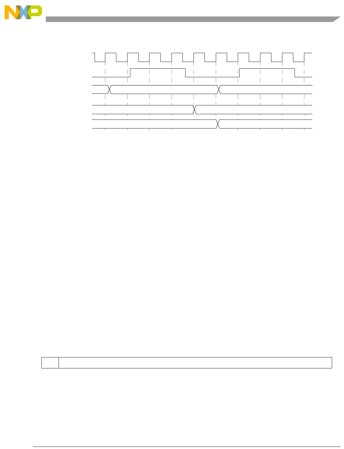
Debug Module
Freescale Semiconductor 28-20
Figure 28-12. Maximum BDM Serial Interface Timing
DSCLK and DSI are synchronized inputs. DSCLK acts as a pseudo clock enable and is sampled, along
with DSI, on the rising edge of PSTCLK. DSO is delayed from the DSCLK-enabled PSTCLK rising edge
(registered after a BDM state machine state change). All events in the debug module’s serial state machine
are based on the PSTCLK rising edge. DSCLK must also be sampled low (on a positive edge of PSTCLK)
between each bit exchange. The msb is sent first. Because DSO changes state based on an internally
recognized rising edge of DSCLK, DSO cannot be used to indicate the start of a serial transfer. The
development system must count clock cycles in a given transfer. C0–C4 are described as:
• C0: Set the state of the DSI bit
• C1: First synchronization cycle for DSI (DSCLK is high)
• C2: Second synchronization cycle for DSI (DSCLK is high)
• C3: BDM state machine changes state depending upon DSI and whether the entire input data
transfer has been transmitted
• C4: DSO changes to next value
NOTE
A not-ready response can be ignored except during a memory-referencing
cycle. Otherwise, the debug module can accept a new serial transfer after 32
processor clock periods.
28.4.1.3 Receive Packet Format
The basic receive packet consists of 16 data bits and 1 status bit
.
161514131211109876543210
SData
Figure 28-13. Receive BDM Packet
PSTCLK
DSCLK
Next State
BDM State
Machine
DSO
DSI
Current State
Current Next
Past Current
C0 C1 C2 C3 C4
MCF52211 ColdFire® Integrated Microcontroller Reference Manual, Rev. 3

Debug Module
28-21 Freescale Semiconductor
28.4.1.3.1 Transmit Packet Format
The basic transmit packet consists of 16 data bits and 1 reserved bit.
28.4.1.3.2 BDM Command Format
All ColdFire family BDM commands include a 16-bit operation word followed by an optional set of one
or more extension words.
Table 28-17. Receive BDM Packet Field Description
Field Description
16
S
Status. Indicates the status of CPU-generated messages listed below. The not-ready response can be ignored
unless a memory-referencing cycle is in progress. Otherwise, the debug module can accept a new serial transfer
after 32 processor clock periods.
15–0
Data
Data. Contains the message to be sent from the debug module to the development system. The response message
is always a single word, with the data field encoded as shown above.
16 15 14 13 12 11 10 9 8 7 6 5 4 3 2 1 0
—Data
Figure 28-14. Transmit BDM Packet
Table 28-18. Transmit BDM Packet Field Description
Field Description
16 Reserved, must be cleared.
15–0
Data
Data bits 15–0. Contains the data to be sent from the development system to the debug module.
1514131211109876543210
Operation 0 R/W Op Size 0 0 A/D Register
Extension Word(s)
Figure 28-15. BDM Command Format
S Data Message
0 xxxx Valid data transfer
0 FFFF Status OK
1 0000 Not ready with response; come again
1 0001 Error-Terminated bus cycle; data invalid
1 FFFF Illegal Command
MCF52211 ColdFire® Integrated Microcontroller Reference Manual, Rev. 3

Debug Module
Freescale Semiconductor 28-22
28.4.1.3.3 Extension Words as Required
Some commands require extension words for addresses and/or immediate data. Addresses require two
extension words because only absolute long addressing is permitted. Longword accesses are forcibly
longword-aligned and word accesses are forcibly word-aligned. Immediate data can be 1 or 2 words long.
Byte and word data each requires a single extension word, while longword data requires two extension
words.
Operands and addresses are transferred most-significant word first. In the following descriptions of the
BDM command set, the optional set of extension words is defined as address, data, or operand data.
28.4.1.4 Command Sequence Diagrams
The command sequence diagram in Figure 28-16 shows serial bus traffic for commands. Each bubble
represents a 17-bit bus transfer. The top half of each bubble indicates the data the development system
sends to the debug module; the bottom half indicates the debug module’s response to the previous
development system commands. Command and result transactions overlap to minimize latency.
Table 28-19. BDM Field Descriptions
Field Description
15–10
Operation
Specifies the command. These values are listed in Table 28-20.
9 Reserved, must be cleared.
8
R/W
Direction of operand transfer.
0 Data is written to the CPU or to memory from the development system.
1 The transfer is from the CPU to the development system.
7–6
Op Size
Operand Data Size for Sized Operations. Addresses are expressed as 32-bit absolute values. A command
performing a byte-sized memory read leaves the upper 8 bits of the response data undefined. Referenced data is
returned in the lower 8 bits of the response.
5–4 Reserved, must be cleared.
3
A/D
Address/Data. Determines whether the register field specifies a data or address register.
0 Data register.
1 Address register.
2–0
Register
Contains the register number in commands that operate on processor registers. See Table 28-21.
Operand Size Bit Values
00 Byte 8 bits
01 Word 16 bits
10 Longword 32 bits
11 Reserved —
MCF52211 ColdFire® Integrated Microcontroller Reference Manual, Rev. 3
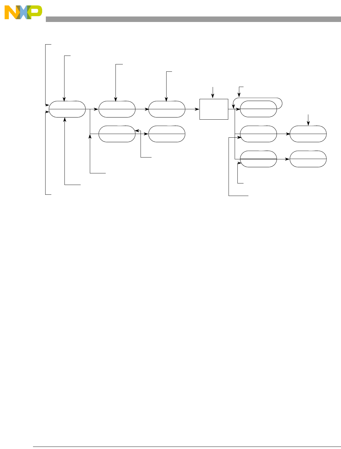
Debug Module
28-23 Freescale Semiconductor
Figure 28-16. Command Sequence Diagram
The sequence is as follows:
• In cycle 1, the development system command is issued (READ in this example). The debug module
responds with the low-order results of the previous command or a command complete status of the
previous command, if no results are required.
• In cycle 2, the development system supplies the high-order 16 address bits. The debug module
returns a not-ready response unless the received command is decoded as unimplemented, which is
indicated by the illegal command encoding. If this occurs, the development system should
retransmit the command.
NOTE
A not-ready response can be ignored except during a memory-referencing
cycle. Otherwise, the debug module can accept a new serial transfer after 32
processor clock periods.
• In cycle 3, the development system supplies the low-order 16 address bits. The debug module
always returns a not-ready response.
• At the completion of cycle 3, the debug module initiates a memory read operation. Any serial
transfers that begin during a memory access return a not-ready response.
• Results are returned in the two serial transfer cycles after the memory access completes. For any
command performing a byte-sized memory read operation, the upper 8 bits of the response data are
undefined and the referenced data is returned in the lower 8 bits. The next command’s opcode is
sent to the debug module during the final transfer. If a bus error terminates a memory or register
access, error status (S = 1, DATA = 0x0001) returns instead of result data.
XXX
’NOT READY’
READ (LONG)
???
MS ADDR
’NOT READY’
LS ADDR
’NOT READY’
NEXT CMD
’NOT READY’
NEXT CMD
’NOT READY’
NEXT CMD
LS RESULT
Commands transmitted to the debug module
Command code transmitted during this cycle
High-order 16 bits of memory address
Low-order 16 bits of memory address
Non-serial-related
Next
Command
Code
Sequence taken if operation
has not completed
activity
READ
MEMORY
LOCATION
XXX
BERR
XXX
MS RESULT
XXX
’ILLEGAL’
Responses from the debug module
Results from previous command
Sequence taken if illegal command
is received by debug module
Data used from this transfer
Sequence taken if bus error
occurs on memory access
High- and low-order 16 bits of result
MCF52211 ColdFire® Integrated Microcontroller Reference Manual, Rev. 3

Debug Module
Freescale Semiconductor 28-24
28.4.1.5 BDM Command Set
Table 28-20 summarizes the BDM command set. Subsequent sections contain detailed descriptions of
each command. Issuing a BDM command when the processor is accessing debug module registers using
the WDEBUG instruction causes undefined behavior. See Table 28-21 for register address encodings.
Table 28-20. BDM Command Summary
Command Mnemonic Description CPU
State1
1General command effect and/or requirements on CPU operation:
- Halted: The CPU must be halted to perform this command.
- Steal: Command generates bus cycles that can be interleaved with bus accesses.
- Parallel: Command is executed in parallel with CPU activity.
Section/Page Command
(Hex)
Read A/D
register
RAREG/
RDREG
Read the selected address or data register and
return the results through the serial interface.
Halted 28.4.1.5.1/28-25 0x218 {A/D,
Reg[2:0]}
Write A/D
register
WAREG/
WDREG
Write the data operand to the specified address or
data register.
Halted 28.4.1.5.2/28-25 0x208 {A/D,
Reg[2:0]}
Read
memory
location
READ Read the data at the memory location specified by
the longword address.
Steal 28.4.1.5.3/28-26 0x1900—byte
0x1940—word
0x1980—lword
Write
memory
location
WRITE Write the operand data to the memory location
specified by the longword address.
Steal 28.4.1.5.4/28-27 0x1800—byte
0x1840—word
0x1880—lword
Dump
memory
block
DUMP Used with READ to dump large blocks of memory. An
initial READ executes to set up the starting address
of the block and to retrieve the first result. A DUMP
command retrieves subsequent operands.
Steal 28.4.1.5.5/28-29 0x1D00—byte
0x1D40—word
0x1D80—lword
Fill memory
block
FILL Used with WRITE to fill large blocks of memory. An
initial WRITE executes to set up the starting address
of the block and to supply the first operand. A FILL
command writes subsequent operands.
Steal 28.4.1.5.6/28-31 0x1C00—byte
0x1C40—word
0x1C80—lword
Resume
execution
GO The pipeline is flushed and refilled before resuming
instruction execution at the current PC.
Halted 28.4.1.5.7/28-32 0x0C00
No operation NOP Perform no operation; may be used as a null
command.
Parallel 28.4.1.5.8/28-33 0x0000
Output the
current PC
SYNC_PC Capture the current PC and display it on the
PST/DDATA outputs.
Parallel 28.4.1.5.9/28-33 0x0001
Read control
register
RCREG Read the system control register. Halted 28.4.1.5.10/28-34 0x2980
Write control
register
WCREG Write the operand data to the system control
register.
Halted 28.4.1.5.13/28-36 0x2880
Read debug
module
register
RDMREG Read the debug module register. Parallel 28.4.1.5.14/28-37 0x2D {0x42
DRc[4:0]}
Write debug
module
register
WDMREG Write the operand data to the debug module
register.
Parallel 28.4.1.5.15/28-38 0x2C {0x42
DRc[4:0]}
MCF52211 ColdFire® Integrated Microcontroller Reference Manual, Rev. 3

Debug Module
28-25 Freescale Semiconductor
Freescale reserves unassigned command opcodes. All unused command formats within any revision level
perform a NOP and return the illegal command response.
The following sections describe the commands summarized in Table 28-20.
NOTE
The BDM status bit (S) is 0 for normally completed commands. S is set for
illegal commands, not-ready responses, and transfers with bus-errors.
Section 28.4.1.2, “BDM Serial Interface,” describes the receive packet
format.
28.4.1.5.1 Read A/D Register (RAREG/RDREG)
Read the selected address or data register and return the 32-bit result. A bus error response is returned if
the CPU core is not halted.
Command/Result Formats:
Command Sequence:
Figure 28-18. RAREG/RDREG Command Sequence
Operand Data: None
Result Data: The contents of the selected register are returned as a longword value,
most-significant word first.
28.4.1.5.2 Write A/D Register (WAREG/WDREG)
The operand longword data is written to the specified address or data register. A write alters all 32 register
bits. A bus error response is returned if the CPU core is not halted.
Command Format:
20x4 is a three-bit field.
1514131211109876543210
Command 0x2 0x1 0x8 A/D Register
Result D[31:16]
D[15:0]
Figure 28-17. RAREG/RDREG Command Format
RAREG/RDREG
???
NEXT CMD
LS RESULT
NEXT CMD
’NOT READY’
XXX
BERR
XXX
MS RESULT
MCF52211 ColdFire® Integrated Microcontroller Reference Manual, Rev. 3
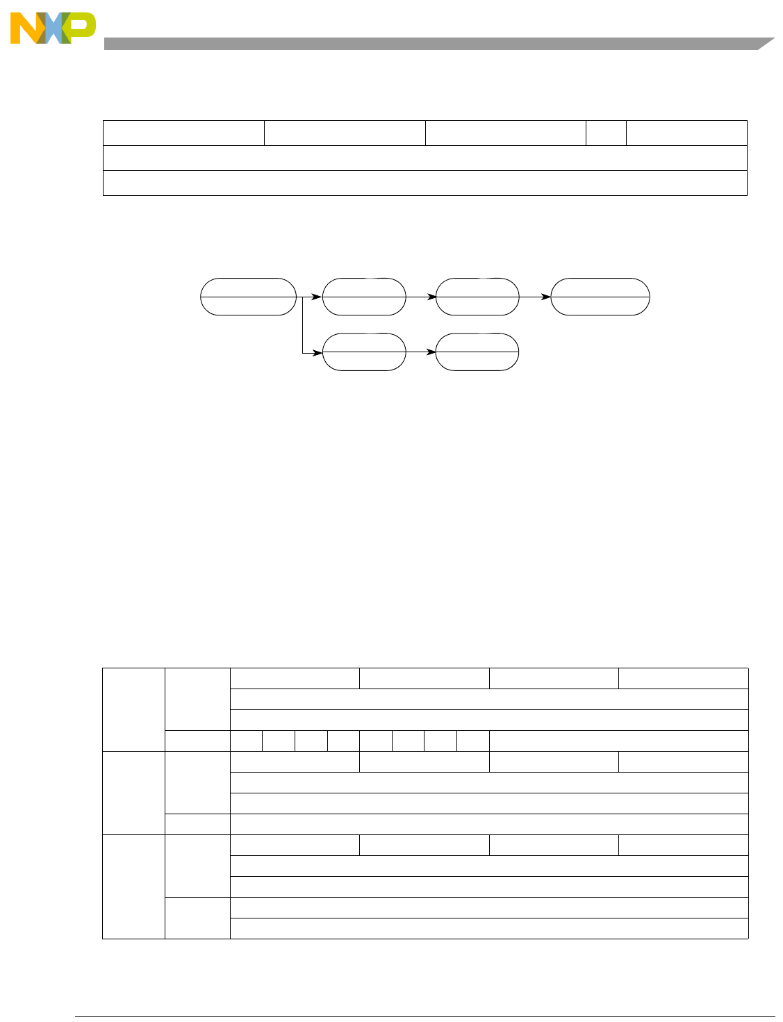
Debug Module
Freescale Semiconductor 28-26
Command Sequence:
Figure 28-20. WAREG/WDREG Command Sequence
Operand Data: Longword data is written into the specified address or data register. The data is
supplied most-significant word first.
Result Data: Command complete status is indicated by returning 0xFFFF (with S cleared)
when the register write is complete.
28.4.1.5.3 Read Memory Location (READ)
Read data at the longword address. Address space is defined by BAAR[TT,TM]. Hardware forces
low-order address bits to 0s for word and longword accesses to ensure that word addresses are
word-aligned and longword addresses are longword-aligned.
Command/Result Formats:
1514131211109876543210
0x2 0x0 0x8 A/D Register
D[31:16]
D[15:0]
Figure 28-19. WAREG/WDREG Command Format
1514131211109876543210
Byte
Command
0x1 0x9 0x0 0x0
A[31:16]
A[15:0]
Result X X X X X X X X D[7:0]
Word Command 0x1 0x9 0x4 0x0
A[31:16]
A[15:0]
Result D[15:0]
Longword Command 0x1 0x9 0x8 0x0
A[31:16]
A[15:0]
Result D[31:16]
D[15:0]
Figure 28-21. READ Command/Result Formats
WAREG/WDREG
???
LS DATA
’NOT READY’
NEXT CMD
’NOT READY’
XXX
BERR
MS DATA
’NOT READY’
NEXT CMD
’CMD COMPLETE’
MCF52211 ColdFire® Integrated Microcontroller Reference Manual, Rev. 3
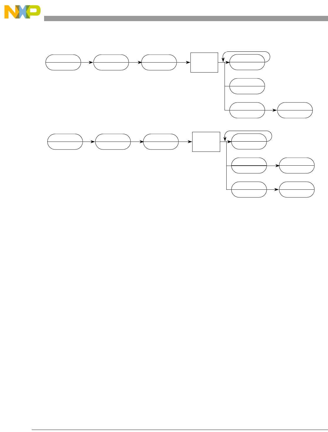
Debug Module
28-27 Freescale Semiconductor
Command Sequence:
Figure 28-22. READ Command Sequence
Operand Data: The only operand is the longword address of the requested location.
Result Data: Word results return 16 bits of data; longword results return 32. Bytes are returned
in the LSB of a word result; the upper byte is undefined. 0x0001 (S = 1) is returned
if a bus error occurs.
28.4.1.5.4 Write Memory Location (WRITE)
Write data to the memory location specified by the longword address. BAAR[TT,TM] defines address
space. Hardware forces low-order address bits to 0s for word and longword accesses to ensure that word
addresses are word-aligned and longword addresses are longword-aligned.
XXX
’NOT READY’
READ (LONG)
???
MS ADDR
’NOT READY’
LS ADDR
’NOT READY’
NEXT CMD
’NOT READY’
NEXT CMD
LS RESULT
READ
MEMORY
LOCATION
XXX
BERR
XXX
MS RESULT
XXX
’NOT READY’
READ (B/W)
???
MS ADDR
’NOT READY’
LS ADDR
’NOT READY’
NEXT CMD
’NOT READY’
READ
MEMORY
LOCATION
XXX
BERR
NEXT CMD
RESULT
MCF52211 ColdFire® Integrated Microcontroller Reference Manual, Rev. 3

Debug Module
Freescale Semiconductor 28-28
Command Formats:
1514131211109876543210
Byte0x10x80x00x0
A[31:16]
A[15:0]
XXXXXXXX D[7:0]
Word0x10x80x40x0
A[31:16]
A[15:0]
D[15:0]
Longword 0x1 0x8 0x8 0x0
A[31:16]
A[15:0]
D[31:16]
D[15:0]
Figure 28-23. WRITE Command Format
MCF52211 ColdFire® Integrated Microcontroller Reference Manual, Rev. 3
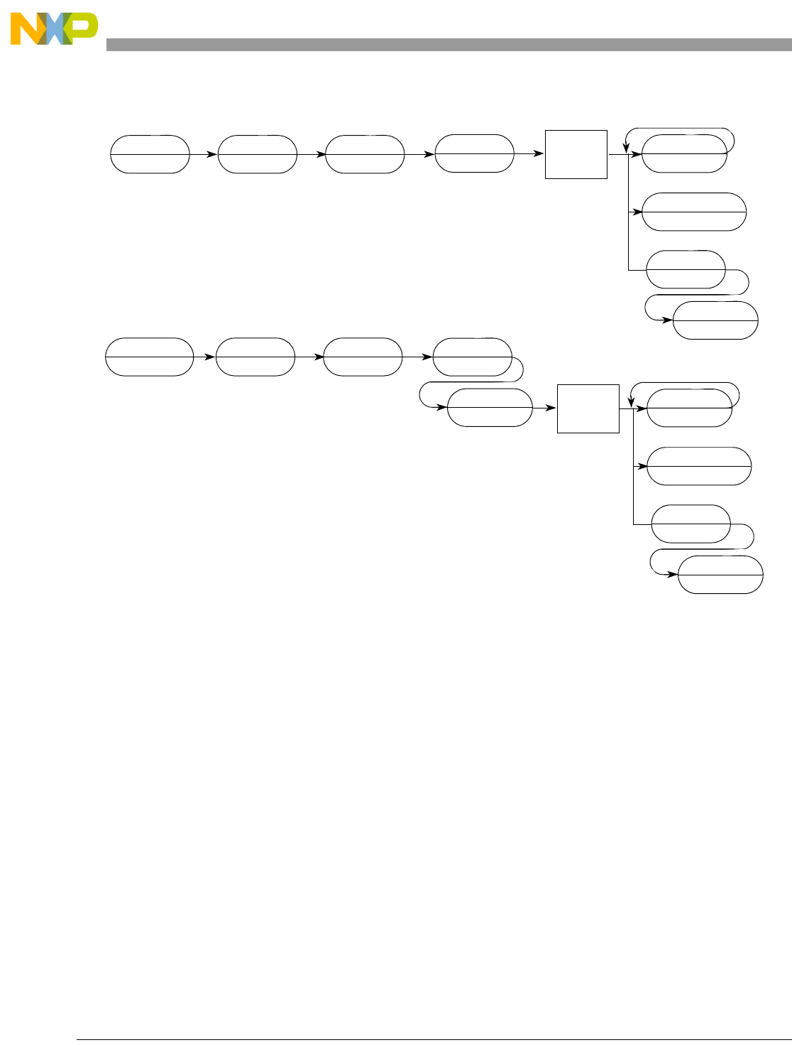
Debug Module
28-29 Freescale Semiconductor
Command Sequence:
Figure 28-24. WRITE Command Sequence
Operand Data: This two-operand instruction requires a longword absolute address that specifies
a location the data operand is written. Byte data is sent as a 16-bit word, justified
in the LSB; 16- and 32-bit operands are sent as 16 and 32 bits, respectively.
Result Data: Command complete status is indicated by returning 0xFFFF (with S cleared)
when the register write is complete. A value of 0x0001 (with S set) is returned if
a bus error occurs.
28.4.1.5.5 Dump Memory Block (DUMP)
DUMP is used with the READ command to access large blocks of memory. An initial READ is executed to
set up the starting address of the block and to retrieve the first result. If an initial READ is not executed
before the first DUMP, an illegal command response is returned. The DUMP command retrieves subsequent
operands. The initial address increments by the operand size (1, 2, or 4) and saves in a temporary register.
Subsequent DUMP commands use this address, perform the memory read, increment it by the current
operand size, and store the updated address in the temporary register.
XXX
’NOT READY’
WRITE (LONG)
???
MS ADDR
’NOT READY’
LS ADDR
’NOT READY’
WRITE
MEMORY
LOCATION
NEXT CMD
’CMD COMPLETE’
MS DATA
’NOT READY’
NEXT CMD
’NOT READY’
XXX
BERR
XXX
’NOT READY’
WRITE (B/W)
???
MS ADDR
’NOT READY’
LS ADDR
’NOT READY’
WRITE
MEMORY
LOCATION
NEXT CMD
’CMD COMPLETE’
DATA
’NOT READY’
NEXT CMD
’NOT READY’
XXX
BERR
LS DATA
’NOT READY’
MCF52211 ColdFire® Integrated Microcontroller Reference Manual, Rev. 3
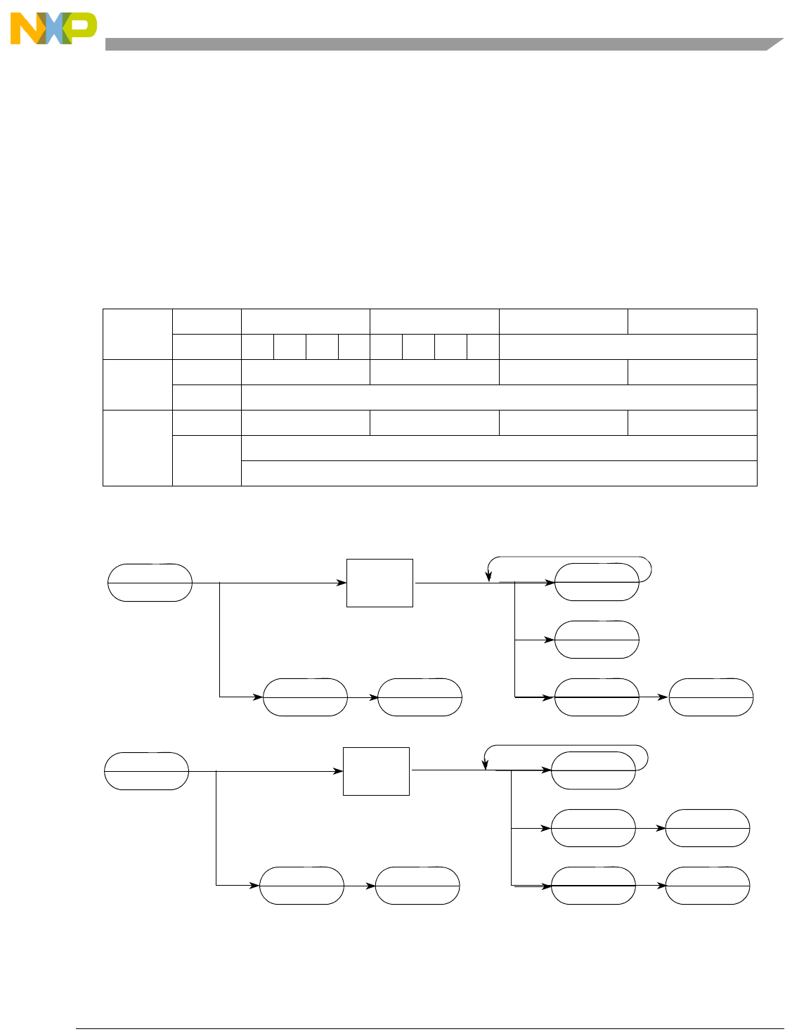
Debug Module
Freescale Semiconductor 28-30
NOTE
DUMP does not check for a valid address; it is a valid command only when
preceded by NOP, READ, or another DUMP command. Otherwise, an illegal
command response is returned. NOP can be used for intercommand padding
without corrupting the address pointer.
The size field is examined each time a DUMP command is processed, allowing the operand size to be
dynamically altered.
Command/Result Formats:
Command Sequence:
Figure 28-26. DUMP Command Sequence
Operand Data: None
1514131211109876543210
Byte Command 0x1 0xD 0x0 0x0
Result XXXXXXXX D[7:0]
Word Command 0x1 0xD 0x4 0x0
Result D[15:0]
Longword Command 0x1 0xD 0x8 0x0
Result D[31:16]
D[15:0]
Figure 28-25. DUMP Command/Result Formats
XXX
’NOT READY’
DUMP (B/W)
???
XXX
’ILLEGAL’
NEXT CMD
’NOT READY’
NEXT CMD
’NOT READY’
READ
MEMORY
LOCATION
XXX
BERR
NEXT CMD
RESULT
XXX
’NOT READY’
DUMP (LONG)
???
XXX
’ILLEGAL’
NEXT CMD
’NOT READY’
NEXT CMD
’NOT READY’
READ
MEMORY
LOCATION
XXX
BERR
NEXT CMD
MS RESULT
NEXT CMD
LS RESULT
MCF52211 ColdFire® Integrated Microcontroller Reference Manual, Rev. 3

Debug Module
28-31 Freescale Semiconductor
Result Data: Requested data is returned as a word or longword. Byte data is returned in the
least-significant byte of a word result. Word results return 16 bits of significant
data; longword results return 32 bits. A value of 0x0001 (with S set) is returned if
a bus error occurs.
28.4.1.5.6 Fill Memory Block (FILL)
A FILL command is used with the WRITE command to access large blocks of memory. An initial WRITE is
executed to set up the starting address of the block and to supply the first operand. The FILL command
writes subsequent operands. The initial address increments by the operand size (1, 2, or 4) and saves in a
temporary register after the memory write. Subsequent FILL commands use this address, perform the write,
increment it by the current operand size, and store the updated address in the temporary register.
If an initial WRITE is not executed preceding the first FILL command, the illegal command response is
returned.
NOTE
The FILL command does not check for a valid address: FILL is a valid
command only when preceded by another FILL, a NOP, or a WRITE command.
Otherwise, an illegal command response is returned. The NOP command can
be used for intercommand padding without corrupting the address pointer.
The size field is examined each time a FILL command is processed, allowing the operand size to be altered
dynamically.
Command Formats:
1514131211109876543210
Byte 0x1 0xC 0x0 0x0
XXXXXXXX D[7:0]
Word 0x1 0xC 0x4 0x0
D[15:0]
Longword 0x1 0xC 0x8 0x0
D[31:16]
D[15:0]
Figure 28-27. FILL Command Format
MCF52211 ColdFire® Integrated Microcontroller Reference Manual, Rev. 3
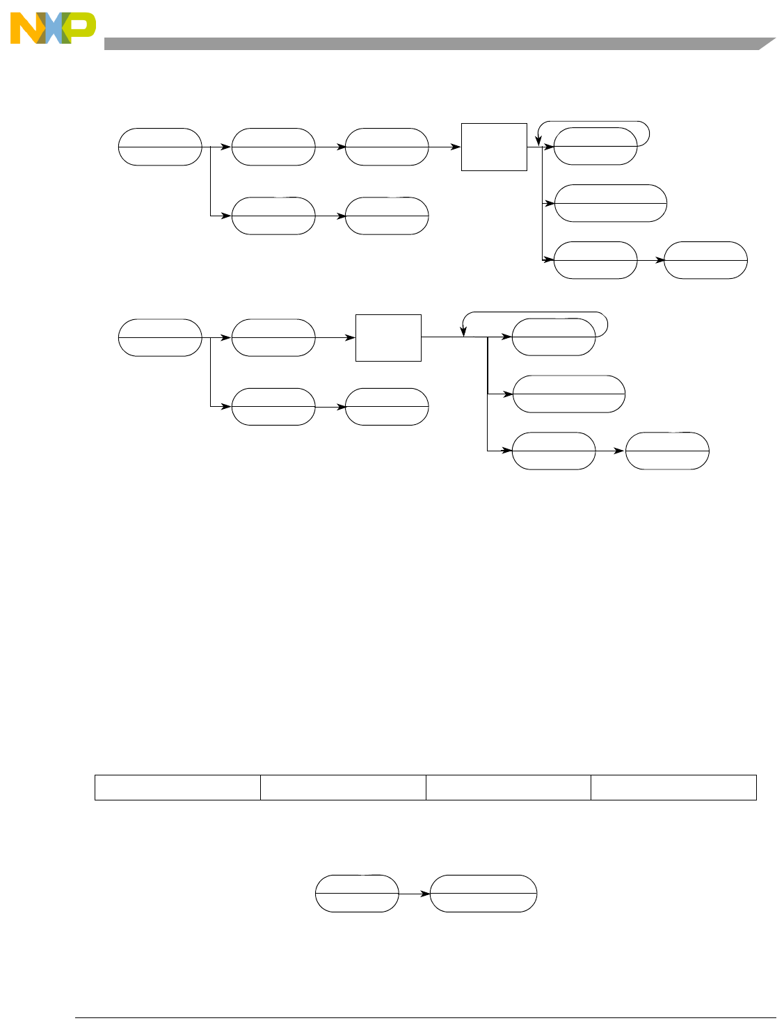
Debug Module
Freescale Semiconductor 28-32
Command Sequence:
Figure 28-28. FILL Command Sequence
Operand Data: A single operand is data to be written to the memory location. Byte data is sent as
a 16-bit word, justified in the least-significant byte; 16- and 32-bit operands are
sent as 16 and 32 bits, respectively.
Result Data: Command complete status (0xFFFF) is returned when the register write is
complete. A value of 0x0001 (with S set) is returned if a bus error occurs.
28.4.1.5.7 Resume Execution (GO)
The pipeline is flushed and refilled before normal instruction execution resumes. Prefetching begins at the
current address in the PC and at the current privilege level. If any register (such as the PC or SR) is altered
by a BDM command while the processor is halted, the updated value is used when prefetching resumes.
If a GO command issues and the CPU is not halted, the command is ignored.
Command Sequence:
Figure 28-30. GO Command Sequence
1514131211109876543210
0x0 0xC 0x0 0x0
Figure 28-29. GO Command Format
XXX
’NOT READY’
FILL (B/W)
???
DATA
’NOT READY’
NEXT CMD
’NOT READY’
WRITE
MEMORY
LOCATION
XXX
BERR
NEXT CMD
’CMD COMPLETE’
XXX
’ILLEGAL’
NEXT CMD
’NOT READY’
XXX
’NOT READY’
FILL (LONG)
???
MS DATA
’NOT READY’
LS DATA
’NOT READY’
WRITE
MEMORY
LOCATION
XXX
BERR
NEXT CMD
’CMD COMPLETE’
XXX
’ILLEGAL’
NEXT CMD
’NOT READY’
NEXT CMD
’NOT READY’
GO
???
NEXT CMD
’CMD COMPLETE’
MCF52211 ColdFire® Integrated Microcontroller Reference Manual, Rev. 3

Debug Module
28-33 Freescale Semiconductor
Operand Data: None
Result Data: The command-complete response (0xFFFF) is returned during the next shift
operation.
28.4.1.5.8 No Operation (NOP)
NOP performs no operation and may be used as a null command where required.
Command Formats:
Command Sequence:
Figure 28-32. NOP Command Sequence
Operand Data: None
Result Data: The command-complete response, 0xFFFF (with S cleared), is returned during the
next shift operation.
28.4.1.5.9 Synchronize PC to the PST/DDATA Lines (SYNC_PC)
The SYNC_PC command captures the current PC and displays it on the PST/DDATA outputs. After the
debug module receives the command, it sends a signal to the ColdFire processor that the current PC must
be displayed. The processor then forces an instruction fetch at the next PC with the address being captured
in the DDATA logic under control of the CSR[BTB] bits. The specific sequence of PST and DDATA
values is defined below:
1. Debug signals a SYNC_PC command is pending.
2. CPU completes the current instruction.
3. CPU forces an instruction fetch to the next PC, generates a PST equaling 0x5 value indicating a
taken branch and signals the capture of DDATA.
4. The instruction address corresponding to the PC is captured.
5. The PST marker (0x9–0xB) is generated and displayed as defined by the CSR[BTB] bit followed
by the captured PC address.
The SYNC_PC command can be used to dynamically access the PC for performance monitoring. The
execution of this command is considerably less obtrusive to the real-time operation of an application than
a HALT-CPU/READ-PC/RESUME command sequence.
Command Formats:
1514131211109876543210
0x00x00x00x0
Figure 28-31. NOP Command Format
NOP
???
NEXT CMD
’CMD COMPLETE’
MCF52211 ColdFire® Integrated Microcontroller Reference Manual, Rev. 3
Debug Module
Freescale Semiconductor 28-34
Command Sequence:
Figure 28-34. SYNC_PC Command Sequence
Operand Data: None
Result Data: Command complete status (0xFFFF) is returned when the register write is
complete.
28.4.1.5.10 Read Control Register (RCREG)
Read the selected control register and return the 32-bit result. Accesses to the processor/memory control
registers are always 32 bits wide, regardless of register width. The second and third words of the command
form a 32-bit address, which the debug module uses to generate a special bus cycle to access the specified
control register. The 12-bit Rc field is the same the processor’s MOVEC instruction uses.
Command/Result Formats:
Command Sequence:
Figure 28-36. RCREG Command Sequence
Operand Data: The only operand is the 32-bit Rc control register select field.
1514131211109876543210
0x00x00x00x1
Figure 28-33. SYNC_PC Command Format
1514131211109876543210
Command 0x2 0x9 0x8 0x0
0x0 0x0 0x0 0x0
0x0 Rc
Result D[31:16]
D[15:0]
Figure 28-35. RCREG Command/Result Formats
SYNC_PC
???
NEXT CMD
CMD COMPLETE
XXX
’NOT READY’
RCREG
???
MS ADDR
’NOT READY’
MS ADDR
’NOT READY’
NEXT CMD
’NOT READY’
READ
CONTROL
REGISTER
XXX
BERR
NEXT CMD
MS RESULT
NEXT CMD
LS RESULT
MCF52211 ColdFire® Integrated Microcontroller Reference Manual, Rev. 3

Debug Module
28-35 Freescale Semiconductor
Result Data: Control register contents are returned as a longword, most-significant word first.
The implemented portion of registers smaller than 32 bits is guaranteed correct;
other bits are undefined.
Rc encoding: See Table 28-21.
28.4.1.5.11 BDM Accesses of the Stack Pointer Registers (A7: SSP and USP)
The ColdFire core supports two unique stack pointer (A7) registers: the supervisor stack pointer (SSP) and
the user stack pointer (USP). The hardware implementation of these two programmable-visible 32-bit
registers does not uniquely identify one as the SSP and the other as the USP. Rather, the hardware uses one
32-bit register as the currently-active A7; the other is named the OTHER_A7. Therefore, the contents of
the two hardware registers is a function of the operating mode of the processor:
if SR[S] = 1
then A7 = Supervisor Stack Pointer
OTHER_A7 = User Stack Pointer
else A7 = User Stack Pointer
OTHER_A7 = Supervisor Stack Pointer
The BDM programming model supports reads and writes to A7 and OTHER_A7 directly. It is the
responsibility of the external development system to determine the mapping of A7 and OTHER_A7 to the
two program-visible definitions (supervisor and user stack pointers), based on the SR[S] bit.
28.4.1.5.12 BDM Accesses of the MAC Registers
The presence of rounding logic in the output datapath of the MAC requires special care for BDM-initiated
reads and writes of its programming model. In particular, any result rounding modes must be disabled
during the read/write process so the exact bit-wise MAC register contents are accessed.
Table 28-21. Control Register Map
Rc Register Definition
0x009 RGPIO Base Address Register (RGPIOBAR)1
1If an RGPIO module is available on this device.
0x(0,1)80 – 0x(0,1)87 Data Registers 0–7 (0 = load, 1 = store)
0x(0,1)88 – 0x(0,1)8F Address Registers 0–7 (0 = load, 1 = store)
(A7 is user stack pointer)
0x800 Other Stack Pointer (OTHER_A7)
0x801 Vector Base Register (VBR)
0x804 MAC Status Register (MACSR)
0x805 MAC Mask Register (MASK)
0x806 MAC Accumulator (ACC)
0x80E Status Register (SR)
0x80F Program Register (PC)
0xC04 Flash Base Address Register (FLASHBAR)
0xC05 RAM Base Address Register (RAMBAR)
MCF52211 ColdFire® Integrated Microcontroller Reference Manual, Rev. 3

Debug Module
Freescale Semiconductor 28-36
For example, a BDM read of the accumulator (ACC) must be preceded by two commands accessing the
MAC status register, as shown in the following sequence:
BdmReadACC (
rcreg macsr; // read current macsr contents and save
wcreg #0,macsr; // disable all rounding modes
rcreg ACC; // read the desired accumulator
wcreg #saved_data,macsr;// restore the original macsr
)
Likewise, to write an accumulator register, the following BDM sequence is needed:
BdmWriteACC (
rcreg macsr; // read current macsr contents and save
wcreg #0,macsr; // disable all rounding modes
wcreg #data,ACC; // write the desired accumulator
wcreg #saved_data,macsr;// restore the original macsr
)
For more information on saving and restoring the complete MAC programming model, see
Section 4.3.1.2, “Saving and Restoring the MAC Programming Model.”
28.4.1.5.13 Write Control Register (WCREG)
The operand (longword) data is written to the specified control register. The write alters all 32 register bits.
See the RCREG instruction description for the Rc encoding and for additional notes on writes to the A7
stack pointers and the EMAC programming model.
Command/Result Formats:
Command Sequence:
1514131211109876543210
Command 0x2 0x8 0x8 0x0
0x0 0x0 0x0 0x0
0x0 Rc
Result D[31:16]
D[15:0]
Figure 28-37. WCREG Command/Result Formats
MCF52211 ColdFire® Integrated Microcontroller Reference Manual, Rev. 3
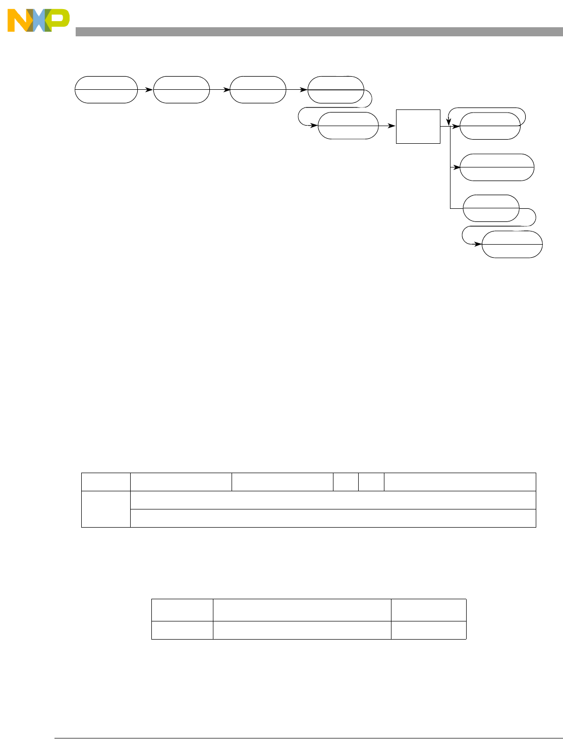
Debug Module
28-37 Freescale Semiconductor
Figure 28-38. WCREG Command Sequence
Operand Data: This instruction requires two longword operands. The first selects the register to
the operand data writes to; the second contains the data.
Result Data: Successful write operations return 0xFFFF. Bus errors on the write cycle are
indicated by the setting of bit 16 in the status message and by a data pattern of
0x0001.
28.4.1.5.14 Read Debug Module Register (RDMREG)
Read the selected debug module register and return the 32-bit result. The only valid register selection for
the RDMREG command is CSR (DRc=0x00).
Command/Result Formats:
Table 28-22 shows the definition of DRc encoding.
1514131211109876543210
Command 0x2 0xD 1 0 DRc
Result D[31:16]
D[15:0]
Figure 28-39. RDMREG Command/Result Formats
Table 28-22. Definition of DRc Encoding—Read
DRc[5:0] Debug Register Definition Mnemonic
0x00 Configuration/Status CSR
XXX
’NOT READY’
WCREG
???
MS ADDR
’NOT READY’
MS ADDR
’NOT READY’
WRITE
CONTROL
REGISTER
NEXT CMD
’CMD COMPLETE’
MS DATA
’NOT READY’
NEXT CMD
’NOT READY’
XXX
BERR
LS DATA
’NOT READY’
MCF52211 ColdFire® Integrated Microcontroller Reference Manual, Rev. 3
Debug Module
Freescale Semiconductor 28-38
Command Sequence:
Figure 28-40. RDMREG Command Sequence
Operand Data: None
Result Data: The contents of the selected debug register are returned as a longword value. The
data is returned most-significant word first.
28.4.1.5.15 Write Debug Module Register (WDMREG)
The operand (longword) data is written to the specified debug module register. All 32 bits of the register
are altered by the write. DSCLK must be inactive while the debug module register writes from the CPU
accesses are performed using the WDEBUG instruction.
Command Format:
Table 28-3 shows the definition of the DRc write encoding.
Command Sequence:
Figure 28-42. WDMREG Command Sequence
Operand Data: Longword data is written into the specified debug register. The data is supplied
most-significant word first.
Result Data: Command complete status (0xFFFF) is returned when register write is complete.
Figure 28-41. WDMREG BDM Command Format
1514131211109876543210
0x2 0xC 1 0 DRc
D[31:16]
D[15:0]
RDMREG
???
XXX
MS RESULT
NEXT CMD
LS RESULT
XXX
’ILLEGAL’
NEXT CMD
’NOT READY’
WDMREG
???
MS DATA
’NOT READY’
LS DATA
’NOT READY’
XXX
’ILLEGAL’
NEXT CMD
’NOT READY’
NEXT CMD
’CMD COMPLETE’
MCF52211 ColdFire® Integrated Microcontroller Reference Manual, Rev. 3

Debug Module
28-39 Freescale Semiconductor
28.4.2 Real-Time Debug Support
The ColdFire family provides support debugging real-time applications. For these types of embedded
systems, the processor must continue to operate during debug. The foundation of this area of debug support
is that while the processor cannot be halted to allow debugging, the system can generally tolerate the small
intrusions of the BDM inserting instructions into the pipeline with minimal effect on real-time operation.
The debug module provides four types of breakpoints: PC with mask, PC without mask, operand address
range, and data with mask. These breakpoints can be configured into one- or two-level triggers with the
exact trigger response also programmable. The debug module programming model can be written from the
external development system using the debug serial interface or from the processor’s supervisor
programming model using the WDEBUG instruction. Only CSR is readable using the external
development system.
28.4.2.1 Theory of Operation
Breakpoint hardware can be configured through TDR[TCR] to respond to triggers by displaying DDATA,
initiating a processor halt, or generating a debug interrupt. As shown in Table 28-23, when a breakpoint is
triggered, an indication (CSR[BSTAT]) is provided on the DDATA output port when it is not displaying
captured processor status, operands, or branch addresses.
The breakpoint status is also posted in the CSR. CSR[BSTAT] is cleared by a CSR read when a level-2
breakpoint is triggered or a level-1 breakpoint is triggered and a level-2 breakpoint is not enabled. Status
is also cleared by writing to either TDR to disable trigger options.
BDM instructions use the appropriate registers to load and configure breakpoints. As the system operates,
a breakpoint trigger generates the response defined in TDR.
PC breakpoints are treated in a precise manner—exception recognition and processing are initiated before
the excepting instruction executes. All other breakpoint events are recognized on the processor’s local bus,
but are made pending to the processor and sampled like other interrupt conditions. As a result, these
interrupts are imprecise.
In systems that tolerate the processor being halted, a BDM-entry can be used. With TDR[TRC] equals 01,
a breakpoint trigger causes the core to halt (PST = 0xF).
If the processor core cannot be halted, the debug interrupt can be used. With this configuration,
TDR[TRC] equals 10, breakpoint trigger becomes a debug interrupt to the processor, which is treated
Table 28-23. DDATA[3:0]/CSR[BSTAT] Breakpoint Response
DDATA[3:0]1CSR[BSTAT]1
1Encodings not shown are reserved for future use.
Breakpoint Status
0000 0000 No breakpoints enabled
0010 0001 Waiting for level-1 breakpoint
0100 0010 Level-1 breakpoint triggered
1010 0101 Waiting for level-2 breakpoint
1100 0110 Level-2 breakpoint triggered
MCF52211 ColdFire® Integrated Microcontroller Reference Manual, Rev. 3

Debug Module
Freescale Semiconductor 28-40
higher than the nonmaskable level-7 interrupt request. As with all interrupts, it is made pending until the
processor reaches a sample point, which occurs once per instruction. Again, the hardware forces the PC
breakpoint to occur before the targeted instruction executes and is precise. This is possible because the PC
breakpoint is enabled when interrupt sampling occurs. For address and data breakpoints, reporting is
considered imprecise, because several instructions may execute after the triggering address or data is
detected.
As soon as the debug interrupt is recognized, the processor aborts execution and initiates exception
processing. This event is signaled externally by the assertion of a unique PST value (PST = 0xD) for
multiple cycles. The core enters emulator mode when exception processing begins. After the standard
8-byte exception stack is created, the processor fetches a unique exception vector, 12, from the vector
table.Refer to the ColdFire Programmer’s Reference Manual. for more information.
Execution continues at the instruction address in the vector corresponding to the debug interrupt. All
interrupts are ignored while the processor is in emulator mode. The debug interrupt handler can use
supervisor instructions to save the necessary context, such as the state of all program-visible registers into
a reserved memory area.
When debug interrupt operations complete, the RTE instruction executes and the processor exits emulator
mode. After the debug interrupt handler completes execution, the external development system can use
BDM commands to read the reserved memory locations.
In revision B/B+, the hardware inhibits generation of another debug interrupt during the first instruction
after the RTE exits emulator mode. This behavior is consistent with the logic involving trace mode where
the first instruction executes before another trace exception is generated. Thus, all hardware breakpoints
are disabled until the first instruction after the RTE completes execution, regardless of the programmed
trigger response.
28.4.2.2 Emulator Mode
Emulator mode facilitates non-intrusive emulator functionality. This mode can be entered in three different
ways:
• Setting CSR[EMU] forces the processor into emulator mode. EMU is examined only if RSTI is
negated and the processor begins reset exception processing. It can be set while the processor is
halted before reset exception processing begins. See Section 28.4.1.1, “CPU Halt”.
• A debug interrupt always puts the processor in emulation mode when debug interrupt exception
processing begins.
• Setting CSR[TRC] forces the processor into emulation mode when trace exception processing
begins.
While operating in emulation mode, the processor exhibits the following properties:
• All interrupts are ignored, including level-7 interrupts.
• If CSR[MAP] is set, all caching of memory and the SRAM module are disabled. All memory
accesses are forced into a specially mapped address space signaled by TT equals 0x2,
TM equals 0x5, or 0x6. This includes stack frame writes and vector fetch for the exception that
forced entry into this mode.
MCF52211 ColdFire® Integrated Microcontroller Reference Manual, Rev. 3

Debug Module
28-41 Freescale Semiconductor
The RTE instruction exits emulation mode. The processor status output port provides a unique encoding
for emulator mode entry (0xD) and exit (0x7).
28.4.3 Concurrent BDM and Processor Operation
The debug module supports concurrent operation of the processor and most BDM commands. BDM
commands may be executed while the processor is running, except these following operations that access
processor/memory registers:
• Read/write address and data registers
• Read/write control registers
For BDM commands that access memory, the debug module requests the processor’s local bus. The
processor responds by stalling the instruction fetch pipeline and waiting for current bus activity to
complete before freeing the local bus for the debug module to perform its access. After the debug module
bus cycle, the processor reclaims the bus.
NOTE
Breakpoint registers must be carefully configured in a development system
if the processor is executing. The debug module contains no hardware
interlocks, so TDR should be disabled while breakpoint registers are loaded,
after which TDR can be written to define the exact trigger. This prevents
spurious breakpoint triggers.
Because there are no hardware interlocks in the debug unit, no BDM operations are allowed while the CPU
is writing the debug’s registers (DSCLK must be inactive).
NOTE
The debug module requires the use of the internal bus to perform BDM
commands. For this processor core, if the processor is executing a tight loop
contained within a single aligned longword, the processor may never grant
the internal bus to the debug module, for example:
align4
label1: nop
bra.b label1
or
align4
label2: bra.w label2
The processor grants the internal bus if these loops are forced across two
longwords.
28.4.4 Real-Time Trace Support
Real-time trace, which defines the dynamic execution path and is also known as instruction trace, is a
fundamental debug function. The ColdFire solution is to include a parallel output port providing encoded
processor status and data to an external development system. This port is partitioned into two 4-bit nibbles:
one nibble allows the processor to transmit processor status, (PST), and the other allows operand data to
MCF52211 ColdFire® Integrated Microcontroller Reference Manual, Rev. 3

Debug Module
Freescale Semiconductor 28-42
be displayed (debug data, DDATA). The processor status may not be related to the current bus transfer, due
to the decoupling FIFOs.
External development systems can use PST outputs with an external image of the program to completely
track the dynamic execution path. This tracking is complicated by any change in flow, where branch target
address calculation is based on the contents of a program-visible register (variant addressing). DDATA
outputs can display the target address of such instructions in sequential nibble increments across multiple
processor clock cycles, as described in Section 28.4.4.1, “Begin Execution of Taken Branch (PST = 0x5)”.
Two 32-bit storage elements form a FIFO buffer connecting the processor’s high-speed local bus to the
external development system through PST[3:0] and DDATA[3:0]. The buffer captures branch target
addresses and certain data values for eventual display on the DDATA port, one nibble at a time starting
with the least significant bit (lsb).
Execution speed is affected only when both storage elements contain valid data to be dumped to the
DDATA port. The core stalls until one FIFO entry is available.
Table 28-24 shows the encoding of these signals.
Table 28-24. Processor Status Encoding
PST[3:0] Definition
0x0 Continue execution. Many instructions execute in one processor cycle. If an instruction requires more clock
cycles, subsequent clock cycles are indicated by driving PST outputs with this encoding.
0x1 Begin execution of one instruction. For most instructions, this encoding signals the first processor clock cycle
of an instruction’s execution. Certain change-of-flow opcodes, plus the PULSE and WDDATA instructions,
generate different encodings.
0x2 Reserved
0x3 Entry into user-mode. Signaled after execution of the instruction that caused the ColdFire processor to enter
user mode.
0x4 Begin execution of PULSE and WDDATA instructions. PULSE defines logic analyzer triggers for debug
and/or performance analysis. WDDATA lets the core write any operand (byte, word, or longword) directly to
the DDATA port, independent of debug module configuration. When WDDATA is executed, a value of 0x4 is
signaled on the PST port, followed by the appropriate marker, and then the data transfer on the DDATA port.
Transfer length depends on the WDDATA operand size.
0x5 Begin execution of taken branch or SYNC_PC command issued. For some opcodes, a branch target
address may be displayed on DDATA depending on the CSR settings. CSR also controls the number of
address bytes displayed, indicated by the PST marker value preceding the DDATA nibble that begins the
data output. See Section 28.4.4.1, “Begin Execution of Taken Branch (PST = 0x5)”. Also indicates that the
SYNC_PC command has been issued.
0x6 Reserved
0x7 Begin execution of return from exception (RTE) instruction.
0x8–
0xB
Indicates the number of bytes to be displayed on the DDATA port on subsequent clock cycles. The value is
driven onto the PST port one PSTCLK cycle before the data is displayed on DDATA.
0x8 Begin 1-byte transfer on DDATA.
0x9 Begin 2-byte transfer on DDATA.
0xA Begin 3-byte transfer on DDATA.
0xB Begin 4-byte transfer on DDATA.
MCF52211 ColdFire® Integrated Microcontroller Reference Manual, Rev. 3

Debug Module
28-43 Freescale Semiconductor
28.4.4.1 Begin Execution of Taken Branch (PST = 0x5)
PST is 0x5 when a taken branch is executed. For some opcodes, a branch target address may be displayed
on DDATA depending on the CSR settings. CSR also controls the number of address bytes displayed,
which is indicated by the PST marker value immediately preceding the DDATA nibble that begins the data
output.
Multiple byte DDATA values are displayed in least-to-most-significant order. The processor captures only
those target addresses associated with taken branches that use a variant addressing mode (RTE and RTS
instructions, JMP and JSR instructions using address register indirect or indexed addressing modes, and
all exception vectors).
The simplest example of a branch instruction using a variant address is the compiled code for a C language
case statement. Typically, the evaluation of this statement uses the variable of an expression as an index
into a table of offsets, where each offset points to a unique case within the structure. For such
change-of-flow operations, the ColdFire processor uses the debug pins to output the following sequence
of information on two successive processor clock cycles:
1. Use PST (0x5) to identify that a taken branch is executed.
2. Signal the target address to be displayed sequentially on the DDATA pins. Encodings 0x9–0xB
identify the number of bytes displayed.Using the PSTB, o
3. The new target address is optionally available on subsequent cycles using the DDATA port. The
number of bytes of displayed on this port is configurable (2, 3, or 4 bytes, where the DDATA
encoding is 0x9, 0xA, and 0xB, respectively).
Another example of a variant branch instruction would be a JMP (A0) instruction. Figure 28-43 shows the
PST and DDATA outputs that indicate a JMP (A0) execution, assuming the CSR was programmed to
display the lower 2 bytes of an address.
0xC Normal exception processing. Exceptions that enter emulation mode (debug interrupt or optionally trace)
generate a different encoding, as described below. Because the 0xC encoding defines a multiple-cycle
mode, PST outputs are driven with 0xC until exception processing completes.
0xD Emulator mode exception processing. Displayed during emulation mode (debug interrupt or optionally
trace). Because this encoding defines a multiple-cycle mode, PST outputs are driven with 0xD until
exception processing completes.
0xE Processor is stopped. Appears in multiple-cycle format when the processor executes a STOP instruction.
The ColdFire processor remains stopped until an interrupt occurs, thus PST outputs display 0xE until the
stopped mode is exited.
0xF Processor is halted. Because this encoding defines a multiple-cycle mode, the PST outputs display 0xF until
the processor is restarted or reset. See Section 28.4.1.1, “CPU Halt”.
Table 28-24. Processor Status Encoding (continued)
PST[3:0] Definition
MCF52211 ColdFire® Integrated Microcontroller Reference Manual, Rev. 3

Debug Module
Freescale Semiconductor 28-44
Figure 28-43. Example JMP Instruction Output on PST/DDATA
PST of 0x5 indicates a taken branch and the marker value 0x9 indicates a 2-byte address. Therefore, the
subsequent 4 nibbles of DDATA display the lower two bytes of address register A0 in
least-to-most-significant nibble order. The PST output after the JMP instruction completes depends on the
target instruction. The PST can continue with the next instruction before the address has completely
displayed on DDATA because of the DDATA FIFO. If the FIFO is full and the next instruction has captured
values to display on DDATA, the pipeline stalls (PST = 0x0) until space is available in the FIFO.
28.4.5 Processor Status, Debug Data Definition
This section specifies the ColdFire processor and debug module’s generation of the processor status (PST)
and debug data (DDATA) output on an instruction basis. In general, the PST/DDATA output for an
instruction is defined as follows:
PST = 0x1, {PST = [0x89B], DDATA = operand}
where the {...} definition is optional operand information defined by the setting of the CSR.
The CSR provides capabilities to display operands based on reference type (read, write, or both). A PST
value {0x8, 0x9, or 0xB} identifies the size and presence of valid data to follow on the DDATA output {1,
2, or 4 bytes}. Additionally, for certain change-of-flow branch instructions, CSR[BTB] provides the
capability to display the target instruction address on the DDATA output {2, 3, or 4 bytes} using a PST
value of {0x9, 0xA, or 0xB}. Addresses use the markers x0D, x0E, or 0xF to store 2, 3, or 4 bytes of
address packets with address shifted right by 1 bit.
28.4.5.1 User Instruction Set
Table 28-25 shows the PST/DDATA specification for user-mode instructions. Rn represents any {Dn, An}
register. In this definition, the y suffix generally denotes the source, and x denotes the destination operand.
For a given instruction, the optional operand data is displayed only for those effective addresses
referencing memory. The DD nomenclature refers to the DDATA outputs.
Table 28-25. PST/DDATA Specification for User-Mode Instructions
Instruction Operand Syntax PST/DDATA
add.l <ea>y,Dx PST = 0x1, {PST = 0xB, DD = source operand}
add.l Dy,<ea>x PST = 0x1, {PST = 0xB, DD = source}, {PST = 0xB, DD = destination}
adda.l <ea>y,Ax PST = 0x1, {PST = 0xB, DD = source operand}
DDATA
PSTCLK
0x0 0x0 A[3:0]
0x5 0x9 default
PST
A[7:4] A[11:8] A[15:12]
default default default
MCF52211 ColdFire® Integrated Microcontroller Reference Manual, Rev. 3

Debug Module
28-45 Freescale Semiconductor
addi.l #<data>,Dx PST = 0x1
addq.l #<data>,<ea>x PST = 0x1, {PST = 0xB, DD = source}, {PST = 0xB, DD = destination}
addx.l Dy,Dx PST = 0x1
and.l <ea>y,Dx PST = 0x1, {PST = 0xB, DD = source operand}
and.l Dy,<ea>x PST = 0x1, {PST = 0xB, DD = source}, {PST = 0xB, DD = destination}
andi.l #<data>,Dx PST = 0x1
asl.l {Dy,#<data>},Dx PST = 0x1
asr.l {Dy,#<data>},Dx PST = 0x1
bcc.{b,w} if taken, then PST = 0x5, else PST = 0x1
bchg.{b,l} #<data>,<ea>x PST = 0x1, {PST = 0x8, DD = source}, {PST = 0x8, DD = destination}
bchg.{b,l} Dy,<ea>x PST = 0x1, {PST = 0x8, DD = source}, {PST = 0x8, DD = destination}
bclr.{b,l} #<data>,<ea>x PST = 0x1, {PST = 0x8, DD = source}, {PST = 0x8, DD = destination}
bclr.{b,l} Dy,<ea>x PST = 0x1, {PST = 0x8, DD = source}, {PST = 0x8, DD = destination}
bitrev.l Dx PST = 0x1
bra.{b,w} PST = 0x5
bset.{b,l} #<data>,<ea>x PST = 0x1, {PST = 0x8, DD = source}, {PST = 0x8, DD = destination}
bset.{b,l} Dy,<ea>x PST = 0x1, {PST = 0x8, DD = source}, {PST = 0x8, DD = destination}
bsr.{b,w} PST = 0x5, {PST = 0xB, DD = destination operand}
btst.{b,l} #<data>,<ea>x PST = 0x1, {PST = 0x8, DD = source operand}
btst.{b,l} Dy,<ea>x PST = 0x1, {PST = 0x8, DD = source operand}
byterev.l Dx PST = 0x1
clr.b <ea>x PST = 0x1, {PST = 0x8, DD = destination operand}
clr.l <ea>x PST = 0x1, {PST = 0xB, DD = destination operand}
clr.w <ea>x PST = 0x1, {PST = 0x9, DD = destination operand}
cmp.l <ea>y,Dx PST = 0x1, {PST = 0xB, DD = source operand}
cmpa.l <ea>y,Ax PST = 0x1, {PST = 0xB, DD = source operand}
cmpi.l #<data>,Dx PST = 0x1
divs.l <ea>y,Dx PST = 0x1, {PST = 0xB, DD = source operand}
divs.w <ea>y,Dx PST = 0x1, {PST = 0x9, DD = source operand}
divu.l <ea>y,Dx PST = 0x1, {PST = 0xB, DD = source operand}
divu.w <ea>y,Dx PST = 0x1, {PST = 0x9, DD = source operand}
eor.l Dy,<ea>x PST = 0x1, {PST = 0xB, DD = source}, {PST = 0xB, DD = destination}
eori.l #<data>,Dx PST = 0x1
Table 28-25. PST/DDATA Specification for User-Mode Instructions (continued)
Instruction Operand Syntax PST/DDATA
MCF52211 ColdFire® Integrated Microcontroller Reference Manual, Rev. 3

Debug Module
Freescale Semiconductor 28-46
ext.l Dx PST = 0x1
ext.w Dx PST = 0x1
extb.l Dx PST = 0x1
illegal PST = 0x11
jmp <ea>y PST = 0x5, {PST = [0x9AB], DD = target address}2
jsr <ea>y PST = 0x5, {PST = [0x9AB], DD = target address},
{PST = 0xB, DD = destination operand}2
lea.l <ea>y,Ax PST = 0x1
link.w Ay,#<displacement> PST = 0x1, {PST = 0xB, DD = destination operand}
lsl.l {Dy,#<data>},Dx PST = 0x1
lsr.l {Dy,#<data>},Dx PST = 0x1
move.b <ea>y,<ea>x PST = 0x1, {PST = 0x8, DD = source}, {PST = 0x8, DD = destination}
move.l <ea>y,<ea>x PST = 0x1, {PST = 0xB, DD = source}, {PST = 0xB, DD = destination}
move.w <ea>y,<ea>x PST = 0x1, {PST = 0x9, DD = source}, {PST = 0x9, DD = destination}
move.w CCR,Dx PST = 0x1
move.w {Dy,#<data>},CCR PST = 0x1
movea.l <ea>y,Ax PST = 0x1, {PST = 0xB, DD = source}
movea.w <ea>y,Ax PST = 0x1, {PST = 0x9, DD = source}
movem.l #list,<ea>x PST = 0x1, {PST = 0xB, DD = destination},... 3
movem.l <ea>y,#list PST = 0x1, {PST = 0xB, DD = source},... 3
moveq.l #<data>,Dx PST = 0x1
muls.l <ea>y,Dx PST = 0x1, {PST = 0xB, DD = source operand}
muls.w <ea>y,Dx PST = 0x1, {PST = 0x9, DD = source operand}
mulu.l <ea>y,Dx PST = 0x1, {PST = 0xB, DD = source operand}
mulu.w <ea>y,Dx PST = 0x1, {PST = 0x9, DD = source operand}
neg.l Dx PST = 0x1
negx.l Dx PST = 0x1
nop PST = 0x1
not.l Dx PST = 0x1
or.l <ea>y,Dx PST = 0x1, {PST = 0xB, DD = source operand}
or.l Dy,<ea>x PST = 0x1, {PST = 0xB, DD = source}, {PST = 0xB, DD = destination}
ori.l #<data>,Dx PST = 0x1
pea.l <ea>y PST = 0x1, {PST = 0xB, DD = destination operand}
Table 28-25. PST/DDATA Specification for User-Mode Instructions (continued)
Instruction Operand Syntax PST/DDATA
MCF52211 ColdFire® Integrated Microcontroller Reference Manual, Rev. 3

Debug Module
28-47 Freescale Semiconductor
pulse PST = 0x4
rems.l <ea>y,Dw:Dx PST = 0x1, {PST = 0xB, DD = source operand}
remu.l <ea>y,Dw:Dx PST = 0x1, {PST = 0xB, DD = source operand}
rts PST = 0x1, {PST = 0xB, DD = source operand},
PST = 0x5, {PST = 0x[9AB], DD = target address}
rts
(not predicted)
PSTDDATA = 0x1, {0xB, source operand}, 0x5, {0x[9AB], target address}
rts
(predicted)4
PSTDDATA = 0x1, {0xB, source operand}, 0x5
scc.b Dx PST = 0x1
sub.l <ea>y,Dx PST = 0x1, {PST = 0xB, DD = source operand}
sub.l Dy,<ea>x PST = 0x1, {PST = 0xB, DD = source}, {PST = 0xB, DD = destination}
suba.l <ea>y,Ax PST = 0x1, {PST = 0xB, DD = source operand}
subi.l #<data>,Dx PST = 0x1
subq.l #<data>,<ea>x PST = 0x1, {PST = 0xB, DD = source}, {PST = 0xB, DD = destination}
subx.l Dy,Dx PST = 0x1
swap.w Dx PST = 0x1
tpf PST = 0x1
tpf.l #<data> PST = 0x1
tpf.w #<data> PST = 0x1
trap #<data> PST = 0x11
tst.b <ea>x PST = 0x1, {PST = 0x8, DD = source operand}
tst.l <ea>y PST = 0x1, {PST = 0xB, DD = source operand}
tst.w <ea>y PST = 0x1, {PST = 0x9, DD = source operand}
unlk Ax PST = 0x1, {PST = 0xB, DD = destination operand}
wddata.b <ea>y PST = 0x4, {PST = 0x8, DD = source operand}
wddata.l <ea>y PST = 0x4, {PST = 0xB, DD = source operand}
wddata.w <ea>y PST = 0x4, {PST = 0x9, DD = source operand}
Table 28-25. PST/DDATA Specification for User-Mode Instructions (continued)
Instruction Operand Syntax PST/DDATA
MCF52211 ColdFire® Integrated Microcontroller Reference Manual, Rev. 3

Debug Module
Freescale Semiconductor 28-48
Table 28-26 shows the PST/DDATA specification for multiply-accumulate instructions.
1During normal exception processing, the PST output is driven to a 0xC indicating the exception processing state. The
exception stack write operands, as well as the vector read and target address of the exception handler may also be
displayed.
Exception Processing:
PST = 0xC,
{PST = 0xB,DD = destination}, // stack frame
{PST = 0xB,DD = destination}, // stack frame
{PST = 0xB,DD = source}, // vector read
PST = 0x5,{PST = [0x9AB],DD = target}// handler PC
The PST/DDATA specification for the reset exception is shown below:
Exception Processing:
PST = 0xC,
PST = 0x5,{PST = [0x9AB],DD = target}// handler PC
The initial references at address 0 and 4 are never captured nor displayed because these accesses are treated as
instruction fetches.
For all types of exception processing, the PST = 0xC value is driven at all times, unless the PST output is needed for one
of the optional marker values or for the taken branch indicator (0x5).
2For JMP and JSR instructions, the optional target instruction address is displayed only for those effective address fields
defining variant addressing modes. This includes the following <ea>x values: (An), (d16,An), (d8,An,Xi), (d8,PC,Xi).
3For move multiple instructions (MOVEM), the processor automatically generates line-sized transfers if the operand
address reaches a 0-modulo-16 boundary and there are four or more registers to be transferred. For these line-sized
transfers, the operand data is never captured nor displayed, regardless of the CSR value.
The automatic line-sized burst transfers are provided to maximize performance during these sequential memory access
operations.
4For a predicted RTS instruction, the source operand is displayed if CSR[12], CSR[9], or CSR[8] is set.
Table 28-26. PST/DDATA Values for User-Mode Multiply-Accumulate Instructions
Instruction Operand Syntax PST/DDATA
mac.l Ry,Rx PST = 0x1
mac.l Ry,Rx,<ea>y,Rw, PST = 0x1, {PST = 0xB, DD = source operand}
mac.w Ry,Rx PST = 0x1
mac.w Ry,Rx,ea,Rw PST = 0x1, {PST = 0xB, DD = source operand}
move.l {Ry,#<data>},ACC PST = 0x1
move.l {Ry,#<data>},MACSR PST = 0x1
move.l {Ry,#<data>},MASK PST = 0x1
move.l ACC,Rx PST = 0x1
move.l MACSR,CCR PST = 0x1
move.l MACSR,Rx PST = 0x1
move.l MASK,Rx PST = 0x1
msac.l Ry,Rx PST = 0x1
msac.l Ry,Rx,<ea>y,Rw PST = 0x1, {PST = 0xB, DD = source},
{PST = 0xB, DD = destination}
MCF52211 ColdFire® Integrated Microcontroller Reference Manual, Rev. 3

Debug Module
28-49 Freescale Semiconductor
28.4.5.2 Supervisor Instruction Set
The supervisor instruction set has complete access to the user mode instructions plus the opcodes shown
below. The PST/DDATA specification for these opcodes is shown in Table 28-27.
The move-to-SR and RTE instructions include an optional PST = 0x3 value, indicating an entry into user
mode. Additionally, if the execution of a RTE instruction returns the processor to emulator mode, a
multiple-cycle status of 0xD is signaled.
Similar to the exception processing mode, the stopped state (PST = 0xE) and the halted state (PST = 0xFF)
display this status throughout the entire time the ColdFire processor is in the given mode.
msac.w Ry,Rx PST = 0x1
msac.w Ry,Rx,<ea>y,Rw PST = 0x1, {PST = 0xB, DD = source},
{PST = 0xB, DD = destination}
Table 28-27. PST/DDATA Specification for Supervisor-Mode Instructions
Instruction Operand Syntax PST/DDATA
cpushl (Ax) PST = 0x1
halt PST = 0x1,
PST = 0xF
move.l Ay,USP PST = 0x1
move.l USP,Ax PST = 0x1
move.w SR,Dx PST = 0x1
move.w {Dy,#<data>},SR PST = 0x1, {PST = 0x3}
movec.l Ry,Rc PST = 0x1
rte PST = 0x7, {PST = 0xB, DD = source operand}, {PST = 0x3}, { PST = 0xB,
DD =source operand},
PST = 0x5, {[PST = 0x9AB], DD = target address}
stldsr.w #imm PST = 0x1, {PST = 0xA, DD = destination operand, PST = 0x3}
stop #<data> PST = 0x1,
PST = 0xE
wdebug.l <ea>y PST = 0x1, {PST = 0xB, DD = source, PST = 0xB, DD = source}
Table 28-26. PST/DDATA Values for User-Mode Multiply-Accumulate Instructions (continued)
Instruction Operand Syntax PST/DDATA
MCF52211 ColdFire® Integrated Microcontroller Reference Manual, Rev. 3
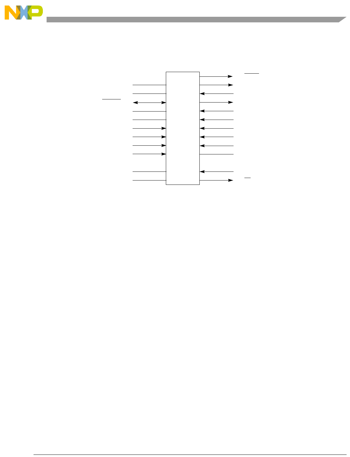
Debug Module
Freescale Semiconductor 28-50
28.4.6 Freescale-Recommended BDM Pinout
The ColdFire BDM connector is a 26-pin Berg connector arranged 2 x 13 as shown below.
Figure 28-44. Recommended BDM Connector
1
3
5
7
9
11
13
15
17
19
21
23
25
2
4
6
8
10
12
14
16
18
20
22
24
26
Developer reserved1
GND
GND
RESET
EVDD2
GND
Freescale reserved
GND
IVDD
BKPT
DSCLK
Developer reserved1
DSI
DSO
GND
Freescale reserved
PSTCLK
2 Supplied by target
1 Pins reserved for BDM developer use.
TA
PST3
PST1
DDATA3
DDATA1
PST2
PST0
DDATA2
DDATA0
MCF52211 ColdFire® Integrated Microcontroller Reference Manual, Rev. 3
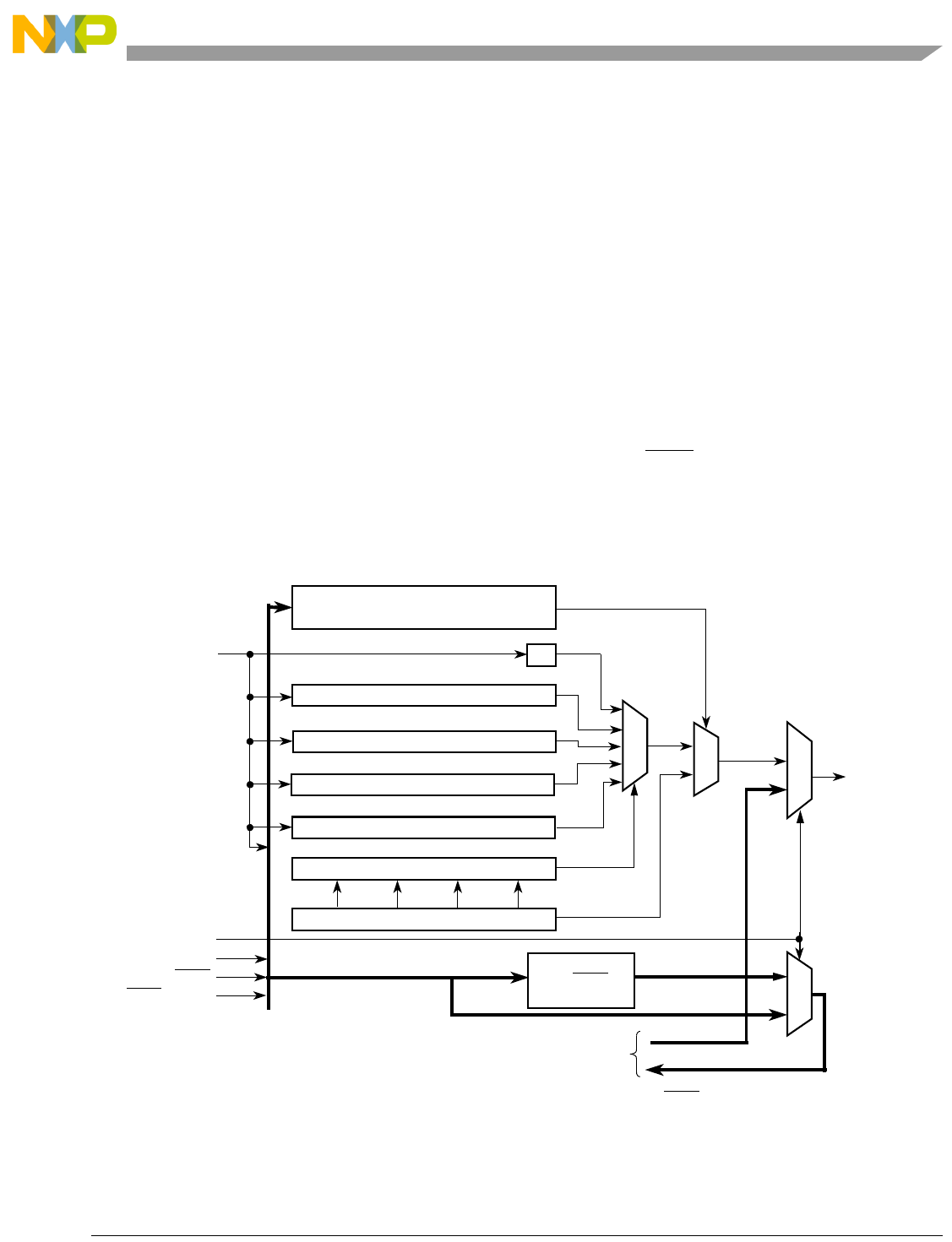
Freescale Semiconductor 29-1
Chapter 29
IEEE 1149.1 Test Access Port (JTAG)
29.1 Introduction
The Joint Test Action Group (JTAG) is a dedicated user-accessible test logic compliant with the
IEEE 1149.1 standard for boundary-scan testability, which helps with system diagnostic and
manufacturing testing.
This architecture provides access to all data and chip control pins from the board-edge connector through
the standard four-pin test access port (TAP) and the JTAG reset pin, TRST.
29.1.1 Block Diagram
Figure 29-1 shows the block diagram of the JTAG module.
Figure 29-1. JTAG Block Diagram
256-bit Boundary Scan Register
TDO/DSO
BKPT
4-bit TAP Instruction Register
30
1-bit Bypass Register
32-bit IDCODE Register
TRST/DSCLK
TCLK
TMS/BKPT
031
0
TAP Controller
TDI/DSI
1
0
JTAG Module
to Debug Module
4-bit TAP Instruction Decoder
1
0
Disable DSCLK
Force BKPT = 1
DSI = 0
JTAG_EN
DSO
DSI
DSCLK
255
7-bit JTAG_CFM_CLKDIV Register
06
3-bit TEST_CTRL Register
02
MCF52211 ColdFire® Integrated Microcontroller Reference Manual, Rev. 3

IEEE 1149.1 Test Access Port (JTAG)
Freescale Semiconductor 29-2
29.1.2 Features
The basic features of the JTAG module are the following:
• Performs boundary-scan operations to test circuit board electrical continuity
• Bypasses instruction to reduce the shift register path to a single cell
• Sets chip output pins to safety states while executing the bypass instruction
• Samples the system pins during operation and transparently shifts out the result
• Selects between JTAG TAP controller and Background Debug Module (BDM) using a dedicated
JTAG_EN pin
29.1.3 Modes of Operation
The JTAG_EN pin can select between the following modes of operation:
• JTAG mode (JTAG_EN = 1)
• Background debug mode (BDM)—for more information, refer to Section 28.4.1, “Background
Debug Mode (BDM)”; (JTAG_EN = 0).
29.2 External Signal Description
The JTAG module has five input and one output external signals, as described in Table 29-1.
29.2.1 JTAG Enable (JTAG_EN)
The JTAG_EN pin selects between the debug module and JTAG. If JTAG_EN is low, the debug module is
selected; if it is high, the JTAG is selected. Table 29-2 summarizes the pin function selected depending on
JTAG_EN logic state.
Table 29-1. Signal Properties
Name Direction Function Reset State Pull up
JTAG_EN Input JTAG/BDM selector input — —
TCLK Input JTAG Test clock input — Active
TMS/BKPT Input JTAG Test mode select / BDM Breakpoint — Active
TDI/DSI Input JTAG Test data input / BDM Development serial input — Active
TRST/DSCLK Input JTAG Test reset input / BDM Development serial clock — Active
TDO/DSO Output JTAG Test data output / BDM Development serial output Hi-Z / 0 —
MCF52211 ColdFire® Integrated Microcontroller Reference Manual, Rev. 3

IEEE 1149.1 Test Access Port (JTAG)
29-3 Freescale Semiconductor
When one module is selected, the inputs into the other module are disabled or forced to a known logic
level, as shown in Table 29-3, to disable the corresponding module.
NOTE
The JTAG_EN does not support dynamic switching between JTAG and
BDM modes.
29.2.2 Test Clock Input (TCLK)
The TCLK pin is a dedicated JTAG clock input to synchronize the test logic. Pulses on TCLK shift data
and instructions into the TDI pin on the rising edge and out of the TDO pin on the falling edge. TCLK is
independent of the processor clock. The TCLK pin has an internal pull-up resistor, and holding TCLK high
or low for an indefinite period does not cause JTAG test logic to lose state information.
29.2.3 Test Mode Select/Breakpoint (TMS/BKPT)
The TMS pin is the test mode select input that sequences the TAP state machine. TMS is sampled on the
rising edge of TCLK. The TMS pin has an internal pull-up resistor.
The BKPT pin is used to request an external breakpoint. Assertion of BKPT puts the processor into a halted
state after the current instruction completes.
29.2.4 Test Data Input/Development Serial Input (TDI/DSI)
The TDI pin receives serial test and data, which is sampled on the rising edge of TCLK. Register values
are shifted in least significant bit (lsb) first. The TDI pin has an internal pull-up resistor.
The DSI pin provides data input for the debug module serial communication port.
Table 29-2. Pin Function Selected
JTAG_EN = 0 JTAG_EN = 1 Pin Name
Module selected BDM JTAG —
Pin Function —
BKPT
DSI
DSO
DSCLK
TCLK
TMS
TDI
TDO
TRST
TCLK
BKPT
DSI
DSO
DSCLK
Table 29-3. Signal State to the Disable Module
JTAG_EN = 0 JTAG_EN = 1
Disabling JTAG TRST = 0
TMS = 1
—
Disabling BDM — Disable DSCLK
DSI = 0
BKPT = 1
MCF52211 ColdFire® Integrated Microcontroller Reference Manual, Rev. 3

IEEE 1149.1 Test Access Port (JTAG)
Freescale Semiconductor 29-4
29.2.5 Test Reset/Development Serial Clock (TRST/DSCLK)
The TRST pin is an active low asynchronous reset input with an internal pull-up resistor that forces the
TAP controller to the test-logic-reset state.
The DSCLK pin clocks the serial communication port to the debug module. Maximum frequency is 1/5
the processor clock speed. At the rising edge of DSCLK, data input on DSI is sampled and DSO changes
state.
29.2.6 Test Data Output/Development Serial Output (TDO/DSO)
The TDO pin is the lsb-first data output. Data is clocked out of TDO on the falling edge of TCLK. TDO
is tri-stateable and actively driven in the shift-IR and shift-DR controller states.
The DSO pin provides serial output data in BDM mode.
29.3 Memory Map/Register Definition
The JTAG module registers are not memory mapped and are only accessible through the TDO/DSO pin.
All registers described below are shift-in and parallel load.
29.3.1 Instruction Shift Register (IR)
The JTAG module uses a 4-bit shift register with no parity. The IR transfers its value to a parallel hold
register and applies an instruction on the falling edge of TCLK when the TAP state machine is in the
update-IR state. To load an instruction into the shift portion of the IR, place the serial data on the TDI pin
before each rising edge of TCLK. The msb of the IR is the bit closest to the TDI pin, and the lsb is the bit
closest to the TDO pin. See Section 29.4.3, “JTAG Instructions” for a list of possible instruction codes.
TAP state: Update-IR Access: User read/write
3210
R 0 1 0 1
WInstruction Code
Reset0001
Figure 29-2. 4-Bit Instruction Register (IR)
MCF52211 ColdFire® Integrated Microcontroller Reference Manual, Rev. 3

IEEE 1149.1 Test Access Port (JTAG)
29-5 Freescale Semiconductor
29.3.2 IDCODE Register
The IDCODE is a read-only register; its value is chip dependent. For more information, see
Section 29.4.3.1, “IDCODE Instruction”.
29.3.3 Bypass Register
The bypass register is a single-bit shift register path from TDI to TDO when the BYPASS instruction is
selected.
29.3.4 JTAG_CFM_CLKDIV Register
The JTAG_CFM_CLKDIV register is a 7-bit clock divider for the CFM that is used with the
LOCKOUT_RECOVERY instruction. It controls the period of the clock used for timed events in the CFM
erase algorithm. The JTAG_CFM_CLKDIV register must be loaded before the lockout sequence can
begin.
29.3.5 TEST_CTRL Register
The TEST_CTRL register is a 3-bit shift register path from TDI to TDO when the
ENABLE_TEST_CTRL instruction is selected. The TEST_CTRL transfers its value to a parallel hold
register on the rising edge of TCLK when the TAP state machine is in the update-DR state.
IR[4:0]: 0_0001 (IDCODE) Access: User read-only
31 30 29 28 27 26 25 24 23 22 21 20 19 18 17 16 15 14 13 12 11 10 9 8 7 6 5 4 3 2 1 0
RPRN DC PIN JEDEC ID
W
Reset See note1See note2See note1000000011101
1The reset values for PRN and PIN are device-dependent.
2Varies, depending on design center location.
Figure 29-3. IDCODE Register
Table 29-4. IDCODE Field Descriptions
Field Description
31–28
PRN
Part revision number. Indicate the revision number of the device.
27–22
DC
Freescale design center number.
21–12
PIN
Part identification number. Indicate the device number.
11–1
JEDEC
Joint Electron Device Engineering Council ID bits. Indicate the reduced JEDEC ID for Freescale (0x0E).
0
ID
IDCODE register ID. This bit is set to 1 to identify the register as the IDCODE register and not the bypass register
according to the IEEE standard 1149.1.
MCF52211 ColdFire® Integrated Microcontroller Reference Manual, Rev. 3

IEEE 1149.1 Test Access Port (JTAG)
Freescale Semiconductor 29-6
29.3.6 Boundary Scan Register
The boundary scan register is connected between TDI and TDO when the EXTEST or
SAMPLE/PRELOAD instruction is selected. It captures input pin data, forces fixed values on output pins,
and selects a logic value and direction for bidirectional pins or high impedance for tri-stated pins.
The boundary scan register contains bits for bonded-out and non bonded-out signals, excluding JTAG
signals, analog signals, power supplies, compliance enable pins, and clock signals.
29.4 Functional Description
29.4.1 JTAG Module
The JTAG module consists of a TAP controller state machine, which is responsible for generating all
control signals that execute the JTAG instructions and read/write data registers.
29.4.2 TAP Controller
The TAP controller is a state machine that changes state based on the sequence of logical values on the
TMS pin. Figure 29-4 shows the machine’s states. The value shown next to each state is the value of the
TMS signal sampled on the rising edge of the TCLK signal.
Asserting the TRST signal asynchronously resets the TAP controller to the test-logic-reset state. As
Figure 29-4 shows, holding TMS at logic 1 while clocking TCLK through at least five rising edges also
causes the state machine to enter the test-logic-reset state, whatever the initial state.
MCF52211 ColdFire® Integrated Microcontroller Reference Manual, Rev. 3
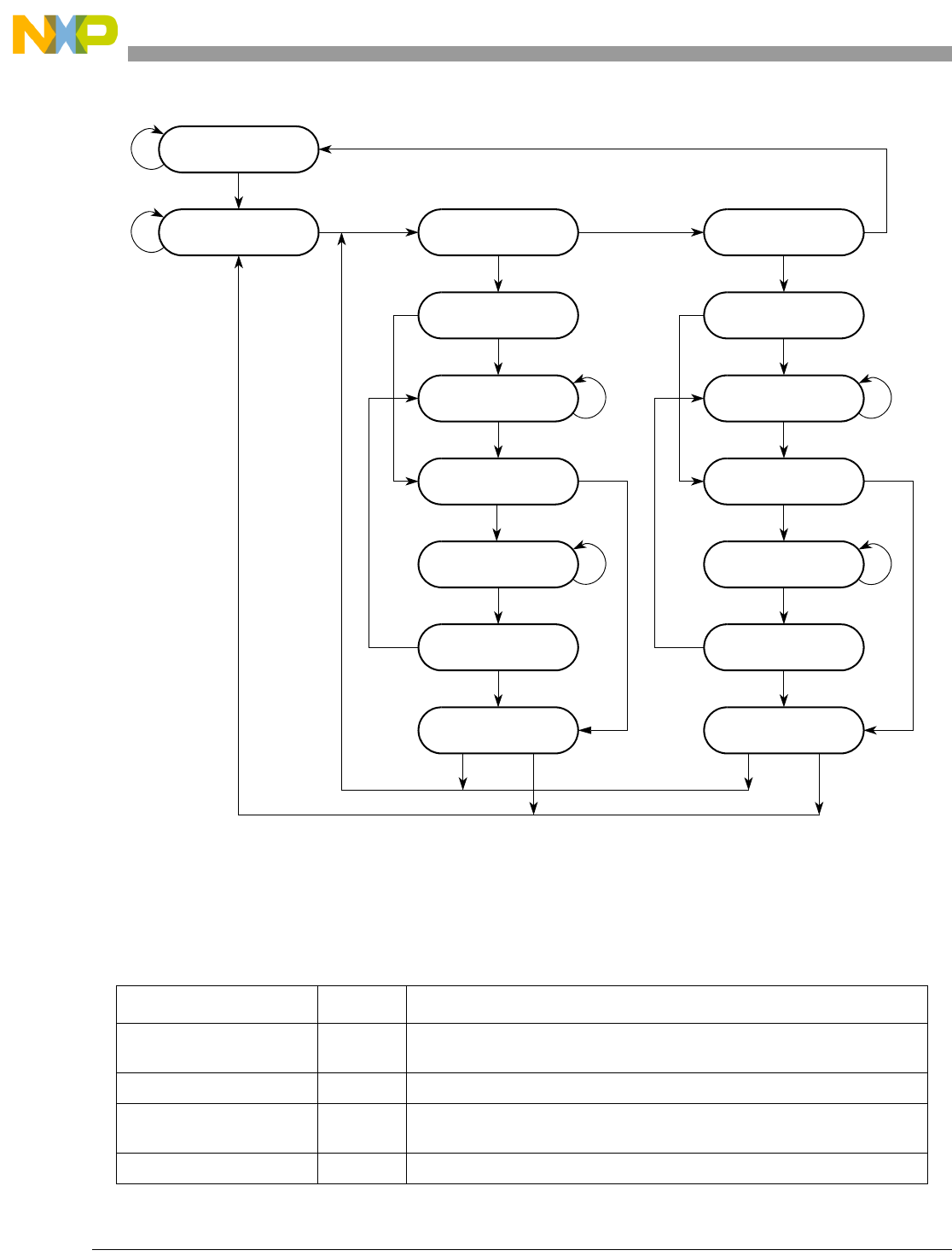
IEEE 1149.1 Test Access Port (JTAG)
29-7 Freescale Semiconductor
Figure 29-4. TAP Controller State Machine Flow
29.4.3 JTAG Instructions
Table 29-5 describes public and private instructions.
Table 29-5. JTAG Instructions
Instruction IR[3:0] Instruction Summary
EXTEST 0000 Selects boundary scan register while applying fixed values to output pins and
asserting functional reset
IDCODE 0001 Selects IDCODE register for shift
SAMPLE/PRELOAD 0010 Selects boundary scan register for shifting, sampling, and preloading without
disturbing functional operation
ENABLE_TEST_CTRL 0110 Selects TEST_CTRL register
RUN-TEST/IDLE
TEST-LOGIC-RESET
1
1
SELECT DR-SCAN
CAPTURE-DR
EXIT1-DR
PAUSE-DR
UPDATE-DR
SELECT IR-SCAN
SHIFT-DR
EXIT2-DR
CAPTURE-IR
SHIFT-IR
EXIT1-IR
PAUSE-IR
EXIT2-IR
UPDATE-IR
0
0
1
1
0
0
0
1
1
10
0
0
1
1
0
0
1
1
0
1
0
1
10
1
1
0
0
1
0
MCF52211 ColdFire® Integrated Microcontroller Reference Manual, Rev. 3

IEEE 1149.1 Test Access Port (JTAG)
Freescale Semiconductor 29-8
29.4.3.1 IDCODE Instruction
The IDCODE instruction selects the 32-bit IDCODE register for connection as a shift path between the
TDI and TDO pin. This instruction allows interrogation of the MCU to determine its version number and
other part identification data. The shift register lsb is forced to logic 1 on the rising edge of TCLK
following entry into the capture-DR state. Therefore, the first bit to be shifted out after selecting the
IDCODE register is always a logic 1. The remaining 31 bits are also forced to fixed values on the rising
edge of TCLK following entry into the capture-DR state.
IDCODE is the default instruction placed into the instruction register when the TAP resets. Thus, after a
TAP reset, the IDCODE register is selected automatically.
29.4.3.2 SAMPLE/PRELOAD Instruction
The SAMPLE/PRELOAD instruction has two functions:
• SAMPLE - obtain a sample of the system data and control signals present at the MCU input pins
and before the boundary scan cell at the output pins. This sampling occurs on the rising edge of
TCLK in the capture-DR state when the IR contains the $2 opcode. The sampled data is accessible
by shifting it through the boundary scan register to the TDO output by using the shift-DR state. The
data capture and the shift operation are transparent to system operation.
NOTE
External synchronization is required to achieve meaningful results because
there is no internal synchronization between TCLK and the system clock.
• PRELOAD - initialize the boundary scan register update cells before selecting EXTEST or
CLAMP. This is achieved by ignoring the data shifting out on the TDO pin and shifting in
initialization data. The update-DR state and the falling edge of TCLK can then transfer this data to
the update cells. The data is applied to the external output pins by the EXTEST or CLAMP
instruction.
29.4.3.3 EXTEST Instruction
The external test (EXTEST) instruction selects the boundary scan register. It forces all output pins and
bidirectional pins configured as outputs to the values preloaded with the SAMPLE/PRELOAD instruction
HIGHZ 1001 Selects bypass register while tri-stating all output pins and asserting
functional reset
CLAMP 1100 Selects bypass while applying fixed values to output pins and asserting
functional reset
BYPASS 1111 Selects bypass register for data operations
Reserved all others1Decoded to select bypass register
1Freescale reserves the right to change the decoding of the unused opcodes in the future.
Table 29-5. JTAG Instructions (continued)
Instruction IR[3:0] Instruction Summary
MCF52211 ColdFire® Integrated Microcontroller Reference Manual, Rev. 3

IEEE 1149.1 Test Access Port (JTAG)
29-9 Freescale Semiconductor
and held in the boundary scan update registers. EXTEST can also configure the direction of bidirectional
pins and establish high-impedance states on some pins. EXTEST asserts internal reset for the MCU system
logic to force a predictable internal state while performing external boundary scan operations.
29.4.3.4 TEST_LEAKAGE Instruction
The TEST_LEAKAGE instruction forces the jtag_leakage output signal to high. It is intended to tri-state
all output pad buffers and disable all of the part’s pad input buffers except TEST and TRST. The
jtag_leakage signal is asserted at the rising edge of TCLK when the TAP controller transitions from
update-IR to run-test/idle state. After asserted, the part disables the TCLK, TMS, and TDI inputs into
JTAG and forces these JTAG inputs to logic 1. The TAP controller remains in the run-test/idle state until
the TRST input is asserted (logic 0).
29.4.3.5 ENABLE_TEST_CTRL Instruction
The ENABLE_TEST_CTRL instruction selects a 3-bit shift register (TEST_CTRL) for connection as a
shift path between the TDI and TDO pin. When the user transitions the TAP controller to the UPDATE_DR
state, the register transfers its value to a parallel hold register. It allows the control chip to test functions
independent of the JTAG TAP controller state.
29.4.3.6 HIGHZ Instruction
The HIGHZ instruction eliminates the need to backdrive the output pins during circuit-board testing.
HIGHZ turns off all output drivers, including the 2-state drivers, and selects the bypass register. HIGHZ
also asserts internal reset for the MCU system logic to force a predictable internal state.
29.4.3.7 LOCKOUT_RECOVERY Instruction
If a user inadvertently enables security on a MCU, the LOCKOUT_RECOVERY instruction allows the
disabling of security by the complete erasure of the internal flash contents including the configuration
field. This does not compromise security as the entire contents of the user’s secured code stored in flash
gets erased before security is disabled on the MCU on the next reset or power-up sequence.
The LOCKOUT_RECOVERY instruction selects a 7-bit shift register for connection as a shift path
between the TDI pin and the TDO pin. When the user transitions the TAP controller to the UPDATE-DR
state, the 7-bit shift register is loaded into the 7-bit JTAG_TFM_CLKDIV register and this value is output
to the TFM’s clock divider circuit. When the user transitions the TAP controller to the RUN-TEST/IDLE
state, the erase signal to the TFM asserts and the lockout sequence starts. The controller must remain in
that state until the erase sequence has completed. After the lockout recovery sequence has completed, the
user must reset the JTAG TAP controller and the MCU to return to normal operation.
29.4.3.8 CLAMP Instruction
The CLAMP instruction selects the bypass register and asserts internal reset while simultaneously forcing
all output pins and bidirectional pins configured as outputs to the fixed values that are preloaded and held
in the boundary scan update register. CLAMP enhances test efficiency by reducing the overall shift path
MCF52211 ColdFire® Integrated Microcontroller Reference Manual, Rev. 3

IEEE 1149.1 Test Access Port (JTAG)
Freescale Semiconductor 29-10
to a single bit (the bypass register) while conducting an EXTEST type of instruction through the boundary
scan register.
29.4.3.9 BYPASS Instruction
The BYPASS instruction selects the bypass register, creating a single-bit shift register path from the TDI
pin to the TDO pin. BYPASS enhances test efficiency by reducing the overall shift path when a device
other than the ColdFire processor is the device under test on a board design with multiple chips on the
overall boundary scan chain. The shift register lsb is forced to logic 0 on the rising edge of TCLK after
entry into the capture-DR state. Therefore, the first bit shifted out after selecting the bypass register is
always logic 0. This differentiates parts that support an IDCODE register from parts that support only the
bypass register.
29.5 Initialization/Application Information
29.5.1 Restrictions
The test logic is a static logic design, and TCLK can be stopped in a high or low state without loss of data.
However, the system clock is not synchronized to TCLK internally. Any mixed operation using the test
logic and system functional logic requires external synchronization.
Using the EXTEST instruction requires a circuit-board test environment that avoids device-destructive
configurations in which MCU output drivers are enabled into actively driven networks.
Low-power stop mode considerations:
• The TAP controller must be in the test-logic-reset state to enter or remain in the low-power stop
mode. Leaving the test-logic-reset state negates the ability to achieve low-power, but does not
otherwise affect device functionality.
• The TCLK input is not blocked in low-power stop mode. To consume minimal power, the TCLK
input should be externally connected to VDD.
• The TMS, TDI, and TRST pins include on-chip pull-up resistors. For minimal power consumption
in low-power stop mode, these three pins should be connected to VDD or left unconnected.
29.5.2 Nonscan Chain Operation
Keeping the TAP controller in the test-logic-reset state ensures that the scan chain test logic is transparent
to the system logic. It is recommended that TMS, TDI, TCLK, and TRST be pulled up. TRST could be
connected to ground. However, because there is a pull-up on TRST, some amount of current results. The
internal power-on reset input initializes the TAP controller to the test-logic-reset state on power-up without
asserting TRST.
MCF52211 ColdFire® Integrated Microcontroller Reference Manual, Rev. 3

Freescale Semiconductor A-1
Appendix A
Register Memory Map Quick Reference
Table A-1 summarizes the address, name, and byte assignment for registers within the MCF52211 CPU
space. Table A-2 lists an overview of the memory map for the on-chip modules, and Table A-3 is a detailed
memory map including all of the registers for on-chip modules.
Table A-1. CPU Space Register Memory Map
Address Name Mnemonic Size
CPU @ 0x800 Other Stack Pointer OTHER_A7 32
CPU @ 0x801 Vector Base Register VBR 32
CPU @ 0x804 MAC Status Register MACSR 8
CPU @ 0x805 MAC Mask Register MASK 16
CPU @ 0x806 MAC Accumulator ACC 16
CPU @ 0x80E Status Register SR 16
CPU @ 0x80F Program Counter PC 32
CPU @ 0xC04 Flash Base Address Register FLASHBAR 32
CPU @ 0xC05 RAM Base Address Register RAMBAR 32
MCF52211 ColdFire® Integrated Microcontroller Reference Manual, Rev. 3

Register Memory Map Quick Reference
A-2 Freescale Semiconductor
Table A-2. Module Memory Map Overview
Address Module Size
0x0000_0000 On-chip Flash/RAM Array 1G
IPSBAR + 0x00_0000 System Control Module 64 bytes
IPSBAR + 0x00_0040 Reserved 64 bytes
IPSBAR + 0x00_0080 Reserved 128 bytes
IPSBAR + 0x00_0100 DMA (Channel 0) 64 bytes
IPSBAR + 0x00_0110 DMA (Channel 1) 64 bytes
IPSBAR + 0x00_0120 DMA (Channel 2) 64 bytes
IPSBAR + 0x00_0130 DMA (Channel 3) 64 bytes
IPSBAR + 0x00_0140 Reserved 196 bytes
IPSBAR + 0x00_0200 UART0 64 bytes
IPSBAR + 0x00_0240 UART1 64 bytes
IPSBAR + 0x00_0280 UART2 64 bytes
IPSBAR + 0x00_02C0 Reserved 64 bytes
IPSBAR + 0x00_0300 I2C0 64 bytes
IPSBAR + 0x00_0340 QSPI 64 bytes
IPSBAR + 0x00_0380 I2C1 64 bytes
IPSBAR + 0x00_03C0 Real-Time Clock 64 bytes
IPSBAR + 0x00_0400 DMA Timer 0 64 bytes
IPSBAR + 0x00_0440 DMA Timer 1 64 bytes
IPSBAR + 0x00_0480 DMA Timer 2 64 bytes
IPSBAR + 0x00_04C0 DMA Timer 3 64 bytes
IPSBAR + 0x00_0500 Reserved 1792 bytes
IPSBAR + 0x00_0C00 Interrupt Controller 256 bytes
IPSBAR + 0x00_0D00 Reserved 256 bytes
IPSBAR + 0x00_0E00 Reserved 256 bytes
IPSBAR + 0x00_0F00 Interrupt Controller: Global Interrupt Acknowledge Registers 256 bytes
IPSBAR + 0x00_1000 Reserved 1M-6K
IPSBAR + 0x10_0000 Ports 64K
IPSBAR + 0x11_0000 Reset Controller, Chip Configuration, and Power Management 64K
IPSBAR + 0x12_0000 Clock Module 64K
IPSBAR + 0x13_0000 Edge Port 64K
IPSBAR + 0x14_0000 Backup Watchdog Timer 64K
IPSBAR + 0x15_0000 Programmable Interval Timer 0 64K
IPSBAR + 0x16_0000 Programmable Interval Timer 1 64K
IPSBAR + 0x17_0000 Reserved 64K
MCF52211 ColdFire® Integrated Microcontroller Reference Manual, Rev. 3

Register Memory Map Quick Reference
Freescale Semiconductor A-3
IPSBAR + 0x18_0000 Reserved 64K
IPSBAR + 0x19_0000 ADC 64K
IPSBAR + 0x1A_0000 General Purpose Timer 64K
IPSBAR + 0x1B_0000 PWM 64K
IPSBAR + 0x1C_0000 USB-OTG 64K
IPSBAR + 0x1D_0000 CFM (Flash) Control Registers 64K
IPSBAR + 0x1E_0000 Reserved 63M+128K
IPSBAR + 0x400_0000 CFM (Flash) Memory for IPS Reads and Writes 128K
Table A-3. Register Memory Map
Address Name Mnemonic Size (bits)
SCM Registers
IPSBAR + 0x0000 Internal Peripheral System Base Address Register IPSBAR 32
IPSBAR + 0x0008 Memory Base Access Register RAMBAR 32
IPSBAR + 0x000C Peripheral Power Management Register - High PPMRH 32
IPSBAR + 0x0010 Core Reset Status Register CRSR 8
IPSBAR + 0x0011 Core Watchdog Control Register CWCR 8
IPSBAR + 0x0012 Low-Power Interrupt Control Register LPICR 8
IPSBAR + 0x0013 Core Watchdog Service Register CWSR 8
IPSBAR + 0x0014 DMA Request Control Register DMAREQC 32
IPSBAR + 0x0018 Peripheral Power Management Register - Low PPMRL 32
IPSBAR + 0x001C Default Bus Master Park Register MPARK 32
IPSBAR + 0x0020 Master Privilege Register MPR 8
IPSBAR + 0x0024 Peripheral Access Control Register 0 PACR0 8
IPSBAR + 0x0025 Peripheral Access Control Register 1 PACR1 8
IPSBAR + 0x0026 Peripheral Access Control Register 2 PACR2 8
IPSBAR + 0x0027 Peripheral Access Control Register 3 PACR3 8
IPSBAR + 0x0028 Peripheral Access Control Register 4 PACR4 8
IPSBAR + 0x0029 Peripheral Access Control Register 5 PACR5 8
IPSBAR + 0x002A Peripheral Access Control Register 6 PACR6 8
IPSBAR + 0x002B Peripheral Access Control Register 7 PACR7 8
IPSBAR + 0x002C Peripheral Access Control Register 8 PACR8 8
IPSBAR + 0x0030 Grouped Peripheral Access Control Register 0 GPACR0 8
Table A-2. Module Memory Map Overview (continued)
Address Module Size
MCF52211 ColdFire® Integrated Microcontroller Reference Manual, Rev. 3

Register Memory Map Quick Reference
A-4 Freescale Semiconductor
IPSBAR + 0x0031 Grouped Peripheral Access Control Register 1 GPACR1 8
DMA Registers
IPSBAR + 0x0100 Source Address Register 0 SAR0 32
IPSBAR + 0x0104 Destination Address Register 0 DAR0 32
IPSBAR + 0x0108 Byte Count Register 0 / DMA Status Register 0 BCR0 / DSR0 32
IPSBAR + 0x010C DMA Control Register 0 DCR0 32
IPSBAR + 0x0110 Source Address Register 1 SAR1 32
IPSBAR + 0x0114 Destination Address Register 1 DAR1 32
IPSBAR + 0x0118 Byte Count Register 1 / DMA Status Register 1 BCR1 / DSR1 32
IPSBAR + 0x011C DMA Control Register 1 DCR1 32
IPSBAR + 0x0120 Source Address Register 2 SAR2 32
IPSBAR + 0x0124 Destination Address Register 2 DAR2 32
IPSBAR + 0x0128 Byte Count Register 2 / DMA Status Register 2 BCR2 / DSR2 32
IPSBAR + 0x012C DMA Control Register 2 DCR2 32
IPSBAR + 0x0130 Source Address Register 3 SAR3 32
IPSBAR + 0x0134 Destination Address Register 3 DAR3 32
IPSBAR + 0x0138 Byte Count Register 3 / DMA Status Register 3 BCR3 / DSR3 32
IPSBAR + 0x013C DMA Control Register 3 DCR3 32
UART Registers
IPSBAR + 0x0200 UART Mode Register 01UMR10, UMR20 8
IPSBAR + 0x0204 (Read) UART Status Register 0 USR0 8
(Write) UART Clock Select Register 01UCSR0 8
IPSBAR + 0x0208 (Read) Reserved 8
(Write) UART Command Register 0 UCR0 8
IPSBAR + 0x020C (Read) UART Receive Buffer 0 URB0 8
(Write) UART Transmit Buffer 0 UTB0 8
IPSBAR + 0x0210 (Read) UART Input Port Change Register 0 UIPCR0 8
(Write) UART Auxiliary Control Register 01UACR0 8
IPSBAR + 0x0214 (Read) UART Interrupt Status Register 0 UISR0 8
(Write) UART Interrupt Mask Register 0 UIMR0 8
IPSBAR + 0x0218 (Read) Reserved 8
UART Baud Rate Generator Register 10 UBG10 8
Table A-3. Register Memory Map (continued)
Address Name Mnemonic Size (bits)
MCF52211 ColdFire® Integrated Microcontroller Reference Manual, Rev. 3

Register Memory Map Quick Reference
Freescale Semiconductor A-5
IPSBAR + 0x021C (Read) Reserved 8
UART Baud Rate Generator Register 20 UBG20 8
IPSBAR + 0x0234 (Read) UART Input Port Register 0 UIP0 8
(Write) Reserved 8
IPSBAR + 0x0238 (Read) Reserved 8
(Write) UART Output Port Bit Set Command Register 0 UOP10 8
IPSBAR + 0x023C (Read) Reserved 8
(Write) UART Output Port Bit Reset Command Register 0 UIP00 8
IPSBAR + 0x0240 UART Mode Registers 11UMR11, UMR21 8
IPSBAR + 0x0244 (Read) UART Status Register 1 USR1 8
(Write) UART Clock Select Register 11UCSR1 8
IPSBAR + 0x0248 (Read) Reserved 8
(Write) UART Command Register 1 UCR1 8
IPSBAR + 0x024C (UART/Read) UART Receive Buffer 1 URB1 8
(UART/Write) UART Transmit Buffer 1 UTB1 8
IPSBAR + 0x0250 (Read) UART Input Port Change Register 1 UIPCR1 8
(Write) UART Auxiliary Control Register 11UACR1 8
IPSBAR + 0x0254 (Read) UART Interrupt Status Register 1 UISR1 8
(Write) UART Interrupt Mask Register 1 UIMR1 8
IPSBAR + 0x0258 (Read) Reserved 8
UART Baud Rate Generator Register 11 UBG11 8
IPSBAR + 0x025C (Read) Reserved 8
UART Baud Rate Generator Register 21 UBG21 8
IPSBAR + 0x0274 (Read) UART Input Port Register 1 UIP1 8
(Write) Reserved 8
IPSBAR + 0x0278 (Read) Reserved 8
(Write) UART Output Port Bit Set Command Register 1 UOP11 8
IPSBAR + 0x027C (Read) Reserved 8
(Write) UART Output Port Bit Reset Command Register 1 UIP01 8
IPSBAR + 0x0280 UART Mode Register 21UMR12, UMR22 8
IPSBAR + 0x0284 (Read) UART Status Register 2 USR2 8
(Write) UART Clock Select Register 21UCSR2 8
Table A-3. Register Memory Map (continued)
Address Name Mnemonic Size (bits)
MCF52211 ColdFire® Integrated Microcontroller Reference Manual, Rev. 3

Register Memory Map Quick Reference
A-6 Freescale Semiconductor
IPSBAR + 0x0288 (Read) Reserved 8
(Write) UART Command Register 2 UCR2 8
IPSBAR + 0x028C (Read) UART Receive Buffer 2 URB2 8
(Write) UART Transmit Buffer 2 UTB2 8
IPSBAR + 0x0290 (Read) UART Input Port Change Register 2 UIPCR2 8
(Write) UART Auxiliary Control Register 21UACR2 8
IPSBAR + 0x0294 (Read) UART Interrupt Status Register 2 UISR2 8
(Write) UART Interrupt Mask Register 2 UIMR2 8
IPSBAR + 0x0298 (Read) Reserved 8
UART Baud Rate Generator Register 12 UBG12 8
IPSBAR + 0x029C (Read) Reserved 8
UART Baud Rate Generator Register 22 UBG22 8
IPSBAR + 0x02B4 (Read) UART Input Port Register 2 UIP2 8
(Write) Reserved 8
IPSBAR + 0x02B8 (Read) Reserved 8
(Write) UART Output Port Bit Set Command Register 2 UOP12 8
IPSBAR + 0x02BC (Read) Reserved 8
(Write) UART Output Port Bit Reset Command Register 2 UIP02 8
I2C0 Registers
IPSBAR + 0x0300 I2C Address Register 0 I2ADR0 8
IPSBAR + 0x0304 I2C Frequency Divider Register 0 I2FDR0 8
IPSBAR + 0x0308 I2C Control Register 0 I2CR0 8
IPSBAR + 0x030C I2C Status Register 0 I2SR0 8
IPSBAR + 0x0310 I2C Data I/O Register 0 I2DR0 8
QSPI Registers
IPSBAR + 0x0340 QSPI Mode Register QMR 16
IPSBAR + 0x0344 QSPI Delay Register QDLYR 16
IPSBAR + 0x0348 QSPI Wrap Register QWR 16
IPSBAR + 0x034C QSPI Interrupt Register QIR 16
IPSBAR + 0x0350 QSPI Address Register QAR 16
IPSBAR + 0x0354 QSPI Data Register QDR 16
Table A-3. Register Memory Map (continued)
Address Name Mnemonic Size (bits)
MCF52211 ColdFire® Integrated Microcontroller Reference Manual, Rev. 3

Register Memory Map Quick Reference
Freescale Semiconductor A-7
I2C1 Registers
IPSBAR + 0x0300 I2C Address Register 1 I2ADR1 8
IPSBAR + 0x0304 I2C Frequency Divider Register 1 I2FDR1 8
IPSBAR + 0x0308 I2C Control Register 1 I2CR1 8
IPSBAR + 0x030C I2C Status Register 1 I2SR1 8
IPSBAR + 0x0310 I2C Data I/O Register 1 I2DR1 8
Real-Time Clock Registers
IPSBAR + 0x03C0 RTC Hours and Minutes Counter Register HOURMIN 32
IPSBAR + 0x03C4 RTC Seconds Counter Register SECONDS 32
IPSBAR + 0x03C8 RTC Hours and Minutes Alarm Register ALRM_HM 32
IPSBAR + 0x03CC RTC Seconds Alarm Register ALRM_SEC 32
IPSBAR + 0x03D0 RTC Control Register RTCCTL 32
IPSBAR + 0x03D4 RTC Interrupt Status Register RTCISR 32
IPSBAR + 0x03D8 RTC Interrupt Enable Register RTCIENR 32
IPSBAR + 0x03DC RTC Stopwatch Minutes Register STPWCH 32
IPSBAR + 0x03E0 RTC Days Counter Register DAYS 32
IPSBAR + 0x03E4 RTC Day Alarm Register ALRM_DAY 32
IPSBAR + 0x03F4 RTC General Oscillator Count Upper Register RTCGOCU 16
IPSBAR + 0x03F8 RTC General Oscillator Count Lower Register RTCGOCL 16
DMA Timer Registers
IPSBAR + 0x0400 DMA Timer Mode Register 0 DTMR0 16
IPSBAR + 0x0402 DMA Timer Extended Mode Register 0 DTXMR0 8
IPSBAR + 0x0403 DMA Timer Event Register 0 DTER0 8
IPSBAR + 0x0404 DMA Timer Reference Register 0 DTRR0 32
IPSBAR + 0x0408 DMA Timer Capture Register 0 DTCR0 32
IPSBAR + 0x040C DMA Timer Counter Register 0 DTCN0 32
IPSBAR + 0x0440 DMA Timer Mode Register 1 DTMR1 16
IPSBAR + 0x0442 DMA Timer Extended Mode Register 1 DTXMR1 8
IPSBAR + 0x0443 DMA Timer Event Register 1 DTER1 8
IPSBAR + 0x0444 DMA Timer Reference Register 1 DTRR1 32
IPSBAR + 0x0448 DMA Timer Capture Register 1 DTCR1 32
IPSBAR + 0x044C DMA Timer Counter Register 1 DTCN1 32
Table A-3. Register Memory Map (continued)
Address Name Mnemonic Size (bits)
MCF52211 ColdFire® Integrated Microcontroller Reference Manual, Rev. 3

Register Memory Map Quick Reference
A-8 Freescale Semiconductor
IPSBAR + 0x0480 DMA Timer Mode Register 2 DTMR2 16
IPSBAR + 0x0482 DMA Timer Extended Mode Register 2 DTXMR2 8
IPSBAR + 0x0483 DMA Timer Event Register 2 DTER2 8
IPSBAR + 0x0484 DMA Timer Reference Register 2 DTRR2 32
IPSBAR + 0x0488 DMA Timer Capture Register 2 DTCR2 32
IPSBAR + 0x048C DMA Timer Counter Register 2 DTCN2 32
IPSBAR + 0x04C0 DMA Timer Mode Register 3 DTMR3 16
IPSBAR + 0x04C2 DMA Timer Extended Mode Register 3 DTXMR3 8
IPSBAR + 0x04C3 DMA Timer Event Register 3 DTER3 8
IPSBAR + 0x04C4 DMA Timer Reference Register 3 DTRR3 32
IPSBAR + 0x04C8 DMA Timer Capture Register 3 DTCR3 32
IPSBAR + 0x04CC DMA Timer Counter Register 3 DTCN3 32
Interrupt Controller 0
IPSBAR + 0x0C00 Interrupt Pending Register High 0 IPRH0 32
IPSBAR + 0x0C04 Interrupt Pending Register Low 0 IPRL0 32
IPSBAR + 0x0C08 Interrupt Mask Register High 0 IMRH0 32
IPSBAR + 0x0C0C Interrupt Mask Register Low 0 IMRL0 32
IPSBAR + 0x0C10 Interrupt Force Register High 0 INTFRCH0 32
IPSBAR + 0x0C14 Interrupt Force Register Low 0 INTFRCL0 32
IPSBAR + 0x0C18 Interrupt Request Level Register 0 IRLR0 8
IPSBAR + 0x0C19 Interrupt Acknowledge Level and Priority Register 0 IACKLPR0 8
IPSBAR + 0x0C41 Interrupt Control Register 0-01 ICR001 8
IPSBAR + 0x0C42 Interrupt Control Register 0-02 ICR002 8
IPSBAR + 0x0C43 Interrupt Control Register 0-03 ICR003 8
IPSBAR + 0x0C44 Interrupt Control Register 0-04 ICR004 8
IPSBAR + 0x0C45 Interrupt Control Register 0-05 ICR005 8
IPSBAR + 0x0C46 Interrupt Control Register 0-06 ICR006 8
IPSBAR + 0x0C47 Interrupt Control Register 0-07 ICR007 8
IPSBAR + 0x0C48 Interrupt Control Register 0-08 ICR008 8
IPSBAR + 0x0C49 Interrupt Control Register 0-09 ICR009 8
IPSBAR + 0x0C4A Interrupt Control Register 0-10 ICR010 8
IPSBAR + 0x0C4B Interrupt Control Register 0-11 ICR011 8
Table A-3. Register Memory Map (continued)
Address Name Mnemonic Size (bits)
MCF52211 ColdFire® Integrated Microcontroller Reference Manual, Rev. 3

Register Memory Map Quick Reference
Freescale Semiconductor A-9
IPSBAR + 0x0C4C Interrupt Control Register 0-12 ICR012 8
IPSBAR + 0x0C4D Interrupt Control Register 0-13 ICR013 8
IPSBAR + 0x0C4E Interrupt Control Register 0-14 ICR014 8
IPSBAR + 0x0C4F Interrupt Control Register 0-15 ICR015 8
IPSBAR + 0x0C50 Interrupt Control Register 0-16 ICR016 8
IPSBAR + 0x0C51 Interrupt Control Register 0-17 ICR017 8
IPSBAR + 0x0C52 Interrupt Control Register 0-18 ICR018 8
IPSBAR +0x0C53 Interrupt Control Register 0-19 ICR019 8
IPSBAR + 0x0C54 Interrupt Control Register 0-20 ICR020 8
IPSBAR + 0x0C55 Interrupt Control Register 0-21 ICR021 8
IPSBAR + 0x0C56 Interrupt Control Register 0-22 ICR022 8
IPSBAR + 0x0C57 Interrupt Control Register 0-23 ICR023 8
IPSBAR + 0x0C58 Interrupt Control Register 0-24 ICR024 8
IPSBAR + 0x0C59 Interrupt Control Register 0-25 ICR025 8
IPSBAR + 0x0C5A Interrupt Control Register 0-26 ICR026 8
IPSBAR + 0x0C5B Interrupt Control Register 0-27 ICR027 8
IPSBAR + 0x0C5C Interrupt Control Register 0-28 ICR028 8
IPSBAR + 0x0C5D Interrupt Control Register 0-29 ICR029 8
IPSBAR + 0x0C5E Interrupt Control Register 0-30 ICR030 8
IPSBAR + 0x0C5F Interrupt Control Register 0-31 ICR031 8
IPSBAR + 0x0C60 Interrupt Control Register 0-32 ICR032 8
IPSBAR + 0x0C61 Interrupt Control Register 0-33 ICR033 8
IPSBAR + 0x0C62 Interrupt Control Register 0-34 ICR034 8
IPSBAR + 0x0C63 Interrupt Control Register 0-35 ICR035 8
IPSBAR + 0x0C64 Interrupt Control Register 0-36 ICR036 8
IPSBAR + 0x0C65 Interrupt Control Register 0-37 ICR037 8
IPSBAR + 0x0C66 Interrupt Control Register 0-38 ICR038 8
IPSBAR + 0x0C67 Interrupt Control Register 0-39 ICR039 8
IPSBAR + 0x0C68 Interrupt Control Register 0-40 ICR040 8
IPSBAR + 0x0C69 Interrupt Control Register 0-41 ICR041 8
IPSBAR + 0x0C6A Interrupt Control Register 0-42 ICR042 8
IPSBAR + 0x0C6B Interrupt Control Register 0-43 ICR043 8
IPSBAR + 0x0C6C Interrupt Control Register 0-44 ICR044 8
Table A-3. Register Memory Map (continued)
Address Name Mnemonic Size (bits)
MCF52211 ColdFire® Integrated Microcontroller Reference Manual, Rev. 3

Register Memory Map Quick Reference
A-10 Freescale Semiconductor
IPSBAR + 0x0C6D Interrupt Control Register 0-45 ICR045 8
IPSBAR + 0x0C6E Interrupt Control Register 0-46 ICR046 8
IPSBAR + 0x0C6F Interrupt Control Register 0-47 ICR047 8
IPSBAR + 0x0C70 Interrupt Control Register 0-48 ICR048 8
IPSBAR + 0x0C71 Interrupt Control Register 0-49 ICR049 8
IPSBAR + 0x0C72 Interrupt Control Register 0-50 ICR050 8
IPSBAR + 0x0C73 Interrupt Control Register 0-51 ICR051 8
IPSBAR + 0x0C74 Interrupt Control Register 0-52 ICR052 8
IPSBAR + 0x0C75 Interrupt Control Register 0-53 ICR053 8
IPSBAR + 0x0C76 Interrupt Control Register 0-54 ICR054 8
IPSBAR + 0x0C77 Interrupt Control Register 0-55 ICR055 8
IPSBAR + 0x0C78 Interrupt Control Register 0-56 ICR056 8
IPSBAR + 0x0C79 Interrupt Control Register 0-57 ICR057 8
IPSBAR + 0x0C7A Interrupt Control Register 0-58 ICR058 8
IPSBAR + 0x0C7B Interrupt Control Register 0-59 ICR059 8
IPSBAR + 0x0C7C Interrupt Control Register 0-60 ICR060 8
IPSBAR + 0x0C7D Interrupt Control Register 0-61 ICR061 8
IPSBAR + 0x0C7E Interrupt Control Register 0-62 ICR062 8
IPSBAR + 0x0C7F Interrupt Control Register 0-63 ICR063 8
IPSBAR + 0x0CE0 Software Interrupt Acknowledge Register 0 SWACK0 8
IPSBAR + 0x0CE4 Level 1 Interrupt Acknowledge Register 0 L1IACK0 8
IPSBAR + 0x0CE8 Level 2 Interrupt Acknowledge Register 0 L2IACK0 8
IPSBAR + 0x0CEC Level 3 Interrupt Acknowledge Register 0 L3IACK0 8
IPSBAR + 0x0CF0 Level 4 Interrupt Acknowledge Register 0 L4IACK0 8
IPSBAR + 0x0CF4 Level 5 Interrupt Acknowledge Register 0 L5IACK0 8
IPSBAR + 0x0CF8 Level 6 Interrupt Acknowledge Register 0 L6IACK0 8
IPSBAR + 0x0CFC Level 7 Interrupt Acknowledge Register 0 L7IACK0 8
IPSBAR + 0x0FE4 Global Level 1 Interrupt Acknowledge Register GL1IACK 8
IPSBAR + 0x0FE8 Global Level 2 Interrupt Acknowledge Register GL2IACK 8
IPSBAR + 0x0FEC Global Level 3 Interrupt Acknowledge Register GL3IACK 8
IPSBAR + 0x0FF0 Global Level 4 Interrupt Acknowledge Register GL4IACK 8
IPSBAR + 0x0FF4 Global Level 5 Interrupt Acknowledge Register GL5IACK 8
IPSBAR + 0x0FF8 Global Level 6 Interrupt Acknowledge Register GL6IACK 8
Table A-3. Register Memory Map (continued)
Address Name Mnemonic Size (bits)
MCF52211 ColdFire® Integrated Microcontroller Reference Manual, Rev. 3

Register Memory Map Quick Reference
Freescale Semiconductor A-11
IPSBAR + 0x0FFC Global Level 6 Interrupt Acknowledge Register GL7IACK 8
GPIO Registers
IPSBAR + 0x10_0000 Reserved — 8
IPSBAR + 0x10_0001 Reserved — 8
IPSBAR + 0x10_0002 Reserved — 8
IPSBAR + 0x10_0003 Reserved — 8
IPSBAR + 0x10_0004 Reserved — 8
IPSBAR + 0x10_0005 Reserved — 8
IPSBAR + 0x10_0006 Reserved — 8
IPSBAR + 0x10_0007 Reserved — 8
IPSBAR + 0x10_0008 Port NQ Out Data Register PORTNQ 8
IPSBAR + 0x10_0009 Reserved — 8
IPSBAR + 0x10_000A Port AN Output Data Register PORTAN 8
IPSBAR + 0x10_000B Port AS Output Data Register PORTAS 8
IPSBAR + 0x10_000C Port QS Output Data Register PORTQS 8
IPSBAR + 0x10_000D Reserved — 8
IPSBAR + 0x10_000E Port TA Output Data Register PORTTA 8
IPSBAR + 0x10_000F Port TC Output Data Register PORTTC 8
IPSBAR + 0x10_0010 Port TD Output Data Register PORTTD 8
IPSBAR + 0x10_0011 Port UA Output Data Register PORTUA 8
IPSBAR + 0x10_0012 Port UB Output Data Register PORTUB 8
IPSBAR + 0x10_0013 Port UC Output Data Register PORTUC 8
IPSBAR + 0x10_0014 Port DD Output Data Register PORTDD 8
IPSBAR + 0x10_0015 Reserved — 8
IPSBAR + 0x10_0016 Reserved — 8
IPSBAR + 0x10_0017 Reserved — 8
IPSBAR + 0x10_0018 Reserved — 8
IPSBAR + 0x10_0019 Reserved — 8
IPSBAR + 0x10_001A Reserved — 8
IPSBAR + 0x10_001B Reserved — 8
IPSBAR + 0x10_001C Reserved — 8
IPSBAR + 0x10_001D Reserved — 8
Table A-3. Register Memory Map (continued)
Address Name Mnemonic Size (bits)
MCF52211 ColdFire® Integrated Microcontroller Reference Manual, Rev. 3

Register Memory Map Quick Reference
A-12 Freescale Semiconductor
IPSBAR + 0x10_001E Reserved — 8
IPSBAR + 0x10_001F Reserved — 8
IPSBAR + 0x10_0020 Port NQ Data Direction Register DDRNQ 8
IPSBAR + 0x10_0021 Reserved — 8
IPSBAR + 0x10_0022 Port AN Data Direction Register DDRAN 8
IPSBAR + 0x10_0023 Port AS Data Direction Register DDRAS 8
IPSBAR + 0x10_0024 Port QS Data Direction Register DDRQS 8
IPSBAR + 0x10_0025 Reserved — 8
IPSBAR + 0x10_0026 Port TA Data Direction Register DDRTA 8
IPSBAR + 0x10_0027 Port TC Data Direction Register DDRTC 8
IPSBAR + 0x10_0028 Port TD Data Direction Register DDRTD 8
IPSBAR + 0x10_0029 Port UA Data Direction Register DDRUA 8
IPSBAR + 0x10_002A Port UB Data Direction Register DDRUB 8
IPSBAR + 0x10_002B Port UC Data Direction Register DDRUC 8
IPSBAR + 0x10_002C Port DD Data Direction Register DDRDD 8
IPSBAR + 0x10_002D Reserved — 8
IPSBAR + 0x10_002E Reserved — 8
IPSBAR + 0x10_002F Reserved — 8
IPSBAR + 0x10_0030 Reserved — 8
IPSBAR + 0x10_0031 Reserved — 8
IPSBAR + 0x10_0032 Reserved — 8
IPSBAR + 0x10_0033 Reserved — 8
IPSBAR + 0x10_0034 Reserved — 8
IPSBAR + 0x10_0035 Reserved — 8
IPSBAR + 0x10_0036 Reserved — 8
IPSBAR + 0x10_0037 Reserved — 8
IPSBAR + 0x10_0038 Port NQ Pin Data/Set Data Register PORTNQP/
SETNQ
8
IPSBAR + 0x10_0039 Reserved — 8
IPSBAR + 0x10_003A Port AN Pin Data/Set Data Register PORTANP/
SETAN
8
IPSBAR + 0x10_003B Port AS Pin Data/Set Data Register PORTASP/
SETAS
8
Table A-3. Register Memory Map (continued)
Address Name Mnemonic Size (bits)
MCF52211 ColdFire® Integrated Microcontroller Reference Manual, Rev. 3

Register Memory Map Quick Reference
Freescale Semiconductor A-13
IPSBAR + 0x10_003C Port QS Pin Data/Set Data Register PORTQSP/
SETQS
8
IPSBAR + 0x10_003D Reserved — 8
IPSBAR + 0x10_003E Port TA Pin Data/Set Data Register PORTTAP/
SETTA
8
IPSBAR + 0x10_003F Port TC Pin Data/Set Data Register PORTTCP/
SETTC
8
IPSBAR + 0x10_0040 Port TD Pin Data/Set Data Register PORTTDP/
SETTD
8
IPSBAR + 0x10_0041 Port UA Pin Data/Set Data Register PORTUAP/
SETUA
8
IPSBAR + 0x10_0042 Port UB Pin Data/Set Data Register PORTUBP/
SETUB
8
IPSBAR + 0x10_0043 Port UC Pin Data/Set Data Register PORTUCP/
SETUC
8
IPSBAR + 0x10_0044 Port DD Pin Data/Set Data Register PORTDDP/
SETDD
8
IPSBAR + 0x10_0045 Reserved — 8
IPSBAR + 0x10_0046 Reserved — 8
IPSBAR + 0x10_0047 Reserved — 8
IPSBAR + 0x10_0048 Reserved — 8
IPSBAR + 0x10_0049 Reserved — 8
IPSBAR + 0x10_004A Reserved — 8
IPSBAR + 0x10_004B Reserved — 8
IPSBAR + 0x10_004C Reserved — 8
IPSBAR + 0x10_004D Reserved — 8
IPSBAR + 0x10_004E Reserved — 8
IPSBAR + 0x10_004F Reserved — 8
IPSBAR + 0x10_0050 Port NQ Clear Output Data Register CLRNQ 8
IPSBAR + 0x10_0051 Reserved — 8
IPSBAR + 0x10_0052 Port AN Clear Output Data Register CLRAN 8
IPSBAR + 0x10_0053 Port AS Clear Output Data Register CLRAS 8
IPSBAR + 0x10_0054 Port QS Clear Output Data Register CLRQS 8
IPSBAR + 0x10_0055 Reserved — 8
IPSBAR + 0x10_0056 Port TA Clear Output Data Register CLRTA 8
IPSBAR + 0x10_0057 Port TC Clear Output Data Register CLRTC 8
Table A-3. Register Memory Map (continued)
Address Name Mnemonic Size (bits)
MCF52211 ColdFire® Integrated Microcontroller Reference Manual, Rev. 3

Register Memory Map Quick Reference
A-14 Freescale Semiconductor
IPSBAR + 0x10_0058 Port TD Clear Output Data Register CLRTD 8
IPSBAR + 0x10_0059 Port UA Clear Output Data Register CLRUA 8
IPSBAR + 0x10_005A Port UB Clear Output Data Register CLRUB 8
IPSBAR + 0x10_005B Port UC Clear Output Data Register CLRUC 8
IPSBAR + 0x10_005C Port DD Clear Output Data Register CLRDD 8
IPSBAR + 0x10_005D Reserved — 8
IPSBAR + 0x10_005E Reserved — 8
IPSBAR + 0x10_005F Reserved — 8
IPSBAR + 0x10_0060 Reserved — 8
IPSBAR + 0x10_0061 Reserved — 8
IPSBAR + 0x10_0062 Reserved — 8
IPSBAR + 0x10_0063 Reserved — 8
IPSBAR + 0x10_0064 Reserved — 8
IPSBAR + 0x10_0065 Reserved — 8
IPSBAR + 0x10_0066 Reserved — 8
IPSBAR + 0x10_0067 Reserved — 8
IPSBAR + 0x10_0068 Port NQ Pin Assignment Register PNQPAR 16
IPSBAR + 0x10_006A Port AN Pin Assignment Register PANPAR 8
IPSBAR + 0x10_006B Port AS Pin Assignment Register PASPAR 8
IPSBAR + 0x10_006C Port QS Pin Assignment Register PQSPAR 16
IPSBAR + 0x10_006E Port TA Pin Assignment Register PTAPAR 8
IPSBAR + 0x10_006F Port TC Pin Assignment Register PTCPAR 8
IPSBAR + 0x10_0070 Port TD Pin Assignment Register PTDPAR 8
IPSBAR + 0x10_0071 Port UA Pin Assignment Register PUAPAR 8
IPSBAR + 0x10_0072 Port UB Pin Assignment Register PUBPAR 8
IPSBAR + 0x10_0073 Port UC Pin Assignment Register PUCPAR 8
IPSBAR + 0x10_0074 Port DD Pin Assignment Register PDDPAR 8
IPSBAR + 0x10_0075 Reserved — 8
IPSBAR + 0x10_0076 Reserved — 8
IPSBAR + 0x10_0077 Reserved — 8
IPSBAR + 0x10_0078 Pin Slew Rate Register PSRR 32
IPSBAR + 0x10_007C Pin Drive Strength Register PDSR 32
Table A-3. Register Memory Map (continued)
Address Name Mnemonic Size (bits)
MCF52211 ColdFire® Integrated Microcontroller Reference Manual, Rev. 3

Register Memory Map Quick Reference
Freescale Semiconductor A-15
Reset Control, Chip Configuration, and Power Management Registers
IPSBAR + 0x11_0000 Reset Control Register RCR 8
IPSBAR + 0x11_0001 Reset Status Register RSR 8
IPSBAR + 0x11_0004 Chip Configuration Register CCR 16
IPSBAR + 0x11_0007 Low-Power Control Register LPCR 8
IPSBAR + 0x11_0008 Reset Configuration Register RCON 16
IPSBAR + 0x11_000A Chip Identification Register CIR 16
Clock Module Registers
IPSBAR + 0x12_0000 Synthesizer Control Register SYNCR 16
IPSBAR + 0x12_0002 Synthesizer Status Register SYNSR 16
IPSBAR + 0x12_0004 Relaxation Oscillator Control Register ROCR 16
IPSBAR + 0x12_0007 Low Power Divider Register LPDR 16
IPSBAR + 0x12_0008 Clock Control High Register CCHR 8
IPSBAR + 0x12_0009 Clock Control Low Register CCLR 8
IPSBAR + 0x12_000A Oscillator Control High Register OCHR 8
IPSBAR + 0x12_000B Oscillator Control Low Register OCLR 8
IPSBAR + 0x12_0012 Real-Time Clock Control Register RTCCR 8
IPSBAR + 0x12_0013 Backup Watchdog Timer Control Register BWCR 8
Edge Port Registers
IPSBAR + 0x13_0000 EPORT Pin Assignment Register EPPAR 16
IPSBAR + 0x13_0002 EPORT Data Direction Register EPDDR 8
IPSBAR + 0x13_0003 EPORT Interrupt Enable Register EPIER 8
IPSBAR + 0x13_0004 EPORT Data Register EPDR 8
IPSBAR + 0x13_0005 EPORT Pin Data Register EPPDR 8
IPSBAR + 0x13_0006 EPORT Flag Register EPFR 8
Backup Watchdog Timer Registers
IPSBAR + 0x14_0000 Backup Watchdog Timer Control Register WCR 8
IPSBAR + 0x14_0002 Backup Watchdog Timer Modulus Register WMR 16
IPSBAR + 0x14_0004 Backup Watchdog Timer Count Register WCNTR 16
IPSBAR + 0x14_0006 Backup Watchdog Timer Service Register WSR 16
Table A-3. Register Memory Map (continued)
Address Name Mnemonic Size (bits)
MCF52211 ColdFire® Integrated Microcontroller Reference Manual, Rev. 3

Register Memory Map Quick Reference
A-16 Freescale Semiconductor
Programmable Interrupt Timer 0 Registers
IPSBAR + 0x15_0000 PIT Control and Status Register 0 PCSR0 16
IPSBAR + 0x15_0002 PIT Modulus Register 0 PMR0 16
IPSBAR + 0x15_0004 PIT Count Register 0 PCNTR0 16
Programmable Interrupt Timer 1 Registers
IPSBAR + 0x16_0000 PIT Control and Status Register 1 PCSR1 16
IPSBAR + 0x16_0002 PIT Modulus Register 1 PMR1 16
IPSBAR + 0x16_0004 PIT Count Register 1 PCNTR1 16
ADC Registers
IPSBAR + 0x19_0000 Control Register 1 CTRL1 16
IPSBAR + 0x19_0002 Control Register 2 CTRL2 16
IPSBAR + 0x19_0004 Zero Crossing Control Register ADZCC 16
IPSBAR + 0x19_0006 Channel List Register 1 ADLST1 16
IPSBAR + 0x19_0008 Channel List Register 2 ADLST2 16
IPSBAR + 0x19_000A Sample Disable Register ADSDIS 16
IPSBAR + 0x19_000C Status Register ADSTAT 16
IPSBAR + 0x19_000E Limit Status Register ADLSTAT 16
IPSBAR + 0x19_0010 Zero Crossing Status Register ADZCSTAT 16
IPSBAR + 0x19_0012-20 Result Registers 0-7 ADRSLT0-7 16
IPSBAR + 0x19_0022-30 Low Limit Registers 0-7 ADLLMT0-7 16
IPSBAR + 0x19_0032-40 High Limit Registers 0-7 ADHLMT0-7 16
IPSBAR + 0x19_0042-50 Offset Registers 0-7 ADOFS0-7 16
IPSBAR + 0x19_0052 Power Control Register POWER 16
IPSBAR + 0x19_0054 Voltage Reference Register CAL 16
General Purpose Timer Registers
IPSBAR + 0x1A_0000 GPT IC/OC Select Register GPTIOS 8
IPSBAR + 0x1A_0001 GPT Compare Force Register GPTCFORC 8
IPSBAR + 0x1A_0002 GPT Output Compare 3 Mask Register GPTOC3M 8
IPSBAR + 0x1A_0003 GPT Output Compare 3 Data Register GPTOC3D 8
IPSBAR + 0x1A_0004 GPT Counter Register GPTCNT 16
IPSBAR + 0x1A_0006 GPT System Control Register 1 GPTSCR1 8
IPSBAR + 0x1A_0008 GPT Toggle-on-Overflow Register GPTTOV 8
Table A-3. Register Memory Map (continued)
Address Name Mnemonic Size (bits)
MCF52211 ColdFire® Integrated Microcontroller Reference Manual, Rev. 3

Register Memory Map Quick Reference
Freescale Semiconductor A-17
IPSBAR + 0x1A_0009 GPT Control Register 1 GPTCTL1 8
IPSBAR + 0x1A_000B GPT Control Register 2 GPTCTL2 8
IPSBAR + 0x1A_000C GPT Interrupt Enable Register GPTIE 8
IPSBAR + 0x1A_000D GPT System Control Register 2 GPTSCR2 8
IPSBAR + 0x1A_000E GPT Flag Register 1 GPTFLG1 8
IPSBAR + 0x1A_000F GPT Flag Register 2 GPTAFLG2 8
IPSBAR + 0x1A_0010 GPT Channel 0 Register GPTC0 16
IPSBAR + 0x1A_0012 GPT Channel 1 Register GPTC1 16
IPSBAR + 0x1A_0014 GPT Channel 2 Register GPTC2 16
IPSBAR + 0x1A_0016 GPT Channel 3 Register GPTC3 16
IPSBAR + 0x1A_0018 Pulse Accumulator Control Register GPTPACTL 8
IPSBAR + 0x1A_0019 Pulse Accumulator Flag Register GPTPAFLG 8
IPSBAR + 0x1A_001A Pulse Accumulator Counter Register GPTPACNT 16
IPSBAR + 0x1A_001D GPT Port Data Register GPTPORT 8
IPSBAR + 0x1A_001E GPT Port Data Direction Register GPTDDR 8
Pulse-Width Modulator
IPSBAR + 0x1B_0000 PWM Enable Register PWME 8
IPSBAR + 0x1B_0001 PWM Polarity Register PWMPOL 8
IPSBAR + 0x1B_0002 PWM Clock Select Register PWMCLK 8
IPSBAR + 0x1B_0003 PWM Prescale Clock Select Register PWMPRCLK 8
IPSBAR + 0x1B_0004 PWM Center Align Enable Register PWMCAE 8
IPSBAR + 0x1B_0005 PWM Control Register PWMCTL 8
IPSBAR + 0x1B_0008 PWM Scale A Register PWMSCLA 8
IPSBAR + 0x1B_0009 PWM Scale B Register PWMSCLB 8
IPSBAR + 0x1B_000C PWM Channel Counter Register 0 PWMCNT0 8
IPSBAR + 0x1B_000D PWM Channel Counter Register 1 PWMCNT1 8
IPSBAR + 0x1B_000E PWM Channel Counter Register 2 PWMCNT2 8
IPSBAR + 0x1B_000F PWM Channel Counter Register 3 PWMCNT3 8
IPSBAR + 0x1B_0010 PWM Channel Counter Register 4 PWMCNT4 8
IPSBAR + 0x1B_0011 PWM Channel Counter Register 5 PWMCNT5 8
IPSBAR + 0x1B_0012 PWM Channel Counter Register 6 PWMCNT6 8
IPSBAR + 0x1B_0013 PWM Channel Counter Register 7 PWMCNT7 8
Table A-3. Register Memory Map (continued)
Address Name Mnemonic Size (bits)
MCF52211 ColdFire® Integrated Microcontroller Reference Manual, Rev. 3

Register Memory Map Quick Reference
A-18 Freescale Semiconductor
IPSBAR + 0x1B_0014 PWM Channel Period Register 0 PWMPER0 8
IPSBAR + 0x1B_0015 PWM Channel Period Register 1 PWMPER1 8
IPSBAR + 0x1B_0016 PWM Channel Period Register 2 PWMPER2 8
IPSBAR + 0x1B_0017 PWM Channel Period Register 3 PWMPER3 8
IPSBAR + 0x1B_0018 PWM Channel Period Register 4 PWMPER4 8
IPSBAR + 0x1B_0019 PWM Channel Period Register 5 PWMPER5 8
IPSBAR + 0x1B_001A PWM Channel Period Register 6 PWMPER6 8
IPSBAR + 0x1B_001B PWM Channel Period Register 7 PWMPER7 8
IPSBAR + 0x1B_001C PWM Channel Duty Register 0 PWMDTY0 8
IPSBAR + 0x1B_001D PWM Channel Duty Register 1 PWMDTY1 8
IPSBAR + 0x1B_001E PWM Channel Duty Register 2 PWMDTY2 8
IPSBAR + 0x1B_001F PWM Channel Duty Register 3 PWMDTY3 8
IPSBAR + 0x1B_0020 PWM Channel Duty Register 4 PWMDTY4 8
IPSBAR + 0x1B_0021 PWM Channel Duty Register 5 PWMDTY5 8
IPSBAR + 0x1B_0022 PWM Channel Duty Register 6 PWMDTY6 8
IPSBAR + 0x1B_0023 PWM Channel Duty Register 7 PWMDTY7 8
IPSBAR + 0x1B_0024 PWM Shutdown Register PWMSDN 8
USB OTG Registers
IPSBAR + 0x1C_0000 Peripheral ID Register PER_ID 8
IPSBAR + 0x1C_0004 Peripheral ID Complement Register ID_COMP 8
IPSBAR + 0x1C_0008 Peripheral Revision Register REV 8
IPSBAR + 0x1C_000C Peripheral Additional Info Register ADD_INFO 8
IPSBAR + 0x1C_0010 OTG Interrupt Status Register OTG_INT_STAT 8
IPSBAR + 0x1C_0014 OTG Interrupt Control Register OTG_INT_EN 8
IPSBAR + 0x1C_0018 OTG Status Register OTG_STATUS 8
IPSBAR + 0x1C_001C OTG Control Register OTG_CTRL 8
IPSBAR + 0x1C_0080 Interrupt Status Register INT_STAT 8
IPSBAR + 0x1C_0084 Interrupt Enable Register INT_ENB 8
IPSBAR + 0x1C_0088 Error Interrupt Status Register ERR_STAT 8
IPSBAR + 0x1C_008C Error Interrupt Enable Register ERR_ENG 8
IPSBAR + 0x1C_0090 Status Register STAT 8
IPSBAR + 0x1C_0094 Control Register CTL 8
Table A-3. Register Memory Map (continued)
Address Name Mnemonic Size (bits)
MCF52211 ColdFire® Integrated Microcontroller Reference Manual, Rev. 3

Register Memory Map Quick Reference
Freescale Semiconductor A-19
IPSBAR + 0x1C_0098 Address Register ADDR 8
IPSBAR + 0x1C_009C BDT Page Register 1 BDT_PAGE_01 8
IPSBAR + 0x1C_00A0 Frame Number Register Low FRM_NUML 8
IPSBAR + 0x1C_00A4 Frame Number Register High FRM_NUMH 8
IPSBAR + 0x1C_00A8 Token Register TOKEN 8
IPSBAR + 0x1C_00AC SOF Threshold Register SOF_THLD 8
IPSBAR + 0x1C_00B0 BDT Page Register 2 BDT_PAGE_02 8
IPSBAR + 0x1C_00B4 BDT Page Register 3 BDT_PAGE_03 8
IPSBAR + 0x1C_00C0 Endpoint Control Register 0 ENDPT0 8
IPSBAR + 0x1C_00C4 Endpoint Control Register 1 ENDPT1 8
IPSBAR + 0x1C_00C8 Endpoint Control Register 2 ENDPT2 8
IPSBAR + 0x1C_00CC Endpoint Control Register 3 ENDPT3 8
IPSBAR + 0x1C_00D0 Endpoint Control Register 4 ENDPT4 8
IPSBAR + 0x1C_00D4 Endpoint Control Register 5 ENDPT5 8
IPSBAR + 0x1C_00D8 Endpoint Control Register 6 ENDPT6 8
IPSBAR + 0x1C_00DC Endpoint Control Register 7 ENDPT7 8
IPSBAR + 0x1C_00E0 Endpoint Control Register 8 ENDPT8 8
IPSBAR + 0x1C_00E4 Endpoint Control Register 9 ENDPT9 8
IPSBAR + 0x1C_00E8 Endpoint Control Register 10 ENDPT10 8
IPSBAR + 0x1C_00EC Endpoint Control Register 11 ENDPT11 8
IPSBAR + 0x1C_00F0 Endpoint Control Register 12 ENDPT12 8
IPSBAR + 0x1C_00F4 Endpoint Control Register 13 ENDPT13 8
IPSBAR + 0x1C_00F8 Endpoint Control Register 14 ENDPT14 8
IPSBAR + 0x1C_00FC Endpoint Control Register 45 ENDPT15 8
IPSBAR + 0x1C_0100 USB Control Register USB_CTRL 8
IPSBAR + 0x1C_0104 USB OTG Observe Register USB_OTG_
OBSERVE
8
IPSBAR + 0x1C_0108 USB OTG Control Register USB_OTG_
CONTROL
8
IPSBAR + 0x1C_010C Reserved 8
Flash Registers
IPSBAR + 0x1D_0000 CFM Configuration Register CFMMCR 16
IPSBAR + 0x1D_0002 CFM Clock Divider Register CFMCLKD 8
Table A-3. Register Memory Map (continued)
Address Name Mnemonic Size (bits)
MCF52211 ColdFire® Integrated Microcontroller Reference Manual, Rev. 3

Register Memory Map Quick Reference
A-20 Freescale Semiconductor
IPSBAR + 0x1D_0008 CFM Security Register CFMSEC 32
IPSBAR + 0x1D_0010 CFM Protection Register CFMPROT 32
IPSBAR + 0x1D_0014 CFM Supervisor Access Register CFMSACC 32
IPSBAR + 0x1D_0018 CFM Data Access Register CFMDACC 32
IPSBAR + 0x1D_0020 CFM User Status Register CFMUSTAT 8
IPSBAR + 0x1D_0024 CFM Command Register CFMCMD 8
IPSBAR + 0x1D_004A CFM Clock Select Register CFMCLKSEL 16
1UMR1n, UMR2n, and UCSRn should be changed only after the receiver/transmitter is issued a software reset command.
That is, if channel operation is not disabled, undesirable results may occur.
Table A-3. Register Memory Map (continued)
Address Name Mnemonic Size (bits)
MCF52211 ColdFire® Integrated Microcontroller Reference Manual, Rev. 3

Freescale Semiconductor B-1
Appendix B
Revision History
This appendix describes corrections to the MCF52211 Reference Manual. For convenience, the corrections
are grouped by revision.
B.1 Changes in Rev. 3
B.2 Changes between Rev. 1 and Rev. 2
Table 1. Changes in Rev. 3
Revision Description
Section 2.6 • Removed the Table; Clocking Mode and consolidated the same in Clock module chapter
(Table6-3)
Fig 6-1 • Updated the block diagram: Replaced PPRML and PPRMH with PPMRH and PPMRL
respectively.
Table 6-3 • Updated table with footnote
Section 6.7.15 • Updated description for Clock Control High Register(CCHR)
Section 23.1.1 • Added NOTE to QSPI Mode Register(QMR)
Section 27.2 • Updated the register access mode in PWM chapter
Table 2. MCF52211RM Rev. 1 to Rev. 2 Changes
Location in Rev. 1 Description
Throughout Formatting, layout, spelling, and grammar corrections.
Chapter 1 Added information about the MCF52212 and MCF52213 devices.
Table 2-1 / Page 2-6 • Changed the GPTn pin assignments for the 64-pin package (were 40...43, are “—” for all
pins).
• Removed the entries for the following signals (not visible off-chip): USB_RPU, USB_ID,
USB_VBUSVLD, USB_PULLUP, USB_SESSEND, USB_SESSVLD, USB_ALT_CLK,
USB_DP_PDOWN, USB_DM_PDOWN, USB_PULLUP, USB_VBUSE, USB_VBUSD,
USB_RCV, USB_SPEED, USB_VBUSCHG, USB_VBUSDIS, USB_DPO, USB_DMO
Figure 6-1 / Page 6-4 • Moved the divide-by-2 block (was downstream of the STOP MODE gate, is downstream of
the PPRML[1] gate).
• Added a note that a 48 MHz frequency is required for the USB module.
Figure 6-4 / Page 6-11 Deleted the sentence “The bits reset to 0b10_0000_0000 during Power-On Reset” from the
footnote.
Figure 6-12 / Page 6-19 Updated the figure with new frequency and capacitance values.
Table 8-1 / Page 8-1 Changed the reset value for PPMRL (was 0x1, is 0x8).
Section 8.2.1.1 / Page 8-4 Corrected the descriptions of bits 3 and 2 to match the register’s correct reset value.
MCF52211 ColdFire® Integrated Microcontroller Reference Manual, Rev. 3

Revision History
B-2 Freescale Semiconductor
B.3 Changes between Rev. 0 and Rev. 1
Figure 13-1 / Page 13-1 • Removed the entries for the following signals (not visible off-chip): USB_RPU, USB_ID,
USB_VBUSVLD, USB_PULLUP, USB_SESSEND, USB_SESSVLD, USB_ALT_CLK,
USB_DP_PDOWN, USB_DM_PDOWN, USB_PULLUP, USB_VBUSE, USB_VBUSD,
USB_RCV, USB_SPEED, USB_VBUSCHG, USB_VBUSDIS, USB_DPO, USB_DMO
• Deleted the PWM7 and PWM1 signals from port UA.
Section 18.4.3 / Page 18-31 • Deleted the duplicate “JTAG Lockout Recovery” section.
• Added the “EzPort Lockout Recovery” section.
Table 22-1 / Page 22-3 Corrected DTRRn reset value (was 0x1111_1111, is 0xFFFF_FFFF).
Table 26-19 / Page 26-20 Changed the description for SEL_VREFH=0 and SEL_VREFL=0 (were “Internal VRx”, are
“VRH” and “VRL”, respectively).
Section 28.4 / Page 28-6 Clarified the last sentence of the first paragraph regarding quiscent DSCLK during WDEBUG.
Table 3. MCF52211RM Rev. 0 to Rev. 1 Changes
Location in Rev. 0 Description
Throughout • Formatting, layout, spelling, and grammar corrections.
• Removed the “Preliminary” label.
Table 2-1 / Page 2-3 Synchronized the table in the reference manual and the device data sheet.
Table 6-4 / Page 6-6 Corrected the CCHR reset value (was 0x04, is 0x05).
Figure 6-12 / Page 6-19 Deleted the RS resistor.
Chapter 8 Deleted references to nonexistent FlexCAN module.
Chapter 11 Added information about the RTC general oscillator count registers, RTCGOCU and RTCGOCL.
Figure 11-13 Corrected the code example for initializing the RTC.
Section 12.5.4 / Page 12-7 Updated the section to reflect the fact that the CWT does not cause a hardware reset.
Table 12-6 / Page 12-8 In the CWCR[CWRI] field description, changed “The interrupt level for the CWT is programmed
in the interrupt control register 7 (ICR7)...” to “The interrupt level for the CWT is programmed in
the interrupt control register 8 (ICR8)...”.
Section 12.7.3.1 / Page 12-14 • Rewrote the introductory text describing the MPR (removing erroneous reference to a fast
Ethernet controller).
• Corrected the MPR reset value (was 0x11, is 0x1).
Table 12-15 / Page 12-18 Deleted reference to nonexistent FlexCAN module.
Section 14-1 / Page 14-2 Deleted the sentence beginning with “For many peripheral devices...”.
Table 14-2 / Page 14-5 Deleted the entry for the (nonexistent) GSWIACK register.
Section 14.3.8 / Page 14-16 Deleted references to the (nonexistent) GSWIACK register.
Table 15-4 / Page 15-10 Corrected the acronym for the SOF threshold register (was OSOF_THLDL, is SOF_THLD).
Table 15-35 / Page 15-31 Corrected the descriptions of USB_CTRL[PDE] (when this bit is cleared, weak pulldowns are
disabled; when this bit is set, weak pulldowns are enabled).
Section 17.4 / Page 17-12 Deleted the sentence “BCRn decrements when an address transfer write completes for a
single-address access (DCRn[SAA] = 0), or when SAA equals 1.”
Table 2. MCF52211RM Rev. 1 to Rev. 2 Changes (continued)
Location in Rev. 1 Description
MCF52211 ColdFire® Integrated Microcontroller Reference Manual, Rev. 3

Revision History
Freescale Semiconductor B-3
Figure 24-6 / Page 24-9 Added a note to clarify the UCSRn reset values.
Figure 24-20 / Page 24-21 • Corrected the label of the top signal (was UnTXD, is UnRXD).
• Corrected the text in the footnote (was TXRTS, is RXRTS).
Figure 24-23 / Page 24-24 Corrected the UnTXD label (was “Input”, is “Output”).
Figure 24-24 / Page 24-25 • Corrected a label on the bottom row (was UMR1n[PT]=2, is UMR1n[PT]=1).
• Deleted duplicate UMR1n[PM]=11 label.
Section 24.5.1.2 / Page 24-27 Added example DMA configuration steps.
Section 27.3.2.5.1 / Page
27-18
Corrected the numerical values in the left-aligned example.
Section 27.3.2.6.1 / Page
27-20
Corrected the numerical values in the center-aligned example.
Appendix A • Corrected the acronym for the SOF threshold register (was OSOF_THLDL, is SOF_THLD).
• Deleted the entry for the (nonexistent) GSWIACK register.
• Added entries for the RTCGOCU and RTCGOCL registers.
Table 3. MCF52211RM Rev. 0 to Rev. 1 Changes (continued)
Location in Rev. 0 Description
MCF52211 ColdFire® Integrated Microcontroller Reference Manual, Rev. 3

Revision History
B-4 Freescale Semiconductor
MCF52211 ColdFire® Integrated Microcontroller Reference Manual, Rev. 3
