MCU Flashloader Reference Manual
User Manual:
Open the PDF directly: View PDF ![]() .
.
Page Count: 91
- MCU Flashloader Reference Manual
- Chapter 1: Introduction
- Chapter 2: MCU flashloader protocol
- Chapter 3: Flashloader packet types
- Chapter 4: MCU flashloader command API
- Introduction
- GetProperty command
- SetProperty command
- FlashEraseAll command
- FlashEraseRegion command
- ReadMemory command
- WriteMemory command
- FillMemory command
- Execute command
- Call command
- Reset command
- FlashProgramOnce/eFuseProgramOnce command
- FlashReadOnce/eFuseReadOnce command
- Configure Memory command
- ReceiveSBFile command
- Chapter 5: Supported peripherals
- Chapter 6: External memory support
- Chapter 7: Security utilities
- Chapter 8: Appendix A: status and error codes
- Chapter 9: Appendix B: GetProperty and SetProperty commands
- Chapter 10: Revision history

MCU Flashloader Reference Manual
Document Number: MCUFLSHLDRRM
Rev. 5, 11/2018

MCU Flashloader Reference Manual, Rev. 5, 11/2018
2 NXP Semiconductors

Contents
Section number Title Page
Chapter 1
Introduction
1.1 Introduction.....................................................................................................................................................................7
1.2 Terminology....................................................................................................................................................................7
1.3 Block diagram.................................................................................................................................................................8
1.4 Features supported.......................................................................................................................................................... 8
1.5 Components supported....................................................................................................................................................9
Chapter 2
MCU flashloader protocol
2.1 Introduction.....................................................................................................................................................................11
2.2 Command with no data phase.........................................................................................................................................11
2.3 Command with incoming data phase..............................................................................................................................12
2.4 Command with outgoing data phase...............................................................................................................................14
Chapter 3
Flashloader packet types
3.1 Introduction.....................................................................................................................................................................17
3.2 Ping packet......................................................................................................................................................................17
3.3 Ping response packet.......................................................................................................................................................18
3.4 Framing packet................................................................................................................................................................19
3.5 CRC16 algorithm............................................................................................................................................................20
3.6 Command packet............................................................................................................................................................ 21
3.7 Response packet..............................................................................................................................................................23
Chapter 4
MCU flashloader command API
4.1 Introduction.....................................................................................................................................................................25
4.2 GetProperty command.................................................................................................................................................... 25
4.3 SetProperty command.....................................................................................................................................................27
4.4 FlashEraseAll command................................................................................................................................................. 29
MCU Flashloader Reference Manual, Rev. 5, 11/2018
NXP Semiconductors 3

Section number Title Page
4.5 FlashEraseRegion command...........................................................................................................................................31
4.6 ReadMemory command..................................................................................................................................................32
4.7 WriteMemory command.................................................................................................................................................34
4.8 FillMemory command.................................................................................................................................................... 36
4.9 Execute command...........................................................................................................................................................38
4.10 Call command.................................................................................................................................................................39
4.11 Reset command...............................................................................................................................................................40
4.12 FlashProgramOnce/eFuseProgramOnce command........................................................................................................ 41
4.13 FlashReadOnce/eFuseReadOnce command................................................................................................................... 43
4.14 Configure Memory command.........................................................................................................................................44
4.15 ReceiveSBFile command................................................................................................................................................45
Chapter 5
Supported peripherals
5.1 Introduction.....................................................................................................................................................................47
5.2 UART peripheral............................................................................................................................................................ 47
5.3 USB HID peripheral....................................................................................................................................................... 49
5.3.1 Device descriptor................................................................................................................................................. 49
5.3.2 Endpoints............................................................................................................................................................. 50
5.3.3 HID reports.......................................................................................................................................................... 50
Chapter 6
External memory support
6.1 Introduction.....................................................................................................................................................................53
6.2 Serial NOR Flash through FlexSPI.................................................................................................................................53
6.2.1 FlexSPI NOR Configuration Block..................................................................................................................... 54
6.2.2 FlexSPI NOR Configuration Option Block......................................................................................................... 58
6.2.2.1 Typical use cases for FlexSPI NOR Configuration Block.....................................................................60
6.2.2.2 Programming Serial NOR Flash device using FlexSPI NOR Configuration Option Block..................60
6.3 Serial NAND Flash through FlexSPI..............................................................................................................................61
6.3.1 FlexSPI NAND Firmware Configuration Block (FCB)...................................................................................... 61
MCU Flashloader Reference Manual, Rev. 5, 11/2018
4 NXP Semiconductors

Section number Title Page
6.3.2 FlexSPI NAND Configuration Block.................................................................................................................. 62
6.3.3 FlexSPI NAND FCB option block.......................................................................................................................64
6.3.4 FlexSPI NAND Configuration Option Block...................................................................................................... 65
6.3.5 Example usage with Flashloader..........................................................................................................................66
6.4 SD/eMMC through uSDHC............................................................................................................................................67
6.4.1 SD Configuration Block.......................................................................................................................................67
6.4.2 Example usage with Flashloader..........................................................................................................................69
6.4.3 eMMC Configuration Block................................................................................................................................ 70
6.4.4 Example usage with Flashloader..........................................................................................................................73
Chapter 7
Security utilities
7.1 Introduction.....................................................................................................................................................................75
7.2 Image encryption and programming...............................................................................................................................75
7.2.1 Example to generate encrypted image and program to Flash.............................................................................. 76
7.3 KeyBlob generation and programming...........................................................................................................................77
7.3.1 KeyBlob............................................................................................................................................................... 77
7.3.2 KeyBlob Option Block.........................................................................................................................................78
7.3.3 Example to generate and program KeyBlob........................................................................................................79
Chapter 8
Appendix A: status and error codes
Chapter 9
Appendix B: GetProperty and SetProperty commands
Chapter 10
Revision history
10.1 Revision history.............................................................................................................................................................. 89
MCU Flashloader Reference Manual, Rev. 5, 11/2018
NXP Semiconductors 5

MCU Flashloader Reference Manual, Rev. 5, 11/2018
6 NXP Semiconductors

Chapter 1
Introduction
1.1 Introduction
The MCU flashloader is a configurable flash programming utility that operates over a
serial connection on MCUs. It enables quick and easy programming of MCUs through
the entire product life cycle, including application development, final product
manufacturing, and more. The MCU flashloader will be delivered as binary or full source
code that is highly configurable. Host-side command line and GUI tools are available to
communicate with the flashloader. Users can utilize host tools to upload and/or download
application code via the flashloader.
1.2 Terminology
target
The device running the bootloader firmware (ROM).
host
The device sending commands to the target for execution.
source
The initiator of a communications sequence. For example, the sender of a command or
data packet.
destination
Receiver of a command or data packet.
incoming
From host to target.
MCU Flashloader Reference Manual, Rev. 5, 11/2018
NXP Semiconductors 7
outgoing
From target to host.
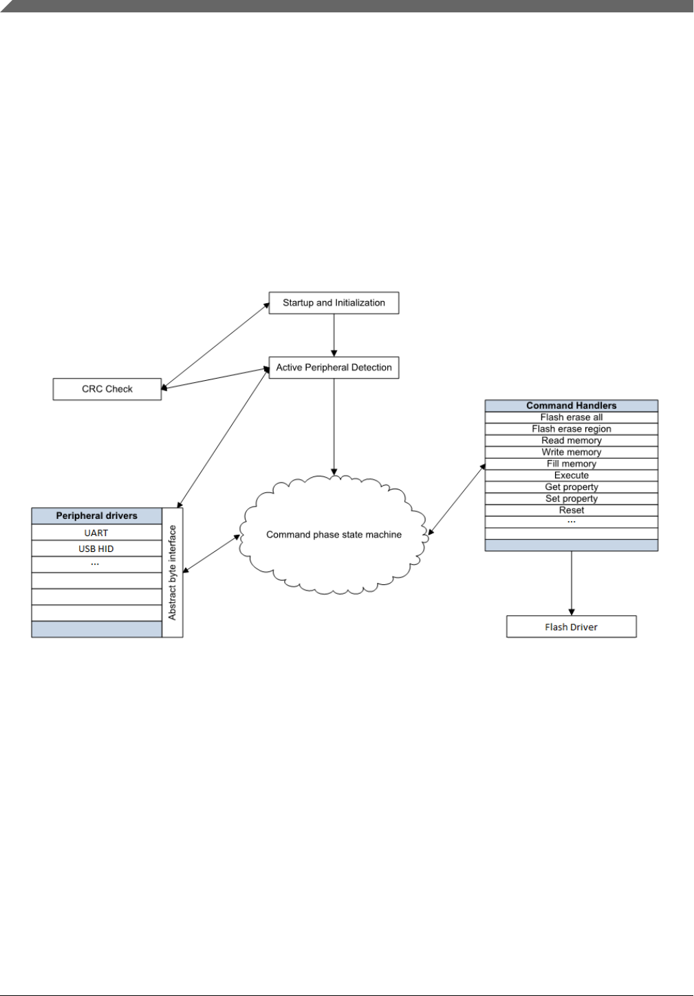
1.3 Block diagram
This block diagram describes the overall structure of the MCU flashloader.
Figure 1-1. Block diagram
1.4 Features supported
Here are some of the features supported by the MCU flashloader:
• Supports UART and USB peripheral interfaces.
• Automatic detection of the active peripheral.
• Ability to disable any peripheral.
Block diagram
MCU Flashloader Reference Manual, Rev. 5, 11/2018
8 NXP Semiconductors

• UART peripheral implements autobaud.
• Common packet-based protocol for all peripherals.
• Packet error detection and retransmit.
• Protection of RAM used by the flashloader while it is running.
• Provides command to read properties of the device, such as RAM size.
• Support for serial QuadSPI and other external memories.
• Support for encrypted image download.
1.5 Components supported
Components for the flashloader firmware:
• Startup code (clocking, pinmux, etc.)
• Command phase state machine
• Command handlers
• GenericResponse
• FlashEraseAll
• FlashEraseRegion
• ReadMemory
• ReadMemoryResponse
• WriteMemory
• FillMemory
• GetProperty
• GetPropertyResponse
• Execute
• Call
• Reset
• SetProperty
• FlashProgramOnce/EfuseProgramOnce
• FlashReadOnce/EfuseReadOnce
• FlashReadOnceResponse
• ConfigureMemory
• SB file state machine
• Encrypted image support (AES-128)
• Packet interface
• Framing packetizer
• Command/data packet processor
• Memory interface
• Abstract interface
Chapter 1 Introduction
MCU Flashloader Reference Manual, Rev. 5, 11/2018
NXP Semiconductors 9

• FlexSPI NOR Memory Interface
• FlexSPI NAND Memory Interface
• SEMC NOR Memory Interface
• SEMC NAND Memory Interface
• SD Card Memory Interface
• eMMC Memory Interface
• Peripheral drivers
• UART
• Auto-baud detector
• USB device
• USB controller driver
• USB framework
• USB HID class
Components supported
MCU Flashloader Reference Manual, Rev. 5, 11/2018
10 NXP Semiconductors

Chapter 2
MCU flashloader protocol
2.1 Introduction
This section explains the general protocol for the packet transfers between the host and
the MCU flashloader. The description includes the transfer of packets for different
transactions, such as commands with no data phase, and commands with an incoming or
outgoing data phase. The next section describes the various packet types used in a
transaction.
Each command sent from the host is replied to with a response command.
Commands may include an optional data phase.
• If the data phase is incoming (from the host to MCU flashloader), it is part of the
original command.
• If the data phase is outgoing (from MCU flashloader to host), it is part of the
response command.
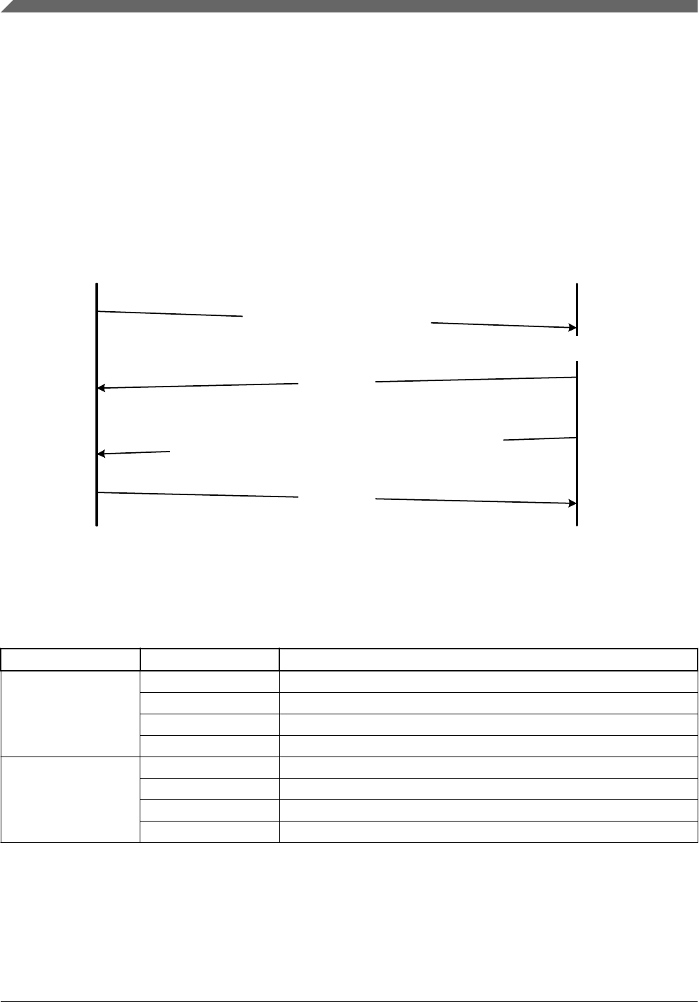
2.2 Command with no data phase
NOTE
In these diagrams, the Ack sent in response to a Command or
Data packet can arrive at any time before, during, or after the
Command/Data packet has processed.
Command with no data phase
The protocol for a command with no data phase contains:
• Command packet (from host)
• Generic response command packet (to host)
MCU Flashloader Reference Manual, Rev. 5, 11/2018
NXP Semiconductors 11

Command
Ack
Response
Ack
Process Command
Host Target
Figure 2-1. Command with no data phase
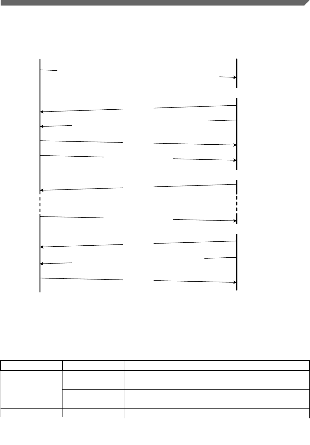
2.3 Command with incoming data phase
The protocol for a command with incoming data phase contains:
• Command packet (from host)(kCommandFlag_HasDataPhase set)
• Generic response command packet (to host)
• Incoming data packets (from host)
• Generic response command packet (to host)
Command with incoming data phase
MCU Flashloader Reference Manual, Rev. 5, 11/2018
12 NXP Semiconductors
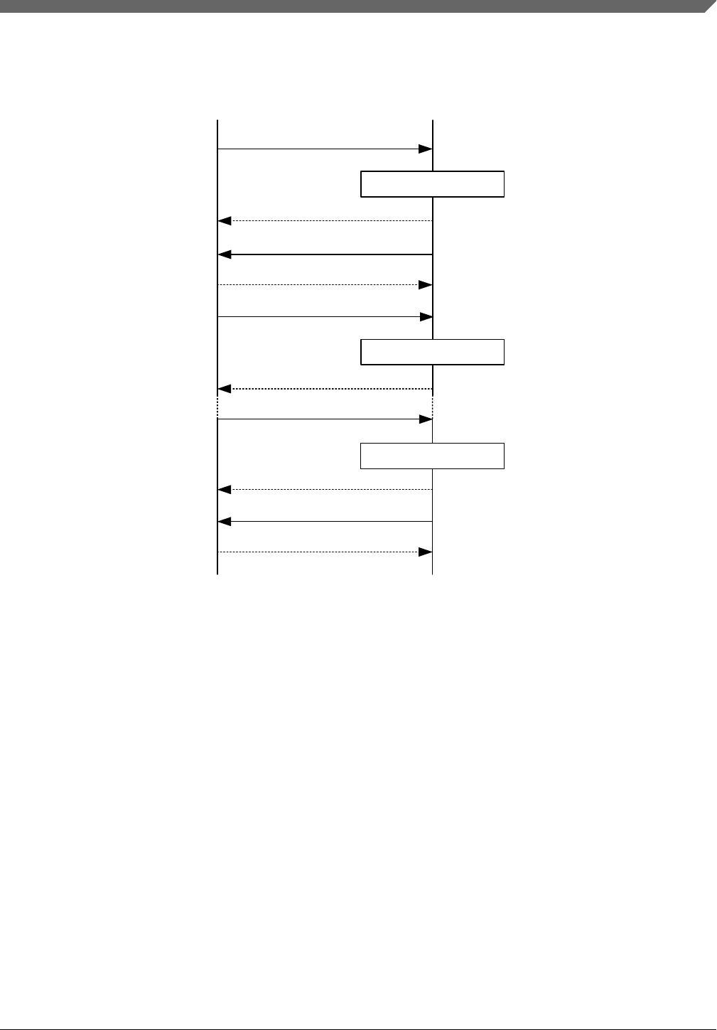
Command
Ack
Initial Response
Ack
Process Command
Host Target
Process Data
Data Packet
Ack
Final Data Packet
Process Data
Ack
Final Response
Ack
Figure 2-2. Command with incoming data phase
Notes
• The host may not send any further packets while it is waiting for the response to a
command.
• The data phase is aborted if, prior to the start of the data phase, the Generic Response
packet does not have a status of kStatus_Success.
• Data phases may be aborted by the receiving side by sending the final Generic
Response early with a status of kStatus_AbortDataPhase. The host may abort the
data phase early by sending a zero-length data packet.
• The final Generic Response packet sent after the data phase includes the status for
the entire operation.
Chapter 2 MCU flashloader protocol
MCU Flashloader Reference Manual, Rev. 5, 11/2018
NXP Semiconductors 13
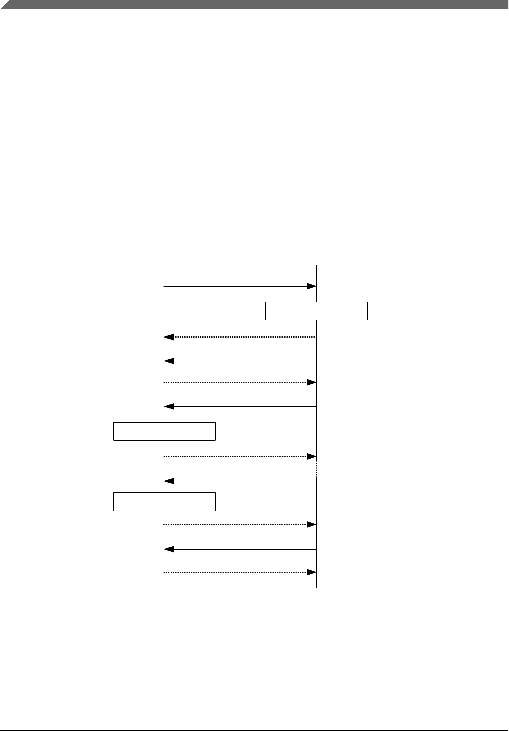
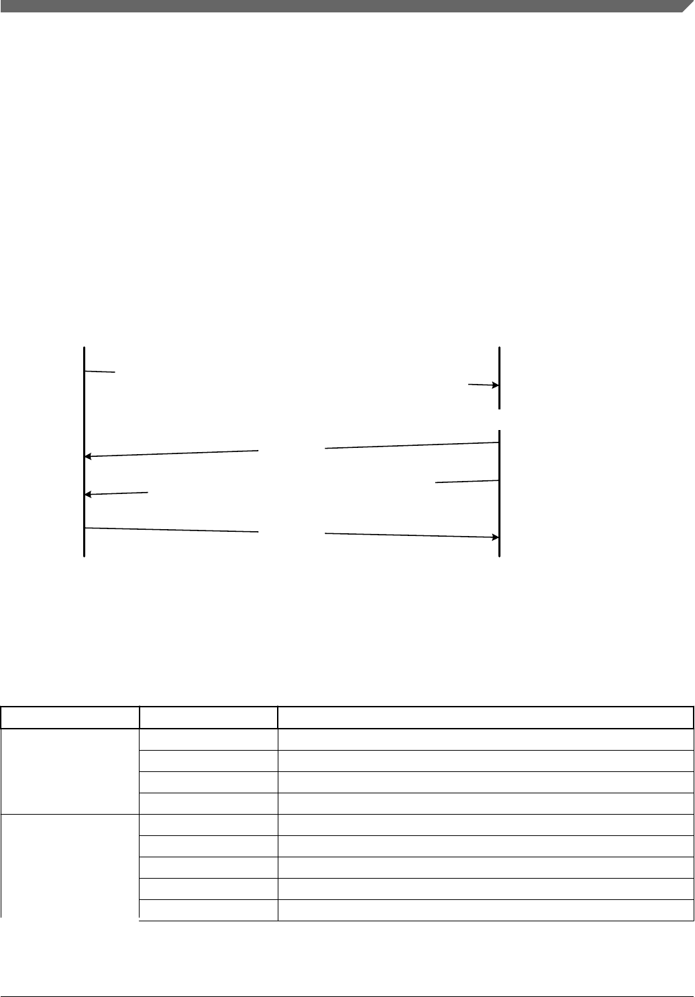
2.4 Command with outgoing data phase
The protocol for a command with an outgoing data phase contains:
• Command packet (from host)
• ReadMemory Response command packet (to host)(kCommandFlag_HasDataPhase
set)
• Outgoing data packets (to host)
• Generic response command packet (to host)
Command
Ack
Initial Response
Ack
Process Command
Host Target
Final Response
Ack
Process Data
Data Packet
Ack
Process Data Ack
Final Data Packet
Figure 2-3. Command with outgoing data phase
Command with outgoing data phase
MCU Flashloader Reference Manual, Rev. 5, 11/2018
14 NXP Semiconductors

Note
• The data phase is considered part of the response command for the outgoing data
phase sequence.
• The host may not send any further packets while the host is waiting for the response
to a command.
• The data phase is aborted if, prior to the start of the data phase, the ReadMemory
Response command packet does not contain the kCommandFlag_HasDataPhase flag.
• Data phases may be aborted by the host sending the final Generic Response early
with a status of kStatus_AbortDataPhase. The sending side may abort the data phase
early by sending a zero-length data packet.
• The final Generic Response packet sent after the data phase includes the status for
the entire operation.
Chapter 2 MCU flashloader protocol
MCU Flashloader Reference Manual, Rev. 5, 11/2018
NXP Semiconductors 15

Command with outgoing data phase
MCU Flashloader Reference Manual, Rev. 5, 11/2018
16 NXP Semiconductors

Chapter 3
Flashloader packet types
3.1 Introduction
The MCU flashloader device works in slave mode. All data communication is initiated by
a host, which is either a PC or embedded host. The MCU flashloader device is the target,
which receives a command or data packet. All data communication between host and
target is packetized.
NOTE
The term "target" refers to the "MCU flashloader device".
There are 6 types of packets used:
• Ping packet
• Ping Response packet
• Framing packet
• Command packet
• Data packet
• Response packet
All fields in the packets are in little-endian byte order.
3.2 Ping packet
The Ping packet can be sent from host to target any time when the target is expecting a
command packet. If the selected peripheral is UART, a ping packet must be sent before
any other communication in order to run autobaud. For other serial peripherals it is
optional, but is recommended in order to determine the serial protocol version.
In response to a Ping packet, the target sends a Ping Response packet, discussed in
following section.
MCU Flashloader Reference Manual, Rev. 5, 11/2018
NXP Semiconductors 17
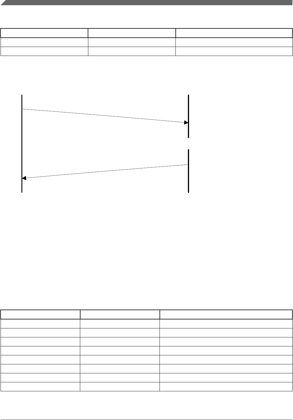
Table 3-1. Ping packet format
Byte # Value Name
0 0x5A start byte
1 0xA6 ping
Target executes UART autobaud if necessary
Host Target
PingResponse Packet:
0x5a 0xa7 0x00 0x02 0x01 0x50 0x00 0x00 0xaa 0xea
Ping Packet 0x5a 0xa6
Figure 3-1. Ping Packet Protocol Sequence
3.3 Ping response packet
The target sends a Ping Response packet back to the host after receiving a Ping packet. If
communication is over a UART peripheral, the target uses the incoming Ping packet to
determine the baud rate before replying with the Ping Response packet. After the Ping
Response packet is received by the host, the connection is established, and the host starts
sending commands to the target.
Table 3-2. Ping Response packet format
Byte # Value Parameter
0 0x5A start byte
1 0xA7 Ping response code
2 Protocol bugfix
3 Protocol minor
4 Protocol major
5 Protocol name = 'P' (0x50)
6 Options low
7 Options high
Table continues on the next page...
Ping response packet
MCU Flashloader Reference Manual, Rev. 5, 11/2018
18 NXP Semiconductors

Table 3-2. Ping Response packet format (continued)
Byte # Value Parameter
8 CRC16 low
9 CRC16 high
3.4 Framing packet
The framing packet is used for flow control and error detection for the communications
links that do not have such features built-in. The framing packet structure sits between
the link layer and command layer. It wraps command and data packets as well.
Every framing packet containing data sent in one direction results in a synchronizing
response framing packet in the opposite direction.
The framing packet described in this section is used for serial peripheral UART. The
USB HID peripheral does not use framing packets. Instead, the packetization inherent in
the USB protocol itself is used.
Table 3-3. Framing packet format
Byte # Parameter Description
0 start byte Value - 0x5A
1 packetType
2 length_low Length is a 16-bit field that specifies the entire
command or data packet size in bytes.
3 length_high
4 crc16_low This is a 16-bit field. The CRC16 value covers entire
framing packet, including the start byte and command or
data packets, but does not include the CRC bytes. See
the CRC16 algorithm after this table.
5 crc16_high
6 . . .n Command or Data packet
payload
A special framing packet that contains only a start byte and a packet type is used for
synchronization between the host and target.
Table 3-4. Special framing packet format
Byte # Value Parameter
0 0x5A start byte
1 0xAnpacketType
Chapter 3 Flashloader packet types
MCU Flashloader Reference Manual, Rev. 5, 11/2018
NXP Semiconductors 19

The Packet Type field specifies the type of the packet from one of the defined types
(below):
Table 3-5. packetType field
packetType Name Description
0xA1 kFramingPacketType_Ack The previous packet was received successfully; the sending
of more packets is allowed.
0xA2 kFramingPacketType_Nak The previous packet was corrupted and must be re-sent.
0xA3 kFramingPacketType_AckAbort Data phase is being aborted.
0xA4 kFramingPacketType_Command The framing packet contains a command packet payload.
0xA5 kFramingPacketType_Data The framing packet contains a data packet payload.
0xA6 kFramingPacketType_Ping Sent to verify the other side is alive. Also used for UART
autobaud.
0xA7 kFramingPacketType_PingResponse A response to Ping; contains the framing protocol version
number and options.
3.5 CRC16 algorithm
This section provides the CRC16 algorithm.
The CRC is computed over each byte in the framing packet header, excluding the crc16
field itself, plus all payload bytes. The CRC algorithm is the XMODEM variant of
CRC-16.
The characteristics of the XMODEM variant are:
Table 3-6. XMODEM charactertistics
width 16
polynomial 0x1021
init value 0x0000
reflect in false
reflect out false
xor out 0x0000
check result 0x31c3
The check result is computed by running the ASCII character sequence "123456789"
through the algorithm.
uint16_t crc16_update(const uint8_t * src, uint32_t lengthInBytes)
{
uint32_t crc = 0;
uint32_t j;
for (j=0; j < lengthInBytes; ++j)
{
CRC16 algorithm
MCU Flashloader Reference Manual, Rev. 5, 11/2018
20 NXP Semiconductors

uint32_t i;
uint32_t byte = src[j];
crc ^= byte << 8;
for (i = 0; i < 8; ++i)
{
uint32_t temp = crc << 1;
if (crc & 0x8000)
{
temp ^= 0x1021;
}
crc = temp;
}
}
return crc;
}
3.6 Command packet
The command packet carries a 32-bit command header and a list of 32-bit parameters.
Table 3-7. Command packet format
Command packet format (32 bytes)
Command header (4 bytes) 28 bytes for parameters (Max 7 parameters)
Tag Flags Rsvd Param
Count
Param1
(32-bit)
Param2
(32-bit)
Param3
(32-bit)
Param4
(32-bit)
Param5
(32-bit)
Param6
(32-bit)
Param7
(32-bit)
byte 0 byte 1 byte 2 byte 3 - - - - - - -
Table 3-8. Command header format
Byte # Command header field
0 Command or Response tag
1 Flags
2 Reserved. Should be 0x00.
3 ParameterCount
The header is followed by 32-bit parameters up to the value of the ParameterCount field
specified in the header.
Chapter 3 Flashloader packet types
MCU Flashloader Reference Manual, Rev. 5, 11/2018
NXP Semiconductors 21

Command packets are also used by the target to send responses back to the host. As
described in section 3.4, command packets and data packets are embedded into framing
packets for all UART transfers.
Table 3-9. Command Tags
Command Tag Name
0x01 FlashEraseAll The command tag specifies one of the
commands supported by the MCU flashloader.
The valid command tags for the MCU
flashloader are listed here.
0x02 FlashEraseRegion
0x03 ReadMemory
0x04 WriteMemory
0x05 FillMemory
0x07 GetProperty
0x08 Reserved
0x09 Execute
0x10 FlashReadResource
0x11 Reserved
0x0A Call
0x0B Reset
0x0C SetProperty
0x0E eFuseProgram
0x0F eFuseRead
0x10 FlashReadResource
0x11 ConfigureMemory
Table 3-10. Response Tags
Response Tag Name
0xA0 GenericResponse The response tag specifies one of the responses
the MCU flashloader (target) returns to the host.
The valid response tags are listed here.
0xA7 GetPropertyResponse (used for sending
responses to GetProperty command only)
0xA3 ReadMemoryResponse (used for sending
responses to ReadMemory command only)
0xAF FlashReadOnceResponse (used for sending
responses to FlashReadOnce command only)
0xB0 FlashReadResourceResponse (used for sending
responses to FlashReadResource command
only)
Flags: Each command packet contains a Flag byte. Only bit 0 of the flag byte is used. If
bit 0 of the flag byte is set to 1, then data packets follow in the command sequence. The
number of bytes that are transferred in the data phase is determined by a command-
specific parameter in the parameters array.
Command packet
MCU Flashloader Reference Manual, Rev. 5, 11/2018
22 NXP Semiconductors

ParameterCount: The number of parameters included in the command packet.
Parameters: The parameters are word-length (32 bits). With the default maximum
packet size of 32 bytes, a command packet can contain up to 7 parameters.
3.7 Response packet
Response packets use the same format as command packets (refer to section 3.6). Types
of responses include:
• GenericResponse
• GetPropertyResponse
• ReadMemoryResponse
• FlashReadOnceResponse
• FlashReadResourceResponse
GenericResponse: After the MCU flashloader has processed a command, the flashloader
sends a generic response with status and command tag information to the host. The
generic response is the last packet in the command protocol sequence. The generic
response packet contains the command packet data (with generic response tag = 0xA0)
and a list of parameters (defined in the next section). The parameter count field in the
header is always set to 2, for status code and command tag parameters.
Table 3-11. GenericResponse parameters
Byte # Parameter Descripton
0 - 3 Status code The Status codes are errors encountered during the execution of a
command by the target. If a command succeeds, then a kStatus_Success
code is returned.
4 - 7 Command tag The Command tag parameter identifies the response to the command sent
by the host.
GetPropertyResponse: The GetPropertyResponse packet is sent by the target in
response to the host query that uses the GetProperty command. The GetPropertyResponse
packet contains the command packet data, with the command/response tag set to a
GetPropertyResponse tag value (0xA7).
The parameter count field in the header is set to greater than 1, to always include the
status code and one or many property values.
Chapter 3 Flashloader packet types
MCU Flashloader Reference Manual, Rev. 5, 11/2018
NXP Semiconductors 23

Table 3-12. GetPropertyResponse parameters
Byte # Value Parameter
0 - 3 Status code
4 - 7 Property value
. . . . . .
Can be up to maximum 6 property values, limited to the size of the 32-bit
command packet and property type.
ReadMemoryResponse: The ReadMemoryResponse packet is sent by the target in
response to the host sending a ReadMemory command. The ReadMemoryResponse
packet contains the command packet data, with the command/response tag set to a
ReadMemoryResponse tag value (0xA3), the flags field set to
kCommandFlag_HasDataPhase (1).
The parameter count is set to 2 for the status code and the data byte count parameters
shown below.
Table 3-13. ReadMemoryResponse Parameters
Byte # Parameter Descripton
0 - 3 Status code The status of the associated Read Memory command.
4 - 7 Data byte count The number of bytes sent in the data phase.
FlashReadOnceResponse:The FlashReadOnceResponse packet is sent by the target in
response to the host sending a FlashReadOnce command. The FlashReadOnceResponse
packet contains the command packet data, with the command/response tag set to a
FlashReadOnceResponse tag value (0xAF), and the flags field set to 0. The parameter
count is set to 2 plus the number of words requested to be read in the
FlashReadOnceCommand.
Table 3-14. FlashReadOnceResponse Parameters
Byte # Value Parameter
0 – 3 Status Code
4 – 7 Byte count to read
… …
Can be up to 20 bytes of requested read data.
Response packet
MCU Flashloader Reference Manual, Rev. 5, 11/2018
24 NXP Semiconductors

Chapter 4
MCU flashloader command API
4.1 Introduction
All MCU flashloader command APIs follows the command packet format wrapped by
the framing packet as explained in previous sections.
See Table 3-9 for a list of commands supported by MCU flashloader.
For a list of status codes returned by MCU flashloader, see Appendix A.
4.2 GetProperty command
The GetProperty command is used to query the flashloader about various properties and
settings. Each supported property has a unique 32-bit tag associated with it. The tag
occupies the first parameter of the command packet. The target returns a
GetPropertyResponse packet with the values for the property identified with the tag in the
GetProperty command.
Properties are the defined units of data that can be accessed with the GetProperty or
SetProperty commands. Properties may be read-only or read-write. All read-write
properties are 32-bit integers, so they can easily be carried in a command parameter.
For a list of properties and their associated 32-bit property tags supported by MCU
flashloader, see Appendix B, "GetProperty and SetProperty commands".
The 32-bit property tag is the only parameter required for GetProperty command.
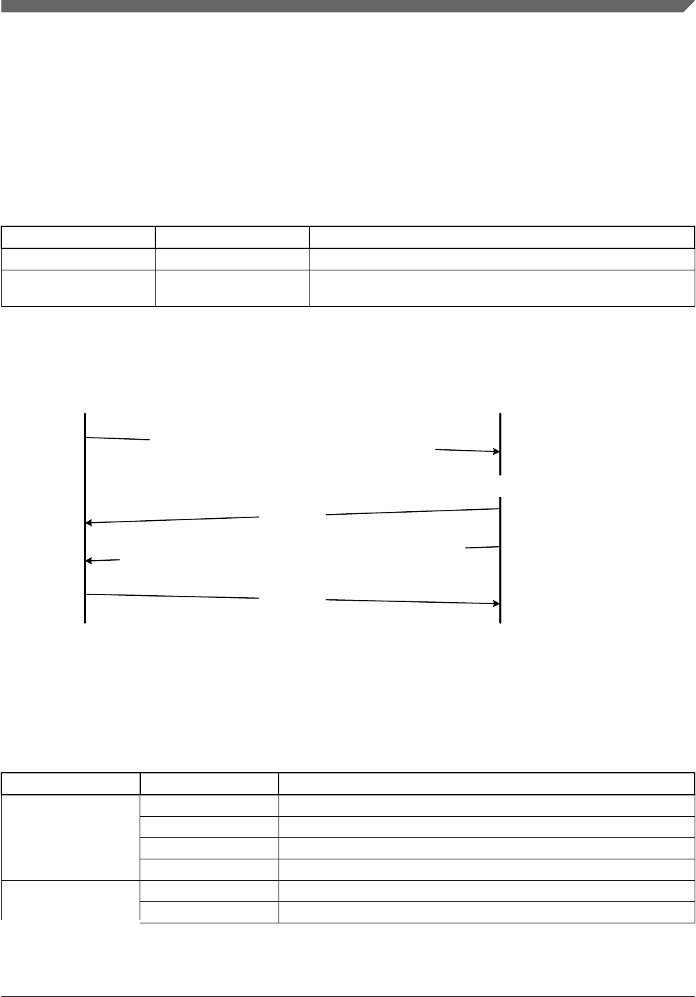
Table 4-1. Parameters for GetProperty command
Byte # Command
0 - 3 Property tag
4 - 7 External Memory Identifier (only applies to get property for external memory)
MCU Flashloader Reference Manual, Rev. 5, 11/2018
NXP Semiconductors 25

Host Target
GetProperty: Property tag = 0x01
0x5a a4 0c 00 4b 33 07 00 00 02 01 00 00 00 00 00 00 00
ACK: 0x5a a1
Process Command
Generic Response:
0x5a a4 0c 00 f4 9d a7 00 00 02 00 00 00 00 00 06 02 4b
ACK: 0x5a a1
Figure 4-1. Protocol sequence for GetProperty command
Table 4-2. GetProperty packet format example
GetProperty Parameter Value
Framing packet start byte 0x5A
packetType 0xA4, kFramingPacketType_Command
length 0x0C 0x00
crc16 0x4B 0x33
Command packet commandTag 0x07 – GetProperty
flags 0x00
reserved 0x00
parameterCount 0x02
propertyTag 0x00000001 - CurrentVersion
Memory ID 0x00000000 - Internal Flash
The GetProperty command has no data phase.
Response: In response to a GetProperty command, the target sends a
GetPropertyResponse packet with the response tag set to 0xA7. The parameter count
indicates the number of parameters sent for the property values, with the first parameter
showing status code 0, followed by the property value(s). The next table shows an
example of a GetPropertyResponse packet.
GetProperty command
MCU Flashloader Reference Manual, Rev. 5, 11/2018
26 NXP Semiconductors

Table 4-3. GetProperty response packet format example
GetPropertyResponse Parameter Value
Framing packet start byte 0x5A
packetType 0xA4, kFramingPacketType_Command
length 0x0c 0x00 (12 bytes)
crc16 0xf4 9d
Command packet responseTag 0xA7
flags 0x00
reserved 0x00
parameterCount 0x02
status 0x00000000
propertyValue 0x4b020600 - CurrentVersion
4.3 SetProperty command
The SetProperty command is used to change or alter the values of the properties or
options of the flashloader. The command accepts the same property tags used with the
GetProperty command. However, only some properties are writable--see Appendix B. If
an attempt to write a read-only property is made, an error is returned indicating the
property is read-only and cannot be changed.
The property tag and the new value to set are the two parameters required for the
SetProperty command.
Table 4-4. Parameters for SetProperty command
Byte # Command
0 - 3 Property tag
4 - 7 Property value
Chapter 4 MCU flashloader command API
MCU Flashloader Reference Manual, Rev. 5, 11/2018
NXP Semiconductors 27

Host Target
SetProperty: Property tag = 0x0a, Property Value = 1
0x5a a4 0c 00 67 8d 0c 00 00 02 0a 00 00 00 01 00 00 00
ACK: 0x5a a1
Process Command
Generic Response:
0x5a a4 0c 00 e0 f7 a0 00 00 02 00 00 00 00 0c 00 00 00
ACK: 0x5a a1
Figure 4-2. Protocol sequence for SetProperty command
Table 4-5. SetProperty packet format example
SetProperty Parameter Value
Framing packet start byte 0x5A
packetType 0xA4, kFramingPacketType_Command
length 0x0C 0x00
crc16 0x67 0x8D
Command packet commandTag 0x0C – SetProperty with property tag 10
flags 0x00
reserved 0x00
parameterCount 0x02
propertyTag 0x0000000A - VerifyWrites
propertyValue 0x00000001
The SetProperty command has no data phase.
Response: The target returns a GenericResponse packet with one of following status
codes:
Table 4-6. SetProperty response status codes
Status Code
kStatus_Success
Table continues on the next page...
SetProperty command
MCU Flashloader Reference Manual, Rev. 5, 11/2018
28 NXP Semiconductors

Table 4-6. SetProperty response status codes (continued)
Status Code
kStatus_ReadOnly
kStatus_UnknownProperty
kStatus_InvalidArgument
4.4 FlashEraseAll command
The FlashEraseAll command performs an erase of the entire flash memory. If any flash
regions are protected, then the FlashEraseAll command fails and returns an error status
code. Executing the FlashEraseAll command releases flash security if it (flash security)
was enabled, by setting the FTFA_FSEC register. However, the FSEC field of the flash
configuration field is erased, so unless it is reprogrammed, the flash security is re-enabled
after the next system reset. The Command tag for FlashEraseAll command is 0x01 set in
the commandTag field of the command packet.
The FlashEraseAll command requires a memory ID. If the memory ID is not specified,
the internal flash (memory ID =0) will be selected as default.
Table 4-7. Parameter for FlashEraseAll command
Byte # Parameter
0-3 Memory ID
0x000 Internal Flash
0x010 Execute-only region in
Internal Flash
0x001 Serial NOR through QuadSPI
0x008 Parallel NOR through SEMC
0x009 Serial NOR through FlexSPI
0x100 SLC Raw NAND through
SEMC
0x101 Serial NAND through FlexSPI
0x110 Serial NOR/EEPROM
through SPI
0x120 SD through uSDHC
0x121 eMMC through uSDHC
Chapter 4 MCU flashloader command API
MCU Flashloader Reference Manual, Rev. 5, 11/2018
NXP Semiconductors 29

Host Target
FlashEraseAll
0x5a a4 08 00 0c 22 01 00 00 01 00 00 00 00
ACK: 0x5a a1
Process Command
Generic Response:
0x5a a4 0c 00 66 ce a0 00 00 02 00 00 00 00 01 00 00 00
ACK: 0x5a a1
Figure 4-3. Protocol sequence for FlashEraseAll command
Table 4-8. FlashEraseAll packet format example
FlashEraseAll Parameter Value
Framing packet start byte 0x5A
packetType 0xA4, kFramingPacketType_Command
length 0x08 0x00
crc16 0x0C 0x22
Command packet commandTag 0x01 - FlashEraseAll
flags 0x00
reserved 0x00
parameterCount 0x01
Memory ID refer to the above table
The FlashEraseAll command has no data phase.
Response: The target returns a GenericResponse packet with status code either set to
kStatus_Success for successful execution of the command, or set to an appropriate error
status code.
FlashEraseAll command
MCU Flashloader Reference Manual, Rev. 5, 11/2018
30 NXP Semiconductors

4.5 FlashEraseRegion command
The FlashEraseRegion command performs an erase of one or more sectors of the flash
memory.
The start address and number of bytes are the 2 parameters required for the
FlashEraseRegion command. The start and byte count parameters must be 4-byte aligned
([1:0] = 00), or the FlashEraseRegion command fails and returns
kStatus_FlashAlignmentError(101). If the region specified does not fit in the flash
memory space, the FlashEraseRegion command fails and returns
kStatus_FlashAddressError(102). If any part of the region specified is protected, the
FlashEraseRegion command fails and returns kStatus_MemoryRangeInvalid(10200).
Table 4-9. Parameters for FlashEraseRegion command
Byte # Parameter
0 - 3 Start address
4 - 7 Byte count
8 - 11 Memory ID
The FlashEraseRegion command has no data phase.
Response: The target returns a GenericResponse packet with one of following error
status codes.
Table 4-10. FlashEraseRegion response status codes
Status code
kStatus_Success (0)
kStatus_MemoryRangeInvalid (10200)
kStatus_FlashAlignmentError (101)
kStatus_FlashAddressError (102)
kStatus_FlashAccessError (103)
kStatus_FlashProtectionViolation (104)
kStatus_FlashCommandFailure (105)
Chapter 4 MCU flashloader command API
MCU Flashloader Reference Manual, Rev. 5, 11/2018
NXP Semiconductors 31

4.6 ReadMemory command
The ReadMemory command returns the contents of memory at the given address, for a
specified number of bytes. This command can read any region of memory accessible by
the CPU and is not protected by security.
The start address and number of bytes are the two parameters required for ReadMemory
command. The memory ID is optional. Internal memory is selected as default if memory
ID is not specified.
Table 4-11. Parameters for read memory command
Byte Parameter Description
0-3 Start address Start address of memory to read from
4-7 Byte count Number of bytes to read and return to caller
8-11 Memory ID Internal or extermal memory Identifier
ReadMemory command
MCU Flashloader Reference Manual, Rev. 5, 11/2018
32 NXP Semiconductors

Host Target
ReadMemory: startAddress = 0x20000400, byteCount = 0x64
0x5a a4 10 00 f4 1b 03 00 00 03 00 04 00 20 64 00 00 00 00 00 00 00
ACK: 0x5a a1
Process Command
Generic Response:
0x5a a4 0c 00 27 f6 a3 01 00 02 00 00 00 00 64 00 00 00
ACK: 0x5a a1
Data packet:
0x5a a5 length16 CRC16 data
Process Data
ACK: 0x5a a1
Final data packet:
0x5a a5 length16 CRC16 data
Process Data
ACK: 0x5a a1
Generic Response:
0x5a a4 0c 00 0e 23 a0 00 00 02 00 00 00 00 03 00 00 00
ACK: 0x5a a1
Figure 4-4. Command sequence for read memory
Table 4-12. ReadMemory packet format example
ReadMemory Parameter Value
Framing packet Start byte 0x5A0xA4,
packetType kFramingPacketType_Command
length 0x10 0x00
crc16 0xF4 0x1B
Command packet commandTag 0x03 - readMemory
flags 0x00
reserved 0x00
parameterCount 0x03
Table continues on the next page...
Chapter 4 MCU flashloader command API
MCU Flashloader Reference Manual, Rev. 5, 11/2018
NXP Semiconductors 33

Table 4-12. ReadMemory packet format example (continued)
ReadMemory Parameter Value
startAddress 0x20000400
byteCount 0x00000064
memoryID 0x0
Data Phase: The ReadMemory command has a data phase. Because the target works in
slave mode, the host needs to pull data packets until the number of bytes of data specified
in the byteCount parameter of the ReadMemory command are received by host.
Response: The target returns a GenericResponse packet with a status code either set to
kStatus_Success upon successful execution of the command, or set to an appropriate
error status code.
4.7 WriteMemory command
The WriteMemory command writes data provided in the data phase to a specified range
of bytes in memory (flash or RAM). However, if flash protection is enabled, then writes
to protected sectors fail.
Special care must be taken when writing to flash.
• First, any flash sector written to must have been previously erased with a
FlashEraseAll, FlashEraseRegion, or FlashEraseAllUnsecure command.
• Writing to flash requires the start address to be page size aligned.
• The byte count is rounded up to a multiple of page size, and trailing bytes are filled
with the flash erase pattern (0xff).
• If the VerifyWrites property is set to true, then writes to flash also perform a flash
verify program operation.
When writing to RAM, the start address does not need to be aligned, and the data is not
padded.
The start address and number of bytes are the 2 parameters required for the WriteMemory
command. The memory ID is optional. Internal memory will be selected as default if a
memory ID is not specified.
Table 4-13. Parameters for WriteMemory command
Byte # Command
0 - 3 Start address
4 - 7 Byte count
8 - 11 Memory ID
WriteMemory command
MCU Flashloader Reference Manual, Rev. 5, 11/2018
34 NXP Semiconductors
Host Target
WriteMemory: startAddress = 0x20000400, byteCount = 0x64
0x5a a4 10 00 97 dd 04 01 00 03 00 04 00 20 64 00 00 00 00 00 00 00
ACK: 0x5a a1
Process Command
Generic Response:
0x5a a4 0c 00 23 72 a0 00 00 02 00 00 00 00 04 00 00 00
ACK: 0x5a a1
Data packet:
0x5a a5 length16 CRC16 data
Process Data
ACK: 0x5a a1
Final data packet:
0x5a a5 length16 CRC16 data
Process Data
Generic Response:
0x5a a4 0c 00 23 72 a0 00 00 02 00 00 00 00 04 00 00 00
ACK: 0x5a a1
ACK: 0x5a a1
Figure 4-5. Protocol sequence for WriteMemory command
Table 4-14. WriteMemory packet format example
WriteMemory Parameter Value
Framing packet start byte 0x5A
packetType 0xA4, kFramingPacketType_Command
length 0x10 0x00
crc16 0x97 0xDD
Command packet commandTag 0x04 - writeMemory
Table continues on the next page...
Chapter 4 MCU flashloader command API
MCU Flashloader Reference Manual, Rev. 5, 11/2018
NXP Semiconductors 35

Table 4-14. WriteMemory packet format example (continued)
WriteMemory Parameter Value
flags 0x01
reserved 0x00
parameterCount 0x03
startAddress 0x20000400
byteCount 0x00000064
memoryID 0x0
Data Phase: The WriteMemory command has a data phase. The host sends data packets
until the number of bytes of data specified in the byteCount parameter of the
WriteMemory command are received by the target.
Response: The target returns a GenericResponse packet with a status code set to
kStatus_Success upon successful execution of the command or to an appropriate error
status code.
4.8 FillMemory command
The FillMemory command fills a range of bytes in memory with a data pattern. It follows
the same rules as the WriteMemory command. The difference between FillMemory and
WriteMemory is that a data pattern is included in the FillMemory command parameter,
and there is no data phase for the FillMemory command, while WriteMemory does have
a data phase.
Table 4-15. Parameters for FillMemory command
Byte # Command
0 - 3 Start address of memory to fill
4 - 7 Number of bytes to write with the pattern
• The start address should be 32-bit aligned.
• The number of bytes must be evenly divisible by 4.
NOTE: For any part that uses FTFE flash, the start
address should be 64-bit aligned, and the number
of bytes must be evenly divisible by 8.
8 - 11 32-bit pattern
• To fill with a byte pattern (8-bit), the byte must be replicated 4 times in the 32-bit
pattern.
• To fill with a short pattern (16-bit), the short value must be replicated 2 times in the
32-bit pattern.
FillMemory command
MCU Flashloader Reference Manual, Rev. 5, 11/2018
36 NXP Semiconductors
For example, to fill a byte value with 0xFE, the word pattern is 0xFEFEFEFE; to fill a
short value 0x5AFE, the word pattern is 0x5AFE5AFE.
Special care must be taken when writing to flash.
• First, any flash sector written to must have been previously erased with a
FlashEraseAll, FlashEraseRegion, or FlashEraseAllUnsecure command.
• Writing to flash requires the start address to be page size aligned.
• If the VerifyWrites property is set to true, then writes to flash also performs a flash
verify program operation.
When writing to RAM, the start address does not need to be aligned.
Host Target
FillMemory, with word pattern 0x12345678
0x5a a4 10 00 e4 57 05 00 00 03 00 70 00 00 00 08 00 00 78 56 34 12
ACK: 0x5a a1
Process Command
Generic Response:
0x5a a4 0c 00 f4 9d a7 00 00 02 00 00 00 00 00 06 02 4b
ACK: 0x5a a1
Figure 4-6. Protocol sequence for FillMemory command
Table 4-16. FillMemory packet format example
FillMemory Parameter Value
Framing packet start byte 0x5A
packetType 0xA4, kFramingPacketType_Command
length 0x10 0x00
crc16 0xE4 0x57
Command packet commandTag 0x05 – FillMemory
flags 0x00
Reserved 0x00
parameterCount 0x03
startAddress 0x00007000
Table continues on the next page...
Chapter 4 MCU flashloader command API
MCU Flashloader Reference Manual, Rev. 5, 11/2018
NXP Semiconductors 37

Table 4-16. FillMemory packet format example (continued)
FillMemory Parameter Value
byteCount 0x00000800
patternWord 0x12345678
The FillMemory command has no data phase.
Response: upon successful execution of the command, the target (MCU flashloader)
returns a GenericResponse packet with a status code set to kStatus_Success, or to an
appropriate error status code.
4.9 Execute command
The execute command results in the flashloader setting the program counter to the code at
the provided jump address, R0 to the provided argument, and a Stack pointer to the
provided stack pointer address. Prior to the jump, the system is returned to the reset state.
The Jump address, function argument pointer, and stack pointer are the parameters
required for the Execute command. If the stack pointer is set to zero, the called code is
responsible for setting the processor stack pointer before using the stack.
Table 4-17. Parameters for Execute command
Byte # Command
0 - 3 Jump address
4 - 7 Argument word
8 - 11 Stack pointer address
The Execute command has no data phase.
Response: Before running the Execute command, the target validates the parameters and
returns a GenericResponse packet with a status code either set to kStatus_Success or an
appropriate error status code.
Execute command
MCU Flashloader Reference Manual, Rev. 5, 11/2018
38 NXP Semiconductors

4.10 Call command
The Call command executes a function that is written in memory at the address sent in
the command. The address needs to be a valid memory location residing in accessible
flash (internal or external) or in RAM. The command supports the passing of one 32-bit
argument. Although the command supports a stack address, at this time the call still takes
place using the current stack pointer. After execution of the function, a 32-bit value is
returned in the generic response message.
Host Target
Call: Address = 0x00000cd9, arg = 0
0x5a a4 0c 00 16 5c 0a 00 00 02 d9 0c 00 00 00 00 00 00 00
ACK: 0x5a a1
Process Command
Generic Response:
0x5a a4 0c 00 79 d0 a0 00 00 02 00 00 00 00 0a 00 00 00
ACK: 0x5a a1
Figure 4-7. Protocol sequence for call command
Table 4-18. Parameters for Call command
Byte # Command
0 - 3 Call address
4 - 7 Argument word
8 - 11 Stack pointer
Response: The target returns a GenericResponse packet with a status code either set to
the return value of the function called or set to kStatus_InvalidArgument (105).
Chapter 4 MCU flashloader command API
MCU Flashloader Reference Manual, Rev. 5, 11/2018
NXP Semiconductors 39
4.11 Reset command
The Reset command results in the flashloader resetting the chip.
The Reset command requires no parameters.
Host Target
Reset
0x5a a4 04 00 6f 46 0b 00 00 00
ACK: 0x5a a1
Process Command
Generic Response:
0x5a a4 0c 00 cd a6 a0 00 00 02 00 00 00 00 0b 00 00 00
ACK: 0x5a a1
Figure 4-8. Protocol sequence for Reset command
Table 4-19. Reset command packet format example
Reset Parameter Value
Framing packet start byte 0x5A
packetType 0xA4, kFramingPacketType_Command
length 0x04 0x00
crc16 0x6F 0x46
Command packet commandTag 0x0B - reset
flags 0x00
reserved 0x00
parameterCount 0x02
The Reset command has no data phase.
Reset command
MCU Flashloader Reference Manual, Rev. 5, 11/2018
40 NXP Semiconductors

Response: The target returns a GenericResponse packet with status code set to
kStatus_Success before resetting the chip.
The Reset command can also be used to switch boot from flash after successful flash
image provisioning via the flashloader. After issuing the reset command, allow 5 seconds
for the user application to start running from flash.
4.12 FlashProgramOnce/eFuseProgramOnce command
The FlashProgramOnce/ eFuseProgramOnce command writes data (that is provided in a
command packet) to a specified range of bytes in the program once field. Special care
must be taken when writing to the program once field.
• The program once field only supports programming once, so any attempt to
reprogram a program once field gets an error response.
• Writing to the program once field requires the byte count to be 4.
The FlashProgramOnce command uses three parameters: index, byteCount, and data.
Table 4-20. Parameters for FlashProgramOnce command
Byte # Command
0 - 3 Index of program once/ eFuse field
4 - 7 Byte count (must be 4 or 8 for a FlashProgramOnce; must be 4 for
eFuseProgramOnce)
8 - 11 Data
12 - 16 Data
Chapter 4 MCU flashloader command API
MCU Flashloader Reference Manual, Rev. 5, 11/2018
NXP Semiconductors 41

Host Target
FlashProgramOnce: index = 0, byteCount = 4, data = 0x12345678
0x5a a4 10 00 7e 89 0e 00 00 03 00 00 00 00 04 00 00 00 78 56 34 12
ACK: 0x5a a1
Process Command
Generic Response:
0x5a a4 0c 00 88 1a a0 00 00 02 00 00 00 00 0e 00 00 00
ACK: 0x5a a1
Figure 4-9. Protocol sequence for FlashProgramOnce command
Table 4-21. FlashProgramOnce packet format example
FlashProgramOnce Parameter Value
Framing packet start byte 0x5A
packetType 0xA4, kFramingPacketType_Command
length 0x10 0x00
crc16 0x7E4 0x89
Command packet commandTag 0x0E – FlashProgramOnce
flags 0
reserved 0
parameterCount 3
index 0x0000_0000
byteCount 0x0000_0004
data 0x1234_5678
Response: upon successful execution of the command, the target (MCU flashloader)
returns a GenericResponse packet with a status code set to kStatus_Success, or to an
appropriate error status code.
FlashProgramOnce/eFuseProgramOnce command
MCU Flashloader Reference Manual, Rev. 5, 11/2018
42 NXP Semiconductors
4.13 FlashReadOnce/eFuseReadOnce command
The FlashReadOnce/eFuseReadOnce command returns the contents of the program once
field by given index and byte count. The FlashReadOnce command uses 2 parameters:
index and byteCount.
Table 4-22. Parameters for FlashReadOnce command
Byte # Parameter Description
0 - 3 index Index of the program once field (to read from)
4 - 7 byteCount Number of bytes to read and return to the caller (must be 4 for
eFuseReadOnce)
Host Target
FlashReadOnce: index = 0, byteCount = 4
0x5a a4 0c 00 c1 a5 0f 00 00 02 00 00 00 00 04 00 00 00
ACK: 0x5a a1
Process Command
Generic Response:
0x5a a4 10 00 3f 6f af 00 00 03 00 00 00 00 04 00 00 00 78 56 34 12
ACK: 0x5a a1
Figure 4-10. Protocol sequence for FlashReadOnce command
Table 4-23. FlashReadOnce packet format example
FlashReadOnce Parameter Value
Framing packet start byte 0x5A
packetType 0xA4
length 0x0C 0x00
crc 0xC1 0xA5
Command packet commandTag 0x0F – FlashReadOnce
flags 0x00
Table continues on the next page...
Chapter 4 MCU flashloader command API
MCU Flashloader Reference Manual, Rev. 5, 11/2018
NXP Semiconductors 43

Table 4-23. FlashReadOnce packet format example (continued)
FlashReadOnce Parameter Value
reserved 0x00
parameterCount 0x02
index 0x0000_0000
byteCount 0x0000_0004
Table 4-24. FlashReadOnce response format example
FlashReadOnce
response
Parameter Value
Framing packet start byte 0x5A
packetType 0xA4
length 0x10 0x00
crc 0x3F 0x6F
Command packet commandTag 0xAF
flags 0x00
reserved 0x00
parameterCount 0x03
status 0x0000_0000
byteCount 0x0000_0004
data 0x1234_5678
Response: Upon successful execution of the command, the target returns a
FlashReadOnceResponse packet with a status code set to kStatus_Success, a byte count
and corresponding data read from Program Once Field upon successful execution of the
command, or returns with a status code set to an appropriate error status code and a byte
count set to 0.
4.14 Configure Memory command
The Configure Memory command configures an external memory device using a pre-
programmed configuration image. The parameters passed are memory ID and memory
address containing the configuration data. The configuration data is written to a RAM or
Configure Memory command
MCU Flashloader Reference Manual, Rev. 5, 11/2018
44 NXP Semiconductors

flash location and then this command directs the flashloader to use the data at that
location to configure the external memory devices. See Chapter 6, External Memory
Support, for configuration data details.
Table 4-25. Parameters for Configure Memory command
Byte # Command
0 – 3 Memory ID
4 – 7 Configuration block address
Response: The target (MCU flashloader) returns a GenericResponse packet with a status
code either set to kStatus_Success upon successful execution of the command, or set to
an appropriate error code.
4.15 ReceiveSBFile command
The ReceiveSBFile command starts the transfer of an SB file to the target. The command
only specifies the size in bytes of the SB file that is sent in the data phase. The SB file is
processed as it is received by the flashloader.
Table 4-26. Parameters for Receive SB File command
Byte # Command
0 - 3 Byte count
Data Phase: The Receive SB file command has a data phase. The host sends data packets
until the number of bytes of data specified in the byteCount parameter of the Receive SB
File command are received by the target.
Response: The target returns a GenericResponse packet with a status code set to the
kStatus_Success upon successful execution of the command, or set to an appropriate
error code.
Chapter 4 MCU flashloader command API
MCU Flashloader Reference Manual, Rev. 5, 11/2018
NXP Semiconductors 45

ReceiveSBFile command
MCU Flashloader Reference Manual, Rev. 5, 11/2018
46 NXP Semiconductors

Chapter 5
Supported peripherals
5.1 Introduction
This section describes the peripherals supported by the MCU flashloader.
5.2 UART peripheral
The MCU flashloader integrates an autobaud detection algorithm for the UART
peripheral, thereby providing flexible baud rate choices.
Autobaud feature: If UARTn is used to connect to the flashloader, then the UARTn_RX
pin must be kept high and not left floating during the detection phase in order to comply
with the autobaud detection algorithm. After the flashloader detects the ping packet
(0x5A 0xA6) on UARTn_RX, the flashloader firmware executes the autobaud sequence.
If the baudrate is successfully detected, then the flashloader sends a ping packet response
[(0x5A 0xA7), protocol version (4 bytes), protocol version options (2 bytes), and crc16 (2
bytes)] at the detected baudrate. The MCU flashloader then enters a loop, waiting for
flashloader commands via the UART peripheral.
NOTE
The data bytes of the ping packet must be sent continuously
(with no more than 80 ms between bytes) in a fixed UART
transmission mode (8-bit data, no parity bit, and 1 stop bit). If
the bytes of the ping packet are sent one-by-one with more than
an 80 ms delay between them, then the autobaud detection
algorithm may calculate an incorrect baud rate.
Supported baud rates: The baud rate is closely related to the MCU core and system
clock frequencies. Typical baud rates supported are 9600, 19200, 38400, and 57600.
Packet transfer: After autobaud detection succeeds, flashloader communications can
take place over the UART peripheral. The following flow charts show:
MCU Flashloader Reference Manual, Rev. 5, 11/2018
NXP Semiconductors 47
• How the host detects an ACK from the target
• How the host detects a ping response from the target
• How the host detects a command response from the target
Wait
for ACK
No Yes
End
No
Process NAK Yes
Report an error
No
Yes
No
Reached
maximum
Report a timeout
error
Yes
0x5A
received?
0xA2
received?
0xA1
received?
Wait for 1 byte
from target
Wait for 1 byte
from target
retries?
Figure 5-1. Host reads an ACK from target via UART
Wait for
ping response
Yes
Yes
End
Report Error
No
No
Wait for 1 byte
from target
Wait for 1 byte
from target
0x5A
received? 0xA7
received?
Wait for
remaining bytes
of ping response
packet
Figure 5-2. Host reads a ping response from target via UART
UART peripheral
MCU Flashloader Reference Manual, Rev. 5, 11/2018
48 NXP Semiconductors
Wait
for response
Yes
Yes
Wait for payload
length part from
target (2 bytes)
Wait for CRC
checksum from
Payload length
less than supported
length?
Yes
Wait for payload
data from target
No
Set payload length
to maximum
supported length
No
No
Reached
maximum
Report a timeout
error (End)
Yes
End
No
0x5A
received?
0xA4
received?
Wait for 1 byte
from target
Wait for 1 byte
from target
retries?
target (2 bytes)
Figure 5-3. Host reads a command response from target via UART
5.3 USB HID peripheral
The MCU flashloader supports loading data into flash via the USB peripheral. The target
is implemented as a USB HID class.
USB HID does not use framing packets. Instead, the packetization inherent in the USB
protocol itself is used. The ability for the device to NAK Out transfers (until they can be
received) provides the required flow control. The built-in CRC of each USB packet
provides the required error detection.
5.3.1 Device descriptor
The MCU flashloader configures the default USB VID/PID/Strings as shown below:
Default VID/PID:
• For legacy FSL device
• VID = 0x15A2
• PID = 0x0073
• For NXP device
• VID = 0x1FC9
• PID = 0x007F
Chapter 5 Supported peripherals
MCU Flashloader Reference Manual, Rev. 5, 11/2018
NXP Semiconductors 49

Default Strings:
• For legacy FSL device
• Manufacturer [1] = "Freescale Semiconductor Inc."
• Product [2] = "Kinetis bootloader"
• For NXP device
• Manufacturer [1] = "NXP Semiconductor Inc."
• Product [2] = "Kinetis bootloader"
5.3.2 Endpoints
The HID peripheral uses 3 endpoints:
• Control (0)
• Interrupt IN (1)
• Interrupt OUT (2)
The Interrupt OUT endpoint is optional for HID class devices, but the MCU flashloader
uses it as a pipe, where the firmware can NAK send requests from the USB host.
5.3.3 HID reports
There are 4 HID reports defined and used by the flashloader USB HID peripheral. The
report ID determines the direction and type of packet sent in the report. Otherwise, the
contents of all reports are the same.
Table 5-1. HID reports
Report ID Packet type Direction
1 Command OUT
2 Data OUT
3 Command IN
4 Data IN
For all reports, these properties apply:
Table 5-2. Report properties
Usage Min 1
Usage Max 1
Logical Min 0
Table continues on the next page...
USB HID peripheral
MCU Flashloader Reference Manual, Rev. 5, 11/2018
50 NXP Semiconductors

Table 5-2. Report properties (continued)
Logical Max 255
Report Size 8
Report Count 34
Each report has a maximum size of 34 bytes. This is derived from the minimum
flashloader packet size of 32 bytes, plus a 2-byte report header that indicates the length
(in bytes) of the packet sent in the report.
NOTE
In the future, the maximum report size may be increased, to
support transfers of larger packets. Alternatively, additional
reports may be added with larger maximum sizes.
The actual data sent in all of the reports looks like:
Table 5-3. Report data
0 Report ID
1 Packet Length LSB
2 Packet Length MSB
3 Packet[0]
4 Packet[1]
5 Packet[2]
...
N+3-1 Packet[N-1]
This data includes the Report ID, which is required if more than one report is defined in
the HID report descriptor. The actual data sent and received has a maximum length of 35
bytes. The Packet Length header is written in little-endian format, and it is set to the size
(in bytes) of the packet sent in the report. This size does not include the Report ID or the
Packet Length header itself. During a data phase, a packet size of 0 indicates a data phase
abort request from the receiver.
Chapter 5 Supported peripherals
MCU Flashloader Reference Manual, Rev. 5, 11/2018
NXP Semiconductors 51

USB HID peripheral
MCU Flashloader Reference Manual, Rev. 5, 11/2018
52 NXP Semiconductors

Chapter 6
External memory support
6.1 Introduction
This section describes the external memory devices supported by the MCU flashloader.
To use an external memory device correctly, the device must be enabled with the
corresponding configuration profile. If the external memory device is not enabled, then it
cannot be accessed by the flashloader. The MCU flashloader enables specific external
memory devices using memory identifiers, as shown below.
Table 6-1. Memory ID for external memory devices
Memory identifier External memory device
0x01 'Serial NOR over QuadSPI module'
0x08 'Parallel NOR over SEMC module'
0x09 'Serial NOR over FlexSPI module'
0x0a 'Serial NOR over SPIFI'
0x100 'SLC raw NAND over SEMC module'
0x101 'Serial NAND over FlexSPI module'
0x110 'Serial NOR/EEPROM over LPSPI module'
0x120 'SD over uSDHC'
0x121 'eMMC over uSDHC'
6.2 Serial NOR Flash through FlexSPI
The MCU Flashloader supports read, write, and erase of external Serial NOR Flash
devices via the FlexSPI Module. Before accessing Serial NOR Flash devices, the FlexSPI
module must be configured properly using a simplified FlexSPI NOR Config option
block or a complete 512-byte FlexSPI NOR Configuration Block. The flashloader can
generate the 512-byte FlexSPI NOR Configuration Block based on the simplified Flash
MCU Flashloader Reference Manual, Rev. 5, 11/2018
NXP Semiconductors 53

Configuration Option Block for most Serial NOR Flash devices in the market. To protect
Intellectual Property on external Serial NOR Flash, the Flashloader also supports image
encryption and programming using OTPMK/SNVS keys if the chip includes the BEE
module. See the Security Utility chapter for additional information.
6.2.1 FlexSPI NOR Configuration Block
Table 6-2. Memory ID for external memory devices
Name Offset Size (bytes) Description
Tag 0x000 4 0x42464346, ascii:”FCFB”
Version 0x004 4 0x56010000
[07:00] bugfix
[15:08] minor
[23:16] major = 1
[31:24] ascii ‘V’
- 0x008 4 Reserved
readSampleClkSrc 0x00c 1 0 – Internal loopback
1 – loopback from DQS pad
3 – Flash provided DQS
csHoldTime 0x00d 1 Serial Flash CS Hold Time
Recommend default value is
0x03
csSetupTime 0x00e 1 Serial Flash CS Setup Time
Recommend default value is
0x03
columnAdressWidth 0x00f 1 3 – For HyperFlash/
HyperRAM
12/13 – For Serial NAND, see
datasheet to find correct value
0 – Other devices
deviceModeCfgEnable 0x010 1 Device Mode Configuration
Enable feature
0 – Disabled
1 – Enabled
deviceModeType 0x011 1 Specify the Configuration
command type
0 - Generic Command
1 - Quad Enable
2 - SPI to OPI
Others - Reserved
Table continues on the next page...
Serial NOR Flash through FlexSPI
MCU Flashloader Reference Manual, Rev. 5, 11/2018
54 NXP Semiconductors

Table 6-2. Memory ID for external memory devices (continued)
Name Offset Size (bytes) Description
waitTimeCfgCommands 0x012 2 Wait time for all configuration
commands, unit: 100us.
0 - Use read status command
to determine the busy status
for configuration commands
Others - Delay
"waitTimeCfgCommads" *
100us for configuration
commands
deviceModeSeq 0x014 4 Sequence parameter for
device mode configuration
[7:0] LUT sequence number
[15:8] LUT sequence index for
this sequence
[31:16] Reserved for future
use
deviceModeArg 0x018 4 Device Mode argument,
effective only when
deviceModeCfgEnable = 1
configCmdEnable 0x01c 1 Config Command Enable
feature
0 – Disabled
1 – Enabled
configModeType 0x01d 3 Configure mode type, the
same definition as
"deviceModeType"
configCmdSeqs 0x020 12 Sequences for Config
Command, allow 4 separate
configuration command
sequences
- 0x02c 4 Reserved
cfgCmdArgs 0x030 12 Arguments for each separate
configuration command
sequence
- 0x03c 4 Reserved
controllerMiscOption 0x040 4 Bit0 – Enable differential clock
Bit2 – Enable Parallel Mode
Bit3 – Enable Word
Addressable
Bit4 – Enable Safe Config
Freq
Bit5 – Enable Pad Setting
Override
Bit6 – Enable DDR Mode
Others - Reserved
Table continues on the next page...
Chapter 6 External memory support
MCU Flashloader Reference Manual, Rev. 5, 11/2018
NXP Semiconductors 55

Table 6-2. Memory ID for external memory devices (continued)
Name Offset Size (bytes) Description
deviceType 0x044 1 1 - Serial NOR
2 - Serial NAND
sflashPadType 0x045 1 1 – Single pad
2 – Dual pads
4 – Quad pads
8 – Octal pads
Others - Invalid value
serialClkFreq 0x046 1 Device specific value, check
System Boot chapter in the
SoC RM for more details
lutCustomSeqEnable 0x047 1 0 - Use pre-defined LUT
sequence index and number
1 - Use LUT sequence
parameters provided in this
block
Reserved 0x048 8 Reserved
sflashA1Size 0x050 4 For SPI NOR, need to fill with
actual size
For SPI NAND, need to fill
with actual size * 2
sflashA2Size 0x054 4 For SPI NOR, need to fill with
actual size
For SPI NAND, need to fill
with actual size * 2
sflashB1Size 0x058 4 For SPI NOR, need to fill with
actual size
For SPI NAND, need to fill
with actual size * 2
sflashB2Size 0x05c 4 For SPI NOR, need to fill with
actual size
For SPI NAND, need to fill
with actual size * 2
csPadSettingOverride 0x060 4 Set to 0 if it is not supported
sclkPadSettingOverride 0x064 4 Set to 0 if it is not supported
dataPadSettingOverride 0x068 4 Set to 0 if it is not supported
dqsPadSettingOverride 0x06c 4 Set to 0 if it is not supported
timeoutInMs 0x070 4 Maximum wait time during
read/write
Not used in ROM
commandInterval 0x074 4 Unit: ns
Currently, it is used for SPI
NAND at high working
frequency
Table continues on the next page...
Serial NOR Flash through FlexSPI
MCU Flashloader Reference Manual, Rev. 5, 11/2018
56 NXP Semiconductors

Table 6-2. Memory ID for external memory devices (continued)
Name Offset Size (bytes) Description
dataValidTime 0x078 4 Time from clock edge to data
valid edge, unit ns
This field is used when the
FlexSPI Root clock is less
than 100MHz and the read
sample clock source is device
provided DQS signal without
CK2 support
[31:16] data valid time for
DLLB in terms of 0.1ns
[15:0] data valid time for DLLA
in terms of 0.1ns
busyOffset 0x07c 2 busy bit offset, valid range :
0-31
busyBitPolarity 0x07e 2 0 – busy bit is 1 if device is
busy
1 – busy bit is 0 if device is
busy
lookupTable 0x080 256 Lookup table
lutCustomSeq 0x180 48 Customized LUT sequence,
see below table for details
- 0x1b0 16 Reserved
pageSize 0x1c0 4 Flash Page size
sectorSize 0x1c4 4 Flash Sector Size
ipCmdSerialClkFreq 0x1c8 4 IP Command Clock
Frequency, the same
definition as "serialClkFreq"
isUniformBlockSize 0x1c9 4 Sector / Block size is identical
or not
- 0x1ca 2 -
serialNorType 0x1cc 1 Serial NOR Flash Type:
0 - Extended SPI
1 - HyperBus
2 - Octal DDR
needExitNoCmdMode 0x1cd 4 Reserved, set to 0
halfClkForNonReadCmd 0x1ce 1 Divide the clock for SDR
command by 2
Need to set for the device that
only supports DDR read, other
commands are SDR
commands
needrestorNoCmdMode 0x1cf 1 Reserved, set 0
blockSize 0x1d0 4 Flash Block size
- 0x1d4 44 Reserved
Chapter 6 External memory support
MCU Flashloader Reference Manual, Rev. 5, 11/2018
NXP Semiconductors 57

NOTE
To customize the LUT sequence for some specific device, users
need to enable “lutCustomSeqEnable” and fill in
corresponding “lutCustomSeq” field specified by the
command index below.
For Serial (SPI) NOR, the pre-defined LUT index is as following:
Table 6-3. Lookup table index pre-assignment for FlexSPI NOR
Name Index in lookup table Description
Read 0 Read command Sequence
ReadStatus 1 Read Status command
ReadStatusXpi 2 Read Status command under OPI mode
WriteEnable 3 Write Enable command sequence
WriteEnableXpi 4 Write Enable command under OPI mode
EraseSector 5 Erase Sector Command
EraseBlock 8 Erase Block Command
PageProgram 9 Page Program Command
ChipErase 11 Full Chip Erase
ExitNoCmd 15 Exit No Command Mode as needed
Reserved 6,7,10,12,13,14 All reserved indexes can be freely used
for other purpose
6.2.2 FlexSPI NOR Configuration Option Block
The FlexSPI NOR Configuration Option Block is organized by 4-bit unit. It is
expandable, and current definition of the block is as shown in the following table.
The Flashloader detects FNORCB using the read SFDP command supported by most
flash devices that are JESD216(A/B)- compliant. However, JESD216A/B only defines
the dummy cycles for Quad SDR reads. In order to get the dummy cycles for DDR/DTR
read mode, the flashloader supports auto probing by writing test patterns to offset 0x200
on the external memory devices. To get optimal timing, the readSampleClkSrc is set to 1
Serial NOR Flash through FlexSPI
MCU Flashloader Reference Manual, Rev. 5, 11/2018
58 NXP Semiconductors

for Flash devices that do not support external provided DQS pad input. It is set to 3 for
flash devices that do support external provided DQS pad input, such as HyperFlash.
FlexSPI_DQS pad is not used for any other purpose.
Table 6-4. FlexSPI NOR Configuration Option Block
Offset Field Description
0 Option0 TAG
[31:28]
Option
size
[27:24]
Device
detectio
n type
[23:20]
Query
CMD
Pad(s)
[19:16]
CMD
Pad(s)
[15:12]
Quad
Enable
Type
[11:8]
Misc
[11:4]
Max
Freq
[3:0]
0x0C Size in
bytes =
(Option
Size + 1)
* 4
0 -
QuadSPI
SDR
1 -
QuadSPI
DDR
2 -
HyperFL
ASH 1V8
3 -
HyperFL
ASH 3V
4 - MXIC
OPI
DDR
6 -
Micron
OPI
DDR
8 -
Adesto
OPI
DDR
0 - 1
2 - 4
3 - 8
0 - 1
2 - 4
3 - 8
1 - QE
bit is bit
6 in
StatusRe
g1
2 - QE
bit is bit
1 in
StatusRe
g2
3 - QE
bit is in
bit7 in
StatusRe
g2
4 - QE
bit is bit
1 in
StatusRe
g2,
enable
comman
d is 0x31
3 - Byte
order is
swapped
under
OPI
DDR
mode
Device-
specific,
see
System
Boot
chapter
in SoC
RM for
more
details
4 Option1 Optional flash_connectio
n[31:28]
drive_strength[2
7:24]
Reserved [23:8] Dummy Cycle
[7:0]
0 - PortA
1 - Parallel Mode
The drive strength
of FlexSPI pad.
See IOMUXC
chapter in SoC RM
for more details.
Reserved for future
use
0 - Use auto-
probing dummy
cycle
Others - dummy
cycles provided in
data sheet
• Tag - Fixed as 0x0C.
• Option Size - Provide scalability for future use, the option block size equals to
(Option size + 1) * 4 bytes.
Chapter 6 External memory support
MCU Flashloader Reference Manual, Rev. 5, 11/2018
NXP Semiconductors 59

• Device Detection type - Software defined device types used for config block auto
detection.
• Query Command Pad(s) - Command pads (1/4/8) for the SFDP command.
• CMD pad(s) - Commands pads for the Flash device (1/4/8). For devices that use
1-1-4, 1-4-4, 1-1-8, or 1-8-8 mode, CMD pad(s) value is always 0x0. For devices that
only support 4-4-4 mode for high performance, CMD pads value is 2. For devices
that only support 8-8-8 mode for high performance, CMD pads value is 3.
• Quad Enable Type - Specify the Quad Enable sequence. Only applicable for devices
that are JESD216-compliant. This field is ignored if device supports JESD216A or
later version.
• Misc - Specify miscellaneous mode for selected flash type.
• Max Frequency - The maximum frequency for the specified flash device.
• Dummy Cycle - User provided dummy cycles for SDR/DDR read command.
6.2.2.1 Typical use cases for FlexSPI NOR Configuration Block
• QuadSPI NOR - Quad SDR Read: option0 = 0xc0000006 (100 MHz).
• QuadSPI NOR - Quad DDR Read: option0 = 0xc0100003 (60 MHz).
• HyperFlash 1V8: option0 = 0xc0233007 (133 MHz).
• HyperFlash 3V0: option0 = 0xc0333006 (100 MHz).
• HyperFlash 3V0: option0 = 0xc0333006 (100 MHz).
• MXIC OPI DDR: option0 = 0xc0403006 (100 MHz), for devices where data order is
consistent between SDR mode and DDR mode, option0 = 0xc0403036, for device
that the data order is inconsistent between SDR mode and DDR mode.
• Micron Octal DDR: option0=0xc0600006 (100 MHz).
• Micron OPI DDR: option0=0xc0603006 (100 MHz), SPI->OPI DDR.
• Micron OPI DDR (DDR read enabled by default): option0=0xc0633006(100 MHz).
• Adesto OPI DDR: option0=0xc0803007(133 MHz).
6.2.2.2 Programming Serial NOR Flash device using FlexSPI NOR
Configuration Option Block
The MCU Flashloader supports generating complete FNORCB using the configure-
memory command. It also supports programming the generated FNORCB to the start of
the flash memory using a specific option "0xF000000F". An example for configuring and
accessing HyperFlash (assuming it is a blank HyperFlash device)o is mentioned below.
blhost -u -- fill-memory 0x2000 0x04 0xc0233007 (write option block to SRAM address 0x2000)
blhost -u -- configure-memory 0x09 0x2000 (configure HyperFLASH using option block)
Serial NOR Flash through FlexSPI
MCU Flashloader Reference Manual, Rev. 5, 11/2018
60 NXP Semiconductors

blhost -u -- fill-memory 0x3000 0x04 0xf000000f (write specific option to SRAM address
0x3000)
blhost -u -- configure-memory 0x09 0x3000 (program FNORCB to the start of HyperFLASH)
blhost -u -- write-memory <addr> image.bin
6.3 Serial NAND Flash through FlexSPI
Some MCUs support booting from Serial NAND Flash devices via BootROM. The MCU
Flashloader works as a companion to program the boot image into the Serial NAND. The
Flashloader supports generating corresponding boot data structures like the FlexSPI
NAND Firmware Configuration Block (FCB) and Discovered Bad Block Table (DBBT)
required by the BootROM. See the System Boot Chapter in the device reference manual
for details regarding FlexSPI NAND boot flow. This chapter only focuses on generating
FCB, DBBT, and programming FCB, DBBT, and boot images using Flashloader.
The Flashloader can configure Serial NAND devices using FCB, or a simplified FCB
option block. The Flashloader can generate a complete FCB based on the simplified FCB
option block.
6.3.1 FlexSPI NAND Firmware Configuration Block (FCB)
FCB is a 1024-byte data structure that contains the optimum NAND timings, page
address of Discovered Bad Block Table (DBBT) Search Area firmware info (including
the start page address and page count), and more.
Table 6-5. FlexSPI NAND Firmware Configuration Block Definition
Name Offset Size (bytes) Description
crcChecksum 0x000 4 Checksum
fingerprint 0x004 4 0x4E46_4342
ASCII: “NFCB”
version 0x008 4 0x0000_0001
DBBTSearchStartPage 0x00c 4 Start Page address for bad
block table search area
searchStride 0x010 2 Search stride for DBBT and
FCB search
Not used by ROM, max value
is defined in Fusemap. See
the Fusemap in SoC RM for
more details.
searchCount 0x012 2 Copies on DBBT and FCB
Table continues on the next page...
Chapter 6 External memory support
MCU Flashloader Reference Manual, Rev. 5, 11/2018
NXP Semiconductors 61

Table 6-5. FlexSPI NAND Firmware Configuration Block Definition
(continued)
Name Offset Size (bytes) Description
Not used by ROM, max value
is defined in Fusemap. See
the Fusemap in SoC RM for
more details.
firmwareCopies 0x014 4 Firmware copies
Valid range 1-8
Reserved 0x018 40 Reserved for future use
Must be set to 0
firmwareInfoTable 0x40 64 This table consists of (up to 8
entries):
Field Size(By
tes)
Descrip
tion
StartPag
e
4 Start
page of
this
firmware
pageCo
unt
4 Pages in
this
firmware
Reserved 0x080 128 Reserved
Must be set to 0
spiNandConfigBlock 0x100 512 Serial NAND configuration
block over FlexSPI
Reserved 0x300 256 Reserved
Must be set to 0
6.3.2 FlexSPI NAND Configuration Block
The optimum Serial NAND parameters are defined in FlexSPI NAND Configuration
Block (FNANDCB). FNANDCB is a 512-byte data structure as shown in the following
table.
Table 6-6. FlexSPI NAND Configuration Block Definition
Name Offset Size (bytes) Description
memCfg 0x00 480 The same definition as the
first 480 bytes in FlexSPI NOR
Configuration Block
Table continues on the next page...
Serial NAND Flash through FlexSPI
MCU Flashloader Reference Manual, Rev. 5, 11/2018
62 NXP Semiconductors

Table 6-6. FlexSPI NAND Configuration Block Definition
(continued)
Name Offset Size (bytes) Description
pageDataSize 0x1c0 480 Page size in bytes. In general,
it is 2048 or 4096
pageTotalSize 0x1c4 4 It equals to 2 ^ width of
column address
pagesPerBlock 0x1c8 4 Pages per Block
bypassReadStatus 0x1cc 1 0 - Perform Read Status
1 - Bypass Read Status
bypassEccRead 0x1cd 1 0 - Perform ECC Read
1 - Bypass ECC Read
hasMultiPlanes 0x1ce 1 0 - Device has only 1 plane
1 - Device has 2 planes
- 0x1cf 1 Reserved
eccCheckCustomEnable 0x1d0 1 0 - Use the commonly used
ECC check command and
masks
1 - Use ECC check related
masks provide in this
configuration block
ipCmdSerialClkFreq 0x1d1 1 Chip specific value, set to 0
readPageTimeUs 0x1d2 2 Wait time during page read,
only effective if
"bypassReadStatus" is set to
1
eccStatusMask 0x1d4 4 ECC status mask, only
effective if
"eccCheckCustomEnable" is
set to 1
eccFailureMask 0x1d8 4 ECC Check Failure mask,
only effective if
"eccCheckCustomEnable" is
set to 1
blocksPerDevice 0x1dc 4 Blocks in a Serial NAND
device
- 0x1e0 32 Reserved
NOTE
For Serial (SPI) NAND, the pre-defined LUT index is as
follows:
Table 6-7. Lookup Table index pre-assignment for FlexSPI
Command Index Name Index in lookup table Description
0 ReadFromCache 0 Read From cache
Table continues on the next page...
Chapter 6 External memory support
MCU Flashloader Reference Manual, Rev. 5, 11/2018
NXP Semiconductors 63

Table 6-7. Lookup Table index pre-assignment for FlexSPI (continued)
Command Index Name Index in lookup table Description
1 ReadStatus 1 Read Status
2 WriteEnable 3 Write Enable
3 BlockErase 5 Erase block
4 ProgramLoad 9 Program Load
5 ReadPage 11 Read page to cache
6 ReadEccStatus 13 Read ECC Status
7 ProgramExecute 14 Program Execute
8 ReadFromCacheOdd 4 Read from Cache while page
in odd plane
9 ProgramLoadOdd 10 -
- Reserved 2, 6, 7, 8, 12, 15 All reserved indexes can be
freely used for other purposes
6.3.3 FlexSPI NAND FCB option block
FlexSPI NAND FCB option block defines the major parameters required by FCB, such as
image info. The detailed configuration block definition is shown below.
Table 6-8. FlexSPI NAND FCB option block
Offset Field Size Description
0 option0 4 Offset Field Description
31:28 tag Fixed to 0x0C
27:24 searchCount Valid value:
1-4
23:20 searchStride 0 - 64 pages
1 - 128 pages
2 - 256 pages
3 - 32 pages
NOTE: This field
is
aligned
with
Fuse
definition
19:12 Reserved -
11:8 addressType 0 - byte
address
Table continues on the next page...
Serial NAND Flash through FlexSPI
MCU Flashloader Reference Manual, Rev. 5, 11/2018
64 NXP Semiconductors

Table 6-8. FlexSPI NAND FCB option block (continued)
1 - block
address
7:4 Reserved -
3:0 Option size Option size in
longword, Min
size is 3, Max
size is 10
4 nandOptionAddr 4 Address of NAND option defined above
8 imageInfo 4-32 Image info is a map of below info, maximum
entry size is 8
Field Size Description
blockCount 2 Maximum
allowed blocks
for this image
blockId 2 Start block
index for this
image
NOTE
• “searchCount” should match the one provisioned in eFUSE
• “searchStride” should match the one provisioned in eFUSE
• “addressType” specifies the address type for the start
address of erase, write and read operation in Flashloader
• “Option size” specifies the total size of the option block
size in longwords
• “nandOptionAddr” specifies the address that stores FlexSPI
NAND Configuration Option
• “imageInfo” is an array that holds each image info used
during boot. For example, 0x00040002 means the block Id
is 4, maximum allowed block count is 2
6.3.4 FlexSPI NAND Configuration Option Block
Chapter 6 External memory support
MCU Flashloader Reference Manual, Rev. 5, 11/2018
NXP Semiconductors 65

Currently, all Serial NAND devices in the market support the same commands. The
differences are the NAND size, page size, and more. This option block focuses on these
differences, and the detailed block definitions are shown below:
Table 6-9. FlexSPI NAND Configuration Option Block
Offset Field Description
0 option 0 TAG
[31:28]
Option
size
[27:24]
Reserve
d [23:20]
Flash
size
[19:16]
Has
multipla
nes
[15:12]
Pages
Per
Block
[11:8]
Page
Size
(Kbytes)
[7:4]
Max
Freq
[3:0]
0x0c Size in
bytes =
(Option
Size + 1)
* 4
0 0 -
512Mb
1 - 1Gb
2 - 2Gb
4 - 4Gb
0 - 1
plane
1 - 2
planes
0 - 64
1 - 128
2 - 256
3 - 32
2 - 2KB
4 - 4KB
NAND
Freq:
Device
specific
4 option 1 This field is optional, it is effective if option size in option0 is greater than 0
Reserved [31:8] Manufacturer ID [7:0]
Reserved for future use Actual Manufacturer ID provided in Serial
NAND device datasheet
For example, 0x2C is the manufacture ID
assigned to Micron
6.3.5 Example usage with Flashloader
Flashloader can generate FCB and DBBT based on a specified FlexSPI NAND FCB
option block.
Assuming FCB parameters are:
• FCB and DBBT copies are 2.
• Firmware copies are 2.
• Firmware 0 starts at block 4, maximum block count is 2.
• Firmware 1 starts at block 8, maximum block count is 2.
Assuming Serial NAND parameters are:
• Flash size: 1 Gb
• Plane number:1
• Pages Per Block: 64
Serial NAND Flash through FlexSPI
MCU Flashloader Reference Manual, Rev. 5, 11/2018
66 NXP Semiconductors

• Page Size: 2 KB
• Maximum Frequency: 80 MHz
Below are the example steps for generating FlexSPI NAND Configuration Option block.
Write FlexSPI NAND Configuration Option Block to SRAM:
blhost -u -- fill-memory 0x2030 0x4 0xc0010025
Write FlexSPI NAND FCB Option Block to SRAM:
blhost -u -- fill-memory 0x2000 0x4 0xc2000104
blhost -u -- fill-memory 0x2004 0x4 0x2030 // nandOptionAddr = 0x2030
blhost -u -- fill-memory 0x2008 0x4 0x00040002 // blockId = 4, blockCount = 2
blhost -u -- fill-memory 0x200c 0x4 0x00080002 // blockId = 8, blockCount = 2
Configure Serial NAND using FCB option and NAND option:
blhost -u -- configure-memory 0x101 0x2000
Erase and Program image
blhost -u -- flash-erase-region 0x4 0x2 0x101 // Erase 2 blocks starting from block 4
blhost -u -- write-memory 0x4 image.bin 0x101 // Program image.bin to block 4
blhost -u -- flash-erase-region 0x8 0x2 0x101 // Erase 2 blocks starting from block 8
blhost -u -- write-memory 0x8 image.bin 0x101 // Program image.bin to block 8
6.4 SD/eMMC through uSDHC
Some MCUs supports booting from SD/eMMC devices via BootROM. The MCU
Flashloader supports flashing the boot image into the SD/eMMC devices. This section
explains the usage of SD/eMMC via Flashloader.
6.4.1 SD Configuration Block
The SD Card must be initialized before the Flashloader accesses SD memory. The SD
configuration block is a combination of several necessary SD configurations used by
Flashloader to initialize the card.
Table 6-10 lists the detailed description of each bits in the SD configuration block.
Chapter 6 External memory support
MCU Flashloader Reference Manual, Rev. 5, 11/2018
NXP Semiconductors 67

Table 6-10. SD Configuration Block Definition
Word index Bit field Name Description
Word0 [31:28] TAG SD configuration block tag
used to mark if the block is
valid or not
0xD: Valid block
Others: Invalid
[27:26] RSV 0x0
[25:24] PWR_DOWN_TIME SD power down delay time
before power up the SD card
Only valid when
PWR_CYCLE_ENABLE is
enable
0: 20 ms
1: 10 ms
2: 5 ms
3: 2.5 ms
23 PWR_POLARITY SD power control polarity
Only valid when
PWR_CYCLE_ENABLE is
enabled
0: Power down when
uSDHC.RST is set low
1: Power down when
uSDHC.RST is set high
[22:21] RSV 0x0
20 PWR_UP_TIME SD power up delay time to
wait voltage regulator output
stable
Only valid when
PWR_CYCLE_ENABLE is
enabled
0: 5 ms
1: 2.5 ms
19 PWR_CYCLE_ENABLE Executes a power cycle
before starting the
initialization progress [1]
0: Disable for non-UHSI
timing [2]
Enable for UHSI timing
1: Enable
[18:15] RSV 0x0
[14:12] TIMING_INTERFACE SD speed timing selection.
0: Normal/SDR12
1: High/SDR25
Table continues on the next page...
SD/eMMC through uSDHC
MCU Flashloader Reference Manual, Rev. 5, 11/2018
68 NXP Semiconductors

Table 6-10. SD Configuration Block Definition
(continued)
2: SDR50
3: SDR104
4: DDR50 (not support yet)
5-7: Reserved
[11:9] RSV 0x0
8 BUS_WIDTH SD bus width selection.
0: 1 bit
4-bit for UHSI timing
1: 4 bit
[7:0] RSV 0x0
Word1 [31:0] RSV 0x0
NOTE
Flashloader toggles the uSDHC.RST pin to execute the power
cycle progress. This needs board-level hardware support. If the
hardware does not support controlling SD power, the power
cycle progress cannot fully reset the SD card.
NOTE
UHSI timing includes SDR50, SDR104, and DDR50.
6.4.2 Example usage with Flashloader
This section uses the SDR25 timing and 4-bit bus width as an example. To make sure the
SD card is reset before the initialization progress, it is suggested to enable the power
cycle. Choose the default settings of power cycle.
The hex of the SD configuration block is 0xD0082100.
• Write the configuration block to MCU internal RAM.
blhost -u –– fill-memory 0x20000000 0x4 0xD0082100
RAM address 0x20000000 is selected as an example. User can select any RAM
position which is available to use. The user can also select an address located at an
XIP external memory, such as Flex SPI NOR Flash.
• Execute the initialization progress using configure-memory command.
blhost -u –– configure-memory 0x120 0x20000000
Chapter 6 External memory support
MCU Flashloader Reference Manual, Rev. 5, 11/2018
NXP Semiconductors 69

0x120 is the memory ID of eMMC card device. If the eMMC card is initialized
successfully, then a “Success” message is received and SD memory is available to be
accessed by Flashloader. If an error occurred, see Chapter 8 Appendix A, "Status and
error codes". for debugging.
• After SD is initialized, the user can use get the property 25 command to check the
SD card capacity.
blhost -u –– get-property 25 0x120
• To program the boot image, the user needs to erase the SD card memory first, then
program the image.
blhost -u –– flash-erase-region 0x0 0x1000 0x120
blhost -u –– write-memory 0x400 C:\Image\bootImage.bin 0x120
0x0 at the flash-erase-region command line and 0x400 at the write-memory
command line is the byte offset of the SD memory, not the sector offset. That means
4 K bytes starting from the start address of SD memory are erased, then the boot
image C:\Image\bootImage.bin is written to the space starting from SD second
Block.
• To check if the boot image is programmed successfully, the user can read the data
out.
blhost –u –– read-memory 0x400 0x1000 0x120
In most cases, the user does not need to read the data out to verify if the boot image
is written successfully or not. Flashloader guarantees this.
6.4.3 eMMC Configuration Block
Similar to the SD Card, eMMC also must be initialized before accessing it. The eMMC
configuration block is used to tell Flashloader how to initialize the eMMC device. To use
the fast boot feature offered by BootROM, eMMC also must be pre-configured. The fast
boot configuration is also included in the eMMC configuration block.
Table 8-11 lists the detailed description of each bits in the eMMC configuration block.
Table 6-11. eMMC Configuration Block Definition
Word index Bit field Name Description
Word0 [31:28] TAG eMMC configuration block tag
used to mark if the block is
valid or not
Table continues on the next page...
SD/eMMC through uSDHC
MCU Flashloader Reference Manual, Rev. 5, 11/2018
70 NXP Semiconductors

Table 6-11. eMMC Configuration Block Definition (continued)
0xC: Valid block
Others: Invalid
27 RSV 0x0
[26:24] PARTITION_ACCESS Select eMMC partition which
the Flashloader write the
image or data to
0: User data area
1: Boot partition 1
2: Boot partition 2
3: RPMB
4: General Purpose parition 1
5: General Purpose parition 2
6: General Purpose parition 3
7: General Purpose parition 4
23 RSV 0x0
[22:20] BOOT_PARTITION_ENABLE Select the boot partition used
for fast boot
Only valid when
BOOT_CONFIG_ENABLE is
set
0: Not enabled
1: Boot partition 1
2: Boot partition 2
3-6: Reserved
7: User data area
[19:18] RSV 0x0
[17:16] BOOT_BUS_WIDTH Select the bus width used for
fast boot
0: x1(SDR),
x4(DDR)
1: x4(SDR,DDR)
2: x8(SDR,DDR)
3: Reserved
[15:12] TIMING_INTERFACE Select the bus timing when
Flashloader accesses eMMC
memory
0: Normal
1: HS
2: HS200(Not support yet)
3: HS400(Not support yet)
4-15: Reserved
Table continues on the next page...
Chapter 6 External memory support
MCU Flashloader Reference Manual, Rev. 5, 11/2018
NXP Semiconductors 71

Table 6-11. eMMC Configuration Block Definition (continued)
[11:8] BUS_WIDTH Select the bus width when
Flashloader accesses eMMC
memory
0: x1 SDR
1: x4 SDR
2: x8 SDR
3-4: Reserved
5: x4 DDR
6: x8 DDR
7-15: Reserved
[7:6] RSV 0x0
[5:4] BOOT_MODE 0: Normal
1: HS
2: DDR
3: Reserved
3 RESET_BOOT_BUS_CONDI
TIONS
Configure eMMC behavior
after exiting fast boot
0: Reset to x1,SDR,Normal
1: Retain boot config
2 BOOT_ACK Configure eMMC ACK
behavior at fast boot.
0: NO ACK
1: ACK
1 RSV 0x0
0 BOOT_CONFIG_ENABLE Determine if write fast boot
configurations into eMMC or
not [2]
0: Boot configuration will be
ignored
1: Boot configuration will be
written into device
Word1 [31:26] RSV 0x0
[25:24] PWR_DOWN_TIME eMMC power down delay time
before power up the eMMC
card
Only valid when
PWR_CYCLE_ENABLE is
enabled
0: 20 ms
1: 10 ms
2: 5 ms
3: 2.5 ms
23 PWR_POLARITY eMMC power control polarity.
Table continues on the next page...
SD/eMMC through uSDHC
MCU Flashloader Reference Manual, Rev. 5, 11/2018
72 NXP Semiconductors

Table 6-11. eMMC Configuration Block Definition (continued)
Only valid when
PWR_CYCLE_ENABLE is
enabled
0: Power down when
uSDHC.RST set low
1: Power down when
uSDHC.RST set high
[22:21] RSV 0x0
20 PWR_UP_TIME eMMC power up delay time to
wait voltage regulator output
stable
Only valid when
PWR_CYCLE_ENABLE is
enabled
0: 5 ms
1: 2.5 ms
19 PWR_CYCLE_ENABLE Execute a power cycle before
start the SD initialization
progress
0: Disable
1: Enable
18 1V8_ENABLE Select if set
uSDHC.VSELECT pin
0: Not set vselect pin
1: Set vselect pin high
[17:0] RSV 0x0
NOTE
Fast boot configuration includes
BOOT_PARTITION_ENABLE, BOOT_BUS_WIDTH,
BOOT_MODE, RESET_BOOT_BUS_CONDITIONS, and
BOOT_ACK.
6.4.4 Example usage with Flashloader
This section uses the 8-bit DDR mode as an example, and boot image is written to the
user data area. After writing the boot image, the user wants boot ROM to boot the image
via fast boot to decrease the boot time. Fast boot also uses the same mode (8-bit DDR
mode). ACK is enabled for fast boot.
The hex of the eMMC configuration block is 0xC0721625, 0x00000000
Chapter 6 External memory support
MCU Flashloader Reference Manual, Rev. 5, 11/2018
NXP Semiconductors 73

• Write the configuration block to MCU internal RAM.
blhost -u –– fill-memory 0x20000000 0x4 0xC0721625
blhost -u –– fill-memory 0x20000004 0x4 0x00000000
RAM address 0x20000000 is selected as an example. The user can select any RAM
position which is available to use. The user also can select an address located at an
XIP external memory, such as Flex SPI NOR Flash.
• Execute the initialization progress using configure-memory command.
blhost -u –– configure-memory 0x121 0x20000000
0x121 is the memory ID of eMMC card device. If the eMMC card is initialized
successfully, then a “Success” message is recieved. If an error occurred, see Chapter
9, "Appendix A: status and error codes" for debugging.
• After step 2, eMMC is available to access. The user can use get the property 25
command to check the eMMC card capacity. blhost -u –– get-property 25 0x121
• To program the boot image, the user needs to erase the eMMC card memory before
program the image.
blhost -u –– flash-erase-region 0x0 0x2000 0x121
blhost -u –– write-memory 0x400 C:\Image\bootImage.bin 0x121
the address of eMMC memory in the command line is byte address, not sector
address. That means 8 K bytes starting from the start address of eMMC memory are
erased, then the boot image C:\Image\bootImage.bin writes to eMMC 1st Block.
• To check if the boot image is programmed successfully, the user can read the data
out.
blhost –u –– read-memory 0x200 0x2000 0x121
In most cases, the user does not need to read the data out to verify if the boot image
is written successfully or not. Flashloader guarantees this when the user gets a
“Success” status for write-memory command.
If user wants to switch to other partitions of the eMMC device, they need to re-
configure the eMMC devices two times.
• Select the Boot partition 1, bus width and speed timing are kept unchanged. Fast boot
configuration is not necessary if user does not want to update it.
blhost -u –– fill-memory 0x20000000 0x4 0xC1001600
blhost -u –– configure-memory 0x121 0x20000000
blhost -u –– flash-erase-region 0x0 0x1000 0x121
blhost -u –– write-memory 0x400 C:\Image\bootPartitionOneImage.bin 0x121
SD/eMMC through uSDHC
MCU Flashloader Reference Manual, Rev. 5, 11/2018
74 NXP Semiconductors

Chapter 7
Security utilities
7.1 Introduction
The MCU Flashloader supports certain security utilities that can generate security related
blocks easily. See that the Flashloader itself must be signed first to enable the security
utilities correctly.
7.2 Image encryption and programming
For devices with the BEE module, it supports two encrypted regions using two unique
crypto keys. Each encrypted region can support up to 3 sub-divided FAC regions. See the
details of the image decryption and data structure required for image decryption in
System Boot Chapter in SoC’s RM. In the section, it focuses on encrypted image
generation and programming using Flashloader. Flashloader generates encrypted images
based on a simplified PRDB option block, which is defined below.
MCU Flashloader Reference Manual, Rev. 5, 11/2018
NXP Semiconductors 75

NOTE
The Flashloader only supports image encryption and
programming for the first encrypted region using the OTPMK/
SNVS key.
Table 7-1. PRDB option block
Offset Field Size
(bytes)
Description
0 Option 4 Tag
[31:28]
Key
source
[27:24]
Mode
[23:20]
FAC
Region
Count
[19:16]
Region1
Protecti
on
Mode
[15:12]
Region2
Protecti
on
Mode
[11:8]
Region3
Protecti
on
Mode
[7:4]
LockOpt
ion [3:0]
0xE 0 -
OTPMK /
SNVS
1-AES
CTR
1/2/3 0/1/ 0/1 0/1 0 - No
Lock
4 Fac
Region info
8-24 Offset Field Description
0 Start Fac Region Start
4 Size Fac Region Size
NOTE
• Tag is fixed as 0x0E.
• Key Source can be OTPMK/SNVS [255:128].
• Mode: It is recommended to use AES-CTR mode.
• FAC Region Count: Maximum allowed FAC region
number is 3 (shared by encrypted region 0 and encrypted
region 1).
• Region n Protection mode: 0 – No protection, 1 – Debug
disabled.
• Lock Option: Must be 0.
7.2.1 Example to generate encrypted image and program to
Flash
Take HyperFlash as an example, assuming the encrypted info is:
• Key source: OTPMK/SNVS [255:128].
• FAC region Count: 2.
• Region Protection mode: 1.
Image encryption and programming
MCU Flashloader Reference Manual, Rev. 5, 11/2018
76 NXP Semiconductors

Below are the steps to create a PRDB option block.
Configure HyperFlash using FlexSPI NOR Configuration Option Block:
blhost -u -- fill-memory 0x2000 0x04 0xc0233007 //(133MHz)
blhost -u -- configure-memory 0x9 0x2000
blhost -u -- fill-memory 0x3000 0x04 0xf000000f
blhost -u -- configure-memory 0x09 0x3000
Prepare PRDB0 info using PRDB option block:
blhost -u -- fill-memory 0x4000 0x04 0xe0121100
blhost -u -- configure-memory 0x09 0x4000
//Program HyperFLASH
blhost -u -- write-memory <addr> image.bin
7.3 KeyBlob generation and programming
7.3.1 KeyBlob
KeyBlob is a data structure that wraps the DEK for image decryption using AES-CCM
algorithm. The whole KeyBlob data structure is shown below.
Table 7-2. KeyBlob Data structure
Field Size (bytes) Description
Header 4 Offset Field Description
0 tag Fixed value: 0x81
1-2 len Length of KeyBlob
block, 16-bit big-
endian order
3 par KeyBlob Version,
set to 0x42 or 0x43
AEAD 4 Offset Field Description
0 mode Fixed to 0x66,
CCM mode
1 alg Fixed to 0x55,
Crypto Algorithm:
AES
2 mac_bytes Fixed to 16
3 aad_bytes Fixed to 0
Table continues on the next page...
Chapter 7 Security utilities
MCU Flashloader Reference Manual, Rev. 5, 11/2018
NXP Semiconductors 77

Table 7-2. KeyBlob Data structure (continued)
Field Size (bytes) Description
EBK 16 / 32 Blob key is used for DEK encryption, it is a random number
generated by TRNG engine
Blob key is encrypted to EBK by a key derived from Security
Engine such as SNVS or CAAM
EDEK 16 / 24 / 32 DEK is used for boot image encryption, it is encrypted to
EDEK by the BK with AES algorithm using AES-CCM mode
MAC 16 MAC is generated during DEK encryption
7.3.2 KeyBlob Option Block
The MCU Flashloader supports KeyBlob generation and programming using a simplified
option block called KeyBlob Option Block.
Table 7-3. KeyBlob Data structure
Offset Field Size Description
0 option 4 Offset Field Description
31:28 Tag Fixed to 0x0B
27:24 type 0 - Update,
used to update
the keyblob
context
1 - Program -
used to notify
memory driver
to program
Keyblob to
destination
23:20 size keyblob_info
size
must equal to 3
if type = 0,
ignored if type
= 1
19:8 Reserved -
7:4 dek_size DEK size
0 - 128 bits
1 - 192 bits
2 - 256 bits
Table continues on the next page...
KeyBlob generation and programming
MCU Flashloader Reference Manual, Rev. 5, 11/2018
78 NXP Semiconductors

Table 7-3. KeyBlob Data structure (continued)
Offset Field Size Description
Offset Field Description
Effective if type
= 0, ignored if
type = 1
3:0 image_index Boot image
index
For example,
index for
firmwareTable
effective if type
= 1, ignored if
type = 0
1 dek_addr 4 Start address for the memory holds DEK
2 keyblob_offset 4 The relative Keyblob offset in the selected image
For example, a signed image that contains IVT,
encrypted application, CSF, Key blob
IVT is at offset 0x400
Encrypted image is at offset 0x2000
CSF is at offset 0xA000
KeyBlob is at offset 0xB000
NOTE: For NAND device, keyblob_offset must
be page aligned
7.3.3 Example to generate and program KeyBlob
Generate KeyBlob
// Write DEK to RAM
blhost -u -- write-memory 0x2100 dek.bin
// Construct KeyBlob option
blhost -u -- fill-memory 0x2080 4 0xb0300000 // tag = 0x0b, type = 0, size = 3, dek_size = 0
(128bits)
blhost -u -- fill-memory 0x2084 4 0x2100 // dek_addr = 0x2100
blhost -u -- fill-memory 02088 4 0x80000 // keybob_offset = 0x80000, keybob is
located at offset 0x80000 in application image
// Update KeyBlob Info
Chapter 7 Security utilities
MCU Flashloader Reference Manual, Rev. 5, 11/2018
NXP Semiconductors 79

blhost -u -- configure-memory 0x101 0x2080 // Update KeyBlob Info (memory id: 0x101 -
FlexSPI NAND)
// Program KeyBlob
blhost -u -- fill-memory 0x2080 0xb1000000 // tag = 0x0b, type = 1, image_index = 0
blhost -u -- configure-memory 0x101 0x2080 // Generate KeyBlob and program it into offset
<keyblob_offset> in the selected Image <image_idex> memory region
KeyBlob generation and programming
MCU Flashloader Reference Manual, Rev. 5, 11/2018
80 NXP Semiconductors

Chapter 8
Appendix A: status and error codes
Status and error codes are grouped by component. Each component that defines errors
has a group number. This expression is used to construct a status code value.
status_code = (group * 100) + code
Component group numbers are listed in this table.
Table 8-1. Component group numbers
Group Component
0 Generic errors
100 Bootloader
101 SB loader
102 Memory interface
103 Property store
104 CRC checker
105 Packetizer
106 Reliable update
The following table lists all of the error and status codes.
Table 8-2. Error and status codes
Name Value Description
kStatus_Success 0 Operation succeeded without error
kStatus_Fail 1 Operation failed with a generic error
kStatus_ReadOnly 2 Property cannot be changed because it is read-only
kStatus_OutOfRange 3 Requested value is out of range
kStatus_InvalidArgument 4 The requested command's argument is undefined
kStatus_Timeout 5 A timeout occurred
kStatus_NoTransferInProgress 6 The current transfer status is idle
kStatus_SDMMC_NotSupportYet 1800 Not supported this feature
kStatus_SDMMC_TransferFailed 1801 Failed to communicate with the device
Table continues on the next page...
MCU Flashloader Reference Manual, Rev. 5, 11/2018
NXP Semiconductors 81

Table 8-2. Error and status codes (continued)
Name Value Description
kStatus_SDMMC_SetCardBlockSizeFail
ed
1802 Failed to set the block size
kStatus_SDMMC_HostNotSupport 1803 Host doesn't support this feature
kStatus_SDMMC_CardNotSupport 1804 The card does not support this feature
kStatus_SDMMC_AllSendCidFailed 1805 Failed to send CID
kStatus_SDMMC_SendRelativeAddress
Failed
1806 Failed to send relative address
kStatus_SDMMC_SendCsdFailed 1807 Failed to send CSD
kStatus_SDMMC_SelectCardFailed 1808 Failed to select card
kStatus_SDMMC_SendScrFailed 1809 Failed to send SCR
kStatus_SDMMC_SetDataBusWidthFail
ed
1810 Failed to set bus width
kStatus_SDMMC_GoIdleFailed 1811 Go idle failed
kStatus_SDMMC_HandShakeOperation
ConditionFailed
1812 Failed to send operation condition
kStatus_SDMMC_SendApplicationCom
mandFailed
1813 Failed to send application command
kStatus_SDMMC_SwitchFailed 1814 Switch command failed
kStatus_SDMMC_StopTransmissionFail
ed
1815 Stop transmission failed
kStatus_SDMMC_WaitWriteCompleteFa
iled
1816 Failed to wait write complete
kStatus_SDMMC_SetBlockCountFailed 1817 Failed to set block count
kStatus_SDMMC_SetRelativeAddressF
ailed
1818 Failed to set relative address
kStatus_SDMMC_SwitchBusTimingFaile
d
1819 Failed to switch high speed
kStatus_SDMMC_SendExtendedCsdFai
led
1820 Failed to send EXT_CSD
kStatus_SDMMC_ConfigureBootFailed 1821 Failed to configure boot
kStatus_SDMMC_ConfigureExtendedCs
dFailed
1822 Failed to configure EXT_CSD
kStatus_SDMMC_EnableHighCapacityE
raseFailed
1823 Failed to enable high capacity erase
kStatus_SDMMC_SendTestPatternFaile
d
1824 Failed to send test pattern
kStatus_SDMMC_ReceiveTestPatternF
ailed
1825 Failed to receive test pattern
kStatus_SDMMC_InvalidVoltage 1829 Invalid voltage
kStatus_SDMMC_TuningFail 1833 Tuning failed
kStatus_SDMMC_SwitchVoltageFail 1834 Failed to switch voltage
kStatus_SDMMC_SetPowerClassFail 1837 Set power class fail
kStatus_UnknownCommand 10000 The requested command value is undefined
Table continues on the next page...
MCU Flashloader Reference Manual, Rev. 5, 11/2018
82 NXP Semiconductors

Table 8-2. Error and status codes (continued)
Name Value Description
kStatus_SecurityViolation 10001 Command is disallowed because flash security is enabled
kStatus_AbortDataPhase 10002 Abort the data phase early
kStatus_Ping 10003 Internal: Received ping during command phase
kStatus_NoResponse 10004 There is no response for the command
kStatus_NoResponseExpected 10005 There is no response expected for the command
kStatusRomLdrSectionOverrun 10100 ROM SB loader section overrun
kStatusRomLdrSignature 10101 ROM SB loader incorrect signature
kStatusRomLdrSectionLength 10102 ROM SB loader incorrect section length
kStatusRomLdrUnencryptedOnly 10103 ROM SB loader does not support plain text image
kStatusRomLdrEOFReached 10104 ROM SB loader EOF reached
kStatusRomLdrChecksum 10105 ROM SB loader checksum error
kStatusRomLdrCrc32Error 10106 ROM SB loader CRC32 error
kStatusRomLdrUnknownCommand 10107 ROM SB loader unknown command
kStatusRomLdrIdNotFound 10108 ROM SB loader ID not found
kStatusRomLdrDataUnderrun 10109 ROM SB loader data underrun
kStatusRomLdrJumpReturned 10110 ROM SB loader return from jump command occurred
kStatusRomLdrCallFailed 10111 ROM SB loader call command failed
kStatusRomLdrKeyNotFound 10112 ROM SB loader key not found
kStatusRomLdrSecureOnly 10113 ROM SB loader security state is secured only
kStatusRomLdrResetReturned 10114 ROM SB loader return from reset occurred
kStatusMemoryRangeInvalid 10200 Memory range conflicts with a protected region
kStatusMemoryReadFailed 10201 Failed to read from memory range
kStatusMemoryWriteFailed 10202 Failed to write to memory range
StatusMemoryCumulativeWrite 10203 Failed to write to unerased memory range
kStatusMemoryAppOverlapWithExecute
OnlyRegion
10204 Memory range contains a protected executed only region
kStatusMemoryNotConfigured 10205 Failed to access to un-configured external memory
kStatusMemoryAlignmentError 10206 Address alignment Error
kStatusMemoryVerifyFailed 10207 Failed to verify the write operation
kStatusMemoryWriteProtected 10208 Memory range contains protected memory region
kStatus_UnknownProperty 10300 The requested property value is undefined
kStatus_ReadOnlyProperty 10301 The requested property value cannot be written
kStatus_InvalidPropertyValue 10302 The specified property value is invalid
kStatus_AppCrcCheckPassed 10400 CRC check passed
kStatus_AppCrcCheckFailed 10401 CRC check failed
kStatus_AppCrcCheckInactive 10402 CRC checker is not enabled
kStatus_AppCrcCheckInvalid 10403 Invalid CRC checker
kStatus_AppCrcCheckOutOfRange 10404 CRC check is valid but addresses are out of range
kStatus_NoPingResponse 10500 Packetizer did not receive any response for the ping
packet
Table continues on the next page...
Chapter 8 Appendix A: status and error codes
MCU Flashloader Reference Manual, Rev. 5, 11/2018
NXP Semiconductors 83

Table 8-2. Error and status codes (continued)
Name Value Description
kStatus_InvalidPacketType 10501 Packet type is invalid
kStatus_InvalidCRC 10502 Invalid CRC in the packet
kStatus_NoCommandResponse 10503 No response received for the command
kStatus_ReliableUpdateSuccess 10600 Reliable update process completed successfully
kStatus_ReliableUpdateFail 10601 Reliable update process failed
kStatus_ReliableUpdateInacive 10602 Reliable update feature is inactive
kStatus_ReliableUpdateBackupApplicati
onInvalid
10603 Backup application image is invalid
kStatus_ReliableUpdateStillInMainApplic
ation
10604 Next boot will still be with Main Application image
kStatus_ReliableUpdateSwapSystemNo
tReady
10605 Cannot swap flash by default because swap system is not
ready
kStatus_ReliableUpdateBackupBootload
erNotReady
10606 Cannot swap flash because there is no valid backup
bootloader image
kStatus_ReliableUpdateSwapIndicatorA
ddressInvalid
10607 Cannot swap flash because provided swap indicator is
invalid
MCU Flashloader Reference Manual, Rev. 5, 11/2018
84 NXP Semiconductors

Chapter 9
Appendix B: GetProperty and SetProperty
commands
Properties are the defined units of data that can be accessed with the GetProperty or
SetProperty commands. Properties may be read-only or read-write. All read-write
properties are 32-bit integers, so they can easily be carried in a command parameter. Not
all properties are available on all platforms. If a property is not available, GetProperty
and SetProperty return kStatus_UnknownProperty.
The tag values shown in the table below are used with the GetProperty and SetProperty
commands to query information about the flashloader.
Table 9-1. Tag values GetProperty and SetProperty
Name Writable Tag value Size Description
CurrentVersion no 0x01 4 Current flashloader
version
AvailablePeripherals no 0x02 4 Set of peripherals
supported on this chip
FlashStartAddress no 0x03 4 Start address of
program flash
FlashSizeInBytes no 0x04 4 Size in bytes of
program flash
FlashSectorSize no 0x05 4 Size in bytes of one
sector of program
flash, this is the
minimum erase size
FlashBlockCount no 0x06 4 Number of blocks in
the flash array
AvailableCommands no 0x07 4 Set of commands
supported by the
flashloader
CRCCheckStatus no 0x08 4 Status of the
application CRC check
Reserved n/a 0x09 n/a
Table continues on the next page...
MCU Flashloader Reference Manual, Rev. 5, 11/2018
NXP Semiconductors 85

Table 9-1. Tag values GetProperty and SetProperty (continued)
Name Writable Tag value Size Description
VerifyWrites yes 0x0a 4 Controls whether the
bootloader verifies
writes to flash. The
VerifyWrites feature is
enabled by default.
0 - No verification is
done
1 - Enable verification
MaxPacketSize no 0x0b 4 Maximum supported
packet size for the
currently active
peripheral interface
ReservedRegions no 0x0c n List of memory regions
reserved by the
flashloader. Returned
as value pairs (<start-
address-of-
region>,<end-address-
of-region>)
• If HasDataPhase
flag is not set,
then Response
packet parameter
count indicates
number of pairs
• If HasDataPhase
flag is set, then
the second
parameter is the
number of bytes
in the data phase
RAMStartAddress no 0x0e 4 Start address of RAM
RAMSizeInBytes no 0x0f 4 Size in bytes of RAM
SystemDeviceId no 0x10 4 Value of the Kinetis
System Device
Identification register
FlashSecurityState no 0x11 4 Indicates whether
Flash security is
enabled
0 - Flash security is
disabled
1 - Flash security is
enabled
UniqueDeviceId no 0x12 n Unique device
identification, value of
Unique Identification
registers (16 for K
series devices, 12 for
KL series devices)
Table continues on the next page...
MCU Flashloader Reference Manual, Rev. 5, 11/2018
86 NXP Semiconductors

Table 9-1. Tag values GetProperty and SetProperty (continued)
Name Writable Tag value Size Description
FlashFacSupport no 0x13 4 FAC (Flash Access
Control) support flag
0 - FAC not supported
1 - FAC supported
FlashAccessSegmentSi
ze
no 0x14 4 Size in bytes of 1
segment of flash
FlashAccessSegmentC
ount
no 0x15 4 FAC segment count
(The count of flash
access segments
within the flash model)
FlashReadMargin yes 0x16 4 The margin level
setting for flash erase
and program verify
commands
0=Normal
1=User
2=Factory
QspiInitStatus no 0x17 4 The result of the QSPI
or OTFAD initialization
process
405 - QSPI is not
initialized
0 - QSPI is initialized
TargetVersion no 0x18 4 Target build version
number
ExternalMemoryAttribut
es
no 0x19 24 List of attributes
supported by the
specified memory Id
(0=Internal Flash,
1=QuadSpi0), see
description for the
return value in the
section
ExternalMemoryAttribut
es Property
Chapter 9 Appendix B: GetProperty and SetProperty commands
MCU Flashloader Reference Manual, Rev. 5, 11/2018
NXP Semiconductors 87

MCU Flashloader Reference Manual, Rev. 5, 11/2018
88 NXP Semiconductors

Chapter 10
Revision history
10.1 Revision history
This table shows the revision history of the document.
Table 10-1. Revision history
Revision number Date Substantive changes
0 04/2016 Kinetis Bootloader v2.0.0 release
1 10/2017 Update for Flashloader application for
i.MX RT Series of devices
2 01/2018 Update for Flashloader application for
QuadSPI NOR Flash device that is only
JESD216-compliant
3 05/2018 MCU Bootloader v2.5.0 release
4 09/2018 MCU Bootloader v2.6.0 release
5 11/2018 MCU Bootloader v2.7.0 release
MCU Flashloader Reference Manual, Rev. 5, 11/2018
NXP Semiconductors 89

Revision history
MCU Flashloader Reference Manual, Rev. 5, 11/2018
90 NXP Semiconductors

How to Reach Us:
Home Page:
nxp.com
Web Support:
nxp.com/support
Information in this document is provided solely to enable system and software implementers to use
NXP products. There are no express or implied copyright licenses granted hereunder to design or
fabricate any integrated circuits based on the information in this document. NXP reserves the right to
make changes without further notice to any products herein.
NXP makes no warranty, representation, or guarantee regarding the suitability of its products for any
particular purpose, nor does NXP assume any liability arising out of the application or use of any
product or circuit, and specifically disclaims any and all liability, including without limitation
consequential or incidental damages. “Typical” parameters that may be provided in NXP data sheets
and/or specifications can and do vary in different applications, and actual performance may vary over
time. All operating parameters, including “typicals,” must be validated for each customer application
by customerʼs technical experts. NXP does not convey any license under its patent rights nor the
rights of others. NXP sells products pursuant to standard terms and conditions of sale, which can be
found at the following address: nxp.com/SalesTermsandConditions.
While NXP has implemented advanced security features, all products may be subject to unidentified
vulnerabilities. Customers are responsible for the design and operation of their applications and
products to reduce the effect of these vulnerabilities on customer's applications and products, and
NXP accepts no liability for any vulnerability that is discovered. Customers should implement
appropriate design and operating safeguards to minimize the risks associated with their applications
and products.
NXP, the NXP logo, NXP SECURE CONNECTIONS FOR A SMARTER WORLD, COOLFLUX,
EMBRACE, GREENCHIP, HITAG, I2C BUS, ICODE, JCOP, LIFE VIBES, MIFARE, MIFARE
CLASSIC, MIFARE DESFire, MIFARE PLUS, MIFARE FLEX, MANTIS, MIFARE ULTRALIGHT,
MIFARE4MOBILE, MIGLO, NTAG, ROADLINK, SMARTLX, SMARTMX, STARPLUG, TOPFET,
TRENCHMOS, UCODE, Freescale, the Freescale logo, AltiVec, C-5, CodeTEST, CodeWarrior,
ColdFire, ColdFire+, C-Ware, the Energy Efficient Solutions logo, Kinetis, Layerscape, MagniV,
mobileGT, PEG, PowerQUICC, Processor Expert, QorIQ, QorIQ Qonverge, Ready Play, SafeAssure,
the SafeAssure logo, StarCore, Symphony, VortiQa, Vybrid, Airfast, BeeKit, BeeStack, CoreNet,
Flexis, MXC, Platform in a Package, QUICC Engine, SMARTMOS, Tower, TurboLink, and UMEMS
are trademarks of NXP B.V. All other product or service names are the property of their respective
owners. AMBA, Arm, Arm7, Arm7TDMI, Arm9, Arm11, Artisan, big.LITTLE, Cordio, CoreLink,
CoreSight, Cortex, DesignStart, DynamIQ, Jazelle, Keil, Mali, Mbed, Mbed Enabled, NEON, POP,
RealView, SecurCore, Socrates, Thumb, TrustZone, ULINK, ULINK2, ULINK-ME, ULINK-PLUS,
ULINKpro, μVision, Versatile are trademarks or registered trademarks of Arm Limited (or its
subsidiaries) in the US and/or elsewhere. The related technology may be protected by any or all of
patents, copyrights, designs and trade secrets. All rights reserved. Oracle and Java are registered
trademarks of Oracle and/or its affiliates. The Power Architecture and Power.org word marks and the
Power and Power.org logos and related marks are trademarks and service marks licensed by
Power.org.
© 2018 NXP B.V.
Document Number MCUFLSHLDRRM
Revision 5, 11/2018
