MCU MSP430x2xxx User Guide Slau144e
User Manual:
Open the PDF directly: View PDF ![]() .
.
Page Count: 695 [warning: Documents this large are best viewed by clicking the View PDF Link!]
- Read This First
- Contents
- 1 Introduction
- 2 System Resets Interrupts and Operating Modes
- 3 RISC 16-Bit CPU
- 4 16-Bit MSP430X CPU
- 4.1 CPU Introduction
- 4.2 Interrupts
- 4.3 CPU Registers
- 4.4 Addressing Modes
- 4.5 MSP430 and MSP430X Instructions
- 4.6 Instruction Set Description
- 5 Basic Clock Module
- 5.1 Basic Clock Module Introduction
- 5.2 Basic Clock Module Operation
- 5.3 Basic Clock Module Registers
- 6 DMA Controller
- 6.1 DMA Introduction
- 6.2 DMA Operation
- 6.2.1 DMA Addressing Modes
- 6.2.2 DMA Transfer Modes
- 6.2.3 Initiating DMA Transfers
- 6.2.4 Stopping DMA Transfers
- 6.2.5 DMA Channel Priorities
- 6.2.6 DMA Transfer Cycle Time
- 6.2.7 Using DMA with System Interrupts
- 6.2.8 DMA Controller Interrupts
- 6.2.9 Using the USCI B I2C Module with the DMA Controller
- 6.2.10 Using ADC12 with the DMA Controller
- 6.2.11 Using DAC12 With the DMA Controller
- 6.2.12 Writing to Flash With the DMA Controller
- 6.3 DMA Registers
- 7 Flash Memory Controller
- 7.1 Flash Memory Introduction
- 7.2 Flash Memory Segmentation
- 7.3 Flash Memory Operation
- 7.3.1 Flash Memory Timing Generator
- 7.3.2 Erasing Flash Memory
- 7.3.3 Writing Flash Memory
- 7.3.4 Flash Memory Access During Write or Erase
- 7.3.5 Stopping a Write or Erase Cycle
- 7.3.6 Marginal Read Mode
- 7.3.7 Configuring and Accessing the Flash Memory Controller
- 7.3.8 Flash Memory Controller Interrupts
- 7.3.9 Programming Flash Memory Devices
- 7.4 Flash Memory Registers
- 8 Digital I/O
- 8.1 Digital I/O Introduction
- 8.2 Digital I/O Operation
- 8.3 Digital I/O Registers
- 9 Supply Voltage Supervisor
- 10 Watchdog Timer
- 11 Hardware Multiplier
- 12 Timer A
- 13 Timer B
- 14 Universal Serial Interface
- 15 Universal Serial Communication Interface UART Mode
- 15.1 USCI Overview
- 15.2 USCI Introduction UART Mode
- 15.3 USCI Operation UART Mode
- 15.3.1 USCI Initialization and Reset
- 15.3.2 Character Format
- 15.3.3 Asynchronous Communication Formats
- 15.3.4 Automatic Baud Rate Detection
- 15.3.5 IrDA Encoding and Decoding
- 15.3.6 Automatic Error Detection
- 15.3.7 USCI Receive Enable
- 15.3.8 USCI Transmit Enable
- 15.3.9 UART Baud Rate Generation
- 15.3.10 Setting a Baud Rate
- 15.3.11 Transmit Bit Timing
- 15.3.12 Receive Bit Timing
- 15.3.13 Typical Baud Rates and Errors
- 15.3.14 Using the USCI Module in UART Mode with Low Power Modes
- 15.3.15 USCI Interrupts
- 15.4 USCI Registers UART Mode
- UCAxCTL0 USCI Ax Control Register 0
- UCAxCTL1 USCI Ax Control Register 1
- UCAxBR0 USCI Ax Baud Rate Control Register 0
- UCAxBR1 USCI Ax Baud Rate Control Register 1
- UCAxMCTL USCI Ax Modulation Control Register
- UCAxSTAT USCI Ax Status Register
- UCAxRXBUF USCI Ax Receive Buffer Register
- UCAxTXBUF USCI Ax Transmit Buffer Register
- UCAxIRTCTL USCI Ax IrDA Transmit Control Register
- UCAxIRRCTL USCI Ax IrDA Receive Control Register
- UCAxABCTL USCI Ax Auto Baud Rate Control Register
- IE2 Interrupt Enable Register 2
- IFG2 Interrupt Flag Register 2
- UC1IE USCI A1 Interrupt Enable Register
- UC1IFG USCI A1 Interrupt Flag Register
- 16 Universal Serial Communication Interface SPI Mode
- 16.1 USCI Overview
- 16.2 USCI Introduction SPI Mode
- 16.3 USCI Operation SPI Mode
- 16.4 USCI Registers SPI Mode
- UCAxCTL0 USCI Ax Control Register 0UCBxCTL0 USCI Bx Control Register 0
- UCAxCTL1 USCI Ax Control Register 1UCBxCTL1 USCI Bx Control Register 1
- UCAxBR0 USCI Ax Bit Rate Control Register 0UCBxBR0 USCI Bx Bit Rate Control Register 0
- UCAxBR1 USCI Ax Bit Rate Control Register 1UCBxBR1 USCI Bx Bit Rate Control Register 1
- UCAxSTAT USCI Ax Status Register UCBxSTAT USCI Bx Status Register
- UCAxRXBUF USCI Ax Receive Buffer Register UCBxRXBUF USCI Bx Receive Buffer Register
- UCAxTXBUF USCI Ax Transmit Buffer Register UCBxTXBUF USCI Bx Transmit Buffer Register
- IE2 Interrupt Enable Register 2
- IFG2 Interrupt Flag Register 2
- UC1IE USCI A1 USCI B1 Interrupt Enable Register
- UC1IFG USCI A1 USCI B1 Interrupt Flag Register
- 17 Universal Serial Communication Interface I2C Mode
- 17.1 USCI Overview
- 17.2 USCI Introduction I2C Mode
- 17.3 USCI Operation I2C Mode
- 17.4 USCI Registers I2C Mode
- UCBxCTL0 USCI Bx Control Register 0
- UCBxCTL1 USCI Bx Control Register 1
- UCBxBR0 USCI Bx Baud Rate Control Register 0
- UCBxBR1 USCI Bx Baud Rate Control Register 1
- UCBxSTAT USCI Bx Status Register
- UCBxRXBUF USCI Bx Receive Buffer Register
- UCBxTXBUF USCI Bx Transmit Buffer Register
- UCBxI2COA USCIBx I2C Own Address Register
- UCBxI2CSA USCI Bx I2C Slave Address Register
- UCBxI2CIE USCI Bx I2C Interrupt Enable Register
- IE2 Interrupt Enable Register 2
- IFG2 Interrupt Flag Register 2
- UC1IE USCI B1 Interrupt Enable Register
- UC1IFG USCI B1 Interrupt Flag Register
- 18 OA
- 19 Comparator A
- 20 ADC10
- 20.1 ADC10 Introduction
- 20.2 ADC10 Operation
- 20.2.1 10 Bit ADC Core
- 20.2.2 ADC10 Inputs and Multiplexer
- 20.2.3 Voltage Reference Generator
- 20.2.4 Auto Power Down
- 20.2.5 Sample and Conversion Timing
- 20.2.6 Conversion Modes
- 20.2.7 ADC10 Data Transfer Controller
- 20.2.8 Using the Integrated Temperature Sensor
- 20.2.9 ADC10 Grounding and Noise Considerations
- 20.2.10 ADC10 Interrupts
- 20.3 ADC10 Registers
- ADC10CTL0 ADC10 Control Register 0
- ADC10CTL1 ADC10 Control Register 1
- ADC10AE0 Analog Input Enable Control Register 0
- ADC10AE1 Analog Input Enable Control Register 1 MSP430x22xx only
- ADC10MEM Conversion Memory Register Binary Format
- ADC10MEM Conversion Memory Register 2s Complement Format
- ADC10DTC0 Data Transfer Control Register 0
- ADC10DTC1 Data Transfer Control Register 1
- ADC10SA Start Address Register for Data Transfer
- 21 ADC12
- 21.1 ADC12 Introduction
- 21.2 ADC12 Operation
- 21.3 ADC12 Registers
- 22 TLV Structure
- 23 DAC12
- 24 SD16 A
- 24.1 SD16 A Introduction
- 24.2 SD16 A Operation
- 24.2.1 ADC Core
- 24.2.2 Analog Input Range and PGA
- 24.2.3 Voltage Reference Generator
- 24.2.4 Auto Power Down
- 24.2.5 Analog Input Pair Selection
- 24.2.6 Analog Input Characteristics
- 24.2.7 Digital Filter
- 24.2.8 Conversion Memory Register SD16MEM0
- 24.2.9 Conversion Modes
- 24.2.10 Using the Integrated Temperature Sensor
- 24.2.11 Interrupt Handling
- 24.3 SD16 A Registers
- 25 Embedded Emulation Module (EEM)

MSP430x2xx Family
2008 Mixed Signal Products
User’s Guide
SLAU144E

Related Documentation From Texas Instruments
iii
Preface
Read This First
About This Manual
This manual discusses modules and peripherals of the MSP430x2xx family of
devices. Each discussion presents the module or peripheral in a general
sense. Not all features and functions of all modules or peripherals are present
on all devices. In addition, modules or peripherals may differ in their exact
implementation between device families, or may not be fully implemented on
an individual device or device family.
Pin functions, internal signal connections, and operational paramenters differ
from device to device. The user should consult the device-specific datasheet
for these details.
Related Documentation From Texas Instruments
For related documentation see the web site http://www.ti.com/msp430.
FCC Warning
This equipment is intended for use in a laboratory test environment only. It
generates, uses, and can radiate radio frequency energy and has not been
tested for compliance with the limits of computing devices pursuant to subpart
J of part 15 of FCC rules, which are designed to provide reasonable protection
against radio frequency interference. Operation of this equipment in other
environments may cause interference with radio communications, in which
case the user at his own expense will be required to take whatever measures
may be required to correct this interference.
Notational Conventions
Program examples, are shown in a special typeface.

Glossary
iv
Glossary
ACLK Auxiliary Clock See Basic Clock Module
ADC Analog-to-Digital Converter
BOR Brown-Out Reset See System Resets, Interrupts, and Operating Modes
BSL Bootstrap Loader See www.ti.com/msp430 for application reports
CPU Central Processing Unit See RISC 16-Bit CPU
DAC Digital-to-Analog Converter
DCO Digitally Controlled Oscillator See Basic Clock Module
dst Destination See RISC 16-Bit CPU
FLL Frequency Locked Loop See FLL+ in MSP430x4xx Family User’s Guide
GIE General Interrupt Enable See System Resets Interrupts and Operating Modes
INT(N/2) Integer portion of N/2
I/O Input/Output See Digital I/O
ISR Interrupt Service Routine
LSB Least-Significant Bit
LSD Least-Significant Digit
LPM Low-Power Mode See System Resets Interrupts and Operating Modes
MAB Memory Address Bus
MCLK Master Clock See Basic Clock Module
MDB Memory Data Bus
MSB Most-Significant Bit
MSD Most-Significant Digit
NMI (Non)-Maskable Interrupt See System Resets Interrupts and Operating Modes
PC Program Counter See RISC 16-Bit CPU
POR Power-On Reset See System Resets Interrupts and Operating Modes
PUC Power-Up Clear See System Resets Interrupts and Operating Modes
RAM Random Access Memory
SCG System Clock Generator See System Resets Interrupts and Operating Modes
SFR Special Function Register
SMCLK Sub-System Master Clock See Basic Clock Module
SP Stack Pointer See RISC 16-Bit CPU
SR Status Register See RISC 16-Bit CPU
src Source See RISC 16-Bit CPU
TOS Top-of-Stack See RISC 16-Bit CPU
WDT Watchdog Timer See Watchdog Timer

Register Bit Conventions
v
Register Bit Conventions
Each register is shown with a key indicating the accessibility of the each
individual bit, and the initial condition:
Register Bit Accessibility and Initial Condition
Key Bit Accessibility
rw Read/write
r Read only
r0 Read as 0
r1 Read as 1
w Write only
w0 Write as 0
w1 Write as 1
(w) No register bit implemented; writing a 1 results in a pulse.
The register bit is always read as 0.
h0 Cleared by hardware
h1 Set by hardware
−0,−1 Condition after PUC
−(0),−(1) Condition after POR

vi

Contents
vii
Contents
1 Introduction 1-1 . . . . . . . . . . . . . . . . . . . . . . . . . . . . . . . . . . . . . . . . . . . . . . . . . . . . . . . . . . . . . . . . . . . .
1.1 Architecture 1-2 . . . . . . . . . . . . . . . . . . . . . . . . . . . . . . . . . . . . . . . . . . . . . . . . . . . . . . . . . . . . . . .
1.2 Flexible Clock System 1-2 . . . . . . . . . . . . . . . . . . . . . . . . . . . . . . . . . . . . . . . . . . . . . . . . . . . . . .
1.3 Embedded Emulation 1-3 . . . . . . . . . . . . . . . . . . . . . . . . . . . . . . . . . . . . . . . . . . . . . . . . . . . . . . .
1.4 Address Space 1-4 . . . . . . . . . . . . . . . . . . . . . . . . . . . . . . . . . . . . . . . . . . . . . . . . . . . . . . . . . . . .
1.4.1 Flash/ROM 1-4 . . . . . . . . . . . . . . . . . . . . . . . . . . . . . . . . . . . . . . . . . . . . . . . . . . . . . . . .
1.4.2 RAM 1-5 . . . . . . . . . . . . . . . . . . . . . . . . . . . . . . . . . . . . . . . . . . . . . . . . . . . . . . . . . . . . . .
1.4.3 Peripheral Modules 1-5 . . . . . . . . . . . . . . . . . . . . . . . . . . . . . . . . . . . . . . . . . . . . . . . . .
1.4.4 Special Function Registers (SFRs) 1-5 . . . . . . . . . . . . . . . . . . . . . . . . . . . . . . . . . . . .
1.4.5 Memory Organization 1-5 . . . . . . . . . . . . . . . . . . . . . . . . . . . . . . . . . . . . . . . . . . . . . . .
1.5 MSP430x2xx Family Enhancements 1-7 . . . . . . . . . . . . . . . . . . . . . . . . . . . . . . . . . . . . . . . . . .
2 System Resets, Interrupts, and Operating Modes 2-1 . . . . . . . . . . . . . . . . . . . . . . . . . . . . . . . . .
2.1 System Reset and Initialization 2-2 . . . . . . . . . . . . . . . . . . . . . . . . . . . . . . . . . . . . . . . . . . . . . .
2.1.1 Brownout Reset (BOR) 2-3 . . . . . . . . . . . . . . . . . . . . . . . . . . . . . . . . . . . . . . . . . . . . . .
2.1.2 Device Initial Conditions After System Reset 2-4 . . . . . . . . . . . . . . . . . . . . . . . . . . . .
2.2 Interrupts 2-5 . . . . . . . . . . . . . . . . . . . . . . . . . . . . . . . . . . . . . . . . . . . . . . . . . . . . . . . . . . . . . . . . .
2.2.1 (Non)-Maskable Interrupts (NMI) 2-6 . . . . . . . . . . . . . . . . . . . . . . . . . . . . . . . . . . . . . .
2.2.2 Maskable Interrupts 2-9 . . . . . . . . . . . . . . . . . . . . . . . . . . . . . . . . . . . . . . . . . . . . . . . . .
2.2.3 Interrupt Processing 2-10 . . . . . . . . . . . . . . . . . . . . . . . . . . . . . . . . . . . . . . . . . . . . . . . .
2.2.4 Interrupt Vectors 2-12 . . . . . . . . . . . . . . . . . . . . . . . . . . . . . . . . . . . . . . . . . . . . . . . . . . .
2.3 Operating Modes 2-14 . . . . . . . . . . . . . . . . . . . . . . . . . . . . . . . . . . . . . . . . . . . . . . . . . . . . . . . . .
2.3.1 Entering and Exiting Low-Power Modes 2-16 . . . . . . . . . . . . . . . . . . . . . . . . . . . . . . .
2.4 Principles for Low-Power Applications 2-17 . . . . . . . . . . . . . . . . . . . . . . . . . . . . . . . . . . . . . . .
2.5 Connection of Unused Pins 2-17 . . . . . . . . . . . . . . . . . . . . . . . . . . . . . . . . . . . . . . . . . . . . . . . .

Contents
viii
3 RISC 16-Bit CPU 3-1 . . . . . . . . . . . . . . . . . . . . . . . . . . . . . . . . . . . . . . . . . . . . . . . . . . . . . . . . . . . . . . . .
3.1 CPU Introduction 3-2 . . . . . . . . . . . . . . . . . . . . . . . . . . . . . . . . . . . . . . . . . . . . . . . . . . . . . . . . . .
3.2 CPU Registers 3-4 . . . . . . . . . . . . . . . . . . . . . . . . . . . . . . . . . . . . . . . . . . . . . . . . . . . . . . . . . . . .
3.2.1 Program Counter (PC) 3-4 . . . . . . . . . . . . . . . . . . . . . . . . . . . . . . . . . . . . . . . . . . . . . .
3.2.2 Stack Pointer (SP) 3-5 . . . . . . . . . . . . . . . . . . . . . . . . . . . . . . . . . . . . . . . . . . . . . . . . . .
3.2.3 Status Register (SR) 3-6 . . . . . . . . . . . . . . . . . . . . . . . . . . . . . . . . . . . . . . . . . . . . . . . .
3.2.4 Constant Generator Registers CG1 and CG2 3-7 . . . . . . . . . . . . . . . . . . . . . . . . . . .
3.2.5 General-Purpose Registers R4 to R15 3-8 . . . . . . . . . . . . . . . . . . . . . . . . . . . . . . . . .
3.3 Addressing Modes 3-9 . . . . . . . . . . . . . . . . . . . . . . . . . . . . . . . . . . . . . . . . . . . . . . . . . . . . . . . . .
3.3.1 Register Mode 3-10 . . . . . . . . . . . . . . . . . . . . . . . . . . . . . . . . . . . . . . . . . . . . . . . . . . . .
3.3.2 Indexed Mode 3-11 . . . . . . . . . . . . . . . . . . . . . . . . . . . . . . . . . . . . . . . . . . . . . . . . . . . . .
3.3.3 Symbolic Mode 3-12 . . . . . . . . . . . . . . . . . . . . . . . . . . . . . . . . . . . . . . . . . . . . . . . . . . . .
3.3.4 Absolute Mode 3-13 . . . . . . . . . . . . . . . . . . . . . . . . . . . . . . . . . . . . . . . . . . . . . . . . . . . .
3.3.5 Indirect Register Mode 3-14 . . . . . . . . . . . . . . . . . . . . . . . . . . . . . . . . . . . . . . . . . . . . .
3.3.6 Indirect Autoincrement Mode 3-15 . . . . . . . . . . . . . . . . . . . . . . . . . . . . . . . . . . . . . . . .
3.3.7 Immediate Mode 3-16 . . . . . . . . . . . . . . . . . . . . . . . . . . . . . . . . . . . . . . . . . . . . . . . . . . .
3.4 Instruction Set 3-17 . . . . . . . . . . . . . . . . . . . . . . . . . . . . . . . . . . . . . . . . . . . . . . . . . . . . . . . . . . . .
3.4.1 Double-Operand (Format I) Instructions 3-18 . . . . . . . . . . . . . . . . . . . . . . . . . . . . . . .
3.4.2 Single-Operand (Format II) Instructions 3-19 . . . . . . . . . . . . . . . . . . . . . . . . . . . . . . .
3.4.3 Jumps 3-20 . . . . . . . . . . . . . . . . . . . . . . . . . . . . . . . . . . . . . . . . . . . . . . . . . . . . . . . . . . . .
3.4.4 Instruction Cycles and Lengths 3-72 . . . . . . . . . . . . . . . . . . . . . . . . . . . . . . . . . . . . . .
3.4.5 Instruction Set Description 3-74 . . . . . . . . . . . . . . . . . . . . . . . . . . . . . . . . . . . . . . . . . .
4 16-Bit MSP430X CPU 4-1 . . . . . . . . . . . . . . . . . . . . . . . . . . . . . . . . . . . . . . . . . . . . . . . . . . . . . . . . . . . .
4.1 CPU Introduction 4-2 . . . . . . . . . . . . . . . . . . . . . . . . . . . . . . . . . . . . . . . . . . . . . . . . . . . . . . . . . .
4.2 Interrupts 4-4 . . . . . . . . . . . . . . . . . . . . . . . . . . . . . . . . . . . . . . . . . . . . . . . . . . . . . . . . . . . . . . . . .
4.3 CPU Registers 4-5 . . . . . . . . . . . . . . . . . . . . . . . . . . . . . . . . . . . . . . . . . . . . . . . . . . . . . . . . . . . .
4.3.1 Program Counter PC 4-5 . . . . . . . . . . . . . . . . . . . . . . . . . . . . . . . . . . . . . . . . . . . . . . . .
4.3.2 Stack Pointer (SP) 4-7 . . . . . . . . . . . . . . . . . . . . . . . . . . . . . . . . . . . . . . . . . . . . . . . . . .
4.3.3 Status Register (SR) 4-9 . . . . . . . . . . . . . . . . . . . . . . . . . . . . . . . . . . . . . . . . . . . . . . . .
4.3.4 Constant Generator Registers CG1 and CG2 4-11 . . . . . . . . . . . . . . . . . . . . . . . . . .
4.3.5 General-Purpose Registers R4 to R15 4-12 . . . . . . . . . . . . . . . . . . . . . . . . . . . . . . . .
4.4 Addressing Modes 4-15 . . . . . . . . . . . . . . . . . . . . . . . . . . . . . . . . . . . . . . . . . . . . . . . . . . . . . . . .
4.4.1 Register Mode 4-16 . . . . . . . . . . . . . . . . . . . . . . . . . . . . . . . . . . . . . . . . . . . . . . . . . . . .
4.4.2 Indexed Mode 4-18 . . . . . . . . . . . . . . . . . . . . . . . . . . . . . . . . . . . . . . . . . . . . . . . . . . . . .
4.4.3 Symbolic Mode 4-24 . . . . . . . . . . . . . . . . . . . . . . . . . . . . . . . . . . . . . . . . . . . . . . . . . . . .
4.4.4 Absolute Mode 4-29 . . . . . . . . . . . . . . . . . . . . . . . . . . . . . . . . . . . . . . . . . . . . . . . . . . . .
4.4.5 Indirect Register Mode 4-32 . . . . . . . . . . . . . . . . . . . . . . . . . . . . . . . . . . . . . . . . . . . . .
4.4.6 Indirect, Autoincrement Mode 4-33 . . . . . . . . . . . . . . . . . . . . . . . . . . . . . . . . . . . . . . .
4.4.7 Immediate Mode 4-34 . . . . . . . . . . . . . . . . . . . . . . . . . . . . . . . . . . . . . . . . . . . . . . . . . . .
4.5 MSP430 and MSP430X Instructions 4-36 . . . . . . . . . . . . . . . . . . . . . . . . . . . . . . . . . . . . . . . . .
4.5.1 MSP430 Instructions 4-37 . . . . . . . . . . . . . . . . . . . . . . . . . . . . . . . . . . . . . . . . . . . . . . .
4.5.2 MSP430X Extended Instructions 4-44 . . . . . . . . . . . . . . . . . . . . . . . . . . . . . . . . . . . . .
4.6 Instruction Set Description 4-58 . . . . . . . . . . . . . . . . . . . . . . . . . . . . . . . . . . . . . . . . . . . . . . . . .
4.6.1 Extended Instruction Binary Descriptions 4-59 . . . . . . . . . . . . . . . . . . . . . . . . . . . . . .
4.6.2 MSP430 Instructions 4-61 . . . . . . . . . . . . . . . . . . . . . . . . . . . . . . . . . . . . . . . . . . . . . . .
4.6.3 Extended Instructions 4-113 . . . . . . . . . . . . . . . . . . . . . . . . . . . . . . . . . . . . . . . . . . . . .
4.6.4 Address Instructions 4-156 . . . . . . . . . . . . . . . . . . . . . . . . . . . . . . . . . . . . . . . . . . . . . .

Contents
ix
5 Basic Clock Module+ 5-1 . . . . . . . . . . . . . . . . . . . . . . . . . . . . . . . . . . . . . . . . . . . . . . . . . . . . . . . . . . . .
5.1 Basic Clock Module+ Introduction 5-2 . . . . . . . . . . . . . . . . . . . . . . . . . . . . . . . . . . . . . . . . . . . .
5.2 Basic Clock Module+ Operation 5-4 . . . . . . . . . . . . . . . . . . . . . . . . . . . . . . . . . . . . . . . . . . . . . .
5.2.1 Basic Clock Module+ Features for Low-Power Applications 5-4 . . . . . . . . . . . . . . .
5.2.2 Internal Very Low Power, Low Frequency Oscillator 5-4 . . . . . . . . . . . . . . . . . . . . .
5.2.3 LFXT1 Oscillator 5-5 . . . . . . . . . . . . . . . . . . . . . . . . . . . . . . . . . . . . . . . . . . . . . . . . . . . .
5.2.4 XT2 Oscillator 5-6 . . . . . . . . . . . . . . . . . . . . . . . . . . . . . . . . . . . . . . . . . . . . . . . . . . . . . .
5.2.5 Digitally-Controlled Oscillator (DCO) 5-6 . . . . . . . . . . . . . . . . . . . . . . . . . . . . . . . . . . .
5.2.6 DCO Modulator 5-9 . . . . . . . . . . . . . . . . . . . . . . . . . . . . . . . . . . . . . . . . . . . . . . . . . . . . .
5.2.7 Basic Clock Module+ Fail-Safe Operation 5-10 . . . . . . . . . . . . . . . . . . . . . . . . . . . . .
5.2.8 Synchronization of Clock Signals 5-12 . . . . . . . . . . . . . . . . . . . . . . . . . . . . . . . . . . . .
5.3 Basic Clock Module+ Registers 5-13 . . . . . . . . . . . . . . . . . . . . . . . . . . . . . . . . . . . . . . . . . . . .
6 DMA Controller 6-1 . . . . . . . . . . . . . . . . . . . . . . . . . . . . . . . . . . . . . . . . . . . . . . . . . . . . . . . . . . . . . . . . .
6.1 DMA Introduction 6-2 . . . . . . . . . . . . . . . . . . . . . . . . . . . . . . . . . . . . . . . . . . . . . . . . . . . . . . . . . .
6.2 DMA Operation 6-4 . . . . . . . . . . . . . . . . . . . . . . . . . . . . . . . . . . . . . . . . . . . . . . . . . . . . . . . . . . . .
6.2.1 DMA Addressing Modes 6-4 . . . . . . . . . . . . . . . . . . . . . . . . . . . . . . . . . . . . . . . . . . . . .
6.2.2 DMA Transfer Modes 6-5 . . . . . . . . . . . . . . . . . . . . . . . . . . . . . . . . . . . . . . . . . . . . . . . .
6.2.3 Initiating DMA Transfers 6-12 . . . . . . . . . . . . . . . . . . . . . . . . . . . . . . . . . . . . . . . . . . . .
6.2.4 Stopping DMA Transfers 6-14 . . . . . . . . . . . . . . . . . . . . . . . . . . . . . . . . . . . . . . . . . . . .
6.2.5 DMA Channel Priorities 6-14 . . . . . . . . . . . . . . . . . . . . . . . . . . . . . . . . . . . . . . . . . . . . .
6.2.6 DMA Transfer Cycle Time 6-15 . . . . . . . . . . . . . . . . . . . . . . . . . . . . . . . . . . . . . . . . . . .
6.2.7 Using DMA with System Interrupts 6-16 . . . . . . . . . . . . . . . . . . . . . . . . . . . . . . . . . . .
6.2.8 DMA Controller Interrupts 6-16 . . . . . . . . . . . . . . . . . . . . . . . . . . . . . . . . . . . . . . . . . . .
6.2.9 Using the USCI_B I2C Module with the DMA Controller 6-17 . . . . . . . . . . . . . . . . .
6.2.10 Using ADC12 with the DMA Controller 6-18 . . . . . . . . . . . . . . . . . . . . . . . . . . . . . . . .
6.2.11 Using DAC12 With the DMA Controller 6-18 . . . . . . . . . . . . . . . . . . . . . . . . . . . . . . .
6.2.12 Writing to Flash With the DMA Controller 6-18 . . . . . . . . . . . . . . . . . . . . . . . . . . . . . .
6.3 DMA Registers 6-19 . . . . . . . . . . . . . . . . . . . . . . . . . . . . . . . . . . . . . . . . . . . . . . . . . . . . . . . . . . .
7 Flash Memory Controller 7-1 . . . . . . . . . . . . . . . . . . . . . . . . . . . . . . . . . . . . . . . . . . . . . . . . . . . . . . . .
7.1 Flash Memory Introduction 7-2 . . . . . . . . . . . . . . . . . . . . . . . . . . . . . . . . . . . . . . . . . . . . . . . . . .
7.2 Flash Memory Segmentation 7-3 . . . . . . . . . . . . . . . . . . . . . . . . . . . . . . . . . . . . . . . . . . . . . . . .
7.2.1 SegmentA 7-4 . . . . . . . . . . . . . . . . . . . . . . . . . . . . . . . . . . . . . . . . . . . . . . . . . . . . . . . . .
7.3 Flash Memory Operation 7-5 . . . . . . . . . . . . . . . . . . . . . . . . . . . . . . . . . . . . . . . . . . . . . . . . . . . .
7.3.1 Flash Memory Timing Generator 7-5 . . . . . . . . . . . . . . . . . . . . . . . . . . . . . . . . . . . . . .
7.3.2 Erasing Flash Memory 7-7 . . . . . . . . . . . . . . . . . . . . . . . . . . . . . . . . . . . . . . . . . . . . . .
7.3.3 Writing Flash Memory 7-10 . . . . . . . . . . . . . . . . . . . . . . . . . . . . . . . . . . . . . . . . . . . . . .
7.3.4 Flash Memory Access During Write or Erase 7-16 . . . . . . . . . . . . . . . . . . . . . . . . . .
7.3.5 Stopping a Write or Erase Cycle 7-17 . . . . . . . . . . . . . . . . . . . . . . . . . . . . . . . . . . . . .
7.3.6 Marginal Read Mode 7-17 . . . . . . . . . . . . . . . . . . . . . . . . . . . . . . . . . . . . . . . . . . . . . . .
7.3.7 Configuring and Accessing the Flash Memory Controller 7-17 . . . . . . . . . . . . . . . .
7.3.8 Flash Memory Controller Interrupts 7-18 . . . . . . . . . . . . . . . . . . . . . . . . . . . . . . . . . . .
7.3.9 Programming Flash Memory Devices 7-18 . . . . . . . . . . . . . . . . . . . . . . . . . . . . . . . . .
7.4 Flash Memory Registers 7-20 . . . . . . . . . . . . . . . . . . . . . . . . . . . . . . . . . . . . . . . . . . . . . . . . . . .

Contents
x
8 Digital I/O 8-1 . . . . . . . . . . . . . . . . . . . . . . . . . . . . . . . . . . . . . . . . . . . . . . . . . . . . . . . . . . . . . . . . . . . . . .
8.1 Digital I/O Introduction 8-2 . . . . . . . . . . . . . . . . . . . . . . . . . . . . . . . . . . . . . . . . . . . . . . . . . . . . . .
8.2 Digital I/O Operation 8-3 . . . . . . . . . . . . . . . . . . . . . . . . . . . . . . . . . . . . . . . . . . . . . . . . . . . . . . . .
8.2.1 Input Register PxIN 8-3 . . . . . . . . . . . . . . . . . . . . . . . . . . . . . . . . . . . . . . . . . . . . . . . . .
8.2.2 Output Registers PxOUT 8-3 . . . . . . . . . . . . . . . . . . . . . . . . . . . . . . . . . . . . . . . . . . . .
8.2.3 Direction Registers PxDIR 8-3 . . . . . . . . . . . . . . . . . . . . . . . . . . . . . . . . . . . . . . . . . . .
8.2.4 Pullup/Pulldown Resistor Enable Registers PxREN 8-3 . . . . . . . . . . . . . . . . . . . . . .
8.2.5 Function Select Registers PxSEL and PxSEL2 8-4 . . . . . . . . . . . . . . . . . . . . . . . . . .
8.2.6 P1 and P2 Interrupts 8-5 . . . . . . . . . . . . . . . . . . . . . . . . . . . . . . . . . . . . . . . . . . . . . . . .
8.2.7 Configuring Unused Port Pins 8-6 . . . . . . . . . . . . . . . . . . . . . . . . . . . . . . . . . . . . . . . .
8.3 Digital I/O Registers 8-7 . . . . . . . . . . . . . . . . . . . . . . . . . . . . . . . . . . . . . . . . . . . . . . . . . . . . . . .
9 Supply Voltage Supervisor 9-1 . . . . . . . . . . . . . . . . . . . . . . . . . . . . . . . . . . . . . . . . . . . . . . . . . . . . . .
9.1 SVS Introduction 9-2 . . . . . . . . . . . . . . . . . . . . . . . . . . . . . . . . . . . . . . . . . . . . . . . . . . . . . . . . . . .
9.2 SVS Operation 9-4 . . . . . . . . . . . . . . . . . . . . . . . . . . . . . . . . . . . . . . . . . . . . . . . . . . . . . . . . . . . .
9.2.1 Configuring the SVS 9-4 . . . . . . . . . . . . . . . . . . . . . . . . . . . . . . . . . . . . . . . . . . . . . . . .
9.2.2 SVS Comparator Operation 9-4 . . . . . . . . . . . . . . . . . . . . . . . . . . . . . . . . . . . . . . . . . .
9.2.3 Changing the VLDx Bits 9-5 . . . . . . . . . . . . . . . . . . . . . . . . . . . . . . . . . . . . . . . . . . . . .
9.2.4 SVS Operating Range 9-6 . . . . . . . . . . . . . . . . . . . . . . . . . . . . . . . . . . . . . . . . . . . . . . .
9.3 SVS Registers 9-7 . . . . . . . . . . . . . . . . . . . . . . . . . . . . . . . . . . . . . . . . . . . . . . . . . . . . . . . . . . . . .
10 Watchdog Timer+ 10-1 . . . . . . . . . . . . . . . . . . . . . . . . . . . . . . . . . . . . . . . . . . . . . . . . . . . . . . . . . . . . . .
10.1 Watchdog Timer+ Introduction 10-2 . . . . . . . . . . . . . . . . . . . . . . . . . . . . . . . . . . . . . . . . . . . . . .
10.2 Watchdog Timer+ Operation 10-4 . . . . . . . . . . . . . . . . . . . . . . . . . . . . . . . . . . . . . . . . . . . . . . . .
10.2.1 Watchdog timer+ Counter 10-4 . . . . . . . . . . . . . . . . . . . . . . . . . . . . . . . . . . . . . . . . . . .
10.2.2 Watchdog Mode 10-4 . . . . . . . . . . . . . . . . . . . . . . . . . . . . . . . . . . . . . . . . . . . . . . . . . . .
10.2.3 Interval Timer Mode 10-4 . . . . . . . . . . . . . . . . . . . . . . . . . . . . . . . . . . . . . . . . . . . . . . . .
10.2.4 Watchdog Timer+ Interrupts 10-5 . . . . . . . . . . . . . . . . . . . . . . . . . . . . . . . . . . . . . . . . .
10.2.5 Watchdog Timer+ Clock Fail-Safe Operation 10-5 . . . . . . . . . . . . . . . . . . . . . . . . . .
10.2.6 Operation in Low-Power Modes 10-6 . . . . . . . . . . . . . . . . . . . . . . . . . . . . . . . . . . . . . .
10.2.7 Software Examples 10-6 . . . . . . . . . . . . . . . . . . . . . . . . . . . . . . . . . . . . . . . . . . . . . . . .
10.3 Watchdog Timer+ Registers 10-7 . . . . . . . . . . . . . . . . . . . . . . . . . . . . . . . . . . . . . . . . . . . . . . . .
11 Hardware Multiplier 11-1 . . . . . . . . . . . . . . . . . . . . . . . . . . . . . . . . . . . . . . . . . . . . . . . . . . . . . . . . . . . .
11.1 Hardware Multiplier Introduction 11-2 . . . . . . . . . . . . . . . . . . . . . . . . . . . . . . . . . . . . . . . . . . . .
11.2 Hardware Multiplier Operation 11-3 . . . . . . . . . . . . . . . . . . . . . . . . . . . . . . . . . . . . . . . . . . . . . .
11.2.1 Operand Registers 11-3 . . . . . . . . . . . . . . . . . . . . . . . . . . . . . . . . . . . . . . . . . . . . . . . . .
11.2.2 Result Registers 11-4 . . . . . . . . . . . . . . . . . . . . . . . . . . . . . . . . . . . . . . . . . . . . . . . . . . .
11.2.3 Software Examples 11-5 . . . . . . . . . . . . . . . . . . . . . . . . . . . . . . . . . . . . . . . . . . . . . . . .
11.2.4 Indirect Addressing of RESLO 11-6 . . . . . . . . . . . . . . . . . . . . . . . . . . . . . . . . . . . . . . .
11.2.5 Using Interrupts 11-6 . . . . . . . . . . . . . . . . . . . . . . . . . . . . . . . . . . . . . . . . . . . . . . . . . . .
11.3 Hardware Multiplier Registers 11-7 . . . . . . . . . . . . . . . . . . . . . . . . . . . . . . . . . . . . . . . . . . . . . .

Contents
xi
12 Timer_A 12-1 . . . . . . . . . . . . . . . . . . . . . . . . . . . . . . . . . . . . . . . . . . . . . . . . . . . . . . . . . . . . . . . . . . . . . . .
12.1 Timer_A Introduction 12-2 . . . . . . . . . . . . . . . . . . . . . . . . . . . . . . . . . . . . . . . . . . . . . . . . . . . . . .
12.2 Timer_A Operation 12-4 . . . . . . . . . . . . . . . . . . . . . . . . . . . . . . . . . . . . . . . . . . . . . . . . . . . . . . . .
12.2.1 16-Bit Timer Counter 12-4 . . . . . . . . . . . . . . . . . . . . . . . . . . . . . . . . . . . . . . . . . . . . . . .
12.2.2 Starting the Timer 12-5 . . . . . . . . . . . . . . . . . . . . . . . . . . . . . . . . . . . . . . . . . . . . . . . . . .
12.2.3 Timer Mode Control 12-5 . . . . . . . . . . . . . . . . . . . . . . . . . . . . . . . . . . . . . . . . . . . . . . . .
12.2.4 Capture/Compare Blocks 12-11 . . . . . . . . . . . . . . . . . . . . . . . . . . . . . . . . . . . . . . . . . .
12.2.5 Output Unit 12-13 . . . . . . . . . . . . . . . . . . . . . . . . . . . . . . . . . . . . . . . . . . . . . . . . . . . . . .
12.2.6 Timer_A Interrupts 12-17 . . . . . . . . . . . . . . . . . . . . . . . . . . . . . . . . . . . . . . . . . . . . . . . .
12.3 Timer_A Registers 12-19 . . . . . . . . . . . . . . . . . . . . . . . . . . . . . . . . . . . . . . . . . . . . . . . . . . . . . . .
13 Timer_B 13-1 . . . . . . . . . . . . . . . . . . . . . . . . . . . . . . . . . . . . . . . . . . . . . . . . . . . . . . . . . . . . . . . . . . . . . . .
13.1 Timer_B Introduction 13-2 . . . . . . . . . . . . . . . . . . . . . . . . . . . . . . . . . . . . . . . . . . . . . . . . . . . . . .
13.1.1 Similarities and Differences From Timer_A 13-2 . . . . . . . . . . . . . . . . . . . . . . . . . . . .
13.2 Timer_B Operation 13-4 . . . . . . . . . . . . . . . . . . . . . . . . . . . . . . . . . . . . . . . . . . . . . . . . . . . . . . . .
13.2.1 16-Bit Timer Counter 13-4 . . . . . . . . . . . . . . . . . . . . . . . . . . . . . . . . . . . . . . . . . . . . . . .
13.2.2 Starting the Timer 13-5 . . . . . . . . . . . . . . . . . . . . . . . . . . . . . . . . . . . . . . . . . . . . . . . . . .
13.2.3 Timer Mode Control 13-5 . . . . . . . . . . . . . . . . . . . . . . . . . . . . . . . . . . . . . . . . . . . . . . . .
13.2.4 Capture/Compare Blocks 13-11 . . . . . . . . . . . . . . . . . . . . . . . . . . . . . . . . . . . . . . . . . .
13.2.5 Output Unit 13-14 . . . . . . . . . . . . . . . . . . . . . . . . . . . . . . . . . . . . . . . . . . . . . . . . . . . . . .
13.2.6 Timer_B Interrupts 13-18 . . . . . . . . . . . . . . . . . . . . . . . . . . . . . . . . . . . . . . . . . . . . . . . .
13.3 Timer_B Registers 13-20 . . . . . . . . . . . . . . . . . . . . . . . . . . . . . . . . . . . . . . . . . . . . . . . . . . . . . . .
14 Universal Serial Interface 14-1 . . . . . . . . . . . . . . . . . . . . . . . . . . . . . . . . . . . . . . . . . . . . . . . . . . . . . . .
14.1 USI Introduction 14-2 . . . . . . . . . . . . . . . . . . . . . . . . . . . . . . . . . . . . . . . . . . . . . . . . . . . . . . . . . .
14.2 USI Operation 14-5 . . . . . . . . . . . . . . . . . . . . . . . . . . . . . . . . . . . . . . . . . . . . . . . . . . . . . . . . . . . .
14.2.1 USI Initialization 14-5 . . . . . . . . . . . . . . . . . . . . . . . . . . . . . . . . . . . . . . . . . . . . . . . . . . .
14.2.2 USI Clock Generation 14-6 . . . . . . . . . . . . . . . . . . . . . . . . . . . . . . . . . . . . . . . . . . . . . .
14.2.3 SPI Mode 14-6 . . . . . . . . . . . . . . . . . . . . . . . . . . . . . . . . . . . . . . . . . . . . . . . . . . . . . . . . .
14.2.4 I2C Mode 14-9 . . . . . . . . . . . . . . . . . . . . . . . . . . . . . . . . . . . . . . . . . . . . . . . . . . . . . . . . .
14.3 USI Registers 14-13 . . . . . . . . . . . . . . . . . . . . . . . . . . . . . . . . . . . . . . . . . . . . . . . . . . . . . . . . . . .
15 Universal Serial Communication Interface, UART Mode 15-1 . . . . . . . . . . . . . . . . . . . . . . . . . . .
15.1 USCI Overview 15-2 . . . . . . . . . . . . . . . . . . . . . . . . . . . . . . . . . . . . . . . . . . . . . . . . . . . . . . . . . . .
15.2 USCI Introduction: UART Mode 15-3 . . . . . . . . . . . . . . . . . . . . . . . . . . . . . . . . . . . . . . . . . . . . .
15.3 USCI Operation: UART Mode 15-5 . . . . . . . . . . . . . . . . . . . . . . . . . . . . . . . . . . . . . . . . . . . . . .
15.3.1 USCI Initialization and Reset 15-5 . . . . . . . . . . . . . . . . . . . . . . . . . . . . . . . . . . . . . . . .
15.3.2 Character Format 15-5 . . . . . . . . . . . . . . . . . . . . . . . . . . . . . . . . . . . . . . . . . . . . . . . . . .
15.3.3 Asynchronous Communication Formats 15-6 . . . . . . . . . . . . . . . . . . . . . . . . . . . . . . .
15.3.4 Automatic Baud Rate Detection 15-10 . . . . . . . . . . . . . . . . . . . . . . . . . . . . . . . . . . . . .
15.3.5 IrDA Encoding and Decoding 15-12 . . . . . . . . . . . . . . . . . . . . . . . . . . . . . . . . . . . . . . .
15.3.6 Automatic Error Detection 15-13 . . . . . . . . . . . . . . . . . . . . . . . . . . . . . . . . . . . . . . . . . .
15.3.7 USCI Receive Enable 15-14 . . . . . . . . . . . . . . . . . . . . . . . . . . . . . . . . . . . . . . . . . . . . .
15.3.8 USCI Transmit Enable 15-15 . . . . . . . . . . . . . . . . . . . . . . . . . . . . . . . . . . . . . . . . . . . . .
15.3.9 UART Baud Rate Generation 15-15 . . . . . . . . . . . . . . . . . . . . . . . . . . . . . . . . . . . . . . .
15.3.10 Setting a Baud Rate 15-18 . . . . . . . . . . . . . . . . . . . . . . . . . . . . . . . . . . . . . . . . . . . . . . .
15.3.11 Transmit Bit Timing 15-19 . . . . . . . . . . . . . . . . . . . . . . . . . . . . . . . . . . . . . . . . . . . . . . .
15.3.12 Receive Bit Timing 15-20 . . . . . . . . . . . . . . . . . . . . . . . . . . . . . . . . . . . . . . . . . . . . . . . .
15.3.13 Typical Baud Rates and Errors 15-21 . . . . . . . . . . . . . . . . . . . . . . . . . . . . . . . . . . . . .
15.3.14 Using the USCI Module in UART Mode with Low Power Modes 15-25 . . . . . . . . .
15.3.15 USCI Interrupts 15-25 . . . . . . . . . . . . . . . . . . . . . . . . . . . . . . . . . . . . . . . . . . . . . . . . . . .
15.4 USCI Registers: UART Mode 15-27 . . . . . . . . . . . . . . . . . . . . . . . . . . . . . . . . . . . . . . . . . . . . . .

Contents
xii
16 Universal Serial Communication Interface, SPI Mode 16-1 . . . . . . . . . . . . . . . . . . . . . . . . . . . . .
16.1 USCI Overview 16-2 . . . . . . . . . . . . . . . . . . . . . . . . . . . . . . . . . . . . . . . . . . . . . . . . . . . . . . . . . . .
16.2 USCI Introduction: SPI Mode 16-3 . . . . . . . . . . . . . . . . . . . . . . . . . . . . . . . . . . . . . . . . . . . . . . .
16.3 USCI Operation: SPI Mode 16-5 . . . . . . . . . . . . . . . . . . . . . . . . . . . . . . . . . . . . . . . . . . . . . . . . .
16.3.1 USCI Initialization and Reset 16-6 . . . . . . . . . . . . . . . . . . . . . . . . . . . . . . . . . . . . . . . .
16.3.2 Character Format 16-6 . . . . . . . . . . . . . . . . . . . . . . . . . . . . . . . . . . . . . . . . . . . . . . . . . .
16.3.3 Master Mode 16-7 . . . . . . . . . . . . . . . . . . . . . . . . . . . . . . . . . . . . . . . . . . . . . . . . . . . . . .
16.3.4 Slave Mode 16-9 . . . . . . . . . . . . . . . . . . . . . . . . . . . . . . . . . . . . . . . . . . . . . . . . . . . . . . .
16.3.5 SPI Enable 16-10 . . . . . . . . . . . . . . . . . . . . . . . . . . . . . . . . . . . . . . . . . . . . . . . . . . . . . .
16.3.6 Serial Clock Control 16-11 . . . . . . . . . . . . . . . . . . . . . . . . . . . . . . . . . . . . . . . . . . . . . . .
16.3.7 Using the SPI Mode with Low Power Modes 16-12 . . . . . . . . . . . . . . . . . . . . . . . . . .
16.3.8 SPI Interrupts 16-13 . . . . . . . . . . . . . . . . . . . . . . . . . . . . . . . . . . . . . . . . . . . . . . . . . . . .
16.4 USCI Registers: SPI Mode 16-15 . . . . . . . . . . . . . . . . . . . . . . . . . . . . . . . . . . . . . . . . . . . . . . . .
17 Universal Serial Communication Interface, I2C Mode 17-1 . . . . . . . . . . . . . . . . . . . . . . . . . . . . .
17.1 USCI Overview 17-2 . . . . . . . . . . . . . . . . . . . . . . . . . . . . . . . . . . . . . . . . . . . . . . . . . . . . . . . . . . .
17.2 USCI Introduction: I2C Mode 17-3 . . . . . . . . . . . . . . . . . . . . . . . . . . . . . . . . . . . . . . . . . . . . . . .
17.3 USCI Operation: I2C Mode 17-5 . . . . . . . . . . . . . . . . . . . . . . . . . . . . . . . . . . . . . . . . . . . . . . . . .
17.3.1 USCI Initialization and Reset 17-6 . . . . . . . . . . . . . . . . . . . . . . . . . . . . . . . . . . . . . . . .
17.3.2 I2C Serial Data 17-7 . . . . . . . . . . . . . . . . . . . . . . . . . . . . . . . . . . . . . . . . . . . . . . . . . . . .
17.3.3 I2C Addressing Modes 17-8 . . . . . . . . . . . . . . . . . . . . . . . . . . . . . . . . . . . . . . . . . . . . .
17.3.4 I2C Module Operating Modes 17-9 . . . . . . . . . . . . . . . . . . . . . . . . . . . . . . . . . . . . . . .
17.3.5 I2C Clock Generation and Synchronization 17-21 . . . . . . . . . . . . . . . . . . . . . . . . . . .
17.3.6 Using the USCI Module in I2C Mode with Low Power Modes 17-22 . . . . . . . . . . .
17.3.7 USCI Interrupts in I2C Mode 17-23 . . . . . . . . . . . . . . . . . . . . . . . . . . . . . . . . . . . . . . .
17.4 USCI Registers: I2C Mode 17-25 . . . . . . . . . . . . . . . . . . . . . . . . . . . . . . . . . . . . . . . . . . . . . . . .
18 OA 18-1 . . . . . . . . . . . . . . . . . . . . . . . . . . . . . . . . . . . . . . . . . . . . . . . . . . . . . . . . . . . . . . . . . . . . . . . . . . .
18.1 OA Introduction 18-2 . . . . . . . . . . . . . . . . . . . . . . . . . . . . . . . . . . . . . . . . . . . . . . . . . . . . . . . . . . .
18.2 OA Operation 18-4 . . . . . . . . . . . . . . . . . . . . . . . . . . . . . . . . . . . . . . . . . . . . . . . . . . . . . . . . . . . .
18.2.1 OA Amplifier 18-4 . . . . . . . . . . . . . . . . . . . . . . . . . . . . . . . . . . . . . . . . . . . . . . . . . . . . . .
18.2.2 OA Input 18-4 . . . . . . . . . . . . . . . . . . . . . . . . . . . . . . . . . . . . . . . . . . . . . . . . . . . . . . . . . .
18.2.3 OA Output and Feedback Routing 18-5 . . . . . . . . . . . . . . . . . . . . . . . . . . . . . . . . . . .
18.2.4 OA Configurations 18-6 . . . . . . . . . . . . . . . . . . . . . . . . . . . . . . . . . . . . . . . . . . . . . . . . .
18.3 OA Registers 18-12 . . . . . . . . . . . . . . . . . . . . . . . . . . . . . . . . . . . . . . . . . . . . . . . . . . . . . . . . . . . .
19 Comparator_A+ 19-1 . . . . . . . . . . . . . . . . . . . . . . . . . . . . . . . . . . . . . . . . . . . . . . . . . . . . . . . . . . . . . . .
19.1 Comparator_A+ Introduction 19-2 . . . . . . . . . . . . . . . . . . . . . . . . . . . . . . . . . . . . . . . . . . . . . . .
19.2 Comparator_A+ Operation 19-4 . . . . . . . . . . . . . . . . . . . . . . . . . . . . . . . . . . . . . . . . . . . . . . . . .
19.2.1 Comparator 19-4 . . . . . . . . . . . . . . . . . . . . . . . . . . . . . . . . . . . . . . . . . . . . . . . . . . . . . . .
19.2.2 Input Analog Switches 19-4 . . . . . . . . . . . . . . . . . . . . . . . . . . . . . . . . . . . . . . . . . . . . . .
19.2.3 Input Short Switch 19-5 . . . . . . . . . . . . . . . . . . . . . . . . . . . . . . . . . . . . . . . . . . . . . . . . .
19.2.4 Output Filter 19-6 . . . . . . . . . . . . . . . . . . . . . . . . . . . . . . . . . . . . . . . . . . . . . . . . . . . . . .
19.2.5 Voltage Reference Generator 19-6 . . . . . . . . . . . . . . . . . . . . . . . . . . . . . . . . . . . . . . . .
19.2.6 Comparator_A+, Port Disable Register CAPD 19-7 . . . . . . . . . . . . . . . . . . . . . . . . .
19.2.7 Comparator_A+ Interrupts 19-7 . . . . . . . . . . . . . . . . . . . . . . . . . . . . . . . . . . . . . . . . . .
19.2.8 Comparator_A+ Used to Measure Resistive Elements 19-8 . . . . . . . . . . . . . . . . . .
19.3 Comparator_A+ Registers 19-10 . . . . . . . . . . . . . . . . . . . . . . . . . . . . . . . . . . . . . . . . . . . . . . . .

Contents
xiii
20 ADC10 20-1 . . . . . . . . . . . . . . . . . . . . . . . . . . . . . . . . . . . . . . . . . . . . . . . . . . . . . . . . . . . . . . . . . . . . . . . .
20.1 ADC10 Introduction 20-2 . . . . . . . . . . . . . . . . . . . . . . . . . . . . . . . . . . . . . . . . . . . . . . . . . . . . . . .
20.2 ADC10 Operation 20-4 . . . . . . . . . . . . . . . . . . . . . . . . . . . . . . . . . . . . . . . . . . . . . . . . . . . . . . . . .
20.2.1 10-Bit ADC Core 20-4 . . . . . . . . . . . . . . . . . . . . . . . . . . . . . . . . . . . . . . . . . . . . . . . . . . .
20.2.2 ADC10 Inputs and Multiplexer 20-5 . . . . . . . . . . . . . . . . . . . . . . . . . . . . . . . . . . . . . . .
20.2.3 Voltage Reference Generator 20-6 . . . . . . . . . . . . . . . . . . . . . . . . . . . . . . . . . . . . . . . .
20.2.4 Auto Power-Down 20-6 . . . . . . . . . . . . . . . . . . . . . . . . . . . . . . . . . . . . . . . . . . . . . . . . .
20.2.5 Sample and Conversion Timing 20-7 . . . . . . . . . . . . . . . . . . . . . . . . . . . . . . . . . . . . . .
20.2.6 Conversion Modes 20-9 . . . . . . . . . . . . . . . . . . . . . . . . . . . . . . . . . . . . . . . . . . . . . . . . .
20.2.7 ADC10 Data Transfer Controller 20-15 . . . . . . . . . . . . . . . . . . . . . . . . . . . . . . . . . . . .
20.2.8 Using the Integrated Temperature Sensor 20-21 . . . . . . . . . . . . . . . . . . . . . . . . . . . .
20.2.9 ADC10 Grounding and Noise Considerations 20-22 . . . . . . . . . . . . . . . . . . . . . . . . .
20.2.10 ADC10 Interrupts 20-23 . . . . . . . . . . . . . . . . . . . . . . . . . . . . . . . . . . . . . . . . . . . . . . . . .
20.3 ADC10 Registers 20-24 . . . . . . . . . . . . . . . . . . . . . . . . . . . . . . . . . . . . . . . . . . . . . . . . . . . . . . . .
21 ADC12 21-1 . . . . . . . . . . . . . . . . . . . . . . . . . . . . . . . . . . . . . . . . . . . . . . . . . . . . . . . . . . . . . . . . . . . . . . . .
21.1 ADC12 Introduction 21-2 . . . . . . . . . . . . . . . . . . . . . . . . . . . . . . . . . . . . . . . . . . . . . . . . . . . . . . .
21.2 ADC12 Operation 21-4 . . . . . . . . . . . . . . . . . . . . . . . . . . . . . . . . . . . . . . . . . . . . . . . . . . . . . . . . .
21.2.1 12-Bit ADC Core 21-4 . . . . . . . . . . . . . . . . . . . . . . . . . . . . . . . . . . . . . . . . . . . . . . . . . . .
21.2.2 ADC12 Inputs and Multiplexer 21-5 . . . . . . . . . . . . . . . . . . . . . . . . . . . . . . . . . . . . . . .
21.2.3 Voltage Reference Generator 21-6 . . . . . . . . . . . . . . . . . . . . . . . . . . . . . . . . . . . . . . . .
21.2.4 Sample and Conversion Timing 21-7 . . . . . . . . . . . . . . . . . . . . . . . . . . . . . . . . . . . . . .
21.2.5 Conversion Memory 21-10 . . . . . . . . . . . . . . . . . . . . . . . . . . . . . . . . . . . . . . . . . . . . . . .
21.2.6 ADC12 Conversion Modes 21-10 . . . . . . . . . . . . . . . . . . . . . . . . . . . . . . . . . . . . . . . . .
21.2.7 Using the Integrated Temperature Sensor 21-16 . . . . . . . . . . . . . . . . . . . . . . . . . . . .
21.2.8 ADC12 Grounding and Noise Considerations 21-17 . . . . . . . . . . . . . . . . . . . . . . . . .
21.2.9 ADC12 Interrupts 21-18 . . . . . . . . . . . . . . . . . . . . . . . . . . . . . . . . . . . . . . . . . . . . . . . . .
21.3 ADC12 Registers 21-20 . . . . . . . . . . . . . . . . . . . . . . . . . . . . . . . . . . . . . . . . . . . . . . . . . . . . . . . .
22 TLV Structure 22-1 . . . . . . . . . . . . . . . . . . . . . . . . . . . . . . . . . . . . . . . . . . . . . . . . . . . . . . . . . . . . . . . . .
22.1 TLV Introduction 22-2 . . . . . . . . . . . . . . . . . . . . . . . . . . . . . . . . . . . . . . . . . . . . . . . . . . . . . . . . . .
22.2 Supported Tags 22-3 . . . . . . . . . . . . . . . . . . . . . . . . . . . . . . . . . . . . . . . . . . . . . . . . . . . . . . . . . . .
22.2.1 DCO Calibration TLV Structure 22-3 . . . . . . . . . . . . . . . . . . . . . . . . . . . . . . . . . . . . . .
22.2.2 TAG_ADC12_1 Calibration TLV structure 22-4 . . . . . . . . . . . . . . . . . . . . . . . . . . . . .
22.3 Checking Integrity of SegmentA 22-7 . . . . . . . . . . . . . . . . . . . . . . . . . . . . . . . . . . . . . . . . . . . . .
22.4 Parsing TLV Structure of Segment A 22-8 . . . . . . . . . . . . . . . . . . . . . . . . . . . . . . . . . . . . . . . . .
23 DAC12 23-1 . . . . . . . . . . . . . . . . . . . . . . . . . . . . . . . . . . . . . . . . . . . . . . . . . . . . . . . . . . . . . . . . . . . . . . . .
23.1 DAC12 Introduction 23-2 . . . . . . . . . . . . . . . . . . . . . . . . . . . . . . . . . . . . . . . . . . . . . . . . . . . . . . .
23.2 DAC12 Operation 23-4 . . . . . . . . . . . . . . . . . . . . . . . . . . . . . . . . . . . . . . . . . . . . . . . . . . . . . . . . .
23.2.1 DAC12 Core 23-4 . . . . . . . . . . . . . . . . . . . . . . . . . . . . . . . . . . . . . . . . . . . . . . . . . . . . . .
23.2.2 DAC12 Reference 23-5 . . . . . . . . . . . . . . . . . . . . . . . . . . . . . . . . . . . . . . . . . . . . . . . . .
23.2.3 Updating the DAC12 Voltage Output 23-5 . . . . . . . . . . . . . . . . . . . . . . . . . . . . . . . . .
23.2.4 DAC12_xDAT Data Format 23-6 . . . . . . . . . . . . . . . . . . . . . . . . . . . . . . . . . . . . . . . . .
23.2.5 DAC12 Output Amplifier Offset Calibration 23-7 . . . . . . . . . . . . . . . . . . . . . . . . . . . .
23.2.6 Grouping Multiple DAC12 Modules 23-8 . . . . . . . . . . . . . . . . . . . . . . . . . . . . . . . . . . .
23.2.7 DAC12 Interrupts 23-9 . . . . . . . . . . . . . . . . . . . . . . . . . . . . . . . . . . . . . . . . . . . . . . . . . .
23.3 DAC12 Registers 23-10 . . . . . . . . . . . . . . . . . . . . . . . . . . . . . . . . . . . . . . . . . . . . . . . . . . . . . . . .

Contents
xiv
24 SD16_A 24-1 . . . . . . . . . . . . . . . . . . . . . . . . . . . . . . . . . . . . . . . . . . . . . . . . . . . . . . . . . . . . . . . . . . . . . . .
24.1 SD16_A Introduction 24-2 . . . . . . . . . . . . . . . . . . . . . . . . . . . . . . . . . . . . . . . . . . . . . . . . . . . . . .
24.2 SD16_A Operation 24-4 . . . . . . . . . . . . . . . . . . . . . . . . . . . . . . . . . . . . . . . . . . . . . . . . . . . . . . . .
24.2.1 ADC Core 24-4 . . . . . . . . . . . . . . . . . . . . . . . . . . . . . . . . . . . . . . . . . . . . . . . . . . . . . . . .
24.2.2 Analog Input Range and PGA 24-4 . . . . . . . . . . . . . . . . . . . . . . . . . . . . . . . . . . . . . . .
24.2.3 Voltage Reference Generator 24-4 . . . . . . . . . . . . . . . . . . . . . . . . . . . . . . . . . . . . . . . .
24.2.4 Auto Power-Down 24-4 . . . . . . . . . . . . . . . . . . . . . . . . . . . . . . . . . . . . . . . . . . . . . . . . .
24.2.5 Analog Input Pair Selection 24-5 . . . . . . . . . . . . . . . . . . . . . . . . . . . . . . . . . . . . . . . . .
24.2.6 Analog Input Characteristics 24-6 . . . . . . . . . . . . . . . . . . . . . . . . . . . . . . . . . . . . . . . . .
24.2.7 Digital Filter 24-7 . . . . . . . . . . . . . . . . . . . . . . . . . . . . . . . . . . . . . . . . . . . . . . . . . . . . . . .
24.2.8 Conversion Memory Register: SD16MEM0 24-11 . . . . . . . . . . . . . . . . . . . . . . . . . . .
24.2.9 Conversion Modes 24-12 . . . . . . . . . . . . . . . . . . . . . . . . . . . . . . . . . . . . . . . . . . . . . . . .
24.2.10 Using the Integrated Temperature Sensor 24-14 . . . . . . . . . . . . . . . . . . . . . . . . . . . .
24.2.11 Interrupt Handling 24-15 . . . . . . . . . . . . . . . . . . . . . . . . . . . . . . . . . . . . . . . . . . . . . . . . .
24.3 SD16_A Registers 24-16 . . . . . . . . . . . . . . . . . . . . . . . . . . . . . . . . . . . . . . . . . . . . . . . . . . . . . . .
25 Embedded Emulation Module (EEM) 25-1 . . . . . . . . . . . . . . . . . . . . . . . . . . . . . . . . . . . . . . . . . . . .
25.1 EEM Introduction 25-2 . . . . . . . . . . . . . . . . . . . . . . . . . . . . . . . . . . . . . . . . . . . . . . . . . . . . . . . . .
25.2 EEM Building Blocks 25-4 . . . . . . . . . . . . . . . . . . . . . . . . . . . . . . . . . . . . . . . . . . . . . . . . . . . . . .
25.2.1 Triggers 25-4 . . . . . . . . . . . . . . . . . . . . . . . . . . . . . . . . . . . . . . . . . . . . . . . . . . . . . . . . . .
25.2.2 Trigger Sequencer 25-5 . . . . . . . . . . . . . . . . . . . . . . . . . . . . . . . . . . . . . . . . . . . . . . . . .
25.2.3 State Storage (Internal Trace Buffer) 25-5 . . . . . . . . . . . . . . . . . . . . . . . . . . . . . . . . .
25.2.4 Clock Control 25-5 . . . . . . . . . . . . . . . . . . . . . . . . . . . . . . . . . . . . . . . . . . . . . . . . . . . . .
25.3 EEM Configurations 25-6 . . . . . . . . . . . . . . . . . . . . . . . . . . . . . . . . . . . . . . . . . . . . . . . . . . . . . . .

1-1
Introduction
Introduction
This chapter describes the architecture of the MSP430.
Topic Page
1.1 Architecture 1-2. . . . . . . . . . . . . . . . . . . . . . . . . . . . . . . . . . . . . . . . . . . . . . . . . . .
1.2 Flexible Clock System 1-2. . . . . . . . . . . . . . . . . . . . . . . . . . . . . . . . . . . . . . . . . .
1.3 Embedded Emulation 1-3. . . . . . . . . . . . . . . . . . . . . . . . . . . . . . . . . . . . . . . . . .
1.4 Address Space 1-4. . . . . . . . . . . . . . . . . . . . . . . . . . . . . . . . . . . . . . . . . . . . . . . .
1.5 MSP430x2xx Family Enhancements 1-7. . . . . . . . . . . . . . . . . . . . . . . . . . . . .
Chapter 1

Architecture
1-2 Introduction
1.1 Architecture
The MSP430 incorporates a 16-bit RISC CPU, peripherals, and a flexible clock
system that interconnect using a von-Neumann common memory address
bus (MAB) and memory data bus (MDB). Partnering a modern CPU with
modular memory-mapped analog and digital peripherals, the MSP430 offers
solutions for demanding mixed-signal applications.
Key features of the MSP430x2xx family include:
-Ultralow-power architecture extends battery life
J0.1-μA RAM retention
J0.8-μA real-time clock mode
J250-μA / MIPS active
-High-performance analog ideal for precision measurement
JComparator-gated timers for measuring resistive elements
-16-bit RISC CPU enables new applications at a fraction of the code size.
JLarge register file eliminates working file bottleneck
JCompact core design reduces power consumption and cost
JOptimized for modern high-level programming
JOnly 27 core instructions and seven addressing modes
JExtensive vectored-interrupt capability
-In-system programmable Flash permits flexible code changes, field
upgrades and data logging
1.2 Flexible Clock System
The clock system is designed specifically for battery-powered applications. A
low-frequency auxiliary clock (ACLK) is driven directly from a common 32-kHz
watch crystal. The ACLK can be used for a background real-time clock self
wake-up function. An integrated high-speed digitally controlled oscillator
(DCO) can source the master clock (MCLK) used by the CPU and high-speed
peripherals. By design, the DCO is active and stable in less than 2 μs at 1 Mhz.
MSP430-based solutions effectively use the high-performance 16-bit RISC
CPU in very short bursts.
-Low-frequency auxiliary clock = Ultralow-power stand-by mode
-High-speed master clock = High performance signal processing
Embedded Emulation
1-3
Introduction
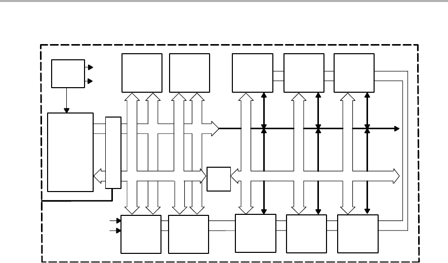
Figure 1−1. MSP430 Architecture
ACLK
Bus
Conv.
Peripheral
MAB 16-Bit
MDB 16-Bit
MCLK
SMCLK
Clock
System
Peripheral Peripheral
Peripheral
Peripheral Peripheral Peripheral
Watchdog
RAM
Flash/
RISC CPU
16-Bit
JTAG/Debug
ACLK
SMCLK
ROM
MDB 8-Bit
JTAG
1.3 Embedded Emulation
Dedicated embedded emulation logic resides on the device itself and is
accessed via JTAG using no additional system resources.
The benefits of embedded emulation include:
-Unobtrusive development and debug with full-speed execution,
breakpoints, and single-steps in an application are supported.
-Development is in-system subject to the same characteristics as the final
application.
-Mixed-signal integrity is preserved and not subject to cabling interference.
Address Space
1-4 Introduction
1.4 Address Space
The MSP430 von-Neumann architecture has one address space shared with
special function registers (SFRs), peripherals, RAM, and Flash/ROM memory
as shown in Figure 1−2. See the device-specific data sheets for specific
memory maps. Code access are always performed on even addresses. Data
can be accessed as bytes or words.
The addressable memory space is currently 128 KB.
Figure 1−2. Memory Map
0FFE0h
Interrupt Vector Table
Flash/ROM
RAM
16-Bit Peripheral Modules
8-Bit Peripheral Modules
Special Function Registers
0FFFFh
0FFDFh
0200h
01FFh
0100h
0FFh
010h
0Fh
0h
Word/Byte
Word/Byte
Word
Byte
Byte
Word/Byte
10000h
Flash/ROM
1FFFFh
Access
Word/Byte
1.4.1 Flash/ROM
The start address of Flash/ROM depends on the amount of Flash/ROM
present and varies by device. The end address for Flash/ROM is 0x1FFFF.
Flash can be used for both code and data. Word or byte tables can be stored
and used in Flash/ROM without the need to copy the tables to RAM before
using them.
The interrupt vector table is mapped into the upper 16 words of Flash/ROM
address space, with the highest priority interrupt vector at the highest
Flash/ROM word address (0x1FFFF).

Address Space
1-5
Introduction
1.4.2 RAM
RAM starts at 0200h. The end address of RAM depends on the amount of RAM
present and varies by device. RAM can be used for both code and data.
1.4.3 Peripheral Modules
Peripheral modules are mapped into the address space. The address space
from 0100 to 01FFh is reserved for 16-bit peripheral modules. These modules
should be accessed with word instructions. If byte instructions are used, only
even addresses are permissible, and the high byte of the result is always 0.
The address space from 010h to 0FFh is reserved for 8-bit peripheral modules.
These modules should be accessed with byte instructions. Read access of
byte modules using word instructions results in unpredictable data in the high
byte. If word data is written to a byte module only the low byte is written into
the peripheral register, ignoring the high byte.
1.4.4 Special Function Registers (SFRs)
Some peripheral functions are configured in the SFRs. The SFRs are located
in the lower 16 bytes of the address space, and are organized by byte. SFRs
must be accessed using byte instructions only. See the device-specific data
sheets for applicable SFR bits.
1.4.5 Memory Organization
Bytes are located at even or odd addresses. Words are only located at even
addresses as shown in Figure 1−3. When using word instructions, only even
addresses may be used. The low byte of a word is always an even address.
The high byte is at the next odd address. For example, if a data word is located
at address xxx4h, then the low byte of that data word is located at address
xxx4h, and the high byte of that word is located at address xxx5h.
Address Space
1-6 Introduction
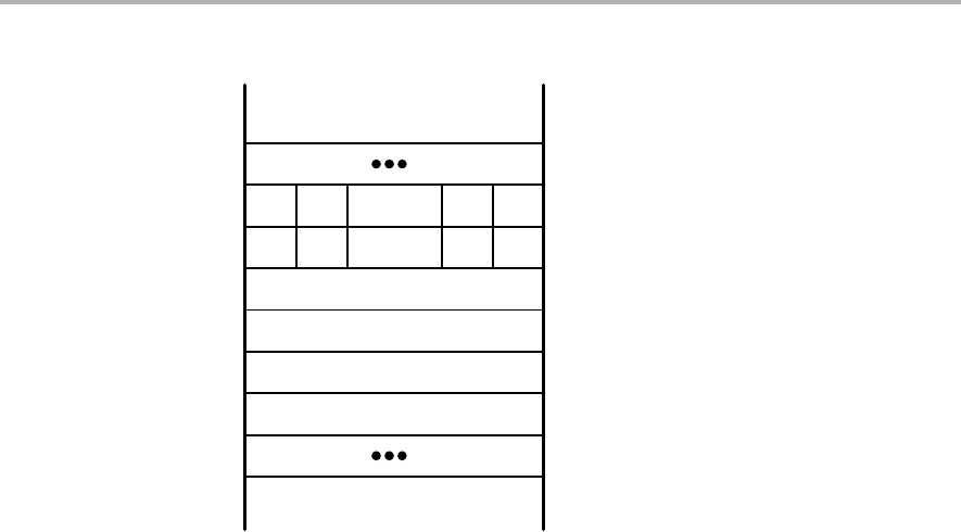
Figure 1−3. Bits, Bytes, and Words in a Byte-Organized Memory
15
7
14
6
. . Bits . .
. . Bits . .
9
1
8
0
Byte
Byte
Word (High Byte)
Word (Low Byte)
xxxAh
xxx9h
xxx8h
xxx7h
xxx6h
xxx5h
xxx4h
xxx3h

Address Space
1-7
Introduction
1.5 MSP430x2xx Family Enhancements
Table 1−1 highlights enhancements made to the MSP430x2xx family. The
enhancements are discussed fully in the following chapters, or in the case of
improved device parameters, shown in the device-specific data sheet.
Table 1−1. MSP430x2xx Family Enhancements
Subject Enhancement
Reset − Brownout reset is included on all MSP430x2xx devices.
− PORIFG and RSTIFG flags have been added to IFG1 to indicate
the cause of a reset.
− An instruction fetch from the address range 0x0000 − 0x01FF
will reset the device.
Watchdog
Timer
− All MSP430x2xx devices integrate the Watchdog Timer+
module (WDT+). The WDT+ ensures the clock source for the
timer is never disabled.
Basic Clock
System
− The LFXT1 oscillator has selectable load capacitors in LF mode.
− The LFXT1 supports up to 16-MHz crystals in HF mode.
− The LFXT1 includes oscillator fault detection in LF mode.
− The XIN and XOUT pins are shared function pins on 20- and
28-pin devices.
− The external ROSC feature of the DCO not supported on some
devices. Software should not set the LSB of the BCSCTL2
register in this case. See the device-specific data sheet for
details.
− The DCO operating frequency has been significantly increased.
− The DCO temperature stability has been significantly improved.
Flash Memory − The information memory has 4 segments of 64 bytes each.
− SegmentA is individually locked with the LOCKA bit.
− All information if protected from mass erase with the LOCKA bit.
− Segment erases can be interrupted by an interrupt.
− Flash updates can be aborted by an interrupt.
− Flash programming voltage has been lowered to 2.2 V
− Program/erase time has been reduced.
− Clock failure aborts a flash update.
Digital I/O − All ports have integrated pullup/pulldown resistors.
− P2.6 and P2.7 functions have been added to 20- and 28- pin
devices. These are shared functions with XIN and XOUT.
Software must not clear the P2SELx bits for these pins if crystal
operation is required.
Comparator_A − Comparator_A has expanded input capability with a new input
multiplexer.
Low Power − Typical LPM3 current consumption has been reduced almost
50% at 3 V.
− DCO startup time has been significantly reduced.
Operating
frequency
− The maximum operating frequency is 16 MHz at 3.3 V.
BSL − An incorrect password causes a mass erase.
− BSL entry sequence is more robust to prevent accidental entry
and erasure.

1-8 Introduction

2-1
System Resets, Interrupts, and Operating Modes
System Resets, Interrupts,
and Operating Modes
This chapter describes the MSP430x2xx system resets, interrupts, and
operating modes.
Topic Page
2.1 System Reset and Initialization 2-2. . . . . . . . . . . . . . . . . . . . . . . . . . . . . . . . .
2.2 Interrupts 2-5. . . . . . . . . . . . . . . . . . . . . . . . . . . . . . . . . . . . . . . . . . . . . . . . . . . . .
2.3 Operating Modes 2-14. . . . . . . . . . . . . . . . . . . . . . . . . . . . . . . . . . . . . . . . . . . . .
2.4 Principles for Low-Power Applications 2-17. . . . . . . . . . . . . . . . . . . . . . . . .
2.5 Connection of Unused Pins 2-17. . . . . . . . . . . . . . . . . . . . . . . . . . . . . . . . . . . .
Chapter 2
System Reset and Initialization
2-2 System Resets, Interrupts, and Operating Modes
2.1 System Reset and Initialization
The system reset circuitry shown in Figure 2−1 sources both a power-on reset
(POR) and a power-up clear (PUC) signal. Different events trigger these reset
signals and different initial conditions exist depending on which signal was
generated.
Figure 2−1. Power-On Reset and Power-Up Clear Schematic
POR
Latch
S
R
PUC
Latch
S
R
Resetwd1
Resetwd2
S
S
Delay
RST/NMI
WDTNMI†
WDTTMSEL
†
WDTQn†
WDTIFG†
EQU†
MCLK
POR
PUC
S
(from flash module)
KEYV
SVS_POR‡
0 V
VCC
0 V
Brownout
Reset
†From watchdog timer peripheral module
‡Devices with SVS only
S
Invalid instruction fetch
~50 μs
A POR is a device reset. A POR is only generated by the following three
events:
-Powering up the device
-A low signal on the RST/NMI pin when configured in the reset mode
-An SVS low condition when PORON = 1.
A PUC is always generated when a POR is generated, but a POR is not
generated by a PUC. The following events trigger a PUC:
-A POR signal
-Watchdog timer expiration when in watchdog mode only
-Watchdog timer security key violation
-A Flash memory security key violation
-A CPU instruction fetch from the peripheral address range 0h − 01FFh
System Reset and Initialization
2-3
System Resets, Interrupts, and Operating Modes
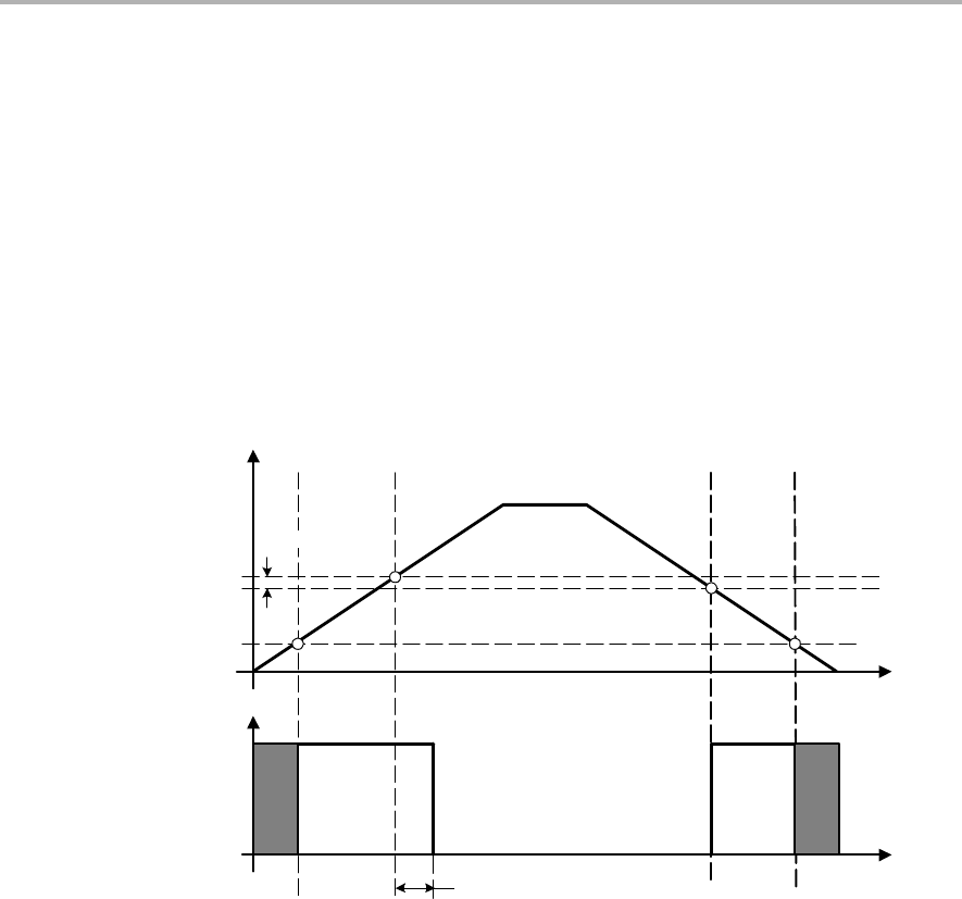
2.1.1 Brownout Reset (BOR)
The brownout reset circuit detects low supply voltages such as when a supply
voltage is applied to or removed from the VCC terminal. The brownout reset
circuit resets the device by triggering a POR signal when power is applied or
removed. The operating levels are shown in Figure 2−2.
The POR signal becomes active when VCC crosses the VCC(start) level. It
remains active until VCC crosses the V(B_IT+) threshold and the delay t(BOR)
elapses. The delay t(BOR) is adaptive being longer for a slow ramping VCC. The
hysteresis Vhys(B_ IT−) ensures that the supply voltage must drop below
V(B_IT−) to generate another POR signal from the brownout reset circuitry.
Figure 2−2. Brownout Timing
t(BOR)
VCC(start)
VCC
V(B_IT−)
Set Signal for
POR circuitry
V(B_IT+)
Vhys(B_IT−)
As the V(B_IT−) level is significantly above the Vmin level of the POR circuit, the
BOR provides a reset for power failures where VCC does not fall below Vmin.
See device-specific data sheet for parameters.

System Reset and Initialization
2-4 System Resets, Interrupts, and Operating Modes
2.1.2 Device Initial Conditions After System Reset
After a POR, the initial MSP430 conditions are:
-The RST/NMI pin is configured in the reset mode.
-I/O pins are switched to input mode as described in the Digital I/O chapter.
-Other peripheral modules and registers are initialized as described in their
respective chapters in this manual.
-Status register (SR) is reset.
-The watchdog timer powers up active in watchdog mode.
-Program counter (PC) is loaded with address contained at reset vector
location (0FFFEh). If the reset vectors content is 0FFFFh the device will
be disabled for minimum power consumption.
Software Initialization
After a system reset, user software must initialize the MSP430 for the
application requirements. The following must occur:
-Initialize the SP, typically to the top of RAM.
-Initialize the watchdog to the requirements of the application.
-Configure peripheral modules to the requirements of the application.
Additionally, the watchdog timer, oscillator fault, and flash memory flags can
be evaluated to determine the source of the reset.
System Reset and Initialization
2-5
System Resets, Interrupts, and Operating Modes
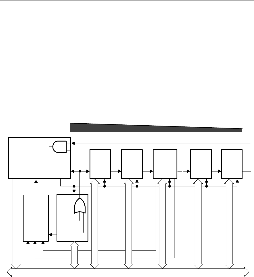
2.2 Interrupts
The interrupt priorities are fixed and defined by the arrangement of the
modules in the connection chain as shown in Figure 2−3. The nearer a module
is to the CPU/NMIRS, the higher the priority. Interrupt priorities determine what
interrupt is taken when more than one interrupt is pending simultaneously.
There are three types of interrupts:
-System reset
-(Non)-maskable NMI
-Maskable
Figure 2−3. Interrupt Priority
Bus
Grant
Module
1
Module
2
WDT
Timer
Module
m
Module
n
12 12 12 12 1
NMIRS
GIE
CPU
OSCfault
Reset/NMI
PUC
Circuit
PUC
WDT Security Key
Priority High Low
MAB − 5LSBs
GMIRS
Flash Security Key
Flash ACCV

System Reset and Initialization
2-6 System Resets, Interrupts, and Operating Modes
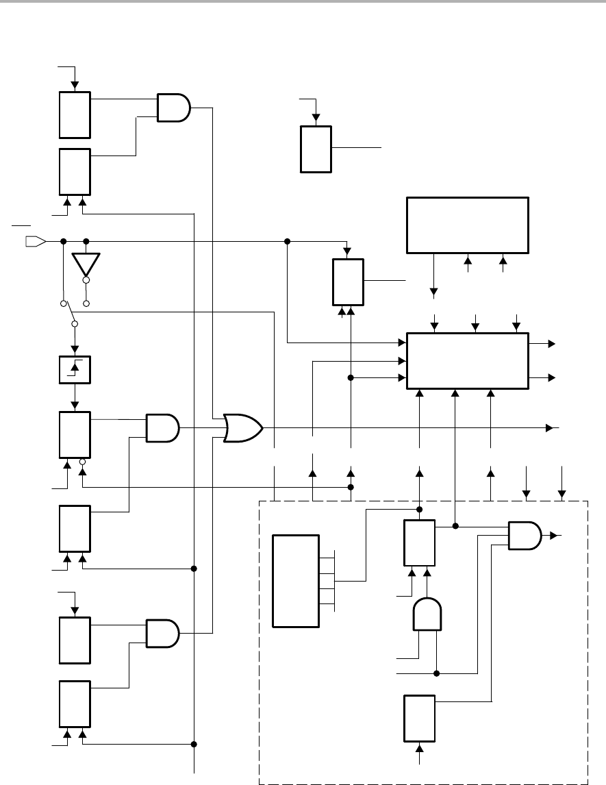
2.2.1 (Non)-Maskable Interrupts (NMI)
(Non)-maskable NMI interrupts are not masked by the general interrupt enable
bit (GIE), but are enabled by individual interrupt enable bits (NMIIE, ACCVIE,
OFIE). When a NMI interrupt is accepted, all NMI interrupt enable bits are
automatically reset. Program execution begins at the address stored in the
(non)-maskable interrupt vector, 0FFFCh. User software must set the required
NMI interrupt enable bits for the interrupt to be re-enabled. The block diagram
for NMI sources is shown in Figure 2−4.
A (non)-maskable NMI interrupt can be generated by three sources:
-An edge on the RST/NMI pin when configured in NMI mode
-An oscillator fault occurs
-An access violation to the flash memory
Reset/NMI Pin
At power-up, the RST/NMI pin is configured in the reset mode. The function
of the RST/NMI pins is selected in the watchdog control register WDTCTL. If
the RST/NMI pin is set to the reset function, the CPU is held in the reset state
as long as the RST/NMI pin is held low. After the input changes to a high state,
the CPU starts program execution at the word address stored in the reset
vector, 0FFFEh, and the RSTIFG flag is set.
If the RST/NMI pin is configured by user software to the NMI function, a signal
edge selected by the WDTNMIES bit generates an NMI interrupt if the NMIIE
bit is set. The RST/NMI flag NMIIFG is also set.
Note: Holding RST/NMI Low
When configured in the NMI mode, a signal generating an NMI event should
not hold the RST/NMI pin low. If a PUC occurs from a different source while
the NMI signal is low, the device will be held in the reset state because a PUC
changes the RST/NMI pin to the reset function.
Note: Modifying WDTNMIES
When NMI mode is selected and the WDTNMIES bit is changed, an NMI can
be generated, depending on the actual level at the RST/NMI pin. When the
NMI edge select bit is changed before selecting the NMI mode, no NMI is
generated.
System Reset and Initialization
2-7
System Resets, Interrupts, and Operating Modes
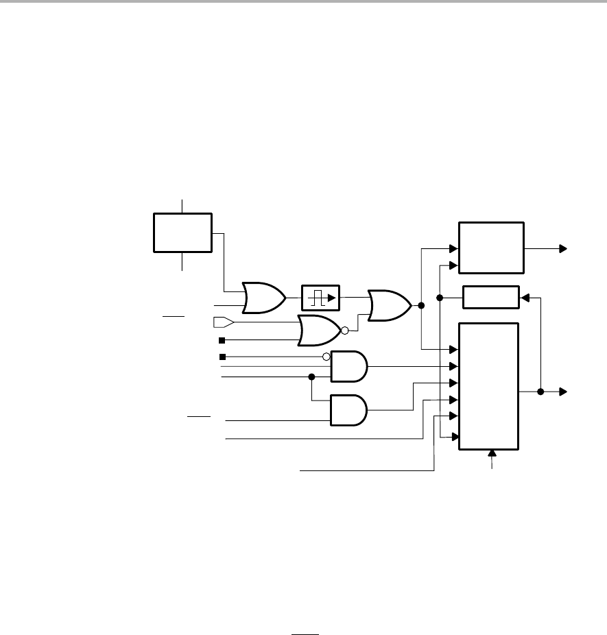
Figure 2−4. Block Diagram of (Non)-Maskable Interrupt Sources
Flash Module
KEYV
System Reset
Generator
BOR
POR PUC
WDTQn EQU
PUC
POR
PUC POR
NMIRS
Clear
SWDTIFG
IRQ
WDTIE
Clear
IE1.0
PUC
POR
IRQA
WDTTMSEL
Counter
IFG1.0
WDTNMI
WDTTMSEL
WDTNMIES
Watchdog Timer Module
Clear
S
IFG1.4
PUC
Clear
IE1.4
PUC
NMIIFG
NMIIE
S
IFG1.1
Clear
IE1.1
PUC
OFIFG
OFIE
OSCFault
NMI_IRQA
IRQA: Interrupt Request Accepted
RST/NMI
S
FCTL3.2
Clear
IE1.5
ACCVIFG
ACCVIE
PUC
ACCV
WDT
S
IFG1.2
POR
PORIFG
Clear
S
IFG1.3
RSTIFG
POR
SVS_POR

System Reset and Initialization
2-8 System Resets, Interrupts, and Operating Modes
Flash Access Violation
The flash ACCVIFG flag is set when a flash access violation occurs. The flash
access violation can be enabled to generate an NMI interrupt by setting the
ACCVIE bit. The ACCVIFG flag can then be tested by NMI the interrupt service
routine to determine if the NMI was caused by a flash access violation.
Oscillator Fault
The oscillator fault signal warns of a possible error condition with the crystal
oscillator. The oscillator fault can be enabled to generate an NMI interrupt by
setting the OFIE bit. The OFIFG flag can then be tested by NMI the interrupt
service routine to determine if the NMI was caused by an oscillator fault.
A PUC signal can trigger an oscillator fault, because the PUC switches the
LFXT1 to LF mode, therefore switching off the HF mode. The PUC signal also
switches off the XT2 oscillator.
System Reset and Initialization
2-9
System Resets, Interrupts, and Operating Modes
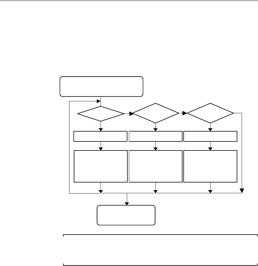
Example of an NMI Interrupt Handler
The NMI interrupt is a multiple-source interrupt. An NMI interrupt automatically
resets the NMIIE, OFIE and ACCVIE interrupt-enable bits. The user NMI
service routine resets the interrupt flags and re-enables the interrupt-enable
bits according to the application needs as shown in Figure 2−5.
Figure 2−5. NMI Interrupt Handler
yes
no
OFIFG=1
yes
no
ACCVIFG=1
yes
Reset ACCVIFG
no
NMIIFG=1
Reset NMIIFGReset OFIFG
Start of NMI Interrupt Handler
Reset by HW:
OFIE, NMIIE, ACCVIE
User’s Software,
Oscillator Fault
Handler
User’s Software,
Flash Access
Violation Handler
User’s Software,
External NMI
Handler
Optional
RETI
End of NMI Interrupt
Handler
Note: Enabling NMI Interrupts with ACCVIE, NMIIE, and OFIE
To prevent nested NMI interrupts, the ACCVIE, NMIIE, and OFIE enable bits
should not be set inside of an NMI interrupt service routine.
2.2.2 Maskable Interrupts
Maskable interrupts are caused by peripherals with interrupt capability
including the watchdog timer overflow in interval-timer mode. Each maskable
interrupt source can be disabled individually by an interrupt enable bit, or all
maskable interrupts can be disabled by the general interrupt enable (GIE) bit
in the status register (SR).
Each individual peripheral interrupt is discussed in the associated peripheral
module chapter in this manual.

System Reset and Initialization
2-10 System Resets, Interrupts, and Operating Modes
2.2.3 Interrupt Processing
When an interrupt is requested from a peripheral and the peripheral interrupt
enable bit and GIE bit are set, the interrupt service routine is requested. Only
the individual enable bit must be set for (non)-maskable interrupts to be
requested.
Interrupt Acceptance
The interrupt latency is 5 cycles (CPUx) or 6 cycles (CPU), starting with the
acceptance of an interrupt request, and lasting until the start of execution of
the first instruction of the interrupt-service routine, as shown in Figure 2−6.
The interrupt logic executes the following:
1) Any currently executing instruction is completed.
2) The PC, which points to the next instruction, is pushed onto the stack.
3) The SR is pushed onto the stack.
4) The interrupt with the highest priority is selected if multiple interrupts
occurred during the last instruction and are pending for service.
5) The interrupt request flag resets automatically on single-source flags.
Multiple source flags remain set for servicing by software.
6) The SR is cleared. This terminates any low-power mode. Because the GIE
bit is cleared, further interrupts are disabled.
7) The content of the interrupt vector is loaded into the PC: the program
continues with the interrupt service routine at that address.
Figure 2−6. Interrupt Processing
Item1
Item2
SP TOS
Item1
Item2
SP TOS
PC
SR
Before
Interrupt
After
Interrupt
System Reset and Initialization
2-11
System Resets, Interrupts, and Operating Modes
Return From Interrupt
The interrupt handling routine terminates with the instruction:
RETI (return from an interrupt service routine)
The return from the interrupt takes 5 cycles (CPU) or 3 cycles (CPUx) to
execute the following actions and is illustrated in Figure 2−7.
1) The SR with all previous settings pops from the stack. All previous settings
of GIE, CPUOFF, etc. are now in effect, regardless of the settings used
during the interrupt service routine.
2) The PC pops from the stack and begins execution at the point where it was
interrupted.
Figure 2−7. Return From Interrupt
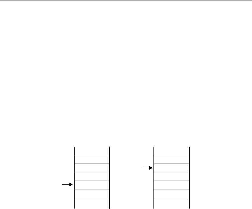
Item1
Item2
SP TOS
Item1
Item2
SP TOS
PC
SR
Before After
PC
SR
Return From Interrupt
Interrupt Nesting
Interrupt nesting is enabled if the GIE bit is set inside an interrupt service
routine. When interrupt nesting is enabled, any interrupt occurring during an
interrupt service routine will interrupt the routine, regardless of the interrupt
priorities.

System Reset and Initialization
2-12 System Resets, Interrupts, and Operating Modes
2.2.4 Interrupt Vectors
The interrupt vectors and the power-up starting address are located in the
address range 0FFFFh to 0FFC0h, as described in Table 2−1. A vector is
programmed by the user with the 16-bit address of the corresponding interrupt
service routine. See the device-specific data sheet for the complete interrupt
vector list.
It is recommended to provide an interrupt service routine for each interrupt
vector that is assigned to a module. A dummy interrupt service routine can
consist of just the RETI instruction and several interrupt vectors can point to
it.
Unassigned interrupt vectors can be used for regular program code if
necessary.
Some module enable bits, interrupt enable bits, and interrupt flags are located
in the SFRs. The SFRs are located in the lower address range and are
implemented in byte format. SFRs must be accessed using byte instructions.
See the device-specific data sheet for the SFR configuration.

System Reset and Initialization
2-13
System Resets, Interrupts, and Operating Modes
Table 2−1. Interrupt Sources,Flags, and Vectors
INTERRUPT SOURCE INTERRUPT FLAG SYSTEM
INTERRUPT
WORD
ADDRESS PRIORITY
Power-up, external
reset, watchdog,
flash password,
illegal instruction
fetch
PORIFG
RSTIFG
WDTIFG
KEYV
Reset 0FFFEh 31, highest
NMI, oscillator fault,
flash memory access
violation
NMIIFG
OFIFG
ACCVIFG
(non)-maskable
(non)-maskable
(non)-maskable
0FFFCh 30
device-specific 0FFFAh 29
device-specific 0FFF8h 28
device-specific 0FFF6h 27
Watchdog timer WDTIFG maskable 0FFF4h 26
device-specific 0FFF2h 25
device-specific 0FFF0h 24
device-specific 0FFEEh 23
device-specific 0FFECh 22
device-specific 0FFEAh 21
device-specific 0FFE8h 20
device-specific 0FFE6h 19
device-specific 0FFE4h 18
device-specific 0FFE2h 17
device-specific 0FFE0h 16
device-specific 0FFDEh 15
device-specific 0FFDCh 14
device-specific 0FFDAh 13
device-specific 0FFD8h 12
device-specific 0FFD6h 11
device-specific 0FFD4h 10
device-specific 0FFD2h 9
device-specific 0FFD0h 8
device-specific 0FFCEh 7
device-specific 0FFCCh 6
device-specific 0FFCAh 5
device-specific 0FFC8h 4
device-specific 0FFC6h 3
device-specific 0FFC4h 2
device-specific 0FFC2h 1
device-specific 0FFC0h 0, lowest
Operating Modes
2-14 System Resets, Interrupts, and Operating Modes
2.3 Operating Modes
The MSP430 family is designed for ultralow-power applications and uses
different operating modes shown in Figure 2−9.
The operating modes take into account three different needs:
-Ultralow-power
-Speed and data throughput
-Minimization of individual peripheral current consumption
The MSP430 typical current consumption is shown in Figure 2−8.
Figure 2−8. Typical Current Consumption of 21x1 Devices vs Operating Modes
315
AM
300
270
225
180
135
90
45
0LPM0 LPM2 LPM3 LPM4
200
55 32
17 11 0.9 0.7 0.1 0.1
VCC = 3 V
VCC = 2.2 V
Operating Modes
ICC/μA at 1 MHz
The low-power modes 0 to 4 are configured with the CPUOFF, OSCOFF,
SCG0, and SCG1 bits in the status register The advantage of including the
CPUOFF, OSCOFF, SCG0, and SCG1 mode-control bits in the status register
is that the present operating mode is saved onto the stack during an interrupt
service routine. Program flow returns to the previous operating mode if the
saved SR value is not altered during the interrupt service routine. Program flow
can be returned to a different operating mode by manipulating the saved SR
value on the stack inside of the interrupt service routine. The mode-control bits
and the stack can be accessed with any instruction.
When setting any of the mode-control bits, the selected operating mode takes
effect immediately. Peripherals operating with any disabled clock are disabled
until the clock becomes active. The peripherals may also be disabled with their
individual control register settings. All I/O port pins and RAM/registers are
unchanged. Wake up is possible through all enabled interrupts.
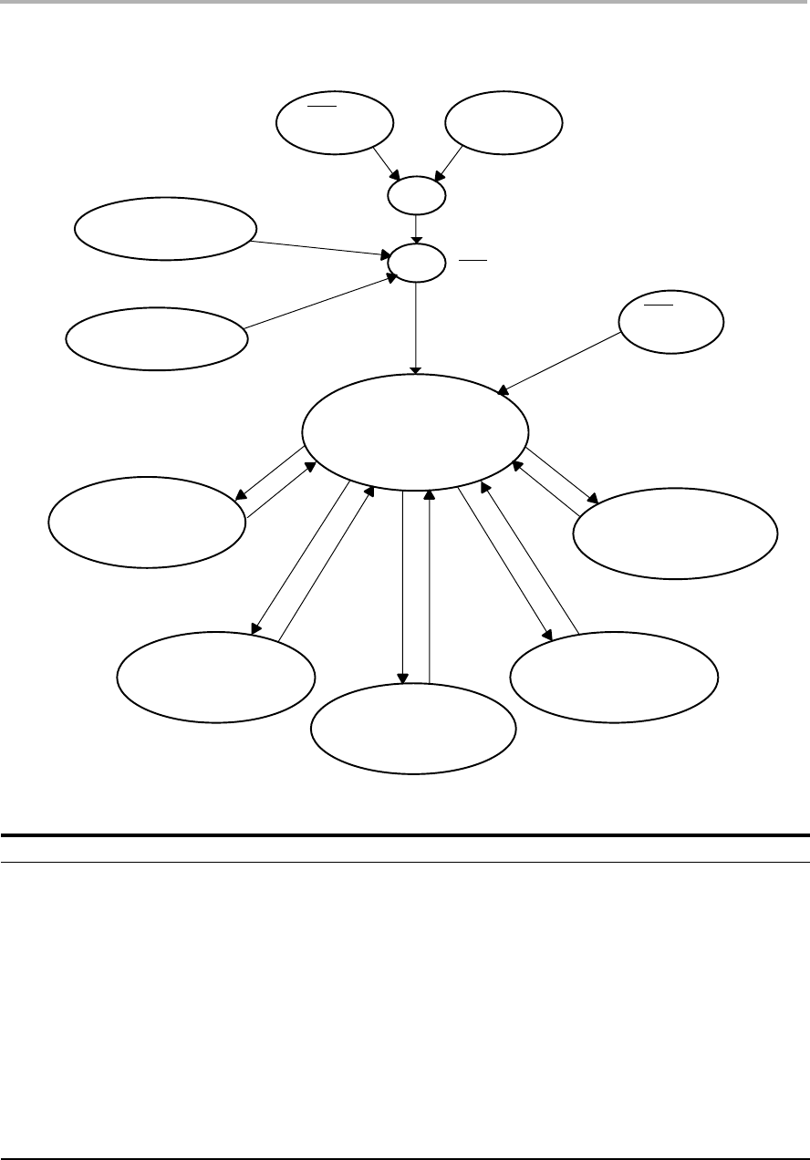
Operating Modes
2-15
System Resets, Interrupts, and Operating Modes
Figure 2−9. MSP430x2xx Operating Modes For Basic Clock System
Active Mode
CPU Is Active
Peripheral Modules Are Active
LPM0
CPU Off, MCLK Off,
SMCLK On, ACLK On
CPUOFF = 1
SCG0 = 0
SCG1 = 0
CPUOFF = 1
SCG0 = 1
SCG1 = 0
LPM2
CPU Off, MCLK Off, SMCLK
Off, DCO Off, ACLK On
CPUOFF = 1
SCG0 = 0
SCG1 = 1 LPM3
CPU Off, MCLK Off, SMCLK
Off, DCO Off, ACLK On
DC Generator Off
LPM4
CPU Off, MCLK Off, DCO
Off, SMCLK Off,
ACLK Off
DC Generator Off
CPUOFF = 1
OSCOFF = 1
SCG0 = 1
SCG1 = 1
RST/NMI
NMI Active
PUC RST/NMI is Reset Pin
WDT is Active
POR
WDT Active,
Security Key Violation
WDT
Time Expired, Overflow WDTIFG = 1
WDTIFG = 1
RST/NMI
Reset Active SVS_POR
WDTIFG = 0
LPM1
CPU Off, MCLK Off,
DCO off, SMCLK On,
ACLK On
DC Generator Off if DCO
not used for SMCLK
CPUOFF = 1
SCG0 = 1
SCG1 = 1
SCG1 SCG0 OSCOFF CPUOFF Mode CPU and Clocks Status
0 0 0 0 Active CPU is active, all enabled clocks are active
0 0 0 1 LPM0 CPU, MCLK are disabled
SMCLK , ACLK are active
0 1 0 1 LPM1 CPU, MCLK are disabled, DCO and DC generator
are disabled if the DCO is not used for SMCLK.
ACLK is active
1 0 0 1 LPM2 CPU, MCLK, SMCLK, DCO are disabled
DC generator remains enabled
ACLK is active
1 1 0 1 LPM3 CPU, MCLK, SMCLK, DCO are disabled
DC generator disabled
ACLK is active
11 1 1 LPM4 CPU and all clocks disabled

Operating Modes
2-16 System Resets, Interrupts, and Operating Modes
2.3.1 Entering and Exiting Low-Power Modes
An enabled interrupt event wakes the MSP430 from any of the low-power
operating modes. The program flow is:
-Enter interrupt service routine:
JThe PC and SR are stored on the stack
JThe CPUOFF, SCG1, and OSCOFF bits are automatically reset
-Options for returning from the interrupt service routine:
JThe original SR is popped from the stack, restoring the previous
operating mode.
JThe SR bits stored on the stack can be modified within the interrupt
service routine returning to a different operating mode when the RETI
instruction is executed.
; Enter LPM0 Example
BIS #GIE+CPUOFF,SR ; Enter LPM0
; ... ; Program stops here
;
; Exit LPM0 Interrupt Service Routine
BIC #CPUOFF,0(SP) ; Exit LPM0 on RETI
RETI
; Enter LPM3 Example
BIS #GIE+CPUOFF+SCG1+SCG0,SR ; Enter LPM3
; ... ; Program stops here
;
; Exit LPM3 Interrupt Service Routine
BIC #CPUOFF+SCG1+SCG0,0(SR) ; Exit LPM3 on RETI
RETI

Principles for Low-Power Applications
2-17
System Resets, Interrupts, and Operating Modes
2.4 Principles for Low-Power Applications
Often, the most important factor for reducing power consumption is using the
MSP430’s clock system to maximize the time in LPM3. LPM3 power
consumption is less than 2 μA typical with both a real-time clock function and
all interrupts active. A 32-kHz watch crystal is used for the ACLK and the CPU
is clocked from the DCO (normally off) which has a 6-μs wake-up.
-Use interrupts to wake the processor and control program flow.
-Peripherals should be switched on only when needed.
-Use low-power integrated peripheral modules in place of software driven
functions. For example Timer_A and Timer_B can automatically generate
PWM and capture external timing, with no CPU resources.
-Calculated branching and fast table look-ups should be used in place of
flag polling and long software calculations.
-Avoid frequent subroutine and function calls due to overhead.
-For longer software routines, single-cycle CPU registers should be used.
2.5 Connection of Unused Pins
The correct termination of all unused pins is listed in Table 2−2.
Table 2−2. Connection of Unused Pins
Pin Potential Comment
AVCC DVCC
AVSS DVSS
VREF+ Open
VeREF+ DVSS
VREF−/VeREF− DVSS
XIN DVCC
XOUT Open
XT2IN DVSS
XT2OUT Open
Px.0 to Px.7 Open Switched to port function, output direction
or input with pullup/pulldown enabled
RST/NMI DVCC or VCC 47 kΩ pullup with 10 nF (2.2 nF†) pulldown
Test Open 20xx, 21xx, 22xx devices
TDO Open
TDI Open
TMS Open
TCK Open
†The pulldown capacitor should not exceed 2.2 nF when using devices with Spy-Bi-Wire
interface in Spy-Bi-Wire mode or in 4-wire JTAG mode with TI tools like FET interfaces or
GANG programmers.

2-18 System Resets, Interrupts, and Operating Modes

3-1
RISC 16-Bit CPU
RISC 16-Bit CPU
This chapter describes the MSP430 CPU, addressing modes, and
instruction set.
Topic Page
3.1 CPU Introduction 3-2. . . . . . . . . . . . . . . . . . . . . . . . . . . . . . . . . . . . . . . . . . . . . .
3.2 CPU Registers 3-4. . . . . . . . . . . . . . . . . . . . . . . . . . . . . . . . . . . . . . . . . . . . . . . . .
3.3 Addressing Modes 3-9. . . . . . . . . . . . . . . . . . . . . . . . . . . . . . . . . . . . . . . . . . . . .
3.4 Instruction Set 3-17. . . . . . . . . . . . . . . . . . . . . . . . . . . . . . . . . . . . . . . . . . . . . . . .
Chapter 3

CPU Introduction
3-2 RISC 16-Bit CPU
3.1 CPU Introduction
The CPU incorporates features specifically designed for modern
programming techniques such as calculated branching, table processing and
the use of high-level languages such as C. The CPU can address the complete
address range without paging.
The CPU features include:
-RISC architecture with 27 instructions and 7 addressing modes
-Orthogonal architecture with every instruction usable with every
addressing mode
-Full register access including program counter, status registers, and stack
pointer
-Single-cycle register operations
-Large 16-bit register file reduces fetches to memory
-16-bit address bus allows direct access and branching throughout entire
memory range
-16-bit data bus allows direct manipulation of word-wide arguments
-Constant generator provides six most used immediate values and
reduces code size
-Direct memory-to-memory transfers without intermediate register holding
-Word and byte addressing and instruction formats
The block diagram of the CPU is shown in Figure 3−1.
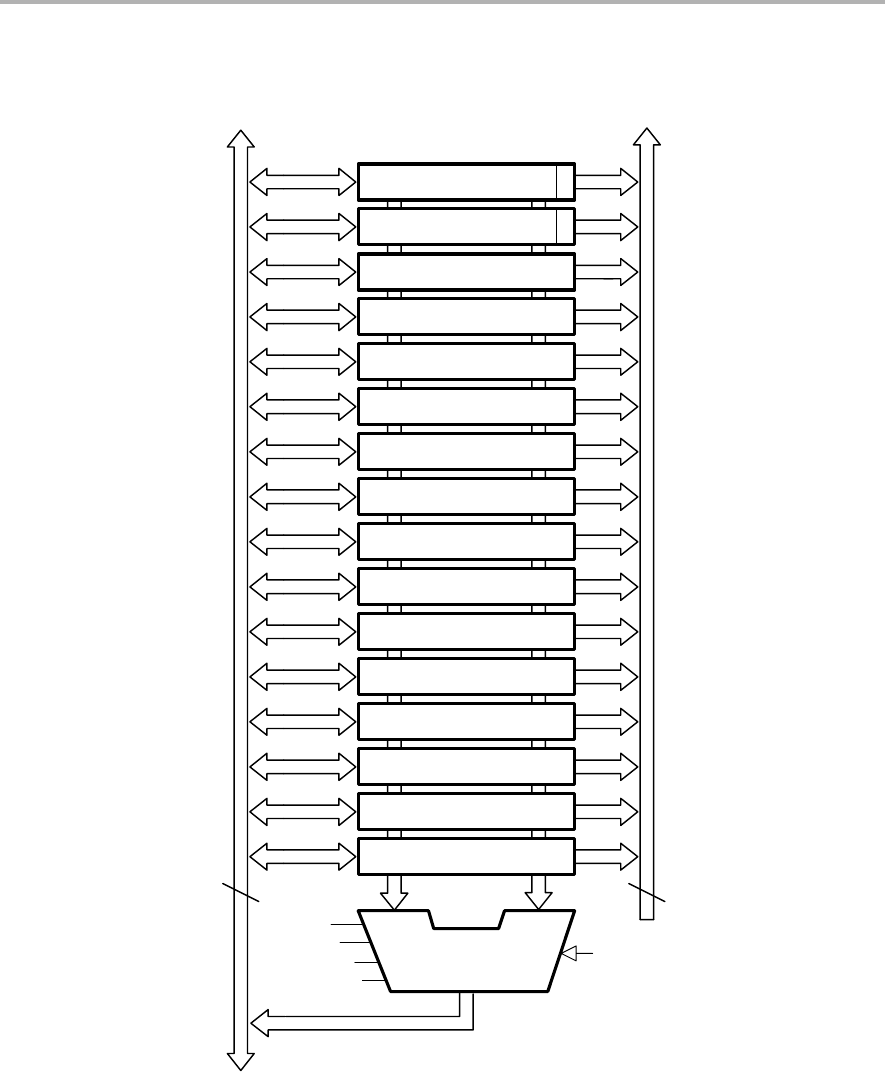
CPU Introduction
3-3
RISC 16-Bit CPU
Figure 3−1. CPU Block Diagram
015
MDB − Memory Data Bus Memory Address Bus − MAB
16
Zero, Z
Carry, C
Overflow, V
Negative, N
16−bit ALU
dst src
R8 General Purpose
R9 General Purpose
R10 General Purpose
R11 General Purpose
R12 General Purpose
R13 General Purpose
R14 General Purpose
R15 General Purpose
R4 General Purpose
R5 General Purpose
R6 General Purpose
R7 General Purpose
R3/CG2 Constant Generator
R2/SR/CG1 Status
R1/SP Stack Pointer
R0/PC Program Counter 0
0
16
MCLK

CPU Registers
3-4 RISC 16-Bit CPU
3.2 CPU Registers
The CPU incorporates sixteen 16-bit registers. R0, R1, R2 and R3 have
dedicated functions. R4 to R15 are working registers for general use.
3.2.1 Program Counter (PC)
The 16-bit program counter (PC/R0) points to the next instruction to be
executed. Each instruction uses an even number of bytes (two, four, or six),
and the PC is incremented accordingly. Instruction accesses in the 64-KB
address space are performed on word boundaries, and the PC is aligned to
even addresses. Figure 3−2 shows the program counter.
Figure 3−2. Program Counter
0
15 0
Program Counter Bits 15 to 1
1
The PC can be addressed with all instructions and addressing modes. A few
examples:
MOV #LABEL,PC ; Branch to address LABEL
MOV LABEL,PC ; Branch to address contained in LABEL
MOV @R14,PC ; Branch indirect to address in R14
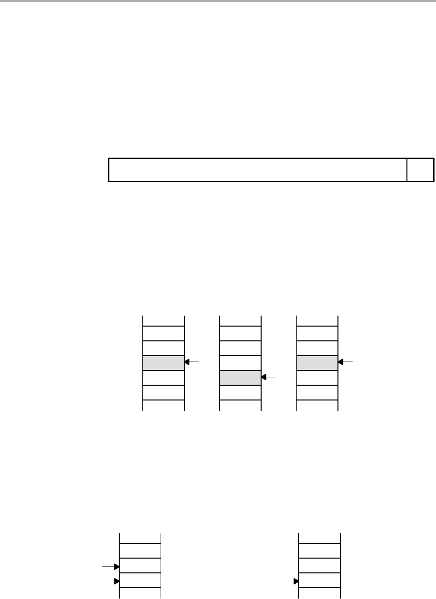
CPU Registers
3-5
RISC 16-Bit CPU
3.2.2 Stack Pointer (SP)
The stack pointer (SP/R1) is used by the CPU to store the return addresses
of subroutine calls and interrupts. It uses a predecrement, postincrement
scheme. In addition, the SP can be used by software with all instructions and
addressing modes. Figure 3−3 shows the SP. The SP is initialized into RAM
by the user, and is aligned to even addresses.
Figure 3−4 shows stack usage.
Figure 3−3. Stack Pointer
0
15 0
Stack Pointer Bits 15 to 1
1
MOV 2(SP),R6 ; Item I2 −> R6
MOV R7,0(SP) ; Overwrite TOS with R7
PUSH #0123h ; Put 0123h onto TOS
POP R8 ; R8 = 0123h
Figure 3−4. Stack Usage
I3
I1
I2
I3
0xxxh
0xxxh − 2
0xxxh − 4
0xxxh − 6
0xxxh − 8
I1
I2
SP
0123h SP
I1
I2
I3 SP
PUSH #0123h POP R8Address
0123h
The special cases of using the SP as an argument to the PUSH and POP
instructions are described and shown in Figure 3−5.
Figure 3−5. PUSH SP - POP SP Sequence
SP1
SPold
SP1
PUSH SP
The stack pointer is changed after
a PUSH SP instruction.
SP1
SP2
POP SP
The stack pointer is not changed after a POP SP
instruction. The POP SP instruction places SP1 into the
stack pointer SP (SP2=SP1)

CPU Registers
3-6 RISC 16-Bit CPU
3.2.3 Status Register (SR)
The status register (SR/R2), used as a source or destination register, can be
used in the register mode only addressed with word instructions. The remain-
ing combinations of addressing modes are used to support the constant gen-
erator. Figure 3−6 shows the SR bits.
Figure 3−6. Status Register Bits
SCG0 GIE Z C
rw
-
0
15 0
Reserved N
CPU
OFF
OSC
OFF
SCG1V
879
Table 3−1 describes the status register bits.
Table 3−1. Description of Status Register Bits
Bit Description
VOverflow bit. This bit is set when the result of an arithmetic operation
overflows the signed-variable range.
ADD(.B),ADDC(.B) Set when:
Positive + Positive = Negative
Negative + Negative = Positive,
otherwise reset
SUB(.B),SUBC(.B),CMP(.B) Set when:
Positive − Negative = Negative
Negative − Positive = Positive,
otherwise reset
SCG1 System clock generator 1. This bit, when set, turns off the SMCLK.
SCG0 System clock generator 0. This bit, when set, turns off the DCO dc
generator, if DCOCLK is not used for MCLK or SMCLK.
OSCOFF Oscillator Off. This bit, when set, turns off the LFXT1 crystal oscillator,
when LFXT1CLK is not use for MCLK or SMCLK
CPUOFF CPU off. This bit, when set, turns off the CPU.
GIE General interrupt enable. This bit, when set, enables maskable
interrupts. When reset, all maskable interrupts are disabled.
N Negative bit. This bit is set when the result of a byte or word operation
is negative and cleared when the result is not negative.
Word operation: N is set to the value of bit 15 of the
result
Byte operation: N is set to the value of bit 7 of the
result
Z Zero bit. This bit is set when the result of a byte or word operation is 0
and cleared when the result is not 0.
CCarry bit. This bit is set when the result of a byte or word operation
produced a carry and cleared when no carry occurred.

CPU Registers
3-7
RISC 16-Bit CPU
3.2.4 Constant Generator Registers CG1 and CG2
Six commonly-used constants are generated with the constant generator
registers R2 and R3, without requiring an additional 16-bit word of program
code. The constants are selected with the source-register addressing modes
(As), as described in Table 3−2.
Table 3−2. Values of Constant Generators CG1, CG2
Register As Constant Remarks
R2 00 − − − − − Register mode
R2 01 (0) Absolute address mode
R2 10 00004h +4, bit processing
R2 11 00008h +8, bit processing
R3 00 00000h 0, word processing
R3 01 00001h +1
R3 10 00002h +2, bit processing
R3 11 0FFFFh −1, word processing
The constant generator advantages are:
-No special instructions required
-No additional code word for the six constants
-No code memory access required to retrieve the constant
The assembler uses the constant generator automatically if one of the six
constants is used as an immediate source operand. Registers R2 and R3,
used in the constant mode, cannot be addressed explicitly; they act as
source-only registers.
Constant Generator − Expanded Instruction Set
The RISC instruction set of the MSP430 has only 27 instructions. However, the
constant generator allows the MSP430 assembler to support 24 additional,
emulated instructions. For example, the single-operand instruction:
CLR dst
is emulated by the double-operand instruction with the same length:
MOV R3,dst
where the #0 is replaced by the assembler, and R3 is used with As=00.
INC dst
is replaced by:
ADD 0(R3),dst
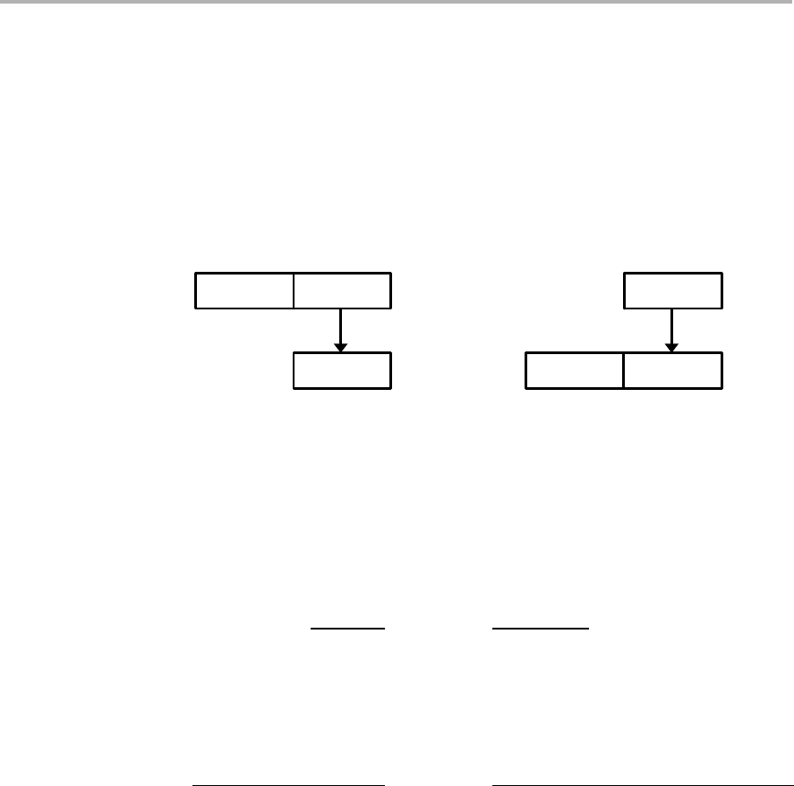
CPU Registers
3-8 RISC 16-Bit CPU
3.2.5 General-Purpose Registers R4 to R15
The twelve registers, R4 to R15, are general-purpose registers. All of these
registers can be used as data registers, address pointers, or index values and
can be accessed with byte or word instructions as shown in Figure 3−7.
Figure 3−7. Register-Byte/Byte-Register Operations
Unused
High Byte Low Byte
Byte
Register-Byte Operation
0h
High Byte Low Byte
Byte
Byte-Register Operation
Register
Memory Register
Memory
Example Register-Byte Operation Example Byte-Register Operation
R5 = 0A28Fh R5 = 01202h
R6 = 0203h R6 = 0223h
Mem(0203h) = 012h Mem(0223h) = 05Fh
ADD.B R5,0(R6) ADD.B @R6,R5
08Fh 05Fh
+ 012h + 002h
0A1h 00061h
Mem (0203h) = 0A1h R5 = 00061h
C = 0, Z = 0, N = 1 C = 0, Z = 0, N = 0
(Low byte of register) (Addressed byte)
+ (Addressed byte) + (Low byte of register)
−>(Addressed byte) −>(Low byte of register, zero to High byte)

Addressing Modes
3-9
RISC 16-Bit CPU
3.3 Addressing Modes
Seven addressing modes for the source operand and four addressing modes
for the destination operand can address the complete address space with no
exceptions. The bit numbers in Table 3−3 describe the contents of the As
(source) and Ad (destination) mode bits.
Table 3−3. Source/Destination Operand Addressing Modes
As/Ad Addressing Mode Syntax Description
00/0 Register mode Rn Register contents are operand
01/1 Indexed mode X(Rn) (Rn + X) points to the operand. X
is stored in the next word.
01/1 Symbolic mode ADDR (PC + X) points to the operand. X
is stored in the next word. Indexed
mode X(PC) is used.
01/1 Absolute mode &ADDR The word following the instruction
contains the absolute address. X
is stored in the next word. Indexed
mode X(SR) is used.
10/− Indirect register
mode
@Rn Rn is used as a pointer to the
operand.
11/− Indirect
autoincrement
@Rn+ Rn is used as a pointer to the
operand. Rn is incremented
afterwards by 1 for .B instructions
and by 2 for .W instructions.
11/− Immediate mode #N The word following the instruction
contains the immediate constant
N. Indirect autoincrement mode
@PC+ is used.
The seven addressing modes are explained in detail in the following sections.
Most of the examples show the same addressing mode for the source and
destination, but any valid combination of source and destination addressing
modes is possible in an instruction.
Note: Use of Labels EDE, TONI, TOM, and LEO
Throughout MSP430 documentation EDE, TONI, TOM, and LEO are used
as generic labels. They are only labels. They have no special meaning.
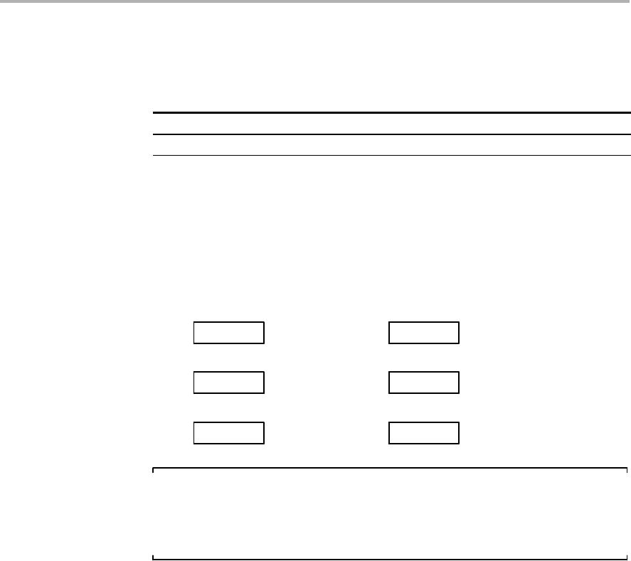
Addressing Modes
3-10 RISC 16-Bit CPU
3.3.1 Register Mode
The register mode is described in Table 3−4.
Table 3−4. Register Mode Description
Assembler Code Content of ROM
MOV R10,R11 MOV R10,R11
Length: One or two words
Operation: Move the content of R10 to R11. R10 is not affected.
Comment: Valid for source and destination
Example: MOV R10,R11
0A023hR10
R11
Before: After:
PC
0FA15h
PCold
0A023hR10
R11
PC PCold + 2
0A023h
Note: Data in Registers
The data in the register can be accessed using word or byte instructions. If
byte instructions are used, the high byte is always 0 in the result. The status
bits are handled according to the result of the byte instruction.
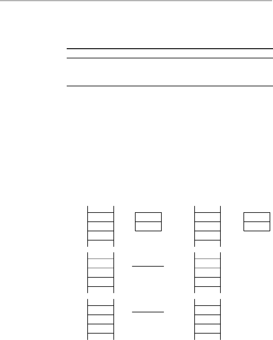
Addressing Modes
3-11
RISC 16-Bit CPU
3.3.2 Indexed Mode
The indexed mode is described in Table 3−5.
Table 3−5. Indexed Mode Description
Assembler Code Content of ROM
MOV 2(R5),6(R6) MOV X(R5),Y(R6)
X = 2
Y = 6
Length: Two or three words
Operation: Move the contents of the source address (contents of R5 + 2)
to the destination address (contents of R6 + 6). The source
and destination registers (R5 and R6) are not affected. In
indexed mode, the program counter is incremented
automatically so that program execution continues with the
next instruction.
Comment: Valid for source and destination
Example: MOV 2(R5),6(R6);
00006h
Address
Space
00002h
04596h PC
0FF16h
0FF14h
0FF12h
0xxxxh
05555h
01094h
01092h
01090h 0xxxxh
0xxxxh
01234h
01084h
01082h
01080h 0xxxxh
01080h
0108Ch
R5
R6
0108Ch
+0006h
01092h
01080h
+0002h
01082h
Register
Before:
00006h
Address
Space
00002h
04596h
PC
0FF16h
0FF14h
0FF12h
0xxxxh
01234h
01094h
01092h
01090h 0xxxxh
0xxxxh
01234h
01084h
01082h
01080h 0xxxxh
01080h
0108Ch
R5
R6
Register
After:
0xxxxh
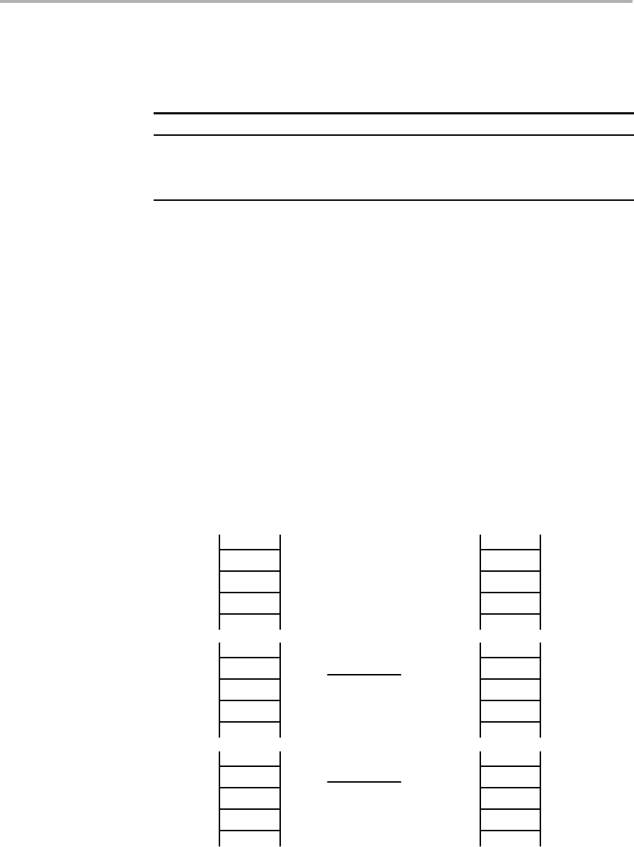
Addressing Modes
3-12 RISC 16-Bit CPU
3.3.3 Symbolic Mode
The symbolic mode is described in Table 3−6.
Table 3−6. Symbolic Mode Description
Assembler Code Content of ROM
MOV EDE,TONI MOV X(PC),Y(PC)
X = EDE − PC
Y = TONI − PC
Length: Two or three words
Operation: Move the contents of the source address EDE (contents of
PC + X) to the destination address TONI (contents of PC + Y).
The words after the instruction contain the differences
between the PC and the source or destination addresses.
The assembler computes and inserts offsets X and Y
automatically. With symbolic mode, the program counter (PC)
is incremented automatically so that program execution
continues with the next instruction.
Comment: Valid for source and destination
Example: MOV EDE,TONI ;Source address EDE = 0F016h
;Dest. address TONI=01114h
011FEh
Address
Space
0F102h
04090h PC
0FF16h
0FF14h
0FF12h
0xxxxh
0A123h
0F018h
0F016h
0F014h 0xxxxh
0xxxxh
05555h
01116h
01114h
01112h 0xxxxh
0FF14h
+0F102h
0F016h
0FF16h
+011FEh
01114h
Register
Before:
011FEh
Address
Space
0F102h
04090h
PC
0FF16h
0FF14h
0FF12h
0xxxxh
0A123h
0F018h
0F016h
0F014h 0xxxxh
0xxxxh
0A123h
01116h
01114h
01112h 0xxxxh
Register
After:
0xxxxh
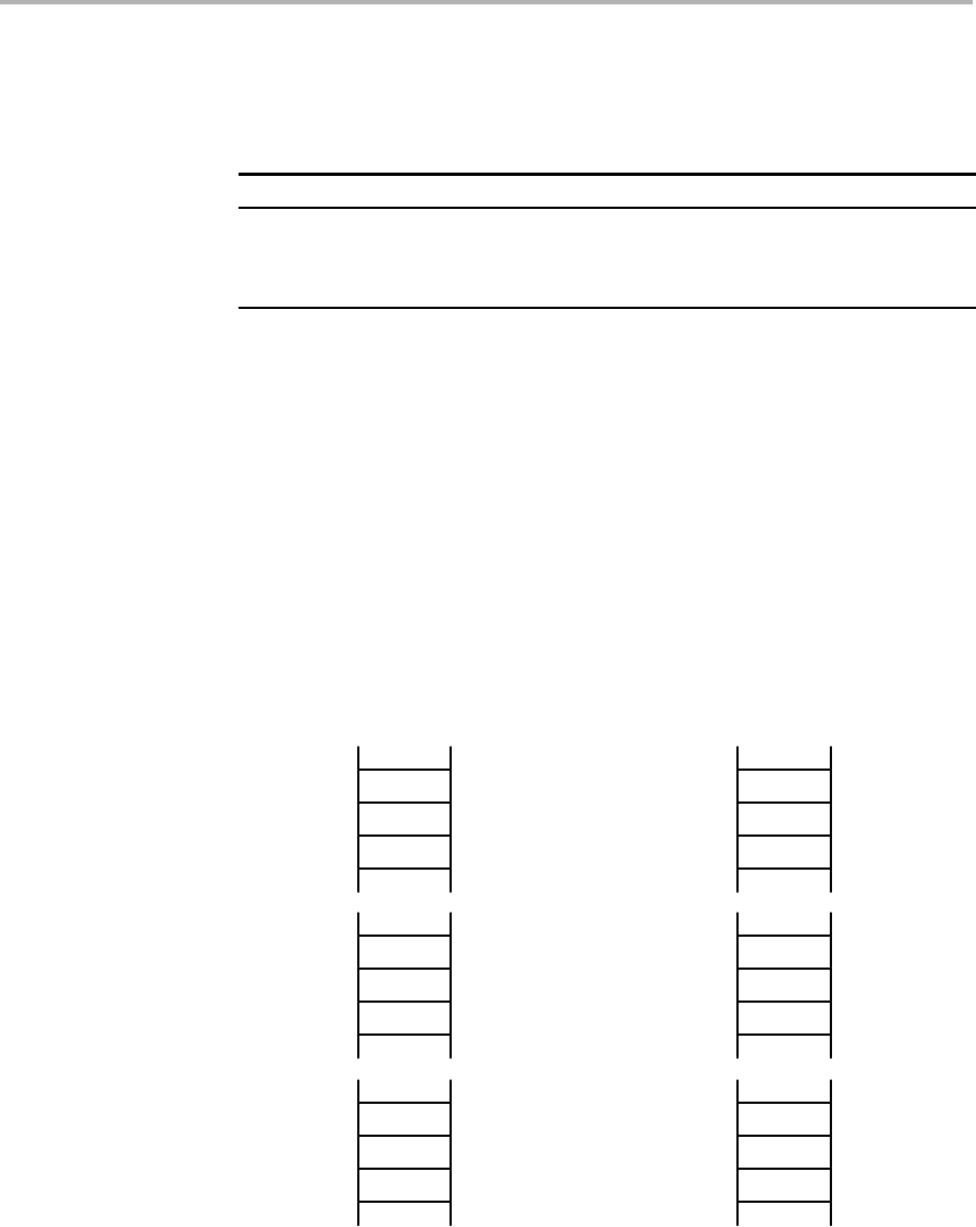
Addressing Modes
3-13
RISC 16-Bit CPU
3.3.4 Absolute Mode
The absolute mode is described in Table 3−7.
Table 3−7. Absolute Mode Description
Assembler Code Content of ROM
MOV &EDE,&TONI MOV X(0),Y(0)
X = EDE
Y = TONI
Length: Two or three words
Operation: Move the contents of the source address EDE to the
destination address TONI. The words after the instruction
contain the absolute address of the source and destination
addresses. With absolute mode, the PC is incremented
automatically so that program execution continues with the
next instruction.
Comment: Valid for source and destination
Example: MOV &EDE,&TONI ;Source address EDE=0F016h,
;dest. address TONI=01114h
01114h
Address
Space
0F016h
04292h PC
0FF16h
0FF14h
0FF12h
0xxxxh
0A123h
0F018h
0F016h
0F014h 0xxxxh
0xxxxh
01234h
01116h
01114h
01112h 0xxxxh
Register
Before:
01114h
Address
Space
0F016h
04292h
PC
0FF16h
0FF14h
0FF12h
0xxxxh
0A123h
0F018h
0F016h
0F014h 0xxxxh
0xxxxh
0A123h
01116h
01114h
01112h 0xxxxh
Register
After:
0xxxxh
This address mode is mainly for hardware peripheral modules that are located
at an absolute, fixed address. These are addressed with absolute mode to
ensure software transportability (for example, position-independent code).
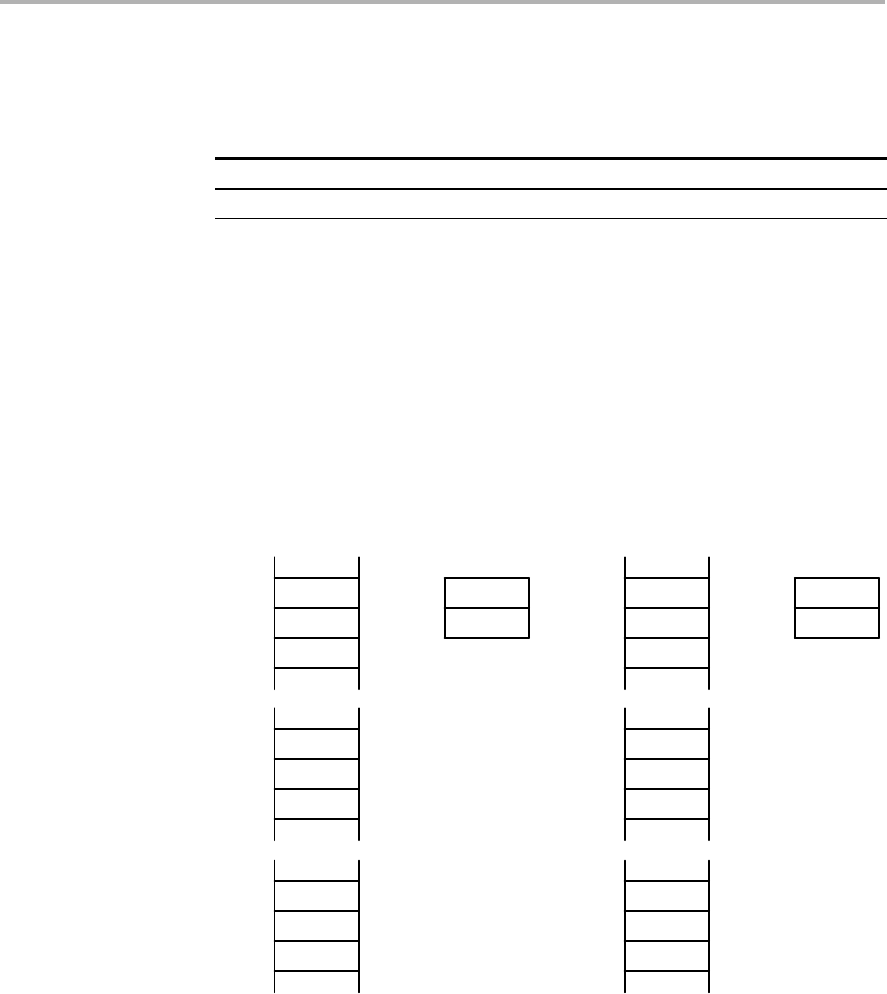
Addressing Modes
3-14 RISC 16-Bit CPU
3.3.5 Indirect Register Mode
The indirect register mode is described in Table 3−8.
Table 3−8. Indirect Mode Description
Assembler Code Content of ROM
MOV @R10,0(R11) MOV @R10,0(R11)
Length: One or two words
Operation: Move the contents of the source address (contents of R10) to
the destination address (contents of R11). The registers are
not modified.
Comment: Valid only for source operand. The substitute for destination
operand is 0(Rd).
Example: MOV.B @R10,0(R11)
0000h
Address
Space
04AEBh PC
0FF16h
0FF14h
0FF12h
0xxxxh
05BC1h
0xxxxh
0xxh
012h
0xxh
0FA33h
002A7h
R10
R11
Register
Before:
0000h
Address
Space
04AEBh
PC
0FF16h
0FF14h
0FF12h
0xxxxh
05BC1h
0FA34h
0FA32h
0FA30h 0xxxxh
0xxh
05Bh
002A8h
002A7h
002A6h 0xxh
0FA33h
002A7h
R10
R11
Register
After:
0xxxxh
0xxxxh
0xxxxh 0xxxxh
0FA34h
0FA32h
0FA30h
002A8h
002A7h
002A6h
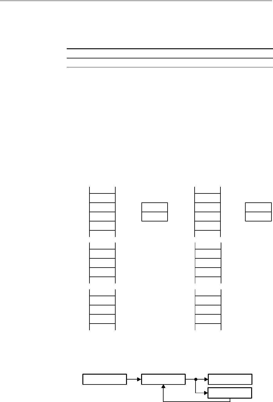
Addressing Modes
3-15
RISC 16-Bit CPU
3.3.6 Indirect Autoincrement Mode
The indirect autoincrement mode is described in Table 3−9.
Table 3−9. Indirect Autoincrement Mode Description
Assembler Code Content of ROM
MOV @R10+,0(R11) MOV @R10+,0(R11)
Length: One or two words
Operation: Move the contents of the source address (contents of R10) to
the destination address (contents of R11). Register R10 is
incremented by 1 for a byte operation, or 2 for a word
operation after the fetch; it points to the next address without
any overhead. This is useful for table processing.
Comment: Valid only for source operand. The substitute for destination
operand is 0(Rd) plus second instruction INCD Rd.
Example: MOV @R10+,0(R11)
00000h
Address
Space
04ABBh PC
0FF16h
0FF14h
0FF12h
0xxxxh
05BC1h
0FA34h
0FA32h
0FA30h 0xxxxh
0xxxxh
01234h
010AAh
010A8h
010A6h 0xxxxh
0FA32h
010A8h
R10
R11
Register
Before: Address
Space
0xxxxh
05BC1h
0FA34h
0FA32h
0FA30h 0xxxxh
0xxxxh
05BC1h
010AAh
010A8h
010A6h 0xxxxh
0FA34hR10
R11
Register
After:
0xxxxh
0xxxxh
0FF18h
00000h
04ABBh
PC
0FF16h
0FF14h
0FF12h
0xxxxh
0xxxxh
0FF18h
010A8h
The autoincrementing of the register contents occurs after the operand is
fetched. This is shown in Figure 3−8.
Figure 3−8. Operand Fetch Operation
Instruction Address Operand
+1/ +2
Addressing Modes
3-16 RISC 16-Bit CPU
3.3.7 Immediate Mode
The immediate mode is described in Table 3−10.
Table 3−10.Immediate Mode Description
Assembler Code Content of ROM
MOV #45h,TONI MOV @PC+,X(PC)
45
X = TONI − PC
Length: Two or three words
It is one word less if a constant of CG1 or CG2 can be used.
Operation: Move the immediate constant 45h, which is contained in the
word following the instruction, to destination address TONI.
When fetching the source, the program counter points to the
word following the instruction and moves the contents to the
destination.
Comment: Valid only for a source operand.
Example: MOV #45h,TONI
01192h
Address
Space
00045h
040B0h PC
0FF16h
0FF14h
0FF12h
0xxxxh
01234h
0xxxxh
0FF16h
+01192h
010A8h
Register
Before:
01192h
Address
Space
00045h
040B0h
PC
0FF16h
0FF14h
0FF12h
0xxxxh010AAh
010A8h
010A6h 0xxxxh
Register
After:
0xxxxh
0FF18h
010AAh
010A8h
010A6h
00045h

Instruction Set
3-17
RISC 16-Bit CPU
3.4 Instruction Set
The complete MSP430 instruction set consists of 27 core instructions and 24
emulated instructions. The core instructions are instructions that have unique
op-codes decoded by the CPU. The emulated instructions are instructions that
make code easier to write and read, but do not have op-codes themselves,
instead they are replaced automatically by the assembler with an equivalent
core instruction. There is no code or performance penalty for using emulated
instruction.
There are three core-instruction formats:
-Dual-operand
-Single-operand
-Jump
All single-operand and dual-operand instructions can be byte or word
instructions by using .B or .W extensions. Byte instructions are used to access
byte data or byte peripherals. Word instructions are used to access word data
or word peripherals. If no extension is used, the instruction is a word
instruction.
The source and destination of an instruction are defined by the following fields:
src The source operand defined by As and S-reg
dst The destination operand defined by Ad and D-reg
As The addressing bits responsible for the addressing mode used
for the source (src)
S-reg The working register used for the source (src)
Ad The addressing bits responsible for the addressing mode used
for the destination (dst)
D-reg The working register used for the destination (dst)
B/W Byte or word operation:
0: word operation
1: byte operation
Note: Destination Address
Destination addresses are valid anywhere in the memory map. However,
when using an instruction that modifies the contents of the destination, the
user must ensure the destination address is writable. For example, a
masked-ROM location would be a valid destination address, but the contents
are not modifiable, so the results of the instruction would be lost.

Instruction Set
3-18 RISC 16-Bit CPU
3.4.1 Double-Operand (Format I) Instructions
Figure 3−9 illustrates the double-operand instruction format.
Figure 3−9. Double Operand Instruction Format
B/W D-Reg
15 0
Op-code AdS-Reg
8714 13 12 11 10 9 6 5 4 3 2 1
As
Table 3−11 lists and describes the double operand instructions.
Table 3−11. Double Operand Instructions
Mnemonic S-Reg, Operation Status Bits
g,
D-Reg VNZC
MOV(.B) src,dst src → dst − − − −
ADD(.B) src,dst src + dst → dst ****
ADDC(.B) src,dst src + dst + C → dst ****
SUB(.B) src,dst dst + .not.src + 1 → dst ****
SUBC(.B) src,dst dst + .not.src + C → dst ****
CMP(.B) src,dst dst − src * * * *
DADD(.B) src,dst src + dst + C → dst (decimally) * * * *
BIT(.B) src,dst src .and. dst 0 * * *
BIC(.B) src,dst .not.src .and. dst → dst −−−−
BIS(.B) src,dst src .or. dst → dst −−−−
XOR(.B) src,dst src .xor. dst → dst ****
AND(.B) src,dst src .and. dst → dst 0 * * *
* The status bit is affected
− The status bit is not affected
0 The status bit is cleared
1 The status bit is set
Note: Instructions CMP and SUB
The instructions CMP and SUB are identical except for the storage of the
result. The same is true for the BIT and AND instructions.

Instruction Set
3-19
RISC 16-Bit CPU
3.4.2 Single-Operand (Format II) Instructions
Figure 3−10 illustrates the single-operand instruction format.
Figure 3−10. Single Operand Instruction Format
B/W D/S-Reg
15 0
Op-code
8714 13 12 11 10 9 6 5 4 3 2 1
Ad
Table 3−12 lists and describes the single operand instructions.
Table 3−12.Single Operand Instructions
Mnemonic S-Reg,
D Reg
Operation Status Bits
D-Reg VNZC
RRC(.B) dst C → MSB →.......LSB → C * * * *
RRA(.B) dst MSB → MSB →....LSB → C0***
PUSH(.B) src SP − 2 → SP, src → @SP − − − −
SWPB dst Swap bytes − − − −
CALL dst SP − 2 → SP, PC+2 → @SP − − − −
dst → PC
RETI TOS → SR, SP + 2 →SP ****
TOS → PC,SP + 2 → SP
SXT dst Bit 7 → Bit 8........Bit 15 0 * * *
* The status bit is affected
− The status bit is not affected
0 The status bit is cleared
1 The status bit is set
All addressing modes are possible for the CALL instruction. If the symbolic
mode (ADDRESS), the immediate mode (#N), the absolute mode (&EDE) or
the indexed mode x(RN) is used, the word that follows contains the address
information.

Instruction Set
3-20 RISC 16-Bit CPU
3.4.3 Jumps
Figure 3−11 shows the conditional-jump instruction format.
Figure 3−11. Jump Instruction Format
C10-Bit PC Offset
15 0
Op-code
8714 13 12 11 10 9 6 5 4 3 2 1
Table 3−13 lists and describes the jump instructions.
Table 3−13.Jump Instructions
Mnemonic S-Reg, D-Reg Operation
JEQ/JZ Label Jump to label if zero bit is set
JNE/JNZ Label Jump to label if zero bit is reset
JC Label Jump to label if carry bit is set
JNC Label Jump to label if carry bit is reset
JN Label Jump to label if negative bit is set
JGE Label Jump to label if (N .XOR. V) = 0
JL Label Jump to label if (N .XOR. V) = 1
JMP Label Jump to label unconditionally
Conditional jumps support program branching relative to the PC and do not
affect the status bits. The possible jump range is from −511 to +512 words
relative to the PC value at the jump instruction. The 10-bit program-counter
offset is treated as a signed 10-bit value that is doubled and added to the
program counter:
PCnew = PCold + 2 + PCoffset × 2

Instruction Set
3-21
RISC 16-Bit CPU
* ADC[.W] Add carry to destination
* ADC.B Add carry to destination
Syntax ADC dst or ADC.W dst
ADC.B dst
Operation dst + C −> dst
Emulation ADDC #0,dst
ADDC.B #0,dst
Description The carry bit (C) is added to the destination operand. The previous contents
of the destination are lost.
Status Bits N: Set if result is negative, reset if positive
Z: Set if result is zero, reset otherwise
C: Set if dst was incremented from 0FFFFh to 0000, reset otherwise
Set if dst was incremented from 0FFh to 00, reset otherwise
V: Set if an arithmetic overflow occurs, otherwise reset
Mode Bits OSCOFF, CPUOFF, and GIE are not affected.
Example The 16-bit counter pointed to by R13 is added to a 32-bit counter pointed to
by R12.
ADD @R13,0(R12) ; Add LSDs
ADC 2(R12) ; Add carry to MSD
Example The 8-bit counter pointed to by R13 is added to a 16-bit counter pointed to by
R12.
ADD.B @R13,0(R12) ; Add LSDs
ADC.B 1(R12) ; Add carry to MSD

Instruction Set
3-22 RISC 16-Bit CPU
ADD[.W] Add source to destination
ADD.B Add source to destination
Syntax ADD src,dst or ADD.W src,dst
ADD.B src,dst
Operation src + dst −> dst
Description The source operand is added to the destination operand. The source operand
is not affected. The previous contents of the destination are lost.
Status Bits N: Set if result is negative, reset if positive
Z: Set if result is zero, reset otherwise
C: Set if there is a carry from the result, cleared if not
V: Set if an arithmetic overflow occurs, otherwise reset
Mode Bits OSCOFF, CPUOFF, and GIE are not affected.
Example R5 is increased by 10. The jump to TONI is performed on a carry.
ADD #10,R5
JC TONI ; Carry occurred
...... ; No carry
Example R5 is increased by 10. The jump to TONI is performed on a carry.
ADD.B #10,R5 ; Add 10 to Lowbyte of R5
JC TONI ; Carry occurred, if (R5) ≥ 246 [0Ah+0F6h]
...... ; No carry

Instruction Set
3-23
RISC 16-Bit CPU
ADDC[.W] Add source and carry to destination
ADDC.B Add source and carry to destination
Syntax ADDC src,dst or ADDC.W src,dst
ADDC.B src,dst
Operation src + dst + C −> dst
Description The source operand and the carry bit (C) are added to the destination operand.
The source operand is not affected. The previous contents of the destination
are lost.
Status Bits N: Set if result is negative, reset if positive
Z: Set if result is zero, reset otherwise
C: Set if there is a carry from the MSB of the result, reset otherwise
V: Set if an arithmetic overflow occurs, otherwise reset
Mode Bits OSCOFF, CPUOFF, and GIE are not affected.
Example The 32-bit counter pointed to by R13 is added to a 32-bit counter, eleven words
(20/2 + 2/2) above the pointer in R13.
ADD @R13+,20(R13) ; ADD LSDs with no carry in
ADDC @R13+,20(R13) ; ADD MSDs with carry
... ; resulting from the LSDs
Example The 24-bit counter pointed to by R13 is added to a 24-bit counter, eleven bytes
above the pointer in R13.
ADD.B @R13+,10(R13) ; ADD LSDs with no carry in
ADDC.B @R13+,10(R13) ; ADD medium Bits with carry
ADDC.B @R13+,10(R13) ; ADD MSDs with carry
... ; resulting from the LSDs

Instruction Set
3-24 RISC 16-Bit CPU
AND[.W] Source AND destination
AND.B Source AND destination
Syntax AND src,dst or AND.W src,dst
AND.B src,dst
Operation src .AND. dst −> dst
Description The source operand and the destination operand are logically ANDed. The
result is placed into the destination.
Status Bits N: Set if result MSB is set, reset if not set
Z: Set if result is zero, reset otherwise
C: Set if result is not zero, reset otherwise ( = .NOT. Zero)
V: Reset
Mode Bits OSCOFF, CPUOFF, and GIE are not affected.
Example The bits set in R5 are used as a mask (#0AA55h) for the word addressed by
TOM. If the result is zero, a branch is taken to label TONI.
MOV #0AA55h,R5 ; Load mask into register R5
AND R5,TOM ; mask word addressed by TOM with R5
JZ TONI ;
...... ; Result is not zero
;
;
;or
;
;
AND #0AA55h,TOM
JZ TONI
Example The bits of mask #0A5h are logically ANDed with the low byte TOM. If the result
is zero, a branch is taken to label TONI.
AND.B #0A5h,TOM ; mask Lowbyte TOM with 0A5h
JZ TONI ;
...... ; Result is not zero

Instruction Set
3-25
RISC 16-Bit CPU
BIC[.W] Clear bits in destination
BIC.B Clear bits in destination
Syntax BIC src,dst or BIC.W src,dst
BIC.B src,dst
Operation .NOT.src .AND. dst −> dst
Description The inverted source operand and the destination operand are logically
ANDed. The result is placed into the destination. The source operand is not
affected.
Status Bits Status bits are not affected.
Mode Bits OSCOFF, CPUOFF, and GIE are not affected.
Example The six MSBs of the RAM word LEO are cleared.
BIC #0FC00h,LEO ; Clear 6 MSBs in MEM(LEO)
Example The five MSBs of the RAM byte LEO are cleared.
BIC.B #0F8h,LEO ; Clear 5 MSBs in Ram location LEO

Instruction Set
3-26 RISC 16-Bit CPU
BIS[.W] Set bits in destination
BIS.B Set bits in destination
Syntax BIS src,dst or BIS.W src,dst
BIS.B src,dst
Operation src .OR. dst −> dst
Description The source operand and the destination operand are logically ORed. The
result is placed into the destination. The source operand is not affected.
Status Bits Status bits are not affected.
Mode Bits OSCOFF, CPUOFF, and GIE are not affected.
Example The six LSBs of the RAM word TOM are set.
BIS #003Fh,TOM; set the six LSBs in RAM location TOM
Example The three MSBs of RAM byte TOM are set.
BIS.B #0E0h,TOM ; set the 3 MSBs in RAM location TOM

Instruction Set
3-27
RISC 16-Bit CPU
BIT[.W] Test bits in destination
BIT.B Test bits in destination
Syntax BIT src,dst or BIT.W src,dst
Operation src .AND. dst
Description The source and destination operands are logically ANDed. The result affects
only the status bits. The source and destination operands are not affected.
Status Bits N: Set if MSB of result is set, reset otherwise
Z: Set if result is zero, reset otherwise
C: Set if result is not zero, reset otherwise (.NOT. Zero)
V: Reset
Mode Bits OSCOFF, CPUOFF, and GIE are not affected.
Example If bit 9 of R8 is set, a branch is taken to label TOM.
BIT #0200h,R8 ; bit 9 of R8 set?
JNZ TOM ; Yes, branch to TOM
... ; No, proceed
Example If bit 3 of R8 is set, a branch is taken to label TOM.
BIT.B #8,R8
JC TOM
Example A serial communication receive bit (RCV) is tested. Because the carry bit is
equal to the state of the tested bit while using the BIT instruction to test a single
bit, the carry bit is used by the subsequent instruction; the read information is
shifted into register RECBUF.
;
; Serial communication with LSB is shifted first:
; xxxx xxxx xxxx xxxx
BIT.B #RCV,RCCTL ; Bit info into carry
RRC RECBUF ; Carry −> MSB of RECBUF
; cxxx xxxx
...... ; repeat previous two instructions
...... ; 8 times
; cccc cccc
; ^ ^
; MSB LSB
; Serial communication with MSB shifted first:
BIT.B #RCV,RCCTL ; Bit info into carry
RLC.B RECBUF ; Carry −> LSB of RECBUF
; xxxx xxxc
...... ; repeat previous two instructions
...... ; 8 times
; cccc cccc
; | LSB
; MSB

Instruction Set
3-28 RISC 16-Bit CPU
* BR, BRANCH Branch to .......... destination
Syntax BR dst
Operation dst −> PC
Emulation MOV dst,PC
Description An unconditional branch is taken to an address anywhere in the 64K address
space. All source addressing modes can be used. The branch instruction is
a word instruction.
Status Bits Status bits are not affected.
Example Examples for all addressing modes are given.
BR #EXEC ;Branch to label EXEC or direct branch (e.g. #0A4h)
; Core instruction MOV @PC+,PC
BR EXEC ; Branch to the address contained in EXEC
; Core instruction MOV X(PC),PC
; Indirect address
BR &EXEC ; Branch to the address contained in absolute
; address EXEC
; Core instruction MOV X(0),PC
; Indirect address
BR R5 ; Branch to the address contained in R5
; Core instruction MOV R5,PC
; Indirect R5
BR @R5 ; Branch to the address contained in the word
; pointed to by R5.
; Core instruction MOV @R5+,PC
; Indirect, indirect R5
BR @R5+ ; Branch to the address contained in the word pointed
; to by R5 and increment pointer in R5 afterwards.
; The next time—S/W flow uses R5 pointer—it can
; alter program execution due to access to
; next address in a table pointed to by R5
; Core instruction MOV @R5,PC
; Indirect, indirect R5 with autoincrement
BR X(R5) ; Branch to the address contained in the address
; pointed to by R5 + X (e.g. table with address
; starting at X). X can be an address or a label
; Core instruction MOV X(R5),PC
; Indirect, indirect R5 + X

Instruction Set
3-29
RISC 16-Bit CPU
CALL Subroutine
Syntax CALL dst
Operation dst −> tmp dst is evaluated and stored
SP − 2 −> SP
PC −> @SP PC updated to TOS
tmp −> PC dst saved to PC
Description A subroutine call is made to an address anywhere in the 64K address space.
All addressing modes can be used. The return address (the address of the
following instruction) is stored on the stack. The call instruction is a word
instruction.
Status Bits Status bits are not affected.
Example Examples for all addressing modes are given.
CALL #EXEC ; Call on label EXEC or immediate address (e.g. #0A4h)
; SP−2 → SP, PC+2 → @SP, @PC+ →PC
CALL EXEC ; Call on the address contained in EXEC
; SP−2 → SP, PC+2 → @SP, X(PC) →PC
; Indirect address
CALL &EXEC ; Call on the address contained in absolute address
; EXEC
; SP−2 → SP, PC+2 → @SP, X(0) →PC
; Indirect address
CALL R5 ; Call on the address contained in R5
; SP−2 → SP, PC+2 → @SP, R5 →PC
; Indirect R5
CALL @R5 ; Call on the address contained in the word
; pointed to by R5
; SP−2 → SP, PC+2 → @SP, @R5 →PC
; Indirect, indirect R5
CALL @R5+ ; Call on the address contained in the word
; pointed to by R5 and increment pointer in R5.
; The next time—S/W flow uses R5 pointer—
; it can alter the program execution due to
; access to next address in a table pointed to by R5
; SP−2 → SP, PC+2 → @SP, @R5 →PC
; Indirect, indirect R5 with autoincrement
CALL X(R5) ; Call on the address contained in the address pointed
; to by R5 + X (e.g. table with address starting at X)
; X can be an address or a label
; SP−2 → SP, PC+2 → @SP, X(R5) →PC
; Indirect, indirect R5 + X

Instruction Set
3-30 RISC 16-Bit CPU
* CLR[.W] Clear destination
* CLR.B Clear destination
Syntax CLR dst or CLR.W dst
CLR.B dst
Operation 0 −> dst
Emulation MOV #0,dst
MOV.B #0,dst
Description The destination operand is cleared.
Status Bits Status bits are not affected.
Example RAM word TONI is cleared.
CLR TONI ; 0 −> TONI
Example Register R5 is cleared.
CLR R5
Example RAM byte TONI is cleared.
CLR.B TONI ; 0 −> TONI

Instruction Set
3-31
RISC 16-Bit CPU
* CLRC Clear carry bit
Syntax CLRC
Operation 0 −> C
Emulation BIC #1,SR
Description The carry bit (C) is cleared. The clear carry instruction is a word instruction.
Status Bits N: Not affected
Z: Not affected
C: Cleared
V: Not affected
Mode Bits OSCOFF, CPUOFF, and GIE are not affected.
Example The 16-bit decimal counter pointed to by R13 is added to a 32-bit counter
pointed to by R12.
CLRC ; C=0: defines start
DADD @R13,0(R12) ; add 16-bit counter to low word of 32-bit counter
DADC 2(R12) ; add carry to high word of 32-bit counter

Instruction Set
3-32 RISC 16-Bit CPU
* CLRN Clear negative bit
Syntax CLRN
Operation 0 → N
or
(.NOT.src .AND. dst −> dst)
Emulation BIC #4,SR
Description The constant 04h is inverted (0FFFBh) and is logically ANDed with the
destination operand. The result is placed into the destination. The clear
negative bit instruction is a word instruction.
Status Bits N: Reset to 0
Z: Not affected
C: Not affected
V: Not affected
Mode Bits OSCOFF, CPUOFF, and GIE are not affected.
Example The Negative bit in the status register is cleared. This avoids special treatment
with negative numbers of the subroutine called.
CLRN
CALL SUBR
......
......
SUBR JN SUBRET ; If input is negative: do nothing and return
......
......
......
SUBRET RET

Instruction Set
3-33
RISC 16-Bit CPU
* CLRZ Clear zero bit
Syntax CLRZ
Operation 0 → Z
or
(.NOT.src .AND. dst −> dst)
Emulation BIC #2,SR
Description The constant 02h is inverted (0FFFDh) and logically ANDed with the
destination operand. The result is placed into the destination. The clear zero
bit instruction is a word instruction.
Status Bits N: Not affected
Z: Reset to 0
C: Not affected
V: Not affected
Mode Bits OSCOFF, CPUOFF, and GIE are not affected.
Example The zero bit in the status register is cleared.
CLRZ

Instruction Set
3-34 RISC 16-Bit CPU
CMP[.W] Compare source and destination
CMP.B Compare source and destination
Syntax CMP src,dst or CMP.W src,dst
CMP.B src,dst
Operation dst + .NOT.src + 1
or
(dst − src)
Description The source operand is subtracted from the destination operand. This is
accomplished by adding the 1s complement of the source operand plus 1. The
two operands are not affected and the result is not stored; only the status bits
are affected.
Status Bits N: Set if result is negative, reset if positive (src >= dst)
Z: Set if result is zero, reset otherwise (src = dst)
C: Set if there is a carry from the MSB of the result, reset otherwise
V: Set if an arithmetic overflow occurs, otherwise reset
Mode Bits OSCOFF, CPUOFF, and GIE are not affected.
Example R5 and R6 are compared. If they are equal, the program continues at the label
EQUAL.
CMP R5,R6 ; R5 = R6?
JEQ EQUAL ; YES, JUMP
Example Two RAM blocks are compared. If they are not equal, the program branches
to the label ERROR.
MOV #NUM,R5 ; number of words to be compared
MOV #BLOCK1,R6 ; BLOCK1 start address in R6
MOV #BLOCK2,R7 ; BLOCK2 start address in R7
L$1 CMP @R6+,0(R7) ; Are Words equal? R6 increments
JNZ ERROR ; No, branch to ERROR
INCD R7 ; Increment R7 pointer
DEC R5 ; Are all words compared?
JNZ L$1 ; No, another compare
Example The RAM bytes addressed by EDE and TONI are compared. If they are equal,
the program continues at the label EQUAL.
CMP.B EDE,TONI ; MEM(EDE) = MEM(TONI)?
JEQ EQUAL ; YES, JUMP

Instruction Set
3-35
RISC 16-Bit CPU
* DADC[.W] Add carry decimally to destination
* DADC.B Add carry decimally to destination
Syntax DADC dst or DADC.W src,dst
DADC.B dst
Operation dst + C −> dst (decimally)
Emulation DADD #0,dst
DADD.B #0,dst
Description The carry bit (C) is added decimally to the destination.
Status Bits N: Set if MSB is 1
Z: Set if dst is 0, reset otherwise
C: Set if destination increments from 9999 to 0000, reset otherwise
Set if destination increments from 99 to 00, reset otherwise
V: Undefined
Mode Bits OSCOFF, CPUOFF, and GIE are not affected.
Example The four-digit decimal number contained in R5 is added to an eight-digit deci-
mal number pointed to by R8.
CLRC ; Reset carry
; next instruction’s start condition is defined
DADD R5,0(R8) ; Add LSDs + C
DADC 2(R8) ; Add carry to MSD
Example The two-digit decimal number contained in R5 is added to a four-digit decimal
number pointed to by R8.
CLRC ; Reset carry
; next instruction’s start condition is defined
DADD.B R5,0(R8) ; Add LSDs + C
DADC.B 1(R8) ; Add carry to MSDs

Instruction Set
3-36 RISC 16-Bit CPU
DADD[.W] Source and carry added decimally to destination
DADD.B Source and carry added decimally to destination
Syntax DADD src,dst or DADD.W src,dst
DADD.B src,dst
Operation src + dst + C −> dst (decimally)
Description The source operand and the destination operand are treated as four binary
coded decimals (BCD) with positive signs. The source operand and the carry
bit (C) are added decimally to the destination operand. The source operand
is not affected. The previous contents of the destination are lost. The result is
not defined for non-BCD numbers.
Status Bits N: Set if the MSB is 1, reset otherwise
Z: Set if result is zero, reset otherwise
C: Set if the result is greater than 9999
Set if the result is greater than 99
V: Undefined
Mode Bits OSCOFF, CPUOFF, and GIE are not affected.
Example The eight-digit BCD number contained in R5 and R6 is added decimally to an
eight-digit BCD number contained in R3 and R4 (R6 and R4 contain the
MSDs).
CLRC ; clear carry
DADD R5,R3 ; add LSDs
DADD R6,R4 ; add MSDs with carry
JC OVERFLOW ; If carry occurs go to error handling routine
Example The two-digit decimal counter in the RAM byte CNT is incremented by one.
CLRC ; clear carry
DADD.B #1,CNT ; increment decimal counter
or
SETC
DADD.B #0,CNT ; ≡ DADC.B CNT
Instruction Set
3-37
RISC 16-Bit CPU
* DEC[.W] Decrement destination
* DEC.B Decrement destination
Syntax DEC dst or DEC.W dst
DEC.B dst
Operation dst − 1 −> dst
Emulation SUB #1,dst
Emulation SUB.B #1,dst
Description The destination operand is decremented by one. The original contents are
lost.
Status Bits N: Set if result is negative, reset if positive
Z: Set if dst contained 1, reset otherwise
C: Reset if dst contained 0, set otherwise
V: Set if an arithmetic overflow occurs, otherwise reset.
Set if initial value of destination was 08000h, otherwise reset.
Set if initial value of destination was 080h, otherwise reset.
Mode Bits OSCOFF, CPUOFF, and GIE are not affected.
Example R10 is decremented by 1
DEC R10 ; Decrement R10
; Move a block of 255 bytes from memory location starting with EDE to memory location starting with
;TONI. Tables should not overlap: start of destination address TONI must not be within the range EDE
; to EDE+0FEh
;
MOV #EDE,R6
MOV #255,R10
L$1 MOV.B @R6+,TONI−EDE−1(R6)
DEC R10
JNZ L$1
; Do not transfer tables using the routine above with the overlap shown in Figure 3−12.
Figure 3−12. Decrement Overlap
EDE
EDE+254
TONI
TONI+254

Instruction Set
3-38 RISC 16-Bit CPU
* DECD[.W] Double-decrement destination
* DECD.B Double-decrement destination
Syntax DECD dst or DECD.W dst
DECD.B dst
Operation dst − 2 −> dst
Emulation SUB #2,dst
Emulation SUB.B #2,dst
Description The destination operand is decremented by two. The original contents are lost.
Status Bits N: Set if result is negative, reset if positive
Z: Set if dst contained 2, reset otherwise
C: Reset if dst contained 0 or 1, set otherwise
V: Set if an arithmetic overflow occurs, otherwise reset.
Set if initial value of destination was 08001 or 08000h, otherwise reset.
Set if initial value of destination was 081 or 080h, otherwise reset.
Mode Bits OSCOFF, CPUOFF, and GIE are not affected.
Example R10 is decremented by 2.
DECD R10 ; Decrement R10 by two
; Move a block of 255 words from memory location starting with EDE to memory location
; starting with TONI
; Tables should not overlap: start of destination address TONI must not be within the
; range EDE to EDE+0FEh
;
MOV #EDE,R6
MOV #510,R10
L$1 MOV @R6+,TONI−EDE−2(R6)
DECD R10
JNZ L$1
Example Memory at location LEO is decremented by two.
DECD.B LEO ; Decrement MEM(LEO)
Decrement status byte STATUS by two.
DECD.B STATUS

Instruction Set
3-39
RISC 16-Bit CPU
* DINT Disable (general) interrupts
Syntax DINT
Operation 0 → GIE
or
(0FFF7h .AND. SR → SR / .NOT.src .AND. dst −> dst)
Emulation BIC #8,SR
Description All interrupts are disabled.
The constant 08h is inverted and logically ANDed with the status register (SR).
The result is placed into the SR.
Status Bits Status bits are not affected.
Mode Bits GIE is reset. OSCOFF and CPUOFF are not affected.
Example The general interrupt enable (GIE) bit in the status register is cleared to allow
a nondisrupted move of a 32-bit counter. This ensures that the counter is not
modified during the move by any interrupt.
DINT ; All interrupt events using the GIE bit are disabled
NOP
MOV COUNTHI,R5 ; Copy counter
MOV COUNTLO,R6
EINT ; All interrupt events using the GIE bit are enabled
Note: Disable Interrupt
If any code sequence needs to be protected from interruption, the DINT
should be executed at least one instruction before the beginning of the
uninterruptible sequence, or should be followed by a NOP instruction.

Instruction Set
3-40 RISC 16-Bit CPU
* EINT Enable (general) interrupts
Syntax EINT
Operation 1 → GIE
or
(0008h .OR. SR −> SR / .src .OR. dst −> dst)
Emulation BIS #8,SR
Description All interrupts are enabled.
The constant #08h and the status register SR are logically ORed. The result
is placed into the SR.
Status Bits Status bits are not affected.
Mode Bits GIE is set. OSCOFF and CPUOFF are not affected.
Example The general interrupt enable (GIE) bit in the status register is set.
; Interrupt routine of ports P1.2 to P1.7
; P1IN is the address of the register where all port bits are read. P1IFG is the address of
; the register where all interrupt events are latched.
;
PUSH.B &P1IN
BIC.B @SP,&P1IFG ; Reset only accepted flags
EINT ; Preset port 1 interrupt flags stored on stack
; other interrupts are allowed
BIT #Mask,@SP
JEQ MaskOK ; Flags are present identically to mask: jump
......
MaskOK BIC #Mask,@SP
......
INCD SP ; Housekeeping: inverse to PUSH instruction
; at the start of interrupt subroutine. Corrects
; the stack pointer.
RETI
Note: Enable Interrupt
The instruction following the enable interrupt instruction (EINT) is always
executed, even if an interrupt service request is pending when the interrupts
are enable.

Instruction Set
3-41
RISC 16-Bit CPU
* INC[.W]Increment destination
* INC.B Increment destination
Syntax INC dst or INC.W dst
INC.B dst
Operation dst + 1 −> dst
Emulation ADD #1,dst
Description The destination operand is incremented by one. The original contents are lost.
Status Bits N: Set if result is negative, reset if positive
Z: Set if dst contained 0FFFFh, reset otherwise
Set if dst contained 0FFh, reset otherwise
C: Set if dst contained 0FFFFh, reset otherwise
Set if dst contained 0FFh, reset otherwise
V: Set if dst contained 07FFFh, reset otherwise
Set if dst contained 07Fh, reset otherwise
Mode Bits OSCOFF, CPUOFF, and GIE are not affected.
Example The status byte, STATUS, of a process is incremented. When it is equal to 11,
a branch to OVFL is taken.
INC.B STATUS
CMP.B #11,STATUS
JEQ OVFL

Instruction Set
3-42 RISC 16-Bit CPU
* INCD[.W] Double-increment destination
* INCD.B Double-increment destination
Syntax INCD dst or INCD.W dst
INCD.B dst
Operation dst + 2 −> dst
Emulation ADD #2,dst
Emulation ADD.B #2,dst
Example The destination operand is incremented by two. The original contents are lost.
Status Bits N: Set if result is negative, reset if positive
Z: Set if dst contained 0FFFEh, reset otherwise
Set if dst contained 0FEh, reset otherwise
C: Set if dst contained 0FFFEh or 0FFFFh, reset otherwise
Set if dst contained 0FEh or 0FFh, reset otherwise
V: Set if dst contained 07FFEh or 07FFFh, reset otherwise
Set if dst contained 07Eh or 07Fh, reset otherwise
Mode Bits OSCOFF, CPUOFF, and GIE are not affected.
Example The item on the top of the stack (TOS) is removed without using a register.
.......
PUSH R5 ; R5 is the result of a calculation, which is stored
; in the system stack
INCD SP ; Remove TOS by double-increment from stack
; Do not use INCD.B, SP is a word-aligned
; register
RET
Example The byte on the top of the stack is incremented by two.
INCD.B 0(SP) ; Byte on TOS is increment by two

Instruction Set
3-43
RISC 16-Bit CPU
* INV[.W] Invert destination
* INV.B Invert destination
Syntax INV dst
INV.B dst
Operation .NOT.dst −> dst
Emulation XOR #0FFFFh,dst
Emulation XOR.B #0FFh,dst
Description The destination operand is inverted. The original contents are lost.
Status Bits N: Set if result is negative, reset if positive
Z: Set if dst contained 0FFFFh, reset otherwise
Set if dst contained 0FFh, reset otherwise
C: Set if result is not zero, reset otherwise ( = .NOT. Zero)
Set if result is not zero, reset otherwise ( = .NOT. Zero)
V: Set if initial destination operand was negative, otherwise reset
Mode Bits OSCOFF, CPUOFF, and GIE are not affected.
Example Content of R5 is negated (twos complement).
MOV #00AEh,R5 ; R5 = 000AEh
INV R5 ; Invert R5, R5 = 0FF51h
INC R5 ; R5 is now negated, R5 = 0FF52h
Example Content of memory byte LEO is negated.
MOV.B #0AEh,LEO ; MEM(LEO) = 0AEh
INV.B LEO ; Invert LEO, MEM(LEO) = 051h
INC.B LEO ; MEM(LEO) is negated,MEM(LEO) = 052h

Instruction Set
3-44 RISC 16-Bit CPU
JC Jump if carry set
JHS Jump if higher or same
Syntax JC label
JHS label
Operation If C = 1: PC + 2 × offset −> PC
If C = 0: execute following instruction
Description The status register carry bit (C) is tested. If it is set, the 10-bit signed offset
contained in the instruction LSBs is added to the program counter. If C is reset,
the next instruction following the jump is executed. JC (jump if carry/higher or
same) is used for the comparison of unsigned numbers (0 to 65536).
Status Bits Status bits are not affected.
Example The P1IN.1 signal is used to define or control the program flow.
BIT.B #02h,&P1IN ; State of signal −> Carry
JC PROGA ; If carry=1 then execute program routine A
...... ; Carry=0, execute program here
Example R5 is compared to 15. If the content is higher or the same, branch to LABEL.
CMP #15,R5
JHS LABEL ; Jump is taken if R5 ≥ 15
...... ; Continue here if R5 < 15

Instruction Set
3-45
RISC 16-Bit CPU
JEQ, JZ Jump if equal, jump if zero
Syntax JEQ label, JZ label
Operation If Z = 1: PC + 2 × offset −> PC
If Z = 0: execute following instruction
Description The status register zero bit (Z) is tested. If it is set, the 10-bit signed offset
contained in the instruction LSBs is added to the program counter. If Z is not
set, the instruction following the jump is executed.
Status Bits Status bits are not affected.
Example Jump to address TONI if R7 contains zero.
TST R7 ; Test R7
JZ TONI ; if zero: JUMP
Example Jump to address LEO if R6 is equal to the table contents.
CMP R6,Table(R5) ; Compare content of R6 with content of
; MEM (table address + content of R5)
JEQ LEO ; Jump if both data are equal
...... ; No, data are not equal, continue here
Example Branch to LABEL if R5 is 0.
TST R5
JZ LABEL
......

Instruction Set
3-46 RISC 16-Bit CPU
JGE Jump if greater or equal
Syntax JGE label
Operation If (N .XOR. V) = 0 then jump to label: PC + 2 × offset −> PC
If (N .XOR. V) = 1 then execute the following instruction
Description The status register negative bit (N) and overflow bit (V) are tested. If both N
and V are set or reset, the 10-bit signed offset contained in the instruction LSBs
is added to the program counter. If only one is set, the instruction following the
jump is executed.
This allows comparison of signed integers.
Status Bits Status bits are not affected.
Example When the content of R6 is greater or equal to the memory pointed to by R7,
the program continues at label EDE.
CMP @R7,R6 ; R6 ≥ (R7)?, compare on signed numbers
JGE EDE ; Yes, R6 ≥ (R7)
...... ; No, proceed
......
......

Instruction Set
3-47
RISC 16-Bit CPU
JL Jump if less
Syntax JL label
Operation If (N .XOR. V) = 1 then jump to label: PC + 2 × offset −> PC
If (N .XOR. V) = 0 then execute following instruction
Description The status register negative bit (N) and overflow bit (V) are tested. If only one
is set, the 10-bit signed offset contained in the instruction LSBs is added to the
program counter. If both N and V are set or reset, the instruction following the
jump is executed.
This allows comparison of signed integers.
Status Bits Status bits are not affected.
Example When the content of R6 is less than the memory pointed to by R7, the program
continues at label EDE.
CMP @R7,R6 ; R6 < (R7)?, compare on signed numbers
JL EDE ; Yes, R6 < (R7)
...... ; No, proceed
......
......

Instruction Set
3-48 RISC 16-Bit CPU
JMP Jump unconditionally
Syntax JMP label
Operation PC + 2 × offset −> PC
Description The 10-bit signed offset contained in the instruction LSBs is added to the
program counter.
Status Bits Status bits are not affected.
Hint: This one-word instruction replaces the BRANCH instruction in the range of
−511 to +512 words relative to the current program counter.

Instruction Set
3-49
RISC 16-Bit CPU
JN Jump if negative
Syntax JN label
Operation if N = 1: PC + 2 × offset −> PC
if N = 0: execute following instruction
Description The negative bit (N) of the status register is tested. If it is set, the 10-bit signed
offset contained in the instruction LSBs is added to the program counter. If N
is reset, the next instruction following the jump is executed.
Status Bits Status bits are not affected.
Example The result of a computation in R5 is to be subtracted from COUNT. If the result
is negative, COUNT is to be cleared and the program continues execution in
another path.
SUB R5,COUNT ; COUNT − R5 −> COUNT
JN L$1 ; If negative continue with COUNT=0 at PC=L$1
...... ; Continue with COUNT≥0
......
......
......
L$1 CLR COUNT
......
......
......

Instruction Set
3-50 RISC 16-Bit CPU
JNC Jump if carry not set
JLO Jump if lower
Syntax JNC label
JLO label
Operation if C = 0: PC + 2 × offset −> PC
if C = 1: execute following instruction
Description The status register carry bit (C) is tested. If it is reset, the 10-bit signed offset
contained in the instruction LSBs is added to the program counter. If C is set,
the next instruction following the jump is executed. JNC (jump if no carry/lower)
is used for the comparison of unsigned numbers (0 to 65536).
Status Bits Status bits are not affected.
Example The result in R6 is added in BUFFER. If an overflow occurs, an error handling
routine at address ERROR is used.
ADD R6,BUFFER ; BUFFER + R6 −> BUFFER
JNC CONT ; No carry, jump to CONT
ERROR ...... ; Error handler start
......
......
......
CONT ...... ; Continue with normal program flow
......
......
Example Branch to STL2 if byte STATUS contains 1 or 0.
CMP.B #2,STATUS
JLO STL2 ; STATUS < 2
...... ; STATUS ≥ 2, continue here

Instruction Set
3-51
RISC 16-Bit CPU
JNE Jump if not equal
JNZ Jump if not zero
Syntax JNE label
JNZ label
Operation If Z = 0: PC + 2 × offset −> PC
If Z = 1: execute following instruction
Description The status register zero bit (Z) is tested. If it is reset, the 10-bit signed offset
contained in the instruction LSBs is added to the program counter. If Z is set,
the next instruction following the jump is executed.
Status Bits Status bits are not affected.
Example Jump to address TONI if R7 and R8 have different contents.
CMP R7,R8 ; COMPARE R7 WITH R8
JNE TONI ; if different: jump
...... ; if equal, continue

Instruction Set
3-52 RISC 16-Bit CPU
MOV[.W] Move source to destination
MOV.B Move source to destination
Syntax MOV src,dst or MOV.W src,dst
MOV.B src,dst
Operation src −> dst
Description The source operand is moved to the destination.
The source operand is not affected. The previous contents of the destination
are lost.
Status Bits Status bits are not affected.
Mode Bits OSCOFF, CPUOFF, and GIE are not affected.
Example The contents of table EDE (word data) are copied to table TOM. The length
of the tables must be 020h locations.
MOV #EDE,R10 ; Prepare pointer
MOV #020h,R9 ; Prepare counter
Loop MOV @R10+,TOM−EDE−2(R10) ; Use pointer in R10 for both tables
DEC R9 ; Decrement counter
JNZ Loop ; Counter ≠ 0, continue copying
...... ; Copying completed
......
......
Example The contents of table EDE (byte data) are copied to table TOM. The length of
the tables should be 020h locations
MOV #EDE,R10 ; Prepare pointer
MOV #020h,R9 ; Prepare counter
Loop MOV.B @R10+,TOM−EDE−1(R10) ; Use pointer in R10 for
; both tables
DEC R9 ; Decrement counter
JNZ Loop ; Counter ≠ 0, continue
; copying
...... ; Copying completed
......
......

Instruction Set
3-53
RISC 16-Bit CPU
* NOP No operation
Syntax NOP
Operation None
Emulation MOV #0, R3
Description No operation is performed. The instruction may be used for the elimination of
instructions during the software check or for defined waiting times.
Status Bits Status bits are not affected.
The NOP instruction is mainly used for two purposes:
-To fill one, two, or three memory words
-To adjust software timing
Note: Emulating No-Operation Instruction
Other instructions can emulate the NOP function while providing different
numbers of instruction cycles and code words. Some examples are:
Examples:
MOV #0,R3 ; 1 cycle, 1 word
MOV 0(R4),0(R4) ; 6 cycles, 3 words
MOV @R4,0(R4) ; 5 cycles, 2 words
BIC #0,EDE(R4) ; 4 cycles, 2 words
JMP $+2 ; 2 cycles, 1 word
BIC #0,R5 ; 1 cycle, 1 word
However, care should be taken when using these examples to prevent
unintended results. For example, if MOV 0(R4), 0(R4) is used and the value
in R4 is 120h, then a security violation will occur with the watchdog timer
(address 120h) because the security key was not used.

Instruction Set
3-54 RISC 16-Bit CPU
* POP[.W] Pop word from stack to destination
* POP.B Pop byte from stack to destination
Syntax POP dst
POP.B dst
Operation @SP −> temp
SP + 2 −> SP
temp −> dst
Emulation MOV @SP+,dst or MOV.W @SP+,dst
Emulation MOV.B @SP+,dst
Description The stack location pointed to by the stack pointer (TOS) is moved to the
destination. The stack pointer is incremented by two afterwards.
Status Bits Status bits are not affected.
Example The contents of R7 and the status register are restored from the stack.
POP R7 ; Restore R7
POP SR ; Restore status register
Example The contents of RAM byte LEO is restored from the stack.
POP.B LEO ; The low byte of the stack is moved to LEO.
Example The contents of R7 is restored from the stack.
POP.B R7 ; The low byte of the stack is moved to R7,
; the high byte of R7 is 00h
Example The contents of the memory pointed to by R7 and the status register are
restored from the stack.
POP.B 0(R7) ; The low byte of the stack is moved to the
; the byte which is pointed to by R7
: Example: R7 = 203h
; Mem(R7) = low byte of system stack
: Example: R7 = 20Ah
; Mem(R7) = low byte of system stack
POP SR ; Last word on stack moved to the SR
Note: The System Stack Pointer
The system stack pointer (SP) is always incremented by two, independent
of the byte suffix.

Instruction Set
3-55
RISC 16-Bit CPU
PUSH[.W] Push word onto stack
PUSH.B Push byte onto stack
Syntax PUSH src or PUSH.W src
PUSH.B src
Operation SP − 2 → SP
src → @SP
Description The stack pointer is decremented by two, then the source operand is moved
to the RAM word addressed by the stack pointer (TOS).
Status Bits Status bits are not affected.
Mode Bits OSCOFF, CPUOFF, and GIE are not affected.
Example The contents of the status register and R8 are saved on the stack.
PUSH SR ; save status register
PUSH R8 ; save R8
Example The contents of the peripheral TCDAT is saved on the stack.
PUSH.B &TCDAT ; save data from 8-bit peripheral module,
; address TCDAT, onto stack
Note: The System Stack Pointer
The system stack pointer (SP) is always decremented by two, independent
of the byte suffix.

Instruction Set
3-56 RISC 16-Bit CPU
* RET Return from subroutine
Syntax RET
Operation @SP→ PC
SP + 2 → SP
Emulation MOV @SP+,PC
Description The return address pushed onto the stack by a CALL instruction is moved to
the program counter. The program continues at the code address following the
subroutine call.
Status Bits Status bits are not affected.
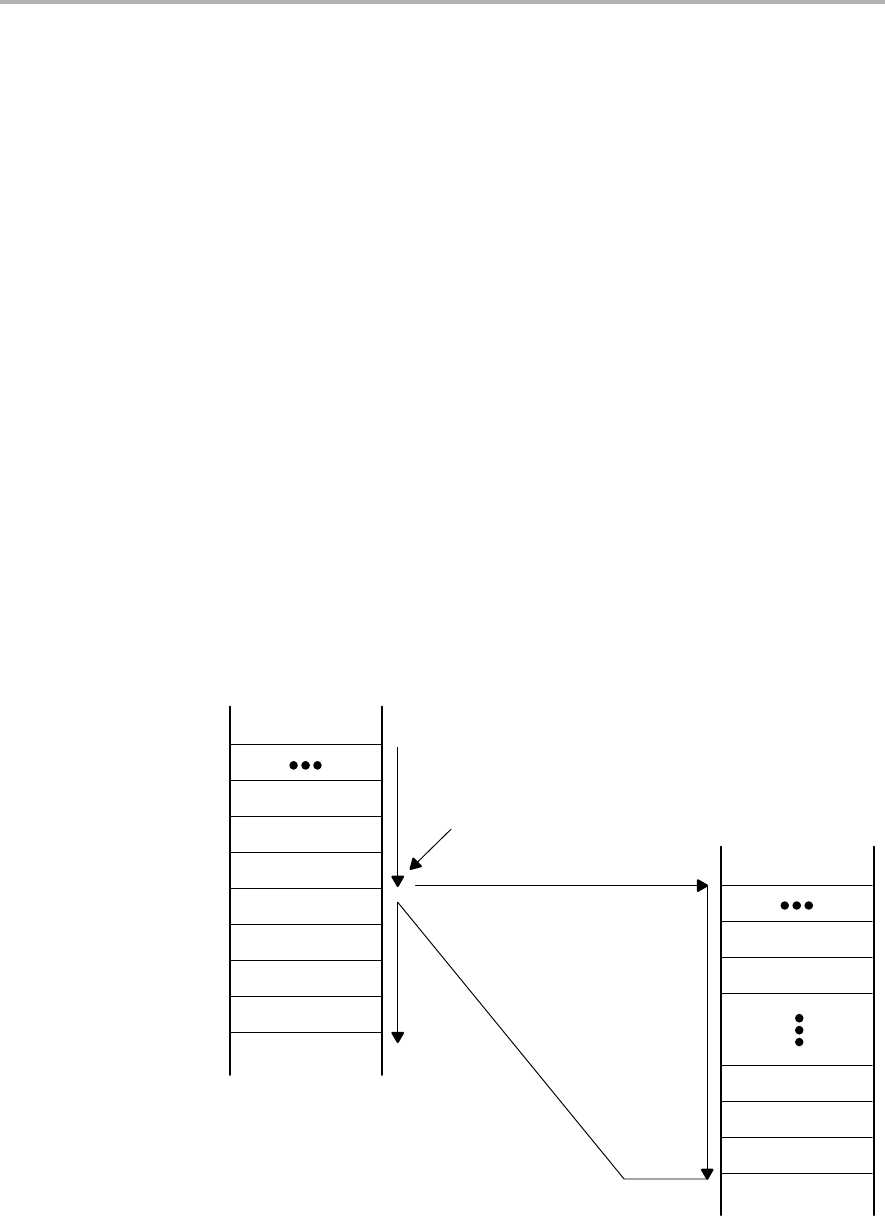
Instruction Set
3-57
RISC 16-Bit CPU
RETI Return from interrupt
Syntax RETI
Operation TOS → SR
SP + 2 → SP
TOS → PC
SP + 2 → SP
Description The status register is restored to the value at the beginning of the interrupt
service routine by replacing the present SR contents with the TOS contents.
The stack pointer (SP) is incremented by two.
The program counter is restored to the value at the beginning of interrupt
service. This is the consecutive step after the interrupted program flow.
Restoration is performed by replacing the present PC contents with the TOS
memory contents. The stack pointer (SP) is incremented.
Status Bits N: restored from system stack
Z: restored from system stack
C: restored from system stack
V: restored from system stack
Mode Bits OSCOFF, CPUOFF, and GIE are restored from system stack.
Example Figure 3−13 illustrates the main program interrupt.
Figure 3−13. Main Program Interrupt
PC −6
PC −4
PC −2
PC
PC +2
PC +4
PC +6
PC +8
PC = PCi
PCi +2
PCi +4
PCi +n−4
PCi +n−2
PCi +n
Interrupt Request
Interrupt Accepted
PC+2 is Stored
Onto Stack
RETI
Instruction Set
3-58 RISC 16-Bit CPU
* RLA[.W] Rotate left arithmetically
* RLA.B Rotate left arithmetically
Syntax RLA dst or RLA.W dst
RLA.B dst
Operation C <− MSB <− MSB−1 .... LSB+1 <− LSB <− 0
Emulation ADD dst,dst
ADD.B dst,dst
Description The destination operand is shifted left one position as shown in Figure 3−14.
The MSB is shifted into the carry bit (C) and the LSB is filled with 0. The RLA
instruction acts as a signed multiplication by 2.
An overflow occurs if dst ≥ 04000h and dst < 0C000h before operation is
performed: the result has changed sign.
Figure 3−14. Destination Operand—Arithmetic Shift Left
15 0
70
C
Byte
Word
0
An overflow occurs if dst ≥ 040h and dst < 0C0h before the operation is
performed: the result has changed sign.
Status Bits N: Set if result is negative, reset if positive
Z: Set if result is zero, reset otherwise
C: Loaded from the MSB
V: Set if an arithmetic overflow occurs:
the initial value is 04000h ≤dst < 0C000h; reset otherwise
Set if an arithmetic overflow occurs:
the initial value is 040h ≤dst < 0C0h; reset otherwise
Mode Bits OSCOFF, CPUOFF, and GIE are not affected.
Example R7 is multiplied by 2.
RLA R7 ; Shift left R7 (× 2)
Example The low byte of R7 is multiplied by 4.
RLA.B R7 ; Shift left low byte of R7 (× 2)
RLA.B R7 ; Shift left low byte of R7 (× 4)
Note: RLA Substitution
The assembler does not recognize the instruction:
RLA @R5+, RLA.B @R5+, or RLA(.B) @R5
It must be substituted by:
ADD @R5+,−2(R5) ADD.B @R5+,−1(R5) or ADD(.B) @R5
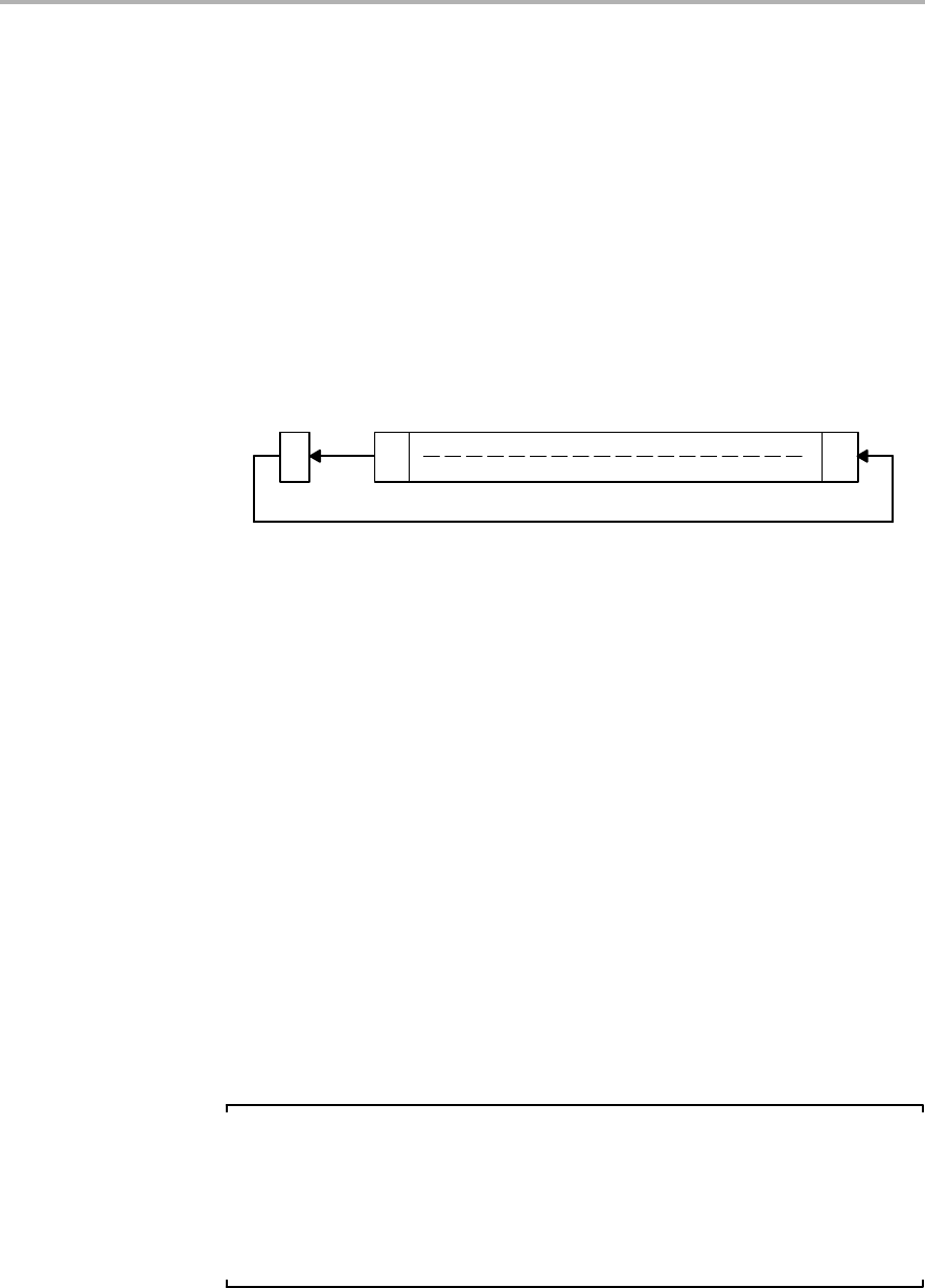
Instruction Set
3-59
RISC 16-Bit CPU
* RLC[.W] Rotate left through carry
* RLC.B Rotate left through carry
Syntax RLC dst or RLC.W dst
RLC.B dst
Operation C <− MSB <− MSB−1 .... LSB+1 <− LSB <− C
Emulation ADDC dst,dst
Description The destination operand is shifted left one position as shown in Figure 3−15.
The carry bit (C) is shifted into the LSB and the MSB is shifted into the carry
bit (C).
Figure 3−15. Destination Operand—Carry Left Shift
15 0
70
C
Byte
Word
Status Bits N: Set if result is negative, reset if positive
Z: Set if result is zero, reset otherwise
C: Loaded from the MSB
V: Set if an arithmetic overflow occurs
the initial value is 04000h ≤dst < 0C000h; reset otherwise
Set if an arithmetic overflow occurs:
the initial value is 040h ≤dst < 0C0h; reset otherwise
Mode Bits OSCOFF, CPUOFF, and GIE are not affected.
Example R5 is shifted left one position.
RLC R5 ; (R5 x 2) + C −> R5
Example The input P1IN.1 information is shifted into the LSB of R5.
BIT.B #2,&P1IN ; Information −> Carry
RLC R5 ; Carry=P0in.1 −> LSB of R5
Example The MEM(LEO) content is shifted left one position.
RLC.B LEO ; Mem(LEO) x 2 + C −> Mem(LEO)
Note: RLC and RLC.B Substitution
The assembler does not recognize the instruction:
RLC @R5+, RLC.B @R5+, or RLC(.B) @R5
It must be substituted by:
ADDC @R5+,−2(R5) ADDC.B @R5+,−1(R5) or ADDC(.B) @R5
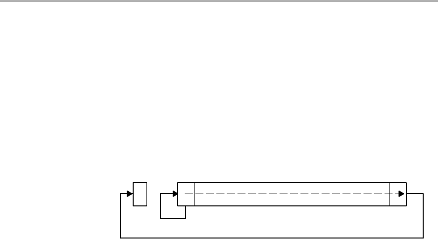
Instruction Set
3-60 RISC 16-Bit CPU
RRA[.W] Rotate right arithmetically
RRA.B Rotate right arithmetically
Syntax RRA dst or RRA.W dst
RRA.B dst
Operation MSB −> MSB, MSB −> MSB−1, ... LSB+1 −> LSB, LSB −> C
Description The destination operand is shifted right one position as shown in Figure 3−16.
The MSB is shifted into the MSB, the MSB is shifted into the MSB−1, and the
LSB+1 is shifted into the LSB.
Figure 3−16. Destination Operand—Arithmetic Right Shift
15 0
15 0
C
Byte
Word
Status Bits N: Set if result is negative, reset if positive
Z: Set if result is zero, reset otherwise
C: Loaded from the LSB
V: Reset
Mode Bits OSCOFF, CPUOFF, and GIE are not affected.
Example R5 is shifted right one position. The MSB retains the old value. It operates
equal to an arithmetic division by 2.
RRA R5 ; R5/2 −> R5
; The value in R5 is multiplied by 0.75 (0.5 + 0.25).
;
PUSH R5 ; Hold R5 temporarily using stack
RRA R5 ; R5 × 0.5 −> R5
ADD @SP+,R5 ; R5 × 0.5 + R5 = 1.5 × R5 −> R5
RRA R5 ; (1.5 × R5) × 0.5 = 0.75 × R5 −> R5
......
Example The low byte of R5 is shifted right one position. The MSB retains the old value.
It operates equal to an arithmetic division by 2.
RRA.B R5 ; R5/2 −> R5: operation is on low byte only
; High byte of R5 is reset
PUSH.B R5 ; R5 × 0.5 −> TOS
RRA.B @SP ; TOS × 0.5 = 0.5 × R5 × 0.5 = 0.25 × R5 −> TOS
ADD.B @SP+,R5 ; R5 × 0.5 + R5 × 0.25 = 0.75 × R5 −> R5
......
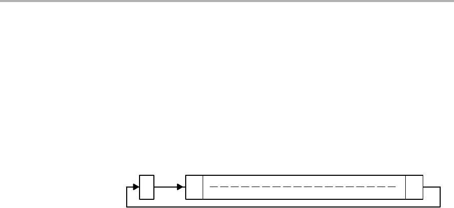
Instruction Set
3-61
RISC 16-Bit CPU
RRC[.W] Rotate right through carry
RRC.B Rotate right through carry
Syntax RRC dst or RRC.W dst
RRC dst
Operation C −> MSB −> MSB−1 .... LSB+1 −> LSB −> C
Description The destination operand is shifted right one position as shown in Figure 3−17.
The carry bit (C) is shifted into the MSB, the LSB is shifted into the carry bit (C).
Figure 3−17. Destination Operand—Carry Right Shift
15 0
70
C
Byte
Word
Status Bits N: Set if result is negative, reset if positive
Z: Set if result is zero, reset otherwise
C: Loaded from the LSB
V: Reset
Mode Bits OSCOFF, CPUOFF, and GIE are not affected.
Example R5 is shifted right one position. The MSB is loaded with 1.
SETC ; Prepare carry for MSB
RRC R5 ; R5/2 + 8000h −> R5
Example R5 is shifted right one position. The MSB is loaded with 1.
SETC ; Prepare carry for MSB
RRC.B R5 ; R5/2 + 80h −> R5; low byte of R5 is used

Instruction Set
3-62 RISC 16-Bit CPU
* SBC[.W] Subtract source and borrow/.NOT. carry from destination
* SBC.B Subtract source and borrow/.NOT. carry from destination
Syntax SBC dst or SBC.W dst
SBC.B dst
Operation dst + 0FFFFh + C −> dst
dst + 0FFh + C −> dst
Emulation SUBC #0,dst
SUBC.B #0,dst
Description The carry bit (C) is added to the destination operand minus one. The previous
contents of the destination are lost.
Status Bits N: Set if result is negative, reset if positive
Z: Set if result is zero, reset otherwise
C: Set if there is a carry from the MSB of the result, reset otherwise.
Set to 1 if no borrow, reset if borrow.
V: Set if an arithmetic overflow occurs, reset otherwise.
Mode Bits OSCOFF, CPUOFF, and GIE are not affected.
Example The 16-bit counter pointed to by R13 is subtracted from a 32-bit counter
pointed to by R12.
SUB @R13,0(R12) ; Subtract LSDs
SBC 2(R12) ; Subtract carry from MSD
Example The 8-bit counter pointed to by R13 is subtracted from a 16-bit counter pointed
to by R12.
SUB.B @R13,0(R12) ; Subtract LSDs
SBC.B 1(R12) ; Subtract carry from MSD
Note: Borrow Implementation.
The borrow is treated as a .NOT. carry : Borrow Carry bit
Yes 0
No 1

Instruction Set
3-63
RISC 16-Bit CPU
* SETC Set carry bit
Syntax SETC
Operation 1 −> C
Emulation BIS #1,SR
Description The carry bit (C) is set.
Status Bits N: Not affected
Z: Not affected
C: Set
V: Not affected
Mode Bits OSCOFF, CPUOFF, and GIE are not affected.
Example Emulation of the decimal subtraction:
Subtract R5 from R6 decimally
Assume that R5 = 03987h and R6 = 04137h
DSUB ADD #06666h,R5 ; Move content R5 from 0−9 to 6−0Fh
; R5 = 03987h + 06666h = 09FEDh
INV R5 ; Invert this (result back to 0−9)
; R5 = .NOT. R5 = 06012h
SETC ; Prepare carry = 1
DADD R5,R6 ; Emulate subtraction by addition of:
; (010000h − R5 − 1)
; R6 = R6 + R5 + 1
; R6 = 0150h

Instruction Set
3-64 RISC 16-Bit CPU
* SETN Set negative bit
Syntax SETN
Operation 1 −> N
Emulation BIS #4,SR
Description The negative bit (N) is set.
Status Bits N: Set
Z: Not affected
C: Not affected
V: Not affected
Mode Bits OSCOFF, CPUOFF, and GIE are not affected.

Instruction Set
3-65
RISC 16-Bit CPU
* SETZ Set zero bit
Syntax SETZ
Operation 1 −> Z
Emulation BIS #2,SR
Description The zero bit (Z) is set.
Status Bits N: Not affected
Z: Set
C: Not affected
V: Not affected
Mode Bits OSCOFF, CPUOFF, and GIE are not affected.

Instruction Set
3-66 RISC 16-Bit CPU
SUB[.W] Subtract source from destination
SUB.B Subtract source from destination
Syntax SUB src,dst or SUB.W src,dst
SUB.B src,dst
Operation dst + .NOT.src + 1 −> dst
or
[(dst − src −> dst)]
Description The source operand is subtracted from the destination operand by adding the
source operand’s 1s complement and the constant 1. The source operand is
not affected. The previous contents of the destination are lost.
Status Bits N: Set if result is negative, reset if positive
Z: Set if result is zero, reset otherwise
C: Set if there is a carry from the MSB of the result, reset otherwise.
Set to 1 if no borrow, reset if borrow.
V: Set if an arithmetic overflow occurs, otherwise reset
Mode Bits OSCOFF, CPUOFF, and GIE are not affected.
Example See example at the SBC instruction.
Example See example at the SBC.B instruction.
Note: Borrow Is Treated as a .NOT.
The borrow is treated as a .NOT. carry : Borrow Carry bit
Yes 0
No 1

Instruction Set
3-67
RISC 16-Bit CPU
SUBC[.W]SBB[.W] Subtract source and borrow/.NOT. carry from destination
SUBC.B,SBB.B Subtract source and borrow/.NOT. carry from destination
Syntax SUBC src,dst or SUBC.W src,dst or
SBB src,dst or SBB.W src,dst
SUBC.B src,dst or SBB.B src,dst
Operation dst + .NOT.src + C −> dst
or
(dst − src − 1 + C −> dst)
Description The source operand is subtracted from the destination operand by adding the
source operand’s 1s complement and the carry bit (C). The source operand
is not affected. The previous contents of the destination are lost.
Status Bits N: Set if result is negative, reset if positive.
Z: Set if result is zero, reset otherwise.
C: Set if there is a carry from the MSB of the result, reset otherwise.
Set to 1 if no borrow, reset if borrow.
V: Set if an arithmetic overflow occurs, reset otherwise.
Mode Bits OSCOFF, CPUOFF, and GIE are not affected.
Example Two floating point mantissas (24 bits) are subtracted.
LSBs are in R13 and R10, MSBs are in R12 and R9.
SUB.W R13,R10 ; 16-bit part, LSBs
SUBC.B R12,R9 ; 8-bit part, MSBs
Example The 16-bit counter pointed to by R13 is subtracted from a 16-bit counter in R10
and R11(MSD).
SUB.B @R13+,R10 ; Subtract LSDs without carry
SUBC.B @R13,R11 ; Subtract MSDs with carry
... ; resulting from the LSDs
Note: Borrow Implementation
The borrow is treated as a .NOT. carry : Borrow Carry bit
Yes 0
No 1
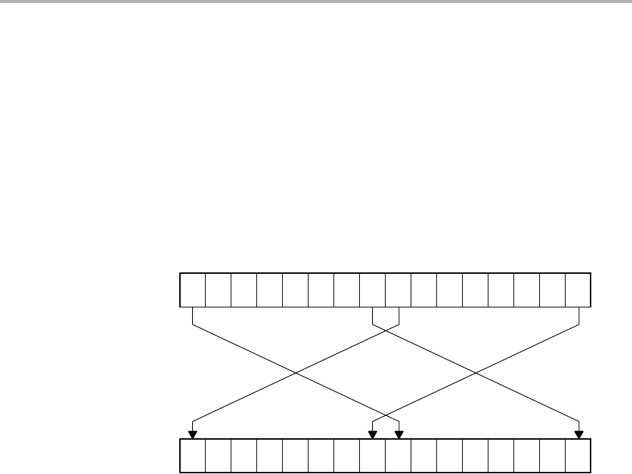
Instruction Set
3-68 RISC 16-Bit CPU
SWPB Swap bytes
Syntax SWPB dst
Operation Bits 15 to 8 <−> bits 7 to 0
Description The destination operand high and low bytes are exchanged as shown in
Figure 3−18.
Status Bits Status bits are not affected.
Mode Bits OSCOFF, CPUOFF, and GIE are not affected.
Figure 3−18. Destination Operand Byte Swap
15 8 7 0
Example
MOV #040BFh,R7 ; 0100000010111111 −> R7
SWPB R7 ; 1011111101000000 in R7
Example The value in R5 is multiplied by 256. The result is stored in R5,R4.
SWPB R5 ;
MOV R5,R4 ;Copy the swapped value to R4
BIC #0FF00h,R5 ;Correct the result
BIC #00FFh,R4 ;Correct the result
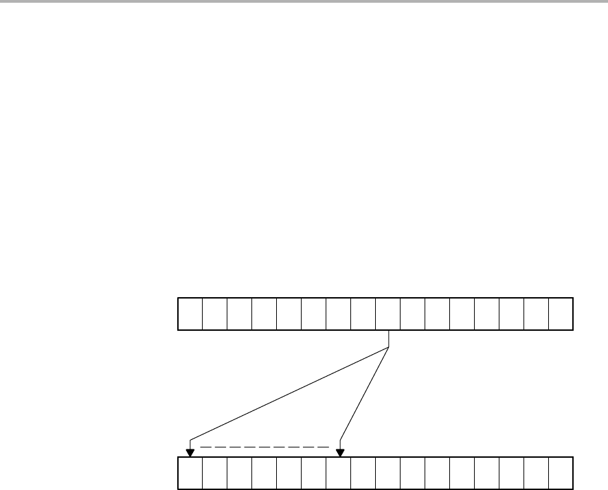
Instruction Set
3-69
RISC 16-Bit CPU
SXT Extend Sign
Syntax SXT dst
Operation Bit 7 −> Bit 8 ......... Bit 15
Description The sign of the low byte is extended into the high byte as shown in Figure 3−19.
Status Bits N: Set if result is negative, reset if positive
Z: Set if result is zero, reset otherwise
C: Set if result is not zero, reset otherwise (.NOT. Zero)
V: Reset
Mode Bits OSCOFF, CPUOFF, and GIE are not affected.
Figure 3−19. Destination Operand Sign Extension
15 8 7 0
Example R7 is loaded with the P1IN value. The operation of the sign-extend instruction
expands bit 8 to bit 15 with the value of bit 7.
R7 is then added to R6.
MOV.B &P1IN,R7 ; P1IN = 080h: . . . . . . . . 1000 0000
SXT R7 ; R7 = 0FF80h: 1111 1111 1000 0000

Instruction Set
3-70 RISC 16-Bit CPU
* TST[.W] Test destination
* TST.B Test destination
Syntax TST dst or TST.W dst
TST.B dst
Operation dst + 0FFFFh + 1
dst + 0FFh + 1
Emulation CMP #0,dst
CMP.B #0,dst
Description The destination operand is compared with zero. The status bits are set accord-
ing to the result. The destination is not affected.
Status Bits N: Set if destination is negative, reset if positive
Z: Set if destination contains zero, reset otherwise
C: Set
V: Reset
Mode Bits OSCOFF, CPUOFF, and GIE are not affected.
Example R7 is tested. If it is negative, continue at R7NEG; if it is positive but not zero,
continue at R7POS.
TST R7 ; Test R7
JN R7NEG ; R7 is negative
JZ R7ZERO ; R7 is zero
R7POS ...... ; R7 is positive but not zero
R7NEG ...... ; R7 is negative
R7ZERO ...... ; R7 is zero
Example The low byte of R7 is tested. If it is negative, continue at R7NEG; if it is positive
but not zero, continue at R7POS.
TST.B R7 ; Test low byte of R7
JN R7NEG ; Low byte of R7 is negative
JZ R7ZERO ; Low byte of R7 is zero
R7POS ...... ; Low byte of R7 is positive but not zero
R7NEG ..... ; Low byte of R7 is negative
R7ZERO ...... ; Low byte of R7 is zero

Instruction Set
3-71
RISC 16-Bit CPU
XOR[.W] Exclusive OR of source with destination
XOR.B Exclusive OR of source with destination
Syntax XOR src,dst or XOR.W src,dst
XOR.B src,dst
Operation src .XOR. dst −> dst
Description The source and destination operands are exclusive ORed. The result is placed
into the destination. The source operand is not affected.
Status Bits N: Set if result MSB is set, reset if not set
Z: Set if result is zero, reset otherwise
C: Set if result is not zero, reset otherwise ( = .NOT. Zero)
V: Set if both operands are negative
Mode Bits OSCOFF, CPUOFF, and GIE are not affected.
Example The bits set in R6 toggle the bits in the RAM word TONI.
XOR R6,TONI ; Toggle bits of word TONI on the bits set in R6
Example The bits set in R6 toggle the bits in the RAM byte TONI.
XOR.B R6,TONI ; Toggle bits of byte TONI on the bits set in
; low byte of R6
Example Reset to 0 those bits in low byte of R7 that are different from bits in RAM byte
EDE.
XOR.B EDE,R7 ; Set different bit to “1s”
INV.B R7 ; Invert Lowbyte, Highbyte is 0h

Instruction Set
3-72 RISC 16-Bit CPU
3.4.4 Instruction Cycles and Lengths
The number of CPU clock cycles required for an instruction depends on the
instruction format and the addressing modes used - not the instruction itself.
The number of clock cycles refers to the MCLK.
Interrupt and Reset Cycles
Table 3−14 lists the CPU cycles for interrupt overhead and reset.
Table 3−14.Interrupt and Reset Cycles
No. of L
e
n
gt
h
o
f
Action
No
.
of
Cycles
Length
of
Instruction
Return from interrupt (RETI) 5 1
Interrupt accepted 6 −
WDT reset 4 −
Reset (RST/NMI) 4 −
Format-II (Single Operand) Instruction Cycles and Lengths
Table 3−15 lists the length and CPU cycles for all addressing modes of
format-II instructions.
Table 3−15.Format-II Instruction Cycles and Lengths
No. of Cycles
Addressing
Mode
RRA, RRC
SWPB, SXT PUSH CALL
Length of
Instruction Example
Rn 1 3 4 1 SWPB R5
@Rn 3 4 4 1 RRC @R9
@Rn+ 3 5 5 1 SWPB @R10+
#N (See note) 4 5 2 CALL #0F000h
X(Rn) 4 5 5 2 CALL 2(R7)
EDE 4 5 5 2 PUSH EDE
&EDE 4 5 5 2 SXT &EDE
Note: Instruction Format II Immediate Mode
Do not use instructions RRA, RRC, SWPB, and SXT with the immediate
mode in the destination field. Use of these in the immediate mode results in
an unpredictable program operation.
Format-III (Jump) Instruction Cycles and Lengths
All jump instructions require one code word, and take two CPU cycles to
execute, regardless of whether the jump is taken or not.

Instruction Set
3-73
RISC 16-Bit CPU
Format-I (Double Operand) Instruction Cycles and Lengths
Table 3−16 lists the length and CPU cycles for all addressing modes of format-I
instructions.
Table 3−16.Format 1 Instruction Cycles and Lengths
Addressing Mode No. of Length of
Src Dst Cycles
g
Instruction Example
Rn Rm 1 1 MOV R5,R8
PC 2 1 BR R9
x(Rm) 4 2 ADD R5,4(R6)
EDE 4 2 XOR R8,EDE
&EDE 4 2 MOV R5,&EDE
@Rn Rm 2 1 AND @R4,R5
PC 2 1 BR @R8
x(Rm) 5 2 XOR @R5,8(R6)
EDE 5 2 MOV @R5,EDE
&EDE 5 2 XOR @R5,&EDE
@Rn+ Rm 2 1 ADD @R5+,R6
PC 3 1 BR @R9+
x(Rm) 5 2 XOR @R5,8(R6)
EDE 5 2 MOV @R9+,EDE
&EDE 5 2 MOV @R9+,&EDE
#N Rm 2 2 MOV #20,R9
PC 3 2 BR #2AEh
x(Rm) 5 3 MOV #0300h,0(SP)
EDE 5 3 ADD #33,EDE
&EDE 5 3 ADD #33,&EDE
x(Rn) Rm 3 2 MOV 2(R5),R7
()
PC 3 2 BR 2(R6)
TONI 6 3 MOV 4(R7),TONI
x(Rm) 6 3 ADD 4(R4),6(R9)
&TONI 6 3 MOV 2(R4),&TONI
EDE Rm 3 2 AND EDE,R6
PC 3 2 BR EDE
TONI 6 3 CMP EDE,TONI
x(Rm) 6 3 MOV EDE,0(SP)
&TONI 6 3 MOV EDE,&TONI
&EDE Rm 3 2 MOV &EDE,R8
PC 3 2 BR &EDE
TONI 6 3 MOV &EDE,TONI
x(Rm) 6 3 MOV &EDE,0(SP)
&TONI 6 3 MOV &EDE,&TONI

Instruction Set
3-74 RISC 16-Bit CPU
3.4.5 Instruction Set Description
The instruction map is shown in Figure 3−20 and the complete instruction set
is summarized in Table 3−17.
Figure 3−20. Core Instruction Map
0xxx
4xxx
8xxx
Cxxx
1xxx
14xx
18xx
1Cxx
20xx
24xx
28xx
2Cxx
30xx
34xx
38xx
3Cxx
4xxx
5xxx
6xxx
7xxx
8xxx
9xxx
Axxx
Bxxx
Cxxx
Dxxx
Exxx
Fxxx
RRC RRC.B SWPB RRA RRA.B SXT PUSH PUSH.B CALL RETI
000 040 080 0C0 100 140 180 1C0 200 240 280 2C0 300 340 380 3C0
JNE/JNZ
JEQ/JZ
JNC
JC
JN
JGE
JL
JMP
MOV, MOV.B
ADD, ADD.B
ADDC, ADDC.B
SUBC, SUBC.B
SUB, SUB.B
CMP, CMP.B
DADD, DADD.B
BIT, BIT.B
BIC, BIC.B
BIS, BIS.B
XOR, XOR.B
AND, AND.B

Instruction Set
3-75
RISC 16-Bit CPU
Table 3−17.MSP430 Instruction Set
Mnemonic Description V N Z C
ADC(.B)†dst Add C to destination dst + C → dst * * * *
ADD(.B) src,dst Add source to destination src + dst → dst * * * *
ADDC(.B) src,dst Add source and C to destination src + dst + C → dst * * * *
AND(.B) src,dst AND source and destination src .and. dst → dst 0 * * *
BIC(.B) src,dst Clear bits in destination .not.src .and. dst → dst − − − −
BIS(.B) src,dst Set bits in destination src .or. dst → dst − − − −
BIT(.B) src,dst Test bits in destination src .and. dst 0 * * *
BR†dst Branch to destination dst → PC −−−−
CALL dst Call destination PC+2 → stack, dst → PC −−−−
CLR(.B)†dst Clear destination 0 → dst − − − −
CLRC†Clear C 0 → C −−−0
CLRN†Clear N 0 → N−0−−
CLRZ†Clear Z 0 → Z −−0−
CMP(.B) src,dst Compare source and destination dst − src * * * *
DADC(.B)†dst Add C decimally to destination dst + C → dst (decimally) * * * *
DADD(.B) src,dst Add source and C decimally to dst. src + dst + C → dst (decimally) * * * *
DEC(.B)†dst Decrement destination dst − 1 → dst * * * *
DECD(.B)†dst Double-decrement destination dst − 2 → dst * * * *
DINT†Disable interrupts 0 → GIE − − − −
EINT†Enable interrupts 1 → GIE − − − −
INC(.B)†dst Increment destination dst +1 → dst * * * *
INCD(.B)†dst Double-increment destination dst+2 →dst * * * *
INV(.B)†dst Invert destination .not.dst → dst * * * *
JC/JHS label Jump if C set/Jump if higher or same − − − −
JEQ/JZ label Jump if equal/Jump if Z set − − − −
JGE label Jump if greater or equal − − − −
JL label Jump if less −−−−
JMP label Jump PC + 2 x offset → PC −−−−
JN label Jump if N set −−−−
JNC/JLO label Jump if C not set/Jump if lower − − − −
JNE/JNZ label Jump if not equal/Jump if Z not set − − − −
MOV(.B) src,dst Move source to destination src → dst − − − −
NOP†No operation −−−−
POP(.B)†dst Pop item from stack to destination @SP → dst, SP+2 → SP −−−−
PUSH(.B) src Push source onto stack SP − 2 → SP, src → @SP − − − −
RET†Return from subroutine @SP → PC, SP + 2 → SP −−−−
RETI Return from interrupt * * * *
RLA(.B)†dst Rotate left arithmetically * * * *
RLC(.B)†dst Rotate left through C * * * *
RRA(.B) dst Rotate right arithmetically 0 * * *
RRC(.B) dst Rotate right through C * * * *
SBC(.B)†dst Subtract not(C) from destination dst + 0FFFFh + C → dst * * * *
SETC†Set C 1 → C −−−1
SETN†Set N 1 → N−1−−
SETZ†Set Z 1 → C −−1−
SUB(.B) src,dst Subtract source from destination dst + .not.src + 1 → dst * * * *
SUBC(.B) src,dst Subtract source and not(C) from dst. dst + .not.src + C → dst * * * *
SWPB dst Swap bytes −−−−
SXT dst Extend sign 0***
TST(.B)†dst Test destination dst + 0FFFFh + 1 0 * * 1
XOR(.B) src,dst Exclusive OR source and destination src .xor. dst → dst * * * *
† Emulated Instruction

3-76 RISC 16-Bit CPU

4-1
16-Bit MSP430X CPU
16-Bit MSP430X CPU
This chapter describes the extended MSP430X 16-bit RISC CPU with 1-MB
memory access, its addressing modes, and instruction set. The MSP430X
CPU is implemented in all MSP430 devices that exceed 64-KB of address
space.
Topic Page
4.1 CPU Introduction 4-2. . . . . . . . . . . . . . . . . . . . . . . . . . . . . . . . . . . . . . . . . . . . . .
4.2 Interrupts 4-4. . . . . . . . . . . . . . . . . . . . . . . . . . . . . . . . . . . . . . . . . . . . . . . . . . . . .
4.3 CPU Registers 4-5. . . . . . . . . . . . . . . . . . . . . . . . . . . . . . . . . . . . . . . . . . . . . . . . .
4.4 Addressing Modes 4-15. . . . . . . . . . . . . . . . . . . . . . . . . . . . . . . . . . . . . . . . . . . .
4.5 MSP430 and MSP430X Instructions 4-36. . . . . . . . . . . . . . . . . . . . . . . . . . . .
4.6 Instruction Set Description 4-58. . . . . . . . . . . . . . . . . . . . . . . . . . . . . . . . . . . .
Chapter 4

CPU Introduction
4-2 16-Bit MSP430X CPU
4.1 CPU Introduction
The MSP430X CPU incorporates features specifically designed for modern
programming techniques such as calculated branching, table processing and
the use of high-level languages such as C. The MSP430X CPU can address
a 1-MB address range without paging. In addition, the MSP430X CPU has
fewer interrupt overhead cycles and fewer instruction cycles in some cases
than the MSP430 CPU, while maintaining the same or better code density than
the MSP430 CPU. The MSP430X CPU is completely backwards compatible
with the MSP430 CPU.
The MSP430X CPU features include:
-RISC architecture.
-Orthogonal architecture.
-Full register access including program counter, status register and stack
pointer.
-Single-cycle register operations.
-Large register file reduces fetches to memory.
-20-bit address bus allows direct access and branching throughout the
entire memory range without paging.
-16-bit data bus allows direct manipulation of word-wide arguments.
-Constant generator provides the six most often used immediate values
and reduces code size.
-Direct memory-to-memory transfers without intermediate register holding.
-Byte, word, and 20-bit address-word addressing
The block diagram of the MSP430X CPU is shown in Figure 4−1.
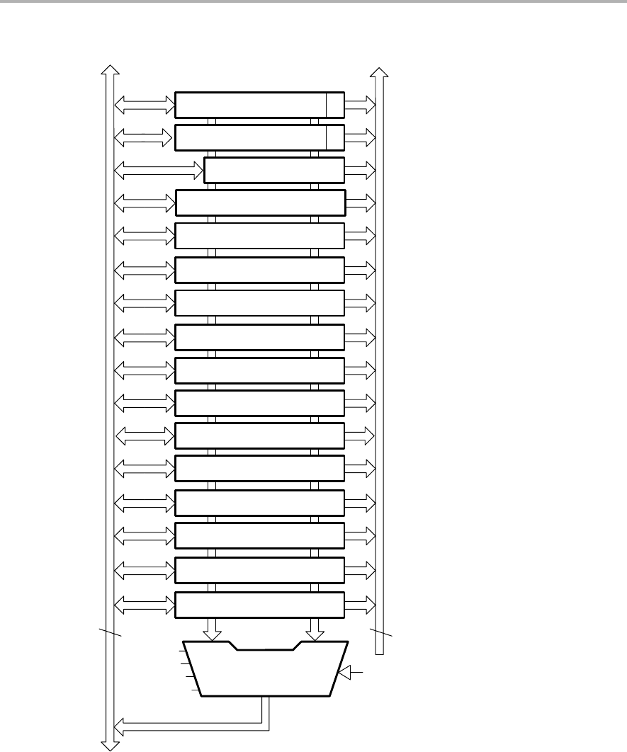
CPU Introduction
4-3
16-Bit MSP430X CPU
Figure 4−1. MSP430X CPU Block Diagram
R6
R5
R4
R3/CG2 Constant Generator
R7
R8
R9
R10
R11
R12
R13
R14
R15
0
0
R0/PC Program Counter
19
R1/SP Pointer Stack
General Purpose
General Purpose
General Purpose
General Purpose
General Purpose
General Purpose
General Purpose
General Purpose
General Purpose
General Purpose
General Purpose
General Purpose
Memory Address Bus − MABMDB − Memory Data Bus
16 20
16/20−bit ALU
srcdst
Zero, Z
Carry, C
Overflow,V
Negative,N
MCLK
0
16 15
R2/SR Status Register
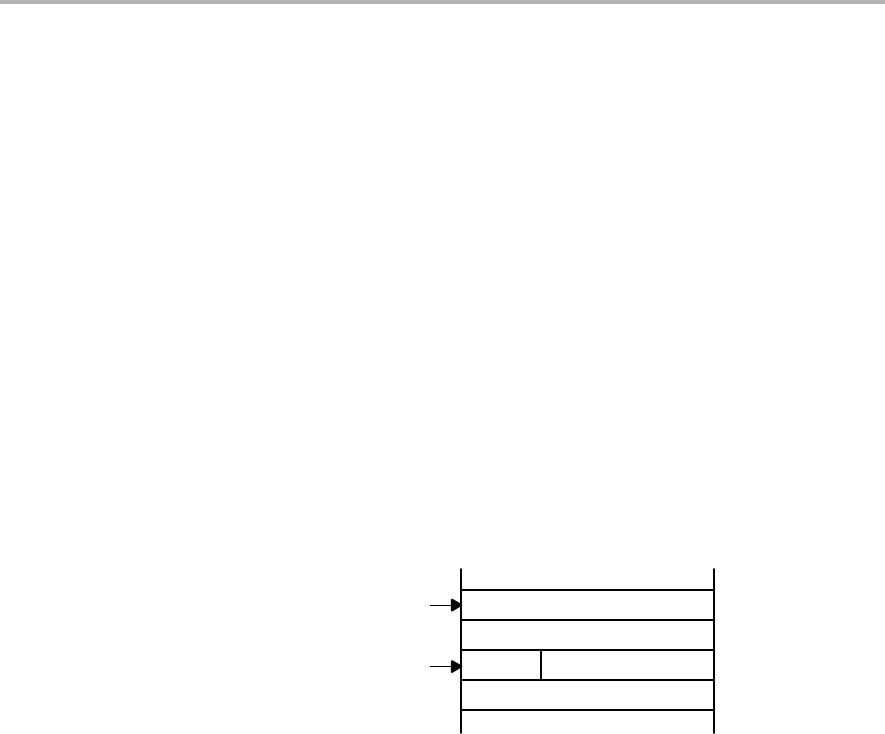
Interrupts
4-4 16-Bit MSP430X CPU
4.2 Interrupts
The MSP430X uses the same interrupt structure as the MSP430:
-Vectored interrupts with no polling necessary
-Interrupt vectors are located downward from address 0FFFEh
Interrupt operation for both MSP430 and MSP430X CPUs is described in
Chapter 2 System Resets, Interrupts, and Operating modes, Section 2
Interrupts. The interrupt vectors contain 16-bit addresses that point into the
lower 64-KB memory. This means all interrupt handlers must start in the lower
64-KB memory − even in MSP430X devices.
During an interrupt, the program counter and the status register are pushed
onto the stack as shown in Figure 4−2. The MSP430X architecture efficiently
stores the complete 20-bit PC value by automatically appending the PC bits
19:16 to the stored SR value on the stack. When the RETI instruction is
executed, the full 20-bit PC is restored making return from interrupt to any
address in the memory range possible.
Figure 4−2. Program Counter Storage on the Stack for Interrupts
Item n−1
PC.19:16
PC.15:0
SPold
SP SR.11:0

CPU Registers
4-5
16-Bit MSP430X CPU
4.3 CPU Registers
The CPU incorporates sixteen registers R0 to R15. Registers R0, R1, R2, and
R3 have dedicated functions. R4 to R15 are working registers for general use.
4.3.1 Program Counter PC
The 20-bit program counter (PC/R0) points to the next instruction to be
executed. Each instruction uses an even number of bytes (two, four, six or
eight bytes), and the PC is incremented accordingly. Instruction accesses are
performed on word boundaries, and the PC is aligned to even addresses.
Figure 4−3 shows the program counter.
Figure 4−3. Program Counter PC
0Program Counter Bits 19 to 1
19 15 1 016
The PC can be addressed with all instructions and addressing modes. A few
examples:
MOV.W #LABEL,PC ; Branch to address LABEL (lower 64 KB)
MOVA #LABEL,PC ; Branch to address LABEL (1MB memory)
MOV.W LABEL,PC ; Branch to address in word LABEL
; (lower 64 KB)
MOV.W @R14,PC ; Branch indirect to address in
; R14 (lower 64 KB)
ADDA #4,PC ; Skip two words (1 MB memory)
The BR and CALL instructions reset the upper four PC bits to 0. Only
addresses in the lower 64-KB address range can be reached with the BR or
CALL instruction. When branching or calling, addresses beyond the lower
64-KB range can only be reached using the BRA or CALLA instructions. Also,
any instruction to directly modify the PC does so according to the used
addressing mode. For example, MOV.W #value,PC will clear the upper four
bits of the PC because it is a .W instruction.

CPU Registers
4-6 16-Bit MSP430X CPU
The program counter is automatically stored on the stack with CALL, or CALLA
instructions, and during an interrupt service routine. Figure 4−4 shows the
storage of the program counter with the return address after a CALLA
instruction. A CALL instruction stores only bits 15:0 of the PC.
Figure 4−4. Program Counter Storage on the Stack for CALLA
Item n
PC.19:16
PC.15:0
SPold
SP
The RETA instruction restores bits 19:0 of the program counter and adds 4 to
the stack pointer. The RET instruction restores bits 15:0 to the program
counter and adds 2 to the stack pointer.
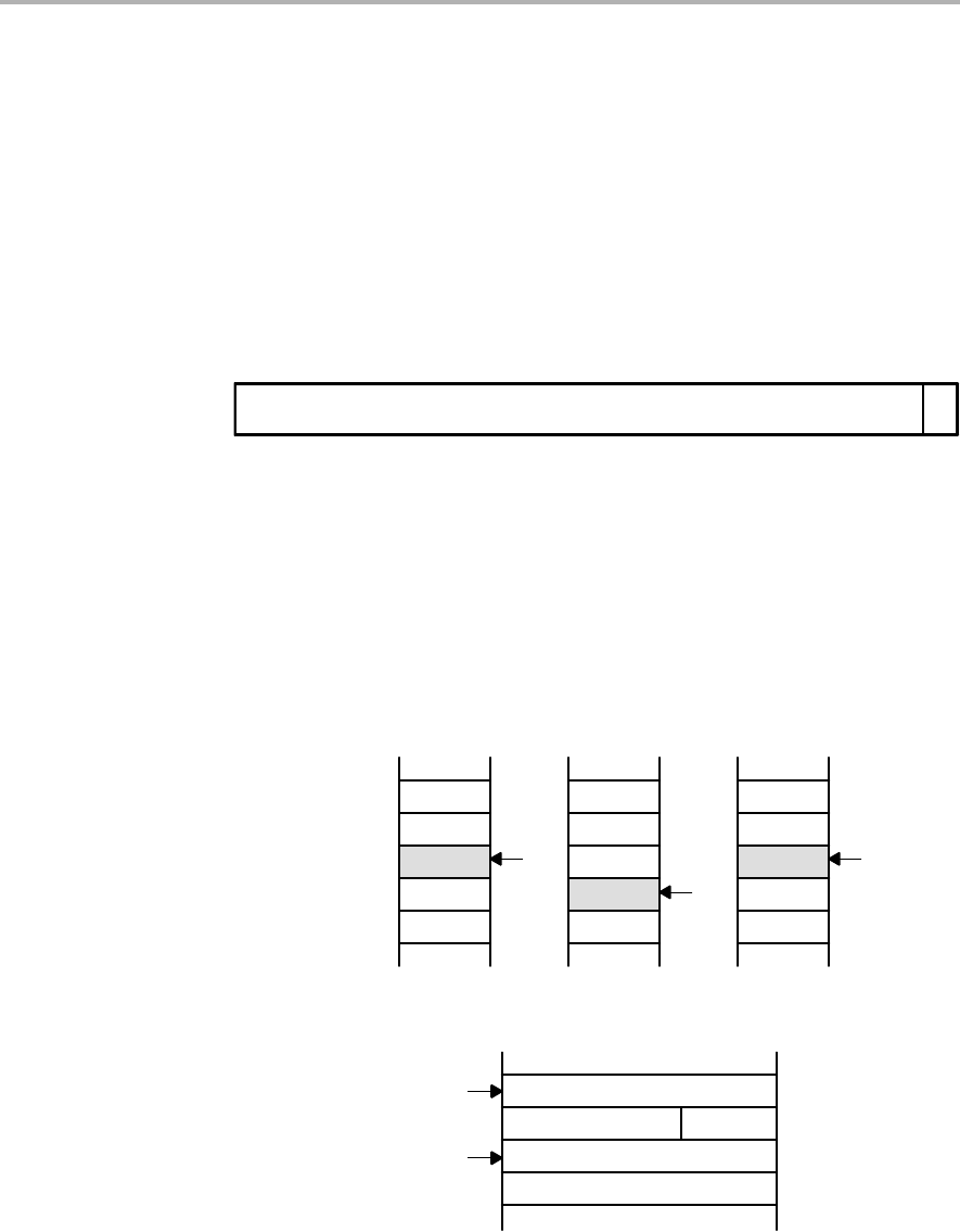
CPU Registers
4-7
16-Bit MSP430X CPU
4.3.2 Stack Pointer (SP)
The 20-bit stack pointer (SP/R1) is used by the CPU to store the return
addresses of subroutine calls and interrupts. It uses a predecrement,
postincrement scheme. In addition, the SP can be used by software with all
instructions and addressing modes. Figure 4−5 shows the SP. The SP is
initialized into RAM by the user, and is always aligned to even addresses.
Figure 4−6 shows the stack usage. Figure 4−7 shows the stack usage when
20-bit address-words are pushed.
Figure 4−5. Stack Pointer
0Stack Pointer Bits 19 to 1
19 10
MOV.W 2(SP),R6 ; Copy Item I2 to R6
MOV.W R7,0(SP) ; Overwrite TOS with R7
PUSH #0123h ; Put 0123h on stack
POP R8 ; R8 = 0123h
Figure 4−6. Stack Usage
I3
I1
I2
I3
0xxxh
0xxxh − 2
0xxxh − 4
0xxxh − 6
0xxxh − 8
I1
I2
SP
0123h SP
I1
I2
I3 SP
PUSH #0123h POP R8Address
Figure 4−7. PUSHX.A Format on the Stack
Item n−1
Item.19:16
Item.15:0
SPold
SP
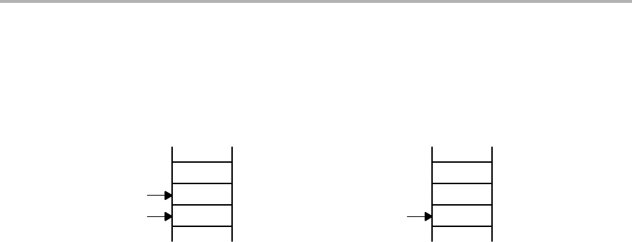
CPU Registers
4-8 16-Bit MSP430X CPU
The special cases of using the SP as an argument to the PUSH and POP
instructions are described and shown in Figure 4−8.
Figure 4−8. PUSH SP - POP SP Sequence
SP1
SPold
SP1
PUSH SP
The stack pointer is changed after
a PUSH SP instruction.
SP1
SP2
POP SP
The stack pointer is not changed after a POP SP
instruction. The POP SP instruction places SP1 into the
stack pointer SP (SP2=SP1)

CPU Registers
4-9
16-Bit MSP430X CPU
4.3.3 Status Register (SR)
The 16-bit status register (SR/R2), used as a source or destination register,
can only be used in register mode addressed with word instructions. The
remaining combinations of addressing modes are used to support the
constant generator. Figure 4−9 shows the SR bits. Do not write 20-bit values
to the SR. Unpredictable operation can result.
Figure 4−9. Status Register Bits
SCG0 GIE Z C
rw-0
15 0
Reserved N
CPU
OFF
OSC
OFF
SCG1V
879
Table 4−1 describes the status register bits.
Table 4−1. Description of Status Register Bits
Bit Description
Reserved Reserved
VOverflow bit. This bit is set when the result of an arithmetic operation
overflows the signed-variable range.
ADD(.B), ADDX(.B,.A),
ADDC(.B), ADDCX(.B.A),
ADDA
Set when:
positive + positive = negative
negative + negative = positive
otherwise reset
SUB(.B), SUBX(.B,.A),
SUBC(.B),SUBCX(.B,.A),
SUBA, CMP(.B),
CMPX(.B,.A), CMPA
Set when:
positive − negative = negative
negative − positive = positive
otherwise reset
SCG1 System clock generator 1. This bit, when set, turns off the DCO dc
generator if DCOCLK is not used for MCLK or SMCLK.
SCG0 System clock generator 0. This bit, when set, turns off the FLL+ loop
control.
OSCOFF Oscillator Off. This bit, when set, turns off the LFXT1 crystal oscillator
when LFXT1CLK is not used for MCLK or SMCLK.
CPUOFF CPU off. This bit, when set, turns off the CPU.
GIE General interrupt enable. This bit, when set, enables maskable inter-
rupts. When reset, all maskable interrupts are disabled.
NNegative bit. This bit is set when the result of an operation is negative
and cleared when the result is positive.

CPU Registers
4-10 16-Bit MSP430X CPU
Bit Description
ZZero bit. This bit is set when the result of an operation is zero and
cleared when the result is not zero.
CCarry bit. This bit is set when the result of an operation produced a
carry and cleared when no carry occurred.

CPU Registers
4-11
16-Bit MSP430X CPU
4.3.4 The Constant Generator Registers CG1 and CG2
Six commonly used constants are generated with the constant generator
registers R2 (CG1) and R3 (CG2), without requiring an additional 16-bit word
of program code. The constants are selected with the source register
addressing modes (As), as described in Table 4−2.
Table 4−2. Values of Constant Generators CG1, CG2
Register As Constant Remarks
R2 00 - Register mode
R2 01 (0) Absolute address mode
R2 10 00004h +4, bit processing
R2 11 00008h +8, bit processing
R3 00 00000h 0, word processing
R3 01 00001h +1
R3 10 00002h +2, bit processing
R3 11 FFh, FFFFh, FFFFFh -1, word processing
The constant generator advantages are:
-No special instructions required
-No additional code word for the six constants
-No code memory access required to retrieve the constant
The assembler uses the constant generator automatically if one of the six
constants is used as an immediate source operand. Registers R2 and R3,
used in the constant mode, cannot be addressed explicitly; they act as
source-only registers.
Constant Generator − Expanded Instruction Set
The RISC instruction set of the MSP430 has only 27 instructions. However, the
constant generator allows the MSP430 assembler to support 24 additional,
emulated instructions. For example, the single-operand instruction:
CLR dst
is emulated by the double-operand instruction with the same length:
MOV R3,dst
where the #0 is replaced by the assembler, and R3 is used with As=00.
INC dst
is replaced by:
ADD 0(R3),dst
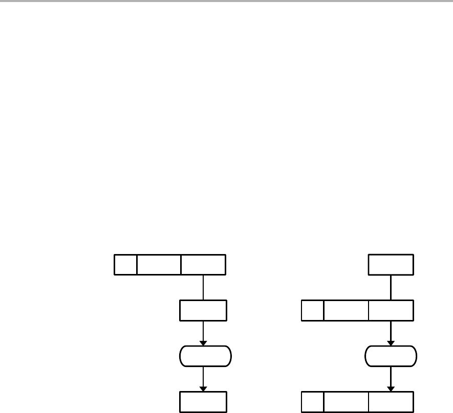
CPU Registers
4-12 16-Bit MSP430X CPU
4.3.5 General-Purpose Registers R4 to R15
The twelve CPU registers R4 to R15, contain 8-bit, 16-bit, or 20-bit values. Any
byte-write to a CPU register clears bits 19:8. Any word-write to a register clears
bits 19:16. The only exception is the SXT instruction. The SXT instruction
extends the sign through the complete 20-bit register.
The following figures show the handling of byte, word and address-word data.
Note the reset of the leading MSBs, if a register is the destination of a byte or
word instruction.
Figure 4−10 shows byte handling (8-bit data, .B suffix). The handling is shown
for a source register and a destination memory byte and for a source memory
byte and a destination register.
Figure 4−10. Register-Byte/Byte-Register Operation
Unused
High Byte Low Byte
Register-Byte Operation
High Byte Low Byte
Byte-Register Operation
Register
Memory Register
Memory
Operation
Memory
Operation
0Register
Un-
used
Unused
Un-
used
0
19 16 15 0
19 16 15 0
8 7
8 7
CPU Registers
4-13
16-Bit MSP430X CPU
Figure 4−11 and Figure 4−12 show 16-bit word handling (.W suffix). The
handling is shown for a source register and a destination memory word and
for a source memory word and a destination register.
Figure 4−11. Register-Word Operation
High Byte Low Byte
Register-Word Operation
Register
Memory
Operation
Memory
Un-
used
19 16 15 0
8 7
Figure 4−12. Word-Register Operation
High Byte Low Byte
Word-Register Operation
Register
Memory
Operation
0Register
Un-
used
19 16 15 0
8 7
CPU Registers
4-14 16-Bit MSP430X CPU
Figure 4−13 and Figure 4−14 show 20-bit address-word handling (.A suffix).
The handling is shown for a source register and a destination memory
address-word and for a source memory address-word and a destination
register.
Figure 4−13. Register − Address-Word Operation
High Byte Low Byte
Register − Address-Word Operation
Register
Memory
Operation
Memory
Unused
0
Memory +2
Memory +2
19 16 15 0
8 7
Figure 4−14. Address-Word − Register Operation
High Byte Low Byte
Address-Word − Register Operation
Register
Memory
Operation
Register
Unused
Memory +2
19 16 15 0
8 7

CPU Registers
4-15
16-Bit MSP430X CPU
4.4 Addressing Modes
Seven addressing modes for the source operand and four addressing modes
for the destination operand use 16-bit or 20-bit addresses. The MSP430 and
MSP430X instructions are usable throughout the entire 1-MB memory range.
Table 4−3. Source/Destination Addressing
As/Ad Addressing Mode Syntax Description
00/0 Register mode Rn Register contents are operand
01/1 Indexed mode X(Rn) (Rn + X) points to the operand. X
is stored in the next word, or
stored in combination of the
preceding extension word and the
next word.
01/1 Symbolic mode ADDR (PC + X) points to the operand. X
is stored in the next word, or
stored in combination of the
preceding extension word and the
next word. Indexed mode X(PC) is
used.
01/1 Absolute mode &ADDR The word following the instruction
contains the absolute address. X
is stored in the next word, or
stored in combination of the
preceding extension word and the
next word. Indexed mode X(SR) is
used.
10/− Indirect register
mode
@Rn Rn is used as a pointer to the
operand.
11/− Indirect
autoincrement
@Rn+ Rn is used as a pointer to the
operand. Rn is incremented
afterwards by 1 for .B instructions.
by 2 for .W instructions, and by 4
for .A instructions.
11/− Immediate mode #N N is stored in the next word, or
stored in combination of the
preceding extension word and the
next word. Indirect autoincrement
mode @PC+ is used.
The seven addressing modes are explained in detail in the following sections.
Most of the examples show the same addressing mode for the source and
destination, but any valid combination of source and destination addressing
modes is possible in an instruction.
Note: Use of Labels EDE, TONI, TOM, and LEO
Throughout MSP430 documentation EDE, TONI, TOM, and LEO are used
as generic labels. They are only labels. They have no special meaning.

CPU Registers
4-16 16-Bit MSP430X CPU
4.4.1 Register Mode
Operation: The operand is the 8-, 16-, or 20-bit content of the used CPU
register.
Length: One, two, or three words
Comment: Valid for source and destination
Byte operation: Byte operation reads only the 8 LSBs of the source register
Rsrc and writes the result to the 8 LSBs of the destination
register Rdst. The bits Rdst.19:8 are cleared. The register
Rsrc is not modified.
Word operation:Word operation reads the 16 LSBs of the source register Rsrc
and writes the result to the 16 LSBs of the destination register
Rdst. The bits Rdst.19:16 are cleared. The register Rsrc is not
modified.
Address-Word operation: Address-word operation reads the 20 bits of the
source register Rsrc and writes the result to the 20 bits of the
destination register Rdst. The register Rsrc is not modified
SXT Exception: The SXT instruction is the only exception for register
operation. The sign of the low byte in bit 7 is extended to the
bits Rdst.19:8.
Example: BIS.W R5,R6 ;
This instruction logically ORs the 16-bit data contained in R5 with the 16-bit
contents of R6. R6.19:16 is cleared.
xxxxh
Address
Space
D506h PC
21036h
21034h
AA550h
11111h
R5
R6
Register
Before:
xxxxh
Address
Space
D506h
PC21036h
21034h
AA550h
0B551h
R5
R6
Register
After:
A550h.or.1111h = B551h

CPU Registers
4-17
16-Bit MSP430X CPU
Example: BISX.A R5,R6 ;
This instruction logically ORs the 20-bit data contained in R5 with the 20-bit
contents of R6.
The extension word contains the A/L-bit for 20-bit data. The instruction word
uses byte mode with bits A/L:B/W = 01. The result of the instruction is:
xxxxh
Address
Space
D546h
PC
21036h
21034h
AA550h
11111h
R5
R6
Register
Before: Address
Space
PC AA550h
BB551h
R5
R6
Register
After:
AA550h.or.11111h = BB551h
1800h21032h
xxxxh
D546h
21036h
21034h
1800h21032h
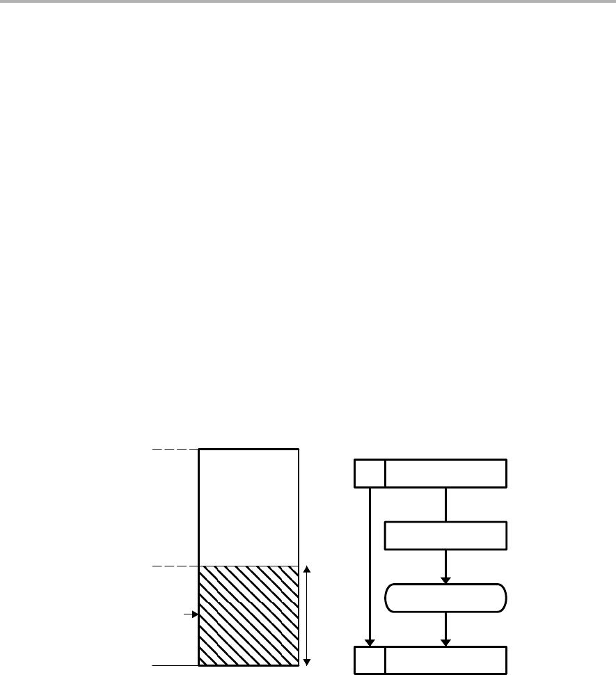
CPU Registers
4-18 16-Bit MSP430X CPU
4.4.2 Indexed Mode
The Indexed mode calculates the address of the operand by adding the signed
index to a CPU register. The Indexed mode has three addressing possibilities:
-Indexed mode in lower 64-KB memory
-MSP430 instruction with Indexed mode addressing memory above the
lower 64-KB memory.
-MSP430X instruction with Indexed mode
Indexed Mode in Lower 64 KB Memory
If the CPU register Rn points to an address in the lower 64 KB of the memory
range, the calculated memory address bits 19:16 are cleared after the addition
of the CPU register Rn and the signed 16-bit index. This means, the calculated
memory address is always located in the lower 64 KB and does not overflow
or underflow out of the lower 64-KB memory space. The RAM and the
peripheral registers can be accessed this way and existing MSP430 software
is usable without modifications as shown in Figure 4−15.
Figure 4−15. Indexed Mode in Lower 64 KB
16-bit
signed index
CPU Register
Rn
16-bit signed add
0 Memory address
FFFFF
00000
Lower 64KB
0FFFF
10000
Rn.19:0
Lower 64 KB.
Rn.19:16 = 0
16-bit byte index
0
19 16 15 0
S
Length: Two or three words
Operation: The signed 16-bit index is located in the next word after the
instruction and is added to the CPU register Rn. The resulting
bits 19:16 are cleared giving a truncated 16-bit memory
address, which points to an operand address in the range
00000h to 0FFFFh. The operand is the content of the
addressed memory location.
Comment: Valid for source and destination. The assembler calculates
the register index and inserts it.
CPU Registers
4-19
16-Bit MSP430X CPU
Example: ADD.B 1000h(R5),0F000h(R6);
The previous instruction adds the 8-bit data contained in source byte
1000h(R5) and the destination byte 0F000h(R6) and places the result into the
destination byte. Source and destination bytes are both located in the lower
64 KB due to the cleared bits 19:16 of registers R5 and R6.
Source: The byte pointed to by R5 + 1000h results in address 0479Ch
+ 1000h = 0579Ch after truncation to a 16-bit address.
Destination: The byte pointed to by R6 + F000h results in address 01778h
+ F000h = 00778h after truncation to a 16-bit address.
xxxxh
Address
Space
F000h
1000h
PC
1103Ah
11038h
11036h
0479Ch
01778h
R5
R6
01778h
+F000h
00778h
Register
Before: Address
Space
Register
After:
55D6h
11034h
xxxxh
F000h
1000h
PC1103Ah
11038h
11036h
0479Ch
01778h
R5
R6
55D6h
11034h
xxxxh
xx45h
0077Ah
00778h
xxxxh
xx77h
0077Ah
00778h
32h
+45h
77h
src
dst
Sum
0479Ch
+1000h
0579Ch
xxxxh
xx32h
0579Eh
0579Ch
xxxxh
xx32h
0579Eh
0579Ch
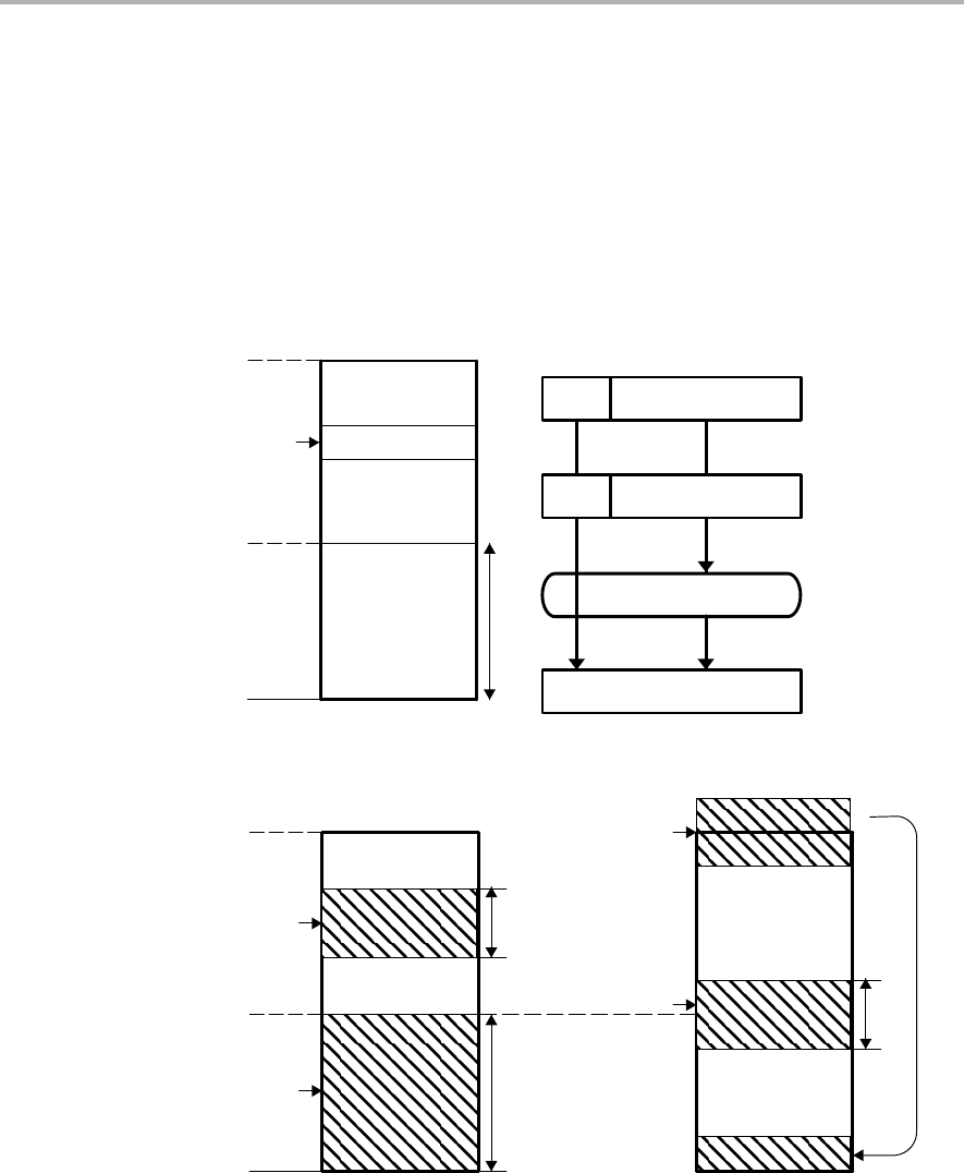
CPU Registers
4-20 16-Bit MSP430X CPU
MSP430 Instruction with Indexed Mode in Upper Memory
If the CPU register Rn points to an address above the lower 64-KB memory,
the Rn bits 19:16 are used for the address calculation of the operand. The
operand may be located in memory in the range Rn ±32 KB, because the
index, X, is a signed 16-bit value. In this case, the address of the operand can
overflow or underflow into the lower 64-KB memory space. See Figure 4−16
and Figure 4−17.
Figure 4−16. Indexed Mode in Upper Memory
16-bit signed index
(sign extended to
20 bits)
CPU Register
Rn
20-bit signed add
Memory address
FFFFF
00000
Lower 64 KB
0FFFF
10000
Upper Memory
Rn.19:16 > 0
16-bit byte index
1 ... 15
19 16 15 0
S
Rn ±32 KB
S
Rn.19:0
Figure 4−17. Overflow and Underflow for the Indexed Mode
FFFFF
0000C
Lower 64 KB
0,FFFF
10000
Rn.19:0
Rn.19:0
Rn.19:0
±32KB
±32KB
Rn.19:0

CPU Registers
4-21
16-Bit MSP430X CPU
Length: Two or three words
Operation: The sign-extended 16-bit index in the next word after the
instruction is added to the 20 bits of the CPU register Rn. This
delivers a 20-bit address, which points to an address in the
range 0 to FFFFFh. The operand is the content of the
addressed memory location.
Comment: Valid for source and destination. The assembler calculates
the register index and inserts it.
Example: ADD.W 8346h(R5),2100h(R6);
This instruction adds the 16-bit data contained in the source and the
destination addresses and places the 16-bit result into the destination. Source
and destination operand can be located in the entire address range.
Source: The word pointed to by R5 + 8346h. The negative index
8346h is sign-extended, which results in address 23456h +
F8346h = 1B79Ch.
Destination: The word pointed to by R6 + 2100h results in address
15678h + 2100h = 17778h.
Figure 4−18. Example for the Indexed Mode
xxxxh
Address
Space
2100h
8346h
PC
1103Ah
11038h
11036h
23456h
15678h
R5
R6
15678h
+02100h
17778h
Register
Before: Address
Space
Register
After:
5596h
11034h
xxxxh
2100h
8346h
PC1103Ah
11038h
11036h
23456h
15678h
R5
R6
5596h
11034h
xxxxh
2345h
1777Ah
17778h
xxxxh
7777h
1777Ah
17778h
05432h
+02345h
07777h
src
dst
Sum
23456h
+F8346h
1B79Ch
xxxxh
5432h
1B79Eh
1B79Ch
xxxxh
5432h
1B79Eh
1B79Ch

CPU Registers
4-22 16-Bit MSP430X CPU
MSP430X Instruction with Indexed Mode
When using an MSP430X instruction with Indexed mode, the operand can be
located anywhere in the range of Rn ± 19 bits.
Length: Three or four words
Operation: The operand address is the sum of the 20-bit CPU register
content and the 20-bit index. The four MSBs of the index are
contained in the extension word, the 16 LSBs are contained
in the word following the instruction. The CPU register is not
modified.
Comment: Valid for source and destination. The assembler calculates
the register index and inserts it.
Example: ADDX.A 12346h(R5),32100h(R6) ;
This instruction adds the 20-bit data contained in the source and the
destination addresses and places the result into the destination.
Source: Two words pointed to by R5 + 12346h which results in
address 23456h + 12346h = 3579Ch.
Destination: Two words pointed to by R6 + 32100h which results in
address 45678h + 32100h = 77778h.
CPU Registers
4-23
16-Bit MSP430X CPU
The extension word contains the MSBs of the source index and of the
destination index and the A/L-bit for 20-bit data. The instruction word uses byte
mode due to the 20-bit data length with bits A/L:B/W = 01.
2100h
Address
Space
2346h
55D6h
PC
21038h
21036h
21034h
23456h
45678h
R5
R6
45678h
+32100h
77778h
Register
Before: Address
Space
Register
After:
PC 23456h
45678h
R5
R6
0001h
2345h
7777Ah
77778h
0007h
7777h
7777Ah
77778h
65432h
+12345h
77777h
src
dst
Sum
0006h
5432h
3579Eh
3579Ch
0006h
5432h
3579Eh
3579Ch
1883h
21032h
xxxxh
2103Ah
2100h
2346h
55D6h
21038h
21036h
21034h
1883h
21032h
xxxxh
2103Ah
23456h
+12346h
3579Ch
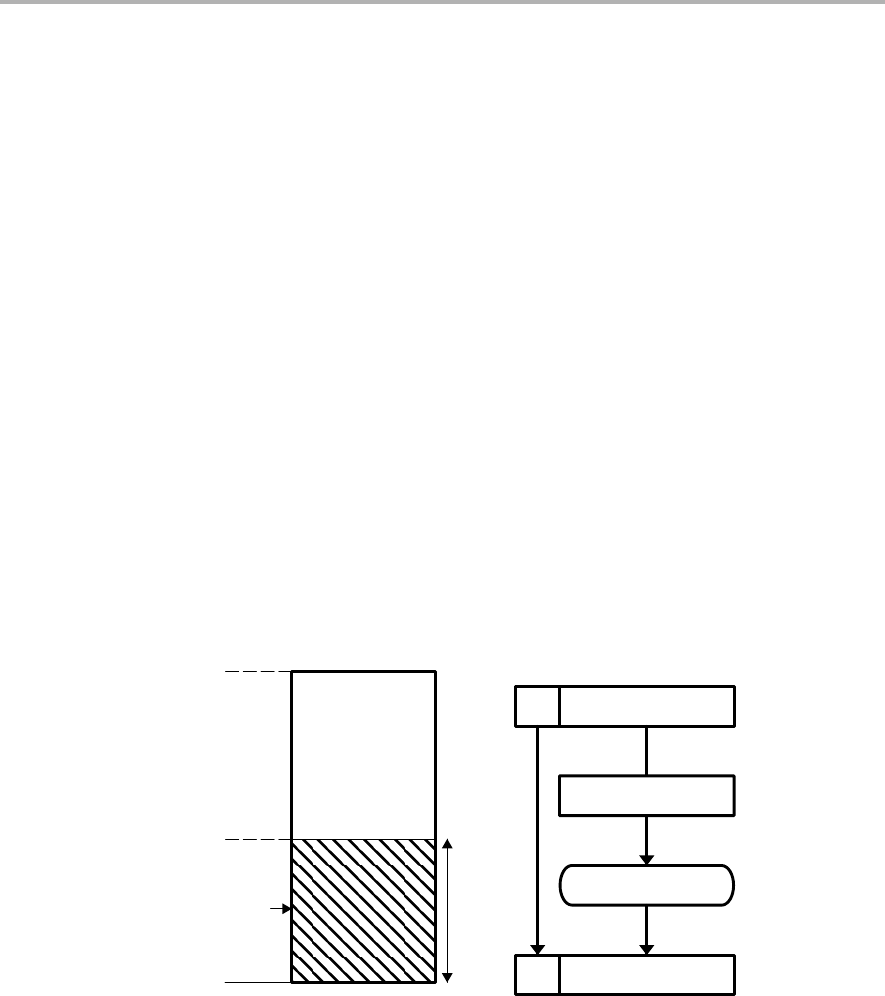
CPU Registers
4-24 16-Bit MSP430X CPU
4.4.3 Symbolic Mode
The Symbolic mode calculates the address of the operand by adding the
signed index to the program counter. The Symbolic mode has three
addressing possibilities:
-Symbolic mode in lower 64-KB memory
-MSP430 instruction with symbolic mode addressing memory above the
lower 64-KB memory.
-MSP430X instruction with symbolic mode
Symbolic Mode in Lower 64 KB
If the PC points to an address in the lower 64 KB of the memory range, the
calculated memory address bits 19:16 are cleared after the addition of the PC
and the signed 16-bit index. This means, the calculated memory address is
always located in the lower 64 KB and does not overflow or underflow out of
the lower 64-KB memory space. The RAM and the peripheral registers can be
accessed this way and existing MSP430 software is usable without
modifications as shown in Figure 4−15.
Figure 4−19. Symbolic Mode Running in Lower 64 KB
16-bit signed
PC index
Program
counter PC
16-bit signed add
0 Memory address
FFFFF
00000
Lower 64 KB
0FFFF
10000
PC.19:0
Lower 64 KB.
PC.19:16 = 0
16-bit byte index
0
19 16 15 0
S
Operation: The signed 16-bit index in the next word after the instruction is
added temporarily to the PC. The resulting bits 19:16 are cleared giving a
truncated 16-bit memory address, which points to an operand address in the
range 00000h, to 0FFFFh. The operand is the content of the addressed
memory location.
Length: Two or three words
Comment: Valid for source and destination. The assembler calculates
the PC index and inserts it.
Example: ADD.B EDE,TONI ;
CPU Registers
4-25
16-Bit MSP430X CPU
The previous instruction adds the 8-bit data contained in source byte EDE and
destination byte TONI and places the result into the destination byte TONI.
Bytes EDE and TONI and the program are located in the lower 64 KB.
Source: Byte EDE located at address 0,579Ch, pointed to by PC +
4766h where the PC index 4766h is the result of 0579Ch −
01036h = 04766h. Address 01036h is the location of the index
for this example.
Destination: Byte TONI located at address 00778h, pointed to by PC +
F740h, is the truncated 16-bit result of
00778h − 1038h = FF740h. Address 01038h is the location
of the index for this example.
xxxxh
Address
Space
F740h
4766h
PC
0103Ah
01038h
01036h
01038h
+0F740h
00778h
Before: Address
Space
After:
05D0h
01034h
xxxxh
F740h
4766h
PC0103Ah
01038h
01036h
50D0h
01034h
xxxxh
xx45h
0077Ah
00778h
xxxxh
xx77h
0077Ah
00778h
32h
+45h
77h
src
dst
Sum
01036h
+04766h
0579Ch
xxxxh
xx32h
0579Eh
0579Ch
xxxxh
xx32h
0579Eh
0579Ch
CPU Registers
4-26 16-Bit MSP430X CPU
MSP430 Instruction with Symbolic Mode in Upper Memory
If the PC points to an address above the lower 64-KB memory, the PC bits
19:16 are used for the address calculation of the operand. The operand may
be located in memory in the range PC ±32 KB, because the index, X, is a
signed 16-bit value. In this case, the address of the operand can overflow or
underflow into the lower 64-KB memory space as shown in Figure 4−20 and
Figure 4−21.
Figure 4−20. Symbolic Mode Running in Upper Memory
16-bit signed PC
index (sign
extended to
20 bits)
Program
counter PC
20-bit signed add
Memory address
FFFFF
00000
Lower 64 KB
0FFFF
10000
PC.19:0
Upper Memory
PC.19:16 > 0
16-bit byte index
1 ... 15
19 16 15 0
S
PC ±32 KB
S
Figure 4−21. Overflow and Underflow for the Symbolic Mode
FFFFF
0000C
Lower 64 KB
0FFFF
10000
PC.19:0
PC.19:0
PC.19:0
±32KB
±32KB
PC.19:0
CPU Registers
4-27
16-Bit MSP430X CPU
Length: Two or three words
Operation: The sign-extended 16-bit index in the next word after the
instruction is added to the 20 bits of the PC. This delivers a
20-bit address, which points to an address in the range 0 to
FFFFFh. The operand is the content of the addressed
memory location.
Comment: Valid for source and destination. The assembler calculates
the PC index and inserts it
Example: ADD.W EDE,&TONI ;
This instruction adds the 16-bit data contained in source word EDE and
destination word TONI and places the 16-bit result into the destination word
TONI. For this example, the instruction is located at address 2,F034h.
Source: Word EDE at address 3379Ch, pointed to by PC + 4766h
which is the 16-bit result of 3379Ch − 2F036h = 04766h.
Address 2F036h is the location of the index for this example.
Destination: Word TONI located at address 00778h pointed to by the
absolute address 00778h.
xxxxh
Address
Space
0778h
4766h
PC
2F03Ah
2F038h
2F036h
2F036h
+04766h
3379Ch
Before: Address
Space
After:
5092h
2F034h
xxxxh
0778h
4766h
PC2F03Ah
2F038h
2F036h
5092h
2F034h
xxxxh
5432h
3379Eh
3379Ch
xxxxh
5432h
3379Eh
3379Ch
5432h
+2345h
7777h
src
dst
Sum
xxxxh
2345h
0077Ah
00778h
xxxxh
7777h
0077Ah
00778h
CPU Registers
4-28 16-Bit MSP430X CPU
MSP430X Instruction with Symbolic Mode
When using an MSP430X instruction with Symbolic mode, the operand can
be located anywhere in the range of PC ± 19 bits.
Length: Three or four words
Operation: The operand address is the sum of the 20-bit PC and the
20-bit index. The four MSBs of the index are contained in the
extension word, the 16 LSBs are contained in the word
following the instruction.
Comment: Valid for source and destination. The assembler calculates
the register index and inserts it.
Example: ADDX.B EDE,TONI ;
The instruction adds the 8-bit data contained in source byte EDE and
destination byte TONI and places the result into the destination byte TONI.
Source: Byte EDE located at address 3579Ch, pointed to by
PC + 14766h, is the 20-bit result of
3579Ch - 21036h = 14766h. Address 21036h is the address
of the index in this example.
Destination: Byte TONI located at address 77778h, pointed to by
PC + 56740h, is the 20-bit result of
77778h - 21038h = 56740h. Address 21038h is the address
of the index in this example..
6740h
Address Space
4766h
50D0h
PC
21038h
21036h
21034h
21038h
+56740h
77778h
Before: Address SpaceAfter:
PC
xxxxh
xx45h
7777Ah
77778h
xxxxh
xx77h
7777Ah
77778h
32h
+45h
77h
src
dst
Sum
xxxxh
xx32h
3579Eh
3579Ch
xxxxh
xx32h
3579Eh
3579Ch
18C5h
21032h
xxxxh
2103Ah
6740h
4766h
50D0h
21038h
21036h
21034h
18C5h
21032h
xxxxh
2103Ah
21036h
+14766h
3579Ch

CPU Registers
4-29
16-Bit MSP430X CPU
4.4.4 Absolute Mode
The Absolute mode uses the contents of the word following the instruction as
the address of the operand. The Absolute mode has two addressing
possibilities:
-Absolute mode in lower 64-KB memory
-MSP430X instruction with Absolute mode
CPU Registers
4-30 16-Bit MSP430X CPU
Absolute Mode in Lower 64 KB
If an MSP430 instruction is used with Absolute addressing mode, the absolute
address is a 16-bit value and therefore points to an address in the lower 64 KB
of the memory range. The address is calculated as an index from 0 and is
stored in the word following the instruction The RAM and the peripheral
registers can be accessed this way and existing MSP430 software is usable
without modifications.
Length: Two or three words
Operation: The operand is the content of the addressed memory
location.
Comment: Valid for source and destination. The assembler calculates
the index from 0 and inserts it
Example: ADD.W &EDE,&TONI ;
This instruction adds the 16-bit data contained in the absolute source and
destination addresses and places the result into the destination.
Source: Word at address EDE
Destination: Word at address TONI
xxxxh
Address Space
7778h
579Ch
PC
2103Ah
21038h
21036h
Before: Address Space
After:
5292h
21034h
xxxxh
7778h
579Ch
PC2103Ah
21038h
21036h
5292h
21034h
xxxxh
2345h
0777Ah
07778h
xxxxh
7777h
0777Ah
07778h
5432h
+2345h
7777h
src
dst
Sum
xxxxh
5432h
0579Eh
0579Ch
xxxxh
5432h
0579Eh
0579Ch
CPU Registers
4-31
16-Bit MSP430X CPU
MSP430X Instruction with Absolute Mode
If an MSP430X instruction is used with Absolute addressing mode, the
absolute address is a 20-bit value and therefore points to any address in the
memory range. The address value is calculated as an index from 0. The four
MSBs of the index are contained in the extension word, and the 16 LSBs are
contained in the word following the instruction.
Length: Three or four words
Operation: The operand is the content of the addressed memory
location.
Comment: Valid for source and destination. The assembler calculates
the index from 0 and inserts it
Example: ADDX.A &EDE,&TONI ;
This instruction adds the 20-bit data contained in the absolute source and
destination addresses and places the result into the destination.
Source: Two words beginning with address EDE
Destination: Two words beginning with address TONI
7778h
Address
Space
579Ch
52D2h
PC
21038h
21036h
21034h
Before: Address
Space
After:
PC
0001h
2345h
7777Ah
77778h
0007h
7777h
7777Ah
77778h
65432h
+12345h
77777h
src
dst
Sum
0006h
5432h
3579Eh
3579Ch
0006h
5432h
3579Eh
3579Ch
1987h
21032h
xxxxh
2103Ah
7778h
579Ch
52D2h
21038h
21036h
21034h
1987h
21032h
xxxxh
2103Ah

CPU Registers
4-32 16-Bit MSP430X CPU
4.4.5 Indirect Register Mode
The Indirect Register mode uses the contents of the CPU register Rsrc as the
source operand. The Indirect Register mode always uses a 20-bit address.
Length: One, two, or three words
Operation: The operand is the content the addressed memory location.
The source register Rsrc is not modified.
Comment: Valid only for the source operand. The substitute for the
destination operand is 0(Rdst).
Example: ADDX.W @R5,2100h(R6)
This instruction adds the two 16-bit operands contained in the source and the
destination addresses and places the result into the destination.
Source: Word pointed to by R5. R5 contains address 3,579Ch for this
example.
Destination: Word pointed to by R6 + 2100h which results in address
45678h + 2100h = 7778h.
xxxxh
Address
Space
2100h
55A6h PC
21038h
21036h
21034h
3579Ch
45678h
R5
R6
45678h
+02100h
47778h
Register
Before: Address
Space
Register
After:
xxxxh
2100h
55A6h
PC21038h
21036h
21034h
3579Ch
45678h
R5
R6
xxxxh
2345h
4777Ah
47778h
xxxxh
7777h
4777Ah
47778h
5432h
+2345h
7777h
src
dst
Sum
xxxxh
5432h
3579Eh
3579Ch
xxxxh
5432h
3579Eh
3579Ch
R5 R5

CPU Registers
4-33
16-Bit MSP430X CPU
4.4.6 Indirect, Autoincrement Mode
The Indirect Autoincrement mode uses the contents of the CPU register Rsrc
as the source operand. Rsrc is then automatically incremented by 1 for byte
instructions, by 2 for word instructions, and by 4 for address-word instructions
immediately after accessing the source operand. If the same register is used
for source and destination, it contains the incremented address for the
destination access. Indirect Autoincrement mode always uses 20-bit
addresses.
Length: One, two, or three words
Operation: The operand is the content of the addressed memory
location.
Comment: Valid only for the source operand.
Example: ADD.B @R5+,0(R6)
This instruction adds the 8-bit data contained in the source and the destination
addresses and places the result into the destination.
Source: Byte pointed to by R5. R5 contains address 3,579Ch for this
example.
Destination: Byte pointed to by R6 + 0h which results in address 0778h for
this example.
xxxxh
Address
Space
0000h
55F6h PC
21038h
21036h
21034h
3579Ch
00778h
R5
R6
00778h
+0000h
00778h
Register
Before: Address
Space
Register
After:
xxxxh
0000h
55F6h
PC21038h
21036h
21034h
3579Dh
00778h
R5
R6
xxxxh
xx45h
0077Ah
00778h
xxxxh
xx77h
0077Ah
00778h
32h
+45h
77h
src
dst
Sum
xxh
32h
3579Dh
3579Ch
xxh
xx32h
3579Dh
3579Ch
R5
R5

CPU Registers
4-34 16-Bit MSP430X CPU
4.4.7 Immediate Mode
The Immediate mode allows accessing constants as operands by including
the constant in the memory location following the instruction. The program
counter PC is used with the Indirect Autoincrement mode. The PC points to
the immediate value contained in the next word. After the fetching of the
immediate operand, the PC is incremented by 2 for byte, word, or
address-word instructions. The Immediate mode has two addressing
possibilities:
-8- or 16-bit constants with MSP430 instructions
-20-bit constants with MSP430X instruction
MSP430 Instructions with Immediate Mode
If an MSP430 instruction is used with Immediate addressing mode, the
constant is an 8- or 16-bit value and is stored in the word following the
instruction.
Length: Two or three words. One word less if a constant of the
constant generator can be used for the immediate operand.
Operation: The 16-bit immediate source operand is used together with
the 16-bit destination operand.
Comment: Valid only for the source operand.
Example: ADD #3456h,&TONI
This instruction adds the 16-bit immediate operand 3456h to the data in the
destination address TONI.
Source: 16-bit immediate value 3456h.
Destination: Word at address TONI.
xxxxh
Address
Space
0778h
3456h
PC
2103Ah
21038h
21036h
Before: Address
Space
After:
50B2h
21034h
xxxxh
0778h
3456h
PC2103Ah
21038h
21036h
50B2h
21034h
xxxxh
2345h
0077Ah
00778h
xxxxh
579Bh
0077Ah
00778h
3456h
+2345h
579Bh
src
dst
Sum
CPU Registers
4-35
16-Bit MSP430X CPU
MSP430X Instructions with Immediate Mode
If an MSP430X instruction is used with immediate addressing mode, the
constant is a 20-bit value. The 4 MSBs of the constant are stored in the
extension word and the 16 LSBs of the constant are stored in the word
following the instruction.
Length: Three or four words. One word less if a constant of the
constant generator can be used for the immediate operand.
Operation: The 20-bit immediate source operand is used together with
the 20-bit destination operand.
Comment: Valid only for the source operand.
Example: ADDX.A #23456h,&TONI ;
This instruction adds the 20-bit immediate operand 23456h to the data in the
destination address TONI.
Source: 20-bit immediate value 23456h.
Destination: Two words beginning with address TONI.
7778h
Address
Space
3456h
50F2h
PC
21038h
21036h
21034h
Before: Address
Space
After:
PC
0001h
2345h
7777Ah
77778h
0003h
579Bh
7777Ah
77778h
23456h
+12345h
3579Bh
src
dst
Sum
1907h
21032h
xxxxh
2103Ah
7778h
3456h
50F2h
21038h
21036h
21034h
1907h
21032h
xxxxh
2103Ah

MSP430 and MSP430X Instructions
4-36 16-Bit MSP430X CPU
4.5 MSP430 and MSP430X Instructions
MSP430 instructions are the 27 implemented instructions of the MSP430
CPU. These instructions are used throughout the 1-MB memory range unless
their 16-bit capability is exceeded. The MSP430X instructions are used when
the addressing of the operands or the data length exceeds the 16-bit capability
of the MSP430 instructions.
There are three possibilities when choosing between an MSP430 and
MSP430X instruction:
-To use only the MSP430 instructions: The only exceptions are the CALLA
and the RETA instruction. This can be done if a few, simple rules are met:
JPlacement of all constants, variables, arrays, tables, and data in the
lower 64 KB. This allows the use of MSP430 instructions with 16-bit
addressing for all data accesses. No pointers with 20-bit addresses
are needed.
JPlacement of subroutine constants immediately after the subroutine
code. This allows the use of the symbolic addressing mode with its
16-bit index to reach addresses within the range of PC ±32 KB.
-To use only MSP430X instructions: The disadvantages of this method are
the reduced speed due to the additional CPU cycles and the increased
program space due to the necessary extension word for any double
operand instruction.
-Use the best fitting instruction where needed
The following sections list and describe the MSP430 and MSP430X
instructions.
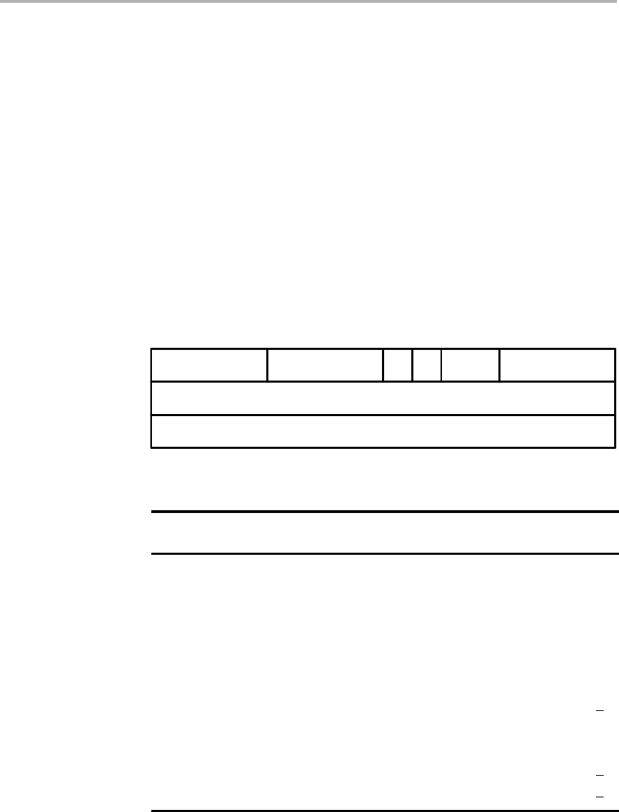
MSP430 and MSP430X Instructions
4-37
16-Bit MSP430X CPU
4.5.1 MSP430 Instructions
The MSP430 instructions can be used, regardless if the program resides in the
lower 64 KB or beyond it. The only exceptions are the instructions CALL and
RET which are limited to the lower 64 KB address range. CALLA and RETA
instructions have been added to the MSP430X CPU to handle subroutines in
the entire address range with no code size overhead.
MSP430 Double Operand (Format I) Instructions
Figure 4−22 shows the format of the MSP430 double operand instructions.
Source and destination words are appended for the Indexed, Symbolic,
Absolute and Immediate modes. Table 4−4 lists the twelve MSP430 double
operand instructions.
Figure 4−22. MSP430 Double Operand Instruction Format
15 1211 87654 0
Op-code Rsrc Ad B/W As Rdst
Source or Destination 15:0
Destination 15:0
Table 4−4. MSP430 Double Operand Instructions
Mnemonic S-Reg, Operation Status Bits
g,
D-Reg VNZC
MOV(.B) src,dst src → dst − − − −
ADD(.B) src,dst src + dst → dst * * * *
ADDC(.B) src,dst src + dst + C → dst * * * *
SUB(.B) src,dst dst + .not.src + 1 → dst * * * *
SUBC(.B) src,dst dst + .not.src + C → dst * * * *
CMP(.B) src,dst dst − src * * * *
DADD(.B) src,dst src + dst + C → dst (decimally) * * * *
BIT(.B) src,dst src .and. dst 0 * * Z
BIC(.B) src,dst .not.src .and. dst → dst − − − −
BIS(.B) src,dst src .or. dst → dst − − − −
XOR(.B) src,dst src .xor. dst → dst * * * Z
AND(.B) src,dst src .and. dst → dst 0 * * Z
* The status bit is affected
− The status bit is not affected
0 The status bit is cleared
1 The status bit is set

MSP430 and MSP430X Instructions
4-38 16-Bit MSP430X CPU
Single Operand (Format II) Instructions
Figure 4−23 shows the format for MSP430 single operand instructions, except
RETI. The destination word is appended for the Indexed, Symbolic, Absolute
and Immediate modes .Table 4−5 lists the seven single operand instructions.
Figure 4−23. MSP430 Single Operand Instructions
15 7654 0
Op-code B/W Ad Rdst
Destination 15:0
Table 4−5. MSP430 Single Operand Instructions
Mnemonic S-Reg,
D Reg
Operation Status Bits
D-Reg VNZC
RRC(.B) dst C → MSB →.......LSB → C * * * *
RRA(.B) dst MSB → MSB →....LSB → C0***
PUSH(.B) src SP − 2 → SP, src → @SP − − − −
SWPB dst bit 15…bit 8 ⇔ bit 7…bit 0 − − − −
CALL dst Call subroutine in lower 64 KB − − − −
RETI TOS → SR, SP + 2 →SP ****
TOS → PC,SP + 2 → SP
SXT dst Register mode:
bit 7 → bit 8 …bit 19
Other modes:
bit 7 → bit 8 …bit 15
0 * * Z
* The status bit is affected
− The status bit is not affected
0 The status bit is cleared
1 The status bit is set

MSP430 and MSP430X Instructions
4-39
16-Bit MSP430X CPU
Jumps
Figure 4−24 shows the format for MSP430 and MSP430X jump instructions.
The signed 10-bit word offset of the jump instruction is multiplied by two,
sign-extended to a 20-bit address, and added to the 20-bit program counter.
This allows jumps in a range of -511 to +512 words relative to the program
counter in the full 20-bit address space Jumps do not affect the status bits.
Table 4−6 lists and describes the eight jump instructions.
Figure 4−24. Format of the Conditional Jump Instructions
15
Op-Code
13 12 10 9 8 0
Condition S 10-Bit Signed PC Offset
Table 4−6. Conditional Jump Instructions
Mnemonic S-Reg, D-Reg Operation
JEQ/JZ Label Jump to label if zero bit is set
JNE/JNZ Label Jump to label if zero bit is reset
JC Label Jump to label if carry bit is set
JNC Label Jump to label if carry bit is reset
JN Label Jump to label if negative bit is set
JGE Label Jump to label if (N .XOR. V) = 0
JL Label Jump to label if (N .XOR. V) = 1
JMP Label Jump to label unconditionally

MSP430 and MSP430X Instructions
4-40 16-Bit MSP430X CPU
Emulated Instructions
In addition to the MSP430 and MSP430X instructions, emulated instructions
are instructions that make code easier to write and read, but do not have
op-codes themselves. Instead, they are replaced automatically by the
assembler with a core instruction. There is no code or performance penalty for
using emulated instructions. The emulated instructions are listed in Table 4−7.
Table 4−7. Emulated Instructions
Instruction Explanation Emulation V N Z C
ADC(.B) dst Add Carry to dst ADDC(.B) #0,dst * * * *
BR dst Branch indirectly dst MOV dst,PC ----
CLR(.B) dst Clear dst MOV(.B) #0,dst ----
CLRC Clear Carry bit BIC #1,SR ---0
CLRN Clear Negative bit BIC #4,SR -0--
CLRZ Clear Zero bit BIC #2,SR --0-
DADC(.B) dst Add Carry to dst decimally DADD(.B) #0,dst ****
DEC(.B) dst Decrement dst by 1 SUB(.B) #1,dst ****
DECD(.B) dst Decrement dst by 2 SUB(.B) #2,dst ****
DINT Disable interrupt BIC #8,SR ----
EINT Enable interrupt BIS #8,SR ----
INC(.B) dst Increment dst by 1 ADD(.B) #1,dst ****
INCD(.B) dst Increment dst by 2 ADD(.B) #2,dst ****
INV(.B) dst Invert dst XOR(.B) #-1,dst ****
NOP No operation MOV R3,R3 ----
POP dst Pop operand from stack MOV @SP+,dst ----
RET Return from subroutine MOV @SP+,PC ----
RLA(.B) dst Shift left dst arithmetically ADD(.B) dst,dst ****
RLC(.B) dst Shift left dst
logically through Carry
ADDC(.B) dst,dst ****
SBC(.B) dst Subtract Carry from dst SUBC(.B) #0,dst ****
SETC Set Carry bit BIS #1,SR ---1
SETN Set Negative bit BIS #4,SR -1--
SETZ Set Zero bit BIS #2,SR --1-
TST(.B) dst Test dst
(compare with 0)
CMP(.B) #0,dst 0 * * 1

MSP430 and MSP430X Instructions
4-41
16-Bit MSP430X CPU
MSP430 Instruction Execution
The number of CPU clock cycles required for an instruction depends on the
instruction format and the addressing modes used - not the instruction itself.
The number of clock cycles refers to MCLK.
Instruction Cycles and Length for Interrupt, Reset, and Subroutines
Table 4−8 lists the length and the CPU cycles for reset, interrupts and
subroutines.
Table 4−8. Interrupt, Return and Reset Cycles and Length
Action
Execution Time
MCLK Cycles
Length of
Instruction (Words)
Return from interrupt RETI 3†1
Return from subroutine RET 3 1
Interrupt request service (cycles
needed before 1st instruction)
5‡-
WDT reset 4 -
Reset (RST/NMI) 4 -
†The cycle count in MSP430 CPU is 5.
‡The cycle count in MSP430 CPU is 6.

MSP430 and MSP430X Instructions
4-42 16-Bit MSP430X CPU
Format-II (Single Operand) Instruction Cycles and Lengths
Table 4−9 lists the length and the CPU cycles for all addressing modes of the
MSP430 single operand instructions.
Table 4−9. MSP430 Format-II Instruction Cycles and Length
No. of Cycles Length of
Instruction Example
Addressing
Mode
RRA, RRC
SWPB, SXT PUSH CALL
Length of
Instruction Example
Rn 1 3 3†1 SWPB R5
@Rn 3 3†4 1 RRC @R9
@Rn+ 3 3†4‡1 SWPB @R10+
#N n.a. 3†4‡2 CALL #LABEL
X(Rn) 4 4‡4‡2 CALL 2(R7)
EDE 4 4‡4‡2 PUSH EDE
&EDE 4 4‡4‡2SXT &EDE
†The cycle count in MSP430 CPU is 4.
‡The cycle count in MSP430 CPU is 5. Also, the cycle count is 5 for X(Rn) addressing mode, when
Rn = SP.
Jump Instructions. Cycles and Lengths
All jump instructions require one code word, and take two CPU cycles to
execute, regardless of whether the jump is taken or not.

MSP430 and MSP430X Instructions
4-43
16-Bit MSP430X CPU
Format-I (Double Operand) Instruction Cycles and Lengths
Table 4−10 lists the length and CPU cycles for all addressing modes of the
MSP430 format-I instructions.
Table 4−10.MSP430 Format-I Instructions Cycles and Length
Addressing Mode No. of Length of
Src Dst Cycles
g
Instruction Example
Rn Rm 1 1 MOV R5,R8
PC 2 1 BR R9
x(Rm) 4†2ADD R5,4(R6)
EDE 4†2XOR R8,EDE
&EDE 4†2MOV R5,&EDE
@Rn Rm 2 1 AND @R4,R5
PC 3 1 BR @R8
x(Rm) 5†2XOR @R5,8(R6)
EDE 5†2MOV @R5,EDE
&EDE 5†2XOR @R5,&EDE
@Rn+ Rm 2 1 ADD @R5+,R6
PC 3 1 BR @R9+
x(Rm) 5†2XOR @R5,8(R6)
EDE 5†2MOV @R9+,EDE
&EDE 5†2MOV @R9+,&EDE
#N Rm 2 2 MOV #20,R9
PC 3 2 BR #2AEh
x(Rm) 5†3MOV #0300h,0(SP)
EDE 5†3ADD #33,EDE
&EDE 5†3ADD #33,&EDE
x(Rn) Rm 3 2 MOV 2(R5),R7
()
PC 3 2 BR 2(R6)
TONI 6†3MOV 4(R7),TONI
x(Rm) 6†3ADD 4(R4),6(R9)
&TONI 6†3MOV 2(R4),&TONI
EDE Rm 3 2 AND EDE,R6
PC 3 2 BR EDE
TONI 6†3CMP EDE,TONI
x(Rm) 6†3MOV EDE,0(SP)
&TONI 6†3MOV EDE,&TONI
&EDE Rm 3 2 MOV &EDE,R8
PC 3 2 BR &EDE
TONI 6†3MOV &EDE,TONI
x(Rm) 6†3MOV &EDE,0(SP)
&TONI 6†3MOV &EDE,&TONI
†MOV, BIT, and CMP instructions execute in 1 fewer cycle

MSP430X Extended Instructions
4-44 16-Bit MSP430X CPU
4.5.2 MSP430X Extended Instructions
The extended MSP430X instructions give the MSP430X CPU full access to its
20-bit address space. Most MSP430X instructions require an additional word
of op-code called the extension word. Some extended instructions do not
require an additional word and are noted in the instruction description. All
addresses, indexes and immediate numbers have 20-bit values, when
preceded by the extension word.
There are two types of extension word:
-Register/register mode for Format-I instructions and register mode for
Format-II instructions.
-Extension word for all other address mode combinations.

MSP430X Extended Instructions
4-45
16-Bit MSP430X CPU
Register Mode Extension Word
The register mode extension word is shown in Figure 4−25 and described in
Table 4−11. An example is shown in Figure 4−27.
Figure 4−25. The Extension Word for Register Modes
15 1211109876543 0
0001 1 00 ZC # A/L 0 0 (n−1)/Rn
Table 4−11. Description of the Extension Word Bits for Register Mode
Bit Description
15:11 Extension word op-code. Op-codes 1800h to 1FFFh are extension
words.
10:9 Reserved
ZC Zero carry bit.
0: The executed instruction uses the status of the carry bit C.
1: The executed instruction uses the carry bit as 0. The carry bit will
be defined by the result of the final operation after instruction execu-
tion.
# Repetition bit.
0: The number of instruction repetitions is set by extension-word bits
3:0.
1: The number of instructions repetitions is defined by the value of the
four LSBs of Rn. See description for bits 3:0.
A/L Data length extension bit. Together with the B/W-bits of the following
MSP430 instruction, the AL bit defines the used data length of the
instruction.
A/L B/W Comment
0 0 Reserved
0 1 20-bit address-word
1 0 16-bit word
1 1 8-bit byte
5:4 Reserved
3:0 Repetition Count.
# = 0: These four bits set the repetition count n. These bits contain
n - 1.
# = 1: These four bits define the CPU register whose bits 3:0 set the
number of repetitions. Rn.3:0 contain n - 1.

MSP430X Extended Instructions
4-46 16-Bit MSP430X CPU
Non-Register Mode Extension Word
The extension word for non-register modes is shown in Figure 4−26 and
described in Table 4−12. An example is shown in Figure 4−28.
Figure 4−26. The Extension Word for Non-Register Modes
15 121110 76543 0
00011 Source bits 19:16 A/L 0 0 Destination bits 19:16
Table 4−12.Description of the Extension Word Bits for Non-Register Modes
Bit Description
15:11 Extension word op-code. Op-codes 1800h to 1FFFh are exten-
sion words.
Source Bits
19:16
The four MSBs of the 20-bit source. Depending on the source
addressing mode, these four MSBs may belong to an immedi-
ate operand, an index or to an absolute address.
A/L Data length extension bit. Together with the B/W-bits of the fol-
lowing MSP430 instruction, the AL bit defines the used data
length of the instruction.
A/L B/W Comment
0 0 Reserved
0 1 20 bit address-word
1 0 16 bit word
1 1 8 bit byte
5:4 Reserved
Destination Bits
19:16
The four MSBs of the 20-bit destination. Depending on the des-
tination addressing mode, these four MSBs may belong to an
index or to an absolute address.
Note: B/W and A/L Bit Settings for SWPBX and SXTX
The B/W and A/L bit settings for SWPBX and SXTX are:
A/L B/W
0 0 SWPBX.A, SXTX.A
0 1 n.a.
1 0 SWPB.W, SXTX.W
1 1 n.a.
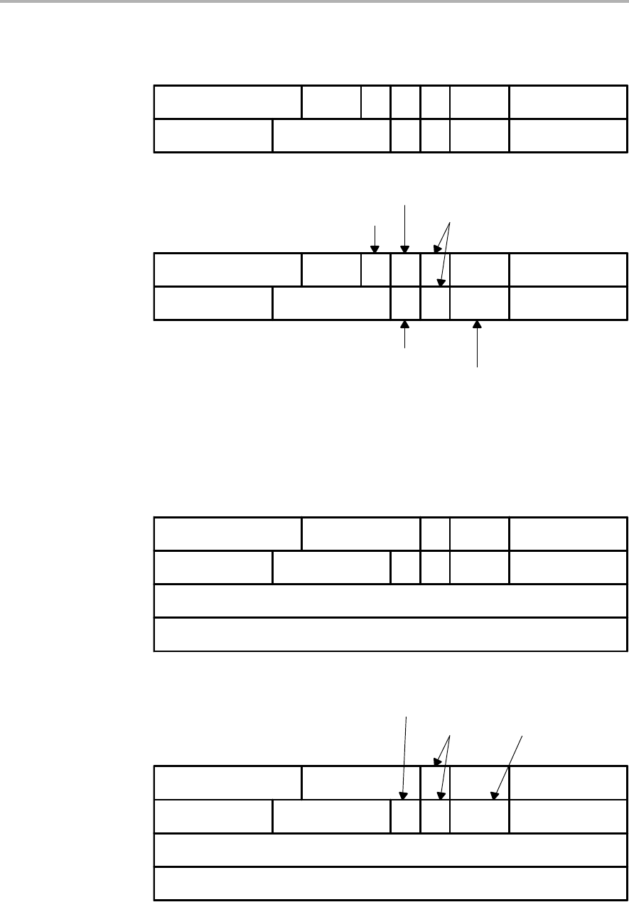
MSP430X Extended Instructions
4-47
16-Bit MSP430X CPU
Figure 4−27. Example for an Extended Register/Register Instruction
1514131211109876543210
00011 00 ZC#A/LRsvd (n−1)/Rn
Op-code Rsrc Ad B/W As Rdst
XORX.A R9,R8
00011 0 000 0 0
14(XOR) 90 1 0 8(R8)
XORX instruction Source R9
0: Use Carry
1: Repetition count
in bits 3:0
01: Address word
Destination
register mode Source
register mode
Destination R8
Figure 4−28. Example for an Extended Immediate/Indexed Instruction
1514131211109876543210
00011 Source 19:16 A/L Rsvd Destination 19:16
Op-code Rsrc Ad B/W As Rdst
XORX.A #12345h, 45678h(R15)
00011 1 0 0 4
14 (XOR) 0 (PC) 1 1 3 15 (R15)
18xx extension word 12345h
@PC+
X(Rn)
Source 15:0
Destination 15:0
Immediate operand LSBs: 2345h
Index destination LSBs: 5678h
01: Address
word

MSP430X Extended Instructions
4-48 16-Bit MSP430X CPU
Extended Double Operand (Format-I) Instructions
All twelve double-operand instructions have extended versions as listed in
Table 4−13.
Table 4−13.Extended Double Operand Instructions
Status Bits
Mnemonic Operands Operation V N Z C
MOVX(.B,.A) src,dst src → dst − − − −
ADDX(.B,.A) src,dst src + dst → dst * * * *
ADDCX(.B,.A) src,dst src + dst + C → dst * * * *
SUBX(.B,.A) src,dst dst + .not.src + 1 → dst * * * *
SUBCX(.B,.A) src,dst dst + .not.src + C → dst * * * *
CMPX(.B,.A) src,dst dst − src * * * *
DADDX(.B,.A) src,dst src + dst + C → dst (decimal) * * * *
BITX(.B,.A) src,dst src .and. dst 0 * * Z
BICX(.B,.A) src,dst .not.src .and. dst → dst − − − −
BISX(.B,.A) src,dst src .or. dst → dst − − − −
XORX(.B,.A) src,dst src .xor. dst → dst * * * Z
ANDX(.B,.A) src,dst src .and. dst → dst 0 * * Z
* The status bit is affected
− The status bit is not affected
0 The status bit is cleared
1 The status bit is set
MSP430X Extended Instructions
4-49
16-Bit MSP430X CPU
The four possible addressing combinations for the extension word for format-I
instructions are shown in Figure 4−29.
Figure 4−29. Extended Format-I Instruction Formats
1514131211109876543 0
0 0 0 1 1 0 A/L n−1/Rn
Op-code B/W dst
0ZC# 0 0
src 0 00
00011 A/L
Op-code B/W dst
src.15:0
src.19:16 0 0
src Ad As
00011 A/L
Op-code B/W dst
dst.15:0
00
src Ad
0 0 0 1 1 A/L dst.19:16
Op-code B/W dst
src.15:0
00
src Ad
0000
dst.19:16
0000
As
src.19:16
As
dst.15:0
If the 20-bit address of a source or destination operand is located in memory,
not in a CPU register, then two words are used for this operand as shown in
Figure 4−30.
Figure 4−30. 20-Bit Addresses in Memory
1514131211109876543210
0 19:16
Operand LSBs 15:0
0.......................................................................................
Address
Address+2

MSP430X Extended Instructions
4-50 16-Bit MSP430X CPU
Extended Single Operand (Format-II) Instructions
Extended MSP430X Format-II instructions are listed in Table 4−14.
Table 4−14.Extended Single-Operand Instructions
Operation Status Bits
Mnemonic Operands n V N Z C
CALLA dst Call indirect to subroutine (20-bit address) − − − −
POPM.A #n,Rdst Pop n 20-bit registers from stack 1 − 16 − − − −
POPM.W #n,Rdst Pop n 16-bit registers from stack 1 − 16 − − − −
PUSHM.A #n,Rsrc Push n 20-bit registers to stack 1 − 16 − − − −
PUSHM.W #n,Rsrc Push n 16-bit registers to stack 1 − 16
PUSHX(.B,.A) src Push 8/16/20-bit source to stack − − − −
RRCM(.A) #n,Rdst Rotate right Rdst n bits through carry
(16-/20-bit register)
1 − 4 0 * * *
RRUM(.A) #n,Rdst Rotate right Rdst n bits unsigned
(16-/20-bit register)
1 − 4 0 * * *
RRAM(.A) #n,Rdst Rotate right Rdst n bits arithmetically
(16-/20-bit register)
1 − 4 * * * *
RLAM(.A) #n,Rdst Rotate left Rdst n bits arithmetically
(16-/20-bit register)
1 − 4 * * * *
RRCX(.B,.A) dst Rotate right dst through carry
(8-/16-/20-bit data)
10***
RRUX(.B,.A) dst Rotate right dst unsigned (8-/16-/20-bit ) 1 0 * * *
RRAX(.B,.A) dst Rotate right dst arithmetically 1 * * * *
SWPBX(.A) dst Exchange low byte with high byte 1 − − − −
SXTX(.A) Rdst Bit7 → bit8 … bit19 1 0 * * *
SXTX(.A) dst Bit7 → bit8 … MSB 1 0 * * *
MSP430X Extended Instructions
4-51
16-Bit MSP430X CPU
The three possible addressing mode combinations for format-II instructions
are shown in Figure 4−31.
Figure 4−31. Extended Format-II Instruction Format
1514131211109876543 0
0 0 0 1 1 0 A/L n−1/Rn
Op-code B/W dst
0ZC# 0 0
00011 A/L
Op-code B/W dst
00
00011A/L
Op-code B/W dst
dst.15:0
00
0000
dst.19:16
00 00
0000
00
1x
x1
Extended Format II Instruction Format Exceptions
Exceptions for the Format II instruction formats are shown below.
Figure 4−32. PUSHM/POPM Instruction Format
15 87 43 0
Op-code n−1 Rdst − n+1
Figure 4−33. RRCM, RRAM, RRUM and RLAM Instruction Format
15 12 11 10 9 4 3 0
C n−1 Op-code Rdst
MSP430X Extended Instructions
4-52 16-Bit MSP430X CPU
Figure 4−34. BRA Instruction Format
15 12 11 8 7 4 3 0
C Rsrc Op-code 0(PC)
C #imm/abs19:16 Op-code 0(PC)
C Rsrc Op-code 0(PC)
#imm15:0 / &abs15:0
index15:0
Figure 4−35. CALLA Instruction Format
15 4 3 0
Op-code Rdst
Op-code Rdst
Op-code #imm/ix/abs19:16
index15:0
#imm15:0 / index15:0 / &abs15:0

MSP430X Extended Instructions
4-53
16-Bit MSP430X CPU
Extended Emulated Instructions
The extended instructions together with the constant generator form the
extended Emulated instructions. Table 4−15 lists the Emulated instructions.
Table 4−15.Extended Emulated Instructions
Instruction Explanation Emulation
ADCX(.B,.A) dst Add carry to dst ADDCX(.B,.A) #0,dst
BRA dst Branch indirect dst MOVA dst,PC
RETA Return from subroutine MOVA @SP+,PC
CLRA Rdst Clear Rdst MOV #0,Rdst
CLRX(.B,.A) dst Clear dst MOVX(.B,.A) #0,dst
DADCX(.B,.A) dst Add carry to dst decimally DADDX(.B,.A) #0,dst
DECX(.B,.A) dst Decrement dst by 1 SUBX(.B,.A) #1,dst
DECDA Rdst Decrement dst by 2 SUBA #2,Rdst
DECDX(.B,.A) dst Decrement dst by 2 SUBX(.B,.A) #2,dst
INCX(.B,.A) dst Increment dst by 1 ADDX(.B,.A) #1,dst
INCDA Rdst Increment Rdst by 2 ADDA #2,Rdst
INCDX(.B,.A) dst Increment dst by 2 ADDX(.B,.A) #2,dst
INVX(.B,.A) dst Invert dst XORX(.B,.A) #-1,dst
RLAX(.B,.A) dst Shift left dst arithmetically ADDX(.B,.A) dst,dst
RLCX(.B,.A) dst Shift left dst logically through carry ADDCX(.B,.A) dst,dst
SBCX(.B,.A) dst Subtract carry from dst SUBCX(.B,.A) #0,dst
TSTA Rdst Test Rdst (compare with 0) CMPA #0,Rdst
TSTX(.B,.A) dst Test dst (compare with 0) CMPX(.B,.A) #0,dst
POPX dst Pop to dst MOVX(.B, .A) @SP+,dst

MSP430X Extended Instructions
4-54 16-Bit MSP430X CPU
MSP430X Address Instructions
MSP430X address instructions are instructions that support 20-bit operands
but have restricted addressing modes. The addressing modes are restricted
to the register mode and the Immediate mode, except for the MOVA instruction
as listed in Table 4−16. Restricting the addressing modes removes the need
for the additional extension-word op-code improving code density and
execution time. Address instructions should be used any time an MSP430X
instruction is needed with the corresponding restricted addressing mode.
Table 4−16.Address Instructions, Operate on 20-bit Registers Data
Status Bits
Mnemonic Operands Operation V N Z C
ADDA Rsrc,Rdst
#imm20,Rdst
Add source to destination
register
* * * *
MOVA Rsrc,Rdst
#imm20,Rdst
z16(Rsrc),Rdst
EDE,Rdst
&abs20,Rdst
@Rsrc,Rdst
@Rsrc+,Rdst
Rsrc,z16(Rdst)
Rsrc,&abs20
Move source to destination - - - -
CMPA Rsrc,Rdst
#imm20,Rdst
Compare source to destina-
tion register
****
SUBA Rsrc,Rdst
#imm20,Rdst
Subtract source from des-
tination register
* * * *

MSP430X Extended Instructions
4-55
16-Bit MSP430X CPU
MSP430X Instruction Execution
The number of CPU clock cycles required for an MSP430X instruction
depends on the instruction format and the addressing modes used — not the
instruction itself. The number of clock cycles refers to MCLK.
MSP430X Format-II (Single-Operand) Instruction Cycles and Lengths
Table 4−17 lists the length and the CPU cycles for all addressing modes of the
MSP430X extended single-operand instructions.
Table 4−17.MSP430X Format II Instruction Cycles and Length
Execution Cycles/Length of Instruction (Words)
Instruction Rn @Rn @Rn+ #N X(Rn) EDE &EDE
RRAM n/1 − − − − − −
RRCM n/1 − − −−−−
RRUM n/1 − − −−−−
RLAM n/1 − − −−−−
PUSHM 2+n/1 − − −−−−
PUSHM.A 2+2n/1 − − −−−−
POPM 2+n/1 − − −−−−
POPM.A 2+2n/1 − − −−−−
CALLA 4/1 5/1 5/1 4/2 6†/2 6/2 6/2
RRAX(.B) 1+n/2 4/2 4/2 − 5/3 5/3 5/3
RRAX.A 1+n/2 6/2 6/2 − 7/3 7/3 7/3
RRCX(.B) 1+n/2 4/2 4/2 − 5/3 5/3 5/3
RRCX.A 1+n/2 6/2 6/2 − 7/3 7/3 7/3
PUSHX(.B) 4/2 4/2 4/2 4/3 5†/3 5/3 5/3
PUSHX.A 5/2 6/2 6/2 6/3 7†/3 7/3 7/3
POPX(.B) 3/2 − − − 5/3 5/3 5/3
POPX.A 4/2 − − − 7/3 7/3 7/3
†Add one cycle when Rn = SP.
MSP430X Format-I (Double-Operand) Instruction Cycles and Lengths
Table 4−18 lists the length and CPU cycles for all addressing modes of the
MSP430X extended format-I instructions.

MSP430X Extended Instructions
4-56 16-Bit MSP430X CPU
Table 4−18.MSP430X Format-I Instruction Cycles and Length
Addressing Mode
No. of
Cycles
Length of
Instruction
Source Destination .B/.W .A .B/.W/.A Examples
Rn Rm†2 2 2 BITX.B R5,R8
PC 3 3 2 ADDX R9,PC
X(Rm) 5‡7§3 ANDX.A R5,4(R6)
EDE 5‡7§3 XORX R8,EDE
&EDE 5‡7§3 BITX.W R5,&EDE
@Rn Rm 3 4 2 BITX @R5,R8
PC 3 4 2 ADDX @R9,PC
X(Rm) 6‡9§3 ANDX.A @R5,4(R6)
EDE 6‡9§3 XORX @R8,EDE
&EDE 6‡9§3 BITX.B @R5,&EDE
@Rn+ Rm 3 4 2 BITX @R5+,R8
PC 4 5 2 ADDX.A @R9+,PC
X(Rm) 6‡9§3 ANDX @R5+,4(R6)
EDE 6‡9§3 XORX.B @R8+,EDE
&EDE 6‡9§3 BITX @R5+,&EDE
#N Rm 3 3 3 BITX #20,R8
PC¶4 4 3 ADDX.A #FE000h,PC
X(Rm) 6‡8§4 ANDX #1234,4(R6)
EDE 6‡8§4 XORX #A5A5h,EDE
&EDE 6‡8§4 BITX.B #12,&EDE
X(Rn) Rm 4 5 3 BITX 2(R5),R8
PC¶5 6 3 SUBX.A 2(R6),PC
X(Rm) 7‡10§4 ANDX 4(R7),4(R6)
EDE 7‡10§4 XORX.B 2(R6),EDE
&EDE 7‡10§4 BITX 8(SP),&EDE
EDE Rm 4 5 3 BITX.B EDE,R8
PC¶5 6 3 ADDX.A EDE,PC
X(Rm) 7‡10§4 ANDX EDE,4(R6)
EDE 7‡10§4 ANDX EDE,TONI
&TONI 7‡10§4 BITX EDE,&TONI
&EDE Rm 4 5 3 BITX &EDE,R8
PC¶5 6 3 ADDX.A &EDE,PC
X(Rm) 7‡10§4 ANDX.B &EDE,4(R6)
TONI 7‡10§4 XORX &EDE,TONI
&TONI 7‡10§4BITX &EDE,&TONI
†Repeat instructions require n+1 cycles where n is the number of times the instruction is
executed.
‡Reduce the cycle count by one for MOV, BIT, and CMP instructions.
§Reduce the cycle count by two for MOV, BIT, and CMP instructions.
¶Reduce the cycle count by one for MOV, ADD, and SUB instructions.

MSP430X Extended Instructions
4-57
16-Bit MSP430X CPU
MSP430X Address Instruction Cycles and Lengths
Table 4−19 lists the length and the CPU cycles for all addressing modes of the
MSP430X address instructions.
Table 4−19.Address Instruction Cycles and Length
Addressing Mode
Execution
Time MCLK
Cycles
Length of
Instruction
(Words)
Source Destination
MOVA
BRA
CMPA
ADDA
SUBA MOVA
CMPA
ADDA
SUBA Example
Rn Rn 1 1 1 1 CMPA R5,R8
PC 2 2 1 1 SUBA R9,PC
x(Rm) 4 - 2 - MOVA R5,4(R6)
EDE 4 - 2 - MOVA R8,EDE
&EDE 4 - 2 - MOVA R5,&EDE
@Rn Rm 3 - 1 - MOVA @R5,R8
PC 3 - 1 - MOVA @R9,PC
@Rn+ Rm 3 - 1 - MOVA @R5+,R8
PC 3 - 1 - MOVA @R9+,PC
#N Rm 2 3 2 2 CMPA #20,R8
PC 3 3 2 2 SUBA #FE000h,PC
x(Rn) Rm 4 - 2 - MOVA 2(R5),R8
PC 4 - 2 - MOVA 2(R6),PC
EDE Rm 4 - 2 - MOVA EDE,R8
PC 4 - 2 - MOVA EDE,PC
&EDE Rm 4 - 2 - MOVA &EDE,R8
PC 4 - 2 - MOVA &EDE,PC

Instruction Set Description
4-58 16-Bit MSP430X CPU
4.6 Instruction Set Description
The instruction map of the MSP430X shows all available instructions:
0xxx
10xx
14xx
18xx
1Cxx
20xx
24xx
28xx
2Cxx
30xx
34xx
38xx
3Cxx
4xxx
5xxx
6xxx
7xxx
8xxx
9xxx
Axxx
Bxxx
Cxxx
Dxxx
Exxx
Fxxx
RRC RRC.B SWPB RRA RRA.B SXT PUSH PUSH.B CALL RETI
000 040 080 0C0 100 140 180 1C0 200 240 280 2C0 300 340 380 3C0
JNE/JNZ
JEQ/JZ
JNC
JC
JN
JGE
JL
JMP
MOV, MOV.B
ADD, ADD.B
ADDC, ADDC.B
SUBC, SUBC.B
SUB, SUB.B
CMP, CMP.B
DADD, DADD.B
BIT, BIT.B
BIC, BIC.B
BIS, BIS.B
XOR, XOR.B
AND, AND.B
MOVA, CMPA, ADDA, SUBA, RRCM, RRAM, RLAM, RRUM
CALLA
PUSHM.A, POPM.A, PUSHM.W, POPM.W
Extension Word For Format I and Format II Instructions
Instruction Set Description
4-59
16-Bit MSP430X CPU
4.6.1 Extended Instruction Binary Descriptions
Detailed MSP430X instruction binary descriptions are shown below.
Instruction
Group
src or
data.19:16
Instruction
Identifier dst
Instruction 15 12 11 8 7 4 3 0
MOVA 0 0 0 0 src 0 0 0 0 dst MOVA @Rsrc,Rdst
0 0 0 0 src 0 0 0 1 dst MOVA @Rsrc+,Rdst
0 0 0 0 &abs.19:16 0 0 1 0 dst MOVA &abs20,Rdst
&abs.15:0
0 0 0 0 src 0 0 1 1 dst MOVA x(Rsrc),Rdst
x.15:0 ±15-bit index x
0 0 0 0 src 0 1 1 0 &abs.19:16 MOVA Rsrc,&abs20
&abs.15:0
0 0 0 0 src 0 1 1 1 dst MOVA Rsrc,X(Rdst)
x.15:0 ±15-bit index x
0 0 0 0 imm.19:16 1 0 0 0 dst MOVA #imm20,Rdst
imm.15:0
CMPA 0 0 0 0 imm.19:16 1 0 0 1 dst CMPA #imm20,Rdst
imm.15:0
ADDA 0 0 0 0 imm.19:16 1 0 1 0 dst ADDA #imm20,Rdst
imm.15:0
SUBA 0 0 0 0 imm.19:16 1 0 1 1 dst SUBA #imm20,Rdst
imm.15:0
MOVA 0 0 0 0 src 1 1 0 0 dst MOVA Rsrc,Rdst
CMPA 0 0 0 0 src 1 1 0 1 dst CMPA Rsrc,Rdst
ADDA 0 0 0 0 src 1 1 1 0 dst ADDA Rsrc,Rdst
SUBA 0 0 0 0 src 1 1 1 1 dst SUBA Rsrc,Rdst
Instruction
Group
Bit
loc.
Inst.
ID
Instruction
Identifier dst
Instruction 15 12 11 10 9 8 7 4 3 0
RRCM.A 0 0 0 0 n−1 0 0 0 1 0 0 dst RRCM.A #n,Rdst
RRAM.A 0 0 0 0 n−1 0 1 0 1 0 0 dst RRAM.A #n,Rdst
RLAM.A 0 0 0 0 n−1 1 0 0 1 0 0 dst RLAM.A #n,Rdst
RRUM.A 0 0 0 0 n−1 1 1 0 1 0 0 dst RRUM.A #n,Rdst
RRCM.W 0 0 0 0 n−1 0 0 0 1 0 1 dst RRCM.W #n,Rdst
RRAM.W 0 0 0 0 n−1 0 1 0 1 0 1 dst RRAM.W #n,Rdst
RLAM.W 0 0 0 0 n−1 1 0 0 1 0 1 dst RLAM.W #n,Rdst
RRUM.W 0 0 0 0 n−1 1 1 0 1 0 1 dst RRUM.W #n,Rdst
Instruction Set Description
4-60 16-Bit MSP430X CPU
Instruction Identifier dst
Instruction 15 12 11 8 7 6 5 4 3 0
RETI 0 0 0 1 0 0 1 1 0 0 0 0 0 0 0 0
CALLA 0 0 0 1 0 0 1 1 0 1 0 0 dst CALLA Rdst
0 0 0 1 0 0 1 1 0 1 0 1 dst CALLA x(Rdst)
x.15:0
0 0 0 1 0 0 1 1 0 1 1 0 dst CALLA @Rdst
0 0 0 1 0 0 1 1 0 1 1 1 dst CALLA @Rdst+
0 0 0 1 0 0 1 1 1 0 0 0 &abs.19:16 CALLA &abs20
&abs.15:0
0 0 0 1 0 0 1 1 1 0 0 1 x.19:16 CALLA EDE
x.15:0 CALLA x(PC)
0 0 0 1 0 0 1 1 1 0 1 1 imm.19:16 CALLA #imm20
imm.15:0
Reserved 0 0 0 1 0 0 1 1 1 0 1 0 x x x x
Reserved 0 0 0 1 0 0 1 1 1 1 x x x x x x
PUSHM.A 0 0 0 1 0 1 0 0 n−1 dst PUSHM.A #n,Rdst
PUSHM.W 0 0 0 1 0 1 0 1 n−1 dst PUSHM.W #n,Rdst
POPM.A 0 0 0 1 0 1 1 0 n−1 dst−n+1 POPM.A #n,Rdst
POPM.W 0 0 0 1 0 1 1 1 n−1 dst−n+1 POPM.W #n,Rdst

MSP430 Instructions
4-61
16-Bit MSP430X CPU
4.6.2 MSP430 Instructions
The MSP430 instructions are listed and described on the following pages.

MSP430 Instructions
4-62 16-Bit MSP430X CPU
* ADC[.W] Add carry to destination
* ADC.B Add carry to destination
Syntax ADC dst or ADC.W dst
ADC.B dst
Operation dst + C −> dst
Emulation ADDC #0,dst
ADDC.B #0,dst
Description The carry bit (C) is added to the destination operand. The previous contents
of the destination are lost.
Status Bits N: Set if result is negative, reset if positive
Z: Set if result is zero, reset otherwise
C: Set if dst was incremented from 0FFFFh to 0000, reset otherwise
Set if dst was incremented from 0FFh to 00, reset otherwise
V: Set if an arithmetic overflow occurs, otherwise reset
Mode Bits OSCOFF, CPUOFF, and GIE are not affected.
Example The 16-bit counter pointed to by R13 is added to a 32-bit counter pointed to
by R12.
ADD @R13,0(R12) ; Add LSDs
ADC 2(R12) ; Add carry to MSD
Example The 8-bit counter pointed to by R13 is added to a 16-bit counter pointed to by
R12.
ADD.B @R13,0(R12) ; Add LSDs
ADC.B 1(R12) ; Add carry to MSD

MSP430 Instructions
4-63
16-Bit MSP430X CPU
ADD[.W] Add source word to destination word
ADD.B Add source byte to destination byte
Syntax ADD src,dst or ADD.W src,dst
ADD.B src,dst
Operation src + dst → dst
Description The source operand is added to the destination operand. The previous content
of the destination is lost.
Status Bits N: Set if result is negative (MSB = 1), reset if positive (MSB = 0)
Z: Set if result is zero, reset otherwise
C: Set if there is a carry from the MSB of the result, reset otherwise
V: Set if the result of two positive operands is negative, or if the result of
two negative numbers is positive, reset otherwise.
Mode Bits OSCOFF, CPUOFF, and GIE are not affected.
Example Ten is added to the 16-bit counter CNTR located in lower 64 K.
ADD.W #10,&CNTR ; Add 10 to 16-bit counter
Example A table word pointed to by R5 (20-bit address in R5) is added to R6. The jump
to label TONI is performed on a carry.
ADD.W @R5,R6 ; Add table word to R6. R6.19:16 = 0
JC TONI ; Jump if carry
... ; No carry
Example A table byte pointed to by R5 (20-bit address) is added to R6. The jump to label
TONI is performed if no carry occurs. The table pointer is auto-incremented by
1. R6.19:8 = 0
ADD.B @R5+,R6 ; Add byte to R6. R5 + 1. R6: 000xxh
JNC TONI ; Jump if no carry
... ; Carry occurred

MSP430 Instructions
4-64 16-Bit MSP430X CPU
ADDC[.W] Add source word and carry to destination word
ADDC.B Add source byte and carry to destination byte
Syntax ADDC src,dst or ADDC.W src,dst
ADDC.B src,dst
Operation src + dst + C → dst
Description The source operand and the carry bit C are added to the destination operand.
The previous content of the destination is lost.
Status Bits N: Set if result is negative (MSB = 1), reset if positive (MSB = 0)
Z: Set if result is zero, reset otherwise
C: Set if there is a carry from the MSB of the result, reset otherwise
V: Set if the result of two positive operands is negative, or if the result of
two negative numbers is positive, reset otherwise.
Mode Bits OSCOFF, CPUOFF, and GIE are not affected.
Example Constant value 15 and the carry of the previous instruction are added to the
16-bit counter CNTR located in lower 64 K.
ADDC.W #15,&CNTR ; Add 15 + C to 16-bit CNTR
Example A table word pointed to by R5 (20-bit address) and the carry C are added to R6.
The jump to label TONI is performed on a carry. R6.19:16 = 0
ADDC.W @R5,R6 ; Add table word + C to R6
JC TONI ; Jump if carry
... ; No carry
Example A table byte pointed to by R5 (20-bit address) and the carry bit C are added to
R6. The jump to label TONI is performed if no carry occurs. The table pointer is
auto-incremented by 1. R6.19:8 = 0
ADDC.B @R5+,R6 ; Add table byte + C to R6. R5 + 1
JNC TONI ; Jump if no carry
... ; Carry occurred

MSP430 Instructions
4-65
16-Bit MSP430X CPU
AND[.W] Logical AND of source word with destination word
AND.B Logical AND of source byte with destination byte
Syntax AND src,dst or AND.W src,dst
AND.B src,dst
Operation src .and. dst → dst
Description The source operand and the destination operand are logically ANDed. The
result is placed into the destination. The source operand is not affected.
Status Bits N: Set if result is negative (MSB = 1), reset if positive (MSB = 0)
Z: Set if result is zero, reset otherwise
C: Set if the result is not zero, reset otherwise. C = (.not. Z)
V: Reset
Mode Bits OSCOFF, CPUOFF, and GIE are not affected.
Example The bits set in R5 (16-bit data) are used as a mask (AA55h) for the word TOM
located in the lower 64 K. If the result is zero, a branch is taken to label TONI.
R5.19:16 = 0
MOV #AA55h,R5 ; Load 16-bit mask to R5
AND R5,&TOM ; TOM .and. R5 -> TOM
JZ TONI ; Jump if result 0
... ; Result > 0
or shorter:
AND #AA55h,&TOM ; TOM .and. AA55h -> TOM
JZ TONI ; Jump if result 0
Example A table byte pointed to by R5 (20-bit address) is logically ANDed with R6. R5 is
incremented by 1 after the fetching of the byte. R6.19:8 = 0
AND.B @R5+,R6 ; AND table byte with R6. R5 + 1

MSP430 Instructions
4-66 16-Bit MSP430X CPU
BIC[.W] Clear bits set in source word in destination word
BIC.B Clear bits set in source byte in destination byte
Syntax BIC src,dst or BIC.W src,dst
BIC.B src,dst
Operation (.not. src) .and. dst → dst
Description The inverted source operand and the destination operand are logically
ANDed. The result is placed into the destination. The source operand is not
affected.
Status Bits N: Not affected
Z: Not affected
C: Not affected
V: Not affected
Mode Bits OSCOFF, CPUOFF, and GIE are not affected.
Example The bits 15:14 of R5 (16-bit data) are cleared. R5.19:16 = 0
BIC #0C000h,R5 ; Clear R5.19:14 bits
Example A table word pointed to by R5 (20-bit address) is used to clear bits in R7.
R7.19:16 = 0
BIC.W @R5,R7 ; Clear bits in R7 set in @R5
Example A table byte pointed to by R5 (20-bit address) is used to clear bits in Port1.
BIC.B @R5,&P1OUT ; Clear I/O port P1 bits set in @R5

MSP430 Instructions
4-67
16-Bit MSP430X CPU
BIS[.W] Set bits set in source word in destination word
BIS.B Set bits set in source byte in destination byte
Syntax BIS src,dst or BIS.W src,dst
BIS.B src,dst
Operation src .or. dst → dst
Description The source operand and the destination operand are logically ORed. The
result is placed into the destination. The source operand is not affected.
Status Bits N: Not affected
Z: Not affected
C: Not affected
V: Not affected
Mode Bits OSCOFF, CPUOFF, and GIE are not affected.
Example Bits 15 and 13 of R5 (16-bit data) are set to one. R5.19:16 = 0
BIS #A000h,R5 ; Set R5 bits
Example A table word pointed to by R5 (20-bit address) is used to set bits in R7.
R7.19:16 = 0
BIS.W @R5,R7 ; Set bits in R7
Example A table byte pointed to by R5 (20-bit address) is used to set bits in Port1. R5 is
incremented by 1 afterwards.
BIS.B @R5+,&P1OUT ; Set I/O port P1 bits. R5 + 1

MSP430 Instructions
4-68 16-Bit MSP430X CPU
BIT[.W] Test bits set in source word in destination word
BIT.B Test bits set in source byte in destination byte
Syntax BIT src,dst or BIT.W src,dst
BIT.B src,dst
Operation src .and. dst
Description The source operand and the destination operand are logically ANDed. The
result affects only the status bits in SR.
Register Mode: the register bits Rdst.19:16 (.W) resp. Rdst. 19:8 (.B) are not
cleared!
Status Bits N: Set if result is negative (MSB = 1), reset if positive (MSB = 0)
Z: Set if result is zero, reset otherwise
C: Set if the result is not zero, reset otherwise. C = (.not. Z)
V: Reset
Mode Bits OSCOFF, CPUOFF, and GIE are not affected.
Example Test if one − or both − of bits 15 and 14 of R5 (16-bit data) is set. Jump to label
TONI if this is the case. R5.19:16 are not affected.
BIT #C000h,R5 ; Test R5.15:14 bits
JNZ TONI ; At least one bit is set in R5
... ; Both bits are reset
Example A table word pointed to by R5 (20-bit address) is used to test bits in R7. Jump to
label TONI if at least one bit is set. R7.19:16 are not affected.
BIT.W @R5,R7 ; Test bits in R7
JC TONI ; At least one bit is set
... ; Both are reset
Example A table byte pointed to by R5 (20-bit address) is used to test bits in output
Port1. Jump to label TONI if no bit is set. The next table byte is addressed.
BIT.B @R5+,&P1OUT ; Test I/O port P1 bits. R5 + 1
JNC TONI ; No corresponding bit is set
... ; At least one bit is set

MSP430 Instructions
4-69
16-Bit MSP430X CPU
* BR, BRANCH Branch to destination in lower 64K address space
Syntax BR dst
Operation dst −> PC
Emulation MOV dst,PC
Description An unconditional branch is taken to an address anywhere in the lower 64K
address space. All source addressing modes can be used. The branch
instruction is a word instruction.
Status Bits Status bits are not affected.
Example Examples for all addressing modes are given.
BR #EXEC ;Branch to label EXEC or direct branch (e.g. #0A4h)
; Core instruction MOV @PC+,PC
BR EXEC ; Branch to the address contained in EXEC
; Core instruction MOV X(PC),PC
; Indirect address
BR &EXEC ; Branch to the address contained in absolute
; address EXEC
; Core instruction MOV X(0),PC
; Indirect address
BR R5 ; Branch to the address contained in R5
; Core instruction MOV R5,PC
; Indirect R5
BR @R5 ; Branch to the address contained in the word
; pointed to by R5.
; Core instruction MOV @R5,PC
; Indirect, indirect R5
BR @R5+ ; Branch to the address contained in the word pointed
; to by R5 and increment pointer in R5 afterwards.
; The next time—S/W flow uses R5 pointer—it can
; alter program execution due to access to
; next address in a table pointed to by R5
; Core instruction MOV @R5,PC
; Indirect, indirect R5 with autoincrement
BR X(R5) ; Branch to the address contained in the address
; pointed to by R5 + X (e.g. table with address
; starting at X). X can be an address or a label
; Core instruction MOV X(R5),PC
; Indirect, indirect R5 + X

MSP430 Instructions
4-70 16-Bit MSP430X CPU
CALL Call a Subroutine in lower 64 K
Syntax CALL dst
Operation dst → tmp 16-bit dst is evaluated and stored
SP − 2 →SP
PC → @SP updated PC with return address to TOS
tmp →PC saved 16-bit dst to PC
Description A subroutine call is made from an address in the lower 64 K to a subroutine
address in the lower 64 K. All seven source addressing modes can be used.
The call instruction is a word instruction. The return is made with the RET
instruction.
Status Bits Not affected
PC.19:16: Cleared (address in lower 64 K)
Mode Bits OSCOFF, CPUOFF, and GIE are not affected.
Examples Examples for all addressing modes are given.
Immediate Mode: Call a subroutine at label EXEC (lower 64 K) or call directly
to address.
CALL #EXEC ; Start address EXEC
CALL #0AA04h ; Start address 0AA04h
Symbolic Mode: Call a subroutine at the 16-bit address contained in address
EXEC. EXEC is located at the address (PC + X) where X is within PC±32 K.
CALL EXEC ; Start address at @EXEC. z16(PC)
Absolute Mode: Call a subroutine at the 16-bit address contained in absolute
address EXEC in the lower 64 K.
CALL &EXEC ; Start address at @EXEC
Register Mode: Call a subroutine at the 16-bit address contained in register
R5.15:0.
CALL R5 ; Start address at R5
Indirect Mode: Call a subroutine at the 16-bit address contained in the word
pointed to by register R5 (20-bit address).
CALL @R5 ; Start address at @R5

MSP430 Instructions
4-71
16-Bit MSP430X CPU
* CLR[.W] Clear destination
* CLR.B Clear destination
Syntax CLR dst or CLR.W dst
CLR.B dst
Operation 0 −> dst
Emulation MOV #0,dst
MOV.B #0,dst
Description The destination operand is cleared.
Status Bits Status bits are not affected.
Example RAM word TONI is cleared.
CLR TONI ; 0 −> TONI
Example Register R5 is cleared.
CLR R5
Example RAM byte TONI is cleared.
CLR.B TONI ; 0 −> TONI

MSP430 Instructions
4-72 16-Bit MSP430X CPU
* CLRC Clear carry bit
Syntax CLRC
Operation 0 −> C
Emulation BIC #1,SR
Description The carry bit (C) is cleared. The clear carry instruction is a word instruction.
Status Bits N: Not affected
Z: Not affected
C: Cleared
V: Not affected
Mode Bits OSCOFF, CPUOFF, and GIE are not affected.
Example The 16-bit decimal counter pointed to by R13 is added to a 32-bit counter
pointed to by R12.
CLRC ; C=0: defines start
DADD @R13,0(R12) ; add 16-bit counter to low word of 32-bit counter
DADC 2(R12) ; add carry to high word of 32-bit counter

MSP430 Instructions
4-73
16-Bit MSP430X CPU
* CLRN Clear negative bit
Syntax CLRN
Operation 0 → N
or
(.NOT.src .AND. dst −> dst)
Emulation BIC #4,SR
Description The constant 04h is inverted (0FFFBh) and is logically ANDed with the
destination operand. The result is placed into the destination. The clear
negative bit instruction is a word instruction.
Status Bits N: Reset to 0
Z: Not affected
C: Not affected
V: Not affected
Mode Bits OSCOFF, CPUOFF, and GIE are not affected.
Example The Negative bit in the status register is cleared. This avoids special treatment
with negative numbers of the subroutine called.
CLRN
CALL SUBR
......
......
SUBR JN SUBRET ; If input is negative: do nothing and return
......
......
......
SUBRET RET

MSP430 Instructions
4-74 16-Bit MSP430X CPU
* CLRZ Clear zero bit
Syntax CLRZ
Operation 0 → Z
or
(.NOT.src .AND. dst −> dst)
Emulation BIC #2,SR
Description The constant 02h is inverted (0FFFDh) and logically ANDed with the
destination operand. The result is placed into the destination. The clear zero
bit instruction is a word instruction.
Status Bits N: Not affected
Z: Reset to 0
C: Not affected
V: Not affected
Mode Bits OSCOFF, CPUOFF, and GIE are not affected.
Example The zero bit in the status register is cleared.
CLRZ
Indirect, Auto-Increment mode: Call a subroutine at the 16-bit address con-
tained in the word pointed to by register R5 (20-bit address) and increment the
16-bit address in R5 afterwards by 2. The next time the software uses R5 as
a pointer, it can alter the program execution due to access to the next word ad-
dress in the table pointed to by R5.
CALL @R5+ ; Start address at @R5. R5 + 2
Indexed mode: Call a subroutine at the 16-bit address contained in the 20-bit
address pointed to by register (R5 + X), e.g. a table with addresses starting at
X. The address is within the lower 64 KB. X is within ±32 KB.
CALL X(R5) ; Start address at @(R5+X). z16(R5)

MSP430 Instructions
4-75
16-Bit MSP430X CPU
CMP[.W] Compare source word and destination word
CMP.B Compare source byte and destination byte
Syntax CMP src,dst or CMP.W src,dst
CMP.B src,dst
Operation (.not.src) + 1 + dst or dst − src
Description The source operand is subtracted from the destination operand. This is made
by adding the 1’s complement of the source + 1 to the destination. The result
affects only the status bits in SR.
Register Mode: the register bits Rdst.19:16 (.W) resp. Rdst. 19:8 (.B) are not
cleared.
Status Bits N: Set if result is negative (src > dst), reset if positive (src = dst)
Z: Set if result is zero (src = dst), reset otherwise (src ≠dst)
C: Set if there is a carry from the MSB, reset otherwise
V: Set if the subtraction of a negative source operand from a positive des-
tination operand delivers a negative result, or if the subtraction of a posi-
tive source operand from a negative destination operand delivers a
positive result, reset otherwise (no overflow).
Mode Bits OSCOFF, CPUOFF, and GIE are not affected.
Example Compare word EDE with a 16-bit constant 1800h. Jump to label TONI if
EDE equals the constant. The address of EDE is within PC ±32 K.
CMP #01800h,EDE ; Compare word EDE with 1800h
JEQ TONI ; EDE contains 1800h
... ; Not equal
Example A table word pointed to by (R5 + 10) is compared with R7. Jump to label TONI if
R7 contains a lower, signed 16-bit number. R7.19:16 is not cleared. The
address of the source operand is a 20-bit address in full memory range.
CMP.W 10(R5),R7 ; Compare two signed numbers
JL TONI ; R7 < 10(R5)
... ; R7 >= 10(R5)
Example A table byte pointed to by R5 (20-bit address) is compared to the value in
output Port1. Jump to label TONI if values are equal. The next table byte is
addressed.
CMP.B @R5+,&P1OUT ; Compare P1 bits with table. R5 + 1
JEQ TONI ; Equal contents
... ; Not equal

MSP430 Instructions
4-76 16-Bit MSP430X CPU
* DADC[.W] Add carry decimally to destination
* DADC.B Add carry decimally to destination
Syntax DADC dst or DADC.W src,dst
DADC.B dst
Operation dst + C −> dst (decimally)
Emulation DADD #0,dst
DADD.B #0,dst
Description The carry bit (C) is added decimally to the destination.
Status Bits N: Set if MSB is 1
Z: Set if dst is 0, reset otherwise
C: Set if destination increments from 9999 to 0000, reset otherwise
Set if destination increments from 99 to 00, reset otherwise
V: Undefined
Mode Bits OSCOFF, CPUOFF, and GIE are not affected.
Example The four-digit decimal number contained in R5 is added to an eight-digit deci-
mal number pointed to by R8.
CLRC ; Reset carry
; next instruction’s start condition is defined
DADD R5,0(R8) ; Add LSDs + C
DADC 2(R8) ; Add carry to MSD
Example The two-digit decimal number contained in R5 is added to a four-digit decimal
number pointed to by R8.
CLRC ; Reset carry
; next instruction’s start condition is defined
DADD.B R5,0(R8) ; Add LSDs + C
DADC 1(R8) ; Add carry to MSDs

MSP430 Instructions
4-77
16-Bit MSP430X CPU
DADD[.W] Add source word and carry decimally to destination word
DADD.B Add source byte and carry decimally to destination byte
Syntax DADD src,dst or DADD.W src,dst
DADD.B src,dst
Operation src + dst + C → dst (decimally)
Description The source operand and the destination operand are treated as two (.B) or four
(.W) binary coded decimals (BCD) with positive signs. The source operand
and the carry bit C are added decimally to the destination operand. The source
operand is not affected. The previous content of the destination is lost. The
result is not defined for non-BCD numbers.
Status Bits N: Set if MSB of result is 1 (word > 7999h, byte > 79h), reset if MSB is 0.
Z: Set if result is zero, reset otherwise
C: Set if the BCD result is too large (word > 9999h, byte > 99h), reset
otherwise
V: Undefined
Mode Bits OSCOFF, CPUOFF, and GIE are not affected.
Example Decimal 10 is added to the 16-bit BCD counter DECCNTR.
DADD #10h,&DECCNTR ; Add 10 to 4-digit BCD counter
Example The eight-digit BCD number contained in 16-bit RAM addresses BCD and
BCD+2 is added decimally to an eight-digit BCD number contained in R4 and
R5 (BCD+2 and R5 contain the MSDs). The carry C is added, and cleared.
CLRC ; Clear carry
DADD.W &BCD,R4 ; Add LSDs. R4.19:16 = 0
DADD.W &BCD+2,R5 ; Add MSDs with carry. R5.19:16 = 0
JC OVERFLOW ; Result >9999,9999: go to error
routine
... ; Result ok
Example The two-digit BCD number contained in word BCD (16-bit address) is added
decimally to a two-digit BCD number contained in R4. The carry C is added,
also. R4.19:8 = 0
CLRC ; Clear carry
DADD.B &BCD,R4 ; Add BCD to R4 decimally.
R4: 0,00ddh

MSP430 Instructions
4-78 16-Bit MSP430X CPU
* DEC[.W] Decrement destination
* DEC.B Decrement destination
Syntax DEC dst or DEC.W dst
DEC.B dst
Operation dst − 1 −> dst
Emulation SUB #1,dst
Emulation SUB.B #1,dst
Description The destination operand is decremented by one. The original contents are
lost.
Status Bits N: Set if result is negative, reset if positive
Z: Set if dst contained 1, reset otherwise
C: Reset if dst contained 0, set otherwise
V: Set if an arithmetic overflow occurs, otherwise reset.
Set if initial value of destination was 08000h, otherwise reset.
Set if initial value of destination was 080h, otherwise reset.
Mode Bits OSCOFF, CPUOFF, and GIE are not affected.
Example R10 is decremented by 1
DEC R10 ; Decrement R10
; Move a block of 255 bytes from memory location starting with EDE to memory location starting with
;TONI. Tables should not overlap: start of destination address TONI must not be within the range EDE
; to EDE+0FEh
;
MOV #EDE,R6
MOV #255,R10
L$1 MOV.B @R6+,TONI−EDE−1(R6)
DEC R10
JNZ L$1
; Do not transfer tables using the routine above with the overlap shown in Figure 4−36.
Figure 4−36. Decrement Overlap
EDE
EDE+254
TONI
TONI+254

MSP430 Instructions
4-79
16-Bit MSP430X CPU
* DECD[.W] Double-decrement destination
* DECD.B Double-decrement destination
Syntax DECD dst or DECD.W dst
DECD.B dst
Operation dst − 2 −> dst
Emulation SUB #2,dst
Emulation SUB.B #2,dst
Description The destination operand is decremented by two. The original contents are lost.
Status Bits N: Set if result is negative, reset if positive
Z: Set if dst contained 2, reset otherwise
C: Reset if dst contained 0 or 1, set otherwise
V: Set if an arithmetic overflow occurs, otherwise reset.
Set if initial value of destination was 08001 or 08000h, otherwise reset.
Set if initial value of destination was 081 or 080h, otherwise reset.
Mode Bits OSCOFF, CPUOFF, and GIE are not affected.
Example R10 is decremented by 2.
DECD R10 ; Decrement R10 by two
; Move a block of 255 words from memory location starting with EDE to memory location
; starting with TONI
; Tables should not overlap: start of destination address TONI must not be within the
; range EDE to EDE+0FEh
;
MOV #EDE,R6
MOV #510,R10
L$1 MOV @R6+,TONI−EDE−2(R6)
DECD R10
JNZ L$1
Example Memory at location LEO is decremented by two.
DECD.B LEO ; Decrement MEM(LEO)
Decrement status byte STATUS by two.
DECD.B STATUS

MSP430 Instructions
4-80 16-Bit MSP430X CPU
* DINT Disable (general) interrupts
Syntax DINT
Operation 0 → GIE
or
(0FFF7h .AND. SR → SR / .NOT.src .AND. dst −> dst)
Emulation BIC #8,SR
Description All interrupts are disabled.
The constant 08h is inverted and logically ANDed with the status register (SR).
The result is placed into the SR.
Status Bits Status bits are not affected.
Mode Bits GIE is reset. OSCOFF and CPUOFF are not affected.
Example The general interrupt enable (GIE) bit in the status register is cleared to allow
a nondisrupted move of a 32-bit counter. This ensures that the counter is not
modified during the move by any interrupt.
DINT ; All interrupt events using the GIE bit are disabled
NOP
MOV COUNTHI,R5 ; Copy counter
MOV COUNTLO,R6
EINT ; All interrupt events using the GIE bit are enabled
Note: Disable Interrupt
If any code sequence needs to be protected from interruption, the DINT
should be executed at least one instruction before the beginning of the
uninterruptible sequence, or should be followed by a NOP instruction.

MSP430 Instructions
4-81
16-Bit MSP430X CPU
* EINT Enable (general) interrupts
Syntax EINT
Operation 1 → GIE
or
(0008h .OR. SR −> SR / .src .OR. dst −> dst)
Emulation BIS #8,SR
Description All interrupts are enabled.
The constant #08h and the status register SR are logically ORed. The result
is placed into the SR.
Status Bits Status bits are not affected.
Mode Bits GIE is set. OSCOFF and CPUOFF are not affected.
Example The general interrupt enable (GIE) bit in the status register is set.
; Interrupt routine of ports P1.2 to P1.7
; P1IN is the address of the register where all port bits are read. P1IFG is the address of
; the register where all interrupt events are latched.
;
PUSH.B &P1IN
BIC.B @SP,&P1IFG ; Reset only accepted flags
EINT ; Preset port 1 interrupt flags stored on stack
; other interrupts are allowed
BIT #Mask,@SP
JEQ MaskOK ; Flags are present identically to mask: jump
......
MaskOK BIC #Mask,@SP
......
INCD SP ; Housekeeping: inverse to PUSH instruction
; at the start of interrupt subroutine. Corrects
; the stack pointer.
RETI
Note: Enable Interrupt
The instruction following the enable interrupt instruction (EINT) is always
executed, even if an interrupt service request is pending when the interrupts
are enable.

MSP430 Instructions
4-82 16-Bit MSP430X CPU
* INC[.W]Increment destination
* INC.B Increment destination
Syntax INC dst or INC.W dst
INC.B dst
Operation dst + 1 −> dst
Emulation ADD #1,dst
Description The destination operand is incremented by one. The original contents are lost.
Status Bits N: Set if result is negative, reset if positive
Z: Set if dst contained 0FFFFh, reset otherwise
Set if dst contained 0FFh, reset otherwise
C: Set if dst contained 0FFFFh, reset otherwise
Set if dst contained 0FFh, reset otherwise
V: Set if dst contained 07FFFh, reset otherwise
Set if dst contained 07Fh, reset otherwise
Mode Bits OSCOFF, CPUOFF, and GIE are not affected.
Example The status byte, STATUS, of a process is incremented. When it is equal to 11,
a branch to OVFL is taken.
INC.B STATUS
CMP.B #11,STATUS
JEQ OVFL

MSP430 Instructions
4-83
16-Bit MSP430X CPU
* INCD[.W] Double-increment destination
* INCD.B Double-increment destination
Syntax INCD dst or INCD.W dst
INCD.B dst
Operation dst + 2 −> dst
Emulation ADD #2,dst
Emulation ADD.B #2,dst
Example The destination operand is incremented by two. The original contents are lost.
Status Bits N: Set if result is negative, reset if positive
Z: Set if dst contained 0FFFEh, reset otherwise
Set if dst contained 0FEh, reset otherwise
C: Set if dst contained 0FFFEh or 0FFFFh, reset otherwise
Set if dst contained 0FEh or 0FFh, reset otherwise
V: Set if dst contained 07FFEh or 07FFFh, reset otherwise
Set if dst contained 07Eh or 07Fh, reset otherwise
Mode Bits OSCOFF, CPUOFF, and GIE are not affected.
Example The item on the top of the stack (TOS) is removed without using a register.
.......
PUSH R5 ; R5 is the result of a calculation, which is stored
; in the system stack
INCD SP ; Remove TOS by double-increment from stack
; Do not use INCD.B, SP is a word-aligned
; register
RET
Example The byte on the top of the stack is incremented by two.
INCD.B 0(SP) ; Byte on TOS is increment by two

MSP430 Instructions
4-84 16-Bit MSP430X CPU
* INV[.W] Invert destination
* INV.B Invert destination
Syntax INV dst
INV.B dst
Operation .NOT.dst −> dst
Emulation XOR #0FFFFh,dst
Emulation XOR.B #0FFh,dst
Description The destination operand is inverted. The original contents are lost.
Status Bits N: Set if result is negative, reset if positive
Z: Set if dst contained 0FFFFh, reset otherwise
Set if dst contained 0FFh, reset otherwise
C: Set if result is not zero, reset otherwise ( = .NOT. Zero)
Set if result is not zero, reset otherwise ( = .NOT. Zero)
V: Set if initial destination operand was negative, otherwise reset
Mode Bits OSCOFF, CPUOFF, and GIE are not affected.
Example Content of R5 is negated (twos complement).
MOV #00AEh,R5 ; R5 = 000AEh
INV R5 ; Invert R5, R5 = 0FF51h
INC R5 ; R5 is now negated, R5 = 0FF52h
Example Content of memory byte LEO is negated.
MOV.B #0AEh,LEO ; MEM(LEO) = 0AEh
INV.B LEO ; Invert LEO, MEM(LEO) = 051h
INC.B LEO ; MEM(LEO) is negated,MEM(LEO) = 052h

MSP430 Instructions
4-85
16-Bit MSP430X CPU
JC Jump if carry
JHS Jump if Higher or Same (unsigned)
Syntax JC label
JHS label
Operation If C = 1: PC + (2 × Offset) → PC
If C = 0: execute the following instruction
Description The carry bit C in the status register is tested. If it is set, the signed 10-bit word
offset contained in the instruction is multiplied by two, sign extended, and
added to the 20-bit program counter PC. This means a jump in the range -511
to +512 words relative to the PC in the full memory range. If C is reset, the
instruction after the jump is executed.
JC is used for the test of the carry bit C
JHS is used for the comparison of unsigned numbers
Status Bits Status bits are not affected
Mode Bits OSCOFF, CPUOFF, and GIE are not affected
Example The state of the port 1 pin P1IN.1 bit defines the program flow.
BIT.B #2,&P1IN ; Port 1, bit 1 set? Bit -> C
JC Label1 ; Yes, proceed at Label1
... ; No, continue
Example If R5 ≥R6 (unsigned) the program continues at Label2
CMP R6,R5 ; Is R5 ≥ R6? Info to C
JHS Label2 ; Yes, C = 1
... ; No, R5 < R6. Continue
Example If R5 ≥12345h (unsigned operands) the program continues at Label2
CMPA #12345h,R5 ; Is R5 ≥ 12345h? Info to C
JHS Label2 ; Yes, 12344h < R5 <= F,FFFFh. C = 1
... ; No, R5 < 12345h. Continue

MSP430 Instructions
4-86 16-Bit MSP430X CPU
JEQ,JZ Jump if equal,Jump if zero
Syntax JZ label
JEQ label
Operation If Z = 1: PC + (2 × Offset) → PC
If Z = 0: execute following instruction
Description The Zero bit Z in the status register is tested. If it is set, the signed 10-bit word
offset contained in the instruction is multiplied by two, sign extended, and
added to the 20-bit program counter PC. This means a jump in the range -511
to +512 words relative to the PC in the full memory range. If Z is reset, the
instruction after the jump is executed.
JZ is used for the test of the Zero bit Z
JEQ is used for the comparison of operands
Status Bits Status bits are not affected
Mode Bits OSCOFF, CPUOFF, and GIE are not affected
Example The state of the P2IN.0 bit defines the program flow
BIT.B #1,&P2IN ; Port 2, bit 0 reset?
JZ Label1 ; Yes, proceed at Label1
... ; No, set, continue
Example If R5 = 15000h (20-bit data) the program continues at Label2
CMPA #15000h,R5 ; Is R5 = 15000h? Info to SR
JEQ Label2 ; Yes, R5 = 15000h. Z = 1
... ; No, R5 ≠ 15000h. Continue
Example R7 (20-bit counter) is incremented. If its content is zero, the program continues
at Label4.
ADDA #1,R7 ; Increment R7
JZ Label4 ; Zero reached: Go to Label4
... ; R7 ≠ 0. Continue here.

MSP430 Instructions
4-87
16-Bit MSP430X CPU
JGE Jump if Greater or Equal (signed)
Syntax JGE label
Operation If (N .xor. V) = 0: PC + (2 × Offset) → PC
If (N .xor. V) = 1: execute following instruction
Description The negative bit N and the overflow bit V in the status register are tested. If both
bits are set or both are reset, the signed 10-bit word offset contained in the
instruction is multiplied by two, sign extended, and added to the 20-bit program
counter PC. This means a jump in the range -511 to +512 words relative to the
PC in full Memory range. If only one bit is set, the instruction after the jump is
executed.
JGE is used for the comparison of signed operands: also for incorrect results
due to overflow, the decision made by the JGE instruction is correct.
Note: JGE emulates the non-implemented JP (jump if positive) instruction if
used after the instructions AND, BIT, RRA, SXTX and TST. These instructions
clear the V-bit.
Status Bits Status bits are not affected
Mode Bits OSCOFF, CPUOFF, and GIE are not affected
Example If byte EDE (lower 64 K) contains positive data, go to Label1. Software can run
in the full memory range.
TST.B &EDE ; Is EDE positive? V <- 0
JGE Label1 ; Yes, JGE emulates JP
... ; No, 80h <= EDE <= FFh
Example If the content of R6 is greater than or equal to the memory pointed to by R7, the
program continues a Label5. Signed data. Data and program in full memory
range.
CMP @R7,R6 ; Is R6 ≥ @R7?
JGE Label5 ; Yes, go to Label5
... ; No, continue here.
Example If R5 ≥12345h (signed operands) the program continues at Label2. Program
in full memory range.
CMPA #12345h,R5 ; Is R5 ≥ 12345h?
JGE Label2 ; Yes, 12344h < R5 <= 7FFFFh.
... ; No, 80000h <= R5 < 12345h.

MSP430 Instructions
4-88 16-Bit MSP430X CPU
JL Jump if Less (signed)
Syntax JL label
Operation If (N .xor. V) = 1: PC + (2 × Offset) → PC
If (N .xor. V) = 0: execute following instruction
Description The negative bit N and the overflow bit V in the status register are tested. If only
one is set, the signed 10-bit word offset contained in the instruction is multiplied
by two, sign extended, and added to the 20-bit program counter PC. This
means a jump in the range -511 to +512 words relative to the PC in full memory
range. If both bits N and V are set or both are reset, the instruction after the
jump is executed.
JL is used for the comparison of signed operands: also for incorrect results due
to overflow, the decision made by the JL instruction is correct.
Status Bits Status bits are not affected
Mode Bits OSCOFF, CPUOFF, and GIE are not affected
Example If byte EDE contains a smaller, signed operand than byte TONI, continue at
Label1. The address EDE is within PC ±32 K.
CMP.B &TONI,EDE ; Is EDE < TONI
JL Label1 ; Yes
... ; No, TONI <= EDE
Example If the signed content of R6 is less than the memory pointed to by R7 (20-bit
address) the program continues at Label Label5. Data and program in full
memory range.
CMP @R7,R6 ; Is R6 < @R7?
JL Label5 ; Yes, go to Label5
... ; No, continue here.
Example If R5 < 12345h (signed operands) the program continues at Label2. Data and
program in full memory range.
CMPA #12345h,R5 ; Is R5 < 12345h?
JL Label2 ; Yes, 80000h =< R5 < 12345h.
... ; No, 12344h < R5 =< 7FFFFh.

MSP430 Instructions
4-89
16-Bit MSP430X CPU
JMP Jump unconditionally
Syntax JMP label
Operation PC + (2 × Offset) → PC
Description The signed 10-bit word offset contained in the instruction is multiplied by two,
sign extended, and added to the 20-bit program counter PC. This means an
unconditional jump in the range -511 to +512 words relative to the PC in the full
memory. The JMP instruction may be used as a BR or BRA instruction within its
limited range relative to the program counter.
Status Bits Status bits are not affected
Mode Bits OSCOFF, CPUOFF, and GIE are not affected
Example The byte STATUS is set to 10. Then a jump to label MAINLOOP is made. Data
in lower 64 K, program in full memory range.
MOV.B #10,&STATUS ; Set STATUS to 10
JMP MAINLOOP ; Go to main loop
Example The interrupt vector TAIV of Timer_A3 is read and used for the program flow.
Program in full memory range, but interrupt handlers always starts in lower
64K.
ADD &TAIV,PC ; Add Timer_A interrupt vector to PC
RETI ; No Timer_A interrupt pending
JMP IHCCR1 ; Timer block 1 caused interrupt
JMP IHCCR2 ; Timer block 2 caused interrupt
RETI ; No legal interrupt, return

MSP430 Instructions
4-90 16-Bit MSP430X CPU
JN Jump if Negative
Syntax JN label
Operation If N = 1: PC + (2 × Offset) → PC
If N = 0: execute following instruction
Description The negative bit N in the status register is tested. If it is set, the signed 10-bit
word offset contained in the instruction is multiplied by two, sign extended, and
added to the 20-bit program counter PC. This means a jump in the range -511
to +512 words relative to the PC in the full memory range. If N is reset, the
instruction after the jump is executed.
Status Bits Status bits are not affected
Mode Bits OSCOFF, CPUOFF, and GIE are not affected
Example The byte COUNT is tested. If it is negative, program execution continues at
Label0. Data in lower 64 K, program in full memory range.
TST.B &COUNT ; Is byte COUNT negative?
JN Label0 ; Yes, proceed at Label0
... ; COUNT ≥ 0
Example R6 is subtracted from R5. If the result is negative, program continues at
Label2. Program in full memory range.
SUB R6,R5 ; R5 − R6 -> R5
JN Label2 ; R5 is negative: R6 > R5 (N = 1)
... ; R5 ≥ 0. Continue here.
Example R7 (20-bit counter) is decremented. If its content is below zero, the program
continues at Label4. Program in full memory range.
SUBA #1,R7 ; Decrement R7
JN Label4 ; R7 < 0: Go to Label4
... ; R7 ≥ 0. Continue here.

MSP430 Instructions
4-91
16-Bit MSP430X CPU
JNC Jump if No carry
JLO Jump if lower (unsigned)
Syntax JNC label
JLO label
Operation If C = 0: PC + (2 × Offset) → PC
If C = 1: execute following instruction
Description The carry bit C in the status register is tested. If it is reset, the signed 10-bit
word offset contained in the instruction is multiplied by two, sign extended, and
added to the 20-bit program counter PC. This means a jump in the range -511
to +512 words relative to the PC in the full memory range. If C is set, the
instruction after the jump is executed.
JNC is used for the test of the carry bit C
JLO is used for the comparison of unsigned numbers .
Status Bits Status bits are not affected
Mode Bits OSCOFF, CPUOFF, and GIE are not affected
Example If byte EDE < 15 the program continues at Label2. Unsigned data. Data in
lower 64 K, program in full memory range.
CMP.B #15,&EDE ; Is EDE < 15? Info to C
JLO Label2 ; Yes, EDE < 15. C = 0
... ; No, EDE ≥ 15. Continue
Example The word TONI is added to R5. If no carry occurs, continue at Label0. The
address of TONI is within PC ±32 K.
ADD TONI,R5 ; TONI + R5 -> R5. Carry -> C
JNC Label0 ; No carry
... ; Carry = 1: continue here

MSP430 Instructions
4-92 16-Bit MSP430X CPU
JNZ Jump if Not Zero
JNE Jump if Not Equal
Syntax JNZ label
JNE label
Operation If Z = 0: PC + (2 × Offset) → PC
If Z = 1: execute following instruction
Description The zero bit Z in the status register is tested. If it is reset, the signed 10-bit word
offset contained in the instruction is multiplied by two, sign extended, and
added to the 20-bit program counter PC. This means a jump in the range -511
to +512 words relative to the PC in the full memory range. If Z is set, the
instruction after the jump is executed.
JNZ is used for the test of the Zero bit Z
JNE is used for the comparison of operands
Status Bits Status bits are not affected
Mode Bits OSCOFF, CPUOFF, and GIE are not affected
Example The byte STATUS is tested. If it is not zero, the program continues at Label3.
The address of STATUS is within PC ±32 K.
TST.B STATUS ; Is STATUS = 0?
JNZ Label3 ; No, proceed at Label3
... ; Yes, continue here
Example If word EDE ≠1500 the program continues at Label2. Data in lower 64 K,
program in full memory range.
CMP #1500,&EDE ; Is EDE = 1500? Info to SR
JNE Label2 ; No, EDE ≠ 1500.
... ; Yes, R5 = 1500. Continue
Example R7 (20-bit counter) is decremented. If its content is not zero, the program
continues at Label4. Program in full memory range.
SUBA #1,R7 ; Decrement R7
JNZ Label4 ; Zero not reached: Go to Label4
... ; Yes, R7 = 0. Continue here.

MSP430 Instructions
4-93
16-Bit MSP430X CPU
MOV[.W] Move source word to destination word
MOV.B Move source byte to destination byte
Syntax MOV src,dst or MOV.W src,dst
MOV.B src,dst
Operation src → dst
Description The source operand is copied to the destination. The source operand is not
affected.
Status Bits N: Not affected
Z: Not affected
C: Not affected
V: Not affected
Mode Bits OSCOFF, CPUOFF, and GIE are not affected.
Example Move a 16-bit constant 1800h to absolute address-word EDE (lower 64 K).
MOV #01800h,&EDE ; Move 1800h to EDE
Example The contents of table EDE (word data, 16-bit addresses) are copied to table
TOM. The length of the tables is 030h words. Both tables reside in the lower
64K.
MOV #EDE,R10 ; Prepare pointer (16-bit address)
Loop MOV @R10+,TOM-EDE-2(R10) ; R10 points to both tables.
R10+2
CMP #EDE+60h,R10 ; End of table reached?
JLO Loop ; Not yet
... ; Copy completed
Example The contents of table EDE (byte data, 16-bit addresses) are copied to table
TOM. The length of the tables is 020h bytes. Both tables may reside in full
memory range, but must be within R10 ±32 K.
MOVA #EDE,R10 ; Prepare pointer (20-bit)
MOV #20h,R9 ; Prepare counter
Loop MOV.B @R10+,TOM-EDE-1(R10) ; R10 points to both tables.
; R10+1
DEC R9 ; Decrement counter
JNZ Loop ; Not yet done
... ; Copy completed

MSP430 Instructions
4-94 16-Bit MSP430X CPU
* NOP No operation
Syntax NOP
Operation None
Emulation MOV #0, R3
Description No operation is performed. The instruction may be used for the elimination of
instructions during the software check or for defined waiting times.
Status Bits Status bits are not affected.

MSP430 Instructions
4-95
16-Bit MSP430X CPU
* POP[.W] Pop word from stack to destination
* POP.B Pop byte from stack to destination
Syntax POP dst
POP.B dst
Operation @SP −> temp
SP + 2 −> SP
temp −> dst
Emulation MOV @SP+,dst or MOV.W @SP+,dst
Emulation MOV.B @SP+,dst
Description The stack location pointed to by the stack pointer (TOS) is moved to the
destination. The stack pointer is incremented by two afterwards.
Status Bits Status bits are not affected.
Example The contents of R7 and the status register are restored from the stack.
POP R7 ; Restore R7
POP SR ; Restore status register
Example The contents of RAM byte LEO is restored from the stack.
POP.B LEO ; The low byte of the stack is moved to LEO.
Example The contents of R7 is restored from the stack.
POP.B R7 ; The low byte of the stack is moved to R7,
; the high byte of R7 is 00h
Example The contents of the memory pointed to by R7 and the status register are
restored from the stack.
POP.B 0(R7) ; The low byte of the stack is moved to the
; the byte which is pointed to by R7
: Example: R7 = 203h
; Mem(R7) = low byte of system stack
: Example: R7 = 20Ah
; Mem(R7) = low byte of system stack
POP SR ; Last word on stack moved to the SR
Note: The System Stack Pointer
The system stack pointer (SP) is always incremented by two, independent
of the byte suffix.

MSP430 Instructions
4-96 16-Bit MSP430X CPU
PUSH[.W] Save a word on the stack
PUSH.B Save a byte on the stack
Syntax PUSH dst or PUSH.W dst
PUSH.B dst
Operation SP − 2 →SP
dst →@SP
Description The 20-bit stack pointer SP is decremented by two. The operand is then copied
to the RAM word addressed by the SP. A pushed byte is stored in the low byte,
the high byte is not affected.
Status Bits Not affected.
Mode Bits OSCOFF, CPUOFF, and GIE are not affected.
Example Save the two 16-bit registers R9 and R10 on the stack.
PUSH R9 ; Save R9 and R10 XXXXh
PUSH R10 ; YYYYh
Example Save the two bytes EDE and TONI on the stack. The addresses EDE and TONI
are within PC ±32 K.
PUSH.B EDE ; Save EDE xxXXh
PUSH.B TONI ; Save TONI xxYYh
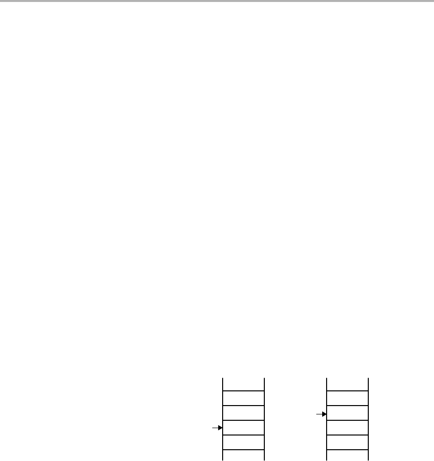
MSP430 Instructions
4-97
16-Bit MSP430X CPU
RET Return from subroutine
Syntax RET
Operation @SP →PC.15:0 Saved PC to PC.15:0. PC.19:16 ← 0
SP + 2 →SP
Description The 16-bit return address (lower 64 K), pushed onto the stack by a CALL
instruction is restored to the PC. The program continues at the address
following the subroutine call. The four MSBs of the program counter PC.19:16
are cleared.
Status Bits Not affected
PC.19:16: Cleared
Mode Bits OSCOFF, CPUOFF, and GIE are not affected.
Example Call a subroutine SUBR in the lower 64 K and return to the address in the lower
64K after the CALL
CALL #SUBR ; Call subroutine starting at SUBR
... ; Return by RET to here
SUBR PUSH R14 ; Save R14 (16 bit data)
... ; Subroutine code
POP R14 ; Restore R14
RET ; Return to lower 64 K
Figure 4−37. The Stack After a RET Instruction
Item n
PCReturn
Item n
Stack before RET Stack after RET
SP
SP
instruction instruction

MSP430 Instructions
4-98 16-Bit MSP430X CPU
RETI Return from interrupt
Syntax RETI
Operation @SP →SR.15:0 Restore saved status register SR with PC.19:16
SP + 2 →SP
@SP →PC.15:0 Restore saved program counter PC.15:0
SP + 2 →SP House keeping
Description The status register is restored to the value at the beginning of the interrupt
service routine. This includes the four MSBs of the program counter PC.19:16.
The stack pointer is incremented by two afterwards.
The 20-bit PC is restored from PC.19:16 (from same stack location as the
status bits) and PC.15:0. The 20-bit program counter is restored to the value
at the beginning of the interrupt service routine. The program continues at the
address following the last executed instruction when the interrupt was granted.
The stack pointer is incremented by two afterwards.
Status Bits N: restored from stack
Z: restored from stack
C: restored from stack
V: restored from stack
Mode Bits OSCOFF, CPUOFF, and GIE are restored from stack
Example Interrupt handler in the lower 64 K. A 20-bit return address is stored on the
stack.
INTRPT PUSHM.A #2,R14 ; Save R14 and R13 (20-bit data)
... ; Interrupt handler code
POPM.A #2,R14 ; Restore R13 and R14 (20-bit data)
RETI ; Return to 20-bit address in full memory range

MSP430 Instructions
4-99
16-Bit MSP430X CPU
* RLA[.W] Rotate left arithmetically
* RLA.B Rotate left arithmetically
Syntax RLA dst or RLA.W dst
RLA.B dst
Operation C <− MSB <− MSB−1 .... LSB+1 <− LSB <− 0
Emulation ADD dst,dst
ADD.B dst,dst
Description The destination operand is shifted left one position as shown in Figure 4−38.
The MSB is shifted into the carry bit (C) and the LSB is filled with 0. The RLA
instruction acts as a signed multiplication by 2.
An overflow occurs if dst ≥ 04000h and dst < 0C000h before operation is
performed: the result has changed sign.
Figure 4−38. Destination Operand—Arithmetic Shift Left
15 0
70
C
Byte
Word
0
An overflow occurs if dst ≥ 040h and dst < 0C0h before the operation is
performed: the result has changed sign.
Status Bits N: Set if result is negative, reset if positive
Z: Set if result is zero, reset otherwise
C: Loaded from the MSB
V: Set if an arithmetic overflow occurs:
the initial value is 04000h ≤dst < 0C000h; reset otherwise
Set if an arithmetic overflow occurs:
the initial value is 040h ≤dst < 0C0h; reset otherwise
Mode Bits OSCOFF, CPUOFF, and GIE are not affected.
Example R7 is multiplied by 2.
RLA R7 ; Shift left R7 (× 2)
Example The low byte of R7 is multiplied by 4.
RLA.B R7 ; Shift left low byte of R7 (× 2)
RLA.B R7 ; Shift left low byte of R7 (× 4)
Note: RLA Substitution
The assembler does not recognize the instruction:
RLA @R5+, RLA.B @R5+, or RLA(.B) @R5
It must be substituted by:
ADD @R5+,−2(R5) ADD.B @R5+,−1(R5) or ADD(.B) @R5,0(R5)
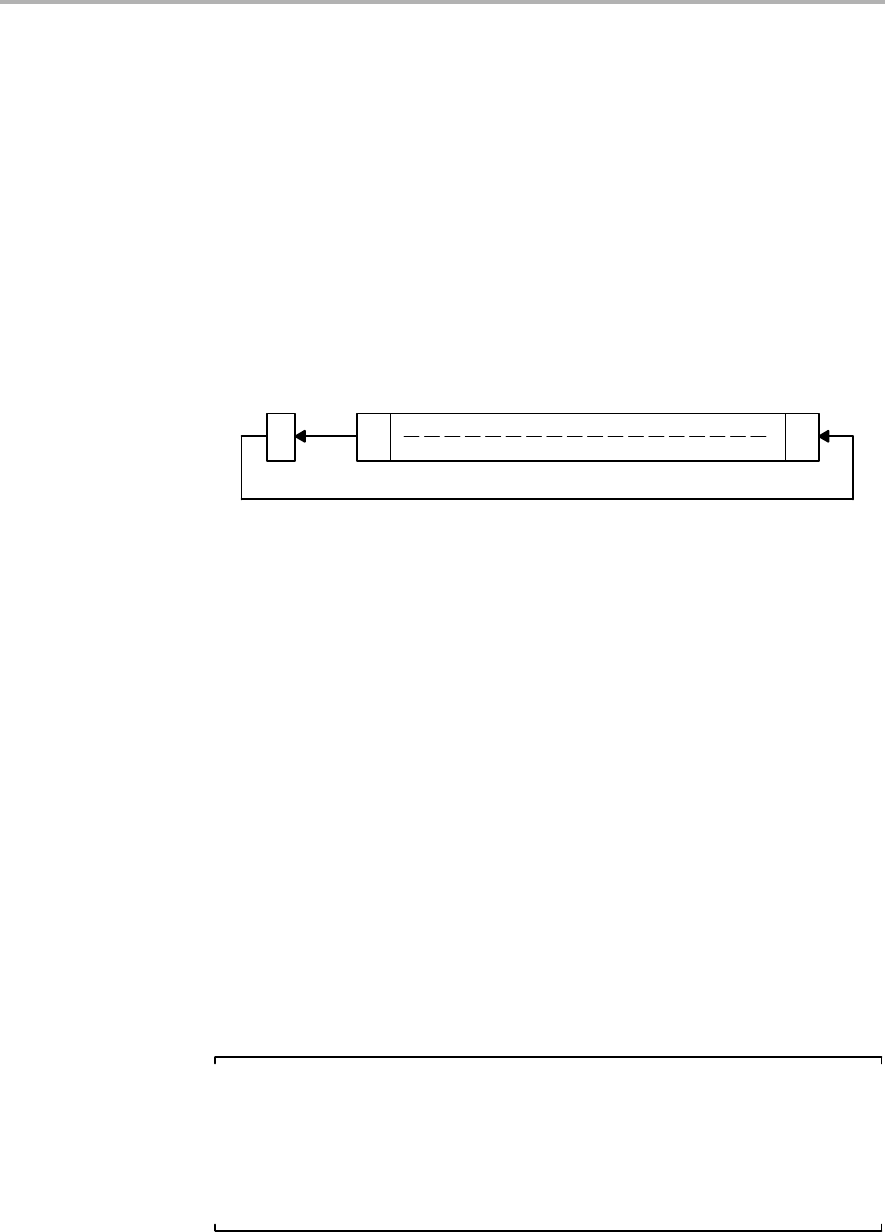
MSP430 Instructions
4-100 16-Bit MSP430X CPU
* RLC[.W] Rotate left through carry
* RLC.B Rotate left through carry
Syntax RLC dst or RLC.W dst
RLC.B dst
Operation C <− MSB <− MSB−1 .... LSB+1 <− LSB <− C
Emulation ADDC dst,dst
Description The destination operand is shifted left one position as shown in Figure 4−39.
The carry bit (C) is shifted into the LSB and the MSB is shifted into the carry
bit (C).
Figure 4−39. Destination Operand—Carry Left Shift
15 0
70
C
Byte
Word
Status Bits N: Set if result is negative, reset if positive
Z: Set if result is zero, reset otherwise
C: Loaded from the MSB
V: Set if an arithmetic overflow occurs
the initial value is 04000h ≤dst < 0C000h; reset otherwise
Set if an arithmetic overflow occurs:
the initial value is 040h ≤dst < 0C0h; reset otherwise
Mode Bits OSCOFF, CPUOFF, and GIE are not affected.
Example R5 is shifted left one position.
RLC R5 ; (R5 x 2) + C −> R5
Example The input P1IN.1 information is shifted into the LSB of R5.
BIT.B #2,&P1IN ; Information −> Carry
RLC R5 ; Carry=P0in.1 −> LSB of R5
Example The MEM(LEO) content is shifted left one position.
RLC.B LEO ; Mem(LEO) x 2 + C −> Mem(LEO)
Note: RLC and RLC.B Substitution
The assembler does not recognize the instruction:
RLC @R5+, RLC.B @R5+, or RLC(.B) @R5
It must be substituted by:
ADDC @R5+,−2(R5) ADDC.B @R5+,−1(R5) or ADDC(.B) @R5,0(R5)

MSP430 Instructions
4-101
16-Bit MSP430X CPU
RRA[.W] Rotate Right Arithmetically destination word
RRA.B Rotate Right Arithmetically destination byte
Syntax RRA.B dst or RRA.W dst
Operation MSB → MSB → MSB-1 . →... LSB+1 →LSB → C
Description The destination operand is shifted right arithmetically by one bit position as
shown in Figure 4−40. The MSB retains its value (sign). RRA operates equal to
a signed division by 2. The MSB is retained and shifted into the MSB-1. The
LSB+1 is shifted into the LSB. The previous LSB is shifted into the carry bit C.
Status Bits N: Set if result is negative (MSB = 1), reset otherwise (MSB = 0)
Z: Set if result is zero, reset otherwise
C: Loaded from the LSB
V: Reset
Mode Bits OSCOFF, CPUOFF, and GIE are not affected.
Example The signed 16-bit number in R5 is shifted arithmetically right one position.
RRA R5 ; R5/2 -> R5
Example The signed RAM byte EDE is shifted arithmetically right one position.
RRA.B EDE ; EDE/2 -> EDE
Figure 4−40. Rotate Right Arithmetically RRA.B and RRA.W
C
19 0
MSB00 00000
715
0 0 0 0 0 LSB
C
19 0
MSB
0000
15
LSB
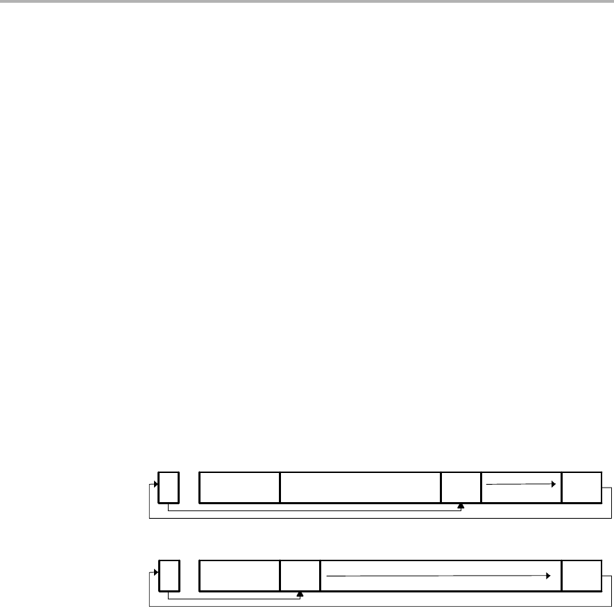
MSP430 Instructions
4-102 16-Bit MSP430X CPU
RRC[.W] Rotate Right through carry destination word
RRC.B Rotate Right through carry destination byte
Syntax RRC dst or RRC.W dst
RRC.B dst
Operation C → MSB → MSB-1 → ... LSB+1 → LSB → C
Description The destination operand is shifted right by one bit position as shown in
Figure 4−41. The carry bit C is shifted into the MSB and the LSB is shifted into
the carry bit C.
Status Bits N: Set if result is negative (MSB = 1), reset otherwise (MSB = 0)
Z: Set if result is zero, reset otherwise
C: Loaded from the LSB
V: Reset
Mode Bits OSCOFF, CPUOFF, and GIE are not affected.
Example RAM word EDE is shifted right one bit position. The MSB is loaded with 1.
SETC ; Prepare carry for MSB
RRC EDE ; EDE = EDE » 1 + 8000h
Figure 4−41. Rotate Right through Carry RRC.B and RRC.W
C
19 0
MSB00 00000
715
0 0 0 0 0 LSB
C
19 0
MSB
0000
15
LSB

MSP430 Instructions
4-103
16-Bit MSP430X CPU
* SBC[.W] Subtract source and borrow/.NOT. carry from destination
* SBC.B Subtract source and borrow/.NOT. carry from destination
Syntax SBC dst or SBC.W dst
SBC.B dst
Operation dst + 0FFFFh + C −> dst
dst + 0FFh + C −> dst
Emulation SUBC #0,dst
SUBC.B #0,dst
Description The carry bit (C) is added to the destination operand minus one. The previous
contents of the destination are lost.
Status Bits N: Set if result is negative, reset if positive
Z: Set if result is zero, reset otherwise
C: Set if there is a carry from the MSB of the result, reset otherwise.
Set to 1 if no borrow, reset if borrow.
V: Set if an arithmetic overflow occurs, reset otherwise.
Mode Bits OSCOFF, CPUOFF, and GIE are not affected.
Example The 16-bit counter pointed to by R13 is subtracted from a 32-bit counter
pointed to by R12.
SUB @R13,0(R12) ; Subtract LSDs
SBC 2(R12) ; Subtract carry from MSD
Example The 8-bit counter pointed to by R13 is subtracted from a 16-bit counter pointed
to by R12.
SUB.B @R13,0(R12) ; Subtract LSDs
SBC.B 1(R12) ; Subtract carry from MSD
Note: Borrow Implementation.
The borrow is treated as a .NOT. carry : Borrow Carry bit
Yes 0
No 1

MSP430 Instructions
4-104 16-Bit MSP430X CPU
* SETC Set carry bit
Syntax SETC
Operation 1 −> C
Emulation BIS #1,SR
Description The carry bit (C) is set.
Status Bits N: Not affected
Z: Not affected
C: Set
V: Not affected
Mode Bits OSCOFF, CPUOFF, and GIE are not affected.
Example Emulation of the decimal subtraction:
Subtract R5 from R6 decimally
Assume that R5 = 03987h and R6 = 04137h
DSUB ADD #06666h,R5 ; Move content R5 from 0−9 to 6−0Fh
; R5 = 03987h + 06666h = 09FEDh
INV R5 ; Invert this (result back to 0−9)
; R5 = .NOT. R5 = 06012h
SETC ; Prepare carry = 1
DADD R5,R6 ; Emulate subtraction by addition of:
; (010000h − R5 − 1)
; R6 = R6 + R5 + 1
; R6 = 0150h

MSP430 Instructions
4-105
16-Bit MSP430X CPU
* SETN Set negative bit
Syntax SETN
Operation 1 −> N
Emulation BIS #4,SR
Description The negative bit (N) is set.
Status Bits N: Set
Z: Not affected
C: Not affected
V: Not affected
Mode Bits OSCOFF, CPUOFF, and GIE are not affected.

MSP430 Instructions
4-106 16-Bit MSP430X CPU
* SETZ Set zero bit
Syntax SETZ
Operation 1 −> Z
Emulation BIS #2,SR
Description The zero bit (Z) is set.
Status Bits N: Not affected
Z: Set
C: Not affected
V: Not affected
Mode Bits OSCOFF, CPUOFF, and GIE are not affected.

MSP430 Instructions
4-107
16-Bit MSP430X CPU
SUB[.W] Subtract source word from destination word
SUB.B Subtract source byte from destination byte
Syntax SUB src,dst or SUB.W src,dst
SUB.B src,dst
Operation (.not.src) + 1 + dst → dst or dst − src → dst
Description The source operand is subtracted from the destination operand. This is made
by adding the 1’s complement of the source + 1 to the destination. The source
operand is not affected, the result is written to the destination operand.
Status Bits N: Set if result is negative (src > dst), reset if positive (src <= dst)
Z: Set if result is zero (src = dst), reset otherwise (src ≠dst)
C: Set if there is a carry from the MSB, reset otherwise
V: Set if the subtraction of a negative source operand from a positive des-
tination operand delivers a negative result, or if the subtraction of a posi-
tive source operand from a negative destination operand delivers a
positive result, reset otherwise (no overflow).
Mode Bits OSCOFF, CPUOFF, and GIE are not affected.
Example A 16-bit constant 7654h is subtracted from RAM word EDE.
SUB #7654h,&EDE ; Subtract 7654h from EDE
Example A table word pointed to by R5 (20-bit address) is subtracted from R7.
Afterwards, if R7 contains zero, jump to label TONI. R5 is then
auto-incremented by 2. R7.19:16 = 0.
SUB @R5+,R7 ; Subtract table number from R7. R5 + 2
JZ TONI ; R7 = @R5 (before subtraction)
... ; R7 <> @R5 (before subtraction)
Example Byte CNT is subtracted from byte R12 points to. The address of CNT is within
PC ±32 K. The address R12 points to is in full memory range.
SUB.B CNT,0(R12) ; Subtract CNT from @R12

MSP430 Instructions
4-108 16-Bit MSP430X CPU
SUBC[.W] Subtract source word with carry from destination word
SUBC.B Subtract source byte with carry from destination byte
Syntax SUBC src,dst or SUBC.W src,dst
SUBC.B src,dst
Operation (.not.src) + C + dst → dst or dst − (src − 1) + C → dst
Description The source operand is subtracted from the destination operand. This is done
by adding the 1’s complement of the source + carry to the destination. The
source operand is not affected, the result is written to the destination operand.
Used for 32, 48, and 64-bit operands.
Status Bits N: Set if result is negative (MSB = 1), reset if positive (MSB = 0)
Z: Set if result is zero, reset otherwise
C: Set if there is a carry from the MSB, reset otherwise
V: Set if the subtraction of a negative source operand from a positive des-
tination operand delivers a negative result, or if the subtraction of a posi-
tive source operand from a negative destination operand delivers a
positive result, reset otherwise (no overflow).
Mode Bits OSCOFF, CPUOFF, and GIE are not affected.
Example A 16-bit constant 7654h is subtracted from R5 with the carry from the previous
instruction. R5.19:16 = 0
SUBC.W #7654h,R5 ; Subtract 7654h + C from R5
Example A 48-bit number (3 words) pointed to by R5 (20-bit address) is subtracted from
a 48-bit counter in RAM, pointed to by R7. R5 points to the next 48-bit number
afterwards. The address R7 points to is in full memory range.
SUB @R5+,0(R7) ; Subtract LSBs. R5 + 2
SUBC @R5+,2(R7) ; Subtract MIDs with C. R5 + 2
SUBC @R5+,4(R7) ; Subtract MSBs with C. R5 + 2
Example Byte CNT is subtracted from the byte, R12 points to. The carry of the previous
instruction is used. The address of CNT is in lower 64 K.
SUBC.B &CNT,0(R12) ; Subtract byte CNT from @R12

MSP430 Instructions
4-109
16-Bit MSP430X CPU
SWPB Swap bytes
Syntax SWPB dst
Operation dst.15:8 ⇔ dst.7:0
Description The high and the low byte of the operand are exchanged. PC.19:16 bits are
cleared in register mode.
Status Bits Not affected
Mode Bits OSCOFF, CPUOFF, and GIE are not affected.
Example Exchange the bytes of RAM word EDE (lower 64 K).
MOV #1234h,&EDE ; 1234h -> EDE
SWPB &EDE ; 3412h -> EDE
Figure 4−42. Swap Bytes in Memory
15 8 7 0
15 8 7 0
Low Byte
Low ByteHigh Byte
High Byte
Before SWPB
After SWPB
Figure 4−43. Swap Bytes in a Register
15 8 7 0
15 8 7 0
Low Byte
Low ByteHigh Byte
High Byte
Before SWPB
After SWPB
0
x
0...
19
19
16
16

MSP430 Instructions
4-110 16-Bit MSP430X CPU
SXT Extend sign
Syntax SXT dst
Operation dst.7 → dst.15:8, dst.7 → dst.19:8 (Register Mode)
Description Register Mode: the sign of the low byte of the operand is extended into the bits
Rdst.19:8
Rdst.7 = 0: Rdst.19:8 = 000h afterwards.
Rdst.7 = 1: Rdst.19:8 = FFFh afterwards.
Other Modes: the sign of the low byte of the operand is extended into the high
byte.
dst.7 = 0: high byte = 00h afterwards.
dst.7 = 1: high byte = FFh afterwards.
Status Bits N: Set if result is negative, reset otherwise
Z: Set if result is zero, reset otherwise
C: Set if result is not zero, reset otherwise (C = .not.Z)
V: Reset
Mode Bits OSCOFF, CPUOFF, and GIE are not affected.
Example The signed 8-bit data in EDE (lower 64 K) is sign extended and added to the
16-bit signed data in R7.
MOV.B &EDE,R5 ; EDE -> R5. 00XXh
SXT R5 ; Sign extend low byte to R5.19:8
ADD R5,R7 ; Add signed 16-bit values
Example The signed 8-bit data in EDE (PC ±32 K) is sign extended and added to the
20-bit data in R7.
MOV.B EDE,R5 ; EDE -> R5. 00XXh
SXT R5 ; Sign extend low byte to R5.19:8
ADDA R5,R7 ; Add signed 20-bit values

MSP430 Instructions
4-111
16-Bit MSP430X CPU
* TST[.W] Test destination
* TST.B Test destination
Syntax TST dst or TST.W dst
TST.B dst
Operation dst + 0FFFFh + 1
dst + 0FFh + 1
Emulation CMP #0,dst
CMP.B #0,dst
Description The destination operand is compared with zero. The status bits are set accord-
ing to the result. The destination is not affected.
Status Bits N: Set if destination is negative, reset if positive
Z: Set if destination contains zero, reset otherwise
C: Set
V: Reset
Mode Bits OSCOFF, CPUOFF, and GIE are not affected.
Example R7 is tested. If it is negative, continue at R7NEG; if it is positive but not zero,
continue at R7POS.
TST R7 ; Test R7
JN R7NEG ; R7 is negative
JZ R7ZERO ; R7 is zero
R7POS ...... ; R7 is positive but not zero
R7NEG ...... ; R7 is negative
R7ZERO ...... ; R7 is zero
Example The low byte of R7 is tested. If it is negative, continue at R7NEG; if it is positive
but not zero, continue at R7POS.
TST.B R7 ; Test low byte of R7
JN R7NEG ; Low byte of R7 is negative
JZ R7ZERO ; Low byte of R7 is zero
R7POS ...... ; Low byte of R7 is positive but not zero
R7NEG ..... ; Low byte of R7 is negative
R7ZERO ...... ; Low byte of R7 is zero

MSP430 Instructions
4-112 16-Bit MSP430X CPU
XOR[.W] Exclusive OR source word with destination word
XOR.B Exclusive OR source byte with destination byte
Syntax XOR dst or XOR.W dst
XOR.B dst
Operation src .xor. dst → dst
Description The source and destination operands are exclusively ORed. The result is
placed into the destination. The source operand is not affected. The previous
content of the destination is lost.
Status Bits N: Set if result is negative (MSB = 1), reset if positive (MSB = 0)
Z: Set if result is zero, reset otherwise
C: Set if result is not zero, reset otherwise (C = .not. Z)
V: Set if both operands are negative before execution, reset otherwise
Mode Bits OSCOFF, CPUOFF, and GIE are not affected.
Example Toggle bits in word CNTR (16-bit data) with information (bit = 1) in
address-word TONI. Both operands are located in lower 64 K.
XOR &TONI,&CNTR ; Toggle bits in CNTR
Example A table word pointed to by R5 (20-bit address) is used to toggle bits in R6.
R6.19:16 = 0.
XOR @R5,R6 ; Toggle bits in R6
Example Reset to zero those bits in the low byte of R7 that are different from the bits in
byte EDE. R7.19:8 = 0. The address of EDE is within PC ±32 K.
XOR.B EDE,R7 ; Set different bits to 1 in R7.
INV.B R7 ; Invert low byte of R7, high byte is 0h

Extended Instructions
4-113
16-Bit MSP430X CPU
4.6.3 Extended Instructions
The extended MSP430X instructions give the MSP430X CPU full access to its
20-bit address space. Some MSP430X instructions require an additional word
of op-code called the extension word. All addresses, indexes, and immediate
numbers have 20-bit values, when preceded by the extension word. The
MSP430X extended instructions are listed and described in the following
pages. For MSP430X instructions that do not require the extension word, it is
noted in the instruction description.

Extended Instructions
4-114 16-Bit MSP430X CPU
* ADCX.A Add carry to destination address-word
* ADCX.[W] Add carry to destination word
* ADCX.B Add carry to destination byte
Syntax ADCX.A dst
ADCX dst or ADCX.W dst
ADCX.B dst
Operation dst + C −> dst
Emulation ADDCX.A #0,dst
ADDCX #0,dst
ADDCX.B #0,dst
Description The carry bit (C) is added to the destination operand. The previous contents
of the destination are lost.
Status Bits N: Set if result is negative (MSB = 1), reset if positive (MSB = 0)
Z: Set if result is zero, reset otherwise
C: Set if there is a carry from the MSB of the result, reset otherwise
V: Set if the result of two positive operands is negative, or if the result of
two negative numbers is positive, reset otherwise
Mode Bits OSCOFF, CPUOFF, and GIE are not affected.
Example The 40-bit counter, pointed to by R12 and R13, is incremented.
INCX.A @R12 ; Increment lower 20 bits
ADCX.A @R13 ; Add carry to upper 20 bits

Extended Instructions
4-115
16-Bit MSP430X CPU
ADDX.A Add source address-word to destination address-word
ADDX[.W] Add source word to destination word
ADDX.B Add source byte to destination byte
Syntax ADDX.A src,dst
ADDX src,dst or ADDX.W src,dst
ADDX.B src,dst
Operation src + dst → dst
Description The source operand is added to the destination operand. The previous
contents of the destination are lost. Both operands can be located in the full
address space.
Status Bits N: Set if result is negative (MSB = 1), reset if positive (MSB = 0)
Z: Set if result is zero, reset otherwise
C: Set if there is a carry from the MSB of the result, reset otherwise
V: Set if the result of two positive operands is negative, or if the result of
two negative numbers is positive, reset otherwise
Mode Bits OSCOFF, CPUOFF, and GIE are not affected.
Example Ten is added to the 20-bit pointer CNTR located in two words CNTR (LSBs)
and CNTR+2 (MSBs).
ADDX.A #10,CNTR ; Add 10 to 20-bit pointer
Example A table word (16-bit) pointed to by R5 (20-bit address) is added to R6. The jump
to label TONI is performed on a carry.
ADDX.W @R5,R6 ; Add table word to R6
JC TONI ; Jump if carry
... ; No carry
Example A table byte pointed to by R5 (20-bit address) is added to R6. The jump to label
TONI is performed if no carry occurs. The table pointer is auto-incremented
by 1.
ADDX.B @R5+,R6 ; Add table byte to R6. R5 + 1. R6: 000xxh
JNC TONI ; Jump if no carry
... ; Carry occurred
Note: Use ADDA for the following two cases for better code density and
execution.
ADDX.A Rsrc,Rdst or
ADDX.A #imm20,Rdst

Extended Instructions
4-116 16-Bit MSP430X CPU
ADDCX.A Add source address-word and carry to destination address-word
ADDCX[.W] Add source word and carry to destination word
ADDCX.B Add source byte and carry to destination byte
Syntax ADDCX.A src,dst
ADDCX src,dst or ADDCX.W src,dst
ADDCX.B src,dst
Operation src + dst + C → dst
Description The source operand and the carry bit C are added to the destination operand.
The previous contents of the destination are lost. Both operands may be
located in the full address space.
Status Bits N: Set if result is negative (MSB = 1), reset if positive (MSB = 0)
Z: Set if result is zero, reset otherwise
C: Set if there is a carry from the MSB of the result, reset otherwise
V: Set if the result of two positive operands is negative, or if the result of
two negative numbers is positive, reset otherwise
Mode Bits OSCOFF, CPUOFF, and GIE are not affected.
Example Constant 15 and the carry of the previous instruction are added to the 20-bit
counter CNTR located in two words.
ADDCX.A #15,&CNTR ; Add 15 + C to 20-bit CNTR
Example A table word pointed to by R5 (20-bit address) and the carry C are added to R6.
The jump to label TONI is performed on a carry.
ADDCX.W @R5,R6 ; Add table word + C to R6
JC TONI ; Jump if carry
... ; No carry
Example A table byte pointed to by R5 (20-bit address) and the carry bit C are added to
R6. The jump to label TONI is performed if no carry occurs. The table pointer is
auto-incremented by 1.
ADDCX.B @R5+,R6 ; Add table byte + C to R6. R5 + 1
JNC TONI ; Jump if no carry
... ; Carry occurred

Extended Instructions
4-117
16-Bit MSP430X CPU
ANDX.A Logical AND of source address-word with destination address-word
ANDX[.W] Logical AND of source word with destination word
ANDX.B Logical AND of source byte with destination byte
Syntax ANDX.A src,dst
ANDX src,dst or ANDX.W src,dst
ANDX.B src,dst
Operation src .and. dst → dst
Description The source operand and the destination operand are logically ANDed. The
result is placed into the destination. The source operand is not affected. Both
operands may be located in the full address space.
Status Bits N: Set if result is negative (MSB = 1), reset if positive (MSB = 0)
Z: Set if result is zero, reset otherwise
C: Set if the result is not zero, reset otherwise. C = (.not. Z)
V: Reset
Mode Bits OSCOFF, CPUOFF, and GIE are not affected.
Example The bits set in R5 (20-bit data) are used as a mask (AAA55h) for the
address-word TOM located in two words. If the result is zero, a branch is taken
to label TONI.
MOVA #AAA55h,R5 ; Load 20-bit mask to R5
ANDX.A R5,TOM ; TOM .and. R5 -> TOM
JZ TONI ; Jump if result 0
... ; Result > 0
or shorter:
ANDX.A #AAA55h,TOM ; TOM .and. AAA55h -> TOM
JZ TONI ; Jump if result 0
Example A table byte pointed to by R5 (20-bit address) is logically ANDed with R6.
R6.19:8 = 0. The table pointer is auto-incremented by 1.
ANDX.B @R5+,R6 ; AND table byte with R6. R5 + 1

Extended Instructions
4-118 16-Bit MSP430X CPU
BICX.A Clear bits set in source address-word in destination address-word
BICX[.W] Clear bits set in source word in destination word
BICX.B Clear bits set in source byte in destination byte
Syntax BICX.A src,dst
BICX src,dst or BICX.W src,dst
BICX.B src,dst
Operation (.not. src) .and. dst → dst
Description The inverted source operand and the destination operand are logically
ANDed. The result is placed into the destination. The source operand is not
affected. Both operands may be located in the full address space.
Status Bits N: Not affected
Z: Not affected
C: Not affected
V: Not affected
Mode Bits OSCOFF, CPUOFF, and GIE are not affected.
Example The bits 19:15 of R5 (20-bit data) are cleared.
BICX.A #0F8000h,R5 ; Clear R5.19:15 bits
Example A table word pointed to by R5 (20-bit address) is used to clear bits in R7.
R7.19:16 = 0
BICX.W @R5,R7 ; Clear bits in R7
Example A table byte pointed to by R5 (20-bit address) is used to clear bits in output
Port1.
BICX.B @R5,&P1OUT ; Clear I/O port P1 bits

Extended Instructions
4-119
16-Bit MSP430X CPU
BISX.A Set bits set in source address-word in destination address-word
BISX[.W] Set bits set in source word in destination word
BISX.B Set bits set in source byte in destination byte
Syntax BISX.A src,dst
BISX src,dst or BISX.W src,dst
BISX.B src,dst
Operation src .or. dst → dst
Description The source operand and the destination operand are logically ORed. The
result is placed into the destination. The source operand is not affected. Both
operands may be located in the full address space.
Status Bits N: Not affected
Z: Not affected
C: Not affected
V: Not affected
Mode Bits OSCOFF, CPUOFF, and GIE are not affected.
Example Bits 16 and 15 of R5 (20-bit data) are set to one.
BISX.A #018000h,R5 ; Set R5.16:15 bits
Example A table word pointed to by R5 (20-bit address) is used to set bits in R7.
BISX.W @R5,R7 ; Set bits in R7
Example A table byte pointed to by R5 (20-bit address) is used to set bits in output Port1.
BISX.B @R5,&P1OUT ; Set I/O port P1 bits

Extended Instructions
4-120 16-Bit MSP430X CPU
BITX.A Test bits set in source address-word in destination address-word
BITX[.W] Test bits set in source word in destination word
BITX.B Test bits set in source byte in destination byte
Syntax BITX.A src,dst
BITX src,dst or BITX.W src,dst
BITX.B src,dst
Operation src .and. dst
Description The source operand and the destination operand are logically ANDed. The
result affects only the status bits. Both operands may be located in the full
address space.
Status Bits N: Set if result is negative (MSB = 1), reset if positive (MSB = 0)
Z: Set if result is zero, reset otherwise
C: Set if the result is not zero, reset otherwise. C = (.not. Z)
V: Reset
Mode Bits OSCOFF, CPUOFF, and GIE are not affected.
Example Test if bit 16 or 15 of R5 (20-bit data) is set. Jump to label TONI if so.
BITX.A #018000h,R5 ; Test R5.16:15 bits
JNZ TONI ; At least one bit is set
... ; Both are reset
Example A table word pointed to by R5 (20-bit address) is used to test bits in R7. Jump to
label TONI if at least one bit is set.
BITX.W @R5,R7 ; Test bits in R7: C = .not.Z
JC TONI ; At least one is set
... ; Both are reset
Example A table byte pointed to by R5 (20-bit address) is used to test bits in input Port1.
Jump to label TONI if no bit is set. The next table byte is addressed.
BITX.B @R5+,&P1IN ; Test input P1 bits. R5 + 1
JNC TONI ; No corresponding input bit is set
... ; At least one bit is set

Extended Instructions
4-121
16-Bit MSP430X CPU
* CLRX.A Clear destination address-word
* CLRX.[W] Clear destination word
* CLRX.B Clear destination byte
Syntax CLRX.A dst
CLRX dst or CLRX.W dst
CLRX.B dst
Operation 0 −> dst
Emulation MOVX.A #0,dst
MOVX #0,dst
MOVX.B #0,dst
Description The destination operand is cleared.
Status Bits Status bits are not affected.
Example RAM address-word TONI is cleared.
CLRX.A TONI ; 0 −> TONI

Extended Instructions
4-122 16-Bit MSP430X CPU
CMPX.A Compare source address-word and destination address-word
CMPX[.W] Compare source word and destination word
CMPX.B Compare source byte and destination byte
Syntax CMPX.A src,dst
CMPX src,dst or CMPX.W src,dst
CMPX.B src,dst
Operation (.not. src) + 1 + dst or dst − src
Description The source operand is subtracted from the destination operand by adding the
1’s complement of the source + 1 to the destination. The result affects only the
status bits. Both operands may be located in the full address space.
Status Bits N: Set if result is negative (src > dst), reset if positive (src <= dst)
Z: Set if result is zero (src = dst), reset otherwise (src ≠dst)
C: Set if there is a carry from the MSB, reset otherwise
V: Set if the subtraction of a negative source operand from a positive
destination operand delivers a negative result, or if the subtraction of
a positive source operand from a negative destination operand delivers
a positive result, reset otherwise (no overflow).
Mode Bits OSCOFF, CPUOFF, and GIE are not affected.
Example Compare EDE with a 20-bit constant 18000h. Jump to label TONI if EDE
equals the constant.
CMPX.A #018000h,EDE ; Compare EDE with 18000h
JEQ TONI ; EDE contains 18000h
... ; Not equal
Example A table word pointed to by R5 (20-bit address) is compared with R7. Jump to
label TONI if R7 contains a lower, signed, 16-bit number.
CMPX.W @R5,R7 ; Compare two signed numbers
JL TONI ; R7 < @R5
... ; R7 >= @R5
Example A table byte pointed to by R5 (20-bit address) is compared to the input in I/O
Port1. Jump to label TONI if the values are equal. The next table byte is
addressed.
CMPX.B @R5+,&P1IN ; Compare P1 bits with table. R5 + 1
JEQ TONI ; Equal contents
... ; Not equal
Note: Use CMPA for the following two cases for better density and execution.
CMPA Rsrc,Rdst or
CMPA #imm20,Rdst

Extended Instructions
4-123
16-Bit MSP430X CPU
* DADCX.A Add carry decimally to destination address-word
* DADCX[.W] Add carry decimally to destination word
* DADCX.B Add carry decimally to destination byte
Syntax DADCX.A dst
DADCX dst or DADCX.W src,dst
DADCX.B dst
Operation dst + C −> dst (decimally)
Emulation DADDX.A #0,dst
DADDX #0,dst
DADDX.B #0,dst
Description The carry bit (C) is added decimally to the destination.
Status Bits N: Set if MSB of result is 1 (address-word > 79999h, word > 7999h,
byte > 79h), reset if MSB is 0.
Z: Set if result is zero, reset otherwise.
C: Set if the BCD result is too large (address-word > 99999h,
word > 9999h, byte > 99h), reset otherwise.
V: Undefined.
Mode Bits OSCOFF, CPUOFF, and GIE are not affected.
Example The 40-bit counter, pointed to by R12 and R13, is incremented decimally.
DADDX.A #1,0(R12) ; Increment lower 20 bits
DADCX.A 0(R13) ; Add carry to upper 20 bits

Extended Instructions
4-124 16-Bit MSP430X CPU
DADDX.A Add source address-word and carry decimally to destination address-word
DADDX[.W] Add source word and carry decimally to destination word
DADDX.B Add source byte and carry decimally to destination byte
Syntax DADDX.A src,dst
DADDX src,dst or DADDX.W src,dst
DADDX.B src,dst
Operation src + dst + C → dst (decimally)
Description The source operand and the destination operand are treated as two (.B), four
(.W), or five (.A) binary coded decimals (BCD) with positive signs. The source
operand and the carry bit C are added decimally to the destination operand.
The source operand is not affected. The previous contents of the destination
are lost. The result is not defined for non-BCD numbers. Both operands may
be located in the full address space.
Status Bits N: Set if MSB of result is 1 (address-word > 79999h, word > 7999h,
byte > 79h), reset if MSB is 0.
Z: Set if result is zero, reset otherwise.
C: Set if the BCD result is too large (address-word > 99999h,
word > 9999h, byte > 99h), reset otherwise.
V: Undefined.
Mode Bits OSCOFF, CPUOFF, and GIE are not affected.
Example Decimal 10 is added to the 20-bit BCD counter DECCNTR located in two
words.
DADDX.A #10h,&DECCNTR ; Add 10 to 20-bit BCD counter
Example The eight-digit BCD number contained in 20-bit addresses BCD and BCD+2 is
added decimally to an eight-digit BCD number contained in R4 and R5
(BCD+2 and R5 contain the MSDs).
CLRC ; Clear carry
DADDX.W BCD,R4 ; Add LSDs
DADDX.W BCD+2,R5 ; Add MSDs with carry
JC OVERFLOW ; Result >99999999: go to error routine
... ; Result ok
Example The two-digit BCD number contained in 20-bit address BCD is added
decimally to a two-digit BCD number contained in R4.
CLRC ; Clear carry
DADDX.B BCD,R4 ; Add BCD to R4 decimally.
; R4: 000ddh

Extended Instructions
4-125
16-Bit MSP430X CPU
* DECX.A Decrement destination address-word
* DECX[.W] Decrement destination word
* DECX.B Decrement destination byte
Syntax DECX dst
DECX dst or DECX.W dst
DECX.B dst
Operation dst − 1 −> dst
Emulation SUBX.A #1,dst
SUBX #1,dst
SUBX.B #1,dst
Description The destination operand is decremented by one. The original contents are
lost.
Status Bits N: Set if result is negative, reset if positive
Z: Set if dst contained 1, reset otherwise
C: Reset if dst contained 0, set otherwise
V: Set if an arithmetic overflow occurs, otherwise reset.
Mode Bits OSCOFF, CPUOFF, and GIE are not affected.
Example RAM address-word TONI is decremented by 1
DECX.A TONI ; Decrement TONI

Extended Instructions
4-126 16-Bit MSP430X CPU
* DECDX.A Double-decrement destination address-word
* DECDX[.W] Double-decrement destination word
* DECDX.B Double-decrement destination byte
Syntax DECDX.A dst
DECDX dst or DECDX.W dst
DECDX.B dst
Operation dst − 2 −> dst
Emulation SUBX.A #2,dst
SUBX #2,dst
SUBX.B #2,dst
Description The destination operand is decremented by two. The original contents are lost.
Status Bits N: Set if result is negative, reset if positive
Z: Set if dst contained 2, reset otherwise
C: Reset if dst contained 0 or 1, set otherwise
V: Set if an arithmetic overflow occurs, otherwise reset.
Mode Bits OSCOFF, CPUOFF, and GIE are not affected.
Example RAM address-word TONI is decremented by 2.
DECDX.A TONI ; Decrement TONI by two

Extended Instructions
4-127
16-Bit MSP430X CPU
* INCX.A Increment destination address-word
* INCX[.W] Increment destination word
* INCX.B Increment destination byte
Syntax INCX.A dst
INCX dst or INCX.W dst
INCX.B dst
Operation dst + 1 −> dst
Emulation ADDX.A #1,dst
ADDX #1,dst
ADDX.B #1,dst
Description The destination operand is incremented by one. The original contents are lost.
Status Bits N: Set if result is negative, reset if positive
Z: Set if dst contained 0FFFFFh, reset otherwise
Set if dst contained 0FFFFh, reset otherwise
Set if dst contained 0FFh, reset otherwise
C: Set if dst contained 0FFFFFh, reset otherwise
Set if dst contained 0FFFFh, reset otherwise
Set if dst contained 0FFh, reset otherwise
V: Set if dst contained 07FFFh, reset otherwise
Set if dst contained 07FFFh, reset otherwise
Set if dst contained 07Fh, reset otherwise
Mode Bits OSCOFF, CPUOFF, and GIE are not affected.
Example RAM address-word TONI is incremented by 1.
INCX.A TONI ; Increment TONI (20-bits)

Extended Instructions
4-128 16-Bit MSP430X CPU
* INCDX.A Double-increment destination address-word
* INCDX[.W] Double-increment destination word
* INCDX.B Double-increment destination byte
Syntax INCDX.A dst
INCDX dst or INCDX.W dst
INCDX.B dst
Operation dst + 2 −> dst
Emulation ADDX.A #2,dst
ADDX #2,dst
ADDX.B #2,dst
Example The destination operand is incremented by two. The original contents are lost.
Status Bits N: Set if result is negative, reset if positive
Z: Set if dst contained 0FFFFEh, reset otherwise
Set if dst contained 0FFFEh, reset otherwise
Set if dst contained 0FEh, reset otherwise
C: Set if dst contained 0FFFFEh or 0FFFFFh, reset otherwise
Set if dst contained 0FFFEh or 0FFFFh, reset otherwise
Set if dst contained 0FEh or 0FFh, reset otherwise
V: Set if dst contained 07FFFEh or 07FFFFh, reset otherwise
Set if dst contained 07FFEh or 07FFFh, reset otherwise
Set if dst contained 07Eh or 07Fh, reset otherwise
Mode Bits OSCOFF, CPUOFF, and GIE are not affected.
Example RAM byte LEO is incremented by two; PC points to upper memory
INCDX.B LEO ; Increment LEO by two

Extended Instructions
4-129
16-Bit MSP430X CPU
* INVX.A Invert destination
* INVX[.W] Invert destination
* INVX.B Invert destination
Syntax INVX.A dst
INVX dst or INVX.W dst
INVX.B dst
Operation .NOT.dst −> dst
Emulation XORX.A #0FFFFFh,dst
XORX #0FFFFh,dst
XORX.B #0FFh,dst
Description The destination operand is inverted. The original contents are lost.
Status Bits N: Set if result is negative, reset if positive
Z: Set if dst contained 0FFFFFh, reset otherwise
Set if dst contained 0FFFFh, reset otherwise
Set if dst contained 0FFh, reset otherwise
C: Set if result is not zero, reset otherwise ( = .NOT. Zero)
V: Set if initial destination operand was negative, otherwise reset
Mode Bits OSCOFF, CPUOFF, and GIE are not affected.
Example 20-bit content of R5 is negated (twos complement).
INVX.A R5 ; Invert R5
INCX.A R5 ; R5 is now negated
Example Content of memory byte LEO is negated. PC is pointing to upper memory
INVX.B LEO ; Invert LEO
INCX.B LEO ; MEM(LEO) is negated

Extended Instructions
4-130 16-Bit MSP430X CPU
MOVX.A Move source address-word to destination address-word
MOVX[.W] Move source word to destination word
MOVX.B Move source byte to destination byte
Syntax MOVX.A src,dst
MOVX src,dst or MOVX.W src,dst
MOVX.B src,dst
Operation src → dst
Description The source operand is copied to the destination. The source operand is not
affected. Both operands may be located in the full address space.
Status Bits N: Not affected
Z: Not affected
C: Not affected
V: Not affected
Mode Bits OSCOFF, CPUOFF, and GIE are not affected.
Example Move a 20-bit constant 18000h to absolute address-word EDE.
MOVX.A #018000h,&EDE ; Move 18000h to EDE
Example The contents of table EDE (word data, 20-bit addresses) are copied to table
TOM. The length of the table is 030h words.
MOVA #EDE,R10 ; Prepare pointer (20-bit address)
Loop MOVX.W @R10+,TOM-EDE-2(R10) ; R10 points to both tables.
R10+2
CMPA #EDE+60h,R10 ; End of table reached?
JLO Loop ; Not yet
... ; Copy completed
Example The contents of table EDE (byte data, 20-bit addresses) are copied to table
TOM. The length of the table is 020h bytes.
MOVA #EDE,R10 ; Prepare pointer (20-bit)
MOV #20h,R9 ; Prepare counter
Loop MOVX.B @R10+,TOM-EDE-1(R10) ; R10 points to both tables.
; R10+1
DEC R9 ; Decrement counter
JNZ Loop ; Not yet done
... ; Copy completed

Extended Instructions
4-131
16-Bit MSP430X CPU
Ten of the 28 possible addressing combinations of the MOVX.A instruction can
use the MOVA instruction. This saves two bytes and code cycles. Examples
for the addressing combinations are:
MOVX.A Rsrc,Rdst MOVA Rsrc,Rdst ; Reg/Reg
MOVX.A #imm20,Rdst MOVA #imm20,Rdst ; Immediate/Reg
MOVX.A &abs20,Rdst MOVA &abs20,Rdst ; Absolute/Reg
MOVX.A @Rsrc,Rdst MOVA @Rsrc,Rdst ; Indirect/Reg
MOVX.A @Rsrc+,Rdst MOVA @Rsrc+,Rdst ; Indirect,Auto/Reg
MOVX.A Rsrc,&abs20 MOVA Rsrc,&abs20 ; Reg/Absolute
The next four replacements are possible only if 16-bit indexes are sufficient for
the addressing.
MOVX.A z20(Rsrc),Rdst MOVA z16(Rsrc),Rdst ; Indexed/Reg
MOVX.A Rsrc,z20(Rdst) MOVA Rsrc,z16(Rdst) ; Reg/Indexed
MOVX.A symb20,Rdst MOVA symb16,Rdst ; Symbolic/Reg
MOVX.A Rsrc,symb20 MOVA Rsrc,symb16 ; Reg/Symbolic

Extended Instructions
4-132 16-Bit MSP430X CPU
POPM.A Restore n CPU registers (20-bit data) from the stack
POPM[.W] Restore n CPU registers (16-bit data) from the stack
Syntax POPM.A #n,Rdst 1 ≤ n ≤ 16
POPM.W #n,Rdst or POPM #n,Rdst 1 ≤ n ≤ 16
Operation POPM.A: Restore the register values from stack to the specified CPU
registers. The stack pointer SP is incremented by four for each register
restored from stack. The 20-bit values from stack (2 words per register) are
restored to the registers.
POPM.W: Restore the 16-bit register values from stack to the specified CPU
registers. The stack pointer SP is incremented by two for each register
restored from stack. The 16-bit values from stack (one word per register) are
restored to the CPU registers.
Note : This does not use the extension word.
Description POPM.A: The CPU registers pushed on the stack are moved to the extended
CPU registers, starting with the CPU register (Rdst - n + 1). The stack pointer
is incremented by (n ×4) after the operation.
POPM.W: The 16-bit registers pushed on the stack are moved back to the
CPU registers, starting with CPU register (Rdst - n + 1). The stack pointer is
incremented by (n ×2) after the instruction. The MSBs (Rdst.19:16) of the
restored CPU registers are cleared
Status Bits Not affected, except SR is included in the operation
Mode Bits OSCOFF, CPUOFF, and GIE are not affected, except SR is included in the op-
eration.
Example Restore the 20-bit registers R9, R10, R11, R12, R13 from the stack.
POPM.A #5,R13 ; Restore R9, R10, R11, R12, R13
Example Restore the 16-bit registers R9, R10, R11, R12, R13 from the stack.
POPM.W #5,R13 ; Restore R9, R10, R11, R12, R13

Extended Instructions
4-133
16-Bit MSP430X CPU
PUSHM.A Save n CPU registers (20-bit data) on the stack
PUSHM[.W] Save n CPU registers (16-bit words) on the stack
Syntax PUSHM.A #n,Rdst 1 ≤ n ≤ 16
PUSHM.W #n,Rdst or PUSHM #n,Rdst 1 ≤ n ≤ 16
Operation PUSHM.A: Save the 20-bit CPU register values on the stack. The stack pointer
(SP) is decremented by four for each register stored on the stack. The MSBs
are stored first (higher address).
PUSHM.W: Save the 16-bit CPU register values on the stack. The stack
pointer is decremented by two for each register stored on the stack.
Description PUSHM.A: The n CPU registers, starting with Rdst backwards, are stored on
the stack. The stack pointer is decremented by (n ×4) after the operation. The
data (Rn.19:0) of the pushed CPU registers is not affected.
PUSHM.W: The n registers, starting with Rdst backwards, are stored on the
stack. The stack pointer is decremented by (n ×2) after the operation. The
data (Rn.19:0) of the pushed CPU registers is not affected.
Note : This instruction does not use the extension word.
Status Bits Not affected.
Mode Bits OSCOFF, CPUOFF, and GIE are not affected.
Example Save the five 20-bit registers R9, R10, R11, R12, R13 on the stack.
PUSHM.A #5,R13 ; Save R13, R12, R11, R10, R9
Example Save the five 16-bit registers R9, R10, R11, R12, R13 on the stack.
PUSHM.W #5,R13 ; Save R13, R12, R11, R10, R9

Extended Instructions
4-134 16-Bit MSP430X CPU
* POPX.A Restore single address-word from the stack
* POPX[.W] Restore single word from the stack
* POPX.B Restore single byte from the stack
Syntax POPX.A dst
POPX dst or POPX.W dst
POPX.B dst
Operation Restore the 8/16/20-bit value from the stack to the destination. 20-bit
addresses are possible. The stack pointer SP is incremented by two (byte and
word operands) and by four (address-word operand).
Emulation MOVX(.B,.A) @SP+,dst
Description The item on TOS is written to the destination operand. Register Mode, Indexed
Mode, Symbolic Mode, and Absolute Mode are possible. The stack pointer is
incremented by two or four.
Note: the stack pointer is incremented by two also for byte operations.
Status Bits Not affected.
Mode Bits OSCOFF, CPUOFF, and GIE are not affected.
Example Write the 16-bit value on TOS to the 20-bit address &EDE.
POPX.W &EDE ; Write word to address EDE
Example Write the 20-bit value on TOS to R9.
POPX.A R9 ; Write address-word to R9

Extended Instructions
4-135
16-Bit MSP430X CPU
PUSHX.A Save a single address-word on the stack
PUSHX[.W] Save a single word on the stack
PUSHX.B Save a single byte on the stack
Syntax PUSHX.A src
PUSHX src or PUSHX.W src
PUSHX.B src
Operation Save the 8/16/20-bit value of the source operand on the TOS. 20-bit addresses
are possible. The stack pointer (SP) is decremented by two (byte and word
operands) or by four (address-word operand) before the write operation.
Description The stack pointer is decremented by two (byte and word operands) or by four
(address-word operand). Then the source operand is written to the TOS. All
seven addressing modes are possible for the source operand.
Note : This instruction does not use the extension word.
Status Bits Not affected.
Mode Bits OSCOFF, CPUOFF, and GIE are not affected.
Example Save the byte at the 20-bit address &EDE on the stack.
PUSHX.B &EDE ; Save byte at address EDE
Example Save the 20-bit value in R9 on the stack.
PUSHX.A R9 ; Save address-word in R9

Extended Instructions
4-136 16-Bit MSP430X CPU
RLAM.A Rotate Left Arithmetically the 20-bit CPU register content
RLAM[.W] Rotate Left Arithmetically the 16-bit CPU register content
Syntax RLAM.A #n,Rdst 1 ≤ n ≤ 4
RLAM.W #n,Rdst or RLAM #n,Rdst 1 ≤ n ≤ 4
Operation C ← MSB ← MSB-1 .... LSB+1 ← LSB ← 0
Description The destination operand is shifted arithmetically left one, two, three, or four
positions as shown in Figure 4−44. RLAM works as a multiplication (signed
and unsigned) with 2, 4, 8, or 16. The word instruction RLAM.W clears the bits
Rdst.19:16
Note : This instruction does not use the extension word.
Status Bits N: Set if result is negative
.A: Rdst.19 = 1, reset if Rdst.19 = 0
.W: Rdst.15 = 1, reset if Rdst.15 = 0
Z: Set if result is zero, reset otherwise
C: Loaded from the MSB (n = 1), MSB-1 (n = 2), MSB-2 (n = 3), MSB-3
(n = 4)
V: Undefined
Mode Bits OSCOFF, CPUOFF, and GIE are not affected.
Example The 20-bit operand in R5 is shifted left by three positions. It operates equal to
an arithmetic multiplication by 8.
RLAM.A #3,R5 ; R5 = R5 x 8
Figure 4−44. Rotate Left Arithmetically RLAM[.W] and RLAM.A
C
19 0
MSB0000
15
LSB
C
19 0
MSB LSB
16
0
0
Extended Instructions
4-137
16-Bit MSP430X CPU
* RLAX.A Rotate left arithmetically address-word
* RLAX[.W] Rotate left arithmetically word
* RLAX.B Rotate left arithmetically byte
Syntax RLAX.B dst
RLAX dst or RLAX.W dst
RLAX.B dst
Operation C <− MSB <− MSB−1 .... LSB+1 <− LSB <− 0
Emulation ADDX.A dst,dst
ADDX dst,dst
ADDX.B dst,dst
Description The destination operand is shifted left one position as shown in Figure 4−45.
The MSB is shifted into the carry bit (C) and the LSB is filled with 0. The RLAX
instruction acts as a signed multiplication by 2.
Figure 4−45. Destination Operand—Arithmetic Shift Left
MSB 0
C0
Status Bits N: Set if result is negative, reset if positive
Z: Set if result is zero, reset otherwise
C: Loaded from the MSB
V: Set if an arithmetic overflow occurs:
the initial value is 040000h ≤dst < 0C0000h; reset otherwise
Set if an arithmetic overflow occurs:
the initial value is 04000h ≤dst < 0C000h; reset otherwise
Set if an arithmetic overflow occurs:
the initial value is 040h ≤dst < 0C0h; reset otherwise
Mode Bits OSCOFF, CPUOFF, and GIE are not affected.
Example The 20-bit value in R7 is multiplied by 2.
RLAX.A R7 ; Shift left R7 (20-bit)
Extended Instructions
4-138 16-Bit MSP430X CPU
* RLCX.A Rotate left through carry address-word
* RLCX[.W] Rotate left through carry word
* RLCX.B Rotate left through carry byte
Syntax RLCX.A dst
RLCX dst or RLCX.W dst
RLCX.B dst
Operation C <− MSB <− MSB−1 .... LSB+1 <− LSB <− C
Emulation ADDCX.A dst,dst
ADDCX dst,dst
ADDCX.B dst,dst
Description The destination operand is shifted left one position as shown in Figure 4−46.
The carry bit (C) is shifted into the LSB and the MSB is shifted into the carry
bit (C).
Figure 4−46. Destination Operand—Carry Left Shift
MSB 0
C
Status Bits N: Set if result is negative, reset if positive
Z: Set if result is zero, reset otherwise
C: Loaded from the MSB
V: Set if an arithmetic overflow occurs
the initial value is 040000h ≤dst < 0C0000h; reset otherwise
Set if an arithmetic overflow occurs:
the initial value is 04000h ≤dst < 0C000h; reset otherwise
Set if an arithmetic overflow occurs:
the initial value is 040h ≤dst < 0C0h; reset otherwise
Mode Bits OSCOFF, CPUOFF, and GIE are not affected.
Example The 20-bit value in R5 is shifted left one position.
RLCX.A R5 ; (R5 x 2) + C −> R5
Example The RAM byte LEO is shifted left one position. PC is pointing to upper memory
RLCX.B LEO ; RAM(LEO) x 2 + C −> RAM(LEO)

Extended Instructions
4-139
16-Bit MSP430X CPU
RRAM.A Rotate Right Arithmetically the 20-bit CPU register content
RRAM[.W] Rotate Right Arithmetically the 16-bit CPU register content
Syntax RRAM.A #n,Rdst 1 ≤ n ≤ 4
RRAM.W #n,Rdst or RRAM #n,Rdst 1 ≤ n ≤ 4
Operation MSB → MSB → MSB-1 …. LSB+1 → LSB → C
Description The destination operand is shifted right arithmetically by one, two, three, or
four bit positions as shown in Figure 4−47. The MSB retains its value (sign).
RRAM operates equal to a signed division by 2/4/8/16. The MSB is retained
and shifted into MSB-1. The LSB+1 is shifted into the LSB, and the LSB is
shifted into the carry bit C. The word instruction RRAM.W clears the bits
Rdst.19:16.
Note : This instruction does not use the extension word.
Status Bits N: Set if result is negative
.A: Rdst.19 = 1, reset if Rdst.19 = 0
.W: Rdst.15 = 1, reset if Rdst.15 = 0
Z: Set if result is zero, reset otherwise
C: Loaded from the LSB (n = 1), LSB+1 (n = 2), LSB+2 (n = 3), or LSB+3
(n = 4)
V: Reset
Mode Bits OSCOFF, CPUOFF, and GIE are not affected.
Example The signed 20-bit number in R5 is shifted arithmetically right two positions.
RRAM.A #2,R5 ; R5/4 -> R5
Example The signed 20-bit value in R15 is multiplied by 0.75. (0.5 + 0.25) x R15
PUSHM.A #1,R15 ; Save extended R15 on stack
RRAM.A #1,R15 ; R15 × 0.5 -> R15
ADDX.A @SP+,R15 ; R15 × 0.5 + R15 = 1.5 × R15 -> R15
RRAM.A #1,R15 ; (1.5 × R15) × 0.5 = 0.75 × R15 -> R15
Figure 4−47. Rotate Right Arithmetically RRAM[.W] and RRAM.A
C
19 0
MSB0000
15
LSB
C
19 0
MSB LSB
16

Extended Instructions
4-140 16-Bit MSP430X CPU
RRAX.A Rotate Right Arithmetically the 20-bit operand
RRAX[.W] Rotate Right Arithmetically the 16-bit operand
RRAX.B Rotate Right Arithmetically the 8-bit operand
Syntax RRAX.A Rdst
RRAX.W Rdst
RRAX Rdst
RRAX.B Rdst
RRAX.A dst
RRAX.W dst or RRAX dst
RRAX.B dst
Operation MSB → MSB → MSB-1 . ... LSB+1 → LSB → C
Description Register Mode for the destination: the destination operand is shifted right by
one bit position as shown in Figure 4−48. The MSB retains its value (sign). The
word instruction RRAX.W clears the bits Rdst.19:16, the byte instruction
RRAX.B clears the bits Rdst.19:8. The MSB retains its value (sign), the LSB is
shifted into the carry bit. RRAX here operates equal to a signed division by 2.
All other modes for the destination: the destination operand is shifted right
arithmetically by one bit position as shown in Figure 4−49. The MSB retains
its value (sign), the LSB is shifted into the carry bit. RRAX here operates equal
to a signed division by 2. All addressing modes − with the exception of the
Immediate Mode − are possible in the full memory.
Status Bits N: Set if result is negative
.A: dst.19 = 1, reset if dst.19 = 0
.W: dst.15 = 1, reset if dst.15 = 0
.B: dst.7 = 1, reset if dst.7 = 0
Z: Set if result is zero, reset otherwise
C: Loaded from LSB
V: Reset
Mode Bits OSCOFF, CPUOFF, and GIE are not affected.

Extended Instructions
4-141
16-Bit MSP430X CPU
Example The signed 20-bit number in R5 is shifted arithmetically right four positions.
RPT #4
RRAX.A R5 ; R5/16 −> R5
Example The signed 8-bit value in EDE is multiplied by 0.5.
RRAX.B &EDE ; EDE/2 -> EDE
Figure 4−48. Rotate Right Arithmetically RRAX(.B,.A). Register Mode
C
0
MSB
7
LSB
C
15 0
MSB LSB
C
19 0
MSB LSB
819
00
19 16
0000
Figure 4−49. Rotate Right Arithmetically RRAX(.B,.A). Non-Register Mode
C
0
MSB
7
LSB
C
15 0
MSB LSB
C
19 0
MSB LSB
31 20
00

Extended Instructions
4-142 16-Bit MSP430X CPU
RRCM.A Rotate Right through carry the 20-bit CPU register content
RRCM[.W] Rotate Right through carry the 16-bit CPU register content
Syntax RRCM.A #n,Rdst 1 ≤ n ≤ 4
RRCM.W #n,Rdst or RRCM #n,Rdst 1 ≤ n ≤ 4
Operation C → MSB → MSB-1 → ... LSB+1 → LSB → C
Description The destination operand is shifted right by one, two, three, or four bit positions
as shown in Figure 4−50. The carry bit C is shifted into the MSB, the LSB is
shifted into the carry bit. The word instruction RRCM.W clears the bits
Rdst.19:16
Note : This instruction does not use the extension word.
Status Bits N: Set if result is negative
.A: Rdst.19 = 1, reset if Rdst.19 = 0
.W: Rdst.15 = 1, reset if Rdst.15 = 0
Z: Set if result is zero, reset otherwise
C: Loaded from the LSB (n = 1), LSB+1 (n = 2), LSB+2 (n = 3) or LSB+3
(n = 4)
V: Reset
Mode Bits OSCOFF, CPUOFF, and GIE are not affected.
Example The address-word in R5 is shifted right by three positions. The MSB-2 is
loaded with 1.
SETC ; Prepare carry for MSB-2
RRCM.A #3,R5 ; R5 = R5 » 3 + 20000h
Example The word in R6 is shifted right by two positions. The MSB is loaded with the
LSB. The MSB-1 is loaded with the contents of the carry flag.
RRCM.W #2,R6 ; R6 = R6 » 2. R6.19:16 = 0
Figure 4−50. Rotate Right Through Carry RRCM[.W] and RRCM.A
C
19 0
MSB0
15
LSB
C
19 0
MSB LSB
16

Extended Instructions
4-143
16-Bit MSP430X CPU
RRCX.A Rotate Right through carry the 20-bit operand
RRCX[.W] Rotate Right through carry the 16-bit operand
RRCX.B Rotate Right through carry the 8-bit operand
Syntax RRCX.A Rdst
RRCX.W Rdst
RRCX Rdst
RRCX.B Rdst
RRCX.A dst
RRCX.W dst or RRCX dst
RRCX.B dst
Operation C → MSB → MSB-1 → ... LSB+1 → LSB → C
Description Register Mode for the destination: the destination operand is shifted right by
one bit position as shown in Figure 4−51. The word instruction RRCX.W clears
the bits Rdst.19:16, the byte instruction RRCX.B clears the bits Rdst.19:8. The
carry bit C is shifted into the MSB, the LSB is shifted into the carry bit.
All other modes for the destination: the destination operand is shifted right by
one bit position as shown in Figure 4−52. The carry bit C is shifted into the
MSB, the LSB is shifted into the carry bit. All addressing modes − with the ex-
ception of the Immediate Mode − are possible in the full memory.
Status Bits N: Set if result is negative
.A: dst.19 = 1, reset if dst.19 = 0
.W: dst.15 = 1, reset if dst.15 = 0
.B: dst.7 = 1, reset if dst.7 = 0
Z: Set if result is zero, reset otherwise
C: Loaded from LSB
V: Reset
Mode Bits OSCOFF, CPUOFF, and GIE are not affected.
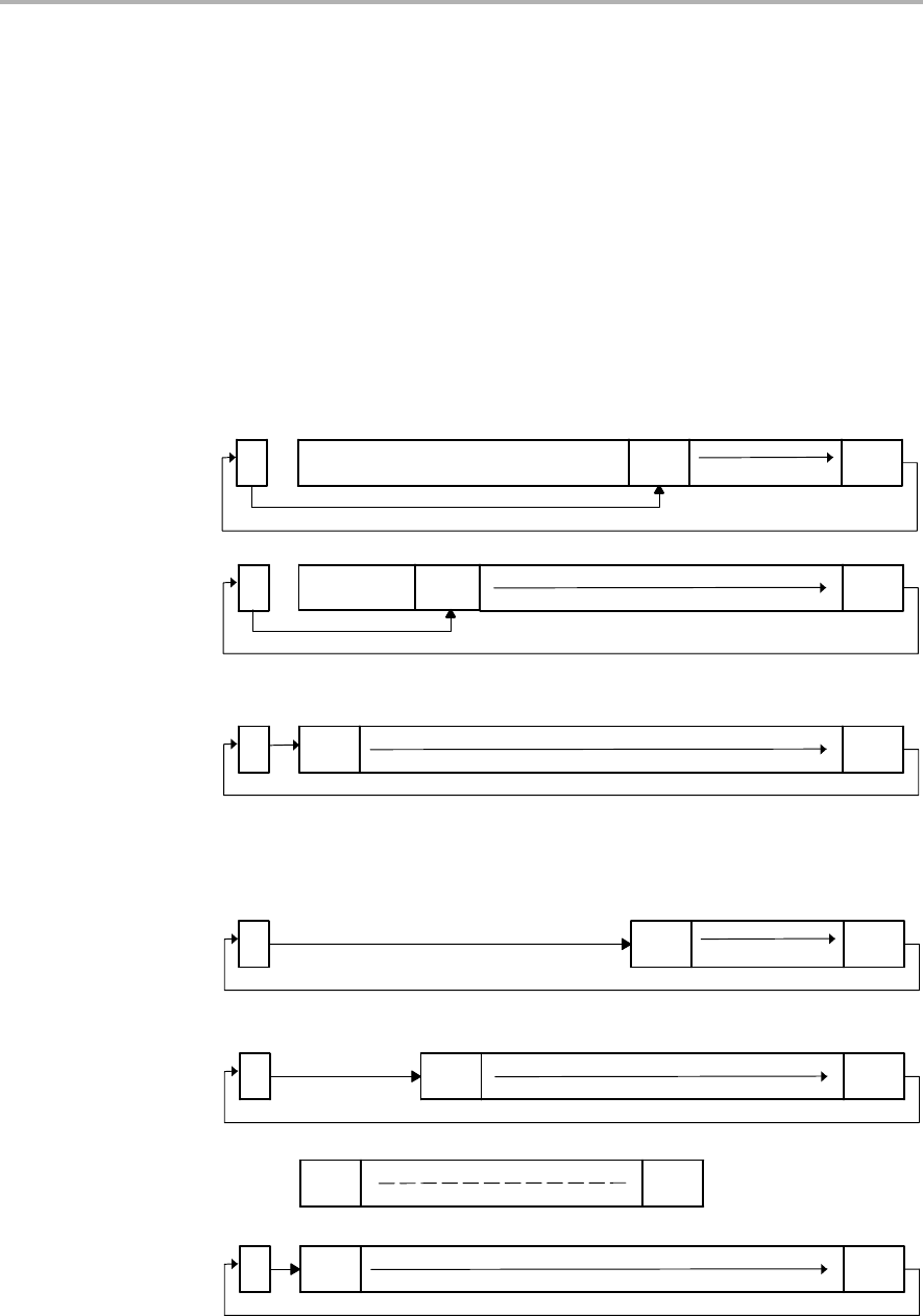
Extended Instructions
4-144 16-Bit MSP430X CPU
Example The 20-bit operand at address EDE is shifted right by one position. The MSB is
loaded with 1.
SETC ; Prepare carry for MSB
RRCX.A EDE ; EDE = EDE » 1 + 80000h
Example The word in R6 is shifted right by twelve positions.
RPT #12
RRCX.W R6 ; R6 = R6 » 12. R6.19:16 = 0
Figure 4−51. Rotate Right Through Carry RRCX(.B,.A). Register Mode
C
19 0
MSB0 − − − − − − − − − − − − − − − − − − − − 0
7
LSB
C
19 0
MSB LSB
8
C
15 0
MSB LSB
19 16
0 0 0 0
Figure 4−52. Rotate Right Through Carry RRCX(.B,.A). Non-Register Mode
C
0
MSB
7
LSB
C
15 0
MSB LSB
C
19 0
MSB LSB
31 20
00

Extended Instructions
4-145
16-Bit MSP430X CPU
RRUM.A Rotate Right Unsigned the 20-bit CPU register content
RRUM[.W] Rotate Right Unsigned the 16-bit CPU register content
Syntax RRUM.A #n,Rdst 1 ≤ n ≤ 4
RRUM.W #n,Rdst or RRUM #n,Rdst 1 ≤ n ≤ 4
Operation 0→ MSB → MSB-1 . →... LSB+1 → LSB → C
Description The destination operand is shifted right by one, two, three, or four bit positions
as shown in Figure 4−53. Zero is shifted into the MSB, the LSB is shifted into
the carry bit. RRUM works like an unsigned division by 2, 4, 8, or 16. The word
instruction RRUM.W clears the bits Rdst.19:16.
Note : This instruction does not use the extension word.
Status Bits N: Set if result is negative
.A: Rdst.19 = 1, reset if Rdst.19 = 0
.W: Rdst.15 = 1, reset if Rdst.15 = 0
Z: Set if result is zero, reset otherwise
C: Loaded from the LSB (n = 1), LSB+1 (n = 2), LSB+2 (n = 3) or LSB+3
(n = 4)
V: Reset
Mode Bits OSCOFF, CPUOFF, and GIE are not affected.
Example The unsigned address-word in R5 is divided by 16.
RRUM.A #4,R5 ; R5 = R5 » 4. R5/16
Example The word in R6 is shifted right by one bit. The MSB R6.15 is loaded with 0.
RRUM.W #1,R6 ; R6 = R6/2. R6.19:15 = 0
Figure 4−53. Rotate Right Unsigned RRUM[.W] and RRUM.A
C
19 0
MSB0000
15
LSB
C
19 0
MSB LSB
0
0
16
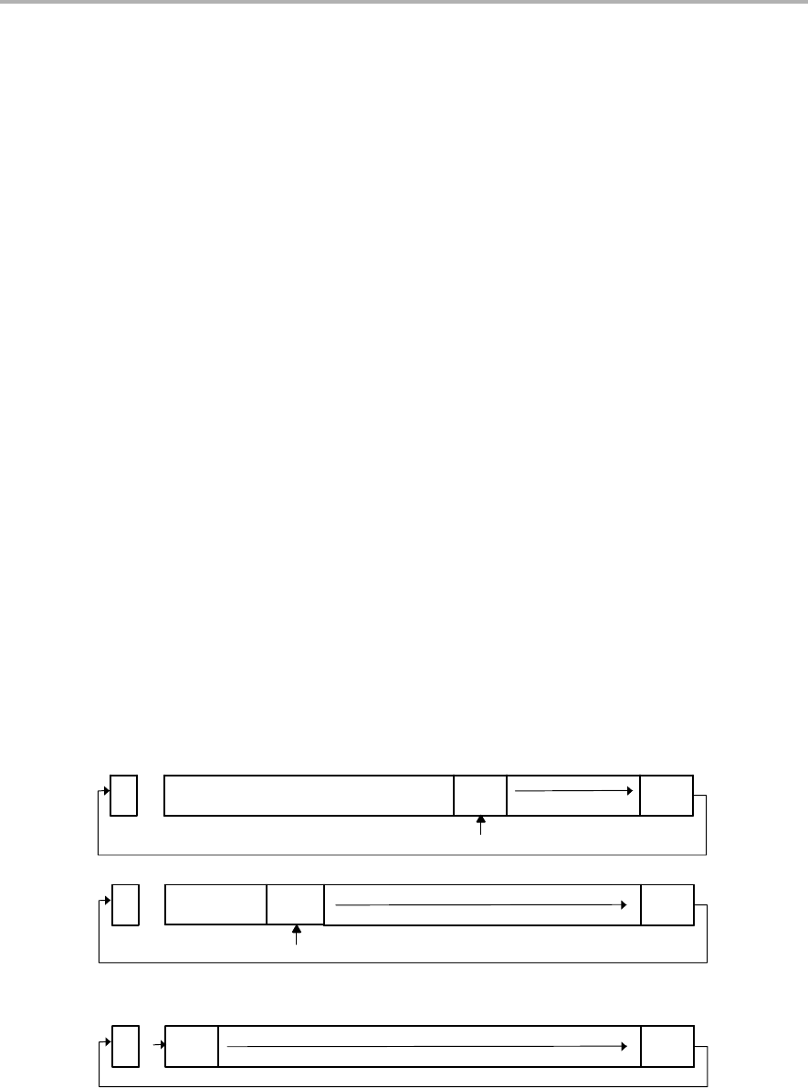
Extended Instructions
4-146 16-Bit MSP430X CPU
RRUX.A Rotate Right unsigned the 20-bit operand
RRUX[.W] Rotate Right unsigned the 16-bit operand
RRUX.B Rotate Right unsigned the 8-bit operand
Syntax RRUX.A Rdst
RRUX.W Rdst
RRUX Rdst
RRUX.B Rdst
Operation C=0 → MSB → MSB-1 → ... LSB+1 → LSB → C
Description RRUX is valid for register Mode only: the destination operand is shifted right by
one bit position as shown in Figure 4−54. The word instruction RRUX.W clears
the bits Rdst.19:16. The byte instruction RRUX.B clears the bits Rdst.19:8.
Zero is shifted into the MSB, the LSB is shifted into the carry bit.
Status Bits N: Set if result is negative
.A: dst.19 = 1, reset if dst.19 = 0
.W: dst.15 = 1, reset if dst.15 = 0
.B: dst.7 = 1, reset if dst.7 = 0
Z: Set if result is zero, reset otherwise
C: Loaded from LSB
V: Reset
Mode Bits OSCOFF, CPUOFF, and GIE are not affected.
Example The word in R6 is shifted right by twelve positions.
RPT #12
RRUX.W R6 ; R6 = R6 » 12. R6.19:16 = 0
Figure 4−54. Rotate Right Unsigned RRUX(.B,.A). Register Mode
C
19 0
MSB0 − − − − − − − − − − − − − − − − − − − − 0
7
LSB
C
19 0
MSB LSB
8
C
15 0
MSB LSB
19 16
0 0 0 0
0
0
0

Extended Instructions
4-147
16-Bit MSP430X CPU
* SBCX.A Subtract source and borrow/.NOT. carry from destination address-word
* SBCX[.W] Subtract source and borrow/.NOT. carry from destination word
* SBCX.B Subtract source and borrow/.NOT. carry from destination byte
Syntax SBCX.A dst
SBCX dst or SBCX.W dst
SBCX.B dst
Operation dst + 0FFFFFh + C −> dst
dst + 0FFFFh + C −> dst
dst + 0FFh + C −> dst
Emulation SUBCX.A #0,dst
SUBCX #0,dst
SUBCX.B #0,dst
Description The carry bit (C) is added to the destination operand minus one. The previous
contents of the destination are lost.
Status Bits N: Set if result is negative, reset if positive
Z: Set if result is zero, reset otherwise
C: Set if there is a carry from the MSB of the result, reset otherwise.
Set to 1 if no borrow, reset if borrow.
V: Set if an arithmetic overflow occurs, reset otherwise.
Mode Bits OSCOFF, CPUOFF, and GIE are not affected.
Example The 8-bit counter pointed to by R13 is subtracted from a 16-bit counter pointed
to by R12.
SUBX.B @R13,0(R12) ; Subtract LSDs
SBCX.B 1(R12) ; Subtract carry from MSD
Note: Borrow Implementation.
The borrow is treated as a .NOT. carry : Borrow Carry bit
Yes 0
No 1

Extended Instructions
4-148 16-Bit MSP430X CPU
SUBX.A Subtract source address-word from destination address-word
SUBX[.W] Subtract source word from destination word
SUBX.B Subtract source byte from destination byte
Syntax SUBX.A src,dst
SUBX src,dst or SUBX.W src,dst
SUBX.B src,dst
Operation (.not. src) + 1 + dst → dst or dst − src → dst
Description The source operand is subtracted from the destination operand. This is made
by adding the 1’s complement of the source + 1 to the destination. The source
operand is not affected. The result is written to the destination operand. Both
operands may be located in the full address space.
Status Bits N: Set if result is negative (src > dst), reset if positive (src <= dst)
Z: Set if result is zero (src = dst), reset otherwise (src ≠dst)
C: Set if there is a carry from the MSB, reset otherwise
V: Set if the subtraction of a negative source operand from a positive des-
tination operand delivers a negative result, or if the subtraction of a posi-
tive source operand from a negative destination operand delivers a
positive result, reset otherwise (no overflow).
Mode Bits OSCOFF, CPUOFF, and GIE are not affected.
Example A 20-bit constant 87654h is subtracted from EDE (LSBs) and EDE+2 (MSBs).
SUBX.A #87654h,EDE ; Subtract 87654h from EDE+2|EDE
Example A table word pointed to by R5 (20-bit address) is subtracted from R7. Jump to
label TONI if R7 contains zero after the instruction. R5 is auto-incremented by
2. R7.19:16 = 0
SUBX.W @R5+,R7 ; Subtract table number from R7. R5 + 2
JZ TONI ; R7 = @R5 (before subtraction)
... ; R7 <> @R5 (before subtraction)
Example Byte CNT is subtracted from the byte R12 points to in the full address space.
Address of CNT is within PC ±512 K.
SUBX.B CNT,0(R12) ; Subtract CNT from @R12
Note: Use SUBA for the following two cases for better density and execution.
SUBX.A Rsrc,Rdst or
SUBX.A #imm20,Rdst

Extended Instructions
4-149
16-Bit MSP430X CPU
SUBCX.A Subtract source address-word with carry from destination address-word
SUBCX[.W] Subtract source word with carry from destination word
SUBCX.B Subtract source byte with carry from destination byte
Syntax SUBCX.A src,dst
SUBCX src,dst or SUBCX.W src,dst
SUBCX.B src,dst
Operation (.not. src) + C + dst → dst or dst − (src − 1) + C → dst
Description The source operand is subtracted from the destination operand. This is made
by adding the 1’s complement of the source + carry to the destination. The
source operand is not affected, the result is written to the destination operand.
Both operands may be located in the full address space.
Status Bits N: Set if result is negative (MSB = 1), reset if positive (MSB = 0)
Z: Set if result is zero, reset otherwise
C: Set if there is a carry from the MSB, reset otherwise
V: Set if the subtraction of a negative source operand from a positive des-
tination operand delivers a negative result, or if the subtraction of a posi-
tive source operand from a negative destination operand delivers a
positive result, reset otherwise (no overflow).
Mode Bits OSCOFF, CPUOFF, and GIE are not affected.
Example A 20-bit constant 87654h is subtracted from R5 with the carry from the
previous instruction.
SUBCX.A #87654h,R5 ; Subtract 87654h + C from R5
Example A 48-bit number (3 words) pointed to by R5 (20-bit address) is subtracted from
a 48-bit counter in RAM, pointed to by R7. R5 auto-increments to point to the
next 48-bit number.
SUBX.W @R5+,0(R7) ; Subtract LSBs. R5 + 2
SUBCX.W @R5+,2(R7) ; Subtract MIDs with C. R5 + 2
SUBCX.W @R5+,4(R7) ; Subtract MSBs with C. R5 + 2
Example Byte CNT is subtracted from the byte, R12 points to. The carry of the previous
instruction is used. 20-bit addresses.
SUBCX.B &CNT,0(R12) ; Subtract byte CNT from @R12

Extended Instructions
4-150 16-Bit MSP430X CPU
SWPBX.A Swap bytes of lower word
SWPBX[.W] Swap bytes of word
Syntax SWPBX.A dst
SWPBX.W dst or SWPBX dst
Operation dst.15:8 à dst.7:0
Description Register Mode: Rn.15:8 are swapped with Rn.7:0. When the .A extension is
used, Rn.19:16 are unchanged. When the .W extension is used, Rn.19:16 are
cleared.
Other Modes: When the .A extension is used, bits 31:20 of the destination
address are cleared, bits 19:16 are left unchanged, and bits 15:8 are swapped
with bits 7:0. When the .W extension is used, bits 15:8 are swapped with bits
7:0 of the addressed word.
Status Bits Not affected
Mode Bits OSCOFF, CPUOFF, and GIE are not affected.
Example Exchange the bytes of RAM address-word EDE.
MOVX.A #23456h,&EDE ; 23456h −> EDE
SWPBX.A EDE ; 25634h −> EDE
Example Exchange the bytes of R5.
MOVA #23456h,R5 ; 23456h −> R5
SWPBX.W R5 ; 05634h −> R5
Figure 4−55. Swap Bytes SWPBX.A Register Mode
15 8 7 0
15 8 7 0
Low Byte
Low ByteHigh Byte
High Byte
Before SWPBX.A
After SWPBX.A
X
X
19
19
16
16
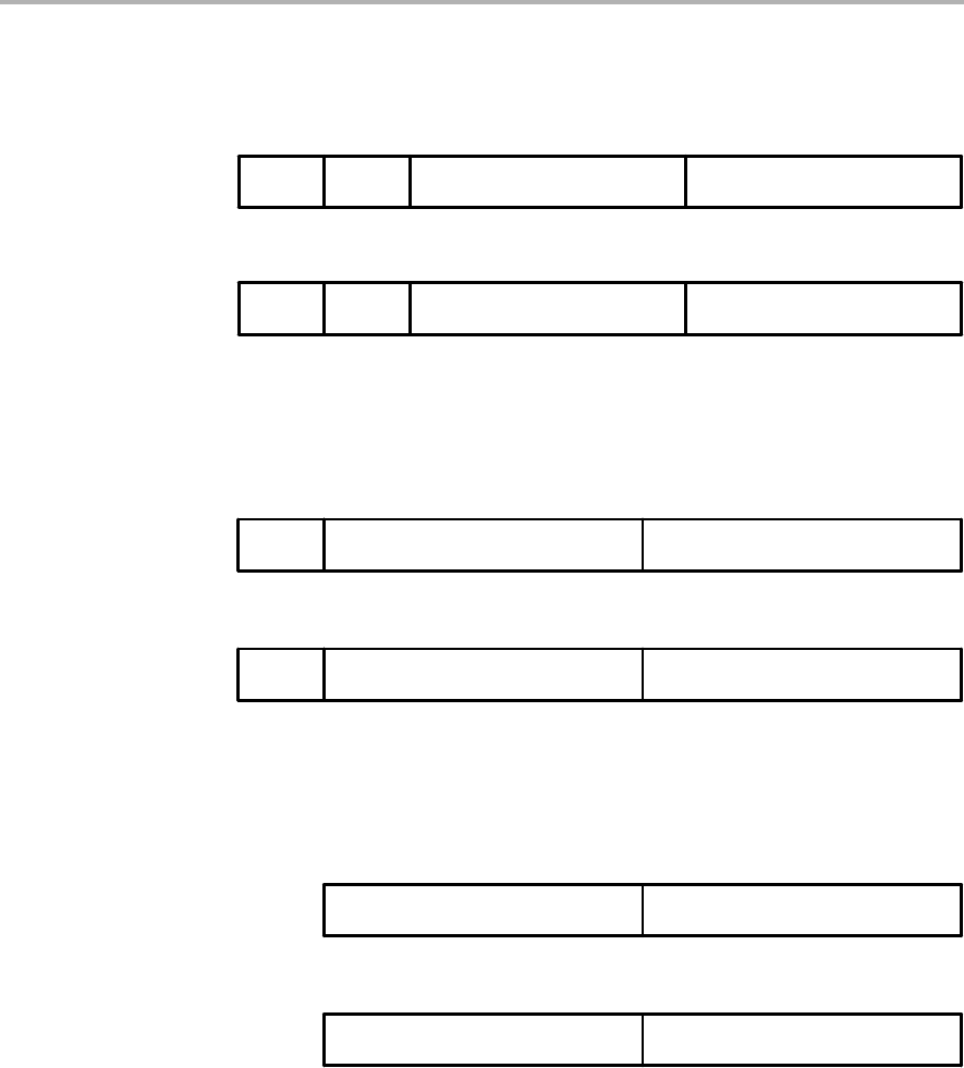
Extended Instructions
4-151
16-Bit MSP430X CPU
Figure 4−56. Swap Bytes SWPBX.A In Memory
15 87 0
Low Byte
High Byte
Before SWPBX.A
After SWPBX.A
X
19 16
31 20
X
15 87 0
High Byte
Low Byte
0
19 16
31 20
X
Figure 4−57. Swap Bytes SWPBX[.W] Register Mode
15 8 7 0
15 8 7 0
Low Byte
Low ByteHigh Byte
High Byte
Before SWPBX
After SWPBX
X
0
19
19
16
16
Figure 4−58. Swap Bytes SWPBX[.W] In Memory
15 8 7 0
15 8 7 0
Low Byte
Low ByteHigh Byte
High Byte
Before SWPBX
After SWPBX

Extended Instructions
4-152 16-Bit MSP430X CPU
SXTX.A Extend sign of lower byte to address-word
SXTX[.W] Extend sign of lower byte to word
Syntax SXTX.A dst
SXTX.W dst or SXTX dst
Operation dst.7 → dst.15:8, Rdst.7 → Rdst.19:8 (Register Mode)
Description Register Mode:
The sign of the low byte of the operand (Rdst.7) is extended into the bits
Rdst.19:8.
Other Modes:
SXTX.A: the sign of the low byte of the operand (dst.7) is extended into
dst.19:8. The bits dst.31:20 are cleared.
SXTX[.W]: the sign of the low byte of the operand (dst.7) is extended into
dst.15:8.
Status Bits N: Set if result is negative, reset otherwise
Z: Set if result is zero, reset otherwise
C: Set if result is not zero, reset otherwise (C = .not.Z)
V: Reset
Mode Bits OSCOFF, CPUOFF, and GIE are not affected.
Example The signed 8-bit data in EDE.7:0 is sign extended to 20 bits: EDE.19:8. Bits
31:20 located in EDE+2 are cleared.
SXTX.A &EDE ; Sign extended EDE −> EDE+2/EDE
Figure 4−59. Sign Extend SXTX.A
15 8 7 6 019 162031
00...... S
19 16
15 8 7 6 019 16
S
19 16
SXTX.A Rdst
SXTX.A dst
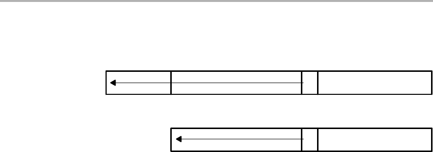
Extended Instructions
4-153
16-Bit MSP430X CPU
Figure 4−60. Sign Extend SXTX[.W]
15 876 0
S
15 876 019 16
S
19 16
SXTX[.W] Rdst
SXTX[.W] dst

Extended Instructions
4-154 16-Bit MSP430X CPU
* TSTX.A Test destination address-word
* TSTX[.W] Test destination word
* TSTX.B Test destination byte
Syntax TSTX.A dst
TSTX dst or TST.W dst
TST.B dst
Operation dst + 0FFFFFh + 1
dst + 0FFFFh + 1
dst + 0FFh + 1
Emulation CMPX.A #0,dst
CMPX #0,dst
CMPX.B #0,dst
Description The destination operand is compared with zero. The status bits are set
according to the result. The destination is not affected.
Status Bits N: Set if destination is negative, reset if positive
Z: Set if destination contains zero, reset otherwise
C: Set
V: Reset
Mode Bits OSCOFF, CPUOFF, and GIE are not affected.
Example RAM byte LEO is tested; PC is pointing to upper memory. If it is negative,
continue at LEONEG; if it is positive but not zero, continue at LEOPOS.
TSTX.B LEO ; Test LEO
JN LEONEG ; LEO is negative
JZ LEOZERO ; LEO is zero
LEOPOS ...... ; LEO is positive but not zero
LEONEG ...... ; LEO is negative
LEOZERO ...... ; LEO is zero

Extended Instructions
4-155
16-Bit MSP430X CPU
XORX.A Exclusive OR source address-word with destination address-word
XORX[.W] Exclusive OR source word with destination word
XORX.B Exclusive OR source byte with destination byte
Syntax XORX.A src,dst
XORX src,dst or XORX.W src,dst
XORX.B src,dst
Operation src .xor. dst → dst
Description The source and destination operands are exclusively ORed. The result is
placed into the destination. The source operand is not affected. The previous
contents of the destination are lost. Both operands may be located in the full
address space.
Status Bits N: Set if result is negative (MSB = 1), reset if positive (MSB = 0)
Z: Set if result is zero, reset otherwise
C: Set if result is not zero, reset otherwise (carry = .not. Zero)
V: Set if both operands are negative (before execution), reset otherwise.
Mode Bits OSCOFF, CPUOFF, and GIE are not affected.
Example Toggle bits in address-word CNTR (20-bit data) with information in
address-word TONI (20-bit address).
XORX.A TONI,&CNTR ; Toggle bits in CNTR
Example A table word pointed to by R5 (20-bit address) is used to toggle bits in R6.
XORX.W @R5,R6 ; Toggle bits in R6. R6.19:16 = 0
Example Reset to zero those bits in the low byte of R7 that are different from the bits in
byte EDE (20-bit address).
XORX.B EDE,R7 ; Set different bits to 1 in R7
INV.B R7 ; Invert low byte of R7. R7.19:8 = 0.

Address Instructions
4-156 16-Bit MSP430X CPU
4.6.4 Address Instructions
MSP430X address instructions are instructions that support 20-bit operands
but have restricted addressing modes. The addressing modes are restricted
to the Register mode and the Immediate mode, except for the MOVA
instruction. Restricting the addressing modes removes the need for the
additional extension-word op-code improving code density and execution
time. The MSP430X address instructions are listed and described in the
following pages.

Address Instructions
4-157
16-Bit MSP430X CPU
ADDA Add 20-bit source to a 20-bit destination register
Syntax ADDA Rsrc,Rdst
ADDA #imm20,Rdst
Operation src + Rdst → Rdst
Description The 20-bit source operand is added to the 20-bit destination CPU register. The
previous contents of the destination are lost. The source operand is not
affected.
Status Bits N: Set if result is negative (Rdst.19 = 1), reset if positive (Rdst.19 = 0)
Z: Set if result is zero, reset otherwise
C: Set if there is a carry from the 20-bit result, reset otherwise
V: Set if the result of two positive operands is negative, or if the result of
two negative numbers is positive, reset otherwise.
Mode Bits OSCOFF, CPUOFF, and GIE are not affected.
Example R5 is increased by 0A4320h. The jump to TONI is performed if a carry occurs.
ADDA #0A4320h,R5 ; Add A4320h to 20-bit R5
JC TONI ; Jump on carry
... ; No carry occurred

Address Instructions
4-158 16-Bit MSP430X CPU
* BRA Branch to destination
Syntax BRA dst
Operation dst → PC
Emulation MOVA dst,PC
Description An unconditional branch is taken to a 20-bit address anywhere in the full
address space. All seven source addressing modes can be used. The branch
instruction is an address-word instruction. If the destination address is
contained in a memory location X, it is contained in two ascending words: X
(LSBs) and (X + 2) (MSBs).
Status Bits N: Not affected
Z: Not affected
C: Not affected
V: Not affected
Mode Bits OSCOFF, CPUOFF, and GIE are not affected.
Examples Examples for all addressing modes are given.
Immediate Mode: Branch to label EDE located anywhere in the 20-bit address
space or branch directly to address.
BRA #EDE ; MOVA #imm20,PC
BRA #01AA04h
Symbolic Mode: Branch to the 20-bit address contained in addresses EXEC
(LSBs) and EXEC+2 (MSBs). EXEC is located at the address (PC + X) where
X is within ±32 K. Indirect addressing.
BRA EXEC ; MOVA z16(PC),PC
Note: if the 16-bit index is not sufficient, a 20-bit index may be used with the
following instruction.
MOVX.A EXEC,PC ; 1M byte range with 20-bit index
Absolute Mode: Branch to the 20-bit address contained in absolute addresses
EXEC (LSBs) and EXEC+2 (MSBs). Indirect addressing.
BRA &EXEC ; MOVA &abs20,PC
Register Mode: Branch to the 20-bit address contained in register R5. Indirect
R5.
BRA R5 ; MOVA R5,PC

Address Instructions
4-159
16-Bit MSP430X CPU
Indirect Mode: Branch to the 20-bit address contained in the word pointed to
by register R5 (LSBs). The MSBs have the address (R5 + 2). Indirect, indirect
R5.
BRA @R5 ; MOVA @R5,PC
Indirect, Auto-Increment Mode: Branch to the 20-bit address contained in the
words pointed to by register R5 and increment the address in R5 afterwards
by 4. The next time the S/W flow uses R5 as a pointer, it can alter the program
execution due to access to the next address in the table pointed to by R5. Indi-
rect, indirect R5.
BRA @R5+ ; MOVA @R5+,PC. R5 + 4
Indexed Mode: Branch to the 20-bit address contained in the address pointed
to by register (R5 + X) (e.g. a table with addresses starting at X). (R5 + X)
points to the LSBs, (R5 + X + 2) points to the MSBs of the address. X is within
R5 ±32 K. Indirect, indirect (R5 + X).
BRA X(R5) ; MOVA z16(R5),PC
Note: if the 16-bit index is not sufficient, a 20-bit index X may be used with the
following instruction:
MOVX.A X(R5),PC ; 1M byte range with 20-bit index

Address Instructions
4-160 16-Bit MSP430X CPU
CALLA Call a Subroutine
Syntax CALLA dst
Operation dst →tmp 20-bit dst is evaluated and stored
SP − 2 →SP
PC.19:16 →@SP updated PC with return address to TOS (MSBs)
SP − 2 →SP
PC.15:0 →@SP updated PC to TOS (LSBs)
tmp →PC saved 20-bit dst to PC
Description A subroutine call is made to a 20-bit address anywhere in the full address
space. All seven source addressing modes can be used. The call instruction is
an address-word instruction. If the destination address is contained in a
memory location X, it is contained in two ascending words: X (LSBs) and
(X + 2) (MSBs). Two words on the stack are needed for the return address.
The return is made with the instruction RETA.
Status Bits N: Not affected
Z: Not affected
C: Not affected
V: Not affected
Mode Bits OSCOFF, CPUOFF, and GIE are not affected.
Examples Examples for all addressing modes are given.
Immediate Mode: Call a subroutine at label EXEC or call directly an address.
CALLA #EXEC ; Start address EXEC
CALLA #01AA04h ; Start address 01AA04h
Symbolic Mode: Call a subroutine at the 20-bit address contained in address-
es EXEC (LSBs) and EXEC+2 (MSBs). EXEC is located at the address
(PC + X) where X is within ±32 K. Indirect addressing.
CALLA EXEC ; Start address at @EXEC. z16(PC)
Absolute Mode: Call a subroutine at the 20-bit address contained in absolute
addresses EXEC (LSBs) and EXEC+2 (MSBs). Indirect addressing.
CALLA &EXEC ; Start address at @EXEC
Register Mode: Call a subroutine at the 20-bit address contained in register
R5. Indirect R5.
CALLA R5 ; Start address at @R5

Address Instructions
4-161
16-Bit MSP430X CPU
Indirect Mode: Call a subroutine at the 20-bit address contained in the word
pointed to by register R5 (LSBs). The MSBs have the address (R5 + 2). Indi-
rect, indirect R5.
CALLA @R5 ; Start address at @R5
Indirect, Auto-Increment Mode: Call a subroutine at the 20-bit address con-
tained in the words pointed to by register R5 and increment the 20-bit address
in R5 afterwards by 4. The next time the S/W flow uses R5 as a pointer, it can
alter the program execution due to access to the next word address in the table
pointed to by R5. Indirect, indirect R5.
CALLA @R5+ ; Start address at @R5. R5 + 4
Indexed Mode: Call a subroutine at the 20-bit address contained in the ad-
dress pointed to by register (R5 + X) e.g. a table with addresses starting at X.
(R5 + X) points to the LSBs, (R5 + X + 2) points to the MSBs of the word ad-
dress. X is within R5 ±32 K. Indirect, indirect (R5 + X).
CALLA X(R5) ; Start address at @(R5+X). z16(R5)

Address Instructions
4-162 16-Bit MSP430X CPU
* CLRA Clear 20-bit destination register
Syntax CLRA Rdst
Operation 0 −> Rdst
Emulation MOVA #0,Rdst
Description The destination register is cleared.
Status Bits Status bits are not affected.
Example The 20-bit value in R10 is cleared.
CLRA R10 ; 0 −> R10

Address Instructions
4-163
16-Bit MSP430X CPU
CMPA Compare the 20-bit source with a 20-bit destination register
Syntax CMPA Rsrc,Rdst
CMPA #imm20,Rdst
Operation (.not. src) + 1 + Rdst or Rdst − src
Description The 20-bit source operand is subtracted from the 20-bit destination CPU
register. This is made by adding the 1’s complement of the source + 1 to the
destination register. The result affects only the status bits.
Status Bits N: Set if result is negative (src > dst), reset if positive (src <= dst)
Z: Set if result is zero (src = dst), reset otherwise (src ≠dst)
C: Set if there is a carry from the MSB, reset otherwise
V: Set if the subtraction of a negative source operand from a positive
destination operand delivers a negative result, or if the subtraction of
a positive source operand from a negative destination operand delivers
a positive result, reset otherwise (no overflow).
Mode Bits OSCOFF, CPUOFF, and GIE are not affected.
Example A 20-bit immediate operand and R6 are compared. If they are equal the
program continues at label EQUAL.
CMPA #12345h,R6 ; Compare R6 with 12345h
JEQ EQUAL ; R5 = 12345h
... ; Not equal
Example The 20-bit values in R5 and R6 are compared. If R5 is greater than (signed) or
equal to R6, the program continues at label GRE.
CMPA R6,R5 ; Compare R6 with R5 (R5 − R6)
JGE GRE ; R5 >= R6
... ; R5 < R6

Address Instructions
4-164 16-Bit MSP430X CPU
* DECDA Double-decrement 20-bit destination register
Syntax DECDA Rdst
Operation Rdst − 2 −> Rdst
Emulation SUBA #2,Rdst
Description The destination register is decremented by two. The original contents are lost.
Status Bits N: Set if result is negative, reset if positive
Z: Set if Rdst contained 2, reset otherwise
C: Reset if Rdst contained 0 or 1, set otherwise
V: Set if an arithmetic overflow occurs, otherwise reset.
Mode Bits OSCOFF, CPUOFF, and GIE are not affected.
Example The 20-bit value in R5 is decremented by 2
DECDA R5 ; Decrement R5 by two

Address Instructions
4-165
16-Bit MSP430X CPU
* INCDA Double-increment 20-bit destination register
Syntax INCDA Rdst
Operation dst + 2 −> dst
Emulation ADDA #2,Rdst
Example The destination register is incremented by two. The original contents are lost.
Status Bits N: Set if result is negative, reset if positive
Z: Set if Rdst contained 0FFFFEh, reset otherwise
Set if Rdst contained 0FFFEh, reset otherwise
Set if Rdst contained 0FEh, reset otherwise
C: Set if Rdst contained 0FFFFEh or 0FFFFFh, reset otherwise
Set if Rdst contained 0FFFEh or 0FFFFh, reset otherwise
Set if Rdst contained 0FEh or 0FFh, reset otherwise
V: Set if Rdst contained 07FFFEh or 07FFFFh, reset otherwise
Set if Rdst contained 07FFEh or 07FFFh, reset otherwise
Set if Rdst contained 07Eh or 07Fh, reset otherwise
Mode Bits OSCOFF, CPUOFF, and GIE are not affected.
Example The 20-bit value in R5 is incremented by 2
INCDA R5 ; Increment R5 by two

Address Instructions
4-166 16-Bit MSP430X CPU
MOVA Move the 20-bit source to the 20-bit destination
Syntax MOVA Rsrc,Rdst
MOVA #imm20,Rdst
MOVA z16(Rsrc),Rdst
MOVA EDE,Rdst
MOVA &abs20,Rdst
MOVA @Rsrc,Rdst
MOVA @Rsrc+,Rdst
MOVA Rsrc,z16(Rdst)
MOVA Rsrc,&abs20
Operation src →Rdst
Rsrc →dst
Description The 20-bit source operand is moved to the 20-bit destination. The source
operand is not affected. The previous content of the destination is lost.
Status Bits Not affected
Mode Bits OSCOFF, CPUOFF, and GIE are not affected.
Examples Copy 20-bit value in R9 to R8.
MOVA R9,R8 ; R9 -> R8
Write 20-bit immediate value 12345h to R12.
MOVA #12345h,R12 ; 12345h -> R12
Copy 20-bit value addressed by (R9 + 100h) to R8. Source operand in ad-
dresses (R9 + 100h) LSBs and (R9 + 102h) MSBs
MOVA 100h(R9),R8 ; Index: ± 32 K. 2 words transferred
Move 20-bit value in 20-bit absolute addresses EDE (LSBs) and EDE+2
(MSBs) to R12.
MOVA &EDE,R12 ; &EDE -> R12. 2 words transferred
Move 20-bit value in 20-bit addresses EDE (LSBs) and EDE+2 (MSBs) to R12.
PC index ±32 K.
MOVA EDE,R12 ; EDE -> R12. 2 words transferred
Copy 20-bit value R9 points to (20 bit address) to R8. Source operand in
addresses @R9 LSBs and @(R9 + 2) MSBs.
MOVA @R9,R8 ; @R9 -> R8. 2 words transferred

Address Instructions
4-167
16-Bit MSP430X CPU
Copy 20-bit value R9 points to (20 bit address) to R8. R9 is incremented by
four afterwards. Source operand in addresses @R9 LSBs and @(R9 + 2)
MSBs.
MOVA @R9+,R8 ; @R9 -> R8. R9 + 4. 2 words transferred.
Copy 20-bit value in R8 to destination addressed by (R9 + 100h). Destination
operand in addresses @(R9 + 100h) LSBs and @(R9 + 102h) MSBs.
MOVA R8,100h(R9) ; Index: +- 32 K. 2 words transferred
Move 20-bit value in R13 to 20-bit absolute addresses EDE (LSBs) and
EDE+2 (MSBs).
MOVA R13,&EDE ; R13 -> EDE. 2 words transferred
Move 20-bit value in R13 to 20-bit addresses EDE (LSBs) and EDE+2 (MSBs).
PC index ±32 K.
MOVA R13,EDE ; R13 -> EDE. 2 words transferred

Address Instructions
4-168 16-Bit MSP430X CPU
* RETA Return from subroutine
Syntax RETA
Operation @SP →PC.15:0 LSBs (15:0) of saved PC to PC.15:0
SP + 2 →SP
@SP →PC.19:16 MSBs (19:16) of saved PC to PC.19:16
SP + 2 →SP
Emulation MOVA @SP+,PC
Description The 20-bit return address information, pushed onto the stack by a CALLA
instruction, is restored to the program counter PC. The program continues at
the address following the subroutine call. The status register bits SR.11:0 are
not affected. This allows the transfer of information with these bits.
Status Bits N: Not affected
Z: Not affected
C: Not affected
V: Not affected
Mode Bits OSCOFF, CPUOFF, and GIE are not affected.
Example Call a subroutine SUBR from anywhere in the 20-bit address space and return
to the address after the CALLA.
CALLA #SUBR ; Call subroutine starting at SUBR
... ; Return by RETA to here
SUBR PUSHM.A #2,R14 ; Save R14 and R13 (20 bit data)
... ; Subroutine code
POPM.A #2,R14 ; Restore R13 and R14 (20 bit data)
RETA ; Return (to full address space)

Address Instructions
4-169
16-Bit MSP430X CPU
* TSTA Test 20-bit destination register
Syntax TSTA Rdst
Operation dst + 0FFFFFh + 1
dst + 0FFFFh + 1
dst + 0FFh + 1
Emulation CMPA #0,Rdst
Description The destination register is compared with zero. The status bits are set
according to the result. The destination register is not affected.
Status Bits N: Set if destination register is negative, reset if positive
Z: Set if destination register contains zero, reset otherwise
C: Set
V: Reset
Mode Bits OSCOFF, CPUOFF, and GIE are not affected.
Example The 20-bit value in R7 is tested. If it is negative, continue at R7NEG; if it is
positive but not zero, continue at R7POS.
TSTA R7 ; Test R7
JN R7NEG ; R7 is negative
JZ R7ZERO ; R7 is zero
R7POS ...... ; R7 is positive but not zero
R7NEG ...... ; R7 is negative
R7ZERO ...... ; R7 is zero

Address Instructions
4-170 16-Bit MSP430X CPU
SUBA Subtract 20-bit source from 20-bit destination register
Syntax SUBA Rsrc,Rdst
SUBA #imm20,Rdst
Operation (.not.src) + 1 + Rdst → Rdst or Rdst − src → Rdst
Description The 20-bit source operand is subtracted from the 20-bit destination register.
This is made by adding the 1’s complement of the source + 1 to the
destination. The result is written to the destination register, the source is not
affected.
Status Bits N: Set if result is negative (src > dst), reset if positive (src <= dst)
Z: Set if result is zero (src = dst), reset otherwise (src ≠dst)
C: Set if there is a carry from the MSB (Rdst.19), reset otherwise
V: Set if the subtraction of a negative source operand from a positive des-
tination operand delivers a negative result, or if the subtraction of a posi-
tive source operand from a negative destination operand delivers a
positive result, reset otherwise (no overflow).
Mode Bits OSCOFF, CPUOFF, and GIE are not affected.
Example The 20-bit value in R5 is subtracted from R6. If a carry occurs, the program
continues at label TONI.
SUBA R5,R6 ; R6 − R5 -> R6
JC TONI ; Carry occurred
... ; No carry

5-1
Basic Clock Module+
Basic Clock Module+
The basic clock module+ provides the clocks for MSP430x2xx devices. This
chapter describes the operation of the basic clock module+ of the
MSP430x2xx device family.
Topic Page
5.1 Basic Clock Module Introduction 5-2. . . . . . . . . . . . . . . . . . . . . . . . . . . . . . . .
5.2 Basic Clock Module Operation 5-4. . . . . . . . . . . . . . . . . . . . . . . . . . . . . . . . . .
5.3 Basic Clock Module Registers 5-13. . . . . . . . . . . . . . . . . . . . . . . . . . . . . . . . .
Chapter 5

Basic Clock Module+ Introduction
5-2 Basic Clock Module+
5.1 Basic Clock Module+ Introduction
The basic clock module+ supports low system cost and ultralow-power
consumption. Using three internal clock signals, the user can select the best
balance of performance and low power consumption. The basic clock
module+ can be configured to operate without any external components, with
one external resistor, with one or two external crystals, or with resonators,
under full software control.
The basic clock module+ includes three or four clock sources:
-LFXT1CLK: Low-frequency/high-frequency oscillator that can be used
with low-frequency watch crystals or external clock sources of 32,768-Hz.
or with standard crystals, resonators, or external clock sources in the
400-kHz to 16-MHz range.
-XT2CLK: Optional high-frequency oscillator that can be used with
standard crystals, resonators, or external clock sources in the 400-kHz to
16-MHz range.
-DCOCLK: Internal digitally controlled oscillator (DCO).
-VLOCLK: Internal very low power, low frequency oscillator with 12-kHz
typical frequency.
Three clock signals are available from the basic clock module+:
-ACLK: Auxiliary clock. ACLK is software selectable as LFXT1CLK or
VLOCLK. ACLK is divided by 1, 2, 4, or 8. ACLK is software selectable for
individual peripheral modules.
-MCLK: Master clock. MCLK is software selectable as LFXT1CLK,
VLOCLK, XT2CLK (if available on-chip), or DCOCLK. MCLK is divided by
1, 2, 4, or 8. MCLK is used by the CPU and system.
-SMCLK: Sub-main clock. SMCLK is software selectable as LFXT1CLK,
VLOCLK, XT2CLK (if available on-chip), or DCOCLK. SMCLK is divided
by 1, 2, 4, or 8. SMCLK is software selectable for individual peripheral
modules.
The block diagram of the basic clock module+ is shown in Figure 5−1.
Note: Device-Specific Clock Variations
All clock features are not available on all MSP430x2xx devices.
MSP430x20xx: LFXT1 does not support HF mode, XT2 is not present, ROSC
is not supported.
MSP430x21x1: Internal LP/LF oscillator is not present, XT2 is not present,
ROSC is not supported.
MSP430x21x2: XT2 is not present.
MSP430x22xx: MSP430x23x0: XT2 is not present.
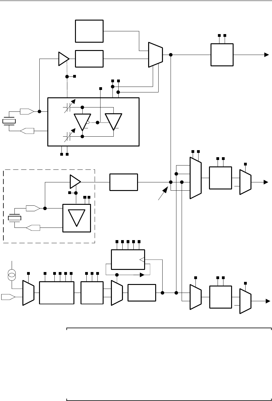
Basic Clock Module+ Introduction
5-3
Basic Clock Module+
Figure 5−1. Basic Clock Module+ Block Diagram
Divider
/1/2/4/8
DIVAx
MCLK
CPUOFF
LFXT1CLK
DCOCLK
XIN
XOUT
Divider
/1/2/4/8
DIVMx
SMCLK
SCG1
DIVSx
ACLK
Main System Clock
Auxillary Clock
Sub System Clock
DCO
DCOx
DC
Generator
SCG0 RSELx
off
SELS
1
0
SELMx
00
01
10
11 1
0
1
0
Divider
/1/2/4/8
Modulator
1
0
n
n+1
XTS
XCAPx
LFXT1 Oscillator
LF
0 V
LFOff
0 V
Min. Puls
Filter
LFXT1Sx
MODx
else
10
Min. Pulse
Filter
Internal
LP/LF VLOCLK
XT2IN
XT2OUT
XT2OFF
XT
Min. Pulse
Filter
Connected only when
XT2 not present on−chip
XT2S
VCC
1
0
DCOR
Oscillator†
XT1Off
XT2 Oscillator†
Rosc†
OSCOFF
XT†
†Note: Device-Specific Clock Variations
All clock features are not available on all MSP430x2xx devices.
MSP430x20xx: LFXT1 does not support HF mode, XT2 is not present, ROSC
is not supported.
MSP430x21x1: Internal LP/LF oscillator is not present, XT2 is not present,
ROSC is not supported.
MSP430x21x2: XT2 is not present.
MSP430x22xx, MSP430x23x0: XT2 is not present.

Basic Clock Module+ Operation
5-4 Basic Clock Module+
5.2 Basic Clock Module+ Operation
After a PUC, MCLK and SMCLK are sourced from DCOCLK at ~1.1 MHz (see
the device-specific data sheet for parameters) and ACLK is sourced from
LFXT1CLK in LF mode with an internal load capacitance of 6pF.
Status register control bits SCG0, SCG1, OSCOFF, and CPUOFF configure
the MSP430 operating modes and enable or disable portions of the basic clock
module+. See Chapter System Resets, Interrupts and Operating Modes. The
DCOCTL, BCSCTL1, BCSCTL2, and BCSCTL3 registers configure the basic
clock module+.
The basic clock module+ can be configured or reconfigured by software at any
time during program execution, for example:
BIS.B #RSEL2+RSEL1+RSEL0,&BCSCTL1 ; Select range 7
BIS.B #DCO2+DCO1+DCO0,&DCOCTL ; Select max DCO tap
5.2.1 Basic Clock Module+ Features for Low-Power Applications
Conflicting requirements typically exist in battery-powered applications:
-Low clock frequency for energy conservation and time keeping
-High clock frequency for fast reaction to events and fast burst processing
capability
-Clock stability over operating temperature and supply voltage
The basic clock module+ addresses the above conflicting requirements by
allowing the user to select from the three available clock signals: ACLK, MCLK,
and SMCLK. For optimal low-power performance, ACLK can be sourced from
a low-power 32,768-Hz watch crystal, providing a stable time base for the
system and low power stand-by operation, or from the internal low-frequency
oscillator when crystal-accurate time keeping is not required.. The MCLK can
be configured to operate from the on-chip DCO that can be activated when
requested by interrupt-driven events. The SMCLK can be configured to
operate from a crystal or the DCO, depending on peripheral requirements. A
flexible clock distribution and divider system is provided to fine tune the
individual clock requirements.
5.2.2 Internal Very Low Power, Low Frequency Oscillator
The internal very-low-power, low-frequency oscillator (VLO) provides a typical
frequency of 12kHz (see device-specific data sheet for parameters) without
requiring a crystal. VLOCLK source is selected by setting LFXT1Sx = 10 when
XTS = 0. The OSCOFF bit disables the VLO for LPM4. The LFXT1 crystal
oscillators are disabled when the VLO is selected reducing current
consumption. The VLO consumes no power when not being used.
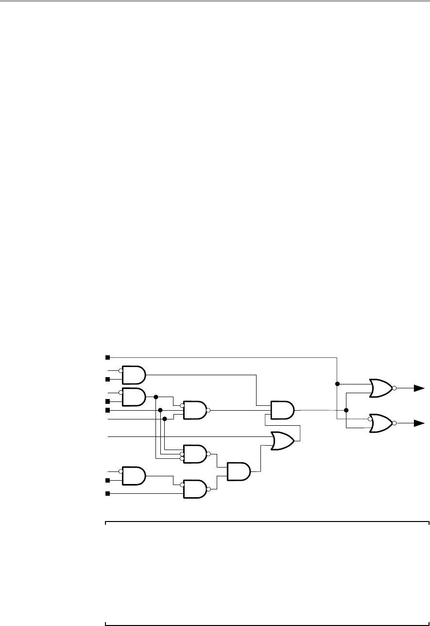
Basic Clock Module+ Operation
5-5
Basic Clock Module+
5.2.3 LFXT1 Oscillator
The LFXT1 oscillator supports ultralow-current consumption using a
32,768-Hz watch crystal in LF mode (XTS = 0). A watch crystal connects to XIN
and XOUT without any other external components. The software-selectable
XCAPx bits configure the internally provided load capacitance for the LFXT1
crystal in LF mode. This capacitance can be selected as 1pF, 6pF, 10pF or
12.5pF typical. Additional external capacitors can be added if necessary.
The LFXT1 oscillator also supports high-speed crystals or resonators when in
HF mode (XTS = 1, XCAPx = 00). The high-speed crystal or resonator
connects to XIN and XOUT and requires external capacitors on both terminals.
These capacitors should be sized according to the crystal or resonator
specifications. When LFXT1 is in HF mode, the LFXT1Sx bits select the range
of operation.
LFXT1 may be used with an external clock signal on the XIN pin in either LF
or HF mode when LFXT1Sx = 11, OSCOFF = 0 and XCAPx = 00. When used
with an external signal, the external frequency must meet the data sheet
parameters for the chosen mode. When the input frequency is below the
specified lower limit, the LFXT1OF bit may be set preventing the CPU from
being clocked with LFXT1CLK.
Software can disable LFXT1 by setting OSCOFF, if LFXT1CLK does not
source SMCLK or MCLK, as shown in Figure 5−2.
Figure 5−2. Off Signals for the LFXT1 Oscillator
XT2 is an Internal Signal
XT2 = 0: Devices without XT2 oscillator
XT2 = 1: Devices with XT2 oscillator
ACLK_request
MCLK_request
OSCOFF
CPUOFF
SCG1
SELS
SMCLK_request
SELM0
XSELM1
XT2
XTS
LFOff
XT1Off
LFXT1Off
Note: LFXT1 Oscillator Characteristics
Low-frequency crystals often require hundreds of milliseconds to start up,
depending on the crystal.
Ultralow-power oscillators such as the LFXT1 in LF mode should be guarded
from noise coupling from other sources. The crystal should be placed as
close as possible to the MSP430 with the crystal housing grounded and the
crystal traces guarded with ground traces.
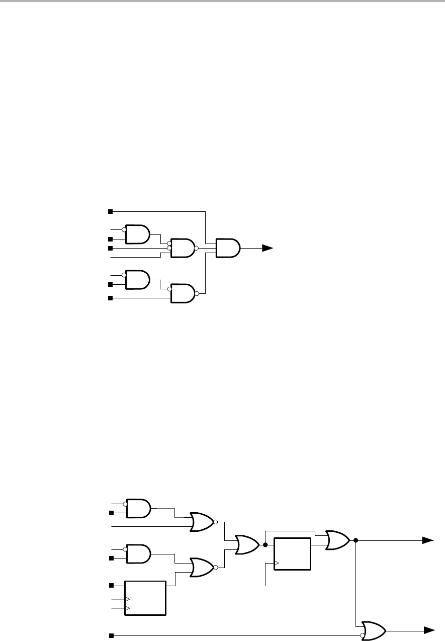
Basic Clock Module+ Operation
5-6 Basic Clock Module+
5.2.4 XT2 Oscillator
Some devices have a second crystal oscillator, XT2. XT2 sources XT2CLK
and its characteristics are identical to LFXT1 in HF mode. The XT2Sx bits
select the range of operation of XT2. The XT2OFF bit disables the XT2
oscillator if XT2CLK is not used for MCLK or SMCLK as shown in Figure 5−3.
XT2 may be used with external clock signals on the XT2IN pin when XT2Sx
= 11 and XT2OFF = 0. When used with an external signal, the external
frequency must meet the data sheet parameters for XT2. When the input
frequency is below the specified lower limit, the XT2OF bit may be set
preventing the CPU from being clocked with XT2CLK.
Figure 5−3. Off Signals for Oscillator XT2
MCLK_request
CPUOFF
SCG1
SELS
SMCLK_request
SELM0
XSELM1
XT2OFF
XT2off (Internal Signal)
5.2.5 Digitally-Controlled Oscillator (DCO)
The DCO is an integrated digitally controlled oscillator. The DCO frequency
can be adjusted by software using the DCOx, MODx, and RSELx bits.
Disabling the DCO
Software can disable DCOCLK by setting SCG0 when it is not used to source
SMCLK or MCLK in active mode, as shown in Figure 5−4.
Figure 5−4. On/Off Control of DCO
MCLK_request
CPUOFF
SCG1
SELS
SMCLK_request
XSELM1
SYNC
DCOCLK
XT2CLK
QD
SCG0
DCOCLK_on
1: on
0: off
1: on
0: off
DCO_Gen_on
DCOCLK
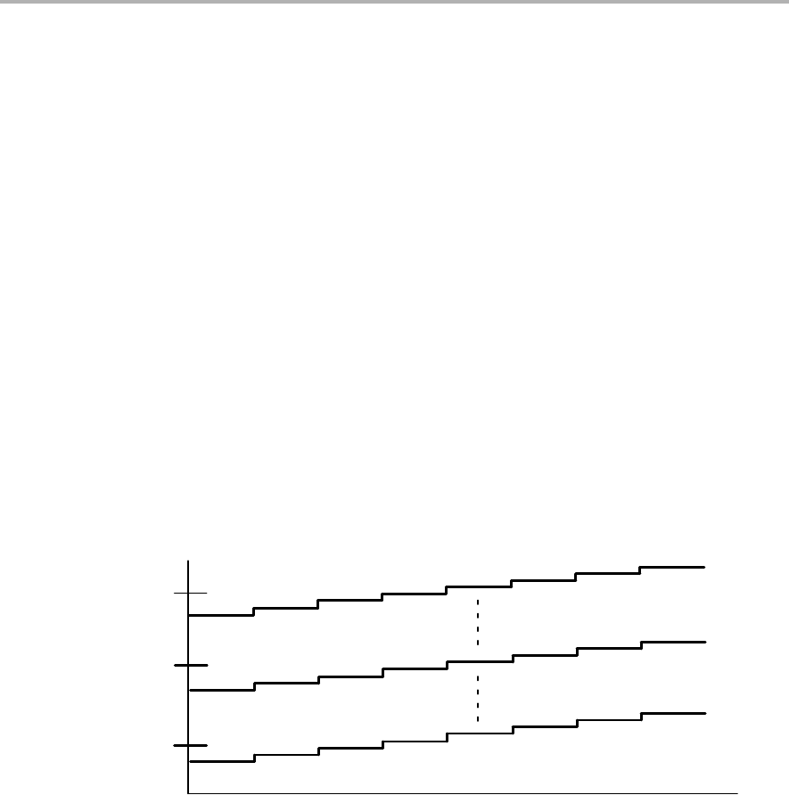
Basic Clock Module+ Operation
5-7
Basic Clock Module+
Adjusting the DCO frequency
After a PUC, RSELx = 7 and DCOx = 3, allowing the DCO to start at a
mid-range frequency. MCLK and SMCLK are sourced from DCOCLK.
Because the CPU executes code from MCLK, which is sourced from the
fast-starting DCO, code execution typically begins from PUC in less than 2 μs.
The typical DCOx and RSELx ranges and steps are shown in Figure 5−5.
The frequency of DCOCLK is set by the following functions:
-The four RSELx bits select one of sixteen nominal frequency ranges for
the DCO. These ranges are defined for an individual device in the
device-specific data sheet.
-The three DCOx bits divide the DCO range selected by the RSELx bits into
8 frequency steps, separated by approximately 10%.
-The five MODx bits, switch between the frequency selected by the DCOx
bits and the next higher frequency set by DCOx+1. When DCOx = 07h,
the MODx bits have no effect because the DCO is already at the highest
setting for the selected RSELx range.
Figure 5−5. Typical DCOx Range and RSELx Steps
RSEL=0
RSEL = 15
DCO=0 DCO=7DCO=4DCO=1 DCO=2 DCO=3 DCO=5 DCO=6
fDCO
20000 kHz
100 kHz
1000 kHz
RSEL = 7

Basic Clock Module+ Operation
5-8 Basic Clock Module+
Each MSP430F2xx device has calibrated DCOCTL and BCSCTL1 register
settings for specific frequencies stored in information memory segment A. To
use the calibrated settings, the information is copied into the DCOCTL and
BCSCTL1 registers. The calibrated settings affect the DCOx, MODx, and
RSELx bits, and clear all other bits, except XT2OFF which remains set. The
remaining bits of BCSCTL1 can be set or cleared as needed with BIS.B or
BIC.B instructions.
; Set DCO to 1 MHz:
MOV.B &CALBC1_1MHZ,&BCSCTL1 ; Set range
MOV.B &CALDCO_1MHZ,&DCOCTL ; Set DCO step + modulation
Using an External Resistor (ROSC) for the DCO
Some MSP430F2xx devices provide the option to source the DCO current
through an external resistor, ROSC, tied to DVCC, when DCOR = 1. In this case,
the DCO has the same characteristics as MSP430x1xx devices, and the
RSELx setting is limited to 0 to 7 with the RSEL3 ignored. This option provides
an additional method to tune the DCO frequency by varying the resistor value.
See the device-specific data sheet for parameters.
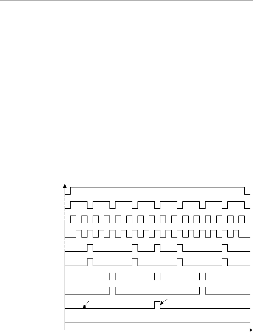
Basic Clock Module+ Operation
5-9
Basic Clock Module+
5.2.6 DCO Modulator
The modulator mixes two DCO frequencies, fDCO and fDCO+1 to produce an
intermediate effective frequency between fDCO and fDCO+1 and spread the
clock energy, reducing electromagnetic interference (EMI). The modulator
mixes fDCO and fDCO+1 for 32 DCOCLK clock cycles and is configured with the
MODx bits. When MODx = 0 the modulator is off.
The modulator mixing formula is:
t =(32− MODx) × tDCO + MODx × tDCO+1
Because fDCO is lower than the effective frequency and fDCO+1 is higher than
the effective frequency, the error of the effective frequency integrates to zero.
It does not accumulate. The error of the effective frequency is zero every 32
DCOCLK cycles. Figure 5−6 illustrates the modulator operation.
The modulator settings and DCO control are configured with software. The
DCOCLK can be compared to a stable frequency of known value and adjusted
with the DCOx, RSELx, and MODx bits. See http://www.msp430.com for
application notes and example code on configuring the DCO.
Figure 5−6. Modulator Patterns
MODx
Lower DCO Tap Frequency fDCO
31
24
16
15
5
4
3
2
1
0
Upper DCO Tap Frequency fDCO+1
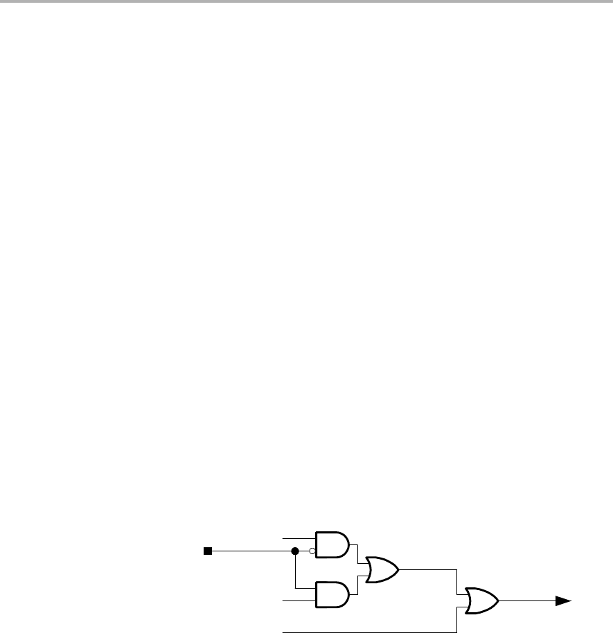
Basic Clock Module+ Operation
5-10 Basic Clock Module+
5.2.7 Basic Clock Module+ Fail-Safe Operation
The basic clock module+ incorporates an oscillator-fault fail-safe feature. This
feature detects an oscillator fault for LFXT1 and XT2 as shown in Figure 5−7
The available fault conditions are:
-Low-frequency oscillator fault (LFXT1OF) for LFXT1 in LF mode
-High-frequency oscillator fault (LFXT1OF) for LFXT1 in HF mode
-High-frequency oscillator fault (XT2OF) for XT2
The crystal oscillator fault bits LFXT1OF, and XT2OF are set if the
corresponding crystal oscillator is turned on and not operating properly. The
fault bits remain set as long as the fault condition exists and are automatically
cleared if the enabled oscillators function normally.
The OFIFG oscillator-fault flag is set and latched at POR or when an oscillator
fault (LFXT1OF, or XT2OF) is detected. When OFIFG is set, MCLK is sourced
from the DCO, and if OFIE is set, the OFIFG requests an NMI interrupt. When
the interrupt is granted, the OFIE is reset automatically. The OFIFG flag must
be cleared by software. The source of the fault can be identified by checking
the individual fault bits.
If a fault is detected for the crystal oscillator sourcing the MCLK, the MCLK is
automatically switched to the DCO for its clock source. This does not change
the SELMx bit settings. This condition must be handled by user software.
Figure 5−7. Oscillator-Fault Logic
LF_OscFault
XT1_OscFault
XT2_OscFault
XTS
XT2OF
LFXT1OF
Set OFIFG Flag

Basic Clock Module+ Operation
5-11
Basic Clock Module+
Sourcing MCLK from a Crystal
After a PUC, the basic clock module+ uses DCOCLK for MCLK. If required,
MCLK may be sourced from LFXT1 or XT2.
The sequence to switch the MCLK source from the DCO clock to the crystal
clock (LFXT1CLK or XT2CLK) is:
1) Switch on the crystal oscillator and select appropriate mode
2) Clear the OFIFG flag
3) Wait at least 50 μs
4) Test OFIFG, and repeat steps 1-4 until OFIFG remains cleared.
; Select LFXT1 (HF mode) for MCLK
BIC.W #OSCOFF,SR ; Turn on osc.
BIS.B #XTS,&BCSCTL1 ; HF mode
MOV.B #LFXT1S0,&BCSCTL3 ; 1−3MHz Crystal
L1 BIC.B #OFIFG,&IFG1 ; Clear OFIFG
MOV.W #0FFh,R15 ; Delay
L2 DEC.W R15 ;
JNZ L2 ;
BIT.B #OFIFG,&IFG1 ; Re−test OFIFG
JNZ L1 ; Repeat test if needed
BIS.B #SELM1+SELM0,&BCSCTL2 ; Select LFXT1CLK
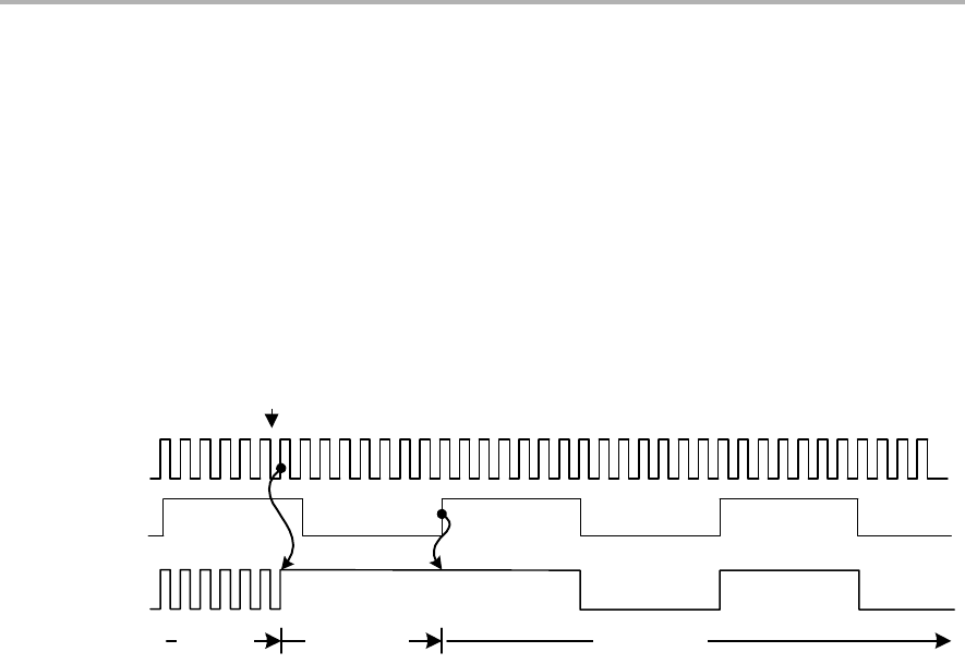
Basic Clock Module+ Operation
5-12 Basic Clock Module+
5.2.8 Synchronization of Clock Signals
When switching MCLK or SMCLK from one clock source to another, the switch
is synchronized to avoid critical race conditions as shown in Figure 5−8:
1) The current clock cycle continues until the next rising edge.
2) The clock remains high until the next rising edge of the new clock.
3) The new clock source is selected and continues with a full high period.
Figure 5−8. Switch MCLK from DCOCLK to LFXT1CLK
DCOCLK
LFXT1CLK
MCLK
LFXT1CLK
DCOCLK
Select
LFXT1CLK
Wait for
LFXT1CLK

Basic Clock Module+ Registers
5-13
Basic Clock Module+
5.3 Basic Clock Module+ Registers
The basic clock module+ registers are listed in Table 5−1.
Table 5−1. Basic Clock module+ Registers
Register Short Form Register Type Address Initial State
DCO control register DCOCTL Read/write 056h060h with PUC
Basic clock system control 1 BCSCTL1 Read/write 057h 087h with POR†
Basic clock system control 2 BCSCTL2 Read/write 058h Reset with PUC
Basic clock system control 3 BCSCTL3 Read/write 053h 005h with PUC
SFR interrupt enable register 1 IE1 Read/write 000hReset with PUC
SFR interrupt flag register 1 IFG1 Read/write 002h Reset with PUC
†Some of the register bits are also PUC initialized. See register summary.

Basic Clock Module+ Registers
5-14 Basic Clock Module+
DCOCTL, DCO Control Register
76543210
DCOx MODx
rw−0 rw−1 rw−1 rw−0 rw−0 rw−0 rw−0 rw−0
DCOx Bits
7-5
DCO frequency select. These bits select which of the eight discrete DCO
frequencies within the range defined by the RSELx setting is selected.
MODx Bits
4-0
Modulator selection. These bits define how often the fDCO+1 frequency is
used within a period of 32 DCOCLK cycles. During the remaining clock
cycles (32−MOD) the fDCO frequency is used. Not useable when DCOx=7.
BCSCTL1, Basic Clock System Control Register 1
76543210
XT2OFF XTS†DIVAx RSELx
rw−(1) rw−(0) rw−(0) rw−(0) rw−0 rw−1 rw−1 rw−1
†XTS = 1 is not supported in MSP430x20xx devices.
XT2OFF Bit 7 XT2 off. This bit turns off the XT2 oscillator
0 XT2 is on
1 XT2 is off if it is not used for MCLK or SMCLK.
XTS Bit 6 LFXT1 mode select.
0 Low frequency mode
1 High frequency mode
DIVAx Bits
5-4
Divider for ACLK
00 /1
01 /2
10 /4
11 /8
RSELx Bits
3-0
Range Select. Sixteen different frequency ranges are available. The lowest
frequency range is selected by setting RSELx=0. RSEL3 is ignored when
DCOR = 1.

Basic Clock Module+ Registers
5-15
Basic Clock Module+
BCSCTL2, Basic Clock System Control Register 2
76543210
SELMx DIVMx SELS DIVSx DCOR†
rw−0 rw−0 rw−0 rw−0 rw−0 rw−0 rw−0 rw−0
†Does not apply to MSP430x20xx or MSP430x21xx
SELMx Bits
7-6
Select MCLK. These bits select the MCLK source.
00 DCOCLK
01 DCOCLK
10 XT2CLK when XT2 oscillator present on-chip. LFXT1CLK or VLOCLK
when XT2 oscillator not present on-chip.
11 LFXT1CLK or VLOCLK
DIVMx BitS
5-4
Divider for MCLK
00 /1
01 /2
10 /4
11 /8
SELS Bit 3 Select SMCLK. This bit selects the SMCLK source.
0 DCOCLK
1 XT2CLK when XT2 oscillator present. LFXT1CLK or VLOCLK when
XT2 oscillator not present
DIVSx BitS
2-1
Divider for SMCLK
00 /1
01 /2
10 /4
11 /8
DCOR Bit 0 DCO resistor select
0 Internal resistor
1 External resistor

Basic Clock Module+ Registers
5-16 Basic Clock Module+
BCSCTL3, Basic Clock System Control Register 3
76543210
XT2Sx LFXT1Sx XCAPx XT2OF†LFXT1OF
rw−0 rw−0 rw−0 rw−0 rw−0 rw−1 r0 r−(1)
†Does not apply to MSP430x2xx, MSP430x21xx, or MSP430x22xx devices
XT2Sx Bits
7-6
XT2 range select. These bits select the frequency range for XT2.
00 0.4 − 1-MHz crystal or resonator
01 1 − 3-MHz crystal or resonator
10 3 − 16-MHz crystal or resonator
11 Digital external 0.4 − 16-MHz clock source
LFXT1Sx Bits
5-4
Low-frequency clock select and LFXT1 range select. These bits select
between LFXT1 and VLO when XTS = 0, and select the frequency range
for LFXT1 when XTS = 1.
When XTS = 0:
00 32768 Hz Crystal on LFXT1
01 Reserved
10 VLOCLK (Reserved in MSP430x21x1 devices)
11 Digital external clock source
When XTS = 1 (Not applicable for MSP430x20xx devices)
00 0.4 − 1-MHz crystal or resonator
01 1 − 3-MHz crystal or resonator
10 3 − 16-MHz crystal or resonator
11 Digital external 0.4 − 16-MHz clock source
XCAPx Bits
3-2
Oscillator capacitor selection. These bits select the effective capacitance
seen by the LFXT1 crystal when XTS = 0. If XTS = 1 or if LFCT1Sx = 11
XCAPx should be 00.
00 ~1 pF
01 ~6 pF
10 ~10 pF
11 ~12.5 pF
XT2OF Bit 1 XT2 oscillator fault
0 No fault condition present
1 Fault condition present
LFXT1OF Bit 0 LFXT1 oscillator fault
0 No fault condition present
1 Fault condition present

Basic Clock Module+ Registers
5-17
Basic Clock Module+
IE1, Interrupt Enable Register 1
76543210
OFIE
rw−0
Bits
7-2
These bits may be used by other modules. See device-specific data sheet.
OFIE Bit 1 Oscillator fault interrupt enable. This bit enables the OFIFG interrupt.
Because other bits in IE1 may be used for other modules, it is recommended
to set or clear this bit using BIS.B or BIC.B instructions, rather than MOV.B
or CLR.B instructions.
0 Interrupt not enabled
1 Interrupt enabled
Bits 0 This bit may be used by other modules. See device-specific data sheet.
IFG1, Interrupt Flag Register 1
76543210
OFIFG
rw−1
Bits
7-2
These bits may be used by other modules. See device-specific data sheet.
OFIFG Bit 1 Oscillator fault interrupt flag. Because other bits in IFG1 may be used for other
modules, it is recommended to set or clear this bit using BIS.B or BIC.B
instructions, rather than MOV.B or CLR.B instructions.
0 No interrupt pending
1 Interrupt pending
Bits 0 This bit may be used by other modules. See device-specific data sheet.

5-18 Basic Clock Module+

6-1
DMA Controller
DMA Controller
The DMA controller module transfers data from one address to another
without CPU intervention. This chapter describes the operation of the DMA
controller of the MSP430x2xx device family.
Topic Page
6.1 DMA Introduction 6-2. . . . . . . . . . . . . . . . . . . . . . . . . . . . . . . . . . . . . . . . . . . . . .
6.2 DMA Operation 6-4. . . . . . . . . . . . . . . . . . . . . . . . . . . . . . . . . . . . . . . . . . . . . . . .
6.3 DMA Registers 6-19. . . . . . . . . . . . . . . . . . . . . . . . . . . . . . . . . . . . . . . . . . . . . . .
Chapter 6

DMA Introduction
6-2 DMA Controller
6.1 DMA Introduction
The direct memory access (DMA) controller transfers data from one address
to another, without CPU intervention, across the entire address range. For
example, the DMA controller can move data from the ADC12 conversion
memory to RAM.
Devices that contain a DMA controller may have one, two, or three DMA
channels available. Therefore, depending on the number of DMA channels
available, some features described in this chapter are not applicable to all
devices.
Using the DMA controller can increase the throughput of peripheral modules.
It can also reduce system power consumption by allowing the CPU to remain
in a low-power mode without having to awaken to move data to or from a
peripheral.
The DMA controller features include:
-Up to three independent transfer channels
-Configurable DMA channel priorities
-Requires only two MCLK clock cycles per transfer
-Byte or word and mixed byte/word transfer capability
-Block sizes up to 65535 bytes or words
-Configurable transfer trigger selections
-Selectable edge or level-triggered transfer
-Four addressing modes
-Single, block, or burst-block transfer modes
The DMA controller block diagram is shown in Figure 6−1.
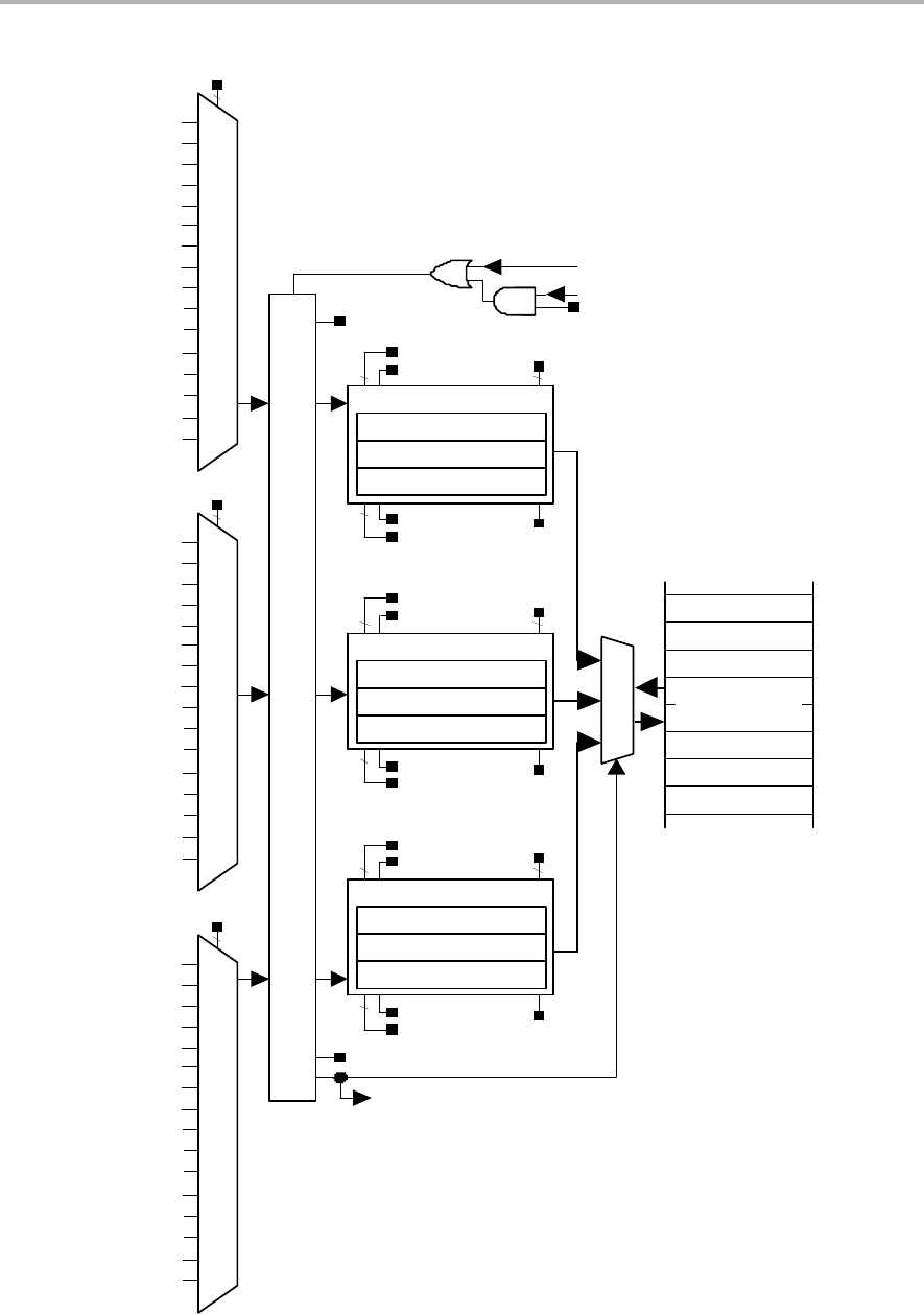
DMA Introduction
6-3
DMA Controller
Figure 6−1. DMA Controller Block Diagram
ENNMI
DT
DMA Channel 2
DMASRSBYTE
DMA2SZ
DMA2DA
DMA2SA
DMADSTBYTE
DMASRCINCRx
DMADSTINCRx
2
2
3
DMADTx
DMAEN
DT
DMA Channel 1
DMASRSBYTE
DMA1SZ
DMA1DA
DMA1SA
DMADSTBYTE
DMASRCINCRx
DMADSTINCRx
2
2
3
DMADTx
DMAEN
DT
DMA Channel 0
DMASRSBYTE
DMA0SZ
DMA0DA
DMA0SA
DMADSTBYTE
DMASRCINCRx
DMADSTINCRx
2
2
3
DMADTx
DMAEN
Address
Space
NMI Interrupt Request
JTAG Active
Halt
Halt CPU
ROUNDROBIN
DMAONFETCH
DAC12_0IFG
DMAE0
DMAREQ
DMA0TSELx
4
DMA2IFG
TACCR2_CCIFG
TBCCR2_CCIFG
ADC12_IFGx
0000
0001
0010
0011
0100
0101
1101
1111
1110
0110
USCI A0 data receive
USCI A0 data transmit
1100
0111
USCI B0 data transmit
USCI B0 data receive
TACCR0_CCIFG
1000
TBCCR0_CCIFG
1010
1001
USCI A1 data Tx
USCI A1 data Rx
1011
Multiplier ready
DMA Priority And Controll
DAC12_0IFG
DMAE0
DMAREQ
DMA1TSELx
4
DMA0IFG
TACCR2_CCIFG
TBCCR2_CCIFG
ADC12_IFGx
0000
0001
0010
0011
0100
0101
1101
1111
1110
0110
1100
0111
TACCR0_CCIFG
1000
TBCCR0_CCIFG
1010
1001
1011
Multiplier ready
DAC12_0IFG
DMAE0
DMAREQ
DMA2TSEL
4
DMA1IFG
TACCR2_CCIFG
TBCCR2_CCIFG
ADC12_IFGx
0000
0001
0010
0011
0100
0101
1101
1111
1110
0110
1100
0111
TACCR0_CCIFG
1000
TBCCR0_CCIFG
1010
1001
1011
Multiplier ready
USCI A0 data receive
USCI A0 data transmit
USCI B0 data transmit
USCI B0 data receive
USCI A0 data receive
USCI A0 data transmit
USCI B0 data transmit
USCI B0 data receive
USCI A1 data Tx
USCI A1 data Rx
USCI A1 data Tx
USCI A1 data Rx
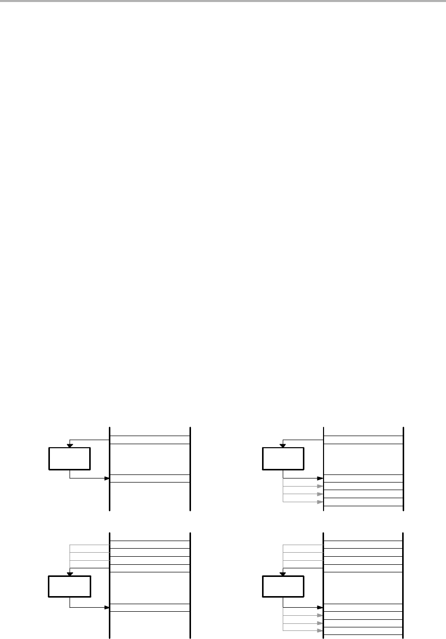
DMA Operation
6-4 DMA Controller
6.2 DMA Operation
The DMA controller is configured with user software. The setup and operation
of the DMA is discussed in the following sections.
6.2.1 DMA Addressing Modes
The DMA controller has four addressing modes. The addressing mode for
each DMA channel is independently configurable. For example, channel 0
may transfer between two fixed addresses, while channel 1 transfers between
two blocks of addresses. The addressing modes are shown in Figure 6−2. The
addressing modes are:
-Fixed address to fixed address
-Fixed address to block of addresses
-Block of addresses to fixed address
-Block of addresses to block of addresses
The addressing modes are configured with the DMASRCINCRx and
DMADSTINCRx control bits. The DMASRCINCRx bits select if the source
address is incremented, decremented, or unchanged after each transfer. The
DMADSTINCRx bits select if the destination address is incremented,
decremented, or unchanged after each transfer.
Transfers may be byte-to-byte, word-to-word, byte-to-word, or word-to-byte.
When transferring word-to-byte, only the lower byte of the source-word
transfers. When transferring byte-to-word, the upper byte of the
destination-word is cleared when the transfer occurs.
Figure 6−2. DMA Addressing Modes
Address SpaceAddress Space
DMA
Controller Address Space Address Space
DMA
Controller
DMA
Controller
DMA
Controller
Fixed Address To Block Of Addresses
Fixed Address To Fixed Address
Block Of Addresses To Fixed Address Block Of Addresses To Block Of Addresses

DMA Operation
6-5
DMA Controller
6.2.2 DMA Transfer Modes
The DMA controller has six transfer modes selected by the DMADTx bits as
listed in Table 6−1. Each channel is individually configurable for its transfer
mode. For example, channel 0 may be configured in single transfer mode,
while channel 1 is configured for burst-block transfer mode, and channel 2
operates in repeated block mode. The transfer mode is configured
independently from the addressing mode. Any addressing mode can be used
with any transfer mode.
Two types of data can be transferred selectable by the DMAxCTL DSTBYTE
and SRCBYTE fields. The source and/or destination location can be either
byte or word data. It is also possible to transfer byte to byte, word to word or
any combination.
Table 6−1. DMA Transfer Modes
DMADTx Transfer
Mode
Description
000 Single transfer Each transfer requires a trigger. DMAEN is
automatically cleared when DMAxSZ transfers have
been made.
001 Block transfer A complete block is transferred with one trigger.
DMAEN is automatically cleared at the end of the
block transfer.
010, 011 Burst-block
transfer
CPU activity is interleaved with a block transfer.
DMAEN is automatically cleared at the end of the
burst-block transfer.
100 Repeated
single transfer
Each transfer requires a trigger. DMAEN remains
enabled.
101 Repeated
block transfer
A complete block is transferred with one trigger.
DMAEN remains enabled.
110, 111 Repeated
burst-block
transfer
CPU activity is interleaved with a block transfer.
DMAEN remains enabled.

DMA Operation
6-6 DMA Controller
Single Transfer
In single transfer mode, each byte/word transfer requires a separate trigger.
The single transfer state diagram is shown in Figure 6−3.
The DMAxSZ register is used to define the number of transfers to be made.
The DMADSTINCRx and DMASRCINCRx bits select if the destination
address and the source address are incremented or decremented after each
transfer. If DMAxSZ = 0, no transfers occur.
The DMAxSA, DMAxDA, and DMAxSZ registers are copied into temporary
registers. The temporary values of DMAxSA and DMAxDA are incremented
or decremented after each transfer. The DMAxSZ register is decremented
after each transfer. When the DMAxSZ register decrements to zero it is
reloaded from its temporary register and the corresponding DMAIFG flag is
set. When DMADTx = 0, the DMAEN bit is cleared automatically when
DMAxSZ decrements to zero and must be set again for another transfer to
occur.
In repeated single transfer mode, the DMA controller remains enabled with
DMAEN = 1, and a transfer occurs every time a trigger occurs.
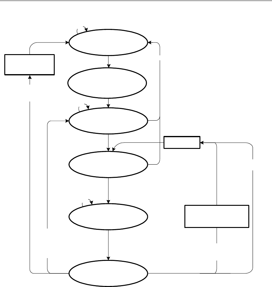
DMA Operation
6-7
DMA Controller
Figure 6−3. DMA Single Transfer State Diagram
Reset
Wait for Trigger
Idle
Hold CPU,
Transfer one word/byte
[+Trigger AND DMALEVEL = 0 ]
OR
[Trigger=1 AND DMALEVEL=1]
DMAABORT=0
DMAABORT = 1
2 x MCLK
DMAEN = 0
Modify T_SourceAdd
Modify T_DestAdd
Decrement DMAxSZ
[ENNMI = 1
AND NMI event]
OR
[DMALEVEL = 1
AND Trigger = 0]
[ DMADTx = 0
AND DMAxSZ = 0]
OR DMAEN = 0
DMAxSZ → T_Size
DMAxSA → T_SourceAdd
DMAxDA → T_DestAdd
DMAREQ = 0
DMAxSZ > 0
AND DMAEN = 1
DMAEN = 0
DMAEN = 1
T_Size → DMAxSZ
DMAxSA → T_SourceAdd
DMAxDA → T_DestAdd
DMADTx = 4
AND DMAxSZ = 0
AND DMAEN = 1
DMAEN = 0
DMAREQ = 0
T_Size → DMAxSZ

DMA Operation
6-8 DMA Controller
Block Transfers
In block transfer mode, a transfer of a complete block of data occurs after one
trigger. When DMADTx = 1, the DMAEN bit is cleared after the completion of
the block transfer and must be set again before another block transfer can be
triggered. After a block transfer has been triggered, further trigger signals
occurring during the block transfer are ignored. The block transfer state
diagram is shown in Figure 6−4.
The DMAxSZ register is used to define the size of the block and the
DMADSTINCRx and DMASRCINCRx bits select if the destination address
and the source address are incremented or decremented after each transfer
of the block. If DMAxSZ = 0, no transfers occur.
The DMAxSA, DMAxDA, and DMAxSZ registers are copied into temporary
registers. The temporary values of DMAxSA and DMAxDA are incremented
or decremented after each transfer in the block. The DMAxSZ register is
decremented after each transfer of the block and shows the number of
transfers remaining in the block. When the DMAxSZ register decrements to
zero it is reloaded from its temporary register and the corresponding DMAIFG
flag is set.
During a block transfer, the CPU is halted until the complete block has been
transferred. The block transfer takes 2 x MCLK x DMAxSZ clock cycles to
complete. CPU execution resumes with its previous state after the block
transfer is complete.
In repeated block transfer mode, the DMAEN bit remains set after completion
of the block transfer. The next trigger after the completion of a repeated block
transfer triggers another block transfer.
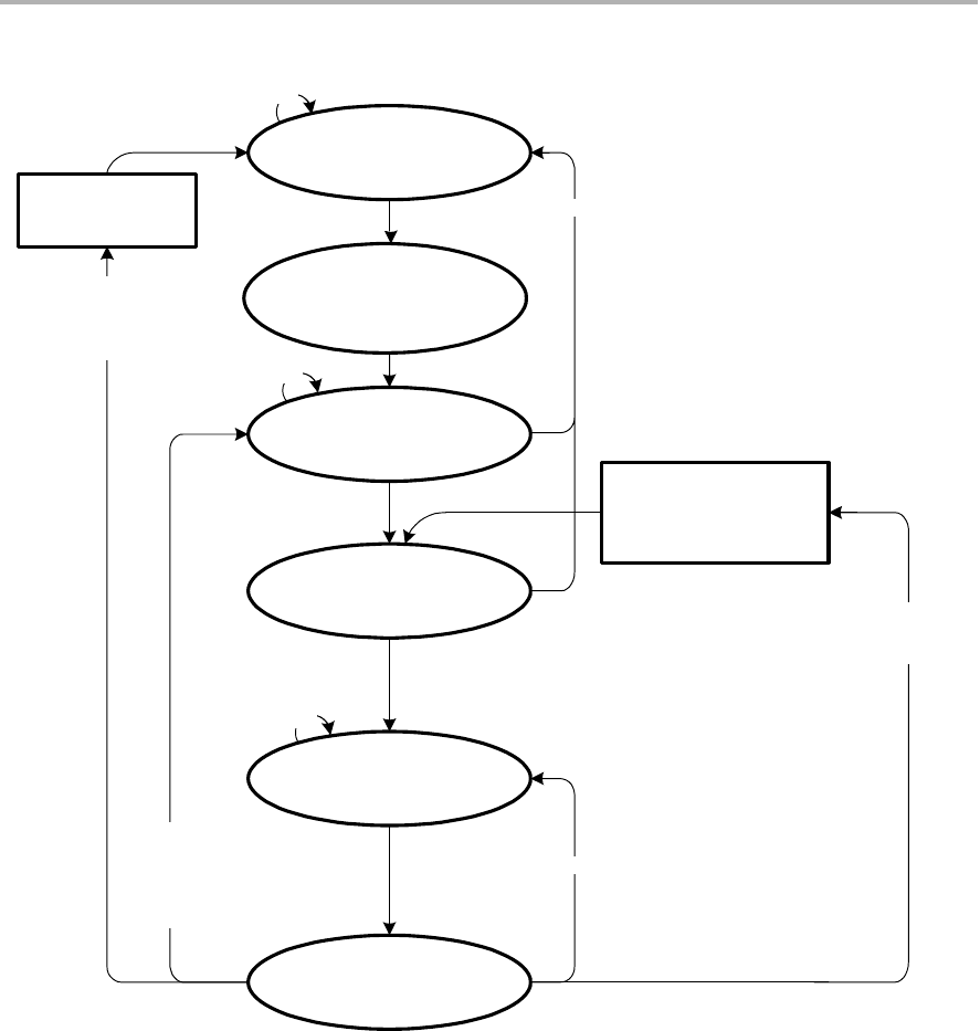
DMA Operation
6-9
DMA Controller
Figure 6−4. DMA Block Transfer State Diagram
Reset
Wait for Trigger
Idle
Hold CPU,
Transfer one word/byte
[+Trigger AND DMALEVEL = 0 ]
OR
[Trigger=1 AND DMALEVEL=1]
DMAABORT=0
DMAABORT = 1
2 x MCLK
DMAEN = 0
Modify T_SourceAdd
Modify T_DestAdd
Decrement DMAxSZ
DMAxSZ > 0
[ENNMI = 1
AND NMI event]
OR
[DMALEVEL = 1
AND Trigger = 0]
[DMADTx = 1
AND DMAxSZ = 0]
OR
DMAEN = 0
DMAxSZ → T_Size
DMAxSA → T_SourceAdd
DMAxDA → T_DestAdd
DMAREQ = 0
T_Size → DMAxSZ
DMAxSA → T_SourceAdd
DMAxDA → T_DestAdd
DMADTx = 5
AND DMAxSZ = 0
AND DMAEN = 1
DMAEN = 0
DMAEN = 1
DMAEN = 0
DMAREQ = 0
T_Size → DMAxSZ

DMA Operation
6-10 DMA Controller
Burst-Block Transfers
In burst-block mode, transfers are block transfers with CPU activity
interleaved. The CPU executes 2 MCLK cycles after every four byte/word
transfers of the block resulting in 20% CPU execution capacity. After the
burst-block, CPU execution resumes at 100% capacity and the DMAEN bit is
cleared. DMAEN must be set again before another burst-block transfer can be
triggered. After a burst-block transfer has been triggered, further trigger
signals occurring during the burst-block transfer are ignored. The burst-block
transfer state diagram is shown in Figure 6−5.
The DMAxSZ register is used to define the size of the block and the
DMADSTINCRx and DMASRCINCRx bits select if the destination address
and the source address are incremented or decremented after each transfer
of the block. If DMAxSZ = 0, no transfers occur.
The DMAxSA, DMAxDA, and DMAxSZ registers are copied into temporary
registers. The temporary values of DMAxSA and DMAxDA are incremented
or decremented after each transfer in the block. The DMAxSZ register is
decremented after each transfer of the block and shows the number of
transfers remaining in the block. When the DMAxSZ register decrements to
zero it is reloaded from its temporary register and the corresponding DMAIFG
flag is set.
In repeated burst-block mode the DMAEN bit remains set after completion of
the burst-block transfer and no further trigger signals are required to initiate
another burst-block transfer. Another burst-block transfer begins immediately
after completion of a burst-block transfer. In this case, the transfers must be
stopped by clearing the DMAEN bit, or by an NMI interrupt when ENNMI is set.
In repeated burst-block mode the CPU executes at 20% capacity continuously
until the repeated burst-block transfer is stopped.
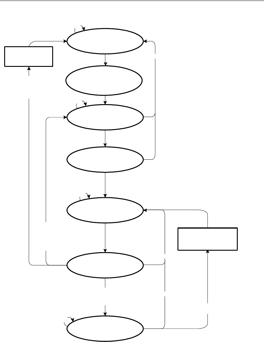
DMA Operation
6-11
DMA Controller
Figure 6−5. DMA Burst-Block Transfer State Diagram
2 x MCLK
Reset
Wait for Trigger
Idle
Hold CPU,
Transfer one word/byte
Burst State
(release CPU for 2xMCLK)
[+Trigger AND DMALEVEL = 0 ]
OR
[Trigger=1 AND DMALEVEL=1]
DMAABORT=0
DMAABORT = 1
2 x MCLK
DMAEN = 0
Modify T_SourceAdd
Modify T_DestAdd
Decrement DMAxSZ
[DMADTx = {6, 7}
AND DMAxSZ = 0]
[ENNMI = 1
AND NMI event]
OR
[DMALEVEL = 1
AND Trigger = 0]
[DMADTx = {2, 3}
AND DMAxSZ = 0]
OR
DMAEN = 0
DMAxSZ → T_Size
DMAxSA → T_SourceAdd
DMAxDA → T_DestAdd
T_Size → DMAxSZ
DMAxSA → T_SourceAdd
DMAxDA → T_DestAdd
DMAEN = 0
DMAEN = 1
DMAxSZ > 0
DMAxSZ > 0 AND
a multiple of 4 words/bytes
were transferred
DMAxSZ > 0
DMAEN = 0
DMAREQ = 0
T_Size → DMAxSZ

DMA Operation
6-12 DMA Controller
6.2.3 Initiating DMA Transfers
Each DMA channel is independently configured for its trigger source with the
DMAxTSELx bits as described in Table 6−2.The DMAxTSELx bits should be
modified only when the DMACTLx DMAEN bit is 0. Otherwise, unpredictable
DMA triggers may occur.
When selecting the trigger, the trigger must not have already occurred, or the
transfer will not take place. For example, if the TACCR2 CCIFG bit is selected
as a trigger, and it is already set, no transfer will occur until the next time the
TACCR2 CCIFG bit is set.
Edge-Sensitive Triggers
When DMALEVEL = 0, edge-sensitive triggers are used and the rising edge
of the trigger signal initiates the transfer. In single-transfer mode, each transfer
requires its own trigger. When using block or burst-block modes, only one
trigger is required to initiate the block or burst-block transfer.
Level-Sensitive Triggers
When DMALEVEL = 1, level-sensitive triggers are used. For proper operation,
level-sensitive triggers can only be used when external trigger DMAE0 is
selected as the trigger. DMA transfers are triggered as long as the trigger
signal is high and the DMAEN bit remains set.
The trigger signal must remain high for a block or burst-block transfer to
complete. If the trigger signal goes low during a block or burst-block transfer,
the DMA controller is held in its current state until the trigger goes back high
or until the DMA registers are modified by software. If the DMA registers are
not modified by software, when the trigger signal goes high again, the transfer
resumes from where it was when the trigger signal went low.
When DMALEVEL = 1, transfer modes selected when DMADTx = {0, 1, 2, 3}
are recommended because the DMAEN bit is automatically reset after the
configured transfer.
Halting Executing Instructions for DMA Transfers
The DMAONFETCH bit controls when the CPU is halted for a DMA transfer.
When DMAONFETCH = 0, the CPU is halted immediately and the transfer
begins when a trigger is received. When DMAONFETCH = 1, the CPU finishes
the currently executing instruction before the DMA controller halts the CPU
and the transfer begins.
Note: DMAONFETCH Must Be Used When The DMA Writes To Flash
If the DMA controller is used to write to flash memory, the DMAONFETCH
bit must be set. Otherwise, unpredictable operation can result.

DMA Operation
6-13
DMA Controller
Table 6−2. DMA Trigger Operation
DMAxTSELx Operation
0000 A transfer is triggered when the DMAREQ bit is set. The DMAREQ bit is automatically reset
when the transfer starts
0001 A transfer is triggered when the TACCR2 CCIFG flag is set. The TACCR2 CCIFG flag is
automatically reset when the transfer starts. If the TACCR2 CCIE bit is set, the TACCR2
CCIFG flag will not trigger a transfer.
0010 A transfer is triggered when the TBCCR2 CCIFG flag is set. The TBCCR2 CCIFG flag is
automatically reset when the transfer starts. If the TBCCR2 CCIE bit is set, the TBCCR2
CCIFG flag will not trigger a transfer.
0011 A transfer is triggered when serial interface receives new data.
Devices with USCI_A0 module: A transfer is triggered when USCI_A0 receives new data.
UCA0RXIFG is automatically reset when the transfer starts. If UCA0RXIE is set, the
UCA0RXIFG flag will not trigger a transfer.
0100 A transfer is triggered when serial interface is ready to transmit new data.
Devices with USCI_A0 module:A transfer is triggered when USCI_A0 is ready to transmit new
data. UCA0TXIFG is automatically reset when the transfer starts. If UCA0TXIE is set, the
UCA0TXIFG flag will not trigger a transfer.
0101 A transfer is triggered when the DAC12_0CTL DAC12IFG flag is set. The DAC12_0CTL
DAC12IFG flag is automatically cleared when the transfer starts. If the DAC12_0CTL
DAC12IE bit is set, the DAC12_0CTL DAC12IFG flag will not trigger a transfer.
0110 A transfer is triggered by an ADC12IFGx flag. When single-channel conversions are
performed, the corresponding ADC12IFGx is the trigger. When sequences are used, the
ADC12IFGx for the last conversion in the sequence is the trigger. A transfer is triggered when
the conversion is completed and the ADC12IFGx is set. Setting the ADC12IFGx with software
will not trigger a transfer. All ADC12IFGx flags are automatically reset when the associated
ADC12MEMx register is accessed by the DMA controller.
0111 A transfer is triggered when the TACCR0 CCIFG flag is set. The TACCR0 CCIFG flag is
automatically reset when the transfer starts. If the TACCR0 CCIE bit is set, the TACCR0
CCIFG flag will not trigger a transfer.
1000 A transfer is triggered when the TBCCR0 CCIFG flag is set. The TBCCR0 CCIFG flag is
automatically reset when the transfer starts. If the TBCCR0 CCIE bit is set, the TBCCR0
CCIFG flag will not trigger a transfer.
1001 A transfer is triggered when the UCA1RXIFG flag is set. UCA1RXIFG is automatically reset
when the transfer starts. If URXIE1 is set, the UCA1RXIFG flag will not trigger a transfer.
1010 A transfer is triggered when the UCA1TXIFG flag is set. UCA1TXIFG is automatically reset
when the transfer starts. If UTXIE1 is set, the UCA1TXIFG flag will not trigger a transfer.
1011 A transfer is triggered when the hardware multiplier is ready for a new operand.
1100 No transfer is triggered.
Devices with USCI_B0 module: A transfer is triggered when USCI_B0 receives new data.
UCB0RXIFG is automatically reset when the transfer starts. If UCB0RXIE is set, the
UCB0RXIFG flag will not trigger a transfer.
1101 No transfer is triggered.
Devices with USCI_B0 module: A transfer is triggered when USCI_B0 is ready to transmit
new data. UCB0TXIFG is automatically reset when the transfer starts. If UCB0TXIE is set, the
UCB0TXIFG flag will not trigger a transfer.

DMA Operation
6-14 DMA Controller
Table 6−2. DMA Trigger Operation (continued)
DMAxTSELx Operation
1110 A transfer is triggered when the DMAxIFG flag is set. DMA0IFG triggers channel 1, DMA1IFG
triggers channel 2, and DMA2IFG triggers channel 0. None of the DMAxIFG flags are
automatically reset when the transfer starts.
1111 A transfer is triggered by the external trigger DMAE0.
6.2.4 Stopping DMA Transfers
There are two ways to stop DMA transfers in progress:
-A single, block, or burst-block transfer may be stopped with an NMI
interrupt, if the ENNMI bit is set in register DMACTL1.
-A burst-block transfer may be stopped by clearing the DMAEN bit.
6.2.5 DMA Channel Priorities
The default DMA channel priorities are DMA0−DMA1−DMA2. If two or three
triggers happen simultaneously or are pending, the channel with the highest
priority completes its transfer (single, block or burst-block transfer) first, then
the second priority channel, then the third priority channel. Transfers in
progress are not halted if a higher priority channel is triggered. The higher
priority channel waits until the transfer in progress completes before starting.
The DMA channel priorities are configurable with the ROUNDROBIN bit.
When the ROUNDROBIN bit is set, the channel that completes a transfer
becomes the lowest priority. The order of the priority of the channels always
stays the same, DMA0−DMA1−DMA2, for example:
DMA Priority Transfer Occurs New DMA Priority
DMA0 − DMA1 − DMA2 DMA1 DMA2 − DMA0 − DMA1
DMA2 − DMA0 − DMA1 DMA2 DMA0 − DMA1 − DMA2
DMA0 − DMA1 − DMA2 DMA0 DMA1 − DMA2 − DMA0
When the ROUNDROBIN bit is cleared the channel priority returns to the
default priority.

DMA Operation
6-15
DMA Controller
6.2.6 DMA Transfer Cycle Time
The DMA controller requires one or two MCLK clock cycles to synchronize
before each single transfer or complete block or burst-block transfer. Each
byte/word transfer requires two MCLK cycles after synchronization, and one
cycle of wait time after the transfer. Because the DMA controller uses MCLK,
the DMA cycle time is dependent on the MSP430 operating mode and clock
system setup.
If the MCLK source is active, but the CPU is off, the DMA controller will use the
MCLK source for each transfer, without re-enabling the CPU. If the MCLK
source is off, the DMA controller will temporarily restart MCLK, sourced with
DCOCLK, for the single transfer or complete block or burst-block transfer. The
CPU remains off, and after the transfer completes, MCLK is turned off. The
maximum DMA cycle time for all operating modes is shown in Table 6−3.
Table 6−3. Maximum Single-Transfer DMA Cycle Time
CPU Operating Mode Clock Source Maximum DMA Cycle Time
Active mode MCLK=DCOCLK 4 MCLK cycles
Active mode MCLK=LFXT1CLK 4 MCLK cycles
Low-power mode LPM0/1 MCLK=DCOCLK 5 MCLK cycles
Low-power mode LPM3/4 MCLK=DCOCLK 5 MCLK cycles + 6 μs†
Low-power mode LPM0/1 MCLK=LFXT1CLK 5 MCLK cycles
Low-power mode LPM3 MCLK=LFXT1CLK 5 MCLK cycles
Low-power mode LPM4 MCLK=LFXT1CLK 5 MCLK cycles + 6 μs†
†The additional 6 μs are needed to start the DCOCLK. It is the t(LPMx) parameter in the data sheet.

DMA Operation
6-16 DMA Controller
6.2.7 Using DMA with System Interrupts
DMA transfers are not interruptible by system interrupts. System interrupts
remain pending until the completion of the transfer. NMI interrupts can
interrupt the DMA controller if the ENNMI bit is set.
System interrupt service routines are interrupted by DMA transfers. If an
interrupt service routine or other routine must execute with no interruptions,
the DMA controller should be disabled prior to executing the routine.
6.2.8 DMA Controller Interrupts
Each DMA channel has its own DMAIFG flag. Each DMAIFG flag is set in any
mode, when the corresponding DMAxSZ register counts to zero. If the
corresponding DMAIE and GIE bits are set, an interrupt request is generated.
All DMAIFG flags source only one DMA controller interrupt vector and, on
some devices, the interrupt vector may be shared with other modules. Please
refer to the device specific datasheet for further details. For these devices,
software must check the DMAIFG and respective module flags to determine
the source of the interrupt. The DMAIFG flags are not reset automatically and
must be reset by software.
Additionally, some devices utilize the DMAIV register. All DMAIFG flags are
prioritized, with DMA0IFG being the highest, and combined to source a single
interrupt vector. The highest priority enabled interrupt generates a number in
the DMAIV register. This number can be evaluated or added to the program
counter to automatically enter the appropriate software routine. Disabled DMA
interrupts do not affect the DMAIV value.
Any access, read or write, of the DMAIV register automatically resets the high-
est pending interrupt flag. If another interrupt flag is set, another interrupt is
immediately generated after servicing the initial interrupt. For example, as-
sume that DMA0 has the highest priority. If the DMA0IFG and DMA2IFG flags
are set when the interrupt service routine accesses the DMAIV register,
DMA0IFG is reset automatically. After the RETI instruction of the interrupt ser-
vice routine is executed, the DMA2IFG will generate another interrupt.

DMA Operation
6-17
DMA Controller
DMAIV Software Example
The following software example shows the recommended use of DMAIV and
the handling overhead. The DMAIV value is added to the PC to automatically
jump to the appropriate routine.
The numbers at the right margin show the necessary CPU cycles for each
instruction. The software overhead for different interrupt sources includes
interrupt latency and return-from-interrupt cycles, but not the task handling
itself.
;Interrupt handler for DMA0IFG, DMA1IFG, DMA2IFG Cycles
DMA_HND ... ; Interrupt latency 6
ADD &DMAIV,PC ; Add offset to Jump table 3
RETI ; Vector 0: No interrupt 5
JMP DMA0_HND ; Vector 2: DMA channel 0 2
JMP DMA1_HND ; Vector 4: DMA channel 1 2
JMP DMA2_HND ; Vector 6: DMA channel 2 2
RETI ; Vector 8: Reserved 5
RETI ; Vector 10: Reserved 5
RETI ; Vector 12: Reserved 5
RETI ; Vector 14: Reserved 5
DMA2_HND ; Vector 6: DMA channel 2
... ; Task starts here
RETI ; Back to main program 5
DMA1_HND ; Vector 4: DMA channel 1
... ; Task starts here
RETI ; Back to main program 5
DMA0_HND ; Vector 2: DMA channel 0
... ; Task starts here
RETI ; Back to main program 5
6.2.9 Using the USCI_B I2C Module with the DMA Controller
The USCI_B I2C module provides two trigger sources for the DMA controller.
The USCI_B I2C module can trigger a transfer when new I2C data is received
and when data is needed for transmit.
A transfer is triggered if UCB0RXIFG is set. The UCB0RXIFG is cleared
automatically when the DMA controller acknowledges the transfer. If
UCB0RXIE is set, UCB0RXIFG will not trigger a transfer.
A transfer is triggered if UCB0TXIFG is set. The UCB0TXIFG is cleared
automatically when the DMA controller acknowledges the transfer. If
UCB0TXIE is set, UCB0TXIFG will not trigger a transfer.

DMA Operation
6-18 DMA Controller
6.2.10 Using ADC12 with the DMA Controller
MSP430 devices with an integrated DMA controller can automatically move
data from any ADC12MEMx register to another location. DMA transfers are
done without CPU intervention and independently of any low-power modes.
The DMA controller increases throughput of the ADC12 module, and
enhances low-power applications allowing the CPU to remain off while data
transfers occur.
DMA transfers can be triggered from any ADC12IFGx flag. When CONSEQx
= {0,2} the ADC12IFGx flag for the ADC12MEMx used for the conversion can
trigger a DMA transfer. When CONSEQx = {1,3}, the ADC12IFGx flag for the
last ADC12MEMx in the sequence can trigger a DMA transfer. Any
ADC12IFGx flag is automatically cleared when the DMA controller accesses
the corresponding ADC12MEMx.
6.2.11 Using DAC12 With the DMA Controller
MSP430 devices with an integrated DMA controller can automatically move
data to the DAC12_xDAT register. DMA transfers are done without CPU
intervention and independently of any low-power modes. The DMA controller
increases throughput to the DAC12 module, and enhances low-power
applications allowing the CPU to remain off while data transfers occur.
Applications requiring periodic waveform generation can benefit from using
the DMA controller with the DAC12. For example, an application that produces
a sinusoidal waveform may store the sinusoid values in a table. The DMA
controller can continuously and automatically transfer the values to the DAC12
at specific intervals creating the sinusoid with zero CPU execution. The
DAC12_xCTL DAC12IFG flag is automatically cleared when the DMA
controller accesses the DAC12_xDAT register.
6.2.12 Writing to Flash With the DMA Controller
MSP430 devices with an integrated DMA controller can automatically move
data to the Flash memory. DMA transfers are done without CPU intervention
and independent of any low-power modes. The DMA controller performs the
move of the data word/byte to the Flash. The write timing control is done by
the Flash controller. Write transfers to the Flash memory succeed if the Flash
controller set−up is prior to the DMA transfer and if the Flash is not busy. To
set up the Flash controller for write accesses, see Chapter 7, Flash Memory
Controller.

DMA Registers
6-19
DMA Controller
6.3 DMA Registers
The DMA registers are listed in Table 6−4.
Table 6−4. DMA Registers
Register Short Form Register Type Address Initial State
DMA control 0 DMACTL0 Read/write 0122h Reset with POR
DMA control 1 DMACTL1 Read/write 0124h Reset with POR
DMA interrupt vector DMAIV Read only 0126h Reset with POR
DMA channel 0 control DMA0CTL Read/write 01D0h Reset with POR
DMA channel 0 source address DMA0SA Read/write 01D2h Unchanged
DMA channel 0 destination address DMA0DA Read/write 01D6h Unchanged
DMA channel 0 transfer size DMA0SZ Read/write 01DAh Unchanged
DMA channel 1 control DMA1CTL Read/write 01DCh Reset with POR
DMA channel 1 source address DMA1SA Read/write 01DEh Unchanged
DMA channel 1 destination address DMA1DA Read/write 01E2h Unchanged
DMA channel 1 transfer size DMA1SZ Read/write 01E6h Unchanged
DMA channel 2 control DMA2CTL Read/write 01E8h Reset with POR
DMA channel 2 source address DMA2SA Read/write 01EAh Unchanged
DMA channel 2 destination address DMA2DA Read/write 01EEh Unchanged
DMA−channel 2 transfer size DMA2SZ Read/write 01F2h Unchanged

DMA Registers
6-20 DMA Controller
DMACTL0, DMA Control Register 0
15 14 13 12 11 10 9 8
Reserved DMA2TSELx
rw−(0) rw−(0) rw−(0) rw−(0) rw−(0) rw−(0) rw−(0) rw−(0)
76543210
DMA1TSELx DMA0TSELx
rw−(0) rw−(0) rw−(0) rw−(0) rw−(0) rw−(0) rw−(0) rw−(0)
Reserved Bits
15−12
Reserved
DMA2
TSELx
Bits
11−8
DMA trigger select. These bits select the DMA transfer trigger.
0000 DMAREQ bit (software trigger)
0001 TACCR2 CCIFG bit
0010 TBCCR2 CCIFG bit
0011 Serial data received UCA0RXIFG
0100 Serial data transmit ready UCA0TXIFG
0101 DAC12_0CTL DAC12IFG bit
0110 ADC12 ADC12IFGx bit
0111 TACCR0 CCIFG bit
1000 TBCCR0 CCIFG bit
1001 Serial data received UCA1RXIFG
1010 Serial data transmit ready UCA1TXIFG
1011 Multiplier ready
1100 Serial data received UCB0RXIFG
1101 Serial data transmit ready UCB0TXIFG
1110 DMA0IFG bit triggers DMA channel 1
DMA1IFG bit triggers DMA channel 2
DMA2IFG bit triggers DMA channel 0
1111 External trigger DMAE0
DMA1
TSELx
Bits
7−4
Same as DMA2TSELx
DMA0
TSELx
Bits
3–0
Same as DMA2TSELx

DMA Registers
6-21
DMA Controller
DMACTL1, DMA Control Register 1
15 14 13 12 11 10 9 8
0 0 0 0 0 0 0 0
r0 r0 r0 r0 r0 r0 r0 r0
76543210
0 0 0 0 0 DMA
ONFETCH
ROUND
ROBIN ENNMI
r0 r0 r0 r0 r0 rw−(0) rw−(0) rw−(0)
Reserved Bits
15−3
Reserved. Read only. Always read as 0.
DMA
ONFETCH
Bit 2 DMA on fetch
0 The DMA transfer occurs immediately
1 The DMA transfer occurs on next instruction fetch after the trigger
ROUND
ROBIN
Bit 1 Round robin. This bit enables the round-robin DMA channel priorities.
0 DMA channel priority is DMA0 − DMA1 − DMA2
1 DMA channel priority changes with each transfer
ENNMI Bit 0 Enable NMI. This bit enables the interruption of a DMA transfer by an NMI
interrupt. When an NMI interrupts a DMA transfer, the current transfer is
completed normally, further transfers are stopped, and DMAABORT is set.
0 NMI interrupt does not interrupt DMA transfer
1 NMI interrupt interrupts a DMA transfer

DMA Registers
6-22 DMA Controller
DMAxCTL, DMA Channel x Control Register
15 14 13 12 11 10 9 8
Reserved DMADTx DMADSTINCRx DMASRCINCRx
rw−(0) rw−(0) rw−(0) rw−(0) rw−(0) rw−(0) rw−(0) rw−(0)
76543210
DMA
DSTBYTE
DMA
SRCBYTE DMALEVEL DMAEN DMAIFG DMAIE DMA
ABORT DMAREQ
rw−(0) rw−(0) rw−(0) rw−(0) rw−(0) rw−(0) rw−(0) rw−(0)
Reserved Bit 15 Reserved
DMADTx Bits
14−12
DMA Transfer mode.
000 Single transfer
001 Block transfer
010 Burst-block transfer
011 Burst-block transfer
100 Repeated single transfer
101 Repeated block transfer
110 Repeated burst-block transfer
111 Repeated burst-block transfer
DMA
DSTINCRx
Bits
11−10
DMA destination increment. This bit selects automatic incrementing or
decrementing of the destination address after each byte or word transfer.
When DMADSTBYTE=1, the destination address increments/decrements by
one. When DMADSTBYTE=0, the destination address
increments/decrements by two. The DMAxDA is copied into a temporary
register and the temporary register is incremented or decremented. DMAxDA
is not incremented or decremented.
00 Destination address is unchanged
01 Destination address is unchanged
10 Destination address is decremented
11 Destination address is incremented
DMA
SRCINCRx
Bits
9−8
DMA source increment. This bit selects automatic incrementing or
decrementing of the source address for each byte or word transfer. When
DMASRCBYTE=1, the source address increments/decrements by one.
When DMASRCBYTE=0, the source address increments/decrements by
two. The DMAxSA is copied into a temporary register and the temporary
register is incremented or decremented. DMAxSA is not incremented or
decremented.
00 Source address is unchanged
01 Source address is unchanged
10 Source address is decremented
11 Source address is incremented
DMA
DSTBYTE
Bit 7 DMA destination byte. This bit selects the destination as a byte or word.
0 Word
1 Byte

DMA Registers
6-23
DMA Controller
DMA
SRCBYTE
Bit 6 DMA source byte. This bit selects the source as a byte or word.
0 Word
1 Byte
DMA
LEVEL
Bit 5 DMA level. This bit selects between edge-sensitive and level-sensitive
triggers.
0 Edge sensitive (rising edge)
1 Level sensitive (high level)
DMAEN Bit 4 DMA enable
0 Disabled
1 Enabled
DMAIFG Bit 3 DMA interrupt flag
0 No interrupt pending
1 Interrupt pending
DMAIE Bit 2 DMA interrupt enable
0 Disabled
1 Enabled
DMA
ABORT
Bit 1 DMA Abort. This bit indicates if a DMA transfer was interrupt by an NMI.
0 DMA transfer not interrupted
1 DMA transfer was interrupted by NMI
DMAREQ Bit 0 DMA request. Software-controlled DMA start. DMAREQ is reset
automatically.
0 No DMA start
1 Start DMA

DMA Registers
6-24 DMA Controller
DMAxSA, DMA Source Address Register
15 14 13 12 11 10 9 8
Reserved
r0 r0 r0 r0 r0 r0 r0 r0
76543210
Reserved DMAxSAx
r0 r0 r0 r0 rw rw rw rw
15 14 13 12 11 10 9 8
DMAxSAx
rw rw rw rw rw rw rw rw
76543210
DMAxSAx
rw rw rw rw rw rw rw rw
DMAxSA Bits
15−0
DMA source address The source address register points to the DMA source
address for single transfers or the first source address for block transfers. The
source address register remains unchanged during block and burst-block
transfers.
Devices that have addressable memory range 64 KB or below contain a single
word for the DMAxSA.
Devices that have addressable memory range beyond 64 KB contain an
additional word for the source address. Bits 15−4 of this additional word are
reserved and always read as zero. When writing to DMAxSA with word
formats, this additional word is automatically cleared. Reads of this additional
word using word formats, are always read as zero.

DMA Registers
6-25
DMA Controller
DMAxDA, DMA Destination Address Register
15 14 13 12 11 10 9 8
Reserved
r0 r0 r0 r0 r0 r0 r0 r0
76543210
Reserved DMAxDAx
r0 r0 r0 r0 rw rw rw rw
15 14 13 12 11 10 9 8
DMAxDAx
rw rw rw rw rw rw rw rw
76543210
DMAxDAx
rw rw rw rw rw rw rw rw
DMAxDA Bits
15−0
DMA destination address The destination address register points to the
DMA destination address for single transfers or the first destination address
for block transfers. The destination address register remains unchanged
during block and burst-block transfers.
Devices that have addressable memory range 64 KB or below contain a single
word for the DMAxDA.
Devices that have addressable memory range beyond 64 KB contain an
additional word for the destination address. Bits 15−4 of this additional word
are reserved and always read as zero. When writing to DMAxDA with word
formats, this additional word is automatically cleared. Reads of this additional
word using word formats, are always read as zero.

DMA Registers
6-26 DMA Controller
DMAxSA, DMA Source Address Register
15 14 13 12 11 10 9 8
Reserved
r0 r0 r0 r0 r0 r0 r0 r0
76543210
Reserved DMAxSAx
r0 r0 r0 r0 rw rw rw rw
15 14 13 12 11 10 9 8
DMAxSAx
rw rw rw rw rw rw rw rw
76543210
DMAxSAx
rw rw rw rw rw rw rw rw
DMAxSA Bits
15−0
DMA source address The source address register points to the DMA source
address for single transfers or the first source address for block transfers. The
source address register remains unchanged during block and burst-block
transfers.
Devices that have addressable memory range 64 KB or below contain a single
word for the DMAxSA. The upper word is automatically cleared when writing
using word operations. Reads from this location are always read as zero.
Devices that have addressable memory range beyond 64 KB contain an
additional word for the source address. Bits 15−4 of this additional word are
reserved and always read as zero. When writing to DMAxSA with word
formats, this additional word is automatically cleared. Reads of this additional
word using word formats, are always read as zero.

DMA Registers
6-27
DMA Controller
DMAxSZ, DMA Size Address Register
15 14 13 12 11 10 9 8
DMAxSZx
rw rw rw rw rw rw rw rw
76543210
DMAxSZx
rw rw rw rw rw rw rw rw
DMAxSZx Bits
15−0
DMA size. The DMA size register defines the number of byte/word data per
block transfer. DMAxSZ register decrements with each word or byte transfer.
When DMAxSZ decrements to 0, it is immediately and automatically reloaded
with its previously initialized value.
00000h Transfer is disabled
00001h One byte or word to be transferred
00002h Two bytes or words have to be transferred
:
0FFFFh 65535 bytes or words have to be transferred

DMA Registers
6-28 DMA Controller
DMAIV, DMA Interrupt Vector Register
15 14 13 12 11 10 9 8
0 0 0 0 0 0 0 0
r0 r0 r0 r0 r0 r0 r0 r0
76543210
0 0 0 0 DMAIVx 0
r0 r0 r0 r0 r−(0) r−(0) r−(0) r0
DMAIVx Bits
15-0
DMA interrupt vector value
DMAIV Contents Interrupt Source Interrupt Flag
Interrupt
Priority
00h No interrupt pending −
02h DMA channel 0 DMA0IFG Highest
04h DMA channel 1 DMA1IFG
06h DMA channel 2 DMA2IFG
08h Reserved −
0Ah Reserved −
0Ch Reserved −
0Eh Reserved − Lowest

7-1
Flash Memory Controller
Flash Memory Controller
This chapter describes the operation of the MSP430x2xx flash memory
controller.
Topic Page
7.1 Flash Memory Introduction 7-2. . . . . . . . . . . . . . . . . . . . . . . . . . . . . . . . . . . . .
7.2 Flash Memory Segmentation 7-3. . . . . . . . . . . . . . . . . . . . . . . . . . . . . . . . . . .
7.3 Flash Memory Operation 7-5. . . . . . . . . . . . . . . . . . . . . . . . . . . . . . . . . . . . . . .
7.4 Flash Memory Registers 7-20. . . . . . . . . . . . . . . . . . . . . . . . . . . . . . . . . . . . . . .
Chapter 7
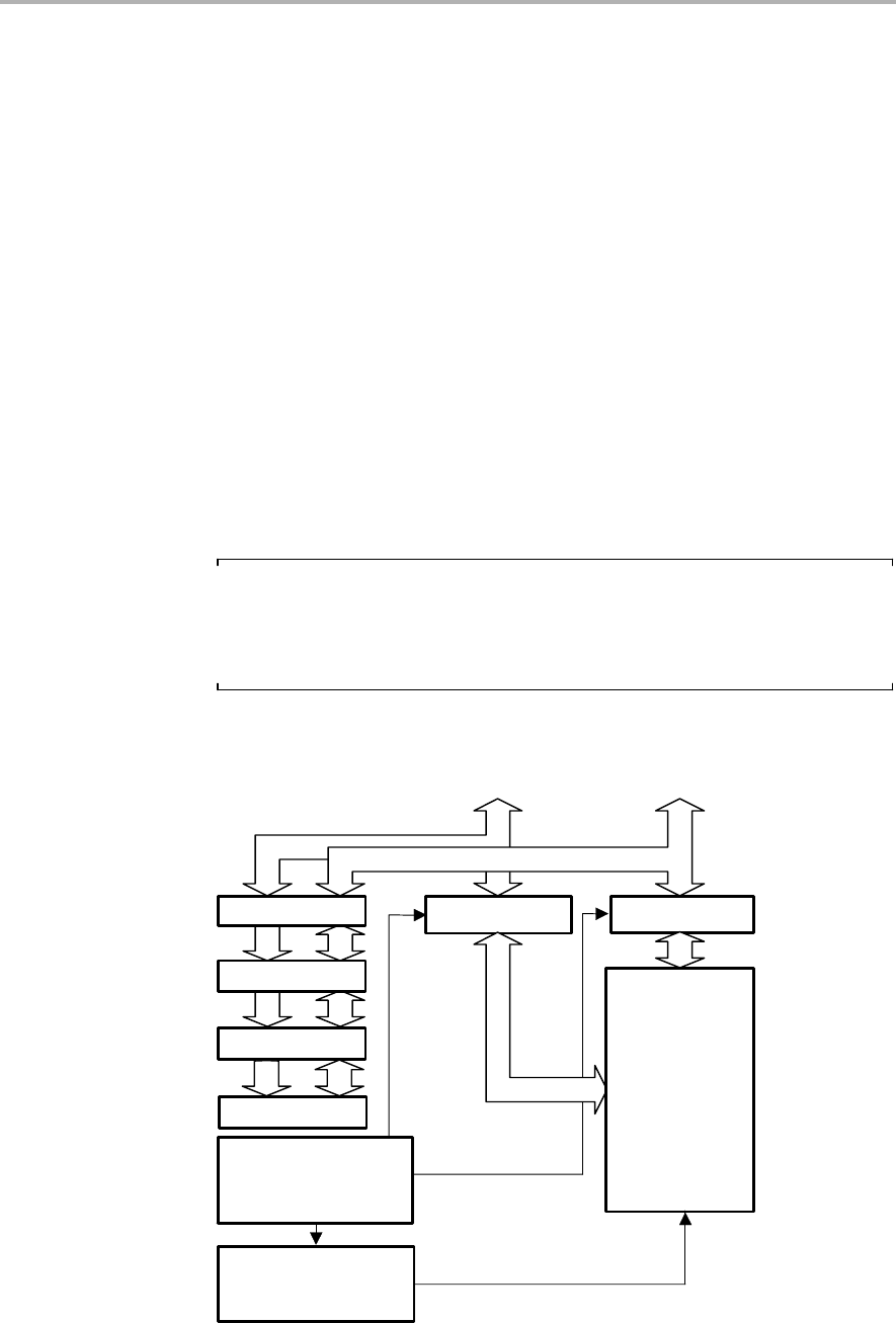
Flash Memory Introduction
7-2 Flash Memory Controller
7.1 Flash Memory Introduction
The MSP430 flash memory is bit−, byte-, and word-addressable and
programmable. The flash memory module has an integrated controller that
controls programming and erase operations. The controller has four registers,
a timing generator, and a voltage generator to supply program and erase
voltages.
MSP430 flash memory features include:
-Internal programming voltage generation
-Bit, byte or word programmable
-Ultralow-power operation
-Segment erase and mass erase
-Marginal 0 and marginal 1 read mode (optional, please refer to device
specific data sheet)
The block diagram of the flash memory and controller is shown in Figure 7−1.
Note: Minimum VCC During Flash Write or Erase
The minimum VCC voltage during a flash write or erase operation is 2.2 V.
If VCC falls below 2.2 V during a write or erase, the result of the write or erase
will be unpredictable.
Figure 7−1. Flash Memory Module Block Diagram
Enable
Data Latch
Enable
Address
Latch
Address Latch Data Latch
MAB MDB
FCTL1
FCTL2
FCTL3
Timing
Generator
Programming
Voltage
Generator
Flash
Memory
Array
FCTL4
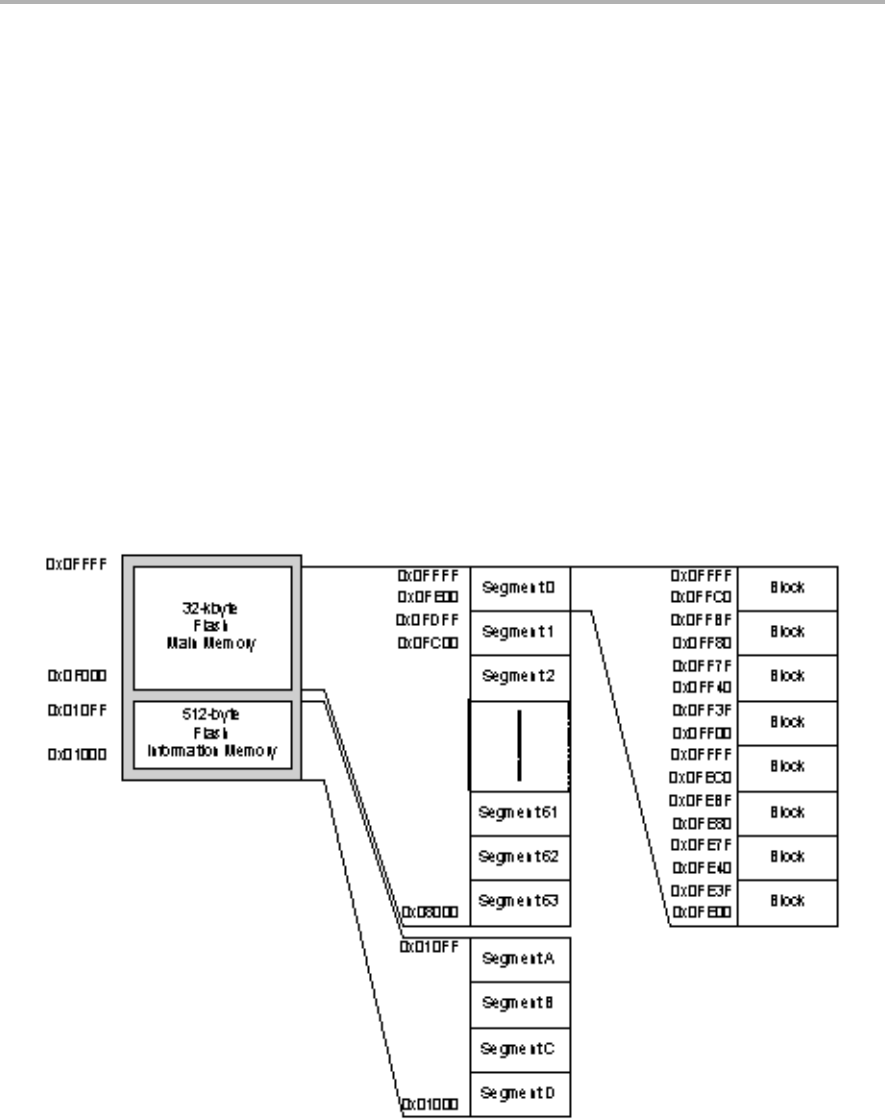
Flash Memory Segmentation
7-3
Flash Memory Controller
7.2 Flash Memory Segmentation
MSP430 flash memory is partitioned into segments. Single bits, bytes, or
words can be written to flash memory, but the segment is the smallest size of
flash memory that can be erased.
The flash memory is partitioned into main and information memory sections.
There is no difference in the operation of the main and information memory
sections. Code or data can be located in either section. The differences
between the two sections are the segment size and the physical addresses.
The information memory has four 64-byte segments. The main memory has
two or more 512-byte segments. See the device-specific data sheet for the
complete memory map of a device.
The segments are further divided into blocks.
Figure 7−2 shows the flash segmentation using an example of 32-KB flash
that has eight main segments and four information segments.
Figure 7−2. Flash Memory Segments, 32-KB Example

Flash Memory Segmentation
7-4 Flash Memory Controller
7.2.1 SegmentA
SegmentA of the information memory is locked separately from all other
segments with the LOCKA bit. When LOCKA = 1, SegmentA cannot be written
or erased and all information memory is protected from erasure during a mass
erase or production programming. When LOCKA = 0, SegmentA can be
erased and written as any other flash memory segment, and all information
memory is erased during a mass erase or production programming.
The state of the LOCKA bit is toggled when a 1 is written to it. Writing a 0 to
LOCKA has no effect. This allows existing flash programming routines to be
used unchanged.
; Unlock SegmentA
BIT #LOCKA,&FCTL3 ; Test LOCKA
JZ SEGA_UNLOCKED ; Already unlocked?
MOV #FWKEY+LOCKA,&FCTL3 ; No, unlock SegmentA
SEGA_UNLOCKED ; Yes, continue
; SegmentA is unlocked
; Lock SegmentA
BIT #LOCKA,&FCTL3 ; Test LOCKA
JNZ SEGALOCKED ; Already locked?
MOV #FWKEY+LOCKA,&FCTL3 ; No, lock SegmentA
SEGA_LOCKED ; Yes, continue
; SegmentA is locked
Flash Memory Operation
7-5
Flash Memory Controller
7.3 Flash Memory Operation
The default mode of the flash memory is read mode. In read mode, the flash
memory is not being erased or written, the flash timing generator and voltage
generator are off, and the memory operates identically to ROM.
MSP430 flash memory is in-system programmable (ISP) without the need for
additional external voltage. The CPU can program its own flash memory. The
flash memory write/erase modes are selected with the BLKWRT, WRT,
MERAS, and ERASE bits and are:
-Byte/word write
-Block write
-Segment Erase
-Mass Erase (all main memory segments)
-All Erase (all segments)
Reading or writing to flash memory while it is being programmed or erased is
prohibited. If CPU execution is required during the write or erase, the code to
be executed must be in RAM. Any flash update can be initiated from within
flash memory or RAM.
7.3.1 Flash Memory Timing Generator
Write and erase operations are controlled by the flash timing generator shown
in Figure 7−3. The flash timing generator operating frequency, fFTG, must be
in the range from ~ 257 kHz to ~ 476 kHz (see device-specific data sheet).
Figure 7−3. Flash Memory Timing Generator Block Diagram
FN5 FN0 PUC
........... EMEX
Flash Timing Generator
Divider, 1−64
BUSY WAIT
Reset
fFTG
FSSELx
SMCLK
SMCLK
ACLK
MCLK
00
01
10
11

Flash Memory Operation
7-6 Flash Memory Controller
Flash Timing Generator Clock Selection
The flash timing generator can be sourced from ACLK, SMCLK, or MCLK. The
selected clock source should be divided using the FNx bits to meet the
frequency requirements for fFTG. If the fFTG frequency deviates from the
specification during the write or erase operation, the result of the write or erase
may be unpredictable, or the flash memory may be stressed above the limits
of reliable operation.
If a clock failure is detected during a write or erase operation, the operation is
aborted, the FAIL flag is set, and the result of the operation is unpredictable.
While a write or erase operation is active the selected clock source can not be
disabled by putting the MSP430 into a low-power mode. The selected clock
source will remain active until the operation is completed before being
disabled.
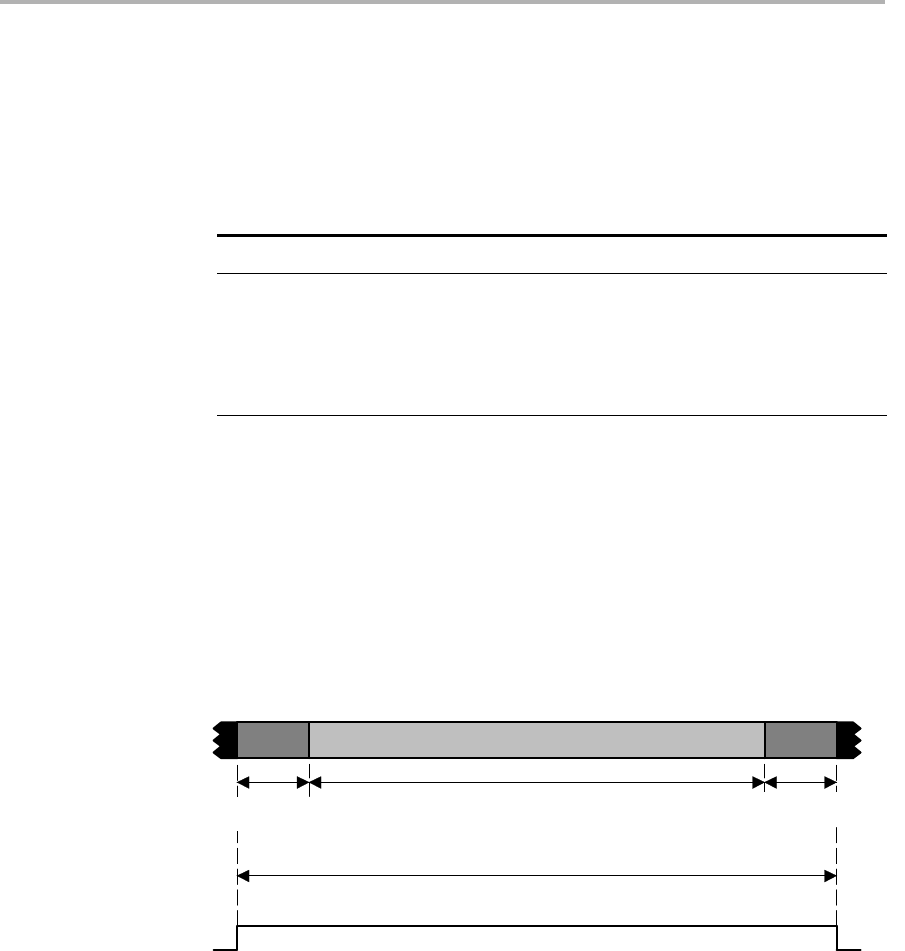
Flash Memory Operation
7-7
Flash Memory Controller
7.3.2 Erasing Flash Memory
The erased level of a flash memory bit is 1. Each bit can be programmed from
1 to 0 individually but to reprogram from 0 to 1 requires an erase cycle. The
smallest amount of flash that can be erased is a segment. There are three
erase modes selected with the ERASE and MERAS bits listed in Table 7−1.
Table 7−1. Erase Modes
MERAS ERASE Erase Mode
0 1 Segment erase
1 0 Mass erase (all main memory segments)
1 1 LOCKA = 0: Erase main and information flash memory.
LOCKA = 1: Erase only main flash memory.
Any erase is initiated by a dummy write into the address range to be erased.
The dummy write starts the flash timing generator and the erase operation.
Figure 7−4 shows the erase cycle timing. The BUSY bit is set immediately after
the dummy write and remains set throughout the erase cycle. BUSY, MERAS,
and ERASE are automatically cleared when the cycle completes. The erase
cycle timing is not dependent on the amount of flash memory present on a
device. Erase cycle times are equivalent for all MSP430F2xx devices.
Figure 7−4. Erase Cycle Timing
BUSY
Erase Operation Active
tmass erase = 10593/fFTG, tsegment erase = 4819/fFTG
Erase Time, VCC Current Consumption is Increased
Generate
Programming Voltage
Remove
Programming Voltage
A dummy write to an address not in the range to be erased does not start the
erase cycle, does not affect the flash memory, and is not flagged in any way.
This errant dummy write is ignored.
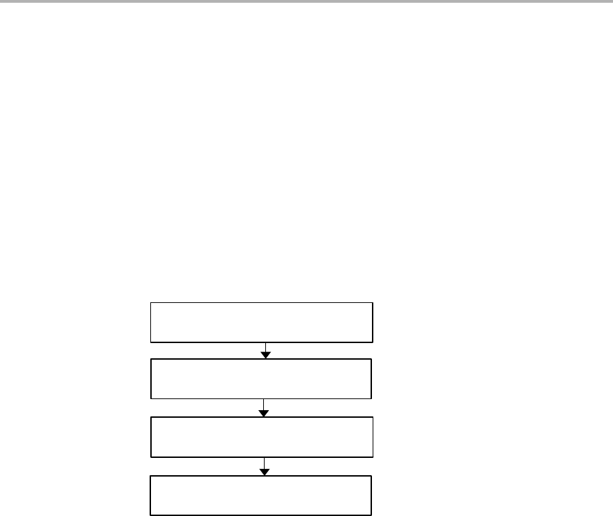
Flash Memory Operation
7-8 Flash Memory Controller
Initiating an Erase from Within Flash Memory
Any erase cycle can be initiated from within flash memory or from RAM. When
a flash segment erase operation is initiated from within flash memory, all timing
is controlled by the flash controller, and the CPU is held while the erase cycle
completes. After the erase cycle completes, the CPU resumes code execution
with the instruction following the dummy write.
When initiating an erase cycle from within flash memory, it is possible to erase
the code needed for execution after the erase. If this occurs, CPU execution
will be unpredictable after the erase cycle.
The flow to initiate an erase from flash is shown in Figure 7−5.
Figure 7−5. Erase Cycle from Within Flash Memory
Setup flash controller and erase
mode
Disable watchdog
Set LOCK=1, re-enable watchdog
Dummy write
; Segment Erase from flash. 514 kHz < SMCLK < 952 kHz
; Assumes ACCVIE = NMIIE = OFIE = 0.
MOV #WDTPW+WDTHOLD,&WDTCTL ; Disable WDT
MOV #FWKEY+FSSEL1+FN0,&FCTL2 ; SMCLK/2
MOV #FWKEY,&FCTL3 ; Clear LOCK
MOV #FWKEY+ERASE,&FCTL1 ; Enable segment erase
CLR &0FC10h ; Dummy write, erase S1
MOV #FWKEY+LOCK,&FCTL3 ; Done, set LOCK
... ; Re-enable WDT?
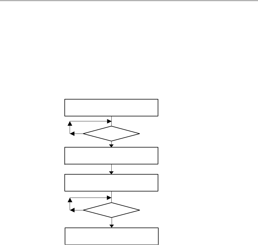
Flash Memory Operation
7-9
Flash Memory Controller
Initiating an Erase from RAM
Any erase cycle may be initiated from RAM. In this case, the CPU is not held
and can continue to execute code from RAM. The BUSY bit must be polled to
determine the end of the erase cycle before the CPU can access any flash
address again. If a flash access occurs while BUSY=1, it is an access violation,
ACCVIFG will be set, and the erase results will be unpredictable.
The flow to initiate an erase from flash from RAM is shown in Figure 7−6.
Figure 7−6. Erase Cycle from Within RAM
yes
BUSY = 1
yes
BUSY = 1
Disable watchdog
Setup flash controller and
erase mode
Dummy write
Set LOCK = 1, re-enable
watchdog
; Segment Erase from RAM. 514 kHz < SMCLK < 952 kHz
; Assumes ACCVIE = NMIIE = OFIE = 0.
MOV #WDTPW+WDTHOLD,&WDTCTL ; Disable WDT
L1 BIT #BUSY,&FCTL3 ; Test BUSY
JNZ L1 ; Loop while busy
MOV #FWKEY+FSSEL1+FN0,&FCTL2 ; SMCLK/2
MOV #FWKEY,&FCTL3 ; Clear LOCK
MOV #FWKEY+ERASE,&FCTL1 ; Enable erase
CLR &0FC10h ; Dummy write, erase S1
L2 BIT #BUSY,&FCTL3 ; Test BUSY
JNZ L2 ; Loop while busy
MOV #FWKEY+LOCK,&FCTL3 ; Done, set LOCK
... ; Re-enable WDT?

Flash Memory Operation
7-10 Flash Memory Controller
7.3.3 Writing Flash Memory
The write modes, selected by the WRT and BLKWRT bits, are listed in
Table 7−1.
Table 7−2. Write Modes
BLKWRT WRT Write Mode
0 1 Byte/word write
1 1 Block write
Both write modes use a sequence of individual write instructions, but using the
block write mode is approximately twice as fast as byte/word mode, because
the voltage generator remains on for the complete block write. Any instruction
that modifies a destination can be used to modify a flash location in either
byte/word mode or block write mode. A flash word (low + high byte) must not
be written more than twice between erasures. Otherwise, damage can occur.
The BUSY bit is set while a write operation is active and cleared when the
operation completes. If the write operation is initiated from RAM, the CPU must
not access flash while BUSY=1. Otherwise, an access violation occurs,
ACCVIFG is set, and the flash write is unpredictable.
Byte/Word Write
A byte/word write operation can be initiated from within flash memory or from
RAM. When initiating from within flash memory, all timing is controlled by the
flash controller, and the CPU is held while the write completes. After the write
completes, the CPU resumes code execution with the instruction following the
write. The byte/word write timing is shown in Figure 7−7.
Figure 7−7. Byte/Word Write Timing
BUSY
Programming Operation Active
Programming Time, VCC Current Consumption is Increased
tWord Write = 30/fFTG
Generate
Programming Voltage
Remove
Programming Voltage
When a byte/word write is executed from RAM, the CPU continues to execute
code from RAM. The BUSY bit must be zero before the CPU accesses flash
again, otherwise an access violation occurs, ACCVIFG is set, and the write
result is unpredictable.
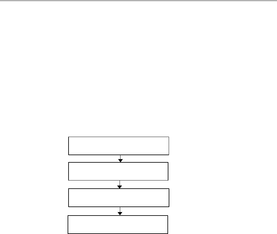
Flash Memory Operation
7-11
Flash Memory Controller
In byte/word mode, the internally-generated programming voltage is applied
to the complete 64-byte block, each time a byte or word is written, for 27 of the
30 fFTG cycles. With each byte or word write, the amount of time the block is
subjected to the programming voltage accumulates. The cumulative
programming time, tCPT, must not be exceeded for any block. If the cumulative
programming time is met, the block must be erased before performing any
further writes to any address within the block. See the device-specific data
sheet for specifications.
Initiating a Byte/Word Write from Within Flash Memory
The flow to initiate a byte/word write from flash is shown in Figure 7−8.
Figure 7−8. Initiating a Byte/Word Write from Flash
Setup flash controller
and set WRT=1
Disable watchdog
Set WRT=0, LOCK=1,
re-enable watchdog
Write byte or word
; Byte/word write from flash. 514 kHz < SMCLK < 952 kHz
; Assumes 0FF1Eh is already erased
; Assumes ACCVIE = NMIIE = OFIE = 0.
MOV #WDTPW+WDTHOLD,&WDTCTL ; Disable WDT
MOV #FWKEY+FSSEL1+FN0,&FCTL2 ; SMCLK/2
MOV #FWKEY,&FCTL3 ; Clear LOCK
MOV #FWKEY+WRT,&FCTL1 ; Enable write
MOV #0123h,&0FF1Eh ; 0123h −> 0FF1Eh
MOV #FWKEY,&FCTL1 ; Done. Clear WRT
MOV #FWKEY+LOCK,&FCTL3 ; Set LOCK
... ; Re-enable WDT?
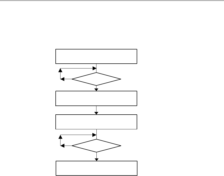
Flash Memory Operation
7-12 Flash Memory Controller
Initiating a Byte/Word Write from RAM
The flow to initiate a byte/word write from RAM is shown in Figure 7−9.
Figure 7−9. Initiating a Byte/Word Write from RAM
yes
BUSY = 1
yes
BUSY = 1
Disable watchdog
Setup flash controller
and set WRT=1
Write byte or word
Set WRT=0, LOCK = 1
re-enable watchdog
; Byte/word write from RAM. 514 kHz < SMCLK < 952 kHz
; Assumes 0FF1Eh is already erased
; Assumes ACCVIE = NMIIE = OFIE = 0.
MOV #WDTPW+WDTHOLD,&WDTCTL ; Disable WDT
L1 BIT #BUSY,&FCTL3 ; Test BUSY
JNZ L1 ; Loop while busy
MOV #FWKEY+FSSEL1+FN0,&FCTL2 ; SMCLK/2
MOV #FWKEY,&FCTL3 ; Clear LOCK
MOV #FWKEY+WRT,&FCTL1 ; Enable write
MOV #0123h,&0FF1Eh ; 0123h −> 0FF1Eh
L2 BIT #BUSY,&FCTL3 ; Test BUSY
JNZ L2 ; Loop while busy
MOV #FWKEY,&FCTL1 ; Clear WRT
MOV #FWKEY+LOCK,&FCTL3 ; Set LOCK
... ; Re-enable WDT?
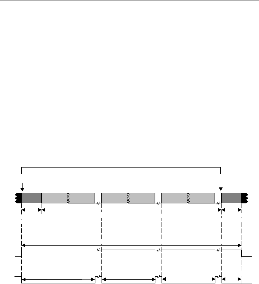
Flash Memory Operation
7-13
Flash Memory Controller
Block Write
The block write can be used to accelerate the flash write process when many
sequential bytes or words need to be programmed. The flash programming
voltage remains on for the duration of writing the 64-byte block. The
cumulative programming time tCPT must not be exceeded for any block during
a block write.
A block write cannot be initiated from within flash memory. The block write
must be initiated from RAM only. The BUSY bit remains set throughout the
duration of the block write. The WAIT bit must be checked between writing
each byte or word in the block. When WAIT is set the next byte or word of the
block can be written. When writing successive blocks, the BLKWRT bit must
be cleared after the current block is complete. BLKWRT can be set initiating
the next block write after the required flash recovery time given by tend. BUSY
is cleared following each block write completion indicating the next block can
be written. Figure 7−10 shows the block write timing.
Figure 7−10. Block-Write Cycle Timing
BUSY
WAIT
Generate Programming Operation Active
tBlock, 0 = 25/fFTG tBlock, 1-63 = 18/fFTG
Write to flash e.g., MOV #123h, &Flash
BLKWRT bit
tBlock, 1-63 = 18/fFTG tend = 6/fFTG
Cumulative Programming Time tCPT ∼=< 4ms, VCC Current Consumption is Increased
Programming Voltage
Remove
Programming Voltage

Flash Memory Operation
7-14 Flash Memory Controller
Block Write Flow and Example
A block write flow is shown in Figure 7−8 and the following example.
Figure 7−11. Block Write Flow
yes
BUSY = 1
Disable watchdog
Setup flash controller
Set BLKWRT=WRT=1
Write byte or word
no Block Border?
yes WAIT=0?
yes
BUSY = 1
Set BLKWRT=0
yes Another
Block?
Set WRT=0, LOCK=1
re-enable WDT

Flash Memory Operation
7-15
Flash Memory Controller
; Write one block starting at 0F000h.
; Must be executed from RAM, Assumes Flash is already erased.
; 514 kHz < SMCLK < 952 kHz
; Assumes ACCVIE = NMIIE = OFIE = 0.
MOV #32,R5 ; Use as write counter
MOV #0F000h,R6 ; Write pointer
MOV #WDTPW+WDTHOLD,&WDTCTL ; Disable WDT
L1 BIT #BUSY,&FCTL3 ; Test BUSY
JNZ L1 ; Loop while busy
MOV #FWKEY+FSSEL1+FN0,&FCTL2 ; SMCLK/2
MOV #FWKEY,&FCTL3 ; Clear LOCK
MOV #FWKEY+BLKWRT+WRT,&FCTL1 ; Enable block write
L2 MOV Write_Value,0(R6) ; Write location
L3 BIT #WAIT,&FCTL3 ; Test WAIT
JZ L3 ; Loop while WAIT=0
INCD R6 ; Point to next word
DEC R5 ; Decrement write counter
JNZ L2 ; End of block?
MOV #FWKEY,&FCTL1 ; Clear WRT,BLKWRT
L4 BIT #BUSY,&FCTL3 ; Test BUSY
JNZ L4 ; Loop while busy
MOV #FWKEY+LOCK,&FCTL3 ; Set LOCK
... ; Re-enable WDT if needed

Flash Memory Operation
7-16 Flash Memory Controller
7.3.4 Flash Memory Access During Write or Erase
When any write or any erase operation is initiated from RAM and while
BUSY=1, the CPU may not read or write to or from any flash location.
Otherwise, an access violation occurs, ACCVIFG is set, and the result is
unpredictable. Also if a write to flash is attempted with WRT=0, the ACCVIFG
interrupt flag is set, and the flash memory is unaffected.
When a byte/word write or any erase operation is initiated from within flash
memory, the flash controller returns op-code 03FFFh to the CPU at the next
instruction fetch. Op-code 03FFFh is the JMP PC instruction. This causes the
CPU to loop until the flash operation is finished. When the operation is finished
and BUSY=0, the flash controller allows the CPU to fetch the proper op-code
and program execution resumes.
The flash access conditions while BUSY=1 are listed in Table 7−3.
Table 7−3. Flash Access While BUSY = 1
Flash
Operation
Flash
Access
WAIT Result
Read 0 ACCVIFG = 0. 03FFFh is the value read
Any erase, or
B/ di
Write 0 ACCVIFG = 1. Write is ignored
y
Byte/word write Instruction
fetch
0 ACCVIFG = 0. CPU fetches 03FFFh. This
is the JMP PC instruction.
Any 0 ACCVIFG = 1, LOCK = 1
Read 1 ACCVIFG = 0, 03FFFh is the value read
Block write Write 1 ACCVIFG = 0, Write is written
Instruction
fetch
1ACCVIFG = 1, LOCK = 1
Interrupts are automatically disabled during any flash operation when EEI =
0 and EEIEX = 0 and on MSP430x20xx devices where EEI and EEIEX are not
present. After the flash operation has completed, interrupts are automatically
re-enabled. Any interrupt that occurred during the operation will have its
associated flag set, and will generate an interrupt request when re-enabled.
When EEIEX = 1 and GIE = 1, an interrupt will immediately abort any flash
operation and the FAIL flag will be set. When EEI = 1, GIE = 1, and EEIEX =
0, a segment erase will be interrupted by a pending interrupt every 32 fFTG
cycles. After servicing the interrupt, the segment erase is continued for at least
32 fFTG cycles or until it is complete. During the servicing of the interrupt, the
BUSY bit remains set but the flash memory can be accessed by the CPU
without causing an access violation occurs. Nested interrupts and using the
RETI instruction inside interrupt service routines are not supported.
The watchdog timer (in watchdog mode) should be disabled before a flash
erase cycle. A reset will abort the erase and the result will be unpredictable.
After the erase cycle has completed, the watchdog may be re-enabled.

Flash Memory Operation
7-17
Flash Memory Controller
7.3.5 Stopping a Write or Erase Cycle
Any write or erase operation can be stopped before its normal completion by
setting the emergency exit bit EMEX. Setting the EMEX bit stops the active
operation immediately and stops the flash controller. All flash operations
cease, the flash returns to read mode, and all bits in the FCTL1 register are
reset. The result of the intended operation is unpredictable.
7.3.6 Marginal Read Mode
The marginal read mode can be used to verify the integrity of the flash memory
contents. This feature is implemented in selected 2xx devices; see the
device-specific data sheet for availability. During marginal read mode
marginally programmed flash memory bit locations can be detected. Events
that could produce this situation include improper fFTG settings, or violation of
minimum VCC during erase/program operations. One method for identifying
such memory locations would be to periodically perform a checksum
calculation over a section of flash memory (for example, a flash segment) and
repeating this procedure with the marginal read mode enabled. If they do not
match, it could indicate an insufficiently programmed flash memory location.
It is possible to refresh the affected Flash memory segment by disabling
marginal read mode, copying to RAM, erasing the flash segment, and writing
back to it from RAM.
The program checking the flash memory contents must be executed from
RAM. Executing code from flash will automatically disable the marginal read
mode. The marginal read modes are controlled by the MRG0 and MRG1
register bits. Setting MRG1 is used to detect insufficiently programmed flash
cells containing a “1” (erased bits). Setting MRG0 is used to detect
insufficiently programmed flash cells containing a “0” (programmed bits). Only
one of these bits should be set at a time. Therefore, a full marginal read check
will require two passes of checking the flash memory content’s integrity. During
marginal read mode, the flash access speed (MCLK) must be limited to 1 MHz
(see the device-specific data sheet).
7.3.7 Configuring and Accessing the Flash Memory Controller
The FCTLx registers are 16-bit, password-protected, read/write registers. Any
read or write access must use word instructions and write accesses must
include the write password 0A5h in the upper byte. Any write to any FCTLx
register with any value other than 0A5h in the upper byte is a security key
violation, sets the KEYV flag and triggers a PUC system reset. Any read of any
FCTLx registers reads 096h in the upper byte.
Any write to FCTL1 during an erase or byte/word write operation is an access
violation and sets ACCVIFG. Writing to FCTL1 is allowed in block write mode
when WAIT=1, but writing to FCTL1 in block write mode when WAIT = 0 is an
access violation and sets ACCVIFG.
Any write to FCTL2 when the BUSY = 1 is an access violation.

Flash Memory Operation
7-18 Flash Memory Controller
Any FCTLx register may be read when BUSY = 1. A read will not cause an
access violation.
7.3.8 Flash Memory Controller Interrupts
The flash controller has two interrupt sources, KEYV, and ACCVIFG.
ACCVIFG is set when an access violation occurs. When the ACCVIE bit is
re-enabled after a flash write or erase, a set ACCVIFG flag will generate an
interrupt request. ACCVIFG sources the NMI interrupt vector, so it is not
necessary for GIE to be set for ACCVIFG to request an interrupt. ACCVIFG
may also be checked by software to determine if an access violation occurred.
ACCVIFG must be reset by software.
The key violation flag KEYV is set when any of the flash control registers are
written with an incorrect password. When this occurs, a PUC is generated
immediately resetting the device.
7.3.9 Programming Flash Memory Devices
There are three options for programming an MSP430 flash device. All options
support in-system programming:
-Program via JTAG
-Program via the Bootstrap Loader
-Program via a custom solution
Programming Flash Memory via JTAG
MSP430 devices can be programmed via the JTAG port. The JTAG interface
requires four signals (5 signals on 20- and 28-pin devices), ground and
optionally VCC and RST/NMI.
The JTAG port is protected with a fuse. Blowing the fuse completely disables
the JTAG port and is not reversible. Further access to the device via JTAG is
not possible For more details see the Application report Programming a
Flash-Based MSP430 Using the JTAG Interface at www.msp430.com.
Programming Flash Memory via the Bootstrap loader (BSL)
Most MSP430 flash devices contain a bootstrap loader. Refer to the device
specific data sheet for implementation details. The BSL enables users to read
or program the flash memory or RAM using a UART serial interface. Access
to the MSP430 flash memory via the BSL is protected by a 256-bit,
user-defined password. For more details see the Application report Features
of the MSP430 Bootstrap Loader at www.ti.com/msp430.
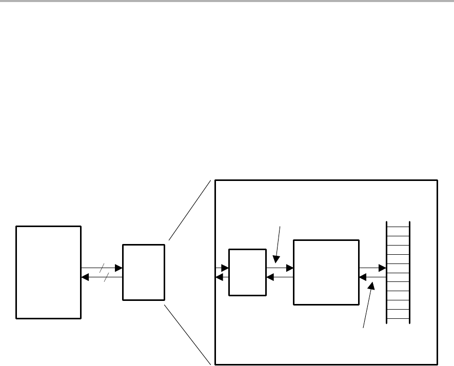
Flash Memory Operation
7-19
Flash Memory Controller
Programming Flash Memory via a Custom Solution
The ability of the MSP430 CPU to write to its own flash memory allows for
in-system and external custom programming solutions as shown in
Figure 7−12. The user can choose to provide data to the MSP430 through any
means available (UART, SPI, etc.). User-developed software can receive the
data and program the flash memory. Since this type of solution is developed
by the user, it can be completely customized to fit the application needs for
programming, erasing, or updating the flash memory.
Figure 7−12. User-Developed Programming Solution
Host
Flash Memory
UART,
Px.x,
SPI,
etc.
CPU executes
user software
Commands, data, etc.
Read/write flash memory
MSP430

Flash Memory Registers
7-20 Flash Memory Controller
7.4 Flash Memory Registers
The flash memory registers are listed in Table 7−4.
Table 7−4. Flash Memory Registers
Register Short Form Register Type Address Initial State
Flash memory control register 1 FCTL1 Read/write 0x0128 0x9600 with PUC
Flash memory control register 2 FCTL2 Read/write 0x012A 0x9642 with PUC
Flash memory control register 3 FCTL3 Read/write 0x012C 0x9658 with PUC†
Flash memory control register 4‡FCTL4 Read/write 0x01BE 0x0000 with PUC
Interrupt Enable 1 IE1 Read/write 0x0000 Reset with PUC
Interrupt Flag 1 IFG1 Read/write 0x0002
†KEYV is reset with POR
‡Not present in all MSP430x2xx devices. See device specific data sheet.

Flash Memory Registers
7-21
Flash Memory Controller
FCTL1, Flash Memory Control Register
15 14 13 12 11 10 9 8
FRKEY, Read as 096h
FWKEY, Must be written as 0A5h
76543210
BLKWRT WRT Reserved EEIEX†EEI†MERAS ERASE Reserved
rw−0 rw−0 r0 rw−0 rw−0 rw−0 rw−0 r0
†Not present on MSP430x20xx Devices
FRKEY/
FWKEY
Bits
15-8
FCTLx password. Always read as 096h. Must be written as 0A5h or a PUC
will be generated.
BLKWRT Bit 7 Block write mode. WRT must also be set for block write mode. BLKWRT is
automatically reset when EMEX is set.
0 Block-write mode is off
1 Block-write mode is on
WRT Bit 6 Write. This bit is used to select any write mode. WRT is automatically reset
when EMEX is set.
0 Write mode is off
1 Write mode is on
Reserved Bit 5 Reserved. Always read as 0.
EEIEX Bit 4 Enable Emergency Interrupt Exit. Setting this bit enables an interrupt to cause
an emergency exit from a flash operation when GIE = 1. EEIEX is
automatically reset when EMEX is set.
0 Exit interrupt disabled.
1 Exit on interrupt enabled.
EEI Bits 3 Enable Erase Interrupts. Setting this bit allows a segment erase to be
interrupted by an interrupt request. After the interrupt is serviced the erase
cycle is resumed.
0 Interrupts during segment erase disabled.
1 Interrupts during segment erase enabled.
MERAS
ERASE
Bit 2
Bit 1
Mass erase and erase. These bits are used together to select the erase mode.
MERAS and ERASE are automatically reset when EMEX is set.
MERAS ERASE Erase Cycle
0 0 No erase
0 1 Erase individual segment only
1 0 Erase all main memory segments
1 1 LOCKA = 0: Erase main and information flash memory.
LOCKA = 1: Erase only main flash memory.
Reserved Bit 0 Reserved. Always read as 0.

Flash Memory Registers
7-22 Flash Memory Controller
FCTL2, Flash Memory Control Register
15 14 13 12 11 10 9 8
FWKEYx, Read as 096h
Must be written as 0A5h
76543210
FSSELx FNx
rw−0 rw−1 rw-0 rw-0 rw-0 rw−0 rw-1 rw−0
FWKEYx Bits
15-8
FCTLx password. Always read as 096h. Must be written as 0A5h or a PUC
will be generated.
FSSELx Bits
7−6
Flash controller clock source select
00 ACLK
01 MCLK
10 SMCLK
11 SMCLK
FNx Bits
5-0
Flash controller clock divider. These six bits select the divider for the flash
controller clock. The divisor value is FNx + 1. For example, when FNx = 00h,
the divisor is 1. When FNx = 03Fh, the divisor is 64.

Flash Memory Registers
7-23
Flash Memory Controller
FCTL3, Flash Memory Control Register FCTL3
15 14 13 12 11 10 9 8
FWKEYx, Read as 096h
Must be written as 0A5h
76543210
FAIL LOCKA EMEX LOCK WAIT ACCVIFG KEYV BUSY
r(w)−0 r(w)−1 rw-0 rw-1 r-1 rw−0 rw-(0) r(w)−0
FWKEYx Bits
15-8
FCTLx password. Always read as 096h. Must be written as 0A5h or a PUC
will be generated.
FAIL Bit 7 Operation failure. This bit is set if the fFTG clock source fails, or a flash
operation is aborted from an interrupt when EEIEX = 1. FAIL must be reset
with software.
0 No failure
1 Failure
LOCKA Bit 6 SegmentA and Info lock. Write a 1 to this bit to change its state. Writing 0 has
no effect.
0 Segment A unlocked and all information memory is erased during a
mass erase.
1 Segment A locked and all information memory is protected from erasure
during a mass erase.
EMEX Bit 5 Emergency exit
0 No emergency exit
1 Emergency exit
LOCK Bit 4 Lock. This bit unlocks the flash memory for writing or erasing. The LOCK bit
can be set anytime during a byte/word write or erase operation and the
operation will complete normally. In the block write mode if the LOCK bit is set
while BLKWRT=WAIT=1, then BLKWRT and WAIT are reset and the mode
ends normally.
0 Unlocked
1 Locked
WAIT Bit 3 Wait. Indicates the flash memory is being written to.
0 The flash memory is not ready for the next byte/word write
1 The flash memory is ready for the next byte/word write
ACCVIFG Bit 2 Access violation interrupt flag
0 No interrupt pending
1 Interrupt pending

Flash Memory Registers
7-24 Flash Memory Controller
KEYV Bit 1 Flash security key violation. This bit indicates an incorrect FCTLx password
was written to any flash control register and generates a PUC when set. KEYV
must be reset with software.
0 FCTLx password was written correctly
1 FCTLx password was written incorrectly
BUSY Bit 0 Busy. This bit indicates the status of the flash timing generator.
0 Not Busy
1 Busy

Flash Memory Registers
7-25
Flash Memory Controller
FCTL4, Flash Memory Control Register FCTL4 (optional, refer to device-specific
data sheet)
15 14 13 12 11 10 9 8
FWKEYx, Read as 096h
Must be written as 0A5h
76543210
MRG1 MRG0
r-0 r-0 rw-0 rw-0 r-0 r-0 r-0 r-0
FWKEYx Bits
15-8
FCTLx password. Always read as 096h. Must be written as 0A5h or a PUC
will be generated.
Reserved Bits
7−6
Reserved. Always read as 0.
MRG1 Bit 5 Marginal read 1 mode. This bit enables the marginal 1 read mode. The
marginal read 1 bit is cleared if the CPU starts execution from the flash
memory. If both MRG1 and MRG0 are set MRG1 is active and MRG0 is
ignored.
0 Marginal 1 read mode is disabled.
1 Marginal 1 read mode is enabled.
MRG0 Bit 4 Marginal read 0 mode. This bit enables the marginal 0 read mode. The
marginal mode 0 is cleared if the CPU starts execution from the flash memory.
If both MRG1 and MRG0 are set MRG1 is active and MRG0 is ignored.
0 Marginal 0 read mode is disabled.
1 Marginal 0 read mode is enabled.
Reserved Bits
3−0
Reserved. Always read as 0.

Flash Memory Registers
7-26 Flash Memory Controller
IE1, Interrupt Enable Register 1
76543210
ACCVIE
rw−0
Bits
7−6,
4-0
These bits may be used by other modules. See the device-specific data sheet.
ACCVIE Bit 5 Flash memory access violation interrupt enable. This bit enables the
ACCVIFG interrupt. Because other bits in IE1 may be used for other modules,
it is recommended to set or clear this bit using BIS.B or BIC.B instructions,
rather than MOV.B or CLR.B instructions.
0 Interrupt not enabled
1 Interrupt enabled

8-1
Digital I/O
Digital I/O
This chapter describes the operation of the digital I/O ports.
Topic Page
8.1 Digital I/O Introduction 8-2. . . . . . . . . . . . . . . . . . . . . . . . . . . . . . . . . . . . . . . . .
8.2 Digital I/O Operation 8-3. . . . . . . . . . . . . . . . . . . . . . . . . . . . . . . . . . . . . . . . . . .
8.3 Digital I/O Registers 8-7. . . . . . . . . . . . . . . . . . . . . . . . . . . . . . . . . . . . . . . . . . .
Chapter 8

Digital I/O Introduction
8-2 Digital I/O
8.1 Digital I/O Introduction
MSP430 devices have up to eight digital I/O ports implemented, P1 to P7.
Each port has eight I/O pins. Every I/O pin is individually configurable for input
or output direction, and each I/O line can be individually read or written to.
Ports P1 and P2 have interrupt capability. Each interrupt for the P1 and P2 I/O
lines can be individually enabled and configured to provide an interrupt on a
rising edge or falling edge of an input signal. All P1 I/O lines source a single
interrupt vector, and all P2 I/O lines source a different, single interrupt vector.
The digital I/O features include:
-Independently programmable individual I/Os
-Any combination of input or output
-Individually configurable P1 and P2 interrupts
-Independent input and output data registers
-Individually configurable pullup or pulldown resistors

Digital I/O Operation
8-3
Digital I/O
8.2 Digital I/O Operation
The digital I/O is configured with user software. The setup and operation of the
digital I/O is discussed in the following sections.
8.2.1 Input Register PxIN
Each bit in each PxIN register reflects the value of the input signal at the
corresponding I/O pin when the pin is configured as I/O function.
Bit = 0: The input is low
Bit = 1: The input is high
Note: Writing to Read-Only Registers PxIN
Writing to these read-only registers results in increased current consumption
while the write attempt is active.
8.2.2 Output Registers PxOUT
Each bit in each PxOUT register is the value to be output on the corresponding
I/O pin when the pin is configured as I/O function, output direction, and the
pull-up/down resistor is disabled.
Bit = 0: The output is low
Bit = 1: The output is high
If the pin’s pull−up/down resistor is enabled, the corresponding bit in the
PxOUT register selects pull-up or pull-down.
Bit = 0: The pin is pulled down
Bit = 1: The pin is pulled up
8.2.3 Direction Registers PxDIR
Each bit in each PxDIR register selects the direction of the corresponding I/O
pin, regardless of the selected function for the pin. PxDIR bits for I/O pins that
are selected for other functions must be set as required by the other function.
Bit = 0: The port pin is switched to input direction
Bit = 1: The port pin is switched to output direction
8.2.4 Pull−Up/Down Resistor Enable Registers PxREN
Each bit in each PxREN register enables or disables the pullup/pulldown
resistor of the corresponding I/O pin. The corresponding bit in the PxOUT
register selects if the pin is pulled up or pulled down.
Bit = 0: Pullup/pulldown resistor disabled
Bit = 1: Pullup/pulldown resistor enabled

Digital I/O Operation
8-4 Digital I/O
8.2.5 Function Select Registers PxSEL and PxSEL2
Port pins are often multiplexed with other peripheral module functions. See the
device-specific data sheet to determine pin functions. Each PxSEL and
PxSEL2 bit is used to select the pin function − I/O port or peripheral module
function.
PxSEL2 PxSEL Pin Function
0 0 I/O function is selected.
01Primary peripheral module function is selected.
10Reserved. See device-specific data sheet.
1 1 Secondary peripheral module function is selected.
Setting PxSELx = 1 does not automatically set the pin direction. Other
peripheral module functions may require the PxDIRx bits to be configured
according to the direction needed for the module function. See the pin
schematics in the device-specific data sheet.
Note: Setting PxREN = 1 When PxSEL = 1
On some I/O ports on the MSP430F261x and MSP430F2416/7/8/9, enabling
the pullup/pulldown resistor (PxREN = 1) while the module function is
selected (PxSEL = 1) does not disable the logic output driver. This
combination is not recommended and may result in unwanted current flow
through the internal resistor. See the device-specific data sheet pin
schematics for more information.
;Output ACLK on P2.0 on MSP430F21x1
BIS.B #01h,&P2SEL ; Select ACLK function for pin
BIS.B #01h,&P2DIR ; Set direction to output *Required*
Note: P1 and P2 Interrupts Are Disabled When PxSEL = 1
When any P1SELx or P2SELx bit is set, the corresponding pin’s interrupt
function is disabled. Therefore, signals on these pins will not generate P1 or
P2 interrupts, regardless of the state of the corresponding P1IE or P2IE bit.
When a port pin is selected as an input to a peripheral, the input signal to the
peripheral is a latched representation of the signal at the device pin. While
PxSELx = 1, the internal input signal follows the signal at the pin. However, if
the PxSELx = 0, the input to the peripheral maintains the value of the input
signal at the device pin before the PxSELx bit was reset.

Digital I/O Operation
8-5
Digital I/O
8.2.6 P1 and P2 Interrupts
Each pin in ports P1 and P2 have interrupt capability, configured with the
PxIFG, PxIE, and PxIES registers. All P1 pins source a single interrupt vector,
and all P2 pins source a different single interrupt vector. The PxIFG register
can be tested to determine the source of a P1 or P2 interrupt.
Interrupt Flag Registers P1IFG, P2IFG
Each PxIFGx bit is the interrupt flag for its corresponding I/O pin and is set
when the selected input signal edge occurs at the pin. All PxIFGx interrupt
flags request an interrupt when their corresponding PxIE bit and the GIE bit
are set. Each PxIFG flag must be reset with software. Software can also set
each PxIFG flag, providing a way to generate a software initiated interrupt.
Bit = 0: No interrupt is pending
Bit = 1: An interrupt is pending
Only transitions, not static levels, cause interrupts. If any PxIFGx flag becomes
set during a Px interrupt service routine, or is set after the RETI instruction of
a Px interrupt service routine is executed, the set PxIFGx flag generates
another interrupt. This ensures that each transition is acknowledged.
Note: PxIFG Flags When Changing PxOUT or PxDIR
Writing to P1OUT, P1DIR, P2OUT, or P2DIR can result in setting the
corresponding P1IFG or P2IFG flags.

Digital I/O Operation
8-6 Digital I/O
Interrupt Edge Select Registers P1IES, P2IES
Each PxIES bit selects the interrupt edge for the corresponding I/O pin.
Bit = 0: The PxIFGx flag is set with a low-to-high transition
Bit = 1: The PxIFGx flag is set with a high-to-low transition
Note: Writing to PxIESx
Writing to P1IES, or P2IES can result in setting the corresponding interrupt
flags.
PxIESx PxINx PxIFGx
0 → 1 0 May be set
0 → 1 1 Unchanged
1 → 0 0 Unchanged
1 → 0 1 May be set
Interrupt Enable P1IE, P2IE
Each PxIE bit enables the associated PxIFG interrupt flag.
Bit = 0: The interrupt is disabled.
Bit = 1: The interrupt is enabled.
8.2.7 Configuring Unused Port Pins
Unused I/O pins should be configured as I/O function, output direction, and left
unconnected on the PC board, to prevent a floating input and reduce power
consumption. The value of the PxOUT bit is irrelevant, since the pin is
unconnected. Alternatively, the integrated pullup/pulldown resistor can be
enabled by setting the PxREN bit of the unused pin to prevent the floating
input. See chapter System Resets, Interrupts, and Operating Modes for
termination of unused pins.

Digital I/O Registers
8-7
Digital I/O
8.3 Digital I/O Registers
The digital I/O registers are listed in Table 8−1.
Table 8−1. Digital I/O Registers
Port Register Short Form Address Register Type Initial State
P1 Input P1IN 020h Read only −
Output P1OUT 021h Read/write Unchanged
Direction P1DIR 022h Read/write Reset with PUC
Interrupt Flag P1IFG 023h Read/write Reset with PUC
Interrupt Edge Select P1IES 024h Read/write Unchanged
Interrupt Enable P1IE 025h Read/write Reset with PUC
Port Select P1SEL 026h Read/write Reset with PUC
Port Select 2 P1SEL2 041h Read/write Reset with PUC
Resistor Enable P1REN 027h Read/write Reset with PUC
P2 Input P2IN 028h Read only −
Output P2OUT 029h Read/write Unchanged
Direction P2DIR 02Ah Read/write Reset with PUC
Interrupt Flag P2IFG 02Bh Read/write Reset with PUC
Interrupt Edge Select P2IES 02Ch Read/write Unchanged
Interrupt Enable P2IE 02Dh Read/write Reset with PUC
Port Select P2SEL 02Eh Read/write 0C0h with PUC
Port Select 2 P2SEL2 042h Read/write Reset with PUC
Resistor Enable P2REN 02Fh Read/write Reset with PUC
P3 Input P3IN 018h Read only −
Output P3OUT 019h Read/write Unchanged
Direction P3DIR 01Ah Read/write Reset with PUC
Port Select P3SEL 01Bh Read/write Reset with PUC
Port Select 2 P3SEL2 043h Read/write Reset with PUC
Resistor Enable P3REN 010h Read/write Reset with PUC
P4 Input P4IN 01Ch Read only −
Output P4OUT 01Dh Read/write Unchanged
Direction P4DIR 01Eh Read/write Reset with PUC
Port Select P4SEL 01Fh Read/write Reset with PUC
Port Select 2 P4SEL2 044h Read/write Reset with PUC
Resistor Enable P4REN 011h Read/write Reset with PUC
P5 Input P5IN 030h Read only −
Output P5OUT 031h Read/write Unchanged
Direction P5DIR 032h Read/write Reset with PUC
Port Select P5SEL 033h Read/write Reset with PUC
Port Select 2 P5SEL2 045h Read/write Reset with PUC
Resistor Enable P5REN 012h Read/write Reset with PUC

Digital I/O Registers
8-8 Digital I/O
P6 Input P6IN 034h Read only −
Output P6OUT 035h Read/write Unchanged
Direction P6DIR 036h Read/write Reset with PUC
Port Select P6SEL 037h Read/write Reset with PUC
Port Select 2 P6SEL2 046h Read/write Reset with PUC
Resistor Enable P6REN 013h Read/write Reset with PUC
P7 Input P7IN 038h Read only −
Output P7OUT 03Ah Read/write Unchanged
Direction P7DIR 03Ch Read/write Reset with PUC
Port Select P7SEL 03Eh Read/write Reset with PUC
Port Select 2 P7SEL2 047h Read/write Reset with PUC
Resistor Enable P7REN 014h Read/write Reset with PUC
P8 Input P8IN 039h Read only −
Output P8OUT 03Bh Read/write Unchanged
Direction P8DIR 03Dh Read/write Reset with PUC
Port Select P8SEL 03Fh Read/write Reset with PUC
Port Select 2 P8SEL2 048h Read/write Reset with PUC
Resistor Enable P8REN 015h Read/write Reset with PUC

9-1
Supply Voltage Supervisor
Supply Voltage Supervisor
This chapter describes the operation of the SVS. The SVS is implemented in
selected MSP430x2xx devices.
Topic Page
9.1 SVS Introduction 9-2. . . . . . . . . . . . . . . . . . . . . . . . . . . . . . . . . . . . . . . . . . . . . .
9.2 SVS Operation 9-4. . . . . . . . . . . . . . . . . . . . . . . . . . . . . . . . . . . . . . . . . . . . . . . . .
9.3 SVS Registers 9-7. . . . . . . . . . . . . . . . . . . . . . . . . . . . . . . . . . . . . . . . . . . . . . . . .
Chapter 9

SVS Introduction
9-2 Supply Voltage Supervisor
9.1 SVS Introduction
The supply voltage supervisor (SVS) is used to monitor the AVCC supply
voltage or an external voltage. The SVS can be configured to set a flag or
generate a POR reset when the supply voltage or external voltage drops below
a user-selected threshold.
The SVS features include:
-AVCC monitoring
-Selectable generation of POR
-Output of SVS comparator accessible by software
-Low-voltage condition latched and accessible by software
-14 selectable threshold levels
-External channel to monitor external voltage
The SVS block diagram is shown in Figure 9−1.
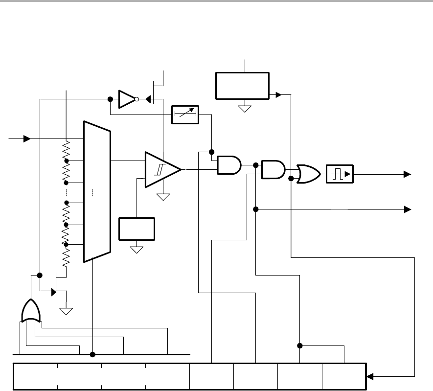
SVS Introduction
9-3
Supply Voltage Supervisor
Figure 9−1. SVS Block Diagram
+
−
1.2V
Brownout
Reset
VCC
Set SVSFG
tReset ~ 50us
Reset
SVSCTL Bits
0001
0010
1011
1111
1101
1100
G
D
S
SVSOUT
G
D
S
VLD SVSONPORON SVSOP SVSFG
~ 50us
SVS_POR
SVSIN
AVCC
AVCC

SVS Operation
9-4 Supply Voltage Supervisor
9.2 SVS Operation
The SVS detects if the AVCC voltage drops below a selectable level. It can be
configured to provide a POR or set a flag, when a low-voltage condition occurs.
The SVS is disabled after a brownout reset to conserve current consumption.
9.2.1 Configuring the SVS
The VLDx bits are used to enable/disable the SVS and select one of 14
threshold levels (V(SVS_IT−)) for comparison with AVCC. The SVS is off when
VLDx = 0 and on when VLDx > 0. The SVSON bit does not turn on the SVS.
Instead, it reflects the on/off state of the SVS and can be used to determine
when the SVS is on.
When VLDx = 1111, the external SVSIN channel is selected. The voltage on
SVSIN is compared to an internal level of approximately 1.25 V.
9.2.2 SVS Comparator Operation
A low-voltage condition exists when AVCC drops below the selected threshold
or when the external voltage drops below its 1.25-V threshold. Any low-voltage
condition sets the SVSFG bit.
The PORON bit enables or disables the device-reset function of the SVS. If
PORON = 1, a POR is generated when SVSFG is set. If PORON = 0, a
low-voltage condition sets SVSFG, but does not generate a POR.
The SVSFG bit is latched. This allows user software to determine if a
low-voltage condition occurred previously. The SVSFG bit must be reset by
user software. If the low-voltage condition is still present when SVSFG is reset,
it will be immediately set again by the SVS.

SVS Operation
9-5
Supply Voltage Supervisor
9.2.3 Changing the VLDx Bits
When the VLDx bits are changed from zero to any non-zero value there is a
automatic settling delay td(SVSon) implemented that allows the SVS circuitry to
settle. The td(SVSon) delay is approximately 50 μs. During this delay, the SVS
will not flag a low-voltage condition or reset the device, and the SVSON bit is
cleared. Software can test the SVSON bit to determine when the delay has
elapsed and the SVS is monitoring the voltage properly. Writing to SVSCTL
while SVSON = 0 will abort the SVS automatic settling delay, td(SVSon), and
switch the SVS to active mode immediately. In doing so, the SVS circuitry
might not be settled, resulting in unpredictable behavior.
When the VLDx bits are changed from any non-zero value to any other
non-zero value the circuitry requires the time tsettle to settle. The settling time
tsettle is a maximum of ~12 μs. See the device-specific data sheet. There is no
automatic delay implemented that prevents SVSFG to be set or to prevent a
reset of the device. The recommended flow to switch between levels is shown
in the following code.
; Enable SVS for the first time:
MOV.B #080h,&SVSCTL ; Level 2.8V, do not cause POR
; ...
; Change SVS level
MOV.B #000h,&SVSCTL ; Temporarily disable SVS
MOV.B #018h,&SVSCTL ; Level 1.9V, cause POR
; ...
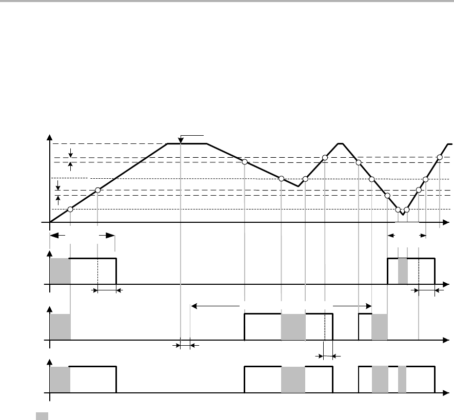
SVS Operation
9-6 Supply Voltage Supervisor
9.2.4 SVS Operating Range
Each SVS level has hysteresis to reduce sensitivity to small supply voltage
changes when AVCC is close to the threshold. The SVS operation and
SVS/Brownout interoperation are shown in Figure 9−2.
Figure 9−2. Operating Levels for SVS and Brownout/Reset Circuit
V
CC(start)
AV
CC
V
(B_IT−)
Brownout
Region
V
(SVSstart)
V
(SVS_IT−)
td(SVSR)
undefined
Vhys(SVS_IT−)
0
1
td(BOR)
Brownout
0
1
td(SVSon)
td(BOR)
0
1
Set SVS_POR
Brown-
Out
Region
SVS Circuit Active
SVSOUT
Vhys(B_IT−)
Software Sets VLD>0

SVS Registers
9-7
Supply Voltage Supervisor
9.3 SVS Registers
The SVS registers are listed in Table 9−1.
Table 9−1. SVS Registers
Register Short Form Register Type Address Initial State
SVS Control Register SVSCTL Read/write 056h Reset with BOR
SVSCTL, SVS Control Register
76543210
VLDx PORON SVSON SVSOP SVSFG
rw−0†rw−0†rw−0†rw−0†rw−0†r†r†rw−0†
†Reset by a brownout reset only, not by a POR or PUC.
VLDx Bits
7-4
Voltage level detect. These bits turn on the SVS and select the nominal SVS
threshold voltage level. See the device−specific data sheet for parameters.
0000 SVS is off
0001 1.9 V
0010 2.1 V
0011 2.2 V
0100 2.3 V
0101 2.4 V
0110 2.5 V
0111 2.65 V
1000 2.8 V
1001 2.9 V
1010 3.05
1011 3.2 V
1100 3.35 V
1101 3.5 V
1110 3.7 V
1111 Compares external input voltage SVSIN to 1.25 V.
PORON Bit 3 POR on. This bit enables the SVSFG flag to cause a POR device reset.
0 SVSFG does not cause a POR
1 SVSFG causes a POR
SVSON Bit 2 SVS on. This bit reflects the status of SVS operation. This bit DOES NOT turn
on the SVS. The SVS is turned on by setting VLDx > 0.
0 SVS is Off
1 SVS is On
SVSOP Bit 1 SVS output. This bit reflects the output value of the SVS comparator.
0 SVS comparator output is low
1 SVS comparator output is high
SVSFG Bit 0 SVS flag. This bit indicates a low voltage condition. SVSFG remains set after
a low voltage condition until reset by software.
0 No low voltage condition occurred
1 A low condition is present or has occurred

9-8 Supply Voltage Supervisor

10-1
Watchdog Timer+
Watchdog Timer+
The watchdog timer+ (WDT+) is a 16-bit timer that can be used as a watchdog
or as an interval timer. This chapter describes the WDT+ The WDT+ is
implemented in all MSP430x2xx devices.
Topic Page
10.1 Watchdog Timer+ Introduction 10-2. . . . . . . . . . . . . . . . . . . . . . . . . . . . . . . .
10.2 Watchdog Timer+ Operation 10-4. . . . . . . . . . . . . . . . . . . . . . . . . . . . . . . . . .
10.3 Watchdog Timer+ Registers 10-7. . . . . . . . . . . . . . . . . . . . . . . . . . . . . . . . . . .
Chapter 10

Watchdog Timer+ Introduction
10-2 Watchdog Timer+
10.1 Watchdog Timer+ Introduction
The primary function of the watchdog timer+ (WDT+) module is to perform a
controlled system restart after a software problem occurs. If the selected time
interval expires, a system reset is generated. If the watchdog function is not
needed in an application, the module can be configured as an interval timer
and can generate interrupts at selected time intervals.
Features of the watchdog timer+ module include:
-Four software-selectable time intervals
-Watchdog mode
-Interval mode
-Access to WDT+ control register is password protected
-Control of RST/NMI pin function
-Selectable clock source
-Can be stopped to conserve power
-Clock fail-safe feature
The WDT+ block diagram is shown in Figure 10−1.
Note: Watchdog Timer+ Powers Up Active
After a PUC, the WDT+ module is automatically configured in the watchdog
mode with an initial 32768 clock cycle reset interval using the DCOCLK. The
user must setup or halt the WDT+ prior to the expiration of the initial reset
interval.
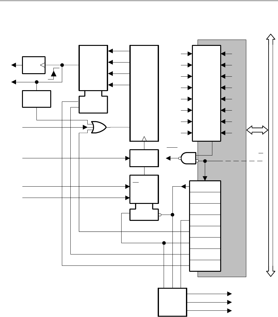
Watchdog Timer+ Introduction
10-3
Watchdog Timer+
Figure 10−1. Watchdog Timer+ Block Diagram
WDTQn
Y
0
1
2
3Q6
Q9
Q13
Q15
16−bit
Counter
CLK
A
B
1
1
AEN
PUC
SMCLK
ACLK
Clear
Password
Compare
0
0
0
0
1
1
1
1
WDTCNTCL
WDTTMSEL
WDTNMI
WDTNMIES
WDTIS1
WDTSSEL
WDTIS0
WDTHOLD
EQU
EQU Write Enable
Low Byte R / W
MDB
LSB
MSB
WDTCTL
(Asyn)
Int.
Flag
Pulse
Generator
SMCLK Active
MCLK Active
ACLK Active
16−bit
Fail-Safe
Logic
Clock
Request
Logic
MCLK

Watchdog Timer+ Operation
10-4 Watchdog Timer+
10.2 Watchdog Timer+ Operation
The WDT+ module can be configured as either a watchdog or interval timer
with the WDTCTL register. The WDTCTL register also contains control bits to
configure the RST/NMI pin. WDTCTL is a 16-bit, password-protected,
read/write register. Any read or write access must use word instructions and
write accesses must include the write password 05Ah in the upper byte. Any
write to WDTCTL with any value other than 05Ah in the upper byte is a security
key violation and triggers a PUC system reset regardless of timer mode. Any
read of WDTCTL reads 069h in the upper byte. The WDT+ counter clock
should be slower or equal than the system (MCLK) frequency.
10.2.1 Watchdog timer+ Counter
The watchdog timer+ counter (WDTCNT) is a 16-bit up-counter that is not
directly accessible by software. The WDTCNT is controlled and time intervals
selected through the watchdog timer+ control register WDTCTL.
The WDTCNT can be sourced from ACLK or SMCLK. The clock source is
selected with the WDTSSEL bit.
10.2.2 Watchdog Mode
After a PUC condition, the WDT+ module is configured in the watchdog mode
with an initial 32768 cycle reset interval using the DCOCLK. The user must
setup, halt, or clear the WDT+ prior to the expiration of the initial reset interval
or another PUC will be generated. When the WDT+ is configured to operate
in watchdog mode, either writing to WDTCTL with an incorrect password, or
expiration of the selected time interval triggers a PUC. A PUC resets the WDT+
to its default condition and configures the RST/NMI pin to reset mode.
10.2.3 Interval Timer Mode
Setting the WDTTMSEL bit to 1 selects the interval timer mode. This mode can
be used to provide periodic interrupts. In interval timer mode, the WDTIFG flag
is set at the expiration of the selected time interval. A PUC is not generated
in interval timer mode at expiration of the selected timer interval and the
WDTIFG enable bit WDTIE remains unchanged.
When the WDTIE bit and the GIE bit are set, the WDTIFG flag requests an
interrupt. The WDTIFG interrupt flag is automatically reset when its interrupt
request is serviced, or may be reset by software. The interrupt vector address
in interval timer mode is different from that in watchdog mode.

Watchdog Timer+ Operation
10-5
Watchdog Timer+
Note: Modifying the Watchdog timer+
The WDT+ interval should be changed together with WDTCNTCL = 1 in a
single instruction to avoid an unexpected immediate PUC or interrupt.
The WDT+ should be halted before changing the clock source to avoid a
possible incorrect interval.
10.2.4 Watchdog Timer+ Interrupts
The WDT+ uses two bits in the SFRs for interrupt control.
-The WDT+ interrupt flag, WDTIFG, located in IFG1.0
-The WDT+ interrupt enable, WDTIE, located in IE1.0
When using the WDT+ in the watchdog mode, the WDTIFG flag sources a
reset vector interrupt. The WDTIFG can be used by the reset interrupt service
routine to determine if the watchdog caused the device to reset. If the flag is
set, then the watchdog timer+ initiated the reset condition either by timing out
or by a security key violation. If WDTIFG is cleared, the reset was caused by
a different source.
When using the WDT+ in interval timer mode, the WDTIFG flag is set after the
selected time interval and requests a WDT+ interval timer interrupt if the
WDTIE and the GIE bits are set. The interval timer interrupt vector is different
from the reset vector used in watchdog mode. In interval timer mode, the
WDTIFG flag is reset automatically when the interrupt is serviced, or can be
reset with software.
10.2.5 Watchdog Timer+ Clock Fail-Safe Operation
The WDT+ module provides a fail-safe clocking feature assuring the clock to
the WDT+ cannot be disabled while in watchdog mode. This means the
low-power modes may be affected by the choice for the WDT+ clock. For
example, if ACLK is the WDT+ clock source, LPM4 will not be available,
because the WDT+ will prevent ACLK from being disabled. Also, if ACLK or
SMCLK fail while sourcing the WDT+, the WDT+ clock source is automatically
switched to MCLK. In this case, if MCLK is sourced from a crystal, and the
crystal has failed, the fail-safe feature will activate the DCO and use it as the
source for MCLK.
When the WDT+ module is used in interval timer mode, there is no fail-safe
feature for the clock source.

Watchdog Timer+ Operation
10-6 Watchdog Timer+
10.2.6 Operation in Low-Power Modes
The MSP430 devices have several low-power modes. Different clock signals
are available in different low-power modes. The requirements of the user’s
application and the type of clocking used determine how the WDT+ should be
configured. For example, the WDT+ should not be configured in watchdog
mode with SMCLK as its clock source if the user wants to use low-power mode
3 because the WDT+ will keep SMCLK enabled for its clock source, increasing
the current consumption of LPM3. When the watchdog timer+ is not required,
the WDTHOLD bit can be used to hold the WDTCNT, reducing power
consumption.
10.2.7 Software Examples
Any write operation to WDTCTL must be a word operation with 05Ah
(WDTPW) in the upper byte:
; Periodically clear an active watchdog
MOV #WDTPW+WDTCNTCL,&WDTCTL
;
; Change watchdog timer+ interval
MOV #WDTPW+WDTCNTL+WDTSSEL,&WDTCTL
;
; Stop the watchdog
MOV #WDTPW+WDTHOLD,&WDTCTL
;
; Change WDT+ to interval timer mode, clock/8192 interval
MOV #WDTPW+WDTCNTCL+WDTTMSEL+WDTIS0,&WDTCTL

Watchdog Timer+ Registers
10-7
Watchdog Timer+
10.3 Watchdog Timer+ Registers
The WDT+ registers are listed in Table 10−1.
Table 10−1.Watchdog timer+ Registers
Register Short Form Register Type Address Initial State
Watchdog timer+ control register WDTCTL Read/write 0120h 06900h with PUC
SFR interrupt enable register 1 IE1 Read/write 0000h Reset with PUC
SFR interrupt flag register 1 IFG1 Read/write 0002h Reset with PUC†
†WDTIFG is reset with POR
Watchdog Timer+ Registers
10-8 Watchdog Timer+
WDTCTL, Watchdog Timer+ Register
15 14 13 12 11 10 9 8
Read as 069h
WDTPW, must be written as 05Ah
76543210
WDTHOLD WDTNMIES WDTNMI WDTTMSEL WDTCNTCL WDTSSEL WDTISx
rw−0 rw−0 rw−0 rw−0 r0(w) rw−0 rw−0 rw−0
WDTPW Bits
15-8
Watchdog timer+ password. Always read as 069h. Must be written as 05Ah,
or a PUC will be generated.
WDTHOLD Bit 7 Watchdog timer+ hold. This bit stops the watchdog timer+. Setting
WDTHOLD = 1 when the WDT+ is not in use conserves power.
0 Watchdog timer+ is not stopped
1 Watchdog timer+ is stopped
WDTNMIES Bit 6 Watchdog timer+ NMI edge select. This bit selects the interrupt edge for the
NMI interrupt when WDTNMI = 1. Modifying this bit can trigger an NMI. Modify
this bit when WDTIE = 0 to avoid triggering an accidental NMI.
0 NMI on rising edge
1 NMI on falling edge
WDTNMI Bit 5 Watchdog timer+ NMI select. This bit selects the function for the RST/NMI pin.
0 Reset function
1 NMI function
WDTTMSEL Bit 4 Watchdog timer+ mode select
0 Watchdog mode
1 Interval timer mode
WDTCNTCL Bit 3 Watchdog timer+ counter clear. Setting WDTCNTCL = 1 clears the count
value to 0000h. WDTCNTCL is automatically reset.
0 No action
1 WDTCNT = 0000h
WDTSSEL Bit 2 Watchdog timer+ clock source select
0 SMCLK
1 ACLK
WDTISx Bits
1-0
Watchdog timer+ interval select. These bits select the watchdog timer+
interval to set the WDTIFG flag and/or generate a PUC.
00 Watchdog clock source /32768
01 Watchdog clock source /8192
10 Watchdog clock source /512
11 Watchdog clock source /64

Watchdog Timer+ Registers
10-9
Watchdog Timer+
IE1, Interrupt Enable Register 1
76543210
NMIIE WDTIE
rw−0
Bits
7-5
These bits may be used by other modules. See device-specific data sheet.
NMIIE Bit 4 NMI interrupt enable. This bit enables the NMI interrupt. Because other bits
in IE1 may be used for other modules, it is recommended to set or clear this
bit using BIS.B or BIC.B instructions, rather than MOV.B or CLR.B
instructions.
0 Interrupt not enabled
1 Interrupt enabled
Bits
3-1
These bits may be used by other modules. See device-specific data sheet.
WDTIE Bit 0 Watchdog timer+ interrupt enable. This bit enables the WDTIFG interrupt for
interval timer mode. It is not necessary to set this bit for watchdog mode.
Because other bits in IE1 may be used for other modules, it is recommended
to set or clear this bit using BIS.B or BIC.B instructions, rather than MOV.B
or CLR.B instructions.
0 Interrupt not enabled
1 Interrupt enabled

Watchdog Timer+ Registers
10-10 Watchdog Timer+
IFG1, Interrupt Flag Register 1
76543210
NMIIFG WDTIFG
rw−0 rw−(0)
Bits
7-5
These bits may be used by other modules. See device-specific data sheet.
NMIIFG Bit 4 NMI interrupt flag. NMIIFG must be reset by software. Because other bits in
IFG1 may be used for other modules, it is recommended to clear NMIIFG by
using BIS.B or BIC.B instructions, rather than MOV.B or CLR.B instructions.
0 No interrupt pending
1 Interrupt pending
Bits
3-1
These bits may be used by other modules. See device-specific data sheet.
WDTIFG Bit 0 Watchdog timer+ interrupt flag. In watchdog mode, WDTIFG remains set until
reset by software. In interval mode, WDTIFG is reset automatically by
servicing the interrupt, or can be reset by software. Because other bits in IFG1
may be used for other modules, it is recommended to clear WDTIFG by using
BIS.B or BIC.B instructions, rather than MOV.B or CLR.B instructions.
0 No interrupt pending
1 Interrupt pending

11-1
Hardware Multiplier
Hardware Multiplier
This chapter describes the hardware multiplier. The hardware multiplier is
implemented in some MSP430x2xx devices.
Topic Page
11.1 Hardware Multiplier Introduction 11-2. . . . . . . . . . . . . . . . . . . . . . . . . . . . . . .
11.2 Hardware Multiplier Operation 11-3. . . . . . . . . . . . . . . . . . . . . . . . . . . . . . . . .
11.3 Hardware Multiplier Registers 11-7. . . . . . . . . . . . . . . . . . . . . . . . . . . . . . . . .
Chapter 11
Hardware Multiplier Introduction
11-2 Hardware Multiplier
11.1 Hardware Multiplier Introduction
The hardware multiplier is a peripheral and is not part of the MSP430 CPU.
This means, its activities do not interfere with the CPU activities. The multiplier
registers are peripheral registers that are loaded and read with CPU
instructions.
The hardware multiplier supports:
-Unsigned multiply
-Signed multiply
-Unsigned multiply accumulate
-Signed multiply accumulate
-16×16 bits, 16×8 bits, 8× 16 bits, 8 ×8 bits
The hardware multiplier block diagram is shown in Figure 11−1.
Figure 11−1. Hardware Multiplier Block Diagram
OP2 138h
16 x 16 Multipiler
32−bit Adder
32−bit Multiplexer
015
15 0
Multiplexer
C
MPY 130h
MPYS 132h
MAC 134h
MACS 136h
RESHI 13Ch
S
SUMEXT 13Eh
OP1
RESLO 13Ah
031
MPY, MPYS MAC, MACS
MACS MPYS
MAC
MPY = 0000
rw
rw
rwrw015 r
Accessible
Register

Hardware Multiplier Operation
11-3
Hardware Multiplier
11.2 Hardware Multiplier Operation
The hardware multiplier supports unsigned multiply, signed multiply, unsigned
multiply accumulate, and signed multiply accumulate operations. The type of
operation is selected by the address the first operand is written to.
The hardware multiplier has two 16-bit operand registers, OP1 and OP2, and
three result registers, RESLO, RESHI, and SUMEXT. RESLO stores the low
word of the result, RESHI stores the high word of the result, and SUMEXT
stores information about the result. The result is ready in three MCLK cycles
and can be read with the next instruction after writing to OP2, except when
using an indirect addressing mode to access the result. When using indirect
addressing for the result, a NOP is required before the result is ready.
11.2.1 Operand Registers
The operand one register OP1 has four addresses, shown in Table 11−1, used
to select the multiply mode. Writing the first operand to the desired address
selects the type of multiply operation but does not start any operation. Writing
the second operand to the operand two register OP2 initiates the multiply
operation. Writing OP2 starts the selected operation with the values stored in
OP1 and OP2. The result is written into the three result registers RESLO,
RESHI, and SUMEXT.
Repeated multiply operations may be performed without reloading OP1 if the
OP1 value is used for successive operations. It is not necessary to re-write the
OP1 value to perform the operations.
Table 11−1. OP1 addresses
OP1 Address Register Name Operation
0130h MPY Unsigned multiply
0132h MPYS Signed multiply
0134h MAC Unsigned multiply accumulate
0136h MACS Signed multiply accumulate

Hardware Multiplier Operation
11-4 Hardware Multiplier
11.2.2 Result Registers
The result low register RESLO holds the lower 16-bits of the calculation result.
The result high register RESHI contents depend on the multiply operation and
are listed in Table 11−2.
Table 11−2. RESHI Contents
Mode RESHI Contents
MPY Upper 16-bits of the result
MPYS The MSB is the sign of the result. The remaining bits are the
upper 15-bits of the result. Two’s complement notation is used
for the result.
MAC Upper 16-bits of the result
MACS Upper 16-bits of the result. Two’s complement notation is used
for the result.
The sum extension registers SUMEXT contents depend on the multiply
operation and are listed in Table 11−3.
Table 11−3. SUMEXT Contents
Mode SUMEXT
MPY SUMEXT is always 0000h
MPYS SUMEXT contains the extended sign of the result
00000h Result was positive or zero
0FFFFh Result was negative
MAC SUMEXT contains the carry of the result
0000h No carry for result
0001h Result has a carry
MACS SUMEXT contains the extended sign of the result
00000h Result was positive or zero
0FFFFh Result was negative
MACS Underflow and Overflow
The multiplier does not automatically detect underflow or overflow in the
MACS mode. The accumulator range for positive numbers is 0 to 7FFF FFFFh
and for negative numbers is 0FFFF FFFFh to 8000 0000h. An underflow
occurs when the sum of two negative numbers yields a result that is in the
range for a positive number. An overflow occurs when the sum of two positive
numbers yields a result that is in the range for a negative number. In both of
these cases, the SUMEXT register contains the sign of the result, 0FFFFh for
overflow and 0000h for underflow. User software must detect and handle
these conditions appropriately.

Hardware Multiplier Operation
11-5
Hardware Multiplier
11.2.3 Software Examples
Examples for all multiplier modes follow. All 8×8 modes use the absolute
address for the registers because the assembler will not allow .B access to
word registers when using the labels from the standard definitions file.
There is no sign extension necessary in software. Accessing the multiplier with
a byte instruction during a signed operation will automatically cause a sign
extension of the byte within the multiplier module.
; 16x16 Unsigned Multiply
MOV #01234h,&MPY ; Load first operand
MOV #05678h,&OP2 ; Load second operand
; ... ; Process results
; 8x8 Unsigned Multiply. Absolute addressing.
MOV.B #012h,&0130h ; Load first operand
MOV.B #034h,&0138h ; Load 2nd operand
; ... ; Process results
; 16x16 Signed Multiply
MOV #01234h,&MPYS ; Load first operand
MOV #05678h,&OP2 ; Load 2nd operand
; ... ; Process results
; 8x8 Signed Multiply. Absolute addressing.
MOV.B #012h,&0132h ; Load first operand
MOV.B #034h,&0138h ; Load 2nd operand
; ... ; Process results
; 16x16 Unsigned Multiply Accumulate
MOV #01234h,&MAC ; Load first operand
MOV #05678h,&OP2 ; Load 2nd operand
; ... ; Process results
; 8x8 Unsigned Multiply Accumulate. Absolute addressing
MOV.B #012h,&0134h ; Load first operand
MOV.B #034h,&0138h ; Load 2nd operand
; ... ; Process results
; 16x16 Signed Multiply Accumulate
MOV #01234h,&MACS ; Load first operand
MOV #05678h,&OP2 ; Load 2nd operand
; ... ; Process results
; 8x8 Signed Multiply Accumulate. Absolute addressing
MOV.B #012h,&0136h ; Load first operand
MOV.B #034h,R5 ; Temp. location for 2nd operand
MOV R5,&OP2 ; Load 2nd operand
; ... ; Process results

Hardware Multiplier Operation
11-6 Hardware Multiplier
11.2.4 Indirect Addressing of RESLO
When using indirect or indirect autoincrement addressing mode to access the
result registers, At least one instruction is needed between loading the second
operand and accessing one of the result registers:
; Access multiplier results with indirect addressing
MOV #RESLO,R5 ; RESLO address in R5 for indirect
MOV &OPER1,&MPY ; Load 1st operand
MOV &OPER2,&OP2 ; Load 2nd operand
NOP ; Need one cycle
MOV @R5+,&xxx ; Move RESLO
MOV @R5,&xxx ; Move RESHI
11.2.5 Using Interrupts
If an interrupt occurs after writing OP1, but before writing OP2, and the
multiplier is used in servicing that interrupt, the original multiplier mode
selection is lost and the results are unpredictable. To avoid this, disable
interrupts before using the hardware multiplier or do not use the multiplier in
interrupt service routines.
; Disable interrupts before using the hardware multiplier
DINT ; Disable interrupts
NOP ; Required for DINT
MOV #xxh,&MPY ; Load 1st operand
MOV #xxh,&OP2 ; Load 2nd operand
EINT ; Interrupts may be enable before
; Process results

Hardware Multiplier Registers
11-7
Hardware Multiplier
11.3 Hardware Multiplier Registers
The hardware multiplier registers are listed in Table 11−4.
Table 11−4. Hardware Multiplier Registers
Register Short Form Register Type Address Initial State
Operand one - multiply MPY Read/write 0130h Unchanged
Operand one - signed multiply MPYS Read/write 0132h Unchanged
Operand one - multiply accumulate MAC Read/write 0134h Unchanged
Operand one - signed multiply accumulate MACS Read/write 0136h Unchanged
Operand two OP2 Read/write 0138h Unchanged
Result low word RESLO Read/write 013Ah Undefined
Result high word RESHI Read/write 013Ch Undefined
Sum extension register SUMEXT Read 013Eh Undefined

11-8 Hardware Multiplier

12-1
Timer_A
Timer_A
Timer_A is a 16-bit timer/counter with multiple capture/compare registers. This
chapter describes the operation of the Timer_A of the MSP430 2xx device
family.
Topic Page
12.1 Timer_A Introduction 12-2. . . . . . . . . . . . . . . . . . . . . . . . . . . . . . . . . . . . . . . . .
12.2 Timer_A Operation 12-4. . . . . . . . . . . . . . . . . . . . . . . . . . . . . . . . . . . . . . . . . . . .
12.3 Timer_A Registers 12-19. . . . . . . . . . . . . . . . . . . . . . . . . . . . . . . . . . . . . . . . . .
Chapter 12

Timer_A Introduction
12-2 Timer_A
12.1 Timer_A Introduction
Timer_A is a 16-bit timer/counter with three capture/compare registers.
Timer_A can support multiple capture/compares, PWM outputs, and interval
timing. Timer_A also has extensive interrupt capabilities. Interrupts may be
generated from the counter on overflow conditions and from each of the
capture/compare registers.
Timer_A features include:
-Asynchronous 16-bit timer/counter with four operating modes
-Selectable and configurable clock source
-Two or three configurable capture/compare registers
-Configurable outputs with PWM capability
-Asynchronous input and output latching
-Interrupt vector register for fast decoding of all Timer_A interrupts
The block diagram of Timer_A is shown in Figure 12−1.
Note: Use of the Word Count
Count is used throughout this chapter. It means the counter must be in the
process of counting for the action to take place. If a particular value is directly
written to the counter, then an associated action will not take place.
Timer_A Introduction
12-3
Timer_A
Figure 12−1. Timer_A Block Diagram
Comparator 2
CCI
15 0
CCISx
OUTMODx
Capture
Mode
CMx
Sync
SCS
COVlogic
Output
Unit2 DSet Q
EQU0
OUT
OUT2 Signal
Reset
GND
VCC
CCI2A
CCI2B
EQU2
Divider
1/2/4/8
Count
Mode
16−bit Timer
TAR
RC
ACLK
SMCLK
TACLK
INCLK Set TAIFG
15 0
TASSELx MCxIDx
00
01
10
11
Clear
Timer Clock
EQU0
Timer Clock
Timer Clock
SCCI Y A
EN
CCR1
POR
TACLR
CCR0
Timer Block
00
01
10
11
CAP
1
0
1
0
CCR2
Set TACCR2
CCIFG
TACCR2

Timer_A Operation
12-4 Timer_A
12.2 Timer_A Operation
The Timer_A module is configured with user software. The setup and
operation of Timer_A is discussed in the following sections.
12.2.1 16-Bit Timer Counter
The 16-bit timer/counter register, TAR, increments or decrements (depending
on mode of operation) with each rising edge of the clock signal. TAR can be
read or written with software. Additionally, the timer can generate an interrupt
when it overflows.
TAR may be cleared by setting the TACLR bit. Setting TACLR also clears the
clock divider and count direction for up/down mode.
Note: Modifying Timer_A Registers
It is recommended to stop the timer before modifying its operation (with
exception of the interrupt enable, interrupt flag, and TACLR) to avoid errant
operating conditions.
When the timer clock is asynchronous to the CPU clock, any read from TAR
should occur while the timer is not operating or the results may be
unpredictable. Alternatively, the timer may be read multiple times while
operating, and a majority vote taken in software to determine the correct
reading. Any write to TAR will take effect immediately.
Clock Source Select and Divider
The timer clock can be sourced from ACLK, SMCLK, or externally via TACLK
or INCLK. The clock source is selected with the TASSELx bits. The selected
clock source may be passed directly to the timer or divided by 2, 4, or 8, using
the IDx bits. The timer clock divider is reset when TACLR is set.

Timer_A Operation
12-5
Timer_A
12.2.2 Starting the Timer
The timer may be started, or restarted in the following ways:
-The timer counts when MCx > 0 and the clock source is active.
-When the timer mode is either up or up/down, the timer may be stopped
by writing 0 to TACCR0. The timer may then be restarted by writing a
nonzero value to TACCR0. In this scenario, the timer starts incrementing
in the up direction from zero.
12.2.3 Timer Mode Control
The timer has four modes of operation as described in Table 12−1: stop, up,
continuous, and up/down. The operating mode is selected with the MCx bits.
Table 12−1.Timer Modes
MCx Mode Description
00 Stop The timer is halted.
01 Up The timer repeatedly counts from zero to the value of
TACCR0.
10 Continuous The timer repeatedly counts from zero to 0FFFFh.
11 Up/down The timer repeatedly counts from zero up to the value of
TACCR0 and back down to zero.
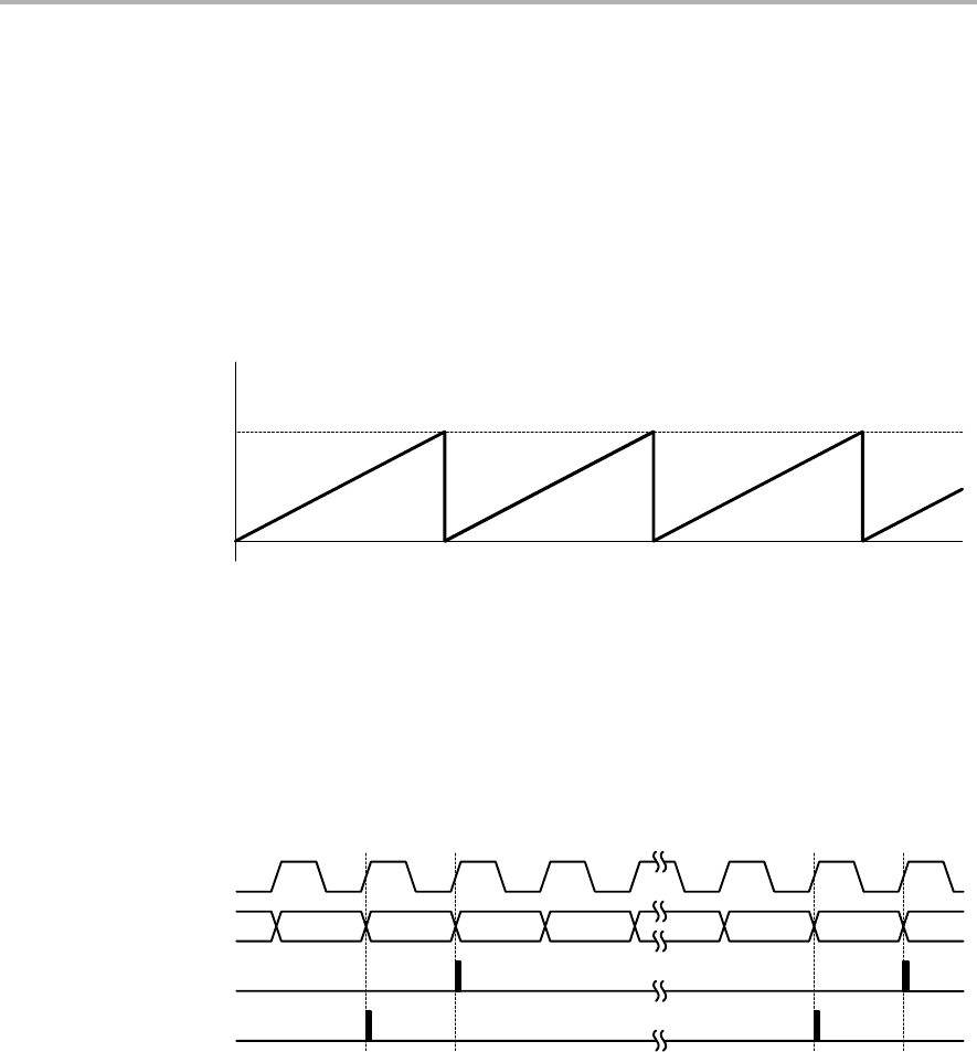
Timer_A Operation
12-6 Timer_A
Up Mode
The up mode is used if the timer period must be different from 0FFFFh counts.
The timer repeatedly counts up to the value of compare register TACCR0,
which defines the period, as shown in Figure 12−2. The number of timer
counts in the period is TACCR0+1. When the timer value equals TACCR0 the
timer restarts counting from zero. If up mode is selected when the timer value
is greater than TACCR0, the timer immediately restarts counting from zero.
Figure 12−2. Up Mode
0h
0FFFFh
TACCR0
The TACCR0 CCIFG interrupt flag is set when the timer counts to the TACCR0
value. The TAIFG interrupt flag is set when the timer counts from TACCR0 to
zero. Figure 12−3 shows the flag set cycle.
Figure 12−3. Up Mode Flag Setting
CCR0−1 CCR0 0h
Timer Clock
Timer
Set TAIFG
Set TACCR0 CCIFG
1h CCR0−1 CCR0 0h
Changing the Period Register TACCR0
When changing TACCR0 while the timer is running, if the new period is greater
than or equal to the old period, or greater than the current count value, the timer
counts up to the new period. If the new period is less than the current count
value, the timer rolls to zero. However, one additional count may occur before
the counter rolls to zero.
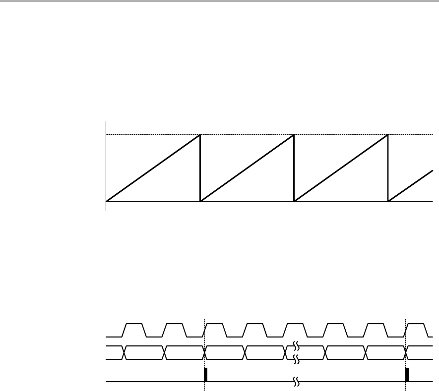
Timer_A Operation
12-7
Timer_A
Continuous Mode
In the continuous mode, the timer repeatedly counts up to 0FFFFh and restarts
from zero as shown in Figure 12−4. The capture/compare register TACCR0
works the same way as the other capture/compare registers.
Figure 12−4. Continuous Mode
0h
0FFFFh
The TAIFG interrupt flag is set when the timer counts from 0FFFFh to zero.
Figure 12−5 shows the flag set cycle.
Figure 12−5. Continuous Mode Flag Setting
FFFEh FFFFh 0h
Timer Clock
Timer
Set TAIFG
1h FFFEh FFFFh 0h
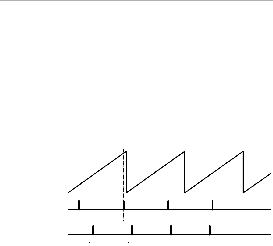
Timer_A Operation
12-8 Timer_A
Use of the Continuous Mode
The continuous mode can be used to generate independent time intervals and
output frequencies. Each time an interval is completed, an interrupt is
generated. The next time interval is added to the TACCRx register in the
interrupt service routine. Figure 12−6 shows two separate time intervals t0 and
t1 being added to the capture/compare registers. In this usage, the time
interval is controlled by hardware, not software, without impact from interrupt
latency. Up to three independent time intervals or output frequencies can be
generated using all three capture/compare registers.
Figure 12−6. Continuous Mode Time Intervals
0FFFFh
TACCR0a
TACCR0b TACCR0c TACCR0d
t1
t0t0
TACCR1a
TACCR1b TACCR1c
TACCR1d
t1t1
t0
Time intervals can be produced with other modes as well, where TACCR0 is
used as the period register. Their handling is more complex since the sum of
the old TACCRx data and the new period can be higher than the TACCR0
value. When the previous TACCRx value plus tx is greater than the TACCR0
data, TACCR0 + 1 must be subtracted to obtain the correct time interval.
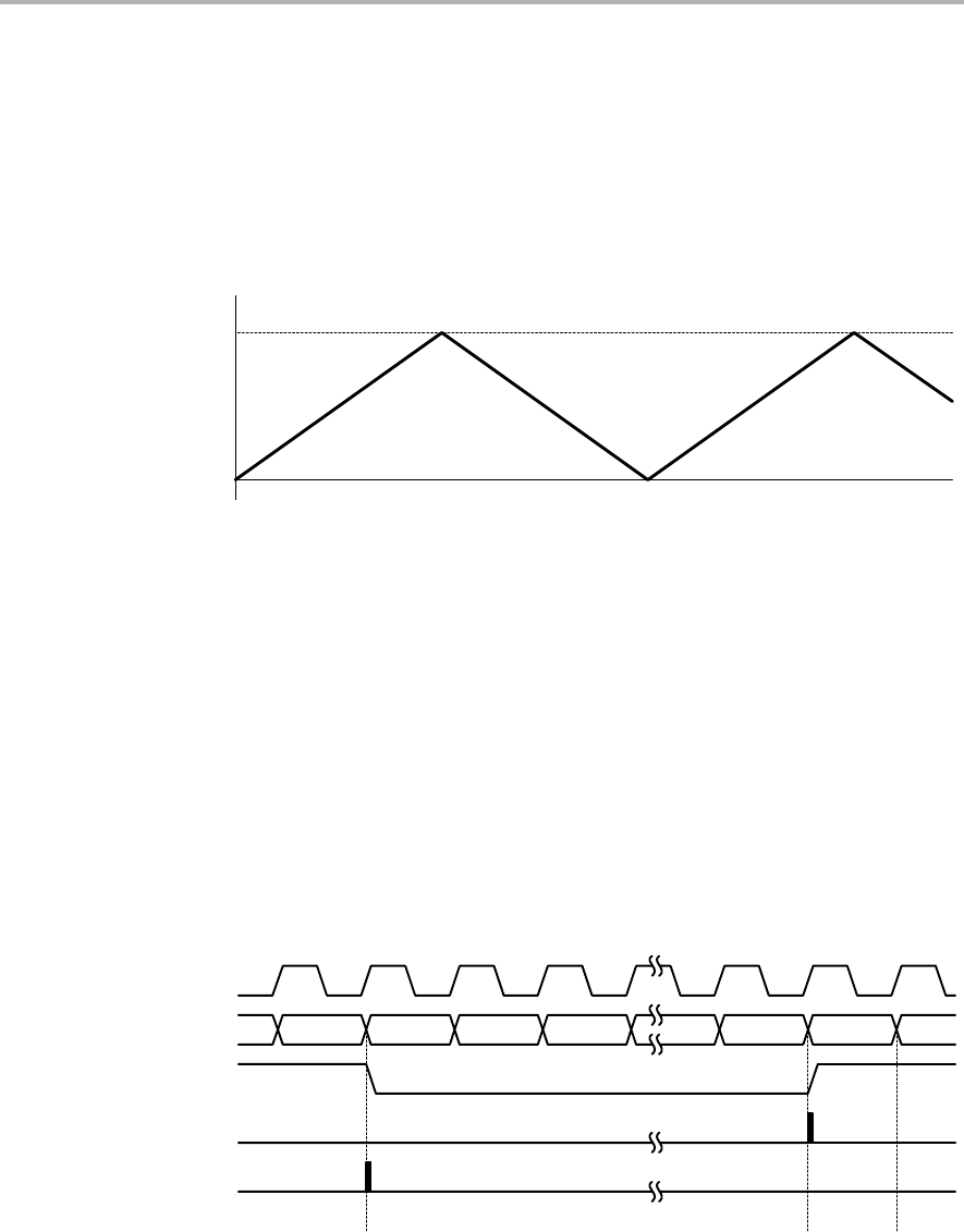
Timer_A Operation
12-9
Timer_A
Up/Down Mode
The up/down mode is used if the timer period must be different from 0FFFFh
counts, and if a symmetrical pulse generation is needed. The timer repeatedly
counts up to the value of compare register TACCR0 and back down to zero,
as shown in Figure 12−7. The period is twice the value in TACCR0.
Figure 12−7. Up/Down Mode
0h
TACCR0
0FFFFh
The count direction is latched. This allows the timer to be stopped and then
restarted in the same direction it was counting before it was stopped. If this is
not desired, the TACLR bit must be set to clear the direction. The TACLR bit
also clears the TAR value and the timer clock divider.
In up/down mode, the TACCR0 CCIFG interrupt flag and the TAIFG interrupt
flag are set only once during a period, separated by 1/2 the timer period. The
TACCR0 CCIFG interrupt flag is set when the timer counts from TACCR0 − 1
to TACCR0, and TAIFG is set when the timer completes counting down from
0001h to 0000h. Figure 12−8 shows the flag set cycle.
Figure 12−8. Up/Down Mode Flag Setting
CCR0−1 CCR0 CCR0−1
Timer Clock
Timer
Set TAIFG
Set TACCR0 CCIFG
CCR0−2 1h 0h
Up/Down

Timer_A Operation
12-10 Timer_A
Changing the Period Register TACCR0
When changing TACCR0 while the timer is running, and counting in the down
direction, the timer continues its descent until it reaches zero. The value in
TACCR0 is latched into TACL0 immediately, however the new period takes
effect after the counter counts down to zero.
When the timer is counting in the up direction, and the new period is greater
than or equal to the old period, or greater than the current count value, the timer
counts up to the new period before counting down. When the timer is counting
in the up direction, and the new period is less than the current count value, the
timer begins counting down. However, one additional count may occur before
the counter begins counting down.
Use of the Up/Down Mode
The up/down mode supports applications that require dead times between
output signals (See section Timer_A Output Unit). For example, to avoid
overload conditions, two outputs driving an H-bridge must never be in a high
state simultaneously. In the example shown in Figure 12−9 the tdead is:
tdead = ttimer × (TACCR1 − TACCR2)
With: tdead Time during which both outputs need to be inactive
ttimer Cycle time of the timer clock
TACCRx Content of capture/compare register x
The TACCRx registers are not buffered. They update immediately when
written to. Therefore, any required dead time will not be maintained
automatically.
Figure 12−9. Output Unit in Up/Down Mode
0h
0FFFFh
TAIFG
Output Mode 2: Toggle/Reset
Output Mode 6: Toggle/Set
TACCR0
TACCR1
EQU1 TAIFG Interrupt Events
EQU1
EQU0
EQU1 EQU1
EQU0
TACCR2
EQU2 EQU2EQU2 EQU2
Dead Time

Timer_A Operation
12-11
Timer_A
12.2.4 Capture/Compare Blocks
Two or three identical capture/compare blocks, TACCRx, are present in
Timer_A. Any of the blocks may be used to capture the timer data, or to
generate time intervals.
Capture Mode
The capture mode is selected when CAP = 1. Capture mode is used to record
time events. It can be used for speed computations or time measurements.
The capture inputs CCIxA and CCIxB are connected to external pins or internal
signals and are selected with the CCISx bits. The CMx bits select the capture
edge of the input signal as rising, falling, or both. A capture occurs on the
selected edge of the input signal. If a capture occurs:
-The timer value is copied into the TACCRx register
-The interrupt flag CCIFG is set
The input signal level can be read at any time via the CCI bit. MSP430x2xx
family devices may have different signals connected to CCIxA and CCIxB. See
the device-specific data sheet for the connections of these signals.
The capture signal can be asynchronous to the timer clock and cause a race
condition. Setting the SCS bit will synchronize the capture with the next timer
clock. Setting the SCS bit to synchronize the capture signal with the timer clock
is recommended. This is illustrated in Figure 12−10.
Figure 12−10. Capture Signal (SCS = 1)
n−2 n−1
Timer Clock
Timer
Set TACCRx CCIFG
n+1 n+3 n+4
CCI
Capture
n+2n
Overflow logic is provided in each capture/compare register to indicate if a
second capture was performed before the value from the first capture was
read. Bit COV is set when this occurs as shown in Figure 12−11. COV must
be reset with software.
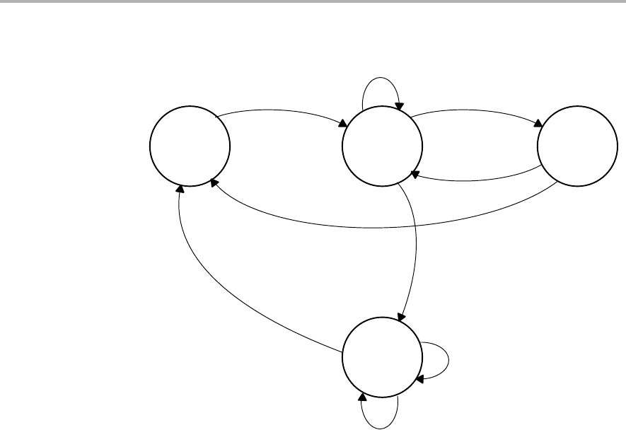
Timer_A Operation
12-12 Timer_A
Figure 12−11.Capture Cycle
Second
Capture
Taken
COV = 1
Capture
Taken
No
Capture
Taken
Read
Taken
Capture
Clear Bit COV
in Register TACCTLx
Idle
Idle
Capture
Capture Read and No Capture
Capture
Capture ReadCapture
Capture
Capture Initiated by Software
Captures can be initiated by software. The CMx bits can be set for capture on
both edges. Software then sets CCIS1 = 1 and toggles bit CCIS0 to switch the
capture signal between VCC and GND, initiating a capture each time CCIS0
changes state:
MOV #CAP+SCS+CCIS1+CM_3,&TACCTLx ; Setup TACCTLx
XOR #CCIS0,&TACCTLx ; TACCTLx = TAR
Compare Mode
The compare mode is selected when CAP = 0. The compare mode is used to
generate PWM output signals or interrupts at specific time intervals. When
TAR counts to the value in a TACCRx:
-Interrupt flag CCIFG is set
-Internal signal EQUx = 1
-EQUx affects the output according to the output mode
-The input signal CCI is latched into SCCI

Timer_A Operation
12-13
Timer_A
12.2.5 Output Unit
Each capture/compare block contains an output unit. The output unit is used
to generate output signals such as PWM signals. Each output unit has eight
operating modes that generate signals based on the EQU0 and EQUx signals.
Output Modes
The output modes are defined by the OUTMODx bits and are described in
Table 12−2. The OUTx signal is changed with the rising edge of the timer clock
for all modes except mode 0. Output modes 2, 3, 6, and 7 are not useful for
output unit 0, because EQUx = EQU0.
Table 12−2.Output Modes
OUTMODx Mode Description
000 Output The output signal OUTx is defined by the
OUTx bit. The OUTx signal updates
immediately when OUTx is updated.
001 Set The output is set when the timer counts
to the TACCRx value. It remains set until
a reset of the timer, or until another
output mode is selected and affects the
output.
010 Toggle/Reset The output is toggled when the timer
counts to the TACCRx value. It is reset
when the timer counts to the TACCR0
value.
011 Set/Reset The output is set when the timer counts
to the TACCRx value. It is reset when the
timer counts to the TACCR0 value.
100 Toggle The output is toggled when the timer
counts to the TACCRx value. The output
period is double the timer period.
101 Reset The output is reset when the timer counts
to the TACCRx value. It remains reset
until another output mode is selected and
affects the output.
110 Toggle/Set The output is toggled when the timer
counts to the TACCRx value. It is set
when the timer counts to the TACCR0
value.
111 Reset/Set The output is reset when the timer counts
to the TACCRx value. It is set when the
timer counts to the TACCR0 value.
Timer_A Operation
12-14 Timer_A
Output Example—Timer in Up Mode
The OUTx signal is changed when the timer counts up to the TACCRx value,
and rolls from TACCR0 to zero, depending on the output mode. An example
is shown in Figure 12−12 using TACCR0 and TACCR1.
Figure 12−12. Output Example—Timer in Up Mode
0h
0FFFFh
EQU0
TAIFG
Output Mode 1: Set
Output Mode 2: Toggle/Reset
Output Mode 3: Set/Reset
Output Mode 4: Toggle
Output Mode 5: Reset
Output Mode 6: Toggle/Set
Output Mode 7: Reset/Set
TACCR0
TACCR1
EQU1 EQU0
TAIFG
EQU1 EQU0
TAIFG Interrupt Events
Timer_A Operation
12-15
Timer_A
Output Example—Timer in Continuous Mode
The OUTx signal is changed when the timer reaches the TACCRx and
TACCR0 values, depending on the output mode. An example is shown in
Figure 12−13 using TACCR0 and TACCR1.
Figure 12−13. Output Example—Timer in Continuous Mode
0h
0FFFFh
TAIFG
Output Mode 1: Set
Output Mode 2: Toggle/Reset
Output Mode 3: Set/Reset
Output Mode 4: Toggle
Output Mode 5: Reset
Output Mode 6: Toggle/Set
Output Mode 7: Reset/Set
TACCR0
TACCR1
EQU1 TAIFG EQU1 EQU0 Interrupt EventsEQU0
Timer_A Operation
12-16 Timer_A
Output Example—Timer in Up/Down Mode
The OUTx signal changes when the timer equals TACCRx in either count
direction and when the timer equals TACCR0, depending on the output mode.
An example is shown in Figure 12−14 using TACCR0 and TACCR2.
Figure 12−14. Output Example—Timer in Up/Down Mode
0h
0FFFFh
TAIFG
Output Mode 1: Set
Output Mode 2: Toggle/Reset
Output Mode 3: Set/Reset
Output Mode 4: Toggle
Output Mode 5: Reset
Output Mode 6: Toggle/Set
Output Mode 7: Reset/Set
TACCR0
TACCR2
EQU2
TAIFG Interrupt Events
EQU2
EQU0
EQU2 EQU2
EQU0
Note: Switching Between Output Modes
When switching between output modes, one of the OUTMODx bits should
remain set during the transition, unless switching to mode 0. Otherwise,
output glitching can occur because a NOR gate decodes output mode 0. A
safe method for switching between output modes is to use output mode 7 as
a transition state:
BIS #OUTMOD_7,&TACCTLx ; Set output mode=7
BIC #OUTMODx,&TACCTLx ; Clear unwanted bits
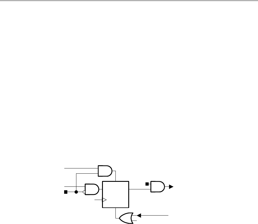
Timer_A Operation
12-17
Timer_A
12.2.6 Timer_A Interrupts
Two interrupt vectors are associated with the 16-bit Timer_A module:
-TACCR0 interrupt vector for TACCR0 CCIFG
-TAIV interrupt vector for all other CCIFG flags and TAIFG
In capture mode any CCIFG flag is set when a timer value is captured in the
associated TACCRx register. In compare mode, any CCIFG flag is set if TAR
counts to the associated TACCRx value. Software may also set or clear any
CCIFG flag. All CCIFG flags request an interrupt when their corresponding
CCIE bit and the GIE bit are set.
TACCR0 Interrupt
The TACCR0 CCIFG flag has the highest Timer_A interrupt priority and has
a dedicated interrupt vector as shown in Figure 12−15. The TACCR0 CCIFG
flag is automatically reset when the TACCR0 interrupt request is serviced.
Figure 12−15. Capture/Compare TACCR0 Interrupt Flag
DSet QIRQ, Interrupt Service Requested
Reset
Timer Clock
POR
CAP
EQU0
Capture
IRACC, Interrupt Request Accepted
CCIE
TAIV, Interrupt Vector Generator
The TACCR1 CCIFG, TACCR2 CCIFG, and TAIFG flags are prioritized and
combined to source a single interrupt vector. The interrupt vector register TAIV
is used to determine which flag requested an interrupt.
The highest priority enabled interrupt generates a number in the TAIV register
(see register description). This number can be evaluated or added to the
program counter to automatically enter the appropriate software routine.
Disabled Timer_A interrupts do not affect the TAIV value.
Any access, read or write, of the TAIV register automatically resets the highest
pending interrupt flag. If another interrupt flag is set, another interrupt is
immediately generated after servicing the initial interrupt. For example, if the
TACCR1 and TACCR2 CCIFG flags are set when the interrupt service routine
accesses the TAIV register, TACCR1 CCIFG is reset automatically. After the
RETI instruction of the interrupt service routine is executed, the TACCR2
CCIFG flag will generate another interrupt.

Timer_A Operation
12-18 Timer_A
TAIV Software Example
The following software example shows the recommended use of TAIV and the
handling overhead. The TAIV value is added to the PC to automatically jump
to the appropriate routine.
The numbers at the right margin show the necessary CPU cycles for each
instruction. The software overhead for different interrupt sources includes
interrupt latency and return-from-interrupt cycles, but not the task handling
itself. The latencies are:
-Capture/compare block TACCR0 11 cycles
-Capture/compare blocks TACCR1, TACCR2 16 cycles
-Timer overflow TAIFG 14 cycles
; Interrupt handler for TACCR0 CCIFG. Cycles
CCIFG_0_HND
; ... ; Start of handler Interrupt latency 6
RETI 5
; Interrupt handler for TAIFG, TACCR1 and TACCR2 CCIFG.
TA_HND ... ; Interrupt latency 6
ADD &TAIV,PC ; Add offset to Jump table 3
RETI ; Vector 0: No interrupt 5
JMP CCIFG_1_HND ; Vector 2: TACCR1 2
JMP CCIFG_2_HND ; Vector 4: TACCR2 2
RETI ; Vector 6: Reserved 5
RETI ; Vector 8: Reserved 5
TAIFG_HND ; Vector 10: TAIFG Flag
... ; Task starts here
RETI 5
CCIFG_2_HND ; Vector 4: TACCR2
... ; Task starts here
RETI ; Back to main program 5
CCIFG_1_HND ; Vector 2: TACCR1
... ; Task starts here
RETI ; Back to main program 5

Timer_A Registers
12-19
Timer_A
12.3 Timer_A Registers
The Timer_A registers are listed in Table 12−3.
Table 12−3.Timer_A Registers
Register Short Form Register Type Address Initial State
Timer_A control TACTL Read/write 0160h Reset with POR
Timer_A counter TAR Read/write 0170h Reset with POR
Timer_A capture/compare control 0 TACCTL0 Read/write 0162h Reset with POR
Timer_A capture/compare 0 TACCR0 Read/write 0172h Reset with POR
Timer_A capture/compare control 1 TACCTL1 Read/write 0164h Reset with POR
Timer_A capture/compare 1 TACCR1 Read/write 0174h Reset with POR
Timer_A capture/compare control 2 TACCTL2†Read/write 0166h Reset with POR
Timer_A capture/compare 2 TACCR2†Read/write 0176h Reset with POR
Timer_A interrupt vector TAIV Read only 012Eh Reset with POR
†Not present on MSP430x20xx Devices

Timer_A Registers
12-20 Timer_A
TACTL, Timer_A Control Register
15 14 13 12 11 10 9 8
Unused TASSELx
rw−(0) rw−(0) rw−(0) rw−(0) rw−(0) rw−(0) rw−(0) rw−(0)
76543210
IDx MCx Unused TACLR TAIE TAIFG
rw−(0) rw−(0) rw−(0) rw−(0) rw−(0) w−(0) rw−(0) rw−(0)
Unused Bits
15-10
Unused
TASSELx Bits
9-8
Timer_A clock source select
00 TACLK
01 ACLK
10 SMCLK
11 INCLK
IDx Bits
7-6
Input divider. These bits select the divider for the input clock.
00 /1
01 /2
10 /4
11 /8
MCx Bits
5-4
Mode control. Setting MCx = 00h when Timer_A is not in use conserves
power.
00 Stop mode: the timer is halted.
01 Up mode: the timer counts up to TACCR0.
10 Continuous mode: the timer counts up to 0FFFFh.
11 Up/down mode: the timer counts up to TACCR0 then down to 0000h.
Unused Bit 3 Unused
TACLR Bit 2 Timer_A clear. Setting this bit resets TAR, the clock divider, and the count
direction. The TACLR bit is automatically reset and is always read as zero.
TAIE Bit 1 Timer_A interrupt enable. This bit enables the TAIFG interrupt request.
0 Interrupt disabled
1 Interrupt enabled
TAIFG Bit 0 Timer_A interrupt flag
0 No interrupt pending
1 Interrupt pending

Timer_A Registers
12-21
Timer_A
TAR, Timer_A Register
15 14 13 12 11 10 9 8
TARx
rw−(0) rw−(0) rw−(0) rw−(0) rw−(0) rw−(0) rw−(0) rw−(0)
76543210
TARx
rw−(0) rw−(0) rw−(0) rw−(0) rw−(0) rw−(0) rw−(0) rw−(0)
TARx Bits
15-0
Timer_A register. The TAR register is the count of Timer_A.
TACCRx, Timer_A Capture/Compare Register x
15 14 13 12 11 10 9 8
TACCRx
rw−(0) rw−(0) rw−(0) rw−(0) rw−(0) rw−(0) rw−(0) rw−(0)
76543210
TACCRx
rw−(0) rw−(0) rw−(0) rw−(0) rw−(0) rw−(0) rw−(0) rw−(0)
TACCRx Bits
15-0
Timer_A capture/compare register.
Compare mode: TACCRx holds the data for the comparison to the timer value
in the Timer_A Register, TAR.
Capture mode: The Timer_A Register, TAR, is copied into the TACCRx
register when a capture is performed.

Timer_A Registers
12-22 Timer_A
TACCTLx, Capture/Compare Control Register
15 14 13 12 11 10 9 8
CMx CCISx SCS SCCI Unused CAP
rw−(0) rw−(0) rw−(0) rw−(0) rw−(0) r r0 rw−(0)
76543210
OUTMODx CCIE CCI OUT COV CCIFG
rw−(0) rw−(0) rw−(0) rw−(0) r rw−(0) rw−(0) rw−(0)
CMx Bit
15-14
Capture mode
00 No capture
01 Capture on rising edge
10 Capture on falling edge
11 Capture on both rising and falling edges
CCISx Bit
13-12
Capture/compare input select. These bits select the TACCRx input signal.
See the device-specific data sheet for specific signal connections.
00 CCIxA
01 CCIxB
10 GND
11 VCC
SCS Bit 11 Synchronize capture source. This bit is used to synchronize the capture input
signal with the timer clock.
0 Asynchronous capture
1 Synchronous capture
SCCI Bit 10 Synchronized capture/compare input. The selected CCI input signal is
latched with the EQUx signal and can be read via this bit
Unused Bit 9 Unused. Read only. Always read as 0.
CAP Bit 8 Capture mode
0 Compare mode
1 Capture mode
OUTMODx Bits
7-5
Output mode. Modes 2, 3, 6, and 7 are not useful for TACCR0 because
EQUx = EQU0.
000 OUT bit value
001 Set
010 Toggle/reset
011 Set/reset
100 Toggle
101 Reset
110 Toggle/set
111 Reset/set

Timer_A Registers
12-23
Timer_A
CCIE Bit 4 Capture/compare interrupt enable. This bit enables the interrupt request of
the corresponding CCIFG flag.
0 Interrupt disabled
1 Interrupt enabled
CCI Bit 3 Capture/compare input. The selected input signal can be read by this bit.
OUT Bit 2 Output. For output mode 0, this bit directly controls the state of the output.
0 Output low
1 Output high
COV Bit 1 Capture overflow. This bit indicates a capture overflow occurred. COV must
be reset with software.
0 No capture overflow occurred
1 Capture overflow occurred
CCIFG Bit 0 Capture/compare interrupt flag
0 No interrupt pending
1 Interrupt pending
TAIV, Timer_A Interrupt Vector Register
15 14 13 12 11 10 9 8
0 0 0 0 0 0 0 0
r0 r0 r0 r0 r0 r0 r0 r0
76543210
0 0 0 0 TAIVx 0
r0 r0 r0 r0 r−(0) r−(0) r−(0) r0
TAIVx Bits
15-0
Timer_A Interrupt Vector value
TAIV Contents Interrupt Source Interrupt Flag
Interrupt
Priority
00h No interrupt pending −
02h Capture/compare 1 TACCR1 CCIFG Highest
04h Capture/compare 2†TACCR2 CCIFG
06h Reserved −
08h Reserved −
0Ah Timer overflow TAIFG
0Ch Reserved −
0Eh Reserved − Lowest
†Not Implemented in MSP430x20xx, devices

12-24 Timer_A

13-1
Timer_B
Timer_B
Timer_B is a 16-bit timer/counter with multiple capture/compare registers. This
chapter describes the operation of the Timer_B of the MSP430 2xx device
family.
Topic Page
13.1 Timer_B Introduction 13-2. . . . . . . . . . . . . . . . . . . . . . . . . . . . . . . . . . . . . . . . .
13.2 Timer_B Operation 13-4. . . . . . . . . . . . . . . . . . . . . . . . . . . . . . . . . . . . . . . . . . . .
13.3 Timer_B Registers 13-20. . . . . . . . . . . . . . . . . . . . . . . . . . . . . . . . . . . . . . . . . .
Chapter 13

Timer_B Introduction
13-2 Timer_B
13.1 Timer_B Introduction
Timer_B is a 16-bit timer/counter with three or seven capture/compare
registers. Timer_B can support multiple capture/compares, PWM outputs, and
interval timing. Timer_B also has extensive interrupt capabilities. Interrupts
may be generated from the counter on overflow conditions and from each of
the capture/compare registers.
Timer_B features include :
-Asynchronous 16-bit timer/counter with four operating modes and four
selectable lengths
-Selectable and configurable clock source
-Three or seven configurable capture/compare registers
-Configurable outputs with PWM capability
-Double-buffered compare latches with synchronized loading
-Interrupt vector register for fast decoding of all Timer_B interrupts
The block diagram of Timer_B is shown in Figure 13−1.
Note: Use of the Word Count
Count is used throughout this chapter. It means the counter must be in the
process of counting for the action to take place. If a particular value is directly
written to the counter, then an associated action does not take place.
13.1.1 Similarities and Differences From Timer_A
Timer_B is identical to Timer_A with the following exceptions:
- The length of Timer_B is programmable to be 8, 10, 12, or 16 bits.
-Timer_B TBCCRx registers are double-buffered and can be grouped.
-All Timer_B outputs can be put into a high-impedance state.
-The SCCI bit function is not implemented in Timer_B.
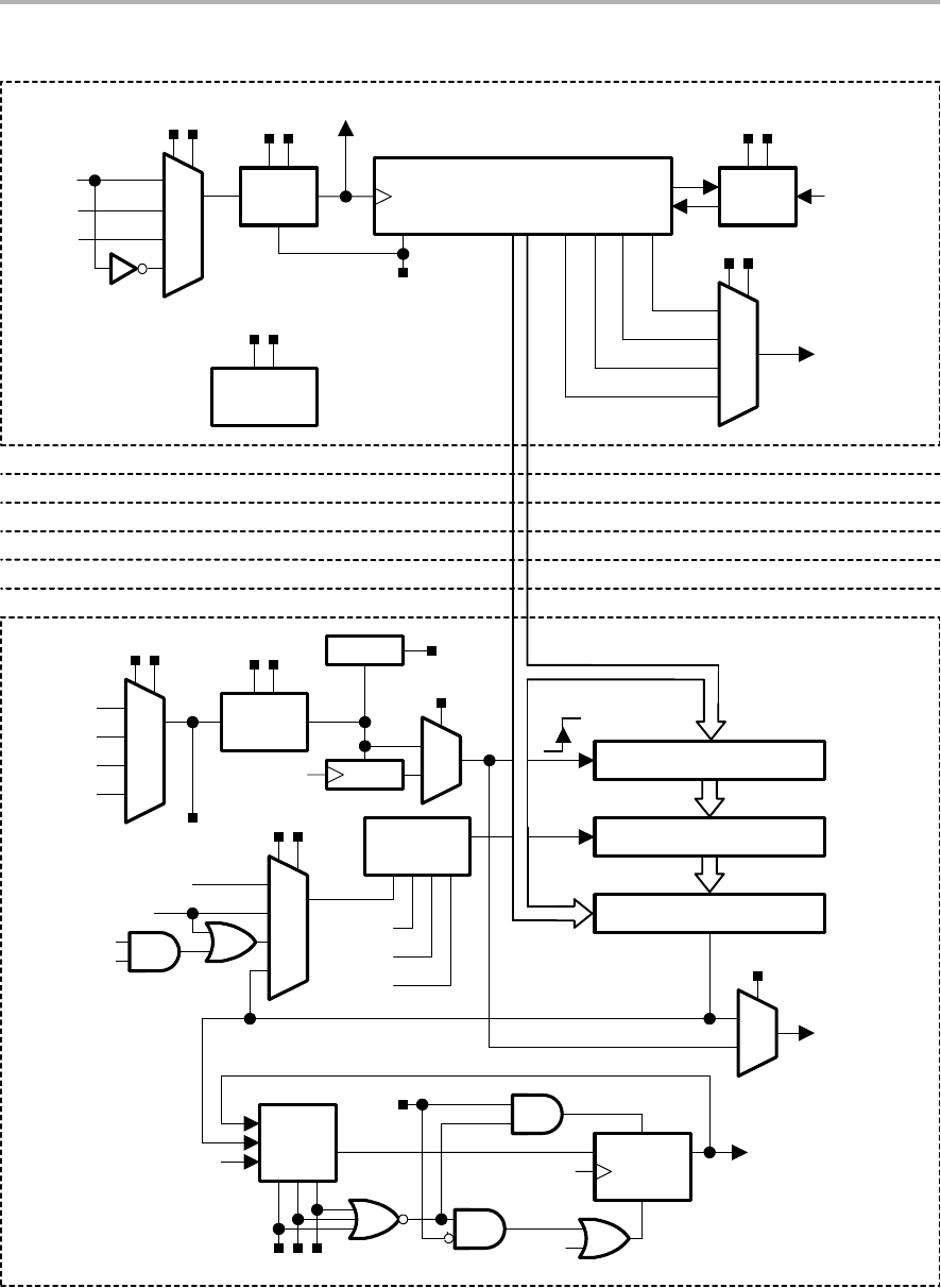
Timer_B Introduction
13-3
Timer_B
Figure 13−1. Timer_B Block Diagram
CCR6
Comparator 6
CCI
15 0
OUTMODx
Capture
Mode
CMx
Sync
COVlogic
Output
Unit6 DSet Q
EQU0
OUT
OUT6 Signal
Reset
POR
EQU6
Divider
1/2/4/8
Count
Mode
16−bit Timer
TBR
Set TBIFG
15 0
MCxIDx
Clear
TBCLR
Timer Clock
CCR0
EQU0
Timer Clock
Timer Clock
VCC
TBR=0
UP/DOWN
EQU0
CLLDx
CNTLx
Load
CCR1
CCR2
CCR3
CCR4
CCR5
Timer Block
TBCCR6
RC
10 12 168
TBCLGRPx
CCR5
CCR4
CCR1
Group
Load Logic
Group
Load Logic
TBSSELx
00
01
10
11
GND
VCC
CCI6A
CCI6B
00
01
10
11
CCISx
00
01
10
11
00
01
10
11 CAP
1
0
SCS
1
0
Set TBCCR6
CCIFG
Compare Latch TBCL6
ACLK
SMCLK
TBCLK

Timer_B Operation
13-4 Timer_B
13.2 Timer_B Operation
The Timer_B module is configured with user software. The setup and
operation of Timer_B is discussed in the following sections.
13.2.1 16-Bit Timer Counter
The 16-bit timer/counter register, TBR, increments or decrements (depending
on mode of operation) with each rising edge of the clock signal. TBR can be
read or written with software. Additionally, the timer can generate an interrupt
when it overflows.
TBR may be cleared by setting the TBCLR bit. Setting TBCLR also clears the
clock divider and count direction for up/down mode.
Note: Modifying Timer_B Registers
It is recommended to stop the timer before modifying its operation (with
exception of the interrupt enable, interrupt flag, and TBCLR) to avoid errant
operating conditions.
When the timer clock is asynchronous to the CPU clock, any read from TBR
should occur while the timer is not operating or the results may be
unpredictable. Alternatively, the timer may be read multiple times while
operating, and a majority vote taken in software to determine the correct
reading. Any write to TBR will take effect immediately.
TBR Length
Timer_B is configurable to operate as an 8-, 10-, 12-, or 16-bit timer with the
CNTLx bits. The maximum count value, TBR(max), for the selectable lengths
is 0FFh, 03FFh, 0FFFh, and 0FFFFh, respectively. Data written to the TBR
register in 8-, 10-, and 12-bit mode is right-justified with leading zeros.
Clock Source Select and Divider
The timer clock can be sourced from ACLK, SMCLK, or externally via TBCLK
(TBCLK or inverted TBCLK). The clock source is selected with the TBSSELx
bits. The selected clock source may be passed directly to the timer or divided
by 2,4, or 8, using the IDx bits. The clock divider is reset when TBCLR is set.

Timer_B Operation
13-5
Timer_B
13.2.2 Starting the Timer
The timer may be started or restarted in the following ways:
-The timer counts when MCx > 0 and the clock source is active.
-When the timer mode is either up or up/down, the timer may be stopped
by loading 0 to TBCL0. The timer may then be restarted by loading a
nonzero value to TBCL0. In this scenario, the timer starts incrementing in
the up direction from zero.
13.2.3 Timer Mode Control
The timer has four modes of operation as described in Table 13−1: stop, up,
continuous, and up/down. The operating mode is selected with the MCx bits.
Table 13−1.Timer Modes
MCx Mode Description
00 Stop The timer is halted.
01 Up The timer repeatedly counts from zero to the value of
compare register TBCL0.
10 Continuous The timer repeatedly counts from zero to the value
selected by the CNTLx bits.
11 Up/down The timer repeatedly counts from zero up to the value of
TBCL0 and then back down to zero.
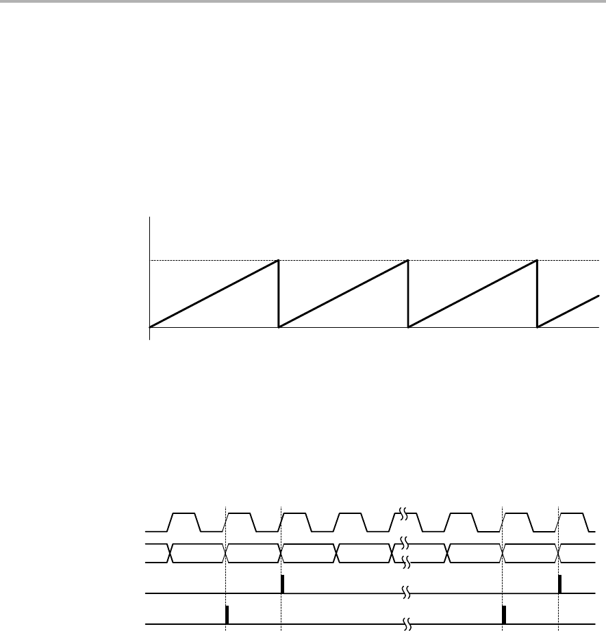
Timer_B Operation
13-6 Timer_B
Up Mode
The up mode is used if the timer period must be different from TBR(max) counts.
The timer repeatedly counts up to the value of compare latch TBCL0, which
defines the period, as shown in Figure 13−2. The number of timer counts in
the period is TBCL0+1. When the timer value equals TBCL0 the timer restarts
counting from zero. If up mode is selected when the timer value is greater than
TBCL0, the timer immediately restarts counting from zero.
Figure 13−2. Up Mode
0h
TBR(max)
TBCL0
The TBCCR0 CCIFG interrupt flag is set when the timer counts to the TBCL0
value. The TBIFG interrupt flag is set when the timer counts from TBCL0 to
zero. Figure 13−3 shows the flag set cycle.
Figure 13−3. Up Mode Flag Setting
TBCL0−1 TBCL0 0h
Timer Clock
Timer
Set TBIFG
Set TBCCR0 CCIFG
1h TBCL0−1 TBCL0 0h
Changing the Period Register TBCL0
When changing TBCL0 while the timer is running and when the TBCL0 load
event is immediate, CLLD0 = 00, if the new period is greater than or equal to
the old period, or greater than the current count value, the timer counts up to
the new period. If the new period is less than the current count value, the timer
rolls to zero. However, one additional count may occur before the counter rolls
to zero.
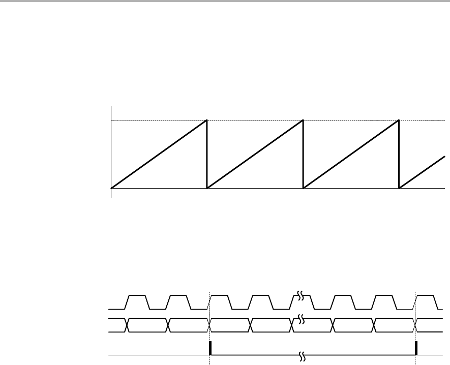
Timer_B Operation
13-7
Timer_B
Continuous Mode
In continuous mode the timer repeatedly counts up to TBR(max) and restarts
from zero as shown in Figure 13−4. The compare latch TBCL0 works the same
way as the other capture/compare registers.
Figure 13−4. Continuous Mode
0h
TBR(max)
The TBIFG interrupt flag is set when the timer counts from TBR(max) to zero.
Figure 13−5 shows the flag set cycle.
Figure 13−5. Continuous Mode Flag Setting
TBR (max)
−1 TBR (max) 0h
Timer Clock
Timer
Set TBIFG
1h TBR (max) 0hTBR (max)
−1
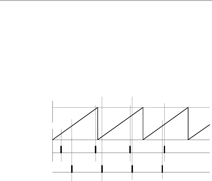
Timer_B Operation
13-8 Timer_B
Use of the Continuous Mode
The continuous mode can be used to generate independent time intervals and
output frequencies. Each time an interval is completed, an interrupt is
generated. The next time interval is added to the TBCLx latch in the interrupt
service routine. Figure 13−6 shows two separate time intervals t0 and t1 being
added to the capture/compare registers. The time interval is controlled by
hardware, not software, without impact from interrupt latency. Up to three
(Timer_B3) or 7 (Timer_B7) independent time intervals or output frequencies
can be generated using capture/compare registers.
Figure 13−6. Continuous Mode Time Intervals
0h
EQU0 Interrupt
TBCL0a
TBCL0b TBCL0c TBCL0d
t1
t0t0
TBCL1a
TBCL1b TBCL1c
TBCL1d
t1t1
t0
EQU1 Interrupt
TBR(max)
Time intervals can be produced with other modes as well, where TBCL0 is
used as the period register. Their handling is more complex since the sum of
the old TBCLx data and the new period can be higher than the TBCL0 value.
When the sum of the previous TBCLx value plus tx is greater than the TBCL0
data, TBCL0 + 1 must be subtracted to obtain the correct time interval.
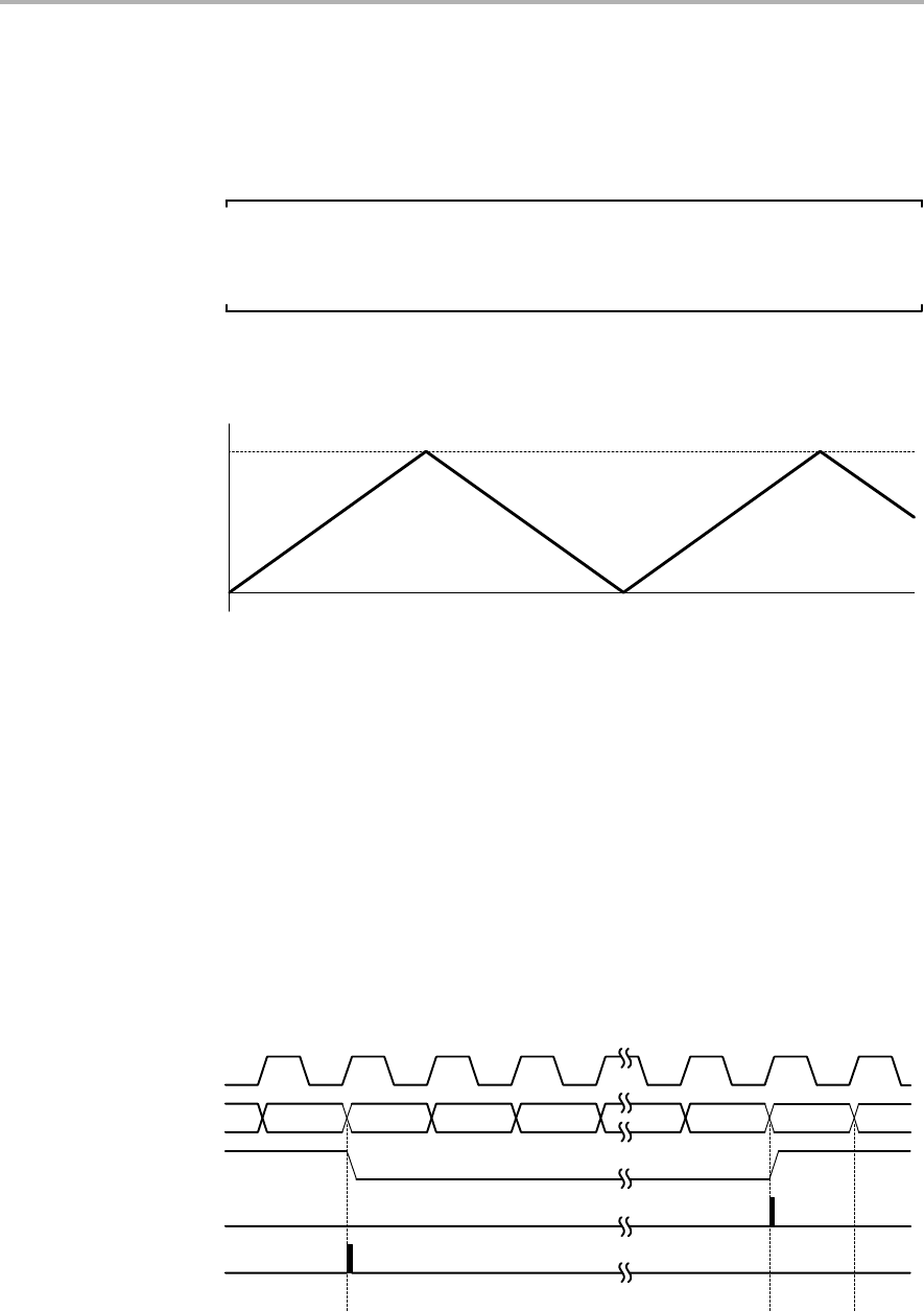
Timer_B Operation
13-9
Timer_B
Up/Down Mode
The up/down mode is used if the timer period must be different from TBR(max)
counts, and if a symmetrical pulse generation is needed. The timer repeatedly
counts up to the value of compare latch TBCL0, and back down to zero, as
shown in Figure 13−7. The period is twice the value in TBCL0.
Note: TBCL0 > TBR(max)
If TBCL0 > TBR(max), the counter operates as if it were configured for
continuous mode. It does not count down from TBR(max) to zero.
Figure 13−7. Up/Down Mode
0h
TBCL0
The count direction is latched. This allows the timer to be stopped and then
restarted in the same direction it was counting before it was stopped. If this is
not desired, the TBCLR bit must be used to clear the direction. The TBCLR bit
also clears the TBR value and the clock divider.
In up/down mode, the TBCCR0 CCIFG interrupt flag and the TBIFG interrupt
flag are set only once during the period, separated by 1/2 the timer period. The
TBCCR0 CCIFG interrupt flag is set when the timer counts from TBCL0−1 to
TBCL0, and TBIFG is set when the timer completes counting down from 0001h
to 0000h. Figure 13−8 shows the flag set cycle.
Figure 13−8. Up/Down Mode Flag Setting
TBCL0−1 TBCL0 TBCL0−1
Timer Clock
Timer
Set TBIFG
Set TBCCR0 CCIFG
TBCL0−2 1h 0h 1h
Up/Down

Timer_B Operation
13-10 Timer_B
Changing the Value of Period Register TBCL0
When changing TBCL0 while the timer is running, and counting in the down
direction, and when the TBCL0 load event is immediate, the timer continues
its descent until it reaches zero. The value in TBCCR0 is latched into TBCL0
immediately; however, the new period takes effect after the counter counts
down to zero.
If the timer is counting in the up direction when the new period is latched into
TBCL0, and the new period is greater than or equal to the old period, or greater
than the current count value, the timer counts up to the new period before
counting down. When the timer is counting in the up direction, and the new
period is less than the current count value when TBCL0 is loaded, the timer
begins counting down. However, one additional count may occur before the
counter begins counting down.
Use of the Up/Down Mode
The up/down mode supports applications that require dead times between
output signals (see section Timer_B Output Unit). For example, to avoid
overload conditions, two outputs driving an H-bridge must never be in a high
state simultaneously. In the example shown in Figure 13−9 the tdead is:
tdead = ttimer × (TBCL1 − TBCL3)
With: tdead Time during which both outputs need to be inactive
ttimer Cycle time of the timer clock
TBCLx Content of compare latch x
The ability to simultaneously load grouped compare latches assures the dead
times.
Figure 13−9. Output Unit in Up/Down Mode
TBIFG
0h
TBR(max)
Output Mode 2: Toggle/Reset
Output Mode 6: Toggle/Set
TBCL0
TBCL1
EQU1 TBIFG Interrupt Events
EQU1
EQU0
EQU1 EQU1
EQU0
TBCL3
EQU3 EQU3EQU3 EQU3
Dead Time
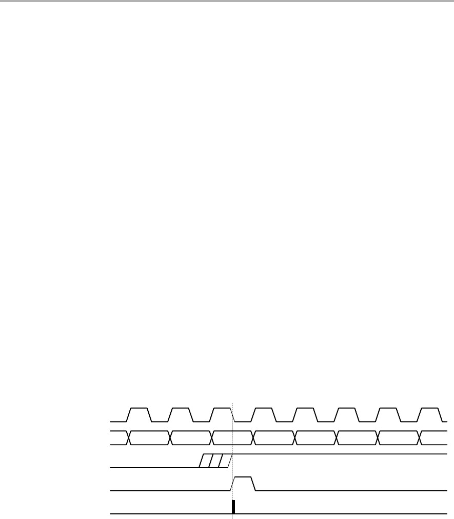
Timer_B Operation
13-11
Timer_B
13.2.4 Capture/Compare Blocks
Three or seven identical capture/compare blocks, TBCCRx, are present in
Timer_B. Any of the blocks may be used to capture the timer data or to
generate time intervals.
Capture Mode
The capture mode is selected when CAP = 1. Capture mode is used to record
time events. It can be used for speed computations or time measurements.
The capture inputs CCIxA and CCIxB are connected to external pins or internal
signals and are selected with the CCISx bits. The CMx bits select the capture
edge of the input signal as rising, falling, or both. A capture occurs on the
selected edge of the input signal. If a capture is performed:
-The timer value is copied into the TBCCRx register
-The interrupt flag CCIFG is set
The input signal level can be read at any time via the CCI bit. MSP430x2xx
family devices may have different signals connected to CCIxA and CCIxB.
Refer to the device-specific data sheet for the connections of these signals.
The capture signal can be asynchronous to the timer clock and cause a race
condition. Setting the SCS bit will synchronize the capture with the next timer
clock. Setting the SCS bit to synchronize the capture signal with the timer clock
is recommended. This is illustrated in Figure 13−10.
Figure 13−10. Capture Signal (SCS=1)
n−2 n−1
Timer Clock
Timer
Set TBCCRx CCIFG
n+1 n+3 n+4
CCI
Capture
n+2n
Overflow logic is provided in each capture/compare register to indicate if a
second capture was performed before the value from the first capture was
read. Bit COV is set when this occurs as shown in Figure 13−11. COV must
be reset with software.

Timer_B Operation
13-12 Timer_B
Figure 13−11.Capture Cycle
Second
Capture
Taken
COV = 1
Capture
Taken
No
Capture
Taken
Read
Taken
Capture
Clear Bit COV
in Register TBCCTLx
Idle
Idle
Capture
Capture Read and No Capture
Capture
Capture ReadCapture
Capture
Capture Initiated by Software
Captures can be initiated by software. The CMx bits can be set for capture on
both edges. Software then sets bit CCIS1=1 and toggles bit CCIS0 to switch
the capture signal between VCC and GND, initiating a capture each time
CCIS0 changes state:
MOV #CAP+SCS+CCIS1+CM_3,&TBCCTLx ; Setup TBCCTLx
XOR #CCIS0,&TBCCTLx ; TBCCTLx = TBR
Compare Mode
The compare mode is selected when CAP = 0. Compare mode is used to
generate PWM output signals or interrupts at specific time intervals. When
TBR counts to the value in a TBCLx:
-Interrupt flag CCIFG is set
-Internal signal EQUx = 1
-EQUx affects the output according to the output mode

Timer_B Operation
13-13
Timer_B
Compare Latch TBCLx
The TBCCRx compare latch, TBCLx, holds the data for the comparison to the
timer value in compare mode. TBCLx is buffered by TBCCRx. The buffered
compare latch gives the user control over when a compare period updates.
The user cannot directly access TBCLx. Compare data is written to each
TBCCRx and automatically transferred to TBCLx. The timing of the transfer
from TBCCRx to TBCLx is user-selectable with the CLLDx bits as described
in Table 13−2.
Table 13−2.TBCLx Load Events
CLLDx Description
00 New data is transferred from TBCCRx to TBCLx immediately when
TBCCRx is written to.
01 New data is transferred from TBCCRx to TBCLx when TBR counts to 0
10 New data is transferred from TBCCRx to TBCLx when TBR counts to 0
for up and continuous modes. New data is transferred to from TBCCRx
to TBCLx when TBR counts to the old TBCL0 value or to 0 for up/down
mode
11 New data is transferred from TBCCRx to TBCLx when TBR
counts to the old TBCLx value.
Grouping Compare Latches
Multiple compare latches may be grouped together for simultaneous updates
with the TBCLGRPx bits. When using groups, the CLLDx bits of the lowest
numbered TBCCRx in the group determine the load event for each compare
latch of the group, except when TBCLGRP = 3, as shown in Table 13−3. The
CLLDx bits of the controlling TBCCRx must not be set to zero. When the
CLLDx bits of the controlling TBCCRx are set to zero, all compare latches
update immediately when their corresponding TBCCRx is written; no compare
latches are grouped.
Two conditions must exist for the compare latches to be loaded when grouped.
First, all TBCCRx registers of the group must be updated, even when new
TBCCRx data = old TBCCRx data. Second, the load event must occur.
Table 13−3.Compare Latch Operating Modes
TBCLGRPx Grouping Update Control
00 None Individual
01 TBCL1+TBCL2
TBCL3+TBCL4
TBCL5+TBCL6
TBCCR1
TBCCR3
TBCCR5
10 TBCL1+TBCL2+TBCL3
TBCL4+TBCL5+TBCL6
TBCCR1
TBCCR4
11 TBCL0+TBCL1+TBCL2+
TBCL3+TBCL4+TBCL5+TBCL6
TBCCR1

Timer_B Operation
13-14 Timer_B
13.2.5 Output Unit
Each capture/compare block contains an output unit. The output unit is used
to generate output signals such as PWM signals. Each output unit has eight
operating modes that generate signals based on the EQU0 and EQUx signals.
The TBOUTH pin function can be used to put all Timer_B outputs into a
high-impedance state. When the TBOUTH pin function is selected for the pin,
and when the pin is pulled high, all Timer_B outputs are in a high-impedance
state.
Output Modes
The output modes are defined by the OUTMODx bits and are described in
Table 13−4. The OUTx signal is changed with the rising edge of the timer clock
for all modes except mode 0. Output modes 2, 3, 6, and 7 are not useful for
output unit 0 because EQUx = EQU0.
Table 13−4.Output Modes
OUTMODx Mode Description
000 Output The output signal OUTx is defined by the
OUTx bit. The OUTx signal updates
immediately when OUTx is updated.
001 Set The output is set when the timer counts
to the TBCLx value. It remains set until a
reset of the timer, or until another output
mode is selected and affects the output.
010 Toggle/Reset The output is toggled when the timer
counts to the TBCLx value. It is reset
when the timer counts to the TBCL0
value.
011 Set/Reset The output is set when the timer counts
to the TBCLx value. It is reset when the
timer counts to the TBCL0 value.
100 Toggle The output is toggled when the timer
counts to the TBCLx value. The output
period is double the timer period.
101 Reset The output is reset when the timer counts
to the TBCLx value. It remains reset until
another output mode is selected and
affects the output.
110 Toggle/Set The output is toggled when the timer
counts to the TBCLx value. It is set when
the timer counts to the TBCL0 value.
111 Reset/Set The output is reset when the timer counts
to the TBCLx value. It is set when the
timer counts to the TBCL0 value.
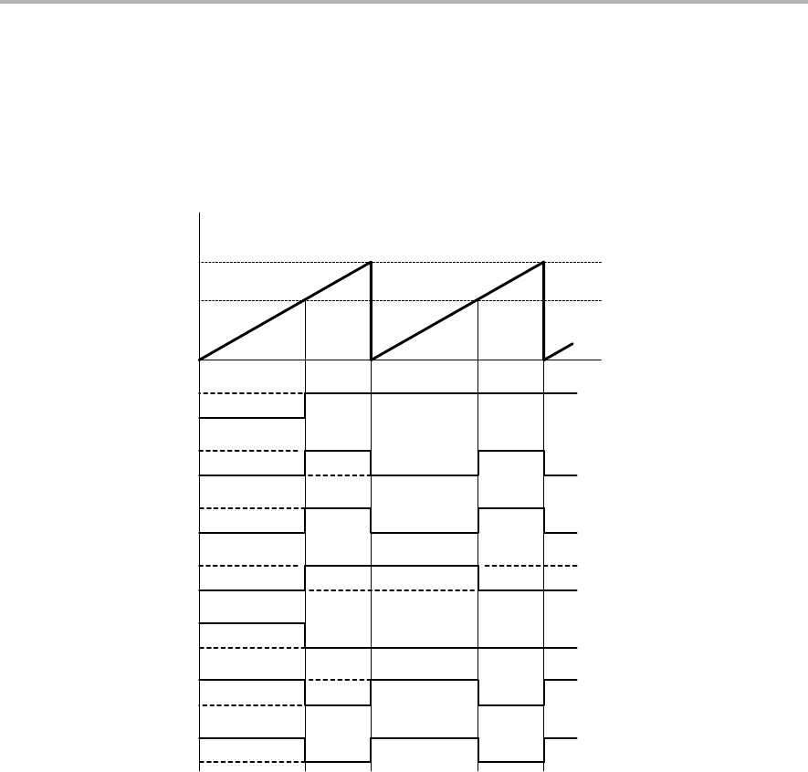
Timer_B Operation
13-15
Timer_B
Output Example—Timer in Up Mode
The OUTx signal is changed when the timer counts up to the TBCLx value, and
rolls from TBCL0 to zero, depending on the output mode. An example is shown
in Figure 13−12 using TBCL0 and TBCL1.
Figure 13−12. Output Example—Timer in Up Mode
0h
TBR(max)
EQU0
TBIFG
Output Mode 1: Set
Output Mode 2: Toggle/Reset
Output Mode 3: Set/Reset
Output Mode 4: Toggle
Output Mode 5: Reset
Output Mode 6: Toggle/Set
Output Mode 7: Reset/Set
TBCL0
TBCL1
EQU1 EQU0
TBIFG
EQU1 EQU0
TBIFG Interrupt Events
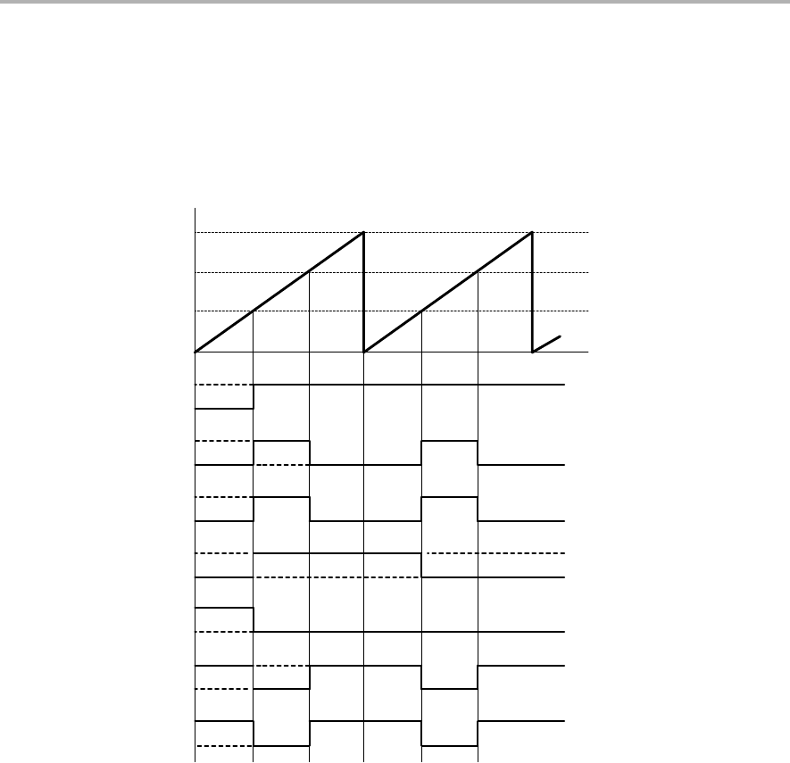
Timer_B Operation
13-16 Timer_B
Output Example—Timer in Continuous Mode
The OUTx signal is changed when the timer reaches the TBCLx and TBCL0
values, depending on the output mode, An example is shown in Figure 13−13
using TBCL0 and TBCL1.
Figure 13−13. Output Example—Timer in Continuous Mode
0h
TBR(max)
TBIFG
Output Mode 1: Set
Output Mode 2: Toggle/Reset
Output Mode 3: Set/Reset
Output Mode 4: Toggle
Output Mode 5: Reset
Output Mode 6: Toggle/Set
Output Mode 7: Reset/Set
TBCL0
TBCL1
EQU1 TBIFG EQU1 EQU0 Interrupt EventsEQU0
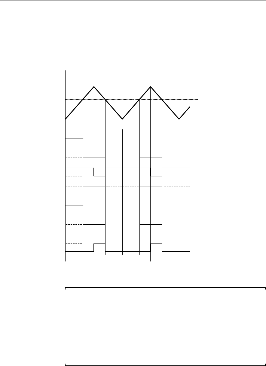
Timer_B Operation
13-17
Timer_B
Output Example − Timer in Up/Down Mode
The OUTx signal changes when the timer equals TBCLx in either count
direction and when the timer equals TBCL0, depending on the output mode.
An example is shown in Figure 13−14 using TBCL0 and TBCL3.
Figure 13−14. Output Example—Timer in Up/Down Mode
0h
TBR(max)
TBIFG
Output Mode 1: Set
Output Mode 2: Toggle/Reset
Output Mode 3: Set/Reset
Output Mode 4: Toggle
Output Mode 5: Reset
Output Mode 6: Toggle/Set
Output Mode 7: Reset/Set
TBCL0
TBCL3
EQU3
TBIFG Interrupt Events
EQU3
EQU0
EQU3 EQU3
EQU0
Note: Switching Between Output Modes
When switching between output modes, one of the OUTMODx bits should
remain set during the transition, unless switching to mode 0. Otherwise,
output glitching can occur because a NOR gate decodes output mode 0. A
safe method for switching between output modes is to use output mode 7 as
a transition state:
BIS #OUTMOD_7,&TBCCTLx ; Set output mode=7
BIC #OUTMODx,&TBCCTLx ; Clear unwanted bits
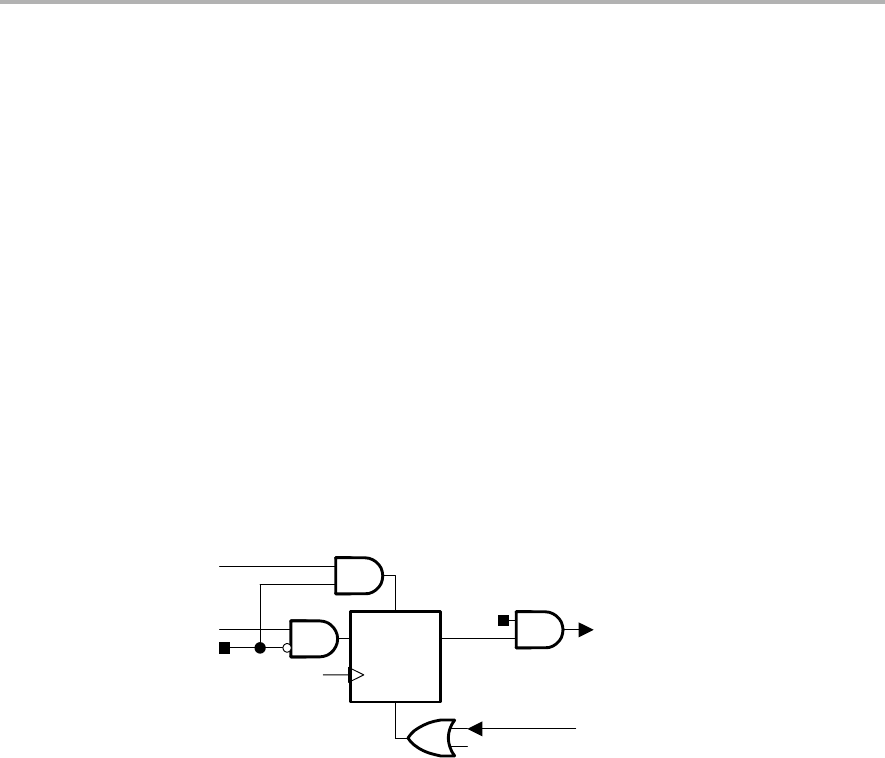
Timer_B Operation
13-18 Timer_B
13.2.6 Timer_B Interrupts
Two interrupt vectors are associated with the 16-bit Timer_B module:
-TBCCR0 interrupt vector for TBCCR0 CCIFG
-TBIV interrupt vector for all other CCIFG flags and TBIFG
In capture mode, any CCIFG flag is set when a timer value is captured in the
associated TBCCRx register. In compare mode, any CCIFG flag is set when
TBR counts to the associated TBCLx value. Software may also set or clear any
CCIFG flag. All CCIFG flags request an interrupt when their corresponding
CCIE bit and the GIE bit are set.
TBCCR0 Interrupt Vector
The TBCCR0 CCIFG flag has the highest Timer_B interrupt priority and has
a dedicated interrupt vector as shown in Figure 13−15. The TBCCR0 CCIFG
flag is automatically reset when the TBCCR0 interrupt request is serviced.
Figure 13−15. Capture/Compare TBCCR0 Interrupt Flag
DSet QIRQ, Interrupt Service Requested
Reset
Timer Clock
POR
CAP
EQU0
Capture
IRACC, Interrupt Request Accepted
CCIE
TBIV, Interrupt Vector Generator
The TBIFG flag and TBCCRx CCIFG flags (excluding TBCCR0 CCIFG) are
prioritized and combined to source a single interrupt vector. The interrupt
vector register TBIV is used to determine which flag requested an interrupt.
The highest priority enabled interrupt (excluding TBCCR0 CCIFG) generates
a number in the TBIV register (see register description). This number can be
evaluated or added to the program counter to automatically enter the
appropriate software routine. Disabled Timer_B interrupts do not affect the
TBIV value.
Any access, read or write, of the TBIV register automatically resets the highest
pending interrupt flag. If another interrupt flag is set, another interrupt is
immediately generated after servicing the initial interrupt. For example, if the
TBCCR1 and TBCCR2 CCIFG flags are set when the interrupt service routine
accesses the TBIV register, TBCCR1 CCIFG is reset automatically. After the
RETI instruction of the interrupt service routine is executed, the TBCCR2
CCIFG flag will generate another interrupt.

Timer_B Operation
13-19
Timer_B
TBIV, Interrupt Handler Examples
The following software example shows the recommended use of TBIV and the
handling overhead. The TBIV value is added to the PC to automatically jump
to the appropriate routine.
The numbers at the right margin show the necessary CPU clock cycles for
each instruction. The software overhead for different interrupt sources
includes interrupt latency and return-from-interrupt cycles, but not the task
handling itself. The latencies are:
-Capture/compare block CCR0 11 cycles
-Capture/compare blocks CCR1 to CCR6 16 cycles
-Timer overflow TBIFG 14 cycles
The following software example shows the recommended use of TBIV for
Timer_B3.
; Interrupt handler for TBCCR0 CCIFG. Cycles
CCIFG_0_HND
... ; Start of handler Interrupt latency 6
RETI 5
; Interrupt handler for TBIFG, TBCCR1 and TBCCR2 CCIFG.
TB_HND ... ; Interrupt latency 6
ADD &TBIV,PC ; Add offset to Jump table 3
RETI ; Vector 0: No interrupt 5
JMP CCIFG_1_HND ; Vector 2: Module 1 2
JMP CCIFG_2_HND ; Vector 4: Module 2 2
RETI ; Vector 6
RETI ; Vector 8
RETI ; Vector 10
RETI ; Vector 12
TBIFG_HND ; Vector 14: TIMOV Flag
... ; Task starts here
RETI 5
CCIFG_2_HND ; Vector 4: Module 2
... ; Task starts here
RETI ; Back to main program 5
; The Module 1 handler shows a way to look if any other
; interrupt is pending: 5 cycles have to be spent, but
; 9 cycles may be saved if another interrupt is pending
CCIFG_1_HND ; Vector 6: Module 3
... ; Task starts here
JMP TB_HND ; Look for pending ints 2

Timer_B Registers
13-20 Timer_B
13.3 Timer_B Registers
The Timer_B registers are listed in Table 13−5:
Table 13−5.Timer_B Registers
Register Short Form Register Type Address Initial State
Timer_B control TBCTL Read/write 0180h Reset with POR
Timer_B counter TBR Read/write 0190h Reset with POR
Timer_B capture/compare control 0 TBCCTL0 Read/write 0182h Reset with POR
Timer_B capture/compare 0 TBCCR0 Read/write 0192h Reset with POR
Timer_B capture/compare control 1 TBCCTL1 Read/write 0184h Reset with POR
Timer_B capture/compare 1 TBCCR1 Read/write 0194h Reset with POR
Timer_B capture/compare control 2 TBCCTL2 Read/write 0186h Reset with POR
Timer_B capture/compare 2 TBCCR2 Read/write 0196h Reset with POR
Timer_B capture/compare control 3 TBCCTL3 Read/write 0188h Reset with POR
Timer_B capture/compare 3 TBCCR3 Read/write 0198h Reset with POR
Timer_B capture/compare control 4 TBCCTL4 Read/write 018Ah Reset with POR
Timer_B capture/compare 4 TBCCR4 Read/write 019Ah Reset with POR
Timer_B capture/compare control 5 TBCCTL5 Read/write 018Ch Reset with POR
Timer_B capture/compare 5 TBCCR5 Read/write 019Ch Reset with POR
Timer_B capture/compare control 6 TBCCTL6 Read/write 018Eh Reset with POR
Timer_B capture/compare 6 TBCCR6 Read/write 019Eh Reset with POR
Timer_B interrupt vector TBIV Read only 011Eh Reset with POR

Timer_B Registers
13-21
Timer_B
Timer_B Control Register TBCTL
15 14 13 12 11 10 9 8
Unused TBCLGRPx CNTLx Unused TBSSELx
rw−(0) rw−(0) rw−(0) rw−(0) rw−(0) rw−(0) rw−(0) rw−(0)
76543210
IDx MCx Unused TBCLR TBIE TBIFG
rw−(0) rw−(0) rw−(0) rw−(0) rw−(0) w−(0) rw−(0) rw−(0)
Unused Bit 15 Unused
TBCLGRP Bit
14-13
TBCLx group
00 Each TBCLx latch loads independently
01 TBCL1+TBCL2 (TBCCR1 CLLDx bits control the update)
TBCL3+TBCL4 (TBCCR3 CLLDx bits control the update)
TBCL5+TBCL6 (TBCCR5 CLLDx bits control the update)
TBCL0 independent
10 TBCL1+TBCL2+TBCL3 (TBCCR1 CLLDx bits control the update)
TBCL4+TBCL5+TBCL6 (TBCCR4 CLLDx bits control the update)
TBCL0 independent
11 TBCL0+TBCL1+TBCL2+TBCL3+TBCL4+TBCL5+TBCL6
(TBCCR1 CLLDx bits control the update)
CNTLx Bits
12-11
Counter Length
00 16-bit, TBR(max) = 0FFFFh
01 12-bit, TBR(max) = 0FFFh
10 10-bit, TBR(max) = 03FFh
11 8-bit, TBR(max) = 0FFh
Unused Bit 10 Unused
TBSSELx Bits
9-8
Timer_B clock source select.
00 TBCLK
01 ACLK
10 SMCLK
11 Inverted TBCLK
IDx Bits
7-6
Input divider. These bits select the divider for the input clock.
00 /1
01 /2
10 /4
11 /8
MCx Bits
5-4
Mode control. Setting MCx = 00h when Timer_B is not in use conserves
power.
00 Stop mode: the timer is halted
01 Up mode: the timer counts up to TBCL0
10 Continuous mode: the timer counts up to the value set by CNTLx
11 Up/down mode: the timer counts up to TBCL0 and down to 0000h

Timer_B Registers
13-22 Timer_B
Unused Bit 3 Unused
TBCLR Bit 2 Timer_B clear. Setting this bit resets TBR, the clock divider, and the count
direction. The TBCLR bit is automatically reset and is always read as zero.
TBIE Bit 1 Timer_B interrupt enable. This bit enables the TBIFG interrupt request.
0 Interrupt disabled
1 Interrupt enabled
TBIFG Bit 0 Timer_B interrupt flag.
0 No interrupt pending
1 Interrupt pending
TBR, Timer_B Register
15 14 13 12 11 10 9 8
TBRx
rw−(0) rw−(0) rw−(0) rw−(0) rw−(0) rw−(0) rw−(0) rw−(0)
76543210
TBRx
rw−(0) rw−(0) rw−(0) rw−(0) rw−(0) rw−(0) rw−(0) rw−(0)
TBRx Bits
15-0
Timer_B register. The TBR register is the count of Timer_B.

Timer_B Registers
13-23
Timer_B
TBCCRx, Timer_B Capture/Compare Register x
15 14 13 12 11 10 9 8
TBCCRx
rw−(0) rw−(0) rw−(0) rw−(0) rw−(0) rw−(0) rw−(0) rw−(0)
76543210
TBCCRx
rw−(0) rw−(0) rw−(0) rw−(0) rw−(0) rw−(0) rw−(0) rw−(0)
TBCCRx Bits
15-0
Timer_B capture/compare register.
Compare mode: Compare data is written to each TBCCRx and automatically
transferred to TBCLx. TBCLx holds the data for the comparison to the timer
value in the Timer_B Register, TBR.
Capture mode: The Timer_B Register, TBR, is copied into the TBCCRx
register when a capture is performed.

Timer_B Registers
13-24 Timer_B
TBCCTLx, Capture/Compare Control Register
15 14 13 12 11 10 9 8
CMx CCISx SCS CLLDx CAP
rw−(0) rw−(0) rw−(0) rw−(0) rw−(0) rw−(0) r−(0) rw−(0)
76543210
OUTMODx CCIE CCI OUT COV CCIFG
rw−(0) rw−(0) rw−(0) rw−(0) r rw−(0) rw−(0) rw−(0)
CMx Bit
15-14
Capture mode
00 No capture
01 Capture on rising edge
10 Capture on falling edge
11 Capture on both rising and falling edges
CCISx Bit
13-12
Capture/compare input select. These bits select the TBCCRx input signal.
See the device-specific data sheet for specific signal connections.
00 CCIxA
01 CCIxB
10 GND
11 VCC
SCS Bit 11 Synchronize capture source. This bit is used to synchronize the capture input
signal with the timer clock.
0 Asynchronous capture
1 Synchronous capture
CLLDx Bit
10-9
Compare latch load. These bits select the compare latch load event.
00 TBCLx loads on write to TBCCRx
01 TBCLx loads when TBR counts to 0
10 TBCLx loads when TBR counts to 0 (up or continuous mode)
TBCLx loads when TBR counts to TBCL0 or to 0 (up/down mode)
11 TBCLx loads when TBR counts to TBCLx
CAP Bit 8 Capture mode
0 Compare mode
1 Capture mode
OUTMODx Bits
7-5
Output mode. Modes 2, 3, 6, and 7 are not useful for TBCL0 because EQUx
= EQU0.
000 OUT bit value
001 Set
010 Toggle/reset
011 Set/reset
100 Toggle
101 Reset
110 Toggle/set
111 Reset/set

Timer_B Registers
13-25
Timer_B
CCIE Bit 4 Capture/compare interrupt enable. This bit enables the interrupt request of
the corresponding CCIFG flag.
0 Interrupt disabled
1 Interrupt enabled
CCI Bit 3 Capture/compare input. The selected input signal can be read by this bit.
OUT Bit 2 Output. For output mode 0, this bit directly controls the state of the output.
0 Output low
1 Output high
COV Bit 1 Capture overflow. This bit indicates a capture overflow occurred. COV must
be reset with software.
0 No capture overflow occurred
1 Capture overflow occurred
CCIFG Bit 0 Capture/compare interrupt flag
0 No interrupt pending
1 Interrupt pending

Timer_B Registers
13-26 Timer_B
TBIV, Timer_B Interrupt Vector Register
15 14 13 12 11 10 9 8
0 0 0 0 0 0 0 0
r0 r0 r0 r0 r0 r0 r0 r0
76543210
0 0 0 0 TBIVx 0
r0 r0 r0 r0 r−(0) r−(0) r−(0) r0
TBIVx Bits
15-0
Timer_B interrupt vector value
TBIV Contents Interrupt Source Interrupt Flag
Interrupt
Priority
00h No interrupt pending −
02h Capture/compare 1 TBCCR1 CCIFG Highest
04h Capture/compare 2 TBCCR2 CCIFG
06h Capture/compare 3†TBCCR3 CCIFG
08h Capture/compare 4†TBCCR4 CCIFG
0Ah Capture/compare 5†TBCCR5 CCIFG
0Ch Capture/compare 6†TBCCR6 CCIFG
0Eh Timer overflow TBIFG Lowest
†Not available on all devices

14-1
Universal Serial Interface
The Universal Serial Interface (USI) module provides SPI and I2C serial
communication with one hardware module. This chapter discusses both
modes. The USI module is implemented in the MSP430x20xx devices.
Topic Page
14.1 USI Introduction 14-2. . . . . . . . . . . . . . . . . . . . . . . . . . . . . . . . . . . . . . . . . . . . . .
14.2 USI Operation 14-5. . . . . . . . . . . . . . . . . . . . . . . . . . . . . . . . . . . . . . . . . . . . . . . .
14.3 USI Registers 14-13. . . . . . . . . . . . . . . . . . . . . . . . . . . . . . . . . . . . . . . . . . . . . . .
Chapter 14

14-2
14.1 USI Introduction
The USI module provides the basic functionality to support synchronous serial
communication. In its simplest form, it is an 8- or 16-bit shift register that can
be used to output data streams, or when combined with minimal software, can
implement serial communication. In addition, the USI includes built-in
hardware functionality to ease the implementation of SPI and I2C
communication. The USI module also includes interrupts to further reduce the
necessary software overhead for serial communication and to maintain the
ultralow-power capabilities of the MSP430.
The USI module features include:
-Three-wire SPI mode support
-I2C mode support
-Variable data length
-Slave operation in LPM4 − no internal clock required
-Selectable MSB or LSB data order
-START and STOP detection for I2C mode with automatic SCL control
-Arbitration lost detection in master mode
-Programmable clock generation
-Selectable clock polarity and phase control
Figure 14−1 shows the USI module in SPI mode. Figure 14−2 shows the USI
module in I2C mode.
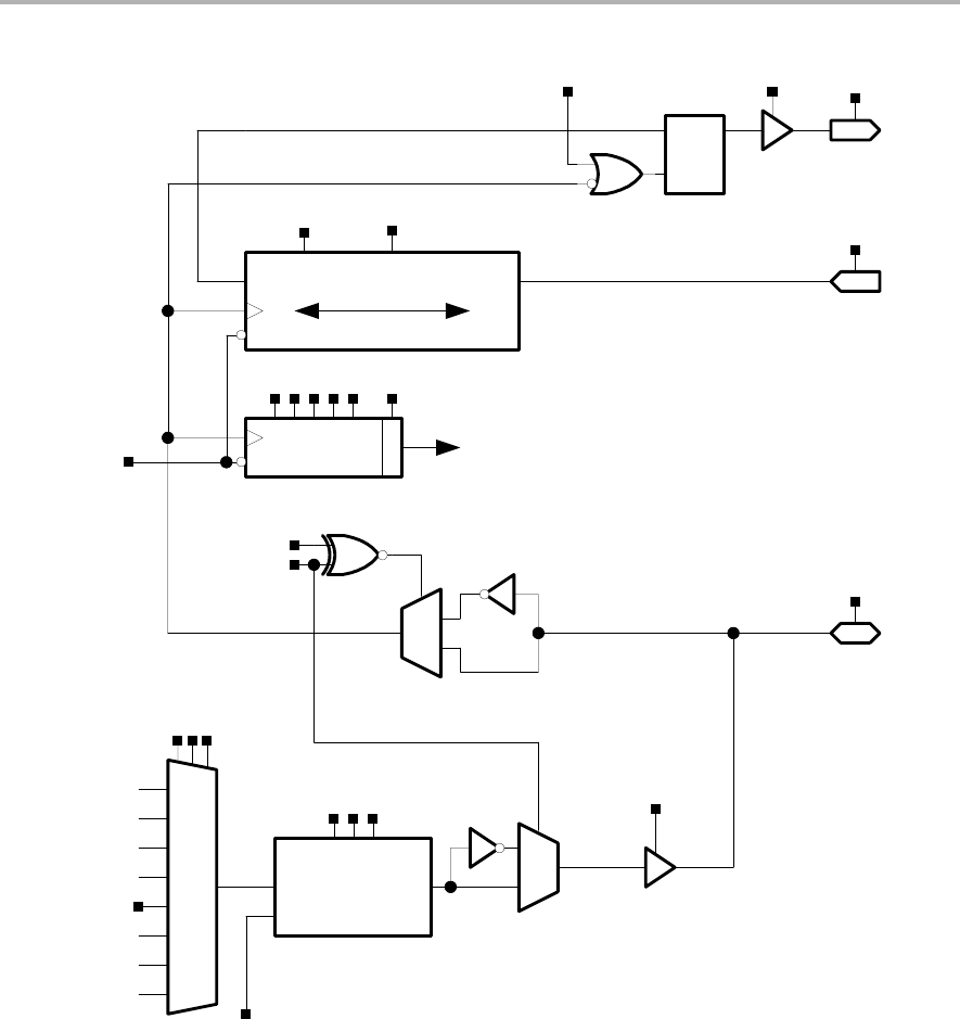
14-3
Figure 14−1. USI Block Diagram: SPI Mode
8/16 Bit Shift Register
USIGE USIOE
SDI
SCLK
Set USIIFG
0
1
USICKPL
USICNTx
Shift Clock
USICKPH
USISSELx
SMCLK
SMCLK
SCLK
ACLK
000
001
010
011
TA 1
TA 2
USISWCLK
TA 0
100
101
110
111
Clock Divider
/1/2/4/8... /128
USIDIVx
0
1USICLK
HOLD
USIIFG
USIMST
SDO
USI16B
D
G
Q
EN
ENUSISWRST
USILSB
USIPE6
USIPE7
USIPE5
USISR
Bit Counter
USIIFGCC
USII2C = 0
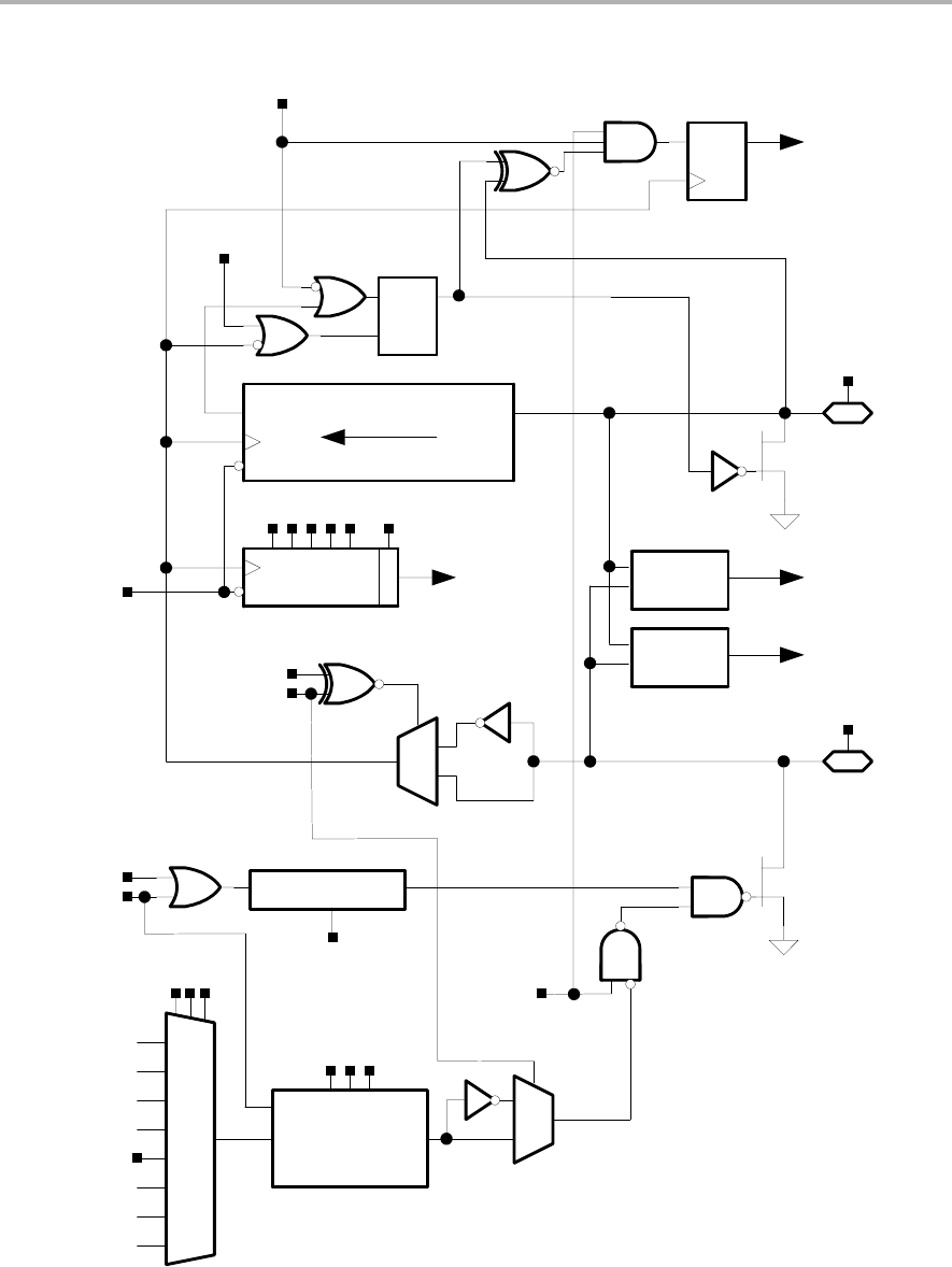
14-4
Figure 14−2. USI Block Diagram: I2C Mode
8−Bit Shift Register
USISRL
MSB LSB
USIGE
D
G
Q
SDA
DQ Set USIAL,
Clear USIOE
SCL
USIIFG
USIMST
START
Detect Set USISTTIFG
Shift Clock
0
1
Set USIIFG
USICNTx
USICKPL
USICKPH
USIOE
STOP
Detect Set USISTP
USISTTIFG
USISSELx
SMCLK
SMCLK
SCLK
ACLK
000
001
010
011
TA 1
TA 2
SWCLK
TA 0
100
101
110
111
Clock Divider
/1/2/4/8... /128
USIDIVx
0
1
USICLK
HOLD
SCL Hold
EN
ENUSISWRST
USISCLREL
USIPE7
USIPE6
Bit Counter
USIIFGCC
USII2C = 1
USICKPL = 1
USICKPH = 0
USILSB = 0
USI16B = 0

14-5
14.2 USI Operation
The USI module is a shift register and bit counter that includes logic to support
SPI and I2C communication. The USI shift register, USISR, is directly
accessible by software and contains the data to be transmitted or the data that
has been received.
The bit counter counts the number of sampled bits and sets the USI interrupt
flag USIIFG when the USICNTx value becomes zero - either by decrementing
or by directly writing zero to the USICNTx bits. Writing USICNTx with a value
> 0 automatically clears USIIFG when USIIFGCC = 0, otherwise USIIFG is not
affected. The USICNTx bits stop decrementing when they become 0. They will
not underflow to 0FFh.
Both the counter and the shift register are driven by the same shift clock. On
a rising shift clock edge, USICNTx decrements and USISR samples the next
bit input. The latch connected to the shift register’s output delays the change
of the output to the falling edge of shift clock. It can be made transparent by
setting the USIGE bit. This setting will immediately output the MSB or LSB of
USISR to the SDO pin, depending on the USILSB bit.
14.2.1 USI Initialization
While the USI software reset bit, USISWRST, is set, the flags USIIFG,
USISTTIFG, USISTP, and USIAL will be held in their reset state. USISR and
USICNTx are not clocked and their contents are not affected. In I2C mode, the
SCL line is also released to the idle state by the USI hardware.
To activate USI port functionality the corresponding USIPEx bits in the USI
control register must be set. This will select the USI function for the pin and
maintains the PxIN and PxIFG functions for the pin as well. With this feature,
the port input levels can be read via the PxIN register by software and the
incoming data stream can generate port interrupts on data transitions. This is
useful, for example, to generate a port interrupt on a START edge.

14-6
14.2.2 USI Clock Generation
The USI clock generator contains a clock selection multiplexer, a divider, and
the ability to select the clock polarity as shown in the block diagrams
Figure 15−1 and Figure 14−2.
The clock source can be selected from the internal clocks ACLK or SMCLK,
from an external clock SCLK, as well as from the capture/compare outputs of
Timer_A. In addition, it is possible to clock the module by software using the
USISWCLK bit when USISSELx = 100.
The USIDIVx bits can be used to divide the selected clock by a power of 2 up
to 128. The generated clock, USICLK, is stopped when USIIFG = 1 or when
the module operates in slave mode.
The USICKPL bit is used to select the polarity of USICLK. When USICKPL = 0,
the inactive level of USICLK is low. When USICKPL = 1 the inactive level of
USICLK is high.
14.2.3 SPI Mode
The USI module is configured in SPI mode when USII2C = 0. Control bit
USICKPL selects the inactive level of the SPI clock while USICKPH selects the
clock edge on which SDO is updated and SDI is sampled. Figure 14−3 shows
the clock/data relationship for an 8-bit, MSB-first transfer. USIPE5, USIPE6,
and USIPE7 must be set to enable the SCLK, SDO, and SDI port functions.
Figure 14−3. SPI Timing
USI
CKPH
USI
CKPL USICNTx
SCLK
SCLK
SCLK
SCLK
SDO/SDI
SDO/SDI
USIIFG
0
1
0
0
01
11
0X
1X
MSB
MSB
87654321
LSB
LSB
00
Load USICNTx

14-7
SPI Master Mode
The USI module is configured as SPI master by setting the master bit USIMST
and clearing the I2C bit USII2C. Since the master provides the clock to the
slave(s) an appropriate clock source needs to be selected and SCLK
configured as output. When USIPE5 = 1, SCLK is automatically configured as
an output.
When USIIFG = 0 and USICNTx > 0, clock generation is enabled and the
master will begin clocking in/out data using USISR.
Received data must be read from the shift register before new data is written
into it for transmission. In a typical application, the USI software will read
received data from USISR, write new data to be transmitted to USISR, and
enable the module for the next transfer by writing the number of bits to be
transferred to USICNTx.
SPI Slave Mode
The USI module is configured as SPI slave by clearing the USIMST and the
USII2C bits. In this mode, when USIPE5 = 1 SCLK is automatically configured
as an input and the USI receives the clock externally from the master.
If the USI is to transmit data, the shift register must be loaded with the data
before the master provides the first clock edge. The output must be enabled
by setting USIOE. When USICKPH = 1, the MSB will be visible on SDO
immediately after loading the shift register.
The SDO pin can be disabled by clearing the USIOE bit. This is useful if the
slave is not addressed in an environment with multiple slaves on the bus.
Once all bits are received, the data must be read from USISR and new data
loaded into USISR before the next clock edge from the master. In a typical
application, after receiving data, the USI software will read the USISR register,
write new data to USISR to be transmitted, and enable the USI module for the
next transfer by writing the number of bits to be transferred to USICNTx.
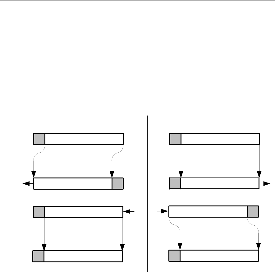
14-8
USISR Operation
The 16-bit USISR is made up of two 8-bit registers, USISRL and USISRH.
Control bit USI16B selects the number of bits of USISR that are used for data
transmit and receive. When USI16B = 0, only the lower 8 bits, USISRL, are
used.
To transfer < 8 bits, the data must be loaded into USISRL such that unused bits
are not shifted out. The data must be MSB- or LSB-aligned depending on
USILSB. Figure 14−4 shows an example of 7-bit data handling.
Figure 14−4. Data adjustments for 7-bit SPI Data
Transmit data in memory
USISRL
Received data in memory
Transmit data in memory
USISRL
Received data in memory
7-bit SPI Mode, MSB first 7-bit SPI Mode, LSB first
USISRL USISRL
TX TX
RX
RX
Shift with software Move
Move Shift with software
7-bit Data 7-bit Data
7-bit Data
7-bit Data
When USI16B = 1, all 16 bits are used for data handling. When using USISR
to access both USISRL and USISRH, the data needs to be properly adjusted
when < 16 bits are used in the same manner as shown in Figure 14−4.
SPI Interrupts
There is one interrupt vector associated with the USI module, and one interrupt
flag, USIIFG, relevant for SPI operation. When USIIE and the GIE bit are set,
the interrupt flag will generate an interrupt request.
USIIFG is set when USICNTx becomes zero, either by counting or by directly
writing 0 to the USICNTx bits. USIIFG is cleared by writing a value > 0 to the
USICNTx bits when USIIFGCC = 0, or directly by software.

14-9
14.2.4 I2C Mode
The USI module is configured in I2C mode when USII2C =1, USICKPL = 1, and
USICKPH = 0. For I2C data compatibility, USILSB and USI16B must be
cleared. USIPE6 and USIPE7 must be set to enable the SCL and SDA port
functions.
I2C Master Mode
To configure the USI module as an I2C master the USIMST bit must be set. In
master mode, clocks are generated by the USI module and output to the SCL
line while USIIFG = 0. When USIIFG = 1, the SCL will stop at the idle, or high,
level. Multi-master operation is supported as described in the Arbitration
section.
The master supports slaves that are holding the SCL line low only when
USIDIVx > 0. When USIDIVx is set to /1 clock division (USIDIVx = 0),
connected slaves must not hold the SCL line low during data transmission.
Otherwise the communication may fail.
I2C Slave Mode
To configure the USI module as an I2C slave the USIMST bit must be cleared.
In slave mode, SCL is held low if USIIFG = 1, USISTTIFG = 1 or if
USICNTx = 0. USISTTIFG must be cleared by software after the slave is setup
and ready to receive the slave address from a master.
I2C Transmitter
In transmitter mode, data is first loaded into USISRL. The output is enabled
by setting USIOE and the transmission is started by writing 8 into USICNTx.
This clears USIIFG and SCL is generated in master mode or released from
being held low in slave mode. After the transmission of all 8 bits, USIIFG is set,
and the clock signal on SCL is stopped in master mode or held low at the next
low phase in slave mode.
To receive the I2C acknowledgement bit, the USIOE bit is cleared with software
and USICNTx is loaded with 1. This clears USIIFG and one bit is received into
USISRL. When USIIFG becomes set again, the LSB of USISRL is the received
acknowledge bit and can be tested in software.
; Receive ACK/NACK
BIC.B #USIOE,&USICTL0 ; SDA input
MOV.B #01h,&USICNT ; USICNTx = 1
TEST_USIIFG
BIT.B #USIIFG,&USICTL1 ; Test USIIFG
JZ TEST_USIIFG
BIT.B #01h,&USISRL ; Test received ACK bit
JNZ HANDLE_NACK ; Handle if NACK
...Else, handle ACK

14-10
I2C Receiver
In I2C receiver mode the output must be disabled by clearing USIOE and the
USI module is prepared for reception by writing 8 into USICNTx. This clears
USIIFG and SCL is generated in master mode or released from being held low
in slave mode. The USIIFG bit will be set after 8 clocks. This stops the clock
signal on SCL in master mode or holds SCL low at the next low phase in slave
mode.
To transmit an acknowledge or no-acknowledge bit, the MSB of the shift
register is loaded with 0 or 1, the USIOE bit is set with software to enable the
output, and 1 is written to the USICNTx bits. As soon as the MSB bit is shifted
out, USIIFG will be become set and the module can be prepared for the
reception of the next I2C data byte.
; Generate ACK
BIS.B #USIOE,&USICTL0 ; SDA output
MOV.B #00h,&USISRL ; MSB = 0
MOV.B #01h,&USICNT ; USICNTx = 1
TEST_USIIFG
BIT.B #USIIFG,&USICTL1 ; Test USIIFG
JZ TEST_USIIFG
...continue...
; Generate NACK
BIS.B #USIOE,&USICTL0 ; SDA output
MOV.B #0FFh,&USISRL ; MSB = 1
MOV.B #01h,&USICNT ; USICNTx = 1
TEST_USIIFG
BIT.B #USIIFG,&USICTL1 ; Test USIIFG
JZ TEST_USIIFG
...continue...
START Condition
A START condition is a high-to-low transition on SDA while SCL is high. The
START condition can be generated by setting the MSB of the shift register to
0. Setting the USIGE and USIOE bits makes the output latch transparent and
the MSB of the shift register is immediately presented to SDA and pulls the line
low. Clearing USIGE resumes the clocked-latch function and holds the 0 on
SDA until data is shifted out with SCL.
; Generate START
MOV.B #000h,&USISRL ; MSB = 0
BIS.B #USIGE+USIOE,&USICTL0 ; Latch/SDA output enabled
BIC.B #USIGE,&USICTL0 ; Latch disabled
...continue...

14-11
STOP Condition
A STOP condition is a low-to-high transition on SDA while SCL is high. To finish
the acknowledgment bit and pull SDA low to prepare the STOP condition
generation requires clearing the MSB in the shift register and loading 1 into
USICNTx. This will generate a low pulse on SCL and during the low phase
SDA is pulled low. SCL stops in the idle, or high, state since the module is in
master mode. To generate the low-to-high transition, the MSB is set in the shift
register and USICNTx is loaded with 1. Setting the USIGE and USIOE bits
makes the output latch transparent and the MSB of USISRL releases SDA to
the idle state. Clearing USIGE stores the MSB in the output latch and the
output is disabled by clearing USIOE. SDA remains high until a START
condition is generated because of the external pullup.
; Generate STOP
BIS.B #USIOE,&USICTL0 ; SDA=output
MOV.B #000H,&USISRL ; MSB = 0
MOV.B #001H,&USICNT ; USICNT = 1 for one clock
TEST_USIIFG
BIT.B #USIIFG,&USICTL1 ; Test USIIFG
JZ TEST_USIIFG ;
MOV.B #0FFH,&USISRL ; USISRL = 1 to drive SDA high
BIS.B #USIGE,&USICTL0 ; Transparent latch enabled
BIC.B #USIGE+USIOE,&USICTL; Latch/SDA output disabled
...continue...
Releasing SCL
Setting the USISCLREL bit will release SCL if it is being held low by the USI
module without requiring USIIFG to be cleared. The USISCLREL bit will be
cleared automatically if a START condition is received and the SCL line will be
held low on the next clock.
In slave operation this bit should be used to prevent SCL from being held low
when the slave has detected that it was not addressed by the master. On the
next START condition USISCLREL will be cleared and the USISTTIFG will be
set.

14-12
Arbitration
The USI module can detect a lost arbitration condition in multi-master I2C
systems. The I2C arbitration procedure uses the data presented on SDA by
the competing transmitters. The first master transmitter that generates a logic
high loses arbitration to the opposing master generating a logic low. The loss
of arbitration is detected in the USI module by comparing the value presented
to the bus and the value read from the bus. If the values are not equal
arbitration is lost and the arbitration lost flag, USIAL, is set. This also clears the
output enable bit USIOE and the USI module no longer drives the bus. In this
case, user software must check the USIAL flag together with USIIFG and
configure the USI to slave receiver when arbitration is lost. The USIAL flag
must be cleared by software.
To prevent other faster masters from generating clocks during the arbitration
procedure SCL is held low if another master on the bus drives SCL low and
USIIFG or USISTTIFG is set, or if USICNTx = 0.
I2C Interrupts
There is one interrupt vector associated with the USI module with two interrupt
flags relevant for I2C operation, USIIFG and USISTTIFG. Each interrupt flag
has its own interrupt enable bit, USIIE and USISTTIE. When an interrupt is
enabled, and the GIE bit is set, a set interrupt flag will generate an interrupt
request.
USIIFG is set when USICNTx becomes zero, either by counting or by directly
writing 0 to the USICNTx bits. USIIFG is cleared by writing a value > 0 to the
USICNTx bits when USIIFGCC = 0, or directly by software.
USISTTIFG is set when a START condition is detected. The USISTTIFG flag
must be cleared by software.
The reception of a STOP condition is indicated with the USISTP flag but there
is no interrupt function associated with the USISTP flag. USISTP is cleared by
writing a value > 0 to the USICNTx bits when USIIFGCC = 0 or directly by
software.

14-13
14.3 USI Registers
The USI registers are listed in Table 14−1.
Table 14−1.USI Registers
Register Short Form Register Type Address Initial State
USI control register 0 USICTL0 Read/write 078h 01h with PUC
USI control register 1 USICTL1 Read/write 079h 01h with PUC
USI clock control USICKCTL Read/write 07Ah Reset with PUC
USI bit counter USICNT Read/write 07Bh Reset with PUC
USI low byte shift register USISRL Read/write 07Ch Unchanged
USI high byte shift register USISRH Read/write 07Dh Unchanged
The USI registers can be accessed with word instructions as shown in
Table 14−2.
Table 14−2.Word Access to USI Registers
Register Short Form High−Byte
Register
Low−Byte
Register Address
USI control register USICTL USICTL1 USICTL0 078h
USI clock and counter control register USICCTL USICNT USICKCTL 07Ah
USI shift register USISR USISRH USISRL 07Ch

14-14
USICTL0, USI Control Register 0
76543210
USIPE7 USIPE6 USIPE5 USILSB USIMST USIGE USIOE USISWRST
rw−0 rw−0 rw−0 rw−0 rw−0 rw−0 rw−0 rw−1
USIPE7 Bit 7 USI SDI/SDA port enable
Input in SPI mode, input or open drain output in I2C mode.
0 USI function disabled
1 USI function enabled
USIPE6 Bit 6 USI SDO/SCL port enable
Output in SPI mode, input or open drain output in I2C mode.
0 USI function disabled
1 USI function enabled
USIPE5 Bit 5 USI SCLK port enable
Input in SPI slave mode, or I2C mode, output in SPI master mode.
0 USI function disabled
1 USI function enabled
USILSB Bit 4 LSB first select. This bit controls the direction of the receive and transmit
shift register.
0 MSB first
1 LSB first
USIMST Bit 3 Master select
0 Slave mode
1 Master mode
USIGE Bit 2 Output latch control
0 Output latch enable depends on shift clock
1 Output latch always enabled and transparent
USIOE Bit 1 Data output enable
0 Output disabled
1 Output enabled
USISWRST Bit 0 USI software reset
0 USI released for operation.
1 USI logic held in reset state.

14-15
USICTL1, USI Control Register 1
76543210
USICKPH USII2C USISTTIE USIIE USIAL USISTP USISTTIFG USIIFG
rw−0 rw−0 rw−0 rw−0 rw−0 rw−0 rw−0 rw−1
USICKPH Bit 7 Clock phase select
0 Data is changed on the first SCLK edge and captured on the
following edge.
1 Data is captured on the first SCLK edge and changed on the
following edge.
USII2C Bit 6 I2C mode enable
0 I2C mode disabled
1 I2C mode enabled
USISTTIE Bit 5 START condition interrupt-enable
0 Interrupt on START condition disabled
1 Interrupt on START condition enabled
USIIE Bit 4 USI counter interrupt enable
0 Interrupt disabled
1 Interrupt enabled
USIAL Bit 3 Arbitration lost
0 No arbitration lost condition
1 Arbitration lost
USISTP Bit 2 STOP condition received. USISTP is automatically cleared if USICNTx is
loaded with a value > 0 when USIIFGCC = 0.
0 No STOP condition received
1 STOP condition received
USISTTIFG Bit 1 START condition interrupt flag
0 No START condition received. No interrupt pending.
1 START condition received. Interrupt pending.
USIIFG Bit 0 USI counter interrupt flag. Set when the USICNTx = 0. Automatically
cleared if USICNTx is loaded with a value > 0 when USIIFGCC = 0.
0 No interrupt pending
1 Interrupt pending

14-16
USICKCTL, USI Clock Control Register
76543210
USIDIVx USISSELx USICKPL USISWCLK
rw−0 rw−0 rw−0 rw−0 rw−0 rw−0 rw−0 rw−0
USIDIVx Bits
7−5
Clock divider select
000 Divide by 1
001 Divide by 2
010 Divide by 4
011 Divide by 8
100 Divide by 16
101 Divide by 32
110 Divide by 64
111 Divide by 128
USISSELx Bits
4−2
Clock source select. Not used in slave mode.
000 SCLK (Not used in SPI mode)
001 ACLK
010 SMCLK
011 SMCLK
100 USISWCLK bit
101 TACCR0
110 TACCR1
111 TACCR2 (Reserved on MSP430F20xx devices)
USICKPL Bit 1 Clock polarity select
0 Inactive state is low
1 Inactive state is high
USISWCLK Bit 0 Software clock
0 Input clock is low
1 Input clock is high

14-17
USICNT, USI Bit Counter Register
76543210
USISCLREL USI16B USIIFGCC USICNTx
rw−0 rw−0 rw−0 rw−0 rw−0 rw−0 rw−0 rw−0
USISCLREL Bit 7 SCL release. The SCL line is released from low to idle. USISCLREL is
cleared if a START condition is detected.
0 SCL line is held low if USIIFG is set
1 SCL line is released
USI16B Bit 6 16-bit shift register enable
0 8-bit shift register mode. Low byte register USISRL is used.
1 16-bit shift register mode. Both high and low byte registers USISRL
and USISRH are used. USISR addresses all 16 bits simultaneously.
USIIFGCC Bit 5 USI interrupt flag clear control. When USIIFGCC = 1 the USIIFG will not be
cleared automatically when USICNTx is written with a value > 0.
0 USIIFG automatically cleared on USICNTx update
1 USIIFG is not cleared automatically
USICNTx Bits
4−0
USI bit count
The USICNTx bits set the number of bits to be received or transmitted.

14-18
USISRL, USI Low Byte Shift Register
76543210
USISRLx
rw rw rw rw rw rw rw rw
USISRLx Bits
7−0
Contents of the USI low byte shift register
USISRH, USI High Byte Shift Register
76543210
USISRHx
rw rw rw rw rw rw rw rw
USISRHx Bits
7−0
Contents of the USI high byte shift register. Ignored when USI16B = 0.

15-1
Universal Serial Communication Interface, UART Mode
Universal Serial Communication Interface,
UART Mode
The universal serial communication interface (USCI) supports multiple serial
communication modes with one hardware module. This chapter discusses the
operation of the asynchronous UART mode.
Topic Page
15.1 USCI Overview 15-2. . . . . . . . . . . . . . . . . . . . . . . . . . . . . . . . . . . . . . . . . . . . . . .
15.2 USCI Introduction: UART Mode 15-3. . . . . . . . . . . . . . . . . . . . . . . . . . . . . . . .
15.3 USCI Operation: UART Mode 15-5. . . . . . . . . . . . . . . . . . . . . . . . . . . . . . . . . .
15.4 USCI Registers: UART Mode 15-27. . . . . . . . . . . . . . . . . . . . . . . . . . . . . . . . .
Chapter 15

USCI Overview
15-2 Universal Serial Communication Interface, UART Mode
15.1 USCI Overview
The universal serial communication interface (USCI) modules support
multiple serial communication modes. Different USCI modules support
different modes. Each different USCI module is named with a different letter.
For example, USCI_A is different from USCI_B, etc. If more than one identical
USCI module is implemented on one device, those modules are named with
incrementing numbers. For example, if one device has two USCI_A modules,
they are named USCI_A0 and USCI_A1. See the device-specific data sheet
to determine which USCI modules, if any, are implemented on which devices.
The USCI_Ax modules support:
-UART mode
-Pulse shaping for IrDA communications
-Automatic baud rate detection for LIN communications
-SPI mode
The USCI_Bx modules support:
-I2C mode
-SPI mode

USCI Introduction: UART Mode
15-3
Universal Serial Communication Interface, UART Mode
15.2 USCI Introduction: UART Mode
In asynchronous mode, the USCI_Ax modules connect the MSP430 to an
external system via two external pins, UCAxRXD and UCAxTXD. UART mode
is selected when the UCSYNC bit is cleared.
UART mode features include:
-7- or 8-bit data with odd, even, or non-parity
-Independent transmit and receive shift registers
-Separate transmit and receive buffer registers
-LSB-first or MSB-first data transmit and receive
-Built-in idle-line and address-bit communication protocols for
multiprocessor systems
-Receiver start-edge detection for auto-wake up from LPMx modes
-Programmable baud rate with modulation for fractional baud rate support
-Status flags for error detection and suppression
-Status flags for address detection
-Independent interrupt capability for receive and transmit
Figure 15−1 shows the USCI_Ax when configured for UART mode.
USCI Introduction: UART Mode
15-4 Universal Serial Communication Interface, UART Mode
Figure 15−1. USCI_Ax Block Diagram: UART Mode (UCSYNC = 0)
Modulator
ACLK
SMCLK
SMCLK
00
01
10
11
UCSSELx
UC0CLK
Prescaler/Divider
Receive Baudrate Generator
UC0BRx
16
UCBRFx
4
UCBRSx
3
UCOS16
UCRXERR
Error Flags
Set Flags
UCPE
UCFE
UCOE
UCABEN
Receive Shift Register
Receive Buffer UC0RXBUF
Receive State Machine
1
0
UCIREN
UCPEN UCPAR UCMSB UC7BIT
UCDORMUCMODEx
2
UCSPB
Set UCBRK
Set UCADDR/UCIDLE
0
1
UCLISTEN
UC0RX
1
0
UCIRRXPL
IrDA Decoder
UCIRRXFE
UCIRRXFLx
6
Transmit Buffer UC0TXBUF
Transmit State Machine
UCTXADDR
UCTXBRK
Transmit Shift Register
UCPEN UCPAR UCMSB UC7BIT UCIREN
UCIRTXPLx
6
0
1
IrDA Encoder UC0TX
Transmit Clock
Receive Clock
BRCLK
UCMODEx
2
UCSPB
UCRXEIE
UCRXBRKIE
Set UC0RXIFG
Set UC0TXIFG
Set RXIFG

USCI Operation: UART Mode
15-5
Universal Serial Communication Interface, UART Mode
15.3 USCI Operation: UART Mode
In UART mode, the USCI transmits and receives characters at a bit rate
asynchronous to another device. Timing for each character is based on the
selected baud rate of the USCI. The transmit and receive functions use the
same baud rate frequency.
15.3.1 USCI Initialization and Reset
The USCI is reset by a PUC or by setting the UCSWRST bit. After a PUC, the
UCSWRST bit is automatically set, keeping the USCI in a reset condition.
When set, the UCSWRST bit resets the UCAxRXIE, UCAxTXIE, UCAxRXIFG,
UCRXERR, UCBRK, UCPE, UCOE, UCFE, UCSTOE and UCBTOE bits and
sets the UCAxTXIFG bit. Clearing UCSWRST releases the USCI for
operation.
Note: Initializing or Re-Configuring the USCI Module
The recommended USCI initialization/re-configuration process is:
1) Set UCSWRST (BIS.B #UCSWRST,&UCAxCTL1)
2) Initialize all USCI registers with UCSWRST = 1 (including UCAxCTL1)
3) Configure ports.
4) Clear UCSWRST via software (BIC.B #UCSWRST,&UCAxCTL1)
5) Enable interrupts (optional) via UCAxRXIE and/or UCAxTXIE
15.3.2 Character Format
The UART character format, shown in Figure 15−2, consists of a start bit,
seven or eight data bits, an even/odd/no parity bit, an address bit (address-bit
mode), and one or two stop bits. The UCMSB bit controls the direction of the
transfer and selects LSB or MSB first. LSB-first is typically required for UART
communication.
Figure 15−2. Character Format
[Parity Bit, UCPEN = 1]
[Address Bit, UCMODEx = 10]
Mark
Space
D0 D6 D7 AD PA SP SP
[Optional Bit, Condition]
[2nd Stop Bit, UCSPB = 1]
[8th Data Bit, UC7BIT = 0]
ST
USCI Operation: UART Mode
15-6 Universal Serial Communication Interface, UART Mode
15.3.3 Asynchronous Communication Formats
When two devices communicate asynchronously, no multiprocessor format is
required for the protocol. When three or more devices communicate, the USCI
supports the idle-line and address-bit multiprocessor communication formats.
Idle-Line Multiprocessor Format
When UCMODEx = 01, the idle-line multiprocessor format is selected. Blocks
of data are separated by an idle time on the transmit or receive lines as shown
in Figure 15−3. An idle receive line is detected when 10 or more continuous
ones (marks) are received after the one or two stop bits of a character. The
baud rate generator is switched off after reception of an idle line until the next
start edge is detected. When an idle line is detected the UCIDLE bit is set.
The first character received after an idle period is an address character. The
UCIDLE bit is used as an address tag for each block of characters. In idle-line
multiprocessor format, this bit is set when a received character is an address
Figure 15−3. Idle-Line Format
ST Address SP ST Data SP ST Data SP
Blocks of
Characters
Idle Periods of 10 Bits or More
UCAxTXD/RXD Expanded
UCAxTXD/RXD
First Character Within Block
Is Address. It Follows Idle
Period of 10 Bits or More
Character Within Block
Idle Period Less Than 10 Bits
Character Within Block
UCAxTXD/RXD

USCI Operation: UART Mode
15-7
Universal Serial Communication Interface, UART Mode
The UCDORM bit is used to control data reception in the idle-line
multiprocessor format. When UCDORM = 1, all non-address characters are
assembled but not transferred into the UCAxRXBUF, and interrupts are not
generated. When an address character is received, the character is
transferred into UCAxRXBUF, UCAxRXIFG is set, and any applicable error
flag is set when UCRXEIE = 1. When UCRXEIE = 0 and an address character
is received but has a framing error or parity error, the character is not
transferred into UCAxRXBUF and UCAxRXIFG is not set.
If an address is received, user software can validate the address and must
reset UCDORM to continue receiving data. If UCDORM remains set, only
address characters will be received. When UCDORM is cleared during the
reception of a character the receive interrupt flag will be set after the reception
completed. The UCDORM bit is not modified by the USCI hardware
automatically.
For address transmission in idle-line multiprocessor format, a precise idle
period can be generated by the USCI to generate address character identifiers
on UCAxTXD. The double-buffered UCTXADDR flag indicates if the next
character loaded into UCAxTXBUF is preceded by an idle line of 11 bits.
UCTXADDR is automatically cleared when the start bit is generated.
Transmitting an Idle Frame
The following procedure sends out an idle frame to indicate an address
character followed by associated data:
1) Set UCTXADDR, then write the address character to UCAxTXBUF.
UCAxTXBUF must be ready for new data (UCAxTXIFG = 1).
This generates an idle period of exactly 11 bits followed by the address
character. UCTXADDR is reset automatically when the address character
is transferred from UCAxTXBUF into the shift register.
2) Write desired data characters to UCAxTXBUF. UCAxTXBUF must be
ready for new data (UCAxTXIFG = 1).
The data written to UCAxTXBUF is transferred to the shift register and
transmitted as soon as the shift register is ready for new data.
The idle-line time must not be exceeded between address and data
transmission or between data transmissions. Otherwise, the transmitted
data will be misinterpreted as an address.

USCI Operation: UART Mode
15-8 Universal Serial Communication Interface, UART Mode
Address-Bit Multiprocessor Format
When UCMODEx = 10, the address-bit multiprocessor format is selected.
Each processed character contains an extra bit used as an address indicator
shown in Figure 15−4. The first character in a block of characters carries a set
address bit which indicates that the character is an address. The USCI
UCADDR bit is set when a received character has its address bit set and is
transferred to UCAxRXBUF.
The UCDORM bit is used to control data reception in the address-bit
multiprocessor format. When UCDORM is set, data characters with address
bit = 0 are assembled by the receiver but are not transferred to UCAxRXBUF
and no interrupts are generated. When a character containing a set address
bit is received, the character is transferred into UCAxRXBUF, UCAxRXIFG is
set, and any applicable error flag is set when UCRXEIE = 1. When UCRXEIE
= 0 and a character containing a set address bit is received, but has a framing
error or parity error, the character is not transferred into UCAxRXBUF and
UCAxRXIFG is not set.
If an address is received, user software can validate the address and must
reset UCDORM to continue receiving data. If UCDORM remains set, only
address characters with address bit = 1 will be received. The UCDORM bit is
not modified by the USCI hardware automatically.
When UCDORM = 0 all received characters will set the receive interrupt flag
UCAxRXIFG. If UCDORM is cleared during the reception of a character the
receive interrupt flag will be set after the reception is completed.
For address transmission in address-bit multiprocessor mode, the address bit
of a character is controlled by the UCTXADDR bit. The value of the
UCTXADDR bit is loaded into the address bit of the character transferred from
UCAxTXBUF to the transmit shift register. UCTXADDR is automatically
cleared when the start bit is generated.
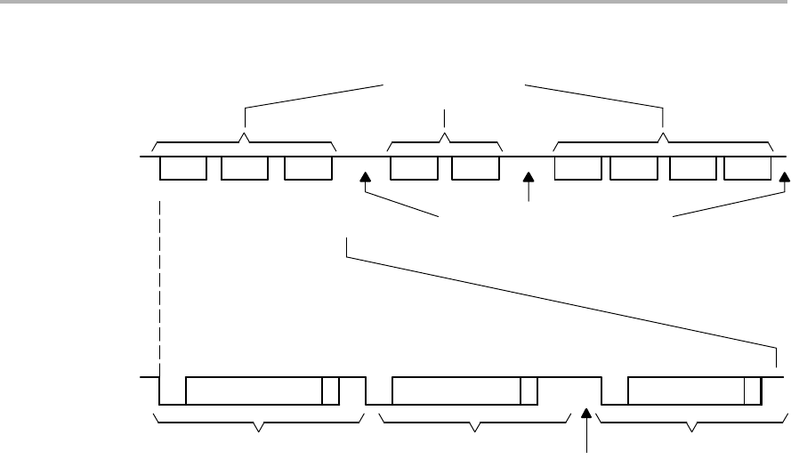
USCI Operation: UART Mode
15-9
Universal Serial Communication Interface, UART Mode
Figure 15−4. Address-Bit Multiprocessor Format
ST Address SP ST Data SP ST Data SP
Blocks of
Characters
Idle Periods of No Significance
UCAxTXD/UCAxRXD
Expanded
UCAxTXD/UCAxRXD
First Character Within Block
Is an Address. AD Bit Is 1
AD Bit Is 0 for
Data Within Block. Idle Time Is of No Significance
UCAxTXD/UCAxRXD 1 0 0
Break Reception and Generation
When UCMODEx = 00, 01, or 10 the receiver detects a break when all data,
parity, and stop bits are low, regardless of the parity, address mode, or other
character settings. When a break is detected, the UCBRK bit is set. If the break
interrupt enable bit, UCBRKIE, is set, the receive interrupt flag UCAxRXIFG
will also be set. In this case, the value in UCAxRXBUF is 0h since all data bits
were zero.
To transmit a break set the UCTXBRK bit, then write 0h to UCAxTXBUF.
UCAxTXBUF must be ready for new data (UCAxTXIFG = 1). This generates
a break with all bits low. UCTXBRK is automatically cleared when the start bit
is generated.
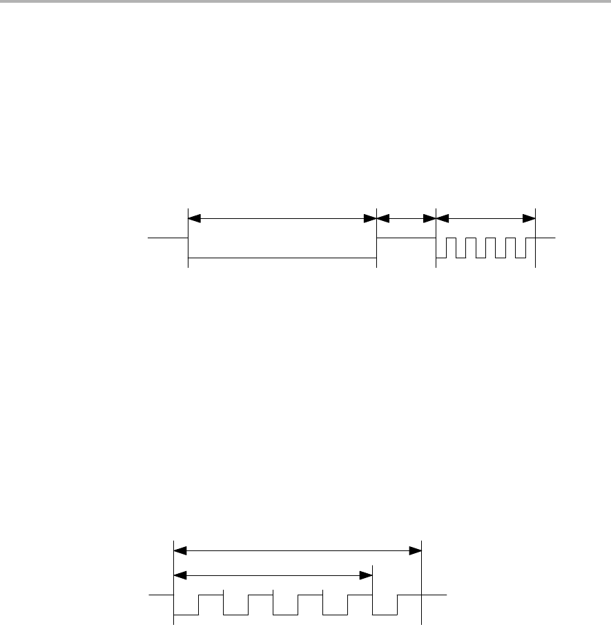
USCI Operation: UART Mode
15-10 Universal Serial Communication Interface, UART Mode
15.3.4 Automatic Baud Rate Detection
When UCMODEx = 11 UART mode with automatic baud rate detection is
selected. For automatic baud rate detection, a data frame is preceded by a
synchronization sequence that consists of a break and a synch field. A break
is detected when 11 or more continuous zeros (spaces) are received. If the
length of the break exceeds 22 bit times the break timeout error flag UCBTOE
is set. The synch field follows the break as shown in Figure 15−5.
Figure 15−5. Auto Baud Rate Detection − Break/Synch Sequence
Break Delimiter Synch
For LIN conformance the character format should be set to 8 data bits, LSB
first, no parity and one stop bit. No address bit is available.
The synch field consists of the data 055h inside a byte field as shown in
Figure 15−6. The synchronization is based on the time measurement between
the first falling edge and the last falling edge of the pattern. The transmit baud
rate generator is used for the measurement if automatic baud rate detection
is enabled by setting UCABDEN. Otherwise, the pattern is received but not
measured. The result of the measurement is transferred into the baud rate
control registers UCAxBR0, UCAxBR1, and UCAxMCTL. If the length of the
synch field exceeds the measurable time the synch timeout error flag
UCSTOE is set.
Figure 15−6. Auto Baud Rate Detection − Synch Field
Synch
Start
Bit
Stop
Bit
01234567
8Bit Times
The UCDORM bit is used to control data reception in this mode. When
UCDORM is set, all characters are received but not transferred into the
UCAxRXBUF, and interrupts are not generated. When a break/synch field is
detected the UCBRK flag is set. The character following the break/synch field
is transferred into UCAxRXBUF and the UCAxRXIFG interrupt flag is set. Any
applicable error flag is also set. If the UCBRKIE bit is set, reception of the
break/synch sets the UCAxRXIFG. The UCBRK bit is reset by user software
or by reading the receive buffer UCAxRXBUF.

USCI Operation: UART Mode
15-11
Universal Serial Communication Interface, UART Mode
When a break/synch field is received, user software must reset UCDORM to
continue receiving data. If UCDORM remains set, only the character after the
next reception of a break/synch field will be received. The UCDORM bit is not
modified by the USCI hardware automatically.
When UCDORM = 0 all received characters will set the receive interrupt flag
UCAxRXIFG. If UCDORM is cleared during the reception of a character the
receive interrupt flag will be set after the reception is complete.
The automatic baud rate detection mode can be used in a full-duplex
communication system with some restrictions. The USCI can not transmit data
while receiving the break/sync field and if a 0h byte with framing error is
received any data transmitted during this time gets corrupted. The latter case
can be discovered by checking the received data and the UCFE bit.
Transmitting a Break/Synch Field
The following procedure transmits a break/synch field:
1) Set UCTXBRK with UMODEx = 11.
2) Write 055h to UCAxTXBUF. UCAxTXBUF must be ready for new data
(UCAxTXIFG = 1).
This generates a break field of 13 bits followed by a break delimiter and the
synch character. The length of the break delimiter is controlled with the
UCDELIMx bits. UCTXBRK is reset automatically when the synch
character is transferred from UCAxTXBUF into the shift register.
3) Write desired data characters to UCAxTXBUF. UCAxTXBUF must be
ready for new data (UCAxTXIFG = 1).
The data written to UCAxTXBUF is transferred to the shift register and
transmitted as soon as the shift register is ready for new data.
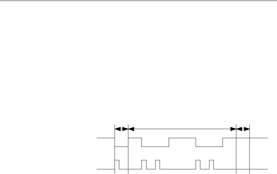
USCI Operation: UART Mode
15-12 Universal Serial Communication Interface, UART Mode
15.3.5 IrDA Encoding and Decoding
When UCIREN is set the IrDA encoder and decoder are enabled and provide
hardware bit shaping for IrDA communication.
IrDA Encoding
The encoder sends a pulse for every zero bit in the transmit bit stream coming
from the UART as shown in Figure 15−7. The pulse duration is defined by
UCIRTXPLx bits specifying the number of half clock periods of the clock
selected by UCIRTXCLK.
Figure 15−7. UART vs. IrDA Data Format
UART
Start
Bit Data Bits
Stop
Bit
IrDA
To set the pulse time of 3/16 bit period required by the IrDA standard the
BITCLK16 clock is selected with UCIRTXCLK = 1 and the pulse length is set
to 6 half clock cycles with UCIRTXPLx = 6 − 1 = 5.
When UCIRTXCLK = 0, the pulse length tPULSE is based on BRCLK and is
calculated as follows:
UCIRTXPLx +tPULSE @2@fBRCLK *1
When the pulse length is based on BRCLK the prescaler UCBRx must to be
set to a value greater or equal to 5.
IrDA Decoding
The decoder detects high pulses when UCIRRXPL = 0. Otherwise it detects
low pulses. In addition to the analog deglitch filter an additional programmable
digital filter stage can be enabled by setting UCIRRXFE. When UCIRRXFE is
set, only pulses longer than the programmed filter length are passed. Shorter
pulses are discarded. The equation to program the filter length UCIRRXFLx
is:
UCIRRXFLx +(tPULSE *tWAKE)@2@fBRCLK *4
where:
tPULSE: Minimum receive pulse width
tWAKE: Wake time from any low power mode. Zero when
MSP430 is in active mode.

USCI Operation: UART Mode
15-13
Universal Serial Communication Interface, UART Mode
15.3.6 Automatic Error Detection
Glitch suppression prevents the USCI from being accidentally started. Any
pulse on UCAxRXD shorter than the deglitch time tτ (approximately 150 ns)
will be ignored. See the device-specific data sheet for parameters.
When a low period on UCAxRXD exceeds tτ a majority vote is taken for the
start bit. If the majority vote fails to detect a valid start bit the USCI halts
character reception and waits for the next low period on UCAxRXD. The
majority vote is also used for each bit in a character to prevent bit errors.
The USCI module automatically detects framing errors, parity errors, overrun
errors, and break conditions when receiving characters. The bits UCFE,
UCPE, UCOE, and UCBRK are set when their respective condition is
detected. When the error flags UCFE, UCPE or UCOE are set, UCRXERR is
also set. The error conditions are described in Table 15−1.
Table 15−1.Receive Error Conditions
Error Condition Error
Flag Description
Framing error UCFE
A framing error occurs when a low stop bit is
detected. When two stop bits are used, both
stop bits are checked for framing error. When a
framing error is detected, the UCFE bit is set.
Parity error UCPE
A parity error is a mismatch between the
number of 1s in a character and the value of
the parity bit. When an address bit is included
in the character, it is included in the parity
calculation. When a parity error is detected, the
UCPE bit is set.
Receive overrun UCOE
An overrun error occurs when a character is
loaded into UCAxRXBUF before the prior
character has been read. When an overrun
occurs, the UCOE bit is set.
Break condition UCBRK
When not using automatic baud rate detection,
a break is detected when all data, parity, and
stop bits are low. When a break condition is
detected, the UCBRK bit is set. A break
condition can also set the interrupt flag
UCAxRXIFG if the break interrupt enable
UCBRKIE bit is set.
When UCRXEIE = 0 and a framing error, or parity error is detected, no
character is received into UCAxRXBUF. When UCRXEIE = 1, characters are
received into UCAxRXBUF and any applicable error bit is set.
When UCFE, UCPE, UCOE, UCBRK, or UCRXERR is set, the bit remains set
until user software resets it or UCAxRXBUF is read. UCOE must be reset by
reading UCAxRXBUF. Otherwise it will not function properly. To detect
overflows reliably, the following flow is recommended. After a character is
received and UCAxRXIFG is set, first read UCAxSTAT to check the error flags
including the overflow flag UCOE. Read UCAxRXBUF next. This will clear all

USCI Operation: UART Mode
15-14 Universal Serial Communication Interface, UART Mode
error flags except UCOE, if UCAxRXBUF was overwritten between the read
access to UCAxSTAT and to UCAxRXBUF. The UCOE flag should be checked
after reading UCAxRXBUF to detect this condition. Note that, in this case, the
UCRXERR flag is not set.
15.3.7 USCI Receive Enable
The USCI module is enabled by clearing the UCSWRST bit and the receiver
is ready and in an idle state. The receive baud rate generator is in a ready state
but is not clocked nor producing any clocks.
The falling edge of the start bit enables the baud rate generator and the UART
state machine checks for a valid start bit. If no valid start bit is detected the
UART state machine returns to its idle state and the baud rate generator is
turned off again. If a valid start bit is detected a character will be received.
When the idle-line multiprocessor mode is selected with UCMODEx = 01 the
UART state machine checks for an idle line after receiving a character. If a start
bit is detected another character is received. Otherwise the UCIDLE flag is set
after 10 ones are received and the UART state machine returns to its idle state
and the baud rate generator is turned off.
Receive Data Glitch Suppression
Glitch suppression prevents the USCI from being accidentally started. Any
glitch on UCAxRXD shorter than the deglitch time tτ (approximately 150 ns)
will be ignored by the USCI and further action will be initiated as shown in
Figure 15−8. See the device-specific data sheet for parameters.
Figure 15−8. Glitch Suppression, USCI Receive Not Started
URXDx
URXS
tτ
When a glitch is longer than tτ, or a valid start bit occurs on UCAxRXD, the
USCI receive operation is started and a majority vote is taken as shown in
Figure 15−9. If the majority vote fails to detect a start bit the USCI halts
character reception.
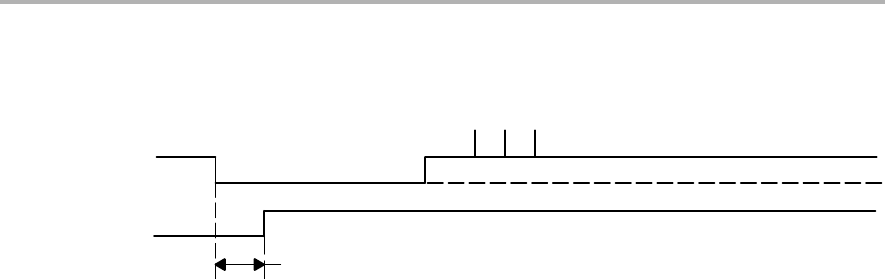
USCI Operation: UART Mode
15-15
Universal Serial Communication Interface, UART Mode
Figure 15−9. Glitch Suppression, USCI Activated
URXDx
URXS
tτ
Majority Vote Taken
15.3.8 USCI Transmit Enable
The USCI module is enabled by clearing the UCSWRST bit and the transmitter
is ready and in an idle state. The transmit baud rate generator is ready but is
not clocked nor producing any clocks.
A transmission is initiated by writing data to UCAxTXBUF. When this occurs,
the baud rate generator is enabled and the data in UCAxTXBUF is moved to
the transmit shift register on the next BITCLK after the transmit shift register
is empty. UCAxTXIFG is set when new data can be written into UCAxTXBUF.
Transmission continues as long as new data is available in UCAxTXBUF at the
end of the previous byte transmission. If new data is not in UCAxTXBUF when
the previous byte has transmitted, the transmitter returns to its idle state and
the baud rate generator is turned off.
15.3.9 UART Baud Rate Generation
The USCI baud rate generator is capable of producing standard baud rates
from non-standard source frequencies. It provides two modes of operation
selected by the UCOS16 bit.
Low-Frequency Baud Rate Generation
The low-frequency mode is selected when UCOS16 = 0. This mode allows
generation of baud rates from low frequency clock sources (e.g. 9600 baud
from a 32768Hz crystal). By using a lower input frequency the power
consumption of the module is reduced. Using this mode with higher
frequencies and higher prescaler settings will cause the majority votes to be
taken in an increasingly smaller window and thus decrease the benefit of the
majority vote.
In low-frequency mode the baud rate generator uses one prescaler and one
modulator to generate bit clock timing. This combination supports fractional
divisors for baud rate generation. In this mode, the maximum USCI baud rate
is one-third the UART source clock frequency BRCLK.
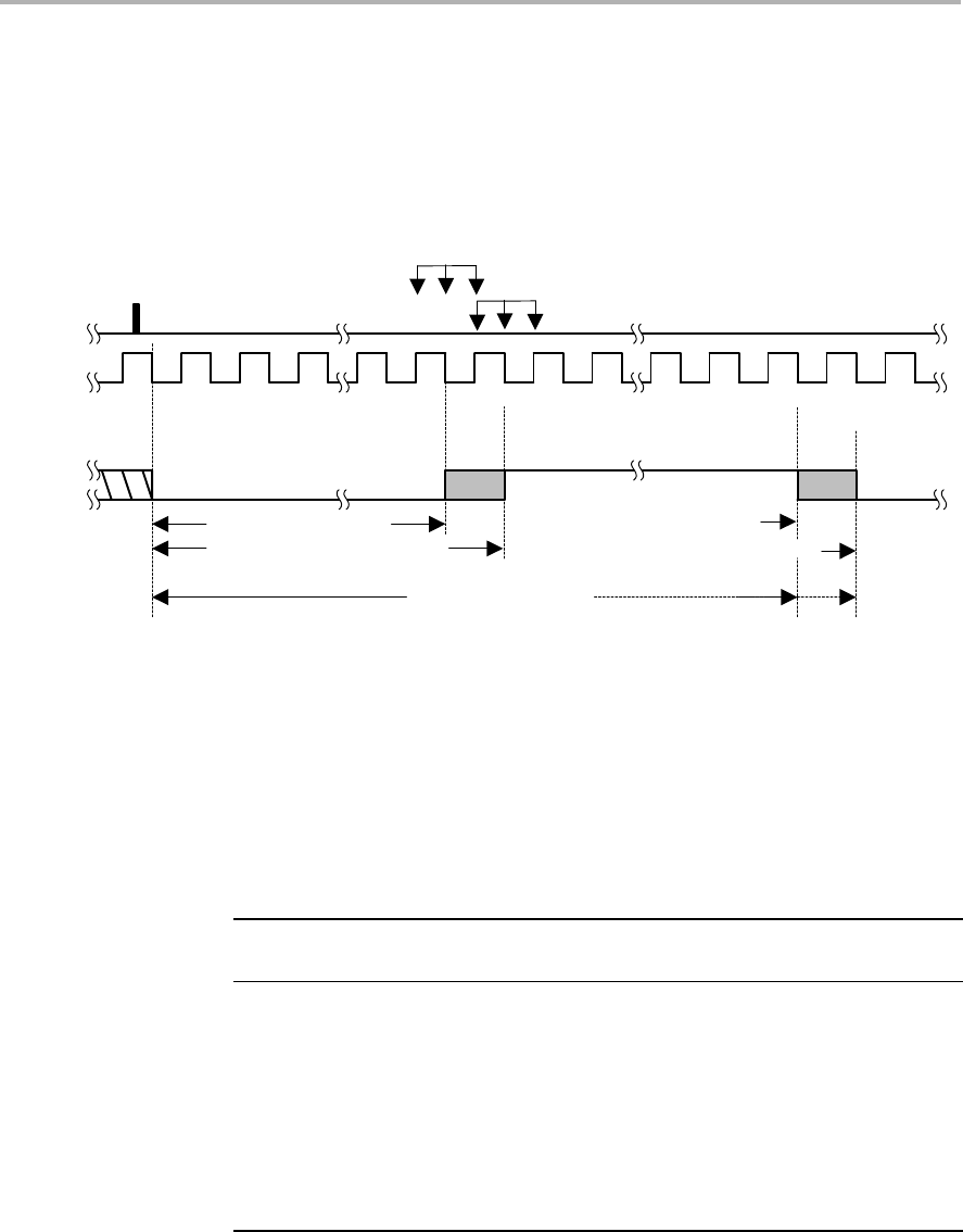
USCI Operation: UART Mode
15-16 Universal Serial Communication Interface, UART Mode
Timing for each bit is shown in Figure 15−10. For each bit received, a majority
vote is taken to determine the bit value. These samples occur at the N/2 − 1/2,
N/2, and N/2 + 1/2 BRCLK periods, where N is the number of BRCLKs per
BITCLK.
Figure 15−10. BITCLK Baud Rate Timing with UCOS16 = 0
N/2
Bit Start
BRCLK
Counter
BITCLK
N/2−1 N/2−2 1 N/2 N/2−1 1 N/2 N/2−1N/2−2
0 N/2 N/2−11
INT(N/2) + m(= 0)
INT(N/2) + m(= 1)
1 0 N/2
Bit Period
NEVEN: INT(N/2)
NODD : INT(N/2) + R(= 1)
m: corresponding modulation bit
R: Remainder from N/2 division
Majority Vote: (m= 0)
(m= 1)
Modulation is based on the UCBRSx setting as shown in Table 15−2. A 1 in
the table indicates that m = 1 and the corresponding BITCLK period is one
BRCLK period longer than a BITCLK period with m = 0. The modulation wraps
around after 8 bits but restarts with each new start bit.
Table 15−2.BITCLK Modulation Pattern
UCBRSx Bit 0
(Start Bit) Bit 1 Bit 2 Bit 3 Bit 4 Bit 5 Bit 6 Bit 7
00 0 0 0 0 0 0 0
10 1000000
20 1000100
30 1010100
40 1010101
50 1110101
60 1110111
70 1 1 1 1 1 1 1

USCI Operation: UART Mode
15-17
Universal Serial Communication Interface, UART Mode
Oversampling Baud Rate Generation
The oversampling mode is selected when UCOS16 = 1. This mode supports
sampling a UART bit stream with higher input clock frequencies. This results
in majority votes that are always 1/16 of a bit clock period apart. This mode also
easily supports IrDA pulses with a 3/16 bit-time when the IrDA encoder and
decoder are enabled.
This mode uses one prescaler and one modulator to generate the BITCLK16
clock that is 16 times faster than the BITCLK. An additional divider and
modulator stage generates BITCLK from BITCLK16. This combination
supports fractional divisions of both BITCLK16 and BITCLK for baud rate
generation. In this mode, the maximum USCI baud rate is 1/16 the UART
source clock frequency BRCLK. When UCBRx is set to 0 or 1 the first prescaler
and modulator stage is bypassed and BRCLK is equal to BITCLK16.
Modulation for BITCLK16 is based on the UCBRFx setting as shown in
Table 15−3. A 1 in the table indicates that the corresponding BITCLK16 period
is one BRCLK period longer than the periods m=0. The modulation restarts
with each new bit timing.
Modulation for BITCLK is based on the UCBRSx setting as shown in
Table 15−2 as previously described.
Table 15−3.BITCLK16 Modulation Pattern
UCBRF
No. of BITCLK16 Clocks after last falling BITCLK edge
UCBRFx 0 1 2 3 4 5 6 7 8 9 10 11 12 13 14 15
00h 0 0 0 0 0 0 0 0 0 0 0 0 0 0 0 0
01h 0100000000000000
02h 0100000000000001
03h 0110000000000001
04h 0110000000000011
05h 0111000000000011
06h 0111000000000111
07h 0111100000000111
08h 0111100000001111
09h 0111110000001111
0Ah 0111110000011111
0Bh 0111111000011111
0Ch 0111111000111111
0Dh 0111111100111111
0Eh 0111111101111111
0Fh 0 1 1 1 1 1 1 1 1 1 1 1 1 1 1 1

USCI Operation: UART Mode
15-18 Universal Serial Communication Interface, UART Mode
15.3.10 Setting a Baud Rate
For a given BRCLK clock source, the baud rate used determines the required
division factor N:
N+fBRCLK
Baudrate
The division factor N is often a non-integer value thus at least one divider and
one modulator stage is used to meet the factor as closely as possible.
If N is equal or greater than 16 the oversampling baud rate generation mode
can be chosen by setting UCOS16.
Low-Frequency Baud Rate Mode Setting
In the low-frequency mode, the integer portion of the divisor is realized by the
prescaler:
UCBRx = INT(N)
and the fractional portion is realized by the modulator with the following
nominal formula:
UCBRSx = round( ( N − INT(N) ) * 8 )
Incrementing or decrementing the UCBRSx setting by one count may give a
lower maximum bit error for any given bit. To determine if this is the case, a
detailed error calculation must be performed for each bit for each UCBRSx
setting.
Oversampling Baud Rate Mode Setting
In the oversampling mode the prescaler is set to:
UCBRx = INT(N/16).
and the first stage modulator is set to:
UCBRFx = round( ( (N/16) − INT(N/16) ) * 16 )
When greater accuracy is required, the UCBRSx modulator can also be
implemented with values from 0 − 7. To find the setting that gives the lowest
maximum bit error rate for any given bit, a detailed error calculation must be
performed for all settings of UCBRSx from 0 − 7 with the initial UCBRFx setting
and with the UCBRFx setting incremented and decremented by one.

USCI Operation: UART Mode
15-19
Universal Serial Communication Interface, UART Mode
15.3.11 Transmit Bit Timing
The timing for each character is the sum of the individual bit timings. Using the
modulation features of the baud rate generator reduces the cumulative bit
error. The individual bit error can be calculated using the following steps.
Low-Frequency Baud Rate Mode Bit Timing
In low-frequency mode, calculate the length of bit i Tbit,TX[i] based on the
UCBRx and UCBRSx settings:
Tbit,TX[i] +1
fBRCLK
ǒUCBRx )mUCBRSx[i]Ǔ
where:
mUCBRSx[i]: Modulation of bit i from Table 15−2
Oversampling Baud Rate Mode Bit Timing
In oversampling baud rate mode calculate the length of bit i Tbit,TX[i] based on
the baud rate generator UCBRx, UCBRFx and UCBRSx settings:
Tbit,TX[i] +1
fBRCLK ǒǒ16 )mUCBRSx[i]Ǔ@UCBRx )ȍ
15
j+0
mUCBRFx[j]Ǔ
where:
ȍ
15
j+0
mUCBRFx[j]: Sum of ones from the corresponding row in Table 15−3
mUCBRSx[i]: Modulation of bit i from Table 15−2
This results in an end-of-bit time tbit,TX[i] equal to the sum of all previous and
the current bit times:
tbit,TX[i] +ȍ
i
j+0
Tbit,TX[j]
To calculate bit error, this time is compared to the ideal bit time tbit,ideal,TX[i]:
tbit,ideal,TX[i] +1
Baudrate (i)1)
This results in an error normalized to one ideal bit time (1/baudrate):
ErrorTX[i] +ǒtbit,TX[i] *tbit,ideal,TX[i]Ǔ@Baudrate @100%
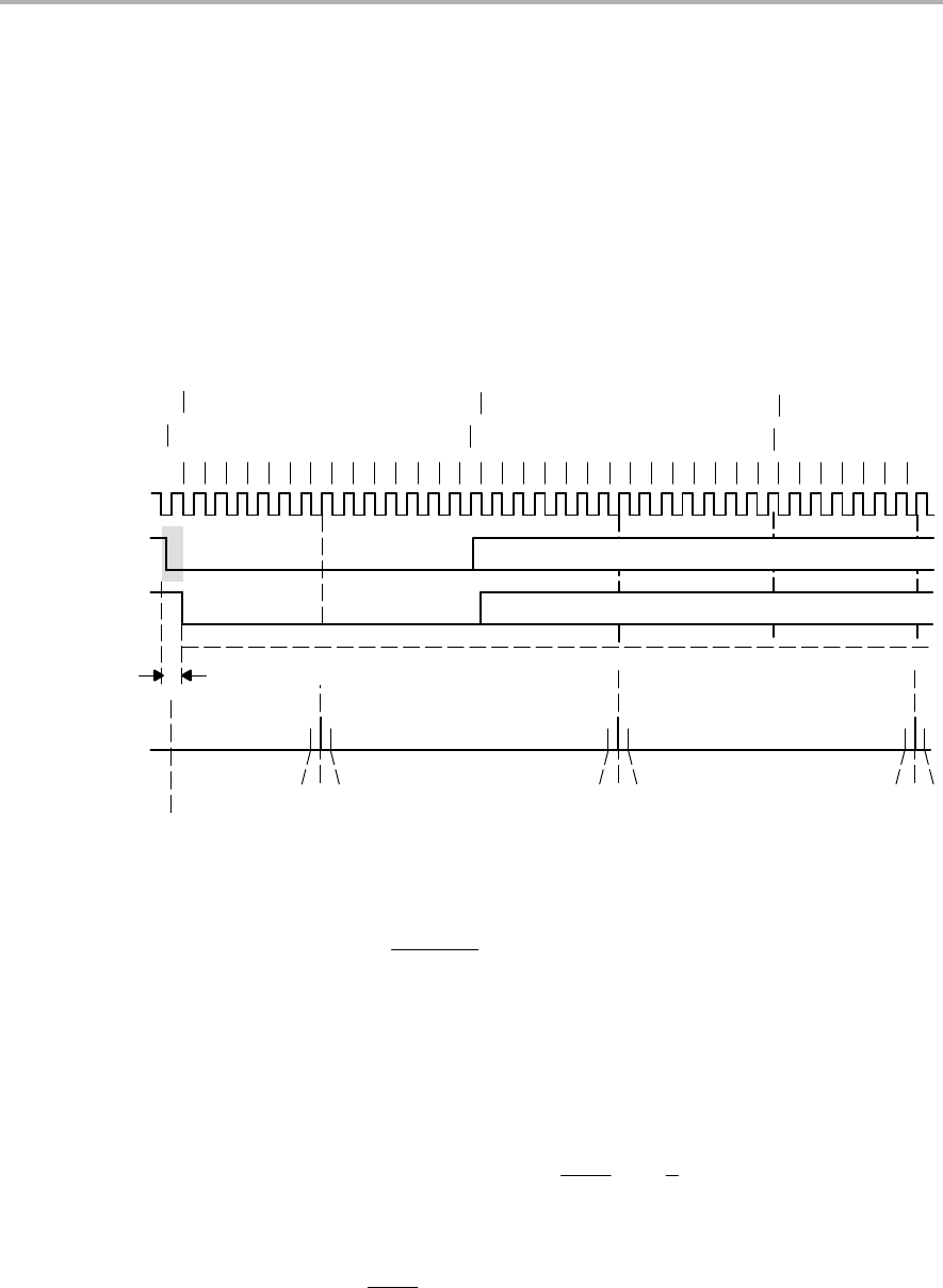
USCI Operation: UART Mode
15-20 Universal Serial Communication Interface, UART Mode
15.3.12 Receive Bit Timing
Receive timing error consists of two error sources. The first is the bit-to-bit
timing error similar to the transmit bit timing error. The second is the error
between a start edge occurring and the start edge being accepted by the USCI
module. Figure 15−11 shows the asynchronous timing errors between data on
the UCAxRXD pin and the internal baud-rate clock. This results in an additional
synchronization error. The synchronization error tSYNC is between
−0.5 BRCLKs and +0.5 BRCLKs independent of the selected baud rate
generation mode.
Figure 15−11.Receive Error
123456
0
i
t0
tideal
78
1
t1
2
9 10 11 12 13 14 1 2 3 4 5 6 7 8 9 10 11 12 13 14 1 2 3 4 5 6 7
t0t1t2
ST D0 D1
D0 D1
ST
Synchronization Error ±0.5x BRCLK
Majority Vote Taken Majority Vote Taken Majority Vote Taken
BRCLK
UCAxRXD
RXD synch.
tactual
Sample
RXD synch.
The ideal sampling time tbit,ideal,RX[i] is in the middle of a bit period:
tbit,ideal,RX[i] +1
Baudrate (i)0.5)
The real sampling time tbit,RX[i] is equal to the sum of all previous bits according
to the formulas shown in the transmit timing section, plus one half BITCLK for
the current bit i, plus the synchronization error tSYNC.
This results in the following tbit,RX[i] for the low-frequency baud rate mode
tbit,RX[i] +tSYNC )ȍ
i*1
j+0
Tbit,RX[j] )1
fBRCLK ǒINT(1
2UCBRx) )mUCBRSx[i]Ǔ
where:
Tbit,RX[i] +1
fBRCLK
ǒUCBRx )mUCBRSx[i]Ǔ
mUCBRSx[i]: Modulation of bit i from Table 15−2

USCI Operation: UART Mode
15-21
Universal Serial Communication Interface, UART Mode
For the oversampling baud rate mode the sampling time tbit,RX[i] of bit i is
calculated by:
tbit,RX[i] +tSYNC )ȍ
i*1
j+0
Tbit,RX[j]
)1
fBRCLK ǒǒ8)mUCBRSx[i]Ǔ@UCBRx )ȍ
7)mUCBRSx[i]
j+0
mUCBRFx[j]Ǔ
where:
Tbit,RX[i] +1
fBRCLK ǒǒ16 )mUCBRSx[i]Ǔ@UCBRx )ȍ
15
j+0
mUCBRFx[j]Ǔ
ȍ
7)mUCBRSx[i]
j+0
mUCBRFx[j]: Sum of ones from columns 0 − 7 )mUCBRSx[i]
from the corresponding row in Table 15−3
mUCBRSx[i]: Modulation of bit i from Table 15−2
This results in an error normalized to one ideal bit time (1/baudrate) according
to the following formula:
ErrorRX[i] +ǒtbit,RX[i] *tbit,ideal,RX[i]Ǔ@Baudrate @100%
15.3.13 Typical Baud Rates and Errors
Standard baud rate data for UCBRx, UCBRSx and UCBRFx are listed in
Table 15−4 and Table 15−5 for a 32768-Hz crystal sourcing ACLK and typical
SMCLK frequencies. Ensure that the selected BRCLK frequency does not
exceed the device-specific maximum USCI input frequency (see the
device-specific data sheet).
The receive error is the accumulated time versus the ideal scanning time in the
middle of each bit. The worst case error is given for the reception of an 8-bit
character with parity and one stop bit including synchronization error.
The transmit error is the accumulated timing error versus the ideal time of the
bit period. The worst case error is given for the transmission of an 8-bit
character with parity and stop bit.

USCI Operation: UART Mode
15-22 Universal Serial Communication Interface, UART Mode
Table 15−4.Commonly Used Baud Rates, Settings, and Errors, UCOS16 = 0
BRCLK
frequency
[Hz]
Baud
Rate
[Baud]
UCBRx UCBRSx UCBRFx Max. TX Error [%] Max. RX Error [%]
32,768 1200 27 2 0 −2.8 1.4 −5.9 2.0
32,768 2400 13 6 0 −4.8 6.0 −9.7 8.3
32,768 4800 6 7 0 −12.1 5.7 −13.4 19.0
32,768 9600 3 3 0 −21.1 15.2 −44.3 21.3
1,048,576 9600 109 2 0 −0.2 0.7 −1.0 0.8
1,048,576 19200 54 5 0 −1.1 1.0 −1.5 2.5
1,048,576 38400 27 2 0 −2.8 1.4 −5.9 2.0
1,048,576 56000 18 6 0 −3.9 1.1 −4.6 5.7
1,048,576 115200 9 1 0 −1.1 10.7 −11.5 11.3
1,048,576 128000 8 1 0 −8.9 7.5 −13.8 14.8
1,048,576 256000 4 1 0 −2.3 25.4 −13.4 38.8
1,000,000 9600 104 1 0 −0.5 0.6 −0.9 1.2
1,000,000 19200 52 0 0 −1.8 0 −2.6 0.9
1,000,000 38400 26 0 0 −1.8 0 −3.6 1.8
1,000,000 56000 17 7 0 −4.8 0.8 −8.0 3.2
1,000,000 115200 8 6 0 −7.8 6.4 −9.7 16.1
1,000,000 128000 7 7 0 −10.4 6.4 −18.0 11.6
1,000,000 256000 3 7 0 −29.6 0 −43.6 5.2
4,000,000 9600 416 6 0 −0.2 0.2 −0.2 0.4
4,000,000 19200 208 3 0 −0.2 0.5 −0.3 0.8
4,000,000 38400 104 1 0 −0.5 0.6 −0.9 1.2
4,000,000 56000 71 4 0 −0.6 1.0 −1.7 1.3
4,000,000 115200 34 6 0 −2.1 0.6 −2.5 3.1
4,000,000 128000 31 2 0 −0.8 1.6 −3.6 2.0
4,000,000 256000 15 5 0 −4.0 3.2 −8.4 5.2
8,000,000 9600 833 2 0 −0.1 0 −0.2 0.1
8,000,000 19200 416 6 0 −0.2 0.2 −0.2 0.4
8,000,000 38400 208 3 0 −0.2 0.5 −0.3 0.8
8,000,000 56000 142 7 0 −0.6 0.1 −0.7 0.8
8,000,000 115200 69 4 0 −0.6 0.8 −1.8 1.1
8,000,000 128000 62 4 0 −0.8 0 −1.2 1.2
8,000,000 256000 31 2 0 −0.8 1.6 −3.6 2.0

USCI Operation: UART Mode
15-23
Universal Serial Communication Interface, UART Mode
Table 15−4.Commonly Used Baud Rates, Settings, and Errors, UCOS16 = 0 (Continued)
12,000,000 9600 1250 0 0 0 0 −0.05 0.05
12,000,000 19200 625 0 0 0 0 −0.2 0
12,000,000 38400 312 4 0 −0.2 0 −0.2 0.2
12,000,000 56000 214 2 0 −0.3 0.2 −0.4 0.5
12,000,000 115200 104 1 0 −0.5 0.6 −0.9 1.2
12,000,000 128000 93 6 0 −0.8 0 −1.5 0.4
12,000,000 256000 46 7 0 −1.9 0 −2.0 2.0
16,000,000 9600 1666 6 0 −0.05 0.05 −0.05 0.1
16,000,000 19200 833 2 0 −0.1 0.05 −0.2 0.1
16,000,000 38400 416 6 0 −0.2 0.2 −0.2 0.4
16,000,000 56000 285 6 0 −0.3 0.1 −0.5 0.2
16,000,000 115200 138 7 0 −0.7 0 −0.8 0.6
16,000,000 128000 125 0 0 0 0 −0.8 0
16,000,000 256000 62 4 0 −0.8 0 −1.2 1.2

USCI Operation: UART Mode
15-24 Universal Serial Communication Interface, UART Mode
Table 15−5.Commonly Used Baud Rates, Settings, and Errors, UCOS16 = 1
BRCLK
frequency
[Hz]
Baud
Rate
[Baud]
UCBRx UCBRSx UCBRFx Max. TX Error [%] Max. RX Error [%]
1,048,576 9600 6 0 13 −2.3 0 −2.2 0.8
1,048,576 19200 3 1 6 −4.6 3.2 −5.0 4.7
1,000,000 9600 6 0 8 −1.8 0 −2.2 0.4
1,000,000 19200 3 0 4 −1.8 0 −2.6 0.9
1,000,000 57600 1 7 0 −34.4 0 −33.4 0
4,000,000 9600 26 0 1 0 0.9 0 1.1
4,000,000 19200 13 0 0 −1.8 0 −1.9 0.2
4,000,000 38400 6 0 8 −1.8 0 −2.2 0.4
4,000,000 57600 4 5 3 −3.5 3.2 −1.8 6.4
4,000,000 115200 2 3 2 −2.1 4.8 −2.5 7.3
4,000,000 230400 1 7 0 −34.4 0 −33.4 0
8,000,000 9600 52 0 1 −0.4 0 −0.4 0.1
8,000,000 19200 26 0 1 0 0.9 0 1.1
8,000,000 38400 13 0 0 −1.8 0 −1.9 0.2
8,000,000 57600 8 0 11 0 0.88 0 1.6
8,000,000 115200 4 5 3 −3.5 3.2 −1.8 6.4
8,000,000 230400 2 3 2 −2.1 4.8 −2.5 7.3
8,000,000 460800 1 7 0 −34.4 0 −33.4 0
12,000,000 9600 78 0 2 0 0 −0.05 0.05
12,000,000 19200 39010000.2
12,000,000 38400 19 0 8 −1.8 0 −1.8 0.1
12,000,000 57600 13 0 0 −1.8 0 −1.9 0.2
12,000,000 115200 6 0 8 −1.8 0 −2.2 0.4
12,000,000 230400 3 0 4 −1.8 0 −2.6 0.9
16,000,000 9600 104 0 3 0 0.2 0 0.3
16,000,000 19200 52 0 1 −0.4 0 −0.4 0.1
16,000,000 38400 26 0 1 0 0.9 0 1.1
16,000,000 57600 17 0 6 0 0.9 −0.1 1.0
16,000,000 115200 8 0 11 0 0.9 0 1.6
16,000,000 230400 4 5 3 −3.5 3.2 −1.8 6.4
16,000,000 460800 2 3 2 −2.1 4.8 −2.5 7.3

USCI Operation: UART Mode
15-25
Universal Serial Communication Interface, UART Mode
15.3.14 Using the USCI Module in UART Mode with Low Power Modes
The USCI module provides automatic clock activation for SMCLK for use with
low-power modes. When SMCLK is the USCI clock source, and is inactive
because the device is in a low-power mode, the USCI module automatically
activates it when needed, regardless of the control-bit settings for the clock
source. The clock remains active until the USCI module returns to its idle
condition. After the USCI module returns to the idle condition, control of the
clock source reverts to the settings of its control bits. Automatic clock activation
is not provided for ACLK.
When the USCI module activates an inactive clock source, the clock source
becomes active for the whole device and any peripheral configured to use the
clock source may be affected. For example, a timer using SMCLK will
increment while the USCI module forces SMCLK active.
15.3.15 USCI Interrupts
The USCI has one interrupt vector for transmission and one interrupt vector
for reception.
USCI Transmit Interrupt Operation
The UCAxTXIFG interrupt flag is set by the transmitter to indicate that
UCAxTXBUF is ready to accept another character. An interrupt request is
generated if UCAxTXIE and GIE are also set. UCAxTXIFG is automatically
reset if a character is written to UCAxTXBUF.
UCAxTXIFG is set after a PUC or when UCSWRST = 1. UCAxTXIE is reset
after a PUC or when UCSWRST = 1.
USCI Receive Interrupt Operation
The UCAxRXIFG interrupt flag is set each time a character is received and
loaded into UCAxRXBUF. An interrupt request is generated if UCAxRXIE and
GIE are also set. UCAxRXIFG and UCAxRXIE are reset by a system reset
PUC signal or when UCSWRST = 1. UCAxRXIFG is automatically reset when
UCAxRXBUF is read.
Additional interrupt control features include:
-When UCAxRXEIE = 0 erroneous characters will not set UCAxRXIFG.
-When UCDORM = 1, non-address characters will not set UCAxRXIFG in
multiprocessor modes. In plain UART mode, no characters will set
UCAxRXIFG.
-When UCBRKIE = 1 a break condition will set the UCBRK bit and the
UCAxRXIFG flag.

USCI Operation: UART Mode
15-26 Universal Serial Communication Interface, UART Mode
USCI Interrupt Usage
USCI_Ax and USCI_Bx share the same interrupt vectors. The receive
interrupt flags UCAxRXIFG and UCBxRXIFG are routed to one interrupt
vector, the transmit interrupt flags UCAxTXIFG and UCBxTXIFG share
another interrupt vector.
Shared Interrupt Vectors Software Example
The following software example shows an extract of an interrupt service
routine to handle data receive interrupts from USCI_A0 in either UART or SPI
mode and USCI_B0 in SPI mode.
USCIA0_RX_USCIB0_RX_ISR
BIT.B #UCA0RXIFG, &IFG2 ; USCI_A0 Receive Interrupt?
JNZ USCIA0_RX_ISR
USCIB0_RX_ISR?
; Read UCB0RXBUF (clears UCB0RXIFG)
...
RETI
USCIA0_RX_ISR
; Read UCA0RXBUF (clears UCA0RXIFG)
...
RETI
The following software example shows an extract of an interrupt service
routine to handle data transmit interrupts from USCI_A0 in either UART or SPI
mode and USCI_B0 in SPI mode.
USCIA0_TX_USCIB0_TX_ISR
BIT.B #UCA0TXIFG, &IFG2 ; USCI_A0 Transmit Interrupt?
JNZ USCIA0_TX_ISR
USCIB0_TX_ISR
; Write UCB0TXBUF (clears UCB0TXIFG)
...
RETI
USCIA0_TX_ISR
; Write UCA0TXBUF (clears UCA0TXIFG)
...
RETI

USCI Registers: UART Mode
15-27
Universal Serial Communication Interface, UART Mode
15.4 USCI Registers: UART Mode
The USCI registers applicable in UART mode are listed in Table 15−6 and
Table 15−7.
Table 15−6.USCI_A0 Control and Status Registers
Register Short Form Register Type Address Initial State
USCI_A0 control register 0 UCA0CTL0 Read/write 060h Reset with PUC
USCI_A0 control register 1 UCA0CTL1 Read/write 061h 001h with PUC
USCI_A0 Baud rate control register 0 UCA0BR0 Read/write 062h Reset with PUC
USCI_A0 baud rate control register 1 UCA0BR1 Read/write 063h Reset with PUC
USCI_A0 modulation control register UCA0MCTL Read/write 064h Reset with PUC
USCI_A0 status register UCA0STAT Read/write 065h Reset with PUC
USCI_A0 receive buffer register UCA0RXBUF Read 066h Reset with PUC
USCI_A0 transmit buffer register UCA0TXBUF Read/write 067h Reset with PUC
USCI_A0 Auto baud control register UCA0ABCTL Read/write 05Dh Reset with PUC
USCI_A0 IrDA transmit control register UCA0IRTCTL Read/write 05Eh Reset with PUC
USCI_A0 IrDA receive control register UCA0IRRCTL Read/write 05Fh Reset with PUC
SFR interrupt enable register 2 IE2 Read/write 001h Reset with PUC
SFR interrupt flag register 2 IFG2 Read/write 003h 00Ah with PUC
Note: Modifying SFR bits
To avoid modifying control bits of other modules, it is recommended to set
or clear the IEx and IFGx bits using BIS.B or BIC.B instructions, rather than
MOV.B or CLR.B instructions.
Table 15−7.USCI_A1 Control and Status Registers
Register Short Form Register Type Address Initial State
USCI_A1 control register 0 UCA1CTL0 Read/write 0D0h Reset with PUC
USCI_A1 control register 1 UCA1CTL1 Read/write 0D1h 001h with PUC
USCI_A1 baud rate control register 0 UCA1BR0 Read/write 0D2h Reset with PUC
USCI_A1 baud rate control register 1 UCA1BR1 Read/write 0D3h Reset with PUC
USCI_A1 modulation control register UCA10MCTL Read/write 0D4h Reset with PUC
USCI_A1 status register UCA1STAT Read/write 0D5h Reset with PUC
USCI_A1 receive buffer register UCA1RXBUF Read 0D6h Reset with PUC
USCI_A1 transmit buffer register UCA1TXBUF Read/write 0D7h Reset with PUC
USCI_A1 auto baud control register UCA1ABCTL Read/write 0CDh Reset with PUC
USCI_A1 IrDA transmit control register UCA1IRTCTL Read/write 0CEh Reset with PUC
USCI_A1 IrDA receive control register UCA1IRRCTL Read/write 0CFh Reset with PUC
USCI_A1/B1 interrupt enable register UC1IE Read/write 006h Reset with PUC
USCI_A1/B1 interrupt flag register UC1IFG Read/write 007h 00Ah with PUC

USCI Registers: UART Mode
15-28 Universal Serial Communication Interface, UART Mode
UCAxCTL0, USCI_Ax Control Register 0
76543210
UCPEN UCPAR UCMSB UC7BIT UCSPB UCMODEx UCSYNC=0
rw−0 rw−0 rw−0 rw−0 rw−0 rw−0 rw−0 rw−0
UCPEN Bit 7 Parity enable
0 Parity disabled.
1 Parity enabled. Parity bit is generated (UCAxTXD) and expected
(UCAxRXD). In address-bit multiprocessor mode, the address bit is
included in the parity calculation.
UCPAR Bit 6 Parity select. UCPAR is not used when parity is disabled.
0 Odd parity
1 Even parity
UCMSB Bit 5 MSB first select. Controls the direction of the receive and transmit shift
register.
0 LSB first
1 MSB first
UC7BIT Bit 4 Character length. Selects 7-bit or 8-bit character length.
0 8-bit data
1 7-bit data
UCSPB Bit 3 Stop bit select. Number of stop bits.
0 One stop bit
1 Two stop bits
UCMODEx Bits
2−1
USCI mode. The UCMODEx bits select the asynchronous mode when
UCSYNC = 0.
00 UART Mode.
01 Idle-Line Multiprocessor Mode.
10 Address-Bit Multiprocessor Mode.
11 UART Mode with automatic baud rate detection.
UCSYNC Bit 0 Synchronous mode enable
0 Asynchronous mode
1 Synchronous Mode

USCI Registers: UART Mode
15-29
Universal Serial Communication Interface, UART Mode
UCAxCTL1, USCI_Ax Control Register 1
76543210
UCSSELx UCRXEIE UCBRKIE UCDORM UCTXADDR UCTXBRK UCSWRST
rw−0 rw−0 rw−0 rw−0 rw−0 rw−0 rw−0 rw−1
UCSSELx Bits
7-6
USCI clock source select. These bits select the BRCLK source clock.
00 UCLK
01 ACLK
10 SMCLK
11 SMCLK
UCRXEIE Bit 5 Receive erroneous-character interrupt-enable
0 Erroneous characters rejected and UCAxRXIFG is not set
1 Erroneous characters received will set UCAxRXIFG
UCBRKIE Bit 4 Receive break character interrupt-enable
0 Received break characters do not set UCAxRXIFG.
1 Received break characters set UCAxRXIFG.
UCDORM Bit 3 Dormant. Puts USCI into sleep mode.
0 Not dormant. All received characters will set UCAxRXIFG.
1 Dormant. Only characters that are preceded by an idle-line or with
address bit set will set UCAxRXIFG. In UART mode with automatic baud
rate detection only the combination of a break and synch field will set
UCAxRXIFG.
UCTXADDR Bit 2 Transmit address. Next frame to be transmitted will be marked as address
depending on the selected multiprocessor mode.
0 Next frame transmitted is data
1 Next frame transmitted is an address
UCTXBRK Bit 1 Transmit break. Transmits a break with the next write to the transmit buffer.
In UART mode with automatic baud rate detection 055h must be written
into UCAxTXBUF to generate the required break/synch fields. Otherwise
0h must be written into the transmit buffer.
0 Next frame transmitted is not a break
1 Next frame transmitted is a break or a break/synch
UCSWRST Bit 0 Software reset enable
0 Disabled. USCI reset released for operation.
1 Enabled. USCI logic held in reset state.

USCI Registers: UART Mode
15-30 Universal Serial Communication Interface, UART Mode
UCAxBR0, USCI_Ax Baud Rate Control Register 0
76543210
UCBRx
rw rw rw rw rw rw rw rw
UCAxBR1, USCI_Ax Baud Rate Control Register 1
76543210
UCBRx
rw rw rw rw rw rw rw rw
UCBRx Clock prescaler setting of the Baud rate generator. The 16-bit value of
(UCAxBR0 + UCAxBR1 ×256) forms the prescaler value.
UCAxMCTL, USCI_Ax Modulation Control Register
76543210
UCBRFx UCBRSx UCOS16
rw−0 rw−0 rw−0 rw−0 rw−0 rw−0 rw−0 rw−0
UCBRFx Bits
7−4
First modulation stage select. These bits determine the modulation pattern
for BITCLK16 when UCOS16 = 1. Ignored with UCOS16 = 0. Table 15−3
shows the modulation pattern.
UCBRSx Bits
3−1
Second modulation stage select. These bits determine the modulation
pattern for BITCLK. Table 15−2 shows the modulation pattern.
UCOS16 Bit 0 Oversampling mode enabled
0 Disabled
1 Enabled

USCI Registers: UART Mode
15-31
Universal Serial Communication Interface, UART Mode
UCAxSTAT, USCI_Ax Status Register
76543210
UCLISTEN UCFE UCOE UCPE UCBRK UCRXERR UCADDR
UCIDLE UCBUSY
rw−0 rw−0 rw−0 rw−0 rw−0 rw−0 rw−0 r−0
UCLISTEN Bit 7 Listen enable. The UCLISTEN bit selects loopback mode.
0 Disabled
1 Enabled. UCAxTXD is internally fed back to the receiver.
UCFE Bit 6 Framing error flag
0 No error
1 Character received with low stop bit
UCOE Bit 5 Overrun error flag. This bit is set when a character is transferred into
UCAxRXBUF before the previous character was read. UCOE is cleared
automatically when UCxRXBUF is read, and must not be cleared by
software. Otherwise, it will not function correctly.
0 No error
1 Overrun error occurred
UCPE Bit 4 Parity error flag. When UCPEN = 0, UCPE is read as 0.
0 No error
1 Character received with parity error
UCBRK Bit 3 Break detect flag
0 No break condition
1 Break condition occurred
UCRXERR Bit 2 Receive error flag. This bit indicates a character was received with error(s).
When UCRXERR = 1, on or more error flags (UCFE, UCPE, UCOE) is also
set. UCRXERR is cleared when UCAxRXBUF is read.
0 No receive errors detected
1 Receive error detected
UCADDR Bit 1 Address received in address-bit multiprocessor mode.
0 Received character is data
1 Received character is an address
UCIDLE Idle line detected in idle-line multiprocessor mode.
0 No idle line detected
1 Idle line detected
UCBUSY Bit 0 USCI busy. This bit indicates if a transmit or receive operation is in
progress.
0 USCI inactive
1 USCI transmitting or receiving

USCI Registers: UART Mode
15-32 Universal Serial Communication Interface, UART Mode
UCAxRXBUF, USCI_Ax Receive Buffer Register
76543210
UCRXBUFx
r r r r r r r r
UCRXBUFx Bits
7−0
The receive-data buffer is user accessible and contains the last received
character from the receive shift register. Reading UCAxRXBUF resets the
receive-error bits, the UCADDR or UCIDLE bit, and UCAxRXIFG. In 7-bit
data mode, UCAxRXBUF is LSB justified and the MSB is always reset.
UCAxTXBUF, USCI_Ax Transmit Buffer Register
76543210
UCTXBUFx
rw rw rw rw rw rw rw rw
UCTXBUFx Bits
7−0
The transmit data buffer is user accessible and holds the data waiting to
be moved into the transmit shift register and transmitted on UCAxTXD.
Writing to the transmit data buffer clears UCAxTXIFG. The MSB of
UCAxTXBUF is not used for 7-bit data and is reset.

USCI Registers: UART Mode
15-33
Universal Serial Communication Interface, UART Mode
UCAxIRTCTL, USCI_Ax IrDA Transmit Control Register
76543210
UCIRTXPLx UCIR
TXCLK UCIREN
rw−0 rw−0 rw−0 rw−0 rw−0 rw−0 rw−0 rw−0
UCIRTXPLx Bits
7−2
Transmit pulse length
Pulse Length tPULSE = (UCIRTXPLx + 1) / (2 * fIRTXCLK)
UCIRTXCLK Bit 1 IrDA transmit pulse clock select
0 BRCLK
1 BITCLK16 when UCOS16 = 1. Otherwise, BRCLK
UCIREN Bit 0 IrDA encoder/decoder enable.
0 IrDA encoder/decoder disabled
1 IrDA encoder/decoder enabled
UCAxIRRCTL, USCI_Ax IrDA Receive Control Register
76543210
UCIRRXFLx UCIRRXPL UCIRRXFE
rw−0 rw−0 rw−0 rw−0 rw−0 rw−0 rw−0 rw−0
UCIRRXFLx Bits
7−2
Receive filter length. The minimum pulse length for receive is given by:
tMIN = (UCIRRXFLx + 4) / (2 * fIRTXCLK)
UCIRRXPL Bit 1 IrDA receive input UCAxRXD polarity
0 IrDA transceiver delivers a high pulse when a light pulse is seen
1 IrDA transceiver delivers a low pulse when a light pulse is seen
UCIRRXFE Bit 0 IrDA receive filter enabled
0 Receive filter disabled
1 Receive filter enabled

USCI Registers: UART Mode
15-34 Universal Serial Communication Interface, UART Mode
UCAxABCTL, USCI_Ax Auto Baud Rate Control Register
76543210
Reserved UCDELIMx UCSTOE UCBTOE Reserved UCABDEN
r−0 r−0 rw−0 rw−0 rw−0 rw−0 r−0 rw−0
Reserved Bits
7-6
Reserved
UCDELIMx Bits
5−4
Break/synch delimiter length
00 1 bit time
01 2 bit times
10 3 bit times
11 4 bit times
UCSTOE Bit 3 Synch field time out error
0 No error
1 Length of synch field exceeded measurable time.
UCBTOE Bit 2 Break time out error
0 No error
1 Length of break field exceeded 22 bit times.
Reserved Bit 1 Reserved
UCABDEN Bit 0 Automatic baud rate detect enable
0 Baud rate detection disabled. Length of break and synch field is not
measured.
1 Baud rate detection enabled. Length of break and synch field is
measured and baud rate settings are changed accordingly.

USCI Registers: UART Mode
15-35
Universal Serial Communication Interface, UART Mode
IE2, Interrupt Enable Register 2
76543210
UCA0TXIE UCA0RXIE
rw−0 rw−0
Bits
7-2
These bits may be used by other modules (see the device-specific data
sheet).
UCA0TXIE Bit 1 USCI_A0 transmit interrupt enable
0 Interrupt disabled
1 Interrupt enabled
UCA0RXIE Bit 0 USCI_A0 receive interrupt enable
0 Interrupt disabled
1 Interrupt enabled
IFG2, Interrupt Flag Register 2
76543210
UCA0
TXIFG
UCA0
RXIFG
rw−1 rw−0
Bits
7-2
These bits may be used by other modules (see the device-specific data
sheet).
UCA0
TXIFG
Bit 1 USCI_A0 transmit interrupt flag. UCA0TXIFG is set when UCA0TXBUF is
empty.
0 No interrupt pending
1 Interrupt pending
UCA0
RXIFG
Bit 0 USCI_A0 receive interrupt flag. UCA0RXIFG is set when UCA0RXBUF has
received a complete character.
0 No interrupt pending
1 Interrupt pending

USCI Registers: UART Mode
15-36 Universal Serial Communication Interface, UART Mode
UC1IE, USCI_A1 Interrupt Enable Register
76543210
Unused Unused Unused Unused UCA1TXIE UCA1RXIE
rw−0 rw−0 rw−0 rw−0 rw−0 rw−0
Unused Bits
7-4
Unused
Bits
3-2
These bits may be used by other USCI modules (see the device-specific data
sheet).
UCA1TXIE Bit 1 USCI_A1 transmit interrupt enable
0 Interrupt disabled
1 Interrupt enabled
UCA1RXIE Bit 0 USCI_A1 receive interrupt enable
0 Interrupt disabled
1 Interrupt enabled
UC1IFG, USCI_A1 Interrupt Flag Register
76543210
Unused Unused Unused Unused UCA1
TXIFG
UCA1
RXIFG
rw−0 rw−0 rw−0 rw−0 rw−1 rw−0
Unused Bits
7-4
Unused
Bits
3-2
These bits may be used by other USCI modules (see the device-specific data
sheet).
UCA1
TXIFG
Bit 1 USCI_A1 transmit interrupt flag. UCA1TXIFG is set when UCA1TXBUF is
empty.
0 No interrupt pending
1 Interrupt pending
UCA1
RXIFG
Bit 0 USCI_A1 receive interrupt flag. UCA1RXIFG is set when UCA1RXBUF has
received a complete character.
0 No interrupt pending
1 Interrupt pending

16-1
Universal Serial Communication Interface, SPI Mode
Universal Serial Communication Interface,
SPI Mode
The universal serial communication interface (USCI) supports multiple serial
communication modes with one hardware module. This chapter discusses the
operation of the synchronous peripheral interface or SPI mode.
Topic Page
16.1 USCI Overview 16-2. . . . . . . . . . . . . . . . . . . . . . . . . . . . . . . . . . . . . . . . . . . . . . .
16.2 USCI Introduction: SPI Mode 16-3. . . . . . . . . . . . . . . . . . . . . . . . . . . . . . . . . .
16.3 USCI Operation: SPI Mode 16-5. . . . . . . . . . . . . . . . . . . . . . . . . . . . . . . . . . . . .
16.4 USCI Registers: SPI Mode 16-15. . . . . . . . . . . . . . . . . . . . . . . . . . . . . . . . . . .
Chapter 16

USCI Overview
16-2 Universal Serial Communication Interface, SPI Mode
16.1 USCI Overview
The universal serial communication interface (USCI) modules support
multiple serial communication modes. Different USCI modules support
different modes. Each different USCI module is named with a different letter.
For example, USCI_A is different from USCI_B, etc. If more than one identical
USCI module is implemented on one device, those modules are named with
incrementing numbers. For example, if one device has two USCI_A modules,
they are named USCI_A0 and USCI_A1. See the device-specific data sheet
to determine which USCI modules, if any, are implemented on which devices.
The USCI_Ax modules support:
-UART mode
-Pulse shaping for IrDA communications
-Automatic baud rate detection for LIN communications
-SPI mode
The USCI_Bx modules support:
-I2C mode
-SPI mode

USCI Introduction: SPI Mode
16-3
Universal Serial Communication Interface, SPI Mode
16.2 USCI Introduction: SPI Mode
In synchronous mode, the USCI connects the MSP430 to an external system
via three or four pins: UCxSIMO, UCxSOMI, UCxCLK, and UCxSTE. SPI
mode is selected when the UCSYNC bit is set and SPI mode (3-pin or 4-pin)
is selected with the UCMODEx bits.
SPI mode features include:
-7- or 8-bit data length
-LSB-first or MSB-first data transmit and receive
-3-pin and 4-pin SPI operation
-Master or slave modes
-Independent transmit and receive shift registers
-Separate transmit and receive buffer registers
-Continuous transmit and receive operation
-Selectable clock polarity and phase control
-Programmable clock frequency in master mode
-Independent interrupt capability for receive and transmit
-Slave operation in LPM4
Figure 16−1 shows the USCI when configured for SPI mode.
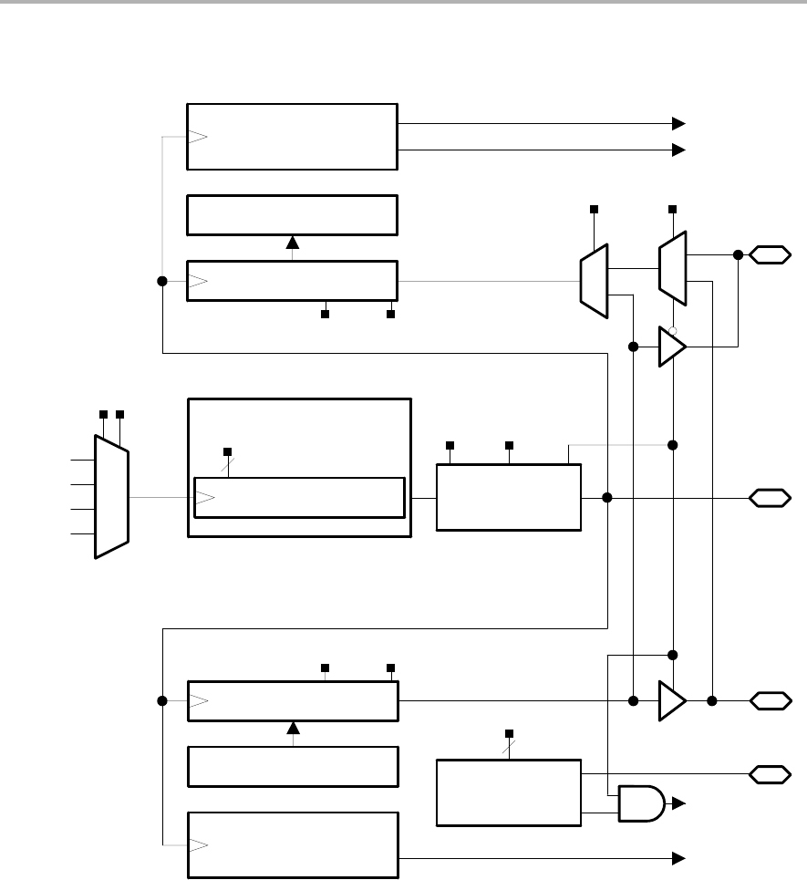
USCI Introduction: SPI Mode
16-4 Universal Serial Communication Interface, SPI Mode
Figure 16−1. USCI Block Diagram: SPI Mode
ACLK
SMCLK
SMCLK
00
01
10
11
UCSSELx
N/A
Prescaler/Divider
Bit Clock Generator
UCxBRx
16
Receive Shift Register
Receive Buffer UCxRXBUF
Receive State Machine
UCMSB UC7BIT
1
0
UCMST
UCxSOMI
Transmit Buffer UCxTXBUF
Transmit State Machine
Transmit Shift Register
UCMSB UC7BIT
BRCLK
Set UCxRXIFG
Set UCxTXIFG
0
1
UCLISTEN
Clock Direction,
Phase and Polarity
UCCKPH UCCKPL
UCxSIMO
UCxCLK
Set UCOE
Transmit Enable
Control
2
UCMODEx
UCxSTE
Set UCFE

USCI Operation: SPI Mode
16-5
Universal Serial Communication Interface, SPI Mode
16.3 USCI Operation: SPI Mode
In SPI mode, serial data is transmitted and received by multiple devices using
a shared clock provided by the master. An additional pin, UCxSTE, is provided
to enable a device to receive and transmit data and is controlled by the master.
Three or four signals are used for SPI data exchange:
-UCxSIMO Slave in, master out
Master mode: UCxSIMO is the data output line.
Slave mode: UCxSIMO is the data input line.
-UCxSOMI Slave out, master in
Master mode: UCxSOMI is the data input line.
Slave mode: UCxSOMI is the data output line.
-UCxCLK USCI SPI clock
Master mode: UCxCLK is an output.
Slave mode: UCxCLK is an input.
-UCxSTE Slave transmit enable. Used in 4-pin mode to allow multiple
masters on a single bus. Not used in 3-pin mode. Table 16−1
describes the UCxSTE operation.
Table 16−1.UCxSTE Operation
UCMODEx UCxSTE Active State UCxSTE Slave Master
01
high
0 inactive active
01 high 1 active inactive
10
low
0 active inactive
10 low 1 inactive active

USCI Operation: SPI Mode
16-6 Universal Serial Communication Interface, SPI Mode
16.3.1 USCI Initialization and Reset
The USCI is reset by a PUC or by the UCSWRST bit. After a PUC, the
UCSWRST bit is automatically set, keeping the USCI in a reset condition.
When set, the UCSWRST bit resets the UCxRXIE, UCxTXIE, UCxRXIFG,
UCOE, and UCFE bits and sets the UCxTXIFG flag. Clearing UCSWRST
releases the USCI for operation.
Note: Initializing or Re-Configuring the USCI Module
The recommended USCI initialization/re-configuration process is:
1) Set UCSWRST (BIS.B #UCSWRST,&UCxCTL1)
2) Initialize all USCI registers with UCSWRST=1 (including UCxCTL1)
3) Configure ports.
4) Clear UCSWRST via software (BIC.B #UCSWRST,&UCxCTL1)
5) Enable interrupts (optional) via UCxRXIE and/or UCxTXIE
16.3.2 Character Format
The USCI module in SPI mode supports 7- and 8-bit character lengths
selected by the UC7BIT bit. In 7-bit data mode, UCxRXBUF is LSB justified
and the MSB is always reset. The UCMSB bit controls the direction of the
transfer and selects LSB or MSB first.
Note: Default Character Format
The default SPI character transmission is LSB first. For communication with
other SPI interfaces it MSB-first mode may be required.
Note: Character Format for Figures
Figures throughout this chapter use MSB first format.
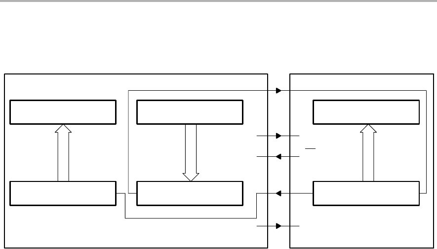
USCI Operation: SPI Mode
16-7
Universal Serial Communication Interface, SPI Mode
16.3.3 Master Mode
Figure 16−2. USCI Master and External Slave
Receive Buffer
UCxRXBUF
Receive Shift Register
Transmit Buffer
UCxTXBUF
Transmit Shift Register
SPI Receive Buffer
Data Shift Register (DSR)
UCx
SOMI SOMI
UCxSIMO SIMO
MASTER SLAVE
Px.x STE
UCxSTE SS
Port.x
UCxCLK SCLK
MSP430 USCI COMMON SPI
Figure 16−2 shows the USCI as a master in both 3-pin and 4-pin
configurations. The USCI initiates data transfer when data is moved to the
transmit data buffer UCxTXBUF. The UCxTXBUF data is moved to the TX shift
register when the TX shift register is empty, initiating data transfer on
UCxSIMO starting with either the most-significant or least-significant bit
depending on the UCMSB setting. Data on UCxSOMI is shifted into the receive
shift register on the opposite clock edge. When the character is received, the
receive data is moved from the RX shift register to the received data buffer
UCxRXBUF and the receive interrupt flag, UCxRXIFG, is set, indicating the
RX/TX operation is complete.
A set transmit interrupt flag, UCxTXIFG, indicates that data has moved from
UCxTXBUF to the TX shift register and UCxTXBUF is ready for new data. It
does not indicate RX/TX completion.
To receive data into the USCI in master mode, data must be written to
UCxTXBUF because receive and transmit operations operate concurrently.

USCI Operation: SPI Mode
16-8 Universal Serial Communication Interface, SPI Mode
Four-Pin SPI Master Mode
In 4-pin master mode, UCxSTE is used to prevent conflicts with another
master and controls the master as described in Table 16−1. When UCxSTE
is in the master-inactive state:
-UCxSIMO and UCxCLK are set to inputs and no longer drive the bus
-The error bit UCFE is set indicating a communication integrity violation to
be handled by the user.
-The internal state machines are reset and the shift operation is aborted.
If data is written into UCxTXBUF while the master is held inactive by UCxSTE,
it will be transmit as soon as UCxSTE transitions to the master-active state.
If an active transfer is aborted by UCxSTE transitioning to the master-inactive
state, the data must be re-written into UCxTXBUF to be transferred when
UCxSTE transitions back to the master-active state. The UCxSTE input signal
is not used in 3-pin master mode.
USCI Operation: SPI Mode
16-9
Universal Serial Communication Interface, SPI Mode
16.3.4 Slave Mode
Figure 16−3. USCI Slave and External Master
Receive Buffer
UCxRXBUF
Receive Shift Register
Transmit Buffer
UCxTXBUF
Transmit Shift Register
SPI Receive Buffer
Data Shift Register DSR
UCx
SOMI
SOMI
UCxSIMOSIMO
MASTER SLAVE
Px.x UCxSTE
STE SS
Port.x
UCxCLK
SCLK
MSP430 USCICOMMON SPI
Figure 16−3 shows the USCI as a slave in both 3-pin and 4-pin configurations.
UCxCLK is used as the input for the SPI clock and must be supplied by the
external master. The data-transfer rate is determined by this clock and not by
the internal bit clock generator. Data written to UCxTXBUF and moved to the
TX shift register before the start of UCxCLK is transmitted on UCxSOMI. Data
on UCxSIMO is shifted into the receive shift register on the opposite edge of
UCxCLK and moved to UCxRXBUF when the set number of bits are received.
When data is moved from the RX shift register to UCxRXBUF, the UCxRXIFG
interrupt flag is set, indicating that data has been received. The overrun error
bit, UCOE, is set when the previously received data is not read from
UCxRXBUF before new data is moved to UCxRXBUF.
Four-Pin SPI Slave Mode
In 4-pin slave mode, UCxSTE is used by the slave to enable the transmit and
receive operations and is provided by the SPI master. When UCxSTE is in the
slave-active state, the slave operates normally. When UCxSTE is in the slave-
inactive state:
-Any receive operation in progress on UCxSIMO is halted
-UCxSOMI is set to the input direction
-The shift operation is halted until the UCxSTE line transitions into the slave
transmit active state.
The UCxSTE input signal is not used in 3-pin slave mode.

USCI Operation: SPI Mode
16-10 Universal Serial Communication Interface, SPI Mode
16.3.5 SPI Enable
When the USCI module is enabled by clearing the UCSWRST bit it is ready
to receive and transmit. In master mode the bit clock generator is ready, but
is not clocked nor producing any clocks. In slave mode the bit clock generator
is disabled and the clock is provided by the master.
A transmit or receive operation is indicated by UCBUSY = 1.
A PUC or set UCSWRST bit disables the USCI immediately and any active
transfer is terminated.
Transmit Enable
In master mode, writing to UCxTXBUF activates the bit clock generator and
the data will begin to transmit.
In slave mode, transmission begins when a master provides a clock and, in
4-pin mode, when the UCxSTE is in the slave-active state.
Receive Enable
The SPI receives data when a transmission is active. Receive and transmit
operations operate concurrently.
USCI Operation: SPI Mode
16-11
Universal Serial Communication Interface, SPI Mode
16.3.6 Serial Clock Control
UCxCLK is provided by the master on the SPI bus. When UCMST = 1, the bit
clock is provided by the USCI bit clock generator on the UCxCLK pin. The clock
used to generate the bit clock is selected with the UCSSELx bits. When
UCMST = 0, the USCI clock is provided on the UCxCLK pin by the master, the
bit clock generator is not used, and the UCSSELx bits are don’t care. The SPI
receiver and transmitter operate in parallel and use the same clock source for
data transfer.
The 16-bit value of UCBRx in the bit rate control registers UCxxBR1 and
UCxxBR0 is the division factor of the USCI clock source, BRCLK. The
maximum bit clock that can be generated in master mode is BRCLK.
Modulation is not used in SPI mode and UCAxMCTL should be cleared when
using SPI mode for USCI_A. The UCAxCLK/UCBxCLK frequency is given by:
fBitClock +fBRCLK
UCBRx
Serial Clock Polarity and Phase
The polarity and phase of UCxCLK are independently configured via the
UCCKPL and UCCKPH control bits of the USCI. Timing for each case is shown
in Figure 16−4.
Figure 16−4. USCI SPI Timing with UCMSB = 1
CKPH CKPL Cycle#
UCxCLK
UCxCLK
UCxCLK
UCxCLK
UCxSIMO/
UCxSOMI
UCxSIMO
UCxSOMI
Move to UCxTXBUF
RX Sample Points
0
1
0
0
01
11
0X
1X
MSB
MSB
12345678
LSB
LSB
TX Data Shifted Out
UCxSTE
UC UC

USCI Operation: SPI Mode
16-12 Universal Serial Communication Interface, SPI Mode
16.3.7 Using the SPI Mode with Low Power Modes
The USCI module provides automatic clock activation for SMCLK for use with
low-power modes. When SMCLK is the USCI clock source, and is inactive
because the device is in a low-power mode, the USCI module automatically
activates it when needed, regardless of the control-bit settings for the clock
source. The clock remains active until the USCI module returns to its idle
condition. After the USCI module returns to the idle condition, control of the
clock source reverts to the settings of its control bits. Automatic clock activation
is not provided for ACLK.
When the USCI module activates an inactive clock source, the clock source
becomes active for the whole device and any peripheral configured to use the
clock source may be affected. For example, a timer using SMCLK will
increment while the USCI module forces SMCLK active.
In SPI slave mode no internal clock source is required because the clock is
provided by the external master. It is possible to operate the USCI in SPI slave
mode while the device is in LPM4 and all clock sources are disabled. The
receive or transmit interrupt can wake up the CPU from any low power mode.

USCI Operation: SPI Mode
16-13
Universal Serial Communication Interface, SPI Mode
16.3.8 SPI Interrupts
The USCI has one interrupt vector for transmission and one interrupt vector
for reception.
SPI Transmit Interrupt Operation
The UCxTXIFG interrupt flag is set by the transmitter to indicate that
UCxTXBUF is ready to accept another character. An interrupt request is
generated if UCxTXIE and GIE are also set. UCxTXIFG is automatically reset
if a character is written to UCxTXBUF. UCxTXIFG is set after a PUC or when
UCSWRST = 1. UCxTXIE is reset after a PUC or when UCSWRST = 1.
Note: Writing to UCxTXBUF in SPI Mode
Data written to UCxTXBUF when UCxTXIFG = 0 may result in erroneous
data transmission.
SPI Receive Interrupt Operation
The UCxRXIFG interrupt flag is set each time a character is received and
loaded into UCxRXBUF. An interrupt request is generated if UCxRXIE and GIE
are also set. UCxRXIFG and UCxRXIE are reset by a system reset PUC signal
or when UCSWRST = 1. UCxRXIFG is automatically reset when UCxRXBUF
is read.

USCI Operation: SPI Mode
16-14 Universal Serial Communication Interface, SPI Mode
USCI Interrupt Usage
USCI_Ax and USCI_Bx share the same interrupt vectors. The receive
interrupt flags UCAxRXIFG and UCBxRXIFG are routed to one interrupt
vector, the transmit interrupt flags UCAxTXIFG and UCBxTXIFG share
another interrupt vector.
Shared Interrupt Vectors Software Example
The following software example shows an extract of an interrupt service
routine to handle data receive interrupts from USCI_A0 in either UART or SPI
mode and USCI_B0 in SPI mode.
USCIA0_RX_USCIB0_RX_ISR
BIT.B #UCA0RXIFG, &IFG2 ; USCI_A0 Receive Interrupt?
JNZ USCIA0_RX_ISR
USCIB0_RX_ISR?
; Read UCB0RXBUF (clears UCB0RXIFG)
...
RETI
USCIA0_RX_ISR
; Read UCA0RXBUF (clears UCA0RXIFG)
...
RETI
The following software example shows an extract of an interrupt service
routine to handle data transmit interrupts from USCI_A0 in either UART or SPI
mode and USCI_B0 in SPI mode.
USCIA0_TX_USCIB0_TX_ISR
BIT.B #UCA0TXIFG, &IFG2 ; USCI_A0 Transmit Interrupt?
JNZ USCIA0_TX_ISR
USCIB0_TX_ISR
; Write UCB0TXBUF (clears UCB0TXIFG)
...
RETI
USCIA0_TX_ISR
; Write UCA0TXBUF (clears UCA0TXIFG)
...
RETI

USCI Registers: SPI Mode
16-15
Universal Serial Communication Interface, SPI Mode
16.4 USCI Registers: SPI Mode
The USCI registers applicable in SPI mode for USCI_A0 and USCI_B0 are
listed in Table 16−2. Registers applicable in SPI mode for USCI_A1 and
USCI_B1 are listed in Table 16−3.
Table 16−2.USCI_A0 and USCI_B0 Control and Status Registers
Register Short Form Register Type Address Initial State
USCI_A0 control register 0 UCA0CTL0 Read/write 060h Reset with PUC
USCI_A0 control register 1 UCA0CTL1 Read/write 061h 001h with PUC
USCI_A0 baud rate control register 0 UCA0BR0 Read/write 062h Reset with PUC
USCI_A0 baud rate control register 1 UCA0BR1 Read/write 063h Reset with PUC
USCI_A0 modulation control register UCA0MCTL Read/write 064h Reset with PUC
USCI_A0 status register UCA0STAT Read/write 065h Reset with PUC
USCI_A0 receive buffer register UCA0RXBUF Read 066h Reset with PUC
USCI_A0 transmit buffer register UCA0TXBUF Read/write 067h Reset with PUC
USCI_B0 control register 0 UCB0CTL0 Read/write 068h 001h with PUC
USCI_B0 control register 1 UCB0CTL1 Read/write 069h 001h with PUC
USCI_B0 bit rate control register 0 UCB0BR0 Read/write 06Ah Reset with PUC
USCI_B0 bit rate control register 1 UCB0BR1 Read/write 06Bh Reset with PUC
USCI_B0 status register UCB0STAT Read/write 06Dh Reset with PUC
USCI_B0 receive buffer register UCB0RXBUF Read 06Eh Reset with PUC
USCI_B0 transmit buffer register UCB0TXBUF Read/write 06Fh Reset with PUC
SFR interrupt enable register 2 IE2 Read/write 001h Reset with PUC
SFR interrupt flag register 2 IFG2 Read/write 003h 00Ah with PUC
Note: Modifying SFR bits
To avoid modifying control bits of other modules, it is recommended to set
or clear the IEx and IFGx bits using BIS.B or BIC.B instructions, rather than
MOV.B or CLR.B instructions.

USCI Registers: SPI Mode
16-16 Universal Serial Communication Interface, SPI Mode
Table 16−3.USCI_A1 and USCI_B1 Control and Status Registers
Register Short Form Register Type Address Initial State
USCI_A1 control register 0 UCA1CTL0 Read/write 0D0h Reset with PUC
USCI_A1 control register 1 UCA1CTL1 Read/write 0D1h 001h with PUC
USCI_A1 baud rate control register 0 UCA1BR0 Read/write 0D2h Reset with PUC
USCI_A1 baud rate control register 1 UCA1BR1 Read/write 0D3h Reset with PUC
USCI_A1 modulation control register UCA10MCTL Read/write 0D4h Reset with PUC
USCI_A1 status register UCA1STAT Read/write 0D5h Reset with PUC
USCI_A1 receive buffer register UCA1RXBUF Read 0D6h Reset with PUC
USCI_A1 transmit buffer register UCA1TXBUF Read/write 0D7h Reset with PUC
USCI_B1 control register 0 UCB1CTL0 Read/write 0D8h 001h with PUC
USCI_B1 control register 1 UCB1CTL1 Read/write 0D9h 001h with PUC
USCI_B1 bit rate control register 0 UCB1BR0 Read/write 0DAh Reset with PUC
USCI_B1 bit rate control register 1 UCB1BR1 Read/write 0DBh Reset with PUC
USCI_B1 status register UCB1STAT Read/write 0DDh Reset with PUC
USCI_B1 receive buffer register UCB1RXBUF Read 0DEh Reset with PUC
USCI_B1 transmit buffer register UCB1TXBUF Read/write 0DFh Reset with PUC
USCI_A1/B1 interrupt enable register UC1IE Read/write 006h Reset with PUC
USCI_A1/B1 interrupt flag register UC1IFG Read/write 007h 00Ah with PUC

USCI Registers: SPI Mode
16-17
Universal Serial Communication Interface, SPI Mode
UCAxCTL0, USCI_Ax Control Register 0
UCBxCTL0, USCI_Bx Control Register 0
76543210
UCCKPH UCCKPL UCMSB UC7BIT UCMST UCMODEx UCSYNC=1
rw-0 rw-0 rw-0 rw-0 rw-0 rw-0 rw-0
UCCKPH Bit 7 Clock phase select.
0 Data is changed on the first UCLK edge and captured on the
following edge.
1 Data is captured on the first UCLK edge and changed on the
following edge.
UCCKPL Bit 6 Clock polarity select.
0 The inactive state is low.
1 The inactive state is high.
UCMSB Bit 5 MSB first select. Controls the direction of the receive and transmit shift
register.
0 LSB first
1 MSB first
UC7BIT Bit 4 Character length. Selects 7-bit or 8-bit character length.
0 8-bit data
1 7-bit data
UCMST Bit 3 Master mode select
0 Slave mode
1 Master mode
UCMODEx Bits
2-1
USCI mode. The UCMODEx bits select the synchronous mode when
UCSYNC = 1.
00 3-Pin SPI
01 4-Pin SPI with UCxSTE active high: slave enabled when UCxSTE = 1
10 4-Pin SPI with UCxSTE active low: slave enabled when UCxSTE = 0
11 I2C Mode
UCSYNC Bit 0 Synchronous mode enable
0 Asynchronous mode
1 Synchronous Mode

USCI Registers: SPI Mode
16-18 Universal Serial Communication Interface, SPI Mode
UCAxCTL1, USCI_Ax Control Register 1
UCBxCTL1, USCI_Bx Control Register 1
76543210
UCSSELx Unused UCSWRST
rw-0 rw-0 rw-0†
r0‡rw-0 rw-0 rw-0 rw-0 rw-1
†UCAxCTL1 (USCI_Ax)
‡UCBxCTL1 (USCI_Bx)
UCSSELx Bits
7-6
USCI clock source select. These bits select the BRCLK source clock in
master mode. UCxCLK is always used in slave mode.
00 NA
01 ACLK
10 SMCLK
11 SMCLK
Unused Bits
5-1
Unused
UCSWRST Bit 0 Software reset enable
0 Disabled. USCI reset released for operation.
1 Enabled. USCI logic held in reset state.

USCI Registers: SPI Mode
16-19
Universal Serial Communication Interface, SPI Mode
UCAxBR0, USCI_Ax Bit Rate Control Register 0
UCBxBR0, USCI_Bx Bit Rate Control Register 0
76543210
UCBRx − low byte
rw rw rw rw rw rw rw rw
UCAxBR1, USCI_Ax Bit Rate Control Register 1
UCBxBR1, USCI_Bx Bit Rate Control Register 1
76543210
UCBRx − high byte
rw rw rw rw rw rw rw rw
UCBRx Bit clock prescaler setting.
The 16-bit value of (UCxxBR0 + UCxxBR1 × 256) forms the prescaler
value.

USCI Registers: SPI Mode
16-20 Universal Serial Communication Interface, SPI Mode
UCAxSTAT, USCI_Ax Status Register
UCBxSTAT, USCI_Bx Status Register
76543210
UCLISTEN UCFE UCOE Unused Unused Unused Unused UCBUSY
rw-0 rw-0 rw-0 rw-0†
r0‡rw-0 rw-0 rw-0 r-0
†UCAxSTAT (USCI_Ax)
‡UCBxSTAT (USCI_Bx)
UCLISTEN Bit 7 Listen enable. The UCLISTEN bit selects loopback mode.
0 Disabled
1 Enabled. The transmitter output is internally fed back to the receiver.
UCFE Bit 6 Framing error flag. This bit indicates a bus conflict in 4-wire master mode.
UCFE is not used in 3-wire master or any slave mode.
0 No error
1 Bus conflict occurred
UCOE Bit 5 Overrun error flag. This bit is set when a character is transferred into
UCxRXBUF before the previous character was read. UCOE is cleared
automatically when UCxRXBUF is read, and must not be cleared by
software. Otherwise, it will not function correctly.
0 No error
1 Overrun error occurred
Unused Bits
4−1
Unused
UCBUSY Bit 0 USCI busy. This bit indicates if a transmit or receive operation is in
progress.
0 USCI inactive
1 USCI transmitting or receiving

USCI Registers: SPI Mode
16-21
Universal Serial Communication Interface, SPI Mode
UCAxRXBUF, USCI_Ax Receive Buffer Register
UCBxRXBUF, USCI_Bx Receive Buffer Register
76543210
UCRXBUFx
r r r r r r r r
UCRXBUFx Bits
7-0
The receive-data buffer is user accessible and contains the last received
character from the receive shift register. Reading UCxRXBUF resets the
receive-error bits, and UCxRXIFG. In 7-bit data mode, UCxRXBUF is LSB
justified and the MSB is always reset.
UCAxTXBUF, USCI_Ax Transmit Buffer Register
UCBxTXBUF, USCI_Bx Transmit Buffer Register
76543210
UCTXBUFx
rw rw rw rw rw rw rw rw
UCTXBUFx Bits
7-0
The transmit data buffer is user accessible and holds the data waiting to
be moved into the transmit shift register and transmitted. Writing to the
transmit data buffer clears UCxTXIFG. The MSB of UCxTXBUF is not
used for 7-bit data and is reset.

USCI Registers: SPI Mode
16-22 Universal Serial Communication Interface, SPI Mode
IE2, Interrupt Enable Register 2
76543210
UCB0TXIE UCB0RXIE UCA0TXIE UCA0RXIE
rw-0 rw-0 rw-0 rw-0
Bits
7-4
These bits may be used by other modules (see the device-specific data
sheet).
UCB0TXIE Bit 3 USCI_B0 transmit interrupt enable
0 Interrupt disabled
1 Interrupt enabled
UCB0RXIE Bit 2 USCI_B0 receive interrupt enable
0 Interrupt disabled
1 Interrupt enabled
UCA0TXIE Bit 1 USCI_A0 transmit interrupt enable
0 Interrupt disabled
1 Interrupt enabled
UCA0RXIE Bit 0 USCI_A0 receive interrupt enable
0 Interrupt disabled
1 Interrupt enabled

USCI Registers: SPI Mode
16-23
Universal Serial Communication Interface, SPI Mode
IFG2, Interrupt Flag Register 2
76543210
UCB0
TXIFG
UCB0
RXIFG
UCA0
TXIFG
UCA0
RXIFG
rw-1 rw-0 rw-1 rw-0
Bits
7-4
These bits may be used by other modules (see the device-specific data
sheet).
UCB0
TXIFG
Bit 3 USCI_B0 transmit interrupt flag. UCB0TXIFG is set when UCB0TXBUF is
empty.
0 No interrupt pending
1 Interrupt pending
UCB0
RXIFG
Bit 2 USCI_B0 receive interrupt flag. UCB0RXIFG is set when UCB0RXBUF has
received a complete character.
0 No interrupt pending
1 Interrupt pending
UCA0
TXIFG
Bit 1 USCI_A0 transmit interrupt flag. UCA0TXIFG is set when UCA0TXBUF
empty.
0 No interrupt pending
1 Interrupt pending
UCA0
RXIFG
Bit 0 USCI_A0 receive interrupt flag. UCA0RXIFG is set when UCA0RXBUF has
received a complete character.
0 No interrupt pending
1 Interrupt pending

USCI Registers: SPI Mode
16-24 Universal Serial Communication Interface, SPI Mode
UC1IE, USCI_A1/USCI_B1 Interrupt Enable Register
76543210
Unused Unused Unused Unused UCB1TXIE UCB1RXIE UCA1TXIE UCA1RXIE
rw−0 rw−0 rw−0 rw−0 rw−0 rw−0 rw−0 rw−0
Unused Bits
7-4
Unused
UCB1TXIE Bit 3 USCI_B1 transmit interrupt enable
0 Interrupt disabled
1 Interrupt enabled
UCB1RXIE Bit 2 USCI_B1 receive interrupt enable
0 Interrupt disabled
1 Interrupt enabled
UCA1TXIE Bit 1 USCI_A1 transmit interrupt enable
0 Interrupt disabled
1 Interrupt enabled
UCA1RXIE Bit 0 USCI_A1 receive interrupt enable
0 Interrupt disabled
1 Interrupt enabled

USCI Registers: SPI Mode
16-25
Universal Serial Communication Interface, SPI Mode
UC1IFG, USCI_A1/USCI_B1 Interrupt Flag Register
76543210
Unused Unused Unused Unused UCB1
TXIFG
UCB1
RXIFG
UCA1
TXIFG
UCA1
RXIFG
rw−0 rw−0 rw−0 rw−0 rw−1 rw−0 rw−1 rw−0
Unused Bits
7-4
Unused
UCB1
TXIFG
Bit 3 USCI_B1 transmit interrupt flag. UCB1TXIFG is set when UCB1TXBUF is
empty.
0 No interrupt pending
1 Interrupt pending
UCB1
RXIFG
Bit 2 USCI_B1 receive interrupt flag. UCB1RXIFG is set when UCB1RXBUF has
received a complete character.
0 No interrupt pending
1 Interrupt pending
UCA1
TXIFG
Bit 1 USCI_A1 transmit interrupt flag. UCA1TXIFG is set when UCA1TXBUF
empty.
0 No interrupt pending
1 Interrupt pending
UCA1
RXIFG
Bit 0 USCI_A1 receive interrupt flag. UCA1RXIFG is set when UCA1RXBUF has
received a complete character.
0 No interrupt pending
1 Interrupt pending

16-26 Universal Serial Communication Interface, SPI Mode

17-1
Universal Serial Communication Interface, I2C Mode
Universal Serial Communication Interface,
I2C Mode
The universal serial communication interface (USCI) supports multiple serial
communication modes with one hardware module. This chapter discusses the
operation of the I2C mode.
Topic Page
17.1 USCI Overview 17-2. . . . . . . . . . . . . . . . . . . . . . . . . . . . . . . . . . . . . . . . . . . . . . .
17.2 USCI Introduction: I2C Mode 17-3. . . . . . . . . . . . . . . . . . . . . . . . . . . . . . . . . . .
17.3 USCI Operation: I2C Mode 17-5. . . . . . . . . . . . . . . . . . . . . . . . . . . . . . . . . . . . .
17.4 USCI Registers: I2C Mode 17-25. . . . . . . . . . . . . . . . . . . . . . . . . . . . . . . . . . .
Chapter 17

USCI Overview
17-2 Universal Serial Communication Interface, I2C Mode
17.1 USCI Overview
The universal serial communication interface (USCI) modules support
multiple serial communication modes. Different USCI modules support
different modes. Each different USCI module is named with a different letter.
For example, USCI_A is different from USCI_B, etc. If more than one identical
USCI module is implemented on one device, those modules are named with
incrementing numbers. For example, if one device has two USCI_A modules,
they are named USCI_A0 and USCI_A1. See the device-specific data sheet
to determine which USCI modules, if any, are implemented on which devices.
The USCI_Ax modules support:
-UART mode
-Pulse shaping for IrDA communications
-Automatic baud rate detection for LIN communications
-SPI mode
The USCI_Bx modules support:
-I2C mode
-SPI mode

USCI Introduction: I2C Mod
17-3
Universal Serial Communication Interface, I2C Mode
17.2 USCI Introduction: I2C Mode
In I2C mode, the USCI module provides an interface between the MSP430 and
I2C-compatible devices connected by way of the two-wire I2C serial bus.
External components attached to the I2C bus serially transmit and/or receive
serial data to/from the USCI module through the 2-wire I2C interface.
The I2C mode features include:
-Compliance to the Philips Semiconductor I2C specification v2.1
J7-bit and 10-bit device addressing modes
JGeneral call
JSTART/RESTART/STOP
JMulti-master transmitter/receiver mode
JSlave receiver/transmitter mode
JStandard mode up to100 kbps and fast mode up to 400 kbps support
-Programmable UCxCLK frequency in master mode
-Designed for low power
-Slave receiver START detection for auto-wake up from LPMx modes
-Slave operation in LPM4
Figure 17−1 shows the USCI when configured in I2C mode.
USCI Introduction: I2C Mod
17-4 Universal Serial Communication Interface, I2C Mode
Figure 17−1. USCI Block Diagram: I2C Mode
ACLK
SMCLK
SMCLK
00
01
10
11
UCSSELx
UC1CLK
Prescaler/Divider
Bit Clock Generator
UCxBRx
16
BRCLK
Slave Address UC1SA
Transmit Shift Register
UCMST
Transmit Buffer UC1TXBUF
I2C State Machine
Own Address UC1OA
Receive Shift Register
UCA10
Receive Buffer UC1RXBUF
UCGCEN
UCxSDA
UCxSCL
UCSLA10
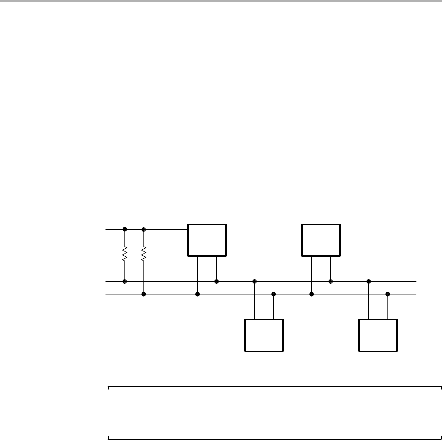
USCI Operation: I2C Mode
17-5
Universal Serial Communication Interface, I2C Mode
17.3 USCI Operation: I2C Mode
The I2C mode supports any slave or master I2C-compatible device.
Figure 17−2 shows an example of an I2C bus. Each I2C device is recognized
by a unique address and can operate as either a transmitter or a receiver. A
device connected to the I2C bus can be considered as the master or the slave
when performing data transfers. A master initiates a data transfer and
generates the clock signal SCL. Any device addressed by a master is
considered a slave.
I2C data is communicated using the serial data pin (SDA) and the serial clock
pin (SCL). Both SDA and SCL are bidirectional, and must be connected to a
positive supply voltage using a pullup resistor.
Figure 17−2. I2C Bus Connection Diagram
MSP430
VCC
Serial Data (SDA)
Serial Clock (SCL)
Device A
Device B Device C
Note: SDA and SCL Levels
The MSP430 SDA and SCL pins must not be pulled up above the MSP430
VCC level.

USCI Operation: I2C Mode
17-6 Universal Serial Communication Interface, I2C Mode
17.3.1 USCI Initialization and Reset
The USCI is reset by a PUC or by setting the UCSWRST bit. After a PUC, the
UCSWRST bit is automatically set, keeping the USCI in a reset condition. To
select I2C operation the UCMODEx bits must be set to 11. After module
initialization, it is ready for transmit or receive operation. Clearing UCSWRST
releases the USCI for operation.
Configuring and reconfiguring the USCI module should be done when
UCSWRST is set to avoid unpredictable behavior. Setting UCSWRST in I2C
mode has the following effects:
-I2C communication stops
-SDA and SCL are high impedance
-UCBxI2CSTAT, bits 6-0 are cleared
-UCBxTXIE and UCBxRXIE are cleared
-UCBxTXIFG and UCBxRXIFG are cleared
-All other bits and registers remain unchanged.
Note: Initializing or Reconfiguring the USCI Module
The recommended USCI initialization/re-configuration process is:
1) Set UCSWRST (BIS.B #UCSWRST,&UCxCTL1)
2) Initialize all USCI registers with UCSWRST=1 (including UCxCTL1)
3) Configure ports.
4) Clear UCSWRST via software (BIC.B #UCSWRST,&UCxCTL1)
5) Enable interrupts (optional) via UCxRXIE and/or UCxTXIE
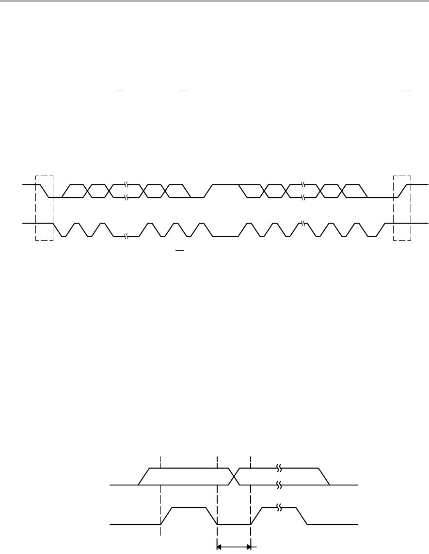
USCI Operation: I2C Mode
17-7
Universal Serial Communication Interface, I2C Mode
17.3.2 I2C Serial Data
One clock pulse is generated by the master device for each data bit
transferred. The I2C mode operates with byte data. Data is transferred most
significant bit first as shown in Figure 17−3.
The first byte after a START condition consists of a 7-bit slave address and the
R/W bit. When R/W = 0, the master transmits data to a slave. When R/W = 1,
the master receives data from a slave. The ACK bit is sent from the receiver
after each byte on the 9th SCL clock.
Figure 17−3. I2C Module Data Transfer
SDA
SCL
MSB Acknowledgement
Signal From Receiver
Acknowledgement
Signal From Receiver
12 789 12 89
ACK ACK
START
Condition (S)
STOP
Condition (P)
R/W
START and STOP conditions are generated by the master and are shown in
Figure 17−3. A START condition is a high-to-low transition on the SDA line
while SCL is high. A STOP condition is a low-to-high transition on the SDA line
while SCL is high. The bus busy bit, UCBBUSY, is set after a START and
cleared after a STOP.
Data on SDA must be stable during the high period of SCL as shown in
Figure 17−4. The high and low state of SDA can only change when SCL is low,
otherwise START or STOP conditions will be generated.
Figure 17−4. Bit Transfer on the I2C Bus
Data Line
Stable Data
Change of Data Allowed
SDA
SCL
USCI Operation: I2C Mode
17-8 Universal Serial Communication Interface, I2C Mode
17.3.3 I2C Addressing Modes
The I2C mode supports 7-bit and 10-bit addressing modes.
7-Bit Addressing
In the 7-bit addressing format, shown in Figure 17−5, the first byte is the 7-bit
slave address and the R/W bit. The ACK bit is sent from the receiver after each
byte.
Figure 17−5. I2C Module 7-Bit Addressing Format
S Slave Address R/W ACK Data ACK Data ACK P
7 8 8
111111
10-Bit Addressing
In the 10-bit addressing format, shown in Figure 17−6, the first byte is made
up of 11110b plus the two MSBs of the 10-bit slave address and the R/W bit.
The ACK bit is sent from the receiver after each byte. The next byte is the
remaining 8 bits of the 10-bit slave address, followed by the ACK bit and the
8-bit data.
Figure 17−6. I2C Module 10-Bit Addressing Format
S
1
Slave Address 1st byte
7
Slave Address 2nd byteACKR/W
11 8
ACK
1
Data
8
ACK
1
P
1
11110XX
Repeated Start Conditions
The direction of data flow on SDA can be changed by the master, without first
stopping a transfer, by issuing a repeated START condition. This is called a
RESTART. After a RESTART is issued, the slave address is again sent out with
the new data direction specified by the R/W bit. The RESTART condition is
shown in Figure 17−7.
Figure 17−7. I2C Module Addressing Format with Repeated START Condition
17 8 7 8
11 11 11 11
S Slave Address R/W ACK Data ACK S Slave Address R/W ACK Data ACK P
1 Any
Number
1Any Number
USCI Operation: I2C Mode
17-9
Universal Serial Communication Interface, I2C Mode
17.3.4 I2C Module Operating Modes
In I2C mode the USCI module can operate in master transmitter, master
receiver, slave transmitter, or slave receiver mode. The modes are discussed
in the following sections. Time lines are used to illustrate the modes.
Figure 17−8 shows how to interpret the time line figures. Data transmitted by
the master is represented by grey rectangles, data transmitted by the slave by
white rectangles. Data transmitted by the USCI module, either as master or
slave, is shown by rectangles that are taller than the others.
Actions taken by the USCI module are shown in grey rectangles with an arrow
indicating where in the the data stream the action occurs. Actions that must
be handled with software are indicated with white rectangles with an arrow
pointing to where in the data stream the action must take place.
Figure 17−8. I2C Time line Legend
...
USCI Master
USCI Slave
Other Master
Other Slave
... Bits set or reset by software
Bits set or reset by hardware

USCI Operation: I2C Mode
17-10 Universal Serial Communication Interface, I2C Mode
Slave Mode
The USCI module is configured as an I2C slave by selecting the I2C mode with
UCMODEx = 11 and UCSYNC = 1 and clearing the UCMST bit.
Initially the USCI module must to be configured in receiver mode by clearing
the UCTR bit to receive the I2C address. Afterwards, transmit and receive
operations are controlled automatically depending on the R/W bit received
together with the slave address.
The USCI slave address is programmed with the UCBxI2COA register. When
UCA10 = 0, 7-bit addressing is selected. When UCA10 = 1, 10-bit addressing
is selected. The UCGCEN bit selects if the slave responds to a general call.
When a START condition is detected on the bus, the USCI module will receive
the transmitted address and compare it against its own address stored in
UCBxI2COA. The UCSTTIFG flag is set when address received matches the
USCI slave address.
I2C Slave Transmitter Mode
Slave transmitter mode is entered when the slave address transmitted by the
master is identical to its own address with a set R/W bit. The slave transmitter
shifts the serial data out on SDA with the clock pulses that are generated by
the master device. The slave device does not generate the clock, but it will hold
SCL low while intervention of the CPU is required after a byte has been
transmitted.
If the master requests data from the slave the USCI module is automatically
configured as a transmitter and UCTR and UCBxTXIFG become set. The SCL
line is held low until the first data to be sent is written into the transmit buffer
UCBxTXBUF. Then the address is acknowledged, the UCSTTIFG flag is
cleared, and the data is transmitted. As soon as the data is transferred into the
shift register the UCBxTXIFG is set again. After the data is acknowledged by
the master the next data byte written into UCBxTXBUF is transmitted or if the
buffer is empty the bus is stalled during the acknowledge cycle by holding SCL
low until new data is written into UCBxTXBUF. If the master sends a NACK
succeeded by a STOP condition the UCSTPIFG flag is set. If the NACK is
succeeded by a repeated START condition the USCI I2C state machine
returns to its address-reception state.
Figure 17−9 illustrates the slave transmitter operation.
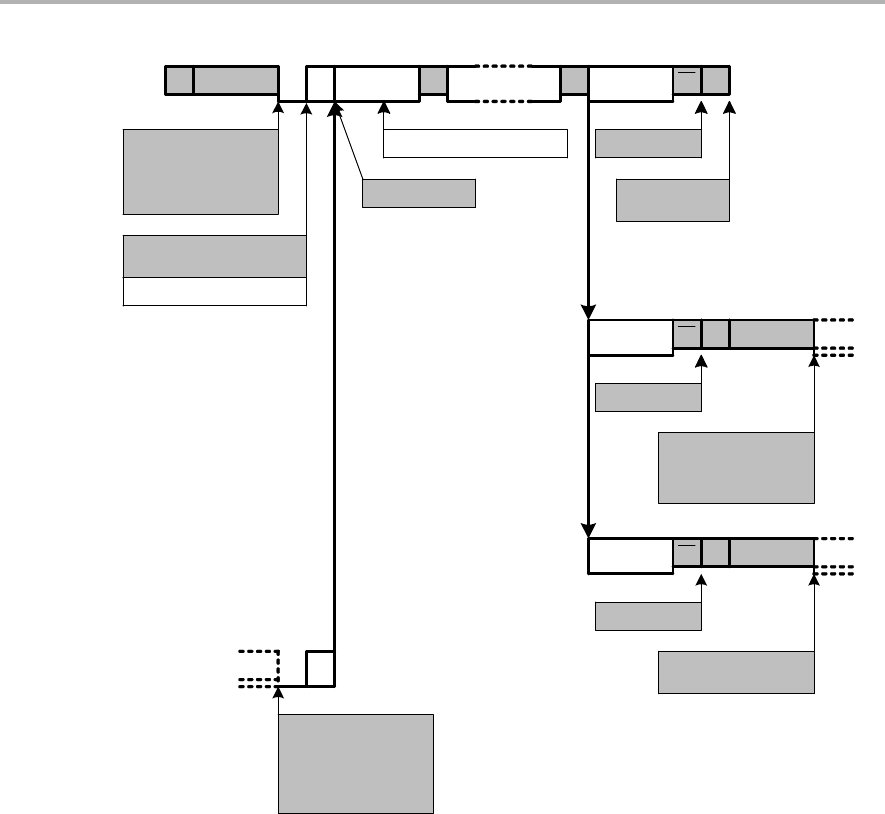
USCI Operation: I2C Mode
17-11
Universal Serial Communication Interface, I2C Mode
Figure 17−9. I2C Slave Transmitter Mode
SSLA/R A DATA A P
UCTR=1 (Transmitter)
UCSTTIFG=1
UCBxTXIFG=1
UCSTPIFG=?0
UCBxTXBUF discarded
Reception of own
address and
transmission of data
bytes
Bus stalled (SCL held low)
until data available
DATADATA A
UCSTPIFG=1
UCSTTIFG=0
A
A
DATA A S SLA/R
UCTR=1 (Transmitter)
UCSTTIFG=1
UCBxTXIFG=1
UCBxTXBUF discarded
DATA A S SLA/W
UCTR=0 (Receiver)
UCSTTIFG=1
Arbitration lost as
master and
addressed as slave
UCALIFG=1
UCMST=0
UCTR=1 (Transmitter)
UCSTTIFG=1
UCBxTXIFG=1
UCSTPIFG=0
UCBxTXIFG=0
Repeated start−
continue as
slave transmitter
Repeated start−
continue as
slave receiver
Write data to UCBxTXBUF
UCBxTXIFG=1
UCBxTXIFG=0
UCBxTXIFG=0
Write data to UCBxTXBUF

USCI Operation: I2C Mode
17-12 Universal Serial Communication Interface, I2C Mode
I2C Slave Receiver Mode
Slave receiver mode is entered when the slave address transmitted by the
master is identical to its own address and a cleared R/W bit is received. In slave
receiver mode, serial data bits received on SDA are shifted in with the clock
pulses that are generated by the master device. The slave device does not
generate the clock, but it can hold SCL low if intervention of the CPU is required
after a byte has been received.
If the slave should receive data from the master the USCI module is
automatically configured as a receiver and UCTR is cleared. After the first data
byte is received the receive interrupt flag UCBxRXIFG is set. The USCI
module automatically acknowledges the received data and can receive the
next data byte.
If the previous data wasn not read from the receive buffer UCBxRXBUF at the
end of a reception, the bus is stalled by holding SCL low. As soon as
UCBxRXBUF is read the new data is transferred into UCBxRXBUF, an
acknowledge is sent to the master, and the next data can be received.
Setting the UCTXNACK bit causes a NACK to be transmitted to the master
during the next acknowledgment cycle. A NACK is sent even if UCBxRXBUF
is not ready to receive the latest data. If the UCTXNACK bit is set while SCL
is held low the bus will be released, a NACK is transmitted immediately, and
UCBxRXBUF is loaded with the last received data. Since the previous data
was not read that data will be lost. To avoid loss of data the UCBxRXBUF
needs to be read before UCTXNACK is set.
When the master generates a STOP condition the UCSTPIFG flag is set.
If the master generates a repeated START condition the USCI I2C state
machine returns to its address reception state.
Figure 17−10 illustrates the the I2C slave receiver operation.
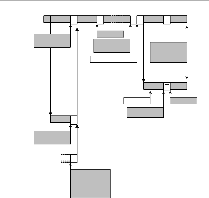
USCI Operation: I2C Mode
17-13
Universal Serial Communication Interface, I2C Mode
Figure 17−10. I2C Slave Receiver Mode
SSLA/W ADATA AP or S
Reception of own
address and data
bytes. All are
acknowledged.
UCBxRXIFG=1
DATADATA A A
UCTXNACK=1
Refer to:
”Slave Transmitter”
Timing Diagram
Bus not stalled even if
UCBxRXBUF not read
P or SDATA A
A
Arbitration lost as
master and
addressed as slave
UCALIFG=1
UCMST=0
UCTR=0 (Receiver)
UCSTTIFG=1
(UCGC=1 if general call)
UCBxTXIFG=0
UCSTPIFG=0
Last byte is not
acknowledged.
UCTR=0 (Receiver)
UCSTTIFG=1
UCSTPIFG=0
Gen Call A
UCTR=0 (Receiver)
UCSTTIFG=1
UCGC=1
Reception of the
general call
address.
UCTXNACK=0
Bus stalled
(SCL held low)
if UCBxRXBUF not read
Read data from UCBxRXBUF
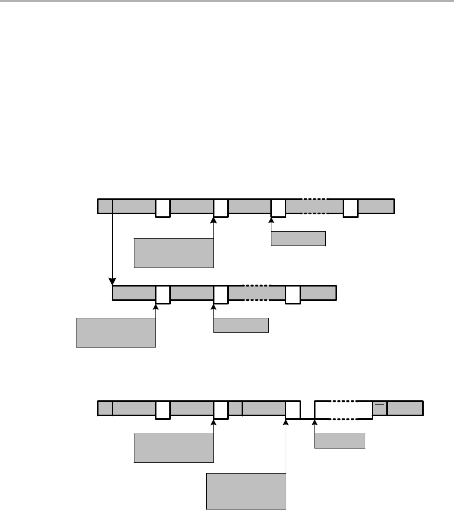
USCI Operation: I2C Mode
17-14 Universal Serial Communication Interface, I2C Mode
I2C Slave 10-bit Addressing Mode
The 10-bit addressing mode is selected when UCA10 = 1 and is as shown in
Figure 17−11. In 10-bit addressing mode, the slave is in receive mode after the
full address is received. The USCI module indicates this by setting the
UCSTTIFG flag while the UCTR bit is cleared. To switch the slave into
transmitter mode the master sends a repeated START condition together with
the first byte of the address but with the R/W bit set. This will set the UCSTTIFG
flag if it was previously cleared by software and the USCI modules switches
to transmitter mode with UCTR = 1.
Figure 17−11.I2C Slave 10-bit Addressing Mode
S
S11110 xx/W ASLA (2.) AP or S
Reception of own
address and data
bytes. All are
acknowledged.
UCBxRXIFG=1
DATA DATA
A A
UCTR=0 (Receiver)
UCSTTIFG=1
UCSTPIFG=0
Gen Call A
UCTR=0 (Receiver)
UCSTTIFG=1
UCGC=1
Reception of the
general call
address.
P or S
UCBxRXIFG=1
DATA DATA
A A
S11110 xx/W ASLA (2.) A
UCTR=0 (Receiver)
UCSTTIFG=1
UCSTPIFG=0
11110 xx/R A
UCTR=1 (Transmitter)
UCSTTIFG=1
UCBxTXIFG=1
UCSTPIFG=0
UCSTTIFG=0
DATA AP or S
Reception of own
address and
transmission of data
bytes
Slave Transmitter
Slave Receiver

USCI Operation: I2C Mode
17-15
Universal Serial Communication Interface, I2C Mode
Master Mode
The USCI module is configured as an I2C master by selecting the I2C mode
with UCMODEx = 11 and UCSYNC = 1 and setting the UCMST bit. When the
master is part of a multi-master system, UCMM must be set and its own
address must be programmed into the UCBxI2COA register. When UCA10 =
0, 7-bit addressing is selected. When UCA10 = 1, 10-bit addressing is
selected. The UCGCEN bit selects if the USCI module responds to a general
call.
I2C Master Transmitter Mode
After initialization, master transmitter mode is initiated by writing the desired
slave address to the UCBxI2CSA register, selecting the size of the slave
address with the UCSLA10 bit, setting UCTR for transmitter mode, and setting
UCTXSTT to generate a START condition.
The USCI module checks if the bus is available, generates the START
condition, and transmits the slave address. The UCBxTXIFG bit is set when
the START condition is generated and the first data to be transmitted can be
written into UCBxTXBUF. As soon as the slave acknowledges the address the
UCTXSTT bit is cleared.
The data written into UCBxTXBUF is transmitted if arbitration is not lost during
transmission of the slave address. UCBxTXIFG is set again as soon as the
data is transferred from the buffer into the shift register. If there is no data
loaded to UCBxTXBUF before the acknowledge cycle, the bus is held during
the acknowledge cycle with SCL low until data is written into UCBxTXBUF.
Data is transmitted or the bus is held as long as the UCTXSTP bit or UCTXSTT
bit is not set.
Setting UCTXSTP will generate a STOP condition after the next acknowledge
from the slave. If UCTXSTP is set during the transmission of the slave’s
address or while the USCI module waits for data to be written into
UCBxTXBUF, a STOP condition is generated even if no data was transmitted
to the slave. When transmitting a single byte of data, the UCTXSTP bit must
be set while the byte is being transmitted, or anytime after transmission
begins, without writing new data into UCBxTXBUF. Otherwise, only the
address will be transmitted. When the data is transferred from the buffer to the
shift register, UCBxTXIFG will become set indicating data transmission has
begun and the UCTXSTP bit may be set.
Setting UCTXSTT will generate a repeated START condition. In this case,
UCTR may be set or cleared to configure transmitter or receiver, and a different
slave address may be written into UCBxI2CSA if desired.
If the slave does not acknowledge the transmitted data the not-acknowledge
interrupt flag UCNACKIFG is set. The master must react with either a STOP
condition or a repeated START condition. If data was already written into
UCBxTXBUF it will be discarded. If this data should be transmitted after a
repeated START it must be written into UCBxTXBUF again. Any set UCTXSTT
is discarded, too. To trigger a repeated start UCTXSTT needs to be set again.
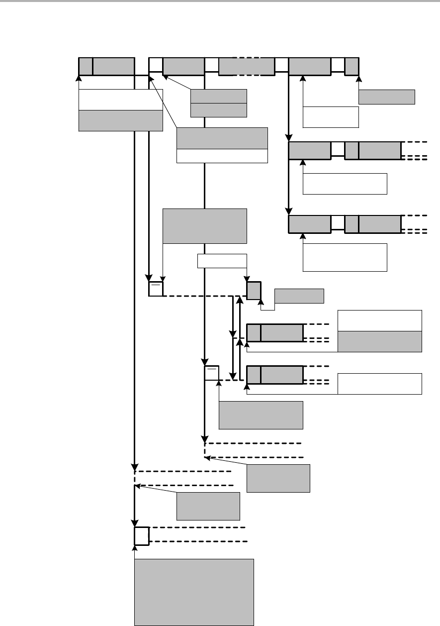
USCI Operation: I2C Mode
17-16 Universal Serial Communication Interface, I2C Mode
Figure 17−12 illustrates the I2C master transmitter operation.
Figure 17−12. I2C Master Transmitter Mode
Other master continues
SSLA/W ADATA AP
Successful
transmission to a
slave receiver
UCBxTXIFG=1
DATADATA A A
UCTXSTP=1
UCBxTXIFG=0
Next transfer started
with a repeated start
condition
DATA ASSLA/W
1) UCTR=1 (Transmitter)
2) UCTXSTT=1
DATA ASSLA/R
1) UCTR=0 (Receiver)
2) UCTXSTT=1
3) UCBxTXIFG=0
Not acknowledge
received after slave
address
P
SSLA/W
SSLA/R
UCTXSTP=1
1) UCTR=1 (Transmitter)
2) UCTXSTT=1
1) UCTR=0 (Receiver)
2) UCTXSTT=1
Arbitration lost in
slave address or
data byte
A
A
Other master continues
Arbitration lost and
addressed as slave Other master continues
A
UCALIFG=1
UCMST=0
UCTR=0 (Receiver)
UCSTTIFG=1
(UCGC=1 if general call)
UCBxTXIFG=0
UCSTPIFG=0
USCI continues as Slave Receiver
Not acknowledge
received after a data
byte
UCTXSTT=0 UCTXSTP=0
UCTXSTP=0
UCALIFG=1
UCMST=0
(UCSTTIFG=0)
Bus stalled (SCL held low)
until data available
Write data to UCBxTXBUF
1) UCTR=1 (Transmitter)
2) UCTXSTT=1
UCBxTXIFG=1
UCBxTXBUF discarded
UCTXSTT=0
UCNACKIFG=1
UCBxTXIFG=0
UCBxTXBUF discarded
UCBxTXIFG=1
UCBxTXBUF discarded
UCNACKIFG=1
UCBxTXIFG=0
UCBxTXBUF discarded
UCALIFG=1
UCMST=0
(UCSTTIFG=0)

USCI Operation: I2C Mode
17-17
Universal Serial Communication Interface, I2C Mode
I2C Master Receiver Mode
After initialization, master receiver mode is initiated by writing the desired
slave address to the UCBxI2CSA register, selecting the size of the slave
address with the UCSLA10 bit, clearing UCTR for receiver mode, and setting
UCTXSTT to generate a START condition.
The USCI module checks if the bus is available, generates the START
condition, and transmits the slave address. As soon as the slave
acknowledges the address the UCTXSTT bit is cleared.
After the acknowledge of the address from the slave the first data byte from
the slave is received and acknowledged and the UCBxRXIFG flag is set. Data
is received from the slave ss long as UCTXSTP or UCTXSTT is not set. If
UCBxRXBUF is not read the master holds the bus during reception of the last
data bit and until the UCBxRXBUF is read.
If the slave does not acknowledge the transmitted address the
not-acknowledge interrupt flag UCNACKIFG is set. The master must react
with either a STOP condition or a repeated START condition.
Setting the UCTXSTP bit will generate a STOP condition. After setting
UCTXSTP, a NACK followed by a STOP condition is generated after reception
of the data from the slave, or immediately if the USCI module is currently
waiting for UCBxRXBUF to be read.
If a master wants to receive a single byte only, the UCTXSTP bit must be set
while the byte is being received. For this case, the UCTXSTT may be polled
to determine when it is cleared:
BIS.B #UCTXSTT,&UCBOCTL1 ;Transmit START cond.
POLL_STT BIT.B #UCTXSTT,&UCBOCTL1 ;Poll UCTXSTT bit
JC POLL_STT ;When cleared,
BIS.B #UCTXSTP,&UCB0CTL1 ;transmit STOP cond.
Setting UCTXSTT will generate a repeated START condition. In this case,
UCTR may be set or cleared to configure transmitter or receiver, and a different
slave address may be written into UCBxI2CSA if desired.
Figure 17−13 illustrates the I2C master receiver operation.
Note: Consecutive Master Transactions Without Repeated Start
When performing multiple consecutive I2C master transactions without the
repeated start feature, the current transaction must be completed before the
next one is initiated. This can be done by ensuring that the transmit stop
condition flag UCTXSTP is cleared before the next I2C transaction is initiated
with setting UCTXSTT = 1. Otherwise, the current transaction might be
affected.
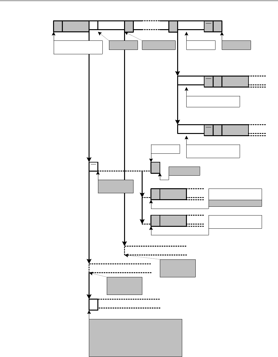
USCI Operation: I2C Mode
17-18 Universal Serial Communication Interface, I2C Mode
Figure 17−13. I2C Master Receiver Mode
Other master continues
S SLA/R A DATA AP
1) UCTR=0 (Receiver)
2) UCTXSTT=1
Successful
reception from a
slave transmitter
UCBxRXIFG=1
DATADATA A
UCTXSTP=1
Next transfer started
with a repeated start
condition
DATA SSLA/W
1) UCTR=1 (Transmitter)
2) UCTXSTT=1
DATA SSLA/R
1) UCTR=0 (Receiver)
2) UCTXSTT=1
Not acknowledge
received after slave
address
UCTXSTT=0
UCNACKIFG=1
P
S SLA/W
SSLA/R
1) UCTR=1 (Transmitter)
2) UCTXSTT=1
1) UCTR=0 (Receiver)
2) UCTXSTT=1
Arbitration lost in
slave address or
data byte
A
Other master continues
UCALIFG=1
UCMST=0
(UCSTTIFG=0)
Arbitration lost and
addressed as slave Other master continues
A
UCALIFG=1
UCMST=0
UCTR=1 (Transmitter)
UCSTTIFG=1
UCBxTXIFG=1
UCSTPIFG=0
USCI continues as Slave Transmitter
A
A
A
UCTXSTT=0 UCTXSTP=0
UCBxTXIFG=1
UCALIFG=1
UCMST=0
(UCSTTIFG=0)
UCTXSTP=1
UCTXSTP=0
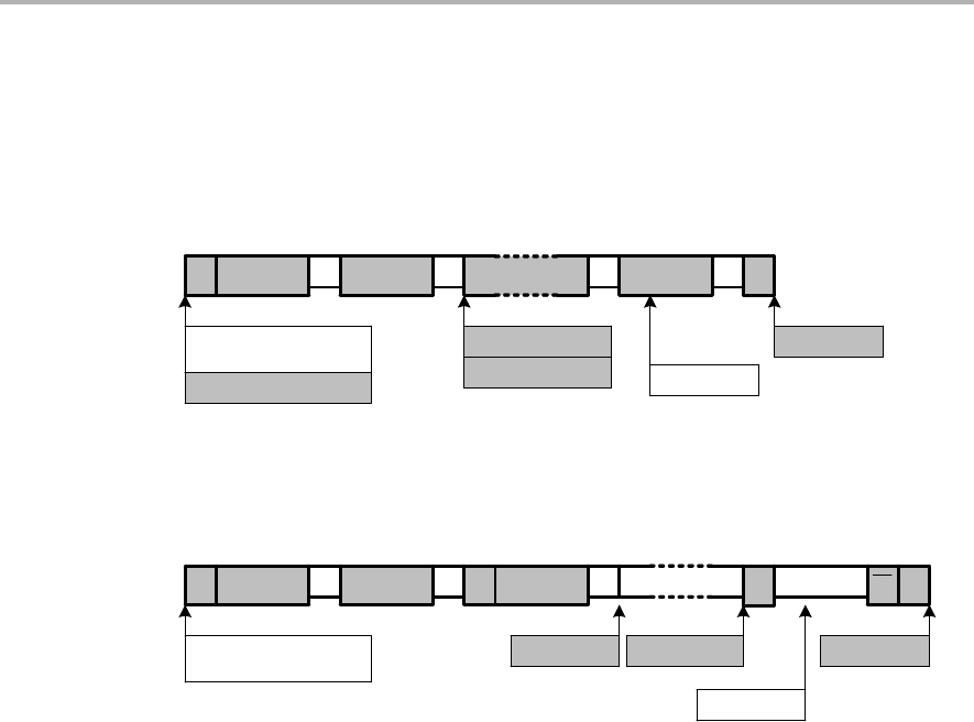
USCI Operation: I2C Mode
17-19
Universal Serial Communication Interface, I2C Mode
I2C Master 10-bit Addressing Mode
The 10-bit addressing mode is selected when UCSLA10 = 1 and is shown in
Figure 17−14.
Figure 17−14. I2C Master 10-bit Addressing Mode
Master Transmitter
SA A P
1) UCTR=1 (Transmitter)
2) UCTXSTT=1
Successful
transmission to a
slave receiver
UCBxTXIFG=1 UCBxTXIFG=1
DATADATA A A
UCTXSTP=1
UCTXSTT=0 UCTXSTP=0
11110 xx/W SLA (2.)
SAP
1) UCTR=0 (Receiver)
2) UCTXSTT=1
Successful
reception from a
slave transmitter
DATADATA A
UCTXSTP=1
A
UCTXSTT=0 UCTXSTP=0
A A
11110 xx/W SLA (2.) 11110 xx/R
Master Receiver
S
UCBxRXIFG=1
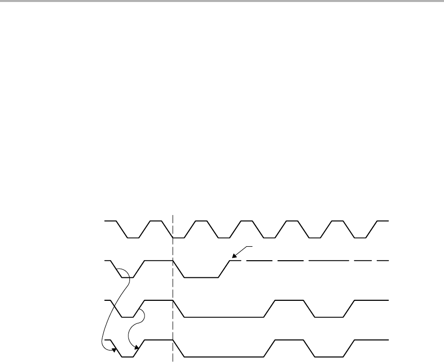
USCI Operation: I2C Mode
17-20 Universal Serial Communication Interface, I2C Mode
Arbitration
If two or more master transmitters simultaneously start a transmission on the
bus, an arbitration procedure is invoked. Figure 17−15 illustrates the
arbitration procedure between two devices. The arbitration procedure uses
the data presented on SDA by the competing transmitters. The first master
transmitter that generates a logic high is overruled by the opposing master
generating a logic low. The arbitration procedure gives priority to the device
that transmits the serial data stream with the lowest binary value. The master
transmitter that lost arbitration switches to the slave receiver mode, and sets
the arbitration lost flag UCALIFG. If two or more devices send identical first
bytes, arbitration continues on the subsequent bytes.
Figure 17−15. Arbitration Procedure Between Two Master Transmitters
1
00 0
1
00 0
11
111
n
Device #1 Lost Arbitration
and Switches Off
Bus Line
SCL
Data From
Device #1
Data From
Device #2
Bus Line
SDA
If the arbitration procedure is in progress when a repeated START condition
or STOP condition is transmitted on SDA, the master transmitters involved in
arbitration must send the repeated START condition or STOP condition at the
same position in the format frame. Arbitration is not allowed between:
-A repeated START condition and a data bit
-A STOP condition and a data bit
-A repeated START condition and a STOP condition
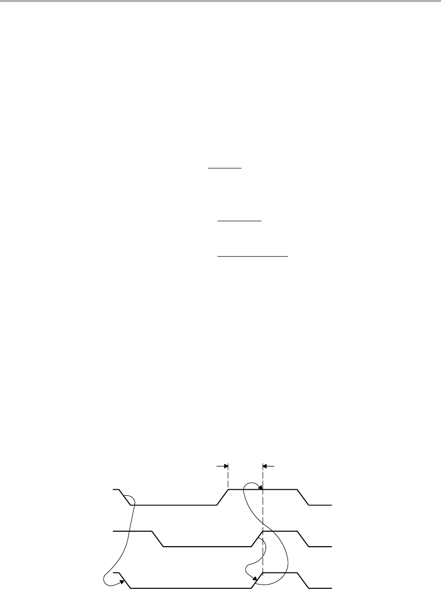
USCI Operation: I2C Mode
17-21
Universal Serial Communication Interface, I2C Mode
17.3.5 I2C Clock Generation and Synchronization
The I2C clock SCL is provided by the master on the I2C bus. When the USCI
is in master mode, BITCLK is provided by the USCI bit clock generator and the
clock source is selected with the UCSSELx bits. In slave mode the bit clock
generator is not used and the UCSSELx bits are don’t care.
The 16-bit value of UCBRx in registers UCBxBR1 and UCBxBR0 is the division
factor of the USCI clock source, BRCLK. The maximum bit clock that can be
used in single master mode is fBRCLK/4. In multi-master mode the maximum
bit clock is fBRCLK/8. The BITCLK frequency is given by:
fBitClock +fBRCLK
UCBRx
The minimum high and low periods of the generated SCL are
tLOW,MIN +tHIGH,MIN +UCBRxń2
fBRCLK
when UCBRx is even and
tLOW,MIN +tHIGH,MIN +(UCBRx *1)ń2
fBRCLK
when UCBRx is odd.
The USCI clock source frequency and the prescaler setting UCBRx must to
be chosen such that the minimum low and high period times of the I2C specifi-
cation are met.
During the arbitration procedure the clocks from the different masters must be
synchronized. A device that first generates a low period on SCL overrules the
other devices forcing them to start their own low periods. SCL is then held low
by the device with the longest low period. The other devices must wait for SCL
to be released before starting their high periods. Figure 17−16 illustrates the
clock synchronization. This allows a slow slave to slow down a fast master.
Figure 17−16. Synchronization of Two I2C Clock Generators During Arbitration
Wait
State Start HIGH
Period
SCL From
Device #1
SCL From
Device #2
Bus Line
SCL

USCI Operation: I2C Mode
17-22 Universal Serial Communication Interface, I2C Mode
Clock Stretching
The USCI module supports clock stretching and also makes use of this feature
as described in the operation mode sections.
The UCSCLLOW bit can be used to observe if another device pulls SCL low
while the USCI module already released SCL due to the following conditions:
-USCI is acting as master and a connected slave drives SCL low.
-USCI is acting as master and another master drives SCL low during
arbitration.
The UCSCLLOW bit is also active if the USCI holds SCL low because it is wait-
ing as transmitter for data being written into UCBxTXBUF or as receiver for the
data being read from UCBxRXBUF.
The UCSCLLOW bit might get set for a short time with each rising SCL edge
because the logic observes the external SCL and compares it to the internally
generated SCL.
17.3.6 Using the USCI Module in I2C Mode with Low Power Modes
The USCI module provides automatic clock activation for SMCLK for use with
low-power modes. When SMCLK is the USCI clock source, and is inactive
because the device is in a low-power mode, the USCI module automatically
activates it when needed, regardless of the control-bit settings for the clock
source. The clock remains active until the USCI module returns to its idle
condition. After the USCI module returns to the idle condition, control of the
clock source reverts to the settings of its control bits. Automatic clock activation
is not provided for ACLK.
When the USCI module activates an inactive clock source, the clock source
becomes active for the whole device and any peripheral configured to use the
clock source may be affected. For example, a timer using SMCLK will
increment while the USCI module forces SMCLK active.
In I2C slave mode no internal clock source is required because the clock is
provided by the external master. It is possible to operate the USCI in I2C slave
mode while the device is in LPM4 and all internal clock sources are disabled.
The receive or transmit interrupts can wake up the CPU from any low power
mode.

USCI Operation: I2C Mode
17-23
Universal Serial Communication Interface, I2C Mode
17.3.7 USCI Interrupts in I2C Mode
Their are two interrupt vectors for the USCI module in I2C mode. One interrupt
vector is associated with the transmit and receive interrupt flags. The other
interrupt vector is associated with the four state change interrupt flags. Each
interrupt flag has its own interrupt enable bit. When an interrupt is enabled, and
the GIE bit is set, the interrupt flag will generate an interrupt request. DMA
transfers are controlled by the UCBxTXIFG and UCBxRXIFG flags on devices
with a DMA controller.
I2C Transmit Interrupt Operation
The UCBxTXIFG interrupt flag is set by the transmitter to indicate that
UCBxTXBUF is ready to accept another character. An interrupt request is
generated if UCBxTXIE and GIE are also set. UCBxTXIFG is automatically
reset if a character is written to UCBxTXBUF or if a NACK is received.
UCBxTXIFG is set when UCSWRST = 1 and the I2C mode is selected.
UCBxTXIE is reset after a PUC or when UCSWRST = 1.
I2C Receive Interrupt Operation
The UCBxRXIFG interrupt flag is set when a character is received and loaded
into UCBxRXBUF. An interrupt request is generated if UCBxRXIE and GIE are
also set. UCBxRXIFG and UCBxRXIE are reset after a PUC signal or when
UCSWRST = 1. UCxRXIFG is automatically reset when UCxRXBUF is read.
I2C State Change Interrupt Operation.
Table 17−1 Describes the I2C state change interrupt flags.
Table 17−1.I2C State Change Interrupt Flags
Interrupt Flag Interrupt Condition
UCALIFG Arbitration-lost. Arbitration can be lost when two or more
transmitters start a transmission simultaneously, or when the
USCI operates as master but is addressed as a slave by another
master in the system. The UCALIFG flag is set when arbitration is
lost. When UCALIFG is set the UCMST bit is cleared and the I2C
controller becomes a slave.
UCNACKIFG Not-acknowledge interrupt. This flag is set when an acknowledge
is expected but is not received. UCNACKIFG is automatically
cleared when a START condition is received.
UCSTTIFG Start condition detected interrupt. This flag is set when the I2C
module detects a START condition together with its own address
while in slave mode. UCSTTIFG is used in slave mode only and
is automatically cleared when a STOP condition is received.
UCSTPIFG Stop condition detected interrupt. This flag is set when the I2C
module detects a STOP condition while in slave mode.
UCSTPIFG is used in slave mode only and is automatically
cleared when a START condition is received.

USCI Operation: I2C Mode
17-24 Universal Serial Communication Interface, I2C Mode
Interrupt Vector Assignment
USCI_Ax and USCI_Bx share the same interrupt vectors. In I2C mode the
state change interrupt flags UCSTTIFG, UCSTPIFG, UCIFG, UCALIFG from
USCI_Bx and UCAxRXIFG from USCI_Ax are routed to one interrupt vector.
The I2C transmit and receive interrupt flags UCBxTXIFG and UCBxRXIFG
from USCI_Bx and UCAxTXIFG from USCI_Ax share another interrupt vector.
Shared Interrupt Vectors Software Example
The following software example shows an extract of the interrupt service
routine to handle data receive interrupts from USCI_A0 in either UART or SPI
mode and state change interrupts from USCI_B0 in I2C mode.
USCIA0_RX_USCIB0_I2C_STATE_ISR
BIT.B #UCA0RXIFG, &IFG2 ; USCI_A0 Receive Interrupt?
JNZ USCIA0_RX_ISR
USCIB0_I2C_STATE_ISR
; Decode I2C state changes ...
; Decode I2C state changes ...
...
RETI
USCIA0_RX_ISR
; Read UCA0RXBUF ... − clears UCA0RXIFG
...
RETI
The following software example shows an extract of the interrupt service
routine that handles data transmit interrupts from USCI_A0 in either UART or
SPI mode and the data transfer interrupts from USCI_B0 in I2C mode.
USCIA0_TX_USCIB0_I2C_DATA_ISR
BIT.B #UCA0TXIFG, &IFG2 ; USCI_A0 Transmit Interrupt?
JNZ USCIA0_TX_ISR
USCIB0_I2C_DATA_ISR
BIT.B #UCB0RXIFG, &IFG2
JNZ USCIB0_I2C_RX
USCIB0_I2C_TX
; Write UCB0TXBUF... − clears UCB0TXIFG
...
RETI
USCIB0_I2C_RX
; Read UCB0RXBUF... − clears UCB0RXIFG
...
RETI
USCIA0_TX_ISR
; Write UCA0TXBUF ... − clears UCA0TXIFG
...
RETI

USCI Registers: I2C Mode
17-25
Universal Serial Communication Interface, I2C Mode
17.4 USCI Registers: I2C Mode
The USCI registers applicable in I2C mode for USCI_B0 are listed in
Table 17−2 and for USCI_B1 in Table 17−3.
Table 17−2.USCI_B0 Control and Status Registers
Register Short Form Register Type Address Initial State
USCI_B0 control register 0 UCB0CTL0 Read/write 068h 001h with PUC
USCI_B0 control register 1 UCB0CTL1 Read/write 069h 001h with PUC
USCI_B0 bit rate control register 0 UCB0BR0 Read/write 06Ah Reset with PUC
USCI_B0 bit rate control register 1 UCB0BR1 Read/write 06Bh Reset with PUC
USCI_B0 I2C interrupt enable register UCB0I2CIE Read/write 06Ch Reset with PUC
USCI_B0 status register UCB0STAT Read/write 06Dh Reset with PUC
USCI_B0 receive buffer register UCB0RXBUF Read 06Eh Reset with PUC
USCI_B0 transmit buffer register UCB0TXBUF Read/write 06Fh Reset with PUC
USCI_B0 I2C own address register UCB0I2COA Read/write 0118h Reset with PUC
USCI_B0 I2C slave address register UCB0I2CSA Read/write 011Ah Reset with PUC
SFR interrupt enable register 2 IE2 Read/write 001h Reset with PUC
SFR interrupt flag register 2 IFG2 Read/write 003h 00Ah with PUC
Note: Modifying SFR bits
To avoid modifying control bits of other modules, it is recommended to set
or clear the IEx and IFGx bits using BIS.B or BIC.B instructions, rather than
MOV.B or CLR.B instructions.
Table 17−3.USCI_B1 Control and Status Registers
Register Short Form Register Type Address Initial State
USCI_B1 control register 0 UCB1CTL0 Read/write 0D8h Reset with PUC
USCI_B1 control register 1 UCB1CTL1 Read/write 0D9h 001h with PUC
USCI_B1 baud rate control register 0 UCB1BR0 Read/write 0DAh Reset with PUC
USCI_B1 baud rate control register 1 UCB1BR1 Read/write 0DBh Reset with PUC
USCI_B1 I2C Interrupt enable register UCB1I2CIE Read/write 0DCh Reset with PUC
USCI_B1 status register UCB1STAT Read/write 0DDh Reset with PUC
USCI_B1 receive buffer register UCB1RXBUF Read 0DEh Reset with PUC
USCI_B1 transmit buffer register UCB1TXBUF Read/write 0DFh Reset with PUC
USCI_B1 I2C own address register UCB1I2COA Read/write 017Ch Reset with PUC
USCI_B1 I2C slave address register UCB1I2CSA Read/write 017Eh Reset with PUC
USCI_A1/B1 interrupt enable register UC1IE Read/write 006h Reset with PUC
USCI_A1/B1 interrupt flag register UC1IFG Read/write 007h 00Ah with PUC

USCI Registers: I2C Mode
17-26 Universal Serial Communication Interface, I2C Mode
UCBxCTL0, USCI_Bx Control Register 0
76543210
UCA10 UCSLA10 UCMM Unused UCMST UCMODEx=11 UCSYNC=1
rw−0 rw−0 rw−0 rw−0 rw−0 rw−0 rw−0 r−1
UCA10 Bit 7 Own addressing mode select
0 Own address is a 7-bit address
1 Own address is a 10-bit address
UCSLA10 Bit 6 Slave addressing mode select
0 Address slave with 7-bit address
1 Address slave with 10-bit address
UCMM Bit 5 Multi-master environment select
0 Single master environment. There is no other master in the system.
The address compare unit is disabled.
1 Multi master environment
Unused Bit 4 Unused
UCMST Bit 3 Master mode select. When a master looses arbitration in a multi-master
environment (UCMM = 1) the UCMST bit is automatically cleared and the
module acts as slave.
0 Slave mode
1 Master mode
UCMODEx Bits
2−1
USCI Mode. The UCMODEx bits select the synchronous mode when
UCSYNC = 1.
00 3-pin SPI
01 4-pin SPI (master/slave enabled if STE = 1)
10 4-pin SPI (master/slave enabled if STE = 0)
11 I2C mode
UCSYNC Bit 0 Synchronous mode enable
0 Asynchronous mode
1 Synchronous mode

USCI Registers: I2C Mode
17-27
Universal Serial Communication Interface, I2C Mode
UCBxCTL1, USCI_Bx Control Register 1
76543210
UCSSELx Unused UCTR UCTXNACK UCTXSTP UCTXSTT UCSWRST
rw−0 rw−0 r0 rw−0 rw−0 rw−0 rw−0 rw−1
UCSSELx Bits
7-6
USCI clock source select. These bits select the BRCLK source clock.
00 UCLKI
01 ACLK
10 SMCLK
11 SMCLK
Unused Bit 5 Unused
UCTR Bit 4 Transmitter/Receiver
0 Receiver
1 Transmitter
UCTXNACK Bit 3 Transmit a NACK. UCTXNACK is automatically cleared after a NACK is
transmitted.
0 Acknowledge normally
1 Generate NACK
UCTXSTP Bit 2 Transmit STOP condition in master mode. Ignored in slave mode. In
master receiver mode the STOP condition is preceded by a NACK.
UCTXSTP is automatically cleared after STOP is generated.
0 No STOP generated
1 Generate STOP
UCTXSTT Bit 1 Transmit START condition in master mode. Ignored in slave mode. In
master receiver mode a repeated START condition is preceded by a
NACK. UCTXSTT is automatically cleared after START condition and
address information is transmitted.
Ignored in slave mode.
0 Do not generate START condition
1 Generate START condition
UCSWRST Bit 0 Software reset enable
0 Disabled. USCI reset released for operation.
1 Enabled. USCI logic held in reset state.

USCI Registers: I2C Mode
17-28 Universal Serial Communication Interface, I2C Mode
UCBxBR0, USCI_Bx Baud Rate Control Register 0
76543210
UCBRx − low byte
rw rw rw rw rw rw rw rw
UCBxBR1, USCI_Bx Baud Rate Control Register 1
76543210
UCBRx − high byte
rw rw rw rw rw rw rw rw
UCBRx Bit clock prescaler setting.
The 16-bit value of (UCBxBR0 + UCBxBR1 ×256} forms the prescaler
value.

USCI Registers: I2C Mode
17-29
Universal Serial Communication Interface, I2C Mode
UCBxSTAT, USCI_Bx Status Register
76543210
Unused UC
SCLLOW UCGC UCBBUSY UCNACK
IFG UCSTPIFG UCSTTIFG UCALIFG
rw−0 r−0 rw−0 r−0 rw−0 rw−0 rw−0 rw−0
Unused Bit 7 Unused.
UC
SCLLOW
Bit 6 SCL low
0 SCL is not held low
1 SCL is held low
UCGC Bit 5 General call address received. UCGC is automatically cleared when a
START condition is received.
0 No general call address received
1 General call address received
UCBBUSY Bit 4 Bus busy
0 Bus inactive
1 Bus busy
UCNACK
IFG
Bit 3 Not-acknowledge received interrupt flag. UCNACKIFG is automatically
cleared when a START condition is received.
0 No interrupt pending
1 Interrupt pending
UCSTPIFG Bit 2 Stop condition interrupt flag. UCSTPIFG is automatically cleared when a
START condition is received.
0 No interrupt pending
1 Interrupt pending
UCSTTIFG Bit 1 Start condition interrupt flag. UCSTTIFG is automatically cleared if a STOP
condition is received.
0 No interrupt pending
1 Interrupt pending
UCALIFG Bit 0 Arbitration lost interrupt flag
0 No interrupt pending
1 Interrupt pending

USCI Registers: I2C Mode
17-30 Universal Serial Communication Interface, I2C Mode
UCBxRXBUF, USCI_Bx Receive Buffer Register
76543210
UCRXBUFx
r r r r r r r r
UCRXBUFx Bits
7−0
The receive-data buffer is user accessible and contains the last received
character from the receive shift register. Reading UCBxRXBUF resets
UCBxRXIFG.
UCBxTXBUF, USCI_Bx Transmit Buffer Register
76543210
UCTXBUFx
rw rw rw rw rw rw rw rw
UCTXBUFx Bits
7−0
The transmit data buffer is user accessible and holds the data waiting to
be moved into the transmit shift register and transmitted. Writing to the
transmit data buffer clears UCBxTXIFG.

USCI Registers: I2C Mode
17-31
Universal Serial Communication Interface, I2C Mode
UCBxI2COA, USCIBx I2C Own Address Register
15 14 13 12 11 10 9 8
UCGCEN 0 0 0 0 0 I2COAx
rw−0 r0 r0 r0 r0 r0 rw−0 rw−0
76543210
I2COAx
rw−0 rw−0 rw−0 rw−0 rw−0 rw−0 rw−0 rw−0
UCGCEN Bit 15 General call response enable
0 Do not respond to a general call
1 Respond to a general call
I2COAx Bits
9-0
I2C own address. The I2COAx bits contain the local address of the USCI_Bx
I2C controller. The address is right-justified. In 7-bit addressing mode Bit 6 is
the MSB, Bits 9-7 are ignored. In 10-bit addressing mode Bit 9 is the MSB.
UCBxI2CSA, USCI_Bx I2C Slave Address Register
15 14 13 12 11 10 9 8
0 0 0 0 0 0 I2CSAx
r0 r0 r0 r0 r0 r0 rw−0 rw−0
76543210
I2CSAx
rw−0 rw−0 rw−0 rw−0 rw−0 rw−0 rw−0 rw−0
I2CSAx Bits
9-0
I2C slave address. The I2CSAx bits contain the slave address of the external
device to be addressed by the USCI_Bx module. It is only used in master
mode. The address is right-justified. In 7-bit slave addressing mode Bit 6 is
the MSB, Bits 9-7 are ignored. In 10-bit slave addressing mode Bit 9 is the
MSB.

USCI Registers: I2C Mode
17-32 Universal Serial Communication Interface, I2C Mode
UCBxI2CIE, USCI_Bx I2C Interrupt Enable Register
76543210
Reserved UCNACKIE UCSTPIE UCSTTIE UCALIE
rw−0 rw−0 rw−0 rw−0 rw−0 rw−0 rw−0 rw−0
Reserved Bits
7−4
Reserved
UCNACKIE Bit 3 Not-acknowledge interrupt enable
0 Interrupt disabled
1 Interrupt enabled
UCSTPIE Bit 2 Stop condition interrupt enable
0 Interrupt disabled
1 Interrupt enabled
UCSTTIE Bit 1 Start condition interrupt enable
0 Interrupt disabled
1 Interrupt enabled
UCALIE Bit 0 Arbitration lost interrupt enable
0 Interrupt disabled
1 Interrupt enabled

USCI Registers: I2C Mode
17-33
Universal Serial Communication Interface, I2C Mode
IE2, Interrupt Enable Register 2
76543210
UCB0TXIE UCB0RXIE
rw−0 rw−0
Bits
7-4
These bits may be used by other modules (see the device-specific data
sheet).
UCB0TXIE Bit 3 USCI_B0 transmit interrupt enable
0 Interrupt disabled
1 Interrupt enabled
UCB0RXIE Bit 2 USCI_B0 receive interrupt enable
0 Interrupt disabled
1 Interrupt enabled
Bits
1-0
These bits may be used by other modules (see the device-specific data
sheet).
IFG2, Interrupt Flag Register 2
76543210
UCB0
TXIFG
UCB0
RXIFG
rw−1 rw−0
Bits
7-4
These bits may be used by other modules (see the device-specific data
sheet).
UCB0
TXIFG
Bit 3 USCI_B0 transmit interrupt flag. UCB0TXIFG is set when UCB0TXBUF is
empty.
0 No interrupt pending
1 Interrupt pending
UCB0
RXIFG
Bit 2 USCI_B0 receive interrupt flag. UCB0RXIFG is set when UCB0RXBUF has
received a complete character.
0 No interrupt pending
1 Interrupt pending
Bits
1-0
These bits may be used by other modules (see the device-specific data
sheet).

USCI Registers: I2C Mode
17-34 Universal Serial Communication Interface, I2C Mode
UC1IE, USCI_B1 Interrupt Enable Register
76543210
Unused Unused Unused Unused UCB1TXIE UCB1RXIE
rw−0 rw−0 rw−0 rw−0 rw−0 rw−0
Unused Bits
7-4
Unused
UCB1TXIE Bit 3 USCI_B1 transmit interrupt enable
0 Interrupt disabled
1 Interrupt enabled
UCB1RXIE Bit 2 USCI_B1 receive interrupt enable
0 Interrupt disabled
1 Interrupt enabled
Bits
1-0
These bits may be used by other USCI modules (see the device-specific data
sheet).
UC1IFG, USCI_B1 Interrupt Flag Register
76543210
Unused Unused Unused Unused UCB1
TXIFG
UCB1
RXIFG
rw−0 rw−0 rw−0 rw−0 rw−1 rw−0
Unused Bits
7-4
Unused.
UCB1
TXIFG
Bit 3 USCI_B1 transmit interrupt flag. UCB1TXIFG is set when UCB1TXBUF is
empty.
0 No interrupt pending
1 Interrupt pending
UCB1
RXIFG
Bit 2 USCI_B1 receive interrupt flag. UCB1RXIFG is set when UCB1RXBUF has
received a complete character.
0 No interrupt pending
1 Interrupt pending
Bits
1-0
These bits may be used by other modules (see the device-specific data
sheet).

18-1
OA
OA
The OA is a general purpose operational amplifier. This chapter describes the
OA. Two OA modules are implemented in the MSP430x22x4 devices.
Topic Page
18.1 OA Introduction 18-2. . . . . . . . . . . . . . . . . . . . . . . . . . . . . . . . . . . . . . . . . . . . . .
18.2 OA Operation 18-4. . . . . . . . . . . . . . . . . . . . . . . . . . . . . . . . . . . . . . . . . . . . . . . . .
18.3 OA Registers 18-12. . . . . . . . . . . . . . . . . . . . . . . . . . . . . . . . . . . . . . . . . . . . . . .
Chapter 18

OA Introduction
18-2 OA
18.1 OA Introduction
The OA operational amplifiers support front-end analog signal conditioning
prior to analog-to-digital conversion.
Features of the OA include:
-Single supply, low-current operation
-Rail-to-rail output
-Programmable settling time vs. power consumption
-Software selectable configurations
-Software selectable feedback resistor ladder for PGA implementations
Note: Multiple OA Modules
Some devices may integrate more than one OA module. In the case where
more than one OA is present on a device, the multiple OA modules operate
identically.
Throughout this chapter, nomenclature appears such as OAxCTL0 to
describe register names. When this occurs, the x is used to indicate which
OA module is being discussed. In cases where operation is identical, the
register is simply referred to as OAxCTL0.
The block diagram of the OA module is shown in Figure 18−1.
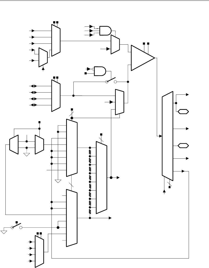
OA Introduction
18-3
OA
Figure 18−1. OA Block Diagram
000
001
100
011
010
111
110
101
3
3
000
001
100
011
010
111
110
101
3
4R
4R
2R
2R
R
R
R
R
OAFBRx
OAxTAP
OAFCx
OAxRBOTTOM
OA1RBOTTOM(OA0)
OA2RBOTTOM
(OA1)
OA0RBOTTOM
(OA2)
000
001
100
011
010
111
110
101
OAPMx
OAxOUT
OAx
+
−
A1 (OA0)
A3 (OA1)
A5 (OA2)
A12 (OA0)
A13 (OA1)
A14 (OA2)
001
else
OAFCx = 6
0
1
OANx = 3
OAPx = 3
OA1TAP (OA0)
OA2TAP (OA1)
OA0TAP (OA2)
OAxR
TOP
000
1
OAPx
OAxI0
OA0I1
00
01
10
11
OAxIA
OAxIB
OA2OUT (OA0)
OA0OUT (OA1)
OA1OUT (OA2)
0
1
OAFCx = 5 OANx
OAxI0
OAxI1
00
01
10
11
OAxIA
OAxIB
OANEXT
OAFCx = 6
OAxR
BOTTOM
A12/OA0O
A13/OA1O
A14/OA2O
A1/OA0O
A3/OA1O
A5/OA2O
OANx
OAxI0
OAxI1
00
01
10
11
OAxIA
AV CC
1
0
OARRIP
0
1
OAFBRx > 0
1
OAFCx = 0
OAADCx
OAxFB
OA2OUT (OA0)
OA0OUT (OA1)
OA1OUT (OA2)
2
Feeback Switch Matrix

OA Operation
18-4 OA
18.2 OA Operation
The OA module is configured with user software. The setup and operation of
the OA is discussed in the following sections.
18.2.1 OA Amplifier
The OA is a configurable, low-current, rail-to-rail output operational amplifier.
It can be configured as an inverting amplifier, or a non-inverting amplifier, or
can be combined with other OA modules to form differential amplifiers. The
output slew rate of the OA can be configured for optimized settling time vs.
power consumption with the OAPMx bits. When OAPMx = 00 the OA is off and
the output is high-impedance. When OAPMx > 0, the OA is on. See the
device-specific data sheet for parameters.
18.2.2 OA Input
The OA has configurable input selection. The signals for the + and − inputs are
individually selected with the OANx and OAPx bits and can be selected as
external signals or internal signals. OAxI0 and OAxI1 are external signals
provided for each OA module. OA0I1 provides a non-inverting input that is tied
together internally for all OA modules. OAxIA and OAxIB provide
device-dependent inputs. Refer to the device data sheet for signal
connections.
When the external inverting input is not needed for a mode, setting the
OANEXT bit makes the internal inverting input externally available.

OA Operation
18-5
OA
18.2.3 OA Output and Feedback Routing
The OA has configurable output selection controlled by the OAADCx bits and
the OAFCx bits. The OA output signals can be routed to ADC12 inputs A12
(OA0), A13 (OA1), or A14 (OA2) internally, or can be routed to these ADC
inputs and their external pins. The OA output signals can also be routed to
ADC inputs A1 (OA0), A3 (OA1), or A5 (OA2) and the corresponding external
pin. The OA output is also connected to an internal R-ladder with the OAFCx
bits. The R-ladder tap is selected with the OAFBRx bits to provide
programmable gain amplifier functionality.
Table 18−1 shows the OA output and feedback routing configurations. When
OAFCx = 0 the OA is in general-purpose mode and feedback is achieved
externally to the device. When OAFCx > 0 and when OAADCx = 00 or 11, the
output of the OA is kept internal to the device. When OAFCx > 0 and OAADCx
= 01 or 10, the OA output is routed both internally and externally.
Table 18−1.OA Output Configurations
OAFCx OAADCx OA Output and Feedback Routing
= 0 x0 OAxOUT connected to external pins and ADC input A1, A3,
or A5.
= 0 x1 OAxOUT connected to external pins and ADC input A12,
A13, or A14.
> 0 00 OAxOUT used for internal routing only.
> 0 01 OAxOUT connected to external pins and ADC input A12,
A13, or A14.
> 0 10 OAxOUT connected to external pins and ADC input A1, A3,
or A5.
> 0 11 OAxOUT connected internally to ADC input A12, A13 , or
A14. External A12, A13, or A14 pin connections are
disconnected from the ADC.

OA Operation
18-6 OA
18.2.4 OA Configurations
The OA can be configured for different amplifier functions with the OAFCx bits
as listed in Table 18−2.
Table 18−2.OA Mode Select
OAFCx OA Mode
000 General-purpose opamp
001 Unity gain buffer for three-opamp differential amplifier
010 Unity gain buffer
011 Comparator
100 Non-inverting PGA amplifier
101 Cascaded non-inverting PGA amplifier
110 Inverting PGA amplifier
111 Differential amplifier
General Purpose Opamp Mode
In this mode the feedback resistor ladder is isolated from the OAx and the
OAxCTL0 bits define the signal routing. The OAx inputs are selected with the
OAPx and OANx bits. The OAx output is connected to the ADC12 input
channel as selected by the OAxCTL0 bits.
Unity Gain Mode for Differential Amplifier
In this mode the output of the OAx is connected to the inverting input of the OAx
providing a unity gain buffer. The non-inverting input is selected by the OAPx
bits. The external connection for the inverting input is disabled and the OANx
bits are don’t care. The output of the OAx is also routed through the resistor
ladder as part of the three-opamp differential amplifier. This mode is only for
construction of the three-opamp differential amplifier.
Unity Gain Mode
In this mode the output of the OAx is connected to the inverting input of the OAx
providing a unity gain buffer. The non-inverting input is selected by the OAPx
bits. The external connection for the inverting input is disabled and the OANx
bits are don’t care. The OAx output is connected to the ADC12 input channel
as selected by the OAxCTL0 bits.

OA Operation
18-7
OA
Comparator Mode
In this mode the output of the OAx is isolated from the resistor ladder. RTOP
is connected to AVSS and RBOTTOM is connected to AVCC when OARRIP = 0.
When OARRIP = 1, the connection of the resistor ladder is reversed. RTOP is
connected to AVCC and RBOTTOM is connected to AVSS. The OAxTAP signal
is connected to the inverting input of the OAx providing a comparator with a
programmable threshold voltage selected by the OAFBRx bits. The
non-inverting input is selected by the OAPx bits. Hysteresis can be added by
an external positive feedback resistor. The external connection for the
inverting input is disabled and the OANx bits are don’t care. The OAx output
is connected to the ADC12 input channel as selected by the OAxCTL0 bits.
Non-Inverting PGA Mode
In this mode the output of the OAx is connected to RTOP and RBOTTOM is
connected to AVSS. The OAxTAP signal is connected to the inverting input of
the OAx providing a non-inverting amplifier configuration with a programmable
gain of [1+OAxTAP ratio]. The OAxTAP ratio is selected by the OAFBRx bits.
If the OAFBRx bits = 0, the gain is unity. The non-inverting input is selected
by the OAPx bits. The external connection for the inverting input is disabled
and the OANx bits are don’t care. The OAx output is connected to the ADC12
input channel as selected by the OAxCTL0 bits.
Cascaded Non-Inverting PGA Mode
This mode allows internal routing of the OA signals to cascade two or three OA
in non-inverting mode. In this mode the non-inverting input of the OAx is
connected to OA2OUT (OA0), OA0OUT (OA1), or OA1OUT (OA2) when
OAPx = 11. The OAx outputs are connected to the ADC12 input channel as
selected by the OAxCTL0 bits.
Inverting PGA Mode
In this mode the output of the OAx is connected to RTOP and RBOTTOM is
connected to an analog multiplexer that multiplexes the OAxI0, OAxI1, OAxIA,
or the output of one of the remaining OAs, selected with the OANx bits. The
OAxTAP signal is connected to the inverting input of the OAx providing an
inverting amplifier with a gain of −OAxTAP ratio. The OAxTAP ratio is selected
by the OAFBRx bits. The non-inverting input is selected by the OAPx bits. The
OAx output is connected to the ADC12 input channel as selected by the
OAxCTL0 bits.
Note: Using OAx Negative Input Simultaneously as ADC Input
When the pin connected to the negative input multiplexer is also used as an
input to the ADC, conversion errors up to 5mV may be observed due to
internal wiring voltage drops.
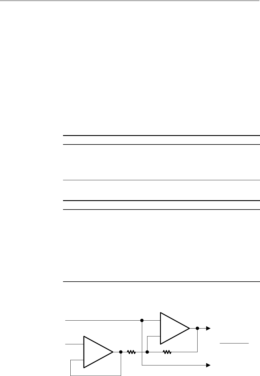
OA Operation
18-8 OA
Differential Amplifier Mode
This mode allows internal routing of the OA signals for a two-opamp or
three-opamp instrumentation amplifier. Figure 18−2 shows a two-opamp
configuration with OA0 and OA1. In this mode the output of the OAx is
connected to RTOP by routing through another OAx in the Inverting PGA mode.
RBOTTOM is unconnected providing a unity gain buffer. This buffer is combined
with one or two remaining OAx to form the differential amplifier. The OAx
output is connected to the ADC12 input channel as selected by the OAxCTL0
bits.
Figure 18−2 shows an example of a two-opamp differential amplifier using
OA0 and OA1. The control register settings and are shown in Table 18−3. The
gain for the amplifier is selected by the OAFBRx bits for OA1 and is shown in
Table 18−4. The OAx interconnections are shown in Figure 18−3.
Table 18−3.Two-Opamp Differential Amplifier Control Register Settings
Register Settings (binary)
OA0CTL0 xx xx xx 0 0
OA0CTL1 000 111 0 x
OA1CTL0 11 xx xx x x
OA1CTL1 xxx 110 0 x
Table 18−4.Two-Opamp Differential Amplifier Gain Settings
OA1 OAFBRx Gain
000 0
001 1/3
010 1
011 1 2/3
100 3
101 4 1/3
110 7
111 15
Figure 18−2. Two-Opamp Differential Amplifier
OA0
+
−
OA1
+
−
1
2)12(
R
xRVV
Vdiff
−
=
R2R1
V2
V1
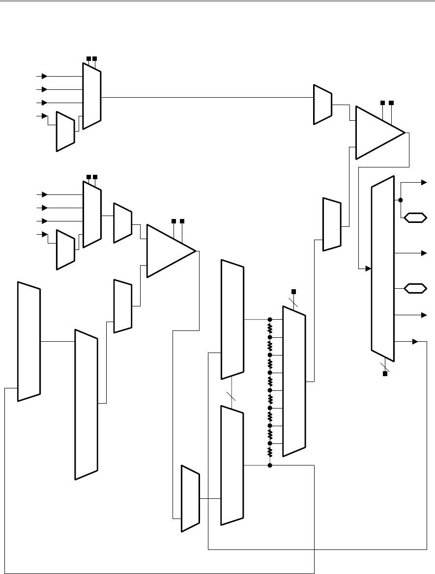
OA Operation
18-9
OA
Figure 18−3. Two-Opamp Differential Amplifier OAx Interconnections
000
001
100
011
010
111
110
101
000
001
100
011
010
111
110
101
OAPMx
+
−
001
else
0
1
OAxR
TOP
000
OAPx
OAxI0
OA0I1
00
01
10
11
OAxIA
OAxIB
0
1OA0
000
001
100
011
010
111
110
101
3
000
001
100
011
010
111
110
101
3
4R
4R
2R
2R
R
R
R
R
OAFBRx
000
001
100
011
010
111
110
101
OAPMx
OA1
+
−
001
else
0
1
OAxR
TOP
000
OAPx
OAxI0
OA0I1
00
01
10
11
OAxIA
OAxIB
0
1
00
01
10
11
OAxFB
OAADCx
2
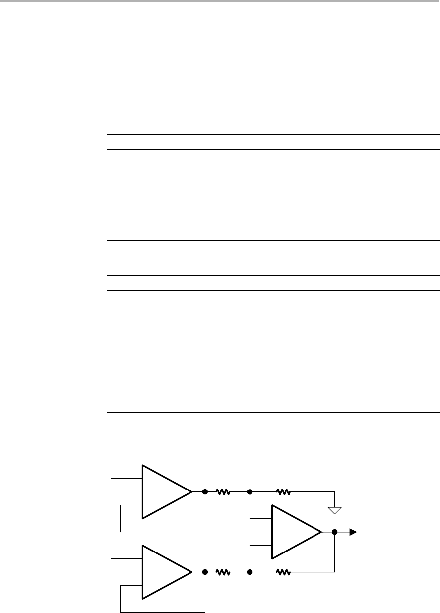
OA Operation
18-10 OA
Figure 18−4 shows an example of a three-opamp differential amplifier using
OA0, OA1 and OA2 (Three opamps are not available on all devices. See
device-specific data sheet for implementation.). The control register settings
are shown in Table 18−5. The gain for the amplifier is selected by the OAFBRx
bits of OA0 and OA2. The OAFBRx settings for both OA0 and OA2 must be
equal. The gain settings are shown in Table 18−6. The OAx interconnections
are shown in Figure 18−5.
Table 18−5.Three-Opamp Differential Amplifier Control Register Settings
Register Settings (binary)
OA0CTL0 xx xx xx 0 0
OA0CTL1 xxx 001 0 x
OA1CTL0 xx xx xx 0 0
OA1CTL1 000 111 0 x
OA2CTL0 11 11 xx x x
OA2CTL1 xxx 110 0 x
Table 18−6.Three-Opamp Differential Amplifier Gain Settings
OA0/OA2 OAFBRx Gain
000 0
001 1/3
010 1
011 1 2/3
100 3
101 4 1/3
110 7
111 15
Figure 18−4. Three-Opamp Differential Amplifier
OA1
+
−
OA2
+
−
1
2)12(
R
xRVV
Vdiff
−
=
R2R1
V2
V1
OA0
+
−
R2R1
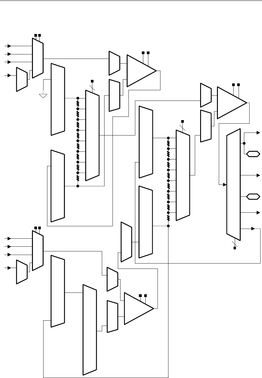
OA Operation
18-11
OA
Figure 18−5. Three-Opamp Differential Amplifier OAx Interconnections
000
001
100
011
010
111
110
101
OAPMx
OA0
+
−
001
else
0
1
000
OAPx
OAxI0
OA0I1
00
01
10
11
OAxIA
OAxIB 0
1
000
001
100
011
010
111
110
101
000
001
100
011
010
111
110
101
OAPMx
OA1
+
−
001
else
0
1
OAxR
TOP
000
OAPx
OAxI0
OA0I1
00
01
10
11
OAxIA
OAxIB 0
1
000
001
100
011
010
111
110
101
000
001
100
011
010
111
110
101
3
4R
4R
2R
2R
R
R
R
R
OAFBRx
000
001
100
011
010
111
110
101
001
else
0
1
OA0TAP (OA2)
OAxRTOP
000
00
01
10
11
000
001
100
011
010
111
110
101
000
001
100
011
010
111
110
101
4R
4R
2R
2R
R
R
R
R
OAPMx
OA2
+
−
OAxFB
OAADCx
2
3
OAFBRx

OA Registers
18-12 OA
18.3 OA Registers
The OA registers are listed in Table 18−7.
Table 18−7.OA Registers
Register Short Form Register Type Address Initial State
OA0 control register 0 OA0CTL0 Read/write 0C0h Reset with POR
OA0 control register 1 OA0CTL1 Read/write 0C1h Reset with POR
OA1 control register 0 OA1CTL0 Read/write 0C2h Reset with POR
OA1 control register 1 OA1CTL1 Read/write 0C3h Reset with POR
OA2 control register 0 OA2CTL0 Read/write 0C4h Reset with POR
OA2 control register 1 OA2CTL1 Read/write 0C5h Reset with POR

OA Registers
18-13
OA
OAxCTL0, Opamp Control Register 0
76543210
OANx OAPx OAPMx OAADCx
rw−0 rw−0 rw−0 rw−0 rw−0 rw−0 rw−0 rw−0
OANx Bits
7-6
Inverting input select. These bits select the input signal for the OA inverting
input.
00 OAxI0
01 OAxI1
10 OAxIA (see the device-specific data sheet for connected signal)
11 OAxIB (see the device-specific data sheet for connected signal)
OAPx Bits
5-4
Non-inverting input select. These bits select the input signal for the OA
non-inverting input.
00 OAxI0
01 OA0I1
10 OAxIA (see the device-specific data sheet for connected signal)
11 OAxIB (see the device-specific data sheet for connected signal)
OAPMx Bits
3-2
Slew rate select. These bits select the slew rate vs. current consumption
for the OA.
00 Off, output high Z
01 Slow
10 Medium
11 Fast
OAADCx Bits
1−0
OA output select. These bits, together with the OAFCx bits, control the
routing of the OAx output when OAPMx > 0.
When OAFCx = 0:
00 OAxOUT connected to external pins and ADC input A1, A3, or A5
01 OAxOUT connected to external pins and ADC input A12, A13, or A14
10 OAxOUT connected to external pins and ADC input A1, A3, or A5
11 OAxOUT connected to external pins and ADC input A12, A13, or A14
When OAFCx > 0:
00 OAxOUT used for internal routing only
01 OAxOUT connected to external pins and ADC input A12, A13, or A14
10 OAxOUT connected to external pins and ADC input A1, A3, or A5
11 OAxOUT connected internally to ADC input A12, A13 , or A14.
External A12, A13, or A14 pin connections are disconnected from the
ADC.

OA Registers
18-14 OA
OAxCTL1, Opamp Control Register 1
76543210
OAFBRx OAFCx OANEXT OARRIP
rw−0 rw−0 rw−0 rw−0 rw−0 rw−0 rw−0 rw−0
OAFBRx Bits
7-5
OAx feedback resistor select
000 Tap 0 − 0R/16R
001 Tap 1 − 4R/12R
010 Tap 2 − 8R/8R
011 Tap 3 − 10R/6R
100 Tap 4 − 12R/4R
101 Tap 5 − 13R/3R
110 Tap 6 − 14R/2R
111 Tap 7 − 15R/1R
OAFCx Bits
4-2
OAx function control. This bit selects the function of OAx
000 General purpose opamp
001 Unity gain buffer for three-opamp differential amplifier
010 Unity gain buffer
011 Comparator
100 Non-inverting PGA amplifier
101 Cascaded non-inverting PGA amplifier
110 Inverting PGA amplifier
111 Differential amplifier
OANEXT Bit 1 OAx inverting input externally available. This bit, when set, connects the
inverting OAx input to the external pin when the integrated resistor network
is used.
0 OAx inverting input not externally available
1 OAx inverting input externally available
OARRIP Bit 0 OAx reverse resistor connection in comparator mode
0R
TOP is connected to AVSS and RBOTTOM is connected to AVCC when
OAFCx = 3
1R
TOP is connected to AVCC and RBOTTOM is connected to AVSS when
OAFCx = 3.

19-1
Comparator_A+
Comparator_A+
Comparator_A+ is an analog voltage comparator. This chapter describes the
operation of the Comparator_A+ of the 2xx family.
Topic Page
19.1 Comparator_A+ Introduction 19-2. . . . . . . . . . . . . . . . . . . . . . . . . . . . . . . . . .
19.2 Comparator_A+ Operation 19-4. . . . . . . . . . . . . . . . . . . . . . . . . . . . . . . . . . . .
19.3 Comparator_A+ Registers 19-10. . . . . . . . . . . . . . . . . . . . . . . . . . . . . . . . . . .
Chapter 19

Comparator_A+ Introduction
19-2 Comparator_A+
19.1 Comparator_A+ Introduction
The Comparator_A+ module supports precision slope analog-to-digital
conversions, supply voltage supervision, and monitoring of external analog
signals.
Features of Comparator_A+ include:
-Inverting and non-inverting terminal input multiplexer
-Software selectable RC-filter for the comparator output
-Output provided to Timer_A capture input
-Software control of the port input buffer
-Interrupt capability
-Selectable reference voltage generator
-Comparator and reference generator can be powered down
-Input Multiplexer
The Comparator_A+ block diagram is shown in Figure 19−1.
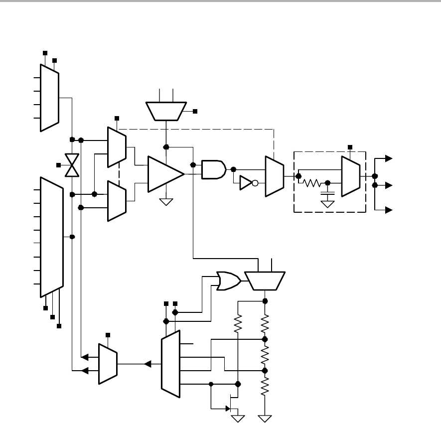
Comparator_A+ Introduction
19-3
Comparator_A+
Figure 19−1. Comparator_A+ Block Diagram
CA1
CA2
CA3
CA4
CA5
CA6
CA7
CAOUT
+
−
CAEX
0.5xVCC
0.25xVCC
Set_CAIFG
CCI1B
+
−
0V
GD
S
P2CA0
CAF
CARSEL
CAON
CAREFx
10
00
01
10
11
00
01
10
11
1
0
1
0
1
0
1
0
1
0
0V
10
Tau ~ 2.0ns
VCAREF
VCC
P2CA4
P2CA1
000
001
010
011
100
101
110
111
CASHORT
P2CA2
P2CA3
CA0
CA1
CA2
00
01
10
11

Comparator_A+ Operation
19-4 Comparator_A+
19.2 Comparator_A+ Operation
The Comparator_A+ module is configured with user software. The setup and
operation of Comparator_A+ is discussed in the following sections.
19.2.1 Comparator
The comparator compares the analog voltages at the + and – input terminals.
If the + terminal is more positive than the – terminal, the comparator output
CAOUT is high. The comparator can be switched on or off using control bit
CAON. The comparator should be switched off when not in use to reduce
current consumption. When the comparator is switched off, the CAOUT is
always low.
19.2.2 Input Analog Switches
The analog input switches connect or disconnect the two comparator input
terminals to associated port pins using the P2CAx bits. Both comparator
terminal inputs can be controlled individually. The P2CAx bits allow:
-Application of an external signal to the + and – terminals of the comparator
-Routing of an internal reference voltage to an associated output port pin
Internally, the input switch is constructed as a T-switch to suppress distortion
in the signal path.
Note: Comparator Input Connection
When the comparator is on, the input terminals should be connected to a
signal, power, or ground. Otherwise, floating levels may cause unexpected
interrupts and increased current consumption.
The CAEX bit controls the input multiplexer, exchanging which input signals
are connected to the comparator’s + and – terminals. Additionally, when the
comparator terminals are exchanged, the output signal from the comparator
is inverted. This allows the user to determine or compensate for the
comparator input offset voltage.
Comparator_A+ Operation
19-5
Comparator_A+
19.2.3 Input Short Switch
The CASHORT bit shorts the comparator_A+ inputs. This can be used to build
a simple sample-and-hold for the comparator as shown in Figure 19−2.
Figure 19−2. Comparator_A+ Sample−And−Hold
Sampling Capacitor, C s
CASHORT
Analog Inputs
The required sampling time is proportional to the size of the sampling capacitor
(CS), the resistance of the input switches in series with the short switch (Ri),
and the resistance of the external source (RS). The total internal resistance
(RI) is typically in the range of 2 − 10 kΩ. The sampling capacitor CS should
be greater than 100pF. The time constant, Tau, to charge the sampling
capacitor CS can be calculated with the following equation:
Tau = (RI + RS) x CS
Depending on the required accuracy 3 to 10 Tau should be used as a sampling
time. With 3 Tau the sampling capacitor is charged to approximately 95% of
the input signals voltage level, with 5 Tau it is charge to more than 99% and
with 10 Tau the sampled voltage is sufficient for 12−bit accuracy.
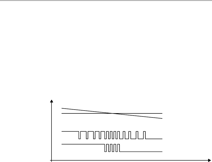
Comparator_A+ Operation
19-6 Comparator_A+
19.2.4 Output Filter
The output of the comparator can be used with or without internal filtering.
When control bit CAF is set, the output is filtered with an on-chip RC-filter.
Any comparator output oscillates if the voltage difference across the input
terminals is small. Internal and external parasitic effects and cross coupling on
and between signal lines, power supply lines, and other parts of the system
are responsible for this behavior as shown in Figure 19−3. The comparator
output oscillation reduces accuracy and resolution of the comparison result.
Selecting the output filter can reduce errors associated with comparator
oscillation.
Figure 19−3. RC-Filter Response at the Output of the Comparator
+ Terminal
− Terminal Comparator Inputs
Comparator Output
Unfiltered at CAOUT
Comparator Output
Filtered at CAOUT
19.2.5 Voltage Reference Generator
The voltage reference generator is used to generate VCAREF
, which can be
applied to either comparator input terminal. The CAREFx bits control the
output of the voltage generator. The CARSEL bit selects the comparator
terminal to which VCAREF is applied. If external signals are applied to both
comparator input terminals, the internal reference generator should be turned
off to reduce current consumption. The voltage reference generator can
generate a fraction of the device’s VCC or a fixed transistor threshold voltage
of ~ 0.55 V.
Comparator_A+ Operation
19-7
Comparator_A+
19.2.6 Comparator_A+, Port Disable Register CAPD
The comparator input and output functions are multiplexed with the associated
I/O port pins, which are digital CMOS gates. When analog signals are applied
to digital CMOS gates, parasitic current can flow from VCC to GND. This
parasitic current occurs if the input voltage is near the transition level of the
gate. Disabling the port pin buffer eliminates the parasitic current flow and
therefore reduces overall current consumption.
The CAPDx bits, when set, disable the corresponding P2 input and output
buffers as shown in Figure 19−4. When current consumption is critical, any
port pin connected to analog signals should be disabled with its CAPDx bit.
Selecting an input pin to the comparator multiplexer with the P2CAx bits
automatically disables the input and output buffers for that pin, regardless of
the state of the associated CAPDx bit.
Figure 19−4. Transfer Characteristic and Power Dissipation in a CMOS Inverter/Buffer
VCC
VSS
ICC
VO
VI
0V
CC
VI
VCC
ICC
CAPD.x = 1
19.2.7 Comparator_A+ Interrupts
One interrupt flag and one interrupt vector are associated with the
Comparator_A+ as shown in Figure 19−5. The interrupt flag CAIFG is set on
either the rising or falling edge of the comparator output, selected by the
CAIES bit. If both the CAIE and the GIE bits are set, then the CAIFG flag
generates an interrupt request. The CAIFG flag is automatically reset when
the interrupt request is serviced or may be reset with software.
Figure 19−5. Comparator_A+ Interrupt System
DQ IRQ, Interrupt Service Requested
Reset
VCC
POR
SET_CAIFG
IRACC, Interrupt Request Accepted
CAIE
CAIES
0
1
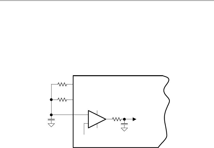
Comparator_A+ Operation
19-8 Comparator_A+
19.2.8 Comparator_A+ Used to Measure Resistive Elements
The Comparator_A+ can be optimized to precisely measure resistive
elements using single slope analog-to-digital conversion. For example,
temperature can be converted into digital data using a thermistor, by
comparing the thermistor’s capacitor discharge time to that of a reference
resistor as shown in Figure 19−6. A reference resister Rref is compared to
Rmeas.
Figure 19−6. Temperature Measurement System
+
−
CA0 CCI1B
Capture
Input
Of Timer_A
+
−
Rmeas
Rref
Px.x
Px.y
0.25xVCC
The MSP430 resources used to calculate the temperature sensed by Rmeas
are:
-Two digital I/O pins to charge and discharge the capacitor.
-I/O set to output high (VCC) to charge capacitor, reset to discharge.
-I/O switched to high-impedance input with CAPDx set when not in use.
-One output charges and discharges the capacitor via Rref.
-One output discharges capacitor via Rmeas.
-The + terminal is connected to the positive terminal of the capacitor.
-The – terminal is connected to a reference level, for example 0.25 x VCC.
-The output filter should be used to minimize switching noise.
-CAOUT used to gate Timer_A CCI1B, capturing capacitor discharge time.
More than one resistive element can be measured. Additional elements are
connected to CA0 with available I/O pins and switched to high impedance
when not being measured.
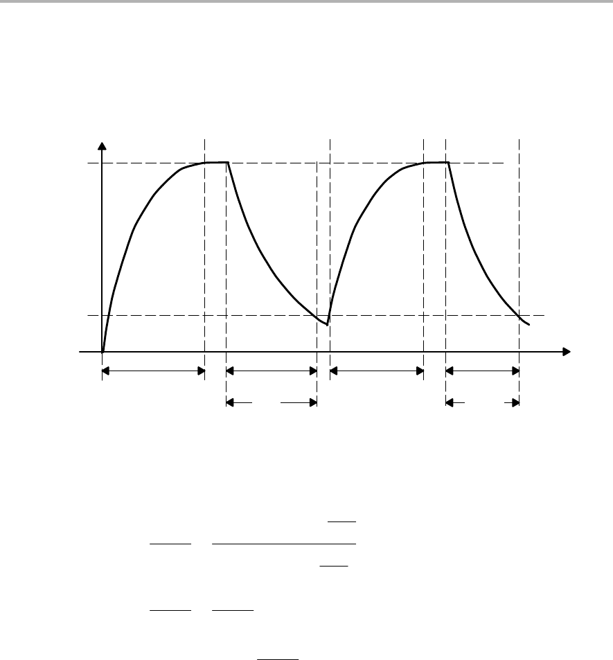
Comparator_A+ Operation
19-9
Comparator_A+
The thermistor measurement is based on a ratiometric conversion principle.
The ratio of two capacitor discharge times is calculated as shown in
Figure 19−7.
Figure 19−7. Timing for Temperature Measurement Systems
VC
VCC
0.25 × VCC
Phase I:
Charge
Phase II:
Discharge
Phase III:
Charge
tref
Phase IV:
Discharge
tmeas
t
Rmeas
Rref
The VCC voltage and the capacitor value should remain constant during the
conversion, but are not critical since they cancel in the ratio:
Nmeas
Nref +
–Rmeas C ln Vref
VCC
–Rref C ln Vref
VCC
Nmeas
Nref +Rmeas
Rref
Rmeas +Rref Nmeas
Nref

Comparator_A+ Registers
19-10 Comparator_A+
19.3 Comparator_A+ Registers
The Comparator_A+ registers are listed in Table 19−1:
Table 19−1.Comparator_A+ Registers
Register Short Form Register Type Address Initial State
Comparator_A+ control register 1 CACTL1 Read/write 059h Reset with POR
Comparator_A+ control register 2 CACTL2 Read/write 05Ah Reset with POR
Comparator_A+ port disable CAPD Read/write 05Bh Reset with POR

Comparator_A+ Registers
19-11
Comparator_A+
CACTL1, Comparator_A+ Control Register 1
76543210
CAEX CARSEL CAREFx CAON CAIES CAIE CAIFG
rw−(0) rw−(0) rw−(0) rw−(0) rw−(0) rw−(0) rw−(0) rw−(0)
CAEX Bit 7 Comparator_A+ exchange. This bit exchanges the comparator inputs and
inverts the comparator output.
CARSEL Bit 6 Comparator_A+ reference select. This bit selects which terminal the
VCAREF is applied to.
When CAEX = 0:
0V
CAREF is applied to the + terminal
1V
CAREF is applied to the – terminal
When CAEX = 1:
0V
CAREF is applied to the – terminal
1V
CAREF is applied to the + terminal
CAREF Bits
5-4
Comparator_A+ reference. These bits select the reference voltage VCAREF.
00 Internal reference off. An external reference can be applied.
01 0.25*VCC
10 0.50*VCC
11 Diode reference is selected
CAON Bit 3 Comparator_A+ on. This bit turns on the comparator. When the
comparator is off it consumes no current. The reference circuitry is enabled
or disabled independently.
0Off
1On
CAIES Bit 2 Comparator_A+ interrupt edge select
0 Rising edge
1 Falling edge
CAIE Bit 1 Comparator_A+ interrupt enable
0 Disabled
1 Enabled
CAIFG Bit 0 The Comparator_A+ interrupt flag
0 No interrupt pending
1 Interrupt pending

Comparator_A+ Registers
19-12 Comparator_A+
CACTL2, Comparator_A+, Control Register
76543210
CASHORT P2CA4 P2CA3 P2CA2 P2CA1 P2CA0 CAF CAOUT
rw−(0) rw−(0) rw−(0) rw−(0) rw−(0) rw−(0) rw−(0) r−(0)
CASHORT Bit 7 Input short. This bit shorts the + and − input terminals.
0 Inputs not shorted.
1 Inputs shorted.
P2CA4 Bit 6 Input select. This bit together with P2CA0 selects the + terminal input when
CAEX = 0 and the − terminal input when CAEX = 1.
P2CA3
P2CA2
P2CA1
Bits
5-3
Input select. These bits select the − terminal input when CAEX = 0 and the
+ terminal input when CAEX = 1.
000 No connection
001 CA1
010 CA2
011 CA3
100 CA4
101 CA5
110 CA6
111 CA7
P2CA0 Bit 2 Input select. This bit, together with P2CA4, selects the + terminal input
when CAEX = 0 and the − terminal input when CAEX = 1.
00 No connection
01 CA0
10 CA1
11 CA2
CAF Bit 1 Comparator_A+ output filter
0 Comparator_A+ output is not filtered
1 Comparator_A+ output is filtered
CAOUT Bit 0 Comparator_A+ output. This bit reflects the value of the comparator output.
Writing this bit has no effect.

Comparator_A+ Registers
19-13
Comparator_A+
CAPD, Comparator_A+, Port Disable Register
76543210
CAPD7 CAPD6 CAPD5 CAPD4 CAPD3 CAPD2 CAPD1 CAPD0
rw−(0) rw−(0) rw−(0) rw−(0) rw−(0) rw−(0) rw−(0) rw−(0)
CAPDx Bits
7-0
Comparator_A+ port disable. These bits individually disable the input
buffer for the pins of the port associated with Comparator_A+. For
example, if CA0 is on pin P2.3, the CAPDx bits can be used to individually
enable or disable each P2.x pin buffer. CAPD0 disables P2.0, CAPD1
disables P2.1, etc.
0 The input buffer is enabled.
1 The input buffer is disabled.

19-14 Comparator_A+

20-1
ADC10
ADC10
The ADC10 module is a high-performance 10-bit analog-to-digital converter.
This chapter describes the operation of the ADC10 module of the 2xx family.
Topic Page
20.1 ADC10 Introduction 20-2. . . . . . . . . . . . . . . . . . . . . . . . . . . . . . . . . . . . . . . . . . .
20.2 ADC10 Operation 20-4. . . . . . . . . . . . . . . . . . . . . . . . . . . . . . . . . . . . . . . . . . . . .
20.3 ADC10 Registers 20-24. . . . . . . . . . . . . . . . . . . . . . . . . . . . . . . . . . . . . . . . . . .
Chapter 20

ADC10 Introduction
20-2 ADC10
20.1 ADC10 Introduction
The ADC10 module supports fast, 10-bit analog-to-digital conversions. The
module implements a 10-bit SAR core, sample select control, reference
generator, and data transfer controller (DTC).
The DTC allows ADC10 samples to be converted and stored anywhere in
memory without CPU intervention. The module can be configured with user
software to support a variety of applications.
ADC10 features include:
-Greater than 200 ksps maximum conversion rate
-Monotonic 10-bit converter with no missing codes
-Sample-and-hold with programmable sample periods
-Conversion initiation by software or Timer_A
-Software selectable on-chip reference voltage generation (1.5 V or 2.5 V)
-Software selectable internal or external reference
-Eight external input channels (twelve on MSP430x22xx devices)
-Conversion channels for internal temperature sensor, VCC, and external
references
-Selectable conversion clock source
-Single-channel, repeated single-channel, sequence, and repeated
sequence conversion modes
-ADC core and reference voltage can be powered down separately
-Data transfer controller for automatic storage of conversion results
The block diagram of ADC10 is shown in Figure 20−1.
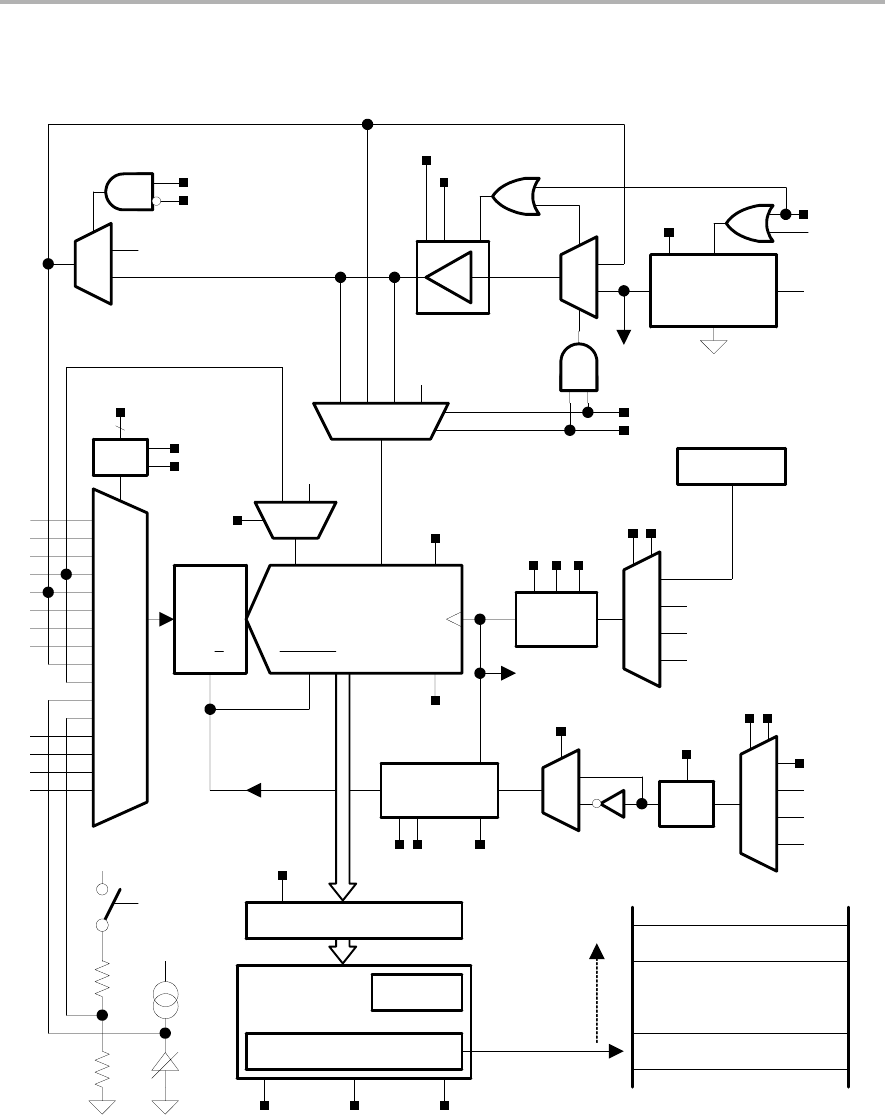
ADC10 Introduction
20-3
ADC10
Figure 20−1. ADC10 Block Diagram
Sample
and
Hold 10−bit SAR Divider
/1 .. /8
AVCC
ACLK
MCLK
SMCLK
ADC10SC
TA 1
TA 0
Data Transfer
Controller RAM, Flash, Peripherials
VR− VR+
VeREF+
VREF+
ADC10ON
INCHx
REFBURST
ADC10SSELx
ADC10DIVx
SHSx
ADC10SHTx MSC
ENC
BUSY
ADC10DF
ADC10CLK
SREF2
ADC10TB ADC10B1ADC10CT
ISSH
ADC10SR
ADC10OSC
Ref_x
S/H Convert
SAMPCON
1
0
Sync
Sample Timer
/4/8/16/64
SHI
ADC10SA
n
4
A0
A1
A2
A3
A4
A5
A6
A7
REFON
INCHx=0Ah
2_5V
1.5V or 2.5V
Reference
on
Ref_x
SREF1
00
01
10
11
00
01
10
11
00
01
10
11
00
01
10
11
000111
01
SREF0
10
CONSEQx
AVSS
1
0
INCHx=0Bh
Auto
ADC10MEM
R
R
0
1
REFOUT
SREF1
1001
1000
0010
0001
0011
0100
0101
0110
0111
0000
1011
1010
0001
1111
1110
1101
1100
A12†
A13†
A14†
A15†
†MSP430x22xx devices only. Channels A12-A15 tied to channel A11 in other devices
‡TA1 on MSP430x20x2 devices
VREF−/VeREF−
AVCC
AVSS
AVCC
TA2‡

ADC10 Operation
20-4 ADC10
20.2 ADC10 Operation
The ADC10 module is configured with user software. The setup and operation
of the ADC10 is discussed in the following sections.
20.2.1 10-Bit ADC Core
The ADC core converts an analog input to its 10-bit digital representation and
stores the result in the ADC10MEM register. The core uses two
programmable/selectable voltage levels (VR+ and VR−) to define the upper and
lower limits of the conversion. The digital output (NADC) is full scale (03FFh)
when the input signal is equal to or higher than VR+, and zero when the input
signal is equal to or lower than VR−. The input channel and the reference
voltage levels (VR+ and VR−) are defined in the conversion-control memory.
Conversion results may be in straight binary format or 2s-complement format.
The conversion formula for the ADC result when using straight binary format
is:
NADC +1023 Vin–V
R–
VR)–V
R–
The ADC10 core is configured by two control registers, ADC10CTL0 and
ADC10CTL1. The core is enabled with the ADC10ON bit. With few exceptions
the ADC10 control bits can only be modified when ENC = 0. ENC must be set
to 1 before any conversion can take place.
Conversion Clock Selection
The ADC10CLK is used both as the conversion clock and to generate the
sampling period. The ADC10 source clock is selected using the ADC10SSELx
bits and can be divided from 1-8 using the ADC10DIVx bits. Possible
ADC10CLK sources are SMCLK, MCLK, ACLK and an internal oscillator
ADC10OSC .
The ADC10OSC, generated internally, is in the 5-MHz range, but varies with
individual devices, supply voltage, and temperature. See the device-specific
data sheet for the ADC10OSC specification.
The user must ensure that the clock chosen for ADC10CLK remains active
until the end of a conversion. If the clock is removed during a conversion, the
operation will not complete, and any result will be invalid.

ADC10 Operation
20-5
ADC10
20.2.2 ADC10 Inputs and Multiplexer
The eight external and four internal analog signals are selected as the channel
for conversion by the analog input multiplexer. The input multiplexer is a
break-before-make type to reduce input-to-input noise injection resulting from
channel switching as shown in Figure 20−2. The input multiplexer is also a
T-switch to minimize the coupling between channels. Channels that are not
selected are isolated from the A/D and the intermediate node is connected to
analog ground (VSS) so that the stray capacitance is grounded to help
eliminate crosstalk.
The ADC10 uses the charge redistribution method. When the inputs are
internally switched, the switching action may cause transients on the input
signal. These transients decay and settle before causing errant conversion.
Figure 20−2. Analog Multiplexer
R ~ 100Ohm
ESD Protection
INCHx
Input
Ax
Analog Port Selection
The ADC10 external inputs Ax, VeREF+, and VREF− share terminals with
general purpose I/O ports, which are digital CMOS gates (see device-specific
data sheet). When analog signals are applied to digital CMOS gates, parasitic
current can flow from VCC to GND. This parasitic current occurs if the input
voltage is near the transition level of the gate. Disabling the port pin buffer
eliminates the parasitic current flow and therefore reduces overall current
consumption. The ADC10AEx bits provide the ability to disable the port pin
input and output buffers.
; P2.3 on MSP430x22xx device configured for analog input
BIS.B #08h,&ADC10AE0 ; P2.3 ADC10 function and enable

ADC10 Operation
20-6 ADC10
20.2.3 Voltage Reference Generator
The ADC10 module contains a built-in voltage reference with two selectable
voltage levels. Setting REFON = 1 enables the internal reference. When
REF2_5V = 1, the internal reference is 2.5 V. When REF2_5V = 0, the
reference is 1.5 V. The internal reference voltage may be used internally and,
when REFOUT = 0, externally on pin VREF+.
External references may be supplied for VR+ and VR− through pins A4 and A3
respectively. When external references are used, or when VCC is used as the
reference, the internal reference may be turned off to save power.
An external positive reference VeREF+ can be buffered by setting SREF0 = 1
and SREF1 = 1. This allows using an external reference with a large internal
resistance at the cost of the buffer current. When REFBURST = 1 the
increased current consumption is limited to the sample and conversion period.
External storage capacitance is not required for the ADC10 reference source
as on the ADC12.
Internal Reference Low-Power Features
The ADC10 internal reference generator is designed for low power
applications. The reference generator includes a band-gap voltage source
and a separate buffer. The current consumption of each is specified separately
in the device-specific data sheet. When REFON = 1, both are enabled and
when REFON = 0 both are disabled. The total settling time when REFON
becomes set is 30 μs.
When REFON = 1, but no conversion is active, the buffer is automatically
disabled and automatically re-enabled when needed. When the buffer is
disabled, it consumes no current. In this case, the band-gap voltage source
remains enabled.
When REFOUT = 1, the REFBURST bit controls the operation of the internal
reference buffer. When REFBURST = 0, the buffer will be on continuously,
allowing the reference voltage to be present outside the device continuously.
When REFBURST = 1, the buffer is automatically disabled when the ADC10
is not actively converting, and automatically re-enabled when needed.
The internal reference buffer also has selectable speed vs. power settings.
When the maximum conversion rate is below 50 ksps, setting ADC10SR = 1
reduces the current consumption of the buffer approximately 50%.
20.2.4 Auto Power-Down
The ADC10 is designed for low power applications. When the ADC10 is not
actively converting, the core is automatically disabled and automatically
re-enabled when needed. The ADC10OSC is also automatically enabled
when needed and disabled when not needed. When the core or oscillator is
disabled, it consumes no current.
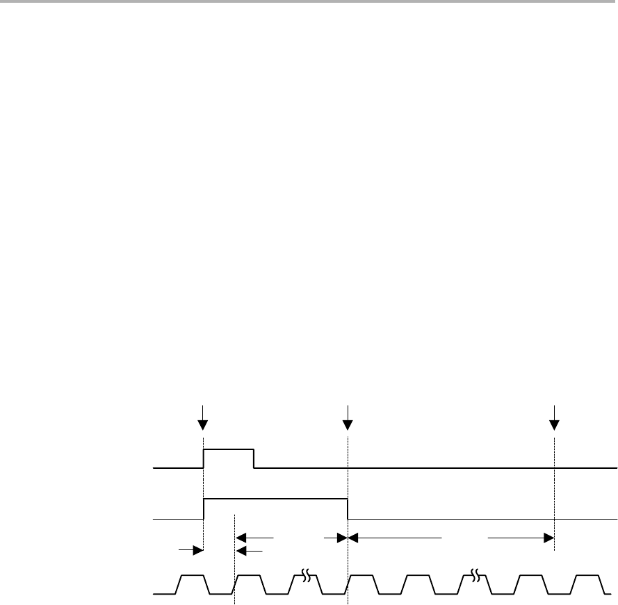
ADC10 Operation
20-7
ADC10
20.2.5 Sample and Conversion Timing
An analog-to-digital conversion is initiated with a rising edge of sample input
signal SHI. The source for SHI is selected with the SHSx bits and includes the
following:
-The ADC10SC bit
-The Timer_A Output Unit 1
-The Timer_A Output Unit 0
-The Timer_A Output Unit 2
The polarity of the SHI signal source can be inverted with the ISSH bit. The
SHTx bits select the sample period tsample to be 4, 8, 16, or 64 ADC10CLK
cycles. The sampling timer sets SAMPCON high for the selected sample
period after synchronization with ADC10CLK. Total sampling time is tsample
plus tsync.The high-to-low SAMPCON transition starts the analog-to-digital
conversion, which requires 13 ADC10CLK cycles as shown in Figure 20−3.
Figure 20−3. Sample Timing
Start
Sampling
Stop
Sampling
Conversion
Complete
SAMPCON
SHI
tsample tconvert
tsync
13 x ADC10CLKs
Start
Conversion
ADC10CLK
Sample Timing Considerations
When SAMPCON = 0 all Ax inputs are high impedance. When SAMPCON =
1, the selected Ax input can be modeled as an RC low-pass filter during the
sampling time tsample, as shown below in Figure 20−4. An internal MUX-on
input resistance RI (max. 2 kΩ) in series with capacitor CI (max. 27 pF) is seen
by the source. The capacitor CI voltage VC must be charged to within ½ LSB
of the source voltage VS for an accurate 10-bit conversion.

ADC10 Operation
20-8 ADC10
Figure 20−4. Analog Input Equivalent Circuit
RSRI
VSVC
MSP430
CI
VI
VI= Input voltage at pin Ax
VS= External source voltage
RS= External source resistance
RI= Internal MUX-on input resistance
CI= Input capacitance
VC= Capacitance-charging voltage
The resistance of the source RS and RI affect tsample.The following equations
can be used to calculate the minimum sampling time for a 10-bit conversion.
tsample u(RS)RI) ln(211) CI
Substituting the values for RI and CI given above, the equation becomes:
tsample u(RS)2k) 7.625 27pF
For example, if RS is 10 kΩ, tsample must be greater than 2.47 μs.
When the reference buffer is used in burst mode, the sampling time must be
greater than the sampling time calculated and the settling time of the buffer,
tREFBURST
:
tsample uNJ(RS)RI) ln(211) CI
tREFBURST
For example, if VRef is 1.5 V and RS is 10 kΩ, tsample must be greater than 2.47
μs when ADC10SR = 0, or 2.5 μs when ADC10SR = 1. See the device-specific
data sheet for parameters.
To calculate the buffer settling time when using an external reference, the
formula is:
tREFBURST +SR VRef *0.5ms
Where:
SR: Buffer slew rate
(~1 μs/V when ADC10SR = 0 and ~2 μs/V when ADC10SR = 1)
Vref: External reference voltage

ADC10 Operation
20-9
ADC10
20.2.6 Conversion Modes
The ADC10 has four operating modes selected by the CONSEQx bits as
discussed in Table 20−1.
Table 20−1.Conversion Mode Summary
CONSEQx Mode Operation
00 Single channel
single-conversion
A single channel is converted once.
01 Sequence-of-
channels
A sequence of channels is converted once.
10 Repeat single
channel
A single channel is converted repeatedly.
11 Repeat sequence-
of-channels
A sequence of channels is converted
repeatedly.
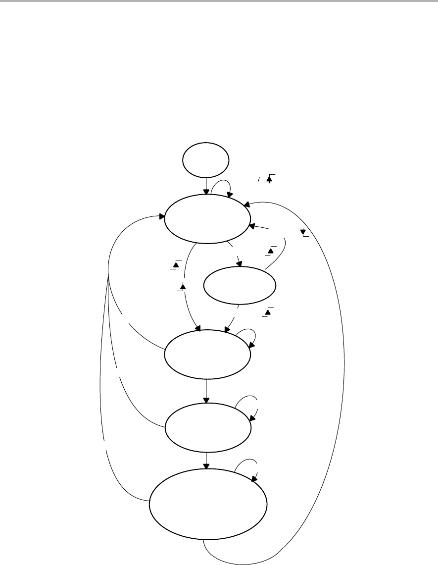
ADC10 Operation
20-10 ADC10
Single-Channel Single-Conversion Mode
A single channel selected by INCHx is sampled and converted once. The ADC
result is written to ADC10MEM. Figure 20−5 shows the flow of the
single-channel, single-conversion mode. When ADC10SC triggers a
conversion, successive conversions can be triggered by the ADC10SC bit.
When any other trigger source is used, ENC must be toggled between each
conversion.
Figure 20−5. Single-Channel Single-Conversion Mode
ADC10
Off
x = INCHx
Wait for Enable
ENC =
Wait for Trigger
Sample, Input
Channel
ENC =
ENC =
SHS = 0
and
ENC = 1 or
and
ADC10SC =
SAMPCON =
Convert
ENC = 0
ENC = 0†
12 x ADC10CLK
Conversion
Completed,
Result to
ADC10MEM,
ADC10IFG is Set
1 x ADC10CLK
†Conversion result is unpredictable
ENC = 0†
ADC10ON = 1
CONSEQx = 00
(4/8/16/64) x ADC10CLK
x = input channel Ax
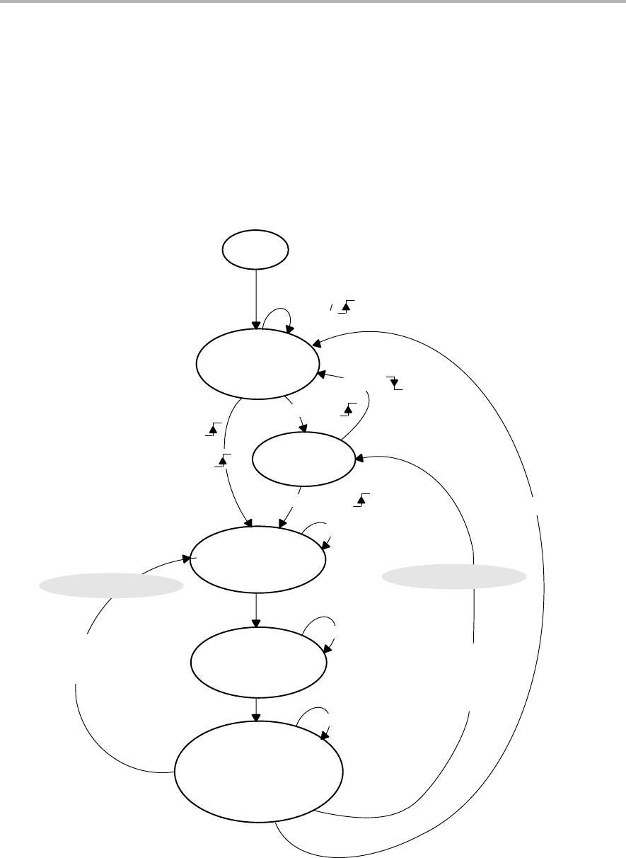
ADC10 Operation
20-11
ADC10
Sequence-of-Channels Mode
A sequence of channels is sampled and converted once. The sequence
begins with the channel selected by INCHx and decrements to channel A0.
Each ADC result is written to ADC10MEM. The sequence stops after
conversion of channel A0. Figure 20−6 shows the sequence-of-channels
mode. When ADC10SC triggers a sequence, successive sequences can be
triggered by the ADC10SC bit . When any other trigger source is used, ENC
must be toggled between each sequence.
Figure 20−6. Sequence-of-Channels Mode
ADC10
Off
x = INCHx
Wait for Enable
ENC =
Wait for Trigger
Sample,
Input Channel Ax
ENC =
ENC =
SHS = 0
and
ENC = 1 or
and
ADC10SC =
SAMPCON =
Convert
12 x ADC10CLK
Conversion
Completed,
Result to ADC10MEM,
ADC10IFG is Set
1 x ADC10CLK
ADC10ON = 1
CONSEQx = 01
MSC = 1
and
x ≠ 0
x = 0
If x > 0 then x = x −1
MSC = 0
and
x ≠0
(4/8/16/64) x ADC10CLK
If x > 0 then x = x −1
x = input channel Ax
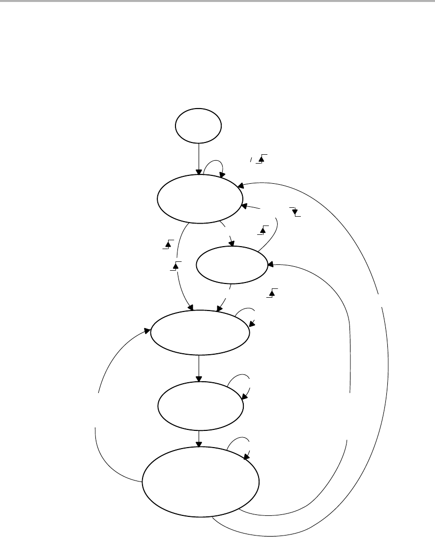
ADC10 Operation
20-12 ADC10
Repeat-Single-Channel Mode
A single channel selected by INCHx is sampled and converted continuously.
Each ADC result is written to ADC10MEM. Figure 20−7 shows the
repeat-single-channel mode.
Figure 20−7. Repeat-Single-Channel Mode
ADC10
Off
x = INCHx
Wait for Enable
ENC =
Wait for Trigger
ENC =
ENC =
SHS = 0
and
ENC = 1 or
and
ADC10SC =
SAMPCON =
(4/8/16/64) × ADC10CLK
Convert
12 x ADC10CLK
Conversion
Completed,
Result to ADC10MEM,
ADC10IFG is Set
1 x ADC10CLK
ADC10ON = 1
CONSEQx = 10
MSC = 1
and
ENC = 1
ENC = 0
MSC = 0
and
ENC = 1
Sample,
Input Channel Ax
x = input channel Ax
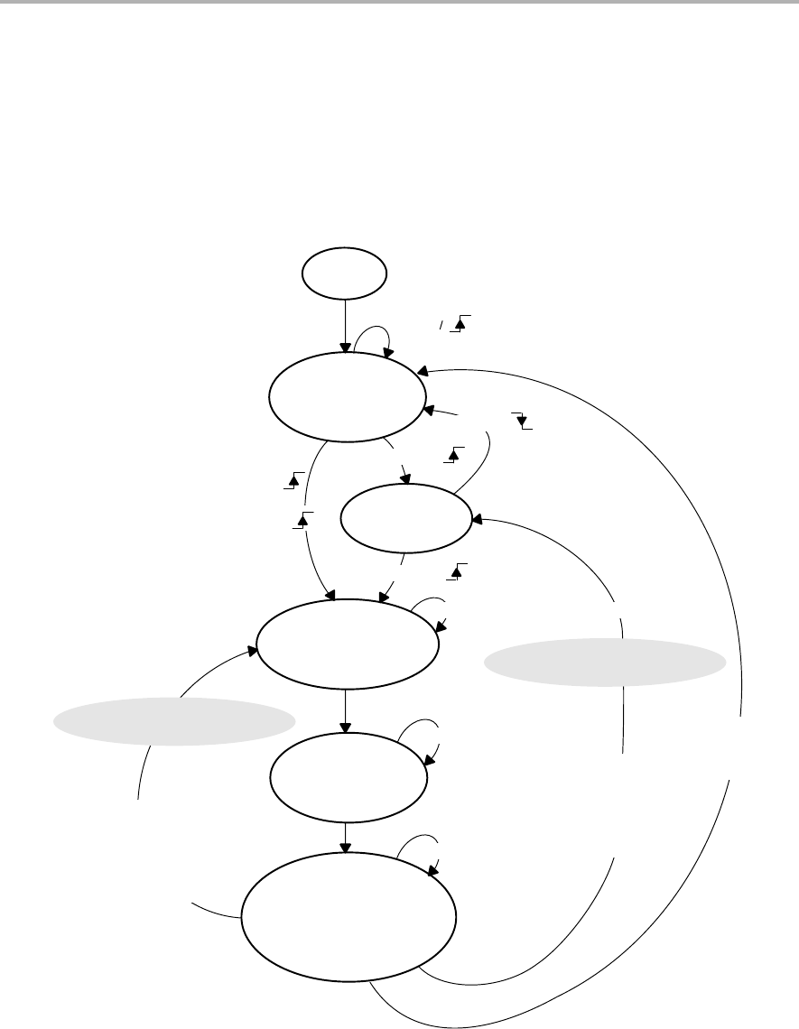
ADC10 Operation
20-13
ADC10
Repeat-Sequence-of-Channels Mode
A sequence of channels is sampled and converted repeatedly. The sequence
begins with the channel selected by INCHx and decrements to channel A0.
Each ADC result is written to ADC10MEM. The sequence ends after
conversion of channel A0, and the next trigger signal re-starts the sequence.
Figure 20−8 shows the repeat-sequence-of-channels mode.
Figure 20−8. Repeat-Sequence-of-Channels Mode
ADC10
Off
x = INCHx
Wait for Enable
ENC =
Wait for Trigger
Sample
Input Channel Ax
ENC =
ENC =
SHS = 0
and
ENC = 1 or
and
ADC10SC =
Convert
12 x ADC10CLK
Conversion
Completed,
Result to ADC10MEM,
ADC10IFG is Set
1 x ADC10CLK
ADC10ON = 1
CONSEQx = 11
MSC = 1
and
(ENC = 1
or
x ≠ 0)
ENC = 0
and
x = 0
MSC = 0
and
(ENC = 1
or
x ≠ 0)
If x = 0 then x = INCH
else x = x −1
(4/8/16/64) x ADC10CLK
If x = 0 then x = INCH
else x = x −1
x = input channel Ax
SAMPCON =

ADC10 Operation
20-14 ADC10
Using the MSC Bit
To configure the converter to perform successive conversions automatically
and as quickly as possible, a multiple sample and convert function is available.
When MSC = 1 and CONSEQx > 0 the first rising edge of the SHI signal
triggers the first conversion. Successive conversions are triggered
automatically as soon as the prior conversion is completed. Additional rising
edges on SHI are ignored until the sequence is completed in the
single-sequence mode or until the ENC bit is toggled in repeat-single-channel,
or repeated-sequence modes. The function of the ENC bit is unchanged when
using the MSC bit.
Stopping Conversions
Stopping ADC10 activity depends on the mode of operation. The
recommended ways to stop an active conversion or conversion sequence are:
-Resetting ENC in single-channel single-conversion mode stops a
conversion immediately and the results are unpredictable. For correct
results, poll the ADC10BUSY bit until reset before clearing ENC.
-Resetting ENC during repeat-single-channel operation stops the
converter at the end of the current conversion.
-Resetting ENC during a sequence or repeat sequence mode stops the
converter at the end of the sequence.
-Any conversion mode may be stopped immediately by setting the
CONSEQx=0 and resetting the ENC bit. Conversion data is unreliable.

ADC10 Operation
20-15
ADC10
20.2.7 ADC10 Data Transfer Controller
The ADC10 includes a data transfer controller (DTC) to automatically transfer
conversion results from ADC10MEM to other on-chip memory locations. The
DTC is enabled by setting the ADC10DTC1 register to a nonzero value.
When the DTC is enabled, each time the ADC10 completes a conversion and
loads the result to ADC10MEM, a data transfer is triggered. No software
intervention is required to manage the ADC10 until the predefined amount of
conversion data has been transferred. Each DTC transfer requires one CPU
MCLK. To avoid any bus contention during the DTC transfer, the CPU is halted,
if active, for the one MCLK required for the transfer.
A DTC transfer must not be initiated while the ADC10 is busy. Software must
ensure that no active conversion or sequence is in progress when the DTC is
configured:
; ADC10 activity test
BIC.W #ENC,&ADC10CTL0 ;
busy_test BIT.W #BUSY,&ADC10CTL1;
JNZ busy_test ;
MOV.W #xxx,&ADC10SA ; Safe
MOV.B #xx,&ADC10DTC1 ;
; continue setup
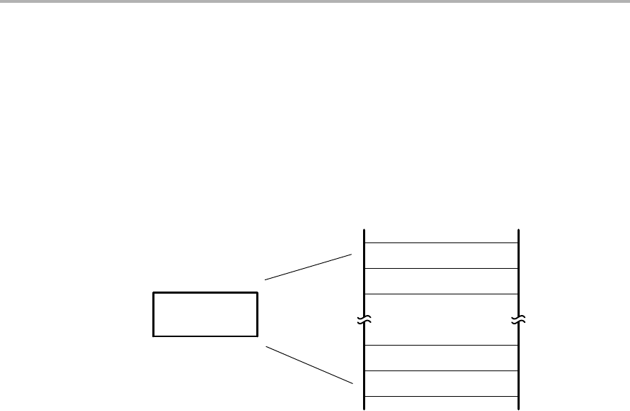
ADC10 Operation
20-16 ADC10
One-Block Transfer Mode
The one-block mode is selected if the ADC10TB is reset. The value n in
ADC10DTC1 defines the total number of transfers for a block. The block start
address is defined anywhere in the MSP430 address range using the 16-bit
register ADC10SA. The block ends at ADC10SA+2n–2. The one-block
transfer mode is shown in Figure 20−9.
Figure 20−9. One-Block Transfer
ADC10SA
ADC10SA+2
ADC10SA+2n−2
ADC10SA+2n−4
1st transfer
’n’th transfer
2nd transfer
TB=0
DTC
The internal address pointer is initially equal to ADC10SA and the internal
transfer counter is initially equal to ‘n’. The internal pointer and counter are not
visible to software. The DTC transfers the word-value of ADC10MEM to the
address pointer ADC10SA. After each DTC transfer, the internal address
pointer is incremented by two and the internal transfer counter is decremented
by one.
The DTC transfers continue with each loading of ADC10MEM, until the
internal transfer counter becomes equal to zero. No additional DTC transfers
will occur until a write to ADC10SA. When using the DTC in the one-block
mode, the ADC10IFG flag is set only after a complete block has been
transferred. Figure 20−10 shows a state diagram of the one-block mode.
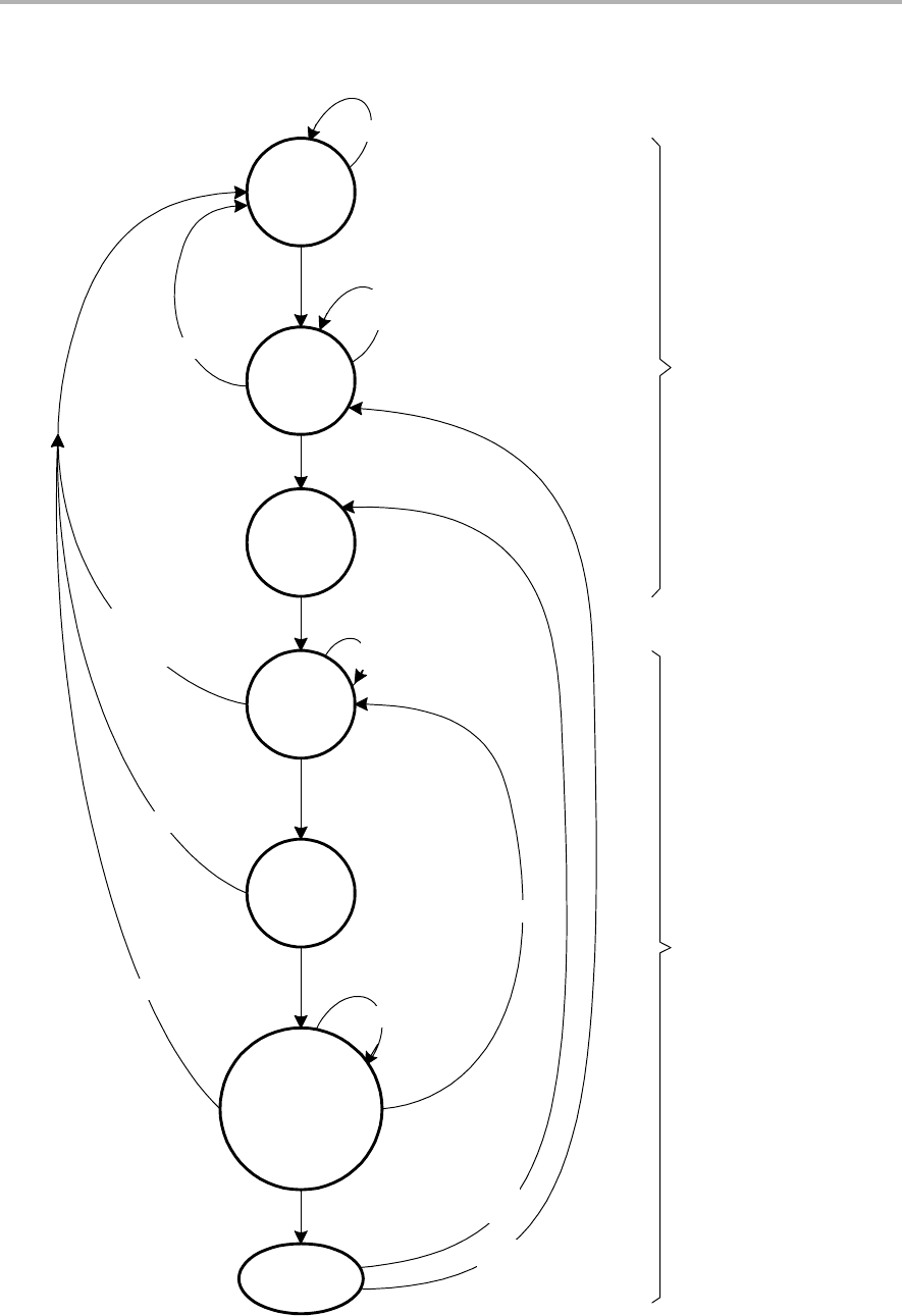
ADC10 Operation
20-17
ADC10
Figure 20−10. State Diagram for Data Transfer Control in One-Block Transfer Mode
DTC idle
DTC reset
n=0 (ADC10DTC1)
Initialize
Start Address in ADC10SA
Wait until ADC10MEM
is written
Wait
for
CPU ready
Write to ADC10MEM
completed
Transfer data to
Address AD
AD = AD + 2
x = x − 1
Synchronize
with MCLK
1 x MCLK cycle
n is latched
in counter ’x’
x > 0
DTC init
Wait for write to
ADC10SA
Write to
ADC10SA
Write to ADC10SA
x = 0
Prepare
DTC
DTC
operation
Write to ADC10SA
or
n = 0
Write to ADC10SA
x = n
AD = SA
n = 0
ADC10IFG=1
ADC10TB = 0
and
ADC10CT = 0
ADC10TB = 0
and
ADC10CT = 1
n≠0
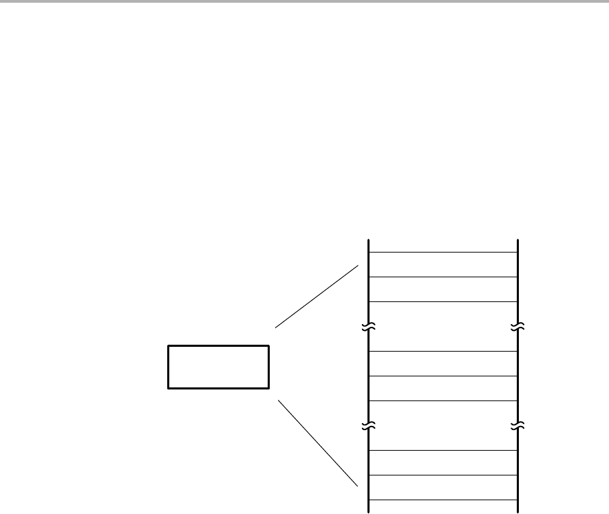
ADC10 Operation
20-18 ADC10
Two-Block Transfer Mode
The two-block mode is selected if the ADC10TB bit is set. The value n in
ADC10DTC1 defines the number of transfers for one block. The address
range of the first block is defined anywhere in the MSP430 address range with
the 16-bit register ADC10SA. The first block ends at ADC10SA+2n–2. The
address range for the second block is defined as SA+2n to SA+4n–2. The
two-block transfer mode is shown in Figure 20−11.
Figure 20−11.Two-Block Transfer
ADC10SA
ADC10SA+2
ADC10SA+2n−2
ADC10SA+2n−4
1st transfer
’n’th transfer
2nd transfer
ADC10SA+4n−2
ADC10SA+4n−4
2 x ’n’th transfer
TB=1
DTC
The internal address pointer is initially equal to ADC10SA and the internal
transfer counter is initially equal to ‘n’. The internal pointer and counter are not
visible to software. The DTC transfers the word-value of ADC10MEM to the
address pointer ADC10SA. After each DTC transfer the internal address
pointer is incremented by two and the internal transfer counter is decremented
by one.
The DTC transfers continue, with each loading of ADC10MEM, until the
internal transfer counter becomes equal to zero. At this point, block one is full
and both the ADC10IFG flag the ADC10B1 bit are set. The user can test the
ADC10B1 bit to determine that block one is full.
The DTC continues with block two. The internal transfer counter is
automatically reloaded with ’n’. At the next load of the ADC10MEM, the DTC
begins transferring conversion results to block two. After n transfers have
completed, block two is full. The ADC10IFG flag is set and the ADC10B1 bit
is cleared. User software can test the cleared ADC10B1 bit to determine that
block two is full. Figure 20−12 shows a state diagram of the two-block mode.
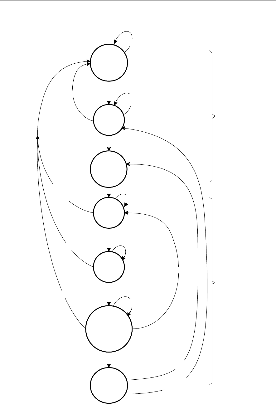
ADC10 Operation
20-19
ADC10
Figure 20−12. State Diagram for Data Transfer Control in Two-Block Transfer Mode
DTC idle
DTC reset
ADC10B1 = 0
ADC10TB = 1
n=0 (ADC10DTC1)
Initialize
Start Address in ADC10SA
Wait until ADC10MEM
is written
Wait
for
CPU ready
Write to ADC10MEM
completed
Transfer data to
Address AD
AD = AD + 2
x = x − 1
Synchronize
with MCLK
1 x MCLK cycle
n is latched
in counter ’x’
x > 0
DTC init
Wait for write to
ADC10SA
Write to
ADC10SA
Write to ADC10SA
x = 0
Prepare
DTC
DTC
operation
Write to ADC10SA
or
n = 0
ADC10IFG=1
Toggle
ADC10B1
Write to ADC10SA
x = n
If ADC10B1 = 0
then AD = SA
ADC10B1 = 1
or
ADC10CT=1
ADC10CT = 0
and
ADC10B1 = 0
n = 0
n ≠0

ADC10 Operation
20-20 ADC10
Continuous Transfer
A continuous transfer is selected if ADC10CT bit is set. The DTC will not stop
after block one in (one-block mode) or block two (two-block mode) has been
transferred. The internal address pointer and transfer counter are set equal to
ADC10SA and n respectively. Transfers continue starting in block one. If the
ADC10CT bit is reset, DTC transfers cease after the current completion of
transfers into block one (in the one-block mode) or block two (in the two-block
mode) have been transfer.
DTC Transfer Cycle Time
For each ADC10MEM transfer, the DTC requires one or two MCLK clock
cycles to synchronize, one for the actual transfer (while the CPU is halted), and
one cycle of wait time. Because the DTC uses MCLK, the DTC cycle time is
dependent on the MSP430 operating mode and clock system setup.
If the MCLK source is active, but the CPU is off, the DTC uses the MCLK
source for each transfer, without re-enabling the CPU. If the MCLK source is
off, the DTC temporarily restarts MCLK, sourced with DCOCLK, only during
a transfer. The CPU remains off and after the DTC transfer, MCLK is again
turned off. The maximum DTC cycle time for all operating modes is show in
Table 20−2.
Table 20−2.Maximum DTC Cycle Time
CPU Operating Mode Clock Source Maximum DTC Cycle Time
Active mode MCLK=DCOCLK 3 MCLK cycles
Active mode MCLK=LFXT1CLK 3 MCLK cycles
Low-power mode LPM0/1 MCLK=DCOCLK 4 MCLK cycles
Low-power mode LPM3/4 MCLK=DCOCLK 4 MCLK cycles + 2 μs†
Low-power mode LPM0/1 MCLK=LFXT1CLK 4 MCLK cycles
Low-power mode LPM3 MCLK=LFXT1CLK 4 MCLK cycles
Low-power mode LPM4 MCLK=LFXT1CLK 4 MCLK cycles + 2 μs†
†The additional 2 μs are needed to start the DCOCLK. See the device-specific data sheet for
parameters.

ADC10 Operation
20-21
ADC10
20.2.8 Using the Integrated Temperature Sensor
To use the on-chip temperature sensor, the user selects the analog input
channel INCHx = 1010. Any other configuration is done as if an external
channel was selected, including reference selection, conversion-memory
selection, etc.
The typical temperature sensor transfer function is shown in Figure 20−13.
When using the temperature sensor, the sample period must be greater than
30 μs. The temperature sensor offset error is large. Deriving absolute
temperature values in the application requires calibration. See the
device-specific data sheet for the parameters.
Selecting the temperature sensor automatically turns on the on-chip reference
generator as a voltage source for the temperature sensor. However, it does not
enable the VREF+ output or affect the reference selections for the conversion.
The reference choices for converting the temperature sensor are the same as
with any other channel.
Figure 20−13. Typical Temperature Sensor Transfer Function
Celsius
Volts
0 50 100
1.000
0.800
0.900
1.100
1.200
1.300
−50
0.700
VTEMP=0.00355(TEMPC)+0.986
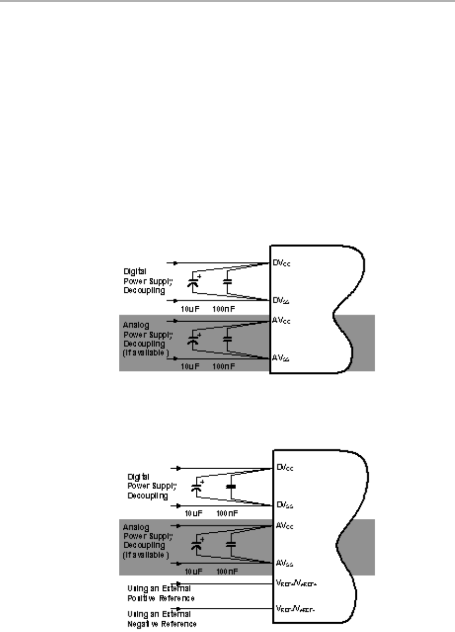
ADC10 Operation
20-22 ADC10
20.2.9 ADC10 Grounding and Noise Considerations
As with any high-resolution ADC, appropriate printed-circuit-board layout and
grounding techniques should be followed to eliminate ground loops, unwanted
parasitic effects, and noise.
Ground loops are formed when return current from the A/D flows through paths
that are common with other analog or digital circuitry. If care is not taken, this
current can generate small, unwanted offset voltages that can add to or
subtract from the reference or input voltages of the A/D converter. The
connections shown in Figure 20−14 help avoid this.
In addition to grounding, ripple and noise spikes on the power supply lines due
to digital switching or switching power supplies can corrupt the conversion
result. A noise-free design is important to achieve high accuracy.
Figure 20−14. ADC10 Grounding and Noise Considerations (internal Vref).
Figure 20−15. ADC10 Grounding and Noise Considerations (external Vref).
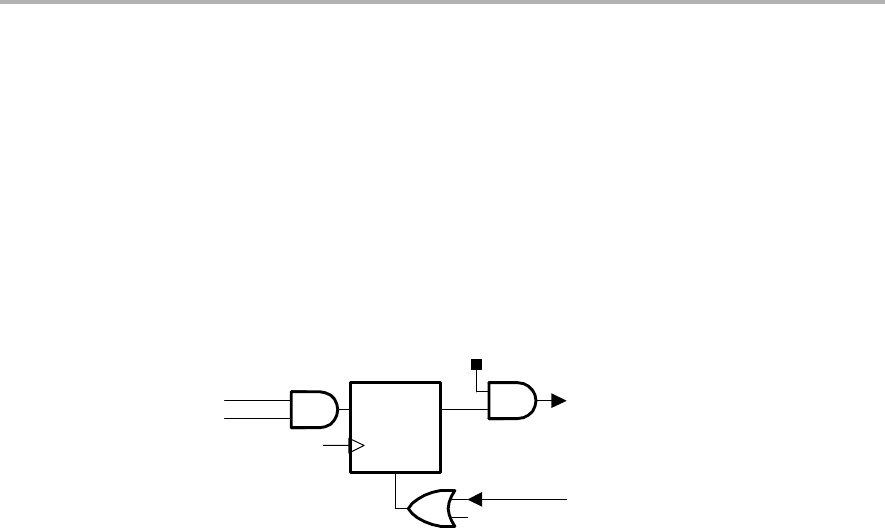
ADC10 Operation
20-23
ADC10
20.2.10 ADC10 Interrupts
One interrupt and one interrupt vector are associated with the ADC10 as
shown in Figure 20−16. When the DTC is not used (ADC10DTC1 = 0)
ADC10IFG is set when conversion results are loaded into ADC10MEM. When
DTC is used (ADC10DTC1 > 0) ADC10IFG is set when a block transfer
completes and the internal transfer counter ’n’ = 0. If both the ADC10IE and
the GIE bits are set, then the ADC10IFG flag generates an interrupt request.
The ADC10IFG flag is automatically reset when the interrupt request is
serviced or may be reset by software.
Figure 20−16. ADC10 Interrupt System
DQ IRQ, Interrupt Service Requested
Reset
ADC10CLK
POR
’n’ = 0
Set ADC10IFG
IRACC, Interrupt Request Accepted
ADC10IE

ADC10 Registers
20-24 ADC10
20.3 ADC10 Registers
The ADC10 registers are listed in Table 20−3.
Table 20−3.ADC10 Registers
Register Short Form Register Type Address Initial State
ADC10 input enable register 0 ADC10AE0 Read/write 04Ah Reset with POR
ADC10 input enable register 1 ADC10AE1 Read/write 04Bh Reset with POR
ADC10 control register 0 ADC10CTL0 Read/write 01B0h Reset with POR
ADC10 control register 1 ADC10CTL1 Read/write 01B2h Reset with POR
ADC10 memory ADC10MEM Read 01B4h Unchanged
ADC10 data transfer control register 0 ADC10DTC0 Read/write 048h Reset with POR
ADC10 data transfer control register 1 ADC10DTC1 Read/write 049h Reset with POR
ADC10 data transfer start address ADC10SA Read/write 01BCh 0200h with POR

ADC10 Registers
20-25
ADC10
ADC10CTL0, ADC10 Control Register 0
15 14 13 12 11 10 9 8
SREFx ADC10SHTx ADC10SR REFOUT REFBURST
rw−(0) rw−(0) rw−(0) rw−(0) rw−(0) rw−(0) rw−(0) rw−(0)
76543210
MSC REF2_5V REFON ADC10ON ADC10IE ADC10IFG ENC ADC10SC
rw−(0) rw−(0) rw−(0) rw−(0) rw−(0) rw−(0) rw−(0) rw−(0)
Modifiable only when ENC = 0
SREFx Bits
15-13
Select reference
000 VR+ = VCC and VR− = VSS
001 VR+ = VREF+ and VR− = VSS
010 VR+ = VeREF+ and VR− = VSS
011 VR+ = Buffered VeREF+ and VR− = VSS
100 VR+ = VCC and VR− = VREF−/ VeREF−
101 VR+ = VREF+ and VR− = VREF−/ VeREF−
110 VR+ = VeREF+ and VR− = VREF−/ VeREF−
111 VR+ = Buffered VeREF+ and VR− = VREF−/ VeREF−
ADC10
SHTx
Bits
12-11
ADC10 sample-and-hold time
00 4 x ADC10CLKs
01 8 x ADC10CLKs
10 16 x ADC10CLKs
11 64 x ADC10CLKs
ADC10SR Bit 10 ADC10 sampling rate. This bit selects the reference buffer drive capability for
the maximum sampling rate. Setting ADC10SR reduces the current
consumption of the reference buffer.
0 Reference buffer supports up to ~200 ksps
1 Reference buffer supports up to ~50 ksps
REFOUT Bit 9 Reference output
0 Reference output off
1 Reference output on
REFBURST Bit 8 Reference burst.
0 Reference buffer on continuously
1 Reference buffer on only during sample-and-conversion

ADC10 Registers
20-26 ADC10
MSC Bit 7 Multiple sample and conversion. Valid only for sequence or repeated modes.
0 The sampling requires a rising edge of the SHI signal to trigger each
sample-and-conversion.
1 The first rising edge of the SHI signal triggers the sampling timer, but
further sample-and-conversions are performed automatically as soon
as the prior conversion is completed
REF2_5V Bit 6 Reference-generator voltage. REFON must also be set.
0 1.5 V
1 2.5 V
REFON Bit 5 Reference generator on
0 Reference off
1 Reference on
ADC10ON Bit 4 ADC10 on
0 ADC10 off
1 ADC10 on
ADC10IE Bit 3 ADC10 interrupt enable
0 Interrupt disabled
1 interrupt enabled
ADC10IFG Bit 2 ADC10 interrupt flag. This bit is set if ADC10MEM is loaded with a conversion
result. It is automatically reset when the interrupt request is accepted, or it may
be reset by software. When using the DTC this flag is set when a block of
transfers is completed.
0 No interrupt pending
1 Interrupt pending
ENC Bit 1 Enable conversion
0 ADC10 disabled
1 ADC10 enabled
ADC10SC Bit 0 Start conversion. Software-controlled sample-and-conversion start.
ADC10SC and ENC may be set together with one instruction. ADC10SC is
reset automatically.
0 No sample-and-conversion start
1 Start sample-and-conversion

ADC10 Registers
20-27
ADC10
ADC10CTL1, ADC10 Control Register 1
15 14 13 12 11 10 9 8
INCHx SHSx ADC10DF ISSH
rw−(0) rw−(0) rw−(0) rw−(0) rw−(0) rw−(0) rw−(0) rw−(0)
76543210
ADC10DIVx ADC10SSELx CONSEQx ADC10
BUSY
rw−(0) rw−(0) rw−(0) rw−(0) rw−(0) rw−(0) rw−(0) r−0
Modifiable only when ENC = 0
INCHx Bits
15-12
Input channel select. These bits select the channel for a single-conversion or
the highest channel for a sequence of conversions.
0000 A0
0001 A1
0010 A2
0011 A3
0100 A4
0101 A5
0110 A6
0111 A7
1000 VeREF+
1001 VREF−/VeREF−
1010 Temperature sensor
1011 (VCC – VSS) / 2
1100 (VCC – VSS) / 2, A12 on MSP430x22xx devices
1101 (VCC – VSS) / 2, A13 on MSP430x22xx devices
1110 (VCC – VSS) / 2, A14 on MSP430x22xx devices
1111 (VCC – VSS) / 2, A15 on MSP430x22xx devices
SHSx Bits
11-10
Sample-and-hold source select
00 ADC10SC bit
01 Timer_A.OUT1
10 Timer_A.OUT0
11 Timer_A.OUT2 (Timer_A.OUT1 on MSP430x20x2 devices)
ADC10DF Bit 9 ADC10 data format
0 Straight binary
1 2s complement
ISSH Bit 8 Invert signal sample-and-hold
0 The sample-input signal is not inverted.
1 The sample-input signal is inverted.

ADC10 Registers
20-28 ADC10
ADC10DIVx Bits
7-5
ADC10 clock divider
000 /1
001 /2
010 /3
011 /4
100 /5
101 /6
110 /7
111 /8
ADC10
SSELx
Bits
4-3
ADC10 clock source select
00 ADC10OSC
01 ACLK
10 MCLK
11 SMCLK
CONSEQx Bits
2-1
Conversion sequence mode select
00 Single-channel-single-conversion
01 Sequence-of-channels
10 Repeat-single-channel
11 Repeat-sequence-of-channels
ADC10
BUSY
Bit 0 ADC10 busy. This bit indicates an active sample or conversion operation
0 No operation is active.
1 A sequence, sample, or conversion is active.

ADC10 Registers
20-29
ADC10
ADC10AE0, Analog (Input) Enable Control Register 0
76543210
ADC10AE0x
rw−(0) rw−(0) rw−(0) rw−(0) rw−(0) rw−(0) rw−(0) rw−(0)
ADC10AE0x Bits
7-0
ADC10 analog enable. These bits enable the corresponding pin for analog
input. BIT0 corresponds to A0, BIT1 corresponds to A1, etc.
0 Analog input disabled
1 Analog input enabled
ADC10AE1, Analog (Input) Enable Control Register 1 (MSP430x22xx only)
76543210
ADC10AE1x Reserved Reserved Reserved Reserved
rw−(0) rw−(0) rw−(0) rw−(0) rw−(0) rw−(0) rw−(0) rw−(0)
ADC10AE1x Bits
7-4
ADC10 analog enable. These bits enable the corresponding pin for analog
input. BIT4 corresponds to A12, BIT5 corresponds to A13, BIT6 corresponds
to A14, and BIT7 corresponds to A15.
0 Analog input disabled
1 Analog input enabled
ADC10 Registers
20-30 ADC10
ADC10MEM, Conversion-Memory Register, Binary Format
15 14 13 12 11 10 9 8
0 0 0 0 0 0 Conversion Results
r0 r0 r0 r0 r0 r0 r r
76543210
Conversion Results
r r r r r r r r
Conversion
Results
Bits
15-0
The 10-bit conversion results are right justified, straight-binary format. Bit 9
is the MSB. Bits 15-10 are always 0.
ADC10MEM, Conversion-Memory Register, 2s Complement Format
15 14 13 12 11 10 9 8
Conversion Results
r r r r r r r r
76543210
Conversion Results 0 0 0 0 0 0
r r r0 r0 r0 r0 r0 r0
Conversion
Results
Bits
15-0
The 10-bit conversion results are left-justified, 2s complement format. Bit 15
is the MSB. Bits 5-0 are always 0.

ADC10 Registers
20-31
ADC10
ADC10DTC0, Data Transfer Control Register 0
76543210
Reserved ADC10TB ADC10CT ADC10B1 ADC10
FETCH
r0 r0 r0 r0 rw−(0) rw−(0) r−(0) rw−(0)
Reserved Bits
7-4
Reserved. Always read as 0.
ADC10TB Bit 3 ADC10 two-block mode
0 One-block transfer mode
1 Two-block transfer mode
ADC10CT Bit 2 ADC10 continuous transfer
0 Data transfer stops when one block (one-block mode) or two blocks
(two-block mode) have completed.
1 Data is transferred continuously. DTC operation is stopped only if
ADC10CT cleared, or ADC10SA is written to.
ADC10B1 Bit 1 ADC10 block one. This bit indicates for two-block mode which block is filled
with ADC10 conversion results. ADC10B1 is valid only after ADC10IFG has
been set the first time during DTC operation. ADC10TB must also be set.
0 Block 2 is filled
1 Block 1 is filled
ADC10
FETCH
Bit 0 This bit should normally be reset.

ADC10 Registers
20-32 ADC10
ADC10DTC1, Data Transfer Control Register 1
76543210
DTC Transfers
rw−(0) rw−(0) rw−(0) rw−(0) rw−(0) rw−(0) rw−(0) rw−(0)
DTC
Transfers
Bits
7-0
DTC transfers. These bits define the number of transfers in each block.
0 DTC is disabled
01h−0FFh Number of transfers per block
ADC10SA, Start Address Register for Data Transfer
15 14 13 12 11 10 9 8
ADC10SAx
rw−(0) rw−(0) rw−(0) rw−(0) rw−(0) rw−(0) rw−(1) rw−(0)
76543210
ADC10SAx 0
rw−(0) rw−(0) rw−(0) rw−(0) rw−(0) rw−(0) rw−(0) r0
ADC10SAx Bits
15-1
ADC10 start address. These bits are the start address for the DTC. A write
to register ADC10SA is required to initiate DTC transfers.
Unused Bit 0 Unused, Read only. Always read as 0.

21-1
ADC12
ADC12
The ADC12 module is a high-performance 12-bit analog-to-digital converter.
This chapter describes the ADC12 of the MSP430 2xx device family.
Topic Page
21.1 ADC12 Introduction 21-2. . . . . . . . . . . . . . . . . . . . . . . . . . . . . . . . . . . . . . . . . . .
21.2 ADC12 Operation 21-4. . . . . . . . . . . . . . . . . . . . . . . . . . . . . . . . . . . . . . . . . . . . .
21.3 ADC12 Registers 21-20. . . . . . . . . . . . . . . . . . . . . . . . . . . . . . . . . . . . . . . . . . .
Chapter 21

ADC12 Introduction
21-2 ADC12
21.1 ADC12 Introduction
The ADC12 module supports fast, 12-bit analog-to-digital conversions. The
module implements a 12-bit SAR core, sample select control, reference
generator and a 16 word conversion-and-control buffer. The
conversion-and-control buffer allows up to 16 independent ADC samples to be
converted and stored without any CPU intervention.
ADC12 features include:
-Greater than 200-ksps maximum conversion rate
-Monotonic 12-bit converter with no missing codes
-Sample-and-hold with programmable sampling periods controlled by
software or timers.
-Conversion initiation by software, Timer_A, or Timer_B
-Software selectable on-chip reference voltage generation (1.5 V or 2.5 V)
-Software selectable internal or external reference
-Eight individually configurable external input channels
-Conversion channels for internal temperature sensor, AVCC, and external
references
-Independent channel-selectable reference sources for both positive and
negative references
-Selectable conversion clock source
-Single-channel, repeat-single-channel, sequence, and repeat-sequence
conversion modes
-ADC core and reference voltage can be powered down separately
-Interrupt vector register for fast decoding of 18 ADC interrupts
-16 conversion-result storage registers
The block diagram of ADC12 is shown in Figure 21−1.
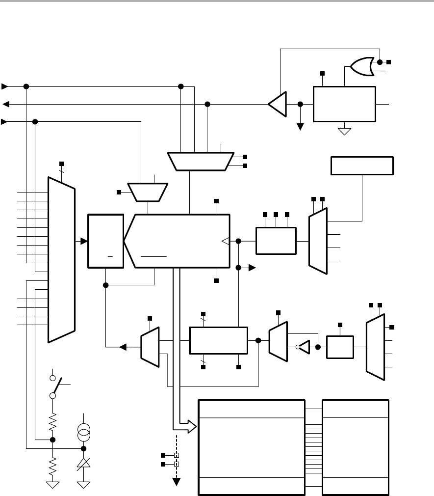
ADC12 Introduction
21-3
ADC12
Figure 21−1. ADC12 Block Diagram
Sample
and
Hold
VeREF+
12−bit SAR
VR−
−
16 x 12
Memory
Buffer
−
−
16 x 8
Memory
Control
−
VR+
VREF+
VeREF−
VREF− /
ADC12SC
TA1
TB1
TB0
Divider
/1 .. /8
ADC12DIVx
ADC12CLK
ENC
MSC
SHP SHT0x
SAMPCON
SHI
S/H Convert
Sync
Sample Timer
/4 .. /1024
INCHx
4
A0
A1
A2
A3
A4
A5
A6
A7
ADC12MEM0
ADC12MEM15
ADC12MCTL0
ADC12MCTL15
CSTARTADDx
4
4
SHT1x
CONSEQx
ACLK
MCLK
SMCLK
ADC12SSELx
ADC12OSC
00
01
10
11
00
01
10
11
SHSx
00
01
10
11
00
01
10
11
ISSH
1
0
0
1
SREF2 01
SREF1
0001 SREF0
10
ADC12ON
BUSY
REFON
INCHx=0Ah
1.5 V or 2.5 V
Reference
on
Ref_x
Ref_x
INCHx=0Bh
11
R
R
0000
1001
1000
0010
0001
0011
0100
0101
0110
0111
1011
1010
0001
1111
1110
1101
1100
REF2_5V
AVCC
AVCC
AVCC
AVSS
AVSS
GND
GND
GND
GND

ADC12 Operation
21-4 ADC12
21.2 ADC12 Operation
The ADC12 module is configured with user software. The setup and operation
of the ADC12 is discussed in the following sections.
21.2.1 12-Bit ADC Core
The ADC core converts an analog input to its 12-bit digital representation and
stores the result in conversion memory. The core uses two
programmable/selectable voltage levels (VR+ and VR−) to define the upper and
lower limits of the conversion. The digital output (NADC) is full scale (0FFFh)
when the input signal is equal to or higher than VR+, and zero when the input
signal is equal to or lower than VR−. The input channel and the reference
voltage levels (VR+ and VR−) are defined in the conversion-control memory.
The conversion formula for the ADC result NADC is:
NADC +4095 Vin *VR*
VR)*VR*
The ADC12 core is configured by two control registers, ADC12CTL0 and
ADC12CTL1. The core is enabled with the ADC12ON bit. The ADC12 can be
turned off when not in use to save power. With few exceptions the ADC12
control bits can only be modified when ENC = 0. ENC must be set to 1 before
any conversion can take place.
Conversion Clock Selection
The ADC12CLK is used both as the conversion clock and to generate the
sampling period when the pulse sampling mode is selected. The ADC12
source clock is selected using the ADC12SSELx bits and can be divided from
1-8 using the ADC12DIVx bits. Possible ADC12CLK sources are SMCLK,
MCLK, ACLK, and an internal oscillator ADC12OSC.
The ADC12OSC, generated internally, is in the 5-MHz range, but varies with
individual devices, supply voltage, and temperature. See the device-specific
datasheet for the ADC12OSC specification.
The user must ensure that the clock chosen for ADC12CLK remains active
until the end of a conversion. If the clock is removed during a conversion, the
operation will not complete and any result will be invalid.
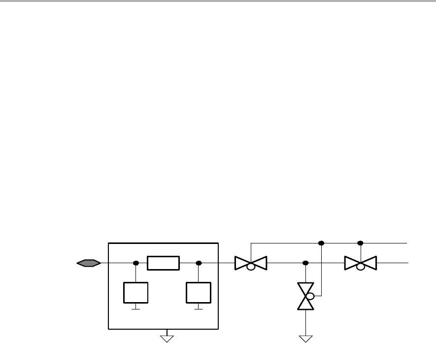
ADC12 Operation
21-5
ADC12
21.2.2 ADC12 Inputs and Multiplexer
The eight external and four internal analog signals are selected as the channel
for conversion by the analog input multiplexer. The input multiplexer is a
break-before-make type to reduce input-to-input noise injection resulting from
channel switching as shown in Figure 21−2. The input multiplexer is also a
T-switch to minimize the coupling between channels. Channels that are not
selected are isolated from the A/D and the intermediate node is connected to
analog ground (AVSS) so that the stray capacitance is grounded to help
eliminate crosstalk.
The ADC12 uses the charge redistribution method. When the inputs are
internally switched, the switching action may cause transients on the input
signal. These transients decay and settle before causing errant conversion.
Figure 21−2. Analog Multiplexer
R ~ 100 Ohm
ESD Protection
ADC12MCTLx.0−3
Input
Ax
Analog Port Selection
The ADC12 inputs are multiplexed with the port P6 pins, which are digital
CMOS gates. When analog signals are applied to digital CMOS gates,
parasitic current can flow from VCC to GND. This parasitic current occurs if the
input voltage is near the transition level of the gate. Disabling the port pin buffer
eliminates the parasitic current flow and therefore reduces overall current
consumption. The P6SELx bits provide the ability to disable the port pin input
and output buffers.
; P6.0 and P6.1 configured for analog input
BIS.B #3h,&P6SEL ; P6.1 and P6.0 ADC12 function

ADC12 Operation
21-6 ADC12
21.2.3 Voltage Reference Generator
The ADC12 module contains a built-in voltage reference with two selectable
voltage levels, 1.5 V and 2.5 V. Either of these reference voltages may be used
internally and externally on pin VREF+.
Setting REFON=1 enables the internal reference. When REF2_5V = 1, the
internal reference is 2.5 V, the reference is 1.5 V when REF2_5V = 0. The
reference can be turned off to save power when not in use.
For proper operation the internal voltage reference generator must be
supplied with storage capacitance across VREF+ and AVSS. The
recommended storage capacitance is a parallel combination of 10-μF and
0.1-μF capacitors. From turn-on, a maximum of 17 ms must be allowed for the
voltage reference generator to bias the recommended storage capacitors. If
the internal reference generator is not used for the conversion, the storage
capacitors are not required.
Note: Reference Decoupling
Approximately 200 μA is required from any reference used by the ADC12
while the two LSBs are being resolved during a conversion. A parallel
combination of 10-μF and 0.1-μF capacitors is recommended for any
reference used as shown in Figure 21−11.
External references may be supplied for VR+ and VR− through pins VeREF+ and
VREF−/VeREF− respectively.
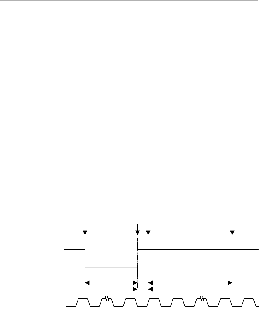
ADC12 Operation
21-7
ADC12
21.2.4 Sample and Conversion Timing
An analog-to-digital conversion is initiated with a rising edge of the sample
input signal SHI. The source for SHI is selected with the SHSx bits and
includes the following:
-The ADC12SC bit
-The Timer_A Output Unit 1
-The Timer_B Output Unit 0
-The Timer_B Output Unit 1
The polarity of the SHI signal source can be inverted with the ISSH bit. The
SAMPCON signal controls the sample period and start of conversion. When
SAMPCON is high, sampling is active. The high-to-low SAMPCON transition
starts the analog-to-digital conversion, which requires 13 ADC12CLK cycles.
Two different sample-timing methods are defined by control bit SHP, extended
sample mode and pulse mode.
Extended Sample Mode
The extended sample mode is selected when SHP = 0. The SHI signal directly
controls SAMPCON and defines the length of the sample period tsample. When
SAMPCON is high, sampling is active. The high-to-low SAMPCON transition
starts the conversion after synchronization with ADC12CLK. See Figure 21−3.
Figure 21−3. Extended Sample Mode
Start
Sampling
Stop
Sampling
Conversion
Complete
SAMPCON
SHI
tsample tconvert
tsync
13 x ADC12CLK
Start
Conversion
ADC12CLK
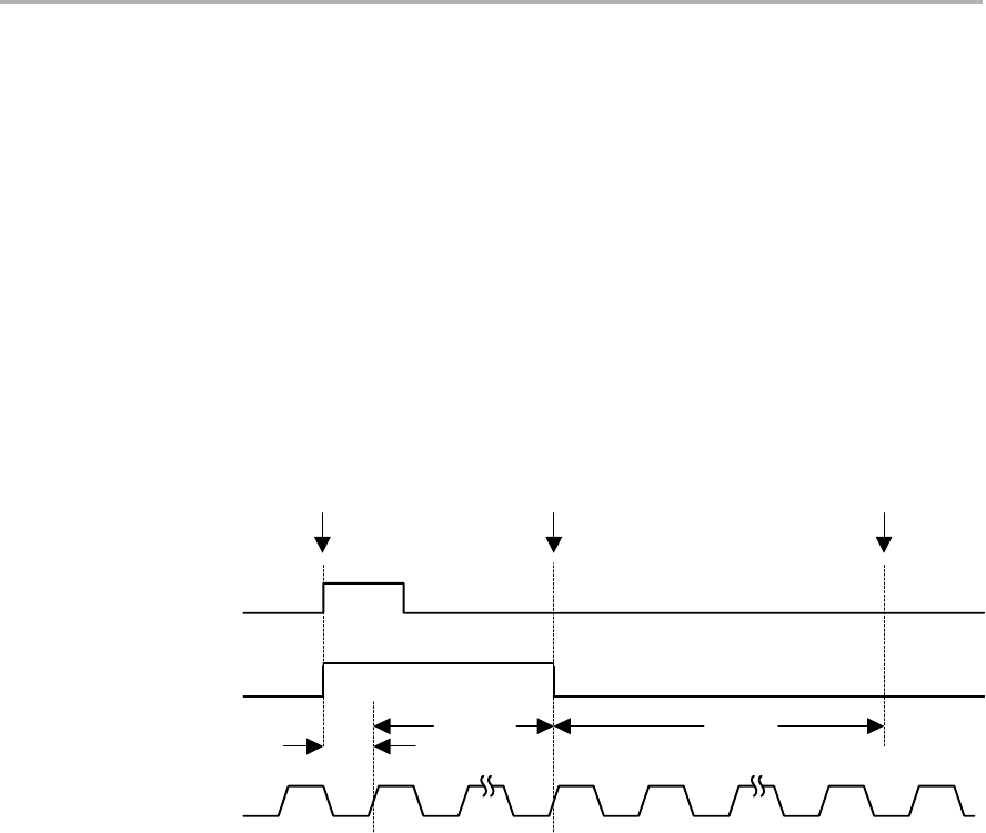
ADC12 Operation
21-8 ADC12
Pulse Sample Mode
The pulse sample mode is selected when SHP = 1. The SHI signal is used to
trigger the sampling timer. The SHT0x and SHT1x bits in ADC12CTL0 control
the interval of the sampling timer that defines the SAMPCON sample period
tsample. The sampling timer keeps SAMPCON high after synchronization with
AD12CLK for a programmed interval tsample. The total sampling time is tsample
plus tsync. See Figure 21−4.
The SHTx bits select the sampling time in 4x multiples of ADC12CLK. SHT0x
selects the sampling time for ADC12MCTL0 to 7 and SHT1x selects the
sampling time for ADC12MCTL8 to 15.
Figure 21−4. Pulse Sample Mode
Start
Sampling
Stop
Sampling
Conversion
Complete
SAMPCON
SHI
tsample tconvert
tsync
13 x ADC12CLK
Start
Conversion
ADC12CLK
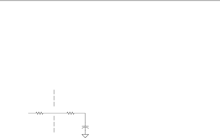
ADC12 Operation
21-9
ADC12
Sample Timing Considerations
When SAMPCON = 0 all Ax inputs are high impedance. When SAMPCON = 1,
the selected Ax input can be modeled as an RC low-pass filter during the
sampling time tsample, as shown below in Figure 21−5. An internal MUX-on
input resistance RI (maximum of 2 kΩ) in series with capacitor CI (maximum
of 40 pF) is seen by the source. The capacitor CI voltage VC must be charged
to within 1/2 LSB of the source voltage VS for an accurate 12-bit conversion.
Figure 21−5. Analog Input Equivalent Circuit
RSRI
VSVC
MSP430
CI
VI
VI= Input voltage at pin Ax
VS= External source voltage
RS= External source resistance
RI= Internal MUX-on input resistance
CI= Input capacitance
VC= Capacitance-charging voltage
The resistance of the source RS and RI affect tsample. The following equation
can be used to calculate the minimum sampling time tsample for a 12-bit
conversion:
tsample u(RS)RI) ln(213) CI)800ns
Substituting the values for RI and CI given above, the equation becomes:
tsample u(RS)2kW) 9.011 40pF )800ns
For example, if RS is 10 kΩ, tsample must be greater than 5.13 μs.

ADC12 Operation
21-10 ADC12
21.2.5 Conversion Memory
There are 16 ADC12MEMx conversion memory registers to store conversion
results. Each ADC12MEMx is configured with an associated ADC12MCTLx
control register. The SREFx bits define the voltage reference and the INCHx
bits select the input channel. The EOS bit defines the end of sequence when
a sequential conversion mode is used. A sequence rolls over from
ADC12MEM15 to ADC12MEM0 when the EOS bit in ADC12MCTL15 is not
set.
The CSTARTADDx bits define the first ADC12MCTLx used for any
conversion. If the conversion mode is single-channel or repeat-single-channel
the CSTARTADDx points to the single ADC12MCTLx to be used.
If the conversion mode selected is either sequence-of-channels or
repeat-sequence-of-channels, CSTARTADDx points to the first
ADC12MCTLx location to be used in a sequence. A pointer, not visible to
software, is incremented automatically to the next ADC12MCTLx in a
sequence when each conversion completes. The sequence continues until an
EOS bit in ADC12MCTLx is processed - this is the last control byte processed.
When conversion results are written to a selected ADC12MEMx, the
corresponding flag in the ADC12IFGx register is set.
21.2.6 ADC12 Conversion Modes
The ADC12 has four operating modes selected by the CONSEQx bits as
discussed in Table 21−1.
Table 21−1.Conversion Mode Summary
CONSEQx Mode Operation
00 Single channel
single-conversion
A single channel is converted once.
01 Sequence-of-
channels
A sequence of channels is converted once.
10 Repeat-single-
channel
A single channel is converted repeatedly.
11 Repeat-sequence-
of-channels
A sequence of channels is converted
repeatedly.
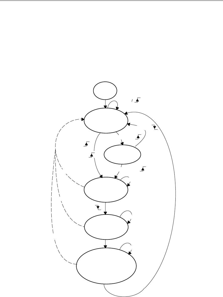
ADC12 Operation
21-11
ADC12
Single-Channel Single-Conversion Mode
A single channel is sampled and converted once. The ADC result is written to
the ADC12MEMx defined by the CSTARTADDx bits. Figure 21−6 shows the
flow of the Single-Channel, Single-Conversion mode. When ADC12SC
triggers a conversion, successive conversions can be triggered by the
ADC12SC bit. When any other trigger source is used, ENC must be toggled
between each conversion.
Figure 21−6. Single-Channel, Single-Conversion Mode
ADC12
off
x = CSTARTADDx
Wait for Enable
ENC =
Wait for Trigger
Sample, Input
Channel Defined in
ADC12MCTLx
ENC =
ENC =
SHSx = 0
and
ENC = 1 or
and
ADC12SC =
SAMPCON =
SAMPCON = 1
Convert
SAMPCON =
ENC = 0
ENC = 0†
12 x ADC12CLK
Conversion
Completed,
Result Stored Into
ADC12MEMx,
ADC12IFG.x is Set
1 x ADC12CLK
ENC = 0†
ADC12ON = 1
CONSEQx = 00
x = pointer to ADC12MCTLx
†Conversion result is unpredictable
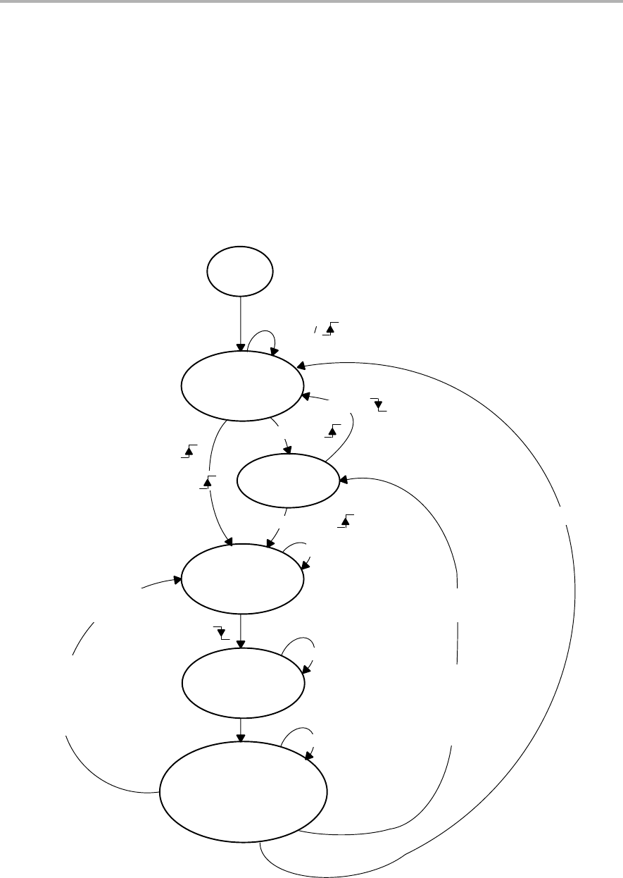
ADC12 Operation
21-12 ADC12
Sequence-of-Channels Mode
A sequence of channels is sampled and converted once. The ADC results are
written to the conversion memories starting with the ADCMEMx defined by the
CSTARTADDx bits. The sequence stops after the measurement of the
channel with a set EOS bit. Figure 21−7 shows the sequence-of-channels
mode. When ADC12SC triggers a sequence, successive sequences can be
triggered by the ADC12SC bit. When any other trigger source is used, ENC
must be toggled between each sequence.
Figure 21−7. Sequence-of-Channels Mode
ADC12
off
x = CSTARTADDx
Wait for Enable
ENC =
Wait for Trigger
Sample, Input
Channel Defined in
ADC12MCTLx
ENC =
ENC =
SHSx = 0
and
ENC = 1 or
and
ADC12SC =
SAMPCON =
SAMPCON = 1
Convert
SAMPCON =
12 x ADC12CLK
Conversion
Completed,
Result Stored Into
ADC12MEMx,
ADC12IFG.x is Set
1 x ADC12CLK
ADC12ON = 1
CONSEQx = 01
MSC = 1
and
SHP = 1
and
EOS.x = 0
EOS.x = 1
If x < 15 then x = x + 1
else x = 0
If x < 15 then x = x + 1
else x = 0
(MSC = 0
or
SHP = 0)
and
EOS.x = 0
x = pointer to ADC12MCTLx
ADC12 Operation
21-13
ADC12
Repeat-Single-Channel Mode
A single channel is sampled and converted continuously. The ADC results are
written to the ADC12MEMx defined by the CSTARTADDx bits. It is necessary
to read the result after the completed conversion because only one
ADC12MEMx memory is used and is overwritten by the next conversion.
Figure 21−8 shows repeat-single-channel mode
Figure 21−8. Repeat-Single-Channel Mode
ADC12
off
x = CSTARTADDx
Wait for Enable
ENC =
Wait for Trigger
Sample, Input
Channel Defined in
ADC12MCTLx
ENC =
ENC =
SHSx = 0
and
ENC = 1 or
and
ADC12SC =
SAMPCON =
SAMPCON = 1
Convert
SAMPCON =
12 x ADC12CLK
Conversion
Completed,
Result Stored Into
ADC12MEMx,
ADC12IFG.x is Set
1 x ADC12CLK
ADC12ON = 1
CONSEQx = 10
MSC = 1
and
SHP = 1
and
ENC = 1
ENC = 0
(MSC = 0
or
SHP = 0)
and
ENC = 1
x = pointer to ADC12MCTLx
ADC12 Operation
21-14 ADC12
Repeat-Sequence-of-Channels Mode
A sequence of channels is sampled and converted repeatedly. The ADC
results are written to the conversion memories starting with the ADC12MEMx
defined by the CSTARTADDx bits. The sequence ends after the measurement
of the channel with a set EOS bit and the next trigger signal re-starts the
sequence. Figure 21−9 shows the repeat-sequence-of-channels mode.
Figure 21−9. Repeat-Sequence-of-Channels Mode
ADC12
off
x = CSTARTADDx
Wait for Enable
ENC =
Wait for Trigger
Sample, Input
Channel Defined in
ADC12MCTLx
ENC =
ENC =
SHSx = 0
and
ENC = 1 or
and
ADC12SC =
SAMPCON =
SAMPCON = 1
SAMPCON =
12 x ADC12CLK
Conversion
Completed,
Result Stored Into
ADC12MEMx,
ADC12IFG.x is Set
1 x ADC12CLK
ADC12ON = 1
CONSEQx = 11
MSC = 1
and
SHP = 1
and
(ENC = 1
or
EOS.x = 0)
ENC = 0
and
EOS.x = 1
(MSC = 0
or
SHP = 0)
and
(ENC = 1
or
EOS.x = 0)
If EOS.x = 1 then x =
CSTARTADDx
else {if x < 15 then x = x + 1 else
x = 0}
If EOS.x = 1 then x =
CSTARTADDx
else {if x < 15 then x = x + 1 else
x = 0}
x = pointer to ADC12MCTLx
Convert

ADC12 Operation
21-15
ADC12
Using the Multiple Sample and Convert (MSC) Bit
To configure the converter to perform successive conversions automatically
and as quickly as possible, a multiple sample and convert function is available.
When MSC = 1, CONSEQx > 0, and the sample timer is used, the first rising
edge of the SHI signal triggers the first conversion. Successive conversions
are triggered automatically as soon as the prior conversion is completed.
Additional rising edges on SHI are ignored until the sequence is completed in
the single-sequence mode or until the ENC bit is toggled in
repeat-single-channel, or repeated-sequence modes. The function of the ENC
bit is unchanged when using the MSC bit.
Stopping Conversions
Stopping ADC12 activity depends on the mode of operation. The
recommended ways to stop an active conversion or conversion sequence are:
-Resetting ENC in single-channel single-conversion mode stops a
conversion immediately and the results are unpredictable. For correct
results, poll the busy bit until reset before clearing ENC.
-Resetting ENC during repeat-single-channel operation stops the
converter at the end of the current conversion.
-Resetting ENC during a sequence or repeat-sequence mode stops the
converter at the end of the sequence.
-Any conversion mode may be stopped immediately by setting the
CONSEQx = 0 and resetting ENC bit. Conversion data are unreliable.
Note: No EOS Bit Set For Sequence
If no EOS bit is set and a sequence mode is selected, resetting the ENC bit
does not stop the sequence. To stop the sequence, first select a
single-channel mode and then reset ENC.

ADC12 Operation
21-16 ADC12
21.2.7 Using the Integrated Temperature Sensor
To use the on-chip temperature sensor, the user selects the analog input
channel INCHx = 1010. Any other configuration is done as if an external
channel was selected, including reference selection, conversion-memory
selection, etc.
The typical temperature sensor transfer function is shown in Figure 21−10.
When using the temperature sensor, the sample period must be greater than
30 μs. The temperature sensor offset error can be large, and may need to be
calibrated for most applications. See device-specific datasheet for
parameters.
Selecting the temperature sensor automatically turns on the on-chip reference
generator as a voltage source for the temperature sensor. However, it does not
enable the VREF+ output or affect the reference selections for the conversion.
The reference choices for converting the temperature sensor are the same as
with any other channel.
Figure 21−10. Typical Temperature Sensor Transfer Function
Celsius
Volts
0 50 100
1.000
0.800
0.900
1.100
1.200
1.300
−50
0.700
VTEMP=0.00355(TEMPC)+0.986
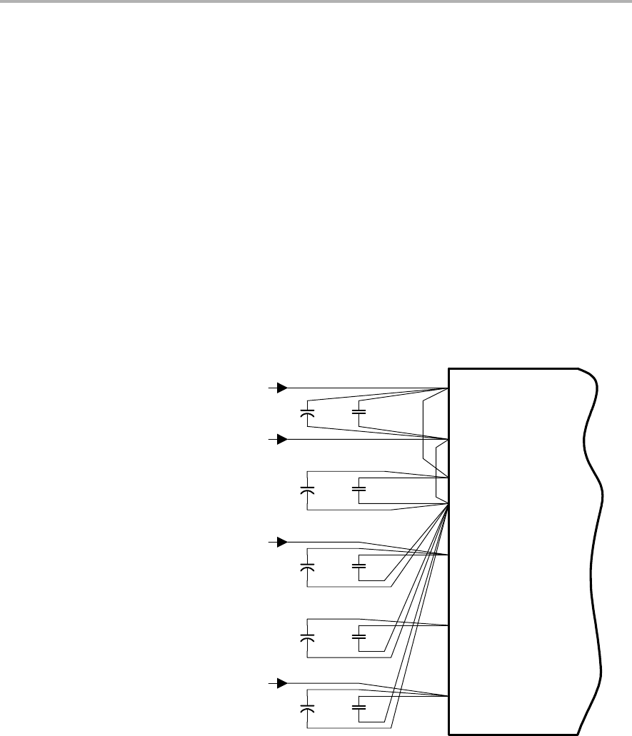
ADC12 Operation
21-17
ADC12
21.2.8 ADC12 Grounding and Noise Considerations
As with any high-resolution ADC, appropriate printed-circuit-board layout and
grounding techniques should be followed to eliminate ground loops, unwanted
parasitic effects, and noise.
Ground loops are formed when return current from the A/D flows through paths
that are common with other analog or digital circuitry. If care is not taken, this
current can generate small, unwanted offset voltages that can add to or
subtract from the reference or input voltages of the A/D converter. The
connections shown in Figure 21−11 help avoid this.
In addition to grounding, ripple and noise spikes on the power supply lines due
to digital switching or switching power supplies can corrupt the conversion
result. A noise-free design using separate analog and digital ground planes
with a single-point connection is recommend to achieve high accuracy.
Figure 21−11.ADC12 Grounding and Noise Considerations
DVCC
DVSS
AV CC
AV SS
VeREF+
Digital
Power Supply
Decoupling
10 uF 100 nF
+
Using an External
Positive
Reference
VREF+
VREF− / VeREF−
Using the Internal
Reference
Generator
10 uF 100 nF
100 nF
+
+
10 uF 100 nF
+
Using an External
Negative
Reference
10 uF
+
Analog
Power Supply
Decoupling
10 uF 100 nF

ADC12 Operation
21-18 ADC12
21.2.9 ADC12 Interrupts
The ADC12 has 18 interrupt sources:
-ADC12IFG0-ADC12IFG15
-ADC12OV, ADC12MEMx overflow
-ADC12TOV, ADC12 conversion time overflow
The ADC12IFGx bits are set when their corresponding ADC12MEMx memory
register is loaded with a conversion result. An interrupt request is generated
if the corresponding ADC12IEx bit and the GIE bit are set. The ADC12OV
condition occurs when a conversion result is written to any ADC12MEMx
before its previous conversion result was read. The ADC12TOV condition is
generated when another sample-and-conversion is requested before the
current conversion is completed. The DMA is triggered after the conversion in
single channel modes or after the completion of a sequence−of−channel
modes.
ADC12IV, Interrupt Vector Generator
All ADC12 interrupt sources are prioritized and combined to source a single
interrupt vector. The interrupt vector register ADC12IV is used to determine
which enabled ADC12 interrupt source requested an interrupt.
The highest priority enabled ADC12 interrupt generates a number in the
ADC12IV register (see register description). This number can be evaluated or
added to the program counter to automatically enter the appropriate software
routine. Disabled ADC12 interrupts do not affect the ADC12IV value.
Any access, read or write, of the ADC12IV register automatically resets the
ADC12OV condition or the ADC12TOV condition if either was the highest
pending interrupt. Neither interrupt condition has an accessible interrupt flag.
The ADC12IFGx flags are not reset by an ADC12IV access. ADC12IFGx bits
are reset automatically by accessing their associated ADC12MEMx register
or may be reset with software.
If another interrupt is pending after servicing of an interrupt, another interrupt
is generated. For example, if the ADC12OV and ADC12IFG3 interrupts are
pending when the interrupt service routine accesses the ADC12IV register, the
ADC12OV interrupt condition is reset automatically. After the RETI instruction
of the interrupt service routine is executed, the ADC12IFG3 generates another
interrupt.

ADC12 Operation
21-19
ADC12
ADC12 Interrupt Handling Software Example
The following software example shows the recommended use of ADC12IV
and the handling overhead. The ADC12IV value is added to the PC to
automatically jump to the appropriate routine.
The numbers at the right margin show the necessary CPU cycles for each
instruction. The software overhead for different interrupt sources includes
interrupt latency and return-from-interrupt cycles, but not the task handling
itself. The latencies are:
-ADC12IFG0 - ADC12IFG14, ADC12TOV and ADC12OV 16 cycles
-ADC12IFG15 14 cycles
The interrupt handler for ADC12IFG15 shows a way to check immediately if
a higher prioritized interrupt occurred during the processing of ADC12IFG15.
This saves nine cycles if another ADC12 interrupt is pending.
; Interrupt handler for ADC12.
INT_ADC12 ; Enter Interrupt Service Routine 6
ADD &ADC12IV,PC; Add offset to PC 3
RETI ; Vector 0: No interrupt 5
JMP ADOV ; Vector 2: ADC overflow 2
JMP ADTOV ; Vector 4: ADC timing overflow 2
JMP ADM0 ; Vector 6: ADC12IFG0 2
... ; Vectors 8-32 2
JMP ADM14 ; Vector 34: ADC12IFG14 2
;
; Handler for ADC12IFG15 starts here. No JMP required.
;
ADM15 MOV &ADC12MEM15,xxx ; Move result, flag is reset
... ; Other instruction needed?
JMP INT_ADC12 ; Check other int pending
;
; ADC12IFG14-ADC12IFG1 handlers go here
;
ADM0 MOV &ADC12MEM0,xxx ; Move result, flag is reset
... ; Other instruction needed?
RETI ; Return 5
;
ADTOV ... ; Handle Conv. time overflow
RETI ; Return 5
;
ADOV ... ; Handle ADCMEMx overflow
RETI ; Return 5

ADC12 Registers
21-20 ADC12
21.3 ADC12 Registers
The ADC12 registers are listed in Table 21−2.
Table 21−2.ADC12 Registers
Register Short Form Register Type Address Initial State
ADC12 control register 0 ADC12CTL0 Read/write 01A0h Reset with POR
ADC12 control register 1 ADC12CTL1 Read/write 01A2h Reset with POR
ADC12 interrupt flag register ADC12IFG Read/write 01A4h Reset with POR
ADC12 interrupt enable register ADC12IE Read/write 01A6h Reset with POR
ADC12 interrupt vector word ADC12IV Read 01A8h Reset with POR
ADC12 memory 0 ADC12MEM0 Read/write 0140h Unchanged
ADC12 memory 1 ADC12MEM1 Read/write 0142h Unchanged
ADC12 memory 2 ADC12MEM2 Read/write 0144h Unchanged
ADC12 memory 3 ADC12MEM3 Read/write 0146h Unchanged
ADC12 memory 4 ADC12MEM4 Read/write 0148h Unchanged
ADC12 memory 5 ADC12MEM5 Read/write 014Ah Unchanged
ADC12 memory 6 ADC12MEM6 Read/write 014Ch Unchanged
ADC12 memory 7 ADC12MEM7 Read/write 014Eh Unchanged
ADC12 memory 8 ADC12MEM8 Read/write 0150h Unchanged
ADC12 memory 9 ADC12MEM9 Read/write 0152h Unchanged
ADC12 memory 10 ADC12MEM10 Read/write 0154h Unchanged
ADC12 memory 11 ADC12MEM11 Read/write 0156h Unchanged
ADC12 memory 12 ADC12MEM12 Read/write 0158h Unchanged
ADC12 memory 13 ADC12MEM13 Read/write 015Ah Unchanged
ADC12 memory 14 ADC12MEM14 Read/write 015Ch Unchanged
ADC12 memory 15 ADC12MEM15 Read/write 015Eh Unchanged
ADC12 memory control 0 ADC12MCTL0 Read/write 080h Reset with POR
ADC12 memory control 1 ADC12MCTL1 Read/write 081h Reset with POR
ADC12 memory control 2 ADC12MCTL2 Read/write 082h Reset with POR
ADC12 memory control 3 ADC12MCTL3 Read/write 083h Reset with POR
ADC12 memory control 4 ADC12MCTL4 Read/write 084h Reset with POR
ADC12 memory control 5 ADC12MCTL5 Read/write 085h Reset with POR
ADC12 memory control 6 ADC12MCTL6 Read/write 086h Reset with POR
ADC12 memory control 7 ADC12MCTL7 Read/write 087h Reset with POR
ADC12 memory control 8 ADC12MCTL8 Read/write 088h Reset with POR
ADC12 memory control 9 ADC12MCTL9 Read/write 089h Reset with POR
ADC12 memory control 10 ADC12MCTL10 Read/write 08Ah Reset with POR
ADC12 memory control 11 ADC12MCTL11 Read/write 08Bh Reset with POR
ADC12 memory control 12 ADC12MCTL12 Read/write 08Ch Reset with POR
ADC12 memory control 13 ADC12MCTL13 Read/write 08Dh Reset with POR
ADC12 memory control 14 ADC12MCTL14 Read/write 08Eh Reset with POR
ADC12 memory control 15 ADC12MCTL15 Read/write 08Fh Reset with POR
ADC12 Registers
21-21
ADC12
ADC12CTL0, ADC12 Control Register 0
15 14 13 12 11 10 9 8
SHT1x SHT0x
rw−(0) rw−(0) rw−(0) rw−(0) rw−(0) rw−(0) rw−(0) rw−(0)
76543210
MSC REF2_5V REFON ADC120N ADC12OVIE ADC12
TOVIE ENC ADC12SC
rw−(0) rw−(0) rw−(0) rw−(0) rw−(0) rw−(0) rw−(0) rw−(0)
Modifiable only when ENC = 0
SHT1x Bits
15-12
Sample-and-hold time. These bits define the number of ADC12CLK cycles in
the sampling period for registers ADC12MEM8 to ADC12MEM15.
SHT0x Bits
11-8
Sample-and-hold time. These bits define the number of ADC12CLK cycles in
the sampling period for registers ADC12MEM0 to ADC12MEM7.
SHTx Bits ADC12CLK cycles
0000 4
0001 8
0010 16
0011 32
0100 64
0101 96
0110 128
0111 192
1000 256
1001 384
1010 512
1011 768
1100 1024
1101 1024
1110 1024
1111 1024

ADC12 Registers
21-22 ADC12
MSC Bit 7 Multiple sample and conversion. Valid only for sequence or repeated modes.
0 The sampling timer requires a rising edge of the SHI signal to trigger
each sample-and-conversion.
1 The first rising edge of the SHI signal triggers the sampling timer, but
further sample-and-conversions are performed automatically as soon
as the prior conversion is completed.
REF2_5V Bit 6 Reference generator voltage. REFON must also be set.
0 1.5 V
1 2.5 V
REFON Bit 5 Reference generator on
0 Reference off
1 Reference on
ADC12ON Bit 4 ADC12 on
0 ADC12 off
1 ADC12 on
ADC12OVIE Bit 3 ADC12MEMx overflow-interrupt enable. The GIE bit must also be set to
enable the interrupt.
0 Overflow interrupt disabled
1 Overflow interrupt enabled
ADC12
TOVIE
Bit 2 ADC12 conversion-time-overflow interrupt enable. The GIE bit must also be
set to enable the interrupt.
0 Conversion time overflow interrupt disabled
1 Conversion time overflow interrupt enabled
ENC Bit 1 Enable conversion
0 ADC12 disabled
1 ADC12 enabled
ADC12SC Bit 0 Start conversion. Software-controlled sample-and-conversion start.
ADC12SC and ENC may be set together with one instruction. ADC12SC is
reset automatically.
0 No sample-and-conversion-start
1 Start sample-and-conversion

ADC12 Registers
21-23
ADC12
ADC12CTL1, ADC12 Control Register 1
15 14 13 12 11 10 9 8
CSTARTADDx SHSx SHP ISSH
rw−(0) rw−(0) rw−(0) rw−(0) rw−(0) rw−(0) rw−(0) rw−(0)
76543210
ADC12DIVx ADC12SSELx CONSEQx ADC12
BUSY
rw−(0) rw−(0) rw−(0) rw−(0) rw−(0) rw−(0) rw−(0) r−(0)
Modifiable only when ENC = 0
CSTART
ADDx
Bits
15-12
Conversion start address. These bits select which ADC12
conversion-memory register is used for a single conversion or for the first
conversion in a sequence. The value of CSTARTADDx is 0 to 0Fh,
corresponding to ADC12MEM0 to ADC12MEM15.
SHSx Bits
11-10
Sample-and-hold source select
00 ADC12SC bit
01 Timer_A.OUT1
10 Timer_B.OUT0
11 Timer_B.OUT1
SHP Bit 9 Sample-and-hold pulse-mode select. This bit selects the source of the
sampling signal (SAMPCON) to be either the output of the sampling timer or
the sample-input signal directly.
0 SAMPCON signal is sourced from the sample-input signal.
1 SAMPCON signal is sourced from the sampling timer.
ISSH Bit 8 Invert signal sample-and-hold
0 The sample-input signal is not inverted.
1 The sample-input signal is inverted.
ADC12DIVx Bits
7-5
ADC12 clock divider
000 /1
001 /2
010 /3
011 /4
100 /5
101 /6
110 /7
111 /8

ADC12 Registers
21-24 ADC12
ADC12
SSELx
Bits
4-3
ADC12 clock source select
00 ADC12OSC
01 ACLK
10 MCLK
11 SMCLK
CONSEQx Bits
2-1
Conversion sequence mode select
00 Single-channel, single-conversion
01 Sequence-of-channels
10 Repeat-single-channel
11 Repeat-sequence-of-channels
ADC12
BUSY
Bit 0 ADC12 busy. This bit indicates an active sample or conversion operation.
0 No operation is active.
1 A sequence, sample, or conversion is active.
ADC12MEMx, ADC12 Conversion Memory Registers
15 14 13 12 11 10 9 8
0000 Conversion Results
r0 r0 r0 r0 rw rw rw rw
76543210
Conversion Results
rw rw rw rw rw rw rw rw
Conversion
Results
Bits
15-0
The 12-bit conversion results are right-justified. Bit 11 is the MSB. Bits 15-12
are always 0. Writing to the conversion memory registers will corrupt the
results.

ADC12 Registers
21-25
ADC12
ADC12MCTLx, ADC12 Conversion Memory Control Registers
76543210
EOS SREFx INCHx
rw−(0) rw−(0) rw−(0) rw−(0) rw−(0) rw−(0) rw−(0) rw−(0)
Modifiable only when ENC = 0
EOS Bit 7 End of sequence. Indicates the last conversion in a sequence.
0 Not end of sequence
1 End of sequence
SREFx Bits
6-4
Select reference
000 VR+ = AVCC and VR− = AVSS
001 VR+ = VREF+ and VR− = AVSS
010 VR+ = VeREF+ and VR− = AVSS
011 VR+ = VeREF+ and VR− = AVSS
100 VR+ = AVCC and VR− = VREF−/ VeREF−
101 VR+ = VREF+ and VR− = VREF−/ VeREF−
110 VR+ = VeREF+ and VR− = VREF−/ VeREF−
111 VR+ = VeREF+ and VR− = VREF−/ VeREF−
INCHx Bits
3-0
Input channel select
0000 A0
0001 A1
0010 A2
0011 A3
0100 A4
0101 A5
0110 A6
0111 A7
1000 VeREF+
1001 VREF−/VeREF−
1010 Temperature diode
1011 (AVCC – AVSS) / 2
1100 GND
1101 GND
1110 GND
1111 GND

ADC12 Registers
21-26 ADC12
ADC12IE, ADC12 Interrupt Enable Register
15 14 13 12 11 10 9 8
ADC12IE15 ADC12IE14 ADC12IE13 ADC12IE12 ADC12IE11 ADC12IE10 ADC12IFG9 ADC12IE8
rw−(0) rw−(0) rw−(0) rw−(0) rw−(0) rw−(0) rw−(0) rw−(0)
76543210
ADC12IE7 ADC12IE6 ADC12IE5 ADC12IE4 ADC12IE3 ADC12IE2 ADC12IE1 ADC12IE0
rw−(0) rw−(0) rw−(0) rw−(0) rw−(0) rw−(0) rw−(0) rw−(0)
ADC12IEx Bits
15-0
Interrupt enable. These bits enable or disable the interrupt request for the
ADC12IFGx bits.
0 Interrupt disabled
1 Interrupt enabled
ADC12IFG, ADC12 Interrupt Flag Register
15 14 13 12 11 10 9 8
ADC12
IFG15
ADC12
IFG14
ADC12
IFG13
ADC12
IFG12
ADC12
IFG11
ADC12
IFG10
ADC12
IFG9
ADC12
IFG8
rw−(0) rw−(0) rw−(0) rw−(0) rw−(0) rw−(0) rw−(0) rw−(0)
76543210
ADC12
IFG7
ADC12
IFG6
ADC12
IFG5
ADC12
IFG4
ADC12
IFG3
ADC12
IFG2
ADC12
IFG1
ADC12
IFG0
rw−(0) rw−(0) rw−(0) rw−(0) rw−(0) rw−(0) rw−(0) rw−(0)
ADC12IFGx Bits
15-0
ADC12MEMx Interrupt flag. These bits are set when corresponding
ADC12MEMx is loaded with a conversion result. The ADC12IFGx bits are
reset if the corresponding ADC12MEMx is accessed, or may be reset with
software.
0 No interrupt pending
1 Interrupt pending

ADC12 Registers
21-27
ADC12
ADC12IV, ADC12 Interrupt Vector Register
15 14 13 12 11 10 9 8
0 0 0 0 0 0 0 0
r0 r0 r0 r0 r0 r0 r0 r0
76543210
0 0 ADC12IVx 0
r0 r0 r−(0) r−(0) r−(0) r−(0) r−(0) r0
ADC12IVx Bits
15-0
ADC12 interrupt vector value
ADC12IV
Contents Interrupt Source Interrupt Flag
Interrupt
Priority
000h No interrupt pending −
002h ADC12MEMx overflow − Highest
004h Conversion time overflow −
006h ADC12MEM0 interrupt flag ADC12IFG0
008h ADC12MEM1 interrupt flag ADC12IFG1
00Ah ADC12MEM2 interrupt flag ADC12IFG2
00Ch ADC12MEM3 interrupt flag ADC12IFG3
00Eh ADC12MEM4 interrupt flag ADC12IFG4
010h ADC12MEM5 interrupt flag ADC12IFG5
012h ADC12MEM6 interrupt flag ADC12IFG6
014h ADC12MEM7 interrupt flag ADC12IFG7
016h ADC12MEM8 interrupt flag ADC12IFG8
018h ADC12MEM9 interrupt flag ADC12IFG9
01Ah ADC12MEM10 interrupt flag ADC12IFG10
01Ch ADC12MEM11 interrupt flag ADC12IFG11
01Eh ADC12MEM12 interrupt flag ADC12IFG12
020h ADC12MEM13 interrupt flag ADC12IFG13
022h ADC12MEM14 interrupt flag ADC12IFG14
024h ADC12MEM15 interrupt flag ADC12IFG15 Lowest

21-28 ADC12

22-1
TLV Structure
TLV Structure
The Tag-Length-Value (TLV) structure is used in selected MSP430x2xx
devices to provide device-specific information in the device’s flash memory
SegmentA, such as calibration data. For the device-dependent
implementation, see the device-specific data sheet.
Topic Page
22.1 TLV Introduction 22-2. . . . . . . . . . . . . . . . . . . . . . . . . . . . . . . . . . . . . . . . . . . . . .
22.2 Supported Tags 22-3. . . . . . . . . . . . . . . . . . . . . . . . . . . . . . . . . . . . . . . . . . . . . . .
22.3 Calculating the Checksum of SegmentA 22-7. . . . . . . . . . . . . . . . . . . . . . . .
22.4 Parsing the TLV Structure of SegmentA 22-8. . . . . . . . . . . . . . . . . . . . . . . .
Chapter 22

TLV Introduction
22-2 TLV Structure
22.1 TLV Introduction
The TLV structure stores device-specific data in SegmentA. The SegmentA
content of an example device is shown in Table 22−1.
Table 22−1.Example SegmentA structure
Word
Address
Upper Byte Lower Byte Tag Address and
Offset
0x10FE CALBC1_1MHZ CALDCO1_1MHZ 0x10F6 + 0x0008
0x10FC CALBC1_8MHZ CALDCO1_8MHZ 0x10F6 + 0x0006
0x10FA CALBC1_12MHZ CALDCO1_12MHZ 0x10F6 + 0x0004
0x10F8 CALBC1_16MHZ CALDCO1_16MHZ 0x10F6 + 0x0002
0x10F6 0x08 (LENGTH) TAG_DCO_30 0x10F6
0x10F4 0xFF 0xFF
0x10F2 0xFF 0xFF
0x10F0 0xFF 0xFF
0x10EE 0xFF 0xFF
0x10EC 0x08 (LENGTH) TAG_EMPTY 0x10EC
0x10EA CAL_ADC_25T85 0x10DA + 0x0010
0x10E8 CAL_ADC_25T30 0x10DA + 0x000E
0x10E6 CAL_ADC_25VREF_FACTOR 0x10DA + 0x000C
0x10E4 CAL_ADC_15T85 0x10DA + 0x000A
0x10E2 CAL_ADC_15T30 0x10DA + 0x0008
0x10E0 CAL_ADC_15VREF_FACTOR 0x10DA + 0x0006
0x10DE CAL_ADC_OFFSET 0x10DA + 0x0004
0x10DC CAL_ADC_GAIN_FACTOR 0x10DA + 0x0002
0x10DA 0x10 (LENGTH) TAG_ADC12_1 0x10DA
0x10D8 0xFF 0xFF
0x10D6 0xFF 0xFF
0x10D4 0xFF 0xFF
0x10D2 0xFF 0xFF
0x10D0 0xFF 0xFF
0x10CE 0xFF 0xFF
0x10CC 0xFF 0xFF
0x10CA 0xFF 0xFF
0x10C8 0xFF 0xFF
0x10C6 0xFF 0xFF
0x10C4 0xFF 0xFF
0x10C2 0x16 (LENGTH) TAG_EMPTY 0x10C2
0x10C0 2th complement of bit-wise XOR 0x10C0
The first two bytes of SegmentA (0x10C0 and 0x10C1) hold the checksum of
the remainder of the segment (addresses 0x10C2 to 0x10FF).
Supported Tags
22-3
TLV Structure
The first tag is located at address 0x10C2 and, in this example, is the
TAG_EMPTY tag. The following byte (0x10C3) holds the length of the
following structure. The length of this TAG_EMPTY structure is 0x16 and,
therefore, the next tag, TAG_ADC12_1, is found at address 0x10DA. Again,
the following byte holds the length of the TAG_ADC12_1 structure.
The TLV structure maps the entire address range 0x10C2 to 0x10FF of the
SegmentA. A program routine looking for tags starting at the SegmentA
address 0x10C2 can extract all information even if it is stored at a different
(device-specific) absolute address.
22.2 Supported Tags
Each device contains a subset of the tags shown in Table 22−2. See the
device-specific data sheet for details.
Table 22−2.Supported Tags (Device Specific)
Tag Description Value
TAG_EMPTY Identifies an unused memory area 0xFE
TAG_DCO_30 Calibration values for the DCO at room temperature and DVCC = 3 V 0x01
TAG_ADC12_1 Calibration values for the ADC12 module 0x08
22.2.1 DCO Calibration TLV Structure
For DCO calibration, the BCS+ registers (BCSCTL1 and DCOCTL) are used.
The values stored in the flash information memory SegmentA are written to the
BCS+ registers.
Table 22−3.DCO Calibration Data (Device Specific)
Label Description Offset
CALBC1_1MHZ Value for the BCSCTL1 register for 1 MHz, TA = 25°C 0x07
CALDCO_1MHZ Value for the DCOCTL register for 1 MHz, TA = 25°C 0x06
CALBC1_8MHZ Value for the BCSCTL1 register for 8 MHz, TA = 25°C 0x05
CALDCO_8MHZ Value for the DCOCTL register for 8 MHz, TA = 25°C 0x04
CALBC1_12MHZ Value for the BCSCTL1 register for 12 MHz, TA = 25°C 0x03
CALDCO_12MHZ Value for the DCOCTL register for 12 MHz, TA = 25°C 0x02
CALBC1_16MHZ Value for the BCSCTL1 register for 16 MHz, TA = 25°C 0x01
CALDCO_16MHZ Value for the DCOCTL register for 16 MHz, TA = 25°C 0x00

Supported Tags
22-4 TLV Structure
Code Example Using Absolute Addressing Mode
The calibration data for the DCO is available in all 2xx devices and is stored
at the same absolute addresses. The device-specific SegmentA content is
applied using the absolute addressing mode if the following code is used.
; Calibrate the DCO to 1 MHz
CLR.B &DCOCTL ; Select lowest DCOx
; and MODx settings
MOV.B &CALBC1_1MHZ,&BCSCTL1 ; Set RSELx
MOV.B &CALDCO_1MHZ,&DCOCTL ; Set DCOx and MODx
The TLV structure allows use of the address of the TAG_DCO_30 tag to
address the DCO registers. The code example shows how to address the DCO
calibration data using the TAG_DCO_30 tag.
Code Example Using the TLV Structure
; Calibrate the DCO to 8 MHz
; It is assumed that R10 contains the address of the
TAG_DCO_30 tag
CLR.B &DCOCTL ; Select lowest DCOx and
; MODx settings
MOV.B 7(R10),&BCSCTL1 ; Set RSEL
MOV.B 6(R10),&DCOCTL ; Set DCOx and MODx
22.2.2 TAG_ADC12_1 Calibration TLV structure
The calibration data for the ADC12 module consists of eight words.
Table 22−4.TAG_ADC12_1 Calibration Data (Device Specific)
Label Description Offset
CAL_ADC_25T85 VREF2_5 = 1, TA = 85°C $ 2K, 12-bit conversion result 0x0E
CAL_ADC_25T30 VREF2_5 = 1, TA = 30°C $ 2K, 12-bit conversion result 0x0C
CAL_ADC_25VREF_FACTOR VREF2_5 = 1, TA = 30°C $ 2K 0x0A
CAL_ADC_15T85 VREF2_5 = 0, TA = 85°C $ 2K, 12-bit conversion result 0x08
CAL_ADC_15T30 VREF2_5 = 0, TA = 30°C $ 2K, 12-bit conversion result 0x06
CAL_ADC_15VREF_FACTOR VREF2_5 = 0, TA = 30°C $ 2K 0x04
CAL_ADC_OFFSET VeREF = 2.5V, TA = 85°C $ 2K, fADC12CLK = 5 MHz 0x02
CAL_ADC_GAIN_FACTOR VeREF = 2.5V, TA = 85°C $ 2K, fADC12CLK = 5 MHz 0x00
Temperature Sensor Calibration Data
The temperature sensor is calibrated using the internal voltage references. At
VREF2_5 = 0 and 1, the conversion result at 30°C and 85°C is written at the
respective SegmentA location (see Table 22−4).

Supported Tags
22-5
TLV Structure
Integrated Voltage Reference Calibration Data
The reference voltages (VREF2_5 = 0 and 1) are measured at room
temperature. The measured value is normalized by 1.5/2.5V before stored into
the flash information memory SegmentA.
CAL_ADC_15VREF_FACTOR +VeREF
1.5V 215
The conversion result is corrected by multiplying it with the
CAL_ADC_15VREF_FACTOR (or CAL_ADC_25VREF_FACTOR) and
dividing the result by 215.
ADC(corrected) +ADC(raw) CAL_ADC_15VREF_FACTOR 1
215
Example Using the Reference Calibration
In the following example, the integrated 1.5-V reference voltage is used during
a conversion.
-Conversion result: 0x0100
-Reference voltage calibration factor (CAL_ADC_15VREF_FACTOR):
0x7BBB
The following steps show an example of how the ADC12 conversion result can
be corrected by using the hardware multiplier:
-Multiply the conversion result by 2 (this step simplifies the final division).
-Multiply the result by CAL_ADC_15VREF_FACTOR.
-Divide the result by 216 (use the upper word of the 32-bit multiplication
result RESHI).
In the example:
-0x0100 × 0x0002 = 0x0200
-0x0200 × 0x7BBB = 0x00F7_7600
-0x00F7_7600 B 0x0001_0000 = 0x0000_00F7 (= 247)
The code example using the hardware multiplier follows.
; The ADC conversion result is stored in ADC12MEM0
; It is assumed that R9 contains the address of the
; TAG_ADC12_1.
; The corrected value is available in ADC_COR
MOV.W &ADC12MEM0,R10 ; move result to R10
RLA.W R10 ; R10 x 2
MOV.W R10,&MPY ; unsigned multiply OP1
MOV.W CAL_ADC_15VREF_FACTOR(R9),&OP2
; calibration value OP2
MOV.W &RESHI,&ADC_COR ; result: upper 16-bit MPY

Supported Tags
22-6 TLV Structure
Offset and Gain Calibration Data
The offset of the ADC12 is determined and stored as a twos-complement
number in SegmentA. The offset error correction is done by adding the
CAL_ADC_OFFSET to the conversion result.
ADC(offset_corrected) +ADC(raw) )CAL_ADC_OFFSET
The gain of the ADC12, stored at offset 0x00, is calculated by the following
equation.
CAL_ADC_GAIN_FACTOR +1
GAIN 215
The conversion result is gain corrected by multiplying it with the
CAL_ADC_GAIN_FACTOR and dividing the result by 215.
ADC(gain_corrected) +ADC(raw) CAL_ADC_GAIN_FACTOR 1
215
If both gain and offset are corrected, the gain correction is done first.
ADC(gain_corrected) +ADC(raw) CAL_ADC_GAIN_FACTOR 1
215
ADC(final) +ADC(gain_corrected) )CAL_ADC_OFFSET
Example Using Gain and Offset Calibration
In the following example, an external reference voltage is used during a
conversion.
-Conversion result: 0x0800 (= 2048)
-Gain calibration factor: 0x7FE0 (gain error: +2 LSB)
-Offset calibration: 0xFFFE (2th complement of −2)
The following steps show an example of how the ADC12 conversion result is
corrected by using the hardware multiplier:
-Multiply the conversion result by 2 (this step simplifies the final division).
-Multiply the result by CAL_ADC_GAIN_FACTOR.
-Divide the result by 216 (use the upper word of the 32-bit multiplication
result RESHI)
-Add CAL_ADC_OFFSET to the result.
In the example:
-0x0800 × 0x0002 = 0x1000
-0x1000 × 0x8010 = 0x0801_0000
-0x0801_0000 B 0x0001_0000 = 0x0000_0801 (= 2049)
-0x801 + 0xFFFE = 0x07FF (= 2047)

Checking Integrity of SegmentA
22-7
TLV Structure
The code example using the hardware multiplier follows.
; The ADC conversion result is stored in ADC12MEM0
; It is assumed that R9 contains the address of the
TAG_ADC12_1.
; The corrected value is available in ADC_COR
MOV.W &ADC12MEM0,R10 ; move result to R10
RLA.W R10 ; R10 * 2
MOV.W R10,&MPY ; unsigned multiply OP1
MOV.W CAL_ADC_GAIN_FACTOR(R9),&OP2
; calibration value OP2
MOV.W &RESHI,&ADC_COR ; use upper 16-bit MPY
ADD.W CAL_ADC_OFFSET(R9),&ADC_COR
; add offset correction
22.3 Checking Integrity of SegmentA
The 64-byte SegmentA contains a 2-byte checksum of the data stored at
0x10C2 up to 0x10FF at addresses 0x10C0 and 0x10C1. The checksum is a
bit-wise XOR of 31 words stored in the twos-complement data format.
A code example to calculate the checksum follows.
; Checking the SegmentA integrity by calculating the 2’s
; complement of the 31 words at 0x10C2 − 0x10FE.
; It is assumed that the SegmentA Start Address is stored
; in R10. R11 is initialized to 0x00.
; The label TLV_CHKSUM is set to 0x10C0.
ADD.W #2,R10 ; Skip the checksum
LP0 XOR.W @R10+,R11 ; Add a word to checksum
CMP.W #0x10FF,R10 ; Last word included?
JN LP0 ; No, add more data
ADD.W &TLV_CHKSUM,R11 ; Add checksum
JNZ CSNOK ; Checksum not ok
... ; Use SegmentA data
CSNOK ... ; Do not use SegmentA Data

Parsing TLV Structure of Segment A
22-8 TLV Structure
22.4 Parsing TLV Structure of Segment A
Example code to analyze SegmentA follows:
; It is assumed that the SegmentA start address
; is stored in R10.
LP1 ADD.W #2,R10 ; Skip two bytes
CMP.W #0x10FF,R10 ; SegmentA end reached?
JGE DONE ; Yes, done
CMP.B #TAG_EMPTY,0(R10)
; TAG_EMPTY?
JNZ T1 ; No, continue
JMP LP2 ; Yes, done with TAG_EMPTY
T1 CMP.B #TAG_ADC12_1,0(R10)
; TAG_ADC12_1?
JNZ T2 ; No, continue
... ; Yes, found TAG_ADC12_1
JMP LP2 ; Done with TAG_ADC12_1
T2 CMP.B #DCO_30,0(R10) ; TAG_DCO_30?
JNZ T3 ; No, continue
CLR.B &DCOCTL ; Select lowest DCOx
MOV.B 7(R10),&BCSCTL1 ; Yes, use e.g. 8MHz data and
MOV.B 6(R10),&DCOCTL ; set DCOx and MODx
JMP LP2 ; Done with TAG_DCO_30
T3 ... ; Test for “next tag”
... ;
JMP LP2 ; Done with “next tag”
LP2 MOV.B 1(R10),R11 ; Store LENGTH in R11
ADD.W R11,R10 ; Add LENGTH to R10
JMP LP1 ; Jump to continue analysis
DONE ;

23-1
DAC12
DAC12
The DAC12 module is a 12-bit, voltage output digital-to-analog converter. This
chapter describes the operation of the DAC12 module of the MSP430 2xx
device family.
Topic Page
23.1 DAC12 Introduction 23-2. . . . . . . . . . . . . . . . . . . . . . . . . . . . . . . . . . . . . . . . . . .
23.2 DAC12 Operation 23-4. . . . . . . . . . . . . . . . . . . . . . . . . . . . . . . . . . . . . . . . . . . . .
23.3 DAC12 Registers 23-10. . . . . . . . . . . . . . . . . . . . . . . . . . . . . . . . . . . . . . . . . . .
Chapter 23

DAC12 Introduction
23-2 DAC12
23.1 DAC12 Introduction
The DAC12 module is a 12-bit, voltage output DAC. The DAC12 can be
configured in 8- or 12-bit mode and may be used in conjunction with the DMA
controller. When multiple DAC12 modules are present, they may be grouped
together for synchronous update operation.
Features of the DAC12 include:
-12-bit monotonic output
-8- or 12-bit voltage output resolution
-Programmable settling time vs power consumption
-Internal or external reference selection
-Straight binary or 2s compliment data format
-Self-calibration option for offset correction
-Synchronized update capability for multiple DAC12s
Note: Multiple DAC12 Modules
Some devices may integrate more than one DAC12 module. In the case
where more than one DAC12 is present on a device, the multiple DAC12
modules operate identically.
Throughout this chapter, nomenclature appears such as DAC12_xDAT or
DAC12_xCTL to describe register names. When this occurs, the x is used
to indicate which DAC12 module is being discussed. In cases where
operation is identical, the register is simply referred to as DAC12_xCTL.
The block diagram of the 2xx DAC12 module is shown in Figure 23−1.
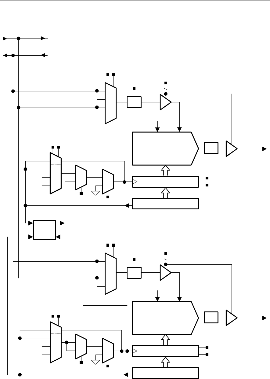
DAC12 Introduction
23-3
DAC12
Figure 23−1. DAC12 Block Diagram
DAC12_0
DAC12_0OUT
2.5V or 1.5V reference from ADC12
DAC12SREFx
VR− VR+
DAC12_0DAT
DAC12_0Latch
DAC12_1
DAC12LSELx
VR− VR+
DAC12_1DAT
DAC12_1Latch
TB2
TA1
DAC12DF
DAC12RES
AV SS
00
01
10
11
00
01
10
11
00
01
10
11
Ve REF+
VREF+
DAC12DF
DAC12RES
Latch Bypass
DAC12LSELx
TB2
TA1
00
01
10
11
00
01
10
11
Latch Bypass
DAC12IR
To ADC12 module
DAC12_1DAT Updated
DAC12_0DAT Updated
1
0
0
1
DAC12ENC
0
1
DAC12ENC
DAC12GRP
1
0
DAC12GRP
DAC12SREFx
AV SS
00
01
10
11
x3
/3
DAC12_1OUT
DAC12AMPx
3
x3
DAC12IR
/3
Group
Load
Logic
DAC12AMPx
3

DAC12 Operation
23-4 DAC12
23.2 DAC12 Operation
The DAC12 module is configured with user software. The setup and operation
of the DAC12 is discussed in the following sections.
23.2.1 DAC12 Core
The DAC12 can be configured to operate in 8- or 12-bit mode using the
DAC12RES bit. The full-scale output is programmable to be 1× or 3× the
selected reference voltage via the DAC12IR bit. This feature allows the user
to control the dynamic range of the DAC12. The DAC12DF bit allows the user
to select between straight binary data and 2s-compliment data for the DAC.
When using straight binary data format, the formula for the output voltage is
given in Table 23−1.
Table 23−1.DAC12 Full-Scale Range (Vref = VeREF+ or VREF+)
Resolution DAC12RES DAC12IR Output Voltage Formula
12 bit 0 0 Vout +Vref 3 DAC12_xDAT
4096
12 bit 0 1 Vout +Vref DAC12_xDAT
4096
8 bit 1 0 Vout +Vref 3 DAC12_xDAT
256
8 bit 1 1 Vout +Vref DAC12_xDAT
256
In 8-bit mode the maximum useable value for DAC12_xDAT is 0FFh and in
12-bit mode the maximum useable value for DAC12_xDAT is 0FFFh. Values
greater than these may be written to the register, but all leading bits are
ignored.
DAC12 Port Selection
The DAC12 outputs are multiplexed with the port P6 pins and ADC12 analog
inputs, and also the VeREF+ pins. When DAC12AMPx > 0, the DAC12
function is automatically selected for the pin, regardless of the state of the
associated PxSELx and PxDIRx bits. The DAC12OPS bit selects between the
P6 pins and the VeREF+ pins for the DAC outputs. For example, when
DAC12OPS = 0, DAC12_0 outputs on P6.6 and DAC12_1 outputs on P6.7.
When DAC12OPS = 1, DAC12_0 outputs on VeREF+ and DAC12_1 outputs
on P6.5. See the port pin schematic in the device-specific data sheet for more
details.

DAC12 Operation
23-5
DAC12
23.2.2 DAC12 Reference
The reference for the DAC12 is configured to use either an external reference
voltage or the internal 1.5-V/2.5-V reference from the ADC12 module with the
DAC12SREFx bits. When DAC12SREFx = {0,1} the VREF+ signal is used as
the reference and when DAC12SREFx = {2,3} the VeREF+ signal is used as the
reference.
To use the ADC12 internal reference, it must be enabled and configured via
the applicable ADC12 control bits.
DAC12 Reference Input and Voltage Output Buffers
The reference input and voltage output buffers of the DAC12 can be
configured for optimized settling time vs power consumption. Eight
combinations are selected using the DAC12AMPx bits. In the low/low setting,
the settling time is the slowest, and the current consumption of both buffers is
the lowest. The medium and high settings have faster settling times, but the
current consumption increases. See the device-specific data sheet for
parameters.
23.2.3 Updating the DAC12 Voltage Output
The DAC12_xDAT register can be connected directly to the DAC12 core or
double buffered. The trigger for updating the DAC12 voltage output is selected
with the DAC12LSELx bits.
When DAC12LSELx = 0 the data latch is transparent and the DAC12_xDAT
register is applied directly to the DAC12 core. the DAC12 output updates
immediately when new DAC12 data is written to the DAC12_xDAT register,
regardless of the state of the DAC12ENC bit.
When DAC12LSELx = 1, DAC12 data is latched and applied to the DAC12
core after new data is written to DAC12_xDAT. When DAC12LSELx = 2 or 3,
data is latched on the rising edge from the Timer_A CCR1 output or Timer_B
CCR2 output respectively. DAC12ENC must be set to latch the new data when
DAC12LSELx > 0.

DAC12 Operation
23-6 DAC12
23.2.4 DAC12_xDAT Data Format
The DAC12 supports both straight binary and 2s compliment data formats.
When using straight binary data format, the full-scale output value is 0FFFh
in 12-bit mode (0FFh in 8-bit mode) as shown in Figure 23−2.
Figure 23−2. Output Voltage vs DAC12 Data, 12-Bit, Straight Binary Mode
Full-Scale Output
0 0FFFh
0
Output Voltage
DAC Data
When using 2s compliment data format, the range is shifted such that a
DAC12_xDAT value of 0800h (0080h in 8-bit mode) results in a zero output
voltage, 0000h is the mid-scale output voltage, and 07FFh (007Fh for 8-bit
mode) is the full-scale voltage output as shown in Figure 23−3.
Figure 23−3. Output Voltage vs DAC12 Data, 12-Bit, 2s Compliment Mode
Full-Scale Output
0800h (−2048) 07FFh (+2047)0
0
Output Voltage
DAC Data
Mid-Scale Output
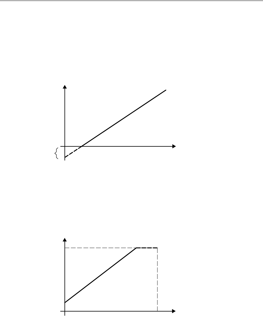
DAC12 Operation
23-7
DAC12
23.2.5 DAC12 Output Amplifier Offset Calibration
The offset voltage of the DAC12 output amplifier can be positive or negative.
When the offset is negative, the output amplifier attempts to drive the voltage
negative, but cannot do so. The output voltage remains at zero until the DAC12
digital input produces a sufficient positive output voltage to overcome the
negative offset voltage, resulting in the transfer function shown in Figure 23−4.
Figure 23−4. Negative Offset
Output Voltage
0
DAC Data
Negative Offset
When the output amplifier has a positive offset, a digital input of zero does not
result in a zero output voltage. The DAC12 output voltage reaches the
maximum output level before the DAC12 data reaches the maximum code.
This is shown in Figure 23−5.
Figure 23−5. Positive Offset
Vcc
Output Voltage
0
DAC Data Full-Scale Code
The DAC12 has the capability to calibrate the offset voltage of the output
amplifier. Setting the DAC12CALON bit initiates the offset calibration. The
calibration should complete before using the DAC12. When the calibration is
complete, the DAC12CALON bit is automatically reset. The DAC12AMPx bits
should be configured before calibration. For best calibration results, port and
CPU activity should be minimized during calibration.
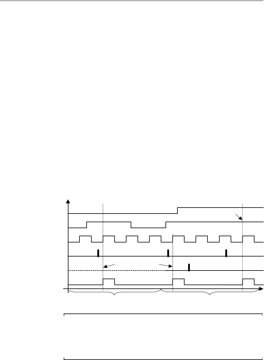
DAC12 Operation
23-8 DAC12
23.2.6 Grouping Multiple DAC12 Modules
Multiple DAC12s can be grouped together with the DAC12GRP bit to
synchronize the update of each DAC12 output. Hardware ensures that all
DAC12 modules in a group update simultaneously independent of any
interrupt or NMI event.
DAC12_0 and DAC12_1 are grouped by setting the DAC12GRP bit of
DAC12_0. The DAC12GRP bit of DAC12_1 is don’t care. When DAC12_0 and
DAC12_1 are grouped:
-The DAC12_1 DAC12LSELx bits select the update trigger for both DACs
-The DAC12LSELx bits for both DACs must be > 0
-The DAC12ENC bits of both DACs must be set to 1
When DAC12_0 and DAC12_1 are grouped, both DAC12_xDAT registers
must be written to before the outputs update - even if data for one or both of
the DACs is not changed. Figure 23−6 shows a latch-update timing example
for grouped DAC12_0 and DAC12_1.
When DAC12_0 DAC12GRP = 1 and both DAC12_x DAC12LSELx > 0 and
either DAC12ENC = 0, neither DAC12 will update.
Figure 23−6. DAC12 Group Update Example, Timer_A3 Trigger
DAC12_0
DAC12GRP
DAC12_0
DAC12ENC
TimerA_OUT1
DAC12_0
Latch Trigger
DAC12_0 Updated
DAC12_0 DAC12LSELx = 2 DAC12_0 DAC12LSELx > 0 AND
DAC12_1 DAC12LSELx = 2
DAC12_0DAT
New Data
DAC12_1DAT
New Data
DAC12_0 and DAC12_1
Updated Simultaneously
Note: DAC12 Settling Time
The DMA controller is capable of transferring data to the DAC12 faster than
the DAC12 output can settle. The user must assure the DAC12 settling time
is not violated when using the DMA controller. See the device-specific data
sheet for parameters.

DAC12 Operation
23-9
DAC12
23.2.7 DAC12 Interrupts
The DAC12 interrupt vector is shared with the DMA controller on some devices
(see device-specific data sheet for interrupt assignment). In this case,
software must check the DAC12IFG and DMAIFG flags to determine the
source of the interrupt.
The DAC12IFG bit is set when DAC12LSELx > 0 and DAC12 data is latched
from the DAC12_xDAT register into the data latch. When DAC12LSELx = 0,
the DAC12IFG flag is not set.
A set DAC12IFG bit indicates that the DAC12 is ready for new data. If both the
DAC12IE and GIE bits are set, the DAC12IFG generates an interrupt request.
The DAC12IFG flag is not reset automatically. It must be reset by software.

DAC12 Registers
23-10 DAC12
23.3 DAC12 Registers
The DAC12 registers are listed in Table 23−2.
Table 23−2.DAC12 Registers
Register Short Form Register Type Address Initial State
DAC12_0 control DAC12_0CTL Read/write 01C0h Reset with POR
DAC12_0 data DAC12_0DAT Read/write 01C8h Reset with POR
DAC12_1 control DAC12_1CTL Read/write 01C2h Reset with POR
DAC12_1 data DAC12_1DAT Read/write 01CAh Reset with POR
DAC12 Registers
23-11
DAC12
DAC12_xCTL, DAC12 Control Register
15 14 13 12 11 10 9 8
DAC12OPS DAC12SREFx DAC12RES DAC12LSELx DAC12
CALON DAC12IR
rw−(0) rw−(0) rw−(0) rw−(0) rw−(0) rw−(0) rw−(0) rw−(0)
76543210
DAC12AMPx DAC12DF DAC12IE DAC12IFG DAC12ENC DAC12
GRP
rw−(0) rw−(0) rw−(0) rw−(0) rw−(0) rw−(0) rw−(0) rw−(0)
Modifiable only when DAC12ENC = 0
DAC12OPS Bit 15 DAC12 output select
0 DAC12_0 output on P6.6, DAC12_1 output on P6.7
1 DAC12_0 output on VeREF+, DAC12_1 output on P6.5
DAC12
SREFx
Bits
14-13
DAC12 select reference voltage
00 VREF+
01 VREF+
10 VeREF+
11 VeREF+
DAC12
RES
Bit 12 DAC12 resolution select
0 12-bit resolution
1 8-bit resolution
DAC12
LSELx
Bits
11-10
DAC12 load select. Selects the load trigger for the DAC12 latch. DAC12ENC
must be set for the DAC to update, except when DAC12LSELx = 0.
00 DAC12 latch loads when DAC12_xDAT written (DAC12ENC is ignored)
01 DAC12 latch loads when DAC12_xDAT written, or, when grouped,
when all DAC12_xDAT registers in the group have been written.
10 Rising edge of Timer_A.OUT1 (TA1)
11 Rising edge of Timer_B.OUT2 (TB2)
DAC12
CALON
Bit 9 DAC12 calibration on. This bit initiates the DAC12 offset calibration sequence
and is automatically reset when the calibration completes.
0 Calibration is not active
1 Initiate calibration/calibration in progress
DAC12IR Bit 8 DAC12 input range. This bit sets the reference input and voltage output range.
0 DAC12 full-scale output = 3x reference voltage
1 DAC12 full-scale output = 1x reference voltage

DAC12 Registers
23-12 DAC12
DAC12
AMPx
Bits
7-5
DAC12 amplifier setting. These bits select settling time vs current
consumption for the DAC12 input and output amplifiers.
DAC12AMPx Input Buffer Output Buffer
000 Off DAC12 off, output high Z
001 Off DAC12 off, output 0 V
010 Low speed/current Low speed/current
011 Low speed/current Medium speed/current
100 Low speed/current High speed/current
101 Medium speed/current Medium speed/current
110 Medium speed/current High speed/current
111 High speed/current High speed/current
DAC12DF Bit 4 DAC12 data format
0 Straight binary
1 2s complement
DAC12IE Bit 3 DAC12 interrupt enable
0 Disabled
1 Enabled
DAC12IFG Bit 2 DAC12 Interrupt flag
0 No interrupt pending
1 Interrupt pending
DAC12
ENC
Bit 1 DAC12 enable conversion. This bit enables the DAC12 module when
DAC12LSELx > 0. when DAC12LSELx = 0, DAC12ENC is ignored.
0 DAC12 disabled
1 DAC12 enabled
DAC12
GRP
Bit 0 DAC12 group. Groups DAC12_x with the next higher DAC12_x. Not used for
DAC12_1.
0 Not grouped
1 Grouped
DAC12 Registers
23-13
DAC12
DAC12_xDAT, DAC12 Data Register
15 14 13 12 11 10 9 8
0 0 0 0 DAC12 Data
r(0) r(0) r(0) r(0) rw−(0) rw−(0) rw−(0) rw−(0)
76543210
DAC12 Data
rw−(0) rw−(0) rw−(0) rw−(0) rw−(0) rw−(0) rw−(0) rw−(0)
Unused Bits
15-12
Unused. These bits are always 0 and do not affect the DAC12 core.
DAC12 Data Bits
11-0
DAC12 data
DAC12 Data Format DAC12 Data
12-bit binary The DAC12 data are right-justified. Bit 11 is the MSB.
12-bit 2s complement The DAC12 data are right-justified. Bit 11 is the MSB
(sign).
8-bit binary The DAC12 data are right-justified. Bit 7 is the MSB.
Bits 11-8 are don’t care and do not effect the DAC12
core.
8-bit 2s complement The DAC12 data are right-justified. Bit 7 is the MSB
(sign). Bits 11-8 are don’t care and do not effect the
DAC12 core.

23-14 DAC12

24-1
SD16_A
SD16_A
The SD16_A module is a single-converter 16-bit, sigma-delta analog-to-digital
conversion module with high impedance input buffer. This chapter describes
the SD16_A. The SD16_A module is implemented in the MSP430x20x3
devices.
Topic Page
24.1 SD16_A Introduction 24-2. . . . . . . . . . . . . . . . . . . . . . . . . . . . . . . . . . . . . . . . .
24.2 SD16_A Operation 24-4. . . . . . . . . . . . . . . . . . . . . . . . . . . . . . . . . . . . . . . . . . . .
24.3 SD16_A Registers 24-16. . . . . . . . . . . . . . . . . . . . . . . . . . . . . . . . . . . . . . . . . .
Chapter 24

SD16_A Introduction
24-2 SD16_A
24.1 SD16_A Introduction
The SD16_A module consists of one sigma-delta analog-to-digital converter
with a high-impedance input buffer and an internal voltage reference. It has up
to eight fully differential multiplexed analog input pairs including a built-in
temperature sensor and a divided supply voltage. The converter is based on
a second-order oversampling sigma-delta modulator and digital decimation
filter. The decimation filter is a comb type filter with selectable oversampling
ratios of up to 1024. Additional filtering can be done in software.
The high impedance input buffer is not implemented in MSP430x20x3
devices.
Features of the SD16_A include:
-16-bit sigma-delta architecture
-Up to eight multiplexed differential analog inputs per channel
(The number of inputs is device dependent, see the device-specific data
sheet.)
-Software selectable on-chip reference voltage generation (1.2V)
-Software selectable internal or external reference
-Built-in temperature sensor
-Up to 1.1 MHz modulator input frequency
-High impedance input buffer
(not implemented on all devices, see the device-specific data sheet)
-Selectable low-power conversion mode
The block diagram of the SD16_A module is shown in Figure 24−1.
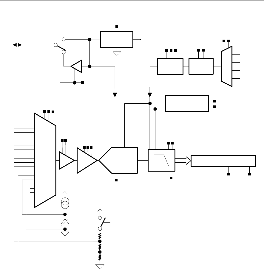
SD16_A Introduction
24-3
SD16_A
Figure 24−1. SD16_A Block Diagram
15 0
SD16DIVx
ACLK
TACLK
SD16SSELx
00
01
10
11
00
01
10
11
MCLK
SMCLK
AV CC
VREF
Divider
1/2/4/8
A0 000
SD16INCHx
+
−
001
+
−
010
+
−
011
+
−
100
+
−
101
+
−
110
+
−
111
+
−
A1
A2
A3
A4
A5
A6
2nd
Order
ΣΔ Modulator
SD16GAINx
SD16DF
SD16LP
SD16SC
SD16OSRx
SD16SNGL
SD16MEM0
Reference
A7
SD16VMIDON
SD16REFON
fM
Reference
1.2V
Start Conversion
Logic
AV SS
SD16XDIVx
Divider
1/3/16/48
SD16XOSR
BUF
1
0
SD16UNI
1
AVCC
SD16INCHx=101
Temp.
sensor
PGA
1..32
5R
R
5R
SD16BUFx†
† Not Implemented in MSP430x20x3 devices
Reference

SD16_A Operation
24-4 SD16_A
24.2 SD16_A Operation
The SD16_A module is configured with user software. The setup and
operation of the SD16_A is discussed in the following sections.
24.2.1 ADC Core
The analog-to-digital conversion is performed by a 1-bit second-order
sigma-delta modulator. A single-bit comparator within the modulator quantizes
the input signal with the modulator frequency fM. The resulting 1-bit data
stream is averaged by the digital filter for the conversion result.
24.2.2 Analog Input Range and PGA
The full-scale input voltage range for each analog input pair is dependent on
the gain setting of the programmable gain amplifier of each channel. The
maximum full-scale range is ±VFSR where VFSR is defined by:
VFSR +VREFń2
GAINPGA
For a 1.2V reference, the maximum full-scale input range for a gain of 1 is:
"VFSR +1.2Vń2
1+" 0.6V
See the device-specific data sheet for full-scale input specifications.
24.2.3 Voltage Reference Generator
The SD16_A module has a built-in 1.2V reference. It is enabled by the
SD16REFON bit. When using the internal reference an external 100-nF
capacitor connected from VREF to AVSS is recommended to reduce noise. The
internal reference voltage can be used off-chip when SD16VMIDON = 1. The
buffered output can provide up to 1mA of drive. When using the internal
reference off-chip, a 470-nF capacitor connected from VREF to AVSS is
required. See the device-specific data sheet for parameters.
An external voltage reference can be applied to the VREF input when
SD16REFON and SD16VMIDON are both reset.
24.2.4 Auto Power-Down
The SD16_A is designed for low power applications. When the SD16_A is not
actively converting, it is automatically disabled and automatically re-enabled
when a conversion is started. The reference is not automatically disabled, but
can be disabled by setting SD16REFON = 0. When the SD16_A or reference
are disabled, they consume no current.

SD16_A Operation
24-5
SD16_A
24.2.5 Analog Input Pair Selection
The SD16_A can convert up to 8 differential input pairs multiplexed into the
PGA. Up to five analog input pairs (A0-A4) are available externally on the
device. A resistive divider to measure the supply voltage is available using the
A5 multiplexer input. An internal temperature sensor is available using the A6
multiplexer input. Input A7 is a shorted connection between the + and − input
pair and can be used to calibrate the offset of the SD16_A input stage.
Analog Input Setup
The analog input is configured using the SD16INCTL0 and the SD16AE
registers. The SD16INCHx bits select one of eight differential input pairs of the
analog multiplexer. The gain for the PGA is selected by the SD16GAINx bits.
A total of six gain settings are available. The SD16AEx bits enable or disable
the analog input pin. Setting any SD16AEx bit disables the multiplexed digital
circuitry for the associated pin. See the device-specific data sheet for pin
diagrams.
During conversion any modification to the SD16INCHx and SD16GAINx bits
will become effective with the next decimation step of the digital filter. After
these bits are modified, the next three conversions may be invalid due to the
settling time of the digital filter. This can be handled automatically with the
SD16INTDLYx bits. When SD16INTDLY = 00h, conversion interrupt requests
will not begin until the 4th conversion after a start condition.
On devices implementing the high impedance input buffer it can be enabled
using the SD16BUFx bits. The speed settings are selected based on the
SD16_A modulator frequency as shown in Table 24−1.
Table 24−1.High Input Impedance Buffer
SD16BUFx Buffer SD16 Modulator Frequency fM
00 Buffer disabled
01 Low speed/current fM < 200kHz
10 Medium speed/current 200kHz < fM < 700kHz
11 High speed/current 700kHz < fM < 1.1MHz
An external RC anti-aliasing filter is recommended for the SD16_A to prevent
aliasing of the input signal. The cutoff frequency should be < 10 kHz for a
1-Mhz modulator clock and OSR = 256. The cutoff frequency may set to a
lower frequency for applications that have lower bandwidth requirements.
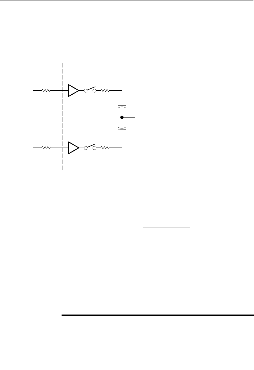
SD16_A Operation
24-6 SD16_A
24.2.6 Analog Input Characteristics
The SD16_A uses a switched-capacitor input stage that appears as an
impedance to external circuitry as shown in Figure 24−2.
Figure 24−2. Analog Input Equivalent Circuit
RS1 kW
VS+
MSP430
CS
VS+ = Positive external source voltage
VS− = Negative external source voltage
RS= External source resistance
CS= Sampling capacitance
RS1 kW
VS−
CS
AVCC / 2
† Not implemented in MSP430x20x3 devices
†
†
When the buffers are used, RS does not affect the sampling frequency fS.
However, when the buffers are not used or are not present on the device, the
maximum sampling frequency fS may be calculated from the minimum settling
time tSettling of the sampling circuit given by:
tSettling w(RS)1kW) CS lnǒGAIN 217 VAx
VREF Ǔ
where
fS+1
2 tSettling
and VAx +maxǒŤAVCC
2*VS)Ť,ŤAVCC
2*VS*ŤǓ,
with VS+ and VS− referenced to AVSS.
CS varies with the gain setting as shown in Table 24−2.
Table 24−2.Sampling Capacitance
PGA Gain Sampling Capacitance CS
11.25 pF
2, 4 2.5 pF
85 pF
16, 32 10 pF
SD16_A Operation
24-7
SD16_A
24.2.7 Digital Filter
The digital filter processes the 1-bit data stream from the modulator using a
SINC3 comb filter. The transfer function is described in the z-Domain by:
H(z)+ǒ1
OSR 1*z*OSR
1*z*1Ǔ3
and in the frequency domain by:
HǒfǓ+ȧ
ȱ
Ȳ
sincǒOSRpf
fMǓ
sincǒpf
fMǓȧ
ȳ
ȴ
3
+ȧ
ȡ
Ȣ
1
OSR
sinǒOSR p f
fMǓ
sinǒp f
fMǓȧ
ȣ
Ȥ
3
where the oversampling rate, OSR, is the ratio of the modulator frequency fM
to the sample frequency fS. Figure 24−3 shows the filter’s frequency response
for an OSR of 32. The first filter notch is at fS = fM/OSR. The notch’s frequency
can be adjusted by changing the modulator’s frequency, fM, using
SD16SSELx and SD16DIVx and the oversampling rate using the SD16OSRx
and SD16XOSR bits.
The digital filter for each enabled ADC channel completes the decimation of
the digital bit-stream and outputs new conversion results to the SD16MEM0
register at the sample frequency fS.
Figure 24−3. Comb Filter’s Frequency Response with OSR = 32
−140
−120
−100
−80
−60
−40
−20
0
Frequency
GAIN [dB]
fSfM
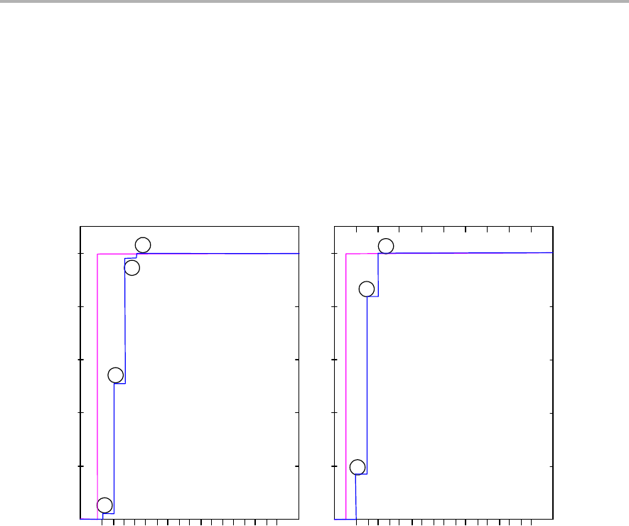
SD16_A Operation
24-8 SD16_A
Figure 24−4 shows the digital filter step response and conversion points. For
step changes at the input after start of conversion a settling time must be
allowed before a valid conversion result is available. The SD16INTDLYx bits
can provide sufficient filter settling time for a full-scale change at the ADC
input. If the step occurs synchronously to the decimation of the digital filter the
valid data will be available on the third conversion. An asynchronous step will
require one additional conversion before valid data is available.
Figure 24−4. Digital Filter Step Response and Conversion Points
1
2
3
4
1
0
0.2
0.4
0.6
0.8
1
0
0.2
0.4
0.6
0.8
1
2
3
Asynchronous Step Synchronous Step
% VFSR
Conversion Conversion
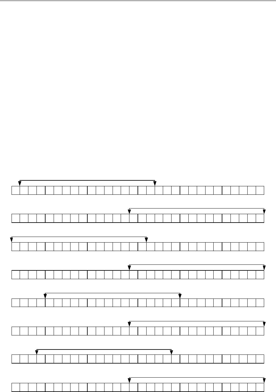
SD16_A Operation
24-9
SD16_A
Digital Filter Output
The number of bits output by the digital filter is dependent on the oversampling
ratio and ranges from 15 to 30 bits. Figure 24−5 shows the digital filter output
and their relation to SD16MEM0 for each OSR, LSBACC, and SD16UNI
setting. For example, for OSR = 1024, LSBACC = 0, and SD16UNI = 1, the
SD16MEM0 register contains bits 28 − 13 of the digital filter output. When
OSR = 32, the one (SD16UNI = 0) or two (SD16UNI=1) LSBs are always zero.
The SD16LSBACC and SD16LSBTOG bits give access to the least significant
bits of the digital filter output. When SD16LSBACC = 1 the 16 least significant
bits of the digital filter’s output are read from SD16MEM0 using word
instructions. The SD16MEM0 register can also be accessed with byte
instructions returning only the 8 least significant bits of the digital filter output.
When SD16LSBTOG = 1 the SD16LSBACC bit is automatically toggled each
time SD16MEM0 is read. This allows the complete digital filter output result to
be read with two reads of SD16MEM0. Setting or clearing SD16LSBTOG does
not change SD16LSBACC until the next SD16MEM0 access.
Figure 24−5. Used Bits of Digital Filter Output
048121620
24 153269723 22 21 19 18 17 15 14 13 11 1028 27 26 2529
OSR=512, LSBACC=1, SD16UNI=0
048121620
24 153269723 22 21 19 18 17 15 14 13 11 1028 27 26 2529
OSR=512, LSBACC=0, SD16UNI=0
048121620
24 153269723 22 21 19 18 17 15 14 13 11 1028 27 26 2529
OSR=512, LSBACC=1, SD16UNI=1
048121620
24 153269723 22 21 19 18 17 15 14 13 11 1028 27 26 2529
OSR=512, LSBACC=0, SD16UNI=1
048121620
24 153269723 22 21 19 18 17 15 14 13 11 1028 27 26 2529
OSR=1024, LSBACC=1, SD16UNI=0
048121620
24 153269723 22 21 19 18 17 15 14 13 11 1028 27 26 2529
OSR=1024, LSBACC=0, SD16UNI=0
04812162024 153269723 22 21 19 18 17 15 14 13 11 1028 27 26 2529
OSR=1024, LSBACC=1, SD16UNI=1
048121620
24 153269723 22 21 19 18 17 15 14 13 11 1028 27 26 2529
OSR=1024, LSBACC=0, SD16UNI=1
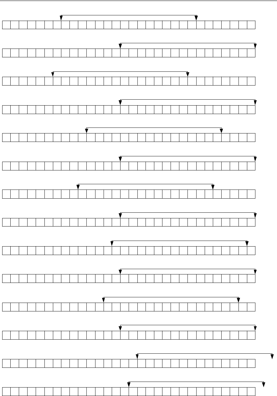
SD16_A Operation
24-10 SD16_A
048121620
24 153269723 22 21 19 18 17 15 14 13 11 1028 27 26 2529
048121620
24 153269723 22 21 19 18 17 15 14 13 11 1028 27 26 2529
OSR=32, LSBACC=x, SD16UNI=1
OSR=32, LSBACC=x, SD16UNI=0
04812162024 153269723 22 21 19 18 17 15 14 13 11 1028 27 26 2529
OSR=64, LSBACC=1, SD16UNI=0
048121620
24 153269723 22 21 19 18 17 15 14 13 11 1028 27 26 2529
OSR=64, LSBACC=0, SD16UNI=0
048121620
24 153269723 22 21 19 18 17 15 14 13 11 1028 27 26 2529
OSR=64, LSBACC=1, SD16UNI=1
048121620
24 153269723 22 21 19 18 17 15 14 13 11 1028 27 26 2529
OSR=64, LSBACC=0, SD16UNI=1
048121620
24 153269723 22 21 19 18 17 15 14 13 11 1028 27 26 2529
OSR=128, LSBACC=1, SD16UNI=0
048121620
24 153269723 22 21 19 18 17 15 14 13 11 1028 27 26 2529
OSR=128, LSBACC=0, SD16UNI=0
048121620
24 153269723 22 21 19 18 17 15 14 13 11 1028 27 26 2529
OSR=128, LSBACC=1, SD16UNI=1
04812162024 153269723 22 21 19 18 17 15 14 13 11 1028 27 26 2529
OSR=128, LSBACC=0, SD16UNI=1
048121620
24 153269723 22 21 19 18 17 15 14 13 11 1028 27 26 2529
OSR=256, LSBACC=1, SD16UNI=0
048121620
24 153269723 22 21 19 18 17 15 14 13 11 1028 27 26 2529
OSR=256, LSBACC=0, SD16UNI=0
048121620
24 153269723 22 21 19 18 17 15 14 13 11 1028 27 26 2529
OSR=256, LSBACC=1, SD16UNI=1
048121620
24 153269723 22 21 19 18 17 15 14 13 11 1028 27 26 2529
OSR=256, LSBACC=0, SD16UNI=1

SD16_A Operation
24-11
SD16_A
24.2.8 Conversion Memory Register: SD16MEM0
The SD16MEM0 register is associated with the SD16_A channel. Conversion
results are moved to the SD16MEM0 register with each decimation step of the
digital filter. The SD16IFG bit is set when new data is written to SD16MEM0.
SD16IFG is automatically cleared when SD16MEM0 is read by the CPU or
may be cleared with software.
Output Data Format
The output data format is configurable in two’s complement, offset binary or
unipolar mode as shown in Table 24−3.The data format is selected by the
SD16DF and SD16UNI bits.
Table 24−3.Data Format
SD16UNI SD16DF Format Analog Input SD16MEM0†Digital Filter Output
(OSR = 256)
Bipolar
+FSR FFFF FFFFFF
00
Bi
po
l
ar
Offset ZERO 8000 800000
0
0
Offset
Binary −FSR 0000 000000
Bipolar
+FSR 7FFF 7FFFFF
01
Bi
po
l
ar
Twos ZERO 0000 000000
0
1
Twos
compliment −FSR 8000 800000
+FSR FFFF FFFFFF
1 0 Unipolar ZERO 0000 800000
1
0
Unipolar
−FSR 0000 000000
†Independent of SD16OSRx and SD16XOSR settings; SD16LSBACC = 0.
Note: Offset Measurements and Data Format
Any offset measurement done either externally or using the internal
differential pair A7 would be appropriate only when the channel is operating
under bipolar mode with SD16UNI = 0.
SD16_A Operation
24-12 SD16_A
Figure 24−6 shows the relationship between the full-scale input voltage range
from −VFSR to +VFSR and the conversion result. The data formats are
illustrated.
Figure 24−6. Input Voltage vs. Digital Output
Input
Voltage
SD16MEMx
−VFSR
+V FSR
7FFFh
8000h
Bipolar Output: 2’s complement
Input
Voltage
SD16MEMx
−VFSR +V FSR
FFFFh
8000h
Bipolar Output: Offset Binary
0000h
0000h
Input
Voltage
SD16MEMx
−VFSR +V FSR
FFFFh
Unipolar Output
0000h
24.2.9 Conversion Modes
The SD16_A module can be configured for two modes of operation, listed in
Table 24−4. The SD16SNGL bit selects the conversion mode.
Table 24−4.Conversion Mode Summary
SD16SNGL Mode Operation
1Single conversion The channel is converted once.
0Continuous conversion The channel is converted continuously.
Single Conversion
Setting the SD16SC bit of the channel initiates one conversion on that channel
when SD16SNGL = 1. The SD16SC bit will automatically be cleared after
conversion completion.
Clearing SD16SC before the conversion is completed immediately stops
conversion of the channel, the channel is powered down and the
corresponding digital filter is turned off. The value in SD16MEM0 can change
when SD16SC is cleared. It is recommended that the conversion data in
SD16MEM0 be read prior to clearing SD16SC to avoid reading an invalid
result.
SD16_A Operation
24-13
SD16_A
Continuous Conversion
When SD16SNGL = 0 continuous conversion mode is selected. Conversion
of the channel will begin when SD16SC is set and continue until the SD16SC
bit is cleared by software.
Clearing SD16SC immediately stops conversion of the selected channel, the
channel is powered down and the corresponding digital filter is turned off. The
value in SD16MEM0 can change when SD16SC is cleared. It is recommended
that the conversion data in SD16MEM0 be read prior to clearing SD16SC to
avoid reading an invalid result.
Figure 24−7 shows conversion operation.
Figure 24−7. Single Channel Operation
SD16SNGL = 1
Time
Conversion
SD16SC
SD16SNGL = 0
Conversion
SD16SC
Conversion Conversion
Set by SW Auto−clear
Set by SW
Conv
Cleared by SW
= Result written to SD16MEM0

SD16_A Operation
24-14 SD16_A
24.2.10 Using the Integrated Temperature Sensor
To use the on-chip temperature sensor, the user selects the analog input pair
SD16INCHx = 110 and sets SD16REFON = 1. Any other configuration is done
as if an external analog input pair was selected, including SD16INTDLYx and
SD16GAINx settings. Because the internal reference must be on to use the
temperature sensor, it is not possible to use an external reference for the
conversion of the temperature sensor voltage. Also, the internal reference will
be in contention with any used external reference. In this case, the
SD16VMIDON bit may be set to minimize the affects of the contention on the
conversion.
The typical temperature sensor transfer function is shown in Figure 24−8.
When switching inputs of an SD16_A channel to the temperature sensor,
adequate delay must be provided using SD16INTDLYx to allow the digital filter
to settle and assure that conversion results are valid. The temperature sensor
offset error can be large, and may need to be calibrated for most applications.
See device-specific data sheet for temperature sensor parameters.
Figure 24−8. Typical Temperature Sensor Transfer Function
Celsius
Volts
0 50 100
0.350
0.250
0.300
0.400
0.450
0.500
−50
0.200
VSensor,typ = TCSensor(273 + T[oC]) + VOffset, sensor [mV]

SD16_A Operation
24-15
SD16_A
24.2.11 Interrupt Handling
The SD16_A has 2 interrupt sources for its ADC channel:
-SD16IFG
-SD16OVIFG
The SD16IFG bit is set when the SD16MEM0 memory register is written with
a conversion result. An interrupt request is generated if the corresponding
SD16IE bit and the GIE bit are set. The SD16_A overflow condition occurs
when a conversion result is written to SD16MEM0 location before the previous
conversion result was read.
SD16IV, Interrupt Vector Generator
All SD16_A interrupt sources are prioritized and combined to source a single
interrupt vector. SD16IV is used to determine which enabled SD16_A interrupt
source requested an interrupt. The highest priority SD16_A interrupt request
that is enabled generates a number in the SD16IV register (see register
description). This number can be evaluated or added to the program counter
to automatically enter the appropriate software routine. Disabled SD16_A
interrupts do not affect the SD16IV value.
Any access, read or write, of the SD16IV register has no effect on the
SD16OVIFG or SD16IFG flags. The SD16IFG flags are reset by reading the
SD16MEM0 register or by clearing the flags in software. SD16OVIFG bits can
only be reset with software.
If another interrupt is pending after servicing of an interrupt, another interrupt
is generated. For example, if the SD16OVIFG and one or more SD16IFG
interrupts are pending when the interrupt service routine accesses the SD16IV
register, the SD16OVIFG interrupt condition is serviced first and the
corresponding flag(s) must be cleared in software. After the RETI instruction
of the interrupt service routine is executed, the highest priority SD16IFG
pending generates another interrupt request.
Interrupt Delay Operation
The SD16INTDLYx bits control the timing for the first interrupt service request
for the corresponding channel. This feature delays the interrupt request for a
completed conversion by up to four conversion cycles allowing the digital filter
to settle prior to generating an interrupt request. The delay is applied each time
the SD16SC bit is set or when the SD16GAINx or SD16INCHx bits for the
channel are modified. SD16INTDLYx disables overflow interrupt generation
for the channel for the selected number of delay cycles. Interrupt requests for
the delayed conversions are not generated during the delay.

SD16_A Registers
24-16 SD16_A
24.3 SD16_A Registers
The SD16_A registers are listed in Table 24−5:
Table 24−5.SD16_A Registers
Register Short Form Register Type Address Initial State
SD16_A control SD16CTL Read/write 0100h Reset with PUC
SD16_A interrupt vector SD16IV Read/write 0110h Reset with PUC
SD16_A channel 0 control SD16CCTL0 Read/write 0102h Reset with PUC
SD16_A conversion memory SD16MEM0 Read/write 0112h Reset with PUC
SD16_A input control SD16INCTL0 Read/write 0B0h Reset with PUC
SD16_A analog enable SD16AE Read/write 0B7h Reset with PUC

SD16_A Registers
24-17
SD16_A
SD16CTL, SD16_A Control Register
15 14 13 12 11 10 9 8
Reserved SD16XDIVx SD16LP
r0 r0 r0 r0 rw−0 rw−0 rw−0 rw−0
76543210
SD16DIVx SD16SSELx SD16
VMIDON
SD16
REFON SD16OVIE Reserved
rw−0 rw−0 rw−0 rw−0 rw−0 rw−0 rw−0 r0
Reserved Bits
15-12
Reserved
SD16XDIVx Bits
11-9
SD16_A clock divider
000 /1
001 /3
010 /16
011 /48
1xx Reserved
SD16LP Bit 8 Low power mode. This bit selects a reduced speed, reduced power mode
0 Low-power mode is disabled
1 Low-power mode is enabled. The maximum clock frequency for the
SD16_A is reduced.
SD16DIVx Bits
7-6
SD16_A clock divider
00 /1
01 /2
10 /4
11 /8
SD16SSELx Bits
5-4
SD16_A clock source select
00 MCLK
01 SMCLK
10 ACLK
11 External TACLK
SD16
VMIDON
Bit 3 VMID buffer on
0Off
1On
SD16
REFON
Bit 2 Reference generator on
0 Reference off
1 Reference on
SD16OVIE Bit 1 SD16_A overflow interrupt enable. The GIE bit must also be set to enable the
interrupt.
0 Overflow interrupt disabled
1 Overflow interrupt enabled
Reserved Bit 0 Reserved

SD16_A Registers
24-18 SD16_A
SD16CCTL0, SD16_A Control Register 0
15 14 13 12 11 10 9 8
Reserved SD16BUFx†SD16UNI SD16XOSR SD16SNGL SD16OSRx
r0 rw−0 rw−0 rw−0 rw−0 rw−0 rw−0 rw−0
76543210
SD16
LSBTOG
SD16
LSBACC
SD16
OVIFG SD16DF SD16IE SD16IFG SD16SC Reserved
rw−0 rw−0 rw−0 rw−0 rw−0 rw−0 rw−0 r−0
†Reserved in MSP430x20x3 devices
Reserved Bit 15 Reserved
SD16BUFx Bits
14−13
High-impedance input buffer mode
00 Buffer disabled
01 Slow speed/current
10 Medium speed/current
11 High speed/current
SD16UNI Bit 12 Unipolar mode select
0 Bipolar mode
1 Unipolar mode
SD16XOSR Bit 11 Extended oversampling ratio. This bit, along with the SD16OSRx bits,
select the oversampling ratio. See SD16OSRx bit description for settings.
SD16SNGL Bit 10 Single conversion mode select
0 Continuous conversion mode
1 Single conversion mode
SD16OSRx Bits
9-8
Oversampling ratio
When SD16XOSR = 0
00 256
01 128
10 64
11 32
When SD16XOSR = 1
00 512
01 1024
10 Reserved
11 Reserved
SD16
LSBTOG
Bit 7 LSB toggle. This bit, when set, causes SD16LSBACC to toggle each time
the SD16MEM0 register is read.
0 SD16LSBACC does not toggle with each SD16MEM0 read
1 SD16LSBACC toggles with each SD16MEM0 read

SD16_A Registers
24-19
SD16_A
SD16
LSBACC
Bit 6 LSB access. This bit allows access to the upper or lower 16-bits of the
SD16_A conversion result.
0 SD16MEMx contains the most significant 16-bits of the conversion.
1 SD16MEMx contains the least significant 16-bits of the conversion.
SD16OVIFG Bit 5 SD16_A overflow interrupt flag
0 No overflow interrupt pending
1 Overflow interrupt pending
SD16DF Bit 4 SD16_A data format
0 Offset binary
1 2’s complement
SD16IE Bit 3 SD16_A interrupt enable
0 Disabled
1 Enabled
SD16IFG Bit 2 SD16_A interrupt flag. SD16IFG is set when new conversion results are
available. SD16IFG is automatically reset when the corresponding
SD16MEMx register is read, or may be cleared with software.
0 No interrupt pending
1 Interrupt pending
SD16SC Bit 1 SD16_A start conversion
0 No conversion start
1 Start conversion
Reserved Bit 0 Reserved

SD16_A Registers
24-20 SD16_A
SD16INCTL0, SD16_A Input Control Register
76543210
SD16INTDLYx SD16GAINx SD16INCHx
rw−0 rw−0 rw−0 rw−0 rw−0 rw−0 rw−0 rw−0
SD16
INTDLYx
Bits
7-6
Interrupt delay generation after conversion start. These bits select the
delay for the first interrupt after conversion start.
00 Fourth sample causes interrupt
01 Third sample causes interrupt
10 Second sample causes interrupt
11 First sample causes interrupt
SD16GAINx Bits
5-3
SD16_A preamplifier gain
000 x1
001 x2
010 x4
011 x8
100 x16
101 x32
110 Reserved
111 Reserved
SD16INCHx Bits
2-0
SD16_A channel differential pair input
000 A0
001 A1
010 A2
011 A3
100 A4
101 A5− (AVCC − AVSS) / 11
110 A6 − Temperature Sensor
111 A7 − Short for PGA offset measurement

SD16_A Registers
24-21
SD16_A
SD16MEM0, SD16_A Conversion Memory Register
15 14 13 12 11 10 9 8
Conversion Results
r r r r r r r r
76543210
Conversion Results
r r r r r r r r
Conversion
Result
Bits
15-0
Conversion Results. The SD16MEMx register holds the upper or lower
16-bits of the digital filter output, depending on the SD16LSBACC bit.
SD16AE, SD16_A Analog Input Enable Register
76543210
SD16AE7 SD16AE6 SD16AE5 SD16AE4 SD16AE3 SD16AE2 SD16AE1 SD16AE0
rw−0 rw−0 rw−0 rw−0 rw−0 rw−0 rw−0 rw−0
SD16AEx Bits
7-0
SD16_A analog enable
0 External input disabled. Negative inputs are internally connected to
VSS.
1 External input enabled.

SD16_A Registers
24-22 SD16_A
SD16IV, SD16_A Interrupt Vector Register
15 14 13 12 11 10 9 8
0 0 0 0 0 0 0 0
r0 r0 r0 r0 r0 r0 r0 r0
76543210
0 0 0 SD16IVx 0
r0 r0 r0 r−0 r−0 r−0 r−0 r0
SD16IVx Bits
15-0
SD16_A interrupt vector value
SD16IV
Contents Interrupt Source Interrupt Flag
Interrupt
Priority
000h No interrupt pending −
002h SD16MEMx overflow SD16CCTLx
SD16OVIFG Highest
004h SD16_A Interrupt SD16CCTL0
SD16IFG
006h Reserved −
008h Reserved −
00Ah Reserved −
00Ch Reserved −
00Eh Reserved −
010h Reserved − Lowest

25-1
Embedded Emulation Module (EEM)
Embedded Emulation Module (EEM)
This chapter describes the Embedded Emulation Module (EEM) that is
implemented in all MSP430 flash devices.
Topic Page
25.1 EEM Introduction 25-2. . . . . . . . . . . . . . . . . . . . . . . . . . . . . . . . . . . . . . . . . . . . .
25.2 EEM Building Blocks 25-4. . . . . . . . . . . . . . . . . . . . . . . . . . . . . . . . . . . . . . . . . .
25.3 EEM Configurations 25-6. . . . . . . . . . . . . . . . . . . . . . . . . . . . . . . . . . . . . . . . . . .
Chapter 25

EEM Introduction
25-2 Embedded Emulation Module (EEM)
25.1 EEM Introduction
Every MSP430 flash-based microcontroller implements an embedded
emulation module (EEM). It is accessed and controlled through JTAG. Each
implementation is device dependent and is described in section 25.3 EEM
Configurations and the device-specific data sheet.
In general, the following features are available:
-Non−intrusive code execution with real−time breakpoint control
-Single step, step into and step over functionality
-Full support of all low-power modes
-Support for all system frequencies, for all clock sources
-Up to eight (device dependent) hardware triggers/breakpoints on memory
address bus (MAB) or memory data bus (MDB)
-Up to two (device dependent) hardware triggers/breakpoints on CPU
register write accesses
-MAB, MDB ,and CPU register access triggers can be combined to form
up to eight (device dependent) complex triggers/breakpoints
-Trigger sequencing (device dependent)
-Storage of internal bus and control signals using an integrated trace buffer
(device dependent)
-Clock control for timers, communication peripherals, and other modules
on a global device level or on a per-module basis during an emulation stop
Figure 25−1 shows a simplified block diagram of the largest currently available
2xx EEM implementation.
For more details on how the features of the EEM can be used together with
the IAR Embedded Workbencht debugger see the application report
Advanced Debugging Using the Enhanced Emulation Module (SLAA263) at
www.msp430.com. Code Composer Essentials (CCE) and most other
debuggers supporting MSP430 have the same or a similar feature set. For
details see the user’s guide of the applicable debugger.
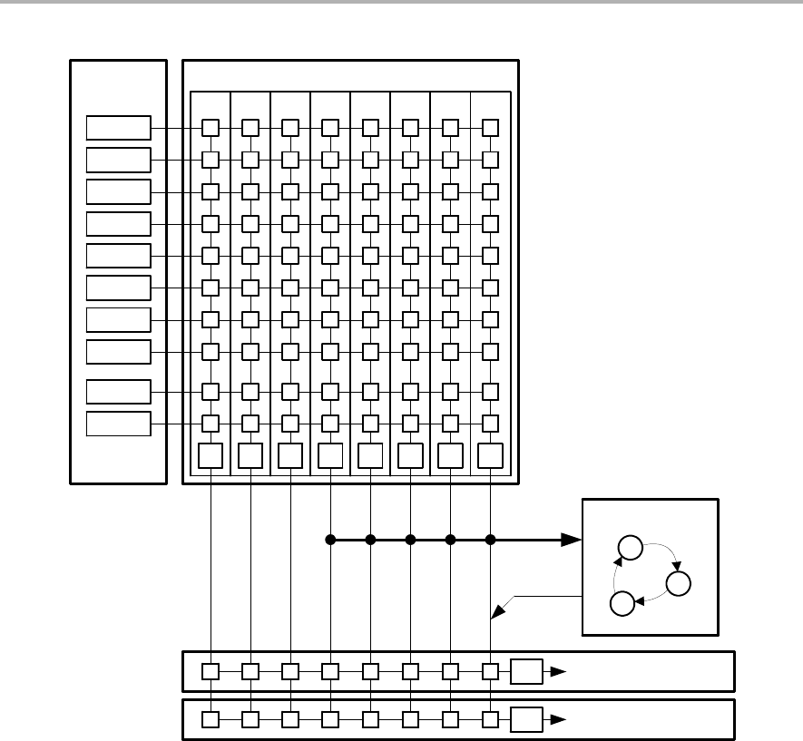
EEM Introduction
25-3
Embedded Emulation Module (EEM)
Figure 25−1. Large Implementation of the Embedded Emulation Module (EEM)
CPU Stop
Trigger
Blocks
MB0
MB1
MB2
MB3
MB4
MB5
MB6
MB7
CPU0
CPU1
&
0
Trigger Sequencer
”AND” Matrix − Combination Triggers
&
1
&
2
&
3
&
4
&
5
&
6
&
7
Start/Stop State Storage
OR
OR

EEM Introduction
25-4 Embedded Emulation Module (EEM)
25.2 EEM Building Blocks
25.2.1 Triggers
The event control in the EEM of the MSP430 system consists of triggers, which
are internal signals indicating that a certain event has happened. These
triggers may be used as simple breakpoints, but it is also possible to combine
two or more triggers to allow detection of complex events and trigger various
reactions besides stopping the CPU.
In general, the triggers can be used to control the following functional blocks
of the EEM:
-Breakpoints (CPU stop)
-State storage
-Sequencer
There are two different types of triggers, the memory trigger and the CPU
register write trigger.
Each memory trigger block can be independently selected to compare either
the MAB or the MDB with a given value. Depending on the implemented EEM
the comparison can be =, ≠, ≥, or ≤. The comparison can also be limited to
certain bits with the use of a mask. The mask is either bit-wise or byte-wise,
depending upon the device. In addition to selecting the bus and the
comparison, the condition under which the trigger is active can be selected.
The conditions include read access, write access, DMA access, and
instruction fetch.
Each CPU register write trigger block can be independently selected to
compare what is written into a selected register with a given value. The
observed register can be selected for each trigger independently. The
comparison can be =, ≠, ≥, or ≤. The comparison can also be limited to certain
bits with the use of a bit mask.
Both types of triggers can be combined to form more complex triggers. For
example, a complex trigger can signal when a particular value is written into
a user-specified address.

EEM Introduction
25-5
Embedded Emulation Module (EEM)
25.2.2 Trigger Sequencer
The trigger sequencer allows the definition of a certain sequence of trigger
signals before an event is accepted for a break or state storage event. Within
the trigger sequencer, it is possible to use the following features:
-Four states (State 0 to State 3)
-Two transitions per state to any other state
-Reset trigger that resets the sequencer to State 0.
The Trigger sequencer always starts at State 0 and must execute to State 3
to generate an action. If State 1 or State 2 are not required, they can be
bypassed.
25.2.3 State Storage (Internal Trace Buffer)
The state storage function uses a built-in buffer to store MAB, MDB, and CPU
control signal information (ie. read, write, or instruction fetch) in a non-intrusive
manner. The built-in buffer can hold up to eight entries. The flexible
configuration allows the user to record the information of interest very
efficiently.
25.2.4 Clock Control
The EEM provides device dependent flexible clock control. This is useful in
applications where a running clock is needed for peripherals after the CPU is
stopped (e.g. to allow a UART module to complete its transfer of a character
or to allow a timer to continue generating a PWM signal).
The clock control is flexible and supports both modules that need a running
clock and modules that must be stopped when the CPU is stopped due to a
breakpoint.

EEM Configurations
25-6 Embedded Emulation Module (EEM)
25.3 EEM Configurations
Table 25−1 gives an overview of the EEM configurations in the MSP430 2xx
family. The implemented configuration is device dependent − please refer to
the device data sheet.
Table 25−1.2xx EEM Configurations
Feature XS S M L
Memory Bus Triggers 2
(=, ≠ only)
358
Memory Bus Trigger Mask for 1) Low byte
2) High byte
1) Low byte
2) High byte
1) Low byte
2) High byte
All 16 or 20 bits
CPU Register-Write Triggers 0112
Combination Triggers 2468
Sequencer No No Yes Yes
State Storage No No No Yes
In general the following features can be found on any 2xx device:
-At least two MAB/MDB triggers supporting:
JDistinction between CPU, DMA, read, and write accesses
J=, ≠, ≥, or ≤ comparison (in XS only =, ≠)
-At least two trigger Combination registers
-Hardware breakpoints using the CPU Stop reaction
-Clock control with individual control of module clocks
(in some XS configurations the control of module clocks is hardwired)

IMPORTANT NOTICE
Texas Instruments Incorporated and its subsidiaries (TI) reserve the right to make corrections, modifications, enhancements, improvements,and other changes to its products and services at any time and to discontinue any product or service without notice. Customers shouldobtain the latest relevant information before placing orders and should verify that such information is current and complete. All products aresold subject to TI’s terms and conditions of sale supplied at the time of order acknowledgment.
TI warrants performance of its hardware products to the specifications applicable at the time of sale in accordance with TI’s standardwarranty. Testing and other quality control techniques are used to the extent TI deems necessary to support this warranty. Except wheremandated by government requirements, testing of all parameters of each product is not necessarily performed.
TI assumes no liability for applications assistance or customer product design. Customers are responsible for their products andapplications using TI components. To minimize the risks associated with customer products and applications, customers should provideadequate design and operating safeguards.
TI does not warrant or represent that any license, either express or implied, is granted under any TI patent right, copyright, mask work right,or other TI intellectual property right relating to any combination, machine, or process in which TI products or services are used. Informationpublished by TI regarding third-party products or services does not constitute a license from TI to use such products or services or awarranty or endorsement thereof. Use of such information may require a license from a third party under the patents or other intellectualproperty of the third party, or a license from TI under the patents or other intellectual property of TI.
Reproduction of TI information in TI data books or data sheets is permissible only if reproduction is without alteration and is accompaniedby all associated warranties, conditions, limitations, and notices. Reproduction of this information with alteration is an unfair and deceptivebusiness practice. TI is not responsible or liable for such altered documentation. Information of third parties may be subject to additionalrestrictions.
Resale of TI products or services with statements different from or beyond the parameters stated by TI for that product or service voids allexpress and any implied warranties for the associated TI product or service and is an unfair and deceptive business practice. TI is notresponsible or liable for any such statements.
TI products are not authorized for use in safety-critical applications (such as life support) where a failure of the TI product would reasonablybe expected to cause severe personal injury or death, unless officers of the parties have executed an agreement specifically governingsuch use. Buyers represent that they have all necessary expertise in the safety and regulatory ramifications of their applications, andacknowledge and agree that they are solely responsible for all legal, regulatory and safety-related requirements concerning their productsand any use of TI products in such safety-critical applications, notwithstanding any applications-related information or support that may beprovided by TI. Further, Buyers must fully indemnify TI and its representatives against any damages arising out of the use of TI products insuch safety-critical applications.
TI products are neither designed nor intended for use in military/aerospace applications or environments unless the TI products arespecifically designated by TI as military-grade or "enhanced plastic." Only products designated by TI as military-grade meet militaryspecifications. Buyers acknowledge and agree that any such use of TI products which TI has not designated as military-grade is solely atthe Buyer's risk, and that they are solely responsible for compliance with all legal and regulatory requirements in connection with such use.
TI products are neither designed nor intended for use in automotive applications or environments unless the specific TI products aredesignated by TI as compliant with ISO/TS 16949 requirements. Buyers acknowledge and agree that, if they use any non-designatedproducts in automotive applications, TI will not be responsible for any failure to meet such requirements.
Following are URLs where you can obtain information on other Texas Instruments products and application solutions:
Products ApplicationsAmplifiers amplifier.ti.com Audio www.ti.com/audioData Converters dataconverter.ti.com Automotive www.ti.com/automotiveDSP dsp.ti.com Broadband www.ti.com/broadbandClocks and Timers www.ti.com/clocks Digital Control www.ti.com/digitalcontrolInterface interface.ti.com Medical www.ti.com/medicalLogic logic.ti.com Military www.ti.com/militaryPower Mgmt power.ti.com Optical Networking www.ti.com/opticalnetworkMicrocontrollers microcontroller.ti.com Security www.ti.com/securityRFID www.ti-rfid.com Telephony www.ti.com/telephonyRF/IF and ZigBee® Solutions www.ti.com/lprf Video & Imaging www.ti.com/videoWireless www.ti.com/wireless
Mailing Address: Texas Instruments, Post Office Box 655303, Dallas, Texas 75265Copyright © 2008, Texas Instruments Incorporated
